


SERVICE MANUAL
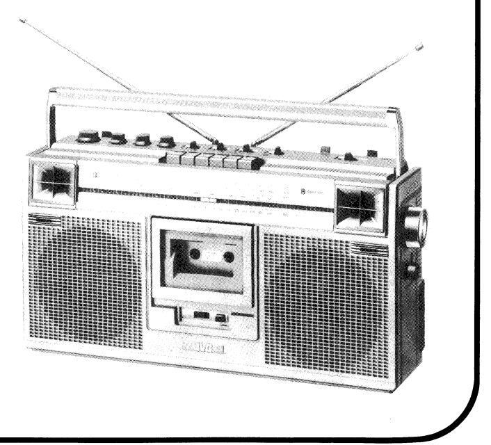
MODEL RC-656L/LB LW-MW-SW-FM 4-BAND STEREO RADIO CASSETTE RECORDER
No. 1422 August 1980
Contents
| Page |
|---|
| Specifications |
| Features |
| Names of Parts |
| Removal of Main Parts |
| Removal of Cassette Mecha Parts |
| Adjustment of Cassette Recorder |
| How to Engage Dial Cord |
| Adjustment of Cassette Recorder Amplifier |
| Tuner Alignment |
| Block Diagrams |
| Schematic Diagram (Tuner Circuit) |
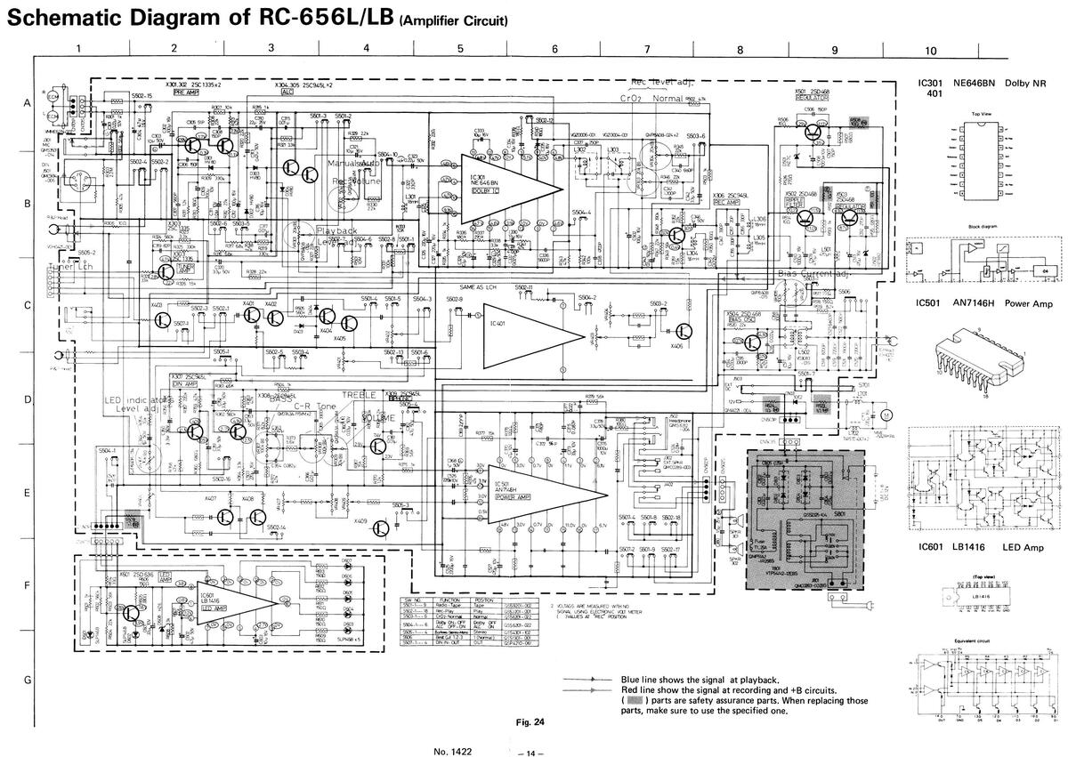
| Schematic Diagram (Amplifier Circuit)14 |
| Wiring Connection |
| raye |
|---|
| Mechanical Component Parts |
| Mechanical Component Parts List |
| Assembly Parts |
| Assembly Parts List |
| Amplifier P.W. Board Parts |
| Amplifier P.W. Board Parts List |
| Tuner P.W. Board Parts (Power Supply, Motor) 25 |
| Tuner P.W. Board Parts List |
| Power Supply P.W. Board Parts List |
| Packing |
| Packing Material Parts List |
| Accessories |
D -----
Specifications
| Semiconductors |
: 9 ICs (including 2 for the micro-
phone and 1 for the motor) |
Rewind time
Fast forward time |
: Within 110 sec. (C-60 cassette)
: Within 110 sec. (C-60 cassette) |
|
|---|---|---|---|---|
| Speakers |
33 (ransistors & 1 FE1
: 16 cm (3. 2 Ω) × 2, 5 cm (4 Ω) × 2 |
Amplifier section
Power output Input jacks |
: Max. 12 W (6 W + 6 W) at 3.2 Ω
: Mic x 2 |
|
| Tuner section | (0.8 mV, low impedance) | |||
| Frequency ranges |
: FM 88 – 108 MHz
SW 6 – 18 MHz MW 540 – 1600 kHz |
Output jacks |
: Ext. speaker x 2
(load impedance 4 — 8 Ω) Headphones x 1 |
|
| LW 150 – 350 kHz | Input/output jack | : DIN jack | ||
| Antennas |
: Telescopic antenna for SW & FM
Ferrite core antenna for MW & LW |
Power supply |
: DC 12 V
(8 "R20 (U2)" batteries) Car battery (DC 12 V) |
|
| Tape recorder section | Power consumption | |||
|
Track system
Frequency response |
Frack system : 4-Track 2-channel stereo
Frequency response : 30 – 15,000 Hz (with chrome tape) 30 – 14,000 Hz |
: 19 W
: 468(W) x 247(H) x 125 (D) mm : 5.2 kg (without batteries) 5.9 kg (with batteries) |
||
|
Wow & flutter
S/N ratio |
(with normal tape)
: 0.12% (WRMS) : 50 dB, The S/N ratio is improved by 5 |
Design and specificatior | ns subject to change without notice. | |
dB at 1 kHz and 10 dB at 5 kHz or above with DOLBY N.R.
switch ON.
Features
- Dolby * NR circuit incorporated for noise-free recording and playback.
- Biphonic * Processor for reproducing three-dimensional Biphonic sound field from binaural recordings and for giving wide stereo effect to ordinary stereo recordings.
- Five-LED Multi Peak Indicator for allowing accurate recording level control in order to make more elaborate "professional-touch" recordings.
- Manual/Automatic switchable recording level control system.
- 2-Way/4- speaker system consisting of two 16-cm (6-1-2") woofers and two 5-cm (2") tweeters.
- High-performance tuner realized by incorporation of a quadrature detector and a PLL IC multiplexer circuit.
- One-button recording ease press only the record but-
ton to start recording
- Auto-stop at the tape end in the record and play modes.
- Pause button to stop the tape temporarily in the record or play mode.
- Fine tuning for clearer short-wave reception.
- External speaker terminals provided.
- DIN jack provided.
- Three-way power supply flexibility; AC, 8 "R20" batteries or car battery.
- * Noise Reduction system made under licence from Dolby Laboratories. "DOLBY" and the double-D symbol are trademarks of Dolby Laboratories.
- * BIPHONIC is a trademark of JVC.
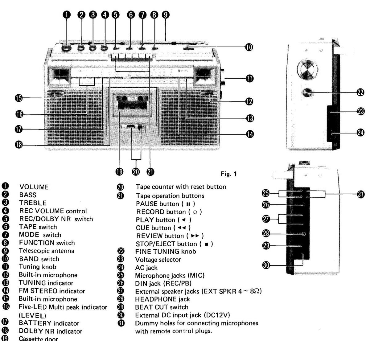
Names of Parts
Removal of Main Parts
- 1. Rear Cabinet
-
(1) Remove 7 screws ( ① ~ ③ )
-
, ❷ = SDSP3012 ●~⑧ = VKZ4008-001
-
, ❷ = SDSP3012 ●~⑧ = VKZ4008-001
- (2) Remove 2 connectors (3 pin) connected to the rod antennas and power supply wires.
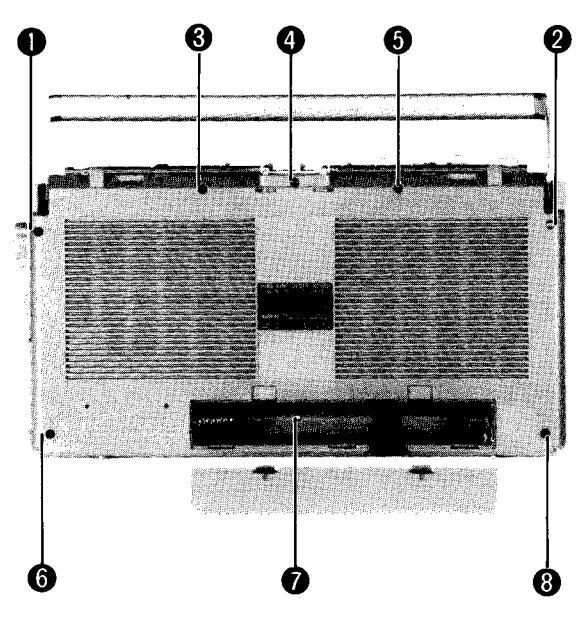
Fig. 2
- 3 Tuner P.W. Board Ass'v
- (1) Remove the rear cabinet.
- (2) Remove Tuning knob and Fine tuning knob.
- (3) Remove 5 screws (SBSF3010V)
- (4) Remove 2 connectors (3 pin and 5 pin).
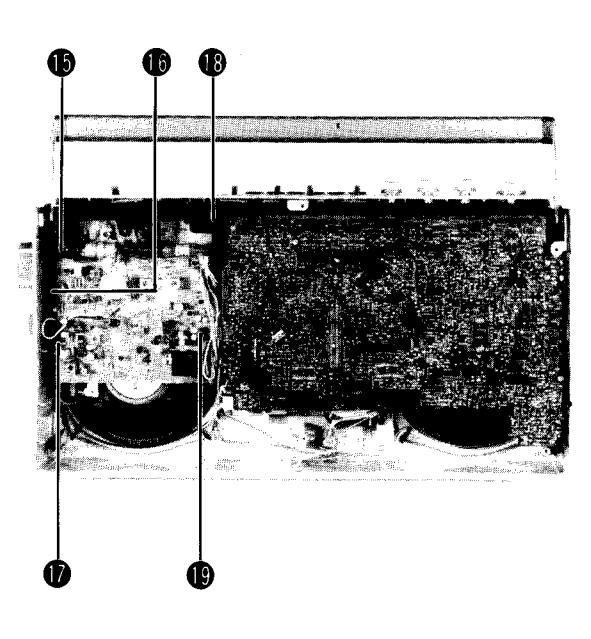
Fig. 4
2. Amplifier P.W. Board Ass'v
- (1) Remove the rear cabinet.
- (2) Remove 4 control knobs (VOLUME, BASS, TREBLE and REC VOLUME)
-
(3) Remove 6 screws ( () ~ () = SDSP3034V
- 0 = SDSP3005V
- (4) Remove the 3 pin connector connected to the E MIC wire terminal P.W.B.
Fig. 3
- 4 -
4. Cassette Mechanism Remove 4 screws ( <a> </a> ( <a> </a> (a) fastening the cassette mechanism.
Fig. 5
Removal of Cassette Mecha Parts
- 1. Pinch roller ( ① )
- Remove the spring (2).
- Remove the E-ring ( 3).
- 2. REC/PB head ( 4)
- Remove 2 screws ( 6 , 6 ).
- Remove the solenoid head circuit board.
- 3. Erase head ( 1 )
- Remove 2 screws ( 8).
- 4. Reel assembly ( ( )
- Insert the special tool for reel removing to reel 3 groove, and then pull out the reel.
-
5. Take-up roller ( 🌒 )
- Push the FF button.
- Remove the washer. If you broke the washer, you can use E-ring (REE 1200).
- 6. RF clutch assembly ( 🕑 )
- Remove the main belt ( 1 ).
- Pull out the pulley (it is pressed).
- 7. Main belt ( 🚯 )
- To flywheel bracket ( 1) remove a screw ( 1) ).
8. Flywheel assembly ( 10)
Do the same manner as for the main belt. (When assembling it, be careful not to forget the nylon washer for capstan.)
- 9. Reef switch ( 🛈 )
- Remvoe the screw ( 1).
-
10. Motor assembly ( (D))
- Remove 3 screws ( 1 ).


Fig. 8
- 5 -
Adjustment of Cassette Recorder
If the following adjustments are performed by ear or eye in a simple manner, be sure to perform then again later.
Head replacement and angle adjustment
-
1. Head replacement
- 1) To replace the record/playback head, remove two screws (A) and (B) shown in Fig. 9.
- 2) To replace the erase head, remove two screws C and D shown in Fig. 9.
- 3) When pressing the playback button, adjust these heads with the screws and the adjustment hole so that they are located as shown in Fig. 9.

Fig. 9
-
2. Angle adjustment of Record/Playback head
- Connect an oscilloscope to the speaker terminal. (A Lissajous waveform will appear.)
- Play back the head angle adjusting tape (JVC test tape VTT-657).
- Adjust the head angle by turning screw B shown in Fig. 9 so that the phase difference between the L and R outputs is 0° and the outputs are maximum.
- 4) After adjustment, be sure to paint-lock screw (B).
- 5) When adjusting the head angle using neither a voltmeter nor test tape, adjust it so that the output (esp. high band) from the speaker is maximum.
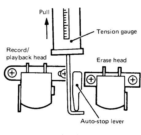
Fig. 10
-
Check of auto-stop detection pressure
- Place the head mechanism with its motor side down, then set the recorder into the playback mode.
- Hang a tension gauge on the detection cap tip as shown in Fig. 10, then confirm that when this gauge is slowly pulled, the auto-stop lever operates in the range of 50-70 g.
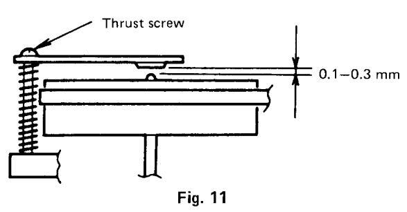
Flywheel thrust adjustment
Insert a clearance gauge into the clearance between the flywheel and the flywheel bracket, then adjust the thrust by turning the thrust screw shown in Fig. 11 to obtain a clearance of 0.1–0.3 mm wide.
Pause operation check
Operation and timing check
- Confirm that when pressing the PAUSE button in the playback mode, the tape stops running, while when re-pressing, the recorder returns to the playback mode without any abnormality.
-
2) Confirm that when slowly pressing the PAUSE button, the pinch roller separates from the capstan to stop rotating earlier than the reel disk which in turn stops rotating. (Although they may stop almost at the same time, this means no abnormality.)
- Note: For positive checking, it is advisable to use a cassette tape with a small number of turns such as C-30, etc.
Adjustment of pinch roller contact force
- Position the mechanism shown in Fig. 12 with the motor side down, enter the recorder into the playback mode, and hang a tension gauge on the protrusion part of the pinch roller arm shown in Fig. 12. Next, confirm that when slowly pulling the tension gauge, the pinch roller stops rotating in the range of 450-550 g.
-
If the pinch roller does not stop in the range, replace the contact spring or adjust the contact force by bending this spring.
- Note: Overly strong contact force may cause noise in the pinch roller bearing part, wow & flutter, or similar adverse effects. Conversely, too little contact force may cause auto-stop function failure, wow & flutter, or similar adverse effects.
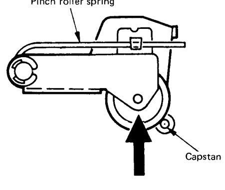
Fig. 12
-
Playback torque adjustment
- Set a torque gauge to the take-up reel, then enter the recorder into the playback mode, and confirm that the playback torque is 45–70 g/cm.

Fig. 13
2) When the playback torque is not in this range, check whether or not rubber and/or rotary members have dirt and/or oil on them. After that, if the torque is still low, lift up the spring plate shown in Fig. 13 to move it to position (3), while if the torque is high, move it to position (1) in the same manner.
Fast forward/rewind torque adjustment
-
1. Fast forward torque adjustment (Fig. 14)
- Set a torque gauge to the take-up reel, then enter the recorder into the playback mode, and confirm that the fast forward torque is 60–130 g/cm.
- When a normal torque is not obtained because of the instability of the sliding mechanism within the R.F. clutch ass'y, lift up the spring plate inside the R.F. clutch ass'y and adjust the torque by moving it in the direction of (1).
- 2) When a normal torque is not obtained should the said sliding mechanism operate normally, adjust the torque by moving the said spring plate in the direction of (4) in the same manner as item 1).
- 2. Rewind torque adjustment (Fig. 14)
Set a torque gauge to the rewind reel, then enter the recorder into the rewind mode, and confirm that the rewind torque is 60–130 g/cm.
When a normal torque is not obtained because of the instability of the sliding mechanism within the R.F. clutch ass'y, lift up the spring plate inside the R.F. clutch ass'y and adjust the torque by moving it in the direction of ①.
-
2) When a normal torque is not obtained should the said sliding mechanism operate normally, adjust the torque by moving the said spring plate in the direction of (4) in the same manner as item 1) of this paragraph.
- Note: When rubber members (belt, idler), the fringe of the flywheel, etc. have dirt on them, a normal torque may not appear, so clean them with alcohol, etc.
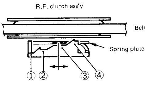
Fig. 14
How to Engage Dial Cord
- 1. Turn the dial drum fully counterclockwise (to the lowest frequency).
- 2. Use tetron cord (995mm long and 0.5mm in diameter)
- 3. Install the string in the sequence of the numbers.
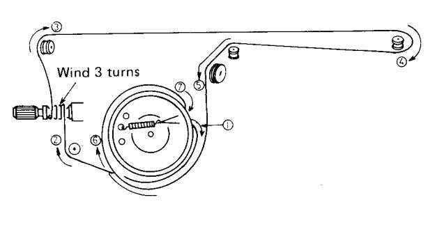
Fig. 15
Adjustment of Cassette Recorder Amplifier
Adjustment location
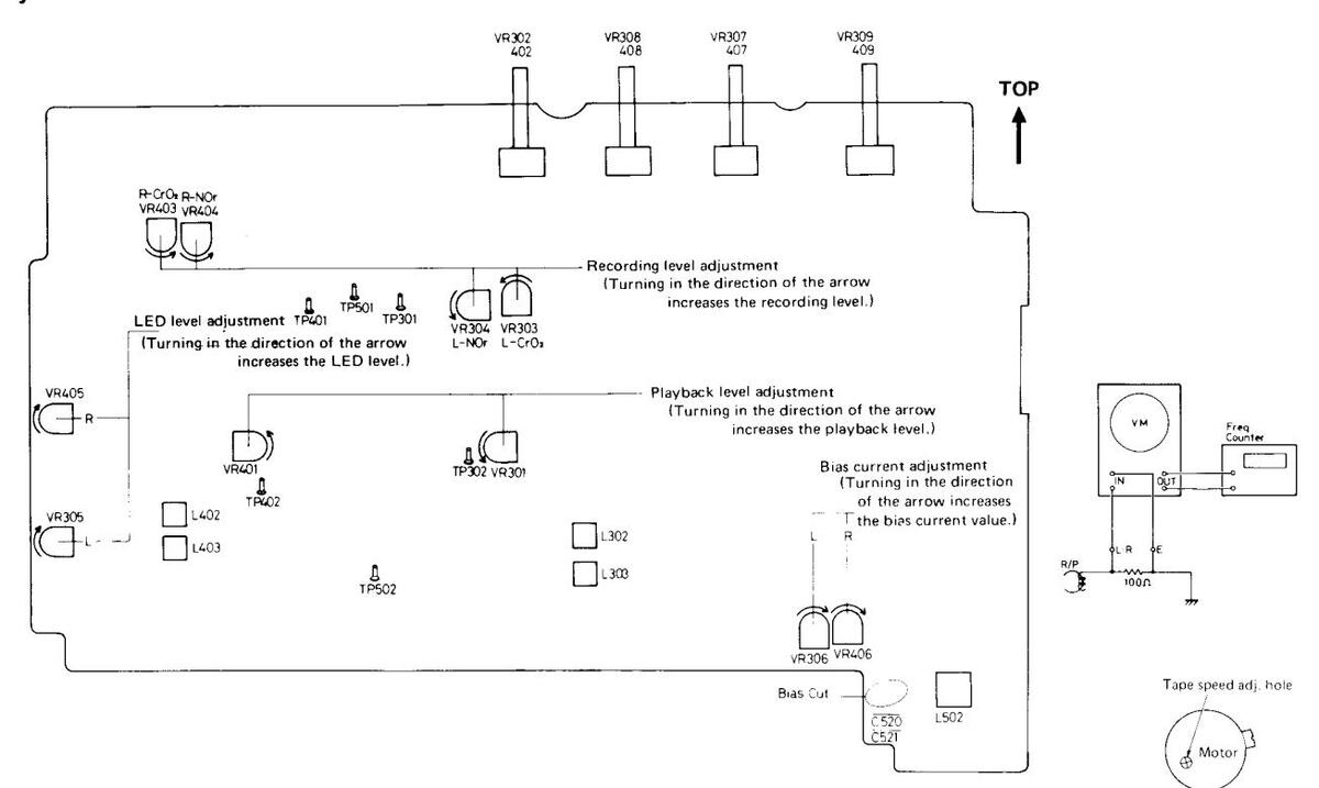
Fig. 16
| Step | ltem | Input | Output |
Adjusting
point |
Standard value |
Tape select
switch |
Dolby NR
switch |
Rec-Play |
Beat cut
switch |
Remarks |
|---|---|---|---|---|---|---|---|---|---|---|
| 1 | Head azimuth |
Test tape
VTT-653,658 (10kHz) |
T302, T402
T502 |
Head |
The phase difference between
the L and R outputs is 0° and maximize the output level at the same time. |
Normal | OFF | Play | _ |
Before playback level adjust-
ment, L and R channel out- put levels become unbalance. |
| 2 | Playback level |
Test tape
VTT-664 |
same as above | VR301,401 | 410m∨ | Normal |
OFF
(ON) |
Play | _ |
Check the playback level
so that difference between ON and OFF with Dolby NR switch is less than ±1dB |
| 3 | LED indicators |
Apply 1kHz -4c
DIN socket. (L aoplied indepen Adjust VR305 s output level bec with R channel. |
dBs signal to the
or R channel is dent signal.) to that TP302 ome 410mV |
VR305,405 |
Check to light LED at 0d8
level and to un-light the LED at -1d8 level down. |
Normal |
ON
(OFF) |
Rec | _ |
Check Test Point 302, 402
levels become less than ±1dB at Dolby SW on. |
| Recording no | rmal same as | TP301, TP401 | VR304,404 | 35μA (0.35mV/10Ω) | Normal | 0.57 | Unsolder the bias cutting | |||
| 4 | Current | ·O2 above | T501 | VR303,403 | 70µA (0.7mV/10s2) | CrO2 | Rec | - | pattern. | |
| 5 | Bias frequency | - | same as above | L502 | 63.5±0.1kHz | Normai | OFF | Rec | "1" |
If the frequency is low, cut
C409 and C408 Turn VR304,406 center. |
| 6 | Bias current | - | same as above | ame as above VR306,406 320μF ( 3.2mV ) Normal OF | OFF | Rec | "1" |
For this adjustment, Bias
frequency not become standard value |
||
| 7 |
Stereo signal
trap |
Apply 19kHz,
OdB signal to the DIN socket VR302=Max. |
TP302, TP402
TP502 |
L303,403 | min. | Normal | ON | Rec | — |
After this adjustment, check
the level so that 1kHz ~ 19kHz frequency become 30dB or more. |
| 8 | Bias trap |
Apply 1kHz -
less than-100 dBs signal to the DIN socket VR302=Max. |
same as above | L302,402 | Less than 0.5dB with the beat cut switch selection | CrO2 | ON | Rec | "1~3" | |
| 9 |
Rec/Play
frequency response (Normal) |
Apply -40dBs
signal to the DIN socket |
same as above | VR306,406 |
(At reference frequency;
1kHz 10kHz; 0±1dB) |
Norma! |
OFF
(ON) |
Rec
(Play) |
''1''
(Normal) |
Check the Rec/PB frequency
responce become standard value at Dolby NR circuit ON. |
| 10 |
Rec/Płay
leve! (Normal) |
Apply -4dBs
signal to the DIN socket. Adjust VR302 so that TP202 output level become 410mV |
same as above | VR304,404 | The output difference level become less than ±1dB. | Normal | OFF |
Rec
(Play) |
''1''
(Normal) |
|
| 11 |
Rec/play level
(CrO2) |
same as above | same as above | VR303.403 | same as above | CrO2 | OFF |
Rec
(Play) |
"1"
(Normal) |
|
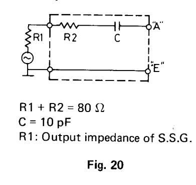
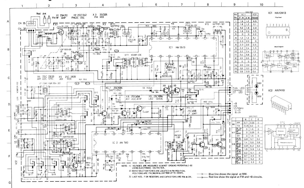
Tuner Alignment
| BASIC CONDITIONS | |||||
|---|---|---|---|---|---|
| POWER SOURCE OF THE RECEIVER | DC 12 V, AC240/220/110 V, 50/60 Hz. | ||||
| LOAD RESISTANCE OF THE RECEIVER | 50 mW (0.4 V)/3.2 Ω. | ||||
| MODULATION OF SSG | 400 Hz. 30% | ||||
| Item | Description |
|---|---|
| 1. MW IF ALIGNMENT | |
|
DC 12 V.
(When the power is supplied directly to the tuner in the receiver, the voltage should be adjusted to the proper level which shall be requir- ed by the tuner.) |
|
RADIO
MW Minimum gain position Center (Bass, Treble) position Near the minimum capacity position where no signal come in. Positive side to TP-7. Positive side to TP-5. Negative side to TP-2. |
|
CFT1, IFT3
Adjust MW I.F.T. (above mentioned aligning position) so that max- imum and symmetrical wave form can be obtained. In this case, the wavehead should be appeared at the center marker (455 kHz) on the scope of Sweeper. |
| 2. FM IF ALIGNMENT | |
|
Same as mentioned in item 1-1
RADIO FM Minimum gain position Center (Bass, Treble) position Near the minimum capacity position where no signal come in. |
|
Positive side to TP-1.
Positive side to TP-3. Negative side to TP-2. |
|
) kΩ) in series to the positive side cable which shall be led from Sweeper
00 kΩ) in series to the positive side cable which shall be led from Sweeper |
| 2-3 Aligning position: |
a) IF Waveform: IFT1
b) Discriminate Waveform: IFT2 ("S" curve waveform) |
| ltem | Description | |
|---|---|---|
|
2-5
a) |
Alignment (Waveform):
IF Waveform: |
Adjust the discriminate coil (IFT2) so that "S" curve waveform may be changed to IF waveform as shown in following figure. |
| b) | Discriminate Waveform: |
Fig. 18
Fig. 18 After above, adjust IFT1 so that max. sensitivity and symmetrical IF waveform can be obtained on the scope of Sweeper. Adjust the discriminate LFT2 again so that above symmetrical IF waveform may be changed to balanced "S" curve waveform. |
| 3. M | W RF ALIGNMENT | |
| 3-1 | Conditions of the receiver. | |
| (1) | Power source: | Same as mentioned in item 1-1 |
| (2) | Function switch position: | RADIO |
| (3) | Volume control: | 50 mW |
| (4) | Variable capacitor: |
Center (Bass, Treble) position
Befer the following list shown in item 3.4 |
| Here, the following hat anown in item 5-4. | ||
|
3-2
(1) |
Conditions of 55G. | Befer the basic condition |
| (2) | Frequency: | Refer the following list shown in item 3-4 |
| (3) | Output level of the attenuator in SSG: | Approx. 50mW |
| 3-3 | Power output measuring position: | Speaker terminals |
3-4 Alignment:
|
Band Select
Switch Position |
Sort of Antenna
to be attached to SSG |
Frequency of SSC | Variable Capacitor Position | Aligning Position | |
|---|---|---|---|---|---|
| 1 | 145 kHz | Max. capacity | L8 | ||
| 2 | 360 kHz | Min. capacity | TC3-1 | ||
| 3 | IW | Loon Antenna | Adjust the above aligning | position (L8 & TC3-1) repeated | lly so that the tuner |
| Loop / internit | can be received above freq | uency range (band width). | |||
| 4 | 160 kHz | to be received 160 kHz | L4 | ||
| 5 | 350 kHz | to be received 350 kHz | TC1-3 | ||
| 6 | Adjust the above aligning | position (L4 & TC1-3) repeated | lly so that the tuner | ||
| can be obtained the best s | ensitivity. | ||||
| 7 | 520 kHz | Max. capacity | L9 | ||
| 8 | 1,650 kHz | Min. capacity | TC3-2 | ||
| 9 | MW | Loon Antenna | Adjust the above aligning position (L9 & TC3-2) repeatedly so th can be received above frequency range (band width). | lly so that the tuner | |
| Loop / intoiniu | |||||
| 10 | 620 kHz | to be received 620 kHz | L6 | ||
| 11 | 1,400 kHz | to be received 1,400 kHz | TC2-2 | ||
| 12 | Adjust the above aligning | position (L6 & TC2-2) repeated | lly so that the tuner | ||
| can be obtained the best s | ensitivity. | ||||
| 13 | 5.8 MHz | Max. capacity | L10 | ||
| 14 | 18.6 MHz | Min. capacity | TC1-4 | ||
| 15 | SW | Dummy | Adjust the above aligning | position (L10 & TC1-4) repeate | edly so that the |
| Antenna | tuner can be received abov | e frequency range (band width | ). | ||
| 16 | 6.0 MHz | to be received 6 MHz | L7 | ||
| 17 | 18.0 MHz | to be received 18.0 MHz | TC2-1 | ||
| 18 | Adjust the above aligning can be obtained the best set |
position (L7 & TC2-1) repeated
ensitivity. |
lly so that the tuner | ||
| Item | Description | |
|---|---|---|
| 4. F | M RF ALIGNMENT | |
| 4-1 | Conditions of the receiver | Same as mentioned in item 1.1 |
| (2) | Function switch position: | RADIO |
| (3) |
Band select switch:
Volume control: |
FM
50 mW |
| (5) | Center (Bass, Treble) position | |
|
(0)
4-2 |
Variable capacitor: | Refer the following list shown in item 4-3 |
| (1) | Modulation: | Refer the basic condition |
| (2) |
Frequency:
Output level of the attenuator in FM SSG |
Refer the following list shown in item 4-3.
The level shall be decided by the load registance of the receiver |
| mentioned in the basic conditions. |
4-3 Alignment:
|
Band Select
Switch Position |
Antenna to be
attached to FM SSG |
Frequency of FM SSG | Variable Capacitor Position | Aligning Position | ||||
|---|---|---|---|---|---|---|---|---|
| 1 | 87.5 MHz | Max. capacity | L5 | |||||
| 2 | 109.0 MHz | Min. capacity | TC1-1 | |||||
| 3 | FM | FM Dummy Adjust the above aligning position (L5 & Antenna Can be received above frequency range (b) |
position (L5 & TC1-1) repeated
uency range (band width) |
lly so that the tuner | ||||
| 4 | 90 MHz | to be received 90 MHz | L1 | |||||
| 5 | 106 MHz | to be received 106 MHz | TC1-1 | |||||
| 6 |
Adjust the above aligning position (L1 & TC1-1) repeatedly so
can be obtained the best sensitivity |
|||||||
| 7 |
Pilot Signal
Alignment |
|
B MONO Signal Freq. 98 MH
VR1, so that output frequency |
z
y of TP6 may be obtained 19 k |
Hz. | |||
| 8 |
Stereo Separa-
tion Alignment |
|
|
|||||
| 9 |
Stereo Tuning
LED checking |
When adjustin
check the LEE |
When adjusting stereo separation, check the LED lit with function switch at stereo mode and check the LED unlit at mono mode. | |||||
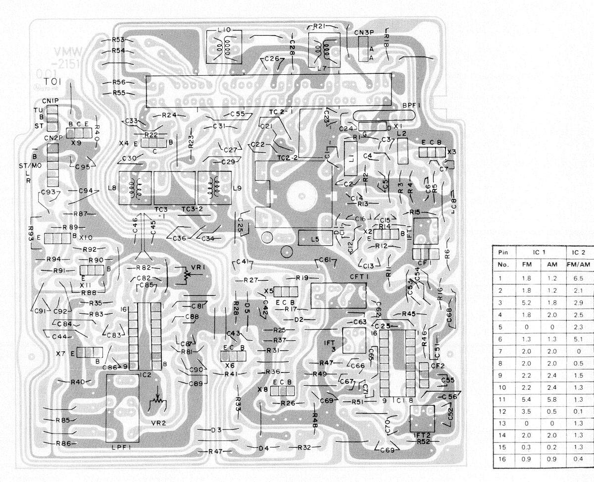
(A) Parts Location on Tuner P.C.B.
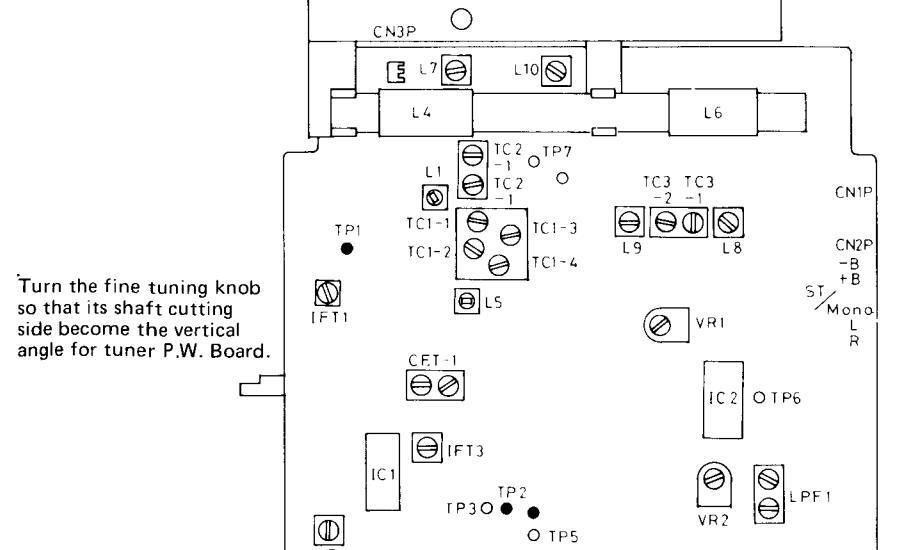
(B) Dummy Antenna
Note; FM ant. CN3P is 300Ω balanced output. If when connecting 50Ω or 75Ω unbalanced SSG, need match its impedance.
Fig. 19
Block Diagrams

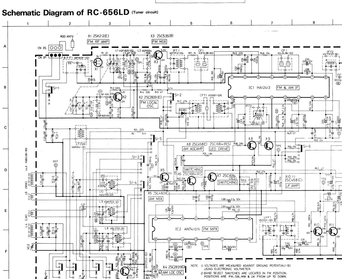
Schematic Diagram of RC-656L/LB (Tuner Circuit)
BC-6561 /I P
Wiring Connection
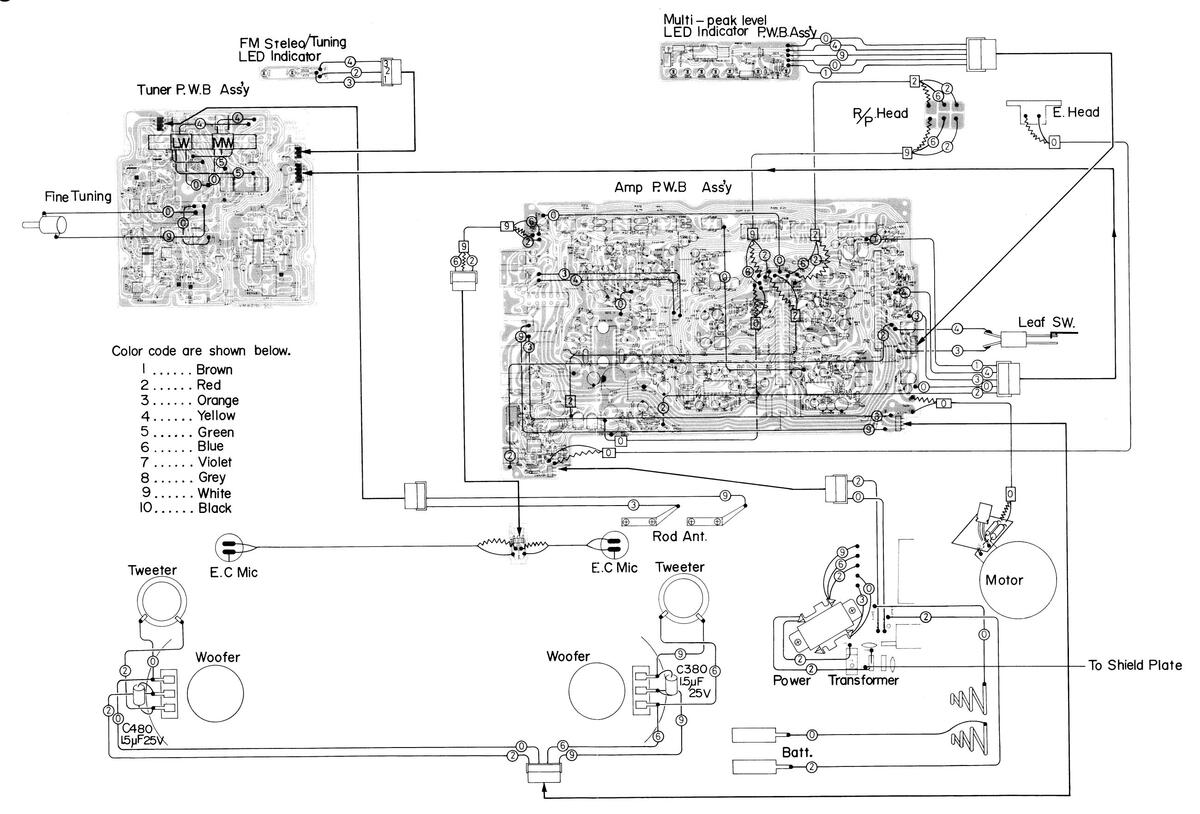
RC-656L/LB
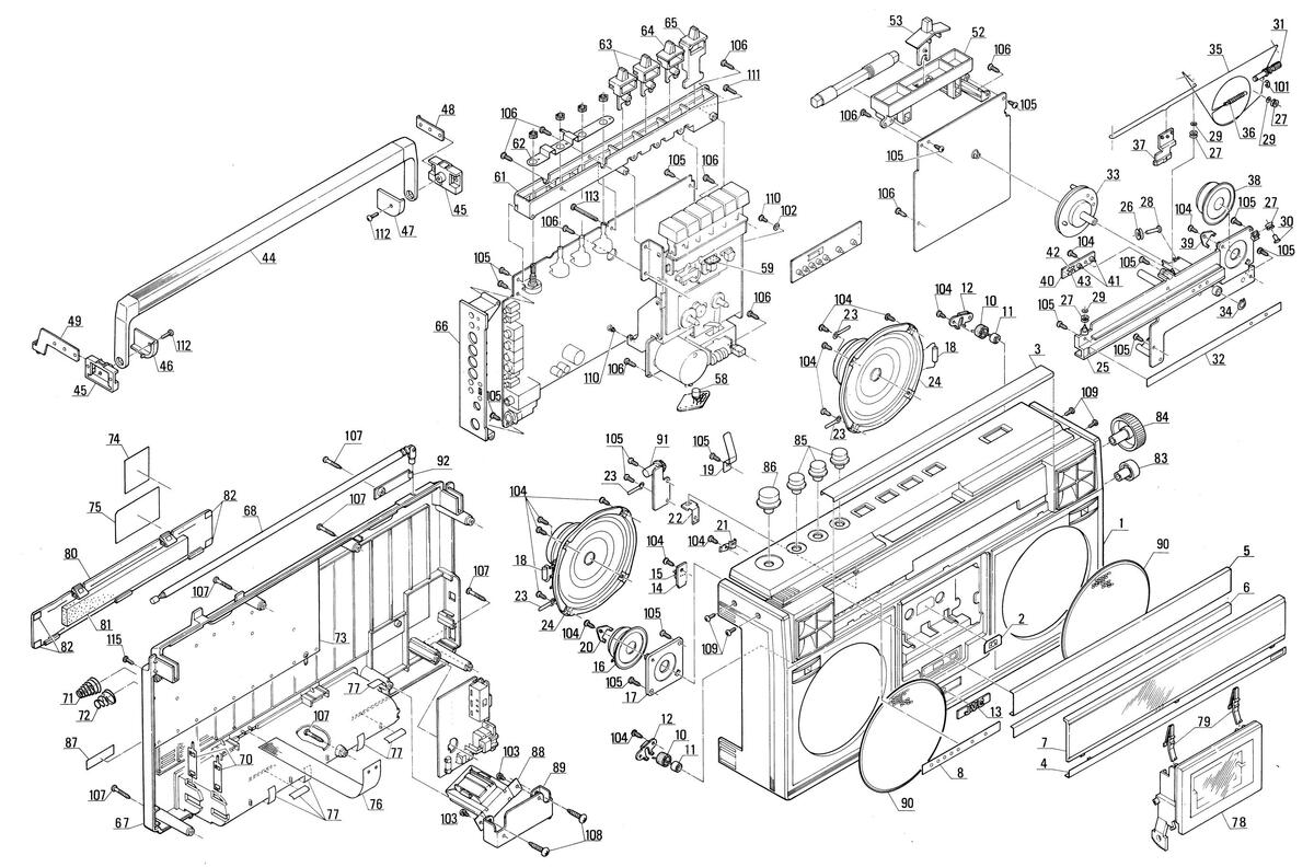
Mechanical Component Parts
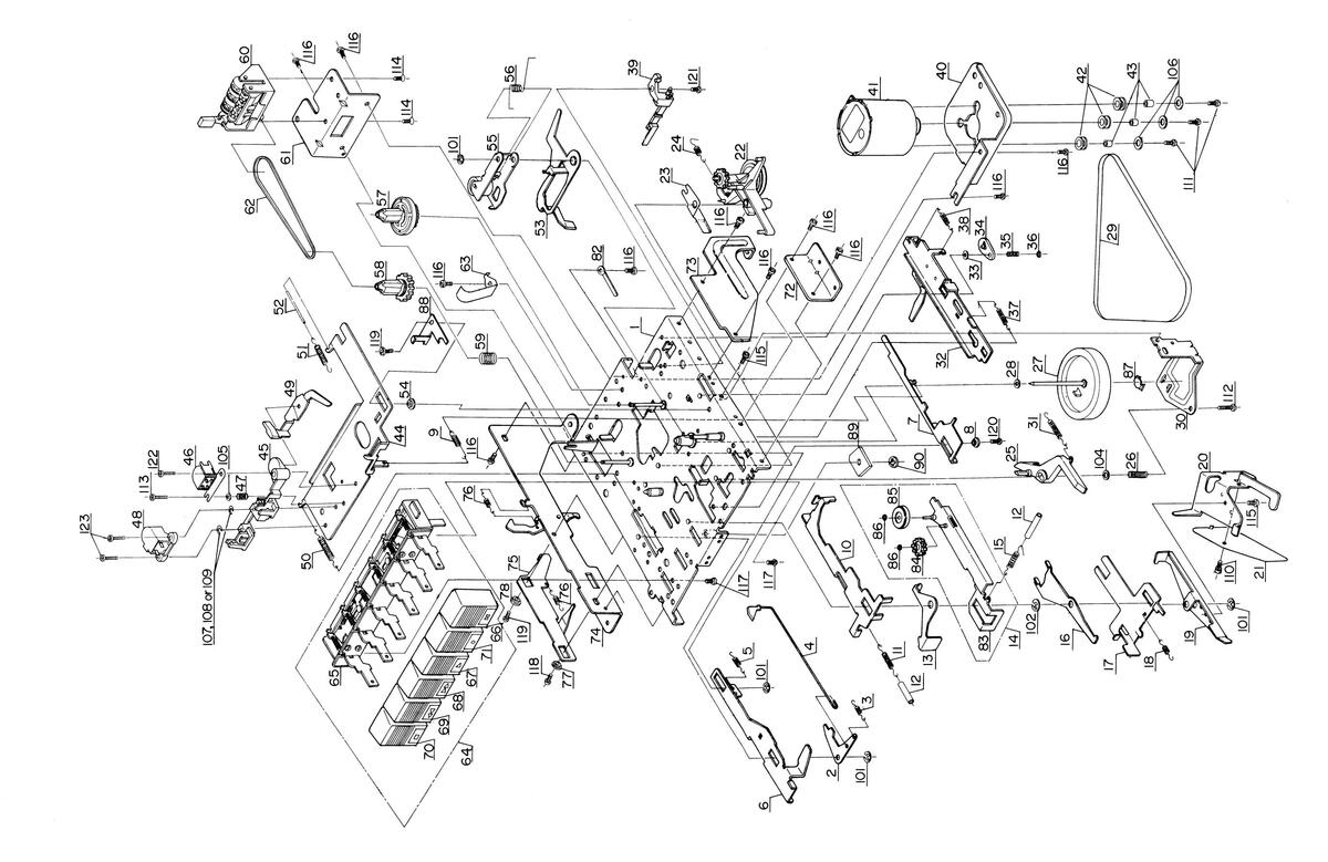
Fig. 26
Mechanical Component Parts List
| Ref. No. | Parts No. | Parts Name | Remarks | Q'ty |
|---|---|---|---|---|
| 1 | 14310182ZT | Mecha Chassis Ass'y | 1 | |
| 2 | 13970201T | Rec. Safety Lever | | 1 | |
| 3 | 2980802T | Spring | | 1 | |
| 4 | 14310291ZT | Rec. Safety Spoke Ass'y | | 1 | |
| 5 | 180502BT | Rec. Slide Lever Spring | 1 | |
| 6 | 14310201T | Rec. Slide Lever | 1 | |
| 7 | 13971002T | Play Slide Lever | | 1 | |
| 8 | 090302T | Play Slide Lever Collar | | 1 | |
| 9 | 13490301T | RC Spring | 1 | |
| 10 | 12001001T | Main Plate | 1 | |
| 11 | 7380702T | Main Plate Spring | 1 | |
| 12 | Tube | φ3.5 x 18 | 2 | |
| 13 | 14311004T | Rewind Arm | ||
| 14 | 12000891ZT | FF. Idler Arm Ass'y | ||
| 15 | 6300403T | FF. Idler Arm Spring | 1 | |
| 16 | 13371901T | RC Lever | ||
| | 17 | 14311901T | RC Slide Lever | 6 50 91 | |
| 18 | 580702⊤ | Spring | for RC Side | |
| 19 | 13970205T | Record Lever | ||
| 20 | 14310203T | Record Bracket | ||
| 21 | 14310202T | Record Spring Plate | ||
| 22 | 14310792ZT | R. F. Clutch Ass'y | ||
| 23 | 14631010T | Rew. Spring Plate | ||
| 24 | 12000709T | R. F. Clutch Arm Spring | ||
| 25 | 12001102T | Auto Stop Lever | ||
| 26 | 14310901 | |||
| 27 | 1200090321 | Flywheel Ass'y | ||
| 28 | 40811201 | Nylon Wasner | 1 | |
| 29 | 120009041 | |||
| 30 |
12000901
15700001T |
Flywheel Bracket | 1 1 | |
| 31 |
15/909011
140717917T |
Auto Stop Lever Spring
Bausa Slide Lever Ass'v |
1 | |
| 32 | 140/1/01Z1 | Collar | or BEE2500 (E Bing) | 1 |
| 24 |
101012011
100012011 |
Pause Lever | of 11222000 (2 1 | 1 |
| 34 | 13231701T | Pause Lever Spring | 1 | |
| 36 | 12601501T | Special Washer | Nylon φ1.7 x φ5 x t0.4 | 1 |
| 37 | 180502BT | Spring | for Pause Slide Lever | 1 |
| 38 | 180311T | " | for Pause Arm | 1 |
| 39 | MSW-0087NKT | Leaf Switch | 1 | |
| 40 | 13971201T | Motor Bracket | 1 | |
| 41 | 14311296ZT | Motor Ass'y | 1 | |
| 42 | F4641-001 | Rubber Cushion | 3 | |
| 43 | 14311202T | Collar | 3 | |
| 44 | 12600301T | Head Panel | | 1 | |
| 45 | 12000302T | Head Block | 1 | |
| 46 | VGH0421-001 | R/P Head | ||
| 47 | 15600305T | R/P Head Spring | 1 | |
| 48 | VGH0212-101 | E. Head | ||
| 49 | 12001193ZT | Detect Plate Ass'y | 1 | |
| 50 | 14000303T | Head Panel Spring (L) | 1 | |
| 51 | 12000303T | " (R) | ||
| 52 | Tube | φ1.4 x φυ.8 x L24 | ||
| 53 | 14311701T | Pause Arm Lever | ||
| 54 | 4080411T | Head Panel Collar | ||
| 55 | 12600491ZT | Pinch Holler Ass'y | ||
| 56 | 12600402T | Take up Bast Ass's | ||
| 57 | 1200059121 | Take-up neel Ass y | ||
| 58 | 139/069121 | Supply neel Ass y | for Back Tension | 1 |
| 59 | 1 | |||
| 60 | VIC5127-0025 | 1 |
| Ref. No. | Parts No. | Parts Name | Remarks | Q'ty | ||
|---|---|---|---|---|---|---|
| 61 | 14311801T | Counter Bracket | 1 | |||
| 62 | 3091001T | Counter Belt | 1 | |||
| 63 | 6010101T | Pack Spring | 1 | |||
| 64 | 14311494 | Push Button Switch Compo | osite | 1 | ||
| 01 | Ass'v | |||||
| 65 | 139714927T | Push Button Switch Ass'v | 1 | |||
| 66 | VXP3054-001 | Push Button | 1 | |||
| 67 | " | PA | USE PLAY | 1 | ||
| 68 | ″ -003 | " | | FF | 1 | ||
| 69 | ··· -004 | RE | W | 1 | ||
| 70 | ″ -005 | ST | OP/EJECT | 1 | ||
| 71 | RE | С | 1 | |||
| 72 | 14311001T | Slide Bracket (A) | 1 | |||
| 73 | 14311002T | " (B) | 1 | |||
| 74 | 14311382ZT | Eject Bracket Ass'y | 1 | |||
| 75 | 13971302T ° | Eject Lever | 1 | |||
| 76 | 581205T | Spring | 2 | |||
| 77 | 4080411T | Collar | 1 | |||
| 78 | 9071904T | " | 1 | |||
| 82 | 4660901T | Cord Clamp | 1 | |||
| 83 | 12000891ZT | FF Idler Arm Sub Ass'y | 1 | |||
| 84 | 12000802T | Idler Gear | 1 | |||
| 85 | 12000804T | Take-up Roller | 1 | |||
| 86 | 12001503T | Washer | 2 | |||
| 87 | 12000906T | Spacer | 1 | |||
| 88 | 13971005T | Guide Plate | 1 | |||
| 89 | 15790103T | Rubber Sheet | 1 | |||
| 90 | RDS3000F | CS Ring | 1 | |||
| 101 | REE2500 | E Ring | 4 | |||
| 102 | REE4000 | " | 1 | |||
| 104 | WNS3000Z | Washer | 1 | |||
| 105 | WSS2000Z | 1 | ||||
| 106 | 14311203T | " | 3 | |||
| 107 | 13270412AT | U Washer | 2 | |||
| 108 | 13270412BT | ret | er to Note | 2 | ||
| 109 | 13270412CT | ) | 2 | |||
| 110 | LPSP2605Z | Ass'y Screw | 3 | |||
| 111 | SPSP2609Z | Screw | 3 | |||
| 112 | SPSP2618Z | 1 | ||||
| 113 | SPSX2011R | PIVI Screw | 1 | |||
| 114 | 555P3005Z5 | 2 | ||||
| 115 | 10PZ20051 | for | Counter Bracket | · v 2 | 11 | |
| 110 | 2082200401 | Tap Screw | Par | Counter Bracker | B: D | |
| Sid | le Bracket (Δ) v ' | 2 | ||||
| Sid | le Bracket (R) x 3 | |||||
| Fie | et Bracket v 1 | - | ||||
| Mo | tor Bracket x 2 | |||||
| 117 | 20P726050T | ,,,,,,,,,,,,,,,,,,,,,,,,,,,,,,,,,,,,,,, | 2 | |||
| 112 | 20P726060T | 1 | ||||
| 110 | 20PZ26070T | 2 | ||||
| 120 | 20PZ26080T | 1 | ||||
| 121 | 23P726050T | " | for | Leaf Switch x 1 | 1 | |
| 122 | 72P720110T | Cap Screw | 1 | |||
| 123 | 72PZ20120T | " | 2 | |||
| , 21 2201201 | ||||||
| Note: | Parts No. | Thickness | Mat | erial | ||
| The U-washe | ers are provided for adju | isting the height of erase head. | 13270/12AT | 0.1 mm | Phoenbo | n-hronze |
| They may no | ot be used, if the head h | eight is normal value. | 13270412RT | 0.2 mm | Rr | ass |
| Choose one | of three types (thicknes | a it | 13270412CT | 0.3 mm | Alum | inium |
the size of erase head when replacing it.

Assembly Parts List
| Re | ef. No. | Parts No. | Parts Name | Remarks | Q'ty | Ref. No. | Parts No. | Parts Name | Remarks | Q'ty |
|---|---|---|---|---|---|---|---|---|---|---|
| 1~9, | ,13,21,22 | ZCRC656L-CBF | Front Cabinet Ass'y | 1 set | 5 | VJK3159-001 | Dial Scale (A) | 1 | ||
| 1 | VJC1120-001 | Front Cabinet | 1 | 6 | VJK3160-001 | Dial Scale (B) | 1 | |||
| 2 | VJD4005-002 | Reflection Plate | 1 | 7 | VJK3161-001 | Dial Lens | 1 | |||
| 3 | VJD4412-001 | Button Plate | 1 | 8 | VJK4123-001 | Scale Plate (A) | 1 | |||
| 4 | VJD4413-001 | Fitting | 1 | 9 | VJD4414-001 | Mic Escutcheon | 2 |
| Ref. No. | Parts No. | Parts Name | Remarks | Q'ty |
|---|---|---|---|---|
| 10 | VYH4102-001 | Mic Bushing | 2 | |
| 11 | VMME62N-D23 | E. C. Mic | ||
| 12 | VYH4298-001 | Holder | 2 | |
| 13 | QXM2251-003 | Mark | 1 | |
| 14 | VMW1017-001D | P. W. Board | for Mic | 1 |
| 15 | OMV5005-003 | Connector | ||
| 16 | EAS5PH08SA | Speaker | SPK302 | |
| 17 | VYH4565-001 | Tweeter Holder | 51 1(302 | |
| 18 | OEN21EM-155 | C380 480 | ||
| 19 | VKY4165-001 | Door Spring | 0000,400 | |
| 20 | VYH4352-002 | Clamp | for Tweeter | |
| 21 | V44981-001 | Earth Catcher | IOI I Weelei | |
| 22 | VYH4389-001 | " | ||
| 23 | VKZ4001-007 | Wire Holder | ||
| 24 | EAS16P127SG | Speaker | SPK 301 | |
| SPK401 | 2 | |||
| 25 | VYH2122-001 | Chassis Base | ||
| 26 | VYH4032-001 | Boller | ||
| 27 | VYH4002-001 | " | ||
| 28 | RTA4020 | Rivet | 1 | |
| 29 | V42562-1 | Special Washer | ||
| 30 | BTA4010 | Bivet | ||
| 31 | V41336-021 | Tuning Shaft | ||
| 32 | V.IK4124-001 | Scale Plate (B) | ||
| 33 | VYH3177.001 | Dial Drum | ||
| 34 | BCSA6000 | C Bing | 1 | |
| 35 | VHR2TT9-05A | Dial Bone | 905 m/m | 1t |
| 36 | 50153-3 | Spring | 333 1011 | 1 1 |
| 37 | V.IN4049-00A | |||
| 38 | FAS5PH08SA | Speaker | SPK BA02 | 1 |
| 39 | VYH4352-002 | Clamp | for Tweeter | 1 |
| 40 | VMW1017-001C | P. W. Board | for Tuper LED | |
| 41 | SLP146B | LED | D201 202 | 2 |
| 42 | QRD147J-471S | C. Resistor | B201 | 1 |
| 43 | QRD147J-101S | " | B202 | 1 |
| 44 | VJH3005-00N | Handle Ass'v | ||
| 45 | VYH3120-001 | Handle Supporter | 2 | |
| 46 | V44943-001 | Washer (L) | 1 | |
| 47 | V44944-001 | " (R) | 1 | |
| 48 | VYH4224-001 | Bracket | i | |
| 49 | VYH4566-001 | Bracket | 1 | |
| 50 | VYH4571-00A | Dump Ass'y | ||
| 51 | VYH4578-001 | Connect Bracket | for Front Cabinet | |
| ~ Rear Cabinet | ||||
| 52 | VYH2124-001 | Tuner Chassis | ||
| 53 | VXQ3018-004 | Toggle Lever | for Band | |
| 54 | QAT5001-203 | M. V. Capacitor | VC2 | |
| 55 | VYH4516-001 | Fine Tuning Bracket | ||
| 56 | VYH4221-001 | Arm | ||
| 57 | T41572-001 | Inductor | L701, 702 | 2 |
| 58 | QET41CR-227 | E. Capacitor | C702 | |
| 59 | VMW3035-301 | P. W. Board | for R/P Head | 1 |
| 60 | VMW3113-001 | P. W. Board | for Motor | |
| 61 | VYH2125-001 | Holder | ||
| 62 | VYH4567-001 | Earth Plate | 1 1 | |
| 63 | VXQ3028-002 | Toggle Lever | 2 | |
| 64 | VXQ3032-001 | " | 1 | |
| 65 | VXQ3033-001 | " | 1 1 | |
| 66 | VJD3193-002 | Jack Board |
| Ref. No. | Parts No. | Parts N | ame | Remarks | Qʻty |
|---|---|---|---|---|---|
| 67,73,75 | ZCRC656L-CBR | Rear Cabinet Ass'y | 1 set | ||
| 76,82, | ···· · · ··· , | ||||
| 67 | VJC1121-001 | Rear Cabinet | 1 | ||
| 68 | QZR4147-001U | Rod Antenna | 2 | ||
| 69 | VYH4189-001 | Holder (B) | 2 | ||
| 70 | VYH4010-002 | Battery Contact | 2 _ | ||
| 71 | 53738-009 | Spring | 1 | ||
| 72 | V44686-002 | Spring | 1 | ||
| 73 | VYH4568-00A | Shield Ass'y | 1 | ||
| 74 | VND4027-001 | Dolby Label | 1 | ||
| 75 | VYN5066-001CBS | Name Plate | RC-656LB | 1 | |
| VYN5066-002C | " | RC-6561 | 1 | ||
| 76 | V41583-3 | Таре | 1 | ||
| 77 | VYSA1R4-050 | Spacer | 2 | ||
| 78 | VJT4029-00A | Cassette Door Ass | Ϋ́Υ | 1 | |
| 79 | V44910-002 | Cassette Spring | 2 | ||
| 80,81 | ZCRC656L-BCA | Battery Cover Ass | ′ у | 1 set | |
| 80 | VJC2016-004 | Battery Cover | 1 | ||
| 81 | VYSH106-020 | Spacer | 1 | ||
| 82 | VYSA1R6-009 | 4 | |||
| 83 | VXKM520-20013 | Knob | 1 | ||
| 84 | VXL4008-002 | Tuning Knob | 1 | ||
| 85 | VXL4122-002 | Knob | 3 | ||
| 86 | VXL4123-002 | ,,,,,,,,,,,,,,,,,,,,,,,,,,,,,,,,,,,,,,, | 1 | ||
| 8/ | 53866-2 | Label | |||
| 88 | VTP54N2-12ES | Power Transforme | r | RC-656LB | |
| V1P54N2-12E | Turne Duralist | RC-050L | |||
| 89 | VY4570-001 | Chassis hasa | |||
|
Chassis base
B W B ~ Macha |
1 | ||||
| 102 | 2 | ||||
| 103 | 00023 | Tapping Screw | E C Mic Hold | er v 2 Woofer v 8 | 21 |
| 104 | 303530002 | Tapping Screw | Mic Wire termin | alx1 LEDPWBx1 | 21 |
| Tweeter x 2 | Connect Bracket x 2 | ||||
| Earth Catcher X | < 1 Holder (B) x 4 | ||||
| 105 | CDCE20107 | Tweeter Holder | Dump Ass'v x 2 | 17 | |
| 105 | 303730102 | ~ Front Cabi | net x 2 Tuner chassis | ||
| Door Spring x 1 | ~ P.W.B. x 2 | ||||
| Fine Tuning Bracket x 1 | |||||
| Front cabinet | x 5 Holder ~ P.W.B. x 2 | ||||
| ********* | Jack Board ~ P.W.B. x 2 | ||||
| 106 | SBSF3012C | " | · | Tuner CB ~ | 8 |
| Front Cabinet x 3 | |||||
| Arm Ass'y ~ Front Cabinet x 5 | |||||
| 107 | SBSF3020R | " | Front Cabinet | 6 | |
| ~ Rear Cabinet | |||||
| 108 | SBSF4020C | " | Trans Bracket | 2 | |
| 109 | SDSP3010RS | Screw | Front Cabinet | 6 | |
| _ | ~ Rear Cabinet x 2 | ||||
| Bracket x 4 | |||||
| 110 | SPSP3006VS | " | P. W. B ~ Mecha | 2 | |
| 111 | SPSP3012VS | " | " | 1 | |
| 112 | SPSP3014ZS | Bracket | 2 | ||
| 113 | SPSP3035VS | " | P. W. B ~ Mecha | 1 | |
| 114 | SSSP2610Z | Tapping Screw | for Arm | 1 | |
| 115 | SDSP3010RS | Screw | Front Cabinet | 2 | |
| ~ Rear Cabinet | |||||
| L | · |
| Fig. | 27 |
|---|
Amplifier P.W. Board Parts
| E | с | в | Е | с | в | ||||||
|---|---|---|---|---|---|---|---|---|---|---|---|
| X301,401 | 2SC1335 | Pre Amp. | 0.3 | 1.7 | 0.9 | X309,409 | 2SC945L | Biphonic | 2.3 | 7.4 | 2.9 |
| X302,402 | 2SC1335 | Pre Amp. | 1.1 | 7.3 | 1.7 | X501 | 2SD468 | Ripple Filter | 2.9 | 11.7 | 3.5 |
| X303,403 | 2SC1335 | Tuner Amp. | 2.2 | 4.7 | 2.8 | X502 | 2SD468 | Ripple Filter | 10.2 | 11.5 | 11.0 |
| X306,406 | 2SC945L | Rec Amp. | 0.4 | 3.0 | 1.0 | X503 | 2SD468 | Regulator | 8.3 | 11.9 | 8.7 |
| X307,407 | 2SC945L | DIN Amp. | 0.5 | 4.0 | 1.1 | X504 | 2SD468 | Bias OSC | 0.1 | 4.3 | 0.7 |
| X308,408 | 2SC945L | Amp. | 2.1 | 4.3 | 2.7 |
RC-656L/LB
Amplifier P.W. Board Parts

Fig. 27
| E | С | В | E | с | в | ||||||
|---|---|---|---|---|---|---|---|---|---|---|---|
| X301,401 | 2SC1335 | Pre Amp. | 0.3 | 1.7 | 0.9 | X309,409 | 2SC945L | Biphonic | 2.3 | 7.4 | 2.9 |
| X302,402 | 2SC1335 | Pre Amp. | 1.1 | 7.3 | 1.7 | X501 | 2SD468 | Ripple Filter | 2.9 | 11.7 | 3.5 |
| X303,403 | 2SC1335 | Tuner Amp. | 2.2 | 4.7 | 2.8 | X502 | 2SD468 | Ripple Filter | 10.2 | 11.5 | 11.0 |
| X306,406 | 2SC945L | Rec Amp. | 0.4 | 3.0 | 1.0 | X503 | 2SD468 | Regulator | 8.3 | 11.9 | 8.7 |
| X307,407 | 2SC945L | DIN Amp. | 0.5 | 4.0 | 1.1 | X504 | 2SD468 | Bias OSC | 0.1 | 4.3 | 0.7 |
| X308,408 | 2SC945L | Amp. | 2.1 | 4.3 | 2.7 | 1 |
Amp. P.W. Board Parts List
| Ref. No. | Parts No. | Parts Name | Remarks | Q'ty |
|---|---|---|---|---|
| VMW1017-001A | P. W. Board | for Amp | ||
| VMW1017-001B | " | for LED | ||
| S501-19 | QSS9201-002 | Slide Switch | 1 | |
| S502-118 | QSSJ201-001 | " | 1 | |
| S503-16 | QSS6201-102 | " | 2 | |
| S504-16 | - | |||
| $505-14 | OSS4301-023 | 1 | ||
| $506 | OSS1301-001 | ,, | ||
| $507-14 | OSP4210-061 | Push Switch | 1 | |
| 1301 401 | OMS3501-014 | Socket | 2 | |
| 1302 402 | OMC0289-003 | DIN SPK Socket | 2 | |
| 1501 | OMC9014-006 | DIN Socket | ||
| 1502 | OMS6312-004 | Headphone lack | ||
| 1503 | OMA1221-004 | Ext Batt look | 1 | |
| VB301 401 303 | OV/P8A0B-024 | |||
| Q VI 0A0D-024 | v. nesistor | D | ||
| VR302 402 | 01/08434 0541/M | |||
| VR305 405 | ||||
| VR305,405 | " 015 | 2 | ||
| VR300, 400 | 2 | |||
| QVD/A3B-115VW | 2 | |||
| 308, 408 | 01/09424 0241/14 | |||
| VR309, 409 | ||||
| 2 | ||||
| AN7146 (H) | 1 | |||
| 25C1335 (D) | Iransistor | 6 | ||
| 402, 303, 403 | ||||
| X 304, 404, 305 | 2SC945L (Q,P) | Iransistor | 12 | |
| 405, 306, 406 | ||||
| 307, 407, 308 | ||||
| 408, 309, 409 | ||||
| X501, 502 | 2SD468 (B, C) | 4 | ||
| 503, 504 | ||||
| X601 | 2SD636 (R, S) | 1 | ||
| D301, 401, 302 | HV80 | Si. Diode | 8 | |
| 402, 303, 403 | ||||
| 304, 404 | ||||
| D501 | HZ7C | Zener Diode | 1 | |
| D502 | HZ9B2 | " | 1 | |
| D503 | 10E2-B | " | 1 | |
| D601 ~607 | SLP146B | Si. Diode | 7 | |
| D608 | HZ6B | Zener Diode | 1 | |
| L301, 401, 305 | VQP0001-183 | Inductor | 6 | |
| 405, 306, 406 | ||||
| L302, 402 | VQZ0006-001 | Dolby Filter | 2 | |
| L303, 403 | VQZ0004-001 | 2 | ||
| L304, 404 | VQP0001-562 | Inductor | 2 | |
| L501 | VQP0002-471M | " | 1 | |
| L502 | V03083-019 | OSC Coil | 1 | |
| C301, 401 | QEB41HM-224 | E. Capacitor (Low Leak) | 0.22 μF 50 V | 4 |
| 323, 423 | ||||
| C302, 402, 312 | QET41CR-107 | E. Capacitor | 100 μF 16 V | 5 |
| 412, 502 | _ | |||
| C303, 403 | QEB41EM-106M | E. Capacitor (Low Leak) | | 10 μF 25 ∨ | 2 |
| C304 | QET41CR-476 | E. Capacitor | 47 μF 16 V | 1 |
| C305, 405 | QCS11HJ-510 | C. Capacitor | 51 pF 50 V | 2 |
| C306, 406, 308 | ″ -151 | 150 pF " | 6 | |
| 408, 506, 507 | ||||
| C307, 407 | " -561 | " | 560 pF " | 2 |
| 1 |
| Ref. No. | Parts No. | Parts Name | Remarks | Q'ty |
|---|---|---|---|---|
| C309, 409 | QET41AR-107 | E. Capacitor | 100 μF 10 V | 2 |
| C310, 410 | QET41ER-226 | " | 22 μF 25 V | 2 |
| C313, 413 | QET41HR-474 | " | 0.47 μF 50 V | 2 |
| C315, 415, 317 | QFM41HJ-103 | Mylar Capacitor | 0.01 μF ″ | 9 |
| 417, 361, 461 | ||||
| 366, 466, 524 | ||||
| C316, 416, 321 | QET41CR-106 | E. Capacitor | 10 μF 16 V | 15 |
| 421, 330, 430 | ||||
| 333, 433, 334 | ||||
| 434, 335, 435 | ||||
| 603, 311, 411 | ||||
| C319, 419 | QCS11HJ-820 | C. Capacitor | 82 pF 50 V | 2 |
| C320, 420, 342 | QET41HR-335 | E. Capacitor | 3.3 µF " | 14 |
| 442, 350, 450 | ||||
| 351, 451, 352 | ||||
| 452 353 453 | ||||
| 378 478 | ||||
| C322 422 | OCS11HJ-391 | C Capacitor | 390 pF " | 2 |
| 347 447 | ||||
| C325 425 | OFM41H.I-473 | Mylar Capacitor | 0.047 µF " | 4 |
| 363 463 | ||||
| C326 426 503 | OET41CB-227 | F Capacitor | 220 µF 16 V | 3 |
| C327 427 526 | OFT414B-227 | " | 220 µF 10 V | 3 |
| C328 428 | OFB41HM-104 | E Capacitor (Low Leak) | 0.1 u F 50 V | 4 |
| 343 443 | GED4111111104 | 0.1 / | ||
| C329 429 | OEB41HM-334 | E Capacitor (Low Leak) | 0.33 µE 50 V | 4 |
| 360 460 | 0200411101004 | 0.00 µ1 00 V | ||
| OEM41H L472 | Mylar Capacitor | 0.0047.0F 50.V | 4 | |
| 338 438 | 011014110-472 | 0.0017 #1 00 1 | ||
| C332 432 | " -273 | 0.027 µF " | 2 | |
| C336 436 | "-562 | " | 0.0056 µ F " | 2 |
| C337, 437 | OCS11HJ-251 | C. Capacitor | 250 pF " | 2 |
| C340 440 | QCY41HK-681 | Mylar Capacitor | 680 pF " | 4 |
| 371 471 | ||||
| C341 441 | QFM41HJ-102 | " | 0.001 µF " | 2 |
| C345 445 | "-123 | 0.012 µF " | 2 | |
| C346, 446 | QET41HB-105 | E. Capacitor | 1 µF " | 4 |
| 349 449 | ||||
| C355, 455, 322, 422 | OCS11HJ-331 | C. Capacitor | 330 pF " | 6 |
| 356 456 | ||||
| C357 457 | " -200 | " | 20 pF " | 2 |
| C358 458 | "-301 | 300 pF " | 2 | |
| C362 462 602 | OFT41HB-475 | E Capacitor | 4.7 uF " | 3 |
| C364 464 | OFM41HJ-823 | Mylar Capacitor | 0.082 µF " | 2 |
| C365 465 515 | 0.0033 µF " | 3 | ||
| C368 468 | OFB41HM-105 | E. Capacitor | 1 µF " | 2 |
| C369 469 | OCY41HK-222 | C Capacitor | 0.0022 //F " | 2 |
| C370 470 | OFT41AB-476 | E Capacitor | 47 µF 10 V | |
| C372 472 | 0051141560 | " | 56 pF " | 2 |
| C373 473 601 | OFT41CR-336 | 33 µF 16 V | 3 | |
| C375 475 | OFM41HK-823 | Mylar Capacitor | 0.082 µF 50 V | 2 |
| C376 476 508 | OFT41AR-108 | E Capacitor | 1000 µF 10 V | 3 |
| C377 477 516 | OFM41H.I-223 | Mylar Capacitor | 0.022 µF 50 V | 3 |
| C505 | OCS11H 1-361 | C. Capacitor | 360 pF " | 1 |
| C509 513 | OFT41CB-477 | E. Capacitor | 470 µF 16 V | 2 |
| C510 | -108 | 11 | 1000 µF " | 1 |
| C512 | OCS11HJ-271 | C. Capacitor | 270 pF 50 V | 1 |
| C514 | OFM41HJ-333 | Mylar Capacitor | 0.033 µF 50 V | 1 |
| C518 | OFM42AK-822 | // // | 0.0082 µF 100 V | 1 |
| Ref. No. | Parts No. | Parts Name | Remarks | Q'ty |
|---|---|---|---|---|
| C519 | QCF11EZ-222 | C. Capacitor | 0.0022 µF 25 V | 1 |
| C520 | OFM424K-222 | Mylar Capacitor | 0.0022 //F 100 V | |
| C520 | " | |||
| 0521 | -392 | 0.0039 µF | ||
| 0522 | -152 | 0.0015 µF | | 1 | |
| C523 | -682 | 0.0068 μF " | 1 | |
| C524 | 0CY41HK-332 | C. Capacitor | 0.0033 μF ″ | 1 |
| C525 | QET41CR-228 | E. Capacitor | 2200 μF 16 V | | 1 |
| C527, 517 | QET41AR-477 | 470 µF 10 V | 2 | |
| R303, 403 | QRD147J-225S | C. Resistor | 2.2 MΩ 1/4 W | 2 |
| B305 405 313 | "-4725 | n * | 47k0 " | 8 |
| A13 318 A18 | 1720 | 4.7 102 | U | |
| 242 442 | ||||
| D206 406 | // 1000 | 10.0 | ||
| R306, 406 | -1005 | 10.22 | 5 | |
| 506, 514, 517 | ||||
| R308, 408 | " -223S | 22 kΩ " | 4 | |
| 520, 604 | ||||
| R309, 409 | " -334S | 330 kΩ " | 4 | |
| 325, 425 | ||||
| B310 410 339 | " -1815 | 180 0 " | 6 | |
| 1015 | 100.75 | U | ||
| // 1000 | 1010 // | |||
| R311,411 | -1225 | 1.2 KS2 | 4 | |
| 370,470 | ||||
| R312, 412 | / " -272S | , | 2.7 kΩ " | 2 |
| R316, 416 | " -682S | 11 | 6.8 kΩ ″ | 4 |
| 317, 417 | ||||
| B322 422 | ORD143J-333S | 33 kΩ " | 2 | |
| B324 424 362 | OBD1471564S | " | 560 kQ " | 6 |
| 462 505 602 | 2101473-3043 | 300 K32 | 0 | |
| // 1500 | ,,,,,,,,,,,,,,,,,,,,,,,,,,,,,,,,,,,,,,, | |||
| R326, 426 | -1525 | 1.5 K32 | 2 | |
| R332, 432 | -220S | 22 \Q " | 2 | |
| R334, 434 | // ·102S | | " | | 1 kΩ ″ | 4 |
| 335, 435 | ||||
| R336, 436 | " -184S | " | 180 kΩ ″ | 2 |
| R337, 437 | " -274S | " | 270 kΩ ″ | 2 |
| B338 438 | ″ - 332 S | 33k0 " | 4 | |
| 364 464 | 0020 | 0.0 112 | ||
| B341 441 | // 1739 | ,, | 47 40 " | |
| -4733 | ||||
| N342, 442 | -1045 | 100 K32 | 2 | |
| R348, 448 | -3948 | 390 K12 | 2 | |
| R360, 460 | 680 Ω " | 2 | ||
| R501 | ORD121J-106 | " | 10 MΩ 1/2 W | 1 |
| R508, 509, 511, 512 | QRH141J-100 | Fusible Resistor | 10 Ω 1/4 W | 4 |
| R517 | QRD147J-680S | C. Resistor | 68 Ω " | 1 |
| R518 | QRD147J-121S | C. Resistor | 120 Ω " | 1 |
| R606 | " -151S | " | 150 Ω ″ | 1 |
| R521 | -4R7S | " | 47.0. " | 1 |
| B523 524 | OBX019L180 | ME Besistor | 10 1W | 2 |
| R526 | 0PD1/11/2710 | C Pasistor | ||
| B602 | 0001413-2/13 | 27032 1/4 W | ||
| URD14/J-5635 | 50 K17 | |||
| R605 | -331S | 330 \2 " | 1 | |
| R614 | 33 Ω " | |||
| | V44611-002 | Formed Bus Wire | 8 | ||
| ······································ | " | 8 | ||
| · · 005 | " | 9 | ||
| " | 3 | |||
| V44691-001 | Wire Clamp | 12 | ||
| 12 | ||||
| Connector | ||||
| CIN502P | ||||
| CN503P | -003 | |||
| VYH45/4-001 | Radiation Plate | |||
| | VYH4334-001 | Earth Contact | | 1 | | ||
| SPSP3012ZS | Screw | |||
| A74138-2 | Test Pin | 6 | ||
| L | L |
Tuner P.W. Board Parts
| Pin | IC | 1 | IC 2 |
|---|---|---|---|
| No. | FM | АМ | FM/AM |
| 1 | 1.8 | 1.2 | 6.5 |
| 2 | 1.8 | 1.2 | 2.1 |
| 3 | 5.2 | 1.8 | 2.9 |
| 4 | 1.8 | 2.0 | 2.5 |
| 5 | 0 | 0 | 2.3 |
| 6 | 1.3 | 1.3 | 5.1 |
| 7 | 2.0 | 2.0 | 0 |
| 8 | 2.0 | 2.0 | 0.5 |
| 9 | 2.2 | 2.4 | 1.5 |
| 10 | 2.2 | 2.4 | 1.3 |
| 11 | 5.4 | 5.8 | 1.3 |
| 12 | 3.5 | 0.5 | 0.1 |
| 13 | 0 | 0 | 1.3 |
| 14 | 2.0 | 2.0 | 1.3 |
| 15 | 0.3 | 0.2 | 1.3 |
| 16 | 0.9 | 0.9 | 0.4 |

| E | С | в | |||
|---|---|---|---|---|---|
| X1 | 2SK212 | FM RF AMP. | (K) 0 | (A) 3.0 | 0 |
| X2 | 2SC1342 | FM LOC OSC | 1.2 | 5.2 | 1.9 |
| X3 | 2SC535 | FM MIX | 1.3 | 5.3 | 2.0 |
| X4 | 2SC2839 | AM LOC OSC | 2.0 | 4.7 | 2.5 |
| X6 | 2SC1684 | Switching | ĥ. | ||
| X7 | 2SC1684 | Switching | |||
| X8 | 2SC458 | AM AGC Amp. | | | ||
| X9 | 2SC1684 | LED Drive | J | ||
| X10 | 2SC458 | LF Amp. | 1.0 | 3.8 | 1.6 |
| X11 | 2SC458 | LF Amp. | 1.0 | 3.8 | 1.6 |
| в | С | Е | в | С | Е | В | С | .Ε | ||||||
|---|---|---|---|---|---|---|---|---|---|---|---|---|---|---|
| X6 | АМ | 0.7 | 0.03 | 0 | ×8 |
FM No.
Signal |
0.01 | 5.7 | 0.2 | х9 |
FM No.
Signal |
0.2 | 5.1 | 0 |
| FM | 0.35 | 0.2 | 0 | EM | EM | 25 | 0 | |||||||
| X7 | FM No. | 0 | 1.5 | 0 | Signal | 1.4 | 5.6 | 0.8 | Signal | 0.7 | 3.5 | 0 | ||
| FM | 0 | 0.03 | 0 |
AM No.
Signal |
0.01 | 6.2 | 0.2 |
AM No.
Signal |
0.1 | 5.2 | 0 | |||
| Signal | AM | AM | 0.7 | 22 | 0 | |||||||||
| AM | 0 | 1.5 | 0 | Signal | 1.9 | 5.9 | 1.3 | Signal | 0.7 | 2.5 |
Tuner P.W. Board Parts
| the second se | the second | and the second sec | |||
|---|---|---|---|---|---|
| E | с | В | |||
| ×1 | 2SK212 | EM RE AMP. | (K) 0 | (A) 3.0 | 0 |
| X2 | 2SC1342 | FM LOC OSC | 1.2 | 5.2 | 1.9 |
| хз | 2SC535 | FM MIX | 1.3 | 5.3 | 2.0 |
| X4 | 2SC2839 | AM LOC OSC | 2.0 | 4.7 | 2.5 |
| X6 | 2SC1684 | Switching | 'n | ||
| X7 | 2SC1684 | Switching | |||
| ×8 | 2SC458 | AM AGC Amp. | ] [ | ||
| X9 | 2SC1684 | LED Drive | ] | ||
| ×10 | 2SC458 | LF Amp. | 1.0 | 3.8 | 1.6 |
| X11 | 25C458 | LE Amo | 1.0 | 3.8 | 1.6 |
Fig. 29
| 1 | В | С | Е | в | С | E | В | C | Έ | |||||
|---|---|---|---|---|---|---|---|---|---|---|---|---|---|---|
| X6 | AM | 0.7 | 0.03 | 0 | X8 |
FM No.
Signal |
0.01 | 5.7 | 0.2 | X9 |
FM No.
Signal |
0.2 | 5.1 | 0 |
| FM | 0.35 | 0.2 | 0 | EM | ||||||||||
| ×7 | FM No. | 0 | 1.5 | 0 |
⊢M
Signal |
1.4 | 5.6 | 0.8 | Signal | 0.7 | 3.5 | 0 | ||
| Signal | 4 | AM No. | 0.04 | 6.0 | 0.0 | AM No. | 0.1 | 52 | 0 | |||||
| FM | 0 | 0.03 | 0 | Signal | 0.01 | 6.2 | 0.2 | Signal | 0.1 | 0.2 | - | |||
| Signal | 0.04 | AM | 1 2 2 | |||||||||||
| AM | 0 | 1.5 | 0 | Signal | 1.9 | 5.9 | 1.3 | 1.1 | Signal | 0.7 | 2.3 |
Motor
No. 1422
Tuner P.W. Board Parts List
| Ref. No. | Parts No. | Parts Name | Remarks | Q'ty |
|---|---|---|---|---|
| VMW2151-001 | P. W. Board | for Tuner | 1 | |
| IC1 | HA12413 | IC | 1 | |
| 1C2 | AN7410 | " | 1 | |
| X1 | 2SK212 (E) | Transistor | 1 | |
| X2 | 2SC1342 (B) | " | 1 | |
| X3 | 2SC535 (B) | " | 1 | |
| X4,5 | 2SC2839(D) | " | 2 | |
| X6, 7, 9 | 2SC1684 (R, S) | " | 3 | |
| X8, 10, 11 | 2SC458 (C) | " | 3 | |
| D1 | MA345 | Si. Diode | 1 | |
| D2, 4 | HV80 | " | 2 | |
| D3, 5 | 1N34A | Ge Diode | 2 | |
| V44611-002 | Formed Bus Wire | (10 mm) | 23 | |
| V44611-005 | " | (12.5 mm) | 2 | |
| VKL3143-001 | Board in Tab | 13 | ||
| BPF1 | VBP3M5F-001 | Band Pass Filter | 1 | |
| LPF1 | VQZ0011-001 | Low Pass Filter | | 1 | |
| VYH4694-001 | Shield Case | 1 | ||
| CF1, 2 | VCF2L3B-102 | Ceramic Filter | 2 | |
| L1,5 | VQF1B20-001 | Coil | FM | 2 |
| L2 | VQP0004-R68 | Inductor | FM | 1 |
| L4, 6 | VQB012B-302T | Bar Antenna | | 1 | |
| L7 | VQR1014-301 | Ant. Coil | SW | 1 |
| L8 | VQL1T03-301 | OSC Coil | LW | 1 |
| L9 | VQM1T03-301 | MW | 1 | |
| L10 | VQS1T03-205 | SW | 1 | |
| IFT1 | VQT7F12-104 | IFT | FM | 1 |
| IFT2 | VQT7F07-501 | " | 1 | |
| IFT3 | VQT7A11-301 | AM | | 1 | |
| CFT1 | V03067-026 | CFT | AM | 1 |
| VYH4369-003 | Shield | 1 | ||
| VR1 | QVP8A0B-014 | V. Resistor | | 1 | |
| VR2 | QVP8A0B-054 | 1 | ||
| RI | URD147J-220S | C. Resistor | 22 S2 1/4 W | 1 |
| R2,6 | -471 | 470 \Q " | 2 | |
| R3, 37 | -6825 | ,,,,,,,,,,,,,,,,,,,,,,,,,,,,,,,,,,,,,,, | 6.8 kΩ " | 2 |
| R4, 23, 28 | -3925 | 3.9 ks2 " | 3 | |
| -1525 | 1.5 KS2 " | 2 | ||
| -1045 | 100 kS2 " | 2 | ||
| R12, 22 | -3345 | 2 | ||
| R14,43 | -3313 | 2 | ||
| R16 |
-4703
// _1010 |
5 | ||
| R17 40 87 88 | ||||
| R19 27 |
|
4 | ||
| R21 | .2219 | " | 220 0 " | |
| R24, 31 | .1825 | " | 18k0 " | |
| B25 51 | -5625 | 56k0 " | 2 | |
| B26.48 | " -3325 | " | 33k0 " | 2 |
| R32 | -4725 | 47k0 " | ||
| R33, 91, 92 | "- 333 S | 33 kΩ " | Δ | |
| R35 | "-823S | 82 kΩ " | ||
| R43 | ··· -473S | " | 47 kΩ " | 1 |
| R41, 54, 56, 34 | ······································ | " | 150 kΩ " | 4 |
| R46, 53 | " -103S | " | 10 kΩ " | 2 |
| R47 | " -222S | " | 2.2 kΩ ″ | 1 |
| R55, 36 | ·· -393S | " | 39 kΩ " | 2 |
| R81 | " -100S | " | 10 Ω " | |
| R82 | " -183S | " | 18 kΩ " | 1 |
| R85, 86 | " -123S | " | 12 kΩ " | 2 |
| R89, 90, 83 | " -102S | " | 1 kΩ " | 3 |
| 1 |
| Ref. No. | Parts No. | Parts Name | Remarks | Q'ty |
|---|---|---|---|---|
| R93, 94 | QRD147J-272S | C. Resistor | 2.7 kΩ 1/4 W | 2 |
| C1 | QCT05CH-180 | C. Capacitor | 18 pF " | 1 |
| C2, 16, 35, 62 | QCF11EZ-103 | 0.01 μF 25 V | 4 | |
| C3 | QCT05CH-5R0 | " | 5 pF 50 V | | 1 |
| C4 | QCT05CH-7R0 | " | 7 pF " | 1 |
| C5 | QCT05CH-100 | " | 10 pF | 1 |
| C7, 8, 33, 45 | QCF11EZ-223 | 0.022 μF 25 V | 5 | |
| 56, 61, 67 | ||||
| C11.24 | QCS11HJ-8R0 | " | 8 pF 50 V | 2 |
| C21 | ′′ -150 | " | 15 pF " | 1 |
| C12, 13, 14 | QCT05CH-150 | " | 15 pF | 3 |
| C15 | " -120 | " | 12 pF | 1 |
| C20. 32 | QCS11HJ-3R0 | " | 3 pF 50 V | 2 |
| C22 | " -390 | " | 39 pF " | 1 |
| C23.25 | ′′ -100 | " | 10 pF " | 2 |
| C26 | " -270 | " | 27 pF " | 1 |
| C27.6 | "-331 | " | 330 pF " | 2 |
| C28 | QFS21HJ-392 | P. Capacitor | 0.0039 μF ″ | 1 |
| C30 | OCS11HJ-390 | C Capacitor | 39 pF " | 1 |
| C31 | QFS21HJ-181 | P. Capacitor | 180 pF " | 1 |
| C29 | OCT05WK-120 | C. Capacitor | 12 pF | 1 |
| C34 46 | OFT41AB-107 | E. Capacitor | 100 µF 10 V | 2 |
| C36 42 43 | OCF11F7-473 | C. Capacitor | 0.047 µF 25 V | 3 |
| C41 | OCY41HK-472 | " | 0.0047 µF 50 V | 1 |
| C51 | OFT41CB-106 | E. Capacitor | 10 µF 16 V | 1 |
| C52 53 54 | OFM41HM-223 | Mylar Capacitor | 0.022 µF 50 V | 3 |
| C55 | OFT41AB-227 | F Capacitor | 220 pF 10 V | 1 |
| C57 | OCE11EM-223 | S. F. Capacitor | 0.022 µF 50 V | 1 |
| C63 | OFT41CB-226 | E. Capacitor | 22 µF 16 V | 1 |
| C64 | OCF11EM-103 | S. E. Capacitor | 0.01 µF 50 V | 1 |
| C65 | OFM41HM-103 | Mylar Capacitor | 0.01 µF " | 1 |
| C66 | OET41AB-476 | E. Capacitor | 47 μF 10 V | 1 |
| C68 | OEB41HM-105 | 1 μF 50 V | 1 | |
| C69, 93, 94, 44 | QET41HR-475 | 4.7 μF " | 4 | |
| C70, 72, 73 | QCS11HJ-151 | C. Capacitor | 150 pF " | 3 |
| C71 | QET41HR-105 | E. Capacitor | 1 µF " | 1 |
| C81, 88, 89, 91, 92 | QET41HR-335 | 3.3 µF " | 5 | |
| C82 | QFS21HJ-471 | P. Capacitor | 470 pF " | 1 |
| C83, 84, 86 | OEC41HM-474 | E. Capacitor | 0.47 µF " | 3 |
| C85 | QFM41HM-473 | Mylar Capacitor | 0.047 μF ″ | 1 |
| C87.90 | "-333 | " | 0.033 µF " | 2 |
| C95 | QET41AR-477 | E. Capacitor | 470 μF 10 V | 1 |
| VC1-1, 2, 3, 4 | QAP1224-512 | V. Capacitor | | 1 | |
| TC1-1, 2, 3, 4 | ||||
| TC3-1, 2 | QAT2002-001 | T. Capacitor | 2 | |
| TC2-1, 2 | ||||
| S1-110 | QSSA401-002 | Slide Switch | 1 | |
| CN2-15 | QMV5005-005 | Connector | 5 P | 1 |
| CN1-13 | QMV5005-003 | " | 3 P | 2 |
| CN3-13 | _ | |||
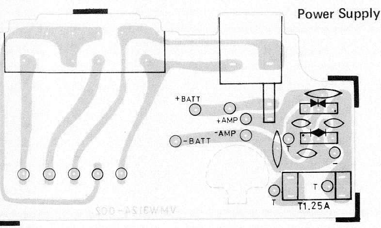
Power Supply P.W. Board Parts List
| Ref. No. | Parts No. | Parts Name | Remarks | Q'ty |
|---|---|---|---|---|
| VMW3124-001 | P. W. Board | 1 | ||
| D801, 802 | DS131A | Si. Diode | 1 | |
| D803, 804 | DS132A | ** | 1 | |
| C801, 802, 803 | QCF11EZ-223 | C. Capacitor | 0.022 μF 25 V | 3 |
| C804, 805 | QCC11EM-154 | ii ii | 0.15 μF ″ | 2 |
| VKL3143-001 | Board in Tab | 2 | ||
| J801 | QMC0263-002BS | AC Socket | RC-656LB | 1 |
| QMC0263-002 | " | RC-656L | 1 | |
| S801-1, 2 | QSS2325-101BS | Slide Switch | RC-656LB | 1 |
| QSS2325-101 | RC-656L | |||
| QMF51A2-1R25BS | Fuse | RC-656LB | 1 | |
| QMF51A2-1R25 | RC-656L | |||
| A44594-001 | Fuse Clip | 2 |
Packing
Instraction Book, etc.
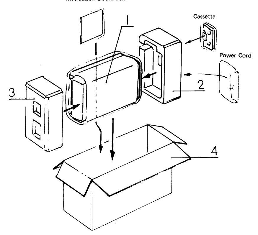
Packing Material Parts List
| Ref. No. | Parts No. | Parts Name | Remarks | Q'ty |
|---|---|---|---|---|
| 1 | VPH4103-002 | Door Protector | 1 | |
| 2 | VPH1213-001 | Side Cushion | Left | | 1 |
| 3 | VPH1214-001 | Side Cushion | Right | | 1 |
| 4 | VPD5066-J01 | Carton | RC-656LB | 1 |
| VPD5066-J03 | 11 | RC-656L | 1 | |
| 2~4 | VDP5066-002A | Carton Ass'y | RC-656L | 1 |
| 5 | QPGA065-05004 | Poly Bag | for set | 1 |
| 6 | VHPJ109-039 | Paper Sheet | 1 |
Accessories
| Parts Name | Remarks | Q'ty |
|---|---|---|
| Cassette Tape | 1 | |
| Power Cord | RC-656LB | 1 |
| RC-656L | 1 | |
| Warning Label | RC-656LB | 1 |
| Poly Bag | for power cord | 1 |
| Feature Sticker | 1 | |
| Mark | RC-656LB | 1 |
| Head Cleaning Stick | 1 | |
| Poly Bag | for Instruction Book | 1 |
| Guarantee Certificate | RC-656LB | 1 |
| Instruction Book | 1 | |
| Troubleshooting | 1 | |
|
Parts Name
Cassette Tape Power Cord " Warning Label Poly Bag Feature Sticker Mark Head Cleaning Stick Poly Bag Guarantee Certificate Instruction Book Troubleshooting |
Parts NameRemarksCassette TapeRC-656LBPower CordRC-656LB"RC-656LBWarning LabelRC-656LBPoly Bagfor power cordFeature StickerRC-656LBMarkRC-656LBHead Cleaning Stickfor Instruction BookGuarantee CertificateRC-656LBInstruction BookTroubleshooting |
JVC SERVCE MANUAL
MODEL RC-656LD
LW - MW - SW - FM
4-BAND STEREO RADIO CASSETTE RECORDER
Please note that the model RC-656LD is the same as RC-656L except relation parts to the enclosure assembly. As the other parts not listed here are the same as those of RC-656L, refer to the service manual (No. 1422) of the model RC-656L/LB.
Assembly Parts List
| Ref. No. | Parts No. | Parts Name | Remarks | Q'ty |
|---|---|---|---|---|
|
(1-8,13,)
(21,22) 1 2 3 4 |
ZCRC656LD-CBF
VJC1225-002 VJD4005-002 VJD4412-002 VJD4413-001 |
Front Cabinet Ass'y
Front Cabinet Reflection Plate Button Plate Fitting |
1
1 1 1 |
|
|
5
6 7 8 10 |
VJK3159-004
VJK3160-003 VJK3161-001 VJK4123-002 VYH4102-001 |
Dial Scale (A)
'' (B) Dial Lens Scale Plate (A) Mic. Bushing |
1
1 1 2 |
|
|
11
12 13 14 15 |
VMME62N-026
VYH4298-001 VJD4018-002 VMW1023-102D QMV5005-003 |
E.C. Mic.
Holder Mark P.W. Board Connector |
for Mic.
CN701-1 ~ 3 |
2
2 1 - 1 |
|
16
17 18 19 20 |
EAS5PH08SA
VYH4565-002 QEN21EM-335 VKY4165-002 VYH4352-002 |
Speaker
Tweeter Holder N.E. Capacitor Door Spring Clamp |
SPK R302
C380, C480 3.3 μF, 25 V for Tweeter |
1
1 2 1 1 |
|
21
22 23 24 25 |
V44981-001
VYH4389-001 VKZ4001-007 EAS16P127SH VYH2122-002 |
Earth Catcher
Wire Holder Speaker Chassis Base |
SPK R301, SPK R401 |
1
1 7 2 1 |
|
26
27 28 29 30 |
VYH4032-001
VYH4002-001 RTA4020 V42562-1 RTA4010 |
Roller
Rivet Special Washer Rivet |
1
4 1 3 1 |
|
|
31
32 33 34 35 |
V41336-021
VJK4124-002 VYH3177-003 RCSA6000 VHR2TT9-05A |
Tuning Shaft
Scale Plate (B) Dial Drum C. Ring Dial Rope |
1005 mm |
1
1 1 1 |
|
36
37 38 39 40 |
E45679-001
VJN4049-00A EAS5PH08SA VYH4352-002 VMW1023-102C |
Spring
Needle Ass'y Speaker Clamp P.W. Board |
SPKR402
for Tweeter for Tuner LED |
1
1 1 - |
| Ref. No. | Parts No. | Parts Name | Remarks | Q'ty |
|---|---|---|---|---|
|
41
42 43 44 45 |
SLP146B
QRD147J-471S "-101S VJH3005-00S VYH3120-001 |
L.E.D.
C. Resistor Handle Ass'y |
D201, D202
R201 R202 |
2
1 1 1 2 |
|
45
46 47 48 49 52 |
V44943-001
V44944-001 VYH4224-001 VYH4556-001 VYH2124-002 |
Washer (L)
" (R) Bracket " Tuner Chassis |
1
1 1 1 1 |
|
|
53
54 55 56 58 |
VXQ3018-006
QAT5001-203 VYH4516-002 VYH4221-001 QET41CR-227 |
Toggle Lever
M.V. Capacitor Fine Tuning Bracket Arm E. Capacitor |
for Band
C702 |
1
1 1 1 |
|
59
61 62 63 64 |
VMW3035-302
VYH2125-002 VYH4567-001 VXQ3028-004 VXQ3032-003 |
P.W. Board
Holder Earth Plate Toggle Lever |
for R/P Head |
1
1 2 1 |
|
65
66 67 68 70 |
VXQ3033-002
VJD3232-001 VJC1226-002 QZR4333-001 VYH4010-002 |
"
Jack Board Rear Cabinet Rod Antenna Battery Contact |
1
1 1 2 |
|
|
71
72 73 74 75 |
53738-009
V44686-002 VYH4568-00B VND4027-005 VYN5066-020C |
Spring
W Shield Ass'y Dolby Label Name Plate |
1
1 1 1 1 |
|
|
76
77 78 79 80, 81 |
V41583-3
VYSA1R4-050 VJT4029-00A V44910-002 ZCRC656LD-BCA |
Tape
Spacer Cassette Door Ass'y Cassette Spring Battery Cover Ass'y |
1
6 1 2 1 |
|
|
80
81 82 83 84 |
VJC2016-006
VYSH106-020 VYSA1R6-009 VXKM520-20013 VXL4008-002 |
Battery Cover
Spacer Knob Tuning Knob |
1
1 4 1 1 |
|
|
85
86 87 88 89 |
VXL4122-002
VXL4123-002 53866-2 VTP54N2-12E VYH4570-003 |
Knob
Label Power Transformer Transformer Bracket |
3
1 1 1 |
|
|
90
91 92 101 102 |
VJD3332-001
VYH4936-001 VJD4508-001 REE3000 WBS3000N |
Punching Panel
Damp Holder Antenna Cover E-Ring Washer |
Chassis Base
P.W.B. – Mecha. |
1
1 1 1 1 |
|
103
104 105 |
DPSP3006ZS
SBSF3008Z SBSF3010Z |
Ass'y Screw
Tapping Screw " |
Trans. Bracket
E.C. Mic. Holder x 2, Mic. Wire Terminal x 1, Tweeter x 2, Earth Catcher x 1, Woofer x 8, L.E.D. P.W.B. x 1, Connect Bracket x 2, Holder (B) x 4 Tweeter Holder – Front Cabinet x 2, Door Spring x 1 Chassis Ass'y – Front Cabinet x 5, Dump Ass'y x 2, Tuper Chassis – P.W.B. x 2, Eine Tuming Bracket x 1 |
2
21 17 |
| 106 | SBSE2012C | Holder – P.W.B. x 2, Jack Board – P.W.B. x 2 | Q | |
|
107
108 100 |
SBSF 3012C
SBSF3020R SBSF4020C SDSP3010PS |
Arm Ass'y – Front Cabinet x 5,
Front Cabinet – Rear Cabinet Trans. Bracket Eront Cabinet – Bear Cabinet x 2, Bracket x 4 |
626 | |
|
110
111 112 113 |
SPSP3006VS
SPSP3012VS SPSP3014ZS SPSP3014ZS SPSP3035VS SPSP3035VS |
Screw |
P.W.B. – Mecha.
Bracket P.W.B. – Mecha. |
2
1 2 1 |
| 114 | SDSP3010RS | Screw | Front Cabinet – Rear Cabinet | 2 |
8C-656LD PC 656LD
10
Unit-Volt
Pin
No.
FM AM FM/AM
18 12
1.8
65
21
23
5.8
-
ST/MONO
Signal
Signal
AM
Signal FM
Signal Signa FM No
Signa FM Signal AM No
AM
0.8
- ICH
- 4 -
3) LAST NO. FOR RESISTORS AND CAPACITORS ARE R95 & C97.
Tuner P.W. Board Parts List
| Ref. No. | Parts No. | Parts Name | Remarks | Qʻty |
|---|---|---|---|---|
| IC1 | HA12413 | I.C. | 1 | |
| IC2 | AN7410N | 1 | ||
| BPF1 | VBP1M3F-001 | B.P. Filter | 1 | |
| X1 | 2SK212(E) | Transistor | ||
| X2 | 2SC1342(B) | |||
| X3 | 2SC535(B) | 1 | ||
| 2SC2839(D) | ||||
| 2SC1684(R S) | 3 | |||
| X8. 10. 11 | 2SC458(C) | 3 | ||
| D2 | HV80 | Si. Diode | 1 | |
| D5 | 1N34A | Ge. Diode | 1 | |
| L1 | VQF1B20-001 | Coil | 1 | |
| L2 | VQP0004-R68 | Inductor | 1 | |
| L4, 6 | VQB012B-302 | Bar Antenna | ||
| VQF1B20-001 | SW | |||
| VOI 1T03-301 | ||||
| -301 | " | MW | 1 | |
| VQS1T03-205 | " | SW | 1 | |
| IFT1 | VQT7F12-104 | I.F.T. | IFT | 1 |
| IFT2 | VQT7F07-501 | FM | 1 | |
| IFT3 | VQT7A11-301 | " | AM | 1 |
| CFT1 | V03067-026 | C.F.T. | AM | 1 |
| VYH4369-003 | Shield | |||
| VYH4728-002 | Shield Plate | 1 | ||
| VBP1M3F-001 | B.P. Filter | 1 | ||
| VCE2L3B-102 | 2 | |||
| VC1-1 4. VC2-1 4 | QAP1224-512 | V. Capacitor | 1 | |
| TC3-1, 2, TC2-1, 2 | QAT2002-001 | T. Capacitor | 2 | |
| S1-1 10 | QSSA401-002 | Slide Switch | 1 | |
| CN1-1 3, CN3-1 3 | QMV5005-003 | Connector | 2 | |
| CN2-1 5 |
-005
0 AD1224 512 |
V. Capacitor | ||
| 0V72512 102 | V. Capacitor | 1 | ||
| 0VP8A0B-053 | 1 | |||
| R1 | ORD147.J-220S | C. Resistor | 22 Ω 1/4 W | 1 |
| R2 | -470S | " | 47 Ω ″ | 1 |
| R3, 37 | " -682S | " | 6.8 kΩ " | 2 |
| R4, 23, 28 | " -392S | " | 3.9 kΩ " | 3 |
| R5, 13 | " -152S | 1.5 kΩ " | 2 | |
| R6 | ······································ | |||
| -8245 | 330 Ω " | |||
| R15 19 42 40 57 |
-3313
"_470S |
" | 47 Ω " | 5 |
| R16 |
-4705
" -181S |
180 Ω " | 1 | |
| R17, 40 | ······································ | " | 27 kΩ ″ | 2 |
| R19, 27 | " -101S | " | 100 Ω " | 2 |
| R21, 45 | " -221S | " | 220 Ω " | 2 |
| R22 | " -334S | | 330 kΩ " | ||
| R24, 31 | -182S | 2 | ||
| -5625 | 2 | |||
| R33 46 53 55 | -3325 | 10 kΩ " | 4 | |
| R34 | ORD1431-2229 | 22kΩ " | 1 | |
| R36 | QRD147J-393S | " | 39 kΩ " | 1 |
| R41 | -153S | 15 kΩ ″ | | 1 | | |
| R47 | " -222S | " | 2.2 kΩ " | | 1 | |
| | R54 | QRD143J-224S | 220 kΩ ″ | 1 |
| Ref. No. | Parts No. | Parts Name | Remarks | Q'ty |
|---|---|---|---|---|
| R71 | QRD143J-102S | C. Resistor | 1 kΩ 1/4 W | 1 |
| B81 | QRD147J-100S | " | 10 Ω ″ | | 1 |
| B82 | " -183S | " | 18 kΩ ″ | | 1 |
| B83 | " -102S | " | 1 kΩ ″ | 1 |
| R85, 86 | " -272S | 2.7 kΩ ″ | 2 | |
| B87 88 | " -472S | 4.7 kΩ ″ | 2 | |
| B89 90 | " -271S | " | 270 Ω ″ | 2 |
| B91 92 | ″ -684 S | " | 680 kΩ ″ | 2 |
| R03 04 | " -8225 | " | 8.2 kΩ ″ | 2 |
| B96 | ORD143J-334S | " | 330 kΩ ″ | 1 |
| C1 12 | OCT05CH-220 | C. Capacitor | 22 pF 50 V | 2 |
| OCE11E7-103 | 0.01 µF 25 V | 4 | ||
| 3 nF 50 V | li | |||
| -780 | ,, | 10 pF " | 1 | |
| 220 mE // | 2 | |||
| QCS11HJ-331 | ||||
| C7, 8, 33, 45, 56, 61, 67 | QCF11EZ-223 | |||
| C14, 21 | QCS11HJ-150 | |||
| C15 | QCT05CH-120 | |||
| _C20, 32 | QCS11HJ-3R0 | 3 pF | 2 | |
| C22, 30 | " -390 | " | | 39 pF " | 2 |
| C23 | ··· -100 | " | | 10 pF " | 1 |
| C24, 25 | " -8R0 | • " | |8pF " | | 2 |
| C26 | // ·270 | " | | 27 pF | | 1 |
| C28 | QFS21HJ-392 | " | 0.0039 μF ″ | 1 |
| C29 | QCT05WK-120 | " | 12 pF | | 1 |
| C31 | QFS21HJ-181 | P. Capacitor | 180 pF 50 V | | 1 |
| C34, 55 | QET41AR-227 | E. Capacitor | | 220 μF 10 V | | 2 |
| C36, 42, 43 | QCF11EZ-473 | C. Capacitor | 0.047 μF 25 V | 3 |
| C41 | QCY41HK-472 | 0.0047 μF 50 V | 1 | |
| C44 69 93 94 | OET41HR-475 | E. Capacitor | 4.7 μF " | 4 |
| C46 | OET41AB-107 | 100 µF 10 V | 1 | |
| C51 | OFT41CB-106 | " | 10 µF 16 V | 1 |
| C52 53 54 | OFM41HM-223 | " | 0.022 μF 50 V | 3 |
| C57 | OCC11EM-223 | " | 0.022 μF 25 V | 1 |
| C63 | OFT41CB-226 | 22 µF 16 V | 1 | |
| 0CC11EM-103 | " | 0.01 µF 25 V | 2 | |
| C66 | OET41AB-476 | " | 47 µF 10 V | 1 |
| 00511HJ-151 | C Capacitor | 150 pF 50 V | 3 | |
| C71 | OFT41HB-105 | E. Capacitor | 1 µF " | 1 |
| C81 88 80 01 02 | " | " | 33 µ F " | 5 |
| 692 | P. Capacitor | 470 pF " | ||
| OEC41HM-474 | 0.47 // E " | |||
| OEM/1UM /72 | M Capacitor | 0.047 //F " | ||
| .152 | 0.015 µF " | 2 | ||
| C. Capacitor | 5.010 ml | 1 | ||
| 695 | UCSTIHJ-SKO | C. Capacitor | 5 PF |


 Loading...