Page 1

Single Supply Single Operational Amplifier
with Full Swing Output
■GENERAL DESCRIPTION
The NJM2741 is a low supply voltage operational amplifier with Full
swing output.
It is suitable for audio section of portable sets, PCs and any
General-purpose use.
■ FEATURES
●Operating Voltage :2.5V to 14V
●Output Full Swing : V
: V
●Offset Voltage :1mV Typ
●Slew Rate : 3.5V/µs Typ.
. ●Low Distortion : 0.001% typ. (at V
. ●Low Input Voltage Noise :10nV/√Hz typ.
●Bipolar Technology
●Package Outline : MTP5, SC88A
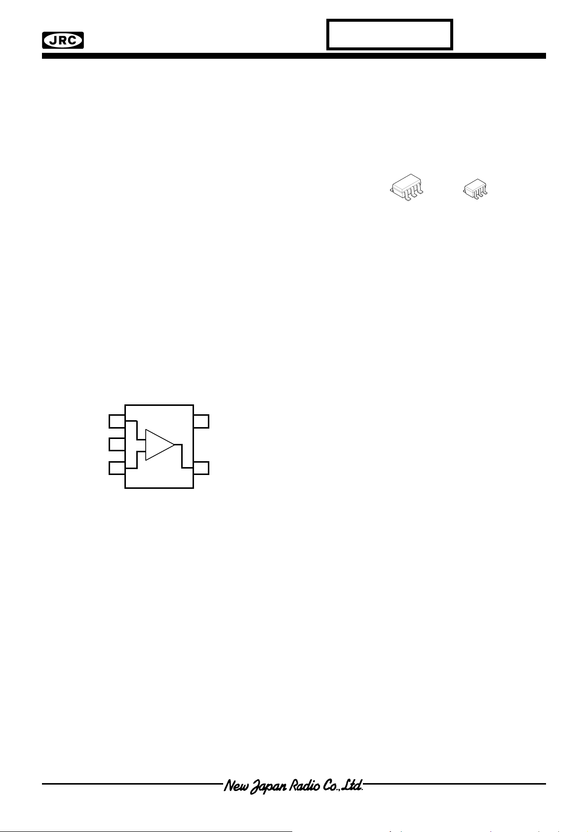
■ PIN CONFIGURATION
1
2
3
NJM2741F
NJM2741F3
++++
−−−−
(Top View)
≥4.9V Typ. (at V+=5V, RL=5kΩ)
OH
≤0.1V Typ. (at V+=5V, RL=5kΩ)
OL
+
=5V, f=1kHz)
PIN FUNCTION
5
4
1. +INPUT
2. GND
3. -INPUT
4. OUTPUT
+
5. V
Preliminary
■PACKAGE OUTLINE
NJM2741F NJM2741F3
NJM2741
Ver.2004-11-26
-1-
Page 2

,
e
w
e
NJM2741
Preliminary
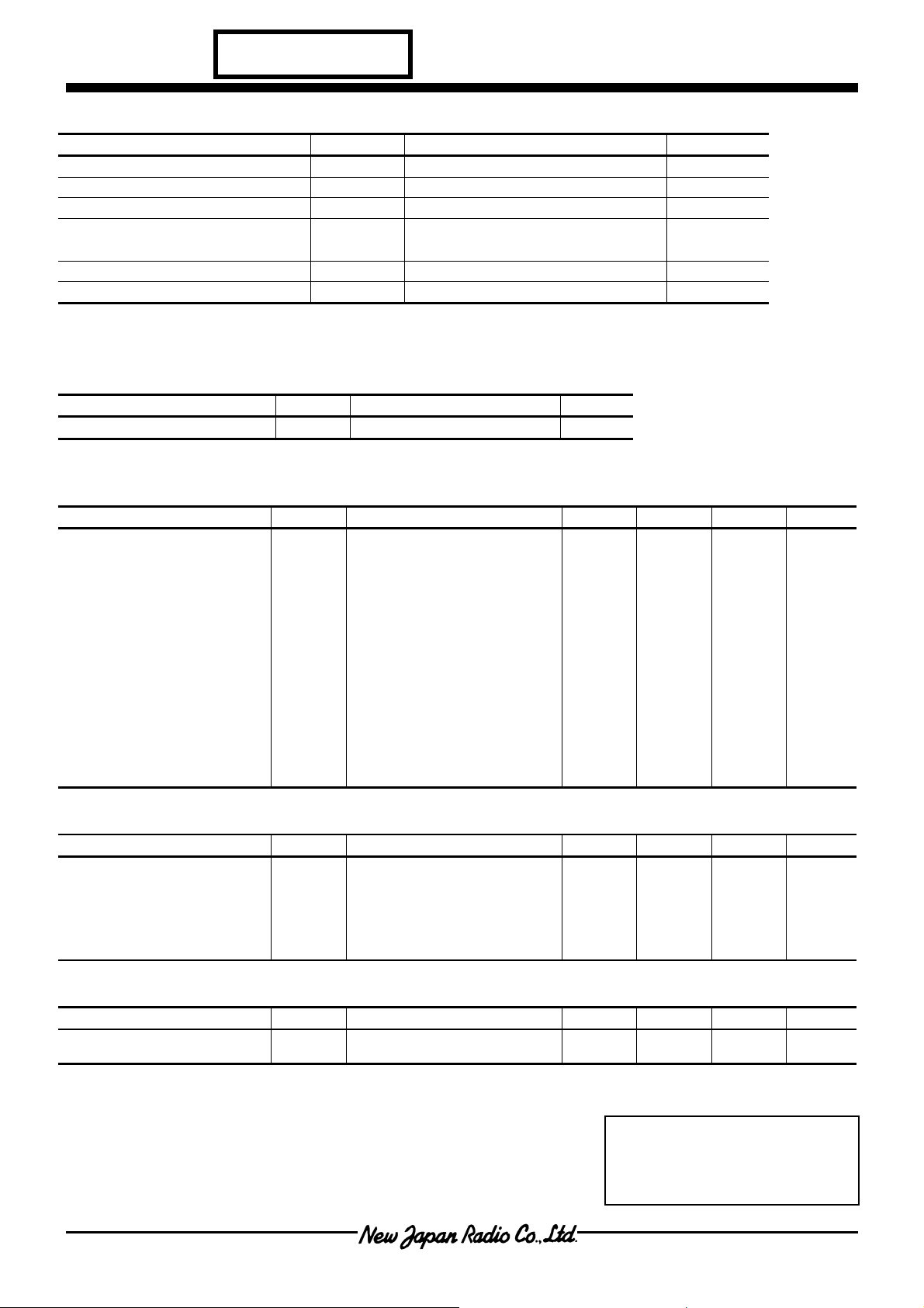
■ ABSOLUTE MAXIMUM RATINGS
PARAMETER SYMBOL RATINGS UNIT
Supply Voltage V+ 15 V
Differential Input Voltage Range VID ±15 (Note1) V
Common Mode Input Voltage Range V
Power Dissipation PD
Operating Temperature Range T
Storage Temperature Range T
0 to 15 (Note1) V
ICM
390[MTP5] (Note2)
280[SC88A] (Note2)
-40 to +85 ˚C
opr
-50 to +125 ˚C
stg
mW
(Note1) For supply voltage less than 15V, the absolute maximum input voltage is equal to the supply voltage.
(Note2) On the PCB “ EIA/JEDEC (76.2×114.3×1.6mm, two layers, FR-4) “
■ OPERATING VOLTAGE (Ta=25˚C)
PARAMETER SYMBOL RATINGS UNIT
Supply Voltage
+
V
2.5 to 14 V
■ ELECTRICAL CHARACTERISTICS
●DC CHARACTERISTICS (V
PARAMETER SYMBOL TEST CONDITION MIN. TYP. MAX. UNIT
Operating Current ICC
Input Offset Voltage VIO R
Input Bias Current IB - 100 350 nA
Input Offset Current IIO - 5 100 nA
Large Signal Voltage Gain AV R
Common Mode Rejection Ratio CM R 0 V ≤ VCM ≤ 4V 60 75 - dB
Supply Voltage Rejection Ratio SV R V+=2.5V to 14V, VCM=V+/2 60 80 - dB
Input Common Mode
Voltage Range
+
=5V,Ta = 2 5 ˚C)
=∞, V
R
L
No Signal Apply
≥10kΩ to 2.5V,
L
Vo=0.5V to 4.5V
VOH R
R
V
OL
V
CMR ≥ 60dB 0 - 4 V
ICM
L
L
=2.5V,
IN
≤ 10kΩ - 1 6 mV
S
- 2.2 3.3 mA
65 85 - dB
=5kΩ to 2.5V 4.75 4.9 - V Output Voltage
=5kΩ to 2.5V - 0.1 0.25 V
+
●AC CHARACTERISTICS (V
=5V,Ta = 2 5 ˚C)
PARAMETER SYMBOL TEST CONDITION MIN. TYP. MAX. UNIT
Unity Gain Bandwidth GB
Phase Margin ΦM
Equivalent Input Noise Voltage VNI
Total Harmonic Distortion T H D
f=10kHz, R
R
=10kΩ to 2.5V, CL=10pF
L
=10kΩ to 2.5V, Vo=1.5Vrms
R
L
L
f=1kHz, V
f=1kHz, A
=10kΩ to 2.5V
=2.5V
CM
=+2
V
- 10 - MHz
- 75 - Deg
- 10 - nV/√Hz
- 0.001 - %
+
●AC CHARACTERISTICS (V
=5V,Ta = 2 5 ˚C)
PARAMETER SYMBOL TEST CONDITION MIN. TYP. MAX. UNIT
Slew Rate SR (Note 3), AV=1, VIN=2Vpp
=10kΩ to 2.5V, CL=10pF
R
L
- 3.5 - V/µs
(Note 3) Number specified is the slower of the positive and negative slew rates.
[CAUTION]
The specifications on this data book are only given for information
without any guarantee as regards either mistakes or omissions. Th
application circuits i n this data book are described only to sho
representative usages of the produ ct and not intended for th
guarantee or permission of a ny right including the industrial rights.
- 2 -
Ver.2004-11-26
 Loading...