

Page 1
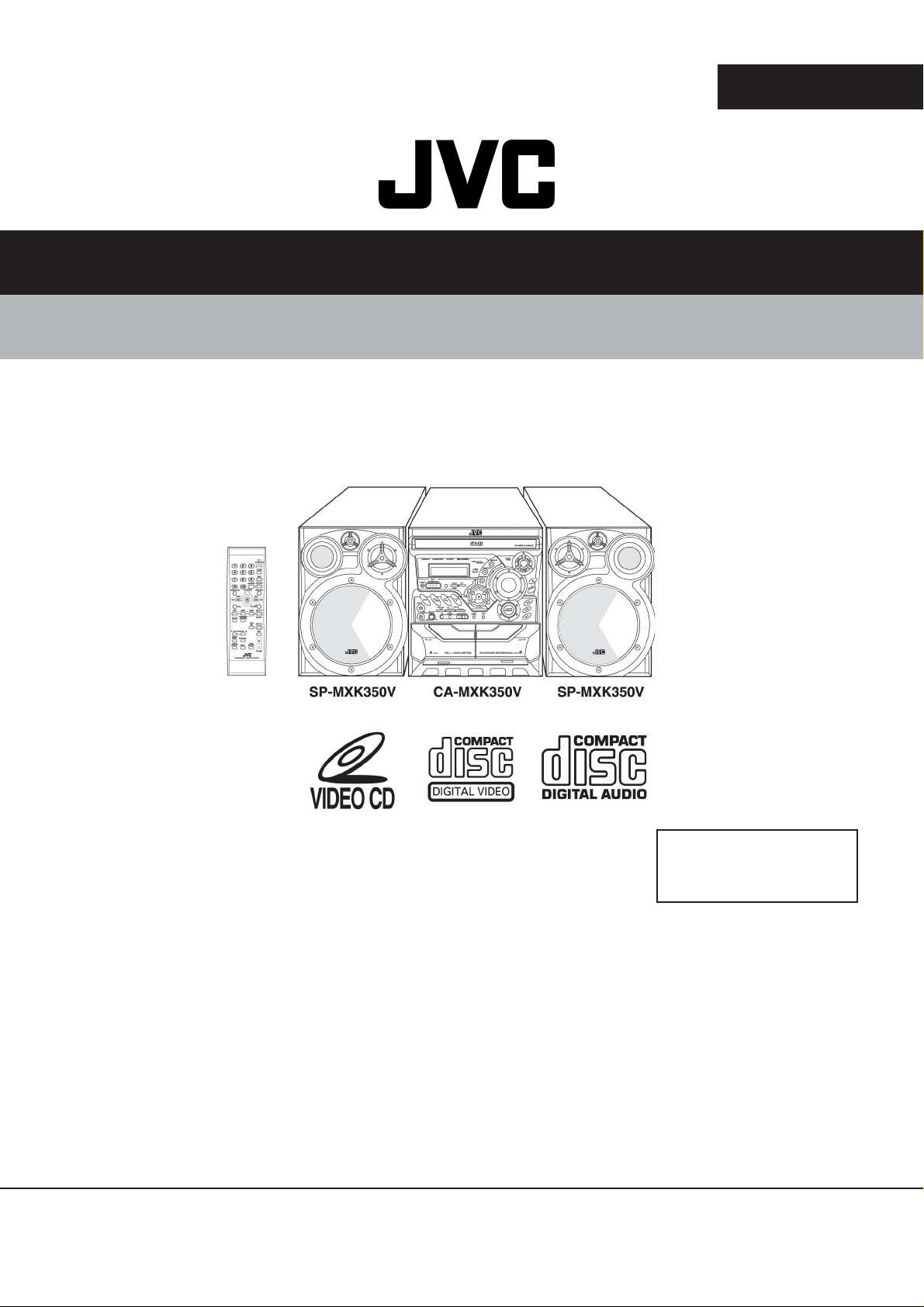
SERVICE MANUAL
COMP ACT COMPONENT SYSTEM
MX-K350V
MX-K350V
Contents
Safety precautions ----------------------------- 1- 2
Important f or la ser products ------------------ 1- 3
Preventing static electricity------------------- 1- 4
Disa ssembly method -------------------------- 1- 5
Adjustment method --------------------------- 1-18
COPYRIGHT © 2001VICTOR COMPANY OF JAPAN, LTD.
Area Suffix
..................
US
..................
UX
Flow of functional
operation until TOC read --------------- 1-20
Maintena nce of la ser pickup ---------------- 1-21
Repla cement of la ser pickup---------------- 1-21
Description of ma jor ICs --------------------- 1-22
SINGAPORE
SAUDI
No.21166
Dec.2002
Page 2
Safety Precautions
1. This design of this product contains special hardware and many circuits and components specially or
safety purposes. For continued protection, no changes should be made to the original design unless
authorized in writing by the manufa cturer . Replace ment parts must be identical to those used in the original
circuits. Services should be performed by qualified personnel only .
2. Alterations of the design or circuitry of the product should not be made. Any design alterations of the
product should not be made. Any design alterations or addition s will void the manufa cturer`s warranty a nd
will further relieve the manufa cture of responsibility for personal in jury or property damage resulting therefrom.
3. Many electrical and mechanical parts in the products have special safety-related characteristics. These
characteristics are often not evident from visual inspection nor can the protection afforded by them
necessarily be obtained by using replacement components rated for higher voltage, wattage, etc.
Replac ement parts which have these special safety chara cteristics are identified in the Parts List of Service
Manual. Electrical components having such fe atures are identified by shading on the schematics a nd by
( ! ) on the Parts List in the Service Ma nual. The use of a substitute repla cement which does not have the
same safety characteristics as the recommended replacement parts shown in the Parts List of Service
Manual may create shock, f ire, or other hazards.
4. The leads in the products are routed and dressed with ties, clamps, tubings, barriers and the like to be
separated from live parts, high temperature parts, moving parts and/or sharp edge s for the prevention
of electric shock and f ire hazard. When service is required, the origin al lead routing a nd dre ss should
be observed, and it should be confirmed that they have been returned to normal, after re-a sse mbling.
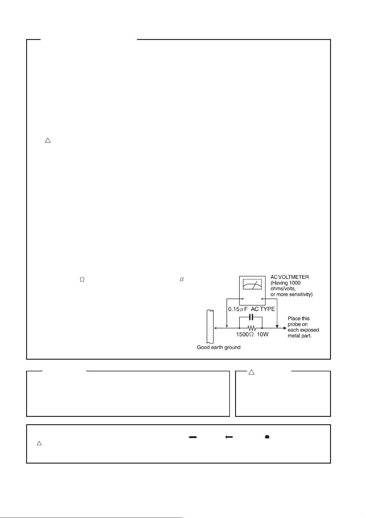
5. Leakage currnet che ck (Electrical shock hazard testing)
After re-assembling the product, always perform an isolation check on the exposed metal parts of the
product (antenna termin als, knobs, metal cabinet, screw heads, hea dphone ja ck, control shafts, etc.) to
be sure the product is safe to operate without danger of electrical shock. Do not use a line isolation
trans former during this check.
l Plug the AC line cord directly into the AC outlet. Using a “ Leakage Current Tester ”, measure the
leak age current from ea ch exposed metal parts of the ca binet, particularly a ny exposed metal part
having a return path to the chassis, to a known good earth ground. Any leakage current must not
exceed 0.5mA AC (r.m.s.)
l Alternate check method
Plug the AC line cord dire ctly into the AC outlet. Use a n AC voltmeter having, 1,000 ohms per volt
or more sensitivity in the following ma nner. Connect
a 1,500
10W resistor paralleled by a 0.15
AC-type capacitor between an exposed metal
part and a known good earth ground. Mea sure the
AC voltage across the resistor with the AC
voltmeter.
Move the resistor connection to ea ch exposed metal
part, particularly any exposed metal part having a
return path to the chassis, and meausre the AC
voltage across the resistor . Now, reverse the plug in
the AC outlet a nd repeat ea ch measurement. V oltage
mea sured Any must not exceed 0.75 V AC (r.m.s.).
This corresponds to 0.5 mA AC (r.m.s.).
F
Warning
1. This equipment ha s been designed and ma nufactured to meet international safety sta ndards.
2. It is the legal responsibility of the repairer to ensure that these safety standards are maintained.
3. Repairs must be made in accorda nce with the relevant safety sta ndards.
4. It is essential that safety critical components are repla ced by approved parts.
5. If mains voltage selector is provided, check setting for local voltage.
In regard with component parts appearing on the silk-screen printed side (parts side) of the PWB diagrams, the
parts that are printed over with black such as the resistor ( ), diode ( ) and ICP ( ) or identified by the
!
“
”mark nearby are critical for safety.
When replacing them, be sure to use the parts of the same type and rating as specified by the manufacturer.
(Except the J and C version)
! CAUTION
Burrs formed during molding may
be left over on some parts of the
chassis. Therefore, pay attention
to such burrs in the case of
preforming repair of this system.
1-2
Page 3
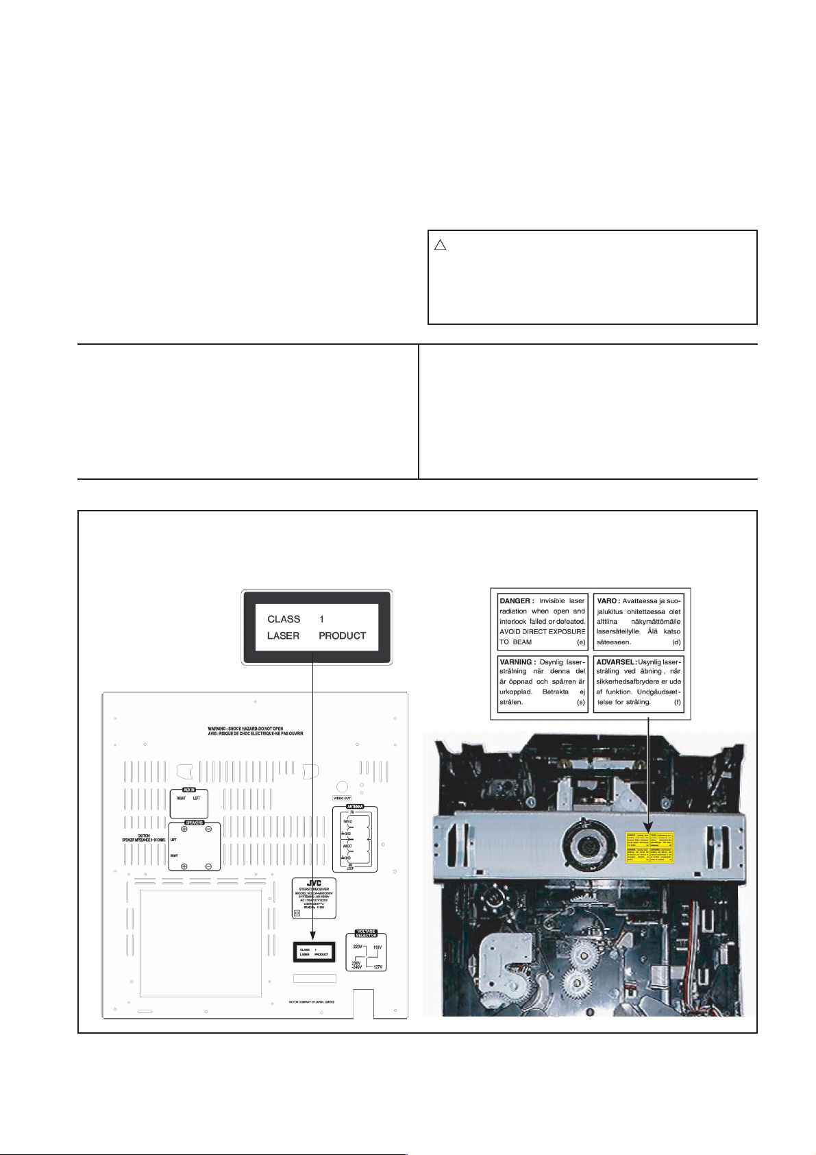
Important for laser products
1. CLASS 1 LASER PRODUCT
2. DANGER : Invisible laser radiation when open and inter
lock failed or defeated. Avoid direct exposure to beam.
3. CAUTION : There are no serviceable parts inside the La ser
Unit. Do not disassemble the Laser Unit. Replace the
complete Laser Unit if it malfunctions.
4. CAUTION : The compact disc player uses invisible laser
radiation and is equipped with safety switches which
prevent emission of radiation when the drawer is open
and the safety interlocks have failed or are defeated. It is
dangerous to defeat the safety switches.
VARNING : Osynlig laserstrålning är denna del är
öppnad och spårren är urkopplad. Betrakta
ej strålen.
VARO : Avattaessa ja suojalukitus ohitetta essa olet
alttiina näkymättömälle lasersäteilylle. Älä
katso säteeseen.
5. CAUTION : If safety switches malfunction, the la ser is able
to function.
6. CAUTION : Use of controls, adjustments or performa nce of
procedures other than those specified herein may result
in hazardous radiation exposure.
! CAUTION Please use enough caution not to
see the bea m directly or touch it in
case of a n adjustment or operation
check.
ADVARSEL : Usynlig laserstråling ved åbning, når
sikkerhedsafbrydere er ude af funktion.
Undgå udsættelse for stråling.
ADVARSEL : Usynlig laserstråling ved åpning, når
sikkerhetsbryteren er avslott. Unngå
utsettelse for stråling.
REPRODUCTION AND POSITION OF LABELS
W ARNING LABEL
1-3
Page 4
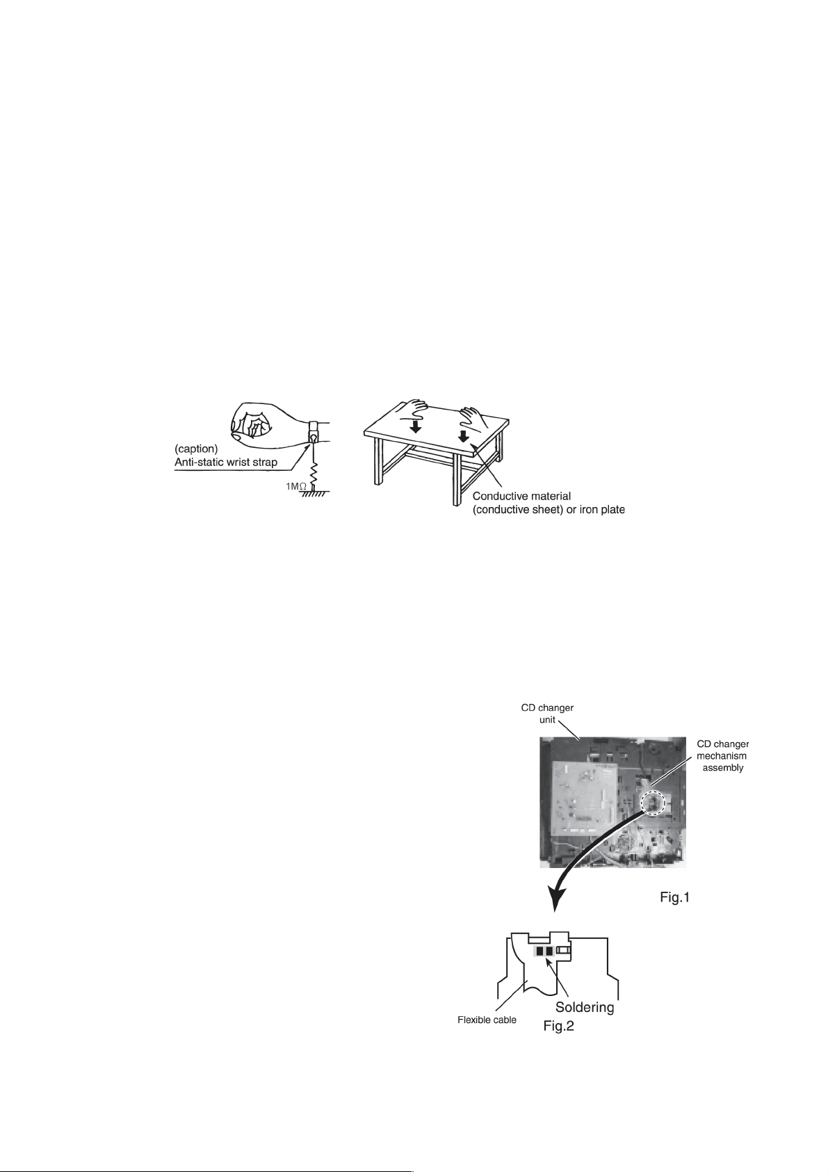
Preventing static electricity
1. Grounding to prevent da mage by static electricity
Electrostatic discharge (ESD), which occurs when static electricity stored in the body, fabric, etc. is
discharged, can destroy the laser diode in the traverse unit (optical pickup). T ake care to prevent this
when performing repairs.
2. About the e arth processing for the de struction prevention by static electricity
In the equipment which uses optical pick-up (laser diode), optical pick-up is destroyed by the static
electricity of the work environment.
Be careful to use proper grounding in the area where repairs are being performed.
2-1 Ground the workbench
Ground the workbench by laying conductive material (such as a conductive sheet) or an iron plate
over it before placing the traverse unit (optical pickup) on it.
2-2 Ground yourself
Use an anti-static wrist strap to release any static electricity built up in your body.
3. Handling the optical pickup
1. In order to maintain quality during transport and before installation, both sides of the laser diode on the
replace ment optical pickup are shorted. After re pla cement, return the shorted parts to their original condition.
(Refer to the text.)
2. Do not use a te ster to check the condition of the la ser diode in the optical pickup. The testers internal power
source can easily destroy the laser diode.
4. Handling the CD cha nger unit (optical pickup)
1. Do not subject the CD changer unit (optical pickup) to strong shocks, as it is a sensitive, complex unit.
2. Cut off the shorted part of the flexible cable using nippers, etc. after replacing the optical pickup. For specific
details, refer to the replacement procedure in the text.
Remove the anti-static pin when replacing the CD changer
unit. Be careful not to take too long a time when atta ching it
to the connector.
3. Handle the flexible cable carefully as it may break when
subjected to strong force.
4. It is not possible to adjust the semi-fixed resistor that adjusts the la ser power. Do not turn it.
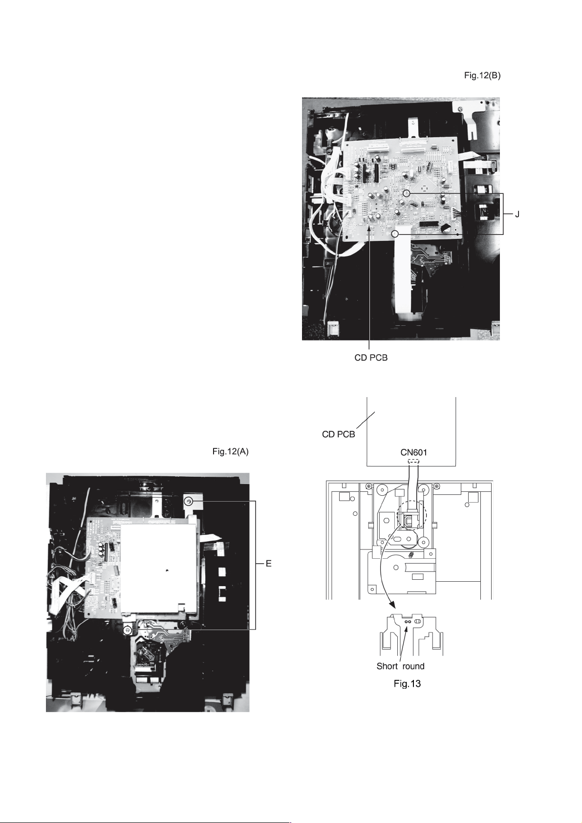
Attention when traverse unit is decomposed
* Please refer to “Disassembly method ” in the text for pick
up and how to detach the CD changer mechanism.
1. Remove the CD cha nger unit.
2. Disconnect the harness from connector on the CD motor board.
3. Solder is put up before the card wire is removed from connector
Cn601on the main board as shown in Fig.1 a nd Fig. 2.
(When the wire is removed without putting up solder, the CD
pick-up asse mbly might destroy .)
4. Please remove solder after connecting the card wire with CN601
when you install picking up in the substrate.
1-4
Page 5

Disa ssembly method
Commence disassembly of this set by re moving the main units and then proceed to the components a nd a ssemblies
inside the units.
Replacement of the fuses a nd the power IC
n Top cover
n CD changer unit
n Front panel a ssembly
n Cha ssis unit
n CD changer unit
n Removing the main PCB
n Removing the CD cha nger me chanism assembly
n Removing the CD pickup
n Repla cing the loa ding motor and belt of the CD changer tray
n Repla cing the CD tray rotor belt of CD changer, and re moving the motor
n Front panel a ssembly
n Removing the cassette deck mechanism
n Removing the earphone jack PCB
n Removing the control/FL PCB
n Removing the switch PCB and ACTIVE BASS EX. switch PCB
n Removing the cassette deck main motor, and re placing the main belts
n Removing the le af switche s of the cassette deck mechanism
n Removing the cassette deck heads
n Chassis unit
n Removing the 3-pin regulator
n Removing the power amp and supply PCB and the Power Trans PCB
n Removing the sub power PCB
1-5
Page 6
<Disasse mbly of the main blocks of this set>
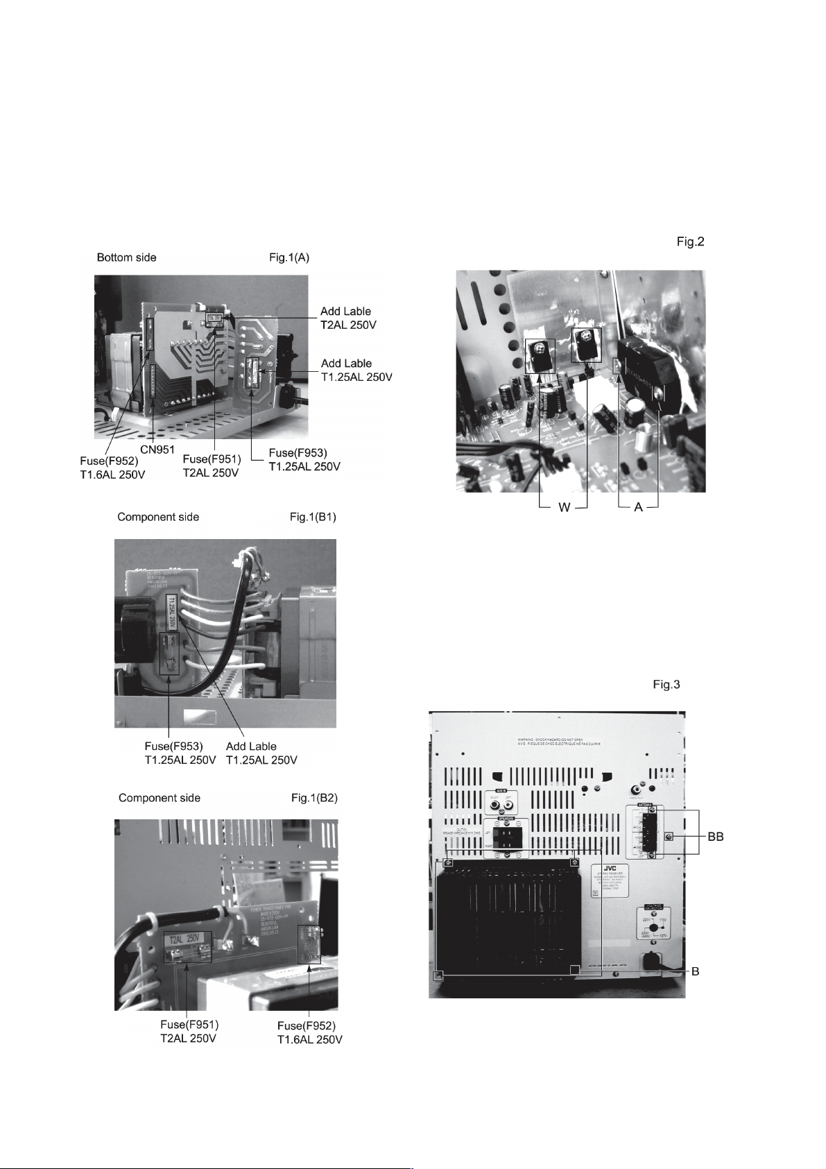
Repla ce ment of the fuse s and the power IC
n Re pla cing the fuse s (See Fig.1, Fig.3)
n Prior to performing the following procedure, remove
the left side BOARD and remove tuner PCB (Fig.3,BB)
1. Replace the fuse s inside.
[Caution] Be sure to use fuses with the specified ratings.
n Re placing the power IC (See Fig.2 )
n Prior to performing the following procedure, remove
the top cover.
1. Remove the two screws “A ” from the heat sinkbetween
the power IC.
2. Remove the solder fixing the power IC.
n Replacing the heat sink cover
1. Remove the six screws from the back pa nel.
2. Pull the heat sink cover outward.
1-6
Page 7
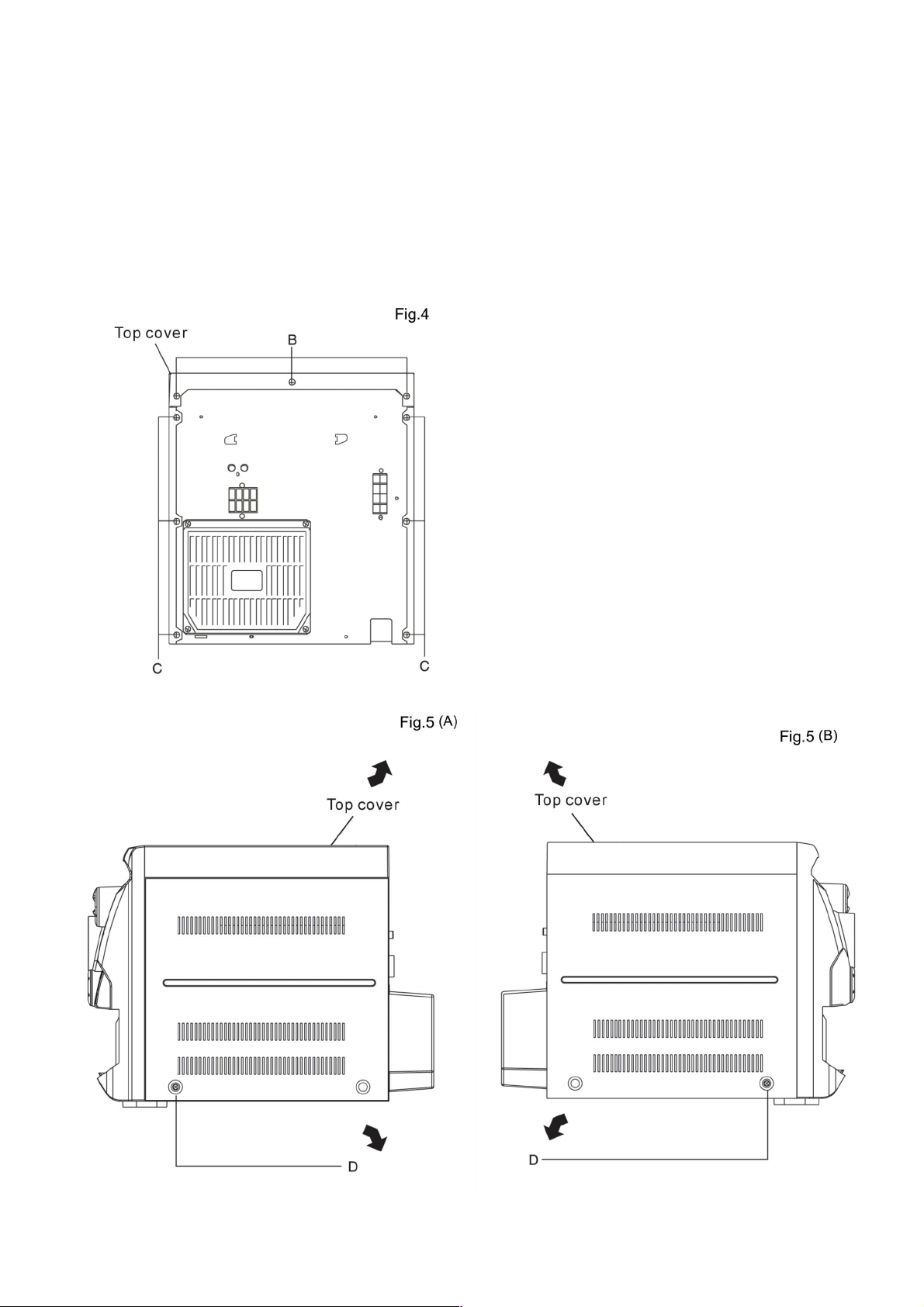
n Removing the top cover and two sides
BOARD (See Fig.4 and 5)
1. Remove the six screws “B ” that retain the top cover
from the rear of the body .
2. Remove the eight screws “ C ” and “D ” that retain the
top from the two sides of the body .
3. Remove the top cover from the body by lifting it toward
the rear .
1-7
Page 8
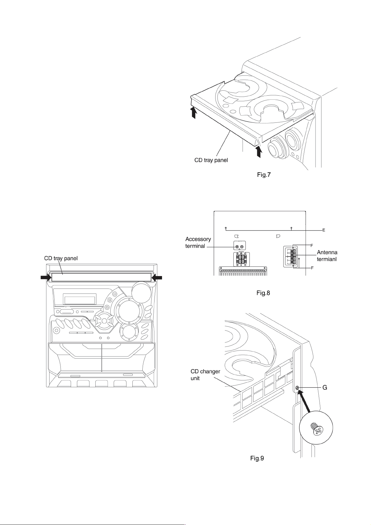
n Removing the CD changer unit
(See Fig.6 and 9)
n
Prior to performing the following procedures, remove
the top cover and both sides BOARD.
[Caution] Although the CD mechanism unit can be
removed without removing the CD tray
panel, it is still recommended to remove it
in order to prevent da mage.
a. From the front pa nel side of this set, push in the sections
marked with arrows and pull out the CD tray toward
the front.
b. Remove the CD tray panel by pushing both of its
extremities upward in the direction of the arrows.
c. Push the CD tray deep into the set.
1. Disconnect the card wires from the CD PCB CN704,
CN607, CN1 101 and disconnect CN1 (shield wire) from
back pa nel.
2. From the rear of the set, remove the two screws “ E ”
and two serews “G ” on the front panel left and right
side.
3. Handle the CD changer unit re ar , take out unit.
1-8
Fig.6
Page 9
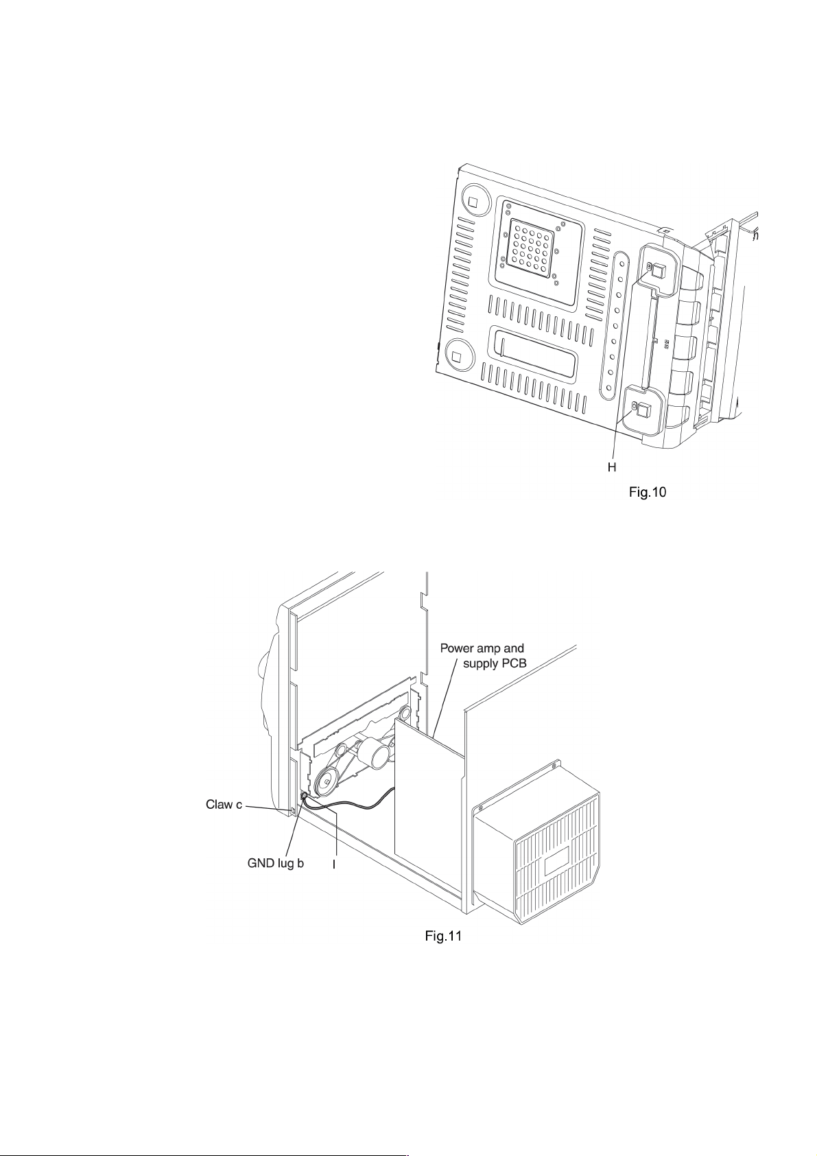
n Removing the front pa nel a sse mbly
(See Fig.10 and 11)
n
Prior to performing the following procedures, remove
the top cover and both sides board.
n
Also remove the CD changer unit.
1. Disconnect the parallel wire and card wire from the
connectors CN702, CN701, CN703, CN850 on the
power amp a nd supply PCB.
2. Remove the two screws “ H ” retaining the front panel
asse mbly onto the bottom of the body.
3. Remove the screw “ I ” retaining the cassette deck
mechanism a nd then remove then GND lug “ b ” that
comes from the power a mp and supply PCB.
4. Disengage the claws “c ” on both sides at the bottom
of the front panel assembly and then remove the
assembly.
1-9
Page 10
<Disassembly of units and assembly inside
this set>
n Removing the CD PCB
(See Fig.12 and 13)
n
Prior to performing the following procedures, remove
the top cover and both sides board.
n
Also remove the CD changer unit.
1. The two screws “E ” that retain the VCD assembly
should be removed.
2. Disconnect the wires from CN602, CN603, CN604
and CN605 on the CD PCB, which is located on the
back side of the CD cha nger unit.
3. The two screws “ J ” that retain the CD PCB should be
removed.
4. Remove the CD PCB by pulling it toward the side where
the CN601 is located.
5. Using solder, short the CD pickup to connect to short
round.
[Caution] After re-connecting the wires, be sure to
remove the shorting solder from the GND connection.
6. Disconnect the card wire from the connector CN601
on the main PCB and then remove the main PCB.
1-10
Page 11
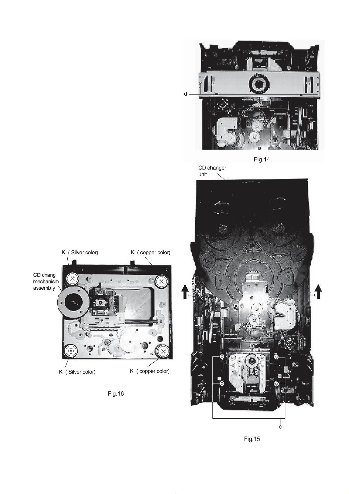
n Removing the CD changer mechanism
assembly (See Fig.14 and 16)
n
Prior to performing the following procedures, remove
the top cover and both sides board.
n
Also remove the CD changer unit.
1. Remove the screws “ d ” from the front chuch base of
the CD changer mechanism unit.
2. Turn the CD changer mecha nism cover base a nd remove
the screws “ e ” connecting the unit to the CD cha nger
mechanism a ssembly .
3. Removing the four screws “ k ” retaining the CD
mechanism holder a ssembly .
[Caution] When replacing the CD changer mecha nism
assembly, be sure not to mistake the
positions of the silver color and copper color
spring.
1-11
Page 12
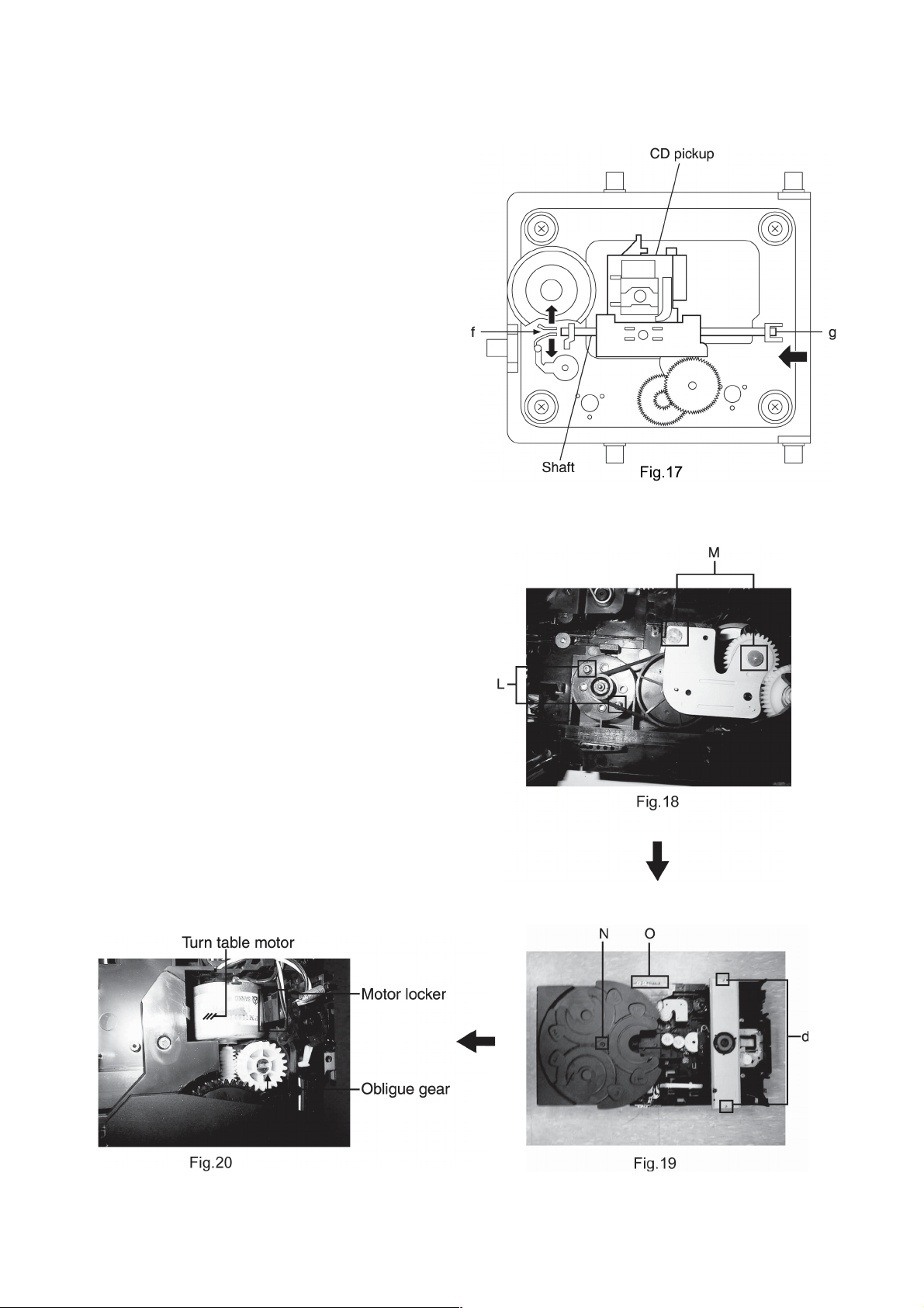
n Removing the CD PCB (See Fig.17)
n
Prior to performing the following procedures, remove
the top cover and both sides board.
n
Also remove the CD changer unit.
n
Also remove the CD cha nger mecha nism.
1. Widen the section “ f ” .
2. While keeping the section “ f ” wide open, push the
section “g ” in the direction of the arrow to remove the
shaft, and then remove the CD pickup.
n Repla cing the loading motor and rotor belt
of the CD changer (See Fig.18)
n
Prior to performing the following procedure, remove
the top cover.
n
Also open the CD changer tray.
1. Remove the two screws “L ” retaining the CD cha nger
tray loading motor .
2. Remove the two screws “M ” retaining the gear plate
and take it out, after remove the rotor belt from the
pulley.
n Re placing the CD turn table a nd removing
the motor (See Fig. 19 and 20)
n
Prior to performing the following procedures, remove
the top cover.
n
Also remove the CD changer unit.
1. Remove the one screws “ N ” retaining the CD (Turn
table).
2. Remove the two screws “ O ” retaining the stopper
brackets on both sides of the CD cha nger unit.
3. Remove the stopper brackets from both sides of the
CD cha nger unit.
4. Pull out the CD tray from the CD changer unit, all the
way and lift the tray (u/~ ward) to remove.
5. Remove the gear and after push out the tray motor
locker and pull out the tray motor from the CD tray.
1-12
Page 13
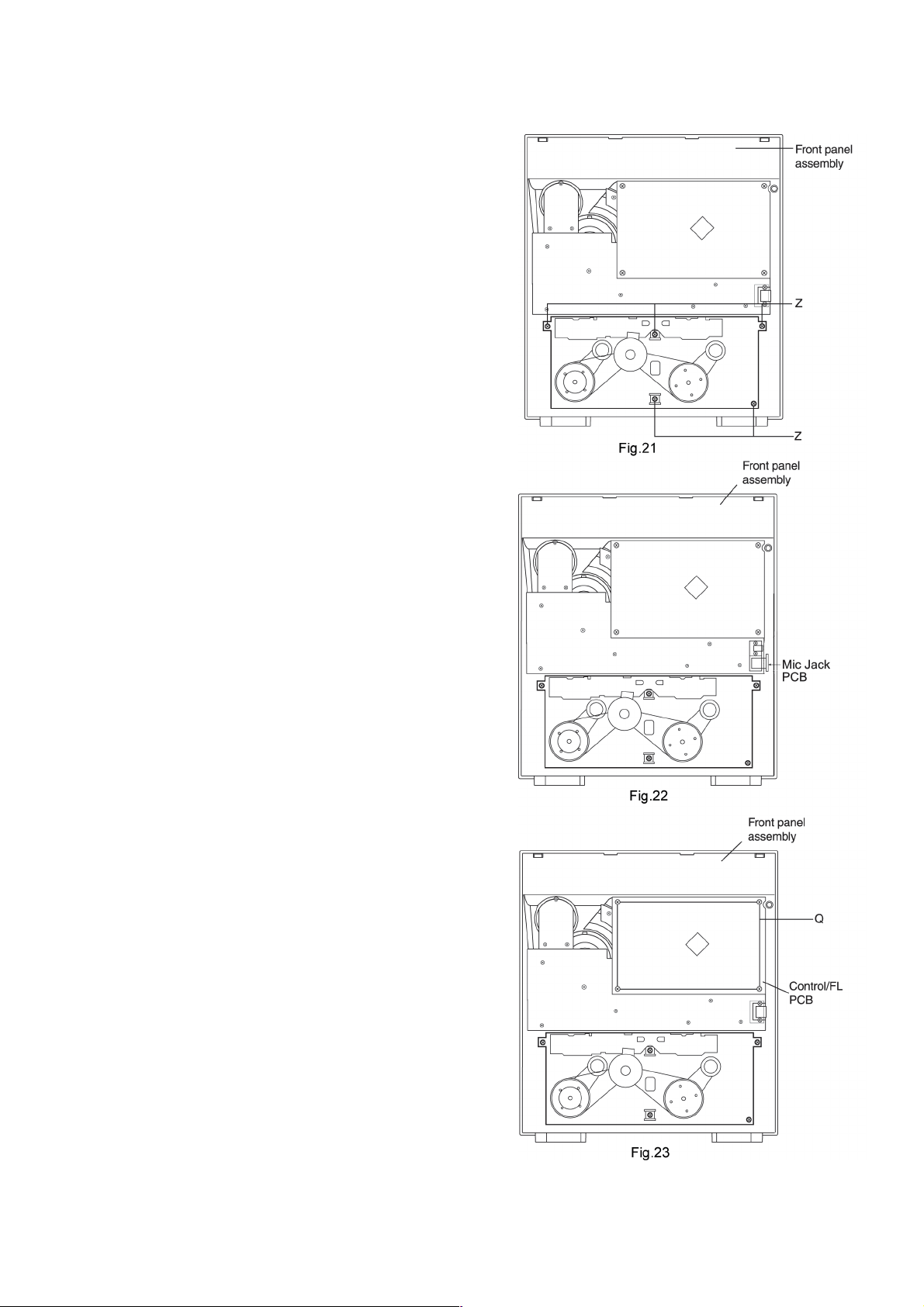
n Removing the cassette deck mechanism
(See Fig.21)
n
Prior to performing the following procedure, remove
the top cover and both sides board.
n
Also re move the CD cha nger unit.
n
Also re move the front pa nel assembly.
1. Remove the five screws “Z ” retaining the cassette
deck mecha nism.
n Removing the e arphone jack PCB And Mic
Jack PCB (See Fig.22)
n
Prior to performing the following procedure, remove
the top cover and both sides board.
n
Also remove the CD changer unit.
n
Also remove the front panel a sse mbly .
1. Remove the screw with the washer, “ P ” that retains
the earphone jack PCB.
n Removing the control/FL PCB
(See Fig.23)
n
Prior to performing the following procedure, remove
the top cover and both sides board. Also re move the
CD cha nger unit.
n
Also remove the CD cha nger unit.
n
Also remove the front panel a sse mbly .
1. Remove the four screws “ Q ” that retain the control/FL
PCB from the back of the front pa nel unit.
1-13
Page 14
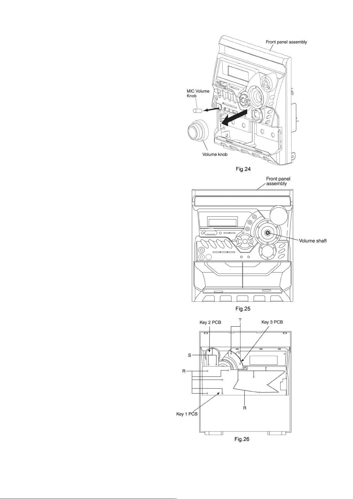
n Removing the switch PCB and sound
mode and CD function switch PCB
(See Fig.23 to 26)
n
Prior to performing the following procedures, remove
the top cover and both sides board.
n
Also remove the CD changer unit.
n
Also remove the front panel a sse mbly .
1. Pull out the volume control knob and MIC Volume
Knob from the front of the front panel a ssembly .
2. Remove the four screws “Q ” retaining the front panel
assembly.
3. Remove the control / FL PCB.
4. Remove the eleven screws “ R ” retaining the switch
(key 1) PCB.
5. Remove the three screws “ S ” retaining the sound
mode (key 2) switch PCB.
6. Remove two screws “ T ” retaining the CD function
(key 3) switch PCB.
1-14
Page 15
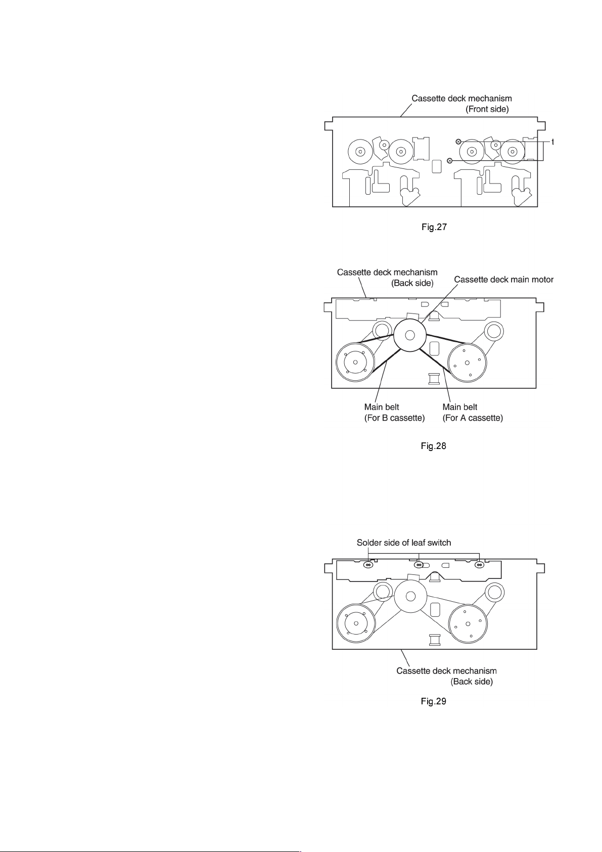
n Removing the ca ssette deck main motor ,
and re placing the main belts
(See Fig. 21, 27 and 28)
n
Prior to performing the following procedures, remove
the top cover and both sides board.
n
Also re move the CD changer unit.
n
Also remove the front panel assembly.
1. Remove the five screws “z ” retaining the cassette
deck mecha nism.
2. Remove the ca ssette deck mecha nism.
3. Remove the two screws “ t ” retaining the main motor
from the front side of the ca ssette deck.
[Caution] After atta ching the main motor , check the
orientation of the motor and the polarity of
the wires.
4. From the backside of the cassette deck, remove the
main motor and two main belts.
[Caution] The lengths of the cassette A (playback
only) and cassette B (record/play) main
belts are different. When atta ching the main
belts, use the longer belt for ca ssette A.
n Removing the leaf switches of the cas-
sette deck mechanism
(See Fig. 21 and 29)
n
Prior to performing the following procedures, remove
the top cover and both sides board.
n
Also remove the CD changer unit.
n
Also remove the front panel a sse mbly .
1. Remove the five screws “O ” that retain the cassette
deck mecha nism.
2. Remove the ca ssette deck mecha nism.
3. Turn the cassette deck mechanism upside down.
4. Remove the solder from around the leaf switches.
5. Pull out the leaf switches from the front side of the
cassette deck mechanism.
1-15
Page 16
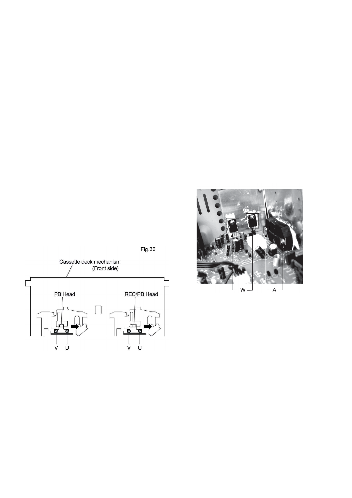
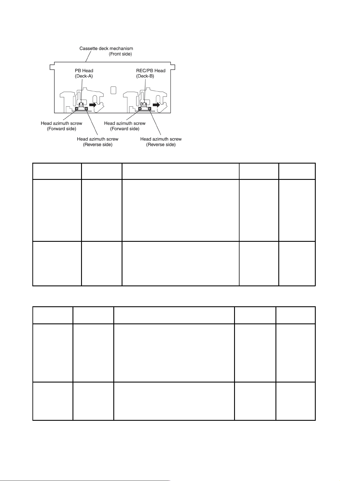
n Removing the cassette deck heads
(See Fig.21 to 30)
n Removing the 3-pin regulator
(See Q904, Q907, 31)
n
Prior to performing the following procedures, remove
the top cover and both sides board.
n
Also re move the CD cha nger unit.
n
Also re move the front pa nel a sse mbly .
1. Remove the five screws “O ” that retain the cassette
deck mecha nism.
2. Remove the ca ssette deck mechanism a nd place it so
that the front side faces up.
3. Remove the solder from the bottom side of the head
terminal and disconnect the wire.
4. Remove the screw “ U ” that retains the head.
5. Remove the screw “ V ” that retains the head.
6. Hold the head and slide it in the dire ction of the arrow
to remove it.
n
Prior to performing the following procedures, remove
the top cover and both sides board.
1. Remove the two screws “ A ” that connect the heat
sink cover to the rear panel.
2. Pull the heat sink outward.
3. Remove the screw “W ” that retains the heat sink the
3-pin terminal regulator Q904,Q907.
4. Remove the solder fixing the 3-pin regulator .
Fig.31
1-16
Page 17
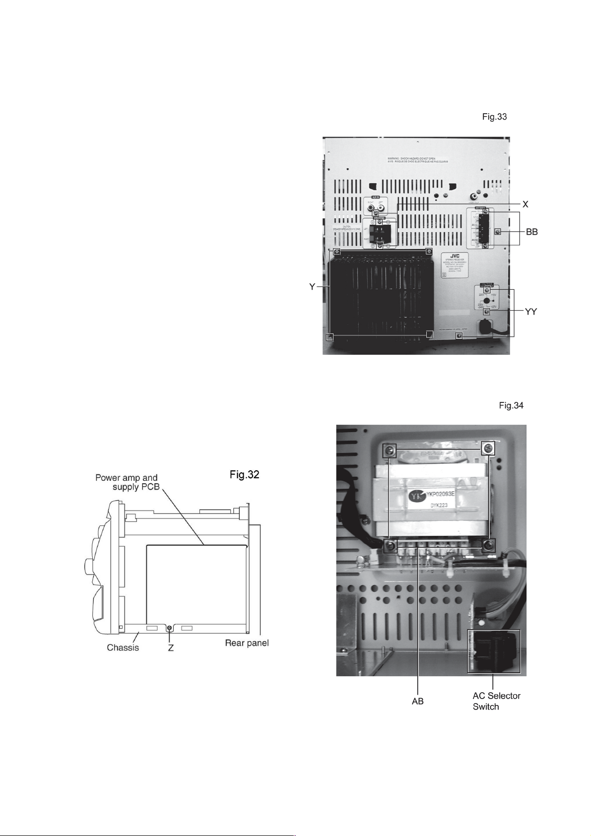
n R emoving the power amp a nd supply PCB
and the power trans PCB
(See Fig. 2, 32 to 34)
n
Prior to performing the following procedures, remove
the top cover and both sides board.
n
Also remove heat sink cover .(Fig.3)
1. Remove the two screws “ A ” connecting the heat sink
cover to the rear panel.(Fig.2)
2. Pull out the heat sink cover toward you.
3. Remove four(CA-MXK350V) screws “AA” form the
MX-K350V ba ck panel between the heat sink.
4. Remove the three screws “ X ” that retain the speaker
terminals and aux termin al.
5. Remove the screw “ YY ” and “Y ” that retains the rear
panel, a nd AC switch screw then re move the rear panel.
6. Disconnect the parallel wires from the connectors
FW951 on the power trans PCB.
7. Remove the screw “ Z ” that retain the power amp a nd
supply PCB and then remove the a ssembly .
8. Remove the clamp of AC power cord from the cha ssis.
9. Remove the four screws “ AB ” that retain the power
trans PCB a nd then remove the a ssembly .
1-17
Page 18

Adjustment method
Mea sure ment in struments required
for adjustment
1. Low frequency oscillator
This oscillator should have a capacity to output 0dB
to 600ohm at an oscillation frequency of 50Hz20kHz.
2. Attenuator impedance : 600ohm
3. Electronic voltmeter
4. Frequency counter
5. Wow flutter meter
6. Test tape
VT712 : For Tape speed and wow flutter ( 3kHz)
VT703 : For Head angle(10kHz),Play ba ck frequency
characteristics(1kHz), and dubbing frequency characteristics (63,1,10kHz)
7. Blank tape
TAPE I : AC-225
8. Torque gauge : For play and back tension forward ;
TW2111A, Reverse ; TW2121A Fast Forward and
Rewind ; TW2231A
9. Test disc: CTS-1000(12cm),GRG-1211(8cm),
CD-T05A
10. Jitter meter
11. Television
Mea surement condition s
(Select correct AC Line Volt.)
Power supply voltage
AC110/127/220/230-240V (50/60Hz) US/UX
Measurement
output terminal : Speaker out
: TP101(Measuring for TUNER
DECK/CD/VCD)
: Dummy load 6ohm
Adio input signal
AM modulation frequency : 400Hz
Modulation factor : 30%
FM modulation frequency : 400Hz
Frequency displacement : 22.5kHz
Frequency Range
AM US: 531kHz~1629kHz (9kHz)
530kHz~1710kHz (10kHz)
UX: 531kHz~1602kHz (9kHz)
530kHz~1600kHz (10kHz)
FM 87.5MHz~108MHz
Standard me asurement positions of
volume and switch
Power: Standby (Light STANDBY Indicator)
S, A, BASS : OFF
Sound mode : OFF
Main VOL. : 0 Minimum
Travers mecha set position : Disc 1
Mic MIX VOL : MAX
ECHO : OFF
Precautions for measurement
1. Apply 30pF and 33kohm to the IF sweeper output side
and 0.082 F and 100kohm in series to the sweeper
input side.
2. The IF sweeper output level should be made as low as
possible within the adjustable range.
3. Since the IF sweeper is a fixed device, there is no
need to adjust this sweeper.
4. Since a ceramic oscillator is used, there is no need to
perform any MPX adjustment.
5. Since a fixed coil is used, there is no need to adjust
the FM tracking.
6. The input and output earth systems are separated. In
case of simultaneously measuring the voltage in both
of the input and output systems with an electronic
voltmeter for two channels, therefore, the earth should
be connected particularly.
7. In the case of BTL connection amplifier, the minus
terminal of speaker is not for earthing. Therefore, be
sure not to connect any other earth terminal to this
terminal. This system is of an OTL system.
1-18
Page 19
n Arrange ment of adjusting position s
n Tape recorder section
Items
Cassette Head
A zimuth Al ignments
Recording Bias
Frequency Alignment
n Tuner section
Items
AM Tracking
Alignments
Measurement
conditions
Input signal:
530kHz (529kH z)
600kHz (603kH z)
Adjustment
point: Antenna
coil (L2)
Measurement
conditions
Test tape :
VT703 (10kHz)
Measurement
output termi nal :
Left and Right
speaker output
(6-ohm loaded)
or Headphone
Output
(32-ohm loaded)
Test tape :
TYPE I AC -225
Measurement
output termi nal :
Erase head
terminal
(CN308 8-Pin)
Measurement method
1. Playback the test tape VT703 (10KHz) or equivalent.
2. Adjust the head azimuth screw to obtain maximum
output and both output of L / R is in 3dB.
3. Put on the screw lock paint after alignments.
1. Insert the recording tape in deck-B.
2. Starting the recording.
3. Adjust the oscillation frequency to 80KHz+/-3KHz
by core of Oscillation coil of L301.
Measurement method
1. Set t he Signal G enerat or sign al to 530KHz (529KHz)
the feed to Loop Antenna.
2. Receiving t he signal and the adju st t he OSC coil (L2)
obtain the V.T is 1.40V +/-0.05V.
3. Ch ange the receiving frequ ency to 600KH z (603KHz).
4. Adjust the Antenna coil ( L2 ) obtain maxi mum
sensitivity .(Ad just the SS G output to out o f AGC
range.)
Standard
values
Maximum output Adjust the
80kHz+/-3kHz Use the High-
Standard
values
V.T :
1.40V+/-0.05V
Adjusting
positions
head azimuth
screw only
when the head
has been
changed.
Impedance
Probe or
Frequency
counter input.
Adjusting
positions
Adjust the OSC
coil only when
the AM c oi l
block has been
changed.
Maximum
sensitivity
AM IFT
Alignments
Input signal:
530kHz (529kH z)
Adjustment
point: IFT (T1)
1. Set the receiving frequency to 530KHz (529KHz ).
2. Feed the 450KHz signal to AM antenna input.
3. Adjust the IFT Block T1 obtain to maxi mum
output.(A djust the SSG output to out of AG C
range.)
Note: The adjustment of CD section is not required.
Maximum output Adjust the IFT
only when the
IFT block h as
been changed.
1-19
Page 20
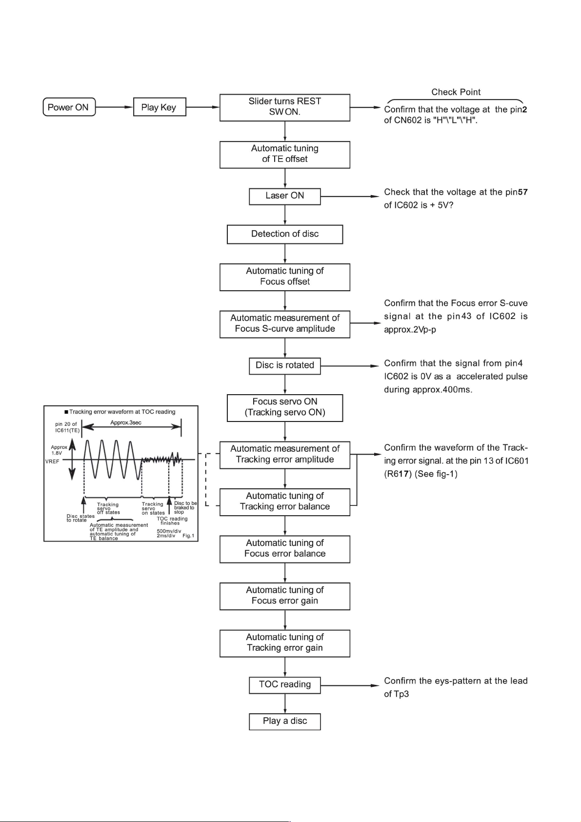
Flow of functional operation until T OC read
1-20
Page 21
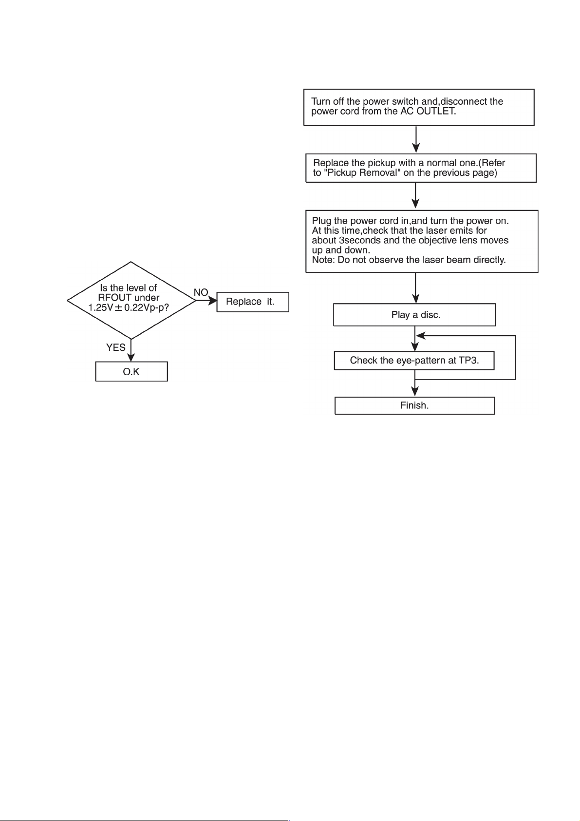
Maintenance of laser pickup
(1) Cleaning the pick up len s
Before you replace the pick up, please
try to clean the lens with a alcohol
soaked cotton swab.
(2) Life of the laser diode
When the life of the laser diode has
expired, the following symptoms will
appear .
1. The level of RF output (EFM output: ampli
tude of eye pattern) will below.
Repla c e ment of la ser pickup
(3) Semi-fixed resistor on the APC PC board
The semi-fixed resistor on the APC printed circuit board which is attached to the pickup is used to a djust the laser
power. Since this a djustment should be performed to match the chara cteristics of the whole optical block, do not
touch the semi-fixed resistor .
If the laser power is lower tha n the specified value, the la ser diode is almost worn out, a nd the laser pickup should
be replaced.
If the semi-fixed resistor would be adjusted when the pickup operates normally , the la ser pickup may be da maged
due to excessive current.
1-21
Page 22
Description of major ICs
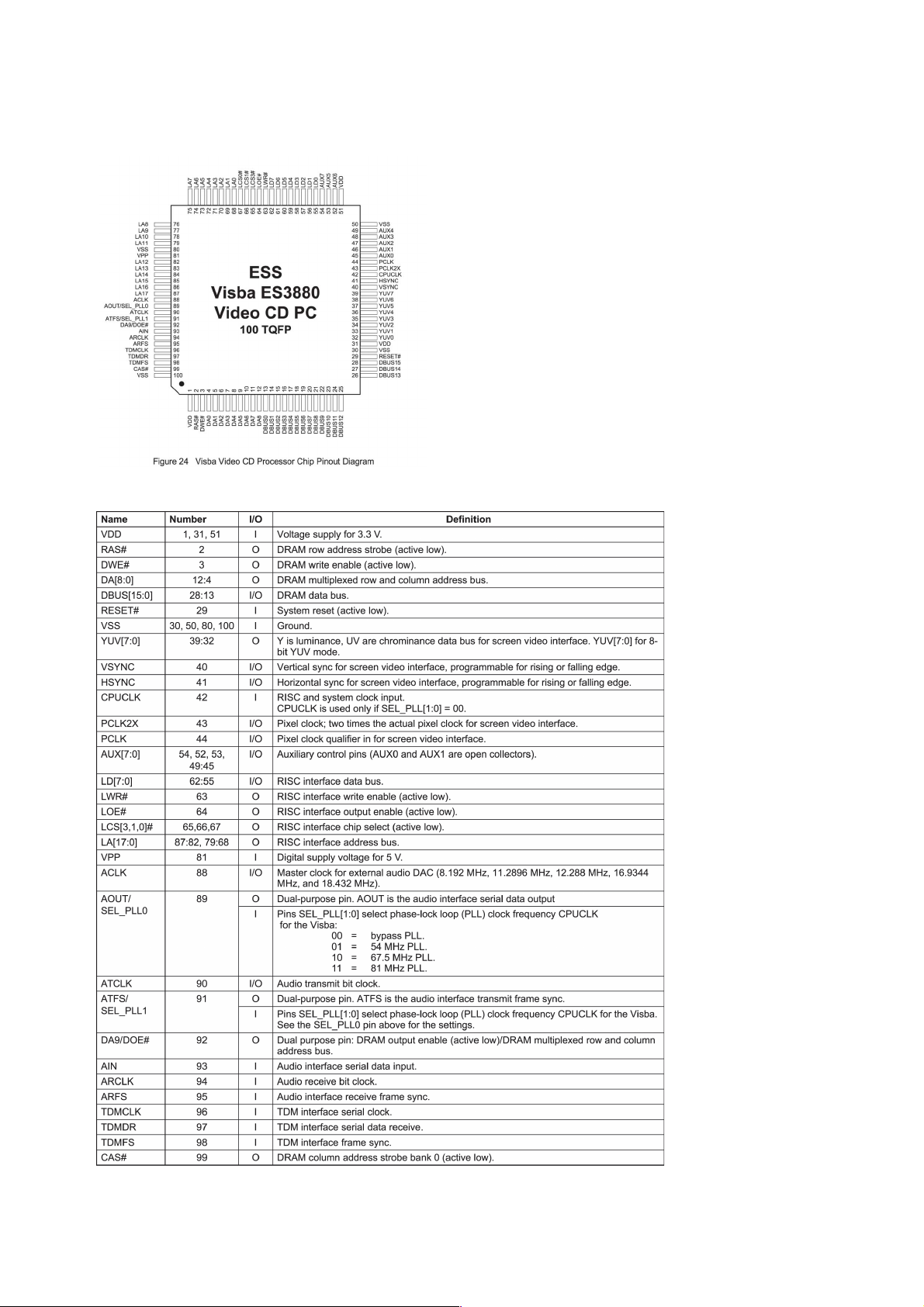
n VIDEO CD PROCESSOR CHIP PINOUT
n VIDEO PC PROCESSOR CHIP PIN DESCRIPTION
1-22
Page 23
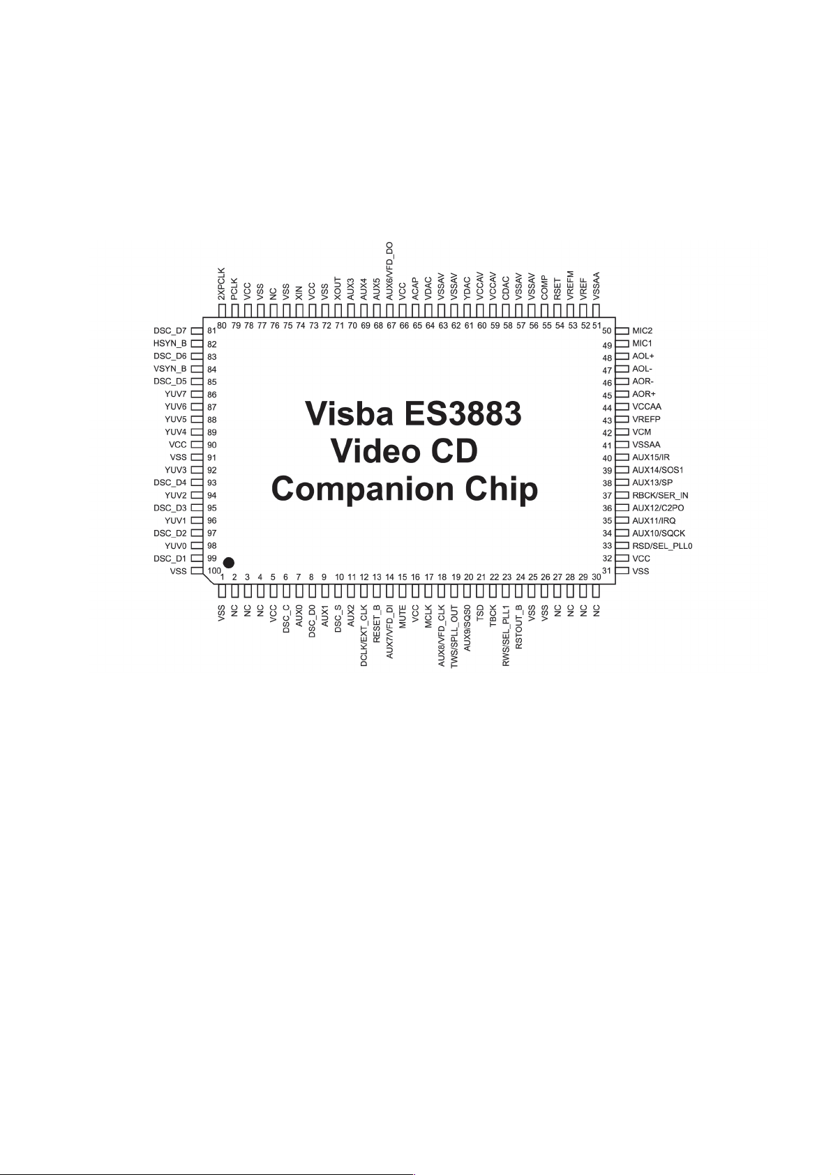
n VIDEO CD COMPANION CHIP
1. Pinout
1-23
Page 24
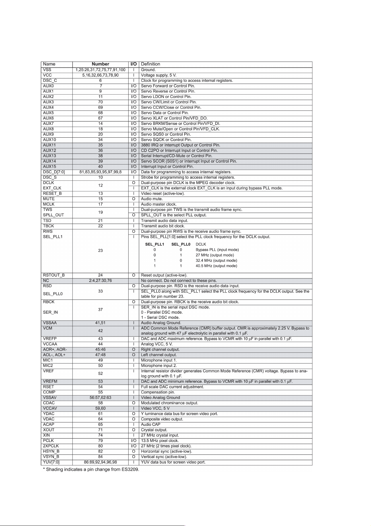
2. Pin description
1-24
Page 25

n BA15218/BA15218F(IC102/IC852): Dual operation al amplifier
1. Terminal layout & block diagram
n BA3837(IC103): MIC Mixer
1. Terminal layout & block diagram 2. Pin function
n BU9253AS(IC851): Low pass f ilter & e cho mixer
1. Terminal layout & block diagram 2. Pin function
1-25
Page 26

n TA8189N (IC401) : REC/PB amp.
1. Terminal layout 2. Block diagram
3. Pin function
1-26
Page 27

n TC74HC4094AP (IC402) : 8-bit shift and store re sister
1. Terminal layout
2. Block diagram
1-27
Page 28

n TDA7440D (IC101) : Audio processor
1. Terminal layout
2. Block diagram
1-28
Page 29

< MEMO >
Page 30

MX-K350V
VICTOR COMPANY OF JAPAN, LIMITED
AUDIO & COMMUNICATION BUSINESS DIVISION
PERSONAL & MOBILE NETWORK B.U.10-1, 1 Chome, Ohwatari-machi, maebashi-city, 371-8543, Japan
No.21166
Printed in Japa n
200212
Page 31

MX-K350
V
SE
R
VI
C
E
M
ANUA
L
COMPACT COMPONENT SYSTEM
M
X-K
S
upplemen
350
t
V
US --------------- Singapore
UX ----------- Saudi Arabia
A
r
ea Suffi
x
Because there were many mistake to the Service Manual MX-K350V
(No.21166,Page 3-3 to 3-21 on PARTS LIST.),please this supplementally
for servicing.
No.
COPYRIGHT 2002 VICTOR COMPANY OF JAPAN, LTD.
21166
May.
B
2003
Page 32

MX-K350
V
ICTOR COMPANY OF JAPAN
V & MALUTIMEDIA COMPANY AUDIO/VIDEO SYSTEM CATEGORY. 10-1,1chome,Ohwatari-machi,Maebashi-city,371-8543,Japan
No.
21166
B
, LIMITE
D
200305
Page 33

MX-K350V
SCHEMATIC DIAGRAMS
COMPACT COMPONENT SYSTEM
MX-K350V
C
S
N
O
PREV. NEXT
CD1CD2CD
PROGRAM
REPEAT
/RANDOM
KEY CONTROL MPX
SOUND
KARAOKE
MODE
ACTIVE
BASS EX.
ECHO
CD-ROM No.SML200212
Area suffix
US ------------- Singapore
UX ---------- Saudi Arabia
3-CD
PLAY & EXCHANGE
STANDBY/ON
SLEEP
AUX
FM /AM
FM MODE
R
E
E
N
HIGHLIGHTVIDEO INTRO
RETURNSTILL
3
CD
SELECT
TAPE
TAPE
A/B
FADE
MUTING
VOLUME
COMPACT COMPONENT SYSTEM
STANDBY
AUX
PHONES
MIC
MX-K350V
1 BIT
DUAL D/A
CONVERTER
STANDBY/ON
CD
FM
/ AM
REC START
/ STOPCD REC START DUBBING
MIC LEVEL
MIN MAX
EJECT EJECT
FULL - LOGIC CO NTROL
PLAY
A
RANDOM
SET
CANCEL
PRESET
/ DEMO
TAPE
TUNING
VCD NUMBER
SELECT
CLOCK
RETURNPBC
KEY CONTROL
/TIMER
A / B
CD SYNCHRO RECORDING
SP-MXK350V SP-MXK350VCA-MXK350V
CD-R/RW PLAYBACK
SOUND
P
K
O
C
MODE
REPEAT
PROGRAM
E
M
U
L
O
V
NEXTPREV.
TAPE
P
O
R
C
L
A
C
I
S
S
P
I
K
S
C
S
I
D
3
CD
ACTIVE
2
D
C
BASS EX.
1
D
C
REC / PLAY
B
Contents
Block diagram
Standard schematic diagrams
Printed circuit boards
COPYRIGHT 2002 VICTOR COMPANY OF JAPAN, LTD.
2-1
2-2
2-9~15
No.21166SCH
Dec. 2002
Page 34

MX-K350V
In regard with component parts appearing on the silk-screen pr inted side (par ts side) of
the PWB diagrams, the parts that are printed over with black such as the resistor ( ),
diode ( ) and ICP ( ) or identified by the " " mark nearby are critical for safety.
(This regulation does not correspond to J and C version.)
Page 35

Block diagram
5
4
MX-K350V
3
2
1
ABCD E F G
2-1
Page 36

Standard schematic diagrams
CD Servo Control Section K350V
5
4
MX-K350V MX-K350V
3
2
1
2-2
HABC DEFG
Page 37

MX-K350V
Power transformer section K350V MIC AMP. and H.P section
5
4
3
2
1
ABCD E F G
2-3
Page 38

MX-K350V MX-K350V
FL Display and CPU Control Section
5
4
3
2
1
2-4
HABC DEFG
Page 39

MX-K350V
Head AMP. audio, power AMP. and power Supply
5
4
3
2
1
ABCD E F G
2-5
Page 40

MX-K350V MX-K350V
MPEG Section
5
4
3
2
1
2-6
HABC DEFG
Page 41

MX-K350V
Tuner Section
5
4
3
2
1
ABCD E F G
2-7
Page 42

MX-K350V MX-K350V
Remote Control Section
5
4
3
2
1
2-8
HABC DEFG
Page 43

Printed circuit boards
Main /power-amp. circuit board (Top side ) K350V
5
4
MX-K350V
3
2
1
ABCD E F G
2-9
Page 44

MX-K350V MX-K350V
Main / power-amp. circuit board(Botton side ) K350V
5
4
3
2
1
2-10
HABC DEFG
Page 45

MX-K350V
CD Main. circuit board (Top side) K350V CD Main. circuit board (Bottom side) K350V
5
4
3
2
1
ABCD E F G
2-11
Page 46

MX-K350V MX-K350V
Display/Uicom control. circuit board (Top side) K350V
5
4
3
2
1
2-12
HABC DEFG
Page 47

MX-K350V
Display/Uicom control. circuit board (Bottom side) K350V
5
4
3
2
1
ABCD E F G
2-13
Page 48

MX-K350V MX-K350V
MPEG. circuit board (Top side) K350V MPEG. circuit board (Bottom side) K350V
5
4
3
2
1
2-14
HABC DEFG
Page 49

MX-K350V
Tuner. circuit board (Top side) K350V
5
4
3
2
1
A
BC D
2-15
Page 50

MX-K350V
VICTOR COMPANY OF JAPAN, LIMITED
AUDIO & COMMUNICATION BUSINESS DIVISION
PERSONAL & MOBILE NETWORK BUSINESS UNIT. 10-1,1chome,Ohwatari-machi,Maebashi-city,371-8543,Japan
No.21166SCH
Printed in Japan
200212
Page 51

PARTS LIST
[ MX-K350V ]
* All printed circuit boards and its assemblies are not available as service parts.
Area suffix
US ---------------------- Singapore
UX ------------------- Saudi Arabia
MX-K350V
- Contents -
Exploded view of general assembly and parts list (Block No.M1)
CD changer mechanism assembly and parts list (Block No.MA)
Cassette mechanism assembly and parts list (Block No.MP)
Packing materials and accessories parts list (Block No.M3,M5)
3- 3
3- 5
3- 7
3- 8
3-1
Page 52

MX-K350V
< MEMO >
3-2
Page 53

234
5
Exploded view of general assembly and parts list
Block No.
M
MX-K350V
M
1
M
47
88
8686
8787
8585
8484
3-3
Page 54

MX-K350V
MX-K350V
Parts list (General assembly)
Item
A
1 BI109808010101
2 BI109809010101
3 BI109806010201
4 BI109807010201
5 BI109819010201
6 BI109823010101
7 BI109805030201
8 BI109810060101
9 BI109830010101
10 BI109835010101
11 BI109834010101
12 BI109969010201
13 BI301781010101
14 BI109804040201
15 BI301388010101
16 BI109840010101
17 BI202408010101
18 BI109841010101
19 BI202266010101
20 BI301789010101
21 BI202262010401
22 BI103362020102
23 BI202103010101
24 G31K300K05S01
26
27 BI109832010101
28 BI109828010101
29 BI109829010201
30 ---------------
31 BI109825010201
32 BI202268010101
33 BI109831010201
34 BI109826010201
35 ---------------
36 G31K300K05S02
38 ---------------
39
40 BI109836010201
41 BI202303010101
42 BI2110110040001
43 ---------------
44 BI109837010401
45 ---------------
46 BI109838010401
47 ---------------
48 BI109824010101
49 ---------------
50 BI301773010101
Parts number Parts name Area
-----------------
-----------------
Q'ty
WINDOW CASS L 1
WINDOW CASS R 1
BOX CASS L
BOX CASS R 1
KNOB VOLUME
KEY BASS 1
PANEL CD 1
WINDOW DISPLAY
KEY POWER A
LOGO JVC
RING VOLUME
SPACER
MIRROR SHEET 1
PANEL FRONT 1
GEAR WHEET DAMP 2
LOCKER 2
SPRING LOCKER 2
HLDR LOCKER 2
SPRING CASS R
BUSHING
BOTTOM PLATE 1
FOOT RUBBER 4
HLDR SENSER
KEY CD CHANGE ASSY 1
CASSETTE DECK 1
KEY CLOCK 1
KEY DEMO 1
KEY PLAY/STOP 1
PWB PHONE 1
KEY OPEN/CLOSE 1
BRACKET PWB A 1
KEY DUBBING 1
KEY REPEAT 1
PWB REPEAT 1
KEY FUNCTION ASSY 1
PWB CD
CD DECK 1
PANEL TOP
BRACKET PWB B 1
PW TRANSFORMERMER
PWB PT 1
PANEL SIDE L 1
PWB MAIN 1
PANEL SIDE R 1
PWB CONTROL 1
KEY SOUND MODE
PWB SOUND MODE 1
TAPE DOUBLE SIDE 2
1
1
1
1
1
1
2
1
1
1
CMAT6Z219A
251152G01V
251099G01V
1
251098G10V
1
1
251100G01V A
251152G01V
251099G01V
1
251099G01V
Description
Block No. M1MM
Parts list (General assembly)
Item
A
51 BI202267010101
52 ---------------
53 BI202264010101
54 ---------------
55 BI202269010101
56 BI202304010101
57 BI202320020101
58 BI109839010101
59 BI109818010101
60 BIRM000604S3
61 BIRM000601S3
62 BIKT000627
63 BIBT000418
64 BIPMW001101S3
65 BI202265101010
66 BIRT000618B2
67 BIBT000206
68 BIBT0006091
69 BIRT000611B3
70 BIBM000618
71 ---------------
72 BI202337010101
73 BI202348010101
74 BI202351010101
75 BIRT000617B3
76 BIRT000621B3
77 BI109820010101
78 BI202364010101
79 BI23B0112
80 BI202423010101
81 BI202454010101
82 ---------------
83 BI202424010101
84 BI403111
85 BI402891
86 BI403021
87 BI1401001
88 BI109820010101
Parts number Parts name Area
BI202320010101
BI1401131
Q'ty
BRACKET HLDR VFD
PWB VFD
BRACKET ADAPTOR 2
PWB TUNNER 1
HEAT SINK 1
HLDR TUNNER 1
PANEL REAR
PANEL REAR 1
HEAT SINK COVER
LES LED 1
SCREW 20
SCREW 8
SCREW
SCREW
SCREW
SPRING CASS L
SCREW
SCREW 2
SCREW 2
SCREW 7
SCREW
PWB PHONE HOLDER 1
BRACKET FORNT 1
BRACKET CD DECK
BRACKET MB
SCREW 2
SCREW 3
KEY VOLUME MIC 1
BRACKET MIC PHONE 1
MIC JACK 1
PLATE VIDEO BOTTOM 1
GRD VIDEO
PWB VIDEO
PLATE VIDEO TOP 1
FUSE
FUSE
FUSE
AC CORD
AC CORD
PUSH BUTTON 1
31
2
1
251099G01V
251151G01V
1
1
RH/MS3X8MM
RH/MS3X6MM
2
KT/TS3X12MM
BH/TS2.6X8MM
4
PMW/TS4X8MM
1
3
RH/TH3X6MM
BH/TS2X8MM
BH/TS3X14MM
RH/TS3X8MM
2
BT/MS3X6MM
251099G01V
1
1
RH/TS3X10MM
RH/TS3X8MM
1
1
251176G01V
1
1.25AL 250V
1
1.6A 250V T218
1
2A 250V
1
1
Block No. M1MM
Description
US
UX
3-4
Page 55

3
4
5
CD changer mechanism assembly and parts list
MX-K350V
Block No.
M
M
M
A
2
3-5
Page 56

MX-K350V
MX-K350V
Parts list (CD changer mechanism)
Item
A
1 BI3199801000
2 BI3199802000
3 BI3199804002
4 BI3499801000
5 BI3499802000
6 BI3599801001
7 BI3599802000
8 BI3599803000
9 BI3599804000
10 BI3599805000
11 BI3599806000
12 BI3599807000
13 BI36CJ000000
14 BI8814035105
15 BI3799802000
16 BI4299801002
17 BI4299802000
18 BI4299803002
19 BI4299804000
20 BI4299821000
21 BI4299806000
22 BI4297307000
23 BI4299808000
24 BI4299809000
25 BI4299810000
26 BI4299811000
27 BI4299812000
28 BI4299813000
29 BI4299814001
30 BI4299815000
31 BI4299816001
32 BI4299817000
33 BI4299818000
34 BI4299819000
35 BI4399801000
36 BI4799801000
37 BI4799803001
38 BI4799804000
39 BI5099807001
40 BI5099808000
41 BI5099809001
42 BI5099813000
43 BI5099814000
44 BI6599801002
45 BI6599802000
46 BI6994301000
47 BI6999801000
48 BI86000102J3
Parts number Parts name Area
GEAR PLATE
GUIDE PLATE
UP COVER PLATE
SHAFT PULLEY
SHAFT SWING
T/T SWITCH SPRING
SWING SPRING
SPRING BIG
SPRING SMALL
TOWER FORM SPRING
CUSHION HARD
CUSHION SOFT
M-399 OPTIMA-7
TABLE
CUSHION RUBBER
BASE
TRAY
TURN CHANGER
INERTIA GEAR A
HOLDER DISC
T/T GEAR
OBLIQUE GEAR
SCREW STICK
T/T LEVER LOCK 1
PULLEY
PULLEY GEAR 1
BASE CHANGE
TRANSMISSION 1
MECHA GEAR
MECHA HOLDER 1
INERTIA GEAR B
ROLLER
BASE CD MECHANISM
BUFFER BASE
BELT
BASE CHANGE FELT
PVC PLATE
MAGNET DISC CRAMP
WIRE ASSY 6P
WIRE ASSY 3P
WIRE ASSY 6P
WIRE ASSY 6P
FLEX CABLE 16P
SWITCH
SWITCH
MOTOR
MOTOR
SCREW
Q'ty
1
2
1
1
1
1
1
1
1
1
1
2
1
CD MECH.W/PICK UP
6
4
1
1
1
1
1
2
1
1
1
1
1
4
2
1
1
1
1
1
1
1
1
1
1
1
2
1
1
1
2
M2.6X5.0
Description
Block No. MAMM
Parts list (CD changer mechanism)
Item
A
49 BI86000115F1
50 BI86000125E1
51 BI86000135E1
52 BI86000145E2
53 BI865F31B075
54 BI865F31B120
55 BI865J31B080
56 BI8811231206
57 BI4500001100
58 BI5599810000
59 BI3599806001
60 BI6599801000
61 BI3799801000
62 BI4799805000
Parts number Parts name Area
SCREW
SCREW
SCREW
SCREW
SCREW
SCREW
SCREW
WASHER
YST BAR CODE
WIRE CLAMPER
CUSHION SPR HARD
SWITCH
RUBBER
WASHER FELT
Q'ty
2
M2.0X12.0
3
M1.7X8.0
1
M3.0X8.0
4
M1.7X8.0
4
M2.0X7.5
2
M2.0X12.0
5
M2.6X8.0
4
2.2X13.0X0.6
1
1
1
2
1
1
Block No. MAMM
Description
3-6
Page 57

Cassette mechanism assembly and parts list
MX-K350V
CMAT6Z219A
L SIDE
TYPE
10
L SIDE
Block No.
M
M
M
P
3
9
4
2
5
4
8
6
8
5
7
1
R SIDE
Parts list (Cassette mechanism)
Item
A
1 BIF513858
2 BIF525346
3 BIF567843
4 BIUE20P12
5 BIF522063
6 BIFF19N31
7 BIF51435
8 BIFF19S31
9 BIFF19N22
10 BIF513855
Parts number Parts name Area
7
R SIDE
TYPE
Note: Parts listed on the Parts List below can be supplied.
However, parts that are not listed below cannot be supplied
individually but only by purchasing the whole Cassette
Mechanism Assembly Unit. (When ordering, use the Parts No.
CMAT6Z219A for Cassette Mechanism Assembly Unit.)
Q'ty
PLATE HD BLK
MTR MAIN BLK 1
PCB CONTROL BLK
LEAF SWITCH
CLUTCH ASSY BLK
MAIN BELT 1
ROLLER PINCH BLK R 2
F/R BELT MO
MAIN BELT
PLATE HD BLK
Block No. MPMM
Description
1
1
3
2
2
1
1
3-7
Page 58

MX-K350V
Packing materials and accessories parts list
P7
Block No.
Block No.
M
M
3
M
M
5
M
M
P4
P4
Note/ /
Depending on the Video CD to be used the VCD NUMBER
or VCD NUMBER
Ð button on the Unit does not work properly.
In this case, when the button is used, ÒINVALIDÓ is displayed.
If this happens, select the desired track with the numeric keys
on the remote control.
A10
+
A9
LV43319-001A
P8
A8
P2
A7
P5
P6
P3
3-8
Page 59

MX-K350V
Parts list (Packing)
Item
A
P 1 BI4312641
P 2 BI4511363
P 3 BI4511373
P 4 BI4005355
P 5 BI4710321
P 6 BI4511451
P 7 BI4710311
P 8 BI4710511
Parts number Parts name Area
Parts list (Accessories)
Item
A
A 1 BI600RMK350080
A 2 BI4411591
A 3 BIAN01012
A 4 BI11F2000SA01
A 5 BIAN01031
A 6 --------------A 7 MXK350K-SPBOX- L
A 8 MXK350K-SPBOX-R
A 9 BI23A0261
A10 BI4033111
Parts number Parts name Area
BI4411481
BI23A0094
CARTON BOX
POLY FOAM L
POLY FOAM R
POLY BAG
POLY BAG
EPE FOAM PAPER
POLY BAG
POLY BAG
REMOTE CONTROL
INSTRUCTIONS
INSTRUCTIONS
WIRE ANT
VIDEO LINE CORD
LOOP ANT
BATTERY
SPEAKER BOX L
SPEAKER BOX R
PLUG CONVERSION
PLUG CONVERSION
CAUTION SHEET
Q'ty
1
1
1
2
REMOTE&AC CORD
1
UNIT
1
1
INSTRUCTIONS
1
LOOP ANT
Q'ty
1
1
LVT0864-002A
1
LVT0864-001A
1
1
1
2
1
1
1
JT-0475
1
JT-0476 250V
1
LV43319-001A
Block No. M3MM
Description
Block No. M5MM
Description
UX
US
UX
US
3-9
Page 60

PARTS LIST
[ MX-K350V ]
* All printed circuit boards and its assemblies are not available as service parts.
Area suffix
US ---------------------- Singapore
UX ------------------- Saudi Arabia
MX-K350V
- Contents -
Exploded view of general assembly and parts list (Block No.M1)
CD changer mechanism assembly and parts list (Block No.MA)
Cassette mechanism assembly and parts list (Block No.MP)
Electrical parts list (Block No.01~05)
Packing materials and accessories parts list (Block No.M3,M5)
3- 3
3- 5
3- 6
3- 7
3-20
3-1
Page 61

MX-K350V
< MEMO >
3-2
Page 62

MX-K350V
Exploded view of general assembly and parts list (K350V)
M
1
Block No.
M
7
6
M
5
4
88
47
3
86
87
2
85
84
1
BC DE FG H I JA
3-3
Page 63

K
R
T
K
T
K
K
X
MX-K350V MX-K350V
Parts list (Exploded view of general assembly)
ltem Parts number Parts name Q'ty Description Area ! ltem Parts number Parts name Q'ty Description Area
!
1 BI109808010101 WINDOW, CASS L 1
2 BI109809010101 WINDOW, CASS R 1
3 BI109806010201 BOX, CASS L 1
4 BI109807010201 BOX,CASS R 1
5 BI109819010201 KNOB, VOLUME 1
6 BI109823010101 KEY, BASS 1
7 BI109805030201 PANEL, CD 1
8 BI109810060101 WINDOW, DISPLAY 1
9 BI109830010101 KEY, POWER A 1
10 BI109835010101 LOGO, JVC 1
11 BI109834010101 RING, VOLUME 1
12 BI109969010201 SPACER 2
13 BI301781010101 MIRROR SHEET 1
14 BI109804040201 PANEL, FRON
1
15 BI301388010101 GEAR WHEET, DAMP 2
16 BI109840010101 LOCKER 2
17 BI202408010101 SPRING, LOCKER 2
18 BI109841010101 HLDR, LOCKER 2
19 BI202266010101 SPRING, CASS R 1
20 BI301789010101 BUSHING 1
21 BI202262010401 BOTTOM PLATE 1
22 BI103362020102 FOOT RUBBER 4
23 BI202103010101 HLDR, SENSER 1
24 G31K300K05S01 KEY, CD CHANGE ASSY 1
26 BI3101441 DEC
1 CMAT6Z219A
27 BI109832010101 KEY, CLOCK 1
28 BI109828010101 KEY, DEMO 1
29 BI109829010201 KEY, PLAY/STOP 1
30 PWB-PHONE 1 251152G01V
31 BI109825010201 KEY, OPEN/CLOSE 1
32 BI202268010101 BRACKET-PWB-A 1
33 BI109831010201 KEY, DUBBING 1
34 BI109826010201 KEY, REPEAT 1
35 PWB-REPEAT 1 251099G01V
36 G31K300K05S02 KEY, FUNCTION ASSY 1
38 PWB-CD 1 251098G10V
39 BI681MXK30000 CD DEC
1
40 BI109836010201 PANEL, TOP 1
41 BI202303010101 BRACKET-PWB-B 1
!
42 BI21101100400010 PW TRANSFORMERMER 1
43 PWB-PT 1 251100G01V(A)
44 BI109837010401 PANEL, SIDE L 1
45 PWB-MAIN 1 251152G01V
46 BI109838010401 PANEL,SIDE R 1
47 PWB-CONTROL 1 251099G01V
48 BI109824010101 KEY, SOUND MODE 1
49 PWB-SOUND MODE 1 251099G01V
50 BI301773010101 TAPE DOUBLE SIDE 2
51 BI202267010101 BRACKET HLDR-VFD 2
52 PWB-VFD 1 251099G01V
53 BI202264010101 BRACKET, ADAPTOR 2
54 PWB-TUNNER 1 251151G01V
55 BI202269010101 HEATSIN
56 BI202304010101 HLDR-TUNNE
1
1
57 BI202320010101 PANEL, REAR 1
BI202320020101 PANEL, REAR 1
58 BI109839010101 HEATSINK-COVER 1
59 BI109818010101 LES, LED 1
60 BIRM000604S3 SCREW 20 RH/MS3X8mm
61 BIRM000601S3 SCREW 8 RH/MS3X6mm
62 BIKT000627 SCREW 2 KT/TS3X12mm
63 BIBT000418 SCREW 31 BH/TS2.6X8mm
64 BIPMW001101S3 SCREW 4 PMW/TS4X8mm
65 BI202265101010 SPRING, CASS L 1
66 BIRT000618B2 SCREW 3 RH/TH3X6mm
67 BIBT000206 SCREW 2 BH/TS2X8mm
68 BIBT0006091 SCREW 2 BH/TS3X14mm
69 BIRT000611B3 SCREW 7 RH/TS3X8mm
70 BIBM000618 SCREW 2 BT/MS3X6mm
71 PWB PHONE HOLDER 2 251099G01V
72 BI202337010101 BRACKET-FORN
73 BI202348010101 BRACKET-CD-DEC
1
1
74 BI202351010101 BRACKET-MB 1
75 BIRT000617B3 SCREW 2 RH/TS3X10mm
76 BIRT000621B3 SCREW 3 RH/TS3X8mm
77 BI109820010101 KEY, Volume MIC 1
78 BI202364010101 BRACKET MIC-PHONE 1
79 BI23B0112 MIC JACK 1
80 BI202423010101 PLATE VIDEO BOTTOM 1
81 BI202454010101 GRD VIDEO 1
82 PWB VIDEO 1 251176G01V
83 BI202424010101 PLATE VIDEO TOP 1
! 84 BI403111 FUSE 1 1.25AL 250V
! 85 BI402891 FUSE 1 1.6A 250 T218
! 86 BI403021 FUSE 1 2A 250V
! 87 BI1401001 AC CORD 1 US
!
BI1401131 AC CORD 1 U
88 BI109820010101 KEY CONTROL 1
3-4
Page 64

CD changer mechanism assembly and parts list
Block No.
M
MX-K350V
M
A
M
51
5
41
46
38
N
S
55
33
4
20
3
40
14
3
53
53
56
56
15
43
57
52 X4
16
55
9
45
55
2
8
6
49
50
29
31
32
55
24
58
31
54
44
34
37
23
21
22
7
31
32
21
44
17
55
2
54
44
18
15
13
2
12
53
56
15
30
11
35
25
3mm
42
47
26
4
48
50
10
50
19
1
31
5
28
36
27
39
1
AB C D E F G
3-5
Page 65

MX-K350V
MX-K350V
Electrical parts list ( K350V-CD Changer )
Item
!
Location
1 BI3199801000 GEAR PLATE 1
2 BI3199802000 GUIDE PLATE 2
3 BI3199804002 UP COVER PLATE 1
4 BI3499801000 SHAFT PULLEY 1
5 BI3499802000 SHAFT SWING 1
6 BI3599801001 T/T SWITCH SPRING 1
7 BI3599802000 SWING SPRING 1
8 BI3599803000 SPRING BIG 1
9 BI3599804000 SPRING SMALL 1
10 BI3599805000 TOWER FORM SPRING 1
11 BI3599806000 CUSHION HARD 1
12 BI3599807000 CUSHION SOFT 3
13 BI36CJ000000 M-399 OPTIMA-7 1 CD MECH.W/PICK UP
14 BI8814035105 TABLE 6
15 BI3799802000 CUSHION RUBBER 4
16 BI4299801002 BASE 1
17 BI4299802000 TRAY 1
18 BI4299803002 TURN CHANGER
19 BI4299804000 INERTIA GEAR (A) 1
20 BI4299821000 HOLDER DISC 1
21 BI4299806000 T/T GEAR 2
22 BI4297307000 OBLIQUE GEAR 1
23 BI4299808000 SCREW STICK 1
24 BI4299809000 T/T LEVER LOCK 1
25 BI4299810000 PULLEY 1
26 BI4299811000 PULLEY GEAR 1
27 BI4299812000 BASE CHANGE 1
28 BI4299813000 TRANSMISSION
29 BI4299814001 MECHA GEAR 1
30 BI4299815000 MECHA HOLDER
31 BI4299816001 INERTIA GEAR (B) 4
32 BI4299817000 ROLLER
33 BI4299818000 BASE CD MECHANISM 1
34 BI4299819000 BUFFER BASE 1
35 BI4399801000 BELT 1
36 BI4799801000 BASE CHANGE FELT 1
37 BI4799803001 PVC PLATE 1
38 BI4799804000 MAGNET DISC CRAMP 1
39 BI5099807001 WIRE ASSY 6P 1
40 BI5099808000 WIRE ASSY 3P 1
41 BI5099809001 WIRE ASSY 6P 1
42 BI5099813000 WIRE ASSY 6P 1
43 BI5099814000 FLEX CABLE 16P 1
44 BI6599801002 SWITCH 3
45 BI6599802000 SWITCH 1
46 BI6994301000 MOTOR
47 BI6999801000 MOTOR 1
48 BI86000102J3 SCREW 2 M2.6 x 5.0
49 BI86000115F1 SCREW 1 M2.0 x 12.0
50 BI86000125E1 SCREW 3 M1.7 x 8.0
51 BI86000135E1 SCREW 1 M3.0 x 8.0
52 BI86000145E2 SCREW 4 M1.7 x 8.0
53 BI865F31B075 SCREW 4 M2.0 x 7.5
54 BI865F31B120 SCREW 2 M2.0 x 12.0
55 BI865J31B080 SCREW 5 M2.6 x 8.0
56 BI8811231206 WASHER 4 2.2 x 13.0 x 0.6
57 BI4500001100 YST BAR CODE 1
58 BI5599810000 WIRE CLAMPER 1
59 BI3599806001 CUSHION SPR HARD 1
60 BI6599801000 SWITCH 1
61 BI3799801000 RUBBER 1
62 BI4799805000 WASHER,FELT 1
Parts number Parts name Q'ty. Description Area
Cassette mechanism assembly and parts list
M
P
Block No.
M
CMAT6Z219A
3
9
4
2
5
4
8
8
1
L SIDE
TYPE
5
10
L SIDE
7
1
1
2
1
R SIDE
7
R SIDE
TYPE
Note: Parts listed on the Parts List below can be supplied.
However, parts that are not listed below cannot be supplied
individually but only by purchasing the whole Cassette
Mechanism Assembly Unit. (When ordering, use the Parts No.
CMAT6Z219A for Cassette Mechanism Assembly Unit.)
Parts List (Cassette mechanism)
Item Parts number Parts name Q'ty Description Area
!
1
1 BIF513-858 PLATE HD BLK 1
2
BIF525-346 MTR MAIN BLK 1
3 BIF567-843 PCB CONTROL BLK 1
4 BIUE20P-12 LEAF SWITCH 3
5 BIF522-063 CLUTCH ASSY BLK 2
6 BIFF19N-31 MAIN BELT 1
7 BIF514-35 ROLLER PINCH BLK R 2
8 BIFF19S-31 F/R BELT MO 2
9 BIFF19N-22 MAIN BELT 1
10 BIF513-855 PLATE HD BLK 1
Block No. MPMM
M
6
3-6
Page 66

MX-K350V
ea
ea
Q
Q
Q
Q
Q
Electrical parts list (CD selection)
Item
A
CN601 12S160031 CONNECTOR 16P/1.0MM
CN602 23S600961 CONNECTOR 6P/PITCH2.0MM
CN603 12S30030 CONNECTOR 3P
CN604 23S600961 CONNECTOR 6P/PITCH2.0MM
CN605 23S600961 CONNECTOR 6P/PITCH2.0MM
CN606 12S250001 CONNECTOR 25P/1.0MM
CN607 12S800421 FFC CONNECTOR P=25MM
CN608 12S1800061 CONNECTOR 18PINS/1.25MM
C601 QCBB1HK-103 C CAPACITOR 0.01UF K 50V
C602 QETM1CM-476 E CAPACITOR 47UF M 16V
C603 QCBB1HK-103 C CAPACITOR 0.01UF K 50V
C604 QCSB1HJ-560 C CAPACITOR 56PF J 50V
C605 QDCB1HM-1R0 C CAPACITOR 1PF M 50V
C606 QCBB1HK-104 C CAPACITOR 0.1UF K 50V
C607 QCBB1HK-104 C CAPACITOR 0.1UF K 50V
C608 QFVA1HJ-224 MF CAPACITOR 0.22UF J 50V
C609 QFVA1HJ-224 MF CAPACITOR 0.22UF J 50V
C610 QETM1CM-476 E CAPACITOR 47UF M 16V
C611 QETM1CM-476 E CAPACITOR 47UF M 16V
C612 QCBB1HK-103 C CAPACITOR 0.01UF K 50V
C613 QETM1CM-476 E CAPACITOR 47UF M 16V
C614 QETM1AM-107 E CAPACITOR 100UF M 10V
C615 QCBB1HK-103 C CAPACITOR 0.01UF K 50V
C616 QETM1CM-476 E CAPACITOR 47UF M 16V
C617 QCBB1HK-471 C CAPACITOR 470PF K 50V
C618 QCBB1HK-471 C CAPACITOR 470PF K 50V
C619 QCBB1HK-472 C CAPACITOR 4700PF K 50V
C620 QCFB1HZ-473 C CAPACITOR 0.047UF Z 50V
C621 QCFB1HZ-473 C CAPACITOR 0.047UF Z 50V
C623 QCBB1HK-103 C CAPACITOR 0.01UF K 50V
C624 QETM1CM-476 E CAPACITOR 47UF M 16V
C625 QFLA1HJ-472 M CAPACITOR 0.0047UF J 50V
C626 CH272500KM0190 C CAPACITOR 2700PF/50V
C627 QCBB1HK-103 C CAPACITOR 0.01UF K 50V
C628 QETM1CM-476 E CAPACITOR 47UF M 16V
C629 QFLA2AJ-153 M CAPACITOR 0.015UF J 100V
C630 QCBB1HK-101 C CAPACITOR 100PF K 50V
C631 QETM1CM-476 E CAPACITOR 47UF M 16V
C632 QCBB1HK-103 C CAPACITOR 0.01UF K 50V
C633 QETM1CM-476 E CAPACITOR 47UF M 16V
C634 QCBB1HK-103 C CAPACITOR 0.01UF K 50V
C636 QETM1CM-476 E CAPACITOR 47UF M 16V
C637 QCBB1HK-103 C CAPACITOR 0.01UF K 50V
C638 QETM1AM-107 E CAPACITOR 100UF M 10V
C639 QCBB1HK-103 C CAPACITOR 0.01UF K 50V
C641 QCSB1HJ-240 C CAPACITOR 24PF J 50V
C642 QCSB1HJ-240 C CAPACITOR 24PF J 50V
C643 QCBB1HK-103 C CAPACITOR 0.01UF K 50V
C644 QETM1CM-476 E CAPACITOR 47UF M 16V
C645 QCBB1HK-103 C CAPACITOR 0.01UF K 50V
C646 QCFB1HZ-473 C CAPACITOR 0.047UF Z 50V
C647 QCBB1HK-104 C CAPACITOR 0.1UF K 50V
C648 QCFB1HZ-473 C CAPACITOR 0.047UF Z 50V
C649 QCBB1HK-104 C CAPACITOR 0.1UF K 50V
C650 QCBB1HK-104 C CAPACITOR 0.1UF K 50V
C651 QCBB1HK-104 C CAPACITOR 0.1UF K 50V
C652 QCFB1HZ-473 C CAPACITOR 0.047UF Z 50V
C653 QCBB1HK-104 C CAPACITOR 0.1UF K 50V
C654 QETM1AM-108 E CAPACITOR 1000UF M 10V
C655 QCBB1HK-104 C CAPACITOR 0.1UF K 50V
C657 QCBB1HK-104 C CAPACITOR 0.1UF K 50V
C658 QETM1CM-106 E CAPACITOR 10UF M 16V
C659 QETM1CM-106 E CAPACITOR 10UF M 16V
Parts number Parts name Ar
Block No. 01
Remarks
Item
A
C660 QETM1CM-106 E CAPACITOR 10UF M 16V
C661 QETM1HM-335 E CAPACITOR 3.3UF M 50V
C662 QENA1HM-475 BP E CAPACITOR 4.7UF/50V
C663 NCB31CK-104 C CAPACITOR 0.1UF K 16V
D601 11ES2-T4 SI DIODE
D602 1N4001 SI DIODE
D603 1N4001 SI DIODE
D604 1N4001 SI DIODE
D605 11ES2-T4 SI DIODE
D607 11ES2-T4 SI DIODE
D609 1N4001 SI DIODE
FB601 18A843556N0002 F-BEAD 843556
FB602 18A843556N0002 F-BEAD 843556
FB603 18A843556N0002 F-BEAD 843556
FB605 18A843556N0002 F-BEAD 843556
IC601 114181 IC TA2153EN
IC602 TC9462F IC
IC603 TA2092N IC
IC604 TA7291S IC
IC605 TA7291S IC
JR2 NRS181J-0R0X MG RESISTOR 0 J 1/8W
JR3 NRS181J-0R0X MG RESISTOR 0 J 1/8W
JR4 NRS181J-0R0X MG RESISTOR 0 J 1/8W
L601 26100000KM0024 INDUCTOR 10UH/26MM
L602 26100000KN0084 FIXED INDUCTOR 10UH4+/-10
L603 26100000KM0024 INDUCTOR 10UH/26MM
PWB 251175G01V CD PWB 139X247MM
R601 QRE141J-333 C RESISTOR 33K J 1/4W
R602 QRE141J-473 C RESISTOR 47K J 1/4W
R603 QRE141J-473 C RESISTOR 47K J 1/4W
R604 QRE141J-473 C RESISTOR 47K J 1/4W
R605 QRE141J-473 C RESISTOR 47K J 1/4W
R606 QRE141J-333 C RESISTOR 33K J 1/4W
R607 QRE141J-822 C RESISTOR 8.2K J 1/4W
R608 QRE141J-822 C RESISTOR 8.2K J 1/4W
R609 QRE141J-822 C RESISTOR 8.2K J 1/4W
R610 QRE141J-822 C RESISTOR 8.2K J 1/4W
R611 QRE141J-223 C RESISTOR 22K J 1/4W
R612 QRE141J-102 C RESISTOR 1K J 1/4W
R613 NRSA63J-223X MG RESISTOR 22K J 1/16W
R614 NRSA63J-222X MG RESISTOR 2.2K J 1/16W
R615 NRSA63J-221X MG RESISTOR 220 J 1/16W
R616 NRSA63J-473X MG RESISTOR 47K J 1/16W
R617 NRSA63J-823X MG RESISTOR 82K J 1/16W
R618 QRE141J-820 C RESISTOR 82 J 1/4W
R619 NRSA63J-910X MG RESISTOR 91 J 1/16W
R620 QRE141J-103 C RESISTOR 10K J 1/4W
R621 QRE141J-100 C RESISTOR 10 J 1/4W
R622 QRE141J-103 C RESISTOR 10K J 1/4W
R623 NRSA63J-332X MG RESISTOR 3.3K J 1/16W
R624 NRSA63J-332X MG RESISTOR 3.3K J 1/16W
R625 QRE141J-332 C RESISTOR 3.3K J 1/4W
R626 NRSA63J-332X MG RESISTOR 3.3K J 1/16W
R627 QRE141J-103 C RESISTOR 10K J 1/4W
R628 QRE141J-332 C RESISTOR 3.3K J 1/4W
R631 QRE141J-153 C RESISTOR 15K J 1/4W
R632 QRE141J-104 C RESISTOR 100K J 1/4W
R633 QRE141J-683 C RESISTOR 68K J 1/4W
Parts number Parts name Ar
601 DTC114YSA-T D.TRANSISTOR
602 2KTA1267GP0008 TRANSISTOR KTA1267GR
603 DTC114YSA-T D.TRANSISTOR
604 DTC114YSA-T D.TRANSISTOR
605 DTC114YSA-T D.TRANSISTOR
Remarks
3-7
Page 67

MX-K350V
ea
Electrical parts list (CD selection)
Item
A
R634 QRE141J-103 C RESISTOR 10K J 1/4W
R635 QRE141J-473 C RESISTOR 47K J 1/4W
R637 QRE141J-332 C RESISTOR 3.3K J 1/4W
R638 QRE141J-222 C RESISTOR 2.2K J 1/4W
R639 QRE141J-104 C RESISTOR 100K J 1/4W
R640 QRE141J-102 C RESISTOR 1K J 1/4W
R641 QRE141J-103 C RESISTOR 10K J 1/4W
R642 QRE141J-102 C RESISTOR 1K J 1/4W
R643 QRE141J-104 C RESISTOR 100K J 1/4W
R644 QRE141J-153 C RESISTOR 15K J 1/4W
R645 QRE141J-101 C RESISTOR 100 J 1/4W
R646 QRE141J-332 C RESISTOR 3.3K J 1/4W
R647 QRE141J-104 C RESISTOR 100K J 1/4W
R648 QRE141J-102 C RESISTOR 1K J 1/4W
R649 QRE141J-473 C RESISTOR 47K J 1/4W
R650 QRE141J-152 C RESISTOR 1.5K J 1/4W
R651 QRE141J-104 C RESISTOR 100K J 1/4W
R652 QRE141J-103 C RESISTOR 10K J 1/4W
R653 QRE141J-103 C RESISTOR 10K J 1/4W
R654 QRE141J-103 C RESISTOR 10K J 1/4W
R655 QRE141J-103 C RESISTOR 10K J 1/4W
R656 QRE141J-103 C RESISTOR 10K J 1/4W
R657 QRE141J-103 C RESISTOR 10K J 1/4W
R658 NRSA63J-104X MG RESISTOR 100K J 1/16W
R659 NRSA63J-101X MG RESISTOR 100 J 1/16W
R660 QRE141J-472 C RESISTOR 4.7K J 1/4W
R661 QRE141J-472 C RESISTOR 4.7K J 1/4W
R662 QRE141J-472 C RESISTOR 4.7K J 1/4W
R663 QRE141J-472 C RESISTOR 4.7K J 1/4W
R664 NRSA63J-472X MG RESISTOR 4.7K J 1/16W
R666 QRE141J-472 C RESISTOR 4.7K J 1/4W
R667 QRE141J-472 C RESISTOR 4.7K J 1/4W
R668 QRE141J-472 C RESISTOR 4.7K J 1/4W
R669 QRE141J-472 C RESISTOR 4.7K J 1/4W
R670 QRE141J-472 C RESISTOR 4.7K J 1/4W
R671 QRE141J-472 C RESISTOR 4.7K J 1/4W
R672 NRSA63J-0R0X MG RESISTOR 0 J 1/16W
R673 NRSA63J-0R0X MG RESISTOR 0 J 1/16W
R674 NRSA63J-0R0X MG RESISTOR 0 J 1/16W
R679 QRE141J-272 C RESISTOR 2.7K J 1/4W
R680 QRE141J-473 C RESISTOR 47K J 1/4W
R681 QRE141J-471 C RESISTOR 471 J 1/4W
X601 2102361 CRYSTAL 16.9344MHZ
Parts number Parts name Ar
Block No. 01
Remarks
3-8
Page 68

MX-K350V
Q
Q
Q
Q
Q
Q
Q
Q
Electrical parts list
(Front disply uicom selection)
Item
A
----- 251173G01V FRONT B 350V
----- 202267010101 HOLDER VFD CHANGE HUA
----- 202103010101 HLDR SENSOR
----- 11AT270B0 BLACK WIRE 270MM
CN701 12S110021 CONNECTOR 11P
CN702 12S130030 CONNECTOR 13P
CN703 12S140018 CONNECTOR 14P
CN704 12S1800071 CONNECTOR 18PINS
C1001 QETM1AM-476 E CAPACITOR 47UF M 10V
C1002 NCB31HK-102X C CAPACITOR 1000PF K 50V
C1003 NCB31CK-104X C CAPACITOR 0.1UF K 16V
C1004 NCB31CK-104X C CAPACITOR 0.1UF K 16V
C701 NCB31CK-104X C CAPACITOR 0.1UF K 16V
C702 QETM1AM-227 E CAPACITOR 220UF M 10V
C703 CE479050MS E CAPACITOR 5.5V
C704 NCB31EK-103X C CAPACITOR 0.01UF K 25V
C705 NCB31EK-103X C CAPACITOR 0.01UF K 25V
C707 NDC31HJ-220X C CAPACITOR 22PF J 50V
C708 NDC31HJ-220X C CAPACITOR 22PF J 50V
C709 NDC31HJ-330X C CAPACITOR 33PF J 50V
C710 NDC31HJ-330X C CAPACITOR 33PF J 50V
C711 NDC31HJ-330X C CAPACITOR 33PF J 50V
C712 NDC31HJ-330X C CAPACITOR 33PF J 50V
C713 NCB31HK-102X C CAPACITOR 1000PF K 50V
C714 NCB31HK-102X C CAPACITOR 1000PF K 50V
C715 NCB31EK-103X C CAPACITOR 0.01UF K 25V
C716 QETM1HM-475 E CAPACITOR 4.7UF M 50V
C718 QETM1HM-226 E CAPACITOR 22UF M 50V
C719 QETM1HM-226 E CAPACITOR 22UF M 50V
C720 NCB31CK-104X C CAPACITOR 0.1UF K 16V
C721 NCB31EK-103X C CAPACITOR 0.01UF K 25V
C722 NCB31EK-103X C CAPACITOR 0.01UF K 25V
D701 11ES2-T4 SI DIODE
D702 11ES2-T SI DIODE
D703 11ES2-T SI DIODE
D704 11ES2-T4 SI DIODE
D705 11ES2-T4 SI DIODE
FL701 2701601 FL DISPLAY BJ828GNK
FW701 1204781 FLAT CABLE 9PINS
FW702 1203941 FLAT CABLE 3PINS
FW703 1203931 FLAT CABLE 3PIN
IC701 114261 IC TMP87CM78
IC702 105231 IC RPM6938-V4
IC703 114351 IC S-80819
J850 23B0112 MINIATURE MSJ-2000
LED1 28B4531EP0110 RED LED B4531E
L701 26100000KM0024 INDUCTOR 10UH/26MM
L702 26100000KM0024 INDUCTOR 10UH/26MM
L703 18A843556N0002 F-BEAD 843556
L801 26033000KM0024 FIXED INDUCTOR 3.3UH/26MM
MIC 12P40238 CONNECTOR 4PINS
RA701 NRSA63J-473X MG RESISTOR 47K J 1/16W
RA702 NRSA63J-473X MG RESISTOR 47K J 1/16W
RA703 NRSA63J-473X MG RESISTOR 47K J 1/16W
RA704 NRSA63J-473X MG RESISTOR 47K J 1/16W
Parts number Parts name Ar
701 DTC114YSA-T D.TRANSISTOR
702 2KRA107MP0008 D.TRANSISTOR KRA107M
703 2KRA107MP0008 D.TRANSISTOR KRA107M
704 2KTC3195YP0008 TRANSISTOR KTC3195 Y
705 2KTC3195YP0008 TRANSISTOR KTC3195 Y
706 DTC114YSA-T D.TRANSISTOR
707 DTC114YSA-T D.TRANSISTOR
708 DTA114TS D.TRANSISTOR
Block No. 02
Remarks
Item
A
RA705 NRSA63J-473X MG RESISTOR 47K J 1/16W
RA706 NRSA63J-473X MG RESISTOR 47K J 1/16W
RA707 NRSA63J-473X MG RESISTOR 47K J 1/16W
RA708 NRSA63J-473X MG RESISTOR 47K J 1/16W
RA709 NRSA63J-473X MG RESISTOR 47K J 1/16W
RA710 NRSA63J-473X MG RESISTOR 47K J 1/16W
RA711 NRSA63J-473X MG RESISTOR 47K J 1/16W
RA712 NRSA63J-473X MG RESISTOR 47K J 1/16W
RA713 NRSA63J-473X MG RESISTOR 47K J 1/16W
RA714 NRSA63J-473X MG RESISTOR 47K J 1/16W
RA715 NRSA63J-473X MG RESISTOR 47K J 1/16W
RA716 NRSA63J-473X MG RESISTOR 47K J 1/16W
RA717 NRSA63J-473X MG RESISTOR 47K J 1/16W
RA718 NRSA63J-473X MG RESISTOR 47K J 1/16W
RA719 NRSA63J-473X MG RESISTOR 47K J 1/16W
RA720 NRSA63J-473X MG RESISTOR 47K J 1/16W
RA721 NRSA63J-473X MG RESISTOR 47K J 1/16W
RA722 NRSA63J-473X MG RESISTOR 47K J 1/16W
RA723 NRSA63J-473X MG RESISTOR 47K J 1/16W
RA724 NRSA63J-473X MG RESISTOR 47K J 1/16W
RA725 NRSA63J-473X MG RESISTOR 47K J 1/16W
RA726 NRSA63J-473X MG RESISTOR 47K J 1/16W
RA727 NRSA63J-473X MG RESISTOR 47K J 1/16W
RA728 NRSA63J-473X MG RESISTOR 47K J 1/16W
RA729 NRSA63J-473X MG RESISTOR 47K J 1/16W
R1001 NRSA63J-681X MG RESISTOR 680 J 1/16W
R1002 NRSA63J-561X MG RESISTOR 560 J 1/16W
R1003 NRSA63J-681X MG RESISTOR 680 J 1/16W
R1004 NRSA63J-821X MG RESISTOR 820 J 1/16W
R1005 NRSA63J-122X MG RESISTOR 1.2K J 1/16W
R1006 NRSA63J-122X MG RESISTOR 1.2K J 1/16W
R1007 NRSA63J-182X MG RESISTOR 1.8K J 1/16W
R1008 NRSA63J-272X MG RESISTOR 2.7K J 1/16W
R1009 NRSA63J-392X MG RESISTOR 3.9K J 1/16W
R1010 NRSA63J-681X MG RESISTOR 680 J 1/16W
R1011 NRSA63J-561X MG RESISTOR 560 J 1/16W
R1012 NRSA63J-681X MG RESISTOR 680 J 1/16W
R1013 NRSA63J-821X MG RESISTOR 820 J 1/16W
R1014 NRSA63J-122X MG RESISTOR 1.2K J 1/16W
R1015 NRSA63J-122X MG RESISTOR 1.2K J 1/16W
R1016 NRSA63J-182X MG RESISTOR 1.8K J 1/16W
R1017 NRSA63J-272X MG RESISTOR 2.7K J 1/16W
R1018 NRSA63J-392X MG RESISTOR 3.9K J 1/16W
R1019 NRSA63J-682X MG RESISTOR 6.8K J 1/16W
R1020 NRSA63J-681X MG RESISTOR 680 J 1/16W
R1021 NRSA63J-561X MG RESISTOR 560 J 1/16W
R1022 NRSA63J-681X MG RESISTOR 680 J 1/16W
R1023 NRSA63J-821X MG RESISTOR 820 J 1/16W
R1024 NRSA63J-122X MG RESISTOR 1.2K J 1/16W
R1025 NRSA63J-122X MG RESISTOR 1.2K J 1/16W
R1026 NRSA63J-182X MG RESISTOR 1.8K J 1/16W
R1027 NRSA63J-272X MG RESISTOR 2.7K J 1/16W
R1028 NRSA63J-392X MG RESISTOR 3.9K J 1/16W
R1029 NRSA63J-682X MG RESISTOR 6.8K J 1/16W
R1030 NRSA63J-103X MG RESISTOR 10K J 1/16W
R1031 NRSA63J-391X MG RESISTOR 390 J 1/16W
R702 NRSA63J-473X MG RESISTOR 47K J 1/16W
R704 NRSA63J-473X MG RESISTOR 47K J 1/16W
R705 NRSA63J-102X MG RESISTOR 1K J 1/16W
R706 NRSA63J-473X MG RESISTOR 47K J 1/16W
R707 NRSA63J-102X MG RESISTOR 1K J 1/16W
R708 NRSA63J-473X MG RESISTOR 47K J 1/16W
R709 NRSA63J-102X MG RESISTOR 1K J 1/16W
Parts number Parts name Ar
Remarks
3-9
Page 69

MX-K350V
ea
ea
Electrical parts list
(Front disply uicom selection)
Item
A
R710 NRSA63J-473X MG RESISTOR 47K J 1/16W
R711 NRSA63J-102X MG RESISTOR 1K J 1/16W
R712 NRSA63J-473X MG RESISTOR 47K J 1/16W
R713 NRSA63J-102X MG RESISTOR 1K J 1/16W
R714 NRSA63J-473X MG RESISTOR 47K J 1/16W
R715 NRSA63J-222X MG RESISTOR 2.2K J 1/16W
R716 NRSA63J-222X MG RESISTOR 2.2K J 1/16W
R717 NRSA63J-222X MG RESISTOR 2.2K J 1/16W
R718 NRSA63J-222X MG RESISTOR 2.2K J 1/16W
R719 NRSA63J-222X MG RESISTOR 2.2K J 1/16W
R720 NRSA63J-222X MG RESISTOR 2.2K J 1/16W
R721 NRSA63J-222X MG RESISTOR 2.2K J 1/16W
R722 NRSA63J-222X MG RESISTOR 2.2K J 1/16W
R723 NRSA63J-102X MG RESISTOR 1K J 1/16W
R724 NRSA63J-473X MG RESISTOR 47K J 1/16W
R725 NRSA63J-102X MG RESISTOR 1K J 1/16W
R726 NRSA63J-473X MG RESISTOR 47K J 1/16W
R727 NRSA63J-102X MG RESISTOR 1K J 1/16W
R728 NRSA63J-473X MG RESISTOR 47K J 1/16W
R729 NRSA63J-102X MG RESISTOR 1K J 1/16W
R730 NRSA63J-473X MG RESISTOR 47K J 1/16W
R731 NRSA63J-472X MG RESISTOR 4.7K J 1/16W
R732 NRSA63J-103X MG RESISTOR 10K J 1/16W
R733 NRSA63J-331X MG RESISTOR 330 J 1/16W
R734 NRSA63J-102X MG RESISTOR 1K J 1/16W
R735 NRSA63J-102X MG RESISTOR 1K J 1/16W
R736 NRSA63J-102X MG RESISTOR 1K J 1/16W
R737 NRSA63J-102X MG RESISTOR 1K J 1/16W
R738 NRSA63J-221X MG RESISTOR 220 J 1/16W
R739 NRSA63J-221X MG RESISTOR 220 J 1/16W
R740 NRSA63J-221X MG RESISTOR 220 J 1/16W
R741 NRSA63J-222X MG RESISTOR 2.2K J 1/16W
R742 NRSA63J-221X MG RESISTOR 220 J 1/16W
R743 NRSA63J-221X MG RESISTOR 220 J 1/16W
R745 NRSA63J-221X MG RESISTOR 220 J 1/16W
R746 NRSA63J-102X MG RESISTOR 1K J 1/16W
R747 NRSA63J-222X MG RESISTOR 2.2K J 1/16W
R748 NRSA63J-222X MG RESISTOR 2.2K J 1/16W
R749 NRSA63J-222X MG RESISTOR 2.2K J 1/16W
R750 NRSA63J-562X MG RESISTOR 5.6K J 1/16W
R751 NRSA63J-562X MG RESISTOR 5.6K J 1/16W
R752 NRSA63J-562X MG RESISTOR 5.6K J 1/16W
R753 NRSA63J-222X MG RESISTOR 2.2K J 1/16W
R754 NRSA63J-222X MG RESISTOR 2.2K J 1/16W
R755 NRSA63J-222X MG RESISTOR 2.2K J 1/16W
R756 NRSA63J-221X MG RESISTOR 220 J 1/16W
R757 NRSA63J-563X MG RESISTOR 56K J 1/16W
R758 NRSA63J-473X MG RESISTOR 47K J 1/16W
R759 NRSA63J-123X MG RESISTOR 12K J 1/16W
R760 NRSA63J-563X MG RESISTOR 56K J 1/16W
R761 NRSA63J-222X MG RESISTOR 2.2K J 1/16W
R762 NRSA63J-221X MG RESISTOR 220 J 1/16W
R763 NRSA63J-222X MG RESISTOR 2.2K J 1/16W
R764 NRSA63J-222X MG RESISTOR 2.2K J 1/16W
R765 NRSA63J-222X MG RESISTOR 2.2K J 1/16W
R766 NRSA63J-221X MG RESISTOR 220 J 1/16W
R767 NRSA63J-222X MG RESISTOR 2.2K J 1/16W
R768 NRSA63J-104X MG RESISTOR 100K J 1/16W
R769 NRSA63J-102X MG RESISTOR 1K J 1/16W
R770 NRSA63J-102X MG RESISTOR 1K J 1/16W
R771 NRSA63J-102X MG RESISTOR 1K J 1/16W
R772 NRSA63J-102X MG RESISTOR 1K J 1/16W
R773 NRSA63J-221X MG RESISTOR 220 J 1/16W
Parts number Parts name Ar
Block No. 02
Remarks
Item
A
R774 NRSA63J-102X MG RESISTOR 1K J 1/16W
R775 NRSA63J-221X MG RESISTOR 220 J 1/16W
R776 NRSA63J-221X MG RESISTOR 220 J 1/16W
R777 NRSA63J-102X MG RESISTOR 1K J 1/16W
R778 NRSA63J-102X MG RESISTOR 1K J 1/16W
R779 NRSA63J-102X MG RESISTOR 1K J 1/16W
R780 NRSA63J-222X MG RESISTOR 2.2K J 1/16W
R781 NRSA63J-222X MG RESISTOR 2.2K J 1/16W
R782 NRSA63J-154X MG RESISTOR 150K J 1/16W
R783 NRSA63J-472X MG RESISTOR 4.7K J 1/16W
R784 NRSA63J-124X MG RESISTOR 120K J 1/16W
R785 NRSA63J-223X MG RESISTOR 22K J 1/16W
R786 NRSA63J-124X MG RESISTOR 120K J 1/16W
R787 NRSA63J-223X MG RESISTOR 22K J 1/16W
R789 NRSA63J-331X MG RESISTOR 330 J 1/16W
R792 NRSA63J-103X MG RESISTOR 10K J 1/16W
R793 NRSA63J-103X MG RESISTOR 10K J 1/16W
R794 NRSA63J-102X MG RESISTOR 1K J 1/16W
R795 NRSA63J-472X MG RESISTOR 4.7K J 1/16W
S1001 8EVQ21405P0154 TOUCH SWITCH EVQ 214 05R
S1002 8EVQ21405P0154 TOUCH SWITCH EVQ 214 05R
S1003 8EVQ21405P0154 TOUCH SWITCH EVQ 214 05R
S1004 8EVQ21405P0154 TOUCH SWITCH EVQ 214 05R
S1005 8EVQ21405P0154 TOUCH SWITCH EVQ 214 05R
S1006 8EVQ21405P0154 TOUCH SWITCH EVQ 214 05R
S1007 8EVQ21405P0154 TOUCH SWITCH EVQ 214 05R
S1008 8EVQ21405P0154 TOUCH SWITCH EVQ 214 05R
S1009 8EVQ21405P0154 TOUCH SWITCH EVQ 214 05R
S1010 8EVQ21405P0154 TOUCH SWITCH EVQ 214 05R
S1011 8EVQ21405P0154 TOUCH SWITCH EVQ 214 05R
S1012 8EVQ21405P0154 TOUCH SWITCH EVQ 214 05R
S1013 8EVQ21405P0154 TOUCH SWITCH EVQ 214 05R
S1014 8EVQ21405P0154 TOUCH SWITCH EVQ 214 05R
S1015 8EVQ21405P0154 TOUCH SWITCH EVQ 214 05R
S1016 8EVQ21405P0154 TOUCH SWITCH EVQ 214 05R
S1017 8EVQ21405P0154 TOUCH SWITCH EVQ 214 05R
S1018 8EVQ21405P0154 TOUCH SWITCH EVQ 214 05R
S1019 8EVQ21405P0154 TOUCH SWITCH EVQ 214 05R
S1020 8EVQ21405P0154 TOUCH SWITCH EVQ 214 05R
S1021 8EVQ21405P0154 TOUCH SWITCH EVQ 214 05R
S1022 8EVQ21405P0154 TOUCH SWITCH EVQ 214 05R
S1023 8EVQ21405P0154 TOUCH SWITCH EVQ 214 05R
S1024 8EVQ21405P0154 TOUCH SWITCH EVQ 214 05R
S1025 8EVQ21405P0154 TOUCH SWITCH EVQ 214 05R
S1026 8EVQ21405P0154 TOUCH SWITCH EVQ 214 05R
S1027 8EVQ21405P0154 TOUCH SWITCH EVQ 214 05R
S1028 8EVQ21405P0154 TOUCH SWITCH EVQ 214 05R
S1029 8EVQ21405P0154 TOUCH SWITCH EVQ 214 05R
S1030 8EVQ21405P0154 TOUCH SWITCH EVQ 214 05R
S1031 8EVQ21405P0154 TOUCH SWITCH EVQ 214 05R
S1032 8EVQ21405P0154 TOUCH SWITCH EVQ 214 05R
S1033 8EVQ21405P0154 TOUCH SWITCH EVQ 214 05R
VR840 1502031 VR RTRY 10K
W1001 804221 SWITCH RTRY REB161
X701 29ZTA8.0MP0151 CERAMIC ZTA8.0 MT-TF21
X702 2101012 CRYSTAL 32.768KHZ
Parts number Parts name Ar
Remarks
3-10
Page 70

MX-K350V
ea
Q
Q
Q
Q
Q
Q
Q
Q
Q
Q
Q
ea
Electrical parts list (Tuner selection)
Item
A
----- QCFB1HZ-473 C CAPACITOR 0.047UF Z 50V
----- 202304010101 HOLDER 0.5MM
CC3 QDGB1HK-102 C CAPACITOR 1000PF K 50V
CF1 29LT10.7MP0151 CERAMIC 10.7MHZ
CF2 29LT10.7MP0151 CERAMIC 10.7MHZ
CF3 2901221 CERAMIC 10.7MHZ
C1 QDVB1EZ-223 C CAPACITOR 0.022UF Z 25V
C10 QCBB1HK-103 C CAPACITOR 0.01UF K 50V
C104 QETM1HM-105 E CAPACITOR 1UF M 50V
C12 QCBB1HK-103 C CAPACITOR 0.01UF K 50V
C13 QETM1AM-107 E CAPACITOR 100UF M 10V
C14 QDVB1EZ-223 C CAPACITOR 0.022UF Z 25V
C15 QDVB1EZ-223 C CAPACITOR 0.022UF Z 25V
C16 QETM1EM-106 E CAPACITOR 10UF M 25V
C17 QCBB1HK-103 C CAPACITOR 0.01UF K 50V
C18 QCBB1HK-103 C CAPACITOR 0.01UF K 50V
C19 QCBB1HK-103 C CAPACITOR 0.01UF K 50V
C2 QDCB1HK-6R8 C CAPACITOR 6.8PF K 50V
C20 QCBB1HK-103 C CAPACITOR 0.01UF K 50V
C204 QETM1HM-105 E CAPACITOR 1UF M 50V
C21 QDCB1HJ-200 C CAPACITOR 20PF J 50V
C22 QDGB1HK-102 C CAPACITOR 1000PF K 50V
C23 QCBB1HK-103 C CAPACITOR 0.01UF K 50V
C24 QDCB1HJ-331 C CAPACITOR 330PF J 50V
C25 QETM1HM-475 E CAPACITOR 4.7UF M 50V
C26 QETM1AM-476 E CAPACITOR 47UF M 10V
C27 QCBB1HK-104 C CAPACITOR 0.1UF K 50V
C28 QCBB1HK-103 C CAPACITOR 0.01UF K 50V
C29 QETM1HM-105 E CAPACITOR 1UF M 50V
C33 QETM1HM-105 E CAPACITOR 1UF M 50V
C34 QDCB1HJ-152 C CAPACITOR 1500PF J 50V
C36 QFLA2AJ-183 M CAPACITOR 0.018UF J 100V
C37 QFLA2AJ-183 M CAPACITOR 0.018UF J 100V
C4 QDVB1EZ-223 C CAPACITOR 0.022UF Z 25V
C40 QDGB1HK-102 C CAPACITOR 1000PF K 50V
C42 QDGB1HK-102 C CAPACITOR 1000PF K 50V
C43 QDGB1HK-102 C CAPACITOR 1000PF K 50V
C45 QDVB1EZ-223 C CAPACITOR 0.022UF Z 25V
C5 QCBB1HK-104 C CAPACITOR 0.1UF K 50V
C50 QETM1CM-476 E CAPACITOR 47UF M 16V
C51 QDCB1HJ-150 C CAPACITOR 15PF J 50V
C52 QDCB1HJ-150 C CAPACITOR 15PF J 50V
C53 QFVA1HJ-105 MF CAPACITOR 1MF J 50V
C54 QFLA2AJ-103 M CAPACITOR 0.01UF J 100V
C55 QCBB1HK-471 C CAPACITOR 470PF K 50V
C56 QCBB1HK-103 C CAPACITOR 0.01UF K 50V
C57 QCBB1HK-103 C CAPACITOR 0.01UF K 50V
C58 QDGB1HK-102 C CAPACITOR 1000PF K 50V
C59 QETM1AM-107 E CAPACITOR 100UF M 10V
C6 QCBB1HK-103 C CAPACITOR 0.01UF K 50V
C60 QCBB1HK-103 C CAPACITOR 0.01UF K 50V
C61 QCBB1HK-101 C CAPACITOR 100PF K 50V
C62 QCBB1HK-101 C CAPACITOR 100PF K 50V
C63 QCBB1HK-101 C CAPACITOR 100PF K 50V
C66 QETM1CM-476 E CAPACITOR 47UF M 16V
C67 QCBB1HK-103 C CAPACITOR 0.01UF K 50V
C7 QDCB1HJ-120 C CAPACITOR 12PF J 50V
C70 QDGB1HK-102 C CAPACITOR 1000PF K 50V
C71 QDGB1HK-102 C CAPACITOR 1000PF K 50V
C72 QDGB1HK-102 C CAPACITOR 1000PF K 50V
C73 QCBB1HK-103 C CAPACITOR 0.01UF K 50V
C8 QDCB1HK-5R6 C CAPACITOR 5.6PF K 50V
C99 QDGB1HK-102 C CAPACITOR 1000PF K 50V
Parts number Parts name Ar
Block No. 03
Remarks
Item
A
D1 11ES2-T4 SI DIODE
D10 11ES2-T4 SI DIODE
D2 11ES2-T4 SI DIODE
D3 11ES2-T4 SI DIODE
D4 11ES2-T4 SI DIODE
D5 11ES2-T4 SI DIODE
D6 11ES2-T4 SI DIODE
D7 3SVC203SPP0002 FM VARACTOR 12.7MM
D8 3SVC203SPP0002 FM VARACTOR 12.7MM
IC1 TA2104BN IC
IC2 114251 IC TC9257P
JA302 23F0101 TERMINAL ANT 4P
LC1 29GFMB3TP0151 BAND PASS 108MHZ
L1 26022000KM0024 FIXED INDUCTOR 2.2UH/26MM
L2 605081 AM PACK 0469-001
L3 7A0170 FM COIL 0.6MM
L4 7A0171 FM COIL 0.4MM
L5 26101000KM0024 FIXED INDUCTOR 100UH/26MM
L50 26221000KM0024 FIXED INDUCTOR 220UH/26MM
L6 26101000KM0024 FIXED INDUCTOR 100UH/26MM
N202A 12S100034 CONNECTOR 10P/P=1.25MM
PWB 251174G01V PWB TUNER 2B K350V
R1 QRE141J-152 C RESISTOR 1.5K J 1/4W
R10 QRE141J-331 C RESISTOR 330 J 1/4W
R11 QRE141J-331 C RESISTOR 330 J 1/4W
R12 QRE141J-474 C RESISTOR 470K J 1/4W
R13 QRE141J-330 C RESISTOR 33 J 1/4W
R14 QRE141J-331 C RESISTOR 330 J 1/4W
R15 QRE141J-473 C RESISTOR 47K J 1/4W
R16 QRE141J-332 C RESISTOR 3.3K J 1/4W
R17 QRE141J-470 C RESISTOR 47 J 1/4W
R18 QRE141J-154 C RESISTOR 150K J 1/4W
R2 QRE141J-104 C RESISTOR 100K J 1/4W
R20 QRE141J-101 C RESISTOR 100 J 1/4W
R21 QRE141J-122 C RESISTOR 1.2K J 1/4W
R22 QRE141J-101 C RESISTOR 100 J 1/4W
R23 QRE141J-562 C RESISTOR 5.6K J 1/4W
R24 QRE141J-562 C RESISTOR 5.6K J 1/4W
R25 QRE141J-222 C RESISTOR 2.2K J 1/4W
R26 QRE141J-222 C RESISTOR 2.2K J 1/4W
R27 QRE141J-102 C RESISTOR 1K J 1/4W
R28 QRE141J-220 C RESISTOR 22 J 1/4W
R3 QRE141J-102 C RESISTOR 1K J 1/4W
R30 QRE141J-101 C RESISTOR 100 J 1/4W
R4 QRE141J-104 C RESISTOR 100K J 1/4W
R5 QRE141J-104 C RESISTOR 100K J 1/4W
R52 QRE141J-472 C RESISTOR 4.7K J 1/4W
R53 QRE141J-332 C RESISTOR 3.3K J 1/4W
R54 QRE141J-102 C RESISTOR 1K J 1/4W
R55 QRE141J-472 C RESISTOR 4.7K J 1/4W
R56 QRE141J-222 C RESISTOR 2.2K J 1/4W
R59 QRE141J-103 C RESISTOR 10K J 1/4W
Parts number Parts name Ar
1 2KTC3194P0008 TRANSISTOR KTC3194
10 2KTA1267GP0008 TRANSISTOR KTA1267GR
11 DTC114YSA-T D.TRANSISTOR
2 2KTC3195YP0008 TRANSISTOR KTC3195
3 DTA114YSTP D.TRANSISTOR
4 DTC114YSA-T D.TRANSISTOR
5 DTC114YSA-T D.TRANSISTOR
6 DTC114YSA-T D.TRANSISTOR
7 2KTC3199GP0008 TRANSISTOR KTC3199GR
8 2KTC3199GP0008 TRANSISTOR KTC3199GR
9 2KTC3199GP0008 TRANSISTOR KTC3199GR
Remarks
3-11
Page 71

MX-K350V
ea
Electrical parts list (Tuner selection)
Item
A
R6 QRE141J-473 C RESISTOR 47K J 1/4W
R60 QRE141J-102 C RESISTOR 1K J 1/4W
R61 QRE141J-102 C RESISTOR 1K J 1/4W
R62 QRE141J-102 C RESISTOR 1K J 1/4W
R63 QRE141J-102 C RESISTOR 1K J 1/4W
R64 QRE141J-102 C RESISTOR 1K J 1/4W
R65 QRE141J-102 C RESISTOR 1K J 1/4W
R67 QRE141J-473 C RESISTOR 47K J 1/4W
R68 QRE141J-473 C RESISTOR 47K J 1/4W
R69 QRE141J-473 C RESISTOR 47K J 1/4W
R7 QRE141J-473 C RESISTOR 47K J 1/4W
R71 QRE141J-332 C RESISTOR 3.3K J 1/4W
R72 QRE141J-104 C RESISTOR 100K J 1/4W
R73 QRE141J-102 C RESISTOR 1K J 1/4W
R74 RF3300045M0000 FUSI RESISTOR
A
R75 QRE141J-121 C RESISTOR 120 J 1/4W
R76 QRE141J-473 C RESISTOR 47K J 1/4W
R77 QRE141J-473 C RESISTOR 47K J 1/4W
R78 QRE141J-473 C RESISTOR 47K J 1/4W
R8 QRE141J-100 C RESISTOR 10 J 1/4W
R81 QRE141J-330 C RESISTOR 33 J 1/4W
R9 QRE141J-103 C RESISTOR 10K J 1/4W
T1 2901541 CF&COIL 450KHZ
X1 2102341 CRYSTAL 7.2MHZ
Parts number Parts name Ar
33OHM J 1/4W
Block No. 03
Remarks
3-12
Page 72

MX-K350V
ea
Q
ea
Electrical parts list (VCD changer)
Item
A
----- 202454010101 GRD VIDEO SPTE T=0.5MM
----- 11AT370B9 BLACK WIRE WITH 1.3MM
C1101 NCF31EZ-104X C CAPACITOR 0.1UF Z 25V
C1102 NCF31EZ-104X C CAPACITOR 0.1UF Z 25V
C1103 CE106500MP4150 E CAPACITOR 10UF/50V
C1104 NCF31EZ-104X C CAPACITOR 0.1UF Z 25V
C1105 NCF31EZ-104X C CAPACITOR 0.1UF Z 25V
C1106 QETM1CM-107 E CAPACITOR 100UF M 16V
C1106 111791 IC AS1117M3-3.3
C1107 NCF31EZ-104X C CAPACITOR 0.1UF Z 25V
C1108 CE106500MP4150 E CAPACITOR 10UF/50V
C1109 CE106500MP4150 E CAPACITOR 10UF/50V
C1110 NCF31EZ-104X C CAPACITOR 0.1UF Z 25V
C1111 NCF31EZ-104X C CAPACITOR 0.1UF Z 25V
C1112 NCF31EZ-104X C CAPACITOR 0.1UF Z 25V
C1113 NCF31EZ-104X C CAPACITOR 0.1UF Z 25V
C1114 NCF31EZ-104X C CAPACITOR 0.1UF Z 25V
C1115 NCF31EZ-104X C CAPACITOR 0.1UF Z 25V
C1116 NCF31EZ-104X C CAPACITOR 0.1UF Z 25V
C1117 QETM1CM-476 E CAPACITOR 47UF M 16V
C1118 NCF31EZ-104X C CAPACITOR 0.1UF Z 25V
C1119 NCF31EZ-104X C CAPACITOR 0.1UF Z 25V
C1120 NCF31EZ-104X C CAPACITOR 0.1UF Z 25V
C1121 QETM1CM-107 E CAPACITOR 100UF M 16V
C1126 QETM1CM-476 E CAPACITOR 47UF M 16V
C1127 NCF31EZ-104X C CAPACITOR 0.1UF Z 25V
C1128 NCF31EZ-104X C CAPACITOR 0.1UF Z 25V
C1129 NCF31EZ-104X C CAPACITOR 0.1UF Z 25V
C1130 QETM1CM-107 E CAPACITOR 100UF M 16V
C1132 NDC31HJ-271X C CAPACITOR 270PF J 50V
C1134 NDC31HJ-331X C CAPACITOR 330PF J 50V
C1135 NCB31HK-103X C CAPACITOR 0.01UF K 50V
C1137 QETM0JM-477 E CAPACITOR 470UF M 6.3V
C1139 NDC31HJ-150X C CAPACITOR 15PF J 50V
C1140 NDC31HJ-150X C CAPACITOR 15PF J 50V
C1141 NCB31HK-102X C CAPACITOR 1000PF K 50V
C1142 NCF31EZ-104X C CAPACITOR 0.1UF Z 25V
C1143 QETM1CM-107 E CAPACITOR 100UF M 16V
C1146 NCF31EZ-104X C CAPACITOR 0.1UF Z 25V
C1148 NCB31HK-222X C CAPACITOR 2200PF K 50V
C1149 NCB31HK-222X C CAPACITOR 2200PF K 50V
C1152 CE106500MP4150 E CAPACITOR 10UF/50V
C1153 NDC31HJ-150X C CAPACITOR 15PF J 50V
C1154 NCF31EZ-104X C CAPACITOR 0.1UF Z 25V
C1155 NCF31EZ-104X C CAPACITOR 0.1UF Z 25V
C1156 NDC31HJ-470X C CAPACITOR 47PF J 50V
C1158 NCF21EZ-224X E CAPACITOR 0.22UF Z 25V
C1160 NCB31HK-222X C CAPACITOR 2200PF K 50V
D1101 1N4001 SI DIODE 1N-4001
D1103 11ES2-T4 SI DIODE
D1104 11ES2-T4 SI DIODE
D1107 11ES2-T4 SI DIODE
I1101 114011 IC ES3880
I1102 114231 IC ES3883
I1103 114241 IC M11B416256A-35J
I1104 114201 IC MX27C2000APC-90
J1101 23B1001 KACL RCA 1PIN
K1112 18A843556N0002 F-BEAD 843556
K1116 18A843556N0002 F-BEAD 843556
L1101 26100000KM0024 FIXED INDUCTOR 10UH/26MM
L1102 18A843556N0002 F-BEAD 843556
L1103 26100000KM0024 FIXED INDUCTOR 10UH/26MM
L1106 26027000KM0024 FIXED INDUCTOR 2.7UH/26MM
Parts number Parts name Ar
Block No. 04
Remarks
Item
A
L1108 26033000KM0024 FIXED INDUCTOR 3.3UH
L1109 26100000KM0024 FIXED INDUCTOR 10UH/26MM
L1110 26100000KM0024 FIXED INDUCTOR 10UH/26MM
L1111 26018000KM0024 FIXED INDUCTOR 1.8UH/26MM
L1113 26010000KM0024 FIXED INDUCTOR 1UH/26MM
L1114 26100000KN0084 FIXED INDUCTOR 10UH
L1115 26100000KM0024 FIXED INDUCTOR 10UH/26MM
L1115 26100000KM0024 FIXED INDUCTOR 10UH/26MM
N1101 12S250002 CONNECTOR 25P/1.0MM
PWB 251176G01V VCD PWB 4 IN ONE
R1101 NRSA63J-472X MG RESISTOR 4.7K J 1/16W
R1103 NRSA63J-122X MG RESISTOR 1.2K J 1/16W
R1104 NRSA63J-122X MG RESISTOR 1.2K J 1/16W
R1105 NRSA63J-100X MG RESISTOR 10 J 1/16W
R1106 NRSA63J-100X MG RESISTOR 10 J 1/16W
R1107 NRSA63J-472X MG RESISTOR 4.7K J 1/16W
R1108 NRSA63J-102X MG RESISTOR 1K J 1/16W
R1109 NRSA63J-102X MG RESISTOR 1K J 1/16W
R1110 NRSA63J-472X MG RESISTOR 4.7K J 1/16W
R1111 NRSA63J-472X MG RESISTOR 4.7K J 1/16W
R1112 NRSA63J-472X MG RESISTOR 4.7K J 1/16W
R1113 NRSA63J-472X MG RESISTOR 4.7K J 1/16W
R1114 NRSA63J-472X MG RESISTOR 4.7K J 1/16W
R1115 NRSA63J-472X MG RESISTOR 4.7K J 1/16W
R1120 NRSA63J-821X MG RESISTOR 820 J 1/16W
R1121 NRSA63J-750X MG RESISTOR 75 J 1/16W
R1123 NRSA63J-472X MG RESISTOR 4.7K J 1/16W
R1124 NRSA63J-104X MG RESISTOR 100K J 1/16W
R1125 NRSA63J-102X MG RESISTOR 1K J 1/16W
R1126 NRSA63J-750X MG RESISTOR 75 J 1/16W
R1127 NRSA63J-750X MG RESISTOR 75 J 1/16W
R1128 NRSA63J-221X MG RESISTOR 220 J 1/16W
R1129 NRSA63J-221X MG RESISTOR 220 J 1/16W
R1130 NRSA63J-221X MG RESISTOR 220 J 1/16W
R1132 NRSA63J-222X MG RESISTOR 2.2K J 1/16W
R1133 NRSA63J-222X MG RESISTOR 2.2K J 1/16W
R1134 NRSA63J-0R0X MG RESISTOR 0 J 1/16W
R1135 NRSA63J-0R0X MG RESISTOR 0 J 1/16W
R1136 NRSA63J-750X MG RESISTOR 75 J 1/16W
R1137 NRSA63J-103X MG RESISTOR 10K J 1/16W
R1138 NRSA63J-472X MG RESISTOR 4.7K J 1/16W
R1139 NRSA63J-221X MG RESISTOR 220 J 1/16W
R1140 NRSA63J-221X MG RESISTOR 220 J 1/16W
R1141 NRSA63J-221X MG RESISTOR 220 J 1/16W
R1142 NRSA63J-221X MG RESISTOR 220 J 1/16W
R1143 NRSA63J-221X MG RESISTOR 220 J 1/16W
R1144 NRSA63J-221X MG RESISTOR 220 J 1/16W
R1145 NRSA63J-221X MG RESISTOR 220 J 1/16W
R1146 NRSA63J-221X MG RESISTOR 220 J 1/16W
R1147 NRSA63J-221X MG RESISTOR 220 J 1/16W
R1148 NRSA63J-221X MG RESISTOR 220 J 1/16W
R1149 NRSA63J-221X MG RESISTOR 220 J 1/16W
R1150 NRSA63J-101X MG RESISTOR 100 J 1/16W
R1152 QRE141J-4R7 C RESISTOR 4.7 J 1/4W
R1154 NRSA63J-472X MG RESISTOR 4.7K J 1/16W
R1155 NRSA63J-102X MG RESISTOR 1K J 1/16W
R1156 NRSA63J-102X MG RESISTOR 1K J 1/16W
R1157 NRSA63J-122X MG RESISTOR 1.2K J 1/16W
R1158 NRSA63J-101X MG RESISTOR 100 J 1/16W
R1159 NRSA63J-122X MG RESISTOR 1.2K J 1/16W
W1101 5283A TIN COATED 0.6MM
W1103 5283A TIN COATED 0.6MM
Parts number Parts name Ar
1101 2KTA1504YA0008 TRANSISTOR KTA1504Y
Remarks
3-13
Page 73

MX-K350V
ea
Electrical parts list (VCD changer)
Item
A
W1104 5283A TIN COATED 0.6MM
X1101 2102401 CRYSTAL COMMUTER
Parts number Parts name Ar
Block No. 04
Remarks
3-14
Page 74

MX-K350V
ea
ea
Electrical parts list (Main)
Item
A
----- RT000611B3 RH/TS 3XL8MM
----- 201771010101 INTERNAL TOOTH M2.6
----- 202323010101 SINK-AMP AL T=1.0MM
CD75 5283A R-3 0.6MM
CN101 12S40047 CONNECTOR 4PINS/4P
CN2 12S140017 CONNECTOR 14P V /1.25MM
CN202 12S100034 CONNECTOR 10P V
CN203 12S800421 CONNECTOR 8P/1.25MM
CN3 12S130027 CONNECTOR 13P/1.25MM
CN305 12S130027 CONNECTOR 13P/1.25MM
CN307 12S30039 CONNECTOR 3P/2MM
CN308 12S80024 CONNECTOR 8P/2MM
CN5 12S110020 CONNECTOR 11P/1.25MM
CN850 12S400551 CONNECTOR 4P/PITCH=2.0MM
CN951 12P90052 CONNECTOR ASSY 9P
C101 NCB31HK-102X C CAPACITOR 1000PF K 50V
C102 QETM1HM-105 E CAPACITOR 1UF M 50V
C103 QETM1HM-105 E CAPACITOR 1UF M 50V
C104 QETM1HM-105 E CAPACITOR 1UF M 50V
C1051 NCB31HK-102X C CAPACITOR 1000PF K 50V
C1052 NCB31HK-102X C CAPACITOR 1000PF K 50V
C1053 QETM1HM-105 E CAPACITOR 1UF M 50V
C1053 NDC31HG-8R0X C CAPACITOR 8P G 50V
C106 QETM1HM-475 E CAPACITOR 4.7UF M 50V
C107 QETM1HM-475 E CAPACITOR 4.7UF M 50V
C108 QETM1HM-475 E CAPACITOR 4.7UF M 50V
C109 QETM1HM-475 E CAPACITOR 4.7UF M 50V
C110 QFLA2AJ-823 M CAPACITOR 0.082UF J 100V
C111 QFLA2AJ-823 M CAPACITOR 0.082UF J 100V
C112 QFLA2AJ-562 M CAPACITOR 0.0056UF J 100V
C113 QFV42AJ-124 MF CAPACITOR 0.12UF J 100V
C114 QFV42AJ-104 MF CAPACITOR 0.1UF J 100V
C115 QETM1AM-107 E CAPACITOR 100UF M 10V
C116 QETM1HM-105 E CAPACITOR 1UF M 50V
C117 5283A R-3 0.6MM
C118 QETM1HM-475 E CAPACITOR 4.7UF M 50V
C119 NDC31HJ-471X C CAPACITOR 470PF J 50V
C119 NDC31HJ-471X C CAPACITOR 470PF J 50V
C120 NDC31HJ-221X C CAPACITOR 220PF J 50V
C121 QETM1HM-476 E CAPACITOR 47UF M 50V
C123 NDC31HG-100X C CAPACITOR 10P G 50V
C124 QETM1HM-107 E CAPACITOR 100UF M 50V
C125 QFV42AJ-104 MF CAPACITOR 0.1UF J 100V
C126 QFV42AJ-104 MF CAPACITOR 0.1UF J 100V
C201 NCB31HK-102X C CAPACITOR 1000PF K 50V
C202 QETM1HM-105 E CAPACITOR 1UF M 50V
C203 QETM1HM-105 E CAPACITOR 1UF M 50V
C204 QETM1HM-105 E CAPACITOR 1UF M 50V
C205 QETM1HM-105 E CAPACITOR 1UF M 50V
C206 QETM1HM-475 E CAPACITOR 4.7UF M 50V
C207 QETM1HM-475 E CAPACITOR 4.7UF M 50V
C208 QETM1HM-475 E CAPACITOR 4.7UF M 50V
C209 QETM1HM-475 E CAPACITOR 4.7UF M 50V
C210 QFLA2AJ-823 M CAPACITOR 0.082UF J 100V
C211 QFLA2AJ-823 M CAPACITOR 0.082UF J 100V
C212 QFLA2AJ-562 M CAPACITOR 0.0056UF J 100V
C213 QFV42AJ-124 MF CAPACITOR 0.12UF J 100V
C215 QFV42AJ-104 MF CAPACITOR 0.1UF J 100V
C215 QETM1AM-107 E CAPACITOR 100UF M 10V
C216 QETM1HM-105 E CAPACITOR 1UF M 50V
C217 5283A R-3 0.6MM
C218 QETM1HM-475 E CAPACITOR 4.7UF M 50V
C219 NDC31HJ-471X C CAPACITOR 470PF J 50V
Parts number Parts name Ar
Block No. 05
Remarks
Item
A
C219 NDC31HJ-471X C CAPACITOR 470PF J 50V
C220 NDC31HJ-221X C CAPACITOR 220PF J 50V
C221 QETM1HM-476 E CAPACITOR 47UF M 50V
C223 NDC31HG-100X C CAPACITOR 10P G 50V
C224 QETM1HM-107 E CAPACITOR 100UF M 50V
C225 QFV42AJ-104 MF CAPACITOR 0.1UF J 100V
C226 QFV42AJ-104 MF CAPACITOR 0.1UF J 100V
C301 NCB31HK-102X C CAPACITOR 1000PF K 50V
C302 5283A R-3 0.6MM
C303 QETM1HM-225 E CAPACITOR 2.2UF M 50V
C304 NCB31HK-102X C CAPACITOR 1000PF K 50V
C305 QETM1CM-107 E CAPACITOR 100UF M 16V
C306 QETM1AM-476 E CAPACITOR 47UF M 10V
C307 NCB31HK-821X C CAPACITOR 820PF K 50V
C308 QFLA2AJ-153 M CAPACITOR 0.015UF J 100V
C309 NCB31HK-103X C CAPACITOR 0.01UF K 50V
C310 QETM1CM-107 E CAPACITOR 100UF M 16V
C311 QFLA2AJ-103 M CAPACITOR 0.01UF J 100V
C312 QFLA2AJ-103 M CAPACITOR 0.01UF J 100V
C313 NCB31HK-103X C CAPACITOR 0.01UF K 50V
C314 NCB31HK-103X C CAPACITOR 0.01UF K 50V
C315 NCB31HK-103X C CAPACITOR 0.01UF K 50V
C316 NCB31HK-103X C CAPACITOR 0.01UF K 50V
C317 QETM1CM-107 E CAPACITOR 100UF M 16V
C318 QETM1HM-475 E CAPACITOR 4.7UF M 50V
C319 QETL1CM-108 E CAPACITOR 1000UF M 16V
C323 NCB31HK-103X C CAPACITOR 0.01UF K 50V
C324 QETM1AM-107 E CAPACITOR 100UF M 10V
C325 QETM1HM-225 E CAPACITOR 2.2UF M 50V
C327 QETM1HM-105 E CAPACITOR 1UF M 50V
C328 QETM1AM-476 E CAPACITOR 47UF M 10V
C329 NCB31HK-103X C CAPACITOR 0.01UF K 50V
C330 NDC31HJ-101X C CAPACITOR 100PF J 50V
C331 QETM1AM-107 E CAPACITOR 100UF M 10V
C332 QETM1AM-476 E CAPACITOR 47UF M 10V
C333 QETM1HM-475 E CAPACITOR 4.7UF M 50V
C334 QETM1HM-105 E CAPACITOR 1UF M 50V
C335 QETM1HM-475 E CAPACITOR 4.7UF M 50V
C336 QETM1HM-105 E CAPACITOR 1UF M 50V
C337 QETM1AM-476 E CAPACITOR 47UF M 10V
C338 NCB31HK-102X C CAPACITOR 1000PF K 50V
C339 NCB31HK-103X C CAPACITOR 0.01UF K 50V
C341 NCB31HK-103X C CAPACITOR 0.01UF K 50V
C342 NCB31HK-103X C CAPACITOR 0.01UF K 50V
C343 QETL1CM-108 E CAPACITOR 1000UF M 16V
C345 NCB31HK-103X C CAPACITOR 0.01UF K 50V
C346 QETM1CM-106 E CAPACITOR 10UF M 16V
C351 QETM1EM-106 E CAPACITOR 10UF M 25V
C352 QETM1HM-105 E CAPACITOR 1UF M 50V
C353 QETM1AM-476 E CAPACITOR 47UF M 10V
C354 QETM1CM-226 E CAPACITOR 22UF M 16V
C355 QETM1HM-225 E CAPACITOR 2.2UF M 50V
C356 NCB31HK-103X C CAPACITOR 0.01UF K 50V
C357 NCB31HK-103X C CAPACITOR 0.01UF K 50V
C363 QETM1EM-106 E CAPACITOR 10UF M 25V
C364 QETM1EM-106 E CAPACITOR 10UF M 25V
C365 QETM1CM-226 E CAPACITOR 22UF M 16V
C366 QETM1HM-105 E CAPACITOR 1UF M 50V
C367 QETM1HM-105 E CAPACITOR 1UF M 50V
C368 QFVA1HJ-334 MF CAPACITOR 0.33UF J 50V
C369 QFLA2AJ-683 M CAPACITOR 0.068UF J 100V
C370 QETM1EM-106 E CAPACITOR 10UF M 25V
C371 NCB31HK-103X C CAPACITOR 0.01UF K 50V
Parts number Parts name Ar
Remarks
3-15
Page 75

MX-K350V
ea
ea
Electrical parts list (Main)
Item
A
C381 NCF31HZ-223X C CAPACITOR 0.022UF Z 50V
C382 QETM1HM-104 E CAPACITOR 0.1UF M 50V
C390 QETM1AM-227 E CAPACITOR 220UF M 10V
C401 NCB31HK-222X C CAPACITOR 2200PF K 50V
C401 5283A R-3 0.6MM
C402 NCB31HK-222X C CAPACITOR 2200PF K 50V
C403 NCB31HK-102X C CAPACITOR 1000PF K 50V
C404 QFLA2AJ-183 M CAPACITOR 0.018UF J 100V
C405 QETM1AM-107 E CAPACITOR 100UF M 10V
C407 QETM1HM-475 E CAPACITOR 4.7UF M 50V
C408 QETM1HM-475 E CAPACITOR 4.7UF M 50V
C409 NCB31HK-102X C CAPACITOR 1000PF K 50V
C410 NCB31HK-332X C CAPACITOR 3300PF K 50V
C411 QETM1EM-106 E CAPACITOR 10UF M 25V
C413 CH181500JM0130 C CAPACITOR 180PF/50V
C414 NCB31HK-102X C CAPACITOR 1000PF K 50V
C415 QETM1HM-475 E CAPACITOR 4.7UF M 50V
C417 NDC31HJ-471X C CAPACITOR 470PF J 50V
C418 NCB31HK-222X C CAPACITOR 2200PF K 50V
C501 NCB31HK-222X C CAPACITOR 2200PF K 50V
C502 NCB31HK-222X C CAPACITOR 2200PF K 50V
C503 NCB31HK-102X C CAPACITOR 1000PF K 50V
C504 QFLA2AJ-183 M CAPACITOR 0.018UF J 100V
C505 QETM1AM-107 E CAPACITOR 100UF M 10V
C507 QETM1HM-475 E CAPACITOR 4.7UF M 50V
C508 QETM1HM-475 E CAPACITOR 4.7UF M 50V
C509 NCB31HK-102X C CAPACITOR 1000PF K 50V
C510 NCB31HK-332X C CAPACITOR 3300PF K 50V
C511 QETM1EM-106 E CAPACITOR 10UF M 25V
C513 CH181500JM0130 C CAPACITOR 180PF/50V
C514 NCB31HK-102X C CAPACITOR 1000PF K 50V
C515 QETM1HM-475 E CAPACITOR 4.7UF M 50V
C517 NDC31HJ-471X C CAPACITOR 470PF J 50V
C518 NCB31HK-222X C CAPACITOR 2200PF K 50V
C851 QETM1HM-475 E CAPACITOR 4.7UF M 50V
C852 NCB31HK-472X C CAPACITOR 4700PF K 50V
C853 QFLA2AJ-123 M CAPACITOR 0.012UF J 100V
C854 QFLA2AJ-103 M CAPACITOR 0.01UF J 100V
C855 QETM1AM-107 E CAPACITOR 100UF M 10V
C856 NCB31HK-103X C CAPACITOR 0.01UF K 50V
C857 NDC31HJ-101X C CAPACITOR 100PF J 50V
C858 QETM1CM-226 E CAPACITOR 22UF M 16V
C859 QFLA2AJ-103 M CAPACITOR 0.01UF J 100V
C860 QFVA1HJ-474 MF CAPACITOR 0.47UF J 50V
C861 NCB31HK-332X C CAPACITOR 3300PF K 50V
C862 NCB31HK-103X C CAPACITOR 0.01UF K 50V
C863 QETM1HM-225 E CAPACITOR 2.2UF M 50V
C864 NDC31HJ-151X C CAPACITOR 150PF J 50V
C865 NDC31HJ-151X C CAPACITOR 150PF J 50V
C866 NDC31HJ-331X C CAPACITOR 330PF J 50V
C867 QETM1HM-105 E CAPACITOR 1UF M 50V
C868 QETM1HM-475 E CAPACITOR 4.7UF M 50V
C869 QETM1AM-107 E CAPACITOR 100UF M 10V
C870 QETM1AM-227 E CAPACITOR 220UF M 10V
C871 NCF31HZ-473X C CAPACITOR 0.047UF Z 50V
C872 NDC31HJ-391X C CAPACITOR 390PF J 50V
C873 NDC31HJ-391X C CAPACITOR 390PF J 50V
C874 QETM1CM-106 E CAPACITOR 10UF M 16V
C875 NCB31HK-103X C CAPACITOR 0.01UF K 50V
C876 QETM1HM-105 E CAPACITOR 1UF M 50V
C877 QETM1CM-227 E CAPACITOR 220UF M 16V
C901 QFLA2AJ-683 M CAPACITOR 0.068UF J 100V
C902 QFLA2AJ-683 M CAPACITOR 0.068UF J 100V
Parts number Parts name Ar
Block No. 05
Remarks
Item
A
C903 QFLA2AJ-683 M CAPACITOR 0.068UF J 100V
C904 QFLA2AJ-683 M CAPACITOR 0.068UF J 100V
C905 CE33863MSN3 E CAPACITOR
A
C906 CE33863MSN3 E CAPACITOR
A
C907 NCB21HJ-104X C CAPACITOR 0.1UF J 50V
C908 NCB21HJ-104X C CAPACITOR 0.1UF J 50V
C909 NCB21HJ-104X C CAPACITOR 0.1UF J 50V
C910 NCB21HJ-104X C CAPACITOR 0.1UF J 50V
C911 CE47825M0 E CAPACITOR
A
C912 QETL1JM-476 E CAPACITOR 47UF M 63V
C913 QETM1HM-226 E CAPACITOR 22UF M 50V
C914 NCB31HK-103X C CAPACITOR 0.01UF K 50V
C915 QETM1HM-226 E CAPACITOR 22UF M 50V
C916 QETM1EM-106 E CAPACITOR 10UF M 25V
C917 QETM1HM-225 E CAPACITOR 2.2UF M 50V
C918 NCB31HK-103X C CAPACITOR 0.01UF K 50V
C919 QETM1AM-337 E CAPACITOR 100UF M 10V
C920 NCB21HJ-104X C CAPACITOR 0.1UF J 50V
C921 QETM1CM-107 E CAPACITOR 100UF M 16V
C922 QETM1EM-106 E CAPACITOR 10UF M 25V
C923 CC22350Z C CAPACITOR 0.022UF/50V
C924 QETM1EM-106 E CAPACITOR 10UF M 25V
D304 11ES2-T4 SI DIODE
D305 11ES2-T4 SI DIODE
D307 UZ5.1BSB ZENER DIODE
D308 11ES2-T4 SI DIODE
D309 11ES2-T4 SI DIODE
D310 11ES2-T4 SI DIODE
D311 11ES2-T4 SI DIODE
D312 11ES2-T4 SI DIODE
D313 11ES2-T4 SI DIODE
D314 11ES2-T4 SI DIODE
D321 11ES2-T4 SI DIODE
D322 11ES2-T4 SI DIODE
D323 1N4001 SI DIODE
D324 11ES2-T4 SI DIODE
D325 11ES2-T4 SI DIODE
D326 11ES2-T4 SI DIODE
D327 11ES2-T4 SI DIODE
D328 11ES2-T4 SI DIODE
D329 11ES2-T4 SI DIODE
D330 11ES2-T4 SI DIODE
D331 11ES2-T4 SI DIODE
D332 11ES2-T4 SI DIODE
D333 11ES2-T4 SI DIODE
D851 11ES2-T4 SI DIODE
D852 UZ5.1BSB ZENER DIODE
D853 MTZJ8.2B-T ZENER DIODE
D901 3RS603M1 BRIDGE DIODE
A
D902 31N5393GWN0000 SI DIODE
A
D903 31N5393GWN0000 SI DIODE
A
D904 31N5393GWN0000 SI DIODE
A
D905 31N5393GWN0000 SI DIODE
A
D906 1N4001 SI DIODE
A
D907 MTZJ33C-T77 ZENER DIODE
D908 MTZ6.2JB ZENER DIODE
D909 11ES2-T4 SI DIODE
D910 MTZ6.2JB ZENER DIODE
D911 MTZJ5.6BT-77 ZENER DIODE
D912 MTZJ13C ZENER DIODE
D913 MTZJ12C ZENER DIODE
D915 MTZJ6.8B ZENER DIODE
D916 11ES2-T4 SI DIODE
Parts number Parts name Ar
3300UF/63V
3300UF/63V
4700/25V
RS603M
1N5393
1N5393
1N5393
1N5393
Remarks
3-16
Page 76

MX-K350V
ea
Q
Q
Q
Q
Q
Q
Q
Q
Q
Q
Q
Q
Q
Q
Q
Q
Q
Q
Q
Q
Q
Q
Q
Q
Q
Q
Q
Q
Q
Q
Q
Q
Q
Q
Q
Q
Q
Q
Q
Q
Q
Q
Q
Q
Q
Q
Q
Q
Q
Q
Q
Q
Q
Q
Q
Q
Q
Q
Q
Q
Q
Q
Q
Q
Q
Q
Q
ea
Electrical parts list (Main)
Item
A
FB304 18A843556N0002 F-BEAD 52MM
FB306 18A843556N0002 F-BEAD 52MM
FB951 201196010101 FUSE HOLDER 0
FB952 201196010101 FUSE HOLDER 0
FB953 201196010101 FUSE HOLDER 0
FW051 12P402341 CONNECTOR 4PINS/2.5MM
FW951 12S90048 CONNECTOR 9P/2.5MM
HJ053 23B0112 MINITURE JACK 3.5M
IC102 BA15218F-W IC
IC103 113231 IC TDA7440D
IC301 BA3837 IC
IC304 113201 IC
A
IC401 TA8189N IC
IC851 BU9253AS IC
IC852 BA15218F-W IC
JA301 23B0931 JACK 2 RCA
JR1 NRSA63J-0R0X MG RESISTOR 0 J 1/16W
JR10 NRSA63J-0R0X MG RESISTOR 0 J 1/16W
JR107 NRSA63J-0R0X MG RESISTOR 0 J 1/16W
JR11 NRSA63J-0R0X MG RESISTOR 0 J 1/16W
JR2 NRSA63J-0R0X MG RESISTOR 0 J 1/16W
JR207 NRSA63J-0R0X MG RESISTOR 0 J 1/16W
JR3 NRSA63J-0R0X MG RESISTOR 0 J 1/16W
JR4 NRSA63J-0R0X MG RESISTOR 0 J 1/16W
JR6 NRSA63J-0R0X MG RESISTOR 0 J 1/16W
JR7 NRSA63J-0R0X MG RESISTOR 0 J 1/16W
JR8 NRSA63J-0R0X MG RESISTOR 0 J 1/16W
J303 23F0251 TERMINAL SP 4P
L101 2600702 FIXED INDUCTOR 1.0UH
L1051 26470000KM0024 FIXED INDUCTOR 47UH/26MM
L1052 26470000KM0024 FIXED INDUCTOR 47UH/26MM
L1054 26004700MM0024 FIXED INDUCTOR 0.47UH/26MM
L201 2600702 FIXED INDUCTOR 1.0UH
L301 605071 IFT 10MM 864306
L305 26100000KN0084 FIXED INDUCTORS 10UH/52MM
PN1 2004771 P.C.B.TERMINAL 0
PN2 2004771 P.C.B.TERMINAL 0
PN3 11A050M0 BLACK WIRE 50MM UL1007
PN4 11A050M0 BLACK WIRE 50MM UL1007
PN5 11A050M0 BLACK WIRE 50MM UL1007
PN6 11A050M0 BLACK WIRE 50MM UL1007
PN8 2004771 P.C.B.TERMINAL 0
PWB 251172G01V PWB COM SIZE 197X326MM
Parts number Parts name Ar
101 2KTC3199GP0008 TRANSISTOR KTC3199GR
103 2KTC3199GP0008 TRANSISTOR KTC3199GR
104 2KTA1267GP0008 TRANSISTOR KTA1267GR
105 2KTC3199GP0008 TRANSISTOR KTC3199GR
201 2KTC3199GP0008 TRANSISTOR KTC3199GR
203 2KTC3199GP0008 TRANSISTOR KTC3199GR
204 2KTA1267GP0008 TRANSISTOR KTA1267GR
205 2KTC3199GP0008 TRANSISTOR KTC3199GR
301 2KRA107MP0008 D.TRANSISTOR KRA107M
302 KTC3200GR TRANSISTOR
303 2KTC3203YP0008 TRANSISTOR KTC3203 Y
304 2KTA1267GP0008 TRANSISTOR KTA1267GR
305 DTC144ESTP D.TRANSISTOR
307 2KTC3199GP0008 TRANSISTOR KTC3199GR
308 DTC144ESTP D.TRANSISTOR
309 KTA1273/Y/-T TRANSISTOR
310 2KTC3199GP0008 TRANSISTOR KTC3199GR
311 KTA1273/Y/-T TRANSISTOR
312 2KTC3199GP0008 TRANSISTOR KTC3199GR
313 KTA1273/Y/-T TRANSISTOR
Block No. 05
STK402-070
Remarks
Item
A
A
A
RY301 8RL00071 RELAY
A
R101 NRSA63J-393X MG RESISTOR 39K J 1/16W
R102 NRSA63J-822X MG RESISTOR 8.2K J 1/16W
R103 NRSA63J-222X MG RESISTOR 2.2K J 1/16W
R104 NRSA63J-222X MG RESISTOR 2.2K J 1/16W
R105 NRSA63J-154X MG RESISTOR 150K J 1/16W
R106 NRSA63J-562X MG RESISTOR 5.6K J 1/16W
R108 NRSA63J-103X MG RESISTOR 10K J 1/16W
R109 NRSA63J-122X MG RESISTOR 1.2K J 1/16W
R110 NRSA63J-222X MG RESISTOR 2.2K J 1/16W
R111 NRSA63J-222X MG RESISTOR 2.2K J 1/16W
R112 NRSA63J-562X MG RESISTOR 5.6K J 1/16W
R113 NRSA63J-103X MG RESISTOR 10K J 1/16W
R114 NRSA63J-182X MG RESISTOR 1.8K J 1/16W
R115 NRSA63J-223X MG RESISTOR 22K J 1/16W
R117 NRSA63J-222X MG RESISTOR 2.2K J 1/16W
Parts number Parts name Ar
314 DTC114YSA-T D.TRANSISTOR
315 2KTC3199GP0008 TRANSISTOR KTC3199GR
316 2KTC3199GP0008 TRANSISTOR KTC3199GR
317 2KTC3199GP0008 TRANSISTOR KTC3199GR
318 DTC114YSA-T D.TRANSISTOR
319 KTA1273/Y/-T TRANSISTOR
320 DTC114YSA-T D.TRANSISTOR
321 DTC114YSA-T D.TRANSISTOR
322 2KRA107MP0008 D.TRANSISTOR KRA107M
323 2KRA107MP0008 D.TRANSISTOR KRA107M
324 2KRA107MP0008 D.TRANSISTOR KRA107M
325 DTC114YSA-T D.TRANSISTOR
327 2KTA1267GP0008 TRANSISTOR KTA1267GR
331 KTC3200GR TRANSISTOR
332 2KTA1268GP0008 TRANSISTOR KTA1268 GR
333 DTC114YSA-T D.TRANSISTOR
334 2KRA107MP0008 D.TRANSISTOR KRA107M
335 2KRA107MP0008 D.TRANSISTOR KRA107M
336 2KTC3199GP0008 TRANSISTOR KTC3199GR
337 2KTC3199GP0008 TRANSISTOR KTC3199GR
338 2KTC3199GP0008 TRANSISTOR KTC3199GR
339 DTC114YSA-T D.TRANSISTOR
401 2SD2144S/VW/-T TRANSISTOR 2SD2144S
402 2SD2144S/VW/-T TRANSISTOR 2SD2144S
403 2KTC3199GP0008 TRANSISTOR KTC3199GR
404 2KTC3199GP0008 TRANSISTOR KTC3199GR
405 2KTC3199GP0008 TRANSISTOR KTC3199GR
501 2SD2144S/VW/-T TRANSISTOR 2SD2144S
502 2SD2144S/VW/-T TRANSISTOR 2SD2144S
503 2KTC3199GP0008 TRANSISTOR KTC3199GR
504 2KTC3199GP0008 TRANSISTOR KTC3199GR
505 2KTC3199GP0008 TRANSISTOR KTC3199GR
851 2SD2144S/VW/-T TRANSISTOR 2SD2144S
852 2KTC3199GP0008 TRANSISTOR KTC3199GR
853 DTA114YSTP D.TRANSISTOR
901 2SA934RP0007 TRANSISTOR 2SA934 R
902 DTC114YSA-T D.TRANSISTOR
903 DTC114YSA-T D.TRANSISTOR
904 2KTB1366Y8 TRANSISTOR
905 2KTC3199GP0008 TRANSISTOR KTC3199GR
906 2KTC3199GP0008 TRANSISTOR KTC3199GR
907 2KTB1366Y8 TRANSISTOR
908 2KTA1267GP0008 TRANSISTOR KTA1267GR
909 2KRA107MP0008 D.TRANSISTOR KRA107M
910 DTC114YSA-T D.TRANSISTOR
911 2KTC3199GP0008 TRANSISTOR KTC3199GR
912 DTC114YSA-T D.TRANSISTOR
KTB1366 Y
KTB1366 Y
G5PA-2
Remarks
3-17
Page 77

MX-K350V
ea
ea
Electrical parts list (Main)
Item
A
R118 NRSA63J-472X MG RESISTOR 4.7K J 1/16W
R119 NRSA63J-103X MG RESISTOR 10K J 1/16W
R120 NRSA63J-563X MG RESISTOR 56K J 1/16W
R121 NRSA63J-152X MG RESISTOR 1.5K J 1/16W
R123 NRSA63J-473X MG RESISTOR 47K J 1/16W
R124 NRSA63J-152X MG RESISTOR 1.5K J 1/16W
R125 QRM024K-R22 MP RESISTOR 0.22 K 2W
R126 QRM024K-R22 MP RESISTOR 0.22 K 2W
R127 RF1510045N0000 FUSI RESISTOR
A
R128 NRSA63J-220X MG RESISTOR 22 J 1/16W
R129 NRSA63J-220X MG RESISTOR 22 J 1/16W
R130 NRSA63J-220X MG RESISTOR 22 J 1/16W
R131 NRSA63J-103X MG RESISTOR 10K J 1/16W
R132 RF3910045N0000 FUSI RESISTOR
A
R133 RF3910045N0000 FUSI RESISTOR
A
R134 NRSA63J-103X MG RESISTOR
A
R136 NRSA63J-102X MG RESISTOR 1K J 1/16W
R137 NRSA63J-104X MG RESISTOR 100K J 1/16W
R138 NRSA63J-102X MG RESISTOR 1K J 1/16W
R139 QRE141J-103 C RESISTOR 10K J 1/4W
R150 NRSA63J-220X MG RESISTOR 22 J 1/16W
R151 NRSA63J-153X MG RESISTOR 15K J 1/16W
R152 NRSA63J-473X MG RESISTOR 47K J 1/16W
R201 NRSA63J-393X MG RESISTOR 39K J 1/16W
R202 NRSA63J-822X MG RESISTOR 8.2K J 1/16W
R203 NRSA63J-222X MG RESISTOR 2.2K J 1/16W
R204 NRSA63J-222X MG RESISTOR 2.2K J 1/16W
R205 NRSA63J-154X MG RESISTOR 150K J 1/16W
R206 NRSA63J-562X MG RESISTOR 5.6K J 1/16W
R208 NRSA63J-103X MG RESISTOR 10K J 1/16W
R209 NRSA63J-122X MG RESISTOR 1.2K J 1/16W
R210 NRSA63J-222X MG RESISTOR 2.2K J 1/16W
R211 NRSA63J-222X MG RESISTOR 2.2K J 1/16W
R212 NRSA63J-562X MG RESISTOR 5.6K J 1/16W
R213 NRSA63J-103X MG RESISTOR 10K J 1/16W
R214 NRSA63J-182X MG RESISTOR 1.8K J 1/16W
R215 NRSA63J-223X MG RESISTOR 22K J 1/16W
R217 NRSA63J-222X MG RESISTOR 2.2K J 1/16W
R218 NRSA63J-472X MG RESISTOR 4.7K J 1/16W
R219 NRSA63J-103X MG RESISTOR 10K J 1/16W
R220 NRSA63J-563X MG RESISTOR 56K J 1/16W
R221 NRSA63J-152X MG RESISTOR 1.5K J 1/16W
R223 NRSA63J-473X MG RESISTOR 47K J 1/16W
R224 NRSA63J-152X MG RESISTOR 1.5K J 1/16W
R225 QRM024K-R22 MP RESISTOR 0.22 K 2W
R226 QRM024K-R22 MP RESISTOR 0.22 K 2W
R227 RF1510045N0000 FUSI RESISTOR
A
R228 NRSA63J-220X MG RESISTOR 22 J 1/16W
R229 NRSA63J-220X MG RESISTOR 22 J 1/16W
R230 NRSA63J-220X MG RESISTOR 22 J 1/16W
R231 NRSA63J-103X MG RESISTOR 10K J 1/16W
R232 RF3910045N0000 FUSI RESISTOR
A
R233 RF3910045N0000 FUSI RESISTOR
A
R234 NRSA63J-103X MG RESISTOR 10K J 1/16W
R235 NRSA63J-103X MG RESISTOR 10K J 1/16W
R236 NRSA63J-102X MG RESISTOR 1K J 1/16W
R237 NRSA63J-104X MG RESISTOR 100K J 1/16W
R238 NRSA63J-102X MG RESISTOR 1K J 1/16W
R239 NRSA63J-103X MG RESISTOR 10K J 1/16W
R250 NRSA63J-220X MG RESISTOR 22 J 1/16W
R251 NRSA63J-153X MG RESISTOR 15K J 1/16W
R301 NRSA63J-102X MG RESISTOR 1K J 1/16W
R303 NRSA63J-102X MG RESISTOR 1K J 1/16W
Parts number Parts name Ar
150 OHM 1/4W
390 OHM J 1/4W
390 OHM J 1/4W
10K J 1/16W
150 OHM 1/4W
390 OHM J 1/4W
390 OHM J 1/4W
Block No. 05
Remarks
Item
A
R304 NRSA63J-331X MG RESISTOR 330 J 1/16W
R305 NRSA63J-103X MG RESISTOR 10K J 1/16W
R306 NRSA63J-105X MG RESISTOR 1M J 1/16W
R307 NRSA63J-222X MG RESISTOR 2.2K J 1/16W
R308 NRSA63J-103X MG RESISTOR 10K J 1/16W
R309 NRSA63J-100X MG RESISTOR 10 J 1/16W
R310 NRSA63J-820X MG RESISTOR 82 J 1/16W
R311 NRSA63J-100X MG RESISTOR 10 J 1/16W
R312 NRSA63J-102X MG RESISTOR 1K J 1/16W
R313 NRSA63J-471X MG RESISTOR 470 J 1/16W
R314 NRSA63J-474X MG RESISTOR 470K J 1/16W
R315 NRSA63J-222X MG RESISTOR 2.2K J 1/16W
R316 RC1030085N0000 C RESISTOR 10 K
R317 NRSA63J-472X MG RESISTOR 4.7K J 1/16W
R319 NRSA63J-223X MG RESISTOR 22K J 1/16W
R320 NRSA63J-473X MG RESISTOR 47K J 1/16W
R321 NRSA63J-222X MG RESISTOR 2.2K J 1/16W
R322 NRSA63J-222X MG RESISTOR 2.2K J 1/16W
R324 NRSA63J-222X MG RESISTOR 2.2K J 1/16W
R325 NRSA63J-222X MG RESISTOR 2.2K J 1/16W
R327 NRSA63J-103X MG RESISTOR 10K J 1/16W
R328 NRSA63J-103X MG RESISTOR 10K J 1/16W
R329 NRSA63J-223X MG RESISTOR 22K J 1/16W
R330 NRSA63J-473X MG RESISTOR 47K J 1/16W
R331 NRSA63J-332X MG RESISTOR 3.3K J 1/16W
R332 NRSA63J-472X MG RESISTOR 4.7K J 1/16W
R333 NRSA63J-151X MG RESISTOR 150 J 1/16W
R334 NRSA63J-332X MG RESISTOR 3.3K J 1/16W
R335 NRSA63J-472X MG RESISTOR 4.7K J 1/16W
R336 NRSA63J-151X MG RESISTOR 150 J 1/16W
R337 NRSA63J-332X MG RESISTOR 3.3K J 1/16W
R338 NRSA63J-102X MG RESISTOR 1K J 1/16W
R344 NRSA63J-102X MG RESISTOR 1K J 1/16W
R345 NRSA63J-102X MG RESISTOR 1K J 1/16W
R346 NRSA63J-221X MG RESISTOR 220 J 1/16W
R347 NRSA63J-102X MG RESISTOR 1K J 1/16W
R348 NRSA63J-222X MG RESISTOR 2.2K J 1/16W
R349 NRSA63J-221X MG RESISTOR 220 J 1/16W
R350 NRSA63J-102X MG RESISTOR 1K J 1/16W
R351 NRSA63J-104X MG RESISTOR 100K J 1/16W
R352 NRSA63J-153X MG RESISTOR 15K J 1/16W
R353 NRSA63J-181X MG RESISTOR 180 J 1/16W
R354 NRSA63J-821X MG RESISTOR 820 J 1/16W
R355 NRSA63J-330X MG RESISTOR 33 J 1/16W
R356 NRSA63J-221X MG RESISTOR 220 J 1/16W
R357 NRSA63J-103X MG RESISTOR 10K J 1/16W
R358 NRSA63J-104X MG RESISTOR 100K J 1/16W
R359 NRSA63J-471X MG RESISTOR 470 J 1/16W
R361 NRSA63J-223X MG RESISTOR 22K J 1/16W
R362 RF0100045N0000 FUSI RESISTOR
A
R363 NRSA63J-271X MG RESISTOR 270 J 1/16W
R364 NRSA63J-153X MG RESISTOR 15K J 1/16W
R365 NRSA63J-332X MG RESISTOR 3.3K J 1/16W
R366 NRSA63J-682X MG RESISTOR 6.8K J 1/16W
R367 NRSA63J-103X MG RESISTOR 10K J 1/16W
R368 NRSA63J-473X MG RESISTOR 47K J 1/16W
R369 NRSA63J-473X MG RESISTOR 47K J 1/16W
R370 NRSA63J-102X MG RESISTOR 1K J 1/16W
R371 NRSA63J-223X MG RESISTOR 22K J 1/16W
R372 NRSA63J-223X MG RESISTOR 22K J 1/16W
R373 NRSA63J-222X MG RESISTOR 2.2K J 1/16W
R374 NRSA63J-223X MG RESISTOR 22K J 1/16W
R375 NRSA63J-472X MG RESISTOR 4.7K J 1/16W
Parts number Parts name Ar
1 OHM 1/4W
Remarks
3-18
Page 78

MX-K350V
ea
ea
Electrical parts list (Main)
Item
A
R376 NRSA63J-472X MG RESISTOR 4.7K J 1/16W
R377 NRSA63J-221X MG RESISTOR 220 J 1/16W
R378 NRSA63J-102X MG RESISTOR 1K J 1/16W
R379 NRSA63J-223X MG RESISTOR 22K J 1/16W
R380 NRSA63J-103X MG RESISTOR 10K J 1/16W
R381 NRSA63J-104X MG RESISTOR 100K J 1/16W
R382 NRSA63J-223X MG RESISTOR 22K J 1/16W
R383 NRSA63J-473X MG RESISTOR 47K J 1/16W
R384 NRSA63J-103X MG RESISTOR 10K J 1/16W
R385 NRSA63J-104X MG RESISTOR 100K J 1/16W
R386 QRE141J-100 C RESISTOR 10 J 1/4W
R387 NRSA63J-150X MG RESISTOR 15 J 1/16W
R388 NRSA63J-222X MG RESISTOR 2.2K J 1/16W
R389 NRSA63J-103X MG RESISTOR 10K J 1/16W
R390 NRSA63J-561X MG RESISTOR 560 J 1/16W
R391 NRSA63J-222X MG RESISTOR 2.2K J 1/16W
R392 RC1030085N0000 C RESISTOR 10 K
R393 NRSA63J-333X MG RESISTOR 33K J 1/16W
R394 NRSA63J-473X MG RESISTOR 47K J 1/16W
R395 NRSA63J-820X MG RESISTOR 82 J 1/16W
R401 NRSA63J-104X MG RESISTOR 100K J 1/16W
R402 NRSA63J-682X MG RESISTOR 6.8K J 1/16W
R404 NRSA63J-101X MG RESISTOR 100 J 1/16W
R405 NRSA63J-103X MG RESISTOR 10K J 1/16W
R406 NRSA63J-682X MG RESISTOR 6.8K J 1/16W
R407 NRSA63J-683X MG RESISTOR 68K J 1/16W
R409 NRSA63J-154X MG RESISTOR 150K J 1/16W
R410 NRSA63J-122X MG RESISTOR 1.2K J 1/16W
R412 NRSA63J-182X MG RESISTOR 1.8K J 1/16W
R413 NRSA63J-223X MG RESISTOR 22K J 1/16W
R414 NRSA63J-472X MG RESISTOR 4.7K J 1/16W
R415 NRSA63J-103X MG RESISTOR 10K J 1/16W
R416 NRSA63J-682X MG RESISTOR 6.8K J 1/16W
R417 NRSA63J-223X MG RESISTOR 22K J 1/16W
R418 NRSA63J-222X MG RESISTOR 2.2K J 1/16W
R421 NRSA63J-222X MG RESISTOR 2.2K J 1/16W
R422 NRSA63J-222X MG RESISTOR 2.2K J 1/16W
R423 NRSA63J-222X MG RESISTOR 2.2K J 1/16W
R501 NRSA63J-104X MG RESISTOR 100K J 1/16W
R502 NRSA63J-682X MG RESISTOR 6.8K J 1/16W
R504 NRSA63J-101X MG RESISTOR 100 J 1/16W
R505 NRSA63J-103X MG RESISTOR 10K J 1/16W
R506 NRSA63J-682X MG RESISTOR 6.8K J 1/16W
R507 NRSA63J-683X MG RESISTOR 68K J 1/16W
R509 NRSA63J-154X MG RESISTOR 150K J 1/16W
R510 NRSA63J-122X MG RESISTOR 1.2K J 1/16W
R512 NRSA63J-182X MG RESISTOR 1.8K J 1/16W
R513 NRSA63J-223X MG RESISTOR 22K J 1/16W
R514 NRSA63J-472X MG RESISTOR 4.7K J 1/16W
R515 NRSA63J-103X MG RESISTOR 10K J 1/16W
R516 NRSA63J-682X MG RESISTOR 6.8K J 1/16W
R517 NRSA63J-223X MG RESISTOR 22K J 1/16W
R518 NRSA63J-222X MG RESISTOR 2.2K J 1/16W
R521 NRSA63J-222X MG RESISTOR 2.2K J 1/16W
R522 NRSA63J-222X MG RESISTOR 2.2K J 1/16W
R523 NRSA63J-222X MG RESISTOR 2.2K J 1/16W
R833 NRSA63J-151X MG RESISTOR 150 J 1/16W
R840 NRSA63J-472X MG RESISTOR 4.7K J 1/16W
R850 NRSA63J-223X MG RESISTOR 22K J 1/16W
R851 NRSA63J-223X MG RESISTOR 22K J 1/16W
R852 NRSA63J-822X MG RESISTOR 8.2K J 1/16W
R853 NRSA63J-103X MG RESISTOR 10K J 1/16W
R855 NRSA63J-393X MG RESISTOR 39K J 1/16W
Parts number Parts name Ar
Block No. 05
Remarks
Item
A
R856 NRSA63J-823X MG RESISTOR 82K J 1/16W
R857 NRSA63J-333X MG RESISTOR 33K J 1/16W
R858 NRSA63J-103X MG RESISTOR 10K J 1/16W
R859 NRSA63J-472X MG RESISTOR 4.7K J 1/16W
R860 NRSA63J-153X MG RESISTOR 15K J 1/16W
R861 NRSA63J-471X MG RESISTOR 470 J 1/16W
R862 NRSA63J-102X MG RESISTOR 1K J 1/16W
R863 NRSA63J-472X MG RESISTOR 4.7K J 1/16W
R864 NRSA63J-470X MG RESISTOR 47 J 1/16W
R865 NRSA63J-273X MG RESISTOR 27K J 1/16W
R866 NRSA63J-391X MG RESISTOR 390 J 1/16W
R867 NRSA63J-152X MG RESISTOR 1.5K J 1/16W
R868 NRSA63J-475X MG RESISTOR 4.7M J 1/16W
R869 NRSA63J-561X MG RESISTOR 560 J 1/16W
R870 NRSA63J-472X MG RESISTOR 4.7K J 1/16W
R871 NRSA63J-472X MG RESISTOR 4.7K J 1/16W
R872 NRSA63J-221X MG RESISTOR 220 J 1/16W
R873 NRSA63J-123X MG RESISTOR 12K J 1/16W
R874 NRSA63J-103X MG RESISTOR 10K J 1/16W
R875 NRSA63J-223X MG RESISTOR 22K J 1/16W
R876 NRSA63J-473X MG RESISTOR 47K J 1/16W
R878 NRSA63J-104X MG RESISTOR 100K J 1/16W
R879 NRSA63J-472X MG RESISTOR 4.7K J 1/16W
R881 NRSA63J-222X MG RESISTOR 2.2K J 1/16W
R882 NRSA63J-123X MG RESISTOR 12K J 1/16W
R901 NRSA63J-472X MG RESISTOR 4.7K J 1/16W
R902 RF1010045N0000 FUSI RESISTOR
A
R903 NRSA63J-222X MG RESISTOR 2.2K J 1/16W
R904 NRSA63J-101X MG RESISTOR 100 J 1/16W
R905 NRSA63J-101X MG RESISTOR 100 J 1/16W
R906 NRSA63J-103X MG RESISTOR 10K J 1/16W
R907 NRSA63J-102X MG RESISTOR 1K J 1/16W
R908 RF0100025N0000 FUSI RESISTOR
A
R909 NRSA63J-473X MG RESISTOR 47K J 1/16W
R910 NRSA63J-223X MG RESISTOR 22K J 1/16W
R911 NRSA63J-332X MG RESISTOR 3.3K J 1/16W
R912 NRSA63J-471X MG RESISTOR 470 J 1/16W
R913 NRSA63J-471X MG RESISTOR 470 J 1/16W
R914 QRE141J-1R0 C RESISTOR 1 J 1/4W
R915 QRE141J-1R0 C RESISTOR 1 J 1/4W
R916 QRE141J-1R0 C RESISTOR 1 J 1/4W
R917 NRSA63J-471X MG RESISTOR 470 J 1/16W
R918 QRE141J-1R0 C RESISTOR 1 J 1/4W
S999 804351 SWITCH
A
TB901 201323010101 TERMINAL
A
TB902 201323010101 TERMINAL 1P MSC
Parts number Parts name Ar
100 OHM J 1/4W
1 OHM 0.5W
C2C TYPE
1P MSC
Remarks
3-19
Page 79

MX-K350V
Packing materials and accessories parts list
Block No.
Block No.
M
M
3
M
M
5
M
M
Note/ /
Depending on the Video CD to be used the VCD NUMBER
or VCD NUMBER Ð button on the Unit does not work properly.
In this case, when the button is used, ÒINVALIDÓ is displayed.
If this happens, select the desired track with the numeric keys
on the remote control.
A9
+
LV43319-001A
3-20
Page 80

MX-K350V
Packing Parts list
Item Parts number Parts name Q'ty Description Area
!
P 1 BI4312641 CARTON BOX 1
P 2 BI4511363 POLY FOAM L 1
BI4511373 POLY FOAM R 1
P 3 BI4005355 POLY BAG 2 REMOTE CONTROL
P 4 BI4710321 POLY BAG 1 UNIT
P 5 BI4511451 EPE Foam Paper 1
P 6 BI4710311 POLY BAG 1 INSTRUCTIONS
P 7 BI4710511 POLY BAG 1 FOR LOOP ANT
Accessories Parts list
!
Item Parts number Parts name Q'ty Description Area
A 1 BI600RMK350080 REMOTE CONTROL 1
A 2 BI4411481 INSTRUCTIONS 1 LVT0864-001A
BI4411591 INSTRUCTIONS 1 UX
A 3 BIAN01012 WIRE ANT 1
A 4 BI11F2000SA01 Video Line Cord 1
A 5 BIAN01031 LOOP ANT 1
A 6 ----------------------- UM-3 Battery 1
A 7 MXK350K-SPBOX-L SPEAKER BOX L
MXK350K-SPBOX-R 1
!
A 8 BI23A0094 PLUG Conversion 1 JT-0476(250V) US
!
BI23A0261 PLUG Conversion 1 JT-0475 UX
A 9 BI403311 Caution Sheet 1 LV43319-001A
Block No. M3MM
AC POWER CORD
Block No. M5MM
US
LVT0864-002A
1
SPEAKER BOX R
3-21
 Loading...