

Page 1
SERVICE MANUAL
COMPACT COMPONENT SYSTEM
MX-K1
MX-K1
RM-SMXK3A REMOTE CONTROL
STANDBY/ON
1 2 3
SLEEP
4 5 6
AUX
7 8 9
FM /AM
10 +10
FM MODE
CD1CD2CD3CD
PROGRAM
TAPE
REPEAT TAPE A/B
/RANDOM
1
1
11
1
COMPU PLAY
CONTROL
111
1
SOUND
1
MODE
ACTIVE
FADE
VOLUME
BASS EX.
MUTING
Contents
Safety precautions
Important for laser products
Preventing static electricity
Disassembly method
Adjustment method
COMPACT COMPONENT SYSTEM
STANDBY/ON
STANDBY
PHONES
AUX
REPEAT PROGRAM RANDOM
MIC MIC
VOL
COMPU PLAY CONTROL
ACTIVE BASS EXTENSION
MAXMIN
EJECT
PLAY
A
PLAY & EXCHANGE
MX-K1
CANCEL SET
/ DEMO
TUNNIG
CD
TAPE
FM/AM
REC START
CD
/STOP REC START DUBBING
CLOCK
/TIMER
VCD NUMBERRETURNPBC
FULL - LOGIC CONTROL CD SYNCHRO RECORDING
1 BIT
CD-R/RW PLAYBACK
DUAL D/A
CONVERTER
ACTIVE
BASS EX.
PRESET
U
L
O
V
TAPE
A/B
P
K
O
C
P
O
R
SOUND
E
M
MODE
C
C
L
I
A
S
S
DISC SKIP
CD CONTROL
1
3
CD
CD 2CD
EJECT
REC/PLAY
B
3-CD
CA-MXK1SP-MXK1 SP-MXK1
1-2
1-3
1-4
1-5
1-18
Flow of functional
operation until TOC read
Maintenance of laser pickup
Replacement of laser pickup
Description of major ICs
J
C
Area Suffix
U.S.A.
Canada
1-20
1-21
1-21
1-22
COPYRIGHT 2001 VICTOR COMPANY OF JAPAN, LTD.
No.20942
May. 2001
Page 2
MX-K1
1. This design of this product contains special hardware and many circuits and components specially for safety
purposes. For continued protection, no changes should be made to the original design unless authorized in
writing by the manufacturer. Replacement parts must be identical to those used in the original circuits. Services
should be performed by qualified personnel only.
2. Alterations of the design or circuitry of the product should not be made. Any design alterations of the product
should not be made. Any design alterations or additions will void the manufacturer`s warranty and will further
relieve the manufacture of responsibility for personal injury or property damage resulting therefrom.
3. Many electrical and mechanical parts in the products have special safety-related characteristics. These
characteristics are often not evident from visual inspection nor can the protection afforded by them necessarily
be obtained by using replacement components rated for higher voltage, wattage, etc. Replacement parts which
have these special safety characteristics are identified in the Parts List of Service Manual. Electrical
components having such features are identified by shading on the schematics and by ( ) on the Parts List in
the Service Manual. The use of a substitute replacement which does not have the same safety characteristics
as the recommended replacement parts shown in the Parts List of Service Manual may create shock, fire, or
other hazards.
4. The leads in the products are routed and dressed with ties, clamps, tubings, barriers and the like to be
separated from live parts, high temperature parts, moving parts and/or sharp edges for the prevention of
electric shock and fire hazard. When service is required, the original lead routing and dress should be
observed, and it should be confirmed that they have been returned to normal, after re-assembling.
5. Leakage currnet check (Electrical shock hazard testing)
After re-assembling the product, always perform an isolation check on the exposed metal parts of the product
(antenna terminals, knobs, metal cabinet, screw heads, headphone jack, control shafts, etc.) to be sure the
product is safe to operate without danger of electrical shock.
Do not use a line isolation transformer during this check.
Plug the AC line cord directly into the AC outlet. Using a "Leakage Current Tester", measure the leakage
current from each exposed metal parts of the cabinet, particularly any exposed metal part having a return
path to the chassis, to a known good earth ground. Any leakage current must not exceed 0.5mA AC (r.m.s.).
Alternate check method
Plug the AC line cord directly into the AC outlet. Use an AC voltmeter having, 1,000 ohms per volt or more
sensitivity in the following manner. Connect a 1,500 10W resistor paralleled by a 0.15 F AC-type capacitor
between an exposed metal part and a known good earth ground.
Measure the AC voltage across the resistor with the AC
voltmeter.
Move the resistor connection to eachexposed metal part,
particularly any exposed metal part having a return path to
the chassis, and meausre the AC voltage across the resistor.
Now, reverse the plug in the AC outlet and repeat each
measurement. Voltage measured any must not exceed 0.75 V
AC (r.m.s.). This corresponds to 0.5 mA AC (r.m.s.).
0.15 F AC TYPE
1500 10W
Good earth ground
AC VOLTMETER
(Having 1000
ohms/volts,
or more sensitivity)
Place this
probe on
each exposed
metal part.
!
1. This equipment has been designed and manufactured to meet international safety standards.
2. It is the legal responsibility of the repairer to ensure that these safety standards are maintained.
3. Repairs must be made in accordance with the relevant safety standards.
4. It is essential that safety critical components are replaced by approved parts.
5. If mains voltage selector is provided, check setting for local voltage.
Burrs formed during molding may
be left over on some parts of the
chassis. Therefore, pay attention to
such burrs in the case of
preforming repair of this system.
In regard with component parts appearing on the silk-screen printed side (parts side) of the PWB diagrams, the
parts that are printed over with black such as the resistor ( ), diode ( ) and ICP ( ) or identified by the " "
mark nearby are critical for safety.
When replacing them, be sure to use the parts of the same type and rating as specified by the manufacturer.
(Except the J and C version)
1-2
Page 3
Important for laser products
MX-K1
1.CLASS 1 LASER PRODUCT
2.DANGER : Invisible laser radiation when open and inter
lock failed or defeated. Avoid direct exposure to beam.
3.CAUTION : There are no serviceable parts inside the
Laser Unit. Do not disassemble the Laser Unit. Replace
the complete Laser Unit if it malfunctions.
4.CAUTION : The compact disc player uses invisible
laserradiation and is equipped with safety switches
whichprevent emission of radiation when the drawer is
open and the safety interlocks have failed or are de
feated. It is dangerous to defeat the safety switches.
VARNING : Osynlig laserstrålning är denna del är öppnad
och spårren är urkopplad. Betrakta ej strålen.
VARO : Avattaessa ja suojalukitus ohitettaessa olet
alttiina näkymättömälle lasersäteilylle.Älä katso
säteeseen.
5.CAUTION : If safety switches malfunction, the laser is able
to function.
6.CAUTION : Use of controls, adjustments or performance of
procedures other than those specified herein may result in
hazardous radiation exposure.
CAUTION
!
Please use enough caution not to
see the beam directly or touch it
in case of an adjustment or operation
check.
ADVARSEL : Usynlig laserstråling ved åbning , når
sikkerhedsafbrydere er ude af funktion. Undgå
udsættelse for stråling.
ADVARSEL : Usynlig laserstråling ved åpning,når
sikkerhetsbryteren er avslott. unngå utsettelse
for stråling.
REPRODUCTION AND POSITION OF LABELS
WARNING LABEL
DANGER : Invisibie laser radiation
when open and interlock or
defeated.
AVOID DIRECT EXPOSURE TO
BEAM (e)
VARO : Avattaessa ja suojalukitus
ohitettaessa olet alttiina
näkymättömälle lasersäteilylle.Älä
katso säteeseen. (d)
VARNING : Osynlig laserstrålning är
denna del är öppnad och spårren är
urkopplad. Betrakta ej strålen. (s)
ADVARSEL :Usynlig laserstråling
ved åbning , når
sikkerhedsafbrydere er ude af
funktion. Undgå udsættelse for
stråling. (f)
1-3
Page 4
MX-K1
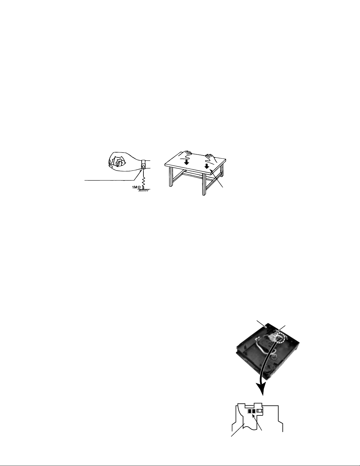
Preventing static electricity
1. Grounding to prevent damage by static electricity
Electrostatic discharge (ESD), which occurs when static electricity stored in the body, fabric, etc. is discharged,
can destroy the laser diode in the traverse unit (optical pickup). Take care to prevent this when performing repairs.
2. About the earth processing for the destruction prevention by static electricity
In the equipment which uses optical pick-up (laser diode), optical pick-up is destroyed by the static electricity of
the work environment.
Be careful to use proper grounding in the area where repairs are being performed.
2-1 Ground the workbench
Ground the workbench by laying conductive material (such as a conductive sheet) or an iron plate over
it before placing the traverse unit (optical pickup) on it.
2-2 Ground yourself
Use an anti-static wrist strap to release any static electricity built up in your body.
(caption)
Anti-static wrist strap
Conductive material
(conductive sheet) or iron plate
3. Handling the optical pickup
1. In order to maintain quality during transport and before installation, both sides of the laser diode on the
replacement optical pickup are shorted. After replacement, return the shorted parts to their original condition.
(Refer to the text.)
2. Do not use a tester to check the condition of the laser diode in the optical pickup. The tester's internal power
source can easily destroy the laser diode.
4. Handling the CD changer unit (optical pickup)
1. Do not subject the CD changer unit (optical pickup) to strong shocks, as it is a sensitive, complex unit.
2. Cut off the shorted part of the flexible cable using nippers, etc. after replacing the optical pickup. For specific
details, refer to the replacement procedure in the text. Remove the anti-static pin when replacing the CD changer
unit. Be careful not to take too long a time when attaching it to the connector.
3. Handle the flexible cable carefully as it may break when subjected to strong force.
4. It is not possible to adjust the semi-fixed resistor that adjusts the laser power.
Do not turn it
CD changer
unit
CD changer
mechanism
assembly
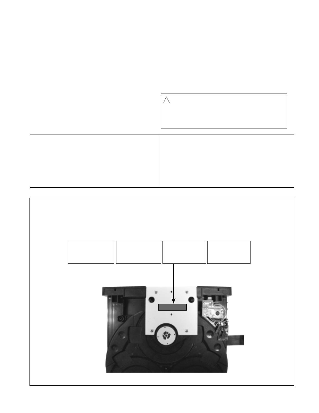
Attention when traverse unit is decomposed
*Please refer to "Disassembly method" in the text for pick-up and how to
detach the CD changer mechanism.
1. Remove the CD changer unit.
2. Disconnect the harness from connector on the CD motor board.
3. Solder is put up before the card wire is removed from connector CN601
on the main board as shown in Fig.1 and Fig. 2.
(When the wire is removed without putting up solder, the CD pick-up
assembly might destroy.)
4. Please remove solder after connecting the card wire with CN601 when
you install picking up in the substrate.
1-4
Flexible cable
Fig.1
Soldering
Fig.2
Page 5
MX-K1
Disassembly method
Commence disassembly of this set by removing the main units and then proceed to the components and
assemblies inside the units.
Replacement of the fuses and the power IC
Top cover
CD changer unit
Front panel assembly
Chassis unit
CD changer unit
Removing the main PCB
Removing the CD changer mechanism assembly
Removing the CD pickup
Replacing the loading motor and belt of the CD changer tray
Replacing the CD tray rotor belt of CD changer, and removing the motor
Front panel assembly
Removing the cassette deck mechanism
Removing the earphone jack PCB
Removing the control/FL PCB
Removing the switch PCB and ACTIVE BASS EX. switch PCB
Removing the cassette deck main motor, and replacing the main belts
Removing the leaf switches of the cassette deck mechanism
Removing the cassette deck heads
Chassis unit
Removing the 3-pin regulator
Removing the power amp and supply PCB and the Power Trans PCB
1-5
Page 6
MX-K1
<Disassembly of the main blocks of this set>
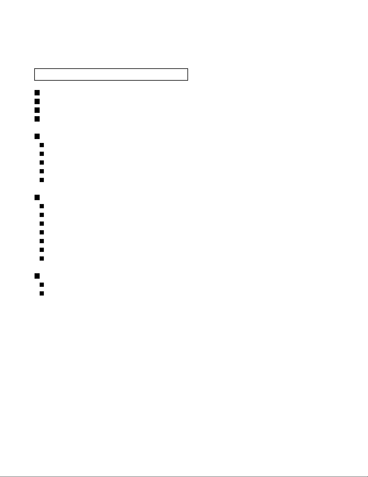
Replacement of the fuses and the power IC
Replacing the fuses (See Fig.1)
Prior to performing the following procedure, remove
the top cover.
1.
Replace the fuses inside.
[Caution] Be sure to use fuses with the specified
ratings.
Replacing the power IC
(See Fig.2 and 3)
Prior to performing the following procedure, remove
the top cover.
Also remove the rear panel. (See Fig.33)
1.
Remove the screw "A" from the bracket that retains
the power IC.
2.
Remove the solder fixing the power IC.
Fuse (F952)
1.6A 250V
Chassis
Power amp
and supply PCB
Fuse (F951)
1A 250V
Power trans PCB
Fig.1
Heat sink
A
Fig.2
Power amp and supply PCB
Heat sink
Power IC
soldering part
1-6
Fig.3
Page 7
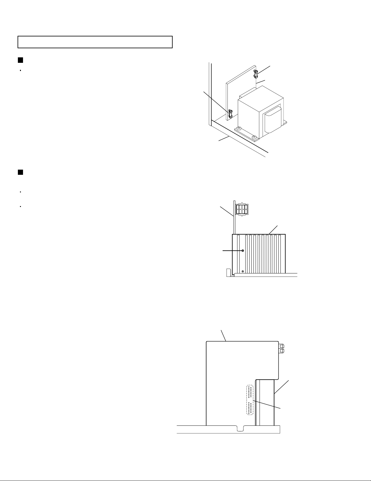
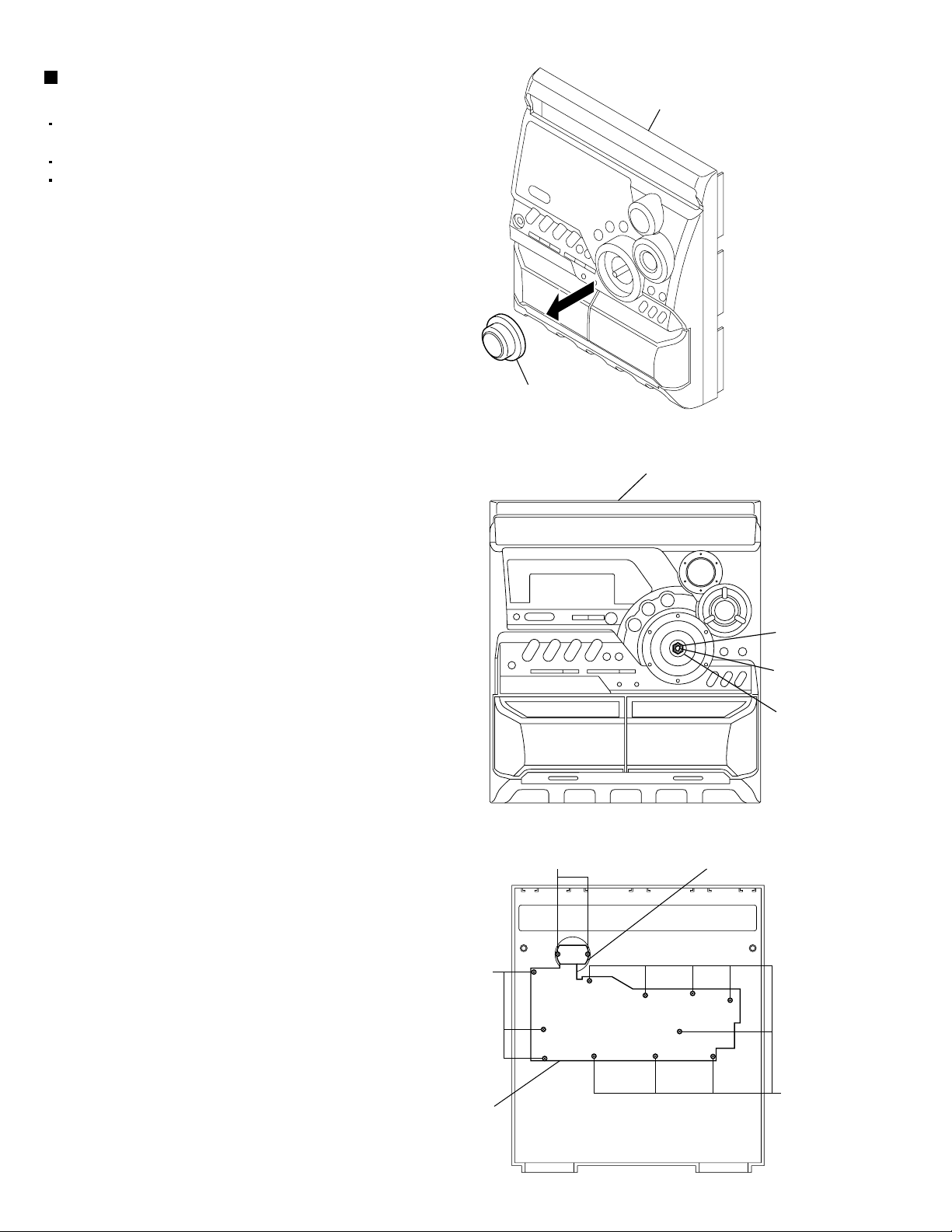
Removing the top cover
(See Fig.4 and 5)
1.
Remove the six screws "B" that retain the top cover
from the rear of the body.
2.
Remove the four screws "C" that retain the top
cover from the two sides of the body.
3.
Remove the top cover from the body by lifting it
toward the rear.
Top cover
MX-K1
B
BB
Fig.4
Front panel assembly
C
Fig.5
1-7
Page 8
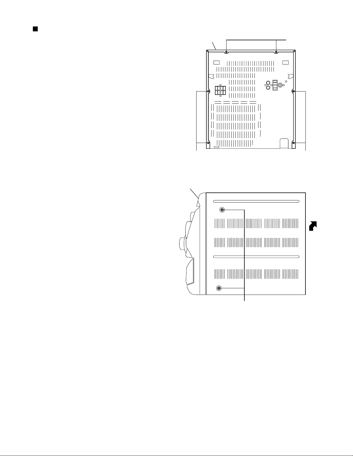
MX-K1
Removing the CD changer unit
(See Fig.6 to 9)
Prior to performing the following procedures,
remove the top cover.
[Caution] Although the CD mechanism unit can be
removed without removing the CD tray
panel, it is still recommended to remove it
in order to prevent damage.
a.
From the front panel side of this set, push in the
sections marked with arrows and pull out the CD
tray toward the front.
b.
Remove the CD tray panel by pushing both of its
extremities upward in the direction of the arrows.
c.
Push the CD tray deep into the set.
1.
Disconnect the cassette head wires from the
connectors CN307 and CN308 on the main PCB,
which is located below the CD changer unit.
2.
Disconnect the card wires from the connectors
CN301, CN302 and CN305 on the main PCB.
3.
Disconnect the parallel wires from the connectors
CN902A, CN902B and CN902C on the power amp
and supply PCB.
4.
From the rear of the set, remove the two screws
"D" retaining the CD changer unit, then remove the
three screws "E" and the screw "F" retaining the
ANTENNA terminal and the AUX IN terminal.
5.
Push down and disengage the two claws "a"
holding the CD changer unit at the bottom of its
front panel and then remove the CD changer unit
(Fig. 9).
CD tray panel
Fig.6
1-8
AUX IN
terminal
CD tray panel
Fig.7
D
F
ANTENNA
E
terminal
CD changer
unit
Fig.8
Claw a
Fig.9
Page 9
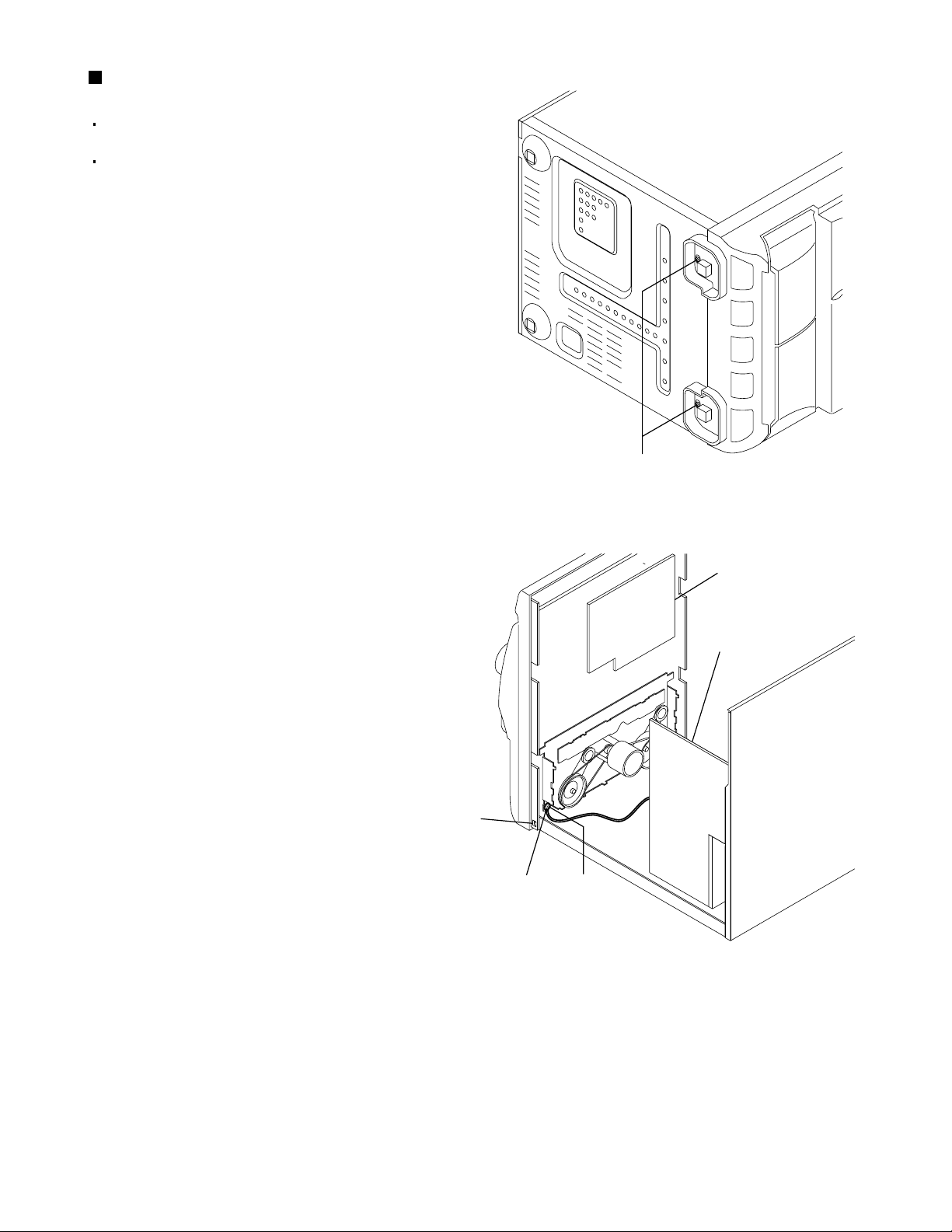
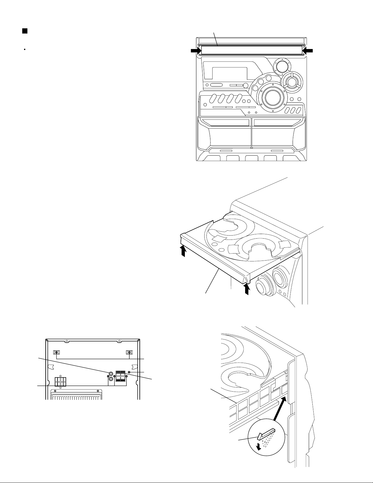
Removing the front panel assembly
(See Fig.10 and 11)
Prior to performing the following procedures,
remove the top cover.
Also remove the CD changer unit.
1.
Disconnect the parallel wire and card wire from the
connectors CN101 and CN901 on the power amp
and supply PCB.
2.
Remove the two screws "G" retaining the front
panel assembly onto the bottom of the body.
3.
Remove the screw "H" retaining the cassette deck
mechanism and then remove the GND lug "b" that
comes from the power amp and supply PCB.
4.
Remove the solder connecting the wire on the
control/FL PCB.
5.
Disengage the claws "c" on both sides at the
bottom of the front panel assembly and then
remove the assembly.
MX-K1
G
Claw c
GND lug b
Fig.10
Control/FL PCB
Power amp and
supply PCB
H
Fig.11
1-9
Page 10
MX-K1
<Disassembly of units and assembly
inside this set>
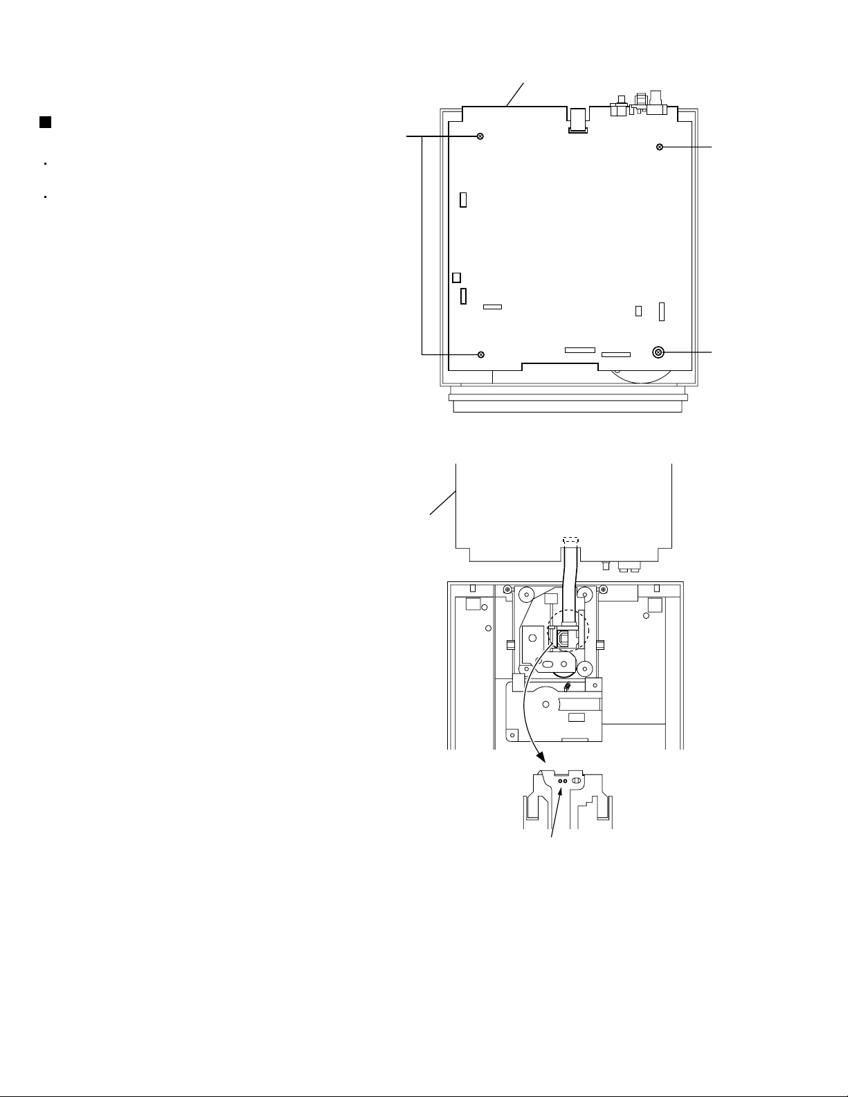
Removing the main PCB
(See Fig.12 and 13)
Prior to performing the following procedures,
remove the top cover.
Also remove the CD changer unit.
1.
Disconnect the wires from CN602 and CN603 on
the main PCB, which is located on the backside of
the CD changer unit.
2.
Disconnect the card wire from connector CN604 of
the main PCB at the back of the CD changer unit.
3.
The three screws "I" and the screw with the washer
"J" that retain the main PCB should be removed.
4.
Remove the main PCB by pulling it toward the side
where the CN601 is located.
5.
Using solder, short the CD pickup to connect to
short round.
[Caution]
6.
Disconnect the card wire from the connector
CN601 on the main PCB and then remove the
main PCB.
After re-connecting the wires, be sure to
remove the shorting solder from the GND
connection.
I
Main PCB
CN604
CN603CN602
Main PCB
Fig.12
CN601
CN601
I
J
1-10
Short round
Fig.13
Page 11
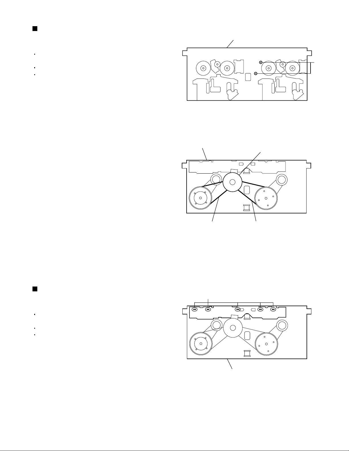
Removing the CD changer mechanism
assembly (See Fig.14 to 16)
Prior to performing the following procedures,
remove the top cover.
Also remove the CD changer unit.
1.
Remove the spring "d" from the front surface of the
CD changer mechanism unit.
2.
Turn the CD changer mechanism unit upside down,
and remove the spring "e" connecting the unit to
the CD changer mechanism assembly.
[Note] When re-assembling after the disassembly
work, apply bonding agent on the spring to
prevent it from slipping off.
3.
Remove the two screws "K" retaining the CD
changer mechanism assembly.
MX-K1
[Note]
Spring d
[Caution] When replacing the CD changer
mechanism assembly, be sure not to
mistake the positions of the red and blue
dampers.
CD changer
mechanism
assembly
K
Fig.15
CD changer
unit
Fig.14
Red Red
[Note]
Spring e
CD changer
mechanism
assembly
Fig.16
BlueBlue
1-11
Page 12

MX-K1
Removing the CD pickup (See Fig.17)
Prior to performing the following procedures,
remove the top cover.
Also remove the CD changer unit.
Also remove the CD changer mechanism
1.2.Widen the section "f ".
While keeping the section "f" wide open, push the
section "g" in the direction of the arrow to remove
the shaft, and then remove the CD pickup.
Replacing the loading motor and belt
of the CD changer tray (See Fig.18)
Prior to performing the following procedure,
remove the top cover.
1.
Pull out the CD changer tray.
2.
Remove the belt from the pulley.
3.
Remove the two screws "L" retaining the CD
changer tray loading motor.
[Caution] When pushing in the CD changer tray, be
sure to lower the CD changer mechanism
assembly by manually turning the UD
cam gear in the direction of the arrow.
Replacing the CD tray rotor belt of the
CD changer, and removing the motor
(See Fig.19 and 20)
Pulley
Belt
L
Shaft
CD pickup
gf
Fig.17
UD cam gear
Prior to performing the following procedures,
remove the top cover.
Also remove the CD changer unit.
1.
Remove the two screws "M" retaining the stopper
brackets on both sides of the CD changer unit.
2.
Remove the stopper brackets from both sides of
the CD changer unit.
3.
Pull out the CD tray from the CD changer unit, all
the way and then lift the tray upward to remove.
4.
Turn the CD tray upside down and remove the tray
rotor belt from the pulley.
5.
Turn the CD tray upside down and disconnect the
card wire from the connector CN605 on the CD
tray rotor motor assembly.
6.
Remove the two screws "N" retaining the CD tray
rotor motor, and then remove the CD tray rotor
motor.
CD changer
tray
Fig.18
CD tray
rotor belt
1-12
Stopper bracket
M
Fig.19 Fig.20
CN605
Pulley
N
Page 13
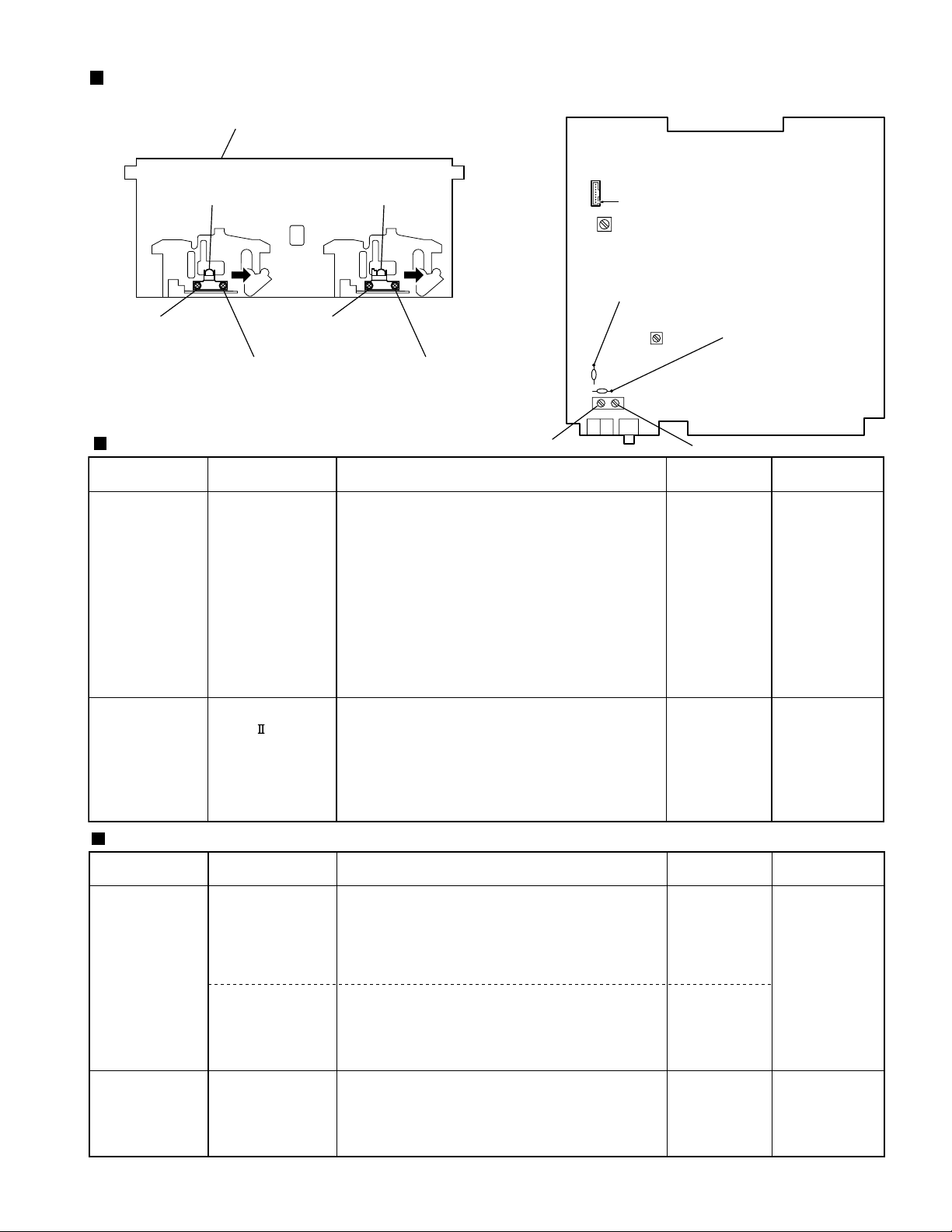
MX-K1
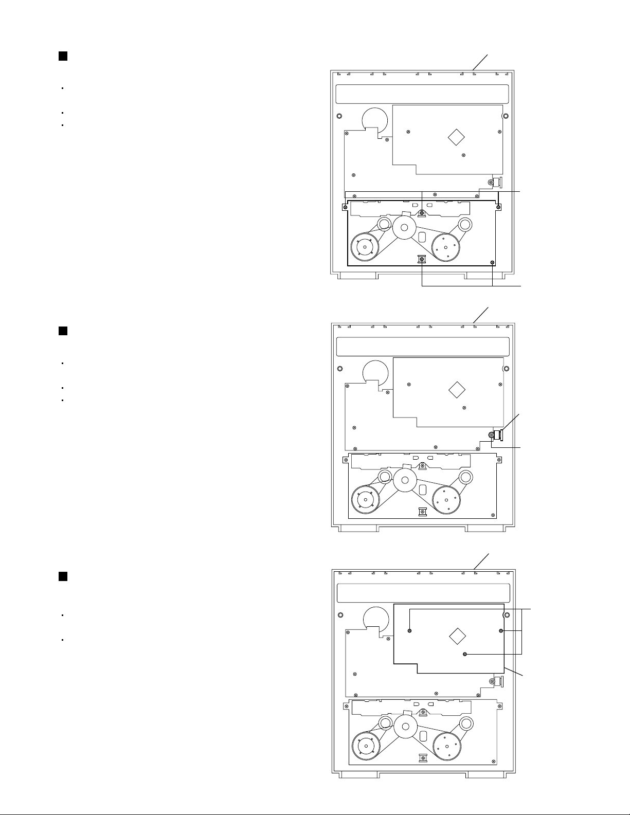
Removing the cassette deck mechanism
(See Fig.21)
Prior to performing the following procedure, remove
the top cover.
Also remove the CD changer unit.
Also remove the front panel assembly.
1.Remove the five screws "O" retaining the cassette
deck mechanism from the back of the front panel
assembly.
Removing the earphone jack PCB
(See Fig.22)
Prior to performing the following procedure, remove
the top cover
Also remove the CD changer unit.
Also remove the front panel assembly.
Remove the screw with the washer, "P" that retains
1.
the earphone jack PCB from the back of the front
panel assembly.
Fig.21
Front panel
assembly
O
O
Front panel
assembly
Earphone jack
PCB
P
Removing the control/FL PCB
(See Fig.23)
Prior to performing the following procedure, remove
the top cover.
Also remove the CD changer unit.
1.Remove the three screws "Q" that retain the
control/FL PCB from the back of the front panel
assembly.
Fig.22
Fig.23
Front panel
assembly
Q
Control/FL
PCB
1-13
Page 14
MX-K1
Removing the switch PCB and ACTIVE
BASS EX. switch PCB (See Fig.23 to 26)
Prior to performing the following procedures,
remove the top cover.
Also remove the CD changer unit.
Also remove the front panel assembly.
1.
Pull out the volume control knob from the front of
the front panel assembly.
2.
Remove the nut and washer retaining the volume
knob shaft.
3.
Remove the three screws "Q" retaining the
control/FL PCB from the back of the front panel
assembly.
4.
Remove the control/FL PCB.
5.
Remove the eleven screws "R" retaining the switch
PCB.
6.
Remove the two screws "S" retaining the ACTIVE
BASS EX. switch PCB.
Front panel assembly
Volume knob
Fig.24
Front panel
assembly
Nut
Volume shaft
Washer
Fig.25
S
R
ACTIVE BASS EX. switch PCB
1-14
Switch
R
PCB
Fig.26
Page 15
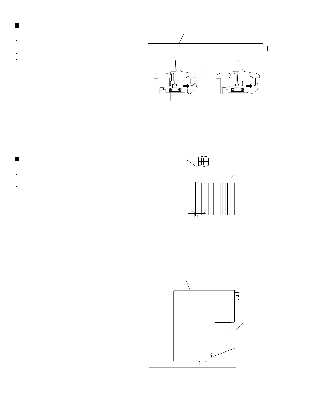
Removing the cassette deck main
motor, and replacing the main belts
(See Fig.21, 27 and 28)
Prior to performing the following procedures,
remove the top cover.
Also remove the CD changer unit.
Also remove the front panel assembly.
1.
Remove the five screws "O" retaining the cassette
deck mechanism.
2.
Remove the cassette deck mechanism.
3.
Remove the two screws "T" retaining the main
motor from the front side of the cassette deck.
[Caution]
4.
From the backside of the cassette deck, remove
the main motor and two main belts.
After attaching the main motor, check the
orientation of the motor and the polarity of
the wires.
Cassette deck mechanism
(Front side)
Fig.27
Cassette deck mechanism
(Back side)
MX-K1
T
Cassette deck main motor
[Caution]
The lengths of the cassette A (playback
only) and cassette B (record/play) main
belts are different. When attaching the
main belts, use the longer belt for
cassette A.
Removing the leaf switches of the
cassette deck mechanism
(See Fig.21 and 29)
Prior to performing the following procedures,
remove the top cover.
Also remove the CD changer unit.
Also remove the front panel assembly.
1.
Remove the five screws "O" that retain the cassette
deck mechanism.
2.
Remove the cassette deck mechanism.
3.
Turn the cassette deck mechanism upside down.
4.
Remove the solder from around the leaf switches.
5.
Pull out the leaf switches from the front side of the
cassette deck mechanism.
Main belt
(For B cassette)
Solder side of leaf switch
Cassette deck mechanism
(Back side)
Main belt
(For A cassette)
Fig.28
Fig.29
1-15
Page 16
MX-K1
Removing the cassette deck heads
(See Fig.21 and 30)
Prior to performing the following procedures,
remove the top cover.
Also remove the CD changer unit.
Also remove the front panel assembly.
1.
Remove the five screws "O" that retain the cassette
deck mechanism.
2.
Remove the cassette deck mechanism and place it
so that the front side faces up.
3.
Remove the solder from the bottom side of the
head terminal and disconnect the wire.
4.
Remove the screw "U" that retains the head.
5.
Loosen the screw "V" that retains the head.
6.
Hold the head and slide it in the direction of the
arrow to remove it.
Removing the 3-pin regulator
(See Fig.31 and 32)
Prior to performing the following procedures,
remove the top cover.
Also remove the rear panel. (See Fig.33)
Cassette deck mechanism
(Front side)
PB Head
VU
Power amp
and supply PCB
REC/PB Head
VU
Fig.30
Heat sink
1.2.Remove the screw "W" that retains the bracket
holding the 3-pin terminal regulator.
Remove the solder fixing the 3-pin regulator.
W
Fig.31
Power amp and supply PCB
Heat sink
Solder on the
3-pin regulator
1-16
Fig.32
Page 17
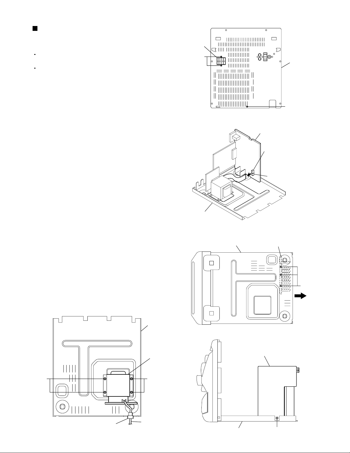
Removing the power amp and supply
PCB and the power trans PCB
(See Fig.33 to 37)
Prior to performing the following procedures,
remove the top cover.
Also remove the CD changer unit.
1.
Remove the two screws "X" that retain the
SPEAKERS terminals.
2.
Remove the screw "Y" that retains the rear panel,
and then remove the rear panel.
3.
Disconnect the parallel wires from the connectors
CN901A and CN901B on the power amp and
supply PCB.
4.
Disconnect the parallel wire and card wire from
the connectors CN101 and CN901 on the power
amp and supply PCB.
5.
Remove the three screws "Z" retaining the heat
sink onto the bottom of the chassis.
6.
Remove the screw "AA" that retain the power amp
and supply PCB and then remove the assembly.
7.
Remove the clamp of AC power cord from the
chassis.
8.
Remove the four screws "AB" that retain the
power trans PCB and then remove the assembly.
Speaker
terminal
MX-K1
X
Fig.33
Power amp and
supply PCB
CN901B
CN901A
Rear panel
Y
AB
(Top view)
Chassis
Power trans PCB
AB
Chassis
Chassis
Fig.34
Heat sink
Z
Rear
Fig.35
Power amp and
supply PCB
Clamp
Fig.37
AC power cord
Chassis
Fig.36
AA
1-17
Page 18

MX-K1
Adjustment method
Measurement instruments required
for adjustment
1. Low frequency oscillator,
This oscillator should have a capacity to output 0dB
to 600ohm at an oscillation frequency of 50Hz-20kHz.
2. Attenuator impedance : 600ohm
3. Electronic voltmeter
4. Frequency counter
5. Wow flutter meter
6. Test tape
VT712 : For Tape speed and wow flutter ( 3kHz)
VT703 : For Head angle(10kHz),Play back frequency
characteristics(1kHz),and dubbing frequency
characteristics(63,1,10kHz)
7. Blank tape
TAPE : AC-225, TAPE : AC-514
8. Torque gauge : For play and back tension
Forward ; TW2111A, Reverse ; TW2121A
Fast Forward and Rewind ; TW2231A
9. Test disc
: CTS-1000(12cm),GRG-1211(8cm)
10. Jitter meter
Radio input signal
AM modulation frequency : 400Hz
Modulation factor : 30%
FM modulation frequency : 400Hz
Frequency displacement : 22.5kHz
Frequency Range
AM 531kHz~1710kHz
FM 87.5MHz~108MHz
Standard measurement positions of volume
and switch
Power : Standby (Light STANDBY Indicator)
S,A,BASS : OFF
Sound mode : OFF
Main VOL. : 0 Minimum
Travers mecha set position : Disc 1
Mic MIX VOL : MAX
ECHO : OFF
Measurement conditions
Power supply voltage
AC120V (60Hz)
Measurement
output terminal : Speaker out
: TP101(Measuring for TUNER/DECK/CD)
: Dummy load 6ohm
Precautions for measurement
1. Apply 30pF and 33kohm to the IF sweeper output
side and 0.082 F and 100kohm in series to
the sweeper input side.
2. The IF sweeper output level should be made as
low as possible within the adjustable range.
3. Since the IF sweeper is a fixed device, there is
no need to adjust this sweeper.
4. Since a ceramic oscillator is used, there is no need
to perform any MPX adjustment.
5. Since a fixed coil is used, there is no need to adjust
the FM tracking.
6. The input and output earth systems are separated.
In case of simultaneously measuring the voltage
in both of the input and output systems with an
electronic voltmeter for two channels, therefore,
the earth should be connected particularly.
7. In the case of BTL connection amplifier, the minus
terminal of speaker is not for earthing. Therefore,
be sure not to connect any other earth terminal
to this terminal. This system is of an OTL system.
1-18
Page 19
Arrangement of adjusting positions
Cassette deck mechanism
(Front side)
MX-K1
PB Head
(Deck-A)
Head azimuth screw
(Forward side)
Head screw Head screw
Head azimuth screw
Tape recorder section
Items
Cassette Head
Azimuth Alignments
Measurement
conditions
Test tape
: VT703 (10kHz)
Measurement output
terminal
: Left and Right
speaker output
(6-ohm loaded)
or
Headphone Output
(32-ohm loaded)
(Forward side)
1. Playback the test tape VT703 (10KHz) or equivalent.
2. Adjust the head azimuth screw to obtain maximum
output and both output of L / R is in 3dB.
3. Put on the screw lock paint after alignments.
REC/PB Head
(Deck-B)
Measurement method
Antenna coil
CN308
8-Pin
L301
FM VT voltage
measurement point
T1
R6
R3
L2
AM VT voltage
measurement point
Main P.C.B. Ass'y
OSC coil
Standard
values
Maximum output
Adjusting
positions
Head azimuth
screw
Adjust the head
azimuth screw only
when the head has
been changed.
Recording Bias
Frequency Alignment
Tuner section
Items
AM Tracking
Alignments
AM IFT Alignments
Test tape
: TYPE AC-514
Measurement output
terminal
: Erase head terminal
(CN308 8-Pin)
Measurement
conditions
Input signal
: 530kHz
Measurement point
: Resistor R3 (AM)
Resistor R6 (FM)
Input signal
: 600kHz
Input signal
: 530kHz
1. Insert the recording tape in deck-B.
2. Starting the recording.
3. Adjust the oscillation frequency to 80KHz+/-3KHz by
core of Oscillation coil of L301.
Measurement method
OSC coil adjustment
1.Set the Signal Generator signal to 530KHz the feed to
Loop Antenna.
2.Receiving the signal and the adjust the OSC coil (L2)
obtain the V.T is 1.40V +/-0.05V.
Antenna coil check or adjustment
1.Change the receiving frequency to 600KHz.
2.Adjust the Antenna coil ( L2 ) obtain maximum sensitivity.
(Adjust the SSG output to out of AGC range.)
1. Set the receiving frequency to 530KHz.
2. Feed the 450KHz signal to AM IF input.
3.Adjust the IFT Block T1 obtain to maximum output.
(Adjust the SSG output to out of AGC range.)
80kHz+/-3kHz
Standard
values
V. T
: 1.40V+/-0.05V
Maximum
sensitivity
Maximum output
Bias coil: L301
Use the HighImpedance Probe for
Frequency counter
input.
Adjusting
positions
OSC/Antenna coil
: L2
Adjust the OSC coil
only when the AM coil
block has been
changed.
IFT (T1)
Adjust the IFT only
when the IFT block has
been changed.
Note: The adjustment of CD section is not required.
1-19
Page 20

MX-K1
Flow of functional operation until TOC read
Power ON
Play Key
Slider turns REST
SW ON.
Automatic tuning
of TE offset
Confirm that the voltage at the pin5
of CN602 is "H"\"L"\"H".
Check Point
Tracking error waveform at TOC reading
Approx.3sec
Tracking
servo
off states
Automatic measurement
of TE amplitude and
automatic tuning of
TE balance
VREF
pin 20 of
IC611(TE)
Approx
1.8V
Disc states
to rotate
Tracking
servo
on states
Disc to be
braked to stop
TOC reading
finishes
500mv/div
2ms/div
Fig.1
Laser ON
Detection of disc
Automatic tuning of
Focus offset
Automatic measurement of
Focus S-curve amplitude
Disc is rotated
Focus servo ON
(Tracking servo ON)
Automatic measurement of
Tracking error amplitude
Automatic tuning of
Tracking error balance
Check that the voltage at the
pin40 of IC601 is + 5V?
Confirm that the Focus error
S-cuve signal at the pin32 of
IC601 is approx.2Vp-p
Confirm that the signal from
pin24 IC601 is 0V as a
accelerated pulse during
approx.400ms.
Confirm the waveform of
the Tracking error signal.
at the pin 20 of IC611 (R643)
(See fig-1)
1-20
Automatic tuning of
Focus error balance
Automatic tuning of
Focus error gain
Automatic tuning of
Tracking error gain
TOC reading
Play a disc
Confirm the eys-pattern
at the lead of TP3
Page 21

MX-K1
Maintenance of laser pickup
(1) Cleaning the pick up lens
Before you replace the pick up, please try to
clean the lens with a alcohol soaked cotton
swab.
(2) Life of the laser diode
When the life of the laser diode has expired,
the following symptoms will appear.
1. The level of RF output (EFM output:ampli
tude of eye pattern) will below.
Is the level of
RFOUT under
1.25V 0.22Vp-p?
YES
O.K
NO
Replace it.
Replacement of laser pickup
Turn off the power switch and,disconnect the
power cord from the AC OUTLET.
Replace the pickup with a normal one.(Refer
to "Pickup Removal" on the previous page)
Plug the power cord in,and turn the power on.
At this time,check that the laser emits for
about 3seconds and the objective lens moves
up and down.
Note: Do not observe the laser beam directly.
Play a disc.
Check the eye-pattern at TP3.
Finish.
(3) Semi-fixed resistor on the APC PC board
The semi-fixed resistor on the APC printed circuit board which is
attached to the pickup is used to adjust the laser power.Since this adjustment should be performed to match the
characteristics of the whole optical block, do not touch the semi-fixed resistor.
If the laser power is lower than the specified value,the laser diode is almost worn out, and the laser pickup should
be replaced.
If the semi-fixed resistor would be adjusted when the pickup operates normally,the laser pickup may be damaged
due to excessive current.
1-21
Page 22

MX-K1
Description of major ICs
AN22000A (IC611) : CD-DA Head Amp.
1. Terminal layout
2. Pin function
132
16 17
3. Block diagram
624754 8
RFOUT
RF_EQ
RFIN
AGC
Pin
Symbol
No.
1 PD I APC Amp. input terminal
2 LD O APC Amp. output terminal
3 VCC - Power supply terminal
4 RFN I RF adder Amp. inverting input
5 RFOUT O RF adder Amp. output terminal
6 RFIN I AGC input terminal
7 CAGC I Input terminal for AGC loop
8 ARF O AGC output terminal
9 CBA I Capacitor connecting terminal
10 3TOUT O 3 TENV output terminal
11 CBOO I Capacitor connecting terminal
12 BDO O BDO output terminal
13 COFTR I Capacitor connecting terminal
14 OFTR O OFTR output terminal
11 12
BDO
I/O
terminal
filter capacitor
for HPF-Amp.
for envelope detection on the
darkness side
for envelope detection on the
light side
13 14
OFTR
9
Function
Pin
Symbol
No.
15 NRFDET O NRFDET output terminal
16 GND - Ground
17 VREF O VREF output terminal
18 VDET O VDET output terminal
19 TEBPF I VDET output terminal
20 TEOUT O TE Amp. output terminal
21 TEN I TE Amp. inverting input
22 FEN I FE Amp. inverting input
23 FEOUT O FE Amp. output terminal
24 GCTL O GCTL & APC terminal
25 FBAL O FBAL control terminal
26 TBAL O TBAL control terminal
27 E I Tracking signal input terminal 1
28 F I Tracking signal input terminal 2
29 D I Focus signal input terminal 4
30 B I Focus signal input terminal 3
31 C I Focus signal input terminal 2
32 A I Focus signal input terminal 1
I/O
Function
terminal
terminal
32
31
30
29
27
28
NRFDET
AMP
AMP
AMP
AMP17GCA BCA
+
-
GCA BCA
GCA BCA
GCA BCA
SUBT
SUBT
3TENV
-
+
-
+
VDET
-
+
10
15
22
23
21
20
19
18
2
LD
1-22
GCTL26TBAL
25 16 3
FBAL
PD
1
Page 23

BA15218 (IC102) : Dual low noise operational amp.
1. Terminal layout
MX-K1
OUT1
- IN1
+-
+IN1
VEE
Vcc
OUT2
- IN2
-+
+IN2
BA5936S (IC621) : 6 channel BTL driver
1. Block diagram
32
31
30
29
x2
x2
D
D
x3/828x3/8
LEVEL SHIFT
LEVEL SHIFT
LEVEL SHIFT
D
D DDDD
BIAS
1 2 3 4 5 6 7 8 9 10 11 12 13 14 15 16
27 26 25 24 23 22 21
MUTE
T. S. D
13.3k
-+
100
BIAS
-+
13.3k
100
OF REG-OUT
Vcc Vcc
DETECTION
CURRENT
BIAS
Vcc 100
13.3k
100
+-
13.3k
10k
+-
10k
BIAS
20
BIAS
D
+-
LEVEL SHIFT
LEVEL SHIFT
x3/8x3/8
19
D
18 17
D D
LEVEL SHIFT
x2x2
2. Pin function
Pin
No.
Symbol
I/O
1 OUT1- O CH1 negative output
2 OUT1+ O CH1 positive output
3 OUT2- O CH2 negative output
4 OUT2+ O CH2 positive output
5 IN2 I CH2 input
6 IN1 I CH1 input
7 VCC - Power supply terminal
8 VCC - Power supply terminal
9 REG-I I Regulator current detection terminal
10 REG-B O
Connect to base terminal of external transistor
11 REG-OUT O Constant voltage output (Connect to
collector terminal of external transistor)
12 IN3-R I CH3 reverse input
13 IN3-F I CH3 forward input
14 OUT3+ O CH3 positive output
15 OUT3- O CH3 negative output
16 GND - Ground
Function
Pin
No.
Symbol
I/O
Function
17 OUT4- O CH4 negative output
18 OUT4+ O CH4 positive output
19 OUT5- O CH5 negative output
20 OUT5+ O CH5 positive output
21 IN5 I CH5 input
22 IN4 I CH4 input
23 VCC - Power supply terminal
24 BIAS IN I Bias input terminal
25 GND - Ground
26 GND - Ground
27 MUTE IN I Mute input terminal
28 IN6-R I CH6 reverse input
29 IN6-F I CH6 forward input
30 OUT6+ O CH6 positive output
31 OUT6- O CH6 negative output
32 GND - Ground
1-23
Page 24

MX-K1
LA1823 (IC1) : 1chip AM/FM, MPX tuner system
1. Block diagram
24
FM
RF
AM
RF
1 2 4 5 10 11 126 7 8 93
23
GND2
REG VCC1 GND1
22
AM
MIX
AM
OSC
21
VCC2
OSC
BUFFER
OSC
2. Pin function
Pin
No.
Symbol
I/O
1 AM_RFIN I AMRF signal input
2 REG. 3 AM_OSC - AM local oscillation circuit
4 VCC_1 - Power supply terminal
5
FM_MIXOUT
O Output terminal for FM mixer
6 GND_1 - Ground
7
IF_BUFFER
O IF buffer output
8 ST_IND O Stereo indicator output
9
AM_MIXOUT
O Output terminal for AM mixer
10 FM_IF IN I Input of FMIF signal
11 AM_IF IN I Input of AMIF signal
12 AGC I AGC voltage input terminal
Function
20
FM
FM
MIX
15
PHASE
COMP
FM
S-METERAMDET
FM
IF
I/O
PILOT
DET
FF
AM
MUTE
IF
BUFFER
ST SW
Pin
No.
17 16
DECODER
VCO FF FF
TRIG
STSD
Symbol
13 FM_DET O FM detection signal output
14
ST/MON_SW
15
AM/FM_SW
I Stereo/Monaural switching signal input
I AM/FM switching signal input
16 L_OUT O Output L-channel
17 R_OUT O Output R-channel
18 MPX_IN I Multiplex signal input
19 DET_OUT O AM/FM detection output
20 FM_OSC - FM local oscillation circuit
21 VCC_2 - Power supply terminal
22
FM_RFOUT
O Output of FMRF signal
23 GND_2 - Ground
24 FM_RFIN I Input of FMRF signal
14
IF
1319 18
FM
DET
AGC
Function
1-24
Page 25

LC72136N (IC2) : PLL Frequency synthesizer
1.Terminal layout
1
CLOCK
VCOSTOP
AM/FM
MW
SDIN
2. Block diagram
XTI
FM
CE
DI
DO
LW
2
3
4
5
6
7
8
9
10
11
22
21
20
19
18
17
16
15
14
13
12
XT
GND
LPFI
LPFO
PD
VCC
FMIN
AMIN
NC
IFCNT
IFIN
MX-K1
1
22
16
15
3
4
5
6
17
21
3. Pin function
Pin
Symbol
No.
XTI
1
FM
2
CE
3
4
5
6
7
8
9
10
11
DI
CLOCK
DO
VCOSTOP
AM/FM
NC
NC
SDIN
Reference
Driver
Swallow Counter
1/2
C
2
B
I/F
Powe r
on
Reset
Function
I/O
X'tal oscillator connect (75KHz)
I
LOW:FM mode
O
When data output/input for 4pin(input) and
I
Swallow Counter
1/16,1/17 4bit
1/16,1/17 4bit
12bit
Programmable
DriverS
Data Shift Register & Latch
7821113
6pin(output): H
Input for receive the serial data from
I
controller
Sync signal input use
I
Data output for Controller
O
Output port
"Low": MW mode
O
Open state after the power on reset
O
Input/output port
Input/output port
Data input/output
I/O
Phase
Detector
Charge Pump
Unlock
Detector
Universal
Counter
Pin
No.
12
13
14
15
16
17
18
19
20
21
22
Symbol
IFIN
IFCNT
NC
AMIN
FMIN
VCC
PD
LPFO
LPFI
GND
XT
18
19
20
12
I/O
Function
IF counter signal input
I
IF signal output
O
Not use
-
AM Local OSC signal output
I
FM Local OSC signal input
I
Power supply(VDD=4.5 5.5V)
When power ON:Reset circuit move
PLL charge pump output(H: Local OSC
O
frequency Height than Reference frequency.
L: Low Agreement: Height impedance)
Output for active lowpassfilter of PLL
O
Input for active lowpassfilter of PLL
I
Connected to GND
X'tal oscillator(75KHz)
I
1-25
Page 26

MX-K1
TA8189N (IC401) : REC/PB amp.
1. Terminal layout 2. Block diagram
NF1
EQ1
GND
1
24
23
22
21
20
19
18
17
16
15
14
13
CH2_A
CH2_B
NF2
EQ2
PREOUT2
A/B_SW
VCC
CG
REC_OUT2
REC_NF2
REC_IN2
ALC
23CH2_B
24CH2_A
1CH1_A
2CH1_B
2
3
4
5
6
7
8
9
10
11
12
CH1_A
CH1_B
PREOUT1
MIX_OUT
GND1
EQSW
REC_OUT1
REC_NF1
REC_IN1
3. Pin function
Pin
No.
Symbol
I/O
1 CH1_A I Input for playback amp. (Ch1): A cassette
(PB)
2 CH1_B I Input for playback amp. (Ch1): B cassette
(REC/PB)
3 NF1 I NF terminal for playback amp.
4 EQ1 O Metal output for playback amp.
5 PREOUT1 O Output terminal for playback amp.
6 MIX_OUT O Mixing output
7 GND1 - Ground
8 EQSW I Metal/Normal mode select switch
9
REC_OUT1
O Output for recording amp.
10 REC_NF1 I NF terminal for recording amp.
11 REC_IN1 I Input for recording amp.
12 GND1 - Ground terminal
Function
NF2
22
3 54 6 7 8
NF1
Ch2
+
+
Ch1
-
Pin
No.
EQ2
EQ1
PREOUT2
2021 19
PREOUT1
Symbol
A/B_SW
A/B
ref1
V
MIX_OUT
I/O
18
I
VCC
ref
GND1
13 ALC I ALC filter terminal
14 REC_IN2 I Input for recording amp.
15 REC_NF2 I NF terminal for recording amp.
16
REC_OUT2
O Output for recording amp.
17 CG O Charge detection terminal
18 VCC - Power supply terminal
19 A/B_SW I REC amp. Select switch (A cassette/B
cassette)
20 PREOUT2 O Output terminal for playback amp.
21 EQ2 O Metal output for playback amp.
22 NF2 I NF terminal for playback amp.
23 CH2_B I Input for playback amp. (Ch2): B cassette
(REC/PB)
24 CH2_A I Input for playback amp. (Ch2): A cassette
(PB)
17
M/N
CG
ref2
V
EQSW
REC_OUT2
16
9
REC_OUT1
-
Ch2
+
+
Ch1
-
Function
REC_NF2
15
14 REC_IN2
13 ALC
ALC
12 GND
11 REC_IN1
10
REC_NF1
1-26
Page 27

TC74HC4094AP (IC402) : 8-bit shift and store resister
1. Terminal layout
MX-K1
ST
CK
Q1
Q2
Q3
Q4
GND
1
2
SI
3
4
5
6
7
8
16
V
CC
OE
15
Q5
14
Q6
13
Q7
12
Q8
11
Q'S
10
QS
9
2. Block diagram
2
SI D Q
F/F
ØØ
QD
F/F
ØØ
DQ
F/F
DQ
F/F
DQ
F/F
DQ
F/F
Ø
Ø
DQ
F/F
9
10
DQ
F/F
Q
S
Q'
S
CK
OE
Ø Ø
3
1
ST
15
Q
D
ØS
ØS
LATCH
ØS ØS
4
Q1
Ø Ø
LATCH
ØS ØS
Q
D
Q
5
Q2
Ø Ø
LATCH
ØS ØS
Q
D
Q
6
Q3
Ø Ø
LATCH
ØS ØS
Q
D
Q
7
Q4
Ø Ø
LATCH
ØS ØS
Q
D
Q
14
Q5
Ø Ø
LATCH
ØS ØS
Q
D
Q
13
Q6
Ø Ø
LATCH
ØS ØS
Q
D
Q
12
Q7
Ø
Ø
LATCH
ØS ØS
Q
Ø
Ø
D
Q
11
Q8
1-27
Page 28

MX-K1
TDA7440D (IC101) : Audio processor
1. Terminal layout
2. Block diagram
4
LIN1
5
LIN2
6
LIN3
7
LIN4
3
RIN1
2
RIN2
1
RIN3
28
RIN4
RIN3
RIN2
RIN1
LIN1
LIN2 VS
LIN3
LIN4
MUXO-L
IN(L)
MUXO-R
IN(R)
BIN(R)
BOUT(R)
BIN(L)
100K
100K
100K
100K
100K
100K
100K
100K
1
2
3
4
5
6
7
8
9
10
11
12
13
14
G
0/30dB
2dB STEP
G
INPUT MULTIPLEXER
+ GAIN
MUXO-L IN(L)
MUXO-R IN(R)
28
RIN4
27
LOUT
26
ROUT
25
AGND
24
CREF23
SDA
22
SCL
21
DGND
20
TRE(R)
19
TRE(L)
18
N.C.
17
N.C.
16
BOUT(L)
15
BASS
BASS
R
R
B
B
BOUT(L)
BOUT(R)BIN(R)
SPKR ATT
LEFT
SPKR ATT
RIGHT
V
REF
SUPPLY
CREF
TRE(L)
8 9 18 14 15
VOLUME
VOLUME
10 11 19 12 13 23
TREBLE
2
CBUS DECODER + LATCHES
I
TREBLE
TRE(R)
BIN(L)
27
LOUT
21
SCL
22
SDA
20
DGND
26
ROUT
24
VS
25
AGND
1-28
Page 29

MN662748RPM (IC601) : Digital servo & digital signal processor
1. Terminal layout
80~61
1
60
MX-K1
20
21~40
2. Pin function
Pin
No
1 BCLK
2 LRCK
3 SRDATA
4 DVDDI
5 DVSSI
6TX
7 MCLK
8 M D ATA
9 MLD
10 SENSE
11 FLOCK
12 TLOCK
13 BLKCK
14 SQCK
15 SUBQ
16 DMUTE
17 STAT
18 RST
19 SMCK
20 PMCK
21 TRV
22 TVD
23 PC
24 ECM
25 ECS
26 KICK
27 TRD
28 FOD
29 VREF
30 FBAL
31 TBAL
32 FE
33 TE
34 RFENV
35 VDET
36 OFT
37 TRCRS
38 /RFDET
39 BDO
40 LDON
41
Symbol Function
I/O I/O
-
Not use
-
Not use
-
Not use
-
Power supply for digital circuit
-
GND for digital circuit
-
Not use
I
Micro computer command
clock signal input
I
Micro computer command
data input
I
Micro computer command
load signal input (L: Load)
-
Not use, connect to TP7
-
Not use, connect to TP6
-
Not use, connect to TP5
O
Sub code block clock
signal output
I
External clock input for sub
code Q register input
O
Sub code Q data output
I
Muting input (H: Mute)
O
Status signal input
I
Reset signal input (L: Reset)
-
Not use
-
Not use, connect to TP8
O
Traverse enforced output
O
Traverse drive output
-
Not used
O
Spindle motor drive signal
(Enforced mode output)
O
Spindle motor drive signal
(Servo error signal output)
O
Kick pulse output
O
Tracking drive output
O
Focus drive output
I
Reference voltage
for D/A output block
O
Focus balance adjust
signal output
O
Tracking balance adjust
signal output
I
Focus error signal input
(Analog input)
I
Tracking error signal input
(Analog input)
I
RF envelope signal input
(Analog input)
I
Vibration detect signal
input (H:Detect)
I
Off track signal input
(H:Off track)
I
Track cross signal input
I
RF detect signal input
(L:Detect)
I
Drop out signal input
(H:Drop out)
Laser on signal output
O
(H:ON)
Pin
No
41 PLLF2
42 TOFS
43 WVEL
44 ARF
45 IREF
46 DRF
47 DSLF
48 PLLF
49 VCOF
50 AVDD2
51 AVSS2
52 EFM
53 PCK
54 VCOF2
55 SUBC
56 SBCK
57 VSS
58 X1
59 X2
60 VDD
61 BYTCK/TRVSTP
62 CLDCK
63 FCLK
64 IPFLAG
65 FLAG
66 CLVS
67 CRC
68 DEMPH
69 RESY
70 IOSEL
71 /TEST
72 AVDD1
73 OUTL
74 AVSS1
75 OUTR
76 RSEL
77 CSEL
78 PSEL
79 MSEL
80 SSEL
Symbol Function
-
Not use
Not use
Not use
RF signal input
I
Reference current input
I
Bias pin for DSL
I
Loop filter pin for DSL
I/O
Loop filter pin for PLL
I/O
Loop filter pin for VCO
I/O
Power supply for analog
circuit
GND for analog circuit
Not use, connect to TP12
Clock output for PLL
O
Loop filter pin for Digital
I/O
servo VCO
Not use
Not use
GND for crystal oscillation
circuit
Input for crystal oscillation
I
circuit (f=16.9344MHz)
Output for crystal oscillation
O
circuit (f=16.9344MHz)
Power supply for crystal
oscillation circuit
Not use
Sub code frame clock
O
signal output
Not used
Interpolation flag signal
O
output, Connect to TP11
Flag signal output,
O
Connect to TP10
Not use
Not use
De-emphasis detect signal
O
output, Connect to TP9
Not use
Mode select pin, Connect
I
to DVDD1 (H fix)
Test pin, Connect to
I
DVDD1 (H fix)
Power supply for analog
circuit
L-channel audio output
O
GND for analog circuit
R-channel audio output
O
RF signal polarity setting pin,
I
Connect to DVDD1 (H fix)
Oscillation frequency setting
I
pin, Connect to GND (L fix)
IOSEL=H, Test pin,
I
Connect to GND (L fix)
IOSEL=H, SMCK output,
I
Frequency select pin
IOSEL=H, SMCK output,
I
SUBQ output mode select pin
1-29
Page 30

MX-K1
TDA7295 (IC101, IC201) : Audio amplifier
1. Terminal layout
( Top view )
2. Block diagram
15
14
13
12
11
10
9
8
7
6
5
4
3
2
1
BOOTSTRAP
VSS-OUT
OUTPUT
VDD-OUT
N.C.
N.C.
MUTE
STAND-BY
VSS-PRE
VDD-PRE
BOOST
N.C.
IN + MUTE
IN +
IN STAND-BY GND
VDD-PRE
+
-
+
BOOST
IN +
IN -
BIPOLAR
TRANSCONDUCTANCE
INPUT STAGE
MDS GAIN &
LEVEL SHIFTING
STAGE
OUTPUT
+
-
+
-
+
VSS-PRE
MOS OUTPUT STAGE SHORT CIRCUIT
PROTECTION
1-30
Page 31

MX-K1
VICTOR COMPANY OF JAPAN, LIMITED
AUDIO & COMMUNICATION BUSINESS DIVISION
PERSONAL & MOBILE NETWORK B.U. 10-1,1Chome,Ohwatari-machi,maebashi-city,371-8543,Japan
No.20942
Printed in Japan
200105(S)
Page 32

MX-K1
1. This design of this product contains special hardware and many circuits and components specially for safety
purposes. For continued protection, no changes should be made to the original design unless authorized in
writing by the manufacturer. Replacement parts must be identical to those used in the original circuits. Services
should be performed by qualified personnel only.
2. Alterations of the design or circuitry of the product should not be made. Any design alterations of the product
should not be made. Any design alterations or additions will void the manufacturer`s warranty and will further
relieve the manufacture of responsibility for personal injury or property damage resulting therefrom.
3. Many electrical and mechanical parts in the products have special safety-related characteristics. These
characteristics are often not evident from visual inspection nor can the protection afforded by them necessarily
be obtained by using replacement components rated for higher voltage, wattage, etc. Replacement parts which
have these special safety characteristics are identified in the Parts List of Service Manual. Electrical
components having such features are identified by shading on the schematics and by ( ) on the Parts List in
the Service Manual. The use of a substitute replacement which does not have the same safety characteristics
as the recommended replacement parts shown in the Parts List of Service Manual may create shock, fire, or
other hazards.
4. The leads in the products are routed and dressed with ties, clamps, tubings, barriers and the like to be
separated from live parts, high temperature parts, moving parts and/or sharp edges for the prevention of
electric shock and fire hazard. When service is required, the original lead routing and dress should be
observed, and it should be confirmed that they have been returned to normal, after re-assembling.
5. Leakage currnet check (Electrical shock hazard testing)
After re-assembling the product, always perform an isolation check on the exposed metal parts of the product
(antenna terminals, knobs, metal cabinet, screw heads, headphone jack, control shafts, etc.) to be sure the
product is safe to operate without danger of electrical shock.
Do not use a line isolation transformer during this check.
Plug the AC line cord directly into the AC outlet. Using a "Leakage Current Tester", measure the leakage
current from each exposed metal parts of the cabinet, particularly any exposed metal part having a return
path to the chassis, to a known good earth ground. Any leakage current must not exceed 0.5mA AC (r.m.s.).
Alternate check method
Plug the AC line cord directly into the AC outlet. Use an AC voltmeter having, 1,000 ohms per volt or more
sensitivity in the following manner. Connect a 1,500 10W resistor paralleled by a 0.15 F AC-type capacitor
between an exposed metal part and a known good earth ground.
Measure the AC voltage across the resistor with the AC
voltmeter.
Move the resistor connection to eachexposed metal part,
particularly any exposed metal part having a return path to
the chassis, and meausre the AC voltage across the resistor.
Now, reverse the plug in the AC outlet and repeat each
measurement. Voltage measured any must not exceed 0.75 V
AC (r.m.s.). This corresponds to 0.5 mA AC (r.m.s.).
0.15 F AC TYPE
1500 10W
Good earth ground
AC VOLTMETER
(Having 1000
ohms/volts,
or more sensitivity)
Place this
probe on
each exposed
metal part.
!
1. This equipment has been designed and manufactured to meet international safety standards.
2. It is the legal responsibility of the repairer to ensure that these safety standards are maintained.
3. Repairs must be made in accordance with the relevant safety standards.
4. It is essential that safety critical components are replaced by approved parts.
5. If mains voltage selector is provided, check setting for local voltage.
Burrs formed during molding may
be left over on some parts of the
chassis. Therefore, pay attention to
such burrs in the case of
preforming repair of this system.
In regard with component parts appearing on the silk-screen printed side (parts side) of the PWB diagrams, the
parts that are printed over with black such as the resistor ( ), diode ( ) and ICP ( ) or identified by the " "
mark nearby are critical for safety.
When replacing them, be sure to use the parts of the same type and rating as specified by the manufacturer.
(Except the J and C version)
2-2
Page 33

Wiring connections
Control/FL P.C.B. Ass'y
7
6
Card wire
5
Cassette deck
main motor
4
Cassette Mechanism
FL TUBE
CN702
1
3-5320-018-01-07
+
-
CN703
1
Card wire
Card wire
3-5310-020-02-07
FW701 FW701
1
CN701
1
Parallel wire
9
4
0
0
2
0
9
3-5400-595-01-00
2
L301
9
0
2
1
FW702-2
3-5302-010-01-07
1
CN308
CN307
3-5400-594-01-00
Switch P.C.B. Ass'y
1
CN302
1
CN301
3-5313-017-01-07
Active bass EX. Switch P.C.B. Ass'y
1
FW702-1
3-5321-018-01-07
CN305
1
CN303
1
CN603
1
CN604
1
MX-K1
3-5311-027-01-07
Pick up SW P.C.B. Ass'y
9/2
9
9/6
9/4
9/0
3-5400-593-01-00
9/2
Table pos P.C.B. Ass'y
9
9/6
9/4
9/0
9/2
9
1
W608
Card wire
1
W603
W606
1
+
9
2/9
Tray motor
8
1
3-5311-019-01-07
1
Parallel wire
3-5303-018-01-07
1
8
3-5400-538-01-00
3-5305-030-01-07
Tray SW P.C.B. Ass'y
1
W606
Parallel wire
3-5302-012-02-07
Turn table motor P.C.B. Ass'y
1
1
CN605
W608
W607
Turn Table motor
1
Disc count P.C.B. Ass'y
1
W607
A
Cass P.C.B. Ass'y
P.B. HEAD bottom sideA REC/P.B. HEAD bottom sideB
+
3
0 29
1
2
Color codes are shown below.
1Brown
2Red
3 Orange
4 Yellow
5 Green
1
6 Blue
7 Violet
8Gray
9 White
0 Black
1
-
912 4 9 2 0
T1
Main P.C.B. Ass'y
L2
A
0
3-5315-010-01-07
CN601
1
Card wire
Spindle motor
PO11
CD
Pick up
1
CD Pick up UNIT
6
4
Feed motor
CN602
AC
INPUT
4
6
FW1051
1
3-5400-569-01-00
Head phone P.C.B. Ass'y
Power amp and Power
1
CN101
supply P.C.B. Ass'y
POWER IC
IC201
IC101
0
9
TB902
TB901
Power trans. P.C.B. Ass'y
CN902A
CN902B
FW951
TRANS
CN902C
CN901
1
CN901B
CN901A
1
3-5309-019-01-07
1
1
0
Parallel wire
BCDEFGH I JA
2-3
Page 34

Block diagram
7
6
5
PB HEAD
(A cassette)
4
REC/PB HEAD
(B cassette)
Cassette Deck
Main Motor
3
2
1
Head/Half/Rec FWD
switch
Turn Table
Motor
(Disk Motor)
Disk count
/Table position
switch
Tray Motor
Tray switch
Pick Up
Focusing/Tracking
Feed/Spindle
Motor
Rest switch
AUX IN
JA301
L
R
ANT-TERMINAL
JA302
CN307a
CN308a
M
M
CN605
M
M
PO11
MAIN PCB
AM
FM
PB R 1
CN307
RB L
REC L
RB R
CN308
REC R
CN305
CN604
CN603
CN601
CN602
LC1
BPF
TPA, TPB
SOLA, SOLB, MOT
TM+
TM-
T+
TF+
F-
Q405
Q505
Q403
Q404
Q503
Q504
DM+
DM-
1
IC1
AM/FM DET
31
24
IC401
REC/PB
24PB L
23
16
DCNT, TPSW
UPSW, DWSW, CLSW, OPSW
AMP.
CH2_A
PREOUT2
CH1_A
PREOUT1
CH2_B
2
CH1_B
REC_OUT2
9
REC_OUT1
A/B_SW
CW, CCW, CNTT
REC_IN2
REC_IN1
1919
IC611
RF&SERVO
IC621
CD DRIVER
16
17
20
5
14
11
A/BRPHD
ARF, RFENV, BDO
OFT, /RFDET
FOD, TRD, KICK, TRV
TVD, ECM, ECS
L OUT
R OUT
PB L
PB R
Q402
Q502
Digital servo
Processor
REC L
REC R
Q401
Q501
IC601
&
MX-K1
MX-K1
Head
SW
SW
LED
switch
Phone
L
R
CN101
J303
SP L
SP R
AC IN
POWER AMP. PCB
7
LIN4
28
RIN4
Source Select
5
LIN2
2
RIN2
6
LIN3
1
RIN3
8
MUXO_L
9
IN(L)
10
MUXO_R
11
IN(R)
4
LIN1
3
RIN1
IC101
L OUT
R OUT
27
3
1
IC102
AMP
CN303
CN902
26
5
VCK, VDATA
MPX
7
IC101
3
Power amp.
IN + OUTPUT
IC201
Power amp.
3
IN + OUTPUT
CN901
14
14
Power supply
&
Control
CN951
FW951
N
T951
POWER TRANS.
PCB
L
IC2
PLL
IC402
SCK, SDO
CN701
Shift Register
75
73
SCK, SDI, SDO, TUCE
IC701
CPU
&
FL driver
RECM, PBM
MDATA, MCLK
CN301 CN302
CN703 CN702
FW701
FW701
Volume
SWITCH PCB
FL display
A.BASS
FW702 FW702
Active bass EX.
CONTROL/FL PCB
switch PCB
BCDEFGH I JA
2-4
Page 35

Standard schematic diagrams
MX-K1
Head AMP, tuner and audio section
7
+
M
-
70uS-A
70uS-B
F-REC
HALF-A
GND
HDP-A
1011121314
15
22K
R330 47K
R329
R328 10K
TPB
1
STRB
VCC
2
DATA
OE
3
CLK
Q5
4
Q1
Q6
SOLA
5
Q2
Q7
SOLB RPHD
6
Q3
Q8
MOT
7
Q4
Q'S
A/B
GND8QS
IC402 74HC4094
(PORT EXTENSION)
FTU
R71
3.3K
C65 0.022
+
C66 16V47
HALF-B
BC2
BC1
BIAS
R72
100K
PDET-A
R-REC
SOL-A
Q309 KTA1273Y
D321 1SS133
R331 3.3K
16
15
14
13
12
11
10
9
Q7
2SC2785
SOL-BM+PDET-B
C315 0.01
BIAS
RPHD
TO CD SCH.SECTION
OPN
CLS
CW
Q318
D323 1N4001
D324 1SS133
IC101 TDA7440D
RIN3
RIN2
RIN1
LIN1
LIN2
LIN3
LIN4
MUXO-L
IN(L)
MUXO-R
TRE(R)
IN(R)
BIN(R)
BOUT(R)
BIN(L)14BOUT(L)
C110 0.082-M
AGND
DGND
TRE(L)
CCW
CNTT
OPSW
CLSW
UPSW
DWSW
DCNT
TPSW
MCLK
MDATA
C341 0.01
R363
470
Q319
KTA1267Y
Q321
DTC114YS
D314
1SS133
C113 0.12-M
28
RIN4
C213
27
LOUT
0.12-M
26
ROUT
25
24
VS
C327
+
23
CREF
16V10
22
SDA
21
SCL
20
C212
0.0056-M
19
18
C112
17
0.0056-M
N.C
16
N.C
15
C111
0.082-M
R112 5.6K
R212 5.6K
HALF-SW
REC-FWD
123456789101112131415
+5V
HDP-B
CN305
123456789
Q311
KTA1273Y
C316 0.01
D322 1SS133
Q310 KTC3199
150
R333
R332 4.7K
R364 15K
+
C346 10V10
BC1
Q312 KTC3199
3.3K
150
R334
R336
R335 4.7K
SW5V
D312 1SS133
+
C324 10V100
HEAD SW
Q313
KTA1273Y
C317
16V100
+
C318
25V4.7
+
R337
R338 1K
Q314
C319
16V1000
DTC114YS
C326
0.01
+
C202 50V1
+
C102 50V1
+
C203 50V1
+
C103 50V1
+
C106
25V4.7
+
+
C206
25V4.7
3.3K
MOTSOLBSOLA
To I-2, I-3
on page 2-6
To I-6
on page 2-6
FCD
R369
47K
DTC114YS
R374 22K
R361 22K
L305
10uH
1
2
3
4
5
6
7
8
C107
+
9
25V4.7
10
C207
+
11
25V4.7
12
13
C210 0.082-M
C211 0.082-M
+
C116 50V1
R202
6.8K
R102
R73 1K
6.8K
R101 39K
R201 39K
C101
100P
C201
!
Q8 KTA1267Y
R74
D10
1SS133
33-1/4W UNF.F
0.001
C338
1SS133
D326
1SS133
D327
FLAME GND
100P
L304
F.B
S1
S2
JA301
R115 22K
R350 1K
CD/TAPE PLAY SIGNAL
TAPE REC SIGNAL
+
C325 50V2.2
17
CG
H.Cro2/L.Nor.
17
16
R_OUT
CF2
10.7MHz
+
16
C408 25V4.7
L_OUT
AM IFT
C508 25V4.7
R507 68K
15
REC_NF2
REC_OUT2
R407 68K
+
R27 22
C27 0.0022
15
AM/FM_SW
T1
+
C510 0.0033C410 0.0033
14
REC_IN2
C36
0.018M
14
13
ST/MON_SW
12
R304 330
C305
16V100
C511 25V10
13
ALC
12
C411 25V10
R317 4.7K
FM_DET
A/B
R509 150K
+
IC401 TA8189
+
R409 150K
R316 10K
L-Tape.A /H-Tape.B
C37
C41
50V2.2
C40
50V2.2
IC1 LA1823
+
C33 25V22
R306 1M
R410 1.2k R510 1.2K
0.018M
+
+
R20 100
Q3 DTC114YS
Q4 DTC114YS
C34 0.022
+
C306 10V47
Q308 DTC144ES
R23 5.6K
R24 5.6K
CF3
CDA10.7MG1-A
R21 3.3K
C38
0.001
C204
C514 1000PC414 1000P
C515
25V4.7
C415
25V4.7
PBM
+
50V1
C28 50V0.47
C29 50V0.22
C30 50V3.3
D9 1SS133
+
+
R418
2.2K
R518
2.2K
+
C43 0.001
C42 0.001
C44 10P
R22 100K
R512 1.8K
R412 1.8K
Q402 2SD2144
C413
C513
2SD2144
50V1
C104
R25 4.7K
R26 4.7K
+
+
+
Q5
DTA114YS
C39
0.001
Q501 2SD2144SQ401 2SD2144S
R513 22K
R413 22K
180P
180P
Q502
HEAD SW
HALF SW
R514 4.7K
C313 0.01
C345 0.01
R321 2.2K
R323 2.2K
R324 2.2K
R322 2.2K
R325 2.2K
R414 4.7K
R15 10K
FLAME GND
RECM
R417 22KR517 22K
C50 16V47
C67
0.01
C52 12P
C70
0.001
R516 6.8K
C518 0.0022 C418 0.0022
R51 1K
+
C53 1-TF
C54
0.0039
R53 3.3K
R52 4.7K
21
20
22
C51
XT
12P
GND
X1
XTI1FM2CE3DI4CLOCK5DO6VCOSTOP7AM/FM8LW9MW10SDIN
IC2 LC72136
75Khz
R76 10K
R60 1K
MPX
TUCE
C61 100P
C62 100P
C63 100P
R319 22K
DETB
DETA
R339 2.2K
EXCE
R416 6.8K
R340 2.2K
SD0
R341 2.2K
SCK
C323 0.01
R54 1.8K
R58 100
4.7K
R55
C55 470P
15
16
19
17
18
PD
LPFI
VCC
FMIN
LPFO
AMIN
R61 1K
R62 1K
R63 1K
1SS133
1SS133
D50
D51
R64 1K
SDO
SCK
SDI
47K
R320
TPA
A/B
C56 0.01
14
NC
R66 47K
R67 47K
R68 47K
R69
R70 47K
R65 1K
C314
0.01
SW5V
C321 150P
C322 150P
C320 150P
C58
0.001
+
C57 0.01
C59
10V100
R57 330
R56 2.2K
13
12
L50
220uH
IFIN
IFCNT
R59
10K
11
C60
47K
0.01
R75 22
C304
CH2_B
DTC144ES
0.01
22
FM_RFOUT
R303 1K
0.001
+
C507
25V4.7
H.Tape A / L.Tape B
18
22
21
19
20
NF2
EQ2
VCC
A/B_SW
PREOUT2
R305 10K
+
C407
25V4.7
R312 1K
BIAS
R19 1.2K
C71 0.001
Q2
KTC3195Y
C24
0.001
R18
220K
R17 100
C17 3P
+
C25 25V4.7
20
18
21
19
MPX_IN
VCC _2
FM_OSC
DET_OUT
C13
10V100
+
R10 100
C14
0.022
R370 1K
100
R504
L3 FM-RF
KTC3194(O)
C12 0.01
R406 6.8K
Q303
KTC3203Y
C312
0.0068M
C11 0.047
Q1
R12
470K
C504
0.018-M
+
R502 6.8K
C505 10V100
R501 100K
C503 33P
23
24
CH2_A
C502 680P
C501 680P
680P
CH1_A1CH1_B2NF13EQ14PREOUT15MIX_OUT6GND17EQSW8REC_OUT19REC_NF110REC_IN111GND
C402
C401 680P
C403 33P
R401 100K
+
R402 6.8K
C404
0.018-M
C405 10V100
100
R404
C409 1000P
R405 10K
R310 39
L6 22uH
Q304 KTA1267Y
Q305
R311 12
RPHD
C10
R7 47K
C21 8.2P
D8 SVC203
L4 FM-OSC
R16 10
C3 0.001
R8 10
23
24
GND_2
FM_RFIN
R9 10
AM_RFIN1REG.2AM_OSC3VCC_14FM_MIXOUT5GND_16IF_BUFFER7ST_IND8AM_MIXOUT9FM_IFIN10AM_IFIN11AGC
R14 330
R13 33
C19 0.01
C509 1000P
R372 22K
SVC203
C303
50V2.2
C309 0.01
IN
+
+
Q325
DTC114YS
R5 100K
2
LC1 BPF
CF1 10.7MHz
+
OUT
GND
R506 6.8K
Q324
DTA114YS
R301 1K
R308 10K
R309
C310 16V100
R6 47K
C22 0.001
C20
0.01
R11 330
R505 10K
C311
0.01M
10
C2 4.7P *
3
L.CH.
PB-HD
CN307
1
6
TAPE.A
RP-HD
TAPE.B
RP-HD
5
E-HD
2
3
PB-HD
CN307a
R.CH.
R.CH.
1
2
3
4
5
6
7
8
L.CH.
CN308a
R521 1K
1
2
3
R421 1K
Q403 2SC2785
1
2
3
4
5
6
7
8
CN308
C417 470P
R415 10K
C339
0.01
R515 10K
KTC3200
Q322 DTA114YS
Q323
Q504
2SC2785
C307 820P
Q505
2SC2785
R523 2.2K
R422 1K
R522
DTA114YS
R371 22K
1K
R373 2.2K
C301 0.001
L301
BIAS-COIL
C308
0.015-M
Q503
2SC2785
R423 2.2K
Q404 2SC2785
Q405 2SC2785
C517 470P
Q302
4
R307 2.2K
Q301
DTA114YS
BC1
C7 12P
R1 1.5K
3
L2 AM BLOCK COIL
L1
2
AM
GND
GND
ANT-TERMINAL
FM
FLAME GND
JA302
2.2uH
C6 10P
1SS133D31SS133
D4
C23 0.01
1SS133
D5
D6 1SS133
C4 0.022
C8 5.6P
R2 100K
C9 0.047
R3 1K
1SS133
D1
C1 0.022
D2 1SS133
C18 0.01
R4 100K
D7
C5 0.047
1
C15 0.022
C16 25V10
L5 100uH
1
+
R362
C216 50V1
R215 22K
OPN
CLS
20
21
OPN
CLS
Q327
KTA1267Y
2.2-1/4W UNF.F
C328 16V47
C329 0.01
100P
+
C334
50V1
CCWCWCNTT
!
C330
VCK
2SC2785
To A-4 on page 2-7
TO CTRL PWB
OPSW
CLSW
UPSW
DWSW
DCNT
TPSW
CCWCWCNTT
101112
13
OPSW
CLSW
UPSW
DWSW
DCNT
TPSW
MCLK
SW5V
R367
10K
+
C343 10V1000
C342 0.01
Q101
2SC2785
+
1K
R205 150K
R204 2.2K
R344 1K
R345
R203 2.2K
R347 1K
R346 47
VDATA
15K
R352
Q316
2SC2785
Q315
R351
100K
180
R353
TPB
TPA
DETB
DETA
RECM
PBM
MDATA
MCLK
LVL
SW5V
CN301
FFC-21P
To I-6, I-7
on page 2-6
R213 10K
R113 10K
R108 10K
R109
1.2K
C115 10V100
R110
123
VCC
8
R210
2.2K
+
R209
1.2K
R208 10K
Q201
D308
1SS133
R358 100K
+
2.2K
IC102
C108 25V4.7
BA15218
LVL
+
C336 50V1
TO CD SCH.SECTION
SQCK
SUBQ
MLD
XRST
MOMU
STAT
REST
BLKCK
GCTL
C208 25V4.7
+
+
10K
R111
+
C332 16V47
R349 220
R211 10K
Q317
2SC2785
R359
470
+
C337 16V47
D309
1SS133
D310
1SS133
D311
1SS133
L306 F.B
L307 F.B
+
C109 25V4.7
+
C209 25V4.7
D313 1SS133
R365 3.3K
R366 6.8K
TPA
TPB
MDATA
R368
D325 1SS133
R103 2.2K
R104 2.2K
R105 150K
C114
+
C331 10V100
C214
0.1-M
AHB
DETA
DETB
LVL
47K
C205 50V1
+
+
C105 50V1
R106 6.8K
0.1-M
4
567
D307 MTZ5.1J
R348 2.2K
820
R354
+
C335
25V4.7
33
R355
220
R356
RECM
PBM
R114 1K R214 1K
G
+
+
-
R206 6.8K
R357 10K
114215316417518619789
SW5V
-
C215 10V100
2SC2785
Parts are safety assurance parts.
When replacing those parts make
sure to use the specified one.
FTU
MPX
AHB
EXCE
SDO
SDI
SCK
TUCE
XRST
FCD
REST
MOMU
MLD
SUBQ
SQCK
VCK
VDATA
STAT
BLKCK
GCTL
20
19
18
17
16
15
14
13
12
11
10
CD+5V
D.GND
OUT.L
A.GND
OUT.R
SW5V
M.GND
M+9V
C371
10
11
CN302
FFC-20P
FTU
MPX
AHB
EXCE
SDO
SDI
SCK
TUCE
XRST
FCD
REST
9
MOMU
8
MLD
7
SUBQ
6
SQCK
5
VCK
4
VDATA
3
STAT
2
BLKCK
1
GCTL
To I-6 on page 2-6
TO CD SCH.SECTION
0.01
CN303
1
R.OUT
2
A.GD
3
L .OUT
4
5V6
5
D.GND
6
MGND
7
B.CTRL
8
SFTY
9
CDA.GND
9V
TUGND
TO CONTROL PWB
To A-5 on page 2-7
TO POWER PWB
To A-5 on page 2-8
RADIO SIGNAL
BCDEFGH I JA
2-5
Page 36

MX-K1
MX-K1
CD servo control section
7
R646 220K
TBAL
270K
R645
FBAL
R618
68K
R654
R655
C662
NOMT
R651
R653
D607
1N4001
C625
NOMT
3.9K
FE
TE
C641
NOMT
VDET
GCTL
LDON
C637
0.47
C638 16V0.1
TP2
Vref
+
C639 10V100
/RFDET
OFT
BDO
ARF
RFENV
R657
FOD
R660
TRD
10K
KICK
R659
100K
27K
ECM
1.2K
ECS
12K
TVD
24K
TRV
OPN
CLS
UPSW
DWSW
CLSW
OPSW
DCNT
TPSW
R619
D601 1SS133
TRV
TVD
ECM
ECS
KICK
TRD
FOD
FBAL
TBAL
FE
TE
RFENV
VDET
OFT
/RFDET
BDO
LDON
GCTL
ARF
100
21
22
23
24
25
26
27
28
29
30
31
32
33
R615
1K
34
35
36
C608
37
0.1
38
39
40
R617
1M
C609
470p
TP3
ARF
+
C610 10V220
33K
CN602
CN603
CN601
FM/REST
SM+
SMREST.G
FM+
CN604
R673
C646
2700p
33K
R672
C647
2700p
R640
6.8K
R639
6.8K
B+D
1
A+C
2
3
E
4
5
6
C636
7
F
8
9
10
11
12
F+
R633
13
T+
10
14
T-
15
F-
6
5
4
3
2
1
1
2
3
4
5
6
TMTM+
7
1
2
3
4
DM-
5
DM+
C648
0.022
C661
C660
1000P
0.022
IC611
AN22000A
C62410V47
120
+
R602
D602 1SS133
39K
R635
R649
10
+
2.2
C622
50V10
R632
Q601
KTA1267
12
R634
CNTT
R666
1K
Q602
DTC114YS
DM+
DM-
1000P
32
R650 4.7K
C652
390p
C653
390p
10K
10K
10K
10K
10K
10K
R647
R648
R629
R630
R611
R631
8.2K
R671
8.2K
R675
31
32
C
A
PD1LD2VCC3RFN4RFOUT5RFIN6ARF8CAGC
C626
0.1
R667 33K
30
31
GND
OUT6-
OUT6+
OUT1-1OUT1+2OUT2-3OUT2+4IN25IN16VCC7VCC8REG-I9REG-B10REG-OUT11IN3-R12IN3-F13OUT3+14OUT3-15GND
FM SM TM
26E27
30
28
29
F
B
D
7
C6350.1
+
C629 0.047
6.3V220
C631
NOMT
R636
R637
22K
2.2K
R638
3.3K
CW
CCW
18K
18K
R665
R664
27
26
29
28
IN6-F
IN6-R
MUTE IN
C651
25V0.022
C649
+
50V10
470K
C643 100p
R644 150K
24
22
25
23
FBAL
GCTL
TBAL
FEOUT
CEA93TOUT10CBOO11BDO12COFTR13NRFDET15GND
NOMT
0.039
C632 0.047
C634
4700p
C628
C627
33p
R601
2.7K
R668
2.7K
23
22
24
IN521IN4
VCC
GND25GND
BIAS IN
+
C650
10V220
R641 0
R643
C642
10p
20
19
TEN21FEN
TEOUT
14
C633 1500pF
C656
T-
F-
T+
C659
18
20
19
390p
OUT5-
OUT5+
R642
150K
TEBPF
OFTR
C658
390p
OUT4+
C645
C644
0.022
0.022
C630
2200p
R670
C640
390K
0.022
18
R616 39K
VREF17VDET
16
TP1
GND
C655
R658 NOMT
C654
+
NOMT
0.0068
C657
R661
+
NOMT
NOMT
0.0047
F+
17
OUT4-
IC621
BA5936S
16
R652
1.2K
R662 5.6K
R663 5.6K
D606
1N4001
CD MECHANISM
OPTIMA - 7A
1
2
3
4
5 6
HDU100
6
Focusing Tracking
10
9
8
7
1
1
F2
2
SR
3
T1
4
NC
5
F1
6
K
7
T2
8
MD
9
LD
1K
10
VR
11
G
12
F+
13
T+
14
T-
15
F-
5
6
5
REST-SW
C675
0.1
-
TRAY MOTOR
M
4
3
2
1
+
M
-
1
2
3
4
5
6
7
1
2
3
4
5
+
CN605
4
SPINDLE
FEED
+
+
M
M
-
-
3
Pickup SW
Tray SW
Open
Close
Disc Count
SW704
Table Position
2
Up
Down
1
3
2
2
3 1
1
2
1
2
Turn Table Motor (Disc Motor)
1
2
1
2
XRST
STAT
SQCK
SUBQ
C673
R614 1K
100p
C607
0.022
PMCK
C611 16V0.1
TP8
TRV
TVD
PC
ECM
ECS
KICK
TRD
FOD
VREF
FBAL
TBAL
FE
TE
RFENV
VDET
OFT
TRCRS
/RFDET
BDO
LDON
17
19
15
18
16
20
RST
STAT
SMCK
PMCK
PLLF241TOFS42WVEL43ARF44IREF45DRF46DSLF47PLLF48VCOF49AVDD250AVSS251EFM52PCK53VCOF254SUBC55SBCK56VSS57X158X259VDD
R620 NOMT
SQCK14SUBQ
DMUTE
R622 68K
R623 120K
R621 68K
R624 1.5M
C612 0.022
C613 0.022
BLKCK
TLOCK
TP5
12
13
BLKCK
IC601
MN662748RPM
0.15
C614
R625
330
C623
NOMT
FLOCK
TP6
FLOCK11TLOCK
R627
NOMT
SENSE
TP7
10
SENSE
(DTA114YS)
NOMT
Q603
MLD
MCLK
MDATA
16V0.1
+
C605 10V220
C606
2
3
6
8
4
7
9
5
TX
MLD
MCLK
MDATA
560K
EFM
TP12
R626
NOMT
D604
NOMT
C663
D603
NOMT
BCLK1LRCK
DVSS1
DVDD1
16.9344MHz
R628 5.6K
1uF
C615
SRDATA
BYTCK/TRVSTP
X601
12p
C616
AVSS1
AVDD1
IOSEL
DEMPH
IPFLAG
CLDCK
60
SSEL
MSEL
PSEL
CSEL
RSEL
OUTR
OUTL
/TEST
RESY
CRC
CLVS
FLAG
FCLK
Bare Jumper
JP601
270
R669
R656
C601
C617 12p
80
79
78
77
76
R604 1K
75
74
R603 1K
73
72
71
70
69
68
67
66
65
64
63
62
61
2.7K
0.33
TP9
DEMPH
TP10
TP11
R605 220
+
C621 10V220
C620 16V0.1
FLAG
IPFLAG
L601
10uH
C619
16V0.1
C618
50V10
+
C603 0.0022
2200P
C604
C602 0.0022
MOMU
D605
1N4001
FB601
FB
GCTL
SQCK
SUBQ
MLD
XRST
MOMU
STAT
MCLK
MDATA
BLKCK
OPSW
CLSW
UPSW
DWSW
DCNT
TPSW
OPN
CLS
CCW
CW
CNTT
GCTL
SQCK
SUBQ
MLD
XRST
MOMU
STAT
MCLK
MDATA
REST
SW5V
M+8V
OPSW
CLSW
UPSW
DWSW
DCNT
TPSW
OPN
CLS
CCW
CW
CNTT
BLKCLK
CD+5V
D.GND
OUT.R
A.GND
OUT.L
M.GND
To J-6
on page 2-5
To H-6
on page 2-5
To J-6
on page 2-5
To J-5
on page 2-5
To H-6
on page 2-5
CD SIGNAL
1
BCDEFGH I JA
2-6
Page 37

FL display and CPU section
MX-K1
JP701
Nil
Nil
18K
18K
18K
18K
18K
Nil
Nil
18K
5.6K
18K
Nil YES
Nil
Nil
Nil
S1007
CD
S1008
CD1
680
S1009
CD2
S1010
CD3
S1011
EJECT
S1012
DISC
S1013
DECK A/B
S1014
TIM/CLK
123
0.01
C1002
R1029
SW PWB (2)
YES
YES
Nil
Nil
Nil
Nil
Nil
NIL
YES
YES
YES
YES
YES
YES
YES
ECO MODESeting
R726
( 10K )
( 10K )
( 10K )
( 10K )
( 10K )
( 10K )
( 10K )
( 10K )
( 10K )
( 10K )
( 10K )
C1001
2
1
J
C
E
B
EN
EE
EV
A
US
VERSION
UP
UX
UY
UW
UT
UB Hong Kong
UJ US Mil
FW702
VERSION
USA
CANADA
EUROPE
UK
NORDIC
RUSSIA
EAST EUROPE
Austraria
Sigapore
Korea
Saudi Arabia
Argentina
Latin America
Taiwan
1
2
3
4
5
6
7
8
9
10
FW701
FW702
2
1
GND1OUT2VCC
C715
R1008
680
680
R1001
680
R1002
820
R1003
1K
R1004
1.5K
R1005
Note2
R1006
S1015 STOP
680
R1017
680
R1018
820
R1019
1K
R1020
1.5K
R1021
2.2K
R1022
2.7K
R1023
5.6K
R1024
12K
R1025
0.001
LED1001
S1001
POWER
S1002
TAPE
S1003
AUX
S1004
BAND
S1005
CANCEL
S1006
R1007
Note2
S1016
TUN -
S1017
TUN +
S1018
PRESET-
S1019
PRESET+
S1020
ROCK
S1021
CLASSIC
S1022
POP
S1024
ECO
R1006
Nil
Nil
18K
18K 8.2K
18K 8.2K
6.8K
18K 8.2K
12K
4.7K
12K 1.5K
Nil Nil
Nil Nil
4.7K JW
4.7K
4.7K JW
4.7K JW
IC702
IR-UNIT
R1080
3
47
+
C716
6.3V47
red
SET
REPEAT
R1007
Nil
Nil
8.2K
820
1.5K
JW
JW
S1025
REC
S1026
DUBBING
S1027
CD REC
S1028
S1029
PROGRAM
S1030
RONDOM
S1031
DISPLAY
S1032
PTY/EON
S1033
SELECT+
S1034
SELECT-
SW101
680
680
820
1K
1.5K
2.2K
2.7K
5.6K
12K
R1016
R1009
R1010
R1011
R1012
R1013
R1014
R1015
R1016
JOG
680
820
1K
1.5K
2.2K
2.7K
Note2
R1026
R1027
R1028
R1030
R1031
R1032
R1033
R1034
7
FL701 VACUUM FLUORESCENT DISPLAY
R792 330
RDS
10
RA707 47K
TA
11
RA708 47K
RA709 47K
P969P870P771P672P573P474P3
C707
39P
EON
NEWS INFO
13
12
P10
RA710 47K
RA711 47K
P10
P11
68
C701 0.1
X701
8.0MHz
C709 22P
+
J/C/UX =11Pin
E=12Pin
CN701
CN703
FFC-23P
1
2
3
4
5
6
7
8
9
10
11
12
1
2
3
4
5
6
7
8
9
10
11
12
13
14
15
16
17
18
19
20
21
22
CN702 FFC-22P
RDS ONLY (21/22P)
1
2
3
4
5
6
7
8
9
10
11
12
13
14
15
16
17
18
19
20
21
22
23
FL2
-35V
FL1
DG
SMUTE
PCNT
SPK
PRT
6
5
4
INH
TO POWER PWB
SFTY
To A-5 on page 2-8To J-6 on page 2-5To I-7 on page 2-5
5V6
(ACSW)
FTU
MPX
AHB
EXCE
SDO
SDI
SCK
TUCE
XRST
FCD
REST
TO MAIN PWB
MOMU
MLD
SUBQ
SQCK
VCK
VDAT
STAT
BLKCK
GCTL
(RDCK)
(RDDI)
OPN
CLS
CW
CCW
CNTT
OPSW
CLSW
UPSW
DWSW
DCNT
TPSW
MCLK
MDATA
TO MAIN PWB
TPA
TPB
DETA
DETB
LVL
RECM
PBM
SW5V
(KOK)
(ECHO)
UX VERSION ONLY
3
C719 50V22
+
C718 50V22
R1039 120KR1040 120K
2
C717 0.1
L707 10uH
SMUTE
PCNT
SPK
PRT
INH
SFTY
ACSW
FTU
MPX
AHB
EXCE
SDO
SDI
SCK
TUCE
XRST
FCD
REST
MOMU
MLD
SUBQ
SQCK
VCK
VDAT
STAT
BLKCK
GCTL
RDCK
RDDI
OPN
CLS
CW
CCW
CNTT
OPSW
CLSW
UPSW
DWSW
DCNT
TPSW
MCLK
MDATA
TPA
TPB
LVL
RECM
PBM
KOK
ECHO
DETA1
R1037 22KR1038 22K
Q714
KTC3199
DETB1
Q715
KTC3199
R1047 47K
R713 47K
R715 47K
R718 47K
R1069 47K
R1070 47K
R1071 47K
R1072 47K
R1073 47K
JP701
SPK
FCD
FTU
PCNT
AHB
R726 10K
REST
C740
100P
RECM
PBM
KOK
ECHO
OPN
CLS
CW
CCW
CNTT
OPSW
CLSW
UPSW
DWSW
DCNT
TPSW
R1048 10K
RDDI
SUBQ
SQCK
SDO
SDI
SCK
R760 2.2
L702 10uH
R707 1K
R732
R709 1K
R710 1KR1060 47K
R711 1K
R781 1KR783 47K
R712 1K
R714 2.2K
R716 2.2K
R717 1K
R719 1K
R720 1K
R722 1K
R724 1K
R727 1K
R728 1K
R729 1K
R730 1K
R731 1K
R733
R734 4.7K
R1061 1K
R736 100
R737 100
R738 220
R739 220
R740 220
C702 6.3V220
R741 330
D701
1SS133
D702
1SS133
D703
1SS133
9
8
765
4
2
1
NP
P1P2P3P4P5P6P7P8P9
F1
F1
47K
47K
RA701
RA702 47K
RA703 47K
RA704
RA705 47K
RA706 47K
P3P4P5P6P7P8P9
75
76
P2
P2
P1
77
P1
78
1K
4.7K
SPK
79
FCD
80
FTU
81
PCNT
82
AHB
83
RECM
84
PBM
85
KOK
86
ECHO
87
OPN
88
CLS
89
CW
90
CCW
91
CNTT
92
MOMU
93
OPSW
94
CLSW
95
UPSW
96
DWSW
97
DCNT
98
TPSW
99
REST
100
VPP
1SUBQ2SQCK3SDO4SDI5SCK6SHFT7VDD8OSC29OSC110VSS11XI12XO13MMOD14VREF-15KEY116KEY217KEY318KEY419TPA20TPB21LVL22SFTY23VREF+24ACSW
+
C703
6.3V220
C704
6.3V220
L703 F.B
+
+
C705
Q704
2SC2668
R742 2.2K
0.001
PBC
MONO
RANDOM ALL
ST
17
16
15
14
P11
P12
P13
P14
RA712 47K
RA713 47K
RA714 47K
RA715 47K
P12
P13
P14
P15
IC701
MN101C35D
X702
32.768KHz
C711
22P
Q705
2SC2668
C708
33P
C710 22P
REPEAT
PRGM
18
P15
47K
RA716
P16
P1662P1563P1464P1365P1266P1167P10
C712
1 CD
22
21
20
19
1G2G3G4G5G6G7G
P16
RA718 47K
RA719 47K
RA717 47K
1G2G3G4G5G6G7G
61
2.2K
2.2K
R745
R746
R744 220
KEY1
KEY2
22P
R743 2.2K
R750 4.7K
R749 4.7K
C706 0.001
C713 0.1
KEY3
24
23
RA720 47K
RA721 47K
R748 2.2K
R747 2.2K
KEY4
4.7K
R752 4.7K
R751
1
kHz
SLEEP
DAILY
REC S.MODE
26
25
2728293031
9G
8G
RA722 47K
RA723 47K
RA724 47K
RA725 47K
8G
G9
G953G854G755G656G557G458G359G260G1
2.2K
R754 2.2K
R753
R756 2.2K
R755 2.2K
TPA
TPB
LVL
SFTY
A
10G
RA726 47K
G10
52
2
MHz
B
11G
RA727 47K
G11
G1151G10
G12
G13
SMUTE
MODL
MPX
TUCE
VOL-
VOL+
DETB
DETA
VCK
VDAT
STAT
RDCK
INH
PRT
BLKCK
REM
XRST
RDDI
EXCE
EXCK
EXDO
MLD
RESET
25
R761 47K
R757 1K
C741
R1042 56K
R1041 56K
R1064 12K
R1043 47K
ACSW
3
Q701
REC
BASS
NP
32
34
35
12G
13G
F2
F2
RA728 47K
RA729 47K
50
49
R791 100
48
R790 1K
47
R789 2.2K
46
R788 1K
45
R785 2.2K
44
43
42
41
40
39
38
37
36
35
34
33
32
31
30
29
28
27
26
C1003 0.001
0.01
R784
R782 2.2K
R780 2.2K
R775 1K
R778
R1065
R725
R773 2.2K
R772 2.2K
R1067
R770 2.2K
R769
R721
R723 220
R1063 220
R1062 220
R771 220
R758 2.2K
C714 0.01
C1004 0.001
2.2K
1K
1K
330
1K
1K
1K
Q713
2SC3199
R793 10K
KTC3199
R759 2.2
SMUTE
MOMU
MPX
TUCE
DETB1
DETA1
VCK
VDAT
STAT
RDCK
INH
PRT
BLKCK
XRST
GCTL
EXCE
MCLK
MDATA
MLD
R704
G9
R701
C721
150P
R1074 47K
R1075 47K
*
+
C723 50V1
R794 47K
9G
10K
47K
C752
C751
*
R786
R787 10K
R776 10K
R779 10K
R1066 10K
R774 1.8K
R768 100K
R1068 10K
R777 47K
Q707
DTC114YS
0.001
0.001
10K
Q702
KTC3199
R705
G10
R702
Q703
10G
10K
47K
KTC3199
G11
R708 10K
KEY4
KEY3
KEY2
KEY1
R706
R703
10K
47K
Q712
11G
DTA114YS
L701 22uH
Q711
1
2
3
4
5
6
7
8
9
10
FW701
C720 150P
DTA114YS
S1023
A.BASS
1
CONTROL PWB
SW PWB (1)
*
C751 C752
Nil
Nil
10K
0.001
10K
0.001
10K
0.001
10K
0.001
10K
0.001
Nil
Nil
Nil
Nil
Nil
Nil
Nil
Nil
Nil
0.01
BCDEFGH I JA
2-7
Page 38

MX-K1
CD/TAPE PLAY SIGNAL
Parts are safety assurance parts.
When replacing those parts make
sure to use the specified one.
J303
1
2
3
4
CN101
1
2
3
4
5
6
7
8
9
CN951
D909 1SS133
D906
1N4001
R907
1K
+
C912
63V47
+
C913
50V22
+
C917
50V2.2
Q901
2SA934
D907
MTZ33J
R903
2.2K
C914
0.01
R904 100
R905 100
R902
100 1/4W UNF.F
D908 MTZ6.2J
+
C915 50V22
D910
MTZ6.2J
R906 10K
Q903
DTC114YS
Q902
DTC114YS
Q905
KTC3199
Q904
2SB1375
Q906
KTC3199
R910
22K
R912
470
R909
47K
R911 3.3K
C918
0.01
D911
MTZ5.6A
+
C919
10V100
+
C906
50V2200
+
C905
50V2200
D902
1N4001
D903
1N4001
D905
1N4001
D904
1N4001
C907 0.1C909 0.1
C908 0.1
C910
0.1
+
C911
25V4700
R908
2.2-1/4W UNF.F
R
SW
L
GND
S1
SP-R +
SP-L +
SP-L -
SP-R -
SPEAKER OUTPUT
S2
S1-GND
S1
S2
S3
S3
S4
S4
PRT
SPK
SMUTE
PCNT
(ACSW)
SFTY
6V
INH
DG
FL1
FL2
-35V
1
2
3
4
5
6
7
8
9
10
11
12
CN901
FFC-12P
L-OUT
A.G
R-OUT
M.GND
9V
B.CTL
SFTY
5.6V
D.GND
CDA.GND
TU.GND
1
2
3
4
5
6
7
8
9
10
11
CN902
CON-11P
-35V
INH
F1
F2
SFTY
F1
F2
-35V
SMUTE
PCNT
SPK
PRT
INH
ACSW
123
4
CN981
ACSW
INH
JP901
D923 1N5401
D921 1N5401
D922 1N5401
D924
1N5401
C904 0.047
C901 0.047
C903 0.047
C902 0.047
Q310
R128
0
ST-BY GND1IN -2IN +3IN + MUTE4N.C5BOOST6VDD-PRE7VSS-PRE8ST-BY9MUTE10N.C11N.C12VDD-OUT13OUTPUT14VSS-OUT
15
IC101
TDA7295
ST-BY GND
1
IN -
2
IN +
3
IN + MUTE
4
N.C
5
BOOST
6
VDD-PRE
7
VSS-PRE
8
ST-BY
9
MUTE
10
N.C11N.C
12
VDD-OUT
13
OUTPUT
14
VSS-OUT
15
IC201
TDA7295
RY901
L101
NOMT
R125 56K
R130
22
R127
1.2K
R124
2.7K
R123 56K
R316
1K
C119 27P
C117
100P
C116
100P
C123
0.1-M
C122
0.1-M
+
C121
50V22
+
C118
50V47
+
C324
50V10
R228
L201
NOMT
R225
56K
R230
22
R224
2.7K
R227
1.2K
R223 56K
C217
100P
C219
27P
C216 100P
C222
0.1-M
C223
0.1-M
+
C221
50V22
+
C218
50V47
+
C323
50V10
D301
1N4002
Q205
R222
4.7K
R135
R235
R236
R136
Q105
R237
R137
Q204
KTC3199
Q104
KTC3199
R122
4.7K
R327
EP901
R120
3.3K
R220
3.3K
R133
R233
R319
R321
R320
R323
R322
+
C326
+
C327
Q308
Q309
Q307
D310
D201
NOMT
D101
NOMT
+
C325
R318
R325
(CJ9029-18-0200A)
R132
0
R232
0
0V0V0V0V0V
+16.87V
+34.3V
-34.3V
+8.98V
+7.69V0V0V
+34.3V
0V
0V0V0V0V0V
+16.87V
+34.3V
-34.3V
+8.98V
+7.69V
0V
0V
+34.3V
0V
-34.3V-34.3V
+
C215
50V2.2(BP)
+
C115
50V2.2(BP)
R147
1K
R247
1K
+
C322
50V2.2
Q301
DTA114YS
R326
D308D309
R328
SMUTE
R918 10K
R131
10K
R313
470
R231
10K
R314
470K
+
C314
25V10
+
C315
50V1
D304
1SS133
PRT
SPK
R311
22K
D307
Q311
0
JP101
JP102
VERSION
JP901
INHIBIT
VERSION
J
C
E
B
EN
EE
EV
USA
CANADA
EUROPE
UK
NORDIC
RUSSIA
EAST EUROPE
YES
YES
YES
YES
YES
SUB.POWER
NIL
NIL
CN981
0
1
0
0
0
0
1
BOARD
INHIBIT CIRCUIT
0
1
0
1
1
1
1
NIL
NIL
NIL
NIL
NIL
YES
YES
CIRCUIT
MAIN AMP BOARD
(MAIN AMP COMBINE)
DIGITAL GROUP GND
ANALOG GROUP
Q907 2SB1375
Q908
KTA1267Y
Q912
DTC114YS
Q911
KTC3199
Q910
DTC114YS
Q909
DTA114YS
R914 1
R915 1
R916 1
R913 470
D913 MTZ11B
D912 MTZ12C
R917 1K
+
C922
25V10
+
C921 16V100
SFTY
PCNT
!
!
!
!
!
!
!
!!
!!
!
!
!
!
!
!
R238
680
R138
680
1
2
3
4
5
CN101
1
2
3
4
5
FW101
J103
J104
NO MOUNTED
R121
10K
R221
10K
C920 0.1
D915 MTZ6.8B
R901 4.7K
R307
22K
R129
22
R290
22
L1053
F.B
L1052
47uH
L1051
47uH
C1051
1000P
C1052
1000P
8
7
3
2
4
5
6
9
1
J101
HD-PHJ_4(M.S.)
R151
1K
R251
1K
R390
560
R391
2.2K
+
C390
6.3V220
C392
3300P
C391
3300P
C393
0.001
C394
0.001
FLAME GND
*
*
*
*
C391
C392
C393
C394
NIL
NIL
NIL
NIL
3300P
3300P
3300P
3300P
3300P
0.001
0.001
0.001
0.001
0.001
C1053
0.001
C1054
0.001
*
*
C1053
C1054
0.001
NIL
NIL
0.001
0.001
0.001
0.001
To SECONDARY
TO CONTROL PWBTO MAIN PWB
Main amp. and power supply section
To A-6 on page 2-7To J-4 on page 2-5
To A-5 on page 2-9
MX-K1
7
6
5
4
3
2
1
BCDEFGH I JA
2-8
Page 39

MX-K1
Power transformer section
7
J/C Version 120V 60Hz
R951
3.3M 1/2W
!
6
16
T951
15
FW951
1
2
To I-3
on page 2-8
5
3
4
5
6
7
8
9
F952 1.6A 250v
!
14
13
12
11
10
9
8
EI-66
5
!
6
2
!
F951
1A 250V
AC-PLUG
4
3
Parts are safety assurance parts.
2
When replacing those parts make
sure to use the specified one.
1
BCDEFGH I JA
2-9
Page 40

Printed circuit boards
Main circuit board
7
6
5
MX-K1
MX-K1
(TRAY SW PCB)
(PICK UP SW PCB)
(TABLE POS. PCB)
(DISC COUNT PCB)
4
(TURN TABLE MOTOR PCB)
3
2
(MAIN PCB)
1
BCDEFGH I JA
2-10
Page 41

MX-K1
Control/FL and Switch circuit board
(ACTIVE BASS EX. SWITCH PCB)(CONTROL/FL PCB)
7
6
(HEAD PHONE PCB)
5
4
3
2
1
(SWITCH PCB)
BCDEFGH I JA
2-11
Page 42

MX-K1
MX-K1
Power amp. and Power supply circuit board
7
6
5
4
3
2
1
BCDEFGH I JA
2-12
Page 43

MX-K1
Power trans. circuit board
7
6
5
4
3
2
1
BCDEA
2-3
2-13
Page 44

MX-K1
MEMO
2-4
2-14
Page 45

MEMO
MX-K1
2-52-15
Page 46

PARTS LIST
[ MX-K1 ]
* All printed circuit boards and its assemblies are not available as service parts.
MX-K1
Area suffix
J ----------------------------- U.S.A.
C -------------------------- Canada
- Contents -
Exploded view of general assembly and parts list
Cassette mechanism assembly and parts list
CD mechanism assembly and parts list
Electrical parts list
Packing materials and accessories parts list
3-2
3-5
3-6
3-9
3-19
3-1
Page 47

3-2
1
Exploded view of general assembly and parts list
ABC
MX-K1
2
3
Block No.
M
4
M
1
M
5
54
Page 48

MX-K1
Parts list
Item Parts number Parts name Area
A
10 GJ660490030101 GEAR BASE 2
11 GJ4D04048001A1 LOCK HOLDER 2
12 GJ422253701 SPRING 2 LOCK
13 GJ460400250101 HOLDER 2 DOOR LOCKER
14 -------------- CD SWITCH PCB1 1 ASS'Y
15 -------------- CONTROL PCB 1 ASS'Y
16 -------------- HEAD PHONE PCB 1 ASS'Y
17 GJ373020041000 DISPLAY 1 BJ828GNK
18 GJ793000150001 SPONGY 2 8X20XT0.8 MM W/
19 GJ560530400101 DISPLAY BRACKET 2 DISPLAY
20 -------------- CD SWITCH PCB2 1 ASS'Y
21 -------------- CASSETTE MECH 1 CMAT6Z219A ASS'
22 GJ560530200101 BOTTOM CASE 1
23 GJ4B05315001E0 CD FITTING 1
24 GJ727450540503 SOLDER TAG 1
25 GJ336660190013 POWER TRANS
A
26 -------------- AC POWER PCB 1 ASS'Y
27 GJ780000180100 HEAT SINK 1
28 -------------- POWER AMP PCB 1
29 GJ560170100101 BRACKET A 1
30 GJ560170110101 BRACKET B 1
31 GJ780000340100 HEAT SINK 1
32 -------------- MAIN PCB 1
33 GJ560170040101 PCB BRACKET 1
34 -------------- CD CHANGER UNIT 1 910-EXLM75-03
35 GJ560530310212 REAR CASE 1
36 GJ560530100101 TOP CASE 1
37 GJ711001850101 SPRING 1 CASS DOOR R
38 GJ711001840100 SPRING 1 CASS DOOR L
39 GJ560170290101 BRACKET 1
40 GJ796000030000 CORD BUSHING 1
41 GJ732000010101 POWERCORD BAND 1
42 GJ702244300810 SCREW 15 TT 3X8 +BV TYP
43 GJ702244260810 SCREW 16 TT 2.6X8 +BV TY
44 GJ702244301010 SCREW 5 TT 3X10 +BV TYP
45 GJ702244301810 SCREW 1 TT 3X18 +BV TYP
46 GJ702244301410 SCREW 1 TT 3X14 +BV TYP
47 GJ702244300610 SCREW 16 TT 3X6 +BV TYPE
48 GJ702244300650 SCREW 2 TT 3X6 +BV TYPE
(General assembly)
Q'ty Description
1 GJA2031003001C CASSETTE DOOR L 1
2 GJA2032001001C CASSETTE DOOR R 1
3 GJ4A05303001B0 VOLUME KNOB 1 VOLUME
4 GJ460170330201 JVC LOGO 1
5 GJA2020061001C 1
6 GJ4C05316003C0 LENS 1 DISPLAY
7 GJ772007940101 LABEL 1
8 GJ763000320106 FELT SHEET 4 10X10MM T=2MM
9 GJ660490020101 GEAR 2
F.CABINET ASS'Y
1 AC120V/60HZT951
Block No. M1MM
3-3
Page 49

MX-K1
Parts list
Item Parts number Parts name Area
A
49 GJ703260800100 SPECIAL SCREW 1 TT 2.6X8 D10 +B
50 GJ702264400610 SCREW 4 TT 4X6 +PW=8 TY
51 GJ703300802000 SCREW 1 TT3X8 D=12 +BW
52 GJ702244301050 SCREW 2 TT 3X10 +BV TYP
53 GJ735000040003 INSULATOR 1
54 GJ350162001119 POWER CORD
A
(General aasembly)
Block No. M1MM
Q'ty Description
1
3-4
Page 50

Cassette mechanism assembly and parts list
Block No.
CMAT6Z216A
CMAT6Z219A
3A
4
4
4
4
3B
10
5
11
4
9
MX-K1
M
2
M
2
7
9
M
6
L SIDE
TYPE
5
12
L SIDE
8
1
R SIDE
8
R SIDE
TYPE
Note: Parts listed on the Parts List below can be supplied.
However, parts that are not listed below cannot be supplied
individually but only by purchasing the whole Cassette
Mechanism Assembly Unit. (When ordering, use the Parts No.
CMAT6Z216A or CMAT6Z219A for
Cassette Mechanism Assembly Unit.)
Parts list (Cassette mechanism)
Item Parts number Parts name Area
A
1 F513-858 PLATE HD BLK 1
2 F525-338 MTR MAIN BLK 1
3A --------------- PCB CONTROL BLK 1 CMAT6Z216A
3B --------------- PCB CONTROL BLK 1 CMAT6Z219A
4 UE20P-12 LEAF SWITCH 5 CMAT6Z216A
UE20P-12 LEAF SWITCH 3 CMAT6Z219A
5 F522-063 CLUTCH ASSY BLK 2
6 FF19U-12 MAIN BELT 1
7 FR25P-11 ASSY F/W 1
8 F514-135 ROLLER PINCH BLK R 2
9 FF19S-31 F/R BELT MO 2
10 FF19N-11 MAIN BELT 1
11 FR25R-11 ASSY F/W 1
12 F513-855 PLATE HD BLK 1
Q'ty Description
Block No. M2MM
3-5
Page 51

MX-K1
CD changer mechanism assembly and parts list
22
34
21
20
46
33
36
Block No.
45
3
M
46
M
M
20
20
14
14
13
61
1
12
23
30
19
15
14
17
43
16
54
19
18
11
33
32
31
19
35
57
19
44
55
65
29
3
56
48
2
62
38
37
39
42
28
48
44
62
43
19
67
58
59
41
40
62
3-6
47
66
49
62
2
51
52
4
24
25
26
27
50
7
8
6
9
5
10
60
58
64
59
63
33
Page 52

MX-K1
Parts list
Item Parts number Parts name Area
A
10 GJ560430010101 LOADING BELT 1
11 GJ4D04300901A1 TRAY LOCK GEAR 1
12 GJ4D04301001A1 RELAY GEAR-C 1
13 GJ4D04301101A1 TRAY GEAR 1
14 GJ700263260612 SCREW 3 2.6 X6
15 GJ4D04301301A2 S.SW. LEVER 1 SENSOR
16 GJ711001630100 SPRING 1 SENSOR SWITCH
17 GJ460430220101 CUSHION RUBBER 1
18 GJ460430230101 GUIDE BRACKET 1 SENSOR SWICH
19 GJ70022320812 SCREW 5 2.6 X 8
20 GJ761000190100 CUSHION 6
21 GJ4A04300101A1 TURRETTO 1
22 GJ700263261042 SCREW 1 2.6 X 10 BLACK
23 GJ560430050101 BLIND SHEET 1
24 GJ729421400300 WASHER 1 4 X 14 X 0.3T
25 GJ711001620100 SPRING 1 CHANGER GEAR
26 GJ4D04300701A1 CHANGER GEAR 1
27 GJ721311000500 WASHER 1 3.1 X 10 X 0.5T
28 GJ4B04301201A2 MAINCHASSIS 1
29 GJ381020310004 MOTOR 2 TRAY MOTOR
30 GJ4L04301901A1 SLIDE GEAR 1
31 GJ4D04300401A1 GEAR PULLEY -A 1
32 GJ560430060101 GEAR BELT 1 LOADING
33 GJ703330800202 SCREW 5 3 X 8
34 GJ711001640100 SPRING 1 CAM BRACKET
35 GJ460430160101 SWITCH LEVER 1
36 GJ4D04301401A1 UD CAM GEAR 1
37 GJ4D04301501A1 UD REDUCE GEAR 1
38 GJ700264200812 SCREW 1 2 X 10
39 GJ793312711 CHUCKING YOKE 1
40 GJ763000440100 FELT 1 35 X 65 X 0.5T
41 GJ4A04301703A1 CLAMPER 1
42 GJ383000040100 MAGNET 1
43 GJ560430070101 RAIL GUIDE 2
44 GJ4D04302001A1 ROLLER 2
45 GJ560430100101 M.C. BRACKET 1 MAIN SHASSIS
46 GJ700221300510 SCREW 4 3 X 5
47 GJ560430110101 EARTH TERMINAL 1
48 GJ761000220100 CUSHION 2 12 X 8 X 5T
(CD mechanism)
Q'ty Description
1 GJ4A0430201A1 TRAY 1
2 GJ701222260432 SCREW 4 M2.6 X 4
3 GJ4D01068100A1 MOTOR PULLEY 2 VE75984
4 GJ4D04300501A1 RELAY GEAR-A 1
5 GJ4D04301801A1 PULLEY GEAR 1
6 GJ700263260812 SCREW 2 2.6 X 8
7 GJ721271400500 METAL WASHER 1 2.7 X 14 X 0.5T
8 GJ4D04300601A1 RELAY GEAR-B 1
9 GJ703260000100 SCREW 1 SPECIAL
Block No. M2MM
3-7
Page 53

MX-K1
Parts list
Item Parts number Parts name Area
A
49 GJ768564711 SCREW 1 3 X 10
50 GJ560430090101 E RING 1
51 GJA2039002001A CHANGE PLATE 1
52 GJ560430030101 C. GEAR SHAFT 1
54 -------------- SWITCH PWB 1 TURN TABLE
55 -------------- SWITCH PWB 1 TRAY SWITCH
56 -------------- SWITCH PWB 1 DISC COUNT
57 -------------- SWITCH PWB 1 PICK-UP
58 GJ302237001 RUBBER CUSHION 1
59 GJ302237011 RUBBER CUSHION 1
60 GJ4O04302101A1 MECHA BASE 1
61 GJ390170021204 SWITCH DIRECT 1
62 GJ700264261840 SCREW 1
63 GJ711001650100 SPRING 1
64 GJ711001660100 SPRING 1
65 GJ560533800101 SHIELD RING 1
66 EXL-M71-03 CD MECHA UNIT 1
67 OPTIMA-7B PICK UP ASS'Y 1
(CD mechanism)
Block No. M2MM
Q'ty Description
3-8
Page 54

MX-K1
Electrical parts list
Item
A
C 1 GJ111067121 C.CAPACITOR 47000PF F Z 50V
C 2 GJ116222821 C.CAPACITOR 50V CH J 4.7PF
C 3 GJ116229421 C.CAPACITOR 50V B K 1000PF
C 4 GJ116259621 C.CAPACITOR 25V F Z 0.022UF
C 5 GJ111067121 C.CAPACITOR 47000PF F Z 50V
C 6 GJ116219921 C.CAPACITOR 50V SL J 10PF
C 7 GJ116223421 C.CAPACITOR 50V CH J 12PF
C 8 GJ116223121 C.CAPACITOR 50V CH J 8.2PF
C 9 GJ111067121 C.CAPACITOR 47000PF F Z 50V
C 10 GJ116230621 C.CAPACITOR 16V Y M 0.01UF
C 11 GJ111067121 C.CAPACITOR 47000PF F Z 50V
C 12 GJ116230621 C.CAPACITOR 16V Y M 0.01UF
C 13 GJ270111070310 E.CAPACITOR 10V M 100UF
C 14 GJ116259621 C.CAPACITOR 25V F Z 0.022UF
C 15 GJ116259621 C.CAPACITOR 25V F Z 0.022UF
C 16 GJ270141060310 E.CAPACITOR 25V VX M 10UF
C 17 GJ116222621 M.CAPACITOR 50V CH J 3.3PF
C 18 GJ116230621 C.CAPACITOR 16V Y M 0.01UF
C 19 GJ116230621 C.CAPACITOR 16V Y M 0.01UF
C 20 GJ116230621 C.CAPACITOR 16V Y M 0.01UF
C 21 GJ116223121 C.CAPACITOR 50V CH J 8.2PF
C 22 GJ116229421 C.CAPACITOR 50V B K 1000PF
C 23 GJ116230621 C.CAPACITOR 16V Y M 0.01UF
C 24 GJ116229421 C.CAPACITOR 50V B K 1000PF
C 25 GJ270144750310 E.CAPACITOR 25V VX M 4.7UF
C 26 GJ264266822101 C.CAPACITOR 16V X M 0.0068U
C 27 GJ116228821 C.CAPACITOR 50V B K 330PF
C 28 GJ282034742415 M.CAPACITOR 50V J 0.47UF
C 29 GJ270192240310 E.CAPACITOR 50V VX M 0.22UF
C 30 GJ270193350310 E.CAPACITOR 50V VX M 3.3UF
C 33 GJ270192260310 E.CAPACITOR 50V M 22UF
C 34 GJ116259621 C.CAPACITOR 25V F Z 0.022UF
C 36 GJ282031032415 M.CAPACITOR 50V J 0.01UF
C 37 GJ282031032415 M.CAPACITOR 50V J 0.01UF
C 38 GJ116229421 C.CAPACITOR 50V B K 1000PF
C 39 GJ116229421 C.CAPACITOR 50V B K 1000PF
C 40 GJ270192250310 E.CAPACITOR 50V VX M 2.2UF
C 41 GJ270192250310 E.CAPACITOR 50V VX M 2.2UF
C 42 GJ116229421 C.CAPACITOR 50V B K 1000PF
C 43 GJ116229421 C.CAPACITOR 50V B K 1000PF
C 50 GJ270124760310 E.CAPACITOR 16V M 47UF
C 51 GJ116223421 C.CAPACITOR 50V CH J 12PF
C 52 GJ116223421 C.CAPACITOR 50V CH J 12PF
C 53 GJ282031052415 M.CAPACITOR 50V J 1U
C 54 GJ283103922415 P.CAPACITOR 50V K 0.0039UF
C 55 GJ116229021 C.CAPACITOR 50V B K 470PF
C 56 GJ116230621 C.CAPACITOR 16V Y M 0.01UF
C 57 GJ116230621 C.CAPACITOR 16V Y M 0.01UF
C 58 GJ116229421 C.CAPACITOR 50V B K 1000PF
C 59 GJ270111070310 E.CAPACITOR 10V M 100UF
C 60 GJ116230621 C.CAPACITOR 16V Y M 0.01UF
C 61 GJ116228221 C.CAPACITOR 50V B K 100PF
C 62 GJ116228221 C.CAPACITOR 50V B K 100PF
C 63 GJ116228221 C.CAPACITOR 50V B K 100PF
C 65 GJ116259621 C.CAPACITOR 25V F Z 0.022UF
C 66 GJ270124760310 E.CAPACITOR 16V M 47UF
C 101 GJ116228221 C.CAPACITOR 50V B K 100PF
C 102 GJ270191050310 E.CAPACITOR 50V VX M 1UF
C 103 GJ270191050310 E.CAPACITOR 50V VX M 1UF
C 104 GJ270191050310 E.CAPACITOR 50V VX M 1UF
C 105 GJ270191050310 E.CAPACITOR 50V VX M 1UF
C 106 GJ270144750310 E.CAPACITOR 25V VX M 4.7UF
C 107 GJ270144750310 E.CAPACITOR 25V VX M 4.7UF
Parts number Parts name Area
(Main board)
Block No. 01
Remarks
Item
A
C 108 GJ270144750310 E.CAPACITOR 25V VX M 4.7UF
C 109 GJ270144750310 E.CAPACITOR 25V VX M 4.7UF
C 110 GJ283108232415 P.CAPACITOR 50V K 0.082UF
C 111 GJ283108232415 P.CAPACITOR 50V K 0.082UF
C 112 GJ283105622415 P.CAPACITOR 50V K 0.0056U
C 113 GJ283101242415 P.CAPACITOR 50V K 0.12UF
C 114 GJ283101042415 P.CAPACITOR 50V K 0.1UF
C 115 GJ270111070310 E.CAPACITOR 10V M 100UF
C 116 GJ270191050310 E.CAPACITOR 50V VX M 1UF
C 201 GJ116228221 C.CAPACITOR 50V B K 100PF
C 202 GJ270191050310 E.CAPACITOR 50V VX M 1UF
C 203 GJ270191050310 E.CAPACITOR 50V VX M 1UF
C 204 GJ270191050310 E.CAPACITOR 50V VX M 1UF
C 205 GJ270191050310 E.CAPACITOR 50V VX M 1UF
C 206 GJ270144750310 E.CAPACITOR 25V VX M 4.7UF
C 207 GJ270144750310 E.CAPACITOR 25V VX M 4.7UF
C 208 GJ270144750310 E.CAPACITOR 25V VX M 4.7UF
C 209 GJ270144750310 E.CAPACITOR 25V VX M 4.7UF
C 210 GJ283108232415 P.CAPACITOR 50V K 0.082UF
C 211 GJ283108232415 P.CAPACITOR 50V K 0.082UF
C 212 GJ283105622415 P.CAPACITOR 50V K 0.0056U
C 213 GJ283101242415 P.CAPACITOR 50V K 0.12UF
C 214 GJ283101042415 P.CAPACITOR 50V K 0.1UF
C 215 GJ270111070310 E.CAPACITOR 10V M 100UF
C 216 GJ270191050310 E.CAPACITOR 50V VX M 1UF
C 301 GJ116229421 C.CAPACITOR 50V B K 1000PF
C 302 GJ116230621 C.CAPACITOR 16V Y M 0.01UF
C 303 GJ270192250310 E.CAPACITOR 50V VX M 2.2UF
C 304 GJ116229421 C.CAPACITOR 50V B K 1000PF
C 305 GJ270121070310 E.CAPACITOR 16V VX M 100UF
C 306 GJ270114760310 E.CAPACITOR 10V M 47UF
C 307 GJ116229321 C.CAPACITOR 50V B K 820PF
C 308 GJ283101532415 P.CAPACITOR 50V K 0.015UF
C 309 GJ116230621 C.CAPACITOR 16V Y M 0.01UF
C 310 GJ270121070310 E.CAPACITOR 16V VX M 100UF
C 311 GJ283106822415 P.CAPACITOR 50V K 0.0068UF
C 312 GJ282031032415 M.CAPACITOR 50V J 0.01UF
C 313 GJ116230621 C.CAPACITOR 16V Y M 0.01UF
C 314 GJ116230621 C.CAPACITOR 16V Y M 0.01UF
C 315 GJ116230621 C.CAPACITOR 16V Y M 0.01UF
C 316 GJ116230621 C.CAPACITOR 16V Y M 0.01UF
C 317 GJ270121070310 E.CAPACITOR 16V VX M 100UF
C 318 GJ270144750310 E.CAPACITOR 25V VX M 4.7UF
C 319 GJ270121080110 E.CAPACITOR 16V M 1000UF
C 320 GJ116228421 C.CAPACITOR 50V B K 150PF
C 321 GJ116228421 C.CAPACITOR 50V B K 150PF
C 322 GJ116228421 C.CAPACITOR 50V B K 150PF
C 323 GJ116230621 C.CAPACITOR 16V Y M 0.01UF
C 324 GJ270111070310 E.CAPACITOR 10V M 100UF
C 325 GJ270192250310 E.CAPACITOR 50V VX M 2.2UF
C 326 GJ116230621 C.CAPACITOR 16V Y M 0.01UF
C 327 GJ270121060310 E.CAPACITOR 16V M 10UF
C 328 GJ270124760310 E.CAPACITOR 16V M 47UF
C 329 GJ116230621 C.CAPACITOR 16V Y M 0.01UF
C 330 GJ116228221 C.CAPACITOR 50V B K 100PF
C 331 GJ270111070310 E.CAPACITOR 10V M 100UF
C 332 GJ270124760310 E.CAPACITOR 16V M 47UF
C 333 GJ270144750310 E.CAPACITOR 25V VX M 4.7UF
C 334 GJ270191050310 E.CAPACITOR 50V VX M 1UF
C 335 GJ270144750310 E.CAPACITOR 25V VX M 4.7UF
C 336 GJ270191050310 E.CAPACITOR 50V VX M 1UF
C 337 GJ270124760310 E.CAPACITOR 16V M 47UF
C 338 GJ116229421 C.CAPACITOR 50V B K 1000PF
Parts number Parts name Area
Remarks
3-9
Page 55

MX-K1
Electrical parts list
Item
A
C 341 GJ116230621 C.CAPACITOR 16V Y M 0.01UF
C 342 GJ116230621 C.CAPACITOR 16V Y M 0.01UF
C 343 GJ270121080110 E.CAPACITOR 16V M 1000UF
C 345 GJ116230621 C.CAPACITOR 16V Y M 0.01UF
C 346 GJ270121060310 E.CAPACITOR 16V M 10UF
C 401 GJ116229221 C.CAPACITOR 680PF BX 10% 5
C 402 GJ116229221 C.CAPACITOR 680PF BX 10% 5
C 403 GJ116221121 C.CAPACITOR 50V SL J 33PF
C 404 GJ283101832415 P.CAPACITOR 50V K 0.018UF
C 405 GJ270111070310 E.CAPACITOR 10V M 100UF
C 407 GJ270144750310 E.CAPACITOR 25V VX M 4.7UF
C 408 GJ270144750310 E.CAPACITOR 25V VX M 4.7UF
C 409 GJ264261822101 C.CAPACITOR 16V X M 0.0018
C 410 GJ264263322101 C.CAPACITOR 16V X M 0.0033U
C 411 GJ270141060310 E.CAPACITOR 25V VX M 10UF
C 413 GJ260771812412 C.CAPACITOR 50V SL J 180PF
C 414 GJ116229421 C.CAPACITOR 50V B K 1000PF
C 415 GJ270144750310 E.CAPACITOR 25V VX M 4.7UF
C 417 GJ116229021 C.CAPACITOR 50V B K 470PF
C 418 GJ116230221 C.CAPACITOR 16V X M 0.0022U
C 501 GJ116229221 C.CAPACITOR 680PF BX 10% 5
C 502 GJ116229221 C.CAPACITOR 680PF BX 10% 5
C 503 GJ116221121 C.CAPACITOR 50V SL J 33PF
C 504 GJ283101832415 P.CAPACITOR 50V K 0.018UF
C 505 GJ270111070310 E.CAPACITOR 10V M 100UF
C 507 GJ270144750310 E.CAPACITOR 25V VX M 4.7UF
C 508 GJ270144750310 E.CAPACITOR 25V VX M 4.7UF
C 509 GJ264261822101 C.CAPACITOR 16V X M 0.0018
C 510 GJ264263322101 C.CAPACITOR 16V X M 0.0033U
C 511 GJ270141060310 E.CAPACITOR 25V VX M 10UF
C 513 GJ260771812412 C.CAPACITOR 50V SL J 180PF
C 514 GJ116229421 C.CAPACITOR 50V B K 1000PF
C 515 GJ270144750310 E.CAPACITOR 25V VX M 4.7UF
C 517 GJ116229021 C.CAPACITOR 50V B K 470PF
C 518 GJ116230221 C.CAPACITOR 16V X M 0.0022U
C 601 GJ282033342499 M.CAPACITOR 50V J 0.33UF
C 602 GJ116230221 C.CAPACITOR 16V X M 0.0022U
C 603 GJ116230221 C.CAPACITOR 16V X M 0.0022U
C 604 GJ116230221 C.CAPACITOR 16V X M 0.0022U
C 605 GJ270112270310 E.CAPACITOR 10V VX M 220UF
C 606 GJ116256191 C CAPACITOR 0.1MF F Z% 16V
C 607 GJ116259621 C.CAPACITOR 25V F Z 0.022UF
C 608 GJ116256191 C CAPACITOR 0.1MF F Z% 16V
C 610 GJ270112270310 E.CAPACITOR 10V VX M 220UF
C 611 GJ116256191 C CAPACITOR 0.1MF F Z% 16V
C 612 GJ116259621 C.CAPACITOR 25V F Z 0.022UF
C 613 GJ116259621 C.CAPACITOR 25V F Z 0.022UF
C 614 GJ113718891 M.F.CAPACITOR 0.15MF 5% 50V
C 615 GJ282031052415 M.CAPACITOR 50V J 1UF
C 616 GJ116223421 C.CAPACITOR 50V CH J 12PF
C 617 GJ116223421 C.CAPACITOR 50V CH J 12PF
C 618 GJ112696491 E.CAPACITOR 10MF 20% 50V
C 619 GJ116256191 C CAPACITOR 0.1MF F Z% 16V
C 620 GJ116256191 C CAPACITOR 0.1MF F Z% 16V
C 621 GJ270112270310 E.CAPACITOR 10V VX M 220UF
C 622 GJ270121060310 E.CAPACITOR 16V M 10UF
C 624 GJ270114760310 E.CAPACITOR 10V M 47UF
C 625 GJ116228821 C.CAPACITOR 50V B K 330PF
C 626 GJ116259621 C.CAPACITOR 25V F Z 0.022UF
C 627 GJ116221121 C.CAPACITOR 50V SL J 33PF
C 628 GJ283112732432 P.CAPACITOR 100V K 0.027UF
C 629 GJ111067121 C.CAPACITOR 47000PF F Z 50V
C 630 GJ116230221 C.CAPACITOR 16V X M 0.0022U
Parts number Parts name Area
(Main board)
Block No. 01
Remarks
Item
A
C 631 GJ270112270310 E.CAPACITOR 10V VX M 220UF
C 632 GJ283112732432 P.CAPACITOR 100V K 0.027UF
C 633 GJ282031032415 M.CAPACITOR 50V J 0.01UF
C 635 GJ283101042415 P.CAPACITOR 50V K 0.1UF
C 636 GJ116259621 C.CAPACITOR 25V F Z 0.022UF
C 638 GJ116256191 C CAPACITOR 0.1MF F Z% 16V
C 639 GJ270111070310 E.CAPACITOR 10V M 100UF
C 640 GJ116259621 C.CAPACITOR 25V F Z 0.022UF
C 642 GJ116220721 C.CAPACITOR 50V SL J 22PF
C 643 GJ116228221 C.CAPACITOR 50V B K 100PF
C 643 GJ264264722101 C.CAPACITOR 6V X M 0.0047U
C 644 GJ116259621 C.CAPACITOR 25V F Z 0.022UF
C 645 GJ116259621 C.CAPACITOR 25V F Z 0.022UF
C 646 GJ116229421 C.CAPACITOR 50V B K 1000PF
C 647 GJ116229421 C.CAPACITOR 50V B K 1000PF
C 648 GJ116259621 C.CAPACITOR 25V F Z 0.022UF
C 649 GJ112696491 E.CAPACITOR 10MF 20% 50V
C 650 GJ270112270310 E.CAPACITOR 10V VX M 220UF
C 651 GJ116259621 C.CAPACITOR 25V F Z 0.022UF
C 652 GJ116228921 C.CAPACITOR 50V B K 390PF
C 653 GJ116228921 C.CAPACITOR 50V B K 390PF
C 654 GJ283106822415 P.CAPACITOR 50V K 0.0068UF
C 656 GJ264264722101 C.CAPACITOR 16V X M 0.0047U
C 657 GJ110988991 E.CAPACITOR 1MF 20% 50V
C 658 GJ116228921 C.CAPACITOR 50V B K 390PF
C 659 GJ116228921 C.CAPACITOR 50V B K 390PF
C 660 GJ116229421 C.CAPACITOR 50V B K 1000PF
C 661 GJ116229421 C.CAPACITOR 50V B K 1000PF
C 690 GJ116229021 C.CAPACITOR 50V B K 470PF
C 797 GJ112427491 E.CAPACITOR 4.7MF 50V
CF1 GJ176012711 CERAMIC FILTER CDA10.7 MG74 S
CN301 GJ340022210102 CONNECTOR P=1.25MM 21PI
CN302 GJ340022200102 CONNECTOR P=1.25MM 20PI
CN305 GJ340022130109 CONNECTOR P=1.25 ST 13 PI
CN307 GJ345202030101 CONNECTOR 3PINS ST P=2MM
CN308 GJ345202080101 CONNECTOR 8PIN ST WHITE
CN601 GJ340122150102 CONNECTOR P=1MM 15PIN
CN603 GJ345202070101 CONNECTOR 7PINS P=2MM
CN604 GJ340021050102 CONNECTOR 5PIN P=1.25MM
CN605 GJ178472711 CONNECTOR 5PIN P=1.25 RA
D 1 GJ871999133 DIODE 1SS133T77
D 2 GJ871999133 DIODE 1SS133T77
D 3 GJ871999133 DIODE 1SS133T77
D 4 GJ871999133 DIODE 1SS133T77
D 5 GJ871999133 DIODE 1SS133T77
D 6 GJ871999133 DIODE 1SS133T77
D 7 GJ310050080104 VARIABLE DIODE FM CAP SVC203S
D 8 GJ310050080104 VARIABLE DIODE FM CAP SVC203SP
D 9 GJ871999133 DIODE 1SS133T77
D 10 GJ871999133 DIODE 1SS133T77
D 11 GJ871999133 DIODE 1SS133T77
D 50 GJ871999133 DIODE 1SS133T77
D 51 GJ871999133 DIODE 1SS133T77
D 307 GJ871992333 ZENER DIODE MTZJT775.1A
D 308 GJ871999133 DIODE 1SS133T77
D 309 GJ871999133 DIODE 1SS133T77
D 310 GJ871999133 DIODE 1SS133T77
D 311 GJ871999133 DIODE 1SS133T77
D 312 GJ871999133 DIODE 1SS133T77
D 313 GJ871999133 DIODE 1SS133T77
D 321 GJ871999133 DIODE 1SS133T77
D 322 GJ871999133 DIODE 1SS133T77
D 323 GJ310020020104 DIODE 1N4001 BAXIAL
Parts number Parts name Area
Remarks
3-10
Page 56

MX-K1
)
)
)
)
)
)
Q
Q
)
Q
Q
Q
Q
Q
Q
Q
Q
Q
)
Q
Q
Q
Q
Q
Q
)
Q
Q
)
Q
Q
)
Q
Q
Q
Q
Q
Q
Q
Q
Q
Q
Q
Q
Electrical parts list
Item
A
D 324 GJ871999133 DIODE 1SS133T77
D 602 GJ871999133 DIODE 1SS133T77
FB601 GJ141039721 FERRITE BEAD 1.1UH (F.B
FF603 GJ353130170107 FFC/FPC CABLE 13PINS P=1.25MM
FW303 GJ353110190107 CABLE FLAT 11PINS L=190MM
FW601 GJ353150150107 FFC CABLE 15PINS P=1MM F
FW602 GJ354005690100 WIRE KIT 6PIN P=2.0MM
FW604 GJ353050300107 FFC/FPC CABLE 5PINS P=1.25MM
HW603 GJ156538621 HOLDER
HW606 GJ156538421 HOLDER
HW607 GJ157328721 HOLDER
IC 1 GJ313011361106 IC LA1823 DIP
IC 2 GJ313070221000 IC LC72136N
IC101 GJ313070541318 IC
A
IC102 GJ313010023103 IC BA15218 DIP
IC401 GJ313080521101 IC TA8189N
IC402 GJ313070041101 IC TC74HC4094AP
IC601 GJ313060841223 IC MN662748RPMFA
IC611 GJ313020851323 IC AN22000A
IC621 GJ313050221003 IC BA5936S
J 1 GJ342040190113 SPK JACK 4PIN BLACK (MS
J 301 GJ342030140109 RCA JACK D=8.2MM 4PINS
L 1 GJ241112292102 INDUCTOR 2.2UH 5% Q40
L 2 GJ320130010103 COIL MW RF BLOCK TK
L 3 GJ320020260109 COIL FM RF (VQC1505
L 4 GJ320020270109 COIL FM OSC
L 5 GJ141052131 INDUCTOR 100UH 5% Q40
L 6 GJ241112202102 INDUCTOR 22UH 10% Q40
L 7 GJ141039721 FERRITE BEAD 1.1UH (F.B
L 50 GJ241112212102 INDUCTOR 220UH 10% Q40
L 301 GJ320060040105 BIAS COIL BLACK R0655OD12
L 302 GJ141039721 FERRITE BEAD 1.1UH
L 303 GJ141039721 FERRITE BEAD 1.1UH (F.B
L 304 GJ141039721 FERRITE BEAD 1.1UH (F.B
L 305 GJ241111002102 INDUCTOR 10UH 5% Q40
L 306 GJ141039721 FERRITE BEAD 1.1UH (F.B
L 307 GJ141039721 FERRITE BEAD 1.1UH (F.B
L 601 GJ241111002102 INDUCTOR 10UH 5% Q40
LC 1 GJ123671122 B.P.FILTER B.P.FILTER GFMB
M 1 GJ381020310004 TRAY MOTOR
M 2 GJ176336711 TUNERBT.MOTOR
P-SW GJ390070031204 PICK UP SWITCH DOUBLE SWING
Parts number Parts name Area
1 GJ312030141210 TRANSISTOR KTC3194
2 GJ312030152210 TRANSISTOR KTC3195(Y
3 GJ872990437 TRANSISTOR DTC114YS
4 GJ872990437 TRANSISTOR DTC114YS
5 GJ872903720 TRANSISTOR KRA107M
6 GJ872990437 TRANSISTOR DTC114YS
7 GJ312030111210 TRANSISTOR KTC3199TPGR
8 GJ312011231210 TRANSISTOR KTA1267Y
101 GJ312030111210 TRANSISTOR KTC3199TPGR
201 GJ312030111210 TRANSISTOR KTC3199TPGR
301 GJ312030131210 TRANSISTOR KTC3200 (GR
302 GJ872903720 TRANSISTOR KRA107M
303 GJ872903686 TRANSISTOR KTC3203Y
304 GJ312011231210 TRANSISTOR KTA1267Y
305 GJ872903003 TRANSISTOR DTC144ESA
308 GJ872903003 TRANSISTOR DTC144ESA
309 GJ872904076 TRANSISTOR KTA1273(Y
310 GJ312030111210 TRANSISTOR KTC3199TPGR
311 GJ872904076 TRANSISTOR KTA1273(Y
312 GJ312030111210 TRANSISTOR KTC3199TPGR
313 GJ872904076 TRANSISTOR KTA1273(Y
(Main board)
Block No. 01
Remarks
TDA7440D
Item
A
R 1 GJ250031522199 CARBON RESISTOR 1/4WM J 1.5K
R 2 GJ250031042199 CARBON RESISTOR 1/4WM J 100K
R 3 GJ250031022199 CARBON RESISTOR 1/4WM J 1K
R 4 GJ250031042199 CARBON RESISTOR 1/4WM J 100K
R 5 GJ250031042199 CARBON RESISTOR 1/4WM J 100K
R 6 GJ250034732199 CARBON RESISTOR 1/4WM J 47K
R 7 GJ250034732199 CARBON RESISTOR 1/4WM J 47K
R 8 GJ250031002199 CARBON RESISTOR 1/4WM J 10
R 9 GJ250031002199 CARBON RESISTOR 1/4WM J 10
R 10 GJ250034712199 CARBON RESISTOR 1/4WM J 470
R 11 GJ250033312199 CARBON RESISTOR 1/4WM J 330
R 12 GJ250034742199 CARBON RESISTOR 1/4WM J 470K
R 13 GJ250035602199 CARBON RESISTOR 1/4WM J 56
R 14 GJ250033312199 CARBON RESISTOR 1/4WM J 330
R 15 GJ250031532199 CARBON RESISTOR 1/4WM J 150
R 16 GJ250032202199 CARBON RESISTOR 1/4WM J 22
R 17 GJ250031012199 CARBON RESISTOR 1/4WM J 100
R 18 GJ250032242199 CARBON RESISTOR 1/4WM J 220K
R 19 GJ250031222199 CARBON RESISTOR 1/4WM J 1.2K
R 20 GJ250031012199 CARBON RESISTOR 1/4WM J 100
R 21 GJ250033322199 CARBON RESISTOR 1/4WM J 3.3K
R 22 GJ250031042199 CARBON RESISTOR 1/4WM J 100K
R 23 GJ250035622199 CARBON RESISTOR 1/4WM J 5.6K
R 24 GJ250035622199 CARBON RESISTOR 1/4WM J 5.6K
R 25 GJ250032222199 CARBON RESISTOR 1/4WM J 2.2K
R 26 GJ250032222199 CARBON RESISTOR 1/4WM J 2.2K
R 27 GJ250031012199 CARBON RESISTOR 1/4WM J 100
R 51 GJ250031022199 CARBON RESISTOR 1/4WM J 1K
R 52 GJ250034722199 CARBON RESISTOR 1/4WM J 4.7K
R 53 GJ250033322199 CARBON RESISTOR 1/4WM J 3.3K
R 54 GJ250031822199 CARBON RESISTOR 1/4WM J 1.8K
R 55 GJ250034722199 CARBON RESISTOR 1/4WM J 4.7K
R 56 GJ250034722199 CARBON RESISTOR 1/4WM J 4.7K
R 57 GJ250033312199 CARBON RESISTOR 1/4WM J 330
R 58 GJ250031012199 CARBON RESISTOR 1/4WM J 100
R 59 GJ250031032199 CARBON RESISTOR 1/4WM J 10K
R 60 GJ250031022199 CARBON RESISTOR 1/4WM J 1K
R 61 GJ250031022199 CARBON RESISTOR 1/4WM J 1K
R 62 GJ250031022199 CARBON RESISTOR 1/4WM J 1K
R 63 GJ250031022199 CARBON RESISTOR 1/4WM J 1K
R 64 GJ250031022199 CARBON RESISTOR 1/4WM J 1K
R 65 GJ250031022199 CARBON RESISTOR 1/4WM J 1K
R 66 GJ250034732199 CARBON RESISTOR 1/4WM J 47K
R 67 GJ250034732199 CARBON RESISTOR 1/4WM J 47K
R 68 GJ250034732199 CARBON RESISTOR 1/4WM J 47K
R 69 GJ250034732199 CARBON RESISTOR 1/4WM J 47K
R 70 GJ250034732199 CARBON RESISTOR 1/4WM J 47K
R 71 GJ250033322199 CARBON RESISTOR 1/4WM J 3.3K
R 72 GJ250031042199 CARBON RESISTOR 1/4WM J 100K
R 73 GJ250031022199 CARBON RESISTOR 1/4WM J 1K
R 74 GJ250033302199 CARBON RESISTORA1/4WM J 33
Parts number Parts name Area
315 GJ312030111210 TRANSISTOR KTC3199TPGR
316 GJ312030111210 TRANSISTOR KTC3199TPGR
317 GJ312030111210 TRANSISTOR KTC3199TPGR
318 GJ312030111210 TRANSISTOR KTC3199TPGR
319 GJ312011231210 TRANSISTOR KTA1267Y
321 GJ872990437 TRANSISTOR DTC114YS
401 GJ872992241 TRANSISTOR 2SD2144STPUVW
402 GJ872992241 TRANSISTOR 2SD2144STPUVW
501 GJ872992241 TRANSISTOR 2SD2144STPUVW
502 GJ872992241 TRANSISTOR 2SD2144STPUVW
601 GJ312011231210 TRANSISTOR KTA1267Y
602 GJ872990437 TRANSISTOR DTC114YS
Remarks
3-11
Page 57

MX-K1
Electrical parts list
Item
A
R 101 GJ250033932199 CARBON RESISTOR 1/4WM J 39K
R 102 GJ250036822199 CARBON RESISTOR 1/4WM J 6.8K
R 103 GJ250032722199 CARBON RESISTOR 1/4WM J 2.7K
R 104 GJ250032222199 CARBON RESISTOR 1/4WM J 2.2K
R 105 GJ250031242199 CARBON RESISTOR 1/4WM J 120K
R 106 GJ250036822199 CARBON RESISTOR 1/4WM J 6.8K
R 107 GJ250031032199 CARBON RESISTOR 1/4WM J 10K
R 108 GJ250031032199 CARBON RESISTOR 1/4WM J 10K
R 109 GJ250031222199 CARBON RESISTOR 1/4WM J 1.2K
R 110 GJ250032222199 CARBON RESISTOR 1/4WM J 2.2K
R 111 GJ250031032199 CARBON RESISTOR 1/4WM J 10K
R 112 GJ250035622199 CARBON RESISTOR 1/4WM J 5.6K
R 113 GJ250031032199 CARBON RESISTOR 1/4WM J 10K
R 114 GJ250031022199 CARBON RESISTOR 1/4WM J 1K
R 115 GJ250032232199 CARBON RESISTOR 1/4WM J 22K
R 201 GJ250033932199 CARBON RESISTOR 1/4WM J 39K
R 202 GJ250036822199 CARBON RESISTOR 1/4WM J 6.8K
R 203 GJ250032722199 CARBON RESISTOR 1/4WM J 2.7K
R 204 GJ250032222199 CARBON RESISTOR 1/4WM J 2.2K
R 205 GJ250031242199 CARBON RESISTOR 1/4WM J 120K
R 206 GJ250036822199 CARBON RESISTOR 1/4WM J 6.8K
R 207 GJ250031032199 CARBON RESISTOR 1/4WM J 10K
R 208 GJ250031032199 CARBON RESISTOR 1/4WM J 10K
R 209 GJ250031222199 CARBON RESISTOR 1/4WM J 1.2K
R 211 GJ250031032199 CARBON RESISTOR 1/4WM J 10K
R 212 GJ250035622199 CARBON RESISTOR 1/4WM J 5.6K
R 213 GJ250031032199 CARBON RESISTOR 1/4WM J 10K
R 214 GJ250031022199 CARBON RESISTOR 1/4WM J 1K
R 215 GJ250032232199 CARBON RESISTOR 1/4WM J 22K
R 301 GJ250031022199 CARBON RESISTOR 1/4WM J 1K
R 302 GJ250032212199 CARBON RESISTOR 1/4WM J 220
R 303 GJ250031022199 CARBON RESISTOR 1/4WM J 1K
R 304 GJ250031012199 CARBON RESISTOR 1/4WM J 100
R 305 GJ250031032199 CARBON RESISTOR 1/4WM J 10K
R 306 GJ250031052199 CARBON RESISTOR 1/4WM J 1M
R 307 GJ250031032199 CARBON RESISTOR 1/4WM J 10K
R 308 GJ250031032199 CARBON RESISTOR 1/4WM J 10K
R 309 GJ250031002199 CARBON RESISTOR 1/4WM J 10
R 310 GJ250033302199 CARBON RESISTOR 1/4WM J 33
R 311 GJ250034792199 CARBON RESISTOR 1/4WM J 4.7
R 312 GJ250031022199 CARBON RESISTOR 1/4WM J 1K
R 316 GJ250031032199 CARBON RESISTOR 1/4WM J 10K
R 317 GJ250034722199 CARBON RESISTOR 1/4WM J 4.7K
R 319 GJ250032232199 CARBON RESISTOR 1/4WM J 22K
R 320 GJ250034732199 CARBON RESISTOR 1/4WM J 47K
R 321 GJ250032222199 CARBON RESISTOR 1/4WM J 2.2K
R 322 GJ250032222199 CARBON RESISTOR 1/4WM J 2.2K
R 323 GJ250032222199 CARBON RESISTOR 1/4WM J 2.2K
R 324 GJ250032222199 CARBON RESISTOR 1/4WM J 2.2K
R 325 GJ250032222199 CARBON RESISTOR 1/4WM J 2.2K
R 328 GJ250031032199 CARBON RESISTOR 1/4WM J 10K
R 329 GJ250032232199 CARBON RESISTOR 1/4WM J 22K
R 330 GJ250034732199 CARBON RESISTOR 1/4WM J 47K
R 331 GJ250033322199 CARBON RESISTOR 1/4WM J 3.3K
R 332 GJ250034722199 CARBON RESISTOR 1/4WM J 4.7K
R 333 GJ250031512199 CARBON RESISTOR 1/4WM J 150
R 334 GJ250033322199 CARBON RESISTOR 1/4WM J 3.3K
R 335 GJ250034722199 CARBON RESISTOR 1/4WM J 4.7K
R 336 GJ250031512199 CARBON RESISTOR 1/4WM J 150
R 337 GJ250033322199 CARBON RESISTOR 1/4WM J 3.3K
R 338 GJ250031022199 CARBON RESISTOR 1/4WM J 1K
R 339 GJ250032222199 CARBON RESISTOR 1/4WM J 2.2K
R 340 GJ250032222199 CARBON RESISTOR 1/4WM J 2.2K
Parts number Parts name Area
(Main board)
Block No. 01
Remarks
Item
A
R 341 GJ250032222199 CARBON RESISTOR 1/4WM J 2.2K
R 344 GJ250031022199 CARBON RESISTOR 1/4WM J 1K
R 345 GJ250031022199 CARBON RESISTOR 1/4WM J 1K
R 346 GJ250034702199 CARBON RESISTOR 1/4WM J 47
R 347 GJ250031022199 CARBON RESISTOR 1/4WM J 1K
R 348 GJ250032222199 CARBON RESISTOR 1/4WM J 2.2K
R 349 GJ250032212199 CARBON RESISTOR 1/4WM J 220
R 350 GJ250031022199 CARBON RESISTOR 1/4WM J 1K
R 351 GJ250031042199 CARBON RESISTOR 1/4WM J 100K
R 352 GJ250031532199 CARBON RESISTOR 1/4WM J 150
R 353 GJ250031812199 CARBON RESISTOR 1/4WM J 180
R 354 GJ250038212199 CARBON RESISTOR 1/4WM J 820
R 355 GJ250033302199 CARBON RESISTOR 1/4WM J 33
R 356 GJ250032212199 CARBON RESISTOR 1/4WM J 220
R 357 GJ250031032199 CARBON RESISTOR 1/4WM J 10K
R 358 GJ250031042199 CARBON RESISTOR 1/4WM J 100K
R 359 GJ250034712199 CARBON RESISTOR 1/4WM J 470
R 361 GJ250033322199 CARBON RESISTOR 1/4WM J 3.3K
R 362 GJ255052291611 FUSE RESISTOR 1/4W J 2.2 OHM
R 363 GJ250034712199 CARBON RESISTOR 1/4WM J 470
R 364 GJ250034732199 CARBON RESISTOR 1/4WM J 47K
R 365 GJ250033322199 CARBON RESISTOR 1/4WM J 3.3K
R 366 GJ250036822199 CARBON RESISTOR 1/4WM J 6.8K
R 401 GJ250031042199 CARBON RESISTOR 1/4WM J 100K
R 402 GJ250036822199 CARBON RESISTOR 1/4WM J 6.8K
R 404 GJ250031012199 CARBON RESISTOR 1/4WM J 100
R 405 GJ250038222199 CARBON RESISTOR 1/4WM J 8.2K
R 406 GJ250038222199 CARBON RESISTOR 1/4WM J 8.2K
R 407 GJ250036832199 CARBON RESISTOR 1/4WM J 68K
R 408 GJ250033322199 CARBON RESISTOR 1/4WM J 3.3K
R 409 GJ250031542199 CARBON RESISTOR 1/4WM J 150K
R 410 GJ250031222199 CARBON RESISTOR 1/4WM J 1.2K
R 412 GJ250031822199 CARBON RESISTOR 1/4WM J 1.8K
R 413 GJ250032232199 CARBON RESISTOR 1/4WM J 22K
R 414 GJ250034722199 CARBON RESISTOR 1/4WM J 4.7K
R 415 GJ250031032199 CARBON RESISTOR 1/4WM J 10K
R 416 GJ250036822199 CARBON RESISTOR 1/4WM J 6.8K
R 417 GJ250032232199 CARBON RESISTOR 1/4WM J 22K
R 418 GJ250032222199 CARBON RESISTOR 1/4WM J 2.2K
R 421 GJ250031022199 CARBON RESISTOR 1/4WM J 1K
R 422 GJ250031022199 CARBON RESISTOR 1/4WM J 1K
R 501 GJ250031042199 CARBON RESISTOR 1/4WM J 100K
R 502 GJ250036822199 CARBON RESISTOR 1/4WM J 6.8K
R 504 GJ250031012199 CARBON RESISTOR 1/4WM J 100
R 505 GJ250038222199 CARBON RESISTOR 1/4WM J 8.2K
R 506 GJ250038222199 CARBON RESISTOR 1/4WM J 8.2K
R 507 GJ250036832199 CARBON RESISTOR 1/4WM J 68K
R 508 GJ250033322199 CARBON RESISTOR 1/4WM J 3.3K
R 509 GJ250031542199 CARBON RESISTOR 1/4WM J 150K
R 510 GJ250031222199 CARBON RESISTOR 1/4WM J 1.2K
R 512 GJ250031822199 CARBON RESISTOR 1/4WM J 1.8K
R 513 GJ250032232199 CARBON RESISTOR 1/4WM J 22K
R 514 GJ250034722199 CARBON RESISTOR 1/4WM J 4.7K
R 515 GJ250031032199 CARBON RESISTOR 1/4WM J 10K
R 516 GJ250036822199 CARBON RESISTOR 1/4WM J 6.8K
R 517 GJ250032232199 CARBON RESISTOR 1/4WM J 22K
R 518 GJ250032222199 CARBON RESISTOR 1/4WM J 2.2K
R 521 GJ250031022199 CARBON RESISTOR 1/4WM J 1K
R 522 GJ250031022199 CARBON RESISTOR 1/4WM J 1K
R 601 GJ250032722199 CARBON RESISTOR 1/4WM J 2.7K
R 602 GJ250031212199 CARBON RESISTOR 1/4WM J 120
R 603 GJ250031022199 CARBON RESISTOR 1/4WM J 1K
R 604 GJ250031022199 CARBON RESISTOR 1/4WM J 1K
Parts number Parts name Area
Remarks
3-12
Page 58

MX-K1
Electrical parts list
Item
A
R 605 GJ250032212199 CARBON RESISTOR 1/4WM J 220
R 611 GJ250031032199 CARBON RESISTOR 1/4WM J 10K
R 615 GJ250031022199 CARBON RESISTOR 1/4WM J 1K
R 616 GJ250033932199 CARBON RESISTOR 1/4WM J 39K
R 617 GJ250031052199 CARBON RESISTOR 1/4WM J 1M
R 618 GJ250036832199 CARBON RESISTOR 1/4WM J 68K
R 619 GJ250031012199 CARBON RESISTOR 1/4WM J 100
R 621 GJ250036832199 CARBON RESISTOR 1/4WM J 68K
R 622 GJ250036832199 CARBON RESISTOR 1/4WM J 68K
R 623 GJ250031242199 CARBON RESISTOR 1/4WM J 120K
R 625 GJ250033312199 CARBON RESISTOR 1/4WM J 330
R 628 GJ250035622199 CARBON RESISTOR 1/4WM J 5.6K
R 629 GJ250031032199 CARBON RESISTOR 1/4WM J 10K
R 630 GJ250031032199 CARBON RESISTOR 1/4WM J 10K
R 631 GJ250031032199 CARBON RESISTOR 1/4WM J 10K
R 632 GJ250031002199 CARBON RESISTOR 1/4WM J 10
R 633 GJ250031002199 CARBON RESISTOR 1/4WM J 10
R 634 GJ250031202199 CARBON RESISTOR 1/4WM J 12
R 635 GJ250033932199 CARBON RESISTOR 1/4WM J 39K
R 636 GJ250032232199 CARBON RESISTOR 1/4WM J 22K
R 637 GJ250032222199 CARBON RESISTOR 1/4WM J 2.2K
R 638 GJ250033322199 CARBON RESISTOR 1/4WM J 3.3K
R 639 GJ250036822199 CARBON RESISTOR 1/4WM J 6.8K
R 640 GJ250036822199 CARBON RESISTOR 1/4WM J 6.8K
R 642 GJ250031542199 CARBON RESISTOR 1/4WM J 150K
R 643 GJ250035642199 CARBON RESISTOR 1/4WM J 560K
R 644 GJ250031842199 CARBON RESISTOR 1/4WM J 180
R 645 GJ250032742199 CARBON RESISTOR 1/4WM J 270
R 646 GJ250032242199 CARBON RESISTOR 1/4WM J 220K
R 647 GJ250031032199 CARBON RESISTOR 1/4WM J 10K
R 648 GJ250031032199 CARBON RESISTOR 1/4WM J 10K
R 649 GJ250032292199 CARBON RESISTOR 1/4WM J 2.2
R 650 GJ250034722199 CARBON RESISTOR 1/4WM J 4.7K
R 651 GJ250032732199 CARBON RESISTOR 1/4WM J 27K
R 652 GJ250031222199 CARBON RESISTOR 1/4WM J 1.2K
R 653 GJ250031222199 CARBON RESISTOR 1/4WM J 1.2K
R 654 GJ250031232199 CARBON RESISTOR 1/4WM J 12K
R 655 GJ250032432199 CARBON RESISTOR 1/4WM J 24K
R 656 GJ250032722199 CARBON RESISTOR 1/4WM J 2.7K
R 657 GJ250033922199 CARBON RESISTOR 1/4WM J 3.9K
R 659 GJ250031042199 CARBON RESISTOR 1/4WM J 100K
R 660 GJ250036822199 CARBON RESISTOR 1/4WM J 6.8K
R 661 GJ250033322199 CARBON RESISTOR 1/4WM J 3.3K
R 662 GJ250031022199 CARBON RESISTOR 1/4WM J 1K
R 663 GJ250031022199 CARBON RESISTOR 1/4WM J 1K
R 664 GJ250036822199 CARBON RESISTOR 1/4WM J 6.8K
R 665 GJ250036822199 CARBON RESISTOR 1/4WM J 6.8K
R 666 GJ250031022199 CARBON RESISTOR 1/4WM J 1K
R 667 GJ250031832199 CARBON RESISTOR 1/4WM J 18K
R 668 GJ250032722199 CARBON RESISTOR 1/4WM J 2.7K
R 669 GJ250032712199 CARBON RESISTOR 1/4WM J 270
R 670 GJ250033942199 CARBON RESISTOR 1/4WM J 390K
R 671 GJ250038222199 CARBON RESISTOR 1/4WM J 8.2K
R 672 GJ250035642199 CARBON RESISTOR 1/4WM J 560K
R 673 GJ250035642199 CARBON RESISTOR 1/4WM J 560K
R 675 GJ250038222199 CARBON RESISTOR 1/4WM J 8.2K
R210R GJ250032222199 CARBON RESISTOR 1/4WM J 2.2K
SW703 GJ390170021204 SWITCH DETECTOR SWITCH
SW704 GJ390170021204 SWITCH 120688
T 1 GJ321000720109 IFT 7MM BLACK PCFA
T-SW GJ390070031204 TRAY SWITCH DOUBLE SWING SW
W 603 GJ354005930100 WIRE KIT
W 606 GJ353030180107 CABLE FLAT 3PIN P=2MM L=1
Parts number Parts name Area
(Main board)
Block No. 01
Remarks
Item
A
W 607 GJ353020120207 FLAT CABLE
W 608 GJ354005380100 WIRE KIT 2PINS P=2.0MM L
WK307 GJ354005940100 WIRE KIT 3PINS P=2MM
WK308 GJ354005950100 WIRE KIT
X 1 GJ361000130003 X'TAL 75KHZ +/20PPM(V
X 601 GJ361000400009 CRYSTAL 16.9344MHZ HC49
Parts number Parts name Area
Remarks
3-13
Page 59

MX-K1
)
Q
Q
Q
Q
)
Q
Q
Q
Q
Q
Q
Q
Electrical parts list
Item
A
C 701 GJ264291042101 C.CAPACITOR 0.1MF FF 50V
C 702 GJ270112270310 E.CAPACITOR 10V VX M 220UF
C 703 GJ270112270310 E.CAPACITOR 10V VX M 220UF
C 704 GJ270112270310 E.CAPACITOR 10V VX M 220UF
C 705 GJ116229421 C.CAPACITOR 50V B K 1000PF
C 706 GJ116229421 C.CAPACITOR 50V B K 1000PF
C 707 GJ116221321 C.CAPACITOR 50V SL J 39PF
C 708 GJ116221121 C.CAPACITOR 50V SL J 33PF
C 709 GJ116220721 C.CAPACITOR 50V SL J 22PF
C 710 GJ116220721 C.CAPACITOR 50V SL J 22PF
C 711 GJ116220721 C.CAPACITOR 50V SL J 22PF
C 712 GJ116220721 C.CAPACITOR 50V SL J 22PF
C 713 GJ264291042101 C.CAPACITOR 0.1MF FF 50V
C 714 GJ116230621 C.CAPACITOR 16V Y M 0.01UF
C 715 GJ116229421 C.CAPACITOR 50V B K 1000PF
C 716 GJ270114760310 E.CAPACITOR 10V M 47UF
C 717 GJ264291042101 C.CAPACITOR 0.1MF FF 50V
C 718 GJ270192260310 E.CAPACITOR 50V M 22UF
C 719 GJ270192260310 E.CAPACITOR 50V M 22UF
C 723 GJ270191050310 E.CAPACITOR 50V VX M 1UF
C 740 GJ116228221 C.CAPACITOR 50V B K 100PF
CN701 GJ340021110102 CONNECTOR P=1.25MM RA 11
CN702 GJ340021200102 CONNECTOR P=1.25MM RA 20
CN703 GJ340021210102 CONNECTOR P=1.25MM RA 21P
C1001 GJ116230621 C.CAPACITOR 16V Y M 0.01UF
C1002 GJ116230621 C.CAPACITOR 16V Y M 0.01UF
C1051 GJ264141022199 C.CAPACITOR 50V B K 1000PF
C1052 GJ264141022199 C.CAPACITOR 50V B K 1000PF
C1053 GJ264141022199 C.CAPACITOR 50V B K 1000PF
C1054 GJ264141022199 C.CAPACITOR 50V B K 1000PF
D 701 GJ871999133 DIODE 1SS133T77
D 702 GJ871999133 DIODE 1SS133T77
D 703 GJ871999133 DIODE 1SS133T77
D 705 GJ871999133 DIODE 1SS133T77
FL701 GJ373020041000 FL DISPLAY DISPLAY FL BJ82
FW101 GJ353040400107 FUSE RESISTOR 4PINS P=2.5 L=4
FW701 GJ353100200107 CABLE FLAT P=2.54 10PINS U
FW702 GJ353200180107 FFC CABLE FFC/FPC L=180M
FW703 GJ353210180107 FFC CABLE FFC/FPC L=180M
IC701 GJ313010662223 IC MN101C35DYC
IC702 GJ313040901006 IC SPS4401E(IR SEN
J 101 GJ342010300113 H/P JACK D=3.5MM (MSJ03
L 701 GJ241112202102 INDUCTOR 10UH 5% Q40
L 702 GJ241111002102 INDUCTOR 10UH 5% Q40
L 703 GJ141039721 FERRITE BEAD 1.1UH (F.B
L 707 GJ241111002102 INDUCTOR 10UH 5% Q40
LED01 GJ374301012101 LED
L1051 GJ241114702102 INDUCTOR INDUCTOR 47UH 1
L1052 GJ241114702102 INDUCTOR INDUCTOR 47UH 1
L1053 GJ371010100005 FERRITE BEAD LGK0305TBA
R 138 GJ250056812510 CARBON RESISTOR
R 238 GJ250056812510 CARBON RESISTOR
Parts number Parts name Area
701 GJ312030111210 TRANSISTOR KTC3199TP
702 GJ312030111210 TRANSISTOR KTC3199TP
703 GJ312030111210 TRANSISTOR KTC3199TP
704 GJ312030152210 TRANSISTOR KTC3195(Y
705 GJ312030152210 TRANSISTOR KTC3195(Y) (TAP
706 GJ312011231210 TRANSISTOR KTA1267Y
707 GJ872990437 TRANSISTOR DTC114YS
711 GJ312011171210 TRANSISTOR KRA102M
713 GJ872990437 TRANSISTOR DTC114YS
714 GJ312030111210 TRANSISTOR KTC3199TP
715 GJ312030111210 TRANSISTOR KTC3199TP
(Control board)
Block No. 02
Remarks
Item
A
R 701 GJ250032242199 CARBON RESISTOR 1/4WM J 220K
R 702 GJ250032242199 CARBON RESISTOR 1/4WM J 220K
R 703 GJ250032242199 CARBON RESISTOR 1/4WM J 220K
R 704 GJ250031032199 CARBON RESISTOR 1/4WM J 10K
R 705 GJ250031032199 CARBON RESISTOR 1/4WM J 10K
R 706 GJ250031032199 CARBON RESISTOR 1/4WM J 10K
R 707 GJ250031022199 CARBON RESISTOR 1/4WM J 1K
R 709 GJ250031022199 CARBON RESISTOR 1/4WM J 1K
R 710 GJ250031022199 CARBON RESISTOR 1/4WM J 1K
R 711 GJ250031022199 CARBON RESISTOR 1/4WM J 1K
R 712 GJ250031022199 CARBON RESISTOR 1/4WM J 1K
R 713 GJ250034732199 CARBON RESISTOR 1/4WM J 47K
R 714 GJ250032222199 CARBON RESISTOR 1/4WM J 2.2K
R 715 GJ250034732199 CARBON RESISTOR 1/4WM J 47K
R 716 GJ250032222199 CARBON RESISTOR 1/4WM J 2.2K
R 717 GJ250031022199 CARBON RESISTOR 1/4WM J 1K
R 718 GJ250031032199 CARBON RESISTOR 1/4WM J 10K
R 719 GJ250032222199 CARBON RESISTOR 1/4WM J 2.2K
R 720 GJ250031022199 CARBON RESISTOR 1/4WM J 1K
R 721 GJ250031022199 CARBON RESISTOR 1/4WM J 1K
R 722 GJ250031022199 CARBON RESISTOR 1/4WM J 1K
R 723 GJ250032212199 CARBON RESISTOR 1/4WM J 220
R 724 GJ250031022199 CARBON RESISTOR 1/4WM J 1K
R 725 GJ250033312199 CARBON RESISTOR 1/4WM J 330
R 726 GJ250031032199 CARBON RESISTOR 1/4WM J 10K
R 727 GJ250031022199 CARBON RESISTOR 1/4WM J 1K
R 728 GJ250031022199 CARBON RESISTOR 1/4WM J 1K
R 729 GJ250031022199 CARBON RESISTOR 1/4WM J 1K
R 730 GJ250031022199 CARBON RESISTOR 1/4WM J 1K
R 731 GJ250031022199 CARBON RESISTOR 1/4WM J 1K
R 732 GJ250031022199 CARBON RESISTOR 1/4WM J 1K
R 733 GJ250034722199 CARBON RESISTOR 1/4WM J 4.7K
R 734 GJ250034722199 CARBON RESISTOR 1/4WM J 4.7K
R 736 GJ250031022199 CARBON RESISTOR 1/4WM J 1K
R 737 GJ250031022199 CARBON RESISTOR 1/4WM J 1K
R 738 GJ250032212199 CARBON RESISTOR 1/4WM J 220
R 739 GJ250032212199 CARBON RESISTOR 1/4WM J 220
R 740 GJ250032212199 CARBON RESISTOR 1/4WM J 220
R 741 GJ250033312199 CARBON RESISTOR 1/4WM J 330
R 742 GJ250032222199 CARBON RESISTOR 1/4WM J 2.2K
R 743 GJ250032222199 CARBON RESISTOR 1/4WM J 2.2K
R 744 GJ250032212199 CARBON RESISTOR 1/4WM J 220
R 745 GJ250032222199 CARBON RESISTOR 1/4WM J 2.2K
R 746 GJ250032222199 CARBON RESISTOR 1/4WM J 2.2K
R 747 GJ250032222199 CARBON RESISTOR 1/4WM J 2.2K
R 748 GJ250032222199 CARBON RESISTOR 1/4WM J 2.2K
R 749 GJ250034722199 CARBON RESISTOR 1/4WM J 4.7K
R 750 GJ250034722199 CARBON RESISTOR 1/4WM J 4.7K
R 751 GJ250034722199 CARBON RESISTOR 1/4WM J 4.7K
R 752 GJ250034722199 CARBON RESISTOR 1/4WM J 4.7K
R 753 GJ250032222199 CARBON RESISTOR 1/4WM J 2.2K
R 754 GJ250032222199 CARBON RESISTOR 1/4WM J 2.2K
R 755 GJ250032222199 CARBON RESISTOR 1/4WM J 2.2K
R 756 GJ250032222199 CARBON RESISTOR 1/4WM J 2.2K
R 757 GJ250031022199 CARBON RESISTOR 1/4WM J 1K
R 758 GJ250032222199 CARBON RESISTOR 1/4WM J 2.2K
R 761 GJ250034732199 CARBON RESISTOR 1/4WM J 47K
R 762 GJ250031032199 CARBON RESISTOR 1/4WM J 10K
R 763 GJ250034732199 CARBON RESISTOR 1/4WM J 47K
R 764 GJ250034732199 CARBON RESISTOR 1/4WM J 47K
R 768 GJ250031032199 CARBON RESISTOR 1/4WM J 10K
R 769 GJ250031022199 CARBON RESISTOR 1/4WM J 1K
R 770 GJ250032222199 CARBON RESISTOR 1/4WM J 2.2K
Parts number Parts name Area
Remarks
3-14
Page 60

MX-K1
(
)
(
)
(
)
(
)
(
)
(
)
)
(
)
(
)
(
)
(
)
(
)
(
)
(
)
(
)
(
)
(
)
(
)
(
)
Electrical parts list
Item
A
R 772 GJ250032222199 CARBON RESISTOR 1/4WM J 2.2K
R 773 GJ250032222199 CARBON RESISTOR 1/4WM J 2.2K
R 774 GJ250031822199 CARBON RESISTOR 1/4WM J 1.8K
R 775 GJ250031022199 CARBON RESISTOR 1/4WM J 1K
R 776 GJ250031032199 CARBON RESISTOR 1/4WM J 10K
R 777 GJ250034732199 CARBON RESISTOR 1/4WM J 47K
R 778 GJ250031022199 CARBON RESISTOR 1/4WM J 1K
R 779 GJ250031032199 CARBON RESISTOR 1/4WM J 10K
R 780 GJ250032222199 CARBON RESISTOR 1/4WM J 2.2K
R 781 GJ250031022199 CARBON RESISTOR 1/4WM J 1K
R 782 GJ250032222199 CARBON RESISTOR 1/4WM J 2.2K
R 783 GJ250034732199 CARBON RESISTOR 1/4WM J 47K
R 784 GJ250032222199 CARBON RESISTOR 1/4WM J 2.2K
R 785 GJ250032222199 CARBON RESISTOR 1/4WM J 2.2K
R 786 GJ250031032199 CARBON RESISTOR 1/4WM J 10K
R 787 GJ250031032199 CARBON RESISTOR 1/4WM J 10K
R 788 GJ250031022199 CARBON RESISTOR 1/4WM J 1K
R 789 GJ250032222199 CARBON RESISTOR 1/4WM J 2.2K
R 790 GJ250031022199 CARBON RESISTOR 1/4WM J 1K
R 791 GJ250031022199 CARBON RESISTOR 1/4WM J 1K
R 792 GJ250033312199 CARBON RESISTOR 1/4WM J 330
RA701 GJ250032242199 CARBON RESISTOR 1/4WM J 220K
RA702 GJ250032242199 CARBON RESISTOR 1/4WM J 220K
RA703 GJ250032242199 CARBON RESISTOR 1/4WM J 220K
RA704 GJ250032242199 CARBON RESISTOR 1/4WM J 220K
RA705 GJ250032242199 CARBON RESISTOR 1/4WM J 220K
RA706 GJ250032242199 CARBON RESISTOR 1/4WM J 220K
RA707 GJ250032242199 CARBON RESISTOR 1/4WM J 220K
RA708 GJ250032242199 CARBON RESISTOR 1/4WM J 220K
RA709 GJ250032242199 CARBON RESISTOR 1/4WM J 220K
RA710 GJ250032242199 CARBON RESISTOR 1/4WM J 220K
RA711 GJ250032242199 CARBON RESISTOR 1/4WM J 220K
RA712 GJ250032242199 CARBON RESISTOR 1/4WM J 220K
RA713 GJ250032242199 CARBON RESISTOR 1/4WM J 220K
RA714 GJ250032242199 CARBON RESISTOR 1/4WM J 220K
RA715 GJ250032242199 CARBON RESISTOR 1/4WM J 220K
RA716 GJ250032242199 CARBON RESISTOR 1/4WM J 220K
RA717 GJ250032242199 CARBON RESISTOR 1/4WM J 220K
RA718 GJ250032242199 CARBON RESISTOR 1/4WM J 220K
RA719 GJ250032242199 CARBON RESISTOR 1/4WM J 220K
RA720 GJ250032242199 CARBON RESISTOR 1/4WM J 220K
RA721 GJ250032242199 CARBON RESISTOR 1/4WM J 220K
RA722 GJ250032242199 CARBON RESISTOR 1/4WM J 220K
RA723 GJ250032242199 CARBON RESISTOR 1/4WM J 220K
RA724 GJ250032242199 CARBON RESISTOR 1/4WM J 220K
RA725 GJ250032242199 CARBON RESISTOR 1/4WM J 220K
RA726 GJ250032242199 CARBON RESISTOR 1/4WM J 220K
RA727 GJ250032242199 CARBON RESISTOR 1/4WM J 220K
RA728 GJ250032242199 CARBON RESISTOR 1/4WM J 220K
RA729 GJ250032242199 CARBON RESISTOR 1/4WM J 220K
R1001 GJ250036812199 CARBON RESISTOR 1/4WM J 680
R1002 GJ250036812199 CARBON RESISTOR 1/4WM J 680
R1003 GJ250038212199 CARBON RESISTOR 1/4WM J 820
R1004 GJ250031022199 CARBON RESISTOR 1/4WM J 1K
R1005 GJ250031522199 CARBON RESISTOR 1/4WM J 1.5K
R1008 GJ250036812199 CARBON RESISTOR 1/4WM J 680
R1009 GJ250036812199 CARBON RESISTOR 1/4WM J 680
R1010 GJ250036812199 CARBON RESISTOR 1/4WM J 680
R1011 GJ250038212199 CARBON RESISTOR 1/4WM J 820
R1012 GJ250031022199 CARBON RESISTOR 1/4WM J 1K
R1013 GJ250031522199 CARBON RESISTOR 1/4WM J 1.5K
R1014 GJ250032222199 CARBON RESISTOR 1/4WM J 2.2K
R1015 GJ250032722199 CARBON RESISTOR 1/4WM J 2.7K
Parts number Parts name Area
(Control board)
Block No. 02
Remarks
Item
A
R1017 GJ250036812199 CARBON RESISTOR 1/4WM J 680
R1018 GJ250036812199 CARBON RESISTOR 1/4WM J 680
R1019 GJ250038212199 CARBON RESISTOR 1/4WM J 820
R1020 GJ250031022199 CARBON RESISTOR 1/4WM J 1K
R1021 GJ250031522199 CARBON RESISTOR 1/4WM J 1.5K
R1022 GJ250032222199 CARBON RESISTOR 1/4WM J 2.2K
R1023 GJ250032722199 CARBON RESISTOR 1/4WM J 2.7K
R1024 GJ250035622199 CARBON RESISTOR 1/4WM J 5.6K
R1025 GJ250031232199 CARBON RESISTOR 1/4WM J 12K
R1026 GJ250036812199 CARBON RESISTOR 1/4WM J 680
R1027 GJ250036812199 CARBON RESISTOR 1/4WM J 680
R1028 GJ250038212199 CARBON RESISTOR 1/4WM J 820
R1029 GJ250031522199 CARBON RESISTOR 1/4WM J 1.5K
R1029 GJ250031022199 CARBON RESISTOR 1/4WM J 1K
R1031 GJ250032222199 CARBON RESISTOR 1/4WM J 2.2K
R1032 GJ250032722199 CARBON RESISTOR 1/4WM J 2.7K
R1033 GJ250035622199 CARBON RESISTOR 1/4WM J 5.6K
R1034 GJ250031232199 CARBON RESISTOR 1/4WM J 12K
R1037 GJ250032232199 CARBON RESISTOR 1/4WM J 22K
R1038 GJ250032232199 CARBON RESISTOR 1/4WM J 22K
R1039 GJ250031242199 CARBON RESISTOR 1/4WM J 120K
R1040 GJ250031242199 CARBON RESISTOR 1/4WM J 120K
R1041 GJ250035632199 CARBON RESISTOR 1/4WM J 56K
R1042 GJ250035632199 CARBON RESISTOR 1/4WM J 56K
R1043 GJ250034732199 CARBON RESISTOR 1/4WM J 47K
R1047 GJ250034732199 CARBON RESISTOR 1/4WM J 47K
R1048 GJ250031032199 CARBON RESISTOR 1/4WM J 10K
R1060 GJ250034732199 CARBON RESISTOR 1/4WM J 47K
R1061 GJ250031022199 CARBON RESISTOR 1/4WM J 1K
R1062 GJ250032212199 CARBON RESISTOR 1/4WM J 220
R1063 GJ250032212199 CARBON RESISTOR 1/4WM J 220
R1064 GJ250031232199 CARBON RESISTOR 1/4WM J 12K
R1065 GJ250031022199 CARBON RESISTOR 1/4WM J 1K
R1066 GJ250031032199 CARBON RESISTOR 1/4WM J 10K
R1067 GJ250031022199 CARBON RESISTOR 1/4WM J 1K
R1068 GJ250031032199 CARBON RESISTOR 1/4WM J 10K
R1069 GJ250034732199 CARBON RESISTOR 1/4WM J 47K
R1070 GJ250034732199 CARBON RESISTOR 1/4WM J 47K
R1071 GJ250034732199 CARBON RESISTOR 1/4WM J 47K
R1072 GJ250034732199 CARBON RESISTOR 1/4WM J 47K
R1073 GJ250034732199 CARBON RESISTOR 1/4WM J 47K
R1074 GJ250034732199 CARBON RESISTOR 1/4WM J 47K
R1075 GJ250034732199 CARBON RESISTOR 1/4WM J 47K
S1001 GJ390110181120 TACT SWITCH
SW101 GJ299000570003 VR ENCODER VR EVEKD2F3024B
S1002 GJ390110181120 TACT SWITCH
S1003 GJ390110181120 TACT SWITCH
S1004 GJ390110181120 TACT SWITCH
S1005 GJ390110181120 TACT SWITCH
S1006 GJ390110181120 TACT SWITCH
S1007 GJ390110181120 TACT SWITCH CD
S1008 GJ390110181120 TACT SWITCH
S1009 GJ390110181120 TACT SWITCH
S1010 GJ390110181120 TACT SWITCH
S1011 GJ390110181120 TACT SWITCH
S1012 GJ390110181120 TACT SWITCH
S1013 GJ390110181120 TACT SWITCH
S1014 GJ390110181120 TACT SWITCH
S1015 GJ390110181120 TACT SWITCH
S1016 GJ390110181120 TACT SWITCH
S1017 GJ390110181120 TACT SWITCH
S1018 GJ390110181120 TACT SWITCH
S1019 GJ390110181120 TACT SWITCH
Parts number Parts name Area
Remarks
POWER
TAPE
AUX
BAND
CANCEL
SET
CD1
CD2
CD3
EJECT
DISC
DECK A/B
TIM/CLK
STOP
TUN+
TUN
PRESET
PRESET+
3-15
Page 61

MX-K1
(
)
(
)
(
)
(
)
(
)
(
)
(
)
(
)
(
)
(
)
(
)
(
)
(
)
Electrical parts list
Item
A
S1020 GJ390110181120 TACT SWITCH
S1021 GJ390110181120 TACT SWITCH
S1022 GJ390110181120 TACT SWITCH
S1023 GJ390110181120 TACT SWITCH TACT SWITCH (A.
S1025 GJ390110181120 TACT SWITCH
S1026 GJ390110181120 TACT SWITCH
S1027 GJ390110181120 TACT SWITCH
S1028 GJ390110181120 TACT SWITCH
S1029 GJ390110181120 TACT SWITCH
S1030 GJ390110181120 TACT SWITCH
S1031 GJ390110181120 TACT SWITCH
S1032 GJ390110181120 TACT SWITCH
S1033 GJ390110181120 TACT SWITCH
S1034 GJ390110181120 TACT SWITCH
X 701 GJ362000370001 X'TAL CSA8.00MTZ 200
X 702 GJ361000230009 CRYSTAL 32.768KHZ DT38
Parts number Parts name Area
(Control board)
Block No. 02
Remarks
ROCK
CLASSIC
POP
REC
DUBBING
CD REC
REPEAT
PROGRAM
RANDOM
DISPLAY
PTY/EON
SELECT+
SELECT
3-16
Page 62

MX-K1
Q
Q
Q
Q
Q
Q
Q
)
Q
Q
Q
)
Q
)
Q
Q
Q
Q
Electrical parts list
Item
A
AI GJ190301420101 AI
C 115 GJ270192256399 E. CAPACITOR 50V SBP M 2.2MF
C 116 GJ264141012199 C.CAPACITOR 50V B K 100PF
C 117 GJ264141012199 C.CAPACITOR 50V B K 100PF
C 118 GJ270194760399 E. CAPACITOR 50V VX M 47UF
C 119 GJ264032702199 C.CAPACITOR 50V SL J 27PF
C 121 GJ270192260399 E. CAPACITOR 50V VX M 22UF
C 122 GJ283111042499 P.CAPACITOR 100V K 0.1UF
C 123 GJ283111042499 P.CAPACITOR 100V K 0.1UF
C 215 GJ270192256399 E. CAPACITOR 50V SBP M 2.2MF
C 216 GJ264141012199 C.CAPACITOR 50V B K 100PF
C 217 GJ264141012199 C.CAPACITOR 50V B K 100PF
C 218 GJ270194760399 E. CAPACITOR 50V VX M 47UF
C 219 GJ264032702199 C.CAPACITOR 50V SL J 27PF
C 221 GJ270192260399 E. CAPACITOR 50V VX M 22UF
C 222 GJ283111042499 P.CAPACITOR 100V K 0.1UF
C 223 GJ283111042499 P.CAPACITOR 100V K 0.1UF
C 314 GJ270141060399 E.CAPACITOR 25V VX M 10UF
C 315 GJ270191050399 E.CAPACITOR 50V VX M 1UF
C 322 GJ270192250399 E.CAPACITOR 50V VX M 2.2UF
C 323 GJ270191060399 E.CAPACITOR 50V VX M 10UF
C 324 GJ270191060399 E.CAPACITOR 50V VX M 10UF
C 390 GJ270112270399 E.CAPACITOR 10V VX M 220UF
C 901 GJ111067121 C.CAPACITOR 47000PF F Z 50
C 902 GJ111067121 C.CAPACITOR 47000PF F Z 50
C 903 GJ111067121 C.CAPACITOR 47000PF F Z 50
C 904 GJ111067121 C.CAPACITOR 47000PF F Z 50
C 905 GJ270192282299 E.CAPACITOR
A
C 906 GJ270192282299 E.CAPACITOR
A
C 907 GJ264291042101 C.CAPACITOR 0.1MF FF 50V
C 908 GJ264291042101 C.CAPACITOR 0.1MF FF 50V
C 909 GJ264291042101 C.CAPACITOR 0.1MF FF 50V
C 910 GJ264291042101 C.CAPACITOR 0.1MF FF 50V
C 911 GJ270144780199 E.CAPACITOR
A
C 912 GJ270304760399 E. CAPACITOR 63V VX M 47UF
C 913 GJ270192260399 E. CAPACITOR 50V VX M 22UF
C 914 GJ116230621 C.CAPACITOR 16V Y M 0.01UF
C 915 GJ270192260399 E. CAPACITOR 50V VX M 22UF
C 917 GJ270192250399 E.CAPACITOR 50V VX M 2.2UF
C 918 GJ116230621 C.CAPACITOR 16V Y M 0.01UF
C 919 GJ270111070399 E.CAPACITOR 10V M 100UF
C 920 GJ264291042101 C.CAPACITOR 0.1MF FF 50V
C 921 GJ270121070399 E.CAPACITOR 16V VX M 100UF
C 922 GJ270141060399 E.CAPACITOR 25V VX M 10UF
CN101 GJ340072050102 CONNECTOR 5PINS P=2.5MM
CN901 GJ340022110102 FFC CONNECTOR P=1.25MM 11PIN
CN902 GJ340072040102 CONNECTOR 4 PIN P=2.5MM
CN951 GJ340072040102 CONN.TERMINAL 4PINS P=2.5MM
CN951 GJ340072050102 CONNECTOR 5PINS P=2.5MM
D 301 GJ310020030105 DIODE 1N4002AT93
D 304 GJ310010220205 DIODE 1SS133T77
D 902 GJ310020020104 DIODE
A
D 903 GJ310020020104 DIODE
A
D 904 GJ310020020104 DIODE
A
D 905 GJ310020020104 DIODE
A
D 906 GJ310020020104 DIODE 1N4001
D 907 GJ310030018905 DIODE MTZJT7733C
D 908 GJ310030011105 DIODE MTZJT776.2A
D 909 GJ310010220205 DIODE 1SS133T77
D 910 GJ310030011105 DIODE MTZJT776.2A
D 911 GJ871992337 ZENER DIODE MTZJT775.6A
D 912 GJ310030133305 DIODE MTZJT7712C
D 913 GJ310030015805 DIODE MTZJT7711B
Parts number Parts name Area
(Power supply board)
Block No. 03
50V M 2200UF
25V M 4700UF
1N4001
1N4001
1N4001
1N4001
Remarks
Item
A
D 915 GJ310030012705 DIODE MTZJT776.8B
D 921 GJ310020010108 DIODE
A
D 922 GJ310020010108 DIODE
A
D 923 GJ310020010108 DIODE
A
D 924 GJ310020010108 DIODE
A
IC101 GJ313070411018 IC TDA7295
IC201 GJ313070411018 IC
A
J 303 GJ342020150913 JACK 4PINS RED/BLACK
A
A
R 120 GJ250033322199 CARBON RESISTOR 1/4WM J 3.3K
R 121 GJ250031032199 CARBON RESISTOR 1/4WM J 10K
R 122 GJ250034722199 CARBON RESISTOR 1/4WM J 4.7K
R 123 GJ250035632199 CARBON RESISTOR 1/4WM J 56K
R 124 GJ250032722199 CARBON RESISTOR 1/4WM J 2.7K
R 125 GJ250035632199 CARBON RESISTOR 1/4WM J 56K
R 127 GJ250031222199 CARBON RESISTOR 1/4WM J 1.2K
R 129 GJ250032202199 CARBON RESISTOR 1/4WM J 22
R 130 GJ250032202199 CARBON RESISTOR 1/4WM J 22
R 131 GJ250031032199 CARBON RESISTOR 1/4WM J 10K
R 147 GJ250031022199 CARBON RESISTOR 1/4WM J 1K
R 151 GJ250031022199 CARBON RESISTOR 1/4WM J 1K
R 220 GJ250033322199 CARBON RESISTOR 1/4WM J 3.3K
R 221 GJ250031032199 CARBON RESISTOR 1/4WM J 10K
R 222 GJ250034722199 CARBON RESISTOR 1/4WM J 4.7K
R 223 GJ250035632199 CARBON RESISTOR 1/4WM J 56K
R 224 GJ250032722199 CARBON RESISTOR 1/4WM J 2.7K
R 225 GJ250035632199 CARBON RESISTOR 1/4WM J 56K
R 227 GJ250031222199 CARBON RESISTOR 1/4WM J 1.2K
R 230 GJ250032202199 CARBON RESISTOR 1/4WM J 22
R 231 GJ250031032199 CARBON RESISTOR 1/4WM J 10K
R 247 GJ250031022199 CARBON RESISTOR 1/4WM J 1K
R 251 GJ250031022199 CARBON RESISTOR 1/4WM J 1K
R 290 GJ250032202199 CARBON RESISTOR 1/4WM J 22
R 307 GJ250032232199 CARBON RESISTOR 1/4WM J 22K
R 311 GJ250032232199 CARBON RESISTOR 1/4WM J 22K
R 313 GJ250034712199 CARBON RESISTOR 1/4WM J 470
R 314 GJ250034742199 CARBON RESISTOR 1/4WM J 470K
R 316 GJ250031022199 CARBON RESISTOR 1/4WM J 1K
R 390 GJ250035612199 CARBON RESISTOR 1/4WM J 560
R 391 GJ250032222199 CARBON RESISTOR 1/4WM J 2.2K
R 901 GJ250034722199 CARBON RESISTOR 1/4WM J 4.7K
R 902 GJ255051011699 FUSE RESISTOR.A1/4W J 100
R 903 GJ250032222199 CARBON RESISTOR 1/4WM J 2.2K
R 904 GJ250031012199 CARBON RESISTOR 1/4WM J 100
R 905 GJ250031012199 CARBON RESISTOR 1/4WM J 100
R 906 GJ250031032199 CARBON RESISTOR 1/4WM J 10K
R 907 GJ250031022199 CARBON RESISTOR 1/4WM J 1K
R 908 GJ255052291699 FUSE RESISTORA1/4W J 2.2 OHM
R 909 GJ250034732199 CARBON RESISTOR 1/4WM J 4.7K
Parts number Parts name Area
104 GJ312030111210 TRANSISTOR KTC3199TP
204 GJ312030111210 TRANSISTOR KTC3199TP
301 GJ312010461303 TRANSISTOR DTA114YS
901 GJ312090191203 TRANSISTOR 2SA934R
902 GJ312010331203 TRANSISTOR DTA114YS
903 GJ312010331203 TRANSISTOR DTA114YS
904 GJ312011241210 TRANSISTOR
905 GJ312030111210 TRANSISTOR KTC3199TP
906 GJ312030111210 TRANSISTOR KTC3199TP
907 GJ312011241210 TRANSISTOR
908 GJ312011231210 TRANSISTOR KTA1267Y (TAPE
909 GJ312010461303 TRANSISTOR DTA114YS
910 GJ312010331203 TRANSISTOR DTA114YS
911 GJ312030111210 TRANSISTOR KTC3199TP
912 GJ312010331203 TRANSISTOR DTA114YS
Remarks
1N5401
1N5401
1N5401
1N5401
TDA7295
KTB1366Y (TAPE
KTB1366Y (TAPE
3-17
Page 63

MX-K1
)
)
)
Q
Q
Electrical parts list
Item
A
R 910 GJ250032232199 CARBON RESISTOR 1/4WM J 22K
R 911 GJ250033322199 CARBON RESISTOR 1/4WM J 3.3K
R 912 GJ250034712199 CARBON RESISTOR 1/4WM J 470
R 913 GJ250034712199 CARBON RESISTOR 1/4WM J 470
R 914 GJ250031092199 CARBON RESISTOR 1/4WM J 1
R 915 GJ250031092199 CARBON RESISTOR 1/4WM J 1
R 916 GJ250031092199 CARBON RESISTOR 1/4WM J 1
R 917 GJ250031022199 CARBON RESISTOR 1/4WM J 1K
R 918 GJ250031032199 CARBON RESISTOR 1/4WM J 10K
Parts number Parts name Area
Electrical parts list
Item
A
F 951 GJ369000680009 FUSE
A
F 952 GJ369000600009 FUSE
A
FW951 GJ353090190107 CABLE FLAT CABLE FLAT 9PIN
HF951 GJ153321741 FUSE HOLDER
HF952 GJ153321741 FUSE HOLDER
R 951 GJ251273352201 CARBON RESISTOR 1/2W 3.3M 5% W
TB901 GJ727000010000 SOLDERRING LUG (TP0047341
TB902 GJ727000010000 SOLDERRING LUG (TP0047341
T951 GJ336660190013 POWER TRANS
A
Parts number Parts name Area
(Amp board)
(Power supply board)
Block No. 03
Remarks
Block No. 04
Remarks
250V D=5X20MM
250V D=5X20MM
EI66 AC120V 60
Electrical parts list
Item
A
C 1 GJ270104763399 E. CAPACITOR
C 2 GJ116303891 CHIP CAPACITOR 0.1UFF(2012)25V
C 3 GJ116325191 CHIP CAPACITOR 100PF(2012
C 4 GJ116325191 CHIP CAPACITOR 100PF(2012
C 5 GJ116303891 CHIP CAPACITOR 0.1UFF(2012)25V
D 1 GJ374502042103 LED INFRARED LED SI
IC 1 GJ313060851302 IC IC UPD6134MC114
J 1 GJ121629691 CHIP RESISTOR OHM
R 1 GJ121780691 CHIP RESISTOR OHM(3216)5%
R 2 GJ121601191 CHIP RESISTOR OH(2012)1/10W
X 1 GJ362000020002 C.RESONATOR CERAMIC RESONAT
Parts number Parts name Area
1 GJ312010941203 CHIP TRANSISTOR 2SD1781K
(Remote control board)
Block No. 05
Remarks
3-18
Page 64

Packing materials and accessories parts list
Block No.
Block No.
10
M
M
MX-K1
4
M
M
5
M
M
A10
3-19
Page 65

MX-K1
Parts list
Item Parts number Parts name Area
A
P 1 GJ560532000101 CARTON 1
P 2 GJ560531300101 POLYFOAM 1 RIGHT
P 3 GJ560531200101 POLYFOAM 1 LEFT
P 4 GJ560531000101 POLY FORM 1 BOTTOM
P 5 GJ560530900101 POLY FORM 1 TOP
P 6 GJ740082550400 POLY BAG 1
P 7 GJ740707020300 POLYBAG 1
P 8 GJ740362550000 POLY BAG 1
P 9 GJ740486230300 POLY BAG 2
P 10 GJ740122550000 POLY BAG 1
Parts list
Item Parts number Parts name Area
A
A 1 GJA1002032001C REMOCON 1
A 2 GJA2052001001C LOOP ANT 1
A 3 -------------- BATTERY 1 R6SPTT/2STA
A 4 GJ773012490102 INST.BOOK J1 ENG
A 5 GJ351001402431 ANT.WIRE 1
A 6 GJ775000140101 ACC SAFETY GUID 1
A 7 GJ775000400101 REGISTRATION CA 1
A 8 GJ773030590101 WARRANTY CARD C1
A 9 GJ775000200202 SVC LIST C1
A 10 MXK1R-SPBOX-L SPEAKER BOX 1
(Packing)
Q'ty Description
(Accessories)
Q'ty Description
GJ773012520101 INST.BOOK C1 ENG FRE
MXK1R-SPBOX-R SPEAKER BOX 1
Block No. M4MM
Block No. M5MM
J
J
3-20
 Loading...