

Page 1
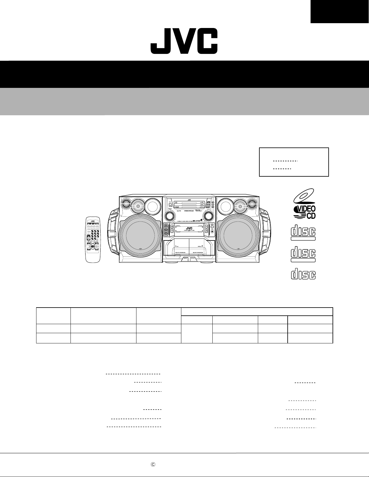
SERVICE MANUAL
COMPACT COMPONENT SYSTEM
MX-J770V
MX-J880V
MX-J770V
MX-J880V
SOUND
VOCAL
SLEEPECHO
MODE
MASKING
FM MODE
STILL
V.INTRO
SUBTITLEHIGHLIGHT
TAPE
A/B
REC
START/STOP
ON SCREEN
NEXT
PREV
KEY CONTROL
SELECT
FADE
MUTING
RM–SMXJ770V REMOTE CONTROL
This illustration is MX-J770V
Each difference point
Model CD/DECK/RECEIVER SPEAKER
MX-J770V CA-MXJ770V
MX-J880V CA-MXJ880V
SP-MXJ770V
SP-MXJ880V
Tray fitting
Silver
Area Suffix
US
UX
Color
Panel
Silver & blue Silver
Champagne-gold Champagne-gold
Net Front
Light blue
Gray
Singapore
Saudi Arabia
COMPACT
SUPER VIDEO
COMPACT
DIGITAL VIDEO
COMPACT
DIGITAL AUDIO
Contents
Safety precautions
Important for laser products
Preventing static electricity
Precautions at disassembly
and parts replacement
Disassembly method
Adjustment method
COPYRIGHT 2000 VICTOR COMPANY OF JAPAN, LTD.
1-2
1-3
1-4
1-5
1-6
1-31
Diagnosis which uses
extension wire method
Flow of functional operation
until TOC read
Maintenance of laser pickup
Replacement of laser pickup
Description of major ICs
1-35
1-36
1-37
1-37
1-38
No.20861
Jul. 2000
Page 2
MX-J770V/MX-J880V
Safety Precautions
1. This design of this product contains special hardware and many circuits and components specially
for safety purposes. For continued protection, no changes should be made to the original design
unless authorized in writing by the manufacturer. Replacement parts must be identical to those
used in the original circuits. Services should be performed by qualified personnel only.
2. Alterations of the design or circuitry of the product should not be made. Any design alterations of
the product should not be made. Any design alterations or additions will void the manufacturer`s
warranty and will further relieve the manufacture of responsibility for personal injury or proper ty
damage resulting therefrom.
3. Many electrical and mechanical par ts in the products have special safety-related characteristics.
These characteristics are often not evident from visual inspection nor can the protection afforded
by them necessarily be obtained by using replacement components rated for higher voltage,
wattage, etc. Replacement parts which have these special safety characteristics are identified in
the Parts List of Service Manual. Electrical components having such features are identified by
shading on the schematics and by ( ) on the Parts List in the Service Manual. The use of a
substitute replacement which does not have the same safety characteristics as the recommended
replacement parts shown in the Parts List of Service Manual may create shock, fire, or other
hazards.
4. The leads in the products are routed and dressed with ties, clamps, tubings, barriers and the
like to be separated from live parts, high temperature parts, moving parts and/or sharp edges
for the prevention of electric shock and fire hazard. When service is required, the or iginal lead
routing and dress should be observed, and it should be confirmed that they have been returned
to normal, after re-assembling.
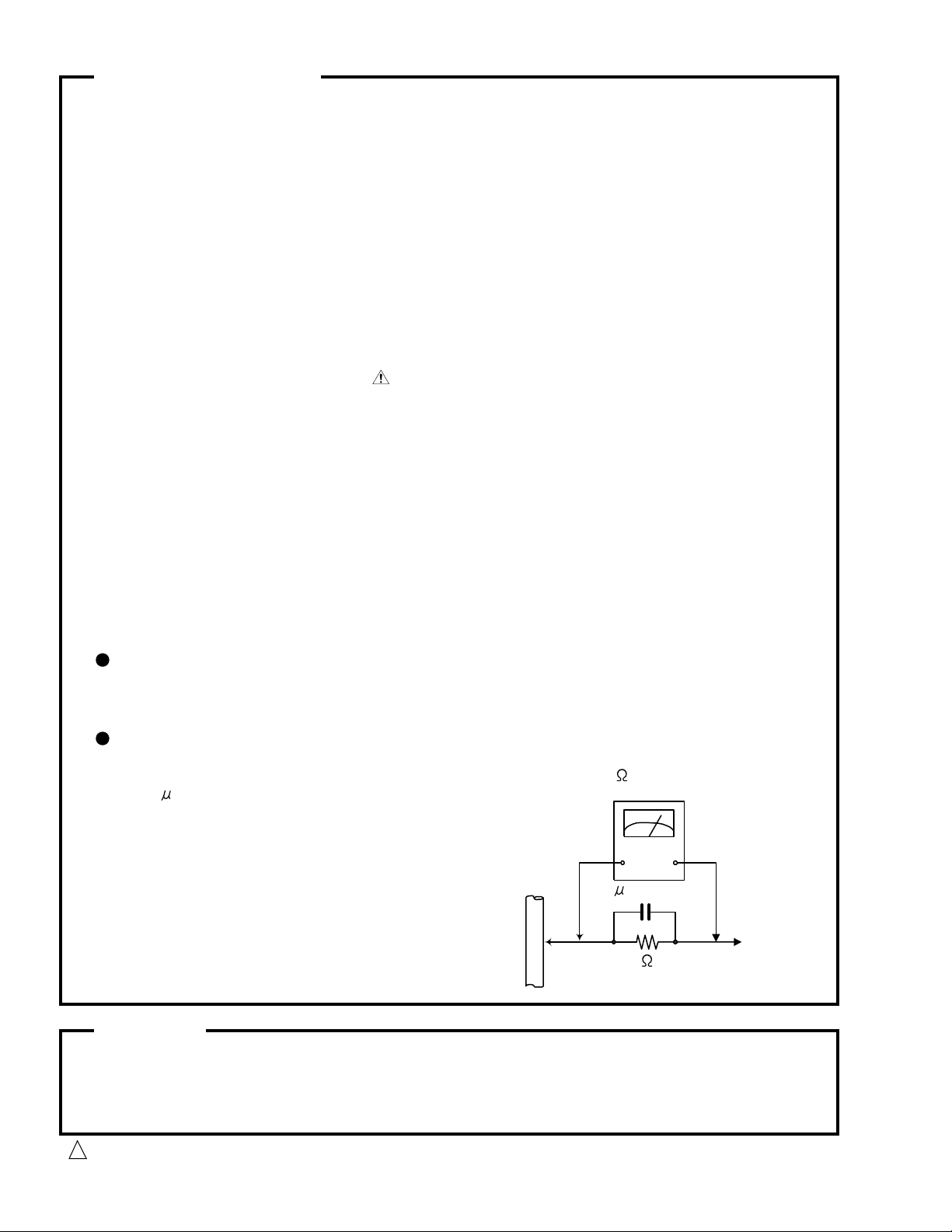
5. Leakage current check (Electrical shock hazard testing)
After re-assembling the product, always perform an isolation check on the exposed metal parts
of the product (antenna terminals, knobs, metal cabinet, screw heads, headphone jack, control
shafts, etc.) to be sure the product is safe to operate without danger of electrical shock.
Do not use a line isolation transformer during this check.
Plug the AC line cord directly into the AC outlet. Using a "Leakage Current Tester", measure
the leakage current from each exposed metal parts of the cabinet , particularly any exposed
metal part having a return path to the chassis, to a known good earth ground. Any leakage
current must not exceed 0.5mA AC (r.m.s.)
Alternate check method
Plug the AC line cord directly into the AC outlet. Use an AC voltmeter having 1,000 ohms
per volt or more sensitivity in the following manner. Connect a 1,500 10W resistor paralleled by
a 0.15 F AC-type capacitor between an exposed
metal part and a known good earth ground.
Measure the AC voltage across the resistor with the
AC voltmeter.
Move the resistor connection to each exposed metal
part, par ticularly any exposed metal part having a
return path to the chassis, and measure the AC
voltage across the resistor. Now, reverse the plug in
the AC outlet and repeat each measurement. Voltage
measured any must not exceed 0.75 V AC (r.m.s.).
This corresponds to 0.5 mA AC (r.m.s.).
0.15 F AC TYPE
1500 10W
Good earth ground
AC VOLTMETER
(Having 1000
ohms/volts,
or more sensitivity)
Place this
probe on
each exposed
metal part.
Warning
1. This equipment has been designed and manufactured to meet international safety standards.
2. It is the legal responsibility of the repairer to ensure that these safety standards are maintained.
3. Repairs must be made in accordance with the relevant safety standards.
4. It is essential that safety critical components are replaced by approved parts.
5. If mains voltage selector is provided, check setting for local voltage.
Burrs formed during molding may be left over on some parts of the chassis. Therefore,
pay attention to such burrs in the case of preforming repair of this system.
1-2
CAUTION
!
Page 3
Important for laser products
1.CLASS 1 LASER PRODUCT
2.DANGER : Invisible laser radiation when open and inter
lock failed or defeated. Avoid direct exposure to beam.
3.CAUTION : There are no serviceable parts inside the
Laser Unit. Do not disassemble the Laser Unit. Replace
the complete Laser Unit if it malfunctions.
4.CAUTION : The compact disc player uses invisible laser
radiation and is equipped with safety switches which
prevent emission of radiation when the drawer is open and
the safety interlocks have failed or are de
feated. It is dangerous to defeat the safety switches.
5.CAUTION : If safety switches malfunction, the laser is able
to function.
6.CAUTION : Use of controls, adjustments or performance of
procedures other than those specified herein may result in
hazardous radiation exposure.
VARNING : Osynlig laserstrålning är denna del är öppnad
och spårren är urkopplad. Betrakta ej strålen.
VARO : Avattaessa ja suojalukitus ohitettaessa olet
alttiina näkymättömälle lasersäteilylle.Älä katso
säteeseen.
ADVARSEL : Usynlig laserstråling ved åbning , når
sikkerhedsafbrydere er ude af funktion. Undgå
udsættelse for stråling.
ADVARSEL : Usynlig laserstråling ved åpning,når
sikkerhetsbryteren er avslott. unngå utsettelse
for stråling.
REPRODUCTION AND POSITION OF LABELS
WARNING LABEL
DANGER : Invisibie laser radiation
when open and interlock or
defeated.
AVOID DIRECT EXPOSURE TO
BEAM (e)
VARNING : Osynlig laserstrålning är
denna del är öppnad och spårren är
urkopplad. Betrakta ej strålen. (s)
VARO : Avattaessa ja suojalukitus
ohitettaessa olet alttiina
näkymättömälle lasersäteilylle.Älä
katso säteeseen. (d)
ADVARSEL :Usynlig laserstråling
ved åbning , når
sikkerhedsafbrydere er ude af
funktion. Undgå udsættelse for
stråling. (f)
!
CAUTION
Please use enough caution not to
see the beam directly or touch it
in case of an adjustment or operation
check.
CLASS 1
LASER PRODUCT
MX-J770V/MX-J880V
1-3
Page 4
MX-J770V/MX-J880V
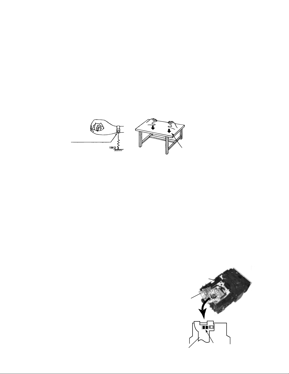
Preventing static electricity
1. Grounding to prevent damage by static electricity
Electrostatic discharge (ESD), which occurs when static electricity stored in the body, fabric, etc. is discharged,
can destroy the laser diode in the traverse unit (optical pickup). Take care to prevent this when performing repairs.
2. About the earth processing for the destruction prevention by static electricity
In the equipment which uses optical pick-up (laser diode), optical pick-up is destroyed by the static electricity of
the work environment.
Be careful to use proper grounding in the area where repairs are being performed.
2-1 Ground the workbench
Ground the workbench by laying conductive material (such as a conductive sheet) or an iron plate over
it before placing the traverse unit (optical pickup) on it.
2-2 Ground yourself
Use an anti-static wrist strap to release any static electricity built up in your body.
(caption)
Anti-static wrist strap
Conductive material
(conductive sheet) or iron plate
3. Handling the optical pickup
1. In order to maintain quality during transport and before installation, both sides of the laser diode on the
replacement optical pickup are shorted. After replacement, return the shorted parts to their original condition.
(Refer to the text.)
2. Do not use a tester to check the condition of the laser diode in the optical pickup. The tester's internal power
source can easily destroy the laser diode.
4. Handling the traverse unit (optical pickup)
1. Do not subject the traverse unit (optical pickup) to strong shocks, as it is a sensitive, complex unit.
2. Cut off the shorted part of the flexible cable using nippers, etc. after replacing the optical pickup. For specific
details, refer to the replacement procedure in the text. Remove the anti-static pin when replacing the traverse
unit. Be careful not to take too long a time when attaching it to the connector.
3. Handle the flexible cable carefully as it may break when subjected to strong force.
4. It is not possible to adjust the semi-fixed resistor that adjusts the laser power. Do not turn it
Attention when traverse unit is decomposed
*Please refer to "Disassembly method" in the text for pick-up and how to
detach the CD traverse mechanism.
CD changer
mechanism
assembly
1. Remove the disk stopper and T. bracket on the CD changer mechanism
assembly.
2. Disconnect the harness from connector on the CD motor board.
3. CD traverse unit is put up as shown in Fig.1.
4. Solder is put up before the card wire is removed from connector CN601
on the CD servo control board as shown in Fig. 2.
(When the wire is removed without putting up solder, the CD pick-up
assembly might destroy.)
5. Please remove solder after connecting the card wire with CN601 when
you install picking up in the substrate.
1-4
CD traverse
unit
Flexible cable
Fig.1
Soldering
Fig.2
Page 5
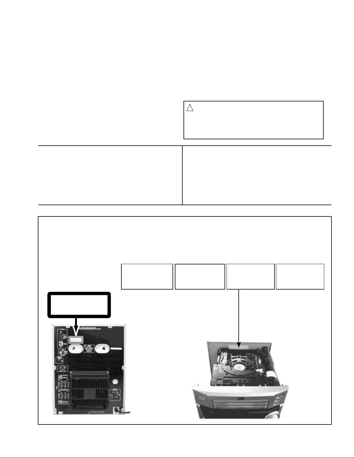
MX-J770V/MX-J880V
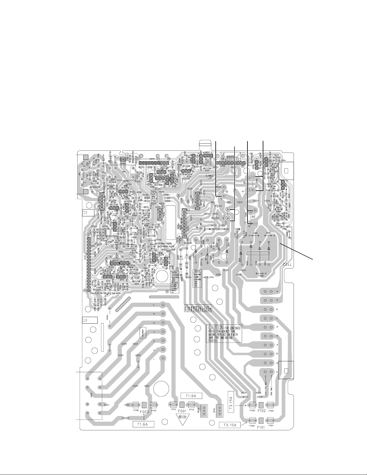
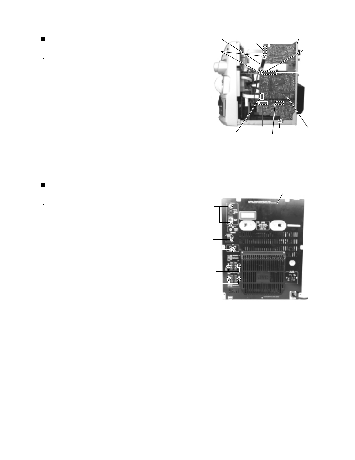
Precautions at disassembling and parts replacement
This model is charged with electricity on the power board
even if the power cord is unplugged.
Therefore, always discharge electricity in accordance with
the steps given below before starting disassembling of the
unit and/or replacement of parts.
While referring to the disassembling steps, remove the
1.
metal cover and the CD changer mechanism.
Set electrical resistances of 1kohm, 1/4W to the places between
2.
the + and - terminals of condensers VH(C204, C205) and VL(C214, C215)
on the power board, and discharge electricity for 4 ~ 5 seconds.
Connection should be made at first for VH.
C214
C215
C205
C204
Power board
1-5
Page 6
MX-J770V/MX-J880V
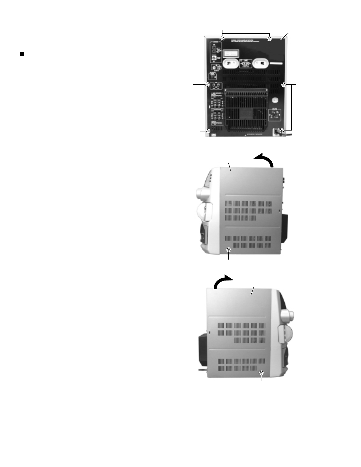
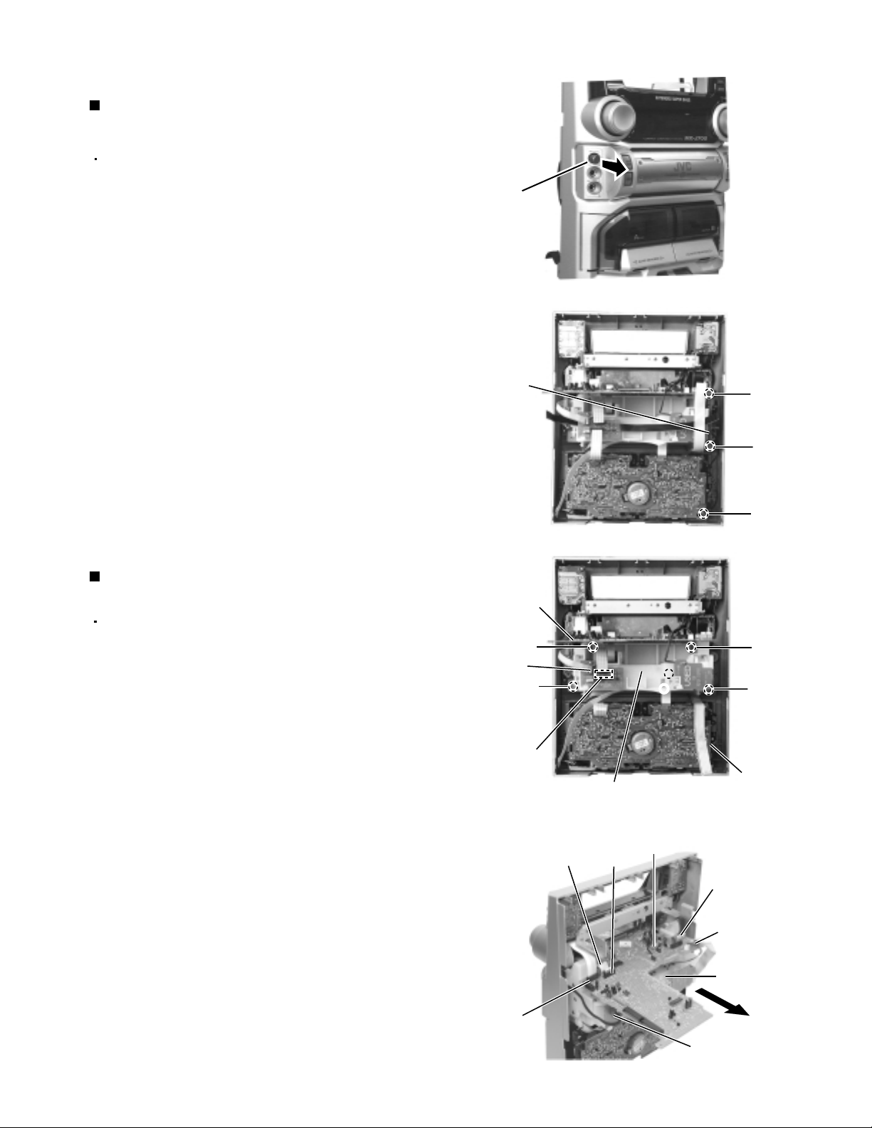
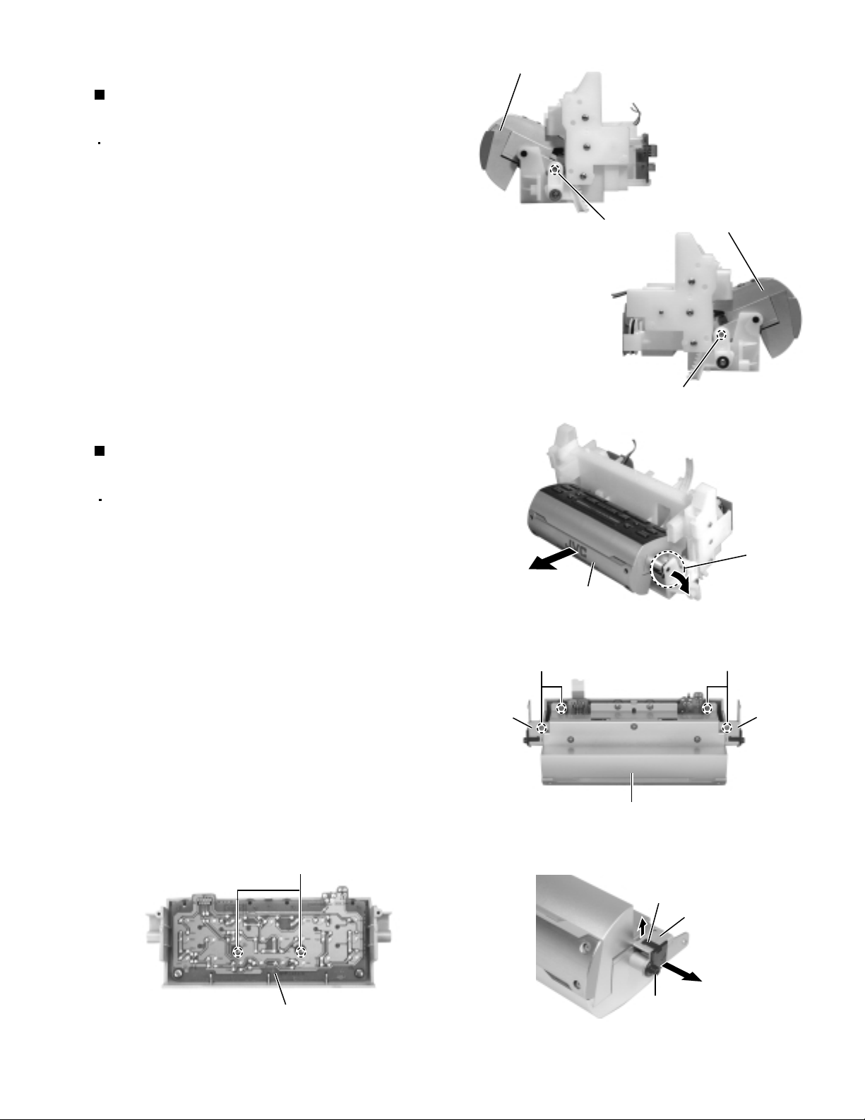
Disassembly method
<Main body>
Removing the metal cover
(See Fig.1 to 3)
1.
Remove the six screws A attaching the metal cover
on the back of the body.
2.
Remove the two screws B attaching the metal cover
on both sides of the body.
3.
Remove the metal cover from the body by lifting the
rear part of the cover.
ATTENTION:
Do not break the front panel tab fitted
to the metal cover.
A
A
Metal cover
Metal cover
A
Fig.1
B
Fig.2
Metal cover
Fig.3
B
1-6
Page 7
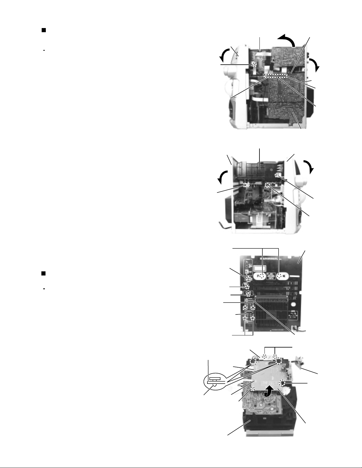
MX-J770V/MX-J880V
Removing the CD changer mechanism
assembly (See Fig.4 to 6)
Prior to performing the following procedure, remove
the metal cover.
1.
For the card wire connecting the CD changer
mechanism board and the main board, disconnect it
from connector CN868 on the main board.
2.
Remove the two screws C attaching the CD changer
mechanism assembly on both sides of the body.
3.
Remove the two screws D attaching the CD changer
mechanism assembly to the rear panel. Remove
the screw E attaching the AUX terminal, two screws
F attaching main speakers terminal and two screws
H attaching the sub woofers terminal on the back of
the body.
4.
Remove the screw G attaching the CD optical digital
output terminal and screw I attaching video out
terminal.
5.
Disconnect the harness from connector CN102 on
the video CD board, and pull out the earth wire
TW100 on the video CD board.
6.
Pull the top of rear panel and the front panel
assembly outward respectively, then remove the CD
changer mechanism assembly and video out
terminal by lifting the rear part of the CD changer
mechanism assembly.
CD changer
mechanism assembly
Front panel assembly
C
Main board
CN868
CD changer
mechanism assembly
Rear panel
CN102
D
Fig.4
Fig.5
CD changer
mechanism board
Rear panel
CN870
CN871
Input / output board
Front panel assembly
C
TW100
Rear panel
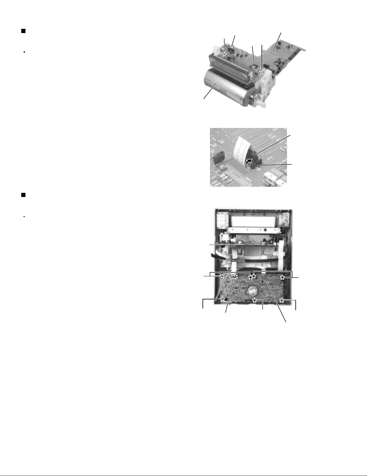
Removing the video CD board
(See Fig.7)
Prior to performing the following procedure, remove
the CD changer mechanism assembly.
1.
Reverse the CD changer mechanism assembly.
2.
Remove the two screws J attaching the bracket.
3.
Remove the screw K attaching the video CD board.
4.
Disconnect the card wire from connector CN100 and
CN101 on the video CD board.
5.
At first, remove the claw a. Then remove the claw b
while raising the video CD board in the direction of
the arrow mark as figure. After removing the claw b,
you can removing the video CD board by pulling it
backward.
I
G
E
F
SUB WOOFERS
terminal
H
Bracket
Video CD board
CN100
CLAW b
CN101
K
CD changer
mechanism assembly
Fig.6
Fig.7
MAIN SPEAKERS
terminal
J
Video out board
CLAW a
Video CD board
1-7
Page 8
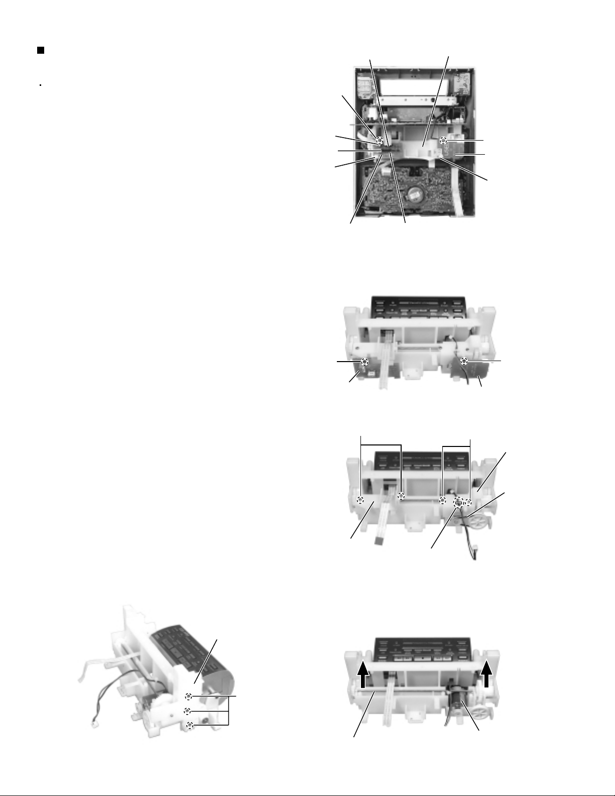
MX-J770V/MX-J880V
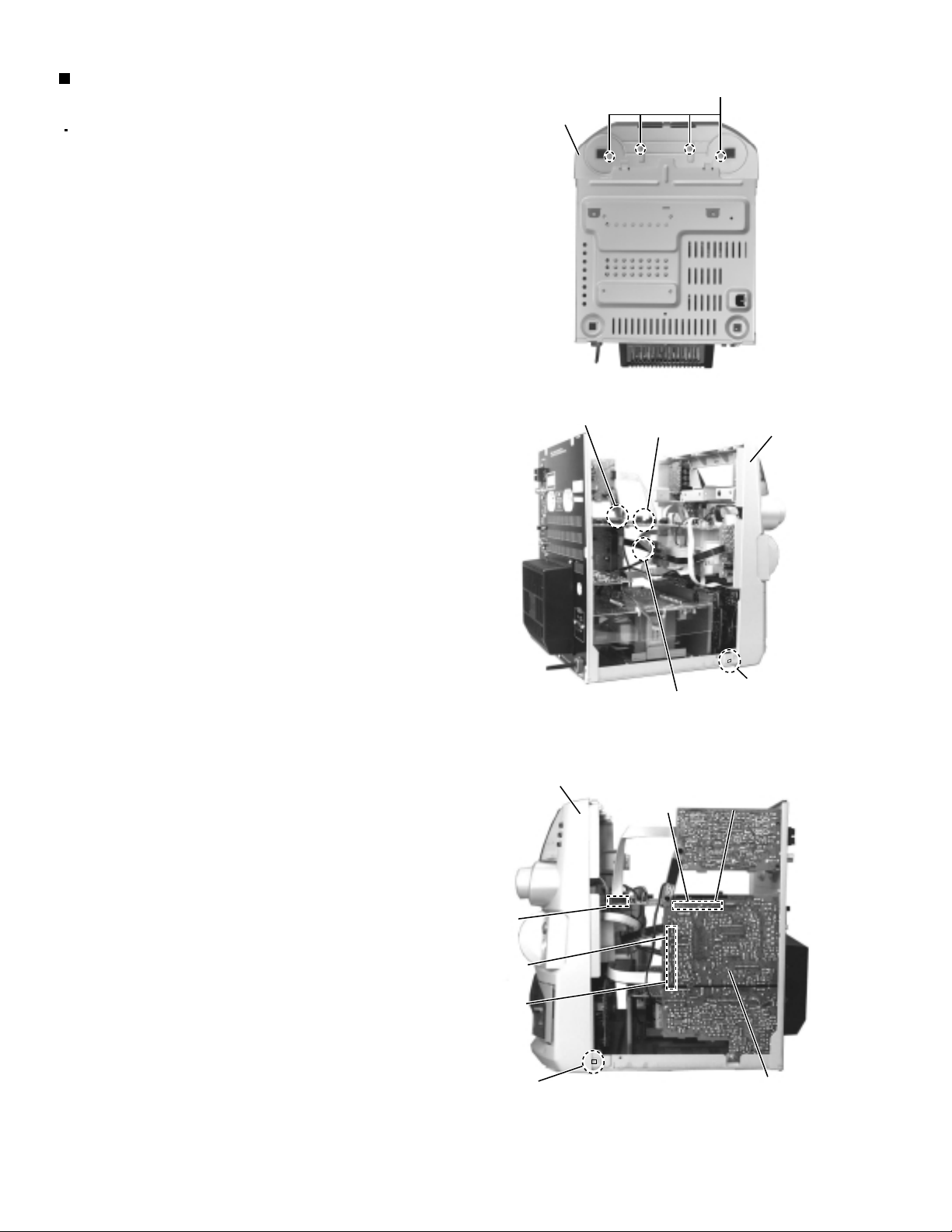
Removing the front panel assembly
(See Fig.8 to 10)
Prior to performing the following procedure, remove
the metal cover and the CD changer mechanism
assembly.
1.
Remove the four screws L attaching the front panel
assembly on the bottom of the body.
2.
Disconnect the card wire from connector CN865 on
the main board and pull out the earth wire on the
main board.
3.
Disconnect the card wire from connector CN315 on
the input / output board.
4.
Disconnect the harness from connector CN901 on
the relay board on the back of the front panel
assembly.
5.
Disconnect the harness from connector CN912 on
the input / output board.
Front panel assembly
Earth wire
Fig.8
Main board
CN865
L
Front panel assembly
6.
Disconnect connector CN870 and CN871 on the
input/output board from the main board.
7.
Release the two joints c and d on the lower part of
the sides using a screwdriver, and remove the front
panel assembly toward the front.
Front panel assembly
Main board
CN865
CN912
Relay board
CN901
Fig.9
CN871
Joint c
CN870
1-8
CN315
Joint d
Input / output board
Fig.10
Page 9
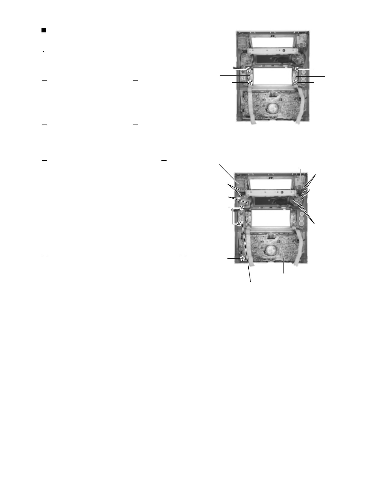
<Front panel assembly>
Removing the Microphone terminal board
assembly (See Fig.11 and 12)
Prior to performing the following procedure, remove
the metal cover, CD changer mechanism assembly
and the front panel assembly.
1.
Pull out the MIC volume knob from the front side.
2.
Remove the two screws M attaching the microphone
terminal board assembly.
3.
Remove the screw N attaching earth wire. Then
release the earth wire from the clamp on the upper
part of the cassette mechanism assembly.
4.
Remove the microphone terminal board assembly
toward you.
MX-J770V/MX-J880V
MIC volume knob
Fig.11
Microphone
terminal board
assembly
M
Removing the rolling panel assembly
(See Fig.13 and 14)
Prior to performing the following procedure, remove
the microphone terminal board assembly.
1.
Disconnect the harness from connector CN900 and
the card wire from connector CN906 on the relay
board on the back of the rolling panel assembly
respectively.
2.
Disconnect the harness from connector CN862,
CN863, CN850, CN851 and CN815 on the main
board respectively. Disconnect the card wire from
connector CN880 on the main board.
3.
Disconnect the card wire from connector CN869 and
the harness from CN883 and CN884 on the main
board respectively.
Main board
Relay board
CN900
Relay board
CN906
CN883,CN884
O
O
Rolling panel assembly
CN869
M
N
Fig.12
O
O
Cassette
mechanism
assembly
Fig.13
CN815
Main board
CN850,CN851
4.
Remove the four screws O attaching the rolling panel
assembly.
ATTENTION:
For the harness which should be
connected to connector CN869,
CN883 and CN884 on the main board,
get them through the slots under the
rolling panel when reattaching the
rolling panel assembly to the front
panel (Refer to Fig.14)
Main board
CN862,CN863
Rolling panel
assembly
Main board
CN880
Relay board
CN900
Fig.14
1-9
Page 10
MX-J770V/MX-J880V
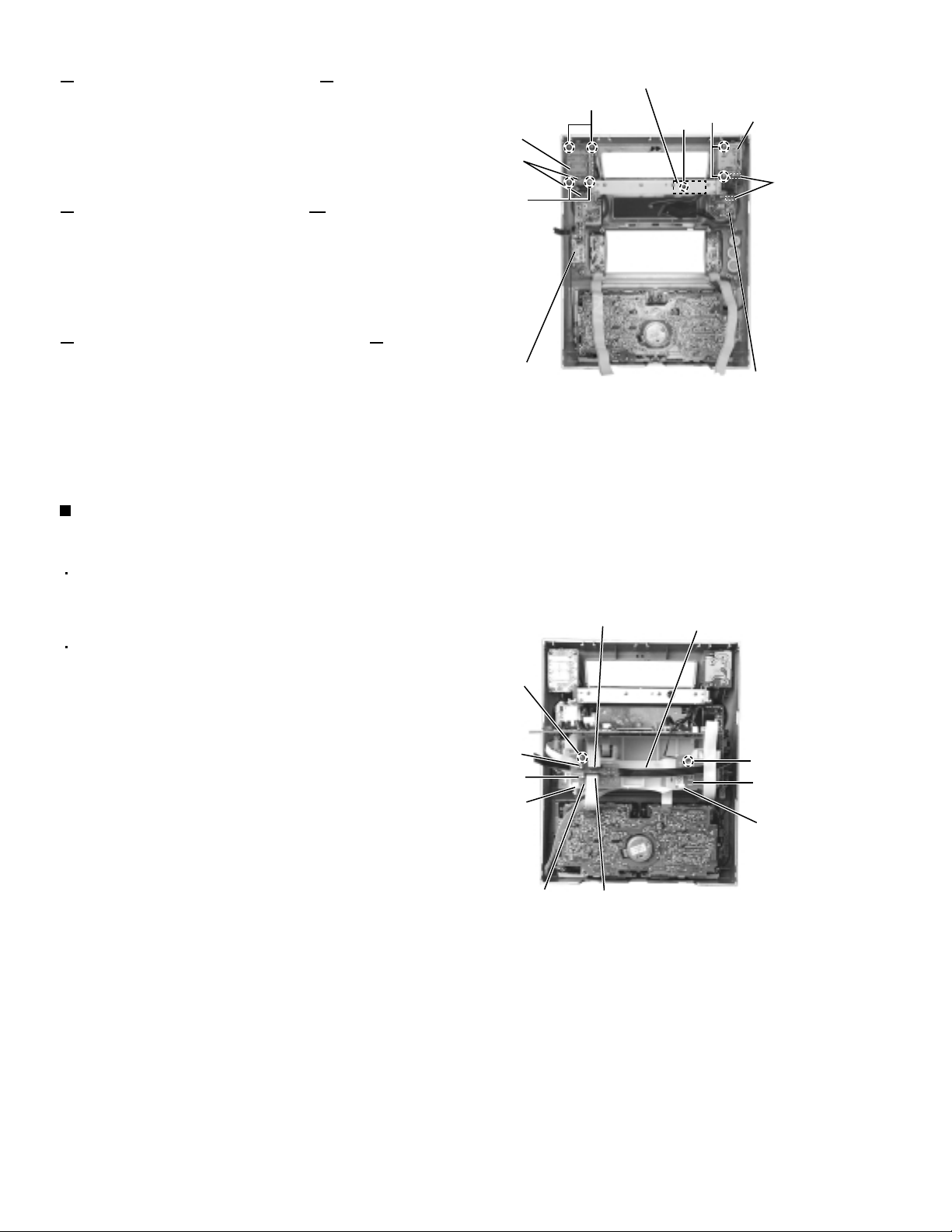
Removing the main board
(See Fig.15 and 16)
Prior to performing the following procedure, remove
the front panel assembly, the microphone terminal
board and the rolling panel assembly.
1.
Disconnect the harness from connector CN867 on
the main board.
2.
Disconnect the card wire from connector CN879 on
the main board (Before pulling out the card wire,
stand the part e of CN879 as shown in Fig.16).
3.
Remove the two screws P attaching the main board.
Removing the cassette mechanism
assembly (See Fig.17)
Rolling panel
assembly
P
CN867
CN879
Main board
P
Fig.15
e
CN879
Fig.16
Prior to performing the following procedure, remove
the front panel assembly.
1.
Disconnect the card wire from connector CN306 on
the cassette mechanism board.
2.
Remove the four screws Q and three screws R
attaching the cassette mechanism assembly.
Q
R
CN306
R
Cassette mechanism board
Fig.17
R
Q
1-10
Page 11
Prior to performing the following procedure, remove
the front panel assembly and the rolling panel
assembly.
Function board1 (See Fig.18)
Remove the two screws S attaching the function
board 1.
Function board2 (See Fig.18)
Remove the two screws T attaching the function
board 2.
Bass-level regulator board (See Fig.19)
Pull out the sub woofer volume knob on the front
side of the front panel assembly and remove the nut
attaching the bass-level regulator board.
Release the two joints f. Unsolder FW951 on the
bass-level regulator board and disconnect the
harness connected to the power switch.
Main volume & headphone board (See Fig.19)
Pull out the volume knob on the front side of the front
panel assembly and remove the nut attaching the
main volume & headphone board.
Remove the two screws U attaching the main
volume & headphone board on the back of the front
panel assembly and release the two joints g.
Unsolder FW850 on the main volume & headphone
board and disconnect the harness connected to the
eject switch board.
Remove the screw V attaching the earth wire
extending from the main volume & headphone
board.
1.
1.
1.
2.
1.
2.
3.
4.
Removing the boards in the front panel
assembly (See Fig.18 to 20)
Fig.18
Fig.19
S
Function
board 1
S
Function
board 2
T
T
FW850
Eject switch board
Joints g
U
Main volume & headphone board
V
Power switch board
Joints f
Bass-level
regulator board
Cassette mechanism assembly
FW951
MX-J770V/MX-J880V
1-11
Page 12
MX-J770V/MX-J880V
Power switch board (See Fig.20)
1.
Remove the two screws W attaching the power
switch board. Unsolder FW951 on the power switch
board and disconnect the harness extending to the
bass-level regulator board.
Eject switch board (See Fig.20)
1.
Remove the four screws X attaching the eject switch
board. Unsolder FW850 on the eject switch board
and disconnect the harness extending to the main
volume & headphone board.
Remote control port board (See Fig.20)
1.
Remove the screw Y attaching the remote control
port board.
Removing the relay board and fixing
board (See Fig.21)
Eject switch
board
FW850
X
Main volume &
headphone board
Remote control port board
X
Fig.20
Y
W
Power switch board
FW951
Bass-level
regulator board
Prior to performing the following procedure, remove
the metal cover and CD changer mechanism
assembly.
There is no need to remove the front panel
assembly.
1.
Disconnect the harness from connector CN900 and
CN901 on the relay board on the back of the rolling
panel assembly.
2.
Disconnect the card wire from connector CN905 and
CN906 on the relay board on the back of the rolling
panel assembly.
3.
Remove the screw Z attaching the relay board.
Remove the relay board from the groove i.
4.
Remove the screw A attaching the fixing board and
remove the fixing board from the groove j.
CN900
CN901
Groove i
Relay board
Z
CN905
CN906
Rolling panel assembly
A
Fixing board
Groove j
Fig.21
1-12
Page 13
Prior to performing the following procedure, remove
the metal cover and CD changer mechanism
assembly.
Remove the two plastic rivets attaching the joint
board, and remove the joint board.
Disconnect the card wire from connector CN1 on the
tuner board.
Remove the two screws B attaching the tuner board
on the back of the body.
1.
2.
3.
Removing the tuner board
(See Fig.22 and 23)
<Rear panel assembly>
Prior to performing the following procedure, remove
the tuner board.
Disconnect the card wire from connector CN315 on
the input / output board.
Remove the screw C attaching the input / output
board on the lower side of the body.
Remove the five screws, E, F & H attaching the AUX,
main speakers, sub woofers terminal board on the
back of the body.
Remove the screw G attaching the CD optical digital
output back of the body.
Disconnect the harness from connector CN912 on
the input / output board and pull out the earth wire on
the main board.
Disconnect connector CN870, CN871, CN612,
CN711 and CN712 on the input / output board by
pulling out them outward. Remove the input / output
board from the body.
1.
2.
3.
4.
5.
6.
Removing the input / output board
(See Fig.22 and 23)
Fig.22
Fig.23
Tuner board
Plastic rivet
Joint board
Input / output board
Rear panel
CN1
CN871
CN870
C
CN711
CN712
CN315
Rear panel
B
G
E
F
H
MX-J770V/MX-J880V
1-13
Page 14
MX-J770V/MX-J880V
Removing the rear cover / rear panel
(See Fig.24 to 27)
Prior to performing the following procedure, remove
the metal cover and the CD changer mechanism
assembly.
There is no need to remove the front panel
assembly.
1.
Remove the two screws D attaching the rear cover
on the back of the body.
2.
Remove the five screws E & F, H attaching AUX,
main speakers and sub woofers terminal board to
the rear panel on the back of the body.
3.
Remove the screw G attaching the CD optical digital
output terminal.
4.
Remove the five screws Z attaching the heat sink
and the pre-amplifier board to the rear panel on the
back of the body.
5.
Remove the two screws Y attaching the voltage
selector to the rear panel on the back of the body.
Rear cover
B
Rear panel
D
Fig.24
Heat sink
6.
Remove the screw X attaching the rear panel to the
chassis base on the back of the body.
7.
Remove the two screws B attaching the tuner board
on the back of the body.
8.
Release the two joints k and l on the rear panel
bottom using a screwdriver, and detach the rear
panel backward.
Rear panel
G
E
Z
F
H
Z
X
Fig.25
Z
Y
Z
Rear panel
1-14
Fig.27
Joint l
Joint k
Fig.26
Page 15
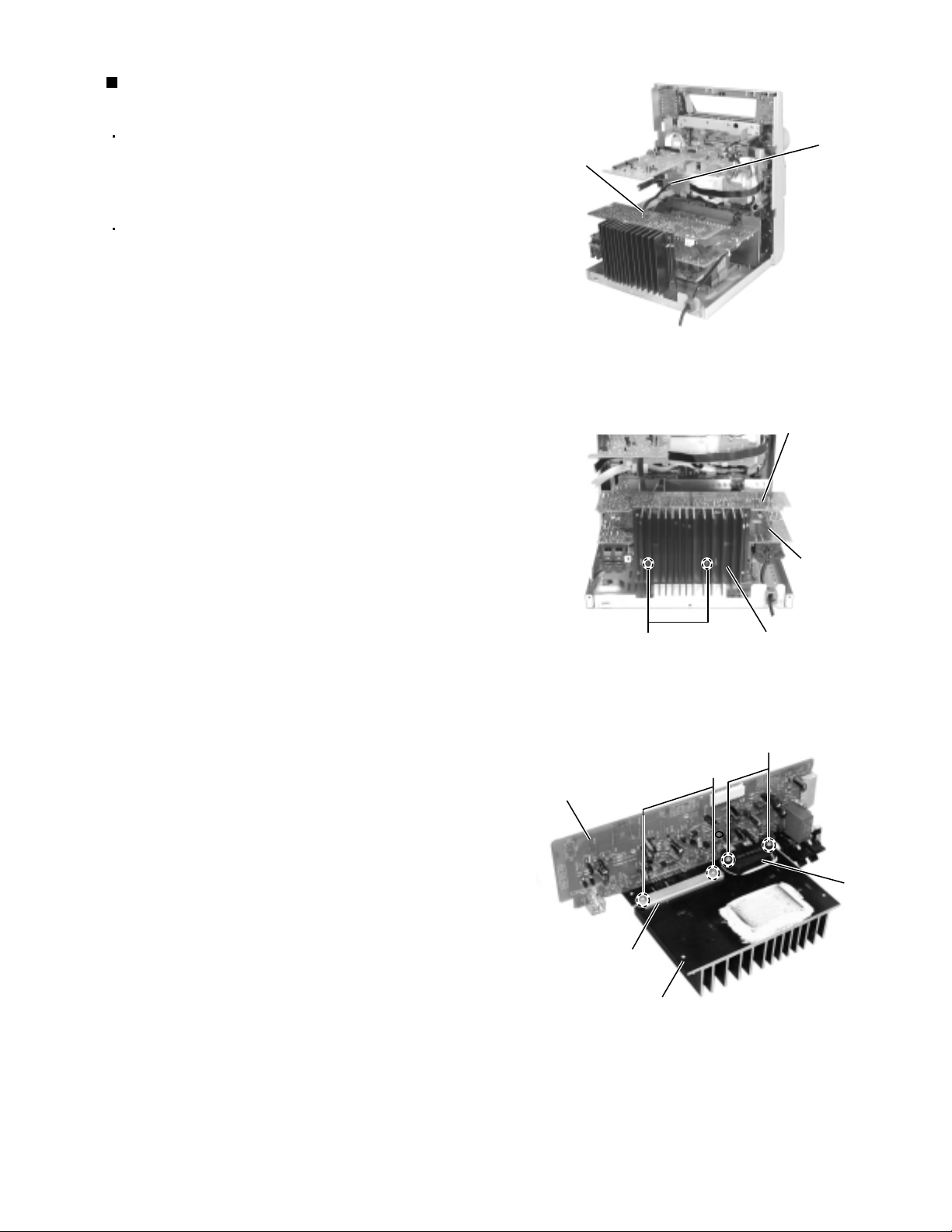
Prior to performing the following procedure, remove
the metal cover, the CD changer mechanism
assembly, the tuner board, input / output board and
the rear cover / rear panel.
There is no need to remove the front panel
assembly.
Disconnect the harness from connector CN901 on
the relay board on the back of the rolling panel
assembly.
Disconnect the harness from connector CN713 on
the pre-amplifier board.
Remove the two screws H attaching the heat sink to
the power & main amplifier board on the back of the
body.
Remove the fore screws I & J attaching the preamplifier board and IC to the heat sink.
Remove the bracket, then detach the pre-amplifier
board from the heat sink.
1.
2.
3.
4.
5.
Removing the pre-amplifier board / heat
sink (See Fig.28 to 30)
Fig.28
Fig.29
Fig.30
Pre-amplifier board
CN713
Relay board
CN901
Pre-amplifier board
Power & main
amplifier board
Heat sink
H
Heat sink
Pre-amplifier board
Bracket
I
J
IC
MX-J770V/MX-J880V
1-15
Page 16
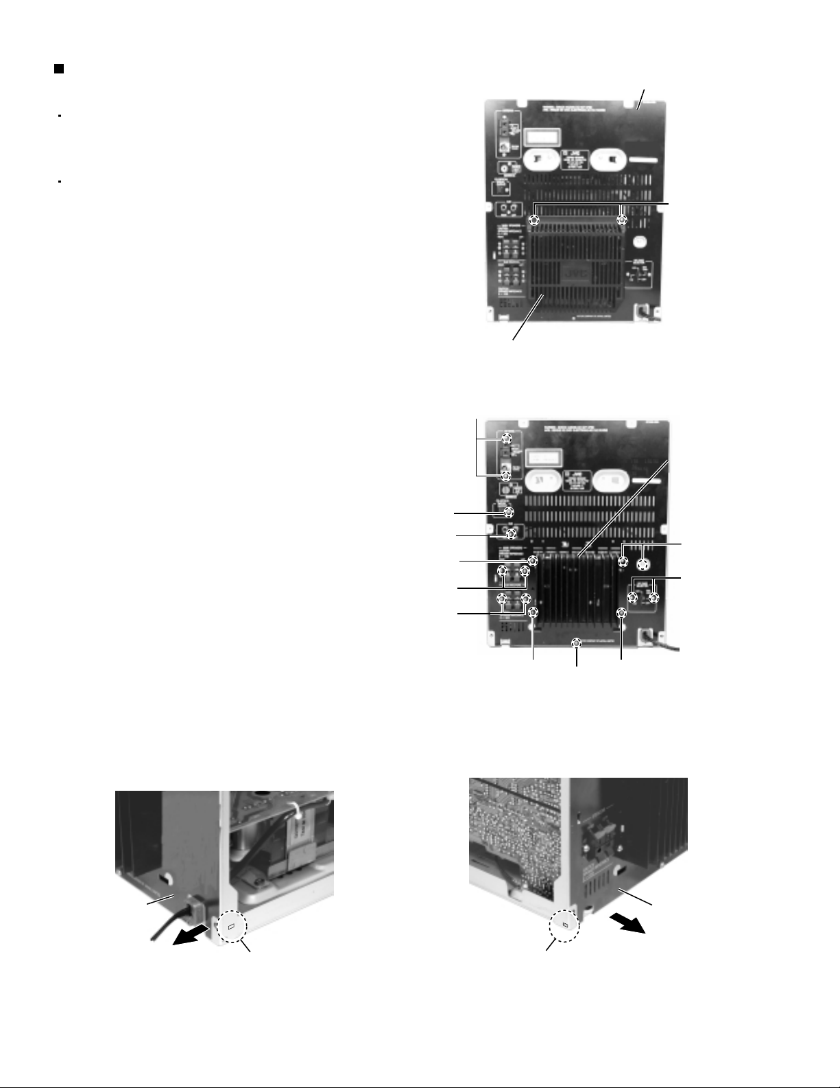
MX-J770V/MX-J880V
Removing the power & main amplifier
board (See Fig.31 and 32)
Prior to performing the following procedure, remove
the metal cover, the CD changer mechanism
assembly, the rear cover / rear panel, the tuner
board, the input / output board and the pre-amplifier
board.
1.
Remove the four screws K attaching the transf. on
the power & main amplifier board through the upper
side slots.
2.
Remove the two plastic rivets fixing the power &
main amplifier board.
3.
Remove the cord stopper by pushing it upward.
4.
Cut off the bands m and n fixing the power cord and
unsolder the power cord on the power & main
amplifier board.
Power & main
amplifier board
Plastic rivet
K
Fig.31
Plastic rivet
K
K
Power & main amplifier board
Cord stopper
Fig.32
Soldered part
Band m
Band n
1-16
Page 17
MX-J770V/MX-J880V
Prior to performing the following procedure, remove
the rolling panel assembly and the main board.
Remove the two screws L attaching the multi-control
assembly on both sides.
Remove the multi-control assembly outward while
pushing the right and left hooks fixing multi-control
assembly outward respectively.
1.
2.
Removing the multi-control assembly
(See Fig.33 to 35)
<Rolling panel assembly>
Prior to performing the following procedure, remove
the rolling panel assembly, the main board and the
multi-control assembly.
Remove the four screws M attaching the cover and
the bracket.
Pull out the right and left panel holders outward
respectively by releasing the tabs o outward.
Remove the cover and the bracket.
Remove the two screws N attaching the multi-control
board.
1.
2.
3.
4.
Removing the multi-control board
(See Fig.36 to 38)
L
Multi-control assembly
Multi-control assembly
L
Fig.36
Fig.37
Fig.38
Fig.35
Fig.33
Fig.34
Multi-control assembly
Hook
Bracket
Bracket
MM
Cover
Bracket
Tab o
Panel holder
N
Multi-control board
1-17
Page 18
MX-J770V/MX-J880V
Removing the drive motor assembly
(See Fig.39 to 42)
Prior to performing the following procedure, remove
the rolling panel assembly and the main board.
1.
Remove the relay board and fixing board (Refer to
Fig.21).
2.
Remove the two screws O attaching the motor
bracket and remove the motor lead staple p.
3.
Remove the two screws P attaching the shaft
bracket.
4.
Remove the motor belt.
5.
Remove the three screws Q attaching the side
bracket.
6.
Remove the shaft assembly from the rolling panel
assembly by lift up the shaft assembly upward.
7.
Remove the drive motor upward.
CN900
CN901
Groove i
Relay board
Z
CN905
Rolling panel assembly
A
Fixing board
Groove j
CN906
Fig.21
Side bracket
Z
Relay board
P
Shaft bracket
A
Fixing board
Fig.39
O
Motor bracket
Motor belt
Motor lead staple p
Fig.40
1-18
Fig.42
Q
Shaft assembly
Drive motor
Fig.41
Page 19
MX-J770V/MX-J880V
Prior to performing the following procedure, remove
the metal cover and the CD changer mechanism
assembly.
Disconnect the card wire from connector CN101 and
CN102 on the super VCD control board.
Remove the two plastic rivets attaching the super
VCD control board.
1.
2.
Removing the super VCD control board
(See Fig.43)
Fig.43
CD changer
mechanism assembly
Super VCD control board
Plastic rivet Plastic rivet
CN101
CN102
1-19
Page 20
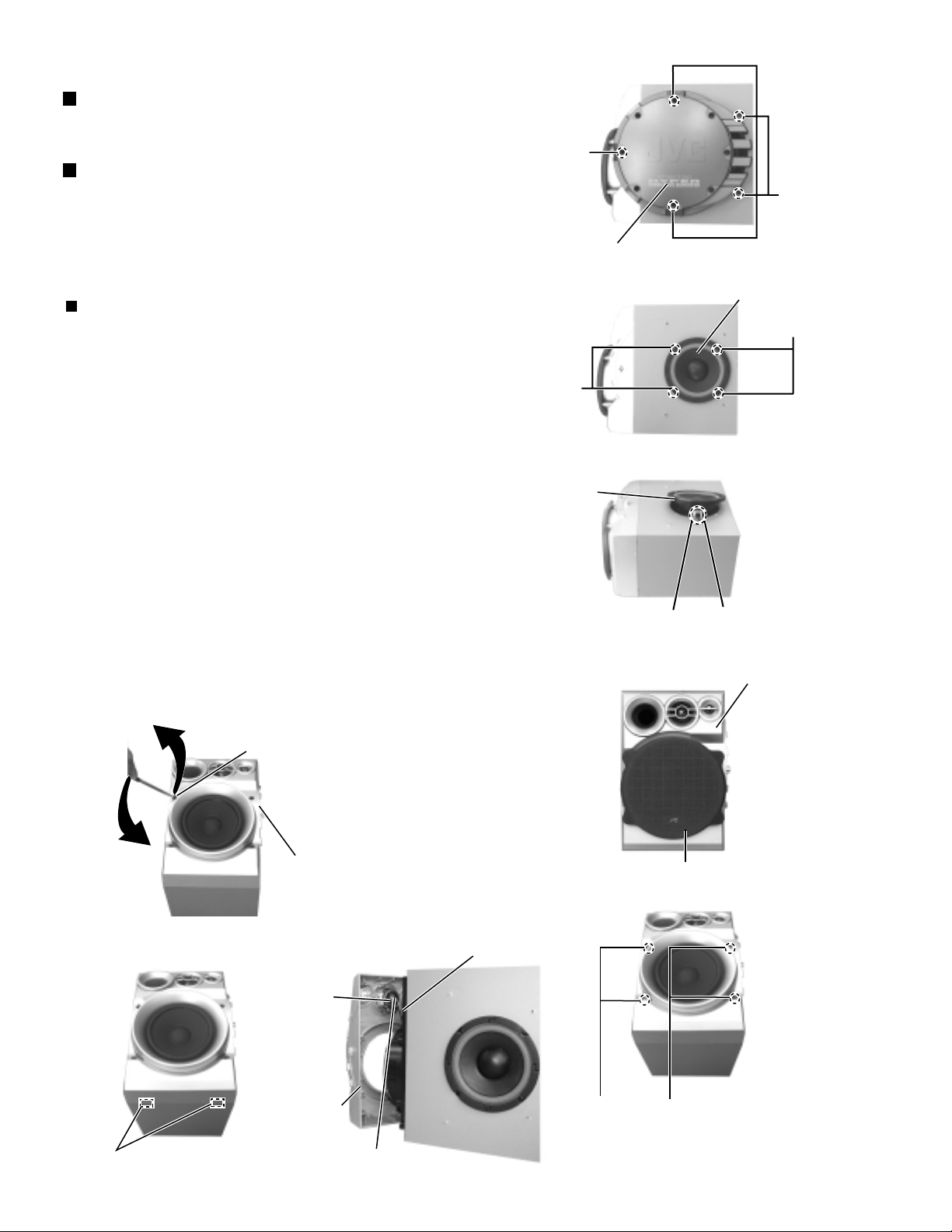
MX-J770V/MX-J880V
Bottom
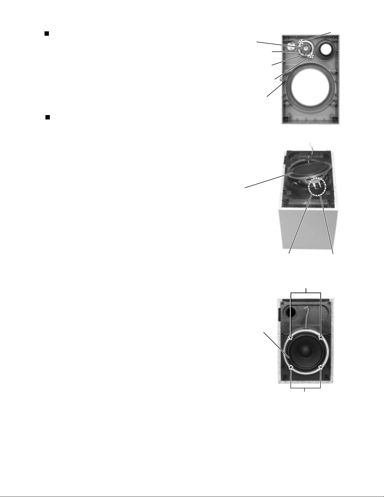
< Speaker section >
Removing the speaker cover (See Fig.1)
1.
Remove the five screws A attaching the speaker
cover on the side of the body.
Removing the sub woofer unit (See Fig.2 and 3)
1.
Remove the four screws B attaching the sub
woofer unit.
2.
Two plug wires connected with the sub woofer
unit are pulled out.
Removing the ornament panel assembly
(See Fig.4 to 8)
Remove the saran board from the speaker box.
1.
(Saran board can be detached by pulling the side
of Saran board forward.)
The plus driver is inserted in the holder, it is lifted,
2.
and the holder is removed.
Four holders are removed, and four screws C under
3.
that are removed.
Screw
A
Screw A
Speaker cover
Fig.1
Sub woofer
unit
Screw B
Screw B
Fig.2
Sub woofer
unit
The minus driver is inserted in the concave part in the
4.
speaker box bottom and inserts in the interior little
by little.
CAUTION : Please apply the felt or the cloth, etc.
to damage neither the ornament panel nor the
cabinet when the ornament panel assembly is
detached when working.
Two plug wires connected with the
5.
middle range unit are pulled out.
Holder
Ornament
panel
assembly
Fig.6
top
Middle range
unit
Plug wire
(Yellow)
Plug wire
(Red)
Fig.3
Saran board
Fig.4
Plug wire
(Black)
Ornament panel assembly
concave part
1-20
Bottom
Fig.7
Ornament
panel
assembly
Plug wire
(Black)
Fig.8
Holder &
screw C
Holder &
screw C
Fig.5
Page 21
MX-J770V/MX-J880V
Ornament
panel
assembly
Middle range
unit
Fig.11
Fig.10
Fig.9
Screw D
Plug wire
(White)
Plug wire
(Blue)
Screw D
Screw E
Screw E
Plug wire
(Blue / Black)
Woofer
unit
Plug wire
(Yellow / Black)
Woofer
unit
Remove the ornament panel assembly.
Remove the two screws D attaching the middle
range unit.
Two plug wires connected with the middle range unit
are pulled out.
1.
2.
3.
Removing the middle range unit (See Fig.9)
Remove the ornament panel assembly.
Remove the four screws E attaching the woofer unit.
Two plug wires connected with the woofer unit
are pulled out.
1.
2.
3.
Removing the woofer unit (See Fig.10 and 11)
1-21
Page 22

MX-J770V/MX-J880V
Removing the CD Servo control board
(See Fig.1)
1.Remove the metal cover.
2.Remove the CD changer mechanism assembly.
3.From bottom side the CD changer mechanism assembly,
remove the two screws A retaining the CD servo control
board.
4.Absorb the four soldered positions "a" of the right and
left motors with a soldering absorber.
5.Pull out the earth wire on the CD changer mechanism
assembly.
6.The two screws B is removed and C.B.holder is detached.
7.Disconnect the connector CN854 on the CD servo
control board.
8.Disconnect the card wire CN601 and the connector
CN801 on the CD servo control board.
A
a
a
CN854
A
CN651
CD servo control board
CN652
CN801
CN601
CN151
Removing the CD tray assembly
(See Fig.2~4)
Remove the front panel assembly.
1.
Remove the CD changer mechanism assembly.
2.
Remove the CD Servo control board.
3.
Remove the screw C' retaining the lod stopper.
4.
From the T.bracket section "b" and clamper base
5.
section "c" , remove both of the edges fixing the
rod(See Fig.2 and 3).
Remove the screw D retaining the disc stopper
6.
(See Fig.3).
Remove the three screws E retaining the T.bracket
7.
(See Fig.3).
Remove the screw F retaining the clamper assembly
8.
(See Fig.3).
From the left side face of the chassis assembly, remove
9.
the one screw G retaining both of the return spring and
lock lever(See Fig. 4).
10.
By removing the pawl at the section "d" fixing the return
spring, dismount the return spring(See Fig.4).
11.
Remove the three lock levers(See Fig.4).
T.Braket
Disc stopper
D
Earth
wire
B
B
C.B.Holder
Fig.1
Clamper base
b
Rod
c
T.Braket
Fig.2
d
EE
C
a
Lod stopper
(C/J version only)
E
F
b
Lock lever
Fig.4
1-22
Clamper ass'y
Fig.3
Return spring
G
Page 23

MX-J770V/MX-J880V
11.
12.
Check whether the lifter unit stopper has been caught
into the hole at the section "e" of CD tray assembly as
shown in Fig.5.
Make sure that the driver unit elevator is positioned as
shown in Fig.6 from to the second or fifth hole on the
left side face of the CD changer mechanism assembly.
Fig.5
Fig.7
Fig.6
Fig.8
Fig.9
[Caution]
In case the driver unit elevator is not at above
position, set the elevator to the position as
shown in Fig.7 by manually turning the pulley
gear as shown in Fig.8.
13.
14.
15.
Manually turn the motor pulley in the clockwise
direction until the lifter unit stopper is lowered from the
section "e" of CD tray assembly(See Fig.8).
Pull out all of the three stages of CD tray assembly in
the arrow direction "f" until these stages stop
(See Fig.6).
At the position where the CD tray assembly has
stopped, pull out the CD tray assembly while pressing
the two pawls "g and g' " on the back side of CD tray
assembly(See Fig.9). In this case, it is easy to pull out
the assembly when it is pulled out first from the stage
CD tray assembly.
CD tray
assembly
e
Drive unit of elevator
CD tray assembly
f
Refer to Fig.7
Pawl
Chassis assembly
Pulley gear
Motor pulley
Pawl ,
CD tray assembly
Stopper
g
g
g'
1-23
Page 24

MX-J770V/MX-J880V
Removing the CD loading mechanism
assembly(See Fig.10)
1.2.While turning the cams R1 and R2 assembly in the
arrow direction "h" ,align the shaft "i" of the CD loading
mechanism assembly to the position shown in Fig.10.
Remove the four screws H retaining the CD loading
mechanism assembly.
Removing the CD traverse mechanism
(See Fig.11 and 12 )
For dismounting only the CD traverse mechanism
1.
without removing the CD loading mechanism assembly,
align the shaft "j" of the CD loading mechanism
assembly to the position shown Fig.11 while turning the
cam R1 and R2 assembly in the arrow direction "k" .
By raising the CD loading mechanism assembly in the
2.
arrow direction "l", remove the assembly from the lifter
unit
Cam R1, R2 assembly
Cams R1, R2 assembly
Arrow
h
i
H
H
CD loading mechanism assembly
Fig.10
H
H
CD traverse mechanism
Arrow
j
Fig.11
Removing the CD pick unit
(See Fig.13 )
1.
Move the cam gear in the arrow direction "m" . Then,
the CD pickup unit will be moved in the arrow direction
"n" .
According to the above step, shift the CD pickup unit to
2.
the center position.
While pressing the stopper retaining the shaft in the
3.
arrow direction "o" , pull out the shaft in the arrow
direction "p".
After dismounting the shaft from the CD pickup unit,
4.
remove the CD pickup unit
1-24
k
Lifter unit
o
Stopper
Shaft
Fig.12
CD Pickup unit
n
m
Shaft
p
Stopper
Fig.13
Arrow
CD loading
mechanism
Shaft
Cam gear
k
Page 25

Removing the cam unit
(See Fig.14 ~17 )
1.
Remove the CD loading mechanism assembly.
2.
While turning the cam gear "q", align the pawl "r"
position of the drive unit to the notch position(Fig.16) on
the cam gear "q".
Pull out the drive unit and cylinder gear(See Fig.17).
3.
While turning the cam gear "q", align the pawl "s"
4.
position of the select lever to the notch position(Fig.18)
on the cam gear "q".
Remove the four screws J retaining the cam unit(cam
5.
gear "q" and cams R1/R2 assembly)(See Fig.18).
MX-J770V/MX-J880V
Chassis assembly
CN801
CN802
Fig.14
Drive unit
Tray select
switch board
Cylinder gear
CN804
Drive unit
r
I
Cam gear q
Cam gear q
Fig.15
J
Cams R1, R2 assembly
Cam unit
Fig.16
J
J
s
Select lever
Fig.17
1-25
Page 26

MX-J770V/MX-J880V
Removing the actuator motor and belt
(See Fig.18~21)
1.
Remove the two screws K retaining the gear bracket
(See Fig.19).
2.
While pressing the pawl "t" fixing the gear bracket in the
arrow direction, remove the gear bracket
(See Fig.19).
From the notch "u section" on the chassis assembly
3.
fixing the edge of gear bracket, remove and take out the
gear bracket(See Fig. 20).
Remove the belts respectively from the right and left
4.
actuator motor pulleys and pulley gears(See Fig. 19).
After turning over the chassis assembly, remove the
5.
actuator motor while spreading the four pawls "v" fixing
the right and left actuator motors in the arrow
direction(See Fig. 21).
[Note]
When the chassis assembly is turned over under
the conditions wherein the gear bracket and belt
have been removed, then the pulley gear as well
as the gear, etc. constituting the gear unit can
possibly be separated to pieces. In such a case,
assemble these parts by referring to the assembly
and configuration diagram in Fig. 22.
Chassis assembly
Pulley gear
Gear bracket
Belt
Motor pulley
K
Fig.18
Actuator motor
Pulley gear
Belt
Motor pulley
K
Pawl
t
u
Gear bracket
Fig.19
Assembly and Configuration Diagram
Pulley gear
Gear B
v
v
Fig.20
Pulley gear
Gear B
Cylinder gear
1-26
Gear C
Select gear
Gross gear L
Fig.21
Gross gear U
Gear C
Page 27

MX-J770V/MX-J880V
Fig.22
[Caution]
To reassemble the cylinder gear, etc.with the
cam unit (cam gear and cans R1/R2 assembly),
gear unit and drive unit, align the position of the
pawl "x" on the drive unit to that of the notch on
the cam gear "q". Then, make sure that the
gear unit is engaged by turning the cam gear
"q" (See Fig. 24).
Removing the cams R1/R2 assembly
and cam gear q(See Fig.22)
1.
2.
3.
4.
Remove the slit washer fixing the cams R1 and R2
assembly.
By removing the two pawls "w" fixing the cam R1,
separate R2 from R1.
Remove the slit washer fixing the cam gear "q".
Pull out the cam gear "q" from the C.G. base assembly.
Removing the C.G. base assembly
(See Fig.22 and 23)
Remove the three screws L retaining the C.G. base
assembly.
Fig.23
Slit washer
Pawl
Cam R2
Slit washer
Cam gear L
Cam switch board
C.G. base assembly
Cam R1
Pawl
Cam gear L
Notch
Cylinder
gear
Gear bracket
Cam R1, R2 assembly
Gear unit
Drive unit
x
Pawl
w
w
L
1-27
Page 28

MX-J770V/MX-J880V
< Cassette mechanism section >
Removing the playback,recording and eraser
heads (See Fig.1~3)
1. While shifting the trigger arms seen on the right
side of the head mount in the arrow direction,turn
the flywheel R in counterclockwise direction until
the head mount has gone out with a click
(See Fig. 1).
2. When the flywheel R is rotated in counterclockwise
direction, the playback head will be turned in
counterclockwise direction from the position in
Fig.2 to that in Fig.3.
3. At this position, disconnect the flexible P.C.board
(outgoing from the playback head) from the
connector CN301 on the head amp. and mechanism
control P.C. board.
4. After dismounting the FPC holder,remove the
flexible P.C.board.
5. Remove the flexible P.C.board from the chassis
base.
6. Remove the spring "a" from behind the playback
head.
7. Loosen the reversing azimuth screw retaining the
playback head.
8. Take out the playback head from the front of the
head mount.
9. The recording and eraser heads should also be
removed similarly according to Steps 1~8 above.
Reassembling the playback, recording
and eraser heads (See Fig.2,3)
Cassette mechanism
Fig.1
Playback/Recording &
eraser head
Flexible
P.C.board
CN301
Head amplifier & mechanism
control P.C. board
Fig.2
Flywheel R
Trigger armHead mount
(Mechanism A side)
Spring "a"
Trigger arm
Flywheel R
(Mechanism A side)
1. Reassemble the playback head from the front of
the head mount to the position as shown in Fig.3.
2. Fix the reversing azimuth screw.
3. Set the spring a from behind the playback head.
4. Attach the flexible P.C.board to the chassis base,
and fix it with the FPC holder as shown in Fig.3.
5. The recording and eraser heads should also be
reassembled similarly according to Steps 1~4
above.
1-28
Playback head
Spring "a"
FPC holder
Fig.3
Reversing azimuth
screw
Head
mount
Flexible
P.C.board
CN302
Head amplifier &
mechanism control
P.C. board
(Mechanism B side)
Page 29

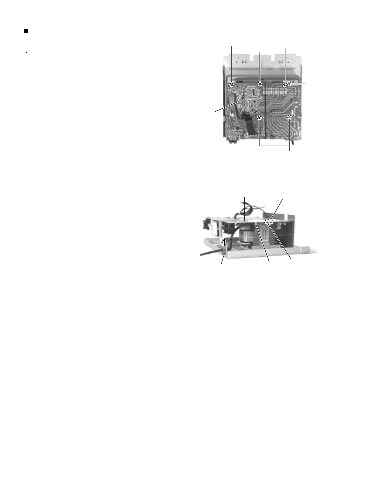
Removing the head amp.and mechanism
control P.C.board (See Fig. 4)
MX-J770V/MX-J880V
1.Remove the cassette mechanism assembly.
2.After turning over the cassette mechanism
assembly,remove the five screws "A" retaining
the head amp. and mechanism control P.C.
board
3.Disconnect the connectors CN303 and CN304
on the P.C.Board and the connectors CN1 on
both the right and left side reel pulse
P.C.Boards.
4.When necessary, remove the 4pin parallel
wire soldered to the main motor
Removing the capstan motor assembly
1.Remove the six screws "B" retaining capstan
motor assembly (See Fig. 5).
2.While raising the capstan motor, remove the
capstan belts A and B respectively from the
motor pulley (See Fig. 6).
A
Flexible
board
Head amplifier &
mechanism control board
AA
CN304
CN302 CN301
Flexible
board
CN303
Fig.4
BB
Capstan motor
assembly
AA
Caution 1: Be sure to handle the capstan
belts so carefully that these belts
will not be stained by grease and
other foreign matter. Moreover,
these belts should be hand while
referring to the capstan belt
hanging method.
Capstan
belt A
BBBB
Fig.5
Capstan motor
Capstan
belt B
Capstan
belt A
Capstan
belt B
Motor pulley
Fig.7 Fig.6
1-29
Page 30

MX-J770V/MX-J880V
Removing the capstan motor (See Fig. 8)
From the joint bracket, remove the two screws "C"
retaining the capstan motor.
Removing the flywheel (See Fig. 9,10)
1.Remove the head amp. and mechanism control
P.C.Board.
2.Remove the capstan motor assembly.
3.After turning over the cassette mechanism, remove
the slit washers "a" and "b" fixing the capstan shafts
R and L, and pull out the flywheels R and L respectively
from behind the cassette mechanism.
C
Capstan motor
Joint
bracket
C
Fig.8
Flywheel R Flywheel L
Flywheel R Flywheel L
Fig.10
Removing the reel pulse P.C.board and solenoid
(See Fig. 11)
1.Remove the five pawls (c,d,e,f,g) retaining
the reel pulse P.C.Board.
2.From the surface of the reel pulse P.C.Board parts,
remove the two pawls "h" and "i" retaining the solenoid.
hi
Solenoid
c
a
d
Slit
washer "a"
Fig.9
e
f
b
Slit
washer "b"
g
Reel pulse board
1-30
Solenoid
Fig.11
Page 31

Adjustment method
Measurement instruments required
for a djustment
1. Low frequency oscillator,
This oscillator should have a capacity to output 0dBs
to 600ohm at an oscillation frequency of 50Hz-20kHz.
2. Attenuator impedance : 600ohm
3. Electronic voltmeter
4. Frequency counter
5. Wow flutter meter
6. Test tape
VTT712 : For Tape speed and wow flutter ( 3kHz)
VTT724 : For Reference level (1kHz)
TMT7036 : For Head angle(10kHz),Play back frequency
characteristics(1kHz),and dubbing frequency
characteristics(63,1,10kHz)
Because of frequency-mixed tape with 63,1k,10k and
14kHz(250nWb/m -24dB).
Use this tape together with a filter.
7. Blank tape
TAPE : AC-225, TAPE : AC-514
8. Torque gauge : For play and back tension
Forward ; TW2111A, Reverse ; TW2121A
Fast Forward and Rewind ; TW2231A
9. Test disc
: CTS-1000(12cm),GRG-1211(8cm)
10. Jitter meter
Measurement conditions
Power supply voltage
AC110/127/220-240V(50/60Hz)
Measurement
output terminal : Speaker out
:TP101(Mesuring for TUNER/DECK/CD)
:Dummy load 6ohm
MX-J770V/MX-J880V
Radio input signal
AM modulation frequency : 400Hz
Modulation factor : 30%
FM modulation frequency : 400Hz
Frequency displacement : 22.5kHz
Frequency Range
AM 531kHz~1602kHz
FM 87.5MHz~108MHz
Standard measurement positions of volume
and switch
Power : Standby (Light STANDBY Indicator)
S,A,BASS : OFF
Sound mode : OFF
Main VOL. : 0 Minimum
Travers mecha set position : Disc 1
Mic MIX vol : MAX
ECHO : OFF
Precautions for measurement
1. Apply 30pF and 33kohm to the IF sweeper output
side and 0.082 F and 100kohm in series to
the sweeper input side.
2. The IF sweeper output level should be made as
low as possible within the adjustable range.
3. Since the IF sweeper is a fixed device, there is
no need to adjust this sweeper.
4. Since a ceramic oscillator is used, there is no need
to perform any MPX adjustment.
5. Since a fixed coil is used, there is no need to adjust
the FM tracking.
6. The input and output earth systems are separated.
In case of simultaneously measuring the voltage
in both of the input and output systems with an
electronic voltmeter for two channels, therefore,
the earth should be connected particularly.
7. In the case of BTL connection amplifier, the minus
terminal of speaker is not for earthing. Therefore,
be sure not to connect any other earth terminal
to this terminal. This system is of an OTL system.
1-31
Page 32

MX-J770V/MX-J880V
Arrangement of adjusting positions
Cassette mechanism section (Mechanism A section)
Head azimuth
adjusting screw
(Forward side)
Playback
head
Head azimuth
adjusting screw
(Reverse side)
Cassette mechanism section (Back side)
Head azimuth
adjusting screw
(Forward side)
Playback,recording and eraser
heads or playback head
Head azimuth
adjusting screw
(Reverse side)
Cassette Mechanism Unit Section
Tape speed ADJ
Bias ADJ L
Bias ADJ R
1-32
Page 33

1.Playback the test tape TMT7036(10kHz).
2.With the playback mechanism or recording &
playback mechanism, adjust the head azimuth
screw so that the forward and reverse output
levels become maximum.After adjustment,lock
the head azimuth at least by half a turn.
3.In either case,this adjustment should be
performed in both the forward and reverse
directions with the head azimuth screw.
<Constant speed>
Adjust VR301 so that the frequency counter reading
becomes 3,000Hz 60Hz when playing back the
test tape VTT712(3kHz)with the playback mechanism
or playback and recording mechanism after ending
forward winding of the tape.
Confirmation
of head angle
Confirmation
of tape speed
Test tape
:TMT7036(10kHz)
Measurement
output terminal
:Speaker terminal
Speaker R
(Load resistor:3 )
:Headphone terminal
Test tape
:VTT712(3kHz) or
TMT7036(3kHz)
Measurement
output terminal
:Headphone terminal
Maximum
output
Tape speed
of decks
(A and B)
:3,000Hz
60Hz
Adjust the head
azimuth screw
only when the
head has been
changed.
VR301
Items Measurement
conditions
Measurement method
Standard
values
Adjusting
positions
Tape recorder section
Items Measurement
conditions
Measurement method
Standard
values
Adjusting
positions
After setting to the double speed motor, confirm
that the frequency counter reading becomes
4,800+400/-300Hz when the test tape VTT712
(3kHz) has been play back with the playback
mechanism.
When the test tape VTT712(3kHz) has been played
back with the playback mechanism or recording and
playback mechanism at the beginning of forward
winding, the frequency counter reading of the
difference between both of the mechanisms should
be 6.0Hz or less.
When the test tape VTT712(3kHz) has been played
back with the playback mechanism or recording and
playback mechanism at the beginning of forward
winding the frequency counter reading of wow &
flutter should be 0.25% or less(WRMS).
Double tape
speed
Difference
between the
forward and
reverse speed.
P.mecha and
R/P mecha
speed
Wow & flutter
Test tape
:TMT7036(10kHz)
Measurement
output terminal
:Speaker terminal
Speaker R
(Load resistance:3 )
measurement
output terminal
:Headphone terminal
Test tape
:TMT7036(10kHz)
Measurement
output terminal
:Headphone terminal
4,800+400/
-300Hz
60Hz or
less
with in
0.25%
JIS(WTD)
Playback
mechanism side
Both the playback
and recording &
playback
mechanism
Both the playback
and recording &
playback
mechanism
Reference values for confirmation items
MX-J770V/MX-J880V
1-33
Page 34

MX-J770V/MX-J880V
Electrical performance
Items Measurement
Adjustment of
recording bias
current
(Reference
value)
conditions
*Mode : Forward or
reverse mode
*Recording mode
*Test tape
:AC-514 and AC-225
Measurement output
terminal
:Both recording and
headphone terminals
Measurement method
1.With the recording and playback mechanism,
load the test tapes(AC-514 to TYP and AC-225 to
TYP ),and set the mechanism to the recording and
pausing conditions in advance.
2.After connecting 100 in series to the recorder
head,measure the bias current with a valve
voltmeter at both of the terminals.
3.After resetting the [PAUSE] mode,start recording.
At this time,adjust VR101 for LcH and VR201 for
RcH so that the recording bias current values
become 4.0 A (TYP ) and 4.20 A(TYP ).
Standard
values
AC-225
:4.20 A
AC-514
:4.0 A
Adjusting
positions
LcH
:VR101
RcH
:VR201
Adjustment of
recording and
playback
frequency
characteristics
Reference frequency
:1kHz and 10kHz
(REF:-20dB)
Test tape
:TYP AC-514
Measurement input
terminal
:OSC IN
1.With the recording and playback mechanism,load
the test tape(AC-514 to TYP ),and set the
mechanism to the recording and pausing condition
in advance.
2.While repetitively inputting the reference frequency
signal of 1kHz and 10kHz from OSC IN, record and
playback the test tape.
3.While recording and playing back the test tape in
TYP ,adjust VR101 for LcH and VR201 for RcH
so that the output deviation between 1kHz and
10kHz becomes -1dB 2dB.
Reference values for electrical function confirmation items
Items Measurement
Recording
bias frequency
conditions
*Recording and
playback side forward
or reverse
*Test tape
:TYP AC-514
*Measurement
terminal BIAS TP on
P.C.board
1.While changing over to and from BIAS 1 and 2,
confirm that the frequency is changed.
2.With the recording and playback mechanism.
load the test tape (AC-514 to TYP ),and set the
mechanism to the recording and pausing
conditions in advance.
3.Confirm that the BIAS TP frequency on the
P.C.board is 100kHz 6kHz.
Measurement method
Output
deviation
between
1kHz and
10kH
:-1dB 2dB
Standard
values
100kHz
+9kHz
-7kHz
LcH
:VR101
RcH
:VR201
Adjusting
positions
Eraser current
(Reference
value)
1-34
*Recording and
playback side forward
or reverse
*Recording mode
*Test tape
:AC-514 and AC-225
Measurement terminal
Both of the eraser
head
1.With the recording and playback mechanism,
load the test tapes(AC-514 to TYP and AC-225
to TYP ),and set the mechanism to the recording
and pausing condition in advance.
2.After setting to the recording conditions,connect
1M in series to the eraser head on the recording
and playback mechanism side,and measure the
eraser current from both of the eraser terminal.
TYP
:120mA
TYP
:75mA
Page 35

Diagnosis which uses extension wire method
System control P.C.board
1.Remove the metal cover and CD changer mechanism.
2.Remove the front panel assembly.
3.One screw A is removed, and relay board is removed.
4.As shown in fig.1, place the front panel assembly after
opening it outward using the right side of the front panel as
an axis.
5.The extension wire is connected with CN870 & CN871 on
the INPUT/OUTPUT board and CN860 & CN861 on the
main board.
Extension wire parts No.
MX-J770V/MX-J880V
QUQ412-4020CJ
JIG-MXJ500
Input/output board
FLAT WIRE
CONNECTOR Board x 2
FLAT WIRE
CONNECTOR Board x 2
CN870
CN871
A
Relay board
Extension wire
Main board
Front panel assembly
CN860
CN861
Relay board
Fig.1
1-35
Page 36

MX-J770V/MX-J880V
Flow of functional operation until TOC read
Power ON
Play Key
Slider turns REST
SW ON.
Automatic tuning
of TE offset
Check Point
Confirm that the voltage at the pin5
of CN801 is "H"\"L"\"H".
Tracking error waveform at TOC reading
Approx.3sec
Tracking
servo
off states
Automatic measurement
of TE amplitude and
automatic tuning of
TE balance
VREF
pin 25 of
IC601(TE)
Approx
1.8V
Disc states
to rotate
Tracking
servo
on states
Disc to be
braked to stop
TOC reading
finishes
500mv/div
2ms/div
Fig.1
Laser ON
Detection of disc
Automatic tuning of
Focus offset
Automatic measurement of
Focus S-curve amplitude
Disc is rotated
Focus servo ON
(Tracking servo ON)
Automatic measurement of
Tracking error amplitude
Automatic tuning of
Tracking error balance
Check that the voltage at the
pin40 of IC651 is + 5V?
Confirm that the Focus error
S-cuve signal at the pin28 of
IC651 is approx.2Vp-p
Confirm that the signal from
pin24 IC651 is 0V as a
accelerated pulse during
approx.400ms.
Confirm the waveform of
the Tracking error signal.
at the pin 25 of IC601 (R604)
(See fig-1)
1-36
Automatic tuning of
Focus error balance
Automatic tuning of
Focus error gain
Automatic tuning of
Tracking error gain
TOC reading
Play a disc
Confirm the eys-pattern
at the lead of TP1
Page 37

MX-J770V/MX-J880V
Maintenance of laser pickup
(1) Cleaning the pick up lens
Before you replace the pick up, please try to
clean the lens with a alcohol soaked cotton
swab.
(2) Life of the laser diode
When the life of the laser diode has expired,
the following symptoms will appear.
1. The level of RF output (EFM output:ampli
tude of eye pattern) will below.
Is the level of
RFOUT under
1.25V 0.22Vp-p?
YES
O.K
NO
Replace it.
Replacement of laser pickup
Turn off the power switch and,disconnect the
power cord from the ac outlet.
Replace the pickup with a normal one.(Refer
to "Pickup Removal" on the previous page)
Plug the power cord in,and turn the power on.
At this time,check that the laser emits for
about 3seconds and the objective lens moves
up and down.
Note: Do not observe the laser beam directly.
Play a disc.
Check the eye-pattern at TP1.
Finish.
(3) Semi-fixed resistor on the APC PC board The semi-fixed resistor on the APC printed circuit board which is
attached to the pickup is used to adjust the laser power.Since this adjustment should be performed to match the
characteristics of the whole optical block, do not touch the semi-fixed resistor.
If the laser power is lower than the specified value,the laser diode is almost worn out, and the laser pickup should
be replaced.
If the semi-fixed resistor is adjusted while the pickup is functioning normally,the laser pickup may be damaged
due to excessive current.
1-37
Page 38

MX-J770V/MX-J880V
Description of major ICs
AN8806SB-W(IC601) :RF&SERVO AMP
1.Pin layout
PD 1
LD 2
LDON 3
LDP 4
VCC 5
RF- 6
RF OUT 7
RF IN 8
C.AGC 9
ARF 10
C.ENV 11
C.EA 12
CS BDO 13
BDO 14
CS BRT 15
OFTR 16
/NRFDET 17
GND 18
2.Block diagram
36 PDAC
35 PDBD
34 PDF
33 PDE
32 PDER
31 PDFR
30 TBAL
29 FBAL
28 EF27 EF OUT
26 TE25 TE OUT
24 CROSS
23 TE BPF
22 VDET
21 LD OFF
20 VREF
19 ENV
6
728
29
27
910 17
8
11
12 19
+
- +
+
EQ
AGC
RF
DET
ENV CURCUIT
36
+
35
+
31
34
-
+
VCBA
-
+
VCBA
-
-
VCBA
+
+
OFTR
BDO
+
13
14
15
16
20
+
- +
32
33
+
-
VCBA
+
+ -
+
- +
21
2
+
-
24 25
30
23
26
22
14
3
1-38
Page 39

3. Pin function
MX-J770V/MX-J880V
Pin No.
1
2
3
4
5
6
7
8
9
10
11
12
13
14
15
16
17
18
19
20
21
22
23
24
25
26
27
28
29
30
31
32
33
34
35
36
symbol
PD
LD
LD ON
LDP
VCC
RF-
RF OUT
RF IN
C.AGC
ARF
C.ENV
C.EA
CS BDO
BDO
CS BRT
OFTR
/NRFDET
GND
ENV
VREF
LD OFF
VDET
TE BPF
CROSS
TE OUT
TE-
FE OUT
FE-
FBAL
TBAL
PDFR
PDER
PDF
PDE
PD BD
PD AC
I/O
I
APC amp . Input terminal
APC amp . Output terminal
O
LD ON/OFF control terminal
I
Connect to GND
-Power supply
-RF amp . Reversing input terminal
I
RFamp . Output terminal
O
AGC input terminal
I
AGC loop filter connection terminal
I/O
ARF output terminal
O
RF detection capacity connection terminal
I/O
HPF-amp capacity connection terminal
I/O
Capacity connection terminal for RF discernment side envelope detection
I/O
BDO output terminal
O
Capacity connection terminal for RF discernment side envelope detection
I/O
O
OFTR output terminal
RFDET output terminal
O
--
Connect to GND
O
3TENV output terminal
O
VREF output terminal
--
APC OFF control terminal
O
VDET output terminal
I
VDET input terminal
O
CROSS output terminal
O
TE amp . Output terminal
I
FE amp . Reversing input terminal
O
FE amp . output terminal
I
FE amp . Reversing input terminal
I
F.BAL control terminal
I
T.BAL control terminal
I/O
I-V amp conversion resistance adjustment terminal
I/O
I-V amp conversion resistance adjustment terminal
I
I-V amp input terminal
I-V amp input terminal
I
I
I-V amp input terminal
I
I-V amp input terminal
Function
1-39
Page 40

MX-J770V/MX-J880V
AN7345K(IC302) PB/REC AMP
1.Block diagram
2. Pin Function
Pin
Symbol
No.
1
R1
2
R2
L1
L2
NF1
24
1
R1
I/O
I
Playback amplifier input
Playback amplifier input
I
R2
23
2
22
AMP
AMP
3
NF2
OUT1
Pre
Pre
OUT2
Function
9
EQ
CTL
ALC
10 11
LC
I/O
I
I
VCC
RF
141516
13
REPPLE
REJ
12
LPF GND
Repple filter
Function
EQ1
CTL1
RIN1
RNF1
ROUT1
2021
EQ
CTRL
5
4
EQ2
CTL2
Pre
Source
CTRL
6
1819
17
78
RIN2
RNF2
Pin
No.
13
14
ALC
AMP
ALC
AMP
ROUT2
Symbol
Vcc Power supply
RF
3
NF2
4
OUT2 Playback amplifier output
EQ2 I
5
CTL2 I Pre Amplifier input swithing time
6
RIN2 I
7
RNF2 I Recording amplifier negative feedback
8
ROUT2
9
LC I
10
11
LPF
GND I
12
I
Playback amplifier negative feedback
O
Equlaizer
constant
Recording amplifier input
Recording amplifier output
O
ALC low cut
ALC low pass filter
I
EQCTL EQ control
15
16
ROUT1
17
RNF1 Recording amplifier negative feedback
RIN1
18
CTL1
19
20
EQ1 Equlayzer
21
OUT1
NF1
22
L2 I
23
24
L1
I
O
Recording amplifier output
I
I Recording amplifier input
Pre amplifier input swithing control
I
I
Playback amplifier output
O
Playback amplifier negative feedback
I
Playback amplifier input
Playback amplifier input
I
1-40
Page 41

BA15218(IC481,501,502,526,571):OP AMP.
MX-J770V/MX-J880V
1OUT1
2-IN1
1
EE
3+IN1
+
4
-
2
+
BA3126N (IC301)
1. Terminal layout and Block diagram
8
7
6
5V
VCC
OUT2
-IN2
+IN2
1
REC SW
2
GND
CONT.
P / B SW
543
GND
6
VCC
7
P / B SW
89
GND
REC SW
1-41
Page 42

MX-J770V/MX-J880V
BA3835S (IC812) : SPI B.P.F.
1.Block Diagrams
BIASC
VREFC
RREF
DIFOUT
N.C.
N.C.
CIN
AIN
VCC
1
2
3
4
5
6
7
8
9
2.Pin Function
No. Symbol
1
2
3
4
5
6
7
8
9
10
11
12
13
14
15
16
17
18
BIASC
VREFC
RPEF
NC
NC
NC
CIN
AIN
VCC
SPI-A
SPI-B
SPI-C
SPICSB
NC
NC
TEST
AOUT
GND
A-C
DIF
105Hz
BPF
340Hz
BPF
1kHz
BPF
3.4kHz
BPF
10.5kHz
BPF
REFERENCE
CURRENT
PEAK
HOLD
PEAK
HOLD
PEAK
HOLD
PEAK
HOLD
PEAK
HOLD
I/O
-
-
-
-
-
-
I
O
O
O
O
-
-
O
-
BIAS
VREF
RES
RES
MPX
RES
RES
RES
DEC
18
17
16
15
14
13
12
11
10
GND
AOUT
TEST
N.C.
N.C.
SEL
C
B
A
Function
Decoupling condenser connection terminal.
Decoupling condenser connection terminal.
Reference resistance connection terminal.
Non connect.
Non connect.
Non connect.
Connected to GND of audio system through a condenser.
Inputs the audio signal through a condenser.
Power supply terminal.
Output selection control terminal.
Output selection control terminal.
Output selection control terminal.
Output selection control terminal.
Non connect.
Non connect.
Connected to GND upon normal use.
Multi-plexor output terminal.
Connect to GND.
1-42
Page 43

BA3837(IC466):MIC Mixer
1.Block diagram
C
16
B
15
14
MX-J770V/MX-J880V
A
ROUT
13
LP
12
LP
11
LP
10
RIN
9
1
VCC
2.Pin function
Pin No.
1
2
3
4
5
6
7
8
9
10
11
12
13
14
15
16
LOGIC
+
-
2
MIC
Symbol
VCC
MIC IN
LOUT
FK
TK
LIN
BIAS
GND
RIN
LPF1
LPF2
LPF3
ROUT
CONTA
CONTB
CONTC
-
+
3
LOUT
+
-
SW2 SW1
4
FK
I/O
Power supply
Microphone mixing input
I
O
O
O
O
O
Channel L output
Non connect
Non connect
Channel L input
I
Signal bias
I
Connect to GND
Channel R input
I
Connects to LPF time constant element
Connects to LPF time constant element
LPF outpout
Channel R output
Mode select input A
I
Mode select input B
I
Mode select input C
I
TK
-
+
-
+
R
L-R
L+R
-
+
+
L
+
-
5
6
LIN
7
BIAS
8
GND
Description
1-43
Page 44

MX-J770V/MX-J880V
BU1427K (IC152) : Digital RGB-TV Encoder
1. Terminal layout
2. Pin function
No. NAME FUNCTION
1
2
3
4
5
6
7
8
9
10
11
12
13
14
15
16
17
18
19
20
21
22
23
24
25
26
27
28
29
30
31
32
* The pin built-in pull-down resister. (30kohm)
BOSD
Y0/YUV0
Y1/YUV1
Y2/YUV2
Y3/YUV3
Y4/YUV4
Y5/YUV5
Y6/YUV6
GND
Y7/YUV7
UV0
UV1
UV2
UV3
OSDSW
CDGSWB
UV4
UV5
UV6
UV7
GND
NTB
IM0
IM1
TEST1
TEST2
VSY
HSY
PIXCLK
VDD
IO VDD
INT
OSD BLUE DATA INPUT
YUV DATA
YUV DATA
YUV DATA
YUV DATA
YUV DATA
YUV DATA
YUV DATA
DIGITAL GROUND
YUV DATA
U V D ATA
U V D ATA
U V D ATA
U V D ATA
OSD ENABLE/DISABLE
SELECT Video CD/CD-G
U V D ATA
U V D ATA
U V D ATA
U V D ATA
DIGITAL GROND
SELECT NISC/PAL MODE
SELECT YUV/YUV
SELECT DAC/NORMAL
Normally pull down to GND
SELECT U/V TIMING
V-SYNC INPUT or OUTPUT
H-SYNC INPUT or OUTPUT
1/2 freq. of BCLK
DIGITAL VDD
VDD for I/O
Interlace /Non-Interlace
No. NAME FUNCTION
33
34
35
36
37
38
39
40
41
42
43
44
45
46
47
48
49
50
51
52
53
54
55
56
57
58
59
60
61
62
63
64
SLABEB
ADDH
VREF-C
CGND
COUT
VGND
VOUT
AVSS
P-VDD
IR
AVDD
YGND
YOUT
VDD
YFILON2B
YCOFF
YFILON1B
PAL60B
VCLK
RSTB
CLKSW
RD0
RD1
RD2
ROSD
RD3
BCLK/RD4
RD5
IO VDD
RD6
RD7
GOSD
SELECT MASTER/SLAVE
+0.5/-0.5 LINE at NON-INTER
DAC BIAS
CHROMA OUTPUT GROUND
CHROMA OUTPUT
Composite Output Ground
COMPOSITE OUTPUT
Analog Ground (DAC, VREF)
POWER(DAC) VDD
REFERENCE RESISTOR
ANALOG (VREF) VDD
Luminance Output Ground
Luminance Output
DIGITAL VDD
Y-FILSEL THROU/FILON2
DAC(YOUT,COUT) OFF
Y-FILSEL THROU/ FILON1
NORMAL/PAL60 at PALMODE
Video Clock Input
NORMAL/RESET
SEL*1CLK/*2CLK
Pull Down to GND
Pull Down to GND
Pull Down to GND
OSD RED DATA INPUT
Pull Down to GND
BASE CLOCK OUT
Pull Down to GND
VDD for I/O
Pull Down to GND
Pull Down to GND
OSDGREEN DATA INPUT
1-44
Page 45

MX-J770V/MX-J880V
STROBE
DATA
CLOCK
Q1
Q2
Q3
Q4
Vss
Vdd
OUTPUT ENABLE
Q5
Q6
Q7
Q8
Q's
Qs
1
2
3
4
5
6
7
8
16
15
14
13
12
11
10
9
1.Pin layout
8-STAGE
SHIFT REGISTER
8-BIT
LATHES
3-STATE
OUTPUTS
1
2
3
15
Q1
Q8
10
9
DATA
CLOCK
STROBE
OUTPUT
ENABLE
PARALLEL OUTPUT
Q's
Qs
SERIAL
OUTPUT
2.Block diagram
BU4094BCF(IC303,304,811):Serial to parallel port extension
1-45
Page 46

MX-J770V/MX-J880V
BU9253AS(IC902) : LPF&ECHO MIX.
1.Pin layout & block diagram
1
GND
BIAS
2
COUNTER
3
4
5
ECHO VR
DAINT IN
OSC
18
17
16
15
14
CR
MUTE
VCC
ADINT IN
DAINT OUT
DALPF IN
DALPF OUT
MIX OUT
2.Pin function
Pin No. Symbol
1
2
ECHO VR
3
4
5
6
7
8
9
DAINT IN
DAINT OUT
DALPF IN
DALPF OUT
MIX OUT
10
11
12
13
14
ADLPF IN
ADLPF OUT
ADINT OUT
ADINT IN
15
16
17
18
6
7
- +
8
9
GND
BIAS
MIX IN
VCC
NC2
MUTE
CR
D/A
MIX
SRAM
I/O
I
-
I
O
I
O
O
I
I
O
O
I
-
-
I
-
A/D
13
ADINT OUT
12
ADLPF OUT
- +
11
ADLPF IN
10
MIX IN
Descriptions
Connect GND
Echo level control
Non connect
Analog part DC bias
DA side integrator input
DA side integrator output
DA side LPF input
DAside LPF output
Mix AMP output for original tone& echo tone
Mix AMP input pin for original tone
AD side LPF input
AD side LPF output
AD side integrator output
AD side integrator input
Power supply
Non connect
Mute control signal input
CR pin for oscillator
1-46
Page 47

MX-J770V/MX-J880V
HY57V161610DTC8 or KM416S1120DT-G8 (IC504,IC505) : 16MB SDRAM
1.Block diagram
CLK
CKE
Address
CS
RAS
CAS
WE
Clock
Generator
Mode
register
Command decoder
Control logic
Row
address
buffer &
Refresh
counter
Column
address
buffer &
burst
counter
Bank B
Bank A
Row decoder
Sense amplifier
Column decoder
& latch circuit
Data counter
Input & output
Latch circuit
DQM
DQ
buffer
2.Pin function
Pin No. Symbol Description Pin No. Symbol Description
1
2,3
4
5,6
7
8,9
10
11,12
13
14
15
16
17
18
19,20
21~24
25
VCC
DQ0,1
VSS
DQ2,3
VDD
DQ4,5
VSS
DQ6,7
VCC
LDQM
WE
CAS
RAS
CS
A11,10
A0~3
VCC
Power supply
Data input/output
Connect to GND
Data input/output
Power supply
Data input/output
Connect to GND
Data input/output
Power supply
Lower DQ mask enable
Write enable
Column address strobe
Row address strobe
Chip enable
Address inputs
Address inputs
Power supply
26
27~32
33
34
35
36
37
38
39,40
41
42,43
44
45,46
47
48,49
50
VSS
A4~9
NC
CKE
CLK
UDQM
NC
VCC
DQ8,9
VSS
DQ10,11
VDD
DQ12,13
VSS
DQ14,15
VSS
Connect to GND
Address inputs
Non connect
Clock enable
System clock input
Upper DQ mask enable
Non connect
Power supply
Data input/output
Connect to GND
Data input/output
Power supply
Data input/output
Connect to GND
Data input/output
Connect to GND
1-47
Page 48

MX-J770V/MX-J880V
LA1838(IC102): FM AM IF AMP&detector, FM MPX Decoder
1. Block Diagram
30
ALC
BUFF
FM
S-METER
FM IF
1
2. Pin Function
Pin
Symbol
No.
FM IN
1
AM MIX
2
3
FM IF
AM IF
4
GND
5
6
TUNED
STEREO
7
8
VCC
9
FM DET
10
AM SD
FM VSM
11
AM VSM
12
13
MUTE
14
FM/AM
MONO/ST O
15
29
28
AM
OSC
SD
COMP
S-CLRVE
PM
DET
2
I/O
I
This is an input terminal of FM IF
REG
AM
MIX
AM/FM
IF-BUFF
3
27
FM
RF.AMP
AM IF
4
26
AGC
AM
S-METER
Function
DET
GND
5
signal.
This is an out put terminal for AM
O
mixer.
I
Bypass of FM IF
Input of AM IF Signal.
I
I
This is the device ground terminal.
When the set is tunning,this terminal
O
becomes "L".
O
Stereo indicator output. Stereo "L",
Mono: "H"
III
This is the power supply terminal.
I
FM detect transformer.
I
This is a terminal of AM ceramic filter.
O
Adjust FM SD sensitivity.
O
Adjust AM SD sensitivity.
I/O
When the signal of IF REQ of IC121(
LC72131) appear, the signal of FM/AM
IF output. //Muting control input.
Change over the FM/AM input.
I
"H" :FM, "L" : AM
Stereo : "H", Mono: "L"
25
TUNING
DRIVE
6
24
STEREO
DRIVE
7
22
23
P-DET
VCC
89
Pin
Symbol
No.
16
R OUT
17
L OUT
18
19
20
21
22
23
24
25
26
27
28
29
30
R IN
L IN
RO
LO
IF IN
FM OUT
AM DET
AM AGC
AFC
AM RF
REG
AM OSC
OSC BUFFER
21
DECODER
ANIT-BIRDIE
VCO
384KHz
10
20
STEREO
5N
SW
FF
38k
11
I/O
O
Right channel signal output.
O
Left channel signal output.
Input terminal of the Right channel post
I
18
19
MUTE
FF
/
19k
2
12 13
FF
19k
/LS
Function
17 16
PILOT
DET
14
AMP.
Input terminal of the Left channel
I
post AMP.
Mpx Right channel signal output.
O
O
Mpx Left channel signal output.
I
Mpx input terminal
FM detection output.
O
AM detection output.
O
This is an AGC voltage input terminal
I
for AM
I
This is an output terminal of voltage
for FM-AFC.
AM RF signal input.
I
Register value between pin 26 and pin28
O
besides the frequency width of the
input signal.
I
This is a terminal of AM Local
oscillation circuit.
AM Local oscillation Signal output.
O
15
1-48
Page 49

LA6541-X(IC801) : Servo Driver
1. Pin Layout & Block Diagram
MX-J770V/MX-J880V
Vcc Vref Vin4 Vg4 Vo8 Vo7
24 23
22
21
20
19
11k
Vcc
Gnd
Vo6 Vo5 Vg3 Vin3 Cd Res
18
17 16
ohm
- +
- +
Level
shift
Level
shift
B T L
driver
B T L
driver
B T L
driver
B T L
driver
Level
shift
Level
shift
11k
ohm
1
2
Vcc Mute Vin1 Vg1 Vo1 Vo2 Vo3 Vo4 Vg2 Vin2 Reg
3456
Gnd
7 8 9101112
2. Pin functions
Pin
Symbol Function
No.
1
10
11
12
13
14
15
16
17
18
19
20
21
22
23
24
2
3
4
5
6
7
8
9
Vcc
Mute
Vin1
Vg1
Vo1
Vo2
Vo3
Vo4
Vg2
Vin2
Reg Out
Reg In
Res
Cd
Vin3
Vg3
Vo5
Vo6
Vo7
Vo8
Vg4
Vin4
Vref
Vcc
Power supply (Shorted to pin 24)
All BTL amplifier outputs ON/OFF
BTL AMP 1 input pin
BTL AMP 1 input pin (For gain adjustment)
BTL AMP 1 input pin (Non inverting side)
BTL AMP 1 input pin (Inverting side)
BTL AMP 2 input pin (Inverting side)
BTL AMP 2 input pin (Non inverting side)
BTL AMP 2 input pin (For gain adjustment)
BTL AMP 2 input pin
External transistor collector (PNP) connection. 5V power supply output
External transistor (PNP) base connection
Reset output
Reset output delay time setting (Capacitor connected externally)
BTL AMP 3 input pin
BTL AMP 3 input pin (For gain adjustment)
BTL AMP 3 output pin (Non inverting side)
BTL AMP 3 output pin (Inverting side)
BTL AMP 4 output pin (Inverting side)
BTL AMP 4 output pin (Non inverting side)
BTL AMP 4 output pin (For gain adjustment)
BTL AMP 4 output pin
Level shift circuit's reference voltage application
Power supply (Shorted to pin 1)
15
14
13
11k
ohm
RESET
Regulator
11k
ohm
Reg
out
In
1-49
Page 50

MX-J770V/MX-J880V
LB1641 (IC853) : DC Motor Driver
1. Pin Layout
1 2 3 4 5 6 7 8 9
GNDOUT1 P1
VZ IN1 IN2
2. Pin Functions
Input Output
IN1 IN2 OUT1 OUT2
0 0 0 0
1 0 1 0
0 1 0 1
1 1 0 0
VCC1
10
VCC2 P2
OUT2
Mode
Brake
CLOCKWISE
COUNTER-CLOCKWISE
Brake
1-50
Page 51

1. Pin layout
1
2
3
4
5
6
7
8
9
10
11
22
21
20
19
18
17
16
15
14
13
12
XT
FM/AM
CE
DI
CLOCK
DO
FM/ST/VCO
AM/FM
SDIN
XT
GND
LPFOUT
LPFIN
PD
VCC
FMIN
AMIN
IFCONT
IFIN
Pin
No.
1
2
3
4
5
6
7
8
9
10
11
Pin
No.
12
13
14
15
16
17
18
19
20
21
22
Symbol
XT
FM/AM
CE
DI
CLOCK
DO
FM/ST/VCO
AM/FM
LW
MW
SDIN
Symbol
IFIN
IFCONT
AMIN
FMIN
VCC
PD
LPFIN
LPFOUT
GND
XT
Function
X'tal oscillator connect (75kHz)
LOW:FM mode
When data output/input for 4pin(input) and
6pin(output): H
Input for receive the serial data from
controller
Sync signal input use
Data output for Controller
Output port
"Low": MW mode
Open state after the power on reset
Input/output port
Input/output port
Data input/output
Function
IF counter signal input
IF signal output
Not use
AM Local OSC signal output
FM Local OSC signal input
Power suplly(VDD=4.5-5.5V)
When power ON:Reset circuit move
PLL charge pump output(H: Local OSC
frequency Height than Reference frequency.
L: Low Agreement: Height impedance)
Input for active lowpassfilter of PLL
Output for active lowpassfilter of PLL
Connected to GND
X'tal oscillator(75KHz)
I/O
I
O
I
I
I
O
O
O
I/O
I/O
I/O
I/O
I
O
-
I
I
-
O
I
O
I
Reference
Driver
Phase
Detector
Charge Pump
Unlock
Detector
Universal
Counter
Swallow Counter
1/16,1/17 4bit
12bit
Programmable
DriverS
Swallow Counter
1/16,1/17 4bit
Data Shift Register & Latch
Power
on
Reset
C
2B
I/F
1/2
7821113
21
17
6
5
4
3
15
16
22
1
18
19
20
12
2. Block diagram
3. Pin function
LC72136N (IC121) : PLL Frequency Synthesizer
MX-J770V/MX-J880V
1-51
Page 52

MX-J770V/MX-J880V
MN35511(IC651) : Digital servo & processor
1.Pin layout
28 1
21
40
2.Block diagram
DEMP/TEST2
LRCKI
BCKI
SDATAI
IOSEL
CRC
BLKCK
CLDCK
SBCK
SBCK2
SUBC
DEMPO
CLVS/FLAG6
SQCK
SUBQ
AVSS
AVDD
PCK/RESY
EFM
PLLF
DSFL
IREF
DRF
AFR
MLD
MCLK
MDATA
CK384
VCFO
SMCK/FCLK
XSEL
STAT
41 60
Digital deemphasis
Subcode
DSL PLL VCO
VCO
X2
X1
80
61
buffer
Timing generator
Pich control
8tims
Over
Sampling
Digital
Filter
EFM DEMODULATION
SYNC INTERPOLATION
Micro computer
Interphace
A/D converter
SUB CODE DEMODULATION
VCOF2
PLL
VCO2
DD
Method
DAC
16k
SRAM
CIRC error
Correction
Deinterleave
Servo cpu
Input port
PEM
R
PEM
L
Digital
Audio
Interface
CLV
Servo
Inter polation
Soft Muting
Digital
Attenuation
Peak detect
aaAuto cue
D/A
converter
Output port
Servo
Timing generator
AVDD2
OUT2D
OUT2C
OUT1D
OUT1C
AVSS2
FLAG
IP FLAG
TX
ECM
PC
LRCK
SRDATA
BCLK
DMUTE
VREF
TRV
KICK
PLAY/TRVSTP
ECS
TVD
TRD
FOD
TBAL
FBAL
/TLOCK
/FLOCK
LDON
TOFS
WVEL
SENSE
1-52
VSS
VDD
/RST
DVSS1
DVDD1
/TEST
FE
TE
RFENV
S
T
R
C
R
T
O
E
D
D
B
V
T
E
D
F
/R
T
F
O
Page 53

3. Pin function
Pin
symbol
No.
BCLK
1
2
LRCK
SRDATA
3
4
DVDD1
DVSS1
5
TX
6
7
MCLK
MDATA
8
MLD
9
10
SENSE
11
FLOCK
12
TLOCK
13
BLKCK
14
SQCK
15
SUBQ
16
DMUTE
STATUS
17
18
RST
19
SMCK
20
PMCK
21
TRV
22
TVD
23
PC
24
ECM
25
ECS
26
KICK
27
TRD
28
FOD
29
VREF
30
FBAL
31
TBAL
FE
32
TE
33
34
RF ENV
35
VDET
36
OFT
37
TRCRS
38
RFDET
BDO
39
LDON
40
I/O
O
Bit clock output for SRDATA
Identification signal output of Lch and Rch
O
O
Serial data output
I
Power supply (Digital)
I
Connected to GND
Digital audio interface output
O
com command clock signal input
I
(Data is latched at signal's rising point)
com command data input
I
I
com command load signal input
Non connect
-
-
Non connect
-
Non connect
Non connect
I
Outside clock for sub-code Q resister input
Sub-code Q -code output
O
I
Connected to GND
Status signal
O
(CRC,CUE,CLVS,TTSTOP,ECLV,SQOK)
Reset signal input (L:Reset)
I
I
Non connect
I
Non connect
O
Traverse enforced output
O
Traverse drive output
I
Non connect
Spindle motor drive signal (Enforced
O
mode output) 3-State
Spindle motor drive signal (Servo error
O
signal output)
Kick pulse output
O
Tracking drive output
O
O
Focus drive output
Reference voltage input pin for D/A
I
output block (TVD,FOD,FBA,TBAL)
Focus Balance adjust signal output
O
O
Tracking Balance adjust signal output
Focus error signal input(Analog input)
I
Tracking error signal input(Analog input)
I
I
RF envelope signal input(Analog input)
Vibration detect signal input(H:detect)
I
Off track signal input(H:off track)
I
Track cross signal input
I
RF detect signal input(L:detect)
I
BDO input pin(L:detect)
I
Laser ON signal output(H:on)
O
Description
Pin
No.
41
42
43
44
45
46
47
48
49
50
51
52
53
54
55
56
57
58
59
60
61
62
63
64
65
66
67
68
69
70
71
72
73
74
75
76
77
78
79
80
symbol
TES
PLAY
WVEL
ARF
IREF
DRF
DSLF
PLLF
VCOF
AVDD2
AVSS2
EFM
PCK
PDO
SUBC
XSEL
VSS
XI
X2
VDD
VCOF2
AVSS1
OUT1C
OUT1D
OUT2D
OUT2C
AVDD1
DEMPO
CK384
IOSEL
TEST
SBCK2
SUBC
SBCK
CLDCK
IPFLAG
DEMPI
SDATI
LRCKI
BCKI
MX-J770V/MX-J880V
I/O
Non connect
II
Non connect
I
Non connect
I
RF signal input
Reference current input pin
I
Bias pin for DSL
I
I/O
Loop filter pin for DSL
Loop filter pin for PLL
I/O
I
Not used
I
Power supply(Analog)
Connected to GND(Analog)
Non connect
III
Non connect
I
Non connect
I
Non connect
Clock input for subcode/serial output
I
Connected to GND(for X'tal oscillation
I
circuit)
Input of 16.9344MHz X'tal oscillation circuit
I
Output of X'tal oscillation circuit
O
I
Power supply(for X'tal cscillation circuit)
PLL loop filter terminal for jitter absorption
O
O
Ground terminal for audio DAC
O
PEM output terminal 1C
PEM output terminal 1D
O
O
PEM output terminal 2D
PEM output terminal 2C
O
Power supply for audio DAC
O
Non connect
384fs clock output
O
I
Mode switch terminal
I
Test mode setting terminal
I
Sub code/data reading clock input
O
Sub code/serial output
Clock input for sub code/serial output
I
O
Sub code /frame clock signal output terminal
Interpolation flag signal output H:Interpolation
I
IOSEL:L The outside DEMPO input terminal
I
SRDATA input terminal
I
When IOSEL is "L", LRCK input H:Lch data
I
L:Rch data
When IOSEL is "L", BCK input
I
Description
1-53
Page 54

MX-J770V/MX-J880V
MN4SV17160BT-10(IC104):16MB SDRAM
1.Block diagram
DQ0
DQ15
Column decoder
Sense amplifier
Bank 0
Memory cell array
2048 Row x 256
Column x 16 bit
Column decoder
~
DQ buffer
LDQM
UDQM
Sense amplifier
Bank 1
Memory cell array
2048 Row x 256
Column x 16 bit
Row decoder Row decoder
Column
address
counter
Column
address
buffer
Row
address
buffer
Refresh
counter
generator
Control signal
Mode
register
Clock
CLK
buffer
CKE
CS
RAS
CAS
WE
Command decoderAddress buffer
A11
A10
A9
~
A0
2.Pin function
Pin No. Symbol Description Pin No. Symbol Description
1
2,3
4
5,6
7
8,9
10
11,12
13
14
15
16
17
18
19,20
21~24
25
VCC
DQ0,1
VSS
DQ2,3
VDD
DQ4,5
VSS
DQ6,7
VCC
LDQM
WE
CAS
RAS
CS
A11,10
A0~3
VCC
Power supply
Data input/output
Connect to GND
Data input/output
Power supply
Data input/output
Connect to GND
Data input/output
Power supply
Lower DQ mask enable
Write enable
Column address strobe
Row address strobe
Chip enable
Address inputs
Address inputs
Power supply
26
27~32
33
34
35
36
37
38
39,40
41
42,43
44
45,46
47
48,49
50
VSS
A4~9
NC
CKE
CLK
UDQM
NC
VCC
DQ8,9
VSS
DQ10,11
VDD
DQ12,13
VSS
DQ14,15
VSS
Connect to GND
Address inputs
Non connect
Clock enable
System clock input
Upper DQ mask enable
Non connect
Power supply
Data input/output
Connect to GND
Data input/output
Power supply
Data input/output
Connect to GND
Data input/output
Connect to GND
1-54
Page 55

NJM4580E-W(IC652) : OP amp
1. Terminal layout
MX-J770V/MX-J880V
A OUT
2. Block diagram
V
A IN
A IN
V
1
2
8
7
V
B OUT
A B
3
4
6
B IN
5
B IN
INPUT
OUTPUT
V
1-55
Page 56

MX-J770V/MX-J880V
NJM4580L (IC901) : Mic Amplifier
1
2
34
5
TA8409S(IC851,IC852):Motor driver
1.Pin layout 2.Pin function
1
IN2
VCC
OUT 2
GND
GND
VS
OUT 1
VR
IN1
2
3
4
5
6
7
8
9
TA8409S
INPUT OUTPUT MODE
IN1
0
1
0
1
IN2
0
0
1
1
6
OUT1
1. A OUTPUT
2. A-INPUT
3. A+INPUT
-
4. V
5. B+INPUT
6. B-INPUT
7
8
7. B OUTPUT
8. V+
OUT2
H
L
L
L
H
L
MOTOR
STOP
CW/CCW
CCW/CW
BRAKE
TC74VHC00FT-X(IC106) : Wright timing control
1.Terminal layout / Block diagram
Vcc 4B 4A 4Y 3B 3A 3Y
14 13
1
1A 1B 1Y 2A 2B 2Y GND
1-56
12
11 10 9 8
2
6
543
7
Page 57

TDA7439 (IC436) : Conrtol volume
1.Pin layout
1
SDA
2
CRE
3
Vs
4
AGND
5
ROUT
6
LOUT
7
R-IN4
8
R-IN3
9
R-IN2
10
R-IN1
11
L-IN1
12
L-IN2
13
L-IN3
14
L-IN4
MUXOUTL
15
2.Block diagram
TDA7439
30
CSL
29
DIG GND
28
TREBLE(R)
27
TREBLE(L)
26
MIN(L)
25
MOUT(L)
24
BOUT(L)
23
BIN(L)
22
BOUT(R)
21
BIN(R)
20
MOUT(R)
19
MIN(R)
18
INR
17
MUXOUTR
16
INL
MX-J770V/MX-J880V
L-IN1
L-IN2
L-IN3
L-IN4
R-IN1
R-IN2
R-IN3
R-IN4
11
12
13
14
10
MIN(L)
26
MIDLE
25
MOT(L)
23
G
0/30dB
2dB STEP
INL
MUXOUT
15 16 27
VOLUME
2
I C BUS DECODER LATCHES
TREBLE
TREBLE(L)
9
G
VOLUME
TREBLE
MIDLE
8
7
INPUT
MULTIPLEXER
GAIN
17
18
201928
BIN(L)
24
BASS
BASS
2221
BOUT(L)
SPEAKER
ATT
LEFT
SPEAKER
ATT
RIGHT
SUPPLY
2
4
30
1
29
5
3
4
AGND
SCL
SDA
DIG-GND
ROUT
Vs
AGND
INR
CREF
MUXOUT
TREBLE(R)
MIN(R)
BIN(R)
MOUT(R)
BOUT(R)
1-57
Page 58

MX-J770V/MX-J880V
CL8830-PE0 (IC101) : MPEG Decoder & DSP
1. Pin layout
208 157
1
52
53 104
2. Block diagram
156
105
1-58
Page 59

3.Pin function(1/2)
Pin No
Symbol and I/O
Description
System Services
Power and Ground
13
178
190,174,156,153,147,141,138,
133,129,52,1
I
I
I/O
Hardware reset. An external device asserts RESET (active LOW)
to execute a decoder hardware reset. To ensure proper initialization after power is stable, assert RESET for at least 20 s.
System clock. Decoder requires an external 27 MHz TTL oscillator.
Drive with the same 27-MHz as VCK.
Programmable I/O pins.
176
179
5,12,17,27,36,40,47,55,61,65,
69,75,81,87,91,95,101,107,113,
117,123,134,144,149,160,168,
175,181,193,197
7,14,19,29,38,42,49,57,63,67,
71,77,83,89,93,97,103,109,115,
119,125,136,146,151,162,170,
183,195,199
Analog
Power
Analog Ground
Power
Ground
3.3-V analog supply voltage.
Analog ground for PLL.
3.3-V supply voltage for core logic and I/O signals.
Ground for core logic and I/O signals.
206
204-202
11-8,6,4-2
16
208
207
15
I
I
I/O
O,OD,PU
I
I
O,OD,PU
Host chip select. Host asserts CS to select the decoder for a read
or write operation. The falling edge of this signal triggers the read or
write operation.
Host address bus. 3-bit address bus selects one of eight host interface registers.
8-bit bi-directional host data bus. Host writes data to the decoder
Code FIFO via HDATA[7:0]. MSB of the 32-bit word is written
first. The host also reads and writes the decoder internal registers
and local SDRAM/ROM via HDAT[7:0].
Host interrupt. Open drain signal, must be pulled-up to 3.3 volts.
Driven high for 10 ns before tristate.
Read strobe in I mode. Must be held HIGH in M Mode.
Read/write strobe in M mode. Write strobe in I mode. Host asserts
R/W LOW to select write and LOW to select Read.
Active LOW to indicate host initiated transfer is not complete.
WAIT is asserted after the falling edge of CS and reasserted when
decoder is ready to complete transfer cycle. Open drain signal, must be pulled-up to 3.3 volts. Driven high for 10 ns before tristate.
8-bit Host Interface
185
184
182
180
I
I
I
I
Asserted HIGH indicates a corrupted byte. Decoder keeps the previouse valid picture on-screen until the next valid picture is decoded.
CD bit clock. Decoder accept multiple BCK rates.
Programmable polarity 16-bit word synchronization to the decoder
(right channel HIGH).
Serial CD data.
CD interface
Name
RESET
SYSCLK
PIO[10:0]
A- VDD
A- VSS
VDD
VSS
CS
HADDR[2:0]
HDAT[7:0]
INT
RD
R/W
WAIT
CD-C2PO
CD-BCK
CD-LRCK
CD-DATA
MX-J770V/MX-J880V
1-59
Page 60

MX-J770V/MX-J880V
3.Pin function(2/2)
Pin No
157
177
155,154,152,150,148,145,143,
142
158
92
94
79
127,126,124,122-120,118,116,
114,112-110,108,106-104,102,
100-98,96
78,76,74-72,70,68,66,64,62,60-
58,56,54,53
82
128
85
84
88,90
86
80
167
161
166
169
173
171
172
1.I-input, O-output, OD-open drain, PU-requires external 4.7-k pull-up resistor.
Name
HSYNC
VCLK
VDATA[7:0]
VSYNC
EDO-CAS
EDO-RAS
LDQM
MADDR[20:0]
MDATA[15:0]
MWE
ROM-CS
SD-CAS
SD-CLK
SD-CS[1:0]
SD-RAS
UDQM
DA-BCK
DA-DATA
DA-LRCK
DA-XCK
DAI-BCK
DAI-DATA
DAI-LRCK
Symbol and I/O
Video Output
I/O
I
O
I/O
SDRAM/EDO/ROM interface
O
O
O
O
I/O
O
O,OD,PU
O
O
O
O
O
Audio interface
O
O
O
I/O
I
I
I
Horizontal sync. The decoder begins outputting pixel data for a new
horizontal line after the falling (active) edge of HSYNC.
Video clock. Clocks out data on input. VDATA[7:0]. Clock is typically 27 MHz.
Video data bus. Byte serial CbYCrY data synchronous with VCLK.
At power-up, the decoder does not drive VDATA. During boot-up,
the decoder uses configuration parameters to drive or 3-state
VDATA.
Vertical sync. Bi-directional, the decoder outputs the top border of
a new field on the first HSYNC after the falling edge of VSYNC.
VSYNC can accept vertical synchronization or top/bottom field notification from an external source. (VSYNC HIGH = bottom field.
VSYNC LOW = Top field)
Active LOW EDO DRAM column address strobe.
Active LOW EDO DRAM Row address strobe.
SDRAM LDQM.
Memory address.
Memory data.
SDRAM/EDO write enable. Decoder asserts active LOW to request
a write operation to the SDRAM array.
ROM chip select. Open drain signal, must be pulled-up to 3.3 volts.
Active LOW SDRAM column address.
SDRAM system clock.
Active LOW SDRAM bank select.
Active LOW SDRAM row address.
SDRAM UDQM.
PCM bit clock. Divided by 8 from DA-XCK, DA-BCK can be either
48 or 32 times the sampling clock.
Serial audio samples relative to DA-BCK clock.
PCM left-right clock. Identifies the channel for each audio sample.
The polarity is programmable.
Audio external frequency clock. Used to generate DA-BCK and DALRCK. DA-XCK can be either 384 or 256 times the sampling frequency.
PCM input bit clock.
PCM input data, two channels. Serial audio samples relative to DABCK clock, resulting in downmixed audio output.
PCM input left-right clock.
Description
1-60
Page 61

GP1U281X (IC915) : Receiver for remote controller
HD74HCT244FP-XE (IC181) : Buffer
1. Terminal layout
2. Block diagram
VSS
VDD
+
–
Amp.
Limiter Integrator Comparator
B.P.F
Demodulator
GND
MX-J770V/MX-J880V
VCC Vout
1-61
Page 62

MX-J770V/MX-J880V
MN101CP35DEB (IC810) : System controller
Pin function (1/2)
Pin No.
1
2
3
4
5
6
7
8
9,10
11
12,13
14
15
16~19
20
21
22
23
24
25
26
27
28
29
30
31
32
33
34
35
36
37
38
39
40~41
42
43
44
45,46
47
48
49
50
Symbol
KCMND
MSTAT
KCLK
DATAOUT
DATAIN
CK
BEAT
VDD
OSC2,1
VSS
XI,XO
MMOD
VREF-
KEY1~4
SLCKEY1
SLCKEY2
SLCKEY3
SPI
MRDY
RESET
P OPEN
P CLOSE
VOLLED
MSI
ECHO2
ECHO1
REMIN
PHOTOA
PHOTOB
INH
RDSCLK
PRT
EXTCE
BASSVOL+/-
RDS-DATA
SPIA
SPIB
VOL+/-
MPX
FVOLDA
VOLCLK
BASSLED
I/O
O
O
O
O
I/O
I/O
O
O
O
O
Function
SVC3 Serial data output
I
I
I
-
-
-
I
I
I
I
I
I
I
I
I
I
I
-
I
I
I
I
I
I
I
I
I
I
SVC3 status input input
SVC3 Serial clock input
SLC/TUNER data output
TUNER data input
SLC/TUNER clock
Beat cut signal output of TUNER
Power supply +5V
Oscillation terminal (8MHz)
Connect to GND
Sub clock (32.768kHz)
Connect to GND
Connect to GND
Key matrix input 1~4
Tape B playback/recording detect switch
Tape B playback detect switch
Tape A playback detect switch
SPI IN
VC3 Ready
Reset signal input
Rolling panel open detection signal input
Rolling panel close detection signal input
LED Control signal output (VOL)
MS detector signal input
Echo ON/OFF(Not used)
Echo ON/OFF(Not used)
Remote control signal input
Tape A mechanism running detection signal input
Tape B mechanism running detection signal input
Inhibit signal input
Clock signal input from IC3 (B/E/EN model)
Protector input
EXT IC Chip enable
Bass volume rotary encoder input(+/-)
RDS data input from IC3(B/E/EN model)
SPI Control A
SPI Control B
Volume rotary encoder input (+/-)
Stereo detect
Front volume data output
Clock sibnal output to IC436
LED Control signal output (BASS)
1-62
Page 63

Pin function (2/2)
MX-J770V/MX-J880V
Pin No.
51~63
64~87
88
89
90
91
92
93
94
95
96
97
98
99
100
Symbol
G13~G1
P1~P24
SLCCE
AUX LED
DOORCL
DOOR OPEN
CDLED
TAPE LED
TU LED
SMUTE
BTU+
POUT
TUCE
VC3RESET
VPP
I/O
O
O
O
O
O
O
O
O
O
O
O
O
O
O
Function
FL grid control signal output
FL segment control signal output
SLC Chip enable signal output to IC303,IC304
LED Control signal output (AUX)
Rolling panel motor control signal output
Rolling panel motor control signal output
LED Control signal output (CD)
LED Control signal output (TAPE)
LED Control signal output (TUNER)
System mute control signal output
Tuner supply control
Power ON/OFF
TUNER Chip enable signal output
VC3 reset output
-
Power supply
1-63
Page 64

MX-J770V/MX-J880V
TC74VHC74FT-X (IC107) : Flip-Flop
Pin layout & Block diagram
1CLR 1
1D 2
1CK 3
1PR 4
1Q 5
1Q 6
GND
CKQD
Q
CKQD
Q
(TOP VIEW)
14
13
12
11
10
9
8
V
CC
2CLR
2D
2CK
2PR
2Q
2Q7
UPD6461GS-635-X (IC151) : 16MB SDRAM
1.Pin layout
CLK
CS
DATA
PCL
VDD
CKOUT
OSCOUT
OSCIN
TEST
VSS
1
2
3
4
5
6
7
8
9
10
20
19
18
17
16
15
14
13
12
11
HSYNC
VSYNC
VB
VG
VR
VBLK
VC2
BLK2
VC1
BLK1
2.Pin function
Pin No. Symbol Description Pin No. Symbol Description
1
2
3
4
5
6
7
8
9
10
11
CLK
CS
DATA
PCL
VDD
CKOUT
OSCOUT
OSCIN
TEST
VSS
BLK1
Clock signal input
Chip select input
Serial data input
Power ON clear
Power supply
Non connect
Non connect
Oscillation terminal (output)
Connect to GND
Connect to GND
Non connect
12
13
14
15
16
17
18
19
20
VC1
BLK2
VC2
VBLK
VR
VG
VB
VSYNC
HSYNC
Non connect
Non connect
Non connect
Blanking signal output
Character signal output
Character signal output
Character signal output
Vertical synchronizing
signal input
Horizontal synchronizing
signal input
1-64
Page 65

1
2
3
4
5
6
7
8
9
10
11
12
13~16
17
18
19
20
21
22
23
24
25
26~33
34
35~41
42
43
44~47
48~53
54
55~57
58
59
60
61
62
63
64
65
66
67
68
69
70
71
72
73
74
75
76
77
78
79,80
81
82
83
84~91
92
93~100
DVDWAIT
OE
WE
ROMCS
RAMCS
DVDCS
BREQ
DVDRST
WORD
HA0~3
VDD
SYSCLK
VSS
XI
XO
VDD
OSCI
OSCO
MODE
HA4~11
VDD
HA12~18
HA19
VSS
HA20~23
VDD
ENCRST
PAL60
N/PAL
VSS
VCDEMP
HREQ
HRDY
VDD
SRCLK
M2HDAT
H2MDAT
SBT1
SBI1
SBO1
MREQ
DVDINT
ADSEP
RESET
VDD
VSS
HD0~7
Wait signal input from
IC106
Read Enable input
Non connect
Write enable signal output
Chip select signal output
(ROM)
Non connect
Non connect
Chip select signal output
(AV decoder)
Power supply
Reset signal output to IC101
Non connect
Connect to ground
Host address bus terminal
Power supply
Non connect
Connect to ground
Connect to ground
Non connect
Power supply
Oscillation terminal(1MHz)
Oscillation terminal(1MHz)
Connect to ground
Host address bus terminal
Power supply
Host address bus terminal
Non connect
Connect to ground
Non connect
Non connect
Power supply
Non connect
Reset signal output to IC152
Normal PAL60 at PAL mode
Select NTSC/PAL mode
Connect to ground
Non connect
Non connect
Request signal output to
IC251
Ready signal output to IC251
Power supply
Data clock input
Mecha to host micom
data port
Host to mecha micom
data port
Power supply
Connect to ground
Non connect
Pull up
Pull up
Power supply
Request signal input
from IC251
Non connect
Interrupt from AV decoder
Non connect
Power supply
Reset signal input
Power supply
Non connect
Connect to ground
Host data bus terminal
I
I
O
O
-
O
O
-
O
-
-
-
-
-
-
I
O
O
O
-
-
-
-
-
O
O
O
-
-
O
O
-
I
I
O
-
-
-
-
-
-
I
-
I
-
-
I
-
-
-
I/O
Pin No. Symbol I/O Description Pin No. Symbol I/O Description
MN102L490A (IC103) : VCD Host micom
1
25
75
51
26 ~ 50
100 ~ 76
~
~
1.Pin layout
2.Pin function
MX-J770V/MX-J880V
1-65
Page 66

Page 67

MX-J770V
MX-J880V
VICTOR COMPANY OF JAPAN, LIMITED
AUDIO & COMMUNICATION BUSINESS DIVISION
PERSONAL & MOBILE NETWORK B.U. 10-1,1chome,Ohwatari-machi,Maebashi-city,371-8543,Japan
(No.20861)
Printed in Japan
200007(V)
 Loading...