

Page 1
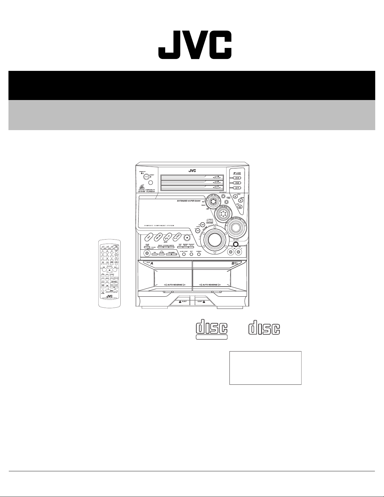
SERVICE MANUAL
COMPACT COMPONENT SYSTEM
MB01120039
MX-GA9V
COMPACT
DIGITAL VIDEO
UX ---------- Saudi Arabia
UN ------------------ Asean
U ------------- Other Areas
COMPACT
DIGITAL AUDIO
Area Suffix
TABLE OF CONTENTS
1 PRECAUTION. . . . . . . . . . . . . . . . . . . . . . . . . . . . . . . . . . . . . . . . . . . . . . . . . . . . . . . . . . . . . . . . . . . . . . . . . 1-3
2 SPECIFIC SERVICE INSTRUCTIONS. . . . . . . . . . . . . . . . . . . . . . . . . . . . . . . . . . . . . . . . . . . . . . . . . . . . . . 1-6
3 DISASSEMBLY . . . . . . . . . . . . . . . . . . . . . . . . . . . . . . . . . . . . . . . . . . . . . . . . . . . . . . . . . . . . . . . . . . . . . . . 1-7
4 ADJUSTMENT . . . . . . . . . . . . . . . . . . . . . . . . . . . . . . . . . . . . . . . . . . . . . . . . . . . . . . . . . . . . . . . . . . . . . . . 1-36
5 TROUBLESHOOTING . . . . . . . . . . . . . . . . . . . . . . . . . . . . . . . . . . . . . . . . . . . . . . . . . . . . . . . . . . . . . . . . . 1-40
COPYRIGHT © 2003 VICTOR COMPANY OF JAPAN, LIMITED
No.MB011
2003/10
Page 2

SPECIFICATION
Amplifier section
Output Power SUB WOOFERS 88 W per channel, min. RMS, both channels driven into 6 Ω at 63
Hz with no more than 0.9% total harmonic distortion.
MAIN SPEAKERS 28 W per channel, min. RMS, both channels driven into 6 Ω at 1
kHz with no more than 0.9% total harmonic distortion.
Audio input sensitivity/Impedance
(Measured at 1 kHz, with tape
recording signal 300 mV)
Digital output CD OPTICAL DIGITAL OUTPUT
Signal wave length 660 nm
Output level -15 dBm to -12 dBm
Speakers/Impedance SUB WOOFERS 6 Ω - 16 Ω
FM tuning range 87.50 MHz - 108.00 MHz
AM tuning range For Saudi Arabia At 9 kHz intervals : 531 kHz - 1 602 kHz
CD capacity 3 CDs
Dynamic range 85 dB
Signal-to-noise ratio 90 dB
Wow and flutter Immeasurable
Frequency response Normal (type I) 50 Hz - 14 000 Hz
Power requirement AC 110 V / AC 127 V / AC 220 V / AC 230 V - AC 240 V~(adjustable with the voltage selector),
Power consumption 170 W (at operation) 25 W (on standby)
Dimensions (approx.) 265 mm × 335 mm × 401 mm (W/H/D) (10 7/16 in. × 13 1/4 in. × 15 13/16 in.)
Mass (approx.) 10.0 kg (22.1 lbs)
AUX 390 mV/50 kΩ
MIC 1/2 3.0 mV/5 kΩ
MAIN SPEAKERS 6 Ω - 16 Ω
SURROUND SPEAKERS 16 Ω - 32 Ω
Tuner
At 10 kHz intervals : 530 kHz - 1 600 kHz
For other countries At 9 kHz intervals : 531 kHz - 1 710 kHz
At 10 kHz intervals : 530 kHz - 1 710 kHz
CD player
Cassette deck
Wow and flutter 0.15% (WRMS)
General
50 Hz / 60 Hz
1-2 (No.MB011)
Page 3
SECTION 1
PRECAUTION
1.1 Safety Precautions
(1) This design of th is product contains special hardw are and
many circuits and components specially for safety purposes. For continued protection, no changes should be made
to the original design unless authorized in writing by the
manufacturer. Replacement parts must be identical to
those used in the original circuits. Services should be performed by qualified personnel only.
(2) Alterations of the design or circuitry of the product should
not be made. Any design alterations of the product should
not be made. Any design alterations or additions will void
the manufacturers warranty and will further relieve the
manufacture of responsibility for personal injury or property
damage resulting therefrom.
(3) Many electrical and mechanical parts in the products have
special safety-related characteristics. These characteristics are often not evident from visual inspection nor can the
protection afforded by them necessarily be obtained by using replacement components rated for higher voltage, wattage, etc. Replacement parts which have these special
safety characteristics are identified in the Parts List of Service Manual. Electrical components having such features
are identified by shading on the schematics and by ( ) on
the Parts List in the Service Manual. The use of a substitute
replacement which does not have the same safety characteristics as the recommended replacement parts shown in
the Parts List of Service Manual may create shock, fire, or
other hazards.
(4) The leads in the products are routed and dressed with ties,
clamps, tubings, barriers and the like to be separated from
live parts, high temperature parts, moving parts and/or
sharp edges for the prevention of electric shock and fire
hazard. When service is required, the original lead routing
and dress should be observed, and it should be confirmed
that they have been returned to normal, after reassembling.
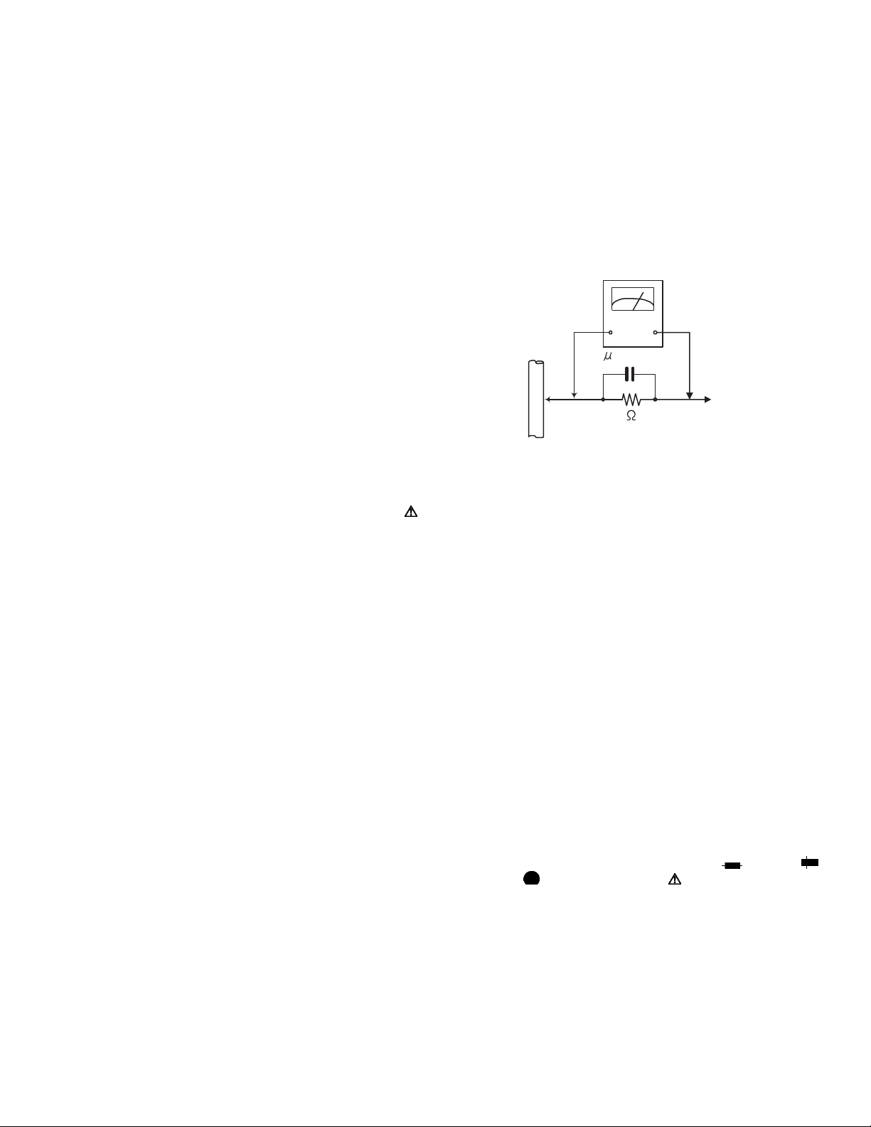
(5) Leakage shock hazard testing
After reassembling the product, always perform an isolation check on the exposed metal parts of the product (antenna terminals, knobs, metal cabinet, screw heads,
headphone jack, control shafts, etc.) to be sure the product
is safe to operate without danger of electrical shock.Do not
use a line isolation transformer during this check.
• Plug the AC line cord directly into the AC outlet. Using a
"Leakage Current Tester", measure the leakage current
from each exposed metal parts of the cabinet, particularly any exposed metal part having a return path to the
chassis, to a known good earth ground. Any leakage current must not exceed 0.5mA AC (r.m.s.).
• Alternate check method
Plug the AC line cord directly into the AC outlet. Use an
AC voltmeter having, 1,000Ω per volt or more sensitivity
in the following manner. Connect a 1,500Ω 10W resistor
paralleled by a 0.15µF AC-type capacitor between an exposed metal part and a known good earth ground.
Measure the AC voltage across the resistor with the AC
voltmeter.
Move the resistor connection to each exposed metal
part, particularly any exposed metal part having a return
path to the chassis, and measure the AC voltage across
the resistor. Now, reverse the plug in the AC outlet and
repeat each measurement. Voltage measured any must
not exceed 0.75 V AC (r.m.s.). This corresponds to 0.5
mA AC (r.m.s.).
AC VOLTMETER
(Having 1000
ohms/volts,
or more sensitivity)
0.15 F AC TYPE
Place this
probe on
1500 10W
Good earth ground
1.2 Warning
(1) This equipment has been designed and manufactured to
meet international safety standards.
(2) It is the legal resp onsibility of the repairer to ensure that
these safety standards are maintained.
(3) Repairs must be made in accordance with the relevant
safety standards.
(4) It is essential that safety critical compone nts are replaced
by approved parts.
(5) If mains voltage selector is provided, check setting for local
voltage.
1.3 Caution
Burrs formed during molding may be left over on some parts
of the chassis.
Therefore, pay attention to such burrs in the case of preforming repair of this system.
1.4 Critical parts for safety
In regard with component parts appearing on the silk-screen
printed side (parts side) of the PWB diagrams, the parts that are
printed over with black such as the resistor ( ), diode ( )
and ICP ( ) or identified by the " " mark nearby are critical
for safety. When replacing them, be sure to use the parts of the
same type and rating as specified by the manufacturer.
(This regulation dose not Except the J and C version)
each exposed
metal part.
(No.MB011)1-3
Page 4
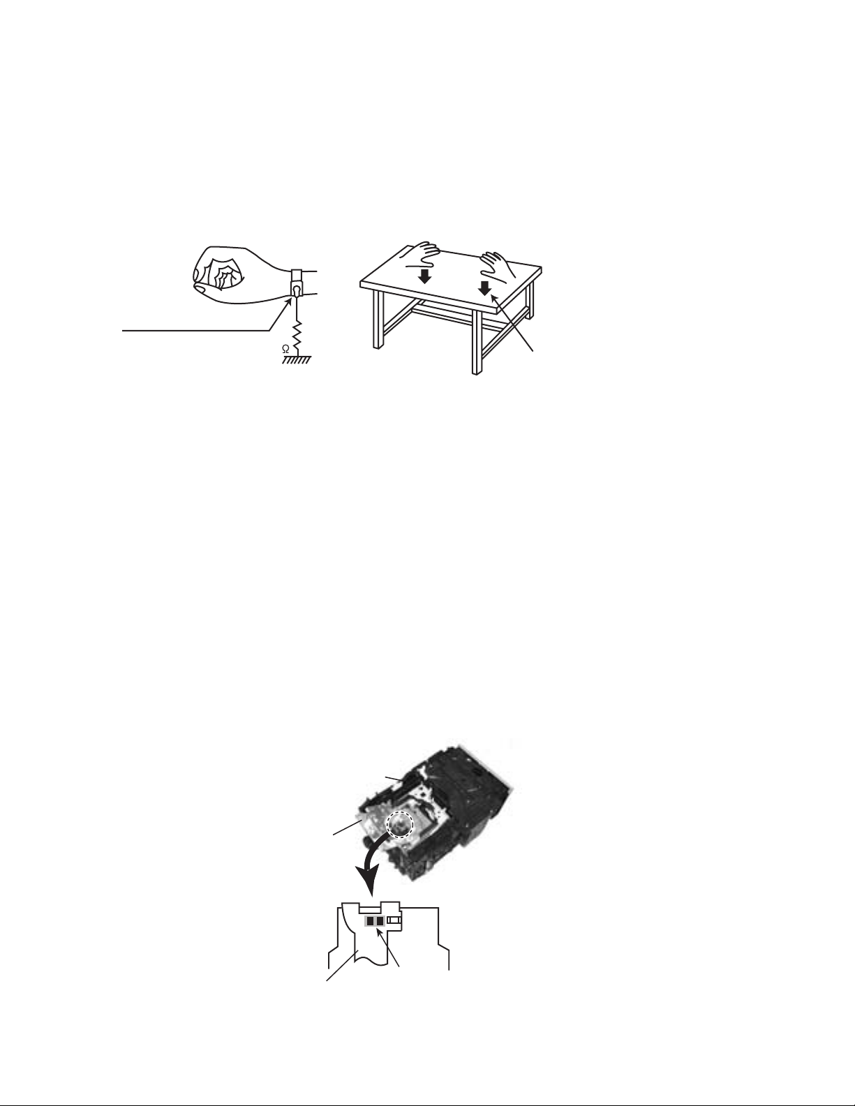
1.5 Preventing static electricity
Electrostatic discharge (ESD), which occurs when static electricity stored in the body, fabric, etc. is discharged, can destroy the laser
diode in the traverse unit (optical pickup). Take care to prevent this when performing repairs.
1.5.1 Grounding to prevent damage by static electricity
Static electricity in the work area can destroy the optical pickup (laser dio de) in devices such as CD players.
Be careful to use proper grounding in the area where repairs are being performed.
(1) Ground the workbench
Ground the workbench by laying conductive material (such as a conductive sh eet) or an iron plate over it before placing the
traverse unit (optical pickup) on it.
(2) Ground yourself
Use an anti-static wrist strap to release any static electricity built up in your body.
(caption)
Anti-static wrist strap
1M
Conductive material
(conductive sheet) or iron palate
(3) Handling the optical pickup
• In order to maintain quality during transport and before installation, both sides of the laser diode on the replacement optica l
pickup are shorted. After replacement, return the shorted parts to their original condition.
(Refer to the text.)
• Do not use a tester to check the condition of the laser diode in the optical pickup. The tester's internal power source can easily
destroy the laser diode.
1.6 Handling the traverse unit (optical pickup)
(1) Do not subject the traverse unit (optical pickup) to strong shocks, as it is a sensitive, complex unit.
(2) Cut off the shorted part of the flexible cable using nippers, etc. after replacing the optical pickup. For specific details, refer to the
replacement procedure in the text. Remove the anti-static pin when replacing the traverse unit. Be careful not to take too long
a time when attaching it to the connector.
(3) Handle the flexible cable carefully as it may break when subjected to strong force.
(4) I t is not possible to adjust the semi-fixed resistor that adjusts the laser power. Do not turn it.
1.7 Attention when traverse unit is decomposed
*Please refer to "Disassembly method" in the text for the CD pickup unit.
• Apply solder to the short land sections before the flexible wire is disconnected from the connector on the CD servo board. (If the
flexible wire is disconnected without applying solder, the CD pickup may be destroyed by static electricity.)
• In the assembly, be sure to remove solder from the short land sections after connecting the flexible wire.
1-4 (No.MB011)
CD changer
mechanism
assembly
CD traverse
unit
Flexible cable
Soldering
Page 5
1.8 Important for laser products
1.CLASS 1 LASER PRODUCT
2.DANGER : Invisible laser radiation when open and inter
lock failed or defeated. Avoid direct exposure to beam.
3.CAUTION : There are no serviceable parts inside the
Laser Unit. Do not disassemble the Laser Unit. Replace
the complete Laser Unit if it malfunctions.
4.CAUTION : The compact disc player uses invisible laser
radiation and is equipped with safety switches which
prevent emission of radiation when the drawer is open and
the safety interlocks have failed or are de
feated. It is dangerous to defeat the safety switches.
5.CAUTION : If safety switches malfunction, the laser is able
to function.
6.CAUTION : Use of controls, adjustments or performance of
procedures other than those specified herein may result in
hazardous radiation exposure.
!
Please use enough caution not to
see the beam directly or touch it
in case of an adjustment or operation
check.
REPRODUCTION AND POSITION OF LABEL and PRINT
WARNING LABEL and PRINT
CLASS 1
LASER PRODUCT
(No.MB011)1-5
Page 6

SECTION 2
SPECIFIC SERVICE INSTRUCTIONS
This service manual does not describe SPECIFIC SERVICE INSTRUCTIONS.
1-6 (No.MB011)
Page 7
SECTION 3
A
A
DISASSEMBLY
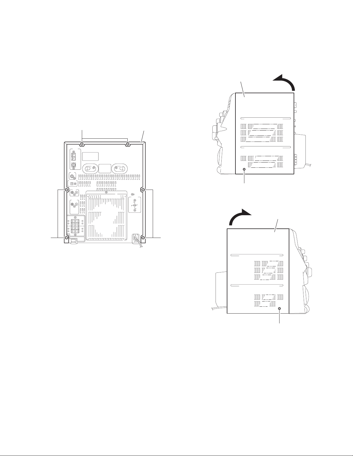
3.1 Main body
3.1.1 Removing the metal cover
(See Fig.1 ~ 3)
(1) Remove the six screws A on the back of the body.
(2) Remove the two screws B on both sides of the body.
(3) Remove the metal cover from the body by lifting the rear
part of the cover.
CAUTION:
Do not break the front panel tab fitted to the metal cover.
Metal cover
A
Metal cover
B
Fig.2
Metal cover
Fig.1
B
Fig.3
(No.MB011)1-7
Page 8
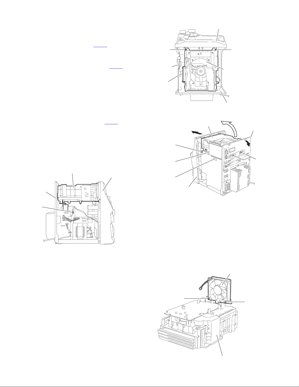
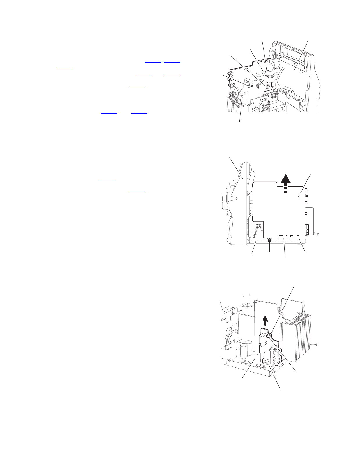
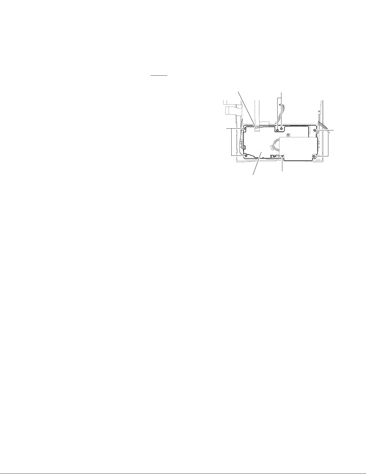
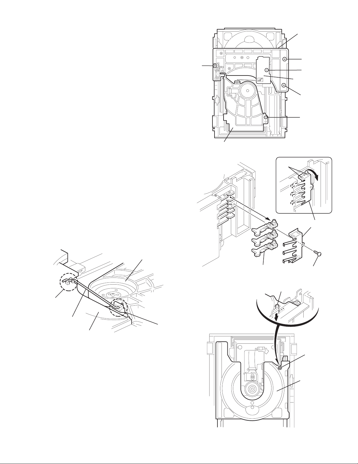
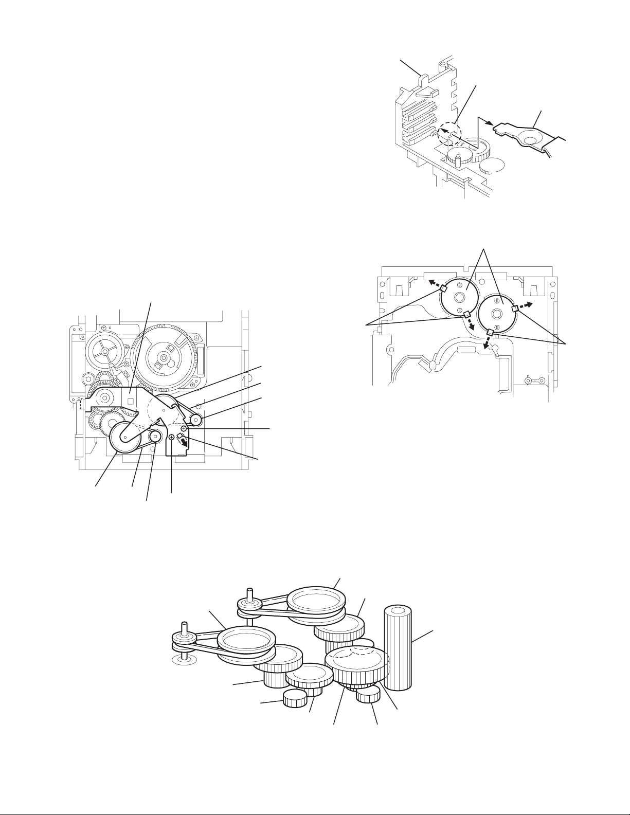
3.1.2 Removing the CD changer mechanism assembly
(See Fig.4 ~ 6)
• Prior to performing the following procedure, remove the metal
cover.
(1) Disconnect the wire from connector CN705 on the amplifier
board.
(2) Remove the plastic rivet attaching the main boa rd to the
front assembly on the right side of the body.
(3) Disconnect the card wire from connector CN661
main board.
(4) Remove the two screws C on the upper si de of the body
and the two screws D on the back of the rear panel.
(5) Pull both the rear panel and the front panel assembly to the
outside, then remove the CD changer mechanism assembly by lifting the rear part of the assembly.
REFERENCE:
At this point, one card wire on the underside of the CD
mechanism assembly is still connected.
(6) Disconnect the card wire from connector CN504
ner side of the main board on the right side of the body. Remove the CD mechanism assembly.
CAUTION:
To prevent damage to the CD fitting, be sure to pull both the
rear panel and the front panel assembly enough to remove the
CD changer mechanism assembly.
CD changer mechanism assembly
Front panel assembly
on the
on the in-
Front panel assembly
C
Main board
CN661
CN504
Fig.5
CD changer mechanism assembly
Plastic rivet
Main board
CN661
CN504
C
CD changer
mechanism assembly
Rear panel
Rear panel
D
Rear panel
Amplifier board
CN705
Fig.4
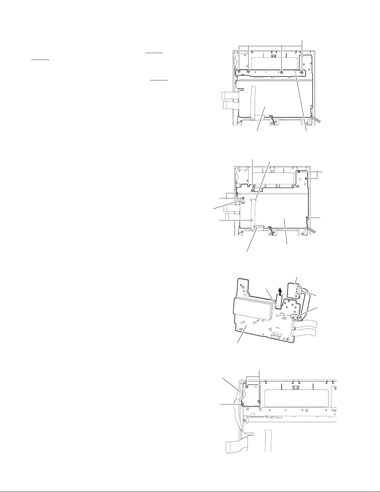
3.1.3 Removing the fan
(See Fig.7)
• Prior to performing the following procedure, remove the metal
cover and the CD changer mechanism assembly.
(1) Turn over the CD changer mechanism assembly and re-
move the two screws E attaching the fan.
Front panel assembly
E
Fig.6
Fan
E
1-8 (No.MB011)
CD changer mechanism assembly
Fig.7
Page 9
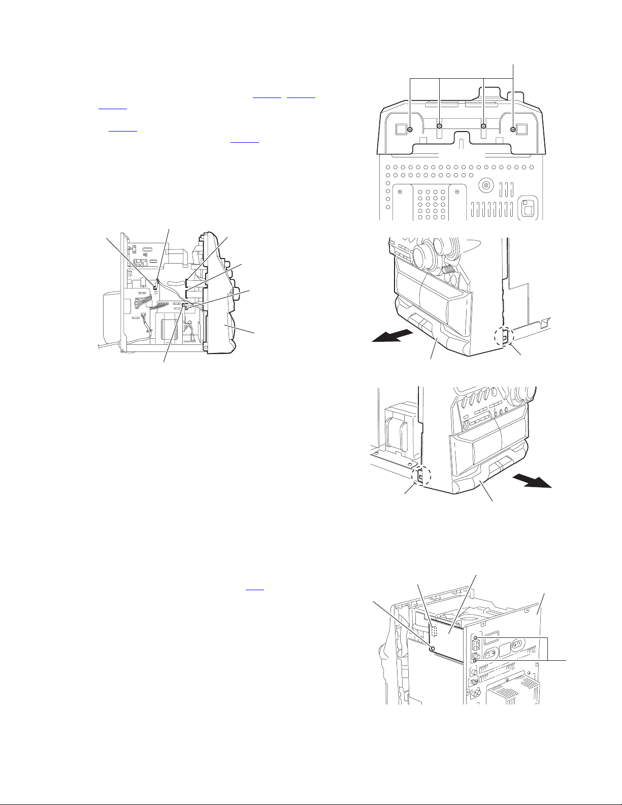
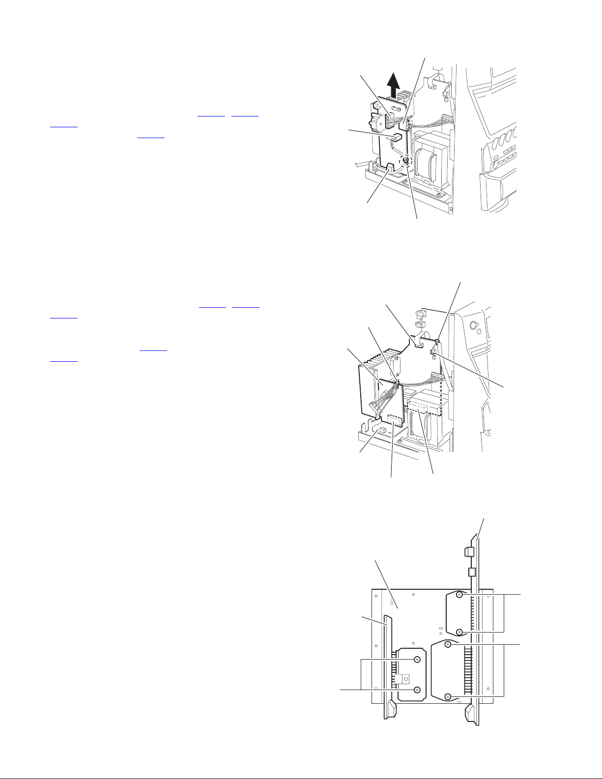
3.1.4 Removing the front panel assembly
A
(Bottom)
(See Fig.8 ~ 11)
• Prior to performing the following procedure, remove the metal
cover and CD changer mechanism assembly.
(1) Disconnect the card wires from connector CN870
and CN315 on the main board respectively.
(2) Remove the wire clamp and disconnect the wire from con-
nector CN703
(3) Disconnect the wire from connector CN220
former board.
(4) Remove the four screws F on the bottom of the body.
(5) Release the two joints a on the lower right and left sides of
the body using a screwdriver, and remove the front panel
assembly toward the front.
on the amplifier board.
, CN871
on the trans-
(Bottom)
(Bottom)
F
mplifier board
CN703
Transformer board
Wire clamp
CN220
Fig.8
Main board
CN870
CN871
CN315
Front panel
assembly
Fig.9
Front panel assembly
Fig.10
Joint a
Fig.11
Joint a
Front panel assembly
3.1.5 Removing the tuner board
(See Fig.12)
• Prior to performing the following procedure, remove the metal
cover.
(1) Disconnect the card wire from connector CN1
board on the right side of the body.
(2) Remove the plastic rivet fixing the tuner board.
(3) Remove the two screws G on the back of the body.
on the tuner
Plastic rivet
CN1
Tuner board
Rear panel
G
Fig.12
(No.MB011)1-9
Page 10
3.1.6 Removing the rear cover / rear panel
(See Fig.13 ~ 16)
• Prior to performing the following procedure, remove the metal
cover and the CD changer mechanism assembly.
(1) Remove the screw H attaching the rear cover on the back
of the body.
(2) Push each tab of the four joints b in the direction of the ar-
row and release.
(3) Remove the sixteen screws G attaching the rear panel.
(4) Disengage the joints c on each lower side of the rear panel
using a screwdriver and remove the rear panel backward.
Joint b
G
G
Rear cover
H
Fig.13
Rear panel
Joint b
Rear panel
G
G
Fig.14
Rear panel
Fig.15
G
G
Joint c
1-10 (No.MB011)
Joint c
Rear panel
Fig.16
Page 11
3.1.7 Removing the main board
A
(See Fig.17 ~ 19)
• Prior to performing the following procedure, remove the metal
cover, the CD changer mechanism assembly, the rear panel
and the antenna board.
(1) Disconnect the card wires from connector CN870
and CN315 on the main board.
(2) Disconnect the wires from connector CN704 and CN706
on the amplifier board.
(3) Disconnect the wire from connector CN710
board.
(4) Remove the screw I attaching the main board on the right
side ofthe body.
(5) Disconnect connector CN211
board from the regulator board.
3.1.8 Removing the speaker board
(See Fig.19)
• Prior to performing the following procedure, remove the metal
cover, the CD changer mechanism assembly and the rear panel.
REFERENCE:
It is not necessary to remove the main board.
(1) Disconnect connector CN217
the regulator board.
(2) Disconnect the wire from connector CN710
board.
and CN212 on the main
on the speaker board from
, CN871
on the speaker
on the speaker
CN315
CN871
mplifier board
CN704
CN706
Speaker board
CN710
Front panel assembly
Main board
CN870
Fig.17
Front panel assembly
Main board
Regulator board
Regulator board
Fig.18
Fig.19
I
CN212
Speaker board
CN217
CN211
CN710
(No.MB011)1-11
Page 12
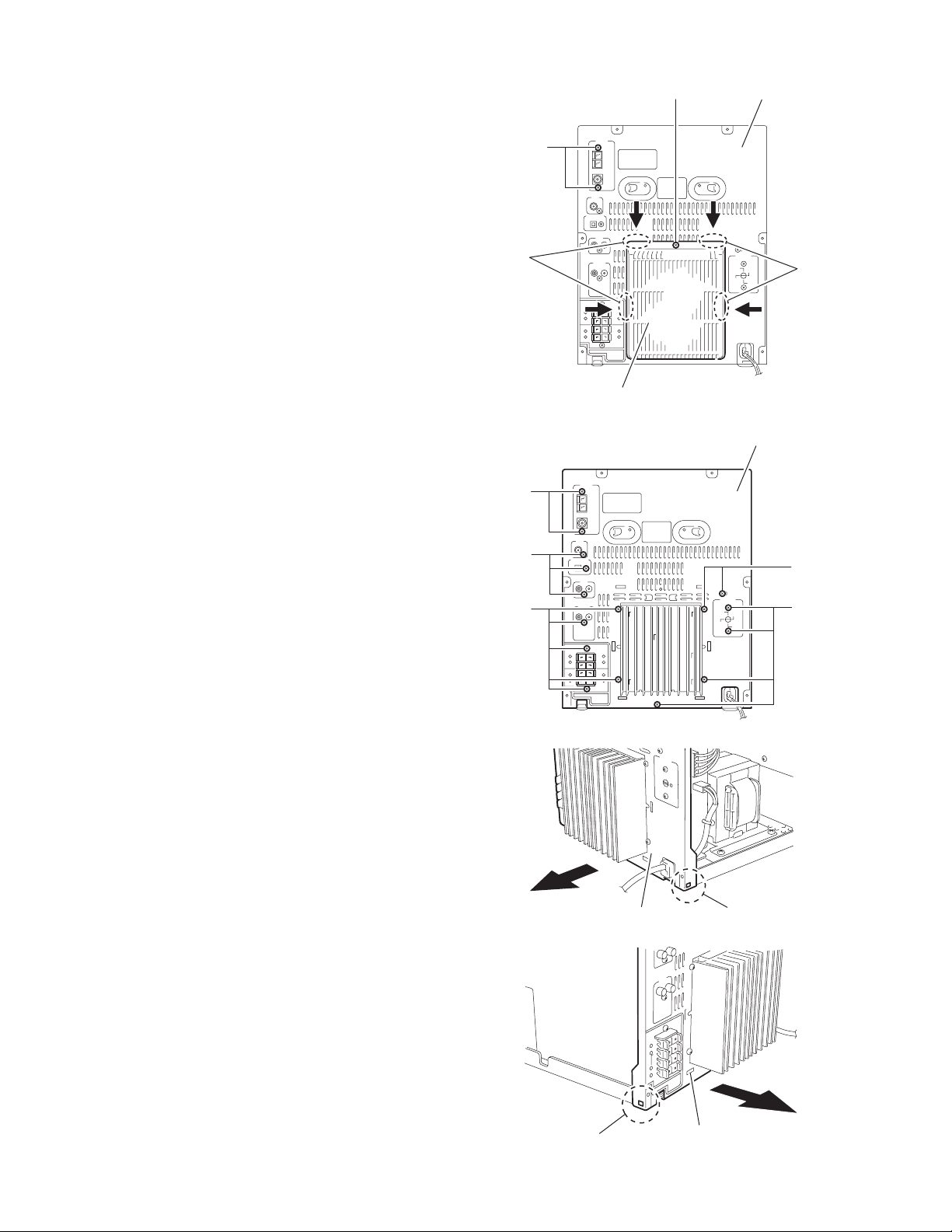
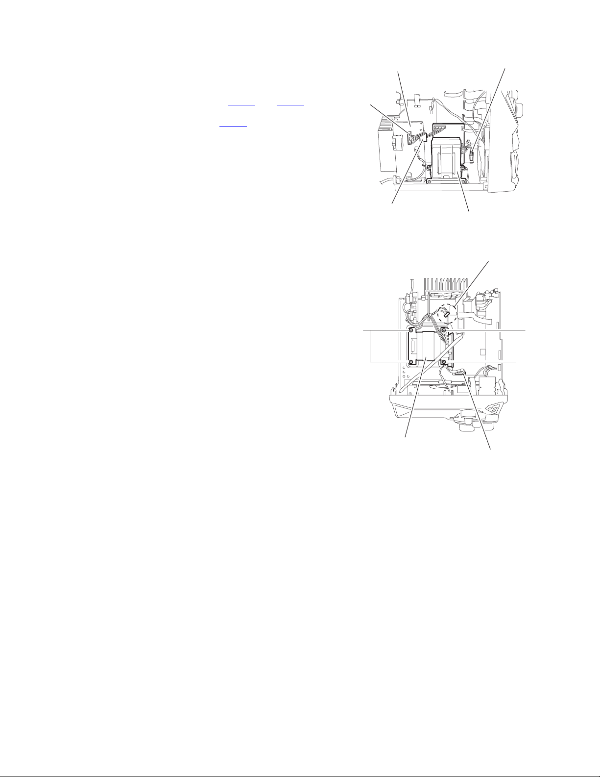
3.1.9 Removing the power board
(See Fig.20)
• Prior to performing the following procedure, remove the metal
cover, the CD changer mechanism assembly and the rear panel.
(1) Remove a wire clamp on the power board.
(2) Disconnect the wire from connector CN218
CN250 on the power board.
(3) Disconnect connector CN213
regulator board.
3.1.10 Removing the amplifier board / voltage board / heat sink
(See Fig.21, 22)
• Prior to performing the following procedure, remove the metal
cover, the CD changer mechanism assembly and the rear panel.
(1) Disconnect the wires from connector CN703
CN706 on the amplifier board respectively.
(2) Remove the two wire clamps attaching the wire to the am-
plifier board and the voltage board.
(3) Disconnect connector CN215
CN216 on the voltage board from the regulator board (The
heat sink will be detached at once).
(4) Remove the four screws J attaching the amplifier board to
the heat sink.
(5) Remove the two screws K, the board bracket and the volt-
age board.
REFERENCE:
It is not necessary to remove the power board.
on the power board from the
on the amplifier board and
, CN219 and
, CN704 and
Power board
CN219
CN250
CN213
Amplifier board
Wire clamp
Voltage board
CN218
Wire clamp
Fig.20
Wire clamp
CN704
CN706
CN703
Regulator board
Heat sink
Voltage board
K
CN216
CN215
Fig.21
Amplifier board
J
J
Fig.22
1-12 (No.MB011)
Page 13
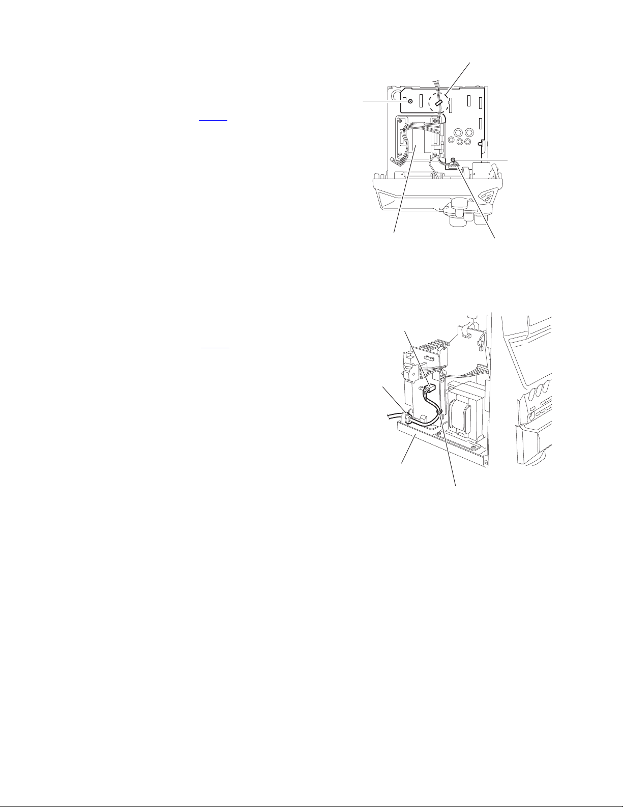
3.1.11 Removing the power transformer assembly
(See Fig.23, 24)
• Prior to performing the following procedure, remove the metal
cover, the CD changer mechanism assembly and the rear panel.
(1) Disconnect the wires from connector CN218
on the power board.
(2) Disconnect the wire from connector CN204 on the regula-
tor board.
(3) Release the wire from the stopper on the regulator bo ard.
(4) Remove the four screws L attaching the transformer as-
sembly.
and CN219
CN219
Power board
Regulator board
CN204
CN218
Power transformer assembly
Fig.23
Stopper
LL
Power transformer
assembly
Fig.24
Regulator board
CN204
(No.MB011)1-13
Page 14
3.1.12 Removing the regulator board
(See Fig.25)
• Prior to performing the following procedure, remove metal cov-
er, CD changer mechanism assembly, rear panel, antenna
board, main board, amplifier board, voltage board, power
board and speaker board.
(1) Disconnect the wire from conne ctor CN204
tor board.
(2) Release the wire from the stopper on the regulator board.
(3) Remove the two screws M attaching the reglator board.
on the regula-
Stopper
M
M
3.1.13 Removing the power cord
(See Fig.26)
• Prior to performing the following procedure, remove the metal
cover, the CD changer mechanism assembly and the rear panel.
(1) Disconnect the wire from connector CN250
board.
(2) Remove the wire clamp from the power board.
(3) Move the power cord stopper upward and pull out it from
the base chassis.
on the power
Power transformer assembly
Power board
CN250
Power cord stopper
Base chassis
Regulator board
CN204
Fig.25
Wire clamp
Fig.26
1-14 (No.MB011)
Page 15
3.2 Front panel assembly
• Prior to performing the following procedure, remove the metal
cover, the CD changer mechanism assembly and the front
panel assembly.
3.2.1 Removing the cassette mechanism assembly
(See Fig.27)
(1) Disconnect the card wire from connector CN306
head amplifier & mechanism control board.
(2) Remove the seven screws N attaching the cassette mech-
anism assembly.
on the
Head amplifier
& mechanismcontrol board
CN306
N
N
Cassette mechanism
assembly
N
N
Fig.27
(No.MB011)1-15
Page 16
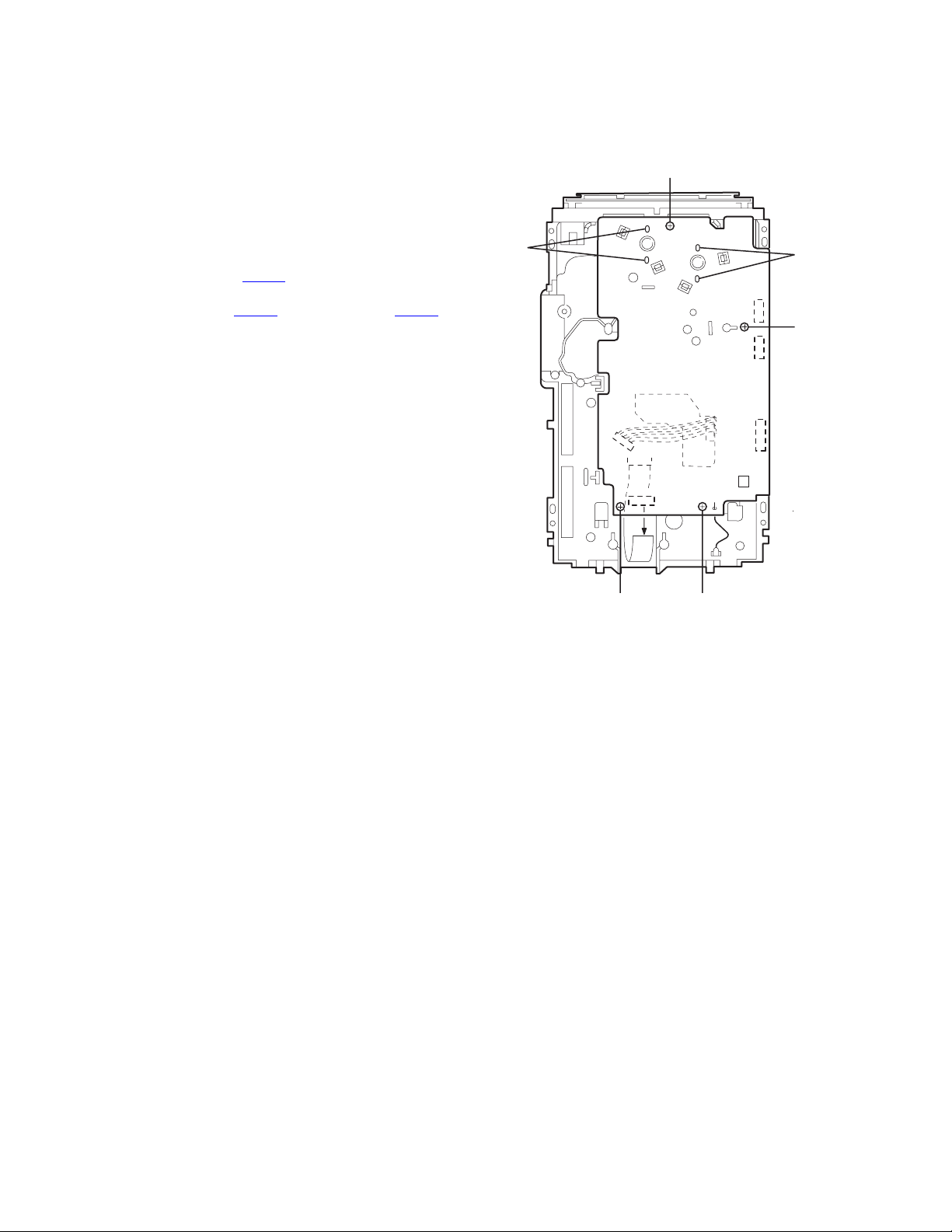
3.2.2 Removing the display system control board
(See Fig.28 ~ 30)
(1) Remove the four screws O attaching the stay bracket.
(2) Disconnect the card wires from connector CN316 and
CN880 on the display system control board.
(3) Remove the seven screws P attaching the display system
control board.
(4) If necessary, disconnect the wire from connector CN911
the front side of the display system control board and unsolder FW915.
3.2.3 Removing the CD eject board
(See Fig.30, 31)
(1) Remove the three screws Q attaching the CD eject board.
(2) If necessary, unsolder FW91 5 on the CD eject board.
on
Display system control board
P
FW915
(Solding)
P
P
O
Stay bracket
Fig.28
CN316
P
P
CN880
Fig.29
CN911
Display system control board
Fig.30
CD eject board
FW915
(Solding)
Q
Q
Display system control board
CD eject board
FW915
FW915
1-16 (No.MB011)
Fig.31
Page 17
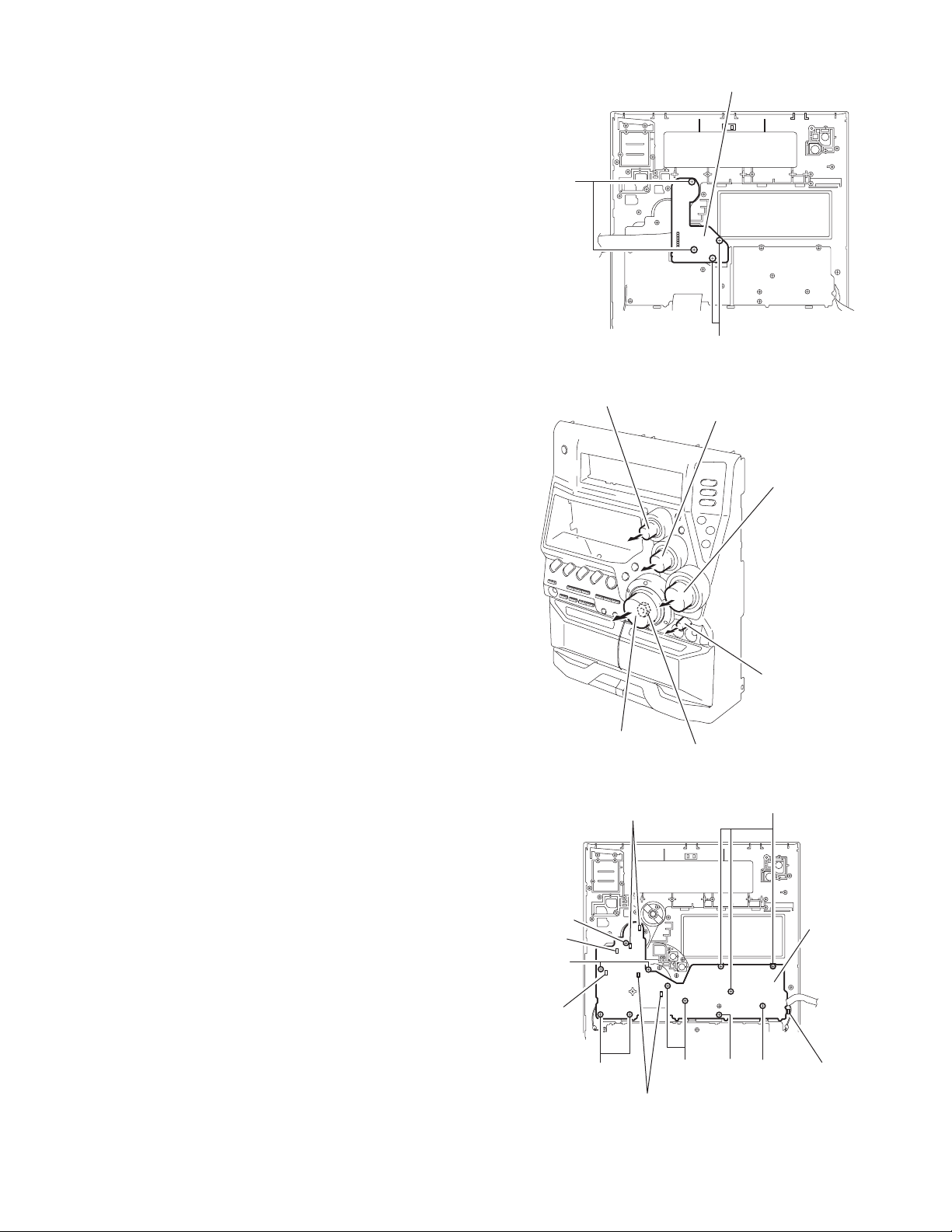
3.2.4 Removing the preset / tuning switch board
(See Fig.32, 33)
• Prior to performing the following procedure, remove the dis-
play system control board.
(1) Pull out the preset knob on the front panel.
(2) Remove the four screws R attaching the preset / tuning
switch board.
(3) If necessary, unsolder FW901 on the preset / tuning switch
board.
3.2.5 Removing the operation switch board
(See Fig.33, 34)
• Prior to performing the following procedure, remove the dis-
play system control board and the preset / tuning switch board.
(1) Pull out the volume knob on the front panel and remove the
nut. Pull out the surround mode knob, the mic level knob
and the surround woofer level knob toward the front.
(2) Remove the twelve screws S attaching the operation
switch board.
(3) Release each tab of the seven joints d retaining the opera-
tion switch board.
Preset / tuning switch board
R
R
Fig.32
Preset knob
Surround mode knob
Surround woofer
level knob
Joint d
Joint d
Volume knob
S
S
S
Joint d
Joint d
Nut
Fig.33
Fig.34
Mic level knob
S
Operation
switch board
SSS
Joint d
(No.MB011)1-17
Page 18
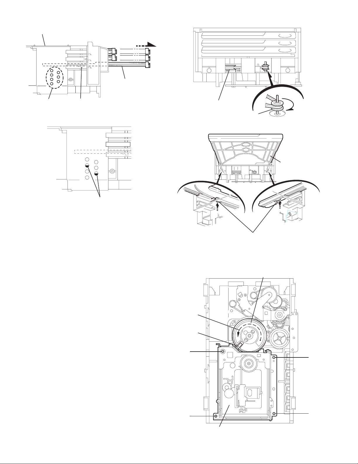
3.3 CD Changer Mechanism
A
• Remove the CD changer mechanism assembly.
3.3.1 Removing the CD Servo control board
(See Fig.1)
(1) From bottom side the CD changer mechanism assem-
bly,remove the four screws A retaining the CD servo control board.
(2) Absorb the four soldered po sitions a of the right and left
motors with a soldering absorber.
(3) Pull out the ea rth wire on the CD cha nger mechanism as-
sembly.
(4) Disconnect the connector CN854
board.
(5) Disconnect the card wire CN601
on the CD servo control board.
on the CD servo control
and the connector CN801
A
a
CN854
CN651
CD servo control board
CN801
CN151
CN601
a
AA
Fig.1
1-18 (No.MB011)
Page 19
3.3.2 Removing the CD tray assembly
(See Fig.2~9)
(1) Remove the CD servo control board.
(2) Remove the screw B retaining the lod stopper.
(3) From the T.bracket section b and clamper base section c ,
remove both of the edges fixing the rod.
(4) Remove the three screws C retaining the T.bracket.
(5) Remove the screw D retaining the clamper assembly.
(6) From the left side face of the chassis assembly, remove the
one screw E retaining both of the return spring and lock le-
ver.
(7) By removing the pawl at the se ction d fixing the return
spring, dismount the return spring.
(8) Remove the three lock levers.
(9) Check whether the lifter unit stopper has be en caught into
the hole at the section e of CD tray assembly as shown in
Fig.5.
(10) Make sure that the driver unit elevator is positioned as
shown in Fig.6 from to the second or fifth hole on the left
side face of the CD changer mechanism assembly.
CAUTION:
In case the driver unit elevator is not at above position,
set the elevator to the position as shown in Fig.7 by manually turning the pulley gear as shown in Fig.8.
(11) Manually turn the motor pul ley in the clockwise direction
until the lifter unit stopper is lowered from the section e of
CD tray assembly.
(12) Pull out all of the thre e stages of CD tray assembly in the
arrow direction f until these stages stop.
(13) At the position where the CD tray assembly has stopped,
pull out the CD tray assembly while pressing the two pawls
g and g' on the back side of CD tray assembly. In this
case, it is easy to pull out the assembly when it is pulled out
first from the stage CD tray assembly.
C
Clamper assembly
T.Braket
C
B
Lod stopper
(C/J version only)
C
D
Fig.3
d
Return spring
Clamper base
Lock lever
Fig.4
Stopper
E
b
Rod
c
T.Braket
Fig.2
e
CD tray
assembly
Fig.5
(No.MB011)1-19
Page 20
f
Chassis assembly
r
A
Refer to Fig.7
Pawl
g
Fig.6
Drive unit of elevato
Fig.7
CD tray assembly
Pulley gear
Motor pulley
Fig.8
CD
3
CD
2
CD
1
CD tray assembly
3.3.3 Removing the CD loading mechanism assembly
(See Fig.10)
(1) While turning the cams R1 and R2 assembly in the arrow
direction h ,align the shaft i of the CD loading mechanism
assembly to the position shown in Fig.10.
(2) Remove the four screws F retaining the CD loading mech-
anism assembly.
Pawl g, g'
Fig.9
Cams R1, R2 assembly
rrow
h
i
F
F
1-20 (No.MB011)
F
CD loading mechanism assembly
Fig.10
F
Page 21
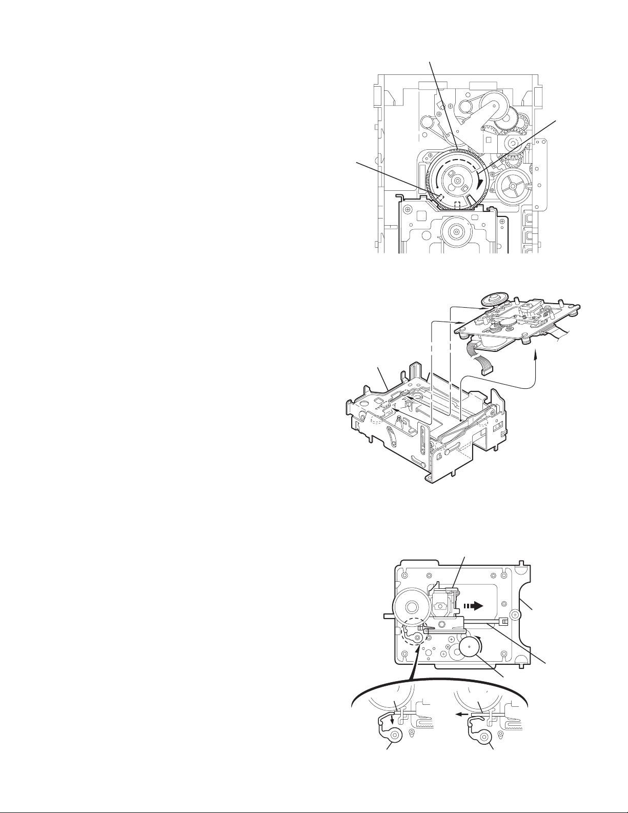
3.3.4 Removing the CD traverse mechanism
j
(See Fig.11 and 12)
(1) For dismounting only the CD traverse mechanism without
removing the CD loading mechanism assembly, align the
shaft j of the CD loading mechanism assembly to the position shown Fig.11 while turning the cam R1 and R2 assembly in the arrow direction k .
(2) By raising the CD loading mechanism assembly in the ar-
row direction l , remove the assembly from the lifter unit.
Cam R1, R2 assembly
Fig.11
Arrow
k
CD traverse mechanism
3.3.5 Removing the CD pick unit
(See Fig.13)
(1) Move the cam gear in the arrow direction m . Then, the CD
pickup unit will be moved in the arrow dire cti o n n .
(2) According to the above step, shift the CD pickup unit to the
center position.
(3) While pressing the stopper retaining the shaft in the arrow
direction o , pull out the shaft in the arrow direction p .
(4) After dismounting the shaft from the CD pickup unit, re-
move the CD pickup unit.
Lifter unit
Fig.12
CD Pickup unit
n
m
Arrow
l
CD loading
mechanism
Shaft
Cam gear
Shaft
o
Stopper Stopper
Shaft
p
Fig.13
(No.MB011)1-21
Page 22
3.3.6 Removing the try select switch board
r
(See Fig.14)
(1) Remove the two screws G retaining the tra y select sw itch
board.
(2) Disconnect the tray select switch board from connector
on the CD servo control board.
CN854
Chassis assembly
Tray select
switch board
CN854
CN851
CD servo
control board
3.3.7 Removing the cam unit
(See Fig.15 ~17)
• Remove the CD loading mechanism assembly.
(1) While turning the cam gear q , align the Paul r position of
the drive unit to the notch position on the cam gear q .
(2) Pull out the drive unit and cylinder gear .
(3) While turning the cam gear q , align the Paul s position
of the select lever to the notch position on the cam gear q .
(4) Remove the four screws H retaining the cam unit(cam
gear q and cams R1/R2 assembly).
Drive unit
Cam gear q
r
Fig.14
Drive unit
Cylinder gea
CN804
G
1-22 (No.MB011)
Fig.15
Cam gear q
s
H
Fig.16
Cams R1, R2 assembly
Cam unit
H
Select lever
Fig.17
Page 23
3.3.8 Removing the actuator motor and belt
r
(See Fig.18~21)
(1) Remove the two screws I retaining the gear bracket.
(2) While pressing the pawl t fixing the gear bracket in the ar-
row direction, remove the gear bracket.
(3) From the notch u section on the chassis assembly fixing
the edge of gear bracket, remove and take out the gear
bracket.
(4) Remove the belts respectively from the right and left actu-
ator motor pulleys and pulley gears.
(5) After turning over the chassis asse mbly, remove the actu-
ator motor while spreading the four pawls v fixing the right
and left actuator motors in the arrow direction.
ATTENTION:
When the chassis assembly is turned over under the conditions wherein the gear bracket and belt have been removed,
then the pulley gear as well as the gear, etc. constituting the
gear unit can possibly be separated to pieces. In such a case,
assemble these parts by referring to the assembly and configuration diagram in Fig. 21.
Gear bracket
Pulley gear
Belt
Motor pulley
Chassis assembly
u
Gear bracket
Fig.19
Actuator motor
v
v
Fig.20
Pulley gear
Belt
Motor pulley
I
Pawl
t
I
Fig.18
Assembly and Configuration Diagram
Pulley gear
Pulley gear
Gear B
Gear C
Select gear
Gross gear L
Fig.21
Gear B
Cylinder gea
Gross gear U
Gear C
(No.MB011)1-23
Page 24
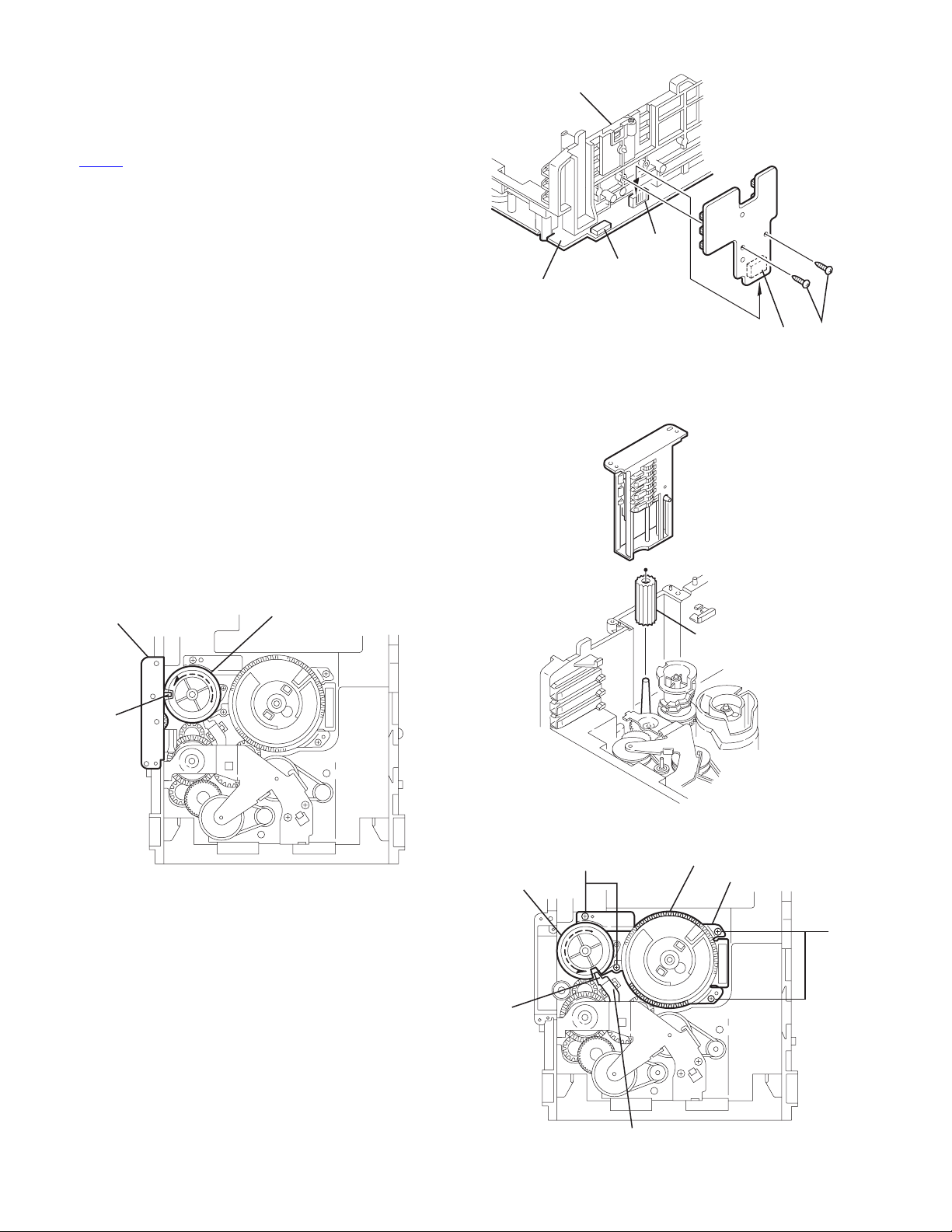
3.3.9 Removing the cams R1/R2 assembly and cam gear q
(See Fig.22)
(1) Remove the slit washer fixing the cams R1 and R2 assem-
bly.
(2) By removing the two pawls w fixing the cam R1, separate
R2 from R1.
(3) Remove the slit washer fixing the cam gear q .
(4) Pull out the cam gear q from the C.G. base assembly.
3.3.10 Removing the C.G. base assembly
(See Fig.22 and 23)
(1) Remove the three screws J retaining the C.G. ba se as-
sembly.
CAUTION:
To reassemble the cylinder gear, etc.with the cam unit (cam
gear and cans R1/R2 assembly), gear unit and drive unit, align
the position of the pawl x on the drive unit to that of the notch
on the cam gear q . Then, make sure that the gear unit is engaged by turning the cam gear q .
Slit washer
Cam gear q
J
Slit washer
Cam R2
Pawl
w
Cam R1
Cam switch board
C.G. base assembly
Pawl
w
Notch
Pawl
x
Cylinder
gear
Drive unit
Fig.22
Cam gear q
Cam R1, R2 assembly
Gear unit
Gear bracket
Fig.23
1-24 (No.MB011)
Page 25
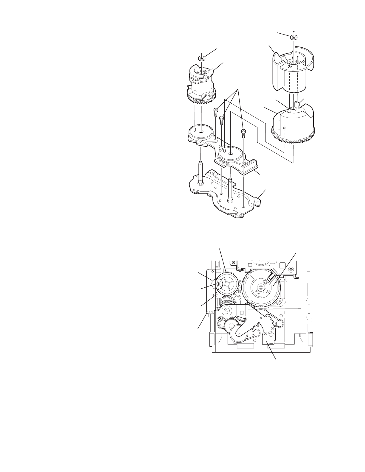
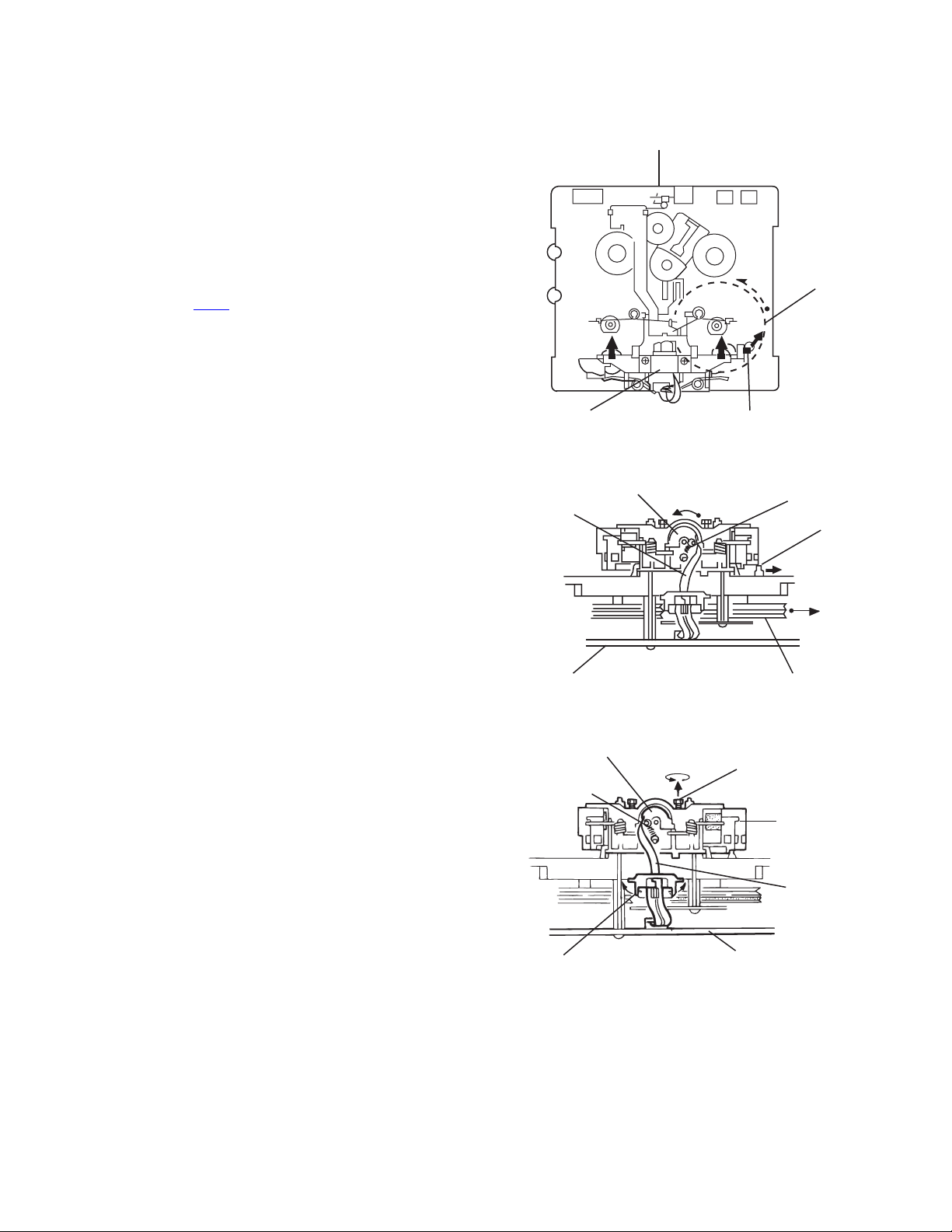
3.3.11 Removing the Pickup unit
(See Fig.24 and 25)
(1) Turn the cam gear in the direction of the arro w to move the
pickup unit toward the center.
(2) Extend the guide shaft stopper in the direction of the arrow,
move the guide shaft and pull out as shown in the figure.
(3) Pull out the pickup unit from the joint a.
CAUTION:
When reassenbling, attch the pickup unit to the chassis
base firmly at the joint a.
(4) Release the four joint b on the back on the pi ckup unit to
remove the CD rack.
Joint a
Pickup unit
Pickup unit
Chassis base
Guide shaft
Cam gear
Guide shaft stopper
Guide shaft
Joint b
Guide shaft
Guide shaft stopper
Fig.24
Pickup unit
Joint b
Joint b CD rack
Fig.25
(No.MB011)1-25
Page 26
3.3.12 Removing the CD mechanism board
(See Fig.26)
(1) On the back of the CD mechanism assembly, unsolder the
four soldering c attaching the CD mechanism board, the
spindle motor and the feed motor.
(2) Removing the screw A.
3.3.13 Removing the Spindle motor/Feed motor
(See Fig.27)
• Prior to performing the following procedure,remove the CD
mechanism board.
(1) Form the top side of the CD mechanism assembly, remove
the two screws B and two screws C attaching the spindle
motor and the feed motor respsctively.
Soldering c
Spindle motor
Soldering c
Spindle motor
CD mechanism board
A
Feed motor
Fig.26
B
Feed motor
Fig.27
C
1-26 (No.MB011)
Page 27
3.4 Cassette mechanism assembly
3.4.1 Removing the R/P & E head
(See Fig. 1 to Fig. 3)
(1) While shifting the trigger arms seen on the right side of the
head mount in the arrow direction, turn the flywheel ( R ) in
counterclockwise direction until the head mount has gone
out with a click (See Fig. 1).
(2) When the flywheel (R) is rotated in counterclockwise
direction, the playback / recording & eraser head will be
turned in counterclockwise direction from the position in
Fig. 2 to that in Fig. 3.
(3) At this position, disconnect the flexible board (outgoing
from the playback / recording & eraser head) from the
connector CN31
control board.
(4) Remove the flexible board from the chassis base.
(5) Remove the spring a from behind the playback / recording
& eraser head.
(6) Loosen the reversing azimuth screw retaining the playback
/ recording & eraser head.
(7) Take out the playback / recording & eraser head from the
front of the head mount.
(8) The playback / recording & eraser head should also be
removed similarly to steps 1 to 7 above.
on the head amplifier & mechanism
Head mount
Flexible board
Cassette mechanism
Fig.1
Playback head
Fly
wheel R
Trigger arm
(A mechanism side)
Spring a
Trigger arm
CN301
Head amp. & Mechanism
control board
R/P E head
Spring a
CN302
FPC holder
Flywheel R
(A mechanism side)
Fig.2
Reverse
Azimuth screw
Head mount
Flexible board
Head amp. & mechanism
control board
(B mechanism side)
Fig.3
(No.MB011)1-27
Page 28

3.4.2 Reassembling the playback / recording & eraser head
(See Fig. 4 to Fig. 6)
(1) Keep the direction lever o f head mount assembly to left
side (head direction is forward direction).
(2) Fix the head mount assembly boss O', P', Q', U' and V' to
mechanism sub assembly hole P, V and ditch O, U and Q
(See Fig. 4 and Fig. 5).
(3) Fix the reversing azimuth screw.
(4) Attaching the spring a from back side of playback /
recording & eraser head.
(5) Attaching the flexible board to the chassis base.
O'
P'
V'
O
P
R/P & E head
or PB head
Q'U'
Head mount assembly
Fig.4
Head mount assembly
Q
U
Fig.5
Reverse
azimuth screw
Direction
lever
Direction
cover
1-28 (No.MB011)
Spring a
Flexible
board
FPC holder
A:CN301
B:CN302
Fig.6
Head mount
Head amp. & mechanism
control board
Page 29

3.4.3 Removing the head amplifier & mechanism control board
(See Fig. 7)
(1) Remove the cassette mechanism assembly
(2) After turning over the cassette mechanism assembly,
remove the three screws 1 retaining the head amplifier &
mechanism control board.
(3) Disconnect the connector CN301
CN304 on the board including the CN1 on the reel pulse
board.
(4) When necessary, remove the 4 pin parallel wire soldered
to the capstan motor.
, CN302, CN303 and
Head amp. & mechanism
11 1
control board
CN301CN302
3.4.4 Removing the capstan motor assembly
(See Fig. 8 to Fig. 10)
(1) Removing the 6 screws 2 retaining the capstan motor
assembly.
(2) While raising the capstan motor, remove the capstan belt
from the motor pulley.
Caution:
Be sure handle the capstan belt so carefully that this belt wi ll
not be stained by grease and other foreign matter. Moreove r,
this belt should be hanged while referring to the capstan belt
handling method in Fig. 9 and Fig. 10.
Flexible
board
Flexible
board
Fig.7
22
Capstan motor
assembly
11
2222
Fig.8
Capstan belt A Capstan belt B
Fig.9
Capstan motor
Capstan belt BCapstan belt A
Motor pulley
Fig.10
(No.MB011)1-29
Page 30

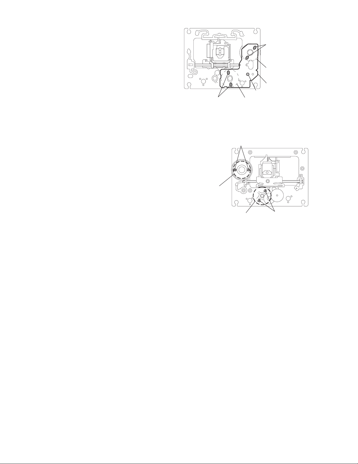
3.4.5 Removing the capstan motor
(See Fig. 11)
(1) Remove the two screws 3 from the capstan motor, and
then remove the joint bracket.
3.4.6 Removing the flywheel
(See Fig. 12, Fig. 13)
(1) Remove the head amplifier & mechanism control board.
(2) Remove the capstan motor assembly.
(3) After turning over the cassette mechanism, remove the two
slit washers and fixing capstan shaft L and R, and pull out
the flywheel (R) and (L) respectively from behind the
cassette mechanism.
3
Capstan motor
Joint
bracket
3
Fig.11
3.4.7 Removing the reel pulse board and solenoid
(See Fig. 14)
(1) Remove the five pawls d to h retaining the reel pulse board.
(2) From the surface of the reel pulse board parts, remove the
two pawls i and j retaining the solenoid.
Solenoid
Flywheel R Flywheel L
Flywheel R
Capstan
shaft R
b
Slit washer
hd e f g
Fig.12
Flywheel L
Capstan
shaft L
c
Slit washer
Fig.13
Reel pulse
board
1-30 (No.MB011)
Solenoid
Fig.14
Page 31

3.4.8 Reassembling the control cam
(See Fig. 15 to Fig. 17)
(1) Shift to left side (forward direction) the head mount
assembly, hole K’ of control cam into the hollow K of the
mechanism sub assembly.
Control cam
K'
(hole)
K
Fig.15
Mechanism sub
assembly (top side)
K
K
(hole)
Fig.16
Control cam (top side)
Fig.17
(No.MB011)1-31
Page 32

3.5 Speaker section
A
A
3.5.1 Removing the front cover
(See Fig.1, 2)
CAUTION:
Do not break or damage the front panel and body that are
glued at the joints a. (See Fig.1)
(1) Remove the four screws A on the front of the body respec-
tively.
(2) Remove the front cover toward the front and disconnect the
yellow and black wires from the two tweeter speaker terminals.
Joint a
Joint a Joint a
Front cover
Fig.1
Joint a
Tweeter speaker
Woofer speaker
Fig.2
1-32 (No.MB011)
Page 33

3.5.2 Removing the woofer speaker
(See Fig.3)
• Prior to performing the following procedure, remove the front
cover.
(1) Remove the four screws B on the front of the body.
(2) Pull out the woofer speaker tow ard the front and discon-
nect the wire (yellow and black, red and black) from the two
speaker terminals.
3.5.3 Removing the tweeter speaker
(See Fig.4)
• Prior to performing the following procedure, remove the front
cover.
(1) Disconnect the red and black wires from the two tweeter
speaker terminals.
(2) Remove the two screws C attaching the tweeter speaker
on the back of the front cover.
B
B
Woofer speaker
Fig.3
C
eeter speaker
Front cover
Fig.4
(No.MB011)1-33
Page 34

3.6 Woofer speaker section
3.6.1 Removing the front cover
(See Fig.5)
CAUTION:
Do not break or damage the front panel and body that are
glued at the joints b. (See Fig.5)
(1) Remove the four screws D on the front of the body respec-
tively.
(2) Remove the front cover toward the front.
3.6.2 Removing the woofer speaker
(See Fig.6)
• Prior to performing the following procedure, remove the front
cover.
(1) Remove the four screws E on the front of the body.
(2) Pull out the woofer speaker toward the fron t and discon-
nect the red and black wires from the two speaker terminals.
Joint b
Joint b Joint b
Front cover
Fig.5
Woofer speaker
Joint b
DD
Fig.6
EE
1-34 (No.MB011)
Page 35

3.7 Removing the Rear speaker
3.7.1 Removing the Rear cover
(See Fig.7 ~ 9 )
(1) Remove the four screws F on the back of the body.
(2) Disconnect the wires from th e two terminals on the rear
speaker.
(3) Remove the four screws G on the back of the front cover.
Rear cover
F
Rear cover
Fig.7
Rear speaker
Fig.8
F
Front cover
terminals
G
Front cover
Rear speaker
Rear speaker
G
terminals
Fig.9
(No.MB011)1-35
Page 36

SECTION 4
ADJUSTMENT
4.1 Measurement instruments required for adjustment
(1) Low frequency oscillator,
This oscillator should have a capacity to output 0dBs to
600Ω at an oscillation frequency of 50Hz-20kHz.
(2) Attenuator impedance : 600Ω
(3) Electronic voltmeter
(4) Frequency counter
(5) Wow flutter meter
(6) Test tape
VT712 : For Tape speed and wow flutter ( 3kHz)
VT710 : Head azimuth
VT724 : For Reference level (1kHz)
(7) Blank tape
TAPE : AC-225
(8) Torque gauge : For play and back tensio n
Forward ; TW2111A, Reverse ; TW2121A
Fast Forward and Rewind ; TW2231A
(9) Test disc
Disc : CTS-1000(12cm), GRG-1211(8cm)
(10) Jitter meter
4.2 Measurement conditions
Power supply voltage
AC110V/127V/220V/230V~240V~, adjustable
Measurement output terminal
• Speaker out
• TP101(Mesuring for TUNER/DECK/CD)
• Dummy load 6Ω
4.2.1 Radio input signal
AM modulation frequency : 400Hz
Modulation factor : 30%
FM modulation frequency : 400Hz
Frequency displacement : 22.5kHz
4.2.2 Frequency Range
AM : 531kHz~1710kHz
FM : 87.5MHz~108MHz
4.2.3 Standard measurement positions of volume and switch
Power : Standby (Light STANDBY Indicator)
Sub woofer VOL. : Minimum
Sound mode : OFF
Main VOL. : 0 Minimum
Traverse mecha set position : Disc 1
Mic MIX VOL : MAX
ECHO : OFF
4.2.4 Precautions for measurement
(1) Apply 30pF and 33k Ω to the IF sweeper output side and
0.082 F and 100kΩ in series to the sweeper input side.
(2) The IF sweeper output level should be made as low as pos-
sible within the adjustable range.
(3) Since the IF sweeper is a fixed device, there is no need to
adjust this sweeper.
(4) Since a ceramic oscillator i s used, there is no need to per-
form any MPX adjustment.
(5) Since a fixed coil is used, there is no need to adjust the FM
tracking.
(6) The input and output earth systems are separated.
In case of simultaneously measuring the voltage in both of
the input and output systems with an electronic voltmeter
for two channels, therefore, the earth should be connected
particularly.
(7) In the case of BTL connection amplifier, the minus terminal
of speaker is not for earthing. Therefore, be sure not to connect any other earth terminal to this terminal. This system
is of an OTL system.
1-36 (No.MB011)
Page 37

4.3 Arrangement of adjusting positions
Cassette mechanism section (Mechanism A section)
Head azimuth
adjusting screw
(Forward side)
Playback
head
Head azimuth
adjusting screw
(Reverse side)
Cassette mechanism section (Back side)
Head azimuth
adjusting screw
(Forward side)
Playback, recording and eraser
heads or playback head
Head azimuth
adjusting screw
(Reverse side)
Cassette Mechanism Unit Section
Tape speed ADJ
Bias ADJ L
Bias ADJ R
(No.MB011)1-37
Page 38

4.4 Tape recorder section
Items Measurement conditions Measurement method Standard values Adjusting positions
Confirmation
of head angle
Confirmation
of tape speed
4.5 Reference values for confirmation items
Test tape
: VT710 (10kHz)
Measurement output terminal
: Speaker terminal
Speaker R (Load resistor : 6Ω)
: Headphone terminal
Test tape
: VT712 (3kHz) or TMT7036 (3kHz)
Measurement output terminal
: Headphone terminal
1.Playback the test tape VT710 (10kHz).
2.With the playback mechanism or
recording & playback mechanism,
adjust the head azimuth screw so that
the forward and reverse output levels
become maximum.After adjustment,
lock the head azimuth at least by half a
turn.
3.In either case,this adjustmen t should
be performed in both the forward and
reverse directions with the head
azimuth screw.
< Constant speed >
Adjust VR301 so that the frequency
counter reading becomes 3,000Hz
±60Hz when playing back the test tape
VT712 (3kHz) with the playback
mechanism or playback and recording
mechanism after ending forward
winding of the tape.
Maximum output Adjust the head
azimuth screw only
when the head has
been changed.
Tape speed of
decks (A and B)
:3,000Hz ±60Hz
VR301
Items Measurement conditions Measurement method Standard values Adjusting positions
Double tape
speed
Difference
between the
forward and
reverse speed.
P.mecha and
R/P mecha
speed
Wow & flutter Test tape : VT712 (3kHz)
Test tape : VT712 (3kHz)
Measurement output terminal
: Speaker terminal
Speaker R (Load resistance:6Ω)
measurement output terminal
: Headphone terminal
Measurement output terminal :
Headphone terminal
After setting to the double speed
motor, confirm that the frequency
counter reading becomes 4,800+400/300Hz when the test tape VT712
(3kHz) has been play back with the
playback mechanism.
When the test tape VT712 (3kHz) has
been played back with the playback
mechanism or recording and playback
mechanism at the beginning of forward
winding, the frequency counter reading
of the difference between both of the
mechanisms should be 6.0Hz or less.
When the test tape VT712 (3kHz) has
been played back with the playback
mechanism or recording and playback
mechanism at the beginning of forward
winding the frequency counter reading
of wow & flutter should be 0.25% or
less(WRMS).
4,800+400/-300Hz Playback
mechanism side
60Hz or less Both the playback
and recording &
playback mechanism
with in 0.25%
JIS(WTD)
Both the playback
and recording &
playback mechanism
1-38 (No.MB011)
Page 39

4.6 Electrical performance
Items Measurement conditions Measurement method Standard values Adjusting positions
Adjustment of
recording
bias current
(Reference
value)
Adjustment of
recording and
playback
frequency
characteristics
*Mode : Forward or reverse mode
*Recording mode
*Test tape : AC-225
Measurement output terminal
: Both recording and headphone
terminals
Reference frequency : 1kHz and
10kHz (REF : -20dB)
Test tape : TYP l AC-225
Measurement input terminal : OSC IN
1.With the recording and playback
mechanism, load the test tapes(AC-225
to TYPl),and set the mechanism to the
recording and pausing conditions in
advance.
2.After connecting 100Ω in series to the
recorder head,measure the bias current
with a valve voltmeter at both of the
terminals.
3.After resetting the [PAUSE] mode,start
recording.
At this time,adjust VR101 for LcH and
VR201 for RcH so that the recording bias
current values become 4.0 A (TYP l).
1.With the recording and playback
mechanism,load the test tape(AC-225
to TYP l), and set the mechanism to the
recording and pausing condition in
advance.
2.While repetitively inputting the
reference frequency signal of 1kHz and
10kHz from OSC IN, record and
playback the test tape.
3.While recording and playing back the
test tape in TYP, adjust VR101 for LcH
and VR201 for RcH so that the output
deviation between 1kHz and 10kHz
becomes -1dB ±2dB.
AC-225 : 4.20µA LcH : VR101
RcH : VR201
Output deviation
between 1kHz
and 10kH
: -1dB ±2dB
LcH : VR101
RcH : VR201
4.7 Reference values for electrical function confirmation items
Items Measurement conditions Measurement method Standard values Adjusting positions
Recording
bias
frequency
Eraser
current
(Reference
value)
*Recording and playback side
forward or reverse
*Test tape : TYP l AC-225
*Measurement terminal BIAS TP on
P.C.board
*Recording and playback side
forward or reverse
*Recording mode
*Test tape : AC-225
Measurement terminal Both of the
eraser head
1.While changing over to and from
BIAS 1 and 2, confirm that the
frequency is changed.
2.With the recording and playback
mechanism, load the test tape (AC-225
to TYP l), and set the mechanism to the
recording and pausing conditions in
advance.
3.Confirm that the BIAS TP frequency
on the P.C.board is 100kHz ±6kHz.
1.With the recording and playback
mechanism, load the test tapes (AC225 to TYP l), and set the mechanism
to the recording and pausing condition
in advance.
2.After setting to the recording
conditions,connect 1MΩ in series to
the eraser head on the recording and
playback mechanism side,and
measure the eraser current from both
of the eraser terminal.
100kHz
+9kHz
-7kHz
TYP : 75mA
(No.MB011)1-39
Page 40

SECTION 5
TROUBLESHOOTING
This service manual does not describe TROUBLESHOOTING.
1-40 (No.MB011)
Page 41

(No.MB011)1-41
Page 42

VICTOR COMPANY OF JAPAN, LIMITED
AV & MULTIMEDIA COMPANY AUDIO/VIDEO SYSTEMS CATEGORY 10-1,1chome,Ohwatari-machi,Maebashi-city,371-8543,Japan
(No.MB011)
Printed in Japan
WPC
Page 43

SCHEMATIC DIAGRAMS
COMPACT COMPONENT SYSTEM
MX-GA9V
CD-ROM No.SML200310
Contents
Block diagram --------------------------------------------Standard schematic diagrams -----------------------Printed circuit boards ------------------------------------
COMPACT
DIGITAL VIDEO
COPYRIGHT 2003 VICTOR COMPANY OF JAPAN, LTD.
Area Suffix
UX ---------- Saudi Arabia
UN ------------------ Asean
U ------------- Other Areas
COMPACT
DIGITAL AUDIO
2-1
2-2
2-11 to 16
No.MB011SCH
2003/10
Page 44

In regard with component parts appearing on the silk-screen printed side (parts side) of
the PWB diagrams, the parts that are printed over with black such as the resistor ( ),
diode ( ) and ICP ( ) or identified by the " " mark nearby are critical for safety.
(This regulation does not correspond to J and C version.)
Page 45

L
Block diagram
DA0 to DA8
DBUS0 to DBUS15
/DWE, /DRAS
IC103
DRAM
OTP EPROM
TRACKING COIL
REST SW
/DCAS0, /DOE
LA0 to LA17
/LOE, /LROMCE
IC102
2MBIT
CAM0 to 3
LCAM
LCAM
CAM4 to 7
SW1 to SW6
PICKUP
&
FOCUS COIL
FM+,FM-
M
SM+,SM-
M
PB HEAD
PB/REC
& ERASE
RP MECHA
&
REEL PULSE
PB MECHA
&
REEL PULSE
IC106
BUFF
/REST
HEAD
SCLK
PROCESSOR
CDBCLK
CN805
CN855
CN804
CN854
CN601
P001
CN801
P011
CN301
CN302
CN303
CN333
FW301
M
AUDATA
BCLK
AIN,ARCLK,ARFS,AUX5
IC101
VCD
/LCS1,LR,AUDIOCLK
/RSTOUT,LD0 to 7,135M10
YUV0 to 7,PCKCSCN
MPUCLK,HSYNC,VSYNC
DATA,WCLK
AUX0 to AUX3
AUX6,AUX7
CN101 CN1
IC107
BUFF
TSD
TBCK
IC104
VCD
COMPANION
CHIP
CDL+
CDR+
CVOUT
CN102
AM
FM
J1
MW RF
& OSC
FM RF
IC2 PLL
DATA
CK,CE
L1
TU1
OSCOUT
IFOUT
CN151
CDDATA,CDLRCK,CDBCK
DSADAT,DSAACK,DSASTB,UDSADAT
UDSAACK,UDSASTB, /VCDRST
CAM0 to 7
1SSW
2SSW
3SSW
1MSW
2MSW
3MSW
A+C,B+D
E,F,MD,LD
LMOTOR
RMOTOR
LM+
LM-
M
RM+
RM-
M
IC601
RF & SERVO
AMP
FBAL,TBAL,FE,TE,OFT
RFENV,VDET,/RFDET
F+,F-
BDO,LDON,WVEL,ARF
T+,T-
FM+
FMSM+
SM-
/REST
R+,L+
R+,R-
HEAD SW
L+,L-
REC/PLAY
FREQUENCY
RESPONSE ADJ.
L3301
BIAS OSC
GCTRL
TRV,TVD
ECM,ECS
TRD,FOD
KICK
IC801
FOCUS & SPINDLE
& FEED & TRACKING
BTL DRIVER
IC301
SOLA
IC651
DIGITAL SERVO
PROCESSOR
IC302
PB/REC AMP
Q3302,Q3305
BIAS CONT
Q3312,Q3313
SOLENOID DEIVE
FOR PB MECHA
LMUP
LMDOWN
RMUP
RMDOWN
IC851,IC852
L/R MOTOR
DRIVER
&
/LSIRST,STAT
SUBQ,SQCK
BLKCK, /TLOCK
/FLOCK,SENSE
MLD,MDATA
MCLK,FLAG
Q3323
IC251
UNIT MICON
P.O N
/P.ON
Q291
PON
TX
CDDATA
CDLRCK
CDBCK
RECL,RECR
PBL,PBR,MS
Q3105Q3205
REC MUTE
SOL_A
KCMD
MSTAT
MCS
/CDMRST
RMUTE
RECB
IC303
SERIAL TO
PARALLEL
PORT
KCMD
MSTAT
MCS
/CDMRST
TX
PON
STTA
SDATA
BCK
EXTENSION
SOLB
Q3314,Q3315
SOLENOID DEIVE
SOL_B
FOR RP MECHA
MB,A,B
MOTOR
SPEED ADJ.
Q3316,Q3317,Q3324
MOTOR DRIVE
& MOTOR
SPEED ADJ.
MOTOR
TKEY1,TKEY2,PHA,PHB
AM RF,AM OSC
AFC,REG
CF1,Q1
FM IN
FM IF
AMP
J411
AUX IN
DIGITAL
OUT
CN551
CN305 CN306
SURROUND
STEREO
J999
JACK
IC1
FM/AM
DET
LOUT
ROUT
TUL,TUR
SDATA,TUCE
CN11
CK,MPX
J426
CN661
PBL
PBR
CN315
AC IN
CN504
TX
KCMND
MSTAT
MCS
/CDMRST
TX,PON
Q401
Q402
MUTE
PBMUTE
RECL
RECR
MSI
CN250
MIC1
JACK
MIC2
JACK
HEAD
PHONE
PB
INL,INR
COML,COMR
VOL. SEL.
J1021 J1022
AUX/TUNER
J1001
VOLDA
VOLCK
CDL,CDR
AUXL,AUXR
TUL,TUR
PBL,PBR
RECL,RECR
LIN,LOUT
RIN,ROUT
Q585
MSI MSI2
Q586
MSI
S500
MAIN VOL.
SOUND VOL.
WOOFER VOL.
OPERATION
SW
CD/TAPE
LED
MPX,TUCE,KCMND,MSTAT
MCS,SDATA,/CDMRST,CK
LOUT
ROUT
IC436
SOURCE
SELECT
&
E.VOL
IC466
KARAOKE
KARAOKE
CN208CN209
CN218CN219
VOL+/SMVOL+/BASSVOL+/-
KEY2,KEY3
AUXLED,CDLED
TPLED,TULED
MIXIN
HPL
HPR
Q573
AHB
CONTROL
IC481
AMP.
Q671
IC502
Q672
IC526
AHB
IC571
AMP.
SWFB
MIC
T001
TRANS.
CN870
FW713
CN220
CN214
SEARCH
KNOB
DISC1 to 3
SW & LED
CVOUT
SMUTE
Q481
Q482
Q483
MUTE
Q556
Q557
MUTE
BASS1
BASS2
PRT,SWFB
SURR.CTRL
PON
POUT
RELAY
R.SEARCH
F.SEARCH
SEARCHLED
KEY1,KEY11
CD1LED
CD2LED
CD3LED
JA566
VIDEO
OUT
CN870
CN871
FW714
CN211
CN212
FW710
FW901
FW915
CN703
CN704
CN706
CN201
CN202
CN204
S1,S2,S4
CN911 FW915
MSI,MPX,INH
CN880
SMUTE,TUCE
VC3RESET
KCMND,MSTAT
KCLK,DATA,CK
MRDY,KARAOKE
VOL-CK
VOL-DATA
AUXMUTE
CN860
CN861
CK,DATA
SLCCE
CN316
SLCKEY1
SLCKEY2
FW230
FL1
FL2
HPL
HPR
Q733 to Q737
H/P MUTE
SMUTE
MAINL
IC602
MAINR
AMP.
VH,-VH
VL,-VL
CN215
CN205
SURR_CTRL
POUT,FLBIAS
POUT
DIODE
BRIDGE
PRT
EXTCE
SLLCE
SURR
MAINL,MAINR
MAINL,MAINR
SWL,SWR
RELAY,SURR
SURR
SURR.
CONT
-9V,-30V
REG.
VH,-VH
VL,-VL
FL1
FL2
INH
IC830
RESET
RST
IC810
FL DRIVE
MICON
KEY4
SET
SW
RELAY
BASS1,BASS2
PBMUTE
POUT,VOLCK
VOLDTA
EXTCE
SURROUND
MIC
POUT
Q961
S/W
SWL
Q680
SWR
SURR
PON
5V,5.5V,8V
9V,12V
FL801
FL TUBE
P1 tp P22
G1 to G17
TAPELED
VOL+/SMODE+/BASSVOL+/KEY1 to 3
R.SEARCH
F.SEARCH
SEARCHLED
CD1LED
CD2LED
CD3LED
REMIN
REMOCON
RECEIVER
RELAY
Q876
Q877
IC811
EXT
ECHO1,ECHO2
IC902
MIXIN
ECHO
MIXER
STANBY-SW
EJECT1 to 3
CANCEL/DEMO
IC701
Q710 to Q712
AMP.
POUT
Q790 to Q792
FANDRIVE
CN207
CN217
CN206
CN216
IC951
HP
AUXLED
SMLED
CDLED
BASSLED
TULED
KEY11
IC STANBY
CTRL
CN710
SURR L/R
RY1,RY2
RELAY
5.6/SW5V
8V/9V/12V
REG.
PON
POUT
5/5.5/8/9/12V
CN705
To
FAN
J81
MAIN/SUB
SPEAKER
TERMINA
2-1
Page 46

Standard schematic diagrams
Power supply section
0.33( 1/2W)
CN220
QGD2504C1-03Z
CN214
QJK015-071214
R1002
F102
T4AL
F101
T4AL
T001
CN218
QGA3901C1-03
CN219
QGA7901C1-04
CN209
WJK0070-002A
F001
T4AL
CN208
WJK0114-001A
F003
T2AL
CN250
QGA7901C1-02
Parts are safety assurance parts.
When replacing those parts make
sure to use the specified one.
2-2
Page 47

Power amp. & DC regulator section
QGA2501C1-02
CN705
CN201
QGD2504C1-03Z
CN703
CN704
QGD2504C1-03Z
MAINL
MAINR
CN706
QGD2504C1-03Z
QGB2510J1-11
PRT
SWFB
SURR.CTRL
KRA111M-T
IC701
2SA965/OY/-T
C706
R740
R725
R729
47/63
82K
KTC3200/GL/-T
Q726
R728
10K
100K
R639
820
R640
820
C281
2SC3576-JVC-T
2SC3576-JVC-T
Q733
2SC3576-JVC-T
Q735
2SC3576-JVC-T
2SC2785/FE/-T
Q728
C729
820
Q736
Q734
R739
820
100K
R726
47/16
Q737
R736
4.7K
R734
4.7K
R733
4.7K
R735
4.7K
C726
R730
10K
10/25
R727
100K
Q727
KTA1268/GL/-T
R281
D703 D704
DZ15BSC-T2
DZ15BSC-T2
R723
R724
R741
6.8k
6.8k
D723
DZ36BSA-T2
D728
10
R774
0.22
R753
DZ36BSA-T2
C709
4.7p
R707
56K
R754
10
R715
10
C713
0.047
C715
0.047
R742
6.8k
D724
6.8k
C707
47/63
820
R705
C705
220P
220P
0.22
R717
C731
0.022
R761
1K
R713
L701
0.45
Q701
D719
10K
R721
KTA1268/GL/-T
R719
1K
5.6K
R766
1K
R718
0.022
Q702
KTA1268/GL/-T
D720
R720
QGB2510K2-14
QGB2510J1-14
33k
C730
R762
1K
5.6K
CN205
KTC1027/OY/-T
R722
CN215
Q713
56k
R704
56k
R703
0.45
L702
R714
10K
R778
10K
10K
R777
C722
C703 C704
C721
C710
4.7p
R708
56K
10
C708
R716
10
C714
0.0470.047
R706
C716
PRT
R786
Q710
10K
10K
R787
R776
0.1
C711
C712
1k
470p
470p
R775
1k
47/63
C739
1/50
820
KTC3200/GL/-T
Q711
D726
100K
R768
2.2K
KTA1268/GL/-T
R220
R769
C723
100/10
Q790
2SC2785/FE/-T
R792
1K
10k
R790
D790
47
1SS119-041-T2
47/25
C790
CN207
QGB2510J1-10
100K
R793
MAINL
SWL
Q712
0.1
47
47
R702
R701
R798
10
10k
R796
6.8K
R795
R797
20K
Q792
Q791
2SC2785/FE/-T
10k
R794
0.1
C639
CN217
QGB2510K2-10
KTC3203/OY/-T
R675
R676
C607
R605
RY1
QSK0109-001
QSK0109-001
1k
1k
C609
10P
R607
56K
47/63
C613C615
RY2
IC602
C621
10/35V
C603
220p
C604
220p
10/35V
R615
10
0.047
0.047
D725
D650
C605
220P
56k
R603R604
56k
C622
C601 C602
10
R613
0.068
L601
0.45
Q601
KTA1268/GL/-T
D619
10K
R621
R619
C683
1M
R680
0.082
Q680
R682
2SK301/PQ/-T
4.7M
R653
D622
DZ9.1BSB-T2
R602
100
47/50
C612
R666
33k
220
R617
C608
2.2K
R606
R681
3.9K
R655
0.22
Q613
C611
R616
10
QNB0107-001
R614
KRC102M-T
47/50
10
C606
220P
Q612
2SA1175/FE/-T
R668
10k
10k
R667
10
100
R674
R601
220
R618
0.068
L602
0.45
KTA1268/GL/-T
Q602
D620
10K
2.2K
R620
R623
0.22
C624
10/50
C623
10/50
C610
10P
R608
56K
47/63
C614C616
0.047
0.047
J81
CN204
CN202
QGB2510J1-10
QGA3901C1-07
Q373
R389
10K
KRA104M-T
Q374
KRC104M-T
DZ2.4BSB-T2
R385
R284
D280
47K
15K
R283
C280
0.22/50
47/50
R248
1
D233
R246
R247
1
R249
1
C372
5.6K
22/50
D369
C373
R384
DZ10BSC-T2
2.7K
0.01
Q372
KTA1023
6800/25
2A02M-T1
D234
2A02M-T
C374
22/50
D370
DZ11BSC-T2
R242
10K
Q240
2SC2785/FE/-T
1N4003S-T5
D227
C216
DZ9.1BSB-T2
47/50
R202
2.2
D220
100/35
C222
27K
R217
D217
C214
C212
0.082
C221
R205
100K
C253
1N4003S-T5
D218
1N4003S-T5
0.082
Q201
2SB740/BC/-T
R203
7.5K
C219
C220
22K
R204
47/50
0.01
C218
D219
C217
22/50
DZ33BSC-T2
CN206
QGB2510J1-12
27K
47K
R218
C211
C215
0.082
C213
0.1
R215
C202
C204
C203
47K
R216
0.1
C205
C201
0.1
QNZ0136-001Z
9V
8V
5.6V
CN216
EP201
QGB2510K2-12
CN710
QGD2504C1-03Z
D315
DZ9.1BSB-T2
330
330
0.01
0.33( 1/2W)
D362
STBY
C309
R309
C362
DZ6.8BSC-T2
L7812CP
IC304
C310
D314
10/50
DZ13BSB-T2
Parts are safety assurance parts.
When replacing those parts make
sure to use the specified one.
IC301
KIA78R05PI
D308
STBY
C301
C302
10/50
DZ5.6BSC-T2
R311
10K
22/50
IC303
R306
0.33
R302
2.2
L7808CP
C307
STBY
C308
D313
10/50
D316
STBY
DZ8.2BSB-T2
R360
2.2
R361
4.7
R365
R366
200
200
D361
R364
1.2K
DZ9.1BSB-T2
IC305
L7809CP
C311
STBY
C312
10/50
Q360
R363
DZ5.1BSB-T2
2SC2785/FE/-T
330
D360
2SC2785/FE/-T
C360
KTC2026/OY/-T
Q362
47/16
R362
R368
C361
Q361
R367
1.2K
2-3
Page 48

External input / Souce select switch section
CN315
QGF1205C1-10
J411
QNN0420-001
CN661
QGF1016F3-19
J999
QNN420-001
FW710
QUM153-09DGZ4
GP1FA550TZ
C1201
220/10
R1208
R1205
C002
J426
C401
220P
QRJ146J-4R7X
R1209
R1206
C1205
0.1
CN870
QGF1205C1-17
R426
56
C427
D426
DZ5.1BSB-T2
C403
0.01
R407
C404
C411
C412
2SC3576-JVC-T
C413
Q411
C414
100/10
3.3k
R501
CDL
10/35
C441
2.2/50
C450
2.7k
R403
4.7k
C1229
R502
PBL
2.2/50
C443
0.018
C460
2.7k
R404
4.7k
47/16
220p
220p
L566
3.3k
R438
R413
R414
Q412
QQR0779-001Z
30k
R503
C502
TUR
TUL
10/25
10/25
C446
C445
0.022
0.1
C458
C454
5.6k
R439
10/25
R401
1K
1K
R402
Q401
2SC3576-JVC-T
2SC3576-JVC-T
Q402
68k
68k
2.2k
R417
10k
R419
R420
10k
R519
100k
C510
R518
4.7/50
C504
0.0082
30k
R508
270k
R507
C1227
0.27
C505
4.7/50
C999
C998
PBR
CDR
AUXR
2.2/50
10/35
10/25
100/10
C436
C442
C440
C444
0.1
0.1
0.1
0.022
0.018
C457
C459
C453
C455
C461
C456
C462
2.7k
5.6k
R440
R441
C426
0.022
C888
220P
C402
R993
D411
D412
C415
D413
D414
C416
R411
C419
10k
0.0022
R412
10k
R415
200
R416
200 2SC3576-JVC-T
C1202
0.082
1K
1k
1k
1k
C1206
C501
4.7/50
AUXL
10/16
10/25
C1207
C432
C447
C439
B150
B108
2.2/50
10/16
C449
B151
C448
R443
100k
B154
R444
100k
C433
0.01
C886
TX
RECL
RECR
R994
10K
R406
BA15218
C887
PBL
PBR
2.2K
Q413
KRA102M-T
AUXMUTE
R421
R410
22k
22k
C507
D501
0.015
R505
22K
R511
100k
R513
220k
R512
R504
220k
100k
100
R1233
VOLDA
10k
R436
0.01
C438
1k
IC436
TDA7439
10k
VOLCK
C503
D502
0.22
R506
22K
100
R582
Q571
2SC2785/FE/-T
100
R583
R581
R580
220k
Q572
2SC2785/FE/-T
C578
1/50
0.027
C508
IC502
BA15218
R523
8.2k
C514
0.082
56K
1K
R524
R517
C889
C466
47/16
0.068
10/25
C472
C469
R470
5.6k
R468
MSI
PBMUTE
2.2K
R405
AUXL
AUXR
RECL
2.2k
R418
RECR
100k
IC501
C509
100/10
10/25
R437
C437
R442
D592
KCMND
MSTAT
TUCE
MCS
MPX
MSI2
D571
D572
180K
R579
100k
R577
2SC2785/FE/-T
C528
0.1
82K
120K
R534
R510
R537
R467
R469
5.6k
10/25
10/25
2.2/50
22/25
R466
C471
C468
C467
C473
1k
10/25
0.27
R472
C475
C474
C470
1/50
22k
R471
R996
10K
KARAOKE
CK
NC
SPISIG
/CDMRST
C576
47/16
100k
R576
IC571
BA15218
C577
47/16
R575
47k
Q573
11K
R536
1.5K
R528
C530
C535
100/10
22k
R529
100
C531
0.068
C527
0.018
100
R475
C476
R474
0.0068
200
IC466
BA3837
RDS_CLK
RDSDA/KARAOKE
100p
C575
22k
R532
R530
8.2K
C532
47/16
0.1
IC526
BA15218
R526
C526
100/10
R473
15K
51K
B242
B312
R431
30k
RECL
CN871
QGF1205C1-17
ECO
B313
RECR
R995
33K
Q999
KRA102M-T
C1228
100/10
D434
DZ5.1BSB-T2
R571
R572
47k
R541
22k
C534
47/16
100
R432
30k
SPISIG
R435
PBMUTE
BASS1
BASS2
10k
PRT
POUT
VOLCK
VOLDA
RELAY
R585
47K
270
2.2/50
C571
C489
100/10
L572
QQR0779-001Z
D586
R487
C585
DZ6.8BSC-T2
470/10V
C481
150K
R488
150K
C482
2SC2785/FE/-T
C593
47P
C594
Q585
1/50
DZ6.8BSC-T2
R593
100K
QQR0779-001Z
R498
C484
R486
56K
D585
QQR0779-001Z
D587
R531
15k
100
R485
C483
56K
R998
10K
R997
10K
-30V
R586
2.2M
C587
C586
33P
0.0018
C589
0.015
Q586
2SC2785/FE/-T
22
100K
R588
C588
680P
R587
L568
L567
12K
4.7K
R558
Q557
22k
R564
2SC3576-JVC-T
D432
BASS2
DZ3.9BSB-T2
R491
4.7k
100
R495
R492
4.7k
C487
1k
100/10
R496
C488
SMUTE
C486
10/35
D431
22k
R563
DZ3.9BSB-T2
C485
10/35
R557
Q556
BASS1
IC481
2SC3576-JVC-T
BA15218
R434
4.7
L571
QQR0779-001Z
C997
1/50
C996
100/10
10P 10P
R490
QQR1277-001Z
C995
C980
0.022
C596
R489
KRA102M-T
100K
L001
C994
470P
R886
33K
D593
CK
L546
QQR0779-001Z
MSI
MSI2
0.01
1.5
C981
C599
1000/6.3
Q562
2SC3576-JVC-T
R562
30K
R560
10k
100K
10k
R493
Q481
2SC3576-JVC-T
Q483
R494
10k
Q482
2SC3576-JVC-T
C993
MPX
TUL
SWFB
TUR
CN11
QGF1205F1-09
CN504
QGF1016F3-15
R1203
1K
R1202
1K
JA566
QNN0017-002
C556
10/25
CN211
QGB2510K2-09/11
PRT
SWFB
SURR.CTRL
R992
10K
POUT
-30V
RELAY
CN212
QGB2510K2-10
FW714
QUM156-18DGZ4
2-4
Page 49

FL display / System control LSI section
IC951
GPIU271X
C836
10/25
100
CN860
CN861
FW230
SURROUND
QGF1205F1-17
QUM153-11DGZ4
QGF1205F1-17
MSI
MPX
INH
SMUTE
TUCE
VC3RESET
KCMND
MSTAT
KCLK
DATA
CK
SPI-IN
MRDY
RDS-DATA/KARAUKE
RDS-CLK
ECON
PRT
VOL-CK
VOL-DATA
RELAY
AUXMUTE
BASS2
BASS1
PBMUTE
C233
KRC102M-T
0.1MY
Q877
KRA102M-T
Q878
R234
R233
L-192ZSRD-T
R961
1K
R911
D962
Q961
D964
220
220
220
220
220
R912
KRA102M-T
S963
R962
10K
R889
R888
R887
R886
R885
10K
RELAY
HP
KRA102M-T
QQR0779-001Z
10K
R842
1000p
R964
C835
3.9K
5.6K
R963
10K
R965
R921
REMIN
L812
D812
10K
R876
1K
R844
R968
10K
Q843
RESET
INH
KIA7042AP-T
R884
68
R898
1K
R993
1.2K
S999
R997
FL801
QLF0081-001
P11
P15
P16
P22
P19
P20CKP21
Q879
Q890
2SD1991A/RS/-T
100K
100K
R826
R890
R879
100K
100K
2G
1G
R839
R854
D805
R838
R855
R820
R819
R851
D803
10K
R817
KRA102M-T
D907
P8
P10
1K
1K
1K
1K
1K
1K
1K
5.6K
10K
R814
R818
L803
QQL244K-100Z
D804
R801
330
C803
470/6.3
Q908
Q907
KRC102M-T
100K
100K
R874
17G
MSI
MPX
INH
F_SEARCH
VOL-
VOL+
SOUNDMODE-
D807
G6G7G8G9G10
100K
R872
16G
10K
R828
1N4003S-T5
G2
G4
G3
G1
G5
100K
100K
100K
R868
R857
R866
R859
R870
13G
3G
15G
14G
10K
10K
10K
R881
R882
R883
1N4003S-T5
D801
R907
10k
G15
G14
G13
G16
G17
L805
QQL244K-100Z
RA801
P3
P2
P1
SPI_A
SPI_B
SPIDTI
BA3835S
SPI_IN
10K
R864
AUXLED
SMLED
CDLED
BASSLED
TULED
ECHO1
ECHO2
RELAY
BASS2
BASS1
PBMUTE
SURROUND
POUT1
POUT1
VDD
C837
100/10
C889
IC830
4.7/50
Q875
BU2092/F
KRC102M-T
P4
P5
P6
C862
22/50
IC811
C840
QGF1210G1-09
QRB169J-104
P16
P13
VOLDTA
VSS
CN316
10P
QQR0779-001Z
C857
C873
R878
C874
C875
EXTCE
VOLCK
C838
0.001
P15
P11
P12
P14
22/50
0.22/50
100K
0.1MY
0.1MY
R877
10K
C872
0.22/50
R861
R860
10K
680k
Q860
2SC2785/FE/-T
22
R862
L801
QQL244K-100Z
C801
0.01MY
R151
220
R905
SLCKEY1
DATA
SLCCE
P78PP9
L872
IC812
D860
100/10
100K
R837
G17
Q905
100K
SLCKEY2
R836
P17
PHOTOB
100K
L802
100K
R834
R835
P18
KRC104M-T
PHOTOA
G12
G11
QQL231K-220Y
100K
100K
100K
100K
100K
100K
R833
R831
R832
R891
R880
P8
P19
P22
P10
P21
TUCE
SMUTE
SEARCH-LED
CD1LED
CD2LED
CD3LED
R_SEARCH
KRC104M-T
Q906
R906
100K
P17
P18
2SD1991A/RS/-T
Q809
10K
R841
P12
P13
P14
P9
P10
2SD1991A/RS/-T
Q810
2SD1991A/RS/-T
R873
R871
100K
100K
17G
16G
1K
1K
1K
R845
R846
R847
KCLK
CK
MSTAT
KCMND
DATA
0.001
C804
C805
470/6.3
0.1MY
C1034
Q811
R869
15G
C820
C808
L813
QQR0779-001Z
100/10
C1035
2SD1991A/RS/-T
100K
MN101C35DEA
1.5MY
C821
0.01
QAX0711-002Z
33P
D1021
IC810
MTZ5.1B-T2
P2P3P4P5P6P7P8
Q812
R867
X801
P1
QQL244K-100Z
100K
14G
2G
1G
L806
3G
Q813
2SD1991A/RS/-T
R865
5G
4G
33P
C809
R1031
20K
C1036
100P
13G
6G
2SD1991A/RS/-T
100K
8G
7G
C817
22/50
C815
22/50
Q817
Q816
Q858
2SD1991A/RS/-T
R858
100K
3G
13G
12G
11G
10G
9G
MRDY
SPIDTI
R1033
8.2K
C1038
R1034
4700P
10K
C1037
0.01
R1035
33K
2SD1991A/RS/-T
2SD1991A/RS/-T
R825
R856
100K
100K
G1
G2
1G
2G
14G
15G
16G
17G
R849
1K
INH
D831
C831
0.01
0.01
DZ5.1BSB-T2
IC902
BU9253AS
QQR0779-001Z
L815
RA802
G3
G1
G2
R848
R843
R850
R895
R893
R824
R823
D832
C832
C1045
2.2/50
C1040
0.01
C1041
3300P
4G
5G
330
220
1K
1K
1K
1K
1K
DZ5.1BSB-T2
R1038
4.7K
R1039
C1042
QRB169J-104
9G
8G
7G
10G
12G
G13
6G
R840
R1032
10K
22/25
G14
11G
G16
G15
10K
10K
R827
VC3RESET
SLLCE
EXTCE
VOLCK
FVOLDA
ECON
TAPELED
PRT
RDS_CLK
SOUNMODE+
PHOTOB
PHOTOA
REMIN
SPI_B
SPI_A
RDS_DATA
AUXMUTE
BASSVOL-
BASSVOL+
RST
KEY1
C1046
KRA111M-T
R1045
10K
R810
1/50
Q1023
1K
10K
10K
R808
R807
C823
0.33MY
C1039
R1036
0.01U
20K
R1037
15K
C1043
0.47MY
C1044
Q1021
KRA111M-T
0.01u
20K
R1044
5.6K
R1040
R1041
2.7K
1.5K
S996
R995
2.2K
S995
R996
2.7K
S997
S998
R998
1K
C816
47/16
56K
R816
56K
R815
10K
R829
KEY3
KEY2
KEY4
10K
10K
10K
R811
R812
R813
Q1022
KRA111M-T
20K
R1043
10K
10K
R822
R821
ECHO1
ECHO2
220
R1042
100
R970
R994
R894
CD1LED
CD2LED
CD3LED
FW915
QUM027-18Z4Z4
R897
R902
18K
10K
CN911
QGD2503F1-07
CN880
QGF1210G1-24
HP
TULED
BASSLED
CDLED
SMLED
AUXLED
BASSVOL+
BASSVOLSMODESMODE+
TAPELED
VOL+
VOL-
2K
2K
R992
R991
2-5
Page 50

User control key / Mic amp. section
FW915
FW901
CN870
QUM027-18Z4Z4
QUM027-13DGZ4
IC901
R1068
20K
D961D960 R960
KTA1267/YG/-T
NJM4580L
D1061
150P
C1065
330P
4.7/50
4.7M
150P
56
R1067
C1064
R1021
4.7k
R1022
4.7k
L-192ZSRD 68
Q960
C960
0.01
R940
68
D940
D945
Q940
KTA1267/YG/-T
R1066
C1022
C1023
QSW0911-001
D941
D944
C1063
MTZJ2.4B-T2
1000p1000p
JS960
R941
68
KTA1267/YG/-T
TW800
QUB220-15DMHP
Q941
R1065
1000p
C1021
D1062
C961
0.01
R954
D954
D943
KTA1267/YG/-T
100
C1062
Q956
68
Q954
R1063
390
R1062
12K
10K
1.5k
QNS0184-001
68
L-192ZSRD
KTA1267/YG/-T
68
Q953
C1061
J1021
J1022
QNS0184-001
R1061
220/10
JS962
QSW0862-001
C962 C963
0.01 0.01
1k
S950
S949
S948
S947
S946
S945
S944
R950
R949
1.2k
1.5k
R948
R947
2.2k
2.7K
R946
3.9k
R945
R944
5.6K
R943
10K
100/10
R1064
R956
D957D956
R953
D953
D942
KTA1267/YG/-T
R919
200
KRC102M-T
200
R920
D920
Q920
KRC102M-T
VR901
QVQ0299-B54
2K
R929
S952
R952
1.2K
S943
1.5K
R955
S942
R931
S931
S932
S933
R930
10K
S935
2.2K
2.7K3.9K5.6K
R932R933R935
C1068
0.22/50
C1066
R1069
1K
Q1061
2SD2144S/VW/-T
C1067
2.2/50
R1071
4.7K
560
R1070
JS956
QSW0912-001
0.01
C956
0.01
C957
2K
R951
S951
1.2K
R936
S936
1.5K
R937
S937
R938
2.2K
S938
2.7K
R939
S939
3.9K
R942
200
R918
S915
S916
S917
C901
0.01
QSW0911-001
D918
1K
R916
R917
1K
Q918
JS901
D904
D905
C902
0.01
D919
Q919
KRC102M-T
68
R904
S901
R908
5.6K
S902
L-192ZSRD-T
Q901
KRC102M-T2
QUM153-33DGZ4
2-6
L1002
QQL231K-470Y
L1001
L1003
C1004
1000p
FW713
QQR0779-001Z
C1005
1000p
QQL231K-470Y
C1006
1000p
C1001
C1002
3900p
3900p
2200p
MTZJ2.4B-T2
J1001
QNS0183-001
D1003
C935
C1070
0.01
TW801
QUB220-15DMHP
Page 51

CD servo control / CD changer mechanism control section
CN805
CN855
QGB2012K2-10
M851
MSN-5D257A
SW1
SW2
SW3
SW4
SW5
SW6
HDU-100
VR001
2KB
E406784+001
ESB110-005
E406783-001
C001
1
HQMV7102-015
QGA2001F1-06
CN804
P001
P011
MSN-5D257A
CN854
QGB2016K1-07
CN851
NI
CN601
QGF1016F3-15
F+
T+
TF-
W601
CN801
QGA2001C1-06
M852
CAM0
R887
1K
CAM1
R886
1K
CAM2
R885
1K
CAM3
R884
1K
CAM4
R883
1K
CAM5
R882
1K
CAM6
R881
1K
CAM7
R880
1K
L853
10
LM-
C859
1
LM+
L854
10
RM-
C860
1
RM+
1SSW
R861
1K
2SSW
R862
1K
3SSW
R863
1K
3MSW
R866
1K
2MSW
R865
1K
1MSW
R864
1K
F
E
B+D
A+C
R620
R619
R618
15k
15k
A+C
F
B+D
E
R636
10
FM-
SM+
R832
SM-
10K
FM+
R831
150
C633
0.022
C632
1
R632
10
R634
12
R621
560K
560K
120
R635
2SA1037AK/RS/-X
Q631
LA6541-X
IC801
C602C601
0.0010.001
R624
IC601
AN22000A-W
100/6.3
C624
NI
R633
C623
R631
2.2
C631
10/16
C853
0.01
D851
DZ5.6BSB-T2
LMUP
LM+
Q842
NI
R842
4.7K
C604
0.022
C603
0.022
8.2k
8.2k
0
0
R625
R623
R622
C612
1/50
1
C611
R611
R609
3.3k
390P
C812
SM- T-
0.027
C614
NI
0.1
C613
R610
NI
R613
3.3k
22K
C620
47p
C619
R617
NI
T+
F+
F-
C801
390P
0.0068
390P
C814
R801
C811
2.7K
390P
C813
SM+
FM+
FM-
C610
C802
LMDOWN
120k
NI
0.012
R855
NI
LM-
R601
220K
R602
270K
0
R607
C605
R603
150P
R614
22k
39p
C606
0.0047
0.01
NI
C616
C615
R616
C618
NI
0.027
Q632
NI
R812
1.5K
C815
2.2/50
R803
R804
R813
NI
C816
NI
R802
R808
R807
1.2K
R805
R806
R608
150k
R641
C642
390k
2200p
R604
C617
330P
R615
NI
2.2K
220K
3.9K
C821 C822
1 220/10
27K
R809
1.2K
13K
24K
IC852IC851
LB1641LB1641
L851
0.01
C854
RMUP
RMDOWN
RM+
0
C641
0.022
R642
390k
1
C621
TP2
0.047
TP1
TRD
KICK
FOD
ECM
ECS
TVD
TRV
RM-
TBAL
FBAL
LDON
FE
TE
C608
820p
VDET
/RFDET
C622
OFT
BDO
RFENV
ARF
WVEL
10
R856
0
C855
C852
0.1/25
10/16
R606
C607
NI
TRV
TVD
ECM
ECS
KICK
TRD
FOD
FBAL
TBAL
FE
TE
RFENV
VDET
OFT
/RFDET
BDO
LDON
1M
R683
WVEL
R667
4.7
22K
R851
1K
R853
1K
R852
1K
R854
1K
GCTRL
62k
R682
1K
C676
0.1/25
R661
39k
470P
C661
ARF
0.1/25
100/6.3
C680
C679
R871
22K
R872
22K
R873
22K
R876
22K
R875
22K
R874
22K
R811
STAT
/LSIRST
1K
1K
R651
R652
C653
0.1/25
68K
R662
NI
R264
C663
C664
0.022
1MSW
X251
QAX0283-001Z
SUBQ
1K
R653
R685
120K
R663
0.022
SQCK
1K
R656
68k
1.5M
R668
2MSW
BLKCK
1K
R647
R664
C665
3SSW
3MSW
C251
/TLOCK
1K1K1K
R648
IC651
MN662748RPMFA
330
0.15
2SSW
MN101C30AEE
R251
SENSE
/FLOCK
R649
R650
NI
C666
1SSW
IC251
NI
C252
33P
33P
MLD
MCLK
MDATA
1K
1K
1K
100
R654
R657
R658
R659
560k
R684
2.7K
5.6K
R672
R669
1
0.047
C672
C667
C668
0.33U
22K
R888
R889
22K
R890
22K
R891
22K
R892
22K
R893
22K
R894
22K
R895
22K
P.ON
R253
1K
R254
100
R255
100
R256
100
R257
1K
R252
1K
SQCK
SUBQ
1K
R258
R259
1K
0
R646
CDBCK
CDLRCK
CDDATA
DABCK
DALRCK
DADAT
10K
R660
270
QAX0413-001Z
R665
NI
C671
C651
12P
R670
100
X651
C652
C656
C669
220/10
12P
C253
0.1/25
C655
0.1/25
NI
NI
NI
R687
R688
R686
R666
C673
C677
0.1/25
0.1/25
/P.ON
C254
47/10
C657
220/10
XCLK
220
P.ON
2SA952/LK/-T
R292
10K
/P.ON
R291
1.2K
R677
100
R679
100
R678
100
R261
100
R262
100
R263
100
C659
1000P
CN151
QGF1016F3-15
C658
0.1/25
CN651
QGF1016F3-19
NI
R692
R691
NI
C694
NI
C693
NI
R294
1K
R293
Q291
1K
C291
47/10
2-7
Page 52

Cassette mechanism control section
VGH0424-037
VGH0425-544
TP3301
CN301
QGF1205F1-06
CN302
QGF1205F1-06
R3327
470K
C3501 C3601
820p 820p
C3346
560P
C3345
330P
C3102
330P
C3202
330P
BA3126N
IC301
C3301
100/10
R3330
10K
R3331
10K
L3202
QQR0621-001Z
RECH
R3301
220
R3203
18K
R3103
18K
VR101
QVPA603-503AZ
VR201
QVPA603-503AZ
SW316
SW303
R3370
27K
R3366
R3368
MSI-5U2LWA
FW301
QUM154-10Z4Z4
R3379
VR301
R3345
47K
Q3316
KTA1267/YG/-T
R3344
220K
10K
KRC107M-T
IC332
SG-105F3-BB,C
QSW0859-001
10K
22K
20K
Q3317
IC303
MTZJ5.1B-T2
C3342
BU4094BCF
4.7/25
R3383
D3309
R3355
3.3K
470
R3336
3.9K
R3335
2.2K
D302
1SR139-400-T2
KRA102M-T
100
R3369
VGP2401-00A
Q3324
IC331
SG-105F3-BB,C
R3362
24K
R3353
4.7K
CN333
QGB2011L1-10
CN303
QGB2011M1-10
D3308
MTZJ5.1B-T2
A/B
C3327
47/16
VGP2401-00A
R3348
2.2k
C3341
100/10
R3347
3.9K
SW305
SW304
QVP0008-103Z
R3367
390
270
R3213
C3204
R3205 R3208
22 240
220P
C3205
100/10
R3207
220P
C3105
R3105
C3206
0.033
100/10
2.2K
R3206
3.9K
C3220
33P
4.7/25
C3207
C3120
33P
R3106
3.9K
C3106
4.7/25
0.033
C3107
R3107
2.2K
C3116
R3108
240
22
C3313
100/10
R3114
390
A/B
C3203
C3201
820P
10P
R3378
47
R3220
47
IC302
AN7345K
R3319
47
R3105
47
C3103
C3101
10P
C3344
820P
4700P
C3316
0.01
C3104
L3301
QQR1118-001
R3214
C3216
C3215
0.0082
0.015
1.2K
R3212
C3213
5.6K
R3211
10/16
4.7/25
C3212
C3214
C3211
0.1/50
C3304
4.7/25
10/16
C3114
C3112
4.7/25
0.1/50
C3111
C3113
0.0033
0.015
C3115
0.0082
1.2K
R3112
270
R3113
L3303
VQP0033-100Z
R3376
10
C3314 C3315
1.5
Q3305
2SC2001( K)
0.0033
0.039
C3305
Q3302
2SC2001( K)
2.2
R3374
4.7
R3311
C3555
R3304
22/16
C3219
0.056
C3303
1000p
R3111
39K
5.6K
220/6.3
R3217
C3502
270p
C3119
0.056
C3306
R3117
3.3K
3.3K
0.022
R3218
R3314
100
Q3205
1.5K
2SC3576-JVC-T
R3302
100
R3221
1.2K
C3302
100/10
C3602
270p
R3121
1.2K
Q3105
2SC3576-JVC-T
1.5K
R3118
R3315
15K
C3308
0.0015
Q3323
KRC104M-T
R3220
1K
R3219
20K
R3119
20K
R3120
1K
C3340
0.01
R3309
1.5K
RECB
RMUTE
C3339
100/10
Q3313
KTC3199/GL/-T
Q3312
2SB562( C)
R3351
150
QSW0832-001
SW306
SW302
39K
R3361
C3335
0.01
R3350
4.7K
QSW0859-001
R3359
10K
TKEY1
TKEY2TKEY2
PHA
D3307
MTZJ5.1B-T2
KTC3199/GL/-T
PHB
Q3315
Q3314
2SB562( C)
C3336
0.01
R3354
150
D311
1SR139-400-T2
Parts are safety assurance parts.
When replacing those parts make
sure to use the specified one.
2-8
CN305
QGF1205F1-10
TKEY1
RECB
TKEY2
PHB
QGF1205F1-09
PHA
CN306
Page 53

Tuner section
TU1
D1
J1
QNB0014-001
*R1
1SS133-T2
1SS133-T2
R8( D2)
1SS133-T2
D3
D4
1SS133-T2
C17
0.0039
C18
0.47/50
R23
1.8k
*R5
C20
1000P
0.047
C19
2.2K
R26
330
R25
4.7k
R21
5.6K
Q5
DTA114YKA-X
R30
1.2K
R29
10K
10K
R24
R27
R28
10K
10K
C6
0.001
!
R17
68( 1/4W) FR
C7
0.001
100/10
C25
R10
2.2K
IC2
150P
150P
150P
LC72136N
R22
1K
1K
1K
R18
R19
R20
C15
12P
C16
12P
X1
QAX0402-001
C22
C23
C24
R3
*R4
220K
C1
C3
0.022
10/16
CF1
VCF2L3B-105Z
R13
R15
3.3k
C11
0.1
Q1
C2
R2
QQR0796-002
10K
C4
0.047
C12
2SC2814/4-5/-X
*R6
0.01
C13
12P
R14
100K
R16
4.7K
C14
100/10
0.01
330
L1
D11
C54
0.047
QQR0793-001
1SS133-T2
C53
C52
0.27
22/16
R41
3.3K
T1
C57
0.001
VCF2L3B-105Z
C51
1/50
LA1838
IC1
CF2
C48
0.0022
C49
470P
C58
C50
0.047
22/16
C32
0.047
C31
22/16
C21
0.022
0
R60
24K
R40
C60
C47
C46
1/50
0.027
0.047
C33
47
R34C34
0.022
0.047
C35
5.6k
R35
CF3
QAX0610-001Z
R33
330
R38
C45
10/16
56K
56K
C44
10/16
R39
*C43
*C42
C41
10/16
C40
10/16
R37
10K
R36
3.3K
1/50
0.22/50
C38
C37
1/50
C39
C36
1/50
C30
100/10
R32
1K
C26
0.001
C27
R31
0.001
1K
DATA
CN1
5.6V
LOUT
ROUT
STEREOCE9V
CK
GND
QGF1205F1-09
Parts are safety assurance parts.
When replacing those parts make
sure to use the specified one.
2-9
Page 54

Video out section
VCC
10/16
C106
DGND
AUDIOCLK
AUDATA
BCLK
LR
4.7k
4.7k
4.7k
4.7k
4.7k
4.7k
VCC
IC106
R112
R113
R111
R105
R104
CN101
QGF1016F3-15
R103
DGND
TC7S08F-W
C139
NI
NI
C143
DGND
R145
220
220
R147
220
R146
AUX0
AUX1
AUX3
AUX7
AUX2
AUX6
VCC
LA17
LA16
LA15
LA12
LA7
C107
0.1/16
4.7k
4.7k
4.7k
4.7k
R107
R108
R106
R109
AIN
ARCLK
ARFS
SCLK
DATA
WCLK
SCLK
NI
R149
WCLK
DATA
IC102
LA3
LA4
LA5
LA6
LA11
C105
0.1
LA12
LA13
LA14
LA15
LA16
LA17
C101
0.1
DGND
/DOE
/DCAS0
/RAS
/DWE
LA11
LA9
LA8
LA13
LA14
LD7
LA10
/LOE
/LROMCE
LD6
LD5
LD4
LD3
LD2
LD1
LD0
LA0
LA1
LA2
R118
D102
DGND
/LOE
/LCS1
/LROMCE
LD6
LD7
LD5
LA7
LA8
LA9
LA10
DA0
DA1
DA2
LA0
LA1
LA2
LA3
LA4
LA5
LA6
DA3
DA4
4.7k
R101
IC101
ES3880FL
DA5
DA6
DA7
DA8
DBUS0
DBUS1
DBUS2
DBUS3
DBUS4
DBUS5
DBUS6
DBUS7
DBUS8
AUX5
LD0
LD1
LD2
LD3
LD4
AUX6
AUX7
VDD3
C103
0.1/16
DGND
R128
R130
R135
R136
YUV7
YUV6
YUV5
YUV4
YUV3
YUV2
YUV1
YUV0
C102
0.1
C104
10/16
DGND
DBUS10
DBUS11
DBUS12
DBUS13
DBUS14
DBUS15
/RSTOUT
DBUS9
AUX3
AUX2
AUX1
AUX0
135M10
33
PCKCSCN
33
MPUCLK
HSYNC
10
VSYNC
10
HSYNC
VSYNC
DGND
LD7
LD6
LD5
LD4
LD3
LD2
LD1
YUV7
YUV6
YUV5
YUV4
C126
0.1
YUV3
YUV2
YUV1
YUV0
C127
0.1
LD0
/LCS1
27p
C113
X101
C115
QAX0700-001Z
27p
C114 L102
R121
3.3u
100k
1000p
C120
PCKCSCN
135M10
C129
0.1
4.7k
R102
0.1
VDAC
IC104
ES3883F
33
R139
MPUCLK
AUX5
R148
1K
C137
0.01/16
DGND
C140
AUDIOCLK
R141
D103
NI
NI
D101
NI
0.1/16
75
75
C116
R134
R133
22P
22P
R142
R138
C141
4.7k
NI
C142
AUDATA
IC107
TC7W08FU-X
ARFS
BCLK
220
LR
NI
L101R119
3.3U0
Q101
NI
75
R120
C131
0.1/16
0.1
C121
270
C118
0.1/16
R132
MIC1
AOL+
AOLAOR-
AOR+
C112C111
470p470p
VCC
K101
C130
100/10
K102
VGND
DGND
C117
47/6.3
C123 C132
ARCLK
AIN
4.7k
4.7k
C128
0.1
R137
R140
C124 C125
0.1/16
VDD3
RT9161/A-27CG-X
NRSA02J-180X
0.1/16
C133
0.1/1647/6.3
VCCVCC
IC105
C135
47/6.3
C122
100/10
K103
100/10
K104
NRSA02J-102X
DGND
CN102
QGF1016F3-15
C136
0.1
DGND
VCC
VCC
0.1/16
C109
C138
100/10
DGND
DBUS0
DBUS1
DBUS2
DBUS3
DBUS4
DBUS5
DBUS6
DBUS7
/DWE
/DRAS
DA0
DA1
DA2
DA3 DA4
C134
10/16
IC103
GLT44016-35J
C110
0.1
DBUS15
DBUS14
DBUS13
DBUS12
DBUS11
DBUS10
DBUS9
DBUS8
/DCAS0
/DOE
DA8
DA7
DA6
DA5
2-10
Page 55

Printed circuit boards
Search board
FW901
R901
Regulator board
D211
D213
D212
D214
CN204
C212
C213
C211
EP201
R249
R247
R904
Q901
R209
C901
R246
R202
R248
C203
D203
D201
C902
C202
D204
D202
JS901
D233
C201
R217
D905
R216
R218
C221
D234
C214
C215
D220
R205
C253
C222
D227
D217
C217
D223
C204
C205
C216
R204
R203
Q201
D218
C218
C219
R215
D219
C220
CN202
R242
D221
C223
R210
R207
Q240
C281
R283
Q204
D280
R281
CN201
C280
R284
CN207
CN205
R908
Q734
Q736
C625
S902
R676
R736
R734
Q737
C604
R604
C622
R659
R735
Q604
C639
R733
R658
Q733
R682
R680
Q680
Q735
S901
Q613
R681
R606
CN705
R668
R796
R601
Q612
R667
R792
R797
C608
C606
R620
D620
R798
C602
R618
R623
C614
Q602
R795
R616
R640
Q792
R793
R674
C618
C616
R614
R794
C610
R608
L602
C790
R655
Q790
R654
Q791
D619
Q601
R653
R675
R617
C623
C601
R621
D904
R619
R603
R652
C603
C612
C613
C615
R615
R657
C621
L601
R613
C607
R605
Q603
C683
D622
IC602
C609
R607
C704
R704
R703
C703
R602
C605
C739
L702
C710
R708
R716
C721
C722
R776
R775
C706
C708
R714
C716
R705
R726
R766
C714
R791
R725
C713
D791
Amp. board
C705
C707
C715
L701
R762
C726
R718
R740
C730
Q726
C709
R707
R790
R720
R754
Q702
R730
D790
R753
R719
R727
R774
D719
C723
D726
R769
C729
R768
Q727
D704
R761
R717
Q701
Q711
D724
Q710
R787
R729
C711
R722
R742
Q728
R778
R701
R702
C731
D703
R723 R724
R741
Q713
R777
R721
R786
Q712
D728
R728
D723
C712
CN215
Q374
R383
R389
CN206
R384
Q373
D369
R385
Q371
Q372
CN206
C373
CN203
C372
C374
D370
2-11
Page 56

JA566
L567
D587
C596
D586
C598
L571
R593
C593
R595
D434
C594
R596
CN504
L568
C599
C1228
L572
C981
C980
C427
R426
D426
C426
C999
J426
C998
R413
C444
D413
C445
C441
D414
C411
C446
C442
C443
R411
D411
R474
C415
C437
C439
C438
R436
C476
R466
D412
C416
C436
C471
C412
R414
R469
C468
IC436
R437
R467
R412
C889
C466
C447
IC466
C440
R470
R421
R410
J411
C448
R431
R442
R443
R432
C419
R468
R420
Q413
R444
C450
C460
C458
C470
C472
C469
C700
FW710
C453
C455
R439
C457
C459
R700
R438
R441
C449
R471
C456
C462
C475
R440
C488
C454
C993
R494
C461
R557
Q482
R493
C486
Q483
R558
Q481
Q556
R1001
J999
R563
Q557
FW714
R492
R491
R564
R496
C485
D431
R1000
D432
R884
R771
R774
C526
R882
Q884
R775
R526
R541
Q885
R883
C777
R529
C501
C531
C527
IC526
Q886
R885
R530
R532
Q888
R536
C535
C502
R534
C532
R528
R537
R881
Q887
R772
C530
C528
Q573
D572
Q571
R572
Q572
C571
R571
R577
C575
R583
R581
R582
Main board
CN211
C578
R992
CN212
2-12
R991
CN661
C1206
R887
R433
CN11
C1201
C1204
C1202
C994
L546
C1207
R888
C1203
R776
C995
C1205
L566
R1202
R777
S500
CN219
R1204
R1203
Q999
D593
R886
R995
FW401
FW401
CN870
C467
R475
FT112
R473
R435
RY3
B132
C473
R472
C474
CN871
C252
R996
D252
L401
R994
R407
C402
R401
R405
R402
R998
Q402
C887
D585
R587
C251
Q401
C585
R404
R998
Q585
R403
R253
C401
D256
C404
R406
CN315
C589
R588
R993
R586
C250
C888
C587
C588
C403
Q586
CN213
Q250
R585
C586
R250
CN214
CN220
FT511
FT521
FT512
FT522
C433
C886
C432
CN209
FT132
FT131
CN250
FT111
L250
R254
D253
Power supply board Trans board
CN208
Page 57

Display system control board
Voltage board
RY301
CP301
R360
R361
CP302
CN217
D650
RY2
RY1
C957
C1061
Q1061
IC901
J1022
R1070
C1066
VR901
D1062
C1021
C1023
Q960
D1061
R1066
R1022
D960
R1068
C1065
C1064
R1067
TW800
C654
R650
D961
C1063
JS956
R1064
C1062
R1021
Q362
R1069
R364
R651
Q956
CN710
R960
R1063
J1021
C1022
R365
R731
C1067
R1071
D301
D361
R363
Q361
Q360
C653
C737
C1068
R732
C733
C361
C732
Q301
R367
R368
C734
C1067
D956
C956
C651
C735
C736
C960
R1065
R301
R366
D360
R362
C652
R1062
R1061
C360
C362
C307
C961
D316
IC303
D962
R961
C308
JS960
S963
IC951
C309
D314
D362
IC304
C311
C312
D315
D313
IC305
Speaker board
CD eject board
J81
FW915
D957
R956
JS962
C963
C962
C310
R963
C835
CN890
IC301
D919
D920
R965
C301
D918
Q919
D308
Q918
R921
S964
R0961
Q920
C302
R918
C836
R919
R920
S916
R915
R916
Q961
R917
R0964
S915
S917
CN216
R0962
R962
S998
R0963
R311
FW915
S950
RA802
RA801
R998
R964
FL801
S995
R950
S997
S999
Q812
R951
S952
S949
Q890
R929
R949
Q879
R997
R996
R995
R837
Q813
Q816
S996
R857
R856
R825
CN911
R897
R993
R970
Q953
S943
Q817
IC810
R902
R952
S951
R947
R890
R879
R891
R880
R836
R835
R834
R833
R832
R831
R948
S948
Q858
R854
D805
R838
R855
R858
R859
R826
L801
R936
R814
R881
R907
R955
S942
Q810
Q809
R819
R820
Q907
Q811
R865
CN316
R873
R874
R871
R872
R869
R882
R883
Q908
FW915
S936
R937
D831
C831
R851
R866
Q905
Q906
D907
D953
C816
C823
R895
R893
R850
R824
R823
R849
R839
R841
R906
R816
R815
R905
CN860
R953
D942
R807
R808
S931
R846
R888
R847
R870
R867
R868
R845
R889
L813
887
R931
D806
D802
S947
D807
D803
D954
C872
R862
R946
R969
D832
C832
R877
C807
R802
C889
R886
R848
R843
D860
Q860
X802
C813
C812
C805
C821
X801
C804
R803
C810
C809
C808
C822
R811
R812
C825
R813
R810
R876
R885
R954
Q954
S937
R932 R933
S932
S946
Operation switch board
R806
C806
R853
Q875
R827
R860
R861
R938
IC812
R991
D943
S945
R945
L812
R804
D801
CN861
S933
C803
Q802
D812
R944
R840
C840
S938
D873
R828
Q941
D815
C857
L872
Q878
Q877
R941
Q801
R844
C875
C874
L803
D941
R896
R801
C837
R1034
C1038
D816
D804
R911
R1042
R934
R943
IC830
C862
R864
R878
C873
C1036
R1035
C1034
S944
R884
R912
L807
R842
C1037
R898
C1039
R1033
R1031
D944
R942
R935
R968
IC811
C1006
R939
C1004
D940
S939
C935
R930
L1001
Q940
Q1021
IC902
R1038
C1044
R822
C1070
S935
C1001
C838
R1045
R992
R1044
C1035
C1002
C815
C817
C221
R818
R817
R894
R994
Q1023
R1043
C1045
R1037
R1036
D945
J1001
R205
L815
L806
C222
CN880
R1032
R940
L805
FW230
R234
R1039
L802
C233
D1021
R1040
D1003
D220
R899
C1040
C1043
TW801
FW713
R233
Q1022
L1002
R1041
L1003
C1005
2-13
Page 58

IC851
IC852
CN854
D851
C852
B6008
CN151
CD servo control board (forward side) CD servo control board (reverse side)
C621
R257
R631
R259
R258
C653
C612
R884
R886
R628
B639
B641
R654
C624
C657
M852
IC601
C631
B640
C655
C610
C613
C859
CN855
B637
C617
C611
R610
R611
B6403
B6404
CN651
B6108
B6206
B6030
B6028
B6003
B6026
B6112
B6033
CN851
B6205
B6027
B6505
B6202
B6801
X651
B6204
B6051
[L851]
B6005
B6702
B6054
B6009
[L854]
B6601
B6405
B6203
C673
B6007
C669
B6501
[L853]
B6011
C679
B6053
B6017
B6406
B6302
W601
B6016
C291
B6101
B6004
Q291
B6119
B6102
M852
B6115
B6402
B6014
B6103
B6013
B6012
B6902
CN855
B6015
B6506
C631
B6104
C657
B6802
B6029
C612
B6904
B6120
C624
B6121
B6122
B6019
X251
B6006
B6022
C254
B6002
B6001
B6409
B6504
CN601
B6114
B6502
B6503
B6018
B6024
B6111
C816
B6412
B6023
M851
CN801
C815
B6508
B6025
B6951
B6509
B6010
B6410
B6105
C822
B601
B602
B609
B648
C812
B652
C813
R806
C822
R805
C821
R811
R851
R852
R853
R854
C815
C811
C814
R808
IC801
C253
CN801
C802
R812
R807
R832
R658
R831
R659
M851
R657
IC251
R648
R802
R801
R636
R888
R889
R890
R891
B647
R602
C801
R649
R614
R803
R813
CN601
R608
R604
C606
R603
C605
R810
C816
R882
R883
R682
R607
R804
R880
R881
C601
C633
C608
R625
X251
R641
R623
C254
R251
C251
R601
R626
R892
R893
R624
R650
R642
C604
C603
C602
R627
B610
R635
R634
R261
R262
R263
R294
R253
C252
R652
R894
R653
R683
C676
R616
C616
C615
C614
C632
R895
R622
C641
C642
R254
R256
R255
R651
R633
C623
Q631
R885
R887
B604
R647
R656
R632
R661
C620
R662
C664
R264
R617
R613
Q632
B638
C619
R609
L853
R615
R291
R685
C677
R663
R292
C291
B611
W601
C661
R872
R873
R876
R875
R874
Q291
R293
IC651
R669
B621
C622
C860
C668
C618
C673
C680
R664
R668
C607
B622
C666
C651
C665
C663
L854
R670
C667
B649
C679
C694
C853
R855
R691
C656
C693
C669
R871
R665
C652
L851
R692
R660
C854
X651
C672
C658
R667
R684
C671
R606
R676
R672
CN851
C852
R677
R675
R673
D851
B605
R864
R865
R866
R863
R862
R861
R679
R686
B630 B631
R674
C855
CN854
CN651
R252
R688
R687
IC851
IC852
R678
R680
C659
CN151
C660
2-14
Page 59

Cassette control board
C3205
SW302
R3361
SW305
R3366
SW303
SW304
P3331
P3302
R3368
R3359
R3362
R3370
SW306
D3331
D3302
IC332
IC331
SW316
CN305
FW301
CN303
CN306
CN306
R3374
R3379
R3369
C3121
CN305
R3367
Q3302
R3345
Q3315
R3311
R3214
R3213
R3221
FW301
CN303
R3212
C3215
C3216
R3121
C3340
C3341
R3344
R3382
R3108
Q3317
D3308
Q3314
Q3305
C3219
Q3316
C3313
C3336
R3314
C3206
R3206
C3207
R3207
R3208
R3209
W3301
R3354
C3308
Q3105
Q3323
R3315
R3219
Q3205
L3202
R3309
L3303
C3314
C3315
C3208
C3213
C3303
W3300
R3376
C3212
C3602
R3302
R3211
C3119
R3111
R3220
L3301
C3342
C3220
R3120
C3327
C3305
R3304
C3211
Q3324
C3203
C3111
R3348
R3327
C3306
C3555
R3218
D3309
R3205
C3204
C3201
C3101
IC3302
W3301
R3217
C3351
C3302
C3210
C3339
R3353
R3355
IC303
W3302
R3119
R3383
C3120
R3118
R3117
R3301
C3107
C3113
C3110 C3103
C3301
R3336
Q3312
R3350
C3316
R3105
C3222
R3347
C3104
R3106
C3502
R3335
C3304
R3114
R3203
R3103
C3112
C3105
R3351
Q3313
C3108
R3107
C3335
C3115
R3112
C3116
R3330
R3109
IC301
C3345
D3307
C3114
C3214
C3102
R3113
W3300
R3331
C3601 C3501
C3202
R3380
R3381
CN301
CN301
W3302
C3556
CN302
CN302
VR301
VR101 VR201
2-15
Page 60

VCD board (forward side)
R145
C103
C102
R147
R104
R146
R103
R111
R112
R113
C104
R128
R130
R135
R136
IC104
IC105
C129
C110
C105
R107
R106
C138
IC102
R108
C109
R109
CN101
C101
IC103
R101
C107
R105
C106
IC101
VCD board (reverse side)
C126
C127
X101
C114
L102
C134
C115
R139
R102
C136
C135
R121
R148
K101
C113
C137
K102
C120
D102
R134
C131
C130
R132
R133
CN102
C112
D101
C116
C118
C121
R138
R141
L101
C111
C117
C124
C128
Q101
C125
R140
R119
R137
R118
R120
K103
C122
C123
C133
C132
K104
2-16
Tuner board
C70
C71
R72
CN1
CN3
R73
X70
C74
C27
C6
B57
C8
C25
C59
B60
B71
C14
C72
C26
C9
C45
R38
C75
B59
X1
C22
L70
C16
C15
B70
R29
R31
R27
IC3
R32
C18
C76
C38
R37
C37
R22
C39
C19
B56
R28
C73
R70
R71
B61
C23
C24
C7
R17
R16
C17
R23
C41
R20
R19
R18
B63
R35
R36
R10
C43
C40
C36
R21
R39
C42
C34
D11
IC2
C44
C35
CF3
R60
C60
R26
R34
C20
C46
C30
C49
C33
R33
R25
C47
R40
R24
C57
C21
C50
C48
T1
B66
B52
B51
C58
C51
C31
B64
C54
C32
CF1
B49
C52
B46
IC1
C11
B43
R41
B48
C53
CF2
B67
C56
L2
B65
C55
B39
B34
Q2
B42
R11
Q1
R6
R30
R4
C2
R2
R3
C4
B58
R15
R13
B31
L1
B32
B33
C12
B35
B45
Q4
B47
B44
B37
C3
TU1
C1
R5
Q5
D4
L3
D3
J1
Q3
B40
D1
B41
C10
B36
R14
C13
R12
Page 61

< MEMO >
Page 62

VICTOR COMPANY OF JAPAN, LIMITED
AV & MULTIMEDIA COMPANY AUDIO/VIDEO SYSTEMS CATEGORY 10-1,1chome,Ohwatari-machi,Maebashi-city,371-8543,Japan
(No.MB011SCH)
Printed in Japan
WPC
Page 63

PARTS LIST
[ MX-GA9V ]
* All printed circuit boards and its assemblies are not available as service parts.
Area suffix
UX ------------------- Saudi Arabia
UN ----------------------------Asean
U ---------------------- Other Areas
- Contents -
Exploded view of general assembly and parts list (Block No.M1)
Speaker assembly and parts list (Main) (Block No.M2)
Speaker assembly and parts list (Surround) (Block No.M6)
Speaker assembly and parts list (Subwoofer) (Block No.M7)
CD changer mechanism assembly and parts list (Block No.MA)
CD mechanism assembly and parts list (Block No.MB)
Cassette mechanism assembly and parts list (Block No.MP)
Electrical parts list (Block No.01~08)
Packing materials and accessories parts list (Block No.M3)
No. MB011 3-1
3- 2
3- 5
3- 6
3- 7
3- 8
3-10
3-11
3-15
3-26
Page 64

Exploded view of general assembly and parts list
5
9
3
Block No.
M
M
1
M
15
86
31
95
31
91
85
A
94
102
96
100
99
93
31
87
87
87
87
119
87
C
120
12
12
c
16
47
4
4
7
16
14
D
12
e
12
d
16
G
H
72
110
Display system
control board
f
87
B1
Operation switch
board
8
b
a
10
114
20
86
7
Preset / tuning
4
1
C
switch board
9
D
19
13
CD eject board
5
c
d
3
i
10
111
13
i
11
6
10
g
h
42
40
10
t
10
CD servo
control board
a
90
89
88
39
3
41
j
112
40
18
30
97
92
31
98
2
101
38
37
38
2
23
F
E
30
28
29
27
34
F
32
36
33
35
24
3-2
21
25
26
22
Page 65

46
47
90
89
88
o
ard
39
1
112
40
43
39
45
72
50
e
G
113
64
64
107
f
t
50
106
65
40
39
48
44
49
43
K
p
50
63
k
Voltage board
m
Transformer
board
70
77
76
p
121
44
52
51
K
53
54
54
118
74
57
VCD board
s
56
61
55
116
115
q
r
b
s
n
62
55
q
l
62
J
B2
l
H
g
h
j
105
104
65
65
103
v
Amplifier
board
68
117
o
66
v
m
66
65
J
A
B2
B1
109
108
k
I
69
n
Regulator
board
o
81
79
74
83
82
74
78
r
67
71
75
84
73
Tuner board
58
u
Main board
Speaker terminal
80
17
u
board
3
60
I
59
E
60
3-3
Page 66

General assembly
Block No. [M][1][M][M]
Symbol No.
1 GV10057-010A FRONT PANEL
2 E75896-001 FELT SPACER (x2)
3 GV40077-002A JVC BADGE
4 GV40136-001A STBY.INDICATOR
5 GV30154-005A CD BUTTON
6 GV20104-002A CD EJECT BUTTON
7 GV30137-001A POWER BUTTON
8 GV30177-009A CONTROL BTTN.AS
9 GV30139-001A REMOTE LENS
10 QYSDSF2608Z SCREW 2.6mm x 8mm(x12)
11 QYSDSF2608Z SCREW 2.6mm x 8mm(x3)
12 QYSDSF2608Z SCREW 2.6mm x 8mm(x7)
13 QYSDSF2608Z SCREW 2.6mm x 8mm(x4)
14 GV30129-001A STAY BRACKET
15 GV10060-016A ORNAMENT
16 QYSDSF2608Z SCREW 2.6mm x 8mm(x4)
17 E310243-002 PLASTIC RIVET
18 GV20103-004A SUB. PANEL
19 GV30138-001A FRONT BUTTON
20 GV40185-002A COVER SHEET
21 GV30211-008A C.HOLD.ASSY.(L)
22 GV30212-008A C.HOLD.ASSY.(R)
23 GV20099-002A EJECT BUTTON(A)
24 GV20100-002A EJECT BUTTON(B)
25 FMKW4009-002 HOLDER SPRING A
26 FMKW4010-002 HOLDER SPRING B
27 FMKW4011-001 SPRING
28 FMKS3002-003 EJECT LEVER(A)
29 FMKS3003-003 EJECT LEVER(B)
30 GV40034-001A DAMPER ASSY. (x2)
31 VKY4180-401 CASSETTE SPRING (x4)
32 FMKL4012-004 EJECT SAFETY(A)
33 FMKL4013-001 EJECT SAFETY(B)
34 FMKW4007-001 SPRING (A)
35 FMKW4008-001 SPRING (B)
36 GV20094-001A HOLDER BRACKET
37 QYSBSG3010Z TAPPING SCREW 3mm x 10mm(x2)
38 QYSBSG3010Z TAPPING SCREW 3mm x 10mm(x2)
39 QYSBSG3010Z TAPPING SCREW 3mm x 10mm(x3)
40 QYSBSF3012Z TAP SCREW 3mm x 12mm(x4)
41 GV30124-001A TRANS SHIELD
42 E3400-431 SPACER
43 LV40761-003A INSULATOR (x2)
44 LV40761-003A INSULATOR (x2)
45 VKS3703-00Q CLAMPER ASSY
46 QYSPST2606Z TAP SCREW 2.6mm x 6mm
47 VKW5187-001 ROD
48 QUQ610-1609AJ FLAT WIRE
49 VDM1001-M002AV WIRE&TUBE
50 QYSBSF2608Z TAPPING SCREW 2.6mm x 8mm(x4)
51 VYSA1R2-033 SPACER
52 GV40189-001A FAN BRACKET
53 QYSBSF3010Z TAP SCREW 3mm x 10mm(x2)
54 QYSBSG3035Z TAP SCREW M3 x 35mm(x2)
55 E310243-002 PLASTIC RIVET (x2)
56 QYSBSF3008Z SCREW 3mm x 8mm
57 GV30223-001A BRACKET
58 E310243-002 PLASTIC RIVET
59 GV10061-001A CHASSIS BASE
60 E75896-006 FELT SPACER (x2)
61 GV30191-002A HEAT SINK
62 QYSBSG3014E TAP SCREW 3mm x 14mm(x4)
63 GV40143-001A LEAF SPRING
64 QYSBSG3014E TAP SCREW 3mm x 14mm(x2)
65 QYSDSTL4008Z ASSY SCREW 4mm x 8mm(x4)
66 QYSBSGG3008E TAPPING SCREW 3mm x 8mm(x2)
67 QYSBSGG3008E TAPPING SCREW 3mm x 8mm
68 QZW0033-001 STRAIN RELIEF
69 GV40236-001A PLASTIC HOLDER
70 GV10062-067A REAR PANEL
71 GV10063-002A REAR COVER
72 QYSBSG3010Z TAPPING SCREW 3mm x 10mm(x2)
73 QYSBSGY3008E SPECIAL SCREW 3mm x 8mm
74 QYSBSGY3008E SPECIAL SCREW 3mm x 8mm(x4)
Part No. Part Name Description Local
Symbol No.
75 QYSBSGY3008E SPECIAL SCREW 3mm x 8mm
76 QYSBSGY3008E SPECIAL SCREW 3mm x 8mm
77 QYSBSGY3008E SPECIAL SCREW 3mm x 8mm(x2)
78 QYSBSGY3008E SPECIAL SCREW 3mm x 8mm(x2)
79 QYSBSGY3008E SPECIAL SCREW 3mm x 8mm(x2)
80 QYSBSGY3008E SPECIAL SCREW 3mm x 8mm
81 QYSBSF3012E SPECIAL SCREW 3mm x 12mm(x2)
82 QYSBSGY3008E SPECIAL SCREW 3mm x 8mm
83 QYSBSGY3008E SPECIAL SCREW 3mm x 8mm
84 QYSBSGY3008E SPECIAL SCREW 3mm x 8mm
85 GV10055-001A/S/ METAL COVER
86 QYSDSG3006M TAP SCREW 3mm x 6mm(x2)
87 QYSBSGY3008E SPECIAL SCREW 3mm x 8mm(x6)
88 GV20106-008A CD FITTING (1)
89 GV20107-008A CD FITTING (2)
90 GV20108-008A CD FITTING (3)
91 GV30473-001A VOLUME KNOB
92 GV30472-001A SUBWOOFER KNOB
93 GV30471-001A SND.MODE KNOB
94 GV30470-001A CD FORWARD KNOB
95 GV20098-025A WINDOW SCREEN
96 GV40181-001A MIRROR SHEET
97 GV30155-001A VOLUME RING
98 GV30151-001A SUB.WOOFER RING
99 GV30152-001A SOUND MODE RING
100 GV30153-001A CD FORWARD RING
101 GV40083-002A MIC KNOB
102 GV40186-001A NUT
103 QQT0322-003 POWER TRANSF T 001
104 QMF51E2-4R0-J1 FUSE
105 QMF51E2-2R0-J1 FUSE
106 QMF51E2-4R0-J1 FUSE
107 QMF51E2-4R0-J1 FUSE
108 QUQH10-1908BJ CARD WIRE
109 QUQ412-0911DJ CARD WIRE
110 QUQ412-1710CJ CARD WIRE
111 QUQ412-1710CJ CARD WIRE
112 QUQ412-1020CJ CARD WIRE
113 QUQ412-0915CJ CARD WIRE
114 QUQ412-2410CJ CARD WIRE
115 QUQH10-1506BJ FFC CABLE
116 QUQH10-1508BJ CARD WIRE
117 QMPK210-205-JN POWER CORD(EU) 2.05m BLACK
117 QMPR270-200-JD POWER CORD(EU) 2m BLACK
118 QAR0228-003 FAN
119 GV30141-001A FL HOLDER
120 E3400-439 SPACER (x2)
121 E406507-001 MECHA C. LABEL
Part No. Part Name Description Local
F 001 4A
AC250V
F 003 2A
AC250V
F 101 4A
AC250V
F 102 4A
AC250V
MXGA
9VU,
MXGA
9VUN
MXGA
9VUX
3-4
Page 67

Speaker assembly and parts list
(Main)
1
Block No.
M
M
2
M
10
7
6
7
2
5
8
11
11
11
3
4
8
11
9
9
Main speaker
Block No. [M][2][M][M]
Symbol No.
1 993060500031 TWEETER ASSY (x2)
2 991061650067 WOOFER ASSY (x2)
3 134720201090 PIEZO ASSY (x2)
4 108650291034 DUST CAP (x2)
5 138730291065 D.SIDE TAPE (x2)
6 199733350190 F.PANEL ASSY(L)
6 199733350191 F.PANEL ASSY(R)
7 135604081045 SCREW (x4)
8 135604161047 SCREW (x8)
Part No. Part Name Description Local
Symbol No.
9 135604161053 SCREW M4X16 (x8)
10 137640601416 BACK LABEL(L)
10 137640601417 BACK LABEL(R)
11 147780071049 LEG CUSHION (x8)
Part No. Part Name Description Local
3-5
Page 68

Speaker assembly and parts list
(Surround)
Block No.
M
M
6
M
7
5
5
5
2
5
4
4
4
4
6
3
1
Surround speaker
Block No. [M][6][M][M]
Symbol No.
1 J227HXZ9V00G40 FRONT CASE ASSY (x2)
2 J227HXZ9V01G10 BACK CASE ASSY (x2)
3 305-080006-00 FULLRANGE-REAR (x2)
4 411-B140080P1 SCREW (x8)
5 411-B840140B1 SCREW (x8)
6 441-915102-00 LEG CUSHION (x8)
3-6
Part No. Part Name Description Local
6
Symbol No.
7 600-00XSZ9-00 SPEC LABEL (x2)
Part No. Part Name Description Local
VC
J
6
Page 69

Speaker assembly and parts list
(Subwoofer)
2
4
Block No.
M
M
7
M
5
3
3
Subwoofer
Block No. [M][7][M][M]
Symbol No.
1 991062000069 SUB WOOFER ASSY (x2)
2 199733350194 F.PANEL ASSY(L)
2 199733350195 F.PANEL ASSY(R)
3 135604161053 SCREW M4X16 (x8)
4 135604161047 SCREW (x12)
5 137640601418 BACK LABEL(L)
5 137640601419 BACK LABEL(R)
6 147780071049 LEG CUSHION (x8)
Part No. Part Name Description Local
4
1
6
6
3-7
Page 70

CD changer mechanism assembly and parts list
C3BASE-2M
Block No.
M
M
M
A
Grease = EM-30L
= EBS0006-009B
= FL-7750E
FIG B
FIG C
Opposite side
the same.
FIG B
45
29
30
40
39
31
36
41
37
51
51
50
49
34
32
42
33
42
35
48
28
42
A
38
16
12
9
7
24
6
20
27
10
H
5
11
FIG C
B
14
C
13
4
3
E
43
17
8
4
5
6
D
3
25
26
23
21
19
6
27
18
22
FIG A
46
3-8
47
47
47
44
15
C
B
H
A
1
2
2
E
FIG A
D
15
52
CAUTION
The axes of each gear
to apply grease:Half face
Page 71

CD changer mechanism
Block No. [M][A][M][M]
Symbol No.
1 VKS1144-004 CHASSIS
2 VKS3698-003 TRAY GUIDE (x2)
3 VKS5532-003 PULLEY GEAR (x2)
4 VKB3000-164 BELT (x2)
5 VKS5505-003 GEAR B (x2)
6 VKS5506-002 GEAR C (x3)
7 VKS5507-002 CROSS GEAR U
8 VKS5508-002 CROSS GEAR L
9 VKS5510-003 SELECT LEVER
10 VKH5769-001 S.G.SHAFT
11 VKS5511-002 SELECT GEAR
12 VKW5155-003 COMP.SPRING
13 VKM3846-003 GEAR BRACKET
14 VKS5509-002MM CYLINDER GEAR
15 MSN-5D257A D. C MOTOR (x2)
16 QYSPSPD2616Z SCREW 2.6mm x 16mm(x2)
17 LV40612-001A COMP.SPRING
18 VKM3825-00B C.G.BASE ASSY
19 VKZ3172-00ASS CAM SW. R ASSY
20 VKZ3173-00ASS CAM SW. R ASSY
21 QYSPST2606Z TAP SCREW 2.6mm x 6mm(x3)
22 VKS2263-002MM CAM R1
23 VKS2264-002MM CAM R2
24 VKS2265-002MM CAM GEAR L
25 WDL316050MM SLIT WASHER
26 WDL316050MM SLIT WASHER
27 QYSBSF2608Z TAP SCREW 2.6mm x 8mm(x4)
28 VKS3702-00FMMVT DRIVE UNIT
29 VKS2247-005 MECHA HOLDER A
30 VKL7767-00D BRACKET ASSY
31 QYSBSF2606Z SCREW 2.6mm x 6mm(x2)
32 VKM3860-00E M.HOLDER B AS'Y
33 VKL7802-00D M.HOLDER C AS'Y
34 QYSDST2604Z SCREW 2.6mm x 4mm(x2)
35 VKL7810-00B LIFTER ASSY R
36 VKL7811-00B LIFTER ASSY L
37 VKL7812-00B LIFTER ASSY H
38 VKL2745-003 LIFTER BASE
39 VKM3857-002 LIFTER BRACKET
40 QYSDST2604Z SCREW 2.6mm x 4mm
41 WDL266035-2 SLIT WASHER
42 QYSBSF2608Z TAP SCREW 2.6mm x 8mm(x4)
43 VKS5514-002MM LOCK LEVER (x3)
44 VKY3133-002MM RETURN SPRING
45 QYSBSF2608Z TAP SCREW 2.6mm x 8mm
46 VKY3134-003MM CLICK SPRING
47 VKS2252-00N TRAY ASSY (x3)
48 VKS2250-004 TOP BRACKET
49 VKS5515-002 S.TRAY STOPPER
50 VKW5156-004 TORSION SPRING
51 QYSBSF2608Z TAP SCREW 2.6mm x 8mm(x3)
52 QYSBSF2608Z TAP SCREW 2.6mm x 8mm(x2)
Part No. Part Name Description Local
3-9
Page 72

CD mechanism assembly and parts list
Grease & Bond
Block No.
M
M
B
M
= JVG-31N
15
4
2
3
5
7
6
1
6
8
CD mechanism
Block No. [M][B][M][M]
Symbol No.
1 LV10723-001A CD MECHA BASE A
2 OPTIMA-73B1 C.D PICK
3 E406777-002SM C.D SHAFT
4 LV31002-001A CD RACK
5 E307745-441SM C.D GEAR 3
6 QYSDSP2003N SCREW 2mm x 3mm(x4)
7 E406750-442SM PINION
8 EPB309173PKA T.T PACKING
9 QAR0253-001 FEED MOTOR
10 QAR0130-001 SP MOTOR
11 EMW10190-441 CIR BOARD
12 QGA2001F1-06 CONNECTOR W-B (1-6)
Part No. Part Name Description Local
10
9
13
12
11
FXL-M73T-1M
14
Symbol No.
13 QSW0506-001 LEAF SW
14 E75832-221SS SPECIAL SCREW
15 QYSDSF2006Z SCREW 2mm x 6mm
Part No. Part Name Description Local
3-10
Page 73

Cassette mechanism assembly and parts list
SLC-W101M
10
Block No.
M
M
M
P
14
1
19
18
21
16
1
5
6
23
15
13
5
9
7
12
6
Cassette
F
switch board
11
16
2
5
6
15
23
13
7
5
12
9
29
29
6
24
F
30
24
1
30
27
27
25
22
17
3
C
31
A
2
38
8
19
D
B
2
38
8
4
25
3
4
20
E
22
17
14
18
21
E
20
28
26
34
28
34
A
B
31
26
36
35
36
36
33
33
32
0.1
0.15 mm
9.7
32
36
36
1
37
C
D
37
2
Head amplifier &
mechanism control board
37
37
3-11
Page 74

Cassette mechanism
Block No. [M][P][M][M]
Symbol No.
1 VKS1165-00P CHASSIS B.ASSY (x2)
2 VKR4749-004 IDLE PULLEY (x2)
3 LV43259-001A SHAFT (x2)
4 WDL173525-2 SLIT WASHER (x2)
5 VKS2274-002 REEL GEAR (x4)
6 VKW5286-002 B.T. SPRING (x4)
7 VKS5559-001 PLAY IDLE GEAR (x2)
8 VKS5595-002 BLIND (x2)
9 LV42013-001A EARTH SPRING (x2)
10 SLC-P1SVM HEAD MOUNT ASSY
11 SLC-RP1SVM HEAD MOUNT ASSY
12 VKY3149-002 CASSETTE SP. (x2)
13 VKM3906-004 PLAY SW.LEVER (x2)
14 VKS1166-003 CONTROL CAM (x2)
15 VKW5279-002 HEAD BASE SP(R) (x2)
16 VKW5280-001 HEAD BASE SP(L) (x2)
17 VKS5603-00G MAIN PULLEY ASSY (x2)
18 VKS3785-001MM FR ARM (x2)
19 VKW5284-002 SWING SPRING (x2)
20 VKS2278-003 TRIGGER ARM (x2)
21 VKW5301-001 FR SPRING (x2)
22 VKW5266-001 ELEVATOR SPRING (x2)
23 WDL214025 WASHER (x2)
24 QYSBSF2005Z SCREW 2mm x 5mm(x2)
25 VKS3786-00G CLUTCH ASSY (x2)
26 VKF3205-00B F.WHEEL ASSY(R) (x2)
27 WDL183425 SLIT WASHER (x2)
28 VKF3207-00B F.WHEEL ASSY(L) (x2)
29 WDL173525-6 SLIT WASHER (x2)
30 VKZ3174-00A DC SOLENOID (x2)
31 LV42764-001A CAPSTAN BELT(B) (x2)
32 MSI-5U2LWA D.C.MOTOR
33 VKR4761-003 MOTOR PULLEY
34 QYSPSP2604Z SCREW 2.6mm x 4mm(x2)
35 VKM3907-001 JOINT BRACKET
36 QYSBSF2608Z TAPPING SCREW 2.6mm x 8mm(x6)
37 QYSBSF2608Z TAPPING SCREW 2.6mm x 8mm(x5)
38 VKS5560-003 FR IDLE GEAR (x2)
Part No. Part Name Description Local
3-12
Page 75

Grease point
Grease
=JC-525
=UD-24
=LEN-320M
=MOBIL-1
1
25
18
B mecha
20
28
26
17
A mecha
3-13
Page 76

Front view
1
9
12
7
Rear view
1
8
5
13
16 15
5
6
A - A (2/1, 2 places)
B
A
A
10
A
B
A
5
E
E
14
2
7
1
B - B (2/1)
8
3
C - C (2/1)
D - D (2/1)
C
C
2
D
3
D
14
E - E (5/1)
13
13
9
14
1
(Dipping)
3-14
Page 77

Electrical parts list
Power board
Block No. [0][1][0][0]
Symbol No.
IC602 STK402-050 IC(HYBRID) 2ch AF power amp.
IC701 STK412-010 POWER I.C
Q201 2SB740/BC/-T TRANSISTOR
Q240 2SC2785/FE/-T TRANSISTOR
Q372 KTA1023/OY/-T TRANSISTOR
Q373 KRA104M-T DIGI TRANSISTOR
Q374 KRC104M-T TRANSISTOR
Q601 KTA1268/GL/-T TRANSISTOR
Q602 KTA1268/GL/-T TRANSISTOR
Q612 2SA1175/FE/-T TRANSISTOR
Q613 KRC102M-T DIGI TRANSISTOR
Q680 2SK301/PQ/-T TRANSISTOR
Q701 KTA1268/GL/-T TRANSISTOR
Q702 KTA1268/GL/-T TRANSISTOR
Q710 2SA965/OY/-T TRANSISTOR
Q711 KTC3200/GL/-T TRANSISTOR
Q712 KTA1268/GL/-T TRANSISTOR
Q713 KTC1027/OY/-T TRANSISTOR
Q726 2SC2389S/SE/-T TRANSISTOR
Q727 KTA1268/GL/-T TRANSISTOR
Q728 2SC2785/FE/-T TRANSISTOR
Q733 2SC3576-JVC-T TRANSISTOR
Q734 2SC3576-JVC-T TRANSISTOR
Q735 2SC3576-JVC-T TRANSISTOR
Q736 2SC3576-JVC-T TRANSISTOR
Q737 KRA111M-T DIGI TRANSISTOR
Q790 2SC2785/FE/-T TRANSISTOR
Q791 2SC2785/FE/-T TRANSISTOR
Q792 KTC3203/OY/-T TRANSISTOR
D201 1N5402M-20 DIODE
D202 1N5402M-20 DIODE
D203 1N5402M-20 DIODE
D204 1N5402M-20 DIODE
D211 1N5402M-20 DIODE
D212 1N5402M-20 DIODE
D213 1N5402M-20 DIODE
D214 1N5402M-20 DIODE
D217 1N4003S-T5 SI DIODE
D218 1N4003S-T5 SI DIODE
D219 DZ33BSC-T2 Z DIODE
D220 DZ9.1BSB-T2 Z DIODE
D227 1N4003S-T5 SI DIODE
D233 2A02-M DIODE
D234 2A02-M DIODE
D280 DZ2.4BSB-T2 Z DIODE
D369 DZ10BSC-T2 Z DIODE
D370 DZ11BSC-T2 Z DIODE
D619 1SS119-041-T2 DIODE
D620 1SS119-041-T2 DIODE
D622 DZ9.1BSB-T2 Z DIODE
D703 DZ15BSC-T2 Z DIODE
D704 DZ15BSC-T2 Z DIODE
D719 1SS119-041-T2 DIODE
D720 1SS119-041-T2 DIODE
D723 DZ36BSA-T2 Z DIODE
D724 DZ36BSA-T2 Z DIODE
D726 1SS119-041-T2 DIODE
D728 1SS119-041-T2 DIODE
D790 1SS119-041-T2 DIODE
C201 QFKC2EK-104 MM CAPACITOR 0.1uF 250V K
C202 QFKC2EK-104 MM CAPACITOR 0.1uF 250V K
C203 QFKC2EK-104 MM CAPACITOR 0.1uF 250V K
C204 EETB1JM-478JC E CAPACITOR
C205 EETB1JM-478JC E CAPACITOR
C211 QFLC1HJ-823Z M CAPACITOR 0.082uF 50V J
C212 QFLC1HJ-823Z M CAPACITOR 0.082uF 50V J
C213 QFLC1HJ-823Z M CAPACITOR 0.082uF 50V J
C214 EETB1HM-228JC E CAPACITOR
C215 EETB1HM-228JC E CAPACITOR
Part No. Part Name Description Local
Symbol No.
C216 QETN1VM-107Z E CAPACITOR 100uF 35V M
C217 EETC2AM-476ZJC E CAPACITOR
C218 EETC1HM-226ZJC E CAPACITOR
C219 QDYB1CM-103Y C CAPACITOR 0.01uF 16V M
C220 EETC1HM-476ZJC E CAPACITOR
C221 EETC1HM-476ZJC E CAPACITOR
C222 EETC1HM-476ZJC E CAPACITOR
C253 EETB1EM-688JC E CAPACITOR
C280 EETC1HM-224ZJC E CAPACITOR
C281 QETN1JM-476Z E CAPACITOR 47uF 63V M
C372 EETC1HM-226ZJC E CAPACITOR
C373 QDYB1CM-103Y C CAPACITOR 0.01uF 16V M
C374 EETC1HM-226ZJC E CAPACITOR
C601 QFVJ1HJ-683Z MF CAPACITOR 0.068uF 50V J
C602 QFVJ1HJ-683Z MF CAPACITOR 0.068uF 50V J
C603 QCBB1HK-221Y C CAPACITOR 220pF 50V K
C604 QCBB1HK-221Y C CAPACITOR 220pF 50V K
C605 QCBB1HK-221Y C CAPACITOR 220pF 50V K
C606 QCBB1HK-221Y C CAPACITOR 220pF 50V K
C607 QETN1JM-476Z E CAPACITOR 47uF 63V M
C608 QETN1JM-476Z E CAPACITOR 47uF 63V M
C609 QCSB1HJ-100Y C CAPACITOR 10pF 50V J
C610 QCSB1HJ-100Y C CAPACITOR 10pF 50V J
C611 QETN1HM-476Z E CAPACITOR 47uF 50V M
C612 QETN1HM-476Z E CAPACITOR 47uF 50V M
C613 QFLC1HJ-473Z M CAPACITOR 0.047uF 50V J
C614 QFLC1HJ-473Z M CAPACITOR 0.047uF 50V J
C615 QFLC1HJ-473Z M CAPACITOR 0.047uF 50V J
C616 QFLC1HJ-473Z M CAPACITOR 0.047uF 50V J
C621 QTE1V06-106Z E CAPACITOR 10uF 35V
C622 QTE1V06-106Z E CAPACITOR 10uF 35V
C623 QETN1HM-106Z E CAPACITOR 10uF 50V M
C624 QETN1HM-106Z E CAPACITOR 10uF 50V M
C639 QFLC1HJ-104Z M CAPACITOR 0.1uF 50V J
C683 QFLC1HJ-823Z M CAPACITOR 0.082uF 50V J
C703 QCBB1HK-471Y C CAPACITOR 470pF 50V K
C704 QCBB1HK-471Y C CAPACITOR 470pF 50V K
C705 QCBB1HK-221Y C CAPACITOR 220pF 50V K
C706 QCBB1HK-221Y C CAPACITOR 220pF 50V K
C707 QETN1JM-476Z E CAPACITOR 47uF 63V M
C708 QETN1JM-476Z E CAPACITOR 47uF 63V M
C709 QCSB1HK-4R7Y C CAPACITOR 4.7pF 50V K
C710 QCSB1HK-4R7Y C CAPACITOR 4.7pF 50V K
C711 QFZ0212-104Z M CAPACITOR 0.1uF
C712 QFZ0212-104Z M CAPACITOR 0.1uF
C713 QFLC1HJ-473Z M CAPACITOR 0.047uF 50V J
C714 QFLC1HJ-473Z M CAPACITOR 0.047uF 50V J
C715 QFLC1HJ-473Z M CAPACITOR 0.047uF 50V J
C716 QFLC1HJ-473Z M CAPACITOR 0.047uF 50V J
C721 QTE1V06-106Z E CAPACITOR 10uF 35V
C722 QTE1V06-106Z E CAPACITOR 10uF 35V
C723 EETC1AM-107ZJC E CAPACITOR
C726 EETC1EM-106ZJC E CAPACITOR
C729 EETC1CM-476ZJC E CAPACITOR
C730 QCF31HZ-223Z C CAPACITOR 0.022uF 50V Z
C731 QCF31HZ-223Z C CAPACITOR 0.022uF 50V Z
C739 EETC1HM-105ZJC E CAPACITOR
C790 EETC1EM-476ZJC E CAPACITOR
C901 QDYB1CM-103Y C CAPACITOR 0.01uF 16V M
C902 QDYB1CM-103Y C CAPACITOR 0.01uF 16V M
R202 QRZ9042-2R2X F RESISTOR 2.2
R203 QRE141J-752Y C RESISTOR 7.5kΩ 1/4W J
R204 QRE141J-223Y C RESISTOR 22k
R205 QRE141J-104Y C RESISTOR 100k
R215 QRE141J-473Y C RESISTOR 47k
R216 QRE141J-473Y C RESISTOR 47kΩ 1/4W J
R217 QRE141J-273Y C RESISTOR 27k
R218 QRE141J-273Y C RESISTOR 27k
R220 QRJ146J-470X UNF C RESISTOR 47Ω 1/4W J
R242 QRE141J-103Y C RESISTOR 10k
R246 QRJ146J-1R0X UNF C RESISTOR 1Ω 1/4W J
R247 QRJ146J-1R0X UNF C RESISTOR 1Ω 1/4W J
R248 QRJ146J-1R0X UNF C RESISTOR 1Ω 1/4W J
Part No. Part Name Description Local
Ω
Ω
1/4W J
Ω
1/4W J
Ω
1/4W J
Ω
1/4W J
Ω
1/4W J
Ω
1/4W J
3-15
Page 78

Symbol No.
R249 QRJ146J-1R0X UNF C RESISTOR 1Ω 1/4W J
R281 QRE141J-103Y C RESISTOR 10kΩ 1/4W J
R283 QRE141J-153Y C RESISTOR 15kΩ 1/4W J
R284 QRE141J-473Y C RESISTOR 47kΩ 1/4W J
R384 QRE141J-272Y C RESISTOR 2.7kΩ 1/4W J
R385 QRE141J-562Y C RESISTOR 5.6k
R389 QRE141J-103Y C RESISTOR 10k
R601 QRJ146J-101X UNF C RESISTOR 100Ω 1/4W J
R602 QRJ146J-101X UNF C RESISTOR 100Ω 1/4W J
R603 QRE141J-563Y C RESISTOR 56kΩ 1/4W J
R604 QRE141J-563Y C RESISTOR 56kΩ 1/4W J
R605 QRJ146J-102X UNF C RESISTOR 1kΩ 1/4W J
R606 QRJ146J-102X UNF C RESISTOR 1kΩ 1/4W J
R607 QRE141J-563Y C RESISTOR 56kΩ 1/4W J
R608 QRE141J-563Y C RESISTOR 56kΩ 1/4W J
R613 QRJ146J-100X UNF C RESISTOR 10Ω 1/4W J
R614 QRJ146J-100X UNF C RESISTOR 10Ω 1/4W J
R615 QRJ146J-100X UNF C RESISTOR 10Ω 1/4W J
R616 QRJ146J-100X UNF C RESISTOR 10Ω 1/4W J
R617 QRE141J-221Y C RESISTOR 220Ω 1/4W J
R618 QRE141J-221Y C RESISTOR 220
R619 QRE141J-222Y C RESISTOR 2.2k
R620 QRE141J-222Y C RESISTOR 2.2kΩ 1/4W J
R621 QRE141J-103Y C RESISTOR 10kΩ 1/4W J
R623 QRE141J-103Y C RESISTOR 10kΩ 1/4W J
R639 QRL01DJ-821X OMF RESISTOR 820Ω 1W J
R640 QRL01DJ-821X OMF RESISTOR 820Ω 1W J
R653 QRT01DJ-R22X MF RESISTOR 0.22Ω 1W J
R655 QRT01DJ-R22X MF RESISTOR 0.22Ω 1W J
R666 QRE141J-333Y C RESISTOR 33kΩ 1/4W J
R667 QRE141J-103Y C RESISTOR 10kΩ 1/4W J
R668 QRE141J-103Y C RESISTOR 10kΩ 1/4W J
R674 QRJ146J-100X UNF C RESISTOR 10Ω 1/4W J
R675 QRE141J-102Y C RESISTOR 1kΩ 1/4W J
R676 QRE141J-102Y C RESISTOR 1kΩ 1/4W J
R680 QRE141J-105Y C RESISTOR 1MΩ 1/4W J
R681 QRE141J-392Y C RESISTOR 3.9kΩ 1/4W J
R682 QRE141J-475Y C RESISTOR 4.7MΩ 1/4W J
R701 QRJ146J-470X UNF C RESISTOR 47Ω 1/4W J
R702 QRJ146J-470X UNF C RESISTOR 47Ω 1/4W J
R703 QRE141J-563Y C RESISTOR 56kΩ 1/4W J
R704 QRE141J-563Y C RESISTOR 56kΩ 1/4W J
R705 QRJ146J-821X UNF C RESISTOR 820Ω 1/4W J
R706 QRJ146J-821X UNF C RESISTOR 820Ω 1/4W J
R707 QRE141J-563Y C RESISTOR 56kΩ 1/4W J
R708 QRE141J-563Y C RESISTOR 56kΩ 1/4W J
R713 QRJ146J-100X UNF C RESISTOR 10Ω 1/4W J
R714 QRJ146J-100X UNF C RESISTOR 10Ω 1/4W J
R715 QRJ146J-100X UNF C RESISTOR 10Ω 1/4W J
R716 QRJ146J-100X UNF C RESISTOR 10Ω 1/4W J
R717 QRE141J-102Y C RESISTOR 1kΩ 1/4W J
R718 QRE141J-102Y C RESISTOR 1k
R719 QRE141J-562Y C RESISTOR 5.6k
R720 QRE141J-562Y C RESISTOR 5.6kΩ 1/4W J
R721 QRE141J-103Y C RESISTOR 10k
R722 QRE141J-103Y C RESISTOR 10k
R723 QRE141J-682Y C RESISTOR 6.8kΩ 1/4W J
R724 QRE141J-682Y C RESISTOR 6.8k
R725 QRE141J-823Y C RESISTOR 82kΩ 1/4W J
R726 QRE141J-104Y C RESISTOR 100k
R727 QRE141J-104Y C RESISTOR 100k
R728 QRE141J-103Y C RESISTOR 10kΩ 1/4W J
R729 QRE141J-104Y C RESISTOR 100k
R730 QRE141J-103Y C RESISTOR 10k
R733 QRE141J-472Y C RESISTOR 4.7kΩ 1/4W J
R734 QRE141J-472Y C RESISTOR 4.7k
R735 QRE141J-472Y C RESISTOR 4.7k
R736 QRE141J-472Y C RESISTOR 4.7k
R739 QRL01DJ-821X OMF RESISTOR 820Ω 1W J
R740 QRL01DJ-821X OMF RESISTOR 820Ω 1W J
R741 QRE141J-682Y C RESISTOR 6.8k
R742 QRE141J-682Y C RESISTOR 6.8k
R753 QRZ0197-R22 EMIT RESISTOR 0.22
R754 QRZ0197-R22 EMIT RESISTOR 0.22
R761 QRE141J-102Y C RESISTOR 1kΩ 1/4W J
R762 QRE141J-102Y C RESISTOR 1kΩ 1/4W J
R766 QRE141J-333Y C RESISTOR 33k
R768 QRE141J-104Y C RESISTOR 100k
Part No. Part Name Description Local
Ω
1/4W J
Ω
1/4W J
Ω
1/4W J
Ω
1/4W J
Ω
1/4W J
Ω
1/4W J
Ω
1/4W J
Ω
1/4W J
Ω
1/4W J
Ω
Ω
Ω
Ω
1/4W J
Ω
1/4W J
Ω
1/4W J
Ω
1/4W J
Ω
1/4W J
Ω
1/4W J
Ω
Ω
Ω
1/4W J
Ω
1/4W J
1/4W J
1/4W J
1/4W J
Symbol No.
R769 QRE141J-222Y C RESISTOR 2.2kΩ 1/4W J
R774 QRJ146J-100X UNF C RESISTOR 10Ω 1/4W J
R775 QRE141J-102Y C RESISTOR 1kΩ 1/4W J
R776 QRE141J-102Y C RESISTOR 1kΩ 1/4W J
R777 QRE141J-103Y C RESISTOR 10kΩ 1/4W J
R778 QRE141J-103Y C RESISTOR 10k
R786 QRE141J-103Y C RESISTOR 10k
R787 QRE141J-103Y C RESISTOR 10kΩ 1/4W J
R790 QRE141J-103Y C RESISTOR 10kΩ 1/4W J
R792 QRE141J-102Y C RESISTOR 1kΩ 1/4W J
R793 QRE141J-104Y C RESISTOR 100kΩ 1/4W J
R794 QRE141J-103Y C RESISTOR 10kΩ 1/4W J
R795 QRE141J-103Y C RESISTOR 10kΩ 1/4W J
R796 QRE141J-682Y C RESISTOR 6.8kΩ 1/4W J
R797 QRE141J-203Y C RESISTOR 20kΩ 1/4W J
R798 QRJ146J-100X UNF C RESISTOR 10Ω 1/4W J
R908 QRE141J-562Y C RESISTOR 5.6kΩ 1/4W J
L601 QQLZ035-R39 COIL 0.39uH
L602 QQLZ035-R39 COIL 0.39uH
L701 QQLZ035-R39 COIL 0.39uH
L702 QQLZ035-R39 COIL 0.39uH
CN201 QGB2510J1-11 CONNECTOR B-B (1-11)
CN202 QGB2510J1-10 CONNECTOR B-B (1-10)
CN203 QGB2510J1-04 CONNECTOR B-B (1-4)
CN204 QGA3901C1-07 CONNECTOR W-B (1-7)
CN205 QGB2510J1-14 CONNECTOR B-B (1-14)
CN206 QGB2510J1-12 CONNECTOR B-B (1-12)
CN207 QGB2510J1-10 CONNECTOR B-B (1-10)
CN215 QGB2510K2-14 CONNECTOR B-B (1-14)
CN703 QGD2504C1-03Z CONNECTOR (1-3)
CN704 QGD2504C1-03Z CONNECTOR (1-3)
CN705 QGA2501C1-02 CONNECTOR W-B (1-2)
CN706 QGD2504C1-03Z CONNECTOR (1-3)
EP201 QNZ0136-001Z EARTH PLATE
EP202 QNZ0136-001Z EARTH PLATE
FW707 QUM153-09Z4Z4 FLAT WIRE
FW901 QUM027-13DGZ4 FLAT WIRE
JS901 QSW0911-001 ROTARY SW
S901 QSW0825-001Z TACT SW
S902 QSW0825-001Z TACT SW
Part No. Part Name Description Local
Ω
1/4W J
Ω
1/4W J
Main board
Block No. [0][2][0][0]
Symbol No.
IC436 TDA7439 IC Control volume
IC466 BA3837 IC MIC Mixer
IC481 NJM4580D IC
IC501 NJM4580D IC
IC502 NJM4580D IC
IC526 NJM4580D IC
IC571 NJM4580D IC
Q401 2SC3576-JVC-T TRANSISTOR
Q402 2SC3576-JVC-T TRANSISTOR
Q481 2SC3576-JVC-T TRANSISTOR
Q482 2SC3576-JVC-T TRANSISTOR
Q483 KRA102M-T DIGI TRANSISTOR
Q556 2SC3576-JVC-T TRANSISTOR
Q557 2SC3576-JVC-T TRANSISTOR
Q562 2SC3576-JVC-T TRANSISTOR
Q571 2SC2785/FE/-T TRANSISTOR
Q572 2SC2785/FE/-T TRANSISTOR
Q573 2SC2785/FE/-T TRANSISTOR
Q585 2SC2785/FE/-T TRANSISTOR
Q586 2SC2785/FE/-T TRANSISTOR
Q999 KRA102M-T DIGI TRANSISTOR
Part No. Part Name Description Local
LPF Mic and
H.phone amp.
LPF Mic and
H.phone amp.
LPF Mic and
H.phone amp.
LPF Mic and
H.phone amp.
LPF Mic and
H.phone amp.
3-16
Page 79

Symbol No.
Part No. Part Name Description Local
Symbol No.
Part No. Part Name Description Local
D411 1SS119-041-T2 DIODE
D412 1SS119-041-T2 DIODE
D426 DZ5.1BSB-T2 Z DIODE
D431 DZ3.9BSB-T2 Z DIODE
D432 DZ3.9BSB-T2 Z DIODE
D434 DZ5.1BSB-T2 Z DIODE
D501 1SS119-041-T2 DIODE
D502 1SS119-041-T2 DIODE
D571 1SS119-041-T2 DIODE
D572 1SS119-041-T2 DIODE
D585 1SS119-041-T2 DIODE
D586 DZ6.8BSC-T2 Z DIODE
D587 DZ6.8BSC-T2 Z DIODE
D592 1SS119-041-T2 DIODE
C002 QFVH1HJ-104 MF CAPACITOR 0.1uF 50V J
C401 QCBB1HK-221Y C CAPACITOR 220pF 50V K
C402 QCBB1HK-221Y C CAPACITOR 220pF 50V K
C403 FQCF31HP-103Z D.CAPACITOR
C404 QETN1CM-476Z E CAPACITOR 47uF 16V M
C419 QDXB1CM-222Y C CAPACITOR 2200pF 16V M
C426 QDVB1EZ-223Y C CAPACITOR 0.022uF 25V Z
C427 EETC1EM-106ZJC E CAPACITOR
C433 FQCF31HP-103Z D.CAPACITOR
C436 EETC1AM-107ZJC E CAPACITOR
C437 EETC1EM-106ZJC E CAPACITOR
C438 QDYB1CM-103Y C CAPACITOR 0.01uF 16V M
C439 QETN1EM-106Z E CAPACITOR 10uF 25V M
C440 QETN1EM-106Z E CAPACITOR 10uF 25V M
C441 QTE1V06-106Z E CAPACITOR 10uF 35V
C442 QTE1V06-106Z E CAPACITOR 10uF 35V
C443 EETC1HM-225ZJC E CAPACITOR
C444 EETC1HM-225ZJC E CAPACITOR
C445 QETN1EM-106Z E CAPACITOR 10uF 25V M
C446 QETN1EM-106Z E CAPACITOR 10uF 25V M
C447 QETN1CM-106Z E CAPACITOR 10uF 16V M
C448 QETN1CM-106Z E CAPACITOR 10uF 16V M
C449 QETN1HM-225Z E CAPACITOR 2.2uF 50V M
C450 QETN1HM-225Z E CAPACITOR 2.2uF 50V M
C453 QFLC1HJ-104Z M CAPACITOR 0.1uF 50V J
C454 QFLC1HJ-104Z M CAPACITOR 0.1uF 50V J
C455 QFVJ1HJ-104Z MF CAPACITOR 0.1uF 50V J
C456 QFVJ1HJ-104Z MF CAPACITOR 0.1uF 50V J
C457 QFLC1HJ-223Z M CAPACITOR 0.022uF 50V J
C458 QFLC1HJ-223Z M CAPACITOR 0.022uF 50V J
C459 QFLC1HJ-183Z M CAPACITOR 0.018uF 50V J
C460 QFLC1HJ-183Z M CAPACITOR 0.018uF 50V J
C461 QFG32AJ-682Z PP CAPACITOR 6800pF 100V J
C462 QFG32AJ-682Z PP CAPACITOR 6800pF 100V J
C466 QTE1C06-476Z E CAPACITOR 47uF 16V
C467 QETN1HM-225Z E CAPACITOR 2.2uF 50V M
C468 EETC1EM-226ZJC E CAPACITOR
C469 QFLC1HJ-683Z M CAPACITOR 0.068uF 50V J
C470 QFVJ1HJ-274Z MF CAPACITOR 0.27uF 50V J
C471 QETN1EM-106Z E CAPACITOR 10uF 25V M
C472 QETN1EM-106Z E CAPACITOR 10uF 25V M
C473 QETN1EM-106Z E CAPACITOR 10uF 25V M
C474 QETN1EM-106Z E CAPACITOR 10uF 25V M
C475 EETC1HM-105ZJC E CAPACITOR
C476 QFLC1HJ-682Z M CAPACITOR 6800pF 50V J
C481 QFG32AJ-223Z PP CAPACITOR 0.022uF 100V J
C482 QFG32AJ-223Z PP CAPACITOR 0.022uF 100V J
C483 QFLC1HJ-223Z M CAPACITOR 0.022uF 50V J
C484 QFLC1HJ-223Z M CAPACITOR 0.022uF 50V J
C485 QTE1V06-106Z E CAPACITOR 10uF 35V
C486 QTE1V06-106Z E CAPACITOR 10uF 35V
C487 EETC1AM-107ZJC E CAPACITOR
C488 EETC1HM-105ZJC E CAPACITOR
C489 EETC1AM-107ZJC E CAPACITOR
C501 QETN1HM-475Z E CAPACITOR 4.7uF 50V M
C502 QETN1HM-475Z E CAPACITOR 4.7uF 50V M
C503 QFVJ1HJ-224Z MF CAPACITOR 0.22uF 50V J
C504 QFLC1HJ-822Z M CAPACITOR 8200pF 50V J
C505 QFVJ1HJ-274Z MF CAPACITOR 0.27uF 50V J
C507 QFLC1HJ-153Z M CAPACITOR 0.015uF 50V J
C508 QFLC1HJ-273Z M CAPACITOR 0.027uF 50V J
C509 QETN1CM-106Z E CAPACITOR 10uF 16V M
C510 QETN1HM-475Z E CAPACITOR 4.7uF 50V M
C514 QFLC1HJ-823Z M CAPACITOR 0.082uF 50V J
C526 EETC1AM-107ZJC E CAPACITOR
C527 QFLC1HJ-183Z M CAPACITOR 0.018uF 50V J
C528 QFLC1HJ-104Z M CAPACITOR 0.1uF 50V J
C530 QFLC1HJ-104Z M CAPACITOR 0.1uF 50V J
C531 QFLC1HJ-683Z M CAPACITOR 0.068uF 50V J
C532 QETN1CM-476Z E CAPACITOR 47uF 16V M
C534 QTE1C06-476Z E CAPACITOR 47uF 16V
C535 EETC1AM-107ZJC E CAPACITOR
C556 QETN1EM-106Z E CAPACITOR 10uF 25V M
C571 QETN1HM-225Z E CAPACITOR 2.2uF 50V M
C575 QCBB1HK-101Y C CAPACITOR 100pF 50V K
C576 QETN1CM-476Z E CAPACITOR 47uF 16V M
C577 QETN1CM-476Z E CAPACITOR 47uF 16V M
C578 EETC1HM-105ZJC E CAPACITOR
C585 EETC1HM-105ZJC E CAPACITOR
C586 QDXB1CM-182Y C CAPACITOR 1800pF 16V M
C587 QCSB1HJ-330Y C CAPACITOR 33pF 50V J
C588 QDGB1HK-681Y C CAPACITOR 680pF 50V K
C589 QFLC1HJ-153Z M CAPACITOR 0.015uF 50V J
C593 FQCS31HJ-470Z D.CAPACITOR
C594 QETN1AM-477Z E CAPACITOR 470uF 10V M
C596 QDYB1CM-103Y C CAPACITOR 0.01uF 16V M
C599 QETN0JM-108Z E CAPACITOR 1000uF 6.3V M
C980 QDVB1EZ-223Y C CAPACITOR 0.022uF 25V Z
C981 QCZ0202-155Z C CAPACITOR 1.5uF 25V Z
C995 EETC1AM-107ZJC E CAPACITOR
C996 QCSB1HJ-100Y C CAPACITOR 10pF 50V J
C997 QCSB1HJ-100Y C CAPACITOR 10pF 50V J
C998 QCBB1HK-222Y C CAPACITOR 2200pF 50V K
C999 QCBB1HK-222Y C CAPACITOR 2200pF 50V K
C1201 QETN1AM-227Z E CAPACITOR 220uF 10V M
C1202 QFLC1HJ-823Z M CAPACITOR 0.082uF 50V J
C1228 EETC1AM-107ZJC E CAPACITOR
R401 QRE141J-102Y C RESISTOR 1kΩ 1/4W J
R402 QRE141J-102Y C RESISTOR 1kΩ 1/4W J
R403 QRE141J-472Y C RESISTOR 4.7kΩ 1/4W J
R404 QRE141J-472Y C RESISTOR 4.7kΩ 1/4W J
R405 QRE141J-222Y C RESISTOR 2.2kΩ 1/4W J
R406 QRE141J-222Y C RESISTOR 2.2kΩ 1/4W J
R407 QRE141J-272Y C RESISTOR 2.7kΩ 1/4W J
R411 QRE141J-103Y C RESISTOR 10kΩ 1/4W J
R412 QRE141J-103Y C RESISTOR 10kΩ 1/4W J
R413 QRE141J-683Y C RESISTOR 68kΩ 1/4W J
R414 QRE141J-683Y C RESISTOR 68kΩ 1/4W J
R426 QRE141J-560Y C RESISTOR 56Ω 1/4W J
R431 QRE141J-303Y C RESISTOR 30kΩ 1/4W J
R432 QRE141J-303Y C RESISTOR 30k
R434 QRJ146J-4R7X UNF C RESISTOR 4.7Ω 1/4W J
R435 QRE141J-103Y C RESISTOR 10k
R436 QRE141J-103Y C RESISTOR 10k
R437 QRE141J-102Y C RESISTOR 1kΩ 1/4W J
R438 QRE141J-272Y C RESISTOR 2.7k
R439 QRE141J-562Y C RESISTOR 5.6k
R440 QRE141J-562Y C RESISTOR 5.6kΩ 1/4W J
R441 QRE141J-272Y C RESISTOR 2.7k
R442 QRE141J-103Y C RESISTOR 10kΩ 1/4W J
R443 QRE141J-104Y C RESISTOR 100k
R444 QRE141J-104Y C RESISTOR 100k
R466 QRE141J-201Y C RESISTOR 200Ω 1/4W J
R467 QRE141J-153Y C RESISTOR 15k
R468 QRE141J-153Y C RESISTOR 15k
R469 QRE141J-562Y C RESISTOR 5.6kΩ 1/4W J
R470 QRE141J-562Y C RESISTOR 5.6k
R471 QRE141J-223Y C RESISTOR 22k
R472 QRE141J-102Y C RESISTOR 1k
R473 QRE141J-153Y C RESISTOR 15k
R474 QRE141J-513Y C RESISTOR 51kΩ 1/4W J
R475 QRE141J-101Y C RESISTOR 100
R485 QRE141J-563Y C RESISTOR 56k
R486 QRE141J-563Y C RESISTOR 56kΩ 1/4W J
R487 QRE141J-154Y C RESISTOR 150k
R488 QRE141J-154Y C RESISTOR 150k
R489 QRE141J-104Y C RESISTOR 100kΩ 1/4W J
R490 QRE141J-104Y C RESISTOR 100k
R491 QRE141J-472Y C RESISTOR 4.7k
Ω
1/4W J
Ω
1/4W J
Ω
1/4W J
Ω
1/4W J
Ω
1/4W J
Ω
1/4W J
Ω
1/4W J
Ω
1/4W J
Ω
1/4W J
Ω
1/4W J
Ω
1/4W J
Ω
1/4W J
Ω
1/4W J
Ω
1/4W J
Ω
1/4W J
Ω
1/4W J
Ω
1/4W J
Ω
1/4W J
Ω
1/4W J
Ω
1/4W J
3-17
Page 80

Symbol No.
Part No. Part Name Description Local
Symbol No.
Part No. Part Name Description Local
R492 QRE141J-472Y C RESISTOR 4.7kΩ 1/4W J
R493 QRE141J-103Y C RESISTOR 10kΩ 1/4W J
R494 QRE141J-103Y C RESISTOR 10kΩ 1/4W J
R495 QRE141J-101Y C RESISTOR 100Ω 1/4W J
R496 QRE141J-102Y C RESISTOR 1kΩ 1/4W J
R498 QRE141J-101Y C RESISTOR 100
R501 QRE141J-332Y C RESISTOR 3.3k
R502 QRE141J-332Y C RESISTOR 3.3kΩ 1/4W J
R503 QRE141J-303Y C RESISTOR 30kΩ 1/4W J
R504 QRE141J-104Y C RESISTOR 100kΩ 1/4W J
R505 QRE141J-223Y C RESISTOR 22kΩ 1/4W J
R506 QRE141J-223Y C RESISTOR 22kΩ 1/4W J
R507 QRE141J-303Y C RESISTOR 30kΩ 1/4W J
R508 QRE141J-274Y C RESISTOR 270kΩ 1/4W J
R510 QRE141J-823Y C RESISTOR 82kΩ 1/4W J
R511 QRE141J-104Y C RESISTOR 100kΩ 1/4W J
R512 QRE141J-224Y C RESISTOR 220kΩ 1/4W J
R513 QRE141J-224Y C RESISTOR 220kΩ 1/4W J
R517 QRE141J-563Y C RESISTOR 56kΩ 1/4W J
R518 QRE141J-104Y C RESISTOR 100kΩ 1/4W J
R519 QRE141J-104Y C RESISTOR 100k
R523 QRE141J-822Y C RESISTOR 8.2k
R524 QRE141J-102Y C RESISTOR 1kΩ 1/4W J
R526 QRE141J-101Y C RESISTOR 100Ω 1/4W J
R528 QRE141J-152Y C RESISTOR 1.5kΩ 1/4W J
R529 QRE141J-223Y C RESISTOR 22kΩ 1/4W J
R530 QRE141J-822Y C RESISTOR 8.2kΩ 1/4W J
R531 QRE141J-103Y C RESISTOR 10kΩ 1/4W J
R532 QRE141J-223Y C RESISTOR 22kΩ 1/4W J
R534 QRE141J-124Y C RESISTOR 120kΩ 1/4W J
R536 QRE141J-113Y C RESISTOR 11kΩ 1/4W J
R537 QRE141J-101Y C RESISTOR 100Ω 1/4W J
R541 QRE141J-223Y C RESISTOR 22kΩ 1/4W J
R557 QRE141J-822Y C RESISTOR 8.2kΩ 1/4W J
R558 QRE141J-472Y C RESISTOR 4.7kΩ 1/4W J
R560 QRE141J-473Y C RESISTOR 47kΩ 1/4W J
R562 QRE141J-103Y C RESISTOR 10kΩ 1/4W J
R563 QRE141J-223Y C RESISTOR 22kΩ 1/4W J
R564 QRE141J-223Y C RESISTOR 22kΩ 1/4W J
R571 QRE141J-271Y C RESISTOR 270Ω 1/4W J
R572 QRE141J-473Y C RESISTOR 47kΩ 1/4W J
R575 QRE141J-473Y C RESISTOR 47kΩ 1/4W J
R576 QRE141J-104Y C RESISTOR 100kΩ 1/4W J
R577 QRE141J-104Y C RESISTOR 100kΩ 1/4W J
R579 QRE141J-184Y C RESISTOR 180kΩ 1/4W J
R580 QRE141J-223Y C RESISTOR 22kΩ 1/4W J
R581 QRE141J-224Y C RESISTOR 220kΩ 1/4W J
R582 QRE141J-101Y C RESISTOR 100Ω 1/4W J
R583 QRE141J-101Y C RESISTOR 100Ω 1/4W J
R585 QRE141J-473Y C RESISTOR 47k
R586 QRE141J-225Y C RESISTOR 2.2MΩ 1/4W J
R587 QRE141J-104Y C RESISTOR 100k
R588 QRE141J-220Y C RESISTOR 22
R593 QRE141J-104Y C RESISTOR 100kΩ 1/4W J
R991 QRE141J-102Y C RESISTOR 1k
R992 QRE141J-103Y C RESISTOR 10k
R994 QRE141J-103Y C RESISTOR 10kΩ 1/4W J
R995 QRE141J-333Y C RESISTOR 33k
R996 QRE141J-103Y C RESISTOR 10kΩ 1/4W J
R997 QRE141J-103Y C RESISTOR 10k
R998 QRE141J-103Y C RESISTOR 10k
R1002 ERX12SJR33E UNF C RESISTOR
R1202 QRE141J-102Y C RESISTOR 1k
R1203 QRE141J-102Y C RESISTOR 1k
L001 QQR1277-001Z COIL
L546 QQR1277-001Z COIL
L566 QQR1277-001Z COIL
L567 QQR1277-001Z COIL
L571 QQR1277-001Z COIL
CN11 QGF1205F1-09 CONNECTOR FFC/FPC (1-9)
CN208 WJK0114-002A WIRE
CN209 WJK0071-002A WIRE
CN211 QGB2510K2-11 CONNECTOR B-B (1-11)
CN212 QGB2510K2-10 CONNECTOR B-B (1-10)
CN213 QGB2510K2-04 CONNECTOR B-B (1-4)
CN214 QJK015-071214 SKT WIRE
Ω
1/4W J
Ω
1/4W J
Ω
1/4W J
Ω
1/4W J
Ω
1/4W J
Ω
1/4W J
Ω
1/4W J
Ω
1/4W J
Ω
1/4W J
Ω
1/4W J
Ω
1/4W J
Ω
1/4W J
Ω
1/4W J
Ω
1/4W J
CN218 QGA7901F1-03 CONNECTOR W-B (1-3)
CN219 QGA7901C1-04 CONNECTOR W-B (1-4)
CN220 QGD2504C1-03Z CONNECTOR (1-3)
CN250 QGA7901C1-02 CONNECTOR W-B (1-2)
CN315 QGF1205C1-10 CONNECTOR FFC/FPC (1-10)
CN504 QGF1016F3-15 CONNECTOR FFC/FPC (1-15)
CN661 QGF1016F3-19 CONNECTOR FFC/FPC (1-19)
CN870 QGF1205C1-17 CONNECTOR FFC/FPC (1-17)
CN871 QGF1205C1-17 CONNECTOR FFC/FPC (1-17)
EP250 E409182-001SM GRAND TERMINAL
FT111 QNG0020-001Z FUSE CLIP
FT112 QNG0020-001Z FUSE CLIP
FT131 QNG0020-001Z FUSE CLIP
FT132 QNG0020-001Z FUSE CLIP
FT511 QNG0020-001Z FUSE CLIP
FT512 QNG0020-001Z FUSE CLIP
FT521 QNG0020-001Z FUSE CLIP
FT522 QNG0020-001Z FUSE CLIP
FW401 QUM155-09Z4Z4 FLAT WIRE
FW710 QUM153-09DGZ4 FLAT WIRE
FW714 QUM156-18DGZ4 FLAT WIRE
J411 QNN0420-001 PIN JACK
J426 GP1FA550TZ OPTICAL JACK
J999 QNN0420-001 PIN JACK
JA566 QNN0017-002 PIN JACK
S500 QSW0812-001 VOLTAGE SWITCH
SP21 VYSA1R3-049 SPACER
SP22 VYSA1R3-049 SPACER
SP23 VYSA1R3-049 SPACER
Fiber-optic
transmitter unit
Micon board
Block No. [0][3][0][0]
Symbol No.
IC301 KIA78R05PI IC
IC303 L7808CP IC
IC304 L7812CP IC
IC305 L7809CP IC
IC810 MN101C35DEM IC
IC811 BU2092 IC EXPANDER
IC812 BA3835S IC SPI B.P.F.
IC830 KIA7042AP-T IC Regulator
IC901 NJM4580L IC
IC902 BU9253AS IC LPF & ECHO MIX.
IC951 GP1U271X RM RECIVER Receiver for remote
Q360 KTC2026/OY/ TRANSISTOR
Q361 2SC2785/FE/-T TRANSISTOR
Q362 2SC2785/FE/-T TRANSISTOR
Q809 2SD1991A/RS/-T TRANSISTOR
Q810 2SD1991A/RS/-T TRANSISTOR
Q811 2SD1991A/RS/-T TRANSISTOR
Q812 2SD1991A/RS/-T TRANSISTOR
Q813 2SD1991A/RS/-T TRANSISTOR
Q816 2SD1991A/RS/-T TRANSISTOR
Q817 2SD1991A/RS/-T TRANSISTOR
Q843 KRA102M-T DIGI TRANSISTOR
Q858 2SD1991A/RS/-T TRANSISTOR
Q875 KRC102M-T DIGI TRANSISTOR
Q877 KRA102M-T DIGI TRANSISTOR
Q878 KRC102M-T DIGI TRANSISTOR
Q879 2SD1991A/RS/-T TRANSISTOR
Q890 2SD1991A/RS/-T TRANSISTOR
Q905 KRC104M-T TRANSISTOR
Q906 KRC104M-T TRANSISTOR
Q907 KRC102M-T DIGI TRANSISTOR
Q908 KRA102M-T DIGI TRANSISTOR
Q918 KRC102M-T DIGI TRANSISTOR
Q919 KRC102M-T DIGI TRANSISTOR
Q920 KRC102M-T DIGI TRANSISTOR
Q940 2SA1175/FE/-T TRANSISTOR
Q941 2SA1175/FE/-T TRANSISTOR
Part No. Part Name Description Local
Dual Operational
Amplifier
3-18
Page 81

Symbol No.
Part No. Part Name Description Local
Symbol No.
Part No. Part Name Description Local
Q953 2SA1175/FE/-T TRANSISTOR
Q954 2SA1175/FE/-T TRANSISTOR
Q961 KRA102M-T DIGI TRANSISTOR
Q1021 KRA111M-T DIGI TRANSISTOR
Q1022 KRA111M-T DIGI TRANSISTOR
Q1023 KRA111M-T DIGI TRANSISTOR
Q1061 2SC3576-JVC-T TRANSISTOR
D308 DZ5.6BSC-T2 Z DIODE
D313 DZ8.2BSB-T2 Z DIODE
D314 DZ13BSB-T2 DIODE
D315 DZ10BSC-T2 Z DIODE
D360 DZ5.1BSB-T2 Z DIODE
D361 DZ9.1BSB-T2 Z DIODE
D362 DZ6.8BSC-T2 Z DIODE
D650 1SS119-041-T2 DIODE
D725 1SS119-041-T2 DIODE
D801 1N4003S-T5 SI DIODE
D803 1SS119-041-T2 DIODE
D804 1SS119-041-T2 DIODE
D805 1SS119-041-T2 DIODE
D807 1N4003S-T5 SI DIODE
D812 1SS119-041-T2 DIODE
D831 DZ5.1BSB-T2 Z DIODE
D832 DZ5.1BSB-T2 Z DIODE
D907 1SS119-041-T2 DIODE
D918 SLI-343DU-W-T LED
D919 SLI-343DU-W-T LED
D920 SLI-343DU-W-T LED
D940 SLI-343DU-W-T LED
D941 SLI-343DU-W-T LED
D942 SLI-343DU-W-T LED
D943 SLI-343DU-W-T LED
D944 SLI-343DU-W-T LED
D945 SLI-343DU-W-T LED
D953 SLI-343DU-W-T LED
D954 SLI-343DU-W-T LED
D962 L-192ZSRD-T LED
D964 1SS119-041-T2 DIODE
D1003 DZ2.4BSB-T2 Z DIODE
D1021 DZ5.1BSB-T2 Z DIODE
D1061 1SS119-041-T2 DIODE
D1062 DZ2.4BSB-T2 Z DIODE
C233 QFVJ1HJ-104Z MF CAPACITOR 0.1uF 50V J
C302 EETC1HM-106ZJC E CAPACITOR
C308 EETC1HM-106ZJC E CAPACITOR
C310 EETC1HM-106ZJC E CAPACITOR
C312 EETC1HM-106ZJC E CAPACITOR
C360 EETC1CM-476ZJC E CAPACITOR
C361 QDYB1CM-103Y C CAPACITOR 0.01uF 16V M
C362 EETC1HM-226ZJC E CAPACITOR
C801 FQCF31HP-103Z D.CAPACITOR
C803 QETN0JM-477Z E CAPACITOR 470uF 6.3V M
C804 QETN0JM-477Z E CAPACITOR 470uF 6.3V M
C805 QDGB1HK-102Y C CAPACITOR 1000pF 50V K
C808 QCSB1HJ-120Y C CAPACITOR 12pF 50V J
C809 QCSB1HJ-180Y C CAPACITOR 18pF 50V J
C815 EETC1HM-226ZJC E CAPACITOR
C816 EETC1CM-476ZJC E CAPACITOR
C817 EETC1HM-226ZJC E CAPACITOR
C820 QCZ0202-155Z C CAPACITOR 1.5uF 25V Z
C821 QDYB1CM-103Y C CAPACITOR 0.01uF 16V M
C823 QFVJ1HJ-334Z MF CAPACITOR 0.33uF 50V J
C831 QDYB1CM-103Y C CAPACITOR 0.01uF 16V M
C832 QDYB1CM-103Y C CAPACITOR 0.01uF 16V M
C835 QDGB1HK-102Y C CAPACITOR 1000pF 50V K
C836 EETC1EM-106ZJC E CAPACITOR
C837 EETC1AM-107ZJC E CAPACITOR
C838 QDGB1HK-102Y C CAPACITOR 1000pF 50V K
C840 EETC1AM-107ZJC E CAPACITOR
C857 EETC1HM-226ZJC E CAPACITOR
C872 EETC1HM-224ZJC E CAPACITOR
C873 EETC1HM-224ZJC E CAPACITOR
C874 QFLC1HJ-104Z M CAPACITOR 0.1uF 50V J
C875 QFLC1HJ-104Z M CAPACITOR 0.1uF 50V J
C889 EETC1HM-475ZJC E CAPACITOR
C935 QDYB1CM-103Y C CAPACITOR 0.01uF 16V M
C956 QDYB1CM-103Y C CAPACITOR 0.01uF 16V M
C957 QDYB1CM-103Y C CAPACITOR 0.01uF 16V M
C960 QDYB1CM-103Y C CAPACITOR 0.01uF 16V M
C961 QDYB1CM-103Y C CAPACITOR 0.01uF 16V M
C962 QDYB1CM-103Y C CAPACITOR 0.01uF 16V M
C963 QDYB1CM-103Y C CAPACITOR 0.01uF 16V M
C1004 QDGB1HK-102Y C CAPACITOR 1000pF 50V K
C1005 QDGB1HK-102Y C CAPACITOR 1000pF 50V K
C1006 QDGB1HK-102Y C CAPACITOR 1000pF 50V K
C1021 QDGB1HK-102Y C CAPACITOR 1000pF 50V K
C1022 QDGB1HK-102Y C CAPACITOR 1000pF 50V K
C1023 QDGB1HK-102Y C CAPACITOR 1000pF 50V K
C1034 QFLC1HJ-104Z M CAPACITOR 0.1uF 50V J
C1035 EETC1AM-107ZJC E CAPACITOR
C1036 QCBB1HK-101Y C CAPACITOR 100pF 50V K
C1037 QDYB1CM-103Y C CAPACITOR 0.01uF 16V M
C1038 QDXB1CM-472Y C CAPACITOR 4700pF 16V M
C1039 QDYB1CM-103Y C CAPACITOR 0.01uF 16V M
C1040 QDXB1CM-332Y C CAPACITOR 3300pF 16V M
C1041 QDYB1CM-103Y C CAPACITOR 0.01uF 16V M
C1042 EETC1EM-226ZJC E CAPACITOR
C1043 QFVJ1HJ-474Z MF CAPACITOR 0.47uF 50V J
C1044 QDYB1CM-103Y C CAPACITOR 0.01uF 16V M
C1045 QETN1HM-225Z E CAPACITOR 2.2uF 50V M
C1046 EETC1HM-105ZJC E CAPACITOR
C1061 QETN1AM-227Z E CAPACITOR 220uF 10V M
C1062 EEKC1AM-107ZJC E CAPACITOR
C1063 EEKC1HM-475ZJC E CAPACITOR
C1064 QCBB1HK-151Y C CAPACITOR 150pF 50V K
C1065 QCBB1HK-151Y C CAPACITOR 150pF 50V K
C1066 QCBB1HK-331Y C CAPACITOR 330pF 50V K
C1067 QEKC1HM-225Z E CAPACITOR 2.2uF 50V M
C1068 QEKC1HM-224Z E CAPACITOR 0.22uF 50V M
C1070 QDXB1CM-222Y C CAPACITOR 2200pF 16V M
R151 QRE141J-221Y C RESISTOR 220Ω 1/4W J
R233 QRK126J-470X UNF C RESISTOR 47Ω 1/2W J
R234 QRK126J-470X UNF C RESISTOR 47Ω 1/2W J
R302 QRJ146J-2R2X UNF C RESISTOR 2.2Ω 1/4W J
R306 ERX12SJR33E UNF C RESISTOR
R309 ERX12SJR33E UNF C RESISTOR
R311 QRE141J-103Y C RESISTOR 10kΩ 1/4W J
R360 QRZ9042-2R2X F RESISTOR 2.2
R361 QRZ9006-4R7X FUSI RESISTOR 4.7Ω 1/4W J
R362 QRE141J-331Y C RESISTOR 330Ω 1/4W J
R363 QRE141J-331Y C RESISTOR 330Ω 1/4W J
R364 QRE141J-122Y C RESISTOR 1.2kΩ 1/4W J
R365 QRE141J-201Y C RESISTOR 200Ω 1/4W J
R366 QRE141J-201Y C RESISTOR 200Ω 1/4W J
R367 QRE141J-122Y C RESISTOR 1.2k
R368 QRE141J-331Y C RESISTOR 330Ω 1/4W J
R801 QRE141J-331Y C RESISTOR 330
R807 QRE141J-103Y C RESISTOR 10k
R808 QRE141J-103Y C RESISTOR 10kΩ 1/4W J
R810 QRE141J-103Y C RESISTOR 10k
R811 QRE141J-103Y C RESISTOR 10k
R812 QRE141J-103Y C RESISTOR 10kΩ 1/4W J
R813 QRE141J-103Y C RESISTOR 10k
R814 QRE141J-562Y C RESISTOR 5.6kΩ 1/4W J
R815 QRE141J-563Y C RESISTOR 56k
R816 QRE141J-563Y C RESISTOR 56k
R817 QRE141J-103Y C RESISTOR 10kΩ 1/4W J
R818 QRE141J-103Y C RESISTOR 10k
R819 QRE141J-102Y C RESISTOR 1k
R820 QRE141J-102Y C RESISTOR 1kΩ 1/4W J
R821 QRE141J-103Y C RESISTOR 10k
R822 QRE141J-103Y C RESISTOR 10k
R823 QRE141J-102Y C RESISTOR 1k
R824 QRE141J-102Y C RESISTOR 1k
R825 QRE141J-104Y C RESISTOR 100kΩ 1/4W J
R826 QRE141J-104Y C RESISTOR 100k
R827 QRE141J-103Y C RESISTOR 10k
R828 QRE141J-103Y C RESISTOR 10kΩ 1/4W J
R829 QRE141J-103Y C RESISTOR 10k
R831 QRE141J-104Y C RESISTOR 100k
R832 QRE141J-104Y C RESISTOR 100kΩ 1/4W J
R833 QRE141J-104Y C RESISTOR 100k
R834 QRE141J-104Y C RESISTOR 100k
Ω
Ω
1/4W J
Ω
1/4W J
Ω
1/4W J
Ω
1/4W J
Ω
1/4W J
Ω
1/4W J
Ω
1/4W J
Ω
1/4W J
Ω
1/4W J
Ω
1/4W J
Ω
1/4W J
Ω
1/4W J
Ω
1/4W J
Ω
1/4W J
Ω
1/4W J
Ω
1/4W J
Ω
1/4W J
Ω
1/4W J
Ω
1/4W J
Ω
1/4W J
3-19
Page 82

Symbol No.
Part No. Part Name Description Local
Symbol No.
Part No. Part Name Description Local
R835 QRE141J-104Y C RESISTOR 100kΩ 1/4W J
R836 QRE141J-104Y C RESISTOR 100kΩ 1/4W J
R837 QRE141J-104Y C RESISTOR 100kΩ 1/4W J
R838 QRE141J-102Y C RESISTOR 1kΩ 1/4W J
R839 QRE141J-102Y C RESISTOR 1kΩ 1/4W J
R840 QRE141J-103Y C RESISTOR 10k
R841 QRE141J-103Y C RESISTOR 10k
R842 QRE141J-103Y C RESISTOR 10kΩ 1/4W J
R844 QRE141J-102Y C RESISTOR 1kΩ 1/4W J
R845 QRE141J-102Y C RESISTOR 1kΩ 1/4W J
R846 QRE141J-102Y C RESISTOR 1kΩ 1/4W J
R847 QRE141J-102Y C RESISTOR 1kΩ 1/4W J
R848 QRE141J-331Y C RESISTOR 330Ω 1/4W J
R849 QRE141J-102Y C RESISTOR 1kΩ 1/4W J
R850 QRE141J-102Y C RESISTOR 1kΩ 1/4W J
R851 QRE141J-102Y C RESISTOR 1kΩ 1/4W J
R854 QRE141J-102Y C RESISTOR 1kΩ 1/4W J
R855 QRE141J-102Y C RESISTOR 1kΩ 1/4W J
R856 QRE141J-104Y C RESISTOR 100kΩ 1/4W J
R857 QRE141J-104Y C RESISTOR 100kΩ 1/4W J
R858 QRE141J-104Y C RESISTOR 100k
R859 QRE141J-104Y C RESISTOR 100k
R865 QRE141J-104Y C RESISTOR 100kΩ 1/4W J
R866 QRE141J-104Y C RESISTOR 100kΩ 1/4W J
R867 QRE141J-104Y C RESISTOR 100kΩ 1/4W J
R868 QRE141J-104Y C RESISTOR 100kΩ 1/4W J
R869 QRE141J-104Y C RESISTOR 100kΩ 1/4W J
R870 QRE141J-104Y C RESISTOR 100kΩ 1/4W J
R871 QRE141J-104Y C RESISTOR 100kΩ 1/4W J
R872 QRE141J-104Y C RESISTOR 100kΩ 1/4W J
R873 QRE141J-104Y C RESISTOR 100kΩ 1/4W J
R874 QRE141J-104Y C RESISTOR 100kΩ 1/4W J
R876 QRE141J-103Y C RESISTOR 10kΩ 1/4W J
R877 QRE141J-103Y C RESISTOR 10kΩ 1/4W J
R878 QRE141J-104Y C RESISTOR 100kΩ 1/4W J
R879 QRE141J-104Y C RESISTOR 100kΩ 1/4W J
R880 QRE141J-104Y C RESISTOR 100kΩ 1/4W J
R881 QRE141J-103Y C RESISTOR 10kΩ 1/4W J
R882 QRE141J-103Y C RESISTOR 10kΩ 1/4W J
R883 QRE141J-103Y C RESISTOR 10kΩ 1/4W J
R884 QRE141J-102Y C RESISTOR 1kΩ 1/4W J
R885 QRE141J-221Y C RESISTOR 220Ω 1/4W J
R886 QRE141J-221Y C RESISTOR 220Ω 1/4W J
R887 QRE141J-221Y C RESISTOR 220Ω 1/4W J
R888 QRE141J-221Y C RESISTOR 220Ω 1/4W J
R889 QRE141J-221Y C RESISTOR 220Ω 1/4W J
R890 QRE141J-104Y C RESISTOR 100kΩ 1/4W J
R891 QRE141J-104Y C RESISTOR 100kΩ 1/4W J
R893 QRE141J-102Y C RESISTOR 1kΩ 1/4W J
R894 QRE141J-334Y C RESISTOR 330k
R894 QRE141J-183Y C RESISTOR 18kΩ 1/4W J
R895 QRE141J-102Y C RESISTOR 1k
R897 QRE141J-183Y C RESISTOR 18kΩ 1/4W J
R898 QRE141J-680Y C RESISTOR 68
R902 QRE141J-103Y C RESISTOR 10k
R905 QRE141J-104Y C RESISTOR 100kΩ 1/4W J
R906 QRE141J-104Y C RESISTOR 100k
R907 QRE141J-103Y C RESISTOR 10k
R911 QRE141J-682Y C RESISTOR 6.8kΩ 1/4W J
R912 QRE141J-103Y C RESISTOR 10k
R916 QRE141J-102Y C RESISTOR 1k
R917 QRE141J-102Y C RESISTOR 1kΩ 1/4W J
R918 QRE141J-201Y C RESISTOR 200
R919 QRE141J-201Y C RESISTOR 200
R920 QRE141J-201Y C RESISTOR 200
R921 QRE141J-183Y C RESISTOR 18k
R930 QRE141J-103Y C RESISTOR 10kΩ 1/4W J
R931 QRE141J-222Y C RESISTOR 2.2k
R932 QRE141J-272Y C RESISTOR 2.7k
R933 QRE141J-392Y C RESISTOR 3.9kΩ 1/4W J
R935 QRE141J-562Y C RESISTOR 5.6k
R936 QRE141J-122Y C RESISTOR 1.2k
R937 QRE141J-152Y C RESISTOR 1.5kΩ 1/4W J
R938 QRE141J-222Y C RESISTOR 2.2k
R939 QRE141J-272Y C RESISTOR 2.7k
Ω
1/4W J
Ω
1/4W J
Ω
1/4W J
Ω
1/4W J
Ω
1/4W J
Ω
1/4W J
Ω
1/4W J
Ω
1/4W J
Ω
1/4W J
Ω
1/4W J
Ω
1/4W J
Ω
1/4W J
Ω
1/4W J
Ω
1/4W J
Ω
1/4W J
Ω
1/4W J
Ω
1/4W J
Ω
1/4W J
Ω
1/4W J
Ω
1/4W J
Ω
1/4W J
Ω
1/4W J
MXGA
9VU,
MXGA
9VUN
MXGA
9VUX
R940 QRE141J-680Y C RESISTOR 68Ω 1/4W J
R941 QRE141J-680Y C RESISTOR 68Ω 1/4W J
R942 QRE141J-392Y C RESISTOR 3.9kΩ 1/4W J
R943 QRE141J-103Y C RESISTOR 10kΩ 1/4W J
R944 QRE141J-562Y C RESISTOR 5.6kΩ 1/4W J
R945 QRE141J-392Y C RESISTOR 3.9k
R946 QRE141J-272Y C RESISTOR 2.7k
R947 QRE141J-222Y C RESISTOR 2.2kΩ 1/4W J
R948 QRE141J-152Y C RESISTOR 1.5kΩ 1/4W J
R949 QRE141J-122Y C RESISTOR 1.2kΩ 1/4W J
R950 QRE141J-102Y C RESISTOR 1kΩ 1/4W J
R952 QRE141J-122Y C RESISTOR 1.2kΩ 1/4W J
R953 QRE141J-680Y C RESISTOR 68Ω 1/4W J
R954 QRE141J-680Y C RESISTOR 68Ω 1/4W J
R955 QRE141J-152Y C RESISTOR 1.5kΩ 1/4W J
R961 QRE141J-101Y C RESISTOR 100Ω 1/4W J
R962 QRE141J-103Y C RESISTOR 10kΩ 1/4W J
R963 QRE141J-562Y C RESISTOR 5.6kΩ 1/4W J
R964 QRE141J-392Y C RESISTOR 3.9kΩ 1/4W J
R965 QRE141J-103Y C RESISTOR 10kΩ 1/4W J
R969 QRE141J-680Y C RESISTOR 68
R970 QRE141J-101Y C RESISTOR 100
R991 QRE141J-202Y C RESISTOR 2kΩ 1/4W J
R992 QRE141J-202Y C RESISTOR 2kΩ 1/4W J
R993 QRE141J-122Y C RESISTOR 1.2kΩ 1/4W J
R994 QRE141J-753Y C RESISTOR 75kΩ 1/4W J
R994 QRE141J-183Y C RESISTOR 18kΩ 1/4W J
R995 QRE141J-222Y C RESISTOR 2.2kΩ 1/4W J
R996 QRE141J-272Y C RESISTOR 2.7kΩ 1/4W J
R997 QRE141J-152Y C RESISTOR 1.5kΩ 1/4W J
R998 QRE141J-102Y C RESISTOR 1kΩ 1/4W J
R1021 QRE141J-472Y C RESISTOR 4.7kΩ 1/4W J
R1022 QRE141J-472Y C RESISTOR 4.7kΩ 1/4W J
R1031 QRE141J-203Y C RESISTOR 20kΩ 1/4W J
R1032 QRE141J-203Y C RESISTOR 20kΩ 1/4W J
R1033 QRE141J-822Y C RESISTOR 8.2kΩ 1/4W J
R1034 QRE141J-103Y C RESISTOR 10kΩ 1/4W J
R1035 QRE141J-333Y C RESISTOR 33kΩ 1/4W J
R1036 QRE141J-303Y C RESISTOR 30kΩ 1/4W J
R1037 QRE141J-153Y C RESISTOR 15kΩ 1/4W J
R1038 QRE141J-472Y C RESISTOR 4.7kΩ 1/4W J
R1039 QRE141J-103Y C RESISTOR 10kΩ 1/4W J
R1040 QRE141J-272Y C RESISTOR 2.7kΩ 1/4W J
R1041 QRE141J-203Y C RESISTOR 20kΩ 1/4W J
R1042 QRE141J-221Y C RESISTOR 220
R1043 QRE141J-203Y C RESISTOR 20k
R1044 QRE141J-562Y C RESISTOR 5.6k
R1045 QRE141J-102Y C RESISTOR 1kΩ 1/4W J
R1061 QRE141J-103Y C RESISTOR 10k
R1062 QRE141J-123Y C RESISTOR 12k
R1063 QRE141J-391Y C RESISTOR 390Ω 1/4W J
R1064 QRE141J-152Y C RESISTOR 1.5k
R1065 QRE141J-101Y C RESISTOR 100Ω 1/4W J
R1066 QRE141J-475Y C RESISTOR 4.7M
R1067 QRE141J-560Y C RESISTOR 56
R1068 QRE141J-203Y C RESISTOR 20kΩ 1/4W J
R1069 QRE141J-102Y C RESISTOR 1k
R1070 QRE141J-561Y C RESISTOR 560
R1071 QRE141J-472Y C RESISTOR 4.7kΩ 1/4W J
RA801 QRB169J-104 NET RESISTOR 100k
RA802 QRB169J-104 NET RESISTOR 100k
VR901 QVQ0299-B54 V RESISTOR
L801 QQL244K-100Z COIL 10uH K
L802 QQL231K-220Y INDUCTOR 22uH K
L803 QQL244K-100Z COIL 10uH K
L805 QQL244K-100Z COIL 10uH K
L806 QQL244K-100Z COIL 10uH K
L813 QQR1277-001Z COIL
L1003 QQL231K-2R2Y COIL 2.2uH K
CN216 QGB2510K2-12 CONNECTOR B-B (1-12)
CN217 QGB2510K2-10 CONNECTOR B-B (1-10)
CN316 QGF1210G1-09 CONNECTOR FFC/FPC (1-9)
CN710 QGD2504C1-03Z CONNECTOR (1-3)
Ω
1/4W J
Ω
1/4W J
Ω
1/4W J
Ω
1/4W J
Ω
1/4W J
Ω
1/4W J
Ω
1/4W J
Ω
1/4W J
Ω
1/4W J
Ω
1/4W J
Ω
Ω
1/4W J
Ω
1/4W J
Ω
1/4W J
Ω
Ω
1/4W J
J
J
MXGA
9VU,
MXGA
9VUN
MXGA
9VUX
3-20
Page 83

Symbol No.
Part No. Part Name Description Local
Symbol No.
Part No. Part Name Description Local
CN860 QGF1205F1-17 CONNECTOR FFC/FPC (1-17)
CN861 QGF1205F1-17 CONNECTOR FFC/FPC (1-17)
CN880 QGF1210G1-24 CONNECTOR FFC/FPC (1-24)
CN890 QGF1205F1-24 CONNECTOR FFC/FPC (1-24)
CN911 QGD2503F1-07 CONNECTOR (1-7)
FL801 QLF0081-001 FL TUBE
FW230 QUM153-11DGZ4 FLAT WIRE
FW713 QUM153-33DGZ4 FLAT WIRE
FW915 QUM027-18Z4Z4 FLAT WIRE
J81 QNB0107-001 SPK.TERMINAL
J1001 QNS0183-001 PHONE JACK
J1021 QNS0184-001 PHONE JACK
J1022 QNS0184-001 PHONE JACK
JS956 QSW0912-001 ROTARY SW
JS960 QSW0911-001 ROTARY SW
JS962 QSW0987-001 ROTARY VR
RY1 QSK0109-001 RELAY
RY2 QSK0109-001 RELAY
S915 QSW0825-001Z TACT SW
S916 QSW0825-001Z TACT SW
S917 QSW0825-001Z TACT SW
S931 QSW0825-001Z TACT SW
S932 QSW0825-001Z TACT SW
S933 QSW0825-001Z TACT SW
S935 QSW0825-001Z TACT SW
S936 QSW0825-001Z TACT SW
S937 QSW0825-001Z TACT SW
S938 QSW0825-001Z TACT SW
S939 QSW0825-001Z TACT SW
S942 QSW0825-001Z TACT SW
S943 QSW0825-001Z TACT SW
S944 QSW0825-001Z TACT SW
S945 QSW0825-001Z TACT SW
S946 QSW0825-001Z TACT SW
S947 QSW0825-001Z TACT SW
S948 QSW0825-001Z TACT SW
S949 QSW0825-001Z TACT SW
S950 QSW0825-001Z TACT SW
S951 QSW0825-001Z TACT SW
S952 QSW0825-001Z TACT SW
S963 QSW0825-001Z TACT SW
S995 QSW0825-001Z TACT SW
S996 QSW0825-001Z TACT SW
S997 QSW0825-001Z TACT SW
S998 QSW0825-001Z TACT SW
S999 QSW0825-001Z TACT SW
SP801 VYH7653-001 IC HOLDER
X801 QAX0711-002Z CRYSTAL 8.000000MHz
CD board
Block No. [0][4][0][0]
Symbol No.
IC251 MN101C30AET1 IC CD micon
IC601 AN22000A-W IC RF & SERVO AMP
IC651 MN6627482WA IC DSP & DAC
IC801 AN4801SB-W IC
IC851 LB1641 IC DC Motor driver
IC852 LB1641 IC DC Motor driver
Q291 2SA952/LK/-T TRANSISTOR
Q631 2SB709A/RS/-X TRANSISTOR
D851 DZ5.6BSB-T2 Z DIODE
C253 NCB31CK-104X C CAPACITOR 0.1uF 16V K
C254 QEKJ0JM-476Z E CAPACITOR 47uF 6.3V M
C291 QERF1AM-476Z E CAPACITOR 47uF 10V M
C601 NCB31HK-222X C CAPACITOR 2200pF 50V K
C602 NCB31HK-222X C CAPACITOR 2200pF 50V K
C603 NCB31EK-223X C CAPACITOR 0.022uF 25V K
C604 NCB31EK-223X C CAPACITOR 0.022uF 25V K
Part No. Part Name Description Local
4 channel power of
amp system driver
C605 NCS31HJ-331X C CAPACITOR 330pF 50V J
C606 NCS31HJ-151X C CAPACITOR 150pF 50V J
C608 NCB31HK-122X C CAPACITOR 1200pF 50V K
C610 NCB31CK-273X C CAPACITOR 0.027uF 16V K
C612 EEKJ1HM-104ZJC E CAPACITOR
C613 NCB31CK-104X C CAPACITOR 0.1uF 16V K
C614 NCB31CK-273X C CAPACITOR 0.027uF 16V K
C615 NCB31HK-472X C CAPACITOR 4700pF 50V K
C616 NCB31EK-103X C CAPACITOR 0.01uF 25V K
C617 NCS31HJ-331X C CAPACITOR 330pF 50V J
C620 NCS31HJ-560X C CAPACITOR 56pF 50V J
C621 NCB30JK-105X C CAPACITOR 1uF 6.3V K
C622 NCB31CK-473X C CAPACITOR 0.047uF 16V K
C623 NCF31AZ-105X C CAPACITOR 1uF 10V Z
C624 QERF0JM-107Z E CAPACITOR 100uF 6.3V M
C631 QERF1CM-106Z E CAPACITOR 10uF 16V M
C632 NCF31AZ-105X C CAPACITOR 1uF 10V Z
C633 NCB31EK-223X C CAPACITOR 0.022uF 25V K
C641 NCB31EK-273X C CAPACITOR 0.027uF 25V K
C642 NCB31HK-472X C CAPACITOR 4700pF 50V K
C651 NCS31HJ-7R0X C CAPACITOR 7pF 50V J
C652 NCS31HJ-7R0X C CAPACITOR 7pF 50V J
C653 NCB31CK-104X C CAPACITOR 0.1uF 16V K
C655 NCB31CK-104X C CAPACITOR 0.1uF 16V K
C656 NCB31CK-104X C CAPACITOR 0.1uF 16V K
C657 QEKJ0JM-227Z E CAPACITOR 220uF 6.3V M
C658 NCB31CK-104X C CAPACITOR 0.1uF 16V K
C659 NCB31HK-102X C CAPACITOR 1000pF 50V K
C660 NCS31HJ-331X C CAPACITOR 330pF 50V J
C661 NCS31HJ-471X C CAPACITOR 470pF 50V J
C663 NCB31EK-223X C CAPACITOR 0.022uF 25V K
C664 NCB31EK-223X C CAPACITOR 0.022uF 25V K
C665 NCB31AK-334X C CAPACITOR 0.33uF 10V K
C667 NCB30JK-105X C CAPACITOR 1uF 6.3V K
C668 NCB31CK-473X C CAPACITOR 0.047uF 16V K
C669 QERF1AM-227Z E CAPACITOR 220uF 10V M
C672 NCB31AK-334X C CAPACITOR 0.33uF 10V K
C676 NCB31CK-104X C CAPACITOR 0.1uF 16V K
C677 NCB31CK-104X C CAPACITOR 0.1uF 16V K
C679 QERF0JM-107Z E CAPACITOR 100uF 6.3V M
C680 NCB31CK-104X C CAPACITOR 0.1uF 16V K
C801 NCB31HK-682X C CAPACITOR 6800pF 50V K
C802 NCB31HK-392X C CAPACITOR 3900pF 50V K
C811 NCS31HJ-220X C CAPACITOR 22pF 50V J
C812 NCS31HJ-220X C CAPACITOR 22pF 50V J
C813 NCS31HJ-220X C CAPACITOR 22pF 50V J
C814 NCS31HJ-220X C CAPACITOR 22pF 50V J
C821 NCF31AZ-105X C CAPACITOR 1uF 10V Z
C822 QERF1AM-227Z E CAPACITOR 220uF 10V M
C852 QEKJ1CM-106Z E CAPACITOR 10uF 16V M
C853 NCB31EK-103X C CAPACITOR 0.01uF 25V K
C854 NCB31EK-103X C CAPACITOR 0.01uF 25V K
C855 NCB31CK-104X C CAPACITOR 0.1uF 16V K
C859 NCF31AZ-105X C CAPACITOR 1uF 10V Z
C860 NCF31AZ-105X C CAPACITOR 1uF 10V Z
Ω
R252 NRSA63J-102X MG RESISTOR 1k
R254 NRSA63J-101X MG RESISTOR 100
R255 NRSA63J-101X MG RESISTOR 100Ω 1/16W J
R256 NRSA63J-101X MG RESISTOR 100
R257 NRSA63J-102X MG RESISTOR 1k
R258 NRSA63J-102X MG RESISTOR 1kΩ 1/16W J
R259 NRSA63J-102X MG RESISTOR 1k
R261 NRSA63J-101X MG RESISTOR 100
R262 NRSA63J-101X MG RESISTOR 100Ω 1/16W J
R263 NRSA63J-101X MG RESISTOR 100
R291 NRSA63J-122X MG RESISTOR 1.2k
R292 NRSA63J-103X MG RESISTOR 10k
R293 NRSA63J-102X MG RESISTOR 1k
R294 NRSA63J-102X MG RESISTOR 1kΩ 1/16W J
R601 NRSA63J-224X MG RESISTOR 220k
R602 NRSA63J-274X MG RESISTOR 270k
R603 NRSA63J-513X MG RESISTOR 51kΩ 1/16W J
R604 NRSA63J-114X MG RESISTOR 110k
R606 NRSA63J-623X MG RESISTOR 62k
R607 NRSA63J-0R0X MG RESISTOR 0Ω 1/16W J
R608 NRSA63J-0R0X MG RESISTOR 0
R609 NRSA63J-272X MG RESISTOR 2.7k
1/16W J
Ω
1/16W J
Ω
1/16W J
Ω
1/16W J
Ω
1/16W J
Ω
1/16W J
Ω
1/16W J
Ω
1/16W J
Ω
1/16W J
Ω
1/16W J
Ω
1/16W J
Ω
1/16W J
Ω
1/16W J
Ω
1/16W J
Ω
1/16W J
Ω
1/16W J
3-21
Page 84

Symbol No.
Part No. Part Name Description Local
Symbol No.
Part No. Part Name Description Local
R611 NRSA63J-512X MG RESISTOR 5.1kΩ 1/16W J
R613 NRSA63J-332X MG RESISTOR 3.3kΩ 1/16W J
R614 NRSA63J-153X MG RESISTOR 15kΩ 1/16W J
R622 NRSA63J-223X MG RESISTOR 22kΩ 1/16W J
R623 NRSA63J-223X MG RESISTOR 22kΩ 1/16W J
R624 NRSA63J-472X MG RESISTOR 4.7k
R625 NRSA63J-472X MG RESISTOR 4.7k
R626 NRSA63J-472X MG RESISTOR 4.7kΩ 1/16W J
R627 NRSA63J-472X MG RESISTOR 4.7kΩ 1/16W J
R628 NRSA63J-225X MG RESISTOR 2.2MΩ 1/16W J
R631 NRSA63J-2R2X MG RESISTOR 2.2Ω 1/16W J
R632 NRSA63J-100X MG RESISTOR 10Ω 1/16W J
R634 NRSA63J-120X MG RESISTOR 12Ω 1/16W J
R635 NRSA63J-121X MG RESISTOR 120Ω 1/16W J
R641 NRSA63J-154X MG RESISTOR 150kΩ 1/16W J
R642 NRSA63J-474X MG RESISTOR 470kΩ 1/16W J
R647 NRSA63J-102X MG RESISTOR 1kΩ 1/16W J
R648 NRSA63J-102X MG RESISTOR 1kΩ 1/16W J
R649 NRSA63J-102X MG RESISTOR 1kΩ 1/16W J
R650 NRSA63J-102X MG RESISTOR 1kΩ 1/16W J
R651 NRSA63J-102X MG RESISTOR 1k
R652 NRSA63J-102X MG RESISTOR 1k
R653 NRSA63J-102X MG RESISTOR 1kΩ 1/16W J
R654 NRSA63J-101X MG RESISTOR 100Ω 1/16W J
R656 NRSA63J-102X MG RESISTOR 1kΩ 1/16W J
R657 NRSA63J-102X MG RESISTOR 1kΩ 1/16W J
R658 NRSA63J-102X MG RESISTOR 1kΩ 1/16W J
R659 NRSA63J-102X MG RESISTOR 1kΩ 1/16W J
R660 NRSA63J-103X MG RESISTOR 10kΩ 1/16W J
R661 NRSA63J-393X MG RESISTOR 39kΩ 1/16W J
R662 NRSA63J-683X MG RESISTOR 68kΩ 1/16W J
R663 NRSA63J-124X MG RESISTOR 120kΩ 1/16W J
R664 NRSA63J-331X MG RESISTOR 330Ω 1/16W J
R665 NRSA63J-271X MG RESISTOR 270Ω 1/16W J
R667 NRSA63J-4R7X MG RESISTOR 4.7Ω 1/16W J
R668 NRSA63J-155X MG RESISTOR 1.5MΩ 1/16W J
R669 NRSA63J-562X MG RESISTOR 5.6kΩ 1/16W J
R670 NRSA63J-101X MG RESISTOR 100Ω 1/16W J
R672 NRSA63J-272X MG RESISTOR 2.7kΩ 1/16W J
R677 NRSA63J-101X MG RESISTOR 100Ω 1/16W J
R678 NRSA63J-101X MG RESISTOR 100Ω 1/16W J
R679 NRSA63J-101X MG RESISTOR 100Ω 1/16W J
R682 NRSA63J-102X MG RESISTOR 1kΩ 1/16W J
R683 NRSA63J-105X MG RESISTOR 1MΩ 1/16W J
R684 NRSA63J-564X MG RESISTOR 560kΩ 1/16W J
R685 NRSA63J-683X MG RESISTOR 68kΩ 1/16W J
R801 NRSA63J-203X MG RESISTOR 20kΩ 1/16W J
R802 NRSA63J-392X MG RESISTOR 3.9kΩ 1/16W J
R803 NRSA63J-392X MG RESISTOR 3.9kΩ 1/16W J
R804 NRSA63J-434X MG RESISTOR 430k
R805 NRSA63J-473X MG RESISTOR 47kΩ 1/16W J
R806 NRSA63J-154X MG RESISTOR 150k
R807 NRSA63J-822X MG RESISTOR 8.2k
R808 NRSA63J-913X MG RESISTOR 91kΩ 1/16W J
R810 NRSA63J-433X MG RESISTOR 43k
R811 NRSA63J-223X MG RESISTOR 22k
R831 NRSA63J-151X MG RESISTOR 150Ω 1/16W J
R832 NRSA63J-103X MG RESISTOR 10k
R851 NRSA63J-102X MG RESISTOR 1kΩ 1/16W J
R852 NRSA63J-102X MG RESISTOR 1k
R853 NRSA63J-102X MG RESISTOR 1k
R854 NRSA63J-102X MG RESISTOR 1kΩ 1/16W J
R861 NRSA63J-102X MG RESISTOR 1k
R862 NRSA63J-102X MG RESISTOR 1k
R863 NRSA63J-102X MG RESISTOR 1kΩ 1/16W J
R864 NRSA63J-102X MG RESISTOR 1k
R865 NRSA63J-102X MG RESISTOR 1k
R866 NRSA63J-102X MG RESISTOR 1k
R871 NRSA63J-223X MG RESISTOR 22k
R872 NRSA63J-223X MG RESISTOR 22kΩ 1/16W J
R873 NRSA63J-223X MG RESISTOR 22k
R874 NRSA63J-223X MG RESISTOR 22k
R875 NRSA63J-223X MG RESISTOR 22kΩ 1/16W J
R876 NRSA63J-223X MG RESISTOR 22k
R880 NRSA63J-102X MG RESISTOR 1k
R881 NRSA63J-102X MG RESISTOR 1kΩ 1/16W J
R882 NRSA63J-102X MG RESISTOR 1k
R883 NRSA63J-102X MG RESISTOR 1k
Ω
1/16W J
Ω
1/16W J
Ω
1/16W J
Ω
1/16W J
Ω
1/16W J
Ω
1/16W J
Ω
1/16W J
Ω
1/16W J
Ω
1/16W J
Ω
1/16W J
Ω
1/16W J
Ω
1/16W J
Ω
1/16W J
Ω
1/16W J
Ω
1/16W J
Ω
1/16W J
Ω
1/16W J
Ω
1/16W J
Ω
1/16W J
Ω
1/16W J
Ω
1/16W J
Ω
1/16W J
Ω
1/16W J
Ω
1/16W J
R884 NRSA63J-102X MG RESISTOR 1kΩ 1/16W J
R885 NRSA63J-102X MG RESISTOR 1kΩ 1/16W J
R886 NRSA63J-102X MG RESISTOR 1kΩ 1/16W J
R887 NRSA63J-102X MG RESISTOR 1kΩ 1/16W J
R888 NRSA63J-223X MG RESISTOR 22kΩ 1/16W J
R889 NRSA63J-223X MG RESISTOR 22k
R890 NRSA63J-223X MG RESISTOR 22k
R891 NRSA63J-223X MG RESISTOR 22kΩ 1/16W J
R892 NRSA63J-223X MG RESISTOR 22kΩ 1/16W J
R893 NRSA63J-223X MG RESISTOR 22kΩ 1/16W J
R894 NRSA63J-223X MG RESISTOR 22kΩ 1/16W J
R895 NRSA63J-223X MG RESISTOR 22kΩ 1/16W J
CN151 QGF1036F1-15 CONNECTOR FFC/FPC (1-15)
CN601 QGF1016F3-16 CONNECTOR FFC/FPC (1-16)
CN651 QGF1036F1-19 CONNECTOR FFC/FPC (1-19)
CN801 QGA2001C1-06 CONNECTOR W-B (1-6)
CN854 QGB2016K1-07 CONNECTOR B-B (1-7)
CN855 QGG2002M4-10 CONNECTOR (1-10)
W601 QUB220-07HPDT SIN TWIST WIRE
X251 QAX0246-001Z C RESONATOR 8.00MHz
X651 QAX0750-001Z CRYSTAL 16.9344MHz
Ω
1/16W J
Ω
1/16W J
VCD board
Block No. [0][5][0][0]
Symbol No.
IC101 ES3880FM IC
IC102 AT27C020-70JC6 IC
IC103 GLT44016-35J4-X IC (4M DRAM) Dram
IC103 M11B416256A-30J DRAM IC
IC103 M11B416256A-35J DRAM IC
IC104 ES3883F IC
IC105 RT9161/A-27CG-X IC
IC106 TC7S08F-W IC Buffer
IC107 TC7W08FU-X IC Nand gate
C101 NCF31CZ-104X C CAPACITOR 0.1uF 16V Z
C102 NCF31CZ-104X C CAPACITOR 0.1uF 16V Z
C103 NCF31CZ-104X C CAPACITOR 0.1uF 16V Z
C104 QERF1CM-106Z E CAPACITOR 10uF 16V M
C105 NCF31CZ-104X C CAPACITOR 0.1uF 16V Z
C106 QERF1CM-106Z E CAPACITOR 10uF 16V M
C107 NCF31CZ-104X C CAPACITOR 0.1uF 16V Z
C109 NCF31CZ-104X C CAPACITOR 0.1uF 16V Z
C110 NCF31CZ-104X C CAPACITOR 0.1uF 16V Z
C111 NCS31HJ-471X C CAPACITOR 470pF 50V J
C112 NCS31HJ-471X C CAPACITOR 470pF 50V J
C113 NCS31HJ-220X C CAPACITOR 22pF 50V J
C114 NCB31HK-102X C CAPACITOR 1000pF 50V K
C115 NCS31HJ-220X C CAPACITOR 22pF 50V J
C116 NCF31CZ-104X C CAPACITOR 0.1uF 16V Z
C117 QERF0JM-476Z E CAPACITOR 47uF 6.3V M
C118 NCF31CZ-104X C CAPACITOR 0.1uF 16V Z
C120 NCF31CZ-104X C CAPACITOR 0.1uF 16V Z
C121 NCF31CZ-104X C CAPACITOR 0.1uF 16V Z
C122 QERF1AM-107Z E CAPACITOR 100uF 10V M
C123 QERF0JM-476Z E CAPACITOR 47uF 6.3V M
C124 NCF31CZ-104X C CAPACITOR 0.1uF 16V Z
C125 NCF31CZ-104X C CAPACITOR 0.1uF 16V Z
C126 NCF31CZ-104X C CAPACITOR 0.1uF 16V Z
C127 NCF31CZ-104X C CAPACITOR 0.1uF 16V Z
C128 NCF31CZ-104X C CAPACITOR 0.1uF 16V Z
C129 NCF31CZ-104X C CAPACITOR 0.1uF 16V Z
C130 QERF1AM-107Z E CAPACITOR 100uF 10V M
C131 NCF31CZ-104X C CAPACITOR 0.1uF 16V Z
C132 QERF1AM-107Z E CAPACITOR 100uF 10V M
C133 NCF31CZ-104X C CAPACITOR 0.1uF 16V Z
C134 QERF1CM-106Z E CAPACITOR 10uF 16V M
C135 QERF0JM-476Z E CAPACITOR 47uF 6.3V M
C136 NCF31CZ-104X C CAPACITOR 0.1uF 16V Z
Part No. Part Name Description Local
Video CD
processor
OTP EPROM 2M
bit
VCD Companion
chip
3-22
Page 85

Symbol No.
Part No. Part Name Description Local
Symbol No.
Part No. Part Name Description Local
C137 NCB31CK-103X C CAPACITOR 0.01uF 16V K
C138 QERF1AM-107Z E CAPACITOR 100uF 10V M
C140 NCS31HJ-220X C CAPACITOR 22pF 50V J
C141 NCS31HJ-220X C CAPACITOR 22pF 50V J
Ω
R101 NRSA63J-472X MG RESISTOR 4.7k
R102 NRSA63J-472X MG RESISTOR 4.7k
R103 NRSA63J-472X MG RESISTOR 4.7kΩ 1/16W J
R104 NRSA63J-472X MG RESISTOR 4.7kΩ 1/16W J
R105 NRSA63J-472X MG RESISTOR 4.7kΩ 1/16W J
R106 NRSA63J-472X MG RESISTOR 4.7kΩ 1/16W J
R107 NRSA63J-472X MG RESISTOR 4.7kΩ 1/16W J
R108 NRSA63J-472X MG RESISTOR 4.7kΩ 1/16W J
R109 NRSA63J-472X MG RESISTOR 4.7kΩ 1/16W J
R111 NRSA63J-472X MG RESISTOR 4.7kΩ 1/16W J
R112 NRSA63J-472X MG RESISTOR 4.7kΩ 1/16W J
R113 NRSA63J-472X MG RESISTOR 4.7kΩ 1/16W J
R119 NRSA63J-0R0X MG RESISTOR 0Ω 1/16W J
R120 NRSA63J-750X MG RESISTOR 75Ω 1/16W J
R121 NRSA63J-104X MG RESISTOR 100kΩ 1/16W J
R128 NRSA63J-330X MG RESISTOR 33
R130 NQR0022-002X FERRITE BEADS
R132 NRSA63J-271X MG RESISTOR 270
R133 NRSA63J-750X MG RESISTOR 75Ω 1/16W J
R134 NRSA63J-750X MG RESISTOR 75Ω 1/16W J
R135 NRSA63J-100X MG RESISTOR 10Ω 1/16W J
R136 NRSA63J-100X MG RESISTOR 10Ω 1/16W J
R137 NRSA63J-472X MG RESISTOR 4.7kΩ 1/16W J
R138 NRSA63J-472X MG RESISTOR 4.7kΩ 1/16W J
R139 NRSA63J-330X MG RESISTOR 33Ω 1/16W J
R140 NRSA63J-472X MG RESISTOR 4.7kΩ 1/16W J
R141 NRSA63J-103X MG RESISTOR 10kΩ 1/16W J
R142 NRSA63J-221X MG RESISTOR 220Ω 1/16W J
R145 NRSA63J-221X MG RESISTOR 220Ω 1/16W J
R146 NRSA63J-221X MG RESISTOR 220Ω 1/16W J
R147 NRSA63J-221X MG RESISTOR 220Ω 1/16W J
R148 NRSA63J-102X MG RESISTOR 1kΩ 1/16W J
L101 NQL591K-3R3X INDUCTOR 3.3uH K
L102 NQL591K-3R3X INDUCTOR 3.3uH K
CN101 QGF1036F1-15 CONNECTOR FFC/FPC (1-15)
CN102 QGF1036F1-15 CONNECTOR FFC/FPC (1-15)
K101 NQR0398-006X FERRITE BEADS
K102 NQR0398-006X FERRITE BEADS
K103 NRSA02J-180X MG RESISTOR 18Ω 1/10W J
K104 NRSA02J-102X MG RESISTOR 1kΩ 1/10W J
X101 QAX0700-001Z CRYSTAL 27.000000MHz
1/16W J
Ω
1/16W J
Ω
1/16W J
Ω
1/16W J
Tuner board
Block No. [0][6][0][0]
Symbol No.
IC1 LA1838 IC
IC2 LC72136N IC
Q1 2SC2814/4-5/-X TRANSISTOR
Q5 KRA107S-X DIGI TRANSISTOR
D1 1SS133-T2 DIODE
D2 1SS133-T2 DIODE
D3 1SS133-T2 DIODE
D4 1SS133-T2 DIODE
D11 1SS133-T2 DIODE
C1 NCB21HK-223X C CAPACITOR 0.022uF 50V K
C2 NCB21HK-103X C CAPACITOR 0.01uF 50V K
C3 EETC1CM-106ZJC E CAPACITOR
C4 NCB21HK-103X C CAPACITOR 0.01uF 50V K
C6 NCB21HK-102X C CAPACITOR 1000pF 50V K
C7 NCB21HK-102X C CAPACITOR 1000pF 50V K
Part No. Part Name Description Local
FM AM IF
AMP&detector FM
MPX Decoder
PLL frequency
synthesizer
C8 NCB21HK-102X C CAPACITOR 1000pF 50V K
C10 NRSA02J-0R0X MG RESISTOR 0Ω 1/10W J
C11 NCB21HK-104X C CAPACITOR 0.1uF 50V K
C12 NCB21HK-473X C CAPACITOR 0.047uF 50V K
C13 NCS21HJ-100X C CAPACITOR 10pF 50V J
C14 QEKC1AM-107Z E CAPACITOR 100uF 10V M
C15 NCS21HJ-120X C CAPACITOR 12pF 50V J
C16 NCS21HJ-120X C CAPACITOR 12pF 50V J
C17 NCB21HK-392X C CAPACITOR 3900pF 50V K
C18 QEQ61HM-474Z E CAPACITOR 0.47uF 50V M
C19 NCB21HK-473X C CAPACITOR 0.047uF 50V K
C20 NCB21HK-102X C CAPACITOR 1000pF 50V K
C21 NCB21HK-223X C CAPACITOR 0.022uF 50V K
C22 NCS21HJ-151X C CAPACITOR 150pF 50V J
C23 NCS21HJ-151X C CAPACITOR 150pF 50V J
C24 NCS21HJ-151X C CAPACITOR 150pF 50V J
C25 QEKC1AM-107Z E CAPACITOR 100uF 10V M
C26 NCB21HK-102X C CAPACITOR 1000pF 50V K
C27 NCB21HK-102X C CAPACITOR 1000pF 50V K
C30 EEKC1CM-107ZJC E CAPACITOR
C31 EEKC1CM-226ZJC E CAPACITOR
C32 NCB21HK-473X C CAPACITOR 0.047uF 50V K
C33 NCB21HK-473X C CAPACITOR 0.047uF 50V K
C34 NCB21HK-223X C CAPACITOR 0.022uF 50V K
C35 NCB21HK-473X C CAPACITOR 0.047uF 50V K
C36 EEKC1HM-105ZJC E CAPACITOR
C37 EEKC1HM-105ZJC E CAPACITOR
C38 EETC1HM-224ZJC E CAPACITOR
C39 EETC1HM-105ZJC E CAPACITOR
C40 QETN1CM-106Z E CAPACITOR 10uF 16V M
C41 QETN1CM-106Z E CAPACITOR 10uF 16V M
C42 NCB21HK-152X C CAPACITOR 1500pF 50V K
C43 NCB21HK-152X C CAPACITOR 1500pF 50V K
C44 QETN1CM-106Z E CAPACITOR 10uF 16V M
C45 QETN1CM-106Z E CAPACITOR 10uF 16V M
C46 NCB21HK-273X C CAPACITOR 0.027uF 50V K
C47 EETC1HM-105ZJC E CAPACITOR
C48 NCB21HK-222X C CAPACITOR 2200pF 50V K
C49 NCS21HJ-471X C CAPACITOR 470pF 50V J
C50 EEKC1CM-226ZJC E CAPACITOR
C51 EEKC1HM-105ZJC E CAPACITOR
C52 QFVJ1HJ-274Z MF CAPACITOR 0.27uF 50V J
C53 EETC1CM-226ZJC E CAPACITOR
C54 NCB21HK-473X C CAPACITOR 0.047uF 50V K
C57 NCB21HK-102X C CAPACITOR 1000pF 50V K
C58 NCB21HK-473X C CAPACITOR 0.047uF 50V K
C59 NCB21HK-102X C CAPACITOR 1000pF 50V K
R1 QRE141J-560Y C RESISTOR 56Ω 1/4W J
R2 NRSA02J-331X MG RESISTOR 330
R3 NRSA02J-224X MG RESISTOR 220kΩ 1/10W J
R4 NRSA02J-331X MG RESISTOR 330
R5 NRSA02J-560X MG RESISTOR 56
R6 NRSA02J-240X MG RESISTOR 24Ω 1/10W J
R10 NRSA02J-222X MG RESISTOR 2.2k
R13 NRSA02J-103X MG RESISTOR 10k
R14 NRSA02J-104X MG RESISTOR 100kΩ 1/10W J
R15 NRSA02J-332X MG RESISTOR 3.3k
R16 NRSA02J-472X MG RESISTOR 4.7kΩ 1/10W J
R17 QRZ9005-680X F RESISTOR 68
R18 NRSA02J-102X MG RESISTOR 1kΩ 1/10W J
R19 NRSA02J-102X MG RESISTOR 1kΩ 1/10W J
R20 NRSA02J-102X MG RESISTOR 1k
R21 NRSA02J-562X MG RESISTOR 5.6k
R22 NRSA02J-472X MG RESISTOR 4.7kΩ 1/10W J
R23 NRSA02J-182X MG RESISTOR 1.8k
R24 NRSA02J-103X MG RESISTOR 10k
R25 NRSA02J-331X MG RESISTOR 330
R26 NRSA02J-222X MG RESISTOR 2.2k
R27 NRSA02J-103X MG RESISTOR 10kΩ 1/10W J
R28 NRSA02J-103X MG RESISTOR 10k
R29 NRSA02J-103X MG RESISTOR 10k
R30 NRSA02J-122X MG RESISTOR 1.2kΩ 1/10W J
R31 NRSA02J-102X MG RESISTOR 1k
R32 NRSA02J-102X MG RESISTOR 1k
R33 NRSA02J-331X MG RESISTOR 330Ω 1/10W J
R34 NRSA02J-470X MG RESISTOR 47
R35 NRSA02J-562X MG RESISTOR 5.6k
Ω
1/10W J
Ω
1/10W J
Ω
1/10W J
Ω
1/10W J
Ω
1/10W J
Ω
1/10W J
Ω
Ω
1/10W J
Ω
1/10W J
Ω
1/10W J
Ω
1/10W J
Ω
1/10W J
Ω
1/10W J
Ω
1/10W J
Ω
1/10W J
Ω
1/10W J
Ω
1/10W J
Ω
1/10W J
Ω
1/10W J
3-23
Page 86

Symbol No.
Part No. Part Name Description Local
Symbol No.
Part No. Part Name Description Local
R36 NRSA02J-332X MG RESISTOR 3.3kΩ 1/10W J
R37 NRSA02J-103X MG RESISTOR 10kΩ 1/10W J
R38 NRSA02J-563X MG RESISTOR 56kΩ 1/10W J
R39 NRSA02J-563X MG RESISTOR 56kΩ 1/10W J
R40 NRSA02J-243X MG RESISTOR 24kΩ 1/10W J
R41 NRSA02J-332X MG RESISTOR 3.3k
R60 NRSA02J-0R0X MG RESISTOR 0
L1 QQR0796-003 COIL BLOCK
T1 QQR0793-001 IFT
CF1 QAX0677-001Z C FILTER 10.700MHz
CF2 QAX0677-001Z C FILTER 10.700MHz
CF3 QAX0610-001Z C DISCRIMINATOR 10.700MHz
CN1 QGF1205F1-09 CONNECTOR FFC/FPC (1-9)
J1 QNB0014-001 ANT.TERMINAL
TU1 QAU0161-001 FRONT END
X1 QAX0402-001 CRYSTAL 75.0kHz
Ω
1/10W J
Ω
1/10W J
CD switch board
Block No. [0][7][0][0]
Symbol No.
CN804 QGB2016J1-07 CONNECTOR B-B (1-7)
CN805 QGB2021L1-10 CONNECTOR B-B (1-10)
SW1 QSW0859-001 LEVER SWITCH
SW2 QSW0859-001 LEVER SWITCH
SW3 QSW0859-001 LEVER SWITCH
SW4 QSW0859-001 LEVER SWITCH
SW5 QSW0859-001 LEVER SWITCH
SW6 QSW0859-001 LEVER SWITCH
Part No. Part Name Description Local
Head amplifier &
mechanism control board
Block No. [0][8][0][0]
Symbol No.
IC301 BA3126N IC R/P Switch
IC302 AN7345K IC PB/REC AMP
IC303 CD4094BC IC
IC331 SG-105F3-BB,C PHOTO SENSER
IC332 SG-105F3-BB,C PHOTO SENSER
Q3105 2SC3576-JVC-T TRANSISTOR
Q3205 2SC3576-JVC-T TRANSISTOR
Q3302 2SC2001/K/-T TRANSISTOR
Q3305 2SC2001/K/-T TRANSISTOR
Q3312 2SB562/C/-T TRANSISTOR
Q3313 KTC3199/GL/-T TRANSISTOR
Q3314 2SB562/C/-T TRANSISTOR
Q3315 KTC3199/GL/-T TRANSISTOR
Q3316 KTA1267/YG/-T TRANSISTOR
Q3317 KRC107M-T DIGI TRANSISTOR
Q3323 KRC104M-T TRANSISTOR
Q3324 KRA102M-T DIGI TRANSISTOR
D3302 1SR139-400-T2 SI DIODE
D3307 DZ5.1BSB-T2 Z DIODE
D3308 DZ5.1BSB-T2 Z DIODE
D3309 DZ5.1BSB-T2 Z DIODE
D3331 1SR139-400-T2 SI DIODE
C3101 QCSB1HJ-100Y C CAPACITOR 10pF 50V J
C3102 QCBB1HK-331Y C CAPACITOR 330pF 50V K
C3103 QDGB1HK-821Y C CAPACITOR 820pF 50V K
C3104 QDGB1HK-102Y C CAPACITOR 1000pF 50V K
Part No. Part Name Description Local
Serial to parallel
port extension
C3105 EEKJ1AM-107ZJC E CAPACITOR
C3107 EEKJ1HM-105ZJC E CAPACITOR 1uF 50V M
C3111 EEKJ1HM-104ZJC E CAPACITOR
C3112 EEKJ1CM-106ZJC E CAPACITOR
C3113 QDXB1CM-332Y C CAPACITOR 3300pF 16V M
C3114 EEKJ1EM-475ZJC E CAPACITOR
C3115 QFLK1HJ-153Z M CAPACITOR 0.015uF 50V J
C3116 QDYB1CM-822Y C CAPACITOR 8200pF 16V M
C3119 QFLM1HJ-563Z M CAPACITOR 0.056uF 50V J
C3120 QCSB1HJ-330Y C CAPACITOR 33pF 50V J
C3121 QDGB1HK-102Y C CAPACITOR 1000pF 50V K
C3201 QCSB1HJ-100Y C CAPACITOR 10pF 50V J
C3202 QCBB1HK-331Y C CAPACITOR 330pF 50V K
C3203 QDGB1HK-821Y C CAPACITOR 820pF 50V K
C3204 QDGB1HK-102Y C CAPACITOR 1000pF 50V K
C3205 EEKJ1AM-107ZJC E CAPACITOR
C3206 QFLK1HJ-333Z M CAPACITOR 0.033uF 50V J
C3207 EEKJ1HM-105ZJC E CAPACITOR 1uF 50V M
C3211 EEKJ1HM-104ZJC E CAPACITOR
C3212 EEKJ1CM-106ZJC E CAPACITOR
C3213 QDXB1CM-332Y C CAPACITOR 3300pF 16V M
C3214 EEKJ1EM-475ZJC E CAPACITOR
C3215 QFLK1HJ-153Z M CAPACITOR 0.015uF 50V J
C3216 QDYB1CM-822Y C CAPACITOR 8200pF 16V M
C3219 QFLM1HJ-563Z M CAPACITOR 0.056uF 50V J
C3220 QCSB1HJ-330Y C CAPACITOR 33pF 50V J
C3221 QDGB1HK-102Y C CAPACITOR 1000pF 50V K
C3222 QFLK1HJ-333Z M CAPACITOR 0.033uF 50V J
C3301 EEKJ1AM-107ZJC E CAPACITOR
C3302 EEKJ1AM-107ZJC E CAPACITOR
C3303 EEKJ1CM-226ZJC E CAPACITOR
C3304 EEKJ1EM-475ZJC E CAPACITOR
C3305 QFLK1HJ-393Z M CAPACITOR 0.039uF 50V J
C3306 EEKJ0JM-227ZJC E CAPACITOR
C3308 QDXB1CM-152Y C CAPACITOR 1500pF 16V M
C3313 EEKJ1AM-107ZJC E CAPACITOR
C3314 QCZ0202-155Z C CAPACITOR 1.5uF 25V Z
C3315 QCBB1HK-223Y C CAPACITOR 0.022uF 50V K
C3316 QFG32AJ-103Z PP CAPACITOR 0.01uF 100V J
C3327 EEKJ1CM-476ZJC E CAPACITOR
C3335 QDYB1CM-103Y C CAPACITOR 0.01uF 16V M
C3336 QDYB1CM-103Y C CAPACITOR 0.01uF 16V M
C3339 EEKJ1CM-476ZJC E CAPACITOR
C3340 QDYB1CM-103Y C CAPACITOR 0.01uF 16V M
C3341 EEKJ1AM-107ZJC E CAPACITOR
C3342 EEKJ1EM-475ZJC E CAPACITOR
C3345 QCBB1HK-331Y C CAPACITOR 330pF 50V K
C3350 QDGB1HK-102Y C CAPACITOR 1000pF 50V K
C3501 QDGB1HK-821Y C CAPACITOR 820pF 50V K
C3502 QCBB1HK-271Y C CAPACITOR 270pF 50V K
C3555 QDGB1HK-102Y C CAPACITOR 1000pF 50V K
C3601 QDGB1HK-821Y C CAPACITOR 820pF 50V K
C3602 QCBB1HK-271Y C CAPACITOR 270pF 50V K
R3103 QRE141J-183Y C RESISTOR 18kΩ 1/4W J
R3105 QRE141J-220Y C RESISTOR 22
R3106 QRE141J-392Y C RESISTOR 3.9kΩ 1/4W J
R3107 QRE141J-222Y C RESISTOR 2.2k
R3108 QRE141J-241Y C RESISTOR 240Ω 1/4W J
R3111 QRE141J-562Y C RESISTOR 5.6k
R3112 QRE141J-102Y C RESISTOR 1k
R3113 QRE141J-271Y C RESISTOR 270Ω 1/4W J
R3114 QRE141J-391Y C RESISTOR 390
R3117 QRE141J-332Y C RESISTOR 3.3k
R3118 QRE141J-152Y C RESISTOR 1.5kΩ 1/4W J
R3119 QRE141J-203Y C RESISTOR 20k
R3120 QRE141J-102Y C RESISTOR 1k
R3121 QRE141J-122Y C RESISTOR 1.2k
R3203 QRE141J-183Y C RESISTOR 18k
R3205 QRE141J-220Y C RESISTOR 22Ω 1/4W J
R3206 QRE141J-392Y C RESISTOR 3.9k
R3207 QRE141J-222Y C RESISTOR 2.2k
R3208 QRE141J-241Y C RESISTOR 240Ω 1/4W J
R3211 QRE141J-562Y C RESISTOR 5.6k
R3212 QRE141J-102Y C RESISTOR 1k
R3213 QRE141J-271Y C RESISTOR 270Ω 1/4W J
R3214 QRE141J-391Y C RESISTOR 390
R3217 QRE141J-332Y C RESISTOR 3.3k
Ω
1/4W J
Ω
1/4W J
Ω
1/4W J
Ω
1/4W J
Ω
1/4W J
Ω
1/4W J
Ω
1/4W J
Ω
1/4W J
Ω
1/4W J
Ω
1/4W J
Ω
1/4W J
Ω
1/4W J
Ω
1/4W J
Ω
1/4W J
Ω
1/4W J
Ω
1/4W J
3-24
Page 87

Symbol No.
R3218 QRE141J-152Y C RESISTOR 1.5kΩ 1/4W J
R3219 QRE141J-203Y C RESISTOR 20kΩ 1/4W J
R3220 QRE141J-102Y C RESISTOR 1kΩ 1/4W J
R3221 QRE141J-122Y C RESISTOR 1.2kΩ 1/4W J
R3301 QRE141J-221Y C RESISTOR 220Ω 1/4W J
R3302 QRE141J-101Y C RESISTOR 100
R3304 QRE141J-393Y C RESISTOR 39k
R3309 QRE141J-152Y C RESISTOR 1.5kΩ 1/4W J
R3311 QRJ146J-4R7X UNF C RESISTOR 4.7Ω 1/4W J
R3314 QRE141J-101Y C RESISTOR 100Ω 1/4W J
R3315 QRE141J-153Y C RESISTOR 15kΩ 1/4W J
R3327 QRE141J-474Y C RESISTOR 470kΩ 1/4W J
R3330 QRE141J-103Y C RESISTOR 10kΩ 1/4W J
R3331 QRE141J-103Y C RESISTOR 10kΩ 1/4W J
R3335 QRE141J-222Y C RESISTOR 2.2kΩ 1/4W J
R3336 QRE141J-392Y C RESISTOR 3.9kΩ 1/4W J
R3344 QRE141J-224Y C RESISTOR 220kΩ 1/4W J
R3345 QRE141J-473Y C RESISTOR 47kΩ 1/4W J
R3347 QRE141J-392Y C RESISTOR 3.9kΩ 1/4W J
R3348 QRE141J-222Y C RESISTOR 2.2kΩ 1/4W J
R3350 QRE141J-472Y C RESISTOR 4.7k
R3351 QRE141J-151Y C RESISTOR 150
R3353 QRE141J-472Y C RESISTOR 4.7kΩ 1/4W J
R3354 QRE141J-151Y C RESISTOR 150Ω 1/4W J
R3355 QRE141J-332Y C RESISTOR 3.3kΩ 1/4W J
R3359 QRE141J-103Y C RESISTOR 10kΩ 1/4W J
R3361 QRE141J-393Y C RESISTOR 39kΩ 1/4W J
R3362 QRE141J-243Y C RESISTOR 24kΩ 1/4W J
R3366 QRE141J-273Y C RESISTOR 27kΩ 1/4W J
R3367 QRE141J-103Y C RESISTOR 10kΩ 1/4W J
R3368 QRE141J-223Y C RESISTOR 22kΩ 1/4W J
R3369 QRE141J-101Y C RESISTOR 100Ω 1/4W J
R3370 QRE141J-103Y C RESISTOR 10kΩ 1/4W J
R3374 QRE141J-2R2Y C RESISTOR 2.2Ω 1/4W J
R3376 QRZ9005-100X FUSI RESISTOR 10
R3377 QRE141J-470Y C RESISTOR 47Ω 1/4W J
R3378 QRE141J-470Y C RESISTOR 47Ω 1/4W J
R3379 QRE141J-203Y C RESISTOR 20kΩ 1/4W J
R3380 QRE141J-470Y C RESISTOR 47Ω 1/4W J
R3381 QRE141J-470Y C RESISTOR 47Ω 1/4W J
R3383 QRE141J-471Y C RESISTOR 470Ω 1/4W J
VR101 QVP0008-503Z TRIM RESISTOR 50k
VR201 QVP0008-503Z TRIM RESISTOR 50k
VR301 QVP0008-103Z TRIM RESISTOR 10k
L3202 QQR0621-001Z COIL
L3301 QQR1118-002 OSC COIL(BIAS)
L3303 QQL244K-100Z COIL 10uH K
Part No. Part Name Description Local
Ω
1/4W J
Ω
1/4W J
Ω
1/4W J
Ω
1/4W J
Ω
Ω
Ω
Ω
CN301 QGF1205F1-06 CONNECTOR FFC/FPC (1-6)
CN302 QGF1205F1-06 CONNECTOR FFC/FPC (1-6)
CN303 QGB2011M1-10 CONNECTOR B-B (1-10)
CN305 QGF1201F3-10 CONNECTOR FFC/FPC (1-10)
CN306 QGF1205F1-09 CONNECTOR FFC/FPC (1-9)
CN333 QGB2011L1-10 CONNECTOR B-B (1-10)
FW301 EWR34D-10CS FLAT WIRE
P3302 QNZ0104-001 POST PIN
P3331 QNZ0104-001 POST PIN
SW302 QSW0832-001 CASS.SWITCH
SW303 QSW0832-001 CASS.SWITCH
SW304 QSW0832-001 CASS.SWITCH
SW305 QSW0832-001 CASS.SWITCH
SW306 QSW0859-001 DETECT SWITCH
SW316 QSW0859-001 DETECT SWITCH
W3301 QUB230-06HPHP WIRE ASSY
3-25
Page 88

Packing materials and accessories parts list
P7
A2,A1, A4,
A5,A6,A7,
A10
A9,A8,
P2
P2
1/2
A3
P6
2/2
Block No.
M
3
M
M
P3
1/2
P5
P4
P1
A11
2/2
P3
P9
P15
A14
P15
A15
P10
A13
P9
P16
P17
P9
P11
P9
P10
3-26
A16
P13
P14
P13
A16
P14
A12
P12
P8
Page 89

Packing and accessories
Block No. [M][3][M][M]
Symbol No.
A 1 GVT0079-001F INST BOOK ENG,CHI,ARA
A 2 GV40215-003A NOTICE SHEET
A 3 GV40350-003A CAUTION SHT
A 4 QAL0014-001 AM LOOP ANT
A 5 QAL0457-001 ANT.WIRE
A 6 QAM0112-002 PLUG ADAPTOR
A 7 QAM0216-001 SIGNAL CORD
A 8 RM-SMXG950V REMOCON
A 9 -------------------- BATTERY (x2)
A 10 VMZ0139-001 CONTHI PLUG
A 11 137602101429 INST.MANUAL(SPK) ENG,CHI,ARA,POR,SPA
A 12 MXGA9VK-SPBOX-R SPEAKER BOX
A 13 MXGA9VK-SPBOX-L SPEAKER BOX
A 14 SPWGA9VKSPBOX-R SPEAKER BOX
A 15 SPWGA9VKSPBOX-L SPEAKER BOX
A 16 SP-XSHXZ9VK SPEAKER BOX (x2)
P 1 GV20239-001A CARTON ASSY.
P 2 GV10071-002A CUSHION UPPER
P 3 GV10072-002A CUSHION BOTTOM
P 4 QPC06507015P POLY BAG 65cm x 70cm
P 5 GV30209-001A P.PAD
P 6 GV40168-003A SHEET
P 7 QPC02503515P POLY BAG 25cm x 35cm
P 8 140776391387 CARTON
P 9 138764501088 MIRAMET SHEET (x4)
P 10 138736001066 POLY BAG (x2)
P 11 139764781094 POLYFOAM(TOP)
P 12 139764781095 POLYFOAM(BTTM)
P 13 700-120080-10 HDPE BAG (x2)
P 14 720-00XGA9-00 POLYFOAM (x2)
P 15 138737001089 POLY BAG (x2)
P 16 139766291074 POLYFOAM(TOP)
P 17 139766291075 POLYFOAM(BTTM)
Part No. Part Name Description Local
MXGA
9VU,
MXGA
9VUN
MXGA
9VUX
3-27
 Loading...