

Page 1
SERVICE MANUAL
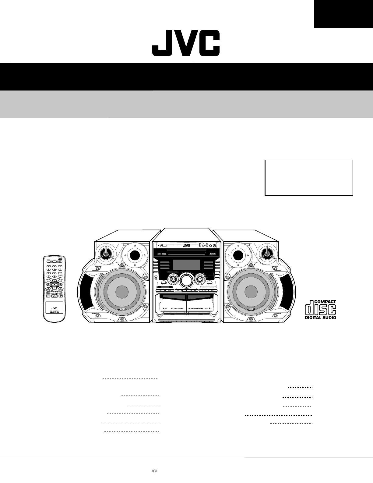
COMPACT COMPONENT SYSTEM
MX-GA77
Area suffix
J ------------------- U.S.A.
C ---------------- Canada
MX-GA77
MP3
SP-MXGA77 SP-MXGA77CA-MXGA77
Contents
Safety Precautions
Importance administering
point on the safety
Preventing static electricity
Disassembly method
Wiring connection
Adjustment method
REC START
/ STOP
CD REC
START
DUBBING
DISPLAY
PHONES
STANDBY
SOUND
TURBO
SUBWOOFER LEVEL
1-2
1-3
1-4
1-5
1-18
1-19
STANDBY/ON
COMPACT COMPONENT SYSTEM MX-GA77
ROCK
POP
CLASSIC
O
S
CD
3
2
CD
CD
1
DISC CHANGE
REPEAT
DANCE
PROGRAM
HALL
RANDOM
U
L
M
O
V
M
D
O
N
U
D
E
TUNING
STADIUM
E
TUNING
BEEP
CLOCK
/ TIMER
SET
PRESET
CANCEL
/ DEMO
TAPE A / B
EJECTEJECT
Flow of functional operation
until TOC read
Maintenance of laser pickup
Replacement of laser pickup
Trouble shooting
Description of major ICs
1-23
1-24
1-24
1-25
1-29~42
COPYRIGHT 2003 VICTOR COMPANY OF JAPAN, LTD.
No.22001
May. 2003
Page 2

MX-GA77
1. This design of this product contains special hardware and many circuits and components specially for safety
purposes. For continued protection, no changes should be made to the original design unless authorized in
writing by the manufacturer. Replacement parts must be identical to those used in the original circuits. Services
should be performed by qualified personnel only.
2. Alterations of the design or circuitr y of the product should not be made. Any design alterations of the product
should not be made. Any design alterations or additions will void the manufacturer`s warranty and will further
relieve the manufacture of responsibility for personal injury or property damage resulting therefrom.
3. Many electrical and mechanical parts in the products have special safety-related characteristics. These
characteristics are often not evident from visual inspection nor can the protection afforded by them necessarily
be obtained by using replacement components rated for higher voltage, wattage, etc. Replacement par ts which
have these special safety characteristics are identified in the Parts List of Service Manual. Electrical
components having such features are identified by shading on the schematics and by ( ) on the Parts List in
the Service Manual. The use of a substitute replacement which does not have the same safety characteristics
as the recommended replacement parts shown in the Parts List of Service Manual may create shock, fire, or
other hazards.
4. The leads in the products are routed and dressed with ties, clamps, tubings, barriers and the like to be
separated from live parts, high temperature parts, moving parts and/or sharp edges for the prevention of
electric shock and fire hazard. When service is required, the original lead routing and dress should be
observed, and it should be confirmed that they have been returned to normal, after re-assembling.
5. Leakage currnet check (Electrical shock hazard testing)
After re-assembling the product, always perform an isolation check on the exposed metal parts of the product
(antenna terminals, knobs, metal cabinet, screw heads, headphone jack, control shafts, etc.) to be sure the
product is safe to operate without danger of electrical shock.
Do not use a line isolation transformer during this check.
Plug the AC line cord directly into the AC outlet. Using a "Leakage Current Tester", measure the leakage
current from each exposed metal parts of the cabinet, particularly any exposed metal part having a return
path to the chassis, to a known good earth ground. Any leakage current must not exceed 0.5mA AC (r.m.s.).
Alternate check method
Plug the AC line cord directly into the AC outlet. Use an AC voltmeter having, 1,000 ohms per volt or more
sensitivity in the following manner. Connect a 1,500 10W resistor paralleled by a 0.15 F AC-type capacitor
between an exposed metal part and a known good earth ground.
Measure the AC voltage across the resistor with the AC
voltmeter.
Move the resistor connection to each exposed metal part,
particularly any exposed metal part having a return path to
the chassis, and meausre the AC voltage across the resistor.
Now, reverse the plug in the AC outlet and repeat each
measurement. Voltage measured any must not exceed 0.75 V
AC (r.m.s.). This corresponds to 0.5 mA AC (r.m.s.).
0.15 F AC TYPE
1500 10W
Good earth ground
AC VOLTMETER
(Having 1000
ohms/volts,
or more sensitivity)
Place this
probe on
each exposed
metal part.
!
1. This equipment has been designed and manufactured to meet international safety standards.
2. It is the legal responsibility of the repairer to ensure that these safety standards are maintained.
3. Repairs m ust be made in accordance with the relevant safety standards.
4. It is essential that safety critical components are replaced by approved parts.
5. If mains voltage selector is provided, check setting for local voltage.
Burrs formed during molding may
be left over on some parts of the
chassis. Therefore, pay attention to
such burrs in the case of
preforming repair of this system.
In regard with component parts appearing on the silk-screen pr inted side (parts side) of the PWB diagrams, the
parts that are printed over with black such as the resistor ( ), diode ( ) and ICP ( ) or identified by the " "
mark nearby are critical for safety.
(This regulation does not correspond to J and C version.)
1-2
Page 3
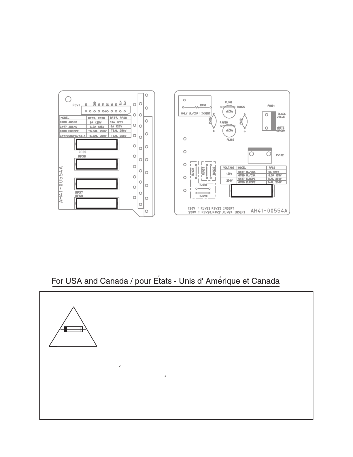
Importance administering point on the safety
6.3A 125V
6.3A 125V
MX-GA77
8A 125V
5A 125V
8A 125V
Fuse board (Forward side) Power supply board (Forward side)
RFS2
Caution: For continued protection against risk of fire,
replace only with same type 5A/125V for RFS2,
6.3A/125V for RFS5 and RFS6, 8A/125V for RFS7
and RFS8.
This symbol specifies type of fast operating fuse.
Precaution: Pour eviter risques de feux, remplacez le
fusible de surete de et RFS2 comme le meme type
que 5A/125V, et 6.3A/125V pour RFS5 et RFS6, et
8A/125V pour RFS7 et RFS8.
Ce sont des fusibles suretes qui functionnes rapide.
^
1-3
Page 4
MX-GA77
Preventing static electricity
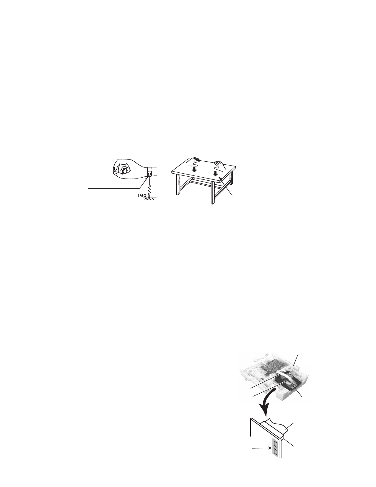
1. Grounding to prevent damage by static electricity
Electrostatic discharge (ESD), which occurs when static electricity stored in the body, fabric, etc. is discharged,
can destroy the laser diode in the traverse unit (optical pickup). Take care to prevent this when performing repairs.
2. About the earth processing for the destruction prevention by static electricity
In the equipment which uses optical pick-up (laser diode), optical pick-up is destroyed by the static electricity of
the work environment.
Be careful to use proper grounding in the area where repairs are being performed.
2-1 Ground the workbench
Ground the workbench by laying conductive material (such as a conductive sheet) or an iron plate over
it before placing the traverse unit (optical pickup) on it.
2-2 Ground yourself
Use an anti-static wrist strap to release any static electricity built up in your body.
(caption)
Anti-static wrist strap
Conductive material
(conductive sheet) or iron plate
3. Handling the optical pickup
1. In order to maintain quality during transport and before installation, both sides of the laser diode on the
replacement optical pickup are shorted. After replacement, return the shorted parts to their original condition.
(Refer to the text.)
2. Do not use a tester to check the condition of the laser diode in the optical pickup. The tester's internal power
source can easily destroy the laser diode.
4. Handling the traverse unit (optical pickup)
1. Do not subject the traverse unit (optical pickup) to strong shocks, as it is a sensitive, complex unit.
2. Cut off the shorted part of the flexible cable using nippers, etc. after replacing the optical pickup. For specific
details, refer to the replacement procedure in the text. Remove the anti-static pin when replacing the traverse
unit. Be careful not to take too long a time when attaching it to the connector.
3. Handle the flexible cable carefully as it may break when subjected to strong force.
4. It is not possible to adjust the semi-fixed resistor that adjusts the laser power. Do not turn it
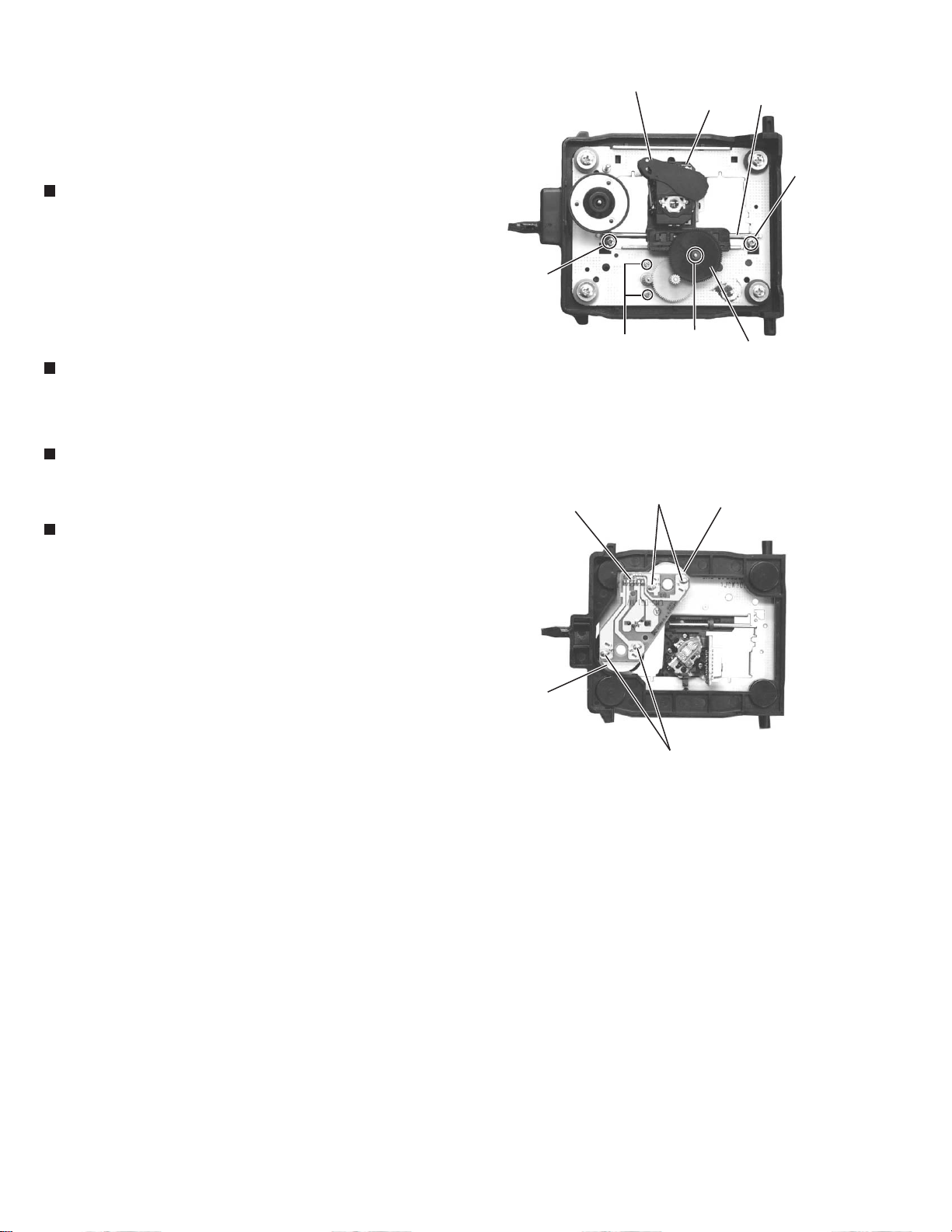
Attention when CD mechanism assembly is decomposed
*Please refer to "Disassembly method" in the text for pick-up and how to
detach the CD mechanism assembly.
1. Remove the CD changer unit.
2. Remove the CD changer mechanism.
3. Solder is put up before the card wire is removed from the pickup unit
connector on the CD mechanism assembly.
(When the card wire is removed without putting up solder, the CD pick-up
assembly might destroy.)
4. Please remove solder after connecting the card wire with the pickup unit
connector when you install picking up in the substrate.
Card wire
Picup unit
connector
Soldering
Fig.2
CD changer unit
Fig.1
Card wire
Picup unit
connector
CD changer
mechanism
1-4
Page 5
MX-GA77
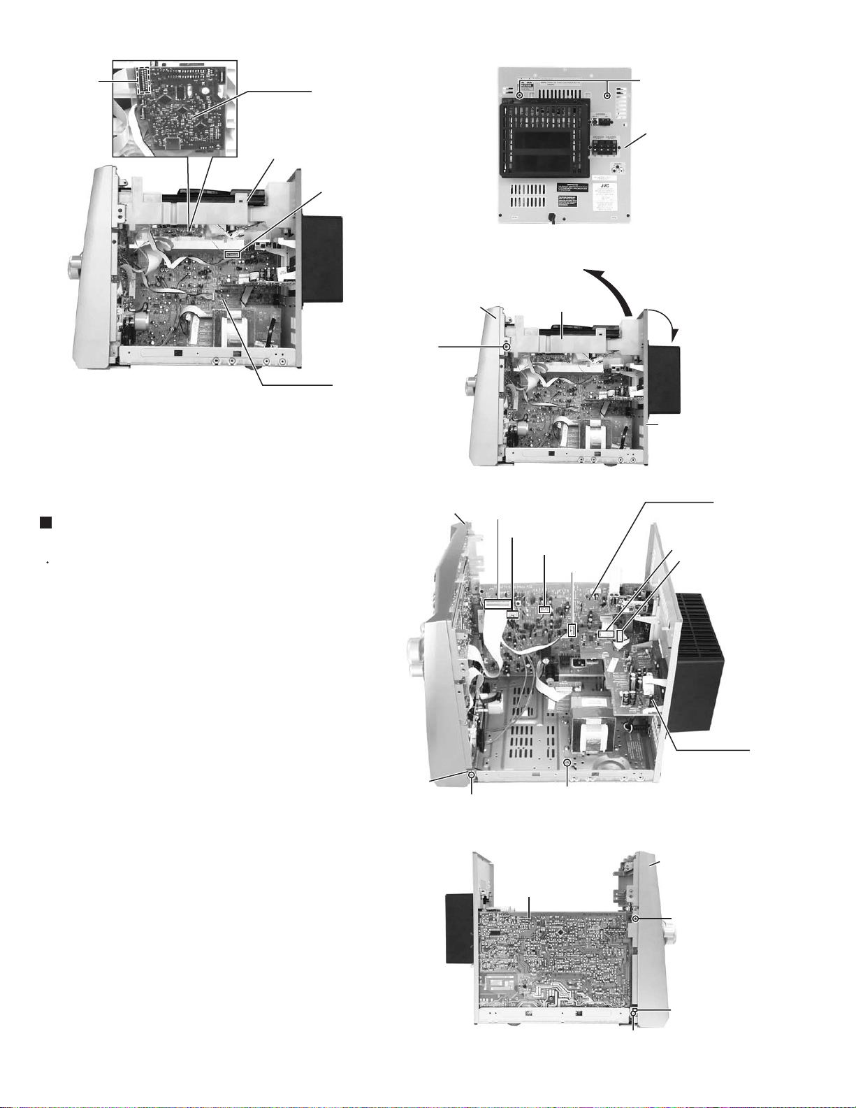
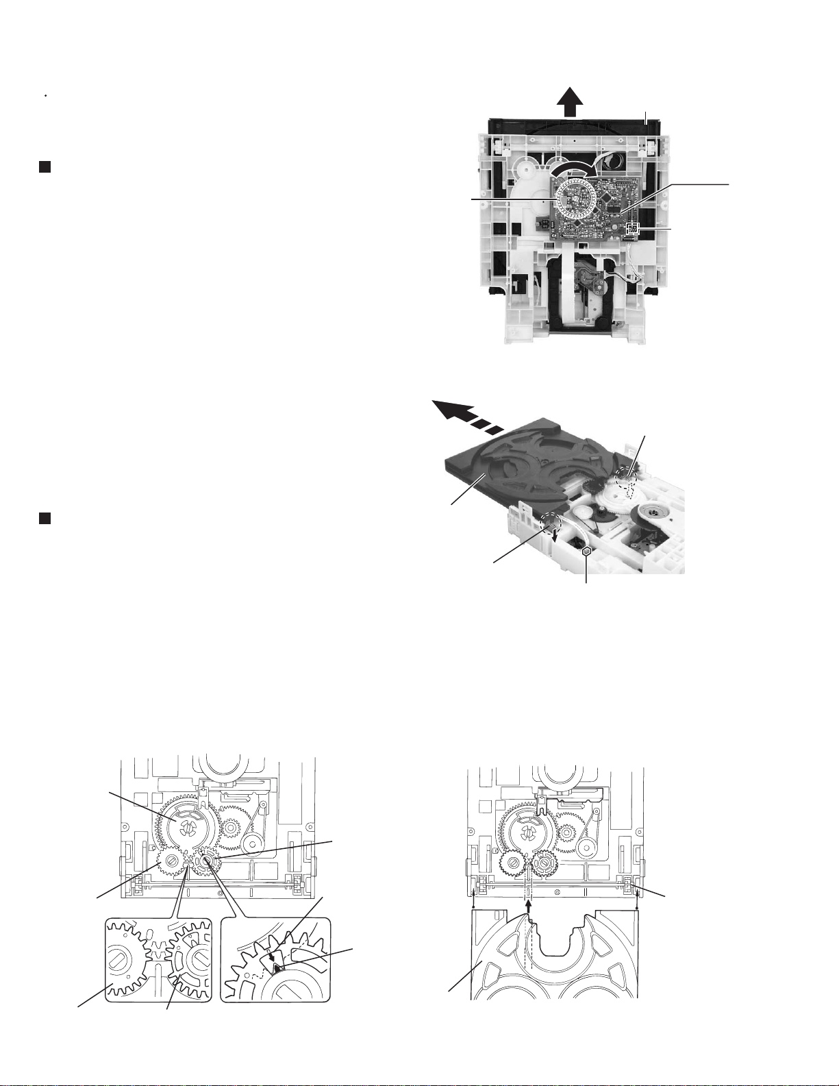
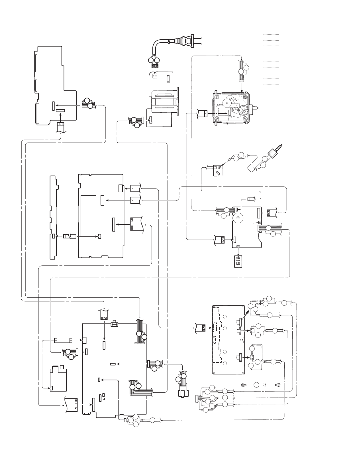
Disassembly method
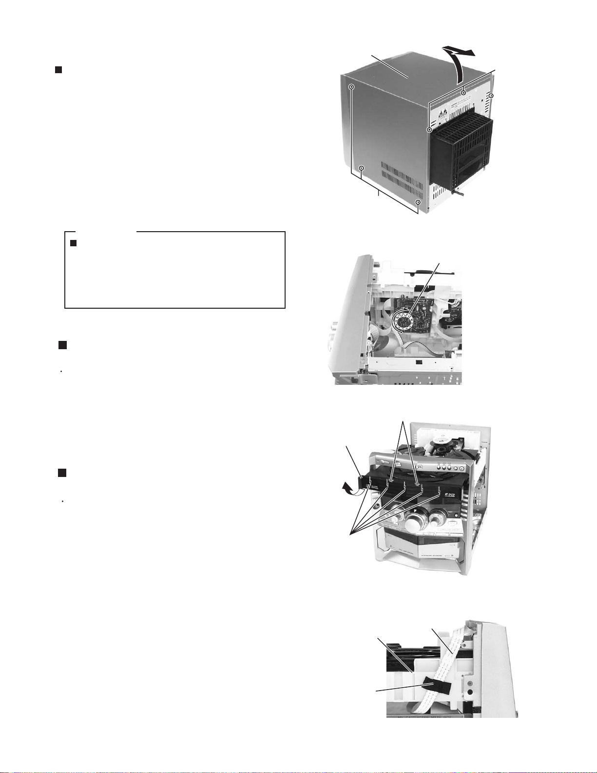
Removing the metal cover (See Fig.1)
1.
Remove the three screws A attaching the metal
cover on the back of the body.
2.
Remove the six screws B attaching the metal cover
on both sides of the body.
3.
Remove the metal cover from the body by lifting the
rear part of the cover.
ONE POINT
How to eject the CD tray manually
(see fig.2)
Turn the loading pulley gear at the bottom of
the CD changer unit as shown in Fig.2 and
draw the CD tray toward the front.
Metal cover
A
B
(both sides)
Fig.1
Loading pulley gear
(See <CD changer unit>fig.1)
Removing the CD tray fitting
(See Fig. 3)
Prior to performing the following procedure, eject the
CD tray.
After drawing the lower part of the tray fitting toward
1.
the front, remove the five claws. Then, while moving
the tray fitting upward, remove it.
Removing the CD changer unit
(See Fig.4 to 7)
Prior to performing the following procedure, remove
the metal cover and CD tray fitting.
1.
Remove the card wire attached to CD changer unit
on the adhesion tape.
2.
Disconnect the card wire from the connector CW105
on the CD board.
3.
Disconnect the harness from the connector CW104
on the main board.
4.
Remove the two screws C attaching the CD changer
unit to the rear panel.
Fig.2
Joint
CD tray fitting
Claw
Fig.3
Card wire
CD changer unit
5.
Remove the two screws D attaching the CD changer
unit to both sides of the front panel assembly.
6.
Draw the CD changer unit upward from behind while
pulling the rear panel outward.
Adhesion tape
Fig.4
1-5
Page 6
MX-GA77
CW105
CD board
CD changer unit
CW104
Main board
Fig.5
Removing the front panel assembly
(See Fig.8 to 10)
Prior to performing the following procedure, remove
the metal cover and CD changer unit.
Front panel
assembly
D
(both sides)
Front panel
assembly
CD changer unit
CW101
CW109
CW110
C
Rear panel
Fig.6
Rear panel
Fig.7
Main board
ACW1
ACW2
CW108
1.
Disconnect the card wire from the connector CW101
on the main board.
2.
Disconnect the harness from the connector CW108,
CW109 and CW110 on the main board.
3.
Remove the screw E fixiing the lug wire.
4.
Remove the two screws F attaching the front panel
assembly to both sides of the body.
5.
Remove the screw G attaching the main board to the
front panel assembly.
6.
Remove the screw H attaching the front panel
assembly to bottom of the body.
7.
Release the two joints1 and two joints2, and detach
the front panel assembly toward the front.
Joint1
(both sides)
(both sides)
F
Fig.8
Main board
Fig.9
Amp. board
E(fixing the lug wire)
Front panel
assembly
G
Joint1
(both sides)
F
(both sides)
1-6
Page 7
MX-GA77
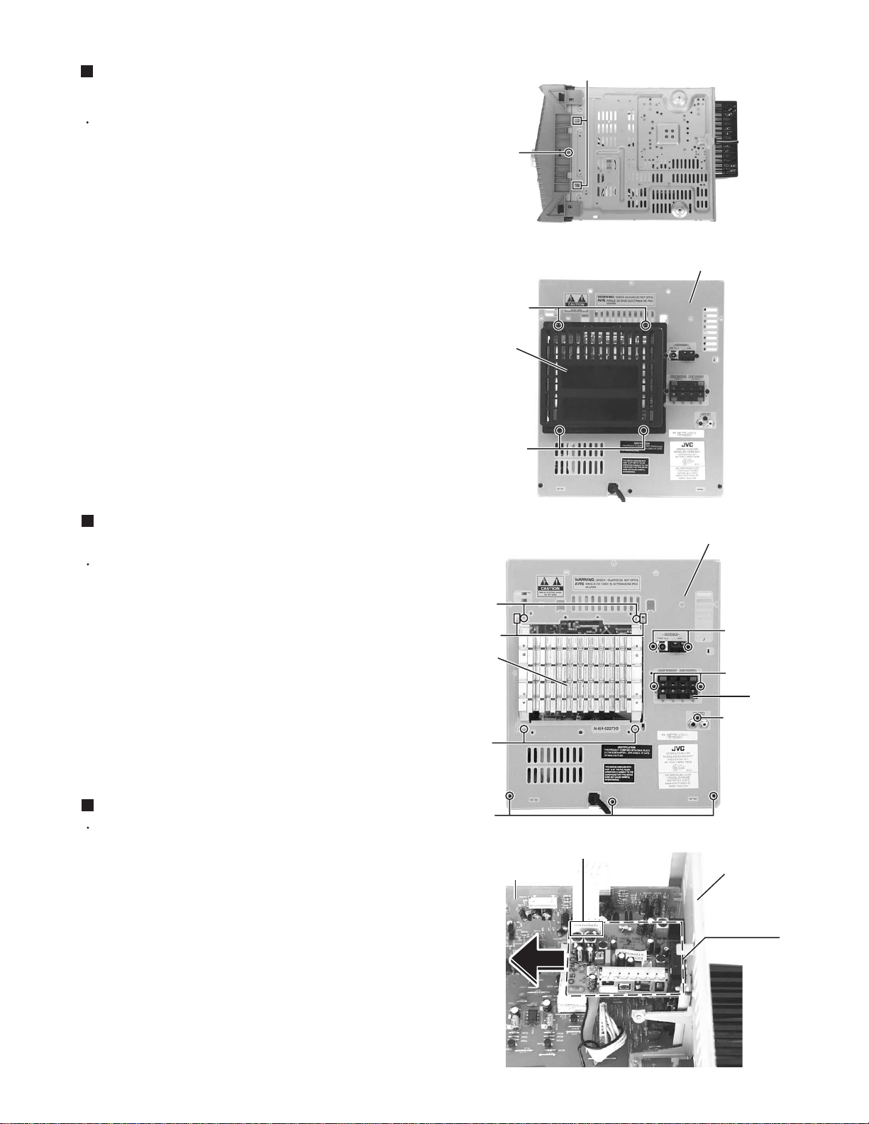
Removing the heat sink & amp. board
(See Fig.8, 11 and 12)
Prior to performing the following procedure, remove
the metal cover and CD changer unit.
1.
Disconnect the card wire from the connector ACW1
and the harness from the connector ACW2 on the
amp. board.
2.
Remove the four screws I attaching the heat sink
cover to the rear panel. Remove the heat sink cover.
3.
Remove the four screws J attaching the heat sink
and two screws K attaching the speaker terminal to
the rear panel.
4.
After moving the heat sink upward, remove the
claws. Then pull out the heat sink & amp. board
inward.
Heat sink
cover
H
Joint2
Fig.10
(Bottom side)
Rear panel
I
I
Removing the tuner board
(See Fig.12 and 13)
Prior to performing the following procedure, remove
the metal cover.
1.
Disconnect the card wire from the connector CON01
on the tuner board.
2.
Remove the two screws L attaching the tuner board
to the rear panel.
Removing the rear panel (See Fig.12)
Prior to performing the following procedure, remove
the metal cover, CD changer unit, heat sink & amp.
board and tuner board.
1.
Remove the screw M and three screws N attaching
the rear panel.
J
Claws
Heat sink
J
N
Main board
CON01
Fig.11
Fig.12
Rear panel
L
K
Speaker
terminal
M
Rear panel
Tuner board
Fig.13
1-7
Page 8
MX-GA77
Removing the main board (See Fig. 14)
Prior to performing the following procedure, remove
the metal cover, CD changer unit and rear panel.
1.
Disconnect the card wire from the connector CW101
and the harness from the connector CW108, CW109
and CW110 on the main board.
2.
Disconnect the harness from the connector PCW1
on the fuse board.
3.
Remove the screw G attaching the main board to the
front panel assembly. (See Fig.9)
4.
Remove the two screws O attaching the heat sink to
the bottom chassis.
Removing the power cord (See Fig. 14)
Prior to performing the following procedure, remove
the metal cover, CD changer unit and rear panel.
1.
Disconnect the power cord from the connector
PW101 on the power supply board and pull up the
power cord stopper upward.
CW108
Fuse board
PCW1
PW101
Power cord
Power cord
stopper
Bottom chassis
CW101
CW109
CW110
Main board
Heat sink
O
Power supply
board
Fig.14
Power ICs solder point
Heat sink
Amp. board
(reverse side)
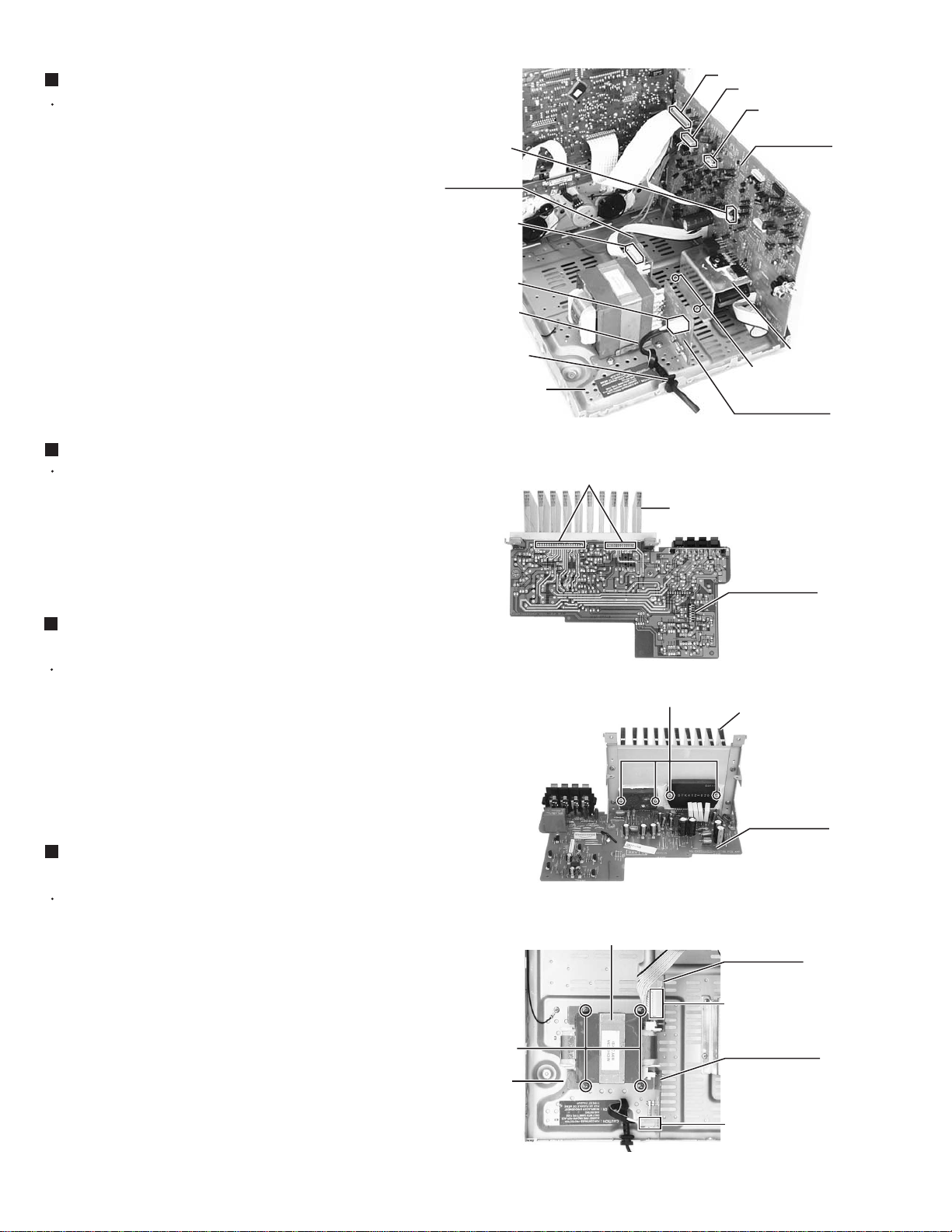
Removing the power ICs
(See Fig.15 and 16)
Prior to performing the following procedure, remove
the metal cover, CD changer unit and heat sink &
amp. board.
1.
Unsolder the power ICs solder points.
2.
Remove the four screws P attaching the power ICs
to the heat sink.
Removing the power transformer
(See Fig .17)
Prior to performing the following procedure, remove
the metal cover, CD changer unit and heat sink &
amp. board.
1.
Disconnect the power cord from the connector
PW101 on the power supply board.
2.
Disconnect the harness from the connector PCW1 on
the fuse board.
Q
Fig.15
Fig.16
Power transformer
P
Heat sink
Amp. board
Fuse board
PCW1
Power supply
board
3.
Remove the four screws Q attaching the power
transformer on the bottom chassis.
1-8
Bottom
chassis
PW101
Fig.17
Page 9
MX-GA77
<Front panel assembly>
Prior to performing the following procedure, remove
the front panel assembly.
Removing the CD switch board (See Fig.1)
1.
Disconnect the card wire from the connector UCW03
on the CD switch board.
2.
Remove the four screws A attaching the CD switch
board.
Removing the front board
(See Fig.1 and 2)
1.
Pull out the sound mode knob, volume knob, and
preset knob from the front side of front panel
assembly.
2.
Disconnect the card wire from the connector UCW02
on the front board and the connector on the mecha.
board.
3.
Remove the fourteen screws B attaching the front
board.
B
B
Connector
Mecha.
board
Front panel assembly (inner side)
A
Fig.1
CD switch board
UCW03
Front board
UCW02
UCW01
4.
Disconnect the card wire from the connector UCW01
on the front board.
Removing the headphone jack board
(See Fig.3)
Prior to performing the following procedure remove
the front board.
1.
You can pull out the headphone jack board.
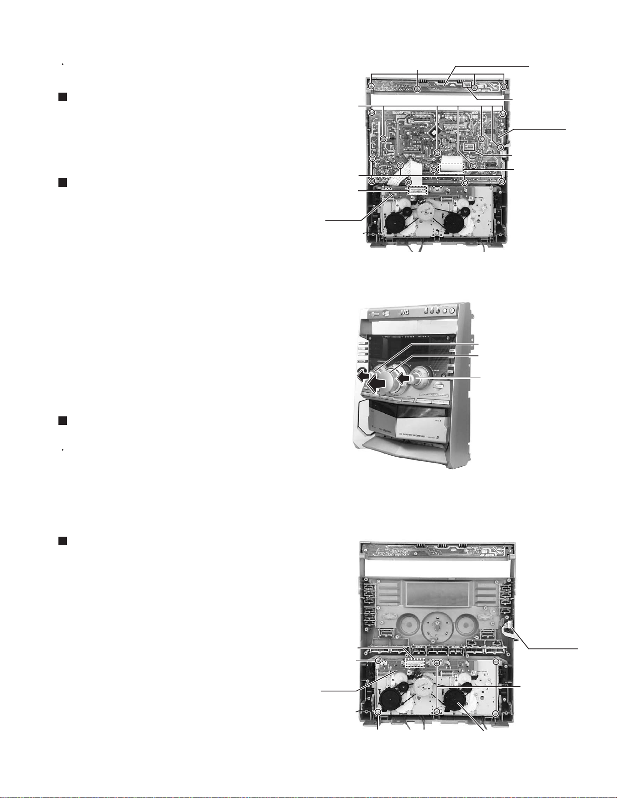
Removing the cassette mechanism
assembly (See Fig.3)
1.
Disconnect the card wire from the connector on the
mecha. board.
2.
Remove the six screws C attaching the cassette
mechanism assembly.
Connector
C
Mecha.
board
Sound mode knob
Volume knob
Preset knob
Fig.2
Front panel assembly (inner side)
Headphone
jack board
C
C
(fixing the lug wire)
Fig.3
Cassette mechanism
assembly
1-9
Page 10
MX-GA77
<CD changer unit>
Prior to performing the following procedure, remove
the CD changer unit.
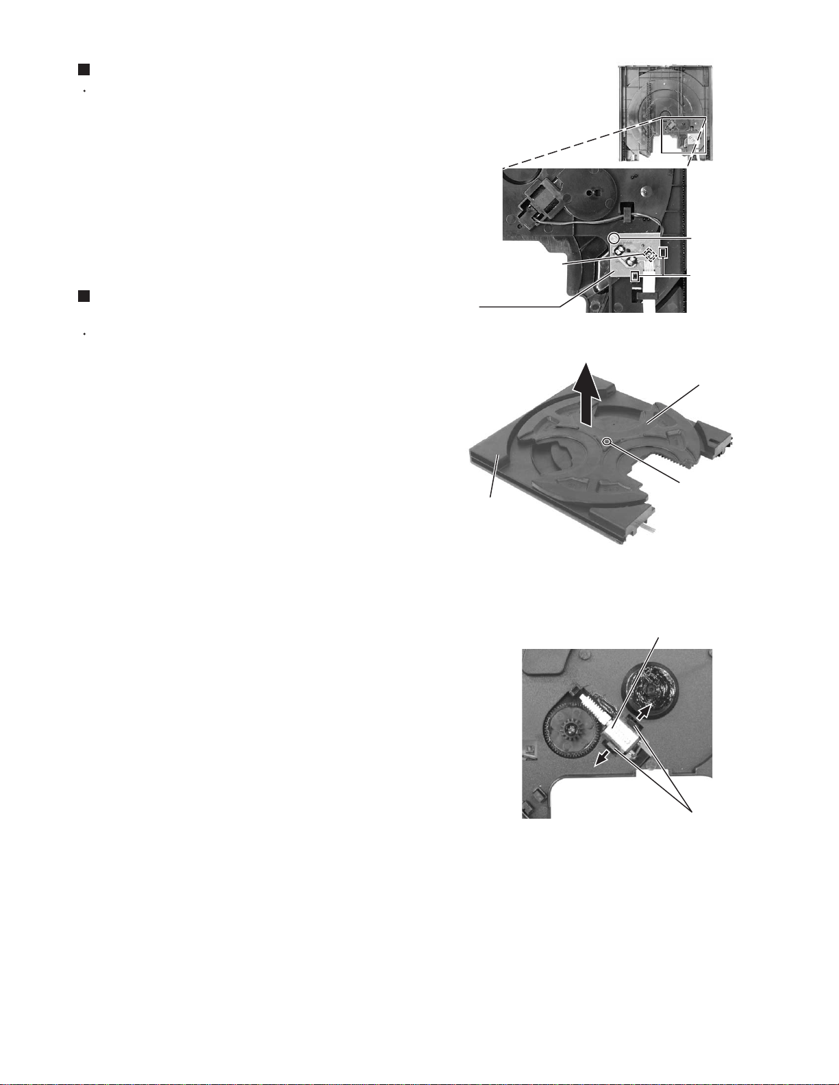
Removing the CD tray (See Fig.1 and 2)
1.
Turn the black loading pulley gear on the under side
of the CD changer unit in the direction of the arrow
and draw the CD tray toward the front until it stops.
2.
Disconnect the card wire from connector CW103 on
the CD board.
3.
Push down the two tray stoppers marked a and pull
out the CD tray.
Loading pulley
gear
CD changer uint (reverse side)
CD tray
CD board
CW103
Fig.1
a (Tray stopper)
Reinstall the CD tray (See Fig.3 and 4)
1.
Align the gear-cam with the gear-tray as shown fig.3,
then mount the CD tray.
2.
When assembling the CD tray, take extreme care not
engage with gear - synchro.
Gear-cam
Gear-convert
Gear-cam
timing point
CD tray
a
(Tray stopper)
CW103
(on the CD board)
Fig.2
Gear-tray
Gear-synchro
Gear-convert
1-10
Gear-tray
CD tray
Gear-tray
Fig.3 Fig.4
Page 11
MX-GA77
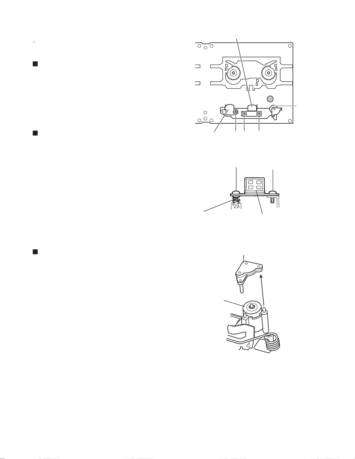
Removing the sensor board (See Fig.5)
Prior to performing the following procedure, remove
the CD tray.
1.
Remove the screw A attaching the sensor board on
the CD tray.
2.
Remove the sensor board releasing the two tabs a.
3.
Disconnect the harness from the connector CW1 on
the sensor board.
Removing the turn tray motor
(See Fig.6 and 7)
Prior to performing the following procedure, remove
the CD tray and sensor board.
1.
Remove the screw B attaching the turn tray. Detach
the turn tray from the base tray.
2.
Pull outward the tab b attaching the turn tray motor
on the base tray and detach the turn tray motor.
CD tray (reverse side)
A
CW1
Tab a
Sensor board
Fig.5
Turn tray
Introductory notes:
Base tray + Turn tray = CD tray
Base tray
B
Fig.6
Turn tray motor
Base tray (upper side)
Tab b
Fig.7
1-11
Page 12
MX-GA77
Removing the belt, the CD board and the
switch board (See Fig.8 and 9)
Prior to performing the following procedure, remove
the CD tray.
1.
Detach the belt from the pulley on the upper side of
the CD changer unit (Do not stain the belt with
grease).
2.
Disconnect the card wire from the pickup unit
connector on the under side of the CD changer unit.
Attention : Solder is put up before the card wire is
removed from the pick-up unit
connector on the CD mechanism
assembly.
(When the card wire is removed without
putting up solder, the CD pick-up unit
assembly might destroy.)
3.
Disconnect the motor wire harness from connector
on the CD board.
4.
Remove the screw C attaching the switch board and
release the two tabs e attaching the switch board
outward and detach the switch board.
5.
Remove the two screws D attaching the CD board.
First release the two tabs f and two tabs g attaching
the motor, then release the CD board.
If the tabs f and g are hard to release, it is
recommendable to unsolder the two soldered parts
on the motor terminal of the CD board.
Tabs e
C
Switch board
CW3
CD changer unit
Fig.8
CD board
D
Tabs g
Soldered parts
CD mechanism board
motor connecter
Pickup unit connector
Card wire
Belt
Motor
Tabs f
1-12
Soldering
Picup unit
connector
Fig.9
Page 13
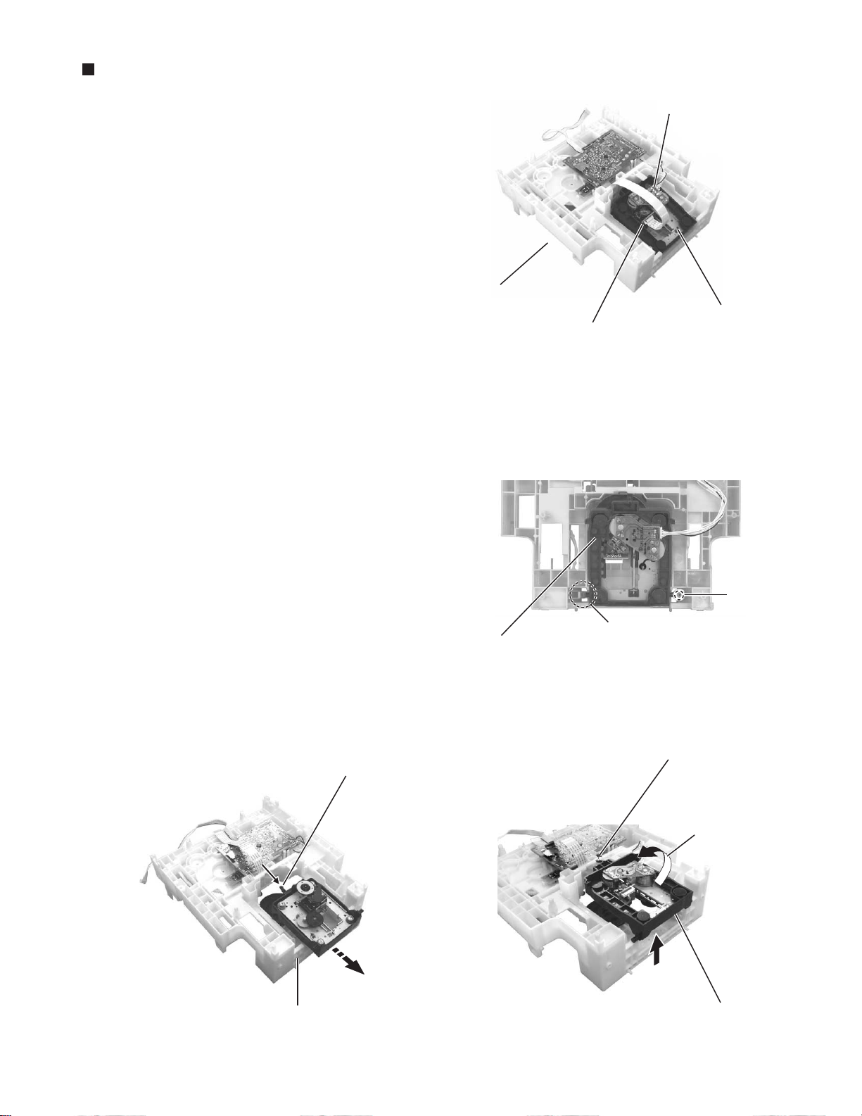
Removing the CD mechanism holder
assembly (mechanism included)
(See Fig.10 to 13)
1.
Disconnect the harness from connector on the CD
mechanism board in the CD mechanism assembly
on the under side of the CD changer unit. Disconnect
the card wire from the pickup unit connector.
Attention : Solder is put up before the card wire is
removed from the pick-up unit
connector on the CD mechanism
assembly. (Refer to Fig.9)
(When the card wire is removed without
putting up solder, the CD pick-up unit
assembly might destroy.)
MX-GA77
Motor connecter
CD changer unit
CD mechanism holder assembly
Pickup unit connector
2.
Remove the screw E attaching the shaft on the right
side of the CD mechanism holder assembly. Pull
outward the stopper fixing the shaft on the left side
and remove the CD mechanism holder assembly
from behind in the direction of the arrow y.
3.
Turn the CD mechanism holder assembly half
around the lift up slide shaft h of the CD mechanism
holder assembly until the turn table is reversed, and
pull out the CD mechanism holder assembly.
Lift up slide shaft
Fig.10
E
Stopper
CD mechanism holder assembly
Fig.11
Lift up slide shaft n
CD mechanism holder assembly
Fig.13
y
CD mechanism holder assembly
Fig.12
1-13
Page 14
MX-GA77
<CD mechanism section>
•
Removing the CD mechanism holder from the CD
chager unit.
(Refer to "Removing the CD mechanism holder
assembly" )
Removing the pickup unit (
1. Removing the cut washer on the feed gear
sleeve and pull out the feed gear.
2. Remove the two screws A fixing the pickup
shaft.
3. Removing the pickup unit.
Removing the motor board
1. Unsolder the motor terminal on the motor board.
2. Remove the moter board.
Removing the feed motor (
Remove the two motor fixing screws at B and
removing the feed motor.
See Fig.1)
(See Fig.2)
See Fig.1)
A
Motor board
Shutter
Cut washer
B
Fig.1
Unsolder
Pickup unit
Feed Gear
Feed motor
Shaft
A
Removing the spindle motor
The spindle motor cannot be removed as a single
unit.
When removing the spindle motor, change the chasis
and turntable together as aunit.
Spindle motor
Unsolder
Fig.2
1-14
Page 15
MX-GA77
<Cassette mechanism section>
Prior to performing the following procedure, remove
the
cassette mechanism assembly.
Removing the R/P head.
(See Fig.1 and 2)
1.
Remove the screw A on the right side of the R/P
head.
2.
Remove the screw B on the left side of the R/P
head.
Remove the erase head.
1.
Remove the screw C fixing the erase head.
(See Fig.1)
E. Head
R/P Head
C
B
B
Pinch roller
A
Fig.1
A
Remove the pinch roller.
Pull out the pinch roller stopper.
1.
Pull out the pinch roller.
2.
(See Fig.3)
Spring
Pinch roller
R/P Head
Fig.2
Pinch roller
stopper
Fig.3
1-15
Page 16
MX-GA77
Removing the motor
1.
Slide the plastic cover in the direction of the arrow,
and remove the three claws. Then remove the
plastic cover.
2.
Remove the two screws D fixing the motor.
Be careful to grease's splash when the drive belt
comes off.
3.
Unsolder the motor terminal.
(See Fig. 4 to 6)
Removing the mechanism board
1.
Unsolder the four solder parts a and the four solder
parts b.
2.
Remove the two screws E attaching the mecha.
board.
(See Fig. 5)
Removing the flywheel
1.
Remove the cut-washer at c from the capstan shaft,
then remove the flywheel.
When reassembling the flywheel, be sure to use new
washers as they cannot be reused.
(See Fig. 7 and 9)
Solder
part
D
Claw
Fig.4
Motor
b
terminal
Solder
part
a
Solder
part
E
a
Plastic cover
Mecha. board
E
Flywheel
Washer
FR belt
Fig.8
Sleeve
c
FR belt
Drive belt
Motor
Drive belt
Fig.5
Motor
Drive belt
Fig.6
1-16
Capstan
washer
Fig.9
Fig.7
Page 17
MX-GA77
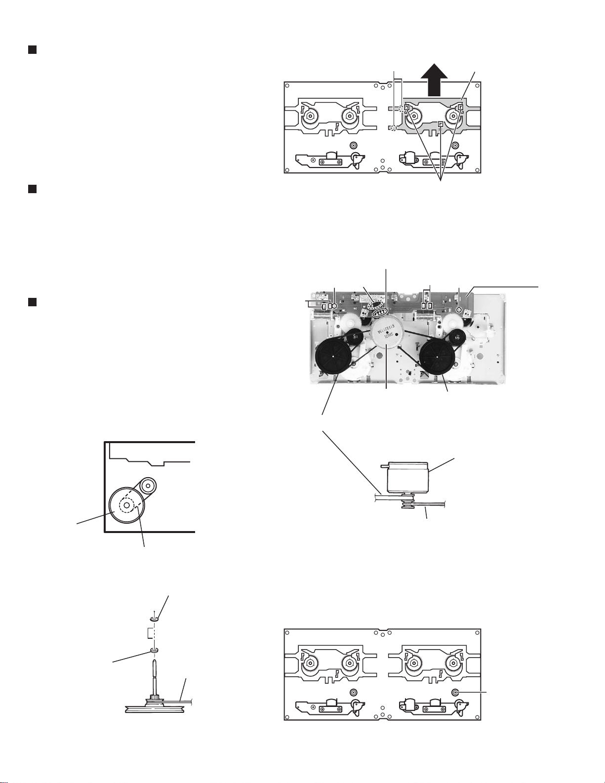
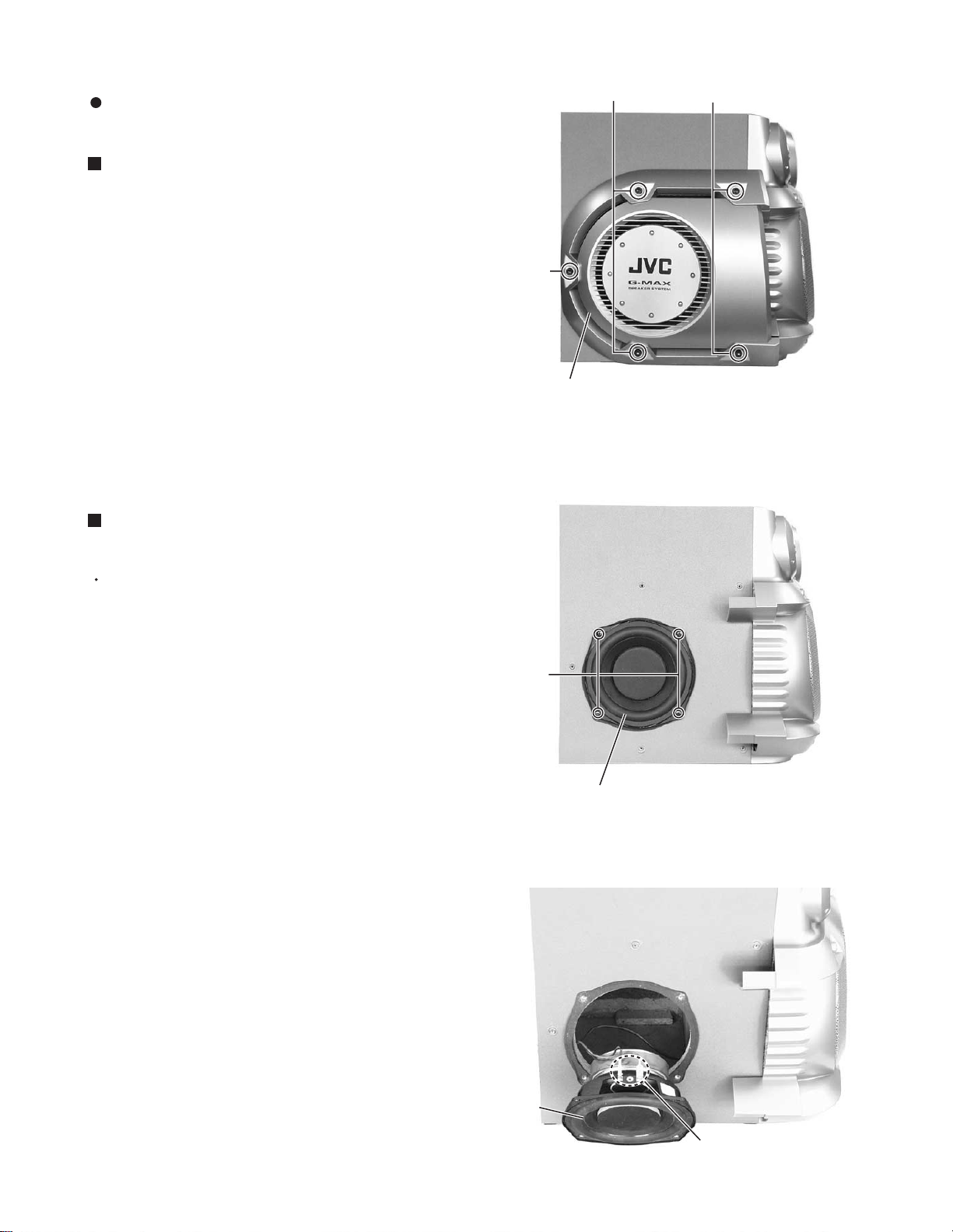
< Speaker section >
It is exchange in a unit.
Please do not decompose as much as possible.
Removing the side panel (See Fig. 1)
1.
Remove the five screws A attaching the side panel
and remove the side panel.
Removing the side speaker
(See Fig. 2 and 3)
A
Side panel
A
A
Fig.1
Prior to performing the following procedure, remove
the side panel.
1.
Remove the four screws B attaching the side
speaker.
2.
Pull out the side speaker and remove the speaker
cord from the speaker terminal.
B
Side speaker
Fig.2
Side speaker
Speaker terminal
Fig.3
1-17
Page 18
MX-GA77
Wiring connection
Amp. board
0
9
Front board
UCW02
3809-001413
AH39-00295A
ACW2
ACW1
CD switch board
3809-001228
UCW03
UCW04
UCW05
UCW01
Color codes are shown below.
1 Brown
2 Red
3 Orange
4 Yellow
9
0
5 Green
6 Blue
7 Violet
0
9
8 Gray
9 White
PW101
Power transformer
RFS2
CD mechanism
0 Black
9
0
CW2
CW1
CW3
AAN1
0
2
AH38-12001A
CW102
CW103
0
2
3809-001034
PCW1
AH39-20561P
3809-001121
AH39-00338A
9
0
CW101
CW3
CW104
CW105
CW107
CW106
9
0
CD board
AH39-00060A
1-18
3809-001211
3809-001434
CON01
0
3809-001259
9
0
9
8
2
0
9
0
CW103
9
0
CW104
CW105
CW106
9
AH39-00247A
0
CW108
Main board
CW110
Tuner board
CW101
CW111
CW109
CW107
9
0
0
9
2
2
0
CW01B
9
0
Headphone J.board
9
AH39-00022A
0
9
2
0
88
9
9
0
9
2
0
AH39-20002D
8
2
Page 19
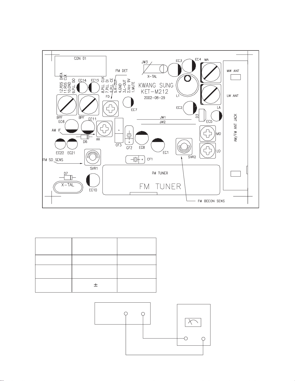
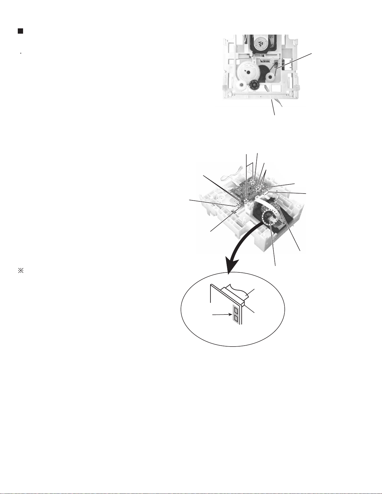
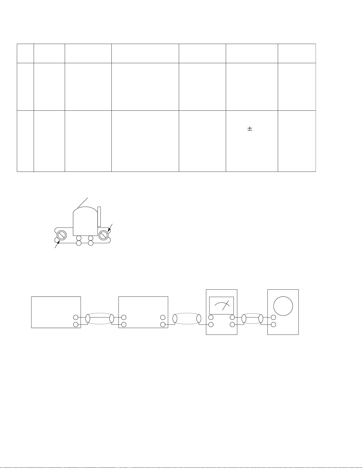
Adjustment method
1. Tuner
MX-GA77
ITEAM
Received FREQ.
Adjustment
point
Output
* Adjustment Location of Tuner PCB
AM(MW) OSC
Adjustment
530~1710 KHz
MO
1~7.0 0.5V
MAIN
PCB
AM(MW) RF
Adjustment
600 KHz
MA
Maximum
Output(Fig.1)
VT GND
TESTER
Fig.1 OSC Voltage
1-19
Page 20
MX-GA77
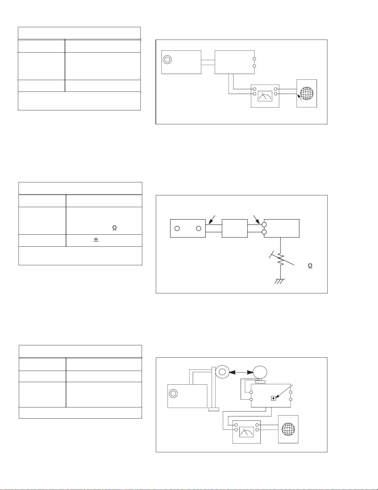
FM THD Adjustment
SSG FREQ.
98 MHz
Adjustment
point
FM DETECTOR COIL
(FM DET)
Output
60 dB
Minumum Distortion (0.4% below)
(Fig.2)
FM Search Level Adjustment
SSG FREQ.
Adjustment
point
(SVR1)
BEACON
SENSITIVITY
SEMI-VR(10K )
98 MHz
Output
GND
FM
Antenna
Terminal
SET
FM S.S.G
Speaker
Terminal
output
Distortion Meter
Fig.2 IF CENTER and THD Adjustment
28 dB
FM Antenna
Input
Oscilloscope
Input
SET
Output
28 dB(
2dB)
Adjust SVR1 (Fig.3)
*Adjust FM S.S.G level to 28dB
AM(MW) I.F Adjustment
SSG FREQ.
Frequency
450 kHz
522 kHz
Adjustment
point
AM IF
Maximum output (Fig.4)
FM S.S.G
GND
FM IN
Fig.3 FM Auto Search Level Adjustment
60cm
OUTPUT
AM SSG
450KHZ
AM ANT
IN
20 k
AM IF
Speaker Terminal
1-20
INPUT
VTVM Oscilloscope
OUTPUT
Fig.4 AM I.F Adjustment
Page 21
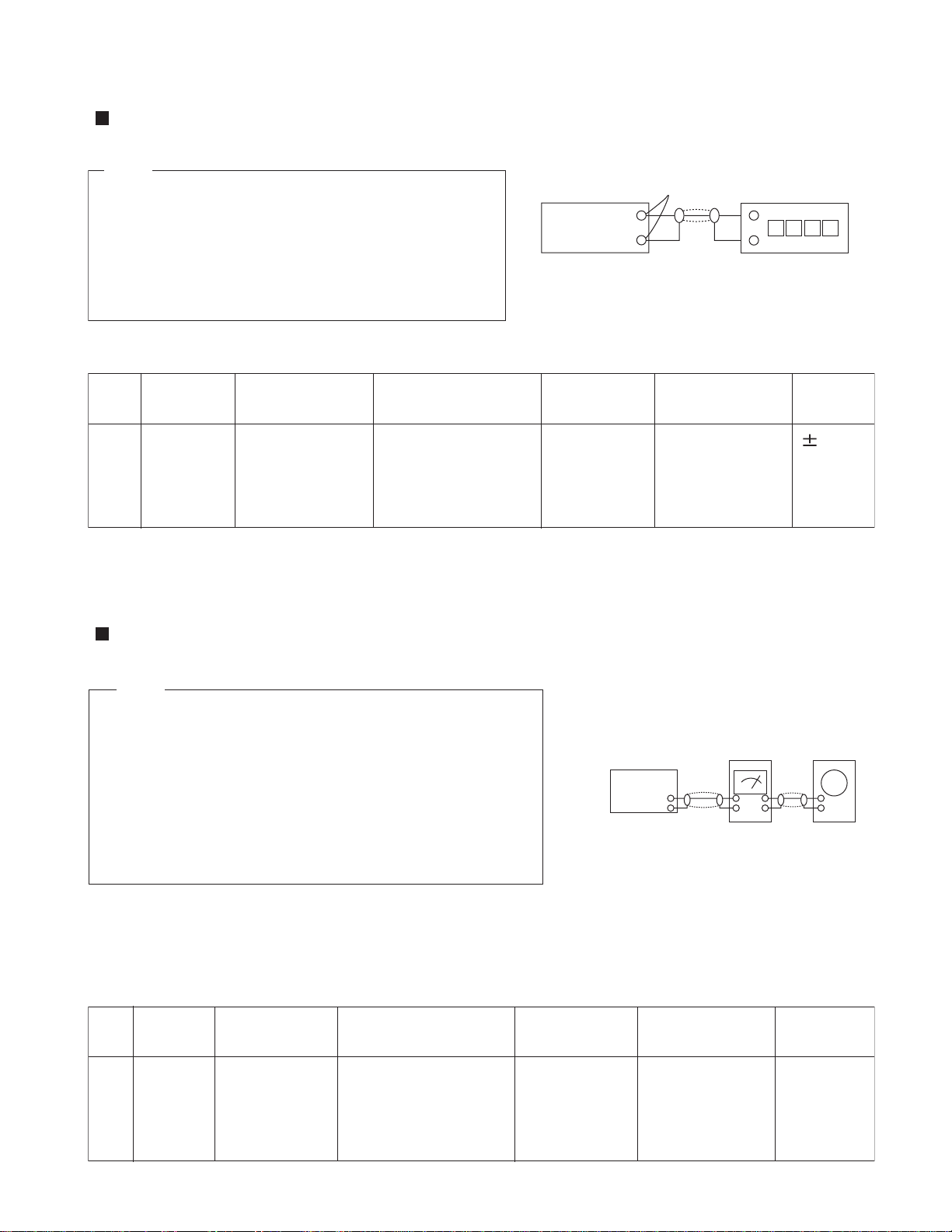
2. Cassette Deck
To adjust tape speed
Notes
1) Measuring tape:
i) VT-712/MTT-111(or equivalent)
(Tapes recorded with 3kHz)
ii) AC-225/MTT-5512(or equivalent)
2) Connect the cassette deck to the frequency counter
as in fig.1.
Cassette Deck
SPK OUT
MX-GA77
Frequency Counter
output
Fig.1
Pre-Setup
Condition
NOR
1 3KHz
SPEED
Control
SPK OUT
(connected to the
frequency counter)
1) Deck 1:VT-712
2) Press PLAY
SW button
To Adjust
Turn VSR1 to
left and right
(FRONT PCB)
3) Deck 2:Same
as above
To adjust plabyback level/REC
Notes
1) Before the actual adjustment, clean the play/recording head.
2) Measuring tape :
i) VT-703/MTT-114N(or equivalent 10kHz AZIMUTH control)
ii) AC-225/MTT-5512(or equivalent)
3) The cassette deck is connections as shown in fig.2.
MAIN PCB
SPK OUT
(GND)
Fig.2
VTVM
In Out
RemarkStandardPre-SetupItemStep
1%
range
Oscilloscope
1. Adjust Deck 1 Play Level
Pre-Setup
Condition
AZIMUTH1 SPK OUT
(VTVM is
connected to
the scope)
After putting VT-703
into Deck 1
- Press FWD PLAY
button.
To Adjust
Turn the control
screw to as
shownin Fig.3.
Max output
and same phase
(both channels)
RemarkStandardPre-SetupItemStep
After
adjustment
secure it with
REGION
LOCK.
1-21
Page 22
MX-GA77
2. Adjust Deck 2 Play Level/REC BIAS
2
AZIMUTH1
Recording
Bias
Voltage
Pre-Setup
Condition
SPK OUT
(VTVM is
connected to
the scope)
Fig.4
Recording /Play head
AZIMUTH control screw
(FWD Play)
After putting VT-703
into Deck 2
1)Press FWD PLAY
button.
After putting AC-225
into Deck 2
1)Press REC PLAY
button.
2)TAPE PCB JCW3,
connectted to VTVM
To Adjust
Turn the control
screw to as
shown in Fig.3.
Turn JSR2L,
JSR2R to the
right and left
Max output
and same phase
(both channels)
CHECK TO
7mV(
0.5mV)
RemarkStandardPre-SetupItemStep
After
adjustment
secure it with
REGION
LOCK.
AZIMUTH control screw
(RVS Play)
Audio OSC.
Fig.3
AUX IN
SET
(MAIN PCB)
IN
TP
SPK OUT
Fig.4
VTVM
IN OUT
Oscilloscope
1-22
Page 23
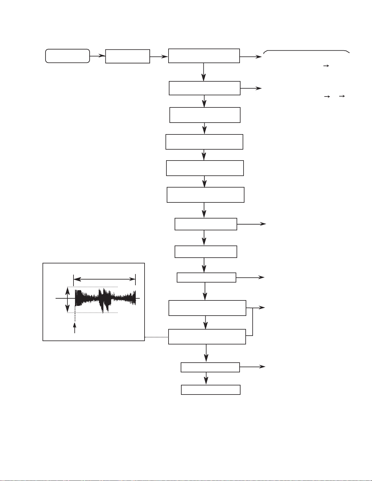
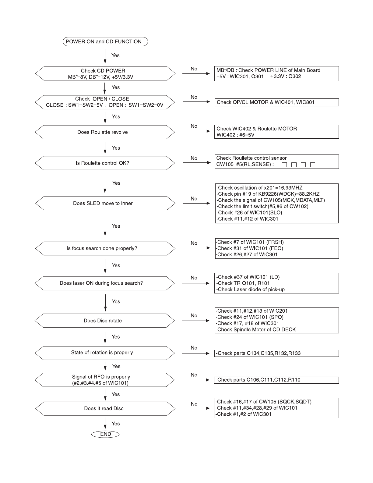
Flow of functional operation until TOC read
Power ON
Play Key
RESET a CD LSI
MX-GA77
Check Point
Confirm that the voltage at the pin17
of KB9226(IC101) is "L" "H".
LIMIT SW ON
SET Default value of
TE gain, TE balance
Automatic adjusting of
focus bias
Automatic adjusting of
FE offset
Automatic adjusting of
TE offset
LASER power ON
Detection of disk
Confirm that the voltage at the pin33
of KB9226(IC101) is "H" "L" "H".
Confirm that the voltage at the
pin37 of KB9226(IC101) is 3.5V.
Tracking error waveform at TOC reading
Pin 34 of
KB9226
(IC101)
Approx
0.4V
2.50V
Disc states
to rotate
Approx.3.7sec
Disc is rotated
Automatic adjusting of
TE balance
Automatic adjusting of
TE gain
TOC reading
Play a disc
Confirm that the signal from pin24
of KB9226(IC101) is 3.5V as a
accelerated pulse during
approx.1.96s.
Confirm the waveform of
the Tracking error signal
at the pin 34 of KB9226(IC101).
Confirm the eye-pattern
at the pin2 of KB9226(IC101).
1-23
Page 24
MX-GA77
Maintenance of laser pickup
(1) Cleaning the pick up lens
Before you replace the pick up, please try to
clean the lens with a alcohol soaked cotton
swab.
(3) Semi-fixed resistor on the APC PC board
The semi-fixed resistor on the APC printed circuit board which is attached to the pickup is used to adjust the
laser power. Since this adjustment should be performed to match the characteristics of the whole optical block,
do not touch the semi-fixed resistor.
If the laser power is lower than the specified value, the laser diode is almost worn out, and the laser pickup
should be replaced.
If the semi-fixed resistor is adjusted while the pickup is functioning normally, the laser pickup may be damaged
due to excessive current.
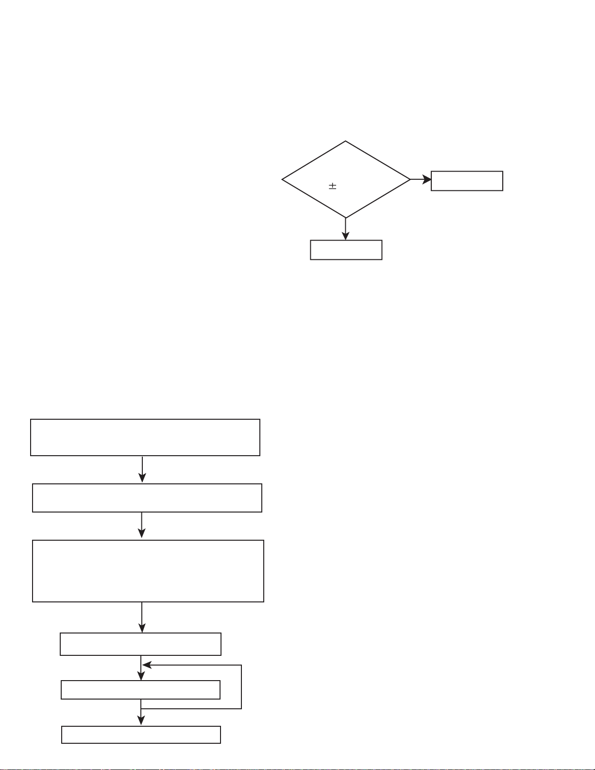
(2) Life of the laser diode
When the life of the laser diode has expired,
the following symptoms will appear.
1. The level of RF output (EFM output :
amplitude of eye pattern) will below.
Is the level of
RF OUT under
1.1V 0.2Vp-p?
YES
O.K
NO
Replace it.
Replacement of laser pickup
Turn off the power switch and,disconnect the
power cord from the ac outlet.
Replace the pickup with a normal one.(Refer
to "Pickup Removal" on the previous page)
Plug the power cord in,and turn the power on.
At this time,check that the laser emits for
about 3seconds and the objective lens moves
up and down.
Note: Do not observe the laser beam directly.
Play a disc.
1-24
Check the eye-pattern at TP1.
Finish.
Page 25
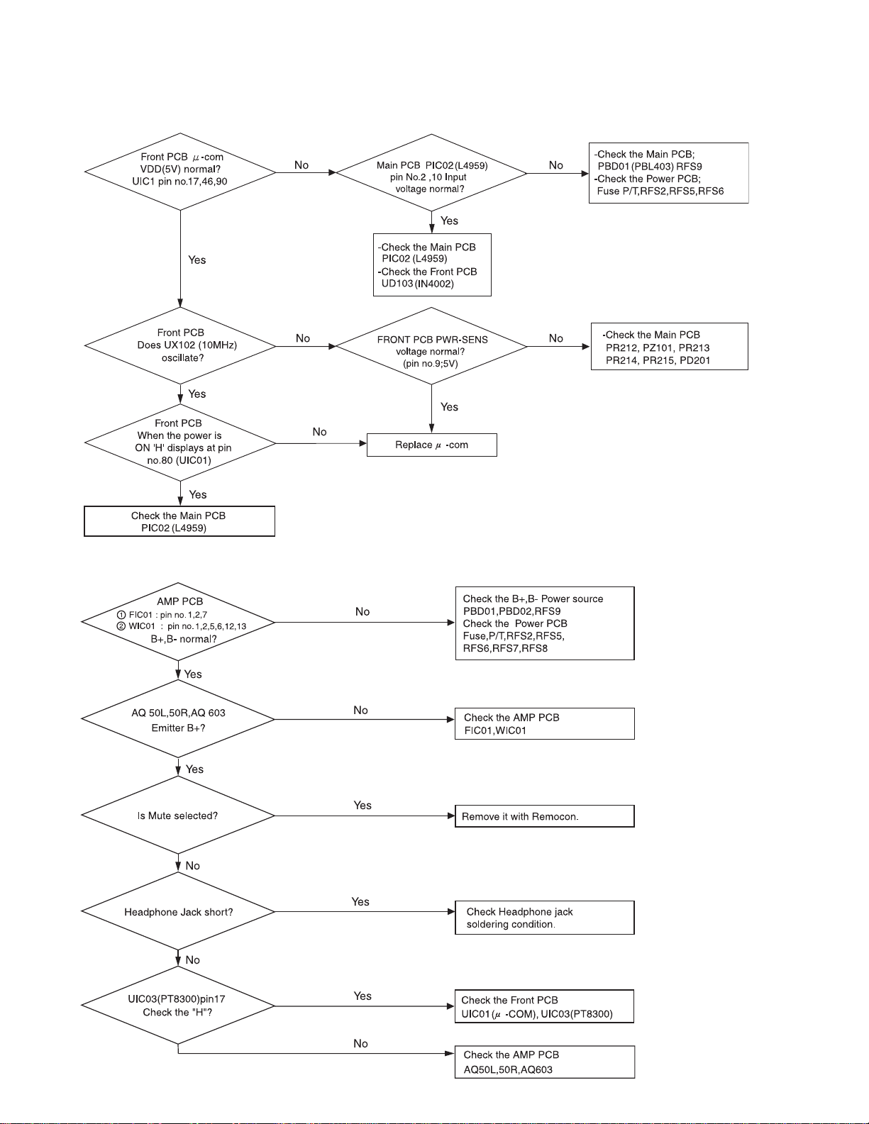
Troubleshooting
1. Amplifier
Power malfunction
MX-GA77
No output
1-25
Page 26
MX-GA77
2.Tuner malfunction (FM/AM)
3.Tape
1-26
Page 27
4.CD
MX-GA77
1-27
Page 28

MX-GA77
5.CD - MP3 parts
1-28
Page 29

Description of major ICs
LC876764 (UIC1) : Microcontroller
1.Pin layout
S47/PF7
S46/PF6
S45/PF5
S44/PF4
S43/PF3
S42/PF2
S41/PF1
S40/PF0
VDD4
S39/PE7
S38/PE6
S37/PE5
S36/PE4
S35/PE3
S34/PE2
S33/PE1
S32/PE0
S31/PD7
S30/PD6
S29/PD5
S28/PD4
S27/PD3
S26/PD2
S25/PD1
S24/PD0
S23/PC7
S22/PC6
S21/PC5
S20/PC4
FIX0
MX-GA77
2.Block diagram
8079787776757473727170696867666564636261605958575655545352
P00
P01
P02
P03
P04
P05
P06
P07
81
82
83
84
85
86
87
88
89
90
91
92
93
94
95
96
97
98
99
100
1234567891011121314151617181920212223242526272829
CF1
RES
VSS1
XT1/AN10
P16/T1PWML
P30/INT4/T1IN
P31/INT4/T1IN
P32/INT4/T1IN
P33/INT4/T1IN
P17/T1PWMH/BUZ
P34/INT5/T1IN
P35/INT5/T1IN
XT2/AN11
P36/INT5/T1IN
P37/INT5/T1IN
IR PLA
S48/PG0
S49/PG1
S50/PG2
S51/PG3
VSS2
VDD2
P10/SO0
P11/SI0/SB0
P12/SCK0
P13/SO1
P14/SI1/SB1
P15/SCK1
Interrupt Control
Stand-by Control ROM
CF2
VDD1
P80/AN0
P81/AN1
P82/AN2
P83/AN3
P84/AN4
P85/AN5
P86/AN6
P87/AN7/MICIN
51
S19/PC3
50
S18/PC2
49
S17/PC1
48
S16/PC0
47
VDD3
46
S15/T15
45
S14/T14
44
S13/T13
43
S12/T12
42
S11/T11
41
S10/T10
40
S9/T9
39
S8/T8
38
S7/T7
37
S6/T6
36
S5/T5
35
S4/T4
34
S3/T3
33
S2/T2
32
S1/T1
31
30
S0/T0
P73/INT3/T0IN/AN13
P70/INT0/T0LCP/AN8
P71/INT1/T0HCP/AN9
P72/INT2/T0IN/NKIN/AN12
SIO0
SIO1
Timer 0
(High speed clock counter)
Timer 1
Base Timer
VFD Controller
INT 0 - 5
Noise Rejection
CF
RC
MRC
X’ tal
Clock
Generator
Bus Interface
Port 0
Port 1
Port 3
Port 7
Port 8
ADC
Weak Signal
Detector
PC
ACC
B Register
C Register
ALU
PSW
RAR
RAM
Timer 4
Timer 5
Timer 6
Timer 7
Stack Pointer
Watch Dog Timer
1-29
Page 30

MX-GA77
3. Pin function (1/2)
Pin name
VSS1, 2
VDD1,2,3,4
FIX0
PORT0
P00 to P07
PORT1
P10 to P17
PORT3
P30 to P37
PORT7
P70 to P73
PORT8
P80 to P87
S0/T0 to
S8/T8
S9/T9 to
S15/T15
S16 to S23
S24 to S31
I/O
I/O
I/O
I/O
I/O
O
O
I/O
I/O
-
-
-
Power supply (-)
Power supply (+)
Test pin
Set as VSS with the user’s option. (see Note 1)
• 8bit input/output port
• Data direction programmable in nibble units
• Use of pull-up resistor can be specified in nibble units
• Input for HOLD release
• Input for port 0 interrupt
• 15V withstand at N-channel open drain output
• 8bit input/output port
• Data direction programmable for each bit
• Use of pull-up resistor can be specified for each bit
• Other pin functions
P10: SIO0 data output
P11: SIO0 data input / bus input / output
P12: SIO0 clock input / output
P13: SIO1 data output
P14: SIO1 data input / bus input / output
P15: SIO1 clock input / output
P16: Timer 1 PWML output
P17: Timer 1 PWMH output / Buzzer output
• 8bit input/output port
• Data direction can be specified for each bit
• Use of pull-up resistor can be specified for each bit
• 15V withstand at N-channel open drain output
• Other functions:
P30 to P33: INT4 input / HOLD release input / Timer 1 event input / Timer 0L
capture input / Timer 0H capture input
P34 to P37: INT5 input / HOLD release input / Timer 1 event input / Timer 0L
capture input / Timer 0H capture input
• 4bit input/output port
• Data direction can be specified for each bit
• Use of pull-up resistor can be specified for each bit
• Other functions
P70: INT0 input / HOLD release input / Timer0L capture input / Output for watchdog timer
P71: INT1 input / HOLD release input / Timer0H capture input
P72: INT2 input / HOLD release input / Timer 0 event input / Timer0L capture input
/ High speed clock counter input
P73: INT3 input(noise rejection filter attached input) / Timer 0 event input
/ Timer 0H capture input
AD input port: AN8(P70), AN9(P71), AN12(P72), AN13(P73)
• 8bit input/output port
• Input/output can be specified in a bit unit
• Other functions:
AD input port: AN0 to AN7
Weak signal detector input port: MICIN(P87)
• Large current output for VFD display controller digit (can be used for segment)
• Large current output for VFD display controller segment/digit
• Output for VFD display controller segment/digit
• Other functions:
High voltage input port: PC0 to PC7
• Output for VFD display controller segment
• Other functions:
High voltage input port: PD0 to PD7
Function I/O
1-30
Page 31

MX-GA77
3. Pin function (2/2)
Pin name
S32 to S39
S40 to S47
S48 to S51
RES
XT1
XT2
CF1
CF2
I/O
I/O
I/O
I
I
I/O
I
O
Function I/O
• Output for VFD display controller segment
• Other functions
High voltage input port: PE0 to PE7
• Output for VFD display controller segment
• Other functions:
High voltage input/output port: PF0 to PF7
• Output for VFD display controller segment
• Other functions:
High voltage input/output port: PG0 to PG3
Reset terminal
• Input for 32.768kHz crystal oscillation
• Other functions:
General purpose input port
When not in use, connect to VDD1.
AD input port: AN10
• Output for 32.768kHz crystal oscillation
• Other functions:
General purpose input port
When not in use, set to oscillation mode and leave open circuit.
AD input port: AN11
Input terminal for ceramic oscillator
Output terminal for ceramic oscillator
KA9258D (IC301) : 4-ch Motor driver
1.Block diagram
28 27 26 25 24 23 22 21 20 19 18 17 16 15
10K
T • S • D
+-
LEVEL SHIFT
VCC VCC
10K
REGULATOR
10K
10K
10K
GND
10K
10K
50K
MUTE
LEVEL SHIFT
-+
10K
1 2 3 4 5 6 7 8 9 10 11 12 13 14
GND
1-31
Page 32

MX-GA77
KB9226 (IC101) : RF amp. & servo signal processor
1. Pin layout
36 35 34 33 32 31 30 29 28 27 26 25
SLP
FEO
VCC
FEM
FRSH
TEO
FSET
TEM
FLB
FGD
2. Block diagram
37
LD
PD
38
39
PDAC
40
PDBD
PDF
41
42
PDE
43
DCB
MCP
44
45
DCCI
46
DCCO
47
VREF
48
EQC
LPFT
ATSC
RFO
RFM
1 2 3 4 5 6 7 8 9 10 11 12
TEIO
TZC/SSTOP
S1L9226X
EQO
EQI
GND
EFMI
FSI
SLO
SLM
SPO
SPM
ASY
EFM
LOCK
WDCK
CLVI
RESET
MLT
MDATA
MCK
ISTAT
TGU
24
23
22
21
20
19
18
17
16
15
14
13
EQO
EFMI
DCCI
DCC0
MCP
DCB
VCC/
VDD
FRSH
FSET
FLB
FGD
FSI
45
46
44
43
10
11
EQI
RFO
RFM
4
5
RF AGC & EQ
Control
Focus OK Detect
Defect Detect Mirror
Gen
Focus Servo Loop
- Gain & Phase
Compensation
- Focus Search
- Offset Adjust
- FZC Gen.
6
7
8
9
EQC
Center
Voltage
APC. Laser
Control &
LPC
Tracking Servo Loop
- Gain & Phase
Compensation
- Track Jump
- Offset Adjust
- TZC Gen.
Hardware Logic
- Auto-Sequencer
- Fast Search
- Febias, Focus Servo,
Tracking Offset ADJ.
VREF
Tracking Error
PDE
(RW)
I/V AMP
PDF
41 40424748123
PDBD
39
RF & Focus
Error (CD-RW)
I/V AMP
Sled Servo &
Kick Gen
PDAC
38
37
35
34
33
36
29
28
27
26
25
PD
LD
LPFT
TEIO
TZC&
SSTOP
ATSC
TEO
TEM
SLP
SLO
SLM
- Tracking Balance & Gain
Adjust
- Interruption Detect
29
FEO
- EFM Muting System
30
FEM
1-32
TGU
12
Micom Data Interface Logic Decoder
Comparator
1413 15 16 17 19 18 20 22 21
ISTAT
MCK
MDATA
MLT
RESET
WDCK
CLVI
LOCK
EFM
ASY
EFM
Spindle
Servo LPF
23
24
SPDLO
SPDLM
Page 33

3. Pin function
Pin No.
1
2
3
4
5
6
7
8
9
10
11
12
13
14
15
16
17
18
19
20
21
22
23
24
25
26
27
28
29
30
31
32
33
34
35
36
37
38
39
40
41
42
43
44
45
46
47
48
Symbol
RFM
RFO
EQI
EQO
EFMI
VCC
FRSH
FSET
FLB
FGD
FSI
TGU
ISTAT
MCK
MDATA
MLT
RESET
CLVI
WDCK
LOCK
EFM
ASY
SPM
SPO
SLM
SLO
SLP
TEM
TEO
FEM
FEO
GND
TZC/
SSTOP
TEIO
LPFT
ATSC
LD
PD
PDAC
PDBD
PDF
PDE
DCB
MCP
DCCI
DCCO
VREF
EQC
Function
I/O
RF summing amp. inverting input
I
RF summing amp. output
O
RFO DC eliminating input(use by MIRROR, FOK ,AGC & EQ terminal)
I
RF equalizer output
O
EFM slice input. (input impedance 47K)
I
Main power supply
P
Capcitor connection to focus search
I
Filter bias for focus,tracking,spindle
I
Capacitor connection to make focus loop rising band
I
Terminal to change the hign frequency gain of focus loop
I
Focus servo input
I
Connect the component to change the high frequency of tracking Loop
I
Internal status output
O
Micom clock
I
Data input
I
Data latch input
I
Reset input
I
Input the spindle control output from DSP
I
88.2KHz input terminal from DSP
I
Sled run away inhibit pin (L: sled off & tracking gain up)
I
EFM output for RFO slice(to DSP)
O
Auto asymmetry control input
I
Spindle amp. inverting input
I
Spindle amp. output
O
Sled servo inverting input
I
Sled servo output
O
Sled servo noninverting input
I
Tracking servo amp.inverting input
I
Tracking servo amp. output
O
Focus servo amp. inverting input
I
Focus servo amp. output pin
O
Main ground
P
Tracking zero crossing input & Check the position of pick-up wherther inside or not
I
Tracking error output & Tracking servo input
B
Tracking error integration input (to automatic control)
I
Anti-shock input
I
APC amp. output
O
APC amp. input
I
Photo diode A & C RF I/V amp. inverting input
I
Photo diode B & D RF I/V amp. inverting input
I
Photo diode F & tracking(F) I/V amp. inverting input
I
Photo diode E & tracking(E) I/V amp. inverting input
I
Capacitor connection to limit the defect detection
I
Capacitor connection to mirror hold
I
Output pin to connect the component for defect detect
O
Input pin to connect the component for defect detect
I
(VCC+GND)/2 Voltage reference output
O
AGC_equalize level control terminal & capacitor terminal to input in to VCA
I
MX-GA77
1-33
Page 34

MX-GA77
5L9290 (IC201) : Digital signal processor for CDP
1. Pin layout
RCHOUT
VSSA_DAC
VREF
VHALF
VDDA_DAC
LRHOUT
VDDA_PLL
48 47 46 45 44 43 42 41 40 39 38 37
VSSD_DAC
VDDD_DAC
SADTI
LRCKI
BCKI
2. Block diagram
VSSA_PLL
VCO1LF
VSSD_PLL
VDDD_PLL
VDDD1_5V
XIN
XOUT
VSSD1_5V
EFMI
LOCK
SMEF
SMON
1
2
3
4
5
6
7
8
9
10
11
12
13 14 15 16 17 18 19 20 21 22 23 24
SMDS
WDCK
S5L9290X
DSP+DAC
48-LQFP-0707
LKFS
TESTV
LKFS
RESETB
MLT
MDAT
SOS1
SQCK
SBCK
SQDT
SBDT
MCK
ISTAT
C2PO
S0S1
SQCK
36
35
34
33
32
31
30
29
28
27
26
25
DATX
BCKO
LRCKO
SADTO
DATX
C2PO
JITB
SBCK
VDDD3-5V
VSSD2-3V
VDDD2-3V
MUTE
SQDT
VCO1LF
EFMI
LOCK
SMEF
SMDP
SMDS
WDCK
WFCK
RFCK
C4M
XIN
ISTAT
MLT
MDAT
MCK
MUTE
DPLL
CLV
Servo
Timing
Generator
Micom
Interface
Subcode
Out
EFM
Demodulator
ECC
16K
SRAM
Address
Generator
JITB
Interpolator
Interface
SADTO
LRCKO
BCKO
I/O
Digital
Out
SADTI
LRCKI
BCKI
Digital
Filter
1-bit
DAC
PWM
LPF
LCHOUT
RCHOUT
VHALF
VREF
1-34
Page 35

3. Pin function
MX-GA77
NO.
1
2
3
4
5
6
7
8
9
10
11
12
13
14
15
16
17
18
19
20
21
22
23
24
25
26
27
28
28
30
31
32
33
34
35
36
37
38
39
40
41
42
43
44
45
46
47
48
Symbol
VSSA_PLL
VCO1LF
VSSD_PLL
VDDD_PLL
VDDD1-5V
XIN
XOUT
VSSD1
EFMI
LOCK
SMEF
SMDP
SMDS
WDCK
TESTV
LKFS
C4M
RESETB
MLT
MDAT
MCK
ISTAT
S0S1
SQCK
SQDT
MUTE
VDDD2-3V
VSSD2
VDDD3-5V
SBCK
JITB
C2PO
DATX
SADTO
LRCKO
BCKO
BCKI
LRCKI
SADTI
VSSD_DAC
VDDD_DAC
RCHOUT
VSSA_DAC
VREF
VHALF
VDDA_DAC
LCHOUT
VDDA_PLL
I/O
-
O
-
-
I
O
-
I
O
O
O
O
O
I
O
O
I
I
I
I
O
O
I
O
I
-
-
-
I
O
O
O
O
O
O
I
I
I
-
-
O
O
O
O
-
Function
Analog Ground for DPLL
Pump out for VCO1
Digital Ground Separated Bulk Bias for DPLL
Digital Power Separated Bulk Bias for DPLL (3V Power)
Digital Power (5V Power, I/O PAD)
X'tal oscillator input (16.9344MHz)
X'tal oscillator output
Digital Ground (I/O PAD)
EFM signal input
CLV Servo locking status output
LPF time constant control of the spindle servo error signal
Phase control output for Spindle Motor drive
Speed control output for Spindle Motor drive
Word clock output (Normal Speed : 88.2KHz, Double Speed : 176.4KHz)
Various Data/Clock Input
The Lock status output of frame sync
4.2336MHz clock output
System Reset at 'L'
Latch signal input from Micom
Serial data input from Micom
Serial data receiving clock input from Micom
The internal status output to Micom
Subcode sync signal(S0+S1) output
Subcode-Q data transfering bit clock input
Subcode-Q data serial output
System mute at 'H'
Digital Power (3V Power, Internal Logic)
Digital Ground (Internal Logic)
Digital Power (5V Power, I/O PAD)
Subcode data transfering bit clock
Internal SRAM jitter margin status output
C2 pointer output
Digital audio data output
Serial audio data output (48 slot, MSB first)
Channel clock output
Bit clock output
Bit clock input
Channel clock input
Serial audio data input (48 slot, MSB first)
Digital Ground for DAC
Digital Power for DAC (3V Power)
Right-Channel audio output through DAC
Analog Ground for DAC
Referance Voltage output for bypass
Referance Voltage output for bypass
Analog Power for DAC (3V Power)
Left-Channel audio output through DAC
Analog Power for PLL (3V Power)
1-35
Page 36

MX-GA77
HA12237 (JIC01) : Audio signal processor
1. Block diagram
TEST
(Open for normal use)
IREF
GND
20
19
18
ALCDET
17
Vcc
REC MUTE OFF/ON
16
15
A
MUTE ON/OFF
14
(REC RETURN ON/OFF)
A/B
13
ALC ON/OFF
High/Normal
11
12
REC OUT(L)
NC
ALC(L)
REC IN(L)
NC
PB OUT(L)
TAI(L)
EQOUT(L)
PB-EQ(L)
PB-NF2(L)
21
22
23
24
2526
27
28
29
30
EQ
120/60
(Norm/High)
+
31
MUTE
AB
32
33
34
Return SW
35
ALC
Return SW
36
37
38
MUTE
AB
39
EQ
120/60
(Norm/High)
+
40
REC OUT(R)
10
9
NC
8
ALC(R)
7
REC IN(R)
6
NC
5
PB OUT(R)
4
TAI(R)
3
EQOUT(R)
2
PB-EQ(R)
1
PB-NF2(R)
2. Pin function
Pin No.
1
2
3
4
5
6
7
8
9
10
11
12
13
14
1-36
Symbol
PB-NF2(R)
PB-EQ(R)
EQOUT(R)
TAI(R)
PBOUT(R)
NC
RECIN(R)
NC
RECOUT(R)
ALC ON/OFF
High/Norm
A/B
MUTE ON/OFF
PB-NF1(L)
Function
PB EQ feed back
NAB output
EQ output
Tape input
PB output
NC pin
REC-EQ input
NC pin
REC output
Mode control input
Mode control input
Mode control input
Mode control input
AIN(L)
Pin No.
RIP
15
16
17
18
19
20
21
22
23
24
25
26
REC
IN(L)
Symbol
REC MUTE
OFF/ON
Vcc
GND
IREF
Test mode
RECOUT(L)
NC
RECIN(L)
NC
PBOUT(L)
GND
Return
Function
Mode control input
Vcc pin
GND pin
Equalizer reference
current input
Test mode pin
REC output
NC pin
REC-EQ input
NC pin
PB output
IN(R)
NC
AIN(R)
Pin No.
27
28
29
30
31
32
33
34
35
36
37
38
39
40
PB-NF1(R)
Symbol
TAI(L)
EQOUT(L)
PB-EQ(L)
PB-NF2(L)
PB-NF(L)
AIN(L)
RIP
BIN(L)
REC-RETURN
GND
BIN(R)
NC
AIN(R)
PB-NF1(R)
Function
Tape input
EQ output
NAB output
PB EQ feed back
PB EQ feed back
PB A deck input
Ripple filter
PB B deck input
REC Return
GND pin
PB B deck input
NC pin
PB A deck input
PB EQ feed back
Page 37

KS9274 (IC601) : CD-MP3 decoder
1.Block diagram
MX-GA77
2.Pin function
5
6
10
14
15
20
21
22
24
25
26
27
35
36
37
38
39
44
45
46
47
50
51
52
53-62
63
CD-ROM Decoder MP3 Decoder
DRAM CONTROLLER
44-63 35-39
1M 4bits DRAM
CLK
RESETB
FILTER_0
FILTER_1
PLL_BYPASS
CD_DATA
CD_LRCK
CD_BCK
ACLK
BCLK
LRCK
ADAT
MDAT
MCK
MLAT
MDOUT
MINT
DDAT0
DDAT1
WEB
RASB
DDAT2
DDAT3
CASB
DA9-DA0
OEB
I
System clock input
I
System reset actibe LOW
O
820uF to GND940uF to GND
O
When "HIGH" PLL is bypassed, Tied to LOW in normal operation
I
I
I
I
O
O
O
O
I
Write/Read data from MCU to CD-MP3
I
Data strobe signal from MCU
I
Micom command identifier from MCU to CD-MP3
O
Data from CD-MP3 to MCU
O
Intertupt output to MCU
Data BUS
Data BUS
O
Wtite enable
O
Row address strobe
Data BUS
Data BUS
O
Colume address strobe
O
Address output
O
Control output to make data output to "High-Z" at DRAM
DAC
INTERFACE
HOST MCU INTERFACE
HOST MCU
24-2720-22
KA3082 (IC401, IC402) : DC motor driver
1.Pin layout 2.Pin function
BIAS
1234
GND
V
V
O1
Z1
V
LOGIC SWITCH
V
CTL
DRIVER OUT
PRE DRIVER
TSD
678910
5
IN1VIN2
SV
CC
PV
CC
Pin No.
V
V
O2
Z2
10
Symbol
1
GND
2
VO1
3
4
5
6
7
8
9
VZ1
VCTL
VIN1
VIN2
SVCC
PVCC
VZ2
VO2
Function
I/O
Ground
Output 1
O
Phase compensation
Motor speed control
I
Input 1
I
Input 2
I
Supply voltage (Signal)
Supply voltage (Power)
Phase compensation
Output 2
O
1-37
Page 38

MX-GA77
TDA7442D (EIC01) : Audio processor
1.Pin layout
R_IN3
R_IN2
R_IN1
L_IN1
L_IN2 V
L_IN3
L_IN4
MUXOUTL
IN(L)
MUXOUT(R)
IN(R)
BIN(R)
BOUT(R)
BIN(L)
1
2
3
4
5
6
7
8
9
10
11
12
13
14
2.Block diagram
MUXOUT(L)
0.47 F
0.47 F
0.47 F
0.47 F
0.47 F
0.47 F
0.47 F
0.47 F
L-IN1
L-IN2
L-IN3
L-IN4
R-IN1
R-IN2
R-IN3
R-IN4
4
50K
5
50K
6
50K
7
50K
3
50K
2
50K
1
50K
28
50K
31.5dB
control
31.5dB
control
MUXOUT(R)
+
2.2 F
+
2.2 F
28
R_IN4
27
LOUT
26
ROUT
25
AGND
24
S
CREF23
SDA
22
SCL
21
DIG-GND
20
TREBLE(R)
19
TREBLE(L)
18
PS1
17
LP
16
15
BOUT(L)
5.6K
100nF
100nF
BIN(L)
BOUT(L)
15
14
RB
FIX
BASS
I2C BUS DECODER + LATCHES
BASS
12
BIN(R) BOUT(R)
100nF 100nF
5.6K
FIX
VAR
RB
1319
79dB CONTROL
-
VAR
+
FIX
+
-
SPKR
ATT
MUTE
SPKR
ATT
MUTE
79dB CONTROL
D98AU947A
27
LOUT
21
SCL
22
SDA
20
DIG GND
26
ROUT
AMP
AMP
5.6nF
TREBLE-L
18
OFF
SURR
TREBLE
TREBLE
SURR
OFF
Vref
TREBLE-R
5.6nF
100nF
IN(L)
98
30K
SYMULATED
L+R
30K
1110
IN(R)
PS1
17
RPS1
PS1
90Hz
MUSIC/
SYMULATED
SUPPLY
AGND
MIXING
MIXING
CREF
22 F
MUSIC
-
L-R
+
OFF
LPF
EFFECT
9KHz
CONTROL
24 25 2316
LP
V
S
1.2nF
BA4560 (FIC02) : Dual op amp.
1.Pin layout
1
OUT1
2
1-38
– IN1
+ IN1
V
EE
1ch
+
–
3
2ch
+
4
V
CC
8
OUT2
7
– IN2
6
–
+ IN2
5
Page 39

L4959 (PIC02) : Voltage regulator
1.Pin layout
MX-GA77
TAB CONNECTED TO PIN 6
2.Block diagram
2/10
V
S
EN 8V
EN 12V(a)
EN 12V(b)
8
7
5
REF
GEN
11
10
9
8
7
6
5
4
3
2
1
D97AU716A
OUT 12V(a)
V
S
OUT 8.6V
EN 8.6V
EN 12V(a)
GND
EN 12V(b)
N.C.
OUT 5.6V
V
S
OUT 12V(b)
5.6V, 250mA
3
OUT 5.6V
REGULATOR
8.6V, 600mA
REGULATOR
9
OUT 8.6V
SWITCHED
12V, 800mA
REGULATOR
11
OUT 12V(a)
SWITCHED
12V, 1.3A
REGULATOR
1
OUT 12V(b)
SWITCHED
D97AU569C
3.Pin function
Pin Pins Description
1 OUT 12V (b) 12V/1.3A SWITCHED OUTPUT VOLTAGE
2V
S
3 OUT 5.6V 5.6V/250mA OUTPUT VOLTAGE
4 N.C. not connected
5 EN 12V (b) Enable 12V/1.3A SWITCHED OUTPUT VOLTAGE
6 GND Ground
7 EN 12V (a) Enable 12V/0.8A SWITCHED OUTPUT VOLTAGE
8 EN 8.6V Enable 8.6V/0.6A SWITCHED OUTPUT VOLTAGE
9 OUT 8.6 8.6V/0.6A SWITCHED OUTPUT VOLTAGE
10 V
S
11 OUT 12V (a) 12V/0.8A SWITCHED OUTPUT VOLTAGE
Supply Voltage
Supply Voltage
GND
6
1-39
Page 40

MX-GA77
M11L1644 (IC602) : DRAM
1. Block diagram
WE
RAS
CAS
A0
A1
A2
A3
A4
A5
A6
A7
A8
A9
A10
CONTROL
CLOCK
GENERATOR
COLUMN
11
ADDRESS
BUFFER
REFRESH
CONTROLLER
REFRESH
COUNTER
11
ADDRESS
BUFFERS(11)
LOGIC
11
ROW
DATA-IN BUFFER
I/O0
.
.
4
I/O3
DATA-OUT
11
COLUMN
BUFFER
CE
DECODER
2048
4
4
SENSE AMPLIFIERS
I/O RATING
2048 x 4
2048 x 2048 x 4
2048
ROW
11
DECODER
MEMORY
ARRAY
2. Pin function
Pin No.
3~11, 14~19, 7
5
21
4
20
2, 3,22, 23
1, 12
13, 24
6
Symbol
A0~A10
RAS
CAS
WE
OE
I/O0~I/O3
Vcc
Vss
NC
I/O
I/O
Function
Address Input
Row Address : A0~A10
I
Column Address : A0~A10
Row Address Strobe
I
Column Address Strobe
I
Write Enable
I
Output Enable
I
Data Input/ Ountput
Power (5V or 3.3V)
Ground
No Connect
-
Vdd GENERATOR
Vcc
Vss
1-40
Page 41

STK403-070 (FIC01) : Power amp.
1.Pin layout
Ch1
Ch1
out
Ch2
out
41
5
2.Block diagram
2
+Vcc
out
2
3
Ch2
out
6
MX-GA77
Ch1
10
Ch1
IN
NF
11
+TRE8SUB9GND-Vcc
7
ST-BY
12
Ch2
NF
13
Ch2
IN
14
7
10
11
Pre Driver IC
CH1
R1
R2
C1
1
SUB
STK412-020 (WIC01) : Power amp.
1.Block diagram
13
TR1 TR4
R5
TR3
R6
TR2
3489 6 125
R7
R8
TR5
TR6
R3
R4
C2
Bias Circuit
1817
Pre Driver IC
CH2
TR41
R41
14
13
1
14
15
16
TR1
TR3
C2
R4
R5
D1
R3
TR6
R6
R7
TR8
TR7
TR9
TR10
9 118
TR19
TR18
TR20
1012
D2
TR2 TR12
R1
C1
TR4
TR5
R2
TR17
R17
R13
TR16
R16
R14
R15
C12
D12
R11
TR14
TR11
C11
TR13
TR15
R12
D41
D51
TR51
Comaprator
SUB
Comaprator
R51
D42
D43
D53
D52
3
2
7
5
4
6
1-41
Page 42

MX-GA77
PT8300 (UIC03, UIC04) : DRAM
1.Pin layout
1
VSS
CLK
LATCH
P15
P14
P13
P12
P11
P10
CLK0
2
3
4
5
6
7
8
9
10
11
P9
12
P8
13
14
/RESET
LATCH0
2.Block diagram
PULLUP
27
28
VDD
VSS
1
4
LATCH
CLK
3
26
DI1
/RESET
2
/RESET
CLKO
14
16
DI2
LATCH0
DO2
DO1
13
25
15
28
27
26
25
24
23
22
21
20
19
18
17
16
15
VDD
PULLUP
DI1
DO2
P0
P1
P2
P3
P4
P5
P6
P7
DI2
DO1
LATCH
RESET
P0 P1 P2 P3 P4 P5 P6 P7 P8 P9 P10 P11 P12 P13 P14 P15
CLK
DI
CLK
DI
O0
I0
Q0
RESET
D0
LATCH 16-BIT
SHIFT REGISTER1: 16-BIT SHIFT REGISTER SERIAL TO PARALLEL
SHIFT REGISTER2: 16-BIT SHIFT REGISTER SERIAL TO PARALLEL
O7 O8
I7 I8
O15
I15
Q15
DO
D15
DO
3. Pin function
Pin No.
1
2
3
4
5-12
13
14
15,25
26,17
17-24
27
28
1-42
Pin Name
VSS
/RESET
CLK
LATCH
P15~P8
LATCHO
CLKO
DO1, DO2
DI1, DI2
P7~P0
PULLUP
VDD
I/O
Function
-
Ground
I
Reset pin
I
Clock input pin
I
Latch input pin
I/O
Parallel data I/O pins
O
Latch output pin
O
Clock output pin
O
Serial data output pins
I
Serial data input pins
O
Parallel data output pin
I
P8 to P15 control pin for internal pull-up resistor
When P8 to P15 are in the output state, the PULLUP pin must be connected to VDD.
When P8 to P15 are in the input state, the PULLUP pin must be connected to VSS.
-
Power supply pin
Page 43

< MEMO >
MX-GA77
1-43
Page 44

MX-GA77
VICTOR COMPANY OF JAPAN, LIMITED
AV & MULTMEDIA COMPANY AUDIO/VIDEO SYSTEM CATEGORY 10-1,1 chome,Ohwatari-machi,maebashi-city,371-8543,Japan
(No.22001)
Printed in Japan
200305
Page 45

MX-GA77
SCHEMATIC DIAGRAMS
COMPACT COMPONENT SYSTEM
MX-GA77
CD-ROM No.SML200305
J ------------------- U.S.A.
C ---------------- Canada
CD
3
2
CD
CD
1
Area suffix
STANDBY
STANDBY/ON
COMPACT COMPONENT SYSTEM MX-GA77
REC START
ROCK
/ STOP
CD REC
POP
START
DUBBING
CLASSIC
DISPLAY
MP3
PHONES
SOUND
TURBO
SUBWOOFER LEVEL
U
L
M
O
E
V
M
D
O
N
U
D
E
O
S
TUNING
BEEP
SP-MXGA77 SP-MXGA77CA-MXGA77
DISC CHANGE
REPEAT
DANCE
PROGRAM
HALL
RANDOM
STADIUM
CLOCK
/ TIMER
SET
PRESET
CANCEL
/ DEMO
TAPE A / B
TUNING
EJECTEJECT
Contents
Block diagram
Standard schematic diagrams
Printed circuit boards
COPYRIGHT 2003 VICTOR COMPANY OF JAPAN, LTD.
2-1
2-2
2-12~19
No.22001SCH
May. 2003
Page 46

MX-GA77
In regard with component parts appearing on the silk-screen pr inted side (par ts side) of
the PWB diagrams, the parts that are printed over with black such as the resistor ( ),
diode ( ) and ICP ( ) or identified by the " " mark nearby are critical for safety.
(This regulation does not correspond to J and C version.)
Page 47

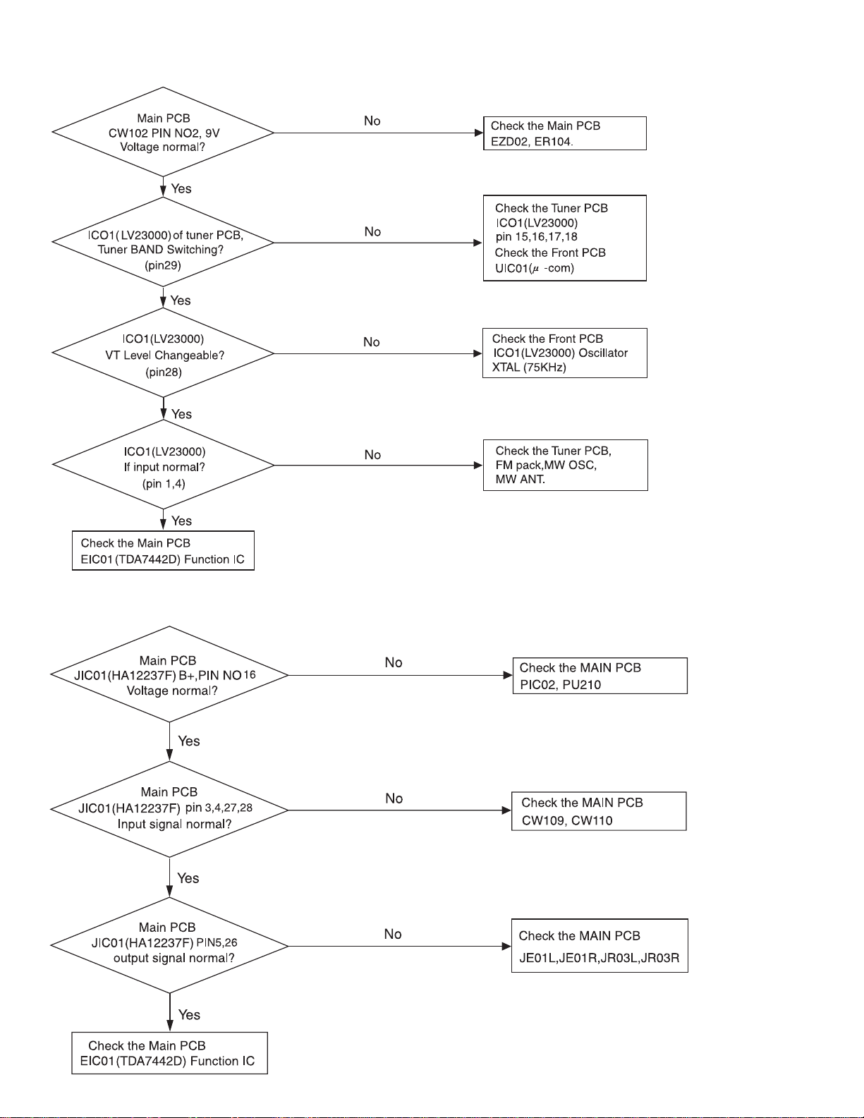
Block diagram
MA-GA77
SW101
STAND-BY
REMOCON
VFD
SW102-106
UCW03
UCW02
UIC1
MICOM
UIC03
UIC04
OP/CL
SW107
SW201-212
SW301-313
UCW05
TAPE P
A-DECK
TAPE DECK
B-DECK
TAPE P/R
H/P
TUNER
CON 01
CW01B
AUX IN
CW103
CW108
UCW01
CW101
HIC01
UCW04
CD
CW106CW105
L/R
DSP
JIC01
TAPE IC
TAPE P
EIC01
SOURCE
SELECTOR
AIC01
AIC02
AIC03
TAPE R
& E.VOL
TUNERAUX
EIC02
AUDIO
AUDIO
CD
TAPE P
TAPE R
CW105 CW104 CW109 CW110CW106
Power
amp.
WIC01
IC601
IC602
IC201
MP3 Decoder
DRAM
IC101 RF AMP. &
IC401 Motor-D
IC301
4ch Motor-D
SS Processor
IC402 Motor-D
ACW2 ACW1
FIC02
amp.
FIC01
Power
TO SPEAKER TO WOOFER
2-1
Page 48

MX-GA77
Standard schematic diagrams
Main section
5
To UCW01
Sheet 2/5
4
To CON01
Sheet 5/5
KTC8050
KTC8050
3
To CW106
Sheet 4/5
NI
KTC8050
2
NI
1
2-2
SHEET
NUMBER
1/5
2/5
3/5
4/5
5/5
KTC8050
CIRCUIT DESCRIPTION
Main
FL display & System control
Amp.
CD
Tuner
MX-GA77 JUS MAIN
TUNER signalMAIN signal
CD signal
ABCD
Page 49

To ACW1
Sheet 3/5
MA-GA77
To ACW2 Sheet 3/5
nal
TAPE P.B. signal
TAPE REC. signal
E F G
Parts are safety assurance parts.
When replacing those parts, make
sure to use the specified parts.
SHEET 1/5
2-3
Page 50

MX-GA77
FL display & System control section
5
To CW101
Sheet 1/5
4
UCW03
3
2
UCW05
1
2-4
MX-GA77 fornt
ABCD
Page 51

To CW105
Sheet 4/5
MA-GA77
UCW04
E F G
UCW02
SHEET 2/5
2-5
Page 52

MX-GA77
5
To CW106
Sheet 1/5
4
Amp. section
To CW105
Sheet 1/5
3
2
1
2-6
MX-GA77 JUS amp.
ABCD
Page 53

MA-GA77
MAIN signal
E F G
Parts are safety assurance parts.
When replacing those parts, make
sure to use the specified parts.
SHEET 3/5
2-7
Page 54

MX-GA77
o
c
5
4
CD section
3
2
1
2-8
To CW2
Sensor board
T
Swit
ABCD
Page 55

MA-GA77
To CW104
SHEET 1/5
To CW3
Switch board
To UCW04
SHEET 2/5
E F G
CD signal
SHEET 4/5
2-9
Page 56

MX-GA77
5
4
Tuner section
3
2
To CW103
SHEET 1/5
1
2-10
ABCD
Page 57

MA-GA77
FM/ TUNER signal
AM signal
E F G
SHEET 5/5
2-11
Page 58

MX-GA77
M
Printed circuit boards
Main board
5
4
3
2
1
2-12
ABCD
Page 59

Main board
MA-GA77
E F G
2-13
Page 60

MX-GA77
Front board
5
4
CD switch boa
Front board
3
2
1
2-14
ABCD
Page 61

board
oard
MA-GA77
E F G
2-15
Page 62

MX-GA77
Amp. board
5
4
3
2
1
2-16
ABCD
Page 63

MA-GA77
E F G
2-17
Page 64

MX-GA77
CD servo board
5
4
3
2
1
2-18
ABCD
Page 65

Power supply board
MA-GA77
Fuse boardTrans. board
E F G
2-19
Page 66

MX-GA77
VICTOR COMPANY OF JAPAN, LIMITED
AV & MULTMEDIA COMPANY AUDIO/VIDEO SYSTEM CATEGORY 10-1,1 chome,Ohwatari-machi,maebashi-city,371-8543,Japan
No.22001SCH
Printed in Japan
200305
Page 67

PARTS LIST
[ MX-GA77 ]
* All printed circuit boards and its assemblies are not available as service parts.
Area suffix
J ----------------------------- U.S.A.
C -------------------------- Canada
MX-GA77
- Contents -
Exploded view of general assembly and parts list (Block No.M1)
Exploded view of general assembly and parts list (Block No.M2)
CD changer mechanism assembly and parts list (Block No.MA)
Cassette mechanism assembly and parts list (Block No.MP)
Electrical parts list (Block No.01~04)
Packing materials and accessories parts list (Block No.M3,M5)
3- 2
3- 6
3- 7
3- 9
3-11
3-22
3-1
Page 68

MX-GA77
Exploded view of general assembly and parts list
Block No.
M
M
1
M
5
B
31
C
36
Main board
C
J
34
C
CD changer mechanism
4
9
28
4
11
16
23
CD switch
board
22
J
Phone jack
board
24-1
24-2
8
24-3
A
U
X
FM
/A
M
VFD
53
19
3
21
41
30
12
28
26
27
39
5
B x2
F x2
C
D
T
A
P
E
20
17
54
37 x2
2
A
6
1
13
44
15
2
14
D
13
7
3
1
44
38 x2
40
G x2
Cassette mechanism
3-2
ABCD
Page 69

Main board
C
J
MX-GA77
C
32
C
32
46
Phone jack
board
VFD
53
12
28
17
34
25-1
25-2
25-3
29
Front board
Fuse board
42
Amp. board
RFS5
RFS6
RFS7
RFS8
D
H
C
C
D
57
47
Tuner board
b
G
b
Trans. board
RFS2
L6
56
43
33
45
C
L7
L8
L1
D
D
E
a
54
C
Cassette mechanism
a
D
D E F G
D
3-3
Page 70

MX-GA77
Parts list (General assembly)
Item
A
A AH64-01106G
B 6002-000126
C 6003-000276
D 6003-000275
E AH60-10107A
F 6003-000277
G 6002-000398
H 6003-001230
J 6003-000283
1 AH64-02252B
2 AH64-02253B
3 AH64-02254B
4 AH64-02255B
5 AH64-02256D
6 AH64-02257A
7 AH64-02258A
8 AH640-2259B
9 AH64-02260B
L1 AH68-01253A
L6 AH68-50252B
L7 AH68-00331C
L8 AH68-00331D
11 AH64-02262B
12 AH64-02263B
13 AH64-02264B
14 AH64-02265B
15 AH64-02266B
16 AH64-02267B
17 AH64-02268B
19 AH64-02270B
20 AH64-02271B
21 AH64-02272B
22 AH67-00200B
23 AH67-00201A
24-1
24-2
24-3
25-1
25-2
25-3
26 AH67-00204B
27 AH67-00205B
28 AH67-00208A
29 AH61-01258A
30 AH63-00507A
31 AH61-01261A
Parts number Parts name Area
AH64-02252D
AH68-01253B
AH67-00202B
AH67-00202C
AH67-00202D
AH67-00203B
AH67-00203C
AH67-00203D
Q'ty
SCREW
SCREW
SCREW
SCREW
SCREW
SCREW
SCREW
SCREW
SCREW
FRONT CABINET
FRONT CABINET
CASSETTE DOOR A
CASSETTE DOOR B
CD DOOR
WINDOW VFD
WINDOW DOOR A
WINDOW DOOR B
KNOB DISC
KNOB POWER
RATING LABEL
RATING LABEL
FUSE LABEL
FCC LABEL
HHS LABEL
KNOB REC
KNOB REPEAT
KNOB SOUND
KNOB VOLUME
DECO RING
KNOB TURBO 1
KNOB TAPE
KNOB FUNCTION L 1
KNOB FUNCTION R
KNOB DECK
LENS DISC
LENS POWER
LENS-EQ L1
LENS-EQ L2
LENS-EQ L3
LENS-EQ R1
LENS-EQ R2
LENS-EQ R3
LENS INNER L
LENS INNER R
LENS MILKY
VFD HOLDER
SHEET MIRROR 1
PCB BRAKET
40
24
Description
4
M3X10 SILVER
3
FH M3X10 BLK
BH M3X10 YEL
BH M3X10 BLACK
4
M4X6 YEL
4
BH M3X12 YEL
3
BH M3X6 YEL
4
BH M3X14 YEL
BH M3X8 YEL
3
1
1
1
1
1
1
1
1
1
1
1
1
1
1
1
1
1
2
1
1
1
1
1
1
1
1
ROCK
1
POP
1
CLASSIC
1
DANCE
1
HALL
1
STADIUM
1
1
2
1
1
Block No. M1MM
J
C
J
C
J
3-4
Page 71

MX-GA77
Parts list (General assembly)
Item
A
32 AH61-01262A
33 AH64-02273D
34 AH62-00042A
36 AH61-40014A
37 AH95-50001A
38 AH61-80030A
39 AH61-00552A
40 AH61-00553A
41 AH64-00462C
42 AH64-30416E
43 AH64-30390K
44 AH69-20031A
45 AH63-00250B
46 AH62-00080A
47 AH26-00228A
53 AH07-00098A
54 ------------------56 AH39-00258J
57 AH40-00051A
Parts number Parts name Area
H SINK BRAKET
REAR CABINET
HEAT SINK
SUPPORT RIVET
LATCH ASSY
DAMPER ASSY
DOOR SPRING A
DOOR SPRING B
BADGE JVC
BOTTOM CABINET
TOP CABINET
CUSHION FOOT
HEAT SINK COVER
HEAT SINK
TRANS POWER
VF DISPLAY
CASSETTE MECHA
POWER CORD
TUNER PACK
Q'ty
2
1
1
4959
1
2
2
1
1
1
1
1
2
1
1
MAIN
1
120V 40.5/40/4
1
1
CWM43FF09
1
1
KST-MJ011MS0-60
Block No. M1MM
Description
3-5
Page 72

MX-GA77
Exploded view of general assembly and parts list
Block No.
SPEAKER BOX
1
M
M
2
M
2
Parts list (General assembly)
A
Item
1 AH81-00959E
2 AH81-01121A
3 AH81-00959M
4 AH81-00959Z
5 AH91-00959X
Parts number Parts name Area
AH81-00959F
4
SIDE PANEL
SIDE PANEL
SCREW
SPEAKER
SCREW
SHEET
3
5
Block No. M2MM
Q'ty
1
RIGHT
1
LEFT
5
4.0X40MM BK
1
130MM 6OHM 120W
4
3.5MMX16MM BK
1
EVA
Description
3-6
Page 73

CD changer mechanism assembly and parts list
Block No.
8
2
M
MX-GA77
A
M
M
Tray stopper
7
3
6
5
4
19
21
1
27
15
Base main
16
12
13
10
11
17
20
18
CD sub board
9
26
14
24
22
23
25
3-7
Page 74

MX-GA77
Parts list (CD changer mechanism)
Item
A
1 AH66-80022A
2 AH66-60034A
3 AH66-20186A
4 AH66-20187A
5 AH66-20188A
6 AH66-20189A
7 AH66-20190A
8 AH66-20191A
9 AH66-20192A
10 AH31-12001A
11 AH66-20193A
12 AH66-90056A
13 AH66-90055A
14 AH32-10001F
15 AH61-20428A-1
16 3302-000159
17 AH66-90053A
18 AH63-00068B
19 3404-000101
20 AH31-10021A
21 AH66-10008A
22 AH73-10031A
23 AH91-60150C
24 AH66-30098A
25 AH30-00007A
26 AH73-10034A
27 AH61-00255A
Parts number Parts name Area
SLIDE CAM
BELT LOAD
GEAR PULLEY
GEAR-LOAD
GEAR-CAM
GEAR-TRAY
GEAR-CONVERTOR
GEAR-SYNCRO
GEAR-WORM
LOADING MOTOR
GEAR-ROULETTE
TRAY-ROULETTE
TRAY DISC
SENSOR
BASE MAIN
MAGNET-FERRITE
TABTE-CHUCK UNI
SHEET CHUCK
SWICH MICRO
DC MORTOR
PULLEY-MOTOR
RUBBER-CD
SP MOTOR ASS'Y
LEVER-LIFTER
CD PICKUP
RUBBER-CD(G)
BRKT CHUCK
Q'ty
1
ABS HF-380 NTR
1
CR
1
POM (M90-44)WHT
1
POM (M90-44)BLK
1
POM(M90-44)WHT
1
POM(M90-44)BLK
1
POM (M90-44) WH
1
ABS HF-380 NTR
1
POM (M90-44)WHT
1
FF-030PN-09120
1
POM(M90-44)BLK
1
ABS XR-401 BLK
1
ABS XR-401 BLK
1
KPI-L06
1
CMS-300,BLK
1
3500-3800G,6P
1
BLK,CMS300
1
HYMERON,BLK,0.4
1
MLS-24
1
RF-500TB,9VDC
1
BLK,CMS-CR3
1
RCD380,RED
1
CMS-D73SG6U
1
ABS(BLK),CMS-30
1
SOH-AD3
1
CMS-300D,GREEN
1
SECL 0.8T
Block No. MAMM
Description
3-8
Page 75

Cassette mechanism assembly and parts list
y
)
14
7
Block No.
M
MX-GA77
M
P
M
CWM43FF09
7
12
13
10
11
4
8
3
16
1
5
8
6
2
15
11
16
3
1
15
Note: Parts listed on the Parts List below can be supplied.
However, parts that are not listed below cannot be supplied
individually but only by purchasing the whole Cassette
Mechanism Assembly Unit. (When ordering, use the Parts No.
AH59-01132A for Cassette Mechanism Assembl
Unit.
3-9
Page 76

MX-GA77
Parts list (Cassette mechanism)
Item
A
1 AH81-00472A
2 AH81-00472B
3 AH81-00472N
4 AH81-00902E
5 AH81-00902G
6 AH81-00902J
7 AH81-00902K
8 AH81-00902L
10 AH81-00902Q
11 AH81-00472V
12 AH81-00902W
13 AH81-00902X
14 AH81-00902Y
15 AH81-00903A
16 AH81-00473H
Parts number Parts name Area
PB HEAD
E HEAD
PINCH ROLLER
MOTOR ASSY
BF BELT
AF BELT
FR BLET
SOLENOID ASSY
HOUSING
CLUTCH ASSY
MODE SWITCH
PHOTO INTERRUPT
LEAF SWITCH
SPRING62
SPRING 04
Q'ty
2
1
2
1
1
1
2
2
1
2
1
1
1
2
2
Block No. MPMM
Description
TC881CB067P
TC2131
22-027-41054
50-093-4879
02-083-4236
02-083-4234
02-083-4188
50-093-4748
6216016100
50-093-4503
MPU11570MLB0
RP1352
LSA11355
01-082-4686
01-080-4635
3-10
Page 77

MX-GA77
ea
ea
Electrical parts list (Main board)
Item
A
AC101 2301-000216 M.CAPACITOR 220NF 5% 50V
AC102 2301-000474 M.CAPACITOR 8.2NF 10% 50V
AC103 2301-000390 M.CAPACITOR 15NF 10% 50V
AC104 2301-000216 M.CAPACITOR 220NF 5% 50V
AC105 2301-000419 M.CAPACITOR 27NF 10% 50V
AC106 2301-000449 M.CAPACITOR 47NF 10% 50V
AC107 2301-000375 M.CAPACITOR 100NF 10% 50V
AC108 2301-000375 M.CAPACITOR 100NF 10% 50V
AC109 2301-000419 M.CAPACITOR 27NF 10% 50V
AC110 2301-000216 M.CAPACITOR 220NF 5% 50V
AC111 2201-000144 C.CAPACITOR 0.1NF 5% 50V
AD101 0401-000101 DIODE 1N4148 100V
AD102 0401-000101 DIODE 1N4148 100V
AD103 0401-000101 DIODE 1N4148 100V
AD104 0401-000101 DIODE 1N4148 100V
AE101 2401-001893 E.CAPACITOR 100UF 20% 16V
AE102 2401-001893 E.CAPACITOR 100UF 20% 16V
AE103 2401-001954 E.CAPACITOR 4.7UF 20% 50V
AE104 2401-001954 E.CAPACITOR 4.7UF 20% 50V
AE105 2401-001893 E.CAPACITOR 100UF 20% 16V
AE106 2401-001893 E.CAPACITOR 100UF 20% 16V
AE107 2401-001893 E.CAPACITOR 100UF 20% 16V
AE108 2401-001893 E.CAPACITOR 100UF 20% 16V
AE109 2401-001511 E.CAPACITOR 47UF 20% 16V
AE110 2401-001511 E.CAPACITOR 47UF 20% 16V
AE111 2401-001912 E.CAPACITOR 1UF 20% 50V
AE112 2401-001893 E.CAPACITOR 100UF 20% 16V
AE113 2401-001893 E.CAPACITOR 100UF 20% 16V
AE114 2401-001511 E.CAPACITOR 47UF 20% 16V
AE115 2401-001511 E.CAPACITOR 47UF 20% 16V
AE116 2401-002180 E.CAPACITOR 2.2UF 20% 50V
AE117 2401-003621 E.CAPACITOR 47UF 20% 63V
AIC01 1201-000191 IC BA4558 8P DIP
AIC02 1201-000191 IC BA4558 8P DIP
AIC03 1201-000191 IC BA4558 8P DIP
AIC04 1201-000191 IC BA4558 8P DIP
AQ101 0501-002409 TRANSISTOR KTC945Y 600MW
AQ102 0501-002409 TRANSISTOR KTC945Y 600MW
AQ103 0501-002409 TRANSISTOR KTC945Y 600MW
AR01L 2001-000522 CARBON RESISTOR 22K 5% 1/8W
AR01R 2001-000522 CARBON RESISTOR 22K 5% 1/8W
AR02L 2001-000786 CARBON RESISTOR 47K 5% 1/8W
AR02R 2001-000786 CARBON RESISTOR 47K 5% 1/8W
AR03L 2001-000508 CARBON RESISTOR 220K 5% 1/8W
AR03R 2001-000508 CARBON RESISTOR 220K 5% 1/8W
AR101 2001-000563 CARBON RESISTOR 27K 5% 1/8W
AR102 2001-000563 CARBON RESISTOR 27K 5% 1/8W
AR103 2001-000548 CARBON RESISTOR 270K 5% 1/8W
AR104 2001-000273 CARBON RESISTOR 100K 5% 1/8W
AR105 2001-000273 CARBON RESISTOR 100K 5% 1/8W
AR106 2001-000522 CARBON RESISTOR 22K 5% 1/8W
AR107 2001-000522 CARBON RESISTOR 22K 5% 1/8W
AR108 2001-000281 CARBON RESISTOR 100 5% 1/8W
AR109 2001-000281 CARBON RESISTOR 100 5% 1/8W
AR110 2001-000273 CARBON RESISTOR 100K 5% 1/8W
AR111 2001-000273 CARBON RESISTOR 100K 5% 1/8W
AR112 2001-000273 CARBON RESISTOR 100K 5% 1/8W
AR113 2001-000281 CARBON RESISTOR 100 5% 1/8W
AR114 2001-000864 CARBON RESISTOR 56K 5% 1/8W
AR115 2001-000258 CARBON RESISTOR 1.8K 5% 1/8W
AR116 2001-000977 CARBON RESISTOR 8.2K 5% 1/8W
AR117 2001-000281 CARBON RESISTOR 100 5% 1/8W
AR118 2001-000508 CARBON RESISTOR 220K 5% 1/8W
Parts number Parts name Ar
Block No. 01
Remarks
Item
A
AR119 2001-000281 CARBON RESISTOR 100 5% 1/8W
AR120 2001-000281 CARBON RESISTOR 100 5% 1/8W
AR121 2001-000802 CARBON RESISTOR 5.6K 5% 1/8W
AR122 2001-000522 CARBON RESISTOR 22K 5% 1/8W
AR123 2001-000258 CARBON RESISTOR 1.8K 5% 1/8W
AR124 2001-000331 CARBON RESISTOR 12K 5% 1/8W
AR125 2001-000522 CARBON RESISTOR 22K 5% 1/8W
AR126 2001-000522 CARBON RESISTOR 22K 5% 1/8W
AR127 2001-000977 CARBON RESISTOR 8.2K 5% 1/8W
AR128 2001-000660 CARBON RESISTOR 33K 5% 1/8W
AR129 2001-000281 CARBON RESISTOR 100 5% 1/8W
AR130 2001-000281 CARBON RESISTOR 100 5% 1/8W
AR131 2001-000281 CARBON RESISTOR 100 5% 1/8W
AR132 2001-000508 CARBON RESISTOR 220K 5% 1/8W
AR133 2001-000449 CARBON RESISTOR 2.2K 5% 1/8W
AR134 2001-001000 CARBON RESISTOR 82K 5% 1/8W
AR135 2001-000273 CARBON RESISTOR 100K 5% 1/8W
AR136 2001-000273 CARBON RESISTOR 100K 5% 1/8W
AR137 2001-000786 CARBON RESISTOR 47K 5% 1/8W
AR138 2001-000786 CARBON RESISTOR 47K 5% 1/8W
AR139 2001-000554 CARBON RESISTOR 270 5% 1/8W
AR140 2001-000802 CARBON RESISTOR 5.6K 5% 1/8W
AR141 2001-000281 CARBON RESISTOR 100 5% 1/8W
AR301 2001-000281 CARBON RESISTOR 100 5% 1/8W
AR302 2001-000290 CARBON RESISTOR 10K 5% 1/8W
BC01L 2301-000361 M.CAPACITOR 1.2NF 10% 50V
BC01R 2301-000361 M.CAPACITOR 1.2NF 10% 50V
BD101 0401-000101 DIODE 1N4148 100V
BL01L AH26-10002W TRANS TRAP-COIL BIAS-TRAP105K
BL01R AH26-10002W TRANS TRAP-COIL BIAS-TRAP105K
BQ02L 0501-000010 TRANSISTOR KTC1008 800MW
BQ02R 0501-000010 TRANSISTOR KTC1008 800MW
BQ03L 0501-000010 TRANSISTOR KTC1008 800MW
BQ03R 0501-000010 TRANSISTOR KTC1008 800MW
BQ101 0504-001128 DIGI TRANSISTOR KRA103M 400MW
BR01L 2001-000281 CARBON RESISTOR 100 5% 1/8W
BR01R 2001-000281 CARBON RESISTOR 100 5% 1/8W
BR02L 2001-000890 CARBON RESISTOR 6.8K 5% 1/8W
BR02R 2001-000890 CARBON RESISTOR 6.8K 5% 1/8W
BR03L 2001-000890 CARBON RESISTOR 6.8K 5% 1/8W
BR03R 2001-000890 CARBON RESISTOR 6.8K 5% 1/8W
BR101 2001-000522 CARBON RESISTOR 22K 5% 1/8W
CE101 2401-000240 E.CAPACITOR 100UF 20% 10V
CE102 2401-001893 E.CAPACITOR 100UF 20% 16V
CE103 2401-001887 E.CAPACITOR 100NF 20% 50V
CQ01L 0504-001125 DIGI TRANSISTOR KRC110M 400MW
CQ01R 0504-001125 DIGI TRANSISTOR KRC110M 400MW
CQ101 0504-001128 DIGI TRANSISTOR KRA103M 400MW
CR01L 2001-000864 CARBON RESISTOR 56K 5% 1/8W
CR01R 2001-000864 CARBON RESISTOR 56K 5% 1/8W
CR02L 2001-000411 CARBON RESISTOR 18K 5% 1/8W
CR02R 2001-000411 CARBON RESISTOR 18K 5% 1/8W
CW101 3708-001577 CONNECTOR 30P 1.25MM
CW103 3708-000412 CONNECTOR 12P 1.25MM
CW104 3711-001137 CONNECTOR 8P 1R 2MM
CW105 3708-001167 CONNECTOR 14P 1.25MM
CW106 AH39-00295A W/HARNESS UNIT MAX-L85 9P
CW107 AH39-00338A LEAD CONNECTOR
CW108 3711-001062 CONNECTOR 6P 1R 2MM
CW109 3711-003111 CONNECTOR 6P 1R 2.5MM
CW110 3711-003107 CONNECTOR 3P 1R 2.5MM
CW111 3711-000907 CONNECTOR 3P 1R 2MM
EC07L 2301-000454 M.CAPACITOR 5.6NF 10% 50V
Parts number Parts name Ar
Remarks
3-11
Page 78

MX-GA77
ea
ea
Electrical parts list (Main board)
Item
A
EC07R 2301-000454 M.CAPACITOR 5.6NF 10% 50V
EC08L 2301-000216 M.CAPACITOR 220NF 5% 50V
EC08R 2301-000216 M.CAPACITOR 220NF 5% 50V
EC09L 2301-000216 M.CAPACITOR 220NF 5% 50V
EC09R 2301-000216 M.CAPACITOR 220NF 5% 50V
EC10L 2201-000368 C.CAPACITOR 0.22NF 10% 50V
EC10R 2201-000368 C.CAPACITOR 0.22NF 10% 50V
EC101 2301-000361 M.CAPACITOR 1.2NF 10% 50V
EC102 2301-000375 M.CAPACITOR 100NF 10% 50V
EC103 2201-000783 C.CAPACITOR 100NF +80-20% 50V
EC11L 2201-000368 C.CAPACITOR 0.22NF 10% 50V
EC11R 2201-000368 C.CAPACITOR 0.22NF 10% 50V
ED102 0401-000101 DIODE 1N4148 100V
EE01L 2401-001912 E.CAPACITOR 1UF 20% 50V
EE01R 2401-001912 E.CAPACITOR 1UF 20% 50V
EE02L 2401-001912 E.CAPACITOR 1UF 20% 50V
EE02R 2401-001912 E.CAPACITOR 1UF 20% 50V
EE03L 2401-001917 E.CAPACITOR 1UF 20% 50V
EE03R 2401-001912 E.CAPACITOR 1UF 20% 50V
EE04L 2401-001912 E.CAPACITOR 1UF 20% 50V
EE04R 2401-001912 E.CAPACITOR 1UF 20% 50V
EE05L 2401-001912 E.CAPACITOR 1UF 20% 50V
EE05R 2401-001912 E.CAPACITOR 1UF 20% 50V
EE06L 2401-001919 E.CAPACITOR 2.2UF 20% 50V
EE06R 2401-001919 E.CAPACITOR 2.2UF 20% 50V
EE07L 2401-001917 E.CAPACITOR 1UF 20% 50V
EE07R 2401-001912 E.CAPACITOR 1UF 20% 50V
EE08L 2401-001917 E.CAPACITOR 1UF 20% 50V
EE08R 2401-001917 E.CAPACITOR 1UF 20% 50V
EE101 2401-000438 E.CAPACITOR 10UF 20% 25V
EE102 2401-001511 E.CAPACITOR 47UF 20% 16V
EE103 2401-000778 E CAPACITOR 220UF 20% 10V
EE107 2401-001954 E.CAPACITOR 4.7UF 20% 50V
EE108 2401-001954 E.CAPACITOR 4.7UF 20% 50V
EE109 2401-000759 E.CAPACITOR 220NF 20% 50V
EIC01 1204-001776 IC TDA7442D 28P
EIC02 1201-000191 IC BA4558 8P DIP
EJ101 3722-000379 JACK-PIN 4P/2C 3.5MM
EQ101 0501-002409 TRANSISTOR KTC945Y 600MW
ER01L 2001-000786 CARBON RESISTOR 47K 5% 1/8W
ER01R 2001-000786 CARBON RESISTOR 47K 5% 1/8W
ER02L 2001-000591 CARBON RESISTOR 3.3K 5% 1/8W
ER02R 2001-000591 CARBON RESISTOR 3.3K 5% 1/8W
ER03L 2001-000411 CARBON RESISTOR 18K 5% 1/8W
ER03R 2001-000411 CARBON RESISTOR 18K 5% 1/8W
ER04L 2001-000411 CARBON RESISTOR 18K 5% 1/8W
ER04R 2001-000411 CARBON RESISTOR 18K 5% 1/8W
ER05L 2001-000515 CARBON RESISTOR 220 5% 1/8W
ER05R 2001-000515 CARBON RESISTOR 220 5% 1/8W
ER06L 2001-000786 CARBON RESISTOR 47K 5% 1/8W
ER06R 2001-000786 CARBON RESISTOR 47K 5% 1/8W
ER07L 2001-000591 CARBON RESISTOR 3.3K 5% 1/8W
ER07R 2001-000591 CARBON RESISTOR 3.3K 5% 1/8W
ER08L 2001-000786 CARBON RESISTOR 47K 5% 1/8W
ER08R 2001-000786 CARBON RESISTOR 47K 5% 1/8W
ER09L 2001-000290 CARBON RESISTOR 10K 5% 1/8W
ER09R 2001-000290 CARBON RESISTOR 10K 5% 1/8W
ER10L 2001-000273 CARBON RESISTOR 100K 5% 1/8W
ER10R 2001-000273 CARBON RESISTOR 100K 5% 1/8W
ER101 2001-000515 CARBON RESISTOR 220 5% 1/8W
ER102 2001-000515 CARBON RESISTOR 220 5% 1/8W
ER103 2001-000023 CARBON RESISTOR 47 5% 1/4W
ER104 2001-000023 CARBON RESISTOR 47 5% 1/4W
Parts number Parts name Ar
Block No. 01
Remarks
Item
A
ER109 2001-000290 CARBON RESISTOR 10K 5% 1/8W
ER110 2001-000773 CARBON RESISTOR 470K 5% 1/8W
ER111 2001-000515 CARBON RESISTOR 220 5% 1/8W
ER112 2001-000645 CARBON RESISTOR 330K 5% 1/8W
ER113 2001-000989 CARBON RESISTOR 820K 5% 1/8W
ER13L 2001-000864 CARBON RESISTOR 56K 5% 1/8W
ER13R 2001-000864 CARBON RESISTOR 56K 5% 1/8W
ER14L 2001-000008 CARBON RESISTOR 15K 5% 1/8W
ER14R 2001-000008 CARBON RESISTOR 15K 5% 1/8W
ER15L 2001-000290 CARBON RESISTOR 10K 5% 1/8W
ER15R 2001-000290 CARBON RESISTOR 10K 5% 1/8W
ER16L 2001-000003 CARBON RESISTOR 330 5% 1/8W
ER16R 2001-000003 CARBON RESISTOR 330 5% 1/8W
ER17L 2001-000003 CARBON RESISTOR 330 5% 1/8W
ER17R 2001-000003 CARBON RESISTOR 330 5% 1/8W
EZD01 0403-000372 ZENER DIODE UZ9.1BM 9.1V
EZD02 0403-000372 ZENER DIODE UZ9.1BM 9.1V
HC01L 2201-000642 C.CAPACITOR 0.68NF 10% 50V
HC01R 2201-000642 C.CAPACITOR 0.68NF 10% 50V
HE01L 2401-001912 E.CAPACITOR 1UF 20% 50V
HE01R 2401-001912 E.CAPACITOR 1UF 20% 50V
HE02L 2401-001164 E.CAPACITOR 33UF 20% 16V
HE02R 2401-001164 E.CAPACITOR 33UF 20% 16V
HE101 2401-000830 E.CAPACITOR 220UF 20% 25V
HE102 2401-000830 E.CAPACITOR 220UF 20% 25V
HE103 2401-001511 E.CAPACITOR 47UF 20% 16V
HIC01 1201-000461 IC BA4558 8P SOIC
HQ01L 0501-002375 TRANSISTOR KTC8050 625MW
HQ01R 0501-002375 TRANSISTOR KTC8050 625MW
HR01L 2001-000449 CARBON RESISTOR 2.2K 5% 1/8W
HR01R 2001-000449 CARBON RESISTOR 2.2K 5% 1/8W
HR02L 2001-000449 CARBON RESISTOR 2.2K 5% 1/8W
HR02R 2001-000449 CARBON RESISTOR 2.2K 5% 1/8W
HR03L 2001-000734 CARBON RESISTOR 4.7K 5% 1/8W
HR03R 2001-000734 CARBON RESISTOR 4.7K 5% 1/8W
HR04L 2001-000290 CARBON RESISTOR 10K 5% 1/8W
HR04R 2001-000290 CARBON RESISTOR 10K 5% 1/8W
HR05L 2001-000019 CARBON RESISTOR 10 5% 1/2W
HR05R 2001-000019 CARBON RESISTOR 10 5% 1/2W
HR06L 2001-000591 CARBON RESISTOR 3.3K 5% 1/8W
HR06R 2001-000591 CARBON RESISTOR 3.3K 5% 1/8W
HR101 2001-000028 CARBON RESISTOR 100 5% 1/2W
HR102 2001-000019 CARBON RESISTOR 10 5% 1/2W
HR103 2001-000890 CARBON RESISTOR 6.8K 5% 1/8W
HR104 2001-000290 CARBON RESISTOR 10K 5% 1/8W
JC00L 2201-000368 C.CAPACITOR 0.22NF 10% 50V
JC00R 2201-000368 C.CAPACITOR 0.22NF 10% 50V
JC01L 2201-000642 C.CAPACITOR 0.68NF 10% 50V
JC01R 2201-000642 C.CAPACITOR 0.68NF 10% 50V
JC02L 2301-000379 M.CAPACITOR 10NF 10% 50V
JC02R 2301-000379 M.CAPACITOR 10NF 10% 50V
JC03L 2301-000375 M.CAPACITOR 100NF 10% 50V
JC03R 2301-000375 M.CAPACITOR 100NF 10% 50V
JC04L 2301-000375 M.CAPACITOR 100NF 10% 50V
JC04R 2301-000375 M.CAPACITOR 100NF 10% 50V
JC05L 2301-000430 M.CAPACITOR 33NF 10% 50V
JC05R 2301-000430 M.CAPACITOR 33NF 10% 50V
JC06L 2201-000674 C.CAPACITOR 0.82NF 10% 50V
JC06R 2201-000674 C.CAPACITOR 0.82NF 10% 50V
JC101 2201-000557 C.CAPACITOR 0.47NF 10% 50V
JC102 2301-000407 M.CAPACITOR 2.7NF 10% 50V
JC103 2301-000404 M.CAPACITOR 2.2NF 10% 50V
JC104 2301-000404 M.CAPACITOR 2.2NF 10% 50V
Parts number Parts name Ar
Remarks
3-12
Page 79

MX-GA77
ea
Item
Parts num
ber
Parts nam
e
Area
Rem
arks
A
Electrical parts list (Main board)
Item
A
JC105 2202-000781 C.CAPACITOR 100PF 10% 50V
JC106 2202-000781 C.CAPACITOR 100PF 10% 50V
JC107 2202-000781 C.CAPACITOR 100PF 10% 50V
JC108 2202-000781 C.CAPACITOR 100PF 10% 50V
JD101 0401-000101 DIODE 1N4148 100V
JE01L 2401-002180 E.CAPACITOR 2.2UF 20% 50V
JE01R 2401-002180 E.CAPACITOR 2.2UF 20% 50V
JE02L 2401-002180 E.CAPACITOR 2.2UF 20% 50V
JE02R 2401-002180 E.CAPACITOR 2.2UF 20% 50V
JE101 2401-001511 E.CAPACITOR 47UF 20% 16V
JE102 2401-001164 E.CAPACITOR 33UF 20% 16V
JE103 2401-001912 E.CAPACITOR 1UF 20% 50V
JE104 2401-001164 E.CAPACITOR 33UF 20% 16V
JE105 2401-000438 E.CAPACITOR 10UF 20% 25V
JIC01 1201-001899 IC HA12237F 40P
JL101 2701-000298 INDUCTOR 470UH 10%
JL102 AH26-10003C TRANS TRAP-COIL PCHNS-5371EQJ
JQ01L 0501-002375 TRANSISTOR KTC8050 625MW
JQ01R 0501-002375 TRANSISTOR
JQ101 0501-002176 TRANSISTOR KTD863 1W
JQ102 0501-000422 TRANSISTOR KTA1273
JQ103 0501-002409 TRANSISTOR KTC945B
JQ104 0504-001128 DIGI TRANSISTOR KRA103M 400MW
JR01L 2001-000977 CARBON RESISTOR 8.2K 5% 1/8W
JR01R 2001-000977 CARBON RESISTOR 8.2K 5% 1/8W
JR02L 2001-000241 CARBON RESISTOR 1.5K 5% 1/8W
JR02R 2001-000241 CARBON RESISTOR 1.5K 5% 1/8W
JR03L 2001-000449 CARBON RESISTOR 2.2K 5% 1/8W
JR03R 2001-000449 CARBON RESISTOR 2.2K 5% 1/8W
JR04L 2001-000734 CARBON RESISTOR 4.7K 5% 1/8W
JR04R 2001-000734 CARBON RESISTOR 4.7K 5% 1/8W
JR05L 2001-000802 CARBON RESISTOR 5.6K 5% 1/8W
JR05R 2001-000802 CARBON RESISTOR 5.6K 5% 1/8W
JR06L 2001-000449 CARBON RESISTOR 2.2K 5% 1/8W
JR06R 2001-000449 CARBON RESISTOR 2.2K 5% 1/8W
JR07L 2001-000302 CARBON RESISTOR 10 5% 1/8W
JR07R 2001-000302 CARBON RESISTOR 10 5% 1/8W
JR08L 2001-000008 CARBON RESISTOR 15K 5% 1/8W
JR08R 2001-000008 CARBON RESISTOR 15K 5% 1/8W
JR101 2001-000290 CARBON RESISTOR 10K 5% 1/8W
JR102 2001-000456 CARBON RESISTOR 2.2 5% 1/4W
JR103 2001-000023 CARBON RESISTOR 47 5% 1/4W
JR104 2001-000786 CARBON RESISTOR 47K 5% 1/8W
JR105 2001-000591 CARBON RESISTOR 3.3K 5% 1/8W
JR106 2001-000734 CARBON RESISTOR 4.7K 5% 1/8W
JR107 2001-000429 CARBON RESISTOR 1K 5% 1/8W
JR108 2001-000290 CARBON RESISTOR 10K 5% 1/8W
JR109 2001-000591 CARBON RESISTOR 3.3K 5% 1/8W
JR110 2001-000281 CARBON RESISTOR 100 5% 1/8W
JR112 2001-000435 CARBON RESISTOR 1M 5% 1/8W
JR113 2001-000522 CARBON RESISTOR 22K 5% 1/8W
JVR01 2103-000248 ROTA V RESISTOR 200K 30% 1/10W
JVR02 2103-000248 ROTA V RESISTOR 200K 30% 1/10W
PBD01 0402-000450 DIODE-BRIDGE
A
PBD02 0402-001258 DIODE-BRIDGE
A
PBD03 0402-001077 DIODE-BRIDGE
A
PCB AH41-00555A PCB MAIN MX-GA77
PC201 2201-000161 C.CAPACITOR
A
PC202 2201-000161 C.CAPACITOR
A
PC203 2201-000161 C.CAPACITOR
A
PD201 0402-000127 DIODE 1N4002 100V 1A
PD202 0402-000127 DIODE 1N4002 100V 1A
PD203 0402-000127 DIODE 1N4002 100V 1A
Parts number Parts name Ar
Block No. 01
KTC8050 625MW
GBU606 600V 6A
GBU606 600V 6A
KBP202G 200V 2A
10NF +80-20% 500V
10NF +80-20% 500V
10NF +80-20% 500V
Remarks
PD204 0402-000127 DIODE 1N4002 100V 1A
PD205 0401-000101 DIODE 1N4148 100V
PD206 0401-000101 DIODE 1N4148 100V
PD209 0402-000127 DIODE 1N4002 100V 1A
PD210 0402-000127 DIODE 1N4002 100V 1A
PE201 2401-001067 E.CAPACITOR
A
PE202 2401-001067 E.CAPACITOR
A
PE203 2401-003381 E.CAPACITOR
A
PE204 2401-003381 E.CAPACITOR
A
PE205 2401-003116 E.CAPACITOR
A
PE206 2401-000830 E.CAPACITOR 220UF 20% 25V
PE207 2401-001938 E.CAPACITOR 22UF 20% 25V
PE208 2401-000407 E.CAPACITOR 10UF 20% 16V
PE209 2401-001912 E.CAPACITOR 1UF 20% 50V
PE210 2401-001912 E.CAPACITOR 1UF 20% 50V
PE211 2401-001954 E.CAPACITOR 4.7UF 20% 50V
PE212 2401-000230 E.CAPACITOR 100UF 20% 100V
PE213 2401-000385 E.CAPACITOR 10UF 20% 100V
PE214 2401-000438 E.CAPACITOR 10UF 20% 25V
PF101 2008-000135 FUSIBLE RESISTORA1 5% 1/2W
PIC02 1203-001653 REGULATOR L4959
PL102 2701-000298 INDUCTOR 470UH 10%
PQ102 0504-000144 DIGI TRANSISTOR KSR2002 300MW
PQ103 0504-001123 DIGI TRANSISTOR KRC103M 400MW
PQ104 0501-000331 TRANSISTOR KSC1009-Y
PQ105 0501-000422 TRANSISTOR KTA1273
PQ106 0501-002408 TRANSISTOR MPS751
PR201 2001-000591 CARBON RESISTOR 3.3K 5% 1/8W
PR202 2001-000734 CARBON RESISTOR 4.7K 5% 1/8W
PR203 2001-000429 CARBON RESISTOR 1K 5% 1/8W
PR204 2001-000786 CARBON RESISTOR 47K 5% 1/8W
PR205 2001-000290 CARBON RESISTOR 10K 5% 1/8W
PR206 2003-000455 OMF RESISTOR 100 5% 2W
PR207 2001-000563 CARBON RESISTOR 27K 5% 1/8W
PR208 2001-000734 CARBON RESISTOR 4.7K 5% 1/8W
PR209 2001-000111 CARBON RESISTOR 150 5% 1/4W
PR210 2001-000055 CARBON RESISTOR 4.7K 5% 1/4W
PR211 2001-000038 CARBON RESISTOR 390 5% 1/4W
PR212 2001-000429 CARBON RESISTOR 1K 5% 1/8W
PR213 2001-000734 CARBON RESISTOR 4.7K 5% 1/8W
PR214 2001-000613 CARBON RESISTOR 3.9K 5% 1/8W
PR215 2001-000890 CARBON RESISTOR 6.8K 5% 1/8W
PR216 2003-000701 OMF RESISTOR 470 5% 2W
PR217 2001-001153 CARBON RESISTOR 47 5% 1/2W
PR218 2001-001153 CARBON RESISTOR 47 5% 1/2W
PR219 2001-000734 CARBON RESISTOR 4.7K 5% 1/8W
PR220 2001-000290 CARBON RESISTOR 10K 5% 1/8W
PR221 2001-000660 CARBON RESISTOR 33K 5% 1/8W
PR222 2001-000244 CARBON RESISTOR 1.5M 5% 1/8W
PZ101 0403-000354 ZENER DIODE UZ5.1B 5.1V
PZ102 0403-000564 ZENER DIODE TZP16A 16V
PZ103 0403-000564 ZENER DIODE TZP16A 16V
PZ104 0403-000393 ZENER DIODE UZP5.1B 5.1V
PZ105 0403-000379 ZENER DIODE UZP12B 12V
RFS9 3601-001295 FUSE
A
3300UF 20% 42V
3300UF 20% 42V
3300UF 20% 63V
3300UF 20% 63V
4700UF 20% 35V
125V 4A FAST
3-13
Page 80

MX-GA77
ea
ea
Electrical parts list (Front board)
Item
A
BUZZ1 3002-001134 BUZZER 85DB 12V
CW01B AH39-00247A LEAD CONNECTOR
FR101 2001-000734 CARBON RESISTOR 4.7K 5% 1/8W
FR102 2001-000734 CARBON RESISTOR 4.7K 5% 1/8W
FR103 2001-000734 CARBON RESISTOR 4.7K 5% 1/8W
FR104 2001-000734 CARBON RESISTOR 4.7K 5% 1/8W
FR105 2001-000734 CARBON RESISTOR 4.7K 5% 1/8W
FR106 2001-000734 CARBON RESISTOR 4.7K 5% 1/8W
FR107 2001-000734 CARBON RESISTOR 4.7K 5% 1/8W
FR108 2001-000734 CARBON RESISTOR 4.7K 5% 1/8W
FR109 2001-000734 CARBON RESISTOR 4.7K 5% 1/8W
FR110 2001-000734 CARBON RESISTOR 4.7K 5% 1/8W
FR111 2001-000734 CARBON RESISTOR 4.7K 5% 1/8W
FR112 2001-000734 CARBON RESISTOR 4.7K 5% 1/8W
FR113 2001-000734 CARBON RESISTOR 4.7K 5% 1/8W
FR114 2001-000734 CARBON RESISTOR 4.7K 5% 1/8W
FR115 2001-000734 CARBON RESISTOR 4.7K 5% 1/8W
FR116 2001-000734 CARBON RESISTOR 4.7K 5% 1/8W
FR117 2001-000734 CARBON RESISTOR 4.7K 5% 1/8W
FR118 2001-000786 CARBON RESISTOR 47K 5% 1/8W
FR119 2001-000786 CARBON RESISTOR 47K 5% 1/8W
FR120 2001-000786 CARBON RESISTOR 47K 5% 1/8W
FR121 2001-000786 CARBON RESISTOR 47K 5% 1/8W
FR122 2001-000786 CARBON RESISTOR 47K 5% 1/8W
FR123 2001-000786 CARBON RESISTOR 47K 5% 1/8W
FR124 2001-000786 CARBON RESISTOR 47K 5% 1/8W
FR125 2001-000786 CARBON RESISTOR 47K 5% 1/8W
FR126 2001-000786 CARBON RESISTOR 47K 5% 1/8W
FR127 2001-000786 CARBON RESISTOR 47K 5% 1/8W
FR128 2001-000786 CARBON RESISTOR 47K 5% 1/8W
FR129 2001-000786 CARBON RESISTOR 47K 5% 1/8W
FR130 2001-000786 CARBON RESISTOR 47K 5% 1/8W
FR131 2001-000786 CARBON RESISTOR 47K 5% 1/8W
FR132 2001-000786 CARBON RESISTOR 47K 5% 1/8W
FR133 2001-000786 CARBON RESISTOR 47K 5% 1/8W
FR134 2001-000786 CARBON RESISTOR 47K 5% 1/8W
FR135 2001-000786 CARBON RESISTOR 47K 5% 1/8W
FR136 2001-000786 CARBON RESISTOR 47K 5% 1/8W
FR140 2001-000995 CARBON RESISTOR 820 5% 1/8W
FR141 2001-000429 CARBON RESISTOR 1K 5% 1/8W
FR142 2001-000221 CARBON RESISTOR 1.2K 5% 1/8W
FR143 2001-000241 CARBON RESISTOR 1.5K 5% 1/8W
FR144 2001-000258 CARBON RESISTOR 1.8K 5% 1/8W
FR145 2001-000449 CARBON RESISTOR 2.2K 5% 1/8W
FR146 2001-000591 CARBON RESISTOR 3.3K 5% 1/8W
FR147 2001-000890 CARBON RESISTOR 6.8K 5% 1/8W
FR148 2001-000734 CARBON RESISTOR 4.7K 5% 1/8W
FR149 2001-000290 CARBON RESISTOR 10K 5% 1/8W
FR150 2001-000522 CARBON RESISTOR 22K 5% 1/8W
FR151 2001-000010 CARBON RESISTOR 68K 5% 1/8W
FR152 2001-000995 CARBON RESISTOR 820 5% 1/8W
FR153 2001-000429 CARBON RESISTOR 1K 5% 1/8W
FR154 2001-000221 CARBON RESISTOR 1.2K 5% 1/8W
FR155 2001-000241 CARBON RESISTOR 1.5K 5% 1/8W
FR156 2001-000258 CARBON RESISTOR 1.8K 5% 1/8W
FR157 2001-000449 CARBON RESISTOR 2.2K 5% 1/8W
FR158 2001-000591 CARBON RESISTOR 3.3K 5% 1/8W
FR159 2001-000734 CARBON RESISTOR 4.7K 5% 1/8W
FR160 2001-000890 CARBON RESISTOR 6.8K 5% 1/8W
FR161 2001-000290 CARBON RESISTOR 10K 5% 1/8W
FR162 2001-000522 CARBON RESISTOR 22K 5% 1/8W
FR201 2001-000034 CARBON RESISTOR 220 5% 1/4W
FR202 2001-000034 CARBON RESISTOR 220 5% 1/4W
Parts number Parts name Ar
Block No. 02
Remarks
Item
A
FR203 2001-000034 CARBON RESISTOR 220 5% 1/4W
FR204 2001-000855 CARBON RESISTOR 560 5% 1/4W
FR205 2001-000995 CARBON RESISTOR 820 5% 1/8W
FR206 2001-000429 CARBON RESISTOR 1K 5% 1/8W
FR207 2001-000221 CARBON RESISTOR 1.2K 5% 1/8W
FR208 2001-000241 CARBON RESISTOR 1.5K 5% 1/8W
FR209 2001-000258 CARBON RESISTOR 1.8K 5% 1/8W
FR210 2001-000449 CARBON RESISTOR 2.2K 5% 1/8W
FR211 2001-000429 CARBON RESISTOR 1K 5% 1/8W
FR212 2001-000429 CARBON RESISTOR 1K 5% 1/8W
FR213 2001-000290 CARBON RESISTOR 10K 5% 1/8W
FR214 2001-000429 CARBON RESISTOR 1K 5% 1/8W
FR215 2001-000734 CARBON RESISTOR 4.7K 5% 1/8W
FR216 2001-000449 CARBON RESISTOR 2.2K 5% 1/8W
FR217 2001-000734 CARBON RESISTOR 4.7K 5% 1/8W
FR218 2001-000508 CARBON RESISTOR 220K 5% 1/8W
FR219 2001-000793 CARBON RESISTOR 47 5% 1/8W
FR220 2001-000295 CARBON RESISTOR 10M 5% 1/8W
FR221 2001-000850 CARBON RESISTOR 560K 5% 1/8W
FR222 2001-000435 CARBON RESISTOR 1M 5% 1/8W
FR223 2001-000290 CARBON RESISTOR 10K 5% 1/8W
FR224 2001-000290 CARBON RESISTOR 10K 5% 1/8W
FR225 2001-000290 CARBON RESISTOR 10K 5% 1/8W
FR226 2001-000290 CARBON RESISTOR 10K 5% 1/8W
FR227 2001-000290 CARBON RESISTOR 10K 5% 1/8W
FR228 2001-000429 CARBON RESISTOR 1K 5% 1/8W
FR229 2001-000429 CARBON RESISTOR 1K 5% 1/8W
FR230 2001-000429 CARBON RESISTOR 1K 5% 1/8W
FR231 2001-000429 CARBON RESISTOR 1K 5% 1/8W
FR232 2001-000281 CARBON RESISTOR 100 5% 1/8W
FR233 2001-000429 CARBON RESISTOR 1K 5% 1/8W
FR234 2001-000429 CARBON RESISTOR 1K 5% 1/8W
FR235 2001-000429 CARBON RESISTOR 1K 5% 1/8W
FR236 2001-000290 CARBON RESISTOR 10K 5% 1/8W
FR237 2001-000281 CARBON RESISTOR 100 5% 1/8W
FR238 2001-000281 CARBON RESISTOR 100 5% 1/8W
FR239 2001-000281 CARBON RESISTOR 100 5% 1/8W
FR240 2001-000281 CARBON RESISTOR 100 5% 1/8W
FR241 2001-000281 CARBON RESISTOR 100 5% 1/8W
FR242 2001-000281 CARBON RESISTOR 100 5% 1/8W
FR243 2001-000281 CARBON RESISTOR 100 5% 1/8W
FR244 2001-000290 CARBON RESISTOR 10K 5% 1/8W
FR245 2001-000290 CARBON RESISTOR 10K 5% 1/8W
FR246 2001-000290 CARBON RESISTOR 10K 5% 1/8W
FR247 2001-000290 CARBON RESISTOR 10K 5% 1/8W
FR248 2001-000290 CARBON RESISTOR 10K 5% 1/8W
FR249 2001-000290 CARBON RESISTOR 10K 5% 1/8W
FR250 2001-000290 CARBON RESISTOR 10K 5% 1/8W
FR251 2001-000290 CARBON RESISTOR 10K 5% 1/8W
FR252 2001-000290 CARBON RESISTOR 10K 5% 1/8W
FR253 2001-000290 CARBON RESISTOR 10K 5% 1/8W
FR254 2001-000290 CARBON RESISTOR 10K 5% 1/8W
FR255 2001-000290 CARBON RESISTOR 10K 5% 1/8W
FR256 2001-000290 CARBON RESISTOR 10K 5% 1/8W
FR257 2001-000290 CARBON RESISTOR 10K 5% 1/8W
FR258 2001-000290 CARBON RESISTOR 10K 5% 1/8W
FR259 2001-000290 CARBON RESISTOR 10K 5% 1/8W
FR260 2001-000522 CARBON RESISTOR 22K 5% 1/8W
FR261 2001-000522 CARBON RESISTOR 22K 5% 1/8W
FR262 2001-000522 CARBON RESISTOR 22K 5% 1/8W
FR263 2001-000449 CARBON RESISTOR 2.2K 5% 1/8W
FR264 2001-000734 CARBON RESISTOR 4.7K 5% 1/8W
FR265 2001-000522 CARBON RESISTOR 22K 5% 1/8W
Parts number Parts name Ar
Remarks
3-14
Page 81

MX-GA77
ea
ea
Electrical parts list (Front board)
Item
A
FR266 2001-000034 CARBON RESISTOR 220 5% 1/4W
FR267 2001-000034 CARBON RESISTOR 220 5% 1/4W
FR268 2001-000034 CARBON RESISTOR 220 5% 1/4W
FR269 2001-000034 CARBON RESISTOR 220 5% 1/4W
FR270 2001-000034 CARBON RESISTOR 220 5% 1/4W
FR271 2001-000034 CARBON RESISTOR 220 5% 1/4W
FR272 2001-000034 CARBON RESISTOR 220 5% 1/4W
FR273 2001-000034 CARBON RESISTOR 220 5% 1/4W
FR274 2001-000613 CARBON RESISTOR 3.9K 5% 1/8W
FR275 2001-000290 CARBON RESISTOR 10K 5% 1/8W
FR276 2001-000290 CARBON RESISTOR 10K 5% 1/8W
FR277 2001-000786 CARBON RESISTOR 47K 5% 1/8W
FR278 2001-000786 CARBON RESISTOR 47K 5% 1/8W
FR279 2001-000008 CARBON RESISTOR 15K 5% 1/8W
FR280 2001-000660 CARBON RESISTOR 33K 5% 1/8W
FR281 2001-000281 CARBON RESISTOR 100 5% 1/8W
FR282 2001-000786 CARBON RESISTOR 47K 5% 1/8W
FR283 2001-000786 CARBON RESISTOR 47K 5% 1/8W
FR284 2001-001178 CARBON RESISTOR 680 5% 1/2W
FR285 2001-001178 CARBON RESISTOR 680 5% 1/2W
FR286 2001-001178 CARBON RESISTOR 680 5% 1/2W
FR287 2802-001174 RESONATOR 10MHZ 0.5%
FR288 2003-000500 OMF RESISTOR 150 5% 1W
FR289 3406-001085 SWITCH-ROTARY DC5V NO CLICK
FR290 3406-001084 SWITCH-ROTARY DC5V 0.5MA CLICK
FR291 3406-001084 SWITCH-ROTARY DC5V 0.5MA CLICK
FR292 3404-001048 SWITCH-TACT DC12V 50MA
FR293 3404-001048 SWITCH-TACT DC12V 50MA
FR294 3404-001048 SWITCH-TACT DC12V 50MA
FR295 3404-001048 SWITCH-TACT DC12V 50MA
FR296 3404-001048 SWITCH-TACT DC12V 50MA
FR297 3404-001048 SWITCH-TACT DC12V 50MA
FR298 3404-001048 SWITCH-TACT DC12V 50MA
FR299 3404-001048 SWITCH-TACT DC12V 50MA
FR300 3404-001048 SWITCH-TACT DC12V 50MA
FR301 3404-001048 SWITCH-TACT DC12V 50MA
FR302 3404-001048 SWITCH-TACT DC12V 50MA
FR303 3404-001048 SWITCH-TACT DC12V 50MA
FR304 3404-001048 SWITCH-TACT DC12V 50MA
FR305 3404-001048 SWITCH-TACT DC12V 50MA
FR306 3404-001048 SWITCH-TACT DC12V 50MA
FR307 3404-001048 SWITCH-TACT DC12V 50MA
FR308 3404-001048 SWITCH-TACT DC12V 50MA
FR309 3404-001048 SWITCH-TACT DC12V 50MA
FR310 3404-001048 SWITCH-TACT DC12V 50MA
FR311 3404-001048 SWITCH-TACT DC12V 50MA
FR312 3404-001048 SWITCH-TACT DC12V 50MA
FR313 3404-001048 SWITCH-TACT DC12V 50MA
FR314 3404-001048 SWITCH-TACT DC12V 50MA
FR315 3404-001048 SWITCH-TACT DC12V 50MA
FR316 3404-001048 SWITCH-TACT DC12V 50MA
FR317 3404-001048 SWITCH-TACT DC12V 50MA
FR318 3404-001048 SWITCH-TACT DC12V 50MA
FR319 3404-001048 SWITCH-TACT DC12V 50MA
FR320 3404-001048 SWITCH-TACT DC12V 50MA
FR321 3404-001048 SWITCH-TACT DC12V 50MA
FR322 3404-001048 SWITCH-TACT DC12V 50MA
FR323 0504-001123 DIGI TRANSISTOR KRC103M 400MW
FR324 0504-001123 DIGI TRANSISTOR KRC103M 400MW
FR325 0504-001123 DIGI TRANSISTOR KRC103M 400MW
FR326 0502-001063 TRANSISTOR KTD2092 25W
FR327 0501-002409 TRANSISTOR KTC945B 625MW
FR328 0501-000422 TRANSISTOR KTA1273
Parts number Parts name Ar
Block No. 02
Remarks
Item
A
FR329 0501-000422 TRANSISTOR KTA1273
FR330 0501-000422 TRANSISTOR KTA1273
FR331 0501-002375 TRANSISTOR KTC8050 625MW
FR332 0501-002375 TRANSISTOR KTC8050 625MW
FR333 0501-002375 TRANSISTOR KTC8050 625MW
FSR01 2103-000341 VR-SEMI 2K 30% 1/10W
HD201 0401-000101 DIODE 1N4148 100V
HJACK 3722-000351 JACK-PHONE 11P 3.5PI AG
LD101 0601-001739 LED ROUND RED
LD102 0601-001739 LED ROUND RED
LD103 0601-001739 LED ROUND RED
LD104 0601-001739 LED ROUND RED
LD105 0601-001739 LED ROUND RED
LD106 0601-001739 LED ROUND RED
LD107 0601-001739 LED ROUND RED
LD108 0601-001739 LED ROUND RED
LD201 0601-001739 LED ROUND RED
LD202 0601-001739 LED ROUND RED
LD203 0601-001739 LED ROUND RED
LD204 0601-001739 LED ROUND RED
PCB AH41-00552A PCB FRONT MX-GA77
UCW01 3708-001577 CONNECTOR 30P 1.25MM
UCW02 3708-000492 CONNECTOR 9P 1.25MM
UCW03 3708-000492 CONNECTOR 9P 1.25MM
UCW04 3708-000454 CONNECTOR 22P 1.25MM ST
UCW05 3708-000178 CONNECTOR 16P 1.25MM AN
UC001 2201-000783 C.CAPACITOR 100NF +80-20% 50V
UC101 2401-002180 E.CAPACITOR 2.2UF 20% 50V
UC102 2401-000759 E.CAPACITOR 220NF 20% 50V
UC103 2401-001355 E.CAPACITOR 470UF 20% 10V
UC104 2401-000240 E.CAPACITOR 100UF 20% 10V
UC105 2201-000389 C.CAPACITOR 0.022NF 5% 50V
UC106 2201-000389 C.CAPACITOR 0.022NF 5% 50V
UC107 2202-000854 C.CAPACITOR 47NF 30% 50V
UC108 2202-000854 C.CAPACITOR 47NF 30% 50V
UC109 2202-000796 C.CAPACITOR 1NF 10% 50V
UC110 2201-000565 C.CAPACITOR 47NF +80-20% 50V
UC111 2401-000475 E.CAPACITOR 10UF 20% 50V
UC112 2202-000854 C.CAPACITOR 47NF 30% 50V
UC113 2401-000475 E.CAPACITOR 10UF 20% 50V
UC114 2201-000783 C.CAPACITOR 100NF +80-20% 50V
UC115 2401-000240 E.CAPACITOR 100UF 20% 10V
UC116 2401-001364 E.CAPACITOR 470UF 20% 16V
UC118 2401-000778 E CAPACITOR 220UF 20% 10V
UC130 2401-000240 E.CAPACITOR 100UF 20% 10V
UC131 2201-000783 C.CAPACITOR 100NF +80-20% 50V
UC132 2202-000797 C.CAPACITOR 10NF 30% 16V
UC133 2202-000780 C.CAPACITOR 100NF +80-20% 50V
UD01 0401-000101 DIODE 1N4148 100V
UD03 0401-000101 DIODE 1N4148 100V
UD09 0401-000101 DIODE 1N4148 100V
UD101 0401-000101 DIODE 1N4148 100V
UD102 0401-000101 DIODE 1N4148 100V
UD103 0402-000127 DIODE 1N4002 100V 1A
UD104 0401-000101 DIODE 1N4148 100V
UD105 0402-000127 DIODE 1N4002 100V 1A
UD106 0402-000127 DIODE 1N4002 100V 1A
UD107 0402-000127 DIODE 1N4002 100V 1A
UD108 0402-000127 DIODE 1N4002 100V 1A
UD109 0402-000127 DIODE 1N4002 100V 1A
UD110 0402-000127 DIODE 1N4002 100V 1A
UD25 0401-000101 DIODE 1N4148 100V
UIC01 AH11-00095A MASK ROM LC876764C-51N5
Parts number Parts name Ar
Remarks
3-15
Page 82

MX-GA77
Electrical parts list (Front board)
Item
A
UIC02 AC59-60060A MODULE REMOCON GP1U281R SHARP
UIC03 0904-001621 IC PT8300 28P
UIC04 0904-001621 IC PT8300 28P
UX101 2801-001394 CRYSTAL 32.768KHZ 20PPM
VFD AH07-00098A VF DISPLAY BJ904GNK
ZD101 0403-000341 ZENER DIODE UZ3.3B 3.3V
ZD102 0403-000341 ZENER DIODE UZ3.3B 3.3V
ZD103 0403-000341 ZENER DIODE UZ3.3B 3.3V
ZD104 0403-000361 ZENER DIODE UZ6.2BSB 6.2V
Parts number Parts name Ar
Block No. 02
Remarks
3-16
Page 83

MX-GA77
ea
ea
Electrical parts list (Amp. board)
Item
A
ACW1 3708-001167 CONNECTOR 14P 1.25MM ST
ACW2 3711-003113 CONNECTOR 9P 1R 2.5MM ST
AC10L 2202-000263 C.CAPACITOR 470PF 10% 50V
AC10R 2202-000263 C.CAPACITOR 470PF 10% 50V
AC11L 2201-000557 C.CAPACITOR 0.47NF 10% 50V
AC11R 2201-000557 C.CAPACITOR 0.47NF 10% 50V
AC12L 2201-000838 C.CAPACITOR 0.003NF 0.25PF
AC12R 2201-000838 C.CAPACITOR 0.003NF 0.25PF
AC13L 2301-000375 M.CAPACITOR 100NF 10% TP50V
AC13R 2301-000375 M.CAPACITOR 100NF 10% TP50V
AC20L 2202-000263 C.CAPACITOR 470PF 10% 50V
AC20R 2202-000263 C.CAPACITOR 470PF 10% 50V
AC21L 2201-000144 C.CAPACITOR 0.1NF 5% 50V
AC21R 2201-000144 C.CAPACITOR 0.1NF 5% 50V
AC22L 2201-000838 C.CAPACITOR 0.003NF 0.25PF
AC22R 2201-000838 C.CAPACITOR 0.003NF 0.25PF
AC25L 2301-000375 M.CAPACITOR 100NF 10% TP50V
AC25R 2301-000375 M.CAPACITOR 100NF 10% TP50V
AC50L 2201-000381 C.CAPACITOR 22NF +80% 50V
AC50R 2201-000381 C.CAPACITOR 22NF +80% 50V
AC51L 2201-000381 C.CAPACITOR 22NF +80% 50V
AC51R 2201-000381 C.CAPACITOR 22NF +80% 50V
AC603 2201-000783 C.CAPACITOR 100NF +80-20% 50V
AC604 2201-000783 C.CAPACITOR 100NF +80-20% 50V
AC607 2201-000547 C.CAPACITOR 4.7NF 20% 500V
AC608 2201-000547 C.CAPACITOR 4.7NF 20% 500V
AD100 0401-000101 DIODE 1N4148 100V
AD303 0402-000127 DIODE 1N4002 100V 1A
AE10L 2401-002180 E.CAPACITOR 2.2UF 20% 50V
AE10R 2401-002180 E.CAPACITOR 2.2UF 20% 50V
AE100 2401-000357 E.CAPACITOR 100UF 0.2 50V
AE101 2401-001164 E.CAPACITOR 33UF 20% 16V
AE102 2401-000357 E.CAPACITOR 100UF 0.2 50V
AE103 2401-000357 E.CAPACITOR 100UF 0.2 50V
AE11L 2401-000438 E.CAPACITOR 10UF 20% 25V
AE11R 2401-000438 E.CAPACITOR 10UF 20% 25V
AE20L 2401-002180 E.CAPACITOR 2.2UF 20% 50V
AE20R 2401-002180 E.CAPACITOR 2.2UF 20% 50V
AE200 2401-000230 E.CAPACITOR 100UF 20% 100V
AE201 2401-000230 E.CAPACITOR 100UF 20% 100V
AE202 2401-000230 E.CAPACITOR 100UF 20% 100V
AE203 2401-000357 E.CAPACITOR 100UF 0.2 50V
AE204 2401-000357 E.CAPACITOR 100UF 0.2 50V
AE205 2401-000230 E.CAPACITOR 100UF 20% 100V
AE21L 2401-000438 E.CAPACITOR 10UF 20% 25V
AE21R 2401-000438 E.CAPACITOR 10UF 20% 25V
AE50L 2401-000459 E.CAPACITOR 10UF 20% 35V
AE50R 2401-000459 E.CAPACITOR 10UF 20% 35V
AE500 2401-001893 E.CAPACITOR 100UF 20% 16V
AE501 2401-001893 E.CAPACITOR 100UF 20% 16V
AJW9 2001-000331 CARBON RESISTOR 12K 5% 1/8W
AL10L AH27-90001A COIL-SPRING 2.2UH SPRING
AL10R AH27-90001A COIL-SPRING 2.2UH SPRING
AL20L AH27-90001A COIL-SPRING 2.2UH SPRING
AL20R AH27-90001A COIL-SPRING 2.2UH SPRING
AQ10L 0501-002375 TRANSISTOR KTC8050 625MW
AQ10R 0501-002375 TRANSISTOR KTC8050 625MW
AQ100 0501-002375 TRANSISTOR KTC8050 625MW
AQ301 0501-000010 TRANSISTOR KTC1008 800MW
AQ50L 0501-002375 TRANSISTOR KTC8050 625MW
AQ50R 0501-002375 TRANSISTOR KTC8050 625MW
AQ603 0501-002375 TRANSISTOR KTC8050 625MW
ARL1 3501-001197 RELAY 12VDC 0.54W
Parts number Parts name Ar
Block No. 03
Remarks
Item
A
AR10L 2001-000591 CARBON RESISTOR 3.3K 5% 1/8W
AR10R 2001-000591 CARBON RESISTOR 3.3K 5% 1/8W
AR101 2003-000008 OMF RESISTOR 100 5% 1W
AR102 2001-000660 CARBON RESISTOR 33K 5% 1/8W
AR103 2001-000429 CARBON RESISTOR 1K 5% 1/8W
AR104 2001-000258 CARBON RESISTOR 1.8K 5% 1/8W
AR11L 2001-000429 CARBON RESISTOR 1K 5% 1/8W
AR11R 2001-000429 CARBON RESISTOR 1K 5% 1/8W
AR12L 2001-000864 CARBON RESISTOR 56K 5% 1/8W
AR12R 2001-000864 CARBON RESISTOR 56K 5% 1/8W
AR13L 2001-000472 CARBON RESISTOR 2.7K 5% 1/8W
AR13R 2001-000472 CARBON RESISTOR 2.7K 5% 1/8W
AR14L 2001-000258 CARBON RESISTOR 1.8K 5% 1/8W
AR14R 2001-001055 CARBON RESISTOR 1.8K 5% 1/2W
AR15L 2003-000390 OMF RESISTOR 0.27 5% 2W
AR15R 2003-000390 OMF RESISTOR 0.27 5% 2W
AR16L 2001-000017 CARBON RESISTOR 4.7 5% 1/4W
AR16R 2001-000017 CARBON RESISTOR 4.7 5% 1/4W
AR17L 2003-000689 OMF RESISTOR 4.7 5% 1W
AR17R 2003-000689 OMF RESISTOR 4.7 5% 1W
AR18L 2001-000864 CARBON RESISTOR 56K 5% 1/8W
AR18R 2001-000864 CARBON RESISTOR 56K 5% 1/8W
AR20L 2001-000429 CARBON RESISTOR 1K 5% 1/8W
AR20R 2001-000429 CARBON RESISTOR 1K 5% 1/8W
AR200 2003-000008 OMF RESISTOR 100 5% 1W
AR201 2003-000008 OMF RESISTOR 100 5% 1W
AR202 2003-000428 OMF RESISTOR 1.5K 5% 1W
AR203 2003-000428 OMF RESISTOR 1.5K 5% 1W
AR204 2001-000331 CARBON RESISTOR 12K 5% 1/8W
AR21L 2001-000864 CARBON RESISTOR 56K 5% 1/8W
AR21R 2001-000864 CARBON RESISTOR 56K 5% 1/8W
AR22L 2001-000258 CARBON RESISTOR 1.8K 5% 1/8W
AR22R 2001-000258 CARBON RESISTOR 1.8K 5% 1/8W
AR23L 2001-000864 CARBON RESISTOR 56K 5% 1/8W
AR23R 2001-000864 CARBON RESISTOR 56K 5% 1/8W
AR24L 2009-001117 OMF RESISTOR 0.1 5% 5W
AR24R 2009-001117 OMF RESISTOR 0.1 5% 5W
AR25L 2009-001117 OMF RESISTOR 0.1 5% 5W
AR25R 2009-001117 OMF RESISTOR 0.1 5% 5W
AR26L 2001-000017 CARBON RESISTOR 4.7 5% 1/4W
AR26R 2001-000017 CARBON RESISTOR 4.7 5% 1/4W
AR27L 2003-000689 OMF RESISTOR 4.7 5% 1W
AR27R 2003-000689 OMF RESISTOR 4.7 5% 1W
AR301 2001-000449 CARBON RESISTOR 2.2K 5% 1/8W
AR302 2001-000273 CARBON RESISTOR 100K 5% 1/8W
AR303 2001-000515 CARBON RESISTOR 220 5% 1/8W
AR50L 2001-000864 CARBON RESISTOR 56K 5% 1/8W
AR50R 2001-000864 CARBON RESISTOR 56K 5% 1/8W
AR500 2001-000281 CARBON RESISTOR 100 5% 1/8W
AR501 2001-000281 CARBON RESISTOR 100 5% 1/8W
AR51L 2001-001000 CARBON RESISTOR 82K 5% 1/8W
AR51R 2001-001000 CARBON RESISTOR 82K 5% 1/8W
AR52L 2001-000429 CARBON RESISTOR 1K 5% 1/8W
AR52R 2001-000429 CARBON RESISTOR 1K 5% 1/8W
AR53L 2001-000522 CARBON RESISTOR 22K 5% 1/8W
AR53R 2001-000522 CARBON RESISTOR 22K 5% 1/8W
AR54L 2001-000786 CARBON RESISTOR 47K 5% 1/8W
AR54R 2001-000786 CARBON RESISTOR 47K 5% 1/8W
AR55L 2001-000591 CARBON RESISTOR 3.3K 5% 1/8W
AR55R 2001-000591 CARBON RESISTOR 3.3K 5% 1/8W
AR603 2001-000591 CARBON RESISTOR 3.3K 5% 1/8W
AZD20 0403-000382 ZENER DIODE UZP15B 15V
AZD21 0403-000382 ZENER DIODE UZP15B 15V
Parts number Parts name Ar
Remarks
3-17
Page 84

MX-GA77
ea
Electrical parts list (Amp. board)
Item
A
FIC01 1201-001955 IC STK403-070 14P
FIC02 1201-000191 IC BA4558 8P
HRFS2 3602-000147 FUSE-CLIP
HRFS5 3602-000147 FUSE-CLIP
HRFS6 3602-000147 FUSE-CLIP
HRFS7 3602-000147 FUSE-CLIP
HRFS8 3602-000147 FUSE-CLIP
PCB AH41-00554A PCB-AMP 247 163 1.6T
PCW1 3711-000588 CONNECTOR 10P 1R 2.5MM ST
PW101 3711-000190 CONNECTOR 2P 1R 7.92MM ST
RFS2 3601-001248 FUSE
A
RFS5 3601-001285 FUSE
A
RFS6 3601-001285 FUSE
A
RFS7 3601-001201 FUSE
A
RFS8 3601-001201 FUSE
A
SPK 3716-001164 TERMINAL-BLOCK SOLDER 8P 60V7A
WIC01 1201-001844 IC STK412-020 18P
Parts number Parts name Ar
Block No. 03
Remarks
125V 5A
125V 6.3A
125V 6.3A
125V 8A
125V 8A
3-18
Page 85

MX-GA77
ea
Q
Q
Q
ea
Electrical parts list (CD board)
Item
A
CW101 3708-001252 CONNECTOR 16P 1MM ST
CW102 AH39-20561P LEAD CONNECTOR 5295 6P 150MM
CW103 3708-001131 CONNECTOR 5P 1.25MM ST
CW104 3711-003379 CONNECTOR 3P 1R 2.5MM ST
CW105 3708-001438 CONNECTOR 22P 1.25MM AN
CW106 AH39-00060A LEAD CONNECTOR 51015-08 004-08
CW107 3711-000906 CONNECTOR 3P 1R 2MM AN SN
C101 2401-000240 E.CAPACITOR 100UF 20% 10V
C102 2203-001537 CHIP CAPACITOR 1NF 10% 50V
C103 2203-001551 CHIP CAPACITOR 1.5NF 10% 50V
C104 2203-001551 CHIP CAPACITOR 1.5NF 10% 50V
C105 2203-000609 CHIP CAPACITOR 22NF 10% 50V
C106 2203-001137 CHIP CAPACITOR 68NF +80-20% 50V
C107 2401-000240 E.CAPACITOR 100UF 20% 10V
C108 2401-000240 E.CAPACITOR 100UF 20% 10V
C111 2203-000892 CHIP CAPACITOR 4.7NF 10% 50V
C112 2203-000892 CHIP CAPACITOR 4.7NF 10% 50V
C113 2202-000780 C.CAPACITOR 100NF +80-20% 50V
C114 2401-001625 E.CAPACITOR 6.8UF 20% 50V
C115 2203-000203 CHIP CAPACITOR 100NF 10% 16V
C116 2203-000203 CHIP CAPACITOR 100NF 10% 16V
C117 2203-001537 CHIP CAPACITOR 1NF 10% 50V
C118 2203-000203 CHIP CAPACITOR 100NF 10% 16V
C119 2203-000802 CHIP CAPACITOR 33NF 10% 50V
C120 2401-001968 E.CAPACITOR 470NF 20% 50V
C121 2203-000260 CHIP CAPACITOR 10NF 10% 50V
C122 2203-001137 CHIP CAPACITOR 68NF +80-20% 50V
C123 2401-000438 E.CAPACITOR 10UF 20% 25V
C124 2203-000203 CHIP CAPACITOR 100NF 10% 16V
C124A 2203-001064 CHIP CAPACITOR 56NF 10% 50V
C125 2203-000840 CHIP CAPACITOR 0.39NF 5% 50V
C126 2203-000495 CHIP CAPACITOR 2.2NF 10% 50V
C127 2203-000595 CHIP CAPACITOR 0.22NF 5% 50V
C128 2203-000802 CHIP CAPACITOR 33NF 10% 50V
C129 2203-000203 CHIP CAPACITOR 100NF 10% 16V
C130 2203-000203 CHIP CAPACITOR 100NF 10% 16V
C131 2203-000203 CHIP CAPACITOR 100NF 10% 16V
C132 2203-000203 CHIP CAPACITOR 100NF 10% 16V
C133 2401-000240 E.CAPACITOR 100UF 20% 10V
C134 2203-000260 CHIP CAPACITOR 10NF 10% 50V
C135 2401-001968 E.CAPACITOR 470NF 20% 50V
C201 2203-001619 CHIP CAPACITOR 0.027NF 5% 50V
C202 2203-001619 CHIP CAPACITOR 0.027NF 5% 50V
C203 2203-001223 CHIP CAPACITOR 0.82NF 10% 50V
C204 2203-000203 CHIP CAPACITOR 100NF 10% 16V
C205 2203-000203 CHIP CAPACITOR 100NF 10% 16V
C207 2203-000260 CHIP CAPACITOR 10NF 10% 50V
C208 2203-000858 CHIP CAPACITOR 0.039NF 5% 50V
C209 2203-000260 CHIP CAPACITOR 10NF 10% 50V
C211 2203-000203 CHIP CAPACITOR 100NF 10% 16V
C212 2401-000240 E.CAPACITOR 100UF 20% 10V
C213 2203-000260 CHIP CAPACITOR 10NF 10% 50V
C214 2203-000260 CHIP CAPACITOR 10NF 10% 50V
C215 2401-000240 E.CAPACITOR 100UF 20% 10V
C216 2203-000260 CHIP CAPACITOR 10NF 10% 50V
C217 2401-000240 E.CAPACITOR 100UF 20% 10V
C218 2203-000260 CHIP CAPACITOR 10NF 10% 50V
C301 2401-001102 E.CAPACITOR 330UF 20% 16V
C302 2401-000240 E.CAPACITOR 100UF 20% 10V
C303 2401-000240 E.CAPACITOR 100UF 20% 10V
C304 2203-000260 CHIP CAPACITOR 10NF 10% 50V
C305 2203-000260 CHIP CAPACITOR 10NF 10% 50V
C401 2203-000260 CHIP CAPACITOR 10NF 10% 50V
Parts number Parts name Ar
Block No. 04
Remarks
Item
A
C402 2203-000260 CHIP CAPACITOR 10NF 10% 50V
C403 2203-000203 CHIP CAPACITOR 100NF 10% 16V
C501L 2401-001954 E.CAPACITOR 4.7MF 20% 50V
C501R 2401-001954 E.CAPACITOR 4.7MF 20% 50V
C502L 2203-001537 CHIP CAPACITOR 1NF 10% 50V
C502R 2203-001537 CHIP CAPACITOR 1NF 10% 50V
C601 2203-000260 CHIP CAPACITOR 10NF 10% 50V
C602 2203-000260 CHIP CAPACITOR 10NF 10% 50V
C603 2401-000240 E.CAPACITOR 100UF 20% 10V
C603A 2202-000780 C.CAPACITOR 100NF +80-20% 50V
C604 2203-000203 CHIP CAPACITOR 100NF 10% 16V
C605 2203-001223 CHIP CAPACITOR 0.82NF 10% 50V
C606 2203-000203 CHIP CAPACITOR 100NF 10% 16V
C607 2203-000203 CHIP CAPACITOR 100NF 10% 16V
C608 2203-001223 CHIP CAPACITOR 0.82NF 10% 50V
C610 2203-000203 CHIP CAPACITOR 100NF 10% 16V
C611 2203-000203 CHIP CAPACITOR 100NF 10% 16V
C612 2203-000203 CHIP CAPACITOR 100NF 10% 16V
C801 2401-002183 E.CAPACITOR 220MF 20% 16V
C803 2203-000787 CHIP CAPACITOR 0.33NF 5% 50V
C804 2202-000243 C.CAPACITOR 33PF 5% 50V SL
C805 2202-000243 C.CAPACITOR 33PF 5% 50V SL
C806 2202-000243 C.CAPACITOR 33PF 5% 50V SL
DR1 2007-000872 CHIP RESISTOR 4.7K 5% 1/10W
DR2 2007-000872 CHIP RESISTOR 4.7K 5% 1/10W
D301 0402-000151 DIODE 1N5392 100V 1.5A
IC101 1204-001799 IC KB9226 48P
IC201 0904-001524 IC 5L9290 QFP 48P
IC301 1003-000179 IC KA9258D 28P
IC401 1003-001162 IC KA3082 10PIN
IC402 1003-001162 IC KA3082 10PIN
IC601 1204-001885 IC S5L9276 64P
IC602 1105-001339 IC M11L1644 24P
IC801 AC14-12001G IC KA78L05
PCB AH41-00282B PCB-CD G3HI-3CD
R101 2007-001039 CHIP RESISTOR 56K 5% 1/10W
R102 2007-001039 CHIP RESISTOR 56K 5% 1/10W
R103 2007-001039 CHIP RESISTOR 56K 5% 1/10W
R104 2007-001039 CHIP RESISTOR 56K 5% 1/10W
R105 2007-000409 CHIP RESISTOR 15K 5% 1/10W
R105 2007-001208 CHIP RESISTOR 82K 5% 1/10W
R106 2007-001208 CHIP RESISTOR 82K 5% 1/10W
R107 2007-001216 CHIP RESISTOR 82 5% 1/10W
R108 2007-000308 CHIP RESISTOR 10 5% 1/10W
R110 2007-000409 CHIP RESISTOR 15K 5% 1/10W
R112 2007-001195 CHIP RESISTOR 820K 5% 1/10W
R113 2007-000444 CHIP RESISTOR 180K 5% 1/10W
R114 2007-000001 CHIP RESISTOR 68K 5% 1/10W
R115 2007-001177 CHIP RESISTOR 8.2K 5% 1/10W
R116 2007-000546 CHIP RESISTOR 20K 5% 1/10W
R117 2001-000331 CARBON RESISTOR 12K 5% 1/8W
R118 2007-000477 CHIP RESISTOR 1M 5% 1/10W
R119 2007-001208 CHIP RESISTOR 82K 5% 1/10W
R120 2007-001039 CHIP RESISTOR 56K 5% 1/10W
R121 2007-000409 CHIP RESISTOR 15K 5% 1/10W
R123 2007-000941 CHIP RESISTOR 47K 5% 1/10W
R124 2007-000338 CHIP RESISTOR 120K 5% 1/10W
R125 2007-000338 CHIP RESISTOR 120K 5% 1/10W
R126 2007-001039 CHIP RESISTOR 56K 5% 1/10W
R127 2007-001208 CHIP RESISTOR 82K 5% 1/10W
Parts number Parts name Ar
101 0501-000314 TRANSISTOR KSA812 150MW
301 0501-000610 TRANSISTOR KSA928A-Y
302 0501-000010 TRANSISTOR KSC1008 800MW
Remarks
3-19
Page 86

MX-GA77
Electrical parts list (CD board)
Item
A
R128 2007-000653 CHIP RESISTOR 27K 5% 1/10W
R129 2007-000941 CHIP RESISTOR 47K 5% 1/10W
R132 2007-000300 CHIP RESISTOR 10K 5% 1/10W
R133 2007-000300 CHIP RESISTOR 10K 5% 1/10W
R201 2007-000290 CHIP RESISTOR 100 5% 1/10W
R202 2007-000477 CHIP RESISTOR 1M 5% 1/10W
R203 2007-000290 CHIP RESISTOR 100 5% 1/10W
R204 2007-000468 CHIP RESISTOR 1K 5% 1/10W
R205 2007-000468 CHIP RESISTOR 1K 5% 1/10W
R206 2007-000468 CHIP RESISTOR 1K 5% 1/10W
R207 2007-000468 CHIP RESISTOR 1K 5% 1/10W
R208 2007-000468 CHIP RESISTOR 1K 5% 1/10W
R209 2007-000468 CHIP RESISTOR 1K 5% 1/10W
R210 2007-000572 CHIP RESISTOR 220 5% 1/10W
R211 2001-000429 CARBON RESISTOR 1K 5% 1/8W
R212 2001-000429 CARBON RESISTOR 1K 5% 1/8W
R213 2007-000468 CHIP RESISTOR 1K 5% 1/10W
R301 2008-000140 FUSIBLE RESISTOR 2.2 5% 1/2W
R302 2001-001006 CARBON RESISTOR 82 5% 1/8W
R501L 2007-000282 CHIP RESISTOR 100K 5% 1/10W
R501R 2007-000282 CHIP RESISTOR 100K 5% 1/10W
R502L 2007-000290 CHIP RESISTOR 100 5% 1/10W
R502R 2007-000290 CHIP RESISTOR 100 5% 1/10W
R601 2007-000468 CHIP RESISTOR 1K 5% 1/10W
R602 2007-000468 CHIP RESISTOR 1K 5% 1/10W
R603 2007-000468 CHIP RESISTOR 1K 5% 1/10W
R604 2001-000515 CARBON RESISTOR 220 5% 1/8W
R605 2001-000429 CARBON RESISTOR 1K 5% 1/8W
R801 2007-000468 CHIP RESISTOR 1K 5% 1/10W
R802 2007-000468 CHIP RESISTOR 1K 5% 1/10W
R803 2001-000429 CARBON RESISTOR 1K 5% 1/8W
R804 2007-000468 CHIP RESISTOR 1K 5% 1/10W
R805 2007-000468 CHIP RESISTOR 1K 5% 1/10W
R806 2007-000468 CHIP RESISTOR 1K 5% 1/10W
R807 2007-000872 CHIP RESISTOR 4.7K 5% 1/10W
R808 2007-000872 CHIP RESISTOR 4.7K 5% 1/10W
R809 2007-000872 CHIP RESISTOR 4.7K 5% 1/10W
R809 2007-000300 CHIP RESISTOR 10K 5% 1/10W
R810 2001-000362 CARBON RESISTOR 150 5% 1/8W
R811 2007-000468 CHIP RESISTOR 1K 5% 1/10W
R812 2007-000468 CHIP RESISTOR 1K 5% 1/10W
R813 2007-000941 CHIP RESISTOR 47K 5% 1/10W
X201 2802-000211 RESONATOR 16.93MHZ 0.5%
ZD301 0403-000344 ZENER DIODE UZ3.9B 3.9V
ZD401 0403-000361 ZENER DIODE UZ6.2BSB 6.2V
ZD402 0403-000352 ZENER DIODE UZ4.7BM 4.7V
Parts number Parts name Ar
Block No. 04
Remarks
3-20
Page 87

< MEMO >
MX-GA77
3-21
Page 88

MX-GA77
Packing materials and accessories parts list
Block No.
Block No.
M
M
3
M
M
5
M
M
A1
A6
A7
A8
A5
A3
A4
REMOCON ASSY
A2
P2
A9
P5
P4
P3
P8
P6
P7
P8
P1
3-22
Page 89

MX-GA77
Parts list (Packing)
Item
A
P 1 AH69-00906B
P 2 AH69-00867B
P 3 AH69-00868B
P 4 AH69-30012T
P 5 AH69-00525A
P 6 AH81-00959Q
P 7 AH81-00929R
P 8 AH81-00631U
Parts number Parts name Area
AH69-00906C
Parts list (Accessories)
Item
A
A 1 AH68-01227A
A 2 AH59-01163B
A 3 AH38-10001A
A 4 AH42-20001P
A 5 --------------A 6 AH68-00415J
A 7 AH68-00416A
A 8 MXGA77-SPBOX-R
A 9 MXGA77-SPBOX-L
Parts number Parts name Area
AH68-01227C
MASTER CARTON
MASTER CARTON
CUSHION L
CUSHION R
PORY BAG
PORY BAG
CUSHION TOP
CUSHION BOTTO M
PORY BAG
INSTRUCTIONS
INSTRUCTIONS
REMOCON-ASSY
FM ANTENNA
AM ANTENNA
BATTERY
IMPORTANT CARD
SAFETY CARD
SPEAKER BOX R
SPEAKER BOX L
Q'ty
1
1
1
1
1
1
1
1
2
Q'ty
1
1
1
1
1
2
1
1
1
1
Description
FRONT
REAR
SET
INSTRUCTIONS
SPEAKER BOX
SPEAKER BOX
SPEAKER BOX
Description
LVT1010-001A
LVT1010-002A
Block No. M3MM
J
C
Block No. M5MM
J
C
3-23
 Loading...