

Page 1
SERVICE MANUAL
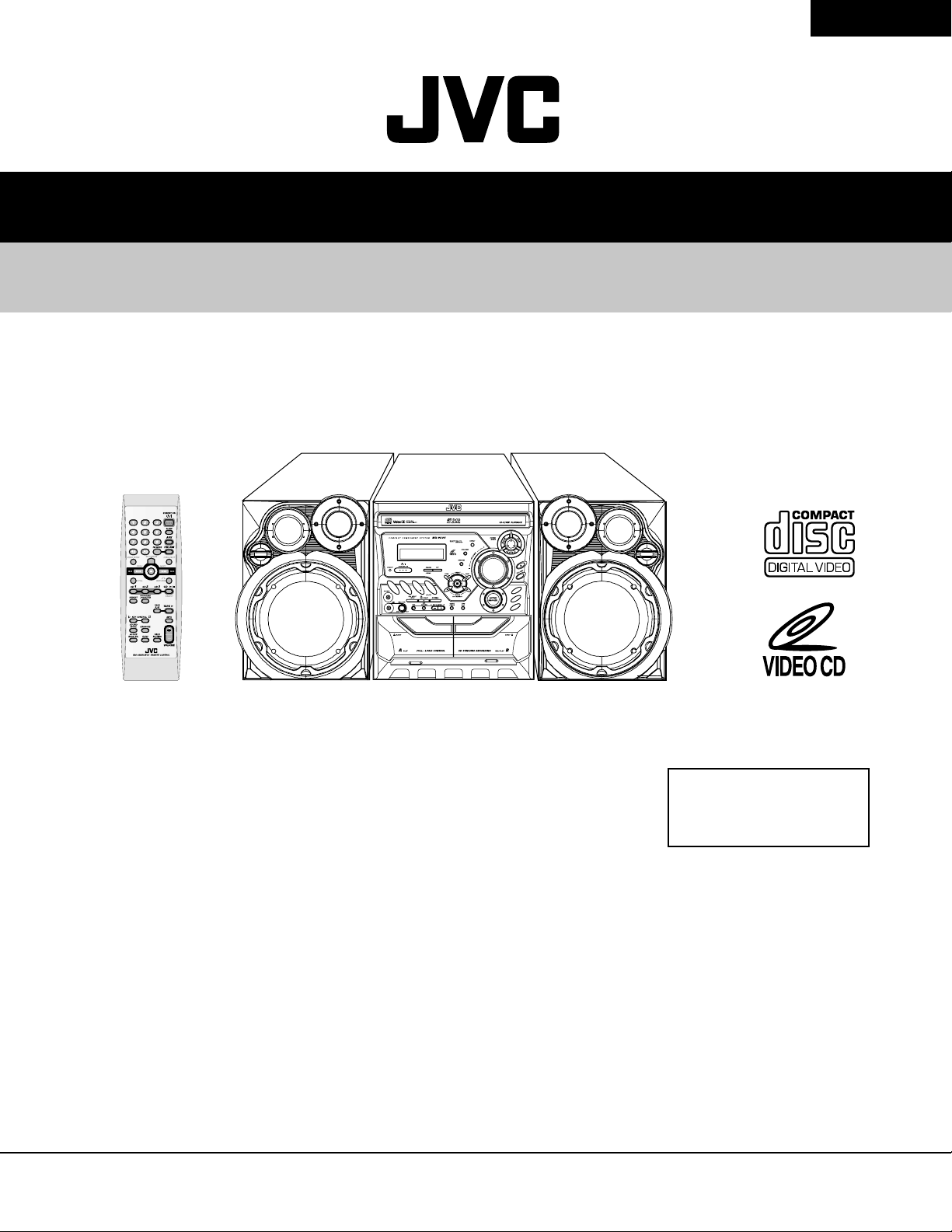
COMPACT COMPONENT SYSTEM
MX-GA3V
MX-GA3V
SP-MXGA3V CA-MXGA3V SP-MXGA3V
Contents
Safety precautions ---------------------------- 1- 2
Important for laser products ----------------- 1- 3
Preventing static electricity ----------------- 1- 4
Disassembly method ------------------------ 1- 5
Adjustment method -------------------------- 1- 18
Area Suffix
US ................... SINGAPORE
Flow of functional
operation until TOC read -------------- 1- 20
Maintenance of laser pickup -------------- 1- 21
Replacement of laser pickup -------------- 1- 21
Description of major ICs ------------------- 1- 22
Wiring connection ----------------------------- 1- 29
COPYRIGHT © 2003 VICTOR COMPANY OF JAPAN, LTD.
No. MB036
2003/11
Page 2
MX-GA3V
1. This design of this product contains special hardware and many circuits and components specially for
safety purposes. For continued protection, no changes should be made to the original design unless
authorized in writing by the manufacturer. Replacement parts must be identical to those used in the
original circuits. Services should be performed by qualified personnel only.
2. Alterations of the design or circuitry of the product should not be made. Any design alterations of the
product should not be made. Any design alterations or additions will void the manufacturer's warranty
and will further relieve the manufacture of responsibility for personal injury or property damage
resulting therefrom.
3. Many electrical and mechanical parts in the products have special safety-related characteristics. These
characteristics are often not evident from visual inspection nor can the protection afforded by them
necessarily be obtained by using replacement components rated for higher voltage, wattage, etc.
Replacement parts which have these special safety characteristics are identified in the Parts List of
Service Manual. Electrical components having such features are identified by shading on the
schematics and by (
which does not have the same safety characteristics as the recommended replacement parts shown in
the Parts List of Service Manual may create shock, fire, or other hazards.
4. The leads in the products are routed and dressed with ties, clamps, tubings, barriers and the like to be
separated from live parts, high temperature parts, moving parts and/or sharp edges for the prevention
of electric shock and fire hazard. When service is required, the original lead routing and dress should
be observed, and it should be confirmed that they have been returned to normal, after re-assembling.
5. Leakage currnet check (Electrical shock hazard testing)
After re-assembling the product, always perform an isolation check on the exposed metal parts of the
product (antenna terminals, knobs, metal cabinet, screw heads, headphone jack, control shafts, etc.)
to be sure the product is safe to operate without danger of electrical shock. Do not use a line isolation
transformer during this check.
Safety Precautions
!
) on the Parts List in the Service Manual. The use of a substitute replacement
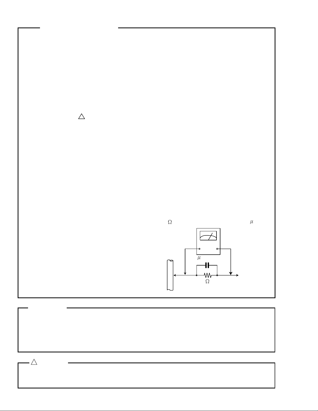
Plug the AC line cord directly into the AC outlet. Using a "Leakage Current Tester", measure the
leakage current from each exposed metal parts of the cabinet, particularly any exposed metal part
having a return path to the chassis, to a known good earth ground. Any leakage current must not
exceed 0.5mA AC (r.m.s.)
Alternate check method
Plug the AC line cord directly into the AC outlet. Use an AC voltmeter having, 1,000 ohms per volt or
more sensitivity in the following manner. Connect a 1,500 10W resistor paralleled by a 0.15 F ACtype capacitor between an exposed metal part
and a known good earth ground. Measure the AC
voltage across the resistor with the AC voltmeter.
Move the resistor connection to each exposed
metal part, particularly any exposed metal part
having a return path to the chassis, and meausre
the AC voltage across the resistor. Now, reverse
the plug in the AC outlet and repeat each
measurement. Voltage measured Any must not
exceed 0.75 V AC(r.m.s.). This corresponds to 0.5
mA AC(r.m.s.).
0.15 F AC TYPE
1500 10W
AC VOLTMETER
(Having 1000
ohms/v
olts,
or more sensitivity)
Place this
probe on
each exposed
metal part.
1-2
Good earth ground
Warning
1. This equipment has been designed and manufactured to meet international safety standards.
2. It is the legal responsibility of the repairer to ensure that these safety standards are maintained.
3. Repairs must be made in accordance with the relevant safety standards.
4. It is essential that safety critical components are replaced by approved parts.
5. If mains voltage selector is provided, check setting for local voltage.
!
CAUTION
Burrs formed during molding may be left over on some parts of the chassis. Therefore,
pay attention to such burrs in the case of preforming repair of this system.
Page 3
Important for laser products
MX-GA3V
1. CLASS 1 LASER PRODUCT
2. CAUTION :
Visible and invisible laser radiation when
open and interlock failed or defeated. Avoid direct
exposure to beam.
3. CAUTION :
There are no serviceable parts inside the
Laser Unit. Do not disassemble the Laser Unit. Replace
the complete Laser Unit if it malfunctions.
4. CAUTION :
The compact disc player uses invisible
laser radiation and is equipped with safety switches
which prevent emission of radiation when the drawer is
open and the safety interlocks have failed or are
defeated. It is dangerous to defeat the safety switches.
VARNING :
Osynlig laserstrålning är denna del är öppnad
och spårren är urkopplad. Betrakta ej strålen.
VAR O :
Avattaessa ja suojalukitus ohitettaessa olet
alttiina näkymättömälle lasersäteilylle. Älä
katso säteeseen.
REPRODUCTION AND POSITION OF LABELS
5. CAUTION :
If safety switches malfunction, the laser is
able to function.
6. CAUTION :
Use of controls, adjustments or performance
of procedures other than those specified herein may
result in hazardous radiation exposure.
!
CAUTION
Please use enough caution not to
see the beam directly or touch it in
case of an adjustment or
operation check.
ADVARSEL :
ADVARSEL :
Usynlig laserstråling ved åbning, når
sikkerhedsafbrydere er ude af funktion.
Undgå udsættelse for stråling.
Usynlig laserstråling ved å pning, når
sikkerhetsbryteren er avslott. Unngå
utsettelse for stråling.
VIDEO OUT
WARNING LABEL
V
220
110V
230V
127V
-240
V
1-3
Page 4
MX-GA3V
Preventing static electricity
1. Grounding to prevent damage by static electricity
Electrostatic discharge (ESD), which occurs when static electricity stored in the body, fabric, etc. is
discharged, can destroy the laser diode in the traverse unit (optical pickup). Take care to prevent this when
performing repairs.
2. About the earth processing for the destruction prevention by static electricity
In the equipment which uses optical pick-up (laser diode), optical pick-up is destroyed by the static electricity
of the work environment.
Be careful to use proper grounding in the area where repairs are being performed.
2-1 Ground the workbench
Ground the workbench by laying conductive material (such as a conductive sheet) or an iron plate over it
before placing the traverse unit (optical pickup) on it.
2-2 Ground yourself
Use an anti-static wrist strap to release any static electricity built up in your body.
(caption)
Anti-static wrist strap
Conductive material
(conductive sheet) or iron plate
3. Handling the optical pickup
1. In order to maintain quality during transport and before installation, both sides of the laser diode on the
replacement optical pickup are shorted. After replacement, return the shorted parts to their original condition.
(Refer to the text.)
2. Do not use a tester to check the condition of the laser diode in the optical pickup. The testers internal power
source can easily destroy the laser diode.
4. Handling the CD changer unit (optical pickup)
1. Do not subject the CD changer unit (optical pickup) to strong shocks, as it is a sensitive, complex unit.
2. Cut off the shorted part of the flexible cable using nippers, etc. after replacing the optical pickup. For specific
details, refer to the replacement procedure in the text.
Remove the anti-static pin when replacing the CD changer
CD changer
unit
unit. Be careful not to take too long a time when attaching it
to the connector.
3. Handle the flexible cable carefully as it may break when
CD changer
mechanism
assembly
subjected to strong force.
4. It is not possible to adjust the semi-fixed resistor that
adjusts the laser power. Do not turn it.
Attention when traverse unit is decomposed
Please refer to “Disassembly method” in the text for
*
pick up and how to detach the CD changer mechanism.
1. Remove the CD changer unit.
2. Disconnect the harness from connector on the CD motor
board.
3. Solder is put up before the card wire is removed from connector
Cn601on the main board as shown in Fig.1 and Fig.2.
(When the wire is removed without putting up solder, the
CD pick-up assembly might destroy.)
4. Please remove solder after connecting the card wire with
CN601 when you install picking up in the substrate.
Flexible cable
Fig.2
Fig.1
Soldering
1-4
Page 5

MX-GA3V
Disassembly method
Commence disassembly of the set by removing the main units and then proceed to the components
and assemblies inside the units.
Replacement of the fuses and the power IC
Top cover
CD changer unit
Front panel assembly
Chassis unit
CD changer unit
Removing the main PCB
Removing the CD changer mechanism assembly
Removing the CD pickup
Replacing the loading motor and belt of the CD changer tray
Replacing the CD tray rotor belt of CD changer, and removing the motor
Front panel assembly
Removing the cassette deck mechanism
Removing the earphone jack PCB
Removing the control/FL PCB
Removing the switch PCB and ACTIVE BASS EX. switch PCB
Removing the cassette deck main motor, and replacing the main belts
Removing the leaf switches of the cassette deck mechanism
Removing the cassette deck heads
Chassis unit
Removing the 3-pin regulator
Removing the power amp and supply PCB and the Power Trans PCB
Removing the sub power PCB
1-5
Page 6
MX-GA3V
<Disassembly of the main blocks of the set>
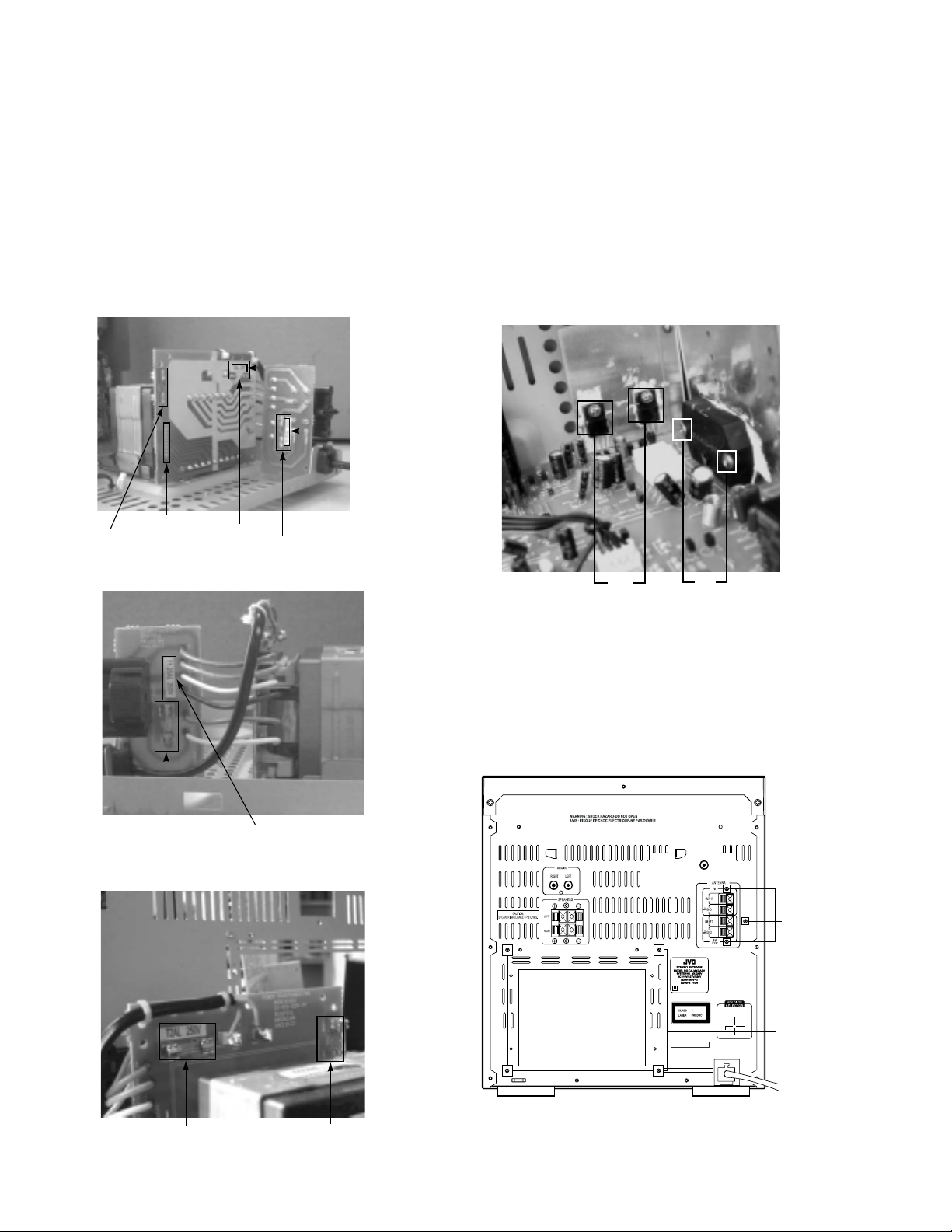
Replacement of the fuses and the power IC
Replacing the fuses (See Fig.1, Fig.3)
Prior to performing the following procedure, remove
the left side BOARD and remove tuner PCB
(Fig.3,BB)
1. Replace the fuses inside.
[Caution]
Be sure to use fuses with the specified ratings.
Replacing the power IC (See Fig.2)
Prior to performing the following procedure, remove
the top cover.
1. Remove the two screws A from the heat sink
between the power IC.
2. Remove the solder fixing the power IC.
Bottom side Fig.1(A)
Fuse(F952)
CN951
T1.6AL 250V
Component side Fig.1(B1)
Fuse(F951)
T2AL 250V
Add Lable
T2AL 250V
Add Lable
T1.25AL 250V
Fuse(F953)
T1.25AL 250V
Fig.2
WA
Replacing the heat sink cover (See Fig.3)
1. Remove four screws B from the rear panel.
2. Pull the heat sink cover outward.
Fig.3
1-6
Fuse(F953)
T1.25AL 250V
Component side Fig.1(B2)
Fuse(F951)
T2AL 250V
Add Lable
T1.25AL 250V
Fuse(F952)
T1.6AL 250V
VIDEO OUT
BB
V
220
110V
230V
127V
-240
V
B
Page 7
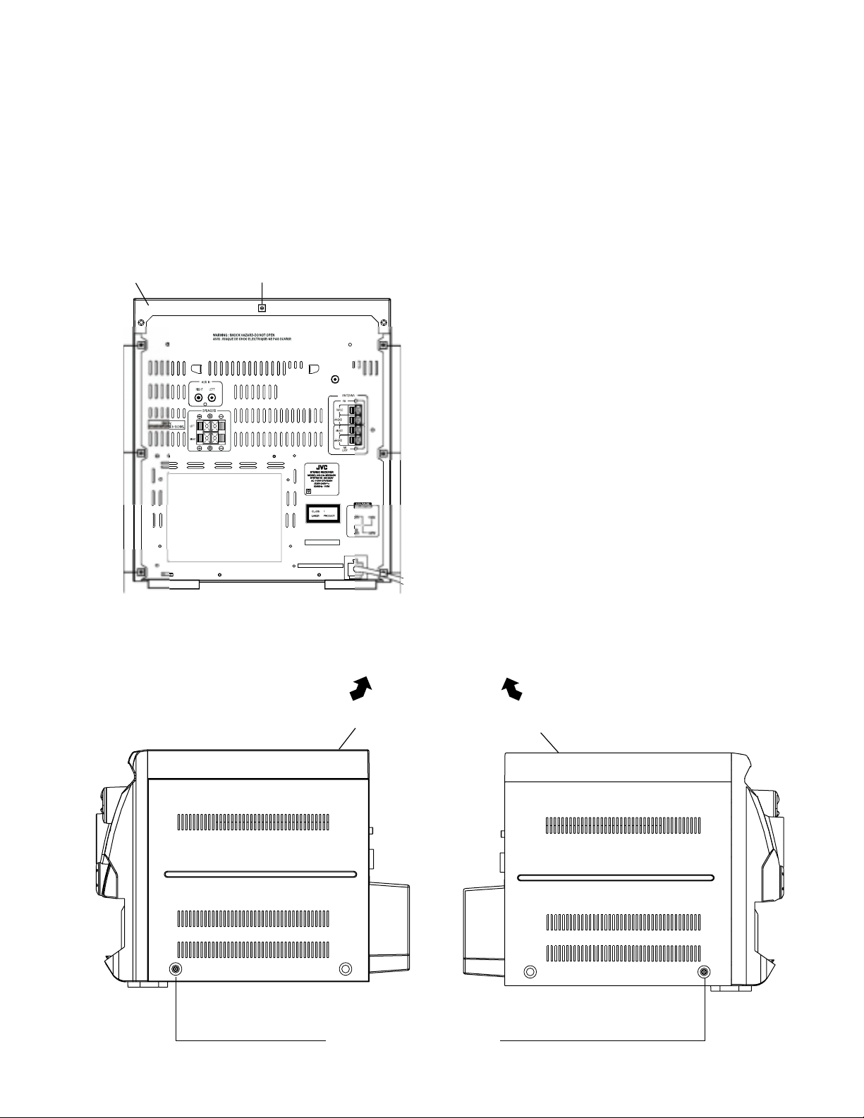
Removing the top cover
(See Fig.4 and 5)
1. Remove six screws B that retain the top cover from
the panel rear of the body.
Remove eight screws C and D that retain the top
2.
cover from the two sides of the body.
3. Remove the top cover from the body by lifting it
toward the rear.
Fig.4
Top cover
B
VIDEO OUT
MX-GA3V
2
23
-2
C
C
Fig.5 (A) Fig.5 (B)
Right Front panel assembly
Left Front panel assembly
DD
1-7
Page 8
MX-GA3V
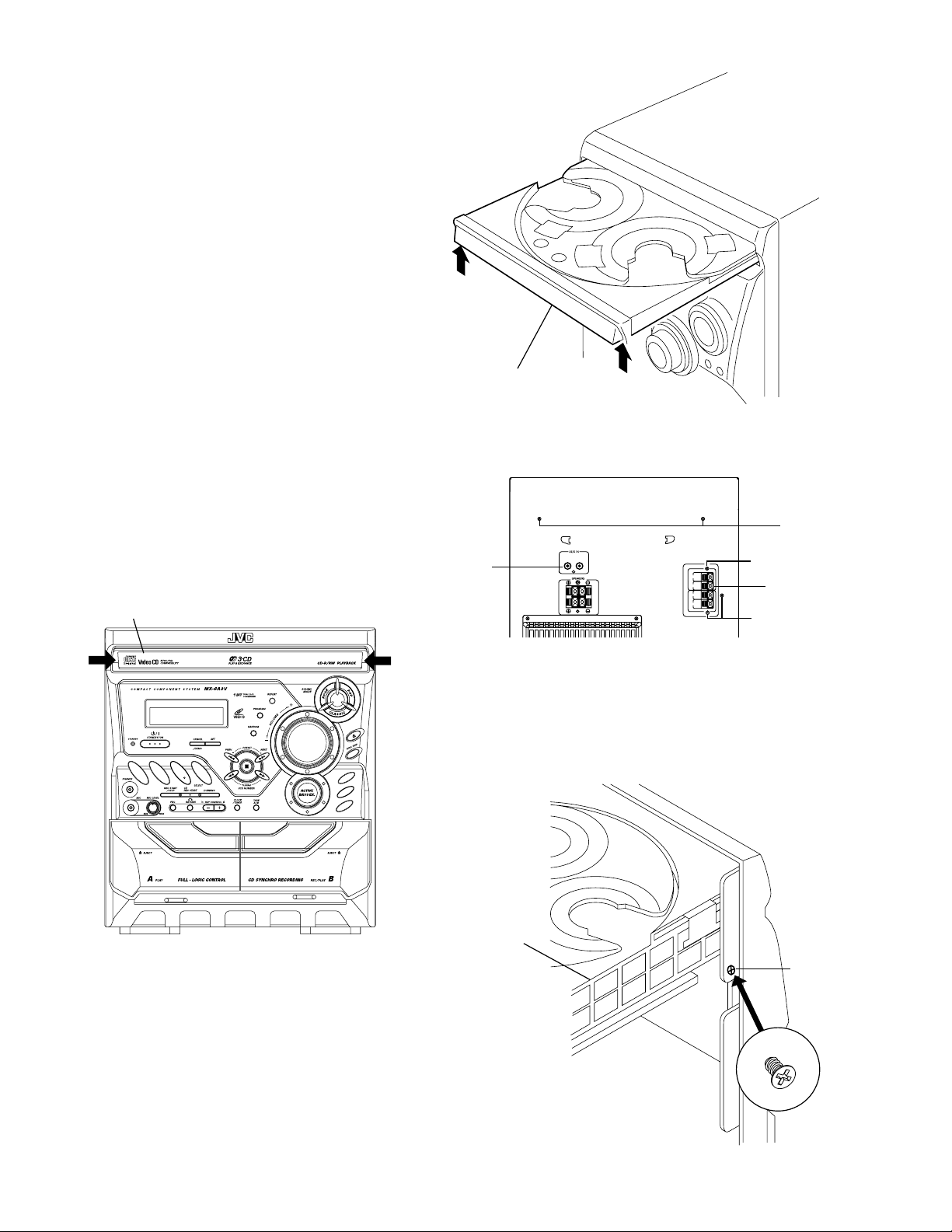
Removing the CD changer unit
Prior to performing the following procedures, remove
the top cover and both sides BOARD.
(See Fig.6 to 9)
[Caution]
Although the CD mechanism unit can be
removed without removing the CD tray
panel, it is still recommended to remove it
in order to prevent damage.
a. From the front panel side of this set, push in the
sections marked with arrows and pull out the CD
tray toward the front.
b. Remove the CD tray panel by pushing both of its
extremities upward in the direction of the arrows.
c. Push the CD tray deep into the set.
1. Disconnect the cord wires from the CD PCB CN704,
CN607, CN1101 and disconnect CN1 (shield wire)
from back panel.
2.
From the rear of the set, remove two screws E and
two screws G on the front panel left and right side.
3. Handle the CD changer unit rear, take out the unit.
CD tray panel
CD tray panel
Accessory
terminal
Fig.7
E
F
Antenna
termianl
F
Fig.6
Fig.8
CD changer
unit
G
1-8
Fig.10
Page 9
Removing the front panel assembly
(See Fig.10 to 11)
Prior to performing the following procedures, remove
the top cover and both board.
Also remove the CD changer unit.
1. Disconnect the parallel wire and the cord wire from
the connectors CN701, CN702, CN703, CN850 on
the power amp. and supply PCB.
H
2. Remove two screws
assembly onto the bottom of the body.
3. Remove two screws I on the left and right side of the set
retaining the panel front from the bottom and then
remove then GND lug
amp and supply PCB.
retaining the front panel
b
that comes from the power
MX-GA3V
4. Disengage the claws
c
on both sides of the front
panel assembly and then remove the assembly.
Claw
c
H
Fig.10
Power amp and
supply PCB
GND lug
I
b
Fig.12
1-9
Page 10

MX-GA3V
<Disassembly of units and assembly
inside this set>
Removing the CD PCB
(See Fig.12 to 13)
Prior to performing the following procedures, remove
the top cover and both sides board.
Also remove the CD changer unit.
1. The two screws E that retain the VCD assembly
should be removed.
2. Disconnect the wires from CN602, CN603, CN604
and CN605 on the CD PCB, which is located on
the back side of the CD changer unit.
J
3. The two screws
removed.
4. Remove the CD PCB by pulling it toward the side
where the CN601 is located.
5.
Using solder, short the CD pickup to connect to
short round.
that retain the CD PCB should be
Fig.12(B)
J
[Caution]
After re-connecting the wires, be sure to
remove the shorting solder from the GND
connection.
6. Disconnect the card wire from the connector CN601
on the main PCB and then remove the main PCB.
Fig.12(A)
CD PCB
CD PCB
CN601
E
1-10
Short round
Fig.14
Page 11

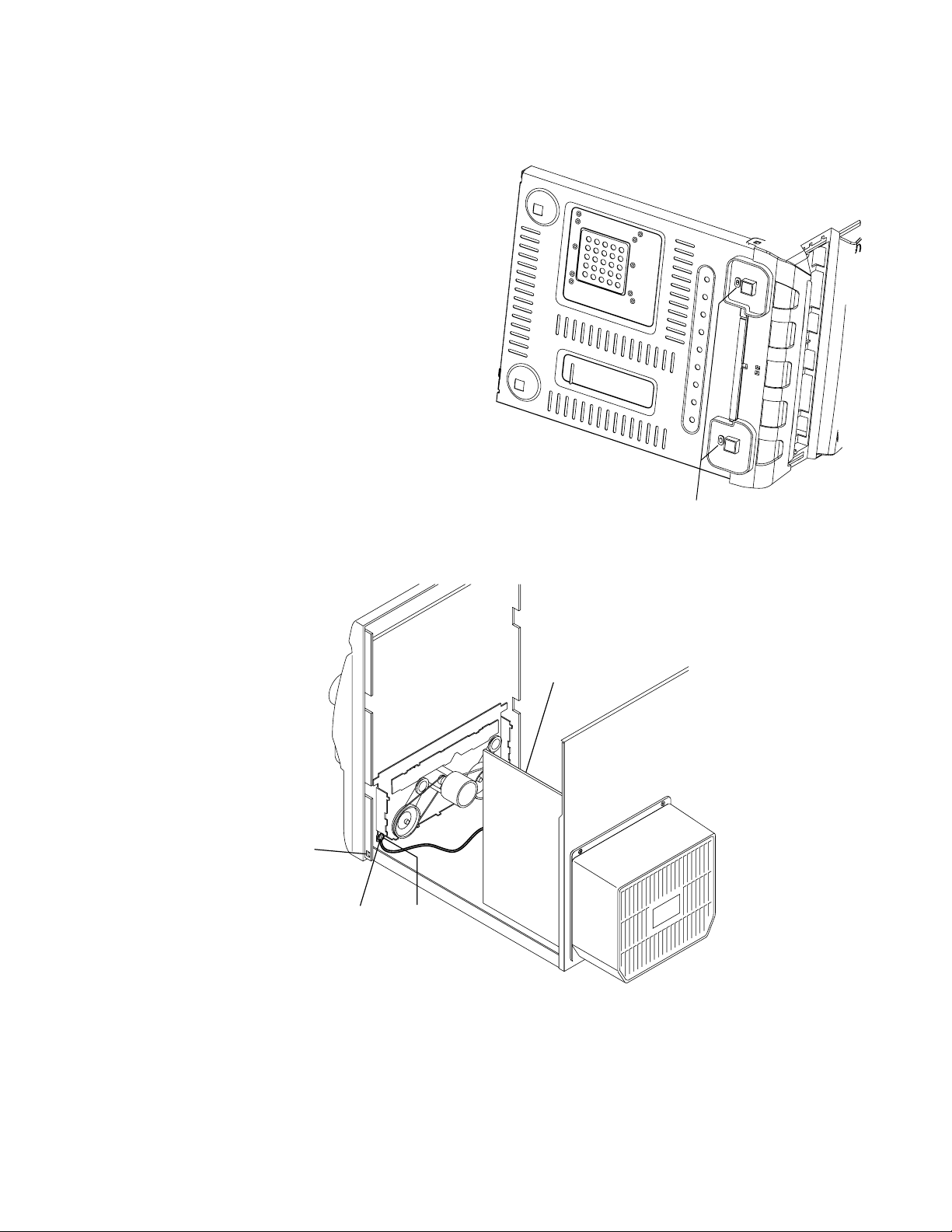
Removing the CD changer mechanism
assembly (See Fig.14 to 15)
Prior to performing the following procedures, remove
the top cover and both sides board.
Also remove the CD changer unit.
D
1. Removing screws
CD changer mechanism unit.
2. Turn the CD changer mechanism cover base and
remove screws
changer mechanism assembly.
from the front chuck base of the
E
connecting the unit to the CD
MX-GA3V
D
3. Removing four screws
holder assembly.
[Caution]
When replacing the CD changer mechanism
assembly, be sure not to mistake the positions
of the silver color and copper color spring.
K
( Silver color)
CD changer
mechanism
assembly
K
retaining the CD mechanism
K
( copper color)
Fig.14
CD changer
unit
K ( Silver color)
Fig.16
K
( copper color)
E
Fig.15
1-11
Page 12

MX-GA3V
Removing the CD pickup (See Fig.17)
Prior to performing the following procedures, remove
the top cover and both sides board.
Also remove the CD changer unit.
Also remove the CD changer mechanism.
1. Widen the section F.
2. While keeping the section
section G in the direction of the arrow to remove
the shaft, and then remove the CD pickup.
Replacing the loading motor and rotor
belt of the CD changer (See Fig .18)
Prior to performing the following procedures, remove
the top cover.
Also open the CD changer tray.
Remove two screws L retaining the CD changer
1.
tray loading motor.
2. Remove two screws
and take it out, after remove the rotor belt from
the pulley.
F
wide open, push the
M
retaining the gear plate
Shaft
CD pic
Fig.17
kup
GF
M
Replacing the CD turn table and remov-
ing the motor (See Fig. 19 and 20 )
Prior to performing the following procedures, remove
the top cover.
Also remove the CD changer unit.
N
1. Remove one screws
2. Remove two screws
on both sides of the CD changer unit.
3. Remove the stopper brackets from both sides of the
CD changer unit.
4. Pull out the CD tray from the CD changer unit, all
the way and lift the tray (u/~ ward) to remove.
5. Remove the gear and after push out the tray motor
locker and pull out the tray motor from the CD tray.
Turn table motor
retaining the CD (Turn table).
O
retaining the stopper brackets
Motor locker
L
Fig.18
NO
1-12
Fig.20
D
Obligue gear
Fig.19
Page 13

Removing the cassette deck mechanism
(See Fig.21)
Prior to performing the following procedures, remove
the top cover.
Also remove the CD changer unit.
Also remove the front panel assembly.
MX-GA3V
Front panel
assembly
1. Remove five screws
Z
retaining the cassette deck
mechanism.
Removing the earphone jack PCB and
Mic Jack PCB
(See Fig.22)
Prior to performing the following procedures, remove
the top cover and both sides board.
Also remove the CD changer unit.
Also remove the front panel assembly.
1. Remove the screw with the washer,
retains the earphone jack PCB.
P
that
Z
Z
Fig.21
Front panel
assembly
P
Earphone jack
PCB
Removing the control/FL PCB
(See Fig.21)
Prior to performing the following procedures, remove
the top cover and both sides board. Also remove
the CD changer unit.
Also remove the CD changer unit.
Also remove the front panel assembly.
Q
1. Remove four screws
from the back of the front panel unit.
that retain the control/FL PCB
Fig.22
Front panel
assembly
Q
Control/FL
PCB
Fig.23
1-13
Page 14

MX-GA3V
Removing the switch PCB and sound
mode and CD function switch PCB
(See Fig.23 to 26)
Prior to performing the following procedures, remove
the top cover and both sides board.
Also remove the CD changer unit.
Also remove the front panel assembly.
1. Pull out the volume control knob and MIC Volume
Knob from the front of the front panel assembly.
(Fig.24)
2. Remove four screws
assembly. (Fig.23)
3. Remove the control/FL PCB.
4. Remove eleven screws R retaining the switch (key 1)
PCB. (Fig.22)
5. Remove three screws S retaining the sound mode
(key 2) switch PCB.
6. Remove two screws T retaining the CD function
(key 3) switch PCB.
Q
retaining the front panel
Front panel
assembly
Volume
shaft
Fig.25
MIC Volume
Knob
Volume Knob
Fig.24
Front panel assembly
S
R
Key 1 PCB
Key 2 PCB
T
R
Fig.26
Key 3 PCB
1-14
Page 15

Removing the cassette deck main motor,
and replacing the main belts
(See Fig.21, 27 and 28)
Prior to performing the following procedures, remove
the top cover and both sides board.
Also remove the CD changer unit.
Also remove the front panel assembly.
Z
1. Remove five screws
mechanism. (Fig.21)
2. Remove the cassette deck mechanism.
3. Remove two screws
the front side of the cassette deck.
retaining the cassette deck
T
retaining the main motor from
MX-GA3V
Cassette deck mechanism
(Front side)
T
Fig.27
[Caution]
After attaching the main motor, check the
orientation of the motor and the polarity of
the wires.
4. From the backside of the cassette deck, remove the
main motor and two main belts.
[Caution]
The lengths of the cassette A(playback
B
only) and cassette
(record/play) main
belts are different. When attaching the main
belts, use the longer belt for cassette
Removing the leaf switches of the cassette
A
.
deck mechanism (See Fig. 21 and 29)
Prior to performing the following procedures, remove
the top cover and both sides board.
Also remove the CD changer unit.
Also remove the front panel assembly.
Cassette deck mechanism
(Back side)
Main belt
B
cassette)
(For
Solder side of leaf switch
Cassette deck main motor
Main belt
(For
A
cassette)
Fig.28
Z
1. Remove five screws
that retain the cassette deck
mechanism. (Fig.21)
2. Remove the cassette deck mechanism.
3. Turn the cassette deck mechanism upside down.
4. Remove the solder from around the leaf switches.
5. Pull out the leaf switches from the front side of the
cassette deck mechanism.
Cassette deck mechanism
(Back side)
Fig.29
1-15
Page 16

MX-GA3V
Removing the cassette deck heads
(See Fig. 21 and 30)
Prior to performing the following procedures, remove
the top cover and both sides board.
Also remove the CD changer unit.
Also remove the front panel assembly.
1. Remove five screws Z that retain the cassette deck
mechanism. (Fig.21)
2. Remove the cassette deck mechanism and place
it so that the front side faces up.
3. Remove the solder from the bottom side of the head
terminal and disconnect the wire.
4. Remove screw U that retains the head.
5. Remove screw V that retains the head.
6. Hold the head and slide it in the direction of the
arrow to remove it.
Removing the 3-pin regulator and bridge
diode
(See Q904, Q907 and Fig.31)
Cassette deck mechanism
(Front side)
PB Head REC/PB Head
U
V
Fig.30
V
U
Prior to performing the following procedures, remove
the top cover and both sides board.
1. Remove two screws A that connect the heat sink
cover to rear panel.
2. Pull the heat sink outward.
3. Remove two screws W that retains the heat sink the
3-pin terminal regulator Q904, Q907.
4. Remove the solder fixing the 3-pin regulator.
W
Fig.31
A
1-16
Page 17

Removing the power amp and supply PCB
and the power trans PCB
(See Fig. 2, 29 to 31)
Prior to performing the following procedures, remove
the top cover and CD changer unit.
MX-GA3V
1. Remove four screws
B
from the rear panel. (Fig.3)
2. Pull the heat sink cover outward.
3. Remove four screws
AA
from the rear panel between
the heat sink holder.
4. Remove two screws X that retain the speaker terminals
and AUX terminal.
5. Remove screws
YY
that retains the rear panel, and
then remove the rear panel.
6. Disconnect the parallel wires from the connectors
FW951 on the power trans PCB.
7. Remove the clamp of AC power cord from the chassis.
8. Remove four screws AB that retain the power trans
PCB and then remove the assembly.
Power AMP and
supply PCB
Rear panel
Fig.33
Chassis
Z
Fig.34
AB
AC Selector
Switch
Fig.34
1-17
Page 18

MX-GA3V
Adjustment method
Measurement instruments required
for adjustment
1. Low frequency oscillator.
This oscillator should have a capacity to output
0dB to 600ohm at an oscillation frequency of
50Hz-20kHz.
2. Attenuator impedance : 600ohm
3. Electronic voltmeter
4. Frequency counter
5. Wow flutter meter
6. Test tape
VT712 : For Tape speed and wow flutter (3kHz)
VT703 : For Head angle(10kHz). Play back frequency
characteristics(1kHz), and dubbing
frequency characteristics(63,1,10kHz)
7. Blank tape
TAPE I : AC-225 TAPE II : AC-514
8. Torque gauge : For play and back tension forward;
TW2111A, Reverse; TW2121A
Fast Forward and Rewind;
TW2231A
9. Test disc: CTS-1000(12cm), GRG-1211(8cm),
CD-T05A
10. Jitter meter
11. Television
Radio input signal
AM modulation frequency : 400Hz
Modulation factor : 30%
FM modulation frequency : 400Hz
Frequency displacement : 22.5kHz
Frequency Range
AM US: 530kHz~1710kHz (10kHz)
531kHz~1629kHz (9kHz)
UX: 530kHz~1600kHz (10kHz)
531kHz~1602kHz (9kHz)
FM 87.5MHz~108MHz
Standard measurement positions of
volume and switch
Power : Standby (Light STANDBY Indicator)
Sound Turbo, A, BASS EX : OFF
Sound mode : OFF
Main VOL. : 0 Minimum
Travers mecha set position : Disc 1
Mic MIX VOL : MAX
ECHO: OFF
Measurement conditions
(Select correct AC Line Volt.)
Power supply voltage
AC 110V/127V/220V/230V~240V (50/60Hz) US/UX
Measurement
output terminal : Speaker out
: TP101(Measuring for TUNER/
DECK/CD/VCD)
: Dummy load 6ohm
Precautions for measurement
1. Apply 30pF and 33kohm to the IF sweeper output
side and 0.082 F and 100kohm in series to the
sweeper input side.
2. The IF sweeper output level should be made as
low as possible within the adjustable range.
3. Since the IF sweeper is a fixed device, there is no
need to adjust this sweeper.
4. Since a ceramic oscillator is used, there is no need
to perform any MPX adjustment.
5. Since a fixed coil is used, there is no need to adjust
the FM tracking.
6. The input and output earth systems are separated.
In case of simultaneously measuring the voltage in
both of the input and output systems with an
electronic voltmeter for two channels, therefore, the
earth should be connected particularly.
7. In the case of BTL connection amplifier, the minus
terminal of speaker is not for earthing. Therefore,
be sure not to connect any other earth terminal to
this terminal. This system is of an OTL system.
1-18
Page 19

Arrangement of adjusting positions
Cassette deck mechanism
(Front side)
MX-GA3V
PB Head
(Dec
k-A)
Head azimuth screw
(Forward side)
Head azimuth screw
(Rev
Tape recorder section
Items
Cassette Head
Azimuth Alignments
Measurement
Test tape
: VT703 (10kHz)
Measurement output
terminal
: Left and Right
speaker output
(6-ohm loaded)
or
Headphone Output
(32-ohm loaded)
Head azimuth screw
(Forw
erse side)
conditions
REC/PB Head
(Deck-B)
ard side)
Head azimuth screw
(Reverse side)
Measurement method
1. Playback the test tape VT703 (10KHz) or equivalent.
2. Adjust the head azimuth screw to obtain maximum
output and both output of L / R is in 3dB.
3. Put on the screw lock paint after alignments.
Standard
values
Maximum output
Adjusting
positions
Adjust the
head azimuth
screw only
when the head
has been
changed.
Recording Bias
F
requency Alignment
Tuner section
Items
AM Tracking
Alignments
AM IFT Alignments
Note: The adjustment of CD section is not required.
Test tape
: TYPE I AC-225
Measurement output
terminal
: Erase head terminal
(CN308 8-Pin)
Measurement
conditions
Input signal
: 530kHz(529kHz)
600kHz(603kHz)
Adjustment point
: Antenna coil (L2)
Input signal
: 530kHz(529kHz)
Adjustment point
: IFT (T1)
1. Insert the recording tape in deck-B.
2. Starting the recording.
3. Adjust the oscillation frequency to 80KHz+/-3KHz by
core of Oscillation coil of L301.
1. Set the Signal Generator signal to 530kHz(529kHz)
the feed to Loop Antenna.
2. Receiving the signal and the adjust the OSC coil (L2)
obtain the V.T is 1.40V +/-0.05V.
3. Change the receiving frequency to 600KHz (603KHz).
4. Adjust the Antenna coil ( L2 ) obtain maximum
sensitivity. (Adjust the SSG output to out of AGC range.)
1. Set the receiving frequency to 530KHz(529kHz).
2. Feed the 450KHz signal to AM antenna input.
3.Adjust the IFT Block T1 obtain to maximum output.
(Adjust the SSG output to out of AGC range.)
Measurement method
80kHz+/-3kHz
Standard
values
V. T
: 1.40V+/-0.05V
Maximum
sensitivity
Maximum output
Use the HighImpedance
Probe or
Frequency
counter input.
Adjusting
positions
Adjust the OSC
coil only when
the AM coil block
has been changed.
Adjust the IFT
only when the
IFT block has
been changed.
1-19
Page 20

MX-GA3V
Flow of functional operation until TOC read
Power ON
Play Key
Slider turns REST
SW ON.
Automatic tuning
of TE offset
Check Point
Confirm that the voltage at the pin2
of CN602 is "H"\"L"\"H".
Tracking error waveform at TOC reading
Approx.3sec
Tracking
servo
off states
Automatic measurement
of TE amplitude and
automatic tuning of
TE balance
VREF
pin 20 of
IC611(TE)
Approx
1.8V
Disc states
to rotate
Tracking
servo
on states
Disc to be
braked to stop
TOC reading
finishes
500mv/div
2ms/div
Fig-1
Laser ON
Detection of disc
Automatic tuning of
Focus offset
Automatic measurement of
Focus S-curve amplitude
Disc is rotated
Focus servo ON
(Tracking servo ON)
Automatic measurement of
Tracking error amplitude
Automatic tuning of
Tracking error balance
Check that the voltage at the
pin57 of IC602 is + 5V?
Confirm that the Focus error
S-cuve signal at the pin43 of
IC602 is approx.2Vp-p
Confirm that the signal from
pin4 IC602 is 0V as a
accelerated pulse during
approx.400ms.
Confirm the waveform of
the Tracking error signal.
at the pin 13 of IC601 (R617)
(See fig-1)
1-20
Automatic tuning of
Focus error balance
Automatic tuning of
Focus error gain
Automatic tuning of
Tracking error gain
TOC reading
Play a disc
Confirm the eys-pattern
at the lead of Tp3
Page 21

MX-GA3V
Maintenance of laser pickup
(1) Cleaning the pick up lens
Before you replace the pick up, please try to clean
the lens with a alcohol soaked cotton swab.
(2) Life of the laser diode
When the life of the laser diode has expired, the
following symptoms will appear.
1. The level of RF output (EFM output : ampli tude of
eye pattern) will below.
Is the level of
RFOUT under
1.25V 0.22Vp-p?
NO
Replace it.
Replacement of laser pickup
Turn off the power switch and,disconnect the
power cord from the AC OUTLET.
Replace the pickup with a normal one.(Refer
to "Pickup Removal" on the previous page)
Plug the power cord in,and turn the power on.
At this time,check that the laser emits for
about 3seconds and the objective lens moves
up and down.
Note: Do not observe the laser beam directly.
Play a disc.
YES
Check the eye-pattern at
O.K
Finish.
(3) Semi-fixed resistor on the APC PC board
The semi-fixed resistor on the APC printed circuit board which is attached to the pickup is used to adjust the
laser power.Since this adjustment should be performed to match the characteristics of the whole optical
block, do not touch the semi-fixed resistor.
If the laser power is lower than the specified value, the laser diode is almost worn out, and the laser pickup
should be replaced.
If the semi-fixed resistor would be adjusted when the pickup operates normally, the laser pickup may be
damaged due to excessive current.
Tp3.
1-21
Page 22

MX-GA3V
Description of major ICs
VIDEO CD PROCESSOR CHIP PINOUT
LA7
LA8
LA9
LA10
LA11
VSS
VPP
LA12
LA13
LA14
LA15
LA16
LA17
ACLK
AOUT/SEL_PLL0
ATCLK
ATFS/SEL_PLL1
DA9/DOE#
AIN
ARCLK
ARFS
TDMCLK
TDMDR
TDMFS
CAS#
VSS
Figure 24 Visba Video CD Processor Chip Pinout Diagram
VIDEO PC PROCESSOR CHIP PIN DESCRIPTION
Name Number I/O Definition
VDD 1, 31, 51 I Voltage supply for 3.3 V.
RAS# 2 O DRAM row address strobe (active low).
DWE# 3 O DRAM write enable (active low).
DA[8:0] 12:4 O DRAM multiplexed row and column address bus.
DBUS[15:0] 28:13 I/O DRAM data bus.
RESET# 29 I System reset (active low).
VSS 30, 50, 80, 100 I Ground.
YUV[7:0] 39:32 O Y is luminance, UV are chrominance data bus for screen video interface. YUV[7:0] for 8-
VSYNC 40 I/O Vertical sync for screen video interface, programmable for rising or falling edge.
HSYNC 41 I/O Horizontal sync for screen video interface, programmable for rising or falling edge.
CPUCLK 42 I RISC and system clock input.
PCLK2X 43 I/O Pixel clock; two times the actual pixel clock for screen video interface.
PCLK 44 I/O Pixel clock qualifier in for screen video interface.
AUX[7:0] 54, 52, 53,
LD[7:0] 62:55 I/O RISC interface data bus.
LWR# 63 O RISC interface write enable (active low).
LOE# 64 O RISC interface output enable (active low).
LCS[3,1,0]# 65,66,67 O RISC interface chip select (active low).
LA[17:0] 87:82, 79:68 O RISC interface address bus.
VPP 81 I Digital supply voltage for 5 V.
ACLK 88 I/O Master clock for external audio DAC (8.192 MHz, 11.2896 MHz, 12.288 MHz, 16.9344
AOUT/
SEL_PLL0
ATCLK 90 I/O Audio transmit bit clock.
ATFS/
SEL_PLL1
DA9/DOE# 92 O Dual purpose pin: DRAM output enable (active low)/DRAM multiplexed row and column
AIN 93 I Audio interface serial data input.
ARCLK 94 I Audio receive bit clock.
ARFS 95 I Audio interface receive frame sync.
TDMCLK 96 I TDM interface serial clock.
TDMDR 97 I TDM interface serial data receive.
TDMFS 98 I TDM interface frame sync.
CAS# 99 O
75737471726970676865666364616259605758555653545152
76
77
78
79
80
81
82
83
84
85
86
87
88
89
90
91
92
93
94
95
96
97
98
99
100
VDD
49:45
89 O Dual-purpose pin. AOUT is the audio interface serial data output
91 O Dual-purpose pin. ATFS is the audio interface transmit frame sync.
LA5
LA6
LA3
LA4
LA1
LA2
LCS0#
LA0
LCS3#
LCS1#
LWR#
LOE#
LD6
LD7
LD4
LD5
LD2
LD3
LD0
LD1
AUX5
AUX7
VDD
AUX6
50
VSS
49
AUX4
48
AUX3
47
AUX2
46
AUX1
45
AUX0
44
PCLK
43
PCLK2X
42
DBUS12
DBUS11
41
40
39
38
37
36
35
34
33
32
31
3029VSS
28
27
26
CPUCLK
HSYNC
VSYNC
YUV7
YUV6
YUV5
YUV4
YUV3
YUV2
YUV1
YUV0
VDD
RESET#
DBUS15
DBUS14
DBUS13
ESS
Visba ES3880
Video CD PC
100 TQFP
21436587109121114131615181720192221242325
DA2
DA1
DA4
DA3
DA5
DA7
DA6
RAS#
DWE#
DA0
DA8
DBUS0
DBUS2
DBUS1
DBUS4
DBUS3
DBUS6
DBUS5
DBUS8
DBUS7
DBUS9
DBUS10
bit YUV mode.
CPUCLK is used only if SEL_PLL[1:0] = 00.
I/O Auxiliary control pins (AUX0 and AUX1 are open collectors).
MHz, and 18.432 MHz).
I Pins SEL_PLL[1:0] select phase-lock loop (PLL) clock frequency CPUCLK
for the Visba:
I Pins SEL_PLL[1:0] select phase-lock loop (PLL) clock frequency CPUCLK for the Visba.
See the SEL_PLL0 pin above for the settings.
00 = bypass PLL.
01 = 54 MHz PLL.
10 = 67.5 MHz PLL.
11 = 81 MHz PLL.
address bus.
DRAM column address strobe bank 0 (active low).
1-22
Page 23

VIDEO CD COMPANION CHIP
1. Pin layout
VCC
PCLK
2XPCLK
MX-GA3V
YDAC
VSSAV
VSSAV
VDAC
ACAP
VCC
AUX6/VFD_DO
AUX5
AUX4
AUX3
XOUT
VSS
VCC
XIN
VSS
NC
VSS
VCCAV
VCCAV
COMP
VSSAV
VSSAV
CDAC
RSET
VSSAA
VREF
VREFM
DSC_D7
HSYN_B
DSC_D6
VSYN_B
DSC_D5
YUV7
YUV6
YUV5
YUV4
VCC
VSS
YUV3
DSC_D4
YUV2
DSC_D3
YUV1
DSC_D2
YUV0
DSC_D1
VSS
80
79 78 77 76 75 74 73 72 71 70 69 68 67 66 65 64 63 62 61 60 59 58 57 56 55 54 53 52
81
82
83
84
85
86
87
88
89
90
91
92
93
94
95
96
97
98
99
100
1
2 3 4 5 6 7 8 9 10 11 12 13 14 15 16 17 18 19 20 21 22 23 24 25 26 27 28 29
NC
NC
VSS
Visba ES3883
Video CD
Companion Chip
NC
VCC
AUX0
DSC_C
AUX2
AUX1
DSC_S
DSC_D0
DCLK/EXT_CLK
VCC
MCLK
MUTE
RESET_B
AUX7/VFD_DI
TSD
TBCK
AUX9/SQS0
AUX8/VFD_CLK
TWS/SPLL_OUT
RSTOUT_B
RWS/SEL_PLL1
VSS
VSS
NC
NC
NC
51
30
NC
50
49
48
47
46
45
44
43
42
41
40
39
38
37
36
35
34
33
32
31
MIC2
MIC1
AOL+
AOLAORAOR+
VCCAA
VREFP
VCM
VSSAA
AUX15/IR
AUX14/SOS1
AUX13/SP
RBCK/SER_IN
AUX12/C2PO
AUX11/IRQ
AUX10/SQCK
RSD/SEL_PLL0
VCC
VSS
1-23
Page 24

MX-GA3V
2. Block diagram
Name Number I/O Definition
VSS 1,25:26,31,72,75,77,91,100 I Ground.
VCC 5,16,32,66,73,78,90 I Voltage supply, 5 V.
DSC_C 6 I Clock for programming to access internal registers.
AUX0 7 I/O Servo Forward or Control Pin.
AUX1 9 I/O Servo Reverse or Control Pin.
AUX2 11 I/O Servo LDON or Control Pin.
AUX3 70 I/O Servo CW/Limit or Control Pin.
AUX4 69 I/O Servo CCW/Close or Control Pin.
AUX5 68 I/O Servo Data or Control Pin.
AUX6 67 I/O Servo XLAT or Control Pin/VFD_DO.
AUX7 14 I/O Servo BRKM/Sense or Control Pin/VFD_DI.
AUX8 18 I/O Servo Mute/Open or Control Pin/VFD_CLK.
AUX9 20 I/O Servo SQS0 or Control Pin.
AUX10 34 I/O Servo SQCK or Control Pin.
AUX11 35 I/O 3880 IRQ or Interrupt Output or Control Pin.
AUX12 36 I/O CD C2PO or Interrupt Input or Control Pin.
AUX13 38 I/O Serial Interrupt/CD-Mute or Control Pin.
AUX14 39 I/O Servo SCOR (S0S1) or Interrupt Input or Control Pin.
AUX15 40 I/O Interrupt Input or Control Pin.
DSC_D[7:0] 81,83,85,93,95,97,99,8 I/O Data for programming to access internal registers.
DSC_S 10 I Strobe for programming to access internal registers.
DCLK
EXT_CLK I EXT_CLK is the external clock EXT_CLK is an input during bypass PLL mode.
RESET_B 13 I Video reset (active-low).
MUTE 15 O Audio mute.
MCLK 17 I Audio master clock.
TWS
SPLL_OUT O
TSD 21 I Transmit audio data input.
TBCK 22 I Transmit audio bit clock.
RWS
SEL_PLL1 I Pins SEL_PLL[1:0] select the PLL clock frequency for the DCLK output.
RSTOUT_B 24 O Reset output (active-low).
NC 2:4,27:30,76 No connect. Do not connect to these pins.
RSD
SEL_PLL0
RBCK
SER_IN
VSSAA 41,51 I Audio Analog Ground.
VCM
VREFP 43 I DAC and ADC maximum reference. Bypass to VCMR with 10 µF in parallel with 0.1 µF.
VCCAA 44 I Analog VCC, 5 V.
AOR+, AOR- 45:46 O Right channel output.
AOL-, AOL+ 47:48 O Left channel output.
MIC1 49 I Microphone input 1.
MIC2 50 I Microphone input 2.
VREF
VREFM 53 I DAC and ADC minimum reference. Bypass to VCMR with 10 µF in parallel with 0.1 µF.
RSET 54 I Full scale DAC current adjustment.
COMP 55 I Compensation pin.
VSSAV 56:57,62:63 I Video Analog Ground
CDAC 58 O Modulated chrominance output.
VCCAV 59,60 I Video VCC, 5 V
YDAC 61 O Y luminance data bus for screen video port.
VDAC 64 O Composite video output.
ACAP 65 I Audio CAP
XOUT 71 O Crystal output.
XIN 74 I 27 MHz crystal input.
PCLK 79 I/O 13.5 MHz pixel clock.
2XPCLK 80 I/O 27 MHz (2 times pixel clock).
HSYN_B 82 O Horizontal sync (active-low).
VSYN_B 84 O Vertical sync (active-low).
YUV[7:0] 86:89,92,94,96,98 I YUV data bus for screen video port.
12
19
23
33
37
42
52
O Dual-purpose pin DCLK is the MPEG decoder clock.
I Dual-purpose pin TWS is the transmit audio frame sync.
SPLL_OUT is the select PLL output.
O Dual-purpose pin RWS is the receive audio frame sync.
SEL_PLL1 SEL_PLL0 DCLK
0 0 Bypass PLL (input mode)
0 1 27 MHz (output mode)
1 0 32.4 MHz (output mode)
1 1 40.5 MHz (output mode)
O Dual-purpose pin. RSD is the receive audio data input.
I SEL_PLL0 along with SEL_PLL1 select the PLL clock frequency for the DCLK output. See the
table for pin number 23.
O Dual-purpose pin. RBCK is the receive audio bit clock.
I SER_IN is the serial input DSC mode.
0 - Parallel DSC mode.
1 - Serial DSC mode.
I ADC Common Mode Reference (CMR) buffer output. CMR is approximately 2.25 V. Bypass to
analog ground with 47 µF electrolytic in parallel with 0.1 µF.
I Internal resistor divider generates Common Mode Reference (CMR) voltage. Bypass to ana-
log ground with 0.1 µF.
1-24
* Shading indicates a pin change from ES3209.
Page 25

BA15218/BA15218F(IC102/IC852): Dual operational amplifier
1. Terminal layout & block digram
BA3837(IC103): MIC Mixer
1. Terminal layout & block digram 2. Pin function
MX-GA3V
BU9253AS(IC851): Low pass filter & echo mixer
1. Terminal layout & block digram 2. Pin function
1-25
Page 26

MX-GA3V
TA8189N(IC401): REC/PCB Amp.
1. Terminal layout
3. Pin function
2. Block diagram
1-26
Page 27

TC74HC4094AP (IC402): 8-bit shift and store resister
1. Terminal layout
2. Block diagram
MX-GA3V
1-27
Page 28

MX-GA3V
TDA7440D (IC101): Audio processor
1. Terminal layout
2. Block diagram
1-28
Page 29

MX-GA3V
Wiring
5
4
CN101
To Headphone
connection
IC852
BA15218F
Pre/ALC
IC851
BU9253FS
Digital Echo
ALC
Q851
Q101
AHB
Q103
IC304
Mute
IC102
Speaker
output
J303
STK402-070
2CH Power Amp
Mute
Q203
AHB
BA15218F
AHB
Q201
To
Primary
CN951
Circuit
Rectifire.
Power Supply
Circuit
Control
Protect.
CN902
To
Control
SWITCH
CN701
To Power Amp
CN704
To Changer
CONTROL
IC702
IR Sensor
Jog
FW701
FW701
MPU
IC701
TMP87CM78-XXX
VFD
Key's
CN703
To Main To Main
CN702
MPEG
PRIMARY
Video Output
J1101
IC1102
ES3883F
MPEG
IC1101
ES3880FM
AC Main
T951
To
Main
Chip
Companion
Decorder
CN1101
Transformer
FW951
IC1105
AMS1117
IC1104
27C020
IC1103
4C16256
Voltage
Selector
3.3V Reg
2MB PROM
4MB EDO-RAM
To
CN603CN608
CN604
CN605
CN606
Changer
To ChangerTo Control
To Changer
To Changer
To MPEG
MIC
To
Main
FW852
VR840
JA851
Mic Jack
Mic VR
CN805
To Mic/Echo
3
JA302
FM/AM Ant.
LPF
Q852
IC1
TA2104N
IC103
JA301
AUX In
Tuner
AM/FM-MPX
BA3837
V.Cancel
IC103
AUX
Tuner
Selector
Vol,Tone,
TDA7440D
CD
Tape
To CD
CN203
IC605
TA7291S
IC604
Motor Driver
TA7291S
Motor Driver
2
IC2
PLL
TC9257P
CN607
To Main
IC602
TC9462F
Digital Servo
IC401
TA8189
Tape PB/Rec
Rec Mute
Q401,501
PB Mute
Q402,502
Headphone
Phone Jack
J1053
To
Power Amp
FW1051
1-29
Q303
To
Deck-B
Bias OSC
CN308
R/P-Head
1
Deck-A
To
CN307
PB-Head
MAIN
Mech
Control
Q309~314
CN305
Cassette
Mechanism
To
CD
IC601
TA2153F
To
CD Pickup
CD RF Amp
CN601
IC603
TA2092N
To
Spindle
Feed
4CH Driver
CN602
AB C
Page 30

MX-GA3V
VICTOR COMPANY OF JAPAN, LIMITED
AV & MULTIMEDIA COMPANY AUDIO/VIDEO SYSTEMS CATEGORY 10-1,1Chome,Ohwatari-machi,Maebashi-city,371-8543,Japan
No.MB036
Printed in Japan
200311
 Loading...