

Page 1
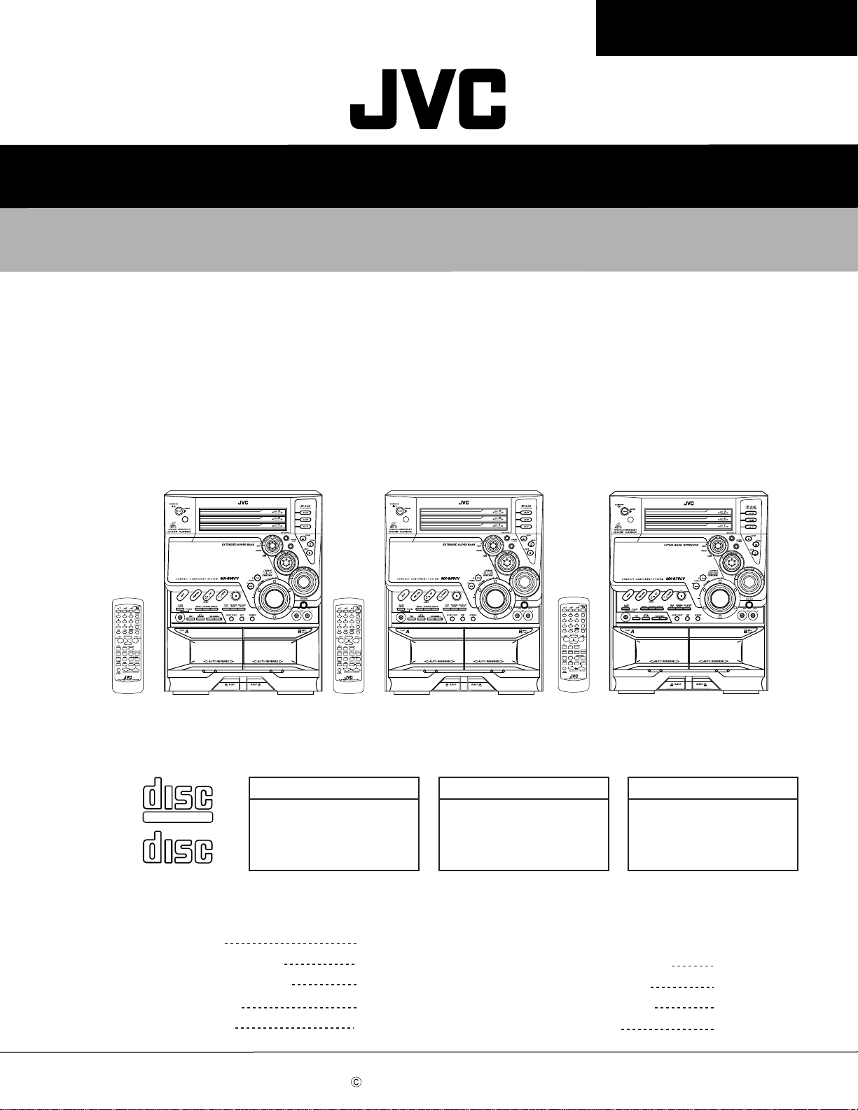
MX-G950V/MX-G880V
MX-G950V/MX-G880V
MX-G850V/MX-G750V
MX-G850V/MX-G750V
SERVICE MANUAL
COMPACT COMPONENT SYSTEM
MX-G950V/MX-G880V
MX-G850V/MX-G750V
CA-MXG950V
COMPACT
DIGITAL VIDEO
COMPACT
DIGITAL AUDIO
MX-G950V/MX-G850V
U-----------------Other Areas
UN----------------------- Asean
UX---------------Saudi Arabia
Contents
Safety precautions
Preventing static electricity
Important for laser products
Disassembly method
Adjustment method
CA-MXG850V
CA-MXG880V
MX-G880V
Area Suffix
UN----------------------- Asean
1-2
1-3
1-4
1-5
1-28
COPYRIGHT 2002 VICTOR COMPANY OF JAPAN, LTD.
Flow of functional operation
until TOC read (CD)
Maintenance of laser pickup
Replacement of laser pickup
Description of major ICs
Area Suffix
CA-MXG750V
MX-G750V
Area Suffix
UN----------------------- Asean
US ----------------- Singapore
UX---------------Saudi Arabia
1-33
1-34
1-34
1-35~56
No.21099
Jul. 2002
1-1
Page 2
MX-G950V/MX-G880V
MX-G850V/MX-G750V
1. This design of this product contains special hardware and many circuits and components specially for safety
purposes. For continued protection, no changes should be made to the original design unless authorized in
writing by the manufacturer. Replacement parts must be identical to those used in the original circuits. Services
should be performed by qualified personnel only.
2. Alterations of the design or circuitry of the product should not be made. Any design alterations of the product
should not be made. Any design alterations or additions will void the manufacturer`s warranty and will further
relieve the manufacture of responsibility for personal injury or property damage resulting therefrom.
3. Many electrical and mechanical parts in the products have special safety-related characteristics. These
characteristics are often not evident from visual inspection nor can the protection afforded by them necessarily
be obtained by using replacement components rated for higher voltage, wattage, etc. Replacement parts which
have these special safety characteristics are identified in the Parts List of Service Manual. Electrical
components having such features are identified by shading on the schematics and by ( ) on the Parts List in
the Service Manual. The use of a substitute replacement which does not have the same safety characteristics
as the recommended replacement parts shown in the Parts List of Service Manual may create shock, fire, or
other hazards.
4. The leads in the products are routed and dressed with ties, clamps, tubings, barriers and the like to be
separated from live parts, high temperature parts, moving parts and/or sharp edges for the prevention of
electric shock and fire hazard. When service is required, the original lead routing and dress should be
observed, and it should be confirmed that they have been returned to normal, after re-assembling.
5. Leakage currnet check (Electrical shock hazard testing)
After re-assembling the product, always perform an isolation check on the exposed metal parts of the product
(antenna terminals, knobs, metal cabinet, screw heads, headphone jack, control shafts, etc.) to be sure the
product is safe to operate without danger of electrical shock.
Do not use a line isolation transformer during this check.
Plug the AC line cord directly into the AC outlet. Using a "Leakage Current Tester", measure the leakage
current from each exposed metal parts of the cabinet, particularly any exposed metal part having a return
path to the chassis, to a known good earth ground. Any leakage current must not exceed 0.5mA AC (r.m.s.).
Alternate check method
Plug the AC line cord directly into the AC outlet. Use an AC voltmeter having, 1,000 ohms per volt or more
sensitivity in the following manner. Connect a 1,500 10W resistor paralleled by a 0.15 F AC-type capacitor
between an exposed metal part and a known good earth ground.
Measure the AC voltage across the resistor with the AC
voltmeter.
Move the resistor connection to each exposed metal part,
particularly any exposed metal part having a return path to
the chassis, and meausre the AC voltage across the resistor.
Now, reverse the plug in the AC outlet and repeat each
measurement. Voltage measured any must not exceed 0.75 V
AC (r.m.s.). This corresponds to 0.5 mA AC (r.m.s.).
0.15 F AC TYPE
1500 10W
Good earth ground
AC VOLTMETER
(Having 1000
ohms/volts,
or more sensitivity)
Place this
probe on
each exposed
metal part.
!
1. This equipment has been designed and manufactured to meet international safety standards.
2. It is the legal responsibility of the repairer to ensure that these safety standards are maintained.
3. Repairs must be made in accordance with the relevant safety standards.
4. It is essential that safety critical components are replaced by approved parts.
5. If mains voltage selector is provided, check setting for local voltage.
Burrs formed during molding may
be left over on some parts of the
chassis. Therefore, pay attention to
such burrs in the case of
preforming repair of this system.
In regard with component parts appearing on the silk-screen printed side (parts side) of the PWB diagrams, the
parts that are printed over with black such as the resistor ( ), diode ( ) and ICP ( ) or identified by the " "
mark nearby are critical for safety.
(This regulation does not correspond to J and C version.)
1-2
Page 3
MX-G950V/MX-G880V
MX-G850V/MX-G750V
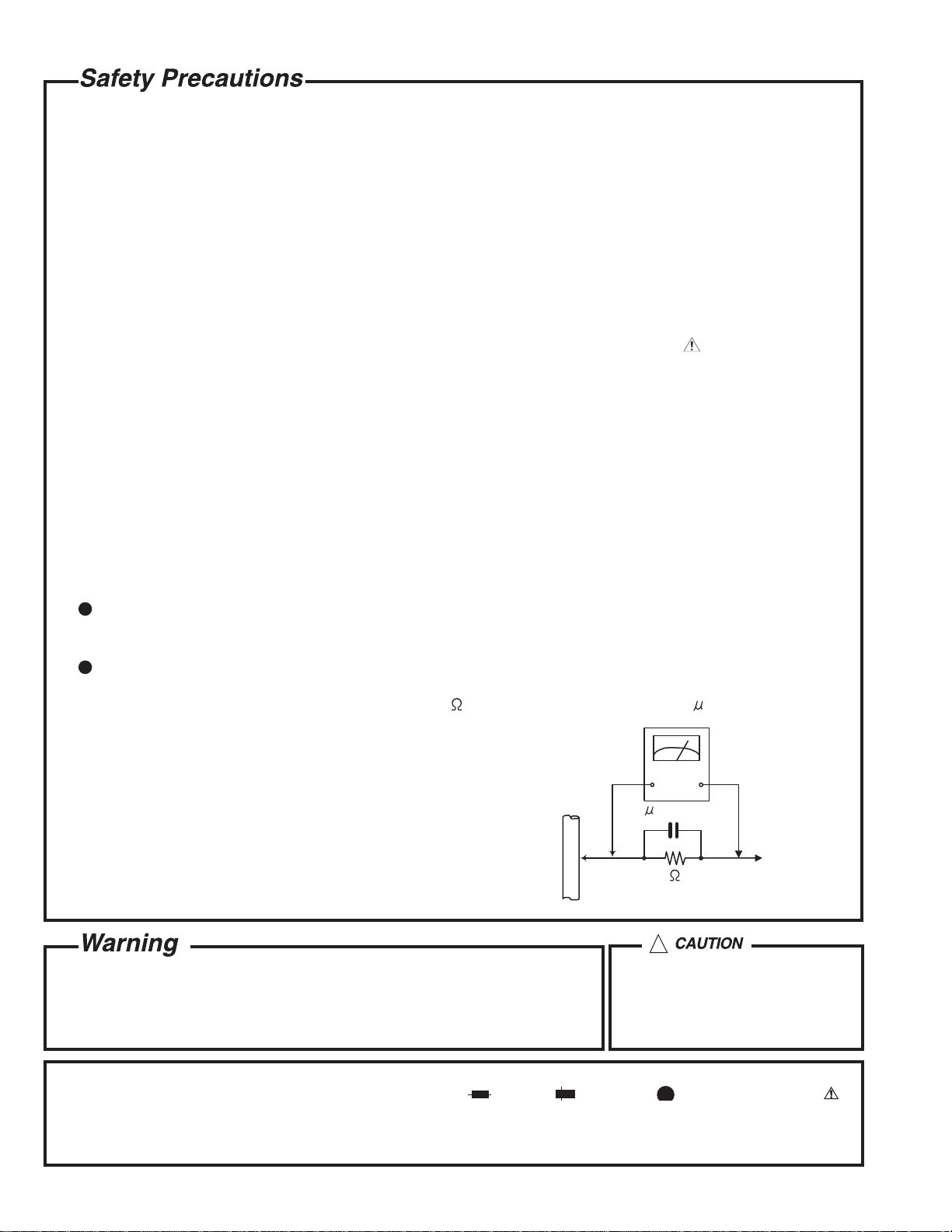
Preventing static electricity
1. Grounding to prevent damage by static electricity
Electrostatic discharge (ESD), which occurs when static electricity stored in the body, fabric, etc. is discharged,
can destroy the laser diode in the traverse unit (optical pickup). Take care to prevent this when performing repairs.
2. About the earth processing for the destruction prevention by static electricity
In the equipment which uses optical pick-up (laser diode), optical pick-up is destroyed by the static electricity of
the work environment.
Be careful to use proper grounding in the area where repairs are being performed.
2-1 Ground the workbench
Ground the workbench by laying conductive material (such as a conductive sheet) or an iron plate over
it before placing the traverse unit (optical pickup) on it.
2-2 Ground yourself
Use an anti-static wrist strap to release any static electricity built up in your body.
(caption)
Anti-static wrist strap
Conductive material
(conductive sheet) or iron plate
3. Handling the optical pickup
1. In order to maintain quality during transport and before installation, both sides of the laser diode on the
replacement optical pickup are shorted. After replacement, return the shorted parts to their original condition.
(Refer to the text.)
2. Do not use a tester to check the condition of the laser diode in the optical pickup. The tester's internal power
source can easily destroy the laser diode.
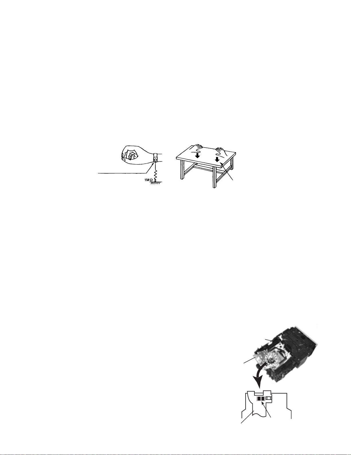
4. Handling the traverse unit (optical pickup)
1. Do not subject the traverse unit (optical pickup) to strong shocks, as it is a sensitive, complex unit.
2. Cut off the shorted part of the flexible cable using nippers, etc. after replacing the optical pickup. For specific
details, refer to the replacement procedure in the text. Remove the anti-static pin when replacing the traverse
unit. Be careful not to take too long a time when attaching it to the connector.
3. Handle the flexible cable carefully as it may break when subjected to strong force.
4. It is not possible to adjust the semi-fixed resistor that adjusts the laser power. Do not turn it
Attention when traverse unit is decomposed
*Please refer to "Disassembly method" in the text for pick-up and how to
detach the CD traverse mechanism.
1. Remove the disk stopper and T. bracket on the CD changer mechanism
assembly.
2. Disconnect the harness from connector on the CD motor board.
3. CD traverse unit is put up as shown in Fig.1.
4. Solder is put up before the card wire is removed from connector CN601
on the CD servo control board as shown in Fig. 2.
(When the wire is removed without putting up solder, the CD pick-up
assembly might destroy.)
5. Please remove solder after connecting the card wire with CN601 when
you install picking up in the substrate.
CD changer
mechanism
assembly
CD traverse
unit
Flexible cable
Fig.1
Soldering
Fig.2
1-3
Page 4
MX-G950V/MX-G880V
MX-G850V/MX-G750V
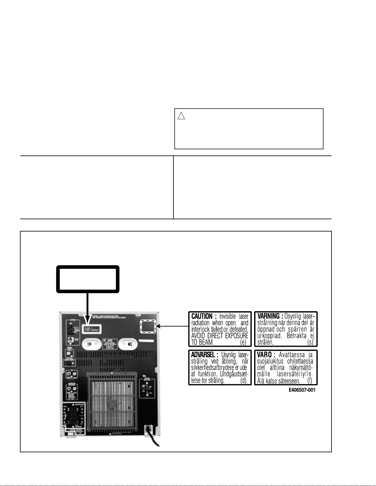
Important for laser products
1.CLASS 1 LASER PRODUCT
2.DANGER : Invisible laser radiation when open and inter
lock failed or defeated. Avoid direct exposure to beam.
3.CAUTION : There are no serviceable parts inside the
Laser Unit. Do not disassemble the Laser Unit. Replace
the complete Laser Unit if it malfunctions.
4.CAUTION : The compact disc player uses invisible laser
radiation and is equipped with safety switches which
prevent emission of radiation when the drawer is open and
the safety interlocks have failed or are defeated. It is
dangerous to defeat the safety switches.
VARNING : Osynlig laserstrålning är denna del är öppnad
och spårren är urkopplad. Betrakta ej strålen.
VARO : Avattaessa ja suojalukitus ohitettaessa olet
alttiina näkymättömälle lasersäteilylle.Älä katso
säteeseen.
5.CAUTION : If safety switches malfunction, the laser is able
to function.
6.CAUTION : Use of controls, adjustments or performance of
procedures other than those specified herein may result in
hazardous radiation exposure.
CAUTION
!
Please use enough caution not to
see the beam directly or touch it
in case of an adjustment or operation
check.
ADVARSEL : Usynlig laserstråling ved åbning , når
sikkerhedsafbrydere er ude af funktion. Undgå
udsættelse for stråling.
ADVARSEL : Usynlig laserstråling ved åpning,når
sikkerhetsbryteren er avslott. unngå utsettelse
for stråling.
REPRODUCTION AND POSITION OF LABELS
WARNING LABEL
CLASS 1
LASER PRODUCT
1-4
Page 5
MX-G950V/MX-G880V
MX-G850V/MX-G750V
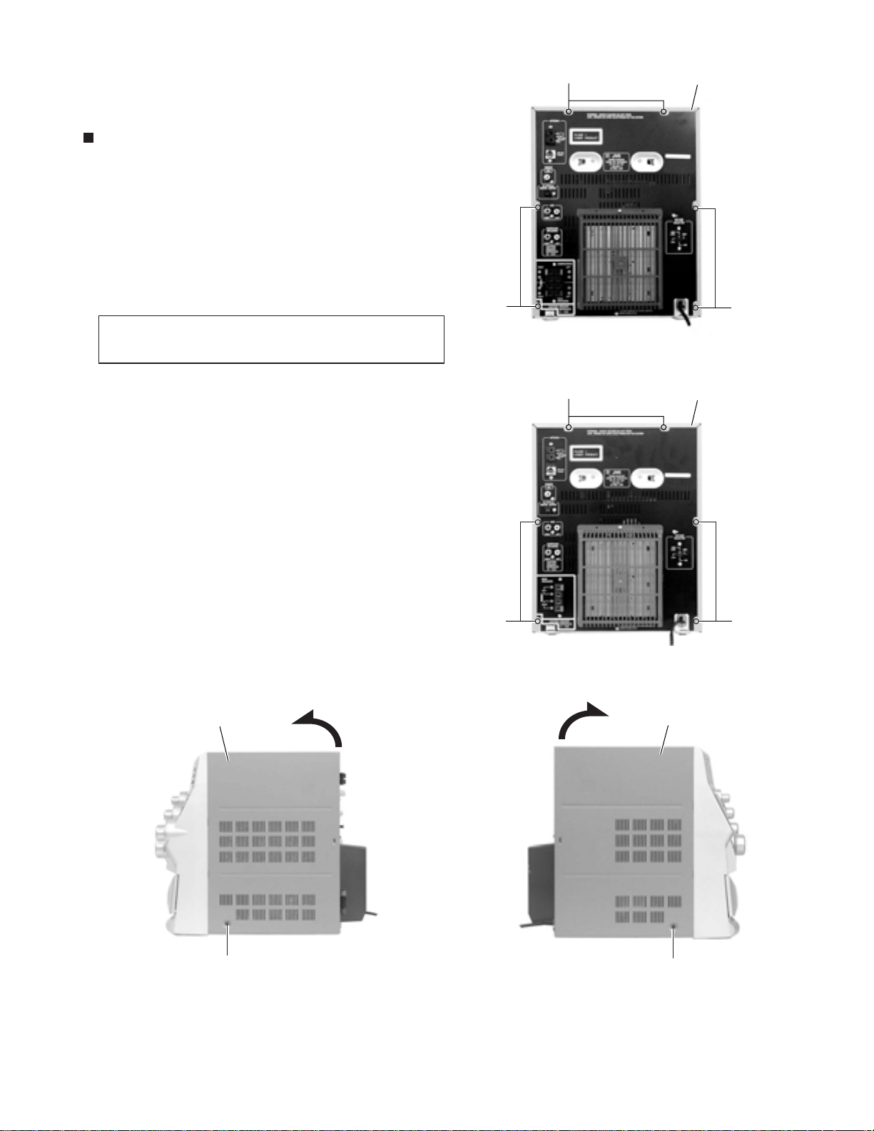
Disassembly method
<Main body>
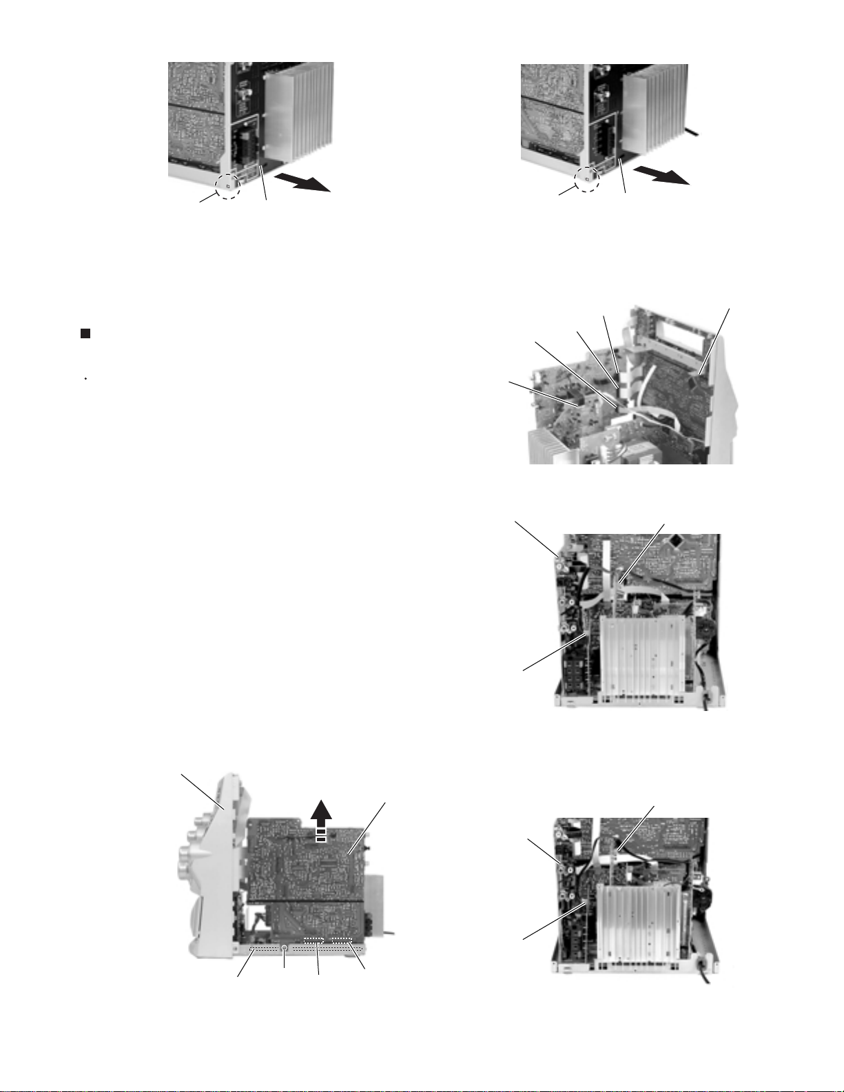
Removing the metal cover
(See Fig.1 ~ 3)
1.
Remove the six screws A on the back of the body.
2.
Remove the two screws B on both sides of the
body.
3.
Remove the metal cover from the body by lifting the
rear part of the cover.
CAUTION:
Do not break the front panel tab fitted to
the metal cover.
A
Metal cover
A
(CA-MXG850VU, CA-MXG950VUX)
A
Fig.1
Metal cover
A
Metal cover
B
Fig.2
A
A
Fig.1
(CA-MXG750VUS)
Metal cover
B
Fig.3
1-5
Page 6
MX-G950V/MX-G880V
MX-G850V/MX-G750V
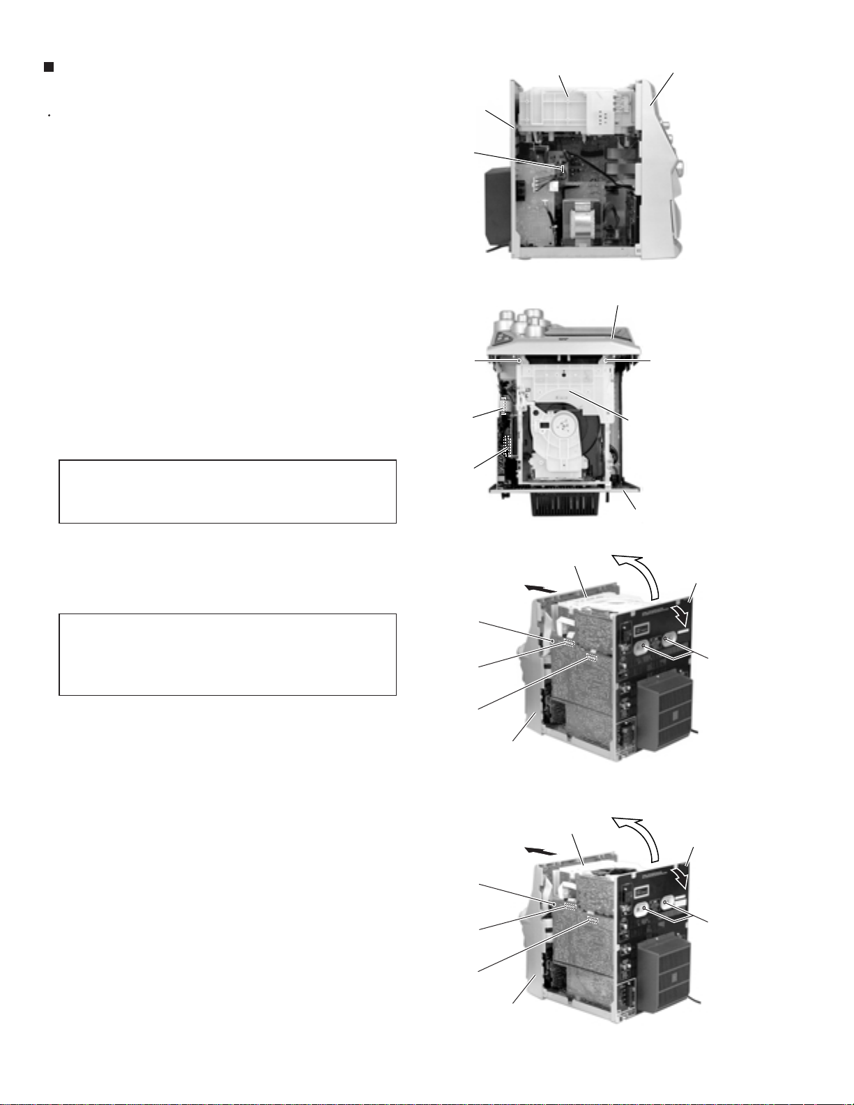
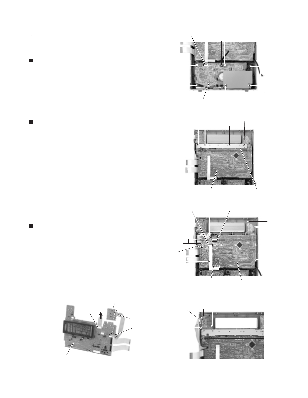
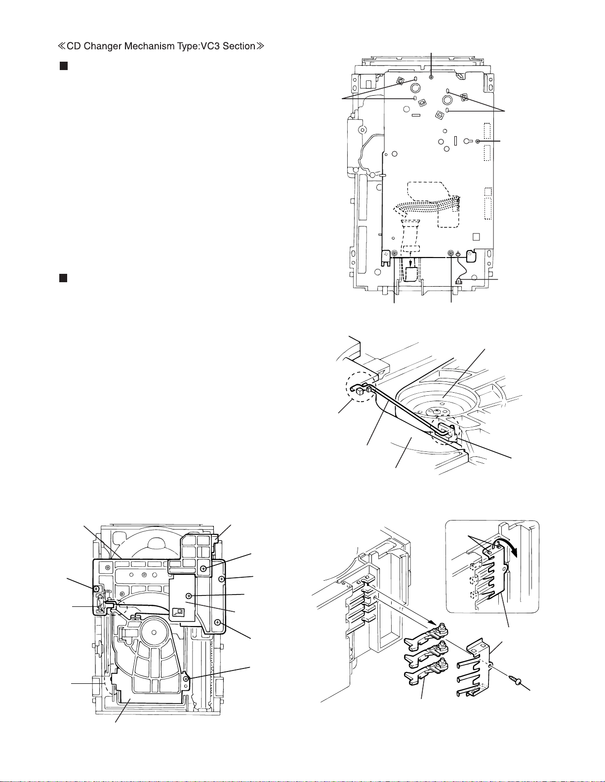
Removing the CD changer mechanism
assembly (See Fig.4, 6)
Prior to performing the following procedure, remove
the metal cover.
1.
Disconnect the wire from connector CN705 on the
amplifier board.
2.
Remove the plastic rivet attaching the main board to
the front assembly on the right side of the body.
3.
Disconnect the card wire from connector CN661 on
the main board.
4.
Remove the two screws C on the upper side of the
body and the two screws D on the back of the rear
panel.
5.
Pull both the rear panel and the front panel assembly
to the outside, then remove the CD changer
mechanism assembly by lifting the rear part of the
assembly.
CD changer mechanism assembly
Rear panel
Amplifier board
CN705
Fig.4
Front panel assembly
C
Main board
CN661
Front panel assembly
C
CD changer
mechanism assembly
REFERENCE:
At this point, one card wire on the
underside of the CD mechanism
assembly is still connected.
6.
Disconnect the card wire from connector CN504 on
the inner side of the main board on the right side of
the body. Remove the CD mechanism assembly.
CAUTION:
To prevent damage to the CD fitting, be
sure to pull both the rear panel and the
front panel assembly enough to remove
the CD changer mechanism assembly.
CN504
Fig.5
CD changer mechanism assembly
Plastic rivet
Main board
CN661
CN504
Front panel assembly
Fig.6
(CA-MXG850VU, CA-MXG950VUX)
CD changer mechanism assembly
Rear panel
Rear panel
D
Rear panel
1-6
Plastic rivet
Main board
CN661
CN504
Front panel assembly
D
Fig.6
(CA-MXG750VUS)
Page 7
MX-G950V/MX-G880V
MX-G850V/MX-G750V
Removing the fan (See Fig.7)
Prior to performing the following procedure, remove
the metal cover and the CD changer mechanism
assembly.
1.
Turn over the CD changer mechanism assembly and
remove the two screws E attaching the fan.
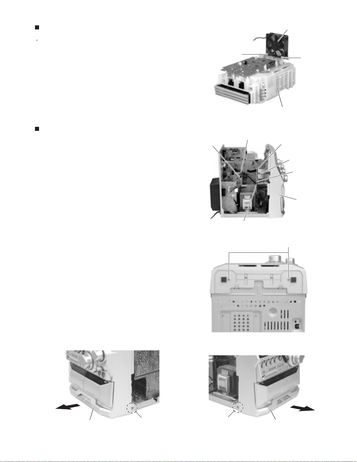
Removing the front panel assembly
(See Fig.8 ~ 11)
Prior to performing the following procedure, remove
the metal cover and CD changer mechanism
assembly.
1.
Disconnect the card wires from connector CN870,
CN871 and CN315 on the main board respectively.
Amplifier board
CN703
Fan
E
CD changer mechanism assembly
Fig.7
Band
Main board
CN870
E
CN871
CN315
2.
Remove the band and disconnect the wire from
connector CN703 on the amplifier board.
3.
Disconnect the wire from connector CN220 on the
transformer board.
4.
Remove the two screws F on the bottom of the
body.
5.
Release the two joints a on the lower right and left
sides of the body using a screwdriver, and remove
the front panel assembly toward the front.
Transformer board
CN220
Fig.8
(Bottom)
Fig.9
Front panel
assembly
F
Front panel assembly
Fig.10
Joint a
Joint a
Front panel assembly
Fig.11
1-7
Page 8
MX-G950V/MX-G880V
MX-G850V/MX-G750V
Removing the tuner board
(See Fig.12)
Prior to performing the following procedure, remove
the metal cover.
1.
Disconnect the card wire from connector CN1 on the
tuner board on the right side of the body.
2.
Remove the plastic rivet fixing the tuner board.
3.
Remove the two screws G on the back of the body.
Removing the rear cover / rear panel
(See Fig.13 ~ 16)
Prior to performing the following procedure, remove
the metal cover and the CD changer mechanism
assembly.
1.
Remove the screw H attaching the rear cover on the
back of the body.
2.
Push each tab of the four joints b in the direction of
the arrow and release.
3.
Remove the sixteen screws G attaching the rear
panel.
4.
Disengage the joints c on each lower side of the rear
panel using a screwdriver and remove the rear panel
backward.
Plastic rivet
G
Joint b
Rear cover
(CA-MXG850VU, CA-MXG950VUX)
G
CN1
Tuner board
Fig.12
H
Fig.13
H
Rear panel
G
Rear panel
Joint b
Rear panel
Rear panel
G
G
G
Fig.14
(CA-MXG850VU, CA-MXG950VUX)
Rear panel
Fig.15
Joint c
G
G
Joint b
Rear cover
G
G
G
Joint b
Fig.13
(CA-MXG750VUS)
Rear panel
G
G
Fig.14
(CA-MXG750VUS)
1-8
Page 9
MX-G950V/MX-G880V
MX-G850V/MX-G750V
Joint c
Rear panel
Fig.16
(CA-MXG850VU, CA-MXG950VUX)
Removing the main board
(See Fig.17 ~ 19)
Prior to performing the following procedure, remove
the metal cover, the CD changer mechanism
assembly, the rear panel and the tuner board.
1.
Disconnect the card wires from connector CN870,
CN871 and CN315 on the main board.
2.
Disconnect the wires from connector CN704 and
CN706 on the amplifier board.
3.
Remove the screw I attaching the main board on
the right side of the body.
4.
Disconnect the wire from connector CN710 on the
speaker board.
CN315
Amplifier board
CN704
CN706
Main board
Joint c
Fig.16
(CA-MXG750VUS)
Main board
CN870
CN871
Fig.17
Rear panel
Front panel assembly
Amplifier board
CN704, CN706
5.
Disconnect connector CN211 and CN212 on the
main board from the regulator board.
Front panel assembly
Main board
Regulator board
I
CN212
CN211
Fig.19
Speaker board
CN710
Fig.18
(CA-MXG850VU, CA-MXG950VUX)
Amplifier board
CN704, CN706
Main board
Speaker board
CN710
Fig.18
(CA-MXG750VUS)
1-9
Page 10
MX-G950V/MX-G880V
MX-G850V/MX-G750V
Removing the speaker board
(See Fig.20)
Prior to performing the following procedure, remove
the metal cover, the CD changer mechanism
assembly and the rear panel.
REFERENCE:
1.
Disconnect the wire from connector CN710 on the
speaker board.
2.
Disconnect connector CN217 on the speaker board
from the regulator board.
It is not necessary to remove the main
board.
Speaker board
CN701
Regulator board
CN217
Fig.20
(CA-MXG850VU, CA-MXG950VUX)
Speaker board
CN710
Removing the power board (See Fig.21)
Prior to performing the following procedure, remove
the metal cover, the CD changermechanism
assembly and the rear panel.
1.
Remove a band on the power board.
2.
Disconnect the wire from connector CN218, CN219
and CN250 on the power board.
3.
Disconnect connector CN213 on the power board
from the regulator board.
Regulator board
Power board
CN219
CN250
CN213
Fig.20
CN217
(CA-MXG750VUS)
CN218
Band
Fig.21
1-10
Page 11
MX-G950V/MX-G880V
MX-G850V/MX-G750V
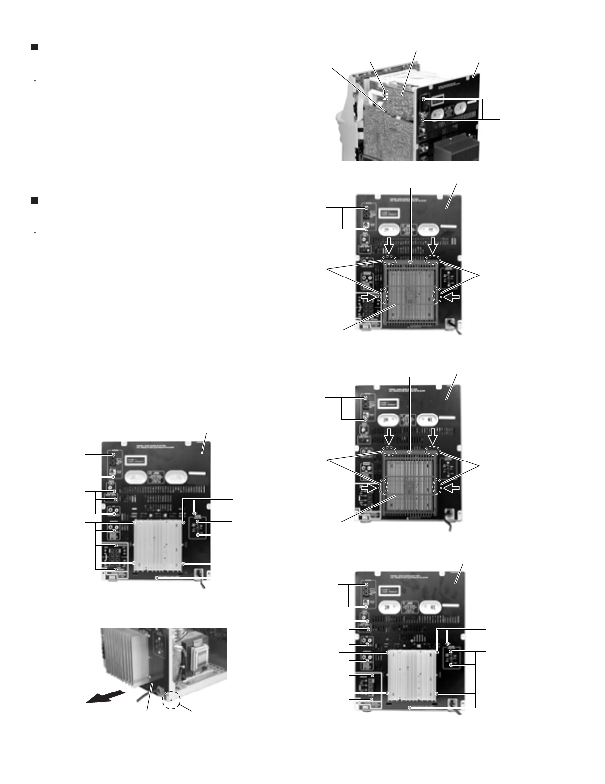
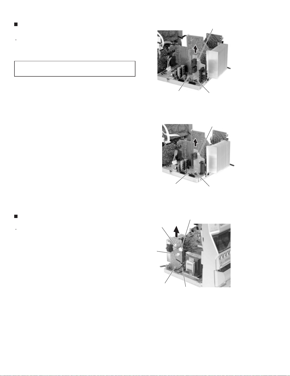
Removing the amplifier board / voltage
board / heat sink (See Fig.22, 23)
Prior to performing the following procedure, remove
the metal cover, the CD changer mechanism
assembly and the rear panel.
1.
Disconnect the wires from connector CN703, CN704
and CN706 on the amplifier board respectively.
2.
Remove the two band attaching the wire to the
amplifier board and the voltage board.
3.
Disconnect connector CN215 on the amplifier board
and CN216 on the voltage board from the regulator
board (The heat sink will be detached at once).
4.
Remove the four screws J attaching the amplifier
board to the heat sink.
5.
Remove the two screws K, the board bracket and
the voltage board.
REFERENCE:
It is not necessary to remove the power
board.
Voltage board
Regulator board
Heat sink
Voltage board
Amplifier board
CN704
CN706
Band
CN216
Fig.22
Band
CN703
CN215
Amplifier board
J
K
CA-MXG850VU, CA-MXG950VUX)
Heat sink
Voltage board
J
Board bracket
Fig.23
Amplifier board
J
J
K
Board bracket
Fig.23
(CA-MXG750VUS)
1-11
Page 12
MX-G950V/MX-G880V
MX-G850V/MX-G750V
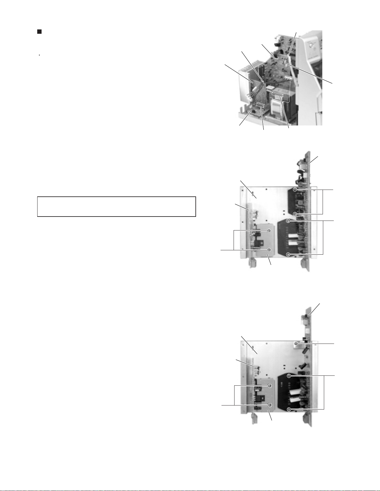
Removing the power transformer
assembly (See Fig.24, 25)
Prior to performing the following procedure, remove
the metal cover, the CD changer mechanism
assembly and the rear panel.
1.
Disconnect the wires from connector CN218 and
CN219 on the power board.
2.
Disconnect the wire from connector CN204 on the
regulator board.
3.
Disconnect the wire from connector CN220 on the
transformer board.
4.
Remove a band on the voltage board.
5.
Release the wire from the stopper on the regulator
board.
6.
Remove the four screws L attaching the transformer
assembly.
Power board
CN219
CN218
Band
L
Transformer board
CN220
Power transformer assembly
Fig.24
Stopper
Regulator board
CN204
L
Removing the regulator board
(See Fig.26)
Prior to performing the following procedure, remove
the metal cover, the CD changer mechanism
assembly, the rear panel, the antenna board, the
main board, the amplifier board, the voltage board,
the power board and the speaker board.
1.
Disconnect the wire from connector CN204 on the
regulator board.
2.
Release the wire from the stopper on the regulator
board.
3.
Remove the two screws M attaching the reglator
board.
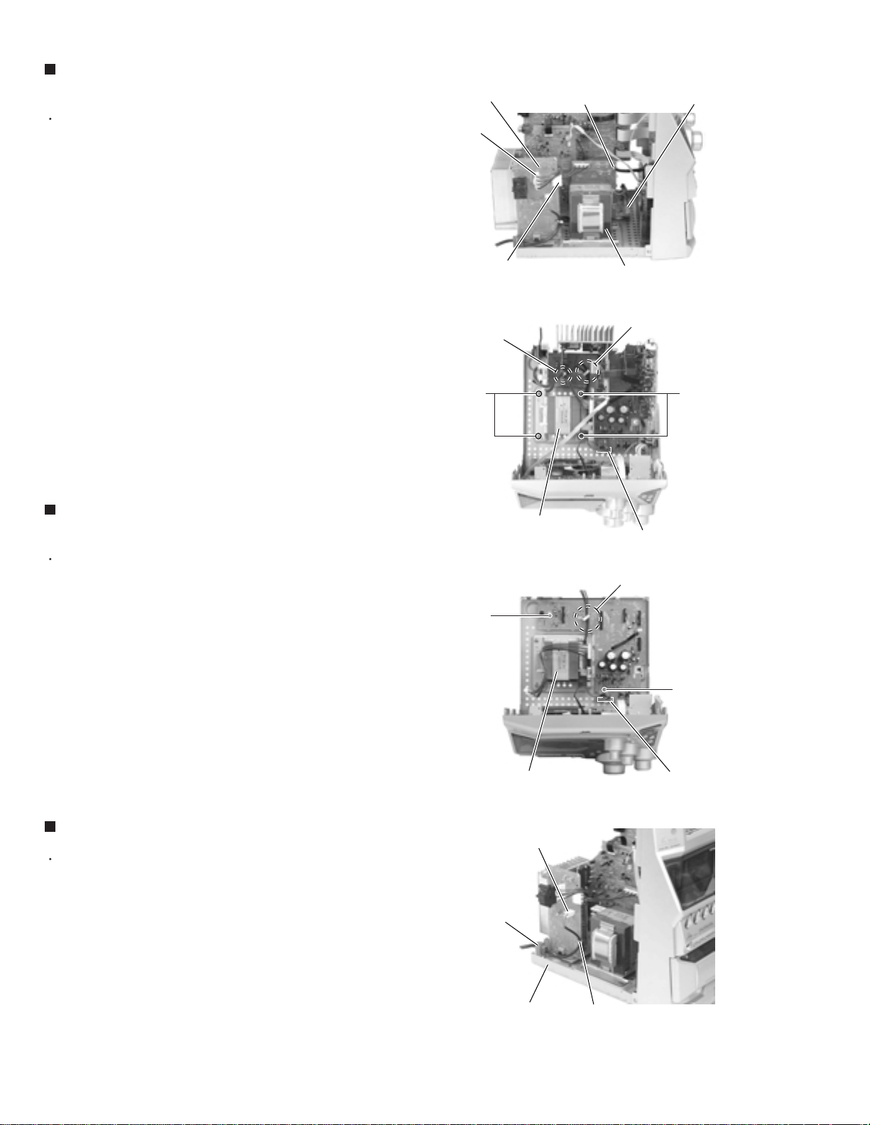
Removing the power cord (See Fig.27)
Prior to performing the following procedure, remove
the metal cover, the CD changer mechanism
assembly and the rear panel.
1.
Disconnect the wire from connector CN250 on the
power board.
Power transformer
assembly
M
Power transformer assembly
Power board
CN250
Power cord stopper
Fig.25
Fig.26
Regulator board
CN204
Stopper
M
Regulator board
CN204
2.
Remove the band from the power board.
3.
Move the power cord stopper upward and pull out it
from the base chassis.
1-12
Base chassis
Band
Fig.27
Page 13
MX-G950V/MX-G880V
MX-G850V/MX-G750V
<Front panel assembly>
Prior to performing the following procedure, remove
the metal cover, the CD changer mechanism
assembly and the front panel assembly.
Removing the cassette mechanism
assembly (See Fig.28)
1.
Disconnect the card wire from connector CN306 on
the head amplifier & mechanism control board.
2.
Remove the seven screws N attaching the cassette
mechanism assembly.
Removing the display system control
board (See Fig.29 ~ 31)
1.
Remove the four screws O attaching the stay
bracket.
2.
Disconnect the card wires from connector CN316
and CN880 on the display system control board.
Head amplifier
& mechanismcontrol board
CN306
N
Cassette mechanism
assembly
N
N
N
Fig.28
O
3.
Remove the seven screws P attaching the display
system control board.
4.
If necessary, disconnect the wire from connector
CN911 on the front side of the display system control
board and unsolder FW915.
Removing the CD eject board
(See Fig.31, 32)
1.
Remove the three screws Q attaching the CD eject
board.
2.
If necessary, unsolder FW915 on the CD eject
board.
CD eject board
CN911
FW915
FW915
Display system control board
CN316
P
FW915
(Solding)
P
CN880
CD eject board
FW915
(Solding)
Q
P
Q
Stay bracket
Fig.29
CN911
P
P
Display system control board
Fig.30
Display system control board
Fig.31
Fig.32
1-13
Page 14
MX-G950V/MX-G880V
MX-G850V/MX-G750V
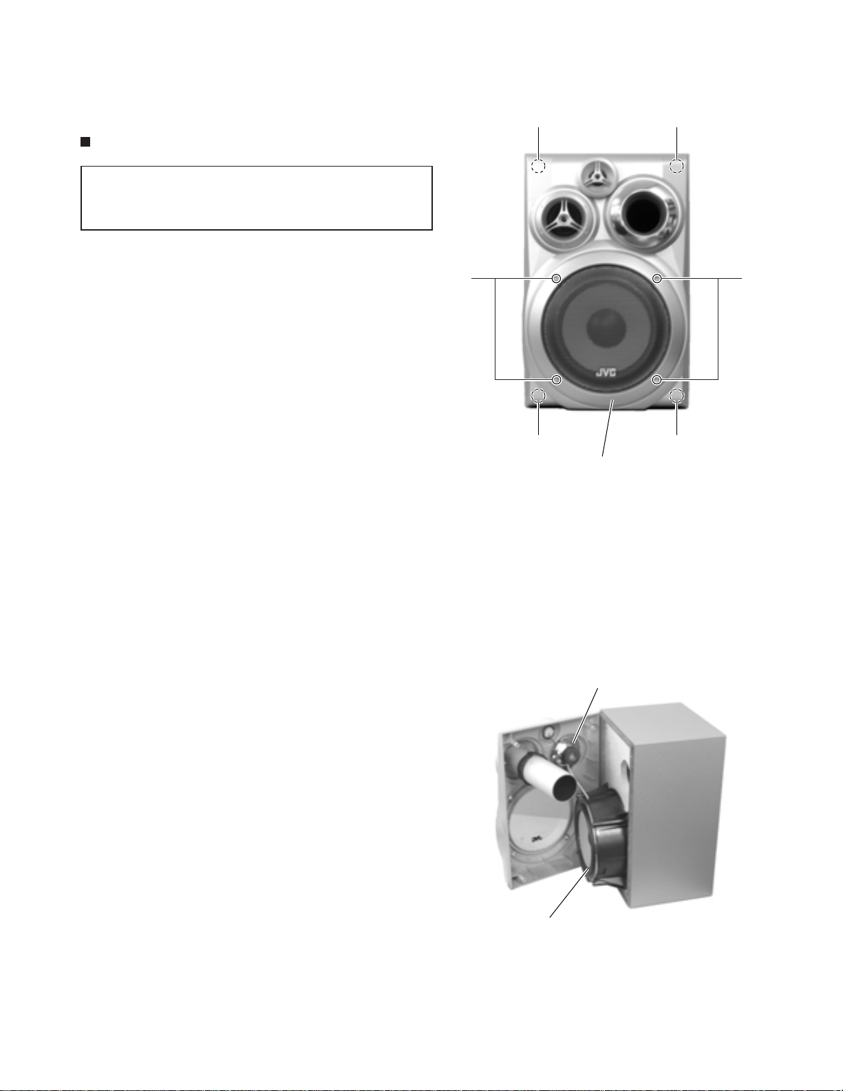
Removing the preset / tuning switch
board (See Fig.33, 34)
Prior to performing the following procedure, remove
the display system control board.
1.
Pull out the preset knob on the front panel.
2.
Remove the four screws R attaching the preset /
tuning switch board.
3.
If necessary, unsolder FW901 on the preset / tuning
switch board.
Removing the operation switch board
(See Fig.34, 35)
Prior to performing the following procedure, remove
the display system control board and the preset /
tuning switch board.
1.
Pull out the volume knob on the front panel and
remove the nut. Pull out the sound mode knob, the
mic level knob and the sub woofer level knob toward
the front.
R
Preset / tuning switch board
FW901
(Solding)
Preset knob
R
Fig.33
Sound mode knob
Sub woofer
level knob
2.
Remove the twelve screws S attaching the
operation switch board.
3.
Release each tab of the seven joints g retaining the
operation switch board.
Joint g
Joint g
S
S
Volume knob
Joint g
Mic level knob
Nut
Fig.33
S
Operation
switch board
1-14
S
Joint g
S
Fig.35
S
S
Joint g
Page 15
Disassembly method
MX-G950V/MX-G880V
MX-G850V/MX-G750V
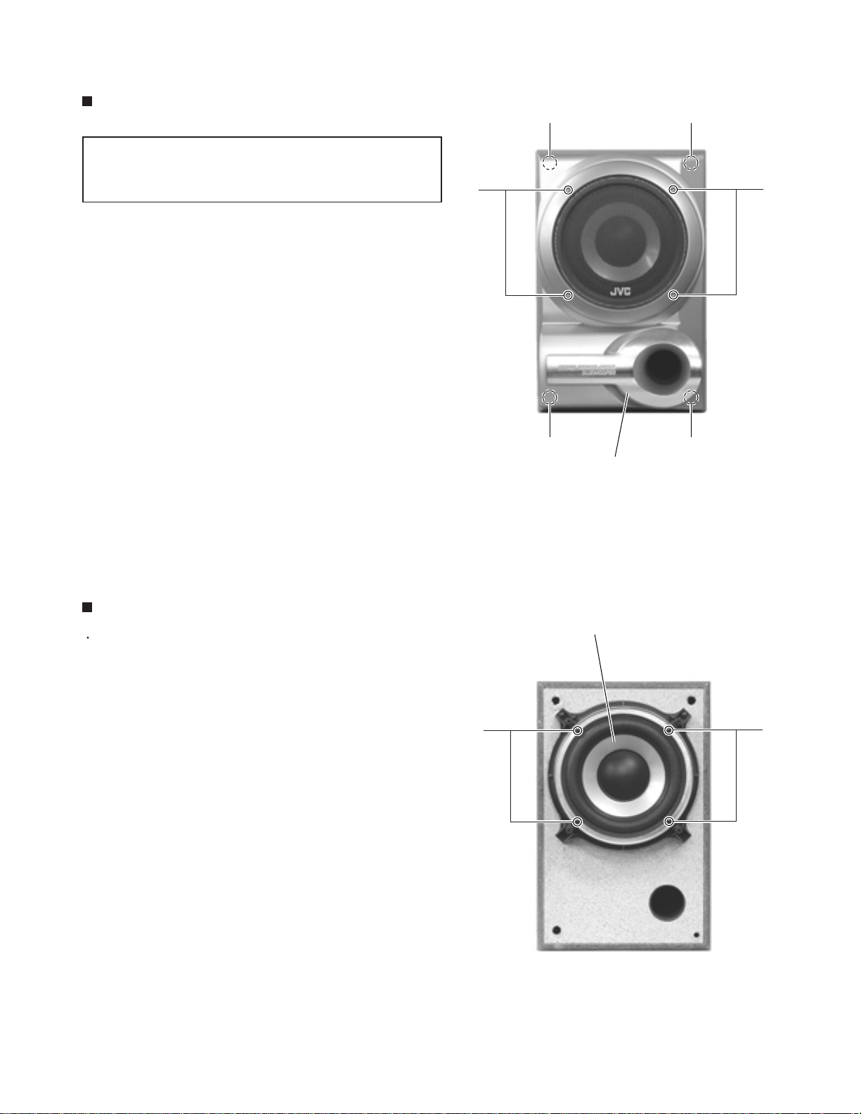
<speaker section>
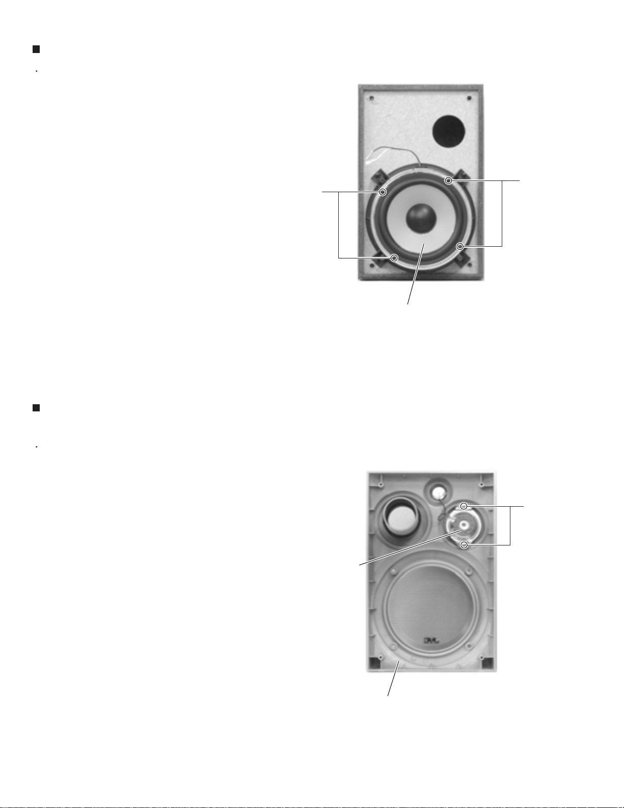
Removing the front cover (See Fig.1,2)
CAUTION:
1.
Remove the four screws A on the front of the body
respectively.
2.
Remove the front cover toward the front and
disconnect the yellow and black wires from the two
tweeter speaker terminals.
Do not break or damage the front panel and
body that are glued at the joints a.
(See Fig.1)
A
Joint a
Joint a Joint a
Front cover
Joint a
A
Fig.1
(SP-MXG750V)
(SP-MXG850V)
(SP-MXG950V)
Tweeter speaker
Woofer speaker
(SP-MXG750V)
(SP-MXG850V)
(SP-MXG950V)
Fig.2
1-15
Page 16
MX-G950V/MX-G880V
MX-G850V/MX-G750V
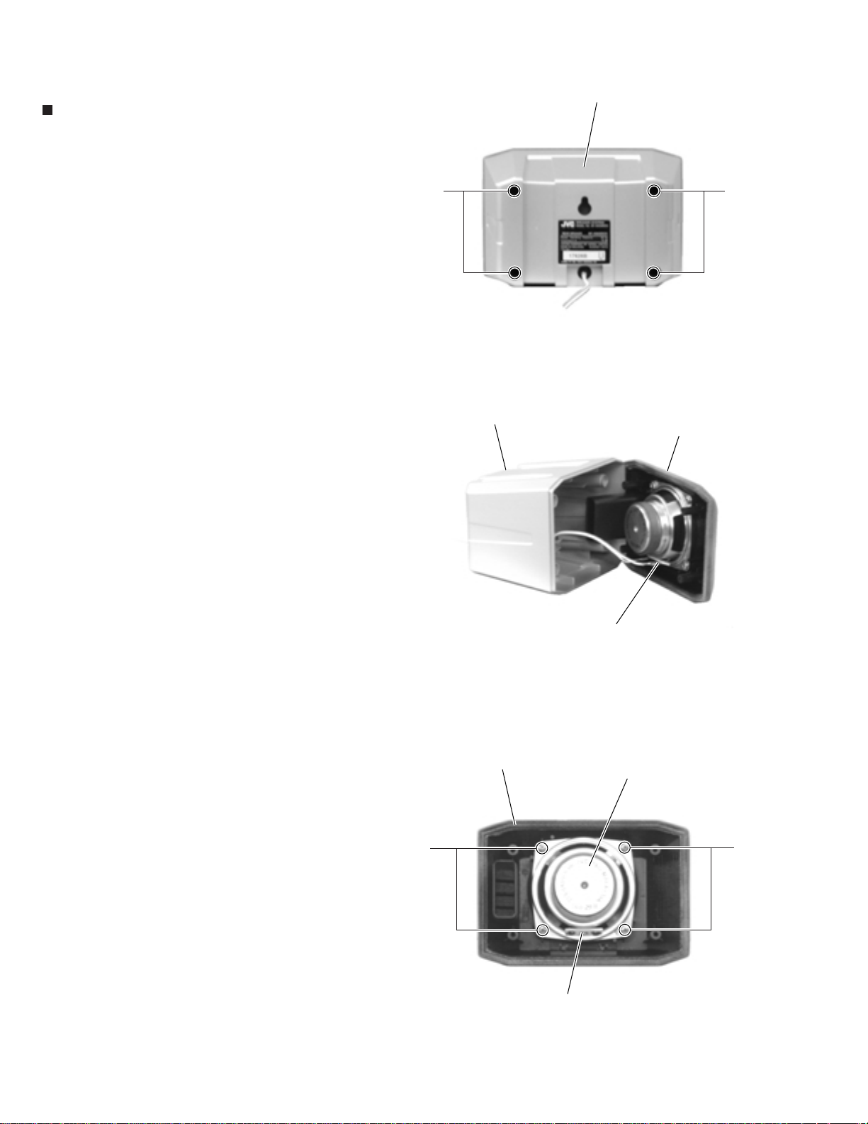
Removing the woofer speaker (See Fig.3)
Prior to performing the following procedure, remove
the front cover.
1.
Remove the four screws B on the front of the body.
2.
Pull out the woofer speaker toward the front and
disconnect the wire (yellow and black,red and black)
from the two speaker terminals.
B
B
Removing the tweeter speaker
(See Fig.4)
Prior to performing the following procedure, remove
the front cover.
1.
Disconnect the red and black wires from the two
tweeter speaker terminals.
2.
Remove the two screws C attaching the tweeter
speaker on the back of the front cover.
Woofer speaker
Fig.3
(SP-MXG750V)
(SP-MXG850V)
(SP-MXG950V)
C
Tweeter speaker
1-16
Front cover
Fig.4
(SP-MXG750V)
(SP-MXG850V)
(SP-MXG950V)
Page 17
<Woofer speaker section>
MX-G950V/MX-G880V
MX-G850V/MX-G750V
Removing the front cover (See Fig.5)
CAUTION:
1.
Remove the four screws D on the front of the body
respectively.
2.
Remove the front cover toward the front.
Do not break or damage the front panel and
body that are glued at the joints b.
(See Fig.5)
Joint b
Joint b Joint b
Front cover
Joint b
DD
Removing the woofer speaker (See Fig.6)
Prior to performing the following procedure, remove
the front cover.
1.
Remove the four screws E on the front of the body.
2.
Pull out the woofer speaker toward the front and
disconnect the red and black wires from the two
speaker terminals.
Fig.5
(SP-MXG850V)
(SP-MXG950V)
Woofer speaker
EE
Fig.6
(SP-MXG850V)
(SP-MXG950V)
1-17
Page 18
MX-G950V/MX-G880V
MX-G850V/MX-G750V
<Removing the Rear speaker>
Removing the Rear cover (See Fig.7 ~ 9 )
1.
Remove the four screws F on the back of the body.
2.
Disconnect the wires from the two terminals on the
rear speaker.
3.
Remove the four screws G on the back of the front
cover.
F
Rear cover
F
Fig.7(SP-MXG950V)
Rear cover
Front cover
Rear speaker
Fig.8(SP-MXG950V)
terminals
Rear speaker
Front cover
1-18
G
Rear speaker
Fig.9(SP-MXG950V)
terminals
G
Page 19
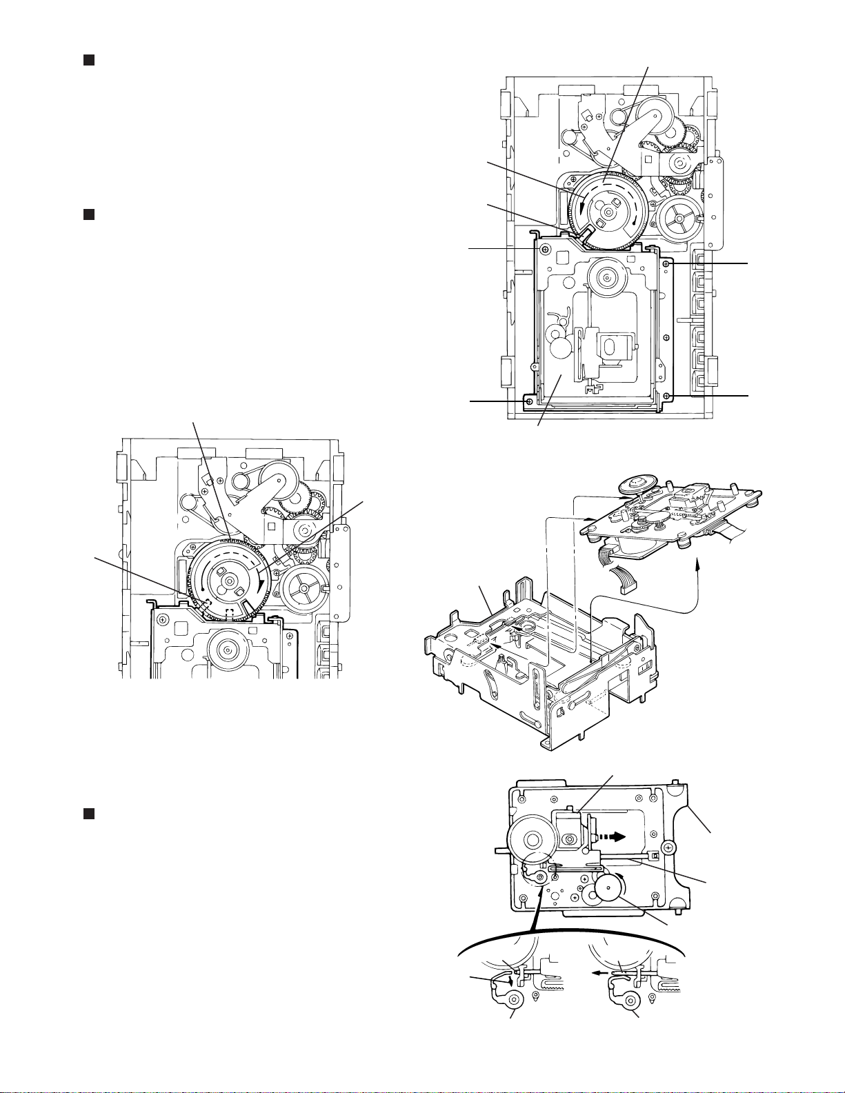
Removing the CD Servo control board
(See Fig.1)
1.Remove the metal cover.
2.Remove the CD changer mechanism assembly.
3.From bottom side the CD changer mechanism assembly,
remove the four screws A retaining the CD servo control
board.
4.Absorb the four soldered positions "a" of the right and
left motors with a soldering absorber.
5.Pull out the earth wire on the CD changer mechanism
assembly.
6.Disconnect the connector CN854 on the CD servo
control board.
7.Disconnect the card wire CN601 and the connector
CN801 on the CD servo control board.
MX-G950V/MX-G880V
MX-G850V/MX-G750V
A
a
a
CN854
A
CN651
CD servo control board
CN652
CN801
CN601
CN151
Removing the CD tray assembly
(See Fig.2~4)
Remove the front panel assembly.
1.
Remove the CD changer mechanism assembly.
2.
Remove the CD Servo control board.
3.
Remove the screw B' retaining the lod stopper.
4.
From the T.bracket section "b" and clamper base
5.
section "c" , remove both of the edges fixing the
rod(See Fig.2 and 3).
Remove the screw B retaining the disc stopper
6.
(See Fig.3).
Remove the three screws C retaining the T.bracket
7.
(See Fig.3).
Remove the screw D retaining the clamper assembly
8.
(See Fig.3).
From the left side face of the chassis assembly, remove
9.
the one screw E retaining both of the return spring and
lock lever(See Fig. 4).
10.
By removing the pawl at the section "d" fixing the return
spring, dismount the return spring(See Fig.4).
11.
Remove the three lock levers(See Fig.4).
T.Braket
Disc stopper
B
Earth
wire
Fig.1
A
Clamper base
A
b
Rod
c
T.Braket
Fig.2
d
CC
B'
a
Lod stopper
(C/J version only)
C
D
b
Lock lever
Clamper ass'y
Fig.3
Fig.4
Return spring
E
1-19
Page 20
MX-G950V/MX-G880V
MX-G850V/MX-G750V
11.
Check whether the lifter unit stopper has been caught
into the hole at the section "e" of CD tray assembly as
shown in Fig.5.
Make sure that the driver unit elevator is positioned as
12.
shown in Fig.6 from to the second or fifth hole on the
left side face of the CD changer mechanism assembly.
[Caution]
13.
14.
15.
Chassis assembly
In case the driver unit elevator is not at above
position, set the elevator to the position as
shown in Fig.7 by manually turning the pulley
gear as shown in Fig.8.
Manually turn the motor pulley in the clockwise
direction until the lifter unit stopper is lowered from the
section "e" of CD tray assembly(See Fig.8).
Pull out all of the three stages of CD tray assembly in
the arrow direction "f" until these stages stop
(See Fig.6).
At the position where the CD tray assembly has
stopped, pull out the CD tray assembly while pressing
the two pawls "g and g' " on the back side of CD tray
assembly(See Fig.9). In this case, it is easy to pull out
the assembly when it is pulled out first from the stage
CD tray assembly.
Stopper
e
CD tray
assembly
Fig.5
Refer to Fig.7
Pulley gear
Pawl
Fig.6
CD tray assembly
g
CD
CD
CD
f
Drive unit of elevator
Fig.7
3
2
1
CD tray assembly
1-20
Motor pulley
Fig.8
Pawl ,
g
Fig.9
g'
Page 21
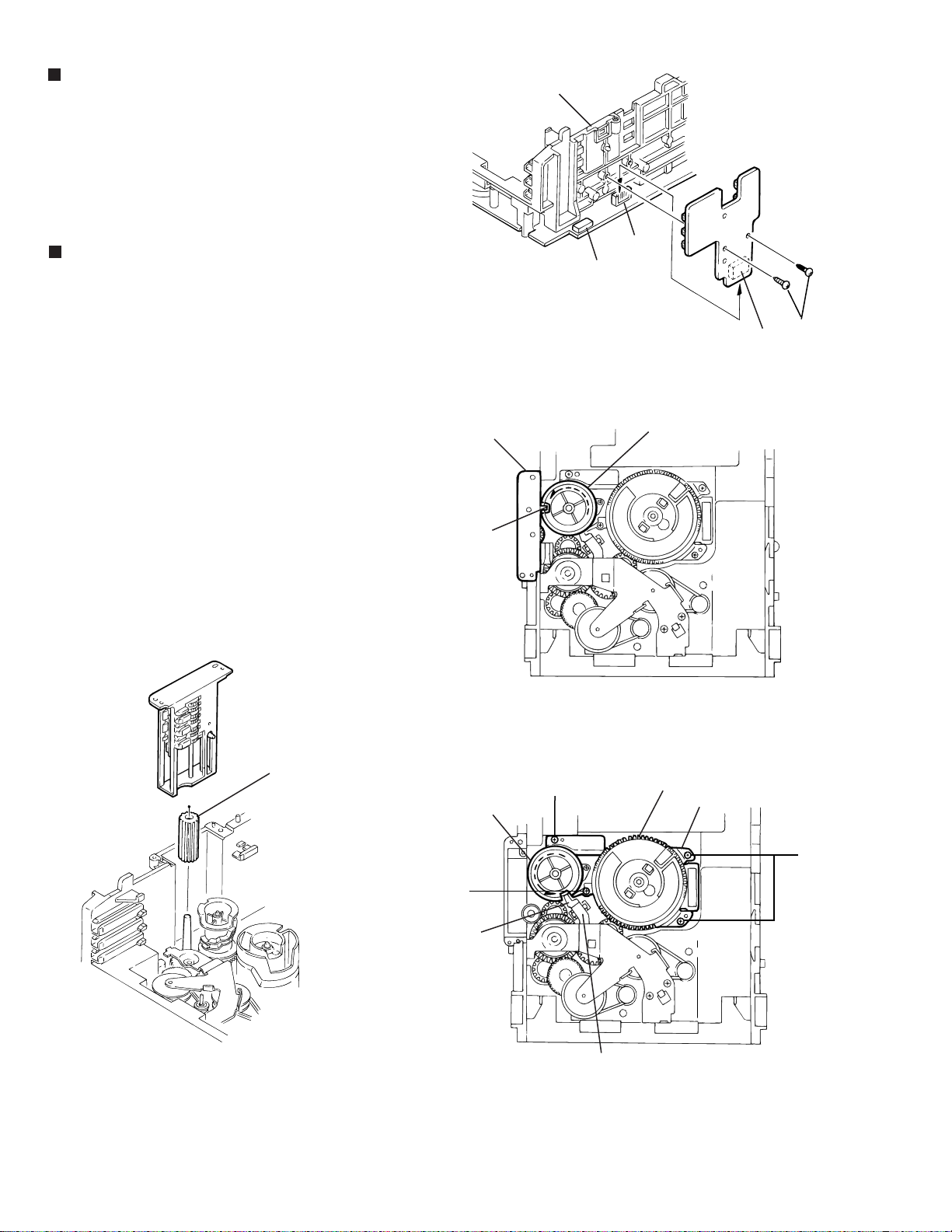
Removing the CD loading mechanism
assembly(See Fig.10)
1.2.While turning the cams R1 and R2 assembly in the
arrow direction "h" ,align the shaft "i" of the CD loading
mechanism assembly to the position shown in Fig.10.
Remove the four screws F retaining the CD loading
mechanism assembly.
Removing the CD traverse mechanism
(See Fig.11 and 12 )
For dismounting only the CD traverse mechanism
1.
without removing the CD loading mechanism assembly,
align the shaft "j" of the CD loading mechanism
assembly to the position shown Fig.11 while turning the
cam R1 and R2 assembly in the arrow direction "k" .
By raising the CD loading mechanism assembly in the
2.
arrow direction "l", remove the assembly from the lifter
unit
MX-G950V/MX-G880V
MX-G850V/MX-G750V
Cams R1, R2 assembly
Arrow
h
i
F
F
Cam R1, R2 assembly
j
Fig.11
Arrow
F
CD loading mechanism assembly
F
Fig.10
CD traverse mechanism
k
Lifter unit
Fig.12
CD Pickup unit
Arrow
l
Removing the CD pick unit
(See Fig.13 )
1.
Move the cam gear in the arrow direction "m" . Then,
the CD pickup unit will be moved in the arrow direction
"n" .
According to the above step, shift the CD pickup unit to
2.
the center position.
While pressing the stopper retaining the shaft in the
3.
arrow direction "o" , pull out the shaft in the arrow
direction "p".
After dismounting the shaft from the CD pickup unit,
4.
remove the CD pickup unit
o
Shaft
Stopper
p
Fig.13
Shaft
n
m
Stopper
CD loading
mechanism
Shaft
Cam gear
1-21
Page 22
MX-G950V/MX-G880V
MX-G850V/MX-G750V
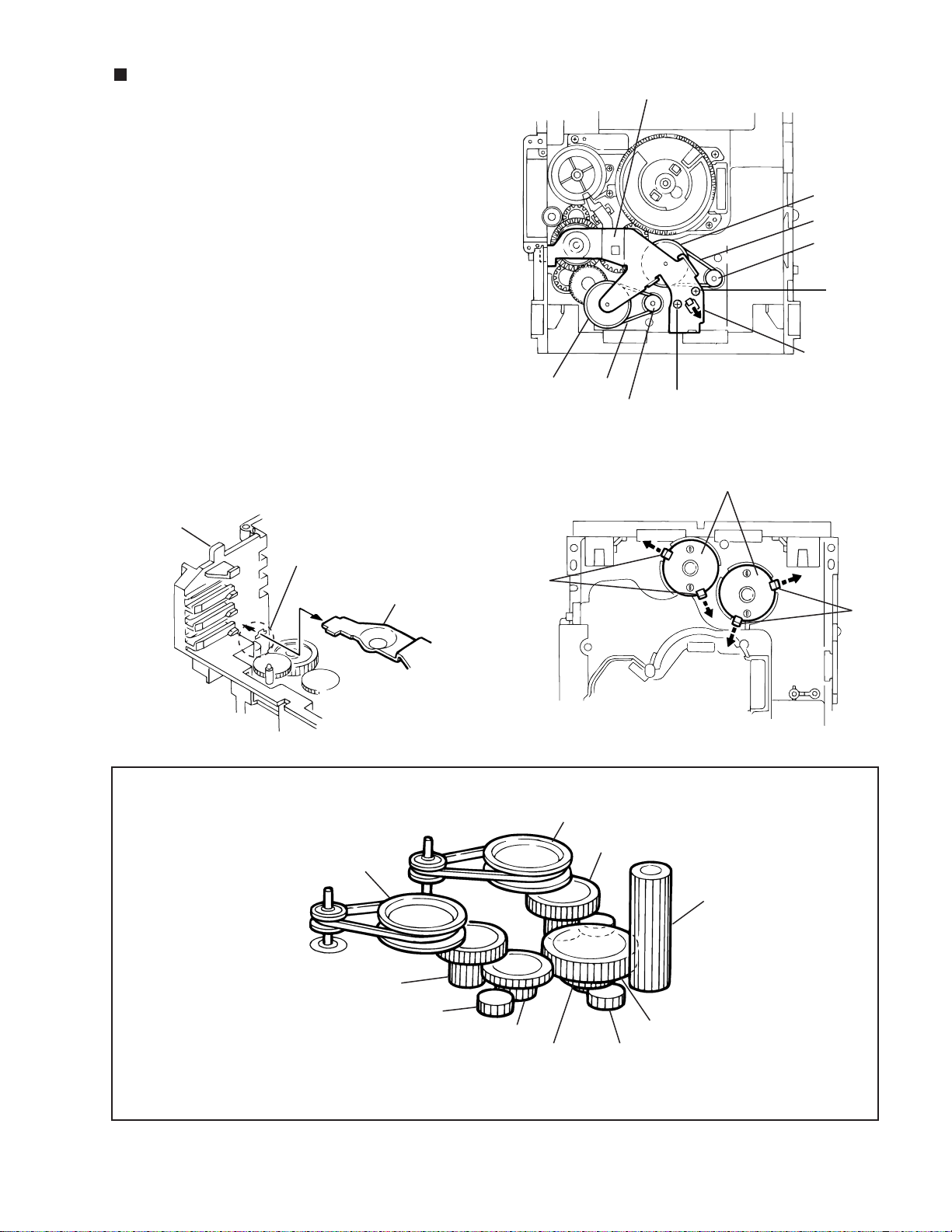
Removing the try select switch board
(See Fig.14)
1.2.Remove the two screws G retaining the tray select
switch board.
Disconnect the tray select switch board from connector
CN804 on the CD servo control board.
Removing the cam unit
(See Fig.15 ~17 )
1.
Remove the CD loading mechanism assembly.
2.
While turning the cam gear "q", align the Paul "r"
position of the drive unit to the notch position(Fig.16) on
the cam gear "q".
Pull out the drive unit and cylinder gear(See Fig.17).
3.
While turning the cam gear "q", align the Paul "s"
4.
position of the select lever to the notch position(Fig.18)
on the cam gear "q".
Remove the four screws H retaining the cam unit(cam
5.
gear "q" and cams R1/R2 assembly)(See Fig.18).
Chassis assembly
Drive unit
CN851
CN854
Fig.14
Cam gear
Tray select
switch board
CN804
q
G
Drive unit
Cylinder gear
r
Cam gear
H
s
Fig.15
H
q
Cams R1, R2 assembly
Cam unit
J
1-22
Fig.16
Select lever
Fig.17
Page 23
MX-G950V/MX-G880V
Fig.18
Fig.20
Fig.19
Fig.21
[Note]
When the chassis assembly is turned over under
the conditions wherein the gear bracket and belt
have been removed, then the pulley gear as well
as the gear, etc. constituting the gear unit can
possibly be separated to pieces. In such a case,
assemble these parts by referring to the assembly
and configuration diagram in Fig. 21.
Removing the actuator motor and belt
(See Fig.18~21)
1.
2.
3.
4.
5.
Remove the two screws I retaining the gear bracket
(See Fig.18).
While pressing the pawl "t" fixing the gear bracket in the
arrow direction, remove the gear bracket
(See Fig.18).
From the notch "u section" on the chassis assembly
fixing the edge of gear bracket, remove and take out the
gear bracket(See Fig. 19).
Remove the belts respectively from the right and left
actuator motor pulleys and pulley gears(See Fig. 18).
After turning over the chassis assembly, remove the
actuator motor while spreading the four pawls "v" fixing
the right and left actuator motors in the arrow
direction(See Fig. 20).
Pulley gear
Belt
Motor pulley
Belt
Pulley gear
Motor pulley
Gear bracket
t
I
I
Pawl
v
Actuator motor
v
Chassis assembly
u
Gear bracket
Pulley gear
Gear B
Cylinder gear
Gross gear U
Gear C
Gross gear L
Select gear
Gear B
Gear C
Pulley gear
Assembly and Configuration Diagram
MX-G850V/MX-G750V
1-23
Page 24
MX-G950V/MX-G880V
MX-G850V/MX-G750V
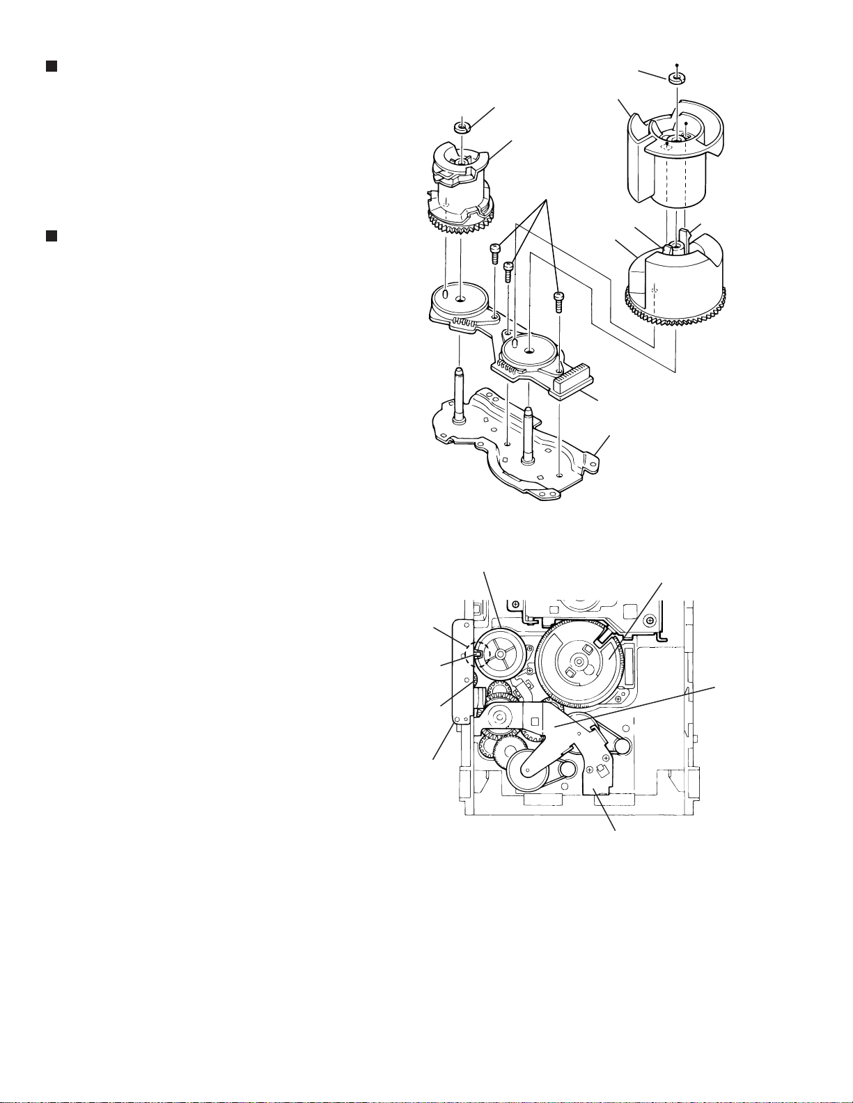
Removing the cams R1/R2 assembly
and cam gear q(See Fig.22)
1.
Remove the slit washer fixing the cams R1 and R2
assembly.
2.
By removing the two pawls "w" fixing the cam R1,
separate R2 from R1.
Remove the slit washer fixing the cam gear "q".
3.
Pull out the cam gear "q" from the C.G. base assembly.
4.
Removing the C.G. base assembly
(See Fig.22 and 23)
Remove the three screws J retaining the C.G. base
assembly.
[Caution]
To reassemble the cylinder gear, etc.with the
cam unit (cam gear and cans R1/R2 assembly),
gear unit and drive unit, align the position of the
pawl "x" on the drive unit to that of the notch on
the cam gear "q". Then, make sure that the
gear unit is engaged by turning the cam gear
"q" (See Fig. 24).
Slit washer
Cam gear q
J
Slit washer
Cam R2
Pawl
w
Cam R1
Cam switch board
C.G. base assembly
Pawl
w
Notch
Pawl
x
Cylinder
gear
Drive unit
Fig.22
Cam gear q
Cam R1, R2 assembly
Gear unit
Gear bracket
Fig.23
1-24
Page 25
MX-G950V/MX-G880V
MX-G850V/MX-G750V
< Cassette mechanism section >
Removing the playback,recording and eraser
heads (See Fig.1~3)
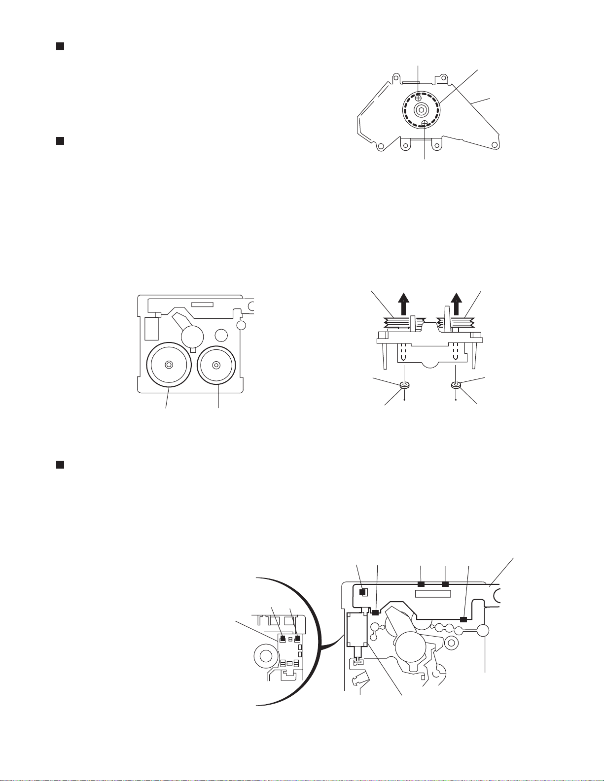
1. While shifting the trigger arms seen on the right
side of the head mount in the arrow direction,turn
the flywheel R in counterclockwise direction until
the head mount has gone out with a click
(See Fig. 1).
2. When the flywheel R is rotated in counterclockwise
direction, the playback / recording & eraser head will
be turned in counterclockwise direction from the
position in Fig.2 to that in Fig.3.
3. At this position, disconnect the flexible P.C.board
(outgoing from the playback head) from the
connector CN301 on the head amp. and mechanism
control P.C. board.
4. Remove the flexible P.C.board from the chassis
base.
5. Remove the spring "a" from behind the playback /
recording head.
6. Loosen the reversing azimuth screw retaining the
playback head.
7. Take out the playback head from the front of the
head mount.
8. The recording and eraser heads should also be
removed similarly according to Steps 1~7 above.
Flexible
P.C.board
Cassette mechanism
Trigger armHead mount
Fig.1
Playback/Recording &
eraser head
(Mechanism A side)
Flywheel R
Spring "a"
Trigger arm
Reassembling the playback, recording
and eraser heads (See Fig.3)
1. Reassemble the playback head from the front of
the head mount to the position as shown in Fig.3.
2. Fix the reversing azimuth screw.
3. Set the spring a from behind the playback head.
4. Attach the flexible P.C.board to the chassis base
as shown in Fig.3.
5. The recording and eraser heads should also be
reassembled similarly according to Steps 1~4
above.
CN301
Head amplifier & mechanism
control P.C. board
Fig.2
Playback head
Spring "a"
CN302
FPC holder
Fig.3
Flywheel R
(Mechanism A side)
Reversing azimuth
screw
Head
mount
Flexible
P.C.board
Head amplifier &
mechanism control
P.C. board
(Mechanism B side)
1-25
Page 26
MX-G950V/MX-G880V
MX-G850V/MX-G750V
Removing the head amp. and mechanism
control board (See Fig. 4)
1.Remove the cassette mechanism assembly.
2.After turning over the cassette mechanism
assembly,remove the five screws "A" retaining
the head amplifier & mechanism control board.
3.Disconnect the connectors CN303 on the board
and the connectors CN301 and on CN302 both
the right and left side reel pulse boards.
4.When necessary, remove the 4pin parallel
wire soldered to the main motor
Removing the capstan motor assembly
(See Fig.5 to 7)
1.Remove the six screws "B" retaining capstan
motor assembly (See Fig. 5).
2.While raising the capstan motor, remove the
capstan belts A and B respectively from the
motor pulley (See Fig. 6).
Caution 1: Be sure to handle the capstan
belts so carefully that these belts
will not be stained by grease and
other foreign matter. Moreover,
these belts should be hand while
referring to the capstan belt
hanging method.(See Fig.6 and 7)
A
Flexible
board
Head amplifier &
mechanism control board
AA
CN303
CN302 CN301
Flexible
board
Fig.4
BB
Capstan motor
assembly
AA
1-26
Capstan
belt A
Fig.5
Capstan motor
Capstan
belt A
Capstan
belt B
Motor pulley
Fig.7 Fig.6
BBBB
Capstan
belt B
Page 27
MX-G950V/MX-G880V
MX-G850V/MX-G750V
Removing the capstan motor (See Fig. 8)
From the joint bracket, remove the two screws "C"
retaining the capstan motor.
Removing the flywheel (See Fig. 9,10)
1.Remove the head amp. and mechanism control
P.C.Board.
2.Remove the capstan motor assembly.
3.After turning over the cassette mechanism, remove
the two slit washers "b" fixing the capstan shafts
R and L, and pull out the flywheels R and L respectively
from behind the cassette mechanism.
C
Capstan motor
Joint
bracket
C
Fig.8
Flywheel R Flywheel L
Flywheel R Flywheel L
Fig.10
Removing the reel pulse board and solenoid
(See Fig. 11)
1.Remove the five pawls (c,d,e,f,g) retaining
the reel pulse P.C.Board.
2.From the surface of the reel pulse P.C.Board parts,
remove the two pawls "h" and "i" retaining the solenoid.
hi
Solenoid
c
a
d
Slit
washer "a"
Fig.9
e
f
b
Slit
washer "b"
Reel pulse board
g
Solenoid
Fig.11
1-27
Page 28

MX-G950V/MX-G880V
MX-G850V/MX-G750V
Adjustment method
Measurement instruments required
for adjustment
1. Low frequency oscillator,
This oscillator should have a capacity to output 0dBs
to 600ohm at an oscillation frequency of 50Hz-20kHz.
2. Attenuator impedance : 600ohm
3. Electronic voltmeter
4. Frequency counter
5. Wow flutter meter
6. Test tape
VT712 : For Tape speed and wow flutter ( 3kHz)
VT710 : Head azimuth
VT724 : For Reference level (1kHz)
7. Blank tape
TAPE : AC-225
8. Torque gauge : For play and back tension
Forward ; TW2111A, Reverse ; TW2121A
Fast Forward and Rewind ; TW2231A
9. Test disc
: CTS-1000(12cm),GRG-1211(8cm)
10. Jitter meter
Radio input signal
AM modulation frequency : 400Hz
Modulation factor : 30%
FM modulation frequency : 400Hz
Frequency displacement : 22.5kHz
Frequency Range
AM 531kHz~1710kHz
FM 87.5MHz~108MHz
Standard measurement positions of volume
and switch
Power : Standby (Light STANDBY Indicator)
Sub woofer VOL. : Minimum
Sound mode : OFF
Main VOL. : 0 Minimum
Traverse mecha set position : Disc 1
Mic MIX VOL : MAX
ECHO : OFF
Measurement conditions
Power supply voltage
AC110V/127V/220V/230V 240V , adjustable
Measurement
output terminal : Speaker out
: TP101(Mesuring for TUNER/DECK/CD)
: Dummy load 6ohm
Precautions for measurement
1. Apply 30pF and 33kohm to the IF sweeper output
side and 0.082 F and 100kohm in series to
the sweeper input side.
2. The IF sweeper output level should be made as
low as possible within the adjustable range.
3. Since the IF sweeper is a fixed device, there is
no need to adjust this sweeper.
4. Since a ceramic oscillator is used, there is no need
to perform any MPX adjustment.
5. Since a fixed coil is used, there is no need to adjust
the FM tracking.
6. The input and output earth systems are separated.
In case of simultaneously measuring the voltage
in both of the input and output systems with an
electronic voltmeter for two channels, therefore,
the earth should be connected particularly.
7. In the case of BTL connection amplifier, the minus
terminal of speaker is not for earthing. Therefore,
be sure not to connect any other earth terminal
to this terminal. This system is of an OTL system.
1-28
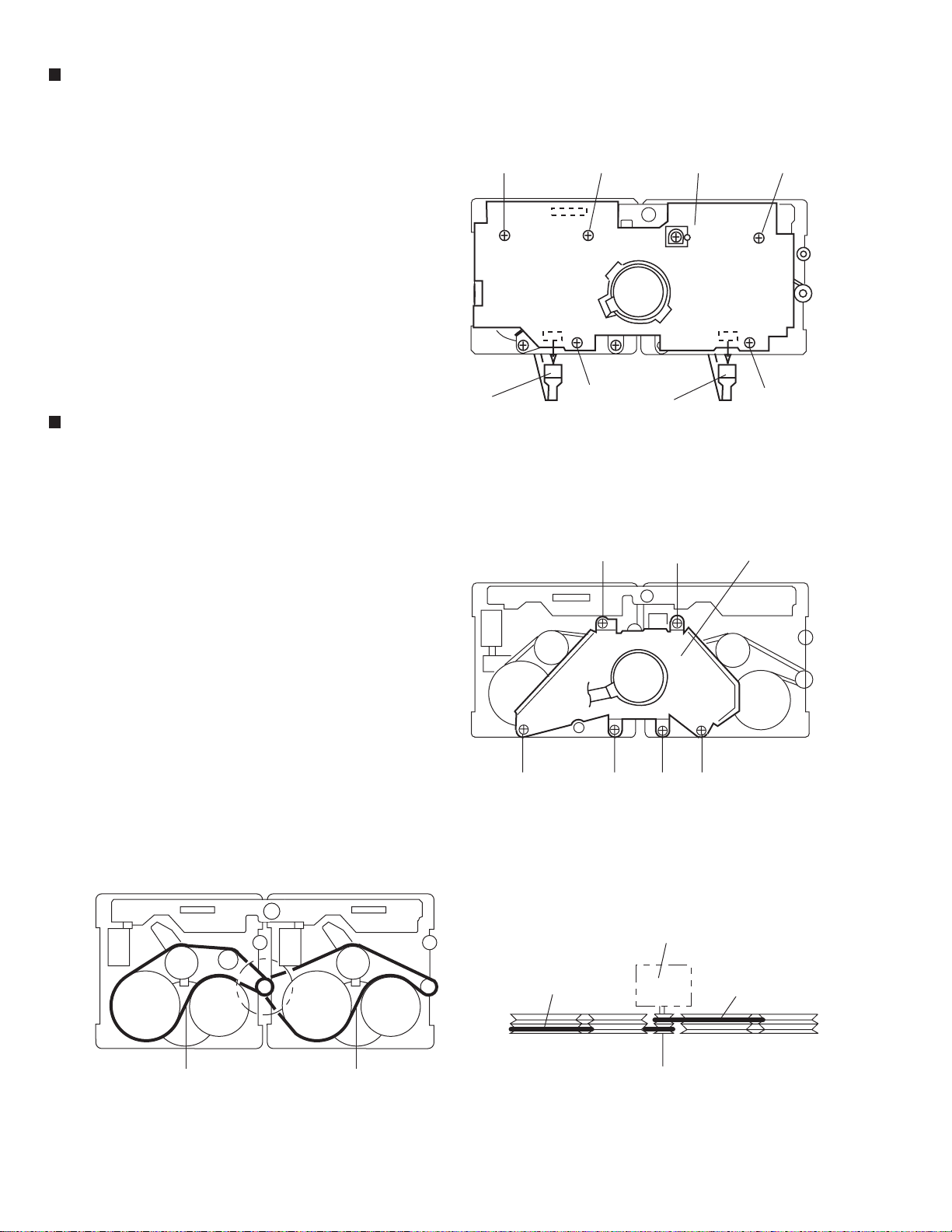
Page 29
Arrangement of adjusting positions
MX-G950V/MX-G880V
MX-G850V/MX-G750V
Cassette mechanism section (Mechanism A section)
Head azimuth
adjusting screw
(Forward side)
Playback
head
Head azimuth
adjusting screw
(Reverse side)
Cassette mechanism section (Back side)
Head azimuth
adjusting screw
(Forward side)
Playback, recording and eraser
heads or playback head
Head azimuth
adjusting screw
(Reverse side)
Cassette Mechanism Unit Section
Tape speed ADJ
Bias ADJ L
Bias ADJ R
1-29
Page 30
MX-G950V/MX-G880V
MX-G850V/MX-G750V
Tape recorder section
Items Measurement
Confirmation
of head angle
Confirmation
of tape speed
conditions
Test tape
:VT710 (10kHz)
Measurement
output terminal
:Speaker terminal
Speaker R
(Load resistor:6 )
:Headphone terminal
Test tape
:VT712 (3kHz) or
TMT7036 (3kHz)
Measurement
output terminal
:Headphone terminal
1.Playback the test tape VT710 (10kHz).
2.With the playback mechanism or recording &
playback mechanism, adjust the head azimuth
screw so that the forward and reverse output
levels become maximum.After adjustment,lock
the head azimuth at least by half a turn.
3.In either case,this adjustment should be
performed in both the forward and reverse
directions with the head azimuth screw.
<Constant speed>
Adjust VR301 so that the frequency counter reading
becomes 3,000Hz 60Hz when playing back the
test tape VT712 (3kHz)with the playback mechanism
or playback and recording mechanism after ending
forward winding of the tape.
Reference values for confirmation items
Items Measurement
Double tape
speed
conditions
Test tape
:VT712 (3kHz)
Measurement
output terminal
:Speaker terminal
Speaker R
(Load resistance:6 )
measurement
output terminal
:Headphone terminal
After setting to the double speed motor, confirm
that the frequency counter reading becomes
4,800+400/-300Hz when the test tape VT712
(3kHz) has been play back with the playback
mechanism.
Measurement method
Measurement method
Standard
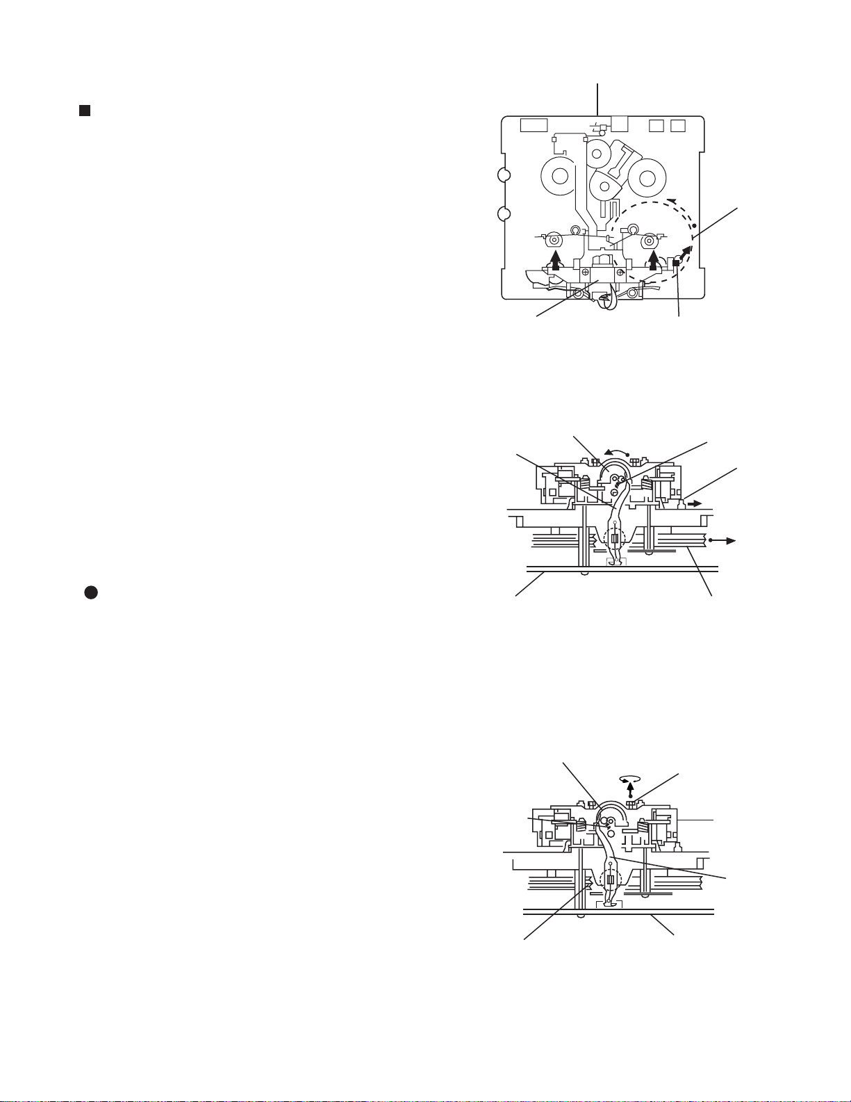
values
Maximum
output
Tape speed
of decks
(A and B)
:3,000Hz
60Hz
Standard
values
4,800+400/
-300Hz
Adjusting
positions
Adjust the head
azimuth screw
only when the
head has been
changed.
VR301
Adjusting
positions
Playback
mechanism side
Difference
between the
forward and
reverse speed.
P.mecha and
R/P mecha
speed
Wow & flutter
1-30
Test tape
:VT712 (3kHz)
Measurement
output terminal
:Headphone terminal
When the test tape VT712 (3kHz) has been played
back with the playback mechanism or recording and
playback mechanism at the beginning of forward
winding, the frequency counter reading of the
difference between both of the mechanisms should
be 6.0Hz or less.
When the test tape VT712 (3kHz) has been played
back with the playback mechanism or recording and
playback mechanism at the beginning of forward
winding the frequency counter reading of wow &
flutter should be 0.25% or less(WRMS).
60Hz or
less
with in
0.25%
JIS(WTD)
Both the playback
and recording &
playback
mechanism
Both the playback
and recording &
playback
mechanism
Page 31

Items Measurement
conditions
Measurement method
Standard
values
Adjusting
positions
1.With the recording and playback mechanism,
load the test tapes(AC-225 to TYP ),and set the
mechanism to the recording and
pausing conditions in advance.
2.After connecting 100 in series to the recorder
head,measure the bias current with a valve
voltmeter at both of the terminals.
3.After resetting the [PAUSE] mode,start recording.
At this time,adjust VR101 for LcH and VR201 for
RcH so that the recording bias current values
become 4.0 A (TYP ).
1.With the recording and playback mechanism,load
the test tape(AC-225 to TYP ),and set the
mechanism to the recording and pausing condition
in advance.
2.While repetitively inputting the reference frequency
signal of 1kHz and 10kHz from OSC IN, record and
playback the test tape.
3.While recording and playing back the test tape in
TYP ,adjust VR101 for LcH and VR201 for RcH
so that the output deviation between 1kHz and
10kHz becomes -1dB 2dB.
Adjustment of
recording bias
current
(Reference
value)
Adjustment of
recording and
playback
frequency
characteristics
*Mode : Forward or
reverse mode
*Recording mode
*Test tape
: AC-225
Measurement output
terminal
:Both recording and
headphone terminals
Reference frequency
:1kHz and 10kHz
(REF:-20dB)
Test tape
:TYP AC-225
Measurement input
terminal
:OSC IN
AC-225
:4.20 A
Output
deviation
between
1kHz and
10kH
:-1dB 2dB
LcH
:VR101
RcH
:VR201
LcH
:VR101
RcH
:VR201
Electrical performance
Items Measurement
conditions
Measurement method
Standard
values
Adjusting
positions
1.While changing over to and from BIAS 1 and 2,
confirm that the frequency is changed.
2.With the recording and playback mechanism.
load the test tape (AC-225 to TYP ),and set the
mechanism to the recording and pausing
conditions in advance.
3.Confirm that the BIAS TP frequency on the
P.C.board is 100kHz 6kHz.
1.With the recording and playback mechanism,
load the test tapes(AC-225 to TYP ),and set the
mechanism to the recording and pausing condition
in advance.
2.After setting to the recording conditions,connect
1M in series to the eraser head on the recording
and playback mechanism side,and measure the
eraser current from both of the eraser terminal.
Recording
bias frequency
Eraser current
(Reference
value)
*Recording and
playback side forward
or reverse
*Test tape
:TYP AC-225
*Measurement
terminal BIAS TP on
P.C.board
*Recording and
playback side forward
or reverse
*Recording mode
*Test tape
:AC-225
Measurement terminal
Both of the eraser
head
100kHz
+9kHz
-7kHz
TYP
:75mA
Reference values for electrical function confirmation items
MX-G950V/MX-G880V
MX-G850V/MX-G750V
1-31
Page 32

MX-G950V/MX-G880V
MX-G850V/MX-G750V
Extension code connecting method
CD changer mechanism
assembly
CD servo board
CN651
CN661
VCD board
CN102
CN504
Main board
1-32
Page 33

Flow of functional operation until TOC read
Power ON
Play Key
Slider turns REST
SW ON.
Automatic tuning
of TE offset
Confirm that the voltage at the pin5
of CN801 is "H"\"L"\"H".
MX-G950V/MX-G880V
MX-G850V/MX-G750V
Check Point
Tracking error waveform at TOC reading
Approx.3sec
Tracking
servo
off states
Automatic measurement
of TE amplitude and
automatic tuning of
TE balance
VREF
pin 25 of
IC601(TE)
Approx
1.8V
Disc states
to rotate
Tracking
servo
on states
Disc to be
braked to stop
TOC reading
finishes
500mv/div
2ms/div
Fig.1
Laser ON
Detection of disc
Automatic tuning of
Focus offset
Automatic measurement of
Focus S-curve amplitude
Disc is rotated
Focus servo ON
(Tracking servo ON)
Automatic measurement of
Tracking error amplitude
Automatic tuning of
Tracking error balance
Check that the voltage at the
pin40 of IC651 is + 5V?
Confirm that the Focus error
S-cuve signal at the pin28 of
IC651 is approx.2Vp-p
Confirm that the signal from
pin24 IC651 is 0V as a
accelerated pulse during
approx.400ms.
Confirm the waveform of
the Tracking error signal.
at the pin 25 of IC601 (R604)
(See fig-1)
Automatic tuning of
Focus error balance
Automatic tuning of
Focus error gain
Automatic tuning of
Tracking error gain
TOC reading
Play a disc
Confirm the eys-pattern
at the lead of TP1
1-33
Page 34

MX-G950V/MX-G880V
MX-G850V/MX-G750V
Maintenance of laser pickup
(1) Cleaning the pick up lens
Before you replace the pick up, please try to
clean the lens with a alcohol soaked cotton
swab.
(2) Life of the laser diode
When the life of the laser diode has expired,
the following symptoms will appear.
1. The level of RF output (EFM output : ampli
tude of eye pattern) will below.
Is the level of
RFOUT under
1.25V 0.22Vp-p?
YES
O.K
NO
Replace it.
Replacement of laser pickup
Turn off the power switch and, disconnect the
power cord from the ac outlet.
Replace the pickup with a normal one.(Refer
to "Pickup Removal" on the previous page)
Plug the power cord in, and turn the power on.
At this time, check that the laser emits for
about 3seconds and the objective lens moves
up and down.
Note: Do not observe the laser beam directly.
Play a disc.
Check the eye-pattern at TP1.
Finish.
(3) Semi-fixed resistor on the APC PC board
The semi-fixed resistor on the APC printed circuit board which is attached to the pickup is used to adjust the laser
power. Since this adjustment should be performed to match the characteristics of the whole optical block, do not
touch the semi-fixed resistor.
If the laser power is lower than the specified value, the laser diode is almost worn out, and the laser pickup should
be replaced.
If the semi-fixed resistor is adjusted while the pickup is functioning normally, the laser pickup may be damaged
due to excessive current.
1-34
Page 35

Description of major ICs
1
2
3
4
5
6
78
9
10 11
12
13
141516
17
1819
2021
22
23
24
AMP
Pre
Source
CTRL
AMP
ALC
ALC
AMP
AMP
EQ
CTRL
ALC
REPPLE
REJ
Pre
Pre
L1
L2
R1
R2
NF2
NF1
OUT1
OUT2
EQ1
EQ2
CTL2
CTL1
RIN2
RIN1
RNF2
RNF1
ROUT2
ROUT1
LC
LPF GND
EQ
CTL
RF
VCC
2. Pin Function
Pin
No.
Symbol
I/O
Function
Function
I/O
Symbol
Pin
No.
1
2
3
4
5
6
7
8
9
10
11
12
13
14
15
I
I
16
17
18
19
20
21
22
23
24
I
I
O
I
I
Playback amplifier output
I
I
I
RIN1
OUT1
1 Block diagram
Playback amplifier input
R1
R2
I
Playback amplifier input
NF2
Playback amplifier negative feedback
OUT2 Playback amplifier output
EQ2 I
Equlaizer
CTL2 I Pre Amplifier input swithing time
constant
RIN2 I
Recording amplifier input
RNF2 I Recording amplifier negative feedback
ROUT2
O
Recording amplifier output
O
LC I
ALC low cut
LPF
I
ALC low pass filter
GND I
Vcc Power supply
RF
I
Repple filter
EQCTL EQ control
ROUT
O
Recording amplifier output
RNF1 Recording amplifier negative feedback
I Recording amplifier input
CTL1
Pre amplifier input swithing control
EQ1 Equlayzer
Playback amplifier negative feedback
NF1
L2 I
L1
Playback amplifier input
Playback amplifier input
AN7345 (IC302) : PB / REC amp
MX-G950V/MX-G880V
MX-G850V/MX-G750V
1-35
Page 36

MX-G950V/MX-G880V
MX-G850V/MX-G750V
AN22000A-W (IC601) : RF head amp.
1. Pin layout
12345678910111213141516
2. Block diagram
OFTR
COFTR
BDO
11
BCDO
14
13
12
3TOUT
CEA
9
OFTR
BDO
10
3TENV
NRFDET
15
FEN
22
FEOUT
23
SUBT
TEN
21
20
SUBT
19
17181920212223242526272829303132
18
VDET
PDLDVDETTEBPFTEOUT
2
1
3
VCC
16
GND
2526
8
ARF
7
CAGC
RFIN
56
RFOUT
4
RFN
3. Pin function
Pin No.
1
2
3
4
5
6
7
8
9
10
11
12
13
14
15
16
AGC
NRFDET
RF_EQ
Function
APC amp input terminal.
APC amp output terminal.
Power supply.
RF amp negative input terminal.
RF amp output terminal.
AGC input terminal.
AGC loop filter capacitor connection terminal.
AGC output terminal.
Capacitor connection terminal for HPF-amp.
3TENV output terminal.
Capacitor connection terminal for RF enberope detection.
BDO output terminal.
Capacitor connection terminal for RF enverope detection.
OFTR output terminal.
NRDET output terminal.
Ground terminal.
GCA BCA
AMP
32
31
A
C
GCA BCA
AMP
30
29
B
D
E
GCA BCA
AMP
27
Pin No.
GCA BCA
AMP
28
F
Function
VREF output terminal.
17
VDET output terminal.
18
VDET input terminal.
19
TE amp. output terminal.
20
TE amp. negative input terminal.
21
FE amp. negative input terminal.
22
FE amp. output terminal.
23
GCTL & APC terminal.
24
FBAL control terminal.
25
TBAL control terminal.
26
Tracking signal input terminal 1.
27
Tracking signal input terminal 2.
28
Focus signal input terminal 4.
29
Focus signal input terminal 3.
30
Focus signal input terminal 2.
31
Focus signal input terminal 1.
32
TBAL FBAL
24
GCTL
17
VREF
1-36
Page 37

BA3835S (IC812) : SPI B.P.F.
1.Block Diagrams
MX-G950V/MX-G880V
MX-G850V/MX-G750V
BIASC
VREFC
RREF
DIFOUT
N.C.
N.C.
CIN
AIN
VCC
1
2
3
4
5
6
7
8
9
2.Pin Function
No. Symbol
1
2
3
4
5
6
7
8
9
10
11
12
13
14
15
16
17
18
BIASC
VREFC
RPEF
NC
NC
NC
CIN
AIN
VCC
SPI-A
SPI-B
SPI-C
SPICSB
NC
NC
TEST
AOUT
GND
A-C
DIF
105Hz
BPF
340Hz
BPF
1kHz
BPF
3.4kHz
BPF
10.5kHz
BPF
REFERENCE
CURRENT
PEAK
HOLD
PEAK
HOLD
PEAK
HOLD
PEAK
HOLD
PEAK
HOLD
I/O
-
-
-
-
-
-
I
O
O
O
O
-
-
O
-
BIAS
VREF
RES
RES
MPX
RES
RES
RES
DEC
18
17
16
15
14
13
12
11
10
GND
AOUT
TEST
N.C.
N.C.
SEL
C
B
A
Function
Decoupling condenser connection terminal.
Decoupling condenser connection terminal.
Reference resistance connection terminal.
Non connect.
Non connect.
Non connect.
Connected to GND of audio system through a condenser.
Inputs the audio signal through a condenser.
Power supply terminal.
Output selection control terminal.
Output selection control terminal.
Output selection control terminal.
Output selection control terminal.
Non connect.
Non connect.
Connected to GND upon normal use.
Multi-plexor output terminal.
Connect to GND.
1-37
Page 38

MX-G950V/MX-G880V
MX-G850V/MX-G750V
ES3883F (IC104) : VCD companion chip
1.Pin function
80
81
~
100
2.Blockdiagram
CD ROM
Kit
ROM
~
51
50
~
31
1
30~
CD-ROM Controller
Interrupt
Control
Audio DAC
NTSC/PAL Video
Remote
receiver
Speakers
Television
Vista ES3880
(Video CD)
Remote
Control
DSC
PLL
Echo/Surround/Vocal Assist
Preamp
Volume Control
Preamp
Volume Control
VFD
Driver
VFD
Panel
DRAM
Mic 1
Mic 2
3.Pin function
Pin No.
1,25:26,31,72,75,77,91,100
5,16,32,66,73,78,90
6
7
9
11
70
69
68
67
14
18
20
34
35
36
38
39
40
81,83,85,93,95,97,99,8
10
12
13
15
17
19
Symbol I/O Function
I
VSS
VCC
DSC_C
AUX0
AUX1
AUX2
AUX3
AUX4
AUX5
AUX6
AUX7
AUX8
AUX9
AUX10
AUX11
AUX12
AUX13
AUX14
AUX15
DSC_D[7:0]
DSC_S
DCLK
EXT_CLK
RESET_B
MUTE
MCLK
TWS
SPLL_OUT
Ground.
I
Voltage supply 5v.
I
Clock programming to access internal registers.
I/O
Servo Foward or Control Pin.
I/O
Servo Reverse or Control Pin.
I/O
Servo LDON or Control Pin.
I/O
Servo CW/Limit or Control Pin.
I/O
Servo CCW/Close or Control Pin.
I/O
Servo Data or Control Pin.
I/O
Servo XLAT or Control Pin/VFD_DO.
I/O
Servo BRKM/Sense or Control Pin/VFD_DI.
I/O
Servo Mute/Open or Control Pin/VFD_CLK.
I/O
Servo SQS0 or Control Pin.
I/O
Servo SQCK or Control Pin.
I/O
3880 IRQ or Interrupt Output or Control Pin.
I/O
CD C2PO or Interrupt input or Control Pin.
I/O
Serial Interrupt/CD-Mute or Control Pin.
I/O
Servo SCOR(S0S1) or Interrupt Input or Control Pin.
I/O
Interrupt Input or Control Pin.
I/O
Data for programming to access Internal registers.
I
Strobe for programming to access Internal registers.
O
Dual-purpose pin DCLK is the MPEG decoder clock.
I
EXT_CLK is the external clock EXT_CLK is an input during bypass PLL mode.
I
Video reset(active-low).
O
Audio mute.
I
Audio master clock.
I
Dual-purpose pin TWS is the transmit audio frame sync.
O
SPLL_OUT is the select PLL output.
1-38
Page 39

Number
21
22
23
24
2:4,27:30,76
33
37
41,51
42
43
44
45:46
47:48
49
50
52
53
54
55
56:57,62:63
58
59,60
61
64
65
71
74
79
80
82
84
86:89,92,94,96,98
Name
TSD
TBCK
RWS
SEL_PLL1
RSTOUT_B
NC
RSD
SEL_PLL0
RBCK
SER_IN
VSSAA
VCM
VREFP
VCCAA
AOR+,AORAOL-,AOL+
MIC1
MIC2
VREF
VREFM
RSET
COMP
VSSAV
CDAC
VCCAV
YDAC
VDAC
ACAP
XOUT
XIN
PCLK
2XPCLK
HSYN_B
VSYN_B
YUV[7:0]
MX-G950V/MX-G880V
MX-G850V/MX-G750V
I/O Function
I
Transmit audio data input.
I
Transmit audio bit clock.
O
Dual-purpose pin RWS is the audio frame sync.
I
Pins SEL_PLL[1.0] select the PLL clock frequency for the DCLK output.
SEL_PLL1
0
0
1
1
O
Reset output(active-low).
No connect.Do not connect to these pins.
O
Dual-purpose pin. RSD is the receive audio data input.
I
SEL_PLL0 along with SEL_PLL1 select the PLL clock frequency for the
DCLK output.See the table for pin number 23.
O
Dual-purpose pin.RBCK is the receive audio bit clock.
I
SER_IN is the serial input DSC mode.
0-Parallel DSC mode.
1-Serial DSC mode.
I
Audio Analog Ground.
I
ADC Common Mode Reference(CMR) buffer output.CMR is approximately
2.25V.Bypass to analog ground with 47 F electrolytic in parallel with 0.1 F.
I
DAC and ADC maximum reference.
Bypass to VCMR with 10 F in parallel with 0.1 F.
I
Analog VCC, 5V.
O
Right channel output.
O
Left channel input.
I
Microphone input 1.
I
Microphone 2.
I
Internal resistor divider generates Common Mode Reference(CMR) voltage.
Bypass to analog ground with 0.1 F.
I
DAC and ADC minimum reference.
Bypass to VCMR with 10 F in parallel with 0.1 F.
I
Full scale DAC current adjustment.
I
Compensation pin.
I
Video Analog Ground
O
Modulates chrominance output.
I
Video VCC, 5V
O
Y Iuminance data bus for screen video port.
O
Composite video output.
I
Audio CAP.
O
Crystal output.
I
27 MHz crystal input.
I/O
13.5 MHz pixel clock.
I/O
27 MHz(2 times pixel clock).
O
Horizontal sync(active-low).
O
Vertical sunc(active-low).
I
YUV data bus for screen video port.
SEL_PLL0
0
0
0
1
DCLK
Bypass PLL(input mode)
27 MHz(output mode)
32.4 MHz(output mode)
40.5 MHz(output mode)
ES3883F(2/2)
1-39
Page 40

MX-G950V/MX-G880V
MX-G850V/MX-G750V
BA3837 (IC466) : MIC mixer
1.Block diagram
C
16
B
15
14
A
ROUT
13
LP
12
LP
11
LP
10
RIN
9
1
VCC
2.Pin function
Pin No.
1
2
3
4
5
6
7
8
9
10
11
12
13
14
15
16
LOGIC
+
-
2
MIC
Symbol
VCC
MIC IN
LOUT
FK
TK
LIN
BIAS
GND
RIN
LPF1
LPF2
LPF3
ROUT
CONTA
CONTB
CONTC
-
+
3
LOUT
+
-
SW2 SW1
4
FK
I/O
-
O
-
-
-
O
O
O
O
Power supply
Microphone mixing input
I
Channel L output
Non connect
Non connect
Channel L input
I
Signal bias
I
Connect to GND
Channel R input
I
Connects to LPF time constant element
Connects to LPF time constant element
LPF outpout
Channel R output
Mode select input A
I
Mode select input B
I
Mode select input C
I
TK
-
+
-
+
R
L-R
L+R
-
+
+
L
+
-
5
6
LIN
7
BIAS
8
GND
Description
1-40
Page 41

BU2092 (IC642) : Port expander
1.Terminal Layout
MX-G950V/MX-G880V
MX-G850V/MX-G750V
Vss
DATA
CLOCK
LCK
Q0
Q1
Q2
Q3
Q4
1
2
3
4
5
6
7
8
9
CONTROL
CIRCUIT
12BIT SHIFT RESISTER
12BIT STRAGE RESISTER
OUTPUT BUFFER(OPEN DRAIN)
17
16
15
14
13
12
11
10
18
Vdd
OE
Q11
Q10
Q9
Q8
Q7
Q6
Q5
2.Pin Function
Pin No.
1
2
3
4
5~16
17
18
Symbol
Vss
DATA
CLOCK
LCK
Q0~Q11
OE
Vdd
I/O
-
I
I
I
O
I
-
Function
Connect to GND
Serial Data input
Shift Clock of Data
Latch Clock of Data
Parallel Data Output
Latch Data L H
OUTPUT ON OFF
Output Enable
Power Supply
1-41
Page 42

MX-G950V/MX-G880V
MX-G850V/MX-G750V
BU9253AS (IC902) : LPF & Echo mix.
1.Pin layout & block diagram
1
GND
ECHO VR
BIAS
DAINT IN
2
3
4
5
OSC
COUNTER
18
17
16
15
14
CR
MUTE
VCC
ADINT IN
DAINT OUT
DALPF IN
DALPF OUT
MIX OUT
2.Pin function
Pin No. Symbol
1
2
ECHO VR
3
4
5
6
7
8
9
DAINT IN
DAINT OUT
DALPF IN
DALPF OUT
MIX OUT
10
11
12
13
14
ADLPF IN
ADLPF OUT
ADINT OUT
ADINT IN
15
16
17
18
6
7
- +
8
9
GND
BIAS
MIX IN
VCC
NC2
MUTE
CR
D/A
MIX
SRAM
I/O
I
-
I
O
I
O
O
I
I
O
O
I
-
-
I
-
A/D
13
ADINT OUT
12
ADLPF OUT
- +
11
ADLPF IN
10
MIX IN
Descriptions
Connect GND
Echo level control
Non connect
Analog part DC bias
DA side integrator input
DA side integrator output
DA side LPF input
DAside LPF output
Mix AMP output for original tone& echo tone
Mix AMP input pin for original tone
AD side LPF input
AD side LPF output
AD side integrator output
AD side integrator input
Power supply
Non connect
Mute control signal input
CR pin for oscillator
1-42
Page 43

ES3880FL (IC101) : MPEG decoder
MX-G950V/MX-G880V
MX-G850V/MX-G750V
1. Terminal layout
80 ~ 51
100 ~ 81
1 ~ 30
3. Pin function
Pin No.
Symbol I/O Function
1
VDD
2
RAS#
3
DWE#
4~12
13~28
32~39
45~49
55~62
68~79
29
30
31
40
41
42
43
44
50
51
52
53
54
63
64
65
66
67
80
81
DA0~8
DBUS0~15
RESET#
VSS
VDD
YUV0~7
VSYNC
HSYNC
CPUCLK
PCLK2X
PCLK
AUX0~4
VSS
VDD
AUX6
AUX5
AUX7
LD0~7
LWR#
LOE#
LCS3#
LCS1#
LCS0#
LA0~11
VSS
VPP
2. Block diagram
Processor
Interface
31 ~ 50
Serial
Audio
Interface
TDM
Interface
3.3V power supply
Row address strobe
O
DRAM write enable
O
DRAM multiplexed row and column address bus
O
DRAM data bus
I/O
System reset
I
Ground
-
3.3V power supply
YUV[7:0] 8-bit video data bus
O
Vertical sync
I/O
Horizontal sync
I/O
RISC and system clock input. CPUCLK is used
I
only if SEL_PLL[1:0] = 00 to bypass PLL.
Doubled 54MHz pixel clock
I/O
27MHz pixel clock
I/O
Auxiliary control pins 4:0
I/O
AUX0 and AUX1 are open collectors.
Ground
-
3.3V power supply
Auxiliary control pins 6
I/O
Auxiliary control pins 5
I/O
Auxiliary control pins 7
I/O
RISC interface data bus
I/O
RISC interface write enable
O
RISC interface output enable
O
RISC interface chip select
O
RISC interface chip select
O
RISC interface chip select
O
RISC interface address bus
O
Ground
-
5.0V power supply
-
LA[17:0]
LD[7:0]
LCS3#, LCS#[1:0]
LWR#
LOE#
ACLK
ATCLK
AOUT
ARFS
ATFS
ARCLK
SEL_PLL[1:0]
TDMCLK
TDMDR
TDMFS
AIN
RISC
Processor
Serial Audio
Interface
TDM
Interface
Pin No.
82~87
88
89
90
91
92
93
94
95
96
97
98
99
100
Huffman
Decoder
64x32 ROM
32x32 SRAM
Registers
Symbol I/O
LA12~17
ACLK
AOUT
SEL_PLL0
ATCLK
ATFS
SEL_PLL1
DA9
DOE#
AIN
ARCLK
ARFS
TDMCLK
TDMDR
TDMFS
CAS#
VSS
DRAM Interface
2Kx32 ROM
512x32 SRAM
MPEG
Processor
Video Output
On Screen
Display
DRAM DMA
Controller
Function
RISC interface address bus
O
Master clock for external audio DAC
I/O
Audio interface serial data output when
O
selected.
System and DSCK output clock
I
frequency selection at reset time. The
matrix below lists the available clock
frequencies and their respective PLL
bit settings.
SEL_PLL1 SEL_PLL0 DCLK
0 0 Bypass PLL (input mode)
0 1 54MHz (output mode)Default
1 0 67.5MHz (output mode)
1 1 81.0MHz (output mode)
I/O
Audio transmit bit clock
O
Audio transmit frame sync
I
Refer to the description and matrix for
SEL_PLL0 pin 89.
DRAM multiplexed row and column
O
address line 9
DRAM output enable
O
Audio serial data input
I
Audio receive bit clock
I
Audio receive frame sync
I
TDM serial clock
I
TDM serial data receive
I
TDM frame sync
I
DRAM column address strobe
O
Ground
-
RAS#
DA[9:0]
DBUS[15:0]
DOE#
DWE#
CAS#
AUX[7:0]
YUV[7:0]
PCLK2X
PCLK
VSYNC
HSYNC
CPUCLK
RESET#
DRAM
AUX
Screen
Display
Misc.
1-43
Page 44

MX-G950V/MX-G880V
MX-G850V/MX-G750V
GLT44016-35J4-X (IC103) : Dram
1. Pin layout
Vcc
DQ
DQ
DQ
DQ
Vcc
DQ
DQ
DQ
DQ
NC
NC
WE
RAS
NC
A
Vcc
1
1
2
2
3
3
4
4
5
6
5
7
6
8
7
9
8
10
11
12
13
14
15
0
16
A
1
17
A
2
18
A
3
19
20
2. Block diagram
OE
WE
UCAS
LCAS
RAS
40
Vss
39
DQ
38
DQ
37
DQ
36
DQ
35
Vss
34
DQ
33
DQ
32
DQ
31
DQ
30
NC
29
LCAS
28
UCAS
27
OE
26
8
A
25
A
7
24
A
6
23
A
5
A
4
22
21
Vss
RAS
GENERATOR
16
15
14
13
12
11
10
9
CLOCK
3. Pin function
Pin Name
0~A8
A
RAS
UCAS
LCAS
WE
OE
1
~DQ
DQ
Vcc
Vss
NC
CAS
CLOCK
GENERATOR
Function
Address inpits
Row address strobe
Columu address strobe / upperbyte control
Columu address strobe / lower byte control
Write enable
Output enable
16
Dara inputs / outputs
+5V power supply
Ground
No connection
WE
CLOCK
GENERATOR
OE
GENERATOR
CLOCK
Vcc
Vss
Data I/O BUS
COLUMN DECODERS
REFRESH
COUNTER
Y
9
A
0
A
1
A
7
A
8
ADDRESS BUFFWRS
AND PREDECODERS
X0 - X
8
SeNSE AMPLIFIERS
- Y
0
8
512 16
512 16
ROW
DECODERS
512
MEMORY
ARRAY
I/O
BUFFER
I/O1
I/O2
I/O3
I/O4
I/O5
I/O6
I/O7
I/O8
I/O9
I/O10
I/O11
I/O12
I/O13
I/O14
I/O15
I/O16
1-44
Page 45

LA1838 (IC1): FM AM IF amp & detector, FM MPX decoder
1. Block Diagram
MX-G950V/MX-G880V
MX-G850V/MX-G750V
30
ALC
BUFF
FM
S-METER
FM IF
1
2. Pin Function
Pin
Symbol
No.
FM IN
1
AM MIX
2
3
FM IF
AM IF
4
GND
5
6
TUNED
STEREO
7
8
VCC
9
FM DET
10
AM SD
FM VSM
11
AM VSM
12
13
MUTE
14
FM/AM
MONO/ST O
15
29
28
AM
OSC
SD
COMP
S-CLRVE
PM
DET
2
I/O
I
This is an input terminal of FM IF
REG
AM
MIX
AM/FM
IF-BUFF
3
27
FM
RF.AMP
AM IF
4
26
AGC
AM
S-METER
GND
Function
DET
5
signal.
This is an out put terminal for AM
O
mixer.
I
Bypass of FM IF
Input of AM IF Signal.
I
I
This is the device ground terminal.
When the set is tunning,this terminal
O
becomes "L".
O
Stereo indicator output. Stereo "L",
Mono: "H"
III
This is the power supply terminal.
I
FM detect transformer.
I
This is a terminal of AM ceramic filter.
O
Adjust FM SD sensitivity.
O
Adjust AM SD sensitivity.
I/O
When the signal of IF REQ of IC121(
LC72131) appear, the signal of FM/AM
IF output. //Muting control input.
Change over the FM/AM input.
I
"H" :FM, "L" : AM
Stereo : "H", Mono: "L"
25
TUNING
DRIVE
6
24
STEREO
DRIVE
7
22
23
P-DET
VCC
89
Pin
Symbol
No.
16
L OUT
17
R OUT
18
19
20
21
22
23
24
25
26
27
28
29
30
L IN
R IN
RO
LO
MPX IN
FM OUT
AM DET
AM AGC
AFC
AM RF
REG
AM OSC
OSC BUFFER
21
DECODER
ANIT-BIRDIE
VCO
384KHz
10
20
STEREO
5N
SW
FF
38k
11
I/O
O
Left channel signal output.
O
Right channel signal output.
Input terminal of the Left channel post
I
18
19
MUTE
FF
/
19k
2
12 13
FF
19k
/
LS
Function
17 16
PILOT
DET
14
AMP.
Input terminal of the Right channel
I
post AMP.
Mpx Right channel signal output.
O
O
Mpx Left channel signal output.
I
Mpx input terminal
FM detection output.
O
AM detection output.
O
This is an AGC voltage input terminal
I
for AM
I
This is an output terminal of voltage
for FM-AFC.
AM RF signal input.
I
Register value between pin 26 and pin28
O
besides the frequency width of the
input signal.
I
This is a terminal of AM Local
oscillation circuit.
AM Local oscillation Signal output.
O
15
1-45
Page 46

MX-G950V/MX-G880V
MX-G850V/MX-G750V
LC72136N (IC2) : PLL frequency synthesizer
1. Pin layout
FM/AM
CLOCK
FM/ST/VCO
AM/FM
2. Block diagram
XT
CE
DI
DO
SDIN
1
2
3
4
5
6
7
8
9
10
11
22
21
20
19
18
17
16
15
14
13
12
XT
GND
LPFOUT
LPFIN
PD
VCC
FMIN
AMIN
IFCONT
IFIN
1
22
16
15
3
4
5
6
17
21
3. Pin function
Pin
Symbol
No.
1
2
3
4
5
6
7
8
9
10
11
XT
FM/AM
CE
DI
CLOCK
DO
FM/ST/VCO
AM/FM
LW
MW
SDIN
Reference
Driver
Swallow Counter
1/2
C
2
B
I/F
Powe r
on
Reset
Function
I/O
X'tal oscillator connect (75kHz)
I
LOW:FM mode
O
When data output/input for 4pin(input) and
I
Swallow Counter
1/16,1/17 4bit
1/16,1/17 4bit
12bit
Programmable
DriverS
Data Shift Register & Latch
7821113
6pin(output): H
Input for receive the serial data from
I
controller
Sync signal input use
I
Data output for Controller
O
Output port
"Low": MW mode
O
Open state after the power on reset
O
Input/output port
I/O
Input/output port
I/O
Data input/output
I/O
Phase
Detector
Charge Pump
Unlock
Detector
Universal
Counter
Pin
Symbol
No.
12
IFCONT
13
14
15
16
17
18
19
LPFOUT
20
21
22
IFIN
AMIN
FMIN
VCC
PD
LPFIN
GND
XT
18
19
20
12
I/O
Function
IF counter signal input
I
IF signal output
O
Not use
-
AM Local OSC signal output
I
FM Local OSC signal input
I
Power suplly(VDD=4.5-5.5V)
When power ON:Reset circuit move
PLL charge pump output(H: Local OSC
O
frequency Height than Reference frequency.
L: Low Agreement: Height impedance)
Input for active lowpassfilter of PLL
I
Output for active lowpassfilter of PLL
O
Connected to GND
X'tal oscillator(75KHz)
I
1-46
Page 47

MN662748RPMFA (IC701) : Digital servo & Digital signal processor
1. Terminal layout
80~61
1
60
MX-G950V/MX-G880V
MX-G850V/MX-G750V
20
21~40
2. Pin function
Pin
No
1 BCLK
2 LRCK
3 SRDATA
4 DVDDI
5 DVSSI
6TX
7 MCLK
8 M DATA
9 MLD
10 SENSE
11 FLOCK
12 TLOCK
13 BLKCK
14 SQCK
15 SUBQ
16 DMUTE
17 STAT
18 RST
19 SMCK
20 PMCK
21 TRV
22 TVD
23 PC
24 ECM
25 ECS
26 KICK
27 TRD
28 FOD
29 VREF
30 FBAL
31 TBAL
32 FE
33 TE
34 RFENV
35 VDET
36 OFT
37 TRCRS
38 /RFDET
39 BDO
40 LDON
41
Symbol Function
I/O I/O
-
Not use
-
Not use
-
Not use
-
Power supply for digital circuit
-
GND for digital circuit
-
Not use
I
Micro computer command
clock signal input
I
Micro computer command
data input
I
Micro computer command
load signal input (L: Load)
-
Not use, connect to TP716
-
Not use, connect to TP717
-
Not use, connect to TP718
O
Sub code block clock
signal output
I
External clock input for sub
code Q register input
O
Sub code Q data output
-
Not use, connect to TP719
O
Status signal input
I
Reset signal input (L: Reset)
-
Not use
-
Not use, connect to TP720
O
Traverse enforced output
O
Traverse drive output
-
Not used
O
Spindle motor drive signal
(Enforced mode output)
O
Spindle motor drive signal
(Servo error signal output)
O
Kick pulse output
O
Tracking drive output
O
Focus drive output
I
Reference voltage
for D/A output block
O
Focus balance adjust
signal output
O
Tracking balance adjust
signal output
I
Focus error signal input
(Analog input)
I
Tracking error signal input
(Analog input)
RF envelope signal input
I
(Analog input)
Vibration detect signal
I
input (H:Detect)
Off track signal input
I
(H:Off track)
Track cross signal input
I
RF detect signal input
I
(L:Detect)
Drop out signal input
I
(H:Drop out)
Laser on signal output
O
(H:ON)
Pin
No
41 PLLF2
42 TOFS
43 WVEL
44 ARF
45 IREF
46 DRF
47 DSLF
48 PLLF
49 VCOF
50 AVDD2
51 AVSS2
52 EFM
53 PCK
54 VCOF2
55 SUBC
56 SBCK
57 VSS
58 X1
59 X2
60 VDD
61 BYTCK/TRVSTP
62 CLDCK
63 FCLK
64 IPFLAG
65 FLAG
66 CLVS
67 CRC
68 DEMPH
69 RESY
70 IOSEL
71 /TEST
72 AVDD1
73 OUTL
74 AVSS1
75 OUTR
76 RSEL
77 CSEL
78 PSEL
79 MSEL
80 SSEL
Symbol Function
-
Not use
Not use
Not use
RF signal input
I
Reference current input
I
Bias pin for DSL
I
Loop filter pin for DSL
I/O
Loop filter pin for PLL
I/O
Loop filter pin for VCO
I/O
Power supply for analog
circuit
GND for analog circuit
Not use, connect to TP724
Clock output for PLL
O
Loop filter pin for Digital
I/O
servo VCO
Not use
Not use
GND for crystal oscillation
circuit
Input for crystal oscillation
I
circuit (f=16.9344MHz)
Output for crystal oscillation
O
circuit (f=16.9344MHz)
Power supply for crystal
oscillation circuit
Not use
Sub code frame clock
O
signal output
Not used
Interpolation flag signal
O
output, Connect to TP721
Flag signal output,
O
Connect to TP722
Not use
Not use
De-emphasis detect signal
O
output, Connect to TP723
Not use
Mode select pin, Connect
I
to DVDD1 (H fix)
Test pin, Connect to
I
DVDD1 (H fix)
Power supply for analog
circuit
L-channel audio output
O
GND for analog circuit
R-channel audio output
O
RF signal polarity setting pin,
I
Connect to DVDD1 (H fix)
Oscillation frequency setting
I
pin, Connect to GND (L fix)
IOSEL=H, Test pin,
I
Connect to GND (L fix)
IOSEL=H, SMCK output,
I
Frequency select pin
IOSEL=H, SMCK output,
I
SUBQ output mode select pin
1-47
Page 48

MX-G950V/MX-G880V
MX-G850V/MX-G750V
LA6541-X (IC801) : Servo driver
1. Pin Layout & block diagram
Vcc Vref Vin4 Vg4 Vo8 Vo7
24 23
11k
ohm
22
21
20
19
Vcc
Gnd
Vo6 Vo5 Vg3 Vin3 Cd Res
18
17 16
- +
- +
Level
shift
Level
shift
11k
ohm
1
2
3456
Vcc Mute Vin1 Vg1 Vo1 Vo2 Vo3 Vo4 Vg2 Vin2 Reg
B T L
driver
B T L
driver
Gnd
B T L
driver
B T L
driver
7 8 9101112
Level
shift
Level
shift
2. Pin function
Pin
Symbol Function
No.
1
10
11
12
13
14
15
16
17
18
19
20
21
22
23
24
2
3
4
5
6
7
8
9
Vcc
Mute
Vin1
Vg1
Vo1
Vo2
Vo3
Vo4
Vg2
Vin2
Reg Out
Reg In
Res
Cd
Vin3
Vg3
Vo5
Vo6
Vo7
Vo8
Vg4
Vin4
Vref
Vcc
Power supply (Shorted to pin 24)
All BTL amplifier outputs ON/OFF
BTL AMP 1 input pin
BTL AMP 1 input pin (For gain adjustment)
BTL AMP 1 input pin (Non inverting side)
BTL AMP 1 input pin (Inverting side)
BTL AMP 2 input pin (Inverting side)
BTL AMP 2 input pin (Non inverting side)
BTL AMP 2 input pin (For gain adjustment)
BTL AMP 2 input pin
External transistor collector (PNP) connection. 5V power supply output
External transistor (PNP) base connection
Reset output
Reset output delay time setting (Capacitor connected externally)
BTL AMP 3 input pin
BTL AMP 3 input pin (For gain adjustment)
BTL AMP 3 output pin (Non inverting side)
BTL AMP 3 output pin (Inverting side)
BTL AMP 4 output pin (Inverting side)
BTL AMP 4 output pin (Non inverting side)
BTL AMP 4 output pin (For gain adjustment)
BTL AMP 4 output pin
Level shift circuit's reference voltage application
Power supply (Shorted to pin 1)
15
14
11k
ohm
13
RESET
Regulator
11k
ohm
out
Reg
In
1-48
Page 49

LB1641 (IC851, IC852) : DC motor driver
MX-G950V/MX-G880V
MX-G850V/MX-G750V
10
OUT2
2. Pin function
Input Output
IN1 IN2 OUT1 OUT2
0 0 0 0
1 0 1 0
0 1 0 1
1 1 0 0
COUNTER-CLOCKWISE
1. Pin layout
1 2 3 4 5 6 7 8 9
GND OUT1 P1
VZ IN1 IN2
VCC1
VCC2 P2
NJM4580D (IC481, IC501, IC502, IC526, IC571) : LPF, Mic and H. phone amp.
1.Terminal layout
A OUT
A -IN
A +IN
V
1
2
A
3
-
4
B
8
7
6
5
+
V
B OUT
B -IN
B +IN
Mode
Brake
CLOCKWISE
Brake
2.Block diagram
+
V
INPUT
+
-
V
(TOP VIEW)
OUTPUT
1-49
Page 50

MX-G950V/MX-G880V
MX-G850V/MX-G750V
TDA7439 (IC303) : Control volume
1.Pin layout
1
SDA
2
CRE
3
Vs
4
AGND
5
ROUT
6
LOUT
7
R-IN4
8
R-IN3
9
R-IN2
10
R-IN1
11
L-IN1
12
L-IN2
13
L-IN3
14
L-IN4
MUXOUTL
15
2.Block diagram
TDA7439
30
29
28
27
26
25
24
23
22
21
20
19
18
17
16
CSL
DIG GND
TREBLE(R)
TREBLE(L)
MIN(L)
MOUT(L)
BOUT(L)
BIN(L)
BOUT(R)
BIN(R)
MOUT(R)
MIN(R)
INR
MUXOUTR
INL
L-IN1
L-IN2
L-IN3
L-IN4
R-IN1
R-IN2
R-IN3
R-IN4
11
12
13
14
10
MIN(L)
25
MIDLE
MOT(L)
23
G
0/30dB
2dB STEP
INL
MUXOUT
15 16 27
VOLUME
2
I C BUS DECODER LATCHES
TREBLE
TREBLE(L)
26
9
G
VOLUME
TREBLE
MIDLE
8
7
INPUT
MULTIPLEXER
GAIN
17
18
201928
BIN(L)
24
BASS
BASS
2221
BOUT(L)
SPEAKER
AT T
LEFT
SPEAKER
AT T
RIGHT
SUPPLY
2
6
30
SCL
1
SDA
29
DIG-GND
5
ROUT
3
Vs
4
AGND
LOUT
INR
CREF
MUXOUT
MIN(R)
TREBLE(R)
BIN(R)
MOUT(R)
BOUT(R)
TC7W08FU-X (IC107) : Nand gate
1. Pin layout & Block diagram 2. Truth table
1-50
1A
1B
2Y
GND
1
2
3
4
8
Vcc
7
1Y
6
2B
5
2A
A B Y
L
L
H
H
L
H
L
H
L
L
L
H
Page 51

NJM4580L (IC901) : Dual operational amplifier
1.Terminal layout
1. A OUTPUT
A
-+
123 4 5678
B
+-
2. A -INPUT
3. A +INPUT
-
4. V
5. B +INPUT
6. B -INPUT
7. B OUTPUT
+
8. V
BR93LC66F-X (IC403) : EEPROM
1.Terminal layout
1
NC
CS
SK
2
3
4
VCC
8
NC
7
GND
6
DO
5
DI
2.Pin Functions
Symbol
VCC
GND
CS
SK
DI
DO
I/O
-
I
I
I
O
MX-G950V/MX-G880V
MX-G850V/MX-G750V
Function
Power supply
Connect to GND
Chip select input
Serial clock input
Start bit,OP-code,address,serial data input
Serial data output,
Internal state display output of READY/BUSY
BA3126N (IC31) : R / P switch
S W
R E C
G
123456789
S W
P / B
GP1U271X (IC701) : Receiver for remote
+
–
Amp.
Limiter Integrator Comparator
C O N T .
B.P.F
G N D
Demodulator
V c c
P / B
S W
G
S W
R E C
GND
VCC Vout
1-51
Page 52

MX-G950V/MX-G880V
MX-G850V/MX-G750V
KIA7042AP-T (IC830) : Regulator
1.
Terminal
layout Block diagram2.
1 2 3
1.VCC
2.GND
3.OUT
RT9161 / A-27CG-X (IC105) : Regulator
1. Pin layout 2. Block diagram
VIN
123
GND VIN
(TAB)
VOUT
Reference
3. Pin function
Pin Name Function
VOUT
GND
VIN
Output Voltage
Ground
Power Input
TC7S08F-W (IC340) : Buffer
1. Pin layout 2. Block diagram
Error Amp
1.2V
VOUT
+
-
GND
Vcc
1-52
IN B
IN A
Vss
1
54VDD
A
Y
2
3
OUT X
B
GND
Page 53

1
4
R1
TR1
TR3
TR2
TR4
TR5
TR6
TR8
R8
C2
TR14 TR15
TR16
R14
R11
R13
R12
R10
R9
TR9
TR10
TR12
TR13
TR11
TR7
C1
D1
R6
R3
R4
R5
R7
13
11
14
15
9
8
1256710
2
R2
SUB
STK402-030 (IC101) : Power amp
1.Pin layout
2.Block diagram
115
MX-G950V/MX-G880V
MX-G850V/MX-G750V
1-53
Page 54

MX-G950V/MX-G880V
MX-G850V/MX-G750V
STK402-050 (IC602) : 2ch AF power amp.
Pin
layout
1.
1 ~ 15
2.Block diagram
4
R1
1
2
TR3
R2
8
TR7
TR4
C1
TR5
TR2TR1
D1
R3
R4
R5
R6
TR8
TR6
R7
TR9
TR10
R8
TR12
TR13
R9
R13
TR1E
C2
R15R14
R11
R12
R10
TR16
R14
9
1-54
SUB
151411106712513
Page 55

STK412-010 (IC701) : 2ch AF power amp.
1.
Pin
layout
1 ~ 18
2.Block diagram
MX-G950V/MX-G880V
MX-G850V/MX-G750V
1813
TR41
17
R41
1
14
15
16
TR1 TR2
C1R1
TR5
R2
Comparator
Comparator
R51
D42
D53
D52
D43
SUB
3
2
7
5
4
6
TR18
R17
TR17
R13
TR16
R15
R14
R15
C12
D12
C11
R11
TR14 TR13
TR15
R12
TR11TR12
D41
D51
TR51
R3
D2
TR6
C2
R4
TR4TR3
R5
R6
D1
TR7
TR9
TR8
TR10
R7
TR19
TR20
12 9 8 11 10
1-55
Page 56

MX-G950V/MX-G880V
MX-G850V/MX-G750V
STK412-090 (IC701) : 2ch AF power amp.
1.
Pin
layout
1 ~ 18
2.Block diagram
1813
TR41
17
R41
1
14
15
16
TR1 TR2
C1R1
TR5
R2
Comparator
Comparator
R51
D42
D53
D52
D43
SUB
3
2
7
5
4
6
TR18
R17
TR17
R13
TR16
R15
R14
R15
C12
D12
C11
R11
TR14 TR13
TR15
R12
TR11TR12
D41
D51
TR51
R3
D2
TR6
C2
R4
TR4TR3
R5
R6
D1
TR7
TR9
TR8
TR10
R7
TR19
TR20
12 9 8 11 10
1-56
Page 57

MX-G950V/MX-G880V
MX-G850V/MX-G750V
SCHEMATIC DIAGRAMS
COMPACT COMPONENT SYSTEM
MX-G950V/MX-G880V
MX-G850V/MX-G750V
CD-ROM No.SML200207
CA-MXG950V
COMPACT
DIGITAL VIDEO
COMPACT
DIGITAL AUDIO
MX-G950V/MX-G850V
U-----------------Other Areas
UN----------------------- Asean
UX---------------Saudi Arabia
Contents
Block diagram
Standard schematic diagrams
Printed circuit boards
COPYRIGHT 2002 VICTOR COMPANY OF JAPAN, LTD.
Area Suffix
CA-MXG850V
CA-MXG880V
MX-G880V
Area Suffix
UN----------------------- Asean
CA-MXG750V
MX-G750V
Area Suffix
UN----------------------- Asean
US ----------------- Singapore
UX---------------Saudi Arabia
2-1
2-2
2-13~21
No.21099SCH
Jul. 2002
Page 58

In regard with component parts appearing on the silk-screen printed side (parts side) of
the PWB diagrams, the parts that are printed over with black such as the resistor ( ),
diode ( ) and ICP ( ) or identified by the " " mark nearby are critical for safety.
(This regulation does not correspond to J and C version.)
Page 59

Block diagram
MX-G950V/MX-G880V
MX-G850V/MX-G750V
CN215
FMH031-1
CN205
FW915
CN911
CN880
FMB-033-4/034-4
CN207
CN217
FMB-033-3/034-3
FW915
FMH-031-3/040-3
SEARCH
KNOB
FW901
FMB-033-2/034-2
MAIN VOL
WOOFER VOL
SOUND MODE
CN870
RELAY
RY2
J81
SPEAKER TERMINAL
RELAY
RY1
KEY
LED
LED
KEY
LED
FMA-006
FM/DET
AM/DET
IC 1
FM
FM FRONTEND
TU1
IF
5
AM
MW RF/OSC
COIL
4
M
M
L CAM
R CAM
3
SW1 6
PICKUP
TRACKING
FOCUS
FEED
M
2
SPINDLE
M
CN805
CN804
P001
P011
CN855
1SSW 3SSW
1MSW 3MSW
CN854
A+C
B+D
E F
CN601
FM SM
CN801
DRIVER
R MOTOR
DRIVER
CAM0 3
CAM4 7
F
T
FOCUS/SPINDLE/
FEED/TRACKING
BTL DRIVER
IC801
PLL
Synthesizer
IC2
L MOTOR
IC 851
IC 852
RF & SERVO AMP
IC601
FMN-011A
DIGITAL
OUT
UNIT MICOM
CD CHANGER
CONTROL
IC 251
ARF
FMC-022/024-1
CN1
CN11
DIGITAL SERVO
PROCESSOR
TUNER
MPX
CN661
CN651
TX
CD OUT
&
IC 651
TX
DRIVER
SOURCE SELECTOR
& E.VOL
IC436
TAPE
CN315
CN151
CD
CN101
FMV-010
VOLDA,VOKCK
CN504
CN102
VCD
CONPANION
CHIP
IC104
CD
VCD
PROCESSOR
IC101
MAIN
MAIN HPF
MUTE SYSTEM
IC481
INPUT AMP
IC 501
CN316
HARMONICS
GENERATOR
IC 502
KCMND
MSTAT
KCLK
MRDY
SLCKEY
1 2
IC 526
CN870/CN871
CN869\0/CN861
MPX
LPF
MICOM
IC 810
FL DISPLAY
FL 801
FW714
FMB-033-1/034-1
FMH-031-2
MAIN
POWER AMP
IC602
CN704
SUB WOOFER
POWER AMP
IC 701
KEY1,11 CD1LED
CD2LED
CD3LED
SEARCH R,F
KEY21,22
VOL
KEY2,3,21,32,41,42
CN305
PB MECHA HEAD
R
L
RP MECHA HEAD
R
CN301CN302
FMP-007-1
PB/REC AMP
IC302
SERIAL TO PARALLEL
PORT EXTENSION
IC303
1
L
HEAD SW
IC301
PHOTO A,B
A B C D E F G
CN306
SOLENOID DRIVE FOR RP MECHA
Q3314 Q3315
SOLENOID DRIVE FOR PB MECHA
Q3312 Q3313
SLCKEY1 2
DRIVER
FW301CN303
M
FMP-007-2
SLCKEY2
PHB
SLCK
CN333
PHA
PB MECHA
PP MECHA
IC332
SW302
SW306
IC331
SOLENOID
SW303
SW304
SW305
SW316
SOLENOID
2-1
Page 60

Standard schematic diagrams
Primary with mains transformer section
5
0.33( 1/2W)
R1002
CN220
QGD2504C1-03Z
CN214
QJK015-071214
F102
T4AL
F101
T4AL
4
T001
CN218
QGA3901C1-03
CN219
QGA7901C1-04
CN208
WJK0114-001A
MX-G950V/MX-G880V
MX-G850V/MX-G750V
CN209
WJK0070-002A
F003
T2AL
F001
T4AL
CN250
QGA7901C1-02
MX-G950V/MX-G880V
MX-G850V/MX-G750V
3
Parts are safety assurance parts.
2
When replacing those parts make
sure to use the specified one.
1
A B C D E F G
2-2
Page 61

DC regulators / Audio output section (for MX-G750V)
QGA2501C1-02
MX-G950V/MX-G880V
MX-G850V/MX-G750V
CN705
IC701
STK412-090
C706
C705
220P
220P
0.22
C731
R717
0.022
R761
1K
L701
0.45
Q701
D719
10K
R721
KTA1268/GL/-T
R719
1K
5.6K
R766
1K
R718
0.022
Q702
KTA1268/GL/-T
D720
R720
5.6K
QGB2510K2-14
QGB2510J1-14
33k
C730
R762
1K
KTC1027/OY/-T
CN205
Q713
56k
R704
56k
R703
L702
0.45
R714
10K
R722
CN215
R725
R729
82K
KTC3200/GL/-T
Q726
R728
10K
100K
Q736
2SC3576-JVC-T
Q734
2SC3576-JVC-T
Q733
2SC3576-JVC-T
Q735
2SC3576-JVC-T
R726
2SC2785/FE/-T
Q728
C729
47/16
R740
820
R739
820
100K
D703 D704
DZ15BSC-T2
DZ15BSC-T2
R723
R724
R741
6.8k
6.8k
D723
DZ36BSA-T2
D728
10
R774
0.22
R753
DZ36BSA-T2
C709
4.7p
R707
56K
R754
10
R713
R715
10
C713
0.047
C715
0.047
R742
6.8k
D724
6.8k
C707
47/63
820
R705
5
4
CN201
CN703
CN704
QGD2504C1-03Z
CN706
QGD2504C1-03Z
KRA111M-T
QGD2504C1-03Z
QGB2510J1-11
Q737
R736
4.7K
R734
4.7K
R733
4.7K
R735
4.7K
C726
R730
10K
10/25
R727
100K
Q727
KTA1268/GL/-T
2SA965/OY/-T
R778
10K
10K
R777
C722
10/50
C703 C704
C721
10/50
C710
4.7p
R708
56K
10
C708
R716
10
C714
0.0470.047
R706
C716
PRT
3
PRT
SURR.CTRL
R281
82K
R282
82K
R786
Q710
10K
10K
R787
R776
0.1
0.1
C711
C712
1k
470p
470p
R775
1k
47/63
C739
1/50
820
KTC3200/GL/-T
Q711
D726
100K
R768
R769
Q712
KTA1268/GL/-T
47
47
R702
R701
2.2K
C723
100/10
Q790
2SC2785/FE/-T
R792
1K
10k
R790
D790
100K
R793
47/25
C790
R798
10
10k
R796
R795
6.8K
R797
20K
Q792
Q791
KTC3203/OY/-T
2SC2785/FE/-T
10k
R794
Parts are safety assurance parts.
When replacing those parts make
sure to use the specified one.
C683
R680
R681
1M
2SK301/PQ/-T
3.9K
CN217
QGB2510K2-10
RY1
QSK0109-001
1SS119-041-T2
D725
QNB0006-001
J81
0.082
Q680
R682
4.7M
CN207
QGB2510J1-10
R220
150
MAIN SIGNAL
CN710
QGD2504C1-03Z
CN202
QGB2510J1-10
DZ2.4BSB-T2
R284
D280
47K
15K
R283
C280
0.22/50
R242
10K
2SC2785/FE/-T
Q240
2
1N4003S-T5
D227
C216
DZ9.1BSB-T2
47/50
R202
2.2
D220
100/35
C222
27K
R217
D217
C214
2200/35
C212
0.082
C221
47/50
R205
D234
C374
DZ11BSC-T2
100K
C253
6800/25
2A02M-T
22/50
CN204
QGA3901C1-07
R248
1
D233
R246
2A02M-T1
R247
1
R249
1
1
Q373
KRA104M-T
R389
10K
Q374
KRC104M-T
C372
5.6K
R385
R384
2.7K
D370
22/50
D369
C373
DZ10BSC-T2
0.01
Q372
KTA1023
1N4003S-T5
D218
1N4003S-T5
0.082
Q201
2SB740/BC/-T
DZ9.1BSB-T2
330
0.33( 1/2W)
D362
STBY
C309
R309
C362
DZ6.8BSC-T2
L7812CP
IC304
C310
D314
10/50
DZ13BSB-T2
IC301
KIA78R05PI
D308
STBY
C301
C302
10/50
DZ5.6BSC-T2
R311
10K
22/50
R203
7.5K
C219
C220
22K
R204
47/50
0.01
C218
D219
C217
22/50
47/63
DZ33BSC-T2
CN206
QNZ0136-001Z
QGB2510J1-12
9V
8V
5.6V
CN216
EP201
QGB2510K2-12
27K
R218
C211
C215
0.082
2200/35
C213
0.1
R215
C204
C202
C203
47K
R216
C205
0.1
4700/53
C201
0.1
4700/53
47K
R306
0.33
R302
2.2
IC303
L7808CP
C307
STBY
C308
D313
10/50
D316
STBY
DZ8.2BSB-T2
R360
2.2
R361
4.7
R365
R366
200
200
D361
R364
DZ9.1BSB-T2
IC305
L7809CP
C360
C312
Q360
KTC2026/OY/-T
Q362
47/16
D315
10/50
R362
R368
330
C361
0.01
C311
STBY
Q361
2SC2785/FE/-T
2SC2785/FE/-T
330
R363
1.2K
R367
1.2K
D360
DZ5.1BSB-T2
A B C D E F G
2-3
Page 62

MX-G950V/MX-G880V
MX-G850V/MX-G750V
MX-G950V/MX-G880V
MX-G850V/MX-G750V
DC regulators / Audio output section (for MX-G850V, G880V, G950V)
CN705
QGA2501C1-02
IC701
2SA965/OY/-T
C706
C705
220P
220P
0.22
C731
R717
0.022
R761
1K
L701
0.45
Q701
D719
10K
R721
KTA1268/GL/-T
R719
1K
5.6K
33k
R766
1K
R718
0.022
Q702
KTA1268/GL/-T
D720
R720
QGB2510K2-14
QGB2510J1-14
C730
R762
1K
5.6K
KTC1027/OY/-T
CN215
CN205
Q713
56k
R704
56k
R703
L702
0.45
R714
10K
R722
R725
R729
82K
KTC3200/GL/-T
Q726
R728
10K
100K
R639
820
R640
820
Q736
2SC3576-JVC-T
Q734
2SC3576-JVC-T
Q733
2SC3576-JVC-T
Q735
2SC3576-JVC-T
R726
2SC2785/FE/-T
Q728
C729
47/16
R740
820
R739
820
100K
D703 D704
DZ15BSC-T2
DZ15BSC-T2
R723
R724
R741
6.8k
6.8k
D723
DZ36BSA-T2
D728
10
R774
0.22
R753
DZ36BSA-T2
C709
4.7p
R707
56K
R754
10
R713
R715
10
C713
0.047
C715
0.047
R742
6.8k
D724
6.8k
C707
47/63
820
R705
5
CN703
QGD2504C1-03Z
KRA111M-T
Q737
R736
4.7K
R734
4.7K
R733
4.7K
R735
4.7K
C726
R730
10K
10/25
R727
100K
Q727
4
KTA1268/GL/-T
QGB2510J1-11
CN201
CN704
QGD2504C1-03Z
MAINL
MAINR
CN706
QGD2504C1-03Z
R778
10K
10K
R777
C722
C703 C704
C721
C710
4.7p
R708
56K
10
C708
R716
10
C714
0.0470.047
R706
C716
PRT
3
PRT
SWFB
SURR.CTRL
C281
R281
47/63
R786
Q710
10K
10K
R787
R776
0.1
0.1
C711
C712
1k
470p
470p
R775
1k
47/63
C739
1/50
820
KTC3200/GL/-T
Q711
D726
100K
R768
R769
Q712
KTA1268/GL/-T
47
47
R702
R701
2.2K
C723
100/10
Q790
2SC2785/FE/-T
R792
1K
10k
R790
D790
R220
47
1SS119-041-T2
47/25
C790
CN207
QGB2510J1-10
100K
R793
MAINL
SWL
R798
10
10k
R796
6.8K
R795
R797
20K
Q792
Q791
2SC2785/FE/-T
10k
R794
0.1
C639
CN217
QGB2510K2-10
KTC3203/OY/-T
C607
R605
RY1
QSK0109-001
QSK0109-001
R675
1k
R676
1k
C609
10P
R607
56K
47/63
C613C615
RY2
IC602
C621
10/35V
C603
220p
C604
220p
10/35V
R615
10
0.047
0.047
D725
D650
C605
220P
56k
R603R604
56k
C622
R617
C601 C602
0.068
10
L601
R613
0.45
Q601
KTA1268/GL/-T
D619
10K
R621
R619
C683
1M
R680
0.082
Q680
R682
2SK301/PQ/-T
4.7M
R653
D622
DZ9.1BSB-T2
R602
100
47/50
C612
R666
33k
220
C608
2.2K
R606
R681
3.9K
R655
0.22
Q613
C611
R616
10
QNB0107-001
C606
220P
R674
0.45
10
0.068
KTA1268/GL/-T
Q602
10K
R623
Q612
2SA1175/FE/-T
R618
D620
R620
R668
10k
10k
R667
220
2.2K
KRC102M-T
100
R601
47/50
10
R614
L602
0.22
C624
10/50
C623
10/50
C610
10P
R608
56K
47/63
C614C616
0.047
0.047
J81
CN202
QGB2510J1-10
DZ2.4BSB-T2
R284
D280
47K
15K
R283
C280
0.22/50
R242
10K
2SC2785/FE/-T
Q240
CN710
QGD2504C1-03Z
2
1N4003S-T5
D227
C216
DZ9.1BSB-T2
47/50
R202
2.2
D220
100/35
C222
27K
R217
D217
C214
C212
0.082
C221
47/50
CN204
QGA3901C1-07
R248
1
R246
2A02M-T1
R247
1
R249
1
Q373
1
KRA104M-T
R389
10K
Q374
KRC104M-T
C372
5.6K
R385
R384
2.7K
D370
22/50
D369
C373
DZ10BSC-T2
0.01
Q372
KTA1023
D233
C374
DZ11BSC-T2
R205
100K
C253
6800/25
D234
2A02M-T
22/50
A B C D E F G
1N4003S-T5
D218
1N4003S-T5
0.082
Q201
2SB740/BC/-T
DZ9.1BSB-T2
330
D362
0.33( 1/2W)
STBY
C309
R309
C362
DZ6.8BSC-T2
L7812CP
IC304
C310
D314
10/50
DZ13BSB-T2
IC301
KIA78R05PI
STBY
C301
R311
22/50
D308
C302
10/50
DZ5.6BSC-T2
10K
Parts are safety assurance parts.
When replacing those parts make
sure to use the specified one.
MAIN SIGNAL
SUB WOOFER SIGNAL
R203
7.5K
C219
C220
22K
R204
47/50
0.01
C218
D219
C217
22/50
DZ33BSC-T2
CN206
QGB2510J1-12
47K
27K
R218
C211
C215
0.082
C213
0.1
R215
C204
C202
C203
47K
R216
0.1
C205
C201
0.1
QNZ0136-001Z
9V
8V
5.6V
CN216
EP201
QGB2510K2-12
R306
0.33
R302
2.2
IC303
L7808CP
C307
STBY
C308
D313
10/50
D316
STBY
DZ8.2BSB-T2
R360
2.2
R361
4.7
R365
R366
200
200
D361
R364
DZ9.1BSB-T2
IC305
L7809CP
2SC2785/FE/-T
C360
C312
Q360
KTC2026/OY/-T
Q362
47/16
D315
10/50
R362
R368
330
C361
0.01
C311
STBY
Q361
2SC2785/FE/-T
330
R363
1.2K
R367
1.2K
D360
DZ5.1BSB-T2
2-4
Page 63

External input / Source selector switch section (for MX-G750V)
MX-G950V/MX-G880V
MX-G950V/MX-G880V
MX-G850V/MX-G750V
MX-G850V/MX-G750V
100K
R587
L572
QQR0779-001Z
10K
R997
10K
-30V
C586
0.0018
C588
DZ6.8BSC-T2
C594
470/10V
R998
C001
1000p
R586
2.2M
C587
33P
Q586
2SC2785/FE/-T
22
R588
680P
L568
QQR0779-001Z
C593
D586 D587
DZ6.8BSC-T2
R593
100K
L567
QQR0779-001Z
L001
QQR1277-001Z
C994
470P
R886
33K
D593
R434
4.7
C995
100/10
C589
0.015
C980
0.022
L571
QQR0779-001Z
47P
C596
0.01
C981
L546
QQR0779-001Z
MSI
MSI2
1.5
C599
1000/6.3
CK
MPX
TUL
TUR
R1203
R1202
QNN0017-002
CN11
QGF1205F1-09
CN504
QGF1016F3-15
1K
1K
JA566
CN211
QGB2510K2-09/11
AUX IN SIGNAL
PRT
Q482
2SC3576-JVC-T
R494
1K
R493
1K
Q483
KRA102M-T
Q481
1k
4.7/50
R496
C488
SMUTE
2SC3576-JVC-T
C993
FEEDBACK
SURR.CTRL
R992
10K
POUT
-30V
RELAY
CN212
QGB2510K2-10
FW714
QUM156-18DGZ4
TUNER SIGNAL
CD SIGNAL
MAIN SIGNAL
TAPE PLAY SIGNAL
TAPE REC / AUX OUT SIGNAL
DIGTAL DATA SIGNAL
Parts are safety assurance parts.
When replacing those parts make
sure to use the specified one.
CN870
R582
15K
100
Q571
2SC2785/FE/-T
QGF1205C1-17
R581
220k
C578
1/50
Q884
2SC2785/FE/-T
R882
6.8K
D431
DZ3.9BSB-T2
R467
C889
4.7/50
C466
0.068
10/25
C472
C469
R470
5.6k
R468
20k
10/25
C471
0.27
C470
Q556
2SC3576-JVC-T
22k
R563
CTRL1
20k
R469
5.6k
D592
KCMND
MSTAT
TUCE
MCS
MPX
MSI2
270K
R577
24K
R557
15K
R558
22k
R564
200K
R534
R537
C527
0.1
D432
CTRL2
DZ3.9BSB-T2
10/25
2.2/50
470/16
R466
C468
C467
C473
IC466
1k
10/25
R472
C475
C474
1/50
22k
R471
R996
10K
KARAOKE
CK
/CDMRST
D572
R536
6.8K
Q557
2SC3576-JVC-T
R528
C528
0.1
0.1
C530
C535
100/10
100
0.1
C531
C777
1K
R529
R775
2.2K
R774
100
R475
C476
R474
0.0068
200
BA3837
SPISIG
2SC2785/FE/-T
R532
1K
47/16
22k
R473
15K
51K
R530
2.2K
Q573
22k
C532
C526
RDSDA/KARAOKE
R572
2.2K
47/16
470/16
B242
RECL
ECO
RDS_CLK
IC526
BA15218
R526
B312
B313
R431
30k
RECR
J426
GP1FA550TZ
D426
C426
DZ5.1BSB-T2
220P
C402
D411
D412
C415
D413
D414
C416
C419
0.0022
C1207
C433
0.01
C886
0.022
C888
C403
0.01
2.7k
R407
R403
4.7k
C404
47/16
R411
20K
C411
220p
R412
220p
20K
C412
R415
2SC3576-JVC-T
200
C413
Q411
R416
C414
200 2SC3576-JVC-T
L566
AUXL
PBL
CDL
10/16
10/25
10/35
2.2/50
C447
C439
C441
C443
2.2/50
10/16
2.2/50
0.018
C449
C460
C450
C448
R443
100k
2.7k
R444
100k
R438
CN315
QGF1205C1-10
C401
220P
QRJ146J-4R7X
R993
5
4
J411
QNN0420-001
CN661
QGF1016F3-19
C1201
220/10
C1202
3
0.082
R1209
1K
1k
R1208
1k
R1205
1k
R1206
2
C1205
C1206
J999
QNN420-001
0.1
C002
FW710
QUM153-09DGZ4
1
C432
R404
4.7k
TUL
10/25
C445
0.022
C458
R401
R402
R413
R414
Q412
QQR0779-001Z
TUR
10/25
C446
0.15
C454
5.6k
R439
R426
56
C427
10/25
1K
1K
Q401
2SC3576-JVC-T
2SC3576-JVC-T
Q402
43K
43K
2.2k
R417
10k
R419
R420
10k
C999
C998
PBR
CDR
AUXR
2.2/50
10/35
10/25
470/16
C436
C442
C440
C444
0.0068
0.15
0.0068
0.27
0.27
0.022
0.018
C457
C459
C453
C455
C461
C456
C462
2.7k
5.6k
R440
R441
TX
RECL
RECR
R994
10K
MSI
PBMUTE
2.2K
R405
R406
AUXL
AUXR
RECL
2.2k
R418
RECR
2SC2785/FE/-T
8200p
8200p
10/25
R437
C437
R442
C887
PBL
100
PBR
2.2K
Q413
KRA102M-T
AUXMUTE
R421
22k
100
R773
Q888
2SC3576-JVC-T
VOLDA
10k
R436
0.01
C438
1k
IC436
TDA7439
10k
VOLCK
R583
Q572
2SC2785/FE/-T
22k
R410
Q887
100
R772
2SC2785/FE/-T
R881
220k
Q885
2SC3576-JVC-T
Q886
22K
24K
R884
22k
R771
R883
R885
CN871
QGF1205C1-17
R995
33K
Q999
KRA102M-T
C1228
100/10
D434
DZ5.1BSB-T2
C571
4.7/50
C575
R571
0.18
3K
R1001
1K
200K
R541
100
R1000
1k
R432
30k
SPISIG
R435
PBMUTE
CTRL1
CTRL2
10k
PRT
POUT
VOLCK
VOLDA
RELAY
R585
47K
Q585
2SC2785/FE/-T
D585
1/50
C585
A B C D E F G
2-5
Page 64

MX-G950V/MX-G880V
MX-G850V/MX-G750V
External input / Source selector switch section (for MX-G850V, G880V, G950V)
MX-G950V/MX-G880V
MX-G850V/MX-G750V
CN870
R523
8.2k
R582
C514
0.082
100
Q571
2SC2785/FE/-T
0.027
QGF1205C1-17
R581
R580
220k
C578
1/50
IC502
BA15218
C889
C466
47/16
0.068
10/25
C472
C469
R470
5.6k
R468
D592
KCMND
MSTAT
TUCE
MCS
MPX
MSI2
D571
D572
180K
R579
100k
R577
2SC2785/FE/-T
C528
0.1
82K
120K
R534
R510
R537
R467
R469
5.6k
10/25
10/25
2.2/50
22/25
R466
C471
C468
C467
C473
1k
10/25
0.27
R472
C475
C474
C470
1/50
22k
R471
R996
10K
KARAOKE
CK
/CDMRST
C576
47/16
100k
R576
IC571
BA15218
C577
47/16
R575
47k
C575
Q573
R532
11K
R536
1.5K
R528
0.1
C530
C535
100/10
22k
R529
100
C531
0.068
C527
0.018
100
R475
C476
51K
R474
0.0068
200
IC466
BA3837
ECO
NC
SPISIG
RDS_CLK
RDSDA/KARAOKE
100p
22k
R530
8.2K
C532
47/16
IC526
BA15218
R526
C526
100/10
R473
15K
B242
B312
B313
R431
30k
RECR
RECL
J426
GP1FA550TZ
D426
C426
DZ5.1BSB-T2
220P
D411
D412
C415
D413
D414
C416
C419
0.0022
C1207
C433
0.01
C886
0.022
C888
C402
C403
0.01
2.7k
R407
R403
4.7k
C404
47/16
R411
10k
C411
220p
R412
220p
10k
C412
R415
2SC3576-JVC-T
200
C413
Q411
R416
C414
200 2SC3576-JVC-T
C1229
100/10
L566
3.3k
3.3k
R502
R501
C501
4.7/50
AUXL
PBL
CDL
10/16
10/25
10/35
2.2/50
C447
C439
C441
C443
B150
B108
2.2/50
10/16
2.2/50
0.018
C449
B151
C460
C450
C448
R443
100k
2.7k
B154
R444
100k
R438
5
CN315
QGF1205C1-10
C401
220P
QRJ146J-4R7X
R993
4
J411
QNN0420-001
CN661
QGF1016F3-19
C1201
220/10
3
C1202
0.082
R1209
1K
1k
R1208
1k
R1205
1k
R1206
2
C1205
C1206
J999
QNN420-001
0.1
C002
FW710
QUM153-09DGZ4
1
C432
R404
4.7k
R414
Q412
QQR0779-001Z
C502
TUL
10/25
C445
0.022
C458
R426
56
C427
10/25
R401
1K
R402
1K
Q401
2SC3576-JVC-T
2SC3576-JVC-T
Q402
68k
R413
68k
2.2k
R417
10k
R419
R420
10k
R418
R519
100k
C510
R518
4.7/50
C504
30k
R503
TUR
10/25
C446
0.1
C454
5.6k
R439
0.0082
30k
R508
270k
R507
C1227
0.27
C505
4.7/50
C999
C998
PBR
CDR
AUXR
2.2/50
10/35
10/25
100/10
C436
C442
C440
C444
0.1
0.1
0.1
0.022
0.018
C457
C459
C453
C455
C461
C456
C462
2.7k
5.6k
R440
R441
TX
RECL
RECR
R994
10K
MSI
PBMUTE
2.2K
R406
R405
AUXL
AUXR
RECL
2.2k
RECR
100k
IC501
BA15218
C509
100/10
10/25
R437
C437
R442
C887
PBL
100
PBR
2.2K
Q413
KRA102M-T
AUXMUTE
R421
22k
C507
D501
0.015
R505
22K
R511
100k
R513
220k
R512
R504
220k
100k
100
R1233
VOLDA
10k
R436
0.01
C438
1k
IC436
TDA7439
10k
VOLCK
R583
Q572
2SC2785/FE/-T
R410
22k
C503
D502
0.22
C508
R506
22K
56K
R524
1K
R517
CN871
QGF1205C1-17
R995
33K
Q999
KRA102M-T
C1228
100/10
D434
DZ5.1BSB-T2
R571
R572
47k
R541
100
R432
30k
270
22k
C534
47/16
SPISIG
R435
PBMUTE
BASS1
BASS2
10k
PRT
POUT
VOLCK
VOLDA
RELAY
R585
47K
Q585
QQR0779-001Z
D586
R487
L572
C585
DZ6.8BSC-T2
470/10V
C481
150K
R488
150K
C482
C593
C594
2SC2785/FE/-T
1/50
47P
DZ6.8BSC-T2
R593
100K
QQR0779-001Z
R498
C484
R486
QQR0779-001Z
R531
15k
100
56K
D585
D587
R485
56K
C483
2.2/50
C571
C489
100/10
R998
10K
R997
10K
-30V
R586
2.2M
C587
C586
33P
0.0018
100K
C588
R587
L568
L567
22k
R563
D431
DZ3.9BSB-T2
C485
10/35
C486
10/35
680P
R557
Q556
BASS1
IC481
R588
12K
2SC3576-JVC-T
BA15218
C487
R495
Q586
2SC2785/FE/-T
22
R564
100
C589
0.015
4.7K
R558
Q557
22k
2SC3576-JVC-T
D432
BASS2
DZ3.9BSB-T2
R491
4.7k
R492
4.7k
1k
100/10
R496
C488
SMUTE
R434
4.7
L571
QQR0779-001Z
C997
1/50
C996
100/10
10P 10P
R490
QQR1277-001Z
C995
C980
0.022
C596
R489
KRA102M-T
100K
L001
C994
470P
R886
33K
D593
CK
L546
QQR0779-001Z
MSI
MSI2
0.01
1.5
C981
C599
1000/6.3
Q562
2SC3576-JVC-T
R562
30K
R560
10k
MPX
TUL
SWFB
TUR
CN11
QGF1205F1-09
CN504
QGF1016F3-15
R1203
1K
R1202
1K
JA566
QNN0017-002
C556
10/25
CN211
QGB2510K2-09/11
MIC SIGNAL
PRT
100K
SWFB
SURR.CTRL
R992
10K
SUBWOOFER SIGNAL
AUX IN SIGNAL
TUNER SIGNAL
10k
R493
Q481
2SC3576-JVC-T
Q483
R494
10k
Q482
2SC3576-JVC-T
C993
POUT
-30V
RELAY
CN212
QGB2510K2-10
FW714
QUM156-18DGZ4
CD SIGNAL
MAIN SIGNAL
TAPE PLAY SIGNAL
TAPE REC / AUX OUT SIGNAL
DIGTAL DATA SIGNAL
Parts are safety assurance parts.
When replacing those parts make
sure to use the specified one.
A B C D E F G
2-6
Page 65

MX-G950V/MX-G880V
MX-G850V/MX-G750V
FL displays / System control LSI
R993
1.2K
S999
R997
IC951
GPIU271X
5
100
L-192ZSRD-T
R961
D962
R963
Q961
D964
KRA102M-T
S963
R962
10K
R965
R921
C836
10/25
G15
G13
G14
G16
P78PP9
QRB169J-104
10P
P11
G17
R837
P16
P13
P15
G17
P12
P14
1000p
R964
C835
3.9K
5.6K
10K
QQL244K-100Z
L805
RA801
P4
P5
P2
P3
P6
P1
G12
G11
L802
QQL231K-220Y
100K
100K
100K
100K
100K
R836
R834
R833
R835
P17
P19
P18
100K
100K
100K
100K
100K
100K
R831
R832
R874
R872
R891
R880
17G
P8
P10
P22
P21
16G
FL801
QLF0081-001
P11
P15
P16
G2
G3
G4
G1
G6G7G8G9G10
G5
100K
100K
100K
100K
100K
R868
R857
R866
R859
R870
13G
3G
15G
2G
14G
P22
P19
P20CKP21
Q879
Q890
2SD1991A/RS/-T
100K
R826
R890
R879
100K
100K
1G
P8
P10
P17
P18
2SD1991A/RS/-T
Q809
R873
P12
P13
P14
P9
P10
2SD1991A/RS/-T
Q810
2SD1991A/RS/-T
R871
100K
100K
17G
16G
P1
P2P3P4P5P6P7P8
C817
100K
C815
22/50
2SD1991A/RS/-T
G1
22/50
QQR0779-001Z
L815
RA802
G3
G1
G2
QRB169J-104
9G
4G
8G
7G
5G
10G
12G
G13
6G
G14
11G
G15
G16
L806
QQL244K-100Z
Q817
Q816
Q858
Q813
100K
2SD1991A/RS/-T
R865
13G
2SD1991A/RS/-T
100K
2SD1991A/RS/-T
2SD1991A/RS/-T
R858
100K
3G
R825
R856
100K
G2
1G
2G
Q812
Q811
2SD1991A/RS/-T
R869
100K
R867
14G
15G
1.5K
S996
R995
2.2K
S995
R996
2.7K
S997
S998
R998
1K
C816
47/16
4
13G
12G
11G
10G
9G
8G
7G
6G
0.01
IC810
MTZ5.1B-T2
5G
4G
3G
2G
1G
14G
15G
16G
17G
R843
R850
R895
R893
R824
DZ5.1BSB-T2
IC902
BU9253AS
R823
1K
INH
D831
C831
C832
0.01
0.01
R849
MRDY
SPIDTI
X801
33P
C809
R1033
8.2K
R1031
20K
C1036
100P
C1038
R1034
4700P
10K
C1037
0.01
R1035
33K
10K
10K
R827
R840
R848
330
220
1K
1K
1K
1K
1K
D832
DZ5.1BSB-T2
C1045
2.2/50
C1040
R1038
0.01
4.7K
C1041
R1039
10K
3300P
C1042
22/25
VC3RESET
SLLCE
EXTCE
VOLCK
FVOLDA
ECON
TAPELED
PRT
RDS_CLK
SOUNMODE+
PHOTOB
PHOTOA
REMIN
SPI_B
SPI_A
RDS_DATA
AUXMUTE
BASSVOL-
BASSVOL+
RST
10K
R829
KEY3
KEY2
KEY1
KEY4
10K
10K
10K
10K
10K
R808
R807
C823
0.33MY
C1039
R1036
0.01U
R1032
20K
R1037
15K
C1043
0.47MY
0.01u
C1044
20K
R1040
R1041
2.7K
KRA111M-T
R1044
C1046
Q1021
KRA111M-T
Q1023
1K
5.6K
R1045
10K
R810
R811
R812
R813
1/50
Q1022
KRA111M-T
20K
R1043
56K
R816
56K
R815
10K
10K
R822
R821
ECHO1
ECHO2
220
R1042
L872
QQR0779-001Z
SPI_A
REMIN
CN860
QGF1205F1-17
MSI
MPX
INH
SMUTE
TUCE
VC3RESET
KCMND
MSTAT
KCLK
DATA
CK
SPI-IN
MRDY
CN861
QGF1205F1-17
FW230
QUM153-11DGZ4
RDS-DATA/KARAUKE
RDS-CLK
ECON
PRT
VOL-CK
VOL-DATA
RELAY
AUXMUTE
BASS2
BASS1
PBMUTE
SURROUND
C233
3
2
KRC102M-T
0.1MY
Q877
KRA102M-T
Q878
R234
R233
220
R889
220
R888
R887
220
220
R886
R885
220
1K
R911
10K
R912
RELAY
HP
KRA102M-T
QQR0779-001Z
R842
L812
D812
10K
R876
1K
R844
R968
10K
Q843
10K
RESET
INH
KIA7042AP-T
IC830
R884
68
R898
1K
SPI_B
SPIDTI
SPI_IN
AUXLED
SMLED
CDLED
BASSLED
TULED
ECHO1
ECHO2
RELAY
BASS2
BASS1
PBMUTE
SURROUND
POUT1
POUT1
VDD
C837
100/10
C889
4.7/50
Q875
KRC102M-T
IC812
BA3835S
D860
10K
R864
C862
22/50
IC811
BU2092/F
C840
100/10
QGF1210G1-09
1
22/50
C857
C873
0.22/50
R878
100K
0.1MY
C874
C875
0.1MY
R877
10K
C872
0.22/50
R861
R860
10K
680k
Q860
2SC2785/FE/-T
22
R862
L801
QQL244K-100Z
C801
0.01MY
R151
EXTCE
220
VOLCK
VOLDTA
VSS
C838
0.001
KRC104M-T
Q905
R905
100K
PHOTOB
PHOTOA
SLCKEY2
SLCKEY1
DATA
SLCCE
CN316
TUCE
SMUTE
SEARCH-LED
CD1LED
CD2LED
CD3LED
R_SEARCH
MSI
MPX
INH
F_SEARCH
VOL-
VOL+
SOUNDMODE-
10K
10K
10K
R828
R882
R883
1N4003S-T5
D807
KRC104M-T
Q906
R906
100K
1N4003S-T5
D801
R907
10k
1K
R839
MN101C35DEA
R854
1K
D805
R838
1K
R855
1K
1K
R820
R819
1K
R851
1K
10K
R841
1K
1K
1K
1.5MY
C820
R845
R846
R847
KCLK
MSTAT
CK
KCMND
10K
R817
KRA102M-T
D907
5.6K
10K
R814
R818
L803
QQL244K-100Z
R801
D804
330
C803
470/6.3
Q908
Q907
KRC102M-T
C804
470/6.3
10K
R881
D803
C821
DATA
QAX0711-002Z
0.001
C808
33P
C805
L813
QQR0779-001Z
0.1MY
100/10
C1035
C1034
D1021
100
R970
R994
R894
CD1LED
CD2LED
CD3LED
FW915
QUM027-18Z4Z4
R897
R902
18K
10K
CN911
QGD2503F1-07
CN880
QGF1210G1-24
HP
TULED
BASSLED
CDLED
SMLED
AUXLED
BASSVOL+
BASSVOL-
SMODE-
SMODE+
TAPELED
VOL+
VOL-
2K
2K
R992
R991
MIC SIGNAL
Parts are safety assurance parts.
When replacing those parts make
sure to use the specified one.
A B C D E F G
2-7
Page 66

User control keys / Mic amp section
MX-G950V/MX-G880V
MX-G850V/MX-G750V
MX-G950V/MX-G880V
MX-G850V/MX-G750V
FW915
QUM027-18Z4Z4
5
FW901
QUM027-13DGZ4
S915
S916
S917
QSW0911-001
R918
D918
1K
R916
R917
1K
Q918
JS901
4
D904
C901
0.01
CN870
D905
C902
0.01
3
R919
L-192ZSRD-T
L-192ZSRD-T
Q901
KRC102M-T2
200
D919
Q919
KRC102M-T
S901
R908
5.6K
S902
200
KRC102M-T
68
R904
L-192ZSRD-T
200
R920
D920
L-192ZSRD-T
Q920
KRC102M-T
VR901
QVQ0299-B54
C1068
0.22/50
C1066
R1069
1K
Q1061
2SD2144S/VW/-T
C1067
2.2/50
R1071
4.7K
560
R1070
JS956
QSW0912-001
0.01
C956
D961D960 R960
0.01
C957
KTA1267/YG/-T
IC901
NJM4580L
C1063
MTZJ2.4B-T2
4.7/50
TW800
QUB220-15DMHP
D1061
100/10
100
C1062
R1065
1000p
C1021
D1062
Q956
C961
0.01
R1068
20K
150P
C1065
330P
4.7M
150P
56
R1067
C1064
R1066
R1021
4.7k
R1022
4.7k
L-192ZSRD 68
Q960
1000p1000p
C1022
C1023
JS960
QSW0911-001
C960
0.01
R1063
390
R1062
12K
10K
R1061
C1061
R1064
1.5k
220/10
J1021
QNS0184-001
J1022
QNS0184-001
68
R956
D957D956
L-192ZSRD
KTA1267/YG/-T
JS962
QSW0862-001
C962 C963
0.01 0.01
1k
R950
R949
1.2k
1.5k
R948
R947
2.2k
2.7K
R946
3.9k
R945
R944
5.6K
R943
10K
C935
0.01
TW801
QUB220-15DMHP
MAIN SIGNAL
MIC SIGNAL
2200p
MTZJ2.4B-T2
J1001
QNS0183-001
D1003
S950
S949
S948
S947
S946
S945
S944
C1070
2K
R929
S952
R952
QUM153-33DGZ4
1.2K
1.5K
R955
R931
2.2K
2.7K3.9K5.6K
R932R933R935
FW713
S943
S942
S931
2
R930
10K
S932
S933
S935
R951
S951
R936
S936
R937
S937
R938
S938
R939
S939
R942
C1004
R940
L1003
QQR0779-001Z
D940
D945
KTA1267/YG/-T
Q940
68
L-192ZSRD-T
C1005
1000p
2K
1.2K
1.5K
2.2K
2.7K
3.9K
1000p
R941
D941
D944
KTA1267/YG/-T
C1006
Q941
68
L-192ZSRD-T
1000p
R954
D954
D943
KTA1267/YG/-T
C1001
L1001
68
L-192ZSRD-T
Q954
QQL231K-470Y
QQL231K-470Y
3900p
R953
68
D953
D942
L-192ZSRD-T
Q953
KTA1267/YG/-T
L1002
C1002
3900p
1
A B C D E F G
2-8
Page 67

CD servo and CD system control section
MX-G950V/MX-G880V
MX-G850V/MX-G750V
CN805
5
SW1
SW2
SW3
SW4
SW5
SW6
CN804
4
C001
1
HDU-100
CN855
QGB2012K2-10
MSN-5D257A
MSN-5D257A
CN854
QGB2016K1-07
CN851
NI
CN601
QGF1016F3-15
M851
M852
3
VR001
2KB
F+
T+
T-
HQMV7102-015
P001
F-
W601
2
CAM0
R887
1K
R886
CAM1
1K
R885
1K
CAM2
CAM3
R884
1K
R883
1K
CAM4
R882
1K
CAM5
CAM6
R881
1K
CAM7
R880
1K
L853
10
C859
C860
1SSW
R861
1K
2SSW
R862
1K
3SSW
R863
1K
3MSW
R866
1K
2MSW
R865
1K
1MSW
R864
1K
F
E
B+D
A+C
R618
15k
A+C
F
B+D
E
R636
10
R634
LM-
1
LM+
L854
10
RM-
1
RM+
C602C601
R621
R620
R619
15k
C633
0.022
C632
1
R632
10
12
560K
560K
120
R635
2SA1037AK/RS/-X
Q631
LA6541-X
0.0010.001
R624
IC601
AN22000A-W
100/6.3
C624
NI
R633
C623
R631
2.2
C631
10/16
C853
0.01
D851
DZ5.6BSB-T2
LMUP
LM+
Q842
NI
R842
4.7K
C604
0.022
C603
0.022
8.2k
8.2k
0
0
R625
R623
R622
C612
1/50
1
NI
C611
R611
R609
3.3k
T+
390P
C814
0.027
C614
0.1
C613
R610
NI
22K
C610
R613
3.3k
C620
47p
C619
NI
R617
F+
F-
C802
C801
0.0068
390P
R801
C811
2.7K
LMDOWN
120k
NI
0.012
R855
NI
LM-
R601
R602
0
R607
C605
R603
150P
R614
22k
39p
C606
0.0047
0.01
NI
C615
R616
C616
C618
NI
0.027
Q632
NI
R812
1.5K
C815
2.2/50
R803
R804
R813
NI
C816
NI
R802
220K
270K
390k
R604
C617
330P
2.2K
220K
3.9K
C821 C822
1 220/10
IC852IC851
LB1641LB1641
L851
0.01
C854
RMUP
RMDOWN
RM+
0
R608
150k
R641
C641
C642
0.022
2200p
R642
390k
1
C621
TP2
0.047
TP1
R615
NI
TRD
KICK
FOD
RM-
TBAL
FBAL
LDON
FE
TE
C608
820p
VDET
/RFDET
C622
OFT
BDO
RFENV
ARF
WVEL
10
R856
0
C855
C852
0.1/25
10/16
R606
62k
C607
NI
TRV
TVD
ECM
ECS
KICK
TRD
FOD
FBAL
TBAL
FE
TE
RFENV
VDET
OFT
/RFDET
BDO
LDON
1M
R683
WVEL
R667
4.7
22K
R851
1K
R853
1K
R852
1K
1K
R854
GCTRL
R682
1K
C676
0.1/25
R661
39k
470P
C661
ARF
0.1/25
100/6.3
C680
C679
R871
22K
R872
22K
R873
22K
R876
22K
R875
22K
R874
22K
R811
STAT
/LSIRST
1K
1K
R651
R652
C653
0.1/25
68K
R662
NI
R264
C663
C664
0.022
1MSW
X251
QAX0283-001Z
SUBQ
0.22
R653
!
R685
120K
R663
0.022
1SSW
2SSW
3SSW
3MSW
2MSW
IC251
MN101C30AEE
R251
NI
/FLOCK
R649
C252
33P
33P
MLD
MCLK
MDATA
SENSE
1K
1K
1K
100
R654
R657
R658
R659
R650
560k
R684
2.7K
5.6K
NI
NI
R672
R669
1
C666
C671
0.047
C667
C672
C668
0.33U
C251
SQCK
BLKCK
/TLOCK
1K1K1K
1K
1K
R656
R647
R648
IC651
MN662748RPMFA
68k
330
R664
1.5M
C665
0.15
R668
CDDATA
R258
1K
CDLRCK
270
QAX0413-001Z
R665
C651
12P
CDBCK
22K
R888
R889
22K
R890
22K
R891
22K
R892
22K
R893
22K
R894
22K
R895
22K
P.ON
R253
1K
R254
100
100
R255
R256
100
R257
1K
R252
1K
SQCK
SUBQ
1K
R259
0
R646
DABCK
DALRCK
DADAT
10K
R660
R670
100
X651
C652
C656
C669
220/10
12P
C253
0.1/25
C655
0.1/25
NI
NI
NI
R687
R688
R686
220
R666
C677
C673
0.1/25
0.1/25
/P.ON
C254
47/10
C657
220/10
XCLK
P.ON
2SA952/LK/-T
R292
10K
/P.ON
R291
1.2K
R677
100
R679
100
R678
100
R261
100
100
R262
R263
100
C659
1000P
CN151
QGF1016F3-15
C658
0.1/25
CN651
QGF1016F3-19
NI
R692
R691
NI
C694
NI
C693
NI
R294
1K
R293
Q291
1K
C291
47/10
CD SIGNAL
DIGTAL DATA SIGNAL
Parts are safety assurance parts.
When replacing those parts make
sure to use the specified one.
CN801
P011
QGA2001F1-06
E406784+001
ESB110-005
1
E406783-001
QGA2001C1-06
FM-
SM+
R832
10K
SM-
FM+
R831
150
A B C D E F G
IC801
R808
27K
ECM
ECS
R809
R807
1.2K
390P
390P
C812
C813
SM- T-
SM+
FM+
FM-
1.2K
R805
13K
R806
TVD
24K
TRV
2-9
Page 68

Tape deck mechanism control section
MX-G950V/MX-G880V
MX-G850V/MX-G750V
MX-G950V/MX-G880V
MX-G850V/MX-G750V
IC331
SG-105F3-BB,C
R3213
390
270
C3204
R3205 R3208
22 240
R3378
R3220
R3319
R3105
47
47
C3101
C3203
820P
47
47
IC302
AN7345K
10P
220P
C3201
10P
220P
C3105
C3104
R3105
L3301
QQR1118-001
C3205
100/10
C3206
0.033
100/10
22
C3106
0.033
R3206
3.9K
R3106
C3220
C3120
3.9K
R3207
33P
33P
R3107
2.2K
R3108
240
2.2K
C3313
100/10
C3207
C3107
4.7/25
4.7/25
C3116
R3114
5
IC301
BA3126N
A/B
CN301
TP3301
QGF1205F1-06
CN302
QGF1205F1-06
R3327
470K
C3501 C3601
820p 820p
C3346
560P
C3345
330P
C3301
C3102
330P
C3202
330P
QQR0621-001Z
100/10
L3202
R3330
R3331
RECH
R3301
220
R3203
18K
R3103
18K
C3103
820P
C3344
4700P
VR101
10K
10K
QVPA603-503AZ
VR201
QVPA603-503AZ
C3316
0.01
VGH0424-037
4
VGH0425-544
3
2
R3214
C3216
C3215
0.0082
0.015
1.2K
R3212
C3213
5.6K
R3211
C3212
C3214
10/16
4.7/25
C3211
0.1/50
C3304
4.7/25
C3114
C3112
10/16
C3111
4.7/25
0.1/50
C3113
0.0033
C3115
0.015
0.0082
R3112
1.2K
270
390
R3113
L3303
VQP0033-100Z
R3376
10
C3314 C3315
1.5
Q3305
2SC2001( K)
0.0033
C3305
Q3302
2SC2001( K)
R3374
R3311
0.039
2.2
4.7
C3555
R3304
C3219
C3303
22/16
0.056
1000p
R3111
39K
R3217
C3502
5.6K
C3119
C3306
220/6.3
270p
0.056
R3117
3.3K
3.3K
0.022
R3218
R3314
Q3205
1.5K
2SC3576-JVC-T
R3302
100
R3221
1.2K
C3302
100/10
C3602
R3121
1.2K
Q3105
2SC3576-JVC-T
1.5K
R3118
100
270p
R3315
C3308
0.0015
15K
Q3323
KRC104M-T
R3220
R3219
R3119
R3120
20K
20K
1K
C3340
1K
0.01
R3309
C3339
100/10
Q3313
KTC3199/GL/-T
1.5K
RECB
RMUTE
Q3312
2SB562( C)
R3351
150
QSW0832-001
SW306
SW302
39K
R3361
C3335
0.01
R3350
4.7K
QSW0859-001
R3359
10K
TKEY1
TKEY2TKEY2
D3307
MTZJ5.1B-T2
KTC3199/GL/-T
PHA
PHB
Q3315
Q3314
2SB562( C)
C3336
0.01
R3354
150
D311
1SR139-400-T2
R3362
R3353
VGP2401-00A
24K
CN333
QGB2011L1-10
CN303
QGB2011M1-10
D3308
MTZJ5.1B-T2
4.7K
R3348
A/B
2.2k
C3327
47/16
C3341
100/10
R3347
3.9K
SW305
SW304
QVP0008-103Z
R3367
VR301
KTA1267/YG/-T
10K
SW316
SW303
R3370
27K
R3366
R3368
MSI-5U2LWA
FW301
QUM154-10Z4Z4
R3379
R3345
47K
Q3316
R3344
220K
KRC107M-T
IC332
SG-105F3-BB,C
QSW0859-001
10K
22K
20K
Q3317
IC303
C3342
BU4094BCF
R3383
470
D3309
MTZJ5.1B-T2
R3355
3.3K
4.7/25
R3336
3.9K
R3335
D302
2.2K
1SR139-400-T2
Q3324
KRA102M-T
100
R3369
VGP2401-00A
RECB
CN305
QGF1205F1-10
1
TAPE REC SIGNAL
TAPE PLAY SIGNAL
TKEY1
TKEY2
PHB
PHA
CN306
QGF1205F1-09
Parts are safety assurance parts.
When replacing those parts make
sure to use the specified one.
A B C D E F G
2-10
Page 69

MX-G950V/MX-G880V
MX-G850V/MX-G750V
Tuner RF / IF / FM multiplex section
5
TU1
*R1
4
R8( D2)
D1
C1
C3
0.022
J1
QNB0014-001
1SS133-T2
1SS133-T2
1SS133-T2
D3
D4
1SS133-T2
10/16
*R5
CF1
VCF2L3B-105Z
R3
*R4
220K
Q1
C2
R2
C4
2SC2814/4-5/-X
*R6
0.01
0.01
330
100/10
C25
C15
12P
X1
C16
12P
3
L1
QQR0796-002
C12
C13
0.047
R13
10K
R15
3.3k
2
C11
0.1
12P
R14
100K
R16
4.7K
!
C14
R17
100/10
68( 1/4W) FR
C7
0.001
IC2
QAX0402-001
C22
150P
C23
150P
C24
150P
0.0039
R23
1.8k
R10
2.2K
LC72136N
C17
C18
0.47/50
22/16
C52
C53
0.27
C51
1/50
C57
0.001
R41
3.3K
LA1838
IC1
CF2
VCF2L3B-105Z
C54
0.047
C20
1000P
C19
0.047
R26
2.2K
R25
R22
4.7k
1K
1K
1K
R18
R19
R20
330
R21
5.6K
Q5
DTA114YKA-X
R30
1.2K
R29
10K
10K
R24
R27
R28
10K
10K
C6
0.001
D11
QQR0793-001
1SS133-T2
T1
C48
0.0022
C49
470P
C58
C50
0.047
22/16
C32
0.047
C31
22/16
C21
0.022
0
R60
24K
R40
C46
C33
0.047
R33
C47
0.027
47
R34C34
0.022
0.047
C35
5.6k
R35
CF3
QAX0610-001Z
330
C60
1/50
R38
C45
10/16
56K
56K
C44
10/16
R39
*C43
*C42
C41
10/16
C40
10/16
R37
10K
R36
3.3K
C38
1/50
0.22/50
C37
1/50
C39
C36
1/50
C30
100/10
R32
1K
C26
0.001
C27
R31
0.001
1K
DATA
1
GND
QGF1205F1-09
AM / TUNER MAIN SIGNAL
CN1
5.6V
LOUT
ROUT
STEREOCE9V
CK
FM RADIO SIGNAL
Parts are safety assurance parts.
When replacing those parts make
sure to use the specified one.
A B C D E F G
2-11
Page 70

MX-G950V/MX-G880V
MX-G850V/MX-G750V
MX-G950V/MX-G880V
MX-G850V/MX-G750V
Video out section
VCC
LA14
LA17
IC102
LA11
LA9
LA8
LA13
5
LA16
LA15
LA12
LA7
C107
0.1/16
LA3
LA4
LA5
LA6
4
VCC
10/16
C106
DGND
4.7k
R109
AUDIOCLK
AUDATA
BCLK
LR
4.7k
4.7k
4.7k
4.7k
4.7k
4.7k
R105
R104
R103
R112
R113
R111
3
DGND
2
CN101
QGF1016F3-15
TC7S08F-W
C143
R145
220
R147
R146
AUX7
AUX2
AUX6
AIN
VCC
ARCLK
ARFS
IC106
SCLK
C139
NI
NI
DGND
220
WCLK
220
DATA
AUX0
AUX1
AUX3
C105
0.1
LA12
LA13
LA14
4.7k
4.7k
4.7k
LA15
LA16
LA17
R107
R108
R106
SCLK
DATA
WCLK
NI
R149
/DOE
/DCAS0
LA11
C101
0.1
DGND
/RAS
/DWE
LD7
LA10
/LOE
/LROMCE
LD6
LD5
LD4
LD3
LD2
LD1
LD0
LA0
LA1
LA2
R118
D102
DGND
/LOE
/LCS1
/LROMCE
LD6
LD7
LD5
LA7
LA8
LA9
LA10
DA0
DA1
DA2
LA0
LA1
LA2
LA3
LA4
LA5
LA6
DA3
DA4
4.7k
R101
IC101
ES3880FL
DA5
DA6
DA7
DA8
DBUS0
DBUS1
DBUS2
DBUS3
DBUS4
DBUS5
DBUS6
DBUS7
DBUS8
AUX5
LD0
LD1
LD2
LD3
LD4
AUX6
AUX7
VDD3
C103
0.1/16
DGND
R128
R130
R135
R136
YUV7
YUV6
YUV5
YUV4
YUV3
YUV2
YUV1
YUV0
0.1
C102
C104
10/16
DGND
DBUS9
DBUS10
DBUS11
DBUS12
DBUS13
DBUS14
DBUS15
/RSTOUT
AUX3
AUX2
AUX1
AUX0
33
135M10
33
PCKCSCN
MPUCLK
10
HSYNC
10
VSYNC
HSYNC
VSYNC
DGND
LD7
LD6
LD5
LD4
LD3
LD2
LD1
YUV7
YUV6
YUV5
YUV4
C126
0.1
YUV3
YUV2
YUV1
YUV0
C127
0.1
LD0
/LCS1
27p
C113
X101
C115
27p
C114 L102
1000p
PCKCSCN
135M10
C129
0.1
QAX0700-001Z
R121
3.3u
100k
C120
0.1
VDAC
IC104
ES3883F
33
4.7k
R102
R139
AUX5
R148
1K
C137
0.01/16
DGND
MPUCLK
22P
C140
R142
AUDIOCLK
R141
D103
NI
NI
D101
NI
0.1/16
75
75
C116
R134
R133
22P
R138
C141
4.7k
NI
C142
AUDATA
IC107
TC7W08FU-X
ARFS
BCLK
220
LR
NI
L101R119
3.3U0
Q101
NI
75
R120
C131
0.1/16
0.1
C121
270
C118
0.1/16
R132
MIC1
AOL+
AOLAOR-
AOR+
C112C111
470p470p
VCC
K101
C130
100/10
K102
VGND
DGND
47/6.3
C117
C124 C125
C123 C132
0.1/16
ARCLK
AIN
4.7k
4.7k
C128
0.1
R137
R140
VDD3
RT9161/A-27CG-X
NRSA02J-180X
0.1/16
C133
0.1/1647/6.3
VCCVCC
IC105
C135
47/6.3
100/10
C122
K103
100/10
K104
NRSA02J-102X
DGND
CN102
QGF1016F3-15
C136
0.1
DGND
VCC
VCC
0.1/16
C109
C138
100/10
DGND
DBUS0
DBUS1
DBUS2
DBUS3
DBUS4
DBUS5
DBUS6
DBUS7
/DWE
/DRAS
1
DA0
DA1
DA2
DA3 DA4
C134
10/16
IC103
GLT44016-35J
C110
0.1
A B C D E F G
DBUS15
DBUS14
DBUS13
DBUS12
DBUS11
DBUS10
DBUS9
DBUS8
/DCAS0
/DOE
DA8
DA7
DA6
DA5
2-12
CD SIGNAL
Page 71

Printed circuit boards
Input board (for MX-G750V)
MX-G950V/MX-G880V
MX-G850V/MX-G750V
Transformer board
4
3
PON
MCS
CN315
MGND
M+B
MSI
PBR
AGND
PBL
SW8V
RECR
NC
RECL
/CDMRST
BU+5
TX
C1203
CN661
BU+5
10
1
17
DGND
1
R1202
C1204
TW18
C433
DGND
CDL
RDSCLK
RDSDATA
SPISIG
/CDMRST
SMUTE
CN870
R888
AGND
AGND
ECO
D.GND
SDATA
MCS
MSTAT
KCMND
TUCE
MPX
MSI2
R887
C886
CD+8V
MGND
CDR
MGND
R403
R404
B
E
NC
CK
NC
L566
C1205
C1202
C1201
19
-9V
5.6V
5V[VCD]
NC
9V
8V
PRT
SWFB
SURR
PON
CN211
5.6V[SUB.T]
E
TW23
R884
C462
C443
C461
R437
1
VSW5V
CN212
R771
VDGND
VSW5V
TW23
C501
C889
R436
VDGND
CN212
POUT
1
C444
CVOUT
VGND
15
M.GND
D.GND
C436
VGND
A.GND
C485
C486
MIC A.GND
MIC
CD.GND
R492
R432
R467
V.INR
-30V
NC
FL BIAS
R1000
R491
R469
C476
R474
V.INL
NC
TW22
VDGND
R468
15
AGND
AGND
10
VGND
10
R1001
R470
R431
CN504
C475
C466
C471
C1228
D434
C472
C469
R471
C468
TUR
9
IC466
AGND
R466
TUNER+B
TUL
C470
9V
MPX
MCS
KCMND
MSTAT
/CDMRST
CK
C467
NC
TUCE
SDATA
1
C474
CN11
C473
CN661
R996
R472
R473
5
FW401
1
R1203
R1204
B132
R475
MSTAT
KCMND
1
NC
C1207
C1206
1
CN211
R420
C593
L567
Q573
E
R530
SURR L
1
J411
D412
C415
D411
C426
1
FW714
SIGR
A.GND
SIGL
A.GND
NC
SMUTE
C532
11
C571
C530
B
R528
R534
R532
R526
6
Q483
1
LEFT
GND
RIGHT
Q413
R421
R412
R426
C427
L572
C594
D587
E
B
D586
C412
C528
R537
C526
R443
C535
C777
B
R410
IC526
R564
R563
R444
C440
L568
R572
C531
R541
R775
R496
B
E
B
C488
TP1
R414
R411
5
11
R536
4
J999
3
[GND] NC
SURR R
R700
3
C700
FW710
C419
2
C416
JA566
J426
D414
D413
D426
R593
C450
C447
C411
R413
R595
C449
C448
C439
C596
C527
R557
R529
C598
R774
C575
Q557
E
E
C445
Q556
R571
R438
C460
C981
R596
C502
R882
R439
1
C578
R581
B
R577
E
D572
B
R881
Q887
E E
1
C446
R558
C458
R493
B
Q884
TW21
FW714
R494
C454
C456
C441
L571
C453
E
B
E
Q886
R885
R883
Q571
Q888
1
R992
R582
E
R583
Q572
B
B
R772
B
Q885
E
D432
D431
6
Q481
E B
Q482
B
C993
R440
R441
C457
C459
C455
R442
IC436
C438
C437
C442
C998
C999
C980
C599
TW22
CN504
1
1
CD+8V
19
Q402
B
R995
C432
B
R407
R993
C404
CN209
2
1
FT522
FT512
FT521
FT511
Q585
C585
-32V
5.6V
POUT
MIC
PRT
T004B
Q250
9V
3
CN220
FL1
NC
FL2
1
C586
R585
E
C888
CN871
CN870
C995
1
R998
R998
R886
R433
C587
R586
B
D585
E
17
1
R588
C589
R587
R435
FL BIAS
5.6V[SUBTR.]
AUXMUTE
VOLDATA
T004B
Q586
C588
B
A.GND
SURR.
PBMUTE
BASS1
BASS2
VOLCK
CN871
C403
10
[C406]
CN315
R406
C401
1
E
Q401
C887
R402
R405
[C405]
R401
C402
R994
13
C994
E
R991
Q999
R776
L401
17
1
17
5
FW401
1
1
D593
R777
L546
CN11
9
R253
RY3
C251
D252
S1
S2
1
R250
D256
TW202
S500
C250
S1
CT
S2
S4
S4
CN214
CN213
C252
FT112
CN219
T004B
7
D253
R254
FT111
FT132
CN208
1
L250
CN250
FT131
Power board
A B C D E F G
2-13
Page 72

Input board (for MX-G950V, G880V, G850V)
MX-G950V/MX-G880V
MX-G850V/MX-G750V
MX-G950V/MX-G880V
MX-G850V/MX-G750V
4
Transformer board
3
MCS
CN315
MGND
M+B
MSI
PBR
AGND
PBL
SW8V
RECR
NC
RECL
/CDMRST
BU+5
TX
C1203
CN661
BU+5
10
1
17
1
C1204
DGND
R1202
TW18
C433
DGND
CDL
RDSCLK
RDSDATA
SPISIG
/CDMRST
SMUTE
CN870
R888
AGND
AGND
ECO
D.GND
SDATA
MCS
MSTAT
KCMND
TUCE
MPX
MSI2
R887
C886
CD+8V
MGND
CDR
MGND
R403
R404
B
E
NC
CK
NC
L566
C1205
C1202
C1201
19
-9V
5.6V
5V[VCD]
NC
9V
8V
PRT
SWFB
SURR
PON
CN211
5.6V[SUB.T]
C509
C443
TW23
R490
R492
C461
C462
R437
D502
R502
C502
IC481
C997
1
VSW5V
CN212
C1229
VDGND
VSW5V
TW23
IC501
C889
R436
VDGND
CN212
POUT
1
C486
C444
CVOUT
VGND
15
M.GND
D.GND
D501
C507
C436
VGND
A.GND
R507
C489
R488
R467
MIC A.GND
MIC
-30V
CD.GND
R432
V.INR
NC
FL BIAS
C505
R469
C476
R474
NC
R485
R487
C487
R503
R508
C504
R498
V.INL
TW22
VDGND
R468
15
AGND
AGND
VGND
10
10
R486
R470
R431
CN504
C475
C466
C483
C471
C484
D434
C472
C1228
C469
R495
R471
C468
TUR
9
IC466
AGND
R466
TUNER+B
TUL
C470
9V
C481
C482
CK
MPX
MCS
KCMND
MSTAT
/CDMRST
TUCE
C467
NC
SDATA
1
C474
CN11
C473
CN661
R996
R472
R473
5
FW401
1
R1203
R1204
B132
R475
MSTAT
KCMND
1
NC
C1207
C1206
PON
1
CN211
R420
E
R530
SURR L
J411
D412
C415
D411
C426
C593
L567
Q573
1
1
B
C532
C531
R529
FW714
MAINR
A.GND
MAINL
SW.GND
SW
SMUTE
C427
R534
R526
L572
11
C530
R528
6
1
C594
D587
RIGHT
Q413
R421
R426
GND
R532
Q483
LEFT
C571
C527
R412
D586
R572
R571
C528
R537
C535
IC526
C526
D432
D431
C534
R564
R563
B
B
E
B
TP1
R444
E
R443
B
R410
C440
R414
C412
R411
L568
5
4
11
R536
R541
J999
3
SURR R
NC [GND]
R700
C700
FW710
C419
2
C416
JA566
J426
D414
D413
D426
R593
R575
E
C447
C411
R413
R595
C449
C448
C439
C596
R557
Q562
C450
C598
IC571
IC502
C575
R496
B
C445
Q557
E
E
R531
Q556
R560
C576
C556
R576
R438
C460
C981
R596
1
R439
R577
R523
D571
1
R562
C446
C577
C514
R558
R579
C458
C503
R506
C1227
C996
R493
C578
R580
TW21
D572
R524
FW714
C454
C456
L571
R581
R494
C441
R510
C453
B
E
C508
R517
Q571
R505
R491
B
R513
R512
C455
C980
1
C438
C442
C999
C599
R992
E
B
6
R440
R582
C510
C485
R489
R441
IC436
R519
R442
TW22
Q572
R501
C993
C457
R583
R504
R518
R511
C501
Q481
E
CN504
1
E B
Q482
C459
C437
C998
1
CD+8V
19
Q402
B
R407
R995
C432
B
R993
C404
13
C401
R994
C994
FT521
Q401
2
1
FT522
[C406]
R405
E
R991
CN209
R406
[C405]
R401
Q999
5
R776
9
E
C887
CN220
1
CN11
C403
10
CN315
R402
C402
17
FW401
1
L401
17
1
1
R777
L546
3
FL1
NC
FL2
1
D593
R585
C888
CN871
CN870
C995
1
R997
R998
R886
R433
C587
R586
FT512
FT511
B
D585
C586
E
17
1
E
R588
C589
R587
R435
FL BIAS
5.6V[SUBTR.]
AUXMUTE
VOLDATA
T005A
Q586
C588
Q585
B
C585
-32V
A.GND
5.6V
SURR.
PBMUTE
BASS1
BASS2
POUT
VOLCK
CN871
MIC
PRT
CN208
1
S1
T005A
Q250
R253
9V
S2
1
R250
D256
C251
D252
RY3
S500
C250
S1
CT
S2
S4
S4
CN214
CN213
C252
FT112
CN219
T005A
7
D253
R254
L250
FT111
CN250
FT132
FT131
Power board
A B C D E F G
2-14
Page 73

Power board (for MX-G750V)
Regulation board
MX-G950V/MX-G880V
MX-G850V/MX-G750V
Amplifier board
R794
C790
R795
B
B
R793
E
Q792
E
R680
CN203
D370
1
5.6V
GND
ECO
NC
C373
C374
12
10
C372
Q372
E
B
5
4
12
10
V.D.GND
PON
12V
V5V
9V
8V
5.6V
3
1
12V
-VH
VH
VL
P.GND
-VL
SURR
M.GND
PRT
POUT
POUT
SWL
A.GND
SWR
M.GND
14
MAINL
MAINR
D.GND
CN205
1
CN206
S4
T002A
4
MAINR
MAINL
SWR
SWL
POUT
SURR
PRT
M.GND
12V
-VL
A.GND
VL
VH
-VH
14
1
CN215
R385
D369
B E
Q373
R389
B
CN206
R383
Q374
E
R384
1
Q371
E
B
C712
D723
R728
Q712
B
E
1
B
D728
E
E
C731
R786
R721
R778
R702
R701
R777
B
Q713
R741
R723 R724
D703
Q728
E
R722
R742
R729
B
Q710
C711
D724
E B
B
R787
Q711
Q701
E
R717
R761
D704
R768
E
Q727
R769
C723
B
D719
C729
R774
R727
D726
R719
R753
L
D790
B
E
R
R730
Q702
R754
R720
B
Q726
E
R790
R707
C709
C705
R740
C730
R718
R762
L701
C726
C715
C707
D791
C713
R725
R791
C714
R766
R726
C716
R714
C708
C706
R705
R776
C722
R716
L702
R708
C710
R704
C704
C721
C739
C683
1
R703
R775
R681
C703
Q791
E
E
Q790
R798
B
R797
R682
R792
B
Q680
R796
CN705
FAN[+]
FAN[-]
E
Q735
Q733
R733
HPL
HPR
A.GND
E
E
R659
R735
Q737
R734
R736
MAINR
A.GND
MAINL
A.GND
S/W IN
SMUTE
C625
B
T002A
B
Q736
Q734
B E
Preset/tuning switch board
R247
C222
C253
R205
D220
C215
C214
D234
C221
R218
R216
C201
R217
CN205
1
14
C205
2
MAINL
SWRGND
MAINR
MRGND
B2
SWLGND
10
CN207
1
3.3V
-9V
9V
10V
11
CN201
8V
5.6V
R282
PRT
10
R284
SURR CTRL
AHB FB
C280
ECO
R281
5.6V
D280
1
Q204
R283
C281
Q240
R207
R210
C223
C204
R215
C218
A.GND
CN202
CD D.GND
-30V
C220
D219
C219
INH
FL1
FL2
10
D221
R242
D.GND
M.GND
POUT
1
D218
Q201
R203
R204
C216
D217
C217
D227
D223
1
SWR
MLGND
SWL
1
D233
R248
R246
D201
D203
C203
D202
D204
C202
R202
R209
EP201
C211
C213
R249
7
CN204
1
R908
D214
D212
C212
D213
D211
S902
1
1
FW901
DGND
SEARCHLED
F.SEARCH
NC
T002A
R901
R.SEARCH
7
7
5V
KEY21
FW901
S901
R904
B
Q901
C901
JS901
E
C902
D904
D905
A B C D E F G
2-15
Page 74

MX-G950V/MX-G880V
MX-G850V/MX-G750V
MX-G950V/MX-G880V
MX-G850V/MX-G750V
Power board (for MX-G950V, G880V, G850V)
Amplifier board
Regulation board
R794
C790
C610
R614
C616
R795
B
B
R793
E
Q792
R623
R640
C602
Q602
R616
R618
C614
C618
R674
CN203
D370
1
5.6V
GND
ECO
NC
C373
C374
10
12
C372
Q372
E
B
5
4
12
10
V.D.GND
PON
12V
V5V
9V
8V
5.6V
3
1
12V
-VH
VH
VL
P.GND
-VL
SURR
M.GND
PRT
POUT
POUT
SWL
A.GND
SWR
M.GND
MAINL
D.GND
14
MAINR
1
S4
CN205
CN206
T001F
4
MAINR
MAINL
SWR
SWL
POUT
SURR
PRT
M.GND
12V
-VL
A.GND
VL
VH
-VH
14
1
CN215
R385
D369
B E
Q373
R389
B
CN206
R383
Q374
E
R384
1
Q371
E
B
B
C712
D723
D728
R728
Q712
R786
R721
E
R723 R724
1
R777
Q713
R741
D703
B
C731
R702
E
R701
E
R778
B
Q728
E
R722
R742
B
Q710
C711
R729
E B
B
R787
D724
Q711
Q701
E
R717
R761
E
D704
Q727
R768
R769
B
D719
C723
C729
R774
R727
D726
R719
R753
D790
L
B
R730
Q726
E
R790
R720
B
Q702
E
R754
R
R707
C709
C705
R740
C730
R718
R762
L701
C726
C715
C707
D791
C713
R725
R791
C714
R766
R726
R705
C716
R714
C708
C706
R775
R776
C722
C721
R716
L702
R708
C710
C739
C605
1
R602
C703
R703
R704
C704
R607
C609
C683
IC602
D622
L
Q603
R605
C607
L601
R613
C621
R657
R615
C615
C603
E
C613
C612
R652
R603
R621
C601
R619
C623
R617
R653
R675
Q601
B
D619
Q791
R654
R
E
Q790
E
R655
L602
R608
R798
B
D620
R620
C606
B
B
C608
R797
B
R792
R667
Q612
R796
R668
R601
R606
CN705
E
E
E
FAN[+]
B
R681
FAN[-]
E
Q613
Q735
B
Q680
R680
R682
E
Q733
R733
C639
Q604
R658
HPL
HPR
A.GND
E
E
R659
R735
C622
R604
Q737
C604
R734
R736
MAINR
A.GND
MAINL
A.GND
S/W IN
SMUTE
R676
C625
B
B
Q736
B E
Q734
T001F
R247
C222
C253
R205
D220
D234
C215
C214
C221
R218
R216
C201
R217
CN205
1
14
C205
2
MRGND
MAINL
SWRGND
SWLGND
MAINR
10
B2
CN207
1
CN207
3.3V
-9V
9V
10V
11
CN201
8V
5.6V
PRT
10
R284
SURR CTRL
SWFB
C280
ECO
R281
5.6V
D280
1
Q204
R283
C281
Q240
R207
R210
C223
C204
R215
C218
A.GND
CN202
CD D.GND
-30V
C220
D219
C219
INH
FL1
FL2
10
D221
R242
D.GND
M.GND
POUT
1
D218
Q201
R203
R204
C216
D217
C217
D227
D223
1
SWR
MLGND
SWL
1
D233
R248
R246
D201
D203
C203
D202
D204
C202
R202
R209
EP201
C211
C213
R249
7
CN204
1
R908
D214
D212
C212
D213
D211
S902
1
1
FW901
DGND
SEARCHLED
NC
7
R901
R.SEARCH
F.SEARCH
5V
T001F
KEY21
S901
FW901
B
R904
7
Q901
C901
C902
D905
D904
JS901
E
Preset/tuning switch board
A B C D E F G
2-16
Page 75

MX-G950V/MX-G880V
MX-G850V/MX-G750V
Front board (for MX-G750V)
Display & System control board
C1022
C1004
R947
R946
R943
C1002
C1005
C1023
S950
S949
S947
S946
S945
S944
S948
22
CN890
1
EDIT
L1003
R1022
-
SELECT
+
MODE
L1001
J1001
MIC 1
R964
R963
R950
R949
R948
R944
MIC2
J1022
J1021
R1061
24
STOP
1
24
T002A
R205
L815
C815
5
4
R871
R874
R873
3
B
68
R962
R921
R965
2
R963
1
TAPELED
VOL+
SMODE+
VOL-
SMODE-
BASSVOL+
BASSVOL-
KEY4
R884
IC830
D816
D815
R840
R827
R872
R869
B
E
E
Q811
B
E
R964
B
Q961
S964
S963
C840
R848
R843
Q809
D962
R865
IC951
R866
R858
C835
R859
D832
R826
C836
R961
R969
R870
R868
R867
B
B
E
E
Q810
Q858
B
Q813
R837
Q812
E
E
1
Voltage board
C817
KEY41
C832
R895
R857
KEY3
C862
R893
R856
KEY2
R898
R850
R825
C221
KEY21
R864
1
18
R877
D220
KEY32
B
B
RA802
R899
SMLED
AUXLED
C872
R824
E
,CDLED
C875
TULED
BASSLED
IC812
R862
R823
R849
50
51
Q360
SW5V
L806
C874
Q817
E
Q816
E
5V
OUT
OUT
IC301
DGND
D860
IC303
IC305
L805
C222
R151
24
ECHO2
AGND
ECHO1
MIC
5V
HP
9V
CN880
L807
C873
R878
L872
C857
9
R860
R861
10
B
Q860
E
26
25
75
76
CP302
Q362
Q361
R363
R368
C312
D308
C311
C361
C308
E
C301
E
R362
8V
C307
D316
D313
9V
D315
C302
R311
X802
R365
D360
D361
C813
RA801
R361
R364
C360
OUT
10
100
IC304
R806
1
IC810
10V
A.GND
R360
10V
C803
R968
C812
CP301
R367
3.3V
D362
L803
C805
9V
B
Q890
C310
D.GND
8V
R801
C821
X801
R366
C362
C309
D314
5.6V
CN216
L802
R994
R894
R817
R818
D804
Q802
B
R819
R890
E
RY301
POUT
C804
E
R803
R845
R820
R879
B
A.GND
C810
R839
Q879
M.GND
R841
R301
D.GND
C809
E
D301
Q301
S4
R804
E
C806
C808
C807
R846
C831
D831
R854
R880
R891
1
Q801
R802
R847
R851
R836
D805
R835
E
B
T002A
D873
R838
C889
C233
E
B
R834
R855
R814
R833
Q875
R832
3
C822
R831
FL801
R881
R882
R991
R811
R883
FW230
S915
T002A
R812
R233
1
R234
R822
R828
C825
1
R915
D918
CN217
6
R813
T002A
1
MAINL
MAINR
MRGND
MLGND
B2
1
C838
1 9
B
E
R842
18
C837
R896
R844
R810
L813
L801
FW915
1
R917
R916
S916
R918
Q918
R919
E B
Q919
D919
B E
1
IC811
CD2LED
CD3LED
7
D920
D.GND
CD1LED
R992
R920
K12
Q905
CN911
S917
K11
E
Q878
B
E
5V
22
CN880
10
R912
R911
B
Q877
E
B
D812
D801
R853
D803
D807
D806
R906
R815
R816
B
Q906
E
9
PHOTOA
PHOTOB
SLCKEY2
1
7
E
Q920
B
FW915
7
J81
CD eject board
C734
C732
Q1022
B
R1043
Q1023
E B
R1044
E
R1045
Q1021
B
L812
R876
D802
R807
R808
R905
1
SLCCE
5V
DATA
SLCKEY1
CK
DGND
R902
R897
R998
S998
C735
R732
R731
R1041
E
D1021
C1035
1
18
C1036
B
887
C816
CN316
R993
S999
C1040
R1040
R1039
IC902
C1039
C1037
R1035
C1034
C
E
R1034
C1038
R885
R886
R888
C823
B
E
Q908
R907
Q907
E
B
R996
R997
7
KEY21
R.SEARCH
5V
Speaker
terminal board
C733
R1032
9
R1038
10
R1033
D907
R995
SEARCHLED
F.SEARCH
RY1
C1043
C1045
R889
FW915
R970
S997
KEY22
C1044
R1031
R1042
1
DGND
CN710
R1037
17
1
17
1
CN860
CN911
R1036
,
CN861
1
CD3LED
CD2LED
S995
FLBIAS
-32V
AGND
MIC
9V
5V[ST]
5V
SURR
PBMUTE
BASS1
BASS2
AUXMT
POUT
VOL-DATA
VOL-CLK
PRT
ECON
RDS CLK
DGND
RDSDT
MRDY
SPI_IN
CK
SDATA
KCLK
MSTAT
KCMND
C3RST
TUCE
SMUTE
INH
MPX
MSI
CD1LED
DGND
S996
1
KEY11
KEY1
EXCEPT UP & UY
FOR U SERIES
7
5V
DUBBING
CD REC
R945
PTY/
EON
C1001
L1002
Operation swicth board
C1064
TAPE
R935
D1003
CD
R938
FM/AM
AUX
C1061
C1067
STOP
R939
C1067
R961
E
R937
HPR
B
R1070
Q953
R936
S938
S939
AGND
C1063
C1062
R951
S936
S937
HPL
1
C1065
Q1061
R1066
JS962
B
D942
E
E
R942
E
D945
FW713
TW800
R1021
REC START
REV MODE
REPEAT
RANDOM
PROGRAM
TIMER/CLOCK
FW713
C1021
S952
S943
S942
S931
S932
S933
S935
D1062
R1062
R934
C1006
TW801
R1067
VR901
MIC LEVEL
R1069
R1071
C963
C962
R962
R929
R952
R955
DECK A/B
R931
R932 R933
C935
C1070
Q954
Q941
S951
Q940
E
C1068
D943
D944
C1066
VOLUME
D953
B
B
B
1
IC901
D954
D940
R1065
R940
R1068
D1061
R1063
R941
R953
D941
R1064
R930
9V
HP
5V
R954
AGND
MIXIN
DGND
TULED
CDLED
SMLED
KEY31
KEY21
KEY2
KEY3
KEY42
KEY4
TPLED
VOL+
VOL-
D961
24
22
BSSLED
AUXLED
SMVOL SMVOL+
1
CN890
C957
BASSVOL+
BASSVOL-
T002A
R960
SUB WOOFER
VOLUME
C960
C956
D960
B E
Q960
JS956
C961
R956
E
SOUND MODE
Q956
B
D956
D957
JS960
A B C D E F G
2-17
Page 76

MX-G950V/MX-G880V
MX-G850V/MX-G750V
MX-G950V/MX-G880V
MX-G850V/MX-G750V
Front board (for MX-G950V, G880V, G850V)
Display & system control board
24
T003A
R205
L815
C815
5
4
R871
R874
R873
3
B
68
R962
R921
R965
2
R963
1
TAPELED
VOL+
SMODE+
VOL-
SMODE-
BASSVOL+
BASSVOL-
KEY4
R884
IC830
D816
D815
R840
R827
R872
R869
B
E
E
Q811
B
E
R964
B
Q961
S964
S963
E
R848
R870
B
R837
E
E
B
Q810
Q813
R867
Q812
C840
R843
Q809
D962
R865
IC951
R866
R858
C835
R859
D832
R826
C836
R961
R969
R868
B
E
Q858
1
Voltage board
C817
KEY41
R895
R857
C832
KEY3
C862
R893
R856
KEY2
C221
KEY21
R898
R864
1
R877
R850
R825
KEY32
18
B
B
D220
AUXLED
RA802
R899
L805
L806
,CDLED
SMLED
TULED
BASSLED
DGND
5V
HP
R878
C874
C875
IC812
B
Q860
D860
R862
C872
R824
R823
R849
50
51
Q817
E
Q816
E
Q360
5V
E
IC303
OUT
IC305
OUT
IC301
SW5V
C222
R151
24
ECHO2
AGND
ECHO1
MIC
9V
CN880
L807
C873
L872
C857
9
R860
R861
10
D313
C307
D315
R368
C312
D308
R311
C311
R363
X802
25
76
CP302
Q362
C361
C308
C301
E
26
75
Q361
E
R362
8V
D316
9V
C302
3
C808
R891
R894
S4
C831
D301
Q301
C807
R854
R880
R994
1
C806
Q801
R851
R836
R802
R847
D805
R835
T003A
C233
D873
E
B
Q875
E
C822
B
C889
R814
R838
R855
R831
R832
R833
R834
FL801
L802
R817
R818
R968
R801
L803
C803
Q802
R806
C812
1
IC810
D361
R361
R364
C360
OUT
C821
C805
X801
R890
E
B
Q890
CP301
R360
R367
R366
C362
D362
10V
IC304
C309
D314
C310
A.GND
D.GND
10
10V
3.3V
9V
8V
CN216
C813
100
RA801
R365
E
D360
D804
R804
B
E
C804
R803
C810
C809
R845
R846
R841
R839
D831
R819
R820
R879
E
Q879
B
RY301
E
R301
5.6V
POUT
A.GND
M.GND
D.GND
R881
R882
R811
R991
R883
1
FW230
R828
R812
S915
S/WL
MLGND
S/WRD
SWRGND
MRGND
MAINR
SWLGND
R822
1
D918
B2
C825
R233
R234
1
C838
B
E
C837
R896
R813
R810
L801
FW915
1
R916
R915
S916
R918
Q918
D919
B E
T003A
C652
1
MAINL
CN217
10
R992
1 9
IC811
R842
18
R844
L813
R917
1
C654
R919
E B
Q919
CD3LED
R650
7
CD1LED
CD2LED
R920
D920
D.GND
C651
Q905
K12
E
Q878
B
E
CN911
S917
5V
K11
22
CN880
10
R912
R911
B
Q877
E
B
D812
D801
R853
D803
D807
D806
R906
R815
R816
B
Q906
E
9
PHOTOA
PHOTOB
SLCKEY2
1
7
E
Q920
B
FW915
7
J81
C734
C732
C653
R651
RY2
D650
Q1022
B
R1043
Q1023
E B
R1044
E
R1045
Q1021
B
L812
R876
D802
R807
R808
R905
1
SLCCE
5V
DATA
SLCKEY1
CK
DGND
R902
R897
R998
S998
CD eject board
C735
R732
R731
R1041
E
D1021
C1035
1
18
B
887
C816
CN316
R993
S999
C733
C1040
R1040
R1039
IC902
C1039
C1037
C1036
R1035
C1034
C
E
R1034
C1038
R885
R886
R888
C823
Q908
R907
Q907
E
B
R996
R997
7
KEY21
R.SEARCH
5V
C736
C737
RY1
C1043
R1032
C1045
R1037
R1036
9
17
17
1
CN911
FLBIAS
-32V
AGND
MIC
9V
5V[ST]
5V
SURR
PBMUTE
BASS1
BASS2
AUXMT
POUT
VOL-DATA
VOL-CLK
PRT
CN861
ECON
RDS CLK
DGND
RDSDT
MRDY
SPI_IN
CK
SDATA
KCLK
MSTAT
KCMND
C3RST
TUCE
SMUTE
,
INH
MPX
MSI
1
CD3LED
CD1LED
CD2LED
S995
R1038
10
R1033
D907
R970
R995
SEARCHLED
F.SEARCH
R889
FW915
S997
1
DGND
KEY22
C1044
R1031
R1042
1
CN860
Speaker
terminal board
CN710
T003A
DGND
S996
1
KEY11
KEY1
EXCEPT UP & UY
7
5V
DUBBING
CD REC
R945
PTY/
EON
C1001
L1002
FOR U SERIES
C1023
C1022
S950
S949
R947
S948
S947
R946
S946
S945
R943
S944
C1004
C1002
C1005
22
CN890
1
EDIT
L1003
R1022
-
SELECT
+
MODE
L1001
J1001
MIC 1
R964
R963
R950
R949
R948
R944
MIC2
J1022
J1021
24
1
R1061
REC START
STOP
REPEAT
PROGRAM
Operation swicth board
R1069
R1071
R1062
R962
DECK A/B
R934
C1006
C935
R1067
C962
R929
R952
R955
R931
R932 R933
C1070
VR901
MIC LEVEL
C963
TAPE
R935
D1003
CD
R938
FM/AM
AUX
C1064
C1061
C1067
STOP
R939
C1067
R961
E
R937
HPR
B
R1070
Q953
R936
S938
S939
C1063
R951
S936
S937
AGND
R1066
C1062
R942
HPL
1
Q1061
JS962
B
E
E
E
FW713
TW800
C1021
R1021
REV MODE
RANDOM
TIMER/CLOCK
FW713
D1062
S952
S943
S942
S931
S932
S933
S935
TW801
C1065
S951
D942
Q954
Q941
Q940
D945
E
C1068
D943
D944
C1066
VOLUME
D953
B
B
B
1
IC901
D954
D940
R1065
R940
R1068
D1061
R1063
R941
R953
D941
R1064
R930
9V
HP
5V
R954
AGND
MIXIN
DGND
TULED
CDLED
SMLED
KEY31
KEY21
KEY2
KEY3
KEY42
KEY4
TPLED
VOL+
VOL-
CN890
D961
24
22
BSSLED
AUXLED
BASSVOL+
BASSVOL SMVOL SMVOL+
1
C957
T003A
R960
SUB WOOFER
VOLUME
C956
D960
B E
Q960
JS956
C960
R956
C961
E
SOUND MODE
Q956
B
D956
D957
JS960
A B C D E F G
2-18
Page 77

MX-G950V/MX-G880V
MX-G850V/MX-G750V
CD boad
5
C859
C254
4
R892
R880
R888
R893
R881
R889
R894
R882
R890
R895
R883
R891
R854
R884
R265
R258
TP10
C253
B642
TP8
TP9
R290
R289
R811
3
R608
R607
R614
R641
R604
C641
C606
C642
B625
R603
R642
C605
R605
C607
R622
C604
C603
C822
C602
R623
R621
R625
R806
R805
2
R809
R808
R807
C812
B653
C813
R813
C801
C802
R803
R804
C814
C811
B650
B651
B652
R280
R281
R288
TP7
R277
R276
R275
R261
R832
TP5
TP4
R264
R263
R262
CN801
R812
C815
C821
R802
R801
C601
R620
B648
R619
R618
IC801
IC251
R260
C251
TP6
TP3
R831
R602
CN601
X251
C252
R274
B647
C816
C633
R636
R885
R886
R887
R852
R853
R851
B629
R606
C676
R682
R601
R635
R634
C632
C608
C621
R683
C612
R616
C616
C615
C614
R624
R631
R632
Q631
R633
B641
C623
CN855
B635
R657
R656
R653
R655
R652
R651
B631
R612
B633
B626
R291
B627
B628
B630
R658
R659
C655
C657
C653
IC651
C610
R661
R615
B637
C617
IC601
B639
C624
C631
B640
L853
C860
L854
IC851
B655
R872
R873
R876
R875
R874
B609
R257
R292
Q291
R256
R255
B610
B613
R254
R284
B614
B615
B619
B620
B621
R663
C661
C620
R617
C613
C611
C619
R610
R609
R611
R613
B612
C291
B616
B618
R253
B617
B638
C673
C677
R666
B649
X651
C652
C651
R670
C668
C667
R669
R685
R662
R664
C665
C666
C664
R649
Q632
C618
B611
C622
R668
C663
CN851
B656
C853
R855
B654
C854
R856
C855
L851
R871
C658
B608
R654
R294
R690
R692
R696
R695
R705
C694
C656
R665
B605
C695
C669
Q842
R842
D851
IC852
R864
R865
R866
R863
C852
R862
R861
CN854
B601
B602
CN651
R293
R688
R687
R686
B606
IC652
R684
C671
R672
C672
B603
CN652
R709
B604
R710
C699
R704
C692
R702
R708
R691
R701
R703
C696
C691
R706
R707
C693
R689
B623
C679
C680
B624
R667
B622
D667
1
A B C
2-19
Page 78

MX-G950V/MX-G880V
MX-G850V/MX-G750V
Head amplifer & mechanism control board
5
4
3
2
1
2-20
A B C
Page 79

MX-G950V/MX-G880V
MX-G850V/MX-G750V
Tuner board
5
4
3
2
1
A B C
2-21
Page 80

MX-G950V/MX-G880V
MX-G850V/MX-G750V
PARTS LIST
[ MX-G950V ]
* All printed circuit boards and its assemblies are not available as service parts.
Area suffix
UX ------------------- Saudi Arabia
UN ----------------------------Asean
U ---------------------- Other Areas
- Contents -
Exploded view of general assembly and parts list (Block No.M1)
Speaker assembly and parts list SP-XG950V (Block No.M7)
Speaker assembly and parts list SP-WG950V (Block No.M8)
CD changer mechanism assembly and parts list (Block No.MA)
CD mechanism assembly and parts list (Block No.MB)
Cassette mechanism assembly and parts list (Block No.MP)
Electrical parts list (Block No.01~08)
Packing materials and accessories parts list (Block No.M3,M5)
3- 3
3- 6
3- 7
3- 8
3-10
3-11
3-15
3-32
3-1
Page 81

MX-G950V/MX-G880V
MX-G850V/MX-G750V
< MEMO >
3-2
Page 82

3
Exploded view of general assembly and parts list
Block No.
M
MX-G950V/MX-G880V
MX-G850V/MX-G750V
M
1
M
108
15
99
21
31
104
98
107
110
114
22
109
113
106
100
100
C
100
12
116
115
c
12
f
FL board
16
16
G
D
12
e
H
14
12
88
d
12
80
102
44
103
g
h
50
88
49
46
47
46
51
52
K
48
45
p
54
q
47
60
125
86
93
121
117
K
59
58
89
91
V
64
J
81
10
A
Switch board
a
1
B
b
99
20
8
C
13
7
4
1
9
19
D
5
3
30
18
F
112
E1
30
28
2
111
31
105
39
38
38
39
23
2
24
84
10
i
10
101
G
p
10
q
10
w
10
i
13
c
11
11
CD servo
control board
53
42
a
53
40
d
27
41
6
76
82
32
43
j
41
e
83
118
41
126
u
53
k
75
74
f
69
33
35
F
40
w
34
29
36
37
122
E
25
2
26
124
2
VCD
board
B
68
n
127
u
t
123
67
l
b
119
V
s
73
r
85
69
66
Amplifier
board
s
o
77
r
72
70
mm
69
J
A
B
2
62
63
E2
E1
63
93
128
70
n
95
97
94
g
h
91
129
91
j
o
87
92
H
120
90
B1
l
79
78
k
Main board
71
96
Tuner board
t
17
61
-
Page 83

MX-G950V/MX-G880V
MX-G850V/MX-G750V
MX-G950V/MX-G880V
MX-G850V/MX-G750V
Parts list (General assembly)
Item
A
1 GV10057-004A
2 E75896-001
3 GV40077-002A
4 GV40136-001A
5 GV30154-003A
6 GV20104-002A
7 GV30137-001A
8 GV30177-007A
9 GV30139-001A
10 QYSDSF2608Z
11 QYSDSF2608Z
12 QYSDSF2608Z
13 QYSDSF2608Z
14 GV30129-001A
15 GV10060-014A
16 QYSDSF2608Z
17 E310243-002
18 GV20103-001A
19 GV30138-001A
20 GV40185-002A
21 GV30211-001A
22 GV30212-001A
23 GV20099-002A
24 GV20100-002A
25 FMKW4009-002
26 FMKW4010-002
27 FMKW4011-001
28 FMKS3002-003
29 FMKS3003-003
30 GV40034-001A
31 VKY4180-401
32 --------------33 FMKL4012-004
34 FMKL4013-001
35 FMKW4007-001
36 FMKW4008-001
37 GV20094-001A
38 QYSBSG3010Z
39 QYSBSG3010Z
40 QYSBSG3010Z
41 QYSBSF3012Z
42 GV30124-001A
43 E3400-431
44 --------------45 --------------46 LV40761-003A
47 LV40761-003A
48 VKS3703-00Q
Parts number Parts name Area
Q'ty
FRONT PANEL 1
FELT SPACER
JVC BADGE
STANDBY INDICATOR 1
CD BUTTON
CD EJECT BUTTON 1
POWER BUTTON 1
CONTROL BUTTON
REMOTE LENS
SCREW
SCREW
SCREW
SCREW
STAY BRACKET
ORNAMENT
SCREW
PLASTIC RIVET
SUB PANEL
FRONT BUTTON
COVER SHEET
CASS.HOLDER ASSY(L) 1
CASS.HOLDER ASSY(R)
EJECT BUTTON(A)
EJECT BUTTON(B)
HOLDER SPRING A 1
HOLDER SPRING B
SPRING
EJECT LEVER(A)
EJECT LEVER(B)
DAMPER ASSY
CASSETTE SPRING
CASETTE MECHA
EJECT SAFETY(A)
EJECT SAFETY(B)
SPRING (A)
SPRING (B)
HOLDER BRACKET
T.SCREW
T.SCREW
T.SCREW
SCREW
TRANS SHIELD
SPACER
CD CHANGER MECHA
CD MECHA
INSULATOR 2
INSULATOR
CLAMPER ASS'Y
12
Description
2
1
1
1
1
ON VOLUME BRD.
3
ON CD BRD.
7
ON MICOM BRD.
4
ON SOURCE BRD.
1
1
4
STY.BRKT.+F.PNL
1
M.BRD.+ STY BRK
1
1
1
1
1
1
1
1
FOR EJECT LEVER
1
1
2
4
1
1
1
1
EJECT SAFETY(A)
1
EJECT SAFETY B
1
2
F.P.TO H.BRKT.
2
F.P.TO CHS.BASE
3
MECHA & H.BRKT.
4
MECHA & F.PANEL
1
1
STICK AT SLC MO
1
1
2
1
Block No. M1MM
Parts list (General assembly)
Item
A
49 QYSPST2606Z
50 VKW5187-001
51 QUQ610-1509AJ
52 VDM1001-M002AV
53 QYSBSF2608Z
54 VYSA1R2-033
58 GV40189-001A
59 QYSBSF3010Z
60 QYSBSG3035Z
61 E310243-002
62 GV10061-001A
63 E75896-006
64 GV30191-002A
66 QYSBSG3014E
67 GV40143-001A
68 QYSBSG3014E
69 QYSDSTL4008Z
70 QYSBSGG3008E
71 QYSBSGG3008E
72 QZW0033-001
73 QMF51E2-4R0-J1
74 QMF51E2-4R0-J1
75 QMF51E2-4R0-J1
76 VKZ4001-110S
77 QQT0322-003
78 QUQH10-1908BJ
79 QUQ412-0911DJ
80 QUQ412-1710CJ
81 QUQ412-1710CJ
82 QUQ412-1020CJ
83 QUQ412-0915CJ
84 QUQ412-2410CJ
85 QMPK210-205-JN
86 GV10062-052A
87 GV10063-002A
88 QYSBSG3010Z
89 QAR0177-001
90 QYSBSGY3008E
91 QYSBSGY3008E
92 QYSBSGY3008E
93 QYSBSGY3008E
94 QYSBSGY3008E
95 QYSBSGY3008E
96 QYSBSGY3008E
97 QYSBSGY3008E
98 GV10055-001A/S/
Parts number Parts name Area
QMPR270-200-JD
GV10062-053A
Q'ty
SCREW 1
ROD
FFC WIRE
WIRE & TUBE 1
T.SCREW
SPACER 1
FAN BRACKET
SCREW
T.SCREW
PLASTIC RIVET
CHASSIS BASE
FELT SPACER
HEAT SINK
T.SCREW
LEAP SPRING
T.SCREW
SPECIAL SCREW
T.SCREW
T.SCREW
STRAIN RELIEF
FUSE
FUSE
FUSE
WIRE HOLDER
POWER TRANSF
FLAT WIRE
FFC WIRE
FFC WIRE
FFC WIRE 1
FFC WIRE
FFC WIRE 1
FFC WIRE
POWER CORD
POWER CORD
REAR PANEL
REAR PANEL
REAR COVER
T.SCREW
FAN
SPECIAL SCREW
SPECIAL SCREW
SPECIAL SCREW
SPECIAL SCREW
SPECIAL SCREW
SPECIAL SCREW
SPECIAL SCREW 1
SPECIAL SCREW
METAL COVER
Description
1
1
4
FOR VDM1001-M00
1
2
FAN BRKT/CD MEC
2
FAN TO FAN BRAC
1
TUNER BRD.+ FMC
1
2
CHASS BASE FOOT
1
4
FOR POWER IC
1
2
FOR LEAF SPRING
4
FOR TRANS/CH.BS
2
FMH BRD./CH.BS
1
FMC BRD./CH.BS
1
1
F001
1
F101
1
F102
1
1
T001
1
FMC TO VC3
1
FMC TO TUNER
1
FMB TO FMC(1)
FMB TO FMC(2)
1
FMC TO SLC
FMB TO SLC
1
FMB TO SW
1
1
1
1
1
2
C3 & STAY BRKT
1
SUPPLIER NIDEC
1
REAR PNL/CHAS.B
4
REAR PNL/ H.SIN
1
REAR PNL/ AUX
2
C3/ REAR PANEL
2
SPK/ REAR PANEL
2
TUNER/REAR PANE
REAR CVR/R.PNL
1
OPTICAL/R.PANEL
1
Block No. M1MM
U,UN
UX
U,UN
UX
3-4
Page 84

MX-G950V/MX-G880V
MX-G850V/MX-G750V
Parts list (General assembly)
Item
A
99 QYSDSG3006M
100 QYSBSGY3008E
101 GV20106-002A
102 GV20107-002A
103 GV20108-002A
104 GV30179-001A
105 GV30180-002A
106 GV30181-002A
107 GV30182-002A
108 GV20098-018A
109 GV40181-001A
110 GV30155-001A
111 GV30151-001A
112 GV30152-001A
113 GV30153-001A
114 GV40186-001A
115 GV30141-001A
116 E3400-439
117 QYSBSGY3008E
118 VKZ4001-110S
119 QMF51E2-2R0-J1
120 GV40236-001A
121 QYSBSF3012E
122 GV40083-002A
123 E310243-002
124 QYSBSF3008Z
125 GV30223-001A
126 QUQH10-1506BJ
127 QUQH10-1508BJ
128 QYSBSGY3008E
129 QYSBSGY3008E
Parts number Parts name Area
Q'ty
T.SCREW
SPECIAL SCREW
CD FITTING 1
CD FITTING 2
CD FITTING 3
VOLUME KNOB ASSY
SUB.WFR.KB.ASSY
SND.MODE KB.ASSY
CD.FWD.KB.ASSY
WINDOW SCREEN
MIRROR SHEET
VOLUME RING
S/WOO FER RING
SOUND MODE RING
CD FORWARD RING
NUT
FL HOLDER
FELT SPACER
SPECIAL SCREW
WIRE HOLDER
FUSE
PLASTIC HOLDER
SPECIAL SCREW
MIC VOLUME KNOB
PLASTIC RIVET
SCREW
BRACKET
FLAT WIRE
FLAT WIRE 1
SPECIAL SCREW
SPECIAL SCREW 1
Description
2
M.COVER/CHAS.BS
6
M.COVER/R.PANEL
1
DISC 1
1
DISC 2
1
DISC 3
1
1
1
1
1
1
1
1
1
1
1
FOR VOLUME ENCO
1
2
1
REAR PNL/ERT PL
1
MIC GROUND WIRE
1
F003
1
STICK AT FMH BO
2
VOLT SEL/R.PNL
1
2
FOR MPEG BOARD
1
BRACKET TO C3
1
1
VC3 TO FMV
FMC TO FMV
1
VIDEO/R.PANEL
SUR.SP/R.PANEL
Block No. M1MM
3-5
Page 85

MX-G950V/MX-G880V
MX-G850V/MX-G750V
Speaker assembly and parts list
Block No.
M
M
7
M
SP-XG950V
1
9
6
5
3
7
4
8
8
8
4
2
2
Parts list (Speaker assembly) SP-XG950V
A
Item
A MXG950K-SPBOX-R
1 199733350151
2 135604161053
3 991061650050
4 135604161047
5 993060500031
6 135604081045
7 134720201090
8 147780071049
9 ---------------
Parts number Parts name Area
SP BOX ASSY(R)
MXG950K-SPBOX-L
199733350152
SP BOX ASSY(L) 1
FRONT PANEL(R)
FRONT PANEL(L)
SCREW
16CM WOOFER
SCREW
5CM TWEETER 2
SCREW
PIEZO ASSY 2
FOOT 8
CABINET ASSY
Q'ty
1
SP-XG950V
SP-XG950V
1
1
8
FOR FRONT PANEL
2
8
M4X16 FOR WOOFER
4
M4X8 FOR TWEETER
PER PIECE
2
Block No. M7MM
Description
3-6
Page 86

Speaker assembly and parts list
SP-WG950V
1
MX-G950V/MX-G880V
MX-G850V/MX-G750V
Block No.
M
6
M
8
M
4
4
2
2
Parts list (Speaker assembly) SP-WG950V
A
Item
A MXG950K-SPKSB-R
1 199733350156
2 135604161053
3 991062000052
4 135604161047
5 147780071049
6 ---------------
Parts number Parts name Area
SP BOX ASSY(R)
MXG950K-SPKSB-L
199733350157
SP BOX ASSY(L)
FRONT PANEL(L)
FRONT PANEL(R)
SCREW
20CM SUBWOOFER
SCREW 8
FOOT
CABINET ASSY
5
3
Q'ty
1
1
1
1
8
2
8
2
5
Block No. M8MM
Description
SP-WG950V
SP-WG950V
FOR SUBWO OFER
FOR SUBWO OFER
FOR FRONT PANEL
FOR SUBWO OFER
3-7
Page 87

MX-G950V/MX-G880V
MX-G850V/MX-G750V
CD changer mechanism assembly and parts list
Grease = EM-30L
= EBS0006-009B
= FL-7750E
FIG B
FIG C
Opposite side
the same.
FIG B
45
M
C3BASE-1M
29
30
40
42
36
33
42
A
25
24
20
27
5
6
21
18
39
51
28
FIG C
B
14
C
13
4
3
43
51
50
49
48
16
17
8
4
5
6
D
E
3
12
9
31
34
7
6
10
H
11
Block No.
32
38
19
46
26
41
37
42
23
22
27
A
35
FIG A
M
M
3-8
47
47
47
44
15
C
B
H
A
E
FIG A
D
15
1
2
2
52
CAUTION
The axes of each gear
to apply grease:Half face
Page 88

MX-G950V/MX-G880V
MX-G850V/MX-G750V
Parts list (CD changer mechanism)
Item
A
1 VKS1144-004
2 VKS3698-003
3 VKS5532-003
4 VKB3000-164
5 VKS5505-003
6 VKS5506-002
7 VKS5507-002
8 VKS5508-002
9 VKS5510-003
10 VKH5769-001
11 VKS5511-002
12 VKW5155-003
13 VKM3846-003
14 VKS5509-002MM
15 MSN5D257A-SA2
16 QYSPSPD2616Z
17 LV40612-001A
18 VKM3825-00B
19 VKZ3172-00ASS
20 VKZ3173-00ASS
21 QYSPST2606Z
22 VKS2263-002MM
23 VKS2264-002MM
24 VKS2265-002MM
25 WDL316050MM
26 WDL316050MM
27 QYSBSF2608Z
28 VKS3702-00FMM
29 VKS2247-005
30 VKL7767-00F
31 QYSBSF2606Z
32 VKM3860-00E
33 VKL7802-00D
34 QYSDST2604Z
35 VKL7810-00B
36 VKL7811-00B
37 VKL7812-00B
38 VKL2745-003
39 VKM3857-002
40 QYSDST2604Z
41 WDL266035-2
42 QYSBSF2608Z
43 VKS5514-002MM
44 VKY3133-002MM
45 QYSBSF2608Z
46 VKY3134-003MM
47 VKS2252-00N
48 VKS2250-004
49 VKS5515-002
50 VKW5156-004
51 QYSBSF2608Z
52 QYSBSF2608Z
Parts number Parts name Area
CHASSIS
TRAY GUIDE
PULLEY GEAR
BELT
GEAR B
GEAR C
CROSS GEAR U
CROSS GEAR L
SELECT LEVER
S.G.SHAFT
SELECT GEAR
COMP.SPRING
GEAR BRACKET
CYLINDER GEAR
DC MOTOR ASSY
SCREW
COMP.SPRING
C.G.BASE ASS'Y
CAM SW. R ASS'Y
CAM SW. L ASS'Y
SCREW
CAM R1
CAM R2
CAM GEAR L
SLIT WASHER
SLIT WASHER
T.SCREW
DRIVE UNIT
MECHA HOLDER A
BRACKET ASS'Y
SCREW
M.HOLDER B AS'Y
M.HOLDER C AS'Y
SCREW
LIFTER ASS'Y R
LIFTER ASS'Y L
LIFTER ASS'Y H
LIFTER BASE
LIFTER BRACKET
SCREW
SLIT WASHER
T.SCREW
LOCK LEVER
RETURN SPRING
T.SCREW
CLICK SPRING
TRAY ASS'Y
TOP BRACKET
S.TRAY STOPPER
TORSION SPRING
T.SCREW
T.SCREW
Q'ty
1
2
2
2
2
3
1
1
1
1
1
1
FOR SELECT GEAR
1
1
2
2
FOR MOTOR
1
1
1
1
3
FOR CAM SW.
1
1
1
1
FOR CAM GEAR L
1
4
FOR C.GEAR BASE
1
1
1
2
FOR BRACKET
1
1
2
FOR M.HOLDER C
1
1
1
1
1
1
1
4
3
1
1
FOR RETURN SP.
1
3
1
1
1
3
2
Block No. MAMM
Description
3-9
Page 89

MX-G950V/MX-G880V
MX-G850V/MX-G750V
CD mechanism assembly and parts list
Grease & Bond
= EBS0006-013B
= 1401B
2
8
Block No.
M
M
B
M
15
4
2
3
5
7
6
1
5
0.1mm
+
-
19.4
8
Turn table hight
Parts list (CD mechanism)
Item
A
1 E102731-221SM
2 OPTIMA-7B
3 E406777-002SM
4 LV31002-001A
5 E307745-441SM
6 QYSDSP2003N
7 E406750-442SM
8 EPB309173PKA
9 E406784-001
10 QAR0130-001
11 EMW10190-441
12 QG A2001F1-06
13 QSW0506-001
14 E75832-221SS
15 QYSDSF2006Z
Parts number Parts name Area
10
CD MECHA BASE A
C.D PICK
C.D SHAFT
CD RACK
C.D GEAR 3
SCREW
PINION
T.T PACKING
FEED MOTOR
SP MOTOR
CIR BOARD
CONNECTOR
LEAF SWITCH
SPECIAL SCREW
SCREW
10
9
13
12
11
EXL-M7TMB
14
Block No. MBMM
Q'ty
1
1
1
1
1
4
1
1
1
1
1
1
1
1
1
Description
3-10
Page 90

Cassette mechanism assembly and parts list
MX-G950V/MX-G880V
MX-G850V/MX-G750V
SLC-W101M
10
29
F
1
16
Block No.
1
5
13
5
9
7
12
6
15
23
6
Cassette
F
switch board
11
16
2
5
6
15
23
5
M
13
M
M
P
7
12
9
29
6
24
30
24
1
30
27
27
19
C
A
2
3
8
19
D
B
8
2
25
3
25
14
28
18
21
31
26
A
34
E
20
34
22
17
14
18
21
28
E
20
31
22
17
26
B
36
35
36
36
33
33
32
0.1
0.15 mm
9.7
32
36
36
1
37
C
D
37
2
Head amplifier &
mechanism control board
37
37
3-11
Page 91

MX-G950V/MX-G880V
MX-G850V/MX-G750V
Parts list (Cassette mechanism)
Item
A
1 VKS1165-00K
2 VKR4749-004
3 LV42026-001A
5 VKS2274-002
6 VKW5286-002
7 VKS5559-001
8 VKS5597-00B
9 LV42013-001A
10 SLC-P1SVM
11 SLC-RP1SVM
12 VKY3149-002
13 VKM3906-004
14 VKS1166-004
15 VKW5279-002
16 VKW5280-001
17 VKS5603-00G
18 VKS3785-001MM
19 VKW5284-002
20 VKS2278-003
21 VKW5301-001
22 VKW5266-001
23 WDL214025
24 QYSBSF2005Z
25 VKS3786-00G
26 VKF3205-00B
27 WDL183425
28 VKF3207-00B
29 WDL173525-6
30 VKZ3174-00A
31 LV42764-001A
32 MSI-5U2LWA
33 VKR4761-001
34 QYSPSP2604Z
35 VKM3907-001
36 QYSBSF2608Z
37 QYSBSF2608Z
Parts number Parts name Area
Q'ty
CHASSIS B.ASS'Y
IDLE PULLEY
SHAFT
REEL GEAR
B.T. SPRING
PLAY IDLE GEAR
BLIND
EARTH SPRING
HEAD MOUNT ASSY
HEAD MOUNT ASSY
CASSETTE SP.
PLAY SW.LEVER
CONTROL CAM
HEAD BASE SP(R)
HEAD BASE SP(L)
MAIN PULLEY ASY
FR ARM
SWING SPRING
TRIGGER ARM
FR SPRING
ELEVATOR SPRING
WASHER
T.SCREW
CLUTCH ASS'Y
F.WHEEL ASSY(R)
SLIT WASHER
F.WHEEL ASSY(L)
SLIT WASHER
DC SOLENOID 2
CAPSTAN BELT(B)
D.C.MOTOR ASS'Y 1
MOTOR PULLEY
SCREW
JOINT BRACKET
T.SCREW
T.SCREW
2
2
2
4
4
2
2
2
1
1
2
2
2
2
2
2
2
2
2
2
2
2
2
2
2
2
2
2
2
1
2
1
6
5
FOR P.W.B.
Block No. MPMM
Description
3-12
Page 92

Grease point
MX-G950V/MX-G880V
MX-G850V/MX-G750V
Grease
=JC-525
=UD-24
=LEN-320M
=MOBIL-1
1
25
18
B mecha
20
28
26
17
A mecha
3-13
Page 93

MX-G950V/MX-G880V
MX-G850V/MX-G750V
Front view
1
9
12
Rear view
7
1
8
5
13
16 15
5
6
A - A (2/1, 2 places)
B
B
A
A
7
B - B (2/1)
5
8
C - C (2/1)
2
D - D (2/1)
14
E
E
3
A
A
10
1
C
C
14
E - E (5/1)
2
D
3
D
13
13
9
14
1
(Dipping)
3-14
Page 94

MX-G950V/MX-G880V
e
Q
MX-G850V/MX-G750V
Electrical parts list (Power board)
Item
A
C 201 QFKC2EK-104 METAL CAPACITOR .10MF 10% 250V
C 202 QFKC2EK-104 METAL CAPACITOR .10MF 10% 250V
C 203 QFKC2EK-104 METAL CAPACITOR .10MF 10% 250V
C 204 EETB1JM-478JC E CAPACITOR
C 205 EETB1JM-478JC E CAPACITOR
C 211 QFLC1HJ-823Z M CAPACITOR .082MF 5% 50V
C 212 QFLC1HJ-823Z M CAPACITOR .082MF 5% 50V
C 213 QFLC1HJ-823Z M CAPACITOR .082MF 5% 50V
C 214 EETB1HM-228JC AL E.CAPACITOR
C 215 EETB1HM-228JC AL E.CAPACITOR
C 216 QETN1VM-107Z E CAPACITOR 100MF 20% 35V
C 217 EETC2AM-476ZJC AL E.CAPACITOR
C 218 EETC1HM-226ZJC E CAPACITOR
C 219 QDYB1CM-103Y C CAPACITOR
C 220 EETC1HM-476ZJC AL E.CAPACITOR
C 221 EETC1HM-476ZJC E CAPACITOR
C 222 EETC1HM-476ZJC E CAPACITOR
C 253 EETB1EM-688JC AL E.CAPACITOR
C 280 EETC1HM-224ZJC E CAPACITOR
C 281 QETN1JM-476Z E CAPACITOR 47MF 20% 63V
C 372 EETC1HM-226ZJC E CAPACITOR
C 373 QDYB1CM-103Y C CAPACITOR
C 374 EETC1HM-226ZJC E CAPACITOR
C 601 QFVJ1HJ-683Z MF CAPACITOR .068MF 5% 50V
C 602 QFVJ1HJ-683Z MF CAPACITOR .068MF 5% 50V
C 603 QCBB1HK-221Y C CAPACITOR 220PF 10% 50V
C 604 QCBB1HK-221Y C CAPACITOR 220PF 10% 50V
C 605 QCBB1HK-221Y C CAPACITOR 220PF 10% 50V
C 606 QCBB1HK-221Y C CAPACITOR 220PF 10% 50V
C 607 QETN1JM-476Z E CAPACITOR 47MF 20% 63V
C 608 QETN1JM-476Z E CAPACITOR 47MF 20% 63V
C 609 QCSB1HJ-100Y C CAPACITOR 10PF 5% 50V
C 610 QCSB1HJ-100Y C CAPACITOR 10PF 5% 50V
C 611 QETN1HM-476Z E CAPACITOR 47MF 20% 50V
C 612 QETN1HM-476Z E CAPACITOR 47MF 20% 50V
C 613 QFLC1HJ-473Z M CAPACITOR .047MF 5% 50V
C 614 QFLC1HJ-473Z M CAPACITOR .047MF 5% 50V
C 615 QFLC1HJ-473Z M CAPACITOR .047MF 5% 50V
C 616 QFLC1HJ-473Z M CAPACITOR .047MF 5% 50V
C 621 QTE1V06-106Z E CAPACITOR
C 622 QTE1V06-106Z E CAPACITOR
C 623 QETN1HM-106Z E CAPACITOR 10MF 20% 50V
C 624 QETN1HM-106Z E CAPACITOR 10MF 20% 50V
C 639 QFLC1HJ-104Z M CAPACITOR .10MF 5% 50V
C 683 QFLC1HJ-823Z M CAPACITOR .082MF 5% 50V
C 703 QCBB1HK-471Y C CAPACITOR 470PF 10% 50V
C 704 QCBB1HK-471Y C CAPACITOR 470PF 10% 50V
C 705 QCBB1HK-221Y C CAPACITOR 220PF 10% 50V
C 706 QCBB1HK-221Y C CAPACITOR 220PF 10% 50V
C 707 QETN1JM-476Z E CAPACITOR 47MF 20% 63V
C 708 QETN1JM-476Z E CAPACITOR 47MF 20% 63V
C 709 QCSB1HK-4R7Y C CAPACITOR 4.7PF 10% 50V
C 710 QCSB1HK-4R7Y C CAPACITOR 4.7PF 10% 50V
C 711 QFZ0212-104Z MM CAPACITOR .10MF
C 712 QFZ0212-104Z MM CAPACITOR .10MF
C 713 QFLC1HJ-473Z M CAPACITOR .047MF 5% 50V
C 714 QFLC1HJ-473Z M CAPACITOR .047MF 5% 50V
C 715 QFLC1HJ-473Z M CAPACITOR .047MF 5% 50V
C 716 QFLC1HJ-473Z M CAPACITOR .047MF 5% 50V
C 721 QTE1V06-106Z E CAPACITOR
C 722 QTE1V06-106Z E CAPACITOR
C 723 EETC1AM-107ZJC E CAPACITOR
C 726 EETC1EM-106ZJC E CAPACITOR
Parts number Parts name Ar
Block No. 01
Remarks
a
Item
A
C 729 EETC1CM-476ZJC E CAPACITOR
C 730 QCF31HZ-223Z C CAPACITOR .022MF +80:-20%
C 731 QCF31HZ-223Z C CAPACITOR .022MF +80:-20%
C 739 EETC1HM-105ZJC E CAPACITOR
C 790 EETC1EM-476ZJC E CAPACITOR
C 901 QDYB1CM-103Y C CAPACITOR
C 902 QDYB1CM-103Y C CAPACITOR
CN201 QGB2510J1-11 CONNECTOR
CN202 QGB2510J1-10 CONNECTOR
CN203 QGB2510J1-04 CONNECTOR
CN204 QGA3901C1-07 CONNECTOR
CN205 QGB2510J1-14 CONNECTOR
CN206 QGB2510J1-12 CONNECTOR
CN207 QGB2510J1-10 CONNECTOR
CN215 QGB2510K2-14 CONNECTOR
CN703 QGD2504C1-03Z SOCKET
CN704 QGD2504C1-03Z SOCKET
CN705 QGA2501C1-02 2P CONNECTOR
CN706 QGD2504C1-03Z SOCKET
D 201 1N5402M-20 DIODE
A
D 202 1N5402M-20 DIODE
A
D 203 1N5402M-20 DIODE
A
D 204 1N5402M-20 DIODE
A
D 211 1N5402M-20 DIODE
A
D 212 1N5402M-20 DIODE
A
D 213 1N5402M-20 DIODE
A
D 214 1N5402M-20 DIODE
A
D 217 1N4003S-T5 SI DIODE
A
D 218 1N4003S-T5 SI DIODE
A
D 219 DZ33BSC-T2 ZENER DIODE
D 220 DZ9.1BSB-T2 ZENER DIODE
D 227 1N4003S-T5 SI DIODE
A
D 233 2A02-M DIODE
A
D 234 2A02-M DIODE
A
D 280 DZ2.4BSB-T2 ZENER DIODE
D 369 DZ10BSC-T2 ZENER DIODE
D 370 DZ11BSC-T2 ZENER DIODE
D 619 1SS119-041-T2 SI DIODE
D 620 1SS119-041-T2 SI DIODE
D 622 DZ9.1BSB-T2 ZENER DIODE
D 703 DZ15BSC-T2 ZENER DIODE
D 704 DZ15BSC-T2 ZENER DIODE
D 719 1SS119-041-T2 SI DIODE
D 720 1SS119-041-T2 SI DIODE
D 723 DZ36BSA-T2 ZENER DIODE
D 724 DZ36BSA-T2 ZENER DIODE
D 726 1SS119-041-T2 SI DIODE
D 728 1SS119-041-T2 SI DIODE
D 790 1SS119-041-T2 SI DIODE
D 904 L-192ZSRD-T LED
D 905 L-192ZSRD-T LED
EP201 QNZ0136-001Z EARTH PLATE
EP202 QNZ0136-001Z EARTH PLATE
FW707 QUM153-09Z4Z4 PARA RIBON WIRE
FW901 QUM027-13DGZ4 PARA RIBON WIRE
IC602 STK402-050 IC(HYBRID)
A
IC701 STK412-010 IC(HYBRID)
A
JS901 QSW0911-001 ROTARY SWITCH
L 601 QQLZ035-R39 INDUCTOR
L 602 QQLZ035-R39 INDUCTOR
L 701 QQLZ035-R39 INDUCTOR
L 702 QQLZ035-R39 INDUCTOR
Parts number Parts name Ar
201 2SB740/BC/-T TRANS ISTOR
Remarks
a
3-15
Page 95

MX-G950V/MX-G880V
e
Q
Q
Q
Q
Q
Q
Q
Q
Q
Q
Q
Q
Q
Q
Q
Q
Q
Q
Q
Q
Q
Q
Q
Q
Q
Q
Q
MX-G850V/MX-G750V
Electrical parts list (Power board)
Item
A
R 202 QRZ9042-2R2X F RESISTOR
A
R 203 QRE141J-752Y C RESISTOR 7.5K 5% 1/4W
R 204 QRE141J-223Y C RESISTOR 22K 5% 1/4W
R 205 QRE141J-104Y C RESISTOR 100K 5% 1/4W
R 215 QRE141J-473Y C RESISTOR 47K 5% 1/4W
R 216 QRE141J-473Y C RESISTOR 47K 5% 1/4W
R 217 QRE141J-273Y C RESISTOR 27K 5% 1/4W
R 218 QRE141J-273Y C RESISTOR 27K 5% 1/4W
R 220 QRJ146J-470X UNF C RESISTORA47 5% 1/4W
R 242 QRE141J-103Y C RESISTOR 10K 5% 1/4W
R 246 QRJ146J-1R0X UNF C RESISTORA1.0 5% 1/4W
R 247 QRJ146J-1R0X UNF C RESISTORA1.0 5% 1/4W
R 248 QRJ146J-1R0X UNF C RESISTORA1.0 5% 1/4W
R 249 QRJ146J-1R0X UNF C RESISTORA1.0 5% 1/4W
R 281 QRE141J-103Y C RESISTOR 10K 5% 1/4W
R 283 QRE141J-153Y C RESISTOR 15K 5% 1/4W
R 284 QRE141J-473Y C RESISTOR 47K 5% 1/4W
R 384 QRE141J-272Y C RESISTOR 2.7K 5% 1/4W
R 385 QRE141J-562Y C RESISTOR 5.6K 5% 1/4W
R 389 QRE141J-103Y C RESISTOR 10K 5% 1/4W
R 601 QRJ146J-101X UNF C RESISTORA100 5% 1/4W
R 602 QRJ146J-101X UNF C RESISTORA100 5% 1/4W
R 603 QRE141J-563Y C RESISTOR 56K 5% 1/4W
R 604 QRE141J-563Y C RESISTOR 56K 5% 1/4W
R 605 QRJ146J-102X UNF C RESISTORA1.0K 5% 1/4W
R 606 QRJ146J-102X UNF C RESISTORA1.0K 5% 1/4W
R 607 QRE141J-563Y C RESISTOR 56K 5% 1/4W
R 608 QRE141J-563Y C RESISTOR 56K 5% 1/4W
R 613 QRJ146J-100X UNF C RESISTORA10 5% 1/4W
R 614 QRJ146J-100X UNF C RESISTORA10 5% 1/4W
R 615 QRJ146J-100X UNF C RESISTORA10 5% 1/4W
R 616 QRJ146J-100X UNF C RESISTORA10 5% 1/4W
R 617 QRE141J-221Y C RESISTOR 220 5% 1/4W
R 618 QRE141J-221Y C RESISTOR 220 5% 1/4W
R 619 QRE141J-222Y C RESISTOR 2.2K 5% 1/4W
R 620 QRE141J-222Y C RESISTOR 2.2K 5% 1/4W
Parts number Parts name Ar
240 2SC2785/FE/-T TRANSISTOR
372 KTA1023/OY/-T T RANSISTOR
373 KRA104M-T D.TRANSISTOR
374 KRC104M-T D.TRANSISTOR
601 KTA1268/GL/-T TRANSISTOR
602 KTA1268/GL/-T TRANSISTOR
612 2SA1175/FE/-T TRANSISTOR
613 KRC102M-T D.TRANSISTOR
680 2SK301/PQ/-T F ET
701 KTA1268/GL/-T TRANSISTOR
702 KTA1268/GL/-T TRANSISTOR
710 2SA965/OY/-T TR ANSISTOR
711 KTC3200/GL/-T TRANSISTOR
712 KTA1268/GL/-T TRANSISTOR
713 KTC1027/OY/-T TRANSISTOR
726 2SC2389S/SE/-T TRANSISTOR
727 KTA1268/GL/-T TRANSISTOR
728 2SC2785/FE/-T TRANSISTOR
733 2SC3576-JVC-T TRANSISTOR
734 2SC3576-JVC-T TRANSISTOR
735 2SC3576-JVC-T TRANSISTOR
736 2SC3576-JVC-T TRANSISTOR
737 KRA111M-T D.TRANSISTOR
790 2SC2785/FE/-T TRANSISTOR
791 2SC2785/FE/-T TRANSISTOR
792 KTC3203/OY/-T TRANSISTOR
901 KRC102M-T D.TRANSISTOR
2.2 1/4W
Block No. 01
Remarks
a
Item
A
R 621 QRE141J-103Y C RESISTOR 10K 5% 1/4W
R 623 QRE141J-103Y C RESISTOR 10K 5% 1/4W
R 639 QRL01DJ-821X OMF RESISTOR
A
R 640 QRL01DJ-821X OMF RESISTOR
A
R 653 QRT01DJ-R22X MF RESISTOR
A
R 655 QRT01DJ-R22X MF RESISTOR
A
R 666 QRE141J-333Y C RESISTOR 33K 5% 1/4W
R 667 QRE141J-103Y C RESISTOR 10K 5% 1/4W
R 668 QRE141J-103Y C RESISTOR 10K 5% 1/4W
R 674 QRJ146J-100X UNF C RESISTORA10 5% 1/4W
R 675 QRE141J-102Y C RESISTOR 1.0K 5% 1/4W
R 676 QRE141J-102Y C RESISTOR 1.0K 5% 1/4W
R 680 QRE141J-105Y C RESISTOR 1.0M 5% 1/4W
R 681 QRE141J-392Y C RESISTOR 3.9K 5% 1/4W
R 682 QRE141J-475Y C RESISTOR 4.7M 5% 1/4W
R 701 QRJ146J-470X UNF C RESISTORA47 5% 1/4W
R 702 QRJ146J-470X UNF C RESISTORA47 5% 1/4W
R 703 QRE141J-563Y C RESISTOR 56K 5% 1/4W
R 704 QRE141J-563Y C RESISTOR 56K 5% 1/4W
R 705 QRJ146J-821X UNF C RESISTORA820 5% 1/4W
R 706 QRJ146J-821X UNF C RESISTORA820 5% 1/4W
R 707 QRE141J-563Y C RESISTOR 56K 5% 1/4W
R 708 QRE141J-563Y C RESISTOR 56K 5% 1/4W
R 713 QRJ146J-100X UNF C RESISTORA10 5% 1/4W
R 714 QRJ146J-100X UNF C RESISTORA10 5% 1/4W
R 715 QRJ146J-100X UNF C RESISTORA10 5% 1/4W
R 716 QRJ146J-100X UNF C RESISTORA10 5% 1/4W
R 717 QRE141J-102Y C RESISTOR 1.0K 5% 1/4W
R 718 QRE141J-102Y C RESISTOR 1.0K 5% 1/4W
R 719 QRE141J-562Y C RESISTOR 5.6K 5% 1/4W
R 720 QRE141J-562Y C RESISTOR 5.6K 5% 1/4W
R 721 QRE141J-103Y C RESISTOR 10K 5% 1/4W
R 722 QRE141J-103Y C RESISTOR 10K 5% 1/4W
R 723 QRE141J-682Y C RESISTOR 6.8K 5% 1/4W
R 724 QRE141J-682Y C RESISTOR 6.8K 5% 1/4W
R 725 QRE141J-823Y C RESISTOR 82K 5% 1/4W
R 726 QRE141J-104Y C RESISTOR 100K 5% 1/4W
R 727 QRE141J-104Y C RESISTOR 100K 5% 1/4W
R 728 QRE141J-103Y C RESISTOR 10K 5% 1/4W
R 729 QRE141J-104Y C RESISTOR 100K 5% 1/4W
R 730 QRE141J-103Y C RESISTOR 10K 5% 1/4W
R 733 QRE141J-472Y C RESISTOR 4.7K 5% 1/4W
R 734 QRE141J-472Y C RESISTOR 4.7K 5% 1/4W
R 735 QRE141J-472Y C RESISTOR 4.7K 5% 1/4W
R 736 QRE141J-472Y C RESISTOR 4.7K 5% 1/4W
R 739 QRL01DJ-821X OMF RESISTOR
A
R 740 QRL01DJ-821X OMF RESISTOR
A
R 741 QRE141J-682Y C RESISTOR 6.8K 5% 1/4W
R 742 QRE141J-682Y C RESISTOR 6.8K 5% 1/4W
R 753 QRZ0197-R22 C RESISTOR 1W
R 754 QRZ0197-R22 C RESISTOR 1W
R 761 QRE141J-102Y C RESISTOR 1.0K 5% 1/4W
R 762 QRE141J-102Y C RESISTOR 1.0K 5% 1/4W
R 766 QRE141J-333Y C RESISTOR 33K 5% 1/4W
R 768 QRE141J-104Y C RESISTOR 100K 5% 1/4W
R 769 QRE141J-222Y C RESISTOR 2.2K 5% 1/4W
R 774 QRJ146J-100X UNF C RESISTORA10 5% 1/4W
R 775 QRE141J-102Y C RESISTOR 1.0K 5% 1/4W
R 776 QRE141J-102Y C RESISTOR 1.0K 5% 1/4W
R 777 QRE141J-103Y C RESISTOR 10K 5% 1/4W
R 778 QRE141J-103Y C RESISTOR 10K 5% 1/4W
R 786 QRE141J-103Y C RESISTOR 10K 5% 1/4W
R 787 QRE141J-103Y C RESISTOR 10K 5% 1/4W
Parts number Parts name Ar
Remarks
820 5% 1/1W
820 5% 1/1W
5% 1W
5% 1W
820 5% 1W
820 5% 1W
a
3-16
Page 96

MX-G950V/MX-G880V
e
[
MX-G850V/MX-G750V
Electrical parts list (Power board)
Item
A
R 790 QRE141J-103Y C RESISTOR 10K 5% 1/4W
R 792 QRE141J-102Y C RESISTOR 1.0K 5% 1/4W
R 793 QRE141J-104Y C RESISTOR 100K 5% 1/4W
R 794 QRE141J-103Y C RESISTOR 10K 5% 1/4W
R 795 QRE141J-103Y C RESISTOR 10K 5% 1/4W
R 796 QRE141J-682Y C RESISTOR 6.8K 5% 1/4W
R 797 QRE141J-203Y C RESISTOR 20K 5% 1/4W
R 798 QRJ146J-100X UNF C RESISTOR
A
R 904 QRE141J-680Y C RESISTOR 68 5% 1/4W
R 908 QRE141J-562Y C RESISTOR 5.6K 5% 1/4W
S 901 QSW0825-001Z TACT SWITCH
S 902 QSW0825-001Z TACT SWITCH
Parts number Parts name Ar
0 5% 1/4W
Block No. 01
Remarks
a
3-17
Page 97

MX-G950V/MX-G880V
e
e
MX-G850V/MX-G750V
Electrical parts list (Input board)
Item
A
C 002 QFVH1HJ-104 MF CAPACITOR .10MF 5% 50V
C 401 QCBB1HK-221Y C CAPACITOR 220PF 10% 50V
C 402 QCBB1HK-221Y C CAPACITOR 220PF 10% 50V
C 403 FQCF31HP-103Z C CAPACITOR
C 404 QETN1CM-476Z E CAPACITOR 47MF 20% 16V
C 419 QDXB1CM-222Y C CAPACITOR
C 426 QDVB1EZ-223Y C CAPACITOR
C 427 EETC1EM-106ZJC E CAPACITOR
C 433 FQCF31HP-103Z C CAPACITOR
C 436 EETC1AM-107ZJC E CAPACITOR
C 437 EETC1EM-106ZJC E CAPACITOR
C 438 QDYB1CM-103Y C CAPACITOR
C 439 QETN1EM-106Z E CAPACITOR 10MF 20% 25V
C 440 QETN1EM-106Z E CAPACITOR 10MF 20% 25V
C 441 QTE1V06-106Z E CAPACITOR
C 442 QTE1V06-106Z E CAPACITOR
C 443 EETC1HM-225ZJC E CAPACITOR
C 444 EETC1HM-225ZJC E CAPACITOR
C 445 QETN1EM-106Z E CAPACITOR 10MF 20% 25V
C 446 QETN1EM-106Z E CAPACITOR 10MF 20% 25V
C 447 QETN1CM-106Z E CAPACITOR 10MF 20% 16V
C 448 QETN1CM-106Z E CAPACITOR 10MF 20% 16V
C 449 QETN1HM-225Z E CAPACITOR 2.2MF 20% 50V
C 450 QETN1HM-225Z E CAPACITOR 2.2MF 20% 50V
C 453 QFLC1HJ-104Z M CAPACITOR .10MF 5% 50V
C 454 QFLC1HJ-104Z M CAPACITOR .10MF 5% 50V
C 455 QFVJ1HJ-104Z MF CAPACITOR .10MF 5% 50V
C 456 QFVJ1HJ-104Z MF CAPACITOR .10MF 5% 50V
C 457 QFLC1HJ-223Z M CAPACITOR .022MF 5% 50V
C 458 QFLC1HJ-223Z M CAPACITOR .022MF 5% 50V
C 459 QFLC1HJ-183Z M CAPACITOR .018MF 5% 50V
C 460 QFLC1HJ-183Z M CAPACITOR .018MF 5% 50V
C 461 QFG32AJ-682Z PP CAPACITOR 6800PF 5% 100V
C 462 QFG32AJ-682Z PP CAPACITOR 6800PF 5% 100V
C 466 QTE1C06-476Z E CAPACITOR
C 467 QETN1HM-225Z E CAPACITOR 2.2MF 20% 50V
C 468 EETC1EM-226ZJC E CAPACITOR
C 469 QFLC1HJ-683Z M CAPACITOR .068MF 5% 50V
C 470 QFVJ1HJ-274Z MF CAPACITOR .27MF 5% 50V
C 471 QETN1EM-106Z E CAPACITOR 10MF 20% 25V
C 472 QETN1EM-106Z E CAPACITOR 10MF 20% 25V
C 473 QETN1EM-106Z E CAPACITOR 10MF 20% 25V
C 474 QETN1EM-106Z E CAPACITOR 10MF 20% 25V
C 475 EETC1HM-105ZJC E CAPACITOR
C 476 QFLC1HJ-682Z M CAPACITOR 6800PF 5% 50V
C 481 QFG32AJ-223Z PP CAPACITOR .022MF 5% 100V
C 482 QFG32AJ-223Z PP CAPACITOR .022MF 5% 100V
C 483 QFLC1HJ-223Z M CAPACITOR .022MF 5% 50V
C 484 QFLC1HJ-223Z M CAPACITOR .022MF 5% 50V
C 485 QTE1V06-106Z E CAPACITOR
C 486 QTE1V06-106Z E CAPACITOR
C 487 EETC1AM-107ZJC E CAPACITOR
C 488 EETC1HM-105ZJC E CAPACITOR
C 489 EETC1AM-107ZJC E CAPACITOR
C 501 QETN1HM-475Z E CAPACITOR 4.7MF 20% 50V
C 502 QETN1HM-475Z E CAPACITOR 4.7MF 20% 50V
C 503 QFVJ1HJ-224Z MF CAPACITOR .22MF 5% 50V
C 504 QFLC1HJ-822Z M CAPACITOR 8200PF 5% 50V
C 505 QFVJ1HJ-274Z MF CAPACITOR .27MF 5% 50V
C 507 QFLC1HJ-153Z M CAPACITOR .015MF 5% 50V
C 508 QFLC1HJ-273Z M CAPACITOR .027MF 5% 50V
C 509 QETN1CM-106Z E CAPACITOR 10MF 20% 16V
C 510 QETN1HM-475Z E CAPACITOR 4.7MF 20% 50V
Parts number Parts name Ar
Block No. 02
Remarks
a
Item
A
C 514 QFLC1HJ-823Z M CAPACITOR .082MF 5% 50V
C 526 EETC1AM-107ZJC E CAPACITOR
C 527 QFLC1HJ-183Z M CAPACITOR .018MF 5% 50V
C 528 QFLC1HJ-104Z M CAPACITOR .10MF 5% 50V
C 530 QFLC1HJ-104Z M CAPACITOR .10MF 5% 50V
C 531 QFLC1HJ-683Z M CAPACITOR .068MF 5% 50V
C 532 QETN1CM-476Z E CAPACITOR 47MF 20% 16V
C 534 QTE1C06-476Z E CAPACITOR
C 535 EETC1AM-107ZJC E CAPACITOR
C 556 QETN1EM-106Z E CAPACITOR 10MF 20% 25V
C 571 QETN1HM-225Z E CAPACITOR 2.2MF 20% 50V
C 575 QCBB1HK-101Y C CAPACITOR 100PF 10% 50V
C 576 QETN1CM-476Z E CAPACITOR 47MF 20% 16V
C 577 QETN1CM-476Z E CAPACITOR 47MF 20% 16V
C 578 EETC1HM-105ZJC E CAPACITOR
C 585 EETC1HM-105ZJC E CAPACITOR
C 586 QDXB1CM-182Y C CAPACITOR
C 587 QCSB1HJ-330Y C CAPACITOR 33PF 5% 50V
C 588 QDGB1HK-681Y C CAPACITOR
C 589 QFLC1HJ-153Z M CAPACITOR .015MF 5% 50V
C 593 FQCS31HJ-470Z C CAPACITOR
C 594 QETN1AM-477Z E CAPACITOR 470MF 20% 10V
C 596 QDYB1CM-103Y C CAPACITOR
C 599 QETN0JM-108Z E CAPACITOR 1000MF 20% 6.3V
C 980 QDVB1EZ-223Y C CAPACITOR
C 981 QCZ0202-155Z ML C CAPACITOR 1.5MF
C 995 EETC1AM-107ZJC E CAPACITOR
C 996 QCSB1HJ-100Y C CAPACITOR 10PF 5% 50V
C 997 QCSB1HJ-100Y C CAPACITOR 10PF 5% 50V
C 998 QCBB1HK-222Y C CAPACITOR 2200PF 10% 50V
C 999 QCBB1HK-222Y C CAPACITOR 2200PF 10% 50V
CN 11 QGF1205F1-09 CONNECTOR
CN208 WJK0114-002A E-SI C WIRE C-B
CN209 WJK0071-002A CONN.WIRE ASSY
CN211 QGB2510K2-11 CONNECTOR
CN212 QGB2510K2-10 CONNECTOR
CN213 QGB2510K2-04 CONNECTOR
CN214 QJK015-071214 CONN.WIRE ASSY
CN218 QGA7901F1-03 CONNECTOR
CN219 QGA7901C1-04 CONNECTOR
CN220 QGD2504C1-03Z SOCKET
CN250 QGA7901C1-02 CONNECTOR
A
CN315 QGF1205C1-10 CONNECTOR
CN504 QGF1016F3-15 CONNECTOR
CN661 QGF1016F3-19 CONNECTOR
CN870 QGF1205C1-17 CONNECTOR
CN871 QGF1205C1-17 CONNECTOR
C1201 QETN1AM-227Z E CAPACITOR 220MF 20% 10V
C1202 QFLC1HJ-823Z M CAPACITOR .082MF 5% 50V
C1228 EETC1AM-107ZJC E CAPACITOR
D 411 1SS119-041-T2 SI DIODE
D 412 1SS119-041-T2 SI DIODE
D 426 DZ5.1BSB-T2 ZENER DIODE
D 431 DZ3.9BSB-T2 ZENER DIODE
D 432 DZ3.9BSB-T2 ZENER DIODE
D 434 DZ5.1BSB-T2 ZENER DIODE
D 501 1SS119-041-T2 SI DIODE
D 502 1SS119-041-T2 SI DIODE
D 571 1SS119-041-T2 SI DIODE
D 572 1SS119-041-T2 SI DIODE
D 585 1SS119-041-T2 SI DIODE
D 586 DZ6.8BSC-T2 ZENER DIODE
D 587 DZ6.8BSC-T2 ZENER DIODE
Parts number Parts name Ar
Remarks
a
3-18
Page 98

MX-G950V/MX-G880V
e
Q
Q
Q
Q
Q
Q
Q
Q
Q
Q
Q
Q
Q
Q
MX-G850V/MX-G750V
Electrical parts list (Input board)
Item
A
D 592 1SS119-041-T2 SI DIODE
EP250 E409182-001SM GRAND TERMINAL
FT111 QNG0020-001Z FUSE CLIP
FT112 QNG0020-001Z FUSE CLIP
FT131 QNG0020-001Z FUSE CLIP
FT132 QNG0020-001Z FUSE CLIP
FT511 QNG0020-001Z FUSE CLIP
FT512 QNG0020-001Z FUSE CLIP
FT521 QNG0020-001Z FUSE CLIP
FT522 QNG0020-001Z FUSE CLIP
FW401 QUM155-09Z4Z4 PARA RIBON WIRE
FW710 QUM153-09DGZ4 FLAT WIRE
FW714 QUM156-18DGZ4 PARA RIBON WIRE
IC436 TDA7439 IC
IC466 BA3837 IC(VOCALFADER)
IC481 NJM4580D IC
IC501 NJM4580D IC
IC502 NJM4580D IC
IC526 NJM4580D IC
IC571 NJM4580D IC
J 411 QNN0420-001 PIN JACK
J 426 GP1FA550TZ OPT TRANSMITTER
J 999 QNN0420-001 PIN JACK
JA566 QNN0017-002 PIN JACK
L 001 QQR1277-001Z F.BEADS
L 546 QQR1277-001Z F.BEADS
L 566 QQR1277-001Z F.BEADS
L 567 QQR1277-001Z F.BEADS
L 571 QQR1277-001Z F.BEADS
R 401 QRE141J-102Y C RESISTOR 1.0K 5% 1/4W
R 402 QRE141J-102Y C RESISTOR 1.0K 5% 1/4W
R 403 QRE141J-472Y C RESISTOR 4.7K 5% 1/4W
R 404 QRE141J-472Y C RESISTOR 4.7K 5% 1/4W
R 405 QRE141J-222Y C RESISTOR 2.2K 5% 1/4W
R 406 QRE141J-222Y C RESISTOR 2.2K 5% 1/4W
R 407 QRE141J-272Y C RESISTOR 2.7K 5% 1/4W
R 411 QRE141J-103Y C RESISTOR 10K 5% 1/4W
R 412 QRE141J-103Y C RESISTOR 10K 5% 1/4W
R 413 QRE141J-683Y C RESISTOR 68K 5% 1/4W
R 414 QRE141J-683Y C RESISTOR 68K 5% 1/4W
R 426 QRE141J-560Y C RESISTOR 56 5% 1/4W
R 431 QRE141J-303Y C RESISTOR 30K 5% 1/4W
R 432 QRE141J-303Y C RESISTOR 30K 5% 1/4W
R 434 QRJ146J-4R7X UNF C RESISTORA4.7 5% 1/4W
R 435 QRE141J-103Y C RESISTOR 10K 5% 1/4W
R 436 QRE141J-103Y C RESISTOR 10K 5% 1/4W
R 437 QRE141J-102Y C RESISTOR 1.0K 5% 1/4W
R 438 QRE141J-272Y C RESISTOR 2.7K 5% 1/4W
R 439 QRE141J-562Y C RESISTOR 5.6K 5% 1/4W
Parts number Parts name Ar
401 2SC3576-JVC-T TRANSISTOR
402 2SC3576-JVC-T TRANSISTOR
481 2SC3576-JVC-T TRANSISTOR
482 2SC3576-JVC-T TRANSISTOR
483 KRA102M-T D.TRANSISTOR
556 2SC3576-JVC-T TRANSISTOR
557 2SC3576-JVC-T TRANSISTOR
562 2SC3576-JVC-T TRANSISTOR
571 2SC2785/FE/-T TRANSISTOR
572 2SC2785/FE/-T TRANSISTOR
573 2SC2785/FE/-T TRANSISTOR
585 2SC2785/FE/-T TRANSISTOR
586 2SC2785/FE/-T TRANSISTOR
999 KRA102M-T D.TRANSISTOR
Block No. 02
Remarks
a
Item
A
R 440 QRE141J-562Y C RESISTOR 5.6K 5% 1/4W
R 441 QRE141J-272Y C RESISTOR 2.7K 5% 1/4W
R 442 QRE141J-103Y C RESISTOR 10K 5% 1/4W
R 443 QRE141J-104Y C RESISTOR 100K 5% 1/4W
R 444 QRE141J-104Y C RESISTOR 100K 5% 1/4W
R 466 QRE141J-201Y C RESISTOR 200 5% 1/4W
R 467 QRE141J-153Y C RESISTOR 15K 5% 1/4W
R 468 QRE141J-153Y C RESISTOR 15K 5% 1/4W
R 469 QRE141J-562Y C RESISTOR 5.6K 5% 1/4W
R 470 QRE141J-562Y C RESISTOR 5.6K 5% 1/4W
R 471 QRE141J-223Y C RESISTOR 22K 5% 1/4W
R 472 QRE141J-102Y C RESISTOR 1.0K 5% 1/4W
R 473 QRE141J-153Y C RESISTOR 15K 5% 1/4W
R 474 QRE141J-513Y C RESISTOR 51K 5% 1/4W
R 475 QRE141J-101Y C RESISTOR 100 5% 1/4W
R 485 QRE141J-563Y C RESISTOR 56K 5% 1/4W
R 486 QRE141J-563Y C RESISTOR 56K 5% 1/4W
R 487 QRE141J-154Y C RESISTOR 150K 5% 1/4W
R 488 QRE141J-154Y C RESISTOR 150K 5% 1/4W
R 489 QRE141J-104Y C RESISTOR 100K 5% 1/4W
R 490 QRE141J-104Y C RESISTOR 100K 5% 1/4W
R 491 QRE141J-472Y C RESISTOR 4.7K 5% 1/4W
R 492 QRE141J-472Y C RESISTOR 4.7K 5% 1/4W
R 493 QRE141J-103Y C RESISTOR 10K 5% 1/4W
R 494 QRE141J-103Y C RESISTOR 10K 5% 1/4W
R 495 QRE141J-101Y C RESISTOR 100 5% 1/4W
R 496 QRE141J-102Y C RESISTOR 1.0K 5% 1/4W
R 498 QRE141J-101Y C RESISTOR 100 5% 1/4W
R 501 QRE141J-332Y C RESISTOR 3.3K 5% 1/4W
R 502 QRE141J-332Y C RESISTOR 3.3K 5% 1/4W
R 503 QRE141J-303Y C RESISTOR 30K 5% 1/4W
R 504 QRE141J-104Y C RESISTOR 100K 5% 1/4W
R 505 QRE141J-223Y C RESISTOR 22K 5% 1/4W
R 506 QRE141J-223Y C RESISTOR 22K 5% 1/4W
R 507 QRE141J-303Y C RESISTOR 30K 5% 1/4W
R 508 QRE141J-274Y C RESISTOR 270K 5% 1/4W
R 510 QRE141J-823Y C RESISTOR 82K 5% 1/4W
R 511 QRE141J-104Y C RESISTOR 100K 5% 1/4W
R 512 QRE141J-224Y C RESISTOR 220K 5% 1/4W
R 513 QRE141J-224Y C RESISTOR 220K 5% 1/4W
R 517 QRE141J-563Y C RESISTOR 56K 5% 1/4W
R 518 QRE141J-104Y C RESISTOR 100K 5% 1/4W
R 519 QRE141J-104Y C RESISTOR 100K 5% 1/4W
R 523 QRE141J-822Y C RESISTOR 8.2K 5% 1/4W
R 524 QRE141J-102Y C RESISTOR 1.0K 5% 1/4W
R 526 QRE141J-101Y C RESISTOR 100 5% 1/4W
R 528 QRE141J-152Y C RESISTOR 1.5K 5% 1/4W
R 529 QRE141J-223Y C RESISTOR 22K 5% 1/4W
R 530 QRE141J-822Y C RESISTOR 8.2K 5% 1/4W
R 531 QRE141J-103Y C RESISTOR 10K 5% 1/4W
R 532 QRE141J-223Y C RESISTOR 22K 5% 1/4W
R 534 QRE141J-124Y C RESISTOR 120K 5% 1/4W
R 536 QRE141J-113Y C RESISTOR 11K 5% 1/4W
R 537 QRE141J-101Y C RESISTOR 100 5% 1/4W
R 541 QRE141J-223Y C RESISTOR 22K 5% 1/4W
R 557 QRE141J-822Y C RESISTOR 8.2K 5% 1/4W
R 558 QRE141J-472Y C RESISTOR 4.7K 5% 1/4W
R 560 QRE141J-473Y C RESISTOR 47K 5% 1/4W
R 562 QRE141J-103Y C RESISTOR 10K 5% 1/4W
R 563 QRE141J-223Y C RESISTOR 22K 5% 1/4W
R 564 QRE141J-223Y C RESISTOR 22K 5% 1/4W
R 571 QRE141J-271Y C RESISTOR 270 5% 1/4W
R 572 QRE141J-473Y C RESISTOR 47K 5% 1/4W
Parts number Parts name Ar
Remarks
a
3-19
Page 99

MX-G950V/MX-G880V
e
MX-G850V/MX-G750V
Electrical parts list (Input board)
Item
A
R 575 QRE141J-473Y C RESISTOR 47K 5% 1/4W
R 576 QRE141J-104Y C RESISTOR 100K 5% 1/4W
R 577 QRE141J-104Y C RESISTOR 100K 5% 1/4W
R 579 QRE141J-184Y C RESISTOR 180K 5% 1/4W
R 580 QRE141J-223Y C RESISTOR 22K 5% 1/4W
R 581 QRE141J-224Y C RESISTOR 220K 5% 1/4W
R 582 QRE141J-101Y C RESISTOR 100 5% 1/4W
R 583 QRE141J-101Y C RESISTOR 100 5% 1/4W
R 585 QRE141J-473Y C RESISTOR 47K 5% 1/4W
R 586 QRE141J-225Y C RESISTOR 2.2M 5% 1/4W
R 587 QRE141J-104Y C RESISTOR 100K 5% 1/4W
R 588 QRE141J-220Y C RESISTOR 22 5% 1/4W
R 593 QRE141J-104Y C RESISTOR 100K 5% 1/4W
R 991 QRE141J-102Y C RESISTOR 1.0K 5% 1/4W
R 994 QRE141J-103Y C RESISTOR 10K 5% 1/4W
R 995 QRE141J-333Y C RESISTOR 33K 5% 1/4W
R 998 QRE141J-103Y C RESISTOR 10K 5% 1/4W
R1002 ERX12SJR33E UNF.C.RESISTOR
A
R1202 QRE141J-102Y C RESISTOR 1.0K 5% 1/4W
R1203 QRE141J-102Y C RESISTOR 1.0K 5% 1/4W
S 500 QSW0812-001 VOLTAGE SWITCH
A
SP 21 VYSA1R3-049 SPACER
SP 22 VYSA1R3-049 SPACER
SP 23 VYSA1R3-049 SPACER
Parts number Parts name Ar
Block No. 02
Remarks
a
3-20
Page 100

MX-G950V/MX-G880V
e
e
MX-G850V/MX-G750V
Electrical parts list (Front board)
Item
A
C 233 QFVJ1HJ-104Z MF CAPACITOR .10MF 5% 50V
C 302 EETC1HM-106ZJC E CAPACITOR
C 308 EETC1HM-106ZJC E CAPACITOR
C 310 EETC1HM-106ZJC E CAPACITOR
C 312 EETC1HM-106ZJC E CAPACITOR
C 360 EETC1CM-476ZJC E CAPACITOR
C 361 QDYB1CM-103Y C CAPACITOR
C 362 EETC1HM-226ZJC E CAPACITOR
C 801 FQCF31HP-103Z C CAPACITOR
C 803 QETN0JM-477Z E CAPACITOR 470MF 20% 6.3V
C 804 QETN0JM-477Z E CAPACITOR 470MF 20% 6.3V
C 805 QDGB1HK-102Y C CAPACITOR
C 808 QCSB1HJ-120Y C CAPACITOR 12PF 5% 50V
C 809 QCSB1HJ-180Y C CAPACITOR 18PF 5% 50V
C 815 EETC1HM-226ZJC E CAPACITOR
C 816 EETC1CM-476ZJC E CAPACITOR
C 817 EETC1HM-226ZJC E CAPACITOR
C 820 QCZ0202-155Z ML C CAPACITOR 1.5MF
C 821 QDYB1CM-103Y C CAPACITOR
C 823 QFVJ1HJ-334Z MF CAPACITOR .33MF 5% 50V
C 831 QDYB1CM-103Y C CAPACITOR
C 832 QDYB1CM-103Y C CAPACITOR
C 835 QDGB1HK-102Y C CAPACITOR
C 836 EETC1EM-106ZJC E CAPACITOR
C 837 EETC1AM-107ZJC E CAPACITOR
C 838 QDGB1HK-102Y C CAPACITOR
C 840 EETC1AM-107ZJC E CAPACITOR
C 857 EETC1HM-226ZJC E CAPACITOR
C 872 EETC1HM-224ZJC E CAPACITOR
C 873 EETC1HM-224ZJC E CAPACITOR
C 874 QFLC1HJ-104Z M CAPACITOR .10MF 5% 50V
C 875 QFLC1HJ-104Z M CAPACITOR .10MF 5% 50V
C 889 EETC1HM-475ZJC E CAPACITOR
C 935 QDYB1CM-103Y C CAPACITOR
C 956 QDYB1CM-103Y C CAPACITOR
C 957 QDYB1CM-103Y C CAPACITOR
C 960 QDYB1CM-103Y C CAPACITOR
C 961 QDYB1CM-103Y C CAPACITOR
C 962 QDYB1CM-103Y C CAPACITOR
C 963 QDYB1CM-103Y C CAPACITOR
CN216 QGB2510K2-12 CONNECTOR
CN217 QGB2510K2-10 CONNECTOR
CN316 QGF1210G1-09 CONNECTOR
CN710 QGD2504C1-03Z SOCKET
CN860 QGF1205F1-17 CONNECTOR
CN861 QGF1205F1-17 CONNECTOR
CN880 QGF1210G1-24 FFC/FPC CONNE
CN890 QGF1205F1-24 CONNECTOR
CN911 QGD2503F1-07 SOCKET
C1004 QDGB1HK-102Y C C APACITOR
C1005 QDGB1HK-102Y C C APACITOR
C1006 QDGB1HK-102Y C C APACITOR
C1021 QDGB1HK-102Y C C APACITOR
C1022 QDGB1HK-102Y C C APACITOR
C1023 QDGB1HK-102Y C C APACITOR
C1034 QFLM1HJ-104Z M CAPACITOR .10MF 5% 50V
C1035 EETC1AM-107ZJC E CAPACITOR
C1036 QCBB1HK-101Y C CAPACITOR 100PF 10% 50V
C1037 QDYB1CM-103Y C C APACITOR
C1038 QDXB1CM-472Y C C APACITOR
C1039 QDYB1CM-103Y C C APACITOR
C1040 QDXB1CM-332Y C C APACITOR
C1041 QDYB1CM-103Y C C APACITOR
Parts number Parts name Ar
Block No. 03
Remarks
a
Item
A
C1042 EETC1EM-226ZJC E CAPACITOR
C1043 QFVJ1HJ-474Z MF CAPACITOR .47MF 5% 50V
C1044 QDYB1CM-103Y C C APACITOR
C1045 QETN1HM-225Z E CAPACITOR 2.2MF 20% 50V
C1046 EETC1HM-105ZJC E CAPACITOR
C1061 QETN1AM-227Z E CAPACITOR 220MF 20% 10V
C1062 EEKC1AM-107ZJC E CAPACITOR
C1063 EEKC1HM-475ZJC E CAPACITOR
C1064 QCBB1HK-151Y C CAPACITOR 150PF 10% 50V
C1065 QCBB1HK-151Y C CAPACITOR 150PF 10% 50V
C1066 QCBB1HK-331Y C CAPACITOR 330PF 10% 50V
C1067 QEKC1HM-225Z E CAPACITOR 2.2MF 20% 50V
C1068 QEKC1HM-224Z E CAPACITOR .22MF 20% 50V
C1070 QDXB1CM-222Y C CAPACITOR
D 308 DZ5.6BSC-T2 ZENER DIODE
D 313 DZ8.2BSB-T2 ZENER DIODE
D 314 DZ13BSB-T2 ZENER DIODE
D 315 DZ9.1BSB-T2 ZENER DIODE
D 360 DZ5.1BSB-T2 ZENER DIODE
D 361 DZ9.1BSB-T2 ZENER DIODE
D 362 DZ6.8BSC-T2 ZENER DIODE
D 650 1SS119-041-T2 SI DIODE
D 725 1SS119-041-T2 SI DIODE
D 801 1N4003S-T5 SI DIODE
D 803 1SS119-041-T2 SI DIODE
D 804 1SS119-041-T2 SI DIODE
D 805 1SS119-041-T2 SI DIODE
D 807 1N4003S-T5 SI DIODE
D 812 1SS119-041-T2 SI DIODE
D 831 DZ5.1BSB-T2 ZENER DIODE
D 832 DZ5.1BSB-T2 ZENER DIODE
D 907 1SS119-041-T2 SI DIODE
D 918 L-192ZSRD-T LED
D 919 L-192ZSRD-T LED
D 920 L-192ZSRD-T LED
D 940 L-192ZSRD-T LED
D 941 L-192ZSRD-T LED
D 942 L-192ZSRD-T LED
D 943 L-192ZSRD-T LED
D 944 L-192ZSRD-T LED
D 945 L-192ZSRD-T LED
D 953 L-192ZSRD-T LED
D 954 L-192ZSRD-T LED
D 956 L-192ZSRD-T LED
D 957 L-192ZSRD-T LED
D 960 L-192ZSRD-T LED
D 961 L-192ZSRD-T LED
D 962 L-192ZSRD-T LED
D 964 1SS119-041-T2 SI DIODE
D1003 DZ2.4BSB-T2 ZENER DIODE
D1021 DZ5.1BSB-T2 ZENER DIODE
D1061 1SS119-041-T2 SI DIODE
D1062 DZ2.4BSB-T2 ZENER DIODE
FL801 QLF0081-001 FL DISPLAY TUBE
FW230 QUM153-11DGZ4 PARA RIBON WIRE
FW713 QUM153-33DGZ4 FLAT WIRE
FW915 QUM027-18Z4Z4 PARA RIBON WIRE
IC301 KIA78R05PI IC
A
IC303 L7808CP IC
A
IC304 L7812CP IC
A
IC305 L7809CP IC
A
IC810 MN101C35DEM IC
IC811 BU2092 IC
Parts number Parts name Ar
Remarks
a
3-21
 Loading...