

Page 1
MX-G68V/MX-G65V
PlayBack
Control
SERVICE MANUAL
COMPACT COMPONENT SYSTEM
MX-G68V
STANDBY/ON
10
12
456
78
SLEEP
FM/AM
CD
SELECT
PREV.
RM–SMXG65VU REMOTE CONTROL
MX-G65V
STANDBY
STANDBY/ON
COMPACT
DIGITAL VIDEO
COMPACT COMPONENT SYSTEM
SOUND
SUBWOOFER
MODE
LEVEL
ON SCREEN
V.INTRO
3
HIGHLIGHT
SLOW
AUX
9
FM MODE/
KEY CONTROL
STILL
+10
RETURN
KARAOKE
ECHO
FADE
TAPE
TAPE A/B
MUTING
DISC SKIP
+
VOLUME
NEXT
VOLUME
–
SP-MXG65V
PHONES
SELECT
CLOCK
DISPLAY
/
TIMER
REPEAT PROGRAM
REC START
RETURNPBC
VCD NUMBER
/STOPCDREC START
EJECT
FULL - LOGIC CONTROL
PLAY
A
CA-MXG65V
DISC CHANGE
PLAY & EXCHANGE
MX-G65V
TUNING
RANDOM
DUBBING
VIDEO CD
PREV
SET
CANCEL
/DEMO
TAPE A
TAPE B
CD SYNCHRO RECORDING
CD-R/RW PLAYBACK
SOUND
MODE
SUBWOOFER
LEVEL
PRESET
NEXT
EJECT
REC/PLAY
B
SP-MXG65V
US Singapore
UX
Saudi Arabia
VIDEO CD
Area Suffix
Model
CA-MXG68V
CA-MXG65V
Contents
Safety precautions
Preventing static electricity
Important for laser products
Disassembly method
Wiring connection
Adjustment method
Color
Shanpagne-gold
Silver
1-2
1-3
1-4
1-5
1-18
1-19
COPYRIGHT 2001 VICTOR COMPANY OF JAPAN, LTD.
Flow of functional operation
until TOC read
Maintenance of laser pickup
Replacement of laser pickup
Troubleshooting
Description of major ICs
1-23
1-24
1-24
1-25
1-33~52
No.20995
Jul. 2001
Page 2
MX-G68V/MX-G65V
1. This design of this product contains special hardware and many circuits and components specially for safety
purposes. For continued protection, no changes should be made to the original design unless authorized in
writing by the manufacturer. Replacement parts must be identical to those used in the original circuits. Services
should be performed by qualified personnel only.
2. Alterations of the design or circuitry of the product should not be made. Any design alterations of the product
should not be made. Any design alterations or additions will void the manufacturer's warranty and will further
relieve the manufacture of responsibility for personal injury or property damage resulting therefrom.
3. Many electrical and mechanical parts in the products have special safety-related characteristics. These
characteristics are often not evident from visual inspection nor can the protection afforded by them necessarily
be obtained by using replacement components rated for higher voltage, wattage, etc. Replacement parts which
have these special safety characteristics are identified in the Parts List of Service Manual. Electrical
components having such features are identified by shading on the schematics and by ( ) on the Parts List in
the Service Manual. The use of a substitute replacement which does not have the same safety characteristics
as the recommended replacement parts shown in the Parts List of Service Manual may create shock, fire, or
other hazards.
4. The leads in the products are routed and dressed with ties, clamps, tubings, barriers and the like to be
separated from live parts, high temperature parts, moving parts and/or sharp edges for the prevention of
electric shock and fire hazard. When service is required, the original lead routing and dress should be
observed, and it should be confirmed that they have been returned to normal, after re-assembling.
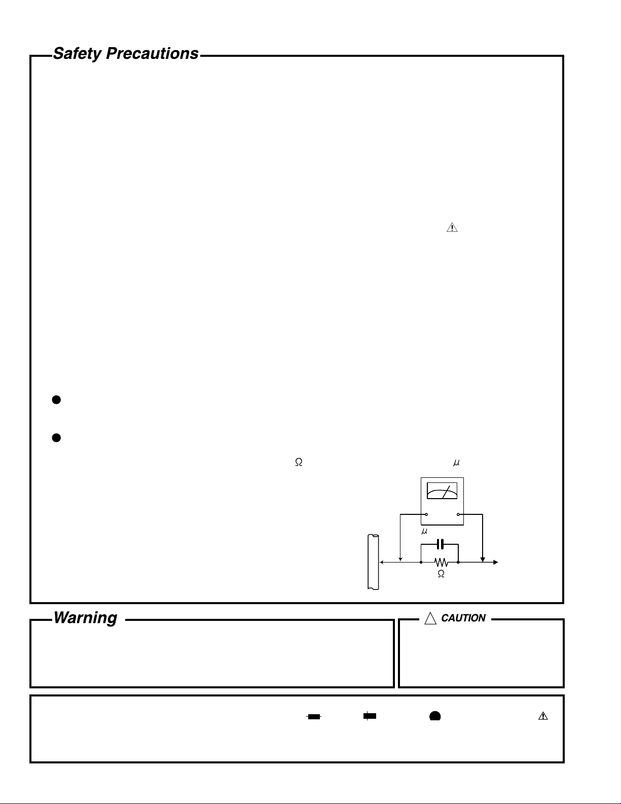
5. Leakage current check (Electrical shock hazard testing)
After re-assembling the product, always perform an isolation check on the exposed metal parts of the product
(antenna terminals, knobs, metal cabinet, screw heads, headphone jack, control shafts, etc.) to be sure the
product is safe to operate without danger of electrical shock.
Do not use a line isolation transformer during this check.
Plug the AC line cord directly into the AC outlet. Using a "Leakage Current Tester", measure the leakage
current from each exposed metal parts of the cabinet, particularly any exposed metal part having a return
path to the chassis, to a known good earth ground. Any leakage current must not exceed 0.5mA AC (r.m.s.).
Alternate check method
Plug the AC line cord directly into the AC outlet. Use an AC voltmeter having, 1,000 ohms per volt or more
sensitivity in the following manner. Connect a 1,500 10W resistor paralleled by a 0.15 F AC-type capacitor
between an exposed metal part and a known good earth ground.
Measure the AC voltage across the resistor with the AC
voltmeter.
Move the resistor connection to each exposed metal part,
particularly any exposed metal part having a return path to
the chassis, and measure the AC voltage across the resistor.
Now, reverse the plug in the AC outlet and repeat each
measurement. Voltage measured any must not exceed 0.75 V
AC (r.m.s.). This corresponds to 0.5 mA AC (r.m.s.).
0.15 F AC TYPE
1500 10W
Good earth ground
AC VOLTMETER
(Having 1000
ohms/volts,
or more sensitivity)
Place this
probe on
each exposed
metal part.
!
1. This equipment has been designed and manufactured to meet international safety standards.
2. It is the legal responsibility of the repairer to ensure that these safety standards are maintained.
3. Repairs must be made in accordance with the relevant safety standards.
4. It is essential that safety critical components are replaced by approved parts.
5. If mains voltage selector is provided, check setting for local voltage.
Burrs formed during molding may
be left over on some parts of the
chassis. Therefore, pay attention to
such burrs in the case of
preforming repair of this system.
In regard with component parts appearing on the silk-screen printed side (parts side) of the PWB diagrams, the
parts that are printed over with black such as the resistor ( ), diode ( ) and ICP ( ) or identified by the " "
mark nearby are critical for safety.
When replacing them, be sure to use the parts of the same type and rating as specified by the manufacturer.
(Except the J&C version)
1-2
Page 3
MX-G68V/MX-G65V
Preventing static electricity
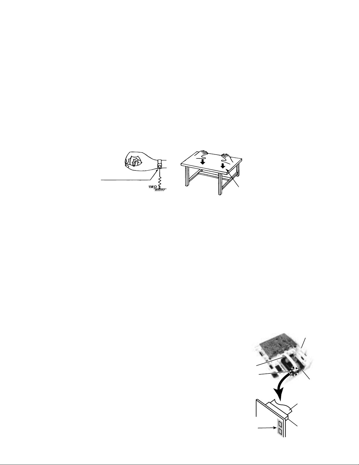
1. Grounding to prevent damage by static electricity
Electrostatic discharge (ESD), which occurs when static electricity stored in the body, fabric, etc. is discharged,
can destroy the laser diode in the traverse unit (optical pickup). Take care to prevent this when performing repairs.
2. About the earth processing for the destruction prevention by static electricity
In the equipment which uses optical pick-up (laser diode), optical pick-up is destroyed by the static electricity of
the work environment.
Be careful to use proper grounding in the area where repairs are being performed.
2-1 Ground the workbench
Ground the workbench by laying conductive material (such as a conductive sheet) or an iron plate over
it before placing the traverse unit (optical pickup) on it.
2-2 Ground yourself
Use an anti-static wrist strap to release any static electricity built up in your body.
(caption)
Anti-static wrist strap
Conductive material
(conductive sheet) or iron plate
3. Handling the optical pickup
1. In order to maintain quality during transport and before installation, both sides of the laser diode on the
replacement optical pickup are shorted. After replacement, return the shorted parts to their original condition.
(Refer to the text.)
2. Do not use a tester to check the condition of the laser diode in the optical pickup. The tester's internal power
source can easily destroy the laser diode.
4. Handling the traverse unit (optical pickup)
1. Do not subject the traverse unit (optical pickup) to strong shocks, as it is a sensitive, complex unit.
2. Cut off the shorted part of the flexible cable using nippers, etc. after replacing the optical pickup. For specific
details, refer to the replacement procedure in the text. Remove the anti-static pin when replacing the traverse
unit. Be careful not to take too long a time when attaching it to the connector.
3. Handle the flexible cable carefully as it may break when subjected to strong force.
4. It is not possible to adjust the semi-fixed resistor that adjusts the laser power. Do not turn it
Attention when CD mechanism assembly is decomposed
*Please refer to "Disassembly method" in the text for pick-up and how to
detach the CD mechanism assembly.
1. Remove the CD changer unit.
2. Remove the CD holder mechanism.
3. Solder is put up before the card wire is removed from the pickup unit
connector on the CD mechanism assembly.
(When the card wire is removed without putting up solder, the CD pick-up
assembly might destroy.)
4. Please remove solder after connecting the card wire with the pickup unit
connector when you install picking up in the substrate.
Card wire
Pickup unit
connector
Soldering
CD changer unit
Fig.1
Card wire
Pickup unit
connector
Fig.2
CD holder
mechanism
1-3
Page 4
MX-G68V/MX-G65V
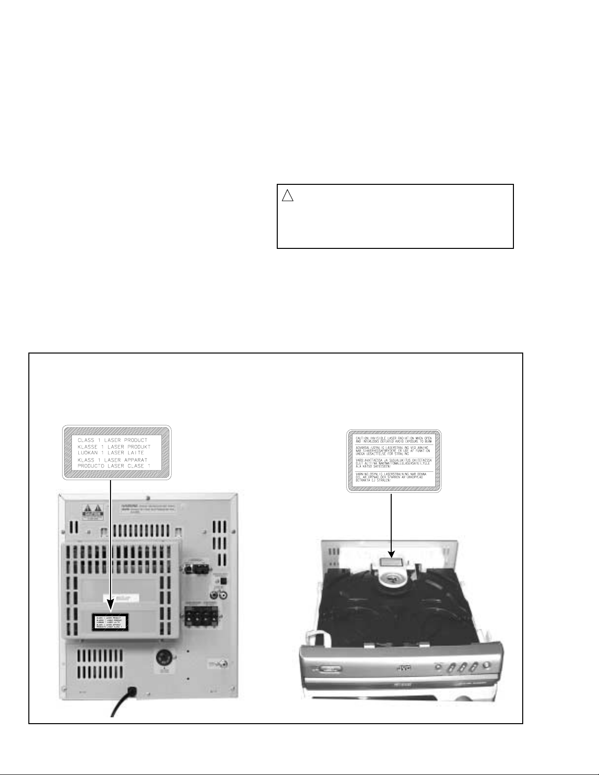
Important for laser products
1.CLASS 1 LASER PRODUCT
2.DANGER : Invisible laser radiation when open and inter
lock failed or defeated. Avoid direct exposure to beam.
3.CAUTION : There are no serviceable parts inside the
Laser Unit. Do not disassemble the Laser Unit. Replace
the complete Laser Unit if it malfunctions.
4.CAUTION : The compact disc player uses invisible
laserradiation and is equipped with safety switches
whichprevent emission of radiation when the drawer is
open and the safety interlocks have failed or are de
feated. It is dangerous to defeat the safety switches.
Position of labels
5.CAUTION : If safety switches malfunction, the laser is able
to function.
6.CAUTION : Use of controls, adjustments or performance of
procedures other than those specified herein may result in
hazardous radiation exposure.
CAUTION
!
Please use enough caution not to
see the beam directly or touch it
in case of an adjustment or operation
check.
CLASS 1
LASER PRODUCT
WARNING LABEL
1-4
Page 5
MX-G68V/MX-G65V
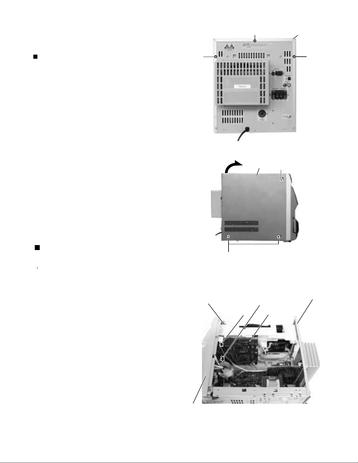
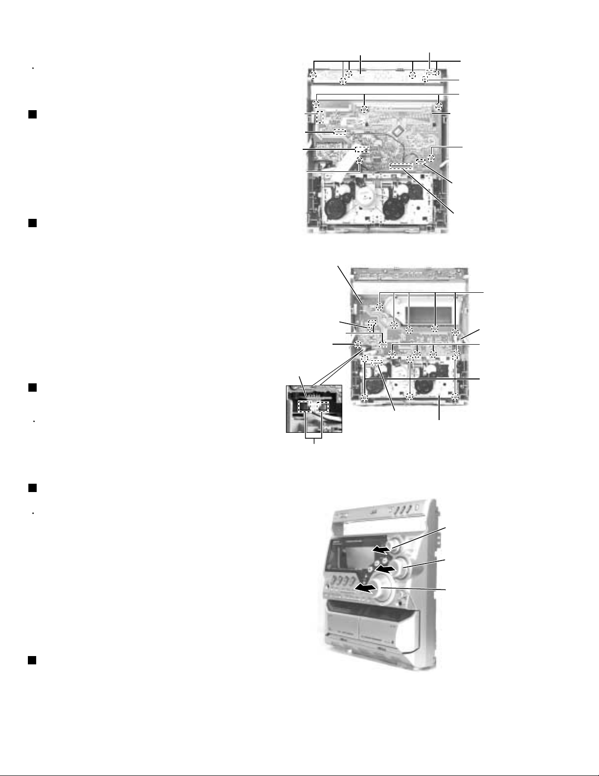
Disassembly method
<Main body>
Removing the metal cover
(See Fig.1 and 2)
Remove the three screws A attaching the metal
1.
cover on the back of the body.
Remove the six screws B attaching the metal cover
2.
on both sides of the body.
Remove the metal cover from the body by lifting the
3.
rear part of the cover.
ATTENTION:
Do not break the front panel tab fitted
to the metal cover.
A
A
Fig.1
Metal cover
Metal cover
A
B
Removing the CD changer unit
(See Fig.3 to 6)
Prior to performing the following procedure, remove
the metal cover.
Disconnect the card wire which is attached with
1.
adhesive to the left side of the CD changer unit.
Disconnect the harness from connector CW1 and
2.
CW7 on the back of the video CD board.
Disconnect the harness from connector RCW6 on
3.
the main board.
Disconnect the card wire from connector UCW3 on
4.
the FL dispaly & system control board.
Remove the two screws C attaching the CD changer
5.
unit on the rear panel.
Remove the two screws D attaching the CD changer
6.
unit on the side body.
Draw the CD changer unit upward from behind while
7.
pulling the rear panel outward.
CD changer unit
Front panel
assembly
B
Fig.2
CW1
CW7
(Bottom side)(Bottom side)
Fig.3
Rear panel
Video CD
board
1-5
Page 6
MX-G68V/MX-G65V
C
UCW3
Front panel
assembly
FLdispaly & system
control board
Rear panel
Fig.4
CD changer unit
RCW6
Adhesive card wire strap
D
Rear panel
Fig.5
CD changer unit
D
Rear panel
1-6
Fig.6a
Front panel assembly
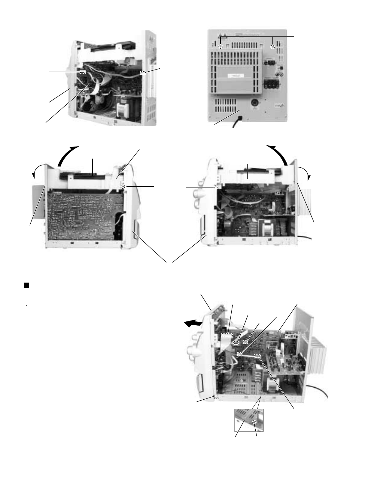
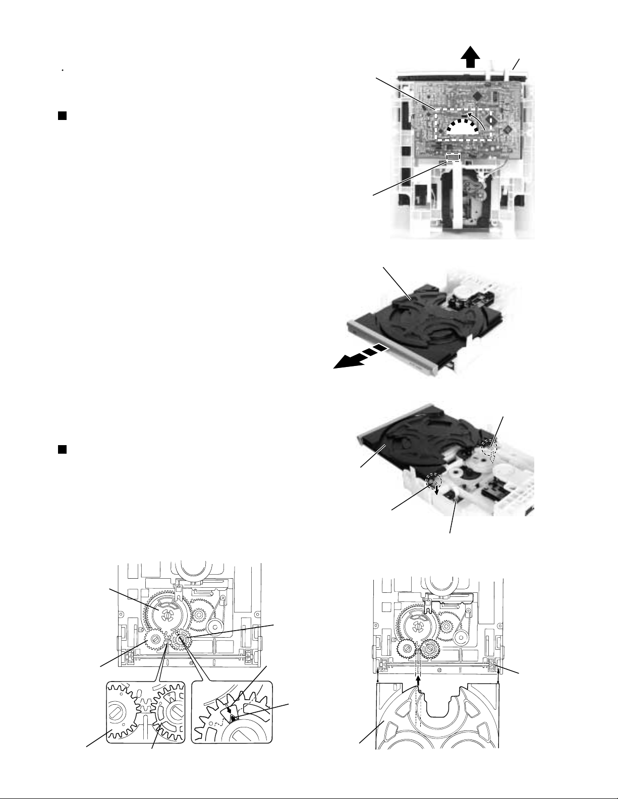
Removing the front panel assembly
(See Fig.7 to 9 )
Prior to performing the following procedure, remove
the metal cover and the CD changer unit.
Disconnect the card wire from connector FCW3 and
1.
the harness from connector JCW1, JCW2 ECW1
and HCW3 on the inner side of the main board in the
body.
Remove the two screws E attaching the front panel
2.
assembly on both sides of the body.
Remove the screw F attaching the earth terminal
3.
extending from the cassette mechanism assembly.
Remove the screw G attaching the front panel
4.
assembly and main board.
Remove the screw H attaching the front panel
5.
assembly on the bottom of the body.
Release the two joints a on both sides and two joints
6.
b on the bottom of the body using a screwdriver.
Front panel assembly
FCW3
Joint a
E
Earth wire
Fig.6b
JCW2
Fig.7
Main board
ECW1
JCW1
HCW3
F
Page 7
MX-G68V/MX-G65V
Front panel assembly
Main board
G
E
Fig.8
Joint c
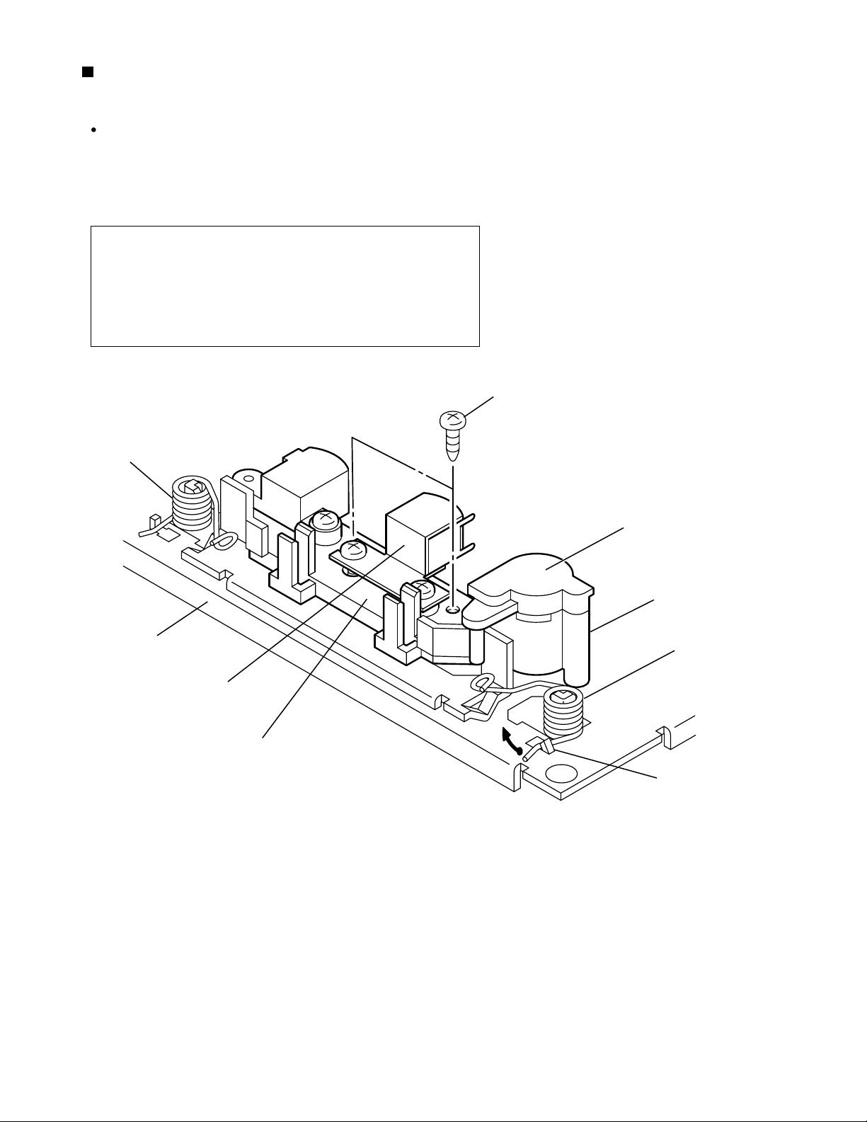
Removing the heat sink & amplifier
board (See Fig.10 to 12)
Prior to performing the following procedure, remove
the metal cover and the CD changer unit.
Remove the four screws I attaching the heat sink
1.
cover to the rear panel on the back of the body.
Bottom side
I
Joint b
H
Fig.9
Joint b
Remove the four screws J attaching the heat sink &
2.
amplifier board to the rear panel on the back of the
body.
Remove the two screws K attaching the speaker
3.
terminal to the rear panel on the back of the body.
Disconnect the card wire from connector ACW1 and
4.
the harness from connector ACW2 on the amplifier
board.
After moving the heat sink upward, remove the
5.
claws. Then pull out the heat sink & amplifier board .
Rear panel
Heat sink
cover
Rear panel
J
Heat sink
I
Fig.10
Tuner terminal
L
K
ACW2
ACW1
Fig.12
Amplifier
board
J
Speaker terminal
Fig.11
1-7
Page 8
MX-G68V/MX-G65V
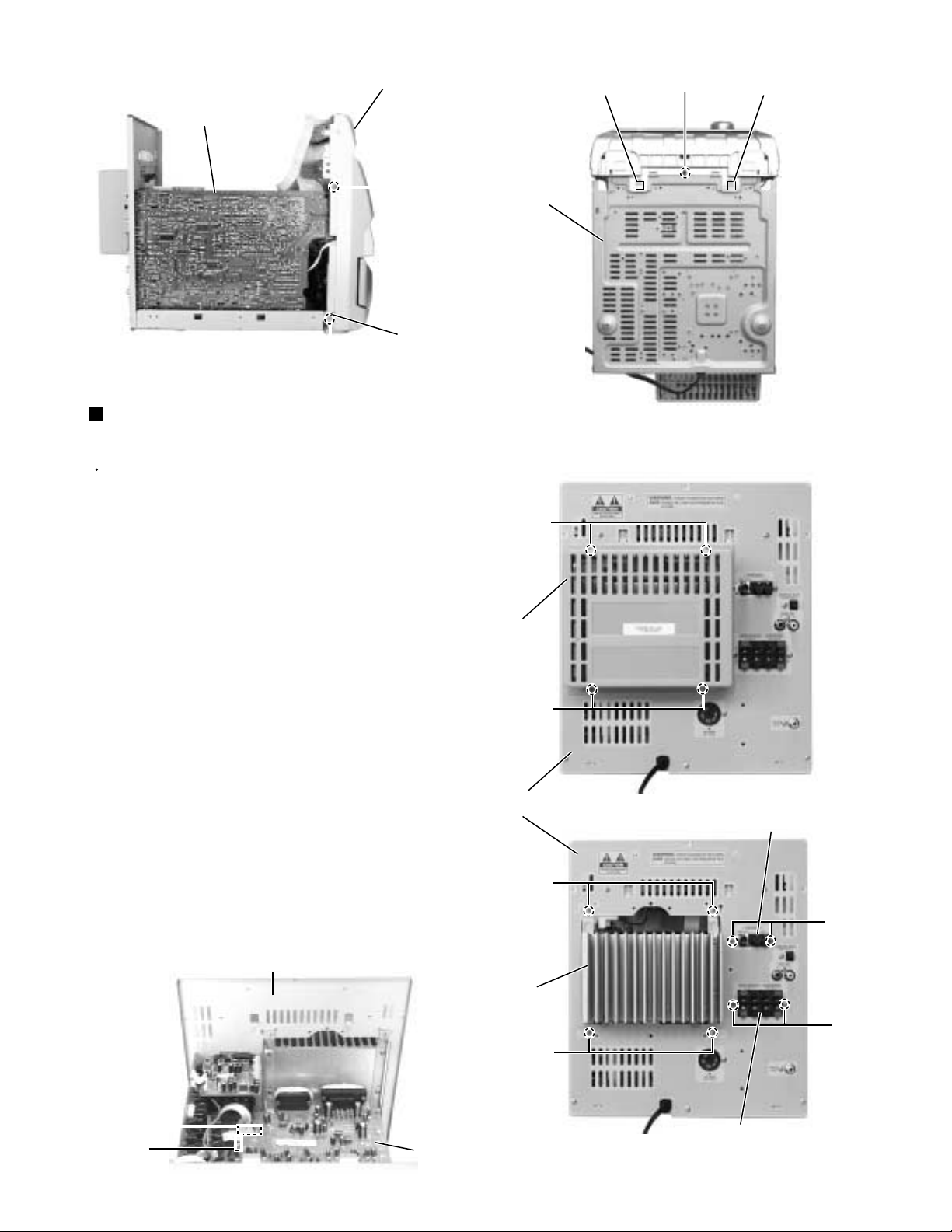
Removing the tuner board
(See Fig.11 and 13)
Prior to performing the following procedure, remove
the metal cover and CD changer unit.
Disconnect the card wire from connector CON01 on
1.
the tuner board.
Rear
panel
CON01
Remove the two screws L attaching the tuner board.
2.
Removing the rear panel (See Fig.14)
Prior to performing the following procedure, remove
the metal cover, CD changer unit, heat sink &
amplifier board and tuner board.
1.
Remove the one screw M, three screws N and three
screws N' attaching the rear panel.
Main board
Tuner board
Fig.13
Rear
panel
N'
M
N
Removing the main Board
(See Fig. 15)
Prior to performing the following procedure, remove
the metal cover, CD changer unit, heat sink &
amplifier board, tuner board and rear cover.
Disconnect the card wire from connector FCW3 and
1.
the harness from connector JCW1, JCW2, ECW1
and HCW3 on the main board.
Disconnect the harness from connector PCW1 on
2.
the power transformer board.
Remove the screw G attaching the main board
3.
holder. (See Fig.8)
Remove the two screws O attaching the heat sink
4.
and bottom chassis.
FCW3
Transformer board
JCW2
PCW1
Fig.14
ECW1
JCW1
Fig.15
Main board
HCW3
O
1-8
Page 9

MX-G68V/MX-G65V
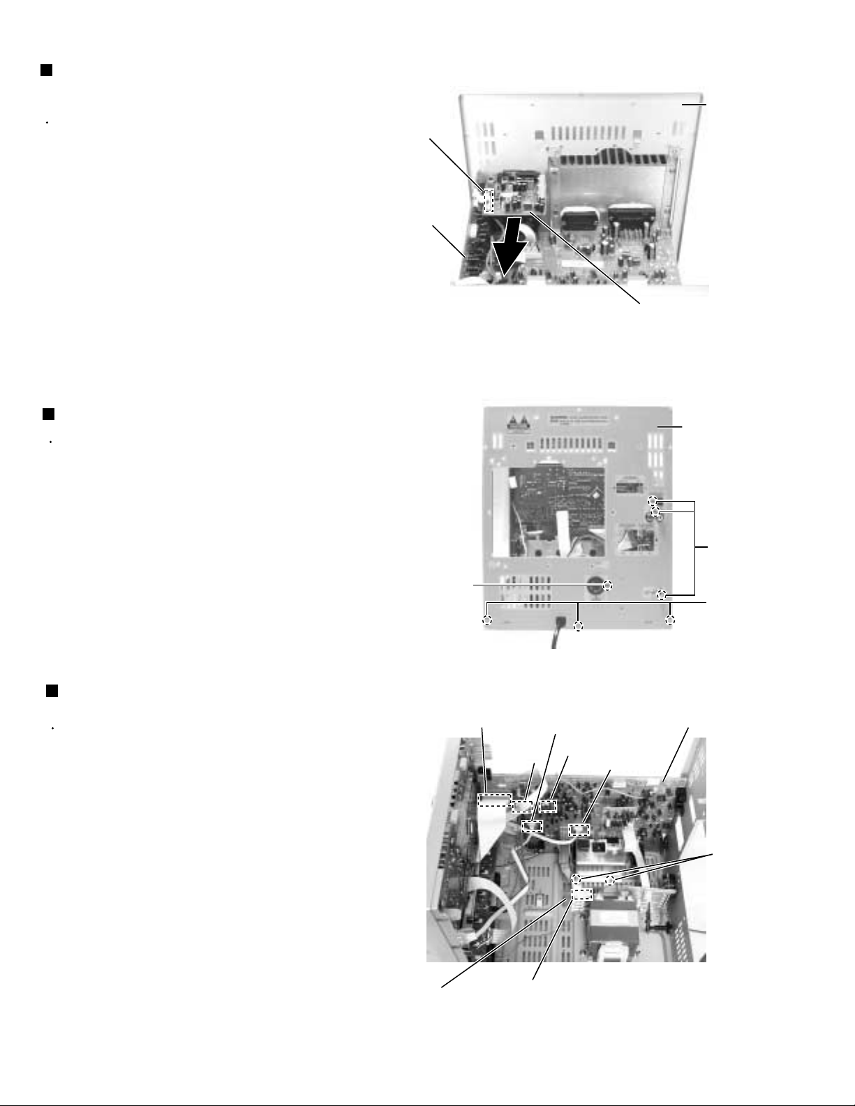
Removing the power ICs
(See Fig.16 and 17)
Prior to performing the following procedure, remove
the metal cover, CD changer unit, heat sink &
amplifier board .
Remove the four screws P attaching the power ICs
1.
to the heat sink.
Unsolder the power ICs solder point.
2.
Heat sink
P
Fig.16
Power ICs solder point
Amplifier board
Heat sink
Removing the power transformer
(See Fig.18)
Prior to performing the following procedure, remove
the metal cover, CD changer unit, heat sink &
amplifier board, tuner board and rear cover.
Disconnect the power cord from connector RCW2 of
1.
the power transformer board.
Disconnect the harness from connector PCW1 of the
2.
power transformer board.
Remove the four screws Q attaching the power
3.
transformer.
Power transformer
PCW1
Q
Fig.17
Q
Fig.18
RCW2
Power cord
1-9
Page 10
MX-G68V/MX-G65V
<Front panel assembly>
Prior to performing the following procedure, remove
the metal cover, the CD changer unit and the front
panel assembly.
Removing the power switch board
(See Fig.19)
Disconnect the card wire from connector UCW1 of
1.
the power switch board.
Remove the five screws R attaching the power
2.
switch board and release the tab c outward.
Removing the FL display & system
control board (See Fig.19)
Disconnect the card wire from the connectors
1.
UCW3, UCW5,UCW6 and UJW5 on the FL display &
system control board.
Remove the five screws S attaching the FL display &
2.
system board.
Disconnect the card wire from the connector UCW2
3.
on the FL display & system control board.
Removing the headphone board
(See Fig.20)
Prior to performing the following procedure remove
the FL display & system control board.
You can pull out the headphone board.
1.
Power switch board
UCW2
UCW3
UJW5
S
Front board
Mic board
Tab e
T
Tab d
T
UCW1
R
Tab c
S
FLdiplay & system
control board
S
UCW5
UCW6
Fig.19
T
Headphone
board
T
U
Card wire f
Cassette mechanism assembly
Fig.20
Removing the front board / MIC board
(See Fig. 20 and 21)
Prior to performing the following procedure, remove
the FL display & system control board.
Pull out the volume knob, subwoofer level knob and
1.
sound mode knob from front side.
Remove the eleven screws T attaching the front
2.
board and release the two tabs d outward.
Release the two tabs e outward and remove the MIC
3.
board.
Removing the cassette mechanism
assembly (See Fig.20)
Disconnect the card wire f from the mechanism
1.
board on the cassette mechanism assembly.
Remove the six screws U attaching the cassette
2.
mechanism assembly.
1-10
SOUND MODE
knob
SUBWOOFER
LEVEL knob
VOLUME knob
Fig.21
Page 11
MX-G68V/MX-G65V
<CD changer unit>
Prior to performing the following procedure, remove
the CD changer unit.
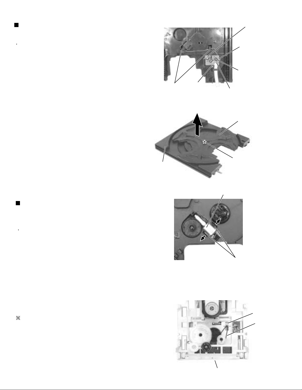
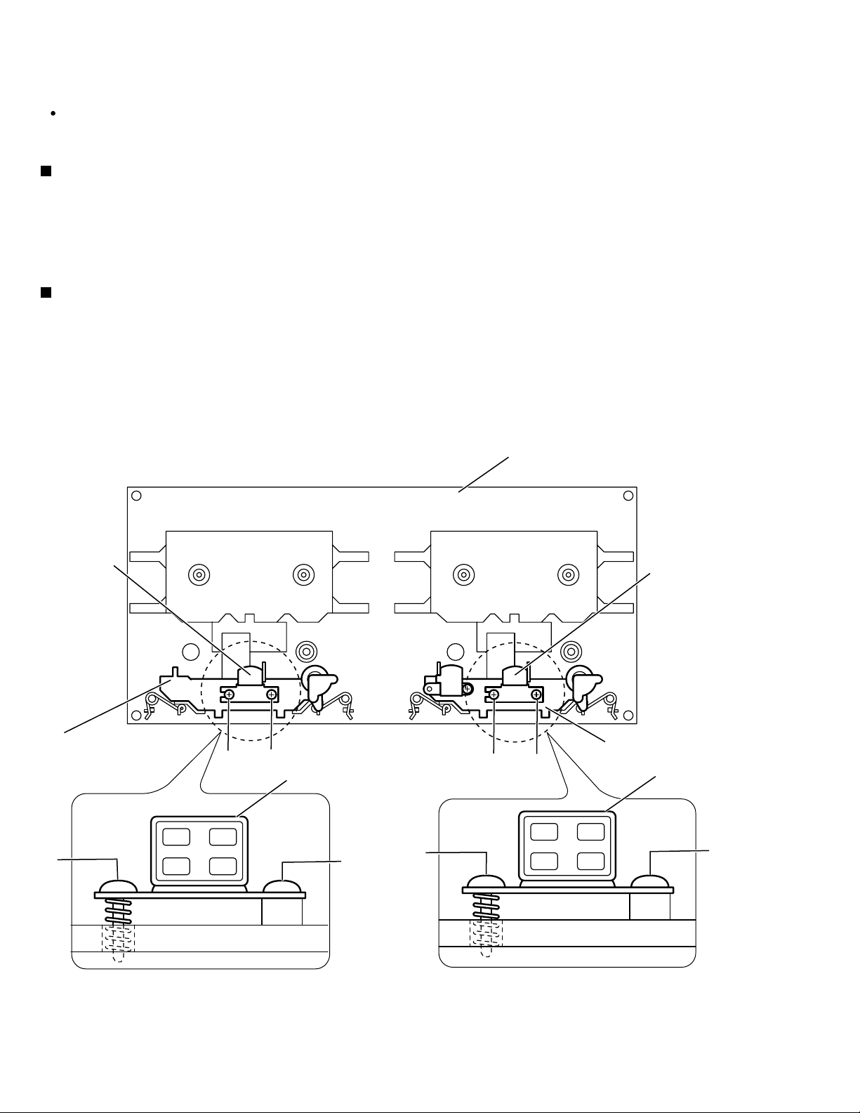
Removing the CD tray (See Fig.1 to 3)
Disconnect the card wire from connector SW1 of the
1.
video CD board.
Turn the black loading pulley gear on the under side
2.
of the CD changer unit in the direction of the arrow
and draw the CD tray toward the front until it stops.
Disconnect the card wire from connector CW6 of the
3.
Video CD board on the upper side of the CD changer
unit.
Push down the two tray stoppers marked a and pull
4.
out the CD tray.
CD tray
Loading pulley
gear
Video CD
board
SW1
Fig.1
CD tray
Reinstall the CD tray (See Fig.4 and 5)
Align the gear-cam with the gear-tray as shown fig.4,
1.
then mount the CD tray.
When assembling the CD tray, take extreme care not
2.
engage with gear-synchro.
Gear-cam
Gear-tray
Gear-convert
Gear-cam
timing point
Fig.2
a (Tray stopper)
CD tray
a
(Tray stopper)
Video CD board
CW6
Fig.3
Gear-synchro
Gear-convert
Gear-tray
Gear-tray
CD tray
Fig.4 Fig.5
1-11
Page 12
MX-G68V/MX-G65V
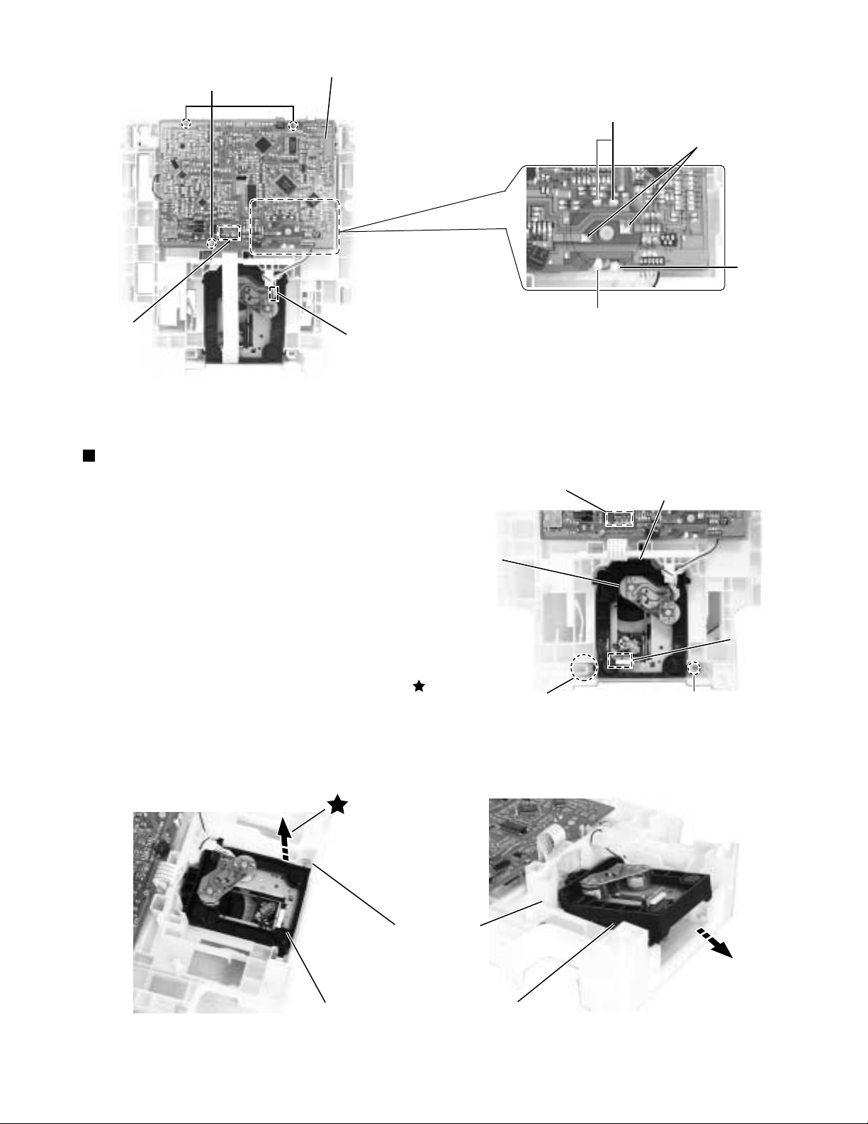
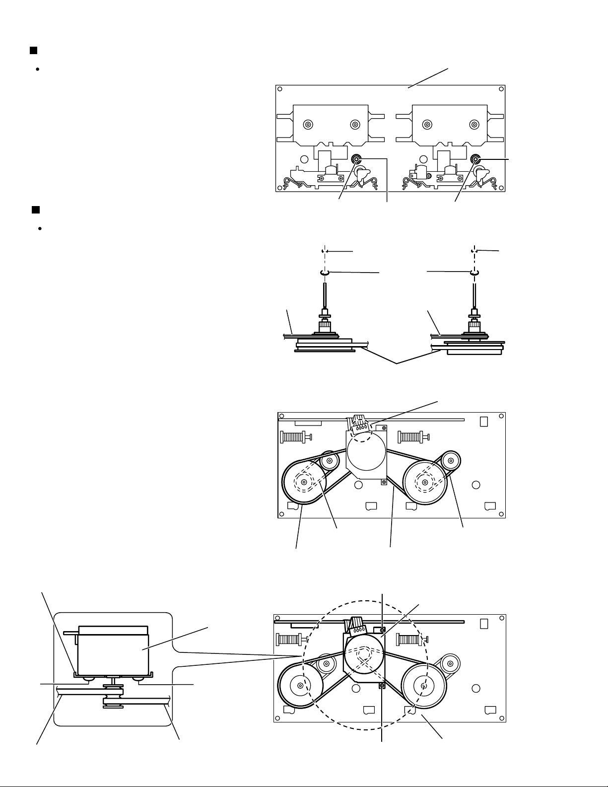
Removing the sensor board / the turn
table motor assembly (See Fig.6 to 8)
Prior to performing the following procedure, remove
the CD tray.
Remove the screw A attaching the sensor board and
1.
release the two tabs b attaching the sensor board on
the under side of the CD tray.
Disconnect the harness from connector CW1 on the
2.
sensor board and release the harness from the two
hooks c. Remove the sensor board.
Remove the screw B attaching the turn table. Detach
3.
the turn table from the tray.
Pull outward the tab marked d attaching the turn
4.
table motor assembly on the upper side of the tray
and detach the turn table motor assembly from the
tray.
Tray
A
Tab b
CW1
c
Tab b
Sensor board
Fig.6
Turn table
B
Removing the belt, the Video CD board
(See Fig.9 and 10)
Prior to performing the following procedure, remove
the CD tray.
Disconnect the harness from connector on the CD
1.
mechanism board in the CD mechanism assembly
on the under side of the CD changer unit. Disconnect
the card wire from the pickup unit connector.
Detach the belt from the pulley on the upper side of
2.
the CD changer unit (Do not stain the belt with
grease).
Disconnect the card wire from the connector SW1 on
3.
the Video CD board.
Remove the three screws D attaching the video CD
board. First release the three tabs f and tabs e
attaching the video CD board motor to raise the
video CD board slightly, then release the video CD
board.
Fig.7
Turn table motor assembly
d
Fig.8
Motor
Belt
If the tabs e and f are hard to release, it is
recommendable to unsolder the two soldered points
on the motor terminal of the video CD board.
1-12
Fig.9
CD changer unit
Page 13
MX-G68V/MX-G65V
D
SW1
Video CD board
Motor board
connector
Fig.10
Removing the CD mechanism holder
assembly (mechanism included)
(See Fig.11 to 13)
SW1
Tabs f
Soldered points
Tabs f
Tab e
CD mechanism
holder assembly
Disconnect the card wire from pickup unit connector
1.
on the motor board in the CD mechanism holder
assembly on the under side of the CD changer unit.
Remove the screw E attaching the shaft on the right
2.
side of the CD mechanism holder assembly.
Pull outward the stopper fixing the shaft on the left
3.
side and remove the CD mechanism holder
assembly from behind in the direction of the arrow .
Pull out the CD mechanism holder assembly.
4.
CD changer unit
Motor board
Stopper
Fig.11
Pickup unit
connector
E
Fig.12
CD mechanism holder assembly
Fig.13
1-13
Page 14
MX-G68V/MX-G65V
<Cassette mechanism section>
Prior to performing the following procedure,
removing the cassette mechanism.
Removing the R/P head. (Fig.1 to 3)
1.
Remove the screw A attaching the R/P head right side.
2.
Remove the screw B attaching R/P head left side.
(Screw B : Head azimuth adjusting screw.)
Removing the P.B. head. (Fig.1 to 3)
1.
Removing the screw C attaching the P.B. head right side.
2.
Removing the screw D attaching the P.B. head left side.
(Screw D : Head azimuth adjusting screw.)
P.B. head
P.B. head assembly
D
Cassette mechanism
R/P head
Fig.1
D
C
P.B. head
C
B
B
A
R/P head assembly
R/P head
A
1-14
Fig.3
Fig.2
Page 15
Removing the pinch roller unit.
(Fig. 4)
Prior to performing the following procedure,
removing the cassette mechanism.
1.
Remove the two screws E attaching the p
Attention:
The pinch roller cap is forcefully fitted to the shaft
of the pinch roller unit. If the pinch roller cap is
taken out by force, the shaft will be broken.
When replacing the pinch roller, it should be
changed as a pinch roller unit itself.
inch roller unit
MX-G68V/MX-G65V
.
E
Slide spring
Cassette mechanism
R/P Head
Pinch roller unit
Fig.4
Pinch roller cap
Pinch roller
Slide spring
Stopper
1-15
Page 16
MX-G68V/MX-G65V
Removing the flywheel. (Fig.5 to 7)
Prior to performing the following procedure,
removing the cassette mechanism.
1.
Remove the cut washers at a and b from the
capstan shaft. Then remove the flywheel.
When reassembling the flywheel, be sure
to use new cut washers as they cannot
be reused.
Removing the motor. (Fig.7 to 9)
Prior to performing the following procedure,
removing the cassette mechanism.
1.
Unsolder the solder point on the motor terminal.
2.
Remove the capstan belt from the motor pulley.
3.
Remove the two screws F attaching the
motor bracket.
4.
Remove the two screws G attaching the motor.
Drive belt
Capstan shaft
b
Capstan belt
Cassette mechanism
b
Fig.5
Washer
Capstan shaft
Drive belt
(Flat)
a
a
Motor bracket
Motor
Capstan belt
Drive belt
(Flat)
Fig.6
Capstan belt
Fig.7
F
Motor bracket
Solder point
Drive belt
(Flat)
Capstan belt
1-16
(Flat)
Fig.9
GG
Capstan belt
(Flat)
Fig.8
F
Cassette mechanism
Page 17
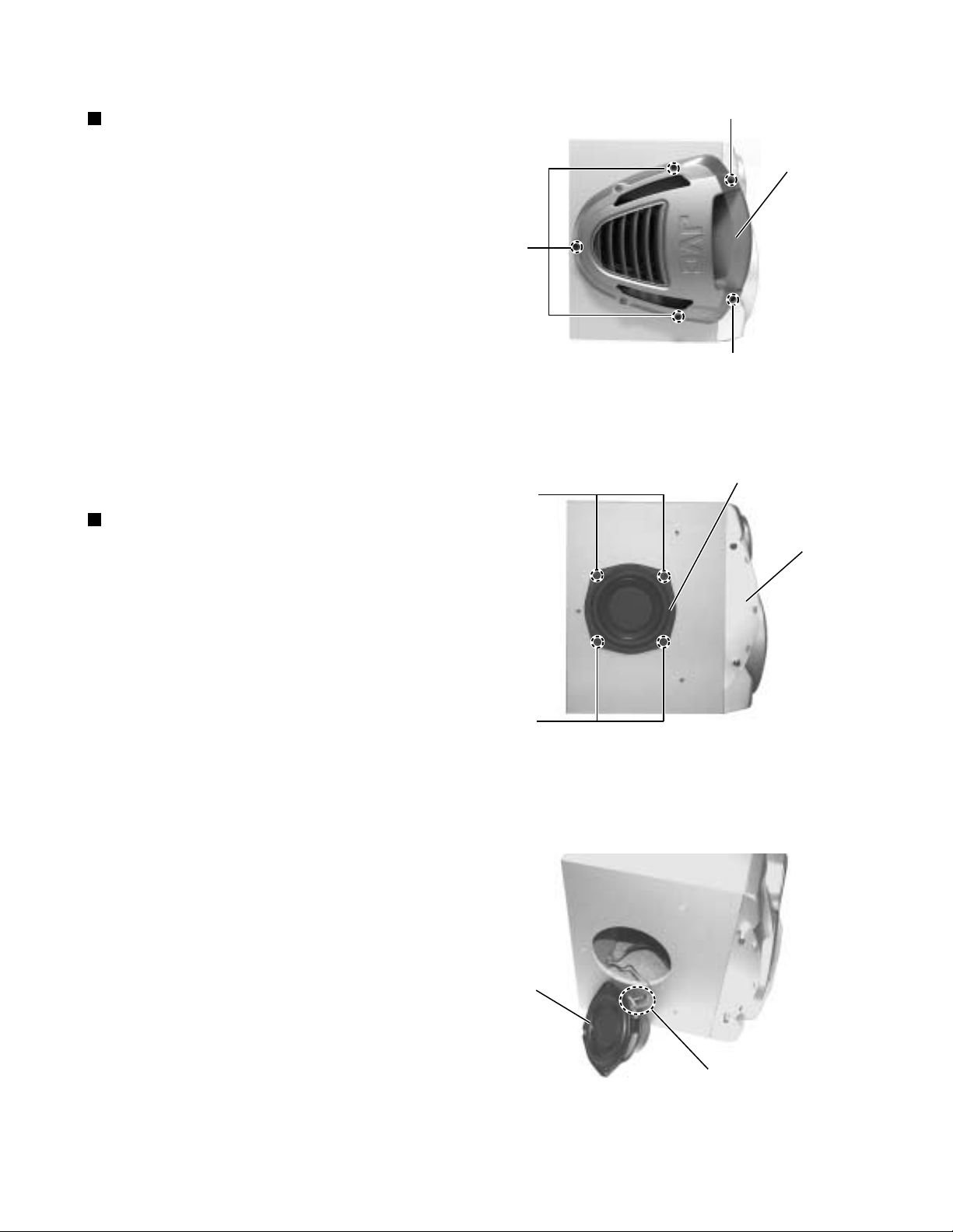
< Speaker section >
MX-G68V/MX-G65V
Removing the side panel (See Fig. 1)
Remove the five screws A and B attaching the side
1.
panel, then remove the side panel.
Removing the side speaker
(See Fig. 2 and 3)
B
Side panel
A
B
Fig.1
Side speaker
C
Front panel
Prior to performing the following procedure, remove
the side panel.
Remove the fore screws C attaching the side
1.
speaker.
Pull out the side speaker and remove the speaker
2.
cord from the speaker terminal.
C
Fig.2
Side speaker
Speaker terminal
Fig.3
1-17
Page 18
MX-G68V/MX-G65V
Wiring connection
Amp. board
3711-001167
ACW2
ACW1
3708-001094
3809-001224
UCW7
CD key switch board
3809-000492
UCW1
3809-001228
0
9
3809-001185
0
9
MCW1
3708-000181
MIC board
Front key switch board
MCW3
AH39-00254A
AH39-00244A
AH39-00248A
MCW2
3711-000190
0
9
0
3711-000588
3708-000178
UCW2
UCW3
3708-001212
Front / Display board
RCW2
RFS4
RFS3
RFS5
RFS6
RFS7
PCW1
UCW4
3708-000451
UCW6
3708-001488
UCW5
3708-000492
RFS8
RFS2
Power transformer
CD tray
Roller board
3809-001233
3809-001185
AH39-00347A
AH39-00097A
Color codes are shown below.
1 Brown
2Red
3 Orange
4 Yellow
5 Green
6 Blue
7 Violet
8Gray
9 White
0Black
Motor board
CD Pick up board
9
CD pick up unit board
9
2
0
9
0
0
OPTICAL
CW1
CW5
3708-001027
CW2
9
0
CW7
CW6
Video CD board
CW1
9
0
AH39-00096B
1-18
3809-001237
3809-001222
Tuner board
CW302
Voice board
CW301
9
0
CON1
AH39-00246A
9
0
3710-000209
FCW1
3708-000122
RCW6
3711-000907
Main board
FCW3
3708-000258
2
OCW
KCW2
3711-000907
FCW2
3711-001557
KCW1
JCW1
3711-003107
JCW3
JCW2
9
0
3711-003111
RW2
3711-001062
3708-001094
HCW3
ECW1
3711-001062
0
VCW1
RW1
2
9
0
9
0
9
8
2
0
9
0
0
9
8
9
0
9
0
0
9
AH39-00022A
0
0
HCW2
AH39-00247A
9
H.phone J.board
Cassette mechanism
9
0
0
9
9
0
2
0
2
88
AH39-00202A
2
9
Page 19
Adjustment method
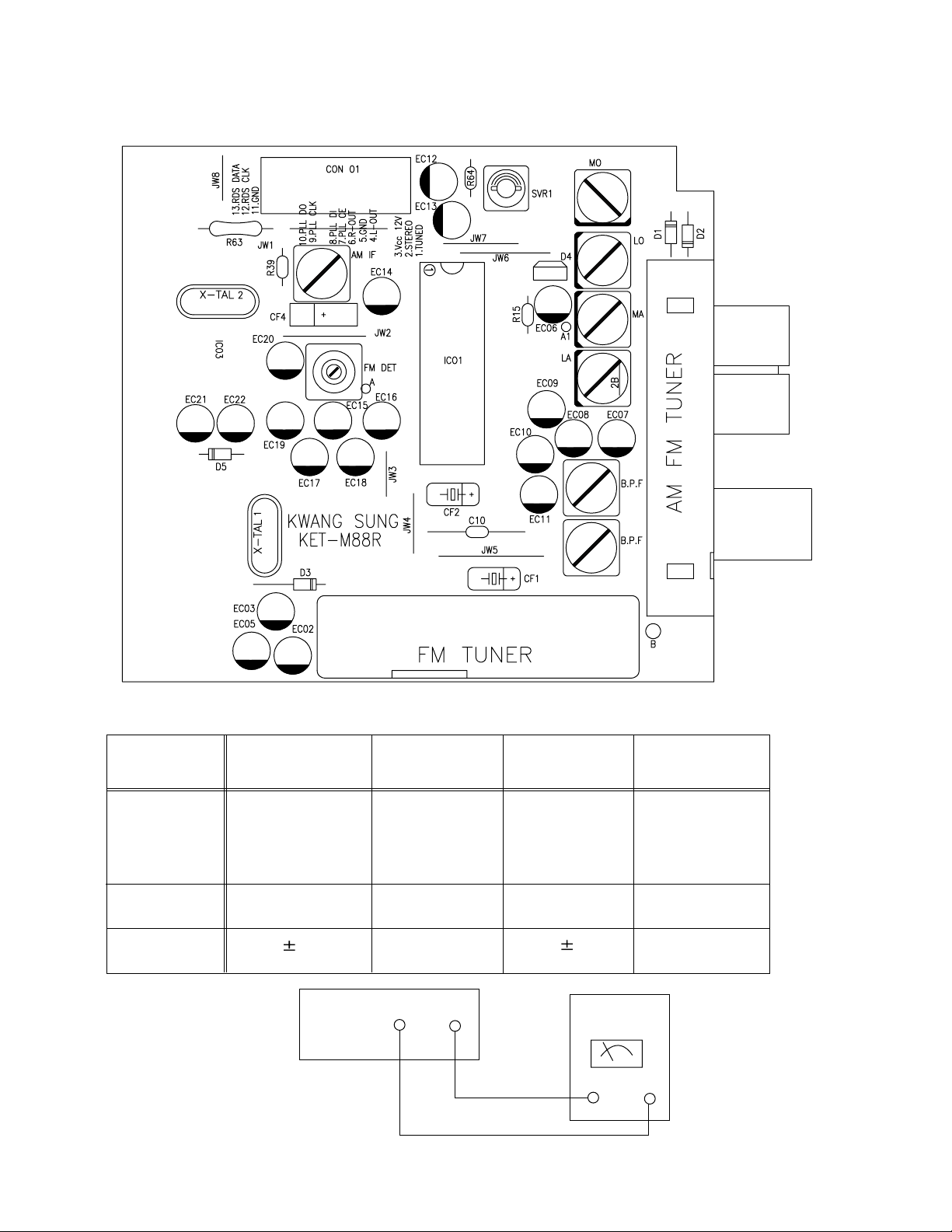
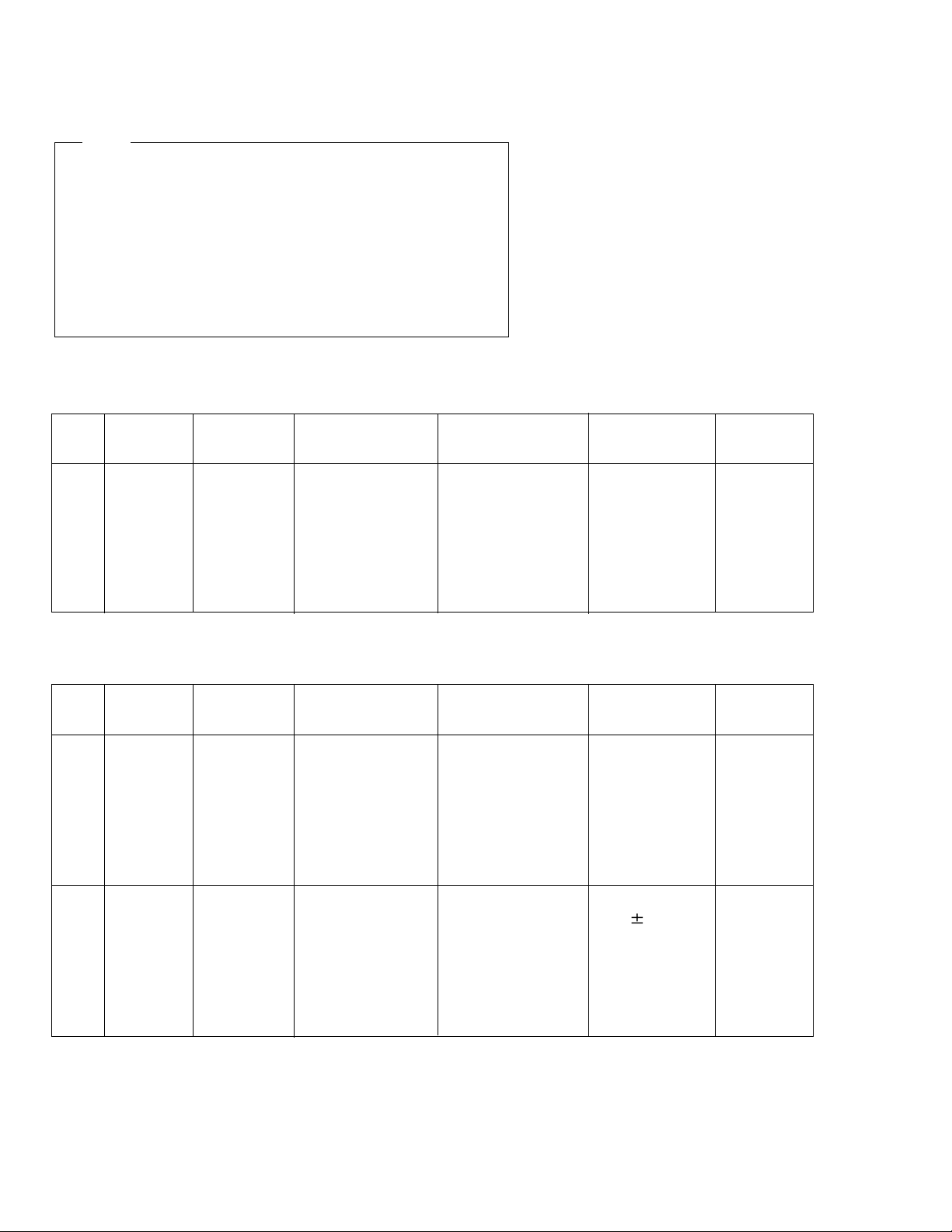
1. Tuner
MX-G68V/MX-G65V
ITEAM
Received FREQ.
Adjustment
point
Output
* Adjustment Location of Tuner PCB
AM(MW) OSC
Adjustment
531~1602 KHz
(9kHz step)
530~1600 KHz
(10kHz step)
MO
1~7.0 0.5V
MAIN
PCB
AM(MW) RF
Adjustment
594 KHz
MA
Maximum
Output(Fig1-4)
VT GND
LW OSC
Adjustment
(Except for J/C)
146~290 KHz
2~7.0 0.5V
LO
AM(MW) RF
Adjustment
150 KHz
LA
Maximum
Output(Fig1-4)
TESTER
Fig 1-4 OSC Voltage
1-19
Page 20
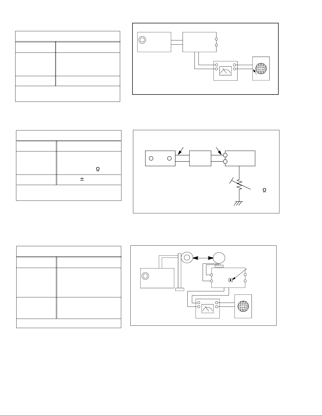
MX-G68V/MX-G65V
FM THD Adjustment
SSG FREQ.
98 MHz
Adjustment
point
FM DETECTOR COIL
(FM DET)
Output
60 dB
Minumum Distortion (0.4% below)
(Figure 1-1)
FM Search Level Adjustment
SSG FREQ.
Adjustment
point
(SVR1)
Output
BEACON
SENSITIVITY
SEMI-VR(20K )
28 dB(
98 MHz
2dB)
Output
GND
FM S.S.G
FM
Antenna
Terminal
Speaker
Terminal
SET
Input
output
Distortion Meter
Figure1-1 IF CENTER and THD Adjustment
FM Antenna
SET
FM IN
FM S.S.G
28 dB
GND
Oscilloscope
Input
Adjust SVR1 so that "TUNED" of FL T
is lighted (Figure 1-2)
*Adjust FM S.S.G level to 28dB
AM(MW) I.F Adjustment
SSG FREQ.
Frequency
450 kHz
531 kHz
(9kHz step)
530 kHz
(10kHz step)
Adjustment
point
AM IF
Maximum output (Figure 1-3)
Figure1-2 FM Auto Search Level Adjustment
60cm
OUTPUT
AM SSG
450KHZ
INPUT
AM ANT
IN
Speaker Terminal
OUTPUT
VTVM Oscilloscope
Figure1-3 AM I.F Adjustment
20 k
AM IF
1-20
Page 21
2 Cassette Deck
To adjust tape speed
MX-G68V/MX-G65V
Notes
1) Measuring tape: i) VT-712
(Tapes recorded with 3kHz)
ii) AC-225
2) Connect the cassette deck to the frequency counter
as in figure 1-5.
Step
Item
Pre-Setup
Condition
Pre-Setup
1) Deck 1:VT-712
1
NOR
SPEED
Control
Recording /Play head
OUT
(connected
to the frequency
counter)
2) Press PLAY
SW button
3) Deck 2:Same
as above
Cassette Deck
SPK OUT
To Adjust
Turn VSR1 to
left and right
(FRONT PCB)
Cassette Deck
SPK OUT
Figure 1-5
VTVM
Frequency Counter
Standard
3KHz
Oscilloscope
output
Remark
1%
range
AZIMUTH control screw
Figure 1-6
Audio OSC.
SET
(MAIN PCB)
IN
AUX IN
LINE OUT
TP
JCW3
Figure 1-8
VTVM
IN OUT
(GND)
In Out
Figure 1-7
Oscilloscope
1-21
Page 22
MX-G68V/MX-G65V
To adjust plabyback level/REC
Notes
1) Before the actual adjustment, clean the play/recording
head.
2) Measuring tape :
i) VT-703 (10kHz AZIMUTH control)
ii) AC-225
3) The cassette deck is connections as shown in figure 1-7.
1. Adjust Deck A Play Level
Step
Item
Pre-Setup
Condition
Pre-Setup
After putting VT-
1
AZIMUTH
SPK OUT
(VTVM is
connected to
703 into Deck A
- Press FWD PLAY
button.
the scope)
2. Adjust Deck B Play Level/REC BIAS
Step
1
Item
AZIMUTH
Pre-Setup
Condition
SPK OUT
(VTVM is
connected to
the scope)
Pre-Setup
After putting VT-703
into Deck B
1)Press FWD PLAY
button.
To Adjust
- Tu rn the control
screw to as shown
in Figure 1-6.
To Adjust
- Turn the control
screw to as shown
in Figure 1-6.
Standard
Max output
and same phase
(both channels)
Standard
Max output
and same phase
(both channels)
Remark
After
adjustment
secure it with
REGION
LOCK.
Remark
After
adjustment
secure it with
REGION
LOCK.
1-22
2
Recording
Bias
Voltage
Fig 1-8
After putting AC-225
into Deck B
1)Press REC PLAY
button.
2)MAIN PCB JCW3,
connectted to VTVM
Turn JSR2L,JSR2R
to the right and left
7mV(
0.5
mV)
Page 23
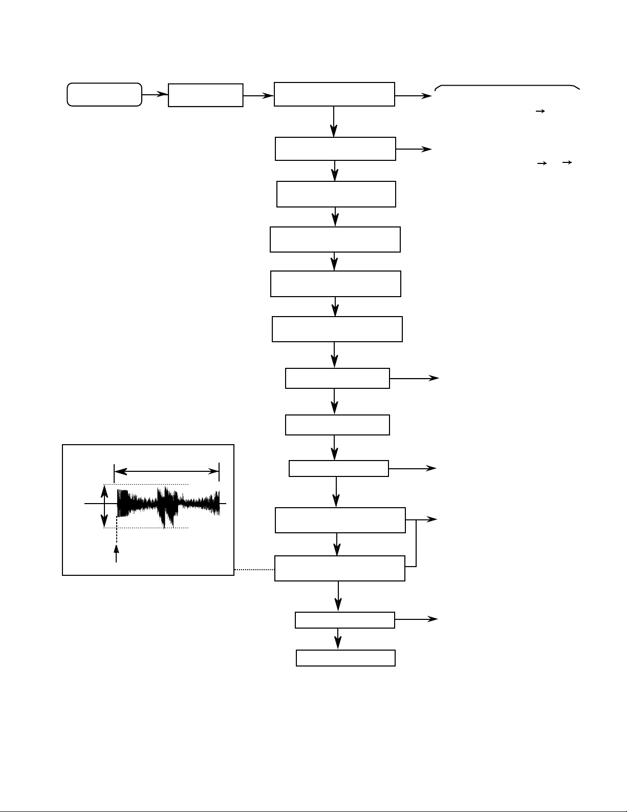
Flow of functional operation until TOC read
Power ON
Play Key
RESET a CD LSI
Confirm that the voltage at the pin17
of KB9226(IC101) is "L" "H".
MX-G68V/MX-G65V
Check Point
LIMIT SW ON
SET Default value of
TE gain, TE balance
Automatic adjusting of
focus bias
Automatic adjusting of
FE offset
Automatic adjusting of
TE offset
LASER power ON
Detection of disk
Confirm that the voltage at the pin33
of KB9226(IC101) is "H" "L" "H".
Confirm that the voltage at the
pin37 of KB9226(IC101) is 3.5V.
Tracking error waveform at TOC reading
Pin 34 of
KB9226
(IC101)
Approx
0.4V
2.50V
Disc states
to rotate
Approx.3.7sec
Disc is rotated
Automatic adjusting of
TE balance
Automatic adjusting of
TE gain
TOC reading
Play a disc
Confirm that the signal from pin24
of KB9226(IC101) is 3.5V as a
accelerated pulse during
approx.1.96s.
Confirm the waveform of
the Tracking error signal
at the pin 34 of KB9226(IC101).
Confirm the eye-pattern
at the pin2 of KB9226(IC101).
1-23
Page 24
MX-G68V/MX-G65V
Maintenance of laser pickup
(1) Cleaning the pick up lens
Before you replace the pick up, please try to
clean the lens with a alcohol soaked cotton
swab.
(2) Life of the laser diode
When the life of the laser diode has expired,
the following symptoms will appear.
1. The level of RF output (EFM output:ampli
tude of eye pattern) will below.
Is the level of
RFOUT under
1.1V 0.2Vp-p?
YES
O.K
NO
Replace it.
Replacement of laser pickup
Turn off the power switch and,disconnect the
power cord from the ac outlet.
Replace the pickup with a normal one.(Refer
to "Pickup Removal" on the previous page)
Plug the power cord in,and turn the power on.
At this time,check that the laser emits for
about 3seconds and the objective lens moves
up and down.
Note: Do not observe the laser beam directly.
Play a disc.
Check the eye-pattern at TP1.
Finish.
(3) Semi-fixed resistor on the APC PC board
The semi-fixed resistor on the APC printed circuit board which is attached to the pickup is used to adjust the laser
power. Since this adjustment should be performed to match the characteristics of the whole optical block, do not
touch the semi-fixed resistor.
If the laser power is lower than the specified value,the laser diode is almost worn out, and the laser pickup should
be replaced.
If the semi-fixed resistor is adjusted while the pickup is functioning normally,the laser pickup may be damaged
due to excessive current.
1-24
Page 25
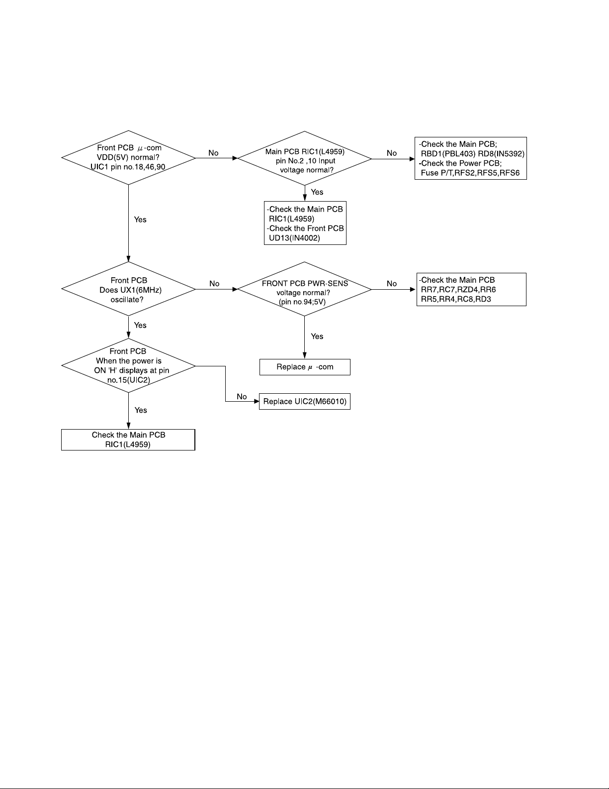
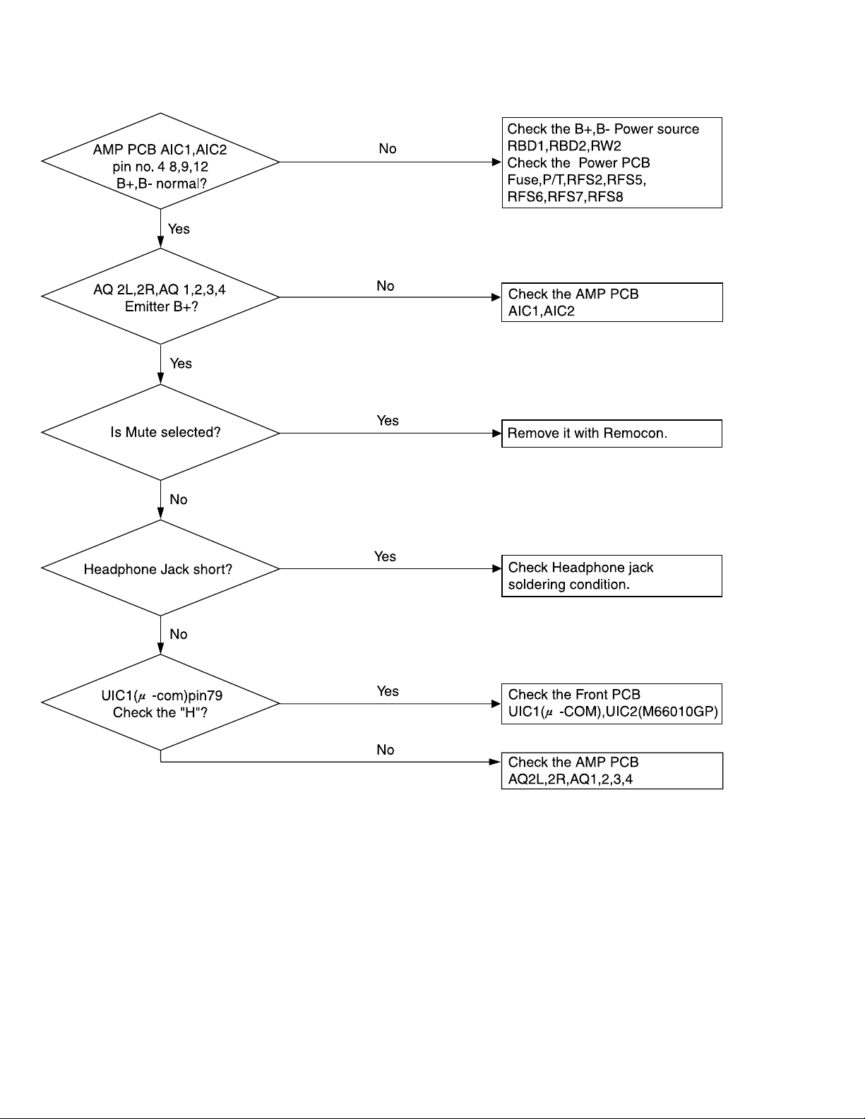
Troubleshooting
1.Amplifier
Power Malfunction : COMMON
MX-G68V/MX-G65V
1-25
Page 26
MX-G68V/MX-G65V
<No Output>
1-26
Page 27
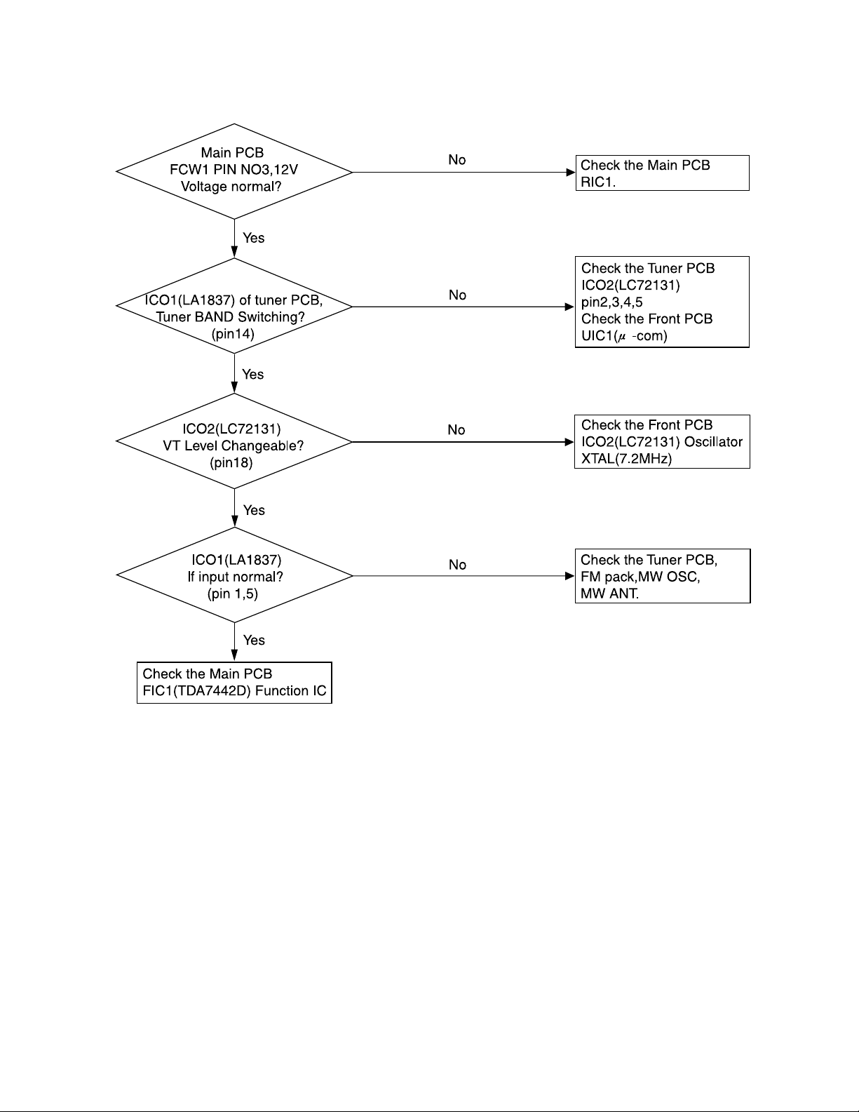
2. Tuner malfunction (FM/AM)
MX-G68V/MX-G65V
1-27
Page 28

MX-G68V/MX-G65V
3. Tape
1-28
Page 29

4. Video CD
< No DISC>
MX-G68V/MX-G65V
1-29
Page 30

MX-G68V/MX-G65V
<No VIDEO>
• Check the Voltage (+5V, +3.3V)
No SamSung Logo Display
Check for VIDEO signal
at PIN 11
of MIC3 (W9952Q)
No
Check for signal
at PIN 1, 32, 29, 21~28
of MIC3 (W9952Q)
NO
Check for 40.5MHZ signal
at PIN 76 of MIC4 (W9925QF)
Yes
Yes
Check the Connection of CW7
Yes
Check MIC3 Sodering or Replace IC
No
Check the OSC of MIC5 (40.5MHz)
1-30
Check PIN100 of W9923=Low
No
Check the line of PIN
of MIC1 and MIC4
Yes
Check MIC6 (DRAM) Sodering
Page 31

<No sound of CD Play>
• Check 16.9344MHz OSC at pin38 of MIC1
• Check Voltage (+5, ±12)
• Check all Connection between VCD pack PCB and Main, Front PCB
NO SOUND
MX-G68V/MX-G65V
Check pin 34 , 35 , 36 of SIC2
at pin 10, 11, 13 of SIC2 and
<Check Pick-up>
Check pin 1 , 7 of AIC3
No
(LRCK, BCK, DATA)
Yes
Check for signal
Resoldering
Check for resistance
at PIN T+, T–
of SW1 : about 10
Yes
No
Check the Connection line of CW2
and Muting Circuit AQ3, AQ4, AQ5
See the No VIDEO
No
Yes
Check for resistance
at PIN F+, F–
of SW1 : about 5
Yes
(When CD lead in)
Check for voltage at PIN2 of SIC1
:about 0.6~1Vp-p
Yes
Pick-up O.K
No
No
Replace Pick-up
1-31
Page 32

MX-G68V/MX-G65V
<3CD Tray does not close/open>
TRAY DOES NOT CLOSE/OPEN
No
pin 5, 6 of SIC4 when open
Check the
Button is pressed
Yes
Check the Pulse
pin 2, 10 of SIC4
Yes
Check the OP/CL Motor
No
Check the MIC1
and Resoldering
No
Replace SIC4
1-32
Page 33

Description of major ICs
74HCU04 (OIC1) : Optical
1. Pin layout
1A 1 14 Vcc
1Y 2 13 6A
2A 3 12 6Y
2Y 4 11 5A
3A 5 10 5Y
3Y 6 9 4A
GND 7 8 4Y
MX-G68V/MX-G65V
04U
BA4560
1. Pin layout
(AIC3,AIC4,AIC5,AIC6,AIC7, FIC2,FIC4,HIC1, JIC2,UIC3) : Dual op. amplifier
OUT1
1
– IN1
2
1ch
–
+ IN1
3
V
EE
4
STK402-090 (AIC2) : Power amplifier
1.Pin layout
STK402-090
1
15
8
V
CC
7
+
2ch
+
OUT2
6
– IN2
–
5
+ IN2
STK402-090
+
ch.1
_
ch.2
+
_
1 2 3 4 5 6 7 8 9 10 11 12 13 14 15
NC
CH1
CH1
NF
IN
STK402-040 (AIC1) : Power amplifier
1.Pin layout
STK402-040
+
1
15
1 2 3 4 5 6 7 8 9 10 11 12 13 14 15
NC
CH1
CH1
NF
IN
Pre
Vcc
BIAS
CH1
VE
CH1
-VE
Vcc -Vcc
CH2
+VE
CH2
-VE
Pre
-Vco
SUB
GND
CH2
NF
CH2
IN
STK402-040
+
CH2
-VE
ch.2
SUB
Pre
-Vco
_
SUB
GND
CH2
NF
CH2
IN
1-33
ch.1
_
Vcc -Vcc
Pre
Vcc
BIAS
CH1
VE
CH1
-VE
CH2
+VE
Page 34

MX-G68V/MX-G65V
KS9290 (IC201) :
1. Pin layout
VDDD_PLL
VDDD1_5V
VSSD1_5V
Digital signal processor for CD player
VSSD_DAC
VDDD_DAC
RCHOUT
VSSA_DAC
VREF
VHALF
VDDA_DAC
LRHOUT
VDDA_PLL
48 47 46 45 44 43 42 41 40 39 38 37
VSSA_PLL
VSSD_PLL
VCO1LF
XIN
XOUT
EFMI
LOCK
SMEF
SMON
1
2
3
4
5
6
7
8
9
10
11
12
13 14 15 16 17 18 19 20 21 22 23 24
KS9290
DSP+DAC
48-LQFP-0707
SADTI
LRCKI
BCKI
36
35
34
33
32
31
30
29
28
27
26
25
BCKO
LRCKO
SADTO
DATX
C2PO
JITB
SBCK
VDDD3-5V
VSSD2-3V
VDDD2-3V
MUTE
SQDT
2. Block diagram
VCO1LF
EFMI
LOCK
SMEF
SMDP
SMDS
WDCK
WFCK
RFCK
C4M
XIN
DPLL
CLV
Servo
Timing
Generator
SMDS
WDCK
TESTV
SQCK
SBCK
Subcode
Demodulator
LKFS
Out
EFM
ECC
16K
SRAM
LKFS
SOS1
SQDT
SBDT
RESETB
MLT
MDAT
MCK
ISTAT
S0S1
C2PO DATX
Interpolator
SQCK
Digital
Out
Digital
Filter
1-bit
DAC
1-34
ISTAT
MLT
MDAT
MCK
MUTE
Micom
Interface
Address
Generator
JITB
SADTO
LRCKO
BCKO
I/O
Interface
SADTI
LRCKI
BCKI
PWM
LPF
LCHOUT
RCHOUT
VHALF
VREF
Page 35

MX-G68V/MX-G65V
3. Pin function
Pin No.
1 VSSA_PLL - Analog Ground for DPLL
2 VCO1LF O Pump out for VCO1
3 VSSD_PLL - Digital Ground Separated Bulk Bias for DPLL
4 VDDD_PLL - Digital Power Separated Bulk Bias for DPLL (3V Power)
5 VDDD1-5V - Digital Power (5V Power, I/O PAD)
6 XIN I X'tal oscillator input (16.9344MHz)
7 XOUT O X'tal oscillator output
8 VSSD1 - Digital Ground (I/O PAD)
9 EFMI I EFM signal input
10 LOCK O CLV Servo locking status output
11 SMEF O LPF time constant control of the spindle servo error signal
12 SMDP O Phase control output for Spindle Motor drive
13 SMDS O Speed control output for Spindle Motor drive
14 WDCK O Word clock output (Normal Speed : 88.2KHz, Double Speed : 176.4KHz)
15 TESTV I Various Data/Clock Input
16 LKFS O The Lock status output of frame sync
17 C4M O 4.2336MHz clock output
18 RESETB I System Reset at 'L'
19 MLT I Latch signal input from Micom
20 MDAT I Serial data input from Micom
21 MCK I Serial data receiving clock input from Micom
22 ISTAT O The internal status output to Micom
23 S0S1 O Sub code sync signal (S0+S1) output
24 SQCK I Sub code-Q data transfering bit clock input
25 SQDT O Sub code-Q data serial output
26 MUTE I System mute at 'H'
27 VDDD2-3V - Digital Power (3V Power, Internal Logic)
28 VSSD2 - Digital Ground (Internal Logic)
28 VDDD3-5V - Digital Power (5V Power, I/O PAD)
30 SBCK I Sub code data transfering bit clock
31 JITB O Internal SRAM jitter margin status output
32 C2PO O C2 pointer output
33 DATX O Digital audio data output
34 SADTO O Serial audio data output (48 slot, MSB first)
35 LRCKO O Channel clock output
36 BCKO O Bit clock output
37 BCKI I Bit clock input
38 LRCKI I Channel clock input
39 SADTI I Serial audio data input (48 slot, MSB first)
40 VSSD_DAC - Digital Ground for DAC
41 VDDD_DAC - Digital Power for DAC (3V Power)
42 RCHOUT O Right-Channel audio output through DAC
43 VSSA_DAC - Analog Ground for DAC
44 VREF O Reference Voltage output for bypass
45 VHALF O Reference Voltage output for bypass
46 VDDA_DAC - Analog Power for DAC (3V Power)
47 LCHOUT O Left-Channel audio output through DAC
48 VDDA_PLL - Analog Power for PLL (3V Power)
Symbol
I/O
Function
KS9290
1-35
Page 36

MX-G68V/MX-G65V
BA3837 (IC301) : MIC Mixer
1.Block diagram
C
16
B
15
14
A
ROUT
13
LP
12
LP
11
LP
10
RIN
9
1
VCC
2.Pin function
Pin No.
1
2
3
4
5
6
7
8
9
10
11
12
13
14
15
16
LOGIC
+
-
2
MIC
Symbol
VCC
MIC IN
LOUT
FK
TK
LIN
BIAS
GND
RIN
LPF1
LPF2
LPF3
ROUT
CONTA
CONTB
CONTC
-
+
3
LOUT
+
-
SW2 SW1
4
FK
I/O
Power supply
Microphone mixing input
I
O
O
O
O
O
Channel L output
Non connect
Non connect
Channel L input
I
Signal bias
I
Connect to GND
Channel R input
I
Connects to LPF time constant element
Connects to LPF time constant element
LPF output
Channel R output
Mode select input A
I
Mode select input B
I
Mode select input C
I
TK
-
+
+
-
R
L-R
L+R
-
+
+
L
+
-
5
6
LIN
7
BIAS
8
GND
Function
1-36
Page 37

KA22291 (JIC1) : Cassette amp.
MX-G68V/MX-G65V
PB
NF(2)
PR IN(2)
R/PSWMUTE
SW
MUTE
(IN2)
23 22 21 8 20 19 18 15
100K
R/P SW
A-IN
B-IN
PBOUT(2)
Vcc
Vcc
REC GND
PB OUT(1)
24
16
17
9
1
RECORD
LREF
PLAYBACK
LREF
100K
PRE
REC.BIAS
PB.BIAS
PRE
N.F
INPUT
INPUT
NF
MODE CONTROL
/BIAS CIRCUIT
A/B SELECT S/W
A-IN
B-IN
2 3 4 5 7 6 10
PU
PB IN(1) A/BSWPB GND MUTE
NF(1)
IN(1)
KA3082 (SIC4) : Bi-directional DC motor driver
ALC RECOUT(2)
ALC TIME CONSTANT
ALC
DET
REC
OUT(1)
100K
PRE
PRE
100K
N.F
INPUT
INPUT
N.F
14
REC NF(2)
REC IN(2)
13
12
REC IN(1)
REC IN(1)
11
1.Pin layout
2.Pin function
Pin
No.
1 GND - Ground
2V
3V
4V
5V
6V
7SV
8PV
9V
10 V
3.Block Diagram
Symbol
O1
Z1
CTL
IN1
IN2
CC
CC
Z2
O2
KA3082
GND
VO1VZ1V
12345678910
CT
LVIN1VIN2SVCC
PV
CC
I/O
O
Output 1
Phase
Motor
I
I
Input 1
I
Input 2
Supply
-
Supply
-
-
Phase
compensation
speed control
voltage (
voltage (
Signal )
Power )
compensation
V
Z2
Function
V
O2
O Ooutput 2
DRIVER OUT
BIAS
1234
GND
V
O1
V
V
Z1
LOGIC SWITCH
5
CTL
V
PRE DRIVER
678910
V
IN1
IN2
SV
CC
TSD
PV
CC
V
V
Z2
O2
1-37
Page 38

MX-G68V/MX-G65V
KB9226 (IC101) :
1. Pin layout
2. Block diagram
RF amp. & Servo signal processor
36 35 34 33 32 31 30 29 28 27 26 25
SLP
FEO
VCC
FEM
FRSH
TEO
FSET
37
LD
PD
38
39
PDAC
40
PDBD
PDF
41
42
PDE
43
DCB
44
MCP
45
DCCI
46
DCCO
47
VREF
EQC
48
LPFT
ATSC
RFO
RFM
1 2 3 4 5 6 7 8 9 10 11 12
TEIO
TZC/SSTOP
S1L9226X
EQO
EQI
GND
EFMI
TEM
FLB
FGD
FSI
SLO
SLM
RESET
MDATA
TGU
SPO
SPM
ASY
EFM
LOCK
WDCK
CLVI
MLT
MCK
ISTAT
24
23
22
21
20
19
18
17
16
15
14
13
EQO
EFMI
DCCI
DCC0
MCP
DCB
VCC/
VDD
FRSH
FSET
FLB
FGD
FSI
45
46
44
43
10
11
EQI
RFO
RFM
4
5
RF AGC & EQ
Control
Focus OK Detect
Defect Detect Mirror
Gen
Focus Servo Loop
- Gain & Phase
Compensation
- Focus Search
- Offset Adjust
- FZC Gen.
6
7
8
9
EQC
Center
Voltage
APC. Laser
Control &
LPC
Tracking Servo Loop
- Gain & Phase
Compensation
- Track Jump
- Offset Adjust
- TZC Gen.
Hardware Logic
- Auto-Sequencer
- Fast Search
- Febias, Focus Servo,
Tracking Offset ADJ.
VREF
PDE
41 40424748123
Tracking Error
(RW)
I/V AMP
PDF
PDBD
39
RF & Focus
Error (CD-RW)
I/V AMP
Sled Servo &
Kick Gen
PDAC
38
37
35
34
33
36
29
28
27
26
25
PD
LD
LPFT
TEIO
TZC&
SSTOP
ATSC
TEO
TEM
SLP
SLO
SLM
- Tracking Balance & Gain
Adjust
- Interruption Detect
29
FEO
- EFM Muting System
30
FEM
1-38
TGU
12
Micom Data Interface Logic Decoder
Comparator
1413 15 16 17 19 18 20 22 21
ISTAT
MCK
MDATA
MLT
RESET
WDCK
CLVI
LOCK
EFM
ASY
EFM
Spindle
Servo LPF
23
24
SPDLO
SPDLM
Page 39

MX-G68V/MX-G65V
3. Pin function
Pin No. Symbol I/O
1 RFM I RF summing amp. inverting input
2 RFO O RF summing amp. output
3 EQI I RFO DC eliminating input(use by MIRROR, FOK ,AGC & EQ terminal)
4 EQO O RF equalizer output
5 EFMI I EFM slice input. (input impedance 47K)
6 VCC P Main power supply
7 FRSH I Capcitor connection to focus search
8 FSET I Filter bias for focus,tracking,spindle
9 FLB I Capacitor connection to make focus loop rising band
10 FGD I Terminal to change the hign frequency gain of focus loop
11 FSI I Focus servo input
12 TGU I Connect the component to change the high frequency of tracking Loop
13 ISTAT O Internal status output
14 MCK I Micom clock
15 MDATA I Data input
16 MLT I Data latch input
17 RESET I Reset input
18 CLVI I Input the spindle control output from DSP
19 WDCK I 88.2KHz input terminal from DSP
20 LOCK I Sled run away inhibit pin (L: sled off & tracking gain up)
21 EFM O EFM output for RFO slice(to DSP)
22 ASY I Auto asymmetry control input
23 SPM I Spindle amp. inverting input
24 SPO O Spindle amp. output
25 SLM I Sled servo inverting input
26 SLO O Sled servo output
27 SLP I Sled servo noninverting input
28 TEM I Tracking servo amp.inverting input
29 TEO O Tracking servo amp. output
30 FEM I Focus servo amp. inverting input
31 FEO O Focus servo amp. output pin
32 GND P Main ground
33 TZC/
SSTOP
34 TEIO B Tracking error output & Tracking servo input
35 LPFT I Tracking error integration input (to automatic control)
36 ATSC I Anti-shock input
37 LD O APC amp. output
38 PD I APC amp. input
39 PDAC I Photo diode A & C RF I/V amp. inverting input
40 PDBD I Photo diode B & D RF I/V amp. inverting input
41 PDF I Photo diode F & tracking(F) I/V amp. inverting input
42 PDE I Photo diode E & tracking(E) I/V amp. inverting input
43 DCB I Capacitor connection to limit the defect detection
44 MCP I Capacitor connection to mirror hold
45 DCCI O Output pin to connect the component for defect detect
46 DCCO I Input pin to connect the component for defect detect
47 VREF O (VCC+GND)/2 Voltage reference output
48 EQC I AGC_equalize level control terminal & capacitor terminal to input in to VCA
I Tracking zero crossing input & Check the position of pick-up wherther inside or
not
Function
KB9226
1-39
Page 40

MX-G68V/MX-G65V
KA9259D (SIC3) : 5-ch Motor driver
1. Pin layout
GND3
DO4.2
DO4.2
DI4.2
DI4.1
VREF
V
1234567 891011121314
REB
10k
REO
MUTE
DI4.2
DI4.1
VREF
10k
+
2.5V
Regulator
−
+
DO1.1
DO1.2
2. Block diaguram
GND3
+
Level
shift
−
DI1.1
Level
shift
−
DI1.2
DO4.2
DO4.1
+
−
−
+
10k
+
10k
FIN
(GND)
CC2
KA9259D
FIN
(GND)
CC2
V
−
10k
10k
FIN
(GND)
Mute
50k
TSD
50k
CC1
V
LD CTL
DI3
DO3.2
DO3.1
DO5.2
DO5.1
1516171819202122232425262728
GND1
CC1
V
DO2.1
DO2.2
LD CTL
DI3
DO3.2
DO3.1
10k
+
−
Level
shift
10k
+
−
−
+
10k
Level
shift
−
+
10k
DI2
DI5.1
GND2
−
DO5.2
Level
shift
+
COMP
DI5.2
DO5.1
1516171819202122232425262728
+
−
12 345 6 8 9 10 11 12 13
I1.1
I1.2
O1.1
O1.2
REB
714
FIN
UTE
REO
(GND)
ND1
I5.1
DI2
I5.2
O2.1
ND2
O2.2
3. Pin function
Pin No. Symbol I/O Function Pin No. Symbol I/O Function
1 DO1.1 O Focus output 1 (−) 15 DO5.1 O Loading output 1(+)
2 DO1.2 O Focus output 2 (+) 16 DO5.2 O Loading output 2(−)
3 DI1.1 I Focus input 1 17 DO3.1 O Sled output (−)
4 DI1.2 I Focus input 2 (Adjustable) 18 DO3.2 O Sled output (+)
5 REB O Regulator base 19 DI3 I Sled input
6 REO O Regulator output, 5V 20 LD CTL I Loading motor speed control
7 MUTE I Mute 21 V
8 GND1 − Ground 1 22 V
CC1
CC2
− Supply voltage 1
− Supply voltage 2
9 DI5.1 I Loading input 1 23 VREF I 2.5V bias
10 DI2 I Spindle input 2 24 DI4.1 I Tracking input 1 (Adjustable)
11 DO2.1 O Spindle output (+) 25 DI4.2 I Tracking input 2
12 DO2.2 O Spindle output (−) 26 DO4.1 O Tracking output 1 (+)
13 GND2 − Ground 2 27 DO4.2 O Tracking output 2 (−)
14 DI5.2 I Loading input 2 28 GND3 − Ground 3
1-40
Page 41

L4959 (RIC1) : Voltage regulator
1.Pin layout
MX-G68V/MX-G65V
TAB CONNECTED TO PIN 6
2.Block diagram
2/10
V
S
EN 8V
EN 12V(a)
EN 12V(b)
8
7
5
REF
GEN
11
10
9
8
7
6
5
4
3
2
1
D97AU716A
OUT 12V(a)
V
S
OUT 8.6V
EN 8.6V
EN 12V(a)
GND
EN 12V(b)
N.C.
OUT 5.6V
V
S
OUT 12V(b)
5.6V, 250mA
3
OUT 5.6V
REGULATOR
8.6V, 600mA
REGULATOR
9
OUT 8.6V
SWITCHED
12V, 800mA
REGULATOR
11
OUT 12V(a)
SWITCHED
12V, 1.3A
REGULATOR
1
OUT 12V(b)
SWITCHED
3.Pin function
Pin No. Symbol
1 OUT 12V (b) 12V/1.3A SWITCHED OUTPUT VOLTAGE
2V
3 OUT 5.6V 5.6V/250mA OUTPUT VOLTAGE
4 N.C. not connected
5 EN 12V (b) Enable 12V/1.3A SWITCHED OUTPUT VOLTAGE
6 GND Ground
7 EN 12V (a) Enable 12V/0.8A SWITCHED OUTPUT VOLTAGE
8 EN 8.6V Enable 8.6V/0.6A SWITCHED OUTPUT VOLTAGE
9 OUT 8.6 8.6V/0.6A SWITCHED OUTPUT VOLTAGE
10 V
11 OUT 12V (a) 12V/0.8A SWITCHED OUTPUT VOLTAGE
D97AU569C
S
S
Supply Voltage
Supply Voltage
Function
GND
6
1-41
Page 42

MX-G68V/MX-G65V
LA1837 (IC01) : FM IF/DET AM RF/IF/DET
1-42
Page 43

LC72131M (IC02) : PLL frequency synthesizer
1. Pin layout
1
XIN
2
CE
3
DI
4
CL
5
DO
6
BO1
7
BO2
8
BO3
9
BO4
10
IO1
2. Block diagram
20
19
18
17
16
15
14
13
12
11
XOUT
V
SS
AOUT
AIN
PD
V
DD
FMIN
AMIN
IO2
IFIN
MX-G68V/MX-G65V
1
20
14
13
2
3
4
5
15
19
3. Pin function
Reference
Driver
Swallow Counter
1/2
C
2
B
I/F
Power
on
Reset
Swallow Counter
1/16,1/17 4bit
1/16,1/17 4bit
12bit
Programmable
DriverS
Data Shift Register & Latch
6891012
7
Phase
Detector
Charge Pump
Unlock
Detector
Universal
Counter
16
17
18
11
Pin
No.
1
2
3
4
5
6
7
8
9
10
Symbol
XIN
CE
DI
CL
DO
BO1
BO2
BO3
BO4
IO1
Function
I/O
X'tal oscillator connect (4.5MHz/7.2MHz)
I
Chip enable
Input data
I
Clook
I
Output data
O
Output port
O
Output port
O
Output port
O
Output port
O
I/O port
I/O
Pin
No.
11
12
13
14
15
16
17
18
19
20
Symbol
IFIN
IO2
AMIN
FMIN
VDD
PD
AIN
AOUT
GND
XOUT
I/O
Function
IF counter signal input
I
I/O port
I/O
AM Local oscillator signal input
I
FM Local oscillator signal input
I
Power suplly(VDD=4.5-5.5V)
I
Charge pump output
O
Low-pass filter
I
Amplifier T r
O
Connected to GND
X'tal oscillator connect (4.5MHz/7.2MHz)
I
1-43
Page 44

MX-G68V/MX-G65V
TDA7442D (FIC1) : Audio processor
1.Pin layout
R_IN3
R_IN2
R_IN1
L_IN1
L_IN2 V
L_IN3
L_IN4
MUXOUTL
IN(L)
MUXOUT(R)
IN(R)
BIN(R)
BOUT(R)
BIN(L)
1
2
3
4
5
6
7
8
9
10
11
12
13
14
2.Block diagram
0.47 F
0.47 F
0.47 F
0.47 F
0.47 F
0.47 F
0.47 F
0.47 F
L-IN1
L-IN2
L-IN3
L-IN4
R-IN1
R-IN2
R-IN3
R-IN4
4
50K
5
50K
6
50K
7
50K
3
50K
2
50K
1
50K
28
50K
MUXOUT(L)
31.5dB
control
31.5dB
control
MUXOUT(R)
+
+
2.2 F
-
2.2 F
28
27
26
25
24
R_IN4
LOUT
ROUT
AGND
S
CREF23
SYMULATED
+
SDA
SCL
DIG-GND
TREBLE(R)
TREBLE(L)
PS1
LP
BOUT(L)
100nF
PS1
17
RPS1
PS1
90Hz
MUSIC
L-R
LP
LPF
9KHz
24 25 2316
1.2nF
OFF
CONTROL
V
S
SYMULATED
EFFECT
MUSIC/
SUPPLY
AGND
CREF
MIXING
AMP
MIXING
AMP
22 F
5.6nF
TREBLE-L
18
OFF
SURR
TREBLE
TREBLE
SURR
OFF
Vref
TREBLE-R
5.6nF
5.6K
100nF
100nF
BIN(L)
BOUT(L)
14
15
RB
FIX
BASS
I2C BUS DECODER + LATCHES
BASS
12
BIN(R) BOUT(R)
100nF 100nF
5.6K
FIX
VAR
RB
1319
79dB CONTROL
-
VAR
+
FIX
+
-
SPKR
ATT
MUTE
SPKR
ATT
MUTE
79dB CONTROL
D98AU947A
27
LOUT
21
SCL
22
SDA
20
DIG GND
26
ROUT
22
21
20
19
18
17
16
15
IN(L)
98
30K
L+R
30K
1110
IN(R)
1-44
Page 45

M65855FP (EIC1) : Sound processor
MX-G68V/MX-G65V
1. Pin layout
1
REF
2
3
4
5
6
7
8
ECHOVOL
3. Block diagram.
CLOCKGND
16
15
ECHOMUTE
V
14
CC
13
OP1 IN
12
OP1 OUT
11
LPF1 IN LPF2 OUT
LPF1 OUT
10
MIC IN
9
1
2
3
4
5
6
7
8
9
10
11
12
13
14
15
16
2. Pin function
SymbolPin No.
GND
ECHOVOL
REF
OP2 IN
OP2 OUT
LPF2 IN
MIC OUT
MIC IN
LPF1 OUT
LPF1 IN
OP1 OUT
OP1 IN
V
CC
ECHOMUTE
CLOCK
Function
Echo level control with external DC voltage
To connect 1/2 Vcc output and filter capacitor
Uses external C to from an D/A conversion
integrator
Uses external CR to from a low pass filter at the
input side
Mixing output echo output and microphone
Microphone input
Uses external CR to from a low pass filter at the
input side
Uses external C to from an D/A conversion
integrator
Applies a voltage of 3.5V to 5.5V(Rated5V)
Echo mute control and clock stop control
with external DC voltage
Controls a built -in clock generation circuit with
external R
REF
3
1/2 Vss
10
CLOCK
Oscillator
AUTO
RESET
LPF1
ECHOMUTE
ECHOVOL
DO1
CLOCK
RESET
15
VOL
Main control
D1
2
DO0
4
5
D/A
MO
MI
16
6
LPF2
20Kbit
SRAM
MIC OUT
7
8
MIX
A/D
11
12
13
1
GND
14
V
cc
9
1-45
Page 46

MX-G68V/MX-G65V
MSM66587 (MIC1) : Microprocessor
1.Pin layout
P6_2/RXD1
P6_3/TXD1
P6_4/RXC1
P6_5/TXC1
97
98
99
100
1
12_0
2P12_1
3INT2/P12_2
4INT3/P12_3
5P12_4
6P12_5
7P12_6
8P12_7
9V
DD
10*(VDD) V
REF
11(GND) AGND
12(TEST0) AI0
13(TEST1) AI1
14(TEST2) AI2
15(TEST3) AI3
16GND
17V
DD
18ETMCK/P4_0
19P4_1
20P4_2
21P4_3
22P4_4
23P4_5
24P4_6
25P4_7
GND
P6_0/INT0
P6_1/INT1
94
95
96
V
93
DD
P10_7
92
P10_6
90
91
P10_4
P10_5
89
P10_2
P10_3
88
87
P10_1
86
P10_0
85
P2_7
84
P2_5/RT09
P2_6
82
83
P2_2
P2_3
P2_4/RT08
79
80
81
P2_1
78
P2_0
77
P9_7
76
75
74
73
72
71
70
69
68
67
66
65
64
63
62
61
60
59
58
57
56
55
54
53
52
51
P9_6
P9_5
P9_4
P9_3/A19
P9_2/A18
P9_1/A17
P9_0/A16
GND
V
DD
P1_7/A15
P1_6/A14
P1_5/A13
P1_4/A12
P1_3/A11
P1_2/A10
P1_1/A9
P1_0/A8
P0_7/AD7
P0_6/AD6
P0_5/AD5
P0_4/AD4
P0_3/AD3
P0_2/AD2
P0_1/AD1
P0_0/AD0
2.Block diagram
P2_4/RT08
P2_5/RTO9
P6_2/RXD1
P6_3/TXD1
P6_4/RXC1
P6_5/TXC1
P7_4/PWM0
V
REF
AGND
AI0
AI3
16-bit RTO
/PWM
Timer
Serial Port
PWM
*2
A to D
Converter
26
P8_0
27
P8_1
29
28
P8_3
P8_2
Control
Registers
32
31
30
P8_6
P8_5
P8_4
SSP
LRB
DSR
ALU
ALU Control
ACC
33
P8_7
TSR
34
RES
35
NMI
PSW
PC
37
36
DD
EA
V
CPU Core
CSR
41
40
39
38
GND
P7_7
OSC1
OSC0
Memory Control
Pointing R
Local R.
Instruction
Decoder
42
P7_6
44
43
P7_5
PWM0/P7_4
48
47
46
45
RD/P7_1
WR/P7_0
WAIT/P7_2
CLKOUT/P7_3
49
P5_4PSEN/P5_4
RAM
2 KB
ROM
64 KB
50
ALE/P5_5
*1
EA
ALE/P5_5
PSEN/P5_4
RD/P7_1
WR/P7_0
WAIT/P7_2
Bus Port Control
AD0/P0_0
AD7/P0_7
A8/P1_0
A15/P1_7
A16/P9_0
A19/P9_3
P4_0/ETMCK
P6_0/INTO
P6_1/INT1
P12_2/INT2
P12_3/INT3
NMI
P7_3/CLKOUT
1-46
Event Timer
Interrupt
Peripheral
System Control
RES
OSC1
OSC0
Port Control
P2
P1
P0
P4
P5
P6
P7
P8
P9
P10
P12
Page 47

MX-G68V/MX-G65V
3.Pin function
Pin No.
1~2
3
4
5~8
9
10
11
12~15
16
17
18
19~25
26~33
34
35
36
37
38
39
40
41~43
44
45
46
47
48
49
50
51~58
59~66
67
68
69~72
73~76
77~80
81
82
83~84
85~92
93
94
95~96
97
98
99
100
Symbol
P12_0~P12~2
INT2/P12_2
INT3/P12_3
P12_4~P12_7
V
DD
(VDD) V
(GND) AGND
(TEST0) AI0~AI3
EIMOK/P4_0
P4_1~P4_7
P8_0~P8_7
P7_5~P7_7
PWN0/P7_4
CLKOUT/P7_3
WAIT/P7_2
P5_4PSEN/P5_4
P0_0~7/AD0~AD7
P1_0~7/A8~A15
P9_0~3/A16~A19
P9_4~P9_7
P2_0~P2_3
P2_4/RT08
P2_5/RT09
P2_6~P2_7
P10_1~P10_7
P6_0~1/INT0~1
P6_2/RXD1
P6_3/TXD1
P6_4/TXD1
P6_5/RXC1
REF
GND
VDD
RES
NMI
EA
V
DD
OSO0
OSC1
GND
RD/P7_1
WR/P7_0
ALE/P5_5
V
DD
GND
V
DD
GND
I/O
I/O
Input or output can be specified for each bit with the
I/O
Input or output can be specified for each bit with the
I/O
Input or output can be specified for each bit with the
I/O
Input or output can be specified for each bit with the
I
Power supply +5V
This is the reference voltage pin for the A/D converter (V
I
This is the ground input pin for the A/D converter (GND for MSM66585).
I
These are analog input pins for the A/D converter (test pins for MSM66585).
I
Connect to GND
I
Power supply +5V
I
Input or output can be specified for each bit with the
I
Input or output can be specified for each bit with the
I
Input or output can be specified for each bit with the port 8 Mode Register
I
This is an active-low reset input pin.
I
This input pin requests a non-maskable interrupt.
I
When this pin is low, all program addresses will access external program memory.
I
Power supply +5V
I
This pins connect to a crystal oscillator.
I
This pins connect to a crystal oscillator.
O
Connect to GND
I
Input or output can be specified for each bit with the
I/O
Input or output can be specified for each bit with the
I/O
Input or output can be specified for each bit with the
I/O
Input or output can be specified for each bit with the
I/O
Input or output can be specified for each bit with the
I/O
Input or output can be specified for each bit with the
I/O
Input or output can be specified for each bit with the
I/O
Input or output can be specified for each bit with the
I/O
Input or output can be specified for each bit with the
I/O
Input or output can be specified for each bit with the
I/O
Power supply +5V
I
Connect to GND
I
Input or output can be specified for each bit with the
I/O
Input or output can be specified for each bit with the
I/O
Input or output can be specified for each bit with the
I/O
Input or output can be specified for each bit with the
I/O
Input or output can be specified for each bit with the
I/O
Input or output can be specified for each bit with the
I/O
Input or output can be specified for each bit with the
I/O
Power supply +5V
I
Connect to GND
I
Input or output can be specified for each bit with the
I/O
Input or output can be specified for each bit with the
I/O
Input or output can be specified for each bit with the
I/O
Input or output can be specified for each bit with the
I/O
Input or output can be specified for each bit with the
I/O
Function
port 12 Mode Register
port 12 Mode Register
port 12 Mode Register
port 12 Mode Register
DD
for MSM66585).
port 4 Mode Register
port 4 Mode Register
port 7 Mode Register
port 7 Mode Register
port 7 Mode Register
port 7 Mode Register
port 7 Mode Register
port 7 Mode Register
port 5 Mode Register
port 5 Mode Register
port 0 Mode Register
port 1 Mode Register
port 9 Mode Register
port 9 Mode Register
port 2 Mode Register
port 2 Mode Register
port 2 Mode Register
port 2 Mode Register
port 10 Mode Register
port 6 Mode Register
port 6 Mode Register
port 6 Mode Register
port 6 Mode Register
port 6 Mode Register
MSM66587
1-47
Page 48

MX-G68V/MX-G65V
W9923QF (MIC4) : VCD driver
1. Pin layout
R
C
E
2
S
P
E
O
T
C
C
D
D
W
S
D
S
A
D
C
C
C
L
L
L
K
K
K
O
A
C
S
S
V
V
D
S
D
S
I
I
S
A
A
A
^
^
^
0
1
2
v
v
v
V
S
S
S
S
D
A
A
D
^
^
5
3
4
V
v
v
S
A
A
A
R
^
^
5
6
v
v
W
^
D
R
7
#
#
v
GP1
GP0
CS#
MD<15>
MD<14>
VDDI
VSSI
MD<13>
MD<12>
MD<11>
MD<10>
MD<9>
MD<8>
VDDB
VSSB
MD<7>
MD<6>
MD<5>
MD<4>
MD<3>
MD<2>
VDDI
VSSI
MD<1>
MD<0>
CASI#
VDD5V
MA<8>
MA<7>
MA<6>
19999999
09876543210987654321
0
1
2
3
4
5
6
7
8
9
10
11
12
13
14
15
16
17
18
19
20
21
22
23
24
25
26
27
28
29
30
333333333
123456789
W9923QF
999888888888
4444444444
012345678950
80
79
78
77
76
75
74
73
72
71
70
69
68
67
66
65
64
63
62
61
60
59
58
57
56
55
54
53
52
51
IRQ#
SO#
ALE
RDY#
MCLK
VSSI
SD<7>
SD<6>
SD<5>
VSSB
SD<4>
VDDI
SD<3>
SD<2>
SD<1>
SD<0>
VSSI
BLANK
PD<0>
PD<1>
VDDB
PD<2>
PD<3>
VCLK
VSSB
PD<4>
PD<5>
PD<6>
PD<7>
CSYNC
2 Pin function
Pin No.
1~2
4
~5 MD<14~15>
6,14,22,35
7,15,23,36,44
8~13
16~21
24~25
26
1-48
V
MAM
M
A
5
4
V
M
A
A
D
3
S
2
D
S
B
B
C
M
M
W
R
A
1
E
A
0
A
A
#
S
S
#
#
V
Symbol
GP0~1
3
CS#
VDD
VSS
MD<8~13>
MD<2~7>
MD<0~1>
CASIN#
type
I/O
I
I/O
I/O
I/O
I/O
Programmable input/output 1
Chip select input, active LOW; optional
DRAM data bus
3.3V power supply
0V ground
DRAM data bus
DRAM data bus
DRAM data bus
Column address strobe input to lach data from DRAM,
rising edge active
V
P
D
D
A
D
E
I
M
P
P
S
C
C
S
M
M
I
C
W
L
S
K
V
H
E
P
S
S
M
C
Y
Y
P
M
N
S
D
N
C
C
#
#
(1/2)
Function
Page 49

MX-G68V/MX-G65V
Pin No.
27
28~34
37~38
39
40
Pin Name
VDD5V
MA<2~8>
MA<0~1>
CS#
WE#
41
42
43,60,69,92
45
46
47
48
49
RAS#
DAEMP
VDD
PCMCLK
PCMWS
PCMSD
EMP
VSYNC#
50
HSYNC#
type
O
O
O
O
O
I
O
O
O
O
I/O
I/O
5V power supply
DRAM address bus
DRAM address bus
Column address strobe output, falling edge active
Write enableoutput, active LOW to indicate write operation to
DRAM
Row address strobe output, falling edge active
DA emphasis input, active HIGH
3.3V power supply
Audio PCM clock output
PCM channel word selector, active HIGH, programmable
Audio PCM serial data output
Audio emphasis flag, active HIGH
Vertical synch, active LOW, input/output programmable,
default in INPUT state
Horizontal sync, active LOW, input/output programmable,
Function
(2/2)
KB9226
default in INPUT state
51
52~55
57
58~59
61~62
63
64,71,75,93
65~68,70 SD<0~3,4>
72~73
76
77
78
79
CSYNC
PD<4~7>
VCLK
PD<2~3>
PD<0~1>
BLANK#
VSS
SD<5~7>
MCLK
BUSY#
ALE
SO
O
O
I/O
O
O
O
I/O
I/O
I
O
I
O
Composite sync signal, active LOW
Pixel Data bus
Video clock, usually 27MHz for TV scan, twice the luminance rate,
input/output programmable, default in INPUT state
Pixel Data bus
Pixel Data bus
Composite blank, active LOW
HSYNC# are in input state
0V ground
System data bus
System data bus
Main clock input, typically 40.5MHz
Bus BUSY, LOW indicates bus busy, open
active HIGH, address latch enable for 8051
Address select output, valid from IOAR+10h to IOAR+2fh
(total 32 byteaddresses), active LOW
80
81
82 RD#
83~85
86
87~91
94
95
IRQ#
WR#
SA<5~7>
VDD5V
SA<0~4>
ACLK
ACLKO
96 CDCLK
97
98
99
100
CDSD
CDWS
C2PO
RESET
O
I write enable, active LOW
I
I
I
O
I
I
I
I
Interrupt request output, active when an interrupt event is triggered,
active LOW
Read enable, active LOW
System address bus
3.3V power supply
I System address bus
Optional secondary clock for audio sampling rate, PCM clock
ACLK output, ACLK and ACLKO are used for crystal input pins
CD bit clock input
CD serial data input
CD data word selector
I
CD data byte erasure flag
System reset, active HIGH
1-49
Page 50

MX-G68V/MX-G65V
W9952QP (MIC3) : TV encoder
1. Pin layout
CVBS_Y
432132 31 30
FSADJ
COMP
VAA
VREF_OUT
VREF_IN
NC
CVBS_C
AGND
SLEEP
5
6
7
8
9
10
11
12
13
14 15 16 17 18 19 20
TEST
AGND
HSYNCN
W9952QP
VDD
VSYNCN
DGND
29
28
27
26
25
24
23
22
21
CLK
P[7]
P[6]
P[5]
P[4]
P[3]
P[2]
P[1]
P[0]
2. Block diagram.
P[7:0]
CBSWAP
CLK
MASTER
SLEEP
MODE[3:0]
SVIDEO
Color
Space
Converter
Video
Timing
Generator
MASTER
CBSWAP
MODE[2]
MODE[3]
MODE[1]
Sync/ Blank/ Pedestal
+
1.3 MHz
Low
Pass
Filter
DTO
MODE[0]
+
Modu -
lator
Mux
Mux
Up
Sampl-
ing
8
DAC
8
DAC
Bandgap
Voltage
Reference
FSADJ
VREF_IN
COMP
Y
C
VREF
_OUT
1-50
VSYNCN
HSYNCN
TEST
SVIDEO
Page 51

MX-G68V/MX-G65V
3. Pin function
Pin No.
Symbol
I/O
21-28 P[7:0] I YCrCb pixel inputs. They are latched on the falling edge of CLK.
YCrCb input data conform to CCIR 601.
29 CLK I 2x Pixel clock input for 8-bit YCrCb data.
32 VSYNCN I/O Vertical sync input/output. VSYNCN is latched/output following
the rising edge of CLK.
1 HSYNCN I/O Horizontal sync input/output. HSYNCN is latched/output following
the rising edge of CLK.
16 MASTER I Master/slave mode select. A logical high for master mode
operation. A logical 0 for slave mode operation
15 CBSWAP I Cr and Cb pixel sequence set up pin. A logic high swap the Cr
and Cb sequence.
14 SVIDEO I SVIDEO select input pin. A logic high selects Y/C output. A logic
low selects composite video output.
13 SLEEP I Power save mode. A logic high on this pin puts the chip into
power-down mode.
17-20 Mode[3:0] I Mode configuration pin.
2 TEST I Test pin. These pins must be connected to DGND.
9 VREF_IN I Voltage reference input. An external voltage reference must
supply typical 1.235V to this pin. A 0.1uF ceramic capacitor must
be used to decouple this input to GND. The decoupling capacitor
must be as close as possible to minimize the length of the load.
This pin may be connected directly to VREF_OUT.
8 VREF_OUT O Voltage reference output. It generates typical 1.2V voltage
reference and may be used to drive VREF_IN pin directly.
5 FSADJ --- Full-Scale adjust control pin. The Full-Scale current of D/A
converters can be adjusted by connecting a resistor (RSET)
between this pin and ground. The relationship is
Function
W9952QP
6 COMP --- Compensation pin. A 0.1uF ceramic capacitor must be used to
bypass this pin to VAA. The lead length must be kept as short as
possible to avoid noise.
4 CVBS_Y O Composite/Luminance output. This is a high-impedance current
source output. The output format can be selected by the PAL pin.
The pin can drive a 37.5 W load. If unused , this pin must be
connected directly to GND.
11 CVBS_C O Composite/Chroma output. This is a high impedance current
source Output. The output format can be selected by the PAL pin.
The pin can drive a 37.5 W load. If unused, this pin must be
connected directly to GND.
10 NC --- No connection
31 VDD --- Digital power pin
30 DGND --- Digital ground pin
7 VAA --- Analog power pin
3,12 AGND --- Analog ground pin
1-51
Page 52

MX-G68V/MX-G65V
W24257 (MIC2) : CMOS static RAM
1. Pin layout
WE
VDD
27
28
2
1
A12
A14
2. Pin function
Pin No.
1 A14
2
3
4
5
6
7
8
9
10
11
12
13
14
15
16
17
18
19
20
21
22
23
24
25
26
27
28
24
A5
OE
A11
22
23
5
6
7
A4
A3
A13
26
3
A7
A8
A9
25
4
A6
Symbol I/O
A12
A7
A6
A5
A4
A3
A2
A1
A0
I/O1
I/O2
I/O3
I/O
I/O
I/O
VSS
I/O4
I/O5
I/O6
I/O7
I/O8
I/O
I/O
I/O
I/O
I/O
CS
A10
OE
O
A11
A9
A8
A13
WE
VDD
CS
A10
20
21
9
8
A2
A1
I
Address input
Address input
I
Address input
I
I
Address input
I
Address input
I
Address input
I
Address input
I
Address input
Address input
I
Data Input/Output
I
Data Input/Output
Data Input/Output
Data Input/Output
I
Ground
Data Input/Output
Data Input/Output
Data Input/Output
Data Input/Output
Data Input/Output
Chip select Input
I
Address input
I
I
I
I
I
I
I
I/O8
19
10
A0
I/O7
I/O1
I/O5
I/O6
18
17
16
11
13
12
I/O2
I/O3
Function
Out put enable
Address input
Address input
Address input
Address input
Write Enable input
Power Supply
I/O4
15
14
VSS
3. Truth table
CS
H
L
L
L
L
OE
WE
X
H
H
L
X
X
H
H
H
L
1-52
Page 53

< MEMO >
MX-G68V/MX-G65V
1-53
Page 54

MX-G68V/MX-G65V
VICTOR COMPANY OF JAPAN, LIMITED
PERSONAL & MOBILE NETWORK BUSINESS UNIT. 10-1,1chome,Ohwatari-machi,Maebashi-city,371-8543,Japan
(No.20995)
200107(V)
Page 55

Block diagram
5
MX-G68V/MX-G65V
Video CD block
KA9259
1
KB9226
KS9290
2
AIC3
AMP
4558
AUDIO OUT
4
M66Q587
W9923
FIC4/ HIC1/ JIC2
BA4560
TO TUNER
(RDS)
MICON
LC86654V-5V32
3
SOURCE
SELECTOR
& E. VOL
TDA7442D
FIC1
2
1
RF ANAL
SSP KB9226
4CH D
KA9258D
DSP
5L9290
KA3082
KA3082
ABCD E F G
Only U version
2-1
Page 56

Standard schematic diagrams
Main section
5
SHEET 3/6
MX-G68V/MX-G65V
MX-G68V/MX-G65V
SHEET 2/5
4
SHEET 6/6
SHEET 4/6
3
SHEET 3/6
SHEET 2/6
SHEET 4/6
2
RSW1
MAIN signal
TUNER signal
CD signal
TAPE P.B. signal
TAPE REC signal
MIC signal
1
2-2
Parts are safety assurance parts.
When replacing those parts make
sure to use the specified one.
SHEET 1/6
HABC DEFG
Page 57

MX-G68V/MX-G65V
Amplifier section
5
SHEET 1/6
4
SHEET 1/6
3
2
MAIN signal
Parts are safety assurance parts.
When replacing those parts make
sure to use the specified one.
1
ABCD E F G
SHEET 2/6
2-3
Page 58

MX-G68V/MX-G65V
MX-G68V/MX-G65V
Display & system control
SHEET 4/6
5
SHEET 1/6
4
3
2
1
MIC signal
2-4
SHEET 3/6
HABC DEFG
Page 59

MX-G68V/MX-G65V
VCD servo section
5
4
3
2
DIGITAL signal
SOUND signal
1
CD signal
ABCD E F G
SHEET 4/6
2-5
Page 60

MX-G68V/MX-G65V
MX-G68V/MX-G65V
VCD MPEG & micom section
5
4
3
2
1
2-6
SHEET 5/6
HABC DEFG
Page 61

MX-G68V/MX-G65V
Tuner section
5
4
3
2
1
TUNER signal
ABCD E F G
SHEET 6/6
2-7
Page 62

Printed circuit boards
Main board
5
4
MX-G68V/MX-G65V
MX-G68V/MX-G65V
3
2
1
2-8
HABC DEFG
Page 63

MX-G68V/MX-G65V
Amplifier board
5
4
3
2
1
ABCD E F G
2-9
Page 64

Front board
MX-G68V/MX-G65V
MX-G68V/MX-G65V
5
Power / CD switch board
4
FL display & system control board
3
2
Front key switch board
1
2-10
HABC DEFG
Page 65

MX-G68V/MX-G65V
Vido CD board
5
4
3
2
1
ABCD E F G
2-11
Page 66

MX-G68V/MX-G65V
MX-G68V/MX-G65V
Tuner board
Voice board
Headphone board
Front side
5
4
3
Reverse side
Power supply board
Primary part
Secondary parts
2
1
2-12
HABC DEFG
Page 67

MX-G68V/MXG65V
PARTS LIST
[ MX-G68V ]
[ MX-G65V ]
* All printed circuit boards and its assemblies are not available as service parts.
Area suffix
US ---------------------- Singapore
UX ------------------- Saudi Arabia
- Contents -
Exploded view of general assembly and parts list (Block No.M1)
CD changer mechanism assembly and parts list (Block No.MA)
CD mechanism assembly and parts list (Block No.MB)
Cassette mechanism assembly and parts list (Block No.MP)
Electrical parts list (Block No.01~05)
Packing materials and accessories parts list (Block No.M3,M5)
3- 3
3- 5
3- 7
3- 8
3-10
3-22
3-1
Page 68

MX-G68V/MXG65V
< MEMO >
3-2
Page 69

Exploded view of general assembly and parts list
Block No.
M
MX-G68V/MX-G65V
M
1
M
b
48
5
b
b
b
9
CD changer unit
4
b
Front key switch board
b
b
CD key
b
switch board
b
b
b
b
50
60
Tuner board
b
36
b
b
b
#
b
Front / display board
43
b
b
b
b
b
b
42
b
b
b
51
b
b
46
40
3
b
26
H.phone
21
d
22
7
b
23
A
b
5
24
J.board
32
31
2
10
8
1
b
2
19
1
3
20
13
b
18
12
A
MIC J.board
27
23
29
35
22
Voice Cancel board
28
30
b
6
d
38
b
b
37
b
b
Main board
b
b
b
c
e
49
e
39
b
e
c
41
59
Trans. board
57
c
47
58
L/Caution
e
#
Voltage Selector
c
4
17
16
15
Cassette mechanism assembly
ABCD E F G
3-3
Page 70

MK-G68V/MX-G65V
A
MK-G68V/MXG65V
Parts list (Genaral assembly)
Item Parts number Parts name Area
A
A 6002-000126 SCREW 2 FH M3*10 BLK
B 6003-000276 SCREW 78 BH M3*10 YEL
C AH60-10107A SCREW 4 M4*6 YEL
D 6003-000277 SCREW 2 BH M3*12 YEL
E 6002-000398 SCREW 3 BH M3*6 YEL
F 6003-000278 SCREW 4
1 AH64-01141A DOOR WINDOW 1 A
2 AH64-01142A DOOR WINDOW 1 B
3 AH64-01128D CASSETTE DOOR 1 A MX-G68V
AH64-01128B CASSETTE DOOR 1 A MX-G65V
4 AH64-01129D CASSETTE DOOR 1 B MX-G68V
AH64-01129B CASSETTE DOOR 1 B MX-G65V
5 AH61-00552A DOOR SPRING 1 A
6 AH61-00553A DOOR SPRING 1 B
7 AH64-01140L VFD WINDOW 1 MX-G68V
AH64-01140K VFD WINDOW 1 MX-G65V
8 AH63-00252A VFD SHEET 1
9 AH64-01126B TRAY DOOR 1
10 AH64-00462B JVC MARK 1
12 AH64-01135B VOLUME KNOB 1
13 AH61-00659B VOLUME CAP 1
15 AH61-00657C MIC CAP 1 MX-G68V
AH61-00657B MIC CAP 1 MX-G65V
16 AJ64-01136B MIC KNOB VOL 1
17 AH64-01134B WOOFER KNOB 1
18 AH67-00105A WOOFER LENS 1
19 AH64-01133B S/MODE KNOB 1
20 AH67-00104A S/MODE LENS 1
21 AH64-01123J FRONT CABINET 1 MX-G65V
AH64-01123Q FRONT CABINET 1 MX-G68V
22 AH61-80030A DAMPER 2 ASSY
23 AH95-50001A LATCH 2 ASSY
24 AH64-01130B POWER KNOB 1
26 AH67-00106A POWER LENS 1
27 AH67-00103B FUNCTION LENS 1
28 AH61-00661A FUNCTION HOLDER 1
29 AH64-01139B RDS KNOB 1
30 AH64-01138B MAIN KNOB 1
31 AH67-00102B CD LENS 1
32 AH64-01132B DISC KNOB 1
35 AH64-01137B STOP KNOB 1
36 AH61-00662A VFD HOLDER 1
37 AH61-40014A RIVET SUPPORT 1
38 AH61-00021B PCB SUPPORT 1
39 AH64-30416C BOTTOM CABINET 1
40 AH62-00043B HEAT SINK 1
41 AH61-00655A H/SINK BRKT 1 L
42 AH61-00656A H/SINK BRKT 1 R
Q'ty Description
Block No. M1MM
Parts list (General assembly)
Item Parts number Parts name Area
A
43 AH64-01125J REAR CABINET 1
46 AH63-00250A REAR COVER 1
47 AH39-00257G POWER CORD
A
48 AH64-30390F TOP CABINET 1 MX-G65V
AH64-30390G TOP CABINET 1 MX-G68V
49 AH62-00042A HEAT SINK 1 4959
50 AH68-50275D CD STICKER 1
51 AH68-00897E RATING LABEL US1 MX-G68V
AH68-00897F RATING LABEL UX1 MX-G68V
AH68-00897C RATING LABEL US1 MX-G65V
AH68-00897D RATING LABEL UX1 MX-G65V
57 AH26-00104A POWER TRANS
58 AH68-50282K CAUTION LABEL 1
59 AH61-00721A HOLDER 1
60 AH40-00011A TUNER BLOCK 1
Q'ty Description
1
1
Block No. M1MM
3-4
Page 71

MX-G68V/MXG65V
CD changer mechanism assembly and parts list
Block No.
8
2
M
A
M
M
Tray stopper
7
3
6
5
4
19
21
1
27
15
Base main
16
12
13
10
11
17
20
18
VCD board
9
26
14
24
22
23
25
3-5
Page 72

MX-G68V/MXG65V
)
Parts list (CD changer mechanism)
Item Parts number Parts name Area
A
1 AH66-80022A SLIDE CAM 1 ABS HF-380 NTR
2 AH66-60034A BELT LOAD 1 CR
3 AH66-20186A GEAR PULLEY 1 POM (M90-44)WHT
4 AH66-20187A GEAR-LOAD 1 POM (M90-44)BLK
5 AH66-20188A GEAR-CAM 1 POM(M90-44)WHT
6 AH66-20189A GEAR-TRAY 1 POM(M90-44)BLK
7 AH66-20190A GEAR-CONVERTOR 1 POM (M90-44) WH
8 AH66-20191A GEAR-SYNCRO 1 ABS HF-380 NTR
9 AH66-20192A GEAR-WORM 1 POM (M90-44)WHT
10 AH31-12001A LOADING MOTOR 1 FF-030PN-09120
11 AH66-20193A GEAR-ROULETTE 1 POM(M90-44)BLK
12 AH66-90056A TRAY-ROULETTE 1 ABS XR-401 BLK
13 AH66-90055A TRAY DISC 1 ABS XR-401 BLK
14 AH32-10001F SENSOR 1 KPI-L06
15 AH61-20428A-1 BASE MAIN 1
16 3302-000159 MAGNET-FERRITE 1
17 AH66-90053A TABTE-CHUCK UNI 1
18 AH63-00068B SHEET CHUCK 1
19 3404-000101 SWICH MICRO 1 MLS-24
20 AH31-10021A DC MORTOR 1
21 AH66-10008A PULLEY-MOTOR 1
22 AH73-10031A RUBBER-CD 1
23 AH91-60150C SP MOTOR ASS'Y 1 CMS-D73SG6U
24 AH66-30098A LEVER-LIFTER 1
25 AH30-00007A CD PICKUP 1 SOH-AD3
26 AH73-10034A RUBBER-CD(G
27 AH61-00255A BRKT CHUCK 1 SECL 0.8T
Q'ty Description
1
Block No. MAMM
3-6
Page 73

CD mechanism assembly and parts list
1
2
MX-G68V/MXG65V
B
Block No.
M
M
M
Parts list(
Item Parts number Parts name Area
A
1 AH30-00007A OPTICAL PICK-UP 1
2 AH91-60150C 1
CD mechanism
)
CDP-DECK ASS'Y
Block No. M2MM
Q'ty Description
SOH-AD3
CMS-D73SG6U
3-7
Page 74

MX-G68V/MXG65V
Cassette mechanism assembly and parts list
13
7
8
9
Block No.
M
M
P
M
19
12
4
19
7
8
22
5
6
14
24
23
27
26
22
15
20
21
26
11
2
25
1
18
17
16
3-8
24
27
15
25
1
18
17
16
Note: Parts listed on the Parts List below can be supplied.
However, parts that are not listed below cannot be supplied
individually but only by purchasing the whole Cassette
Mechanism Assembly Unit. (When ordering, use the Parts No.
AH59-00126A for Cassette Mechanism Assembly Unit.)
Page 75

MX-G68V/MXG65V
Parts list (Cassette machanism)
MPMM
Block No.
Item Parts number Parts name Area
A
1 AH81-00472A PB HEAD 2 TC881CB067P
2 AH81-00472B E HEAD 1 TC2131
4 AH81-00472W MOTOR ASS'Y 1 SHU2L61
5 AH81-00472C MAIN BELT B 1 02-084-4204
6 AH81-00472D MAIN BELT A 1 02-084-4202
7 AH81-00472X FR BELT 2 02-083-4188
8 AH81-00474A SOLENOID 2 50-093-4145
9 AH81-00472Y PCB ASS'Y 1 50-093-4558
11 AH81-00473A HOUSING 1 16FESTVKN
12 AH81-00473D BOX SWITCH 5 50-219-4028
13 AH81-00472K FLYWHEEL B 1 50-093-3441
14 AH81-00472H FLYWHEEL A 1 50-093-3440
15 AH81-00472R BRAKE LEVER 2 50-259-3246
16 AH81-00472P REEL F CAP 4 50-228-4020
17 AH81-00473F DESK SPRING 02 4 01-081-4601
18 AH81-00472Q REEL DESK GEAR 4 50-222-4245
19 AH81-00472V CLUTCH ASS'Y 2 50-093-4503
20 AH81-00473B MODE SWITCH 4 MSW17220MVQ1
Q'ty Description
3-9
Page 76

MX-G68V/MXG65V
e
e
Electrical parts list (Main board)
Item
A
AUX 3722-000377 RCA JACK
EC 1 2202-000148 C.CAPACITOR
EC 2 2202-000817 C.CAPACITOR
EC 3 2401-002180 E.CAPACITOR
EC 4 2401-002180 E.CAPACITOR
EC 5 2202-000797 C.CAPACITOR
EC 6 2202-000809 C.CAPACITOR
EC 7 2202-000797 C.CAPACITOR
EC 8 2401-001889 E.CAPACITOR
EC 9 2401-000907 E.CAPACITOR
EC 10 2401-001465 E.CAPACITOR
EC 11 2202-000854 C.CAPACITOR
EC 12 2202-000797 C.CAPACITOR
EC 15 2202-000797 C.CAPACITOR
ECW 1 3711-001062 CONNECTOR
ED 1 0401-000101 DIODE
ED 2 0401-000101 DIODE
EIC 1 1204-001730 IC
EQ 1 0501-000398 TRANSISTOR
EQ 2 0504-000118 DIGITAL TR
EQ 3 0504-000118 DIGITAL TR
ER 2 2001-000522 CARBON RESISTOR
ER 3 2001-000290 CARBON RESISTOR
ER 4 2001-000977 CARBON RESISTOR
ER 5 2001-000522 CARBON RESISTOR
ER 6 2001-000563 CARBON RESISTOR
ER 7 2001-000429 CARBON RESISTOR
ER 8 2001-000734 CARBON RESISTOR
ER 9 2001-000008 CARBON RESISTOR
ER 10 2001-000290 CARBON RESISTOR
ER 11 2001-000734 CARBON RESISTOR
ER 12 2001-000563 CARBON RESISTOR
ER 13 2001-000290 CARBON RESISTOR
ER 14 2001-000319 CARBON RESISTOR
ER 15 2001-000563 CARBON RESISTOR
ER 16 2001-000034 CARBON RESISTOR
ER 25 2001-000786 CARBON RESISTOR
EZD 1 0403-000354 DIODE-ZENER
FC 9 2401-000419 E.CAPACITOR
FC 11 2401-001975 E.CAPACITOR
FC 17 2401-001954 E.CAPACITOR
FC 23 2401-000419 E.CAPACITOR
FC 31 2401-000759 E.CAPACITOR
FC 32 2401-001954 E.CAPACITOR
FC 35 2301-000361 M.CAPACITOR
FC 36 2301-000375 M.CAPACITOR
FC 50 2401-000419 E.CAPACITOR
FC 51 2202-000806 C.CAPACITOR
FC 52 2202-000806 C.CAPACITOR
FC 53 2401-001912 E.CAPACITOR
FC 54 2401-001912 E.CAPACITOR
FC 57 2401-001975 E.CAPACITOR
FCW 1 3708-000122 CONNECTOR
FCW 2 3708-001094 CONNECTOR
FCW 3 3708-000258 CONNECTOR 30P 1.25MM52045
FC1L 2201-000368 C.CAPACITOR
FC1R 2201-000368 C.CAPACITOR
FC10L 2301-000216 C-FLIM,PEF
FC10R 2301-000216 C-FLIM,PEF
FC12L 2202-000781 C.CAPACITOR
FC12R 2202-000781 C.CAPACITOR
FC13L 2202-000806 C.CAPACITOR
FC13R 2201-000368 C.CAPACITOR
Parts number Parts name Ar
Block No. 01
Remarks
Item
a
A
FC2L 2401-001912 E.CAPACITOR
FC2R 2401-001912 E.CAPACITOR
FC251 2401-001912 E.CAPACITOR
FC252 2401-001912 E.CAPACITOR
FC253 2401-001912 E.CAPACITOR
FC3L 2401-001912 E.CAPACITOR
FC3R 2401-001912 E.CAPACITOR
FC4L 2401-001912 E.CAPACITOR
FC4R 2401-001912 E.CAPACITOR
FC5L 2401-001912 E.CAPACITOR
FC6L 2401-002180 E.CAPACITOR
FC6R 2401-002180 E.CAPACITOR
FC7L 2401-001912 E.CAPACITOR
FC7R 2401-001912 E.CAPACITOR
FC8L 2301-000454 M.CAPACITOR
FC8R 2301-000454 M.CAPACITOR
FC9L 2301-000216 C-FLIM,PEF
FC9R 2301-000216 C-FLIM,PEF
FD 2 0401-000101 DIODE
FD 3 0401-000101 DIODE
FIC 1 1204-001776 IC
FIC 2 1201-000163 IC
FIC 4 1201-000163 IC
FQ 2 0504-001003 DIGITAL TR
FQ 4 0501-000398 TRANSISTOR
FQ1L 0504-000122 DIGITAL TR
FQ1R 0504-000122 DIGITAL TR
FQ151 0504-000144 DIGITAL TR
FQ152 0504-000118 DIGITAL TR
FR 9 2001-000027 CARBON RESISTOR
FR 18 2001-000515 CARBON RESISTOR
FR 20 2001-000515 CARBON RESISTOR
FR 21 2001-000864 CARBON RESISTOR
FR 22 2001-000864 CARBON RESISTOR
FR 23 2001-000773 CARBON RESISTOR
FR 24 2001-000290 CARBON RESISTOR
FR 25 2001-000429 CARBON RESISTOR
FR 26 2001-000850 CARBON RESISTOR
FR 28 2001-000645 CARBON RESISTOR
FR 51 2001-000515 CARBON RESISTOR
FR 52 2001-000786 CARBON RESISTOR
FR 53 2001-000515 CARBON RESISTOR
FR 54 2001-000786 CARBON RESISTOR
FR 55 2001-000890 CARBON RESISTOR
FR 56 2001-000411 CARBON RESISTOR
FR 57 2001-000273 CARBON RESISTOR
FR 58 2001-000273 CARBON RESISTOR
FR 59 2001-000411 CARBON RESISTOR
FR 61 2001-000429 CARBON RESISTOR
FR 62 2001-000429 CARBON RESISTOR
FR 81 2001-000786 CARBON RESISTOR
FR 82 2001-000591 CARBON RESISTOR
FR1L 2001-000411 CARBON RESISTOR
FR1R 2001-000411 CARBON RESISTOR
FR10L 2001-000429 CARBON RESISTOR
FR10R 2001-000429 CARBON RESISTOR
FR11L 2001-000429 CARBON RESISTOR
FR11R 2001-000429 CARBON RESISTOR
FR12L 2001-000241 CARBON RESISTOR
FR12R 2001-000241 CARBON RESISTOR
FR13L 2001-000734 CARBON RESISTOR
FR13R 2001-000734 CARBON RESISTOR
FR15L 2001-000591 CARBON RESISTOR
Parts number Parts name Ar
Remarks
a
3-10
Page 77

MX-G68V/MXG65V
e
e
Electrical parts list (Main board)
Item
A
FR15R 2001-000591 CARBON RESISTOR
FR2L 2001-000411 CARBON RESISTOR
FR2R 2001-000411 CARBON RESISTOR
FR200 2001-000273 CARBON RESISTOR
FR201 2001-000273 CARBON RESISTOR
FR251 2001-000591 CARBON RESISTOR
FR252 2001-000786 CARBON RESISTOR
FR253 2001-000290 CARBON RESISTOR
FR27L 2001-000786 CARBON RESISTOR
FR27R 2001-000786 CARBON RESISTOR
FR4L 2001-000924 CARBON RESISTOR
FR4R 2001-000924 CARBON RESISTOR
FR5L 2001-000864 CARBON RESISTOR
FR5R 2001-000864 CARBON RESISTOR
FR6L 2001-000977 CARBON RESISTOR
FR6R 2001-000977 CARBON RESISTOR
FR8L 2001-000802 CARBON RESISTOR
FR8R 2001-000802 CARBON RESISTOR
FZD 1 0403-000372 ZENER DIODE
HC 1 2401-000795 E.CAPACITOR
HC 2 2401-000795 E.CAPACITOR
HCW 2 AH39-00247A LEAD CONNECTOR
HCW 3 3711-001062 CONNECTOR
HC1L 2401-001912 E.CAPACITOR
HC1R 2401-001912 E.CAPACITOR
HC2L 2401-001465 E.CAPACITOR
HC2R 2401-001465 E.CAPACITOR
HC3L 2201-000642 C.CAPACITOR
HC3R 2201-000642 C.CAPACITOR
HD 1 0401-000101 DIODE
HIC 1 1201-000163 IC
HJK 1 3722-000351 PHONE JACK
HQ1L 0501-000407 TRANSISTOR
HQ1R 0501-000407 TRANSISTOR
HR 1 2001-000028 CARBON RESISTOR
HR 2 2001-000028 CARBON RESISTOR
HR 10 2001-000008 CARBON RESISTOR
HR1L 2001-000449 CARBON RESISTOR
HR1R 2001-000449 CARBON RESISTOR
HR2L 2001-000449 CARBON RESISTOR
HR2R 2001-000591 CARBON RESISTOR
HR3L 2001-000734 CARBON RESISTOR
HR3R 2001-000734 CARBON RESISTOR
HR4L 2001-000290 CARBON RESISTOR
HR4R 2001-000290 CARBON RESISTOR
HR5L 2001-000019 CARBON RESISTOR
HR5R 2001-000019 CARBON RESISTOR
JC 7 2401-000419 E.CAPACITOR
JC 9 2401-000240 E.CAPACITOR
JC 10 2401-001954 E.CAPACITOR
JC 11 2401-000795 E.CAPACITOR
JC 26 2301-000404 M.CAPACITOR
JC 27 2301-000404 M.CAPACITOR
JC 28 2401-001975 E.CAPACITOR
JC 29 2301-000407 M.CAPACITOR
JC 31 2401-002180 E.CAPACITOR
JC 35 2201-000601 C.CAPACITOR
JC 37 2201-000601 C.CAPACITOR
JC 51 2401-001938 E.CAPACITOR
JCW 1 3711-003107 CONNECTOR
JCW 2 3711-003111 CONNECTOR
JCW 3 3711-003107 CONNECTOR
JC1L 2301-000370 M.CAPACITOR
Parts number Parts name Ar
Block No. 01
Remarks
Item
a
A
JC1R 2301-000370 M.CAPACITOR
JC10L 2201-000368 C.CAPACITOR
JC10R 2201-000368 C.CAPACITOR
JC12R 2401-000419 E.CAPACITOR
JC13L 2401-002180 E.CAPACITOR
JC13R 2401-002180 E.CAPACITOR
JC14L 2401-001465 E.CAPACITOR
JC14R 2401-001465 E.CAPACITOR
JC15L 2401-002180 E.CAPACITOR
JC15R 2401-002180 E.CAPACITOR
JC151 2401-001912 E.CAPACITOR
JC16L 2201-000368 C.CAPACITOR
JC16R 2201-000368 C.CAPACITOR
JC17L 2301-000413 M.CAPACITOR
JC17R 2301-000413 M.CAPACITOR
JC19L 2301-000462 C-FILM,PEF
JC19R 2301-000462 C-FILM,PEF
JC20L 2401-000419 E.CAPACITOR
JC21L 2401-000419 E.CAPACITOR
JC21R 2401-000419 E.CAPACITOR
JC22L 2301-000407 M.CAPACITOR
JC22R 2301-000407 M.CAPACITOR
JC23L 2201-000674 C.CAPACITOR
JC23R 2201-000674 C.CAPACITOR
JC24L 2301-000370 M.CAPACITOR
JC24R 2301-000370 M.CAPACITOR
JC3L 2401-001465 E.CAPACITOR
JC3R 2401-001465 E.CAPACITOR
JC30L 2201-000368 C.CAPACITOR
JC30R 2201-000368 C.CAPACITOR
JC300 2201-000499 C.CAPACITOR
JC4L 2301-000413 M.CAPACITOR
JC4R 2301-000413 M.CAPACITOR
JC5L 2401-001954 E.CAPACITOR
JC5R 2401-001954 E.CAPACITOR
JC8L 2301-000413 M.CAPACITOR
JC8R 2301-000413 M.CAPACITOR
JD 1 0401-000101 DIODE
JD 2 0401-000101 DIODE
JD 3 0401-000101 DIODE
JIC 1 1201-000358 IC S1A0291*01-A0B0
JIC 2 1201-000163 IC
JL 1 2701-000298 INDUCTOR AX470UH 04
JL 2 AH26-10003C TRAP COIL BIAS-TRAP
JLP1L AH26-10002W TRAP COIL BIAS-TRAP
JLP1R AH26-10002W TRAP COIL BIAS-TRAP
JL1L AH27-10001D CHOKE COIL
JL1R AH27-10001D CHOKE COIL
JQ 6 0504-001003 DIGITAL TR 300MW22KOHM
JQ 8 0504-001003 DIGITAL TR
JQ 10 0501-000398 TRANSISTOR
JQ 14 0501-000610 TRANSISTOR
JQ 15 0501-000369 TRANSISTOR
JQ 16 0501-000398 TRANSISTOR
JQ 51 0504-001003 DIGITAL TR
JQ11L 0501-000407 TRANSISTOR
JQ11R 0501-000407 TRANSISTOR
JQ2L 0501-000010 TRANSISTOR
JQ2R 0501-000010 TRANSISTOR
JQ3L 0501-000010 TRANSISTOR
JQ3R 0501-000010 TRANSISTOR
JQ4L 0501-000398 TRANSISTOR
JQ4R 0501-000398 TRANSISTOR
Parts number Parts name Ar
Remarks
a
3-11
Page 78

MX-G68V/MXG65V
e
e
Electrical parts list (Main board)
Item
A
JQ5L 0501-000407 TRANSISTOR
JQ5R 0501-000407 TRANSISTOR
JR 4 2001-000522 CARBON RESISTOR
JR 13 2001-000773 CARBON RESISTOR
JR 14 2001-000802 CARBON RESISTOR
JR 15 2001-000708 CARBON RESISTOR
JR 21 2001-000027 CARBON RESISTOR
JR 22 2001-000660 CARBON RESISTOR
JR 23 2001-000591 CARBON RESISTOR
JR 25 2001-000429 CARBON RESISTOR
JR 26 2001-000734 CARBON RESISTOR
JR 27 2001-000023 CARBON RESISTOR
JR 29 2001-000786 CARBON RESISTOR
JR 30 2001-000591 CARBON RESISTOR
JR 31 2001-000734 CARBON RESISTOR
JR 32 2001-000456 CARBON RESISTOR
JR 33 2001-000290 CARBON RESISTOR
JR 38 2001-000890 CARBON RESISTOR
JR 39 2001-000290 CARBON RESISTOR
JR 40 2001-000290 CARBON RESISTOR
JR 43 2001-000591 CARBON RESISTOR
JR 44 2001-000522 CARBON RESISTOR
JR 45 2001-000522 CARBON RESISTOR
JR 46 2001-000591 CARBON RESISTOR
JR 51 2001-000660 CARBON RESISTOR
JR 52 2001-000591 CARBON RESISTOR
JR 53 2001-000319 CARBON RESISTOR
JR 61 2001-000734 CARBON RESISTOR
JR1L 2001-000449 CARBON RESISTOR
JR1R 2001-000449 CARBON RESISTOR
JR10L 2001-000449 CARBON RESISTOR
JR10R 2001-000449 CARBON RESISTOR
JR11L 2001-000802 CARBON RESISTOR
JR11R 2001-000802 CARBON RESISTOR
JR12L 2001-000734 CARBON RESISTOR
JR12R 2001-000734 CARBON RESISTOR
JR16L 2001-000613 CARBON RESISTOR
JR16R 2001-000613 CARBON RESISTOR
JR17L 2001-000003 CARBON RESISTOR
JR17R 2001-000003 CARBON RESISTOR
JR18L 2001-000734 CARBON RESISTOR
JR18R 2001-000734 CARBON RESISTOR
JR19L 2001-000522 CARBON RESISTOR
JR19R 2001-000522 CARBON RESISTOR
JR2L 2001-000449 CARBON RESISTOR
JR2R 2001-000456 CARBON RESISTOR
JR20L 2001-000977 CARBON RESISTOR
JR20R 2001-000977 CARBON RESISTOR
JR24L 2001-000613 CARBON RESISTOR
JR24R 2001-000613 CARBON RESISTOR
JR251 2001-000008 CARBON RESISTOR
JR252 2001-000449 CARBON RESISTOR
JR253 2001-000449 CARBON RESISTOR
JR254 2001-000008 CARBON RESISTOR
JR28L 2001-000734 CARBON RESISTOR
JR28R 2001-000734 CARBON RESISTOR
JR3L 2001-000591 CARBON RESISTOR
JR3R 2001-000591 CARBON RESISTOR
JR37L 2001-000786 CARBON RESISTOR
JR37R 2001-000786 CARBON RESISTOR
JR40L 2001-000302 CARBON RESISTOR
JR40R 2001-000302 CARBON RESISTOR
JR41L 2001-000008 CARBON RESISTOR
Parts number Parts name Ar
Block No. 01
Remarks
Item
a
A
JR41R 2001-000008 CARBON RESISTOR
JR42L 2001-000429 CARBON RESISTOR
JR42R 2001-000429 CARBON RESISTOR
JR5L 2001-000449 CARBON RESISTOR
JR5R 2001-000449 CARBON RESISTOR
JR6L 2001-000449 CARBON RESISTOR
JR6R 2001-000449 CARBON RESISTOR
JR7L 2001-000890 CARBON RESISTOR
JR7R 2001-000890 CARBON RESISTOR
JR9L 2001-000281 CARBON RESISTOR
JR9R 2001-000281 CARBON RESISTOR
JSR1L 2103-000492 VR-SEMI
JSR1R 2001-000591 CARBON RESISTOR
JSR2L 2103-000248 SEMI V RESISTOR
JSR2R 2103-000248 SEMI V RESISTOR
JW 64 2001-000003 CARBON RESISTOR
JW 66 2001-000003 CARBON RESISTOR
KCW 1 3711-001557 CONNECTOR
KCW 2 3711-001557 CONNECTOR
OC 1 2202-000807 C.CAPACITOR
OC 2 2201-000483 C.CAPACITOR
OC 3 2401-000240 E.CAPACITOR
OCW 3711-001137 CONNECTOR
OIC 1 AH14-10004R IC
OJACK 0603-001069 OPTIC TRANSMITT
OLPF AH29-00004A FILTER NOISE
PCW 1 3711-000588 CONNECTOR 5267-10P
RBD 1 0402-000450 DIODE
A
RBD 2 0402-001258 DIODE
A
RC 1 2401-001928 E.CAPACITOR
A
RC 2 2401-001928 E.CAPACITOR
A
RC 3 2401-003381 E.CAPACITOR
A
RC 4 2401-003381 E.CAPACITOR
A
RC 5 2401-001954 E.CAPACITOR
RC 6 2401-000907 E.CAPACITOR
RC 7 2401-001912 E.CAPACITOR
RC 8 2401-001954 E.CAPACITOR
RC 11 2201-000161 C.CAPACITOR
A
RC 13 2401-000230 E.CAPACITOR
RC 14 2401-000795 E.CAPACITOR
RC 19 2401-001893 E.CAPACITOR
RC 20 2401-001893 E.CAPACITOR
RC 37 2401-000438 E.CAPACITOR
RC 81 2201-000161 C.CAPACITOR
A
RCW 1 AH37-22001N CONNECTOR JACK
RCW 6 3711-001137 CONNECTOR
RD 1 0402-000127 DIODE
RD 2 0402-000127 DIODE
RD 3 0402-000127 DIODE
RD 5 0402-000127 DIODE
RD 7 0401-000101 DIODE
RD 8 0402-000151 DIODE
RD 9 0402-000127 DIODE
RD 10 0402-000127 DIODE
RD 30 0402-000151 DIODE
RD 31 0402-000151 DIODE
RD 32 0402-000151 DIODE
RF 23 2008-000135 FUSE RESISTOR
A
RFS 5 3602-000147 FUSE CLIP
RFS 5 3601-000282 FUSE CARTRIDGE
A
RFS 6 3602-000147 FUSE CLIP
RFS 6 3601-000282 FUSE CARTRIDGE
A
RFS 7 3602-000147 FUSE CLIP
Parts number Parts name Ar
Remarks
a
3-12
Page 79

MX-G68V/MXG65V
e
Electrical parts list (Main board)
Electrical parts list (Front board)
Item
A
RFS 7 3601-000282 FUSE CARTRIDGE
A
RFS 8 3602-000147 FUSE CLIP
RFS 8 3601-000282 FUSE CARTRIDGE
A
RIC 1 1203-001653 IC
RJW 1 AH39-50001L LEAD-FASTEN
RL 1 2701-000298 INDUCTOR AX470UH 04
RQ 1 0501-000610 TRANSISTOR
RQ 3 0501-000331 TRANSISTOR
RQ 4 0501-000294 TRANSISTOR
RR 1 2003-000701 OMF RESISTOR
RR 3 2001-000023 CARBON RESISTOR
RR 4 2001-000023 CARBON RESISTOR
RR 5 2001-000613 CARBON RESISTOR
RR 6 2001-000734 CARBON RESISTOR
RR 8 2003-000455 OMF RESISTOR
RR 9 2001-000563 CARBON RESISTOR
RR 10 2001-000055 CARBON RESISTOR
RR 11 2001-000591 CARBON RESISTOR
RR 12 2001-000734 CARBON RESISTOR
RR 13 2001-000111 CARBON RESISTOR
RR 15 2001-000734 CARBON RESISTOR
RR 16 2001-000038 CARBON RESISTOR
RR 17 2001-000429 CARBON RESISTOR
RR 20 2001-000786 CARBON RESISTOR
RW 1 AH39-00338A LEAD CONNECTOR
RW 2 AH39-00244A LEAD CONNECTOR
RZD 1 0403-000379 ZENER DIODE
RZD 2 0403-000570 ZENER DIODE
RZD 3 0403-000570 ZENER DIODE
RZD 4 0403-000354 DIODE-ZENER
RZD 5 0403-001010 ZENER DIODE
TC101 2201-000783 C.CAPACITOR
TC102 2201-000783 C.CAPACITOR
VBD 3 0402-001077 DIODE
VC 6 2201-000161 C.CAPACITOR
VC 7 2401-000686 E.CAPACITOR
VCW 1 AH39-00096C CONNECTOR
VIC 2 1203-001006 IC
VJACK AH37-00005A JACK KRCA YELLOW(WITH SHI
Parts number Parts name Ar
Block No. 01
Remarks
Block No. 02
Item
a
A
MC 1 2401-001975 E.CAPACITOR
MC 2 2201-000576 C.CAPACITOR
MC 3 2401-001954 E.CAPACITOR
MC 4 2401-001954 E.CAPACITOR
MC 5 2401-001954 E.CAPACITOR
MC 6 2401-001975 E.CAPACITOR
MC 7 2401-001954 E.CAPACITOR
MC 8 2401-001912 E.CAPACITOR
MC 9 2201-000653 C.CAPACITOR
MC 10 2401-001954 E.CAPACITOR
MC 11 2201-000747 C.CAPACITOR
MC 12 2401-001912 E.CAPACITOR
MC 17 2401-001954 E.CAPACITOR
MCW 1 AH39-00246A LEAD CONNECTOR
MCW 2 AH39-00248A LEAD CONNECTOR
MCW 3 AH39-00248A LEAD CONNECTOR
MD 1 0401-000101 DIODE
MD 2 0401-000101 DIODE
MIC 3722-000351 PHONE JACK
MIC 1 1201-000163 IC
MQ 1 0501-000398 TRANSISTOR
MQ 2 0501-000398 TRANSISTOR
MR 1 2001-000319 CARBON RESISTOR
MR 2 2001-000290 CARBON RESISTOR
MR 3 2001-000290 CARBON RESISTOR
MR 4 2001-000449 CARBON RESISTOR
MR 5 2001-000472 CARBON RESISTOR
MR 6 2001-000290 CARBON RESISTOR
MR 7 2001-000290 CARBON RESISTOR
MR 8 2001-000290 CARBON RESISTOR
MR 9 2001-000290 CARBON RESISTOR
MR 10 2001-000290 CARBON RESISTOR
MR 11 2001-000522 CARBON RESISTOR
MR 12 2001-000734 CARBON RESISTOR
MR 13 2001-000290 CARBON RESISTOR
MR 14 2001-000734 CARBON RESISTOR
MR 15 2001-000290 CARBON RESISTOR
MVR 1 2101-001052 ROTA V.RESISTOR 10KOHM XV092PVP
R-EYE AC59-60060A REMOCON MODULE
U 15 0504-000117 DIGITAL TR
UC 1 2401-000475 E.CAPACITOR
UC 2 2201-000565 C.CAPACITOR
UC 3 2401-000475 E.CAPACITOR
UC 4 2201-000565 C.CAPACITOR
UC 5 2201-000565 C.CAPACITOR
UC 6 2201-000825 C.CAPACITOR
UC 7 2201-000825 C.CAPACITOR
UC 8 2201-000247 C.CAPACITOR
UC 9 2201-000247 C.CAPACITOR
UC 10 2401-000240 E.CAPACITOR
UC 11 2401-000759 E.CAPACITOR
UC 12 2401-001355 E.CAPACITOR
UC 15 2201-000565 C.CAPACITOR
UC 19 2201-000565 C.CAPACITOR
UC 20 2201-000163 C.CAPACITOR
UC 21 2201-000163 C.CAPACITOR
UC 30 2201-000146 C.CAPACITOR
UC 32 2401-001364 E.CAPACITOR
UCW 1 3708-000492 CONNECTOR
UCW 2 3708-000178 CONNECTOR
UCW 3 3708-000448 CONNECTOR
UCW 4 3708-000451 CONNECTOR
UCW 5 3708-000492 CONNECTOR
Parts number Parts name Ar
Remarks
a
3-13
Page 80

MX-G68V/MXG65V
e
e
Electrical parts list (Front board)
Item
A
UCW 6 3708-001488 CONNECTOR
UCW 7 3708-000181 CONNECTOR
UD 11 0402-000127 DIODE
UD 12 0402-000127 DIODE
UD 13 0402-000127 DIODE
UD 14 0401-000101 DIODE
UD 15 0401-000101 DIODE
UD 16 0401-000101 DIODE
UD 17 0401-000101 DIODE
UD 18 0402-000127 DIODE
UD 19 0402-000127 DIODE
UIC 1 AH11-00039A IC
UIC 2 0904-001316 IC
ULD 2 0601-001238 LED
ULD 3 0601-001238 LED
ULD 4 0601-001238 LED
ULD 5 0601-001238 LED
ULD 6 0601-001238 LED
ULD 7 0601-001238 LED
ULD 8 0601-001238 LED
ULD 9 0601-001238 LED
ULD10 0601-001238 LED
ULD11 0601-001238 LED
ULD12 0601-001238 LED
UQ 1 0504-000117 DIGITAL TR
UQ 2 0504-000117 DIGITAL TR
UQ 3 0504-000117 DIGITAL TR
UQ 4 0504-000117 DIGITAL TR
UQ 5 0504-000118 DIGITAL TR
UQ 6 0501-000398 TRANSISTOR
UQ 7 0504-000118 DIGITAL TR
UQ 8 0501-000610 TRANSISTOR
UQ 9 0504-000118 DIGITAL TR
UQ 10 0501-000610 TRANSISTOR
UQ 11 0501-000610 TRANSISTOR
UQ 12 0504-000117 DIGITAL TR
UQ 13 0504-000117 DIGITAL TR
UQ 14 0504-000117 DIGITAL TR
UR 1 2001-000003 CARBON RESISTOR
UR 2 2001-000995 CARBON RESISTOR
UR 4 2001-000855 CARBON RESISTOR
UR 5 2001-000855 CARBON RESISTOR
UR 6 2001-000855 CARBON RESISTOR
UR 7 2001-000429 CARBON RESISTOR
UR 8 2001-000221 CARBON RESISTOR
UR 9 2001-000241 CARBON RESISTOR
UR 10 2001-000258 CARBON RESISTOR
UR 11 2001-000449 CARBON RESISTOR
UR 12 2001-000734 CARBON RESISTOR
UR 13 2001-000734 CARBON RESISTOR
UR 14 2001-000734 CARBON RESISTOR
UR 15 2001-000734 CARBON RESISTOR
UR 16 2001-000734 CARBON RESISTOR
UR 17 2001-000734 CARBON RESISTOR
UR 18 2001-000734 CARBON RESISTOR
UR 19 2001-000734 CARBON RESISTOR
UR 20 2001-000734 CARBON RESISTOR
UR 21 2001-000734 CARBON RESISTOR
UR 22 2001-000734 CARBON RESISTOR
UR 23 2001-000734 CARBON RESISTOR
UR 24 2001-000734 CARBON RESISTOR
UR 25 2001-000734 CARBON RESISTOR
UR 26 2001-000734 CARBON RESISTOR
Parts number Parts name Ar
Block No. 02
Remarks
Item
a
A
UR 27 2001-000734 CARBON RESISTOR
UR 28 2001-000786 CARBON RESISTOR
UR 29 2001-000786 CARBON RESISTOR
UR 30 2001-000786 CARBON RESISTOR
UR 31 2001-000786 CARBON RESISTOR
UR 32 2001-000786 CARBON RESISTOR
UR 33 2001-000786 CARBON RESISTOR
UR 34 2001-000290 CARBON RESISTOR
UR 35 2001-000290 CARBON RESISTOR
UR 36 2001-000290 CARBON RESISTOR
UR 37 2001-000290 CARBON RESISTOR
UR 38 2001-000290 CARBON RESISTOR
UR 39 2001-000290 CARBON RESISTOR
UR 40 2001-000591 CARBON RESISTOR
UR 41 2001-000429 CARBON RESISTOR
UR 42 2001-000429 CARBON RESISTOR
UR 43 2001-000435 CARBON RESISTOR
UR 44 2001-000734 CARBON RESISTOR
UR 45 2001-000508 CARBON RESISTOR
UR 46 2001-000793 CARBON RESISTOR
UR 47 2001-000850 CARBON RESISTOR
UR 48 2001-000295 CARBON RESISTOR
UR 49 2001-001178 CARBON RESISTOR
UR 50 2001-001178 CARBON RESISTOR
UR 51 2001-001178 CARBON RESISTOR
UR 52 2001-000449 CARBON RESISTOR
UR 54 2001-000995 CARBON RESISTOR
UR 55 2001-000290 CARBON RESISTOR
UR 56 2001-000429 CARBON RESISTOR
UR 57 2001-000429 CARBON RESISTOR
UR 58 2001-000429 CARBON RESISTOR
UR 59 2001-000429 CARBON RESISTOR
UR 62 2001-000429 CARBON RESISTOR
UR 63 2001-000290 CARBON RESISTOR
UR 64 2001-000290 CARBON RESISTOR
UR 65 2001-000290 CARBON RESISTOR
UR 66 2001-000290 CARBON RESISTOR
UR 67 2001-000290 CARBON RESISTOR
UR 68 2001-000290 CARBON RESISTOR
UR 69 2001-000290 CARBON RESISTOR
UR 70 2001-000290 CARBON RESISTOR
UR 71 2001-000290 CARBON RESISTOR
UR 72 2001-000290 CARBON RESISTOR
UR 73 2001-000290 CARBON RESISTOR
UR 74 2001-000290 CARBON RESISTOR
UR 75 2001-000290 CARBON RESISTOR
UR 76 2001-000290 CARBON RESISTOR
UR 77 2001-000005 CARBON RESISTOR
UR 79 2001-000290 CARBON RESISTOR
UR 80 2001-000290 CARBON RESISTOR
UR 81 2001-000290 CARBON RESISTOR
UR 82 2001-000290 CARBON RESISTOR
UR 83 2001-000290 CARBON RESISTOR
UR 84 2001-000290 CARBON RESISTOR
UR 85 2001-000290 CARBON RESISTOR
UR 86 2001-000290 CARBON RESISTOR
UR 87 2001-000290 CARBON RESISTOR
UR 88 2001-000290 CARBON RESISTOR
UR 89 2001-000290 CARBON RESISTOR
UR 90 2001-000290 CARBON RESISTOR
UR 91 2001-000290 CARBON RESISTOR
UR 92 2001-000429 CARBON RESISTOR
UR 93 2001-000995 CARBON RESISTOR
Parts number Parts name Ar
Remarks
a
3-14
Page 81

MX-G68V/MXG65V
e
Electrical parts list (Front board)
Item
A
UR 94 2001-000221 CARBON RESISTOR
UR 95 2001-000522 CARBON RESISTOR
UR110 2001-000995 CARBON RESISTOR
UR111 2001-000855 CARBON RESISTOR
UR112 2001-000241 CARBON RESISTOR
UR113 2001-000855 CARBON RESISTOR
UR114 2001-000258 CARBON RESISTOR
UR115 2001-000855 CARBON RESISTOR
UR116 2001-000591 CARBON RESISTOR
UR117 2001-000449 CARBON RESISTOR
UR118 2001-000890 CARBON RESISTOR
UR119 2001-000290 CARBON RESISTOR
UR120 2001-000890 CARBON RESISTOR
UR121 2001-000290 CARBON RESISTOR
UR123 2001-000010 CARBON RESISTOR
UR124 2001-000734 CARBON RESISTOR
UR125 2001-000734 CARBON RESISTOR
UR126 2001-000591 CARBON RESISTOR
UR127 2001-000449 CARBON RESISTOR
UR128 2001-000258 CARBON RESISTOR
UR129 2001-000241 CARBON RESISTOR
UR130 2001-000221 CARBON RESISTOR
UR131 2001-000429 CARBON RESISTOR
UR150 2001-000786 CARBON RESISTOR
UR151 2001-000786 CARBON RESISTOR
UR152 2001-000786 CARBON RESISTOR
UR153 2001-000786 CARBON RESISTOR
UR154 2001-000290 CARBON RESISTOR
UR162 2001-000290 CARBON RESISTOR
UR164 2001-000515 CARBON RESISTOR
UR196 2001-000855 CARBON RESISTOR
UR201 2001-000290 CARBON RESISTOR
UR202 2001-000290 CARBON RESISTOR
UR203 2001-000290 CARBON RESISTOR
UR204 2001-000290 CARBON RESISTOR
UR205 2001-000290 CARBON RESISTOR
UR206 2001-000290 CARBON RESISTOR
USR 1 2103-000492 VR-SEMI
USW 1 3404-000165 TACT SWITCH
USW 3 3404-000165 TACT SWITCH
USW 4 3404-000165 TACT SWITCH
USW 5 3404-000165 TACT SWITCH
USW 6 3404-000165 TACT SWITCH
USW 7 3404-000165 TACT SWITCH
USW 8 3404-000165 TACT SWITCH
USW 9 3404-000165 TACT SWITCH
USW10 3404-000165 TACT SWITCH
USW11 3404-000165 TACT SWITCH
USW12 3404-000165 TACT SWITCH
USW13 3404-000165 TACT SWITCH
USW14 3404-000165 TACT SWITCH
USW15 3404-000165 TACT SWITCH
USW16 3404-000165 TACT SWITCH
USW17 3404-000165 TACT SWITCH
USW18 3404-000165 TACT SWITCH
USW19 3404-000165 TACT SWITCH
USW20 3404-000165 TACT SWITCH
USW21 3404-000165 TACT SWITCH
USW22 3404-000165 TACT SWITCH
USW23 3404-000165 TACT SWITCH
USW24 3404-000165 TACT SWITCH
USW25 3404-000165 TACT SWITCH
USW26 3404-000165 TACT SWITCH
Parts number Parts name Ar
Block No. 02
Remarks
Item
a
A
USW27 3404-000165 TACT SWITCH
USW28 3404-000165 TACT SWITCH
USW29 3404-000165 TACT SWITCH
USW30 3404-000165 TACT SWITCH
USW31 3404-000165 TACT SWITCH
USW32 3404-000165 TACT SWITCH
UVR 2 3406-001047 ROTARY SWITCH
UVR 3 3406-001047 ROTARY SWITCH
UX 1 2802-000181 RESONATOR
UX 2 2801-001394 CRYSTAL
VFD AH07-00040A VF DISPLAY
Parts number Parts name Ar
Remarks
a
3-15
Page 82

MX-G68V/MXG65V
e
e
Electrical parts list (Amp board)
Item
A
AC 3 2301-000375 M.CAPACITOR
AC 4 2301-000375 M.CAPACITOR
AC 8 2201-000368 C.CAPACITOR
AC 9 2401-000357 E.CAPACITOR
AC 10 2401-000357 E.CAPACITOR
AC 11 2201-000368 C.CAPACITOR
AC 12 2401-002180 E.CAPACITOR
AC 13 2401-001154 E.CAPACITOR
AC 14 2201-000658 C.CAPACITOR
AC 15 2201-000658 C.CAPACITOR
AC 16 2401-001154 E.CAPACITOR
AC 17 2401-002180 E.CAPACITOR
AC 20 2401-000230 E.CAPACITOR
AC 22 2301-000390 M.CAPACITOR
AC 23 2401-000240 E.CAPACITOR
AC 24 2301-000411 M.CAPACITOR
AC 25 2301-000419 M.CAPACITOR
AC 26 2401-000240 E.CAPACITOR
AC 27 2201-000783 C.CAPACITOR
AC 28 2201-000783 C.CAPACITOR
AC 29 2401-000240 E.CAPACITOR
AC 30 2401-001975 E.CAPACITOR
AC 31 2201-000146 C.CAPACITOR
AC 32 2401-000240 E.CAPACITOR
AC 33 2401-003621 E.CAPACITOR
AC 34 2401-001954 E.CAPACITOR
AC 35 2301-000475 M.CAPACITOR
AC 36 2201-000547 C.CAPACITOR
AC 37 2401-001975 E.CAPACITOR
AC 38 2401-001975 E.CAPACITOR
AC 39 2401-001912 E.CAPACITOR
AC 40 2401-001954 E.CAPACITOR
AC 41 2401-000240 E.CAPACITOR
AC 42 2301-000411 M.CAPACITOR
AC 43 2401-000240 E.CAPACITOR
AC 44 2401-000240 E.CAPACITOR
AC 45 2301-000411 M.CAPACITOR
AC 46 2301-000419 M.CAPACITOR
AC 47 2201-000381 C.CAPACITOR
AC 49 2401-001975 E.CAPACITOR
AC 50 2401-000240 E.CAPACITOR
AC 51 2401-002180 E.CAPACITOR
AC 52 2401-000871 E.CAPACITOR
AC 54 2201-000783 C.CAPACITOR
AC 55 2201-000783 C.CAPACITOR
AC 56 2301-000375 M.CAPACITOR
ACW 1 3708-001094 CONNECTOR
ACW 2 3711-001167 CONNECTOR 9P 1R 2.5MM STR
AC1L 2201-000368 C.CAPACITOR
AC1R 2201-000368 C.CAPACITOR
AC10L 2301-000375 M.CAPACITOR
AC2L 2401-000357 E.CAPACITOR
AC2R 2401-000357 E.CAPACITOR
AC3R 2401-002180 E.CAPACITOR
AC301 2401-000475 E.CAPACITOR
AC302 2401-000475 E.CAPACITOR
AC303 2401-000475 E.CAPACITOR
AC304 2401-000475 E.CAPACITOR
AC4L 2401-001154 E.CAPACITOR
AC4R 2401-001154 E.CAPACITOR
AC5L 2201-000658 C.CAPACITOR
AC6L 2401-002180 E.CAPACITOR
AC7L 2401-000240 E.CAPACITOR
Parts number Parts name Ar
Block No. 03
Remarks
Item
a
A
AC7R 2401-000240 E.CAPACITOR
AC8L 2401-000459 E.CAPACITOR
AC8R 2401-000459 E.CAPACITOR
AC9L 2201-000381 C.CAPACITOR
AC9R 2201-000381 C.CAPACITOR
AD 5 0402-000127 DIODE
AD 6 0401-000101 DIODE
AD 7 0401-000101 DIODE
AD 8 0401-000101 DIODE
AD 9 0401-000101 DIODE
AIC 1 1201-001544 IC
A
AIC 2 1201-001599 IC
A
AIC 3 1201-000163 IC
AIC 4 1201-000163 IC
AIC 5 1201-000163 IC
AIC 6 1201-000163 IC
AIC 7 1201-000163 IC
AL 1 AH27-90001A COIL-SPRING
AL 2 AH27-90001A COIL-SPRING
AL1L AH27-90001A COIL-SPRING
AL1R AH27-90001A COIL-SPRING
AQ 1 0501-000407 TRANSISTOR
AQ 2 0501-000407 TRANSISTOR
AQ 3 0501-000407 TRANSISTOR
AQ 6 0501-000010 TRANSISTOR KSC1008-YTA
AQ 8 0501-000610 TRANSISTOR
AQ 11 0501-000398 TRANSISTOR
AQ 12 0501-000398 TRANSISTOR
AQ 13 0501-000398 TRANSISTOR
AQ 14 0501-000610 TRANSISTOR
AQ2L 0501-000407 TRANSISTOR
AQ2R 0501-000407 TRANSISTOR
AR 1 2003-000689 OMF RESISTOR
AR 2 2003-000689 OMF RESISTOR
AR 3 2001-000065 CARBON RESISTOR
AR 4 2001-000290 CARBON RESISTOR
AR 5 2003-000008 OMF RESISTOR
AR 6 2001-000290 CARBON RESISTOR
AR 7 2001-000258 CARBON RESISTOR
AR 8 2001-000864 CARBON RESISTOR
AR 9 2003-000390 OMF RESISTOR
AR 10 2003-000390 OMF RESISTOR
AR 11 2003-000390 OMF RESISTOR
AR 12 2003-000390 OMF RESISTOR
AR 13 2003-000008 OMF RESISTOR
AR 14 2001-000864 CARBON RESISTOR
AR 15 2001-000258 CARBON RESISTOR
AR 20 2001-000660 CARBON RESISTOR
AR 21 2001-000429 CARBON RESISTOR
AR 22 2001-000017 CARBON RESISTOR
AR 24 2001-000017 CARBON RESISTOR
AR 25 2001-000515 CARBON RESISTOR
AR 26 2001-000273 CARBON RESISTOR
AR 32 2001-000273 CARBON RESISTOR
AR 33 2001-000281 CARBON RESISTOR
AR 34 2001-000522 CARBON RESISTOR
AR 35 2001-000522 CARBON RESISTOR
AR 36 2001-000281 CARBON RESISTOR
AR 37 2001-000258 CARBON RESISTOR
AR 38 2001-000802 CARBON RESISTOR
AR 39 2001-000522 CARBON RESISTOR
AR 40 2001-000508 CARBON RESISTOR
AR 41 2001-000281 CARBON RESISTOR
Parts number Parts name Ar
Remarks
a
3-16
Page 83

MX-G68V/MXG65V
e
e
Electrical parts list (Amp board)
Item
A
AR 42 2001-000008 CARBON RESISTOR
AR 43 2001-000331 CARBON RESISTOR
AR 44 2001-000273 CARBON RESISTOR
AR 45 2001-000786 CARBON RESISTOR
AR 46 2001-000281 CARBON RESISTOR
AR 47 2001-000273 CARBON RESISTOR
AR 48 2001-000273 CARBON RESISTOR
AR 49 2001-000548 CARBON RESISTOR
AR 50 2001-000563 CARBON RESISTOR
AR 51 2001-000273 CARBON RESISTOR
AR 52 2001-000977 CARBON RESISTOR
AR 53 2001-000508 CARBON RESISTOR
AR 54 2001-000449 CARBON RESISTOR
AR 55 2001-000786 CARBON RESISTOR
AR 56 2001-000554 CARBON RESISTOR
AR 57 2001-000802 CARBON RESISTOR
AR 58 2001-000273 CARBON RESISTOR
AR 59 2001-000281 CARBON RESISTOR
AR 60 2001-000522 CARBON RESISTOR
AR 61 2001-000522 CARBON RESISTOR
AR 62 2001-000563 CARBON RESISTOR
AR 63 2001-000281 CARBON RESISTOR
AR 64 2001-000258 CARBON RESISTOR
AR 65 2001-000864 CARBON RESISTOR
AR 66 2001-000508 CARBON RESISTOR
AR 67 2001-000508 CARBON RESISTOR
AR 68 2001-000281 CARBON RESISTOR
AR 69 2001-000522 CARBON RESISTOR
AR 70 2001-000522 CARBON RESISTOR
AR 71 2001-000281 CARBON RESISTOR
AR 72 2001-000281 CARBON RESISTOR
AR 73 2001-001000 CARBON RESISTOR
AR 74 2001-000273 CARBON RESISTOR
AR 75 2001-000281 CARBON RESISTOR
AR 77 2001-000065 CARBON RESISTOR
AR 78 2003-000008 OMF RESISTOR
AR 79 2003-000008 OMF RESISTOR
AR 80 2001-000660 CARBON RESISTOR
AR 81 2001-000660 CARBON RESISTOR
AR 82 2001-000660 CARBON RESISTOR
AR 83 2001-000786 CARBON RESISTOR
AR 84 2001-000591 CARBON RESISTOR
AR 86 2001-000591 CARBON RESISTOR
AR 87 2001-000591 CARBON RESISTOR
AR 88 2001-000290 CARBON RESISTOR
AR 89 2001-000786 CARBON RESISTOR
ARL 1 3501-001197 RELAY MINIATURE OSA-SS-212DM3
AR1L 2001-000290 CARBON RESISTOR
AR1R 2001-000290 CARBON RESISTOR
AR11L 2001-000522 CARBON RESISTOR
AR11R 2001-000522 CARBON RESISTOR
AR12L 2001-000281 CARBON RESISTOR
AR12R 2001-001000 CARBON RESISTOR
AR13L 2001-000864 CARBON RESISTOR
AR13R 2001-000281 CARBON RESISTOR
AR14L 2001-001000 CARBON RESISTOR
AR14R 2001-000864 CARBON RESISTOR
AR15L 2003-000689 OMF RESISTOR
AR15R 2003-000689 OMF RESISTOR
AR2L 2001-000258 CARBON RESISTOR
AR2R 2001-000258 CARBON RESISTOR
AR3L 2001-000864 CARBON RESISTOR
AR3R 2001-000864 CARBON RESISTOR
Parts number Parts name Ar
Block No. 03
Remarks
Item
a
A
AR300 2001-000429 CARBON RESISTOR
AR310 2001-000786 CARBON RESISTOR
AR311 2001-000786 CARBON RESISTOR
AR312 2001-000786 CARBON RESISTOR
AR4L 2001-000864 CARBON RESISTOR
AR4R 2001-000864 CARBON RESISTOR
AR6L 2001-000017 CARBON RESISTOR
AR6R 2001-000017 CARBON RESISTOR
AR7L 2001-000429 CARBON RESISTOR
AR7R 2001-000429 CARBON RESISTOR
AR8L 2001-000591 CARBON RESISTOR
AR8R 2001-000591 CARBON RESISTOR
SPK 3716-001164 TERMINAL-BLOCK
Parts number Parts name Ar
Remarks
a
3-17
Page 84

MX-G68V/MXG65V
e
e
Electrical parts list (Voice cancel board)
Item
A
C 301 2401-000907 E.CAPACITOR
C 302 2401-000438 E.CAPACITOR
C 303 2301-000216 C-FLIM,PEF
C 304 2301-000470 C-FILM,PEF
C 305 2401-000438 E.CAPACITOR
C 306 2301-000462 C-FILM,PEF
C 307 2401-000656 E.CAPACITOR
C 308 2401-000438 E.CAPACITOR
C 309 2401-000438 E.CAPACITOR
C 310 2401-001954 E.CAPACITOR
C 311 2401-001912 E.CAPACITOR
CW301 3710-000209 CONNECTOR
CW302 3710-000209 CONNECTOR
IC301 1204-000393 IC
R 301 2001-000027 CARBON RESISTOR
R 302 2001-000522 CARBON RESISTOR
R 303 2001-000522 CARBON RESISTOR
R 304 2001-000802 CARBON RESISTOR
R 305 2001-000894 CARBON RESISTOR
R 306 2001-000786 CARBON RESISTOR
R 307 2001-000281 CARBON RESISTOR
R 308 2001-000522 CARBON RESISTOR
R 309 2001-000802 CARBON RESISTOR
RCW 2 3711-000190 CONNECTOR
RFS 2 3602-000147 FUSE CLIP
RFS 2 3601-000282 FUSE CARTRIDGE
A
RFS 3 3601-000226 FUSE CARTRIDGE
A
RFS 3 3602-000147 FUSE CLIP
RFS 4 3601-000216 FUSE CARTRIDGE
A
RFS 4 3602-000147 FUSE CLIP
RSW 1 AH34-00013A VOLTAGE SELECT
A
ZD301 0403-000317 ZENER DIODE
Parts number Parts name Ar
Block No. 04
Remarks
Electrical parts list (VCD board)
a
It
A
AC 5 2202-000791 C.CAPACITOR
AC 6 2202-000791 C.CAPACITOR
AC 11 2202-000780 C.CAPACITOR
AC 12 2202-000780 C.CAPACITOR
ACE 1 2401-000419 E.CAPACITOR
ACE 2 2401-000419 E.CAPACITOR
ACE 3 2401-000459 E.CAPACITOR
ACE 4 2401-001092 E CAPACITOR
ACE 8 2401-001511 E.CAPACITOR
ACE 9 2401-001511 E.CAPACITOR
ACE10 2401-000459 E.CAPACITOR
ACE4A 2401-001364 E.CAPACITOR
AIC 3 A4012-0597 IC KA4558DTF STICK
AQ 3 0501-000637 TRANSISTOR
AQ 4 0504-000144 DIGI TRANSISTOR
AQ 5 0501-000637 TRANSISTOR
AR 12 2001-000273 CARBON RESISTOR
AR 13 2001-000290 CARBON RESISTOR
AR 15 2001-000273 CARBON RESISTOR
AR 16 2001-000290 CARBON RESISTOR
AR 17 2001-000522 CARBON RESISTOR
AR 20 2001-000273 CARBON RESISTOR
AR 22 2001-000273 CARBON RESISTOR
AR 24 2001-000515 CARBON RESISTOR
AR 28 2001-000515 CARBON RESISTOR
AR 30 2001-000515 CARBON RESISTOR
AR 31 2001-000515 CARBON RESISTOR
AR 32 2001-000515 CARBON RESISTOR
AR 33 2001-000515 CARBON RESISTOR
C 101 2401-000244 E.CAPACITOR
C 102 2202-000796 C.CAPACITOR
C 103 2202-000797 C.CAPACITOR
C 104 2202-000848 C.CAPACITOR
C 105 2202-000644 C.CAPACITOR
C 106 2401-001965 E.CAPACITOR
C 107 2401-000244 E.CAPACITOR
C 111 2202-000797 C.CAPACITOR
C 112 2202-000796 C.CAPACITOR
C 113 2202-000797 C.CAPACITOR
C 114 2401-001627 E.CAPACITOR
C 115 2202-000780 C.CAPACITOR
C 116 2202-000780 C.CAPACITOR
C 117 2202-000796 C.CAPACITOR
C 118 2202-000780 C.CAPACITOR
C 119 2202-000644 C.CAPACITOR
C 120 2401-001965 E.CAPACITOR
C 121 2202-000797 C.CAPACITOR
C 122 2301-000469 M.CAPACITOR
C 123 2401-000419 E.CAPACITOR
C 124 2202-000780 C.CAPACITOR
C 125 2202-000814 C.CAPACITOR
C 126 2201-000338 C.CAPACITOR
C 127 2201-000368 C.CAPACITOR
C 128 2202-000644 C.CAPACITOR
C 129 2202-000780 C.CAPACITOR
C 130 2202-000780 C.CAPACITOR
C 132 2401-000795 E.CAPACITOR
C 133 2401-000244 E.CAPACITOR
C 134 2202-000797 C.CAPACITOR
C 201 2202-000797 C.CAPACITOR
C 203 2202-000829 C.CAPACITOR
C 204 2202-000797 C.CAPACITOR
C 209 2202-000797 C.CAPACITOR
Parts number Parts name Area
Block No. 05
Remarks
3-18
Page 85

Electrical parts list (VCD board)
Item
e
A
C 212 2401-000244 E.CAPACITOR
C 213 2202-000797 C.CAPACITOR
C 215 2401-000244 E.CAPACITOR
C 216 2202-000797 C.CAPACITOR
C 217 2401-000244 E.CAPACITOR
C 218 2202-000797 C.CAPACITOR
CW 1 3711-000906 CONNECTOR
CW 2 AH39-00345A WIRE HARNESS
CW 3 AH39-20561P LEAD CONNECTOR
CW 4 3711-003379 CONNECTOR 35366-0310
CW 5 3708-001027 CONNECTOR
CW 6 3708-001131 CONNECTOR
CW 7 3711-000826 CONNECTOR
C101A 2401-000795 E.CAPACITOR
C111B 2201-000432 C.CAPACITOR
C120A 2401-000795 E.CAPACITOR
C124A 2301-000456 M.CAPACITOR
C201A 2202-000797 C.CAPACITOR
DR 1 2001-000666 CARBON RESISTOR
DR 2 2001-000666 CARBON RESISTOR
DR 3 2001-000666 CARBON RESISTOR
DR 4 2001-000666 CARBON RESISTOR
DR 5 2001-000666 CARBON RESISTOR
DR 6 2001-000666 CARBON RESISTOR
DR 7 2001-000666 CARBON RESISTOR
DR 8 2001-000666 CARBON RESISTOR
DR 9 2001-000666 CARBON RESISTOR
DR 10 2001-000666 CARBON RESISTOR
DR 11 2001-000666 CARBON RESISTOR
DR 12 2001-000281 CARBON RESISTOR
DR 13 2001-000281 CARBON RESISTOR
DR 14 2001-000281 CARBON RESISTOR
DR 15 2001-000666 CARBON RESISTOR
DR 16 2001-000666 CARBON RESISTOR
DR 17 2001-000666 CARBON RESISTOR
DR 18 2001-000666 CARBON RESISTOR
DR 19 2001-000666 CARBON RESISTOR
DR 20 2001-000666 CARBON RESISTOR
DR 21 2001-000666 CARBON RESISTOR
DR 22 2001-000666 CARBON RESISTOR
DR 23 2001-000666 CARBON RESISTOR
DR 24 2001-000666 CARBON RESISTOR
DR 25 2001-000666 CARBON RESISTOR
DR 26 2001-000666 CARBON RESISTOR
DR 27 2001-000666 CARBON RESISTOR
DR 28 2001-000666 CARBON RESISTOR
DR 29 2001-000666 CARBON RESISTOR
DR 30 2001-000666 CARBON RESISTOR
DR 31 2001-000666 CARBON RESISTOR
DR 32 2001-000666 CARBON RESISTOR
DR 33 2001-000666 CARBON RESISTOR
DR 34 2001-000666 CARBON RESISTOR
DR 35 2001-000666 CARBON RESISTOR
DR 36 2001-000666 CARBON RESISTOR
DR 37 2001-000666 CARBON RESISTOR
DR 38 2001-000666 CARBON RESISTOR
DR 39 2001-000666 CARBON RESISTOR
DR 40 2001-000666 CARBON RESISTOR
DR 41 2001-000281 CARBON RESISTOR
DR 42 2001-000666 CARBON RESISTOR
DR 43 2001-000666 CARBON RESISTOR
DR 44 2001-000666 CARBON RESISTOR
DR 45 2001-000281 CARBON RESISTOR
Parts number Parts name Ar
Block No. 05
Remarks
MX-G68V/MXG65V
a
Item
A
DR 46 2001-000281 CARBON RESISTOR
DR 47 2001-000281 CARBON RESISTOR
DR 48 2001-000281 CARBON RESISTOR
DR 49 2001-000281 CARBON RESISTOR
DR 50 2001-000281 CARBON RESISTOR
DR 51 2001-000281 CARBON RESISTOR
DR 52 2001-000281 CARBON RESISTOR
DR 53 2001-000281 CARBON RESISTOR
DR 54 2001-000281 CARBON RESISTOR
DR 55 2001-000281 CARBON RESISTOR
DR 56 2001-000281 CARBON RESISTOR
DR 57 2001-000281 CARBON RESISTOR
DR 58 2001-000281 CARBON RESISTOR
DR 59 2001-000281 CARBON RESISTOR
DR 60 2001-000281 CARBON RESISTOR
DR 61 2001-000429 CARBON RESISTOR
FMR 1 2001-000273 CARBON RESISTOR
FMR 2 2001-000273 CARBON RESISTOR
MB 1 3301-000297 FERRITE BEAD 3.6X1.2X5.7MM
MB 2 3301-000297 FERRITE BEAD 3.6X1.2X5.7MM
MC 1 2201-000247 C.CAPACITOR
MC 2 2201-000247 C.CAPACITOR
MC 4 2202-000797 C.CAPACITOR
MC 5 2202-000797 C.CAPACITOR
MC 6 2202-000797 C.CAPACITOR
MC 8 2202-000797 C.CAPACITOR
MC 9 2202-000780 C.CAPACITOR
MC 10 2202-000780 C.CAPACITOR
MC 11 2202-000780 C.CAPACITOR
MC 12 2202-000780 C.CAPACITOR
MC 13 2202-000825 C.CAPACITOR
MC 15 2202-000851 C.CAPACITOR
MC 16 2202-000781 C.CAPACITOR
MC 17 2202-000231 C.CAPACITOR
MC 18 2201-000247 C.CAPACITOR
MC 19 2201-000247 C.CAPACITOR
MC 20 2201-000423 C.CAPACITOR
MC 21 2202-000797 C.CAPACITOR
MC 25 2202-000780 C.CAPACITOR
MC 26 2202-000780 C.CAPACITOR
MCE 1 2401-001511 E.CAPACITOR
MCE 3 2401-001511 E.CAPACITOR
MCE 4 2401-001511 E.CAPACITOR
MCE 5 2401-000244 E.CAPACITOR
MCE3A 2401-000244 E.CAPACITOR
MCE3D 2401-000244 E.CAPACITOR
MC21A 2202-000797 C.CAPACITOR
MC21B 2202-000797 C.CAPACITOR
MC8A 2201-000504 C.CAPACITOR
MC8B 2202-000797 C.CAPACITOR
MC8V 2202-000797 C.CAPACITOR
MC9A 2202-000780 C.CAPACITOR
MC9V 2202-000797 C.CAPACITOR
MIC 1 AH09-00072A IC
MIC 2 AJ11-12001A IC-SRAM
MIC 3 1204-001370 IC
MIC 4 1204-001723 IC W9923QF
MIC 5 AH14-10004R IC
MIC 6 AH11-12001A-1 IC MHB416256A-35J
ML 1 2701-000150 INDUCTOR
ML 2 2701-000197 INDUCTOR
ML 3 2701-000146 INDUCTOR
MQ 1 0504-000117 DIGI TRANSISTOR
Parts number Parts name
Remarks
a
3-19
Page 86

MX-G68V/MXG65V
e
Electrical parts list (VCD board)
Item
A
MQ 2 0501-000610 TRANSISTOR
MQ1A 1203-001543 IC 78R33
MQ10B 0501-000010 TRANSISTOR
MR 11 2001-000522 CARBON RESISTOR
MR 25 2001-000429 CARBON RESISTOR
MR 33 2001-000429 CARBON RESISTOR
MR 34 2001-000429 CARBON RESISTOR
MR 35 2001-000429 CARBON RESISTOR
MR 36 2001-000429 CARBON RESISTOR
MR 37 2001-000429 CARBON RESISTOR
MR 39 2001-000429 CARBON RESISTOR
MR 40 2001-000290 CARBON RESISTOR
MR 51 2001-000969 CARBON RESISTOR
MR 52 2001-000924 CARBON RESISTOR
MR 53 2001-000325 CARBON RESISTOR
MR 57 2001-000435 CARBON RESISTOR
MR10B 2001-000995 CARBON RESISTOR
MR23A 2001-000734 CARBON RESISTOR
MR24A 2001-000734 CARBON RESISTOR
MR52A 2001-000591 CARBON RESISTOR
MR53A 2001-000660 CARBON RESISTOR
MX 1 2801-001423 CRYSTAL
MX 2 2801-003130 CRYSTAL
MZ 10 0403-000344 ZENER DIODE
PR 20 2001-000734 CARBON RESISTOR
PR 50 2001-001004 CARBON RESISTOR
R 101 2001-000864 CARBON RESISTOR
R 102 2001-000864 CARBON RESISTOR
R 103 2001-000864 CARBON RESISTOR
R 104 2001-000864 CARBON RESISTOR
R 105 2001-000319 CARBON RESISTOR
R 106 2001-000319 CARBON RESISTOR
R 107 2001-001006 CARBON RESISTOR
R 108 2001-000302 CARBON RESISTOR
R 110 2001-000411 CARBON RESISTOR
R 112 2001-000989 CARBON RESISTOR
R 113 2001-000548 CARBON RESISTOR
R 114 2001-000522 CARBON RESISTOR
R 115 2001-000591 CARBON RESISTOR
R 116 2001-000009 CARBON RESISTOR
R 117 2001-000331 CARBON RESISTOR
R 118 2001-000435 CARBON RESISTOR
R 119 2001-000319 CARBON RESISTOR
R 120 2001-000864 CARBON RESISTOR
R 121 2001-000008 CARBON RESISTOR
R 123 2001-000702 CARBON RESISTOR
R 124 2001-000319 CARBON RESISTOR
R 125 2001-000273 CARBON RESISTOR
R 126 2001-000864 CARBON RESISTOR
R 127 2001-000319 CARBON RESISTOR
R 128 2001-000273 CARBON RESISTOR
R 129 2001-000786 CARBON RESISTOR
R 131 2001-000429 CARBON RESISTOR
R 132 2001-000290 CARBON RESISTOR
R 133 2001-001000 CARBON RESISTOR
R 201 2001-000281 CARBON RESISTOR
R 202 2001-000435 CARBON RESISTOR
R 204 2001-000429 CARBON RESISTOR
R 206 2001-000429 CARBON RESISTOR
R 207 2001-000429 CARBON RESISTOR
R 208 2001-000429 CARBON RESISTOR
R 209 2001-000429 CARBON RESISTOR
R 210 2001-000515 CARBON RESISTOR
Parts number Parts name Ar
Block No. 05
Remarks
a
Item
A
R 211 2001-000281 CARBON RESISTOR
R 212 2001-000281 CARBON RESISTOR
R 213 2001-000281 CARBON RESISTOR
R 803 2001-000429 CARBON RESISTOR
R 804 2001-000429 CARBON RESISTOR
R 805 2001-000429 CARBON RESISTOR
R 806 2001-000429 CARBON RESISTOR
R110A 2001-000850 CARBON RESISTOR
R210A 2001-000734 CARBON RESISTOR
R210B 2001-000734 CARBON RESISTOR
SC 45 2202-000797 C.CAPACITOR
SC 46 2202-000780 C.CAPACITOR
SC 47 2202-000780 C.CAPACITOR
SC 48 2202-000780 C.CAPACITOR
SC 49 2202-000780 C.CAPACITOR
SCE17 2401-001893 E.CAPACITOR
SCE7A 2401-001893 E.CAPACITOR
SIC 1 1204-001799 IC
SIC 2 0904-001524 IC
SIC 3 1003-001100 IC
SIC 4 1003-001162 IC
SR 0 2001-000429 CARBON RESISTOR
SR 1 2001-000429 CARBON RESISTOR
SR 3 2001-000429 CARBON RESISTOR
SR 4 2001-000429 CARBON RESISTOR
SR 23 2001-000429 CARBON RESISTOR
SR 38 2001-000734 CARBON RESISTOR
SR 39 2001-000734 CARBON RESISTOR
SR 41 2001-000281 CARBON RESISTOR
SR 42 2001-000734 CARBON RESISTOR
SR4A 2001-000429 CARBON RESISTOR
SR40A 2001-000429 CARBON RESISTOR
SR42A 2001-000429 CARBON RESISTOR
SW 1 3708-001388 CONNECTOR
SW 2 3711-001061 CONNECTOR
SX 1 2801-001423 CRYSTAL
SZD 1 0403-000361 DIODE-ZENER
SZD 2 0403-000354 DIODE-ZENER
Parts number Parts name Ar
Remarks
a
3-20
Page 87

< MEMO >
MX-G68V/MXG65V
3-21
Page 88

MX-G68V/MXG65V
Packing materials and accessories parts list
Block No.
Block No.
M
M
3
M
M
5
M
M
P2
P5
A1 A7
P3
P4
A8
P7
P8
P6
A9
P1
A10
3-22
P9
Page 89

Item Parts number Parts name Area
Parts list (Packing)
M3MM
Parts list (Accessories)
M5MM
)
)
)
A
P 1 AH69-00351G PACKING CASE 1 MX-G65V
P 2 AH69-00343A CUSHION-L 1 FOR SET
P 3 AH69-00344A CUSHION-R 1 FOR SET
P 4 AH69-30012T POLY BAG 1 FOR SET
P 5 18654-101-00 POLY BAG 1 FOR ACCESSORIES
P 6 AH81-00374U CUSHION-BOTTOM 1 FOR SPEAKER
P 7 AH81-00374T CUSHION-TOP 1 FOR SPEAKER
P 8 AH81-00373P POLY BAG 2 FOR SPEAKER
P 9 AH81-00373S PACKING-CASE UX1 SP-MXG65V
Item Parts number Parts name Area
A
A 1 AH68-00900A I/B MX-G65V/68V US1 ARA
A 2 AH59-00125B REMOCON-ASSY 1 RM-SMXG65V(G65V
A 3 AH38-10001A FM-WIRE 1
A 4 AH42-20001S LOOP ANTENNA 1
A 5 --------------- BATTERY 2
A 6 3721-000117 CONVERSION PLUG US
A
A
A 7 AH39-40001T VIDEO CABLE 1
A 8 LVT0731-001A I/B SP-MXG68/65 1 ARA
A 9 MXG68K-SPBOX-L SPEAKER BOX 1 MX-G68V
A 10 MXG68K-SPBOX-R SPEAKER BOX 1 MX-G68V
MX-G68V/MXG65V
Block No.
Q'ty Description
AH69-00351H PACKING CASE 1 MX-G68V
AH81-00374Z PACKING-CASE US1 SP-MXG68V
AH81-00374Y PACKING-CASE US1 SP-MXG65V
AH81-00373T PACKING-CASE UX1 SP-MXG68V
Block No.
Q'ty Description
AH68-00900B I/B MX-G65V/68V UX1 ARA
AH68-00900B I/B MX-G65V/68V UX1 ENG CHI(PEKIN
AH68-00900A I/B MX-G65V/68V US1 ENG CHI(PEKIN
1
3721-001045 CONVERSION PLUG UX
LVT0731-001A I/B SP-MXG68/65 1 ENG CHI(PEKIN
MXG65K-SPBOX-L SPEAKER BOX 1 MX-G65V
MXG65K-SPBOX-R SPEAKER BOX 1 MX-G65V
1
3-23
 Loading...