

Page 1
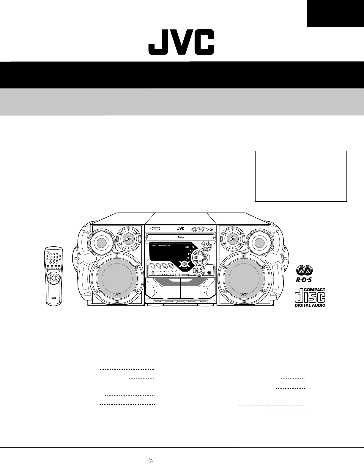
SERVICE MANUAL
COMPACT COMPONENT SYSTEM
MX-G500R
STANDBY/ON
SLEEP
AUX
DISPLAY
M
FM/AM
O
DE
CD
RMÐSMXG500R R EMOT
12
456
78
10
PTY/EON
T
APE
VOL
VOL
MX-G500R
Area suffix
B ------------------------ U.K.
E ---- Continental Europe
EN ----- Northern Europe
EV ------- Eastern Europe
STANDB
Y
ECO
STANDBY/ON
3
CD
MX-G
500R
3
SUBWOOFER
L
EVE
L
O
UND
S
O
DE
M
9
FM MODE
+10
Ð SELECT +
FADE
T
APE A/B
MUTIN
G
DISC
SKIP
+
UME
UME
Ð
E CONTROL
SP-MXG500 SP-MXG500
EXTENDED SUP ER BASS
FM
CD
AUX
/ AM
PROGRAMRANDO
M
EPEAT
R
PHONES
REC STAR
T
C
D REC
DUBBING
/STO
P
START
FULL - LOGIC CONTROL
CA-MXG500R
DISPLAY
T
APE
TAPE BTAPE
A
Ð
DISPLA
Y MOD
E
SELECT +
PTY/EO
N
CD SYNCHRO RECORDIN
DISC CHANGE
2
3
1
D
D
D
C
C
C
CD-R/RW PLAYBACK
SOUND
M
ODE
CLOCK
/TIMER
SUBWOOFER
LEVEL
G
Contents
Safety Precautions
Important for laser produbts
Preventing static electricity
Disassembly method
Wiring connection
Adjustment method
COPYRIGHT 2002 VICTOR COMPANY OF JAPAN, LTD.
1-2
1-4
1-5
1-6
1-19
1-20
Flow of functional operation
until TOC read
Maintenance of laser pickup
Replacement of laser pickup
Trouble shooting
Description of major ICs
1-24
1-25
1-25
1-26
1-29~42
No.21098
Apr. 2002
Page 2
MX-G500R
1. This design of this product contains special hardware and many circuits and components specially for safety
purposes. For continued protection, no changes should be made to the original design unless authorized in
writing by the manufacturer. Replacement parts must be identical to those used in the original circuits. Services
should be performed by qualified personnel only.
2. Alterations of the design or circuitr y of the product should not be made. Any design alterations of the product
should not be made. Any design alterations or additions will void the manufacturer`s warranty and will further
relieve the manufacture of responsibility for personal injury or property damage resulting therefrom.
3. Many electrical and mechanical parts in the products have special safety-related characteristics. These
characteristics are often not evident from visual inspection nor can the protection afforded by them necessarily
be obtained by using replacement components rated for higher voltage, wattage, etc. Replacement parts which
have these special safety characteristics are identified in the Parts List of Service Manual. Electrical
components having such features are identified by shading on the schematics and by ( ) on the Parts List in
the Service Manual. The use of a substitute replacement which does not have the same safety characteristics
as the recommended replacement parts shown in the Parts List of Service Manual may create shock, fire, or
other hazards.
4. The leads in the products are routed and dressed with ties, clamps, tubings, barriers and the like to be
separated from live parts, high temperature parts, moving parts and/or sharp edges for the prevention of
electric shock and fire hazard. When service is required, the original lead routing and dress should be
observed, and it should be confirmed that they have been returned to normal, after re-assembling.
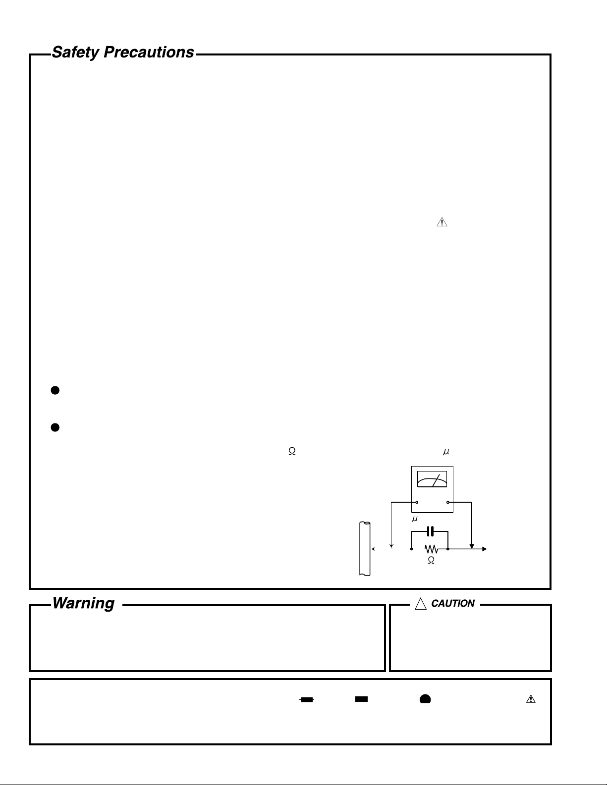
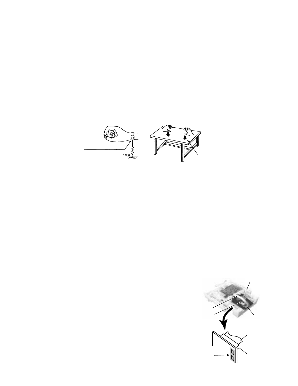
5. Leakage currnet check (Electrical shock hazard testing)
After re-assembling the product, always perform an isolation check on the exposed metal parts of the product
(antenna terminals, knobs, metal cabinet, screw heads, headphone jack, control shafts, etc.) to be sure the
product is safe to operate without danger of electrical shock.
Do not use a line isolation transformer during this check.
Plug the AC line cord directly into the AC outlet. Using a "Leakage Current Tester", measure the leakage
current from each exposed metal parts of the cabinet, particularly any exposed metal part having a return
path to the chassis, to a known good earth ground. Any leakage current must not exceed 0.5mA AC (r.m.s.).
Alternate check method
Plug the AC line cord directly into the AC outlet. Use an AC voltmeter having, 1,000 ohms per volt or more
sensitivity in the following manner. Connect a 1,500 10W resistor paralleled by a 0.15 F AC-type capacitor
between an exposed metal part and a known good earth ground.
Measure the AC voltage across the resistor with the AC
voltmeter.
Move the resistor connection to each exposed metal part,
particularly any exposed metal part having a return path to
the chassis, and meausre the AC voltage across the resistor.
Now, reverse the plug in the AC outlet and repeat each
measurement. Voltage measured any must not exceed 0.75 V
AC (r.m.s.). This corresponds to 0.5 mA AC (r.m.s.).
0.15 F AC TYPE
1500 10W
Good earth ground
AC VOLTMETER
(Having 1000
ohms/volts,
or more sensitivity)
Place this
probe on
each exposed
metal part.
!
1. This equipment has been designed and manufactured to meet international safety standards.
2. It is the legal responsibility of the repairer to ensure that these safety standards are maintained.
3. Repairs m ust be made in accordance with the relevant safety standards.
4. It is essential that safety critical components are replaced by approved parts.
5. If mains voltage selector is provided, check setting for local v oltage.
Burrs formed during molding may
be left over on some parts of the
chassis. Therefore, pay attention to
such burrs in the case of
preforming repair of this system.
In regard with component parts appearing on the silk-screen pr inted side (parts side) of the PWB diagrams, the
parts that are printed over with black such as the resistor ( ), diode ( ) and ICP ( ) or identified by the " "
mark nearby are critical for safety.
(This regulation does not correspond to J and C version.)
1-2
Page 3
MX-G500R
(U.K only)
1. This design of this product contains special hardware and many circuits and components specially
for safety purposes. For continued protection, no changes should be made to the original
design unless authorized in writing by the manufacturer. Replacement parts must be identical to
those used in the original circuits.
2. Any unauthorised design alterations or additions will void the manufacturer's guarantee ; further more the
manufacturer cannot accept responsibility f or personal injury or property damage resulting therefrom.
3. Essential safety critical components are identified by ( ) on the Parts List and by shading on the
schematics, and must never be replaced by parts other than those listed in the manual. Please note
however that many electrical and mechanical parts in the product have special safety related
characteristics. These characteristics are often not evident from visual inspection. Parts other than
specified by the manufacturer may not have the same safety characteristics as the recommended
replacement parts shown in the Parts List of the Service Manual and may create shock, fire, or
other hazards.
4. The leads in the products are routed and dressed with ties, clamps, tubings, barriers and the
like to be separated from live parts, high temperature parts, moving parts and/or sharp edges
for the prevention of electric shock and fire hazard. When service is required, the or iginal lead
routing and dress should be observed, and it should be confirmed that they have been returned
to normal, after re-assembling.
1. Service should be performed by qualified personnel only.
2. This equipment has been designed and manufactured to meet international safety standards.
3. It is the legal responsibility of the repairer to ensure that these safety standards are maintained.
4. Repairs must be made in accordance with the relevant safety standards.
5. It is essential that safety critical components are replaced by approved parts.
6. If mains voltage selector is provided, check setting for local voltage.
!
Burrs formed during molding may be left over on some parts of the chassis. Therefore,
pay attention to such burrs in the case of preforming repair of this system.
1-3
Page 4
MX-G500R
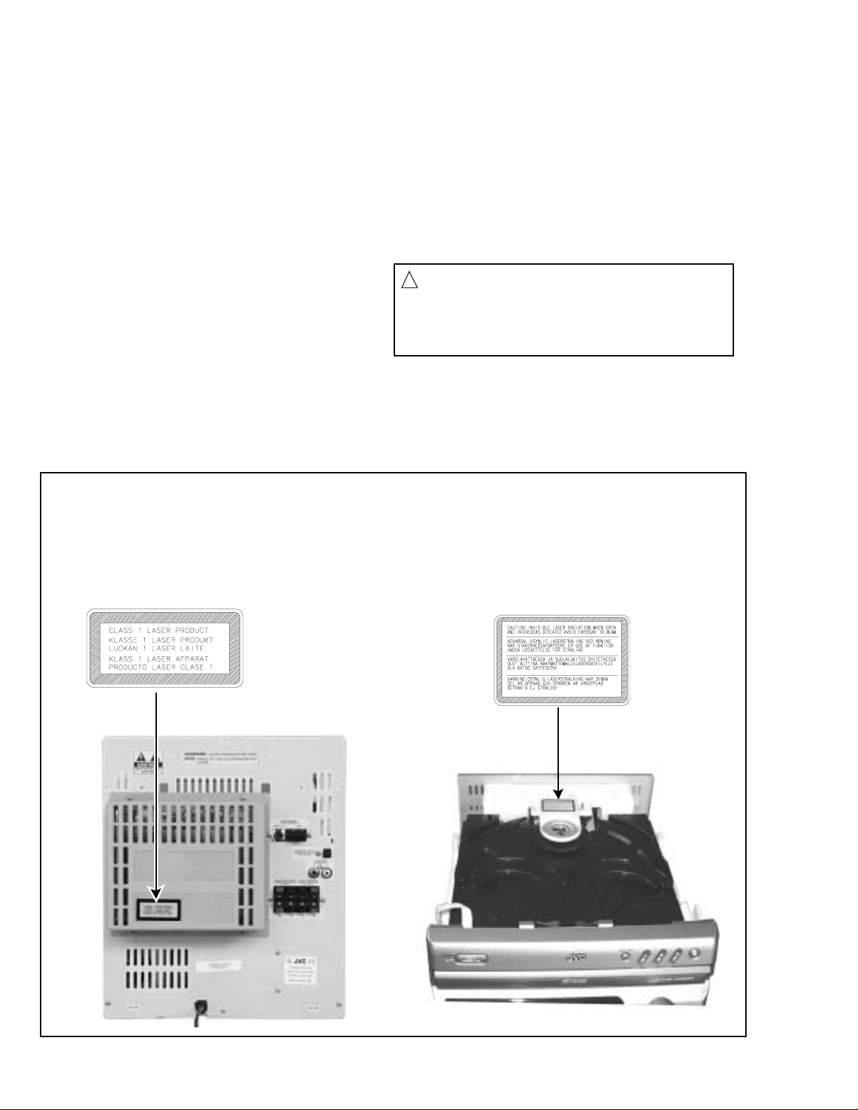
Important for laser products
1.CLASS 1 LASER PRODUCT
2.DANGER : Invisible laser radiation when open and inter
lock failed or defeated. Avoid direct exposure to beam.
3.CAUTION : There are no serviceable parts inside the
Laser Unit. Do not disassemble the Laser Unit. Replace
the complete Laser Unit if it malfunctions.
4.CAUTION : The compact disc player uses invisible
laserradiation and is equipped with safety switches
whichprevent emission of radiation when the drawer is
open and the safety interlocks have failed or are de
feated. It is dangerous to defeat the safety switches.
5.CAUTION : If safety switches malfunction, the laser is able
to function.
6.CAUTION : Use of controls, adjustments or performance of
procedures other than those specified herein may result in
hazardous radiation exposure.
!
REPRODUCTION AND POSITION OF LABELS
CAUTION
Please use enough caution not to
see the beam directly or touch it
in case of an adjustment or operation
check.
CLASS 1
LASER PRODUCT
WARNING LABEL
1-4
Page 5
MX-G500R
Preventing static electricity
1. Grounding to prevent damage by static electricity
Electrostatic discharge (ESD), which occurs when static electricity stored in the body, fabric, etc. is discharged,
can destroy the laser diode in the traverse unit (optical pickup). Take care to prevent this when performing repairs.
2. About the earth processing for the destruction prevention by static electricity
In the equipment which uses optical pick-up (laser diode), optical pick-up is destroyed by the static electricity of
the work environment.
Be careful to use proper grounding in the area where repairs are being performed.
2-1 Ground the workbench
Ground the workbench by laying conductive material (such as a conductive sheet) or an iron plate over
it before placing the traverse unit (optical pickup) on it.
2-2 Ground yourself
Use an anti-static wrist strap to release any static electricity built up in your body.
(caption)
Anti-static wrist strap
Conductive material
(conductive sheet) or iron plate
3. Handling the optical pickup
1. In order to maintain quality during transport and before installation, both sides of the laser diode on the
replacement optical pickup are shorted. After replacement, return the shorted parts to their original condition.
(Refer to the text.)
2. Do not use a tester to check the condition of the laser diode in the optical pickup. The tester's internal power
source can easily destroy the laser diode.
4. Handling the traverse unit (optical pickup)
1. Do not subject the traverse unit (optical pickup) to strong shocks, as it is a sensitive, complex unit.
2. Cut off the shorted part of the flexible cable using nippers, etc. after replacing the optical pickup. For specific
details, refer to the replacement procedure in the text. Remove the anti-static pin when replacing the traverse
unit. Be careful not to take too long a time when attaching it to the connector.
3. Handle the flexible cable carefully as it may break when subjected to strong force.
4. It is not possible to adjust the semi-fixed resistor that adjusts the laser power. Do not turn it
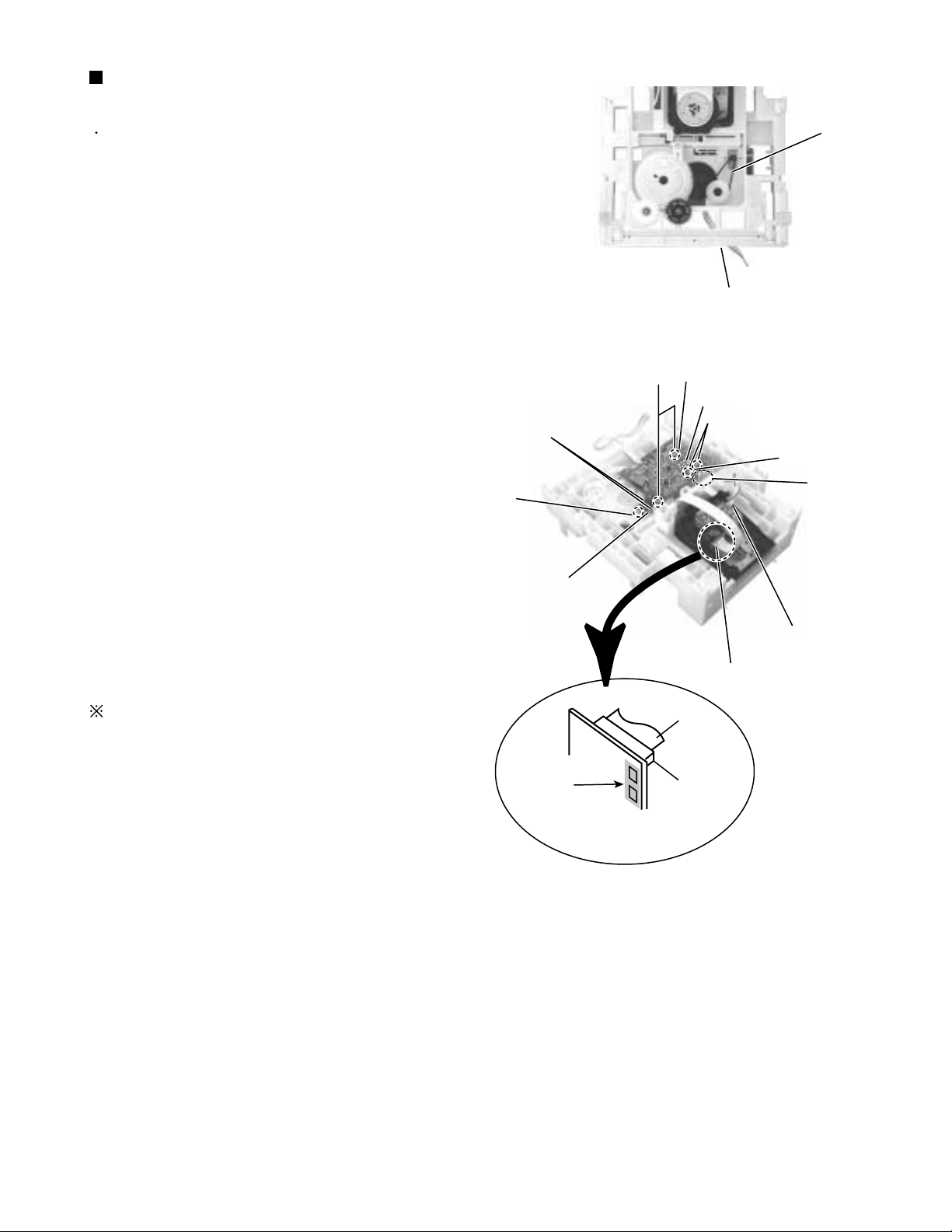
Attention when CD mechanism assembly is decomposed
*Please refer to "Disassembly method" in the text for pick-up and how to
detach the CD mechanism assembly.
1. Remove the CD changer unit.
2. Remove the CD changer mechanism.
3. Solder is put up before the card wire is removed from the pickup unit
connector on the CD mechanism assembly.
(When the card wire is removed without putting up solder, the CD pick-up
assembly might destroy.)
4. Please remove solder after connecting the card wire with the pickup unit
connector when you install picking up in the substrate.
Card wire
Picup unit
connector
Soldering
Fig.2
CD changer unit
Fig.1
Card wire
Picup unit
connector
CD changer
mechanism
1-5
Page 6
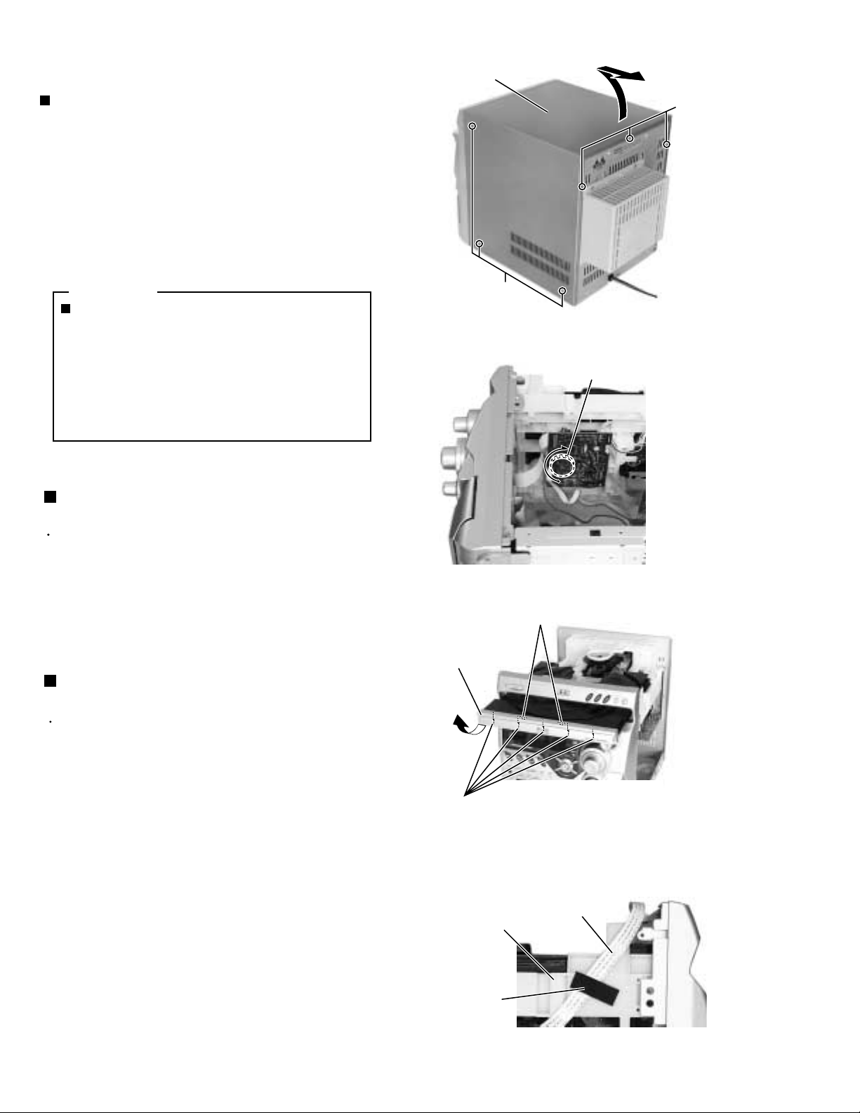
MX-G500R
Disassembly method
Removing the metal cover (See Fig.1)
1.
Remove the three screws A attaching the metal
cover on the back of the body.
2.
Remove the six screws B attaching the metal cover
on the both sides of the body.
3.
Remove the metal cover from the body by lifting the
rear part of the cover.
ONE POINT
How to eject the CD tray (see fig.2)
Although it will end if the OPEN/CLOSE
button is pushed when a power supply can
be taken, when that is not right, CD tray will
be opened manually.
Turn the loading pulley gear at the bottom of
the CD changer unit as shown in Fig.2 and
draw the CD tray toward the front.
Metal cover
A
B
(both sides)
Fig.1
Loading pulley gear
(See <CD changer unit>fig.1)
Removing the CD Tray fitting
(See Fig. 3)
Prior to performing the following procedure, eject the
CD tray.
After drawing the lower part of the tray fitting toward
1.
the front, remove the five claws. Then, while moving
the tray fitting upward, remove it.
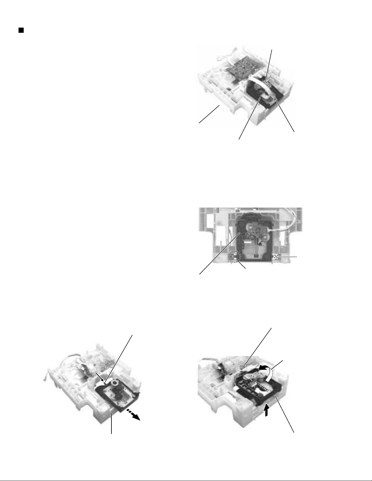
Removing the CD changer unit
(See Fig.4 to 7)
Prior to performing the following procedure, remove
the metal cover and CD tray fitting.
1.
Remove the card wire attached to CD changer unit
on the adhesion tape.
2.
Disconnect the card wire from the connector CW105
on the CD servo board.
3.
Disconnect the harness from the connector RCW6
on the main board and CW107 on the CD servo
board.
4.
Remove the two screws C attaching the CD changer
unit to the rear panel.
Fig.2
Joint
CD tray fitting
Claw
Fig.3
Card wire
CD changer unit
5.
Remove the two screws D attaching the CD changer
unit to the both sides of front panel assembly.
6.
Draw the CD changer unit upward from behind while
pulling the rear panel outward.
1-6
Adhesion tape
Fig.4
Page 7
MX-G500R
CW105
CW107
Fig.5
CD servo board
CD changer unit
Main board
RCW6
Front panel
assembly
D
(both sides)
C
Rear panel
Fig.6
CD changer unit
Rear panel
Fig.7
Removing the front panel assembly
(See Fig.8 to 10)
Prior to performing the following procedure, remove
the metal cover and CD changer unit.
1.
Disconnect the card wire from the connector FCW3
on the main board.
2.
Disconnect the harness from the connector JCW1,
JCW2 and HCW3 on the main board.
3.
Remove the screw E attaching the earth terminal
extending from the cassette mechanism assembly.
4.
Remove the two screws F attaching the front panel
assembly to both sides of the body.
5.
Remove the screw G attaching the main board to the
front panel assembly.
6.
Remove the screw H attaching the front panel
assembly to the bottom of the body.
7.
Release the two joints1 and two joints2, and detach
the front panel assembly toward the front.
Front panel
assembly
Joint1
(both sides)
(both sides)
F
FCW3
JCW2
Fig.8
Main board
JCW1
HCW3
E
(fixing the earth wire)
Main board
ACW1
ACW2
Amp. board
Front panel
assembly
G
Fig.9
Joint1
(both sides)
F
(both sides)
1-7
Page 8
MX-G500R
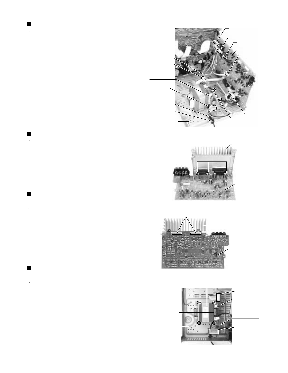
Removing the heat sink & amp. board
(See Fig.8, 11 and 12)
Prior to performing the following procedure, remove
the metal cover and the CD changer unit.
1.
Disconnect the card wire from the connector ACW1
and the harness from the connector ACW2 on the
amp. board.
2.
Remove the four screws I attaching the heat sink
cover to the rear panel. Remove the heat sink cover.
3.
Remove the four screws J attaching the heat sink
and two screws K attaching the speaker terminal to
the rear panel.
4.
After moving the heat sink upward, remove the
claws. Then pull out the heat sink & amp. board
inward.
H
Heat sink
cover
Joint2
Fig.10
(Bottom side)
Rear panel
I
I
Removing the tuner board
(See Fig.12 and 13)
Prior to performing the following procedure, remove
the metal cover.
1.
Disconnect the card wire from the connector CON01
on the tuner board.
2.
Remove the two screws L attaching the tuner board
to the rear panel.
Removing the eco board
(See Fig.12 and 13)
Prior to performing the following procedure, remove
the metal cover, CD changer unit and heat sink &
amp. board.
1.
Disconnect the power cord from the connector PJ2
on the eco board.
2.
Disconnect the harness from the connector PJ3 and
RCW5 on the eco baord.
3.
Remove the two screws M attaching the eco board
to the rear panel.
J
Heat sink
J
O
Rear panel
Tuner board
Fig.11
Rear panel
L
N
K
Speaker
terminal
M
Fig.12
Eco board
Removing the rear panel (See Fig.12)
Prior to performing the following procedure, remove
the metal cover, CD changer unit, heat sink & amp.
board and tuner board.
1.
Remove the two screws N and three screws O
attaching the rear panel.
1-8
RCW5
PJ2
PJ3
Main board
CON01
Fig.13
Page 9
MX-G500R
Removing the main board (See Fig. 14)
Prior to performing the following procedure, remove
the metal cover, CD changer unit and rear panel.
1.
Disconnect the card wire from the connector FCW3
and the harness from the connector JCW1, JCW2
and HCW3 on the main board.
2.
Disconnect the harness from the connector PCW1
on the fuse board.
3.
Remove the screw G attaching the main board
holder to the front panel assembly. (See Fig.9)
4.
Remove the two screws P attaching the heat sink to
the bottom chassis.
Removing the power cord (See Fig. 14)
Prior to performing the following procedure, remove
the metal cover, CD changer unit and rear panel.
1.
Disconnect the power cord from the connector PJ2
on the eco board (see fig.13) and pull up the power
cord stopper upward.
Fuse board
PCW1
Power supply
board
RCW1
Power cord
Power cord
stopper
Bottom chassis
Fig.14
Q
FCW3
JCW2
JCW1
Main board
HCW3
Heat sink
P
Heat sink
Removing the power ICs
(See Fig.15 and 16)
Prior to performing the following procedure, remove
the metal cover, CD changer unit and heat sink &
amp. board.
1.
Remove the four screws Q attaching the power ICs
to the heat sink.
2.
Unsolder the power ICs solder point.
Removing the power transformer
(See Fig .17)
Prior to performing the following procedure, remove
the metal cover, CD changer unit and heat sink &
amp. board.
1.
Disconnect the harness from the connector RCW1 on
the power supply board.
2.
Disconnect the harness from the connector PCW1 on
the fuse board.
Power ICs solder point
Bottom chassis
R
Amp. board
Fig.15
Heat sink
Amp. board
(reverse side)
Fig.16
Power transformer
PCW1
Fuse board
Power supply
board
RCW1
3.
Remove the four screws R attaching the power
transformer to the bottom chassis.
Fig.17
1-9
Page 10
MX-G500R
)
)
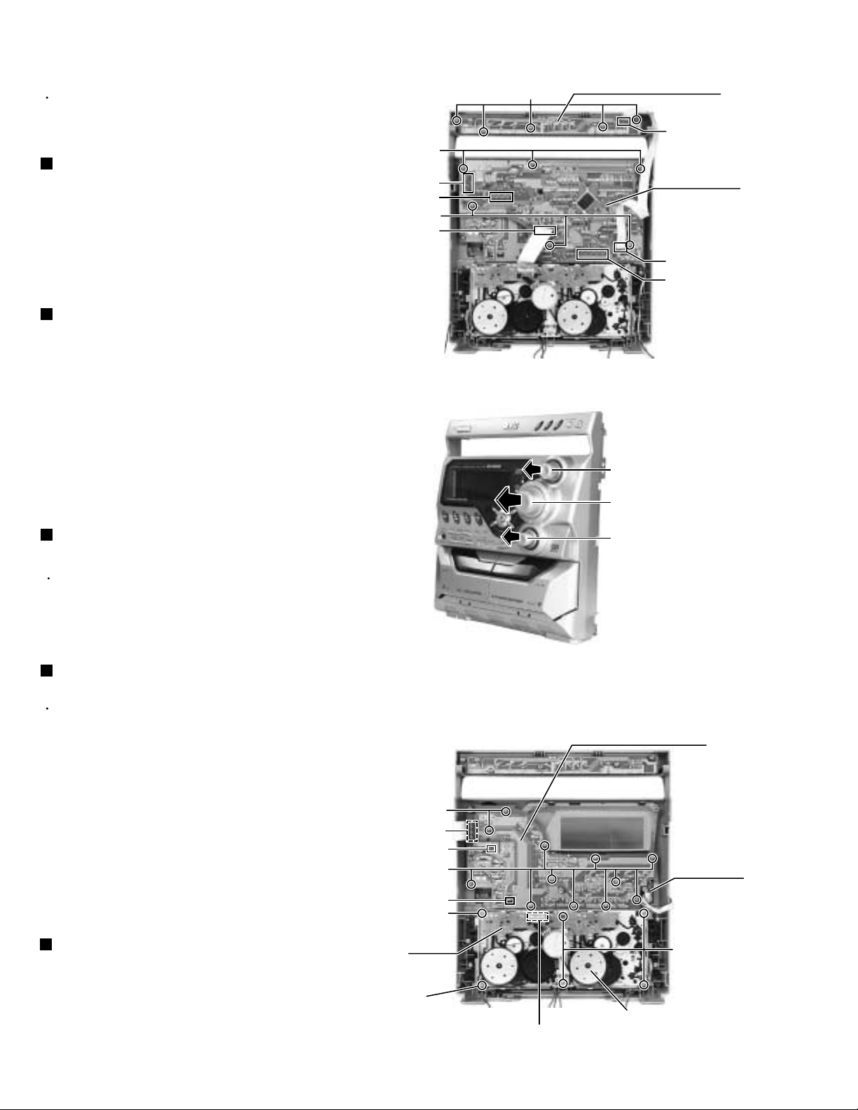
<Front panel assembly>
Prior to performing the following procedure, remove
the metal cover, the CD changer unit and the front
panel assembly.
Removing the power / CD switch board
(See Fig.1)
1.
Disconnect the card wire from the connector UCW1
on the power / CD switch board.
2.
Remove the five screws A attaching the power / CD
switch board.
Removing the FL display & system control
board (See Fig.1)
1.
Disconnect the card wire from the connector UCW3,
UCW4, UCW5 and UCW6 on the FL display & system
control board.
2.
Remove the six screws B attaching the FL display &
system control board.
3.
Disconnect the card wire from the connector UCW2
on the FL display & system control board.
B
UCW2
UCW3
B
UCW4
Front panel assembly (inner side
A
Power / CD switch board
Fig.1
Sound mode knob
Volume knob
FL diplay &
system control
board
UCW1
UCW5
UCW6
Removing the headphone jack board
(See Fig.3)
Prior to performing the following procedure remove
the FL display & system control board.
1.
You can pull out the headphone jack board.
Removing the front key switch board
(See Fig.2 and 3)
Prior to performing the following procedure, remove
the FL display & system control board.
1.
Pull out the sound mode knob, volume knob and
subwoofer level knob from front side.
2.
Remove the twelve screws C attaching the front key
switch board.
3.
Remove the front board releasing the two tabs.
4.
Disconnect the card wire from the connector UCW7
on the front key switch baord, if needed.
Removing the cassette mechanism
assembly (See Fig.3)
UCW7
Tab
Tab
Mecha.
board
C
C
D
Subwoofer level knob
Fig.2
Front panel assembly (inner side
Front key switch board
Headphone
jack board
D
1.
Disconnect the card wire from the connector on the
mecha. board.
2.
Remove the six screws D attaching the cassette
mechanism assembly.
1-10
D
(fixing the earth wire)
Connector
Cassette mechanism
assembly
Fig.3
Page 11
MX-G500R
<CD changer unit>
Prior to performing the following procedure, remove
the CD changer unit.
Removing the CD tray (See Fig.1 to 3)
1.
Turn the black loading pulley gear on the under side
of the CD changer unit in the direction of the arrow
and draw the CD tray toward the front until it stops.
2.
Disconnect the card wire from connector CW103 on
the CD servo board.
3.
Push down the two tray stoppers marked a and pull
out the CD tray.
CD servo board
Loading pulley gear
CD tray
CD changer uint (reverse side)
CW103
CD tray
Fig.1
Reinstall the CD tray (See Fig.4 to 5)
1.
Align the gear-cam with the gear-tray as shown fig.4,
then mount the CD tray.
2.
When assembling the CD tray, take extreme care not
engage with gear - synchro.
Gear-cam
Gear-tray
CD tray
(Tray stopper)
Fig.2
a (Tray stopper)
a
CD servo board
CW103
Fig.3
Gear-convert
Gear-convert
Gear-tray
Gear-cam
timing point
Gear-tray
CD tray
Fig.4 Fig.5
Gear-synchro
1-11
Page 12
MX-G500R
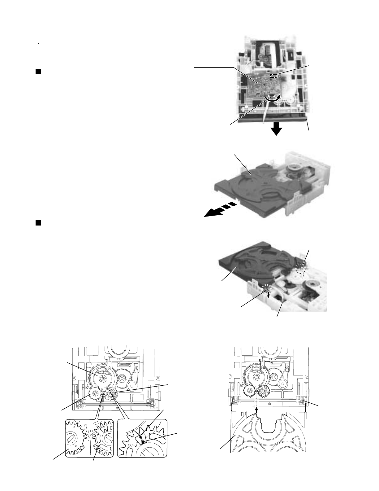
Removing the sensor board / the turn
table motor assembly (See Fig.6 to 8)
Prior to performing the following procedure, remove
the CD tray.
A
1.
Remove the screw A attaching the sensor board and
release the two tabs b attaching the sensor board on
the under side of the CD tray.
2.
Disconnect the harness from connector CW1 on the
sensor board and release the harness from the two
hooks c. Remove the sensor board.
3.
Remove the screw B attaching the turn table. Detach
the turn table from the tray.
4.
Pull outward the tab marked d attaching the turn
table motor assembly on the upper side of the tray
and detach the turn table motor assembly from the
tray.
Tray
b
CW1
c
b
Sensor board
Fig.6
Turn table
B
Turn table motor assembly
Fig.7
d
Fig.8
1-12
Page 13
Removing the belt, the CD servo board
and the switch board (See Fig.9 and 10)
Prior to performing the following procedure, remove
the CD tray.
1.
Detach the belt from the pulley on the upper side of
the CD changer unit (Do not stain the belt with
grease).
2.
Disconnect the card wire from the pickup unit
connector on the under side of the CD changer unit.
Attention : Solder is put up before the card wire is
removed from the pick-up unit
connector on the CD mechanism
assembly.
(When the card wire is removed without
putting up solder, the CD pick-up unit
assembly might destroy.)
3.
Disconnect the motor wire harness from connector
on the CD servo board.
4.
Remove the screw C attaching the switch board and
release the two tabs e attaching the switch board
outward and detach the switch board.
5.
Remove the two screws D attaching the CD servo
board and . First release the two tabs f and two tabs
g attaching the CD servo board motor to raise the
CD servo board slightly, then release the CD servo
board.
Tabs e
C
Switch board
CW3
CD changer unit
Fig.9
CD servo board
D
Tabs g
Soldered parts
CD mechanism board
motor connecter
Pickup unit connector
MX-G500R
Belt
Motor
Tabs f
If the tabs f and g are hard to release, it is
recommendable to unsolder the two soldered parts
on the motor terminal of the CD servo board.
Soldering
Card wire
Picup unit
connector
Fig.10
1-13
Page 14
MX-G500R
Removing the CD mechanism holder
assembly (mechanism included)
(See Fig.11 to 14)
1.
Disconnect the harness from connector on the CD
mechanism board in the CD mechanism assembly
on the under side of the CD changer unit. Disconnect
the card wire from the pickup unit connector.
Attention : Solder is put up before the card wire is
removed from the pick-up unit
connector on the CD mechanism
assembly. (Refer to Fig.10)
(When the card wire is removed without
putting up solder, the CD pick-up unit
assembly might destroy.)
Motor connecter
CD changer unit
CD mechanism holder assembly
Pickup unit connector
2.
Remove the screw E attaching the shaft on the right
side of the CD mechanism holder assembly. Pull
outward the stopper fixing the shaft on the left side
and remove the CD mechanism holder assembly
from behind in the direction of the arrow y.
3.
Turn the CD mechanism holder assembly half
around the lift up slide shaft h of the CD mechanism
holder assembly until the turn table is reversed, and
pull out the CD mechanism holder assembly.
Lift up slide shaft
Fig.11
E
Stopper
CD mechanism holder assembly
Fig.12
Lift up slide shaft n
1-14
CD mechanism holder assembly
Fig.14
y
CD mechanism holder assembly
Fig.13
Page 15

MX-G500R
<CD mechanism section>
•
Removing the CD mechanism holder from the CD
chager unit.
(Refer to "Removing the CD mechanism holder
assembly" )
Removing the pickup unit (
1. Removing the cut washer on the feed gear
sleeve and pull out the feed gear.
2. Remove the two screws A fixing the pickup
shaft.
3. Removing the pickup unit.
Removing the motor board
1. Unsolder the motor terminal on the motor board.
2. Remove the moter board.
Removing the feed motor (
Remove the two motor fixing screws at B and
removing the feed motor.
See Fig.1)
(See Fig.2)
See Fig.1)
A
Motor board
Shutter
Cut washer
B
Fig.1
Unsolder
Pickup unit
Feed Gear
Feed motor
Shaft
A
Removing the spindle motor
The spindle motor cannot be removed as a single
unit.
When removing the spindle motor, change the chasis
and turntable together as aunit.
Spindle motor
Unsolder
Fig.2
1-15
Page 16

MX-G500R
<Cassette mechanism section>
Removing the record/playback mechanism.
Removing the R/P head.
1. Remove the screw A on the right side of the
R/P head.(Fig.1, Fig.2)
2. Remove the screw B on the left side of the
R/P head.(Fig.1, Fig.2)
Remove the erase head.
Remove the screw C fixing the erase head.(Fig.1)
Removing the pinch roller.
1. Pull out the pinch roller by opening the pinch
roller stopper outward to unlock .(Fig.3)
2. When reassembling the pinch roller, refer to
fig. 4 to hook up the spring.
R/P Head
E. Head
Stoppsr
A
B
C
Fig.1
B
Pinch roller
assembly
A
Spring
Pinch roller
Return spring
R/P Head
Fig.2
Pinch roller
Fig.3
Pinch roller
stopper
Pinch roller
spring
1-16
Return spring
Return spring
Fig.4
Page 17

MX-G500R
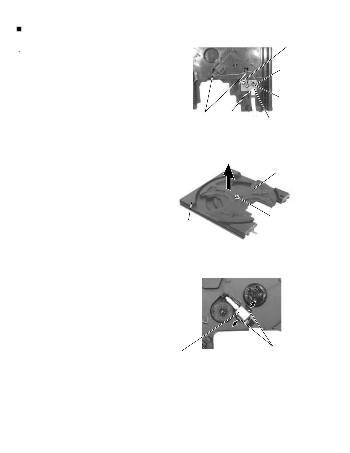
Removing the motor.
1. Remove the two screws D fixing the motor.
Be careful to grease's splash when the
drive belt comes off.(Fig.5, Fig.6)
2. Unsolder the motor terminal.(Fig.5)
Removing the mechanism board.
1.
coil terminal.(Fig.5)
2. Remove the two screws E fixing the board.(Fig.5)
Removing the flywheel.
capstan shaft, then remove the flywheel.
When reassembling the flywheel,
be sure to use new washers as they
cannot be reused.(Fig.8, Fig.9)
Unsolder the four parts a on the solenoid
3. Unhook the three parts b from the board.(Fig.5)
4. Remove the mechanism board.(Fig.5)
Remove the cut-washers at c and d from the
Mecha.
a
Drive belt (Flat)
board
E
terminal
b
Motor
Motor
D
D
Fig.5
Fig.6
E
Drive belt
Motor
Drive belt
b
a
Sleeve
Flywheel
c
Washer
Sleeve
d
FR belt
Capstan
washer
Flywheel
Fig.7
FR belt
Fig.8Fig.9
Capstan
washer
Flywheel
1-17
Page 18

MX-G500R
< Speaker section >
It is exchange in a unit.
Please do not decompose as much as possible.
Removing the side panel (See Fig. 1)
1.
Remove the five screws A attaching the side panel
and remove the side panel.
NOTES : It will be good to use the tool with a flat tip, since a
boss's portion is pasted with adhesives. Please take care not to
damage the cabinet at this time.
Removing the side speaker
(See Fig. 2 and 3)
A(long wood screw)
A(short wood screw)
Side panel
Fig.1
Side speaker
Boss and adhesion
A(long screw)
Boss and
adhesion
Front panel
Prior to performing the following procedure, remove
the side panel.
1.
Remove the four screws B attaching the side
speaker.
2.
Pull out the side speaker and remove the speaker
cord from the speaker terminal.
B
Fig.2
1-18
Side speaker
Speaker terminal
Fig.3
Page 19

MX-G500R
Wiring connection
Amp. board
0
ACW2
ACW1
3809-001224
Power /CD switch board
UCW1
3809-001228
UCW7
9
9
0
3809-001315
Front key switch board
2
PJ2
AH39-00045A
9
0
AH39-00244A
AH39-00245A
UCW2
FL dispaly & system control board
UCW3
P/T
SUB
PJ3
PCW1
RCW5
RCW1
RFS5
UCW4
RFS2
RFS6
RFS7
UCW5
ECO board
RFS8
UCW6
ECW1
9
0
Power transformer
AH39-20561P
3809-001121
CD mechanism
CW2
CW1
CW3
0
3809-001185
9
Color codes are shown below.
1 Brown
2 Red
3 Orange
4 Yellow
5 Green
6 Blue
7 Violet
9
8 Gray
9 White
0 Black
AAN1
0
2
AH38-12001A
CW102
CW103
9
CW101
CW104
CW3
0
0
CW105
CW107
CW106
0
9
0
AH39-00249B
2
3809-001034
2
0
9
9
0
AH39-00060A
AH39-00096D
CD servo board
0
9
8
2
3809-001184
3809-001223
Tuner board
JW1
0
FCW1
OCW
9
0
RCW6
FCW2
Main board
HCW3
JCW1
FCW3
JCW2
FCW3
0
9
RW2
0
9
0
0
9
RW1
2
0
2
9
0
HCW2
AH39-00247A
9
Headphone J.board
AH39-00022A
2
9
0
9
0
2
0
88
9
0
AH39-20002D
8
9
2
9
1-19
Page 20

MX-G500R
Adjustment method
1. Tuner
ITEAM
Received FREQ.
Adjustment
point
Output
* Adjustment Location of Tuner PCB
AM(MW) OSC
Adjustment
522~1629 KHz
MO
1~7.0V
MAIN
PCB
AM(MW) RF
Adjustment
594 KHz
MA
Maximum
Output(Fig.1)
VT
GND
LW OSC
Adjustment
144~288 KHz
LO
2~7.0V
TESTER
LW RF
Adjustment
150 KHz
LA
Maximum
Output(Fig.1)
1-20
Fig.1 OSC Voltage
Page 21

FM THD Adjustment
MX-G500R
SSG FREQ.
98 MHz
Adjustment
point
FM DETECTOR COIL
(FM DET)
Output
60 dB
Minumum Distortion (0.4% below)
(Fig.2)
FM Search Level Adjustment
SSG FREQ.
Adjustment
point
(SVR1)
BEACON
SENSITIVITY
SEMI-VR(20K
98 MHz
Output
GND
FM S.S.G
FM
Antenna
Terminal
SET
Oscilloscope
Input
Speaker
Terminal
output
Input
Distortion Meter
Fig.2 IF CENTER and THD Adjustment
28 dB
)
FM Antenna
SET
Output
28 dB(
2dB)
Adjust SVR1 so that "TUNED" of FLT
is lighted (Fig.3)
*Adjust FM S.S.G level to 28dB
AM(MW) I.F Adjustment
SSG FREQ.
Frequency
450 kHz
522 kHz
Adjustment
point
AM IF
Maximum output (Fig.4)
FM S.S.G
GND
FM IN
Fig.3 FM Auto Search Level Adjustment
60cm
OUTPUT
AM SSG
450KHZ
AM ANT
IN
20 k
AM IF
Speaker Terminal
INPUT
VTVM Oscilloscope
OUTPUT
Fig.4 AM I.F Adjustment
1-21
Page 22

MX-G500R
2. Cassette Deck
To adjust tape speed
Notes
1) Measuring tape:
i) VT-712/MTT-111(or equivalent)
(Tapes recorded with 3kHz)
ii) AC-225/MTT-5512(or equivalent)
2) Connect the cassette deck to the frequency counter
as in fig.1.
Cassette Deck
SPK OUT
Frequency Counter
output
Fig.1
Pre-Setup
Condition
NOR
1 3KHz
SPEED
Control
OUT
(connected to the
frequencycounter)
1) Deck 1:VT-712
2) Press PLAY
SW button
To Adjust
Turn VSR1 to
left and right
(FRONT PCB)
3) Deck 2:Same
as above
To adjust plabyback level/REC
Notes
1) Before the actual adjustment, clean the play/recording head.
2) Measuring tape :
i) VT-703/MTT-114N(or equivalent 10kHz AZIMUTH control)
ii) AC-225/MTT-5512(or equivalent)
3) The cassette deck is connections as shown in fig.2.
Cassette Deck
SPK OUT
(GND)
Fig.2
VTVM
In Out
RemarkStandardPre-SetupItemStep
1%
range
Oscilloscope
1. Adjust Deck 1 Play Level
Pre-Setup
Condition
AZIMUTH1 SPK OUT
(VTVM is
connected to
the scope)
1-22
After putting VT-703
into Deck 1
- Press FWD PLAY
button.
To Adjust
Turn the control
screw to as
shownin Fig.3.
Max output
and same phase
(both channels)
RemarkStandardPre-SetupItemStep
After
adjustment
secure it with
REGION
LOCK.
Page 23

2. Adjust Deck 2 Play Level/REC BIAS
MX-G500R
2
AZIMUTH1
Recording
Bias
Voltage
Pre-Setup
Condition
SPK OUT
(VTVM is
connected to
the scope)
Fig.4
Recording /Play head
After putting VT-703
into Deck 2
1)Press FWD PLAY
button.
After putting AC-225
into Deck 2
1)Press REC PLAY
button.
2)MAIN PCB JCW3,
connectted to VTVM
To Adjust
Turn the control
screw to as
shown in Fig.3.
Turn JSR2L,
JSR2R to the
right and left
Max output
and same phase
(both channels)
7mV(
0.5mV)
RemarkStandardPre-SetupItemStep
After
adjustment
secure it with
REGION
LOCK.
AZIMUTH control screw
Audio OSC.
Fig.3
AUX IN
SET
(MAIN PCB)
LINE OUT
IN
TP
JCW3
Fig.4
VTVM
IN OUT
Oscilloscope
1-23
Page 24

MX-G500R
Flow of functional operation until TOC read
Power ON
Play Key
RESET a CD LSI
Check Point
Confirm that the voltage at the pin17
of KB9226(IC101) is "L" "H".
LIMIT SW ON
SET Default value of
TE gain, TE balance
Automatic adjusting of
focus bias
Automatic adjusting of
FE offset
Automatic adjusting of
TE offset
LASER power ON
Detection of disk
Confirm that the voltage at the pin33
of KB9226(IC101) is "H" "L" "H".
Confirm that the voltage at the
pin37 of KB9226(IC101) is 3.5V.
Tracking error waveform at TOC reading
Pin 34 of
KB9226
(IC101)
2.50V
Approx
0.4V
Disc states
to rotate
Approx.3.7sec
Disc is rotated
Automatic adjusting of
TE balance
Automatic adjusting of
TE gain
TOC reading
Play a disc
Confirm that the signal from pin24
of KB9226(IC101) is 3.5V as a
accelerated pulse during
approx.1.96s.
Confirm the waveform of
the Tracking error signal
at the pin 34 of KB9226(IC101).
Confirm the eye-pattern
at the pin2 of KB9226(IC101).
1-24
Page 25

Maintenance of laser pickup
MX-G500R
(1) Cleaning the pick up lens
Before you replace the pick up, please try to
clean the lens with a alcohol soaked cotton
swab.
(3) Semi-fixed resistor on the APC PC board
The semi-fixed resistor on the APC printed circuit board which is attached to the pickup is used to adjust the
laser power. Since this adjustment should be performed to match the characteristics of the whole optical block,
do not touch the semi-fixed resistor.
If the laser power is lower than the specified value, the laser diode is almost worn out, and the laser pickup
should be replaced.
If the semi-fixed resistor is adjusted while the pickup is functioning normally, the laser pickup may be damaged
due to excessive current.
(2) Life of the laser diode
When the life of the laser diode has expired,
the following symptoms will appear.
1. The level of RF output (EFM output :
amplitude of eye pattern) will below.
Is the level of
RF OUT under
1.1V 0.2Vp-p?
YES
O.K
NO
Replace it.
Replacement of laser pickup
Turn off the power switch and,disconnect the
power cord from the ac outlet.
Replace the pickup with a normal one.(Refer
to "Pickup Removal" on the previous page)
Plug the power cord in,and turn the power on.
At this time,check that the laser emits for
about 3seconds and the objective lens moves
up and down.
Note: Do not observe the laser beam directly.
Play a disc.
Check the eye-pattern at TP1.
Finish.
1-25
Page 26

MX-G500R
Troubleshooting
1. Amplifier
Power malfunction
No output
1-26
Page 27

2.Tuner malfunction (FM/AM)
MX-G500R
3.Tape
HA12235F
HA12235F
JIC1(HA12235F) PIN5,26
3,4,27,28
16
JC63L,JC63R,JR65L,JR65R
1-27
Page 28

MX-G500R
4.CD
1-28
Page 29

Description of major ICs
KA3082 (IC401, IC402) : DC motor driver
1.Pin layout
DRIVER OUT
PRE DRIVER
MX-G500R
BIAS
1234
GND
O1
V
V
Z1
V
CTL
2.Pin function
Pin No.
1
2
3
4
5
6
7
8
9
10
Symbol
GND
VO1
VZ1
VCTL
VIN1
VIN2
SVCC
PVCC
VZ2
VO2
I/O
-
O
I
I
I
-
-
-
O
LOGIC SWITCH
5
V
IN1
678910
V
IN2
Function
Ground
Output 1
Phase compensation
Motor speed control
Input 1
Input 2
Supply voltage (Signal)
Supply voltage (Power)
Phase compensation
Output 2
SV
CC
TS
D
PV
CC
Z2
V
O2
V
74HCU04 (OIC1) : Optical
1.Pin layout
1A 1 14 Vcc
1Y 2 13 6A
2A 3 12 6Y
2Y 4 11 5A
3A 5 10 5Y
3Y 6 9 4A
GND 7 8 4Y
04U
1-29
Page 30

MX-G500R
5L9290 (IC201) : Digital signal processor for CDP
1. Pin layout
RCHOUT
VSSA_DAC
VREF
VHALF
VDDA_DAC
LRHOUT
VDDA_PLL
48 47 46 45 44 43 42 41 40 39 38 37
VSSD_DAC
VDDD_DAC
SADTI
LRCKI
BCKI
2. Block diagram
VSSA_PLL
VCO1LF
VSSD_PLL
VDDD_PLL
VDDD1_5V
XIN
XOUT
VSSD1_5V
EFMI
LOCK
SMEF
SMON
1
2
3
4
5
6
7
8
9
10
11
12
13 14 15 16 17 18 19 20 21 22 23 24
SMDS
WDCK
S5L9290X
DSP+DAC
48-LQFP-0707
LKFS
TESTV
LKFS
RESETB
MLT
MDAT
SOS1
SQCK
SBCK
SQDT
SBDT
MCK
ISTAT
C2PO
S0S1
SQCK
36
35
34
33
32
31
30
29
28
27
26
25
DATX
BCKO
LRCKO
SADTO
DATX
C2PO
JITB
SBCK
VDDD3-5V
VSSD2-3V
VDDD2-3V
MUTE
SQDT
VCO1LF
EFMI
LOCK
SMEF
SMDP
SMDS
WDCK
WFCK
RFCK
C4M
XIN
ISTAT
MLT
MDAT
MCK
MUTE
DPLL
CLV
Servo
Timing
Generator
Micom
Interface
Subcode
Out
EFM
Demodulator
ECC
16K
SRAM
Address
Generator
JITB
Interpolator
Interface
SADTO
LRCKO
BCKO
I/O
Digital
Out
SADTI
LRCKI
BCKI
Digital
Filter
1-bit
DAC
PWM
LPF
LCHOUT
RCHOUT
VHALF
VREF
1-30
Page 31

3. Pin function
MX-G500R
NO.
1
2
3
4
5
6
7
8
9
10
11
12
13
14
15
16
17
18
19
20
21
22
23
24
25
26
27
28
28
30
31
32
33
34
35
36
37
38
39
40
41
42
43
44
45
46
47
48
Symbol
VSSA_PLL
VCO1LF
VSSD_PLL
VDDD_PLL
VDDD1-5V
XIN
XOUT
VSSD1
EFMI
LOCK
SMEF
SMDP
SMDS
WDCK
TESTV
LKFS
C4M
RESETB
MLT
MDAT
MCK
ISTAT
S0S1
SQCK
SQDT
MUTE
VDDD2-3V
VSSD2
VDDD3-5V
SBCK
JITB
C2PO
DATX
SADTO
LRCKO
BCKO
BCKI
LRCKI
SADTI
VSSD_DAC
VDDD_DAC
RCHOUT
VSSA_DAC
VREF
VHALF
VDDA_DAC
LCHOUT
VDDA_PLL
I/O
-
O
-
-
I
O
I
O
O
O
O
O
I
O
O
I
I
I
I
O
O
I
O
I
-
-
I
O
O
O
O
O
O
I
I
I
-
-
O
-
O
O
-
O
-
Function
Analog Ground for DPLL
Pump out for VCO1
Digital Ground Separated Bulk Bias for DPLL
Digital Power Separated Bulk Bias for DPLL (3V Power)
Digital Power (5V Power, I/O PAD)
X'tal oscillator input (16.9344MHz)
X'tal oscillator output
Digital Ground (I/O PAD)
EFM signal input
CLV Servo locking status output
LPF time constant control of the spindle servo error signal
Phase control output for Spindle Motor drive
Speed control output for Spindle Motor drive
Word clock output (Normal Speed : 88.2KHz, Double Speed : 176.4KHz)
Various Data/Clock Input
The Lock status output of frame sync
4.2336MHz clock output
System Reset at 'L'
Latch signal input from Micom
Serial data input from Micom
Serial data receiving clock input from Micom
The internal status output to Micom
Subcode sync signal(S0+S1) output
Subcode-Q data transfering bit clock input
Subcode-Q data serial output
System mute at 'H'
Digital Power (3V Power, Internal Logic)
Digital Ground (Internal Logic)
Digital Power (5V Power, I/O PAD)
Subcode data transfering bit clock
Internal SRAM jitter margin status output
C2 pointer output
Digital audio data output
Serial audio data output (48 slot, MSB first)
Channel clock output
Bit clock output
Bit clock input
Channel clock input
Serial audio data input (48 slot, MSB first)
Digital Ground for DAC
Digital Power for DAC (3V Power)
Right-Channel audio output through DAC
Analog Ground for DAC
Referance Voltage output for bypass
Referance Voltage output for bypass
Analog Power for DAC (3V Power)
Left-Channel audio output through DAC
Analog Power for PLL (3V Power)
1-31
Page 32

MX-G500R
KB9226 (IC101) : RF amp. & servo signal processor
1. Pin layout
36 35 34 33 32 31 30 29 28 27 26 25
LD
37
PD
38
39
PDAC
40
PDBD
41
PDF
42
PDE
43
DCB
44
MCP
45
DCCI
46
DCCO
47
VREF
48
EQC
TEIO
LPFT
ATSC
EQI
RFO
RFM
1 2 3 4 5 6 7 8 9 10 11 12
FEO
FEM
GND
TZC/SSTOP
S1L9226X
EFMI
VCC
EQO
FRSH
TEO
FSET
TEM
FLB
SLP
FGD
FSI
SLO
SLM
SPO
SPM
ASY
EFM
LOCK
WDCK
CLVI
RESET
MLT
MDATA
MCK
ISTAT
TGU
24
23
22
21
20
19
18
17
16
15
14
13
2. Block diagram
4
EQO
EFMI
5
45
DCCI
DCC0
46
MCP
44
DCB
43
VCC/
6
VDD
7
FRSH
8
FSET
FLB
9
FGD
10
11
FSI
EQI
RFO
RFM
RF AGC & EQ
Control
Focus OK Detect
Defect Detect Mirror
Gen
Focus Servo Loop
- Gain & Phase
Compensation
- Focus Search
- Offset Adjust
- FZC Gen.
EQC
VREF
Center
Voltage
APC. Laser
Control &
LPC
Tracking Servo Loop
- Gain & Phase
Compensation
- Track Jump
- Offset Adjust
- TZC Gen.
Hardware Logic
- Auto-Sequencer
- Fast Search
- Febias, Focus Servo,
Tracking Offset ADJ.
- Tracking Balance & Gain
Adjust
- Interruption Detect
- EFM Muting System
PDE
41 40424748123
Tracking Error
(RW)
I/V AMP
PDF
PDBD
39
RF & Focus
Error (CD-RW)
I/V AMP
Sled Servo &
Kick Gen
PDAC
38
37
35
34
33
36
29
28
27
26
25
29
30
PD
LD
LPFT
TEIO
TZC&
SSTOP
ATSC
TEO
TEM
SLP
SLO
SLM
FEO
FEM
1-32
TGU
12
Micom Data Interface Logic Decoder
1413 15 16 17 19 18 20 22 21
ISTAT
MCK
MDATA
MLT
RESET
WDCK
CLVI
LOCK
EFM
Comparator
ASY
EFM
Spindle
Servo LPF
23
24
SPDLO
SPDLM
Page 33

3. Pin function
Pin No.
1
2
3
4
5
6
7
8
9
10
11
12
13
14
15
16
17
18
19
20
21
22
23
24
25
26
27
28
29
30
31
32
33
34
35
36
37
38
39
40
41
42
43
44
45
46
47
48
Symbol
RFM
RFO
EQI
EQO
EFMI
VCC
FRSH
FSET
FLB
FGD
FSI
TGU
ISTAT
MCK
MDATA
MLT
RESET
CLVI
WDCK
LOCK
EFM
ASY
SPM
SPO
SLM
SLO
SLP
TEM
TEO
FEM
FEO
GND
TZC/
SSTOP
TEIO
LPFT
ATSC
LD
PD
PDAC
PDBD
PDF
PDE
DCB
MCP
DCCI
DCCO
VREF
EQC
Function
I/O
RF summing amp. inverting input
I
RF summing amp. output
O
RFO DC eliminating input(use by MIRROR, FOK ,AGC & EQ terminal)
I
RF equalizer output
O
EFM slice input. (input impedance 47K)
I
Main power supply
P
Capcitor connection to focus search
I
Filter bias for focus,tracking,spindle
I
Capacitor connection to make focus loop rising band
I
Terminal to change the hign frequency gain of focus loop
I
Focus servo input
I
Connect the component to change the high frequency of tracking Loop
I
Internal status output
O
Micom clock
I
Data input
I
Data latch input
I
Reset input
I
Input the spindle control output from DSP
I
88.2KHz input terminal from DSP
I
Sled run away inhibit pin (L: sled off & tracking gain up)
I
EFM output for RFO slice(to DSP)
O
Auto asymmetry control input
I
Spindle amp. inverting input
I
Spindle amp. output
O
Sled servo inverting input
I
Sled servo output
O
Sled servo noninverting input
I
Tracking servo amp.inverting input
I
Tracking servo amp. output
O
Focus servo amp. inverting input
I
Focus servo amp. output pin
O
Main ground
P
Tracking zero crossing input & Check the position of pick-up wherther inside or not
I
Tracking error output & Tracking servo input
B
Tracking error integration input (to automatic control)
I
Anti-shock input
I
APC amp. output
O
APC amp. input
I
Photo diode A & C RF I/V amp. inverting input
I
Photo diode B & D RF I/V amp. inverting input
I
Photo diode F & tracking(F) I/V amp. inverting input
I
Photo diode E & tracking(E) I/V amp. inverting input
I
Capacitor connection to limit the defect detection
I
Capacitor connection to mirror hold
I
Output pin to connect the component for defect detect
O
Input pin to connect the component for defect detect
I
(VCC+GND)/2 Voltage reference output
O
AGC_equalize level control terminal & capacitor terminal to input in to VCA
I
MX-G500R
1-33
Page 34

MX-G500R
LC72131(IC02) : PLL frequency synthesizer for electron alignment
1. Pin layout
1
XIN
2
CE
3
DI
4
CL
5
DO
6
BO1
7
BO2
8
BO3
9
BO4
10
I01
20
19
18
17
16
15
14
13
12
11
XOUT
VSS
AOUT
AIN
PD
VDD
FMIN
AMIN
I02
IFIN
2. Block diagram
1
20
14
13
2
3
4
5
15
19
CCB
I/F
Power
on
Reset
Reference
Driver
1
2
Swallow
Counter
1/16,1/17 4bits
12bits
Programmable
Divider
Data Shift Register & Latch
Phase
Detector
Charge
Pump
Unlock
Detector
Universal
Counter
16
17
18
11
3.Pin function
Symbol
XIN
XOUT
FMIN
AMIN
Pin No.
1
20
14
13
Type
Xtal OSC
Local
oscillator
signal input
Local
oscillator
signal input
6
7
9
8
Functions
Crystal resonator connection
(4.5MHz/7.2MHz)
Serial data input : FMIN is selected when DVS is set to 1.
The input frequency range is from 10 to 160MHz.
The signal is passed through a built-in divide-by-two prescaler
and then supplied to the swallow counter.
A1 though the range of divisor setting is from
272 to 65, 535, the actual divisor is twice the setting since
there is also a built-in divide-by-two prescaler.
Serial data input : AMIN is selected when DVS is set to 0.
Serial data input : When SNS is set to 1 :
The input frequency range is form 2 to 40MHz
The signal is supplied directly to the swallow counter.
The range of divisor setting is from 272 to
65, 535 and the actual divisor will be the value set.
Serial data input : When SNS is set to 0 :
The input frequency ranges is from 0.5 to 10MHz.
The signal is supplied directly to a 12-bit
programmable divider.
The range of divisor setting is from 4 to 4,095 and the
actual divisor will be the value set.
1210
(1/2)
Circuit configuration
1-34
CE
2
Chip enable
Most be set high when serial data is input to the
LC72131M (DI ), or when serial data is output (DO).
S
Page 35

MX-G500R
3.Pin function
Symbol
CL
DI
DO
VDD
VSS
BO1
BO2
BO3
BO4
Pin No.
4
3
5
15
19
6
7
8
9
Type
Clock
Input data
Output data
Power supply
Ground
Output port
Functions
Used as the synchronization clock when serial data is input
to the LC72131 (DI ), or when serial data is output (DO).
Inputs serial data sent from the controller to the LC72131M.
Output serial data sent from the LC72131M to the controller.
The content of the output data is determined by the serial
data DOCO to DOC2.
The LC72131M power supply (VDD=4.5 to 5/5V)
The power on reset circuit operates when power is first applied.
The LC72131M ground.
Dedicated output pins
The output states are determined by BO1 to BO4 in the
serial data.
'Data"=0:Open
=1:Low
The pins go to the open state after the power-on reset.
An 8Hz time base signal can be output from BO1 when TBC
in the serial data is set to 1.
Note that the ON impedance of the BO1 pin is higher than
that of the other pins (BO2 to BO4)
(2/2)
Circut confguration
S
S
IO1
IO2
PD
AIN
AOUT
10
12
16
17
18
I/O Port
Charge pump
output
L.P.F
amplifier Tr
Pins used for both input and output
The input or output state is determined by bits IOC1 and IOC2
in the serial state.
'Data"=0:Input port
=1:Output port
When specified for use as an input port :
The input state is transmitted to the controller through the
DO pin.
'Input state"=Low:data value 0
=High:data value 1
When specified for use as an output port :
The output state is determined by bits IO1 and IO2 in the
serial sate.
'Data"=0:Open
=1:Low
These pins go to the input port state after the power-on reset.
PLL Charge pump output
When the frequency generated by dividing the Local oscillator
frequency by N is higher than the reference frequency,
a high level will be output from the PD in. similarly, when that
frequency is lower, a low level will be output.
The PD pin goes to the high impedance state when the
frequencies agree.
The MOS transistor used for the PLL active Low-pass filter.
S
IFIN
11
IF counter
The input frequency range is from 0.4 to 12MHz.
The signal is supplied directly to the IF counter.
The result from the IF counter MBS is output through
the DO pin.
There are four measurement periods: 4, 8, 32 or 64ms.
1-35
Page 36

MX-G500R
LC86P6548 (UIC1) : Microcontroller
1.Pin layout
S47/PF7
S46/PF6
S45/PF5
S44/PF4
S43/PF3
S42/PF2
S41/PF1
S40/PF0
VDD4
S39/PE7
S38/PE6
S37/PE5
S36/PE4
S35/PE3
S34/PE2
S33/PE1
S32/PE0
S31/PD7
S30/PD6
S29/PD5
S28/PD4
S27/PD3
S26/PD2
S25/PD1
S24/PD0
S23/PC7
S22/PC6
S21/PC5
S20/PC4
VP
2.Block diagram
S48/PG0
S49/PG1
S50/PG2
S51/PG3
P00
P01
P02
P03
VSS2
VDD2
P04
P05
P06
P07
P10/SO0
P11/SI0/SB0
P12/SCK0
P13/SO1
P14/SI1/SB1
P15/SCK1
81
82
83
84
85
86
87
88
89
90
91
92
93
94
95
96
97
98
99
100
Interrupt Control
Standby Control
CF
RC
X’ta
l
8079787776757473727170696867666564636261605958575655545352
1234567891011121314151617181920212223242526272829
P30
P31
P32
P33
P34
P35
P36
P16/BUZ
P17/PWM0
Clock
Generator
P37
P70/INT0
RES
XT1/P74
CF1
VSS1
XT2/P75
CF2
VDD1
P80/AN0
IR
PLA
PROM
Control
PROM(48KB)
P81/AN1
P82/AN2
P83/AN3
PC
P84/AN4
P85/AN5
P86/AN6
A15-A0
D7-D0
TA
CE
OE
DAS
EC
P87/AN7
P71/INT1
P72/INT2/T0I
51
50
49
48
47
46
45
44
43
42
41
40
39
38
37
36
35
34
33
32
31
30
S0/T0
P72/INT3/T0I
S19/PC3
S18/PC2
S17/PC1
S16/PC0
VDD3
S15/T15
S14/T14
S13/T13
S12/T12
S11/T11
S10/T10
S9/T9
S8/T8
S7/T7
S6/T6
S5/T5
S4/T4
S3/T3
S2/T2
S1/T1
Base Time
SI
O0
O1
SI
Timer 0
er 1
Tim
ADC
INT0-3
Noise Filter
SIO Auto
transmissio
RAM
128 by
VFD
Controller
High voltage O
r
matic
s
te
utput
Bus Interface
n
Port 1
Port 3
Port 7
Port 8
ACC
B Register
C Register
A
PSW
RAR
RAM
Stack Poi nter
Port 0
Watchdog Timer
1-36
Page 37

3. Pin function
Pin No.
1
2
3
to
10
11
12
13
14
15
16
17
18
19
to
22
23
to
26
27
28
29
30
to
36
37
to
45
46
47
to
50
51
52
to
63
64
to
71
72
73
to
80
81
to
84
85
86
87
88
89
90
91
92
93
94
95
96
97
98
99
100
P16/BUZ
P17/PWM0
P70/INT0
XT1/P74
XT2/P75
P80/AN0
P83/AN3
P84/AN4
P87/AN7
P71/INT1
P72/INT2/T0I
P72/INT3/T0I
S15/T15
S16/PC0
P19/PC3
S20/PC4
S31/PD7
S32/PE0
S39/PE7
S40/PF0
S47/PF7
S48/PG0
S51/PG3
P10/SO0
P11/SI0/SB0
P12/SCK0
P13/SO1
P14/SI1/SB1
P15/SCK1
Symbol
P30
to
P37
RES
VSS1
CF1
CF2
VDD1
to
to
S0/T0
to
S6/T6
S7/T7
to
VDD3
to
VP
to
to
VDD4
to
to
P00
P01
P02
P03
VSS2
VDD2
P04
P05
P06
P07
I/O
Function
I/O
Buzzer output
I/O
Timer 1 output (PWM0 output)
I/O
8bit input/output port
Input/output in bit unit
15V withstand at N-channel open drain output
I/O
INT0 input /HOLD release/N-channel Tr. ouptput forwatchdog timer
I
Reset pin
I
32.768kHz crystal oscillation terminal XT1
I
32.768kHz crystal oscillation terminal XT2
-
Power pin (-)
I
Input pin for the ceramic resonator oscillation
O
Output pin for the ceramic resonator oscillation
-
Power pin (+)
I
4-bit input port
Input /output in bit unit
O
I
INT1 input/HOLD release input
I
INT2 input/timer 0 event input
O
Output for VFD display controller segment/timing incommon
O
Output for VFD dis;lay controller segment/timing withinternal pull-down
resistor in common
Internal pull-down resistor output
-
Power pin (+)
I/O
Output for VFD display controller
High voltage input port PC0 to PC3
-
Power pin (+) for the VFD output pull-down resist
I/O
Output for VFD display controller
High voltage input port PC4 to PC7, PD0 to PD7
I/O
Output for VFD displaya controller segment
High voltage input port PE0 to PE7
-
Power pin (+)
I/O
Output for VFD displaya controller segment
High voltage input port PF0 to PF7
I/O
Output for VFD displaya controller segment
High voltage I/O port PG0 to PG3
I/O
8-bit input/output port. Input for port0 interrupt.
Input/output in nibble unit
Input for HOLD release
15V withstand at N-channel open drain output
-
Power pin (-)
-
Power pin (+)
I/O
8-bit input/output port. Input for port0 interrupt.
Input/output in nibble unit
Input for HOLD release
15V withstand at N-channel open drain output
I/O
SIO0 data output
SIO0 data input/bus input/output
SIO0 clock input/output
SIO1 data output
SIO1 data input/bus input/output
SIO1 clock input/output
8-bit input/output port
Input/output can be specified in a bit unit
MX-G500R
1-37
Page 38

MX-G500R
HA12235 (JIC1) : Audio signal processor
1. Block diagram
TEST
(Open for normal use)
IREF
GND
20
19
18
ALCDET
17
Vcc
16
A
MUTE ON/OFF
REC MUTE OFF/ON
15
14
(REC RETURN ON/OFF)
A/B
13
ALC ON/OFF
High/Normal
11
12
REC OUT(L)
NC
ALC(L)
REC IN(L)
NC
PB OUT(L)
TAI(L)
EQOUT(L)
PB-EQ(L)
PB-NF2(L)
21
22
23
24
2526
27
28
29
30
EQ
120/60
(Norm/High)
+
31
MUTE
AB
32
33
34
Return SW
35
ALC
Return SW
36
37
38
MUTE
AB
39
EQ
120/60
(Norm/High)
+
40
REC OUT(R)
10
9
NC
8
ALC(R)
7
REC IN(R)
6
NC
5
PB OUT(R)
4
TAI(R)
3
EQOUT(R)
2
PB-EQ(R)
1
PB-NF2(R)
2. Pin function
Pin No.
1
2
3
4
5
6
7
8
9
10
11
12
13
14
1-38
Symbol
PB-NF2(R)
PB-EQ(R)
EQOUT(R)
TAI(R)
PBOUT(R)
NC
RECIN(R)
NC
RECOUT(R)
ALC ON/OFF
High/Norm
A/B
MUTE ON/OFF
PB-NF1(L)
Function
PB EQ feed back
NAB output
EQ output
Tape input
PB output
NC pin
REC-EQ input
NC pin
REC output
Mode control input
Mode control input
Mode control input
Mode control input
AIN(L)
Pin No.
RIP
15
16
17
18
19
20
21
22
23
24
25
26
REC
IN(L)
Symbol
REC MUTE
OFF/ON
Vcc
GND
IREF
Test mode
RECOUT(L)
NC
RECIN(L)
NC
PBOUT(L)
GND
Return
Function
Mode control input
Vcc pin
GND pin
Equalizer reference
current input
Test mode pin
REC output
NC pin
REC-EQ input
NC pin
PB output
IN(R)
NC
AIN(R)
Pin No.
27
28
29
30
31
32
33
34
35
36
37
38
39
40
PB-NF1(R)
Symbol
TAI(L)
EQOUT(L)
PB-EQ(L)
PB-NF2(L)
PB-NF(L)
AIN(L)
RIP
BIN(L)
REC-RETURN
GND
BIN(R)
NC
AIN(R)
PB-NF1(R)
Function
Tape input
EQ output
NAB output
PB EQ feed back
PB EQ feed back
PB A deck input
Ripple filter
PB B deck input
REC Return
GND pin
PB B deck input
NC pin
PB A deck input
PB EQ feed back
Page 39

M66010 (UIC2) : I/O control
1.Pin layout
MX-G500R
D0
D1
CLK
CS
Vcc
GND
D24
D23
D22
D21
D20
D19
D18
D17
GND
1
2
3
4
5
S
6
7
8
9
10
11
12
13
14
15
16
2.Block diagram
CLOCK INPUT CLK
SET INPUT S
CHIP SELECT CS
INPUT
SERIAL DATA DI
INPUT
DO
DI
CLK
CS
S
D24
D23
D22
D21
D20
D19
D18
D17
D1
D2
D3
D4
D5
D6
D7
D8
D9
D10
D11
D12
D13
D14
D15
D16
3
6
4
2
32
31
30
29
28
27
26
25
24
23
22
21
20
19
18
17
Control circuit
D1
D2
D3
D4
D5
D6
D7
D8
D9
D10
D11
D12
D13
D14
D15
D16
Shift register 1
D24 D23 D22 D3 D2 D1
Q24 Q23 Q22 Q3 Q2 Q1
Parallel output latch
D24 D23 D22 D3 D2 D1
Q24 Q23 Q22 Q3 Q2 Q1
Shift register 2
DI
DO
GND GND
Vcc
5
DO SERIAL DATA
1
OUTPUT
32
D1
31
D2
30
D3
PARALLEL
DATA I/O
10
D22
9
D23
8
D24
7
16
STK402-040 (AIC1)
1.Pin layout
STK402-040
1
15
1 2 3 4 5 6 7 8 9 10 11 12 13 14 15
CH1
CH1
NF
IN
NC
STK402-040
+
ch.1
_
Pre
Vcc
BIAS
CH1
VE
CH1
-VE
Vcc -Vcc
CH2
+VE
CH2
-VE
ch.2
Pre
-Vco
+
_
SUB
GND
CH2
NF
CH2
IN
1-39
Page 40

MX-G500R
TDA7442D (FIC1) : Audio processor
1.Pin layout
R_IN3
R_IN2
R_IN1
L_IN1
L_IN2 V
L_IN3
L_IN4
MUXOUTL
IN(L)
MUXOUT(R)
IN(R)
BIN(R)
BOUT(R)
BIN(L)
1
2
3
4
5
6
7
8
9
10
11
12
13
14
2.Block diagram
MUXOUT(L)
0.47
0.47 F
0.47 F
0.47 F
0.47
0.47
0.47
0.47
F
L-IN1
L-IN2
L-IN3
L-IN4
F
R-IN1
F
R-IN2
F
R-IN3
F
R-IN4
4
50K
5
50K
6
50K
7
50K
3
50K
2
50K
1
50K
28
50K
31.5dB
control
31.5dB
control
MUXOUT(R)
+
2.2
+
2.2 F
28
R_IN4
27
LOUT
26
ROUT
25
AGND
24
S
CREF23
SDA
22
SCL
21
DIG-GND
20
TREBLE(R)
19
TREBLE(L)
18
PS1
17
LP
16
15
BOUT(L)
5.6K
100nF
100nF
BIN(L)
BOUT(L)
15
14
RB
FIX
BASS
I2C BUS DECODER + LATCHES
BASS
12
BIN(R) BOUT(R)
100nF 100nF
5.6K
FIX
VAR
RB
1319
79dB CONTROL
-
VAR
+
FIX
+
-
SPKR
MUTE
SPKR
MUTE
79dB CONTROL
D98AU947A
ATT
27
LOUT
21
SCL
22
SDA
20
DIG GND
ATT
26
ROUT
AMP
AMP
5.6nF
TREBLE-L
18
OFF
SURR
TREBLE
TREBLE
SURR
OFF
Vref
TREBLE-R
F
5.6nF
SYMULATED
-
L-R
+
100nF
RPS1
PS1
90Hz
MUSIC
PS1
17
LPF
9KHz
24 25 23
16
LP
1.2nF
OFF
V
S
SYMULATED
EFFECT
CONTROL
MUSIC/
SUPPLY
AGND
MIXING
MIXING
CREF
22
F
IN(L)
98
30K
L+R
30K
1110
IN(R)
BA4560 (AIC3, AIC4, AIC5, AIC6, AIC7, FIC4, HIC1) : Dual op amp.
1.Pin layout
V
CC
8
OUT2
7
– IN2
6
+ IN2
5
1-40
OUT1
– IN1
+ IN1
V
1
2
1ch
+
–
3
EE
4
2ch
+
–
Page 41

L4959 (RIC1) : Voltage regulator
1.Pin layout
MX-G500R
TAB CONNECTED TO PIN 6
2.Block diagram
2/10
V
S
EN 8V
EN 12V(a)
EN 12V(b)
8
7
5
REF
GEN
11
10
9
8
7
6
5
4
3
2
1
D97AU716A
OUT 12V(a)
V
S
OUT 8.6V
EN 8.6V
EN 12V(a)
GND
EN 12V(b)
N.C.
OUT 5.6V
V
S
OUT 12V(b)
5.6V, 250mA
3
OUT 5.6V
REGULATOR
8.6V, 600mA
REGULATOR
9
OUT 8.6V
SWITCHED
12V, 800mA
REGULATOR
11
OUT 12V(a)
SWITCHED
12V, 1.3A
REGULATOR
1
OUT 12V(b)
SWITCHED
D97AU569C
3.Pin function
Pin Pins Description
1 OUT 12V (b) 12V/1.3A SWITCHED OUTPUT VOLTAGE
2V
S
3 OUT 5.6V 5.6V/250mA OUTPUT VOLTAGE
4 N.C. not connected
5 EN 12V (b) Enable 12V/1.3A SWITCHED OUTPUT VOLTAGE
6 GND Ground
7 EN 12V (a) Enable 12V/0.8A SWITCHED OUTPUT VOLTAGE
8 EN 8.6V Enable 8.6V/0.6A SWITCHED OUTPUT VOLTAGE
9 OUT 8.6 8.6V/0.6A SWITCHED OUTPUT VOLTAGE
10 V
S
11 OUT 12V (a) 12V/0.8A SWITCHED OUTPUT VOLTAGE
Supply Voltage
Supply Voltage
GND
6
1-41
Page 42

MX-G500R
KA9258D (IC301) : 4-ch Motor driver
1.Block diagram
28 27 26 25 24 23 22 21 20 19 18 17 16 15
10K
T • S • D
+-
LEVEL SHIFT
10K
VCC VCC
10K
REGULATOR
10K
10K
1 2 3 4 5 6 7 8 9 10 11 12 13 14
GND
10K
GND
10K
10K
50K
MUTE
LEVEL SHIFT
-+
LA1837 (IC01) : FM IF/DET AM RF/IF/DET
1.Block diagram
1-42
Page 43

< MEMO >
MX-G500R
1-43
Page 44

MX-G500R
VICTOR COMPANY OF JAPAN, LIMITED
AUDIO & COMMUNICATION BUSINESS DIVISION
PERSONAL & MOBILE NETWORK BUSINESS UNIT. 10-1,1chome,Ohwatari-machi,Maebashi-city,371-8543,Japan
(No.21098)
200204(V)
 Loading...