

Page 1
SERVICE MANUAL
COMPACT COMPONENT SYSTEM
MX-DVB10
(SP-XDVB10)
MAIN
MX-DVB10
(SP-XSDVB10)
REAR
(SP-WDVB10)
SUBWOOFER
(SP-XCDVB10)
CENTER
(CA-MXDVB10)
(SP-XSDVB10)
REAR
(SP-WDVB10)
SUBWOOFER
Area suffix
US ------------- Singapore
UX ---------- Saudi Arabia
UN -------------------Asean
(SP-XDVB10)
MAIN
Contents
Safety precautions
Preventing static electricity
Precautions for service
Important for laser products
Disassembly method
Adjustment method
1-2
1-3
1-4
1-5
1-6
Maintenance of laser pickup
Replacement of laser pickup
Flow of functional operation
until TOC read
Description of major ICs
1-26
COPYRIGHT 2002 VICTOR COMPANY OF JAPAN, LTD.
1-34
1-34
1-35
1-36~70
No.21120
Sep. 2002
Page 2
MX-DVB10
1. This design of this product contains special hardware and many circuits and components specially for safety
purposes. For continued protection, no changes should be made to the original design unless authorized in
writing by the manufacturer. Replacement parts must be identical to those used in the original circuits. Services
should be performed by qualified personnel only.
2. Alterations of the design or circuitr y of the product should not be made. Any design alterations of the product
should not be made. Any design alterations or additions will void the manufacturers warranty and will further
relieve the manufacture of responsibility for personal injury or property damage resulting therefrom.
3. Many electrical and mechanical parts in the products have special safety-related characteristics. These
characteristics are often not evident from visual inspection nor can the protection afforded by them necessarily
be obtained by using replacement components rated for higher voltage, wattage, etc. Replacement par ts which
have these special safety characteristics are identified in the Parts List of Service Manual. Electrical
components having such features are identified by shading on the schematics and by ( ) on the Parts List in
the Service Manual. The use of a substitute replacement which does not have the same safety characteristics
as the recommended replacement parts shown in the Parts List of Service Manual may create shock, fire, or
other hazards.
4. The leads in the products are routed and dressed with ties, clamps, tubings, barriers and the like to be
separated from live parts, high temperature parts, moving parts and/or sharp edges for the prevention of
electric shock and fire hazard. When service is required, the original lead routing and dress should be
observed, and it should be confirmed that they have been returned to normal, after re-assembling.
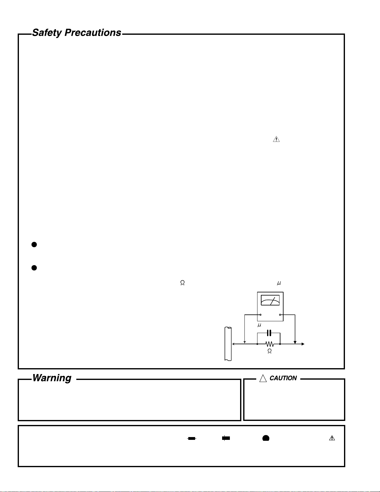
5. Leakage current check (Electrical shock hazard testing)
After re-assembling the product, always perform an isolation check on the exposed metal parts of the product
(antenna terminals, knobs, metal cabinet, screw heads, headphone jack, control shafts, etc.) to be sure the
product is safe to operate without danger of electrical shock.
Do not use a line isolation transformer during this check.
Plug the AC line cord directly into the AC outlet. Using a "Leakage Current Tester", measure the leakage
current from each exposed metal parts of the cabinet, particularly any exposed metal part having a return
path to the chassis, to a known good earth ground. Any leakage current must not exceed 0.5mA AC (r.m.s.).
Alternate check method
Plug the AC line cord directly into the AC outlet. Use an AC voltmeter having, 1,000 ohms per volt or more
sensitivity in the following manner. Connect a 1,500 10W resistor paralleled by a 0.15 F AC-type capacitor
between an exposed metal part and a known good earth ground.
Measure the AC voltage across the resistor with the AC
voltmeter.
Move the resistor connection to each exposed metal part,
particularly any exposed metal part having a return path to
the chassis, and measure the AC voltage across the resistor.
Now, reverse plug in the AC outlet and repeat each
measurement. Voltage measured any must not exceed 0.75 V
AC (r.m.s.). This corresponds to 0.5 mA AC (r.m.s.).
0.15 F AC TYPE
1500 10W
Good earth ground
AC VOLTMETER
(Having 1000
ohms/volts,
or more sensitivity)
Place this
probe on
each exposed
metal part.
!
1. This equipment has been designed and manufactured to meet international safety standards.
2. It is the legal responsibility of the repairer to ensure that these safety standards are maintained.
3. Repairs m ust be made in accordance with the relevant safety standards.
4. It is essential that safety critical components are replaced by approved parts.
5. If mains voltage selector is provided, check setting for local v oltage.
Burrs formed during molding may
be left over on some parts of the
chassis. Therefore, pay attention to
such burrs in the case of
preforming repair of this system.
In regard with component parts appearing on the silk-screen pr inted side (parts side) of the PWB diagrams, the
parts that are printed over with black such as the resistor ( ), diode ( ) and ICP ( ) or identified by the " "
mark nearby are critical for safety.
(This regulation does not correspond to J and C version.)
1-2
Page 3
MX-DVB10
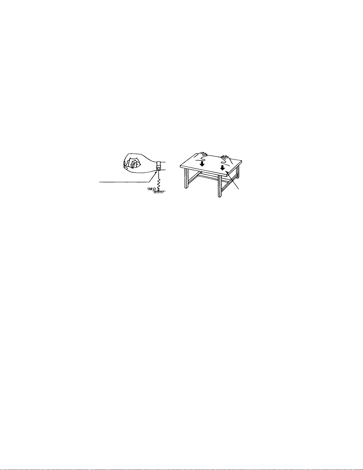
Preventing static electricity
1. Grounding to prevent damage by static electricity
Electrostatic discharge (ESD), which occurs when static electricity stored in the body, fabric, etc. is discharged,
can destroy the laser diode in the traverse unit (optical pickup). Take care to prevent this when performing repairs.
2. About the earth processing for the destruction prevention by static electricity
In the equipment which uses optical pick-up (laser diode), optical pick-up is destroyed by the static electricity of
the work environment.
Be careful to use proper grounding in the area where repairs are being performed.
2-1 Ground the workbench
Ground the workbench by laying conductive material (such as a conductive sheet) or an iron plate over
it before placing the traverse unit (optical pickup) on it.
2-2 Ground yourself
Use an anti-static wrist strap to release any static electricity built up in your body.
(caption)
Anti-static wrist strap
Conductive material
(conductive sheet) or iron plate
3. Handling the optical pickup
1. In order to maintain quality during transport and before installation, both sides of the laser diode on the
replacement optical pickup are shorted. After replacement, return the shorted parts to their original condition.
(Refer to the text.)
2. Do not use a tester to check the condition of the laser diode in the optical pickup. The tester's internal power
source can easily destroy the laser diode.
4. Handling the traverse unit (optical pickup)
1. Do not subject the traverse unit (optical pickup) to strong shocks, as it is a sensitive, complex unit.
2. Cut off the shorted part of the flexible cable using nippers, etc. after replacing the optical pickup. For specific
details, refer to the replacement procedure in the text. Remove the anti-static pin when replacing the traverse
unit. Be careful not to take too long a time when attaching it to the connector.
3. Handle the flexible cable carefully as it may break when subjected to strong force.
4. It is not possible to adjust the semi-fixed resistor that adjusts the laser power. Do not turn it.
1-3
Page 4
MX-DVB10
Precautions for service
Handling of Traverse Unit and Laser Pickup
1. Do not touch any peripheral element of the pickup or the actuator.
2. The traverse unit and the pickup are precision devices and therefore must not be subjected to
strong shock.
3. Do not use a tester to examine the laser diode. (The diode can easily be destroyed by the
internal power supply of the tester.)
4. When replacing the pickup, after mounting a new pickup, remove the solder on the short land
which is provided at the center of the flexible wire to open the circuit.
5. Half-fixed resistors for laser power adjustment are adjusted in pairs at shipment to match the
characteristics of the optical block.
Do not change the setting of these half-fixed resistors for laser power adjustment.
Destruction of Traverse Unit and Laser Pickup by Static Electricity
Laser diodes are easily destroyed by static electricity charged on clothing
or the human body. Before repairing peripheral elements of the traverse
unit or pickup, be sure to take the following electrostatic protection:
1. Wear an antistatic wrist wrap.
2. With a conductive sheet or a steel plate on the workbench on which
the traverse unit or the pick up is to be repaired, ground the sheet
or the plate.
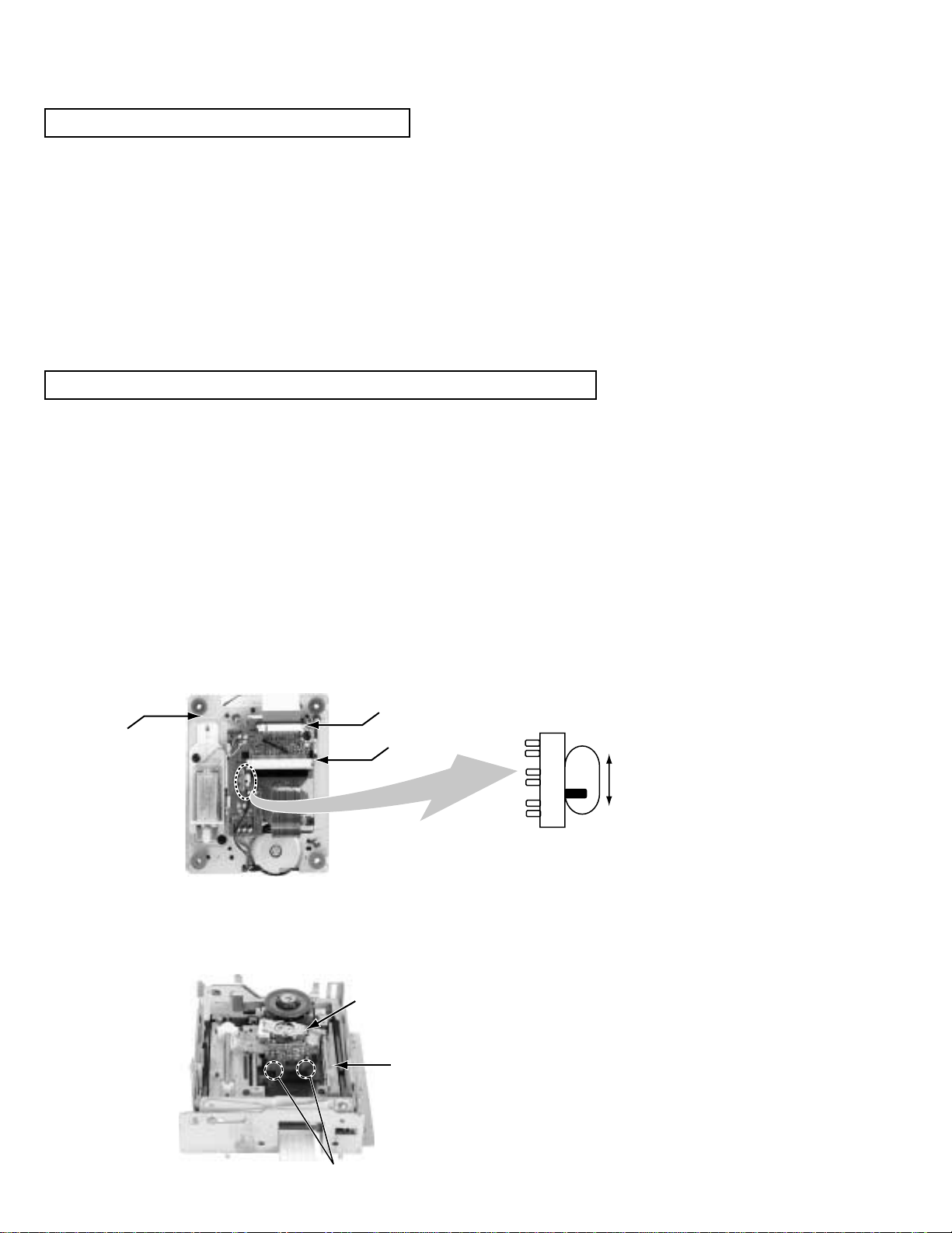
When you remove the traverse mechanism from the servo control substrate
The laser diode of pick-up might be destroyed by static electricity and set switch (S11) on the pick-up board
on "SHORT" side, please before removing the card wire from connector (CN10).
Moreover, please set switch (S11) on "OPEN" side after assembling and inserting the card wire in
connector (CN10) without fail at times.
Traverse
mechanism
CN10
CN12
SWITCH S11
SHORT
OPEN
When you remove the pick-up from the traverse mechanism
The laser diode of the pick-up might be destroyed by static electricity. Before extracting
the flexible wire from connector (CN12), please solder point A as shown below.
Moreover, please remove solder in point A after inserting a flexible wire in connector (CN12).
Pick-up
1-4
Traverse
mechanism
Soldering points A
Page 5
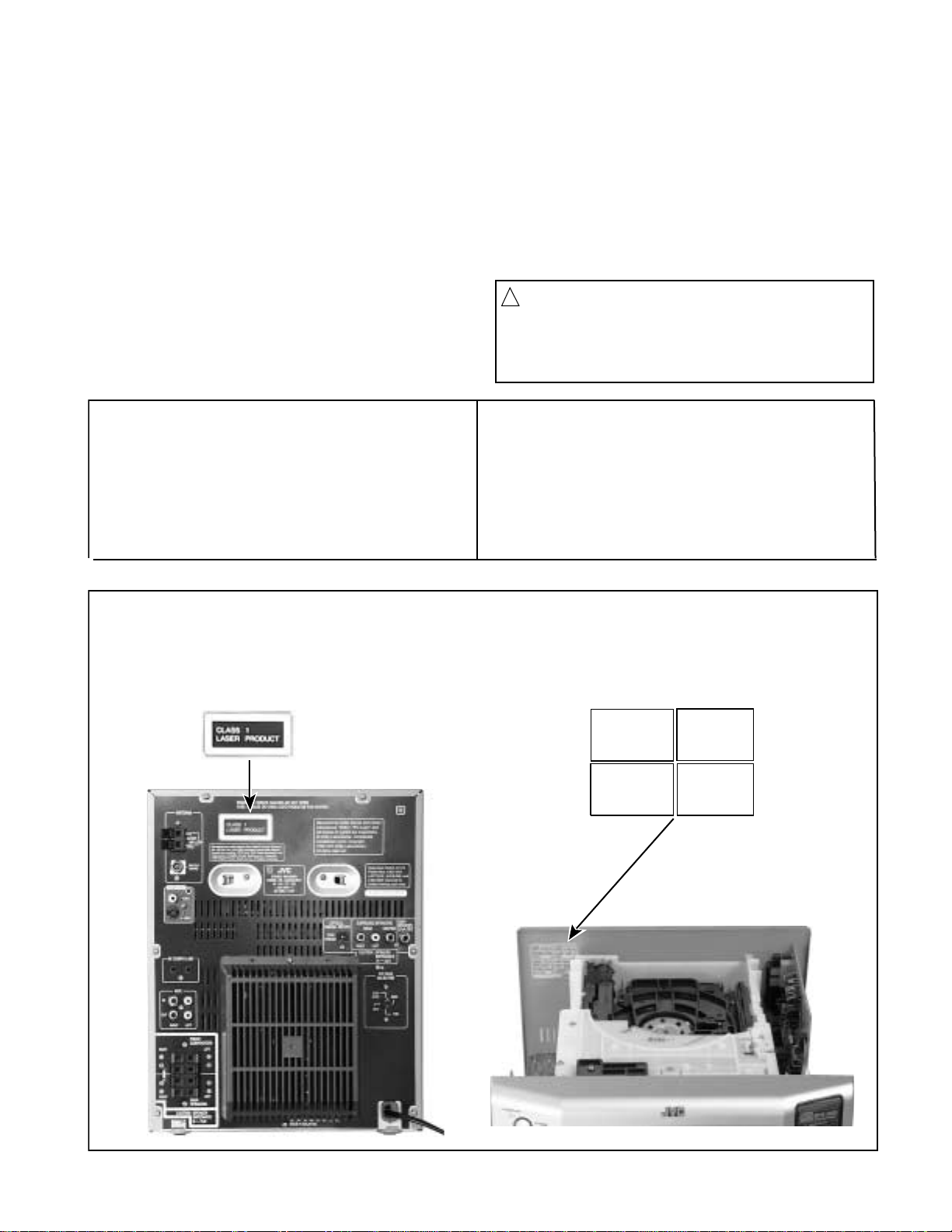
Important for laser products
MX-DVB10
1. CLASS 1 LASER PRODUCT
2. DANGER : Invisible laser radiation when open and inter
lock failed or defeated. Avoid direct exposure to beam.
3. CAUTION : There are no serviceable parts inside the
Laser Unit. Do not disassemble the Laser Unit. Replace
the complete Laser Unit if it malfunctions.
4.CAUTION : The compact disc player uses invisible laser
radiation and is equipped with safety switches which
prevent emission of radiation when the drawer is open
and the safety interlocks have failed or are defeated. It is
dangerous to defeat the safety switches.
VARNING : Osynlig laserstrålning är denna del är öppnad
och spårren är urkopplad. Betrakta ej strålen.
VARO : Avattaessa ja suojalukitus ohitettaessa olet
alttiina näkymättömälle lasersäteilylle.Älä katso
säteeseen.
5.CAUTION : If safety switches malfunction, the laser is able
to function.
6.CAUTION : Use of controls, adjustments or performance of
procedures other than those specified herein may result in
hazardous radiation exposure.
CAUTION
!
Please use enough caution not to
see the beam directly or touch it
in case of an adjustment or operation
check.
ADVARSEL : Usynlig laserstråling ved åbning , når
sikkerhedsafbrydere er ude af funktion. Undgå
udsættelse for stråling.
ADVARSEL : Usynlig laserstråling ved åpning,når
sikkerhetsbryteren er avslott. unngå utsettelse
for stråling.
REPRODUCTION AND POSITION OF LABELS
CLASS 1
LASER PRODUCT
WARNING LABEL
DANGER : Invisibie laser radiation
when open and interlock or
defeated.
AVOID DIRECT EXPOSURE TO
BEAM (e)
VARO : Avattaessa ja suojalukitus
ohitettaessa olet alttiina
näkymättömälle lasersäteilylle.Älä
katso säteeseen. (d)
VARNING : Osynlig laserstrålning
är denna del är öppnad och spårren
är
urkopplad. Betrakta ej strålen.
(s)
ADVARSEL :Usynlig laserstråling
ved åbning , når
sikkerhedsafbrydere er ude af
funktion. Undgå udsættelse for
stråling. (f)
1-5
Page 6
MX-DVB10
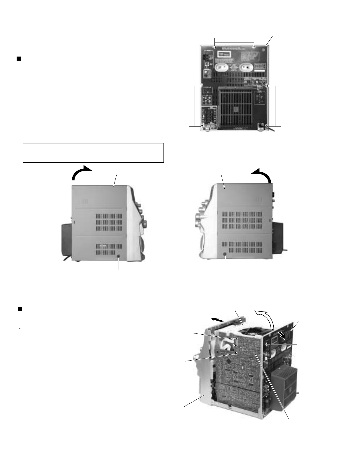
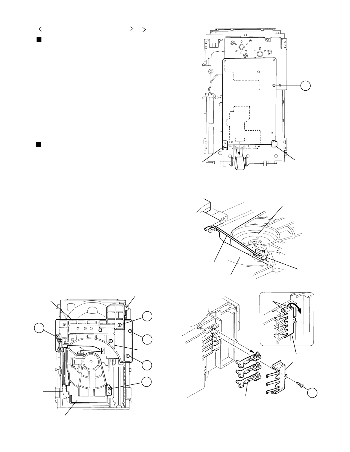
Disassembly method
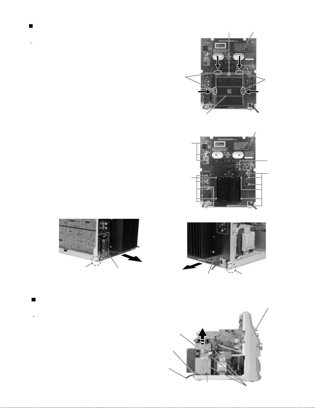
<Main body>
Removing the metal cover
(See Fig.1 to 3)
1.
Remove the six screws marked A on the back of the
body.
2.
Remove the two screws marked B on both sides of
the body.
3.
Remove the metal cover from the body by lifting the
rear part of the cover.
CAUTION:
Do not break the front panel tab fitted to
the metal cover.
Metal cover
A
Metal cover
Metal cover
AA
Fig.1
Fig.3
B
Removing the tuner board
(See Fig.4)
Prior to performing the following procedures, remove
the metal cover.
1.
Disconnect the card wire from connector CN1 on the
tuner board.
2.
Remove the plastic rivet fixing the tuner board.
3.
Remove the two screws marked C on the back of the
body.
B
Fig.2
DVD changer mechanism assembly
Rear panel
CN1
C
Plastic rivet
Front panel
assembly
Tuner board
Fig.4
1-6
Page 7
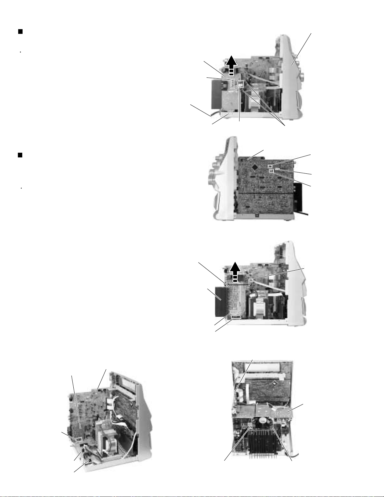
Removing the DVD changer mechanism
assembly (See Fig.5 to 6)
Prior to performing the following procedures, remove
the metal cover and the tuner board.
MX-DVB10
1.
Disconnect the card wire from the connectors
CN540, CN541 and CN542 on the main board.
2.
Remove the two screws marked D on the upper side
of the body and two screws marked F on the back of
rear panel.
3.
Remove the plastic rivet attaching the main board.
4.
Pull both the rear panel and the front panel assembly
to the outside, then remove the DVD changer
mechanism assembly by lifting the rear part of the
assembly.
CAUTION:
To prevent damage to the DVD fitting,
be sure to pull both the rear panel and
the front panel assembly enough to
remove the DVD changer mechanism
assembly.
Main board
CN542
CN541
CN540
D
Front panel assembly
D
DVD changer
mechanism
assembly
Fig.5
Rear panel
DVD changer mechanism assembly
Plastic rivet
Main board
Front panel assembly
Fig.6
Rear panel
F
1-7
Page 8
MX-DVB10
Removing the front panel assembly
(See Fig.7 to 11)
Prior to performing the following procedures, remove
the metal cover, the tuner board and the DVD
changer mechanism assembly.
1.
Remove the plastic rivet attaching the main board.
2.
Disconnect the card wires from the connector
CN500, CN505 and CN510 on the main board
respectively.
3.
Remove the tie band and disconnect the wire from
the connector CN513 on the main board.
4.
Disconnect the wire from the connector CN220 on
the transformer board.
5.
Remove the two screws marked G on the bottom of
the body.
6.
Release the two joints marked a on the lower right
and left sides of the body using a screwdriver, and
remove the front panel assembly toward the front.
CN513
Transformer board
CN220
Plastic rivet
Main board
Tie band
CN500
CN505
CN510
Front panel
assembly
Fig.7
Front panel assembly
Front panel assembly
Fig.8
Main board
G
(Bottom)
Fig.9
1-8
Joint a
Front panel assembly
Fig.11
Front panel assembly
Joint a
Fig.10
Page 9
MX-DVB10
Removing the rear cover / rear panel
(See Fig.12 to 15)
Prior to performing the following procedures, remove
the metal cover, the tuner board and the DVD
changer mechanism assembly.
1.
Remove the screw marked H attaching the rear
cover on the back of the body.
2.
Push each tab of the four joints marked b in the
direction of the arrow and release.
3.
Remove the seventeen screws marked I attaching
the rear panel.
4.
Release the joints marked c on each lower side of
the rear panel using a screwdriver and remove the
rear panel backward.
Joint b
Rear cover
I
I
H
Fig.12
Rear panel
Joint b
Rear panel
I
I
Joint c
Fig.15
Rear panel
Removing the power cord
(See Fig.16)
Prior to performing the following procedures, remove
the metal cover, the tuner board the DVD changer
mechanism assembly and rear panel.
1.
Move the power cord stopper upward and pull out it
from the base chassis.
2.
Disconnect the power cord from connector CN250
on the power supply board.
3.
Remove the tie band from the power supply board.
Power supply
board
Power cord
stopper
Power cord
Rear panel
Fig.13
Joint c
Fig.14
Front panel assembly
CN250
Fig.16
Tie band
1-9
Page 10
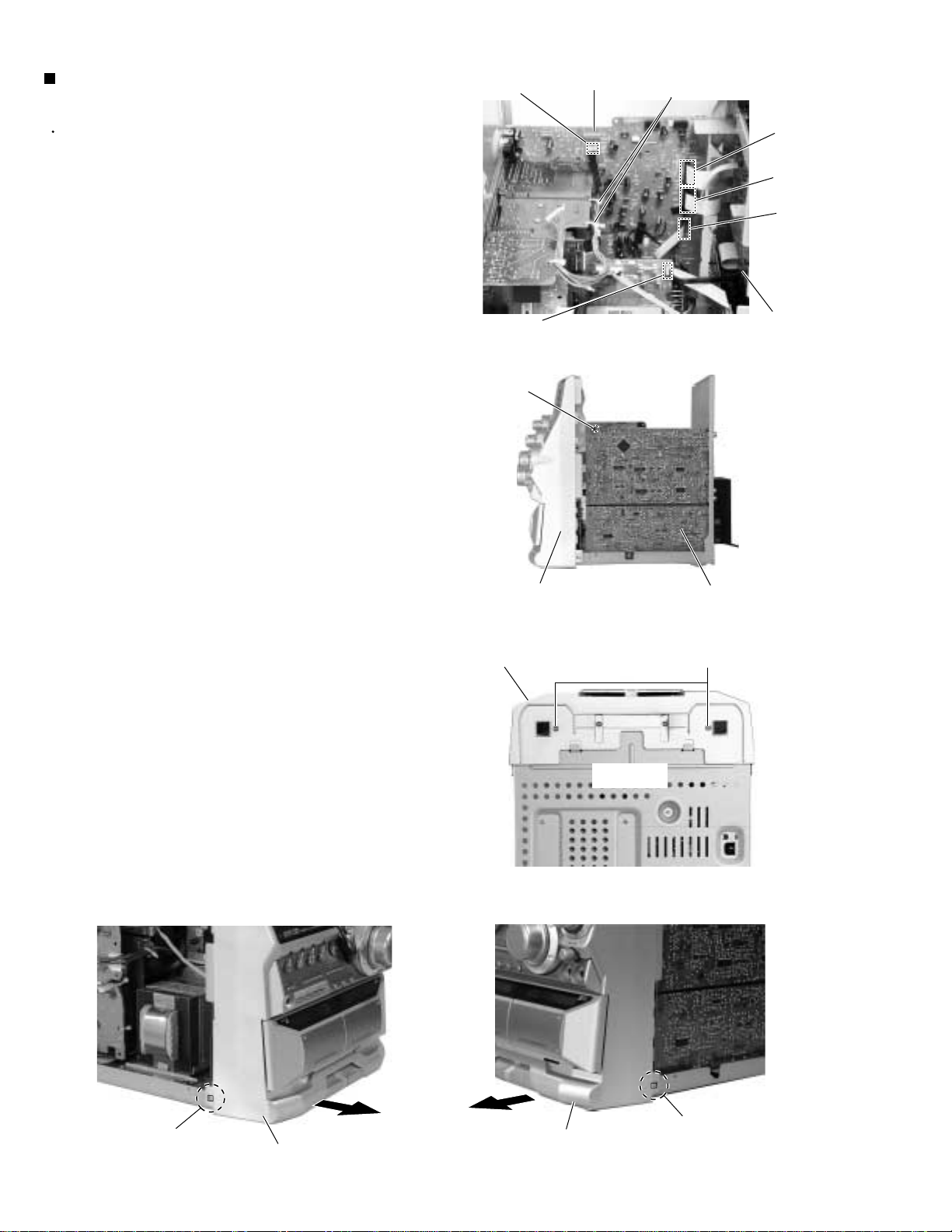
MX-DVB10
Removing the power supply board
(See Fig.17)
Prior to performing the following procedures, remove
the metal cover, the tuner board, the DVD changer
mechanism assembly, the rear panel and the power
cord.
1.
Remove the tie band marked a attaching the p
board.
supply
2.
Disconnect the connector CN218 and CN219 on the
p
ower supply board
3.
Disconnect the connector CN203 on the p
board
from the regulator board.
.
ower
Power cord
ower supply
Removing the amplifier board (1, 2), AV
output board & speaker terminal board
(See Fig.18 to 21)
Prior to performing the following procedures, remove
the metal cover, the tuner board, the DVD changer
mechanism assembly, the p
the rear panel.
ower supply
board and
Power supply
board
CN219
CN203
CN218
Fig.17
Main board
Front panel assembly
Tie band
a
CN513
CN521
AV output
board
Tie band
b
1.
Remove the tie band marked b attaching the wire to
the AV output board.
2.
Disconnect the card wire from the connector CN513
on the main board.
3.
Disconnect the connector CN521 on the main board.
4.
Disconnect the card wire from the connector CN703
on the amplifier board (2).
5.
Disconnect the connectors CN205 and CN206 on
the amplifier board (1, 2) from the regulator board
(The heat sink and heat sink bracket will be
detached at once).
Disconnect the connector CN207 on the speaker
6.
terminal
board from the regulator board.
Speaker terminal
board
Main board
Amplifier board (1)
Heat sink
CN205
CN206
Fig.18
CN703
Fig.19
Main board
AV output
board
1-10
CN207
CN205
Regulator
board
CN206
Fig.21
Amp. board (2)
Amp. board (1)
Fig.20
Page 11
MX-DVB10
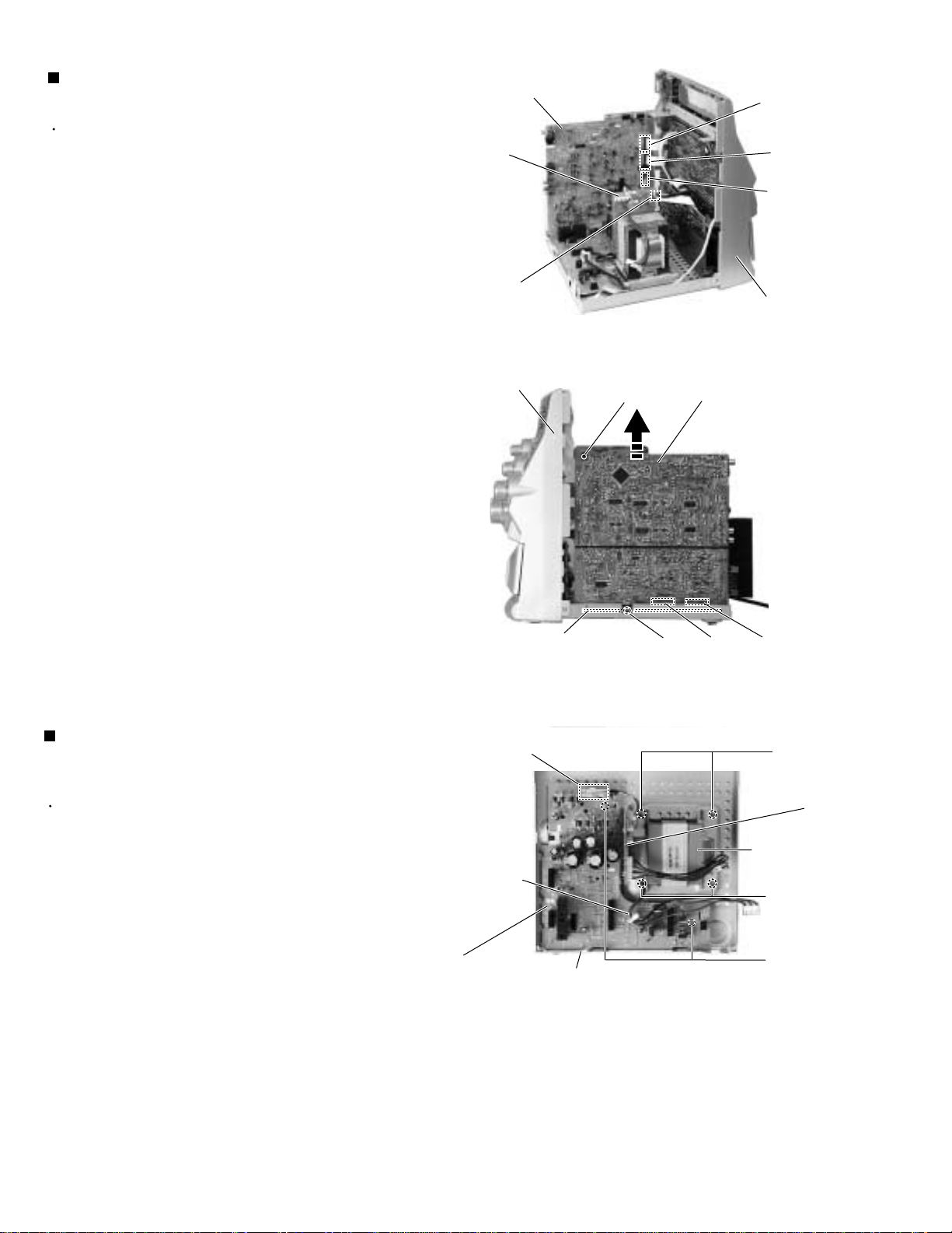
Removing the AV output board
(See Fig.22, 23)
Prior to performing the following procedures, remove
the metal cover, the tuner board, the DVD changer
mechanism assembly, the rear panel, the amplifier
board (1,2) and the power supply board.
Disconnect the connector CN705, CN372 and
1.
CN373 on the amplifier board (1, 2).
Remove the two screws marked J attaching the AV
2.
output board to the fan bracket.
Pull out the fan bracket from the
3.
AV output board.
amplifier
board (1)
AV output board
Fig.22
CN372
AV output board
Fan bracket
CN705
Fan
amplifier
board (2)
Hook
CN373
Removing the Heat sink
(See Fig.24)
Prior to performing the following procedures, remove
the metal cover, the tuner board, the power supply
board, the DVD changer mechanism, assembly the
rear panel, the tuner board, the amplifier board (1,2)
and AV output board.
1.
Remove the eight screws marked K attaching the
ICs on the heat sink.
Removing the ICs (See Fig.25)
Prior to performing the following procedures, remove
the metal cover, the tuner board, the DVD changer
mechanism assembly, the rear panel, the tuner
board, the AV output board, the amplifier board (1,2),
the power supply board and the heat sink.
1.
Unsolder the ICs s
older points
.
J
Heat sink
Fig.23
Heat sink
Amp. board (1, 2)
K
K
Fig.24
Solder points
Solder points
2.
Remove the ICs.
Fig.25
1-11
Page 12
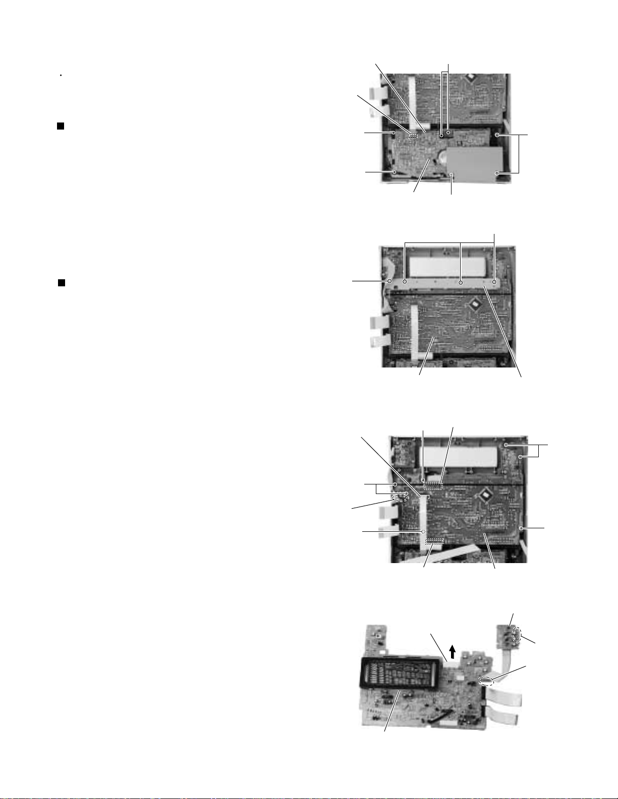
MX-DVB10
Removing the main board
(See Fig.26, 27)
Prior to performing the following procedures, remove
the metal cover, the tuner board, the DVD changer
mechanism assembly, the rear panel, the power
supply board, the amplifier board and AV output
board.
1.
Disconnect the card wires from the connector
CN500, CN505 and CN510 on the main board.
2.
Disconnect the flat wires from the connector CN220
on the transformer board.
3.
Disconnect the connector CN530 and CN531 on the
main board from the regulator board.
4.
Remove the screw marked L attaching the main
board on the right side of the body.
Main board
Transformer
board
CN220
Front panel assembly
Fig.26
Plastic rivet
CN500
CN505
CN510
Front panel
assembly
Main board
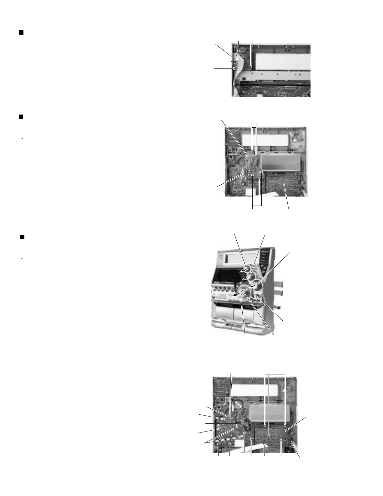
Removing the regulator board / power
transformer assembly
(See Fig.28)
Prior to performing the following procedures, remove
the metal cover, the tuner board, the DVD changer
mechanism assembly, the rear panel, the power
supply board, the amplifier board (1, 2), the main
board, the speaker terminal board and AV output
board.
1.
Disconnect the wire from connector CN204 on the
regulator board.
2.
Remove the two screws marked N attaching the
regulator board.
3.
Remove the four screws marked M attaching the
transformer.
Regulator board
Regulator
board
CN204
Plastic
holder
Regulator board
Hook
Fig.27
Fig.28
L
CN530
CN531
M
Transformer
board
Power
transformer
assembly
M
N
1-12
Page 13
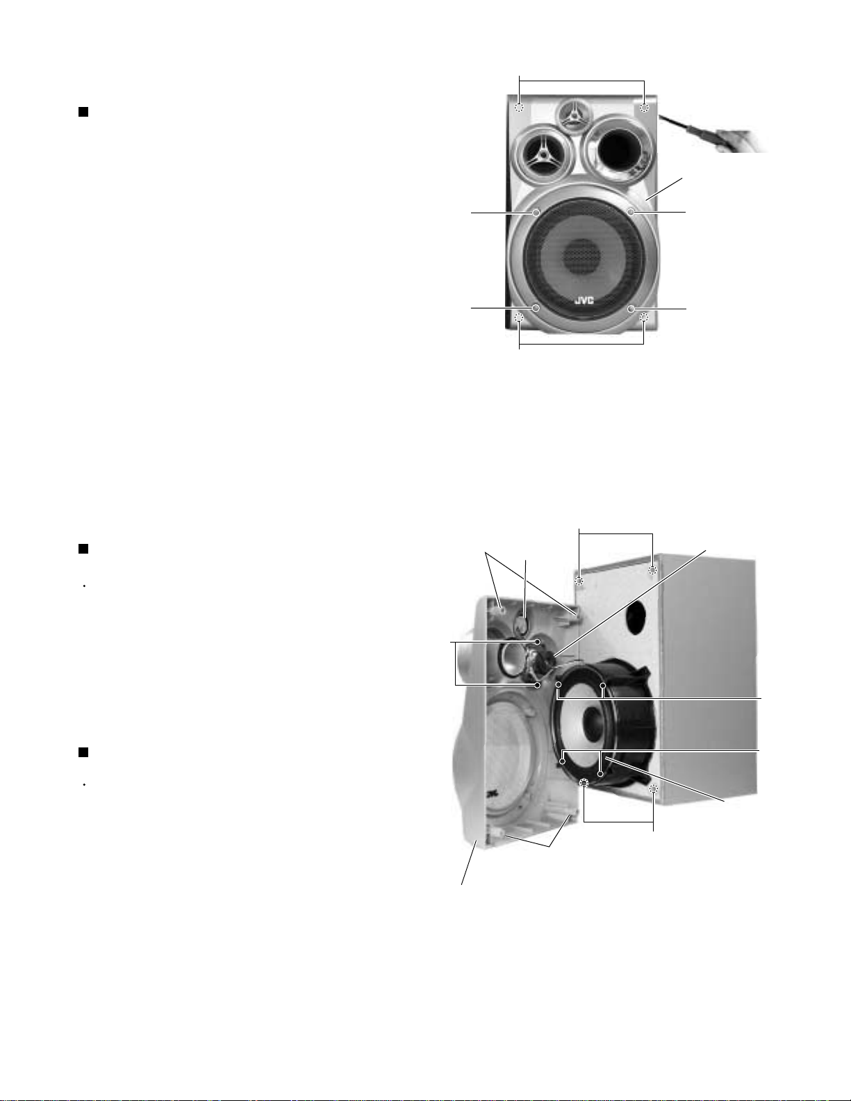
MX-DVB10
<Front panel assembly>
Prior to performing the following procedures, remove
the metal cover, the DVD changer mechanism
assembly and front panel assembly.
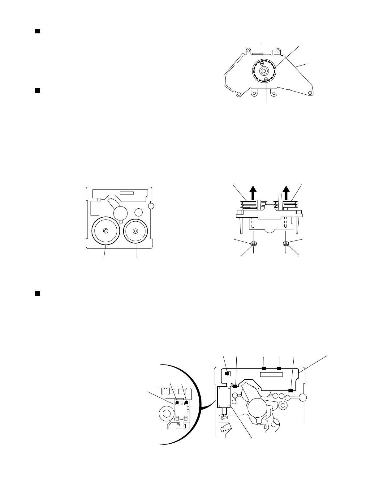
Removing the cassette mechanism
assembly (See Fig.29)
1.
Disconnect the card wire from the connector
CN306 on the head amplifier & mechanism control
board.
2.
Remove the seven screws marked O attaching the
cassette mechanism assembly.
Removing the display & system control
board (See Fig.30 to 32)
1.
Remove the four screws marked P attaching the
stay bracket.
Head amplifier
& mechanism control board
CN306
O
O
Cassette mechanism
assembly
P
O
O
O
Fig.29
P
2.
Remove the seven screws marked Q attaching the
isplay & system control board
d
3.
Disconnect the card wires from the connector
CN316 and CN881 on the display & system control
board.
4.
Disconnect the connector CN870 on the
system control board
board
.
5.
If necessary, disconnect the wire from the
connector CN870 on the front side of the display &
system control board and unsolder FW915.
.
from the p
display &
reset / tuning switch
Display & system control board
Fig.30
Q
CN316
Q
FW915
(Solders)
Q
CN881
CN870
Stay bracket
CN870
Q
Q
Display & system control board
Fig.31
DVD eject board
FW915
Display & system
control board
FW915
Fig.32
1-13
Page 14
MX-DVB10
Removing the DVD eject board
(See Fig.33)
1.
Remove the three screws marked R attaching the
DVD eject board.
2.
If necessary, unsolder FW915 on the DVD eject
board.
Removing the preset / tuning switch
board
Prior to performing the following procedures, remove
the display & system control board.
1.
Pull out the PRESET knob on the front panel.
2.
Remove the five screws marked S attaching the
preset / tuning switch board.
3.
If necessary, unsolder FW901 on the preset / tuning
switch board.
(See Fig.34, 35)
Removing the operation switch board
(See Fig.35, 36)
Prior to performing the following procedures,
remove the display & system control board and
the preset / tuning switch board.
DVD eject board
FW915
(Soldered)
R
Preset / tuning switch board
FW901
(Soldered)
PRESET knob
R
Fig.33
S
S
Fig.34
Operation switch board
SOUND MODE knob
SUBWOOFER
level knob
1.
Pull out the volume knob on the front panel and
remove the nut. Pull out the SOUND MODE knob
and the SUBWOOFER level knob toward the front.
Pull out the mic level knob toward the front.
2.
Remove the twelve screws marked T attaching the
operation switch board.
3.
Release each tab of the seven joints marked g
retaining the operation switch board.
Joint g
Joint g
Joints g
T
T
Volume knob
Joints g
T
T
Fig.35
T
Fig.36
T
Mic level knob
Nut
T
T
Operation
switch board
Joint g
1-14
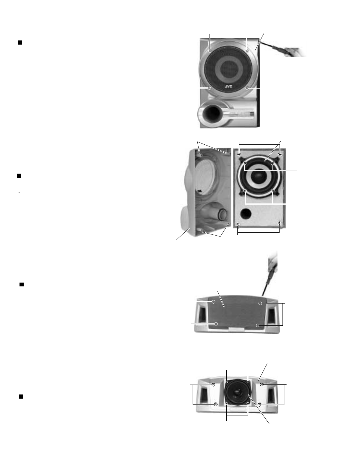
Page 15
MX-DVB10
< Main Speaker >
Removing the front cover (See Fig.1, 2)
Remove the four screws marked A on the front of the
1.
body.
Remove the front cover from the four holders marked
2.
a that are fixing the front cover.
Pull out the front cover toward the front while
3.
disengaging the four joints marked a.
Note:
Because it is difficult to take away the cover,
insert a minus driver, etc. in the place between
the main body and the front cover as shown in
Fig.1 before removing the front cover. Exercise
care not to damage the main body and the front
cover when inserting the minus driver. For this
purpose, insert the minus driver together with
cloth and the like.
A
A
Joints a
Joints a
Front cover
A
A
Fig.1
Removing the squawker (See Fig.2)
Prior to performing the following procedures, remove
the front cover.
1.
Remove the two screws marked B on the front
cover.
2.
Disconnect the yellow and black wires from the
speaker terminals on the squawker.
Removing the woofer (See Fig.2)
Prior to performing the following procedures, remove
the front cover.
1.
Remove the four screws marked C .
2.
Remove the woofer and disconnect the yellow and
black wires from the speaker terminals.
3.
Remove the squawker and disconnect the yellow
and black wires from the speaker terminals.
Joints a
B
Front cover
Holder a
Tweeter
Joints a
Squawker
C
C
Woofer
Holder a
Fig.2
1-15
Page 16
MX-DVB10
< Subwoofer >
Removing the front cover (See Fig.3, 4)
1.
Remove the four screws D on the front of the body.
2.
Remove the front cover from the four holders marked
b that are fixing the front cover.
3.
Pull out the front cover toward the front while
disengaging the four joints marked b.
Note:
Because it is difficult to take away the cover,
insert a minus driver, etc. in the place between
the main body and the front cover as shown in
Fig.1 before removing the front cover. Exercise
care not to damage the main body and the front
cover when inserting the minus driver. For this
purpose, insert the minus driver together with
cloth and the like.
Removing the subwoofer
(See Fig.4)
Prior to performing the following procedures, remove
the front cover.
1.
Remove the four screws marked E on the front of the
body.
D
Joints b
D
Fig.3
Holder b
D
Front cover
D
Subwoofer
E
E
2.
Pull out the subwoofer speaker toward the front and
disconnect the wire (red and black) from the
speaker terminals.
< Center speaker >
Removing the front net (See Fig.5, 6 )
1.
Remove the front net from the four holders marked c
that are fixing the front net.
2.
Pull out the front net toward the front while
disengaging the four joints marked c.
Note:
When it is hard to remove the front net, insert a
minus driver, etc. in the place between the front
net and the front cover as shown in Fig.5 before
removing the front cover. Exercise care not to
damage the main body and the front cover
when inserting the minus driver. For this
purpose, insert the minus driver together with
cloth and the like.
Removing the center speaker (See Fig.6 )
Front cover
Joints c
Holder c
Joints b
Front net
Holder b
Fig.4
Joints c
Fig.5
Front cover
F
Holder c
1.
Remove the four screws marked F on the front of the
body.
2.
Pull out the center speaker toward the front and
disconnect the wire (black and black with white line)
from the speaker terminals.
1-16
F
Center speaker
Fig.6
Page 17
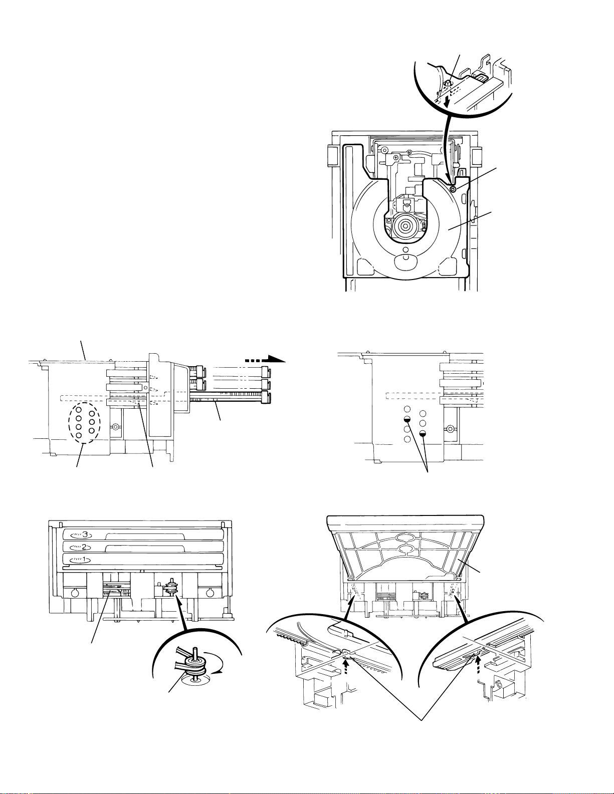
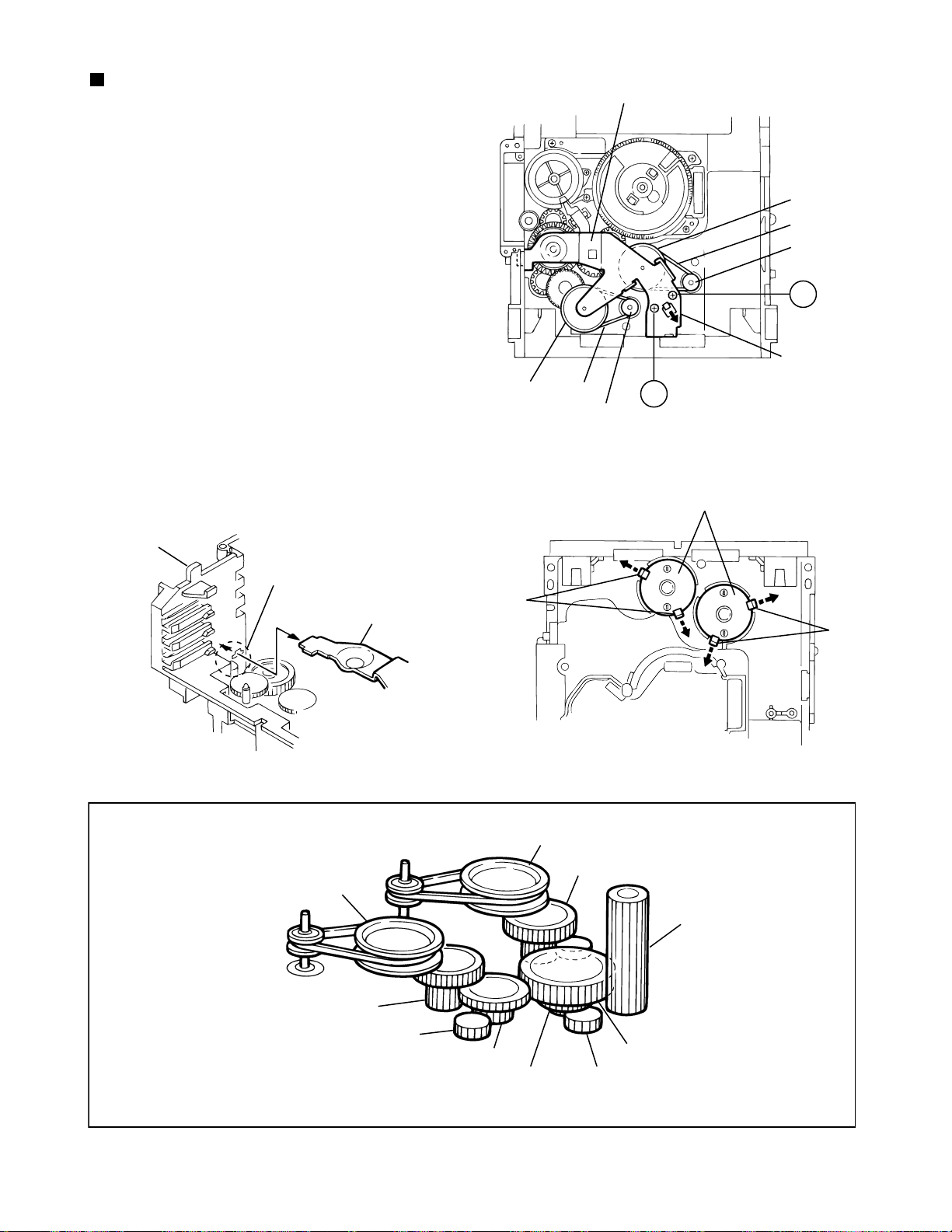
DVD Changer Mechanism
Removing the DVD Servo control
board (See Fig.1)
1.
Remove the metal cover.
2.
Remove the DVD changer mechanism assembly.
3.
From bottom side the DVD changer mechanism
assembly, remove the one screw 1 retaining the DVD
servo control board.
Disconnect the card wire, from the connector CN101,
4.
on the DVD servo control board.
Disengage the two engagements "A", remove the DVD
5.
servo control board.
Removing the DVD tray assembly
(See Fig.2~4)
MX-DVB10
1
DVD servo control board
CN101
Remove the front panel assembly.
1.
Remove the DVD changer mechanism assembly.
2.
Remove the DVD servo control board.
3.
Remove the screw 2 retaining the disc stopper.
4.
(See Fig.3)
Remove the three screws 3 retaining the T. bracket.
5.
(See Fig.3)
From the T. bracket section and clamper base section
6.
"B", remove the edges fixing the rod.
(See Fig.2)
Remove the screw 4 retaining the clamper assembly.
7.
(See Fig.3)
From the blacket section "C", remove the clamper ass'y.
8.
(See Fig.3)
From the left side face of the chassis assembly, remove
9.
the one screw 5 retaining both of the return spring and
lock lever. (See Fig. 4)
By removing the pawl at the section "D" fixing the return
10.
spring, dismount the return spring. (See Fig.4)
Remove the three lock levers. (See Fig.4)
11.
Disc stopper
T. Bracket
2
3
AA
Fig.1
Clamper base
Rod
B
T. Bracket
Fig.2
D
C
Clamper ass'y
Fig.3
3
Rod stopper
(C/J version only)
3
4
Return spring
5
Lock lever
Fig.4
1-17
Page 18
MX-DVB10
11.
Check whether the lifter unit stopper has been caught
into the hole at the section "E" of DVD tray assembly
as shown in Fig.5.
Make sure that the driver unit elevator is positioned as
12.
shown in Fig.6 from to the second or fifth hole on the
left side face of the DVD Traverse mechanism
assembly.
[Caution]
13.
14.
15.
Chassis assembly
In case the driver unit elevator is not at above
position, set the elevator to the position as
shown in Fig.7 by manually turning the pulley
gear as shown in Fig.8.
Manually turn the motor pulley in the clockwise
direction until the lifter unit stopper is lowered from the
section "E" of DVD tray assembly (See Fig.8).
Pull out all of the three stages of DVD tray assembly in
the arrow direction "F" until these stages stop
(See Fig.6).
At the position where the DVD tray assembly has stop
end, pull out the DVD tray assembly while pressing the
two pawls "G and G' " on the back side of DVD tray
assembly (See Fig.9). In this case, it is easy to pull out
the assembly when it is pulled out first from the stage
DVD tray assembly.
Stopper
E
DVD tray
assembly
Fig.5
Refer to Fig.7
Pulley gear
Pawl
DVD tray assembly
G
F
Drive unit of elevator
Fig.7Fig.6
DVD tray assembly
1-18
Motor pulley
Fig.8
Pawl ,
G
Fig.9
G'
Page 19
MX-DVB10
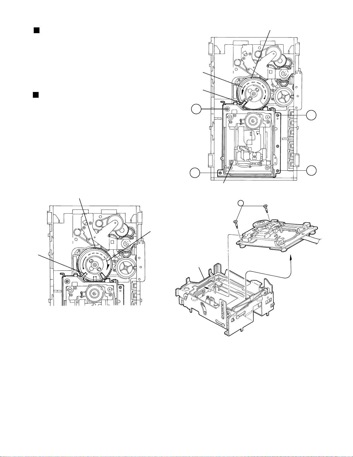
Removing the DVD mechanism
assembly (See Fig.10)
1.2.While turning the cams R1 and R2 assembly in the
arrow direction "H" . align the shaft "I" of the DVD
mechanism assembly to the position shown in Fig.10.
Remove the four screw 6 retaining the DVD
mechanism assembly.
Removing the DVD mechanism
(See Fig.11, 12 )
1.
For dismounting only the DVD mechanism without
removing the DVD mechanism assembly, align the shaft
"J" of the DVD mechanism assembly to the position
shown Fig.11 while turning the cam R1 and R2
assembly in the arrow direction "K" .
By raising the DVD mechanism assembly in the arrow
2.
direction "L" , remove the assembly from the lifter unit
(See Fig.12).
Cam R1, R2 assembly
Cams R1, R2 assembly
Arrow
H
I
6
6
DVD mechanism assembly
10
6
6
Fig.10
DVD mechanism
Arrow
K
J
Lifter unit
Fig.11
Fig.12
Arrow
L
1-19
Page 20
MX-DVB10
Removing the actuator motor board
(See Fig.14, 15)
Absorb the four soldered positions "M" of the right and
1.
left motors with a soldering absorber (See Fig.14).
Remove the two screws 7 retaining the actuator motor
2.
board (See Fig.14).
Remove the two screws 8 retaining the tray select
3.
switch board (See Fig.15).
Removing the cam unit
(See Fig.15~18 )
1.
Remove the DVD mechanism assembly.
2.
While turning the cam gear L, align the pawl "N"
position of the drive unit to the notch position (Fig.15)
on the cam gear L.
Pull out the drive unit and cylinder gear (See Fig.17).
3.
While turning the cam gear L, align the pawl "O"
4.
position of the select lever to the notch position (Fig.18)
on the cam gear L.
Remove the four screws 9 retaining the cam unit (cam
5.
gear L and cams R1/R2 assembly) (See Fig.18).
Chassis assembly
M
Drive unit
Motor L
Actuator motor board
Fig.14
Motor R
7
M
7
Cam gear L
CN801
Fig.15
CN802
Drive unit
Tray select
switch board
Cylinder gear
CN804
N
8
Cam gear L
9
O
Fig.16
9
Cams R1, R2 assembly
Cam unit
9
1-20
Select lever
Fig.18
Fig.17
Page 21
MX-DVB10
Removing the actuator motor and belt
(See Fig.19~22)
1.
Remove the two screws 10 retaining the gear bracket
(See Fig.19).
2.
While pressing the pawl "P" fixing the gear bracket in
the arrow direction, remove the gear bracket
(See Fig.19).
From the notch "Q section" on the chassis assembly
3.
fixing the edge of gear bracket, remove and take out the
gear bracket (See Fig. 20).
Remove the belts respectively from the right and left
4.
actuator motor pulleys and pulley gears (See Fig. 19).
After turning over the chassis assembly, remove the
5.
actuator motor while spreading the four pawls "R" fixing
the right and left actuator motors in the arrow direction
(See Fig. 21).
[Note]
When the chassis assembly is turned over under
the conditions wherein the gear bracket and belt
have been removed, then the pulley gear as well
as the gear, etc. constituting the gear unit can
possibly be separated to pieces. In such a case,
assemble these parts by referring to the assembly
and configuration diagram in Fig. 22.
Pulley gear
Gear bracket
Belt
Motor pulley
10
Fig.19
Actuator motor
Pulley gear
Belt
Motor pulley
10
Pawl
P
Chassis assembly
Q
Gear bracket
Fig.20
Assembly and Configuration Diagram
Pulley gear
R
R
Fig.21
Pulley gear
Gear B
Cylinder gear
Gear B
Gear C
Select gear
Gross gear L
Fig.22
Gross gear U
Gear C
1-21
Page 22
MX-DVB10
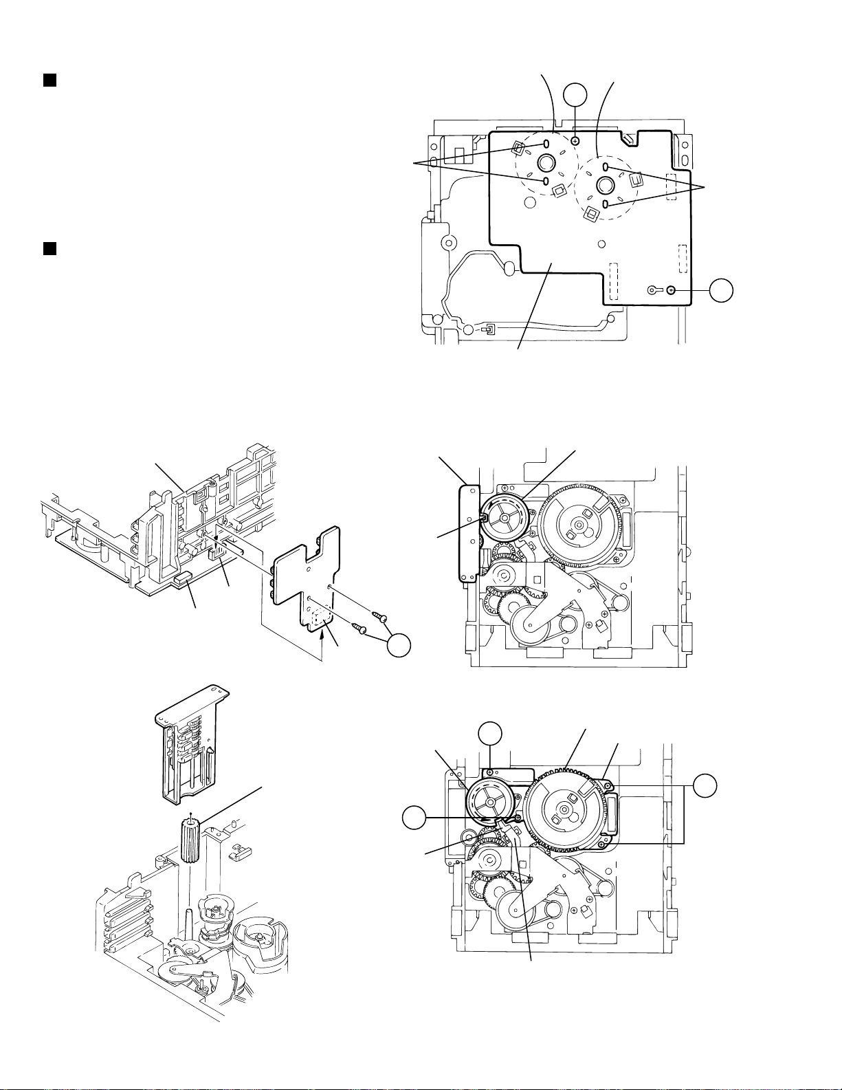
Removing the cams R1/R2 assembly
and cam gear L (See Fig.23)
1.
Remove the slit washer fixing the cams R1 and R2
assembly.
2.
By removing the two pawls "S" fixing the cam R1,
separate R2 from R1.
Remove the slit washer fixing the cam gear L.
3.
Pull out the cam gear L from the C.G. base assembly.
4.
Removing the C.G. base assembly
(See Fig.23, 24)
Remove the three screws 11 retaining the C.G. base
assembly.
[Caution]
To re-assemble the cylinder gear, etc. with the
cam unit (cam gear and cans R1/R2 assembly),
gear unit and drive unit, align the position of the
pawl "N" on the drive unit to that of the notch on
the cam gear L. Then, make sure that the gear
unit is engaged by turning the cam gear L
(See Fig. 24).
Slit washer
Cam gear L
11
Slit washer
Cam R2
Pawl
S
Cam R1
Cam switch board
C.G. base assembly
Pawl
S
Notch
Pawl
N
Cylinder
gear
Drive unit
Fig.23
Cam gear L
Cam R1, R2 assembly
Gear unit
Gear bracket
Fig.24
1-22
Page 23
MX-DVB10
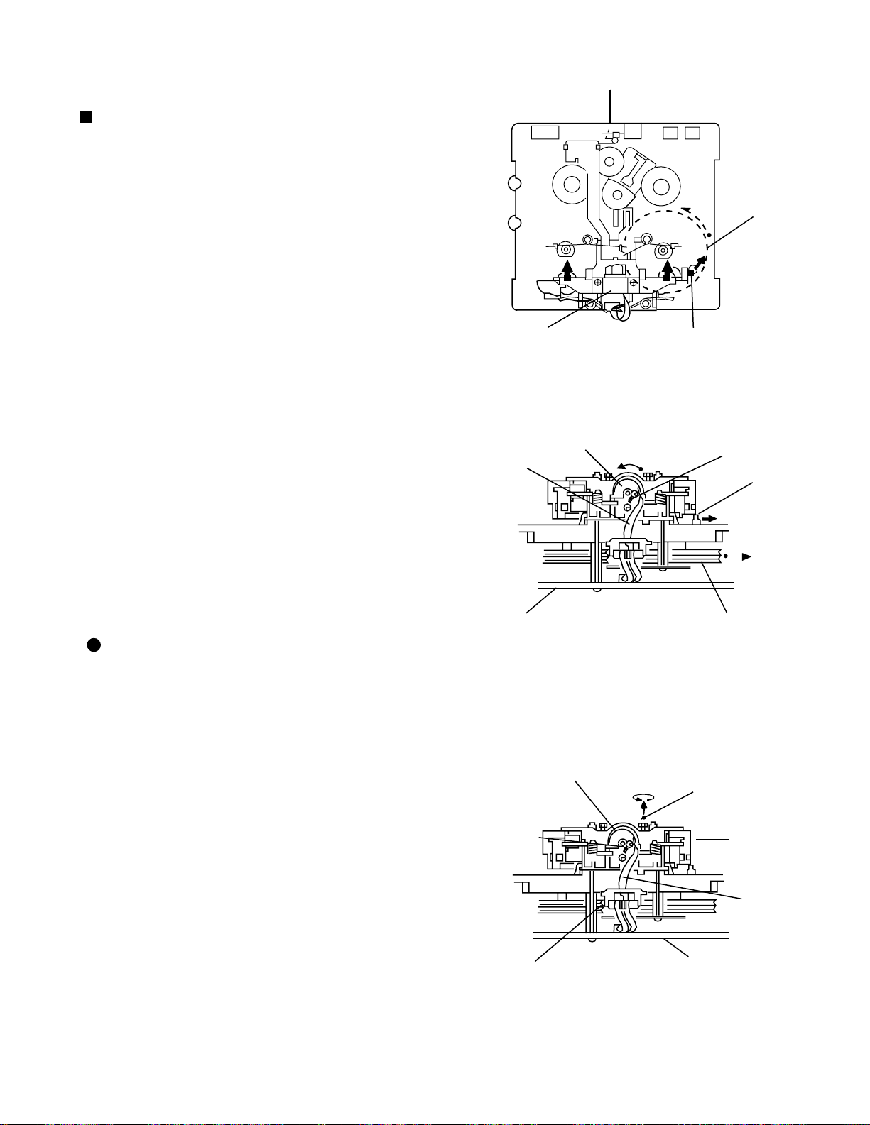
< Cassette Mechanism Section >
Removing the Playback, Recording and
Eraser Heads (See Fig.1~3)
1. While shifting the trigger arms seen on the right
side of the head mount in the arrow direction, turn
the flywheel R in counterclockwise direction until
the head mount has gone out with a click
(See Fig. 1).
2. When the flywheel R is rotated in counterclockwise
direction, the playback head will be turned in
counterclockwise direction from the position in
Fig. 2 to that in Fig. 3.
3. At this position, disconnect the flexible P.C. board
(outgoing from the playback head) from the
connector CN301 on the head amp. and mechanism
control P.C. board.
4. After dismounting the FPC holder, remove the
flexible P.C. board.
5. Remove the flexible P.C. board from the chassis
base.
6. Remove the spring "a" from behind the playback
head.
7. Loosen the reversing azimuth screw retaining the
playback head.
8. Take out the playback head from the front of the
head mount.
9. The recording and eraser heads should also be
removed similarly according to Steps 1~8 above.
Reassembling the Playback, Recording
and Eraser Heads (See Fig.2,3)
Cassette mechanism
Fig. 1
Playback/Recording &
eraser head
Flexible
P.C. board
CN301
Head amplifier & mechanism
control P.C. board
Fig. 2
Flywheel R
Trigger armHead mount
(Mechanism A side)
Spring "a"
Trigger arm
Flywheel R
(Mechanism A side)
1. Reassemble the playback head from the front of
the head mount to the position as shown in Fig. 3.
2. Fix the reversing azimuth screw.
3. Set the spring a from behind the playback head.
4. Attach the flexible P.C. board to the chassis base,
and fix it with the FPC holder as shown in Fig. 3.
5. The recording and eraser heads should also be
reassembled similarly according to steps 1~4
above.
Playback head
Spring "a"
FPC holder
Fig. 3
Reversing azimuth
screw
Head
mount
Flexible
P.C. board
CN302
Head amplifier &
mechanism control
P.C. board
(Mechanism B side)
1-23
Page 24
MX-DVB10
Removing the Head Amplifier. and
Mechanism Control P.C. Board
(See Fig. 4)
1. Remove the cassette mechanism assembly.
2. After turning over the cassette mechanism
assembly, remove the five screws "A" retaining
the head amp. and mechanism control P.C.
board
3. Disconnect the connectors CN303 and CN304
on the P.C. board and the connectors CN1 on
both the right and left side reel pulse
P.C. boards.
4. When necessary, remove the 4 pin parallel
wire soldered to the main motor.
Removing the Capstan Motor Assembly
(See Fig. 5 to 7)
1. Remove the six screws "B" retaining capstan
motor assembly (See Fig. 5).
2. While raising the capstan motor, remove the
capstan belts A and B respectively from the
motor pulley (See Fig. 6).
A
Flexible
board
Head amplifier &
mechanism control board
AA
CN304
CN302 CN301
Flexible
board
CN303
Fig. 4
BB
Capstan motor
assembly
AA
Caution 1: Be sure to handle the capstan
belts so carefully that these belts
will not be stained by grease and
other foreign matter. Moreover,
these belts should be hand while
referring to the capstan belt
hanging method.
Capstan
belt A
Capstan
belt B
Capstan
belt A
BBBB
Fig. 5
Capstan motor
Capstan
belt B
Motor pulley
1-24
Fig. 7 Fig. 6
Page 25
MX-DVB10
Removing the Capstan Motor (See Fig. 8)
From the joint bracket, remove the two screws "C"
retaining the capstan motor.
Removing the Flywheel (See Fig. 9,10)
1. Remove the head amp. and mechanism control
P.C. Board.
2. Remove the capstan motor assembly.
3. After turning over the cassette mechanism, remove
the slit washers "a" and "b" fixing the capstan shafts
R and L, and pull out the flywheels R and L respectively
from behind the cassette mechanism.
Flywheel R
C
C
Fig. 8
Capstan motor
Joint
bracket
Flywheel L
Flywheel R
Flywheel L
Fig. 10
Removing the Reel Pulse P.C. Board and
Solenoid (See Fig. 11)
1. Remove the five pawls (c, d, e, f, g) retaining
the reel pulse P.C. board.
2. From the surface of the reel pulse P.C. board parts,
remove the two pawls "h" and "i" retaining the solenoid.
hi
Solenoid
c
a
d
Slit
washer "a"
Fig. 9
e
f
b
Slit
washer "b"
g
Reel pulse board
Solenoid
Fig. 11
1-25
Page 26

MX-DVB10
Adjustment method
Measurement instruments required
for adjustment
1. Low frequency oscillator,
This oscillator should have a capacity to output 0dBs
with a termination of 600ohm impedance at an
oscillation frequency of 50Hz-20kHz.
2. Attenuator impedance : 600 ohm
3. Electronic voltmeter
4. Frequency counter
5. Wow flutter meter
6. Test tape
VT712 : For Tape speed and wow flutter ( 3kHz)
VT724 : For Reference level (1kHz)
VT703L : For Head angle (10kHz)
In case of using frequency-mixed tape with 63,1k,10k
and 14kHz(250nWb/m -24dB),
use this tape together with a filter.
7. Blank tape
TAPE : AC-225
8. Torque gauge : For play and back tension
Forward ; TW2111A, Reverse ; TW2121A
Fast Forward and Rewind ; TW2231A
9. Test disc
: VT-501(12cm)
10. Jitter meter
Measurement conditions
Power supply voltage
AC110/127/230-240V(50Hz)
Measurement
output terminal : Speaker out
:TP101
(Measuring for TUNER / DECK / CD / DVD)
:Dummy load 6ohm
Radio input signal
AM modulation frequency : 400Hz
Modulation factor : 30%
FM modulation frequency : 400Hz
Frequency displacement : 22.5kHz
Frequency Range
AM 531kHz~1602kHz (9kHz step)
530kHz~1600kHz (10kHz step)
FM 87.5MHz~108MHz
Standard measurement positions of volume
and switch
Power : Standby (Light STANDBY Indicator)
Sub woofer VOL. : Minimum
Sound mode : OFF
Main VOL. : 0 Minimum
Traverse mecha set position : Disc 1
Mic MIX VOL : MAX
ECHO : OFF
Precautions for measurement
1. Apply 30pF and 33k ohm to the IF sweeper output
side and 0.082 F and 100kohm in series to
the sweeper input side.
2. The IF sweeper output level should be made as
low as possible within the adjustable range.
3. Since the IF sweeper is a fixed device, there is
no need to adjust this sweeper.
4. Since a ceramic oscillator is used, there is no need
to perform any MPX adjustment.
5. Since a fixed coil is used, there is no need to adjust
the FM tracking.
6. The input and output earth systems are separated.
In case of simultaneously measuring the voltage
in both of the input and output systems with an
electronic voltmeter for two channels, therefore,
the earth should be connected particularly.
7. In the case of BTL connection amplifier, the minus
terminal of speaker is not for earthing. Therefore,
be sure not to connect any other earth terminal
to this terminal. This system is not BTL system.
1-26
Page 27
Arrangement of adjusting positions
MX-DVB10
Cassette mechanism section (Mechanism A section)
Head azimuth
adjusting screw
(Forward side)
Playback
head
Head azimuth
adjusting screw
(Reverse side)
Cassette mechanism section (Back side)
Head azimuth
adjusting screw
(Forward side)
Playback, recording and eraser
heads or playback head
Head azimuth
adjusting screw
(Reverse side)
Cassette Mechanism Unit Section
Tape speed ADJ
Bias ADJ L
Bias ADJ R
1-27
Page 28
MX-DVB10
Tape recorder section
Items Measurement
Confirmation
of head angle
Confirmation
of tape speed
conditions
Test tape
:VT703L (10kHz)
Measurement
output terminal
:Speaker terminal
Speaker R
(Load resistor :6 )
:Headphone terminal
Test tape
:VT712 (3kHz)
Measurement
output terminal
:Headphone terminal
1. Playback the test tape VT703L (10kHz).
2. With the playback mechanism or recording &
playback mechanism, adjust the head azimuth
screw so that the forward and reverse output
levels become maximum. After adjustment, lock
the head azimuth at least by half a turn.
3. In either case, this adjustment should be
performed in both the forward and reverse
directions with the head azimuth screw.
<Constant speed>
Adjust VR301 so that the frequency counter reading
becomes 3,000Hz 60Hz when playing back the
test tape VT712 (3kHz) with the playback mechanism
or playback and recording mechanism after ending
forward winding of the tape.
Reference values for confirmation items
Items Measurement
Difference
between the
forward and
reverse speed.
P. mecha and
R/P mecha
speed
conditions
Test tape
:VT703L(10kHz)
Measurement
output terminal
:Speaker terminal
Speaker R
(Load resistance :6 )
measurement
output terminal
:Headphone terminal
When the test tape VT712 (3kHz) has been played
back with the playback mechanism or recording and
playback mechanism at the beginning of forward
winding, the frequency counter reading of the
difference between both of the mechanisms should
be 6.0Hz or less.
Measurement method
Measurement method
Standard
values
Maximum
output
Tape speed
of decks
(A and B)
:3,000Hz
60Hz
Standard
values
60Hz or
less
Adjusting
positions
Adjust the head
azimuth screw
only when the
head has been
changed.
VR301
Adjusting
positions
Both the playback
and recording &
playback
mechanism
Wow & flutter
1-28
Test tape
:VT712(3kHz)
Measurement
output terminal
:Headphone terminal
When the test tape VT712(3kHz) has been played
back with the playback mechanism or recording and
playback mechanism at the beginning of forward
winding the frequency counter reading of wow &
flutter should be 0.25% or less (WRMS).
with in
0.25%
JIS (WTD)
Both the playback
and recording &
playback
mechanism
Page 29
Electrical performance
Items Measurement
Adjustment of
recording bias
current
(Reference
value)
conditions
*Mode : Forward or
reverse mode
*Recording mode
*Test tape
: AC-225
Measurement output
terminal
:Both recording and
headphone terminals
Measurement method
1. With the recording and playback mechanism,
load the test tapes (AC-225 to TYP ), and set the
mechanism to the recording and
pausing conditions in advance.
2. After connecting 100 in series to the recorder
head, measure the bias current with a valve
voltmeter at both of the terminals.
3. After resetting the [PAUSE] mode, start recording.
At this time, adjust VR101 for LcH and VR201 for
RcH so that the recording bias current values
become 4.0 A (TYP ).
Standard
values
AC-225
:4.20 A
MX-DVB10
Adjusting
positions
LcH
:VR101
RcH
:VR201
Adjustment of
recording and
playback
frequency
characteristics
Reference frequency
:1kHz and 10kHz
(REF:-20dB)
Test tape
:TYP AC-225
Measurement input
terminal
:OSC IN
1. With the recording and playback mechanism, load
the test tape (AC-225 to TYP ), and set the
mechanism to the recording and pausing condition
in advance.
2. While repetitively inputting the reference frequency
signal of 1kHz and 10kHz from OSC IN, record and
playback the test tape.
3. While recording and playing back the test tape in
TYP , adjust VR101 for LcH and VR201 for RcH
so that the output deviation between 1kHz and
10kHz becomes -1dB 2dB.
Reference values for electrical function confirmation items
Items Measurement
Recording
bias frequency
conditions
*Recording and
playback side forward
or reverse
*Test tape
:TYP AC-225
*Measurement
terminal BIAS TP on
P.C. board
1. With the recording and playback mechanism.
load the test tape (AC-225 to TYP ), and set the
mechanism to the recording and pausing
conditions in advance.
2. Confirm that the BIAS TP frequency on the
P.C. board is 100kHz 6kHz.
Measurement method
Output
deviation
between
1kHz and
10kH
:-1dB 2dB
Standard
values
100kHz
+9kHz
-7kHz
LcH
:VR101
RcH
:VR201
Adjusting
positions
Eraser current
(Reference
value)
*Recording and
playback side forward
or reverse
*Recording mode
*Test tape
:AC-225
Measurement terminal
Both of the eraser
head
1. With the recording and playback mechanism,
load the test tapes (AC-225 to TYP ), and set the
mechanism to the recording and pausing condition
in advance.
2. After setting to the recording conditions, connect
1M in series to the eraser head on the recording
and playback mechanism side, and measure the
eraser current from both of the eraser terminal.
TYP
:75mA
1-29
Page 30
MX-DVB10
DVD section
TEST MODE FOR DVD and to INITIALISE THE DVD UNIT BOARD
a) Insert A/C Power Cord
b) At standby mode press Stop Button and CANCEL/DEMO button.
Wait 4 seconds for the display of " TEST VERSION REGION " i.e. TEST JC 1
c) Press the 'ENTER' button on remocon. The FL panel will display 'EEPROM'.
Plug out and plug in again the power cord. Repeat the process 1(a) and 1(b) again.
Confirm that the Area Code and Region Code is correctly display as below.
Area Code FL indicate of Area Code in Test mode
J/C
UJ
UG/UX
US/UN/UP
UT
UW
E/EN/B
A
EE
JC
JC
2U
3U
UT
4U
E
A
EE
Region Code.
1
1
2
3
3
4
2
4
5
Note: Please plug out and plug in the power cord from A/C supply before continue the next test.
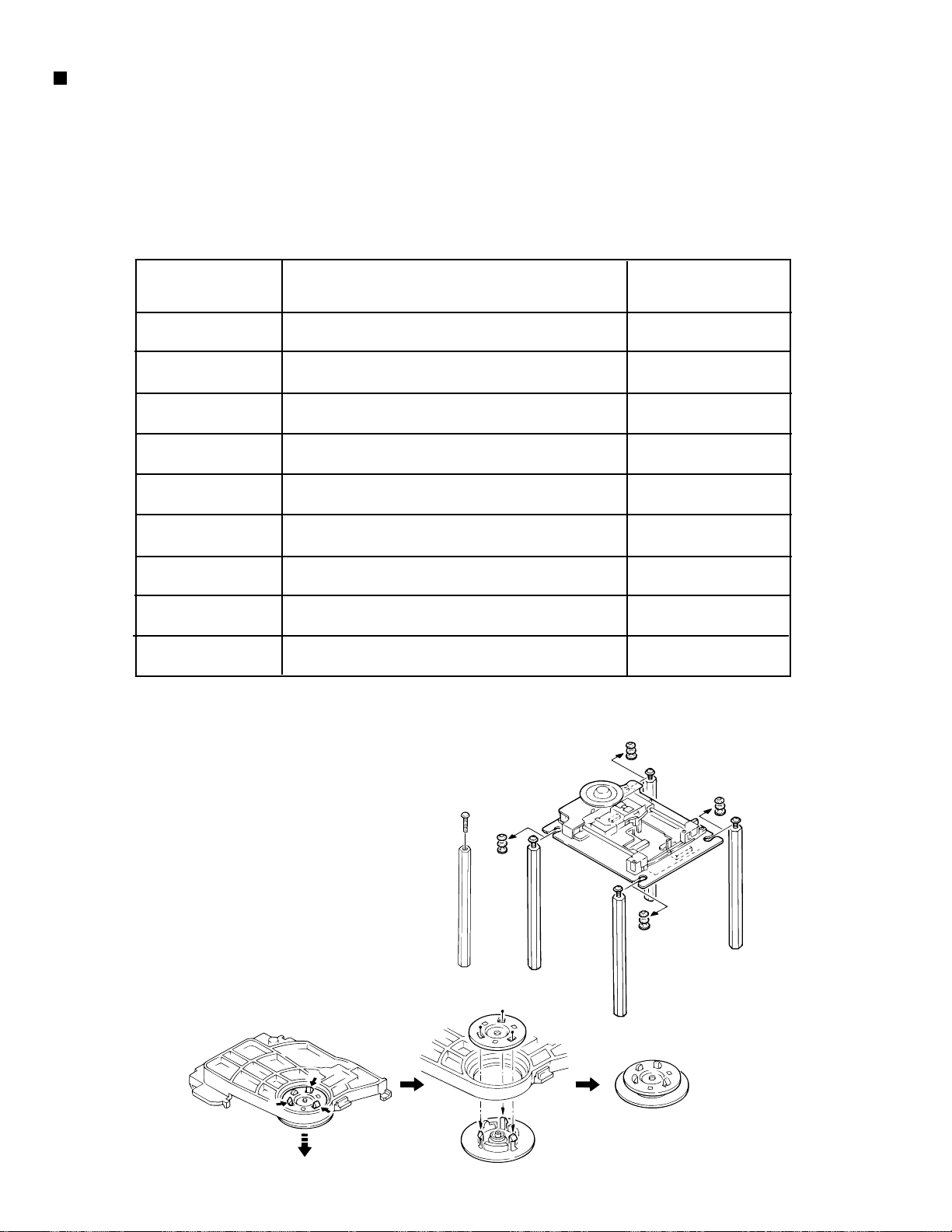
Adjustment
Jig set up
1.
Remove the rubber cushion from each of the four
corners of the traverse mechanism.
2.
(When installing be sure not to make a mistake with
the cushion colors).
3.
Install the jig stud.
Make a jig clamp (Remove the clamp from the set
and assemble it as shown in the diagram below).
Note:
How to handle the pickup
To protect the pickup from electro-static damage,
make sure to hold it by the die-cast chassis (optical
base). And make sure that pickup lens do not touch
the top cover.
Jig stud
Green rubber
cushion
Installing the
4 jig studs
Blue rubber
cushion
Blue rubber
cushion
1-30
How to prepare a clamp
Remove the claws
from the 3 locations
Disassemble the clamp
and holder
Combine the clamp
and holder to become
a jig clamp.
Page 31

MX-DVB10
Integrated wiring for adjustment
(See Fig.1 to 3)
1.
Place a board on top of the unit and put the
changer on it. Then carry out the wiring of the
main unit.
2.
Connect a extension cable to the traverse
mechanism for adjustment and then connect
them to the changer.
3.
Remove the solder of the short-circuited flexible
wire.
Then remove the short-circuited pin from the
traverse mechanism.
4.
Connection is completed.
Adjustment preparation
1.
The 3 adjustment locations.
2.
1.4 mm hexagonal wrench.
(See Fig.1 to 3)
Extension cord
QUQ605-4040AJ
Stud
JIGXVM555
Adjustment location
(Adjust screw A )
Hexagonal wrench
(Adjust screw B )
3.
Set the VT501 or VT502 test disc.
FL jitter display
(See Fig.1 to 3)
1.
During standby Demo Mode when AC plug in.
Press and hold "STOP" and "CANCEL/DEMO"
button on the unit.
---*THE display will show " " on the
FL display.
2.
When the key (PLAY) is pressed the jitter
value is displayed. Ensure that the disc VT-501
or VT-502 is in the tray.
3.
Adjust the jitter value to minimum by using the
adjust screw.
a). Turn the adjustment screw (A and B)
clockwise half.
b). Return the adjustment screw (A and B) to
former position.
c). Set the adjustment screw (A and B) to the
position of best jitter at three positions.
Adjustment location
(Adjust screw C )
Jig ass'y clamp adjustment
Test disc
3 locations
for adjustment
Next, do it similar to the above-mentioned in
adjustment screw A and C.
Adjust by using
a hexagonal
wrench
1-31
Page 32

MX-DVB10
Display of "Laser current value and" "Jitter value"
"Laser current value" and "Jitter value" are displayed on the FL display by the undermentioned
method. Please refer to the failure diagnosis.
1) Take out the disc and close the tray.
2) Unplug the power plug.
3) Insert power plug into outlet while pressing both "STOP" button and "CANCEL / DEMO" button.
4) FL Display indicate " " , depend on its area and region code.
5) Press the "OPEN / CLOSE" button to move the tray outward.
Put the test disc (VT-501) on the tray and press "OPEN / CLOSE" button.
The tray should move inward (Note:Don't push to close the tray directly by hand etc.)
6) Press the "PLAY" button.
7) After a few seconds, The laser current value and the jitter value is displayed on the FL indicator as follows..
FL Display
* The test mode is canceled when
0 0 4 0 3 9 7 8
Laser current value Jitter value
the power is turned off.
For Laser current value
The laser current value becomes 40mA for the above-mentioned.
Becomes a test mode by doing above-mentioned procedure 1) - 4). Afterwards, the laser current value can
be switched by pushing the button to remote controller without turning on the disk.
Remote control "4" button --- Laser of CD
Remote control "5" button --- Laser of DVD
If the laser current value is 64mA or less, it is roughly good. There is a possibility to which pick-up is
deteriorated, please change the pick-up when there is 65mA or more laser current value.
*Returns to a usual test mode by the
thing to push the "CLEAR" button of
remote controller.
1-32
Page 33

MX-DVB10
For Jitter value
The jitter value is displayed by the hexadecimal number and please refer to the conversion table below.
If the indication value is 11 or less, it can be judged by this simple checking method that the signal
read precision of the set is satisfactory.
Before using the TEST disc VT-501, careful check it if there is neither damage nor dirt on the read surface.
STOP Button
(Test mode)
CANCEL/DEMO
Button(Test mode)
5 Button
(Laser of DVD)
4 Button
(Laser of CD)
CLEAR Button
(Test mode)
FL Display
PLAY Button
(Test mode & display of jitter)
Jitter value
FL display FL display
3818
3828
3838
3848
3858
3868
3878
3888
3898
38A8
38b8
38c8
38d8
38E8
38F8
3918
3928
3938
3948
3958
3968
3978
3988
Conversion
value( )
4.7
4.8
4.9
5.1
5.2
5.3
5.4
5.5
5.7
5.8
5.9
6.0
6.1
6.3
6.4
6.6
6.7
6.9
7.0
7.1
7.2
7.3
7.5
3998
39A8
39B8
39C8
39D8
39E8
39F8
3A18
3A28
3A38
3A48
3A58
3A68
3A78
3A88
3A98
3AA8
3AB8
3AC8
3AD8
3AE8
3AF8
Conversion
value( )
7.6
7.7
7.8
7.9
8.1
8.2
8.3
8.5
8.7
8.8
8.9
9.0
9.1
9.3
9.4
9.5
9.6
9.7
9.9
10.0
10.1
10.2
FL display FL display
3B18
3B28
3B38
3B48
3B58
3B68
3B78
3B88
3B98
3BA8
3BB8
3BC8
3BD8
3BE8
3BF8
3C18
3C28
3C38
3C48
3C58
3C68
3C78
3C88
Conversion
value( )
10.5
10.6
10.7
10.8
10.9
11.1
11.2
11.3
11.4
11.5
11.7
11.8
11.9
12.0
12.1
12.4
12.5
12.7
12.7
12.9
13.0
13.1
13.2
3C98
3CA8
3CB8
3CC8
3CD8
3CE8
3CF8
3D18
3D28
3D38
3D48
3D58
3D68
3D78
3D88
3D98
3DA8
3DB8
3DC8
3DD8
3DE8
3DF8
Conversion
alue( )
v
13.3
13.5
13.6
13.7
13.8
13.9
14.1
14.3
14.4
14.5
14.7
14.8
14.9
15.0
15.1
15.3
15.4
15.5
15.6
15.7
15.9
16.0
1-33
Page 34

MX-DVB10
Maintenance of laser pickup
(1) Cleaning the pick up lens
Before you replace the pick up, please try to
clean the lens with a alcohol soaked cotton
swab.
(2) Life of the laser diode
When the life of the laser diode has expired,
the following symptoms will appear.
1. The level of RF output (EFM output : amp.
tude of eye pattern) will define as below.
Is the level of
RFOUT under
1.25V 0.22Vp-p?
YES
O.K
NO
Replace it.
Replacement of laser pickup
Turn off the power switch and, disconnect the
power cord from the ac outlet.
Replace the pickup with a normal one. (Refer
to "Pickup Removal" on the previous page)
Plug the power cord in, and turn the power on.
At this time, check that the laser emits for
about 3 seconds and the objective lens moves
up and down.
Note: Do not observe the laser beam directly.
Play a disc.
Check the eye-pattern at TP101.
Finish.
(3) Semi-fixed resistor on the APC PC board
The semi-fixed resistor on the APC printed circuit board which is attached to the pickup is used to adjust the laser
power. Since this adjustment should be performed to match the characteristics of the whole optical block, do not
touch the semi-fixed resistor.
If the laser power is lower than the specified value, the laser diode is almost worn out, and the laser pickup should
be replaced.
If the semi-fixed resistor is adjusted while the pickup is functioning normally, the laser pickup may be damaged
due to excessive current.
1-34
Page 35

Flow of functional operation until TOC read
Power ON
Play Key
Slider turns REST
SW ON.
Automatic tuning
of TE offset
Confirm that the voltage at the pin29
of CN101 (TP28) is "H"\"L"\"H".
MX-DVB10
Check Point
Tracking error waveform at TOC reading
Approx.3sec
Tracking
servo
off states
Automatic measurement
of TE amplitude and
automatic tuning of
TE balance
VREF
pin 18 of
IC101(TE)
Approx
1.8V
Disc states
to rotate
Tracking
servo
on states
Disc to be
braked to stop
TOC reading
finishes
500mv/div
2ms/div
Fig.1
Laser ON
Detection of disc
Automatic tuning of
Focus offset
Automatic measurement of
Focus S-curve amplitude
Disc is rotated
Focus servo ON
(Tracking servo ON)
Automatic measurement of
Tracking error amplitude
Automatic tuning of
Tracking error balance
Check that the voltage at the
CN101 (TP2) is +2V ?
When play DVD or
CN101
pin24 (TP23) is +2V ?
When play CD, VCD or SVCD.
Confirm that the Focus error
S-cuve signal at the pin22 of
IC101 is approx. 2Vp-p
Confirm the waveform of
the Tracking error signal
at the pin 18 of IC101 (R116)
(See fig-1)
Automatic tuning of
Focus error balance
Automatic tuning of
Focus error gain
Automatic tuning of
Tracking error gain
TOC reading
Play a disc
Confirm the eys-pattern
at the lead of TP101
1-35
Page 36

MX-DVB10
Description of major ICs
MN101C35DEG (IC810) : System control & FL driver
1. Pin layout
~
100 76
1
~
75
~
2. Pin function
Pin No.
1
2
3
4
5
6
7
8
9
10
11
12
13
14
15
16
17
18
19
20
21
22
23
24
25
26
27
28
29
30
31
32
33
34
35
36
37
38
39
40
41
42
43
Symbol
SYSOUT
SYSIN
DVDCLK
DATAOUT
DATAIN
TUCLK
DVDCS
MMOD
VDRF-
SLCKEY1
SLCKEY2
SPIDTI
VREF+
SMODE+
BASSVOL+
BASSVOL-
ECHO2
RDSDATA
/ECHO1
REMAIN
PHOTOA
PHOTOB
DVDHBSY
RDSCLK
VOL1CE
VSCE
FVOLDA
VOLCK
25
VDD
OSC2
OSC1
VSS
X1
NC
KEY1
KEY2
KEY3
KEY4
H/P-IN
RST
SPIA
SPIB
PRT
POUT
~
26 50
51
I/O
DVD signal output
I
DVD signal input
O
DVD signal clock
I
Tuner signal output
O
Tuner signal input
I
Tuner signal clock
I
DVD signal data input
I
Power supply
External terminal for main clock
I
External terminal for main clock
O
Connect to GND
Connect to GND
No connect
Connect to GND
Connect to GND
Key input terminal 1
I
Key input terminal 2
I
Key input terminal 3
I
Key input terminal 4
I
SLC key input 1
I
SLC key input 2
I
Head phone signal output
O
FL level data input
I
Reference voltage terminal
I
Surround volume control input
I
Reset input
I
E.volume control signal output +
O
E.volume control signal output -
O
Echo switching control 2
O
Echo switching control 1
O
FL level control signal A
O
FL level control signal B
O
Remote control signal input
I
Reel pulse detection A
I
Reel pulse detection B
I
DVD signal input
O
Serial clock switching for RDS and Echo 2
O
I Power amplifier output protect detection
E.volume data chip enable
O
System bus chip enable
O
Power ON control output
O
E.volume control data output
O
E.volume data communication clock
O
Function
1-36
Page 37

MX-DVB10
Pin No.
44
45
46
47
48
49
50
51
52
53
54
55
56
57
58
59
60
61
62
63
64
65
66
67
68
69
70
71
72
73
74
75
76
77
78
79
80
81
82
83
84
85
86
87
88
89
90
91
92
93
94
95
96
97
98
99
100
Symbol I/O
EXIT1
SLCCE
DVDRST
G17
G16
G15
G14
G13
G12
G11
G10
G9
G8
G7
G6
G5
G4
G3
G2
G1
P22
P21
P20
P19
P18
P17
P16
P15
P14
P13
P12
P11
P10
P9
P8
P7
P6
P5
P4
P3
P2
P1
TUCE
VOL2CE
VSCLK
DVD1LED
DVD2LED
DVD3LED
R_SEARCH
MSI
MPX
INH
F_SEARCH
VOLVOL+
SMODE-
VPP
Chip enable for EXT.IC
O
Chip enable for SLC control
O
DVD reset
O
FL drive control
O
FL drive control
O
FL drive control
O
FL drive control
O
FL drive control
O
FL drive control
O
FL drive control
O
FL drive control
O
FL drive control
O
FL drive control
O
FL drive control
O
FL drive control
O
FL drive control
O
FL drive control
O
FL drive control
O
FL drive control
O
FL drive control
O
FL drive control
O
FL drive control
O
FL drive control
O
FL drive control
O
FL drive control
O
FL drive control
O
FL drive control
O
FL drive control
O
FL drive control
O
FL drive control
O
FL drive control
O
FL drive control
O
FL drive control
O
FL drive control
O
FL drive control
O
FL drive control
O
FL drive control
O
FL drive control
O
FL drive control
O
FL drive control
O
FL drive control
O
FL drive control
O
Tuner control chip enable
O
Volume control chip enable
O
Volume clock
O
Disc 1 LED drive
O
Disc 2 LED drive
O
Disc 3 LED drive
O
Tuner signal detection
I
Detection between the broadcasting
I
Stereo signal detection
I
Tuner signal inhibit
O
Tuner signal detection
Volume drive control
Volume drive control
Sub woofer volume control
O
Power supply
I
Function
1-37
Page 38

MX-DVB10
MN103S13BDA (IC301) : Optical disc controller
1. Pin layout
DMARQ
NIOWR
VSS
NIORD
IORDY
NDMACK
VDD
INTRQ
NIOCS16
DA1
VSS
NPDIAG
DA0
DA2
VDD
144
143
142
141
140
139
138
137
136
135
134
133
132
131
HDD15
HDD0
HDD14
VDD
HDD1
HDD13
HDD2
VSS
HDD12
VDD
HDD3
HDD11
HDD4
HDD10
VDD
HDD5
HDD9
VSS
HDD6
HDD8
HDD7
VDDH
NRESET
MASTER
NINT0
NINT1
WAITDOC
NMRST
DASPST
VDD
OSCO2
OSCI2
UAT ASEL
VSS
PVSSDRAM
PVDDDRAM
1
2
3
4
5
6
7
8
9
10
11
12
13
14
15
16
17
18
19
20
21
22
23
24
25
26
27
28
29
30
31
32
33
34
35
36
3738394041424344454647484950515253545556575859606162636465666768697071
130
MN103S13BDA
NCS1FX
NCS3FX
NDASP
129
128
127
NTRYCL
126
VDD
125
NEJECT
VSS
124
123
MONI0
MONI1
122
121
MONI2
MONI3
120
119
SDATA
SCLOCK
118
117
VDD
116
DAT0
115
DAT1
114
DAT2
113
DAT3
CHCK40
112
111
NCLDCK
SUBC
110
109
108
107
106
105
104
103
102
101
100
99
98
97
96
95
94
93
92
91
90
89
88
87
86
85
84
83
82
81
80
79
78
77
76
75
74
73
72
SBCK
VSS
P0
P1
PVDD
PVSS
VDD
OSCO1
OSCI1
VSS
LRCK
BLKCK
IPFLAG
DACCLK
DACLRCK
DACDATA
NTRON
LG
JMPINH
IDHOLD
SBCK/PLLOK
CLKOUT2
VDD
NRST
MMOD
VSS
CPDET1
CPDET2
BDO
IDGT
DTRD
TEHLD
VDD
CLKOUT1
CPUDT0
CPUDT1
2. Block diagram
DVD-ROM
Formatter
CGEN
MODE
CPUADR17
CPUADR16
VSS
CPUADR15
CPUADR14
CPUADR13
CD-PRE
Instruction
memory
(40KB)
DATA
MEMORY
(6KB)
VDD
CPUADR9
CPUADR8
CPUADR11
CPUADR10
CPUADR7
CPUADR12
Formatter
General purpose IO bus
CPUADR6
CPUADR5
CPUADR4
CPUADR3
CPUADR2
i /t
High speed IO bus
32 bit
CPU core
GCAL
CPUADR1
VSS
NCS
CPUADR0
ECC
NWR
NRD
VDD
CPUDT7
CPUDT6
PVPPDRAM
PTESTDRAM
Host i / f
MPEG i / t
DMA
BCU
DRAMC
CPUDT5
CPUDT4
PVSSDRAM
PVDDDRAM
VSS
CPUDT3
CPUDT2
ATAPI
4Mbit
DRAM
1-38
WDT
16 bit
timer x 2
SYSTEM
i / f
INTC
Page 39

3. Pin function (1/3)
MX-DVB10
Pin No.
1
2
3
4
5
6
7
8
9
10
11
12
13
14
15
16
17
18
19
20
21
22
23
24
25
26
27
28
29
30
31
32
33
34
35
36
37
38
39
40
41
42
43
44
45
46
47
48
49
50
Symbol
HDD15
HDD0
HDD14
VDD
HDD1
HDD13
HDD2
VSS
HDD12
VDD
HDD3
HDD11
HDD4
HDD10
VDD
HDD5
HDD9
VSS
HDD6
HDD8
HDD7
VDDH
NRESET
MASTER
NINT0
NINT1
WAITDOC
NMRST
DASPST
VDD
OSCO2
OSCI2
UATASEL
VSS
PVSSDRAM
PVDDDRAM
CPUADR17
CPUADR16
VSS
CPUADR15
CPUADR14
CPUADR13
CPUADR12
VDD
CPUADR11
CPUADR10
CPUADR9
CPUADR8
CPUADR7
CPUADR6
I/O
I/O
I/O
I/O
I/O
I/O
I/O
I/O
I/O
I/O
I/O
I/O
I/O
I/O
I/O
I/O
I/O
I/O
O
O
O
O
O
Description
ATAPI Data
ATAPI Data
ATAPI Data
Power supply 3V
ATAPI Data
ATAPI Data
ATAPI Data
Connect to GND
ATAPI Data
Power supply 2.7V
ATAPI Data
ATAPI Data
ATAPI Data
ATAPI Data
Power supply 3V
ATAPI Data
ATAPI Data
Connect to GND
ATAPI Data
ATAPI Data
ATAPI Data
ATAPI Reset input
I
ATAPI Master/slave select
Interruption of system control 0
Interruption of system control 1
Wait control of system control
Reset of system control (Connect to TP302)
Setting of initial value of DASP signal
I
Power supply 3V
Non connect
Non connect
I
Connect to VSS
I
Connect to GND
Connect to VSS
Connect to VDD(2.7V)
System control address
I
System control address
I
Connect to GND
System control address
I
System control address
I
System control address
I
System control address
I
Power supply 2.7V
System control address
I
System control address
I
System control address
I
System control address
I
System control address
I
System control address
I
1-39
Page 40

MX-DVB10
3. Pin function (2/3)
Pin No.
51
52
53
54
55
56
57
58
59
60
61
62
63
64
65
66
67
68
69
70
71
72
73
74
75
76
77
78
79
80
81
82
83
84
85
86
87
88
89
90
91
92
93
94
95
96
97
98
99
100
Symbol
CPUADR5
CPUADR4
CPUADR3
CPUADR2
CPUADR1
VSS
CPUADR0
NCS
NWR
NRD
VDD
CPUDT7
CPUDT6
PVPPDRAM
PTESTDRAM
PVDDDRAM
PVSSDRAM
CPUDT5
CPUDT4
CPUDT3
VSS
CPUDT2
CPUDT1
CPUDT0
CLKOUT1
VDD
TEHLD
DTRD
IDGT
BDO
CPDET2
CPDET1
VSS
MMOD
NRST
VDD
CLKOUT2
SBCK/PLLOK
IDOHOLD
JMPINH
LG
NTRON
DACDATA
DACLRCK
DACCLK
IPFLAG
BLKCK
LRCK
VSS
OSCI1
I/O
I
I
I
I
I
I
I
I
I
I/O
I/O
O
I
I/O
I/O
I/O
I/O
I/O
I/O
O
-
O
O
O
I
I
I
-
I
I
-
O
O
O
O
O
I
O
O
I
I
I
I
-
I
Description
System control address
System control address
System control address
System control address
System control address
Connect to GND
System control address
System control chip select
Writing system control
Reading system control
Power supply 3V
System control data
System control data
Connect to VSS
Connect to VSS
Connect to VDD(2.7V)
Connect to VSS
System control data
System control data
System control data
Connect to GND
System control data
System control data
System control data
Clock signal output (16.9/11.2/8.45MHz)
Power supply 3V
Mirror gate (Connect to TP141)
Data frequency control switch (Connect to TP304)
CAPA switch
RF Dropout/BCA data
Outer capacity detection
Inner capacity detection
Connect to GND
Connect to VSS
System reset
Power supply 3V
Clock 16.9MHz
Flame mark detection
ID gate for tracking holding
Jump prohibition
Land/group switch
Tracking ON
Serial data output (Connect to TP148)
Identification signal of L and R (Connect to TP149)
Clock for serial data output
Input of IP flag
Sub code/block/input clock
Identification signal of L and R (Connect to VSS)
Connect to GND
Oscillation input terminal 16.9MHz
1-40
Page 41

3. Pin function (3/3)
MX-DVB10
Pin No.
101
102
103
104
105
106
107
108
109
110
111
112
113
114
115
116
117
118
119
120
121
122
123
124
125
126
127
128
129
130
131
132
133
134
135
136
137
138
139
140
141
142
143
144
Symbol
OSCO1
VDD
PVSS
PVDD
P1
P0
VSS
SBCK
SUBC
NCLDCK
CHCK40
DA T3
DA T2
DA T1
DA T0
VDD
SCLOCK
SDATA
MONI3
MONI2
MONI1
MONI0
VSS
NEJECT
VDD
NTRYCL
NDASP
NCS3FX
NCS1FX
VDD
DA2
DA0
NPDIAG
VSS
DA1
NIOCS16
INTRQ
VDD
NDMACK
IORDY
NIORD
VSS
NIOWR
DMARQ
I/O
O
-
-
I/O
I/O
-
O
I
I
I
I
I
I
I
I/O
I/O
O
O
O
O
-
I
-
I
I/O
I
I
I/O
I/O
I/O
I/O
O
O
-
I
O
I
I/O
O
Description
Oscillation output terminal 16.9MHz
Power supply 3V
Connect to GND
Power supply 3V
Terminal master polarity switch input
CIRC-RAM,OVER/UNDER Interruption
Connect to GND
Clock output for sub code,serial input
Sub code,serial input
Sub code,flame clock input
Clock is read to DAT3~0 (Output of division frequency from ADSC)
Data is read from disc (Going side by side output from ADSC)
Data is read from disc (Going side by side output from ADSC)
Data is read from disc (Going side by side output from ADSC)
Data is read from disc (Going side by side output from ADSC)
Power supply 3V
Debug serial clock (270 ohm pull up)
Debug serial data (270 ohm pull up)
Internal good title monitor (Connect to TP150)
Internal good title monitor (Connect to TP151)
Internal good title monitor (Connect to TP152)
Internal good title monitor (Connect to TP153)
Connect to GND
Eject detection
Power supply 2.7V
Non connect (Tray close detection)
ATAPI drive active / slave connect I/O
Non connect (ATAPI host chip select)
Non connect (ATAPI host chip select)
Power supply 3V
ATAPI host address
Non connect (ATAPI host address)
ATAPI Slave master diagnosis input
Connect to GND
Non connect (ATAPI host address)
Output of selection of width of ATAPI host data bus
ATAPI Host interruption output
Power supply 3V
Non connect (ATAPI Host DMA characteristic)
ATAPI Host ready output (Connect to TP157)
Non connect (ATAPI host read)
Connect to GND
ATAPI Host write
ATAPI Host DMA request (Connect to TP159)
1-41
Page 42

MX-DVB10
MN101C49GEH 1 (IC500) : AV decorder
1. Pin layout
~
100 76
1
~
75
~
25
~
26 50
51
2. Pin function
Pin No.
1 VREF I Reference voltage
2 NC - No connect
3 NC - No connect
4 NC - No connect
5 NTSEL I NTSC/PAL selection
6 POWER SW -
7 SHUT1 -
8 KEY1-5 -
9 KEY6-10 -
10 VREF+ I
11 VDD I Power supply
12 OSC2 O External terminal for connected oscirator
13 OSC1 I External terminal for connected oscirator
14 VSS - Connect to GND
15 XI I External terminal for sub oscirator (Supply to voltage)
16 XO O No connect
17 MMOD I connects with gnd
18 DADATA I/O Data bus for DAC
19 DACS1 I/O Serial bus S1 for DAC
20 DCLK I/O Clock for DAC
21 S2UDT O
22 U2SDT I
23 SCLK I/O Serial clock bus
24 BUSY I/O Busy bus
25 CPURST O Unit microcomputer reset
26 REQ I Commnication between unit microcomputers REQ
27 REMO I Remote control interrruption
28 TEST1 - Test terminal
29 TEST2 - Test terminal
30 TEST3 - Test terminal
31 DVDCS I Chip select for DVD
32 NC - No connect
33 DVDRST I DVD reset
34 NC - No connect
35 DACS2 I/O Serial bus S2 for DAC
36 DACS3 I/O Serial bus S3 for DAC
37 NC - No connect
38 NC - No connect
39 FS2 I Over sampling frequency
40 CHREQ I Changer commnication REQUEST
41 CHST O Changer commnication STROBE
42 CHDATA O Changer commnication DATA I/O
43 NC - No connect
Symbol
I/O
No connect
No connect
No connect
No connect
Reference voltage
Function
Communication between unit microcomputers DATA output
Communication between unit microcomputers DATA output
1-42
Page 43

MX-DVB10
Pin No.
44 CHCK I Channel clock
45 DVDOUT O DVD data output
46 DVDIN I DVD data input
47 DVDCLK I DVD clock
48 DVDBSY Busy bus for DVD
49 NC - No connect
50 NC - No connect
51 NC - No connect
52 NC - No connect
53 NC - No connect
54 VS1 O Fanction SW control
55 VS3 O Fanction SW control
56 SL/SRMUTE O No connect
57 CMUTE O Center signal output mute
58 SWMUTE O No connect
59 POB2 O No connect
60 DEMP2 O No connect
61 DEMP1 O No connect
62 DENA O No connect
63 KARAOKE O No connect
64 POWER ON O Power on control output
65 VS2 O Fanction SW control
66 NC - No connect
67 NC - No connect
68 NC - No connect
69 NC - No connect
70 NC - No connect
71 NC - No connect
72 NC - No connect
73 NC - No connect
74 NC - No connect
75 NC - No connect
76 NC - No connect
77 AVCI I Power supply
78 AVCO I/O AV compu link signal I/O port
79 RGB I RGB signal in
80 STD IND O Standby LED output
81 MPX1 I MPX1 signal input
82 MPX2 I MPX2 signal input
83 SRELAY O S. Relay control
84 MRELAY O M. Relay control
85 BASS1 O BASS1 switching
86 BASS2 O BASS2 switching
87 FCD O CD power supply control signal
88 PBMUTE O PB mute
89 AUXMUTE O AUX mute
90 SMUTE O System mute output
91 NC - No connect
92 NC - No connect
93 NC - No connect
94 NC - No connect
95 DAVSS - Connect to GND
96 NC - No connect
97 NC - No connect
98 NC - No connect
99 HPMUTE O Head phone mute
100 VREF- I
Symbol
I/O
Connected GND
Function
1-43
Page 44

MX-DVB10
ZIVA-4.1 PA2 (IC501) : AV decoder
1. Pin layout
~
208 157
1
~
156
~
2. Pin function (1/5)
Pin No.
1
2
3
4
5
6
7
8
9
10
11
12
13
14
15
16
17
18
19
20
21
22
23
24
25
26
27
28
29
30
31
32
33
34
35
36
Symbol
RD
R/W
VDD
WAIT
RESET
VSS
VDD
INT
NC
NC
NC
NC
VDD
VSS
NC
NC
NC
NC
VSS
VDD
VDATA0
VDATA1
VDATA2
VDATA3
VDATA4
VDATA5
VDATA6
VDATA7
VSYNC
HSYNC
VSS
VDD
NC
NC
NC
VDD
52
53 104
I/O
O
O
O
O
O
O
O
O
O
O
I/O
I/O
105
~
Description
I
I
-
I
-
-
-
-
-
-
-
-
-
-
-
-
-
-
-
-
-
-
-
-
Read strobe input
Read/write strobe input
Power supply terminal 3.3V
Transfer not complete / data acknowledge.
Active LOW to indicate host initiated transfer is complete.
Active LOW : reset signal input
Connect to ground
Power supply terminal 3.3V
Host interrupt signal output
Non connect
Non connect
Non connect
Non connect
Power supply terminal 2.5V
Connect to ground
Non connect
Non connect
Non connect
Non connect
Connect to ground
Power supply 3.3V
Video data bus output. Byte serial CbYCrY data synchronous with VCLK.
Video data bus output. Byte serial CbYCrY data synchronous with VCLK.
Video data bus output. Byte serial CbYCrY data synchronous with VCLK.
Video data bus output. Byte serial CbYCrY data synchronous with VCLK.
Video data bus output. Byte serial CbYCrY data synchronous with VCLK.
Video data bus output. Byte serial CbYCrY data synchronous with VCLK.
Video data bus output. Byte serial CbYCrY data synchronous with VCLK.
Video data bus output. Byte serial CbYCrY data synchronous with VCLK.
Vertical sync. Bi-directional, the decoder output the top border of a new
field on the first HSYNC after the falling edge of VSYNC.
Horizontal sync. The decoder begins outputting pixel data for a new
horizontal line after the falling (active) edge of HSYNC.
Connect to ground
Power supply terminal 3.3V
Non connect
Non connect
Non connect
Power supply terminal 2.5V
1-44
Page 45

2. Pin function (2/5)
MX-DVB10
Pin No.
37
38
39
40
41
42
43
44
45
46
47
48
49
50
51
52
53
54
55
56
57
58
59
60
61
62
63
64
65
66
67
68
69
70
71
72
73
74
75
76
77
78
79
80
81
82
83
84
Symbol
VSS
NC
NC
NC
NC
NC
PIO0
VSS
VDD
PIO1
PIO2
PIO3
PIO4
PIO5
PIO6
PIO7
MDATA0
MDATA1
VDD
VSS
MDATA2
MDATA3
MDATA4
MDATA5
MDATA6
MDATA7
MDATA15
VDD
VSS
MDATA14
VDD
VSS
MDATA13
MDATA12
MDATA11
MDATA10
MDATA9
VDD
VSS
MDATA8
LDQM
SD-CLK
CLKSEL
MADDR9
MADDR8
VDD
VSS
MADDR7
I/O
Connect to ground
Non connect
Non connect
Non connect
Non connect
Non connect
Programmable I/O terminal
I/O
Connect to ground
Power supply terminal 3.3V
Programmable I/O terminal
I/O
Programmable I/O terminal
I/O
Programmable I/O terminal
I/O
Programmable I/O terminal
I/O
Programmable I/O terminal
I/O
Programmable I/O terminal
I/O
Programmable I/O terminal
I/O
SDRAM data
I/O
SDRAM data
I/O
Power supply terminal 3.3V
Connect to ground
SDRAM data
I/O
SDRAM data
I/O
SDRAM data
I/O
SDRAM data
I/O
SDRAM data
I/O
SDRAM data
I/O
SDRAM data
I/O
Power supply terminal 3.3V
Connect to ground
SDRAM data
I/O
Power supply terminal 2.5
Connect to ground
SDRAM data
I/O
SDRAM data
I/O
SDRAM data
I/O
SDRAM data
I/O
SDRAM data
I/O
Power supply terminal 3.3V
Connect to ground
SDRAM data
I/O
SDRAM Lower or upper mask
O
SDRAM Clock
O
Selects SYSCLK or VCLK as clock source. Normal operation is to tie HIGH.
I
SDRAM address
O
SDRAM address
O
Power supply terminal 3.3V
Connect to ground
SDRAM address
O
Description
1-45
Page 46

MX-DVB10
2. Pin function (3/5)
Pin No.
85
86
87
88
89
90
91
92
93
94
95
96
97
98
99
100
101
102
103
104
105
106
107
108
109
110
111
112
113
114
115
116
117
118
119
120
121
122
123
124
125
126
127
128
Symbol
MADDR6
MADDR5
VDD
VSS
MADDR4
MWE
SD-CAS
VDD
VSS
SD-RAS
SD-CS0
SD-CS1/MADDR11
SD-BS
MADDR10
MADDR0
VDD
VSS
MADDR1
MADDR2
MADDR3
RESERVED
NC
NC
RESERVED
NC
RESERVED
RESERVED
RESERVED
DAI-LRCK
DAI-BCK
VDD
VSS
DAI-DATA
DA-DATA3
DA-DATA2
DA-DATA1
DA-DATA0
DA-LRCK
VDD
VSS
DA-XCK
DA-BCK
DA-IEC
VDD
I/O
SDRAM address
O
SDRAM address
O
Power supply terminal 2.5V
Connect to ground
SDRAM address
O
SDRAM write enable
O
Active LOW SDRAM column address
O
Power supply terminal 3.3V
Connect to ground
Active LOW SDRAM row address
O
Active LOW SDRAM chip select 0
O
Active LOW SDRAM chip select 1 or use as MADDR11 for larger SDRAM
O
SDRAM bank select
O
SDRAM address
O
SDRAM address
O
Power supply terminal 3.3V
Connect to ground
SDRAM address
O
SDRAM address
O
SDRAM address
O
Tie to VSS or VDD_3.3 as specified in table1
I
Non connect
Non connect
Tie to VSS or VDD_3.3 as specified in table1
I
Non connect
Tie to VSS or VDD_3.3 as specified in table1
I
Tie to VSS or VDD_3.3 as specified in table1
I
Tie to VSS or VDD_3.3 as specified in table1
I
PCM left/right clock
I
PCM input bit clock
I
Power supply 3.3V
Connect to ground
PCM data input
I
PCM data output. Eight channels. Serial audio samples relative to
O
DA_BCK and DA_LRCK
PCM data output. Eight channels. Serial audio samples relative to
O
DA_BCK and DA_LRCK
PCM data output. Eight channels. Serial audio samples relative to
O
DA_BCK and DA_LRCK
PCM data output. Eight channels. Serial audio samples relative to
O
DA_BCK and DA_LRCK
PCM left clock. Identifies the channel for each sample
O
Power supply terminal 3.3V
Connect to ground
Audio external frequency clock input or output
I/O
PCM bit clock output
O
PCM data out in IEC-958 format or compressed data out in IEC-1937 format
O
Power supply terminal 2.5V
-
Description
1-46
Page 47

2. Pin function (4/5)
MX-DVB10
Pin No.
129
130
131
132
133
134
135
136
137
138
139
140
141
142
143
144
145
146
147
148
149
150
151
152
153
154
155
156
157
158
159
160
161
162
163
164
165
166
167
168
169
Symbol
VSS
NC
VSS_DAC
VSS_VIDEO
CVBS
VDD_DAC
VDD_VIDEO
NC
VSS_DAC
VSS_VIDEO
CVBS/G/Y
VDD_DAC
VDD_VIDEO
NC
VSS_DAC
VSS_VIDEO
Y/B/U
VDD_DAC
VDD_VIDEO
NC
VSS_DAC
VSS_VIDEO
C/R/V
VDD_DAC
VDD_VIDEO
VSS_RREF
RREF
VDD_RREF
A_VSS
SYSCLK
VCLK
A_VDD
DVD-DATA0/CD-DATA
DVD-DATA1/CD-LRC
DVD-DATA2/CD-BCK
DVD-DATA3/CD-C2PO
DVD-DATA4/CDGSDATA
VSS
VDD
DVD-DATA5/CDG-VFSY
DVD-DATA6/CDG-SOS1
I/O
Connect to ground
Non connect
Connect to ground for analog video DAC
Connect to ground for analog video
DAC video output format : CVBS. Macrovision encoded
O
Power supply terminal for analog video DAC
Power supply terminal for analog video
Non connect
Connect to ground for analog video DAC
Connect to ground for analog video
DAC video output format. Macrovision encoded
O
Power supply terminal for analog video DAC
Power supply terminal for analog video
Non connect
Connect to ground for analog video DAC
Connect to ground for analog video
DAC video output format. Macrovision encoded
O
Power supply terminal for analog video DAC
Power supply terminal for analog video
Non connect
Connect to ground for analog video DAC
Connect to ground for analog video
DAC video output format. Macrovision encoded
O
Power supply terminal for analog video DAC
Power supply terminal for analog video
Connect to ground for analog video
Reference resistor. Connecting to pin 154
O
Power supply terminal for analog video 3.3V
Power supply terminal for analog PLL 3.3V
Optical system clock. Tie to A_VDD through a 1K ohm resistor
I
System clock input
I
Power supply terminal for analog PLL 3.3V
Serial CD data. This pin is shared with DVD compressed data DVD-DATA0
I
Programmable polarity 16-bit word synchronization to the decoder.
I
Description
This pin is shared with DVD compressed data DVD-DATA1
CD bit clock. Decoder accept multiple BCK rates. This pin is shared with
I
DVD compressed DVD-DATA2
Asserted HIGH indicates a corrupted byte. This pin is shared with DVD
I
compressed data DVD-DATA3
DVD parallel compressed data from DVD DSP. or CD-G data indicating
I
serial subcode data input
Connect to ground
Power supply terminal 3.3V
DVD parallel compressed data from DVD DSP. or CD-G frame sync
I
indicating frame-start or composite synchronization input.
DVD parallel compressed data from DVD DSP. or CD-G block sync
I
indicating block-start synchronization input
1-47
Page 48

MX-DVB10
2. Pin function (5/5)
Pin No.
170
171
172
173
174
175
176
177
178
179
180
181
182
183
184
185
186
187
188
189
190
191
192
193
194
195
196
197
198
199
200
201
202
203
204
205
206
207
208
Symbol
DVD-DATA7/CDG-SCLK
VDACK
VREQUEST
VSTROBE
ERROR
RESERVED
RESERVED
HADDR0
HADDR1
HADDR2
RESERVED
RESERVED
RESERVED
RESERVED
RESERVED
RESERVED
RESERVED
RESERVED
HDATA7
HDATA6
HDATA5
HDATA4
HDATA3
HDATA2
HDATA1
HDATA0
VDD
VDD
VSS
NC
NC
VSS
VDD
VSS
VDD
VSS
VDD
VSS
CS
I/O
DVD parallel compressed data from DVD DSP. or CD-G clock indicating
I
Description
sub code data clock input or output
In synchronous mode, bitstream data acknowledge. Asserted when DVD
I
data is valid.Polarity is programmable
Bitstream request
O
Bitstream strobe
I
Error in input data
I
Power supply terminal 3.3V
Tie to VSS or VDD_3.3 as specified in table 1
I
Power supply terminal 3.3V
Connect to ground
Non connect
Tie to VSS or VDD_3.3 as specified in table 1
I
Non connect
-
Host addressbus. 3-bit address bus selects one of eight host interface registers
I
Host addressbus. 3-bit address bus selects one of eight host interface registers
I
Host addressbus. 3-bit address bus selects one of eight host interface registers
I
Tie to VSS or VDD_3.3 as specified in table 1
I
Tie to VSS or VDD_3.3 as specified in table 1
I
Tie to VSS or VDD_3.3 as specified in table 1
I
Connect to ground
Power supply terminal 2.5V
Tie to VSS or VDD_3.3 as specified in table 1
I
Connect to ground
Power supply terminal 3.3V
Tie to VSS or VDD_3.3 as specified in table 1
I
Tie to VSS or VDD_3.3 as specified in table 1
I
Tie to VSS or VDD_3.3 as specified in table 1
I
Tie to VSS or VDD_3.3 as specified in table 1
I
The 8-bit bi-derectional host data through which the host writes data to
I/O
the decoder code.
Connect to ground
The 8-bit bi-derectional host data through which the host writes data to
I/O
the decoder code.
The 8-bit bi-derectional host data through which the host writes data to
I/O
the decoder code.
The 8-bit bi-derectional host data through which the host writes data to
I/O
the decoder code.
The 8-bit bi-derectional host data through which the host writes data to
I/O
the decoder code.
The 8-bit bi-derectional host data through which the host writes data to
I/O
the decoder code.
Power supply terminal 3.3V
Connect to ground
The 8-bit bi-derectional host data through which the host writes data to
I/O
the decoder code.
The 8-bit bi-derectional host data through which the host writes data to
I/O
the decoder code.
Host chip select input
I
1-48
Page 49

AN7345K (IC302) : REC/PRE Amp.
1. Pin layout / Block diagram
24 23 22 21 20 19 18 17 16 15 14 13
MX-DVB10
123456789101112
2. Pin function
Pin No.
1
2
3
4
5
6
7
8
9
10
11
12
13
14
15
16
17
18
19
20
21
22
23
24
I/O
I
I
I
O
I
O
I
I
O
O
O
-
-
O
I
O
I
I
O
I
O
I
I
I
EQ
CTRL
Pre
Source
CTRL
REC
Amp
REC
Amp
PRE
Amp
PRE
Amp
Function
CH1 Playback amplifier input(1)
CH1 Playback amplifier input(2)
CH1 Playback amplifier negative feedback
CH1 Playback amplifier output
CH1 Equalizer input
Pre amplifier input control time constant
CH1 Recoding amplifier input
CH1 Recoding amplifier negative output
CH1 Recoding amplifier output
ALC low cut
ALC L.P.F
Connect to GND
Power supply
Repple filter
Equalizer control
CH2 Recoding amplifier output
CH2 Recoding amplifier negative output
CH2 Recoding amplifier input
Pre amplifier input control
CH2 Equalizer input
CH2 Playback amplifier output
CH2 Playback amplifier negative feedback
CH2 Playback amplifier input(2)
CH2 Playback amplifier input(1)
ALC
REPPLE
REJ
1-49
Page 50

MX-DVB10
MN67706ZY (IC201) : Auto digital servo controller
1. Pin layout
33VDD
33VSS
TEST
MINTEST
NCLDCK/JUMP
SUBC
IPFLAG
DACCLK
NTRON
DACDATA/LG
DACLRCK/JMPINH
IDHOLD
SBCK/PLLOK
BLKCK/CPDET1
LRCK/CPDET2
IDGT/TEMUTE
DTRD
25VDD
25VSS
TILTN
TILT
TILTPFGSPDRV
TRSDRV
7574737271706968676665646362616059585756555453
CHCK40
DAT3
DAT2
DAT1
DAT0
33VSS
33VDD
XRESET
ENS
ENC
CPUIRQ
CPUCLK
CPUDTIN
CPUDTOUT
MONA
MONB
MONC
25VSS
25VDD
LDCUR(AD6)
TDOFS(AD5)
TG(AD4)
RFENV(AD3)
NC
TX
76
77
78
79
80
81
82
83
84
85
86
87
88
89
90
91
92
93
94
95
96
97
98
99
100
123456789
TE(AD1)
FE(AD0)
AS(AD2)
MN67706ZY
ARF
AVSS
AVDD
TRDRV(DA0)
FODRV(DA1)
101112131415161718192021222324
PLFG
DSLF1
DSLF2
AVDD
VHALF
PLPG
NARF
IREF1
IREF2
2. Pin functions (1/3)
Pin No. Symbol I/O Function
1
10
11
12
13
14
15
16
17
18
19
20
21
22
23
24
25
2
3
4
5
6
7
8
9
AS(AD2)
TE(AD1)
FE(AD0)
AVDD
FODRV(DA1)
TRDRV(DA0)
AVSS
ARF
NARF
IREF1
IREF2
DSLF1
DSLF2
AVDD
VHALF
PLPG
PLFG
VREFH
RVI
AVSS
PLFLT1
PLFLT2
JITOUT
RFDIF
CSLFL1
I
I
I
O
O
-
I
I
I
I
I/O
I/O
-
I
-
-
I
I/O
O
O
I/O
I
I/O
AS : Full adder signal (FEP)
Phase difference / 3 beam tracking error(FEP)
Focus error (FEP)
Apply 3.3V (For analog circuit)
Focus drive (DRVIC)
Tracking drive (DRVIC)
Ground (For analog circuit)
Equivalence RF+ (FEP)
Equivalence RF- (FEP)
Reference current1 (For DBAL)
Reference current2 (For DBAL)
Connect to capacitor1 for DSL
Connect to capacitor2 for DSL
Apply 3.3V (For analog circuit)
Reference voltage 1.65+-0.1V (FEP)
Not use(PLL phase gain setting resistor terminal)
Not use(PLL frequency gain setting resistor terminal)
Reference voltage 2.2V+-0.1V (FEP)
Connect to resistor forVREFH reference current source
Ground (For analog circuit)
Connect to capacitor1 for PLL
Connect to capacitor 2 for PLL
Output or jitter signal monitorf
Not use
Pull-up to VHALF
RVI
VREFH
AVSS
PLFLT1
JITOUT
PLFLT2
51
52
25
RFDIF
CSLFL1
TSTSG
50
BDO
49
SYSCLK
48
OFTR
47
33VDD
46
33VSS
45
FBAL
44
TBAL
43
TGBAL
42
AVSS
41
ROUT
40
LOUT
39
AVDD
38
JLINE
37
DBALO
36
VCOF
35
TRCRS
34
CMPIN
33
LPFOUT
32
LPFIN
31
AVSS
30
HPFOUT
29
HPFIN
28
AVDD
27
VFOSHORT
26
1-50
Page 51

2. Pin function (2/3)
Pin No. Symbol I/O Function
VFOSHORT
26
AVDD
27
HPFIN
28
HPFOUT
29
AVSS
30
LPFIN
31
LPFOUT
32
CMPIN
33
TRCRS
34
VCOF
35
DBALO
36
JLINE
37
AVDD
38
LOUT
39
ROUT
40
AVSS
41
TGBAL
42
TBAL
43
FBAL
44
33VSS
45
33VDD
46
OFTR
47
SYSCLK
48
BDO
49
TSTSG
50
TRSDRV
51
SPDRV
52
FG
53
TILTP
54
TILT
55
TILTN
56
25VSS
57
25VDD
58
DTRD
59
60
IDGT/TEMUTE
61
LRCK/CPDET2
62
BLKCK/CPDET1
63
SBCK/PLLOK
64
IDHOLD
65
DACLRCK/JMPINH
66
DACDATA/LG
67
NTRON
68
DACCLK
69
IPFLAG
70
SUBC
71
NCLDCK/JUMP
72
MINTEST
73
TEST
74
33VSS
75
33VDD
76
CHCK40
77
DA T3
78
DA T2
79
DA T1
80
DA T0
O
O
O
I/O
O
O
O
O
O
O
O
O
O
O
O
O
O
O
O
O
O
O
O
O
O
O
O
O
O
VFO short output
-
Apply 3.3V(For analog circuit)
I
Pull-up to VHALF
Connect to TP208
-
Ground(For analog circuit)
I
Pull-up to VHALF
Not use
I
Connect to TP210
I
Input signal for track cross formation
JFVCO control voltage
DSL balance adjust output
J-line setting output(FEP)
-
Apply 3.3V(For analog circuit)
Connect to TP203 (Analog audio left output)
Connect to TP204 (Analog audio right output)
-
Ground(For analog circuit)
Tangential balance adjust(FEP)
Tracking balance adjust(FEP)
Focus balance adjust(FEP)
-
Ground(For I/O)
-
Apply 3.3V(For I/O)
I
Off track signal
I
16.9344MHz system clock input(ODC)
I
Drop out(FEP)
Calibration signal(FEP)
Traverse drive(DRVIC)
Spindle drive output(DRVIC)
I
FG signal input (Spindle motor driver)
Connect to TP205
Connect to TP206
Connect to TP207
-
Ground(For internal core)
-
Apply 2.5V(For internal core)
I
Data read control signal(ODC)
I
Pull-down to Ground
LR channel data strobe(ODC)/
CD sub code synchronous signal(ODC)/
I
CD sub code data shift clock(ODC)/PLL pull-in OK signal input
I
Pull-down to Ground
I
1bit DAC-LR channel data strobe(ODC)/
I
CD 1bit DAC channel data(ODC)
L : Tracking ON(ODC)
1bit DAC channel data shift clock(ODC)
CIRC error flag(ODC)
CD sub code(ODC)
CD sub code data frame clock(ODC)/DVD JUMP signal(ODC)
I
Pull-down to Ground(For MINTEST)
I
Pull-down to Ground(For TEST)
-
Ground(For I/O)
-
Apply 3.3V(For I/O)
Clock for SRDATA(ODC)
SRDATA3(ODC)
SRDATA2(ODC)
SRDATA1(ODC)
SRDATA0(ODC)
MX-DVB10
1-51
Page 52

MX-DVB10
2. Pin function (3/3)
Pin No. Symbol I/O Function
-
81
82
83
84
85
86
87
88
89
90
91
92
93
94
95
96
97
98
99
100
33VSS
33VDD
TX
XRESET
ENS
ENC
CPUIRQ
CPUCLK
CPUDTIN
CPUDTOUT
MONA
MONB
MONC
NC
25VSS
25VDD
LDCUR(AD6)
TDOFS(AD5)
TG(AD4)
RFENV(AD3)
O
O
O
O
O
O
O
Ground (For I/O)
-
Apply 3.3V (For I/O)
Digital audio interface
I
Reset input (System control)
I
Servo DSC serial I/F chip select (System control)vo
I
CIRC serial I/F chip select (System control)
Interrupt request (System control)
I
Syscon serial I/F clock (System control)
I
Syscon serial I/F data input (System control)
Syscon serial I/F data output (System control)
Connect to TP226 (Monitor terminal A)
Connect to TP225 (Monitor terminal A)
Connect to TP224 (Monitor terminal A)
Connect to TP211
-
Ground (For internal core)
-
Apply 2.5V (For internal core)
I
I
I
Tangential phase difference (FEP)
I
RF enelope input (FEP)
1-52
Page 53

AN8702FH (IC101) : Frontend processor
1. Pin layout
HDTYPE
VIN12
VIN11
646362616059585756555453525150
GND1
VIN4
VIN3
VIN2
VIN1
VREF1
VCC1
VIN10
VIN9
VIN8
VIN7
VIN6
VIN5
49
MX-DVB10
2. Pin function
Pin No.
Symbol
1
PC1
2
PC01
3
PC2
4
PC02
TGBAL
5
6
TBAL
7
FBAL
8
POFLT
9
DTRD
10
IDGT
11
STANDBY
12
13
14
15
16
17
18
19
20
21
22
23
24
25
26
27
28
29
30
31
32
33
SEN
SCK
STDI
RSEL
JLINE
TEN
TEOUT
ASN
ASOUT
FEN
FEOUT
VSS
TG
VDD
GND2
VREF2
VCC2
VHALF
DFLTON
DFLTOP
DSFLT
GND3
1
PC1
2
PC01
3
PC2
4
PC02
5
TGBAL
6
TBAL
7
FBAL
8
POFLT
9
DTRD
10
IDGT
SEN
SCK
STDI
RSEL
JLINE
11
12
13
14
15
16
171819202122232425262728293031
TEN
ASN
TEOUT
STANDBY
I/O Description
Input for Laser current monitor
I
Laser power control output for DVD
O
Photo detector fo CD
I
Laser power control output for CD
O
Tangential phase balance control terminal
I
Tracking balance control terminal
I
Focus balance control terminal
I
Track detection threshold level terminal
O
Data slice part data read signal input terminal
I
(For RAM)
I
Data slice part address part gate signal input
terminal (For RAM)
Standby mode control terminal
I
SEN(Serial data input terminal)
I
SCK(Serial data input terminal)
I
STDI(Serial data input terminal)
I
I
DVD and CD selection
J-line setting output (FEP)
I
Tracking error output amplifier reversing input terminal
I
Tracking error signal output terminal
O
Off set adjustment terminal for DRC
I
All added signal output terminal
O
Focus error output amplifier reversing input terminal
I
Focus error signal output terminal
O
Connect to GND
-
Tangential phase error signal output terminal
O
Power supply terminal 3V
-
Connect to GND
-
VREF2 voltage output terminal
O
Power supply terminal 5V
-
VHALF voltage output terminal
O
Filter amplifier reversing output terminal
O
Filter amplifier output terminal
O
Connected capacitor terminal for filter output
O
Connect to GND
-
AN8702FH
TG
FEN
VSS
FEOUT
ASOUT
VDD
GND2
Pin No.
34
35
36
37
38
39
40
41
42
43
44
45
46
47
48
49
50
51
52
53
54
55
56
57
58
59
60
61
62
63
64
48
RFINN
RFINP
47
TESTSG
46
AGCO
45
AGCG
44
PEAK
43
42
BOTTOM
41
RFENV
40
BDO
39
OFTR
38
DCRF
37
RFC
36
VCC3
35
RFOUT
34
RFDIFO
33
GND3
32
VCC2
VREF2
VHALF
DFLTON
DSFLT
DFLTOP
Symbol I/O Description
RF operation output terminal
RFDIFO
RFOUT
VCC3
RFC
DCRF
OFTR
BDO
RFENV
BOTTOM
PEAK
AGCG
AGCO
TESTSG
RFINP
RFINN
VIN5
VIN6
VIN7
VIN8
VIN9
VIN10
VCC1
VREF1
VIN1
VIN2
VIN3
VIN4
GND1
VIN11
VIN12
HDTYPE
O
RF output terminal
O
Power supply terminal 5V
-
I Filter for RF amplifier
All addition amplifier capacitor terminal
O
OFTR output terminal
O
BDO output terminal
O
RF envelope output terminal
O
Bottom envelope detection filter terminal
O
Peak envelope detection filter terminal
O
AGC amplifier gain control terminal
O
AGC amplifier level control terminal
O
TEST signal input terminal
I
RF signal positive input terminal
I
RF signal negative input terminal
I
RF input of external division into 4 terminal for CD
I
RF input of external division into 4 terminal for CD
I
I
RF input of external division into 4 terminal for CD
RF input of external division into 4 terminal for CD
I
I
RF input of external division into 2 terminal for DVD
I
RF input of external division into 2 terminal for DVD
Power supply terminal 5V
-
VREF1 voltage output terminal
O
External division into four (DVD/CD) RF input
I
terminal1
External division into four (DVD/CD) RF input
I
terminal2
External division into four (DVD/CD) RF input
I
terminal3
External division into four (DVD/CD) RF input
I
terminal4
Connect to GND
-
3 beem sub input terminal for CD
I
I
3 beem sub input terminal for CD
HD type switching
I
1-53
Page 54

MX-DVB10
BA3838F-X (IC560) : Stero A/D converter
1. Pin layout
16 ~ 9
1 ~ 8
2. Block diagram
Pin No. Symbol I/O Function
-
Power supply
I
Microphone mixing input
Channel L output
I
Accepts signal from the key controller
I
Output signal to the key controller
I
Channel L input
I
Signal bias
-
Connect to GND
I
Channel R input
I
Connects to LPF time constant element
I
Connects to LPF time constant element
LPF output
Channel R output
I
Mode select input A
I
Mode select input B
I
Mode select input C
10
11
12
13
14
15
16
VCC
1
MICIN
2
LOUT
3
FK
4
TK
5
LIN
6
BIAS
7
GND
8
RIN
9
O
LPF1
LPF2
LPF3
ROUT
O
O
CTRLA
CTRLB
CTRLC
BU4094BCF (IC303) : Serial to parallel port extension
1. Pin layout
DATA
Q1
Q2
Q3
Q4
Vss
1
2
3
4
5
6
7
8
STROBE
CLOCK
Vdd
16
15
OUTPUT ENABLE
14
Q5
13
Q6
12
Q7
11
Q8
10
Q`s
9
Qs
2. Block diagram
DATA
CLOCK
STROBE
OUTPUT
15
ENABLE
2
3
1
Q1 Q8
PARALLEL OUTPUT
8-STAGE
SHIFT REGISTER
8-BIT
LATHES
3-STATE
OUTPUTS
10
9
Q`s
Qs
SERIAL
OUTPUT
1-54
Page 55

BA15218 (IC511~IC516, IC531~IC536) : Operation amplifier
1. Pin layout
MX-DVB10
2. Block diagram
Vcc
-IN
+IN
1OUT1
2-IN1
1
3+IN1
+
4
R1
Q5
Q1
Q2
D1
Q3 Q4
2
C2
CC
8
V
OUT2
7
-IN2
6
-
+IN2
5GND
+
Q8
Q18Q13
Q19
Q11
Q9
R6
Q10
R5
R7
OTHER
CH
Q17Q16
R8
Q6
Q12
Q7
C1
R3R2
VEE
BA3126N (IC301) : R/P Switch
S W
R E C
G
123456789
P / B
S W
C O N T .
NAX0393-001 (IC502) : 27MHz Oscilator
1. Pin layout
4 3
VDD D
NC GND
1
2
R4
G N D
V c c
S W
P / B
OUTPUT
G
S W
R E C
Q14 Q15Q114
R9
1-55
Page 56

MX-DVB10
BU9253AS (IC902) : LPF / Echo Mix.
1. Pin layout / Block diagram
1
GND
ECHO VR
BIAS
DAINT IN
2
3
4
5
OSC
COUNTER
18
17
16
15
14
CR
MUTE
VCC
ADINT IN
DAINT OUT
DALPF IN
DALPF OUT
MIX OUT
2. Pin function
Pin No. Symbol
1
2
ECHO VR
3
4
5
6
7
8
9
DAINT IN
DAINT OUT
DALPF IN
DALPF OUT
MIX OUT
10
11
12
13
14
ADLPF IN
ADLPF OUT
ADINT OUT
ADINT IN
15
16
17
18
6
7
- +
8
9
GND
BIAS
MIX IN
VCC
NC2
MUTE
CR
D/A
MIX
SRAM
I/O
I
-
I
O
I
O
O
I
I
O
O
I
-
-
I
-
A/D
13
ADINT OUT
12
ADLPF OUT
- +
11
ADLPF IN
10
MIX IN
Descriptions
Connect GND
Echo level control
Non connect
Analog part DC bias
DA side integrator input
DA side integrator output
DA side LPF input
DAside LPF output
Mix AMP output for original tone& echo tone
Mix AMP input pin for original tone
AD side LPF input
AD side LPF output
AD side integrator output
AD side integrator input
Power supply
Non connect
Mute control signal input
CR pin for oscillator
1-56
Page 57

KM416S1120DT-G8 (IC504, IC505) : 16M SDRAM
1. Pin layout
MX-DVB10
1
VDD
DQ0
2
DQ1
3
4
VSSQ
5
DQ2
6
DQ3
7
VDDQ
8
DQ4
9
DQ5
10
VSSQ
11
DQ6
12
DQ7
13
VDDQ
LDQM
14
15
WE
16
CAS
17
RAS
18
CS
19
BA
A0
A1
A2
A3
VDD
20
21
22
23
24
25
A10/AP
2. Pin function
Pin No Symbol Function.
1
2
3
4
5
6
7
8
9
10
11
12
13
14
15
16
17
18
19
20
21
22
23
24
25
VCC
DQ0
DQ1
VSSQ
DQ2
DQ3
VSSQ
DQ4
DQ5
VSSQ
DQ6
DQ7
VCCQ
LDQM
-WE
-CAS
-RAS
CS
A11
A10
A0
A1
A2
A3
VCC
50
49
48
47
46
45
44
43
42
41
40
39
38
37
36
35
34
33
32
31
30
29
28
27
26
I/O
I/O
I/O
I/O
I/O
I/O
I/O
I/O
I/O
O
Vss
DQ15
DQ14
VSSQ
DQ13
DQ12
VDDQ
DQ11
DQ10
VSSQ
DQ9
DQ8
VDDQ
N.C/RFU
UDQM
CLK
CKE
N.C
A9
A8
A7
A6
A5
A4
Vss
-
Power supply
Data input/output
Data input/output
Connect to GND
Data input/output
Data input/output
Power supply
Data input/output
Data input/output
-
Connect to GND
Data input/output
Data input/output
Power supply
Data input/output mask
Write enable
I
Colum address strobe
I
Row addres strobe
I
Chip select
I
Bank select adress
Address input
I
Address input
I
Address input
I
Address input
I
Address input
I
Power supply
-
Pin No Symbol Function.
26
27
28
29
30
31
32
33
34
35
36
37
38
39
40
41
42
43
44
45
46
47
48
49
50
VSS
A4
A5
A6
A7
A8
A9
NC
CKE
CLK
UDQM
NC
VCCQ
DQ8
DQ9
VSSQ
DQ10
DQ11
VCCQ
DQ12
DQ13
VSSQ
DQ14
DQ15
VSS
I/O
-
-
O
-
I/O
I/O
I/O
I/O
I/O
I/O
I/O
I/O
-
Connect to GND
Address input
I
I
Address input
Address input
I
Address input
I
I
Address input
Address input
I
No connect
Clock enable
I
System clock input
I
Data input/output mask
No connect
Power supply
Data input/output
Data input/output
Connect to GND
Data input/output
Data input/output
Power supply
Data input/output
Data input/output
Connect to GND
Data input/output
Data input/output
Connect to GND
1-57
Page 58

MX-DVB10
LA1838 (IC1) : FM AM IF Amp. & Detector, FM MPX Decoder
1. Block diagram
30
ALC
BUFF
FM
S-METER
FM IF
1
2. Pin function
Pin
Symbol
No.
FM IN
1
AM MIX
2
3
FM IF
AM IF
4
GND
5
6
TUNED
STEREO
7
8
VCC
9
FM DET
10
AM SD
FM VSM
11
AM VSM
12
13
MUTE
14
FM/AM
MONO/ST O
15
29
28
AM
OSC
SD
COMP
S-CLRVE
PM
DET
2
I/O
I
This is an input terminal of FM IF
REG
AM
MIX
AM/FM
IF-BUFF
3
27
FM
RF.AMP
AM IF
4
26
AGC
AM
S-METER
GND
Function
DET
5
signal.
This is an out put terminal for AM
O
mixer.
I
Bypass of FM IF
Input of AM IF Signal.
I
I
This is the device ground terminal.
When the set is tunning, this terminal
O
becomes "L".
O
Stereo indicator output. Stereo "L",
Mono: "H"
III
This is the power supply terminal.
I
FM detect transformer.
I
This is a terminal of AM ceramic filter.
O
Adjust FM SD sensitivity.
O
Adjust AM SD sensitivity.
I/O
When the signal of IF REQ of IC121(
LC72131) appear, the signal of FM/AM
IF output. //Muting control input.
Change over the FM/AM input.
I
"H" :FM, "L" : AM
Stereo : "H", Mono: "L"
25
TUNING
DRIVE
6
24
STEREO
DRIVE
7
22
23
P-DET
VCC
89
Pin
Symbol
No.
16
L OUT
17
R OUT
18
19
20
21
22
23
24
25
26
27
28
29
30
L IN
R IN
RO
LO
MPX IN
FM OUT
AM DET
AM AGC
AFC
AM RF
REG
AM OSC
OSC BUFFER
21
DECODER
ANIT-BIRDIE
VCO
384KHz
10
20
STEREO
5N
SW
FF
38k
11
I/O
O
Left channel signal output.
O
Right channel signal output.
Input terminal of the Left channel post
I
18
19
MUTE
FF
/
19k
2
12 13
FF
19k
/
LS
Function
17 16
PILOT
DET
14
AMP.
Input terminal of the Right channel
I
post AMP.
Mpx Right channel signal output.
O
O
Mpx Left channel signal output.
I
Mpx input terminal
FM detection output.
O
AM detection output.
O
This is an AGC voltage input terminal
I
for AM
I
This is an output terminal of voltage
for FM-AFC.
AM RF signal input.
I
Register value between pin 26 and pin28
O
besides the frequency width of the
input signal.
I
This is a terminal of AM Local
oscillation circuit.
AM Local oscillation Signal output.
O
15
1-58
Page 59

LC72136N (IC2) : PLL Frequency synthesizer
1. Pin layout
FM/ST/VCO
2. Block diagram
XT
FM/AM
CE
DI
CLOCK
DO
AM/FM
SDIN
1
2
3
4
5
6
7
8
9
10
11
22
21
20
19
18
17
16
15
14
13
12
XT
GND
LPFOUT
LPFIN
PD
VCC
FMIN
AMIN
IFCONT
IFIN
MX-DVB10
1
22
16
15
3
4
5
6
17
21
3. Pin function
Pin
Symbol
No.
1
2
3
4
5
6
7
8
9
10
11
XT
FM/AM
CE
DI
CLOCK
DO
FM/ST/VCO
AM/FM
LW
MW
SDIN
Reference
Driver
Swallow Counter
1/2
2B
C
I/F
Power
on
Reset
Function
I/O
X'tal oscillator connect (75kHz)
I
LOW:FM mode
O
When data output / input for 4pin (input) and
I
Swallow Counter
1/16,1/17 4bit
1/16,1/17 4bit
12bit
Programmable
Drivers
Data Shift Register & Latch
782
6pin (output) : H
Input for receive the serial data from
I
controller
Sync signal input use
I
Data output for Controller
O
Output port
"Low": MW mode
O
Open state after the power on reset
O
Input/output port
I/O
Input/output port
I/O
Data input/output
I/O
Phase
Detector
Charge Pump
Unlock
Detector
Universal
Counter
11
13
Pin
Symbol
No.
IFIN
12
IFCONT
13
14
AMIN
15
FMIN
16
VCC
17
18
19
20
12
I/O
Function
IF counter signal input
I
IF signal output
O
Not use
-
AM Local OSC signal output
I
FM Local OSC signal input
I
Power sully (VDD=4.5-5.5V)
When power ON: Reset circuit move
PLL charge pump output (H: Local OSC
18
PD
O
frequency Height than Reference frequency.
L: Low Agreement: Height impedance)
Input for active low pass filter of PLL
19
20
21
22
LPFIN
LPFOUT
GND
XT
I
Output for active low pass filter of PLL
O
Connected to GND
X'tal oscillator (75KHz)
I
1-59
Page 60

MX-DVB10
LC75342M-X (IC522, IC523) : E. volume
1. Pin layout
30 16~
115
11
12
13
14
15
16
17
18
19
20
~
10
9 8 8 7 5
CONTROL
CIRCUIT
LOGIC
CIRCUIT
CONTROL
CIRCUIT
CCB
INTERFACE
LVref
RVref
4
3
2
1
30
29
28
3. Pin function
Pin
Symbol Symbol
No.
DI
1
2
3
4
5
6
7
8
VSS
TEST
LOUT
LBASS2
LBASS1
LTRE
Serial data and clock input for IC control
CE
Chip enable
Connect to GND
Electric volume connection for test
Volume control and equalizer input
Connection for resistor and capacitor that
the bass band filter
from
Connection for capacitor that from the
Function
treble band filter
LIN
9
10
11
12
13
14
15
16
LSEL0
Volume control and equalizer input
Input selector output
L4
Not used
L3
Input signal connections, not used
L2
Input signal connections
L1
Input signal connections
NC
Connect to GND
NC
Connect to GND
Pin
No.
17
18
19
20
21
22
23
24
25
26
27
28
29
30
R1
R2
R3
R4
RSEL0
RIN
RTRE
RBASS1
RBASS2
ROUT
NC
VREF
VDD
CL
27
262524232221
Function
Input signal connections
Input signal connections
Input signal connections, not used
Not used
Input selector output
Volume control and equalizer input
Connection for capacitor that from the treble
band filter
Connection for resistor and capacitor that from
the bass band filter
Volume control and equalizer input
Not used
Connection to the 0.5X VDD voltage generator
circuit used as the analog signal ground
Power supply
Serial data and clock input for IC control
1-60
Page 61

LC75345M-X (IC521) : Input selector
1. Pin layout
36 19~
MX-DVB10
118
2. Block diagram
2423222120191817161514
3. Pin function
~
13
12
11
LVref
RVref
25
26
27
CONTROL
CIRCUIT
LOGIC
CIRCUIT
CONTROL
CIRCUIT
10
9
8
7
6
CCB
INTERFACE
323334353612345
28
29
30
31
Pin
Symbol Symbol
No.
DI
1
2
3
LOPOUT
4
VSS
Serial data input
CE
Chip enable
Connect to GND
Output pin of genral purpose
Function
operation amplifier
5
LINM
Non-inverterd pin of general
purpose operation amplifier
NC
6
7
8
9
10
11
LOUT
LBASS2
LBASS1
LTRE
No connect
Att + equalizer output
LSB
Capacitor and resistor connection
pins comprising filters
for bass and super-bass band
Capacitor connection pin comprising
treble band filter
LIN
12
13
14
15
16
17
18
19
LSEL0
AUXL
DVDL
Volume input
Input selector output pin
NC
No connect
Aux Lch signal input pin
TUL
Tuner Lch signal input pin
PBL
Playback Lch signal input pin
DVD Lch signal input pin
0.5 X VDD voltag genration
block for analog ground
Pin
No.
19
VREF
20
DVDR
21
22
23
AUXR
24
25
RSEL0
26
27
RTRE
28
RBASS1
29
RBASS2
30
31
ROUT
32
33
RINM
ROPOUT
34
35
36
PBR
TUR
NC
RIN
RSB
NC
VDD
CL
Function
0.5 X VDD voltage genration
block for analog ground
DVD Rch signal input pin
Playback Rch signal input pin
Tuner Rch signal input pin
Aux Rch signal input pin
No connect
Input selector output pin
Volume input
Capacitor connection pin
comprising terble band filter
Capacitor and resistor connection
pins comprising
filters for bass and superbass band
Att + equalizer output
No connect
Non-inverterd pin of general
purpose operation amplifier
Output pin of genral purpose
operation amplifier
Power supply
Clock input
1-61
Page 62

MX-DVB10
LV1100 (IC550) : Karaoke mic echo surround amp.
1. Pin layout
24 13~
112
2. Block diagram
OSC
5KX2
L.P.F.
SRAM 12K
23
A/D CONV.
2
24
D/A CONV.
PIN
1
3. Pin function
Pin No.
1 VSS
2
3
4
5
6
7
8
9
10
11
12
13
14
15
16
17
18
19
20
21
22
23
24
CLOCK
DATA
ENABLE
REV-OUT
REV-IN
VCC
IN-L
IN-R
IN-A
OUT-A
DC-OUT
LPF
VREF
OUT-R
OUT-L
AGND
DC-OUT
A/D
A/D
D/A
VDD
X2
X1
~
I/OSymbol
O
O
O
O
O
O
O
DC-CUT
DC-CUT
I
I
I
I
I
I
I
I
I
-
I
I
I
-
I
21
12PIN
18PIN
4
20
7KHZ L.P.F
5
19
EFECT VOL
6
18
REF
REF
REF
7
Connect to GND
Clock for communicated data
Amp. control data
Control signal enable
Reverse signal output
Reverse signal input
Power supply
Analog signal input L
Analog signal input R
N.C.
N.C.
DC-output
External terminal for low pass filter
Reference voltage
Analog signal output R
Analog signal output L
Connect to GND
DC-output
External terminal for A/D
External terminal for A/D
External terminal for D/A
Power supply
External terminal for oscillator
External terminal for oscillator
17
REF
REF
REF
8
Function
16
9
15
REF
REF
REF
10
14
REF
REF
REF
REF
11
13
12
20PIN
22
REG
19PIN
DEC
3
1-62
Page 63

M56788FP-M (IC271) : Traverse mechanism driver
1. Pin layout
CH3IN
OUT3
IN3-
VBS2
Vm2
N.C
GND
IN3+
VM3-
VM3+
GND
VM4+
VM4-
VM5+
VM5-
OUT5
IN5IN5+
IN4+
IN4-
OUT4
1
2
3
4
5
6
7
8
9
10
11
12
13
14
15
16
17
18
19
20
21
42
41
40
39
38
37
36
35
34
33
32
31
30
29
28
27
26
25
24
23
22
MX-DVB10
REG+
REGB
IN1+
VBS1
Vm1
IN1OUT1
VM1VM1+
GND
VM2+
VM2OUT2
GND
IN2IN2+
MUTE1
MUTE2
SS.GND
VREF
VERFO
2.Block diagram
Vm1
IN1+
IN1-
OUT1
VM1(+)
VM1(-)
VM2(+)
VM2(-)
OUT2
IN2-
IN2+
VREF0
VREF
REGB
REG+
VBS2
VREG
CH1
X5
CH2
X5
VBS1
VREF
E1
E2
VBS1
VBS1
VBS1
VBS1
VBS1 VBS2
R
RR
Vrefm1 Vrefm2
BIAS
Vm1 Vm2
VBS1
Low, Open
MUTE ON
1~4
CH
1.25V
VREF0
Hi:Sleep
SLEEP
5CH
TSD
Vm2
VBS2
R
E3
VBS2
CH3
X8
VBS2
CH4
X8
VBS2
E4
VBS2
CH5
X8
VBS2
E5
IN3IN3+
OUT3
CH3IN
VM3(+)
VM3(-)
VM4(+)
VM4(-)
IN4IN4+
OUT4
VM5(+)
VM5(-)
IN5IN5+
OUT5
SS.GND
MUTE1 MUTE2
GND (4PIN)
1-63
Page 64

MX-DVB10
MN102L62GEJ (IC401) : Unit CPU
1. Pin layouty
~
100 76
1
75
~
25
~
26 50
~
51
2. Pin function
Pin No. Pin No.
1
2
3
4
5
6
7
8
9
10
11
12
13
14
15
16
17
18
19
20
21
22
23
24
25
26
27
28
29
30
31
32
33
34
35
36
37
38
39
40
41
42
43
44
45
46
47
48
49
50
Symbol Symbol
WAIT
RE
SPMUTE
WEN
CS0
CS1
CS2
CS3
DRVMUTE
SPKICK
LSIRST
WORD
A0
A1
A2
A3
VDD
SYSCLK
VSS
XI
XO
VDD
OSCI
OSCO
MODE
A4
A5
A6
A7
A8
A9
A10
A11
VDD
A12
A13
A14
A15
A16
A17
A18
A19
VSS
A20
TXSEL
HAGUP
CD/DVD
ADPD
HMFON
TRVSW
I/O I/O
Micon wait signal input
I
Read enable
O
Spindle muting outout to IC251
O
Write enable
O
Non connect
Chip select for ODC
O
Chip select for ZIVA
O
Chip select for outer ROM
O
Driver mute
O
Spin kick (Non connect)
O
LSI reset
O
Bus selection input
O
Address bus 0 for CPU
O
Address bus 1 for CPU
O
Address bus 2 for CPU
O
Address bus 3 for CPU
O
Power supply
System clock signal output
O
Ground
Not use (Connect to vss)
Non connect
Power supply
Clock signal input(13.5MHz)
I
Clock signal output(13.5MHz)
O
CPU Mode selection input
I
Address bus 4 for CPU
O
Address bus 5 for CPU
O
Address bus 6 for CPU
O
Address bus 7 for CPU
O
Address bus 8 for CPU
O
Address bus 9 for CPU
O
Address bus 10 for CPU
O
Address bus 11 for CPU
O
Power supply
Address bus 12 for CPU
O
Address bus 13 for CPU
O
Address bus 14 for CPU
O
Address bus 15 for CPU
O
Address bus 16 for CPU
O
Address bus 17 for CPU
O
Address bus 18 for CPU
O
Address bus 19 for CPU
O
Ground
Address bus 20 for CPU
O
TX Select
O
O
Foucs balance & leaser power select
O
Power up out put
O
O
Detection switch of traverse inside
I
Function
51
52
53
54
55
56
57
58
59
60
61
62
63
64
65
66
67
68
69
70
71
72
73
74
75
76
77
78
79
80
81
82
83
84
85
86
87
88
89
90
91
92
93
94
95
96
97
98
99
100
FGIN
TRS
ADSCEN
VDD
FEPEN
SLEEP
BUSY
REQ
CIRCEN
HSSEEK
VSS
EPCS
EPSK
DPDI
EPDO
VDD
SCLKO
S2UDT
U2SDT
CPSCK
SDIN
SDOUT
-
-
NMI
ADSCIRQ
ODCIRQ
DECIRQ
WAKEUP
ODCIRQ2
ADSEP
RST
VDD
TEST1
TEST2
TEST3
TEST4
TEST5
TEST6
TEST7
TEST8
VSS
D0
D1
D2
D3
D4
D5
D6
D7
Function
Serial enable signal for ADSC
O
Power er supplyo
Serial enabial signal for FEP
O
Standby signal for FEP
O
Communication busy
I
Communication Request
O
CIRC command select
O
Non connect
Ground
EEPROM chip select
O
EEPROM clock
O
EEPROM data input
I
EEPROM data output
O
Power supply
Communication clock
I
Communication input data
I
Communication output data
O
Clock for ADSC serial
O
ADSC serial data input
I
ADSC serial data output
O
Not use
Not use
Not use
Interrupt input of ADSC
I
Interrupt input of ODC
I
Interrupt input of ZIVA
I
Not use
O
Interruption of system control
I
Address data selection input
I
Reset input
I
Power supply
Test signal 1 input
I
Test signal 2 input
I
Test signal 3 input
I
Test signal 4 input
I
Test signal 5 input
I
Test signal 6 input
I
Test signal 7 input
I
Test signal 8 input
I
Ground
Data bus 0 of CPU
I/O
Data bus 1 of CPU
I/O
Data bus 2 of CPU
I/O
Data bus 3 of CPU
I/O
Data bus 4 of CPU
I/O
Data bus 5 of CPU
I/O
Data bus 6 of CPU
I/O
Data bus 7 of CPU
I/O
1-64
Page 65

MM3023DN-X (IC1, IC102) : Switching regulator
MX-DVB10
1. Pin layout
GND
V
V
OUT
DD
1
2
3
CE
4
NC
5
1. Block diagram
DD
V
2
CE
10k
5
3. Pin function
Pin No. Symbol I/O Function
GND
1
VDD
2
VOUT
3
NC
4
CE
5
-
-
O
I
Connect to GND
Power supply
Regulator output
No connect
Output voltage on/off control
BR93LC66F-X (IC403) : EEPROM
1. Pin layout
1
NC
CS
SK
2
3
4
VCC
2. Block diagram
8
NC
7
GND
6
DO
5
DI
2.Pin Functions
Symbol
VCC
GND
CS
SK
DI
DO
I/O
-
-
O
Power supply
Connect to GND
I
Chip select input
I
Serial clock input
I
Start bit,OP-code,address,serial data input
Serial data output,
Internal state display output of READY/BUSY
Vref
Current Limit
Function
3
1
V
OUT
GND
DI
CS
SK
PE
INSTRUCTION
REGISTER
INSTRUCTION
DECODE,
CONTROL
AND
CLOCK
GENERATION
DATA
REGISTER
ADD.
BUFFERS
16
VREF
R/W AMPS
AND
AUTO ERASE
DECODER
VPP SW
GENERATOR
DO
16
EEPROM
4096bit
256 x 16
VPP
1-65
Page 66

MX-DVB10
MN35505 (IC501, IC502, IC503) : DAC
1. Pin layout
28 15~
114
2. Pin function
Pin No.
1M5
2
3
4
5
6
7
8
9
10
11
12
13
14
15
16
17
18
19
20
21
22
23
24
25
26 M8
27
28
DIN
LRCK
BCK
M3
DVDD2
CKO
DVSS2
M2
M1
OUT1C
AVDD1
OUT1D
AVSS1
AVSS2
OUT2D
AVDD2
OUT2C
M9
DVSS2
XOUT
XIN
VCOF
DVDD1
M7
M4
M6
~
I/OSymbol
I
I
I
I
I
-
-
I
I
O
-
O
-
-
O
-
O
I
-
-
I
-
-
I
I
Control signal for DAC
Digital data input
L and R clock for DAC
Bit clock for DAC
Control signal for DAC
Power supply
No connect
Connect to GND
Control signal for DAC
Control signal for DAC
Analog output 1
Power supply
Analog output 1
Connect to GND
Connect to GND
Analog output 2
Power supply
Analog output 2
Control signal for DAC
Connect to GND
No connect
No connect
VCO frequency
Power supply D+5V
Connect to GND
Connect to GND
Control signal for DAC
Clock for control signal
Function
1-66
Page 67

MR27V1602EM (IC402) : 16M ROM
1. Pin layout
1
NC
2
A18
3
A17
A7
4
5
A6
6
A5
7
A4
8
A3
9
A2
A1
10
11
A0
12
CE
Vss
13
14
OE
D0
15
D8
16
D1
17
D9
18
D2
19
D10
20
21
D3
D11
22
44
43
42
41
40
39
38
37
36
35
34
33
32
31
30
29
28
27
26
25
24
23
MX-DVB10
NC
A19
A8
A9
A10
A11
A12
A13
A14
A15
A16
BYTE/Vpp
Vss
D15/A-1
D7
D14
D6
D13
D5
D12
D4
Vcc
2. Pin function
Pin No Symbol Function.
1
2
3
4
5
6
7
8
9
10
11
12
13
14
15
16
17
18
19
20
21
22
NC
A18
A17
A7
A6
A5
A4
A3
A2
A1
A0
CE
Vss
OE
D0
D8
D1
D9
D2
D10
D3
D11
I/O
O
O
O
O
O
O
O
O
O
I
I
I
I
I
I
I
I
I
I
I
-
Address input
Address input
Address input
Address input
Address input
Address input
Address input
Address input
Address input
Address input
Chip enable
Connect to GND
Output enable
Data output
Data output
Data output
Data output
Data output
Data output
Data output
Data output
Pin No Symbol Function.
23
24
25
26
27
28
29
30
31
32
33
34
35
36
37
38
39
40
41
42
43
44
Vcc
D4
D12
D5
D13
D6
D14
D7
D15/A-1
Vss
BYTE/Vpp
A16
A15
A14
A13
A12
A11
A10
A9
A8
A19
NC
I/O
O
O
O
O
O
O
O
I/O
-
Power supply
Data output
Data output
Data output
Data output
Data output
Data output
Data output
Data output/address input
I
I
I
I
I
I
I
I
I
I
I
Connect to GND
Mode switch
Address input
Address input
Address input
Address input
Address input
Address input
Address input
Address input
Address input
Address input
1-67
Page 68

MX-DVB10
STK412-090 (IC701) : Operation amplifier
1. Pin layout
STK412-000
1
18
2. Block diagram
13 18 17
14
15
16
TR1 TR2
TR3
TR5
R2
R3
D2
TG6
R1
C1
C2
R4
TR4
R5
R6
D1
TR3
TR8
TR10
TR7
R7
12 9
TR19
TR20
81110
TR18
R13
TR16
R16
TR17
R17
STK402-040 (IC752) : Operation amplifier
TR41
R41
D12
C12
R14
R15
TR12
TR14
TR11
R11
C11
TR13
TR15
R12
D41
D51
TR51
Compartor
D42
D43
SUB
D53
D52
Compartor
R51
1
3
2
7
5
4
6
1. Pin layout
2. Block diagram
1-68
STK402-050
1
ch. 1
15
ch. 1 ch. 2
ch 1
ch. 1
NF
IN
Pre.
N.C. +Vcc
BIAS +Vcc
+VE
ch 1
-VE -Vcc
ch. 2
+VE
ch. 2
Pre.
-VE -Vcc
SUB
SUB
GND
NF
ch. 2
123456789101112131415
ch. 2
IN
Page 69

MX-DVB10
TC7SH08FU-X (IC311, 312) : Timing control
1.Pin layout
IN B
IN A
GND
1
2
3
5
4
VCC
OUT Y
TA8409S (IC802, 803) : Motor driver
1. Pin layout
2. Pin function
TC74VHC00FT-X (IC322,IC503) : Write timing control
1. Pin layout / Block diagram
1
2
3
4
5
6
IN2
VCC
OUT 2
INPUT OUTPUT MODE
IN1
IN2
OUT1
0
0
1
0
0
1
1
1
H
L
L
GND
OUT2
L
H
L
GND
VS
MOTOR
CW/CCW
CCW/CW
7
8
VR
OUT 1
STOP
BRAKE
TA8409S
9
IN1
Vcc 4B 4A 4Y 3B 3A 3Y
14 13
1
12
11 10 9 8
2
6
543
1A 1B 1Y 2A 2B 2Y GND
TC74VHC125FT (IC411) : Buffer
1. Pin layout / Block diagram
1G 1
1A 2
1Y 3
2G 4
14 Vcc
13 4G
12 4A
11 4Y
7
2. Truth table
INPUTS OUTPUTS
G
H
L
L
A
X
L
H
Y
Z
L
H
2A 5
2Y 6
GND 7
10 3G
9 3A
8 3Y
X: Don't care
Z:High impedance
1-69
Page 70

MX-DVB10
TC7WH74FU-X (IC321) : Clock buffer
1. Pin layout
(TOP VIEW)
1
CK
2
D
3
Q
GND
4
2. Block diagram
(7)
PR
CK
(1)
(2)
D
CLR
(6)
S
C
D
R
8
Vcc
7
PR
6
CLR
5
Q
(5)
(3)QQ
TC7W125FU-X (IC412) : Buffer
1. Pin layout
2. Block diagram
G1
A1
Y2
GND
1
2
3
4
8
Vcc
7
G2
6
Y1
5
A2
STK402-230 (IC321) : Power amp
1. Pin layout
STK402-230
1
2. Block diagram
CH1IN
CH1NF
BIAS
-Vcc
GND
4
1
2
12
5
9
13
PRE+Vcc
PRE-Vcc
R1
TR1
TR3
R2
SUB
TR2
D1
C1
R3
R4
19
TR4
R6
TR7
TR8
TR5
R5
TR6
R7
7 6 10 14 15 16 17 19 1811
CH1–VE
CH1+VE
CH2+VE
CH2–VE
TR9
TR10
R8
TR12
R10
TR13
R9
TR11
R11
R12
C2
TR14
TR16
R14
R13 R20
TR15
TR23
CH2IN
CH3IN
CH2NF
TR24
CH3NF
C3
R18
TR22
R19
TR21
R17
R15
TR19
R16R21
TR17
TR18
TR20
CH3–VE
+Vcc
8
CH3+VE
1-70
Page 71

< MEMO >
MX-DVB10
1-71
Page 72

MX-DVB10
VICTOR COMPANY OF JAPAN, LIMITED
AUDIO & COMMUNICATION BUSINESS DIVISION
PERSONAL & MOBILE NETWORK BUSINESS UNIT. 10-1,1chome,Ohwatari-machi,Maebashi-city,371-8543,Japan
(No.21120)
Printed in Japan
200209
Page 73

PARTS LIST
[ MX-DVB10 ]
* All printed circuit boards and its assemblies are not available as service parts.
MX-DVB10
Area suffix
US ---------------------- Singapore
UX ------------------- Saudi Arabia
UN ----------------------------Asean
- Contents -
Exploded view of general assembly and parts list (Block No.M1)
Speaker assembly and parts list SP-XDVB10 (Block No.M7)
Speaker assembly and parts list SP-WDVB10 (Block No.M8)
DVD mechanism assembly and parts list (Block No.MJ)
DVD changer mechanism assembly and parts list (Block No.MK)
Cassette mechanism assembly and parts list (Block No.MP)
Electrical parts list (Block No.01~10)
Packing materials and accessories parts list (Block No.M3,M5)
3- 3
3- 6
3- 7
3- 8
3-10
3-12
3-16
3-37
3-1
Page 74

MX-DVB10
< MEMO >
3-2
Page 75

3
Exploded view of general assembly and parts lis
t
8
Block No.
M
MX-DVB10
M
1
M
114
16
23
123
33
113
119
A
125
3
122
121
124
129
33
32
128
127
1
114
120
126
134
115
2
57
51
64
l
87
76
board
79
q
48
49
84
69
r
q
s
Amplifier
board(1)
n
b
s
73
76
A
AV output board
K
v
63
99
r
Amplifier
board(2)
o
130
E2
67
51
88
k
f
65
81
76
83
53
47
K
75
86
82
52
50
t
73
74
p
w
x
m
Transformer
p
13
55
c
131
board
a
b
20
F
E1
25
13
32
f
93
11
14
c
DVD eject
5
19
30
31
26
13
e
13
d
90
g
h
118
89
117
i
116
11
i
14
Preset / tuning
switch board
12
d
board
29
45
96
6
35
37
39
11
44
u
11
11
46
100
17
D
15
t
43
38
85
42
DVD servo
control board
j
91
F
36
a
115
C
132
115
Display system
control board
Operation switch
B1
8
22
7
40
C
9
41
40
10
21
4
D
2
54
52
50
100
17
H
56
e
92
96
43
43
u
42
34
95
97
J
80
m
J
71
98
112
108
k
n
board
w
62
103
106
111
110
102
101
103
105
Tuner board
x
Main board
78
59
o
109
104
103
B2
g
h
j
72
77
G
70
94
l
H
G
77
Regulator
B2
107
B1
68
v
18
Speaker terminal
board
24
27
2
E2
E1
70
-
Page 76

MX-DVB10
MX-DVB10
Parts list (General assembly)
Item
A
1 GV10057-007A
2 GV40246-001A
3 GV40077-002A
4 GV40136-001A
5 GV30154-004A
6 GV20104-002A
7 GV30137-001A
8 GV30177-008A
9 GV30139-001A
10 GV30140-002A
11 QYSDSF2608Z
12 QYSDSF2608Z
13 QYSDSF2608Z
14 QYSDSF2608Z
15 GV30129-001A
16 GV10060-011A
17 QYSDSF2608Z
18 E310243-002
19 GV20103-003A
20 GV30138-001A
21 GV40144-001A
22 GV40185-002A
23 GV30211-005A
24 GV30212-005A
25 GV20099-002A
26 GV20100-002A
27 FMKW4009-002
28 FMKW4010-002
29 FMKW4011-001
30 FMKS3002-003
31 FMKS3003-003
32 GV40034-001A
33 VKY4180-401
34 ---------------
35 FMKL4012-004
36 FMKL4013-001
37 FMKW4007-001
38 FMKW4008-001
39 GV20094-001A
40 QYSBSG3010Z
41 QYSBSG3010Z
42 QYSBSG3010Z
43 QYSBSF3012Z
44 GV30124-001A
45 E3400-431
46 ---------------
47 ---------------
48 LV41362-001A
Parts number Parts name Area
Q'ty
FRONT PANEL 1
FOOT SPACER
JVC BADGE
STANDBY INDICAT
CD BUTTON
CD EJECT BUTTON 1
POWER BUTTON 1
CONTROL BUTTON
REMOTE LENS
DVD INDICATOR
SCREW
SCREW
SCREW
SCREW
STAY BRACKET
ORNAMENT
SCREW
PLASTIC RIVET 1
SUB PANEL
FRONT BUTTON 1
DVD LENS 1
COVER SHEET 1
C.HOLD.ASSY(L)
C.HOLD.ASSY(R) 1
EJECT BUTTON A
EJECT BUTTON B 1
HOLDER SPRING A
HOLDER SPRING B 1
SPRING 1
EJECT LEVER(A) 1
EJECT LEVER(B) 1
DAMPER ASSY
CASSETTE SPRING
CASSETTE MECHA
EJECT SAFETY(A)
EJECT SAFETY(B)
SPRING (A)
SPRING (B)
HOLDER BRACKET 1
T.SCREW
T.SCREW 2
T.SCREW
SCREW 4
TRANS SHIELD
SPACER 1
DVD CHANGER MEC
DVD MECHA 1
HEAT SINK
12
Description
2
1
1
1
1
1
1
ON VOLUME BRD.
3
ON CD BRD.
7
ON MICOM BRD.
5
ON SOURCE BRD.
1
1
4
STY.BRKT.+F.PNL
M.BRD.+ STY BRK
1
1
1
1
FOR EJECT LEVER
2
4
1
1
1
1
EJECT SAFETY A
1
EJECT SAFETY B
2
F.P.TO H.BRKT.
F.P.TO CHS.BASE
3
MECHA & H.BRKT.
MECHA & F.PANEL
1
STICK AT SLC MO
1
1
Block No. M1MM
Parts list (General assembly)
Item
A
49 LV41363-002A
50 LV41120-003A
51 LV41120-004A
52 LV41119-001A
53 VKS3703-00K
54 QYSPST2606Z
55 VKW5187-001
56 QYSBSF3008Z
57 QUQ105-4010AJ
59 GV40236-001A
62 QYSBSF3012E
63 GV40189-001A
64 QYSBSG3035Z
65 VYSA1R3-003
67 QQR1259-002
68 E310243-002
69 GV10061-001A
70 GV40246-002A
71 GV30191-001A
72 QMF51W2-2R0-J8
73 QYSBSG3014E
74 GV40143-001A
75 QYSBSG3014E
76 QYSDSTL4008Z
77 QYSBSGG3008E
78 QYSBSGG3008E
79 QYSBSGG3008E
80 QMF51W2-4R0-J8
81 QMF51W2-5R0-J8
82 QMF51W2-5R0-J8
83 QMF51W2-4R0-J8
84 QQT0341-003
85 QJJ015-091804
86 QUQH10-0916BJ
87 QUQH10-1708BJ
88 QUQ412-1013DJ
89 QUQ412-1710CJ
90 QUQ412-1410CJ
91 QUQ412-1020CJ
92 QUQ412-0915CJ
93 QUQ412-2410CJ
94 QUQ412-0911DJ
95 QMPK200-200-JD
96 VKZ4001-110S
97 GV10062-055A
98 GV10063-002A
Parts number Parts name Area
QMPR290-200-JN
GV10062-056A
Q'ty
HOLDER 1
INSULATOR
INSULATOR
SPECIAL SCREW
CLAMPER ASSY
SCREW 1
ROD 1
SCREW
FFC WIRE
PLASTIC HOLDER
SPECIAL SCREW
FAN BRACKET
T.SCREW
SPACER
FERRITE CORE
PLASTIC RIVET
CHASSIS BASE
FOOT SPACER 2
HEAT SINK
FUSE
T.SCREW 6
LEAP SPRING 1
T.SCREW
SPECIAL SCREW 4
T.SCREW
T.SCREW 1
T.SCREW
FUSE
FUSE
FUSE
FUSE
POWER TRANSF
SIN CR C-C WIRE
CARD WIRE
CARD WIRE
FFC WIRE
FFC WIRE
FFC WIRE
FFC WIRE 1
FFC WIRE
FFC WIRE 1
FFC WIRE
POWER CORD
POWER CORD
WIRE HOLDER 2
REAR PANEL
REAR PANEL
REAR COVER
Description
2
FRONT ONLY
2
REAR ONLY
2
FRONT ONLY
1
CLAMP ASSY
1
MODULE CB
1
FW101
1
STICK AT FMH BO
2
VOLT SEL/R.PNL
1
2
FAN TO FAN BRAC
1
AT FERRITE CORE
1
1
TUNER BRD.+ FMC
1
CHASS BASE FOOT
1
1
F003
FOR POWER IC
2
FOR LEAF SPRING
FOR TRANS/CH.BS
2
FMH BRD./CH.BS
FMC BRD./CH.BS
2
FMP BRD./FAN BK
1
F001
1
F101
1
F102
1
F103
1
T001
1
FMH TO DVD MECH
1
FMC TO DVD MECH
1
FMC TO DVD MECH
1
FMC TO DVD MECH
1
FMC TO FMB
1
FMC TO FMB
FMC TO SLC
1
FMB TO SLC
FMB TO SW
1
FMC TO TUNER
1
1
1
1
1
Block No. M1MM
US,UN
UX
US,UN
UX
3-4
Page 77

MX-DVB10
Parts list (General assembly)
Item
A
99 QAR0177-001
100 QYSBSG3010Z
101 QYSBSGY3008E
102 QYSBSGY3008E
103 QYSBSGY3008E
104 QYSBSGY3008E
105 QYSBSGY3008E
106 QYSBSGY3008E
107 QYSBSGY3008E
108 QYSBSGY3008E
109 QYSBSGY3008E
110 QYSBSGY3008E
111 QYSBSGY3008E
112 QYSBSGY3008E
113 GV10055-001A/S/
114 QYSDSG3006M
115 QYSBSGY3008E
116 GV20106-003A
117 GV20107-003A
118 GV20108-003A
119 GV30179-001A
120 GV30180-002A
121 GV30181-002A
122 GV30182-002A
123 GV20098-019A
124 GV40181-001A
125 GV30155-001A
126 GV30151-001A
127 GV30152-001A
128 GV30153-001A
129 GV40186-001A
130 QZW0033-001
A
131 GV30141-001A
132 E3400-439
134 GV40083-002A
Parts number Parts name Area
Q'ty
FAN
T.SCREW
SPECIAL SCREW
SPECIAL SCREW
SPECIAL SCREW
SPECIAL SCREW
SPECIAL SCREW
SPECIAL SCREW
SPECIAL SCREW
SPECIAL SCREW
SPECIAL SCREW
SPECIAL SCREW
SPECIAL SCREW
SPECIAL SCREW
METAL COVER
T.SCREW
SPECIAL SCREW
CD FITTING 1
CD FITTING 2
CD FITTING 3
VOLUME KNOB ASS
SUB.WFR.KB.ASSY
SND.MODE KB.ASS
CD FWD.KB.ASSY
WINDOW SCREEN
MIRROR SHEET
VOLUME RING
S/WOO FER RING
SOUND MODE RING 1
CD FORWARD RING
NUT
STRAIN RELIEF
FL HOLDER
FELT SPACER
MIC VOLUME KNOB
Description
1
SUPPLIER NIDEC
2
C3 & STAY BRKT
1
REAR PNL/CHAS.B
1
REAR PNL/AUX
4
REAR PNL/H.SINK
2
C3/ REAR PANEL
2
SPK/ REAR PANEL
2
TUNER/REAR PANE
1
REAR CVR/R.PNL
1
OPTICAL/R.PANEL
1
SURR.SPK/R.PANE
1
AV COMPULINK/R.
1
VIDEO OUT/R.PNL
1
REAR PNL/ERT PL
1
2
M.COVER/CHAS.BS
6
M.COVER/R.PANEL
1
DISC 1
1
DISC 2
1
DISC 3
1
1
1
1
1
1
1
1
1
1
FOR VOLUME ENCO
1
1
2
1
Block No. M1MM
3-5
Page 78

MX-DVB10
Speaker assembly and parts list
Block No.
M
M
7
M
SP-XDVB10
1
9
6
5
3
7
4
8
8
8
4
2
2
Parts list (Speaker assembly) SP-XDVB10
A
Item
A MXDVB10K-SPBOXL
1 199733350151
2 135604161053
3 991061650050
4 135604161047
5 993060500031
6 135604081045
7 134720201090
8 147780071049
9 ---------------
Parts number Parts name Area
SP BOX ASSY(L)
MXDVB10K-SPBOXR
199733350152
SP BOX ASSY(R)
FRONT PANEL(R)
FRONT PANEL(L)
HEXAGON SCREW
16CM WOOFER
SCREW M4X16
5CM TWEETER
SCREW M4X8
PIEZO ASSY
LEG CUSHION
CABINET ASSY
Q'ty
Block No. M7MM
Description
1
1
1
1
8
2
8
2
4
2
8
2
3-6
Page 79

Speaker assembly and parts list
SP-WDVB10
1
MX-DVB10
Block No.
M
6
M
8
M
4
4
2
2
Parts list (Speaker assembly) SP-WDVB10
Item
A
A MXDVB10K-SPKSBL
1 199733350153
2 135604161053
3 991061650051
4 135604161047
5 147780071049
6 ---------------
Parts number Parts name Area
SP BOX ASSY(L)
MXDVB10K-SPKSBR
199733350154
SP BOX ASSY(R)
FRONT PANEL(R)
FRONT PANEL(L)
HEXAGON SCREW
16CM SUB WOOFER
SCREW M4X16
LEG CUSHION
CABINET ASSY
5
3
Q'ty
1
1
1
1
8
2
8
8
2
5
Block No. M8MM
Description
3-7
Page 80

MX-DVB10
DVD mechanism assembly and parts list
FXL-V62-1M
Grease &
Grease & Three bond
Three bond
= EBS0006-013B
=CFD-4007ZY2
=946P
=1401B
19
18
16
15
6
13
15
3
Block No.
18
16
2
M
J
M
M
5
24
65.2 mm
17
15
0.2
0
25
7
11
12
4
30
25
24
27
9
8
10
23
26
31
Relay
14
board
29
30
30
1
20
29
21
22
21
22
3-8
28
12.0 0.2mm
Page 81

MX-DVB10
Parts list (DVD mechanism)
Item
A
1 LV20638-201A
2 LV20635-001A
3 QYSBST2606M
4 FXL-V6SPSV-2C
5 QUM193-08B2B2
6 QYSBST2606M
7 OPTIMA-2010B1
8 LV31670-001A
9 LV31666-002A
10 QYSPSGT2040M
11 LV31743-002A
12 QYSPSGT1416M
13 LV41121-002A
14 LV41121-002A
15 LV41732-001A
16 LV31669-001A
17 LV31668-001A
18 QYSPST2614M
19 QYSPST2614M
20 LV31746-004A
21 QAR0127-001
22 LV41510-201A
23 QYSPSPU2040M
24 LV41512-201A
25 LV41517-001A
26 LV41511-202A
27 LV31667-001A
28 QYSPSPU2040M
29 QYSBST2606M
30 QYYASPF2608N
31 QYSBST2606M
Parts number Parts name Area
Q'ty
MECHA BASE
SHAFT HOLDER
T.SCREW
SP.MOTOR ASSY
PARA RIBON WIRE
T.SCREW
DVD PICK UP
SWITCH ACTUATOR
LEAD SPRING
SCREW
P.U. SPRING
MINI SCREW
SHAFT
SHAFT
SKEW SPRING
SHAFT STOPPER R
SHAFT STOPPER F
SCREW
SCREW
FEED HOLDER ASY
FEED MOTOR
FEED GEAR T
SCREW
FEED GEAR E
LEAD SCREW
FEED GEAR M
THRUST SPRING
SCREW
T.SCREW 2
HEX SCREW
T.SCREW 1
Description
1
1
1
1
1
1
FOR S.BASE&M.BA
1
1
1
1
1
1
FOR PU.SPRING
1
MAIN SHAFT
1
SUB SHAFT
3
2
1
2
FOR SSTOPER R
1
FOR SSTOPER F
1
1
1
1
FOR F.M
1
1
1
1
1
FOR F.M
FOR F.HOLDER
3
FOR TILT ADJUST
FOR PW BOARD
Block No. MJMM
3-9
Page 82

MX-DVB10
DVD changer mechanism assembly and parts list
Grease = EM-30L
= EBS0006-009B
= FL-7750
FIG B
FIG B
FIG C
Opposite side
the same.
45
51
28
FIG C
14
FLM-C5-3M
51
13
4
3
43
50
48
16
Block No.
29
30
40
41
32
42
26
27
46
42
36
33
42
38
25
24
20
27
5
6
21
19
18
39
49
17
8
4
5
6
3
12
9
31
34
7
6
10
H
11
M
37
35
23
22
FIG A
M
K
M
3-10
47
47
47
44
15
H
FIG A
15
52
1
2
2
52
CAUTION
The axes of each gear
to apply grease:Half face
Page 83

MX-DVB10
Parts list (DVD changer mechanism)
Item
A
1 VKS1144-004
2 VKS3698-003
3 VKS5532-003
4 VKB3000-164
5 VKS5505-003
6 VKS5506-002
7 VKS5507-002
8 VKS5508-002
9 VKS5510-003
10 VKH5769-001
11 VKS5511-002
12 VKW5155-003
13 VKM3846-003
14 VKS5509-002MM
15 MSN5D257A-SA2
16 QYSPSPD2616Z
17 LV40612-001A
18 VKM3825-00B
19 VKZ3172-00ASS
20 VKZ3173-00ASS
21 QYSPST2606Z
22 VKS2263-002MM
23 VKS2264-002MM
24 VKS2265-002MM
25 WDL316050MM
26 WDL316050MM
27 QYSBSF2608Z
28 VKS3702-00FMM
29 LV20466-002A
30 LV41747-002A
31 QYSBSF2606Z
32 VKM3860-00D
33 VKL7802-00D
34 QYSDST2604Z
35 VKL7810-00B
36 VKL7811-00B
37 VKL7812-00B
38 VKL2732-003
39 VKM3857-002
40 QYSDST2604Z
41 WDL266035-2
42 QYSBSF2608Z
43 VKS5514-002MM
44 VKY3133-002MM
45 QYSBSF2608Z
46 VKY3134-003MM
47 VKS2252-00M
48 VKS2250-004
49 VKS5515-002
50 VKW5156-004
51 QYSBSF2608Z
52 QYSBSF2608Z
Parts number Parts name Area
CHASSIS
TRAY GUIDE
PULLEY GEAR
BELT
GEAR B
GEAR C
CROSS GEAR U
CROSS GEAR L
SELECT LEVER
S.G.SHAFT
SELECT GEAR
COMP.SPRING
GEAR BRACKET
CYLINDER GEAR
D.C.MOTOR ASS'Y
SCREW
COMP.SPRING
C.G.BASE ASS'Y
CAM SW. R ASS'Y
CAM SW. L ASS'Y
SCREW
CAM R1
CAM R2
CAM GEAR L
SLIT WASHER
SLIT WASHER
T.SCREW
DRIVE UNIT
MECHA HOLDER A
BRAKET ASSY
SCREW
MCHA HOLDER ASS
M.HOLDER C AS'Y
SCREW
LIFTER ASS'Y R
LIFTER ASS'Y L
LIFTER ASS'Y H
LIFTER BASE
LIFTER BRACKET
SCREW
SLIT WASHER
T.SCREW
LOCK LEVER
RETURN SPRING
T.SCREW
CLICK SPRING
TRAY ASS'Y
TOP BRACKET
S.TRAY STOPPER
TORSION SPRING
T.SCREW
T.SCREW
Q'ty
1
2
2
2
2
3
1
1
1
1
1
1
FOR SELECT GEAR
1
1
2
2
FOR MOTOR
1
1
1
1
3
FOR CAM SW.
1
1
1
1
FOR CAM GEAR L
1
4
FOR C.GEAR BASE
1
1
1
2
FOR BRACKET
1
1
2
FOR M.HOLDER C
1
1
1
1
1
1
1
4
3
1
1
FOR RETURN SP.
1
3
1
1
1
3
4
Block No. MKMM
Description
3-11
Page 84

MX-DVB10
Cassette mechanism assembly and parts list
SLC-W101M
10
29
F
1
16
Block No.
1
5
13
5
9
7
12
6
15
23
6
Cassette
F
switch board
11
16
2
5
6
15
23
5
M
13
M
M
P
7
12
9
29
6
24
30
24
1
30
27
27
19
C
A
2
3
8
19
D
B
8
2
25
3
25
14
28
18
21
31
26
A
34
20
E
34
22
17
14
18
21
28
E
20
31
22
17
26
B
36
35
36
36
36
33
33
32
0.1
0.15 mm
9.7
32
36
1
37
C
D
37
2
Head amplifier &
mechanism control board
37
37
3-12
Page 85

MX-DVB10
Parts list (Cassette mechanism)
Item
A
1 VKS1165-00K
2 VKR4749-004
3 LV42026-001A
5 VKS2274-002
6 VKW5286-002
7 VKS5559-001
8 VKS5597-00B
9 LV42013-001A
10 SLC-P1SVM
11 SLC-RP1SVM
12 VKY3149-002
13 VKM3906-004
14 VKS1166-004
15 VKW5279-002
16 VKW5280-001
17 VKS5603-00G
18 VKS3785-001MM
19 VKW5284-002
20 VKS2278-003
21 VKW5301-001
22 VKW5266-001
23 WDL214025
24 QYSBSF2005Z
25 VKS3786-00G
26 VKF3205-00B
27 WDL183425
28 VKF3207-00B
29 WDL173525-6
30 VKZ3174-00A
31 LV42764-001A
32 MSI-5U2LWA
33 VKR4761-001
34 QYSPSP2604Z
35 VKM3907-001
36 QYSBSF2608Z
37 QYSBSF2608Z
Parts number Parts name Area
Q'ty
CHASSIS B.ASS'Y
IDLE PULLEY
SHAFT
REEL GEAR
B.T. SPRING
PLAY IDLE GEAR
BLIND
EARTH SPRING
HEAD MOUNT ASSY
HEAD MOUNT ASSY
CASSETTE SP.
PLAY SW.LEVER
CONTROL CAM
HEAD BASE SP(R)
HEAD BASE SP(L)
MAIN PULLEY ASY
FR ARM
SWING SPRING
TRIGGER ARM
FR SPRING
ELEVATOR SPRING
WASHER
T.SCREW
CLUTCH ASS'Y
F.WHEEL ASSY(R)
SLIT WASHER
F.WHEEL ASSY(L)
SLIT WASHER
DC SOLENOID 2
CAPSTAN BELT(B)
D.C.MOTOR ASS'Y 1
MOTOR PULLEY
SCREW
JOINT BRACKET
T.SCREW
T.SCREW
2
2
2
4
4
2
2
2
1
1
2
2
2
2
2
2
2
2
2
2
2
2
2
2
2
2
2
2
2
1
2
1
6
5
FOR P.W.B.
Block No. MPMM
Description
3-13
Page 86

MX-DVB10
Grease point
Grease
=JC-525
=UD-24
=LEN-320M
=MOBIL-1
1
25
18
B mecha
20
28
26
17
3-14
A mecha
Page 87

Front view
1
MX-DVB10
9
12
7
Rear view
1
8
5
13
16 15
5
6
A - A (2/1, 2 places)
B
A
A
10
A
B
A
5
14
2
7
1
B - B (2/1)
8
3
C - C (2/1)
D - D (2/1)
C
C
E
E
2
D
3
D
14
E - E (5/1)
13
13
9
14
1
(Dipping)
3-15
Page 88

MX-DVB10
ea
ea
Electrical parts list (Power board)
Item
A
C 201 QFZ0212-104Z MM CAPACITOR .10MF
C 202 QFZ0212-104Z MM CAPACITOR .10MF
C 203 QFZ0212-104Z MM CAPACITOR .10MF
C 204 EETB1HM-478JC E CAPACITOR
C 205 EETB1HM-478JC E CAPACITOR
C 211 QFZ0212-104Z MM CAPACITOR .10MF
C 212 QFZ0212-104Z MM CAPACITOR .10MF
C 213 QFZ0212-104Z MM CAPACITOR .10MF
C 214 EETB1HM-228JC AL E.CAPACITOR
C 215 EETB1HM-228JC AL E.CAPACITOR
C 216 QETN1VM-107Z E CAPACITOR 100MF 20% 35V
C 217 EETC2AM-476ZJC E CAPACITOR
C 218 EETC1HM-226ZJC E CAPACITOR
C 219 QDYB1CM-103Y C CAPACITOR
C 220 EETC1HM-226ZJC E CAPACITOR
C 221 EETC1HM-475ZJC E CAPACITOR
C 222 EETC1HM-475ZJC E CAPACITOR
C 224 QETN1JM-476Z E CAPACITOR 47MF 20% 63V
C 232 EETB1EM-688JC AL E.CAPACITOR
C 260 QEKC1HM-226Z E CAPACITOR 22MF 20% 50V
C 261 EETC1HM-226ZJC E CAPACITOR
C 262 QDYB1CM-103Y C CAPACITOR
C 270 QEKC1AM-107Z E CAPACITOR 100MF 20% 10V
C 271 EETC1CM-227ZJC E CAPACITOR
C 280 QDXB1CM-222Y C CAPACITOR
C 281 FQCF31HP-473Z C CAPACITOR
C 282 QDXB1CM-222Y C CAPACITOR
C 283 FQCF31HP-473Z C CAPACITOR
C 285 QDXB1CM-222Y C CAPACITOR
C 286 FQCF31HP-473Z C CAPACITOR
C 287 QDXB1CM-222Y C CAPACITOR
C 288 FQCF31HP-473Z C CAPACITOR
C 299 EETC0JM-107ZJC AL E.CAPACITOR
C 301 EETC1CM-107ZJC E CAPACITOR
C 302 EETC1AM-227ZJC E CAPACITOR
C 303 QDYB1CM-103Y C CAPACITOR
C 304 EETC1HM-106ZJC E CAPACITOR
C 306 EETC0JM-107ZJC E CAPACITOR
C 307 EETC1HM-106ZJC E CAPACITOR
C 308 EETC0JM-107ZJC E CAPACITOR
C 309 EETC1HM-106ZJC E CAPACITOR
C 310 EETC1HM-226ZJC E CAPACITOR
C 311 EETC0JM-107ZJC E CAPACITOR
C 321 QCBB1HK-221Y C CAPACITOR 220PF 10% 50V
C 322 QETC1EM-106Z E CAPACITOR 10MF 20% 25V
C 323 QCBB1HK-221Y C CAPACITOR 220PF 10% 50V
C 324 QETC1EM-106Z E CAPACITOR 10MF 20% 25V
C 325 QCBB1HK-221Y C CAPACITOR 220PF 10% 50V
C 326 QETC1EM-106Z E CAPACITOR 10MF 20% 25V
C 328 QFLC1HJ-473Z M CAPACITOR .047MF 5% 50V
C 329 QFLC1HJ-473Z M CAPACITOR .047MF 5% 50V
C 330 QCSB1HJ-100Y C CAPACITOR 10PF 5% 50V
C 331 QETN1JM-476Z E CAPACITOR 47MF 20% 63V
C 333 QFLC1HJ-473Z M CAPACITOR .047MF 5% 50V
C 334 QFLC1HJ-473Z M CAPACITOR .047MF 5% 50V
C 335 QCSB1HJ-100Y C CAPACITOR 10PF 5% 50V
C 336 QETN1JM-476Z E CAPACITOR 47MF 20% 63V
C 338 QFLC1HJ-473Z M CAPACITOR .047MF 5% 50V
C 339 QFLC1HJ-473Z M CAPACITOR .047MF 5% 50V
C 340 QCSB1HJ-100Y C CAPACITOR 10PF 5% 50V
C 341 QETN1JM-476Z E CAPACITOR 47MF 20% 63V
C 342 EETC1HM-476ZJC E CAPACITOR
C 343 QETN1HM-106Z E CAPACITOR 10MF 20% 50V
Parts number Parts name Ar
Block No. 01
Remarks
Item
A
C 344 QETN1HM-106Z E CAPACITOR 10MF 20% 50V
C 345 EETC1HM-476ZJC E CAPACITOR
C 346 QCBB1HK-221Y C CAPACITOR 220PF 10% 50V
C 347 QCBB1HK-221Y C CAPACITOR 220PF 10% 50V
C 348 QCBB1HK-221Y C CAPACITOR 220PF 10% 50V
C 349 EETC1HM-105ZJC E CAPACITOR
C 703 QCBB1HK-471Y C CAPACITOR 470PF 10% 50V
C 704 QCBB1HK-471Y C CAPACITOR 470PF 10% 50V
C 705 QCBB1HK-221Y C CAPACITOR 220PF 10% 50V
C 706 QCBB1HK-221Y C CAPACITOR 220PF 10% 50V
C 707 QETN1JM-476Z E CAPACITOR 47MF 20% 63V
C 708 QETN1JM-476Z E CAPACITOR 47MF 20% 63V
C 709 QCSB1HK-4R7Y C CAPACITOR 4.7PF 10% 50V
C 710 QCSB1HK-4R7Y C CAPACITOR 4.7PF 10% 50V
C 711 QFV72AJ-104Z MF CAPACITOR .10MF 5% 100V
C 712 QFV72AJ-104Z MF CAPACITOR .10MF 5% 100V
C 713 QFLC1HJ-473Z M CAPACITOR .047MF 5% 50V
C 714 QFLC1HJ-473Z M CAPACITOR .047MF 5% 50V
C 715 QFLC1HJ-473Z M CAPACITOR .047MF 5% 50V
C 716 QFLC1HJ-473Z M CAPACITOR .047MF 5% 50V
C 721 QETC1EM-106Z E CAPACITOR 10MF 20% 25V
C 722 QETC1EM-106Z E CAPACITOR 10MF 20% 25V
C 723 EETC1AM-107ZJC E CAPACITOR
C 726 QETC1EM-106Z E CAPACITOR 10MF 20% 25V
C 729 EETC1CM-476ZJC E CAPACITOR
C 730 FQCF31HZ-223Z D CAPACITOR
C 731 FQCF31HZ-223Z D CAPACITOR
C 739 EETC1HM-105ZJC E CAPACITOR
C 751 FQCF31HZ-223Z D CAPACITOR
C 752 FQCF31HZ-223Z D CAPACITOR
C 753 QCBB1HK-221Y C CAPACITOR 220PF 10% 50V
C 754 QCBB1HK-221Y C CAPACITOR 220PF 10% 50V
C 755 QCBB1HK-221Y C CAPACITOR 220PF 10% 50V
C 756 QCBB1HK-221Y C CAPACITOR 220PF 10% 50V
C 757 QETN1JM-476Z E CAPACITOR 47MF 20% 63V
C 758 QETN1JM-476Z E CAPACITOR 47MF 20% 63V
C 759 QCSB1HJ-100Y C CAPACITOR 10PF 5% 50V
C 760 QCSB1HJ-100Y C CAPACITOR 10PF 5% 50V
C 761 EETC1HM-476ZJC E CAPACITOR
C 762 EETC1HM-476ZJC E CAPACITOR
C 763 QFLC1HJ-473Z M CAPACITOR .047MF 5% 50V
C 764 QFLC1HJ-473Z M CAPACITOR .047MF 5% 50V
C 765 QFLC1HJ-473Z M CAPACITOR .047MF 5% 50V
C 766 QFLC1HJ-473Z M CAPACITOR .047MF 5% 50V
C 771 QETC1EM-106Z E CAPACITOR 10MF 20% 25V
C 772 QETC1EM-106Z E CAPACITOR 10MF 20% 25V
C 773 QETN1HM-106Z E CAPACITOR 10MF 20% 50V
C 774 QETN1HM-106Z E CAPACITOR 10MF 20% 50V
C 789 EETC1HM-105ZJC E CAPACITOR
C 790 EETC1EM-476ZJC E CAPACITOR
CN201 QGB2510J1-08 CONNECTOR
CN202 QGB2510J1-09 CONNECTOR
CN203 QGB2510J1-04 CONNECTOR
CN204 QGA3901C1-07 CONNECTOR
CN205 QGB2510J1-15 CONNECTOR
CN206 QGB2510J1-14 CONNECTOR
CN207 QGB2510J1-08 CONNECTOR
CN287 QGB2510K2-08 CONNECTOR
CN310 QGB2510K2-14 CONNECTOR
CN311 QGB2510K2-15 CONNECTOR
CN312 QGA2001F1-09 CONNECTOR
CN701 QGB2510K2-15 CONNECTOR
CN703 QGD2504C1-03Z SOCKET
Parts number Parts name Ar
Remarks
3-16
Page 89

MX-DVB10
ea
Q
Q
Q
Q
Q
Q
Q
Q
Q
Q
Q
Q
Q
Q
Q
Q
Q
Q
Q
Q
Q
Q
Q
Q
Q
Q
Q
Q
Q
Q
Q
Q
Q
Q
Q
Q
Q
Q
ea
Electrical parts list (Power board)
Item
A
CN705 QGA2501F1-02 CONNECTOR
CN772 QGB2510K2-06 CONNECTOR
D 201 1N5402M-20 DIODE
A
D 202 1N5402M-20 DIODE
A
D 203 1N5402M-20 DIODE
A
D 204 1N5402M-20 DIODE
A
D 211 1N5402M-20 DIODE
A
D 212 1N5402M-20 DIODE
A
D 213 1N5402M-20 DIODE
A
D 214 1N5402M-20 DIODE
A
D 216 1N4003S-T5 SI DIODE
A
D 217 1N4003S-T5 SI DIODE
A
D 218 1N4003S-T5 SI DIODE
A
D 219 DZ33BSC-T2 ZENER DIODE
D 220 DZ9.1BSC-T2 ZENER DIODE
D 224 1SS119-041-T2 SI DIODE
D 225 1SS119-041-T2 SI DIODE
D 231 2A02-M DIODE
A
D 232 2A02-M DIODE
A
D 233 2A02-M DIODE
A
D 234 2A02-M DIODE
A
D 260 DZ11BSC-T2 ZENER DIODE
D 262 DZ10BSC-T2 ZENER DIODE
D 270 DZ10BSC-T2 Z.DIODE
D 271 DZ13BSC-T2 ZENER DIODE
D 301 DZ10BSA-T2 ZENER DIODE
D 302 DZ11BSC-T2 ZENER DIODE
D 303 DZ3.9BSB-T2 ZENER DIODE
D 305 DZ8.2BSC-T2 ZENER DIODE
D 306 1SS119-041-T2 SI DIODE
D 307 DZ6.8BSC-T2 ZENER DIODE
D 308 DZ4.3BSB-T2 ZENER DIODE
D 309 DZ6.8BSC-T2 ZENER DIODE
D 311 1SS119-041-T2 SI DIODE
D 321 DZ9.1BSC-T2 ZENER DIODE
D 322 1SS119-041-T2 SI DIODE
D 323 1SS119-041-T2 SI DIODE
D 324 1SS119-041-T2 SI DIODE
D 325 DZ9.1BSC-T2 ZENER DIODE
D 703 DZ15BSC-T2 ZENER DIODE
D 704 DZ15BSC-T2 ZENER DIODE
D 719 1SS119-041-T2 SI DIODE
D 720 1SS119-041-T2 SI DIODE
D 723 DZ36BSA-T2 ZENER DIODE
D 724 DZ36BSA-T2 ZENER DIODE
D 726 1SS119-041-T2 SI DIODE
D 728 1SS119-041-T2 SI DIODE
D 769 1SS119-041-T2 SI DIODE
D 770 1SS119-041-T2 SI DIODE
D 772 DZ9.1BSC-T2 ZENER DIODE
D 787 1SS119-041-T2 SI DIODE
D 788 1SS119-041-T2 SI DIODE
D 790 1SS119-041-T2 SI DIODE
D 791 1SS119-041-T2 SI DIODE
D 792 DZ5.1BSB-T2 ZENER DIODE
EP201 QNZ0136-001Z EARTH PLATE
FW313 QUM154-18DGZ4 PARA RIBON WIRE
HS270 LE40505-001A HEAT SI NK
IC270 KIA7809API IC
IC271 KIA7812API +12V REG.IC
IC321 STK402-230 IC
IC330 KIA7805API IC
A
IC701 STK412-090 IC
Parts number Parts name Ar
Block No. 01
Remarks
Item
A
IC752 STK402-040 IC
A
J 280 QN B0107-001 SPK TERMINAL
L 301 QQR1277-001Z F.BEADS
L 321 QQLZ035-R39 INDUCTOR
L 322 QQLZ035-R39 INDUCTOR
L 323 QQLZ035-R39 INDUCTOR
L 701 QQLZ035-R39 INDUCTOR
L 702 QQLZ035-R39 INDUCTOR
L 751 QQLZ035-R39 INDUCTOR
L 752 QQLZ035-R39 INDUCTOR
R 202 QRZ9042-2R2X F RESISTOR
A
R 203 QRE141J-752Y C RESISTOR 7.5K 5% 1/4W
R 204 QRE141J-223Y C RESISTOR 22K 5% 1/4W
R 205 QRE141J-104Y C RESISTOR 100K 5% 1/4W
R 211 QRE141J-103Y C RESISTOR 10K 5% 1/4W
R 212 QRE141J-103Y C RESISTOR 10K 5% 1/4W
R 213 QRE141J-103Y C RESISTOR 10K 5% 1/4W
R 214 QRE141J-103Y C RESISTOR 10K 5% 1/4W
R 215 QRE141J-473Y C RESISTOR 47K 5% 1/4W
R 216 QRE141J-473Y C RESISTOR 47K 5% 1/4W
R 217 QRE141J-273Y C RESISTOR 27K 5% 1/4W
R 218 QRE141J-273Y C RESISTOR 27K 5% 1/4W
R 220 QRK126J-121X C RESISTOR 120 5% 1/2W
R 221 QRE141J-682Y C RESISTOR 6.8K 5% 1/4W
R 250 QRE141J-103Y C RESISTOR 10K 5% 1/4W
Parts number Parts name Ar
211 2SB740/BC/-T TRANSISTO R
212 KTC3199/GL/-T TRANSISTOR
213 KTC3199/GL/-T TRANSISTOR
261 2SB1274/RS/ TRAN SISTOR
325 KTA1267/YG/-T TRANS ISTOR
326 KTA1267/YG/-T TRANS ISTOR
327 KTA1267/YG/-T TRANS ISTOR
331 KTC3199/GL/-T TRANSISTOR
332 2SD1913/RS/ TRANSISTOR
333 KRA104M-T D.TRANSISTOR
334 KRC102M-T D.TRANSISTOR
335 KTC3199/GL/-T TRANSISTOR
336 2SB1274/RS/ TRAN SISTOR
337 2SD2061/EF/ TRANSISTOR
338 KTC3199/GL/-T TRANSISTOR
339 KTC3199/GL/-T TRANSISTOR
340 2SD2061/EF/ TRANSISTOR
341 KRA104M-T D.TRANSISTOR
342 KRC104M-T D.TRANSISTOR
701 KTA1268/GL/-T TRANSISTOR
702 KTA1268/GL/-T TRANSISTOR
710 2SA965/OY/-T TRANSIST OR
711 KTC3200/GL/-T TRANSISTOR
712 KTA1268/GL/-T TRANSISTOR
713 2SC2235/OY/-T TRANS ISTOR
726 2SC2389S/SE/-T TRA NSISTOR
727 KTA1268/GL/-T TRANSISTOR
728 KTC3199/GL/-T TRANSISTOR
733 2SC3576-JVC-T TRANSISTOR
734 2SC3576-JVC-T TRANSISTOR
735 2SC3576-JVC-T TRANSISTOR
736 2SC3576-JVC-T TRANSISTOR
737 KRA102M-T D.TRANSISTOR
751 KTA1268/GL/-T TRANSISTOR
752 KTA1268/GL/-T TRANSISTOR
762 KTA1267/YG/-T TRANS ISTOR
763 KRC102M-T D.TRANSISTOR
792 KTC3203/OY/-T TRANSISTOR
2.2 1/4W
Remarks
3-17
Page 90

MX-DVB10
ea
ea
Electrical parts list (Power board)
Item
A
R 260 QRE141J-272Y C RESISTOR 2.7K 5% 1/4W
R 261 QRE141J-562Y C RESISTOR 5.6K 5% 1/4W
R 262 QRJ146J-100X UNF C RESISTOR 10 5% 1/4W
R 280 QRJ146J-4R7X UNF C RESISTOR 4.7 5% 1/4W
R 281 QRJ146J-4R7X UNF C RESISTOR 4.7 5% 1/4W
R 285 QRJ146J-4R7X UNF C RESISTOR 4.7 5% 1/4W
R 286 QRJ146J-4R7X UNF C RESISTOR 4.7 5% 1/4W
R 301 QRE141J-561Y C RESISTOR 560 5% 1/4W
R 302 QRE141J-562Y C RESISTOR 5.6K 5% 1/4W
R 303 QRE141J-103Y C RESISTOR 10K 5% 1/4W
R 304 QRE141J-512Y C RESISTOR 5.1K 5% 1/4W
R 305 QRE141J-152Y C RESISTOR 1.5K 5% 1/4W
R 306 QRE141J-331Y C RESISTOR 330 5% 1/4W
R 307 QRE141J-331Y C RESISTOR 330 5% 1/4W
R 308 QRE141J-331Y C RESISTOR 330 5% 1/4W
R 309 QRE141J-681Y C RESISTOR 680 5% 1/4W
R 310 QRE141J-122Y C RESISTOR 1.2K 5% 1/4W
R 311 QRE141J-201Y C RESISTOR 200 5% 1/4W
R 312 QRE141J-201Y C RESISTOR 200 5% 1/4W
R 316 QRE141J-103Y C RESISTOR 10K 5% 1/4W
R 321 QRE141J-102Y C RESISTOR 1.0K 5% 1/4W
R 322 QRE141J-563Y C RESISTOR 56K 5% 1/4W
R 323 QRE141J-102Y C RESISTOR 1.0K 5% 1/4W
R 324 QRE141J-563Y C RESISTOR 56K 5% 1/4W
R 325 QRE141J-102Y C RESISTOR 1.0K 5% 1/4W
R 326 QRE141J-563Y C RESISTOR 56K 5% 1/4W
R 327 QRJ146J-100X UNF C RESISTOR 10 5% 1/4W
R 328 QRJ146J-100X UNF C RESISTOR 10 5% 1/4W
R 329 QRE141J-753Y C RESISTOR 75K 5% 1/4W
R 330 QRJ146J-122X UNF C RESISTOR 1.2K 5% 1/4W
R 331 QRJ146J-100X UNF C RESISTOR 10 5% 1/4W
R 332 QRJ146J-100X UNF C RESISTOR 10 5% 1/4W
R 333 QRE141J-753Y C RESISTOR 75K 5% 1/4W
R 334 QRJ146J-122X UNF C RESISTOR 1.2K 5% 1/4W
R 335 QRJ146J-100X UNF C RESISTOR 10 5% 1/4W
R 336 QRJ146J-100X UNF C RESISTOR 10 5% 1/4W
R 337 QRE141J-753Y C RESISTOR 75K 5% 1/4W
R 338 QRJ146J-122X UNF C RESISTOR 1.2K 5% 1/4W
R 339 QRJ146J-100X UNF C RESISTOR 10 5% 1/4W
R 340 QRE141J-101Y C RESISTOR 100 5% 1/4W
R 341 QRE141J-333Y C RESISTOR 33K 5% 1/4W
R 342 QRE141J-101Y C RESISTOR 100 5% 1/4W
R 343 QRE141J-473Y C RESISTOR 47K 5% 1/4W
R 344 QRE141J-183Y C RESISTOR 18K 5% 1/4W
R 346 QRT01DJ-R22X MF RESISTOR 5% 1W
R 348 QRT01DJ-R22X MF RESISTOR 5% 1W
R 350 QRT01DJ-R22X MF RESISTOR 5% 1W
R 351 QRE141J-183Y C RESISTOR 18K 5% 1/4W
R 352 QRE141J-102Y C RESISTOR 1.0K 5% 1/4W
R 353 QRE141J-473Y C RESISTOR 47K 5% 1/4W
R 354 QRE141J-183Y C RESISTOR 18K 5% 1/4W
R 355 QRE141J-102Y C RESISTOR 1.0K 5% 1/4W
R 356 QRE141J-473Y C RESISTOR 47K 5% 1/4W
R 357 QRE141J-102Y C RESISTOR 1.0K 5% 1/4W
R 358 QRE141J-102Y C RESISTOR 1.0K 5% 1/4W
R 360 QRE141J-104Y C RESISTOR 100K 5% 1/4W
R 361 QRE141J-104Y C RESISTOR 100K 5% 1/4W
R 362 QRE141J-104Y C RESISTOR 100K 5% 1/4W
R 701 QRJ146J-470X UNF C RESISTOR 47 5% 1/4W
R 702 QRJ146J-470X UNF C RESISTOR 47 5% 1/4W
R 703 QRE141J-563Y C RESISTOR 56K 5% 1/4W
R 704 QRE141J-563Y C RESISTOR 56K 5% 1/4W
R 705 QRJ146J-821X UNF C RESISTOR 820 5% 1/4W
Parts number Parts name Ar
Block No. 01
Remarks
Item
A
R 706 QRJ146J-821X UNF C RESISTOR 820 5% 1/4W
R 707 QRE141J-563Y C RESISTOR 56K 5% 1/4W
R 708 QRE141J-563Y C RESISTOR 56K 5% 1/4W
R 709 QRJ146J-100X UNF C RESISTOR 10 5% 1/4W
R 710 QRJ146J-100X UNF C RESISTOR 10 5% 1/4W
R 711 QRJ146J-100X UNF C RESISTOR 10 5% 1/4W
R 712 QRJ146J-100X UNF C RESISTOR 10 5% 1/4W
R 713 QRE141J-102Y C RESISTOR 1.0K 5% 1/4W
R 714 QRE141J-102Y C RESISTOR 1.0K 5% 1/4W
R 715 QRE141J-562Y C RESISTOR 5.6K 5% 1/4W
R 716 QRE141J-562Y C RESISTOR 5.6K 5% 1/4W
R 717 QRE141J-103Y C RESISTOR 10K 5% 1/4W
R 718 QRE141J-103Y C RESISTOR 10K 5% 1/4W
R 719 QRE141J-682Y C RESISTOR 6.8K 5% 1/4W
R 720 QRE141J-682Y C RESISTOR 6.8K 5% 1/4W
R 721 QRE141J-104Y C RESISTOR 100K 5% 1/4W
R 722 QRE141J-104Y C RESISTOR 100K 5% 1/4W
R 723 QRE141J-104Y C RESISTOR 100K 5% 1/4W
R 724 QRE141J-103Y C RESISTOR 10K 5% 1/4W
R 725 QRE141J-104Y C RESISTOR 100K 5% 1/4W
R 726 QRE141J-103Y C RESISTOR 10K 5% 1/4W
R 727 QRE141J-472Y C RESISTOR 4.7K 5% 1/4W
R 728 QRE141J-472Y C RESISTOR 4.7K 5% 1/4W
R 729 QRE141J-472Y C RESISTOR 4.7K 5% 1/4W
R 730 QRE141J-472Y C RESISTOR 4.7K 5% 1/4W
R 731 QRL01DJ-821X OMF RESISTOR 820 5% 1/1W
R 732 QRL01DJ-821X OMF RESISTOR 820 5% 1/1W
R 733 QRE141J-682Y C RESISTOR 6.8K 5% 1/4W
R 734 QRE141J-682Y C RESISTOR 6.8K 5% 1/4W
R 735 QRZ0218-R22 C RESISTOR 1/2W
R 736 QRZ0218-R22 C RESISTOR 1/2W
R 737 QRE141J-102Y C RESISTOR 1.0K 5% 1/4W
R 738 QRE141J-102Y C RESISTOR 1.0K 5% 1/4W
R 739 QRE141J-333Y C RESISTOR 33K 5% 1/4W
R 740 QRE141J-104Y C RESISTOR 100K 5% 1/4W
R 741 QRE141J-222Y C RESISTOR 2.2K 5% 1/4W
R 742 QRJ146J-100X UNF C RESISTORA10 5% 1/4W
R 743 QRE141J-102Y C RESISTOR 1.0K 5% 1/4W
R 744 QRE141J-102Y C RESISTOR 1.0K 5% 1/4W
R 745 QRE141J-103Y C RESISTOR 10K 5% 1/4W
R 746 QRE141J-103Y C RESISTOR 10K 5% 1/4W
R 747 QRE141J-103Y C RESISTOR 10K 5% 1/4W
R 748 QRE141J-103Y C RESISTOR 10K 5% 1/4W
R 749 QRE141J-202Y C RESISTOR 2.0K 5% 1/4W
R 750 QRE141J-202Y C RESISTOR 2.0K 5% 1/4W
R 751 QRJ146J-101X UNF C RESISTOR 100 5% 1/4W
R 752 QRJ146J-101X UNF C RESISTOR 100 5% 1/4W
R 753 QRE141J-563Y C RESISTOR 56K 5% 1/4W
R 754 QRE141J-563Y C RESISTOR 56K 5% 1/4W
R 755 QRJ146J-122X UNF C RESISTOR 1.2K 5% 1/4W
R 756 QRJ146J-122X UNF C RESISTOR 1.2K 5% 1/4W
R 757 QRE141J-563Y C RESISTOR 56K 5% 1/4W
R 758 QRE141J-563Y C RESISTOR 56K 5% 1/4W
R 759 QRJ146J-100X UNF C RESISTOR 10 5% 1/4W
R 760 QRJ146J-100X UNF C RESISTOR 10 5% 1/4W
R 761 QRJ146J-100X UNF C RESISTOR 10 5% 1/4W
R 762 QRJ146J-100X UNF C RESISTOR 10 5% 1/4W
R 763 QRE141J-221Y C RESISTOR 220 5% 1/4W
R 764 QRE141J-221Y C RESISTOR 220 5% 1/4W
R 765 QRE141J-222Y C RESISTOR 2.2K 5% 1/4W
R 766 QRE141J-222Y C RESISTOR 2.2K 5% 1/4W
R 767 QRE141J-103Y C RESISTOR 10K 5% 1/4W
R 768 QRE141J-103Y C RESISTOR 10K 5% 1/4W
Parts number Parts name Ar
Remarks
3-18
Page 91

MX-DVB10
ea
Electrical parts list (Power board)
Item
A
R 769 QRL01DJ-821X OMF R ESISTOR 820 5% 1/1W
R 770 QRL01DJ-821X OMF RESISTOR 820 5% 1/1W
R 774 QRE141J-333Y C RESISTOR 33K 5% 1/4W
R 775 QRE141J-103Y C RESISTOR 10K 5% 1/4W
R 776 QRE141J-103Y C RESISTOR 10K 5% 1/4W
R 777 QRJ146J-100X UNF C RESISTORA10 5% 1/4W
R 778 QRE141J-102Y C RESISTOR 1.0K 5% 1/4W
R 779 QRE141J-102Y C RESISTOR 1.0K 5% 1/4W
R 784 QRT01DJ-R22X MF RESISTOR 5% 1W
R 786 QRT01DJ-R22X MF RESISTOR 5% 1W
R 787 QRE141J-202Y C RESISTOR 2.0K 5% 1/4W
R 788 QRE141J-202Y C RESISTOR 2.0K 5% 1/4W
RY201 QSK0109-001 RELAY
RY202 QSK0109-001 RELAY
Parts number Parts name Ar
Block No. 01
Remarks
3-19
Page 92

MX-DVB10
ea
ea
Electrical parts list (Main board)
Item
A
C 402 QCZ0202-155Z ML C CAPACITOR 1.5MF
C 404 QCZ0202-155Z ML C CAPACITOR 1.5MF
C 405 EETC0JM-477ZJC C CAPACITOR
C 408 QCZ0202-155Z ML C CAPACITOR 1.5MF
C 409 EETC1AM-477ZJC E CAPACITOR
C 410 NCB31HK-103X C CAPACITOR
C 411 NCB31AK-224X C CAPACITOR
C 413 QCZ0202-155Z ML C CAPACITOR 1.5MF
C 414 EETC0JM-477ZJC C CAPACITOR
C 420 QDXB1CM-182Y C CAPACITOR
C 421 QCSB1HJ-330Y C CAPACITOR 33PF 5% 50V
C 422 QDVB1EZ-223Y C CAPACITOR
C 423 QDGB1HK-681Y C CAPACITOR
C 424 EETC1HM-105ZJC E CAPACITOR
C 425 EETC1AM-107ZJC E CAPACITOR
C 430 NCB31HK-102X C CAPACITOR
C 431 NCB31CK-333X C CAPACITOR
C 432 EETC1AM-107ZJC E CAPACITOR
C 433 NCB31HK-221X C CAPACITOR
C 434 NCB31HK-681X C CAPACITOR
C 437 NCB31HK-103X C CAPACITOR
C 450 NCB31HK-102X C CAPACITOR
C 451 NCB31CK-333X C CAPACITOR
C 452 EETC1AM-107ZJC E CAPACITOR
C 453 NCB31HK-221X C CAPACITOR
C 454 NCB31HK-681X C CAPACITOR
C 457 NCB31HK-103X C CAPACITOR
C 500 EETC1AM-477ZJC E CAPACITOR
C 501 NCS31HJ-470X C CAPACITOR
C 502 NCS31HJ-221X C CAPACITOR
C 503 NCS31HJ-471X C CAPACITOR
C 504 EETC1AM-477ZJC E CAPACITOR
C 505 NCS31HJ-470X C CAPACITOR
C 506 NCS31HJ-221X C CAPACITOR
C 507 NCS31HJ-471X C CAPACITOR
C 508 NCB31CK-104X C CAPACITOR
C 509 NCS31HJ-470X C CAPACITOR
C 510 NCS31HJ-221X C CAPACITOR
C 511 NCS31HJ-471X C CAPACITOR
C 515 QFLC1HJ-223Z M CAPACITOR .022MF 5% 50V
C 516 QFLC1HJ-223Z M CAPACITOR .022MF 5% 50V
C 517 QFG32AJ-223Z PP CAPACITOR .022MF 5% 100V
C 518 QFG32AJ-223Z PP CAPACITOR .022MF 5% 100V
C 519 EETC1EM-106ZJC E CAPACITOR
C 520 EETC1EM-106ZJC E CAPACITOR
C 521 NCS31HJ-100X C CAPACITOR
C 522 NCS31HJ-100X C CAPACITOR
C 525 EETC1HM-105ZJC E CAPACITOR
C 526 QFLC1HJ-223Z M CAPACITOR .022MF 5% 50V
C 527 QDGB1HK-102Y C CAPACITOR
C 528 FQCF31HP-103Z C CAPACITOR
C 531 NCB31HK-221X C CAPACITOR
C 532 NCB31HK-221X C CAPACITOR
C 533 NCB31HK-221X C CAPACITOR
C 534 NCB31HK-221X C CAPACITOR
C 535 NCB31HK-222X C CAPACITOR
C 536 NCB31HK-222X C CAPACITOR
C 542 QETN1AM-477Z E CAPACITOR 470MF 20% 10V
C 543 EETC1AM-107ZJC E CAPACITOR
C 544 NCF31CZ-104X C CAPACITOR
C 545 EETC1AM-107ZJC E CAPACITOR
C 546 NCF31CZ-104X C CAPACITOR
C 547 NCB31HK-331X C CAPACITOR
Parts number Parts name Ar
Block No. 02
Remarks
Item
A
C 548 EETC1AM-227ZJC E CAPACITOR
C 549 NCF31CZ-104X C CAPACITOR
C 550 QETN1EM-106Z E CAPACITOR 10MF 20% 25V
C 560 QTE1C06-476Z E CAPACITOR
C 561 QETN1EM-106Z E CAPACITOR 10MF 20% 25V
C 562 EETC1HM-225ZJC E CAPACITOR
C 563 QETN1EM-106Z E CAPACITOR 10MF 20% 25V
C 564 QETN1CM-476Z E CAPACITOR 47MF 20% 16V
C 565 QETN1EM-106Z E CAPACITOR 10MF 20% 25V
C 566 NCB31CK-563X C CAPACITOR
C 567 NCB31AK-224X C CAPACITOR
C 568 QETN1EM-106Z E CAPACITOR 10MF 20% 25V
C 580 QETN1CM-106Z E CAPACITOR 10MF 20% 16V
C 600 NCS31HJ-101X C CAPACITOR
C 601 EETC1HM-106ZJC E CAPACITOR
C 602 EETC1HM-106ZJC E CAPACITOR
C 603 EETC1HM-225ZJC E CAPACITOR
C 604 EETC1HM-225ZJC E CAPACITOR
C 605 EETC1EM-106ZJC E CAPACITOR
C 606 EETC1EM-106ZJC E CAPACITOR
C 607 EETC1EM-106ZJC E CAPACITOR
C 608 EETC1EM-106ZJC E CAPACITOR
C 609 EETC1HM-106ZJC E CAPACITOR
C 610 EETC1HM-106ZJC E CAPACITOR
C 611 EETC1HM-225ZJC E CAPACITOR
C 612 EETC1HM-225ZJC E CAPACITOR
C 613 NCB31HK-102X C CAPACITOR
C 614 NCB31HK-102X C CAPACITOR
C 615 NCB31HK-103X C CAPACITOR
C 616 NCB31HK-103X C CAPACITOR
C 617 NCB31HK-103X C CAPACITOR
C 618 NCB31HK-103X C CAPACITOR
C 619 EETC1HM-106ZJC E CAPACITOR
C 620 NCS31HJ-101X C CAPACITOR
C 621 EETC1HM-475ZJC E CAPACITOR
C 622 EETC1HM-475ZJC E CAPACITOR
C 623 QETN1HM-475Z E CAPACITOR 4.7MF 20% 50V
C 625 QETN1AM-107Z E CAPACITOR 100MF 20% 10V
C 626 EETC1HM-475ZJC E CAPACITOR
C 627 QFVJ1HJ-274Z MF CAPACITOR .27MF 5% 50V
C 628 QFLC1HJ-822Z M CAPACITOR 8200PF 5% 50V
C 629 QFLC1HJ-153Z M CAPACITOR .015MF 5% 50V
C 630 QFV61HJ-823Z MF CAPACITOR .082MF 5% 50V
C 631 QFVJ1HJ-224Z MF CAPACITOR .22MF 5% 50V
C 632 QFLC1HJ-273Z M CAPACITOR .027MF 5% 50V
C 633 EETC1HM-225ZJC E CAPACITOR
C 634 NCS31HJ-101X C CAPACITOR
C 635 QETN1CM-476Z E CAPACITOR 47MF 20% 16V
C 636 QETN1CM-476Z E CAPACITOR 47MF 20% 16V
C 637 EETC1HM-105ZJC E CAPACITOR
C 638 QTE1C06-476Z E CAPACITOR
C 640 QFVJ1HJ-683Z MF CAPACITOR .068MF 5% 50V
C 641 NCB31CK-183X C CAPACITOR
C 642 EETC1AM-107ZJC E CAPACITOR
C 643 EEKC1CM-476ZJC E CAPACITOR
C 644 NCF31CZ-104X C CAPACITOR
C 645 NCF31CZ-104X C CAPACITOR
C 650 EETC1CM-106ZJC E CAPACITOR
C 651 EETC1CM-106ZJC E CAPACITOR
C 652 EETC1CM-106ZJC E CAPACITOR
C 655 EETC1HM-105ZJC E CAPACITOR
C 656 EETC1HM-105ZJC E CAPACITOR
C 657 EETC1HM-106ZJC E CAPACITOR
Parts number Parts name Ar
Remarks
3-20
Page 93

MX-DVB10
ea
ea
Electrical parts list (Main board)
Item
A
C 660 EETC1CM-476ZJC E CAPACITOR
C 661 EETC1CM-106ZJC E CAPACITOR
C 666 EETC1CM-476ZJC E CAPACITOR
C 667 EETC1HM-105ZJC E CAPACITOR
C 668 EETC1HM-106ZJC E CAPACITOR
C 670 EETC1HM-224ZJC E CAPACITOR
C 671 EETC1HM-105ZJC E CAPACITOR
C 672 EETC1HM-105ZJC E CAPACITOR
C 673 EETC1CM-227ZJC E CAPACITOR
C 674 NCB31HK-472X C CAPACITOR
C 675 QETN1HM-225Z E CAPACITOR 2.2MF 20% 50V
C 678 EETC1HM-224ZJC E CAPACITOR
C 679 NCB31CK-683X C CAPACITOR
C 680 NCB31HK-472X C CAPACITOR
C 681 NCB31CK-683X C CAPACITOR
C 682 EETC1CM-227ZJC E CAPACITOR
CN500 QGF1205C1-17 CONNECTOR
CN505 QGF1205C1-14 CONNECTOR
CN510 QGF1205C1-10 CONNECTOR
CN513 QGD2504C1-04Z SOCKET
CN521 QGB1214J1-14S CONNECTOR
CN530 QGB2510K2-09 CONNECTOR
CN531 QGB2510K2-08 CONNECTOR
CN540 QGF1016C1-09 CONNECTOR
CN541 QGF1016C1-17 CONNECTOR
CN542 QGF1205F1-10 CONNECTOR
CN550 QGF1205F1-09 CONNECTOR
C1400 EETC1CM-227ZJC E CAPACITOR
C1401 NCB31HK-471X C CAPACITOR
C1405 QDGB1HK-102Y C C APACITOR
C1406 QDGB1HK-102Y C C APACITOR
C1408 QDGB1HK-102Y C C APACITOR
C1409 QDGB1HK-103Y C C APACITOR
C1410 NCS31HJ-470X C CAPACITOR
C1411 NCS31HJ-470X C CAPACITOR
C1412 NCS31HJ-470X C CAPACITOR
C1501 EETC1AM-107ZJC E CAPACITOR
C1502 NCB31HK-123X C CAPACITOR
C1503 NCB31HK-152X C CAPACITOR
C1504 NCS31HJ-101X C CAPACITOR
C1505 NCB31CK-333X C CAPACITOR
C1506 NCB31HK-102X C CAPACITOR
C1507 NCB31HK-123X C CAPACITOR
C1508 NCB31HK-152X C CAPACITOR
C1509 NCS31HJ-101X C CAPACITOR
C1510 NCB31CK-333X C CAPACITOR
C1511 NCB31HK-102X C CAPACITOR
C1513 EETC1AM-107ZJC E CAPACITOR
C1531 EETC1AM-107ZJC E CAPACITOR
C1532 NCB31HK-123X C CAPACITOR
C1533 NCB31HK-152X C CAPACITOR
C1534 NCS31HJ-101X C CAPACITOR
C1535 NCB31CK-333X C CAPACITOR
C1536 NCB31HK-102X C CAPACITOR
C1537 NCB31HK-123X C CAPACITOR
C1538 NCB31HK-152X C CAPACITOR
C1539 NCS31HJ-101X C CAPACITOR
C1540 NCB31CK-333X C CAPACITOR
C1541 NCB31HK-102X C CAPACITOR
C1543 EETC1AM-107ZJC E CAPACITOR
C1560 QCZ0202-155Z ML C CAPACITOR 1.5MF
C1561 QCZ0202-155Z ML C CAPACITOR 1.5MF
C1562 QCZ0202-155Z ML C CAPACITOR 1.5MF
Parts number Parts name Ar
Block No. 02
Remarks
Item
A
C1563 QDGB1HK-103Y C CAPACITOR
C1564 EETC0JM-477ZJC C CAPACITOR
C1565 EETC0JM-477ZJC C CAPACITOR
C1566 EETC0JM-477ZJC C CAPACITOR
C1567 NCB31HK-103X C CAPACITOR
C1568 NCB31AK-224X C CAPACITOR
C1574 EETC1HM-105ZJC E CAPACITOR
C1580 QCZ0202-155Z ML C CAPACITOR 1.5MF
C1581 QCZ0202-155Z ML C CAPACITOR 1.5MF
C1582 QCZ0202-155Z ML C CAPACITOR 1.5MF
C1583 QCZ0202-155Z ML C CAPACITOR 1.5MF
C1584 EETC0JM-477ZJC C CAPACITOR
C1585 EETC0JM-477ZJC C CAPACITOR
C1586 EETC0JM-477ZJC C CAPACITOR
C1587 NCB31HK-103X C CAPACITOR
C1588 NCB31AK-224X C CAPACITOR
C1590 NCF31CZ-104X C CAPACITOR
C1591 NCF31CZ-104X C CAPACITOR
C1592 NCF31CZ-104X C CAPACITOR
C1593 NCF31CZ-104X C CAPACITOR
D 420 1SS119-041-T2 SI DIODE
D 421 DZ5.1BSB-T2 ZENER DIODE
D 500 1SS119-041-T2 SI DIODE
D 501 1SS119-041-T2 SI DIODE
D 502 1SS119-041-T2 SI DIODE
D 531 1SS119-041-T2 SI DIODE
D 532 1SS119-041-T2 SI DIODE
D 533 1SS119-041-T2 SI DIODE
D 534 1SS119-041-T2 SI DIODE
D 545 1SS119-041-T2 SI DIODE
D 546 DZ3.9BSB-T2 ZENER DIODE
D 547 DZ3.9BSB-T2 ZENER DIODE
D 600 1SS119-041-T2 SI DIODE
D 601 1SS119-041-T2 SI DIODE
D 605 1SS119-041-T2 SI DIODE
D 606 1SS119-041-T2 SI DIODE
D1401 1SS119-041-T2 SI DIODE
D1402 1SS119-041-T2 SI DIODE
D1403 DZ3.9BSB-T2 ZENER DIODE
D1406 1SS119-041-T2 SI DIODE
IC500 MN101C49GEH1 IC
IC501 MN35505-X IC
IC502 MN35505-X IC
IC503 MN35505-X IC
IC511 BA15218F-XE IC
IC512 BA15218F-XE IC
IC513 BA15218F-XE IC
IC514 BA15218F-XE IC
IC515 BA15218F-XE IC
IC516 BA15218F-XE IC
IC521 LC75345M-X IC
IC522 LC75342M-X IC
IC523 LC75342M-X IC
IC531 BA15218F-XE IC
IC532 BA15218F-XE IC
IC533 BA15218F-XE IC
IC534 BA15218F-XE IC
IC535 BA15218F-XE IC
IC536 BA15218F-XE IC
IC550 LV1100 IC
IC560 BA3838F-X IC
J 500 QNZ0430-001 AV JACK
J 501 QNN0167-001 PIN JACK
Parts number Parts name Ar
Remarks
3-21
Page 94

MX-DVB10
ea
Q
Q
Q
Q
Q
Q
Q
Q
Q
Q
Q
Q
Q
Q
Q
Q
Q
Q
Q
Q
Q
Q
Q
Q
Q
Q
Q
ea
Electrical parts list (Main board)
Item
A
J 502 QNS0009-001 3.5 JACK
K 401 NQR0428-002X F.BEADS
K 402 NQR0428-002X F.BEADS
K 403 NQR0428-002X F.BEADS
K 404 NQR0428-002X F.BEADS
K 420 QQR1277-001Z F.BEADS
K 421 QQR1277-001Z F.BEADS
K 422 QQR1277-001Z F.BEADS
K 423 QQR1277-001Z F.BEADS
K 424 QQR1277-001Z F.BEADS
K 425 QQR1277-001Z F.BEADS
K 429 QQR1277-001Z F.BEADS
K 430 QQR1277-001Z F.BEADS
K 532 QQR1277-001Z F.BEADS
K1561 NQR0428-002X F.BEADS
K1562 NQR0428-002X F.BEADS
K1580 NQR0428-002X F.BEADS
K1581 NQR0428-002X F.BEADS
L 500 QQL231K-2R2Y INDUCTO R
L 501 QQL231K-5R6Y INDUCTO R
L 502 QQL231K-2R2Y INDUCTO R
L 503 QQL231K-5R6Y INDUCTO R
L 504 QQL231K-2R2Y INDUCTO R
L 505 QQL231K-5R6Y INDUCTO R
L 506 QQL231K-2R2Y INDUCTO R
L 507 QQL231K-2R2Y INDUCTO R
L 545 QQL231K-2R2Y INDUCTO R
R 401 QRE141J-470Y C RESISTOR 47 5% 1/4W
R 402 NRSA63J-471X MG RESISTOR
R 403 NRSA63J-471X MG RESISTOR
R 404 NRSA63J-471X MG RESISTOR
R 405 NRSA63J-471X MG RESISTOR
R 406 QRE141J-101Y C RESISTOR 100 5% 1/4W
R 408 NRSA63J-471X MG RESISTOR
R 409 NRSA63J-471X MG RESISTOR
R 410 NRSA63J-332X MG RESISTOR
Parts number Parts name Ar
420 2SC2812N/6/-X SI.TRANSISTOR
421 2SC2812N/6/-X SI.TRANSISTOR
500 2SB709A/QR/-X TRANS ISTOR
501 2SB709A/QR/-X TRANS ISTOR
502 2SB709A/QR/-X TRANS ISTOR
505 2SB709A/QR/-X TRANS ISTOR
506 UN2214-X TRANSISTOR
507 UN2111-X TRANSISTOR
515 UN2111-X TRANSISTOR
516 2SC2812N/6/-X SI.TRANSISTOR
517 2SC2812N/6/-X SI.TRANSISTOR
531 2SC2812N/6/-X SI.TRANSISTOR
532 2SC2812N/6/-X SI.TRANSISTOR
534 2SC2812N/6/-X SI.TRANSISTOR
535 2SC2812N/6/-X SI.TRANSISTOR
541 UN2111-X TRANSISTOR
545 UN2214-X TRANSISTOR
546 2SC2812N/6/-X SI.TRANSISTOR
547 2SC2812N/6/-X SI.TRANSISTOR
548 2SC2812N/6/-X SI.TRANSISTOR
549 2SC2812N/6/-X SI.TRANSISTOR
550 2SC2812N/6/-X SI.TRANSISTOR
551 2SC2812N/6/-X SI.TRANSISTOR
600 2SC2812N/6/-X SI.TRANSISTOR
601 2SC2812N/6/-X SI.TRANSISTOR
602 2SC2812N/6/-X SI.TRANSISTOR
1574 2SC2812N/6/-X SI.TRANSISTOR
Block No. 02
Remarks
Item
A
R 411 QRE141J-101Y C RESISTOR 100 5% 1/4W
R 412 NRSA63J-104X MG RESISTOR
R 413 NRSA63J-104X MG RESISTOR
R 414 NRSA63J-104X MG RESISTOR
R 420 NRSA63J-473X MG RESISTOR
R 421 QRE141J-225Y C RESISTOR 2.2M 5% 1/4W
R 422 QRE141J-220Y C RESISTOR 22 5% 1/4W
R 423 NRSA63J-104X MG RESISTOR
R 424 QRJ146J-4R7X UNF C RESISTOR 4.7 5% 1/4W
R 430 NRSA63J-273X MG RESISTOR
R 431 NRSA63J-273X MG RESISTOR
R 432 NRSA63J-183X MG RESISTOR
R 433 NRSA63J-183X MG RESISTOR
R 434 NRSA63J-362X MG RESISTOR
R 435 NRSA63J-183X MG RESISTOR
R 436 NRSA63J-332X MG RESISTOR
R 437 NRSA63J-362X MG RESISTOR
R 440 NRSA63J-112X MG RESISTOR
R 441 NRSA63J-681X MG RESISTOR
R 442 NRSA63J-112X MG RESISTOR
R 443 NRSA63J-183X MG RESISTOR
R 450 NRSA63J-273X MG RESISTOR
R 451 NRSA63J-273X MG RESISTOR
R 452 NRSA63J-183X MG RESISTOR
R 453 NRSA63J-183X MG RESISTOR
R 454 NRSA63J-362X MG RESISTOR
R 455 NRSA63J-183X MG RESISTOR
R 456 NRSA63J-332X MG RESISTOR
R 457 NRSA63J-362X MG RESISTOR
R 460 NRSA63J-112X MG RESISTOR
R 461 NRSA63J-681X MG RESISTOR
R 462 NRSA63J-112X MG RESISTOR
R 463 NRSA63J-183X MG RESISTOR
R 470 NRSA63J-472X MG RESISTOR
R 471 NRSA63J-472X MG RESISTOR
R 472 NRSA63J-472X MG RESISTOR
R 500 QRE141J-680Y C RESISTOR 68 5% 1/4W
R 501 NRSA63J-221X MG RESISTOR
R 502 NRSA63J-151X MG RESISTOR
R 503 NRSA63J-151X MG RESISTOR
R 504 QRE141J-561Y C RESISTOR 560 5% 1/4W
R 505 NRSA63J-750X MG RESISTOR
R 506 NRSA63J-221X MG RESISTOR
R 507 NRSA63J-151X MG RESISTOR
R 508 NRSA63J-151X MG RESISTOR
R 509 QRE141J-561Y C RESISTOR 560 5% 1/4W
R 510 NRSA63J-750X MG RESISTOR
R 511 NRSA63J-221X MG RESISTOR
R 512 NRSA63J-151X MG RESISTOR
R 513 NRSA63J-151X MG RESISTOR
R 514 QRE141J-561Y C RESISTOR 560 5% 1/4W
R 515 NRSA63J-563X MG RESISTOR
R 516 NRSA63J-563X MG RESISTOR
R 517 NRSA63J-222X MG RESISTOR
R 518 NRSA63J-222X MG RESISTOR
R 521 NRSA63J-154X MG RESISTOR
R 522 NRSA63J-154X MG RESISTOR
R 525 QRE141J-563Y C RESISTOR 56K 5% 1/4W
R 526 QRE141J-563Y C RESISTOR 56K 5% 1/4W
R 527 NRSA63J-221X MG RESISTOR
R 528 NRSA63J-222X MG RESISTOR
R 529 NRSA63J-222X MG RESISTOR
R 531 NRSA63J-103X MG RESISTOR
Parts number Parts name Ar
Remarks
3-22
Page 95

MX-DVB10
ea
ea
Electrical parts list (Main board)
Item
A
R 532 NRSA63J-103X MG RESISTOR
R 533 NRSA63J-683X MG RESISTOR
R 534 NRSA63J-683X MG RESISTOR
R 535 NRSA63J-201X MG RESISTOR
R 536 NRSA63J-201X MG RESISTOR
R 537 NRSA63J-222X MG RESISTOR
R 538 NRSA63J-222X MG RESISTOR
R 539 NRSA63J-472X MG RESISTOR
R 540 NRSA63J-472X MG RESISTOR
R 541 NRSA63J-272X MG RESISTOR
R 543 NRSA63J-102X MG RESISTOR
R 544 NRSA63J-102X MG RESISTOR
R 545 NRSA63J-222X MG RESISTOR
R 546 NRSA63J-222X MG RESISTOR
R 547 QRE141J-102Y C RESISTOR 1.0K 5% 1/4W
R 548 NRSA63J-472X MG RESISTOR
R 549 NRSA63J-472X MG RESISTOR
R 553 NRSA63J-105X MG RESISTOR
R 554 NRSA63J-103X MG RESISTOR
R 555 NRSA63J-103X MG RESISTOR
R 556 NRSA63J-221X MG RESISTOR
R 557 NRSA63J-221X MG RESISTOR
R 558 NRSA63J-101X MG RESISTOR
R 560 NRSA63J-123X MG RESISTOR
R 561 NRSA63J-123X MG RESISTOR
R 562 NRSA63J-223X MG RESISTOR
R 563 NRSA63J-472X MG RESISTOR
R 564 NRSA63J-223X MG RESISTOR
R 565 NRSA63J-303X MG RESISTOR
R 566 NRSA63J-222X MG RESISTOR
R 567 NRSA63J-222X MG RESISTOR
R 568 NRSA63J-112X MG RESISTOR
R 569 NRSA63J-222X MG RESISTOR
R 571 QRE141J-303Y C RESISTOR 30K 5% 1/4W
R 572 QRE141J-303Y C RESISTOR 30K 5% 1/4W
R 573 NRSA63J-562X MG RESISTOR
R 574 NRSA63J-203X MG RESISTOR
R 575 NRSA63J-562X MG RESISTOR
R 576 NRSA63J-203X MG RESISTOR
R 577 NRSA63J-362X MG RESISTOR
R 578 NRSA63J-362X MG RESISTOR
R 580 NRSA63J-102X MG RESISTOR
R 582 NRSA63J-104X MG RESISTOR
R 584 NRSA63J-0R0X MG RESISTOR
R 585 NRSA63J-101X MG RESISTOR
R 600 NRSA63J-752X MG RESISTOR
R 601 NRSA63J-752X MG RESISTOR
R 602 NRSA63J-222X MG RESISTOR
R 603 NRSA63J-222X MG RESISTOR
R 604 NRSA63J-222X MG RESISTOR
R 605 NRSA63J-332X MG RESISTOR
R 606 NRSA63J-332X MG RESISTOR
R 607 NRSA63J-303X MG RESISTOR
R 608 NRSA63J-303X MG RESISTOR
R 609 QRE141J-274Y C RESISTOR 270K 5% 1/4W
R 610 QRE141J-104Y C RESISTOR 100K 5% 1/4W
R 611 QRE141J-104Y C RESISTOR 100K 5% 1/4W
R 612 NRSA63J-224X MG RESISTOR
R 613 QRE141J-224Y C RESISTOR 220K 5% 1/4W
R 614 NRSA63J-104X MG RESISTOR
R 615 NRSA63J-104X MG RESISTOR
R 616 NRSA63J-223X MG RESISTOR
R 617 NRSA63J-223X MG RESISTOR
Parts number Parts name Ar
Block No. 02
Remarks
Item
A
R 619 NRSA63J-563X MG RESISTOR
R 620 QRE141J-102Y C RESISTOR 1.0K 5% 1/4W
R 621 QRE141J-822Y C RESISTOR 8.2K 5% 1/4W
R 622 QRE141J-823Y C RESISTOR 82K 5% 1/4W
R 623 QRE141J-271Y C RESISTOR 270 5% 1/4W
R 624 QRE141J-473Y C RESISTOR 47K 5% 1/4W
R 625 NRSA63J-473X MG RESISTOR
R 626 NRSA63J-104X MG RESISTOR
R 627 NRSA63J-104X MG RESISTOR
R 628 QRE141J-184Y C RESISTOR 180K 5% 1/4W
R 629 QRE141J-153Y C RESISTOR 15K 5% 1/4W
R 630 NRSA63J-224X MG RESISTOR
R 631 NRSA63J-101X MG RESISTOR
R 632 NRSA63J-101X MG RESISTOR
R 634 NRSA63J-113X MG RESISTOR
R 635 NRSA63J-223X MG RESISTOR
R 636 NRSA63J-562X MG RESISTOR
R 637 NRSA63J-472X MG RESISTOR
R 638 NRSA63J-203X MG RESISTOR
R 639 NRSA63J-223X MG RESISTOR
R 641 QRE141J-124Y C RESISTOR 120K 5% 1/4W
R 650 NRSA63J-222X MG RESISTOR
R 651 NRSA63J-222X MG RESISTOR
R 652 NRSA63J-222X MG RESISTOR
R 660 NRSA63J-222X MG RESISTOR
R 661 NRSA63J-222X MG RESISTOR
R 662 NRSA63J-222X MG RESISTOR
R 663 NRSA63J-222X MG RESISTOR
R 670 NRSA63J-102X MG RESISTOR
R 671 NRSA63J-102X MG RESISTOR
R 672 NRSA63J-513X MG RESISTOR
R 673 NRSA63J-513X MG RESISTOR
R 674 NRSA63J-105X MG RESISTOR
R1400 NRSA63J-103X MG RE SISTOR
R1403 NRSA63J-112X MG RE SISTOR
R1405 NRSA63J-100X MG RE SISTOR
R1406 NRSA63J-102X MG RE SISTOR
R1407 NRSA63J-102X MG RE SISTOR
R1408 NRSA63J-102X MG RE SISTOR
R1409 NRSA63J-103X MG RE SISTOR
R1410 QRE141J-681Y C RESISTOR 680 5% 1/4W
R1411 NRSA63J-102X MG RE SISTOR
R1412 NRSA63J-103X MG RE SISTOR
R1500 NRSA63J-821X MG RE SISTOR
R1501 NRSA63J-471X MG RE SISTOR
R1502 NRSA63J-183X MG RE SISTOR
R1503 NRSA63J-681X MG RE SISTOR
R1504 NRSA63J-363X MG RE SISTOR
R1505 NRSA63J-102X MG RE SISTOR
R1506 NRSA63J-362X MG RE SISTOR
R1507 NRSA63J-272X MG RE SISTOR
R1508 NRSA63J-183X MG RE SISTOR
R1509 NRSA63J-183X MG RE SISTOR
R1510 NRSA63J-272X MG RE SISTOR
R1511 NRSA63J-303X MG RE SISTOR
R1512 NRSA63J-303X MG RE SISTOR
R1514 NRSA63J-183X MG RE SISTOR
R1515 NRSA63J-821X MG RE SISTOR
R1516 NRSA63J-471X MG RE SISTOR
R1517 NRSA63J-681X MG RE SISTOR
R1518 NRSA63J-362X MG RE SISTOR
R1519 NRSA63J-363X MG RE SISTOR
R1520 NRSA63J-102X MG RE SISTOR
Parts number Parts name Ar
Remarks
3-23
Page 96

MX-DVB10
ea
ea
Electrical parts list (Main board)
Item
A
R1521 NRSA63J-183X MG RE SISTOR
R1522 NRSA63J-183X MG RE SISTOR
R1523 NRSA63J-303X MG RE SISTOR
R1524 NRSA63J-303X MG RE SISTOR
R1525 NRSA63J-272X MG RE SISTOR
R1526 NRSA63J-272X MG RE SISTOR
R1530 NRSA63J-821X MG RE SISTOR
R1531 NRSA63J-471X MG RE SISTOR
R1532 NRSA63J-183X MG RE SISTOR
R1533 NRSA63J-681X MG RE SISTOR
R1534 NRSA63J-363X MG RE SISTOR
R1535 NRSA63J-102X MG RE SISTOR
R1536 NRSA63J-362X MG RE SISTOR
R1537 NRSA63J-272X MG RE SISTOR
R1538 NRSA63J-183X MG RE SISTOR
R1539 NRSA63J-183X MG RE SISTOR
R1540 NRSA63J-272X MG RE SISTOR
R1541 NRSA63J-303X MG RE SISTOR
R1542 NRSA63J-303X MG RE SISTOR
R1544 NRSA63J-183X MG RE SISTOR
R1545 NRSA63J-821X MG RE SISTOR
R1546 NRSA63J-471X MG RE SISTOR
R1547 NRSA63J-681X MG RE SISTOR
R1548 NRSA63J-362X MG RE SISTOR
R1549 NRSA63J-363X MG RE SISTOR
R1550 NRSA63J-102X MG RE SISTOR
R1551 NRSA63J-183X MG RE SISTOR
R1552 NRSA63J-183X MG RE SISTOR
R1553 NRSA63J-303X MG RE SISTOR
R1554 NRSA63J-303X MG RE SISTOR
R1555 NRSA63J-272X MG RE SISTOR
R1556 NRSA63J-272X MG RE SISTOR
R1561 NRSA63J-471X MG RE SISTOR
R1562 NRSA63J-471X MG RE SISTOR
R1563 NRSA63J-471X MG RE SISTOR
R1564 NRSA63J-471X MG RE SISTOR
R1565 QRE141J-470Y C RESISTOR 47 5% 1/4W
R1566 QRE141J-101Y C RESISTOR 100 5% 1/4W
R1567 QRE141J-101Y C RESISTOR 100 5% 1/4W
R1568 NRSA63J-332X MG RE SISTOR
R1569 QRE141J-470Y C RESISTOR 47 5% 1/4W
R1570 NRSA63J-471X MG RE SISTOR
R1571 NRSA63J-471X MG RE SISTOR
R1572 NRSA63J-752X MG RE SISTOR
R1573 NRSA63J-752X MG RE SISTOR
R1574 NRSA63J-472X MG RE SISTOR
R1575 NRSA63J-104X MG RE SISTOR
R1580 QRE141J-470Y C RESISTOR 47 5% 1/4W
R1581 NRSA63J-471X MG RE SISTOR
R1582 NRSA63J-471X MG RE SISTOR
R1583 NRSA63J-471X MG RE SISTOR
R1584 NRSA63J-471X MG RE SISTOR
R1586 QRE141J-101Y C RESISTOR 100 5% 1/4W
R1587 QRE141J-101Y C RESISTOR 100 5% 1/4W
R1588 NRSA63J-332X MG RE SISTOR
R1589 QRE141J-470Y C RESISTOR 47 5% 1/4W
R1590 NRSA63J-471X MG RE SISTOR
R1591 NRSA63J-471X MG RE SISTOR
R1595 QRE141J-103Y C RESISTOR 10K 5% 1/4W
R1666 NRSA63J-102X MG RE SISTOR
R1667 NRSA63J-102X MG RE SISTOR
R1686 NRSA63J-102X MG RE SISTOR
R1687 NRSA63J-102X MG RE SISTOR
Parts number Parts name Ar
Block No. 02
Remarks
Item
A
SP 10 VYSA1R3-049 SPACER
SP 11 VYSA1R3-049 SPACER
X 500 QAX0671-001Z RESONATOR
X 670 QAX0572-001Z CRYSTAL
Parts number Parts name Ar
Remarks
3-24
Page 97

MX-DVB10
ea
ea
Electrical parts list (Front board)
Item
A
C 233 QFLC1HJ-104Z M CAPACITOR .10MF 5% 50V
C 801 FQCF31HP-103Z C CAPACITOR
C 803 QETN0JM-477Z E CAPACITOR 470MF 20% 6.3V
C 804 QETN0JM-477Z E CAPACITOR 470MF 20% 6.3V
C 805 QDGB1HK-102Y C CAPACITOR
C 808 QCSB1HJ-150Y C CAPACITOR 15PF 5% 50V
C 809 QCSB1HJ-150Y C CAPACITOR 15PF 5% 50V
C 815 EETC1HM-226ZJC E CAPACITOR
C 816 EETC1CM-476ZJC E CAPACITOR
C 817 EETC1HM-226ZJC E CAPACITOR
C 820 QCZ0202-155Z ML C CAPACITOR 1.5MF
C 821 QDYB1CM-103Y C CAPACITOR
C 823 QFVJ1HJ-334Z MF CAPACITOR .33MF 5% 50V
C 831 QDYB1CM-103Y C CAPACITOR
C 832 QDYB1CM-103Y C CAPACITOR
C 835 QDGB1HK-102Y C CAPACITOR
C 836 EETC1EM-106ZJC E CAPACITOR
C 837 EETC1AM-107ZJC E CAPACITOR
C 838 QDGB1HK-102Y C CAPACITOR
C 840 EETC1AM-107ZJC E CAPACITOR
C 857 EETC1HM-226ZJC E CAPACITOR
C 872 EETC1HM-224ZJC E CAPACITOR
C 873 EETC1HM-224ZJC E CAPACITOR
C 874 QFLC1HJ-104Z M CAPACITOR .10MF 5% 50V
C 875 QFLC1HJ-104Z M CAPACITOR .10MF 5% 50V
C 889 EETC1HM-475ZJC E CAPACITOR
C 901 QDYB1CM-103Y C CAPACITOR
C 902 QDYB1CM-103Y C CAPACITOR
C 935 QDYB1CM-103Y C CAPACITOR
C 956 QDYB1CM-103Y C CAPACITOR
C 957 QDYB1CM-103Y C CAPACITOR
C 960 QDYB1CM-103Y C CAPACITOR
C 961 QDYB1CM-103Y C CAPACITOR
C 962 QDYB1CM-103Y C CAPACITOR
C 963 QDYB1CM-103Y C CAPACITOR
CN316 QGF1210G1-09 CONNECTOR
CN860 QGF1205F1-17 CONNECTOR
CN861 QGF1205F1-14 CONNECTOR
CN870 QGD2503F1-11 CONN.TERMINAL
CN881 QGF1210G1-24 FFC/FPC CONNE
CN920 QGF1205F1-24 CONNECTOR
C1004 QDGB1HK-102Y C C APACITOR
C1005 QDGB1HK-102Y C C APACITOR
C1006 QDGB1HK-102Y C C APACITOR
C1021 QDGB1HK-102Y C C APACITOR
C1022 QDGB1HK-102Y C C APACITOR
C1023 QDGB1HK-102Y C C APACITOR
C1034 QFLC1HJ-104Z M CAPACITOR .10MF 5% 50V
C1035 EETC1AM-107ZJC E CAPACITOR
C1036 QCBB1HK-101Y C CAPACITOR 100PF 10% 50V
C1037 QDYB1CM-103Y C C APACITOR
C1038 QDXB1CM-472Y C C APACITOR
C1039 QDYB1CM-103Y C C APACITOR
C1040 QDXB1CM-332Y C C APACITOR
C1041 QDYB1CM-103Y C C APACITOR
C1042 EETC1EM-226ZJC E CAPACITOR
C1043 QFVJ1HJ-474Z MF CAPACITOR .47MF 5% 50V
C1044 QDYB1CM-103Y C C APACITOR
C1045 EETC1HM-225ZJC E CAPACITOR
C1046 EETC1HM-105ZJC E CAPACITOR
C1061 QEKC1AM-227Z E CAPACITOR 220MF 20% 10V
C1062 EEKC1AM-107ZJC E CAPACITOR
C1063 EEKC1HM-475ZJC E CAPACITOR
Parts number Parts name Ar
Block No. 03
Remarks
Item
A
C1064 QCBB1HK-151Y C CAPACITOR 150PF 10% 50V
C1065 QCBB1HK-151Y C CAPACITOR 150PF 10% 50V
C1066 QCBB1HK-331Y C CAPACITOR 330PF 10% 50V
C1067 QEKC1HM-225Z E CAPACITOR 2.2MF 20% 50V
C1068 QEKC1HM-224Z E CAPACITOR .22MF 20% 50V
C1070 QDXB1CM-222Y C CAPACITOR
D 801 1N4003S-T5 SI DIODE
D 803 1SS119-041-T2 SI DIODE
D 804 1SS119-041-T2 SI DIODE
D 805 1SS119-041-T2 SI DIODE
D 807 1N4003S-T5 SI DIODE
D 812 1SS119-041-T2 SI DIODE
D 831 DZ5.1BSB-T2 ZENER DIODE
D 832 DZ5.1BSB-T2 ZENER DIODE
D 903 QLMP-KB49 LED
D 904 L-192ZSRD-T LED
D 905 L-192ZSRD-T LED
D 906 SLR-342VC-T LED
D 907 SLR-342VC-T LED
D 908 SLR-342VC-T LED
D 918 L-192ZSRD-T LED
D 919 L-192ZSRD-T LED
D 920 L-192ZSRD-T LED
D 940 L-192ZSRD-T LED AUX
D 941 L-192ZSRD-T LED TUNER
D 942 L-192ZSRD-T LED TAPE
D 943 L-192ZSRD-T LED DVD
D 944 L-192ZSRD-T LED TUNER
D 945 L-192ZSRD-T LED AUX
D 953 L-192ZSRD-T LED TAPE
D 954 L-192ZSRD-T LED DVD
D 956 L-192ZSRD-T LED SOUND MODE
D 957 L-192ZSRD-T LED SOUND MODE
D 960 L-192ZSRD-T LED WOOFER
D 961 L-192ZSRD-T LED WOOFER
D 962 L-192ZSRD-T LED STANDBY
D 964 1SS119-041-T2 SI DIODE
D1003 DZ2.4BSB-T2 ZENER DIOD E
D1021 DZ5.1BSB-T2 ZENER DIODE
D1061 1SS119-041-T2 SI DIODE
D1062 DZ2.4BSB-T2 ZENER DIODE
FL801 QLF0081-001 FL DISPLAY TUBE
FW230 QUM153-11DGZ4 PARA RIBON WIRE
FW713 QUM023-33DGZ4 FLAT WIRE
FW901 QUM02B-13DGZ4 PARA RIBON WIRE
FW915 QUM027-18Z4Z4 PARA RIBON WIRE
IC810 MN101C35DEP IC
A
IC811 BU2092 IC
IC812 BA3835S IC
IC830 KIA7042AP-T IC
IC901 NJM4580L IC
IC902 BU9253AS IC
IC951 GP1U271X IC
JS901 QSW0911-001 ROTARY SWITCH
JS956 QSW0912-001 ROTARY SWITCH S/WOOFER VOL
JS960 QSW0911-001 ROTARY SWITCH S/MODE VOL
JS962 QSW0987-001 ROTARY ENCODER MAIN VOL
J1001 QNS0183-001 HEADPHONE JACK HEAD PHONE
J1021 QNS0184-001 JACK
J1022 QNS0184-001 JACK
L 801 QQL244K-100Z INDUCTOR
L 802 QQL231K-220Y INDUCTOR
L 803 QQL244K-100Z INDUCTOR
Parts number Parts name Ar
Remarks
3-25
Page 98

MX-DVB10
ea
Q
Q
Q
Q
Q
Q
Q
Q
Q
Q
Q
Q
Q
Q
Q
Q
Q
Q
Q
Q
Q
ea
Electrical parts list (Front board)
Item
A
L 805 QQL244K-100Z INDUCTOR
L 806 QQL244K-100Z INDUCTOR
L 813 QQR1277-001Z F.BEADS
L1003 QQL231K-2R2Y INDUCTOR
R 151 QRE141J-221Y C RESISTOR 220 5% 1/4W
R 233 QRK126J-470X C RESISTOR 47 5% 1/2W
R 234 QRK126J-470X C RESISTOR 47 5% 1/2W
R 801 QRE141J-331Y C RESISTOR 330 5% 1/4W
R 807 QRE141J-103Y C RESISTOR 10K 5% 1/4W
R 808 QRE141J-103Y C RESISTOR 10K 5% 1/4W
R 810 QRE141J-103Y C RESISTOR 10K 5% 1/4W
R 811 QRE141J-103Y C RESISTOR 10K 5% 1/4W
R 812 QRE141J-103Y C RESISTOR 10K 5% 1/4W
R 813 QRE141J-103Y C RESISTOR 10K 5% 1/4W
R 814 QRE141J-562Y C RESISTOR 5.6K 5% 1/4W
R 815 QRE141J-563Y C RESISTOR 56K 5% 1/4W
R 816 QRE141J-563Y C RESISTOR 56K 5% 1/4W
R 817 QRE141J-103Y C RESISTOR 10K 5% 1/4W
R 818 QRE141J-103Y C RESISTOR 10K 5% 1/4W
R 819 QRE141J-102Y C RESISTOR 1.0K 5% 1/4W
R 820 QRE141J-102Y C RESISTOR 1.0K 5% 1/4W
R 821 QRE141J-103Y C RESISTOR 10K 5% 1/4W
R 822 QRE141J-103Y C RESISTOR 10K 5% 1/4W
R 823 QRE141J-102Y C RESISTOR 1.0K 5% 1/4W
R 824 QRE141J-102Y C RESISTOR 1.0K 5% 1/4W
R 825 QRE141J-104Y C RESISTOR 100K 5% 1/4W
R 826 QRE141J-104Y C RESISTOR 100K 5% 1/4W
R 827 QRE141J-103Y C RESISTOR 10K 5% 1/4W
R 828 QRE141J-103Y C RESISTOR 10K 5% 1/4W
R 829 QRE141J-103Y C RESISTOR 10K 5% 1/4W
R 831 QRE141J-104Y C RESISTOR 100K 5% 1/4W
R 832 QRE141J-104Y C RESISTOR 100K 5% 1/4W
R 833 QRE141J-104Y C RESISTOR 100K 5% 1/4W
R 834 QRE141J-104Y C RESISTOR 100K 5% 1/4W
R 835 QRE141J-104Y C RESISTOR 100K 5% 1/4W
R 836 QRE141J-104Y C RESISTOR 100K 5% 1/4W
R 837 QRE141J-104Y C RESISTOR 100K 5% 1/4W
R 838 QRE141J-102Y C RESISTOR 1.0K 5% 1/4W
R 839 QRE141J-102Y C RESISTOR 1.0K 5% 1/4W
R 840 QRE141J-103Y C RESISTOR 10K 5% 1/4W
R 841 QRE141J-103Y C RESISTOR 10K 5% 1/4W
R 842 QRE141J-103Y C RESISTOR 10K 5% 1/4W
Parts number Parts name Ar
809 2SD1991A/RS/-T TRANS ISTOR
810 2SD1991A/RS/-T TRANS ISTOR
811 2SD1991A/RS/-T TRANS ISTOR
812 2SD1991A/RS/-T TRANS ISTOR
813 2SD1991A/RS/-T TRANS ISTOR
816 2SD1991A/RS/-T TRANS ISTOR
817 2SD1991A/RS/-T TRANS ISTOR
858 2SD1991A/RS/-T TRANS ISTOR
875 KRC102M-T D.TRANSISTOR
879 2SD1991A/RS/-T TRANS ISTOR
890 2SD1991A/RS/-T TRANS ISTOR
905 KRC104M-T D.TRANSISTOR
906 KRC104M-T D.TRANSISTOR
918 KRC102M-T D.TRANSISTOR
919 KRC102M-T D.TRANSISTOR
920 KRC102M-T D.TRANSISTOR
961 KRA102M-T D.TRANSISTO R
1021 KRA111M-T D.TRANSISTOR
1022 KRA111M-T D.TRANSISTOR
1023 KRA111M-T D.TRANSISTOR
1061 2SC3576-JVC-T TRANSISTOR
Block No. 03
Remarks
Item
A
R 845 QRE141J-102Y C RESISTOR 1.0K 5% 1/4W
R 846 QRE141J-102Y C RESISTOR 1.0K 5% 1/4W
R 847 QRE141J-102Y C RESISTOR 1.0K 5% 1/4W
R 848 QRE141J-331Y C RESISTOR 330 5% 1/4W
R 849 QRE141J-102Y C RESISTOR 1.0K 5% 1/4W
R 850 QRE141J-102Y C RESISTOR 1.0K 5% 1/4W
R 851 QRE141J-102Y C RESISTOR 1.0K 5% 1/4W
R 852 QRE141J-102Y C RESISTOR 1.0K 5% 1/4W
R 854 QRE141J-102Y C RESISTOR 1.0K 5% 1/4W
R 855 QRE141J-102Y C RESISTOR 1.0K 5% 1/4W
R 856 QRE141J-104Y C RESISTOR 100K 5% 1/4W
R 857 QRE141J-104Y C RESISTOR 100K 5% 1/4W
R 858 QRE141J-104Y C RESISTOR 100K 5% 1/4W
R 859 QRE141J-104Y C RESISTOR 100K 5% 1/4W
R 865 QRE141J-104Y C RESISTOR 100K 5% 1/4W
R 866 QRE141J-104Y C RESISTOR 100K 5% 1/4W
R 867 QRE141J-104Y C RESISTOR 100K 5% 1/4W
R 868 QRE141J-104Y C RESISTOR 100K 5% 1/4W
R 869 QRE141J-104Y C RESISTOR 100K 5% 1/4W
R 870 QRE141J-104Y C RESISTOR 100K 5% 1/4W
R 871 QRE141J-104Y C RESISTOR 100K 5% 1/4W
R 872 QRE141J-104Y C RESISTOR 100K 5% 1/4W
R 873 QRE141J-104Y C RESISTOR 100K 5% 1/4W
R 874 QRE141J-104Y C RESISTOR 100K 5% 1/4W
R 876 QRE141J-103Y C RESISTOR 10K 5% 1/4W
R 877 QRE141J-103Y C RESISTOR 10K 5% 1/4W
R 878 QRE141J-104Y C RESISTOR 100K 5% 1/4W
R 879 QRE141J-104Y C RESISTOR 100K 5% 1/4W
R 880 QRE141J-104Y C RESISTOR 100K 5% 1/4W
R 881 QRE141J-103Y C RESISTOR 10K 5% 1/4W
R 882 QRE141J-103Y C RESISTOR 10K 5% 1/4W
R 883 QRE141J-103Y C RESISTOR 10K 5% 1/4W
R 884 QRE141J-102Y C RESISTOR 1.0K 5% 1/4W
R 885 QRE141J-221Y C RESISTOR 220 5% 1/4W
R 886 QRE141J-221Y C RESISTOR 220 5% 1/4W
R 887 QRE141J-221Y C RESISTOR 220 5% 1/4W
R 888 QRE141J-221Y C RESISTOR 220 5% 1/4W
R 889 QRE141J-221Y C RESISTOR 220 5% 1/4W
R 890 QRE141J-104Y C RESISTOR 100K 5% 1/4W
R 891 QRE141J-104Y C RESISTOR 100K 5% 1/4W
R 893 QRE141J-102Y C RESISTOR 1.0K 5% 1/4W
R 894 QRE141J-183Y C RESISTOR UX18K 5% 1/4W
R 894 QRE141J-334Y C RESISTOR US,UN330K 5% 1/4W
R 895 QRE141J-102Y C RESISTOR 1.0K 5% 1/4W
R 896 QRE141J-103Y C RESISTOR 10K 5% 1/4W
R 897 QRE141J-753Y C RESISTOR 75K 5% 1/4W
R 901 QRE141J-331Y C RESISTOR 330 5% 1/4W
R 902 QRE141J-103Y C RESISTOR 10K 5% 1/4W
R 903 QRE141J-101Y C RESISTOR 100 5% 1/4W
R 904 QRE141J-331Y C RESISTOR 330 5% 1/4W
R 905 QRE141J-104Y C RESISTOR 100K 5% 1/4W
R 906 QRE141J-104Y C RESISTOR 100K 5% 1/4W
R 907 QRE141J-201Y C RESISTOR 200 5% 1/4W
R 908 QRE141J-562Y C RESISTOR 5.6K 5% 1/4W
R 909 QRE141J-201Y C RESISTOR 200 5% 1/4W
R 910 QRE141J-201Y C RESISTOR 200 5% 1/4W
R 916 QRE141J-102Y C RESISTOR 1.0K 5% 1/4W
R 917 QRE141J-102Y C RESISTOR 1.0K 5% 1/4W
R 918 QRE141J-201Y C RESISTOR 200 5% 1/4W
R 919 QRE141J-201Y C RESISTOR 200 5% 1/4W
R 920 QRE141J-201Y C RESISTOR 200 5% 1/4W
R 921 QRE141J-334Y C RESISTOR 330K 5% 1/4W
R 930 QRE141J-103Y C RESISTOR 10K 5% 1/4W
Parts number Parts name Ar
Remarks
3-26
Page 99

MX-DVB10
ea
ea
Electrical parts list (Front board)
Item
A
R 931 QRE141J-222Y C RESISTOR 2.2K 5% 1/4W
R 932 QRE141J-272Y C RESISTOR 2.7K 5% 1/4W
R 933 QRE141J-392Y C RESISTOR 3.9K 5% 1/4W
R 935 QRE141J-562Y C RESISTOR 5.6K 5% 1/4W
R 936 QRE141J-122Y C RESISTOR 1.2K 5% 1/4W
R 937 QRE141J-152Y C RESISTOR 1.5K 5% 1/4W
R 938 QRE141J-222Y C RESISTOR 2.2K 5% 1/4W
R 939 QRE141J-272Y C RESISTOR 2.7K 5% 1/4W
R 940 QRE141J-680Y C RESISTOR 68 5% 1/4W
R 941 QRE141J-680Y C RESISTOR 68 5% 1/4W
R 942 QRE141J-392Y C RESISTOR 3.9K 5% 1/4W
R 943 QRE141J-103Y C RESISTOR 10K 5% 1/4W
R 944 QRE141J-562Y C RESISTOR 5.6K 5% 1/4W
R 945 QRE141J-392Y C RESISTOR 3.9K 5% 1/4W
R 946 QRE141J-272Y C RESISTOR 2.7K 5% 1/4W
R 947 QRE141J-222Y C RESISTOR 2.2K 5% 1/4W
R 948 QRE141J-152Y C RESISTOR 1.5K 5% 1/4W
R 949 QRE141J-122Y C RESISTOR 1.2K 5% 1/4W
R 950 QRE141J-102Y C RESISTOR 1.0K 5% 1/4W
R 952 QRE141J-122Y C RESISTOR 1.2K 5% 1/4W
R 953 QRE141J-680Y C RESISTOR 68 5% 1/4W
R 954 QRE141J-680Y C RESISTOR 68 5% 1/4W
R 955 QRE141J-152Y C RESISTOR 1.5K 5% 1/4W
R 956 QRE141J-331Y C RESISTOR 330 5% 1/4W
R 957 QRE141J-331Y C RESISTOR 330 5% 1/4W
R 959 QRE141J-331Y C RESISTOR 330 5% 1/4W
R 960 QRE141J-331Y C RESISTOR 330 5% 1/4W
R 961 QRE141J-101Y C RESISTOR 100 5% 1/4W
R 962 QRE141J-103Y C RESISTOR 10K 5% 1/4W
R 963 QRE141J-562Y C RESISTOR 5.6K 5% 1/4W
R 964 QRE141J-392Y C RESISTOR 3.9K 5% 1/4W
R 965 QRE141J-103Y C RESISTOR 10K 5% 1/4W
R 969 QRE141J-680Y C RESISTOR 68 5% 1/4W
R 970 QRE141J-101Y C RESISTOR 100 5% 1/4W
R 991 QRE141J-202Y C RESISTOR 2.0K 5% 1/4W
R 992 QRE141J-202Y C RESISTOR 2.0K 5% 1/4W
R 993 QRE141J-122Y C RESISTOR 1.2K 5% 1/4W
R 994 QRE141J-753Y C RESISTOR US,UN75K 5% 1/4W
R 994 QRE141J-183Y C RESISTOR UX18K 5% 1/4W
R 995 QRE141J-222Y C RESISTOR 2.2K 5% 1/4W
R 996 QRE141J-272Y C RESISTOR 2.7K 5% 1/4W
R 997 QRE141J-152Y C RESISTOR 1.5K 5% 1/4W
R 998 QRE141J-102Y C RESISTOR 1.0K 5% 1/4W
RA801 QRB169J-104 NET RESISTOR 100K 5% 1/6W
RA802 QRB169J-104 NET RESISTOR 100K 5% 1/6W
R1021 QRE141J-472Y C RESISTOR 4.7K 5% 1/4W
R1022 QRE141J-472Y C RESISTOR 4.7K 5% 1/4W
R1031 QRE141J-203Y C RESISTOR 20K 5% 1/4W
R1032 QRE141J-203Y C RESISTOR 20K 5% 1/4W
R1033 QRE141J-822Y C RESISTOR 8.2K 5% 1/4W
R1034 QRE141J-103Y C RESISTOR 10K 5% 1/4W
R1035 QRE141J-333Y C RESISTOR 33K 5% 1/4W
R1036 QRE141J-392Y C RESISTOR 3.9K 5% 1/4W
R1037 QRE141J-153Y C RESISTOR 15K 5% 1/4W
R1038 QRE141J-472Y C RESISTOR 4.7K 5% 1/4W
R1039 QRE141J-103Y C RESISTOR 10K 5% 1/4W
R1040 QRE141J-272Y C RESISTOR 2.7K 5% 1/4W
R1041 QRE141J-203Y C RESISTOR 20K 5% 1/4W
R1042 QRE141J-221Y C RESISTOR 220 5% 1/4W
R1043 QRE141J-203Y C RESISTOR 20K 5% 1/4W
R1044 QRE141J-562Y C RESISTOR 5.6K 5% 1/4W
R1045 QRE141J-102Y C RESISTOR 1.0K 5% 1/4W
R1061 QRE141J-103Y C RESISTOR 10K 5% 1/4W
Parts number Parts name Ar
Block No. 03
Remarks
Item
A
R1062 QRE141J-123Y C RESISTOR 12K 5% 1/4W
R1063 QRE141J-391Y C RESISTOR 390 5% 1/4W
R1064 QRE141J-152Y C RESISTOR 1.5K 5% 1/4W
R1065 QRE141J-101Y C RESISTOR 100 5% 1/4W
R1066 QRE141J-475Y C RESISTOR 4.7M 5% 1/4W
R1067 QRE141J-151Y C RESISTOR 150 5% 1/4W
R1068 QRE141J-203Y C RESISTOR 20K 5% 1/4W
R1069 QRE141J-102Y C RESISTOR 1.0K 5% 1/4W
R1070 QRE141J-561Y C RESISTOR 560 5% 1/4W
R1071 QRE141J-472Y C RESISTOR 4.7K 5% 1/4W
S 901 QSW0825-001Z TACT SWITCH
S 902 QSW0825-001Z TACT SWITCH
S 915 QSW0825-001Z TACT SWITCH
S 916 QSW0825-001Z TACT SWITCH
S 917 QSW0825-001Z TACT SWITCH
S 931 QSW0825-001Z TACT SWITCH
S 932 QSW0825-001Z TACT SWITCH
S 933 QSW0825-001Z TACT SWITCH
S 935 QSW0825-001Z TACT SWITCH
S 936 QSW0825-001Z TACT SWITCH
S 937 QSW0825-001Z TACT SWITCH
S 938 QSW0825-001Z TACT SWITCH
S 939 QSW0825-001Z TACT SWITCH
S 942 QSW0825-001Z TACT SWITCH
S 943 QSW0825-001Z TACT SWITCH
S 944 QSW0825-001Z TACT SWITCH
S 945 QSW0825-001Z TACT SWITCH
S 946 QSW0825-001Z TACT SWITCH
S 947 QSW0825-001Z TACT SWITCH
S 948 QSW0825-001Z TACT SWITCH
S 949 QSW0825-001Z TACT SWITCH
S 950 QSW0825-001Z TACT SWITCH
S 951 QSW0825-001Z TACT SWITCH
S 952 QSW0825-001Z TACT SWITCH
S 963 QSW0825-001Z TACT SWITCH
S 995 QSW0825-001Z TACT SWITCH
S 996 QSW0825-001Z TACT SWITCH
S 997 QSW0825-001Z TACT SWITCH
S 998 QSW0825-001Z TACT SWITCH
S 999 QSW0825-001Z TACT SWITCH
SP801 VYH7653-00 1 IC HOLDER
TW800 QUB220-15DMHP SIN TWIST WIRE
TW801 QUB220-15DMHP SIN TWIST WIRE GND WIRE
VR901 QVQ0299-B54 V.RESISTOR
X 801 QAX0718-001Z CRYSTAL
Parts number Parts name Ar
Remarks
3-27
Page 100

MX-DVB10
ea
Electrical parts list (Power supply board)
Item
A
C 254 QFZ9075-683 M CAPACITOR
A
C 381 QDGB1HK-102Y C CAPACITOR
C 382 QDGB1HK-102Y C CAPACITOR
C 383 QDGB1HK-102Y C CAPACITOR
C 384 QDGB1HK-102Y C CAPACITOR
C 387 EETC0JM-107ZJC E CAPACITOR
C 388 QDGB1HK-102Y C CAPACITOR
CN208 WJK0114-002A E-SI C WIRE C-B
CN209 WJK0071-003A E-SI C WIRE C-B
CN213 QGB2510K2-04 CONN ECTOR
CN214 QJK015-071214 CONN.WIRE ASSY
CN218 QGA7901F1-03 CONNE CTOR
CN219 QGA7901C1-04 CONNEC TOR
CN220 QGD2504C1-03Z SOCKET
CN250 QGA7901C1-02 CONNECTOR
CN371 QGB1214K1-14S C ONNECT OR
CN372 QGB2510J1-06 CON NECTOR
CN373 QGB2510J1-15 CON NECTOR
D 390 1SS133-T2 SI DIODE
D 391 1SS133-T2 SI DIODE
EP250 E409182-001SM GR AND TERMIN AL
FT111 QNG0020-001Z FUSE CLIP
A
FT112 QNG0020-001Z FUSE CLIP
A
FT131 QNG0020-001Z FUSE CLIP
A
FT132 QNG0020-001Z FUSE CLIP
A
FT511 QNG0020-001Z FUSE CLIP
A
FT512 QNG0020-001Z FUSE CLIP
A
FT521 QNG0020-001Z FUSE CLIP
A
FT522 QNG0020-001Z FUSE CLIP
A
FT531 QNG0020-001Z FUSE CLIP
A
FT532 QNG0020-001Z FUSE CLIP
A
J 371 GP1FA550TZ OPT TRANSMITTER
J 372 QNN0436-002 PIN JACK
R 387 QRE141J-2R2Y C RESISTOR 2.2 5% 1/4W
R 388 QRE141J-104Y C RESISTOR 100K 5% 1/4W
R 390 QRE141J-221Y C RESISTOR 220 5% 1/4W
R 394 QRK126J-121X C RESISTOR 120 5% 1/2W
RY370 QSK0109-001 RELAY
RY371 QSK0109-001 RELAY
R1002 ERX12SJR33E UNF.C.RE SISTOR
A
S 500 QSW0812-001 VOLTAGE SWITCH
A
Parts number Parts name Ar
.068MF
Block No. 04
Remarks
3-28
 Loading...