

Page 1
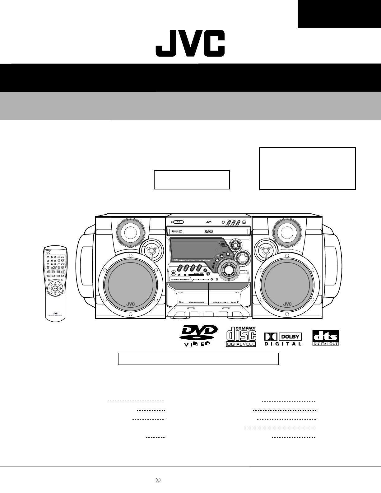
SERVICE MANUAL
COMPACT COMPONENT SYSTEM
MX-DVA5
MX-DVA5
Area suffix
J ---------------------- U.S.A.
Tentative
SP-MXDVA5
/
CA-MXDVA5
STANDBY
STANDBY/ON
COMPACT
DIGITAL VIDEO
PHONES
SELECT
CLOCK
DISPLAY
/
TIMER
REPEAT
REC START
/STOPCDREC START
DISC CHANGE
CD-R/RW PLAYBACK
SOUND
MODE
SUBWOOFER
TUNING
TAPE A
TAPE B
DUBBING
C -------------------- Canada
SP-MXDVA5
LEVEL
CD / DVD Mechanism is exchanged by a unit (contain CPC cords).
Contents
Safety Precautions
Important for laser products
Preventing static electricity
Importance administering
point on the safety
COPYRIGHT 2001 VICTOR COMPANY OF JAPAN, LTD.
1-2
1-3
1-4
1-5
Disassembly method
Wiring connection
Adjustment method
Troubleshooting
Description of major ICs
1-6
1-18
1-19
1-23
1-26~39
No.21032
Sep. 2001
Page 2
MX-DVA5
1. This design of this product contains special hardware and many circuits and components specially for safety
purposes. For continued protection, no changes should be made to the original design unless authorized in
writing by the manufacturer. Replacement parts must be identical to those used in the original circuits. Services
should be performed by qualified personnel only.
2. Alterations of the design or circuitry of the product should not be made. Any design alterations of the product
should not be made. Any design alterations or additions will void the manufacturer`s warranty and will further
relieve the manufacture of responsibility for personal injury or property damage resulting therefrom.
3. Many electrical and mechanical parts in the products have special safety-related characteristics. These
characteristics are often not evident from visual inspection nor can the protection afforded by them necessarily
be obtained by using replacement components rated for higher voltage, wattage, etc. Replacement parts which
have these special safety characteristics are identified in the Parts List of Service Manual. Electrical
components having such features are identified by shading on the schematics and by ( ) on the Parts List in
the Service Manual. The use of a substitute replacement which does not have the same safety characteristics
as the recommended replacement parts shown in the Parts List of Service Manual may create shock, fire, or
other hazards.
4. The leads in the products are routed and dressed with ties, clamps, tubings, barriers and the like to be
separated from live parts, high temperature parts, moving parts and/or sharp edges for the prevention of
electric shock and fire hazard. When service is required, the original lead routing and dress should be
observed, and it should be confirmed that they have been returned to normal, after re-assembling.
5. Leakage currnet check (Electrical shock hazard testing)
After re-assembling the product, always perform an isolation check on the exposed metal parts of the product
(antenna terminals, knobs, metal cabinet, screw heads, headphone jack, control shafts, etc.) to be sure the
product is safe to operate without danger of electrical shock.
Do not use a line isolation transformer during this check.
Plug the AC line cord directly into the AC outlet. Using a "Leakage Current Tester", measure the leakage
current from each exposed metal parts of the cabinet, particularly any exposed metal part having a return
path to the chassis, to a known good earth ground. Any leakage current must not exceed 0.5mA AC (r.m.s.).
Alternate check method
Plug the AC line cord directly into the AC outlet. Use an AC voltmeter having, 1,000 ohms per volt or more
sensitivity in the following manner. Connect a 1,500 10W resistor paralleled by a 0.15 F AC-type capacitor
between an exposed metal part and a known good earth ground.
Measure the AC voltage across the resistor with the AC
voltmeter.
Move the resistor connection to each exposed metal part,
particularly any exposed metal part having a return path to
the chassis, and meausre the AC voltage across the resistor.
Now, reverse the plug in the AC outlet and repeat each
measurement. Voltage measured any must not exceed 0.75 V
AC (r.m.s.). This corresponds to 0.5 mA AC (r.m.s.).
0.15 F AC TYPE
1500 10W
Good earth ground
AC VOLTMETER
(Having 1000
ohms/volts,
or more sensitivity)
Place this
probe on
each exposed
metal part.
!
1. This equipment has been designed and manufactured to meet international safety standards.
2. It is the legal responsibility of the repairer to ensure that these safety standards are maintained.
3. Repairs must be made in accordance with the relevant safety standards.
4. It is essential that safety critical components are replaced by approved parts.
5. If mains voltage selector is provided, check setting for local voltage.
Burrs formed during molding may
be left over on some parts of the
chassis. Therefore, pay attention to
such burrs in the case of
preforming repair of this system.
In regard with component parts appearing on the silk-screen printed side (parts side) of the PWB diagrams, the
parts that are printed over with black such as the resistor ( ), diode ( ) and ICP ( ) or identified by the " "
mark nearby are critical for safety.
When replacing them, be sure to use the parts of the same type and rating as specified by the manufacturer.
(Except the J and C version)
1-2
Page 3
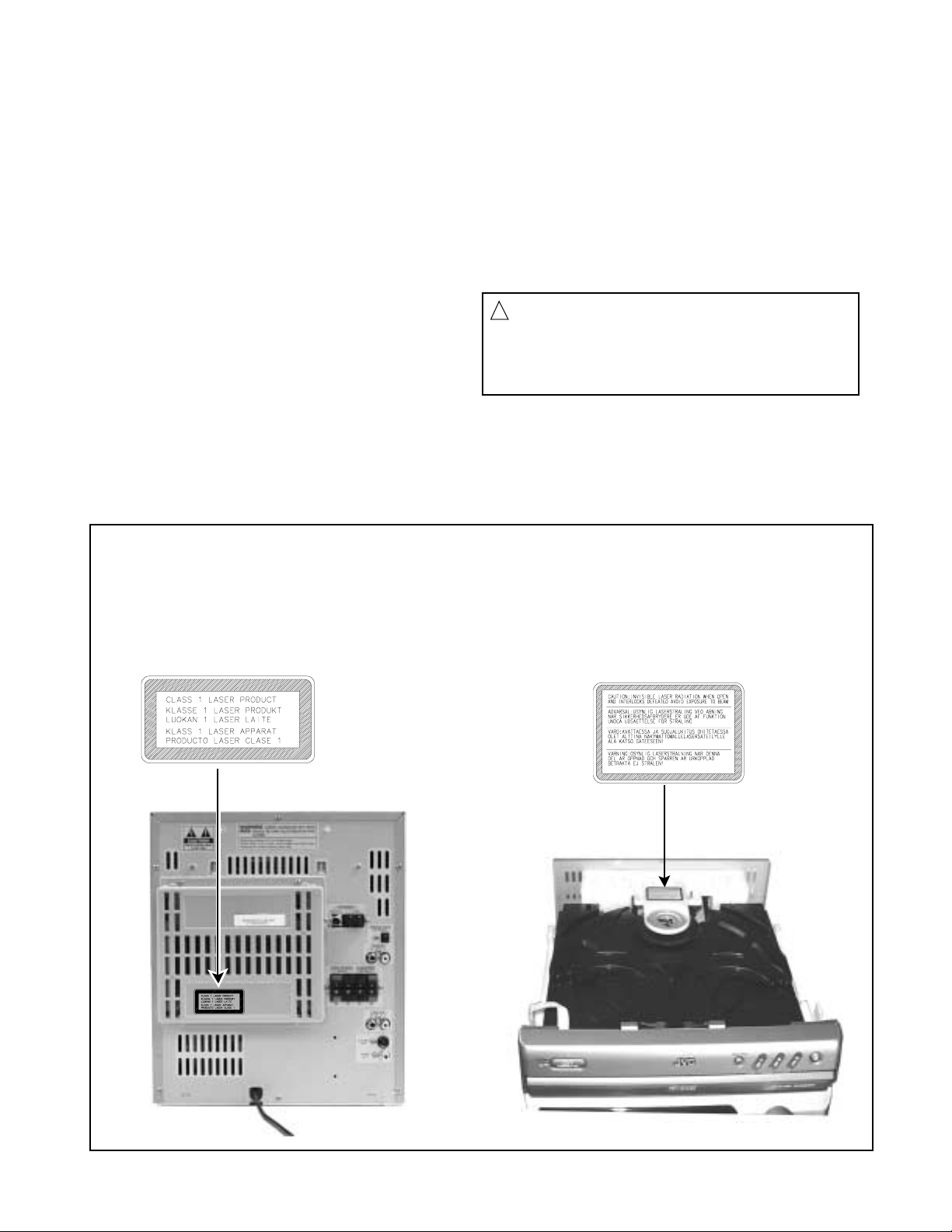
Important for laser products
MX-DVA5
1.CLASS 1 LASER PRODUCT
2.DANGER : Invisible laser radiation when open and inter
lock failed or defeated. Avoid direct exposure to beam.
3.CAUTION : There are no serviceable parts inside the
Laser Unit. Do not disassemble the Laser Unit. Replace
the complete Laser Unit if it malfunctions.
4.CAUTION : The compact disc player uses invisible
laserradiation and is equipped with safety switches
whichprevent emission of radiation when the drawer is
open and the safety interlocks have failed or are de
feated. It is dangerous to defeat the safety switches.
Reproduction and position of labels
5.CAUTION : If safety switches malfunction, the laser is able
to function.
6.CAUTION : Use of controls, adjustments or performance of
procedures other than those specified herein may result in
hazardous radiation exposure.
CAUTION
!
Please use enough caution not to
see the beam directly or touch it
in case of an adjustment or operation
check.
CLASS 1
LASER PRODUCT
WARNING LABEL
1-3
Page 4
MX-DVA5
Preventing static electricity
1. Grounding to prevent damage by static electricity
Electrostatic discharge (ESD), which occurs when static electricity stored in the body, fabric, etc. is discharged,
can destroy the laser diode in the traverse unit (optical pickup). Take care to prevent this when performing repairs.
2. About the earth processing for the destruction prevention by static electricity
In the equipment which uses optical pick-up (laser diode), optical pick-up is destroyed by the static electricity of
the work environment.
Be careful to use proper grounding in the area where repairs are being performed.
2-1 Ground the workbench
Ground the workbench by laying conductive material (such as a conductive sheet) or an iron plate over
it before placing the traverse unit (optical pickup) on it.
2-2 Ground yourself
Use an anti-static wrist strap to release any static electricity built up in your body.
(caption)
Anti-static wrist strap
Conductive material
(conductive sheet) or iron plate
3. Handling the optical pickup
1. In order to maintain quality during transport and before installation, both sides of the laser diode on the
replacement optical pickup are shorted. After replacement, return the shorted parts to their original condition.
(Refer to the text.)
2. Do not use a tester to check the condition of the laser diode in the optical pickup. The tester's internal power
source can easily destroy the laser diode.
4. Handling the traverse unit (optical pickup)
1. Do not subject the traverse unit (optical pickup) to strong shocks, as it is a sensitive, complex unit.
2. Cut off the shorted part of the flexible cable using nippers, etc. after replacing the optical pickup. For specific
details, refer to the replacement procedure in the text. Remove the anti-static pin when replacing the traverse
unit. Be careful not to take too long a time when attaching it to the connector.
3. Handle the flexible cable carefully as it may break when subjected to strong force.
4. It is not possible to adjust the semi-fixed resistor that adjusts the laser power. Do not turn it.
CD / DVD changer unit
Attention when traverse unit is decomposed
Because the CD / DVD mechanism assembly of this model is a
unit component, the individual component parts consisting of
the CD / DVD mechanism assembly are not supplied
separately.
If you need to decompose the traverse unit, short-circuit the
connector of the flexible board by using a metal clip and the like
prior to decomposing the traverse unit.
Soldering
points
Fig.2
Fig.1
Card wire
CD / DVD
holder
mechanism
Pickup unit
connector
1-4
Page 5
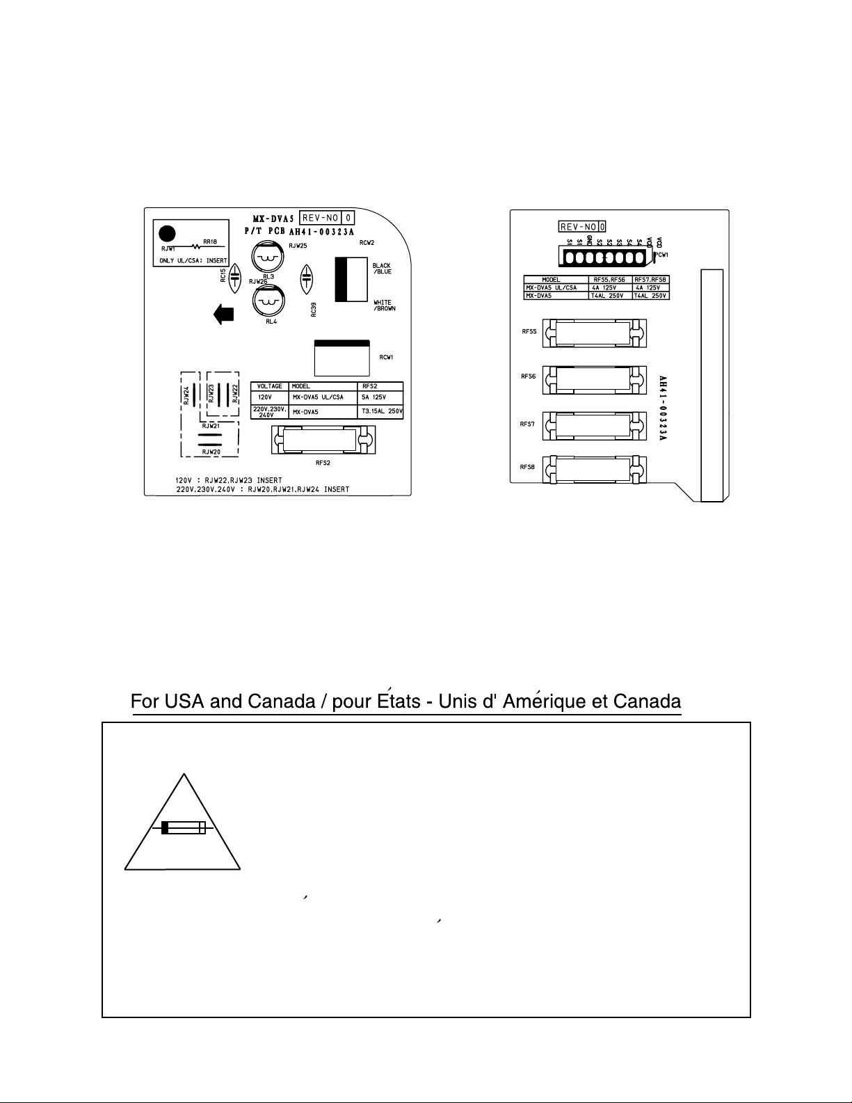
Importance administering point on the safety
MX-DVA5
Primary part
Secondary parts
F101
F102
F103
F001
F104
Caution: For continued protection against risk of
fire, replace only with same type 5A/125V for
F001, 4A/125V for F101,F102,F103, and F104.
This symbol specifies type of fast operating fuse.
Precaution: Pour eviter risques de feux, remplacez
le fusible de surete de F001 comme le meme type
que 5A/125V, et 4A/125V pour F101,F102,F103,
et F104.
Ce sont des fusibles suretes qui functionnes rapide.
^
1-5
Page 6
MX-DVA5
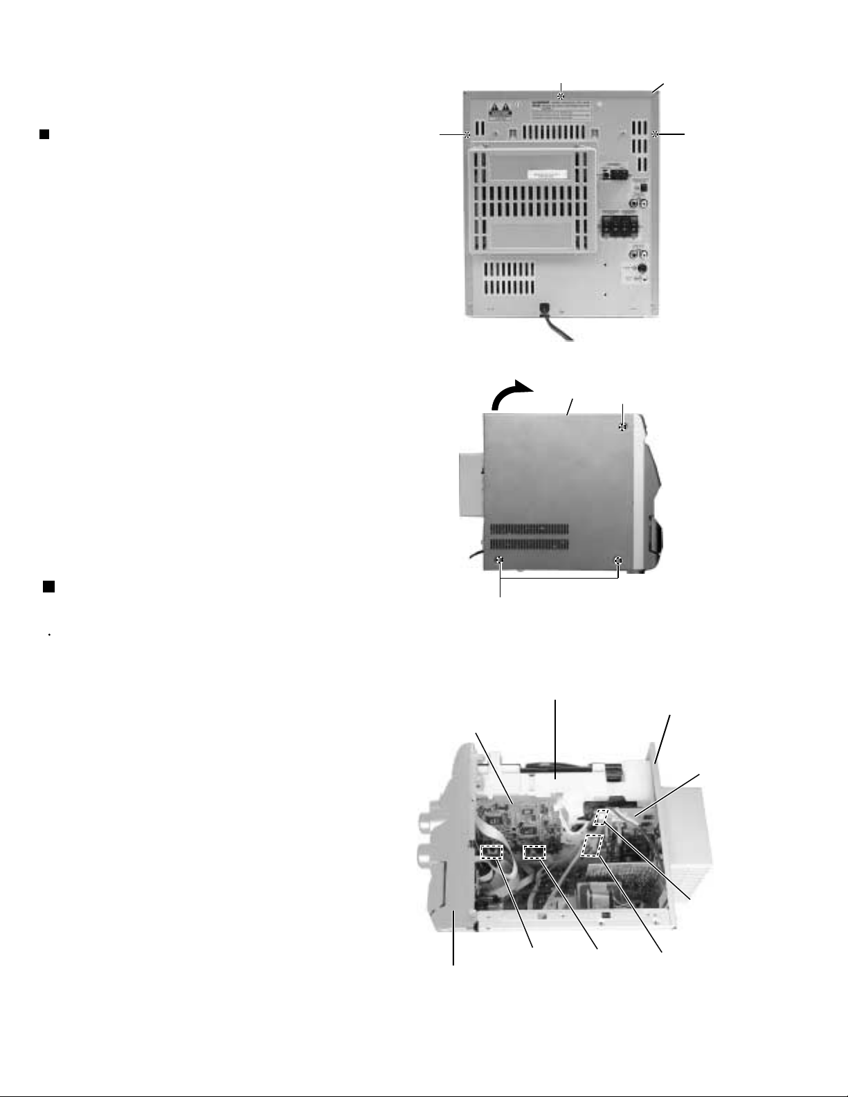
Disassembly method
<Main body>
Removing the metal cover
(See Fig.1 and 2)
1.
Remove the three screws A attaching the metal
cover on the back of the body.
2.
Remove the six screws B attaching the metal cover
on both sides of the body.
3.
Remove the metal cover from the body by lifting the
rear part of the cover.
ATTENTION:
Do not break the front panel tab fitted
to the metal cover.
A
A
Fig.1
Metal cover
Metal cover
A
B
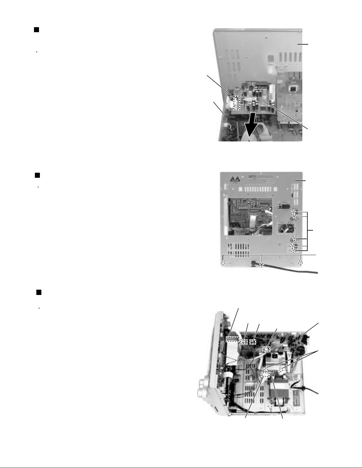
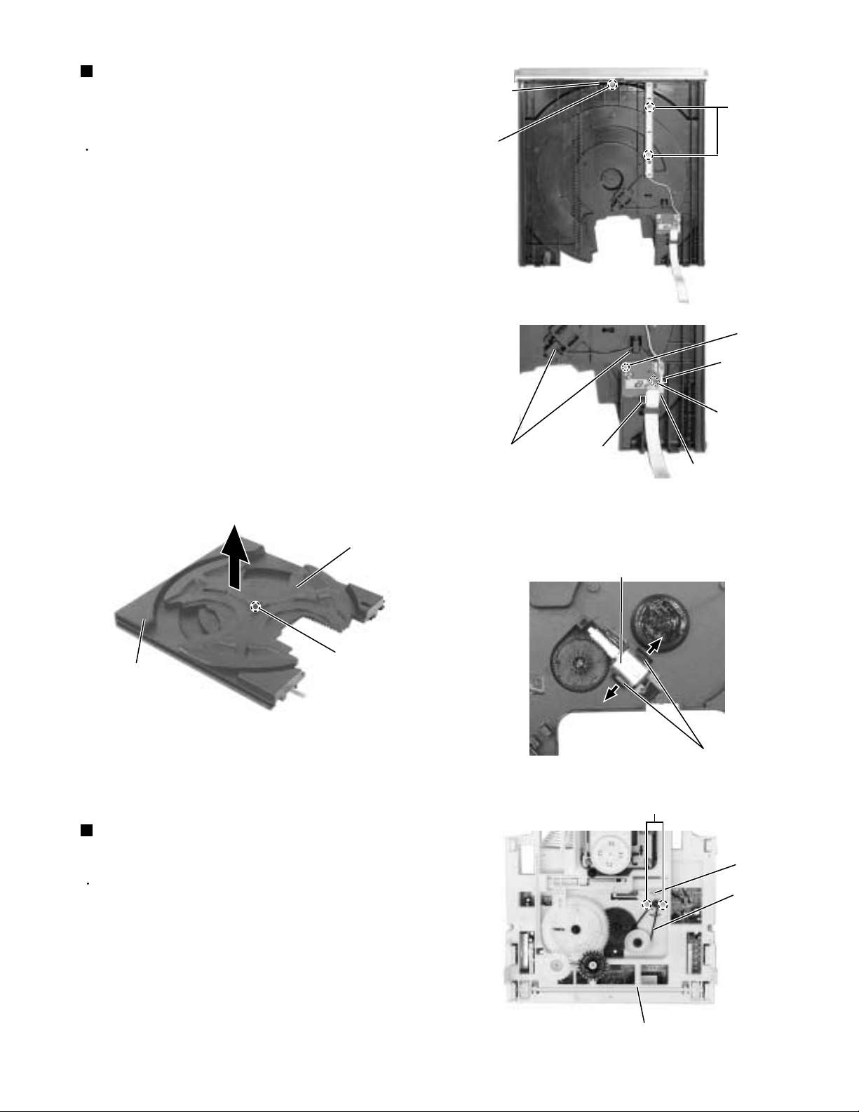
Removing the CD / DVD changer unit
(See Fig.3 to 6)
Prior to performing the following procedure, remove
the metal cover.
1.
Disconnect the card wire which is attached with
adhesive to the left side of the CD / DVD changer
unit.
2.
Disconnect the harness from connector
ACW1,DCW4 and VCW1 of the CD / DVD servo
board on the back of the CD / DVD changer unit.
3.
Disconnect the harness from connector LCW2 and
LCW6 on the DVD power board.
4.
Disconnect the card wire from connector UCW3 on
the FL dispaly & System control board.
5.
Remove the two screws C attaching the CD / DVD
changer unit on the back of the body.
6.
Remove the two screws D attaching the CD / DVD
changer unit on the both side of the body.
CD / DVD
servo
board
Front panel
assembly
B
DCW4 / VCW1
Fig.2
CD / DVD changer unit
ACW1
Rear panel
DVD power
board
LCW6
LCW2
7.
Draw the CD / DVD changer unit upward from
behind while pulling the rear panel outward.
1-6
Fig.3
Page 7
FL dispaly & system
control board
UCW3
Front panel
assembly
MX-DVA5
C
Fig.4
Adhesive card wire strap
CD / DVD changer unit
Rear panel
Fig.6a
Front panel assembly
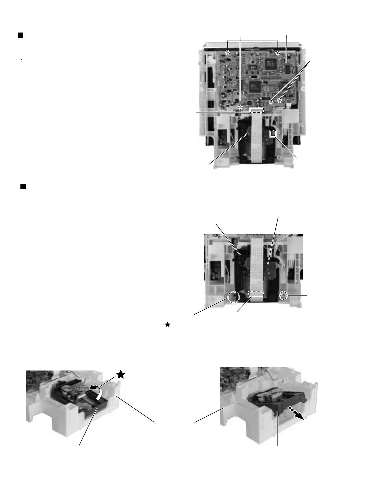
Removing the front panel assembly
(See Fig.7 to 9 )
Prior to performing the following procedure, remove
the metal cover and the CD / DVD changer unit.
1.
Disconnect the card wire from connector FCW3 and
the harness from connector JCW1, JCW2 and
HCW3 on the inner side of the main board in the
body.
D
Rear panel
CD / DVD changer unit
D
Front panel assembly
Fig.6b
FCW3
Fig.5
Rear panel
Main board
JCW2
JCW1
2.
Remove the two screws E attaching the front panel
assembly on both sides of the body.
3.
Remove the screw F attaching the earth terminal
extending from the cassette mechanism assembly.
4.
Remove the screw G attaching the front panel
assembly and main board.
5.
Remove the screw H attaching the front panel
assembly on the bottom of the body.
6.
Release the two joints a on both sides and two joints
b on the bottom of the body using a screwdriver.
Joint a
E
earth wire
HCW3
F
Fig.7
1-7
Page 8
MX-DVA5
Front panel assembly
Main board
G
E
Fig.8
Joint c
Removing the heat sink, amp. board and
DVD power board (See Fig.10 to 12)
Prior to performing the following procedure, remove
the metal cover and the CD / DVD changer unit.
1.
Remove the four screws I attaching the heat sink
cover on the back of the body. Remove the heat sink
cover.
Bottom side
I
Joint b
H
Fig.9
Joint b
2.
Remove the four screws J attaching the heat sink,
amp. board and DVD power board to the rear panel
on the back of the body.
3.
Remove the two screws K attaching the speaker
terminal to the rear panel on the back of the body.
4.
Disconnect the card wire from connector ACW1 and
the harness from connector ACW2 on the amp.
board.
5.
Disconnect the harness from connector LCW5 and
LCW4 on the DVD power board.
6.
After moving the heat sink upward, remove the
claws. Then pull out the heat sink, amp. board and
DVD power board inward.
Rear panel
DVD power board
Heat sink
cover
Rear panel
J
Heat sink
I
Fig.10
Tuner terminal
L
K
1-8
LCW5
ACW2
ACW1
Fig.12
LCW4
Amp. board
J
Speaker terminal
Fig.11
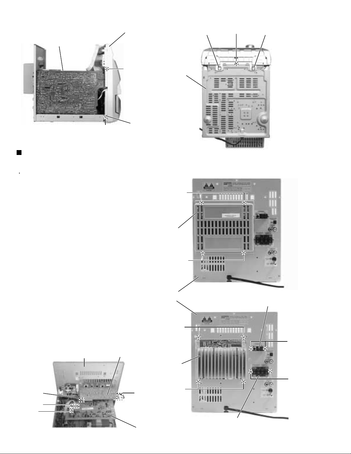
Page 9
Removing the tuner board
(See Fig.11 and 13)
Prior to performing the following procedure, remove
the metal cover and CD / DVD changer unit.
MX-DVA5
Rear
panel
1.
Disconnect the card wire from connector CON01 on
the tuner board.
2.
Remove the two screws L attaching the tuner board.
Removing the rear panel (See Fig.14)
Prior to performing the following procedure, remove
the metal cover, CD / DVD changer unit, heat sink &
Amp. board and tuner board.
1.
Remove the three screws N and five screws M
attaching the rear panel.
CON01
Main board
Tuner board
Fig.13
Rear
panel
M
Removing the main Board
(See Fig. 15)
Prior to performing the following procedure, remove
the metal cover, CD / DVD changer unit, heat sink &
Amp. board tuner board and rear panel.
1.
Disconnect the card wire from connector FCW3 and
the harness from connector JCW1, JCW2, and
HCW3 on the main board.
2.
Disconnect the harness from connector PCW1 on
the power transformer board.
3.
Remove the screw G attaching the main board
holder. (See Fig.8)
4.
Remove the two screws O attaching the heat sink
and bottom chassis.
FCW3
JCW2
PCW1
Fig.14
JCW1
HCW3
Power transformer board
N
Main board
O
Fig.15
1-9
Page 10
MX-DVA5
Removing the power ICs and DVD power
board (See Fig.16 to 18)
Prior to performing the following procedure, remove
the metal cover, CD / DVD changer unit, heat sink,
amp. board and DVD power board.
1.
Remove the four screws P attaching the power ICs
to the heat sink.
2.
Unsolder the power ICs solder point.
3.
Remove the three screws Q and three screws R
attaching the DVD power board to the heat sink.
Heat sink
R
Amp. board
Heat sink
DVD power board
Power ICs solder point
Q
P
Fig.16
Amp. board
Fig.18
DVD power board
Removing the power transformer
(See Fig .19)
Prior to performing the following procedure, remove
the metal cover, CD / DVD changer unit, heat sink &
Amp. board, tuner board and rear panel.
1.
Disconnect the power cord from connector RCW2 of
the power transformer board.
2.
Disconnect the harness from connector PCW1 of the
power transformer board.
3.
Remove the four screws S attaching the power
transformer.
Power transformer
S
Power cord
Fig.17
Heat sink
PCW1
S
RCW2
1-10
Fig.19
Page 11
MX-DVA5
<Front panel assembly>
Prior to performing the following procedure, remove
the metal cover, the CD / DVD changer unit and the
front panel assembly.
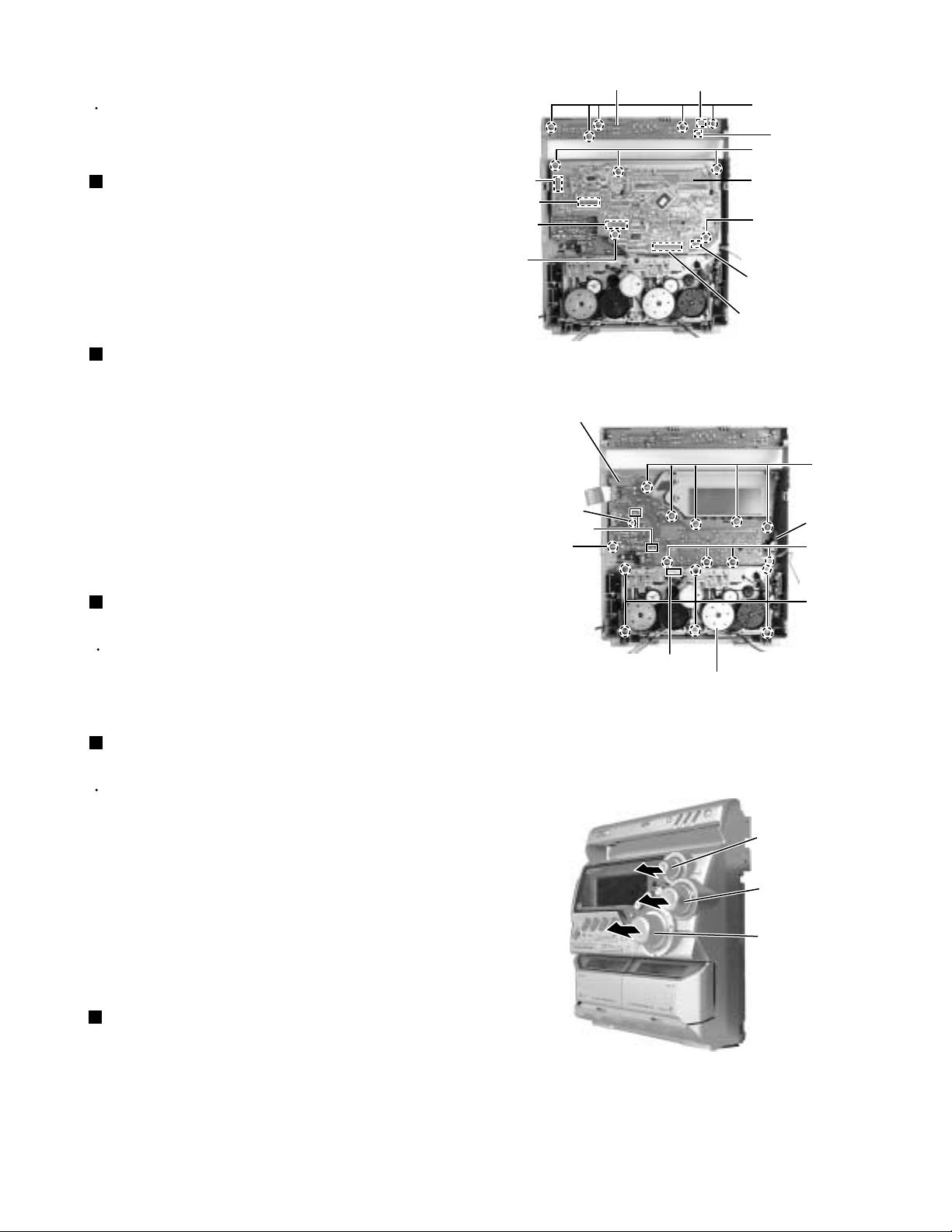
Removing the power / DVD switch board
(See Fig.20)
1.
Disconnect the card wire from connector UCW1 of
the power / DVD switch board.
2.
Remove the five screws T attaching the power / DVD
switch board and release the tab c outward.
Removing the FL display & System
control board (See Fig.20)
1.
Disconnect the card wire from the connector UCW3,
UCW4,UCW5 and UCW6 on the FL display &
System control board.
2.
Remove the five screws U attaching the FL display &
System board.
3.
Disconnect the card wire from the connector UCW2
on the FL display & System control board.
Power / DVD switch board
UCW2
UCW3
UCW4
U
Fig.20
Front board
V
Tab d
V
UCW1
T
Tab c
U
FL diplay & System
control board
U
UCW5
UCW6
V
Headphone
board
V
Removing the headphone board
(See Fig.21)
Prior to performing the following procedure remove
the FL display & System control board.
1.
You can pull out the headphone board.
Removing the front board
(See Fig. 21 and 22)
Prior to performing the following procedure, remove
the FL display & System control board.
1.
Pull out the volume knob, subwoofer level knob and
sound mode nob from front side.
2.
Remove the eleven screws V attaching the front
board and release the two tabs d outward.
Removing the cassette mechanism
assembly (See Fig.21)
W
Card wire e
Cassette mechanism assembly
Fig.21
SOUND MODE
knob
SUBWOOFER
LEVEL knob
VOLUME knob
1.
Disconnect the card wire e from the mechanism
board on the cassette mechanism assembly.
2.
Remove the six screws W attaching the cassette
mechanism assembly.
Fig.22
1-11
Page 12
MX-DVA5
<CD / DVD changer unit>
Prior to performing the following procedure, remove
the CD / DVD changer unit.
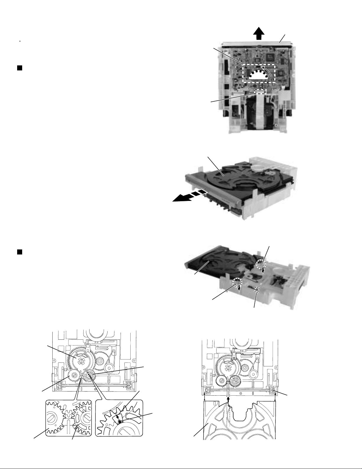
Removing the CD / DVD tray
(See Fig.1 to 3)
1.
Disconnect the card wire from connector RCW1 of
the CD /DVD servo board.
2.
Turn the black loading pulley gear on the under side
of the CD / DVD changer unit in the direction of the
arrow and draw the CD / DVD tray toward the front
until it stops.
3.
Disconnect the card wire from connector DCW1 of
the CD / DVD servo board on the upper side of the
CD / DVD changer unit.
4.
Push down the two tray stoppers marked a and pull
out the CD / DVD tray.
CD / DVD tray
Loading pulley
gear
CD / DVD
servo board
RCW1
Fig.1
CD / DVD tray
Reinstall the CD / DVD tray
(See Fig.4 and 5)
1.
Align the gear-cam with the gear-tray as shown fig.3,
then mount the CD / DVD tray.
2.
When assembling the CD / DVD tray, take extreme
care not engage with gear - synchro.
Gear-cam
Gear-tray
Gear-convert
Gear-cam
timing point
CD / DVD tray
(Tray stopper)
Fig.2
a (Tray stopper)
a
CD / DVD
servo board
DCW1
Fig.3
Gear-synchro
Gear-convert
1-12
Gear-tray
Gear-tray
CD / DVD tray
Fig.4 Fig.5
Page 13
Removing the sensor board, the LED
board and the turn table motor assembly
(See Fig.6 to 9)
MX-DVA5
LED board
B
Prior to performing the following procedure, remove
the CD / DVD tray.
1.
Remove the screw A attaching the LED board and
release the screws B attaching the bracket.
2.
Remove the screw C attaching the sensor board and
release the two tabs b attaching the sensor board on
the under side of the CD / DVD tray.
3.
Disconnect the harness from connector on the
sensor board and release the harness from the two
hooks c. Remove the sensor board.
4.
Remove the screw D attaching the turn table. Detach
the turn table from the tray.
5.
Pull outward the tab marked d attaching the turn
table motor assembly on the upper side of the tray
and detach the turn table motor assembly from the
tray.
Turn table
A
Tab c
Fig.6
C
Tab b
Connector
Tab b
Sensor board
Fig.7
Tray
Fig.8
D
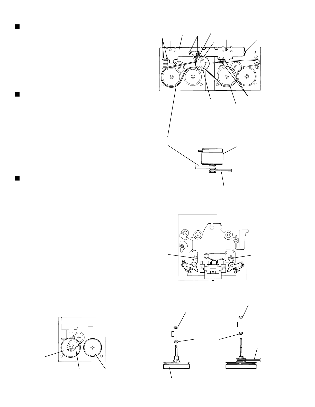
Removing the belt, and the motor
(See Fig.10)
Prior to performing the following procedure, remove
the CD / DVD tray.
1.
Detach the belt from the pulley on the upper side of
the CD / DVD changer unit (Do not stain the belt with
grease).
Turn table motor assembly
Fig.9
Tab d
D
Motor
Belt
2.
Remove the two screws D attaching the motor.
CD / DVD changer unit
Fig.10
1-13
Page 14
MX-DVA5
Removing the CD / DVD servo board
(See Fig. 12)
Prior to performing the following procedure, remove
the CD / DVD tray, the two screws attaching the
motor and detach the belt from the pulley.
1.
Unsolder points the motor terminal.
2.
Disconnect the card wire from the connector RCW1
on the CD / DVD servo board.
3.
Disconnect the motor board wire from the motor
board connector on the motor board.
4.
Remove the three screws D attaching the CD / DVD
servo board.
Removing the CD / DVD mechanism
holder assembly (mechanism included)
(See Fig.12 to 14)
1.
Disconnect the motor wire from connector on the
motor board in the CD / DVD mechanism holder
assembly on the under side of the CD / DVD
changer unit.
2.
Disconnect the card wire from connector on the
pickup unit in the CD / DVD mechanism holder
assembly.
RCW1
Motor board
CD / DVD mechanism
D
holder assembly
CD / DVD servo board
Solder
points
Motor board
connector
Fig.11
Motor board
3.
Remove the screw E attaching the shaft on the right
side of the CD / DVD mechanism holder assembly.
4.
Pull outward the stopper fixing the shaft on the left
side and remove the CD / DVD mechanism holder
assembly from behind in the direction of the arrow .
5.
Pull out the CD / DVD mechanism holder assembly.
CD/ DVD changer unit
CD / DVD mechanism holder assembly
Fig.13
Stopper
E
Connecter
Fig.12
CD / DVD mechanism holder assembly
Fig.14
1-14
Page 15
MX-DVA5
<Cassette mechanism section>
Removing the record/playback mechanism.
Removing the R/P head.
1.
Remove the screw A on the right side of the
R/P head.(Fig.1)
2.
Remove the screw B on the left side of the
R/P head.(Fig.1)
Removing the pinch roller.
1.
Pull out the pinch roller by opening the pinch
roller stopper outward to unlock .(Fig.2)
2.
When reassembling the pinch roller, refer to
fig. 3 to hook up the spring.
R/P Head
Pinch roller
Fig.1
AB
Pinch roller
assembly
Pinch roller
stopper
Stopper
Return spring
Return spring
Fig.2
Pinch roller
Return spring
Fig.3
Pinch roller
spring
1-15
Page 16
MX-DVA5
Removing the motor.
1.
Remove the two screws C fixing the motor.
Be careful to grease's splash when the
drive belt comes off.(Fig.4, Fig.5)
2.
Unsolder the motor terminal.(Fig.4)
Removing the mechanism board.
Unsolder the four parts a on the solenoid
1.
coil terminal.(Fig.4)
Remove the two screws D fixing the board.(Fig.4)
2.
Unhook the three parts b from the board.(Fig.4)
3.
Remove the mechanism board.(Fig.4)
4.
Mecha.
a
Drive belt (Flat)
board
D
b
Motor
Motor
terminal
C
C
Fig.4
D
Drive belt
Motor
b
a
Removing the flywheel.
Remove the cut-washers at c and d from the
capstan shaft, then remove the flywheel.
When reassembling the flywheel,
be sure to use new washers as they
cannot be reused. (Fig.7, Fig.8)
Capstan
washer
Drive belt
Fig.5
Capstan
washer
Fig.6
c
Sleeve
d
1-16
Flywheel
FR belt
Fig.7
Flywheel
Sleeve
Flywheel
Washer
FR belt
Fig.8
Page 17
< Speaker section >
MX-DVA5
Removing the side panel (See Fig. 1)
1.
Remove the five screws A and B attaching the side
panel, then remove the side panel.
Removing the side speaker
(See Fig. 2 and 3)
B
Side panel
A
B
Fig.1
Side speaker
C
Front panel
Prior to performing the following procedure, remove
the side panel.
1.
Remove the fore screws C attaching the side
speaker.
2.
Pull out the side speaker and remove the speaker
cord from the speaker terminal.
C
Fig.2
Side speaker
Speaker terminal
Fig.3
1-17
Page 18
MX-DVA5
Wiring connection
Amp board
3711-001167
3809-000492
3809-001228
ACW2
3809-001224
CD key switch board
UCW1
3711-000820
ACW3
ACW1
3708-001094
UCW7
0
9
3809-001185
MIC board
3708-000181
Front key switch board
2
0
AH39-20008M
MCW3
AH39-00254A
AH39-00244A
AH39-00248A
MCW2
3711-000190
0
9
0
3711-003112
3708-000178
UCW2
UCW3
3708-001212
Front / Display board
RCW2
RFS3
RFS5
RFS6
RFS7
PCW1
UCW4
3708-000451
3708-001488
UCW5
3708-000492
RFS4
RFS8
UCW6
RFS2
Power transformer
Motor board
board
Roller
CD/DVD tray
AH39-00096C
3809-001185
AH39-00097A
Pickup unit
3809-001225
Color codes are shown below.
1 Brown
2 Red
3 Orange
4 Yellow
5 Green
6 Blue
9
0
7 Violet
8Gray
9 White
0 Black
2
9
0
8
0
2
9
9
0
2
9
8
0
0
8
9
9
0
DCW1
ACW3
AH39-00097A
LCW4
LCW5
3711-000988
LCW2
LCW6
3711-000988
0
PCW1
3711-001095
LCW1
2
MCW1
ACW1
CD/DVD board
VCW1
DCW4
DVD Power board
9
0
2
0
9
9
2
0
8
0
9
2
2
0
9
1-18
3809-001237
3809-001222
CW302
Voice board
CW301
Tuner board
CON1
3710-000209
9
0
2
2
9
0
FCW1
3708-000122
OCW
3711-000907
RCW6
3711-000907
JCW1
Main board
JCW2
FCW3
3708-000258
KCW2
FCW2
3711-001557
KCW1
3708-001094
3711-003107
JCW3
3711-003111
RW2
HCW3
RW1
3711-001062
0
VCW1
2
9
0
9
0
9
8
2
9
8
0
8
0
9
2
0
9
8
0
9
9
0
0
9
AH39-00022A
0
HCW2
AH39-00247A
9
E.phone J.board
Cassette mechanism
9
0
0
9
9
0
2
88
0
0
2
0
AH39-00202A
2
9
Page 19
TESTER
MAIN
PCB
VT GND
Adjustment method
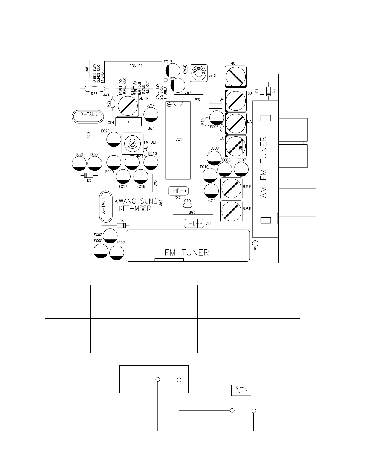
1. Tuner
MX-DVA5
ITEAM
Received FREQ.
Adjustment
point
Output
* Adjustment Location of Tuner PCB
AM(MW) OSC
Adjustment
530~1710 KHz
MO
1~7.0 V
AM(MW) RF
Adjustment
594 KHz
MA
Maximum
Output(Fig1-4)
LW OSC
Adjustment
146~290 KHz
2~7.0 V
Fig 1-4 OSC Voltage
LO
AM(MW) RF
Adjustment
150 KHz
LA
Maximum
Output(Fig1-4)
1-19
Page 20
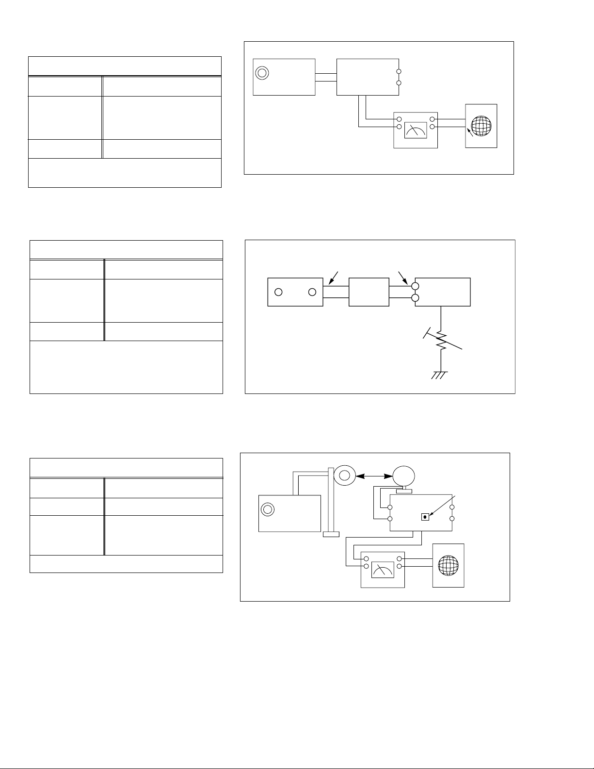
MX-DVA5
FM THD Adjustment
SSG FREQ.
98 MHz
Adjustment
point
FM DETECTOR COIL
(FM DET)
Output
60 dB
Minumum Distortion (0.4% below)
(Figure 1-1)
FM Search Level Adjustment
SSG FREQ.
Adjustment
point
(SVR1)
Output
BEACON
SENSITIVITY
SEMI-VR(20K)
98 MHz
28 dB
Output
GND
FM S.S.G
FM
Antenna
Terminal
Speaker
Terminal
SET
Input
output
Distortion Meter
Figure1-1 IF CENTER and THD Adjustment
FM Antenna
SET
FM IN
FM S.S.G
28 dB
GND
Oscilloscope
Input
Adjust SVR1 so that “TUNED” of FL T
is lighted (Figure 1-2)
*Adjust FM S.S.G level to 28dB
AM(MW) I.F Adjustment
SSG FREQ.
Frequency
450 kHz
530 kHz
Adjustment
point
AM IF
Maximum output (Figure 1-3)
Figure1-2 FM Auto Search Level Adjustment
60cm
OUTPUT
AM SSG
450KHZ
INPUT
AM ANT
IN
Speaker Terminal
OUTPUT
VTVM Oscilloscope
Figure1-3 AM I.F Adjustment
20 k
AM IF
1-20
Page 21
2 Cassette Deck
2-1 To Adjust Tape Speed
MX-DVA5
Notes
1) Measuring tape : i) VT712
(Tapes recorded with 3kHz)
ii) AC-225
2) Connect the cassette deck to the frequency counter
as in figure 1-5.
Step
Item
Pre-Setup
Condition
Pre-Setup
1) Deck 1:VT712
TAPE
1
SPEED
Control
REVERSE PLAY
OUT
(connected
to the frequency
counter)
Recording /Play head
AZIMUTH control screw
2) Press PLAY
SW button
3) Deck 2:Same
as above
REVERSE PLAY
(FORWORD)
Cassette Deck
SPK OUT
To Adjust
Turn VSR1 to
left and right
(FRONT board)
Cassette Deck
SPK OUT
(GND)
Figure 1-5
VTVM
In Out
Figure 1-7
Frequency Counter
Standard
3KHz 30Hz
Oscilloscope
output
Remark
Figure 1-6
Audio OSC.
SET
(MAIN PCB)
IN
AUX IN
LINE OUT
TP
JCW3
Figure 1-8
VTVM
IN OUT
Oscilloscope
1-21
Page 22
MX-DVA5
2-2 T o Adjust Playback Level/REC
Notes
1) Before the actual adjustment, clean the play/recording
head.
2) Measuring tape :
i) VT-703 ( 10kHz AZIMUTH control)
ii) AC-225
3) The cassette deck is connections as shown in figure 1-7.
1. Adjust Deck A Play Level
Step
Item
AZIMUTH1
Pre-Setup
Condition
SPK OUT
(VTVM is
connected to
the scope)
Pre-Setup
After putting VT703 into Deck A
1) Press FWD PLYA
button.
2) Press RVS PLAY
button.
2. Adjust Deck B Play Level/REC BIAS
Step
Item
AZIMUTH1
Pre-Setup
Condition
SPK OUT
(VTVM is
connected to
the scope)
Pre-Setup
After putting VT703 into Deck B
1)Press FWD PLAY
button.
2)Press RVS PLAY
button.
To Adjust
Turn the control
screw to as shown
in Figure 1-6.
To Adjust
Turn the control
screw to as shown
in Figure 1-6.
Standard
Max output
and same phase
(both channels)
Standard
Max output
and same phase
(both channels)
Remark
After adjustment
secure it with
REGION LOCK.
Adjust AZIMUTH
when you
exchange the
head.
Remark
After adjustment
secure it with
REGION LOCK.
Adjust AZIMUTH
when you
exchange the
head.
1-22
2
Recording
Bias
Voltage
Fig 1-8
After putting AC225 into Deck B
1)Press REC PLYA
button.
2)MAIN board JCW3,
connectted to VTVM
Turn JSR2L,JSR2R
to the right and left
7mV
Page 23
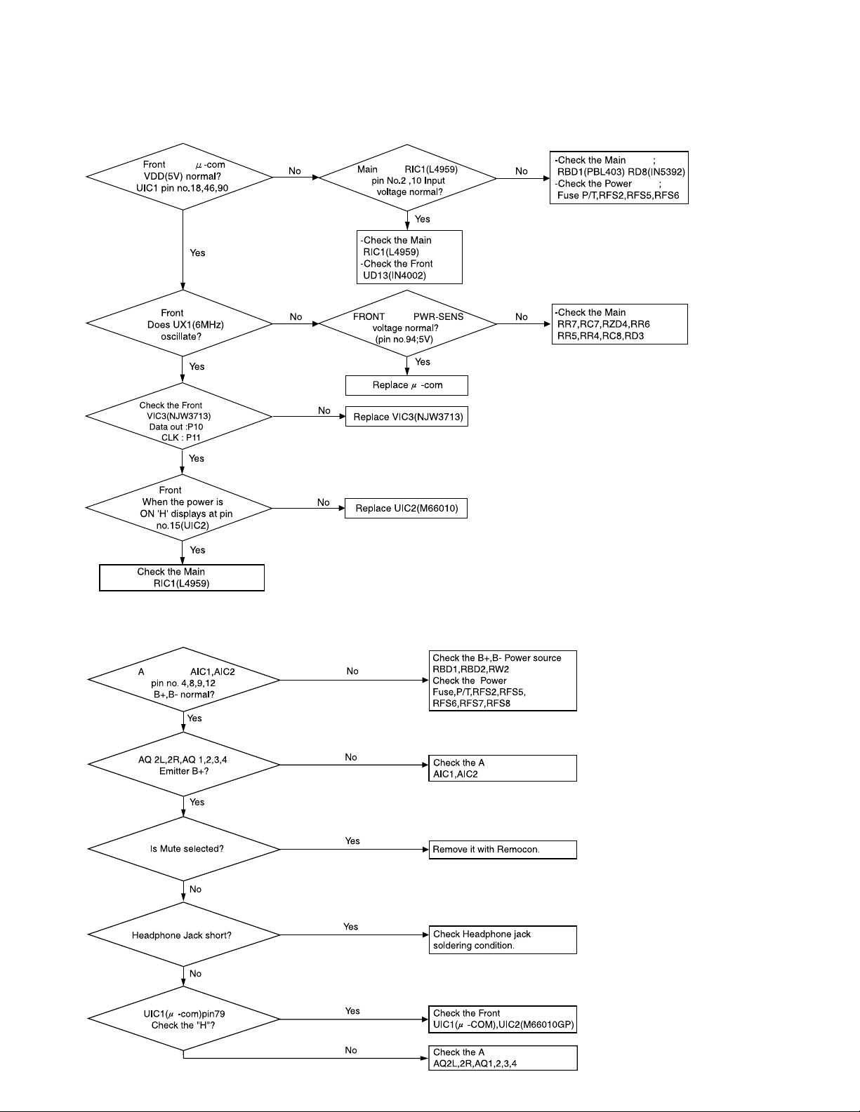
Troubleshooting
1. Amplifier
Power Malfunction
MX-DVA5
board
board
board
board
board
board
board
board
No Output
mp.
board
board
mp.
board
board
mp.
board
board
1-23
Page 24
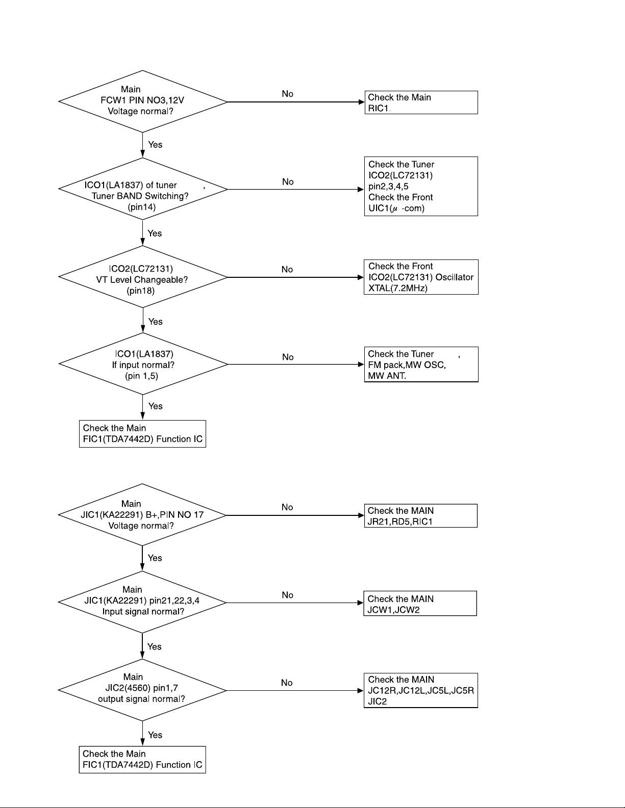
MX-DVA5
2. Tuner Malfunction (FM/AM)
board
board
board
board
board
board
board
3. Tape
board
board
board
board
board
board
board
1-24
board
Page 25
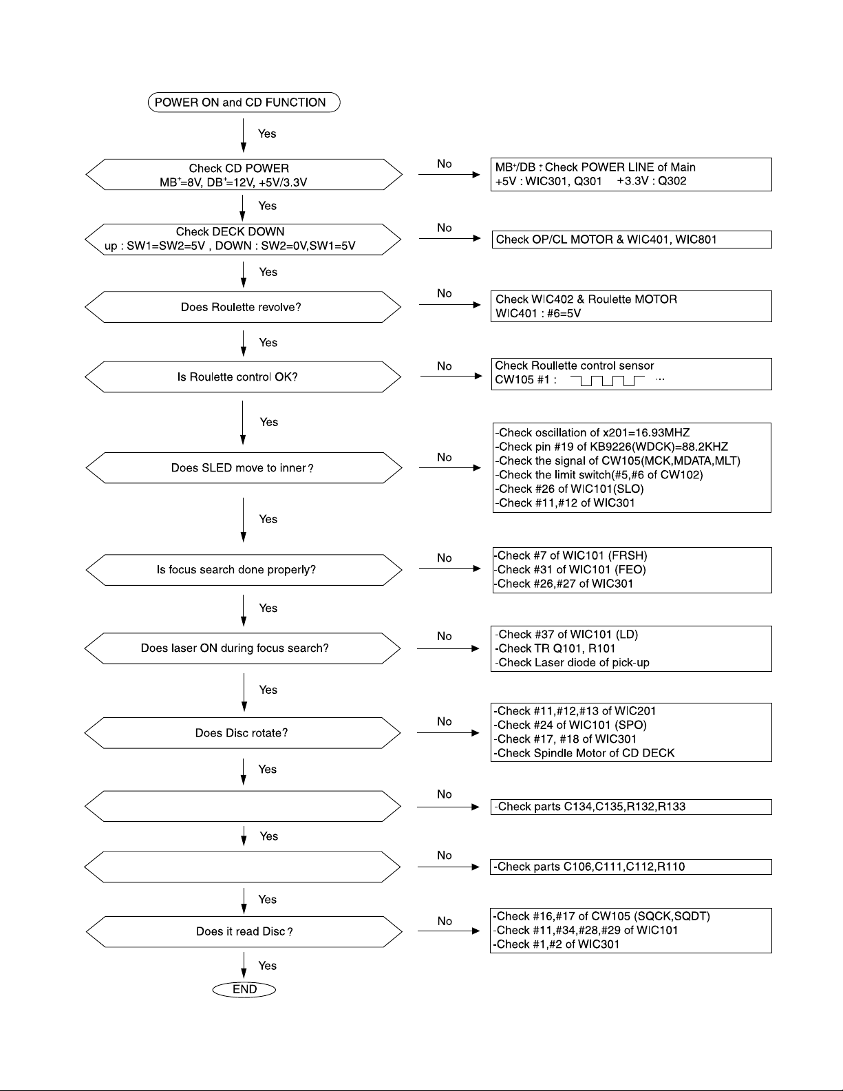
4. CD
MX-DVA5
board
Is state of rotation proper?
Is signal of RAO proper?
(#2, #3, #4, #5 of WIC101)
1-25
Page 26
MX-DVA5
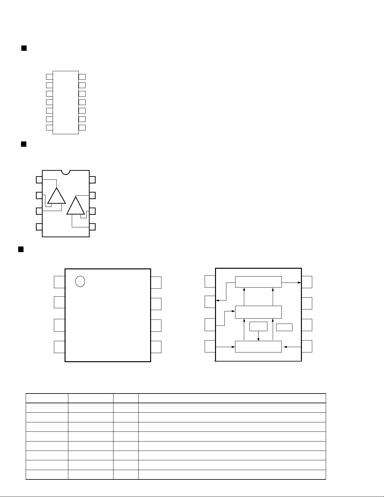
Description of major ICs
74HCU04 (VIC6) : Optical
1.Pin layout
1A 1 14 Vcc
1Y 2 13 6A
2A 3 12 6Y
2Y 4 11 5A
04U
3A 5 10 5Y
3Y 6 9 4A
GND 7 8 4Y
BA4560 (AIC1, AIC2, AIC2, AIC4, AIC5, AIC6, AIC7, FIC4, FIC5, HIC1, JIC3) : Op. amp.
1.Pin layout
OUT1
– IN1
+ IN1
V
1
2
1ch
+
–
3
EE
4
2ch
+
VCC
8
OUT2
7
– IN2
6
–
+ IN2
5
FAN8082 (DIC3,DIC3) : DC motor driver
1.Pin layout
1
GND
V
O1
2
FAN8082
V
CTL
3
V
IN1
4
2. Block diagram
8
V
O2
7
PV
CC
GND
V
O1
1
2
DRIVER OUT
PRE DRIVER
V
CTL
6
SV
CC
5
V
IN2
3
V
IN1
4
TSD
LOGIC SWITCH
BIAS
8
V
O2
7
PV
CC
6
SV
CC
5
V
IN2
1-26
3. Pin function
Pin Number Pin Name I/O Pin Function Description
1 GND - Ground
2V
3V
4V
5V
6SV
7PV
8V
O1
CTL
IN1
IN2
CC
CC
O2
O Output 1
I Motor speed control
I Input 1
I Input 2
- Supply voltage (Signal)
- Supply voltage (Power)
O Output 2
Page 27

BA5983FM (DIC1) : CD-ROM 4ch BTL Driver
1.Pin layout
BIAS
OPIN1(-)
OPIN18(+)
OPOUT8(-)
OPIN2(+)
OPIN2(-)
OPOUT2(-)
1
2
3
4
5
6
7
MA5983FM
28
27
26
25
24
23
22
PreVcc
OPIN4(+)
OPIN4(-)
OPOUT4
OPIN3(+)
OPIN3(-)
OPOUT3
MX-DVA5
2.Block diagram
+
Vcc
GND
STBY1
PowVcc1
VO2(-)
VO2(+)
VO1(-)
VO1(+)
262728
–
10
11
12
13
14
8
9
2425
23
–
+
21
20
19
18
17
16
15
GND
STBY2
PowVcc
VO3(-)
VO3(+)
VO4(-)
VO4(+)
22
21
20
Vcc
19
1718
+
+
–
16
–
–
15
+
+
–
STAND BY
CH 4
–
+
–
+
+
–
+
–
Level
shift
Level
shift
Level
shift
Level
shift
2 3 4 5 6
1
3.Pin function
1
Symbol
BIAS IN
Pin No.
2
3
OPOUT
4
OPIN2
5
OPIN2
6
OPOUT2
7
8
STBY1
9
PowVcc1
10
11
12
13
14
+
–
OPIN
OPIN
GND
VO2
VO2
VO1
VO1
+
–
I/O
Input for Bias-amplifier
I
Non inverting input for ch1
I
Inverting input for ch1
I
Output for ch1 op-amp
O
Non inverting input for ch2
I
Inverting input for ch2
I
Output for fh2 op-amp
O
Substrate ground
Input for ch1/2/3
I
Vcc for ch1/2 power block
Inverted output of ch2
O
Non inverted output of ch2
O
Inverted output of ch1
O
Non inverted output of ch1
O
Function
STAND BY
CH 1/2/3
Vcc
7
8
Pin No.
15
16
17
18
19
20
21
22
23
24
25
26
27
28
9
Symbol
VO4
VO4
VO3
VO3
PowVcc2
STBY2
GND
OPOUT3
OPIN3
OPIN3
OPOUT4
OPIN4
OPIN4
PreVcc
10
I/O
O
O
O
O
I
-
O
I
I
O
I
I
-
–
+
+
12
11
Function
Non Inverted output of ch4
Inverted output of ch4
Non inverted output ch3
Inverted output of ch3
Vcc for ch3/4 power block
Input for ch4 stand by control
Substrate ground
Output for ch3 op-amp
Inverting input for ch3 op-amp
Non inverting input for ch3
Output for ch4 op-amp
Inverting input for ch4 op-amp
Non inverting input for ch4
Vcc for pre block
–
–
+
13
+
–
14
1-27
Page 28

MX-DVA5
FAN8082 (DIC2,DIC3) : DC motor driver
1.Pin layout
2. Block diagram
GND
V
O1
1
2
8
V
O2
7
PV
CC
GND
V
O1
1
2
DRIVER OUT
PRE DRIVER
FAN8082
V
V
CTL
V
IN1
3
4
6
SV
CC
5
V
IN2
3. Pin function
Pin Number Pin Name I/O Pin Function Description
1 GND - Ground
2V
3V
4V
5V
6SV
7PV
8V
O1
CTL
IN1
IN2
CC
CC
O2
O Output 1
I Motor speed control
I Input 1
I Input 2
- Supply voltage (Signal)
- Supply voltage (Power)
O Output 2
CTL
V
IN1
3
4
TSD
LOGIC SWITCH
BIAS
8
V
O2
7
PV
CC
6
SV
CC
5
V
IN2
1-28
Page 29

KA3082 (LIC1, LIC2) : Bidirectional DC motor driver
1.Pin layout
KA3082
MX-DVA5
2.Pin function
Pin No.
1 GND - Ground
2V
3V
4V
5V
6V
7SV
8PV
9V
10 V
GND V
12345678910
Symbol
O1
Z1
CTL
IN1
IN2
CC
CC
Z2
O2
V
O1
I/O Function
O Output 1
- Phase compensation
I Motor speed control
I Input 1
I Input 2
- Supply voltage (Signal)
- Supply voltage (Power)
- Phase compensation
O Output 2
V
Z1
CTLVIN1
V
IN2
SV
CC
PV
CCVZ2
V
O2
3.Block diagram
BIAS
1234
GND
O1
V
V
Z1
V
CTL
DRIVER OUT
PRE DRIVER
LOGIC SWITCH
5
V
IN1
678910
V
IN2
SV
CC
TSD
PV
CC
Z2
V
O2
V
1-29
Page 30

MX-DVA5
KM416C256D (SIC1) : CMOS DRAM
1.Pin layout
VCC
DQ0
DQ1
DQ2
DQ3
V
DQ4
DQ5
DQ6
DQ7
N.C
N.C
RAS
N.C
A0
A1
A2
A3
V
CC
W
CC
1
2
3
4
5
6
7
8
9
10
11
12
13
14
15
16
17
18
19
20
40
39
38
37
36
35
34
33
32
31
30
29
28
27
26
25
24
23
22
21
VSS
DQ15
DQ14
DQ13
DQ12
V
SS
DQ11
DQ10
DQ9
DQ8
N.C
LCAS
UCAS
OE
A8
A7
A6
A5
A4
V
SS
2. Pin function
Pin No.
16~19
22~26
2~5
7~10
31~34
36~39
Symbol
A0~A3
A4~A8
DQ0~3
DQ4~7
DQ8~11
DQ12~15
35,40
14
28
29
UCAS
LCAS
13
27
1,20
11,12
Vss
RAS
W
OE
Vcc
N.C
I/O
Function
I
Address Inputs
I
Address Inputs
I/O
Data In/Out
I/O
Data In/Out
I/O
Data In/Out
I/O
Data In/Out
-
Ground
-
Row Address Strobe
-
Upper Column Address Strobe
--
Lower Column Address Strobe
I
Read/Write Input
O
Data Output Enable
-
Power(+5V)
-
Power(+3.3V)
-
No Connection
3. Block diagram
RAS
UCAS
LCAS
W
A0~A8
Control
Clocks
Refresh Timer
Refresh Control
Refresh Counter
Row Address Buffer
Col. Address Buffer
VBB Generator
Row Decoder
Memory Array
262,144 x16
Cells
Column Decoder
Vcc
Vss
Lower
Data in
Buffer
Lower
DQ0
to
DQ7
Data out
Buffer
Upper
OE
Data in
Buffer
Sense Am ps & I/O
Upper
DQ8
to
DQ15
Data out
Buffer
1-30
Page 31

L4959 (RIC1) : Voltage regulator
1.Pin layout
MX-DVA5
TAB CONNECTED TO PIN 6
2.Block diagram
2/10
V
S
EN 8V
EN 12V(a)
EN 12V(b)
8
7
5
REF
GEN
11
10
9
8
7
6
5
4
3
2
1
D97AU716A
OUT 12V(a)
V
S
OUT 8.6V
EN 8.6V
EN 12V(a)
GND
EN 12V(b)
N.C.
OUT 5.6V
V
S
OUT 12V(b)
5.6V, 250mA
3
OUT 5.6V
REGULATOR
8.6V, 600mA
REGULATOR
9
OUT 8.6V
SWITCHED
12V, 800mA
REGULATOR
11
OUT 12V(a)
SWITCHED
12V, 1.3A
REGULATOR
1
OUT 12V(b)
SWITCHED
D97AU569C
3.Pin function
Pin No. Function
1 OUT 12V (b) 12V/1.3A SWITCHED OUTPUT VOLTAGE
2V
3 OUT 5.6V 5.6V/250mA OUTPUT VOLTAGE
4 N.C. not connected
5 EN 12V (b) Enable 12V/1.3A SWITCHED OUTPUT VOLTAGE
6 GND Ground
7 EN 12V (a) Enable 12V/0.8A SWITCHED OUTPUT VOLTAGE
8 EN 8.6V Enable 8.6V/0.6A SWITCHED OUTPUT VOLTAGE
9 OUT 8.6 8.6V/0.6A SWITCHED OUTPUT VOLTAGE
10 V
11 OUT 12V (a) 12V/0.8A SWITCHED OUTPUT VOLTAGE
Symbol
S
S
Supply Voltage
Supply Voltage
GND
6
1-31
Page 32

MX-DVA5
M66010 (UIC2) : I/O control
1.Pin layout
D0
D1
CLK
CS
Vcc
GND
D24
D23
D22
D21
D20
D19
D18
D17
GND
2.Block diagram
CLOCK INPUT CLK
SET INPUT S
CHIP SELECT CS
INPUT
SERIAL DATA DI
INPUT
DO
1
DI
2
CLK
3
CS
4
5
S
S
6
7
D24
8
D23
9
D22
10
D21
11
D20
12
D19
13
D18
14
D17
15
16
3
6
4
2
D1
32
D2
31
D3
30
D4
29
D5
28
D6
27
D7
26
D8
25
D9
D10
D11
D12
D13
D14
D15
D16
Control circuit
24
23
22
21
20
19
18
17
D24 D23 D22 D3 D2 D1
Q24 Q23 Q22 Q3 Q2 Q1
D24 D23 D22 D3 D2 D1
Q24 Q23 Q22 Q3 Q2 Q1
D1
D2
D3
D4
D5
D6
D7
D8
D9
D10
D11
D12
D13
D14
D15
D16
Shift register 1
Parallel output latch
DI
Shift register 2
DO
GND GND
7
Vcc
5
16
DO SERIAL DATA
1
OUTPUT
32
D1
31
D2
30
D3
PARALLEL
DATA I/O
10
D22
9
D23
8
D24
STK402-040 (AIC1) : 2channel AF power amp.
1.Pin layout
1.Pin layout
+
+
ch.1
ch.1
_
NF
NF
NC
NC
_
STK402-040
1
15
1 2 3 4 5 6 7 8 9 10 11 12 13 14 15
1 2 3 4 5 6 7 8 9 10 11 12 13 14 15
CH1
CH1
CH1
CH1
IN
IN
STK402-090 (AIC2) : 2channel AF power amp.
1.Pin layout
+
ch.1
STK402-090
1
15
1 2 3 4 5 6 7 8 9 10 11 12 13 14 15
CH1
CH1
IN
_
NC
NF
1-32
Pre
Pre
Vcc
Vcc
Pre
Vcc
BIAS
BIAS
BIAS
CH1
CH1
VE
VE
CH1
VE
CH1
CH1
-VE
-VE
CH1
-VE
Vcc -Vcc
Vcc -Vcc
Vcc -Vcc
CH2
CH2
+VE
+VE
CH2
+VE
CH2
CH2
-VE
-VE
CH2
-VE
ch.2
ch.2
Pre
Pre
-Vco
-Vco
ch.2
Pre
-Vco
+
+
_
_
SUB
SUB
GND
GND
+
_
SUB
GND
CH2
CH2
NF
NF
CH2
NF
CH2
CH2
IN
IN
CH2
IN
Page 33

M11B416256A (SIC1) : DRAM
MX-DVA5
1.Pin layout
CC
CC
CC
1
2
3
4
5
6
7
8
9
10
11
12
13
14
15
16
17
18
19
20
V
I/O0
I/O1
I/O2
I/O3
V
I/O4
I/O5
I/O6
I/O7
N.C
N.C
WE
RAS
N.C
A0
A1
A2
A3
V
3. Block diagram
40
39
38
37
36
35
34
33
32
31
30
29
28
27
26
25
24
23
22
21
V
SS
I/O15
I/O14
I/O13
I/O12
V
SS
I/O11
I/O10
I/O9
I/O8
N.C
CASL
CASH
OE
A8
A7
A6
A5
A4
V
SS
2. Pin function
Pin No.
16~19
22~26
2~5
7~10
31~34
36~39
Symbol
A0~A3
A4~A8
I/O
I/O
I/O
I/O
35,40
14
28
29
CASH
CASL
13
27
1,20
11,12
0~3
4~7
8~11
12~15
Vss
RAS
WE
OE
Vcc
N.C
I/O
Function
I
Address Input
I
Address Input
I/O
Data Input/Output
I/O
Data Input/Output
I/O
Data Input/Output
I/O
Data Input/Output
-
Ground
-
Row Address Strobe
-
Column Address Strobe / Upper Byte Control
--
Column Address Strobe / Lower Byte Control
I
Write Enable
O
Output Enable
-
Power(+5V)
-
Power(+3.3V)
-
No Connect
WE
CASL
CASH
A0
A1
A2
A3
A4
A5
A6
A7
A8
CAS
No.2 Clock
Generator
9
Column
Address
Buffer
Refresh
Control
Logic
9
DATA-IN Buffer
Column
Decoder
512
8
8
Sense amplifiers VO gating
Data out
Buffer
16
16
I/O0
to
I/O15
OE
Controller
512 x 16
Refresh
Counter
512 x 512 x 16
9
9
Row.
Address
9
512
512
Row Decoder
Memory Array
Buffers (9)
RAS
No.1 Clock
Generator
Vcc
Vss
1-33
Page 34

MX-DVA5
SP3721A (RIC1) : DVD Driver
1.Pin layout
2.Pin Function (1/2)
1
9
10
17
18
19
20
21
22
23
24
25
26
27
28
29
30
31
32
33
Symbol
DVDRFP
DVDRFN
PD1,PD2
A2,B2
C2,D2
CP
CN
A,B,C,D
E,F
CDTE
VCI2
NC
VNB
DVDPD
DVDLD
CDPD
CDLD
LDON#
VC
VCI
VPB
MIRR
MP
MB
FDCHG#
MLPF
Pin No.
2
3,4
5~6
7~ 8
11~14
15~16
64 ~ 49
1
~
16
17 ~ 32
I/O
RF Signal Inputs. Differential RF signal attenuator input pins.
I
CD Photo detector Interface Inputs. Inputs from the CD photo detector error outputs.
I
Photo Detector Interface Inputs. AC coupled inputs for the DPD from
I
the main beam Photo detector matrix outputs.
Differential Phase tracking LPF pin. An external capacitance is
I/O
connected between this pin and the CN pin.
Differential Phase tracking LPF pin. An external capacitance is
I/O
connected between this pin and the CP pin.
Photo Detector Interface Inputs. Inputs from the main beam Photo
I
detector matrix outputs.
CD tracking Error Inputs. Inputs from the CD photo detector error outputs.
I
CD Tracking. E-F Opamp output for feedback.
Reference Voltage input. DC bias voltage input for the servo input reference.
No Connect.
Ground. Ground pin for the servo block.
APC Input. DVD APC input pin from the monitor photo diode.
I
APC output. DVD APC output pin to control the laser power.
O
APC Input. DVD APC input pin from the monitor photo diode.
I
APC output. DVD APC output pin to control the laser power.
O
APC output. on/off. APC output control pin. A low level activates the
I
LD output. (open high)
Reference Voltage output. This pin provides the internal DC bias
reference voltage (+2.5+ fix). Output impedance is less than 50 ohms.
Reference Voltage input. DC bias voltage input for the servo input reference.
Power. Power supply pin for the servo block.
Mirror Detect Output. Mirror Detect comparator output. Pseudo CMOS output.
O
MIRR signal Peak hold pin. An external capacitance is connected to
between this pin and VPB.
MIRR signal Bottom hold pin. An external capacitance is connected to
between this pin and VPB.
Low Impedance Enable. A TTL compatible input pin that activates the FDCHG switches.
I
A low level activates the switches and the falling edge of the internal FDCHG triggers
the fast decay for the NIRR bottom hold circuit. (open high)
MIRR signal LPF pin. An external capacitance is connected between this pin and VPB.
-
Function
48
~
33
1-34
Page 35

MX-DVA5
Pin Function (2/2)
Pin No.
34
35
36
37
38
39
40
41
42
43
44
45
46
47
48
49
50
51
52
53
54
55
56
57
58
59
60
61
62
63
64
Symbol
MEVO
MIN
PI
DFT
TPH
MEV
MEI
TE
FE
CE
LCN
LCP
SCLK
SDATA
SDEN
HOLD1
VNA
FNN
FNP
DIP
DIN
RX
BYP
SIGO
VPA
AIP
AIN
ATON
ATOP
CDRF
CDRFDC
I/O
SIGO Bottom Envelope Output. Bottom envelope for Mirror detection.
O
RF signal Input for Mirror. AC coupled inputs for the mirror detection
I
Function
circuit from the pull-in signal output. (PI)
Pull-in Signal Output. The summing signal output of A,B,C,D or PD1,
O
PD2 for mirror detection. Reference to VCI.
Defect Output. Pseudo CMOS output. When a defect is detected, the
O
DFT output goes high. Also the servo AGC output can be monitored at
this pin, When CAR bits 7-4 are '0011'.
PI Top Hold pin. An external capacitance is connected between this pin and VPB.
SIGO Bottom Envelope pin. An external capacitance is connected
between this pin and VPB.
Mirror Envelope Input. The SIGO envelope input pin.
I
Tracking Error Signal Output. Tracking error output reference to VCI.
O
Focusing Error Signal Output. Focus error output reference to VCI.
O
Center Error Signal Output. Center error out put reference to VCI.
O
Center Error LPF pin. An external capacitance is connected between
this pin and the LCP pin.
Center Error LPF pin. An external capacitance is connected between
this pin and the LCN pin.
Serial Clock. Serial Clock CMOS input. The clock applied to this pin
I
is synchronized with the data applied to SDATA. (Not to be left open).
Serial Data. Serial data bi-directional CMOS pin. NRZ programming
I/O
data for the internal registers is applied to this input. (Not to be left open)
Serial Data Enable. Serial enable CMOS input. A high level input
I
enables the serial port. (Not to be left open)
Hold Control. ATTL compatible control pin which, when pulled high, disables the RF AFC
I
charge pump and holds the RE AGC amplifier gain at its present value. (open high)
Ground. Ground pin for the RF block and serial port.
Differential Normal Output. Filter normal outputs.
O
Differential Normal Output. Filter normal outputs.
O
Analog inputs for RF Single Buffer. Differential analog inputs to the RF single-ended
I
output buffer and full wave rectifier.
Analog inputs for RF Single Buffer. Differential analog inputs to the RF single-ended
I
output buffer and full wave rectifier.
Reference Resistor Input. An external 8.2 kohm, 1% resistor is
connected from this pin to ground to establish a precise PTAT
(proportional to absolute temperature) reference current for the filter.
The RF AGC integration capacitor CBYP, is connected between BYP and VPA.
I/O
Single Ended Normal Output. SIngle-ended RF output.
O
Power. Power supply pin for the RF block and serial port.
AGC Amplifier Inputs. Differential AGC amplifier input pins.
I
AGC Amplifier Inputs. Differential AGC amplifier input pins.
I
Differential Attenuator Output. Attenuator outputs.
O
Differential Attenuator Output. Attenuator outputs.
O
RF Signal Input. Single-ended RF signal attenuator input pin.
I
CD RF Signal Output. Single ended CD RF summing output.
O
SP3721A
1-35
Page 36

MX-DVA5
KA22291 (JIC1) : RB/REC PRE amp.
1.Pin layout
131415161718192021222324
KA22291
1 2 3 4 5 6 7 8 9 101112
2.Block diagram
PB OUT(2)
Vcc
Vcc
REC GND
PB OUT(1)
24
16
17
9
1
PB NF(2) PB IN(2) R/P SW SW IN(2) ALC OUT(2)
22 21 8 20
B-IN
A-AN
INPUT
MODE CONTROL
B-IN
/BIAS CIRCUIT
A-AN
PB.BIAS
INPUT
N.F
100k
PRE
RECORE
I.REF
PLAYBACK
I.REF
PRE
100k
23
REC.BIAS
PB NF(1) PB IN(1) A/B SW PB MUTE REC
MUTE MUTE REC
19
R/P SW
A/B SELECT SW
GND IN(1) OUT(1)
18
15
ALC TIME CONSTANT
102 3 4 5 7 6
ALC
DET
100k
PRE
PRE
100k
NF
INPUT
INPUT
N.F
14
13
12
11
REC NF(2)
REC IN(2)
REC IN(1)
REC NF(1)
1-36
Page 37

TDA7442D (FIC1) : Audio processor
1.Pin layout
MX-DVA5
R_IN3
R_IN2
R_IN1
L_IN1
L_IN2 V
L_IN3
L_IN4
MUXOUTL
IN(L)
MUXOUT(R)
IN(R)
BIN(R)
BOUT(R)
BIN(L)
1
2
3
4
5
6
7
8
9
10
11
12
13
14
2.Block diagram
MUXOUT(L)
0.47 F
0.47 F
0.47 F
0.47 F
0.47 F
0.47 F
0.47 F
0.47 F
L-IN1
L-IN2
L-IN3
L-IN4
R-IN1
R-IN2
R-IN3
R-IN4
4
50K
5
50K
6
50K
7
50K
3
50K
2
50K
1
50K
28
50K
31.5dB
control
31.5dB
control
MUXOUT(R)
+
2.2 F
-
+
2.2 F
28
27
26
25
24
R_IN4
LOUT
ROUT
AGND
S
CREF23
SYMULATED
+
SDA
SCL
DIG-GND
TREBLE(R)
TREBLE(L)
PS1
LP
BOUT(L)
100nF
PS1
17
RPS1
PS1
90Hz
MUSIC
L-R
LP
LPF
9KHz
24 25 2316
1.2nF
OFF
CONTROL
V
S
EFFECT
MUSIC/
SYMULATED
SUPPLY
AGND
CREF
22 F
MIXING
AMP
MIXING
AMP
OFF
Vref
5.6nF
TREBLE-L
18
OFF
SURR
TREBLE
TREBLE BASS
SURR
TREBLE-R
5.6nF
5.6K
100nF
100nF
BIN(L)
BOUT(L)
15
14
RB
FIX
BASS
I2C BUS DECODER + LATCHES
FIX
VAR
RB
1319
12
BIN(R) BOUT(R)
100nF 100nF
5.6K
79dB CONTROL
-
VAR
+
FIX
+
-
SPKR
ATT
MUTE
SPKR
ATT
MUTE
79dB CONTROL
D98AU947A
27
LOUT
21
SCL
22
SDA
20
DIG GND
26
ROUT
22
21
20
19
18
17
16
15
IN(L)
98
30K
L+R
30K
1110
IN(R)
1-37
Page 38

MX-DVA5
LA1837 (IC01) : FM IF/DET AM RF/IF/DET
1-38
Page 39

LC72131M (IC02) : PLL frequency synthesizer
1. Pin layout
1
XIN
2
CE
3
DI
4
CL
5
DO
6
BO1
7
BO2
8
BO3
9
BO4
10
IO1
2. Block diagram
20
19
18
17
16
15
14
13
12
11
XOUT
V
SS
AOUT
AIN
PD
V
DD
FMIN
AMIN
IO2
IFIN
MX-DVA5
1
20
14
13
2
3
4
5
15
19
3. Pin function
Reference
Driver
Swallow Counter
1/2
2
B
C
I/F
Powe r
on
Reset
Swallow Counter
1/16,1/17 4bit
1/16,1/17 4bit
12bit
Programmable
Drivers
Data Shift Register & Latch
6891012
7
Phase
Detector
Charge Pump
Unlock
Detector
Universal
Counter
16
17
18
11
Pin
No.
1
2
3
4
5
6
7
8
9
10
Symbol
XIN
CE
DI
CL
DO
BO1
BO2
BO3
BO4
IO1
Function
I/O
X'tal oscillator connect (4.5MHz/7.2MHz)
I
Chip enable
Input data
I
Clook
I
Output data
O
Output port
O
Output port
O
Output port
O
Output port
O
I/O port
I/O
Pin
No.
11
12
13
14
15
16
17
18
19
20
Symbol
IFIN
IO2
AMIN
FMIN
VDD
PD
AIN
AOUT
GND
XOUT
I/O
Function
IF counter signal input
I
I/O port
I/O
AM Local oscillator signal input
I
FM Local oscillator signal input
I
Power suplly(VDD=4.5-5.5V)
I
Charge pump output
O
Low-pass filter
I
Amplifier Tr
O
Connected to GND
X'tal oscillator connect (4.5MHz/7.2MHz)
I
1-39
Page 40

MX-DVA5
VICTOR COMPANY OF JAPAN, LIMITED
AUDIO & COMMUNICATION BUSINESS DIVISION
PERSONAL & MOBILE NETWORK BUSINESS UNIT. 10-1,1chome,Ohwatari-machi,Maebashi-city,371-8543,Japan
(No.21032)
200109(V)
Page 41

Block diagram
MX-DVA5
H/ P
5
HCW2
RCW6
4
D.OUT
AUX
74HCU04
OIC1
OCW HCW3
FIC4/ HIC4
BA4560X2
SOURCE
SELECTOR
& E.VOL
TDA7442D
FIC1
TO TUNER
U only
ECHO IC
M65855
TAPE IC
KA22291
FCW1UCW6
FCW3
VFD
UCW3
UCW4
ECW1
3
RW2 FCW2
ACW2
ACW1 ACW3
VCW1
KCW1
CW301
KCW2 JCW2
CW302
JCW1
REMOCON
MICOM
LC86P6548
UX1 UX2
UCW2
UCW7
KEY
USW8-14.19.20
30-32
AUX9 TUNER10
CD11 TAPE12
UCW5
STAND-BY
USW1
USW2-6
UCW1
OP/ CL
USW7
MASTER
VOLUME
BASS
LEVEL
SOUND
LEVEL
STK
B- B+ B-
402-
2
040
TO SPEAKER TO WOODER
1
ABCD E F G
STK
402-
LCW1
090
LCW5
LIC8
278R33
LCW2
LIC7
278R05
MIC AMP
BA3837
U only
LIC6
78R05
LIC10
7808
LIC9
78R08
LCW6
LCW4
LCW7
FAN
KEY2
USW15-18.21-29
TAPE-DECK
A-DECK B-DECK
POWER
-SUPPLY
CIRCUIT
MCW1
POWER
TRANS
MCW2
MCW3
MIC JACK
U only
2-1
Page 42

Standard schematic diagrams
Main section
5
4
MX-DVA5
MX-DVA5
MAIN signal
PRE MAIN signal
TUNER signal
CD signal
TAPE P.B. signal
TAPE REC. signal
SHEET 2/8
3
2
1
Parts are safety assurance parts.
When replacing those parts make
sure to use the specified one.
2-2
SHEET 1/9
HABC DEFG
Page 43

MX-DVA5
Amplifier section
5
SD1
RB441Q
4
3
2
MAIN Signal
Parts are safety assurance parts.
1
When replacing those parts make
sure to use the specified one.
ABCD E F G
SHEET 2/9
2-3
Page 44

MX-DVA5
MX-DVA5
Front control section
5
4
3
2
1
2-4
SHEET 3/9
HABC DEFG
Page 45

MX-DVA5
Main / Ziva section
5
4
3
2
1
CD signal
ABCD E F G
SHEET 4/9
2-5
Page 46

MX-DVA5
MX-DVA5
DVD Pre amp. Driver section
5
4
3
2
1
2-6
SHEET 5/9
HABC DEFG
Page 47

MX-DVA5
DVD Memory section
5
4
3
2
1
ABCD E F G
SHEET 6/9
2-7
Page 48

MX-DVA5
MX-DVA5
DVD 3Dec Model section
5
4
3
2
1
2-8
SHEET 7/9
HABC DEFG
Page 49

MX-DVA5
DVD Connecter section
5
4
3
2
1
ABCD E F G
SHEET 8/9
2-9
Page 50

MX-DVA5
MX-DVA5
Tuner section
5
4
3
2
FM/TUNER Signal
SHEET 1/8
AM Signal
1
2-10
SHEET 9/9
HABC DEFG
Page 51

Printed circuit boards
Main board
5
4
MX-DVA5
3
2
1
ABCD E F G
2-11
Page 52

MX-DVA5
MX-DVA5
Amp. board (Front side)
5
4
3
2
1
2-12
HABC DEFG
Page 53

MX-DVA5
Amp. board (Revese side)
5
4
3
2
1
ABCD E F G
2-13
Page 54

Front board
MX-DVA5
MX-DVA5
5
Power / CD switch board
4
FL display & system control board
3
2
Front key switch board
1
2-14
HABC DEFG
Page 55

MX-DVA5
DVD board (Forward side)
5
4
3
2
1
ABCD E F G
2-15
Page 56

MX-DVA5
DVD board (Reverse side)
MX-DVA5
5
4
3
2
1
2-16
HABC DEFG
Page 57

MX-DVA5
Power supply board
Primary part
Tuner board
Front side
5
4
Secondary parts
3
Reverse side
2
Headphone board
1
ABCD E F G
2-17
Page 58

MX-DVA5
DVD power board
5
4
MX-DVA5
3
2
1
2-18
HABC DEFG
Page 59

PARTS LIST
[ MX-DVA5 ]
* All printed circuit boards and its assemblies are not available as service parts.
MX-DVA5
Area suffix
UG - Turkey,South Africa,Egypt
US --------------------- Singapore
UW --------- Brazil,Mexico,Peru
UY ---------------------- Argentina
- Contents -
Exploded view of general assembly and parts list
DVD changer mechanism assembly and parts list
Cassette mechanism assembly and parts list
Electrical parts list
Packing materials and accessories parts list
3- 3
3- 5
3- 7
3- 8
3-26
3-1
Page 60

MX-DVA5
< MEMO >
3-2
Page 61

MX-DVA5
Exploded view of general assembly and parts list
b
48
b
b
5
b
4
b
b
b
CD key
b
switch board
Front key switch board
b
b
Block No.
9
M
DVD changer unit
b
M
1
M
b
50
60
Tuner board
b
36
b
44
b
33
b
DVD Sub board
Front / display board
b
#
b
43
68
b
b
b
b
b
b
42
b
b
40
51
53
b
54
b
46
3
26
H.phone
21
24
a
d
22
2
1
7
8
1
20
2
3
19
13
b
5
10
b
18
12
J.board
31
b
b
32
a
MIC J.board
23
27
b
23
35
b
6
22
34
30
Voice Cancel board
28
d
38
b
b
37
b
Amp board
f
b
Main board
b
b
f
b
b
c
e
49
e
39
b
b
e
c
64
65
66
67
41
Voltage Selector
59
Trans. board
57
c
47
58
L/Caution
e
#
63
c
61
62
4
17
16
15
Cassette mechanism assembly
AB CD E F G
3-3
Page 62

MX-DVA5
A
A
Parts list(General assembly)
Item Parts number Parts name Area
A
a 6002-000126 SCREW 2 FH M3*10 BLK
b 6003-000276 SCREW 86 BH M3*10 YEL
c AH60-10107A SCREW 4 M4*6 YEL
d 6003-000277 SCREW 2 BH M3*12 YEL
e 6002-000398 SCREW 3 BH M3*6 YEL
f 6003-000278 SCREW 4
1 AH64-01141A DOOR WINDOW 1 DOOR A
2 AH64-01142A DOOR WINDOW 1 DOOR B
3 AH64-01128E CASSETTE DOOR 1 CASSETTE A
4 AH64-01129E CASSETTE DOOR 1 CASSETTE B
5 AH61-00552A DOOR SPRING 1 DOOR A
6 AH61-00553A DOOR SPRING 1 DOOR B
7 AH64-01140N WINDOW 1 VFD
8 AH63-00252A SHEET-VFD 1 PC T0.5
9 AH64-01127B DOOR 1 TRAY DVD
10 AH64-00462B JVC BADGE 1
11 AH63-00253A VOLUME SHEET 1 PC T0.5
12 AH64-01135B KNOB 1 VOLUME
13 AH61-00659D CAP 1 VOLUME
15 AH61-00657B CAP 1 MIC
16 AJ64-01136B KNOB 1 MIC VOL
17 AH64-01134B KNOB 1 WOOFER
18 AH67-00105A LENS 1 WOOFER
19 AH64-01133B KNOB 1 S/MODE
20 AH67-00104A LENS 1 S/MODE
21 AH64-01123L FRONT CABINET 1
22 AH61-80030A DAMPER ASSY 2
23 AH95-50001A LATCH ASSY 2
24 AH64-01130B KNOB 1 POWER
26 AH67-00106A LENS 1 POWER
27 AH67-00103C LENS 1 FUNCTION
28 AH61-00661A HOLDER 1 FUNCTION
30 AH64-01138B KNOB 1 MAIN
31 AH67-00102C LENS 1 CD
32 AH64-01132B KNOB 1 DISC
33 AH67-00107B LENS 1 DVD
34 AH61-00660A HOLDER 1 DVD
35 AH64-01137B KNOB 1 STOP
36 AH61-00662A HOLDER 1 VFD
37 AH61-40014A SUPPORT 1 RIVET
38 AH61-00021B SUPPORT 1 PCB
39 AH64-30416C BOTTOM CABINET 1 SECC T1.0
40 AH62-00043C HEAT SINK 1
41 AH61-00655A BRACKET 1 T1.0 H/SINK L
42 AH61-00656A BRACKET 1 T1.0 H/SINK R
43 AH64-01125L REAR CABINET UG1 SECC T0.8
AH64-01125M REAR CABINET 1
44 AH63-00254A FILTER 1 PVC T0.5 VFD
Q'ty Description
Block No. M1MM
UY UW US
Parts list(General assembly)
Item Parts number Parts name Area
A
46 AH63-00250A REAR COVER 1
47 AH39-00257G POWER CORD
A
48 AH64-30390F TOP CABINET 1 PCM T0.625
49 AH62-00042A HEAT SINK 4959 1
50 AH68-50275D CD STICKER 1 T0.1 YEL
51 AH68-00848E RATING LABEL UG1
AH68-00848C RATING LABEL 1 T0.05
53 AH68-00093L LABEL-NO 4 1
AH68-00093G LABEL-NO 2 UG1
AH68-00093J LABEL-NO 3 US1
57 AH26-00113A POWER-TRANS
A
58 AH68-50282K CAUTION LABEL 1 T0.1
59 AH61-00721A VOLUME HOLDER 1
60 AH40-00011A TUNER BLOCK 1
61 3601-000263 FUSE
62 3601-000263 FUSE
63 3601-000297 FUSE
A
64 3601-000282 FUSE
A
65 3601-000282 FUSE
A
66 3601-000282 FUSE
A
67 3601-000282 FUSE
A
68 3601-000263 FUSE
Q'ty Description
1
1
1 FOR RFS3
1 FOR RFS4
1 FOR RFS2
1 FOR RFS5
1 FOR RFS6
1 FOR RFS7
1 FOR RFS8
3 FOR LFU1.2.3
Block No. M1MM
UY UW US
UY UW
3-4
Page 63

DVD changer mechanism assembly and parts list
Block No.
8
2
7
1
6
3
5
4
15
Base main
MX-DVA5
2
M
M
M
12
13
Tray stopper
10
9
11
19
DVD board
20
21
24
25
16
17
22
23
14
3-5
Page 64

MX-DVA5
Parts list(DVD changer mechanism)
Item Parts number Parts name Area
A
1 AH66-80022A CLID-CAM 1
2 AH66-60034A BELT-LOAD 1
3 AH66-20186A GEAR-PULLY 1
4 AH66-20187A GEAR-LOAD 1
5 AH66-20188B GEAR-CAM 1
6 AH66-20189B GEAR-TRAY 1
7 AH66-20190B GEAR-CONVERT 1
8 AH66-20191A GEAR-SYNCHRO 1
9 AH66-20192A GEAR-WORM 1
10 AH31-12001A MOTOR-LOADINF 1
11 AH66-20193A GEAR-ROULLETTE 1
12 AH63-00324A TRAY-ROULLETTE 1
13 AH63-00325A TRAY-DISC 1
14 AH41-10456A MOTOR-SHASSIS 1
15 AH61-00070A PLATE-CHUCK 1
16 AH33-00002A MAGNET 1
17 AH66-00027A CLAMPER 1
19 AH41-10455A MOTOR-SHASSIS 1
20 AH31-10021A MOTOR-DC 1
21 AH66-10008A PULLY-MOTOR 1
22 AH41-00063A PCB LED SENSOR 1
23 AH61-00390A HOLDER-DVD 1
24 AH97-00199B DV-P32N 1
25 AH61-00837A BASE-MAIN 1
Q'ty Description
Block No. M2MM
3-6
Page 65

Cassette mechanism assembly and parts list
)
)
)
)
Block No.
2
1
M
MX-DVA5
4
M
M
11
9
5
10
11
8
7
3
9
12
16
6
14
15
13
16
17
10
8
7
4
6
Note: Parts listed on the Parts List below can be supplied.
However, parts that are not listed below cannot be supplied
individually but only by purchasing the whole Cassette
Mechanism Assembly Unit. (When ordering, use the Parts No.
AH59-00104A for Cassette Mechanism Assembly Unit.)
Parts list(Cassette mechanism)
Item Parts number Parts name Area
A
1 AH81-00368A RP HEAD 1 MT91-11010T
2 AH81-00369A PB HEAD 1 MT59-00044A
3 AH81-00450A MOTOR ASS'Y 1 MT91-15014A
4 AH81-00364A MAIN BELT 1 1 6602-001056
5 AH81-00370A MAIN BELT 2 1 6602-001010
6 AH81-00101A SUB BELT 1 6602-001055
7 AH81-00102A SOLENOID 1 MT75-000494A
8 AH81-00282A SPRING(F
9 AH81-00451A SPRING(R
10 AH81-00366A PINCH ASS'Y(F
11 AH81-00452A PINCH ASS'Y(R
12 AH81-00367A MOTOR BRAKET 1 MT70-00494A
13 AH81-00286A SWITCH 1 3404-000306
14 AH81-00287A PHOTO SENSOR 1 0604-000199
15 AH81-00288A CONNECTOR 1 3708-001377
16 AH81-00289A L/FSWITCH 1 3409-000185
17 AH81-00375A PCB 1 MT41-00162A
Q'ty Description
1 6107-000177
1 6107-000395
1 MT92-01010K
1 MT75-01010J
Block No. M3MM
3-7
Page 66

MX-DVA5
Electrical parts list(Main board)
Item
A
AUX 3722-000377 JACK-RCA
CR 36 2001-000290 CARBON RESISTOR
EC 1 2202-000148 C CAPACITOR
EC 2 2202-000817 C CAPACITOR
EC 3 2401-002180 E.CAPACITOR
EC 4 2401-002180 E.CAPACITOR
EC 5 2202-000797 C CAPACITOR
EC 6 2202-000809 C CAPACITOR
EC 7 2202-000797 C CAPACITOR
EC 8 2401-001889 E CAPACITOR
EC 9 2401-000907 E-CAPACITOR
EC 10 2401-001465 E.CAPACITOR
EC 11 2202-000854 C CAPACITOR
EC 12 2202-000797 C CAPACITOR
EC 15 2202-000797 C CAPACITOR
ECW 1 3711-001062 CONNECTOR
ED 1 0401-000101 DIODE
ED 2 0401-000101 DIODE
EIC 1 1204-001730 IC
EQ 1 0501-000398 TRANSISTOR C945
EQ 2 0504-000118 TRANSISTOR R1003
EQ 3 0504-000118 TRANSISTOR R1003
ER 2 2001-000522 CARBON RESISTOR
ER 3 2001-000290 CARBON RESISTOR
ER 4 2001-000977 CARBON RESISTOR
ER 5 2001-000522 CARBON RESISTOR
ER 6 2001-000563 CARBON RESISTOR
ER 7 2001-000429 CARBON RESISTOR
ER 8 2001-000734 CARBON RESISTOR
ER 9 2001-000008 CARBON RESISTOR
ER 10 2001-000290 CARBON RESISTOR
ER 11 2001-000734 CARBON RESISTOR
ER 12 2001-000331 CARBON RESISTOR
ER 13 2001-000290 CARBON RESISTOR
ER 14 2001-000319 CARBON RESISTOR
ER 15 2001-000802 CARBON RESISTOR
ER 16 2001-000034 CARBON RESISTOR
ER 25 2001-000786 CARBON RESISTOR
EZD 1 0403-000354 ZERNER DIODE
FC 9 2401-000419 E.0CAPACITOR
FC 11 2401-001975 E.0CAPACITOR
FC 15 2301-000361 C.CAPACITOR
FC 16 2301-000375 C.CAPACITOR
FC 17 2401-001954 E.CAPACITOR
FC 23 2401-000419 E.0CAPACITOR
FC 31 2401-000759 E.CAPACITOR
FC 32 2401-001954 E.CAPACITOR
FC 51 2202-000806 C.CAPACITOR
FC 52 2202-000806 C.CAPACITOR
FC 53 2401-001912 E.CAPACITOR
FC 54 2401-001912 E.CAPACITOR
FC 57 2401-001975 E.CAPACITOR
FCW 1 3708-000122 CONNECTOR
FCW 2 3708-001094 CONNECTOR
FCW 3 3708-000258 CONNECTOR
FC1L 2201-000368 C.CAPACITOR
FC1R 2201-000368 C.CAPACITOR
FC10L 2301-000216 C.CAPACITOR
FC10R 2301-000216 C.CAPACITOR
FC12L 2202-000781 C.CAPACITOR
FC12R 2202-000781 C.CAPACITOR
FC13L 2202-000806 C.CAPACITOR
FC13R 2201-000368 C.CAPACITOR
Parts number Parts name Area
Block No. 01
Remarks
Item
A
FC2L 2401-001912 E.CAPACITOR
FC2R 2401-001912 E.CAPACITOR
FC251 2401-001912 E.CAPACITOR
FC252 2401-001912 E.CAPACITOR
FC253 2401-001912 E.CAPACITOR
FC3L 2401-001912 E.CAPACITOR
FC3R 2401-001912 E.CAPACITOR
FC4L 2401-001912 E.CAPACITOR
FC4R 2401-001912 E.CAPACITOR
FC5L 2401-001912 E.CAPACITOR
FC5R 2401-001912 E.CAPACITOR
FC56L 2401-001912 E.CAPACITOR
FC56R 2401-001912 E.CAPACITOR
FC57L 2201-000368 C.CAPACITOR
FC57R 2201-000368 C.CAPACITOR
FC6L 2401-002180 E.CAPACITOR
FC6R 2401-002180 E.CAPACITOR
FC7L 2401-001912 E.CAPACITOR
FC7R 2401-001912 E.CAPACITOR
FC8L 2301-000454 C.CAPACITOR
FC8R 2301-000454 C.CAPACITOR
FC9L 2301-000216 C.CAPACITOR
FC9R 2301-000216 C.CAPACITOR
FD 2 0401-000101 DIODE
FD 3 0401-000101 DIODE
FIC 1 1204-001776 IC
FIC 2 1201-000163 IC
FIC 4 1201-000163 IC
FIC 5 1201-000163 IC
FQ 4 0501-000398 TRANSISTOR C945
FQ 12 0504-000145 TRANSISTOR R2003
FQ11L 0504-000122 TRANSISTOR R1009
FQ11R 0504-000122 TRANSISTOR R1009
FQ151 0504-000145 TRANSISTOR R2003
FQ152 0504-000118 TRANSISTOR R1003
FR 9 2001-000027 CARBON RESISTOR
FR 18 2001-000515 CARBON RESISTOR
FR 20 2001-000515 CARBON RESISTOR
FR 21 2001-000864 CARBON RESISTOR
FR 22 2001-000864 CARBON RESISTOR
FR 23 2001-000773 CARBON RESISTOR
FR 24 2001-000290 CARBON RESISTOR
FR 25 2001-000429 CARBON RESISTOR
FR 26 2001-000850 CARBON RESISTOR
FR 28 2001-000645 CARBON RESISTOR
FR 51 2001-000515 CARBON RESISTOR
FR 52 2001-000786 CARBON RESISTOR
FR 53 2001-000515 CARBON RESISTOR
FR 54 2001-000786 CARBON RESISTOR
FR 55 2001-000890 CARBON RESISTOR
FR 56 2001-000411 CARBON RESISTOR
FR 57 2001-000273 CARBON RESISTOR
FR 58 2001-000273 CARBON RESISTOR
FR 59 2001-000411 CARBON RESISTOR
FR 61 2001-000429 CARBON RESISTOR
FR 62 2001-000429 CARBON RESISTOR
FR 81 2001-000786 CARBON RESISTOR
FR 82 2001-000591 CARBON RESISTOR
FR1L 2001-000411 CARBON RESISTOR
FR1R 2001-000411 CARBON RESISTOR
FR10L 2001-000429 CARBON RESISTOR
FR10R 2001-000429 CARBON RESISTOR
FR11L 2001-000429 CARBON RESISTOR
Parts number Parts name Area
Remarks
3-8
Page 67

MX-DVA5
Electrical parts list(Main board)
Item
A
FR11R 2001-000429 CARBON RESISTOR
FR12L 2001-000591 CARBON RESISTOR
FR12R 2001-000591 CARBON RESISTOR
FR13L 2001-000008 CARBON RESISTOR
FR13R 2001-000008 CARBON RESISTOR
FR15L 2001-000591 CARBON RESISTOR
FR15R 2001-000591 CARBON RESISTOR
FR2L 2001-000411 CARBON RESISTOR
FR2R 2001-000411 CARBON RESISTOR
FR251 2001-000591 CARBON RESISTOR
FR252 2001-000786 CARBON RESISTOR
FR253 2001-000290 CARBON RESISTOR
FR27L 2001-000786 CARBON RESISTOR
FR27R 2001-000786 CARBON RESISTOR
FR29L 2001-000429 CARBON RESISTOR
FR29R 2001-000429 CARBON RESISTOR
FR30L 2001-000429 CARBON RESISTOR
FR30R 2001-000429 CARBON RESISTOR
FR31L 2001-000411 CARBON RESISTOR
FR31R 2001-000411 CARBON RESISTOR
FR32L 2001-000290 CARBON RESISTOR
FR32R 2001-000290 CARBON RESISTOR
FR33L 2001-000429 CARBON RESISTOR
FR33R 2001-000429 CARBON RESISTOR
FR34L 2001-000786 CARBON RESISTOR
FR34R 2001-000786 CARBON RESISTOR
FR4L 2001-000780 CARBON RESISTOR
FR4R 2001-000780 CARBON RESISTOR
FR5L 2001-000864 CARBON RESISTOR
FR5R 2001-000864 CARBON RESISTOR
FR501 2001-000003 CARBON RESISTOR
FR502 2001-000003 CARBON RESISTOR
FR6L 2001-000331 CARBON RESISTOR
FR6R 2001-000331 CARBON RESISTOR
FR8L 2001-000802 CARBON RESISTOR
FR8R 2001-000802 CARBON RESISTOR
FZD 1 0403-000372 ZERNER DIODE UZ9.1BM
HC 1 2401-000795 E.CAPACITOR
HC 2 2401-000795 E.CAPACITOR
HCW 2 AH39-00247A LEAD CONNECTOR 6P
HCW 3 3711-001062 CONNECTOR
HC1L 2401-001912 E.CAPACITOR
HC1R 2401-001912 E.CAPACITOR
HC2L 2401-001465 E.CAPACITOR
HC2R 2401-001465 E.CAPACITOR
HC3L 2201-000642 C.CAPACITOR
HC3R 2201-000642 C.CAPACITOR
HD 1 0401-000101 DIODE 1N4148
HIC 1 1201-000163 IC
HJK 1 3722-000351 JACK-PHONE
HQ1L 0501-000407 TRANSISTOR D471A
HQ1R 0501-000407 TRANSISTOR D471A
HR 1 2001-000028 CARBON RESISTOR
HR 2 2001-000028 CARBON RESISTOR
HR 10 2001-000411 CARBON RESISTOR
HR1L 2001-000449 CARBON RESISTOR
HR1R 2001-000449 CARBON RESISTOR
HR2L 2001-000449 CARBON RESISTOR
HR2R 2001-000449 CARBON RESISTOR
HR20L 2001-000591 CARBON RESISTOR
HR20R 2001-000591 CARBON RESISTOR
HR3L 2001-000734 CARBON RESISTOR
HR3R 2001-000734 CARBON RESISTOR
Parts number Parts name Area
Block No. 01
Remarks
Item
A
HR4L 2001-000290 CARBON RESISTOR
HR4R 2001-000290 CARBON RESISTOR
HR5L 2001-000019 CARBON RESISTOR
HR5R 2001-000019 CARBON RESISTOR
JC 7 2401-000419 E.CAPACITOR
JC 9 2401-000240 E.CAPACITOR
JC 10 2401-001954 E.CAPACITOR
JC 11 2401-000795 E.CAPACITOR
JC 26 2301-000404 C.CAPACITOR
JC 27 2301-000404 C.CAPACITOR
JC 28 2401-001975 E.CAPACITOR
JC 29 2301-000407 C.CAPACITOR
JC 31 2401-002180 E.CAPACITOR
JC 35 2201-000601 C.CAPACITOR
JC 37 2201-000601 C.CAPACITOR
JC 51 2401-001938 C.CAPACITOR
JCW 1 3711-003107 CONNECTOR
JCW 2 3711-003111 CONNECTOR
JC1L 2202-000847 C.CAPACITOR
JC1R 2202-000847 C.CAPACITOR
JC10L 2201-000368 C.CAPACITOR
JC10R 2201-000368 C.CAPACITOR
JC13L 2401-002180 E.CAPACITOR
JC13R 2401-002180 E.CAPACITOR
JC14L 2401-001465 E.CAPACITOR
JC14R 2401-001465 E.CAPACITOR
JC15L 2401-002180 E.CAPACITOR
JC15R 2401-002180 E.CAPACITOR
JC151 2401-001912 E.CAPACITOR
JC152 2401-001912 E.CAPACITOR
JC16L 2201-000368 C.CAPACITOR
JC16R 2201-000368 C.CAPACITOR
JC162 2401-000419 E.CAPACITOR
JC17L 2301-000413 C.CAPACITOR
JC17R 2301-000413 C.CAPACITOR
JC19L 2301-000462 C.CAPACITOR
JC19R 2301-000462 C.CAPACITOR
JC20L 2401-000419 E.CAPACITOR
JC21L 2401-000419 E.CAPACITOR
JC21R 2401-000419 E.CAPACITOR
JC22L 2301-000407 C.CAPACITOR
JC22R 2301-000407 C.CAPACITOR
JC23L 2201-000674 C.CAPACITOR
JC23R 2201-000674 C.CAPACITOR
JC24L 2202-000847 C.CAPACITOR
JC24R 2202-000847 C.CAPACITOR
JC3L 2401-001465 E.CAPACITOR
JC3R 2401-001465 E.CAPACITOR
JC30L 2201-000368 C.CAPACITOR
JC30R 2201-000368 C.CAPACITOR
JC4L 2301-000413 C.CAPACITOR
JC4R 2301-000413 C.CAPACITOR
JC5L 2401-001954 E.CAPACITOR
JC5R 2401-001954 E.CAPACITOR
JC8L 2301-000413 C.CAPACITOR
JC8R 2301-000413 C.CAPACITOR
JD 1 0401-000101 DIODE 1N4148
JD 2 0401-000101 DIODE 1N4148
JD 3 0401-000101 DIODE 1N4148
JIC 1 1201-000358 TRANSISTOR
JIC 2 1201-000163 IC
JL 1 2701-000298 INDUCTOR AX470UH 04
JL 2 2909-000210 FILTER-LC
Parts number Parts name Area
Remarks
3-9
Page 68

MX-DVA5
Electrical parts list(Main board)
Item
A
JLP1L AH26-10002W COIL-TRAP
JLP1R AH26-10002W COIL-TRAP
JL1L AH27-10001D COIL-CHOKE
JL1R AH27-10001D COIL-CHOKE
JQ 6 0504-001003 TRANSISTOR R2003
JQ 8 0504-001003 TRANSISTOR R2003
JQ 10 0501-000398 TRANSISTOR C945
JQ 14 0501-000610 TRANSISTOR A928A
JQ 15 0501-000369 TRANSISTOR C2331
JQ 16 0501-000398 TRANSISTOR C945
JQ 51 0504-001003 TRANSISTOR R2003
JQ11L 0501-000407 TRANSISTOR D471A
JQ11R 0501-000407 TRANSISTOR D471A
JQ2L 0501-000010 TRANSISTOR C1008
JQ2R 0501-000010 TRANSISTOR C1008
JQ3L 0501-000010 TRANSISTOR C1008
JQ3R 0501-000010 TRANSISTOR C1008
JQ4L 0501-000398 TRANSISTOR C945
JQ4R 0501-000398 TRANSISTOR C945
JQ5L 0501-000407 TRANSISTOR D471A
JQ5R 0501-000407 TRANSISTOR D471A
JR 4 2001-000522 CARBON RESISTOR
JR 13 2001-000773 CARBON RESISTOR
JR 14 2001-000802 CARBON RESISTOR
JR 15 2001-000708 CARBON RESISTOR
JR 21 2001-000027 CARBON RESISTOR
JR 22 2001-000660 CARBON RESISTOR
JR 23 2001-000591 CARBON RESISTOR
JR 25 2001-000429 CARBON RESISTOR
JR 26 2001-000734 CARBON RESISTOR
JR 27 2001-000023 CARBON RESISTOR
JR 29 2001-000786 CARBON RESISTOR
JR 30 2001-000591 CARBON RESISTOR
JR 31 2001-000734 CARBON RESISTOR
JR 32 2001-000456 CARBON RESISTOR
JR 33 2001-000290 CARBON RESISTOR
JR 38 2001-000890 CARBON RESISTOR
JR 39 2001-000290 CARBON RESISTOR
JR 40 2001-000290 CARBON RESISTOR
JR 43 2001-000591 CARBON RESISTOR
JR 44 2001-000660 CARBON RESISTOR
JR 45 2001-000660 CARBON RESISTOR
JR 46 2001-000591 CARBON RESISTOR
JR 51 2001-000660 CARBON RESISTOR
JR 52 2001-000591 CARBON RESISTOR
JR 53 2001-000319 CARBON RESISTOR
JR 61 2001-000734 CARBON RESISTOR
JR1L 2001-000890 CARBON RESISTOR
JR1R 2001-000890 CARBON RESISTOR
JR10L 2001-000449 CARBON RESISTOR
JR10R 2001-000449 CARBON RESISTOR
JR11L 2001-000802 CARBON RESISTOR
JR11R 2001-000802 CARBON RESISTOR
JR12L 2001-000734 CARBON RESISTOR
JR12R 2001-000734 CARBON RESISTOR
JR16L 2001-000613 CARBON RESISTOR
JR16R 2001-000613 CARBON RESISTOR
JR17L 2001-000003 CARBON RESISTOR
JR17R 2001-000003 CARBON RESISTOR
JR18L 2001-000734 CARBON RESISTOR
JR18R 2001-000734 CARBON RESISTOR
JR19L 2001-000522 CARBON RESISTOR
JR19R 2001-000522 CARBON RESISTOR
Parts number Parts name Area
Block No. 01
Remarks
Item
A
JR2L 2001-000890 CARBON RESISTOR
JR2R 2001-000890 CARBON RESISTOR
JR20L 2001-000522 CARBON RESISTOR
JR20R 2001-000522 CARBON RESISTOR
JR24L 2001-000613 CARBON RESISTOR
JR24R 2001-000613 CARBON RESISTOR
JR251 2001-000008 CARBON RESISTOR
JR252 2001-000449 CARBON RESISTOR
JR253 2001-000449 CARBON RESISTOR
JR254 2001-000008 CARBON RESISTOR
JR28L 2001-000734 CARBON RESISTOR
JR28R 2001-000734 CARBON RESISTOR
JR3L 2001-000591 CARBON RESISTOR
JR3R 2001-000591 CARBON RESISTOR
JR37L 2001-000786 CARBON RESISTOR
JR37R 2001-000786 CARBON RESISTOR
JR40L 2001-000302 CARBON RESISTOR
JR40R 2001-000302 CARBON RESISTOR
JR41L 2001-000008 CARBON RESISTOR
JR41R 2001-000008 CARBON RESISTOR
JR42L 2001-000429 CARBON RESISTOR
JR42R 2001-000429 CARBON RESISTOR
JR5L 2001-000449 CARBON RESISTOR
JR5R 2001-000449 CARBON RESISTOR
JR6L 2001-000449 CARBON RESISTOR
JR6R 2001-000449 CARBON RESISTOR
JR7L 2001-000890 CARBON RESISTOR
JR7R 2001-000890 CARBON RESISTOR
JR9L 2001-000281 CARBON RESISTOR
JR9R 2001-000281 CARBON RESISTOR
JSR1L 2103-000492 TACT SWITCH
JSR1R 2001-000591 CARBON RESISTOR
JSR2L 2103-000248 SEMI F. VR
JSR2R 2103-000248 SEMI F. VR
KCW 1 3711-001557 CONNECTOR
KCW 2 3711-001557 CONNECTOR
OC 1 2202-000807 C.CAPACITOR
OC 2 2201-000487 C.CAPACITOR
OC 3 2401-000240 E.CAPACITOR
OCW 3711-000907 CONNECTOR
OIC 1 AH14-10004R IC
OJACK 0603-001051 OPT TRANSMITT TX178A
OJCK1 3722-000377 JACK-RCA 4P
OLPF AH29-00004A FILTER NOISE
PCW 1 3711-003112 CONNECTOR
RBD 1 0402-000450 DIODE
A
RBD 2 0402-001258 DIODE
A
RC 1 2401-001928 E.CAPACITOR
A
RC 2 2401-001928 E.CAPACITOR
A
RC 3 2401-003381 E.CAPACITOR
A
RC 4 2401-003381 E.CAPACITOR
A
RC 5 2401-001954 E.CAPACITOR
RC 6 2401-000907 E.CAPACITOR
RC 7 2401-001912 E.CAPACITOR
RC 8 2401-001954 E.CAPACITOR
RC 11 2201-000795 C.CAPACITOR
A
RC 13 2401-000230 E.CAPACITOR
RC 14 2401-000795 E.CAPACITOR
RC 37 2401-000438 E.CAPACITOR
RC 81 2201-000795 C.CAPACITOR
A
RCW 6 3711-000907 CONNECTOR
RD 1 0402-000127 DIODE 1N4002
RD 2 0402-000127 DIODE 1N4002
Parts number Parts name Area
Remarks
3-10
Page 69

MX-DVA5
Electrical parts list(Main board)
Item
A
RD 3 0402-000127 DIODE 1N4002
RD 5 0402-000127 DIODE 1N4002
RD 7 0401-000101 DIODE 1N4148
RD 8 0402-000151 DIODE 1N5392
RD 10 0402-000127 DIODE 1N4002
RD 30 0402-000151 DIODE 1N4002
RD 31 0402-000151 DIODE 1N4002
RF 23 2008-000135 FUSE RESISTOR
A
RFS 5 3602-000147 FUSE-CLIP
RFS 6 3602-000147 FUSE-CLIP
RFS 7 3602-000147 FUSE-CLIP
RFS 8 3602-000147 FUSE-CLIP
RIC 1 1203-001653 IC
RQ 1 0501-000610 TRANSISTOR A928A
RQ 3 0501-000398 TRANSISTOR C945
RQ 4 0501-000294 TRANSISTOR A708
RR 1 2003-000701 OM RESISTOR
RR 3 2001-000023 CARBON RESISTOR
RR 4 2001-000023 CARBON RESISTOR
RR 5 2001-000613 CARBON RESISTOR
RR 6 2001-000734 CARBON RESISTOR
RR 7 2001-000429 CARBON RESISTOR
RR 8 2003-000455 OM RESISTOR
RR 9 2001-000563 CARBON RESISTOR
RR 10 2001-000055 CARBON RESISTOR
RR 11 2001-000591 CARBON RESISTOR
RR 12 2001-000734 CARBON RESISTOR
RR 13 2001-000111 CARBON RESISTOR
RR 15 2001-000734 CARBON RESISTOR
RR 16 2001-000038 CARBON RESISTOR
RR 17 2001-000429 CARBON RESISTOR
RR 20 2001-000786 CARBON RESISTOR
RR 51 2001-000890 CARBON RESISTOR
RW 1 AH39-00245A LEAD CONNECTOR
RW 2 AH39-00244A LEAD CONNECTOR 9P
RZD 1 0403-000379 ZENER DIODE UZP12B
RZD 2 0403-000570 ZENER DIODE UZP18P
RZD 3 0403-000570 ZENER DIODE UZP18P
RZD 4 0403-000354 ZENER DIODE UZ5.1B
RZD 5 0403-000394 ZENER DIODE UZP6.8P
TC101 2201-000783 C.CAPACITOR
TC102 2201-000783 C.CAPACITOR
VC 4 2401-001364 E.CAPACITOR
VC 5 2201-000783 C.CAPACITOR
VCW 1 AH39-00096C LEAD CONNECTOR 5P
VJCK2 AH37-00005A JACK RCA 1P
VJCK3 3722-001502 JACK DIN 4P
VR 1 2001-000864 CARBON RESISTOR
VR 2 2001-000864 CARBON RESISTOR
VR 3 2001-000969 C.RESISTOR
VR 4 2001-000969 C.RESISTOR
Parts number Parts name Area
Block No. 01
Remarks
QTY 2
QTY 2
QTY 2
3-11
Page 70

MX-DVA5
Electrical parts list(Front board)
Item
A
MC 1 2401-001975 E.CAPACITOR
MC 2 2201-000236 E.CAPACITOR
MC 3 2401-001954 E.CAPACITOR
MC 4 2401-001954 E.CAPACITOR
MC 5 2401-001954 E.CAPACITOR
MC 6 2401-001975 E CAPACITOR
MC 7 2401-001954 E.CAPACITOR
MC 8 2401-001912 E.CAPACITOR
MC 9 2201-000653 C CAPACITOR
MC 10 2401-001954 E.CAPACITOR
MC 11 2201-000281 E.CAPACITOR
MC 12 2401-001912 E.CAPACITOR
MC 14 2201-000783 C.CAPACITOR
MCW 1 AH39-00246A LEAD-CONNECTOR 6P
MCW 2 AH39-00248A LEAD-CONNECTOR 5P
MCW 3 AH39-00248A LEAD-CONNECTOR 5P
MD 1 0401-000101 DIODE 1N4148
MD 2 0401-000101 DIODE 1N4148
MD 3 0401-000101 DIODE 1N4148
MD 4 0401-000101 DIODE 1N4148
MD 5 0401-000101 DIODE 1N4148
MD 6 0401-000101 DIODE 1N4148
MIC 3722-000351 JACK-PHONE 11P
MIC 1 1201-000163 IC
MQ 1 0501-000398 TRANSISTOR C945
MQ 2 0501-000398 TRANSISTOR C945
MR 1 2001-000864 CARBON RESISTOR
MR 2 2001-000290 CARBON RESISTOR
MR 3 2001-000290 CARBON RESISTOR
MR 4 2001-000449 CARBON RESISTOR
MR 5 2001-000472 CARBON RESISTOR
MR 6 2001-000290 CARBON RESISTOR
MR 7 2001-000429 CARBON RESISTOR
MR 8 2001-000734 CARBON RESISTOR
MR 9 2001-000273 CARBON RESISTOR
MR 10 2001-000472 CARBON RESISTOR
MR 11 2001-000522 CARBON RESISTOR
MR 12 2001-000734 CARBON RESISTOR
MR 13 2001-000734 CARBON RESISTOR
MR 14 2001-000734 CARBON RESISTOR
MR 15 2001-000660 CARBON RESISTOR
R-EYE AC59-60060A REMOCON-EYE
UC 1 2401-000475 E.CAPASITOR
UC 2 2201-000565 C.CAPASITOR
UC 3 2401-000475 E.CAPASITOR
UC 4 2201-000565 C.CAPASITOR
UC 5 2201-000565 C.CAPACITOR
UC 6 2201-000825 C.CAPACITOR
UC 7 2201-000825 C.CAPACITOR
UC 8 2201-000247 C.CAPACITOR
UC 9 2201-000247 C.CAPACITOR
UC 10 2401-000240 E.CAPACITOR
UC 11 2401-000759 E.CAPACITOR
UC 12 2401-001355 E.CAPACITOR
UC 17 2401-001954 E.CAPACITOR
UC 20 2201-000163 C.CAPACITOR
UC 21 2201-000163 C.CAPACITOR
UC 30 2201-000146 C.CAPACITOR
UC 32 2401-001364 E.CAPACITOR
UC 33 2201-000163 C.CAPACITOR
UC 34 2201-000783 C.CAPACITOR
UC 35 2201-000470 C.CAPACITOR
UC 36 2201-000470 C.CAPACITOR
Parts number Parts name Area
Block No. 02
Remarks
Item
A
UC 37 2201-000470 C.CAPACITOR
UC 38 2201-000783 C.CAPACITOR
UC 40 2201-000565 C.CAPACITOR
UCW 1 3708-000492 CONNECTOR 52492-09
UCW 2 3708-000178 CONNECTOR 52044-16
UCW 3 3708-001212 CONNECTOR 52492-27
UCW 4 3708-000451 CONNECTOR 52492-16
UCW 5 3708-000492 CONNECTOR 52492-09
UCW 6 3708-001488 CONNECTOR 52492-30
UCW 7 3708-000181 CONNECTOR 52405-16
UD 1 0401-000101 DIODE 1N4148
UD 3 0401-000101 DIODE 1N4148
UD 7 0401-000101 DIODE 1N4148UG
UD 9 0401-000101 DIODE 1N4148UW
UD 10 0401-000101 DIODE
UD 11 0401-000101 DIODE 1N4148US
UD 13 0401-000101 DIODE 1N4148
UD 14 0402-000127 DIODE 1N4002
UD 15 0402-000127 DIODE 1N4002
UD 16 0401-000101 DIODE 1N4148
UD 17 0401-000101 DIODE 1N4148
UD 18 0402-000127 DIODE 1N4002
UD 19 0402-000127 DIODE 1N4002
UD 20 0401-000101 DIODE 1N4148
UD 21 0401-000101 DIODE 1N4148
UD 22 0401-000101 DIODE 1N4148
UIC 1 AH11-00038A DIODE
UIC 2 0904-001316 IC
UIC 3 AH14-10004M IC
ULD 1 0601-001238 LED LTL-1CHESS-UA
ULD 2 0601-001238 LED LTL-1CHESS-UA
ULD 3 0601-001238 LED LTL-1CHESS-UA
ULD 4 0601-001238 LED LTL-1CHESS-UA
ULD 5 0601-001238 LED LTL-1CHESS-UA
ULD 6 0601-001238 LED LTL-1CHESS-UA
ULD 7 0601-001238 LED LTL-1CHESS-UA
ULD 8 0601-001238 LED LTL-1CHESS-UA
ULD 9 0601-001238 LED LTL-1CHESS-UA
ULD10 0601-001238 LED LTL-1CHESS-UA
ULD11 0601-001238 LED LTL-1CHESS-UA
ULD12 0601-001238 LED LTL-1CHESS-UA
ULD13 0601-001490 LED
ULD14 0601-001238 LED LTL-1CHESS-UA
ULD15 0601-001238 LED LTL-1CHESS-UA
ULD16 0601-001238 LED LTL-1CHESS-UA
ULD17 0601-001238 LED LTL-1CHESS-UA
UQ 1 0504-000117 TRANSISTOR R1002
UQ 2 0504-000117 TRANSISTOR R1002
UQ 3 0504-000117 TRANSISTOR R1002
UQ 4 0504-000117 TRANSISTOR R1002
UQ 5 0504-000118 TRANSISTOR R1003
UQ 6 0501-000398 TRANSISTOR C945
UQ 7 0504-000118 TRANSISTOR R1003
UQ 8 0501-000610 TRANSISTOR A928A
UQ 9 0504-000118 TRANSISTOR R1003
UQ 10 0501-000610 TRANSISTOR A928A
UQ 11 0501-000610 TRANSISTOR A928A
UQ 12 0504-000117 TRANSISTOR R1002
UQ 13 0504-000117 TRANSISTOR R1002
UQ 14 0504-000117 TRANSISTOR R1002
UQ 15 0504-000117 TRANSISTOR R1002
UQ 17 0504-000118 TRANSISTOR R1003
UQ 18 0501-000398 TRANSISTOR C945
Parts number Parts name Area
Remarks
3-12
Page 71

MX-DVA5
Electrical parts list(Front board)
Item
A
UQ 19 0504-001003 TRANSISTOR R2003
UR 1 2001-000003 CARBON RESISTOR
UR 2 2001-000995 CARBON RESISTOR
UR 4 2001-000855 CARBON RESISTOR
UR 5 2001-000855 CARBON RESISTOR
UR 6 2001-000855 CARBON RESISTOR
UR 7 2001-000429 CARBON RESISTOR
UR 8 2001-000221 CARBON RESISTOR
UR 9 2001-000241 CARBON RESISTOR
UR 10 2001-000258 CARBON RESISTOR
UR 11 2001-000449 CARBON RESISTOR
UR 92 2001-000429 CARBON RESISTOR
UR 93 2001-000995 CARBON RESISTOR
UR 94 2001-000221 CARBON RESISTOR
UR 95 2001-000522 CARBON RESISTOR
UR101 2001-000786 CARBON RESISTOR
UR102 2001-000786 CARBON RESISTOR
UR103 2001-000786 CARBON RESISTOR
UR104 2001-000734 CARBON RESISTOR
UR105 2001-000734 CARBON RESISTOR
UR106 2001-000734 CARBON RESISTOR
UR107 2001-000734 CARBON RESISTOR
UR108 2001-000734 CARBON RESISTOR
UR109 2001-000734 CARBON RESISTOR
UR110 2001-000995 CARBON RESISTOR
UR111 2001-000855 CARBON RESISTOR
UR112 2001-000241 CARBON RESISTOR
UR113 2001-000855 CARBON RESISTOR
UR114 2001-000258 CARBON RESISTOR
UR115 2001-000855 CARBON RESISTOR
UR116 2001-000591 CARBON RESISTOR
UR117 2001-000449 CARBON RESISTOR
UR118 2001-000890 CARBON RESISTOR
UR119 2001-000290 CARBON RESISTOR
UR120 2001-000890 CARBON RESISTOR
UR121 2001-000290 CARBON RESISTOR
UR122 2001-000522 CARBON RESISTOR
UR123 2001-000010 CARBON RESISTOR
UR124 2001-000734 CARBON RESISTOR
UR125 2001-000734 CARBON RESISTOR
UR126 2001-000591 CARBON RESISTOR
UR127 2001-000449 CARBON RESISTOR
UR128 2001-000258 CARBON RESISTOR
UR129 2001-000241 CARBON RESISTOR
UR130 2001-000221 CARBON RESISTOR
UR131 2001-000429 CARBON RESISTOR
UR132 2001-000295 CARBON RESISTOR
UR133 2001-000435 CARBON RESISTOR
UR134 2001-000793 CARBON RESISTOR
UR135 2001-000591 CARBON RESISTOR
UR136 2001-000508 CARBON RESISTOR
UR137 2001-000734 CARBON RESISTOR
UR138 2001-000449 CARBON RESISTOR
UR139 2001-000429 CARBON RESISTOR
UR140 2001-000429 CARBON RESISTOR
UR141 2001-000429 CARBON RESISTOR
UR142 2001-000429 CARBON RESISTOR
UR143 2001-000281 CARBON RESISTOR
UR144 2001-000281 CARBON RESISTOR
UR145 2001-000281 CARBON RESISTOR
UR146 2001-000290 CARBON RESISTOR
UR147 2001-000290 CARBON RESISTOR
UR148 2001-000290 CARBON RESISTOR
Parts number Parts name Area
Block No. 02
Remarks
Item
A
UR149 2001-000515 CARBON RESISTOR
UR150 2001-000290 CARBON RESISTOR
UR151 2001-000290 CARBON RESISTOR
UR152 2001-000290 CARBON RESISTOR
UR153 2001-000290 CARBON RESISTOR
UR154 2001-000290 CARBON RESISTOR
UR155 2001-000290 CARBON RESISTOR
UR156 2001-000290 CARBON RESISTOR
UR157 2001-000290 CARBON RESISTOR
UR158 2001-000290 CARBON RESISTOR
UR159 2001-000290 CARBON RESISTOR
UR160 2001-000290 CARBON RESISTOR
UR161 2001-000290 CARBON RESISTOR
UR162 2001-000290 CARBON RESISTOR
UR163 2001-000290 CARBON RESISTOR
UR164 2001-000290 CARBON RESISTOR
UR165 2001-000290 CARBON RESISTOR
UR166 2001-000290 CARBON RESISTOR
UR167 2001-000290 CARBON RESISTOR
UR168 2001-000290 CARBON RESISTOR
UR169 2001-000290 CARBON RESISTOR
UR170 2001-000290 CARBON RESISTOR
UR171 2001-000290 CARBON RESISTOR
UR172 2001-000290 CARBON RESISTOR
UR173 2001-000290 CARBON RESISTOR
UR174 2001-000005 CARBON RESISTOR
UR175 2001-001178 CARBON RESISTOR
UR176 2001-001178 CARBON RESISTOR
UR177 2001-001178 CARBON RESISTOR
UR178 2001-000290 CARBON RESISTOR
UR179 2001-000429 CARBON RESISTOR
UR180 2001-000857 CARBON RESISTOR
UR181 2001-000281 CARBON RESISTOR
UR182 2001-000281 CARBON RESISTOR
UR183 2001-000281 CARBON RESISTOR
UR184 2001-000281 CARBON RESISTOR
UR185 2001-000281 CARBON RESISTOR
UR186 2001-000281 CARBON RESISTOR
UR187 2001-000281 CARBON RESISTOR
UR188 2001-000281 CARBON RESISTOR
UR189 2001-000281 CARBON RESISTOR
UR190 2001-000281 CARBON RESISTOR
UR191 2001-000281 CARBON RESISTOR
UR192 2001-000281 CARBON RESISTOR
UR194 2001-000281 CARBON RESISTOR
UR195 2001-000281 CARBON RESISTOR
UR196 2001-000855 CARBON RESISTOR
UR197 2001-000281 CARBON RESISTOR
UR198 2001-000281 CARBON RESISTOR
UR199 2001-000855 CARBON RESISTOR
UR200 2001-000786 CARBON RESISTOR
UR201 2001-000290 CARBON RESISTOR
UR202 2001-000290 CARBON RESISTOR
UR203 2001-000290 CARBON RESISTOR
UR204 2001-000290 CARBON RESISTOR
UR205 2001-000290 CARBON RESISTOR
UR206 2001-000786 CARBON RESISTOR
UR207 2001-000995 CARBON RESISTOR
UR208 2001-000786 CARBON RESISTOR
UR209 2001-000786 CARBON RESISTOR
UR210 2001-000786 CARBON RESISTOR
UR211 2001-000786 CARBON RESISTOR
UR212 2001-000786 CARBON RESISTOR
Parts number Parts name Area
Remarks
3-13
Page 72

MX-DVA5
Electrical parts list(Front board)
Item
A
UR213 2001-000786 CARBON RESISTOR
UR214 2001-000786 CARBON RESISTOR
UR215 2001-000855 CARBON RESISTOR
UR216 2001-000855 CARBON RESISTOR
UR220 2001-000734 CARBON RESISTOR
UR221 2001-000734 CARBON RESISTOR
UR222 2001-000734 CARBON RESISTOR
UR223 2001-000734 CARBON RESISTOR
UR224 2001-000734 CARBON RESISTOR
UR225 2001-000734 CARBON RESISTOR
UR226 2001-000734 CARBON RESISTOR
UR227 2001-000734 CARBON RESISTOR
UR228 2001-000734 CARBON RESISTOR
UR229 2001-000734 CARBON RESISTOR
UR230 2001-000786 CARBON RESISTOR
UR231 2001-000786 CARBON RESISTOR
UR232 2001-000786 CARBON RESISTOR
UR233 2001-000786 CARBON RESISTOR
UR234 2001-000786 CARBON RESISTOR
UR235 2001-000786 CARBON RESISTOR
UR236 2001-000786 CARBON RESISTOR
UR237 2001-000281 CARBON RESISTOR
UR238 2001-000281 CARBON RESISTOR
UR239 2001-000281 CARBON RESISTOR
UR240 2001-000786 CARBON RESISTOR
UR241 2001-000786 CARBON RESISTOR
UR242 2001-000281 CARBON RESISTOR
UR243 2001-000290 CARBON RESISTOR
UR244 2001-000290 CARBON RESISTOR
UR245 2001-000290 CARBON RESISTOR
UR246 2001-000290 CARBON RESISTOR
UR247 2001-000290 CARBON RESISTOR
UR248 2001-000281 CARBON RESISTOR
UR249 2001-000281 CARBON RESISTOR
UR250 2001-000281 CARBON RESISTOR
UR251 2001-000281 CARBON RESISTOR
USR 1 2103-000492 TACT SWITCH SKHV10910A
USW 1 3404-000165 TACT SWITCH SKHV10910A
USW 3 3404-000165 TACT SWITCH SKHV10910A
USW 4 3404-000165 TACT SWITCH SKHV10910A
USW 5 3404-000165 TACT SWITCH SKHV10910A
USW 6 3404-000165 TACT SWITCH SKHV10910A
USW 7 3404-000165 TACT SWITCH SKHV10910A
USW 8 3404-000165 TACT SWITCH SKHV10910A
USW 9 3404-000165 TACT SWITCH SKHV10910A
USW10 3404-000165 TACT SWITCH SKHV10910A
USW11 3404-000165 TACT SWITCH SKHV10910A
USW12 3404-000165 TACT SWITCH SKHV10910A
USW13 3404-000165 TACT SWITCH SKHV10910A
USW14 3404-000165 TACT SWITCH SKHV10910A
USW15 3404-000165 TACT SWITCH SKHV10910A
USW16 3404-000165 TACT SWITCH SKHV10910A
USW17 3404-000165 TACT SWITCH SKHV10910A
USW18 3404-000165 TACT SWITCH SKHV10910A
USW19 3404-000165 TACT SWITCH SKHV10910A
USW20 3404-000165 TACT SWITCH SKHV10910A
USW25 3404-000165 TACT SWITCH SKHV10910A
USW26 3404-000165 TACT SWITCH SKHV10910A
USW27 3404-000165 TACT SWITCH SKHV10910A
USW28 3404-000165 TACT SWITCH SKHV10910A
USW29 3404-000165 TACT SWITCH SKHV10910A
USW30 3404-000165 TACT SWITCH SKHV10910A
USW31 3404-000165 TACT SWITCH SKHV10910A
Parts number Parts name Area
Block No. 02
Remarks
Item
A
USW32 3404-000165 TACT SWITCH SKHV10910A
UVR 1 3406-001071 ROTARY SWITCH
UVR 2 3406-001047 ROTARY SWITCH RE012104PVB25FI
UVR 3 3406-001047 ROTARY SWITCH RE012104PVB25FI
UX 1 2802-000181 CERAMICRESONAT
UX 2 2801-001394 CRYSTAL-UNIT 32.768KHZ
Parts number Parts name Area
Remarks
3-14
Page 73

MX-DVA5
Electrical parts list(Amp board)
Item
A
AC 3 2301-000375 C.CAPACITOR
AC 4 2301-000375 C.CAPACITOR
AC 8 2201-000368 C.CAPACITOR
AC 9 2401-000357 E.CAPACITOR
AC 10 2401-000357 E.CAPACITOR
AC 11 2201-000368 C.CAPACITOR
AC 12 2401-002180 E.CAPACITOR
AC 13 2401-001154 E.CAPACITOR
AC 14 2201-000658 C.CAPACITOR
AC 15 2201-000658 C.CAPACITOR
AC 16 2401-001154 E.CAPACITOR
AC 17 2401-002180 E.CAPACITOR
AC 20 2401-000230 E.CAPACITOR
AC 22 2301-000390 C.CAPACITOR
AC 23 2401-000240 E.CAPACITOR
AC 24 2301-000411 C.CAPACITOR
AC 25 2301-000419 C.CAPACITOR
AC 26 2401-000240 E.CAPACITOR
AC 27 2201-000783 C.CAPACITOR
AC 28 2201-000783 C.CAPACITOR
AC 29 2401-000240 E.CAPACITOR
AC 30 2401-001975 E.CAPACITOR
AC 31 2201-000146 C.CAPACITOR
AC 32 2401-000240 E.CAPACITOR
AC 33 2401-003621 E.CAPACITOR
AC 34 2401-001954 E.CAPACITOR
AC 35 2301-000475 C.CAPACITOR
AC 36 2201-000564 C.CAPACITOR
AC 37 2401-001975 E.CAPACITOR
AC 38 2401-001975 E.CAPACITOR
AC 39 2401-001912 E.CAPACITOR
AC 40 2401-001954 E.CAPACITOR
AC 41 2401-000240 E.CAPACITOR
AC 42 2301-000411 C.CAPACITOR
AC 43 2401-000240 E.CAPACITOR
AC 44 2401-000240 E.CAPACITOR
AC 45 2301-000411 C.CAPACITOR
AC 46 2301-000419 C.CAPACITOR
AC 47 2201-000381 C.CAPACITOR
AC 48 2201-000381 C.CAPACITOR
AC 49 2401-001975 E.CAPACITOR
AC 50 2401-000240 E.CAPACITOR
AC 51 2401-002180 E.CAPACITOR
AC 52 2401-000871 E.CAPACITOR
AC 56 2301-000375 C.CAPACITOR
ACW 1 3708-001094 CONNECTOR 52045-13
ACW 2 3711-001167 CONNECTOR 5267 09
ACW 3 3711-000820 CONNECTOR 5267 02
AC1L 2201-000368 C.CAPACITOR
AC1R 2201-000368 C.CAPACITOR
AC10L 2301-000375 C.CAPACITOR
AC2L 2401-000357 E.CAPACITOR
AC2R 2401-000357 E.CAPACITOR
AC3R 2401-002180 E.CAPACITOR
AC303 2401-000475 E.CAPACITOR
AC304 2401-000475 E.CAPACITOR
AC4L 2401-001154 E.CAPACITOR
AC4R 2401-001154 E.CAPACITOR
AC5L 2201-000658 C.CAPACITOR
AC5R 2201-000658 C.CAPACITOR
AC6L 2401-002180 E.CAPACITOR
AC7L 2401-000240 E.CAPACITOR
AC7R 2401-000240 E.CAPACITOR
Parts number Parts name Area
Block No. 03
Remarks
Item
A
AC8L 2401-000459 E.CAPACITOR
AC8R 2401-000459 E.CAPACITOR
AD 5 0402-000127 DIODE 1N4002
AD 6 0401-000101 DIODE 1N4148
AD 7 0401-000101 DIODE 1N4148
AD 8 0401-000101 DIODE 1N4148
AD 9 0401-000101 DIODE 1N4148
AIC 1 1201-001544 IC
A
AIC 2 1201-001599 IC
A
AIC 3 1201-000163 IC
AIC 4 1201-000163 IC
AIC 5 1201-000163 IC
AIC 6 1201-000163 IC
AIC 7 1201-000163 IC
AL 1 AH27-90001A COIL
AL 2 AH27-90001A COIL
AL 3 3811-000389 WIRE
AL 4 3811-000389 WIRE
AL 5 3811-000389 WIRE
AL 6 3811-000389 WIRE
AL1L AH27-90001A COIL
AL1R AH27-90001A COIL
AQ 1 0501-000407 TRANSISTOR 2SD471
AQ 2 0501-000407 TRANSISTOR 2SD471
AQ 3 0501-000407 TRANSISTOR 2SD471
AQ 6 0501-000010 TRANSISTOR 2SC1008
AQ 8 0501-000610 TRANSISTOR 2SA928
AQ 11 0501-000398 TRANSISTOR 2SC945
AQ 12 0501-000398 TRANSISTOR 2SC945
AQ 13 0501-000398 TRANSISTOR 2SC945
AQ 14 0501-000610 TRANSISTOR 2SA928
AQ2L 0501-000407 TRANSISTOR 2SD471
AQ2R 0501-000407 TRANSISTOR 2SD471
AR 1 2003-000689 OM RESISTOR
AR 2 2003-000689 OM RESISTOR
AR 3 2001-000065 CARBON RESISTOR
AR 4 2001-000290 CARBON RESISTOR
AR 5 2003-000008 OM RESISTOR
AR 6 2001-000290 CARBON RESISTOR
AR 7 2001-000258 CARBON RESISTOR
AR 8 2001-000864 CARBON RESISTOR
AR 9 2003-000390 OM RESISTOR
AR 10 2003-000390 OM RESISTOR
AR 11 2003-000390 OM RESISTOR
AR 12 2003-000390 OM RESISTOR
AR 13 2003-000008 OM RESISTOR
AR 14 2001-000864 CARBON RESISTOR
AR 15 2001-000258 CARBON RESISTOR
AR 20 2001-000660 CARBON RESISTOR
AR 21 2001-000429 CARBON RESISTOR
AR 22 2001-000017 CARBON RESISTOR
AR 24 2001-000017 CARBON RESISTOR
AR 25 2001-000515 CARBON RESISTOR
AR 26 2001-000273 CARBON RESISTOR
AR 32 2001-000273 CARBON RESISTOR
AR 33 2001-000281 CARBON RESISTOR
AR 34 2001-000522 CARBON RESISTOR
AR 35 2001-000522 CARBON RESISTOR
AR 36 2001-000281 CARBON RESISTOR
AR 37 2001-000258 CARBON RESISTOR
AR 38 2001-000802 CARBON RESISTOR
AR 39 2001-000522 CARBON RESISTOR
AR 40 2001-000508 CARBON RESISTOR
Parts number Parts name Area
Remarks
3-15
Page 74

MX-DVA5
Q
Q
Q
Electrical parts list(Amp board)
Item
A
AR 41 2001-000281 CARBON RESISTOR
AR 42 2001-000008 CARBON RESISTOR
AR 43 2001-000331 CARBON RESISTOR
AR 44 2001-000273 CARBON RESISTOR
AR 45 2001-000786 CARBON RESISTOR
AR 46 2001-000281 CARBON RESISTOR
AR 47 2001-000273 CARBON RESISTOR
AR 48 2001-000273 CARBON RESISTOR
AR 49 2001-000548 CARBON RESISTOR
AR 50 2001-000563 CARBON RESISTOR
AR 51 2001-000273 CARBON RESISTOR
AR 52 2001-000977 CARBON RESISTOR
AR 53 2001-000508 CARBON RESISTOR
AR 54 2001-000449 CARBON RESISTOR
AR 55 2001-000786 CARBON RESISTOR
AR 56 2001-000554 CARBON RESISTOR
AR 57 2001-000802 CARBON RESISTOR
AR 58 2001-000273 CARBON RESISTOR
AR 59 2001-000281 CARBON RESISTOR
AR 60 2001-000522 CARBON RESISTOR
AR 61 2001-000522 CARBON RESISTOR
AR 62 2001-000563 CARBON RESISTOR
AR 63 2001-000281 CARBON RESISTOR
AR 64 2001-000258 CARBON RESISTOR
AR 65 2001-000864 CARBON RESISTOR
AR 66 2001-000508 CARBON RESISTOR
AR 67 2001-000508 CARBON RESISTOR
AR 68 2001-000281 CARBON RESISTOR
AR 69 2001-000522 CARBON RESISTOR
AR 70 2001-000522 CARBON RESISTOR
AR 71 2001-000281 CARBON RESISTOR
AR 72 2001-000281 CARBON RESISTOR
AR 73 2001-001000 CARBON RESISTOR
AR 74 2001-000273 CARBON RESISTOR
AR 75 2001-000281 CARBON RESISTOR
AR 77 2001-000065 CARBON RESISTOR
AR 78 2003-000008 OM RESISTOR
AR 79 2003-000008 OM RESISTOR
AR 80 2001-000660 CARBON RESISTOR
AR 81 2001-000660 CARBON RESISTOR
AR 82 2001-000660 CARBON RESISTOR
AR 83 2001-000786 CARBON RESISTOR
AR 84 2001-000591 CARBON RESISTOR
AR 86 2001-000591 CARBON RESISTOR
AR 87 2001-000591 CARBON RESISTOR
AR 88 2001-000449 CARBON RESISTOR
AR 89 2001-000786 CARBON RESISTOR
ARL 1 3501-001197 RELAY
AR1L 2001-000290 CARBON RESISTOR
AR1R 2001-000290 CARBON RESISTOR
AR11L 2001-000522 CARBON RESISTOR
AR11R 2001-000522 CARBON RESISTOR
AR12L 2001-000281 CARBON RESISTOR
AR12R 2001-001000 CARBON RESISTOR
AR13L 2001-000864 CARBON RESISTOR
AR13R 2001-000281 CARBON RESISTOR
AR14L 2001-001000 CARBON RESISTOR
AR14R 2001-000864 CARBON RESISTOR
AR15L 2003-000689 OM RESISTOR
AR15R 2003-000689 OM RESISTOR
AR2L 2001-000258 CARBON RESISTOR
AR2R 2001-000258 CARBON RESISTOR
AR3L 2001-000864 CARBON RESISTOR
Parts number Parts name Area
Block No. 03
Remarks
Item
A
AR3R 2001-000864 CARBON RESISTOR
AR300 2001-000429 CARBON RESISTOR
AR310 2001-000786 CARBON RESISTOR
AR311 2001-000786 CARBON RESISTOR
AR312 2001-000786 CARBON RESISTOR
AR4L 2001-000864 CARBON RESISTOR
AR4R 2001-000864 CARBON RESISTOR
AR6L 2001-000017 CARBON RESISTOR
AR6R 2001-000017 CARBON RESISTOR
AR7L 2001-000429 CARBON RESISTOR
AR7R 2001-000429 CARBON RESISTOR
AR8L 2001-000591 CARBON RESISTOR
AR8R 2001-000591 CARBON RESISTOR
AR9L 2201-000381 C.CAPACITOR
AR9R 2201-000381 C.CAPACITOR
SPK 3716-001164 TERMINAL
Parts number Parts name Area
Electrical parts list(DVD power board)
Item
A
LCW 1 AH39-20008M LEAD CONNECTOR 2P
LCW 3 3711-000626 CONNECTOR 5268 11
LCW 4 3711-001095 CONNECTOR 5268 07
LCW 5 3711-000988 CONNECTOR 53015-05
LCW 6 3711-000988 CONNECTOR 53015-05
LD 1 0402-000127 DIODE 1N4002
LD 2 0402-001077 DIODE KBP2002G
A
LD 3 0402-001077 DIODE KBP2002G
A
LD 4 0402-001258 DIODE GBU606
A
LFU 1 3602-000147 FUSE-CLIP
LFU 2 3602-000147 FUSE-CLIP
LFU 3 3602-000147 FUSE-CLIP
LIC 6 1203-001006 IC
A
LIC 7 1203-001006 IC
A
LIC 8 1203-001543 IC
A
LIC 9 1203-001697 IC
A
LIC10 1203-000294 IC
A
LPC 1 2201-000546 C.CAPACITOR
LPC 2 2201-000546 C.CAPACITOR
LPC 3 2201-000546 C.CAPACITOR
LPC 4 2401-001052 E.CAPACITOR
A
LPC 5 2401-001633 E.CAPACITOR
A
LPC 6 2401-001633 E.CAPACITOR
A
LPC 8 2401-000475 E.CAPACITOR
LPC 9 2401-001895 E CAPACITOR
LPC11 2401-001895 E CAPACITOR
LPC13 2401-001895 E CAPACITOR
LPC15 2401-001895 E CAPACITOR
LPC17 2401-000475 E.CAPACITOR
LPC25 2301-000375 C.CAPACITOR
LPC26 2401-001975 E.CAPACITOR
LPC27 2401-001883 E.CAPACITOR
A
LPC28 2401-001883 E.CAPACITOR
A
LPC29 2301-000375 C.CAPACITOR
LPR25 2003-000650 OM RESISTOR
LPR26 2001-000429 CARBON RESISTOR
LZD 1 0403-000398 ZENER DIODE UZP8.2B
Parts number Parts name Area
Remarks
Block No. 04
Remarks
TY 2
TY 2
TY 2
78R05
78R05R
78R33
78R08
7808
3-16
Page 75

MX-DVA5
Electrical parts list(DVD board)
Item
A
AC 1 2203-000178 CHIP CAPACITOR
AC 2 2203-000178 CHIP CAPACITOR
AC 3 2203-000178 CHIP CAPACITOR
AC 4 2203-001126 CHIP CAPACITOR
AC 5 2203-000178 CHIP CAPACITOR
AC 6 2203-000236 CHIP CAPACITOR
AC 7 2203-000140 CHIP CAPACITOR
AC 8 2203-001126 CHIP CAPACITOR
AC 9 2203-000236 CHIP CAPACITOR
AC 10 2203-000140 CHIP CAPACITOR
AC 24 2203-000178 CHIP CAPACITOR
AC 55 2203-000178 CHIP CAPACITOR
AC 56 2203-000440 CHIP CAPACITOR
AC 57 2203-000178 CHIP CAPACITOR
AC 68 2203-000178 CHIP CAPACITOR
ACW 2 3708-001197 CORE-FERRITE BE
ACW 4 3711-000906 CONNECTOR
AD 4 0407-000114 DIODE DAN202K
AE 1 2401-001895 E.CAPACITOR
AE 2 2401-001895 E.CAPACITOR
AE 3 2401-000419 E.CAPACITOR
AE 4 2401-000907 E.CAPACITOR
AE 5 2401-000907 E.CAPACITOR
AE2A 2401-001895 E.CAPACITOR
AF 1 3301-000353 FERRITE BEAD BLM21A121SP
AIC 1 1002-001255 IC WM8720EDS
AIC 5 1201-000163 IC 4560 OP AMP
AIC 9 0801-000885 IC 7S04 LOGIC
AIC5A AH14-10004R IC M74HCU04
AQ 1 0501-000341 TRANSISTOR KSC1623L
AQ 2 0501-000341 TRANSISTOR KSC1623L
AQ 15 0504-000156 TRANSISTOR KSR2103
AQ 16 0504-000128 TRANSISTOR KSR1103
AR 1 2007-000074 CHIP RESISTOR
AR 2 2007-000074 CHIP RESISTOR
AR 3 2007-000074 CHIP RESISTOR
AR 4 2007-000074 CHIP RESISTOR
AR 5 2007-000074 CHIP RESISTOR
AR 6 2007-000074 CHIP RESISTOR
AR 7 2007-000074 CHIP RESISTOR
AR 8 2007-000052 CHIP RESISTOR 10KOHM1% 1/16W
AR 9 2007-000052 CHIP RESISTOR 10KOHM1% 1/16W
AR 10 2007-000090 CHIP RESISTOR
AR 11 2007-000074 CHIP RESISTOR
AR 12 2007-000097 CHIP RESISTOR
AR 13 2007-000052 CHIP RESISTOR 10KOHM1% 1/16W1
AR 14 2007-000052 CHIP RESISTOR 10KOHM1% 1/16W
AR 15 2007-000052 CHIP RESISTOR 10KOHM1% 1/16W
AR 16 2007-000074 CHIP RESISTOR
AR 17 2007-000078 CHIP RESISTOR
AR 18 2007-000097 CHIP RESISTOR
AR 19 2007-000078 CHIP RESISTOR
AR 61 2007-000094 CHIP RESISTOR
AR 63 2007-000491 CHIP RESISTOR
AR 69 2007-000450 CHIP RESISTOR
AR 77 2007-000074 CHIP RESISTOR
AR 78 2007-000074 CHIP RESISTOR
ARC 1 2203-000178 CHIP CAPACITOR
ARC 2 2203-000178 CHIP CAPACITOR
ARR 1 2007-007157 CHIP RESISTOR
ARR 2 2007-007157 CHIP RESISTOR
CN 5 3708-000279 CONNECTOR 36P 1.25MM ANGL
CW 1 3711-000629 CORE-FERRITE BE
Parts number Parts name Area
Block No. 05
Remarks
Item
A
DC 1 2203-000575 C CAPACITOR
DC 2 2203-000575 C CAPACITOR
DC 3 2203-000575 C CAPACITOR
DC 4 2203-000178 CHIP CAPACITOR
DC 5 2203-000178 CHIP CAPACITOR
DC 6 2203-000178 CHIP CAPACITOR
DC 7 2203-000178 CHIP CAPACITOR
DC 8 2203-000178 CHIP CAPACITOR
DC 9 2203-000178 CHIP CAPACITOR
DC 11 2203-000178 CHIP CAPACITOR
DC 12 2203-000178 CHIP CAPACITOR
DC 13 2203-000178 CHIP CAPACITOR
DC 14 2203-000178 CHIP CAPACITOR
DC 16 2203-000178 CHIP CAPACITOR
DC 23 2203-000178 CHIP CAPACITOR
DC 24 2203-000178 CHIP CAPACITOR
DCW 1 3711-000906 CONNECTOR
DE 1 2401-001975 E.CAPACITOR
DE 2 2401-000240 E.CAPACITOR
DIC 1 AH13-10030P IC S5L1453A01-Q0R0
DIC 7 0801-002097 IC TC7SET08F LOGIC
DL 1 3301-000353 FERRITE BEAD BLM21A121SP
DL 3 2703-000001 INDUCTOR
DL 5 2703-000001 INDUCTOR
DRC 1 2203-000178 CHIP CAPACITOR
DRC 2 2203-000178 CHIP CAPACITOR
DRC 3 2203-000178 CHIP CAPACITOR
DRC 4 2203-000178 CHIP CAPACITOR
DRC 5 2203-000178 CHIP CAPACITOR
DRC 6 2203-000178 CHIP CAPACITOR
DRC 7 2203-000178 CHIP CAPACITOR
DRC 8 2203-000178 CHIP CAPACITOR
DRC 9 2203-000178 CHIP CAPACITOR
DRC10 2203-000178 CHIP CAPACITOR
DRC12 2203-000178 CHIP CAPACITOR
DRC16 2202-000780 C.CAPACITOR
DRE 1 2401-001954 E.CAPACITOR
DRE 2 2401-001954 E.CAPACITOR
DRE 3 2401-001954 E.CAPACITOR
DRE 4 2401-001975 E.CAPACITOR
DRE 5 2401-001975 E.CAPACITOR
DRE 6 2401-001102 E.CAPACITOR
DRE 7 2401-001102 E.CAPACITOR
DRE 8 2401-001975 E.CAPACITOR
DRE 9 2401-001975 E.CAPACITOR
DRE11 2401-001975 E.CAPACITOR
DRIC1 1003-001130 IC KA3011DTF
DRIC2 1003-001284 IC FAN8000D
DRIC2 AH62-00012A HERT SINK MAIN MAIN
DRL 1 3301-000353 FERRITE BEAD BLM21A121SP
DRL 2 3301-000353 FERRITE BEAD BLM21A121SP
DRR 2 2001-000405 CARBON RESISTOR RN 1/8T 180-J
DRR 3 2007-007157 CHIP RESISTOR
DRR 4 2007-007157 CHIP RESISTOR
DRR 7 2007-000615 CHIP RESISTOR
DRR 9 2007-000735 CHIP RESISTOR
DRR10 2007-000872 CHIP RESISTOR
DRR11 2007-001071 CHIP RESISTOR
DRR12 2007-001071 CHIP RESISTOR
DRR13 2007-000546 CHIP RESISTOR
DRR14 2001-000397 CARBON RESISTOR RN 1/8T 180K-J
DRR14 2007-000029 CHIP RESISTOR
DRR18 2001-000221 CARBON RESISTOR
Parts number Parts name Area
Remarks
3-17
Page 76

MX-DVA5
Electrical parts list(DVD board)
Item
A
FREE 3809-001215 CONNECTOR
FREE AH39-00220A CONNECTOR ASSY
HA 1 BG32-30002A HALL SENSOR 122TO274MW 20MA
HA 2 BG32-30002A HALL SENSOR 122TO274MW 20MA
JP 1 2007-000029 CHIP RESISTOR
LC 1 2203-000260 C CAPACITOR
LC 3 2203-000178 CHIP CAPACITOR
LC 4 2203-000260 C CAPACITOR
LC 5 2203-000178 CHIP CAPACITOR
LC 6 2203-000260 C CAPACITOR
LC 7 2203-000260 C CAPACITOR
LC 8 2203-000178 CHIP CAPACITOR
LCE 1 2401-001895 E.CAPACITOR
LCW 1 3708-001311 CORE-FERRITE BE
LIC 1 1003-001162 IC KA3082-MOT
LIC 2 1003-001162 IC KA3082-MOTOR
LQ 1 AC14-12001G IC KA78L05Z-TA
LR 1 2007-000872 CHIP RESISTOR
LR 2 2007-000872 CHIP RESISTOR
LR 3 2007-000078 CHIP RESISTOR
LR 4 2007-000078 CHIP RESISTOR
LR 5 3301-000353 FERRITE BEAD BLM21A121SP
LR 6 2001-000780 C.RESISTOR
LR 7 2007-000822 CHIP RESISTOR
LR 8 2007-000822 CHIP RESISTOR
LR 9 2007-000822 CHIP RESISTOR
LR 10 2007-000872 CHIP RESISTOR
LR 14 2007-000074 CHIP RESISTOR
LW 1 3711-003379 CONNECTOR 35366-0310
LZD 1 0403-000357 ZENER DIODE UZ5.6BM
LZD 2 0403-000352 ZENER DIODE UZ4.7BM
MC 1 2203-000178 CHIP CAPACITOR
MC 2 2203-000178 CHIP CAPACITOR
MC 3 2203-000429 C CAPACITOR
MC 4 2203-000429 C CAPACITOR
MC 5 2203-000178 CHIP CAPACITOR
MC 6 2203-000178 CHIP CAPACITOR
MC 7 2203-000178 CHIP CAPACITOR
MC 8 2203-000178 CHIP CAPACITOR
MC 9 2203-000178 CHIP CAPACITOR
MC 10 2203-000178 CHIP CAPACITOR
MC 11 2203-000178 CHIP CAPACITOR
MC 12 2203-000178 CHIP CAPACITOR
MC 13 2203-000178 CHIP CAPACITOR
MC 14 2203-000178 CHIP CAPACITOR
MC 16 2203-000953 CHIP CAPACITOR
MC 18 2203-000953 CHIP CAPACITOR
MC 19 2203-000953 CHIP CAPACITOR
MC 20 2203-000178 CHIP CAPACITOR
MIC 1 0903-001144 IC TMP93CM41F
MIC 2 0801-002207 IC TC74AC573F LOGI
MIC 5 1103-001133 IC S524C20D21 EPRO
MIC 6 0801-002143 IC 7S32 LOGIC
MIC 7 0801-000379 IC 74HC00 LOGIC
MIC 8 3704-000472 SOCKET-IC 32P
MIC 8 1102-001090 IC 27C081-EPROM
ML 1 3301-000353 FERRITE BEAD BLM21A121SP
MR 1 2007-000872 CHIP RESISTOR
MR 2 2007-000477 CHIP RESISTOR
MR 3 2007-000872 CHIP RESISTOR
MR 4 2007-000872 CHIP RESISTOR
MR 5 2007-000872 CHIP RESISTOR
MR 6 2007-000872 CHIP RESISTOR
Parts number Parts name Area
Block No. 05
Remarks
Item
A
MR 7 2007-000872 CHIP RESISTOR
MR 8 2007-000872 CHIP RESISTOR
MR 9 2007-000872 CHIP RESISTOR
MR 10 2007-000872 CHIP RESISTOR
MR 12 2007-000074 CHIP RESISTOR
MR 13 2007-000074 CHIP RESISTOR
MR 14 2007-000074 CHIP RESISTOR
MR 15 2007-000074 CHIP RESISTOR
MR 16 2007-000074 CHIP RESISTOR
MR 17 2007-000074 CHIP RESISTOR
MR 18 2007-000074 CHIP RESISTOR
MR 19 2007-000074 CHIP RESISTOR
MR 20 2007-000074 CHIP RESISTOR
MR 21 2007-000074 CHIP RESISTOR
MR 22 2007-000074 CHIP RESISTOR
MR 23 2007-000074 CHIP RESISTOR
MR 24 2007-000074 CHIP RESISTOR
MR 25 2007-000029 CHIP RESISTOR
MR 27 2007-000830 CHIP RESISTOR
MR 34 2007-000872 CHIP RESISTOR
MR 35 2007-000872 CHIP RESISTOR
MR 36 2007-000493 CHIP RESISTOR
MR 37 2007-000090 CHIP RESISTOR
MR 38 2007-000090 CHIP RESISTOR
MR 39 2007-000338 CHIP RESISTOR
MR 41 2007-000282 CHIP RESISTOR
MR 42 2007-000282 CHIP RESISTOR
MR 43 2007-000282 CHIP RESISTOR
MR 44 2007-000074 CHIP RESISTOR
MR 45 2007-000074 CHIP RESISTOR
MR 46 2007-000074 CHIP RESISTOR
MR 47 2007-000074 CHIP RESISTOR
MR 48 2007-000074 CHIP RESISTOR
MR 49 2007-000074 CHIP RESISTOR
OC 9 2203-000178 CHIP CAPACITOR
OE 1 2401-001975 E.CAPACITOR
OR 1 2007-000113 CHIP RESISTOR
OR 36 2007-000593 CHIP RESISTOR
OR 37 2007-000074 CHIP RESISTOR
PC 1 2203-000178 CHIP CAPACITOR
PC 2 2203-000178 CHIP CAPACITOR
PC 4 2203-000178 CHIP CAPACITOR
PE 1 2401-000303 C CAPACITOR
PE 2 2401-000303 C CAPACITOR
PE 3 2401-001102 E.CAPACITOR
PE 4 2401-000303 C CAPACITOR
R 1 2007-000766 CHIP RESISTOR
R 2 2007-000290 CHIP RESISTOR
RC 1 2203-000178 CHIP CAPACITOR
RC 2 2203-000178 CHIP CAPACITOR
RC 3 2203-000178 CHIP CAPACITOR
RC 4 2203-000239 C CAPACITOR
RC 5 2203-000178 CHIP CAPACITOR
RC 6 2203-001058 C CAPASITOR
RC 7 2203-000840 CHIP CAPACITOR
RC 8 2203-001517 C CAPACITOR
RC 9 2203-000260 C CAPACITOR
RC 10 2203-000260 C CAPACITOR
RC 11 2203-000178 CHIP CAPACITOR
RC 12 2203-000575 C CAPACITOR
RC 13 2203-000575 C CAPACITOR
RC 14 2203-000440 CHIP CAPACITOR
RC 15 2203-000178 CHIP CAPACITOR
Parts number Parts name Area
Remarks
3-18
Page 77

MX-DVA5
Electrical parts list(DVD board)
Item
A
RC 16 2203-000178 CHIP CAPACITOR
RC 17 2203-000178 CHIP CAPACITOR
RC 20 2203-000178 CHIP CAPACITOR
RC 21 2203-001517 C CAPACITOR
RC 22 2203-000178 CHIP CAPACITOR
RC 23 2203-000178 CHIP CAPACITOR
RC 24 2203-001245 CHIP CAPACITOR
RC 25 2203-000178 CHIP CAPACITOR
RC 26 2203-000178 CHIP CAPACITOR
RC 27 2203-000178 CHIP CAPACITOR
RC 28 2203-001058 C CAPASITOR
RC 29 2203-000178 CHIP CAPACITOR
RC 31 2203-000178 CHIP CAPACITOR
RC 32 2203-000178 CHIP CAPACITOR
RC 33 2203-000178 CHIP CAPACITOR
RC 34 2203-000178 CHIP CAPACITOR
RC 35 2203-000239 C CAPACITOR
RC 36 2203-001551 C CAPACITOR
RC 37 2203-000178 CHIP CAPACITOR
RC 38 2203-000178 CHIP CAPACITOR
RC 39 2203-000533 C CAPACITOR
RC 40 2203-000260 C CAPACITOR
RC 41 2203-000178 CHIP CAPACITOR
RC 42 2203-000178 CHIP CAPACITOR
RC 43 2203-000178 CHIP CAPACITOR
RC 44 2203-000178 CHIP CAPACITOR
RC 45 2203-000919 C CAPACITOR
RC 46 2203-000575 C CAPACITOR
RC 47 2203-000178 CHIP CAPACITOR
RC 50 2203-000178 CHIP CAPACITOR
RC 51 2203-000178 CHIP CAPACITOR
RC 52 2203-000178 CHIP CAPACITOR
RC 53 2203-000178 CHIP CAPACITOR
RC 54 2203-000178 CHIP CAPACITOR
RC 55 2203-000892 C CAPACITOR
RC47A 2203-000575 C CAPACITOR
RD 3 0403-000344 ZENER DIODE UZ3.9B
RD 6 0407-000114 DIODE DAN202K
RD 7 0407-000114 DIODE DAN202K
RE 2 2401-000419 E.CAPACITOR
RE 8 2401-000419 E.CAPACITOR
RE 9 2401-001975 E.CAPACITOR
RE 12 2401-001975 E.CAPACITOR
RE 13 2401-000419 E.CAPACITOR
RE 17 2401-001975 E.CAPACITOR
RIC 2 0801-002279 IC 74VHC4053 LOGIC
RIC 3 1202-000121 IC KA2903DTF
RIC 4 1201-000163 IC 4560 OP AMP
RL 3 2703-000001 INDUCTOR
RL 4 3301-000353 FERRITE BEAD BLM21A121SP
RQ 2 0504-000128 TRANSISTOR KSR1103
RR 1 2007-000355 CHIP RESISTOR
RR 2 2007-000355 CHIP RESISTOR
RR 3 2007-000355 CHIP RESISTOR
RR 4 2007-000090 CHIP RESISTOR
RR 5 2007-001056 CHIP RESISTOR
RR 6 2007-000409 CHIP RESISTOR
RR 7 2007-000947 CHIP RESISTOR
RR 10 2007-001177 CHIP RESISTOR
RR 11 2007-000508 CHIP RESISTOR
RR 12 2007-000546 CHIP RESISTOR
RR 13 2007-001177 CHIP RESISTOR
RR 14 2007-000355 CHIP RESISTOR
Parts number Parts name Area
Block No. 05
Remarks
Item
A
RR 15 2007-001177 CHIP RESISTOR
RR 16 2007-000703 CHIP RESISTOR
RR 17 2007-000409 CHIP RESISTOR
RR 18 2007-000282 CHIP RESISTOR
RR 19 2007-000282 CHIP RESISTOR
RR 20 2007-000872 CHIP RESISTOR
RR 21 2007-000518 CHIP RESISTOR
RR 22 2007-000282 CHIP RESISTOR
RR 23 2007-000282 CHIP RESISTOR
RR 24 2007-000078 CHIP RESISTOR
RR 25 2007-000355 CHIP RESISTOR
RR 26 2007-000090 CHIP RESISTOR
RR 27 2007-000830 CHIP RESISTOR
RR 28 2007-000078 CHIP RESISTOR
RR 29 2007-000078 CHIP RESISTOR
RR 30 2007-000355 CHIP RESISTOR
RR 31 2007-001177 CHIP RESISTOR
RR 32 2007-000282 CHIP RESISTOR
RR 33 2007-000686 CHIP RESISTOR
RR 34 2007-000090 CHIP RESISTOR
RR 35 2007-000409 CHIP RESISTOR
RR 36 2007-000282 CHIP RESISTOR
RR 37 2007-000282 CHIP RESISTOR
RR 38 2007-000282 CHIP RESISTOR
RR 39 2007-000282 CHIP RESISTOR
RR 40 2007-000653 CHIP RESISTOR
RR 41 2007-000710 CHIP RESISTOR
RR 42 2007-000090 CHIP RESISTOR
RR 43 2007-000090 CHIP RESISTOR
RR 44 2007-000090 CHIP RESISTOR
RR 45 2007-000090 CHIP RESISTOR
RR 46 2007-000872 CHIP RESISTOR
RR 47 2007-000282 CHIP RESISTOR
RR 48 2007-000282 CHIP RESISTOR
RR 49 2007-000872 CHIP RESISTOR
RR 50 2007-000872 CHIP RESISTOR
RR 51 2007-000774 CHIP RESISTOR
RR 53 2007-000029 CHIP RESISTOR
RR 56 2007-000872 CHIP RESISTOR
RR 57 2007-001141 CHIP RESISTOR
RR 59 2007-000686 CHIP RESISTOR
RR 62 2007-000872 CHIP RESISTOR
RR 63 2007-000090 CHIP RESISTOR
RR 65 2007-000686 CHIP RESISTOR
RR 67 2007-000409 CHIP RESISTOR
RR 68 2007-000457 CHIP RESISTOR
RR 69 2007-000409 CHIP RESISTOR
RR 70 2007-000774 CHIP RESISTOR
RR 71 2007-000029 CHIP RESISTOR
RR 72 2007-000032 CHIP RESISTOR
RR 73 2007-000830 CHIP RESISTOR
RR 75 2007-000686 CHIP RESISTOR
RR 76 2007-000593 CHIP RESISTOR
RR 77 2007-000355 CHIP RESISTOR
RR73A 2007-000872 CHIP RESISTOR
RS 1 2007-000493 CHIP RESISTOR
RS 5 2007-000941 CHIP RESISTOR
RSC 1 2203-000178 CHIP CAPACITOR
SC 2 2203-001517 C CAPACITOR
SC 3 2203-001517 C CAPACITOR
SC 4 2203-000178 CHIP CAPACITOR
SC 5 2203-000178 CHIP CAPACITOR
SC 6 2203-000178 CHIP CAPACITOR
Parts number Parts name Area
Remarks
3-19
Page 78

MX-DVA5
Electrical parts list(DVD board)
Item
A
SC 7 2203-000178 CHIP CAPACITOR
SC 9 2203-000575 C CAPACITOR
SC 10 2203-000260 C CAPACITOR
SC 11 2203-000178 CHIP CAPACITOR
SC 14 2203-000495 C CAPACITOR
SC 15 2203-001058 C CAPASITOR
SC 16 2203-000178 CHIP CAPACITOR
SC 17 2203-000575 C CAPACITOR
SC 18 2203-000178 CHIP CAPACITOR
SC 19 2203-001551 C CAPACITOR
SC 21 2203-000295 C CAPACITOR
SC 22 2203-000295 C CAPACITOR
SC 26 2203-000609 C CAPASITOR
SC 29 2203-000374 CHIP CAPACITOR
SC 30 2203-000374 CHIP CAPACITOR
SC 31 2203-000495 C CAPACITOR
SC 32 2203-000495 C CAPACITOR
SC 33 2203-000575 C CAPACITOR
SC 34 2203-000408 CHIP CAPACITOR
SC 36 2203-000178 CHIP CAPACITOR
SC 37 2203-000178 CHIP CAPACITOR
SC 38 2203-000178 CHIP CAPACITOR
SC 39 2203-000178 CHIP CAPACITOR
SCW 1 3708-000279 CONNECTOR 36P 1.25MM
SC1A 2203-000444 CHIP CAPACITOR
SC20A 2203-000178 CHIP CAPACITOR
SD 2 0407-000114 DIODE DAN202K
SD 3 0407-000114 DIODE DAN202K
SE 1 2401-001975 E.CAPACITOR
SE 2 2401-001975 E.CAPACITOR
SE 3 2401-001975 E.CAPACITOR
SE 4 2401-001975 E.CAPACITOR
SE 5 2401-000907 E.CAPACITOR
SIC 2 0801-002097 IC TC7SET08F LOGIC
SIC 3 0801-002097 IC TC7SET08F LOGIC
SIC 8 1202-000121 IC KA2903DTF
SL 1 2701-000114 INDUCTOR
SL 2 3301-000353 FERRITE BEAD BLM21A121SP
SL 3 3301-000353 FERRITE BEAD BLM21A121SP
SL 4 3301-000353 FERRITE BEAD BLM21A121SP
SQ 1 0504-000128 TRANSISTOR KSR1103
SR 1 2007-000090 CHIP RESISTOR
SR 2 2007-000477 CHIP RESISTOR
SR 3 2007-000090 CHIP RESISTOR
SR 4 2007-000355 CHIP RESISTOR
SR 5 2007-001177 CHIP RESISTOR
SR 6 2007-001039 CHIP RESISTOR
SR 7 2007-000798 CHIP RESISTOR
SR 8 2007-000029 CHIP RESISTOR
SR 9 2007-000872 CHIP RESISTOR
SR 10 2007-000872 CHIP RESISTOR
SR 11 2007-000068 CHIP RESISTOR
SR 12 2007-001234 CHIP RESISTOR
SR 13 2007-000029 CHIP RESISTOR
SR 14 2007-000449 CHIP RESISTOR
SR 15 2007-000282 CHIP RESISTOR
SR 16 2007-001243 CHIP RESISTOR
SR 17 2007-000546 CHIP RESISTOR
SR 18 2007-000546 CHIP RESISTOR
SR 19 2007-000409 CHIP RESISTOR
SR 20 2007-000409 CHIP RESISTOR
SR 21 2007-000029 CHIP RESISTOR
SR 22 2007-000029 CHIP RESISTOR
Parts number Parts name Area
Block No. 05
Remarks
Item
A
SR 23 2007-000830 CHIP RESISTOR
SR 24 2007-000029 CHIP RESISTOR
SR 26 2007-000355 CHIP RESISTOR
SR 31 2007-000671 CHIP RESISTOR
SR 32 2007-000671 CHIP RESISTOR
SR 33 2007-000671 CHIP RESISTOR
SR 34 2007-000493 CHIP RESISTOR
SR 35 2007-000493 CHIP RESISTOR
SR 36 2007-000493 CHIP RESISTOR
SR 37 2007-000493 CHIP RESISTOR
SR 38 2007-000409 CHIP RESISTOR
SR 39 2007-000457 CHIP RESISTOR
SR 40 2007-000090 CHIP RESISTOR
SR 42 2007-000090 CHIP RESISTOR
SR 44 2007-000078 CHIP RESISTOR
SR 45 2007-000078 CHIP RESISTOR
SR 46 2007-000078 CHIP RESISTOR
SR 47 2007-000078 CHIP RESISTOR
SR 48 2007-000477 CHIP RESISTOR
SR 49 2007-000477 CHIP RESISTOR
SR 50 2007-000686 CHIP RESISTOR
SR 51 2007-000686 CHIP RESISTOR
SR 52 2007-000703 CHIP RESISTOR
SR 53 2007-000241 CHIP RESISTOR
SR 54 2007-000931 CHIP RESISTOR
SY 1 2801-000261 CRYSTAL UNIT 33.8688MHZ
TR 1 0501-000314 TRANSISTOR KSA812
TR 2 0501-000314 TRANSISTOR KSA812
VB 1 3301-000353 FERRITE BEAD BLM21A121SP
VC 1 2203-000178 CHIP CAPACITOR
VC 2 2203-000178 CHIP CAPACITOR
VC 3 2203-000178 CHIP CAPACITOR
VC 4 2203-000178 CHIP CAPACITOR
VC 5 2203-000178 CHIP CAPACITOR
VC 6 2203-000178 CHIP CAPACITOR
VC 7 2203-000178 CHIP CAPACITOR
VC 8 2203-000178 CHIP CAPACITOR
VC 9 2203-000178 CHIP CAPACITOR
VC 10 2203-000178 CHIP CAPACITOR
VC 11 2203-000178 CHIP CAPACITOR
VC 12 2203-000178 CHIP CAPACITOR
VC 13 2203-000178 CHIP CAPACITOR
VC 14 2203-000178 CHIP CAPACITOR
VC 15 2203-000178 CHIP CAPACITOR
VC 16 2203-000178 CHIP CAPACITOR
VC 17 2203-000178 CHIP CAPACITOR
VC 18 2203-000178 CHIP CAPACITOR
VC 19 2203-000178 CHIP CAPACITOR
VC 20 2203-000178 CHIP CAPACITOR
VC 21 2203-000178 CHIP CAPACITOR
VC 22 2203-000178 CHIP CAPACITOR
VC 23 2203-000178 CHIP CAPACITOR
VC 24 2203-000178 CHIP CAPACITOR
VC 25 2203-000178 CHIP CAPACITOR
VC 26 2203-000178 CHIP CAPACITOR
VC 27 2203-000178 CHIP CAPACITOR
VC 28 2203-000178 CHIP CAPACITOR
VC 29 2203-000178 CHIP CAPACITOR
VC 30 2203-000178 CHIP CAPACITOR
VC 31 2203-000178 CHIP CAPACITOR
VC 32 2203-000178 CHIP CAPACITOR
VC 33 2203-000178 CHIP CAPACITOR
VC 34 2203-000178 CHIP CAPACITOR
Parts number Parts name Area
Remarks
3-20
Page 79

MX-DVA5
Electrical parts list(DVD board)
Item
A
VC 35 2203-000178 CHIP CAPACITOR
VC 36 2203-000575 C CAPACITOR
VC 37 2203-000575 C CAPACITOR
VC 38 2203-000575 C CAPACITOR
VC 39 2203-000575 C CAPACITOR
VC 40 2203-000575 C CAPACITOR
VC 41 2203-000575 C CAPACITOR
VC 42 2203-000178 CHIP CAPACITOR
VC 43 2203-000178 CHIP CAPACITOR
VC 44 2203-000178 CHIP CAPACITOR
VC 45 2203-000178 CHIP CAPACITOR
VC 47 2203-001611 C CAPACITOR
VC 48 2203-001619 C CAPACITOR
VC 50 2203-000575 C CAPACITOR
VC 51 2203-000575 C CAPACITOR
VC 52 2203-000575 C CAPACITOR
VC 53 2203-000575 C CAPACITOR
VC 54 2203-000575 C CAPACITOR
VC 55 2203-000575 C CAPACITOR
VC 79 2203-001611 C CAPACITOR
VCW 2 3711-001018 CONNECTOR
VCW 2 AH39-00221A CONNECTOR ASSY RXD-DV9
VC100 2203-000178 CHIP CAPACITOR
VC101 2203-000178 CHIP CAPACITOR
VC102 2203-000178 CHIP CAPACITOR
VC103 2203-000178 CHIP CAPACITOR
VC104 2203-000178 CHIP CAPACITOR
VC105 2203-000178 CHIP CAPACITOR
VC106 2203-000178 CHIP CAPACITOR
VD 1 0402-000127 DIODE
VE 1 2401-000303 C CAPACITOR
VE 51 2401-001975 E.CAPACITOR
VE 66 2401-001364 E.CAPACITOR
VE 69 2401-001975 E.CAPACITOR
VFC 1 2203-000626 CHIP CAPACITOR
VFC 2 2203-000626 CHIP CAPACITOR
VFC 3 2203-000626 CHIP CAPACITOR
VFR 1 2007-000029 CHIP RESISTOR
VFR 2 2007-000029 CHIP RESISTOR
VFR 3 2007-000029 CHIP RESISTOR
VIC 1 1204-001438 IC DECODER
VIC 3 0801-002097 IC TC7SET08F LOGIC
VIC 4 1105-001261 IC 12L1616A D-RAM
VIC 6 AH14-10004R IC M74HCU04
VIC10 1105-001261 IC 12L1616A D-RAM
VIC50 1204-001366 IC SAA7128
VIC52 1201-001419 IC 7660 VIDEO AMP
VL 1 3301-000353 FERRITE BEAD BLM21A121SP
VL 2 2007-000572 CHIP RESISTOR
VL 3 3301-000353 FERRITE BEAD BLM21A121SP
VL 4 2007-000931 CHIP RESISTOR
VL 5 2007-000572 CHIP RESISTOR
VL 6 3301-000353 FERRITE BEAD BLM21A121SP
VL 8 3301-000353 FERRITE BEAD BLM21A121SP
VL100 2703-000001 INDUCTOR
VR 1 2104-000001 CHIP RESISTOR 1KOHM 25% 0.15W
VR 2 2007-000872 CHIP RESISTOR
VR 3 2007-000074 CHIP RESISTOR
VR 4 2007-000872 CHIP RESISTOR
VR 7 2007-000023 CHIP RESISTOR
VR 9 2007-000477 CHIP RESISTOR
VR 10 2007-000872 CHIP RESISTOR
VR 11 2007-000774 CHIP RESISTOR
Parts number Parts name Area
Block No. 05
Remarks
Item
A
VR 12 2007-000981 CHIP RESISTOR
VR 13 2007-000981 CHIP RESISTOR
VR 14 2007-000981 CHIP RESISTOR
VR 15 2007-000872 CHIP RESISTOR
VR 16 2007-000872 CHIP RESISTOR
VR 21 2007-000052 CHIP RESISTOR 10KOHM1% 1/16W
VR 22 2007-000090 CHIP RESISTOR
VR 23 2007-000090 CHIP RESISTOR
VR 24 2007-000052 CHIP RESISTOR 10KOHM1% 1/16W
VR 25 2007-000052 CHIP RESISTOR 10KOHM1% 1/16W
VR 26 2007-000052 CHIP RESISTOR 10KOHM1% 1/16W
VR 27 2007-000090 CHIP RESISTOR
VR 28 2007-000090 CHIP RESISTOR
VR 30 2007-000113 CHIP RESISTOR
VR 31 2007-000113 CHIP RESISTOR
VR 32 2007-000113 CHIP RESISTOR
VR 33 2007-000113 CHIP RESISTOR
VR 34 2007-000113 CHIP RESISTOR
VR 35 2007-000113 CHIP RESISTOR
VR 36 2007-000113 CHIP RESISTOR
VR 37 2007-000113 CHIP RESISTOR
VR 38 2007-000113 CHIP RESISTOR
VR 39 2007-000113 CHIP RESISTOR
VR 40 2007-000113 CHIP RESISTOR
VR 41 2007-000113 CHIP RESISTOR
VR 42 2007-000074 CHIP RESISTOR
VR 43 2007-000074 CHIP RESISTOR
VR 44 2007-000074 CHIP RESISTOR
VR 45 2007-000074 CHIP RESISTOR
VR 46 2007-000074 CHIP RESISTOR
VR 47 2007-000074 CHIP RESISTOR
VR 48 2007-000074 CHIP RESISTOR
VR 49 2007-000074 CHIP RESISTOR
VR 50 2007-000074 CHIP RESISTOR
VR 51 2007-000074 CHIP RESISTOR
VR 52 2007-000074 CHIP RESISTOR
VR 54 2007-000074 CHIP RESISTOR
VR 55 2007-000074 CHIP RESISTOR
VR 56 2007-000029 CHIP RESISTOR
VR 57 2007-000074 CHIP RESISTOR
VR 66 2007-000074 CHIP RESISTOR
VR 67 2007-000074 CHIP RESISTOR
VR 68 2007-000074 CHIP RESISTOR
VR 69 2007-000074 CHIP RESISTOR
VR 70 2007-000074 CHIP RESISTOR
VR 71 2007-000074 CHIP RESISTOR
VR 72 2007-000074 CHIP RESISTOR
VR 73 2007-000074 CHIP RESISTOR
VR 74 2007-000074 CHIP RESISTOR
VR 75 2007-000074 CHIP RESISTOR
VR 76 2007-000074 CHIP RESISTOR
VR 77 2007-000074 CHIP RESISTOR
VR 78 2007-000074 CHIP RESISTOR
VR 79 2007-000074 CHIP RESISTOR
VR 80 2007-000074 CHIP RESISTOR
VR 81 2007-000074 CHIP RESISTOR
VR 82 2007-000402 CHIP RESISTOR
VR 83 2007-001134 CHIP RESISTOR
VR 84 2007-001134 CHIP RESISTOR
VR 85 2007-001134 CHIP RESISTOR
VR 86 2007-001134 CHIP RESISTOR
VR 87 2007-001134 CHIP RESISTOR
VR 88 2007-001134 CHIP RESISTOR
Parts number Parts name Area
Remarks
3-21
Page 80

MX-DVA5
Electrical parts list(DVD board)
Item
A
VR 89 2007-001134 CHIP RESISTOR
VR 90 2007-001134 CHIP RESISTOR
VR 91 2007-001134 CHIP RESISTOR
VR 92 2007-001134 CHIP RESISTOR
VR 93 2007-001134 CHIP RESISTOR
VR 94 2007-001134 CHIP RESISTOR
VR 95 2007-001134 CHIP RESISTOR
VR 96 2007-001134 CHIP RESISTOR
VR 97 2007-001134 CHIP RESISTOR
VR 98 2007-001134 CHIP RESISTOR
VR100 2007-001134 CHIP RESISTOR
VR101 2007-000872 CHIP RESISTOR
VR102 2007-000113 CHIP RESISTOR
VR103 2007-000113 CHIP RESISTOR
VR104 2007-000113 CHIP RESISTOR
VR108 2007-001134 CHIP RESISTOR
VR109 2007-000074 CHIP RESISTOR
VR110 2007-000074 CHIP RESISTOR
VR111 2007-000074 CHIP RESISTOR
VR112 2007-000074 CHIP RESISTOR
VR113 2007-000074 CHIP RESISTOR
VR114 2007-000074 CHIP RESISTOR
VR115 2007-000074 CHIP RESISTOR
VR116 2007-000074 CHIP RESISTOR
VR117 2007-000074 CHIP RESISTOR
VR176 2007-000904 CHIP RESISTOR
VR177 2007-000904 CHIP RESISTOR
VR178 2007-000904 CHIP RESISTOR
VR193 2007-001166 CHIP RESISTOR
VR200 2007-000774 CHIP RESISTOR
VR201 2007-000774 CHIP RESISTOR
VY 1 2801-003554 CRYSTAL UNIT 27MHZ
XTAL1 2801-000199 CRYSTAL UNIT 20MHZ 50PPM
Parts number Parts name Area
Block No. 05
Remarks
Electrical parts list(Voice cancel board)
Item
A
C 301 2401-000907 E.CAPACITOR
C 302 2401-000438 E.CAPACITOR
C 303 2301-000216 C.CAPACITOR
C 304 2301-000470 C.CAPACITOR
C 305 2401-000438 E.CAPACITOR
C 306 2301-000462 C.CAPACITOR
C 307 2401-000656 E.CAPACITOR
C 308 2401-000438 E.CAPACITOR
C 309 2401-000438 E.CAPACITOR
C 310 2401-001954 E.CAPACITOR
C 311 2401-001912 E.CAPACITOR
CW301 3710-000209 CONNECTOR
CW302 3710-000209 CONNECTOR
IC301 1204-000393 IC(VOCALFADER)
R 301 2001-000027 CARBON RESISTOR
R 302 2001-000522 CARBON RESISTOR
R 303 2001-000522 CARBON RESISTOR
R 304 2001-000802 CARBON RESISTOR
R 305 2001-000894 CARBON RESISTOR
R 306 2001-000786 CARBON RESISTOR
R 307 2001-000281 CARBON RESISTOR
R 308 2001-000522 CARBON RESISTOR
R 309 2001-000802 CARBON RESISTOR
RCW 2 3711-000190 CONNECTOR
RFS 2 3602-000147 FUSE CLIP
RFS 3 3602-000147 FUSE CLIP
RFS 4 3602-000147 FUSE CLIP
RSW 1 AH34-00013A
A
ZD301 0403-000317 ZENER-DIODE UZ10BSA
Parts number Parts name Area
VOLTAGE SELECTOR
Block No. 06
Remarks
3-22
Page 81

MX-DVA5
Q
Q
Q
Electrical parts list(CD board)
Item
A
C 101 2401-000240 E CAPACITOR
C 102 2203-000440 CHIP CAPACITOR
C 103 2203-000257 CHIP CAPACITOR
C 104 2203-000257 CHIP CAPACITOR
C 105 2203-000257 CHIP CAPACITOR
C 106 2203-001140 CHIP CAPACITOR
C 107 2401-000240 E CAPACITOR
C 108 2401-000240 E CAPACITOR
C 111 2203-000888 CHIP CAPACITOR
C 112 2203-000888 CHIP CAPACITOR
C 113 2202-000780 C CAPACITOR
C 114 2401-001954 E CAPACITOR
C 115 2203-000206 CHIP CAPACITOR
C 116 2203-000206 CHIP CAPACITOR
C 117 2203-000440 CHIP CAPACITOR
C 118 2203-000206 CHIP CAPACITOR
C 119 2203-000800 CHIP CAPACITOR
C 120 2401-001968 E CAPACITOR
C 121 2203-000257 CHIP CAPACITOR
C 122 2203-001140 CHIP CAPACITOR
C 123 2401-000419 E CAPACITOR
C 124 2203-000206 CHIP CAPACITOR
C 126 2203-000491 CHIP CAPACITOR
C 127 2203-000592 CHIP CAPACITOR
C 128 2203-000800 CHIP CAPACITOR
C 129 2203-000206 CHIP CAPACITOR
C 130 2203-000206 CHIP CAPACITOR
C 131 2203-000178 CHIP CAPACITOR
C 132 2203-000178 CHIP CAPACITOR
C 133 2401-000240 E CAPACITOR
C 134 2203-000257 CHIP CAPACITOR
C 135 2401-001968 E CAPACITOR
C 201 2203-000681 CHIP CAPACITOR
C 202 2203-000681 CHIP CAPACITOR
C 203 2203-001222 CHIP CAPACITOR
C 204 2203-000178 CHIP CAPACITOR
C 205 2203-000178 CHIP CAPACITOR
C 207 2203-000257 CHIP CAPACITOR
C 208 2203-000851 CHIP CAPACITOR
C 209 2203-000257 CHIP CAPACITOR
C 211 2203-000178 CHIP CAPACITOR
C 212 2401-000240 E CAPACITOR
C 213 2203-000257 CHIP CAPACITOR
C 214 2203-000257 CHIP CAPACITOR
C 215 2401-000240 E CAPACITOR
C 216 2203-000257 CHIP CAPACITOR
C 217 2401-000240 E CAPACITOR
C 218 2203-000257 CHIP CAPACITOR
C 301 2401-001102 E CAPACITOR
C 302 2401-000240 E CAPACITOR
C 303 2401-000240 E CAPACITOR
C 304 2203-000257 CHIP CAPACITOR
C 305 2203-000257 CHIP CAPACITOR
C 401 2203-000257 CHIP CAPACITOR
C 402 2203-000257 CHIP CAPACITOR
C 403 2203-000178 CHIP CAPACITOR
C 801 2401-000795 E CAPACITOR
C 804 2202-000243 C CAPACITOR
C 805 2202-000243 C CAPACITOR
C 806 2202-000243 C CAPACITOR
CW101 3708-001252 CONNECTOR
CW102 AH39-20561P LEAD CONNECTOR
CW103 3708-001131 CONNECTOR
Parts number Parts name Area
Block No. 07
Remarks
Item
A
CW104 3711-003379 CONNECTOR 35366-0310
CW105 3708-001438 CONNECTOR
CW106 AH39-20025S LEAD CONNECTOR
CW107 3711-000906 CONNECTOR
C124A 2203-001063 CHIP CAPACITOR
C501L 2401-001954 E CAPACITOR
C501R 2401-001954 E CAPACITOR
C502L 2203-000440 CHIP CAPACITOR
C502R 2203-000440 CHIP CAPACITOR
D 301 0402-000151 DIODE
IC101 1204-001799 IC
IC201 0904-001524 IC
IC301 1003-000179 IC
IC401 1003-001162 IC
IC402 1003-001162 IC
IC801 AC14-12001G IC
J 1 2007-000070 CHIP RESISTOR
J 2 2007-000070 CHIP RESISTOR
J 3 2007-000070 CHIP RESISTOR
J 4 2007-000029 CHIP RESISTOR
J 5 2007-000070 CHIP RESISTOR
J 7 2007-000029 CHIP RESISTOR
J 8 2007-000029 CHIP RESISTOR
J 9 2007-000029 CHIP RESISTOR
J 10 2007-000070 CHIP RESISTOR
J 12 2007-000029 CHIP RESISTOR
J 13 2007-000070 CHIP RESISTOR
MJ 1 2007-000070 CHIP RESISTOR
MR 1 2007-000090 CHIP RESISTOR
MR 2 2007-000090 CHIP RESISTOR
MR 3 2007-000090 CHIP RESISTOR
R 101 2007-000098 CHIP RESISTOR
R 102 2007-000098 CHIP RESISTOR
R 103 2007-000098 CHIP RESISTOR
R 104 2007-000098 CHIP RESISTOR
R 105 2007-000100 CHIP RESISTOR 68KOHM 5% 1/16W
R 106 2007-000100 CHIP RESISTOR 68KOHM 5% 1/16W
R 107 2007-000115 CHIP RESISTOR
R 108 2007-000308 CHIP RESISTOR
R 110 2007-000455 CHIP RESISTOR
R 112 2007-001196 CHIP RESISTOR
R 113 2007-000132 CHIP RESISTOR
R 114 2007-000100 CHIP RESISTOR 68KOHM 5% 1/16W
R 115 2007-001179 CHIP RESISTOR
R 116 2007-000093 CHIP RESISTOR
R 117 2001-000331 C RESISTOR
R 118 2007-000109 CHIP RESISTOR
R 119 2007-000101 CHIP RESISTOR
R 120 2007-000098 CHIP RESISTOR
R 121 2007-000092 CHIP RESISTOR
R 123 2007-000097 CHIP RESISTOR
R 124 2007-000103 CHIP RESISTOR
R 125 2007-000103 CHIP RESISTOR
R 126 2007-000098 CHIP RESISTOR
R 127 2007-000100 CHIP RESISTOR 68KOHM 5% 1/16W
R 128 2007-000129 CHIP RESISTOR
R 132 2007-000090 CHIP RESISTOR
R 133 2007-000090 CHIP RESISTOR
R 201 2007-000074 CHIP RESISTOR
R 202 2007-000109 CHIP RESISTOR
Parts number Parts name Area
101 0501-000314 TRANSISTOR
301 0501-000610 TRANSISTOR
302 0501-000010 TRANSISTOR
Remarks
3-23
Page 82

MX-DVA5
Electrical parts list(CD board)
Item
A
R 204 2007-000078 CHIP RESISTOR
R 205 2007-000078 CHIP RESISTOR
R 206 2007-000078 CHIP RESISTOR
R 207 2007-000078 CHIP RESISTOR
R 208 2007-000078 CHIP RESISTOR
R 209 2007-000078 CHIP RESISTOR
R 210 2007-000075 CHIP RESISTOR
R 301 2008-000140 C RESISTOR
R 302 2001-001006 C RESISTOR
R 803 2001-000429 C RESISTOR
R 804 2007-000078 CHIP RESISTOR
R 805 2007-000078 CHIP RESISTOR
R 806 2007-000078 CHIP RESISTOR
R 807 2007-000084 CHIP RESISTOR
R 808 2007-000084 CHIP RESISTOR
R 809 2007-000084 CHIP RESISTOR
R 810 2001-000515 C RESISTOR
R 811 2007-000078 CHIP RESISTOR
R 813 2007-000097 CHIP RESISTOR
R501L 2007-000102 CHIP RESISTOR
R501R 2007-000102 CHIP RESISTOR
R502L 2007-000074 CHIP RESISTOR
R502R 2007-000074 CHIP RESISTOR
X 201 2802-000211 CERAMIC RESONAT
ZD301 0403-000344 ZENER DIODE
ZD401 0403-000361 ZENER DIODE
ZD402 0403-000352 ZENER DIODE
Parts number Parts name Area
Block No. 07
Remarks
3-24
Page 83

< MEMO >
MX-DVA5
3-25
Page 84

MX-DVA5
Packing materials and accessories parts list
P3
P5
(A1 A9)
Block No.
Block No.
M
M
5
M
M
6
M
M
P2
P4
P7
P8
P6
A7
P1
A8
P9
3-26
Page 85

MX-DVA5
)
Parts list(Packing)
Item Parts number Parts name Area
A
P 1 AH69-00351K PACKING CASE 1
AH69-00351J PACKING CASE US1
AH69-00351L PACKING CASE UG1
P 2 AH69-00343A CUSHION-L 1 FOR SET
P 3 AH69-00344A CUSHION-R 1 FOR SET
P 4 AH69-30012T POLY BAG 1 FOR SET
P 5 18654-101-071 POLY BAG 1 FOR INSTRUCIONS
P 6 AH81-00374U CUSHION-BOTTOM 1 FOR SPEAKER
P 7 AH81-00374T CUSHION-TOP 1 FOR SPEAKER
P 8 AH81-00373P POLY BAG 2 FOR SPEAKER
P 9 AH81-00435H PACKING CASE 1 FOR SPEAKER
Q'ty Description
Parts list(Accessories)
Item Parts number Parts name Area
A
A 1 AH68-00748P INSTRUCIONS UW1 ENG SPA POR
AH68-00748B INSTRUCIONS US1 ENG CHI(PEKIN
AH68-00748M INSTRUCIONS UY1 SPA
AH68-00748Q INSTRUCIONS UG1 ENG ARA
A 2 AH59-00098B REMOCON 1 RM-SMXDVA5U
A 3 AH38-10001A FM-WIRE 1
A 4 AH42-20001P LOOP ANTENNA 1
A 5 --------------- BATTERY 2 BATTERY
A 6 AH39-40001T RCA CABLE 1
A 7 MXDVA5K-SPBOX-L SPEAKER BOX 1
A 8 MXDVA5K-SPBOX-R SPEAKER BOX 1
A 9 3721-000117 CONVERSION-PLUG 1
Q'ty Description
Block No. M4MM
Block No. M5MM
UY UW
3-27
 Loading...