

Page 1
SERVICE MANUAL
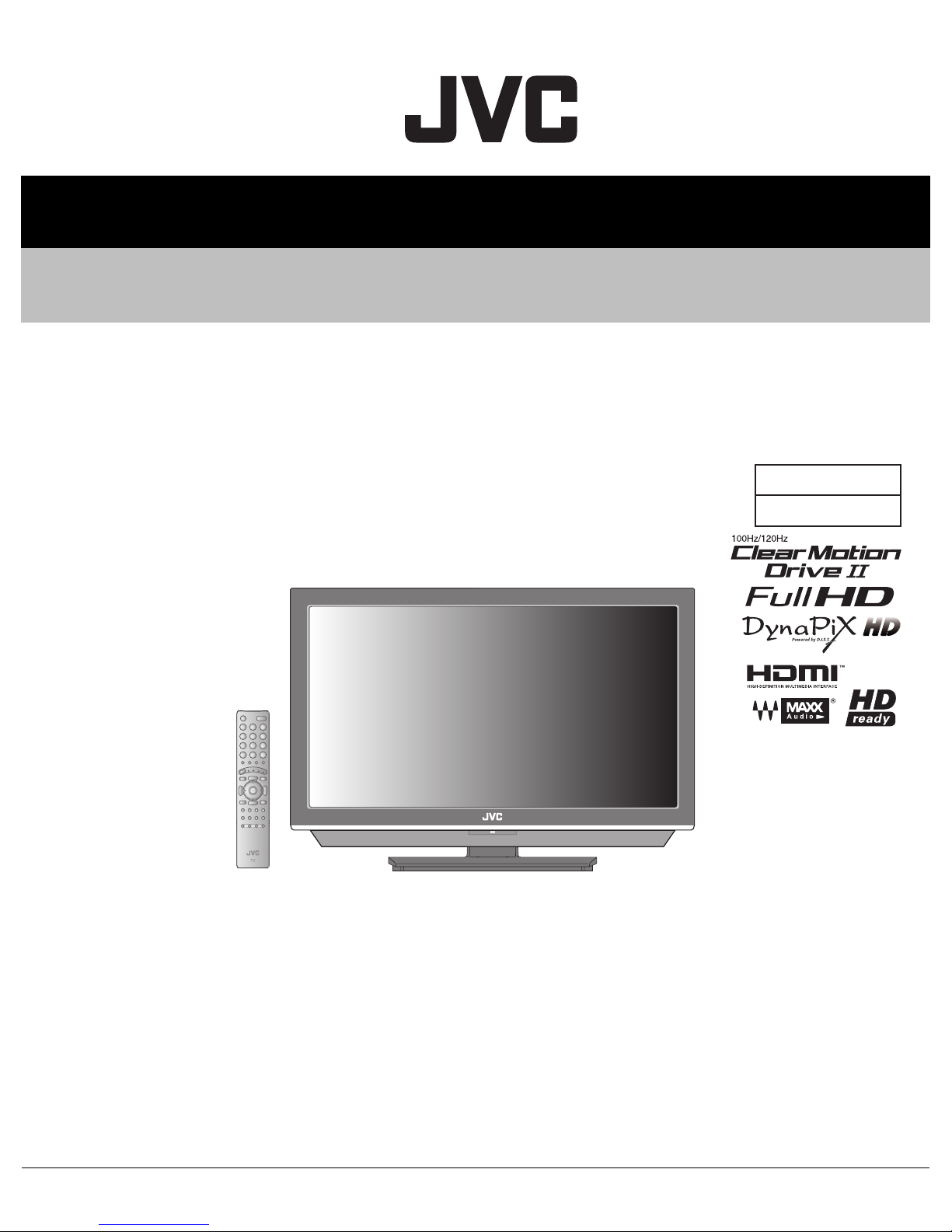
YA665<Rev.001>200812SERVICE MANUAL
LT-52GZ79, LT-52GZ79/BA,
WIDE LCD PANEL TELEVISION
LT-52GZ79
COPYRIGHT © 2008 Victor Company of Japan, Limited
/E, LT-52GZ79/S
BASIC CHASSIS
FL5
1 PRECAUTION. . . . . . . . . . . . . . . . . . . . . . . . . . . . . . . . . . . . . . . . . . . . . . . . . . . . . . . . . . . . . . . . . . . . . . . . . 1-3
2 SPECIFIC SERVICE INSTRUCTIONS . . . . . . . . . . . . . . . . . . . . . . . . . . . . . . . . . . . . . . . . . . . . . . . . . . . . . . 1-6
3 DISASSEMBLY . . . . . . . . . . . . . . . . . . . . . . . . . . . . . . . . . . . . . . . . . . . . . . . . . . . . . . . . . . . . . . . . . . . . . . . 1-9
4 ADJUSTMENT . . . . . . . . . . . . . . . . . . . . . . . . . . . . . . . . . . . . . . . . . . . . . . . . . . . . . . . . . . . . . . . . . . . . . . . 1-15
5 TROUBLESHOOTING . . . . . . . . . . . . . . . . . . . . . . . . . . . . . . . . . . . . . . . . . . . . . . . . . . . . . . . . . . . . . . . . . 1-20
COPYRIGHT © 2008 Victor Company of Japan, Limited
TABLE OF CONTENTS
No.YA665<Rev.001>
2008/12
Page 2
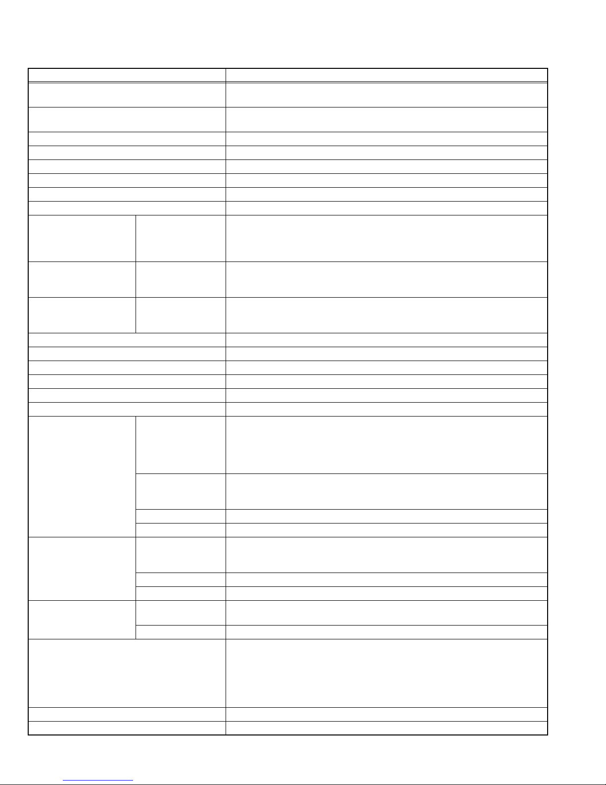
SPECIFICATION
Items Contents
Dimensions ( W × H × D ) 121.74 cm
121.74 cm
Mass 40.0 kg [With stand]
34.0 kg [Without stand]
Power Input AC110V - AC240 V, 50 Hz / 60 Hz
Power Consumption 277 W (Standby:0.5 W)
TV RF System B, G, I, D, K, K1, M
Colour System PAL / SECAM / NTSC 3.58 / NTSC 4.43
Stereo System A2 (B/G, D/K), NICAM (B/G, I, D/K)
Teletext System FLOF (Fastext), WST (World Standard System)
Receiving
Frequency
Intermediate Frequency VIF
Colour Sub
Carrier
LCD panel 52 V-inch wide aspect (16 : 9)
Screen Size Diagonal: 132.1 cm (H: 93.1 cm
Display Pixels Horizontal: 1920 dots × Vertical: 1080 dots
Audio Power Output 10 W + 10 W
Speaker 4.5 cm × 16.0 cm, Twin Oblique cone × 2
Aerial terminal (VHF/UHF) 75 Ω unbalanced, coaxial
Video / Audio
Input-1/2/3
Video / Audio Output S-Video Mini-DIN 4 pin connector × 1
HDMI Input Video HDMI connector × 3
PC (RGB) Input D-sub 15 pin × 1
Headphone 3.5 mm stereo mini jack × 1
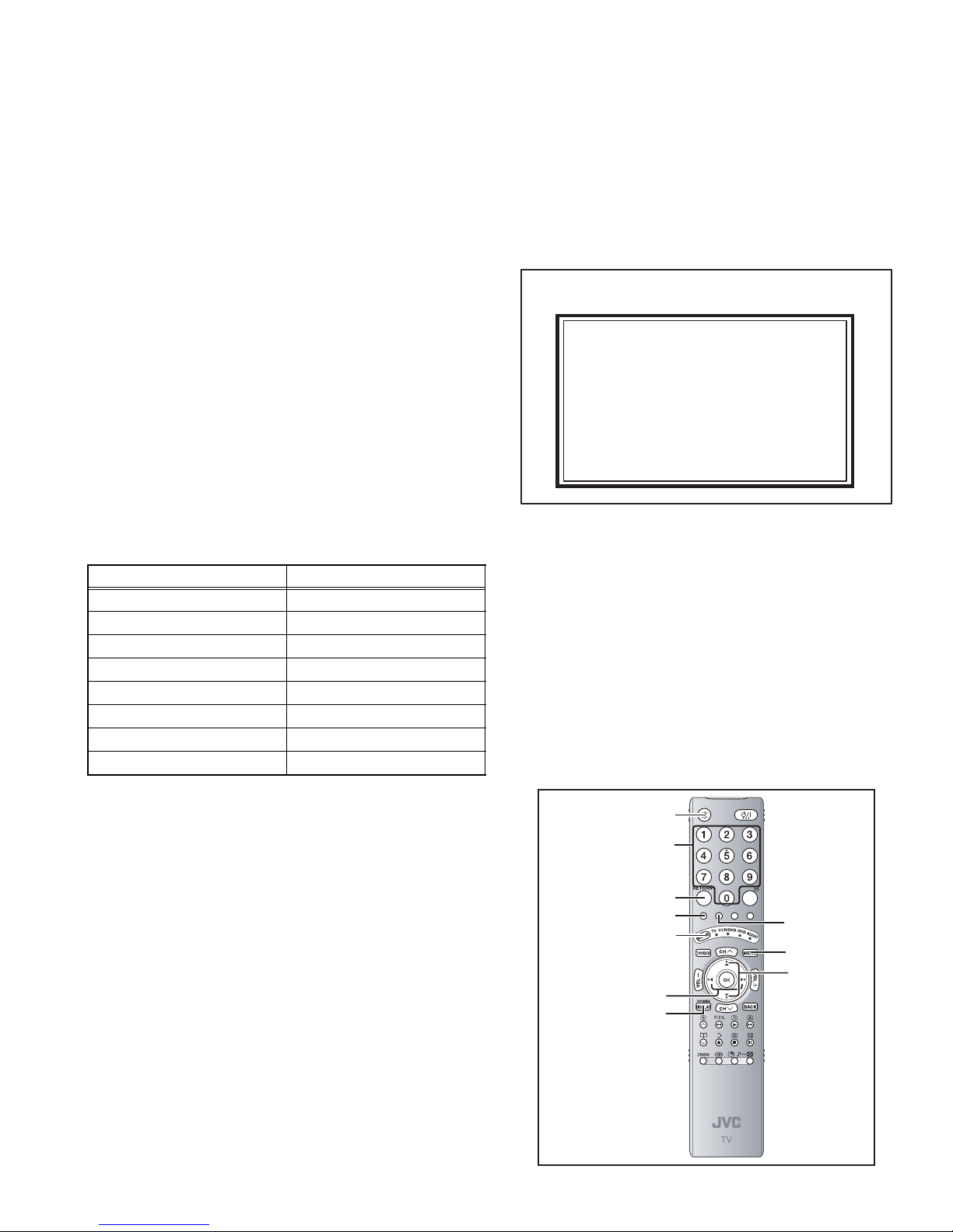
Remote Control Unit RM-C1856 (AAA/R03 dry cell battery × 2)
Design & specifications are subject to change without notice.
Component Video
625p / 525p / 625i / 525i
VHF Low
VHF High
SECAM
[Input-1/3]
750p / 1125i
S-Video
[Input-1/2]
46.25MHz - 140.25MHz
147.25MHz - 423.25MHz
UHF
431.25MHz - 863.25MHz
CATV
Mid (X - Z+2, S1 - S10) / Super (S11 - S20) / Hyper (S21 - S41) bands
38.0MHz (B, G, I, D, K, L)
SIF
32.26MHz (5.74MHz: B), 32.15MHz (5.85MHz: G), 31.45MHz (6.55MHz: I)
31.75MHz (6.25MHz: D), 32.15MHz (5.85MHz: K)
PAL
4.43MHz
4.40625MHz / 4.25MHz
NTSC
3.58MHz / 4.43MHz
RCA pin jack × 6 (Input-3)
Y: 1V (p-p) (Sync signal: ±0.35V(p-p), 3-value sync.), 75 Ω / Pb/Pr: ±0.35V(p-p),
75 Ω
Y: 1V (p-p), Positive (Negative sync provided), 75 Ω / Pb/Pr: 0.7V(p-p), 75 Ω
Mini-DIN 4 pin connector × 2
Y: 1 V (p-p), Positive (Negative sync provided), 75 Ω
C: 0.286 V (p-p) (Burst signal), 75 Ω
Video 1 V (p-p), Positive (Negative sync provided), 75 Ω, RCA pin jack × 3
Audio 500 mV (rms), High impedance, RCA pin jack × 6
Y: 1 V (p-p), Positive (Negative sync provided), 75 Ω
C: 0.286 V (p-p) (Burst signal), 75 Ω
Video 1 V (p-p), Positive (Negative sync provided), 75 Ω, RCA pin jack × 1
Audio 500 mV (rms), Low impedance, RCA pin jack × 2
(Digital-input terminal is not compatible with picture signals of computer signal)
Audio Analog: 500mV(rms) (-4dBs), high impedance, RCA pin jack × 2
R/G/B: 0.7 V (p-p), 75Ω
HD / VD: 1 V (p-p) to 5 V (p-p), high impedance
< Available signal >
VGA: 640 pixels × 480 pixels (Horizontal: 31.5 kHz / Vertical: 60 Hz)
XGA: 1024 pixels × 768 pixels (Horizontal: 48.4 kHz / Vertical: 60 Hz)
×
82.55 cm × 34.57 cm [With stand]
×
77.85 cm × 13.5 cm [Without stand]
×
V: 52.4 cm)
1-2 (No.YA665<Rev.001>)
Page 3
SECTION 1
PRECAUTION
1.1 SAFETY PRECAUTIONS
(1) The design of this product contains special hardware,
many circuits and components specially for safety
purposes. For continued protection, no changes should be
made to the original design unless authorized in writing by
the manufacturer. Replacement parts must be identical to
those used in the original circuits. Service should be
performed by qualified personnel only.
(2) Alterations of the design or circuitry of the products should
not be made. Any design alterations or additions will void
the manufacturer's warranty and will further relieve the
manufacturer of responsibility for personal injury or
property damage resulting therefrom.
(3) Many electrical and mechanical parts in the products have
special safety-related characteristics. These
characteristics are often not evident from visual inspection
nor can the protection afforded by them necessarily be
obtained by using replacement components rated for
higher voltage, wattage, etc. Replacement parts which
have these special safety characteristics are identified in
the parts list of Service manual. Electrical components
having such features are identified by shading on the
schematics and by ( ) on the parts list in Service
manual. The use of a substitute replacement which does
not have the same safety characteristics as the
recommended replacement part shown in the parts list of
Service manual may cause shock, fire, or other hazards.
(4) Don't short between the LIVE side ground and
ISOLATED (NEUTRAL) side ground or EARTH side
ground when repairing.
Some model's power circuit is partly different in the GND.
The difference of the GND is shown by the LIVE : ( ) side
GND, the ISOLATED (NEUTRAL) : ( ) side GND and
EARTH : ( ) side GND.
Don't short between the LIVE side GND and ISOLATED
(NEUTRAL) side GND or EARTH side GND and never
measure the LIVE side GND and ISOLATED (NEUTRAL)
side GND or EARTH side GND at the same time with a
measuring apparatus (oscilloscope etc.). If above note will
not be kept, a fuse or any parts will be broken.
(5) When service is required, observe the original lead dress.
Extra precaution should be given to assure correct lead
dress in the high voltage circuit area. Where a short circuit
has occurred, those components that indicate evidence of
overheating should be replaced. Always use the
manufacturer's replacement components.
(6) Isolation Check (Safety for Electrical Shock Hazard)
After re-assembling the product, always perform an
isolation check on the exposed metal parts of the cabinet
(antenna terminals, video/audio input and output terminals,
Control knobs, metal cabinet, screw heads, earphone jack,
control shafts, etc.) to be sure the product is safe to operate
without danger of electrical shock.
a) Dielectric Strength Test
The isolation between the AC primary circuit and all metal
parts exposed to the user, particularly any exposed metal
part having a return path to the chassis should withstand a
voltage of 3000V AC (r.m.s.) for a period of one second. (.
. . . Withstand a voltage of 1100V AC (r.m.s.) to an
appliance rated up to 120V, and 3000V AC (r.m.s.) to an
appliance rated 200V or more, for a period of one second.)
This method of test requires a test equipment not generally
found in the service trade.
b) Leakage Current Check
Plug the AC line cord directly into the AC outlet (do not use
a line isolation transformer during this check.). Using a
"Leakage Current Tester", measure the leakage current
from each exposed metal part of the cabinet, particularly
any exposed metal part having a return path to the chassis,
to a known good earth ground (water pipe, etc.). Any
leakage current must not exceed 0.5mA AC (r.m.s.).
However, in tropical area, this must not exceed 0.2mA AC
(r.m.s.).
Alternate Check Method
Plug the AC line cord directly into the AC outlet (do not
use a line isolation transformer during this check.). Use
an AC voltmeter having 1000Ω per volt or more
sensitivity in the following manner. Connect a 1500Ω
10W resistor paralleled by a 0.15µF AC-type capacitor
between an exposed metal part and a known good earth
ground (water pipe, etc.). Measure the AC voltage
across the resistor with the AC voltmeter. Move the
resistor connection to each exposed metal part,
particularly any exposed metal part having a return path
to the chassis, and measure the AC voltage across the
resistor. Now, reverse the plug in the AC outlet and
repeat each measurement. Any voltage measured must
not exceed 0.75V AC (r.m.s.). This corresponds to
0.5mA AC (r.m.s.).
However, in tropical area, this must not exceed 0.3V AC
(r.m.s.). This corresponds to 0.2mA AC (r.m.s.).
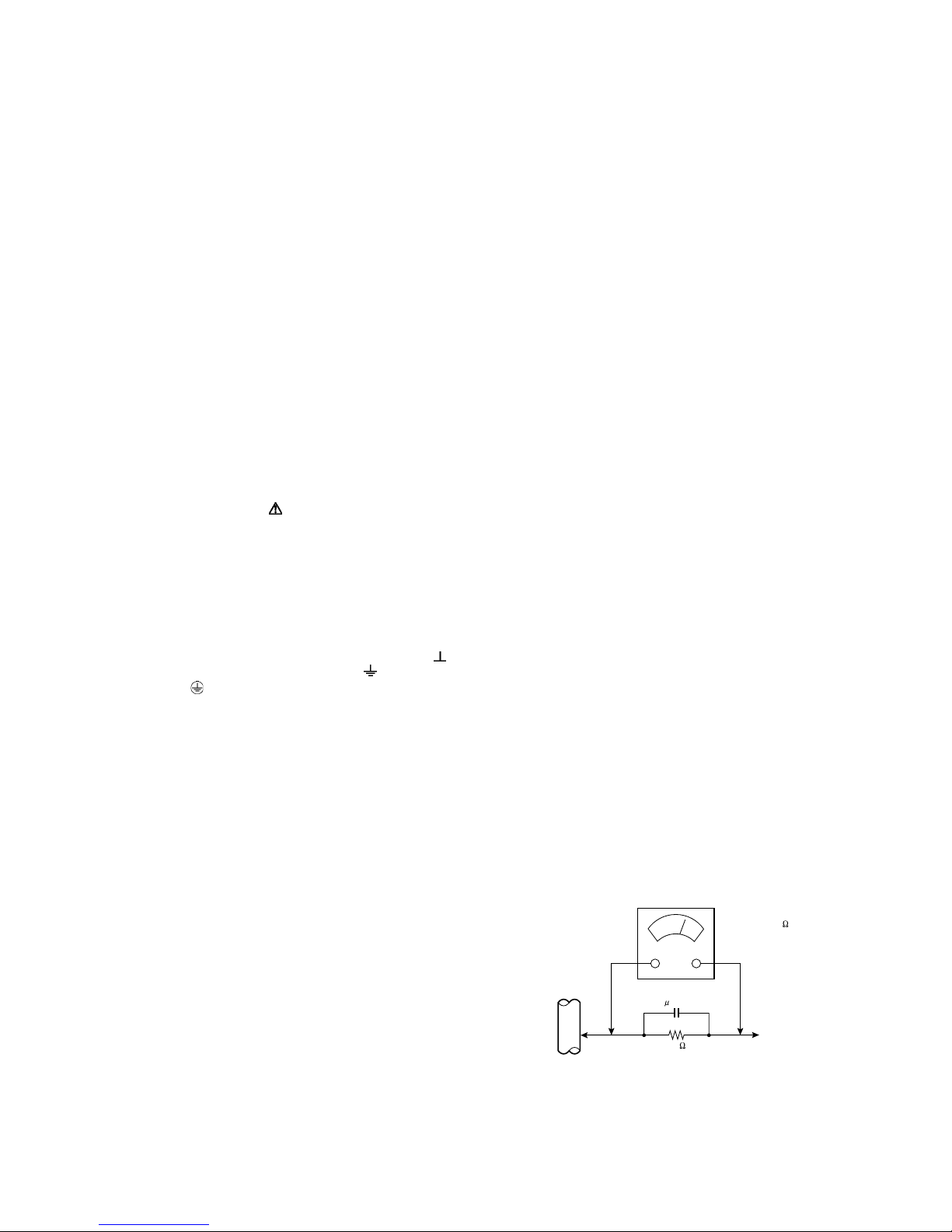
AC VOLTMETER
(HAVING 1000 /V,
OR MORE SENSITIVITY)
0.15 F AC-TYPE
GOOD EARTH GROUND
1500 10W
PLACE THIS PROBE
ON EACH EXPOSED
ME TAL PAR T
(No.YA665<Rev.001>)1-3
Page 4
1.2 INSTALLATION
1.2.1 HEAT DISSIPATION
If the heat dissipation vent behind this unit is blocked, cooling
efficiency may deteriorate and temperature inside the unit will
rise. The temperature sensor that protects the unit will be
activated when internal temperature exceeds the pre-determined
level and power will be turned off automatically.Therefore,
please make sure pay attention not to block the heat dissipation
vent as well as the ventilation outlet behind the unit and ensure
that there is room for ventilation around it.
1.2.3 INSTALLATION REQUIREMENTS
To ensure safety in an emergency such as an earthquake, and
to prevent accidents, ensure that measures are taken to prevent
the TV dropping or falling over.
It fixes in a band.
Ventilation hole
*Diagram differs from actual appearance.
1.2.2 INSTALLATION REQUIREMENTS
Ensure that the minimal distance is maintained, as specified
below, between the unit with and the surrounding walls, as well
as the floor etc.Install the unit on stable flooring or stands.Take
precautionary measures to prevent the unit from tipping in order
to protect against accidents and earthquakes.
200 mm
150 mm 50
*Diagram differs from actual appearance.
mm
150 mm 50 mm
TV STAND
*Diagram differs from actual appearance.
1.2.4 NOTES ON HANDLING
When taking the unit out of a packing case, do not grasp the
upper part of the unit. If you take the unit out while grasping the
upper part, the LCD PANEL may be damaged because of a
pressure. Instead of grasping the upper part, put your hands on
the lower backside or sides of the unit.
1.3 HANDLING LCD PANEL
1.3.1 PRECAUTIONS FOR TRANSPORTATION
When transporting the unit, pressure exerted on the internal LCD
panel due to improper handling (such as tossing and dropping)
may cause damages even when the unit is carefully packed. To
prevent accidents from occurring during transportation, pay
careful attention before delivery, such as through explaining the
handling instructions to transporters.
Ensure that the following requirements are met during
transportation, as the LCD panel of this unit is made of glass and
therefore fragile:
(1) USE A SPECIAL PACKING CASE FOR THE LCD PANEL
When transporting the LCD panel of the unit, use a special
packing case (packing materials). A special packing case
is used when a LCD panel is supplied as a service spare
part.
(2) ATTACH PROTECTION SHEET TO THE FRONT
Since the front (display part) of the panel is vulnerable,
attach the protection sheet to the front of the LCD panel
before transportation. Protection sheet is used when a LCD
panel is supplied as a service spare part.
(3) AVOID VIBRATIONS AND IMPACTS
The unit may be broken if it is toppled sideways even when
properly packed. Continuous vibration may shift the gap of
the panel, and the unit may not be able to display images
properly. Ensure that the unit is carried by at least 2
persons and pay careful attention not to exert any vibration
or impact on it.
(4) DO NOT PLACE EQUIPMENT HORIZONTALLY
Ensure that it is placed upright and not horizontally during
transportation and storage as the LCD panel is very
vulnerable to lateral impacts and may break. During
transportation, ensure that the unit is loaded along the
traveling direction of the vehicle, and avoid stacking them
on one another. For storage, ensure that they are stacked
in 2 layers or less even when placed upright.
1-4 (N o.YA 665<R ev.001>)
Page 5
1.3.2 OPTICAL FILTER (ON THE FRONT OF THE LCD PANEL)
SERVICE MENU
1. ADJUST
2. SELF CHECK
3. I2C STOP
LOB 0 FAN 0
AUD 0
ANA 9 DIG 9
HOUR 131070 MAX 0
RESET : TV 1
(1) Avoid placing the unit under direct sunlight over a
prolonged period of time. This may cause the optical filter
to deteriorate in quality and COLOUR.
(2) Clean the filter surface by wiping it softly and lightly with a
soft and lightly fuzz cloth (such as outing flannel).
(3) Do not use solvents such as benzene or thinner to wipe the
filter surface. This may cause the filter to deteriorate in
quality or the coating on the surface to come off. When
cleaning the filter, usually use the neutral detergent diluted
with water. When cleaning the dirty filter, use water-diluted
ethanol.
(4) Since the filter surface is fragile, do not scratch or hit it with
hard materials. Be careful enough not to touch the front
surface, especially when taking the unit out of the packing
case or during transportation.
1.3.3 PRECAUTIONS FOR REPLACEMENT OF EXTERIOR
PARTS
Take note of the following when replacing exterior parts (REAR
COVER, FRONT PANEL, etc.):
(1) Do not exert pressure on the front of the LCD panel (filter
surface). It may cause irregular COLOUR.
(2) Pay careful attention not to scratch or stain the front of the
LCD panel (filter surface) with hands.
(3) When replacing exterior parts, the front (LCD panel) should
be placed facing downward. Place a mat, etc. underneath
to avoid causing scratches to the front (filter surface).
1.3.4 HOW TO CHECK THE OPERATING TIME
This model has a function to count and record the LCD panel
operating time. The operating time can be checked in the
following procedure.
• Maximum count time = 131070 hours
(1) Press the [DISPLAY] key and [MUTING] key simulta-
neously, then enter the SERVICE MODE.
(2) When the Main Menu is displayed, press [2] key to enter
the self check mode.
(3) The operating time of the LCD panel is displayed in 5-digit
decimal number.(Refer to the below figure)
SERVICE MODE SCREEN
SERVICE MENU
1. ADJUST
2. SELF CHECK
3. I2C STOP
Press [2] key
Switch the display/ non-display
with the [ZOOM] key.
SELF CHECK MODE SCREEN (Page 1)
The operating time is displayed
LOB 0 FAN 0
AUD 0
ANA 9 DIG 9
HOUR 131070 MAX 0
RESET : TV 1
MAX is displayed when the maximum
count time is exceeded
*When the power is turned off with the remote control unit or the power
button of the main unit, the count restarts from the turn off time.
*When the power is turned off by disconnecting the power cord from the
AC outlet, the recorded time count less than 2 hours is not counted.
*When the operating time exceeds the maximum count time, "MAX" is
displayed to the right of the counted time, and the following count is
discontinued.
1.3.5 HOW TO RESET THE OPERATING TIME
(1) Press the [MENU] key simultaneously, then enter the
USER MENU.
(2) Select the "Features" from the USER MENU.
(3) Select the Blue back from the Features.
(4) Set the Blue back to "Off".
(5) Press the [DISPLAY] key and [MUTING] key
simultaneously, then enter the SERVICE MODE.
(6) When the Main Menu is displayed, press [2] key to enter
the self check mode.
(7) When the self check screen(page-1) is displayed, press
[ZOOM] key.
(8) "RESET : TV" is displayed under the operating time.
(9) Press the [TV/VIDEO] key to reset the operating time.
NOTE:
When the LCD PANEL UNIT is replaced, be sure to reset the
operating time following the above method.
(No.YA665<Rev.001>)1-5
Page 6
2.1 SYSTEM SETTING
SERVICE MENU
1. ADJUST
2. SELF CHECK
3. I2C STOP
LOB 0 FAN 0
AUD 0
ANA 9 DIG 9
HOUR 131070 MAX 0
1
SECTION 2
SPECIFIC SERVICE INSTRUCTIONS
Be sure to carry out the following operation at the end of
the procedure.
(1) Press the [DISPLAY] key and [MUTING] key
simultaneously, then enter the SERVICE MODE.
(2) When the Main Menu is displayed, press [2] key to enter
the self check mode.
(3) Turn off the power by pressing the [POWER] key on the
remote control unit.
SERVICE MODE SCREEN
SERVICE MENU
1. ADJUST
2. SELF CHECK
3. I2C STOP
Press [2] key
SELF CHECK MODE SCREEN (Page 1)
LOB 0 FAN 0
AUD 0
ANA 9 DIG 9
HOUR 131070 MAX 0
1
2.2 FEATURES
Full HD
Full HD models deliver superbly detailed image reproduction
of more than 2 megapixels (1920 x 1080), which represents
double the resolution offered by WXGA panels.
100Hz/120Hz Clear Motion Drive ll
This function is able to display twice as many frames as a
conventional LCD display.
D.I.S.T. (Digital Image Scaling Technology)
This system uses line interpolation to double the number of
scanning lines and achieve high resolution, flicker-free picture.
Colour Management
This function ensures dull colours are compensated to
produce natural hues.
Picture Management
This function makes it easier to see the dark areas when a
picture has many dark areas, and makes it easier to see the
bright areas when a picture has many bright areas.
Smart Picture
This function detects the APL (Average Picture Level) and
adjusts the contrast suitable for what you are watching.
DIGITAL VNR
This function cuts down the amount of noise in the original
picture.
MPEG Noise Reduction
This function effects the block noise removal and mosquito NR
simultaneously.
MaxxAudio
MaxxAudio improves sound performance with four sound
features (MaxxBass, MaxxTreble, MaxxStereo and
MaxxVolume).
1-6 (No.YA665<Rev.001>)
Page 7
2.3 MAIN DIFFERENCE LIST
Item LT-52GZ79 LT-52GZ79/BA LT-52GZ79/BA LT-52GZ79/S
POWER CORD EU Type (2 Pins) EU Type (2 Pins) EU Type (2 Pins) UK Type (3 Pins)
ANALOG PWB SFL-1237A-H2 SFL-1237A-H8 SFL-1237A-H2 SFL-1237A-H2
SW PWB SFL-7221A-H2 SFL-7221A-H8 SFL-7221A-H2 SFL-7221A-H2
LED PWB SFL-8728A-H2 SFL-8728A-H8 SFL-8728A-H2 SFL-8728A-H2
MAIN POW ASSY SFL-90A5A-H2 SFL-90A5A-H8 SFL-90A6A-H2 SFL-90A5A-H2
DC-DC PWB SFL-91A1A-H2 SFL-91A1A-H8 SFL-91A1A-H2 SFL-91A1A-H2
DIGITAL PWB SFL0D403A-H2 SFL0D403A-H8 SFL0D403A-H2 SFL0D404A-H2
2.4 TECHNICAL INFORMATION
2.4.1 LCD PANEL
This unit uses the flat type panel LCD (Liquid Crystal Display) panel that occupies as little space as possible, instead of the
conventional CRT (Cathode Ray Tube), as a display unit.
Since the unit has the two polarizing filter that are at right angles to each other, the unit adopts "normally black" mode, where light
does not pass through the polarizing filter and the screen is black when no voltage is applied to the liquid crystals.
2.4.1.1 SPECIFICATIONS
The following table shows the specifications of this unit.
Item Specifications
Maximum dimensions ( W × H × D ) 119.2 cm × 68.8 cm × 5.9 cm
Weight 19.0 kg
×
Screen size Diagonal: 132.1 cm (H: 93.1 cm
V: 52.4 cm)
Aspect ratio 16 : 9
Drive device / system a-Si-TFT active matrix system
Number of Pixels Horizontally 1920 × Vertically 1080
Pixel pitch (pixel size) Horizontally: 0.6 mm, Vertically: 0.6 mm
Displayed colour 16777216 colours 256 colours for R G and B
Brightness 500 cd/m
2
Contrast ratio 3000 : 1
Response time (G to G) 6 ms
View angle Horizontally: 178°, Vertically: 178°
Surface polarizer Anti-Glare type Low reflective coat
Colour filter Vertical stripe
Backlight Cold cathode fluorescent lamp × 24
Power supply voltage in LCD 12 V
Power supply voltage in inverter 24 V
Panel interface system LVDS (Low Voltage Differential Signaling)
2.4.1.2 PIXEL FAULT
There are three pixel faults - bright fault, dark fault and flicker fault - that are respectively defined as follows.
BRIGHT FAULT
In this pixel fault, a cell that should not light originally is lighting on and off.
For checking this pixel fault, input ALL BLACK SCREEN and find out the cell that is lighting on and off.
DARK FAULT
In this pixel fault, a cell that should light originally is not lighting or lighting with the brightness twice as brighter as originally lighting.
For checking this pixel fault, input 100% of each R/G/B color and find out the cell that is not lighting.
FLICKER FAULT
In the pixel fault, a cell that should light originally or not light originally is flashing on and off.
For checking this pixel fault, input ALL BLACK SCREEN signal or 100% of each RGB color and find out the cell that is flashing on
and off.
(No.YA665<Rev.001>)1-7
Page 8
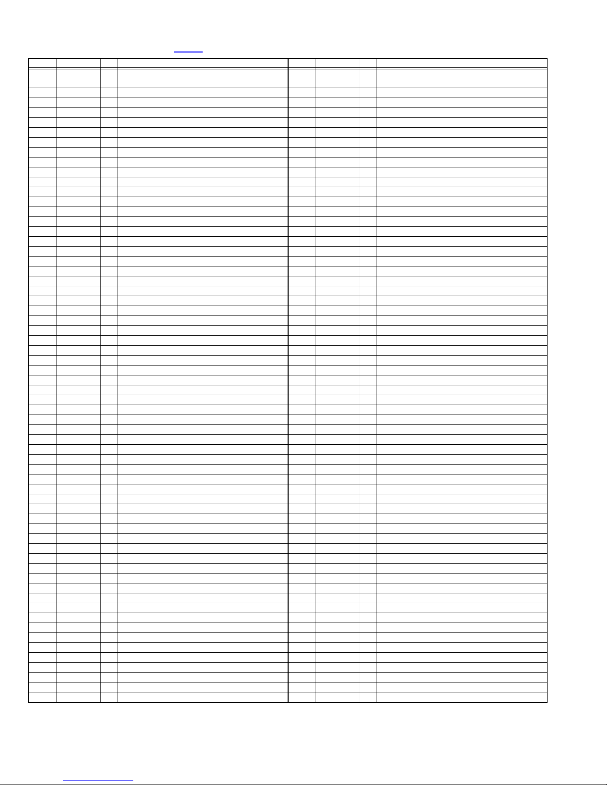
2.4.2 MAIN CPU PIN FUNCTION [IC7301
Pin Pin name I/O Function Pin Pin name I/O Function
1 TCK O Test purpose 65 D2 I/O Program ROM data for main CPU
2 TMS I Test purpose 66 D12 I/O Program ROM data for main CPU
3 TDI I Test purpose 67 D10 I/O Program ROM data for main CPU
4 TDO O Test purpose 68 VSS33 - GND
5 P2.8 I Input for HDMI CEC 69 VDD33 I 3.3V
6 P2.9 O Blue for OSD 70 D4 I/O Program ROM data for main CPU
7 P2.10 O Blue for OSD 71 D3 I/O Program ROM data for main CPU
8 P2.11 O Blue for OSD 72 D11 I/O Program ROM data for main CPU
9 P2.12 O Blue for OSD 73 RSTIN I Reset
10 P2.13 O Blue for OSD 74 POWER O Sleep state release for chassis CPU [Release : L]
11 P2.14 I Not used 75 P3.1 O Not used: Reset for digital tuner unit
12 P2.15 O Not used: Request for chassis CPU communication 76 REMOCON I Remote control
13 VSS33 - GND 77 P3.3 I Clock for OSD
14 VDD33 I 3.3V 78 P3.4 O Red for OSD
15 P4.5 O Not used 79 P3.5 O Red for OSD
16 A20 O Program ROM address for main CPU 80 P3.6 O Red for OSD
17 A19 O Program ROM address for main CPU 81 P3.7 O Red for OSD
18 A18 O Program ROM address for main CPU 82 MTST I/O Data transmission for chassis CPU communication
19 A17 O Program ROM address for main CPU 83 MTSR I/O Data receive for chassis CPU communication
20 VSS25 - GND 84 VSS33 - GND
21 VDD25 I 2.5V 85 VDD33 I 3.3V
22 A16 O Program ROM address for main CPU 86 VSS25 - GND
23 A8 O Program ROM address for main CPU 87 VDD25 I 2.5V
24 A7 O Program ROM address for main CPU 88 TXD0 I/O Not used: Data transmission for digital tuner unit
25 A9 O Program ROM address for main CPU 89 RXD0 I/O Not used: Data receive for digital tuner unit
26 A6 O Program ROM address for main CPU 90 P3.12 O Red for OSD
27 A5 O Program ROM address for main CPU 91 CLK O Clock for chassis CPU communication
28 A10 O Program ROM address for main CPU 92 P3.15 O Output for HDMI CEC
29 A11 O Program ROM address for main CPU 93 P5.14 O Green for OSD
30 A12 O Program ROM address for main CPU 94 P5.15 O Green for OSD
31 VSS33 - GND 95 TRIG_IN O Green for OSD
32 VDD33 I 3.3V 96 TRIG_OUT O Green for OSD
33 A4 O Program ROM address for main CPU 97 P6.2 O Green for OSD
34 A3 O Program ROM address for main CPU 98 P6.3 I/O I
35 A2 O Program ROM address for main CPU 99 P6.4 I/O I
36 A1 O Program ROM address for main CPU 100 P6.5 O Sync signal select for OSD / Teletext
37 A0 O Program ROM address for main CPU 101 IRQ O Not used: Interrupt request for digital tuner unit
38 A13 O Program ROM address for main CPU 102 VSYNC I Vertical sync
39 ARAS/A14 O Program ROM address for main CPU 103 HSYNC I Horizontal sync
40 CAS/A15 O Program ROM address for main CPU 104
41 VSS33 - GND 105 BLANK O Ys for OSD / Teletext
42 VDD33 I 3.3V 106 VDD33 I 3.3V
43 MEMCLK O Clock for memory 107 VSS33 - GND
44 CSSDRAM O Chip select for memory 108 XTAL1 I 6MHz for system clock
45 CLKEN O Clock enable for memory 109 XTAL2 O 6MHz for system clock
46 CSROM O Chip select for memory 110 VSSA - GND
47 RD O Read for memory 111 VDDA I 2.5V
48 UDQM O Control buffer of memory 112 R O R for Teletext
49 LDQM O Control buffer of memory 113 G O G for Teletext
50 WR O Write for memory 114 B O B for Teletext
51 D15 I/O Program ROM data for main CPU 115 VSSA - GND
52 VSS33 - GND 116 VDDA I 2.5V
53 VDD33 I 3.3V 117 CVBS2 I Not used
54 D7 I/O Program ROM data for main CPU 118 VSSA - GND
55 D0 I/O Program ROM data for main CPU 119 VDDA I 2.5V
56 D14 I/O Program ROM data for main CPU 120 CVBS1B I Not used
57 D8 I/O Program ROM data for main CPU 121 CVBS1A I Video for Teletext
58 D6 I/O Program ROM data for main CPU 122 VSSA - GND
59 D1 I/O Program ROM data for main CPU 123 VDDA I 2.5V
60 VSS33 - GND 124 KEY1 I Key scan data 1 [ON : H]
61 VDD33 I 3.3V 125 KEY2 I Key scan data 2 [ON : H]
62 D13 I/O Program ROM data for main CPU 126 MECA_SW I Main power ON / OFF control [ON : L]
63 D9 I/O Program ROM data for main CPU 127
64 D5 I/O Program ROM data for main CPU 128 TMODE I Test purpose
: DIGITAL PWB]
COR/RSTOUT
(KEYP2)P5.3
2
C bus clock (for main memory)
2
C bus Data (for main memory)
O Not used
I Not used: Error detection for digital tuner unit
1-8 (No.YA665<Rev.001>)
Page 9

SECTION 3
DISASSEMBLY
3.1 CAUTION AT DISASSEMBLY
• Be sure to perform the SYSTEM SETTING, at the end of the
procedure.
• Make sure that the power cord is disconnected from the outlet.
• Pay special attention not to break or damage the parts.
• Make sure that there is no bent or stain on the connectors
before inserting, and firmly insert the connectors.
• Be sure to reattach the wire clamps removed during the
procedure to the original positions. (Attaching the wire clamps
in wrong positions may affect the performance.)
REFERENCE:
When removing each board, remove the connector if
necessary. The operation is easier if you write down the
connection points (connector numbers) of the connector. For
connection of each board, refer to the "WIRING DIAGRAM" of
the Standard Circuit Diagram.
3.2 DISASSEMBLY PROCEDURE
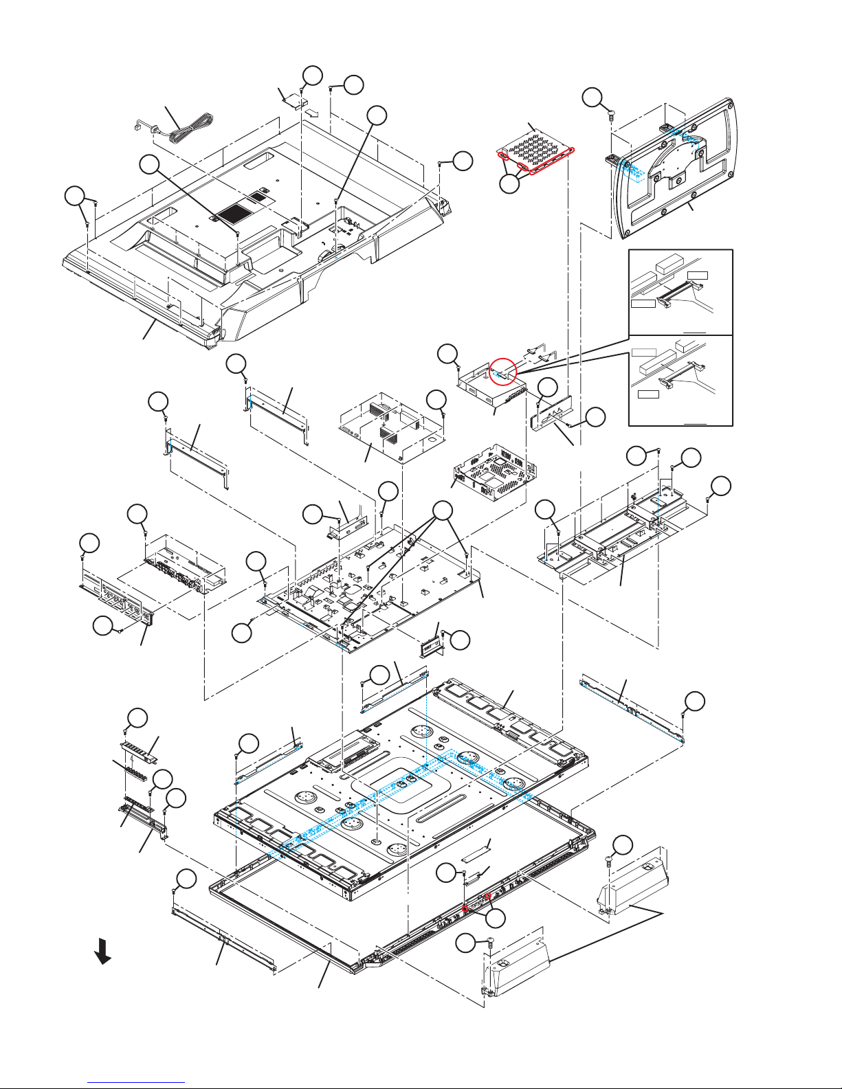
3.2.1 REMOVING THE REAR COVER (Fig.3-1)
(1) Remove the 1 screw [A].
(2) Remove the POWER CORD COVER in the direction of the
arrow.
(3) Remove the POWER CORD.
(4) Remove the 1 screw [B], 10 screws [C] and 11 screws [D].
(5) Remove the REAR COVER.
3.2.2 REMOVING THE ANALOG PWB (Fig.3-1)
• Remove the REAR COVER.
(1) Remove the 1 screw [E].
(2) Remove the TUNER BASE.
(3) Remove the 3 screws [F] and 7 screws [G].
(4) Remove the TERMINAL BASE.
(5) Remove the 3 screws [H].
(6) Remove the BACK BRACKET(R).
(7) Remove the 6 screws [J] and 2 screws [K].
(8) Remove the ANALOG PWB.
3.2.3 REMOVING THE DC-DC PWB (Fig.3-1)
• Remove the REAR COVER.
• Remove the BACK BRACKET(R).
(1) Remove the 3 screws [L].
(2) Remove the DC-DC PWB.
3.2.4 REMOVING THE POWER PWB (Fig.3-1)
• Remove the REAR COVER.
(1) Remove the 3 screws [M].
(2) Remove the BACK BRACKET(L).
(3) Remove the 11 screws [N].
(4) Remove the POWER PWB.
3.2.5 REMOVING THE SW PWB/CONTROL BASE (Fig.3-1)
• Remove the REAR COVER.
(1) Remove the 1 screw [P].
(2) Remove the KNOB BASE.
(3) Remove the 1 screw [Q].
(4) Remove the SW PWB.
(5) Remove the 1 screw [R].
(6) Remove the CONTROL BASE.
3.2.6 REMOVING THE DIGITAL PWB (Fig.3-1)
• Remove the REAR COVER.
• Remove the SHIELD COVER.
• Remove the SHIELD TERMINAL.
(1) Remove the 1 screw [S] and 3 screws [T].
(2) Remove the SHIELD TERMINAL.
(3) Remove the 9 screws [U].
(4) Remove the DIGITAL PWB.
CAUTION :
Make sure to perform the "SYSTEM SETTING", when
DIGITAL PWB is replaced.
3.2.7 REMOVING THE SPEAKER (Fig.3-1)
• Remove the REAR COVER.
(1) Remove the 6 screws [V].
(2) Remove the SPEKAER.
NOTE
When the SPEAKER is decomposed, the performance cannot
be kept.
3.2.8 REMOVING THE STAND (Fig.3-1)
(1) Remove the 1 screw [B] and 4 screws [W].
(2) Remove the STAND.
3.2.9 REMOVING THE LED PWB (Fig.3-1)
• Remove the REAR COVER.
• Remove the STAND.
• Remove the SPEKAER.
(1) Remove the 5 screws [AA] 4 screws [AB] and 8 screws
[AC].
(2) Remove the BOTTOM BRACKET.
(3) Remove the 2 hooks [b].
(4) Remove the LED PWB.
3.2.10 REMOVING THE LED LENS (Fig.3-1)
• Remove the REAR COVER.
• Remove the STAND.
• Remove the BOTTOM BRACKET.
• Remove the LED PWB.
(1) Remove the 2 screws [AD].
(2) Remove the LED LENS.
3.2.11 REMOVING THE LCD PANEL UNIT (Fig.3-1)
• Remove the REAR COVER.
• Remove the STAND.
• Remove the TUNER BASE.
• Remove the SPEKAER.
• Remove the BOTTOM BRACKET.
(1) Remove the 3 screws [AE] and 2 screws [AF].
(2) Remove the MAIN BASE.
(3) Remove the 6 screws [AG].
(4) Remove the SIDE BRACKET(L/R).
(5) Remove the 4 screws [AH].
(6) Remove the TOP FRAME in the direction of the arrow.
(7) Remove the LCD PANEL UNIT from the FRONT PANEL.
(No.YA665<Rev.001>)1-9
Page 10
POWER CORD COVER
POWER CORD
A
C
W
B
SHIELD COVER
D
D
a
C
STAND
41 PIN
CN0LV1
The terminal of a connector is turned up and connects.
REAR COVER
H
J
M
BACK
BRACKET(R)
BACK
BRACKET(L)
POWER PWB
DC-DC PWB
L
AF
SHIELD BASE
U
N
DIGITAL PWB
AE
S
T
SHIELD
TERMINAL
AB
CN0LV2
51 PIN
The terminal of a connector is turned below and connects.
AA
AB
AC
F
AF
G
TERMINAL BASE
CONTROL
KNOB
SW PWB
CONTROL BASE
FRONT
P
KNOB BASE
Q
K
R
AG
SIDE BRACKET
TOP FRAME
AH
FRONT PANEL
TOP FRAME
AH
MAIN BASE
TUNER BASE
E
LCD PANEL UNIT
LED PWB
LED LENS
AD
Y
BOTTOM
BRACKET
SIDE BRACKET
AG
Y
b
SPEAKER
1-10 (No.YA665<Rev.001>)
Fig.3-1
Page 11
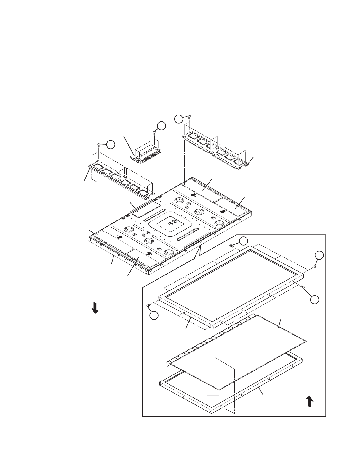
3.2.12 REMOVING THE LCD CONTROL PWB (Fig.3-2)
• Remove the REAR COVER.
(1) Remove the 4 screws [A].
(2) Remove the LCD CONTROL PWB COVER.
(3) Remove the LCD CONTROL PWB.
3.2.13 REMOVING THE INVERTER PWB (Fig.3-2)
• Remove the REAR COVER.
(1) Remove the 7 screws [B].
(2) Remove the INVERTER PWB COVER.
(3) Remove the INVERTER PWB by sliding it in the direction
of the arrow.
(4) Follow the same steps when removing another INVERTER
PWB.
A
LCD CONTROL PWB COVER
B
INVERTER PWB
COVER
LCD CONTROL PWB
3.2.14 REMOVING THE BACK LIGHT UNIT (Fig.3-2)
• Remove the REAR COVER.
• Remove the STAND ASS'Y.
• Remove the SPEKAER.
• Remove the BOTTOM BRACKET.
• Remove the SIDE BRACKET.
• Remove the TOP FRAME.
• Remove the MAIN BASE.
• Remove the LCD PANEL UNIT.
(1) Remove the 14 screws [C].
(2) Remove the PANEL FRAME.
(3) Remove the LCD PANEL.
B
INVERTER PWB COVER
INVERTER PWB (SLAVE-T)
INVERTER PWB (SLAVE-B)
INVERTER PWB
(MASTER-T)
LCD PANEL UNIT
INVERTER PWB (MASTER-B)
FRONT
C
PANEL FRAME
C
C
C
LCD PANEL
FRONT
BACK LIGHT UNIT
Fig.3-2
(No.YA665<Rev.001>)1-11
Page 12
3.3 MEMORY IC REPLACEMENT
SERVICE MENU
1. ADJUST
2. SELF CHECK
3. I2C STOP
S001 R DRIVE 137
PAL50 FULL STD H
• This model uses the memory IC.
• This memory IC stores data for proper operation of the video and drive circuits.
• When replacing, be sure to use an IC containing this (initial value) data.
3.3.1 MEMORY IC TABLE
Symbol Number of pins Mounting PWB Main content of data
IC7201
IC7602
48-pin DIGITAL PWB Program (Video process) of IC6001(System CPU) is memorized.
8-pin DIGITAL PWB Setting value of IC7301(MAIN CPU) is memorized.
3.3.2 MEMORY IC REPLACEMENT PROCEDURE
1. Power off
Switch off the power and disconnect the power plug from the AC outlet.
2. Replace the memory IC
Be sure to use the memory IC written with the initial setting values.
3. Power on
Connect the power plug to the AC outlet and switch on the power.
4. Receiving channel setting
Refer to the OPERATING INSTRUCTIONS and set the receive channels (Channels Preset) as described.
5. User setting
Check the user setting items according to the given in page later. Where these do not agree, refer to the OPERATING
INSTRUCTIONS and set the items as described.
6. SERVICE MODE setting
Verify what to set in the SERVICE MODE, and set whatever is necessary (Fig.3-2). Refer to the SERVICE ADJUSTMENT for setting.
3.3.3 SERVICE MODE SETTING
SERVICE MODE SCREEN
MAIN MENU SCREEN
SERVICE MENU
1. ADJUST
2. SELF CHECK
3. I2C STOP
ADJUSTMENT MODE SCREEN
S001 R DRIVE 137
PAL50 FULL STD H
Fig.3-2
SETTING ITEM
Setting items Settings Item No.
Video system setting Adjust S001 - S009
(Not used) Fixed T001 - T003
(Not used) Fixed M001 - M224
(Not used) Fixed F001 - F002
(Not used) Fixed D001
(Not used) Fixed Z001
1-12 (No.YA665<Rev.001>)
Page 13
3.3.4 SETTINGS OF FACTORY SHIPMENT
3.3.4.1 BUTTON OPERATION 3.3.4.2 REMOTE CONTROL DIRECT OPERATION
Setting item Setting position
POWER Off
CHANNEL PR1
VOLUME 10
TV/AV TV
3.3.4.3 REMOTE CONTROL MENU OPERATION
(1) PICTURE
Setting item Setting position
Picture Mode Bright
White Balance Cool
Features
Super DigiPure Auto
Pull Down Auto
Colour Management On
Picture Management On
Smart Picture On
MPEG Noise Reduction On
Colour System Main Depends PR
Sub Auto
Zoom Panoramic
Setting item Setting position
CHANNEL PR1
VOLUME 10
ZOOM Auto
SUB PICTURE EXT-1
SUB POWER Off
(4) SET UP
Setting item Setting position
Auto Program Tv Channel Automatically Set
Edit/manual -
Language English
Video-1 Setting Component
Video-3 Setting Component
Teletext Language Group-1
HDMI Setting All setting is auto
PC Position Centre
Auto Demonstration Off
(2) SOUND
Setting item Setting position
Stereo / l•ll Stereo Sound
MaxxAudio Low
Balance Centre
Voice Enhancer Off
(3) FEATURES
Setting item Setting position
Timer Off
Channel Guard Off (ID:0000)
Appearance Type A
Blue Back On
Child Lock Off
Auto Shutoff Off
Favorite Setting Blank
Illumination Bright
Power Lamp On
Eco Sensor Off
(No.YA665<Rev.001>)1-13
Page 14
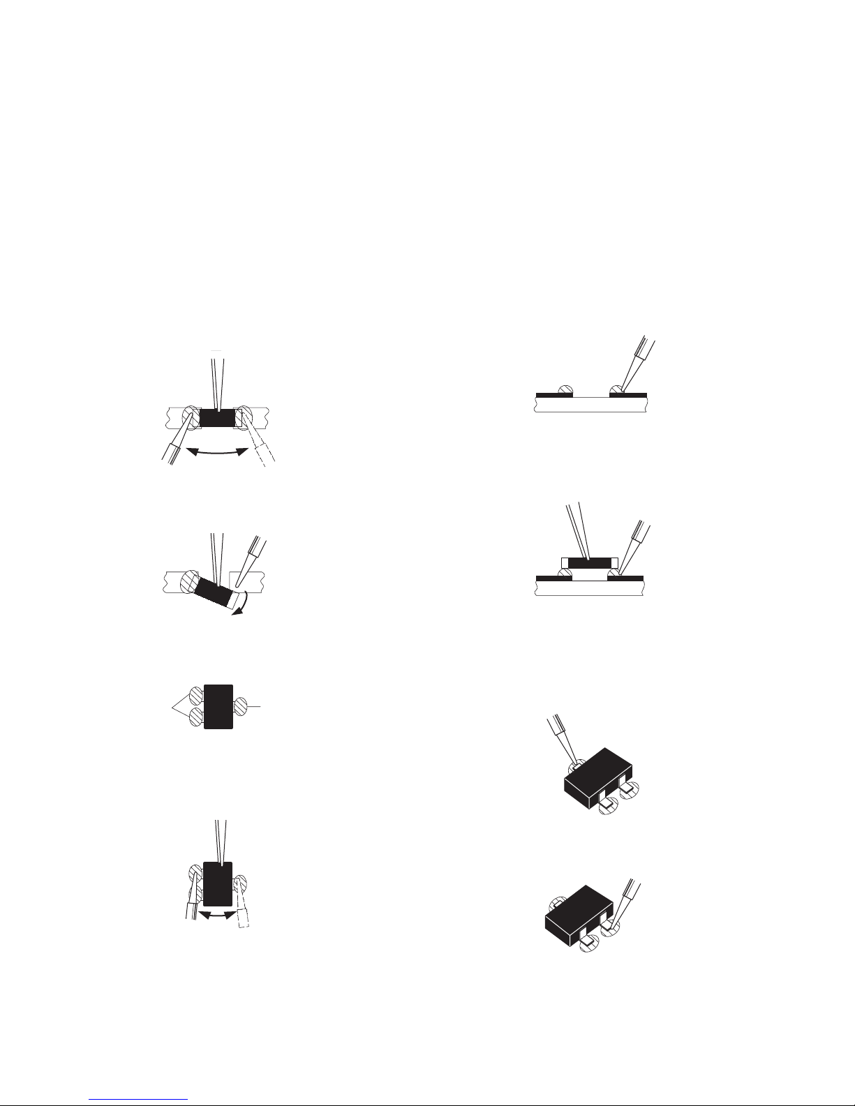
3.4 REPLACEMENT OF CHIP COMPONENT
3.4.1 CAUTIONS
(1) Avoid heating for more than 3 seconds.
(2) Do not rub the electrodes and the resist parts of the pattern.
(3) When removing a chip part, melt the solder adequately.
(4) Do not reuse a chip part after removing it.
3.4.2 SOLDERING IRON
(1) Use a high insulation soldering iron with a thin pointed end of it.
(2) A 30w soldering iron is recommended for easily removing parts.
3.4.3 REPLACEMENT STEPS
1. How to remove Chip parts
2. How to install Chip parts
[Resistors, capacitors, etc.]
(1) As shown in the figure, push the part with tweezers and
alternately melt the solder at each end.
(2) Shift with the tweezers and remove the chip part.
[Transistors, diodes, variable resistors, etc.]
(1) Apply extra solder to each lead.
SOLDER
SOLDER
[Resistors, capacitors, etc.]
(1) Apply solder to the pattern as indicated in the figure.
(2) Grasp the chip part with tweezers and place it on the
solder. Then heat and melt the solder at both ends of the
chip part.
[Transistors, diodes, variable resistors, etc.]
(1) Apply solder to the pattern as indicated in the figure.
(2) Grasp the chip part with tweezers and place it on the
solder.
(3) First solder lead A as indicated in the figure.
(2) As shown in the figure, push the part with tweezers and
alternately melt the solder at each lead. Shift and remove
the chip part.
NOTE :
After removing the part, remove remaining solder from the
pattern.
1-14 (No.YA665<Rev.001>)
A
B
C
(4) Then solder leads B and C.
A
B
C
Page 15
SECTION 4
SERVICE MENU
1. ADJUST
2. SELF CHECK
3. I2C STOP
ADJUSTMENT
4.1 ADJUSTMENT PREPARATION
(1) There are 2 ways of adjusting this TV : One is with the
REMOTE CONTROL UNIT and the other is the
conventional method using adjustment parts and
components.
(2) The adjustment using the REMOTE CONTROL UNIT is
made on the basis of the initial setting values. The
setting values which adjust the screen to the optimum
condition can be different from the initial setting
values.
(3) Make sure that connection is correctly made AC to AC
power source.
(4) Turn on the power of the TV and measuring instruments for
warming up for at least 30 minutes before starting
adjustments.
(5) If the receive or input signal is not specified, use the most
appropriate signal for adjustment.
(6) Never touch the parts (such as variable resistors,
transformers and condensers) not shown in the adjustment
items of this service adjustment.
4.2 PRESET SETTING BEFORE ADJUSTMENTS
Unless otherwise specified in the adjustment items, preset the
following functions with the REMOTE CONTROL UNIT.
Setting item Settings position
Picture Mode Standard
Picture Adjustments Centre
Colour Temp. Normal
Super Digipure Auto
Movie Theatre Auto
Colour Management On
Picture Management On
Zoom Full
4.3 MEASURING INSTRUMENT AND FIXTURES
• Signal generator (Pattern generator) [PAL]
• Remote control unit
4.5 BASIC OPERATION OF SERVICE MODE
4.5.1 HOW TO ENTER THE SERVICE MODE
(1) Press [DISPLAY] key and [MUTING] key on the remote
control unit simultaneously to enter the SERVICE MODE
SCREEN.
(2) In the SERVICE MENU, press the [1] key to display
ADJUSTMENT MODE SCREEN.
SERVICE MENU SCREEN
SERVICE MENU
1. ADJUST
2. SELF CHECK
3. I2C STOP
NOTE:
• Before enter the SERVICE MODE, press the [MODE] key to
confirm that "TV" position is indicated. If it is in a wrong
position, the SERVICE MODE operation cannot be
performed.
• When a number key other than the [1] key is pressed in the
SERVICE MODE SCREEN, the other relevant screen may
be displayed.
This is not used in the adjustment procedure. Press the
[MENU] key to return to the SERVICE MODE SCREEN.
4.5.2 HOW TO EXIT THE SERVICE MODE
Press the [MENU] key to exit the Service mode.
4.5.3 SERVICE MODE SELECT KEY LOCATION
[MUTING] key
[Nunber] key
4.4 ADJUSTMENT ITEMS
VIDEO CIRCUIT
• WHITE BALANCE (HIGH LIGHT) adjustment
[RETURN+] key
[Red] key
[MODE] key
[Function/] key
[DISPLAY] key
[Green] key
[MENU] key
[FUNCTION
/] key
(No.YA665<Rev.001>)1-15
Page 16

4.5.4 ADJUSTMENT MODE
S001 R DRIVE 137
PAL50 FULL STD H
This mode is used to adjust the VIDEO CIRCUIT and the MTS CIRCUIT.
4.5.4.1 HOW TO ENTER THE ADJUSTMENT MODE
When the SERVICE MENU SCREEN of SERVICE MODE is displayed, press [1] key to enter the ADJUSTMENT MODE.
4.5.5 DESCRIPTION OF STATUS DISPLAY
(3) PICTURE MODE
SOFT : Soft
ADJUSTMENT MODE
SETTING ITEM No.
SETTING ITEM
SETTING VALUE (DATA)
STD : Standard
BRI : Bright
(4) COLOUR TEMP.
H : Cool
M: Mid
S001 R DRIVE 137
PAL50 FULL STD H
L: Warm
(5) SETTING ITEM NAME
Setting item name are displayed. For the setting item names
to be displayed, refer to "INITIAL SETTING VALUES IN THE
SERVICE MODE".
SIGNAL SYSTEM
ZOOM MODE
PICTURE MODE
COLOUR TEMP.
(1) SIGNAL SYSTEM
The signal displayed on the screen is displayed.
PAL50 : PAL50Hz (Composite / S-video)
PAL60 : PAL60Hz (Composite / S-video)
SECAM : SECAM
NTSC3 : NTSC3.58
NTSC4 : NTSC4.43
525I : 525i (Component)
525P : 525p
625I : 625i (Component)
625P : 625p
1125I5 : 1125i 50Hz
1125I6 : 1125i 60Hz
RGB5 : RGB 525i
RGB6 : RGB 625i
PCVGA : PC (VGA)
PCXGA : PC (XGA)
H525I : HDMI 525i
H525P : HDMI 525p
H625I : HDMI 625i
H625P : HDMI 625p
H750P : HDMI 750p
H125I5 : HDMI 1125i 50Hz
H125I6 : HDMI 1125i 60Hz
--- : OTHER
(2) ZOOM MODE
State of the SCREEN SIZE or MULTI PICTURE is displayed.
SINGLE SCREEN
FULL : Full
JUST : Full Native
PANO : Panoramic
1609 : 16:9 Zoom
1609S : 16:9 Zoom Subtitle
1409 : 14:9 Zoom
REGU : Regular
MULTI SCREEN
FRZ : Freeze screen
M12 : 12-pictures screen
(6) SETTING ITEM NO.
Setting item numbers are displayed. The setting item numbers
to be displayed are listed below.
Item No. Setting item
S001 - S009 Video system setting
T001 - T003 (NOT USED)
M001 - M224 (NOT USED)
F001 - F002 (NOT USED)
D001 (NOT USED)
Z001 (NOT USED)
(7) SETTING VALUE (DATA)
The SETTING VALUE is displayed.
4.5.6 CHANGE AND MEMORY OF SETTING VALUE
SELECTION OF SETTING ITEM
• [FUNCTION /] key.
For scrolling up / down the setting items.
S001...S009 ↔ T001...T003 ↔ M001...M224 ↔
F001...F002 ↔ D001 ↔ Z001↔return to S001
CHANGE OF SETTING VALUE (DATA)
• [FUNCTION /] key.
For scrolling up / down the setting values.
MEMORY OF SETTING VALUE (DATA)
Changed setting value is memorized by pressing [MUTING]
key.
1-16 (No.YA665<Rev.001>)
Page 17
4.6 INITIAL SETTING VALUES IN THE SERVICE MODE
• Perform fine-tuning based on the "initial values" using the remote control when in the Service mode.
• The "initial values" serve only as an indication rough standard and therefore the values with which optimal display can be achieved
may be different from the default values. But, don't change the values that are not written in "ADJUSTMENT PROCEDURE". They
are fixed values.
4.6.1 VIDEO SYSTEM SETTING
Item No. Item Variable range Setting value
S001 R DRIVE 0 - 255 137
S002 G DRIVE 0 - 255 137
S003 B DRIVE 0 - 255 137
S004 RESERV 0 - 255 --S005 2D YC 0 - 255 0
S006 RESERV 0 - 255 --S007 RESERV 0 - 255 --S008 RESERV 0 - 255 --S009 RESERV 0 - 255 ---
4.6.2 NOT USED ITEM (All values are Fixed values)
Item No. Item Variable range Setting value
T001 RESERV 0 - 15 ---
T002 RESERV 0 - 63 ---
T003 RESERV 0 - 63 ---
M001 1E00 00 - FF ---
M002 1E01 00 - FF ---
M003 1E02 00 - FF ---
M004 1E03 00 - FF ---
M005 1E04 00 - FF ---
M006 1E05 00 - FF ---
M007 1E06 00 - FF ---
M008 1E07 00 - FF ---
M009 1E08 00 - FF ---
M010 1E09 00 - FF ---
M011 1E0A 00 - FF ---
M012 1E0B 00 - FF ---
M013 1E0C 00 - FF ---
M014 1E0D 00 - FF ---
M015 1E0E 00 - FF ---
M016 1E0F 00 - FF ---
M017 1E10 00 - FF ---
M018 1E11 00 - FF ---
M019 1E12 00 - FF ---
M020 1E13 00 - FF ---
M021 1E14 00 - FF ---
M022 1E15 00 - FF ---
M023 1E16 00 - FF ---
M024 1E17 00 - FF ---
M025 1E18 00 - FF ---
M026 1E19 00 - FF ---
M027 1E1A 00 - FF ---
M028 1E1B 00 - FF ---
M029 1E1C 00 - FF ---
M030 1E1D 00 - FF ---
M031 1E1E 00 - FF ---
Item No. Item Variable range Setting value
M032 1E1F 00 - FF ---
M033 1E20 00 - FF ---
M034 1E21 00 - FF ---
M035 1E22 00 - FF ---
M036 1E23 00 - FF ---
M037 1E24 00 - FF ---
M038 1E25 00 - FF ---
M039 1E26 00 - FF ---
M040 1E27 00 - FF ---
M041 1E28 00 - FF ---
M042 1E29 00 - FF ---
M043 1E2A 00 - FF ---
M044 1E2B 00 - FF ---
M045 1E2C 00 - FF ---
M046 1E2D 00 - FF ---
M047 1E2E 00 - FF ---
M048 1E2F 00 - FF ---
M049 1E30 00 - FF ---
M050 1E31 00 - FF ---
M051 1E32 00 - FF ---
M052 1E33 00 - FF ---
M053 1E34 00 - FF ---
M054 1E35 00 - FF ---
M055 1E36 00 - FF ---
M056 1E37 00 - FF ---
M057 1E38 00 - FF ---
M058 1E39 00 - FF ---
M059 1E3A 00 - FF ---
M060 1E3B 00 - FF ---
M061 1E3C 00 - FF ---
M062 1E3D 00 - FF ---
M063 1E3E 00 - FF ---
M064 1E3F 00 - FF ---
M065 1E40 00 - FF ---
M066 1E41 00 - FF ---
M067 1E42 00 - FF ---
M068 1E43 00 - FF ---
M069 1E44 00 - FF ---
M070 1E45 00 - FF ---
M071 1E46 00 - FF ---
M072 1E47 00 - FF ---
M073 1E48 00 - FF ---
M074 1E49 00 - FF ---
M075 1E4A 00 - FF ---
M076 1E4B 00 - FF ---
(No.YA665<Rev.001>)1-17
Page 18
Item No. Item Variable range Setting value
M077 1E4C 00 - FF ---
M078 1E4D 00 - FF ---
M079 1E4E 00 - FF ---
M080 1E4F 00 - FF ---
M081 1E50 00 - FF ---
M082 1E51 00 - FF ---
M083 1E52 00 - FF ---
M084 1E53 00 - FF ---
M085 1E54 00 - FF ---
M086 1E55 00 - FF ---
M087 1E56 00 - FF ---
M088 1E57 00 - FF ---
M089 1E58 00 - FF ---
M090 1E59 00 - FF ---
M091 1E5A 00 - FF ---
M092 1E5B 00 - FF ---
M093 1E5C 00 - FF ---
M094 1E5D 00 - FF ---
M095 1E5E 00 - FF ---
M096 1E5F 00 - FF ---
M097 1E60 00 - FF ---
M098 1E61 00 - FF ---
M099 1E62 00 - FF ---
M100 1E63 00 - FF ---
M101 1E64 00 - FF ---
M102 1E65 00 - FF ---
M103 1E66 00 - FF ---
M104 1E67 00 - FF ---
M105 1E68 00 - FF ---
M106 1E69 00 - FF ---
M107 1E6A 00 - FF ---
M108 1E6B 00 - FF ---
M109 1E6C 00 - FF ---
M110 1E6D 00 - FF ---
M111 1E6E 00 - FF ---
M112 1E6F 00 - FF ---
M113 1E70 00 - FF ---
M114 1E71 00 - FF ---
M115 1E72 00 - FF ---
M116 1E73 00 - FF ---
M117 1E74 00 - FF ---
M118 1E75 00 - FF ---
M119 1E76 00 - FF ---
M120 1E77 00 - FF ---
M121 1E78 00 - FF ---
M122 1E79 00 - FF ---
M123 1E7A 00 - FF ---
M124 1E7B 00 - FF ---
M125 1E7C 00 - FF ---
M126 1E7D 00 - FF ---
Item No. Item Variable range Setting value
M127 1E7E 00 - FF ---
M128 1E7F 00 - FF ---
M129 1E80 00 - FF ---
M130 1E81 00 - FF ---
M131 1E82 00 - FF ---
M132 1E83 00 - FF ---
M133 1E84 00 - FF ---
M134 1E85 00 - FF ---
M135 1E86 00 - FF ---
M136 1E87 00 - FF ---
M137 1E88 00 - FF ---
M138 1E89 00 - FF ---
M139 1E8A 00 - FF ---
M140 1E8B 00 - FF ---
M141 1E8C 00 - FF ---
M142 1E8D 00 - FF ---
M143 1E8E 00 - FF ---
M144 1E8F 00 - FF ---
M145 1E90 00 - FF ---
M146 1E91 00 - FF ---
M147 1E92 00 - FF ---
M148 1E93 00 - FF ---
M149 1E94 00 - FF ---
M150 1E95 00 - FF ---
M151 1E96 00 - FF ---
M152 1E97 00 - FF ---
M153 1E98 00 - FF ---
M154 1E99 00 - FF ---
M155 1E9A 00 - FF ---
M156 1E9B 00 - FF ---
M157 1E9C 00 - FF ---
M158 1E9D 00 - FF ---
M159 1E9E 00 - FF ---
M160 1E9F 00 - FF ---
M161 1EA0 00 - FF ---
M162 1EA1 00 - FF ---
M163 1EA2 00 - FF ---
M164 1EA3 00 - FF ---
M165 1EA4 00 - FF ---
M166 1EA5 00 - FF ---
M167 1EA6 00 - FF ---
M168 1EA7 00 - FF ---
M169 1EA8 00 - FF ---
M170 1EA9 00 - FF ---
M171 1EAA 00 - FF ---
M172 1EAB 00 - FF ---
M173 1EAC 00 - FF ---
M174 1EAD 00 - FF ---
M175 1EAE 00 - FF ---
M176 1EAF 00 - FF ---
1-18 (No.YA665<Rev.001>)
Page 19
Item No. Item Variable range Setting value
M177 1EB0 00 - FF ---
M178 1EB1 00 - FF ---
M179 1EB2 00 - FF ---
M180 1EB3 00 - FF ---
M181 1EB4 00 - FF ---
M182 1EB5 00 - FF ---
M183 1EB6 00 - FF ---
M184 1EB7 00 - FF ---
M185 1EB8 00 - FF ---
M186 1EB9 00 - FF ---
M187 1EBA 00 - FF ---
M188 1EBB 00 - FF ---
M189 1EBC 00 - FF ---
M190 1EBD 00 - FF ---
M191 1EBE 00 - FF ---
M192 1EBF 00 - FF ---
M193 1EC0 00 - FF ---
M194 1EC1 00 - FF ---
M195 1EC2 00 - FF ---
M196 1EC3 00 - FF ---
M197 1EC4 00 - FF ---
M198 1EC5 00 - FF ---
M199 1EC6 00 - FF ---
M200 1EC7 00 - FF ---
M201 1EC8 00 - FF ---
M202 1EC9 00 - FF ---
M203 1ECA 00 - FF ---
Item No. Item Variable range Setting value
M204 1ECB 00 - FF ---
M205 1ECC 00 - FF ---
M206 1ECD 00 - FF ---
M207 1ECE 00 - FF ---
M208 1ECF 00 - FF ---
M209 1ED0 00 - FF ---
M210 1ED1 00 - FF ---
M211 1ED2 00 - FF ---
M212 1ED3 00 - FF ---
M213 1ED4 00 - FF ---
M214 1ED5 00 - FF ---
M215 1ED6 00 - FF ---
M216 1ED7 00 - FF ---
M217 1ED8 00 - FF ---
M218 1ED9 00 - FF ---
M219 1EDA 00 - FF ---
M220 1EDB 00 - FF ---
M221 1EDC 00 - FF ---
M222 1EDD 00 - FF ---
M223 1EDE 00 - FF ---
M224 1EDF 00 - FF ---
F001 DD 0 - 1 ---
F002 RAM REF 0 - 1 ---
D001 RESERV 0 - 255 ---
Z001 RESERV 0 - 255 ---
4.7 ADJUSTMENT PROCEDURE
4.7.1 VIDEO CIRCUIT
Item
WHITE
BALANCE
Measuring
instrument
Remote
control unit
Test point Adjustment part Description
(HIGHLIGHT)
Signal
generator
[1.ADJUST]
S001: R DRIVE (Red drive)
S002: G DRIVE (Green drive)
S003: B DRIVE (Blue drive)
(1) Receive a PAL 75% all white signal.
(2) Set PICTURE MODE to "Standard".
(3) Set ZOOM to "Full".
(4) Set WHITE BALANCE to "Mid".
(5) Select "1.ADJUST" from the SERVICE MODE.
(6) Adjust to Keep one of <S001> (Red drive),
<S002> (Green drive) or <S003> (Blue drive)
unchanged, then lower the other two so that the
all-white screen is equally white throughout.
NOTE:
Set one or more of <S001>, <S002>, and
<S003> to "137".
(7) Check that white balance is properly tracked
from low light to high light. If the white balance
tracking is deviated, adjust to correct it.
(8) Press the [MUTING] key to memorize the set
value.
(No.YA665<Rev.001>)1-19
Page 20
SECTION 5
SERVICE MENU
1. ADJUST
2. SELF CHECK
3. I2C STOP
TMP 0 L 1 0
L 2 0 DDT 0
FAN 0 L C 0
IRS 0
LOB 0 FAN 0
AUD 0
ANA 9 DIG 9
HOUR 131070 MAX 00
00
TROUBLESHOOTING
5.1 SELF CHECK FEATURE
5.1.1 OUTLINE
This unit comes with the "Self check" feature, which checks the
operational state of the circuit and displays/saves it during
failure.Diagnosis is performed when power is turned on, and
information input to the main microcomputer is monitored at all
time.Diagnosis is displayed in 2 ways via screen display and LED
flashes. Failure detection is based on input state of I
2
C bus and
the various control lines connected to the main microcomputer.
5.1.2 HOW TO ENTER THE SELF CHECK MODE
Before enter the SELF CHECK MODE, press the [MODE] key to
confirm that "TV" position is indicated. If it is in a wrong position,
the SELF CHECK MODE operation cannot be performed.
(1) Press the [DISPLAY] key and [MUTING] key
simultaneously, then enter the SERVICE MODE.
(2) Press the [2] key SELF CHECK MODE.
(3) Press the [RED] key to enter Page 2 of the SELF CHECK
MODE.
*Use the [GREEN] key to toggle between Page 1 and Page 2.
NOTE:
When a number key other than the [2] key is pressed in the
SERVICE MODE screen, the other relevant screen may be
displayed.
This is not used in the SELF CHECK MODE. Press the
[MENU] key to return to the MAIN MENU SCREEN.
5.1.3 HOW TO EXIT THE SELF CHECK MODE
To Save Failure History:
Turn off the power by unplugging the AC power cord plug when
in the Self check display mode.
To Clear (Reset) Failure History:
Turn off the power by pressing the [POWER] key on the remote
control unit when in the Self check display mode.
5.1.4 FAILURE HISTORY
Failure history can be counted up to 9 times for each item. When
the number exceeds 9, display will remain as 9. Failure history
will be stored in the memory unless it has been deleted.
5.1.5 POINTS TO NOTE WHEN USING THE SELF CHECK
FEATURE
In addition to circuit failures (abnormal operation), the following
cases may also be diagnosed as "Abnormal" and counted.
(1) Temporary defective transmissions across circuits due to
pulse interruptions.
(2) Misalignment in the on/off timing of power for I
2
C bus (Vcc)
when turning on/off the main power.
Therefore, turn on the main power, and then wait for about 3
seconds before starting Self check.
If recurrences are expected, ensure to clear (reset) the failure
history and record the new diagnosis results.
SERVICE MENU SCREEN
SERVICE MENU
1. ADJUST
2. SELF CHECK
3. I2C STOP
Press [2] key
SELF CHECK MODE SCREEN (Page 1)
Item
LOB 0 FAN 0
AUD 0
ANA 9 DIG 9
HOUR 131070 MAX 00
00
Press [Red] key
Failure
history
Failure
Item
history
Press [Green] key
SELF CHECK MODE SCREEN (Page 2)
1-20 (No.YA665<Rev.001>)
Not used
TMP 0 L 1 0
L 2 0 DDT 0
FAN 0 L C 0
IRS 0
Fig.5-1
Page 21
5.1.6 DETAILS
Self check is performed for the following items: (---- is not used items)
<Page 1 of screen>
Detection item Display Detection content
Low bias line short
protection
LOB Confirm the operation of the low bias protection
circuit.
, Q9401, Q9601, Q9703 [DC-DC PWB]
IC9401
---- FAN ---- ---- ----
---- AUD ---- ---- ----
Devices on the ANALOG
PWB
ANA Confirmation of reply of ACK signal which uses
2
C communication.
I
IC101
, IC102, IC601, IC3501, TU3001
[ANALOG PWB]
Devices on the DIGITAL
PWB
DIG Confirmation of reply of ACK signal which uses
2
C communication.
I
[DIGITAL PWB]
IC5001
<Page 2 of screen>
Detection item Display Detection content
---- TMP ---- ---- ----
---- L1 ---- ---- ----
---- L2 ---- ---- ----
---- DDT ---- ---- ----
---- FAN ---- ---- ----
---- LC ---- ---- ----
---- IRS ---- ---- ----
Diagnosis
signal (line)
Detection timing
LB_PRO Detection starts 3 seconds after
the power is turned on. If error
continues between 200 ms the
power is turned off.
SDA Detection starts 3 seconds after
the power is turned on. If it checks
whenever I
2
C communication is
performed and no reply of ACK
signal an error will be counted.
SDA Detection starts 3 seconds after
the power is turned on. If it checks
whenever I2C communication is
performed and no reply of ACK
signal an error will be counted.
Diagnosis
signal (line)
Detection timing
5.1.7 METHOD OF DISPLAY WHEN A RASTER IS NOT OUTPUT
In the state where a raster is not output by breakdown of the set, an error is displayed by blink of the POWER LED.
Type of error POWER LED flash cycle
Low bias line short protection POWER LED turnig on and off at 1 second intervals.
<Explanation of operation>
If error is detected, the power is turned off.
Shortly after a power is turned off, POWER LED will be blinked.
Power cannot be turned on until the power cord takes out and inserts, after a power is turned off.
(No.YA665<Rev.001>)1-21
Page 22

Victor Company of Japan, Limited
Display Division 12, 3-chome, Moriya-cho, Kanagawa-ku, Yokohama-city, Kanagawa-prefecture, 221-8528, Japan
(No.YA665<Rev.001>)
Printed in Japan
VPT
Page 23
SCHEMATIC DIAGRAMS
WIDE LCD PANEL TELEVISION
LT-52GZ79, LT-52GZ79/BA,
LT-52GZ79/E, LT-52GZ79/S
BASIC CHASSIS
DVD-ROM No.SML2008Q3
FL5
COPYRIGHT © 2008 Victor Company of Japan, Limited.
No.YA665<Rev.001>
2008/12
Page 24
LT-52GZ79, LT-52GZ79/BA, LT-52GZ79/E, LT-52GZ79/S
STANDARD CIRCUIT DIAGRAM
NOTE ON USING CIRCUIT DIAGRAMS
1.SAFETY
The components identified by the symbol and shading are
critical for safety. For continued safety replace safety ciritical
components only with manufactures recommended parts.
2.SPECIFIED VOLTAGE AND WAVEFORM VALUES
The voltage and waveform values have been measured under the
following conditions.
(1)Input signal : Colour bar signal
(2)Setting positions of
each knob/button and
variable resistor
(3)Internal resistance of tester
(4)Oscilloscope sweeping time
(5)Voltage values
Since the voltage values of signal circuit vary to some extent
according to adjustments, use them as reference values.
: Original setting position
when shipped
: DC 20kΩ/V
: H
: V
: Othters
: All DC voltage values
20µs / div
5ms / div
Sweeping time is
specified
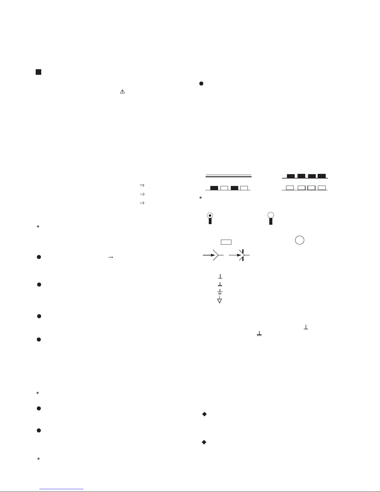
3.INDICATION OF PARTS SYMBOL [EXAMPLE]
In the PW board
: R1209
R209
Type
No indication
MM
PP
MPP
MF
TF
BP
TAN
(3)Coils
No unit
Others
(4)Power Supply
Respective voltage values are indicated
(5)Test point
: Test point
(6)Connecting method
: Ceramic capacitor
: Metalized mylar capacitor
: Polypropylene capacitor
: Metalized polypropylene capacitor
: Metalized film capacitor
: Thin film capacitor
: Bipolar electrolytic capacitor
: Tantalum capacitor
: [µH]
: As specified
: B1
: 9V
: Connector
: Receptacle
: Only test point display
: Wrapping or soldering
: B2 (12V
: 5V
)
4.INDICATIONS ON THE CIRCUIT DIAGRAM
(1)Resistors
Resistance value
No unit : [Ω]
K
M
Rated allowable power
No indication : 1/16 [W]
Others : As specified
Type
No indication
OMR
MFR
MPR
UNFR
FR
Composition resistor 1/2 [W] is specified as 1/2S or Comp.
(2)Capacitors
Capacitance value
1 or higher : [pF]
less than 1
Withstand voltage
No indication : DC50[V]
Others : DC withstand voltage [V]
AC indicated
Electrolytic Capacitors
47/50[Example]: Capacitance value [µF]/withstand voltage[V]
: [kΩ]
: [MΩ]
: Carbon resistor
: Oxide metal film resistor
: Metal film resistor
: Metal plate resistor
: Uninflammable resistor
: Fusible resistor
: [µF]
: AC withstand voltage [V]
(7)Ground symbol
: LIVE side ground
: ISOLATED(NEUTRAL) side ground
: EARTH ground
: DIGITAL ground
5.NOTE FOR REPAIRING SERVICE
This model's power circuit is partly different in the GND. The
difference of the GND is shown by the LIVE : ( ) side GND and the
ISOLATED(NEUTRAL) : ( ) side GND. Therefore, care must be
taken for the following points.
(1)Do not touch the LIVE side GND or the LIVE side GND and the
ISOLATED(NEUTRAL) side GND simultaneously. if the above
caution is not respected, an electric shock may be caused.
Therefore, make sure that the power cord is surely removed from
the receptacle when, for example, the chassis is pulled out.
(2)Do not short between the LIVE side GND and ISOLATED(NEUTRAL
side GND or never measure with a measuring apparatus measure
with a measuring apparatus ( oscilloscope, etc.) the LIVE side GND
and ISOLATED(NEUTRAL) side GND at the same time.
If the above precaution is not respected, a fuse or any parts will be broken.
Since the circuit diagram is a standard one, the circuit and
circuit constants may be subject to change for improvement
without any notice.
NOTE
Due improvement in performance, some part numbers show
in the circuit diagram may not agree with those indicated in
the part list.
When ordering parts, please use the numbers that appear
in the Parts List.
)
(No.YA665<Rev.001>)2-1
Page 25
CONTENTS
SEMICONDUCTOR SHAPES ......................................................................2-2
WIRING DIAGRAM .......................................................................................2-3
BLOCK DIAGRAM ........................................................................................2-5
CIRCUIT DIAGRAMS ...................................................................................2-7
ANALOG PWB CIRCUIT DIAGRAM ........................................................................................................... 2-7
DIGIT AL PWB CIRCUIT DIA GRAM .......................................................................................................... 2-19
POWER PWB CIRCUIT DIA GRAM ........................................................................................................... 2-43
DC-DC PWB CIRCUIT DIAGRAM ............................................................................................................. 2-49
LED PWB CIRCUIT DIAGRAM................................................................................................................. 2-51
SW PWB CIRCUIT DIAGRAM .................................................................................................................. 2-53
PATTERN DIAGRAMS .............................................................................. 2-55
ANALOG PWB P A TTERN ........................................................................................................................ 2-55
DIGIT AL PWB PA TTERN ......................................................................................................................... 2-57
POWER PWB PA TTERN .......................................................................................................................... 2-61
DC-DC PWB P A TTERN ............................................................................................................................ 2-63
LED PWB P ATTERN ................................................................................................................................ 2-63
SW PWB P ATTERN ................................................................................................................................. 2-64
VOLTAGE CHARTS ................................................................................... 2-65
WAVEFORMS ............................................................................................ 2-67
USING P.W. BOARD
P.W.B ASS㵭Y name LT-52GZ79 LT-52GZ79/E LT-52GZ79/S LT-52GZ79/BA
ANALOG P.W. BOARD
SW P.W. BOARD
LED P.W. BOARD
POWER P.W. BOARD
DC-DC P.W. BOARD
DIGITAL P.W. BOARD
SFL-1237A-H2
SFL-7221A-H2
SFL-8728A-H2
SFL-90A5A-H2
SFL-91A1A-H2
SFL0D403A-H2
φ
φ
φ
SFL-90A6A-H2
φ
φ
φ
φ
φ
SFL-90A5A-H2
φ
SFL0D404A-H2
SFL-1237A-H8
SFL-7221A-H8
SFL-8728A-H8
SFL-90A5A-H8
SFL-91A1A-H8
SFL0D403A-H8
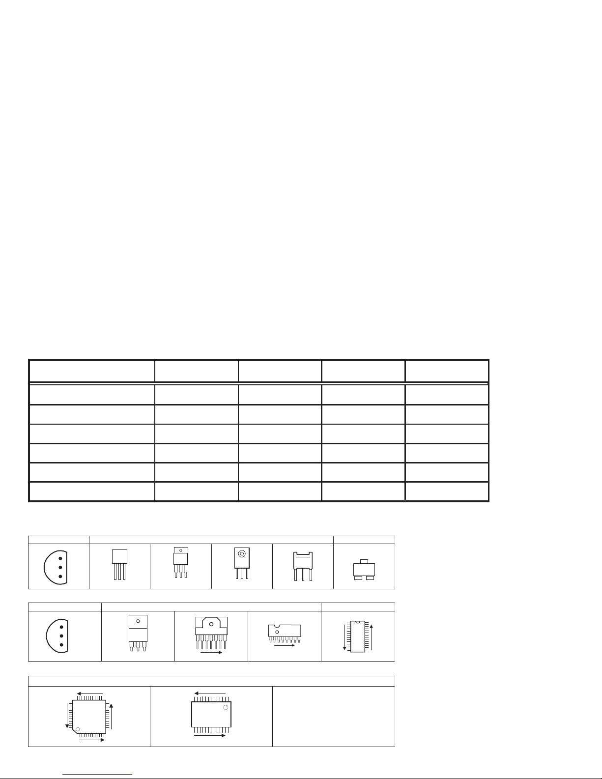
SEMICONDUCTOR SHAPES
TRANSISTOR
BOTTOM VIEW FRONT VIEW TOP VIEW
E
C
B
IC
BOTTOM VIEW FRONT VIEW TOP VIEW
OUT
E
IN
ECB
IN OUTE
B
(G)E(S)C(D)
1 N
ECB
ECB
1 N
CHIP TR
1
C
BE
N
CHIP IC
TOP VIEW
N
1
2-2(No.YA665<Rev.001>)
1
N
Page 26
2-4(No.YA665<Rev.001>)(No.YA665<Rev.001>)2-3
21
91
101
110
15 1
41 21
14
13
12
501401
CN00R
CN00U
CN0SR
CN001
CN002
CN0SL
CN100U
F9001
250V/6.3A
CN00W
CN00P
CN00F
CN00A
CN0PW
114
15 1
115
CN00A
CN0DC
123
CN00H
123
CN00H
CN10F
ANALOG
TUNER
115
CN0DC
14
CN001W
150140
CN001
CN002
CN100R
91
151
41 1
CN0LV2
CN0LV1
CN00Q
110
LED PWB
DC-DC PWB
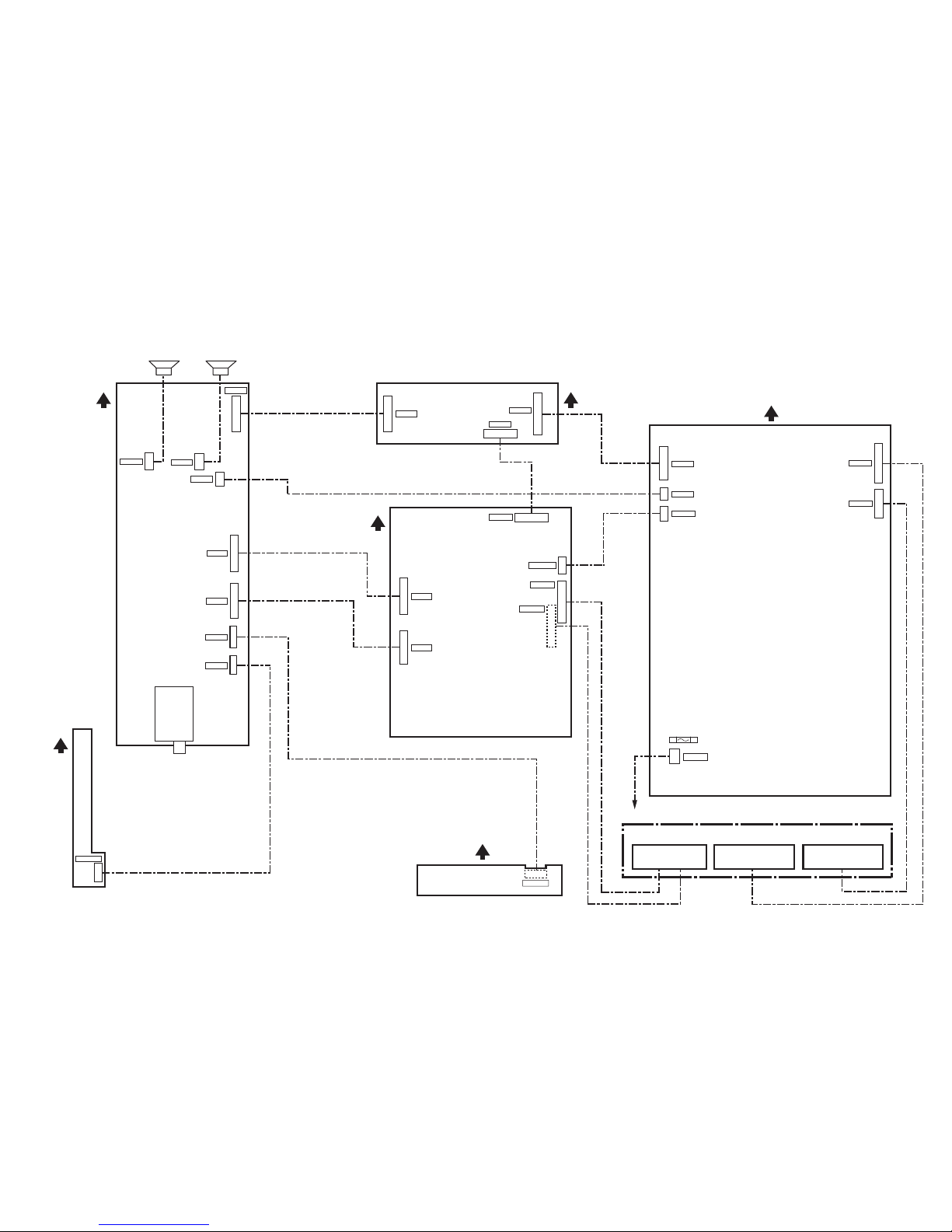
TOP
TOP
TOP
TOP
TOP
TOP
DIGITAL PWB
ANALOG PWB
SW PWB
POWER PWB
POWER CORD
SPEAKER (R) SPEAKER (L)
LCD PANEL UNIT
CONTROL PWB
INVERTER PWB
(SLAVE SIDE)
INVERTER PWB
(MASTER SIDE)
WIRING DIAGRAM
Page 27
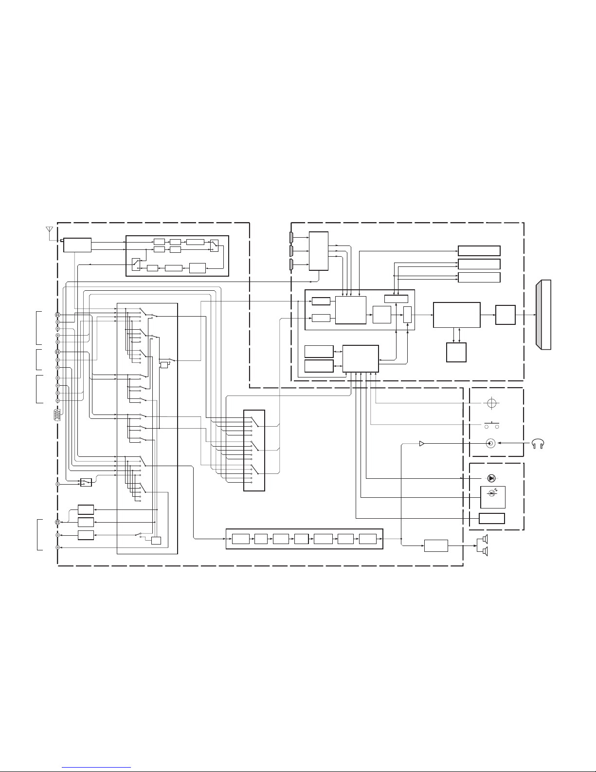
(No.YA665<Rev.001>)2-5 2-6(No.YA665<Rev.001>)
IC8751
EE_CDS
E.E. SENSOR
IC5001
DQ
ADRS
IC5002
IC5003
FRAME INTERPOLATE/
LCD CONTROL/
BACK-LIGHT CONTROL
FRAME
MEMORY
IC5503
IC6503
LVDS
DRIVE
DBO 0-9
DGO 0-9
DRO 0-9
DBE 0-9
DGE 0-9
DRE 0-9
SPEAKER(R)
SPEAKER(L)
DIGITAL PWB
SW PWB
OSDR1-5
OSDG1-5
OSDB1-5
J7001
S7701~S7706
S7707
PROGRAM MEMORY
PROGRAM MEMORY
MAIN CPU
IC7201
FRAME MEMORY
IC6101
IC7203
HDMI
DIGITAL IN
HDMI-1
HDMI
RECEIVE
IC7301
SETTING DATA
MEMORY
IC7602
IC6001
DV1_R0-7
D0-15
D0-15
A0-21
SD_DQ1-32
A0-21
DV1_G0-7
DV1_B0-7
MI_TX
MI_RX
MI_CLK
HDMI
DIGITAL IN
HDMI-2
HDMI
DIGITAL IN
HDMI-3
AUDIO L/R
S-VIDEO
VIDEO-1
VIDEO
DEC_Y
V1_VIN
V2_VIN
V3_VIN
V1_YIN
V1_CIN
V2_CIN
TV_L/R
V1_L/R
V2_L/R
V3_L/R
DIN_SL/SR
V2_YIN
MAIN_VY
SUB_VY
SUB_VY
Y_OUT
MAIN_VY
V3_G_Y
V1_G_Y
V1_B_Cb
V1_R_Cr
PC_G
TEXT_G
MAIN_C
V3_R_Cr
PC_R
TEXT_R
SUB_C
V3_B_Cb
PC_B
TEXT_B
BY_OUT
RY_OUT
SUB_C
MAIN_C
HP_L/R
AUDIO L/R
S-VIDEO
VIDEO-2
VIDEO
AUDIO L/R
HDMI-1
AUDIO INPUT
L/R
Pr/Pb
Y
Pr/Pb
Y
PC IN
(D-SUB)
VIDEO
VIDEO-3
Y/C
MIX
AUDIO SELECT
IC106
POWER
CONTROL
SWITCH
HEADPHONE
YM_IN
BYM_IN
RYM_IN
KEY_1/2
MECA_SW
TV_MAIN
TU3001
UHF/VHV
TUNER
IC3501
MULTI SOUND PROCESS
REMOCON
POWER_LED
IR RECEIVE
LED PWB
LCD
(PANEL)
SUB CPU/A-D CONVERT/YC SEPARATE/
CHROMA DEMOD./FORMAT CONVERT/
ENHANCE/NR/RGB PROCESS/OSD MIX
A-D
CONVERT
A-D
CONVERT
YC SEPARATE/
CHROMA DEMOD./
FORMAT
CONVERT/
ENHANCE/
NOISE REDUCT
RGB
PROCESS
OSD
MIX
SUB CPU
DVI_L/R
DIN_L/R
DIN_DL/DR
IC8752
HEADPHONE AMP
IC751
POWER
D8702
IC102
VIDEO SELECT
IC101
VIDEO/AUDIO SELECT
TEXT DATA
MEMORY
IC7303
SIF_OUT
MONO
TV_L/R
ANALOG PWB
D-A VOLUME
AGC
DSP
A-D
A-D
DEMOD.
MATRIX
Y/C
MIX
AUDIO L/R
S-VIDEO
MONITOR
OUT
VIDEO
AMP
IC105
MON_L/R
MON_VOUT
MON_YOUT
MON_COUT
AMP
IC104
MAIN_L/R
AMP
IC103
MAIN_CCD
TEXT_R/G/B
IC6001
IC601
AMP_L/R
AUDIO OUT
AUDIO CONTROL
A-D
CONVERT
D-A
CONVERT
VOLUME
BASS
BOOST
TREBLE
BOOST
STEREO
BOOST
EQUALIZE
DBU00-09
DGY00-09
DRV00-09
MAIN_L/R
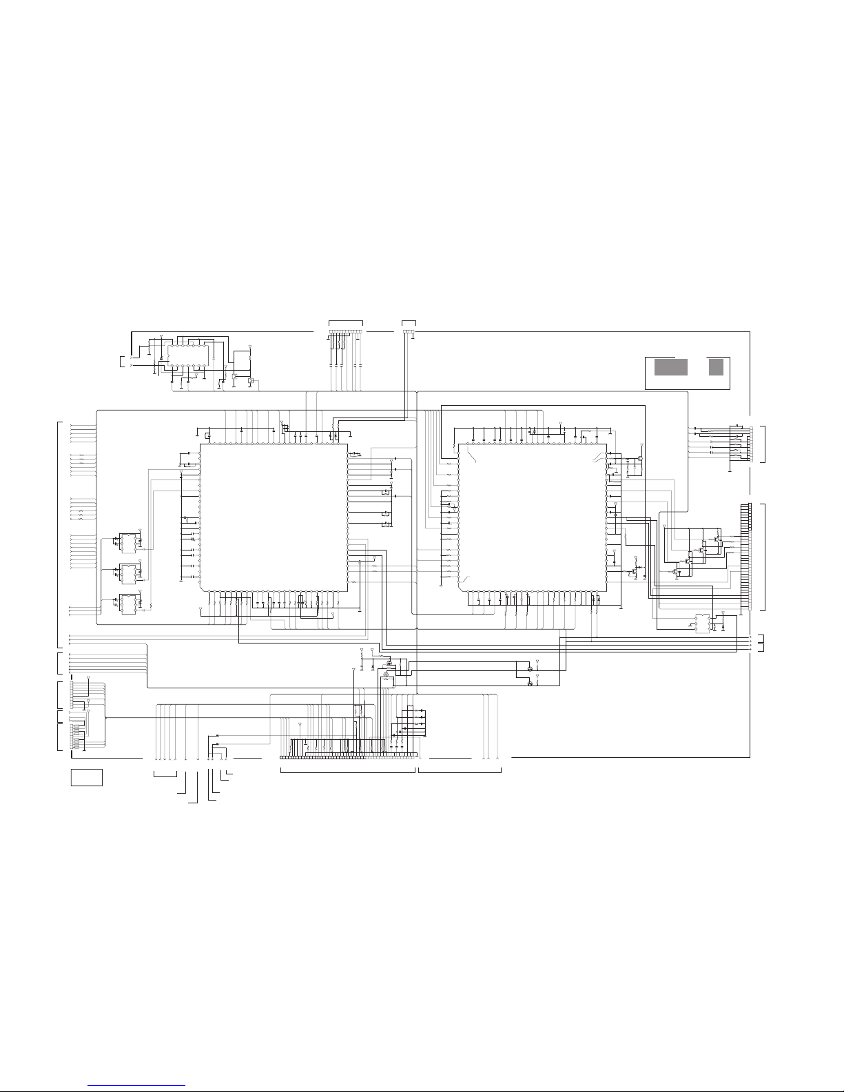
BLOCK DIAGRAM
Page 28
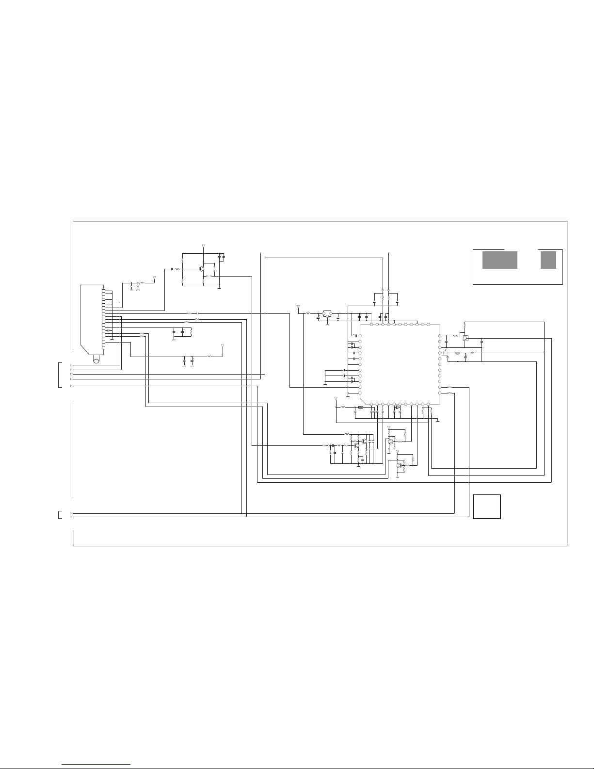
2-8(No.YA665<Rev.001>)(No.YA665<Rev.001>)2-7
ANALOG PWB ASS'Y (1/6)
SFL-1237A-H2 [LT-52GZ79, LT-52GZ79/E, LT-52GZ79/S]
SFL-1237A-H8 [LT-52GZ79/BA]
ggs10021001a_12/4_2/6_0.0
18.432MHz
STANBY
ADR_SEL
D_CTR_OUT0
D_CTR_OUT1
NC
XTAL_OUT
XTAL_IN
TESTEN
ANA_IN-
ANA_IN+
AVSUP
AVSS
MONO_IN
VREFTOP
SC1_IN_R
SC1_IN_L
ASG1
SC2_IN_R
SC2_IN_L
AGNDC
AHVSS
CAPL_M
AHVSUP
NC
SC1_OUT_R
SC1_OUT_L
VREF1
NC
DACM_L
DACM_R
NC
VREF2
SCL
SDA
I2S_CL
I2S_WS
I2S_DA_OUT
TP
DVSUP
DVSS
NC
NC
I2S_DA_IN
NC
RESETQ
NC
NC
AUDIO_OUT
BM
AFT
VIDEO_OUT
IF_OUT
BTL
NC
SIF_OUT
RF_AGC
BT
SCL
SW2
SW1
NC
SDA
NC
NC
G
OUTIN
BUFFER
LT-52GZ79BA
LT-52GZ79EA
LT-52GZ79SA
LT-52GZ79A
LT47GZ78NASKLT42GZ78NASK
OR 2SC1623A/5-6/-X
SFL-1237A -
LT-47GZ78BLT-42GZ78B
LT-47GZ78SA
LT-47GZ78TA
LT-47GZ78BA
LT-42GZ78SA
:NCB11AK-106X
:DTC144EKA-X
:DTC323TK-X
:2SA1037AK/QR/-X
:2SC2412K/QR/-X
:NRSA63J-0R0X
:OPTION(NON MOUNT)
*4
*5
*3
*2
*1
0
OPEN
LT-47GZ78ASFL-1236A
ASSY NO. - MODEL LIST
- NOTE -
LT-42GZ78TA
GND
GND
GND
1_13O
1_14O
1_14O
:2SC3928A/QR/-X
LT-42GZ78BA
GND
1_15O
LT-42GZ78A-
1_5O
NPN
5_1O3_2L1_22L
5_1O3_2L1_22L
GND
GND
GND
GND
GND
GND
GND
GND
TV_R
TV_L
BS_A9V
BS_A5V
GND
32V
MSP_RSTO
BS_A5V
GND
BS_A5V
GND
BS_A5V
SCL3A5
BS_A9V
GND
GND
GND
1
AFT1
TV_R
TV_L
TV_MAIN
MSP_RSTO
SCL3A5
SDA3A5
CH
C3514
2p
/16
C3527
.1
/10
C3528
100
R3510
OPEN
R3509
OPEN
NRSA02J-0R0X
L3503
R3514
100
R3515
100
/10
C3516
100
NQL79GM-4R7X
L3504
NQR0436-001X
LC3501
/16
C3515
.1
C3517
.01
R3516
100
C3526
.01
/16
C3525
10
/16
C3529
10
/16
C3531
.1
/16
C3537
.1
/16
C3502
.1
C3503 .01
C3512 .01
QAX0773-001Z
X3501
44
43
42
41
40
39
38
37
36
35
34
33 32 31 30 29 28 27 26 25 24 23
22
21
20
19
18
17
16
15
14
13
12
1110987654321
MSP3417GQGB8V3X
IC3501
NQR0389-003X
K3502
CH
C3524
.001
CH
C3523
.001
NCF31AZ-105X
C3534
NCF31AZ-105X
C3535
CH
C3513
2p
NQR0389-003X
K3501
C3545
.01
C3547
.01
R3547
680
R3546
680
R3016
100
UN2213-X
Q3503
C3518
2200p
R3517
10k
NQL79GM-220X
L3003
/10
C3546
1/10
C3544
1
C3530
*5
321
BA80BC0FP-X
IC3504
C3536
*5
C3501
*5
/50
C3011
10
Q3001
NPN
R3011
1k
R3010
1k
R3019
1K
R3020
1K
R3018
OPEN
R3017
OPEN
R3001
OPEN
R3006
100
R3021
100
C3008
.01
R3024
1K
R3025
1K
/50
C3009
10
R3007 100
R3009
2.2k
R3008
0
C3012
.01
C3010
.01
/50
C3002
10
NQL79GM-100X
L3002
C3015
.01
NRSA02J-0R0X
L3506
R3022
OPEN
R3023
OPEN
/50
C3014
10
C3001
0.0022
R3026
100
NCF31AZ-105X
C3007
C3563
OPEN
Q3504
OPEN
R3503
OPEN
R3502
OPEN
R3501
OPEN
R35060R3505
0
L3501
OPEN
NRSA02J-0R0X
L3502
C3562
OPEN
C35640C3561
.01
C3511 .01
R3508
1k
2SC3928A/QR/-X
BUFFER
Q3502
R3504
0
C3504
OPEN
NRSA02J-0R0X
L3507
R3512
1k
R3511
2.2k
Q3003
NPN
Q3002
NPN
Y3001
OPEN
Y3002
0
R3015
100
R3014
100
C3003
OPEN
21
20
19
18
17
16
15
14
13
12
11
10
9
8
7
6
5
4
3
2
1
QAU0390-001
TU3001
C3505
OPEN
C3565 OPEN
C3533
OPEN
C3532
OPEN
UHF/VHV
TUNER
MULTI SOUND PROCESS
ANALOG PWB
(2/6)
ANALOG PWB
(2/6,6/6)
CIRCUIT DIAGRAMS
A
NALOG PWB CIRCUIT DIAGRAM (1/6)
Page 29
(No.YA665<Rev.001>)2-9 2-10(No.YA665<Rev.001>)
ANALOG PWB ASS'Y (2/6)
SFL-1237A-H2
[LT-52GZ79, LT-52GZ79/E, LT-52GZ79/S]
SFL-1237A-H8
[LT-52GZ79/BA]
ggs10021001a_12/4_1/6_0.0
OR 2SC1623A/5-6/-X
LT-52GZ79BA
LT-52GZ79EA
LT-52GZ79SA
LT-52GZ79A
LT47GZ78NASKLT42GZ78NASK
A
GND
Vcc
S
VCC IN
OUT
PS
4_2K
4_2K
SAG
6_15H
GND
CNT_C
CNT_B
CNT_D
CNT_A
VSS
VDD
C_IN
C_OUT
D_OUT
D_IN
B_OUT
B_IN
A_OUT
A_IN
SFL-1237A
6_15I
6_15H
VCC IN
B1
6_15J
:2SA1530A/QR/-X
:2SC3928A/QR/-X
:NRSA63-0R0X
PNP
NPN
0
GND
B2
-
6_15J
6_15J
LT-47GZ78B
6_15L
6_15L
6_15L
OUT
6_15L
KEY1
KEY2
LT-42GZ78B
MECA_SW
GND
LT-47GZ78SA
HP_L
HP_GND
HP_R
HP_DET
5V
POWER_LED
GND
DIMMED_LED
STB_5V
DBS_LED1
DBS_LED2
REC_LED
EE_CDS
REMOCON
6_15L
6_15G
6_15G
6_15G
6_15G
6_15H
6_15H
6_15H
6_15I
6_15I
6_15I
LT-47GZ78TA
LT-47GZ78BA
2_2K
PS
6_15K
6_15K
OPTION(NON MOUNT)
LT-42GZ78SA
SAG
GND
: OPEN
VCC
LT-47GZ78A
6_15F
6_15F
6_15F
6_15F
6_15F
6_15J
6_15J
SFL-1236A
ASSY NO. - MODEL LIST
LT-42GZ78TA
LT-42GZ78BA
LT-42GZ78A
6_15H
6_15H
IN
OUT
3.3V
5_1O3_2L
:2SA1022/BC/-X
-
2_2P
- NOTE -
PS
5_1O3_2L
SAG
2_2O
PNP2
6_15J
CARD_RIN
BS_A5V
GND
GND
BS_A5V
BS_A5V
GND
BS_A5V
BS_A5V
BS_A5V
TV_MAIN
GND
GND
GND
BS_A9V
GND
GND
GND
DTU_Cr
DTU_Cb
GND
CVBS/Y_OUT
BS_A5V
CVBS/Y_OUT
GND
BS_A9V
DIN_SL
GND
GND
GND GND
BS_A5V
BS_A9V
GNDGND
BS_A9V
DIN_R
GND
DIN_SR
BS_A5V
CARD_Cr
CARD_Cb
TEXT_G
TEXT_B
CARD_Y
GND
BS_A5V
SUB_C
SDA3A5
DIN_SL
MAIN_C
MAIN_VY
SCL3A5
TV_R
DIN_SR
CARD_LIN
GND
BS_A9V
GND
DVI/DIN
BS_A5V
GND
V2__S
CARD_VD
CARD_HD
MAIN_C
SUB_C
PC_VS
PC_HS
V1_G_Y
BS_A5V
BS_A5V
V1_B_Cb
GND
V1_S
V3_VIN
V2__CIN
V2__YIN
MAXX_RST
V3_RIN
V3_LIN
DBS_LED2
DBS_LED1
V2_RIN
KEY1
TEXT_R
BS_A5V
GNDGND
V2_VIN
EE_CDS1
MAIN_POW
MSP_RSTO
MAIN_POW
V1_CIN
AC_IN
STB_5V
STB3.3V
DBS_LED1
REMOCON
POW_LED
V2_LIN
DIN_L
V1_RIN
V1_LIN
GND
DTU_VIN
GND
DIN_R
TEXT_B
TV_L
DVI/DIN
TEXT_G
KEY2
MECA_SW
TEXT_R
BS_A9V
CARD_RIN
DIMMER
DEC_Y
A-MUTE
SCL3A5
AUDIO_R
SDA3A5
POW_LED
DTU_RIN
DTU_Cr
GND
BS_A9V
DTU_Y
REC_LED
GNDGND
SDA3A
SCL3A
CARD_Cr
TV_MAIN
EE_CDS1
CARD_VD
CARD_HD
GND
PC_VS
REC_LED
PC_HS
GND
PC_B
BS_A5V STB3.3V
CARD_Cb
GND
DIN_L
PC_G
V3__G_Y
MAIN_VY
AMP_MUTE
V3__B_Cb
MON_VOUT
V3__R_Cr
PC_R
BS_A3.3V
MECA_SW
KEY2
KEY1
GND
PC_G
PC_B
MON_YOUT
MON_Y
PC_R
V2__S
MON_C
STB_5V
MON_V
V2__CIN
GND
DTU_LIN
GND
MSP_RSTO
BS_A5V
GND
BS_A9V
AC_IN
POW_GOOD
TV_R
REMOCON
CARD_Y
DTU_Y
TV_L
AMP_MUTE
CARD_LIN
MAXX_RST
GND
SCL3A
SDA3A
HP_MUTE
CARD_CK
DTU_VIN
DTU_Cb
V1_CIN
V1_YIN
BS_A5V
V1_YIN
V1_VIN
DIMMER
V1_VIN
V1_LIN
V1_RIN
CARD_DA
V1_R_Cr
V2__YIN
DBS_LED2
V1_S
CARD_CK
V1_B_Cb
V2_VIN
BS_A9V
V1_G_Y
V2_LIN
DEC_Y
V3_RIN
V3_LIN
V3_VIN
CARD_DA
V3__R_Cr
1080P_SW
V3__B_Cb
V3__G_Y
V2_RIN
MON_Y
V1_R_Cr
MON_C
MON_V
B1_POW
MON_R
MON_L
DIN_PHOTO
A-MUTE
DIN_PHOTO
HP_MUTE
DTU_LIN
AUDIO_R
B1_POW
1080P_SW
DTU_RIN
POW_GOOD
GND
GND
GND
MAIN_R
MAIN_L
V2_S
V2_CIN
V2_YIN
V3_G_Y
V3_B_Cb
V3_R_Cr
MON_C
MON_Y
MON_V
MON_L
MON_R
V1_S
V1_CIN
V1_YIN
V1_VIN
V1_LIN
V1_RIN
V1_R_Cr
V2_VIN
V2_RIN
V2_LIN
AMP_MUTE
DIN_PHOTO
AFT1
DVI_R
DVI_L
B1_POW
CARD_CK
CARD_DA
HP_MUTE
PC_VS
PC_HS
PC_B
PC_G
PC_R
V3_RIN
V3_LIN
HP_DET
HP_R
SDA3A
A_MUTE
HP_L
POW_GOOD
AC_IN
M_MUTE
A_MUTE
SCL3A
M_MUTE
MSP_RSTO
MAXX_RST
V1_B_Cb
V1_G_Y
1080P_SW
MAIN_POW
TV_MAIN
TV_L
TV_R
SDA3A5
SCL3A5
V3_VIN
NCB21AK-225X
C293
NCB21AK-225X
C292
NCB21AK-225X
C291
R192 0
R191 0
R190 0
C287
OPEN
C286
OPEN
C285
OPEN
C284
OPEN
C283
OPEN
C282
OPEN
L102
OPEN
L103
OPEN
L104
OPEN
R294 0
R293 82
R289 82
R288 82
R210 OPEN
R209 OPEN
C220 OPEN
C219 OPEN
B1
C218 OPENB1C217 OPENB1C216 OPEN
R229
OPEN
NQL79GM-100X
L101
R232
470
Q113
NPN
CH
C185
82p
R231
33
CH
C184
150p
R194
0
/16
C262
0.1
/16
C263
0.1
C139
OPEN
/16
C134
1
R237 100
/16
C130
47
/16
C131
0.1
R168
100
R169
100
D102
OPEN
D101
OPEN
/16
C117
0.1
/16
C122
0.1
/16
C123
0.1
/16
C177
0.1
/16
C179
47
/16
C180
0.1
/16
C187
0.1
C186 OPEN
/16
C167
0.1
/16
C168
0.1
R220
100
R219
100
D104 OPEN
D103 OPEN
/16C189 10
R247 0
R246 0
R245 0
R239 100
R238 100
C175
.01
CH
/16
C174
330p
/16
C176
0.01
/16
C178
1
/16
C181
0.01
/16
C182
.01
/16
C183
.01
R242 0
/16
C172
0.1
/16
C169
0.01
/16
C170
0.01
/16
C171
0.01
CH
/50
C173
68p
R2180R2170R216
0
R213
OPEN
R212
OPEN
/16
C158
0.01
R211
OPEN
/16
C157
0.01
/16
C156
0.01
R184 220k
/16
C138
0.1
/16
C141
10
/16C133 1
/16
C142
0.1
/16
C143
0.1
R181
220k
/16
C132
1
/16
C129
0.1
/16
C128
0.1
C127
OPEN
R167
220k
/16
C126
1
R166
220k
/16
C120
1
R165 220k
/16
C119
1
R164
220k
100
99
98
97
96
95
94
93
92
91
90
89
88
87
86
85
84
83
82
81
80
79
78
77
76
75 74 73 72 71 70 69 68 67 66 65 64 63 62 61 60 59 58 57 56 55 54 53 52 51
50
49
48
47
46
45
44
43
42
41
40
39
38
37
36
35
34
33
32
31
30
29
28
27
26
2524232221
2019181716151413121110987654321
R2S11003FT
Clamp_Pulse2_in
INT_VD_OUT2
INT_HD_OUT2
Sync1_GND1
Cr/Pr/R_OUT2
Sync_VCC1
Cb/Pb/B_OUT2
SUB_GND3
Y/G_OUT2
OUT_GND
Clamp_Pulse1_in
INT_VD_OUT1
INT_HD_OUT1
HD_poldet1
OUT_VCC
Cr/Pr/R_OUT1
HD_DET1
Cb/Pb/B_OUT1
Sync2_GND
Y/G_OUT1
VD_slice1
Sync_slice1
Clamp_in1
Clamp_driver1
VD_filter1
COMP_T5DC6
Cr_IN5
DC5
Cb_IN5
DC4
Y_IN5
DC3
FB_IN3
INPUT_GND
Cr/Pr/R_IN4
VREF
Cb/Pb/B_IN4
INPUT_VCC
Y/G_IN4
DC2
Cr/Pr/R_IN3
COMP/RGB_T4
FB_IN2
DC1
Cb/Pb/B_IN3
COMP/RGB_T3
Y/G_IN3
FB_DET_IN2
FB_IN1
VD_filter2
Sync_slice2
Clamp_in2
Clamp_driver2
VD_slice2
ATT_MON_OUT
Sync2_VCC
FB_OUT2
FB_OUT1
G_IN1_DET
VD_IN1
HD_IN1
MAIN_VCC2
G_IN1
CL_Cr1
B_IN1
CL_Cb1
R_IN1
CL_Y1
Y/G_IN2
COMP/RGB_T1
Cb/Pb/B_IN2
COMP/RGB_T2
Cr/Pr/R_IN2
FB_DET_IN1
SCLK
SDATANCNC
R_IN8
INPUT_GND2
B_IN8NCG_IN8NCVD_IN2
HD_IN2NCR_IN7
HD_IN_DET
B_IN7
MAIN_GND
G_IN7
CL_Cr2
Cr/R_IN6
CL_Cb2
Cb/B_IN6
CL_Y2
Y/G_IN6
SUB_GND1
IC102
100
99
98
97
96
95
94
93
92
91
90
89
88
87
86
85
84
83
82
81
80
79
78
77
76
75 74 73 72 71 70 69 68 67 66 65 64 63 62 61 60 59 58 57 56 55 54 53 52 51
50
49
48
47
46
45
44
43
42
41
40
39
38
37
36
35
34
33
32
31
30
29
28
27
26
2524232221
2019181716151413121110987654321
R2S11004FT
ATT_MON_OUT
COMP_Y_IN2
S5
COMP_Y_IN1
CVBS5
C_IN5
C5_DC
Y_IN5
VREF
CVBS_IN5
INPUT_GND
C_IN4
C4_DC
Y_IN4
CVBS4
CVBS_IN4
DRIVER_GND
C_OUT3
DC_OUT
Y_OUT3
DRIVER_VCC5V
CVBS_OUT3
FBC_CVBS_OUT3
C_IN3
C3_DC
R9_IN
NC
L10_IN
R10_IN
AU_O_VCC9V
L3_OUT
R3_OUT
L2_OUT
R2_OUT
L1_OUT
R1_OUT
FBC_CVBS_OUT5
CVBS_OUT5
FBC_CVBS_OUT4
CVBS_OUT4
OUT2_GND
C_OUT2
FBC_Y_OUT2
OUT2_VCC5V
CVBS/Y_OUT2
OUT1_GND
C_OUT1
OUT1_VCC5V
CVBS/Y_OUT1
FBC_Y_OUT1
SDATA
SCLK
CVBS1
S1
CVBS_IN7S4CVBS_IN6
Y_IN1_DET
CVBS_IN1_DET
CVBS_IN1
INPUT_VCC5V
Y_IN1
C1_DC
C_IN
CVBS2
CVBS_IN2
S2
Y_IN2
C2_DC
C_IN2
CVBS3
CVBS_IN3
S3
Y_IN3
FBC_Y_OUT3
L9_IN
AU_O_GND
R8_IN
L8_IN
P_EXP4
R7_IN
L7_IN
AU_I_VCC9V
R6_IN
L6_IN
AU_1/2_VCC
R5_IN
L5_IN
P_EXP3
R4_IN
L4_IN
AU_I_GND
R3_IN
L3_IN
P_EXP2
R2_IN
L2_IN
P_EXP1
R1_IN
L1_IN
IC101
R142 33k
R161 0
R162 OPEN
R163 OPEN
R160 0
/16
C121
1
/16
C124
1
/16
C125
1
R159 0
R158 0
R156 OPEN
R145 33k
R157 33k
R150 33k
R155 OPEN
R154 OPEN
R153 OPEN
/16
C108
47
/16
C107
0.1
R147 6.8k
R146 6.8k
R144 6.8k
R143 6.8k
R141 6.8k
/16
C118
1
R140 6.8k
R171
100
R170
OPEN
R222
0
R204
0
R203 0
SGD
Q115
OPEN
SGD
Q114
OPEN
R221
OPEN
R205
OPEN
R290
OPEN
C290
OPEN
D290
OPEN
R308
5.6K
R306
OPEN
R305 OPEN
NCB31HK-104X
R304
R202
5.6K
NDC31HJ-102X
R309
NDC31HJ-102X
R303
R297
100k
R295
100k
R296
100k
/16
C202
0.1
/16C201 0.1
/16
C200
0.1
123456789
1011121314151617181920212223242526272829303132333435363738394041424344454647484950
SDA0
MAIN_VY
DEC_Y
TXET_FB
TEXT_FG
GND
GND
GND
GND
TEXT_FR
DIN_PHOTO
CARD_DA
CARD_CK
SCL3A
SDA3A
MSP_RST
EE_CDS
AFT1
MECA_SW
HP_MUTE
POW_LED
AMP_MUTE
M_MUTE
STB3.3V
STB3.3V
DBS_LED2
DBS_LED1
AGC
EXT_YS1
[EXT_YS2]
REC_LED
MAXX_RST
B1_POW
AUDIO_L
[AUDIO_R}
MAINPOW
LB_POW
1080P_SW
AC_IN
POW_GOOD
TVLINK
STB_5V
GND
GND
SCL0
BS_IR
ONTIMER
REMOCON
KEY2
KEY1
QGF0508C2-50W
CN001
R280
100k
/16
C199
0.1
R259 0
R197
0
B1
/10
C116
10
R251 0
R255 0
R112 0
R111 0
R110 0
1234567
891011121314
CD4066BNS-X
IC106
R104
100k
R103
100k
R102
100k
R101
100k
/16
C101
100
R106
10k
R105
10k
UN2213-X
Q102
UN2213-X
Q101
C166
.01
MA111-X
D105
R225
10K
R223
2.2K
Q108
NPN
NDC31HJ-102X
R302
R312 0
NDC31HJ-102X
R311
R310 OPEN
R271
OPEN
R585 OPEN
R584 OPEN
C208
OPEN
C207
OPEN
R268
OPEN
NQR0389-003X
K105
R270
OPEN
C198
OPEN
C197
OPEN
R269
OPEN
C196 OPEN
C195 OPEN
/16
C153
10
R307
5.6K
/16
C155
10
/10
C154
100
/16
C152
1
654
321
MM1510XN-X
IC105
NQR0389-003X
K106
R535
100
C194 OPEN
C533
0.1 MA8033-X
D503
R538
1k
13
12
11
10
9
8
7
6
5
4
3
2
1
V
Y
U
CV
GND
GND
GND
GND
GND
GND
GND
U_L
U_R
CN0UV
OPEN
NQR0389-003X
K107
654
321
SN74LC1G3157K-X
IC541
B1
/16C106 4.7
Q109
PNP2
/16
C278
.01
Q112
PNP2
Q111
PNP2
R267
330
R265
330
R263
330
R266
100
R207
5.6K
R264
100
R262
100
Q110
PNP2
R278 OPEN
NQR0389-003X
K108
NQR0389-003X
K104
NQR0389-003X
K103
NQR0389-003X
K102
NQR0389-003X
K101
/16
C277
.01
R261
2.7k
/16
C276
.01
R260
100
/16
C235
.01
/16
C145
10
2SK1374-X
SGD
Q106
/16
C161
.01
2SK1374-X
SGD
Q107
R206
5.6K
/16
C147
10
/10
C146
100
R224
2.2K
R183 150K
/16
C144
1
654
321
MM1510XN-X
IC103
R236
0
B1
/16
C102
2.2
R188
OPEN
MA111-X
D283
/16
C149
10
R122 0
/16
C151
10
9
8
7
6
5
4
3
2
1
QGA1217C2-09X
CN00R
R243 0
/10
C150
100
R300
0
R241
0
R208 OPEN
/16
C264
0.1
R279
0
/16
C261
0.1
/16
C234
.01
/16
C270
0.1
/16
C233
.01
MA111-X
D284
121110
987654321
RLVDHDCrCbY
GND
GND
GND
GND
GND
CNCV1
OPEN
R121 0
R228
330
432
1
GND
INT
SCL
SDA
CNCV2
OPEN
R256 OPEN
/16
C148
1
B1
/16
C103
2.2
654
321
MM1510XN-X
IC104
10
9
8
7
6
5
4
3
2
1
QGA1217C2-10X
CN00U
R252 OPEN
NDC31HJ-102X
R301
R248 OPEN
B1
/16
C204
4.7
R230 OPEN
/16C272 .1
/16C273 .1
/16C274 .1
/16C275 .1
R120 0
1
2
3
4
5
6
7
8
9
10
11
12
13
14
15
16
17
18
19
20
21
22
23
24
25
26
27
28
29
30
31
32
33
34
35
36
37
38
39
40
QGF0508C2-40W
RYMINGND
CmpVS
CmpHS
NC
FBMIN
CLPH_Y2G
CLPH_Y1V
SUB_VY
RYMIN
BYMINGND
BYMIN
YMAIN_GND
YMIN
GND
GND
GND
GND
GND
GND
GND
GND
ML
MR
GND
DIN_DL
DIN_DR
BS_COUT
BS_YOUT
BS_ROUT
GND
GND
GND
GND
GND
BS_LOUT
CN002
B1
/16
C206
4.7
/16
C211
0.1
R277 0
VIDEO/AUDIO SELECT
AMP
AMP
AMP
AUDIO
SELECT
VIDEO SELECT
OPEN OPEN
ANALOG PWB(3/6)
ANALOG PWB
(3/6)
ANALOG PWB
(5/6)
ANALOG PWB
(5/6)
LED PWB
CN100U
SW PWB
CN100R
ANALOG PWB
(6/6)
DIGITAL PWB(7/12)
CN001
ANALOG PWB(1/6)
ANALOG PWB(5/6)
ANALOG PWB(1/6)
ANALOG PWB
(3/6,5/6)
ANALOG PWB
(3/6,5/6)
ANALOG PWB(5/6)
ANALOG PWB(5/6)
ANALOG PWB
(5/6)
ANALOG PWB
(1/6,6/6)
DIGITAL PWB
(2/12)
CN002
OPEN
A
NALOG PWB CIRCUIT DIAGRAM (2/6)
Page 30
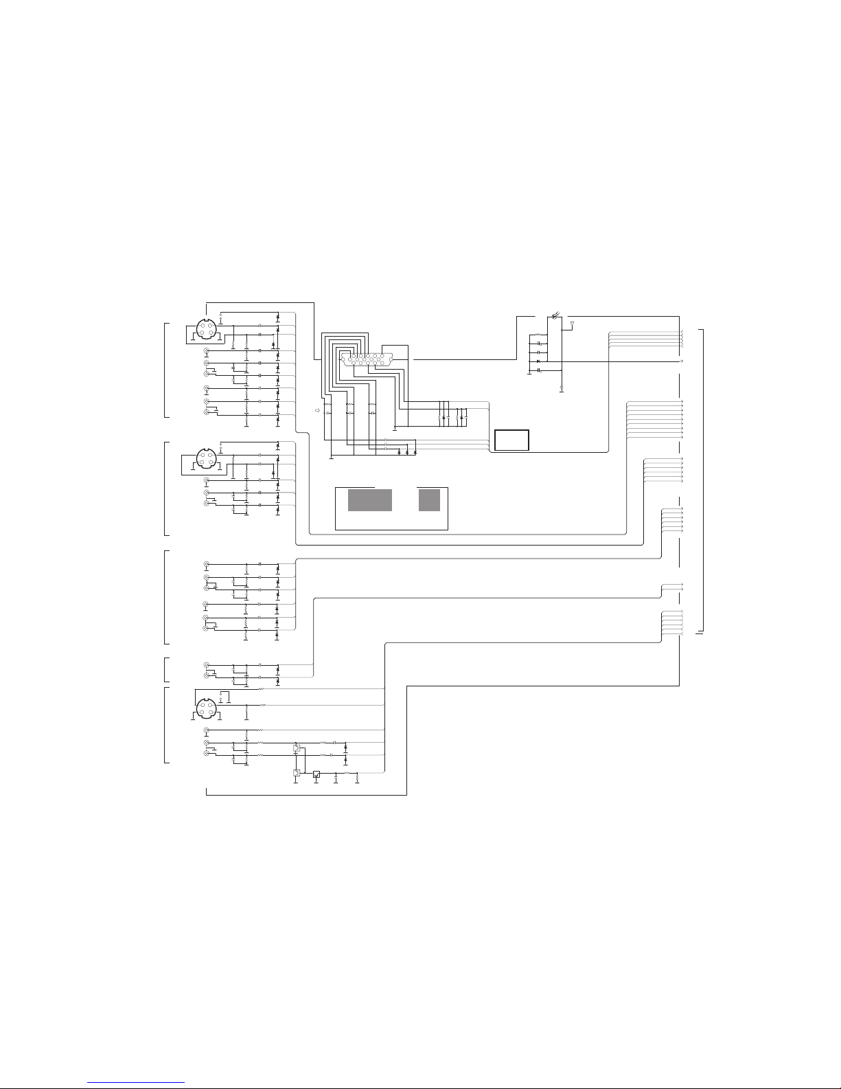
2-12(No.YA665<Rev.001>)(No.YA665<Rev.001>)2-11
ANALOG PWB ASS'Y (3/6)
SFL-1237A-H2 [LT-52GZ79, LT-52GZ79/E, LT-52GZ79/S]
SFL-1237A-H8 [LT-52GZ79/BA]
ggs10021001a_12/4_5/6_0.0
OR MA8033-X
OR MA8100/M/-X
OR 2SC1623A/5-6/-X
LT-52GZ79BA
LT-52GZ79EA
LT-52GZ79SA
LT-52GZ79A
LT47GZ78NASKLT42GZ78NASK
SFL-1237A -
LT-47GZ78BLT-42GZ78B
LT-47GZ78SA
LT-47GZ78TA
:2SA1530A/QR/-XPNP
LT-47GZ78BA
LT-42GZ78SA
:UDZS10B-X
:NRSA63J-0R0X
:OPTION(NON MOUNT)
LT-47GZ78ASFL-1236A
ASSY NO. - MODEL LIST
LT-42GZ78TA
*1
0
OPEN
- NOTE -
:2SC3928A/QR/-X
1_2F
1_2F
1_2E
1_2E
1_2F
1_2I
1_2I
1_2I
1_2I
1_2I
1_2I
1_2I
1_2I
1_2J
1_2L
1_2L
1_2L
1_2K
1_2L
1_2L
1_2C
1_2D
1_2H
1_2H
1_2H
1_2G
2_2L1_2L
1_2G
1_2F
1_2F
1_2F
PHOTO SENSOR
LT-42GZ78BA
LT-42GZ78A
1_2G
1_2H
-
1_2H
1_2H
NPN
2_2O
V1_R_Cr
GND
V1_G_Y
V1_B_Cb
GND
GND
M_MUTE
MON_R
MON_L
MON_V
MON_Y
MON_C
DVI_L
DVI_R
V2_VIN
V2_LIN
V2_RIN
V3_RIN
V3_LIN
V3_VIN
V2_CIN
V2_YIN
V2_S
V1_R_Cr
V1_B_Cb
V1_G_Y
V1_RIN
V1_LIN
V1_VIN
V1_YIN
V1_CIN
V1_S
PC_G
PC_B
PC_B
PC_G
PC_R
PC_HS
V3_R_Cr
V3_B_Cb
V3_G_Y
PC_VS
PC_R
PC_VS
PC_HS
MON_L
GND
BS_A5V
GND
GND
MON_R
GND
GND
GND
GND
GND
GND
M_MUTE
GND
GND
GND
GND
GND
GND
GND
GND
GND
GND
GND
GND
GND
MON_Y
MON_V
MON_C
GND
GND
DVI_R
DVI_L
GND
GND
GND
GND
GND
GND
GND
GND
GND
V3_RIN
V3_VIN
V3_LIN
GND
GND
GND
GND
GND
DIN_PHOTO
GND
GND
GNDGND
GND
GND
GND
GND
GND
GND
V2_RIN
V2_LIN
V2_VIN
V2_YIN
GND
V2_S
V2_CIN
V3_R_Cr
GND
GND
V3_B_Cb
GNDGND
GND GND
GND
GND
GNDGND
GNDGND
V3_G_Y
GND
GND
GND
GND
GND
GND
GND
GND
GND
GND
GNDGND
GND
V1_RIN
V1_YIN
GND
V1_LIN
V1_VIN
GND
GND
GND
V1_S
GND
V1_CIN
PC_VS
PC_B
PC_G
PC_R
PC_HS
V1_R_Cr
V1_B_Cb
V1_G_Y
V1_RIN
V1_LIN
V1_VIN
V1_YIN
V1_CIN
V1_S
M_MUTE
MON_R
MON_L
MON_V
MON_Y
MON_C
DVI_L
DVI_R
V2_VIN
V2_LIN
V2_RIN
V3_RIN
DIN_PHOTO
V3_LIN
V3_R_Cr
V3_B_Cb
V3_G_Y
V3_VIN
V2_CIN
V2_YIN
V2_S
/50
CH
C468
100p
/50
CH
C469
100p
S9648
D492
R476
330
D408
*1
D409
*1
D407
*1
R408
75
R407
75
R406
75
/10
CB2
C408
2.2
/10
CB2
C407
2.2
/10
CB2
C406
2.2
D466*1D465
*1
R475
330
C442
OPEN
C443
OPEN
C441
OPEN
D461*1D462
*1
C494
1000p
C440
OPEN
C439
OPEN
C438
OPEN
C437
OPEN
R461
75
R467
75
R435
75
R437
390
R442
470
UN2110-X
Q433
R464
75
R444
39k
R439
470
R443
1k
R440
390
UN2226-X
Q432
UN2226-X
Q431
R436
2.2k
2
3
1
QNN0652-001
J407
R441
22k
R438
22k
10
11
9
QNZ0726-001
J408
7
8
43
21
5
6
/16
CB1
C432
2.2
/16
CB1
C431
2.2
C436
OPEN
D432
*1
D431
*1
R434
2.2k
R433
75
/16
CB1
C433
1
1716
1514131211
109876
54321
QNZ0973-001
J410
R431
75
D463
*1
/10
CB2
C425
2.2
/10
CB2
C424
2.2
/10CB2
C466
2.2
/10CB2
C465
2.2
R427
220k
R426
220k
D428
*1
D427
*1
/10CB2
C464
2.2
CH
C461
100p
CH
C462
100p
CH
C463
100p
R420
220k
R419
220k
R418
75
CB2
/10
C417
2.2
4
5
3
QNN0651-001
J405
1
2
CB2
/10
C418
2.2
CB2
/10
C419
2.2
D421
*1
D422
*1
D420
*1
D415
*1
D416
*1
D413
*1
D412
*1
D414
*1
CB2
/10
C411
2.2
R411
75
D411
*1
CB2
/10
C409
2.2
R412
75
R414
220k
R413
220k
R410
75
CB2
/10
C413
2.2
CB2
/10
C412
2.2
4
5
3
QNN0650-001
J406
1
2
D424
*1
C435
OPEN
C410
.01
D425
*1
D423
*1
UDZS3.3B-X
D491
R423
75
R422
75
R421
75
/16
C493
100
C492
0.1/16
/16
C491
10
/10
CB2
C422
2.2
/10
CB2
C421
2.2
/10
CB2
C420
2.2
D405
*1
D406
*1
D402
*1
D403
*1
D404
*1
R402
75
D401
*1
CB2
/10
C402
2.2
R405
220k
R404
220k
R403
75
R401
75
CB2
/10
C403
2.2
/10
CB2
C405
2.2
R491
1M
/10
CB2
C404
2.2
6
QNZ0726-001
J403
5
10
11
9
7
8
43
21
QNZ0726-001
J401
10
11
9
7
8
43
21
4
5
3
1
2
QNN0650-001
J402
C434
OPEN
C401
.01
VIDEO-1
VIDEO-2
VIDEO-3
MONITOR OUT
HDMI-1
AUDIO INPUT
L/R
R
L
VIDEO
AUDIO
S-VIDEO
DVI-R
Cr
Cb
DVI-L
Y
R
L
VIDEO
AUDIO
S-VIDEO
S-VIDEO
R
L
VIDEO
AUDIO
Cr
R
L
VIDEO
AUDIO
Cb
Y
PC IN(D-SUB)
ANALOG PWB(2/6)
ANALOG PWB(2/6,5/6)
A
NALOG PWB CIRCUIT DIAGRAM (3/6)
Page 31

(No.YA665<Rev.001>)2-13 2-14(No.YA665<Rev.001>)
ANALOG PWB ASS'Y (4/6)
SFL-1237A-H2 [LT-52GZ79, LT-52GZ79/E, LT-52GZ79/S]
SFL-1237A-H8 [LT-52GZ79/BA]
ggs10021001a_12/4_6/6_0.0
LT-52GZ79BA
LT-52GZ79EA
LT-52GZ79SA
LT-52GZ79A
LT47GZ78NASKLT42GZ78NASK
SFL-1237A -
LT-47GZ78BLT-42GZ78B
LT-47GZ78SA
LT-47GZ78TA
LT-47GZ78BA
LT-42GZ78SA
LT-47GZ78ASFL-1236A
ASSY NO. - MODEL LIST
LT-42GZ78TA
LT-42GZ78BA
LT-42GZ78A-
L-
L+
R-
R+
AU_GND
AU_+VCC
:2SA1530A/QR/-XPNP
:MA8056/M/-X
:MA111-X
:MA8033-X
:UDZW10B-X
:NRSA63J-0R0X
:OPTION(NON MOUNT)
ZD5.6
DI
*2
*1
0
OPEN
- NOTE -
:2SC3928A/QR/-XNPN
AU_VCC
AU_GND
GND
AU_GND
AU_GND
AU_GND
AU_GND
AU_VCC
AU_VCC
AU_GND
AU_VCC
GND
AU_GND
AU_GND
AU_GND
AU_GND
AMP-MUTE
GND
GND
GND
AU_GND
GND
AU_GND
AU_GND
GND
AU_GND
GND
5VSTB_5V
AU_GND
AMP_R
GND
AMP_L
NQR0499-002X
K6601
C6601
0.1
QETN1EM-477Z
C6602
C6128
OPEN
R6126
OPEN
B2
/25
C6126
1
D6104
DI
R6120
2.7k
R6116
OPEN
R6118
22k
R6119
12k
Q6106
NPN
R6121
OPEN
NQR0499-002X
K6104
3
2
1
QGA2013C2-03
CN0SL
NQR0499-002X
K6103
NQR0499-002X
K6101
NQR0499-002X
K6102
R6110
OPEN
CH
C6103
OPEN
CH
C6102
OPEN
R6109
33K
R6108
33K
R6107
5.6k
R6106
5.6k
R6111
OPEN
R6112
OPEN
/25
B2C6118
1
R6113 100K
R6114 OPEN
R6115 100K
R6135 OPEN
/25
B2
C6120
1
J2/16
C6105
4.7
/16
C6107
1
J2
/16
C6106
4.7
R6134 100K
/16
C6104
1
Q6104
OPEN
QEHR1EM-227Z
C6116
/25
B2
C6115
1
/25
B2
C6117
1
QEHR1EM-227Z
C6119
/25
C6127
22
R6117
100K
/16
C6109
1
C6108
.01
R6133 OPEN
RT1N441C-X
UN2213-X
Q6105
B2
/25
C6121
.22
B2
/25
C6122
.22
Q6103
OPEN
Q6102
OPEN
R6125
OPEN
B2
/25
C6114
.22
R6124
22k
B2
/25
C6113
.22
/25
B2
C6123
.33
/25
B2
C6112
.33
4
3
2
1
QGA2013C2-04
CN0SR
NQLF3EM-330X
L6102
NQLF3EM-330X
L6101
NQLF3EM-330X
L6103
NQLF3EM-330X
L6104
B2
/25
C6125
0.22
B2 /25
C6124
.22
B2
/25
C6110
.22
B2
/25
C6111
.22
4847464544434241403938
37
363534333231302928272625
2423222120191817161514
13
121110987654321
TPA3100D2PHP-W
AVCC
AVCC
FAULT
MUTE
SHUTDOWN
BSRP
ROUTP
ROUTP
ROUTN
ROUTN
BSRN
PVCCR
PVCCR
PGNDR
PGNDR
VCLAMPL
VCLAMPL
PGNDL
PGNDL
PVCCL
PVCCL
BSLN
LOUTN
LOUTN
LOUTP
LOUTP
BSLP
AGND
VBYP
VREG
ROSC
SYNC
MSTR/SCV
GAIN1
GAIN0
GAIN0
LININ
LINIP
AGND
RINP
RININ
GND
GND
GND
GND
GNDGND
GND
IC6001
R6150
OPEN
R6149
OPEN
R6156
OPEN
R6155
OPEN
R6154
OPEN
R6153
OPEN
R6152
OPEN
R6151
OPEN
R6157
OPEN
R6158
OPEN
R6148
OPEN
R6147
OPEN
R6146
OPEN
R6145
OPEN
R6144
OPEN
R6143
0
R6142
0
R6141
0
2
1
QGA2013C2-02
CN10F
Q6107
OPEN
C6663
OPEN
C6662
OPEN
R6140
OPEN
R6128
OPEN
R6127
0
CB2
/10
C6661
4.7
CB2
/10
C6651
4.7
AUDIO OUT
POWER PWB(2/3)
CN00F
SPEAKER(R)
SPEAKER(L)
ANALOG PWB
(5/6)
A
NALOG PWB CIRCUIT DIAGRAM (4/6)
Page 32

2-16(No.YA665<Rev.001>)(No.YA665<Rev.001>)2-15
ANALOG PWB ASS'Y (5/6)
SFL-1237A-H2
[LT-52GZ79, LT-52GZ79/E, LT-52GZ79/S]
SFL-1237A-H8
[LT-52GZ79/BA]
ggs10021001a_12/4_3/6_0.0
GND
VCC
BIAS
MUTE
6dB
GND
OE
A
Y
VCC
CTR0
CTR1
SDO
VDD
VSS
BCK
LRI
SDI
OR 2SC1623A/5-6/-X
OR UN2226-X
LT-52GZ79BA
LT-52GZ79EA
LT-52GZ79SA
LT-52GZ79A
52GZ
LT47GZ78NASKLT42GZ78NASK
42GZNOTE.
* DIFFERENCE LIST
OR 2SA812A/5-6/-X
SFL-1237A -
LT-47GZ78BLT-42GZ78B
LT-47GZ78SA
LT-47GZ78TA
LT-47GZ78BA
LT-42GZ78SA
LT-47GZ78ASFL-1236A
ASSY NO. - MODEL LIST
(2.5V)
(3.3V)
(1.8V)
LT-42GZ78TA
LT-42GZ78BA
:QUY160-100Y
:QUY153-050Y
:2SA1530A/QR/-X
:NRSA63J-0R0X
:OPTION(NON MOUNT)
LT-42GZ78A
BW2
BW1
PNP
0
OPEN
- NOTE -
:2SC3928A/QR/-XNPN
I2S_CL
I2S_WS
MAXXAUDIO
12.288MHz
-
VO2
VO1
GND
NC
VIN2
VIN1
PS1
PS2
NC
VOUT
CE
GND
VDD
VCC
GND
CARD_CK
CARD_DA
HP_L
HP_R
GND
GND
AMP_R
GND
BS_A5V
3.3V
AMP-MUTE
GND
GND
POW_GOOD
GND
SCL3A
BS_A9V
BS_A9V
SDA3A
BS_A5V
GND
GND
GND
BS_A9V24V 5V
BS_A5V
A_MUTE
STB_5V
VCC5V
BS_A3.3V
HP_MUTE
GND
HP_DET
GND
16V
MAIN_L
AMP_L
BS_A3.3V
MAIN_R
M_MUTE
MAXX_RST
GND
AMP_MUTE
GND
BS_A5V
GND
SFL-1237A
OPEN
-0R0X
NRSA63J
R657
-0R0X
NRSA63J
SFL-1236A
OPENR655
-227X
NEAF0JM
-336X
NEHM1EM
C670
R657
*
MA111-X
D603
MA111-X
D602
R755
0
R756
0
R767
OPEN
C758
OPEN
C751
OPEN
C760
0.1
R769
47
R768
1k
/16
NEHL1CM-476X
C754
47
C759
0.1
R765
47
R764
1k
R762
OPEN
/4
NEHL0GM-227X
C753
220
/10
C761
100
/4
NEHL0GM-227X
C755
220
C671
OPEN
R653
OPEN
R654
OPEN
Q602
NPN
R652
OPEN
R651
100k
R650
56k
C670
*
MA111-X
D607
Q601
PNP
R662
15k
R601
0
R602
0
R603 OPEN
R604
OPEN
R656
OPEN
R655
*
5678
4321
BH3547F-X
IC751
R627
100
R624
4.7k
R625 OPEN
/6.3
CB2
C639
10
/6.3
CB2
C638
10
R621 47
R620
47
R623 47
R622 47
1234
5678
R2S15901SP-X
IC603
54
321
74LVC1G125GW-X
IC604
R629
OPEN
R628
4.7K
R626
100
R761
0
R760
47k
RT4N430C-X
Q752
R759
0
R758
100k
Q751
PNP
R757
4.7k
C771
OPEN
C774
OPEN
R773
OPEN
R770
0
R783
0
R772
OPEN
R782
OPEN
1234
5678
VCC
GND
IC752
OPEN
R781
OPEN
R771
OPEN
R780
0
R779
0
NRSA02J-0R0X
C772
NRSA02J-0R0X
C773
R776
OPEN
R775
OPEN
R778
0
R777
0
C622
OPEN
C643 .01
R613 10K
/6.3
C631
1
/6.3C632 1
/6.3C633 1
R618 10K
/6.3
C626
1
C630
.01
/6.3
C629
47
C601
.01
C602
.01
C624 0.001
C625
0.001
/6.3
C623
1
/6.3C613 1
CH
C604
12p
CH
C603
12p
R609
100K NAX0932-001X
X601
/16
J2
C618 4.7
/16
J2
C617 4.7
/6.3C614 1
/6.3C616 1
/6.3C615 1
NQLE42M-100X
L601
R616
100
R617 100
R612 47
R611 47
R610 47
/50
C619
10
R659 47
/6.3
C666
47
/6.3
C667
47
NQLE42M-100X
L606
NQLE42M-100X
L605
NQR0499-002X
K601
/6.3
C668
47
C628 0
C627 0
C664
0.01
NQLE42M-100X
L607
R661
0
R660
0
/6.3
C634
100
/6.3
C652
100
/6.3
C665
1
R663
10K
D608
OPEN
/6.3
C653
100
/6.3
C654
47
/6.3
C621
100
R671 10K
R670 10K
/6.3
C636
100
R669 10K
R666 10K
C637
.01
R668 10K
R665 10K
R667 10K
R664 10K
D609
OPEN
C641 .01
C655
.01
C662
OPEN
C661
OPEN
R614
OPEN
C620
.01
R643
0
D611
OPEN
R642
0
R672
OPEN
C663
OPEN
R673
OPEN
C656
OPEN
R615
1K
R786
0
R787
0
R785
OPEN
R784
OPEN
R631
OPEN
R630
OPEN
R644
2.2K
L604
OPEN
C658
OPEN
J2
/16
C685
4.7
J2
/16
C686
4.7
C776
OPEN
C657 OPEN
R633
OPEN
R632
OPEN
R635
0
D610
OPEN
C660
0
R6340
R639 OPEN
C659
0
R638
OPEN
R641
0
R637
OPEN
R636
OPEN
R640
0
1234
5678
IC606
OPEN
MA111-X
D604
/6.3
C756
1
CB2
/10
C757
4.7
MA111-X
D606
MA111-X
D605
R605 10K
R606 10K
R607
10K
R608
10K
40
39
38
37
36
35
34
33
32
31
30292827262524232221
20
19
18
17
16
15
14
13
12
11
10987654321
MX5000A
VDD_5A
VDD_1.8V
VDD_1.8V
VDD_3.3V
VDD_3.3V
HPSENCE
TEST
SYNKH
DCLK
Xtal_out
Xtal_in
A_ctr1
A_ctr0
R_IN3
L_IN3
R_IN2
L_IN2
R_IN1
L_IN1
RCAP AMP_MUTE
DOUT2
DOUT1
DIN2
DIN1
DIN0
SBW
ROUT
LOUT
xRESET
VDD_1.8V
VDD_3.3V
SDA
SCL
IC601
41
NQLE42M-100X
L608
C672
OPEN
R658
OPEN
R7630R766
OPEN
NQLE42M-100X
L609
L602
OPEN
/6.3
C644
47
C645
.01
L603
OPEN
/6.3
C646
100
/6.3
C649
1
/6.3
C648
1
C651
.01
C650
.01
1234
5678
MM1689AH-X
IC605
54
321
MM3272FN-X
IC602
/6.3C642 100
/6.3C640 100
CB2
/10
C752
4.7
C775
OPEN
R774
OPEN
C647
.01
C635
.01
R619
OPEN
AUDIO CONTROL
HEADPHONE
AMP
ANALOG PWB(2/6)
ANALOG PWB(2/6,3/6)
ANALOG PWB(2/6)
ANALOG PWB(4/6)
ANALOG PWB(2/6)
A
NALOG PWB CIRCUIT DIAGRAM (5/6)
Page 33

(No.YA665<Rev.001>)2-17 2-18(No.YA665<Rev.001>)
ANALOG PWB ASS'Y (6/6)
SFL-1237A-H2 [LT-52GZ79, LT-52GZ79/E, LT-52GZ79/S]
SFL-1237A-H8 [LT-52GZ79/BA]
ggs10021001a_12/4_4/6_0.0
LT-52GZ79BA
LT-52GZ79EA
LT-52GZ79SA
LT-52GZ79A
LT47GZ78NASKLT42GZ78NASK
0.2A
9V
UK2.5V
Vadj
IN
OUT
GND
ON/OFF
SFL-1237A -
LT-47GZ78BLT-42GZ78B
:NRSA02J-0R0XCBW
LT-47GZ78SA
LT-47GZ78TA
LT-47GZ78BA
LT-42GZ78SA
LT-47GZ78A
1.3A
0.3A
SFL-1236A
UK2.5V
UK3.3V
UK3.3V
UK12V
ASSY NO. - MODEL LIST
LT-42GZ78TA
LT-42GZ78BA
:2SA1530A/QR/-XPNP
:NCB11AK-106X
:DTC144EKA-X
:DTC323TK-X
:2SA1037AK/QR/-X
:2SC2412K/QR/-X
:NRSA63J-0R0X
:OPTION(NON MOUNT)
*4
*5
*3
*2
*1
0
LT-42GZ78A
OPEN
- NOTE -
:2SC3928A/QR/-XNPN
-
GND
GND
GND
GND
GND
GND
GND
GND GND
GND
GND
GND
GND
GND
16V
GND
5V
VCC5V
GND
24V
GND
BS_A5VBS_A9VSTB3.3V
32V
STB_5V
GND
POW_GOOD
GND
1
SDA3A5
SCL3A5
MAIN_POW
POW_GOOD
1080P_SW
AC_IN
B1_POW
10
9
8
7
6
5
4
3
2
1
UK3.3V
UK3.3V
UK5V
UK5V
GND
GND
UK12V
32V
UK2.5V
UK2.5V
CN0UD
OPEN
R940
OPEN
R939
OPEN
R936
OPEN
R938
OPEN
Q934
OPEN
Q933
OPEN
C931
OPEN
D931
OPEN
R931
OPEN
R933
OPEN
R932
OPEN
R934
OPEN
R935
OPEN
Q931
OPEN
R937
OPEN
C907
OPEN
NCB21EK-334X
C972
NEHM1EM-336X
C973
1234
5678
BS SS
IC961
OPEN
NEHM1EM-336X
C971
5321
PQ090DNA1Z-X
IC971
R906
OPEN
R967
OPEN
R968
OPEN
NRSA02J-0R0X
R982
R983 OPEN
R981
OPEN
R984
OPEN
R904
OPEN
C901
OPEN
D903
OPEN
R903 OPEN
NEX50JM-156X
C914
NQR0562-010X
L903
R951
OPEN
C965
OPEN
R905
OPEN
C951
OPEN
54321
GNDNCVoutON/OFFVin
IC951
OPEN
D963
OPEN
NEX51CM-335X
C913
/16
NEHM1CM-476X
C905
47
L961
OPEN
R966
OPEN
R963
OPEN
R964
OPEN
R912
OPEN
C920
OPEN
L906
OPEN
R962
OPEN
R961
OPEN
C963
OPEN
C962
OPEN
C966
OPEN
C964
OPEN
C968
OPEN
C952
OPEN
C953
OPEN
C961
OPEN
D962
OPEN
D961
OPEN
C967OPEN
R965
OPEN
C969
OPEN
L901 OPEN
R901
OPEN
R902
CBW
Q932
OPEN
23
22
21
20
19
18
17
16
15
14
13
12
11
10
9
8
7
6
5
4
3
2
1
UK_5V
GND
QGB1231L1-23
24V
GND
5V
NC
5V
5V
GND
9V
16V
GND
SDA
GND
SCL
GND
STB_5V
AC_IN
LCD_POW
1080P_SW
MAIN_POW
GND
BT32V
CN00H
C982
OPEN
C981
OPEN
321
IC981
OPEN
/25
NCB31EK-104X
C906
0.1
NCB11AK-106X
C904
321
BA33BC0FP-X
IC902
NQL52EM-220X
L902
DC-DC PWB
CN00H
ANALOG PWB(1/6,2/6)
OPEN
ANALOG PWB(2/6)
A
NALOG PWB CIRCUIT DIAGRAM (6/6) [POWER BLOCK]
Page 34

2-20(No.YA665<Rev.001>)(No.YA665<Rev.001>)2-19
DIGITAL PWB ASS'Y (1/12)
SFL0D403A-H2
[LT-52GZ79, LT-52GZ79/E]
SFL0D403A-H8
[LT-52GZ79/BA]
SFL0D404A-H2
[LT-52GZ79/S]
ggs20019001a_12/4_14/14_0.0
OR NAK0938-001X
SFL-0D398A ...
NOTE.
SFL-0D397A
LT47GZ78NASK
LT42GZ78NASK...
SFL-0D396A
SFL-0D395A
...
...
LT-47GZ78SA
SFL-0D394A
LT-47GZ78BA
LT-42GZ78SA
LT-47GZ78A
SFL-0D393A
ASSY NO. - MODEL LIST
RESET IC
...
LT-42GZ78BA
LT-42GZ78A...
(A20)
A16
BYTE
VSS
DQ12
DQ4
VCC
DQ11
DQ3
DQ2
DQ9
DQ1
DQ8
DQ0
OE
DQ10
DQ5
DQ13
DQ6
DQ14
DQ7
DQ15/A-1
VSS
CE
A0A1
A2
A3
A4
A5
A6
A7
A17
A18
A19
RY/BY
NC
NC
LT-47GZ78TA
RESET
WE
LT-42GZ78TA
LT-52GZ79BA
NC
A8
A9
A10
A11
A12
A13
A14
A15
...SFL-0D404A LT-52GZ79SA
SFL-0D403A
64MB_SD-RAM
VSS
A12
LT-52GZ79EA
OR TC74HC4053AFT-X
MICRO_COMPUTER
P6.2
P6.3
P6.4
P6.5
IRQ
VSYNC
HSYNC
COR/RSTOUT
BLANK
VDD33
VSS33
XTAL1
XTAL2
VSSA
VDDA
R
G
B
VSSA
VDDA
CVBS2
VSSA
VDDA
CVBS1B
CVBS1A
VSSA
VDDA
KEY1
KEY2
MECA_SW
P5.3
TMODE
D2
D12
D10
VSS33
VDD33
D4
D3
D11
RSTIN
POWER
P3.1
REMOCON
P3.3
P3.4
P3.5
P3.6
P3.7
MTST
MTSR
VSS33
VDD33
VSS25
VDD25
TXD0
RXD0
P3.12
CLK
P3.15
P5.14
P5.15
TRIG_IN
TRIG_OUT
D5D9D13
VDD33
VSS33D1D8
D14D0D7
VDD33
VSS33
D15
WR
LT-52GZ79A
D6
LDQM
UDQMRDCSROM
CLKEN
CSSDRAM
MEMCLK
VDD33
VSS33
CAS/A15
RAS/A14
A13A0A1A2A3
A4
A9
VDD33
VSS33
A11
A12
A10
A5
A6
A7
A8
A16
VDD25
VSS25
A17
A18
A19
A20
P4.5
VDD33
VSS33
P2.15
P2.14
P2.13
P2.12
P2.11
P2.10
P2.9
P2.8
TDO
TDI
TMS
TCK
...
(KEYP2)
VSS
A4
A5
A6
A7
A8
A9
NC
CKE
CLK
UDQM
NC
*6:NQL092K-4R7X
VCC
DQ9
DQ10
VSS
DQ11
DQ12
VCC
DQ13
DQ14
VSS
DQ15
A13
VSS
VCC
DQ0
VCC
A3
A2
A1
A0
A10
A11
CS
RAS
CAS
WE
LDQM
VCC
DQ8DQ7
VSS
DQ6
DQ5
VCC
DQ4
DQ3
VSS
DQ2
DQ1
VCC
MI_A20
MI_A16
GND
GNDGND
STB3.3V
CEC_NMI
CEC_P85
CEC_TX
CEC_RX
GND
MECA_SW
KEY2
QAM_RXD
GND
GND
GND
TDO
TDI
SBD5
QAM_TXD
CLK_7309_3
TMS
BS_RST
MI_A16
MI_D15
MI_D7
TCK
MI_D14
MI_D6
MI_D13
MI_D5
GND
MI_D12
MI_D4
MI_D14
MI_D11
MI_D3
KEY1
MI_D10
MI_D2
MI_D9
MI_D1
MI_D8
MI_D0
RD
CSROM
MI_A0MI_A1
MI_A2
MI_A3
MI_A4
MI_A5
MI_A6
MI_A7
GND
MI_A17
MI_A18
WR
MI_A20
MI_A19
MI_A8
MI_A9
MI_A10
MI_A11
MI_A12
MI_A13
STB_5V
MI_A14
MI_A15
MI_A5
MI_A4
GND GND
GND
CLK_7309_1
GND
SCLM
MI_D9
MI_D13
MI_D1
MI_D6
MI_D8
MI_D0
MI_D7
MI_D15WRLDQM
TDO
CLK_7309_2
TDI
TMS
TCK
STB3.3MI
MI_CK
MI_TX
MI_RX
POW_GOOD
POW_GOOD
GND
FBin
FBout
MI_A17
TEXT_FB
MI_A18
MI_A19
MI_A6
TEXT_FG
TEXT_FR
GND
WAKE
REMOCON
MI_TX
MI_RX
OSDB5
OSDB4
OSDB3
OSDB2
OSDB1
OSDG5
OSDG4
OSDG3
OSDG2
OSDG1
OSDR5
OSDR4
OSDR3
OSDR2
OSDR1
SCLM
SDAM
KEY2
KEY1
MECA_SW
GND
GND
WAKE
GND
CK100
GND
TEXT_FR
MI_A7
MI_A8
MI_A9
MI_A11
TEXT_FG
CKE
TEXT_FB
MI_CK
STB3.3V
CPURST2
CK100
UDQM
MI_D8
MI_D9
MI_D10
MI_D11
MI_D12
MI_D13
MI_D14
MI_D15
MI_A3
MI_A2
MI_A1
MI_A0
MI_A10
MI_A12
MI_A13
CSSDRAM
MI_A14
MI_A15
WR
LDQM
MI_D7
MI_D6
MI_D5
MI_D4
MI_D3
MI_D2
MI_D1
GND
MI_D5
CPURST2
MI_D0
STB3.3MI
OSDG5
OSDR1
OSDR2
OSDR3
OSDR4
OSDR5
GND
OSDG1
OSDG2
OSDG3
OSDG4
OSDB5
OSDB4
OSDB3
OSDB2
OSDB1
REMOCON
GND
GND
STB_5V
GND GND
GND
GND
GND
SDAM
GND
WORD
CEC_INT
MI_OSDYM
STB3.3MI
GND
UDQM
MI_OSDYS
STB2.5MI
MI_A8
MI_A7
MI_A9
CK100_0
MI_A6
MI_A5
MI_A10
MI_A11
RD
CSROM
CKE
CSSDRAM
MI_A15
MI_A14
MI_A13
MI_A0
MI_A1
MI_A2
MI_A3
MI_A12
MI_A4
MI_D2
MI_D12
MI_D10
MI_D4
MI_D3
MI_D11
MI_OSDYS
MI_OSDYM
GND
GND
POW_GOOD
CPURST2
AFT1
DD_OSDHS
TVLINKIN
MI_RESET
CEC_CLK
MI_REQ
TVLINKOUT
CECIN
MECA_SW
KEY1
KEY2
SDAM
MAINCCD2
SCLM
WAKE
OSDB5
OSDB4
OSDB3
OSDB2
OSDB1
OSDG3
OSDG5
REMOCON
OSDG4
OSDG2
OSDG1
MI_TX
OSDR5
OSDR4
OSDR3
OSDR2
OSDR1
DD_OSDCK
DD_OSDVS
TEXT_FB
MI_OSDYS
TEXT_FG
TEXT_FR
MI_RX
MI_CK
CPURST
TEXT_VD
CEC_RST
BS_RST
TEXT_HD
MI_OSDYM
R7374
1k
R7375
0
R7373
OPEN
R7371 0
R7372 0
131211
10
987654321
QGA1501F4-13W
UKD_TX
UKD_RX
CEC_CLK
GND
5Vin
A16
3.3V
RST
GND
TDO
TDI
TMS
TCK
CN0MI
R7370 OPEN
C7353
6800p/25
R7347
47k
R7346 2.2k
R7339 4.7k
R7323 10k
R7369
10k
R7368
10k
RB501V-40-XD7301
R7367
220
R7366
OPEN
R7365
OPEN
R7364
0
UN2213-X
Q7301
0.5%R7363 27k
R7357 OPEN
R7360
OPEN
R7359
0
43
21
S-80928CLNB-G-W
CD
OUT
VDD
VSS
IC7306
F
C7348
0.1/16
R7358 470
C7349
1000p
R7361 OPEN
R7362 15k
C7351
OPEN
B1
C7352 OPEN
R7384 33 R7385 33
R7383 33
R7382 33
R7381 33
R7380 33
R7379 33
R7378 33
R7386 33
R7387 33
R7388 33
R7389 33
R7390 33
R7391 33
R7377 33 R7392 33
CH
C7354
OPEN
C7357
0.1/16
C7356
0.1/16
C7355
0.1/16
C7322
OPEN
C7323
OPEN
B1
C7303
10/10
128
127
126
125
124
123
122
121
120
119
118
117
116
115
114
113
112
111
110
109
108
107
106
105
104
103
102
101
100
999897
9695949392919089888786858483828180797877767574737271706968676665
64636261605958575655545352515049484746454443424140393837363534
33
32 31 30 29 28 27 26 25 24 23 22 21 20 19 18 17 16 15 14 13 12 11 10 9 8 7 6 5 4 3 2 1
SDA6000-B12
IC7301
F
C7301
0.1/16
F
C7304
0.1/16
NQR0339-001X
L7302
R7329
OPEN
R7304
4.7k
R7305
4.7k
R7309
4.7k
R7311
4.7k
R7312
4.7k
L7312
*6
L7313 *6
NQR0339-001X
L7314
NRSA02J-390X
K7308
L7310 *6
L7311 *6
L7303
*6
L7304
*6
L7307 *6
F
C7320 0.1/16
L7305 *6
L7306 *6
L7308 *6
R7313
10k
L7309 *6
R7334 100
R7316 100
R7340
100
R7315
100
F
C7302
0.1/16
R7310
OPEN
R7318 100
R7317 100
R7314 100
C7325 0.01
R7320 10k
F
C7333
0.1/16
F
C7334
0.1/16
F
C7335
0.1/16
/16
F
C7331
0.1
/16
F
C7330
0.1
/16
F
C7324
0.1
R7319 10k
F
C7329 0.1/16FC7328 0.1/16FC7321 0.1/16
F
C7319 0.1/16
F
C7313
0.1/16
F
C7312
0.1/16
F
C7311
0.1/16
R7321
82
1234
5678
MM1689CH-X
PS1
VIN1
NC
VO2
VO1
VIN2
GND
PS2
IC7305
9
IC7305
R7330 10k
54321
CEC_RST
CEC_NMI
CEC_P85
CEC_TX
CEC_RX
CN0C3
OPEN
R7322 10k
NQR0339-001X
L7301
R7355 47
1SS357-XD7302
R7393
0
R7397 OPEN
F
C7307
0.1/16
0.5%
R7396
100
F
C7350
0.1/16
R7335 100
R7333
100
F
C7308
0.1/16
F
C7306
0.1/16
F
C7305
0.1/16
NQR0599-004X
K7302
R7352 27k
123456789101112131415161718192021222324
25 26 27 28 29 30 31 32 33 34 35 36 37 38 39 40 41 42 43 44 45 46 47 48
IC7302
R7353 27k
R7327 10k
R7354 27k
NAX0618-001X
X7309
CH
C7327
33p
R7324
100
R7349 10k
R7350
10k
R7351
10k
CH
C7326
27p
R7332
100
R7348
0
R7356
0
R7338
OPEN
R7337 100
1
2
3
Q7302
OPEN
Q7303
OPEN
R7398 OPEN
12345
6
QGA1217F1-06X
STATUS_DET
DM_RESET
IRQ
GND
UKD_TX
UKD_RX
CN0ID
B1
C7341
10/10
L7315
*6
L7316 *6
R7325
22
R7341
100
R7342 100
NEHM1CM-106X
B1
C7338
B1
C7343
10/10
C7342
2.2/6.3
B1
C7346
10/10
C7345
2.2/6.3
R7343
100
C7344
2.2/6.3
C7340
0.01
12345678
910111213141516
CD74HC4053PW-X
VCC
BN
AN
A1A0S0S1S2GND
VEEEC0CNC1B0B1
IC7304
B1
C7318 10/10
F
C7315
0.1/16
RB521S-30-X
D7303
R7328 0
R7302 4.7k
R7303 4.7k
F
C7309
0.1/16
F
C7310
0.1/16
B1
C7314 10/10
5453
1234567891011121314151617181920212223242526
52515049484746454443424140393837363534333231302928
27
K4S641632K-UC75
IC7303
MAIN CPU
TEXT DATA MEMORY
NOTE : Refer to the part list for the part number of IC7302.
DIGITAL PWB(10/12)
DIGITAL PWB
(10/12)
DIGITAL PWB(9/12,10/12)
DIGITAL PWB
(10/12)
DIGITAL PWB
(9/12)
OPEN OPEN
OPEN
DIGITAL PWB(10/12,DIGITAL INPUT BLOCK)
DIGITAL PWB(10/12)
DIGITAL PWB(7/12)
DIGITAL PWB(7/12)
DIGITAL PWB(3/12,7/12)
DIGITAL PWB(3/12,11/12)
DIGITAL PWB(4/12,7/12)
DIGITAL PWB(4/12)
DIGITAL PWB(9/12)
DIGITAL PWB(4/12,7/12,8/12)
DIGITAL PWB(8/12,9/12)
DIGITAL PWB(4/12,7/12)
DIGITAL PWB(7/12)
DIGITAL PWB(7/12)
DIGITAL PWB(2/12)
DIGITAL PWB(4/12)
DIGITAL PWB(3/12,9/12)
DIGITAL PWB(3/12)
DIGITAL PWB(7/12,9/12,10/12)
DIGITAL PWB(4/12)
DIGITAL PWB(9/12)
DIGITAL PWB(3/12)
DIGITAL PWB(4/12)
DIGITAL PWB CIRCUIT DIAGRAM (1/12) [Micronas micon]
Page 35

(No.YA665<Rev.001>)2-21 2-22(No.YA665<Rev.001>)
DIGITAL PWB ASS'Y (2/12)
SFL0D403A-H2 [LT-52GZ79, LT-52GZ79/E]
SFL0D403A-H8 [LT-52GZ79/BA]
SFL0D404A-H2 [LT-52GZ79/S]
ggs20019001a_12/4_1/14_0.0
NPN:2SC3928A/QR/-X
PNP:2SA1530A/QR/-X
*4:MA111-X
OR 2SC1623A/5-6/-X
OR 2SA812A/5-6/-X
OR
RT1A3906-X
OR RT1A3906-X
OR RT1A3906-X
OR RT1A3906-X
OR 2SC5477-X
OR 2SC5477-X
OR 2SC5477-X
OR 2SC5477-X
OR 2SC5477-X
OR 2SC5477-X
OR 2SC5477-X
OR 2SC5477-X
OR
NAX0580-001X
OR HN1C01F/Y/-X
OR HN1C01F/Y/-X
NOTE.
SFL-0D398A ...
SFL-0D397A
LT47GZ78NASK
LT42GZ78NASK...
SFL-0D396A
SFL-0D395A
...
...
LT-47GZ78SA
SFL-0D394A
LT-47GZ78BA
LT-42GZ78SA
LT-47GZ78A
SFL-0D393A
ASSY NO. - MODEL LIST
...
LT-42GZ78BA
LT-42GZ78A...
LT-47GZ78TA
LT-42GZ78TA
LT-52GZ79BA
...SFL-0D404A LT-52GZ79SA
*5:NQR0499-001X
SFL-0D403A
LT-52GZ79EA
LT-52GZ79A
OR 1SS355W-X
...
GND
DIN_DR_1
DIN_DL_1
ADA3V BS_5V
ADY1V_INN
GND
ADA3V
BS_5V
ADA3V
ADA3V
BS_5V2
BS_5V2
GND
GND
GND
GND
BS_5V
BYMIN_5
BS_5V2
RYMIN_1
BYMIN_1
YMIN_1
ADC1B_INN
GND
YMIN_5
RYMIN_5
BS_5V
GND
ADA3V
ADY2G_INN
ADA3V_001
GND
CLPH_Y1V
CLPH_C2R
PWM_C2R
GND
CLPH_C1B
ADC2R_INN
GND
CLPH_Y2G
PWM_Y2G
ADA3V_004
GND
GND
ADC2R_IN
GND
SUB_VY
GND
SUB_VY_2
GND
ADY1V_IN
RYMIN
GND
ADC1B_IN
GND
GND
BS_5V_010
BS_5V
GND
PWM_Y2G
CLPH_Y2G
PWM_C1B
CLPH_C1B
GND
PWM_C2R
GND
BYMIN
ADY2G_IN
GND
VCC3D
FBout
27M_CLK_A1_0
27M_CLK_A1
YMIN
CLPH_C2R
GND
VCC3D
BS_COUT_1
ML_1
GND
BS_LOUT_1
GND
GND
PWM_Y1V
BS_YOUT_1
MR_1
VCC3D_001
VCC3D
DIN_DL
BS_5V2
CLPH_Y1V
ASIG_A033
RYMIN_4
DIN_DR
GND
ADA3V
SUB_VY_4
GND
GND
PWM_Y1V
GND
ADA3V_003
PWM_C1B
GND
BS_5V
LB_POW
GND
BYMIN_6
RYMIN_6
YMIN_6
SUB_VY_6
BS_5V
ADC1B_IN
ADY2G_IN
BYMIN_4
ADY1V_IN
BS_5V
ADC2R_IN
YMIN_4
GND
BS_ROUT_1
BS_5V2
MAIN_CCD
625IP
FBin
C6229
0.1/16
C6227 0.1/16
C6228
0.1/16
R6237
3.3k
R6240 6.8k
R6243
1k
2SC3837K/NP/-X
Q6209
C6300
0.1/16
C6299
0.1/16
R6246
3.3k
NRSA63J-0R0X
L6260
NRSA63J-0R0X
L6259
NRSA63J-0R0X
L6258
NRSA63J-0R0X
L6257
C6236
0.1/16
C6237
0.1/16
C6238
0.1/16
C6239
0.1/16
R6245
330
R6242
330
R6239
330
R6236
330
R6218
OPEN
R6235 100
R6238 100
R6241 100
R6211
OPEN
R6244 100
2SA1022/BC/-X
Q6206
2SA1022/BC/-X
Q6205
2SA1022/BC/-X
Q6204
2SA1022/BC/-X
Q6203
/10
C6249
1
0.5%R6249 OPEN
R6248
OPEN
Q6251
NPN
Q6250
NPN
CH
C6233
22p
CH
C6232
22p
R6232
0
R6233
0
CH
C6231
22p
CH
C6230
22p
R6231
0
R6230
0
C6234
OPEN
C6235
OPEN
R6285
OPEN
R6284
0
D6302
*4
D6301
*4
R6335
0
0.5%
R6337
10k
R6336
OPEN
R6332
OPEN
R6333
OPEN
R6314
0
654
321
IMX1-XW
Q6302
CH
C6304
OPEN
C6303
0.1/16
R6306
OPEN R6310
2.2k
R6311
OPEN
R6308
OPEN
CH
C6305
OPEN
R6312
4.7k
B1
C6312
10/10
R6322
0
R6309
0
R6330
0
R6327
0
654
321
IMX1-XW
Q6304
CH
C6309
OPEN
C6308
0.1/16
R6319
OPEN
R6323
2.2k
R6324
OPEN
R6321
OPEN
CH
C6310
OPEN
R6325
4.7k
R6320
OPEN
R6329
4.7k
Q6303
PNP
B1
C6307
OPEN
R6331
OPEN
R6307
OPEN
R6326
OPEN
R6328
OPEN
R6316
4.7k
Q6301
PNP
54
321
TC7SET08F-X
A
GNDBY
VCC
IC6302
R6247
6.8k
R6277
390
2SC3837K/NP/-X
Q6210
C6219
0.1/16
C6211
0.1/16
R6205
3.3k
R6220
6.8k
R6227
390
2SC3837K/NP/-X
Q6207
C6240
0.1/16
C6220 0.1/16
C6205
0.1/16
R6228
3.3k
R6229 6.8k
R6234
390
2SC3837K/NP/-X
Q6208
R6305
OPEN
C6301
0.1/16
R6304
OPEN
R6302 OPEN
R6303 OPEN
R6300 OPEN
R6301 OPEN
R6290 OPEN
R6293 OPEN
CH
C6222
OPEN
LC6222
OPEN
R6222
OPEN
CH
C6221
OPEN
LC6221
OPEN
R6221
OPEN
CH
C6226
OPEN
LC6226
OPEN
K6271
*5
K6272
*5
K6274
*5
R6278
OPEN
K6268
OPEN
C9626
OPEN
C6298
OPEN
R6291
47K
R6292
47k
54
321
VOUT
VDD
NC
GND
CE
IC6251
R6226
OPEN
CH
C6225
OPEN
LC6225
OPEN
R6225
OPEN
CH
C6224
OPEN
LC6224
OPEN
R6224
OPEN
CH
C6223
OPEN
LC6223
OPEN
R6223
OPEN
C6244 1/10B1C6243 10/10
C6248
1/10
B1
C6245 10/10
B1
C6241 10/10
C6246 1/10
C6311
0.1/16
B1
C6302
OPEN
R6289 1K
R6214
0
CH
C6213
OPEN
LC6213
OPEN
CH
C6214
OPEN
NQR0646-001XLC6214
R6215
OPEN
0.5%
R6340
12k
D6304
OPEN
123456789101112
13 14 15 16 17 18 19 20 21 22 23 24
PWM3
PWM2
GNDGND
OUT3OUT2
VCCVCC
CLUMP3
CLUMP2
GND
DCLUMP4
PWM4
GND
OUT4
VCC
CLUMP4
GND
DCLUMP1
PWM1
GND
OUT1
VCC
CLUMP1
UPC5702GS-027-X
IC6250
C6273
0.1/16
C6272
0.1/16
C6271
0.1/16
C6269
OPEN
0.5%
R6268
2.4k
C6268
0.1/16
C6270 0.1/16
C6291
0.1/16
C6290
OPEN
C6289
0.1/16
C6287 OPEN
0.5%
R6271
2.4k
C6286
0.1/16
C6288
0.1/16
C6285
0.1/16
C6284
0.1/16
C6283
0.1/16
C6281
OPEN
0.5%
R6270
2.4k
C6280
0.1/16
D6303
OPEN
C6279
0.1/16
C6278
0.1/16
C6277
0.1/16
C6275
OPEN
0.5%
R6269
2.4k
R6341
0
R6216
0
CH
C6215
OPEN
LC6215
OPEN
CH
C6216
OPEN
LC6216
OPEN
C6274
0.1/16
R6317
0
C6276 0.1/16C6282 0.1/16
R6251 OPEN
R6250
OPEN
R6217
0
R6288 390
R6263
4.7k
R6267
4.7k
R6255
4.7k
B2
C6260 2.2/10B2C6263 2.2/10B2C6262 2.2/10
B2
C6256 OPENB2C6259 OPENB2C6258 OPEN
B2
C6261 2.2/10
B2
C6257 OPEN
R6257
10k
R6261
10k
R6265
10k
R6253
10k
R6256
0
R6260
0
R6264
0
R6252
0
R6259
4.7k
R6273
OPEN
R6272
OPEN
CH
C6267 12p
C6266 OPEN
C6265 OPEN
C6264 OPEN
NQL092K-2R2X
L6253
L6252 OPEN
L6251 OPEN
L6250 OPEN
R6254
150
R6258
150
R6262
150
R6266
220
C6251
0.1/16
R6287 390
NRSA02J-0R0X
K6250
R6286 390
2SC3837K/NP/-X
Q6214
B1
C6255
1/16
2SC3837K/NP/-X
Q6213
2SC3837K/NP/-X
Q6212
CH
C6212
OPEN
LC6212
OPEN
R6209
0
CH
C6209
OPEN
LC6209
OPEN
CH
C6210
OPEN
LC6210
OPEN
R6210
OPEN
R6213
OPEN
CH
C6208
OPEN
LC6208
OPEN
R6208
0
CH
C6207
OPEN
LC6207
OPEN
R6207
0
R6318
OPEN
CH
C6206
OPEN
LC6206
OPEN
R6206
OPEN
R6204
0
CH
C6204
OPEN
LC6204
OPEN
R6313
OPEN
C9625
OPEN
R6203
0
CH
C6203
OPEN
LC6203
OPEN
R6202
0
CH
C6202
OPEN
LC6202
OPEN
R6201
0
CH
C6201
OPEN
LC6201
OPEN
R6315
OPEN
54
321
TC7SET08F-X
A
GNDBY
VCC
IC6301
R6338
OPEN
R6343
OPEN
2SC3837K/NP/-X
Q6211
R6283 100
C6242 1/10
B1
C6247
10/10
R6279
OPEN
NEX60JM-227X
C6294
L6265
*5
B1
/10
C6297
10B1/10
C6296
10
C6313
0.1/16
L6254
OPEN
C6293
0.1/16
43
21
EN/DL GND
OUTVDD
NAX0824-002X
X6250
B1
C6292
OPEN
R6342
0
R6276
OPEN
L6266
*5
R6274
22
R6275
OPEN
40
39
38
37
36
35
34
33
32
31
30
29
28
27
26
25
24
23
22
21
20
19
18
17
16
15
14
13
12
11
10
9
8
7
6
5
4
3
2
1
NC
NC
NC
NC
NC
QGF0508C2-40W
DIN_DR
DIN_DL
CmpVS
CmpHS
NC
CLPH_Y2G
FBMIN
CLPH_Y1V
SUB_VY
RYMINGND
RYMIN
BYMIGND
BYMIN
YMIN_GND
YMIN
BS_LOUT
GND
GND
GND
GND
GND
GND
GND
GND
GND
GND
GND
GND
GND
LCD
GND
BS_ROUT
BS_YOUT
BS_COUT
ML
MR
CN002
40
39
38
37
36
35
34
33
32
31
30
29
28
27
26
25
24
23
22
21
20
19
18
17
16
15
14
13
12
11
10
9
8
7
6
5
4
3
2
1
NC
NC
NC
NC
NC
NC
MR
ML
BS_COUNT
BS_YOUT
BS_ROUT
BS_LOUT
GND
GND
GND
GND
GND
GND
YMIN
YMIN_GND
BYMIN
BYMINGND
RYMIN
RYMINGND
SUB_VY
GND
GND
CLPH_Y1V
FBMIN
CLPH_Y2G
GND
GND
GND
GND
CmpHS
CmpVS
GND
DIN_DL
GND
DIN_DR
ILA
CN012
OPEN
676
675
674
673
672
671
670
669
668
667
666
665
664
663
662
661
660
659
658
657
656
655
654
653
652
651
GND
JCC5068
IC6001
729
728
727
726
725
724
723
722
721
720
719
718
717
716
715
714
713
712
711
710
709
708
707
706
705
GND
704
703
702
701
700
699
698
697
696
695
694
693
692
691
690
689
688
687
686
685
684
683
682
681
680
679
GND
650
ADCY1VADY1V_AVDD1
IC6001
678
ADCC2RADC2R_AVDD1
649
ADCC1BADC1B_AVDD2
677
ADCY2GADY2G-ADD1
132
JCC5068
ADC1B_AGND1 ADCC1B
252
ADC1B_AGND2 ADCC1B
365
ADC1B_AVDD1 ADCC1B
6
ADC1B_INN ADCC1B
4
ADC1B_DGND ADCC1B
467
ADC1B_DVDD ADCC1B
364
ADC1B_IB ADCC1B
563
ADC1B_IBG ADCC1B
133
ADC1B_IN ADCC1B
253
ADC1B_VCOM ADCC1B
5
ADC1B_VRB ADCC1B
468
ADC1B_VRT ADCC1B
251
CLPH_C1B ADCC1B
131
PWM_C1B ADCC1B
642
ADC2R_AGND1 ADCC2R
118
ADC2R_AGND2 ADCC2R
554
ADC2R_INN ADCC2R
643
ADC2R_AVDD2 ADCC2R
553
ADC2R_DGND ADCC2R
456
ADC2R_DVDD ADCC2R
119
ADC2R_IB ADCC2R
239
ADC2R_IBG ADCC2R
457
ADC2R_IN ADCC2R
120
ADC2R_VCOM ADCC2R
240
ADC2R_VRB ADCC2R
352
ADC2R_VRT ADCC2R
121
CLPH_C2R ADCC2R
354
PWM_C2R ADCC2R
470
ADY1V_AGND1 ADCY1V
565
ADY1V_AGND2 ADCY1V
469
ADY1V_VRB ADCY1V
564
ADY1V_AVDD2 ADCY1V
367
ADY1V_DGND ADCY1V
8
ADY1V_DVDD ADCY1V
135
ADY1V_IB ADCY1V
255
ADY1V_IBG ADCY1V
460
FB ADC
254
ADY1V_IN ADCY1V
134
ADY1V_VCOM ADCY1V
366
ADY1V_INN ADCY1V
7
ADY1V_VRT ADCY1V
361
CLPH_Y1V ADCY1V
249
PWM_Y1V ADCY1V
349
ADY2G_AGND1 ADCY2G
454
ADY2G_AGND2 ADCY2G
552
ADY2G_INN ADCY2G
641
ADY2G_AVDD2 ADCY2G
236
ADY2G_DGND ADCY2G
115
ADY2G_DVDD ADCY2G
640
ADY2G_IB ADCY2G
551
ADY2G_IBG ADCY2G
455
ADY2G_IN ADCY2G
350
ADY2G_VCOM ADCY2G
237
ADY2G_VRB ADCY2G
116
ADY2G_VRT ADCY2G
458
CLPH_Y2G ADCY2G
242
PWM_Y2G ADCY2G
243
HD_A2 A2
123
VD_A2 A2
244
CLK_A2 A2
356
CLK_HPLL0 A2
556
FD_A2 A2
360
CLK_A1 A1
R6282
330
Q6202
PNP
NEX60JM-227X
C6295
C6218
0.1/16
C6217
0.1/16
C6321
0.1/16
C6322
0.1/16
C6306
0.1/16
C6320
0.1/16
C6319
0.1/16
C6318
0.1/16
R6339
OPEN
B1
C6323
10/10
B1
C6317
10/10
C6314
OPEN
R6345
OPEN
NRSA02J-0R0X
K6251
C6315
OPEN
R6212
OPEN
R6219
OPEN
B1
C6252
1/16
B1
C6253
1/16
B1
C6254
1/16
B1
/10
C6250
10
54
321
TC7SH86FU-X
VCC
YGND
A
B
IC6303
SUB CPU/A-D CONVERT/
YC SEPARATE/CHROMA DEMOD./
FORMAT CONVERT/ENHANCE/NR/
RGB PROCESS/OSD MIX
SUB CPU/A-D CONVERT/
YC SEPARATE/CHROMA DEMOD./
FORMAT CONVERT/ENHANCE/NR/
RGB PROCESS/OSD MIX
DIGITAL PWB(9/12)
OPEN
ANALOG PWB(2/6)
CN002
DIGITAL INPUT
BLOCK
DIGITAL PWB(1/12)
DIGITAL PWB(4/12) DIGITAL PWB(1/12)
DIGITAL PWB(4/12,6/12,7/12)
DIGITAL PWB CIRCUIT DIAGRAM (2/12)
Page 36

2-24(No.YA665<Rev.001>)(No.YA665<Rev.001>)2-23
DIGITAL PWB ASS'Y (3/12)
SFL0D403A-H2
[LT-52GZ79, LT-52GZ79/E]
SFL0D403A-H8
[LT-52GZ79/BA]
SFL0D404A-H2
[LT-52GZ79/S]
ggs20019001a_12/4_2/14_0.0
OR 74LVC1G08GW-X
SFL-0D398A ...
SFL-0D397A
LT47GZ78NASK
LT42GZ78NASK...
SFL-0D396A
SFL-0D395A
...
...
LT-47GZ78SA
SFL-0D394A
LT-47GZ78BA
LT-42GZ78SA
LT-47GZ78A
SFL-0D393A
ASSY NO. - MODEL LIST
...
LT-42GZ78BA
LT-42GZ78A...
LT-47GZ78TA
LT-42GZ78TA
LT-52GZ79BA
...SFL-0D404A LT-52GZ79SA
SFL-0D403A
LT-52GZ79EA
LT-52GZ79A...
Y
V
UV
Test
MONITOR
EXTERNAL
PORT
Scan
Reset
JTAG
Debug
Graphic
DV
VD_DV1
HD_DV1
GND
GND
VCC3D
CLK_DV1R_5
GND
GND
VCC3D
CLK_DV1_7
GND
GND
GND
GND
DD_OSDCK
OSDCK1
CLK_DV1_6
CLK_DV1_3
GND
GND
DV1_Y7
DV1_Y6
DV1_Y5
DV1_Y4
DV1_Y3
DV1_Y2
DV1_Y1
DV1_Y0
DV1_R7
DV1_R6
DV1_R5
GND
GND
VCC3D
GND
GND
GND
DV1_R4
STB3.3V
DV1_R2
GND
DV1_R1
GND
DV1_R0
DV1_B7
DV1_R3
DV1_B6
STB3.3V
VCC3D
TEST0
DV1_B5
DV1_B4
DV1_B3
DV1_B2
DV1_B1
DV1_B0
CLK_DV1_2
GND
GND
VCC3D
GND
VCC3D
1080P_ON
CLK_DV1R
CLK_DV1
TEXT_VD
TEXT_HD
DIN_EQSW
1080P_ON
MECA_SW
UDL_RESET
OSDR5
OSDR4
OSDR3
OSDR2
OSDR1
OSDG5
OSDG4
OSDG3
OSDG2
OSDG1
DD_OSDVS
DD_OSDHS
OSDB5
OSDB4
OSDB3
OSDB2
OSDB1
MI_OSDYS
MI_OSDYM
JW
C7068
0.1/16
R6024
0
R6025
0
R6080
33
0.5%
R6037
OPEN
R6034
0
R6035
OPEN
R6036
OPEN
C6005
OPEN
4321
5678
S1
CLK1
VDD
CLK2
S0
GND
ICLK
FBIN
IC6003
OPEN
R6033 0
C6003
0.1/16
R6028
0
R6079
OPEN
R6077
OPEN
R6078
OPEN
C6002
0.1/16
54
321
TC7SZ08FU-X
IC6002
16
15
14
13
12
11
10987
6
5
4
3
2
1
RA6012
OPEN
R6023
OPEN
R6021 OPEN
R6022 OPEN
C6001
OPEN
R6029
OPEN
C6004
0.1/16
R6026
0
5
6
7
8
4
3
2
1
RA6002
OPEN
R6027
OPEN
1234567
89
10111213141516
RA6011
OPEN
R6083
0
R6013
OPEN
R6012
OPEN
432
1
567
8
RA6009
OPEN
7654813
2
15
14
169131211
10
RA6008
OPEN
3245618
710
9
1611121315
14
RA6007
OPEN
R6011
OPEN
R6007
OPEN
R6009
22
TP-DBINT
TP-JW
43
21
OUT
CD VDD
VSS
S-80928CLNB-G-W
IC6724
POWER FAILURE
DETECTOR
/50
C6724
0.01
C6723
0.0022
D6001 OPEN
NRVA63D-330XR6082
R6004
OPEN
R6003
OPEN
R6002
OPEN
TP-TREND
TP-TRD3
TP-TRD2
TP-TRD1
TP-TRD0
TP-TRCK
R6001
OPEN
TP-DRSTZ
TP-DMS
TP-DDO
TP-DDI
TP-DCK
R6006
0
R6005
OPEN
0.5%
R6032 47
R6031
0
4321
5678
ICS574MLF-X
VDD
CLK3
CLK4
FBIN
GND
CLK2
CLK1
CLKIN
IC6004
16
15
14
13
12
11
10987
6
5
4
3
2
1
RA6013
OPEN
5
6
7
8
4
3
2
1
RA6014
OPEN
56
55
180
296
CPU_ADVREFP
CPU_ADVREFM
389
161
491
P32_INTPZ10_DB
P31_INTPZ9_EVT
P30_INTPZ8
124
557
461
357
245
358
125
558
462
246
126
127
247
559
463
359
128
248
129
EXVDIO
EXHDIO
EXDIO9
EXDIO8
EXDIO7
EXDIO6
EXDIO5
EXDIO4
EXDIO3
EXDIO2
EXDIO15
EXDIO14
EXDIO13
EXDIO12
EXDIO11
EXDIO10
EXDIO1
EXDIO0
EXCLKO
290
49
174
291
400
594
289
51
176
293
402
503
596
172
47
398
52
501
50
175
292
502
401
48
173
593
399
RSI5
RSI4
RSI3
RSI2
RSI1
RSI0
GVDO
GSI5
GSI4
GSI3
GSI2
GSI1
GSI0
GHDO
GHDI
GCKO
GCKI
BSI5
BSI4
BSI3
BSI2
BSI1
BSI0
ASI3
ASI2
ASI1
ASI0
IC6001
648
560
464
498
397
278
160
34
33
386
65
97
545
1
394
41
167
588
495
285
35
584
45
170
396
497
590
VD_MO
HD_MO
FD_MO
TMC2
TMC1
TEST4
TEST3
TEST2
TEST1
TEST0
TEN
SMC
XRST
TRST
TRCEND
TRCDATA3
TRCDATA2
TRCDATA1
TRCDATA0
TRCCLK
PSEL1
PSEL0
DRSTZ
DMS
DDO
DDI
DCK
220
334
443
102
541
224
338
444
103
225
222
336
629
442
540
101
223
337
440
538
99
628
441
335
221
100
98
JCC5068
VD_DV1
HD_DV1
DV1_Y7
DV1_Y6
DV1_Y5
DV1_Y4
DV1_Y3
DV1_Y2
DV1_Y1
DV1_Y0
DV1_R7
DV1_R6
DV1_R5
DV1_R4
DV1_R3
DV1_R2
DV1_R1
DV1_R0
DV1_B7
DV1_B6
DV1_B5
DV1_B4
DV1_B3
DV1_B2
DV1_B1
DV1_B0
CLK_DV1
445
542
341
106
107
633
544
447
342
229
104
226
340
105
227
228
543
446
108
VD_DV2
HD_DV2
DV2_Y7
DV2_Y6
DV2_Y5
DV2_Y4
DV2_Y3
DV2_Y2
DV2_Y1
DV2_Y0
DV2_RB7
DV2_RB6
DV2_RB5
DV2_RB4
DV2_RB3
DV2_RB2
DV2_RB1
DV2_RB0
CLK_DV2
SUB CPU/A-D CONVERT/
YC SEPARATE/CHROMA DEMOD./
FORMAT CONVERT/ENHANCE/NR/
RGB PROCESS/OSD MIX
DIGITAL PWB(6/12)
(A)
DIGITAL INPUT BLOCK
DIGITAL PWB(1/12)
DIGITAL PWB(11/12)
DIGITAL PWB(9/12)
DIGITAL PWB(1/12,7/12)
(A)
DIGITAL INPUT BLOCK
DIGITAL PWB(7/12)
DIGITAL PWB(1/12,11/12)
DIGITAL PWB(1/12,9/12)
DIGITAL PWB(1/12,9/12)
DIGITAL PWB(1/12)
DIGITAL PWB(1/12)
DIGITAL PWB(1/12)
DIGITAL PWB(1/12)
DIGITAL PWB CIRCUIT DIAGRAM (3/12)
Page 37

(No.YA665<Rev.001>)2-25 2-26(No.YA665<Rev.001>)
DIGITAL PWB ASS'Y (4/12)
SFL0D403A-H2 [LT-52GZ79, LT-52GZ79/E]
SFL0D403A-H8 [LT-52GZ79/BA]
SFL0D404A-H2 [LT-52GZ79/S]
ggs20019001a_12/4_5/14_0.0
LT-52GZ79SALT-52GZ79BA
LT-52GZ79EA
LT-52GZ79A
LT47GZ78NASK
LT-47GZ78SA
LT-47GZ78BA
LT-47GZ78A
LT-47GZ78TA
LT-42GZ78BA
LT-42GZ78A
DIFFERENCE PART LIST
LT42GZ78NASK
LT-42GZ78SA
LT-42GZ78TA
OR 74HC4094PW-X
NOTE.
SFL-0D398A ...
SFL-0D397A
LT47GZ78NASK
LT42GZ78NASK...
SFL-0D396A
SFL-0D395A
...
...
LT-47GZ78SA
SFL-0D394A
LT-47GZ78BA
LT-42GZ78SA
LT-47GZ78A
SFL-0D393A
ASSY NO. - MODEL LIST
...
LT-42GZ78BA
LT-42GZ78A...
LT-47GZ78TA
LT-42GZ78TA
LT-52GZ79BA
...SFL-0D404A LT-52GZ79SA
SFL-0D403A
(EE_CDS1)
LT-52GZ79EA
LT-52GZ79A...
L22:NQL79GM-220X
L10:NQL79GM-100X
NPN:2SC3928A/QR/-X
PNP:2SA1530A/QR/-X
RA0:NRZ0034-0R0W
*4:MA111-X
*2:NQR0489-002X
UART
PWM
I2C
TMC
3 LINE
CEREAL
AD
IMTPZ
AUDIO
POWER
SUPPLY
(ABL)
*1:NQR0498-001X
PLL
STB3.3V
GND
CARD_DA_0
CARD_CK_0
STB3.3V
STB3.3V
GND
DBS_LED1
DBS_LED2
GND
GND
STB3.3V
P70_SCK2
GND
GNDGND GND
GND
STB3.3V
P63_SCK1
GND GND
GND GND GND
STB3.3V
GND
GND
GND
STB3.3V
VCC3D
GND
GND
STB3.3V
STB3.3V
AUDIO_R_0
STB1.2V
GND
STB3.3V
GND
GND
STB1.2V
GND
GND
GND
GND
CLK_7001_1
STB3.3V
CLK_7001_3
VCC3D
STB3.3V
GND
A_DATA_1
A_MCLK_I2
A_BCLK_1
A_LRCLK_1
A_MCLK_1
A_DATA_2
A_BCLK_2
BS_5V_001
A_LRCLK_2
BS_5V
A_MCLK_2
GND
GND
AUDIO_L_0
DIN_RST
BL_ON
DIN_RWSW
LCDFRAME
MI_TX
MI_CK
MI_RX
TCCS_TX
TCCS_RX
DIMMER
REC_LED
POW_LED
CARD_INT
PDP_RX
PWM_DIM
CARD_DA
CARD_CK
SDA3A
SCL3A
REMOCON
DIN_INT
WAKE
EE_CDS1
AFT1
AGC
EXT_YS1
EXT_YS2
DINPHOT
LB_PRO
CODECRST
MSP_RST
MI_REQ
BS_RST
A_MUTE
M_MUTE
DIN_HOTP1
POW_GOOD
PPOW_CNT
PFC_RST
ANA_DIM_0
DIN_HOTP3
625IP
PDP_TX
PFC_POW
DIN_DEEN
DIN_HOTP2
B1_POW
LB_POW
MAIN_POW
AUDIO_R
AUDIO_L
OPEN
OPEN
-0D404A
SFL
OPEN
-0R0X
NRSA63J
OPEN
-0D403A
SFL
NRSA63J
-0R0X
-0D398A
SFL
NRSA63J
-0R0X
-0R0X
NRSA63J
NRSA63J
-0R0X
-0R0X
NRSA63J
-0R0X
NRSA63J
-0R0X
NRSA63J
-0D396A
SFL
-0D397A
SFL
NRSA63J
-0R0X
-0D394A
SFL
NRSA63J
-0R0X-0R0X
NRSA63J
R7112
*
-0D395A
SFL
-0D393A
SFL
-0R0X
NRSA63J
R7072
R7199
OPEN
R7197 OPEN
R7196
OPEN
R7191
0
R7190
0
R7189
OPEN
654
321
IC7038
OPEN
NCB31HK-103XR7186
C7076 OPEN
R7183
OPEN
Q7036
OPEN
Q7037
OPEN
C7073
0.1/16
R7175
OPEN
R7176
OPEN
R7179 OPEN
R7178 OPEN
R7177 OPEN
C7074
OPEN
R7174
47k
R7172 0
R7171 0
654
321
ADC081S021CIS-X
CS
SD
SCVIN
GND
VA
IC7036
7
IC7036
B1
C7045
OPEN
C7044
0.1/16
R7127
0
R7109 0
R7108 OPEN
R7107 0
R7106 OPEN
R7112
*
R7111
OPEN
R7110
OPEN
R7037
OPEN
R7105
OPEN
R7104
OPEN
C7043
OPEN
12345678
910111213141516
CD74HC4094PW-X
QS1
QS2
Q8
Q7
Q6
Q5
OE
VCC
GND
Q4
Q3
Q2
Q1
CK
S1
ST
IC7033
1234
5678
D
C
HOLD
VCC
VSS
W
Q
S
IC7032
OPEN
R7101 OPEN
R7100 OPEN
R7195
OPEN
R7085 220
R7084 220
R7099 OPEN
R7098 OPEN
R7097 OPEN
R7096 OPEN
R7095 OPEN
R7094 100
R7093 0
R7092 0
R7091 OPEN
R7090 OPEN
R7073
OPEN
C7032
OPEN
R7064
10K
R7065
10K
R7066
5.6k
R7067
5.6k
R7188 OPEN
R7072
*
R7071 0
R7070 0
R7069 OPEN
R7089 0
R7088 0
R7087 OPEN
R7068 OPEN
R7086 OPEN
K7030
OPEN
R7185 OPEN
R7184 0
R7042
100k
R7041
47k
C7033
0.1/16
R7157
OPEN
C7034
0.33/10
R7059 0
R7060
150k
C7039
.001
R7040
OPEN
R7039 47k
C7030
0.01
C7031
0.01
R7156
OPEN
R7061 OPEN
R7055 OPEN
R7058 OPEN
R7057 OPEN
R7056 OPEN
R7075
OPEN
R7052
47k
R7047 OPEN
R7046
OPEN
R7045 OPEN
R7035 OPEN
R7034 OPEN
R7032 150
R7031 OPEN
1
2
3
UN2213-X
Q7041
CH
C7075
OPEN
UN2113-X
Q7034
UN2113-X
Q7033
UN2113-X
Q7032
R7137
OPEN
Q7039
OPEN
R7135
47k
R7131 OPEN
R7033 OPEN
K7033
OPEN
K7032
OPEN
K7034
OPEN
R7132 OPEN
R7038 OPEN
R7128 OPEN
C7067 0.1/16
C7066 0.1/16
C7065 0.1/16
C7064 0.1/16
C7063 0.1/16
C7062 0.1/16
C7061 0.1/16
C7060 0.1/16
C7059 0.1/16
C7058 0.1/16
C7057 0.1/16
C7056 0.1/16
C7055 0.1/16
C7054 0.1/16
C7053 0.1/16
C7052 0.1/16
C7051 0.1/16
R7043
OPEN
R7044
47k
R7081
47K
R7103 OPEN
1
2
3
NAX0669-001X
X7001
C7042
OPEN
C7041
OPEN
R7126 OPEN
UN2113-X
Q7035
R7125 0
R7124 OPEN
R7123 OPEN
R7118 OPEN
R7117 0
R7116 OPEN
R7115 OPEN
R7114 OPEN
391
38
586
493
164
282
28
485
383
273
155
29
P75_SO3
P74_SI3
P73_SCK3
P72_SO2
P71_SI2
P70_SCK2
P65_SO1
P64_SI1
P63_SCK1
P62_SO0
P61_SI0
P60_SCK0
392
39
165
283
393
40
166
284
P57_RXD3
P56_TXD3
P55_RXD2
P54_TXD2
P53_RXD1
P52_TXD1
P51_RXD0
P50_TXD0
43
589
395
44
P45_PWM
P44_TMC2TO
P43_TMC1TO
P40_TMC0TO
26
381
271
153
SDA1
SCL1
SDA0
SCL0
42
168
27
484
382
579
286
169
P83_TMC4INTP1
P82_TMC4INTP0
P80_TMC3INTP0
P47_TMC5INTP1
P46_TMC5INTP0
P41_TMC0INTP0
P42_TMC0INTP1
P81_TMC3INTP1
179
598
505
404
295
54
178
53
597
504
403
294
CPU_ADIN11
CPU_ADIN10
CPU_ADIN9
CPU_ADIN8
CPU_ADIN7
CPU_ADIN6
CPU_ADIN5
CPU_ADIN4
CPU_ADIN3
CPU_ADIN2
CPU_ADIN1
CPU_ADIN0
496
279
163
580
151
575
373
591
287
494
587
387
388
489
490
581
380
573
476
JCC5068
IC6001
261 142
288
583
150
571
483 NMI
277
272
574
15
36
162
280
585
390
492
37
281
JCC5068
P27_INTPZ7
P26_INTPZ6
P25_INTPZ5
P24_INTPZ4
P23_INTPZ3
P22_INTPZ2
P21_INTPZ1
P20_INTPZ0
IC6001
14316XTI
XTO
154
157
32
158
31
POWER_SEL
P07
P06
P05
P04_INTPZ11
555
644
122
459
355
A_DATA_O
A_MCLK_I2
A_BCLK_O
A_LRCLK_O
A_MCLK_O
NQR0450-008X
K7031
C7050
OPEN
R7122
OPEN
R7120
OPEN
R7119
OPEN
C7048
OPEN
R7134
47k
B1
C7049
OPEN
B1
C7046
OPEN
B1 C7047
OPEN
D7032
OPEN
D7033
OPEN
12345678
910111213141516
CDTI
DIFO
P/S
AOUTR
/CCLK
ACKS
/CSN
SMUTE
AOUTL
VCOMPDN
LRCK VSS
VDDSDTI
BICK DZFR
DZFLMCLK
IC7034
OPEN
R7121
OPEN
SUB CPU/A-D CONVERT/
YC SEPARATE/CHROMA DEMOD./
FORMAT CONVERT/ENHANCE/NR/
RGB PROCESS/OSD MIX
SUB CPU/A-D CONVERT/
YC SEPARATE/CHROMA DEMOD./
FORMAT CONVERT/ENHANCE/NR/
RGB PROCESS/OSD MIX
DIGITAL INPUT BLOCK
DIGITAL PWB(1/12)
DIGITAL PWB(1/12)
DIGITAL PWB(1/12)
DIGITAL PWB(7/12)
DIGITAL PWB
(1/12,7/12)
DIGITAL PWB(6/12)
DIGITAL PWB
(1/12,7/12,8/12)
DIGITAL INPUT BLOCK
DIGITAL PWB(7/12)
DIGITAL PWB(7/12)
DIGITAL PWB(7/12)
DIGITAL PWB(11/12)
DIGITAL PWB(7/12)
DIGITAL PWB
(7/12,10/12,11/12,
DIGITAL INPUT BLOCK)
DIGITAL PWB(9/12)
DIGITAL PWB(2/12)
DIGITAL PWB(11/12)
DIGITAL PWB(1/12,7/12)
DIGITAL PWB(7/12)
DIGITAL PWB(11/12)
DIGITAL PWB(6/12)
DIGITAL PWB(7/12)
DIGITAL PWB(2/12,6/12,7/12)
DIGITAL PWB(11/12)
DIGITAL INPUT BLOCK
DIGITAL PWB(11/12)
DIGITAL PWB(7/12)
DIGITAL PWB(1/12)
DIGITAL PWB(7/12)
DIGITAL PWB(7/12)
DIGITAL INPUT BLOCK
DIGITAL PWB CIRCUIT DIAGRAM (4/12)
Page 38

2-28(No.YA665<Rev.001>)(No.YA665<Rev.001>)2-27
DIGITAL PWB ASS'Y (5/12)
SFL0D403A-H2 [LT-52GZ79, LT-52GZ79/E]
SFL0D403A-H8 [LT-52GZ79/BA]
SFL0D404A-H2 [LT-52GZ79/S]
ggs20019001a_12/4_3/14_0.0
*5:NQR0499-001X
SFL-0D398A ...
SFL-0D397A
LT47GZ78NASK
LT42GZ78NASK...
SFL-0D396A
SFL-0D395A
...
...
LT-47GZ78SA
SFL-0D394A
LT-47GZ78BA
LT-42GZ78SA
LT-47GZ78A
SFL-0D393A
ASSY NO. - MODEL LIST
...
LT-42GZ78BA
LT-42GZ78A...
LT-47GZ78TA
LT-42GZ78TA
LT-52GZ79BA
...SFL-0D404A LT-52GZ79SA
SFL-0D403A
LT-52GZ79EA
LT-52GZ79A
166MHz
NOTE.
...
SD_ADRS7
SD_ADRS6
SD_ADRS5
SD_ADRS4
SD_ADRS9
SD_ADRS10
SD_ADRS3
SD_ADRS2
SD_ADRS1
SD_DQM2
SD_DQM3
SD_ADRS0
SD_DQM1
SD_DQ21
SD_DQ22
SD_DQ23
SD_DQ20
SD_DQ24
SD_DQ25
SD_DQ16
SD_DQ26
SD_DQ27
SD_DQM0
SD_RAS_M
SD_CAS_M
SD_DQ0
SD_DQ3
SD_DQ1
SD_DQ2
SD_WE_M
SD_DQ11
SD_DQ10
SD_CKE_M
SD_DQM2_M
SD_DQ8
SD_DQ9
CLK_SDNO_M
GND
GND
SD_DQ4
SD_DQ7
VTT0034
CLK_SDPO_M
GND
SD_DQ16_M
SD_DQ8_M
SD_DQ9_M
SD_DQ7_M
SD_DQ4_M
SD_DQ6_M
SD_DQM1_M
SD_DQ6
SD_DQ5_M
SD_DQM3_M
SD_DQ13
SD_DQ3_M
SD_DQ10_M
SD_DQ28_M
SD_DQ13_M
SD_DQ14
SD_DQ5
SD_DQ0_M
SD_DQ14_M
SD_DQ15
SD_DQ29_M
SD_DQ15_M
SD_DQ2_M
SD_DQM0_M
SD_DQ30_M
SD_DQ11_M
SD_DQ1_M
SD_GDQS_M
SD_DQ18
SD_DQ23_M
SD_DQ18_M
SD_DQ25_M
SD_DQ24_M
SD_DQ27_M
SD_DQ17_M
SD_DQ20_M
SD_DQ21_M
SD_DQ22_M
SD_ADRS10_M
SD_ARDS3_M
SD_ADRS2_M
SD_ADRS_M
SD_ADRS0_M
SD_ADRS11
CLK_SDI_0
SD_ADRS8_M
SD_BA0_M
SD_BA1_MSD_DQ19
SD_DQ19_M
SD_ADRS11
SD_DQ12_M
SD_DQ12
SD_DQ28
SD_DQ29
SD_GDQS
SD_CKE
CLK_SDNO
CLK_SDPO
CLK_SDPO
CLK_SDNO
SD_CKE
CLK_SDI
SD_DQM3
SD_DQM2
SD_DQM1
SD_BA0
SD_BA1
SD_DQ9
SD_DQ8
SD_DQ7
SD_DQ6
SD_DQ5
SD_DQ4
SD_DQ31
SD_DQ30
SD_DQ3
SD_DQ29
SD_DQ28
SD_WE
SD_DQ27
SD_DQ26
SD_DQ25
SD_DQ23
SD_DQ24
SD_DQ22
SD_DQ21
SD_DQ20
SD_DQ2
SD_DQ19
SD_DQ18
SD_DQM0
SD_WE
VCC3D
SD_CAS
SD_RAS
SD_BA1
SD_BA0
SD_DQ17
SD_DQ16
SD_DQS3
SD_DQ15
SD_DQ14
SD_DQS2
SD_RAS
SD_DQ13
SD_DQ12
SD_DQS1
SD_CAS
SD_GDQS
SD_DQ11
SD_DQ10
SD_DQ1
SD_ADRS9
SD_ADRS8
SD_ADRS7
SD_ADRS5
SD_ADRS4
SD_ADRS6
VCC_PLL5
SD_ADRS3
SD_ADRS2
SD_DQ0
SD_ADRS10
SD_ADRS1
SD_ADRS0
SD_ADRS11_M
SD_DQS0
VCC1.2D
SD_ADRS8
VCC2.5D
SD_DQ17
SD_DQ31
SD_DQ30
L6115
*5
C6139
0.1/16
R6142
0
R6143
OPEN
R6105 22
R6104 22
R6103 22
R6102 22
R6116
47
R6115
47
R6114
47
R6113
47
R6101 22R6112
47
R6106 22
R6107 10
R6108 10
R6109 22
R6117
47
R6118
47
R6119
47
R6120
47
R6110 22
/25
C6132
22
C6135
0.1/16
B1
/10
C6134
10
R6122 47
R6111
22
NQLE3GK-220X
L6102
C6108
OPEN
/6.3
PS
C6117
2.2
/10C6119 0.47
/10
C6118
0.47
C6136 OPEN
C6138 OPEN
/16
C6133
0.15
/6.3
C6130
2.2
L6104
OPEN
R6129
0
R6130 OPEN
C6111
0.1/16
C6109
0.1/16
NQLE3GK-220X
L6103
R6126 OPEN
R6125 OPEN
R6124 OPEN
R6123 OPEN
/6.3
PS
C6101
2.2
/16C6112 0.1
C6120 OPEN
C6102
OPEN
/10
C6116
0.47
C6115 OPEN
/10C6113 0.47 /10C6107 0.47
C6105 OPEN
C6104
OPEN
/10C6103 0.47
43
21
En/Pl
GND OUT
VDD
IC6103
OPEN
100
99989796959493929190898887868584838281
80 79 78 77 76 75 74 73 72 71 70 69 68 67 66 65 64 63 62 61 60 59 58 57 56 55 54 53 52 51
50494847464544434241403938373635343332
31
302928272625242322212019181716151413121110987654321
DQ29
VSSQ
DQ30
DQ31
VSS
N.C.
N.C.
N.C.
VDD
DQ1
VDDQ
N.C.
N.C.
VSSQ
N.C.
DQS
VDDQ
DQ0
VSSQ
DQ2
WE
DM0
DQ22
VDD
DQ19
DQ17
DQ7
DQ6
DQ4
DQ3
VDDQ
DQ5
VSSQ
VDDQ
DQ16
VSSQ
DQ18
VDDQ
VSS
DQ20
DQ21
VSSQ
DQ23
VDDQ
DM2
CAS
RAS
CS
BA0
BA1
A4A7A6
A5
VSS
A9
N.C.
N.C.
N.C.
N.C.
N.C.
N.C.
N.C.
A11
A10
VDD
A3A2A1
A0
DQ10
DQ13
DQ8
VREF
DM1
CKE
A8[AP]
MCL
CK
CK
DM3
VDDQ
DQ9
VSSQ
DQ11
VDD
VSS
VDDQ
DQ12
VSSQ
DQ14
DQ15
VDDQ
DQ24
DQ25
VSSQ
DQ26
DQ27
VDDQ
DQ28
IC6101
/10C6121 0.47
C6114
0.1/16
C6110
OPEN
C6106 OPEN
R6121
47
C6125 0.1/16
/6.3C6124 100
/16C6123 0.1
/6.3C6122 100
9
AIC1384PSH-X
IC6102
4321
5678
LP2996MR-X
VTT
PVIN
AVIN
VDDQ VREF
VS
SD
GND
IC6102
R6128
0
L6105
OPEN
R6127
1.5
/6.3
C6128
2.2
C6131
OPEN
C6127
OPEN
8765432
116
1514131211109
NRZ0080-470X
RA6116
C6129
OPEN
/6.3
C6126
2.2
8765432
116
1514131211109
NRZ0080-470X
RA6115
1
2
3
4
8
7
6
5
NRZ0040-470X
RA6114
123
4
876
5
NRZ0040-220X
RA6104
123
4
876
5
NRZ0040-220X
RA6103
8
7
6
5
4
3
2
116
15
14
13
12
11
10
9
NRZ0080-470X
RA6113
123
4
876
5
NRZ0040-470X
RA6112
1
2
3
4
8
7
6
5
NRZ0040-220X
RA6101
8
7
6
5
4
3
2
1
16
15
14
13
12
11
10
9
NRZ0080-220X
RA6102
123
4
876
5
NRZ0040-470X
RA6111
8
7
6
5
4
3
2
116
15
14
13
12
11
10
9
NRZ0080-470X
RA6110
1234567
89
10111213141516
NRZ0080-220X
RA6108
1234567
89
10111213141516
NRZ0080-220X
RA6107
1
2
3
4
8
7
6
5
NRZ0040-470X
RA6109
1
2
3
4
8
7
6
5
NRZ0040-220X
RA6106
8
7
6
5
4
3
2
1
16
15
14
13
12
11
10
9
NRZ0080-220X
RA6105
91
VDDQ
86
VDDQ
74
VDDQ
71
SD_WE
317
SD_VREF1
325
SD_VREF0
316
SD_SDLL_VDD12
614
SD_SDLL_VDD11
530
SD_SDLL_VDD02
621
SD_SDLL_VDD01
522
SD_SDLL_GND12
423
SD_SDLL_GND11
324
SD_SDLL_GND02
431
SD_SDLL_GND01
518
SD_RAS
438
SD_MDLL_VDD3
537
SD_MDLL_VDD2
439
SD_MDLL_VDD1
332
SD_MDLL_GND3
626
SD_MDLL_GND2
536
SD_MDLL_GND1
428
SD_GDQS
315
SD_DQS3
319
SD_DQS2
323
SD_DQS1
434
SD_DQS0
199
SD_DQM3
318
SD_DQM2
85
SD_DQM1
327
SD_DQM0
87
SD_DQ9
88
SD\DQ8
326
SD_DQ7
212
SD_DQ6
90
SD_DQ5
433
SD_DQ4
198
SD_DQ31
75
SD_DQ30
328
SD_DQ3
421
SD_DQ29
314
SD_DQ28
422
SD_DQ27
77
SD_DQ26
78
SD_DQ25
201
SD_DQ24
79
SD_DQ23
80
SD_DQ22
203
SD_DQ21
425
SD_DQ20
214
SD_DQ2
426
SD_DQ19
320
SD_DQ18
427
SD_DQ17
526
SD_DQ16
207
SD_DQ15
322
SD_DQ14
429
SD_DQ13
528
SD_DQ12
430
SD_DQ11
209
SD_DQ10
92
SD_DQ1
435
SD_DQ0
418
SD_CKE
195
SD_CAS
419
SD_BA1
72
SD_BA0
610
SD_ADRS9
93
SD_ADRS8
534
SD_ADRS7
436
SD_ADRS6
94
SD_ADRS5
95
SD_ADRS4
625
SD_ADRS3
331
SD_ADRS2
73
SD_ADRS11
197
SD_ADRS10
217
SD_ADRS1
96
SD_ADRS0
83
CLK_SDPO
82
CLK_SDNO
416
CLK_SDI
623
VSSQ
622
VSSQ
617
VSSQ
616
VSSQ
615
VSSQ
613
VSSQ
612
VSSQ
611
VSSQ
535
VSSQ
533
VSSQ
529
VSSQ
519
VSSQ
330
VSSQ
311
VSSQ
218
VSSQ
213
VSSQ
210
VSSQ
208
VSSQ
206
VSSQ
196
VSSQ
84
VSSQ
81
VSSQ
76
JCC5068
VSSQ
IC6001
624
VDDQ
620
VDDQ
619
VDDQ
609
VDDQ
532
VDDQ
531
VDDQ
525
VDDQ
524
VDDQ
521
VDDQ
520
VDDQ
437
VDDQ
432
VDDQ
321
VDDQ
312
VDDQ
310
VDDQ
216
VDDQ
205
VDDQ
204
VDDQ
202
VDDQ
200
VDDQ
608
SD_PLL_AVDD
70
SD_PLL_AGND
FRAME MEMORY
SUB CPU/A-D CONVERT/
YC SEPARATE/CHROMA DEMOD./
FORMAT CONVERT/ENHANCE/NR/
RGB PROCESS/OSD MIX
DIGITAL PWB CIRCUIT DIAGRAM (5/12)
Page 39

(No.YA665<Rev.001>)2-29 2-30(No.YA665<Rev.001>)
DIGITAL PWB ASS'Y (6/12)
SFL0D403A-H2 [LT-52GZ79, LT-52GZ79/E]
SFL0D403A-H8 [LT-52GZ79/BA]
SFL0D404A-H2 [LT-52GZ79/S]
ggs20019001a_12/4_8/14_0.0
OR NCJ21CK-106X-R
OR NCJ21CK-106X-R
OR NCJ21CK-106X-R
OR NCJ21CK-106X-R
SFL-0D398A ...
SFL-0D397A
LT47GZ78NASK
LT42GZ78NASK...
SFL-0D396A
SFL-0D395A
...
...
LT-47GZ78SA
SFL-0D394A
LT-47GZ78BA
LT-42GZ78SA
LT-47GZ78A
SFL-0D393A
ASSY NO. - MODEL LIST
...
LT-42GZ78BA
LT-42GZ78A...
LT-47GZ78TA
LT-42GZ78TA
LT-52GZ79BA
...SFL-0D404A LT-52GZ79SA
C9056-C9058,C9063
SFL-0D403A
LT-52GZ79EA
LT-52GZ79A...
K9701,K9702
VIN
SVB
CONT
GND
N.C
C9706-C9708,C9725
K9051,K9052
VOUT
VCC1.5D
GND
GND
GND
VCC1.2D
GND
GND
GND
GND
LCD5V/12V
GND
BS_5V
GND
GND
GND
GND
GND
GND
STB3.3V
GND
GND
GND
GND
VCC1.5D
VCC2.5D
GND
VCC2.5D2
STB_5V
GND
GND
VCC2.5D
GND
VCC1.2D
LCD5V/12V
VCC3D
GND
GND
VCC2.5D2
GND
VCC3D
GND
GND
VCC3D
GND
GND
CLK_DV1R_3
CLK_DV1R_2
GND
GND
GNDGND
GND
VCC3D
VCC3D
CLK_DV1R
GND GND
GND
VCC3D
GND
GND
GND
GND
GND
BS_5V
GND
GND
VCC3D
LV_CK0
LB_PRO
GND
VCC3D
BS_5V
GND
GND
STB3.3MI
GND
GND
GND
GND
GND
VCC3D
GND
GND
VCC1.5DV
GND
GND
GND
STB2.5MI
GND
VCC3D
GND
BS_5V
GND
STB3.3V
VCC3D
GND
STB_5V
STB3.3VA
GND
LCD3V
GND
VCC1.2D
BSD_5V
STB1.2V
PFC_POW
CLK_DV1R_4
VCC1.2D
BS_9V
STB_5V
VCC_PLL5
POW_GOOD2
GND
VCC3D
GND
VCC1.2D_2
GND
VCC1.2D
POW_GOOD2
LB_POW
LV_CK
43
21
EN/DL GND
OUTVDD
X6901
OPEN
L6926
OPEN
C6931
OPEN
B1
C6930
OPEN
R6926 OPEN
NQR0499-001X
L6931
NQR0499-001X
L6912
NQR0499-001X
L6911
C9209
OPEN
K6052
OPEN
L9204
OPEN
D9401
OPEN
R9402
OPEN
C9316
OPEN
C9314
OPEN
C9313
OPEN
C9305
OPEN
C9308
OPEN
C9307
OPEN
C9306
OPEN
C9315
OPEN
C9311
OPEN
C9310
OPEN
C9309
OPEN
C6929
1/10
15
14
13
12
11
10
9
8
7
6
5
4
3
2
1
QGA2013C1-15W
BT32V
BS_AODV
9V
LCD5V/12V
5V
SVD(5V)
LCD5V/12V
LB_POW
GND
GND
GND
GND
GND
PFC_POW
LB_PRO
CN0DC
C9502
OPEN
D9504
OPEN
R9510
OPEN
Q9503
OPEN
R9509
OPEN
R9508
OPEN
R9507
OPEN
R9506
OPEN
D9503
OPEN
R9505
OPEN
Q9502
OPEN
C9501
OPEN
R9503
OPEN
D9502
OPEN
D9501
OPEN
R9504
OPEN
R9502
OPEN
R9501
OPEN
Q9501
OPEN
C6636
0.1/16
C9657
0.1/16
C9650
0.1/16
C9649
0.1/16
C9648
0.1/16
C9605
0.1/16
C9604
0.1/16
C9603
0.1/16
C9602
0.1/16
C9601
0.1/16
C9647
0.1/16
C9646
0.1/16
C9610
0.1/16
C6695
0.1/16
C9607
0.1/16
C6694
0.1/16
C9606
0.1/16
C6693
0.1/16
C6692
0.1/16
C6691
0.1/16
C6697
0.1/16
C6690
0.1/16
C6696
0.1/16
C6689
0.1/16
C9618
0.1/16
C6688
0.1/16
C9617
0.1/16
C6687
0.1/16
C9616
0.1/16
C6686
0.1/16
C9645
0.1/16
C9615
0.1/16
C6685
0.1/16
C9644
0.1/16
C9614
0.1/16
C6684
0.1/16
C9643
0.1/16
C9613
0.1/16
C6683
0.1/16
C9642
0.1/16
C9612
0.1/16
C6682
0.1/16
NRSA02J-0R0X
L9306
NRSA02J-0R0X
L9307
C9641
0.1/16
C9611
0.1/16
C6681
0.1/16
C9660
0.1/16
C6671
0.1/16
C6668
0.1/16
C6667
0.1/16
C6666
0.1/16
C6663
0.1/16
C6662
0.1/16
C9659
0.1/16
C6657
0.1/16
C6655
0.1/16
C6654
0.1/16
C6653
0.1/16
C6652
0.1/16
C6651
0.1/16
C6630
0.1/16
C6629
0.1/16
C6628
0.1/16
C6627
0.1/16
C6626
0.1/16
C6625
0.1/16
C6624
0.1/16
C6623
0.1/16
C6622
0.1/16
C6621
0.1/16
C6620
0.1/16
C6619
0.1/16
C6618
0.1/16
C6617
0.1/16
C6616
0.1/16
C6615
0.1/16
C6614
0.1/16
C6613
0.1/16
C6612
0.1/16
NCB11AK-106X
C9725
NCJ21CK-106X-D
C9724
NCB11AK-106X
C9063
NCJ21CK-106X-D
C9062
C6611
0.1/16
C6610
0.1/16
C6609
0.1/16
C6608
0.1/16
C9052
0.01
R9710
2.2k
C9702
OPEN
R9050
100k
R9712
10k
NCB11AK-106X
C9708
C9020
0.1/25NCB11EK-225X
C9030
NCB11AK-106X
C9058
NRSA02J-0R0X
K9701
NRSA02J-0R0X
K9051
C9254
0.1/16
R9040
10k
CH
C9709
390p
0.5%
R9708
47k
R9251
100
9
IC9251
1234
5678
CN
MM1701CH-X
ONOFF
VOUT VIN
GND NC
NCNC
IC9251
NCB11AK-475X
C9252
C9255
0.01
NCB11AK-475X
C9253
4.7/10
0.5%
R9707
10k
C6607
0.1/16
C6606
0.1/16
321
MM1662FT-X
VIN
GND
VOUT
IC9101
C6635
0.1/16
C6634
0.1/16
C6678
0.1/16
C6677
0.1/16
NCJ21CK-106X-D
C9701
NCJ21CK-106X-D
C9051
C6676
0.1/16
PTZ3.9B-X
D9053
R9061
15k
C9061
1000p
C9682
0.1/16
C9681
0.1/16
CH
C9059
680p/50
0.5%
R9058
33k
0.5%
R9057
56k
0.5%
R9056
OPEN
NCB11AK-106X
C9707
C9706
B1
NCB11AK-106X
C6912
10/10
NQLC8CM-150X
L9701
R9010
22k
C9680
0.1/16
UN2212-X
Q9010
R9020
100k
D9702
OPEN
EC30HA03L-X
D9701
C9057
C9679
0.1/16
C9056
C9678
0.1/16
NQLC8CM-150X
L9051
D9052
OPEN
R9701
0
R6952
OPEN
1234
5678
RSS040P03-X
DDDD
GSSS
Q9051
C9677
0.1/16
C9676
0.1/16
1234
5678
RSS040P03-X
GSSS
DDDD
Q9701
B1
C9101
4.7/16
B1
C9103
2.2/16
EC30HA03L-X
D9051
R6941
OPEN
321
MM1662FT-X
VIN
GND
VOUT
IC9102
B1
C9105
4.7/16
R6931
OPEN
R6934
OPEN
R6932
OPEN
R6936
OPEN
R6935
OPEN
R6933
OPEN
C6933
OPEN
0.5%
R9706
OPEN
4321
5678
LEE
S0
S1
SD
CLK
GND
VDD
ICLK
IC6903
OPEN
R6953
0
C6934
OPEN
C6935
OPEN
R6943
15
R6930
OPEN
R6942
OPEN
R6949
OPEN
R6948
OPEN
R6947
OPEN
0.5%
R6946 22
R6945
OPEN
R6944
OPEN
R6940
OPEN
R6938
OPEN
R6939
OPEN
R6937
OPEN
R6954
OPEN
12345678
910111213141516
OE1
GND
CLK4
CLK3
CLK2
CLK1
VDD
DIV
OE0
FBIN
GND
INB
INA
VDD
S1
S0
IC6904
OPEN
C9675
0.1/16
C9674
0.1/16
R9090
100k
NQR0413-003X
K9010
R9709
100k
B1
C9104
2.2/16
R9511
OPEN
C9673
0.1/16
R9253
100k
R9311
OPEN
C9672
0.1/16
C9711
6800p/50
R9711
22k
R9051
0
0.5%
R9713
47k
C9671
0.1/16
R9059
2k
C9670
0.1/16
R9063
47k
R9062
10k
PTZ3.9B-X
D9703
C9667
0.1/16
C9050
0.1/16
C9664
0.1/16
C9624
0.1/16
C9621
0.1/16
C9620
0.1/16
C9619
0.1/16
C9663
0.1/16
R9030
0
Q9702
OPEN
UN2212-X
Q9052
0.5%
R9080
15k
C9040
0.01
R9060
4.7k
123456789101112
13 14 15 16 17 18 19 20 21 22 23 24
THV1021-X
P-GOOD2
OUT_2
OUT_SYS
XP_DET
DTC_2
FB_2
INV_2
NON_INV_2
SS_VREF
SS_2
VREF
P-GOOD1
OUT_1
SLCT_1
DTC_1
FB_1
INV_1
SS_1
GND
GND
RT
SCP
SYSUVL0
VCC
IC9000
K6923
OPEN
K6922
OPEN
R9070
47k
C9251
0.1/16
R9252
OPEN
C6656
0.1/16
C9403
OPEN
C9402
OPEN
C9401
OPEN
NRSA02J-0R0X
K6921
R9307
OPEN
NQR0415-006X
LC9307
NCB21EK-102X
R9306
C9301
OPEN
R9401
OPEN
34
12
R1141Q331B-X
VDD CE
GNDVOUT
IC6901
C9322 OPEN
C9321 OPEN
C9320 OPEN
C9319 OPEN
C9318 OPEN
C9317 OPEN
C9323 OPEN
7654321
CN
IC9401
OPEN
NRSA02J-0R0X
K9702
K9052
R9071
OPEN
R9309
OPEN
L6921
OPEN
R9055
OPEN
C6605
0.1/16
C6660
0.1/16
C6604
0.1/16
C6633
0.1/16
C6632
0.1/16
C6603
0.1/16
C6602
0.1/16
C9658
0.1/16
NRS181J-101X
R9054
R6924
0
NRS181J-151X
R9053
NQR0415-005X
LC9305
9
IC9301
1234
5678
MM1701CH-X
CN ONOFF
VOUT VIN
GND NC
NCNC
IC9301
NQR0415-005X
LC9303
C6658
0.1/16
C9662
0.1/16
R6922 OPEN
LC9302
OPEN
R9301
OPEN
NRSA02J-0R0XR9302
R9303 OPEN
R9052
OPEN
R9305
OPEN
/16
NCB11CK-475X
C9304
4.7
NQR0450-004X
LC9301
C6601
0.1/16
C9661
0.1/16
C6631
0.1/16
R9714
0
0.5%
R9715
1.8k
R9716
0
C9303
0.01
/16
NCB11CK-475X
C9302
4.7
C6928
0.1/16
C6926
0.1/16
C6924
0.1/16
B1
/10
C6927
10
B1
/10
C6925
10
B1
/10
C6923
10
NQLE3GK-220X
L6925
NQLE3GK-220X
L6924
L6923
OPEN
0.5%
R9717
3.3k
R6923 OPEN
NEX60JM-227X
/4
C6901
100
C6919
0.1/16
C6918
0.1/16
C6917
0.1/16
C6916
0.1/16
C6915
0.1/16
C6914
0.1/16
C6913
0.1/16
C6911
0.1/16
C6910
0.1/16
C6909
0.1/16
C6908
0.1/16
C6907
0.1/16
C6906
0.1/16
C6905
0.1/16
C6904
0.1/16
C6903
0.1/16
C6052
OPEN
C6902
0.1/16
638
JCC5068
PLLK_AGND HPLL_K
IC6001
549
PLLK_AVDD HPLL_K
347
PLLK_DGND HPLL_K
452
PLLK_DVDD HPLL_K
636
PLL1_AGND PLL1
110
PLL1_AVDD PLL1
14
PLL2_AGND PLL2
141
PLL2_AVDD PLL2
339
TCLKI PLL2
11
CLK_RI PLL3
301
JCC5068
CLK_RO PLL3
259
PLL3_AGND1 PLL3
258
PLL3_AGND2 PLL3
370
PLL3_AVDD1 PLL3
369
PLL3_AVDD2 PLL3
10
CLK_RWI PLL4
474
PLL4_AGND PLL4
569
PLL4_AVDD PLL4
69
PLL5_AGND PLL5
193
PLL5_AVDD PLL5
465
647
639
632
630
618
605
548
527
523
646
466
517
420
309
603
599
300
631
539
219
570
372
568
566
260
140
139
546
514
500
499
473
472
453
451
450
424
371
343
333
313
241
238
235
232
231
215
211
194
184
177
138
113
112
109
13
12
1.2V_GND
637
635
550
547
449
448
351
348
346
345
234
233
230
114
111
329
89
595
592
46
JCC5068
1.2V_VDD
IC6001
627
567
516
413
405
344
171
645
562
561
353
117
JCC5068
3.3V_VDD
IC6001
634
513
506
475
417
363
3.3V_GND
C6922
0.1/16
B1
C6921
10/10
NQLE3GK-220X
L6922
L6902
OPEN
L6901
OPEN
SUB CPU/
A-D CONVERT/
YC SEPARATE/
CHROMA DEMOD./
FORMAT CONVERT/
ENHANCE/NR/
RGB PROCESS/
OSD MIX
SUB CPU/
A-D CONVERT/
YC SEPARATE/
CHROMA DEMOD./
FORMAT CONVERT/
ENHANCE/NR/
RGB PROCESS/
OSD MIX
SUB CPU/
A-D CONVERT/
YC SEPARATE/
CHROMA DEMOD./
FORMAT CONVERT/
ENHANCE/NR/
RGB PROCESS/
OSD MIX
DIGITAL PWB
(11/12)
DIGITAL PWB
(3/12)
DIGITAL PWB(4/12)
DC-DC PWB
CN0DC
DIGITAL PWB
(2/12,4/12,7/12)
DIGITAL PWB(7/12)
DIGITAL PWB CIRCUIT DIAGRAM (6/12)
Page 40

2-32(No.YA665<Rev.001>)(No.YA665<Rev.001>)2-31
DIGITAL PWB ASS'Y (7/12)
SFL0D403A-H2 [LT-52GZ79, LT-52GZ79/E]
SFL0D403A-H8 [LT-52GZ79/BA]
SFL0D404A-H2 [LT-52GZ79/S]
ggs20019001a_12/4_9/14_0.0
SFL-0D398A ...
SFL-0D397A
LT47GZ78NASK
LT42GZ78NASK...
SFL-0D396A
SFL-0D395A
...
...
LT-47GZ78SA
SFL-0D394A
LT-47GZ78BA
LT-42GZ78SA
LT-47GZ78A
SFL-0D393A
ASSY NO. - MODEL LIST
...
LT-42GZ78BA
LT-42GZ78A...
LT-47GZ78TA
LT-42GZ78TA
LT-52GZ79BA
...SFL-0D404A LT-52GZ79SA
SFL-0D403A
(AC_IN)
LT-52GZ79EA
LT-52GZ79A...
SCL3A_2
SDA3A_2
TEXT_FB
TEXT_FG
TEXT_FR
POW_LED
GND
GND
GND
GND
M_MUTE
A_MUTE
TEXT_FB
GND
TEXT_FG
SCL3A_1
SDA3A_1
STB3.3VA
MECA_SW
TEST0
GND
STB3.3V
STB_5V
STB_5V
GND
STB3.3V
GND
GND
GND
STB3.3V
AGC
EXT_YS2
EXT_YS1
BS_IR_1
TEXT_FR
VCC3D
GND
DIMMER
REMOCON
KEY2
KEY1
POW_GOOD2
POW_GOOD
SDAM
SCLM
TEST0
TVLINKIN
CARD_DA
CARD_CK
AUDIO_R
AUDIO_L
CODECRST
DBS_LED2
DBS_LED1
TVLINKOUT
CARD_INT
TEXT_FB
TEXT_FG
TEXT_FR
PFC_RST
EE_CDS1
LB_POW
MAIN_POW
EXT_YS2
EXT_YS1
AGC
DINPHOT
REC_LED
MSP_RST
AFT1
B1_POW
MECA_SW
A_MUTE
M_MUTE
POW_LED
SCL3A
SDA3A
R7513 100
R7514 100
R7515 1k
C7521
OPEN
C7520
OPEN
R7549
OPEN
R7554
OPEN
R7555
OPEN
D7514
OPEN
K7502 OPEN
K7503 OPEN
K7505 OPEN
K7506 OPEN
D7512 OPEN D7513 OPEN
C7519 OPEN
C7517
0.01
C7516
OPEN
C7515
0.01
C7514
0.01
NRSA63J-0R0X
K7504
C7518 OPEN
R7544
OPEN
L7502 0
L7501 0
C7510 0.01
R7521 OPEN
R75250R75240R7523
0
CH
C7504 OPEN
R7540 OPEN
R7541 OPEN
CH
C7505 OPEN
C7506 0.01
R7551
OPEN
4
3
2
1
5
6
7
8
NQR0271-004X
RA7503
R7539
OPEN
R7550
OPEN
R7548
OPEN
R7533
OPEN
R8885 OPEN
R8886 OPEN
LC8802
OPEN
LC8801
OPEN
C7507 0.01
NQR0415-005X
LC7505
LC7507
OPEN
LC7508
OPEN
LC7509
OPEN
R7547
OPEN
R7512
0
R7553
OPEN
R7552
OPEN
R7546
OPEN
C7547 OPEN
C7548 OPEN
C7546 OPEN
C7545 OPEN
C7544 OPEN
C7543 OPEN
C7542 OPEN
C7541 OPEN
C7508 0.01
C7539 OPEN
C7540 OPEN
C7537 OPEN
C7536 OPEN
C7535 OPEN
C7534 OPEN
C7533 OPEN
C7532 OPEN
C7531 OPEN
C7530 OPEN
R7529
10k
R7530 1k
R7532
OPEN
D7508
OPEN
D7509
OPEN
C7529 OPEN
CH
C7511
OPEN
NQR0413-002X
K7501
C7528 OPEN
Q7512
OPEN
R7502 OPEN
R7501 OPEN
C7513
OPEN
654
321
2Y
VCC
1Y
2A
GND
1A
IC7502
OPEN
Q7515
OPEN
Q7513
OPEN
Q7514
OPEN
C7527 OPEN
C7526 OPEN
C7525 OPEN
C7524 OPEN
R7556 OPEN
C7523 OPEN
Q7511
OPEN
C7522 OPEN
6
5
4
3
2
1
GND
SCL3A
SDA3A
CN7501
OPEN
R7534 OPEN
C7502
OPEN R7545
OPEN
5049484746454443424140393837363534333231302928272625242322212019181716151413121110
987654321
QGF0508C2-50W
SDA0
GND
TV_MAIN
DEC_Y
CARD_DA
CARD_CK
CARD_INT
BS_IR
REC_LED
DIN_PHOT
TVLINK
KEY1
KEY2
REMOCON
ONTIMER
STB_5V
GND
POW_GOOD
NC
LB_PR
LB_POW
MAINPOW
(AUDIO_R)
AUDIO_L
B1_POW
CODECRST
(EXT_YS2)
EXT_YS1
AGC
DBS_LED1
DBS_LED2
STB3.3V
STB3.3V
A_MUTE
M_MUTE
POW_LED
MECA_SW
AFT1
EE_CDS
MSP_RST
SDA3A
SCL3A
TEXT_FR
TEXT_FG
TEXT_FB
SCL0
GND
GND
GND
GND
CN001
OPEN
DIGITAL PWB(4/12)
DIGITAL PWB(3/12)
DIGITAL PWB(1/12,4/12,8/12)
DIGITAL PWB(6/12)
DIGITAL PWB(4/12)
DIGITAL PWB(1/12,4/12)
DIGITAL PWB(1/12)
ANALOG PWB(2/6)
CN001
DIGITAL PWB(1/12)
DIGITAL PWB(4/12)
DIGITAL PWB(4/12)
DIGITAL PWB(1/12)
DIGITAL PWB(4/12)
DIGITAL PWB(4/12,10/12,11/12,DIGITAL INPUT BLOCK)
DIGITAL PWB(1/12,9/12,10/12)
DIGITAL PWB(4/12)
DIGITAL PWB(2/12,4/12,6/12)
DIGITAL PWB(1/12,3/12)
DIGITAL PWB(1/12,4/12)
DIGITAL PWB CIRCUIT DIAGRAM (7/12)
Page 41

(No.YA665<Rev.001>)2-33 2-34(No.YA665<Rev.001>)
DIGITAL PWB ASS'Y (8/12)
SFL0D403A-H2 [LT-52GZ79, LT-52GZ79/E]
SFL0D403A-H8 [LT-52GZ79/BA]
SFL0D404A-H2 [LT-52GZ79/S]
ggs20019001a_12/4_4/14_0.0
SFL-0D398A ...
SFL-0D397A
LT47GZ78NASK
LT42GZ78NASK...
SFL-0D396A
SFL-0D395A
...
NOTE.
...
LT-47GZ78SA
SFL-0D394A
LT-47GZ78BA
LT-42GZ78SA
LT-47GZ78A
SFL-0D393A
ASSY NO. - MODEL LIST
...
LT-42GZ78BA
LT-42GZ78A...
LT-47GZ78TA
LT-42GZ78TA
LT-52GZ79BA
L22:NQL79GM-220X
...
L10:NQL79GM-100X
SFL-0D404A LT-52GZ79SA
SFL-0D403A
LT-52GZ79EA
NPN:2SC3928A/QR/-X
PNP:2SA1530A/QR/-X
RA0:NRZ0034-0R0W
LT-52GZ79A
*4:MA111-X
*2:NQR0489-002X
...
RESET IC
*1:NQR0498-001X
STB3.3V
STB3.3V
GND
GND
GND
STB3.3V
A4
A5
A6
A7
A8
A9
A10
A11
A12
A13
A14
A3
A15
GND
A2
D8
GND
GND
BUSCLK
A16
STB3.3V
A17
A1
A0
STB3.3V
GND
D0
D1
D2
STB3.3V
D3
D4
D5
D6
D7
D8
D9
D10
D11
D12
D13
D14
D15
A17
GND
A16
A15
A14
A13
A12
A11
A10
A9
A8
A7
A6
A5
A4
A3
A2
A1
D9
D10
D11
D12
D13
D14
D15
D7
D6
D5
D4
D3
D2
D1
D0
A4
A5
A6
A7
A8
A9
A3
A2
A1
A0
GNDA0GND
GND
STB3.3V
GND
STB3.3V
A10
D0
D1
D2
D3
D4
D5
D6
D7
D8
D9
D10
D11
D12
D13
D14
D15
STB3.3V
A16
A0
A1
A2
A3
A4
A5
A6
A7
A17
A8
A9
A10
A11
A12
A13
A14
A15
D0
D8
D1
D9
D2
D10
D3
D11
D4
D12
D5
D13
D6
D14
D7
D15
POW_GOOD
CPURST
R7243
0
R7238
0
R7239
OPEN
R7240
OPEN
C7216
OPEN
54
321
VCC
OUTINGND
IC7206
OPEN
NQR0499-002X
K7211
NRSA63J-0R0X
K7202
CH
C7215
33p
R7228
OPEN
582
275
486
385
30
156
488
487
578
262
269
147
20
479
376
265
146
19
478
375
264
145
18
477
572
374
263
144
17
384
274
577
270
276
482
379
24
268
23
149
576
481
378
267
22
148
21
480
377
266
JCC5068
P15_CSZ1
P01_SDRASZ
P00_SDCASZ
P02_SDWEZ
P10_SDDQML
P11_SDDQMH
P14_BUSCLK
P03_SDCKE
CPURST
P16_A18
WRSTBZ
A0
A1
A2
A3
A4
A5
A6
A7
A8
A9
A10
A11
A12
A13
A14
A15
A16
A17
P13_SDBANKSEL1
P12_SDBANKSEL0
RDZ
CSZ0
P17_CSZ2_A19
D0
D1
D2
D3
D4
D5
D6
D7
D8
D9
D10
D11
D12
D13
D14
D15
IC6001
R7225
47K
16151413121110
98
76543
2
1
RA7201
OPEN
43
21
CD
OUT
VDD
VSS
S-80928CLNB-G-W
IC7204
F
/16
C7202
0.1
R7207
0
D7201
OPEN
R7202
47K
R7201
47k
C7209
0.1/16
R7221
OPEN
R7208
OPEN
R7211
OPEN
R7212
OPEN
R7203
47K
C7211
1000p
R7244
0
R7224 47K
R7223 47K
R7217
47K
R7216 47k
R7215 47k
C7205
0.1/16
C7208
0.1/16
C7207
0.1/16
C7206
0.1/16
C7204
0.1/16
C7203
0.1/16
R7227
OPEN
16
15
14
13
12
11
10987
6
5
4
3
2
1
NRZ0080-473X
RA7203
47K
16
15
14
13
12
11
10987
6
5
4
3
2
1
NRZ0080-473X
RA7202 47K
16
15
14
13
12
11
10987
6
5
4
3
2
1
NRZ0080-473X
RA7205 47K
16
15
14
13
12
11
10987
6
5
4
3
2
1
NRZ0080-473X
RA7204 47K
50494847464544434241403938373635343332313029282726
25 24 23
22 21 20 19 18 17 16 15 14 13 12 11 10 9 8 7 6 5 4 3 2 1
M12L16161A7T11U
VSS
A4
A5
A6
A7
A8
A9
N.C.
CKE
CLK
UDQM
N.C./RFU
VDDQ
DQ8
DQ9
VSSQ
DQ10
DQ11
VDDQ
DQ12
DQ13
VSSQ
DQ14
DQ15
VSS
VDD
A3
A2
A1
A0
A10/AP
BA
_CS
_RAS
_CAS
_WE
LDQM
VDDQ
DQ7
DQ6
VSSQ
DQ5
DQ4
VDDQ
DQ3
DQ2
VSSQ
DQ1
DQ0
VDD
IC7203
R7214 OPEN
R7226
OPEN
123456789101112131415161718192021222324
25 26 27 28 29 30 31 32 33 34 35 36 37 38 39 40 41 42 43 44 45 46 47 48
39VF80A7IEKLJ09
A0
_CE
VSS
_OE
DQ0
DQ8
DQ1
DQ9
DQ2
DQ10
DQ3
DQ11
VCC
DQ4
DQ12
DQ5
DQ13
DQ6
DQ14
DQ7
DQ15/A-1
VSS
_BYTE
A16
A1
A2
A3
A4
A5
A6
A7
A17
A18
RY/_BY
WP#/ACC
A21
_RESET
_WE
A20
A19
A8
A9
A10
A11
A12
A13
A14
A15
IC7201
PROGRAM MEMORY
PROGRAM MEMORY
SUB CPU/
A-D CONVERT/
YC SEPARATE/
CHROMA DEMOD./
FORMAT CONVERT/
ENHANCE/NR/
RGB PROCESS/OSD MIX
DIGITAL PWB(1/12,9/12)
DIGITAL PWB(1/12,4/12,7/12)
DIGITAL PWB CIRCUIT DIAGRAM (8/12)
Page 42

2-36(No.YA665<Rev.001>)(No.YA665<Rev.001>)2-35
DIGITAL PWB ASS'Y (9/12)
SFL0D403A-H2 [LT-52GZ79, LT-52GZ79/E]
SFL0D403A-H8 [LT-52GZ79/BA]
SFL0D404A-H2 [LT-52GZ79/S]
ggs20019001a_12/4_13/14_0.0
Y
VM
R-Y
(MAIN_CCD)
SFL-0D398A ...
B-Y
SFL-0D397A
LT47GZ78NASK
LT42GZ78NASK...
SFL-0D396A
SFL-0D395A
...
...
LT-47GZ78SA
SFL-0D394A
LT-47GZ78BA
LT-42GZ78SA
LT-47GZ78A
SFL-0D393A
ASSY NO. - MODEL LIST
...
LT-42GZ78BA
LT-42GZ78A...
LT-47GZ78TA
LT-42GZ78TA
LT-52GZ79BA
...SFL-0D404A LT-52GZ79SA
SFL-0D403A
LT-52GZ79EA
LT-52GZ79A...
GND
GND
STB3.3V
STB3.3V
CEC_RST
GND
MAIN_CCD_1
STB3.3V
GND
GND
STB3.3MI
GND
GND
GND
GND
WORD
MAIN_CCD
MAIN_CCD_2
BS_5V
SCLM
STB3.3V
GND
SBD5
GND
GND
VCC3D
STB3.3MI
WORD
SBD5
CPURST
CPURST2
MAINCCD2
TCCS_RX
TCCS_TX
JW
SDAM
DD_OSDVS
DD_OSDHS
NCF11CZ-475X
CF1
C6701
4.7/16
D7607
OPEN
D7605
OPEN
R7652
OPEN
R7653
OPEN
B1
C7629
OPEN
R7649
OPEN
R7646 OPEN
R7645 OPEN
D7604
OPEN
R7642
OPEN
R7641
OPEN
C7624
OPEN
C7625
OPEN
R7639
OPEN
R7640
OPEN
1
2
3
4
5
6
7
89
10
11
12
13
14
15
16
R1OR1I
V- INVAL
T1IC2-
C2+ FON
T1OC1-
V+ GND
C1+ VCC
FOFFEN
IC7607
OPEN
C7623
OPEN
C7622
OPEN
C7632
0.22/10
R7648
OPEN
R7635
1.2k
R7634
390
654
321
MM1671XN-X
IN
GND
PS Vcc
OUT
SAG
IC7606
CF1
C7620
4.7/16
6
5
4
3
2
1
QGA1501F4-06W
CEC_RST
JW
GND
TCCS_RX
TCCS_TX
STB3.3V
CN0MM
4
3
2
1
QGA1501F4-04W
STB3.3V
SDAM
SCLM
GND
CN0C1
B1
C7601
1/16
1234
5678
Vss
A2A1A0
SDA1
SCL1
TEST
Vcc
IC7602
R7601 10k
R7602 10k
C7626
0.1/16
4
3
2
1
T1O
R1O
SBDS
WORD
CN232SW
OPEN
D7606
OPEN
R7637
OPEN
R7636
OPEN
EF7602
OPEN
EF7601
OPEN
R6715 OPEN
R6714 OPEN
4
3
2
1
GND
VCC3D
CEDIA2
CEDIA1
CN232C
OPEN
NQR0499-001X
L6701
B2
C6707
OPEN
C6711
OPEN
C6710
OPEN
C6709
OPEN
C6708
OPEN
C6705
OPEN
R6701
OPEN
R6706
OPEN
R6705
OPEN
R6704
OPEN
R6703
OPEN
R6702
OPEN
182
297
406
408
299
59
183
600
407
58
298
507
57
181
508
601
60
409
509
410
JCC5068
DAY_IO
DAY_AVDD
DAY_AGND
DAVM_IO
DAVM_AVDD
DAVM_AGND
DAR_IO
DAR_AVDD
DAR_AGND
DAB_IO
DAB_AVDD
DAB_AGND
DA_RSET
DA_REF
DA_AVDD
DA_AGND
VSI
NEP
HSI
FLS
IC6001
R7680
0
SUB CPU/
A-D CONVERT/
YC SEPARATE/
CHROMA DEMOD./
FORMAT CONVERT/
ENHANCE/NR/
RGB PROCESS/OSD MIX
SETTING DATA MEMORY
NOTE : Refer to the part list for the part number of IC7602.
DIGITAL PWB(1/12,3/12)
DIGITAL PWB(1/12,7/12,10/12)
DIGITAL PWB(4/12)
OPEN
OPEN
DIGITAL PWB(3/12)
DIGITAL PWB(1/12,10/12)
DIGITAL PWB(2/12)
DIGITAL PWB(1/12)
DIGITAL PWB(1/12)
DIGITAL PWB(1/12,8/12)
OPEN
OPEN
DIGITAL PWB(1/12)
DIGITAL PWB CIRCUIT DIAGRAM (9/12)
Page 43

(No.YA665<Rev.001>)2-37 2-38(No.YA665<Rev.001>)
DIGITAL PWB ASS'Y (10/12)
SFL0D403A-H2 [LT-52GZ79, LT-52GZ79/E]
SFL0D403A-H8 [LT-52GZ79/BA]
SFL0D404A-H2 [LT-52GZ79/S]
ggs20019001a_12/4_10/14_0.0
SFL-0D398A ...
SFL-0D397A
LT47GZ78NASK
LT42GZ78NASK...
SFL-0D396A
SFL-0D395A
...
...
LT-47GZ78SA
SFL-0D394A
LT-47GZ78BA
LT-42GZ78SA
LT-47GZ78A
SFL-0D393A
ASSY NO. - MODEL LIST
...
LT-42GZ78BA
LT-42GZ78A...
LT-47GZ78TA
LT-42GZ78TA
LT-52GZ79BA
...SFL-0D404A LT-52GZ79SA
SFL-0D403A
LT-52GZ79EA
LT-52GZ79A...
CEC_CLK
CEC_RX
CEC_TX
STB_5V
CEC_LINE6
CEC_LINE7
CEC_LINE4
CEC_LINE8
CEC_LINE5
CEC_P85
CEC_NMI
CEC_RST
GND
CEC_LINE15
CECIN
STB3.3MI
SDA3A
SCL3A
EQ_3V
HDMI_3V1
MI_RESET
SCL3A
CEC_INT
SDAM
SCLM
R8651 OPEN
R8650 OPEN
R8649
OPEN
R8644
OPEN
R8648
OPEN
B1
C8628
OPEN
R8641
OPEN
B1
C8627
OPEN
R8627 OPEN
L8602
OPEN
R8626 OPEN
R8629
OPEN
R8631 OPEN
R8630
OPEN
B1
C8614 OPEN
B1
C8606 OPEN
B1
C8601 OPEN
R8637
OPEN
B1
C8609
OPEN
B1
C8608
OPEN
C8602 OPEN
R8624 OPEN
54
321
CEGNDVDD
NCOUT
IC8604
OPEN
D8603
OPEN
321
X8601
OPEN
B1
C8603
OPEN
CH
C8612
OPEN
CH
C8611
OPEN
D8601 OPEN
R8635 OPEN
R8634 OPEN
R8625
OPEN
C8617
OPEN
C8616
OPEN
R8647
OPEN
B1
C8613
OPEN
TP_C2
Q8601
OPEN
TP_C3
R8633 OPEN
5
6
7
8
4
3
2
1
RA8607
OPEN
R8632 OPEN
R8617 OPEN
R8636 OPEN
D8602
OPEN
C8626
OPEN
64
63
62
61
60
59
58
57
56
55
54
53
52
51
50
49
48 47 46 45 44 43 42 41 40 39 38 37 36 35 34 33
32
31
30
29
28
27
26
25
24
23
22
21
20
19
18
17
16151413121110987654321
P62/FTIOC0
P61/FTIOB0
NMI
P60/FTIOA0
P64/FTIOA1
P65/FTIOB1
P66/FTIOC1
P67/FTIOD1
P85
P86
P87
P20/SCK3
P21/RXD
P22/TXD
P23
P70/SCK3_2
P71/RXD_2
P72/TXD_2
P14/IRQ0
P15/IRQ1/TMIB1
P16/IRQ2
P17/IRQ3/TRGV
P33
P32
P31
P30
PB3/AN3
PB2/AN2
PB1/AN1
PB0/AN0
PB4/AN4
PB5/AN5
PB6/AN6
PB7/AN7
VCC
RES
TEST
AVCCX2X1
VSS
OSC2
OSC1
VCC
P50/WKP0
P51/WKP1
P34
P35
P36
P37
P52/WKP2
P53/WKP3
P54/WKP4
P55/WKP5/ADTRG
P10/TMOW
P11/PWM
P12
P56/SDA
P57/SCL
P74/TMRIV
P75/TMCIV
P76/TMOV
P24
P63/FTIOD0
IC8601
OPEN
R8640
OPEN
R8645 OPEN
R8619 OPEN
R8642 OPEN
R8643 OPEN
R8628
OPEN
D8604
OPEN
567
8
432
1
RA8603
OPEN
C8615 OPEN
5
6
7
8
4
3
2
1
RA8606
OPEN
5
6
7
8
4
3
2
1
RA8605
OPEN
R8638
OPEN
C8604 OPEN
C8630
OPEN
C8629 OPEN
R8639
OPEN
C8607
OPEN
C8610
OPEN
C8625
OPEN
C8624
OPEN
C8623
OPEN
C8622
OPEN
C8621
OPEN
C8620
OPEN
5
6
7
8
4
3
2
1
RA8602
OPEN
R8623 OPEN
R8622 OPEN
5
6
7
8
4
3
2
1
RA8601
OPEN
R8615 OPEN
R8614
OPEN
34
12
CD
VSS
VDD
OUT
IC8602
OPEN
B1
C8605
OPEN
1234
5678
VCC
WC
SCL
SDAVSS
E2
E1
E0
IC8603
OPEN
R8606
OPEN
R8605 OPEN
R8604 OPEN
R8603 OPEN
R8602 OPEN
R8662 OPEN
R8661 OPEN
L8603
OPEN
DIGITAL INPUT
BLOCK
DIGITAL PWB(1/12)
DIGITAL PWB(1/12)
DIGITAL PWB(1/12,DIGITAL INPUT BLOCK)
DIGITAL PWB(1/12)
DIGITAL PWB(1/12,9/12)
DIGITAL PWB(1/12,7/12,9/12)
DIGITAL PWB(4/12,7/12,11/12,DIGITAL INPUT BLOCK)
DIGITAL PWB(1/12)
DIGITAL PWB CIRCUIT DIAGRAM (10/12)
Page 44

2-40(No.YA665<Rev.001>)(No.YA665<Rev.001>)2-39
DIGITAL PWB ASS'Y (11/12)
SFL0D403A-H2 [LT-52GZ79, LT-52GZ79/E]
SFL0D403A-H8 [LT-52GZ79/BA]
SFL0D404A-H2 [LT-52GZ79/S]
ggs20019001a_12/4_6/14_0.0
1.5V
1.5V
1.5V
1.5V
Power source
separation
/32
PRESTO
OR 2SC1623A/5-6/-X
LT-52GZ79BA LT-52GZ79SA
LT-52GZ79EA
LT-52GZ79A
LT47GZ78NASKLT-47GZ78SA
LT-47GZ78BA
LT-47GZ78A
LT-47GZ78TA
LT-42GZ78BA
LT-42GZ78A
DIFFERENCE PART LIST
LT42GZ78NASK
LT-42GZ78SA
LT-42GZ78TA
OR INK0001AM1-X
OR 1SS355W-X
OR INK0001AM1-X
RA5034,RA5036,RA5038
RA5028,RA5030,RA5032,
NPN:2SC3928A/QR/-X
RA5033,RA5035,RA5037
*4:MA111-X
NOTE.
RA5027,RA5029,RA5031,
SFL-0D398A ...
SFL-0D397A
LT47GZ78NASK
LT42GZ78NASK...
SFL-0D396A
SFL-0D395A
...
...
LT-47GZ78SA
SFL-0D394A
LT-47GZ78BA
LT-42GZ78SA
LT-47GZ78A
SFL-0D393A
ASSY NO. - MODEL LIST
...
LT-42GZ78BA
LT-42GZ78A...
LT-47GZ78TA
LT-42GZ78TA
LT-52GZ79BA
...SFL-0D404A LT-52GZ79SA
SFL-0D403A
LT-52GZ79EA
LT-52GZ79A...
148.5MHz
or
74.25MHz
VCC1.5DVVCC1.5D
GND
GND
VCC2.5D
GND
GND
GND
GND
GND
DRO9
DRE9
DRE8
DRE7
DRE6
DRE5
DRE4
DRE3
DRE2
DRE1
DRE0
DGE9
DGE8
DGE7
DGE6
DGE5
DGE4
DGE3
DGE2
DGE1
DGE0
DBE9
DBE8
DBE7
DBE6
DBE5
DBE4
DBE3
DBE2
DBE1
DBE0
GND
VCC3D
GND
GND
LCD5V/12V
GND
GND
VCC3.3LV
520M_ATE2+2
520M_ATE2-2
GND
520M_ATD2+2
520M_ATD2-2
150M_LVG7_1
150M_LVG6_1
150M_LVG5_1
150M_LVG4_1
150M_LVG3_1
150M_LVG2_1
150M_LVG1_1
150M_LVG0_1
150M_DDGO1_1
150M_DDGO0_1
150M_DDRO0_1
150M_DDRO1_1
150M_LVR0_1
150M_LVR1_1
150M_LVR2_1
150M_LVR3_1
150M_LVR4_1
150M_LVR5_1
150M_LVR6_1
150M_LVR7_1
150M_DDBO0_1
150M_DDBO1_1
150M_LVB0_1
150M_LVB1_1
150M_LVB2_1
150M_LVB3_1
150M_LVB4_1
150M_LVB5_1
LCD3V
150M_LVB6_1
GND
LCD5V/12V
LCD5V/12V
GND
150M_LVR7
150M_LVR6
150M_LVR5
150M_LVR4
520M_ATCLK2+2
520M_ATCLK2-2
520M_ATC2+2
520M_ATC2-2
520M_ATA2+2
150M_LVR3
150M_LVR2
520M_ATA2-2
520M_ATB2+2
150M_LVR1
150M_LVR0
520M_ATB2-2
520M_ATE1+2
520M_ATE1-2
520M_ATD1+2
520M_ATD1-2
520M_ATCLK1+2
520M_ATCLK1-2
DRO8
DRO7
520M_ATC1+2
520M_ATC1-2
520M_ATB1+2
520M_ATB1-2
GND
150M_DDR01
150M_DDR00
150M_LVG7
150M_LVG6
150M_LVG5
VCC3.3LV
GND
150M_LVG4
150M_LVG3
150M_LVG2
150M_LVG1
GND
GND
150M_LVG0
DRO6
DRO5
150M_DDG01
150M_DDG00
DRO4
DRO3
DRO2
DRO1
DRO0
DGO9
DGO8
DGO7
150M_LVB7
DGO6
DGO5
DGO4
150M_LVB6
150M_LVB3
150M_LVB2
VCC3D
520M_ATA1+2
DGO3
DGO2
150M_LVB4
150M_LVB1
150M_LVB5
150M_LVB0
GND
DGO1
DGO0
DBO9
DBO8
DBO7
DBO6
DBO5
DBO4
DBO3
DBO2
DBO1
DBO0
150M_DDB01
150M_DDB00
520M_ATA1-2
GND
150M_LVB7_1
GND
GND
VCC3D LCD5V/12V
GND
LCD3V
LCD3V
VCC3D
VCC3D
BS_5V
GND
GND
GND
VCC3DBS_5V
LCD5V/12V
GND
DRE0
DRE1
DRE2
DRE3
DRE4
DRE5
DRE6
DRE7
DRE8
DRE9
DGE0
DGE1
DGE2
DGE3
DGE4
DGE5
DGE6
DGE7
DGE8
DGE9
DBE0
DBE1
DBE2
DBE3
DBE4
DBE5
DBE7
DBE8
DBE9
DBE6
LCD5V/12V
VCC3D
VCC3.3LV
GND
DBO9
DBO8
DBO7
DBO6
DBO5
DBO4
DBO3
DBO2
DBO1
DBO0
DGO9
DGO8
DGO7
DGO6
DGO5
DGO4
DGO3
DGO2
DGO1
DGO0
DRO9
DRO8
DRO7
DRO6
DRO5
DRO4
DRO3
DRO2
DRO1
DRO0
520M_ATA1-1
520M_ATA1+1
520M_ATB1-1
520M_ATB1+1
520M_ATC1-1
520M_ATC1+1
520M_ATCLK1-1
520M_ATCLK1+1
520M_ATD1-1
520M_ATD1+1
520M_ATE1-1
520M_ATE1+1
520M_ATA2-1
520M_ATA2+1
520M_ATB2-1
520M_ATB2+1
520M_ATC2-1
520M_ATC2+1
520M_ATCLK2-1
520M_ATCLK2+1
520M_ATE2-1
520M_ATD2+1
LCD3V
LCD5V/12V
520M_ATD2-1
520M_ATE2+1
GND
GND
GND
520M_BTE2+2
520M_BTE2-2
520M_BTD2+2
520M_BTD2-2
520M_BTB1-2
520M_BTE2+1
520M_BTE2-1
520M_BTD2+1
520M_BTD2-1
520M_BTB2+2
520M_BTA2+2
520M_BTA2-2
520M_BTCLK1-2
520M_BTCLK2+2
520M_BTCLK2-2
520M_BTCLK1+2
520M_BTC2+2
520M_BTC2-2
520M_BTC1+2
520M_BTB1+2
520M_BTC1-2
520M_BTE1+2
520M_BTB2-2
520M_BTE1-2
520M_BTD1+2
520M_BTA1+2
520M_BTA1-2
520M_BTA1-1
520M_BTA1+1
520M_BTB1-1
520M_BTB1+1
520M_BTC1-1
520M_BTC1+1
520M_BTCLK1-1
520M_BTCLK1+1
520M_BTD1-1
520M_BTD1+1
520M_BTE1-1
520M_BTE1+1
520M_BTA2-1
520M_BTA2+1
520M_BTB2-1
520M_BTB2+1
520M_BTC2-1
520M_BTC2+1
520M_BTCLK2-1
520M_BTCLK2+1
GND
520M_BTD1-2
GND
VCC3D
VCC3D
LCD3V
VCC1.5DV
VCC1.5DV
VCC1.5DV
UDL_RESET
SCL3A
SDA3A
PDP_RX
PDP_TX
LCDFRAME
BL_ON
PWM_DIM
MI_OSDYS
LV_CK
ANA_DIM_0
PPOW_CNT
-0R0X
NRSA63J
-0R0X
NRSA63J
-562X
NRSA63J
-562X
NRSA63J
-562X
NRSA63J
-562X
NRSA63J
-102X
NRSA63J
-102X
NRSA63J
-0R0X
NRSA63J
-0R0X
NRSA63J
NRSA63J
-0R0X
-0R0X
NRSA63J
-104X
NCB31CK
-104X
NCB31CK
-473X
NRSA63J
-0R0X
NRSA63J
-0R0X
NRSA63J
NRSA63J
-473X
-0R0X
NRSA63J
OPEN
OPEN
-0R0X
NRSA63J
-473X
NRSA63J
-473X
NRSA63J
/5-6/-X
2SC1623A
-0R0W
NRZ0034
-0R0W
NRZ0034
UN2213-X
UN2213-X
-0D398A
SFL
-0D396A
SFL
/5-6/-X
2SC1623A
-0R0X
NRSA63J
-0R0X
NRSA63J
-562X
NRSA63J
-562X
NRSA63J
-562X
NRSA63J
-562X
NRSA63J
-102X
NRSA63J
-102X
NRSA63J
-0R0X
NRSA63J
-0R0X
NRSA63J
NRSA63J
-0R0X
-0R0X
NRSA63J
-104X
NCB31CK
-104X
NCB31CK
-473X
NRSA63J
-0R0X
NRSA63J
-0R0X
NRSA63J
NRSA63J
-473X
-0R0X
NRSA63J
OPEN
OPEN
-0R0X
NRSA63J
-473X
NRSA63J
-473X
NRSA63J
/5-6/-X
2SC1623A
-0R0W
NRZ0034
-0R0W
NRZ0034
UN2213-X
UN2213-X
-0D395A
SFL
-0D397A
SFL
/5-6/-X
2SC1623A
OPEN
OPEN
OPEN
OPEN
OPEN
OPEN
OPEN
OPEN
OPEN
OPEN
OPEN
OPEN
OPEN
OPEN
-0R0X
NRSA63J
-0D404A
SFL
OPEN
-0R0X
NRSA63J
-0R0X
NRSA63J
R6789
-562X
NRSA63J
-562X
NRSA63J
R6787
OPEN
OPEN
-562X
NRSA63J
-562X
NRSA63J
R6786
-102X
NRSA63J
-102X
NRSA63J
R6768
OPEN
OPEN
-0R0X
NRSA63J
OPEN
-0R0X
NRSA63J
NRSA63J
-0R0X
R6536
-0R0X
NRSA63J
R6765
OPEN
-104X
NCB31CK
-104X
NCB31CK
C6532
OPEN
-473X
NRSA63J
-0R0X
NRSA63J
-0R0X
NRSA63J
R6761
NRSA63J
-473X
R6549
OPEN
-0R0X
NRSA63J
OPEN
OPEN
OPEN
OPEN
R6537
-0R0X
NRSA63J
R6533
-473X
NRSA63J
OPEN
-473X
NRSA63J
R6548
OPEN
/5-6/-X
2SC1623A
OPEN
-0R0X
NRSA63J
-0D403A
SFL
-0R0W
NRZ0034
-0R0W
NRZ0034
RA6532
UN2213-X
UN2213-X
Q6503
*
-0D394A
SFL
-0D393A
SFL
/5-6/-X
2SC1623A
Q6502
NQR0199-007X
L5014
L5013
OPEN
/10
B1
C5086
10
R5033
10K
R5034
10K
R5035
0
C5515
0.1/16
R5511 1k
R6599
82k
NQR0499-001X
L6531
R6598
OPEN
R5513 OPEN
R5514 0
R5512 OPEN
C5514
0.1/16
C5513
0.1/16
D6502
*4
B2
C6572
1/16
R6594
15k
R6593
47k
D6501
OPEN
1
2
3
4
8
7
6
5
RA6532
*
R6543 OPEN
R6546 OPEN
R6545 OPEN
R6542
OPEN
R6544
OPEN
R6573 OPEN
R6572 OPEN
CH
C6571
OPEN
R6547
OPEN
R6558
OPEN
C5506
0.1/16
C5507
0.1/16
C5511
0.1/16
C5502
0.1/16
C5501
0.1/16
NCJ20JK-106X-R
C5503
C5504
0.1/16
C5505
0.1/16
61
510
602
185
67
606
415
VDO
HDO
FDO
AREA
DRV09
DRV08
DRV07
307
191
515
68
192
308
607
304
604
512
412
189
305
66
190
306
414
302
186
62
63
511
411
303
187
64
188
JCC5068
DRV06
DRV05
DRV04
DRV03
DRV02
DRV01
DRV00
DGY09
DGY08
DGY07
DGY06
DGY05
DGY04
DGY03
DGY02
DGY01
DGY00
DBU09
DBU08
DBU07
DBU06
DBU05
DBU04
DBU03
DBU02
DBU01
DBU00
IC6001
5
6
7
8
4
3
2
1
RA6531
OPEN
R6531
OPEN
R6541
OPEN
R6538
10k
R6539
47k
Q6501
NPN
R65321kR6533*R6534
0
NRSA63J-272X
C6533
C6532
*
C6531
0.1/16
NRSA02J-0R0X
L6502
R6537
*
R6535 OPEN
R6536
*
567
8
432
1
RA6533
OPEN
5
6
7
8
4
3
2
1
NQR0504-001X
L5513
5
6
7
8
4
3
2
1
NQR0504-001X
L5511
5
6
7
8
4
3
2
1
NQR0504-001X
L6515
5
6
7
8
4
3
2
1
NQR0504-001X
L6514
5
6
7
8
4
3
2
1
NQR0504-001X
L6513
R6549
*
R6548
*
Q6502
*
C5509
0.1/16
5
6
7
8
4
3
2
1
RA5501 OPEN
C5510
0.1/16
16
15
14
13
12
11
10987
6
5
4
3
2
1
RA5504 OPEN
C6515
0.1/16
16
15
14
13
12
11
10987
6
5
4
3
2
1
RA5505 OPEN
R5507 OPEN
R5502 100
R5501 100
R6557
OPEN
R6556
OPEN
16
15
14
13
12
11
10987
6
5
4
3
2
1
RA5506 OPEN
R6511 1K
5
6
7
8
4
3
2
1
NQR0504-001X
L6512
5
6
7
8
4
3
2
1
NQR0504-001X
L5512
5
6
7
8
4
3
2
1
NQR0504-001X
L6511
R6513 OPEN
5
6
7
8
4
3
2
1
RA5503 OPEN
R6555
OPEN
R6554
OPEN
R6514 0
R6512 OPEN
C6514
0.1/16
C6513
0.1/16
C6506
0.1/16
C6507
0.1/16
C6511
0.1/16
C6502
0.1/16
C6501
0.1/16
NCJ20JK-106X-R
C6503
C6504
0.1/16
C6505
0.1/16
C6509
0.1/16
5
6
7
8
4
3
2
1
RA6501 OPEN
C6510
0.1/16
16
15
14
13
12
11
10987
6
5
4
3
2
1
RA6504 OPEN
16
15
14
13
12
11
10987
6
5
4
3
2
1
RA6505 OPEN
R6507 OPEN
R6562
OPEN
R6551
OPEN
R6552
OPEN
R6553
OPEN
R6502 100
R6501 100
R5568 0
R6571
OPEN
16
15
14
13
12
11
10987
6
5
4
3
2
1
RA6506
OPEN
342
1
NRZ0033-0R0W
RA6545
5
6
7
8
4
3
2
1
RA6503 OPEN
1
2
3
4
5
6
7
8
9
10
11
12
TEMP3
GND
DC_DIM
PWM_DIM
BL-ON
TEMP1
TEMP2
TEMP3
GND
GND
O/SSET
FRAME
CN000W
OPEN
R6561 OPEN
82
NQR0628-002X
LC6501
735
64
10
19
L6501
OPEN
R5508 0
R5505 1k
R5506 OPEN
R6568
0
567
8
432
1
RA5502 RA0
342
1
NRZ0033-0R0W
RA6543
NEX60JM-107X
B1
C6520
R6508 0
R6505 1k
R6506 OPEN
4
3
1
2
NRZ0033-0R0W
RA6541
16
15
14
13
12
11
10987
6
5
4
3
2
1
NRZ0080-0R0X
RA6546
16
15
14
13
12
11
10987
6
5
4
3
2
1
NRZ0080-0R0X
RA6544
5
6
7
8
4
3
2
1
NQR0504-001X
L6516
567
8
432
1
RA6502 RA0
12
16
14
13
11
15
10
9
8
7
2
6
4
3
1
5
NRZ0080-0R0X
RA6542
59
242
241
153
152
319
57
240
151
239
DBO0
DBO1
DBO2
DBO3
DBO4
DBO5
DBO6
DBO7
DBO8
DBO9
158
156
62
324
61
244
155
243
60
154
DGO1
DGO2
DGO0
DGO3
DGO4
DGO5
DGO6
DGO7
DGO8
DGO9
248
161
66
65
160
159
64
245
246
157
DRO0
DRO1
DRO2
DRO3
DRO4
DRO5
DRO6
DRO7
DRO8
DRO9
235
148
146
145
234
233
144
143
47
232
DRE0
DRE1
DRE2
DRE3
DRE4
DRE5
DRE6
DRE7
DRE8
DRE9
231
46
230
142
310
141
45
44
140
229
DGE0
DGE1
DGE2
DGE3
DGE4
DGE5
DGE6
DGE7
DGE8
DGE9
139
228
138
226
227
41
40
137
136
39
DBE0
DBE1
DBE2
DBE3
DBE4
DBE5
DBE6
DBE7
DBE8
DBE9
51
50
52
147
75
170
76
77
TDI
TCK
SMC
TDO
TRST
TMC1
TMC2
TMS
222
210
193
182
MVREF0
MVREF1
MVREF2
MVREF3
198
115
114
106
M-DLL_G
M-DLL_G
M-DLL_G
M-DLL_G
208
207
199
197
M-DLL_V
M-DLL_V
M-DLL_V
M-DLL_V
176
85
264
260
TEST0
TEST1
TEST2
RST
175
261
84
83
SDA
SCL
MKCI
XCKI
177
178
SCG_GNI
SCG_GNI
56
238
237
150
DCKO
VDO
HDO
DEO
53
149
236
54
DCKE
VDE
HDE
DEE
262
263
SCG_VDI
SCG_VDI
343
344
35
34
349
188
127
216
S-DLL_G
S-DLL_G
S-DLL_G
S-DLL_G
S-DLL_G
S-DLL_G
S-DLL_G
S-DLL_G
184
91
132
221
95
217
189
30
S-DLL_V
S-DLL_V
S-DLL_V
S-DLL_V
S-DLL_V
S-DLL_V
S-DLL_V
S-DLL_V
80
259
174
81
DCKI
VDI
HDI
DEI
258
79
173
172
169
257
256
255
74
168
DBI9
DBI8
DBI7
DBI6
DBI5
DBI4
DBI3
DBI2
DBI1
DBI0
254
253
167
252
73
72
166
71
165
251
DGI5
DGI9
DGI8
DGI7
DGI6
DGI4
DGI3
DGI2
DGI1
DGI0
330
70
328
163
250
68
164
249
162
247
JCC5070
DRI9
DRI8
DRI7
DRI6
DRI5
DRI4
DRI3
DRI2
DRI1
DRI0
IC5001
R6784
OPEN
R6783 1k
R6782
OPEN
R6781
0
C6590 2.2/6.3
C6591
OPEN
C6589
2.2/6.3
54
321
MM3143DN-X
VOUT
NCCE
GND
VDD
IC6510
R6780 OPEN
R6778 0
R6777
OPEN
R6776
0
C6588
0.1/16
B2
C6587 1/16
R6779
OPEN
54
321
TC7SET08F-X
VCC
OUTYGND
INA
INB
IC6509
R6775 1k
D6504 *4
R6774 3.3k
R6773 OPENB2C6586 OPEN
R6772 OPEN
R6767
OPEN
R6765
*
R6766
OPEN
R6768
*
R6764 OPEN
R6761 *
R5061 0
128
127
126
125
124
123
122
121
120
119
118
117
116
115
114
113
112
111
110
109
108
107
106
105
104
103
102
101
100
99
98
97
96 95 94 93 92 91 90 89 88 87 86 85 84 83 82 81 80 79 78 77 76 75 74 73 72 71 70 69 68 67 66 65
64
63
62
61
60
59
58
57
56
55
54
53
52
51
50
49
48
47
46
45
44
43
42
41
40
39
38
37
36
35
34
33
3231302928272625242322212019181716151413121110987654321
BU7986KUT
B21
B20
GND
VDD
G29
G28
G27
G26
G25
G24
G23
G22
G21
G20
GND
VDD
R29
R28
R27
R26
R25
R24
R23
R22
R21
R20
GND
VDD
B19
B18
B17
B16
B15
B14
GND
VDD
B13
B12
B11
B10
G19
G18
G17
G16
G15
GND
VDD
G14
G13
G12
G11
G10
R19
R18
R17
R16
GND
VDD
R15
R14
R13
R12
R11
R10
LVDSVDD
LVDSGND
TA1N
TA1P
TB1N
TB1P
LVDSVDD
LVDSGND
TC1N
TC1P
TCLK1N
TCLK1P
TD1N
TD1P
TE1N
TE1P
LVDSVDD
LVDSGND
TA2N
TA2P
TB2N
TB2P
LVDSVDD
LVDSGND
TC2N
TC2P
TCLK2N
TCLK2P
TD2N
TD2P
TE2N
TE2P
TEST3
TEST2
TEST1
TEST0
XRST
TEST4
GND
VDD
MODE1
MODE0RFRS
CONT22
CONT21
CONT12
CONT11
CLK_IN
GND
VDDDEVSYNC
HSYNC
B29
B28
GND
VDD
B27
B26
B25
B24
B23
B22
IC5503
128
127
126
125
124
123
122
121
120
119
118
117
116
115
114
113
112
111
110
109
108
107
106
105
104
103
102
101
100
99
98
97
96 95 94 93 92 91 90 89 88 87 86 85 84 83 82 81 80 79 78 77 76 75 74 73 72 71 70 69 68 67 66 65
64
63
62
61
60
59
58
57
56
55
54
53
52
51
50
49
48
47
46
45
44
43
42
41
40
39
38
37
36
35
34
33
3231302928272625242322212019181716151413121110987654321
BU7986KUT
B21
B20
GND
VDD
G29
G28
G27
G26
G25
G24
G23
G22
G21
G20
GND
VDD
R29
R28
R27
R26
R25
R24
R23
R22
R21
R20
GND
VDD
B19
B18
B17
B16
B15
B14
GND
VDD
B13
B12
B11
B10
G19
G18
G17
G16
G15
GND
VDD
G14
G13
G12
G11
G10
R19
R18
R17
R16
GND
VDD
R15
R14
R13
R12
R11
R10
LVDSVDD
LVDSGND
TA1N
TA1P
TB1N
TB1P
LVDSVDD
LVDSGND
TC1N
TC1P
TCLK1N
TCLK1P
TD1N
TD1P
TE1N
TE1P
LVDSVDD
LVDSGND
TA2N
TA2P
TB2N
TB2P
LVDSVDD
LVDSGND
TC2N
TC2P
TCLK2N
TCLK2P
TD2N
TD2P
TE2N
TE2P
TEST3
TEST2
TEST1
TEST0
XRST
TEST4
GND
VDD
MODE1
MODE0RFRS
CONT22
CONT21
CONT12
CONT11
CLK_IN
GND
VDDDEVSYNC
HSYNC
B29
B28
GND
VDD
B27
B26
B25
B24
B23
B22
IC6503
R5571 0 R6771 0
C6585
OPEN
C6584
OPEN
C6593
0.1/16
R6793 0
R6792 OPEN
R6791
OPEN
C6592 0.1/16
R6790 1k
R6789
*
R6788
OPEN
3
2
1SSM3K17FU-X
S
G
DQ6506
R6787
*
3
2
1
SSM3K17FU-X
S
G
D
Q6505
R6769
OPEN
R6770
OPEN
4
3
2
1
QGA1217F1-04X
DC_DIM
TEMP3
PWM_DIM
BL-ON
CN001W
6
7
8
9
10
11
GND
TE2+
TE2-
TD2+
TD2-
GND
CN0LV1
1
2
3
4
5
LCD5V
LCD5V
LCD5V
LCD5V
LCD5V
12
13
14
15
16
17
18
19
20
21
22
23
24
25
26
27
28
29
30
31
32
33
34
35
36
37
38
39
40
41
QGA0504F1-41X
GND
TCLK2+
TCLK2-
TC2+
TC2-
GND
GND
TB2+
TB2-
TA2+
TA2-
GND
GND
TE1+
TE1-
TD1+
TD1-
GND
GND
TCLK1+
TCLK1-
TC1+
TC1-
GND
GND
TB1+
TB1-
TA1+
TA1-
GND
53
52
51
50
49
48
47
46
45
44
43
42
CN0LV1
UN2213-X
Q7030
R7078
3.3k
R7076
3.9k
R7077
OPEN
B1
C7040
10/10
C6582
OPEN
C6583
OPEN
C6581
OPEN
Q6503
*
R6752 OPEN
R6751 0
R6799
OPEN
R6798
OPEN
R6797
OPEN
R6796
OPEN
C6580
OPEN
C6578
OPEN
R6794
OPEN
R6795
OPEN
Q6507
OPEN
C6579
OPEN
R6785
OPEN
R5054
OPEN
R6762 OPEN
R6763 OPEN
R5057
OPEN
5
6
7
8
4
3
2
1
NQR0504-001X
L5516
5
6
7
8
4
3
2
1
NQR0504-001X
L5515
5
6
7
8
4
3
2
1
NQR0504-001X
L5514
16
15
14
13
12
11
10987
6
5
4
3
2
1
NRZ0080-0R0X
RA5038
4
3
1
2
NRZ0033-0R0W
RA5037
16
15
14
13
12
11
10987
6
5
4
3
2
1
RA5036
4
3
1
2
RA5035
16
15
14
13
12
11
10987
6
5
4
3
2
1
RA5034
4
3
1
2
RA5033
4
3
1
2
RA5031
4
3
1
2
RA5029
16
15
14
13
12
11
10987
6
5
4
3
2
1
RA5032
16
15
14
13
12
11
10987
6
5
4
3
2
1
RA5030
16
15
14
13
12
11
10987
6
5
4
3
2
1
RA5028
63
62
61
60
59
58
57
56
55
54
53
52
CN0LV2
51
50
49
48
47
46
45
44
43
42
41
40
39
38
37
36
35
34
33
32
31
30
29
28
27
26
25
24
23
22
21
20
19
18
17
16
15
14
13
12
11
10
9
8
7
6
5
4
3
2
1
QGA0504F1-51X
TCLK2+
TCLK2-
TC2+
TC2-
TB2+
TB2-
TA2+
TA2-
TE1+
TE1-
TD1TD1+
TCLK1+
TCLK1-
TC1+
TC1-
TB1+
TB1-
TA1+
TA1-
GND
GND
GND
GND
GND
GND
GND
GND
GND
GND
NC
GND
SDA
GND
SCL
GND
RSV3
RSV2
RSV1
I2CREADY
GND
SLE
SCK
SDATA
DISPEN
GND
TE2+
TE2-
TD2+
TD2-
GND
CN0LV2
4
3
1
2
RA5027
NQR0499-001X
L5010
C5084
0.1/16
43
21
NAX0637-001X
EN/DL GND
OUTVDD
X5001
B1
C5083
OPEN
R5036 56
R6786
*
R5032 0
R5031 0
R5030 0
R5029 0
R5037 0
LVDS DRIVE
LVDS DRIVE
FRAME INTERPOLATE/
LCD CONTROL/
BACK-LIGHT CONTROL
SUB CPU/
A-D CONVERT/
YC SEPARATE/
CHROMA DEMOD./
FORMAT CONVERT/
ENHANCE/NR/
RGB PROCESS/
OSD MIX
DIGITAL PWB
(6/12)
DIGITAL PWB
(4/12)
DIGITAL PWB(3/12)
DIGITAL PWB
(1/12,3/12)
DIGITAL PWB
(4/12)
DIGITAL PWB(4/12)
Pin for
connector
mount
LCD PANEL UNIT
[CONTROL PWB]
LCD PANEL UNIT
[CONTROL PWB]
DIGITAL PWB
(4/12,7/12,10/12,
DIGITAL INPUT BLOCK)
DIGITAL PWB(4/12)
OPEN
POWER PWB(2/3)
CN00W
DIGITAL PWB CIRCUIT DIAGRAM (11/12)
Page 45

(No.YA665<Rev.001>)2-41 2-42(No.YA665<Rev.001>)
DIGITAL PWB ASS'Y (12/12)
SFL0D403A-H2 [LT-52GZ79, LT-52GZ79/E]
SFL0D403A-H8 [LT-52GZ79/BA]
SFL0D404A-H2 [LT-52GZ79/S]
ggs20019001a_12/4_7/14_0.0
SFL-0D398A ...
SFL-0D397A
LT47GZ78NASK
LT42GZ78NASK...
SFL-0D396A
SFL-0D395A
...
...
LT-47GZ78SA
SFL-0D394A
LT-47GZ78BA
LT-42GZ78SA
LT-47GZ78A
SFL-0D393A
ASSY NO. - MODEL LIST
...
LT-42GZ78BA
LT-42GZ78A...
LT-47GZ78TA
LT-42GZ78TA
LT-52GZ79BA
RA5013-RA5020
3/3
...
RA5009-RA5012
SFL-0D404A
PRESTO
LT-52GZ79SA
SFL-0D403A
1/3
RA5001-RA5008
PRESTO
1
DDR
DDR
LT-52GZ79EA
LT-52GZ79A...
/3
GNDGND
VCC2.5D2
GND
VCC1.5D
GND
GND
GND
GND
GNDGND
VCC2.5D2
VCC2.5D2
GND
VCC1.5D
GND
VCC3D
GND
GND
GND
GND
GND
VCC2.5D2
VCC2.5D
GNDGND
GND
ADM3
ADM2
ADM1
ADM0
BDM3
PCKE
WE
RAS
CS
CAS
BA1
BA0
AAD11
AAD10
AAD9
AAD8
AAD7
AAD6
AAD5
AAD4
AAD3
AAD2
AAD1
AAD0
BDM2
BDM1
BDM0
PCKE
WE
RAS
CS
CAS
BA1
BA0
AAD11
AAD10
AAD9
AAD8
AAD7
AAD6
AAD5
AAD4
AAD3
AAD2
AAD1
AAD0
BCKP
BCKN
BDQS3
BDQS2
BDQS1
BDQS0
ACKP
ACKN
BDQ0
BDQ1
BDQ2
BDQ3
BDQ4
BDQ5
BDQ6
BDQ7
BDQ8
BDQ9
BDQ10
BDQ11
BDQ12
BDQ13
BDQ14
BDQ15
BDQ16
BDQ17
BDQ18
BDQ19
BDQ20
BDQ21
BDQ22
BDQ23
BDQ24
BDQ25
BDQ26
BDQ27
BDQ28
BDQ29
BDQ30
BDQ31
BDQS0
BDQS1
BDQS2
BDQS3
BCKP
BCKN
PCKE
WE
CAS
RAS
CS
AAD11
AAD10
AAD9
AAD8
AAD7
AAD6
AAD5
AAD4
AAD3
AAD2
AAD1
AAD0
BA1
BA0
ACKN
ACKP
ADQS3
ADQS2
ADQS1
ADQS0
ADQ0
ADQ1
ADQ2
ADQ3
ADQ4
ADQ5
ADQ6
ADQ7
ADQ8
ADQ9
ADQ10
ADQ11
ADQ12
ADQ13
ADQ14
ADQ15
ADQ16
ADQ17
ADQ18
ADQ19
ADQ20
ADQ21
ADQ22
ADQ23
ADQ24
ADQ25
ADQ26
ADQS3
ADQS2
ADQS1
BDQ31
BDQ30
BDQ29
BDQ28
BDQ27
BDQ26
BDQ25
BDQ24
BDQ23
BDQ22
BDQ21
BDQ20
BDQ19
BDQ18
BDQ17
BDQ16
BDQ15
BDQ14
BDQ13
BDQ12
BDQ11
BDQ10
BDQ9
BDQ8
BDQ7
BDQ6
BDQ5
BDQ4
BDQ3
BDQ2
BDQ1
BDQ0
ADQS0
ADQ31
ADQ30
ADQ29
ADQ28
ADQ27
ADQ26
ADQ25
ADQ24
ADQ23
ADQ22
ADQ21
ADQ20
ADQ19
ADQ18
ADQ17
ADQ16
ADQ15
ADQ14
ADQ13
ADQ12
ADQ11
ADQ10
ADQ9
ADQ8
ADQ7
ADQ6
ADQ5
ADQ4
ADQ3
ADQ2
ADQ1
ADQ0
ADQ27
ADQ28
ADQ29
ADQ30
ADQ31
5
6
7
8
4
3
2
1
NRZ0034-220W
RA5013
5
6
7
8
4
3
2
1
NRZ0034-220W
RA5014
R5017 22
R5016 22
R5015 22
R5014 22
R5013 22
R5011 22
R5010 22
R5009 22
R5008 22
C5024
0.1/16
C5023
0.1/16
C5022
0.1/16
C5021
0.1/16
C5020
0.1/16
C5019
0.1/16
C5018
0.1/16
C5017
0.1/16
C5016
0.1/16
C5015
0.1/16
C5014
0.1/16
C5013
0.1/16
C5012
0.1/16
C5011
0.1/16
C5010
0.1/16
C5051 0.1/16
R5007 22
NQR0499-001X
L5008
L5007
OPEN
NQLE3GK-220X
L5009
R5006 22
NQR0499-001X
L5006
L5005
OPEN
NQR0499-001X
L5004
L5003
OPEN
NQR0499-001X
L5002
R5005 22
R5004 22
R5003 22
L5001
OPEN
R5002 22
B1
C5081
10/10
C5082
0.1/16
C5009
0.1/16
R5001 22
R5012 22
8
7
6
5
1
2
3
4
NRZ0034-220W
RA5015
8
5
7
6
1
4
2
3
NRZ0034-220W
RA5016
5
6
7
8
4
3
2
1
NRZ0034-220W
RA5017
6
5
7
8
3
4
2
1
NRZ0034-220W
RA5018
7
8
6
5
2
1
3
4
NRZ0034-220W
RA5020
5
6
7
8
4
3
2
1
NRZ0034-330W
RA5009
8
7
5
6
1
2
4
3
NRZ0034-330W
RA5012
5
6
7
8
4
3
2
1
NRZ0034-330W
RA5011
5
6
7
8
4
3
2
1
NRZ0034-330W
RA5010
8
7
6
5
1
2
3
4
NRZ0034-220W
RA5019
5
6
7
8
4
3
2
1
NRZ0034-220W
RA5008
5
6
7
8
4
3
2
1
NRZ0034-220W
RA5007
7
8
6
5
2
1
3
4
NRZ0034-220W
RA5006
7
6
8
5
2
3
1
4
NRZ0034-220W
RA5005
5
6
7
8
4
3
2
1
NRZ0034-220W
RA5004
5
6
7
8
4
3
2
1
NRZ0034-220W
RA5003
C5080 0.1/16
C5079 0.1/16
C5078 0.1/16
C5077 0.1/16
C5073 0.1/16
C5074 0.1/16
C5075 0.1/16
C5072 0.1/16
C5076 0.1/16
C5050
OPEN
R5028
10k
R5027
10k
C5071 0.1/16
C5062 0.1/16
C5070 0.1/16
C5069 0.1/16
C5068 0.1/16
C5067 0.1/16
C5066 0.1/16
C5065 0.1/16
C5064 0.1/16
C5063 0.1/16
C5061 0.1/16
C5060 0.1/16
C5059 0.1/16
C5058 0.1/16
C5057 0.1/16
C5056 0.1/16
C5055 0.1/16
C5054 0.1/16
C5053 0.1/16
C5052 0.1/16
C5048
0.1/16
C5047
0.1/16
C5046
0.1/16
C5045
0.1/16
C5044
0.1/16
C5043
0.1/16
C5042
0.1/16
C5041
0.1/16
C5040
0.1/16
C5039
0.1/16
C5038
0.1/16
C5037
0.1/16
C5036
0.1/16
C5035
0.1/16
C5034
0.1/16
C5033
0.1/16
C5032
0.1/16
C5031
0.1/16
C5030
0.1/16
C5029
0.1/16
C5028
0.1/16
C5027
0.1/16
C5026
0.1/16
C5025
0.1/16
C5008 0.1/16
R5058 0
R5024 0
R5023 0
R5022 0
R5021 0
R5020 0
R5019 0
C5007 0.1/16
C5006 0.1/16
C5005 0.1/16
C5004 0.1/16
C5003 0.1/16
C5002 0.1/16
C5001 0.1/16
C5049
OPEN
R5026
10k
R5025
10k
8
7
6
5
1
2
3
4
NRZ0034-220W
RA5002
R5018 0
R5060
100
R5059
100
133
7
139
1
EDD1232ABBH-5C
DQS3
DQS2
DQS1
DQS0
92
91
90
89
80
79
78
77
68
67
66
65
56
55
54
53
VSS_THERMAL
111
109
105
104
103
102
101
99
88
87
52
51
45
44
43
42
41
39
27
25
VSSQ
106
100
93
81
76
69
64
57
46
40
VSS
144
VREF
124
122
117
116
114
113
98
74
62
38
33
32
30
29
16
14
VDDQ
118
112
82
75
70
63
34
28
VDD
143
MCL
142
130
115
110
35
31
26
24
23
NC
121
19
127
13
DM3
DM2
DM1
DM0
119
131
CK
/CK
132
22
11
12
10
CKE
/WE
/RAS
/CS
/CAS
47
36
71
58
83
120
108
96
95
84
72
59
60
48
BA1
BA0
A11
A10
A9
A8
A7
A6
A5
A4
A3
A2
A1
A0
73
86
85
97
134
123
135
136
21
9
8
20
6
18
5
17
DQ31
DQ30
DQ29
DQ28
DQ27
DQ26
DQ25
DQ24
DQ23
DQ22
DQ21
DQ20
DQ19
DQ18
DQ17
DQ16
125
137
126
138
128
140
129
141
4
3
15
2
37
49
50
61
DQ15
DQ14
DQ13
DQ12
DQ11
DQ10
DQ9
DQ8
DQ7
DQ6
DQ5
DQ4
DQ3
DQ2
DQ1
DQ0
IC5002
107
94
RFU2
RFU1
8
7
5
6
1
2
4
3
NRZ0034-220W
RA5001
133
7
139
1
EDD1232ABBH-5C
DQS3
DQS2
DQS1
DQS0
92
91
90
89
80
79
78
77
68
67
66
65
56
55
54
53
VSS_THERMAL
111
109
105
104
103
102
101
99
88
87
52
51
45
44
43
42
41
39
27
25
VSSQ
106
100
93
81
76
69
64
57
46
40
VSS
144
VREF
124
122
117
116
114
113
98
74
62
38
33
32
30
29
16
14
VDDQ
118
112
82
75
70
63
34
28
VDD
107
94
RFU2
RFU1
143
MCL
142
130
115
110
35
31
26
24
23
NC
121
19
127
13
DM3
DM2
DM1
DM0
119
131
CK
/CK
132
22
11
12
10
CKE
/WE
/RAS
/CS
/CAS
47
36
71
58
83
120
108
96
95
84
72
59
60
48
BA1
BA0
A11
A10
A9
A8
A7
A6
A5
A4
A3
A2
A1
A0
73
86
85
97
134
123
135
136
21
9
8
20
6
18
5
17
DQ31
DQ30
DQ29
DQ28
DQ27
DQ26
DQ25
DQ24
DQ23
DQ22
DQ21
DQ20
DQ19
DQ18
DQ17
DQ16
125
137
126
138
128
140
129
141
4
3
15
2
37
49
50
61
DQ15
DQ14
DQ13
DQ12
DQ11
DQ10
DQ9
DQ8
DQ7
DQ6
DQ5
DQ4
DQ3
DQ2
DQ1
DQ0
IC5003
55
58
63
67
315
316
317
322
323
332
333
334
314
335
338
339
340
341
342
305
304
297
352
296
295
294
287
279
278
277
VDD1.5
171
318
320
321
325
326
327
329
331
313
336
312
337
311
309
308
307
VDD3.3
345
303
346
302
347
301
348
93
300
299
350
298
351
293
292
291
290
289
288
286
285
284
282
281
280
214
209
196
192
123
117
116
112
14
4
VDDQ
69
49
78
48
82
43
42
364
365
366
367
368
369
363
380
381
382
383
370
362
379
388
389
384
371
88
361
378
387
386
359
358
357
356
355
354
33
94
353
27
385
372
89
360
377
376
375
374
373
36
124
101
100
26
25
19
10
7
2
1
GND
IC5001
86
PLL-GND
179
PLL-VDD
15
16
32
29
118
38
JCC5070
BCKN
BCKP
BDQS3
BDQS2
BDQS1
BDQS0
119
120
211
20
121
23
22
21
133
223
37
134
135
224
306
225
BDQ15
BDQ14
BDQ13
BDQ12
BDQ11
BDQ10
BDQ9
BDQ8
BDQ7
BDQ6
BDQ5
BDQ4
BDQ3
BDQ2
BDQ1
BDQ0
129
128
130
31
218
219
131
220
213
212
122
24
215
125
28
126
BDQ31
BDQ30
BDQ29
BDQ28
BDQ27
BDQ26
BDQ25
BDQ24
BDQ23
BDQ22
BDQ21
BDQ20
BDQ19
BDQ18
BDQ17
BDQ16
11
109
13
206
205
204
203
113
110
111
200
12
202
201
AAD11
AAD10
AAD9
AAD8
AAD7
AAD6
AAD5
AAD4
AAD3
AAD2
AAD1
AAD0
BA1
BA0
180
87
265
266
181
90
267
268
103
194
102
3
6
195
5
104
ADQ31
ADQ30
ADQ29
ADQ28
ADQ27
ADQ26
ADQ25
ADQ24
ADQ23
ADQ22
ADQ21
ADQ20
ADQ19
ADQ18
ADQ17
ADQ16
96
274
190
275
98
191
99
276
269
186
92
187
270
271
273
272
ADQ15
ADQ14
ADQ13
ADQ12
ADQ11
ADQ10
ADQ9
ADQ8
ADQ7
ADQ6
ADQ5
ADQ4
ADQ3
ADQ2
ADQ1
ADQ0
IC5001
18
107
108
283
17
CKE
WE
CAS
RAS
CS
8
9
183
105
97
185
ACKN
ACKP
ADQS3
ADQS2
ADQS1
ADQS0
FRAME INTERPOLATE/
LCD CONTROL/
BACK-LIGHT CONTROL
FRAME MEMORY
FRAME INTERPOLATE/
LCD CONTROL/
BACK-LIGHT CONTROL
FRAME MEMORY
DIGITAL PWB CIRCUIT DIAGRAM (12/12)
Page 46

2-44(No.YA665<Rev.001>)(No.YA665<Rev.001>)2-43
POWER PWB ASS'Y (1/3)
SFL-90A5A-H2 [LT-52GZ79, LT-52GZ79/S]
SFL-90A5A-H8 [LT-52GZ79/BA]
SFL-90A6A-H2 [LT-52GZ79/E]
ggs20023001a_12/4_1/3_0.0
!
!
!
!
!
!
!
!
!
!
!
!
!
!
! !
!
!!
!
!
!
!
!
!
!
!
LIVE
COUNTER
FREQ.
LT-52GZ79EALT-52GZ79SA
LT-52GZ79A
LT47GZ78NASK
LT-47GZ78TA
LT-47GZ78B
LT-47GZ78SA
PFC_CONTROL
DIODE
BRIDGE
LT-47GZ78BA
LT-47GZ78A
DIFFERENCE PART LIST
SW
LT-52GZ79BA
SW
SW
SW
LT-52GZ79BA
LT-52GZ79EA
SW
SW
-
SFL-90A6A
SW
(STBY)
TRANSF
AC
ERROR AMP
SW
LT-52GZ79SA
PFC-POW
LT-52GZ79A
.
.
-
LT47GZ78NASK
SFL-90A5A
LT-47GZ78TA
GND3
LT-47GZ78B
SW
LT-47GZ78SA
SFL-9092A
ISOLATED
LT-47GZ78BA
ISOLATED
LT-47GZ78A
ASSY NO. - MODEL LIST
M-POW
-
SFL-9092A
PFC COIL
GND1
GND2C
GND3
GND3 GND2B
GND2A
GND1
GND1
GND1
GND2C
GND2B
GND2B
GND3
GND2A
GND2B GND2C
GND3
GND2GND2BGND2A
GND1GND3
GND3
GND1
GND2A
GND1
375V
STB_5V
AC2
AC1
PFC_POW
PON
PFC_CTR
18V
SW18V
1
AC_IN
MAIN_POW
LC33293-001A
H9502
10
MSSCF
MIP2C20
0.01/50
R9210
1047
IC9201
MSSCF
MIP2F30
MSSCF
MIP2C20
-90A6A
SFL
-106
QEZ0709
C9207
C9204
*
0.01/500.1/50
-90A5A
SFL
-226
QEZ0632
-106
QEZ0709
-9092A
SFL
H9001
OPEN
4123
QQR1784-001
LF9003
4123
QQR1281-005
LF9002
4123
QQR1654-001
LF9001
1
2
QGA7901C1-02
CN0PW
QFZ9084-474
C9001
QAF0028-621
VA9001
QMF5AD2-6R3-J1
F9001
QCZ9071-681
C9003
QCZ9071-331
C9004
QMFZ043-5R0Z-J1
CP9501
CP
R9521
100k
1/8W
R9513
820k
450V
QEZ0739-337
C9501
QQR0621-002Z
K9202
QQR0621-002Z
K9201
R9509
220k
C9508
47/35
CH
C9507
.001
C9505
0.01
CB2
C9506
.1/50
0.5%
R9514
18k
R9508
220k
0.5%
R9506
9.1k
R9510
100
1/8W
R9518
390k
1/8W
R9516
330k
1/8W
R9517
330k
3
2
1
2SK3522A-01
SG
D
Q9501
YG972S6R
D9501
QCZ9078-222
C9007
QFZ0231-225
MPP450V
C9503
QCZ9078-222
C9006
QCZ9078-222
C9008
QFZ9084-474
C9002
QCZ9078-222
C9009
1/8W
R9511
820k
1/8W
R9512
820k
QRM059J-R15
R9502
QRM059J-R15
R9501
1/8W
R9504
470k
1/8W
R9503
470k
2
4
1
3
D25XB60
D9001
2413
QSK0162-001
RY9002
C9512
.1/50
R9532
47K
D9211
OPEN
Y9052
OPEN
Y9051
OPEN
EM1A-T2
D9212
EM1A-T2
D9214
EM1A-T2
D9213
R9534
47K
UN2212-X
Q9508
NRSA02J-562X
R9533
5.6K
Y9009
OPEN
Y9502
OPEN
Y9501
OPEN
QRZ9058-8R2
R9010
C9010
OPEN
R9008
OPEN
C9540
OPEN
C9012
1000/6.3
R9007
2.2K
R9006
OPEN
1SS355W-X
D9006
D9004
OPEN
54
321
Q9511
OPEN
C9204
*
MA8330/M/-X
D9216
1234567
891011121314
QQR1789-001
L9501
1SS355W-X
D9005
1
CN0E1
R9220
OPEN
C9220
OPEN
C9221
OPEN
R9543
OPEN
R9210
*
QRZ0107-474Z
R9001
R9214
470
UTCTL431-T
D9205
C9210
0.1
R9212
1k
R9542
OPEN
0.5%
R9213
10k
0.5%
R9215
10k
EC21QS10-X
D9206
QCB32HK-103
C9205
EG01C-T2
D9203
2413
QSK0162-001
RY9001
Q9001
NPN
R9002
2.2k
R9003
47k
1SS355W-X
D9002
1/2W
R9205
220k
R9350
OPEN
C9208
0.0022
R9208
3.3K
4
1
23
PS2581AL1/QW/
PC9202
D9301
OPEN
R9004
2.2k
UN2212-X
Q9505
C9511
100/50
C9510
0.1
MA8100/M/-X
D9507
1SS355W-X
D9506
RF101L2S-X
D9505
1SS355W-X
D9508
R9527
47k
R9528
220k
R9522
15k
R9523
47k
R9525
820k
R95240UN2213-X
Q9504
C9504
0.0022
Y9004
OPEN
Y9003
OPEN
Y9001
OPEN
Y9002
OPEN
QQR0621-002Z
K9503
R9207
390K
C9207
*
C9206
1/50
1/2W
R9206
100
SJPX-H6-W
D9204
1234567
8 9 10 11 12 13 14
QQS0381-001
T9201
R9304
OPEN
QQL26AM-5R6Z
L9201
R9303
OPEN
QECR1VM-477Z
C9211
R9302
OPEN
C9509
0.01
Q9503
NPN
C9011
OPEN
R9301
OPEN
R9211
3.3k
C9212
330/10
41
23
PC9301
OPEN
UN2212-X
Q9506
NRS12BJ-102W
R9216
RF101L2S-X
D9502
R9520
68k
2SB1188/QR/-W
Q9507
QCZ0340-331
C9502
1/2W
R9529
100
QQR0621-002Z
K9502
MA8330/M/-X
D9215
1SS355W-X
D9503
Q9002
NPN
QMFZ052-2R0Z-E
CP
CP9201
1234
5678
DSS
VCCCLFB
VDD
IC9201
*
Y9008
OPEN
Y9007
OPEN
R9541
OPEN
QRZ9046-825Z
R9209
R9540
CBW
QRE122J-220
R9221
1/2W
R9526
1k
QAD0174-250
TH9001
QQR1513-001
L9502
QCZ9071-471
C9209
1/8W
R9505
330k
1/8W
R9519
470k
1/2W
R9507
22k
Y9006
OPEN
R9005
47k
SJPX-H6-W
D9218
1SS355W-X
D9003
QUY160-150Y
Y9251
1SS355W-X
D9504
3
2
1
S
G
DQ9510
OPEN
Y9005
OPEN
0.5%
R9515
220k
1/2W
R9530
22
Q9502
NPN
2KV
C9214
OPEN
QEHR1VM-107Z
C9219
100/35
4321
5678
ZCD
GND
OUT
VCC
IS
MUL
COMP
FB
FA5500AN-W
IC9502
POWER CORD
OPEN
POWER PWB(2/3)
POWER PWB(3/3)
POWER PWB CIRCUIT DIAGRAM (1/3)
Page 47

(No.YA665<Rev.001>)2-45 2-46(No.YA665<Rev.001>)
POWER PWB ASS'Y (2/3)
SFL-90A5A-H2 [LT-52GZ79, LT-52GZ79/S]
SFL-90A5A-H8 [LT-52GZ79/BA]
SFL-90A6A-H2 [LT-52GZ79/E]
ggs20023001a_12/4_2/3_0.0
!
!
!
!
!
!
!
!
PC9503PC9502
PFC_POW
PFC_POW
LB_POW
MAIN_POW37/42
47
LB_POW
PFC_POW
TRANSF
FEED BACK
Q2 SW
SW
SW
SW
SW
SW
SW
DIFFERENCE PART LIST
LT-52GZ79EALT-52GZ79SA
SW
LT-52GZ79A
SW
LT47GZ78NASK
LT-47GZ78TA
LT-47GZ78B
LT-47GZ78SA
LT-47GZ78BA
LT-47GZ78A
SW
LT-52GZ79BA
LCD_POW
FEED BACK
VOLTAGE
ERROR AMP
/16V
LT-52GZ79BA
LCD5V/12V
AUDIO+13.5V
LT-52GZ79EA
ON/OFF
Vadj
GND-OUT
IN
REG.
REG.
SFL-90A6A
LT-52GZ79SA
LT-52GZ79A
-
LT47GZ78NASK
1k
68k10k
12.24v
SFL-90A5A
1k
39k3.3k
5.09v
LT-47GZ78TA
PFC_POW
MAIN_POW
ISOLATED
LIVE
FEED BACK
VOLTAGE
FEED BACK
IS
S-GND
VW
D1
G2
S1
S1
P-GND
VCC
IC_GND
ON/OFF
Vadj
GND
OUT
IN
D2
LT-47GZ78B
FB
LT-47GZ78SA
SFL-9092A
FEED BACK
VOLTAGE
CON
STB
LT-47GZ78BA
AUDIO_VCC
LT-47GZ78A
ASSY NO. - MODEL LIST
VOLTAGE
MAIN POWER
-
GND2GND1
AUDIO_GND
GND2
GND2
GND2
GND2
GND2
GND1
GND24
GND2
GND1
GND1
GND2
GND1
GND1
GND1
GND2
GND2
GND24
GND24
Vcc_GND
GND24
GND24
GND2
GND2
GND24
GND24
GND2
GND1
GND24
GND24
IC_GND
BT32V
GND2
16V
AUDIO+13.5V
PFC_CTR
AUDIO_GND
PON
GND1
AC_IN
PFC_POW
STB_5V
MAIN_POW
18V
SW18V
375V
H9751 OPEN
UDZW3.9B-X
D9556 UDZW3.9B-X
UDZS3.9B-X
-90A6A
SFL
*
-90A5A
SFL
LC31334-003BH9701
LC32802-001B
H9601
LC32819-001B
H9501
-9092A
SFL
4
3
2
1
STATUS
BURST DIM.
ON/OFF
ANALOG DIM.
QGA2013C2-04
CN00W
MTZJ16B-T2
D9653
QQR0621-002Z
K9610
QQR0621-002Z
K9609
QQR0621-002Z
K9608
QQR0621-002Z
K9607
QCZ9071-102
C9591
1/2W
R9603
2.2K
C9610
OPEN
Y9755
OPEN
Y9753
OPEN
Y9631
OPEN
Y9632
BW
Y9756
OPEN
Y9661
OPEN
ICP-N70-T
CP
CP9601
K9603
BW
K9604
BW
QUY160-125Y
Y9664
Y9662
OPEN
1
3
2
UTCTL431-T
IC9601
K9601
BW
K9606
BW
1/2W
R9552
47
C9552
OPEN
NQR0499-002X
K9751
C9754
OPEN
0.5%
R9754
OPEN
0.5%
R9755
OPEN
23
22
20
19
18
15
7
14
6
3
13
1
12
11
10
2
8
5
4
NC
NC
NC
NC
NC
NC
MP2A5038-F233
IC9501
D9557
OPEN
QEHR1CM-107Z
C9556
100/16
C9553
820p
QUY160-125Y
Y9663
0.5%
R9752
OPEN
0.5%
R9751
OPEN
C9752
OPEN
D9752
OPEN
D9751
OPEN
R9604
10k
Y9622
BW
R9758
OPEN
R9709
100k
R9708
330
Q9701
NPN
2
1
AUDIO_GND
AUDIO+13.5V
QGA2013C2-02
CN00F
Y9621
OPEN
NRSA02J-103X
R9605
10k
L9752
OPEN
D9611
OPEN
K9605
BW
R9608
100k
0.5%
R9609
3.9k
0.5%
R9607
6.8k
D9551
OPEN
1/8W
R9561
10k
QEHR1HM-107Z
C9562
100/50
QQL26AK-100Z
L9703
QEHR1CM-477Z
C9705
D9703
OPEN
R9554
OPEN
QECR1EM-687Z
C9753
680/25
R9576
100k
R9580
47K
R9631
1.8k
UN2212-X
Q9603
C9654
100/50
K9602
BW
QQL244J-101Z
L9651
C9653
33/50
MTZJ16B-T2
D9654
C9652
OPEN
D9652
OPEN
D9651
OPEN
C9704
OPEN
UN2213-X
Q9558
0.5%
R9704
68K
1/8W
R9553
22k
C9555
330p
0.5%
R9705
OPEN
0.5%
R9702
OPEN
0.5%
R9701
10K
C9702
OPEN
EC30HA03L-X
D9702D9701
OPEN
R9651
OPEN
QQR1432-001
L9702
QECR1EM-687Z
C9703
680/25
R9641
1.8K
UN2212-X
Q9604
QECR1VM-337Z
C9701
330/35
C9651
OPEN
41
23
PS2581AL1/QW/
PC9504
R9579
OPEN
QQL26AK-100Z
L9701
0.5%
R9703
1K
R9706
0
R9707
OPEN
C9751
OPEN
Y9551
OPEN
1/2W
R9555
22
SD883-04-X
D9552
2
1
3
FCHS20A08
D9603
R9566
OPEN
R9567
OPEN
R9577
100k
1/2W
R9565
820
C9554
0.0018
54321
PQ1CG2032FZ
IC9701
QQL26AM-4R7Z
L9753
R9625
CBW
QUY160-075Y
Y9752
C9557
0.1
L9751
OPEN
QFZ0230-563
C9551
1/8W
R9557
1k
2
1
3
FCHS20A08
D9602
C9559
0.001
R9574
68k
NCB31CK-105X
C9558
1
NRSA02J-223X
R9559
22k
0.5%
R9753
OPEN
R9562
OPEN
1/8W
R9564
68k
C9561
0.1
R9575
OPEN
NRSA02J-562X
R9573
5.6k
QUY160-075Y
Y9751
C9564
OPEN
Q9551
NPN
R9572
47k
Q9553
OPEN
Q9552
OPEN
R9563
OPEN
SD883-04-X
D9555
UN2213-X
Q9557
UN2212-X
Q9556
2SB1188/QR/-W
Q9555
NRZ0096-R010X
R9568
0.1
54321
IC9751
OPEN
PTZ27B-X
D9553
PTZ27B-X
D9554
2
3
1
FCHS20A08
D9604
1SS355W-X
D9561
NRZ0096-R010X
R9569
0.1
NCB21HK-104X
C9612
0.1/50
0.5%
R9606
27k
R9652
OPEN
Y9602
BW2
R9621
1.8k
Y9601
BW2
QECQ1VM-128
C9601
1200/35
41
23
PS2581AL1/QW/
PC9501
L9601
OPEN
QRZ9046-105Z
1/2W
R9551
1M
C9611
OPEN
UN2212-X
Q9602
41
23
PS2581AL1/QW/
PC9502
K9551
OPEN
1/2W
R9578
150
1/8W
R9556
100k
1/8W
R9560
18k
C9560
0.047
D9556
*
UN2213-X
Q9702
1/8W
R9558
10k
C9592
OPEN
QECQ1VM-128
C9604
1200/35
10
987654321
24V
24V
24V
24V
24V
GND
GND
GND
GND
GND
QGA2013C2-10
CN00Q
R9757
OPEN
QECQ1VM-128
C9605
1200/35
41
23
PS2581AL1/QW/
PC9503
QECQ1VM-128
C9602
1200/35
15
14
13
12
11
10
9
8
7
6
5
4
3
2
1
16V
BT32V
GND
GND
GND
GND
LCD5/12V
24V
24V/16V
STB_5V
AC_IN
LCD_POW
PFC_POW
LB_POW
MAIN_POW
QGA2013C2-15
CN00A
C9603
OPEN
R9756
OPEN
L9602
OPEN
2
3
1
FCHS20A08
D9601
1413121110
987654321
24V
24V
24V
24V
24V
GND
GND
GND
GND
GND
STATUS
BURST DIM.
ON/OFF
ANALOG DIM.
QGA2013C2-14
CN00P
Y9754
CBW
12
11
10
9
13
141516
1
2
3456
7
8
QQS0406-002
T9501
DIGITAL PWB
(11/12)
CN001W
ANALOG PWB
(4/6)
CN10F
DC-DC PWB
CN00A
POWER PWB
(1/3)
POWER PWB
(3/3)
POWER PWB
(3/3)
POWER PWB(1/3)
LCD PANEL UNIT
[SLAVE SIDE]
LCD PANEL UNIT
[MASTER SIDE]
POWER PWB CIRCUIT DIAGRAM (2/3)
Page 48

2-48(No.YA665<Rev.001>)(No.YA665<Rev.001>)2-47
POWER PWB ASS'Y (3/3)
SFL-90A5A-H2 [LT-52GZ79, LT-52GZ79/S]
SFL-90A5A-H8 [LT-52GZ79/BA]
SFL-90A6A-H2 [LT-52GZ79/E]
ggs20023001a_12/4_3/3_0.0
!
!
!
!
!
!
DIFFERENCE PART LIST
LT-52GZ79EALT-52GZ79SA
LT-52GZ79A
LT47GZ78NASK
LT-47GZ78TA
LT-47GZ78B
LT-47GZ78SA
LT-47GZ78BA
LT-47GZ78A
OR UTCTL431-T
LT-52GZ79BA
LT-52GZ79EA
-
SFL-90A6A
LT-52GZ79SA
LT-52GZ79A
-
LT-52GZ79BA
LT47GZ78NASK
ISOLATEDLIVE
SUB POWER
SFL-90A5A
LT-47GZ78TA
LT-47GZ78B
NC
TRANSF
OCP/BD
DIODE
FB
SS/OLP
Vcc
LT-47GZ78SA
SFL-9092A
LT-47GZ78BA
S/GND
LT-47GZ78A
Drain
BRIDE
FEED BACK
ERROR AMP
ASSY NO. - MODEL LIST
-
VOLTAGE
GND2
GND5
GND2
GND5
GND5
GND5
GND2B
GND2B
AUDIO_GND
AC2
GND2
BT32V
16V
AUDIO_GND
AC1
AUDIO+13.5V
LC42130-003A
H9901
OPEN
-4R7
QRF074K
-4R7
QRF074K
R9801
-003
QQR1130
L9801
OPEN
OPEN
-90A6A
SFL
*
-90A5A
SFL
-9092A
SFL
LC34005-001A-H
H9801
Y9902
OPEN
FMX-G12S
D9902
1
3
2
TL431/A/-T
IC9901
0.5%
R9908
OPEN
R9903
1K
FR105GT-T3
D9808
SARS01-T2
D9804
QRT01EJ-R82X
R9813
FR105GT-T3
D9807
QRT01EJ-R39X
R9812
R9904
1K
QCZ0340-471
C9808
C9814
470p
C9811
OPEN
C9810
OPEN
1/2W
R9803
560K
K9803
BW
2
1
3
FMX-22S
D9903
Y9901
OPEN
QRL02EJ-152X
R9902
QRL01EJ-821X
R9901
QFP32JK-332
C9805
3W
R9804
22
QRL02EJ-473X
R9802
1/2W
R9810
1K
C9812
820p
ICP-N50-T
CP
CP9902
QMFZ034-5R0Z-J1
CP
CP9901
QQL26AK-100Z
L9903
1/2W
R9808
150
K9902
BW
SARS01-T2
D9803
1SS355W-X
D9809
K9802
BW
C9909
.1
R9906
12K
0.5%
R9907
3.3K
C9817
OPEN
0.5%
R9905
18K
C9902
OPEN
C9806
.1/50
C9905
OPEN
C9910
.0022
QCZ9071-331
C9816
3142
L9801
*
1SS355W-X
D9805
R9801
*
R9807
47K
1/2W
R9806
220K
1/2W
R9805
220K
4
1
23
PS2581AL1/QW/
PC9801
D9901 OPEN
K9801
BW
QECQ1EM-188
C9904
C9813
.1
MTZJ33B-T2
D9806
R9809
3.3K
QECQ1EM-188
C9903
C9809
22/50
C9807
3.3/50
R9811
1K
QRK126J-221X
R9814
FR105GT-T3
D9802
C9906
10/100
QMFZ043-5R0Z-J1
CP9801
CP
QEZ0476-157
C9801
QFP32JK-332
C9804
FR105GT-T3
D9904
K9901
BW
2
3
1
4
D2SBA60
D9801
7654321
STR-W6765-F5
IC9801
1SS355W-X
D9810
12345678
12
1011
9
13141516
QQS0380-001
T9801
POWER PWB(1/3)
POWER PWB(2/3)
POWER PWB CIRCUIT DIAGRAM (3/3)
Page 49

(No.YA665<Rev.001>)2-49 2-50(No.YA665<Rev.001>)
DC-DC PWB ASS'Y
SFL-91A1A-H2
[LT-52GZ79, LT-52GZ79/E, LT-52GZ79/S]
SFL-91A1A-H8
[LT-52GZ79/BA]
ggs20020001a_12/4_1/1_0.0
OR RB501V-40-X
LT-52GZ79BA
LT-52GZ79EA
LT-52GZ79SA
LT-52GZ79A
ODU_PRO
15/11_SW
ODU_SW
NC
UK5.5V
LT47GZ78NASKLT42GZ78NASK
VCC
5V
LCD5V/12V
VCC
GND
GND
GNDNCSCL
SDA
0.27A
LT-47GZ78TA
12V_REG
LT-47GZ78B
OR
ODU_REG
Vadj
IN
OUT
LT-42GZ78B
LT-42GZ78TA
GND
ON/OFF
LT-47GZ78SA
SFL-91A1A
10mA
LT-47GZ78BA
24V
LT-42GZ78SA
OVP
GND
VCC
GND
LT-47GZ78A
Vadj
SFL-91A0A
Vout
ON/OFF
Vin
027A
ASSY NO. - MODEL LIST
2SA1530A/QR/-X
ࠕࡦ࠹࠽㔚Ḯ
OR
12V
2SC3928A/QR/-X
or
5V/UK5V
OPEN: -
PNP : 2SA812A/5-6/-X
-
LT-42GZ78BA
LT-42GZ78A-
NPN : 2SC1623A/5-6/-X
NC
0 : NRSA63J-0R0X
LCD5/12V
CBW : NRSA02J-0R0X
(12V)
NOTE
or
NC
5V/UK5V
NC
NC
0.2A
TO ANALOG PB
9V
12V/ODU
GNDGND
GNDGND
GND
GNDGND
GND
GND
GND
GND
GND
GND
GND
GND
GND
GND
GND
GND
GND
GND
GND
GND
GND
GND
GND
GND
GND
GND
GND
GND
GND
GND
GND
GND
GND
GND
GND
GND
GND
GND
GND
GND
GNDGND
GND
GND
GND
GND
GND
GND
GND
GND
GND
GND
GND
GND
Y9908
0
Y9907
0
Y9952
OPEN
R9814
OPEN
Y9951
OPEN
Y9906
0
Y9905
0
Y9904
0
Y9903
0
Y9902
0
Y9901
0
K9802
OPEN
C9998
0.1
R9750
CBW
C9723
.1
C9722
OPEN
CH
C9724
1500p
CH
C9721
1500p
C9456
0.1
C9455
0.1
C9451
0.1
C9454
0.1
C9453
0.1
C9452
0.1
R9955
OPEN
C9992
0.1
C9995
OPEN
C9986
0.1
C9985
0.1
C9993
0.1
C9991
0.1
C9990
OPEN
C9989
0.1
C9994
OPEN
C9988
0.1
C9984
0.1
C9982
0.1
C9981
0.1
C9983
0.1
C9725
OPEN
L9901
OPEN
R9723
0
R9751
OPEN
L9701 OPEN
C9801
OPEN
R9805
OPEN
R9804
OPEN
K9801
OPEN
C9805
OPEN
R9807
OPEN
Q9603
OPEN
Q9604
OPEN
R9602
OPEN
C9802
OPEN
D9804
OPEN
R9802
OPEN
R9811
OPEN
NCB11HK-104X
C9715
Q9801
OPEN
R9810
OPEN
R9809
OPEN
C9803
OPEN
0.5%
R9808
OPEN
0.5%
R9806
OPEN
R9801
OPEN
R9618
OPEN
C9804
OPEN
R9953
OPEN
1SS355W-X
D9706
D9801
OPEN
L9802
OPEN
C9809
OPEN
C9808
OPEN
D9802
OPEN
D9803
OPEN
1234
5678
BS SS
IC9801
OPEN
R9803
OPEN
C9810
OPEN
C9807
OPEN
R9812
OPEN
C9806
OPEN
C9403
0.1/25
C9402
0.1/25
1/2W
R9401
3.3k
UDZW9.1B-X
D9401
1SS355W-X
D9402
NEHM1HM-105X
C9401
1/50
C9404
0.1/25
0.5%
R9405
27k
R9403
6.8k
0.5%
R9406
4.7k
0.5%
R9404
4.7k
0.5%
R9402
4.7k
1234
5678
S393-X
IC9401
0.5%
R9720
150K
R9615
OPEN
R9616
OPEN
1/8WR9719 10
1/8W
R9617
OPEN
C9708
OPEN
R9701 CBW
R9702 CBW
R9721
OPEN
R9716 OPEN
NQR0413-001X
K9701
R9606
OPEN
R9607
OPEN
C9713
OPEN
L9704 OPEN
1SS357-X
D9701
D9951
OPEN
C9954
OPEN
R9952
OPEN
R9954
OPEN
D9805
OPEN
R9813
OPEN
Q9952
OPEN
15
14
13
12
11
10
9
8
7
6
5
4
3
2
1
QGA2013C2-15
BT32V
BS_ODU
GND
9V
GND
LCD5/12V
GND
5V
GND
SVD(5V)
LCD5/12V
LB_POW
GND
PFC_POW
LB_PRO
CN0DC
C9987
0.1
NEZ0038-227X
C9712
C9904
OPEN
R9914
OPEN
R9913
OPEN
R9902
OPEN
NQR0562-002X
L9703
C9901
OPEN
0.5%
R9908
OPEN
R9904
OPEN
Q9901
OPEN
C9902
OPEN D9903
OPEN
0.5%
R9906
OPEN
0.5%
R9905
OPEN
0.5%
R9907
OPEN
D9904
OPEN
R9910
OPEN
1/2W
R9911
OPEN
R9903
OPEN
12345678
910111213141516
IC9902
OPEN
23
22
21
20
19
18
17
16
15
14
13
12
11
10
9
8
7
6
5
4
3
2
1
QGB1231M1-23
24V/16V
5V
5V/UK5V
NC/5V
5V/UK5V
5V/UK5V
9V
16V(AU+Vcc)
SDA
SCL
STB5V
AC_IN
LCD_POW
1080P_SW
MAIN_POW
BT32V
GND
GND
GND
GND
GND
GND
GND
CN00H
CH
C9906
OPEN
R9909
OPEN
CH
C9905
OPEN
54321
IC9901
OPEN
D9901
OPEN
C9903
OPEN
C9952
OPEN
C9953
OPEN
C9951
OPEN
5321
IC9951
OPEN
Q9951
OPEN
R9951
OPEN
1234
5678
RSS090N03-X
DDDD
SSSG
Q9702
1234
5678
RSS090N03-X
GSSS
DDDD
Q9701
NEX60JM-227X
C9710
R9614
15k
R9912
OPEN
1SS355W-X
D9605
1SS355W-X
D9403
R9408
12k
15
14
13
12
11
10
9
8
7
6
5
4
3
2
1
WJK0249-001A-E
BT32V
GND
16V/AU+VCC
24V
GND
GND
GND
LCD5/12V
24V/16V
STB_5V
AC_IN
LCD_POW
PFC_POW
LB_POW
MAIN_POW
CN00A
Q9401
NPN
R9407
1k
C9601
OPEN
0.5%
R9610
OPEN
0.5%
R9608
OPEN
L9601
OPEN
D9602
OPEN
C9603
OPEN
PTZ16B-X
D9604
0.5%
R9609
OPEN
L9602
OPEN
C9606
OPEN
C9602
OPEN
C9612
OPEN
C9611
OPEN
D9601
OPEN
C9604
OPEN
1SS355W-X
D9606
4
3
2
1
NC
FAN_LOCK
GND
VCC(9V)
CN00Y
OPEN
5
4
3
2
1
VCC-5V
GND
VCC-5V
GND
VCC-5V
CN00K
OPEN
R9613
12k
Q9601
NPN
R9612
1.2k
R9611
6.8K
C9609
OPEN
R9604
OPEN
CH
C9608
OPEN
NQR0413-001X
K9702
R9601
OPEN
R9717 OPEN
1234
5678
FB
COMP
SW
VIN
OSC
GND
BS
SS
IC9601
OPEN
D9608
OPEN
R9603
OPEN
UN2213-X
Q9602
NEX60JM-227X
C9709
QEZ0849-128
C9703
NCJ11HK-105X-U
C9714
1SS355W-X
D9704
R9712
12K
R9713
22k
NEHM1HM-105X
C9711
1/50
UDZW3.0B-X
D9705
Q9703
NPN
R9711
1.8K
R9710
6.8K
C9704
.01
NCB21EK-105X
C9705
CHC9706
100p
0.5%
R9709
3.3K
0.5%
R9707
18K
R9708
820K
R9706
33K
EC30HA04-X
D9702
NCB11AK-106X
C9701
C9707
.22/10
NRZ0096-R010X
R9704
NQLB1EN-7R4X
L9702
NCJ11HK-105X-U
C9702
R9409
8.2k
PTZ6.8B-X
D9703
NQLE42M-470X
L9902
12345678
910111213141516
AL1042-X
SS/PON
FSYN
PWGD
CC
VREF
S-GND
FB
GND
VL
VU
BST
VIN
IC9701
POWER PWB(2/3)
CN00A
DIGITAL PWB(6/12)
CN0DC
ANALOG PWB(6/6)
CN00H
OPEN
OPEN
DC-DC PWB CIRCUIT DIAGRAM
Page 50

2-52(No.YA665<Rev.001>)(No.YA665<Rev.001>)2-51
LED PWB ASS'Y
SFL-8728A-H2
[LT-52GZ79, LT-52GZ79/E, LT-52GZ79/S]
SFL-8728A-H8
[LT-52GZ79/BA]
ggs30018001a_12/4_1/1_0.0
(G)(W)
(W) (G)
(W)
(W)
(W)
(W)
(G)
(G)
(G)
(G)
[GREEN/RED]
POWER LED
[BLUE]
POWER LED
[ORANGE]
PROGRAM
[GREEN]
ON LINE
[BLUE]
ILLUMINATION
WITH EE SENSOR MODEL
[LC42542-001B-HK]
EE SAPCER
E.E. SENSOR
OR
S9648-100
OR MA8068-X
LT-52GZ79BA
LT-52GZ79EA
LT-52GZ79SA
LT-52GZ79A
LT-47GZ78TA
SFL-8731A LT47GZ78NASKLT42GZ78NASK
-
LT-47GZ78B
LT-42GZ78B
LT-47GZ78SA
5V
LT-47GZ78BA
REMOCON
LT-42GZ78SA
LT-47GZ78A
SFL-8728A
ASSY NO. - MODEL LIST
LT-42GZ78BA
REC_LED
LT-42GZ78A
NRSA63J-0R0X
OPTION(NON MOUNT)
SELT5E20CS/EF/T
*2
DIMMER_LED
EE_CDS
:
:
-
NOTE
:
GND
0
OPEN
UDZW6.8B-X
*1 :
LT-42GZ78TA
DBS_LED2
POWER_LED
STB5V
DBS_LED1
GND
GND
GND
GND
5V
GND
GND
GND
GND
GND
GND
GND
GND
GND
GND
STB5V
R8702
OPEN
NCJ41CM-226X-U
C8752
321
GP1UM261RKVF
IC8752
321
IC8772
OPEN
IC8771
OPEN
D8771
OPEN
D8772
OPEN
D8773
OPEN
D8774
OPEN
C8755
OPEN
C8754
OPEN
R8725
OPEN
D8709
OPEN
D8711
OPEN
D8710
OPEN
D8708
OPEN
D8706
*2
D8707
*2
D8703
OPEN
R8726
OPEN
R8729
OPEN
R8728 OPEN
R8727 OPEN
R8718
OPEN
R8719
OPEN
R8755
1K
C8753
OPEN
R8701 OPEN
C8751
22/25
S9648
IC8751
R8752
100
R8754
33K
10
9
8
7
6
5
4
3
2
1
QGA1217F1-10X
CN100U
R8715
OPEN
R8713
OPEN
R8714
330
R8753
68K
R8721
OPEN
Q8706
OPEN
R8751
270K
R8717
10K
Q8703
OPEN
Q8707
OPEN
UN2110-X
Q8705
R8711
OPEN
R8712
OPEN
UN2212-X
Q8712
R8720
OPEN
Q8701
OPEN
UN2212-X
Q8709
UN2212-X
Q8713
Q8708
OPEN
R8722
100
Q8711
OPEN
R8723
270
D8701
OPEN
Q8710
OPEN
R8724
0
D8713
*2
D8712
*2
D8702
*1
Q8702
OPEN
Q8704
OPEN
D8704
OPEN
D8705
*1
R8716
OPEN
IR RECEIVE
ANALOG PWB(2/6)
CN00U
LED PWB CIRCUIT DIAGRAM
Page 51

(No.YA665<Rev.001>)2-53 2-54(No.YA665<Rev.001>)
SW PWB ASS'Y
SFL-7221A-H2
[LT-52GZ79, LT-52GZ79/E, LT-52GZ79/S]
SFL-7221A-H8
[LT-52GZ79/BA]
ggs30019001a_12/4_1/1_0.0
LT-52GZ79BA
OR MA8062/M/-X
LT-47GZ78TA
SFL-7222A
LT47GZ78NASK
LT42GZ78NASK
-
LT-47GZ78B
LT-42GZ78B
R
L
LT-47GZ78SA
LT-47GZ78BA
LT-42GZ78SA
LT-47GZ78A
SFL-7221A
ASSY NO. - MODEL LIST
LT-42GZ78BA
LT-42GZ78A
-
LT-42GZ78TA
NRSA63J-0R0X
OPTION(NON MOUNT)
LT-52GZ79EA
UN2110-X
LT-52GZ79SA
*2
LT-52GZ79A
:
:
NOTE
: 0OPEN
UN2212-X
*1 :
POWER
CHCH
VOL
MECA_SW
/MENU
Screen size
+
-
VOL
-+
KEY1
KEY2
GND
5V
INPUT
HP_DET
HP_R
HP_GND
HP_L
GND
GND
GND
GND
GNDGND GND
GND
GND
5V
GND
GND
9
7
8
6
4
5
2
1
3
QNS0097-002
J7001
C7701
OPEN
C7702
OPEN
C7703
OPEN
R7708 0
R7707 0
R7706 OPEN
R7705
OPEN
R7711
0
R7710
0
R7712
OPEN
R7709
OPEN
UDZW6.2B-X
D7011
R7016
100
C7011
0.1/16
CN70E2
OPEN
R7012
1K
R7011
1K
12
QSW1121-001Z
S7707
12
QSW1121-001Z
S7706
R7704
8.2K
R7702
8.2K
R7701
4.7K
12
QSW1121-001Z
S7701
12
QSW1121-001Z
S7705
12
QSW1121-001Z
S7702
12
QSW1121-001Z
S7703
12
QSW1121-001Z
S7704
R7703
4.7K
R7015
10K
R7014
0
R7013
0
9
8
7
6
5
4
3
2
1
QGA1217F1-09X
CN100R
C7012
0.1/16
CONTROL SWITCH
HEADPHONE
ANALOG PWB(2/6)
CN00R
SW PWB CIRCUIT DIAGRAM
Page 52

2-56(No.YA665<Rev.001>)(No.YA665<Rev.001>)2-55
100
10
1 5
1
5
9
1
8
10
14
7
5
75
50
1
25
75
50
100
FOR DIRECTION.
REFER TO INSTRUCTION SHEET
SFL-12 A
ANALOG PB ASS'Y
GGA10074-
1 2
4
1
2
1
20
10
15
5
40
21
8
1
3
1
1
12
10
5
2
5 15 25 35 39
10
50
15
25
35
45
1
4
5
8
10
1
5
1
13
5
48
12
36
24
5
10
5
1
4
25
1
30
20
1
8
4
8
5
4
4
1
403020
10
1
1
40
49
5
2
1
101
22
23
15
10
5
11
6
1
A
B
C
F
G
21
21
A
B
C
D
E
F
G
1
234
5
67891011121314151617181920
E
D
20 19 18 17 16 15 14 13 12 11 10 9
8
7 6 5 4 3 2
1
R436
R435
R434
R433
R431
R418
R408
R407
R297
R296
R295
R280
R194
R106
R105
R104
R103
R102R101
Q102
Q101
L3506
J408
J407
J402
J401
IC103
D420
C439
C438
C437
C436
C435
C434
C278
C277C276
C275
C274
C273
C272
C270
C235
C234
C233
C206
C204
C147
C146
C145
C144
C103
CL002
CL001
R6149
R6148
R6147
R6146
R6145
R6144
R6143
R6142
R6141
R906
R905
R290
R222
R221 R205R204
R203
Q115
Q114
D290
C907
C290
C686
C685
SIDE.A
321 321
31302520151051 31302520151051
1261 1261
PbF
R644
L609
UD
X3501
X601
R6140
R6135
R6134
R6133
R6128
R6127
R6126
R6125
R6124
R6121
R6120
R6119
R6118
R6117
R6116
R6115
R6114
R6113
R6112
R6111
R6110
R6109
R6108
R6107
R6106
R968
R967
R966
R965
R964
R963
R962
R961
R912
R904 R903
R902
R901
R673
R672
R671
R670R669
R668R667
R666
R665
R664
R662
R661
R660
R659
R658
R657
R656
R655
R654
R653
R652
R651
R650
R643
R642
R641
R640
R639
R638
R635
R634
R629
R628
R627
R626
R625
R624
R623
R622
R621
R620
R619
R618
R617
R616
R615
R614
R613
R612
R611
R610
R609
R608
R607
R606
R605
R604
R603 R602
R601
R538
R535
R491
R476
R475
R444
R443
R442
R441
R440
R439
R438
R437
R427
R426
R420
R419
R414
R413
R412
R411
R410
R406
R405
R404
R403
R402
R401
R311
R310
R308
R306
R305
R302
R301
R300
R293R289R288
R279
R278
R267
R266
R265
R264
R263
R262
R261
R260
R259
R256
R255
R252
R251
R248
R247
R246
R245
R243
R242
R241
R239
R238
R237
R236
R232
R231
R230
R229
R225
R224
R223
R220
R219
R218
R217
R216
R213
R212
R211
R207
R206
R202
R188
R184
R181
R169
R168
R167
R166
R165
R164
R163
R162
R161
R160
R159
R158
R156
R155
R154
R153
R147
R146
R144
R143
R141
R140
Q6107
Q6106
Q6105
Q6104
Q6103
Q6102
Q934
Q933
Q932
Q931
Q602
Q601
Q433
Q432
Q431
Q113
Q112
Q111
Q110
Q109
Q108
Q107
Q106
L6104
L6103
L6102
L6101
L3003
L3002
L961
L906
L903
L902
L901
L606
L605
L604
L603
L602
L104L103L102
L101
K6601
K6104
K6103
K6102
K6101
K601
K108
K107
K106
K105
K104
K103
K102
K101
J410
J406J405
J403
C102
C101
IC6001
IC981
IC971
IC961
IC951
IC902
IC605
IC604
IC603
IC602
IC601
IC541
IC105
IC104
IC102
IC101
D6104
D963
D962
D961
D931
D903
D611
D610
D609
D608
D607
D606
D605
D604
D603
D602
D503
D492
D491
D466
D465
D463
D462
D461
D432
D431
D428
D427
D422
D421
D416
D415
D414
D413
D412
D411
D409
D408
D407
D406
D405
D404
D403
D402
D401
D284
D283
D105
D104
D103
D102
D101
CV2
CV1
CN002
CN001
10F
U
R
H
UV
L608
CN0SR
SR
SL
C6663
C6662
C6661
C6651
C6602
C6128
C6127
C6126
C6124
C6123
C6122
C6121
C6120
C6119
C6118
C6117
C6116
C6115
C6114
C6113
C6112
C6111
C6109
C6108
C6107
C6106
C6105
C6104
C6103
C6102
C3529
C3528
C3525
C3516
C3015
C3014
C3012
C3011
C3009
C3008
C3002
C982
C981
C973
C971
C969
C968
C967
C966
C965
C964
C963
C962
C961
IC606
C953
C952
C951
C931
C920
C914
C913
C906
C905
C904
C901
C774
C771
C761
C755
C754
C753
C672
C671
C670
C668
C667C666
C665
C663
C662
C661
C660
C659
C656
C655
C654
C653
C652
C651
C650
C649
C648
C647
C646
C645
C644
C642
C640
C639
C638
C637
C636
C635
C634
C631
C629
C628
C627
C626
C625
C624
C623
C622
C621
C620
C619
C618
C617
C616
C615C614
C613
C604
C603
C533
C494
C493
C492
C491
C469
C468
C466
C465
C464
C463
C462 C461
C443
C442
C441
C440
C433
C432
C431
C425
C424
C419
C418
C417
R122
R121
C413
C412
C411
C410
C409
C408
C407
C406
C405
C404
C403
C402
C401
C293
C292
C291
C287
C286
C285
C284
C283
C282
C264
C263
C262
C261
R120
R268
C208
C207
C201
C200
C199
C196
C195
C194
C189
C185
C184
C179
C175
C172
C166
C155
C154
C153
C152
C151
C150
C149
C148
C141
C139
C138
C133
C132
C130
C129
C128
C127
C126
C125
C124
C121
C120
C119
C118
C108
C106
TU3001
B
F
C
B
1413
76
5
21
1
A
18 19 20
A
C
D
E
F
G
1 2 3 4 5 6 7 8 9 10 11 12 13 14 15 16 17 18 19 20
G
E
D
21
17
1615
12
11109
8
432
GGB10074 -001B
1
5
15
23
11
40
34
22
20
12
23
44
33
30
10
5
1
15
ANALOG PWB
1
10
20
4
3
2
5
10
15
8
1
5
4
1
8 5
4
1
6
11
1
1
6
3
5
Y3002
Y3001
R3512
R3511
R3508
R3506
R3505
R3504
R3503
R3502
R3501
R3026
R3007
R112
R111
R110
Q3504
Q3502
Q3002
L3507
L3502
L3501
J408
J407
J402
J401
C3565
C3564
C3563
C3562
C3561
C3527
C3511
C3504
R787
R786
R785
R784
CL002
CL001
R6158
R6157
R6156
R6155
R6154
R6153
R6152
R6151
R6150
R3006
SIDE.B
A
321 321
31302520151051 31302520151051
1261 1261
N
MARK
UL
R309
X3501
R3547
R3546
R3517
R3516
R3515
R3514
R3510
R3509
R3025
R3024
R3023
R3022
R3021
R3020
R3019
R3018
R3017
R3016
R3015
R3014
R3011
R3010
R3009
R3008
R3001
R984
R983
R982
R981
R951
R940
R939
R938
R937
R936
R935
R934
R933
R932
R931
R783
R782
R781
R780
R779
R778
R777
R776
R775
R774
R773
R772
R771
R770
R769
R768
R767
R766
R765
R764
R763
R762
R761
R760
R759
R758
R757
R756
R755
R663
R637
R636
R633
R632 R631
R630
R585
R584
R467
R464
R461
R423
R422
R421
R312
R307
R304
R303
R294
R277
R271
R270
R269
R228
R210
R209
R208
R197
R192
R191
R190
R183
R171
R170
R157
R150
R145
R142
Q3503
Q3003
Q3001
Q752
Q751
LC3501
L3504
L3503
L607
L601
K3502
K3501
J410
J406
J405
J403
IC3504
IC3501
IC752
IC751
D492
D425
D424
D423
10F
H
SR
CN0SL
SL
C6602
C6601
C6125
C6119
C6116
C6110
C3547
C3546
C3545
C3544
C3537
C3536
C3535
C3534
C3533
C3532
C3531
C3530
C3526
C3524
C3523
C3518
C3517
C3515
C3514
C3513
C3512
C3505
C3503
C3502
C3501
C3010
C3007
C3003
C3001
C972
C776
C775
C773
C772
C760 C759
C758
C757
C756
C752
C751
C664
C658
C657
C643
C641
C633
C632
C630
C602
C601
C422
C421
C420
C220
C219
C218
C217
C216
IP319
C211
C202
C198C197
C187
C186
C183
C182
C181
C180
C178
C177
C176
C174
C173
C171
C170
C169
C168
C167
C161
C158
C157
C156
C143
C142
C134
C131
C123
C122
C117
C116
C107
TU3001
T
OP
T
OP
PATTERN DIAGRAMS
A
NALOG PWB PATTERN [SOLDER SIDE]
A
NALOG PWB PATTERN [PARTS SIDE]
Page 53

(No.YA665<Rev.001>)2-57 2-58(No.YA665<Rev.001>)
G
D
E
F
A
I
H
13
1
J
C
B
12 65432
LCB10774 -001B
4
1
1
16
9
8
8
6
1
DIGITAL PWB
1
144
133
26
1
1
133
1
12
12
144
33
1
4
4
5
9
51 13
1
54
1
27
28
845
G
9
25
8
1
24
12
1
3A1
3A2
2A
1GG
13
1
100
1
16
5
81
9
40
1
5
1
26
80
50
30
31
50
51
81
97
1
C7548
C7547
C7546
C7545
C7545
C7544
C7544
C7542
C7541
C7541
R6799
R6799
R6798
R6798
R6797
R6796
C9323
C9323
C9322
C9322
C9321
C9321
C9320
C9320
C9319
C9319
C9318
C9318
R6794
R6795
Q6507
R7137
R7137
R9055
R9054
R7398
R7398
R6789
R6788
R6787 R6786
Q7303
Q7303
Q7302
Q7302
Q6506
Q6505
IP000W-10
D7303
D7303
C8596
C8596
C8595
C8594
C8593
C8593
C7540
C7540
C7539
C7539
C7537
C7537
C7536
C7536
C7535
C7535
C7534
C7534
C7533
C7533
C7532
C7532
C7531
C7531
C7530
C7530
C7529
C7529
C7528
C7528
C7527
C7527
C7526
C7526
C7525
C7525
C7524
C7524
C7523
C7523
C7522
C7522
R6785
C9682
C9682
C9681
C9681
C9680
C9680
C9679
C9679
C9678
C9678
C9677
C9677
C9676
C9676
C9675
C9675
C9674
C9674
C9673
C9673
C9672
C9672
C9671
C9671
C9670
C9670
C9664
C9663
C9667
C9667
IP7601-4IP7601-3IP7601-2IP7601-1
TP8908
TP8908
TP8907
TP8907
TP8906
TP8906
TP8905
TP8905
TP8904
TP8904
TP8903
TP8903
TP8902
TP8902
TP8901
TP8901
R8939
R8938
R8938
R8937 R8936
R8936
R8935
R8935
R8934
R8934
R8933
R8933
R8932
R8932
R8931
R8930
R8925
R8925
R8924
R8924
R8923 R8922
R8921
R8920
R8919R8918
R8917
R8917
R8916
R8915
R8911
R8907
R8907
R8906
R8903
R8903
R8902
R8902
R8901
R8901
R8595
R8595
R8588
R8588
R7680
R7680
R7396
R7396
R7132
R6784
R6783
R6782
R6781
R6780
R6779
R6778
R6777
R6774 R6772
R6771
R5571
R5061
R5061
Q8911
Q8911
Q8910
Q8910
Q8909
Q8909
Q8908
Q8908
Q8907
Q8907
Q8906
Q8906
Q8905
Q8905
LC6501
LC6501
K8901
K8512
K8512
K8511
K8511
IP0ID-6
IC8904
IC8904
IC8903
IC8903
IC8902
IC8902
IC6510
IC6510
IC6509
IC6509
IC6503
D8910
D8910
D8909
D8909
D8908
D8908
D8907
D8907
D8906
D8906
D8905
D8905
D8904
D8904
D8902
D8902
D7302
D7302
D6504
C9661
C9657
C9650
C9650
C9648
C9648
C9647
C9647
C9645
C9645
C9644
C9642
C9618
C9618
C6691
C6691
R9511
R7392
R7392
R7391
R7391
R7390
R7390
R7389
R7389
R7388
R7388
R7387
R7387
R7386
R7386
R7385
R7385
R7384
R7384
R7383
R7383
R7382
R7382
R7381
R7381
R7380
R7380
R7379
R7379
R7378
R7378
R7377
R7377
R7244
R6752
R6751
R6343
R6343
R6342
R6342
Q6503
IPDC-GND
IPDC-510
IPDC-15
IPDC-14
IPDC-12
IPDC-8
IPDC-6
IPDC-4IPDC-2
IPDC-1
IPADA3V
IP7501-6
IP7501-5
IP7501-4 IP7501-2IP7501-1
IP232SW-4
IP232SW-3
IP232SW-2
IP232SW-1
IP002-40
IP002-39
IP002-38
IP002-37
IP002-36
IP002-35
IP002-34
IP002-33
IP002-32
IP002-31
IP002-30
IP002-29
IP002-28
IP002-27
IP002-26
IP002-25
IP002-24
IP002-23
IP002-22
IP002-21
IP002-20
IP002-19IP002-18
IP002-17IP002-16IP002-15
IP002-14
IP002-13
IP002-12
IP002-11IP002-10IP002-9
IP002-8
IP002-7
IP002-6IP002-5
IP002-4
IP002-3
IP002-2
IP002-1
IP001-50
IP001-49
IP001-48
IP001-47
IP001-46
IP001-45
IP001-44
IP001-43
IP001-42 IP001-41
IP001-40
IP001-39
IP001-38
IP001-37
IP001-36IP001-35 IP001-34
IP001-33
IP001-32
IP001-31
IP001-30
IP001-29
IP001-28
IP001-27
IP001-26 IP001-25
IP001-24
IP001-23
IP001-22
IP001-21
IP001-20
IP001-19
IP001-18
IP001-17
IP001-16
IP001-15
IP001-14IP001-13
IP001-11
IP001-10
IP001-9 IP001-8
IP001-7
IP001-6
IP001-5
IP001-4
IP001-3
IP001-2
IP001-1
IP000W-12
IP000W-11IP000W-9IP000W-8
IP000W-7IP000W-6IP000W-5
IP000W-4
IP000W-3
IP000W-2IP000W-1
IP0MT-13IP0MT-12
IP0MT-11
IP0MT-10IP0MT-9 IP0MT-8 IP0MT-7
IP0MT-6
IP0MT-5
IP0MT-4
IP0MT-3
IP0MT-2
IP0MT-1
IP0MM-6
IP0MM-5
IP0MM-4
IP0MM-3
IP0MM-2
IP0MM-1
IP0ID-5IP0ID-4
IP0ID-3
IP0ID-2IP0ID-1
IP0C3-5
IP0C3-4IP0C3-3IP0C3-2IP0C3-1
IP0C1-4
IP0C1-3
IP0C1-2
IP0C1-1
IC6303
IC6303
IC5003
IC5003
IC5002
IC5002
IC5001
IC5001
RA5038
RA5036
RA5034
RA5032 RA5030 RA5028
RA5018
RA5018
RA5017
RA5017
RA5014
RA5014
RA5013
RA5013
RA5012
RA5012
RA5008
RA5008
RA5007
RA5007
RA5004
RA5004
RA5003
RA5003
X5001
L5010
L5009
L5009
RA5037
RA5035
RA5033
RA5031
RA5029RA5027
C6607
C5084
C5083
C5082
C5081
C9604
R6775
R5568
R5502
R5501
R5037
R5036
R5035
R5032
R5031
R5030
R5029
R5024
R5024
R5022
R5022
R5021
R5021
R5019
R5019
R5017
R5017
R5016
R5016
R5014
R5014
R5012
R5012
R5011
R5011
R5008
R5008
R5007
R5007
R5006
R5006
R5005
R5005
R6034
C8582
C8583
C8583
R6773
R6345
C9602
C9602
R7134
R7134
R7135
R7135
R6952
R6952
R6949
R6948
R6947
R6946
R6945
R6944
R6944
R6943
R6943
R6942
R6941
R6940
R6939
R6939
R6938
R6937
R6937
R6936
R6935
R6934
R6933
R6932
R6931
R6930
R6954
R6032
R6026
R6026
IC6904
IC6904
IC6903
IC6903
C6935
C6934
C6933
C6004
C8629
C8629
R8649
R8649
C8630
C8630
R8647
D8604
D8604
D8603
D8603
C8626
R8625
R8625
R8624
R8624
R6923
R7199
R7197
R7197
R6339
R6339
R6338
R6337
R6337
R6336
R6335
R6335
R6333R6332
R6331
R6330
R6329
R6328
R6327
R6326
R6325
R6324
R6323
R6322
R6322
R6321
R6320
R6319
R6318
R6317
R6317
R6316
R6315
R6314
R6313
R6312
R6311
R6310
R6309
R6309
R6308
R6308
R6307
R6307
R6306
R6306
Q6304
Q6304
Q6303
Q6303
Q6302
Q6302
Q6301
Q6301
IC8602
IC8602
IC6302
IC6302
IC6301
IC6301
D8601
D8601
D6302
D6302
D6301
D6301
C8623
C8623
C8622
C8622
C8621
C8621
C6582
C6582
C6581
C8610
C8610
C8609
C8609
C8606
C8602
C8601
C8601
C6312
C6312
C6311
C6310
C6309
C6308
C6307
C6307
C6306
C6305
C6304
C6303
C6302
C6302
C9626
C9626
R6025
R6025
R6024
R6024
C6931
C6930
C6930
L6926
L6926
X6901
X6901
R6926
R6926
R7037
R7037
C8914
C8914
R8606
C8907
C8907
R7555
R7554
R7553
R7553
R7552
R7552
R7551
R7550
R7549
R7548
R7548
R7547
R7547
R7546
R7545
R7545
R7375
R7374
Q7515
Q7515
Q7514
Q7514
Q7513
Q7513
Q7512
Q7512
Q7511
Q7511
C7521
C7521
C7520
C7520
IC6001
IC6001
R7372
R7372
R7371
R7371
K8528
K8528
L6911
L6911
K7211
K7211
L6912
L6912
K8522
K8523
K8523
K8529
K8529
K8510
K8510
R6598
D6502
C6572
R6080
D6501
D6501
L9204
L9204
C9209
C7215
C7215
K7202
K7202
R7189
R7189
R7188
R7188
R7369
R7369
R7368
R7368
R7366
R7366
R7365
R7365
R7364
R7364
R7228
R7228
R6219
R6218
R6218
R6212
R6211
R6211
K7504
K7504
IC7038
IC7038
D7513
D7513
D7512
D7512
D7301
D7301
C7076
IC6002
CN0LV1
R7544
R7544
R7186
R7186
R7185
R7185
R7184
R7184
R6079
R6077
C9314
C9313
C9313
C9310
C9310
C9309
C9309
C9308
C9308
C9307
C9307
C9306
C9305
C8581
C8581
C8580
C8580
C7075
C7075
C7074
C7074
C6217
C6217
C6002
R6285
R6285
R6284
R6284
C9317
C9317
C6235
C6235
C6234
C6234
R7179
R7179
R7178
R7178
R7177
R7177
R7176
R7176
R7175
R7175
R7174
R7174
R6249
R6248
Q6251
Q6251
Q6250
Q6250
IC7036
IC7036
C7073
C7073
C6249
#PC01235
1 5 10 152025 3031313025
20
151051
#PC01234
1 6 121261
#PC01233
1 23321
SIDE.B
TP8514
TP8514
TP8513
TP8513
C8906
C8906
C8905
C8905
R9510
R9510
R9509
R9508
R9508
R9507
R9506
R9505
R9504
R9503
R9502
R9501
R9501
R7541
R7541
R7540
R7540
Q9503
Q9503
Q9502
Q9502
Q9501
Q9501
D9504
D9504
D9503
D9503
D9502
D9502
D9501
D9501
C9502
C9501
N
MARKUL
C6656
C6656
R7648
R7648
C6571
C6571
C8904
C8903
C8903
C8901
C8901
C7357
C7357
C7356
C7356
C7355
C7355
C7354
C7354
C6313
C6313
R8645
CN0C3
CN0C3
D6304
D6304
D6303
D6303
R6341
R6340
R6340
L9306
L9306
D7514
D7514
C7353
C7353
D8538
D8538
C8592
C8592
X6250
X6250
TP8504
TP8504
TP8503
TP8503
C8591
C8591
RA7205
RA7205
RA7204
RA7204
RA7203
RA7203
RA7202
RA7202
RA7201
RA7201
RA6546
RA6545
RA6544
RA6543
RA6542
RA6541
C9601
C9601
RA6532
RA6506RA6505RA6504
RA6503
RA6502
RA6501
RA6108
RA6108
RA6107
RA6107
RA6106
RA6105
RA6104 RA6103
RA6103
RA6102
RA6102
RA6101
RA6101
RA6014
RA6014
RA6013
RA6013
RA6012
RA6012
RA6011
RA6011
RA6009
RA6009
RA6008
RA6008
RA6007
RA6007
R6031
R6031
IC6004
IC6004
RA6002
RA6002
R8584
R8584
R8583
R8583
R8582
R8582
R8581
R8581
R8580
C6696
C6696
R8575
R8575
R8574
R8574
R8573
R8573
R8544
R8544
R8543
R8542
R8541
R8541
R8540
R8539
R8539
R8538
R8538
R8537
R8537
R8534 R8533
R8530
R8529R8528
R8527
R8527
R8526
R8525
R8524
R8522
R8520
R8520
C6688
C6688
R8910
R8910
R8503
R6776
R7646
R7646
R7645
R7645
R7642
R7642
R7641
R7641
R7640
R7640
R7639
R7639
R7635
R7635
R7634
R7634
C7632
C7632
R6594
R7533
R7533
R7532
R7530
R7529
R7525
R7525
R7524
R7524
R7523
R7523
R7521
R7502
R7502
R7501
R7360
R7360
R7359
R7359
R7358
R7358
R7357
R7357
R7356
R7356
R7346
R7343
R7343
R7342
R7342
R7341
R7341
R7340
R7340
R7339
R7338
R7338
R7337
R7337
R7333
R7333
R7332
R7332
R7321
R7321
R7320
R7320
R7317
R7317
R7312
R7312
R7310
R7310
R7224
R7224
R7223
R7223
R7172
R7172
R7171
R7171
R7131
R7131
R7128
R7128
R7126
R7126
R7125
R7125
R7124R7123
R7118
R7118
R7117
R7117
R7116
R7116
R7115
R7115
R7114
R7114
R7103
R7103
R7100
R7100
R7099
R7099
R7098
R7098
R7096
R7096
R7095
R7094
R7094
R7093
R7093
R7092
R7092
R7091
R7090
R7090
R7089
R7089
R7088
R7085
R7085
R7084
R7081
R7075
R7075
R7073
R7073
R7072
R7072
R7061
R7060
R7060
R7059
R7059
R7058
R7058
R7057
R7057
R7056
R7056
R7055
R7055
R7052
R7052
R7047
R7047
R7046
R7046
R7045
R7045
R7044
R7044
R7043
R7043
R7042
R7042
R7041
R7041
R7040
R7040
R7039
R7039
R7035
R7035
R7034
R7034
R7033
R7033
R7032
R7032
R7031
R7031
R6924
R6922
R6922
R6715
R6715
R6714
R6714
R6705
R6704
R6703
R6702
R6701
R6701
R6573
R6572
R6571
R6571
R6568
C6671
C6671
C6668
R6562
R6561
R6558
R6557
R6556
R6555
R6554
R6553
R6552
R6551
R6547
R6546
R6541
R6534
R6534
R6533
R6532
R6532
R6514R6513
R6512R6511
C6667
R6508 R6507
R6506R6505
R6502
R6501
R6279
R6278
R6276
R6276
R6275
R6275
R6274
R6274
R6273
R6272
R6270
R6267
R6267
R6266
R6264
R6263
R6262
R6262
R6261
R6261
R6260
R6259
R6258
R6256
R6255
R6255
R6254
R6254
R6253
R6253
R6252
R6251
R6251
R6250
R6226
R6226
R6225
R6225
R6224
R6224
R6223
R6223
R6222
R6222
R6221
R6221
R6217
R6217
R6216
R6216
R6215
R6215
R6214
R6214
R6213
R6213
R6210
R6210
R6209
R6209
R6208
R6208
R6207
R6207
R6206
R6206
R6204
R6204
R6203
R6203
R6202
R6202
R6201
R6201
R6143
R6142
R6111
R6111
R6110
R6110
R6109
R6109
R6108
R6108
R6107
R6107
R6106
R6106
R6105
R6104
R6103
R6102
R6101
R6022
R6022
R6021
R6021
R6013
R6013
R6006
R6006
R6005
R6005
C6666
Q8514
Q8514
Q8513
Q8513
Q8512
Q8512
Q8511
Q8511
Q8510
Q8510
Q8509
Q8509
Q8508
Q8508
Q8507
Q8507
C6624
Q7035
Q7035
Q7034
Q7034
Q7033
Q7033
Q7032
Q7032
Q6502
Q6502
Q6501
Q6501
LC9307
LC9307
A
LC9305
LC9305
LC9303
LC9303
LC9302
LC9302
LC9301
LC9301
L7312
L7312
L7302
L7302
L6902
L6902
L6901
L6901
L6516 L6515 L6514 L6513 L6512
L6511
L6254
L6254
L6253
L6253
L6252
L6252
L6251
L6251
L6250
L6250
C6653
C6653
C6652
K8509
K8509
K8508
K8508
C6631
C6631
K8503
K8502
K8502
K7030
K7030
K6250
K6250
K6052
K6052
IC8506
IC8506
IC8505
IC8505
IC8504
IC8504
IC8502
IC8502
C6628
IC7606
IC7606
IC7502
IC7502
IC7306
IC7306
IC7305
IC7305
IC7304
IC7304
IC7303
IC7303
IC7203
IC7203
IC6250
IC6250
IC6101
IC6101
D8536
D8536
D8535
D8535
C6636
C6636
C6635
C6635
C6634
C6634
C6620
C6620
C6616
C6614
D8521
D8521
D8520
D8520
C6613
D8518
D8518
D8517
D8517
D8516
D8516
C6611
C6611
C6608
C6591
C6590
C6589
C6588
C6587
C6586
C6585
C6585
C6584
C6584
C6583
C6583
D8901
D8901
D7509
D7509
D7508
D7508
C6592
R6791
CN7501
CN7501
CN012
CN012
CN0MI
CN0MI
R5004
R5004
R6790
C8579
C8578
C8578
C8577
C8576
C8576
C8575
C8575
C8574
C8574
C8573
C8572
C8571
C8571
C8570
C8569
C8568
C8568
C8561
C8561
C8560
C8560
C8559
C8559
C8558
C8558
C8556
C8556
C8555
C8555
C8545
C8545
C8543
C8543
C6580
C6503
C8506
C8506
C8505
C8505
C8504
C6579
C6578
C7624
C7623
C7622
C7620
C7620
C7513
C7513
C7502
C7350
C7350
C7349
C7348
C7348
R6593
C7346
C7346
C7345
C7345
C7344
C7344
C7343
C7343
C7342
C7342
C7341
C7341
C7340
C7340
C7334
C7334
C7310
C7310
C7309
C7309
C7308
C7308
C7307
C7307
C7306
C7306
C7305
C7305
C7304
C7304
C7303
C7303
C7208
C7208
C7207
C7207
C7206
C7206
C7205
C7205
C7204
C7204
C7203
C7203
C7039
C7039
C7034
C7034
C7033
C7033
C7031
C7031
C7030
C7030
C6912
C6533
C6533
C6532
C6531
C8908
C8908
C6515
C6514
C6513
C6511
C6510
C6509
C6315
C6315
C6507
C6506
C6505
C6504
C6314
C6502
C6501
C6293
C6293
C6292
C6292
C6281
C6281
C6279
C6279
C6278
C6278
C6277
C6277
C6267
C6266
C6265
C6265
C6264
C6264
C6262
C6262
C6260
C6260
C6259
C6258
C6257
C6256
C6255
C6255
C6254
C6254
C6253
C6253
C6252
C6252
C6251
C6250
C6250
C6138
C6138
C6121
C6120
C6120
C6117
C6117
C6116
C6116
C6115
C6115
C6114
C6114
C6113
C6113
C6112
C6112
C6110
C6110
C6108
C6107
C6106
C6105
C6104
C6103
C6052
C6052
C6001
C6001
R7649
R7649
R5002
R5002
TOP
DIGITAL PWB PATTERN [SOLDER SIDE]
Page 54

2-60(No.YA665<Rev.001>)(No.YA665<Rev.001>)2-59
SFL-0D A
SRA-0D A
SIZE:188x155x1.5
4
1
1
6
3B2
24
1
50
5
4
4
8
1
8
5
4
1
37
G
G
48
3B1
DIGITAL PB ASSY
LCA10774-
9
40
1
8
16
73
13
24
1
32
1
6
4
19
1
36
37
48
19 1
13
4
8
1
8
1
16
4
1
8
5
1
4
64
65
97
96
33
32
128
1
1
48
25
12
G
1B2
4
1
5
G
64
1
8
G
2B
149 391
24
9
1
16
1
15
2 2
19
16
1
4
72
144
1
1
25
J
H
F
E
D
B
13
A
1 1265432
C
G
I
C7543
C7543
K9702
K9702
R9071
R9053
R9052
R7397
Q7041
Q7041
K6251
K6251
CN001W
C6323
C6323
C6322
C6321
C6320
C6319
C6318
C6318
C6317
C6317
C6678
C6677
C6677
C6676
C6676
C9610
C9610
C9607
C9607
C9624
C9624
C9621
C9621
X8501
X8501
R8929
R8929
R8928
R8928
R8927
R8927
R8913
R8913
R8912
R8912
R8662
R8661
R7556
R7393
R7393
R6768
R6767
R6766
R6764
R6083
R6082
Q8904
Q8904
Q8903
Q8903
Q7039
Q7039
K8902
K8902
K8505
K8505
J8903
J8903
J8902
J8902
IC8901
IC8901
IC5503
D8903
D8903
CN232C
CN232C
CN0ID
CN0ID
C9725
C9724
C9708
C9708
C9707
C9706
C9701
C9662
C9660
C9660
C9658
C9658
C6697
C9649
C9646
C9646
C9643
C9641
C9617
C9617
C9616
C9616
C9615
C9615
C9613
C9613
R9717
R9716
R9715
R9714
R9713
R9712
R9711
R9710
R9709
R9708
R9707
R9706
R9701
R9701
R9311
R9253
R9252
R9252
R9251
R9251
R9090
R9080
R9070
R9063
R9062
R9061
R9060
R9059
R9058
R9057
R9056
R9051
R9050
R9040
R9030
R9020
R9010
R5060
R5060
R5059
R5059
Q9702
Q9702
Q9701
Q9701
Q9052
Q9052
Q9051
Q9051
Q9010
Q9010
L9701
L9701
L9051
L9051
K9701
K9701
K9051
K9010
IC9251
IC9251
IC9102
IC9000
IC9000
D9703
D9703
D9702
D9701
D9053
D9052
D9051
D9051
C9711
C9709
C9612
C9611
C9659
C9659
C9702
C9255
C9255
C9254
C9254
RA5506RA5505RA5504
RA5502
RA5501
RA5503
RA5020
RA5020
RA5019
RA5019
RA5016
RA5016
RA5015
RA5015
RA5011
RA5011
RA5010
RA5010
RA5009
RA5009
RA5006
RA5006
RA5005
RA5005
RA5002
RA5002
RA5001
RA5001
L5516 L5515 L5514
L5014
L5013
L5008
L5007
L5006
L5005
L5004
L5003
L5002
L5001
C9606
C9606
C5504
C5505
C5506
C5507
C6606
C6606
C5502
C5501
C5509
C5510 C5511
C6660
C5515
C5514 C5513
C5086
C5080
C5079
C5078
C5077
C5076
C5075
C5074
C5073
C5072
C5071
C5070
C5069
C5068
C5067
C5066
C5065
C5064
C5063
C5062
C5061
C5060
C5060
C5059
C5059
C5058
C5058
C5057
C5056
C5056
C5055
C5055
C5054
C5053
C5053
C5052
C5052
C5051
C5051
C5050
C5050
C5049
C5049
C5048
C5048
C5047
C5047
C5046
C5046
C5045
C5045
C5044
C5044
C5043
C5043
C5042
C5042
C5041
C5041
C5040
C5040
C5039
C5039
C5038
C5038
C5037
C5037
C5036
C5036
C5035
C5035
C5034
C5034
C5033
C5033
C5032
C5032
C5031
C5031
C5030
C5030
C5029
C5029
C5028
C5028
C5027
C5027
C5026
C5026
C5025
C5025
C5024
C5024
C5023
C5023
C5022
C5022
C5021
C5021
C5020
C5020
C5019
C5019
C5018
C5018
C5017
C5017
C5016
C5016
C5015
C5015
C5014
C5014
C5013
C5013
C5012
C5012
C5011
C5011
C5010
C5010
C5009
C5009
C5008
C5008
C5007
C5007
C5006
C5006
C5005
C5005
C5004
C5004
C5003
C5003
C5002
C5002
C5001
C5001
R5058
R5058
R5057
C9605
C9605
R5054
R5513
R5514
R5511
R5512
C9603
C9603
R5507
R5508
R5505
R5506
R5034R5033
R5028
R5028
R5027
R5027
R5026
R5026
R5025
R5025
R5023
R5023
R5020
R5020
R5018
R5018
R5015
R5015
R5013
R5013
R5010
R5009
R6037
R6036
R6036
R6035
R6035
R8651
R8650
R8650
C6603
R6029
R6029
R6028
R6027
R6027
IC6003
IC6003
C6003
C6003
C9253
C9253
C8628
C8628
C8627
C8627
R8648
R8648
L8603
L8603
IC8604
IC8604
X8601
X8601
TP C3
TP_C3
TP C2
TP_C2
RA8607
RA8607
RA8606 RA8605
C9063
RA8603
RA8602 RA8601
R8644
R8643
R8643
R8642
R8642
R8641
R8641
R8640
R8639
R8638
R8637
R8636
R8635
R8634
R8633
R8632
R8631
R8631
R8630
R8629
R8628
R8627
R8626
R8623
R8622
C9062
C9058
R8619
R8617
C9057
R8615
R8614
Q8601
Q8601
L8602
C9056
IC8603
IC8603
IC8601
IC8601
D8602
D8602
C8625
C8625
C8624
C8620
C8620
C8617
C8616
C8615
C8614
C8614
C8613
C8613
C8612
C8612
C8611
C8611
C8608
C8608
C8607
C8605
C8605
C8604
C8603
C8603
L6265
L6265
C9625
R7515
R7515
R7514
R7513
R7512
R7512
R7243
R7243
C9051
C8917
C8917
C8915
C8915
C8913
C8913
C8912
C8912
C8911
C8911
R8605
R8605
R8604
R8604
R8603
R8603
R8602
R8602
C8910
C8910
C8909
C8909
R7373
R6305
R6304
R6303
R6302
R6301
R6300
R6293
R6290
R6277
R6247
R6246
R6243
R6240
R6237
R6234
R6229
R6229
R6228
R6228
R6227
R6220
R6205
Q6210
Q6210
Q6209
Q6209
Q6208
Q6208
Q6207
Q6207
C6301
C6300
C6299
C6240
C6229
C6228
C6227
C6220
C6219
C6211
R6599
IC7206
IC7206
C7216
C7216
R7240
R7240
R7239
R7239
R7238
R7238
L6531
K8524
K8524
K8527
K8527
L6115
L6931
L6931
R7191
R7191
R7190
R7190
R7370
R7370
R9402
R9402
L6260
L6259
L6258
L6257
D8537
D8537
R8585
R8585
R7367
R7367
R7363
Q7301
Q7301
K7506
K7506
K7505
K7505
K7503
K7503
K7502
K7502
C9316
C9316
C9315
C9315
C7519
C7519
C7518
C7518
C7517
C7517
C7516
C7516
C7515
C7515
C7514
C7514
R7653
R7653
R7652
R7183
R6769
R6769
R6770
R6245
R6245
R6244
R6244
R6242
R6242
R6241
R6241
R6239
R6239
R6238
R6238
R6236
R6236
R6235
R6235
R6078
Q7037
Q7037
Q7036
Q7036
Q6206
Q6206
Q6205
Q6205
Q6204
Q6204
Q6203
Q6203
CN0DC
CN0DC
D7607
D7607
D7606
D7606
D7605
D7605
D7604
D7604
C9311
C9311
C6239
C6239
C6238
C6238
C6237
C6237
C6236
C6236
C6218
C6218
TM8
TM7
TM6
TM5
TM4
TM3
TM2
TM1
IC6901
IC6901
C7629
C7629
C6929
R8599
R8599
LC8802
LC8802
LC8801
LC8801
C8599
C8599
C6233
C6232
C6231
C6230
R8886
R8886
R8885
R7362
R7361
R6233
R6232
R6231
R6230
C7352
C7351
C7351
C6139
K9052
R6793
X7001
X7001
RA7503
RA7503
C9252
C9252
C9251
C9251
C9105
C9104
C9061
C9059
C8902
C8902
C9052
C9050
C9040
C9030
C9030
C9020
#PC01158
#PC01157
K6923
K6923
K6922
L9307
X7309
X7309
TP-TREND
TP-TREND
TP-TRD3
TP-TRD3
TP-TRD2
TP-TRD2
TP-TRD1
TP-TRD1
TP-TRD0
TP-TRD0
TP-TRCK
TP-TRCK
TP-JW
TP-JW
R6033
R6033
TP-DRSTZ
TP-DRSTZ
TP-DMS
TP-DMS
TP-DDO
TP-DDO
TP-DDI
TP-DDI
TP-DCK
TP-DCK
TP-DBINT
TP-DBINT
TP8506
TP8506
TP8505
TP8505
C9614
C9614
RA8503
RA8503
RA8502
RA8502
RA8501
RA8501
RA6533
RA6531
RA6116
RA6116
RA6115
RA6115
RA6114
RA6114
RA6113
RA6113
RA6112
RA6112
RA6111
RA6111
RA6110
RA6110
RA6109
RA6109
C6005
C6005
R6953
R6953
R9401
R9309
R9307
R9306
R9305
R9303
R9303
R9302
R9302
R9301
R9301
R8579
R8579
C6695
R8572
R8571
R8570
R8570
R6765
R8568
R8567
R8566
R8565
R8565
R8564
R8564
R8563
R8562
R8562
R8561
R8561
R8560
R8560
R8559
R8559
R8558
R8558
R8557
R8557
R8556
R8556
C6605
C6605
R8554
R8554
C6694
C6694
C6693
R8551
R8551
R8550
R8549
R8548
R8548
R8547
R8547
R8546
R8546
R8545
R8545
C6692
R6763
C6621
C6621
C6690
C6690
C6689
R8909
R8909
R8908
R8908
C6687
C6686
C6686
C6685
C6685
C6684
C6683
C6683
C6682
C6682
C6681
C6681
R6762
R7637
R7636
R7636
R7602
R7601
R7539
R7534
R7534
R7355
R7354
R7353
R7352
R7351
R7350
R7349
R7348
R7348
R7347
R7347
R7335
R7334
R7330
R7330
R7329
R7329
R7328
R7327
R7327
R7325
R7324
R7323
R7322
R7322
R7319
R7319
R7318
R7318
R7316
R7315
R7314
R7313
R7311
R7311
R7309
R7309
R7305
R7305
R7304
R7304
R7303
R7303
R7302
R7302
R7227
R7226
R7225
R7225
R7221
R7221
R7217
R7216
R7215
R7214
R7214
R7212
R7212
R7211
R7211
R7208
R7208
R7207
R7207
R7203
R7202
R7202
R7201
R7201
R7157
R7156
R7156
R7127
R7127
R7122
R7121
R7120
R7119
R7119
R7112
R7112
R7111
R7111
R7110
R7110
R7109
R7109
R7108
R7108
R7107
R7107
R7106
R7105
R7105
R7104
R7104
R7101
R7101
R7097
R7097
R7087
R7087
R7086
R7086
R7078
R7077
R7076
R7071
R7071
R7070
R7070
R7069
R7069
R7068
R7068
R7067
R7067
R7066
R7066
R7065
R7065
R7064
R7064
R7038
C6604
C6604
R6706
R6792
C6622
C6622
C6593
R6549
R6549
R6548
R6548
R6545
R6544
R6543
R6542
R6542
R6539
R6538
R6537
R6536
R6535
R6531
R6531
R6761
R6292
R6292
R6291
R6291
R6289
R6288 R6287R6286
R6283
R6283
R6282
R6282
R6271R6269
R6268
R6265
R6257
R6130
R6129
R6128
R6127
R6126
R6126
R6125
R6125
R6124
R6124
R6123
R6123
R6122
R6122
R6121
R6121
R6120
R6120
R6119
R6119
R6118
R6118
R6117
R6117R6116
R6115
R6114
R6113
R6112
R6023
R6012
R6011
R6009R6007
R6004
R6003
R6002
R6001
C6663
C6662
C6662
C6630
C6630
C6657
C6655
Q7030
Q7030
Q6214
Q6214
Q6213
Q6213
Q6212
Q6212
Q6211
Q6211
Q6202
Q6202
LC7509
LC7509
LC7508
LC7508
LC7507
LC7507
LC7505
LC7505
C6654
C6654
LC6226
LC6226
LC6225
LC6225
LC6224
LC6224
LC6223
LC6223
LC6222
LC6222
LC6221
LC6221
LC6216
LC6216
LC6215
LC6215
LC6214
LC6214
LC6213
LC6213
LC6212
LC6212
LC6210
LC6210
LC6209
LC6209
LC6208
LC6208
LC6207
LC6207
LC6206
LC6206
LC6204
LC6204
LC6203
LC6203
LC6202
LC6202
LC6201
LC6201
L7502
L7502
L7501
L7501
L7316
L7316
L7315
L7315
L7314
L7314
L7313
L7313
L7311
L7311
L7310
L7310
L7309
L7309
L7308
L7307
L7307
L7306
L7306
L7305
L7305
L7304
L7304
L7303
L7303
L7301
L7301
L6925
L6925
L6924
L6924
L6923
L6923
L6922
L6922
L6921
L6701
L5513 L5512 L5511
L6502
L6501
K6271
K6271
L6266
L6266
L6105
L6105
L6104
L6103
L6103
L6102
L6102
C6651
C6651
C6633
K8507
K8507
C6632
K8504
K8504
K7501
K7501
K7308
K7308
K7302
K7302
K7034
K7034
K7033
K7033
K7032
K7032
K7031
K7031
K6921
K6921
K6268
K6268
K6272
K6274
K6274
C6658
J8501
J8501
C6629
IC9401
IC9401
IC9301
IC9301
IC9101
IC8503
IC8503
IC7607
IC7607
IC7602
IC7602
IC7302
IC7302
IC7301
IC7301
IC7204
IC7204
IC7201
IC7201
IC7034
IC7034
IC7033
IC7033
IC7032
IC7032
R7196
IC6724
IC6724
C6627
C6627
IC6251
IC6251
IC6103
IC6102
C6205
C6205
EF7602
EF7602
EF7601
EF7601
C6626
C6626
C6625
C6625
C6623
C6619
C6618
C6617
C6617
C6615
C6612
C6612
C6610
C6610
C6609
C6609
D7201
D7201
D9401
D9401
D7033
D7033
D7032
D7032
R7195
D6001
D6001
CN232SW
CN232SW
CN001
CN001
CN002
CN002
CN000W
CN000W
CN0MM
CN0MM
C6520
CN0C1
CN0C1
C9403
C9403
C9402
C9401
C9304
C9304
C9303
C9302
C9302
C9301
C9103
C9101
C8567
C8566
C8566 C8565
C8564
C8564
C8563 C8562 C8557
C8554
C8554
C8553
C8552
C8552
C8551
C8550
C8549
C8548C8547
C8546
C8544
C8542
C8541
C8540
C8539
C8538
C8538
C8537
C8537
C8536
C8536
C8535
C8535
C8534
C8534
C8533
C8533
C8532
C8532
C8531
C8531
C8530
C8530
C8916
C8916
C8527
C8527
C8526
C8526
C8525
C8525
C8524
C8523
C8521
C8521
C5503
C8519 C8518 C8517
C8516
C8514
C8513
C8513
C8512 C8509
C6602
C6602
C7626
C7626
C7625
C7625
C7601
C7511
C7511
C7510
C7508
C7508
C7507
C7506
C7506
C7505
C7505
C7504
C7504
C7338
C7338
C7335
C7335
C7333
C7333
C7331
C7331C7330
C7329
C7328
C7327
C7326
C7325
C7325
C7324 C7323
C7322
C7321C7320C7319
C7318
C7315
C7314
C7313
C7313
C7312
C7312
C7311
C7311
C7302
C7302
C7301
C7301
C7211
C7211
C7209
C7209
C7202
C7202
C7068
C7067
C7066
C7065
C7065
C7064
C7064
C7063
C7062
C7061
C7060
C7059
C7058
C7057
C7056
C7055
C7054
C7053
C7053
C7052
C7051
C7050
C7050
C7049
C7049
C7048
C7047
C7047
C7046
C7046
C7045
C7045
C7044
C7044
C7043
C7043
C7042
C7041
C7040
C7032
C6928
C6927
C6927
C6926
C6925
C6925
C6924
C6924
C6923
C6923
C6922
C6922
C6921
C6921
C6919
C6919
C6918
C6917
C6917
C6916
C6915
C6915
C6914
C6913
C6911
C6911
C6910
C6910
C6909
C6909
C6908
C6907
C6907
C6906
C6906
C6905
C6904
C6904
C6903
C6903
C6902
C6901
C6901
C6724
C6724
C6723
C6723
C6711
C6710
C6709
C6708
C6707
C6707
C6705
C6701
C6701
C6601
C6601
C6298
C6298
C6297
C6297
C6296
C6296
C6295
C6295
C6294
C6294
C6291
C6290
C6289
C6288
C6287
C6286
C6285
C6284
C6283
C6282
C6280
C6276
C6275
C6274
C6273
C6272
C6271
C6270
C6269
C6268
C6263
C6263
C6261
C6248
C6247
C6247
C6246
C6245
C6245
C6244
C6243
C6243
C6242
C6241
C6241
C6226
C6226
C6225
C6225
C6224
C6224
C6223
C6223
C6222
C6222
C6221
C6221
C6216
C6216
C6215
C6215
C6214
C6214
C6213
C6213
C6212
C6212
C6210
C6210
C6209
C6209
C6208
C6208
C6207
C6207
C6206
C6206C6204
C6203
C6203
C6202
C6202
C6201
C6201
C6136
C6135
C6134
C6134
C6133
C6133
C6132
C6132
C6131
C6131
C6130
C6130
C6129
C6128
C6128
C6127
C6127
C6126
C6126
C6125
C6124
C6123
C6122
C6119
C6119
C6118
C6118
C6111
C6111
C6109
C6109
C6102
C6102
C6101
C6101
R5003
R5003
R5001
R5001
CN0LV2
#PC00022
321 321
#PC00021
313025
20
151051 313025
20
151051
#PC00020
1261 1261
C9620
C9619
PbF
SIDE.A
#PC00007#PC00006#PC00005
#PC00004
#PC00003 #PC00002#PC00001
TOP
DIGITAL PWB PATTERN [PARTS SIDE]
Page 55

(No.YA665<Rev.001>)2-61 2-62(No.YA665<Rev.001>)
3
8
11109 765 21
A
B
C
D
E
F
G
H
4
LCB10796 -001C
3
1
2
57
8
4
1354
7
6
543
2
10
14 13 12
11
9
8
MAIN POWER PWB
4
5
4
1
9
15
13
14
12
1110
87
5
2
4
3
8
7
6
10
11
16
15
141312
9
1
2
20
19
23
1
23
57
8
9101112
1314
1
2
5
6
4
73
1
4
8
5
1
㕖ల㔚ㇱ
7
24
315
2
153
10
11
105
14
5
13
15
12 141085
11
15 10
1
1
8
5
4
ISOLATED
LIVE
ల㔚ㇱ
K9202
Y9756
K9201
W9626
W9718
W9717
K9610
K9609
K9608
K9607
W9617
W9413
W9414
W9616
W9712
Y9755
W9622
W9408
W9206
Y9754
R9543
R9542
R9541
R9540
R9008R9007
R9006
Q9511
L9703
D9006D9005
D9004
C9705
C9540
C9012
CP9601
Y9052
Y9051
W9412
W9416
W9415
Y9902
Y9664
Y9663
Y9662
Y9661
Y9632
Y9631
Y9622
Y9621
W9713
Y9251
W9720
W9605
W9210
W9610
321 321
31302520151051 31302520151051
1261 1261
A
N
W9625
Q9702
Q9701
R9709
R9708
R9758
W9203
W9305
W9802
W9224
W9201
W9218
D9654
W9410
W9217
W9312
W9714
W9220
W9706
W9403
W9711
W9709
W9708
W9503
W9402
W9207
W9209
W9401
W9208
W9407
W9404
W9406
W9214
W9213
W9615
W9302
W9202
W9609
Q9510
W9303
W9803
W9306
W9215
W9606
W9705
W9301
W9501
W9614
W9310
W9309
W9308
W9307
W9620
W9311
W9612
C9804
W9405
Y9753
W9621
W9601
W9602
W9716
W9703
W9211
W9613
W9804
W9805
W9704
W9702
Y9502
W9624
W9619
W9623
W9618
W9313
W9219
W9222
W9223
W9701
W9221
W9809
Y9501
W9719
W9212
W9504
R9010
W9607
W9611
W9608
W9801
W9409
W9710
W9603
W9808
Y9009
W9604
F9001
C9503
D9214
D9213
D9212
D9211
Q9501
TH9001
T9501
IC9501
H9601
H9502
L9752
L9702
L9502
P
F
C9551
R9801
LF9003
LF9002
LF9001
L9801
L9501
IC9801
H9801
H9501
CP9801
CP9501
R9567
R9566
T9801
C9801
Y9901
Y9752
Y9751
Y9602
Y9601
K9551
Y9551
Y9008
Y9007
Y9006
Y9005
Y9004
Y9003
Y9002
Y9001
VA9001
T9201
RY9002
RY9001
R9908
R9907
R9906
R9905
R9904
R9903
R9902
R9901
R9814
R9813
R9812
R9811
R9810
R9809
R9808
R9807
R9806
R9805
R9804
R9803
R9802
R9757
R9756
R9755
R9754
R9753
R9752
R9751
R9707
R9706
R9705
R9704
R9703
R9702
R9701
R9652
R9651
R9641
R9631
R9625
R9621
R9609
R9608
R9607
R9606
R9605
R9604
R9603
R9580
R9579
R9578
R9577
R9576
R9575
R9574
R9573 R9572
R9569
R9568
R9565
R9564
R9563
R9562
R9561
R9560
R9559
R9558
R9557
R9556
R9555
R9554
R9553
R9552
R9551
R9534
R9533
R9532
R9530
R9529
R9528
R9527
R9526
R9525
R9524
R9523
R9522
R9521
R9520
R9519
R9518
R9517
R9516
R9515
R9514
R9513
R9512
R9511
R9510
R9509
R9508
R9507
R9506
R9505
R9504
R9503
R9502
R9501
R9350
R9304
R9303
R9302
R9301
R9221
R9220
R9216
R9215
R9214
R9213
R9212
R9211
R9210
R9209
R9208
R9207
R9206
R9205
R9005
R9004
R9003
R9002
R9001
Q9604
Q9603
Q9602
Q9558
Q9557
Q9556
Q9555
Q9553
Q9552
Q9551
Q9508
Q9507
Q9506
Q9505
Q9504
Q9503
Q9502
Q9002
Q9001
PC9801
PC9504
PC9503
PC9502
PC9501
PC9301
PC9202
L9753
L9751
L9701
L9651
L9602
L9601
L9201
L9903
K9902
K9901
K9803
K9802
K9801
K9751
K9606
K9605
K9604
K9603
K9602
K9601
K9503
K9502
IC9901
IC9751
IC9701
IC9601
IC9502
IC9201
H9901
H9751
H9701
H9001
D9904
D9903
D9902D9901
D9810
D9809
D9808
D9807
D9806
05
D98
D9804
D9803
D9802
D
9
801
D9752
D9751
D9703
D9702
D9701
D9653
D9652
D9651
D9611
D9604
D9603
D9602
D9601
D9561
D9557
D9556
D9555
D9554
D9553
D9552
D9551
D9508
D9507
D9506
D9505
D9504
D9503
D9502
D9501
D9301
D9218
D9216
D9215
D9206
D9205
D9204
D9203
D9003
D9002
D9001
CP9902
CP9901
CP9201
PW
E1
W
Q
A
C9910
C9909
C9906
C9905
C9904
C9903
C9902
C9817
C9816
C9814
C9813
C9812
C9811
C9810
C9809
C9808
C9807
C9806
C9805
MARK
UL
W9707
W9216
C9754
C9753
C9752
C9751
C9704
C9703
C9702
C9701
C9654
C9653
C9652
C9651
C9612
C9611
C9610
C9605
C9604
C9603 C9602 C9601
C9592
C9591
C9564
C9562
C9561
C9560
C9559
C9558
C9557
C9556
C9555
C9554
C9553
C9552
C9512
C9511
C9510
C9509
C9508
C9507
C9506
C9505
C9504
C9502
C9501
C9221
C9220
C9219
C9214
C9212
C9211
C9210
C9209
C9208
C9207
C9206
C9205
C9204
C9011
C9010
C9009
C9008
C9007
C9006
W9506
C9004
C9003
C9002
C9001
TOP
POWER PWB PATTERN
Page 56

2-64(No.YA665<Rev.001>)(No.YA665<Rev.001>)2-63
03B
LCA90735-
SFL-87 A
8 7
10
1
5
LED PB ASS'Y
3
1
3
1
#PC00112
PbF
#PC00068
#PC00067
#PC00066
#PC00065
R8755
R8754
R8753R8752
R8751
R8729
R8728
R8727
R8726
R8721
R8717
R8716
R8715
R8713
R8712
R8711
Q8711
Q8711
Q8709
Q8709
Q8708
Q8708
Q8706
Q8706
Q8704
Q8704
Q8703
Q8703
Q8702
Q8702
Q8701
Q8701
IC8772
IC8772
IC8
771
IC8771
IC8752
IC8752
IC8751
IC8751
D8774
D8774
D8773
D8773
D8772
D8772
D8771
D8771
D8713
D8713
D8712
D8712
D8711
D8711
D8710
D8710
D8709
D8709
D8708
D8708
D8707
D8707
D8706
D8706
D8705
D8705
D8704
D8704
D8703
D8703
D8702
D8702
D8701
D8701
U
CN100U
C8755
C8754
C8753
C8752
C8752
C8751
C8751
05C
10
1
D
1
4
5
8
1
5
16
1
9
1
5
10
15
4
8
5
4
1
8
15
DC-DC PB ASS'Y
1
5
4
91
SFL-9186A
8
10
5
20
10
5
23
22
C
B
A
1
2
8
1 11
14
1
5
5
8
14
2
3
4
5
6
78
9
1
15
5
LCA90737-
15
Y9908
Y9907
Y9903
Y9904
K9802 K9801
R9750
C9724
C9723
C9721
Y9951
Y9952
PbF
L9902
L9902
Q9604
Q9604
Q9603
Q9603
#PC00188#PC00187
#PC00186#PC00185
54
R99
R9954
R9953
R9953
R9952
R9952
R9951
R9951
R9912
R9912
R9910
R9910
R9909
R9909
R9908
R9908
R9907
R9907
R9906
R9906
R9905
R9905
R9904
R9904
R9903
R9903
R9902
R9902
R9813
R9813
R9812
R9812
R9810
R9810
R9809
R9809
R9808
R9808
R9807
R9807
R9806
R9806
R9805
R9805
R9803
R9803
R9802
R9801
R9801
R9720
R9720
R9719
R9719
R9717
R9717
R9716
R9716
D9805
R9713
R9713
R9711
R9711
R9710
R9710
R9709
R9709
R9708
R9708
R9707
R9707
R9706
R9706
R9723
R9723
R9704
R9704
D9706
D9706
R9702
R9702
R9701
R9701
R9618
R9618
R9617
R9616
R9616
R9615
R9615
R9614
R9613
R9613
R9612
R9612
R9611
R9611
R9609
R9608
R9608
R9607
R9607
R9606
R9606
R9603
R9603
R9602
R9602
R9601
R9601
R9409
R9409
R9408
R9406
R9406
R9405
R9404
R9404
R9403
R9402
R9402
R9401
R9401
Q9952
Q9952
Q9951
Q9951
Q9901
Q9901
Q9801
Q9801
Q9703
Q9703
Q9702
Q9702
Q9701
Q9701
Q9602
Q9602
Q9601
Q9601
Q9401
Q9401
L9802
L9802
L9704
L9704
L9703
L9703
L9702
L9702
L9701
L9701
L9602
L9602
L9601
L9601
K9702
K9702
K9701
K9701
IC9951
IC9951
IC9901
IC9901
IC9801
IC9801
IC9701
IC9701
IC9601
IC9601
IC9401
IC9401
D9951
D9951
D9904
D9904
D9903
D9903
D9901
D9901
D9804
D9804
D9803
D9803
D9802
D9802
D9801
D9801
D9705
D9705
D9704
D9704
D9703
D9703
D9702
D9702
D9701
D9701
D9608
D9608
C9714
C9714
D9606
D9606
D9605
D9605
D9604
D9604
D9602
D9602
D9601
D9601
D9403
D9403
D9402
D9402
D9401
D9401
Y
CN00Y
K
CN00K
H
CN00H
A
CN00A
DC
CN0DC
C9954
C9954
C9953
C9953
C9952
C9952
C9951
C9951
C9902
C9902
C9901
C9901
C9810
C9810
C9809
C9809
C9808
C9808
C9807
C9807
C9806
C9806
C9805
C9805
C9804
C9804
C9803
C9802
C9802
C9801
C9801
L9901
L9901
R9721
R9721
C9713
C9713
C9712
C9712
C9711
C9711
C9710
C9710
C9709
C9709
C9708
C9708
C9707
C9707
C9706
C9706
C9705
C9705
C9704
C9704
C9703
C9703
C9702
C9702
C9701
C9701
C9612
C9612
C9611
C9611
C9606
C9606
C9604
C9604
C9603
C9603
C9602
C9602
C9601
C9601
C9404
C9404
C9403
C9403
C9402
C9402
C9401
C9401
02A
SFL-72 A
LCA90750-
1
9
SW PB ASS'Y
7 2
INPUT
ജಾࠅ឵߃
POWER
㔚Ḯ
MENU
6
4
-+
㖸㊂
VOL
-+
CH
࠴ࡖࡦࡀ࡞
58
12
3
9
7
↹㕙ࠨࠗ࠭ㆬᛯ
S7707
S7707
S7706
S7706
S7705
S7705
S7704
S7704
S7703
S7703
S7702
S7702
S7701
S7701
PbF
E2
J7001
J7001
CN100R
CN100R
LCB90735 -001C
G cabi.
for
W cabi.
for
2
1
2
1
LED PWB
1
3
1
3
R8702
R8701
MARK
UL
R8725
R8725
R8724
R8724
R8723
R8723
R8722
R8722
R8720
R8720
R8719
R8719
R8718
R8718
R8714
R8714
Q8713
Q8713
Q8712
Q8712
Q8710
Q8710
Q8707
Q8707
Q8705
Q8705
IC8772
IC8771
IC8752
IC8751
D8774
D8773
D8772
D8771
D8705
D8704
D8703
D8702
D8701
20
10
LCB90737 -001C
11
10
15
97
1
8
2
A
15
1
DC-DC PWB
5
23
22
10
8
5
1
5
15
4
1
10
4
5
6
1
16
9
3
1
5
1
B
C
2
D
Y9902
Y9901
Y9906
Y9905
C9998
C9722
C9456
C9455
R9955
C9995
C9994
C9993
C9992
C9991
C9990
C9989
C9988
C9987
C9986
C9985
C9984 C9983 C9982 C9981
C9454
C9453
C9452
C9451
321 321
31302520151051 31302520151051
1261 1261
A
MARK
UL
R9751
R9751
#PC00194
#PC00193
#PC00192
#PC00191#PC00190
#PC00189
R9914
R9914
R9913
R9913
R9911
R9911
R9811
R9811
R9804
R9804
R9802
R9712
R9712
R9617
R9610
C9715
C9715
R9604
R9604
R9407
R9407
C9725
IC9902
IC9902
Y
K
H
A
DC
C9906
C9906
C9905
C9905
C9904
C9904
C9903
C9903
C9803
C9703
C9609
C9609
C9608
C9608
92
1
6
8
7
LCB90750 -001B
SW PWB
3
54
MARK
UL
S7707
S7706
S7705
S7704
S7703
S7702
S7701
R7712
R7712
R7711
R7711
R7710
R7710
R7709
R7709
R7708
R7708
R7707
R7707
R7706
R7706
R7705
R7705
R7704
R7704
R7703
03
R77
R7702
R7702
R7701
R7701
R7016
16
R70
R7015
R7015
R7014
14
R70
R7013
R7013
R7012
R7012
R7011
R7011
E2
J7001
D7011
D7011
C7703
C7703
C7702
C7702
C7701
C7701
C7012
C7012
C7011
C7011
TOP
TOPTOP
T
OP
TOP
TOP
DC-DC PWB PATTERN [SOLDER SIDE] SW PWB PATTERN [SOLDER SIDE]
LED PWB PATTERN [SOLDER SIDE]
DC-DC PWB PATTERN [PARTS SIDE]
SW PWB PATTERN [PARTS SIDE]
LED PWB PATTERN [PARTS SIDE]
Page 57

(No.YA665<Rev.001>)2-65 2-66(No.YA665<Rev.001>)
<
ANALOG PWB(1/6)
>
MODE
DC (V
)
PIN NO.
IC3501
1 4.9
2 1.5
3 1.4
4 0
5 2.4
6 2.1
7 NC
8 0
9 0
10 2.4
11 5
12 4.9
13 4.9
14 NC
15 NC
16 NC
17 NC
18 NC
19 4.9
20 0
21 NC
22 4.8
23 NC
24 NC
25 0
26 NC
27 NC
28 NC
29 0
30 3.2
31 3.2
32 NC
33 8.1
34 6.5
35 0
36 3.6
37 0
38 0
39 0
40 3.7
41 3.6
42 2.5
43 3.6
44 0
IC3504
1 9
2 0
3 8.1
Q3001
E 1.9
C 0
B 1.3
Q3002
E 0
C 5
B 0
Q3003
E 0
C 5
B 0
Q3502
E 2.1
C 9
B 2.8
Q3503
E 0
C 5
B 0
TU3001
1 NC
2 NC
3 4.8
4 NC
5 5
6 5
7 8.2
8 4.1
9 NC
10 4.9
11 4.9
12 2.3
13 2.3
14 1.9
15 32
16 0
17 1.9
18 0
19 0
20 0
21 0
<
ANALOG PWB(2/6)
>
MODE
DC (V
)
PIN NO.
MODE
DC (V
)
PIN NO.
MODE
DC (V
)
PIN NO.
IC101
1 4.5
2 4.5
3 0
4 4.5
5 4.5
6 0
7 4.5
8 4.5
9 0
10 4.5
11 4.5
12 0
13 4.5
14 4.5
15 4.5
16 NC
17 NC
18 9
19 NC
20 NC
21 0
22 4.5
23 4.5
24 0
25 4.5
26 4.5
27 NC
28 NC
29 NC
30 9
31 4.5
32 4.5
33 4.5
34 4.5
35 NC
36 NC
37 1.4
38 NC
39 1.4
40 NC
41 0
42 2.1
43 1.6
44 5
45 1.9
46 0
47 2
48 5
49 1.9
50 1.6
51 4.9
52 4.9
53 NC
54 4.9
55 NC
56 NC
57 2.5
58 2.1
59 2.1
60 2.5
61 5
62 2.5
63 0.2
64 2.1
65 NC
66 2.5
67 4.9
68 2.5
69 0.2
70 2.1
71 NC
72 2.5
73 NC
74 NC
75 0
76 0
77 NC
78 1.4
79 2.3
80 5
81 2.3
82 NC
83 2.8
84 0
85 NC
86 NC
87 NC
88 2.2
89 2.1
90 0
91 2.5
92 2.8
93 NC
94 0.2
95 2.1
96 NC
97 2.5
98 NC
99 2.5
100 NC
IC102
1 0
2 2.5
3 2.4
4 2.5
5 2.4
6 2.5
7 2.4
8 2.4
9 0
10 2.3
11 2.2
12 2.4
13 NC
14 NC
15 NC
16 0
17 2.4
18 0
19 2.4
20 0
21 2.4
22 0
23 0
24 4.9
25 4.5
26 0
27 NC
28 3.1
29 0
30 NC
31 5
32 NC
33 0
34 NC
35 0
36 3.4
37 4.1
38 3.4
39 1.7
40 5
41 1.8
42 2.9
43 1.8
44 0
45 1.3
46 2.8
47 NC
48 2.5
49 3.2
50 5
51 4.9
52 NC
53 1.9
54 3
55 2.4
56 NC
57 5
58 NC
59 NC
60 2.2
61 0
62 0
63 5
64 2.5
65 2.5
66 2.5
67 2.5
68 2.5
69 2.5
70 2.4
71 NC
72 2.4
73 NC
74 2.4
75 NC
76 0.6
77 0.2
78 2.4
79 NC
80 2.4
81 NC
82 2.4
83 0
84 0.6
85 0
86 2.4
87 5
88 2.4
89 2.8
90 2.4
91 0
92 0
93 NC
94 NC
95 0
96 NC
97 0
98 NC
99 0
100 NC
IC103
1 2
2 2
3 8.9
4 2.2
5 0
6 8.9
IC104
1 2
2 2
3 8.9
4 2.2
5 0
6 8.9
IC105
1 2
2 2
3 8.9
4 2.1
5 0
6 8.9
IC106
1 4.5
2 4.5
3 4.5
4 4.5
5 7.4
6 7.4
7 0
8 4.5
9 4.5
10 4.5
11 4.5
12 0
13 0
14 0
IC541
1 0
2 0
3 3.1
4 3.1
5 2.9
6 0.1
Q101
E 0
C 0
B 7.4
Q102
E 0
C 7.4
B 0
Q106
S 3.2
D 4.9
G 3.3
Q107
S 3.2
D 4.8
G 3.3
Q108
E 0
C 0
B 0.6
Q109
E 2.6
C 0
B 1.9
Q110
E 2.2
C 0
B 1.4
Q111
E 2.2
C 0
B 1.4
Q112
E 1.7
C 0
B 1
Q113
E 0
C 5
B 2.9
<
ANALOG PWB(3/6)
>
MODE
DC (V
)
PIN NO.
Q431
E 0
C 0
B 0
Q432
E 0
C 0
B 0
Q433
E 0
C 0
B 0
<
ANALOG PWB(4/6)
>
MODE
DC (V
)
PIN NO.
IC6001
1 0
2 1.8
3 1.8
4 0
5 1.8
6 1.8
7 2.8
8 2.7
9 2.7
10 2.7
11 1.8
12 0
13 0
14 2.3
15 4
16 1.3
17 0
18 16
19 8.2
20 8.2
21 8.2
22 8.2
23 16
24 0
25 0
26 16
27 16
28 0
29 0
30 10.2
31 10.1
32 0
33 0
34 16
35 16
36 0
37 0
38 16
39 8.2
40 8.2
41 8.2
42 8.2
43 16
44 5
45 0
46 0
47 16
48 16
Q6105
E 0
C 0
B 2.5
Q6106
E 0
C 2.5
B 0.1
<
ANALOG PWB(5/6)
>
MODE
DC (V
)
PIN NO.
MODE
DC (V
)
PIN NO.
IC602
1 3.2
2 0
3 3.2
4 NC
5 2.4
IC603
1 1
2 1.6
3 1.6
4 0
5 2.1
6 0.2
7 0
8 2.4
IC604
1 0
2 0.5
3 0
4 0.6
5 3.2
IC605
1 5
2 5
3 5
4 5
5 3.2
6 1.7
7 0
8 NC
IC751
1 2
2 0
3 2
4 0
5 2
6 2
7 2
8 5
Q601
E 4.5
C -0.3
B 4.9
Q602
E 0
C 0.2
B -0.3
Q751
E 0
C 0.8
B 0
Q752
E 0
C 0
B 0.8
<
ANALOG PWB(6/6)
>
MODE
DC (V
)
PIN NO.
IC902
1 5
2 0
3 3.3
IC971
1 15.9
2 15.9
3 8.9
4 NC
5 0
<DIGITAL PWB(1/12)>
MODE
DC (V
)
PIN NO.
MODE
DC (V
)
PIN NO.
MODE
DC (V
)
PIN NO.
MODE
DC (V
)
PIN NO.
IC7301
1 3.3
2 0.3
3 0.3
4 3.3
5 3.3
6 0
7 0
8 0
9 0
10 0
11 NC
12 3.3
13 0
14 3.3
15 NC
16 0
17 0
18 0
19 0
20 0
21 2.4
22 0
23 0
24 2.6
25 0
26 0.6
27 2.5
28 0
29 0
30 1.1
31 0
32 3.2
33 0.5
34 0.5
35 1.6
36 1.1
37 0
38 1
39 3
40 2.8
41 0
42 3.2
43 2.1
44 2.8
45 3.2
46 3.2
47 3.2
48 0
49 0
50 3.2
51 1.7
52 0
53 3.2
54 1.3
55 0.4
56 2.2
57 0.4
58 1.6
59 1.4
60 0
61 3.2
62 0.7
63 0
64 0
65 0
66 0
67 0
68 0
69 3.2
70 0
71 0
72 0
73 3.2
74 3.2
75 NC
76 3
77 1.5
78 0
79 0
80 0
81 0
82 3.2
83 3.2
84 0
85 3.2
86 0
87 2.4
88 NC
89 NC
90 0
91 3.2
92 0.1
93 0
94 0
95 0
96 0
97 0
98 3.2
99 3.2
100 0
101 NC
102 3.2
103 3.2
104 0
105 0
106 3.2
107 0
108 0.5
109 0.4
110 0
111 2.4
112 0.3
113 0.3
114 0.3
115 0
116 2.4
117 0
118 0
119 2.4
120 0
121 0.7
122 0
123 2.4
124 2.3
125 2.4
126 2.8
127 NC
128 0
IC7302
1 3
2 2.4
3 0
4 2.5
5 0
6 0
7 0
8 0
9 0
10 0
11 3.2
12 3.2
13 NC
14 0
15 0
16 0
17 0
18 1.3
19 0
20 1.3
21 1.3
22 1.3
23 1.3
24 0
25 0
26 3.2
27 0
28 3.2
29 0
30 0
31 0
32 0
33 0
34 0
35 0
36 0
37 3.2
38 0
39 0
40 0
41 0
42 0
43 3.2
44 0
45 3.2
46 0
47 0
48 0
IC7303
1 0
2 0
3 3.2
4 0
5 0
6 0
7 0
8 0
9 0
10 0
11 0
12 0
13 0
14 3.2
15 0
16 3.2
17 3
18 2.4
19 3
20 2.5
21 2.5
22 0
23 0
24 0
25 1.3
26 0
27 3.2
28 0
29 1.3
30 1.3
31 1.3
32 1.3
33 0
34 0
35 0
36 NC
37 3.2
38 3.5
39 0
40 NC
41 0
42 0
43 3.2
44 0
45 0
46 0
47 0
48 0
49 3.2
50 0
51 3.2
52 0
53 3.2
54 0
IC7304
1 0
2 3.2
3 0
4 0.2
5 0.2
6 0
7 0
8 0
9 0
10 0
11 0
12 3.2
13 0
14 3.2
15 3.2
16 3.2
IC7305
1 4.8
2 4.8
3 4.8
4 4.8
5 3.2
6 2.4
7 0
8 0
IC7306
1 0
2 3.2
3 0
4 3.2
Q7301
E 0
C 3.4
B 0.1
<DIGITAL PWB(2/12)>
MODE
DC (V
)
PIN NO.
MODE
DC (V
)
PIN NO.
IC6250
1 0
2 5.4
3 1.6
4 0
5 0
6 0
7 0
8 0
9 5.3
10 0.7
11 0
12 3.5
13 0
14 0
15 0
16 5.3
17 0
18 0
19 0
20 2.2
21 0
22 0
23 5.3
24 5.3
IC6251
1 1.6
2 0
3 NC
4 5
5 3.3
IC6301
1 0.1
2 0.1
3 0
4 0.1
5 5
IC6302
1 0.1
2 0.1
3 0
4 0.1
5 5
IC6303
1 3.1
2 0
3 0
4 3.2
5 3.2
Q6202
E 3.3
C 0
B 2.6
Q6203
E 0.5
C 0
B 0.5
Q6204
E 2.9
C 0
B 2.2
Q6205
E 2.9
C 0
B 2.2
Q6206
E 3.3
C 0
B 2.6
Q6207
E 1.3
C 5
B 2
Q6208
E 1.3
C 5
B 2.1
Q6209
E 1.4
C 5
B 2.1
Q6210
E 1.3
C 5
B 2.1
Q6211
E 0.8
C 5
B 1.5
Q6212
E 0
C 5
B 0.7
Q6213
E 0
C 5
B 0.7
Q6214
E 1.5
C 5
B 2.2
Q6250
E 1.5
C 5
B 2
Q6251
E 2.2
C 5
B 2
Q6301
E 3.8
C 0
B 3.2
Q6302
1 3.8
2 0.1
3 3.8
4 3.6
5 0.1
6 3.6
Q6303
E 1.9
C 0
B 1.3
Q6304
1 1.9
2 0.1
3 1.9
4 1.9
5 0.1
6 1.9
<DIGITAL PWB(3/12)>
MODE
DC (V
)
PIN NO.
MODE
DC (V
)
PIN NO.
IC6002
1 1.5
2 1.5
3 0
4 1.8
5 3.2
IC6004
1 0
2 NC
3 0
4 0
5 3.2
6 0
7 0
8 0
IC6724
1 0
2 3.3
3 0
4 3.3
<DIGITAL PWB(4/12)>
MODE
DC (V
)
PIN NO.
IC7033
1 0
2 3.2
3 3.2
4 3.2
5 3.2
6 3.2
7 3.2
8 0
9 NC
10 NC
11 3.2
12 3.2
13 3.3
14 NC
15 0
16 3.2
IC7036
1 3.3
2 0
3 0.1
4 0
5 3.3
6 0
Q7032
E 3.3
C 3.3
B 0
Q7033
E 3.3
C 3.2
B 0
Q7034
E 3.3
C 3.2
B 0
Q7035
E 3.3
C 3.2
B 0
<DIGITAL PWB(5/12)>
MODE
DC (V
)
PIN NO.
MODE
DC (V
)
PIN NO.
IC6101
1 1.2
2 2.4
3 1.2
4 1.2
5 0
6 1.2
7 1.2
8 2.4
9 1.2
10 1.2
11 0
12 1.2
13 1.2
14 2.4
15 2.4
16 0
17 1.2
18 1.2
19 0
20 1.2
21 1.2
22 1.2
23 0.6
24 0.6
25 1.7
26 1.7
27 1.8
28 0
29 0.7
30 0.7
31 0.6
32 0.6
33 0.7
34 0.7
35 2.4
36 0.6
37 0.7
38 NC
39 NC
40 NC
41 NC
42 NC
43 NC
44 NC
45 0.6
46 0
47 0.7
48 0.7
49 0.7
50 0.7
51 0.6
52 0
53 1.8
54 1.3
55 1.3
56 0.6
57 0.6
58 1.2
59 2.4
60 1.2
61 1.2
62 0
63 1.2
64 1.2
65 2.5
66 0
67 2.4
68 1.2
69 1.2
70 0
71 1.2
72 1.2
73 2.4
74 1.2
75 1.2
76 0
77 1.2
78 1.2
79 2.4
80 1.2
81 1.2
82 0
83 1.2
84 1.2
85 0
86 2.4
87 NC
88 NC
89 NC
90 NC
91 NC
92 0
93 NC
94 1.2
95 2.4
96 2.5
97 1.2
98 1.2
99 0
100 1.2
IC6102
1 0
2 2.6
3 1.3
4 1.3
5 2.6
6 2.6
7 2.6
8 1.3
<DIGITAL PWB(6/12)>
MODE
DC (V
)
PIN NO.
MODE
DC (V
)
PIN NO.
IC6901
1 3
2 0
3 3.2
4 5
IC9000
1 0
2 0
3 1.1
4 0
5 2.8
6 1.1
7 0.9
8 0.9
9 5
10 0.2
11 1.6
12 1.6
13 0
14 4.6
15 3
16 0
17 0
18 0.9
19 0
20 1.1
21 1.1
22 0
23 2.8
24 1.1
IC9101
1 3.2
2 0
3 2.4
IC9102
1 3.2
2 0
3 2.5
IC9251
1 1.2
2 NC
3 0
4 0.2
5 1.6
6 NC
7 NC
8 1.8
IC9301
1 1.2
2 NC
3 0
4 0.3
5 3.2
6 NC
7 NC
8 3.2
Q9010
E 0
C 0
B 3.2
Q9051
1 5
2 5
3 5
4 1.6
5 3.2
6 3.2
7 3.2
8 3.2
Q9052
E 0
C 2.8
B 0
Q9701
1 5
2 5
3 5
4 3
5 1.8
6 1.8
7 1.8
8 1.8
<DIGITAL PWB(8/12)>
MODE
DC (V
)
PIN NO.
MODE
DC (V
)
PIN NO.
IC7201
1 0.1
2 0.2
3 0.2
4 0.2
5 0.2
6 0.1
7 0.3
8 0.2
9 0
10 0
11 3.2
12 3.3
13 0
14 0
15 0
16 0
17 0.1
18 0.2
19 0.2
20 0.2
21 0.2
22 0.2
23 0.2
24 0.2
25 0.2
26 3.3
27 0
28 3.3
29 0.2
30 0.2
31 0.2
32 0.2
33 0.2
34 0.2
35 0.2
36 0.2
37 3.3
38 0.1
39 0.2
40 0.2
41 0.1
42 0.2
43 0.2
44 0.2
45 0.1
46 0
47 3.3
48 0.2
IC7203
1 3.2
2 0.3
3 0.3
4 0
5 0.4
6 0.3
7 3.3
8 0.2
9 0.4
10 0
11 0.3
12 0.3
13 3.2
14 2.7
15 3.2
16 3
17 3.2
18 2.6
19 0
20 0.1
21 0.3
22 0.3
23 0.3
24 0.3
25 3.2
26 0
27 0.3
28 0.3
29 0.3
30 0.3
31 0.4
32 0.4
33 NC
34 3.2
35 3
36 2.7
37 NC
38 3.2
39 0.4
40 0.4
41 0
42 0.4
43 0.2
44 3.3
45 0.3
46 0.2
47 0
48 0.3
49 0.2
50 0
IC7204
1 0
2 3.3
3 0
4 3.3
<DIGITAL PWB(9/12)>
MODE
DC (V
)
PIN NO.
IC7602
1 0
2 0
3 0
4 0
5 3.2
6 3.2
7 0
8 3.2
IC7606
1 5
2 0
3 0
4 0
5 0
6 5
<DIGITAL PWB(11/12)>
MODE
DC (V
)
PIN NO.
MODE
DC (V
)
PIN NO.
IC5503
1 0
2 0
3 0
4 0
5 0
6 0
7 3.3
8 0
9 0
10 0
11 0.1
12 0.1
13 2.9
14 3.3
15 0
16 1.1
17 0
18 0
19 0
20 0
21 0
22 3.3
23 0
24 3.3
25 3.3
26 0
27 0
28 2.9
29 NC
30 NC
31 NC
32 NC
33 1.1
34 1.2
35 1.1
36 1.2
37 1.2
38 1.1
39 1.1
40 1.2
41 0
42 3.3
43 1.1
44 1.2
45 1.1
46 1.2
47 0
48 3.3
49 1.1
50 1.2
51 1.1
52 1.2
53 1.2
54 1.1
55 1.1
56 1.2
57 0
58 3.3
59 1.1
60 1.2
61 1.1
62 1.2
63 0
64 3.3
65 0.8
66 0.8
67 1
68 0.5
69 0.4
70 0.7
71 3.3
72 0
73 0.8
74 1.1
75 0.1
76 1.4
77 0.9
78 1.2
79 0.7
80 0.6
81 1.3
82 3.3
83 0
84 0
85 0
86 0
87 0
88 0
89 0
90 0
91 0
92 0
93 3.3
94 0
95 0.5
96 0.8
97 1.3
98 0.4
99 0.9
100 1.4
101 3.3
102 0
103 0
104 0
105 0
106 0
107 0
108 0
109 0
110 0
111 0
112 0
113 3.3
114 0
115 0
116 0
117 0
118 0
119 0
120 0
121 0
122 0
123 0
124 0
125 3.3
126 0
127 0
128 0
IC6509
1 2.8
2 3.2
3 0
4 4.3
5 5
IC6510
1 5
2 0
3 4.3
4 NC
5 3.3
Q6501
E 0
C 3.2
B 0
Q6505
S 3.2
D 3.2
G 3.2
Q6506
S 3.1
D 3.1
G 3.2
Q7030
E 0
C 3.2
B 0
<
POWER PWB(1/3)
>
MODE
DC (V
)
PIN NO.
MODE
DC (V
)
PIN NO.
IC9201
1 5.8
2 0.8
3 2.3
4 16.1
5 316
6 NC
7 0
8 0
IC9502
1 2.4
2 2.2
3 1.4
4 0
5 4.4
6 0
7 4.6
8 18.2
Q9001
E 0
C 0.1
B 0.7
Q9002
E 0
C 0.1
B 0.7
Q9501
S 0
D 210
G 3.1
Q9502
E 0
C 4.4
B 0
Q9503
E 0
C 0
B 0.6
Q9504
E 0
C 4.4
B 0.4
Q9505
E 0
C 0
B 6
Q9506
E 0
C 10.4
B 0.1
Q9507
E 18.2
C 18.2
B 17.6
Q9508
E 0
C 0
B 4.4
PC9202
1 5
2 4
3 0.8
4 5.1
<
POWER PWB(2/3)
>
MODE
DC (V
)
PIN NO.
MODE
DC (V
)
PIN NO.
IC9501
4 NC
5 0
7 0
8 0
10 18.1
11 4.7
12 0
13 2.5
14 0.9
15 0.5
19 241
20 241
23 379
IC9701
1 15.9
2 12.1
3 0
4 1.1
5 3.6
Q9551
E 0
C 0
B 0.5
Q9555
E 17.4
C 17.4
B 16.7
Q9556
E 0
C 0
B 4.4
Q9557
E 0
C 4.4
B 0.1
Q9558
E 0
C 4.4
B 0.1
Q9602
E 0
C 0.1
B 3.2
Q9603
E 0
C 0.1
B 0.1
Q9604
E 0
C 0
B 3.2
Q9701
E 0
C 6.6
B 0
Q9702
E 0
C 0
B 3.2
PC9501
1 13.5
2 12.4
3 0
4 2.5
PC9502
1 1.1
2 0.1
3 0
4 0.1
PC9503
1 1.1
2 0.1
3 0
4 0.1
PC9504
1 1.1
2 0.1
3 0
4 0.1
<
POWER PWB(3/3)
>
<DC-DC PWB>
MODE
DC (V
)
PIN NO.
MODE
DC (V
)
PIN NO.
IC9401
1 0.1
2 4.4
3 3.5
4 0
5 0
6 0
7 NC
8 9
IC9701
1 5.1
2 0.7
3 3.3
4 0
5 3.2
6 2.7
7 0
8 0
9 15.9
10 4.9
11 3.1
12 0
13 5.1
14 6.4
15 10.1
16 5.1
Q9401
E 0
C 0
B 0.6
Q9601
E 0
C 0
B 0.6
Q9602
E 0
C 0
B 3.2
Q9701
1 5.1
2 5.1
3 5.1
4 6.4
5 15.9
6 15.9
7 15.9
8 15.9
Q9702
1 0
2 0
3 0
4 3.1
5 5.1
6 5.1
7 5.1
8 5.1
Q9703
E 0
C 0
B 0.5
MODE
DC (V
)
PIN NO.
IC9801
1 383
2 NC
3 0
4 15.3
5 0.1
6 1.2
7 0.6
PC9801
1 7.1
2 6
3 1.7
4 13
<LED PWB>
MODE
DC (V
)
PIN NO.
IC8751
1 4.9
2 2.1
IC8752
1 2.8
2 4.9
3 0
Q8705
E 3
C 2
B 0
Q8709
E 0
C 0
B 3
Q8712
E 0
C 3.5
B 0
Q8713
E 0
C 3.5
B 0
VOLTAGE CHARTS
Page 58

WAVEFORMS
ANALOG PWB(1/6)
TU3001-17
1.1 Vp-p
(H)
ANALOG PWB(2/6)
IC101-45
0.8 Vp-p
IC102-41
0.6 Vp-p
DIGITAL PWB(1/12)
IC7301-102
3.2 Vp-p
(H)
(H)
(V)
IC101-49
0.8 Vp-p
IC102-43
0.6 Vp-p
IC7301-103
3.2 Vp-p
(H)
(H)
(H)
IC101-57
0.8 Vp-p
IC102-45
0.8 Vp-p
IC7301-109
1.5Vp-p
(H)
(H)
(1µs)
IC101-79
1.0 Vp-p
IC7301-121
0.8 Vp-p
(H)
(H)
IC102-2
IC7304-2
3.0 Vp-p
0.8 Vp-p
(H)
(H)
IC102-37
IC7304-12
3.3 Vp-p
3.2 Vp-p
(V)
(V)
IC102-38
3.0 Vp-p
IC7304-14
3.5 Vp-p
(H)
(V)
IC7304-15
3.2 Vp-p
(H)
(No.YA665<Rev.001>)2-67
Page 59

Victor Company of Japan, Limited
Display Division 12, 3-chome, Moriya-cho, Kanagawa-ku, Yokohama-city, Kanagawa-prefecture, 221-8528, Japan
(No.YA665<Rev.001>)
Printed in Japan
VPT
Page 60

PARTS LIST
CAUTION
J The parts identified by the symbol are important for the safety . Whenever replacing these parts, be sure to use specified ones to secure the
safety.
J The parts not indicated in this Parts List and those which are filled with lines --- in the Parts No. columns will not be supplied.
J P.W. BOARD Ass'y will not be supplied, but those which are filled with the Parts No. in the Parts No. columns will be supplied.
ABBREVIATIONS OF RESISTORS, CAPACITORS AND TOLERANCES
RESISTORS CAPACITORS
CR Carbon Resistor C CAP. Ceramic Capacitor
FR Fusible Resistor E CAP. Electrolytic Capacitor
PR Plate Resistor M CAP. Mylar Capacitor
VR Variable Resistor CH CAP. Chip Capacitor
HV R High Voltage Resistor HV CAP. High Voltage Capacitor
MF R Metal Film Resistor MF CAP. Metalized Film Capacitor
MG R Metal Glazed Resistor MM CAP. Metalized Mylar Capacitor
MP R Metal Plate Resistor MP CAP. Metalized Polystyrol Capacitor
OM R Metal Oxide Film Resistor PP CAP. Polypropylene Capacitor
CMF R Coating Metal Film Resistor PS CAP. Polystyrol Capacitor
UNF R Non-Flammable Resistor TF CAP. Thin Film Capacitor
CH V R Chip Variable Resistor MPP CAP. Metalized Polypropylene Capacitor
CH MG R Chip Metal Glazed Resistor TAN. CAP. Tantalum Capacitor
COMP. R Composition Resistor CH C CAP. Chip Ceramic Capacitor
LPTC R Linear Positive Temperature Coefficient Resistor BP E CAP. Bi-Polar Electrolytic Capacitor
CH AL E CAP. Chip Aluminum Electrolytic Capacitor
CH AL BP CAP. Chip Aluminum Bi-Polar Capacitor
CH TAN. E CAP. Chip Tantalum Electrolytic Capacitor
CH AL BP E CAP. Chip Tantalum Bi-Polar Electrolytic Capacitor
RESISTORS
FGJ KMNRHZP
±1% ±2% ±5% ±10% ±20% ±30%
+30%
-10%
+50%
-10%
+80%
-20%
+100%
-0%
(No.YA665<Rev.001>)3-1
Page 61

CONTENTS
USING P.W. BOARD & REMOTE CONTROL UNIT ................................................................................................... 3-3
EXPLODED VIEW PARTS LIST -1 ............................................................................................................................. 3-4
EXPLODED VIEW -1 ................................................................................................................................................... 3-5
EXPLODED VIEW PARTS LIST -2 ............................................................................................................................. 3-6
EXPLODED VIEW -2 ................................................................................................................................................... 3-6
PRINTED WIRING BOARD PARTS LIST [LT-52GZ79] ............................................................................................. 3-7
ANALOG P.W. BOARD ASS'Y (SFL-1237A-H2) ............................................................................................... 3-7
SW P.W. BOARD ASS'Y (SFL-7221A-H2) ...................................................................................................... 3-10
LED P.W. BOARD ASS'Y (SFL-8728A-H2) ..................................................................................................... 3-11
POWER P.W. BOARD ASS'Y (SFL-90A5A-H2) .............................................................................................. 3-11
DC-DC P.W. BOARD ASS'Y (SFL-91A1A-H2) ................................................................................................ 3-13
DIGITAL P.W. BOARD ASS'Y (SFL0D403A-H2) ............................................................................................ 3-13
PRINTED WIRING BOARD PARTS LIST [LT-52GZ79/E] ........................................................................................ 3-20
ANALOG P.W. BOARD ASS'Y (SFL-1237A-H2) ............................................................................................. 3-20
SW P.W. BOARD ASS'Y (SFL-7221A-H2) ...................................................................................................... 3-20
LED P.W. BOARD ASS'Y (SFL-8728A-H2) ..................................................................................................... 3-20
POWER P.W. BOARD ASS'Y (SFL-90A6A-H2) .............................................................................................. 3-20
DC-DC P.W. BOARD ASS'Y (SFL-91A1A-H2) ................................................................................................ 3-21
DIGITAL P.W. BOARD ASS'Y (SFL0D403A-H2) ............................................................................................ 3-21
PRINTED WIRING BOARD PARTS LIST [LT-52GZ79/S] ........................................................................................ 3-22
ANALOG P.W. BOARD ASS'Y (SFL-1237A-H2) ............................................................................................. 3-22
SW P.W. BOARD ASS'Y (SFL-7221A-H2) ...................................................................................................... 3-22
LED P.W. BOARD ASS'Y (SFL-8728A-H2) ..................................................................................................... 3-22
POWER P.W. BOARD ASS'Y (SFL-90A6A-H2) .............................................................................................. 3-22
DC-DC P.W. BOARD ASS'Y (SFL-91A1A-H2) ................................................................................................ 3-22
DIGITAL P.W. BOARD ASS'Y (SFL0D404A-H2) ............................................................................................ 3-22
PRINTED WIRING BOARD PARTS LIST [LT-52GZ79/BA] ..................................................................................... 3-29
ANALOG P.W. BOARD ASS'Y (SFL-1237A-H8) ............................................................................................. 3-29
SW P.W. BOARD ASS'Y (SFL-7221A-H8) ...................................................................................................... 3-32
LED P.W. BOARD ASS'Y (SFL-8728A-H8) ..................................................................................................... 3-33
POWER P.W. BOARD ASS'Y (SFL-90A5A-H8) .............................................................................................. 3-33
DC-DC P.W. BOARD ASS'Y (SFL-91A1A-H8) ................................................................................................ 3-35
DIGITAL P.W. BOARD ASS'Y (SFL0D403A-H8) ............................................................................................ 3-35
REMOTE CONTROL UNIT PARTS LIST (RM-C1856-1C) ....................................................................................... 3-42
PACKING ................................................................................................................................................................... 3-42
PACKING PARTS LIST ............................................................................................................................................. 3-42
3-2(No.YA665<Rev.001>)
Page 62

USING P.W. BOARD & REMOTE CONTROL UNIT
P.W.B ASS'Y name
LT-52GZ79 LT-52GZ79/E LT-52GZ79/S LT-52GZ79/BA
ANALOG P.W.B SFL-1237A-H2
SW P.W.B SFL-7221A-H2
LED P.W.B SFL-8728A-H2
POWER P.W.B SFL-90A5A-H2 SFL-90A6A-H2 SFL-90A5A-H2 SFL-90A5A-H8
DC-DC P.W.B SFL-91A1A-H2
DIGITAL P.W.B SFL0D403A-H2
REMOTE CONTROL UNIT RM-C1856-1C
P.W.B ASS'Y No.
←
←←
←←
←←
←
←←←
←
SFL0D404A-H2 SFL0D403A-H8
SFL-1237A-H8
SFL-7221A-H8
SFL-8728A-H8
SFL-91A1A-H8
(No.YA665<Rev.001>)3-3
Page 63

EXPLODED VIEW PARTS LIST -1
Ref.No. Part No. Part Name Description Local
LV1 WJW0097-001A-E DIGITAL(LVDS) CABLE
LV2 WJW0098-001A-E DIGITAL(LVDS) CABLE
1 LC13360-002A-0K REAR COVER
2 LC13345-003A-0K FRONT PANEL
5 LC42777-005A-C SPEAKER
6 LC42777-002A-C SPEAKER
7 QMPRB50-170-Q1 POWER CORD 1.7m BLACK LT-52GZ79,LT-52GZ79E
7 QMPRA90-165-Q1 POWER CORD 1.65m BLACK LT-52GZ79BA
7 QMPN370-170-JC POWER CORD 1.7m BLACK LT-52GZ79S
8 LC13337-002B-H TERMINAL BASE
9 LC13348-001C-C MAIN BASE
10 LC22577-001A-C SIDE BRACKET (x2)
11 LC33981-002A-H BACK BRACKET (x2)
14 LC13350-001B-C STAND SUPPORT
16 LC13349-001A-H STAND BASE UNIT
18 LC12497-020A-H SHIELD TERMINAL
20 LC34028-002A-H POWER CORD COVER
21 LC33980-001A-H CONTROL KNOB
22 LC22423-005A-H KNOB BASE
23 LC33936-001A-H CORD CLAMP
24 LC34239-001A-C TOP BRACKET (x2)
26 LC12507-006B-0K TUNER BASE
27 LC12496-001F-H SHIELD COVER
28 LC12495-002F-H SHIELD BASE
32 LC34030-001C-H ILLUMI LENS
50 LC42784-002A SCREW (x10)
51 QYSBSFG3010MA TAP SCREW M3 x 10mm(x11)
52 LC41424-002A GDCP WARNING
53 QYSBSFG3010MA TAP SCREW M3 x 10mm
54 QYSBSFG3010MA TAP SCREW M3 x 10mm
55 QYSPSPD5016MA SCREW M5 x 16mm(x4)
56 QYSPSPD5030ZA SCREW M5 x 30mm(x6)
57 LC42152-003A COOLING SHEET
58 CM34837-008-H STICK SHEET
59 LC42991-003A COOLING SHEET
60 WJJ0920-002A-E WIRE DIGITAL CN0DC - DC-DC CN0DC
61 WJJ0846-002A-E WIRE DIGITAL CN001W - POWER CN00W
62 QUQR05-5009AB-E FFC WIRE DIGITAL CN001 - ANALOG CN001
63 QUQR05-4009AB-E FFC WIRE DIGITAL CN002 - ANALOG CN002
64 QYSPSP3004ZA SCREW M3 x 4mm(x3)
65 LC43110-001A SERVICE SHEET
66 QZW0338-001 EDGING
67 WJJ0843-001A-E WIRE POWER CN00F-ANALOG CN10F
68 WJJ0844-001B-E WIRE POWER CN00P - LCD PANEL UNIT
69 WJJ0921-001A-E WIRE POWER CN00Q - LCD PANEL UNIT
70 QQR0491-001 FERRITE CORE LT-52GZ79,LT-52GZ79E,LT-52GZ79S
71 QZW0156-002 WIRE CLAMP
72 LC13464-001A-C STAND BRACKET
73 QZW0375-001 EDGING
74 LC34128-010A-C SOFT GASKET LT-52GZ79,LT-52GZ79E,LT-52GZ79S
75 QNB0036-001 CONN ACCESSORY (x2)
76 QQR0490-001 NOISE FILTER LT-52GZ79,LT-52GZ79E,LT-52GZ79S
77 LC42784-002A SCREW (x3)
78 QYSBSF3010MA TAP SCREW M3 x 10mm(x7)
80 WJZ0282-010A-E WIRE
81 LC22575-001A-0K CONTROL BASE
82 LC40226-005A-H SPACER (x6)
83 LC41458-002A TAPPING SCREW (x6)
84 QZW0156-002 WIRE CLAMP
85 LC33978-007B-H INDICATE WINDOW
86 LC13523-003A-H FRONT WINDOW
200 SFL-90A5A-H2 POWER PWB LT-52GZ79,LT-52GZ79S
200 SFL-90A5A-H8 POWER PWB LT-52GZ79BA
200 SFL-90A6A-H2 POWER PWB LT-52GZ79E
201 SFL-1237A-H2 ANALOG PWB LT-52GZ79,LT-52GZ79E,LT-52GZ79S
201 SFL-1237A-H8 ANALOG PWB LT-52GZ79BA
202 SFL0D403A-H2 DIGITAL PWB LT-52GZ79,LT-52GZ79E
202 SFL0D403A-H8 DIGITAL PWB LT-52GZ79BA
202 SFL0D404A-H2 DIGITAL PWB LT-52GZ79S
203 SFL-7221A-H2 SW PWB LT-52GZ79,LT-52GZ79E,LT-52GZ79S
203 SFL-7221A-H8 SW PWB LT-52GZ79BA
204 SFL-8728A-H2 LED PWB LT-52GZ79,LT-52GZ79E,LT-52GZ79S
204 SFL-8728A-H8 LED PWB LT-52GZ79BA
205 SFL-91A1A-H2 DC-DC PWB LT-52GZ79,LT-52GZ79E,LT-52GZ79S
205 SFL-91A1A-H8 DC-DC PWB LT-52GZ79BA
SW CN100R - ANALOG CN00R/CN00U - LED CN100U
3-4(No.YA665<Rev.001>)
Page 64

EXPLODED VIEW -1
50
RATING LABEL
77
70
201
20
7
52
11
76
53
50
51
1
67
11
200
205
68
54
69
23
73
51
58
59
60
62
63
66
28
57
DIGITAL PWB(SIDE A)
LV1
61
LV2
202
18
55
27
56
14
16
64
65
71
72
9
84
85
26
32
204
83
10
2
83
86
82
6
82
FRONT
5
82
82
8
78
22
21
203
80
81
75
74
24
24
10
(No.YA665<Rev.001>)3-5
Page 65

EXPLODED VIEW PARTS LIST -2
Ref.No. Part No. Part Name Description Local
3 QLD0539-001-JMT LCD PANEL UNIT LT-52GZ79,LT-52GZ79E,LT-52GZ79S
3 QLD0539-001-JET LCD PANEL UNIT LT-52GZ79BA
3A LJ94-02306G LCD CONTROL PWB
3B QLD0539-INVKIT INVERTER PWB 4pcs in 1set(SERVICE)
3C LJ96-04249A BACK LIGHT UNIT
EXPLODED VIEW -2
LCD CONTROL PWB COVER
INVERTER PWB COVER
INVERTER PWB
COVER
3A
3B
3B
FRONT
3
LCD PANEL
PANEL FRAME
FRONT
3C
3-6(No.YA665<Rev.001>)
Page 66

PRINTED WIRING BOARD PARTS LIST [LT-52GZ79]
ANALOG P.W. BOARD ASS'Y (SFL-1237A-H2)
Ref No. Part No. Part Name Description Local
IC101 R2S11004FT IC
IC102 R2S11003FT IC
IC103 MM1510XN-X IC
IC104 MM1510XN-X IC
IC105 MM1510XN-X IC
IC106 CD4066BNS-X IC
IC541 SN74LC1G3157K-X IC
IC601 MX5000A IC
IC602 MM3272FN-X IC
IC603 R2S15901SP-X IC
IC604 74LVC1G125GW-X IC
IC605 MM1689AH-X IC
IC751 BH3547F-X IC
IC902 BA33BC0FP-X IC
IC971 PQ090DNA1Z-X IC
IC3501 MSP3417GQGB8V3X IC
IC3504 BA80BC0FP-X IC
IC6001 TPA3100D2PHP-W IC
Q101 UN2213-X DIGI TRANSISTOR
Q102 UN2213-X DIGI TRANSISTOR
Q106 2SK1374-X MOS FET
Q107 2SK1374-X MOS FET
Q108 2SC1623A/5-6/-X TRANSISTOR
Q109 2SA1022/BC/-X TRANSISTOR
Q110 2SA1022/BC/-X TRANSISTOR
Q111 2SA1022/BC/-X TRANSISTOR
Q112 2SA1022/BC/-X TRANSISTOR
Q113 2SC1623A/5-6/-X TRANSISTOR
Q431 UN2226-X DIGI TRANSISTOR
Q432 UN2226-X DIGI TRANSISTOR
Q433 UN2110-X DIGI TRANSISTOR
Q601 2SA812A/5-6/-X TRANSISTOR
Q602 2SC1623A/5-6/-X TRANSISTOR
Q751 2SA812A/5-6/-X TRANSISTOR
Q752 UN2226-X DIGI TRANSISTOR
Q3001 2SC1623A/5-6/-X TRANSISTOR
Q3002 2SC1623A/5-6/-X TRANSISTOR
Q3003 2SC1623A/5-6/-X TRANSISTOR
Q3502 2SC1623A/5-6/-X TRANSISTOR
Q3503 UN2213-X DIGI TRANSISTOR
Q6105 UN2213-X DIGI TRANSISTOR
Q6106 2SC1623A/5-6/-X TRANSISTOR
D105 MA111-X SI DIODE
D283 MA111-X SI DIODE
D284 MA111-X SI DIODE
D401 UDZS10B-X Z DIODE
D402 UDZS10B-X Z DIODE
D403 UDZS10B-X Z DIODE
D404 UDZS10B-X Z DIODE
D405 UDZS10B-X Z DIODE
D406 UDZS10B-X Z DIODE
D407 UDZS10B-X Z DIODE
D408 UDZS10B-X Z DIODE
D409 UDZS10B-X Z DIODE
D411 UDZS10B-X Z DIODE
D412 UDZS10B-X Z DIODE
D413 UDZS10B-X Z DIODE
D414 UDZS10B-X Z DIODE
D415 UDZS10B-X Z DIODE
D416 UDZS10B-X Z DIODE
D420 UDZS10B-X Z DIODE
D421 UDZS10B-X Z DIODE
D422 UDZS10B-X Z DIODE
D423 UDZS10B-X Z DIODE
D424 UDZS10B-X Z DIODE
D425 UDZS10B-X Z DIODE
D427 UDZS10B-X Z DIODE
D428 UDZS10B-X Z DIODE
D431 UDZS10B-X Z DIODE
D432 UDZS10B-X Z DIODE
D461 UDZS10B-X Z DIODE
D462 UDZS10B-X Z DIODE
D463 UDZS10B-X Z DIODE
D465 UDZS10B-X Z DIODE
D466 UDZS10B-X Z DIODE
D491 UDZS3.3B-X Z DIODE
D492 S9648 PHOTO CONDUCTOR
D503 MA8033-X Z DIODE
D602 MA111-X SI DIODE
D603 MA111-X SI DIODE
D604 MA111-X SI DIODE
D605 MA111-X SI DIODE
Ref No. Part No. Part Name Description Local
D606 MA111-X SI DIODE
D607 MA111-X SI DIODE
C101 NEHL1CM-107X E CAPACITOR 100uF 16V M
C102 NCB11CK-225X C CAPACITOR 2.2uF 16V K
C103 NCB11CK-225X C CAPACITOR 2.2uF 16V K
C106 NCB11CK-475X C CAPACITOR 4.7uF 16V K
C107 NCB31CK-104X C CAPACITOR 0.1uF 16V K
C108 NEHL1CM-476X E CAPACITOR 47uF 16V M
C116 NCB11AK-106X C CAPACITOR 10uF 10V K
C117 NCB31CK-104X C CAPACITOR 0.1uF 16V K
C118 NCB31CK-105X C CAPACITOR 1uF 16V K
C119 NCB31CK-105X C CAPACITOR 1uF 16V K
C120 NCB31CK-105X C CAPACITOR 1uF 16V K
C121 NCB31CK-105X C CAPACITOR 1uF 16V K
C122 NCB31CK-104X C CAPACITOR 0.1uF 16V K
C123 NCB31CK-104X C CAPACITOR 0.1uF 16V K
C124 NCB31CK-105X C CAPACITOR 1uF 16V K
C125 NCB31CK-105X C CAPACITOR 1uF 16V K
C126 NCB31CK-105X C CAPACITOR 1uF 16V K
C128 NCB31CK-104X C CAPACITOR 0.1uF 16V K
C129 NCB31CK-104X C CAPACITOR 0.1uF 16V K
C130 NEHL1CM-476X E CAPACITOR 47uF 16V M
C131 NCB31CK-104X C CAPACITOR 0.1uF 16V K
C132 NCB31CK-105X C CAPACITOR 1uF 16V K
C133 NCB31CK-105X C CAPACITOR 1uF 16V K
C134 NCB31CK-105X C CAPACITOR 1uF 16V K
C138 NCB31CK-104X C CAPACITOR 0.1uF 16V K
C141 NEHL1CM-106X E CAPACITOR 10uF 16V M
C142 NCB31CK-104X C CAPACITOR 0.1uF 16V K
C143 NCB31CK-104X C CAPACITOR 0.1uF 16V K
C144 NCB31CK-105X C CAPACITOR 1uF 16V K
C145 NEHL1CM-106X E CAPACITOR 10uF 16V M
C146 NEHL1AM-107X E CAPACITOR 100uF 10V M
C147 NEHL1CM-106X E CAPACITOR 10uF 16V M
C148 NCB31CK-105X C CAPACITOR 1uF 16V K
C149 NEHL1CM-106X E CAPACITOR 10uF 16V M
C150 NEHL1AM-107X E CAPACITOR 100uF 10V M
C151 NEHL1CM-106X E CAPACITOR 10uF 16V M
C152 NCB31CK-105X C CAPACITOR 1uF 16V K
C153 NEHL1CM-106X E CAPACITOR 10uF 16V M
C154 NEHL1AM-107X E CAPACITOR 100uF 10V M
C155 NEHL1CM-106X E CAPACITOR 10uF 16V M
C156 NCB31CK-103X C CAPACITOR 0.01uF 16V K
C157 NCB31CK-103X C CAPACITOR 0.01uF 16V K
C158 NCB31CK-103X C CAPACITOR 0.01uF 16V K
C161 NCB31CK-103X C CAPACITOR 0.01uF 16V K
C166 NCB31CK-103X C CAPACITOR 0.01uF 16V K
C167 NCB31CK-104X C CAPACITOR 0.1uF 16V K
C168 NCB31CK-104X C CAPACITOR 0.1uF 16V K
C169 NCB31CK-103X C CAPACITOR 0.01uF 16V K
C170 NCB31CK-103X C CAPACITOR 0.01uF 16V K
C171 NCB31CK-103X C CAPACITOR 0.01uF 16V K
C172 NCB31CK-104X C CAPACITOR 0.1uF 16V K
C173 NDC31HJ-680X C CAPACITOR 68pF 50V J
C174 NDC31HJ-331X C CAPACITOR 330pF 50V J
C175 NCB31CK-103X C CAPACITOR 0.01uF 16V K
C176 NCB31CK-103X C CAPACITOR 0.01uF 16V K
C177 NCB31CK-104X C CAPACITOR 0.1uF 16V K
C178 NCB31CK-105X C CAPACITOR 1uF 16V K
C179 NEHL1CM-476X E CAPACITOR 47uF 16V M
C180 NCB31CK-104X C CAPACITOR 0.1uF 16V K
C181 NCB31CK-103X C CAPACITOR 0.01uF 16V K
C182 NCB31CK-103X C CAPACITOR 0.01uF 16V K
C183 NCB31CK-103X C CAPACITOR 0.01uF 16V K
C184 NDC31HJ-151X C CAPACITOR 150pF 50V J
C185 NDC31HJ-820X C CAPACITOR 82pF 50V J
C187 NCB31CK-104X C CAPACITOR 0.1uF 16V K
C189 NEHL1CM-106X E CAPACITOR 10uF 16V M
C199 NCB31CK-104X C CAPACITOR 0.1uF 16V K
C200 NCB31CK-104X C CAPACITOR 0.1uF 16V K
C201 NCB31CK-104X C CAPACITOR 0.1uF 16V K
C202 NCB31CK-104X C CAPACITOR 0.1uF 16V K
C204 NCB11CK-475X C CAPACITOR 4.7uF 16V K
C206 NCB11CK-475X C CAPACITOR 4.7uF 16V K
C211 NCB31CK-104X C CAPACITOR 0.1uF 16V K
C233 NCB31CK-103X C CAPACITOR 0.01uF 16V K
C234 NCB31CK-103X C CAPACITOR 0.01uF 16V K
C235 NCB31CK-103X C CAPACITOR 0.01uF 16V K
C261 NCB31CK-104X C CAPACITOR 0.1uF 16V K
C262 NCB31CK-104X C CAPACITOR 0.1uF 16V K
C263 NCB31CK-104X C CAPACITOR 0.1uF 16V K
C264 NCB31CK-104X C CAPACITOR 0.1uF 16V K
C270 NCB31CK-104X C CAPACITOR 0.1uF 16V K
C272 NCB31CK-104X C CAPACITOR 0.1uF 16V K
C273 NCB31CK-104X C CAPACITOR 0.1uF 16V K
(No.YA665<Rev.001>)3-7
Page 67

Ref No. Part No. Part Name Description Local
Ref No. Part No. Part Name Description Local
C274 NCB31CK-104X C CAPACITOR 0.1uF 16V K
C275 NCB31CK-104X C CAPACITOR 0.1uF 16V K
C276 NCB31CK-103X C CAPACITOR 0.01uF 16V K
C277 NCB31CK-103X C CAPACITOR 0.01uF 16V K
C278 NCB31CK-103X C CAPACITOR 0.01uF 16V K
C291 NCB21AK-225X C CAPACITOR 2.2uF 10V K
C292 NCB21AK-225X C CAPACITOR 2.2uF 10V K
C293 NCB21AK-225X C CAPACITOR 2.2uF 10V K
C401 NCB31HK-103X C CAPACITOR 0.01uF 50V K
C402 NCB21AK-225X C CAPACITOR 2.2uF 10V K
C403 NCB21AK-225X C CAPACITOR 2.2uF 10V K
C404 NCB21AK-225X C CAPACITOR 2.2uF 10V K
C405 NCB21AK-225X C CAPACITOR 2.2uF 10V K
C406 NCB21AK-225X C CAPACITOR 2.2uF 10V K
C407 NCB21AK-225X C CAPACITOR 2.2uF 10V K
C408 NCB21AK-225X C CAPACITOR 2.2uF 10V K
C409 NCB21AK-225X C CAPACITOR 2.2uF 10V K
C410 NCB31HK-103X C CAPACITOR 0.01uF 50V K
C411 NCB21AK-225X C CAPACITOR 2.2uF 10V K
C412 NCB21AK-225X C CAPACITOR 2.2uF 10V K
C413 NCB21AK-225X C CAPACITOR 2.2uF 10V K
C417 NCB21AK-225X C CAPACITOR 2.2uF 10V K
C418 NCB21AK-225X C CAPACITOR 2.2uF 10V K
C419 NCB21AK-225X C CAPACITOR 2.2uF 10V K
C420 NCB21AK-225X C CAPACITOR 2.2uF 10V K
C421 NCB21AK-225X C CAPACITOR 2.2uF 10V K
C422 NCB21AK-225X C CAPACITOR 2.2uF 10V K
C424 NCB21AK-225X C CAPACITOR 2.2uF 10V K
C425 NCB21AK-225X C CAPACITOR 2.2uF 10V K
C431 NCB11CK-225X C CAPACITOR 2.2uF 16V K
C432 NCB11CK-225X C CAPACITOR 2.2uF 16V K
C433 NCB11CK-105X C CAPACITOR 1uF 16V K
C461 NDC31HJ-101X C CAPACITOR 100pF 50V J
C462 NDC31HJ-101X C CAPACITOR 100pF 50V J
C463 NDC31HJ-101X C CAPACITOR 100pF 50V J
C464 NCB21AK-225X C CAPACITOR 2.2uF 10V K
C465 NCB21AK-225X C CAPACITOR 2.2uF 10V K
C466 NCB21AK-225X C CAPACITOR 2.2uF 10V K
C468 NDC31HJ-101X C CAPACITOR 100pF 50V J
C469 NDC31HJ-101X C CAPACITOR 100pF 50V J
C491 NEHL1CM-106X E CAPACITOR 10uF 16V M
C492 NCB31CK-104X C CAPACITOR 0.1uF 16V K
C493 NEHL1CM-107X E CAPACITOR 100uF 16V M
C494 NCB31HK-102X C CAPACITOR 1000pF 50V K
C533 NCB31HK-104X C CAPACITOR 0.1uF 50V K
C601 NCB31HK-103X C CAPACITOR 0.01uF 50V K
C602 NCB31HK-103X C CAPACITOR 0.01uF 50V K
C603 NDC31HJ-120X C CAPACITOR 12pF 50V J
C604 NDC31HJ-120X C CAPACITOR 12pF 50V J
C613 NCB30JK-105X C CAPACITOR 1uF 6.3V K
C614 NCB30JK-105X C CAPACITOR 1uF 6.3V K
C615 NCB30JK-105X C CAPACITOR 1uF 6.3V K
C616 NCB30JK-105X C CAPACITOR 1uF 6.3V K
C617 NCJ21CK-475X-R C CAPACITOR 4.7uF 16V K
C618 NCJ21CK-475X-R C CAPACITOR 4.7uF 16V K
C619 NEHL1HM-106X E CAPACITOR 10uF 50V M
C620 NCB31HK-103X C CAPACITOR 0.01uF 50V K
C621 NEHL0JM-107X E CAPACITOR 100uF 6.3V M
C623 NCB30JK-105X C CAPACITOR 1uF 6.3V K
C624 NCB31HK-102X C CAPACITOR 1000pF 50V K
C625 NCB31HK-102X C CAPACITOR 1000pF 50V K
C626 NCB30JK-105X C CAPACITOR 1uF 6.3V K
C627 NRSA63J-0R0X MG RESISTOR 0
C628 NRSA63J-0R0X MG RESISTOR 0
C629 NEHL0JM-476X E CAPACITOR 47uF 6.3V M
C630 NCB31HK-103X C CAPACITOR 0.01uF 50V K
C631 NCB30JK-105X C CAPACITOR 1uF 6.3V K
C632 NCB30JK-105X C CAPACITOR 1uF 6.3V K
C633 NCB30JK-105X C CAPACITOR 1uF 6.3V K
C634 NEHL0JM-107X E CAPACITOR 100uF 6.3V M
C635 NCB31HK-103X C CAPACITOR 0.01uF 50V K
C636 NEHL0JM-107X E CAPACITOR 100uF 6.3V M
C637 NCB31HK-103X C CAPACITOR 0.01uF 50V K
C638 NCB20JK-106X C CAPACITOR 10uF 6.3V K
C639 NCB20JK-106X C CAPACITOR 10uF 6.3V K
C640 NEHL0JM-107X E CAPACITOR 100uF 6.3V M
C641 NCB31HK-103X C CAPACITOR 0.01uF 50V K
C642 NEHL0JM-107X E CAPACITOR 100uF 6.3V M
C643 NCB31HK-103X C CAPACITOR 0.01uF 50V K
C644 NEHL0JM-476X E CAPACITOR 47uF 6.3V M
C645 NCB31HK-103X C CAPACITOR 0.01uF 50V K
C646 NEHL0JM-107X E CAPACITOR 100uF 6.3V M
C647 NCB31HK-103X C CAPACITOR 0.01uF 50V K
C648 NCB30JK-105X C CAPACITOR 1uF 6.3V K
C649 NCB30JK-105X C CAPACITOR 1uF 6.3V K
C650 NCB31HK-103X C CAPACITOR 0.01uF 50V K
C651 NCB31HK-103X C CAPACITOR 0.01uF 50V K
C652 NEHL0JM-107X E CAPACITOR 100uF 6.3V M
C653 NEHL0JM-107X E CAPACITOR 100uF 6.3V M
Ω
1/16W J
Ω
1/16W J
C654 NEHL0JM-476X E CAPACITOR 47uF 6.3V M
C655 NCB31HK-103X C CAPACITOR 0.01uF 50V K
C659 NRSA63J-0R0X MG RESISTOR 0
C660 NRSA63J-0R0X MG RESISTOR 0
C664 NCB31HK-103X C CAPACITOR 0.01uF 50V K
C665 NCB30JK-105X C CAPACITOR 1uF 6.3V K
C666 NEHL0JM-476X E CAPACITOR 47uF 6.3V M
C667 NEHL0JM-476X E CAPACITOR 47uF 6.3V M
C668 NEHL0JM-476X E CAPACITOR 47uF 6.3V M
C670 NEHM1EM-336X E CAPACITOR 33uF 25V M
C685 NCJ21CK-475X-R C CAPACITOR 4.7uF 16V K
C686 NCJ21CK-475X-R C CAPACITOR 4.7uF 16V K
C752 NCB21AK-475X C CAPACITOR 4.7uF 10V K
C753 NEHL0GM-227X E CAPACITOR 220uF 4V M
C754 NEHL1CM-476X E CAPACITOR 47uF 16V M
C755 NEHL0GM-227X E CAPACITOR 220uF 4V M
C756 NCB30JK-105X C CAPACITOR 1uF 6.3V K
C757 NCB21AK-475X C CAPACITOR 4.7uF 10V K
C759 NCB31HK-104X C CAPACITOR 0.1uF 50V K
C760 NCB31HK-104X C CAPACITOR 0.1uF 50V K
C761 NEHL1AM-107X E CAPACITOR 100uF 10V M
C772 NRSA02J-0R0X MG RESISTOR 0
C773 NRSA02J-0R0X MG RESISTOR 0
C904 NCB11AK-106X C CAPACITOR 10uF 10V K
C905 NEHM1CM-476X E CAPACITOR 47uF 16V M
C906 NCB31EK-104X C CAPACITOR 0.1uF 25V K
C913 NEX51CM-335X E CAPACITOR 3.3uF 16V M
C914 NEX50JM-156X E CAPACITOR 15uF 6.3V M
C971 NEHM1EM-336X E CAPACITOR 33uF 25V M
C972 NCB21EK-334X C CAPACITOR 0.33uF 25V K
C973 NEHM1EM-336X E CAPACITOR 33uF 25V M
C3001 NCB31HK-222X C CAPACITOR 2200pF 50V K
C3002 NEHL1HM-106X E CAPACITOR 10uF 50V M
C3007 NCF31AZ-105X C CAPACITOR 1uF 10V Z
C3008 NCB31HK-103X C CAPACITOR 0.01uF 50V K
C3009 NEHL1HM-106X E CAPACITOR 10uF 50V M
C3010 NCB31HK-103X C CAPACITOR 0.01uF 50V K
C3011 NEHL1HM-106X E CAPACITOR 10uF 50V M
C3012 NCB31HK-103X C CAPACITOR 0.01uF 50V K
C3014 NEHL1HM-106X E CAPACITOR 10uF 50V M
C3015 NCB31HK-103X C CAPACITOR 0.01uF 50V K
C3501 NCB11AK-106X C CAPACITOR 10uF 10V K
C3502 NCB31CK-104X C CAPACITOR 0.1uF 16V K
C3503 NCB31HK-103X C CAPACITOR 0.01uF 50V K
C3511 NCB31HK-103X C CAPACITOR 0.01uF 50V K
C3512 NCB31HK-103X C CAPACITOR 0.01uF 50V K
C3513 NDC31HJ-2R0X C CAPACITOR 2pF 50V J
C3514 NDC31HJ-2R0X C CAPACITOR 2pF 50V J
C3515 NCB31CK-104X C CAPACITOR 0.1uF 16V K
C3516 NEHL1AM-107X E CAPACITOR 100uF 10V M
C3517 NCB31HK-103X C CAPACITOR 0.01uF 50V K
C3518 NCB31HK-222X C CAPACITOR 2200pF 50V K
C3523 NDC31HJ-102X C CAPACITOR 1000pF 50V J
C3524 NDC31HJ-102X C CAPACITOR 1000pF 50V J
C3525 NEHL1CM-106X E CAPACITOR 10uF 16V M
C3526 NCB31HK-103X C CAPACITOR 0.01uF 50V K
C3527 NCB31CK-104X C CAPACITOR 0.1uF 16V K
C3528 NEHL1AM-107X E CAPACITOR 100uF 10V M
C3529 NEHL1CM-106X E CAPACITOR 10uF 16V M
C3530 NCB11AK-106X C CAPACITOR 10uF 10V K
C3531 NCB31CK-104X C CAPACITOR 0.1uF 16V K
C3534 NCF31AZ-105X C CAPACITOR 1uF 10V Z
C3535 NCF31AZ-105X C CAPACITOR 1uF 10V Z
C3536 NCB11AK-106X C CAPACITOR 10uF 10V K
C3537 NCB31CK-104X C CAPACITOR 0.1uF 16V K
C3544 NCB31AK-105X C CAPACITOR 1uF 10V K
C3545 NCB31HK-103X C CAPACITOR 0.01uF 50V K
C3546 NCB31AK-105X C CAPACITOR 1uF 10V K
C3547 NCB31HK-103X C CAPACITOR 0.01uF 50V K
C3561 NCB31HK-103X C CAPACITOR 0.01uF 50V K
C3564 NRSA63J-0R0X MG RESISTOR 0
C6104 NCB31CK-105X C CAPACITOR 1uF 16V K
C6105 NCJ21CK-475X-R C CAPACITOR 4.7uF 16V K
C6106 NCJ21CK-475X-R C CAPACITOR 4.7uF 16V K
C6107 NCB31CK-105X C CAPACITOR 1uF 16V K
C6108 NCB31HK-103X C CAPACITOR 0.01uF 50V K
C6109 NCB31CK-105X C CAPACITOR 1uF 16V K
C6110 NCB21EK-224X C CAPACITOR 0.22uF 25V K
C6111 NCB21EK-224X C CAPACITOR 0.22uF 25V K
C6112 NCB21EK-334X C CAPACITOR 0.33uF 25V K
C6113 NCB21EK-224X C CAPACITOR 0.22uF 25V K
C6114 NCB21EK-224X C CAPACITOR 0.22uF 25V K
C6115 NCB21EK-105X C CAPACITOR 1uF 25V K
C6116 QEHR1EM-227Z E CAPACITOR 220uF 25V M
C6117 NCB21EK-105X C CAPACITOR 1uF 25V K
C6118 NCB21EK-105X C CAPACITOR 1uF 25V K
C6119 QEHR1EM-227Z E CAPACITOR 220uF 25V M
C6120 NCB21EK-105X C CAPACITOR 1uF 25V K
C6121 NCB21EK-224X C CAPACITOR 0.22uF 25V K
Ω
1/16W J
Ω
1/16W J
Ω
1/10W J
Ω
1/10W J
Ω
1/16W J
3-8(No.YA665<Rev.001>)
Page 68

Ref No. Part No. Part Name Description Local
Ref No. Part No. Part Name Description Local
C6122 NCB21EK-224X C CAPACITOR 0.22uF 25V K
C6123 NCB21EK-334X C CAPACITOR 0.33uF 25V K
C6124 NCB21EK-224X C CAPACITOR 0.22uF 25V K
C6125 NCB21EK-224X C CAPACITOR 0.22uF 25V K
C6126 NCB21EK-105X C CAPACITOR 1uF 25V K
C6127 NEHL1EM-226X E CAPACITOR 22uF 25V M
C6601 NCB31HK-104X C CAPACITOR 0.1uF 50V K
C6602 QETN1EM-477Z E CAPACITOR 470uF 25V M
C6651 NCB21AK-475X C CAPACITOR 4.7uF 10V K
C6661 NCB21AK-475X C CAPACITOR 4.7uF 10V K
Ω
R101 NRSA63J-104X MG RESISTOR 100k
R102 NRSA63J-104X MG RESISTOR 100k
R103 NRSA63J-104X MG RESISTOR 100k
R104 NRSA63J-104X MG RESISTOR 100k
R105 NRSA63J-103X MG RESISTOR 10k
R106 NRSA63J-103X MG RESISTOR 10k
R110 NRSA63J-0R0X MG RESISTOR 0
R111 NRSA63J-0R0X MG RESISTOR 0
R112 NRSA63J-0R0X MG RESISTOR 0
R120 NRSA63J-0R0X MG RESISTOR 0
R121 NRSA63J-0R0X MG RESISTOR 0
R122 NRSA63J-0R0X MG RESISTOR 0
R140 NRSA63J-682X MG RESISTOR 6.8k
R141 NRSA63J-682X MG RESISTOR 6.8k
R142 NRSA63J-333X MG RESISTOR 33k
R143 NRSA63J-682X MG RESISTOR 6.8k
R144 NRSA63J-682X MG RESISTOR 6.8k
R145 NRSA63J-333X MG RESISTOR 33k
R146 NRSA63J-682X MG RESISTOR 6.8k
R147 NRSA63J-682X MG RESISTOR 6.8k
R150 NRSA63J-333X MG RESISTOR 33k
R157 NRSA63J-333X MG RESISTOR 33k
R158 NRSA63J-0R0X MG RESISTOR 0
R159 NRSA63J-0R0X MG RESISTOR 0
R160 NRSA63J-0R0X MG RESISTOR 0
R161 NRSA63J-0R0X MG RESISTOR 0
R164 NRSA63J-224X MG RESISTOR 220k
R165 NRSA63J-224X MG RESISTOR 220k
R166 NRSA63J-224X MG RESISTOR 220k
R167 NRSA63J-224X MG RESISTOR 220k
R168 NRSA63J-101X MG RESISTOR 100
R169 NRSA63J-101X MG RESISTOR 100
R171 NRSA63J-101X MG RESISTOR 100
R181 NRSA63J-224X MG RESISTOR 220k
R183 NRSA63J-154X MG RESISTOR 150k
R184 NRSA63J-224X MG RESISTOR 220k
R190 NRSA63J-0R0X MG RESISTOR 0
R191 NRSA63J-0R0X MG RESISTOR 0
R192 NRSA63J-0R0X MG RESISTOR 0
R194 NRSA63J-0R0X MG RESISTOR 0
R197 NRSA63J-0R0X MG RESISTOR 0
R202 NRSA63J-562X MG RESISTOR 5.6k
R203 NRSA63J-0R0X MG RESISTOR 0
R204 NRSA63J-0R0X MG RESISTOR 0
R206 NRSA63J-562X MG RESISTOR 5.6k
R207 NRSA63J-562X MG RESISTOR 5.6k
R216 NRSA63J-0R0X MG RESISTOR 0
R217 NRSA63J-0R0X MG RESISTOR 0
R218 NRSA63J-0R0X MG RESISTOR 0
R219 NRSA63J-101X MG RESISTOR 100
R220 NRSA63J-101X MG RESISTOR 100
R222 NRSA63J-0R0X MG RESISTOR 0
R223 NRSA63J-223X MG RESISTOR 22k
R224 NRSA63J-223X MG RESISTOR 22k
R225 NRSA63J-103X MG RESISTOR 10k
R228 NRSA63J-331X MG RESISTOR 330
R231 NRSA63J-330X MG RESISTOR 33
R232 NRSA63J-471X MG RESISTOR 470
R236 NRSA63J-0R0X MG RESISTOR 0
R237 NRSA63J-101X MG RESISTOR 100
R238 NRSA63J-101X MG RESISTOR 100
R239 NRSA63J-101X MG RESISTOR 100
R241 NRSA63J-0R0X MG RESISTOR 0
R242 NRSA63J-0R0X MG RESISTOR 0
R243 NRSA63J-0R0X MG RESISTOR 0
R245 NRSA63J-0R0X MG RESISTOR 0
R246 NRSA63J-0R0X MG RESISTOR 0
R247 NRSA63J-0R0X MG RESISTOR 0
R251 NRSA63J-0R0X MG RESISTOR 0
R255 NRSA63J-0R0X MG RESISTOR 0
R259 NRSA63J-0R0X MG RESISTOR 0
R260 NRSA63J-101X MG RESISTOR 100
R261 NRSA63J-272X MG RESISTOR 2.7k
R262 NRSA63J-101X MG RESISTOR 100
R263 NRSA63J-331X MG RESISTOR 330
R264 NRSA63J-101X MG RESISTOR 100
R265 NRSA63J-331X MG RESISTOR 330
R266 NRSA63J-101X MG RESISTOR 100
1/16W J
Ω
1/16W J
Ω
1/16W J
Ω
1/16W J
Ω
1/16W J
Ω
1/16W J
Ω
1/16W J
Ω
1/16W J
Ω
1/16W J
Ω
1/16W J
Ω
1/16W J
Ω
1/16W J
Ω
1/16W J
Ω
1/16W J
Ω
1/16W J
Ω
1/16W J
Ω
1/16W J
Ω
1/16W J
Ω
1/16W J
Ω
1/16W J
Ω
1/16W J
Ω
1/16W J
Ω
1/16W J
Ω
1/16W J
Ω
1/16W J
Ω
1/16W J
Ω
1/16W J
Ω
1/16W J
Ω
1/16W J
Ω
1/16W J
Ω
1/16W J
Ω
1/16W J
Ω
1/16W J
Ω
1/16W J
Ω
1/16W J
Ω
1/16W J
Ω
1/16W J
Ω
1/16W J
Ω
1/16W J
Ω
1/16W J
Ω
1/16W J
Ω
1/16W J
Ω
1/16W J
Ω
1/16W J
Ω
1/16W J
Ω
1/16W J
Ω
1/16W J
Ω
1/16W J
Ω
1/16W J
Ω
1/16W J
Ω
1/16W J
Ω
1/16W J
Ω
1/16W J
Ω
1/16W J
Ω
1/16W J
Ω
1/16W J
Ω
1/16W J
Ω
1/16W J
Ω
1/16W J
Ω
1/16W J
Ω
1/16W J
Ω
1/16W J
Ω
1/16W J
Ω
1/16W J
Ω
1/16W J
Ω
1/16W J
Ω
1/16W J
Ω
1/16W J
Ω
1/16W J
Ω
1/16W J
Ω
1/16W J
Ω
1/16W J
Ω
1/16W J
Ω
1/16W J
Ω
1/16W J
Ω
1/16W J
Ω
1/16W J
Ω
1/16W J
R267 NRSA63J-331X MG RESISTOR 330Ω 1/16W J
R277 NRSA63J-0R0X MG RESISTOR 0
R279 NRSA63J-0R0X MG RESISTOR 0
R280 NRSA63J-104X MG RESISTOR 100k
R288 NRSA63J-820X MG RESISTOR 82
R289 NRSA63J-820X MG RESISTOR 82
R293 NRSA63J-820X MG RESISTOR 82
R294 NRSA63J-0R0X MG RESISTOR 0
R295 NRSA63J-104X MG RESISTOR 100k
R296 NRSA63J-104X MG RESISTOR 100k
R297 NRSA63J-104X MG RESISTOR 100k
R300 NRSA63J-0R0X MG RESISTOR 0
R301 NDC31HJ-102X C CAPACITOR 1000pF 50V J
R302 NDC31HJ-102X C CAPACITOR 1000pF 50V J
R303 NDC31HJ-102X C CAPACITOR 1000pF 50V J
R304 NCB31HK-104X C CAPACITOR 0.1uF 50V K
R307 NRSA63J-562X MG RESISTOR 5.6k
R308 NRSA63J-562X MG RESISTOR 5.6k
R309 NDC31HJ-102X C CAPACITOR 1000pF 50V J
R311 NDC31HJ-102X C CAPACITOR 1000pF 50V J
R312 NRSA63J-0R0X MG RESISTOR 0
R401 NRSA63J-750X MG RESISTOR 75
R402 NRSA63J-750X MG RESISTOR 75
R403 NRSA63J-750X MG RESISTOR 75
R404 NRSA63J-224X MG RESISTOR 220k
R405 NRSA63J-224X MG RESISTOR 220k
R406 NRSA63J-750X MG RESISTOR 75
R407 NRSA63J-750X MG RESISTOR 75
R408 NRSA63J-750X MG RESISTOR 75
R410 NRSA63J-750X MG RESISTOR 75
R411 NRSA63J-750X MG RESISTOR 75
R412 NRSA63J-750X MG RESISTOR 75
R413 NRSA63J-224X MG RESISTOR 220k
R414 NRSA63J-224X MG RESISTOR 220k
R418 NRSA63J-750X MG RESISTOR 75
R419 NRSA63J-224X MG RESISTOR 220k
R420 NRSA63J-224X MG RESISTOR 220k
R421 NRSA63J-750X MG RESISTOR 75
R422 NRSA63J-750X MG RESISTOR 75
R423 NRSA63J-750X MG RESISTOR 75
R426 NRSA63J-224X MG RESISTOR 220k
R427 NRSA63J-224X MG RESISTOR 220k
R431 NRSA63J-750X MG RESISTOR 75
R433 NRSA63J-750X MG RESISTOR 75
R434 NRSA63J-222X MG RESISTOR 2.2k
R435 NRSA63J-750X MG RESISTOR 75
R436 NRSA63J-222X MG RESISTOR 2.2k
R437 NRSA63J-391X MG RESISTOR 390
R438 NRSA63J-223X MG RESISTOR 22k
R439 NRSA63J-471X MG RESISTOR 470
R440 NRSA63J-391X MG RESISTOR 390
R441 NRSA63J-223X MG RESISTOR 22k
R442 NRSA63J-471X MG RESISTOR 470
R443 NRSA63J-102X MG RESISTOR 1k
R444 NRSA63J-393X MG RESISTOR 39k
R461 NRSA63J-750X MG RESISTOR 75
R464 NRSA63J-750X MG RESISTOR 75
R467 NRSA63J-750X MG RESISTOR 75
R475 NRSA63J-331X MG RESISTOR 330
R476 NRSA63J-331X MG RESISTOR 330
R491 NRSA63J-105X MG RESISTOR 1M
R535 NRSA63J-101X MG RESISTOR 100
R538 NRSA63J-102X MG RESISTOR 1k
R601 NRSA63J-0R0X MG RESISTOR 0
R602 NRSA63J-0R0X MG RESISTOR 0
R605 NRSA63J-103X MG RESISTOR 10k
R606 NRSA63J-103X MG RESISTOR 10k
R607 NRSA63J-103X MG RESISTOR 10k
R608 NRSA63J-103X MG RESISTOR 10k
R609 NRSA63J-104X MG RESISTOR 100k
R610 NRSA63J-470X MG RESISTOR 47
R611 NRSA63J-470X MG RESISTOR 47
R612 NRSA63J-470X MG RESISTOR 47
R613 NRSA63J-103X MG RESISTOR 10k
R615 NRSA63J-102X MG RESISTOR 1k
R616 NRSA63J-101X MG RESISTOR 100
R617 NRSA63J-101X MG RESISTOR 100
R618 NRSA63J-103X MG RESISTOR 10k
R620 NRSA63J-470X MG RESISTOR 47
R621 NRSA63J-470X MG RESISTOR 47
R622 NRSA63J-470X MG RESISTOR 47
R623 NRSA63J-470X MG RESISTOR 47
R624 NRSA63J-472X MG RESISTOR 4.7k
R626 NRSA63J-101X MG RESISTOR 100
R627 NRSA63J-101X MG RESISTOR 100
R628 NRSA63J-472X MG RESISTOR 4.7k
R634 NRSA63J-0R0X MG RESISTOR 0
R635 NRSA63J-0R0X MG RESISTOR 0
R640 NRSA63J-0R0X MG RESISTOR 0
Ω
1/16W J
Ω
1/16W J
Ω
1/16W J
Ω
1/16W J
Ω
1/16W J
Ω
1/16W J
Ω
1/16W J
Ω
1/16W J
Ω
1/16W J
Ω
1/16W J
Ω
1/16W J
Ω
1/16W J
Ω
1/16W J
Ω
1/16W J
Ω
1/16W J
Ω
1/16W J
Ω
1/16W J
Ω
1/16W J
Ω
1/16W J
Ω
1/16W J
Ω
1/16W J
Ω
1/16W J
Ω
1/16W J
Ω
1/16W J
Ω
1/16W J
Ω
1/16W J
Ω
1/16W J
Ω
1/16W J
Ω
1/16W J
Ω
1/16W J
Ω
1/16W J
Ω
1/16W J
Ω
1/16W J
Ω
1/16W J
Ω
1/16W J
Ω
1/16W J
Ω
1/16W J
Ω
1/16W J
Ω
1/16W J
Ω
1/16W J
Ω
1/16W J
Ω
1/16W J
Ω
1/16W J
Ω
1/16W J
Ω
1/16W J
Ω
1/16W J
Ω
1/16W J
Ω
1/16W J
Ω
1/16W J
Ω
1/16W J
Ω
1/16W J
Ω
1/16W J
Ω
1/16W J
Ω
1/16W J
Ω
1/16W J
Ω
1/16W J
Ω
1/16W J
Ω
1/16W J
Ω
1/16W J
Ω
1/16W J
Ω
1/16W J
Ω
1/16W J
Ω
1/16W J
Ω
1/16W J
Ω
1/16W J
Ω
1/16W J
Ω
1/16W J
Ω
1/16W J
Ω
1/16W J
Ω
1/16W J
Ω
1/16W J
Ω
1/16W J
Ω
1/16W J
Ω
1/16W J
Ω
1/16W J
Ω
1/16W J
Ω
1/16W J
Ω
1/16W J
Ω
1/16W J
Ω
1/16W J
Ω
1/16W J
Ω
1/16W J
(No.YA665<Rev.001>)3-9
Page 69

Ref No. Part No. Part Name Description Local
Ref No. Part No. Part Name Description Local
R641 NRSA63J-0R0X MG RESISTOR 0Ω 1/16W J
R642 NRSA63J-0R0X MG RESISTOR 0
R643 NRSA63J-0R0X MG RESISTOR 0
R644 NRSA63J-222X MG RESISTOR 2.2k
R650 NRSA63J-563X MG RESISTOR 56k
R651 NRSA63J-104X MG RESISTOR 100k
R655 NRSA63J-0R0X MG RESISTOR 0
R659 NRSA63J-470X MG RESISTOR 47
R660 NRSA63J-0R0X MG RESISTOR 0
R661 NRSA63J-0R0X MG RESISTOR 0
R662 NRSA63J-153X MG RESISTOR 15k
R663 NRSA63J-103X MG RESISTOR 10k
R664 NRSA63J-103X MG RESISTOR 10k
R665 NRSA63J-103X MG RESISTOR 10k
R666 NRSA63J-103X MG RESISTOR 10k
R667 NRSA63J-103X MG RESISTOR 10k
R668 NRSA63J-103X MG RESISTOR 10k
R669 NRSA63J-103X MG RESISTOR 10k
R670 NRSA63J-103X MG RESISTOR 10k
R671 NRSA63J-103X MG RESISTOR 10k
R755 NRSA63J-0R0X MG RESISTOR 0
R756 NRSA63J-0R0X MG RESISTOR 0
R757 NRSA63J-472X MG RESISTOR 4.7k
R758 NRSA63J-104X MG RESISTOR 100k
R759 NRSA63J-0R0X MG RESISTOR 0
R760 NRSA63J-473X MG RESISTOR 47k
R761 NRSA63J-0R0X MG RESISTOR 0
R763 NRSA63J-0R0X MG RESISTOR 0
R764 NRSA63J-102X MG RESISTOR 1k
R765 NRSA63J-470X MG RESISTOR 47
R768 NRSA63J-102X MG RESISTOR 1k
R769 NRSA63J-470X MG RESISTOR 47
R770 NRSA63J-0R0X MG RESISTOR 0
R777 NRSA63J-0R0X MG RESISTOR 0
R778 NRSA63J-0R0X MG RESISTOR 0
R779 NRSA63J-0R0X MG RESISTOR 0
R780 NRSA63J-0R0X MG RESISTOR 0
R783 NRSA63J-0R0X MG RESISTOR 0
R786 NRSA63J-0R0X MG RESISTOR 0
R787 NRSA63J-0R0X MG RESISTOR 0
R902 NRSA02J-0R0X MG RESISTOR 0
R982 NRSA02J-0R0X MG RESISTOR 0
R3006 NRSA63J-101X MG RESISTOR 100
R3007 NRSA63J-101X MG RESISTOR 100
R3008 NRSA63J-0R0X MG RESISTOR 0
R3009 NRSA63J-222X MG RESISTOR 2.2k
R3010 NRSA63J-102X MG RESISTOR 1k
R3011 NRSA63J-102X MG RESISTOR 1k
R3014 NRSA63J-101X MG RESISTOR 100
R3015 NRSA63J-101X MG RESISTOR 100
R3016 NRSA63J-101X MG RESISTOR 100
R3019 NRSA63J-102X MG RESISTOR 1k
R3020 NRSA63J-102X MG RESISTOR 1k
R3021 NRSA63J-101X MG RESISTOR 100
R3024 NRSA63J-102X MG RESISTOR 1k
R3025 NRSA63J-102X MG RESISTOR 1k
R3026 NRSA63J-101X MG RESISTOR 100
R3504 NRSA63J-0R0X MG RESISTOR 0
R3505 NRSA63J-0R0X MG RESISTOR 0
R3506 NRSA63J-0R0X MG RESISTOR 0
R3508 NRSA63J-102X MG RESISTOR 1k
R3511 NRSA63J-222X MG RESISTOR 2.2k
R3512 NRSA63J-102X MG RESISTOR 1k
R3514 NRSA63J-101X MG RESISTOR 100
R3515 NRSA63J-101X MG RESISTOR 100
R3516 NRSA63J-101X MG RESISTOR 100
R3517 NRSA63J-103X MG RESISTOR 10k
R3546 NRSA63J-681X MG RESISTOR 680
R3547 NRSA63J-681X MG RESISTOR 680
R6106 NRSA63J-562X MG RESISTOR 5.6k
R6107 NRSA63J-562X MG RESISTOR 5.6k
R6108 NRSA63J-333X MG RESISTOR 33k
R6109 NRSA63J-333X MG RESISTOR 33k
R6113 NRSA63J-104X MG RESISTOR 100k
R6115 NRSA63J-104X MG RESISTOR 100k
R6117 NRSA63J-104X MG RESISTOR 100k
R6118 NRSA63J-223X MG RESISTOR 22k
R6119 NRSA63J-123X MG RESISTOR 12k
R6120 NRSA63J-272X MG RESISTOR 2.7k
R6124 NRSA63J-223X MG RESISTOR 22k
R6127 NRSA63J-0R0X MG RESISTOR 0
R6134 NRSA63J-104X MG RESISTOR 100k
R6141 NRSA63J-0R0X MG RESISTOR 0
R6142 NRSA63J-0R0X MG RESISTOR 0
R6143 NRSA63J-0R0X MG RESISTOR 0
L101 NQL79GM-100X COIL 10uH M
L601 NQLE42M-100X MM1689OR 10uH M
L605 NQLE42M-100X MM1689OR 10uH M
Ω
1/16W J
Ω
1/16W J
Ω
1/16W J
Ω
1/16W J
Ω
1/16W J
Ω
1/16W J
Ω
1/16W J
Ω
1/16W J
Ω
1/16W J
Ω
1/16W J
Ω
1/16W J
Ω
1/16W J
Ω
1/16W J
Ω
1/16W J
Ω
1/16W J
Ω
1/16W J
Ω
1/16W J
Ω
1/16W J
Ω
1/16W J
Ω
1/16W J
Ω
1/16W J
Ω
1/16W J
Ω
1/16W J
Ω
1/16W J
Ω
1/16W J
Ω
1/16W J
Ω
1/16W J
Ω
1/16W J
Ω
1/16W J
Ω
1/16W J
Ω
1/16W J
Ω
1/16W J
Ω
1/16W J
Ω
1/16W J
Ω
1/16W J
Ω
1/16W J
Ω
1/16W J
Ω
1/16W J
Ω
1/16W J
Ω
1/10W J
Ω
1/10W J
Ω
1/16W J
Ω
1/16W J
Ω
1/16W J
Ω
1/16W J
Ω
1/16W J
Ω
1/16W J
Ω
1/16W J
Ω
1/16W J
Ω
1/16W J
Ω
1/16W J
Ω
1/16W J
Ω
1/16W J
Ω
1/16W J
Ω
1/16W J
Ω
1/16W J
Ω
1/16W J
Ω
1/16W J
Ω
1/16W J
Ω
1/16W J
Ω
1/16W J
Ω
1/16W J
Ω
1/16W J
Ω
1/16W J
Ω
1/16W J
Ω
1/16W J
Ω
1/16W J
Ω
1/16W J
Ω
1/16W J
Ω
1/16W J
Ω
1/16W J
Ω
1/16W J
Ω
1/16W J
Ω
1/16W J
Ω
1/16W J
Ω
1/16W J
Ω
1/16W J
Ω
1/16W J
Ω
1/16W J
Ω
1/16W J
Ω
1/16W J
Ω
1/16W J
Ω
1/16W J
Ω
1/16W J
L606 NQLE42M-100X MM1689OR 10uH M
L607 NQLE42M-100X MM1689OR 10uH M
L608 NQLE42M-100X MM1689OR 10uH M
L609 NQLE42M-100X MM1689OR 10uH M
L902 NQL52EM-220X COIL 22uH M
L903 NQR0562-010X CHOKE COIL
L3002 NQL79GM-100X COIL 10uH M
L3003 NQL79GM-220X COIL 22uH M
L3502 NRSA02J-0R0X MG RESISTOR 0
L3503 NRSA02J-0R0X MG RESISTOR 0
L3504 NQL79GM-4R7X COIL 4.7uH M
L3506 NRSA02J-0R0X MG RESISTOR 0
L3507 NRSA02J-0R0X MG RESISTOR 0
L6101 NQLF3EM-330X COIL 33uH M
L6102 NQLF3EM-330X COIL 33uH M
L6103 NQLF3EM-330X COIL 33uH M
L6104 NQLF3EM-330X COIL 33uH M
CN001 QGF0508C2-50W CONNECTOR FFC/FPC (1-50)
CN002 QGF0508C2-40W CONNECTOR FFC/FPC (1-40)
CN00H QGB1231L1-23 CONNECTOR B-B (1-23)
J401 QNZ0726-001 AV JACK VIDEO-1(S/V/L/R)
J402 QNN0650-001 PIN JACK
J403 QNZ0726-001 AV JACK VIDEO-2(S/V/L/R)
J405 QNN0651-001 PIN JACK VIDEO-3(V/L/R)
J406 QNN0650-001 PIN JACK
J407 QNN0652-001 PIN JACK AUDIO IN(HDMI-1)
J408 QNZ0726-001 AV JACK AUDIO OUT(S/V/L/R)
J410 QNZ0973-001 D CONNECTOR PC IN
K101 NQR0389-003X FERRITE BEADS
K102 NQR0389-003X FERRITE BEADS
K103 NQR0389-003X FERRITE BEADS
K104 NQR0389-003X FERRITE BEADS
K105 NQR0389-003X FERRITE BEADS
K106 NQR0389-003X FERRITE BEADS
K107 NQR0389-003X FERRITE BEADS
K108 NQR0389-003X FERRITE BEADS
K601 NQR0499-002X FERRITE BEADS
K3501 NQR0389-003X FERRITE BEADS
K3502 NQR0389-003X FERRITE BEADS
K6101 NQR0499-002X FERRITE BEADS
K6102 NQR0499-002X FERRITE BEADS
K6103 NQR0499-002X FERRITE BEADS
K6104 NQR0499-002X FERRITE BEADS
K6601 NQR0499-002X FERRITE BEADS
LC3501 NQR0436-001X EMI FILTER
TU3001 QAU0390-001 TUNER
X601 NAX0932-001X CRYSTAL 12.288MHz
X3501 QAX0773-001Z CRYSTAL 18.432000MHz
VIDEO-1(COMPONENT
VIDEO-3(COMPONENT)
Ω
1/10W J
Ω
1/10W J
Ω
1/10W J
Ω
1/10W J
SW P.W. BOARD ASS'Y (SFL-7221A-H2)
Ref No. Part No. Part Name Description Local
D7011 UDZW6.2B-X Z DIODE
C7011 NCB31CK-104X C CAPACITOR 0.1uF 16V K
C7012 NCB31CK-104X C CAPACITOR 0.1uF 16V K
Ω
R7011 NRSA63J-102X MG RESISTOR 1k
R7012 NRSA63J-102X MG RESISTOR 1k
R7013 NRSA63J-0R0X MG RESISTOR 0
R7014 NRSA63J-0R0X MG RESISTOR 0
R7015 NRSA63J-103X MG RESISTOR 10k
R7016 NRSA63J-101X MG RESISTOR 100
R7701 NRSA63J-472X MG RESISTOR 4.7k
R7702 NRSA63J-822X MG RESISTOR 8.2k
R7703 NRSA63J-472X MG RESISTOR 4.7k
R7704 NRSA63J-822X MG RESISTOR 8.2k
R7707 NRSA63J-0R0X MG RESISTOR 0
R7708 NRSA63J-0R0X MG RESISTOR 0
R7710 NRSA63J-0R0X MG RESISTOR 0
R7711 NRSA63J-0R0X MG RESISTOR 0
J7001 QNS0097-002 3.5 JACK HEADPHONE
S7701 QSW1121-001Z PUSH SWITCH CHS7702 QSW1121-001Z PUSH SWITCH CH+
S7703 QSW1121-001Z PUSH SWITCH MENU/OK
S7704 QSW1121-001Z PUSH SWITCH TV/AV
S7705 QSW1121-001Z PUSH SWITCH VOL+
S7706 QSW1121-001Z PUSH SWITCH VOLS7707 QSW1121-001Z PUSH SWITCH POWER
1/16W J
Ω
1/16W J
Ω
1/16W J
Ω
1/16W J
Ω
1/16W J
Ω
1/16W J
Ω
1/16W J
Ω
1/16W J
Ω
1/16W J
Ω
1/16W J
Ω
1/16W J
Ω
1/16W J
Ω
1/16W J
Ω
1/16W J
)
3-10(No.YA665<Rev.001>)
Page 70

LED P.W. BOARD ASS'Y (SFL-8728A-H2)
Ref No. Part No. Part Name Description Local
IC8751 S9648 PHOTO CONDUCTOR
IC8752 GP1UM261RKVF IR DETECT UNIT
Q8705 UN2110-X DIGI TRANSISTOR
Q8709 UN2212-X DIGI TRANSISTOR
Q8712 UN2212-X DIGI TRANSISTOR
Q8713 UN2212-X DIGI TRANSISTOR
D8702 SELT5E20CS/EF/T LED POWER
D8705 SELT5E20CS/EF/T LED ILLUMINATION
D8706 UDZW6.8B-X Z DIODE
D8707 UDZW6.8B-X Z DIODE
D8712 UDZW6.8B-X Z DIODE
D8713 UDZW6.8B-X Z DIODE
C8751 NEHL1EM-226X E CAPACITOR 22uF 25V M
C8752 NCJ41CM-226X-U C CAPACITOR 22uF 16V M
Ω
R8714 NRSA63J-331X MG RESISTOR 330
R8717 NRSA63J-103X MG RESISTOR 10k
R8722 NRSA63J-101X MG RESISTOR 100
R8723 NRSA63J-271X MG RESISTOR 270
R8724 NRSA63J-0R0X MG RESISTOR 0
R8751 NRSA63J-274X MG RESISTOR 270k
R8752 NRSA63J-101X MG RESISTOR 100
R8753 NRSA63J-683X MG RESISTOR 68k
R8754 NRSA63J-333X MG RESISTOR 33k
R8755 NRSA63J-102X MG RESISTOR 1k
1/16W J
Ω
1/16W J
Ω
1/16W J
Ω
1/16W J
Ω
1/16W J
Ω
1/16W J
Ω
1/16W J
Ω
1/16W J
Ω
1/16W J
Ω
1/16W J
POWER P.W. BOARD ASS'Y (SFL-90A5A-H2)
Ref No. Part No. Part Name Description Local
IC9201 MIP2F30MSSCF IC
IC9501 MP2A5038-F233 IC
IC9502 FA5500AN-W IC
IC9601 TL431/A/-T IC
IC9701 PQ1CG2032FZ IC
IC9801 STR-W6765-F5 IC
IC9901 TL431/A/-T IC
Q9001 2SC1623A/5-6/-X TRANSISTOR
Q9002 2SC1623A/5-6/-X TRANSISTOR
Q9501 2SK3522A-01 POWER MOS FET
Q9502 2SC1623A/5-6/-X TRANSISTOR
Q9503 2SC1623A/5-6/-X TRANSISTOR
Q9504 UN2213-X DIGI TRANSISTOR
Q9505 UN2212-X DIGI TRANSISTOR
Q9506 UN2212-X DIGI TRANSISTOR
Q9507 2SB1188/QR/-W TRANSISTOR
Q9508 UN2212-X DIGI TRANSISTOR
Q9551 2SC1623A/5-6/-X TRANSISTOR
Q9555 2SB1188/QR/-W TRANSISTOR
Q9556 UN2212-X DIGI TRANSISTOR
Q9557 UN2213-X DIGI TRANSISTOR
Q9558 UN2213-X DIGI TRANSISTOR
Q9602 UN2212-X DIGI TRANSISTOR
Q9603 UN2212-X DIGI TRANSISTOR
Q9604 UN2212-X DIGI TRANSISTOR
Q9701 2SC1623A/5-6/-X TRANSISTOR
Q9702 UN2213-X DIGI TRANSISTOR
D9001 TS25P05G-C2 BRIDGE DIODE
D9002 1SS355W-X DIODE
D9003 1SS355W-X DIODE
D9005 1SS355W-X DIODE
D9006 1SS355W-X DIODE
D9203 EG01C-T2 SI DIODE
D9204 SJPX-H6-W DIODE
D9205 TL431/A/-T IC
D9206 EC21QS10-X SB DIODE
D9212 EM1A-T2 SI DIODE
D9213 EM1A-T2 SI DIODE
D9214 EM1A-T2 SI DIODE
D9215 MA8330/M/-X Z DIODE
D9216 MA8330/M/-X Z DIODE
D9218 SJPX-H6-W DIODE
D9501 YG972S6R SI DIODE
D9502 RF101L2S-X DIODE
D9503 1SS355W-X DIODE
D9504 1SS355W-X DIODE
D9505 RF101L2S-X DIODE
D9506 1SS355W-X DIODE
Ref No. Part No. Part Name Description Local
D9507 MA8100/M/-X Z DIODE
D9508 1SS355W-X DIODE
D9552 SD883-04-X SB DIODE
D9553 PTZ27B-X Z DIODE
D9554 PTZ27B-X Z DIODE
D9555 SD883-04-X SB DIODE
D9556 UDZW3.9B-X Z DIODE
D9561 1SS355W-X DIODE
D9601 FCHS20A08 SB DIODE
D9602 FCHS20A08 SB DIODE
D9603 FCHS20A08 SB DIODE
D9604 FCHS20A08 SB DIODE
D9653 MTZJ16B-T2 Z DIODE
D9654 MTZJ16B-T2 Z DIODE
D9702 EC30HA03L-X SB DIODE
D9801 D2SBA60 BRIDGE DIODE
D9802 FR105GT-T3 SI DIODE
D9803 SARS01-T2 FR DIODE
D9804 SARS01-T2 FR DIODE
D9805 1SS355W-X DIODE
D9806 MTZJ33B-T2 Z DIODE
D9807 FR105GT-T3 SI DIODE
D9808 FR105GT-T3 SI DIODE
D9809 1SS355W-X DIODE
D9810 1SS355W-X DIODE
D9902 FMX-G12S SI DIODE
D9903 FMX-22S SI DIODE
D9904 FR105GT-T3 SI DIODE
C9001 QFZ9084-474 MPP CAPACITOR 0.47uF
C9002 QFZ9084-474 MPP CAPACITOR 0.47uF
C9003 QCZ9071-681 C CAPACITOR 680pF AC400V M
C9004 QCZ9071-331 C CAPACITOR 330pF AC400V K
C9006 QCZ9078-222 C CAPACITOR 2200pF AC250V M
C9007 QCZ9078-222 C CAPACITOR 2200pF AC250V M
C9008 QCZ9078-222 C CAPACITOR 2200pF AC250V M
C9009 QCZ9078-222 C CAPACITOR 2200pF AC250V M
C9012 QEHR0JM-108Z E CAPACITOR 1000uF 6.3V M
C9204 QEZ0709-106 E CAPACITOR 10uF 450V M
C9205 QCB32HK-103 C CAPACITOR 0.01uF 500V K
C9206 QEHR1HM-105Z E CAPACITOR 1uF 50V M
C9207 NCB31HK-103X C CAPACITOR 0.01uF 50V K
C9208 NCB31HK-222X C CAPACITOR 2200pF 50V K
C9209 QCZ9071-471 C CAPACITOR 470pF AC400V K
C9210 NCB31HK-104X C CAPACITOR 0.1uF 50V K
C9211 QECR1VM-477Z E CAPACITOR 470uF 35V M
C9212 QEHR1AM-337Z E CAPACITOR 330uF 10V M
C9219 QEHR1VM-107Z E CAPACITOR 100uF 35V M
C9501 QEZ0739-337 E CAPACITOR 330uF
C9502 QCZ0340-331 C CAPACITOR 330pF 2kV K
C9503 QFZ0231-225 MM CAPACITOR 2.2uF
C9504 NCB31HK-222X C CAPACITOR 2200pF 50V K
C9505 NCB31HK-103X C CAPACITOR 0.01uF 50V K
C9506 NCB21HK-104X C CAPACITOR 0.1uF 50V K
C9507 NDC31HJ-102X C CAPACITOR 1000pF 50V J
C9508 QEHR1VM-476Z E CAPACITOR 47uF 35V M
C9509 NCB31HK-103X C CAPACITOR 0.01uF 50V K
C9510 NCB31HK-104X C CAPACITOR 0.1uF 50V K
C9511 QEHR1HM-107Z E CAPACITOR 100uF 50V M
C9512 NCB31HK-104X C CAPACITOR 0.1uF 50V K
C9551 QFZ0230-563 MPP CAPACITOR 0.056uF
C9553 NCB31HK-821X C CAPACITOR 820pF 50V K
C9554 NCB31HK-182X C CAPACITOR 1800pF 50V K
C9555 NCB31HK-331X C CAPACITOR 330pF 50V K
C9556 QEHR1CM-107Z E CAPACITOR 100uF 16V M
C9557 NCB31HK-104X C CAPACITOR 0.1uF 50V K
C9558 NCB31CK-105X C CAPACITOR 1uF 16V K
C9559 NCB31HK-102X C CAPACITOR 1000pF 50V K
C9560 NCB31HK-473X C CAPACITOR 0.047uF 50V K
C9561 NCB31HK-104X C CAPACITOR 0.1uF 50V K
C9562 QEHR1HM-107Z E CAPACITOR 100uF 50V M
C9591 QCZ9071-102 C CAPACITOR 1000pF AC400V M
C9601 QECQ1VM-128 E CAPACITOR 1200uF 35V M
C9602 QECQ1VM-128 E CAPACITOR 1200uF 35V M
C9603 QECQ1VM-128 E CAPACITOR 1200uF 35V M
C9604 QECQ1VM-128 E CAPACITOR 1200uF 35V M
C9605 QECQ1VM-128 E CAPACITOR 1200uF 35V M
C9612 NCB21HK-104X C CAPACITOR 0.1uF 50V K
C9653 QEHR1HM-336Z E CAPACITOR 33uF 50V M
C9654 QEHR1HM-107Z E CAPACITOR 100uF 50V M
C9701 QECR1VM-337Z E CAPACITOR 330uF 35V M
C9703 QECR1EM-687Z E CAPACITOR 680uF 25V M
C9705 QEHR1CM-477Z E CAPACITOR 470uF 16V M
C9753 QECR1EM-687Z E CAPACITOR 680uF 25V M
C9801 QEZ0476-157 E CAPACITOR 150uF
C9804 QFP32JK-332 PP CAPACITOR 3300pF 630V K
C9805 QFP32JK-332 PP CAPACITOR 3300pF 630V K
C9806 NCB31HK-104X C CAPACITOR 0.1uF 50V K
C9807 QEHR1HM-335Z E CAPACITOR 3.3uF 50V M
(No.YA665<Rev.001>)3-11
Page 71

Ref No. Part No. Part Name Description Local
Ref No. Part No. Part Name Description Local
C9808 QCZ0340-471 C CAPACITOR 470pF 2kV K
C9809 QEHR1HM-226Z E CAPACITOR 22uF 50V M
C9812 NCB31HK-821X C CAPACITOR 820pF 50V K
C9813 NCB31HK-104X C CAPACITOR 0.1uF 50V K
C9814 NCB31HK-471X C CAPACITOR 470pF 50V K
C9816 QCZ9071-331 C CAPACITOR 330pF AC400V K
C9903 QECQ1EM-188 E CAPACITOR 1800uF 25V M
C9904 QECQ1EM-188 E CAPACITOR 1800uF 25V M
C9906 QEHR2AM-106Z E CAPACITOR 10uF 100V M
C9909 NCB31HK-104X C CAPACITOR 0.1uF 50V K
C9910 NCB31HK-222X C CAPACITOR 2200pF 50V K
R9001 QRZ0107-474Z C RESISTOR 470kΩ 1/2W K
R9002 NRSA63J-222X MG RESISTOR 2.2k
R9003 NRSA63J-473X MG RESISTOR 47k
R9004 NRSA63J-222X MG RESISTOR 2.2k
R9005 NRSA63J-473X MG RESISTOR 47k
R9007 NRSA63J-222X MG RESISTOR 2.2k
R9010 QRZ9058-8R2 C RESISTOR 8.2
R9205 NRS12BJ-224W MG RESISTOR 220kΩ 1/2W J
R9206 NRS12BJ-101W MG RESISTOR 100
R9207 NRSA63J-394X MG RESISTOR 390k
R9208 NRSA63J-332X MG RESISTOR 3.3k
R9209 QRZ9046-825Z C RESISTOR 8.2MΩ 1/2W K
R9210 NRSA63J-101X MG RESISTOR 100
R9211 NRSA63J-332X MG RESISTOR 3.3k
R9212 NRSA63J-102X MG RESISTOR 1k
R9213 NRSA63D-103X MG RESISTOR 10k
R9214 NRSA63J-471X MG RESISTOR 470
R9215 NRSA63D-103X MG RESISTOR 10k
R9216 NRS12BJ-102W MG RESISTOR 1k
R9221 QRE121J-220Y C RESISTOR 22
R9501 QRM059J-R15 MP RESISTOR 0.15
R9502 QRM059J-R15 MP RESISTOR 0.15
R9503 NRS181J-474X MG RESISTOR 470k
R9504 NRS181J-474X MG RESISTOR 470k
R9505 NRS181J-334X MG RESISTOR 330k
R9506 NRSA63D-912X MG RESISTOR 9.1k
R9507 NRS12BJ-223W MG RESISTOR 22k
R9508 NRSA63J-224X MG RESISTOR 220k
R9509 NRSA63J-224X MG RESISTOR 220k
R9510 NRSA63J-101X MG RESISTOR 100
R9511 NRS181J-824X MG RESISTOR 820k
R9512 NRS181J-824X MG RESISTOR 820k
R9513 NRS181J-824X MG RESISTOR 820k
R9514 NRSA63D-183X MG RESISTOR 18k
R9515 NRSA63D-224X MG RESISTOR 220k
R9516 NRS181J-334X MG RESISTOR 330k
R9517 NRS181J-334X MG RESISTOR 330k
R9518 NRS181J-394X MG RESISTOR 390k
R9519 NRS181J-474X MG RESISTOR 470k
R9520 NRSA63J-683X MG RESISTOR 68k
R9521 NRSA63J-104X MG RESISTOR 100k
R9522 NRSA63J-153X MG RESISTOR 15k
R9523 NRSA63J-473X MG RESISTOR 47k
R9524 NRSA63J-0R0X MG RESISTOR 0
R9525 NRSA63J-824X MG RESISTOR 820k
R9526 NRS12BJ-102W MG RESISTOR 1k
R9527 NRSA63J-473X MG RESISTOR 47k
R9528 NRSA63J-224X MG RESISTOR 220k
R9529 NRS12BJ-101W MG RESISTOR 100
R9530 NRS12BJ-220W MG RESISTOR 22
R9532 NRSA63J-473X MG RESISTOR 47k
R9533 NRSA02J-562X MG RESISTOR 5.6k
R9534 NRSA63J-473X MG RESISTOR 47k
R9540 NRSA02J-0R0X MG RESISTOR 0
R9551 QRZ9046-105Z C RESISTOR 1MΩ 1/2W K
R9552 NRS12BJ-470W MG RESISTOR 47
R9553 NRS181J-223X MG RESISTOR 22k
R9555 NRS12BJ-220W MG RESISTOR 22
R9556 NRS181J-104X MG RESISTOR 100k
R9557 NRS181J-102X MG RESISTOR 1k
R9558 NRS181J-103X MG RESISTOR 10k
R9559 NRSA02J-223X MG RESISTOR 22k
R9560 NRS181J-183X MG RESISTOR 18k
R9561 NRS181J-103X MG RESISTOR 10k
R9564 NRS181J-683X MG RESISTOR 68k
R9565 NRS12BJ-821W MG RESISTOR 820
R9568 NRZ0096-R010X MP RESISTOR 0.01
R9569 NRZ0096-R010X MP RESISTOR 0.01
R9572 NRSA63J-473X MG RESISTOR 47kΩ 1/16W J
R9573 NRSA02J-562X MG RESISTOR 5.6k
R9574 NRSA63J-683X MG RESISTOR 68k
R9576 NRSA63J-104X MG RESISTOR 100k
R9577 NRSA63J-104X MG RESISTOR 100k
R9578 NRS12BJ-151W MG RESISTOR 150
R9580 NRSA63J-473X MG RESISTOR 47k
R9603 NRS12BJ-222W MG RESISTOR 2.2k
R9604 NRSA63J-103X MG RESISTOR 10k
Ω
1/16W J
Ω
1/16W J
Ω
1/16W J
Ω
1/16W J
Ω
1/16W J
Ω
1/2W J
Ω
1/16W J
Ω
1/16W J
Ω
1/16W J
Ω
1/16W J
Ω
1/16W J
Ω
1/16W D
Ω
1/16W J
Ω
1/16W D
Ω
1/2W J
Ω
1/2W J
Ω
Ω
Ω
1/8W J
Ω
1/8W J
Ω
1/8W J
Ω
1/16W D
Ω
1/2W J
Ω
1/16W J
Ω
1/16W J
Ω
1/16W J
Ω
1/8W J
Ω
1/8W J
Ω
1/8W J
Ω
1/16W D
Ω
1/16W D
Ω
1/8W J
Ω
1/8W J
Ω
1/8W J
Ω
1/8W J
Ω
1/16W J
Ω
1/16W J
Ω
1/16W J
Ω
1/16W J
Ω
1/16W J
Ω
1/16W J
Ω
1/2W J
Ω
1/16W J
Ω
1/16W J
Ω
1/2W J
Ω
1/2W J
Ω
1/16W J
Ω
1/10W J
Ω
1/16W J
Ω
1/10W J
Ω
1/2W J
Ω
1/8W J
Ω
1/2W J
Ω
1/8W J
Ω
1/8W J
Ω
1/8W J
Ω
1/10W J
Ω
1/8W J
Ω
1/8W J
Ω
1/8W J
Ω
1/2W J
Ω
1/10W J
Ω
1/16W J
Ω
1/16W J
Ω
1/16W J
Ω
1/2W J
Ω
1/16W J
Ω
1/2W J
Ω
1/16W J
5W J
5W J
R9605 NRSA02J-103X MG RESISTOR 10kΩ 1/10W J
R9606 NRSA63D-273X MG RESISTOR 27k
R9607 NRSA63D-682X MG RESISTOR 6.8k
R9608 NRSA63J-104X MG RESISTOR 100k
R9609 NRSA63D-392X MG RESISTOR 3.9k
R9621 NRSA63J-182X MG RESISTOR 1.8k
R9625 NRSA02J-0R0X MG RESISTOR 0
R9631 NRSA63J-182X MG RESISTOR 1.8k
R9641 NRSA63J-182X MG RESISTOR 1.8k
R9701 NRSA63D-103X MG RESISTOR 10k
R9703 NRSA63D-102X MG RESISTOR 1k
R9704 NRSA63D-683X MG RESISTOR 68k
R9706 NRSA63J-0R0X MG RESISTOR 0
R9708 NRSA63J-331X MG RESISTOR 330
R9709 NRSA63J-104X MG RESISTOR 100k
R9801 QRF074K-4R7 UNF WW RESISTOR 4.7
R9802 QRL02EJ-473X OMF RESISTOR 47k
Ω
Ω
Ω
R9803 QRE121J-564Y C RESISTOR 560k
R9804 QRL03EJ-220X OMF RESISTOR 22
R9805 QRE121J-224Y C RESISTOR 220k
R9806 QRE121J-224Y C RESISTOR 220k
R9807 NRSA63J-473X MG RESISTOR 47k
R9808 QRE121J-151Y C RESISTOR 150
R9809 NRSA63J-332X MG RESISTOR 3.3k
R9810 QRE121J-102Y C RESISTOR 1k
R9811 NRSA63J-102X MG RESISTOR 1k
R9812 QRT01EJ-R39X MF RESISTOR 0.39
R9813 QRT01EJ-R82X MF RESISTOR 0.82
R9814 QRK126J-221X UNF C RESISTOR 220
R9901 QRL01EJ-821X OMF RESISTOR 820
R9902 QRL02EJ-152X OMF RESISTOR 1.5k
R9903 NRSA63J-102X MG RESISTOR 1k
R9904 NRSA63J-102X MG RESISTOR 1k
R9905 NRSA63D-183X MG RESISTOR 18k
R9906 NRSA63J-123X MG RESISTOR 12k
R9907 NRSA63D-332X MG RESISTOR 3.3k
L9201 QQL26AM-5R6Z CHOKE COIL 5.6uH M
L9501 QQR1789-001 CHOKE COIL
L9502 QQR1513-001 CHOKE COIL
L9651 QQL244J-101Z PEAKING COIL 100uH J
L9701 QQL26AK-100Z CHOKE COIL 10uH K
L9702 QQR1432-001 CHOKE COIL
L9703 QQL26AK-100Z CHOKE COIL 10uH K
L9753 QQL26AM-4R7Z COIL 4.7uH M
L9903 QQL26AK-100Z CHOKE COIL 10uH K
T9201 QQS0381-001 SW TRANSF
T9501 QQS0406-002 SW TRANSF
T9801 QQS0380-001 SW TRANSF
CP9201 QMFZ052-2R0Z-E FUSE 2A
CP9501 QMFZ043-5R0Z-J1 FUSE 5A AC250V
CP9601 ICP-N70-T IC PROTECTOR 2.5A
CP9801 QMFZ043-5R0Z-J1 FUSE 5A AC250V
CP9901 QMFZ034-5R0Z-J1 FUSE 5A 125V
CP9902 ICP-N50-T IC PROTECTOR 2.0A
F9001 QMF5AD2-6R3-J1 FUSE 6.3A AC250V
K9201 QQR0621-002Z FERRITE BEADS
K9202 QQR0621-002Z FERRITE BEADS
K9502 QQR0621-002Z FERRITE BEADS
K9503 QQR0621-002Z FERRITE BEADS
K9607 QQR0621-002Z FERRITE BEADS
K9608 QQR0621-002Z FERRITE BEADS
K9609 QQR0621-002Z FERRITE BEADS
K9610 QQR0621-002Z FERRITE BEADS
K9751 NQR0499-002X FERRITE BEADS
LF9001 QQR1654-001 LINE FILTER
LF9002 QQR1281-005 LINE FILTER
LF9003 QQR1784-001 LINE FILTER
PC9202 PS2581AL1/QW/ PHOTO COUPLER
PC9501 PS2581AL1/QW/ PHOTO COUPLER
PC9502 PS2581AL1/QW/ PHOTO COUPLER
PC9503 PS2581AL1/QW/ PHOTO COUPLER
PC9504 PS2581AL1/QW/ PHOTO COUPLER
PC9801 PS2581AL1/QW/ PHOTO COUPLER
RY9001 QSK0162-001 RELAY
RY9002 QSK0162-001 RELAY
TH9001 QAD0174-250 P THERMISTOR 25
VA9001 QAF0028-621 VARISTOR 620V
Ω
1/16W D
Ω
1/16W D
Ω
1/16W J
Ω
1/16W D
Ω
1/16W J
Ω
1/10W J
Ω
1/16W J
Ω
1/16W J
Ω
1/16W D
Ω
1/16W D
Ω
1/16W D
Ω
1/16W J
Ω
1/16W J
Ω
1/16W J
Ω
Ω
Ω
1/2W J
Ω
Ω
1/2W J
Ω
1/2W J
Ω
1/16W J
Ω
1/2W J
Ω
1/16W J
Ω
1/2W J
Ω
1/16W J
Ω
Ω
Ω
1/2W J
Ω
Ω
Ω
1/16W J
Ω
1/16W J
Ω
1/16W D
Ω
1/16W J
Ω
1/16W D
7W K
2W J
3W J
1W J
1W J
1W J
2W J
Ω
3-12(No.YA665<Rev.001>)
Page 72

DC-DC P.W. BOARD ASS'Y (SFL-91A1A-H2)
Ref No. Part No. Part Name Description Local
IC9401 S393-X IC
IC9701 AL1042-X IC
Q9401 2SC1623A/5-6/-X TRANSISTOR
Q9601 2SC1623A/5-6/-X TRANSISTOR
Q9602 UN2213-X DIGI TRANSISTOR
Q9701 RSS090N03-X POWER MOS FET
Q9702 RSS090N03-X POWER MOS FET
Q9703 2SC1623A/5-6/-X TRANSISTOR
D9401 UDZW9.1B-X Z DIODE
D9402 1SS355W-X DIODE
D9403 1SS355W-X DIODE
D9604 PTZ16B-X Z DIODE
D9605 1SS355W-X DIODE
D9606 1SS355W-X DIODE
D9701 1SS357-X DIODE
D9702 EC30HA04-X SB DIODE
D9703 PTZ6.8B-X Z DIODE
D9704 1SS355W-X DIODE
D9705 UDZW3.0B-X Z DIODE
D9706 1SS355W-X DIODE
C9401 NEHM1HM-105X E CAPACITOR 1uF 50V M
C9402 NCB31EK-104X C CAPACITOR 0.1uF 25V K
C9403 NCB31EK-104X C CAPACITOR 0.1uF 25V K
C9404 NCB31EK-104X C CAPACITOR 0.1uF 25V K
C9451 NCB31HK-104X C CAPACITOR 0.1uF 50V K
C9452 NCB31HK-104X C CAPACITOR 0.1uF 50V K
C9453 NCB31HK-104X C CAPACITOR 0.1uF 50V K
C9454 NCB31HK-104X C CAPACITOR 0.1uF 50V K
C9455 NCB31HK-104X C CAPACITOR 0.1uF 50V K
C9456 NCB31HK-104X C CAPACITOR 0.1uF 50V K
C9701 NCB11AK-106X C CAPACITOR 10uF 10V K
C9702 NCJ11HK-105X-U C CAPACITOR 1uF 50V K
C9703 QEZ0849-128 E CAPACITOR 1200uF
C9704 NCB31HK-103X C CAPACITOR 0.01uF 50V K
C9705 NCB21EK-105X C CAPACITOR 1uF 25V K
C9706 NDC31HJ-101X C CAPACITOR 100pF 50V J
C9707 NCB31AK-224X C CAPACITOR 0.22uF 10V K
C9709 NEX60JM-227X E CAPACITOR 220uF 6.3V M
C9710 NEX60JM-227X E CAPACITOR 220uF 6.3V M
C9711 NEHM1HM-105X E CAPACITOR 1uF 50V M
C9712 NEZ0038-227X E CAPACITOR 220uF
C9714 NCJ11HK-105X-U C CAPACITOR 1uF 50V K
C9715 NCB11HK-104X C CAPACITOR 0.1uF 50V K
C9721 NDC31HJ-152X C CAPACITOR 1500pF 50V J
C9723 NCB31HK-104X C CAPACITOR 0.1uF 50V K
C9724 NDC31HJ-152X C CAPACITOR 1500pF 50V J
C9981 NCB31HK-104X C CAPACITOR 0.1uF 50V K
C9982 NCB31HK-104X C CAPACITOR 0.1uF 50V K
C9983 NCB31HK-104X C CAPACITOR 0.1uF 50V K
C9984 NCB31HK-104X C CAPACITOR 0.1uF 50V K
C9985 NCB31HK-104X C CAPACITOR 0.1uF 50V K
C9986 NCB31HK-104X C CAPACITOR 0.1uF 50V K
C9987 NCB31HK-104X C CAPACITOR 0.1uF 50V K
C9988 NCB31HK-104X C CAPACITOR 0.1uF 50V K
C9989 NCB31HK-104X C CAPACITOR 0.1uF 50V K
C9991 NCB31HK-104X C CAPACITOR 0.1uF 50V K
C9992 NCB31HK-104X C CAPACITOR 0.1uF 50V K
C9993 NCB31HK-104X C CAPACITOR 0.1uF 50V K
C9998 NCB31HK-104X C CAPACITOR 0.1uF 50V K
Ω
R9401 NRS12BJ-332W MG RESISTOR 3.3k
R9402 NRSA63D-472X MG RESISTOR 4.7k
R9403 NRSA63J-682X MG RESISTOR 6.8k
R9404 NRSA63D-472X MG RESISTOR 4.7k
R9405 NRSA63D-273X MG RESISTOR 27k
R9406 NRSA63D-472X MG RESISTOR 4.7k
R9407 NRSA63J-102X MG RESISTOR 1k
R9408 NRSA63J-123X MG RESISTOR 12k
R9409 NRSA63J-822X MG RESISTOR 8.2k
R9611 NRSA63J-682X MG RESISTOR 6.8k
R9612 NRSA63J-122X MG RESISTOR 1.2k
R9613 NRSA63J-123X MG RESISTOR 12k
R9614 NRSA63J-153X MG RESISTOR 15k
R9701 NRSA02J-0R0X MG RESISTOR 0
R9702 NRSA02J-0R0X MG RESISTOR 0
R9704 NRZ0096-R010X MP RESISTOR 0.01
R9706 NRSA63J-333X MG RESISTOR 33kΩ 1/16W J
R9707 NRSA63D-183X MG RESISTOR 18k
R9708 NRSA63J-824X MG RESISTOR 820k
R9709 NRSA63D-332X MG RESISTOR 3.3k
R9710 NRSA63J-682X MG RESISTOR 6.8k
R9711 NRSA63J-182X MG RESISTOR 1.8k
R9712 NRSA63J-123X MG RESISTOR 12k
R9713 NRSA63J-223X MG RESISTOR 22k
1/2W J
Ω
1/16W D
Ω
1/16W J
Ω
1/16W D
Ω
1/16W D
Ω
1/16W D
Ω
1/16W J
Ω
1/16W J
Ω
1/16W J
Ω
1/16W J
Ω
1/16W J
Ω
1/16W J
Ω
1/16W J
Ω
1/10W J
Ω
1/10W J
Ω
1/16W D
Ω
1/16W J
Ω
1/16W D
Ω
1/16W J
Ω
1/16W J
Ω
1/16W J
Ω
1/16W J
Ω
Ref No. Part No. Part Name Description Local
R9719 NRS181J-100X MG RESISTOR 10Ω 1/8W J
R9720 NRSA63D-154X MG RESISTOR 150k
R9723 NRSA63J-0R0X MG RESISTOR 0
R9750 NRSA02J-0R0X MG RESISTOR 0
L9702 NQLB1EN-7R4X COIL 7.4uH N
L9703 NQR0562-002X CHOKE COIL
L9902 NQLE42M-470X SNDUCTOR 47uH M
CN00A WJK0249-001A-E E-SI C WIRE C-B
CN00H QGB1231M1-23 CONNECTOR B-B (1-23)
K9701 NQR0413-001X FERRITE BEADS
K9702 NQR0413-001X FERRITE BEADS
Ω
1/16W D
Ω
1/16W J
Ω
1/10W J
DIGITAL P.W. BOARD ASS'Y (SFL0D403A-H2)
Ref No. Part No. Part Name Description Local
IC5001 JCC5070 IC
IC5002 EDD1232ABBH-5C IC
IC5003 EDD1232ABBH-5C IC
IC5503 BU7986KUT IC
IC6001 JCC5068 IC
IC6002 74LVC1G08GW-X IC
IC6004 ICS574MLF-X IC
IC6101 EDD1232AAFA-6B IC
IC6102 AIC1384PSH-X IC
IC6250 UPC5702GS-027-X IC
IC6251 S-1170B33UC-W IC
IC6301 TC7SET08F-X IC
IC6302 TC7SET08F-X IC
IC6303 TC7SH86FU-X IC
IC6503 BU7986KUT IC
IC6509 TC7SET08F-X IC
IC6510 MM3143DN-X IC
IC6724 S-80928CLNB-G-W IC
IC6901 R1141Q331B-X IC
IC7033 74HC4094PW-X IC
IC7036 ADC081S021CIS-X IC
IC7201 39VF80A7IEKLJ09 IC(MICRO C ROM)
IC7203 M12L16161A7T11U IC
IC7204 S-80928CLNB-G-W IC
IC7301 SDA6000-B12 IC
IC7302 SA16D90-52GZ IC(MICRO C ROM) (SERVICE)
IC7303 K4S641632K-UC75 IC
IC7304 TC74HC4053AFT-X IC(DIGITAL)
IC7305 MM1689CH-X IC
IC7306 S-80928CLNB-G-W IC
IC7602 ATF32-52GZ79 IC (SERVICE)
IC7606 MM1671XN-X IC
IC9000 THV1021-X IC
IC9101 MM1662FT-X IC
IC9102 MM1662FT-X IC
IC9251 MM1701CH-X IC
IC9301 MM1701CH-X IC
Q6202 2SA1530A/QR/-X TRANSISTOR
Q6203 RT1A3906-X TRANSISTOR
Q6204 RT1A3906-X TRANSISTOR
Q6205 RT1A3906-X TRANSISTOR
Q6206 RT1A3906-X TRANSISTOR
Q6207 2SC5477-X TRANSISTOR
Q6208 2SC5477-X TRANSISTOR
Q6209 2SC5477-X TRANSISTOR
Q6210 2SC5477-X TRANSISTOR
Q6211 2SC5477-X TRANSISTOR
Q6212 2SC5477-X TRANSISTOR
Q6213 2SC5477-X TRANSISTOR
Q6214 2SC5477-X TRANSISTOR
Q6250 2SC3928A/QR/-X TRANSISTOR
Q6251 2SC3928A/QR/-X TRANSISTOR
Q6301 2SA1530A/QR/-X TRANSISTOR
Q6302 HN1C01F/Y/-X PAIR TRANSISTOR
Q6303 2SA1530A/QR/-X TRANSISTOR
Q6304 HN1C01F/Y/-X PAIR TRANSISTOR
Q6501 2SC3928A/QR/-X TRANSISTOR
Q6505 INK0001AM1-X MOS FET
Q6506 INK0001AM1-X MOS FET
Q7030 RT1N441C-X TRANSISTOR
Q7032 RT1P441C-X DIGI TRANSISTOR
Q7033 RT1P441C-X DIGI TRANSISTOR
Q7034 RT1P441C-X DIGI TRANSISTOR
Q7035 RT1P441C-X DIGI TRANSISTOR
Q7041 RT1N441C-X TRANSISTOR
Q7301 UN2213-X DIGI TRANSISTOR
(No.YA665<Rev.001>)3-13
Page 73

Ref No. Part No. Part Name Description Local
Ref No. Part No. Part Name Description Local
Q9010 UN2212-X DIGI TRANSISTOR
Q9051 RSS040P03-X POWER MOS FET
Q9052 UN2212-X DIGI TRANSISTOR
Q9701 RSS040P03-X POWER MOS FET
D6301 MA111-X SI DIODE
D6302 MA111-X SI DIODE
D6502 MA111-X SI DIODE
D6504 MA111-X SI DIODE
D7301 RB501V-40-X SB DIODE
D7302 1SS357-X DIODE
D7303 RB521S-30-X SB DIODE
D9051 EC30HA03L-X SB DIODE
D9053 PTZ3.9B-X Z DIODE
D9701 EC30HA03L-X SB DIODE
D9703 PTZ3.9B-X Z DIODE
C5001 NCB31CK-104X C CAPACITOR 0.1uF 16V K
C5002 NCB31CK-104X C CAPACITOR 0.1uF 16V K
C5003 NCB31CK-104X C CAPACITOR 0.1uF 16V K
C5004 NCB31CK-104X C CAPACITOR 0.1uF 16V K
C5005 NCB31CK-104X C CAPACITOR 0.1uF 16V K
C5006 NCB31CK-104X C CAPACITOR 0.1uF 16V K
C5007 NCB31CK-104X C CAPACITOR 0.1uF 16V K
C5008 NCB31CK-104X C CAPACITOR 0.1uF 16V K
C5009 NCB31CK-104X C CAPACITOR 0.1uF 16V K
C5010 NCB31CK-104X C CAPACITOR 0.1uF 16V K
C5011 NCB31CK-104X C CAPACITOR 0.1uF 16V K
C5012 NCB31CK-104X C CAPACITOR 0.1uF 16V K
C5013 NCB31CK-104X C CAPACITOR 0.1uF 16V K
C5014 NCB31CK-104X C CAPACITOR 0.1uF 16V K
C5015 NCB31CK-104X C CAPACITOR 0.1uF 16V K
C5016 NCB31CK-104X C CAPACITOR 0.1uF 16V K
C5017 NCB31CK-104X C CAPACITOR 0.1uF 16V K
C5018 NCB31CK-104X C CAPACITOR 0.1uF 16V K
C5019 NCB31CK-104X C CAPACITOR 0.1uF 16V K
C5020 NCB31CK-104X C CAPACITOR 0.1uF 16V K
C5021 NCB31CK-104X C CAPACITOR 0.1uF 16V K
C5022 NCB31CK-104X C CAPACITOR 0.1uF 16V K
C5023 NCB31CK-104X C CAPACITOR 0.1uF 16V K
C5024 NCB31CK-104X C CAPACITOR 0.1uF 16V K
C5025 NCB31CK-104X C CAPACITOR 0.1uF 16V K
C5026 NCB31CK-104X C CAPACITOR 0.1uF 16V K
C5027 NCB31CK-104X C CAPACITOR 0.1uF 16V K
C5028 NCB31CK-104X C CAPACITOR 0.1uF 16V K
C5029 NCB31CK-104X C CAPACITOR 0.1uF 16V K
C5030 NCB31CK-104X C CAPACITOR 0.1uF 16V K
C5031 NCB31CK-104X C CAPACITOR 0.1uF 16V K
C5032 NCB31CK-104X C CAPACITOR 0.1uF 16V K
C5033 NCB31CK-104X C CAPACITOR 0.1uF 16V K
C5034 NCB31CK-104X C CAPACITOR 0.1uF 16V K
C5035 NCB31CK-104X C CAPACITOR 0.1uF 16V K
C5036 NCB31CK-104X C CAPACITOR 0.1uF 16V K
C5037 NCB31CK-104X C CAPACITOR 0.1uF 16V K
C5038 NCB31CK-104X C CAPACITOR 0.1uF 16V K
C5039 NCB31CK-104X C CAPACITOR 0.1uF 16V K
C5040 NCB31CK-104X C CAPACITOR 0.1uF 16V K
C5041 NCB31CK-104X C CAPACITOR 0.1uF 16V K
C5042 NCB31CK-104X C CAPACITOR 0.1uF 16V K
C5043 NCB31CK-104X C CAPACITOR 0.1uF 16V K
C5044 NCB31CK-104X C CAPACITOR 0.1uF 16V K
C5045 NCB31CK-104X C CAPACITOR 0.1uF 16V K
C5046 NCB31CK-104X C CAPACITOR 0.1uF 16V K
C5047 NCB31CK-104X C CAPACITOR 0.1uF 16V K
C5048 NCB31CK-104X C CAPACITOR 0.1uF 16V K
C5051 NCB31CK-104X C CAPACITOR 0.1uF 16V K
C5052 NCB31CK-104X C CAPACITOR 0.1uF 16V K
C5053 NCB31CK-104X C CAPACITOR 0.1uF 16V K
C5054 NCB31CK-104X C CAPACITOR 0.1uF 16V K
C5055 NCB31CK-104X C CAPACITOR 0.1uF 16V K
C5056 NCB31CK-104X C CAPACITOR 0.1uF 16V K
C5057 NCB31CK-104X C CAPACITOR 0.1uF 16V K
C5058 NCB31CK-104X C CAPACITOR 0.1uF 16V K
C5059 NCB31CK-104X C CAPACITOR 0.1uF 16V K
C5060 NCB31CK-104X C CAPACITOR 0.1uF 16V K
C5061 NCB31CK-104X C CAPACITOR 0.1uF 16V K
C5062 NCB31CK-104X C CAPACITOR 0.1uF 16V K
C5063 NCB31CK-104X C CAPACITOR 0.1uF 16V K
C5064 NCB31CK-104X C CAPACITOR 0.1uF 16V K
C5065 NCB31CK-104X C CAPACITOR 0.1uF 16V K
C5066 NCB31CK-104X C CAPACITOR 0.1uF 16V K
C5067 NCB31CK-104X C CAPACITOR 0.1uF 16V K
C5068 NCB31CK-104X C CAPACITOR 0.1uF 16V K
C5069 NCB31CK-104X C CAPACITOR 0.1uF 16V K
C5070 NCB31CK-104X C CAPACITOR 0.1uF 16V K
C5071 NCB31CK-104X C CAPACITOR 0.1uF 16V K
C5072 NCB31CK-104X C CAPACITOR 0.1uF 16V K
C5073 NCB31CK-104X C CAPACITOR 0.1uF 16V K
C5074 NCB31CK-104X C CAPACITOR 0.1uF 16V K
C5075 NCB31CK-104X C CAPACITOR 0.1uF 16V K
C5076 NCB31CK-104X C CAPACITOR 0.1uF 16V K
C5077 NCB31CK-104X C CAPACITOR 0.1uF 16V K
C5078 NCB31CK-104X C CAPACITOR 0.1uF 16V K
C5079 NCB31CK-104X C CAPACITOR 0.1uF 16V K
C5080 NCB31CK-104X C CAPACITOR 0.1uF 16V K
C5081 NCB11AK-106X C CAPACITOR 10uF 10V K
C5082 NCB31CK-104X C CAPACITOR 0.1uF 16V K
C5084 NCB31CK-104X C CAPACITOR 0.1uF 16V K
C5086 NCB11AK-106X C CAPACITOR 10uF 10V K
C5501 NCB31CK-104X C CAPACITOR 0.1uF 16V K
C5502 NCB31CK-104X C CAPACITOR 0.1uF 16V K
C5503 NCJ20JK-106X-R C CAPACITOR 10uF 6.3V K
C5504 NCB31CK-104X C CAPACITOR 0.1uF 16V K
C5505 NCB31CK-104X C CAPACITOR 0.1uF 16V K
C5506 NCB31CK-104X C CAPACITOR 0.1uF 16V K
C5507 NCB31CK-104X C CAPACITOR 0.1uF 16V K
C5509 NCB31CK-104X C CAPACITOR 0.1uF 16V K
C5510 NCB31CK-104X C CAPACITOR 0.1uF 16V K
C5511 NCB31CK-104X C CAPACITOR 0.1uF 16V K
C5513 NCB31CK-104X C CAPACITOR 0.1uF 16V K
C5514 NCB31CK-104X C CAPACITOR 0.1uF 16V K
C5515 NCB31CK-104X C CAPACITOR 0.1uF 16V K
C6002 NCB31CK-104X C CAPACITOR 0.1uF 16V K
C6003 NCB31CK-104X C CAPACITOR 0.1uF 16V K
C6004 NCB31CK-104X C CAPACITOR 0.1uF 16V K
C6101 NCB30JK-225X C CAPACITOR 2.2uF 6.3V K
C6103 NCB31AK-474X C CAPACITOR 0.47uF 10V K
C6107 NCB31AK-474X C CAPACITOR 0.47uF 10V K
C6109 NCB31CK-104X C CAPACITOR 0.1uF 16V K
C6111 NCB31CK-104X C CAPACITOR 0.1uF 16V K
C6112 NCB31CK-104X C CAPACITOR 0.1uF 16V K
C6113 NCB31AK-474X C CAPACITOR 0.47uF 10V K
C6114 NCB31CK-104X C CAPACITOR 0.1uF 16V K
C6116 NCB31AK-474X C CAPACITOR 0.47uF 10V K
C6117 NCB30JK-225X C CAPACITOR 2.2uF 6.3V K
C6118 NCB31AK-474X C CAPACITOR 0.47uF 10V K
C6119 NCB31AK-474X C CAPACITOR 0.47uF 10V K
C6121 NCB31AK-474X C CAPACITOR 0.47uF 10V K
C6122 NEHL0JM-107X E CAPACITOR 100uF 6.3V M
C6123 NCB31CK-104X C CAPACITOR 0.1uF 16V K
C6124 NEHL0JM-107X E CAPACITOR 100uF 6.3V M
C6125 NCB31CK-104X C CAPACITOR 0.1uF 16V K
C6126 NCB30JK-225X C CAPACITOR 2.2uF 6.3V K
C6128 NCB30JK-225X C CAPACITOR 2.2uF 6.3V K
C6130 NCB30JK-225X C CAPACITOR 2.2uF 6.3V K
C6132 NEHL1EM-226X E CAPACITOR 22uF 25V M
C6133 NCB31CK-154X C CAPACITOR 0.15uF 16V K
C6134 NCB11AK-106X C CAPACITOR 10uF 10V K
C6135 NCB31CK-104X C CAPACITOR 0.1uF 16V K
C6139 NCB31CK-104X C CAPACITOR 0.1uF 16V K
C6205 NCB31CK-104X C CAPACITOR 0.1uF 16V K
C6211 NCB31CK-104X C CAPACITOR 0.1uF 16V K
C6217 NCB31CK-104X C CAPACITOR 0.1uF 16V K
C6218 NCB31CK-104X C CAPACITOR 0.1uF 16V K
C6219 NCB31CK-104X C CAPACITOR 0.1uF 16V K
C6220 NCB31CK-104X C CAPACITOR 0.1uF 16V K
C6227 NCB31CK-104X C CAPACITOR 0.1uF 16V K
C6228 NCB31CK-104X C CAPACITOR 0.1uF 16V K
C6229 NCB31CK-104X C CAPACITOR 0.1uF 16V K
C6230 NDC31HJ-220X C CAPACITOR 22pF 50V J
C6231 NDC31HJ-220X C CAPACITOR 22pF 50V J
C6232 NDC31HJ-220X C CAPACITOR 22pF 50V J
C6233 NDC31HJ-220X C CAPACITOR 22pF 50V J
C6236 NCB31CK-104X C CAPACITOR 0.1uF 16V K
C6237 NCB31CK-104X C CAPACITOR 0.1uF 16V K
C6238 NCB31CK-104X C CAPACITOR 0.1uF 16V K
C6239 NCB31CK-104X C CAPACITOR 0.1uF 16V K
C6240 NCB31CK-104X C CAPACITOR 0.1uF 16V K
C6241 NCB11AK-106X C CAPACITOR 10uF 10V K
C6242 NCB31AK-105X C CAPACITOR 1uF 10V K
C6243 NCB11AK-106X C CAPACITOR 10uF 10V K
C6244 NCB31AK-105X C CAPACITOR 1uF 10V K
C6245 NCB11AK-106X C CAPACITOR 10uF 10V K
C6246 NCB31AK-105X C CAPACITOR 1uF 10V K
C6247 NCB11AK-106X C CAPACITOR 10uF 10V K
C6248 NCB31AK-105X C CAPACITOR 1uF 10V K
C6249 NCB31AK-105X C CAPACITOR 1uF 10V K
C6250 NCB11AK-106X C CAPACITOR 10uF 10V K
C6251 NCB31CK-104X C CAPACITOR 0.1uF 16V K
C6252 NCB11CK-105X C CAPACITOR 1uF 16V K
C6253 NCB11CK-105X C CAPACITOR 1uF 16V K
C6254 NCB11CK-105X C CAPACITOR 1uF 16V K
C6255 NCB11CK-105X C CAPACITOR 1uF 16V K
C6260 NCB21AK-225X C CAPACITOR 2.2uF 10V K
C6261 NCB21AK-225X C CAPACITOR 2.2uF 10V K
C6262 NCB21AK-225X C CAPACITOR 2.2uF 10V K
C6263 NCB21AK-225X C CAPACITOR 2.2uF 10V K
C6267 NDC31HJ-120X C CAPACITOR 12pF 50V J
3-14(No.YA665<Rev.001>)
Page 74

Ref No. Part No. Part Name Description Local
Ref No. Part No. Part Name Description Local
C6268 NCB31CK-104X C CAPACITOR 0.1uF 16V K
C6270 NCB31CK-104X C CAPACITOR 0.1uF 16V K
C6271 NCB31CK-104X C CAPACITOR 0.1uF 16V K
C6272 NCB31CK-104X C CAPACITOR 0.1uF 16V K
C6273 NCB31CK-104X C CAPACITOR 0.1uF 16V K
C6274 NCB31CK-104X C CAPACITOR 0.1uF 16V K
C6276 NCB31CK-104X C CAPACITOR 0.1uF 16V K
C6277 NCB31CK-104X C CAPACITOR 0.1uF 16V K
C6278 NCB31CK-104X C CAPACITOR 0.1uF 16V K
C6279 NCB31CK-104X C CAPACITOR 0.1uF 16V K
C6280 NCB31CK-104X C CAPACITOR 0.1uF 16V K
C6282 NCB31CK-104X C CAPACITOR 0.1uF 16V K
C6283 NCB31CK-104X C CAPACITOR 0.1uF 16V K
C6284 NCB31CK-104X C CAPACITOR 0.1uF 16V K
C6285 NCB31CK-104X C CAPACITOR 0.1uF 16V K
C6286 NCB31CK-104X C CAPACITOR 0.1uF 16V K
C6288 NCB31CK-104X C CAPACITOR 0.1uF 16V K
C6289 NCB31CK-104X C CAPACITOR 0.1uF 16V K
C6291 NCB31CK-104X C CAPACITOR 0.1uF 16V K
C6293 NCB31CK-104X C CAPACITOR 0.1uF 16V K
C6294 NEX60JM-227X E CAPACITOR 220uF 6.3V M
C6295 NEX60JM-227X E CAPACITOR 220uF 6.3V M
C6296 NCB11AK-106X C CAPACITOR 10uF 10V K
C6297 NCB11AK-106X C CAPACITOR 10uF 10V K
C6299 NCB31CK-104X C CAPACITOR 0.1uF 16V K
C6300 NCB31CK-104X C CAPACITOR 0.1uF 16V K
C6301 NCB31CK-104X C CAPACITOR 0.1uF 16V K
C6303 NCB31CK-104X C CAPACITOR 0.1uF 16V K
C6306 NCB31CK-104X C CAPACITOR 0.1uF 16V K
C6308 NCB31CK-104X C CAPACITOR 0.1uF 16V K
C6311 NCB31CK-104X C CAPACITOR 0.1uF 16V K
C6312 NCB11AK-106X C CAPACITOR 10uF 10V K
C6313 NCB31CK-104X C CAPACITOR 0.1uF 16V K
C6317 NCB11AK-106X C CAPACITOR 10uF 10V K
C6318 NCB31CK-104X C CAPACITOR 0.1uF 16V K
C6319 NCB31CK-104X C CAPACITOR 0.1uF 16V K
C6320 NCB31CK-104X C CAPACITOR 0.1uF 16V K
C6321 NCB31CK-104X C CAPACITOR 0.1uF 16V K
C6322 NCB31CK-104X C CAPACITOR 0.1uF 16V K
C6323 NCB11AK-106X C CAPACITOR 10uF 10V K
C6501 NCB31CK-104X C CAPACITOR 0.1uF 16V K
C6502 NCB31CK-104X C CAPACITOR 0.1uF 16V K
C6503 NCJ20JK-106X-R C CAPACITOR 10uF 6.3V K
C6504 NCB31CK-104X C CAPACITOR 0.1uF 16V K
C6505 NCB31CK-104X C CAPACITOR 0.1uF 16V K
C6506 NCB31CK-104X C CAPACITOR 0.1uF 16V K
C6507 NCB31CK-104X C CAPACITOR 0.1uF 16V K
C6509 NCB31CK-104X C CAPACITOR 0.1uF 16V K
C6510 NCB31CK-104X C CAPACITOR 0.1uF 16V K
C6511 NCB31CK-104X C CAPACITOR 0.1uF 16V K
C6513 NCB31CK-104X C CAPACITOR 0.1uF 16V K
C6514 NCB31CK-104X C CAPACITOR 0.1uF 16V K
C6515 NCB31CK-104X C CAPACITOR 0.1uF 16V K
C6520 NEX60JM-107X E CAPACITOR 100uF 6.3V M
C6531 NCB31CK-104X C CAPACITOR 0.1uF 16V K
C6533 NRSA63J-272X MG RESISTOR 2.7k
C6572 NCB21CK-105X C CAPACITOR 1uF 16V K
C6587 NCB21CK-105X C CAPACITOR 1uF 16V K
C6588 NCB31CK-104X C CAPACITOR 0.1uF 16V K
C6589 NCB30JK-225X C CAPACITOR 2.2uF 6.3V K
C6590 NCB30JK-225X C CAPACITOR 2.2uF 6.3V K
C6592 NCB31CK-104X C CAPACITOR 0.1uF 16V K
C6593 NCB31CK-104X C CAPACITOR 0.1uF 16V K
C6601 NCB31CK-104X C CAPACITOR 0.1uF 16V K
C6602 NCB31CK-104X C CAPACITOR 0.1uF 16V K
C6603 NCB31CK-104X C CAPACITOR 0.1uF 16V K
C6604 NCB31CK-104X C CAPACITOR 0.1uF 16V K
C6605 NCB31CK-104X C CAPACITOR 0.1uF 16V K
C6606 NCB31CK-104X C CAPACITOR 0.1uF 16V K
C6607 NCB31CK-104X C CAPACITOR 0.1uF 16V K
C6608 NCB31CK-104X C CAPACITOR 0.1uF 16V K
C6609 NCB31CK-104X C CAPACITOR 0.1uF 16V K
C6610 NCB31CK-104X C CAPACITOR 0.1uF 16V K
C6611 NCB31CK-104X C CAPACITOR 0.1uF 16V K
C6612 NCB31CK-104X C CAPACITOR 0.1uF 16V K
C6613 NCB31CK-104X C CAPACITOR 0.1uF 16V K
C6614 NCB31CK-104X C CAPACITOR 0.1uF 16V K
C6615 NCB31CK-104X C CAPACITOR 0.1uF 16V K
C6616 NCB31CK-104X C CAPACITOR 0.1uF 16V K
C6617 NCB31CK-104X C CAPACITOR 0.1uF 16V K
C6618 NCB31CK-104X C CAPACITOR 0.1uF 16V K
C6619 NCB31CK-104X C CAPACITOR 0.1uF 16V K
C6620 NCB31CK-104X C CAPACITOR 0.1uF 16V K
C6621 NCB31CK-104X C CAPACITOR 0.1uF 16V K
C6622 NCB31CK-104X C CAPACITOR 0.1uF 16V K
C6623 NCB31CK-104X C CAPACITOR 0.1uF 16V K
C6624 NCB31CK-104X C CAPACITOR 0.1uF 16V K
C6625 NCB31CK-104X C CAPACITOR 0.1uF 16V K
C6626 NCB31CK-104X C CAPACITOR 0.1uF 16V K
Ω
1/16W J
C6627 NCB31CK-104X C CAPACITOR 0.1uF 16V K
C6628 NCB31CK-104X C CAPACITOR 0.1uF 16V K
C6629 NCB31CK-104X C CAPACITOR 0.1uF 16V K
C6630 NCB31CK-104X C CAPACITOR 0.1uF 16V K
C6631 NCB31CK-104X C CAPACITOR 0.1uF 16V K
C6632 NCB31CK-104X C CAPACITOR 0.1uF 16V K
C6633 NCB31CK-104X C CAPACITOR 0.1uF 16V K
C6634 NCB31CK-104X C CAPACITOR 0.1uF 16V K
C6635 NCB31CK-104X C CAPACITOR 0.1uF 16V K
C6636 NCB31CK-104X C CAPACITOR 0.1uF 16V K
C6651 NCB31CK-104X C CAPACITOR 0.1uF 16V K
C6652 NCB31CK-104X C CAPACITOR 0.1uF 16V K
C6653 NCB31CK-104X C CAPACITOR 0.1uF 16V K
C6654 NCB31CK-104X C CAPACITOR 0.1uF 16V K
C6655 NCB31CK-104X C CAPACITOR 0.1uF 16V K
C6656 NCB31CK-104X C CAPACITOR 0.1uF 16V K
C6657 NCB31CK-104X C CAPACITOR 0.1uF 16V K
C6658 NCB31CK-104X C CAPACITOR 0.1uF 16V K
C6660 NCB31CK-104X C CAPACITOR 0.1uF 16V K
C6662 NCB31CK-104X C CAPACITOR 0.1uF 16V K
C6663 NCB31CK-104X C CAPACITOR 0.1uF 16V K
C6666 NCB31CK-104X C CAPACITOR 0.1uF 16V K
C6667 NCB31CK-104X C CAPACITOR 0.1uF 16V K
C6668 NCB31CK-104X C CAPACITOR 0.1uF 16V K
C6671 NCB31CK-104X C CAPACITOR 0.1uF 16V K
C6676 NCB31CK-104X C CAPACITOR 0.1uF 16V K
C6677 NCB31CK-104X C CAPACITOR 0.1uF 16V K
C6678 NCB31CK-104X C CAPACITOR 0.1uF 16V K
C6681 NCB31CK-104X C CAPACITOR 0.1uF 16V K
C6682 NCB31CK-104X C CAPACITOR 0.1uF 16V K
C6683 NCB31CK-104X C CAPACITOR 0.1uF 16V K
C6684 NCB31CK-104X C CAPACITOR 0.1uF 16V K
C6685 NCB31CK-104X C CAPACITOR 0.1uF 16V K
C6686 NCB31CK-104X C CAPACITOR 0.1uF 16V K
C6687 NCB31CK-104X C CAPACITOR 0.1uF 16V K
C6688 NCB31CK-104X C CAPACITOR 0.1uF 16V K
C6689 NCB31CK-104X C CAPACITOR 0.1uF 16V K
C6690 NCB31CK-104X C CAPACITOR 0.1uF 16V K
C6691 NCB31CK-104X C CAPACITOR 0.1uF 16V K
C6692 NCB31CK-104X C CAPACITOR 0.1uF 16V K
C6693 NCB31CK-104X C CAPACITOR 0.1uF 16V K
C6694 NCB31CK-104X C CAPACITOR 0.1uF 16V K
C6695 NCB31CK-104X C CAPACITOR 0.1uF 16V K
C6696 NCB31CK-104X C CAPACITOR 0.1uF 16V K
C6697 NCB31CK-104X C CAPACITOR 0.1uF 16V K
C6701 NCF11CZ-475X C CAPACITOR 4.7uF 16V Z
C6723 NCB31HK-222X C CAPACITOR 2200pF 50V K
C6724 NCB31HK-103X C CAPACITOR 0.01uF 50V K
C6901 NEX60JM-227X E CAPACITOR 220uF 6.3V M
C6902 NCB31CK-104X C CAPACITOR 0.1uF 16V K
C6903 NCB31CK-104X C CAPACITOR 0.1uF 16V K
C6904 NCB31CK-104X C CAPACITOR 0.1uF 16V K
C6905 NCB31CK-104X C CAPACITOR 0.1uF 16V K
C6906 NCB31CK-104X C CAPACITOR 0.1uF 16V K
C6907 NCB31CK-104X C CAPACITOR 0.1uF 16V K
C6908 NCB31CK-104X C CAPACITOR 0.1uF 16V K
C6909 NCB31CK-104X C CAPACITOR 0.1uF 16V K
C6910 NCB31CK-104X C CAPACITOR 0.1uF 16V K
C6911 NCB31CK-104X C CAPACITOR 0.1uF 16V K
C6912 NCB11AK-106X C CAPACITOR 10uF 10V K
C6913 NCB31CK-104X C CAPACITOR 0.1uF 16V K
C6914 NCB31CK-104X C CAPACITOR 0.1uF 16V K
C6915 NCB31CK-104X C CAPACITOR 0.1uF 16V K
C6916 NCB31CK-104X C CAPACITOR 0.1uF 16V K
C6917 NCB31CK-104X C CAPACITOR 0.1uF 16V K
C6918 NCB31CK-104X C CAPACITOR 0.1uF 16V K
C6919 NCB31CK-104X C CAPACITOR 0.1uF 16V K
C6921 NCB11AK-106X C CAPACITOR 10uF 10V K
C6922 NCB31CK-104X C CAPACITOR 0.1uF 16V K
C6923 NCB11AK-106X C CAPACITOR 10uF 10V K
C6924 NCB31CK-104X C CAPACITOR 0.1uF 16V K
C6925 NCB11AK-106X C CAPACITOR 10uF 10V K
C6926 NCB31CK-104X C CAPACITOR 0.1uF 16V K
C6927 NCB11AK-106X C CAPACITOR 10uF 10V K
C6928 NCB31CK-104X C CAPACITOR 0.1uF 16V K
C6929 NCB31AK-105X C CAPACITOR 1uF 10V K
C7030 NCB31HK-103X C CAPACITOR 0.01uF 50V K
C7031 NCB31HK-103X C CAPACITOR 0.01uF 50V K
C7033 NCB31CK-104X C CAPACITOR 0.1uF 16V K
C7034 NCB31AK-334X C CAPACITOR 0.33uF 10V K
C7039 NCB31HK-102X C CAPACITOR 1000pF 50V K
C7040 NCB11AK-106X C CAPACITOR 10uF 10V K
C7044 NCB31CK-104X C CAPACITOR 0.1uF 16V K
C7051 NCB31CK-104X C CAPACITOR 0.1uF 16V K
C7052 NCB31CK-104X C CAPACITOR 0.1uF 16V K
C7053 NCB31CK-104X C CAPACITOR 0.1uF 16V K
C7054 NCB31CK-104X C CAPACITOR 0.1uF 16V K
C7055 NCB31CK-104X C CAPACITOR 0.1uF 16V K
C7056 NCB31CK-104X C CAPACITOR 0.1uF 16V K
(No.YA665<Rev.001>)3-15
Page 75

Ref No. Part No. Part Name Description Local
Ref No. Part No. Part Name Description Local
C7057 NCB31CK-104X C CAPACITOR 0.1uF 16V K
C7058 NCB31CK-104X C CAPACITOR 0.1uF 16V K
C7059 NCB31CK-104X C CAPACITOR 0.1uF 16V K
C7060 NCB31CK-104X C CAPACITOR 0.1uF 16V K
C7061 NCB31CK-104X C CAPACITOR 0.1uF 16V K
C7062 NCB31CK-104X C CAPACITOR 0.1uF 16V K
C7063 NCB31CK-104X C CAPACITOR 0.1uF 16V K
C7064 NCB31CK-104X C CAPACITOR 0.1uF 16V K
C7065 NCB31CK-104X C CAPACITOR 0.1uF 16V K
C7066 NCB31CK-104X C CAPACITOR 0.1uF 16V K
C7067 NCB31CK-104X C CAPACITOR 0.1uF 16V K
C7068 NCB31CK-104X C CAPACITOR 0.1uF 16V K
C7073 NCB31CK-104X C CAPACITOR 0.1uF 16V K
C7202 NCB31CK-104X C CAPACITOR 0.1uF 16V K
C7203 NCB31CK-104X C CAPACITOR 0.1uF 16V K
C7204 NCB31CK-104X C CAPACITOR 0.1uF 16V K
C7205 NCB31CK-104X C CAPACITOR 0.1uF 16V K
C7206 NCB31CK-104X C CAPACITOR 0.1uF 16V K
C7207 NCB31CK-104X C CAPACITOR 0.1uF 16V K
C7208 NCB31CK-104X C CAPACITOR 0.1uF 16V K
C7209 NCB31CK-104X C CAPACITOR 0.1uF 16V K
C7211 NCB31HK-102X C CAPACITOR 1000pF 50V K
C7215 NDC31HJ-330X C CAPACITOR 33pF 50V J
C7301 NCF31CZ-104X C CAPACITOR 0.1uF 16V Z
C7302 NCF31CZ-104X C CAPACITOR 0.1uF 16V Z
C7303 NCB11AK-106X C CAPACITOR 10uF 10V K
C7304 NCF31CZ-104X C CAPACITOR 0.1uF 16V Z
C7305 NCF31CZ-104X C CAPACITOR 0.1uF 16V Z
C7306 NCF31CZ-104X C CAPACITOR 0.1uF 16V Z
C7307 NCF31CZ-104X C CAPACITOR 0.1uF 16V Z
C7308 NCF31CZ-104X C CAPACITOR 0.1uF 16V Z
C7309 NCF31CZ-104X C CAPACITOR 0.1uF 16V Z
C7310 NCF31CZ-104X C CAPACITOR 0.1uF 16V Z
C7311 NCF31CZ-104X C CAPACITOR 0.1uF 16V Z
C7312 NCF31CZ-104X C CAPACITOR 0.1uF 16V Z
C7313 NCF31CZ-104X C CAPACITOR 0.1uF 16V Z
C7314 NCB11AK-106X C CAPACITOR 10uF 10V K
C7315 NCF31CZ-104X C CAPACITOR 0.1uF 16V Z
C7318 NCB11AK-106X C CAPACITOR 10uF 10V K
C7319 NCF31CZ-104X C CAPACITOR 0.1uF 16V Z
C7320 NCF31CZ-104X C CAPACITOR 0.1uF 16V Z
C7321 NCF31CZ-104X C CAPACITOR 0.1uF 16V Z
C7324 NCF31CZ-104X C CAPACITOR 0.1uF 16V Z
C7325 NCB31HK-103X C CAPACITOR 0.01uF 50V K
C7326 NDC31HJ-270X C CAPACITOR 27pF 50V J
C7327 NDC31HJ-330X C CAPACITOR 33pF 50V J
C7328 NCF31CZ-104X C CAPACITOR 0.1uF 16V Z
C7329 NCF31CZ-104X C CAPACITOR 0.1uF 16V Z
C7330 NCF31CZ-104X C CAPACITOR 0.1uF 16V Z
C7331 NCF31CZ-104X C CAPACITOR 0.1uF 16V Z
C7333 NCF31CZ-104X C CAPACITOR 0.1uF 16V Z
C7334 NCF31CZ-104X C CAPACITOR 0.1uF 16V Z
C7335 NCF31CZ-104X C CAPACITOR 0.1uF 16V Z
C7338 NEHM1CM-106X E CAPACITOR 10uF 16V M
C7340 NCB31HK-103X C CAPACITOR 0.01uF 50V K
C7341 NCB11AK-106X C CAPACITOR 10uF 10V K
C7342 NCB30JK-225X C CAPACITOR 2.2uF 6.3V K
C7343 NCB11AK-106X C CAPACITOR 10uF 10V K
C7344 NCB30JK-225X C CAPACITOR 2.2uF 6.3V K
C7345 NCB30JK-225X C CAPACITOR 2.2uF 6.3V K
C7346 NCB11AK-106X C CAPACITOR 10uF 10V K
C7348 NCF31CZ-104X C CAPACITOR 0.1uF 16V Z
C7349 NCB31HK-102X C CAPACITOR 1000pF 50V K
C7350 NCF31CZ-104X C CAPACITOR 0.1uF 16V Z
C7353 NCB31EK-682X C CAPACITOR 6800pF 25V K
C7355 NCB31CK-104X C CAPACITOR 0.1uF 16V K
C7356 NCB31CK-104X C CAPACITOR 0.1uF 16V K
C7357 NCB31CK-104X C CAPACITOR 0.1uF 16V K
C7506 NCB31HK-103X C CAPACITOR 0.01uF 50V K
C7507 NCB31HK-103X C CAPACITOR 0.01uF 50V K
C7508 NCB31HK-103X C CAPACITOR 0.01uF 50V K
C7510 NCB31HK-103X C CAPACITOR 0.01uF 50V K
C7514 NCB31HK-103X C CAPACITOR 0.01uF 50V K
C7515 NCB31HK-103X C CAPACITOR 0.01uF 50V K
C7517 NCB31HK-103X C CAPACITOR 0.01uF 50V K
C7601 NCB11CK-105X C CAPACITOR 1uF 16V K
C7620 NCF11CZ-475X C CAPACITOR 4.7uF 16V Z
C7626 NCB31CK-104X C CAPACITOR 0.1uF 16V K
C7632 NCB31AK-224X C CAPACITOR 0.22uF 10V K
C9020 NCB31EK-104X C CAPACITOR 0.1uF 25V K
C9030 NCB11EK-225X C CAPACITOR 2.2uF 25V K
C9040 NCB31HK-103X C CAPACITOR 0.01uF 50V K
C9050 NCB31CK-104X C CAPACITOR 0.1uF 16V K
C9051 NCJ21CK-106X-D C CAPACITOR 10uF 16V K
C9052 NCB31HK-103X C CAPACITOR 0.01uF 50V K
C9056 NCB11AK-106X C CAPACITOR 10uF 10V K
C9057 NCB11AK-106X C CAPACITOR 10uF 10V K
C9058 NCB11AK-106X C CAPACITOR 10uF 10V K
C9059 NDC31HJ-681X C CAPACITOR 680pF 50V J
C9061 NCB31HK-102X C CAPACITOR 1000pF 50V K
C9062 NCJ21CK-106X-D C CAPACITOR 10uF 16V K
C9063 NCB11AK-106X C CAPACITOR 10uF 10V K
C9101 NCB11CK-475X C CAPACITOR 4.7uF 16V K
C9103 NCB11CK-225X C CAPACITOR 2.2uF 16V K
C9104 NCB11CK-225X C CAPACITOR 2.2uF 16V K
C9105 NCB11CK-475X C CAPACITOR 4.7uF 16V K
C9251 NCB31CK-104X C CAPACITOR 0.1uF 16V K
C9252 NCB11AK-475X C CAPACITOR 4.7uF 10V K
C9253 NCB11AK-475X C CAPACITOR 4.7uF 10V K
C9254 NCB31CK-104X C CAPACITOR 0.1uF 16V K
C9255 NCB31HK-103X C CAPACITOR 0.01uF 50V K
C9302 NCB11CK-475X C CAPACITOR 4.7uF 16V K
C9303 NCB31HK-103X C CAPACITOR 0.01uF 50V K
C9304 NCB11CK-475X C CAPACITOR 4.7uF 16V K
C9601 NCB31CK-104X C CAPACITOR 0.1uF 16V K
C9602 NCB31CK-104X C CAPACITOR 0.1uF 16V K
C9603 NCB31CK-104X C CAPACITOR 0.1uF 16V K
C9604 NCB31CK-104X C CAPACITOR 0.1uF 16V K
C9605 NCB31CK-104X C CAPACITOR 0.1uF 16V K
C9606 NCB31CK-104X C CAPACITOR 0.1uF 16V K
C9607 NCB31CK-104X C CAPACITOR 0.1uF 16V K
C9610 NCB31CK-104X C CAPACITOR 0.1uF 16V K
C9611 NCB31CK-104X C CAPACITOR 0.1uF 16V K
C9612 NCB31CK-104X C CAPACITOR 0.1uF 16V K
C9613 NCB31CK-104X C CAPACITOR 0.1uF 16V K
C9614 NCB31CK-104X C CAPACITOR 0.1uF 16V K
C9615 NCB31CK-104X C CAPACITOR 0.1uF 16V K
C9616 NCB31CK-104X C CAPACITOR 0.1uF 16V K
C9617 NCB31CK-104X C CAPACITOR 0.1uF 16V K
C9618 NCB31CK-104X C CAPACITOR 0.1uF 16V K
C9619 NCB31CK-104X C CAPACITOR 0.1uF 16V K
C9620 NCB31CK-104X C CAPACITOR 0.1uF 16V K
C9621 NCB31CK-104X C CAPACITOR 0.1uF 16V K
C9624 NCB31CK-104X C CAPACITOR 0.1uF 16V K
C9641 NCB31CK-104X C CAPACITOR 0.1uF 16V K
C9642 NCB31CK-104X C CAPACITOR 0.1uF 16V K
C9643 NCB31CK-104X C CAPACITOR 0.1uF 16V K
C9644 NCB31CK-104X C CAPACITOR 0.1uF 16V K
C9645 NCB31CK-104X C CAPACITOR 0.1uF 16V K
C9646 NCB31CK-104X C CAPACITOR 0.1uF 16V K
C9647 NCB31CK-104X C CAPACITOR 0.1uF 16V K
C9648 NCB31CK-104X C CAPACITOR 0.1uF 16V K
C9649 NCB31CK-104X C CAPACITOR 0.1uF 16V K
C9650 NCB31CK-104X C CAPACITOR 0.1uF 16V K
C9657 NCB31CK-104X C CAPACITOR 0.1uF 16V K
C9658 NCB31CK-104X C CAPACITOR 0.1uF 16V K
C9659 NCB31CK-104X C CAPACITOR 0.1uF 16V K
C9660 NCB31CK-104X C CAPACITOR 0.1uF 16V K
C9661 NCB31CK-104X C CAPACITOR 0.1uF 16V K
C9662 NCB31CK-104X C CAPACITOR 0.1uF 16V K
C9663 NCB31CK-104X C CAPACITOR 0.1uF 16V K
C9664 NCB31CK-104X C CAPACITOR 0.1uF 16V K
C9667 NCB31CK-104X C CAPACITOR 0.1uF 16V K
C9670 NCB31CK-104X C CAPACITOR 0.1uF 16V K
C9671 NCB31CK-104X C CAPACITOR 0.1uF 16V K
C9672 NCB31CK-104X C CAPACITOR 0.1uF 16V K
C9673 NCB31CK-104X C CAPACITOR 0.1uF 16V K
C9674 NCB31CK-104X C CAPACITOR 0.1uF 16V K
C9675 NCB31CK-104X C CAPACITOR 0.1uF 16V K
C9676 NCB31CK-104X C CAPACITOR 0.1uF 16V K
C9677 NCB31CK-104X C CAPACITOR 0.1uF 16V K
C9678 NCB31CK-104X C CAPACITOR 0.1uF 16V K
C9679 NCB31CK-104X C CAPACITOR 0.1uF 16V K
C9680 NCB31CK-104X C CAPACITOR 0.1uF 16V K
C9681 NCB31CK-104X C CAPACITOR 0.1uF 16V K
C9682 NCB31CK-104X C CAPACITOR 0.1uF 16V K
C9701 NCJ21CK-106X-D C CAPACITOR 10uF 16V K
C9706 NCB11AK-106X C CAPACITOR 10uF 10V K
C9707 NCB11AK-106X C CAPACITOR 10uF 10V K
C9708 NCB11AK-106X C CAPACITOR 10uF 10V K
C9709 NDC31HJ-391X C CAPACITOR 390pF 50V J
C9711 NCB31HK-682X C CAPACITOR 6800pF 50V K
C9724 NCJ21CK-106X-D C CAPACITOR 10uF 16V K
C9725 NCB11AK-106X C CAPACITOR 10uF 10V K
Ω
R5001 NRSA63J-220X MG RESISTOR 22
R5002 NRSA63J-220X MG RESISTOR 22
R5003 NRSA63J-220X MG RESISTOR 22
R5004 NRSA63J-220X MG RESISTOR 22
R5005 NRSA63J-220X MG RESISTOR 22
R5006 NRSA63J-220X MG RESISTOR 22
R5007 NRSA63J-220X MG RESISTOR 22
R5008 NRSA63J-220X MG RESISTOR 22
R5009 NRSA63J-220X MG RESISTOR 22
R5010 NRSA63J-220X MG RESISTOR 22
R5011 NRSA63J-220X MG RESISTOR 22
R5012 NRSA63J-220X MG RESISTOR 22
R5013 NRSA63J-220X MG RESISTOR 22
1/16W J
Ω
1/16W J
Ω
1/16W J
Ω
1/16W J
Ω
1/16W J
Ω
1/16W J
Ω
1/16W J
Ω
1/16W J
Ω
1/16W J
Ω
1/16W J
Ω
1/16W J
Ω
1/16W J
Ω
1/16W J
3-16(No.YA665<Rev.001>)
Page 76

Ref No. Part No. Part Name Description Local
Ref No. Part No. Part Name Description Local
R5014 NRSA63J-220X MG RESISTOR 22Ω 1/16W J
R5015 NRSA63J-220X MG RESISTOR 22
R5016 NRSA63J-220X MG RESISTOR 22
R5017 NRSA63J-220X MG RESISTOR 22
R5018 NRSA63J-0R0X MG RESISTOR 0
R5019 NRSA63J-0R0X MG RESISTOR 0
R5020 NRSA63J-0R0X MG RESISTOR 0
R5021 NRSA63J-0R0X MG RESISTOR 0
R5022 NRSA63J-0R0X MG RESISTOR 0
R5023 NRSA63J-0R0X MG RESISTOR 0
R5024 NRSA63J-0R0X MG RESISTOR 0
R5025 NRSA63J-103X MG RESISTOR 10k
R5026 NRSA63J-103X MG RESISTOR 10k
R5027 NRSA63J-103X MG RESISTOR 10k
R5028 NRSA63J-103X MG RESISTOR 10k
R5029 NRSA63J-0R0X MG RESISTOR 0
R5030 NRSA63J-0R0X MG RESISTOR 0
R5031 NRSA63J-0R0X MG RESISTOR 0
R5032 NRSA63J-0R0X MG RESISTOR 0
R5033 NRSA63J-103X MG RESISTOR 10k
R5034 NRSA63J-103X MG RESISTOR 10k
R5035 NRSA63J-0R0X MG RESISTOR 0
R5036 NRSA63J-560X MG RESISTOR 56
R5037 NRSA63J-0R0X MG RESISTOR 0
R5058 NRSA63J-0R0X MG RESISTOR 0
R5059 NRSA63J-101X MG RESISTOR 100
R5060 NRSA63J-101X MG RESISTOR 100
R5061 NRSA63J-0R0X MG RESISTOR 0
R5501 NRSA63J-101X MG RESISTOR 100
R5502 NRSA63J-101X MG RESISTOR 100
R5505 NRSA63J-102X MG RESISTOR 1k
R5508 NRSA63J-0R0X MG RESISTOR 0
R5511 NRSA63J-102X MG RESISTOR 1k
R5514 NRSA63J-0R0X MG RESISTOR 0
R5568 NRSA63J-0R0X MG RESISTOR 0
R5571 NRSA63J-0R0X MG RESISTOR 0
R6006 NRSA63J-0R0X MG RESISTOR 0
R6009 NRSA63J-220X MG RESISTOR 22
R6024 NRSA63J-0R0X MG RESISTOR 0
R6025 NRSA63J-0R0X MG RESISTOR 0
R6026 NRSA63J-0R0X MG RESISTOR 0
R6028 NRSA63J-0R0X MG RESISTOR 0
R6031 NRSA63J-0R0X MG RESISTOR 0
R6032 NRSA63D-470X MG RESISTOR 47
R6033 NRSA63J-0R0X MG RESISTOR 0
R6034 NRSA63J-0R0X MG RESISTOR 0
R6080 NRSA63J-330X MG RESISTOR 33
R6082 NRVA63D-330X CMF RESISTOR 33
R6083 NRSA63J-0R0X MG RESISTOR 0
R6101 NRSA63J-220X MG RESISTOR 22
R6102 NRSA63J-220X MG RESISTOR 22
R6103 NRSA63J-220X MG RESISTOR 22
R6104 NRSA63J-220X MG RESISTOR 22
R6105 NRSA63J-220X MG RESISTOR 22
R6106 NRSA63J-220X MG RESISTOR 22
R6107 NRSA63J-100X MG RESISTOR 10
R6108 NRSA63J-100X MG RESISTOR 10
R6109 NRSA63J-220X MG RESISTOR 22
R6110 NRSA63J-220X MG RESISTOR 22
R6111 NRSA63J-220X MG RESISTOR 22
R6112 NRSA63J-470X MG RESISTOR 47
R6113 NRSA63J-470X MG RESISTOR 47
R6114 NRSA63J-470X MG RESISTOR 47
R6115 NRSA63J-470X MG RESISTOR 47
R6116 NRSA63J-470X MG RESISTOR 47
R6117 NRSA63J-470X MG RESISTOR 47
R6118 NRSA63J-470X MG RESISTOR 47
R6119 NRSA63J-470X MG RESISTOR 47
R6120 NRSA63J-470X MG RESISTOR 47
R6121 NRSA63J-470X MG RESISTOR 47
R6122 NRSA63J-470X MG RESISTOR 47
R6127 NRSA63J-1R5X MG RESISTOR 1.5
R6128 NRSA63J-0R0X MG RESISTOR 0
R6129 NRSA63J-0R0X MG RESISTOR 0
R6142 NRSA63J-0R0X MG RESISTOR 0
R6201 NRSA63J-0R0X MG RESISTOR 0
R6202 NRSA63J-0R0X MG RESISTOR 0
R6203 NRSA63J-0R0X MG RESISTOR 0
R6204 NRSA63J-0R0X MG RESISTOR 0
R6205 NRSA63J-332X MG RESISTOR 3.3k
R6207 NRSA63J-0R0X MG RESISTOR 0
R6208 NRSA63J-0R0X MG RESISTOR 0
R6209 NRSA63J-0R0X MG RESISTOR 0
R6214 NRSA63J-0R0X MG RESISTOR 0
R6216 NRSA63J-0R0X MG RESISTOR 0
R6217 NRSA63J-0R0X MG RESISTOR 0
R6220 NRSA63J-682X MG RESISTOR 6.8k
R6227 NRSA63J-391X MG RESISTOR 390
R6228 NRSA63J-332X MG RESISTOR 3.3k
Ω
1/16W J
Ω
1/16W J
Ω
1/16W J
Ω
1/16W J
Ω
1/16W J
Ω
1/16W J
Ω
1/16W J
Ω
1/16W J
Ω
1/16W J
Ω
1/16W J
Ω
1/16W J
Ω
1/16W J
Ω
1/16W J
Ω
1/16W J
Ω
1/16W J
Ω
1/16W J
Ω
1/16W J
Ω
1/16W J
Ω
1/16W J
Ω
1/16W J
Ω
1/16W J
Ω
1/16W J
Ω
1/16W J
Ω
1/16W J
Ω
1/16W J
Ω
1/16W J
Ω
1/16W J
Ω
1/16W J
Ω
1/16W J
Ω
1/16W J
Ω
1/16W J
Ω
1/16W J
Ω
1/16W J
Ω
1/16W J
Ω
1/16W J
Ω
1/16W J
Ω
1/16W J
Ω
1/16W J
Ω
1/16W J
Ω
1/16W J
Ω
1/16W J
Ω
1/16W J
Ω
1/16W D
Ω
1/16W J
Ω
1/16W J
Ω
1/16W J
Ω
1/16W D
Ω
1/16W J
Ω
1/16W J
Ω
1/16W J
Ω
1/16W J
Ω
1/16W J
Ω
1/16W J
Ω
1/16W J
Ω
1/16W J
Ω
1/16W J
Ω
1/16W J
Ω
1/16W J
Ω
1/16W J
Ω
1/16W J
Ω
1/16W J
Ω
1/16W J
Ω
1/16W J
Ω
1/16W J
Ω
1/16W J
Ω
1/16W J
Ω
1/16W J
Ω
1/16W J
Ω
1/16W J
Ω
1/16W J
Ω
1/16W J
Ω
1/16W J
Ω
1/16W J
Ω
1/16W J
Ω
1/16W J
Ω
1/16W J
Ω
1/16W J
Ω
1/16W J
Ω
1/16W J
Ω
1/16W J
Ω
1/16W J
Ω
1/16W J
Ω
1/16W J
Ω
1/16W J
Ω
1/16W J
Ω
1/16W J
Ω
1/16W J
Ω
1/16W J
R6229 NRSA63J-682X MG RESISTOR 6.8kΩ 1/16W J
R6230 NRSA63J-0R0X MG RESISTOR 0
R6231 NRSA63J-0R0X MG RESISTOR 0
R6232 NRSA63J-0R0X MG RESISTOR 0
R6233 NRSA63J-0R0X MG RESISTOR 0
R6234 NRSA63J-391X MG RESISTOR 390
R6235 NRSA63J-101X MG RESISTOR 100
R6236 NRSA63J-331X MG RESISTOR 330
R6237 NRSA63J-332X MG RESISTOR 3.3k
R6238 NRSA63J-101X MG RESISTOR 100
R6239 NRSA63J-331X MG RESISTOR 330
R6240 NRSA63J-682X MG RESISTOR 6.8k
R6241 NRSA63J-101X MG RESISTOR 100
R6242 NRSA63J-331X MG RESISTOR 330
R6243 NRSA63J-102X MG RESISTOR 1k
R6244 NRSA63J-101X MG RESISTOR 100
R6245 NRSA63J-331X MG RESISTOR 330
R6246 NRSA63J-332X MG RESISTOR 3.3k
R6247 NRSA63J-682X MG RESISTOR 6.8k
R6252 NRSA63J-0R0X MG RESISTOR 0
R6253 NRSA63J-103X MG RESISTOR 10k
R6254 NRSA63J-151X MG RESISTOR 150
R6255 NRSA63J-472X MG RESISTOR 4.7k
R6256 NRSA63J-0R0X MG RESISTOR 0
R6257 NRSA63J-103X MG RESISTOR 10k
R6258 NRSA63J-151X MG RESISTOR 150
R6259 NRSA63J-472X MG RESISTOR 4.7k
R6260 NRSA63J-0R0X MG RESISTOR 0
R6261 NRSA63J-103X MG RESISTOR 10k
R6262 NRSA63J-151X MG RESISTOR 150
R6263 NRSA63J-472X MG RESISTOR 4.7k
R6264 NRSA63J-0R0X MG RESISTOR 0
R6265 NRSA63J-103X MG RESISTOR 10k
R6266 NRSA63J-221X MG RESISTOR 220
R6267 NRSA63J-472X MG RESISTOR 4.7k
R6268 NRSA63D-242X MG RESISTOR 2.4k
R6269 NRSA63D-242X MG RESISTOR 2.4k
R6270 NRSA63D-242X MG RESISTOR 2.4k
R6271 NRSA63D-242X MG RESISTOR 2.4k
R6274 NRSA63J-220X MG RESISTOR 22
R6277 NRSA63J-391X MG RESISTOR 390
R6282 NRSA63J-331X MG RESISTOR 330
R6283 NRSA63J-101X MG RESISTOR 100
R6284 NRSA63J-0R0X MG RESISTOR 0
R6286 NRSA63J-391X MG RESISTOR 390
R6287 NRSA63J-391X MG RESISTOR 390
R6288 NRSA63J-391X MG RESISTOR 390
R6289 NRSA63J-102X MG RESISTOR 1k
R6291 NRSA63J-473X MG RESISTOR 47k
R6292 NRSA63J-473X MG RESISTOR 47k
R6309 NRSA63J-0R0X MG RESISTOR 0
R6310 NRSA63J-222X MG RESISTOR 2.2k
R6312 NRSA63J-472X MG RESISTOR 4.7k
R6314 NRSA63J-0R0X MG RESISTOR 0
R6316 NRSA63J-472X MG RESISTOR 4.7k
R6317 NRSA63J-0R0X MG RESISTOR 0
R6322 NRSA63J-0R0X MG RESISTOR 0
R6323 NRSA63J-222X MG RESISTOR 2.2k
R6325 NRSA63J-472X MG RESISTOR 4.7k
R6327 NRSA63J-0R0X MG RESISTOR 0
R6329 NRSA63J-472X MG RESISTOR 4.7k
R6330 NRSA63J-0R0X MG RESISTOR 0
R6335 NRSA63J-0R0X MG RESISTOR 0
R6337 NRSA63D-103X MG RESISTOR 10k
R6340 NRSA63D-123X MG RESISTOR 12k
R6341 NRSA63J-0R0X MG RESISTOR 0
R6342 NRSA63J-0R0X MG RESISTOR 0
R6501 NRSA63J-101X MG RESISTOR 100
R6502 NRSA63J-101X MG RESISTOR 100
R6505 NRSA63J-102X MG RESISTOR 1k
R6508 NRSA63J-0R0X MG RESISTOR 0
R6511 NRSA63J-102X MG RESISTOR 1k
R6514 NRSA63J-0R0X MG RESISTOR 0
R6532 NRSA63J-102X MG RESISTOR 1k
R6534 NRSA63J-0R0X MG RESISTOR 0
R6537 NRSA63J-0R0X MG RESISTOR 0
R6538 NRSA63J-103X MG RESISTOR 10k
R6539 NRSA63J-473X MG RESISTOR 47k
R6568 NRSA63J-0R0X MG RESISTOR 0
R6593 NRSA63J-473X MG RESISTOR 47k
R6594 NRSA63J-153X MG RESISTOR 15k
R6599 NRSA63J-823X MG RESISTOR 82k
R6751 NRSA63J-0R0X MG RESISTOR 0
R6771 NRSA63J-0R0X MG RESISTOR 0
R6774 NRSA63J-332X MG RESISTOR 3.3k
R6775 NRSA63J-102X MG RESISTOR 1k
R6776 NRSA63J-0R0X MG RESISTOR 0
R6778 NRSA63J-0R0X MG RESISTOR 0
R6781 NRSA63J-0R0X MG RESISTOR 0
Ω
1/16W J
Ω
1/16W J
Ω
1/16W J
Ω
1/16W J
Ω
1/16W J
Ω
1/16W J
Ω
1/16W J
Ω
1/16W J
Ω
1/16W J
Ω
1/16W J
Ω
1/16W J
Ω
1/16W J
Ω
1/16W J
Ω
1/16W J
Ω
1/16W J
Ω
1/16W J
Ω
1/16W J
Ω
1/16W J
Ω
1/16W J
Ω
1/16W J
Ω
1/16W J
Ω
1/16W J
Ω
1/16W J
Ω
1/16W J
Ω
1/16W J
Ω
1/16W J
Ω
1/16W J
Ω
1/16W J
Ω
1/16W J
Ω
1/16W J
Ω
1/16W J
Ω
1/16W J
Ω
1/16W J
Ω
1/16W J
Ω
1/16W D
Ω
1/16W D
Ω
1/16W D
Ω
1/16W D
Ω
1/16W J
Ω
1/16W J
Ω
1/16W J
Ω
1/16W J
Ω
1/16W J
Ω
1/16W J
Ω
1/16W J
Ω
1/16W J
Ω
1/16W J
Ω
1/16W J
Ω
1/16W J
Ω
1/16W J
Ω
1/16W J
Ω
1/16W J
Ω
1/16W J
Ω
1/16W J
Ω
1/16W J
Ω
1/16W J
Ω
1/16W J
Ω
1/16W J
Ω
1/16W J
Ω
1/16W J
Ω
1/16W J
Ω
1/16W J
Ω
1/16W D
Ω
1/16W D
Ω
1/16W J
Ω
1/16W J
Ω
1/16W J
Ω
1/16W J
Ω
1/16W J
Ω
1/16W J
Ω
1/16W J
Ω
1/16W J
Ω
1/16W J
Ω
1/16W J
Ω
1/16W J
Ω
1/16W J
Ω
1/16W J
Ω
1/16W J
Ω
1/16W J
Ω
1/16W J
Ω
1/16W J
Ω
1/16W J
Ω
1/16W J
Ω
1/16W J
Ω
1/16W J
Ω
1/16W J
Ω
1/16W J
Ω
1/16W J
(No.YA665<Rev.001>)3-17
Page 77

Ref No. Part No. Part Name Description Local
Ref No. Part No. Part Name Description Local
R6783 NRSA63J-102X MG RESISTOR 1kΩ 1/16W J
R6790 NRSA63J-102X MG RESISTOR 1k
R6793 NRSA63J-0R0X MG RESISTOR 0
R6924 NRSA63J-0R0X MG RESISTOR 0
R6943 NRSA63J-150X MG RESISTOR 15
R6946 NRSA63D-220X MG RESISTOR 22
R6953 NRSA63J-0R0X MG RESISTOR 0
R7032 NRSA63J-151X MG RESISTOR 150
R7039 NRSA63J-473X MG RESISTOR 47k
R7041 NRSA63J-473X MG RESISTOR 47k
R7042 NRSA63J-104X MG RESISTOR 100k
R7044 NRSA63J-473X MG RESISTOR 47k
R7052 NRSA63J-473X MG RESISTOR 47k
R7059 NRSA63J-0R0X MG RESISTOR 0
R7060 NRSA63J-154X MG RESISTOR 150k
R7064 NRSA63J-103X MG RESISTOR 10k
R7065 NRSA63J-103X MG RESISTOR 10k
R7066 NRSA63J-562X MG RESISTOR 5.6k
R7067 NRSA63J-562X MG RESISTOR 5.6k
R7070 NRSA63J-0R0X MG RESISTOR 0
R7071 NRSA63J-0R0X MG RESISTOR 0
R7076 NRSA63J-392X MG RESISTOR 3.9k
R7078 NRSA63J-332X MG RESISTOR 3.3k
R7081 NRSA63J-473X MG RESISTOR 47k
R7084 NRSA63J-221X MG RESISTOR 220
R7085 NRSA63J-221X MG RESISTOR 220
R7088 NRSA63J-0R0X MG RESISTOR 0
R7089 NRSA63J-0R0X MG RESISTOR 0
R7092 NRSA63J-0R0X MG RESISTOR 0
R7093 NRSA63J-0R0X MG RESISTOR 0
R7094 NRSA63J-101X MG RESISTOR 100
R7107 NRSA63J-0R0X MG RESISTOR 0
R7109 NRSA63J-0R0X MG RESISTOR 0
R7117 NRSA63J-0R0X MG RESISTOR 0
R7125 NRSA63J-0R0X MG RESISTOR 0
R7127 NRSA63J-0R0X MG RESISTOR 0
R7134 NRSA63J-473X MG RESISTOR 47k
R7135 NRSA63J-473X MG RESISTOR 47k
R7171 NRSA63J-0R0X MG RESISTOR 0
R7172 NRSA63J-0R0X MG RESISTOR 0
R7174 NRSA63J-473X MG RESISTOR 47k
R7184 NRSA63J-0R0X MG RESISTOR 0
R7186 NCB31HK-103X C CAPACITOR 0.01uF 50V K
R7190 NRSA63J-0R0X MG RESISTOR 0
R7191 NRSA63J-0R0X MG RESISTOR 0
R7201 NRSA63J-473X MG RESISTOR 47k
R7202 NRSA63J-473X MG RESISTOR 47k
R7203 NRSA63J-473X MG RESISTOR 47k
R7207 NRSA63J-0R0X MG RESISTOR 0
R7215 NRSA63J-473X MG RESISTOR 47k
R7216 NRSA63J-473X MG RESISTOR 47k
R7217 NRSA63J-473X MG RESISTOR 47k
R7223 NRSA63J-473X MG RESISTOR 47k
R7224 NRSA63J-473X MG RESISTOR 47k
R7225 NRSA63J-473X MG RESISTOR 47k
R7238 NRSA63J-0R0X MG RESISTOR 0
R7243 NRSA63J-0R0X MG RESISTOR 0
R7244 NRSA63J-0R0X MG RESISTOR 0
R7302 NRSA63J-472X MG RESISTOR 4.7k
R7303 NRSA63J-472X MG RESISTOR 4.7k
R7304 NRSA63J-472X MG RESISTOR 4.7k
R7305 NRSA63J-472X MG RESISTOR 4.7k
R7309 NRSA63J-472X MG RESISTOR 4.7k
R7311 NRSA63J-472X MG RESISTOR 4.7k
R7312 NRSA63J-472X MG RESISTOR 4.7k
R7313 NRSA63J-103X MG RESISTOR 10k
R7314 NRSA63J-101X MG RESISTOR 100
R7315 NRSA63J-101X MG RESISTOR 100
R7316 NRSA63J-101X MG RESISTOR 100
R7317 NRSA63J-101X MG RESISTOR 100
R7318 NRSA63J-101X MG RESISTOR 100
R7319 NRSA63J-103X MG RESISTOR 10k
R7320 NRSA63J-103X MG RESISTOR 10k
R7321 NRSA63J-820X MG RESISTOR 82
R7322 NRSA63J-103X MG RESISTOR 10k
R7323 NRSA63J-103X MG RESISTOR 10k
R7324 NRSA63J-101X MG RESISTOR 100
R7325 NRSA63J-220X MG RESISTOR 22
R7327 NRSA63J-103X MG RESISTOR 10k
R7328 NRSA63J-0R0X MG RESISTOR 0
R7330 NRSA63J-103X MG RESISTOR 10k
R7332 NRSA63J-101X MG RESISTOR 100
R7333 NRSA63J-101X MG RESISTOR 100
R7334 NRSA63J-101X MG RESISTOR 100
R7335 NRSA63J-101X MG RESISTOR 100
R7337 NRSA63J-101X MG RESISTOR 100
R7339 NRSA63J-472X MG RESISTOR 4.7k
R7340 NRSA63J-101X MG RESISTOR 100
R7341 NRSA63J-101X MG RESISTOR 100
Ω
1/16W J
Ω
1/16W J
Ω
1/16W J
Ω
1/16W J
Ω
1/16W D
Ω
1/16W J
Ω
1/16W J
Ω
1/16W J
Ω
1/16W J
Ω
1/16W J
Ω
1/16W J
Ω
1/16W J
Ω
1/16W J
Ω
1/16W J
Ω
1/16W J
Ω
1/16W J
Ω
1/16W J
Ω
1/16W J
Ω
1/16W J
Ω
1/16W J
Ω
1/16W J
Ω
1/16W J
Ω
1/16W J
Ω
1/16W J
Ω
1/16W J
Ω
1/16W J
Ω
1/16W J
Ω
1/16W J
Ω
1/16W J
Ω
1/16W J
Ω
1/16W J
Ω
1/16W J
Ω
1/16W J
Ω
1/16W J
Ω
1/16W J
Ω
1/16W J
Ω
1/16W J
Ω
1/16W J
Ω
1/16W J
Ω
1/16W J
Ω
1/16W J
Ω
1/16W J
Ω
1/16W J
Ω
1/16W J
Ω
1/16W J
Ω
1/16W J
Ω
1/16W J
Ω
1/16W J
Ω
1/16W J
Ω
1/16W J
Ω
1/16W J
Ω
1/16W J
Ω
1/16W J
Ω
1/16W J
Ω
1/16W J
Ω
1/16W J
Ω
1/16W J
Ω
1/16W J
Ω
1/16W J
Ω
1/16W J
Ω
1/16W J
Ω
1/16W J
Ω
1/16W J
Ω
1/16W J
Ω
1/16W J
Ω
1/16W J
Ω
1/16W J
Ω
1/16W J
Ω
1/16W J
Ω
1/16W J
Ω
1/16W J
Ω
1/16W J
Ω
1/16W J
Ω
1/16W J
Ω
1/16W J
Ω
1/16W J
Ω
1/16W J
Ω
1/16W J
Ω
1/16W J
Ω
1/16W J
Ω
1/16W J
Ω
1/16W J
Ω
1/16W J
Ω
1/16W J
Ω
1/16W J
Ω
1/16W J
Ω
1/16W J
R7342 NRSA63J-101X MG RESISTOR 100Ω 1/16W J
R7343 NRSA63J-101X MG RESISTOR 100
R7346 NRSA63J-222X MG RESISTOR 2.2k
R7347 NRSA63J-473X MG RESISTOR 47k
R7348 NRSA63J-0R0X MG RESISTOR 0
R7349 NRSA63J-103X MG RESISTOR 10k
R7350 NRSA63J-103X MG RESISTOR 10k
R7351 NRSA63J-103X MG RESISTOR 10k
R7352 NRSA63J-273X MG RESISTOR 27k
R7353 NRSA63J-273X MG RESISTOR 27k
R7354 NRSA63J-273X MG RESISTOR 27k
R7355 NRSA63J-470X MG RESISTOR 47
R7356 NRSA63J-0R0X MG RESISTOR 0
R7358 NRSA63J-471X MG RESISTOR 470
R7359 NRSA63J-0R0X MG RESISTOR 0
R7362 NRSA63J-153X MG RESISTOR 15k
R7363 NRSA63D-273X MG RESISTOR 27k
R7364 NRSA63J-0R0X MG RESISTOR 0
R7367 NRSA63J-221X MG RESISTOR 220
R7368 NRSA63J-103X MG RESISTOR 10k
R7369 NRSA63J-103X MG RESISTOR 10k
R7371 NRSA63J-0R0X MG RESISTOR 0
R7372 NRSA63J-0R0X MG RESISTOR 0
R7374 NRSA63J-102X MG RESISTOR 1k
R7375 NRSA63J-0R0X MG RESISTOR 0
R7377 NRSA63J-330X MG RESISTOR 33
R7378 NRSA63J-330X MG RESISTOR 33
R7379 NRSA63J-330X MG RESISTOR 33
R7380 NRSA63J-330X MG RESISTOR 33
R7381 NRSA63J-330X MG RESISTOR 33
R7382 NRSA63J-330X MG RESISTOR 33
R7383 NRSA63J-330X MG RESISTOR 33
R7384 NRSA63J-330X MG RESISTOR 33
R7385 NRSA63J-330X MG RESISTOR 33
R7386 NRSA63J-330X MG RESISTOR 33
R7387 NRSA63J-330X MG RESISTOR 33
R7388 NRSA63J-330X MG RESISTOR 33
R7389 NRSA63J-330X MG RESISTOR 33
R7390 NRSA63J-330X MG RESISTOR 33
R7391 NRSA63J-330X MG RESISTOR 33
R7392 NRSA63J-330X MG RESISTOR 33
R7393 NRSA63J-0R0X MG RESISTOR 0
R7396 NRSA63D-101X MG RESISTOR 100
R7512 NRSA63J-0R0X MG RESISTOR 0
R7513 NRSA63J-101X MG RESISTOR 100
R7514 NRSA63J-101X MG RESISTOR 100
R7515 NRSA63J-102X MG RESISTOR 1k
R7523 NRSA63J-0R0X MG RESISTOR 0
R7524 NRSA63J-0R0X MG RESISTOR 0
R7525 NRSA63J-0R0X MG RESISTOR 0
R7529 NRSA63J-103X MG RESISTOR 10k
R7530 NRSA63J-102X MG RESISTOR 1k
R7601 NRSA63J-103X MG RESISTOR 10k
R7602 NRSA63J-103X MG RESISTOR 10k
R7634 NRSA63J-391X MG RESISTOR 390
R7635 NRSA63J-122X MG RESISTOR 1.2k
R7680 NRSA63J-0R0X MG RESISTOR 0
R9010 NRSA63J-223X MG RESISTOR 22k
R9020 NRSA63J-104X MG RESISTOR 100k
R9030 NRSA63J-0R0X MG RESISTOR 0
R9040 NRSA63J-103X MG RESISTOR 10k
R9050 NRSA63J-104X MG RESISTOR 100k
R9051 NRSA63J-0R0X MG RESISTOR 0
R9053 NRS181J-151X MG RESISTOR 150
R9054 NRS181J-101X MG RESISTOR 100
R9057 NRSA63D-563X MG RESISTOR 56k
R9058 NRSA63D-333X MG RESISTOR 33k
R9059 NRSA63J-202X MG RESISTOR 2k
R9060 NRSA63J-472X MG RESISTOR 4.7k
R9061 NRSA63J-153X MG RESISTOR 15k
R9062 NRSA63J-103X MG RESISTOR 10k
R9063 NRSA63J-473X MG RESISTOR 47k
R9070 NRSA63J-473X MG RESISTOR 47k
R9080 NRSA63D-153X MG RESISTOR 15k
R9090 NRSA63J-104X MG RESISTOR 100k
R9251 NRSA63J-101X MG RESISTOR 100
R9253 NRSA63J-104X MG RESISTOR 100k
R9302 NRSA02J-0R0X MG RESISTOR 0
R9306 NCB21EK-102X C CAPACITOR 1000pF 25V K
R9701 NRSA63J-0R0X MG RESISTOR 0
R9707 NRSA63D-103X MG RESISTOR 10k
R9708 NRSA63D-473X MG RESISTOR 47k
R9709 NRSA63J-104X MG RESISTOR 100k
R9710 NRSA63J-222X MG RESISTOR 2.2k
R9711 NRSA63J-223X MG RESISTOR 22k
R9712 NRSA63J-103X MG RESISTOR 10k
R9713 NRSA63D-473X MG RESISTOR 47k
R9714 NRSA63J-0R0X MG RESISTOR 0
R9715 NRSA63D-182X MG RESISTOR 1.8k
Ω
1/16W J
Ω
1/16W J
Ω
1/16W J
Ω
1/16W J
Ω
1/16W J
Ω
1/16W J
Ω
1/16W J
Ω
1/16W J
Ω
1/16W J
Ω
1/16W J
Ω
1/16W J
Ω
1/16W J
Ω
1/16W J
Ω
1/16W J
Ω
1/16W J
Ω
1/16W D
Ω
1/16W J
Ω
1/16W J
Ω
1/16W J
Ω
1/16W J
Ω
1/16W J
Ω
1/16W J
Ω
1/16W J
Ω
1/16W J
Ω
1/16W J
Ω
1/16W J
Ω
1/16W J
Ω
1/16W J
Ω
1/16W J
Ω
1/16W J
Ω
1/16W J
Ω
1/16W J
Ω
1/16W J
Ω
1/16W J
Ω
1/16W J
Ω
1/16W J
Ω
1/16W J
Ω
1/16W J
Ω
1/16W J
Ω
1/16W J
Ω
1/16W J
Ω
1/16W D
Ω
1/16W J
Ω
1/16W J
Ω
1/16W J
Ω
1/16W J
Ω
1/16W J
Ω
1/16W J
Ω
1/16W J
Ω
1/16W J
Ω
1/16W J
Ω
1/16W J
Ω
1/16W J
Ω
1/16W J
Ω
1/16W J
Ω
1/16W J
Ω
1/16W J
Ω
1/16W J
Ω
1/16W J
Ω
1/16W J
Ω
1/16W J
Ω
1/16W J
Ω
1/8W J
Ω
1/8W J
Ω
1/16W D
Ω
1/16W D
Ω
1/16W J
Ω
1/16W J
Ω
1/16W J
Ω
1/16W J
Ω
1/16W J
Ω
1/16W J
Ω
1/16W D
Ω
1/16W J
Ω
1/16W J
Ω
1/16W J
Ω
1/10W J
Ω
1/16W J
Ω
1/16W D
Ω
1/16W D
Ω
1/16W J
Ω
1/16W J
Ω
1/16W J
Ω
1/16W J
Ω
1/16W D
Ω
1/16W J
Ω
1/16W D
3-18(No.YA665<Rev.001>)
Page 78

Ref No. Part No. Part Name Description Local
Ref No. Part No. Part Name Description Local
R9716 NRSA63J-0R0X MG RESISTOR 0Ω 1/16W J
R9717 NRSA63D-332X MG RESISTOR 3.3k
RA5001 NRZ0034-220W NET RESISTOR 22
RA5002 NRZ0034-220W NET RESISTOR 22
RA5003 NRZ0034-220W NET RESISTOR 22
RA5004 NRZ0034-220W NET RESISTOR 22
RA5005 NRZ0034-220W NET RESISTOR 22
RA5006 NRZ0034-220W NET RESISTOR 22
RA5007 NRZ0034-220W NET RESISTOR 22
RA5008 NRZ0034-220W NET RESISTOR 22
RA5009 NRZ0034-330W NET RESISTOR 33
RA5010 NRZ0034-330W NET RESISTOR 33
RA5011 NRZ0034-330W NET RESISTOR 33
RA5012 NRZ0034-330W NET RESISTOR 33
RA5013 NRZ0034-220W NET RESISTOR 22
RA5014 NRZ0034-220W NET RESISTOR 22
RA5015 NRZ0034-220W NET RESISTOR 22
RA5016 NRZ0034-220W NET RESISTOR 22
RA5017 NRZ0034-220W NET RESISTOR 22
RA5018 NRZ0034-220W NET RESISTOR 22
RA5019 NRZ0034-220W NET RESISTOR 22
RA5020 NRZ0034-220W NET RESISTOR 22
RA5027 NRZ0033-0R0W NET RESISTOR 0
RA5028 NRZ0080-0R0X NET RESISTOR 0Ω 1/16W J
RA5029 NRZ0033-0R0W NET RESISTOR 0
RA5030 NRZ0080-0R0X NET RESISTOR 0Ω 1/16W J
RA5031 NRZ0033-0R0W NET RESISTOR 0
RA5032 NRZ0080-0R0X NET RESISTOR 0Ω 1/16W J
RA5033 NRZ0033-0R0W NET RESISTOR 0
RA5034 NRZ0080-0R0X NET RESISTOR 0Ω 1/16W J
RA5035 NRZ0033-0R0W NET RESISTOR 0
RA5036 NRZ0080-0R0X NET RESISTOR 0Ω 1/16W J
RA5037 NRZ0033-0R0W NET RESISTOR 0
RA5038 NRZ0080-0R0X NET RESISTOR 0Ω 1/16W J
RA5502 NRZ0034-0R0W NET RESISTOR 0
RA6101 NRZ0040-220X NET RESISTOR 22
RA6102 NRZ0080-220X NET RESISTOR 22
RA6103 NRZ0040-220X NET RESISTOR 22
RA6104 NRZ0040-220X NET RESISTOR 22
RA6105 NRZ0080-220X NET RESISTOR 22
RA6106 NRZ0040-220X NET RESISTOR 22
RA6107 NRZ0080-220X NET RESISTOR 22
RA6108 NRZ0080-220X NET RESISTOR 22
RA6109 NRZ0040-470X NET RESISTOR 47
RA6110 NRZ0080-470X NET RESISTOR 47
RA6111 NRZ0040-470X NET RESISTOR 47
RA6112 NRZ0040-470X NET RESISTOR 47
RA6113 NRZ0080-470X NET RESISTOR 47
RA6114 NRZ0040-470X NET RESISTOR 47
RA6115 NRZ0080-470X NET RESISTOR 47
RA6116 NRZ0080-470X NET RESISTOR 47
RA6502 NRZ0034-0R0W NET RESISTOR 0
RA6541 NRZ0033-0R0W NET RESISTOR 0
RA6542 NRZ0080-0R0X NET RESISTOR 0Ω 1/16W J
RA6543 NRZ0033-0R0W NET RESISTOR 0
RA6544 NRZ0080-0R0X NET RESISTOR 0Ω 1/16W J
RA6545 NRZ0033-0R0W NET RESISTOR 0
RA6546 NRZ0080-0R0X NET RESISTOR 0Ω 1/16W J
RA7202 NRZ0080-473X NET RESISTOR 47k
RA7203 NRZ0080-473X NET RESISTOR 47k
RA7204 NRZ0080-473X NET RESISTOR 47k
RA7205 NRZ0080-473X NET RESISTOR 47k
RA7503 NQR0271-004X EMI FILTER
L5002 NQR0499-001X FERRITE BEADS
L5004 NQR0499-001X FERRITE BEADS
L5006 NQR0499-001X FERRITE BEADS
L5008 NQR0499-001X FERRITE BEADS
L5009 NQLE3GK-220X COIL 22uH K
L5010 NQR0499-001X FERRITE BEADS
L5014 NQR0199-007X FERRITE BEADS
L5511 NQR0504-001X EMI FILTER
L5512 NQR0504-001X EMI FILTER
L5513 NQR0504-001X EMI FILTER
L5514 NQR0504-001X EMI FILTER
L5515 NQR0504-001X EMI FILTER
L5516 NQR0504-001X EMI FILTER
L6102 NQLE3GK-220X COIL 22uH K
L6103 NQLE3GK-220X COIL 22uH K
L6115 NQR0499-001X FERRITE BEADS
L6253 NQL092K-2R2X COIL 2.2uH K
L6257 NRSA63J-0R0X MG RESISTOR 0
L6258 NRSA63J-0R0X MG RESISTOR 0
L6259 NRSA63J-0R0X MG RESISTOR 0
L6260 NRSA63J-0R0X MG RESISTOR 0
L6265 NQR0499-001X FERRITE BEADS
L6266 NQR0499-001X FERRITE BEADS
L6502 NRSA02J-0R0X MG RESISTOR 0
L6511 NQR0504-001X EMI FILTER
Ω
1/16W D
Ω
1/32W J x4
Ω
1/32W J x4
Ω
1/32W J x4
Ω
1/32W J x4
Ω
1/32W J x4
Ω
1/32W J x4
Ω
1/32W J x4
Ω
1/32W J x4
Ω
1/32W J x4
Ω
1/32W J x4
Ω
1/32W J x4
Ω
1/32W J x4
Ω
1/32W J x4
Ω
1/32W J x4
Ω
1/32W J x4
Ω
1/32W J x4
Ω
1/32W J x4
Ω
1/32W J x4
Ω
1/32W J x4
Ω
1/32W J x4
Ω
1/32W J x4
Ω
1/16W J x4
Ω
1/16W J
Ω
1/16W J x4
Ω
1/16W J x4
Ω
1/16W J
Ω
1/16W J x4
Ω
1/16W J
Ω
1/16W J
Ω
1/16W J x4
Ω
1/16W J
Ω
1/16W J x4
Ω
1/16W J x4
Ω
1/16W J
Ω
1/16W J x4
Ω
1/16W J
Ω
1/16W J
Ω
1/32W J x4
Ω
1/16W J
Ω
1/16W J
Ω
1/16W J
Ω
1/16W J
Ω
1/10W J
L6512 NQR0504-001X EMI FILTER
L6513 NQR0504-001X EMI FILTER
L6514 NQR0504-001X EMI FILTER
L6515 NQR0504-001X EMI FILTER
L6516 NQR0504-001X EMI FILTER
L6531 NQR0499-001X FERRITE BEADS
L6701 NQR0499-001X FERRITE BEADS
L6911 NQR0499-001X FERRITE BEADS
L6912 NQR0499-001X FERRITE BEADS
L6922 NQLE3GK-220X COIL 22uH K
L6924 NQLE3GK-220X COIL 22uH K
L6925 NQLE3GK-220X COIL 22uH K
L6931 NQR0499-001X FERRITE BEADS
L7301 NQR0339-001X FERRITE BEADS
L7302 NQR0339-001X FERRITE BEADS
L7303 NQL092K-4R7X COIL 4.7uH K
L7304 NQL092K-4R7X COIL 4.7uH K
L7305 NQL092K-4R7X COIL 4.7uH K
L7306 NQL092K-4R7X COIL 4.7uH K
L7307 NQL092K-4R7X COIL 4.7uH K
L7308 NQL092K-4R7X COIL 4.7uH K
Ω
Ω
Ω
Ω
Ω
Ω
Ω
Ω
Ω
Ω
Ω
Ω
Ω
L7309 NQL092K-4R7X COIL 4.7uH K
L7310 NQL092K-4R7X COIL 4.7uH K
L7311 NQL092K-4R7X COIL 4.7uH K
L7312 NQL092K-4R7X COIL 4.7uH K
L7313 NQL092K-4R7X COIL 4.7uH K
L7314 NQR0339-001X FERRITE BEADS
L7315 NQL092K-4R7X COIL 4.7uH K
L7316 NQL092K-4R7X COIL 4.7uH K
L7501 NRSA63J-0R0X MG RESISTOR 0
L7502 NRSA63J-0R0X MG RESISTOR 0
L9051 NQLC8CM-150X COIL 15uH M
L9306 NRSA02J-0R0X MG RESISTOR 0
L9307 NRSA02J-0R0X MG RESISTOR 0
L9701 NQLC8CM-150X COIL 15uH M
CN001 QGF0508C2-50W CONNECTOR FFC/FPC (1-50)
CN002 QGF0508C2-40W CONNECTOR FFC/FPC (1-40)
J8501 NNZ0179-001 HDMI CONNECTOR DIGITAL-IN
J8902 NNZ0179-001 HDMI CONNECTOR DIGITAL-IN
J8903 NNZ0179-001 HDMI CONNECTOR DIGITAL-IN
K6250 NRSA02J-0R0X MG RESISTOR 0
K6251 NRSA02J-0R0X MG RESISTOR 0
K6271 NQR0499-001X FERRITE BEADS
K6272 NQR0499-001X FERRITE BEADS
K6274 NQR0499-001X FERRITE BEADS
K6921 NRSA02J-0R0X MG RESISTOR 0
K7031 NQR0450-008X EMI FILTER 2200pF 50V M
K7202 NRSA63J-0R0X MG RESISTOR 0
K7211 NQR0499-002X FERRITE BEADS
K7302 NQR0599-004X FERRITE BEADS
K7308 NRSA02J-390X MG RESISTOR 39
K7501 NQR0413-002X FERRITE BEADS
K7504 NRSA63J-0R0X MG RESISTOR 0
K9010 NQR0413-003X FERRITE BEADS
K9051 NRSA02J-0R0X MG RESISTOR 0
K9052 NRSA02J-0R0X MG RESISTOR 0
K9701 NRSA02J-0R0X MG RESISTOR 0
K9702 NRSA02J-0R0X MG RESISTOR 0
LC6214 NQR0646-001X EMI FILTER
LC6501 NQR0628-002X EMI FILTER
LC7505 NQR0415-005X EMI FILTER 0.1uF 25V M
LC9301 NQR0450-004X EMI FILTER 100pF 50V M
LC9303 NQR0415-005X EMI FILTER 0.1uF 25V M
LC9305 NQR0415-005X EMI FILTER 0.1uF 25V M
LC9307 NQR0415-006X EMI FILTER
X5001 NAX0637-001X CXO 74.1758MHz
X6250 NAX0824-002X CXO 27.000000MHz
X7001 NAX0669-001X C RESONATOR 6.000MHz
X7309 NAX0938-001X CRYSTAL 6.000MHz
Ω
1/16W J
Ω
1/16W J
Ω
1/10W J
Ω
1/10W J
Ω
1/10W J
Ω
1/10W J
Ω
1/10W J
Ω
1/16W J
Ω
1/10W J
Ω
1/16W J
Ω
1/10W J
Ω
1/10W J
Ω
1/10W J
Ω
1/10W J
(No.YA665<Rev.001>)3-19
Page 79

PRINTED WIRING BOARD PARTS LIST [LT-52GZ79/E]
ANALOG P.W. BOARD ASS'Y (SFL-1237A-H2)
REFER TO PARTS LIST IN PAGE 3-7 FOR THIS P.W. BOARD.
SW P.W. BOARD ASS'Y (SFL-7221A-H2)
REFER TO PARTS LIST IN PAGE 3-10 FOR THIS P.W. BOARD.
LED P.W. BOARD ASS'Y (SFL-8728A-H2)
REFER TO PARTS LIST IN PAGE 3-11 FOR THIS P.W. BOARD.
POWER P.W. BOARD ASS'Y (SFL-90A6A-H2)
Ref No. Part No. Part Name Description Local
IC9201 MIP2F30MSSCF IC
IC9501 MP2A5038-F233 IC
IC9502 FA5500AN-W IC
IC9601 TL431/A/-T IC
IC9701 PQ1CG2032FZ IC
IC9801 STR-W6765-F5 IC
IC9901 TL431/A/-T IC
Q9001 2SC1623A/5-6/-X TRANSISTOR
Q9002 2SC1623A/5-6/-X TRANSISTOR
Q9501 2SK3522A-01 POWER MOS FET
Q9502 2SC1623A/5-6/-X TRANSISTOR
Q9503 2SC1623A/5-6/-X TRANSISTOR
Q9504 UN2213-X DIGI TRANSISTOR
Q9505 UN2212-X DIGI TRANSISTOR
Q9506 UN2212-X DIGI TRANSISTOR
Q9507 2SB1188/QR/-W TRANSISTOR
Q9508 UN2212-X DIGI TRANSISTOR
Q9551 2SC1623A/5-6/-X TRANSISTOR
Q9555 2SB1188/QR/-W TRANSISTOR
Q9556 UN2212-X DIGI TRANSISTOR
Q9557 UN2213-X DIGI TRANSISTOR
Q9558 UN2213-X DIGI TRANSISTOR
Q9602 UN2212-X DIGI TRANSISTOR
Q9603 UN2212-X DIGI TRANSISTOR
Q9604 UN2212-X DIGI TRANSISTOR
Q9701 2SC1623A/5-6/-X TRANSISTOR
Q9702 UN2213-X DIGI TRANSISTOR
D9001 TS25P05G-C2 BRIDGE DIODE
D9002 1SS355W-X DIODE
D9003 1SS355W-X DIODE
D9005 1SS355W-X DIODE
D9006 1SS355W-X DIODE
D9203 EG01C-T2 SI DIODE
D9204 SJPX-H6-W DIODE
D9205 TL431/A/-T IC
D9206 EC21QS10-X SB DIODE
D9212 EM1A-T2 SI DIODE
D9213 EM1A-T2 SI DIODE
D9214 EM1A-T2 SI DIODE
D9215 MA8330/M/-X Z DIODE
D9216 MA8330/M/-X Z DIODE
D9218 SJPX-H6-W DIODE
D9501 YG972S6R SI DIODE
D9502 RF101L2S-X DIODE
D9503 1SS355W-X DIODE
D9504 1SS355W-X DIODE
D9505 RF101L2S-X DIODE
D9506 1SS355W-X DIODE
D9507 MA8100/M/-X Z DIODE
D9508 1SS355W-X DIODE
D9552 SD883-04-X SB DIODE
D9553 PTZ27B-X Z DIODE
D9554 PTZ27B-X Z DIODE
D9555 SD883-04-X SB DIODE
D9556 UDZW3.9B-X Z DIODE
D9561 1SS355W-X DIODE
D9601 FCHS20A08 SB DIODE
D9602 FCHS20A08 SB DIODE
D9603 FCHS20A08 SB DIODE
D9604 FCHS20A08 SB DIODE
D9653 MTZJ16B-T2 Z DIODE
D9654 MTZJ16B-T2 Z DIODE
D9702 EC30HA03L-X SB DIODE
D9801 D2SBA60 BRIDGE DIODE
Ref No. Part No. Part Name Description Local
D9802 FR105GT-T3 SI DIODE
D9803 SARS01-T2 FR DIODE
D9804 SARS01-T2 FR DIODE
D9805 1SS355W-X DIODE
D9806 MTZJ33B-T2 Z DIODE
D9807 FR105GT-T3 SI DIODE
D9808 FR105GT-T3 SI DIODE
D9809 1SS355W-X DIODE
D9810 1SS355W-X DIODE
D9902 FMX-G12S SI DIODE
D9903 FMX-22S SI DIODE
D9904 FR105GT-T3 SI DIODE
C9001 QFZ9084-474 MPP CAPACITOR 0.47uF
C9002 QFZ9084-474 MPP CAPACITOR 0.47uF
C9003 QCZ9071-681 C CAPACITOR 680pF AC400V M
C9004 QCZ9071-331 C CAPACITOR 330pF AC400V K
C9006 QCZ9078-222 C CAPACITOR 2200pF AC250V M
C9007 QCZ9078-222 C CAPACITOR 2200pF AC250V M
C9008 QCZ9078-222 C CAPACITOR 2200pF AC250V M
C9009 QCZ9078-222 C CAPACITOR 2200pF AC250V M
C9012 QEHR0JM-108Z E CAPACITOR 1000uF 6.3V M
C9204 QEZ0709-106 E CAPACITOR 10uF 450V M
C9205 QCB32HK-103 C CAPACITOR 0.01uF 500V K
C9206 QEHR1HM-105Z E CAPACITOR 1uF 50V M
C9207 NCB31HK-103X C CAPACITOR 0.01uF 50V K
C9208 NCB31HK-222X C CAPACITOR 2200pF 50V K
C9209 QCZ9071-471 C CAPACITOR 470pF AC400V K
C9210 NCB31HK-104X C CAPACITOR 0.1uF 50V K
C9211 QECR1VM-477Z E CAPACITOR 470uF 35V M
C9212 QEHR1AM-337Z E CAPACITOR 330uF 10V M
C9219 QEHR1VM-107Z E CAPACITOR 100uF 35V M
C9501 QEZ0739-337 E CAPACITOR 330uF
C9502 QCZ0340-331 C CAPACITOR 330pF 2kV K
C9503 QFZ0231-225 MM CAPACITOR 2.2uF
C9504 NCB31HK-222X C CAPACITOR 2200pF 50V K
C9505 NCB31HK-103X C CAPACITOR 0.01uF 50V K
C9506 NCB21HK-104X C CAPACITOR 0.1uF 50V K
C9507 NDC31HJ-102X C CAPACITOR 1000pF 50V J
C9508 QEHR1VM-476Z E CAPACITOR 47uF 35V M
C9509 NCB31HK-103X C CAPACITOR 0.01uF 50V K
C9510 NCB31HK-104X C CAPACITOR 0.1uF 50V K
C9511 QEHR1HM-107Z E CAPACITOR 100uF 50V M
C9512 NCB31HK-104X C CAPACITOR 0.1uF 50V K
C9551 QFZ0230-563 MPP CAPACITOR 0.056uF
C9553 NCB31HK-821X C CAPACITOR 820pF 50V K
C9554 NCB31HK-182X C CAPACITOR 1800pF 50V K
C9555 NCB31HK-331X C CAPACITOR 330pF 50V K
C9556 QEHR1CM-107Z E CAPACITOR 100uF 16V M
C9557 NCB31HK-104X C CAPACITOR 0.1uF 50V K
C9558 NCB31CK-105X C CAPACITOR 1uF 16V K
C9559 NCB31HK-102X C CAPACITOR 1000pF 50V K
C9560 NCB31HK-473X C CAPACITOR 0.047uF 50V K
C9561 NCB31HK-104X C CAPACITOR 0.1uF 50V K
C9562 QEHR1HM-107Z E CAPACITOR 100uF 50V M
C9591 QCZ9071-102 C CAPACITOR 1000pF AC400V M
C9601 QECQ1VM-128 E CAPACITOR 1200uF 35V M
C9602 QECQ1VM-128 E CAPACITOR 1200uF 35V M
C9603 QECQ1VM-128 E CAPACITOR 1200uF 35V M
C9604 QECQ1VM-128 E CAPACITOR 1200uF 35V M
C9605 QECQ1VM-128 E CAPACITOR 1200uF 35V M
C9612 NCB21HK-104X C CAPACITOR 0.1uF 50V K
C9653 QEHR1HM-336Z E CAPACITOR 33uF 50V M
C9654 QEHR1HM-107Z E CAPACITOR 100uF 50V M
C9701 QECR1VM-337Z E CAPACITOR 330uF 35V M
C9703 QECR1EM-687Z E CAPACITOR 680uF 25V M
C9705 QEHR1CM-477Z E CAPACITOR 470uF 16V M
C9753 QECR1EM-687Z E CAPACITOR 680uF 25V M
C9801 QEZ0476-157 E CAPACITOR 150uF
C9804 QFP32JK-332 PP CAPACITOR 3300pF 630V K
C9805 QFP32JK-332 PP CAPACITOR 3300pF 630V K
C9806 NCB31HK-104X C CAPACITOR 0.1uF 50V K
C9807 QEHR1HM-335Z E CAPACITOR 3.3uF 50V M
C9808 QCZ0340-471 C CAPACITOR 470pF 2kV K
C9809 QEHR1HM-226Z E CAPACITOR 22uF 50V M
C9812 NCB31HK-821X C CAPACITOR 820pF 50V K
C9813 NCB31HK-104X C CAPACITOR 0.1uF 50V K
C9814 NCB31HK-471X C CAPACITOR 470pF 50V K
C9816 QCZ9071-331 C CAPACITOR 330pF AC400V K
C9903 QECQ1EM-188 E CAPACITOR 1800uF 25V M
C9904 QECQ1EM-188 E CAPACITOR 1800uF 25V M
C9906 QEHR2AM-106Z E CAPACITOR 10uF 100V M
C9909 NCB31HK-104X C CAPACITOR 0.1uF 50V K
C9910 NCB31HK-222X C CAPACITOR 2200pF 50V K
R9001 QRZ0107-474Z C RESISTOR 470kΩ 1/2W K
3-20(No.YA665<Rev.001>)
Page 80

Ref No. Part No. Part Name Description Local
Ref No. Part No. Part Name Description Local
R9002 NRSA63J-222X MG RESISTOR 2.2kΩ 1/16W J
R9003 NRSA63J-473X MG RESISTOR 47k
R9004 NRSA63J-222X MG RESISTOR 2.2k
R9005 NRSA63J-473X MG RESISTOR 47k
R9007 NRSA63J-222X MG RESISTOR 2.2k
R9010 QRZ9058-8R2 C RESISTOR 8.2
R9205 NRS12BJ-224W MG RESISTOR 220kΩ 1/2W J
R9206 NRS12BJ-101W MG RESISTOR 100
R9207 NRSA63J-394X MG RESISTOR 390k
R9208 NRSA63J-332X MG RESISTOR 3.3k
R9209 QRZ9046-825Z C RESISTOR 8.2MΩ 1/2W K
R9210 NRSA63J-101X MG RESISTOR 100
R9211 NRSA63J-332X MG RESISTOR 3.3k
R9212 NRSA63J-102X MG RESISTOR 1k
R9213 NRSA63D-103X MG RESISTOR 10k
R9214 NRSA63J-471X MG RESISTOR 470
R9215 NRSA63D-103X MG RESISTOR 10k
R9216 NRS12BJ-102W MG RESISTOR 1k
R9221 QRE121J-220Y C RESISTOR 22
R9501 QRM059J-R15 MP RESISTOR 0.15
R9502 QRM059J-R15 MP RESISTOR 0.15
R9503 NRS181J-474X MG RESISTOR 470k
R9504 NRS181J-474X MG RESISTOR 470k
R9505 NRS181J-334X MG RESISTOR 330k
R9506 NRSA63D-912X MG RESISTOR 9.1k
R9507 NRS12BJ-223W MG RESISTOR 22k
R9508 NRSA63J-224X MG RESISTOR 220k
R9509 NRSA63J-224X MG RESISTOR 220k
R9510 NRSA63J-101X MG RESISTOR 100
R9511 NRS181J-824X MG RESISTOR 820k
R9512 NRS181J-824X MG RESISTOR 820k
R9513 NRS181J-824X MG RESISTOR 820k
R9514 NRSA63D-183X MG RESISTOR 18k
R9515 NRSA63D-224X MG RESISTOR 220k
R9516 NRS181J-334X MG RESISTOR 330k
R9517 NRS181J-334X MG RESISTOR 330k
R9518 NRS181J-394X MG RESISTOR 390k
R9519 NRS181J-474X MG RESISTOR 470k
R9520 NRSA63J-683X MG RESISTOR 68k
R9521 NRSA63J-104X MG RESISTOR 100k
R9522 NRSA63J-153X MG RESISTOR 15k
R9523 NRSA63J-473X MG RESISTOR 47k
R9524 NRSA63J-0R0X MG RESISTOR 0
R9525 NRSA63J-824X MG RESISTOR 820k
R9526 NRS12BJ-102W MG RESISTOR 1k
R9527 NRSA63J-473X MG RESISTOR 47k
R9528 NRSA63J-224X MG RESISTOR 220k
R9529 NRS12BJ-101W MG RESISTOR 100
R9530 NRS12BJ-220W MG RESISTOR 22
R9532 NRSA63J-473X MG RESISTOR 47k
R9533 NRSA02J-562X MG RESISTOR 5.6k
R9534 NRSA63J-473X MG RESISTOR 47k
R9540 NRSA02J-0R0X MG RESISTOR 0
R9551 QRZ9046-105Z C RESISTOR 1MΩ 1/2W K
R9552 NRS12BJ-470W MG RESISTOR 47
R9553 NRS181J-223X MG RESISTOR 22k
R9555 NRS12BJ-220W MG RESISTOR 22
R9556 NRS181J-104X MG RESISTOR 100k
R9557 NRS181J-102X MG RESISTOR 1k
R9558 NRS181J-103X MG RESISTOR 10k
R9559 NRSA02J-223X MG RESISTOR 22k
R9560 NRS181J-183X MG RESISTOR 18k
R9561 NRS181J-103X MG RESISTOR 10k
R9564 NRS181J-683X MG RESISTOR 68k
R9565 NRS12BJ-821W MG RESISTOR 820
R9568 NRZ0096-R010X MP RESISTOR 0.01
R9569 NRZ0096-R010X MP RESISTOR 0.01
R9572 NRSA63J-473X MG RESISTOR 47kΩ 1/16W J
R9573 NRSA02J-562X MG RESISTOR 5.6k
R9574 NRSA63J-683X MG RESISTOR 68k
R9576 NRSA63J-104X MG RESISTOR 100k
R9577 NRSA63J-104X MG RESISTOR 100k
R9578 NRS12BJ-151W MG RESISTOR 150
R9580 NRSA63J-473X MG RESISTOR 47k
R9603 NRS12BJ-222W MG RESISTOR 2.2k
R9604 NRSA63J-103X MG RESISTOR 10k
R9605 NRSA02J-103X MG RESISTOR 10k
R9606 NRSA63D-273X MG RESISTOR 27k
R9607 NRSA63D-682X MG RESISTOR 6.8k
R9608 NRSA63J-104X MG RESISTOR 100k
R9609 NRSA63D-392X MG RESISTOR 3.9k
R9621 NRSA63J-182X MG RESISTOR 1.8k
R9625 NRSA02J-0R0X MG RESISTOR 0
R9631 NRSA63J-182X MG RESISTOR 1.8k
R9641 NRSA63J-182X MG RESISTOR 1.8k
R9701 NRSA63D-103X MG RESISTOR 10k
R9703 NRSA63D-102X MG RESISTOR 1k
R9704 NRSA63D-683X MG RESISTOR 68k
R9706 NRSA63J-0R0X MG RESISTOR 0
Ω
1/16W J
Ω
1/16W J
Ω
1/16W J
Ω
1/16W J
Ω
1/2W J
Ω
1/16W J
Ω
1/16W J
Ω
1/16W J
Ω
1/16W J
Ω
1/16W J
Ω
1/16W D
Ω
1/16W J
Ω
1/16W D
Ω
1/2W J
Ω
1/2W J
Ω
Ω
Ω
1/8W J
Ω
1/8W J
Ω
1/8W J
Ω
1/16W D
Ω
1/2W J
Ω
1/16W J
Ω
1/16W J
Ω
1/16W J
Ω
1/8W J
Ω
1/8W J
Ω
1/8W J
Ω
1/16W D
Ω
1/16W D
Ω
1/8W J
Ω
1/8W J
Ω
1/8W J
Ω
1/8W J
Ω
1/16W J
Ω
1/16W J
Ω
1/16W J
Ω
1/16W J
Ω
1/16W J
Ω
1/16W J
Ω
1/2W J
Ω
1/16W J
Ω
1/16W J
Ω
1/2W J
Ω
1/2W J
Ω
1/16W J
Ω
1/10W J
Ω
1/16W J
Ω
1/10W J
Ω
1/2W J
Ω
1/8W J
Ω
1/2W J
Ω
1/8W J
Ω
1/8W J
Ω
1/8W J
Ω
1/10W J
Ω
1/8W J
Ω
1/8W J
Ω
1/8W J
Ω
1/2W J
Ω
1/10W J
Ω
1/16W J
Ω
1/16W J
Ω
1/16W J
Ω
1/2W J
Ω
1/16W J
Ω
1/2W J
Ω
1/16W J
Ω
1/10W J
Ω
1/16W D
Ω
1/16W D
Ω
1/16W J
Ω
1/16W D
Ω
1/16W J
Ω
1/10W J
Ω
1/16W J
Ω
1/16W J
Ω
1/16W D
Ω
1/16W D
Ω
1/16W D
Ω
1/16W J
5W J
5W J
R9708 NRSA63J-331X MG RESISTOR 330Ω 1/16W J
R9709 NRSA63J-104X MG RESISTOR 100k
R9802 QRL02EJ-473X OMF RESISTOR 47k
R9803 QRE121J-564Y C RESISTOR 560k
Ω
Ω
Ω
R9804 QRL03EJ-220X OMF RESISTOR 22
R9805 QRE121J-224Y C RESISTOR 220k
R9806 QRE121J-224Y C RESISTOR 220k
R9807 NRSA63J-473X MG RESISTOR 47k
R9808 QRE121J-151Y C RESISTOR 150
R9809 NRSA63J-332X MG RESISTOR 3.3k
R9810 QRE121J-102Y C RESISTOR 1k
R9811 NRSA63J-102X MG RESISTOR 1k
R9812 QRT01EJ-R39X MF RESISTOR 0.39
R9813 QRT01EJ-R82X MF RESISTOR 0.82
R9814 QRK126J-221X UNF C RESISTOR 220
R9901 QRL01EJ-821X OMF RESISTOR 820
R9902 QRL02EJ-152X OMF RESISTOR 1.5k
R9903 NRSA63J-102X MG RESISTOR 1k
R9904 NRSA63J-102X MG RESISTOR 1k
R9905 NRSA63D-183X MG RESISTOR 18k
R9906 NRSA63J-123X MG RESISTOR 12k
R9907 NRSA63D-332X MG RESISTOR 3.3k
L9201 QQL26AM-5R6Z CHOKE COIL 5.6uH M
L9501 QQR1789-001 CHOKE COIL
L9502 QQR1513-001 CHOKE COIL
L9651 QQL244J-101Z PEAKING COIL 100uH J
L9701 QQL26AK-100Z CHOKE COIL 10uH K
L9702 QQR1432-001 CHOKE COIL
L9703 QQL26AK-100Z CHOKE COIL 10uH K
L9753 QQL26AM-4R7Z COIL 4.7uH M
L9801 QQR1130-003 CHOKE COIL
L9903 QQL26AK-100Z CHOKE COIL 10uH K
T9201 QQS0381-001 SW TRANSF
T9501 QQS0406-002 SW TRANSF
T9801 QQS0380-001 SW TRANSF
CP9201 QMFZ052-2R0Z-E FUSE 2A
CP9501 QMFZ043-5R0Z-J1 FUSE 5A AC250V
CP9601 ICP-N70-T IC PROTECTOR 2.5A
CP9801 QMFZ043-5R0Z-J1 FUSE 5A AC250V
CP9901 QMFZ034-5R0Z-J1 FUSE 5A 125V
CP9902 ICP-N50-T IC PROTECTOR 2.0A
F9001 QMF5AD2-6R3-J1 FUSE 6.3A AC250V
K9201 QQR0621-002Z FERRITE BEADS
K9202 QQR0621-002Z FERRITE BEADS
K9502 QQR0621-002Z FERRITE BEADS
K9503 QQR0621-002Z FERRITE BEADS
K9607 QQR0621-002Z FERRITE BEADS
K9608 QQR0621-002Z FERRITE BEADS
K9609 QQR0621-002Z FERRITE BEADS
K9610 QQR0621-002Z FERRITE BEADS
K9751 NQR0499-002X FERRITE BEADS
LF9001 QQR1654-001 LINE FILTER
LF9002 QQR1281-005 LINE FILTER
LF9003 QQR1784-001 LINE FILTER
PC9202 PS2581AL1/QW/ PHOTO COUPLER
PC9501 PS2581AL1/QW/ PHOTO COUPLER
PC9502 PS2581AL1/QW/ PHOTO COUPLER
PC9503 PS2581AL1/QW/ PHOTO COUPLER
PC9504 PS2581AL1/QW/ PHOTO COUPLER
PC9801 PS2581AL1/QW/ PHOTO COUPLER
RY9001 QSK0162-001 RELAY
RY9002 QSK0162-001 RELAY
TH9001 QAD0174-250 P THERMISTOR 25
VA9001 QAF0028-621 VARISTOR 620V
Ω
1/16W J
Ω
2W J
Ω
1/2W J
Ω
3W J
Ω
1/2W J
Ω
1/2W J
Ω
1/16W J
Ω
1/2W J
Ω
1/16W J
Ω
1/2W J
Ω
1/16W J
Ω
1W J
Ω
1W J
Ω
1/2W J
Ω
1W J
Ω
2W J
Ω
1/16W J
Ω
1/16W J
Ω
1/16W D
Ω
1/16W J
Ω
1/16W D
Ω
DC-DC P.W. BOARD ASS'Y (SFL-91A1A-H2)
REFER TO PARTS LIST IN PAGE 3-13 FOR THIS P.W. BOARD.
DIGITAL P.W. BOARD ASS'Y (SFL0D403A-H2)
REFER TO PARTS LIST IN PAGE 3-13 FOR THIS P.W. BOARD.
(No.YA665<Rev.001>)3-21
Page 81

PRINTED WIRING BOARD PARTS LIST [LT-52GZ79/S]
ANALOG P.W. BOARD ASS'Y (SFL-1237A-H2)
REFER TO PARTS LIST IN PAGE 3-7 FOR THIS P.W. BOARD.
SW P.W. BOARD ASS'Y (SFL-7221A-H2)
REFER TO PARTS LIST IN PAGE 3-10 FOR THIS P.W. BOARD.
LED P.W. BOARD ASS'Y (SFL-8728A-H2)
REFER TO PARTS LIST IN PAGE 3-11 FOR THIS P.W. BOARD.
POWER P.W. BOARD ASS'Y (SFL-90A6A-H2)
REFER TO PARTS LIST IN PAGE 3-11 FOR THIS P.W. BOARD.
DC-DC P.W. BOARD ASS'Y (SFL-91A1A-H2)
REFER TO PARTS LIST IN PAGE 3-13 FOR THIS P.W. BOARD.
DIGITAL P.W. BOARD ASS'Y (SFL0D404A-H2)
Ref No. Part No. Part Name Description Local
IC5001 JCC5070 IC
IC5002 EDD1232ABBH-5C IC
IC5003 EDD1232ABBH-5C IC
IC5503 BU7986KUT IC
IC6001 JCC5068 IC
IC6002 74LVC1G08GW-X IC
IC6004 ICS574MLF-X IC
IC6101 EDD1232AAFA-6B IC
IC6102 AIC1384PSH-X IC
IC6250 UPC5702GS-027-X IC
IC6251 S-1170B33UC-W IC
IC6301 TC7SET08F-X IC
IC6302 TC7SET08F-X IC
IC6303 TC7SH86FU-X IC
IC6503 BU7986KUT IC
IC6509 TC7SET08F-X IC
IC6510 MM3143DN-X IC
IC6724 S-80928CLNB-G-W IC
IC6901 R1141Q331B-X IC
IC7033 74HC4094PW-X IC
IC7036 ADC081S021CIS-X IC
IC7201 39VF80A7IEKLJ09 IC(MICRO C ROM)
IC7203 M12L16161A7T11U IC
IC7204 S-80928CLNB-G-W IC
IC7301 SDA6000-B12 IC
IC7302 SA16D90-52GZ IC(MICRO C ROM) (SERVICE)
IC7303 K4S641632K-UC75 IC
IC7304 TC74HC4053AFT-X IC(DIGITAL)
IC7305 MM1689CH-X IC
IC7306 S-80928CLNB-G-W IC
IC7602 ATF32-52GZ79S IC (SERVICE)
IC7606 MM1671XN-X IC
IC9000 THV1021-X IC
IC9101 MM1662FT-X IC
IC9102 MM1662FT-X IC
IC9251 MM1701CH-X IC
IC9301 MM1701CH-X IC
Q6202 2SA1530A/QR/-X TRANSISTOR
Q6203 RT1A3906-X TRANSISTOR
Q6204 RT1A3906-X TRANSISTOR
Q6205 RT1A3906-X TRANSISTOR
Q6206 RT1A3906-X TRANSISTOR
Q6207 2SC5477-X TRANSISTOR
Q6208 2SC5477-X TRANSISTOR
Q6209 2SC5477-X TRANSISTOR
Q6210 2SC5477-X TRANSISTOR
Q6211 2SC5477-X TRANSISTOR
Q6212 2SC5477-X TRANSISTOR
Q6213 2SC5477-X TRANSISTOR
Q6214 2SC5477-X TRANSISTOR
Q6250 2SC3928A/QR/-X TRANSISTOR
Q6251 2SC3928A/QR/-X TRANSISTOR
Q6301 2SA1530A/QR/-X TRANSISTOR
Ref No. Part No. Part Name Description Local
Q6302 HN1C01F/Y/-X PAIR TRANSISTOR
Q6303 2SA1530A/QR/-X TRANSISTOR
Q6304 HN1C01F/Y/-X PAIR TRANSISTOR
Q6501 2SC3928A/QR/-X TRANSISTOR
Q6505 INK0001AM1-X MOS FET
Q6506 INK0001AM1-X MOS FET
Q7030 RT1N441C-X TRANSISTOR
Q7032 RT1P441C-X DIGI TRANSISTOR
Q7033 RT1P441C-X DIGI TRANSISTOR
Q7034 RT1P441C-X DIGI TRANSISTOR
Q7035 RT1P441C-X DIGI TRANSISTOR
Q7041 RT1N441C-X TRANSISTOR
Q7301 UN2213-X DIGI TRANSISTOR
Q9010 UN2212-X DIGI TRANSISTOR
Q9051 RSS040P03-X POWER MOS FET
Q9052 UN2212-X DIGI TRANSISTOR
Q9701 RSS040P03-X POWER MOS FET
D6301 MA111-X SI DIODE
D6302 MA111-X SI DIODE
D6502 MA111-X SI DIODE
D6504 MA111-X SI DIODE
D7301 RB501V-40-X SB DIODE
D7302 1SS357-X DIODE
D7303 RB521S-30-X SB DIODE
D9051 EC30HA03L-X SB DIODE
D9053 PTZ3.9B-X Z DIODE
D9701 EC30HA03L-X SB DIODE
D9703 PTZ3.9B-X Z DIODE
C5001 NCB31CK-104X C CAPACITOR 0.1uF 16V K
C5002 NCB31CK-104X C CAPACITOR 0.1uF 16V K
C5003 NCB31CK-104X C CAPACITOR 0.1uF 16V K
C5004 NCB31CK-104X C CAPACITOR 0.1uF 16V K
C5005 NCB31CK-104X C CAPACITOR 0.1uF 16V K
C5006 NCB31CK-104X C CAPACITOR 0.1uF 16V K
C5007 NCB31CK-104X C CAPACITOR 0.1uF 16V K
C5008 NCB31CK-104X C CAPACITOR 0.1uF 16V K
C5009 NCB31CK-104X C CAPACITOR 0.1uF 16V K
C5010 NCB31CK-104X C CAPACITOR 0.1uF 16V K
C5011 NCB31CK-104X C CAPACITOR 0.1uF 16V K
C5012 NCB31CK-104X C CAPACITOR 0.1uF 16V K
C5013 NCB31CK-104X C CAPACITOR 0.1uF 16V K
C5014 NCB31CK-104X C CAPACITOR 0.1uF 16V K
C5015 NCB31CK-104X C CAPACITOR 0.1uF 16V K
C5016 NCB31CK-104X C CAPACITOR 0.1uF 16V K
C5017 NCB31CK-104X C CAPACITOR 0.1uF 16V K
C5018 NCB31CK-104X C CAPACITOR 0.1uF 16V K
C5019 NCB31CK-104X C CAPACITOR 0.1uF 16V K
C5020 NCB31CK-104X C CAPACITOR 0.1uF 16V K
C5021 NCB31CK-104X C CAPACITOR 0.1uF 16V K
C5022 NCB31CK-104X C CAPACITOR 0.1uF 16V K
C5023 NCB31CK-104X C CAPACITOR 0.1uF 16V K
C5024 NCB31CK-104X C CAPACITOR 0.1uF 16V K
C5025 NCB31CK-104X C CAPACITOR 0.1uF 16V K
C5026 NCB31CK-104X C CAPACITOR 0.1uF 16V K
C5027 NCB31CK-104X C CAPACITOR 0.1uF 16V K
C5028 NCB31CK-104X C CAPACITOR 0.1uF 16V K
C5029 NCB31CK-104X C CAPACITOR 0.1uF 16V K
C5030 NCB31CK-104X C CAPACITOR 0.1uF 16V K
C5031 NCB31CK-104X C CAPACITOR 0.1uF 16V K
C5032 NCB31CK-104X C CAPACITOR 0.1uF 16V K
C5033 NCB31CK-104X C CAPACITOR 0.1uF 16V K
C5034 NCB31CK-104X C CAPACITOR 0.1uF 16V K
C5035 NCB31CK-104X C CAPACITOR 0.1uF 16V K
C5036 NCB31CK-104X C CAPACITOR 0.1uF 16V K
C5037 NCB31CK-104X C CAPACITOR 0.1uF 16V K
C5038 NCB31CK-104X C CAPACITOR 0.1uF 16V K
C5039 NCB31CK-104X C CAPACITOR 0.1uF 16V K
C5040 NCB31CK-104X C CAPACITOR 0.1uF 16V K
C5041 NCB31CK-104X C CAPACITOR 0.1uF 16V K
C5042 NCB31CK-104X C CAPACITOR 0.1uF 16V K
C5043 NCB31CK-104X C CAPACITOR 0.1uF 16V K
C5044 NCB31CK-104X C CAPACITOR 0.1uF 16V K
C5045 NCB31CK-104X C CAPACITOR 0.1uF 16V K
C5046 NCB31CK-104X C CAPACITOR 0.1uF 16V K
C5047 NCB31CK-104X C CAPACITOR 0.1uF 16V K
C5048 NCB31CK-104X C CAPACITOR 0.1uF 16V K
C5051 NCB31CK-104X C CAPACITOR 0.1uF 16V K
C5052 NCB31CK-104X C CAPACITOR 0.1uF 16V K
C5053 NCB31CK-104X C CAPACITOR 0.1uF 16V K
C5054 NCB31CK-104X C CAPACITOR 0.1uF 16V K
C5055 NCB31CK-104X C CAPACITOR 0.1uF 16V K
C5056 NCB31CK-104X C CAPACITOR 0.1uF 16V K
C5057 NCB31CK-104X C CAPACITOR 0.1uF 16V K
C5058 NCB31CK-104X C CAPACITOR 0.1uF 16V K
3-22(No.YA665<Rev.001>)
Page 82

Ref No. Part No. Part Name Description Local
Ref No. Part No. Part Name Description Local
C5059 NCB31CK-104X C CAPACITOR 0.1uF 16V K
C5060 NCB31CK-104X C CAPACITOR 0.1uF 16V K
C5061 NCB31CK-104X C CAPACITOR 0.1uF 16V K
C5062 NCB31CK-104X C CAPACITOR 0.1uF 16V K
C5063 NCB31CK-104X C CAPACITOR 0.1uF 16V K
C5064 NCB31CK-104X C CAPACITOR 0.1uF 16V K
C5065 NCB31CK-104X C CAPACITOR 0.1uF 16V K
C5066 NCB31CK-104X C CAPACITOR 0.1uF 16V K
C5067 NCB31CK-104X C CAPACITOR 0.1uF 16V K
C5068 NCB31CK-104X C CAPACITOR 0.1uF 16V K
C5069 NCB31CK-104X C CAPACITOR 0.1uF 16V K
C5070 NCB31CK-104X C CAPACITOR 0.1uF 16V K
C5071 NCB31CK-104X C CAPACITOR 0.1uF 16V K
C5072 NCB31CK-104X C CAPACITOR 0.1uF 16V K
C5073 NCB31CK-104X C CAPACITOR 0.1uF 16V K
C5074 NCB31CK-104X C CAPACITOR 0.1uF 16V K
C5075 NCB31CK-104X C CAPACITOR 0.1uF 16V K
C5076 NCB31CK-104X C CAPACITOR 0.1uF 16V K
C5077 NCB31CK-104X C CAPACITOR 0.1uF 16V K
C5078 NCB31CK-104X C CAPACITOR 0.1uF 16V K
C5079 NCB31CK-104X C CAPACITOR 0.1uF 16V K
C5080 NCB31CK-104X C CAPACITOR 0.1uF 16V K
C5081 NCB11AK-106X C CAPACITOR 10uF 10V K
C5082 NCB31CK-104X C CAPACITOR 0.1uF 16V K
C5084 NCB31CK-104X C CAPACITOR 0.1uF 16V K
C5086 NCB11AK-106X C CAPACITOR 10uF 10V K
C5501 NCB31CK-104X C CAPACITOR 0.1uF 16V K
C5502 NCB31CK-104X C CAPACITOR 0.1uF 16V K
C5503 NCJ20JK-106X-R C CAPACITOR 10uF 6.3V K
C5504 NCB31CK-104X C CAPACITOR 0.1uF 16V K
C5505 NCB31CK-104X C CAPACITOR 0.1uF 16V K
C5506 NCB31CK-104X C CAPACITOR 0.1uF 16V K
C5507 NCB31CK-104X C CAPACITOR 0.1uF 16V K
C5509 NCB31CK-104X C CAPACITOR 0.1uF 16V K
C5510 NCB31CK-104X C CAPACITOR 0.1uF 16V K
C5511 NCB31CK-104X C CAPACITOR 0.1uF 16V K
C5513 NCB31CK-104X C CAPACITOR 0.1uF 16V K
C5514 NCB31CK-104X C CAPACITOR 0.1uF 16V K
C5515 NCB31CK-104X C CAPACITOR 0.1uF 16V K
C6002 NCB31CK-104X C CAPACITOR 0.1uF 16V K
C6003 NCB31CK-104X C CAPACITOR 0.1uF 16V K
C6004 NCB31CK-104X C CAPACITOR 0.1uF 16V K
C6101 NCB30JK-225X C CAPACITOR 2.2uF 6.3V K
C6103 NCB31AK-474X C CAPACITOR 0.47uF 10V K
C6107 NCB31AK-474X C CAPACITOR 0.47uF 10V K
C6109 NCB31CK-104X C CAPACITOR 0.1uF 16V K
C6111 NCB31CK-104X C CAPACITOR 0.1uF 16V K
C6112 NCB31CK-104X C CAPACITOR 0.1uF 16V K
C6113 NCB31AK-474X C CAPACITOR 0.47uF 10V K
C6114 NCB31CK-104X C CAPACITOR 0.1uF 16V K
C6116 NCB31AK-474X C CAPACITOR 0.47uF 10V K
C6117 NCB30JK-225X C CAPACITOR 2.2uF 6.3V K
C6118 NCB31AK-474X C CAPACITOR 0.47uF 10V K
C6119 NCB31AK-474X C CAPACITOR 0.47uF 10V K
C6121 NCB31AK-474X C CAPACITOR 0.47uF 10V K
C6122 NEHL0JM-107X E CAPACITOR 100uF 6.3V M
C6123 NCB31CK-104X C CAPACITOR 0.1uF 16V K
C6124 NEHL0JM-107X E CAPACITOR 100uF 6.3V M
C6125 NCB31CK-104X C CAPACITOR 0.1uF 16V K
C6126 NCB30JK-225X C CAPACITOR 2.2uF 6.3V K
C6128 NCB30JK-225X C CAPACITOR 2.2uF 6.3V K
C6130 NCB30JK-225X C CAPACITOR 2.2uF 6.3V K
C6132 NEHL1EM-226X E CAPACITOR 22uF 25V M
C6133 NCB31CK-154X C CAPACITOR 0.15uF 16V K
C6134 NCB11AK-106X C CAPACITOR 10uF 10V K
C6135 NCB31CK-104X C CAPACITOR 0.1uF 16V K
C6139 NCB31CK-104X C CAPACITOR 0.1uF 16V K
C6205 NCB31CK-104X C CAPACITOR 0.1uF 16V K
C6211 NCB31CK-104X C CAPACITOR 0.1uF 16V K
C6217 NCB31CK-104X C CAPACITOR 0.1uF 16V K
C6218 NCB31CK-104X C CAPACITOR 0.1uF 16V K
C6219 NCB31CK-104X C CAPACITOR 0.1uF 16V K
C6220 NCB31CK-104X C CAPACITOR 0.1uF 16V K
C6227 NCB31CK-104X C CAPACITOR 0.1uF 16V K
C6228 NCB31CK-104X C CAPACITOR 0.1uF 16V K
C6229 NCB31CK-104X C CAPACITOR 0.1uF 16V K
C6230 NDC31HJ-220X C CAPACITOR 22pF 50V J
C6231 NDC31HJ-220X C CAPACITOR 22pF 50V J
C6232 NDC31HJ-220X C CAPACITOR 22pF 50V J
C6233 NDC31HJ-220X C CAPACITOR 22pF 50V J
C6236 NCB31CK-104X C CAPACITOR 0.1uF 16V K
C6237 NCB31CK-104X C CAPACITOR 0.1uF 16V K
C6238 NCB31CK-104X C CAPACITOR 0.1uF 16V K
C6239 NCB31CK-104X C CAPACITOR 0.1uF 16V K
C6240 NCB31CK-104X C CAPACITOR 0.1uF 16V K
C6241 NCB11AK-106X C CAPACITOR 10uF 10V K
C6242 NCB31AK-105X C CAPACITOR 1uF 10V K
C6243 NCB11AK-106X C CAPACITOR 10uF 10V K
C6244 NCB31AK-105X C CAPACITOR 1uF 10V K
C6245 NCB11AK-106X C CAPACITOR 10uF 10V K
C6246 NCB31AK-105X C CAPACITOR 1uF 10V K
C6247 NCB11AK-106X C CAPACITOR 10uF 10V K
C6248 NCB31AK-105X C CAPACITOR 1uF 10V K
C6249 NCB31AK-105X C CAPACITOR 1uF 10V K
C6250 NCB11AK-106X C CAPACITOR 10uF 10V K
C6251 NCB31CK-104X C CAPACITOR 0.1uF 16V K
C6252 NCB11CK-105X C CAPACITOR 1uF 16V K
C6253 NCB11CK-105X C CAPACITOR 1uF 16V K
C6254 NCB11CK-105X C CAPACITOR 1uF 16V K
C6255 NCB11CK-105X C CAPACITOR 1uF 16V K
C6260 NCB21AK-225X C CAPACITOR 2.2uF 10V K
C6261 NCB21AK-225X C CAPACITOR 2.2uF 10V K
C6262 NCB21AK-225X C CAPACITOR 2.2uF 10V K
C6263 NCB21AK-225X C CAPACITOR 2.2uF 10V K
C6267 NDC31HJ-120X C CAPACITOR 12pF 50V J
C6268 NCB31CK-104X C CAPACITOR 0.1uF 16V K
C6270 NCB31CK-104X C CAPACITOR 0.1uF 16V K
C6271 NCB31CK-104X C CAPACITOR 0.1uF 16V K
C6272 NCB31CK-104X C CAPACITOR 0.1uF 16V K
C6273 NCB31CK-104X C CAPACITOR 0.1uF 16V K
C6274 NCB31CK-104X C CAPACITOR 0.1uF 16V K
C6276 NCB31CK-104X C CAPACITOR 0.1uF 16V K
C6277 NCB31CK-104X C CAPACITOR 0.1uF 16V K
C6278 NCB31CK-104X C CAPACITOR 0.1uF 16V K
C6279 NCB31CK-104X C CAPACITOR 0.1uF 16V K
C6280 NCB31CK-104X C CAPACITOR 0.1uF 16V K
C6282 NCB31CK-104X C CAPACITOR 0.1uF 16V K
C6283 NCB31CK-104X C CAPACITOR 0.1uF 16V K
C6284 NCB31CK-104X C CAPACITOR 0.1uF 16V K
C6285 NCB31CK-104X C CAPACITOR 0.1uF 16V K
C6286 NCB31CK-104X C CAPACITOR 0.1uF 16V K
C6288 NCB31CK-104X C CAPACITOR 0.1uF 16V K
C6289 NCB31CK-104X C CAPACITOR 0.1uF 16V K
C6291 NCB31CK-104X C CAPACITOR 0.1uF 16V K
C6293 NCB31CK-104X C CAPACITOR 0.1uF 16V K
C6294 NEX60JM-227X E CAPACITOR 220uF 6.3V M
C6295 NEX60JM-227X E CAPACITOR 220uF 6.3V M
C6296 NCB11AK-106X C CAPACITOR 10uF 10V K
C6297 NCB11AK-106X C CAPACITOR 10uF 10V K
C6299 NCB31CK-104X C CAPACITOR 0.1uF 16V K
C6300 NCB31CK-104X C CAPACITOR 0.1uF 16V K
C6301 NCB31CK-104X C CAPACITOR 0.1uF 16V K
C6303 NCB31CK-104X C CAPACITOR 0.1uF 16V K
C6306 NCB31CK-104X C CAPACITOR 0.1uF 16V K
C6308 NCB31CK-104X C CAPACITOR 0.1uF 16V K
C6311 NCB31CK-104X C CAPACITOR 0.1uF 16V K
C6312 NCB11AK-106X C CAPACITOR 10uF 10V K
C6313 NCB31CK-104X C CAPACITOR 0.1uF 16V K
C6317 NCB11AK-106X C CAPACITOR 10uF 10V K
C6318 NCB31CK-104X C CAPACITOR 0.1uF 16V K
C6319 NCB31CK-104X C CAPACITOR 0.1uF 16V K
C6320 NCB31CK-104X C CAPACITOR 0.1uF 16V K
C6321 NCB31CK-104X C CAPACITOR 0.1uF 16V K
C6322 NCB31CK-104X C CAPACITOR 0.1uF 16V K
C6323 NCB11AK-106X C CAPACITOR 10uF 10V K
C6501 NCB31CK-104X C CAPACITOR 0.1uF 16V K
C6502 NCB31CK-104X C CAPACITOR 0.1uF 16V K
C6503 NCJ20JK-106X-R C CAPACITOR 10uF 6.3V K
C6504 NCB31CK-104X C CAPACITOR 0.1uF 16V K
C6505 NCB31CK-104X C CAPACITOR 0.1uF 16V K
C6506 NCB31CK-104X C CAPACITOR 0.1uF 16V K
C6507 NCB31CK-104X C CAPACITOR 0.1uF 16V K
C6509 NCB31CK-104X C CAPACITOR 0.1uF 16V K
C6510 NCB31CK-104X C CAPACITOR 0.1uF 16V K
C6511 NCB31CK-104X C CAPACITOR 0.1uF 16V K
C6513 NCB31CK-104X C CAPACITOR 0.1uF 16V K
C6514 NCB31CK-104X C CAPACITOR 0.1uF 16V K
C6515 NCB31CK-104X C CAPACITOR 0.1uF 16V K
C6520 NEX60JM-107X E CAPACITOR 100uF 6.3V M
C6531 NCB31CK-104X C CAPACITOR 0.1uF 16V K
C6533 NRSA63J-272X MG RESISTOR 2.7k
C6572 NCB21CK-105X C CAPACITOR 1uF 16V K
C6587 NCB21CK-105X C CAPACITOR 1uF 16V K
C6588 NCB31CK-104X C CAPACITOR 0.1uF 16V K
C6589 NCB30JK-225X C CAPACITOR 2.2uF 6.3V K
C6590 NCB30JK-225X C CAPACITOR 2.2uF 6.3V K
C6592 NCB31CK-104X C CAPACITOR 0.1uF 16V K
C6593 NCB31CK-104X C CAPACITOR 0.1uF 16V K
C6601 NCB31CK-104X C CAPACITOR 0.1uF 16V K
C6602 NCB31CK-104X C CAPACITOR 0.1uF 16V K
C6603 NCB31CK-104X C CAPACITOR 0.1uF 16V K
C6604 NCB31CK-104X C CAPACITOR 0.1uF 16V K
C6605 NCB31CK-104X C CAPACITOR 0.1uF 16V K
C6606 NCB31CK-104X C CAPACITOR 0.1uF 16V K
C6607 NCB31CK-104X C CAPACITOR 0.1uF 16V K
C6608 NCB31CK-104X C CAPACITOR 0.1uF 16V K
C6609 NCB31CK-104X C CAPACITOR 0.1uF 16V K
C6610 NCB31CK-104X C CAPACITOR 0.1uF 16V K
Ω
1/16W J
(No.YA665<Rev.001>)3-23
Page 83

Ref No. Part No. Part Name Description Local
Ref No. Part No. Part Name Description Local
C6611 NCB31CK-104X C CAPACITOR 0.1uF 16V K
C6612 NCB31CK-104X C CAPACITOR 0.1uF 16V K
C6613 NCB31CK-104X C CAPACITOR 0.1uF 16V K
C6614 NCB31CK-104X C CAPACITOR 0.1uF 16V K
C6615 NCB31CK-104X C CAPACITOR 0.1uF 16V K
C6616 NCB31CK-104X C CAPACITOR 0.1uF 16V K
C6617 NCB31CK-104X C CAPACITOR 0.1uF 16V K
C6618 NCB31CK-104X C CAPACITOR 0.1uF 16V K
C6619 NCB31CK-104X C CAPACITOR 0.1uF 16V K
C6620 NCB31CK-104X C CAPACITOR 0.1uF 16V K
C6621 NCB31CK-104X C CAPACITOR 0.1uF 16V K
C6622 NCB31CK-104X C CAPACITOR 0.1uF 16V K
C6623 NCB31CK-104X C CAPACITOR 0.1uF 16V K
C6624 NCB31CK-104X C CAPACITOR 0.1uF 16V K
C6625 NCB31CK-104X C CAPACITOR 0.1uF 16V K
C6626 NCB31CK-104X C CAPACITOR 0.1uF 16V K
C6627 NCB31CK-104X C CAPACITOR 0.1uF 16V K
C6628 NCB31CK-104X C CAPACITOR 0.1uF 16V K
C6629 NCB31CK-104X C CAPACITOR 0.1uF 16V K
C6630 NCB31CK-104X C CAPACITOR 0.1uF 16V K
C6631 NCB31CK-104X C CAPACITOR 0.1uF 16V K
C6632 NCB31CK-104X C CAPACITOR 0.1uF 16V K
C6633 NCB31CK-104X C CAPACITOR 0.1uF 16V K
C6634 NCB31CK-104X C CAPACITOR 0.1uF 16V K
C6635 NCB31CK-104X C CAPACITOR 0.1uF 16V K
C6636 NCB31CK-104X C CAPACITOR 0.1uF 16V K
C6651 NCB31CK-104X C CAPACITOR 0.1uF 16V K
C6652 NCB31CK-104X C CAPACITOR 0.1uF 16V K
C6653 NCB31CK-104X C CAPACITOR 0.1uF 16V K
C6654 NCB31CK-104X C CAPACITOR 0.1uF 16V K
C6655 NCB31CK-104X C CAPACITOR 0.1uF 16V K
C6656 NCB31CK-104X C CAPACITOR 0.1uF 16V K
C6657 NCB31CK-104X C CAPACITOR 0.1uF 16V K
C6658 NCB31CK-104X C CAPACITOR 0.1uF 16V K
C6660 NCB31CK-104X C CAPACITOR 0.1uF 16V K
C6662 NCB31CK-104X C CAPACITOR 0.1uF 16V K
C6663 NCB31CK-104X C CAPACITOR 0.1uF 16V K
C6666 NCB31CK-104X C CAPACITOR 0.1uF 16V K
C6667 NCB31CK-104X C CAPACITOR 0.1uF 16V K
C6668 NCB31CK-104X C CAPACITOR 0.1uF 16V K
C6671 NCB31CK-104X C CAPACITOR 0.1uF 16V K
C6676 NCB31CK-104X C CAPACITOR 0.1uF 16V K
C6677 NCB31CK-104X C CAPACITOR 0.1uF 16V K
C6678 NCB31CK-104X C CAPACITOR 0.1uF 16V K
C6681 NCB31CK-104X C CAPACITOR 0.1uF 16V K
C6682 NCB31CK-104X C CAPACITOR 0.1uF 16V K
C6683 NCB31CK-104X C CAPACITOR 0.1uF 16V K
C6684 NCB31CK-104X C CAPACITOR 0.1uF 16V K
C6685 NCB31CK-104X C CAPACITOR 0.1uF 16V K
C6686 NCB31CK-104X C CAPACITOR 0.1uF 16V K
C6687 NCB31CK-104X C CAPACITOR 0.1uF 16V K
C6688 NCB31CK-104X C CAPACITOR 0.1uF 16V K
C6689 NCB31CK-104X C CAPACITOR 0.1uF 16V K
C6690 NCB31CK-104X C CAPACITOR 0.1uF 16V K
C6691 NCB31CK-104X C CAPACITOR 0.1uF 16V K
C6692 NCB31CK-104X C CAPACITOR 0.1uF 16V K
C6693 NCB31CK-104X C CAPACITOR 0.1uF 16V K
C6694 NCB31CK-104X C CAPACITOR 0.1uF 16V K
C6695 NCB31CK-104X C CAPACITOR 0.1uF 16V K
C6696 NCB31CK-104X C CAPACITOR 0.1uF 16V K
C6697 NCB31CK-104X C CAPACITOR 0.1uF 16V K
C6701 NCF11CZ-475X C CAPACITOR 4.7uF 16V Z
C6723 NCB31HK-222X C CAPACITOR 2200pF 50V K
C6724 NCB31HK-103X C CAPACITOR 0.01uF 50V K
C6901 NEX60JM-227X E CAPACITOR 220uF 6.3V M
C6902 NCB31CK-104X C CAPACITOR 0.1uF 16V K
C6903 NCB31CK-104X C CAPACITOR 0.1uF 16V K
C6904 NCB31CK-104X C CAPACITOR 0.1uF 16V K
C6905 NCB31CK-104X C CAPACITOR 0.1uF 16V K
C6906 NCB31CK-104X C CAPACITOR 0.1uF 16V K
C6907 NCB31CK-104X C CAPACITOR 0.1uF 16V K
C6908 NCB31CK-104X C CAPACITOR 0.1uF 16V K
C6909 NCB31CK-104X C CAPACITOR 0.1uF 16V K
C6910 NCB31CK-104X C CAPACITOR 0.1uF 16V K
C6911 NCB31CK-104X C CAPACITOR 0.1uF 16V K
C6912 NCB11AK-106X C CAPACITOR 10uF 10V K
C6913 NCB31CK-104X C CAPACITOR 0.1uF 16V K
C6914 NCB31CK-104X C CAPACITOR 0.1uF 16V K
C6915 NCB31CK-104X C CAPACITOR 0.1uF 16V K
C6916 NCB31CK-104X C CAPACITOR 0.1uF 16V K
C6917 NCB31CK-104X C CAPACITOR 0.1uF 16V K
C6918 NCB31CK-104X C CAPACITOR 0.1uF 16V K
C6919 NCB31CK-104X C CAPACITOR 0.1uF 16V K
C6921 NCB11AK-106X C CAPACITOR 10uF 10V K
C6922 NCB31CK-104X C CAPACITOR 0.1uF 16V K
C6923 NCB11AK-106X C CAPACITOR 10uF 10V K
C6924 NCB31CK-104X C CAPACITOR 0.1uF 16V K
C6925 NCB11AK-106X C CAPACITOR 10uF 10V K
C6926 NCB31CK-104X C CAPACITOR 0.1uF 16V K
C6927 NCB11AK-106X C CAPACITOR 10uF 10V K
C6928 NCB31CK-104X C CAPACITOR 0.1uF 16V K
C6929 NCB31AK-105X C CAPACITOR 1uF 10V K
C7030 NCB31HK-103X C CAPACITOR 0.01uF 50V K
C7031 NCB31HK-103X C CAPACITOR 0.01uF 50V K
C7033 NCB31CK-104X C CAPACITOR 0.1uF 16V K
C7034 NCB31AK-334X C CAPACITOR 0.33uF 10V K
C7039 NCB31HK-102X C CAPACITOR 1000pF 50V K
C7040 NCB11AK-106X C CAPACITOR 10uF 10V K
C7044 NCB31CK-104X C CAPACITOR 0.1uF 16V K
C7051 NCB31CK-104X C CAPACITOR 0.1uF 16V K
C7052 NCB31CK-104X C CAPACITOR 0.1uF 16V K
C7053 NCB31CK-104X C CAPACITOR 0.1uF 16V K
C7054 NCB31CK-104X C CAPACITOR 0.1uF 16V K
C7055 NCB31CK-104X C CAPACITOR 0.1uF 16V K
C7056 NCB31CK-104X C CAPACITOR 0.1uF 16V K
C7057 NCB31CK-104X C CAPACITOR 0.1uF 16V K
C7058 NCB31CK-104X C CAPACITOR 0.1uF 16V K
C7059 NCB31CK-104X C CAPACITOR 0.1uF 16V K
C7060 NCB31CK-104X C CAPACITOR 0.1uF 16V K
C7061 NCB31CK-104X C CAPACITOR 0.1uF 16V K
C7062 NCB31CK-104X C CAPACITOR 0.1uF 16V K
C7063 NCB31CK-104X C CAPACITOR 0.1uF 16V K
C7064 NCB31CK-104X C CAPACITOR 0.1uF 16V K
C7065 NCB31CK-104X C CAPACITOR 0.1uF 16V K
C7066 NCB31CK-104X C CAPACITOR 0.1uF 16V K
C7067 NCB31CK-104X C CAPACITOR 0.1uF 16V K
C7068 NCB31CK-104X C CAPACITOR 0.1uF 16V K
C7073 NCB31CK-104X C CAPACITOR 0.1uF 16V K
C7202 NCB31CK-104X C CAPACITOR 0.1uF 16V K
C7203 NCB31CK-104X C CAPACITOR 0.1uF 16V K
C7204 NCB31CK-104X C CAPACITOR 0.1uF 16V K
C7205 NCB31CK-104X C CAPACITOR 0.1uF 16V K
C7206 NCB31CK-104X C CAPACITOR 0.1uF 16V K
C7207 NCB31CK-104X C CAPACITOR 0.1uF 16V K
C7208 NCB31CK-104X C CAPACITOR 0.1uF 16V K
C7209 NCB31CK-104X C CAPACITOR 0.1uF 16V K
C7211 NCB31HK-102X C CAPACITOR 1000pF 50V K
C7215 NDC31HJ-330X C CAPACITOR 33pF 50V J
C7301 NCF31CZ-104X C CAPACITOR 0.1uF 16V Z
C7302 NCF31CZ-104X C CAPACITOR 0.1uF 16V Z
C7303 NCB11AK-106X C CAPACITOR 10uF 10V K
C7304 NCF31CZ-104X C CAPACITOR 0.1uF 16V Z
C7305 NCF31CZ-104X C CAPACITOR 0.1uF 16V Z
C7306 NCF31CZ-104X C CAPACITOR 0.1uF 16V Z
C7307 NCF31CZ-104X C CAPACITOR 0.1uF 16V Z
C7308 NCF31CZ-104X C CAPACITOR 0.1uF 16V Z
C7309 NCF31CZ-104X C CAPACITOR 0.1uF 16V Z
C7310 NCF31CZ-104X C CAPACITOR 0.1uF 16V Z
C7311 NCF31CZ-104X C CAPACITOR 0.1uF 16V Z
C7312 NCF31CZ-104X C CAPACITOR 0.1uF 16V Z
C7313 NCF31CZ-104X C CAPACITOR 0.1uF 16V Z
C7314 NCB11AK-106X C CAPACITOR 10uF 10V K
C7315 NCF31CZ-104X C CAPACITOR 0.1uF 16V Z
C7318 NCB11AK-106X C CAPACITOR 10uF 10V K
C7319 NCF31CZ-104X C CAPACITOR 0.1uF 16V Z
C7320 NCF31CZ-104X C CAPACITOR 0.1uF 16V Z
C7321 NCF31CZ-104X C CAPACITOR 0.1uF 16V Z
C7324 NCF31CZ-104X C CAPACITOR 0.1uF 16V Z
C7325 NCB31HK-103X C CAPACITOR 0.01uF 50V K
C7326 NDC31HJ-270X C CAPACITOR 27pF 50V J
C7327 NDC31HJ-330X C CAPACITOR 33pF 50V J
C7328 NCF31CZ-104X C CAPACITOR 0.1uF 16V Z
C7329 NCF31CZ-104X C CAPACITOR 0.1uF 16V Z
C7330 NCF31CZ-104X C CAPACITOR 0.1uF 16V Z
C7331 NCF31CZ-104X C CAPACITOR 0.1uF 16V Z
C7333 NCF31CZ-104X C CAPACITOR 0.1uF 16V Z
C7334 NCF31CZ-104X C CAPACITOR 0.1uF 16V Z
C7335 NCF31CZ-104X C CAPACITOR 0.1uF 16V Z
C7338 NEHM1CM-106X E CAPACITOR 10uF 16V M
C7340 NCB31HK-103X C CAPACITOR 0.01uF 50V K
C7341 NCB11AK-106X C CAPACITOR 10uF 10V K
C7342 NCB30JK-225X C CAPACITOR 2.2uF 6.3V K
C7343 NCB11AK-106X C CAPACITOR 10uF 10V K
C7344 NCB30JK-225X C CAPACITOR 2.2uF 6.3V K
C7345 NCB30JK-225X C CAPACITOR 2.2uF 6.3V K
C7346 NCB11AK-106X C CAPACITOR 10uF 10V K
C7348 NCF31CZ-104X C CAPACITOR 0.1uF 16V Z
C7349 NCB31HK-102X C CAPACITOR 1000pF 50V K
C7350 NCF31CZ-104X C CAPACITOR 0.1uF 16V Z
C7353 NCB31EK-682X C CAPACITOR 6800pF 25V K
C7355 NCB31CK-104X C CAPACITOR 0.1uF 16V K
C7356 NCB31CK-104X C CAPACITOR 0.1uF 16V K
C7357 NCB31CK-104X C CAPACITOR 0.1uF 16V K
C7506 NCB31HK-103X C CAPACITOR 0.01uF 50V K
C7507 NCB31HK-103X C CAPACITOR 0.01uF 50V K
C7508 NCB31HK-103X C CAPACITOR 0.01uF 50V K
C7510 NCB31HK-103X C CAPACITOR 0.01uF 50V K
C7514 NCB31HK-103X C CAPACITOR 0.01uF 50V K
3-24(No.YA665<Rev.001>)
Page 84

Ref No. Part No. Part Name Description Local
Ref No. Part No. Part Name Description Local
C7515 NCB31HK-103X C CAPACITOR 0.01uF 50V K
C7517 NCB31HK-103X C CAPACITOR 0.01uF 50V K
C7601 NCB11CK-105X C CAPACITOR 1uF 16V K
C7620 NCF11CZ-475X C CAPACITOR 4.7uF 16V Z
C7626 NCB31CK-104X C CAPACITOR 0.1uF 16V K
C7632 NCB31AK-224X C CAPACITOR 0.22uF 10V K
C9020 NCB31EK-104X C CAPACITOR 0.1uF 25V K
C9030 NCB11EK-225X C CAPACITOR 2.2uF 25V K
C9040 NCB31HK-103X C CAPACITOR 0.01uF 50V K
C9050 NCB31CK-104X C CAPACITOR 0.1uF 16V K
C9051 NCJ21CK-106X-D C CAPACITOR 10uF 16V K
C9052 NCB31HK-103X C CAPACITOR 0.01uF 50V K
C9056 NCB11AK-106X C CAPACITOR 10uF 10V K
C9057 NCB11AK-106X C CAPACITOR 10uF 10V K
C9058 NCB11AK-106X C CAPACITOR 10uF 10V K
C9059 NDC31HJ-681X C CAPACITOR 680pF 50V J
C9061 NCB31HK-102X C CAPACITOR 1000pF 50V K
C9062 NCJ21CK-106X-D C CAPACITOR 10uF 16V K
C9063 NCB11AK-106X C CAPACITOR 10uF 10V K
C9101 NCB11CK-475X C CAPACITOR 4.7uF 16V K
C9103 NCB11CK-225X C CAPACITOR 2.2uF 16V K
C9104 NCB11CK-225X C CAPACITOR 2.2uF 16V K
C9105 NCB11CK-475X C CAPACITOR 4.7uF 16V K
C9251 NCB31CK-104X C CAPACITOR 0.1uF 16V K
C9252 NCB11AK-475X C CAPACITOR 4.7uF 10V K
C9253 NCB11AK-475X C CAPACITOR 4.7uF 10V K
C9254 NCB31CK-104X C CAPACITOR 0.1uF 16V K
C9255 NCB31HK-103X C CAPACITOR 0.01uF 50V K
C9302 NCB11CK-475X C CAPACITOR 4.7uF 16V K
C9303 NCB31HK-103X C CAPACITOR 0.01uF 50V K
C9304 NCB11CK-475X C CAPACITOR 4.7uF 16V K
C9601 NCB31CK-104X C CAPACITOR 0.1uF 16V K
C9602 NCB31CK-104X C CAPACITOR 0.1uF 16V K
C9603 NCB31CK-104X C CAPACITOR 0.1uF 16V K
C9604 NCB31CK-104X C CAPACITOR 0.1uF 16V K
C9605 NCB31CK-104X C CAPACITOR 0.1uF 16V K
C9606 NCB31CK-104X C CAPACITOR 0.1uF 16V K
C9607 NCB31CK-104X C CAPACITOR 0.1uF 16V K
C9610 NCB31CK-104X C CAPACITOR 0.1uF 16V K
C9611 NCB31CK-104X C CAPACITOR 0.1uF 16V K
C9612 NCB31CK-104X C CAPACITOR 0.1uF 16V K
C9613 NCB31CK-104X C CAPACITOR 0.1uF 16V K
C9614 NCB31CK-104X C CAPACITOR 0.1uF 16V K
C9615 NCB31CK-104X C CAPACITOR 0.1uF 16V K
C9616 NCB31CK-104X C CAPACITOR 0.1uF 16V K
C9617 NCB31CK-104X C CAPACITOR 0.1uF 16V K
C9618 NCB31CK-104X C CAPACITOR 0.1uF 16V K
C9619 NCB31CK-104X C CAPACITOR 0.1uF 16V K
C9620 NCB31CK-104X C CAPACITOR 0.1uF 16V K
C9621 NCB31CK-104X C CAPACITOR 0.1uF 16V K
C9624 NCB31CK-104X C CAPACITOR 0.1uF 16V K
C9641 NCB31CK-104X C CAPACITOR 0.1uF 16V K
C9642 NCB31CK-104X C CAPACITOR 0.1uF 16V K
C9643 NCB31CK-104X C CAPACITOR 0.1uF 16V K
C9644 NCB31CK-104X C CAPACITOR 0.1uF 16V K
C9645 NCB31CK-104X C CAPACITOR 0.1uF 16V K
C9646 NCB31CK-104X C CAPACITOR 0.1uF 16V K
C9647 NCB31CK-104X C CAPACITOR 0.1uF 16V K
C9648 NCB31CK-104X C CAPACITOR 0.1uF 16V K
C9649 NCB31CK-104X C CAPACITOR 0.1uF 16V K
C9650 NCB31CK-104X C CAPACITOR 0.1uF 16V K
C9657 NCB31CK-104X C CAPACITOR 0.1uF 16V K
C9658 NCB31CK-104X C CAPACITOR 0.1uF 16V K
C9659 NCB31CK-104X C CAPACITOR 0.1uF 16V K
C9660 NCB31CK-104X C CAPACITOR 0.1uF 16V K
C9661 NCB31CK-104X C CAPACITOR 0.1uF 16V K
C9662 NCB31CK-104X C CAPACITOR 0.1uF 16V K
C9663 NCB31CK-104X C CAPACITOR 0.1uF 16V K
C9664 NCB31CK-104X C CAPACITOR 0.1uF 16V K
C9667 NCB31CK-104X C CAPACITOR 0.1uF 16V K
C9670 NCB31CK-104X C CAPACITOR 0.1uF 16V K
C9671 NCB31CK-104X C CAPACITOR 0.1uF 16V K
C9672 NCB31CK-104X C CAPACITOR 0.1uF 16V K
C9673 NCB31CK-104X C CAPACITOR 0.1uF 16V K
C9674 NCB31CK-104X C CAPACITOR 0.1uF 16V K
C9675 NCB31CK-104X C CAPACITOR 0.1uF 16V K
C9676 NCB31CK-104X C CAPACITOR 0.1uF 16V K
C9677 NCB31CK-104X C CAPACITOR 0.1uF 16V K
C9678 NCB31CK-104X C CAPACITOR 0.1uF 16V K
C9679 NCB31CK-104X C CAPACITOR 0.1uF 16V K
C9680 NCB31CK-104X C CAPACITOR 0.1uF 16V K
C9681 NCB31CK-104X C CAPACITOR 0.1uF 16V K
C9682 NCB31CK-104X C CAPACITOR 0.1uF 16V K
C9701 NCJ21CK-106X-D C CAPACITOR 10uF 16V K
C9706 NCB11AK-106X C CAPACITOR 10uF 10V K
C9707 NCB11AK-106X C CAPACITOR 10uF 10V K
C9708 NCB11AK-106X C CAPACITOR 10uF 10V K
C9709 NDC31HJ-391X C CAPACITOR 390pF 50V J
C9711 NCB31HK-682X C CAPACITOR 6800pF 50V K
C9724 NCJ21CK-106X-D C CAPACITOR 10uF 16V K
C9725 NCB11AK-106X C CAPACITOR 10uF 10V K
Ω
R5001 NRSA63J-220X MG RESISTOR 22
R5002 NRSA63J-220X MG RESISTOR 22
R5003 NRSA63J-220X MG RESISTOR 22
R5004 NRSA63J-220X MG RESISTOR 22
R5005 NRSA63J-220X MG RESISTOR 22
R5006 NRSA63J-220X MG RESISTOR 22
R5007 NRSA63J-220X MG RESISTOR 22
R5008 NRSA63J-220X MG RESISTOR 22
R5009 NRSA63J-220X MG RESISTOR 22
R5010 NRSA63J-220X MG RESISTOR 22
R5011 NRSA63J-220X MG RESISTOR 22
R5012 NRSA63J-220X MG RESISTOR 22
R5013 NRSA63J-220X MG RESISTOR 22
R5014 NRSA63J-220X MG RESISTOR 22
R5015 NRSA63J-220X MG RESISTOR 22
R5016 NRSA63J-220X MG RESISTOR 22
R5017 NRSA63J-220X MG RESISTOR 22
R5018 NRSA63J-0R0X MG RESISTOR 0
R5019 NRSA63J-0R0X MG RESISTOR 0
R5020 NRSA63J-0R0X MG RESISTOR 0
R5021 NRSA63J-0R0X MG RESISTOR 0
R5022 NRSA63J-0R0X MG RESISTOR 0
R5023 NRSA63J-0R0X MG RESISTOR 0
R5024 NRSA63J-0R0X MG RESISTOR 0
R5025 NRSA63J-103X MG RESISTOR 10k
R5026 NRSA63J-103X MG RESISTOR 10k
R5027 NRSA63J-103X MG RESISTOR 10k
R5028 NRSA63J-103X MG RESISTOR 10k
R5029 NRSA63J-0R0X MG RESISTOR 0
R5030 NRSA63J-0R0X MG RESISTOR 0
R5031 NRSA63J-0R0X MG RESISTOR 0
R5032 NRSA63J-0R0X MG RESISTOR 0
R5033 NRSA63J-103X MG RESISTOR 10k
R5034 NRSA63J-103X MG RESISTOR 10k
R5035 NRSA63J-0R0X MG RESISTOR 0
R5036 NRSA63J-560X MG RESISTOR 56
R5037 NRSA63J-0R0X MG RESISTOR 0
R5058 NRSA63J-0R0X MG RESISTOR 0
R5059 NRSA63J-101X MG RESISTOR 100
R5060 NRSA63J-101X MG RESISTOR 100
R5061 NRSA63J-0R0X MG RESISTOR 0
R5501 NRSA63J-101X MG RESISTOR 100
R5502 NRSA63J-101X MG RESISTOR 100
R5505 NRSA63J-102X MG RESISTOR 1k
R5508 NRSA63J-0R0X MG RESISTOR 0
R5511 NRSA63J-102X MG RESISTOR 1k
R5514 NRSA63J-0R0X MG RESISTOR 0
R5568 NRSA63J-0R0X MG RESISTOR 0
R5571 NRSA63J-0R0X MG RESISTOR 0
R6006 NRSA63J-0R0X MG RESISTOR 0
R6009 NRSA63J-220X MG RESISTOR 22
R6024 NRSA63J-0R0X MG RESISTOR 0
R6025 NRSA63J-0R0X MG RESISTOR 0
R6026 NRSA63J-0R0X MG RESISTOR 0
R6028 NRSA63J-0R0X MG RESISTOR 0
R6031 NRSA63J-0R0X MG RESISTOR 0
R6032 NRSA63D-470X MG RESISTOR 47
R6033 NRSA63J-0R0X MG RESISTOR 0
R6034 NRSA63J-0R0X MG RESISTOR 0
R6080 NRSA63J-330X MG RESISTOR 33
R6082 NRVA63D-330X CMF RESISTOR 33
R6083 NRSA63J-0R0X MG RESISTOR 0
R6101 NRSA63J-220X MG RESISTOR 22
R6102 NRSA63J-220X MG RESISTOR 22
R6103 NRSA63J-220X MG RESISTOR 22
R6104 NRSA63J-220X MG RESISTOR 22
R6105 NRSA63J-220X MG RESISTOR 22
R6106 NRSA63J-220X MG RESISTOR 22
R6107 NRSA63J-100X MG RESISTOR 10
R6108 NRSA63J-100X MG RESISTOR 10
R6109 NRSA63J-220X MG RESISTOR 22
R6110 NRSA63J-220X MG RESISTOR 22
R6111 NRSA63J-220X MG RESISTOR 22
R6112 NRSA63J-470X MG RESISTOR 47
R6113 NRSA63J-470X MG RESISTOR 47
R6114 NRSA63J-470X MG RESISTOR 47
R6115 NRSA63J-470X MG RESISTOR 47
R6116 NRSA63J-470X MG RESISTOR 47
R6117 NRSA63J-470X MG RESISTOR 47
R6118 NRSA63J-470X MG RESISTOR 47
R6119 NRSA63J-470X MG RESISTOR 47
R6120 NRSA63J-470X MG RESISTOR 47
R6121 NRSA63J-470X MG RESISTOR 47
R6122 NRSA63J-470X MG RESISTOR 47
R6127 NRSA63J-1R5X MG RESISTOR 1.5
R6128 NRSA63J-0R0X MG RESISTOR 0
1/16W J
Ω
1/16W J
Ω
1/16W J
Ω
1/16W J
Ω
1/16W J
Ω
1/16W J
Ω
1/16W J
Ω
1/16W J
Ω
1/16W J
Ω
1/16W J
Ω
1/16W J
Ω
1/16W J
Ω
1/16W J
Ω
1/16W J
Ω
1/16W J
Ω
1/16W J
Ω
1/16W J
Ω
1/16W J
Ω
1/16W J
Ω
1/16W J
Ω
1/16W J
Ω
1/16W J
Ω
1/16W J
Ω
1/16W J
Ω
1/16W J
Ω
1/16W J
Ω
1/16W J
Ω
1/16W J
Ω
1/16W J
Ω
1/16W J
Ω
1/16W J
Ω
1/16W J
Ω
1/16W J
Ω
1/16W J
Ω
1/16W J
Ω
1/16W J
Ω
1/16W J
Ω
1/16W J
Ω
1/16W J
Ω
1/16W J
Ω
1/16W J
Ω
1/16W J
Ω
1/16W J
Ω
1/16W J
Ω
1/16W J
Ω
1/16W J
Ω
1/16W J
Ω
1/16W J
Ω
1/16W J
Ω
1/16W J
Ω
1/16W J
Ω
1/16W J
Ω
1/16W J
Ω
1/16W J
Ω
1/16W J
Ω
1/16W J
Ω
1/16W D
Ω
1/16W J
Ω
1/16W J
Ω
1/16W J
Ω
1/16W D
Ω
1/16W J
Ω
1/16W J
Ω
1/16W J
Ω
1/16W J
Ω
1/16W J
Ω
1/16W J
Ω
1/16W J
Ω
1/16W J
Ω
1/16W J
Ω
1/16W J
Ω
1/16W J
Ω
1/16W J
Ω
1/16W J
Ω
1/16W J
Ω
1/16W J
Ω
1/16W J
Ω
1/16W J
Ω
1/16W J
Ω
1/16W J
Ω
1/16W J
Ω
1/16W J
Ω
1/16W J
Ω
1/16W J
Ω
1/16W J
Ω
1/16W J
(No.YA665<Rev.001>)3-25
Page 85

Ref No. Part No. Part Name Description Local
Ref No. Part No. Part Name Description Local
R6129 NRSA63J-0R0X MG RESISTOR 0Ω 1/16W J
R6142 NRSA63J-0R0X MG RESISTOR 0
R6201 NRSA63J-0R0X MG RESISTOR 0
R6202 NRSA63J-0R0X MG RESISTOR 0
R6203 NRSA63J-0R0X MG RESISTOR 0
R6204 NRSA63J-0R0X MG RESISTOR 0
R6205 NRSA63J-332X MG RESISTOR 3.3k
R6207 NRSA63J-0R0X MG RESISTOR 0
R6208 NRSA63J-0R0X MG RESISTOR 0
R6209 NRSA63J-0R0X MG RESISTOR 0
R6214 NRSA63J-0R0X MG RESISTOR 0
R6216 NRSA63J-0R0X MG RESISTOR 0
R6217 NRSA63J-0R0X MG RESISTOR 0
R6220 NRSA63J-682X MG RESISTOR 6.8k
R6227 NRSA63J-391X MG RESISTOR 390
R6228 NRSA63J-332X MG RESISTOR 3.3k
R6229 NRSA63J-682X MG RESISTOR 6.8k
R6230 NRSA63J-0R0X MG RESISTOR 0
R6231 NRSA63J-0R0X MG RESISTOR 0
R6232 NRSA63J-0R0X MG RESISTOR 0
R6233 NRSA63J-0R0X MG RESISTOR 0
R6234 NRSA63J-391X MG RESISTOR 390
R6235 NRSA63J-101X MG RESISTOR 100
R6236 NRSA63J-331X MG RESISTOR 330
R6237 NRSA63J-332X MG RESISTOR 3.3k
R6238 NRSA63J-101X MG RESISTOR 100
R6239 NRSA63J-331X MG RESISTOR 330
R6240 NRSA63J-682X MG RESISTOR 6.8k
R6241 NRSA63J-101X MG RESISTOR 100
R6242 NRSA63J-331X MG RESISTOR 330
R6243 NRSA63J-102X MG RESISTOR 1k
R6244 NRSA63J-101X MG RESISTOR 100
R6245 NRSA63J-331X MG RESISTOR 330
R6246 NRSA63J-332X MG RESISTOR 3.3k
R6247 NRSA63J-682X MG RESISTOR 6.8k
R6252 NRSA63J-0R0X MG RESISTOR 0
R6253 NRSA63J-103X MG RESISTOR 10k
R6254 NRSA63J-151X MG RESISTOR 150
R6255 NRSA63J-472X MG RESISTOR 4.7k
R6256 NRSA63J-0R0X MG RESISTOR 0
R6257 NRSA63J-103X MG RESISTOR 10k
R6258 NRSA63J-151X MG RESISTOR 150
R6259 NRSA63J-472X MG RESISTOR 4.7k
R6260 NRSA63J-0R0X MG RESISTOR 0
R6261 NRSA63J-103X MG RESISTOR 10k
R6262 NRSA63J-151X MG RESISTOR 150
R6263 NRSA63J-472X MG RESISTOR 4.7k
R6264 NRSA63J-0R0X MG RESISTOR 0
R6265 NRSA63J-103X MG RESISTOR 10k
R6266 NRSA63J-221X MG RESISTOR 220
R6267 NRSA63J-472X MG RESISTOR 4.7k
R6268 NRSA63D-242X MG RESISTOR 2.4k
R6269 NRSA63D-242X MG RESISTOR 2.4k
R6270 NRSA63D-242X MG RESISTOR 2.4k
R6271 NRSA63D-242X MG RESISTOR 2.4k
R6274 NRSA63J-220X MG RESISTOR 22
R6277 NRSA63J-391X MG RESISTOR 390
R6282 NRSA63J-331X MG RESISTOR 330
R6283 NRSA63J-101X MG RESISTOR 100
R6284 NRSA63J-0R0X MG RESISTOR 0
R6286 NRSA63J-391X MG RESISTOR 390
R6287 NRSA63J-391X MG RESISTOR 390
R6288 NRSA63J-391X MG RESISTOR 390
R6289 NRSA63J-102X MG RESISTOR 1k
R6291 NRSA63J-473X MG RESISTOR 47k
R6292 NRSA63J-473X MG RESISTOR 47k
R6309 NRSA63J-0R0X MG RESISTOR 0
R6310 NRSA63J-222X MG RESISTOR 2.2k
R6312 NRSA63J-472X MG RESISTOR 4.7k
R6314 NRSA63J-0R0X MG RESISTOR 0
R6316 NRSA63J-472X MG RESISTOR 4.7k
R6317 NRSA63J-0R0X MG RESISTOR 0
R6322 NRSA63J-0R0X MG RESISTOR 0
R6323 NRSA63J-222X MG RESISTOR 2.2k
R6325 NRSA63J-472X MG RESISTOR 4.7k
R6327 NRSA63J-0R0X MG RESISTOR 0
R6329 NRSA63J-472X MG RESISTOR 4.7k
R6330 NRSA63J-0R0X MG RESISTOR 0
R6335 NRSA63J-0R0X MG RESISTOR 0
R6337 NRSA63D-103X MG RESISTOR 10k
R6340 NRSA63D-123X MG RESISTOR 12k
R6341 NRSA63J-0R0X MG RESISTOR 0
R6342 NRSA63J-0R0X MG RESISTOR 0
R6501 NRSA63J-101X MG RESISTOR 100
R6502 NRSA63J-101X MG RESISTOR 100
R6505 NRSA63J-102X MG RESISTOR 1k
R6508 NRSA63J-0R0X MG RESISTOR 0
R6511 NRSA63J-102X MG RESISTOR 1k
R6514 NRSA63J-0R0X MG RESISTOR 0
Ω
1/16W J
Ω
1/16W J
Ω
1/16W J
Ω
1/16W J
Ω
1/16W J
Ω
1/16W J
Ω
1/16W J
Ω
1/16W J
Ω
1/16W J
Ω
1/16W J
Ω
1/16W J
Ω
1/16W J
Ω
1/16W J
Ω
1/16W J
Ω
1/16W J
Ω
1/16W J
Ω
1/16W J
Ω
1/16W J
Ω
1/16W J
Ω
1/16W J
Ω
1/16W J
Ω
1/16W J
Ω
1/16W J
Ω
1/16W J
Ω
1/16W J
Ω
1/16W J
Ω
1/16W J
Ω
1/16W J
Ω
1/16W J
Ω
1/16W J
Ω
1/16W J
Ω
1/16W J
Ω
1/16W J
Ω
1/16W J
Ω
1/16W J
Ω
1/16W J
Ω
1/16W J
Ω
1/16W J
Ω
1/16W J
Ω
1/16W J
Ω
1/16W J
Ω
1/16W J
Ω
1/16W J
Ω
1/16W J
Ω
1/16W J
Ω
1/16W J
Ω
1/16W J
Ω
1/16W J
Ω
1/16W J
Ω
1/16W J
Ω
1/16W D
Ω
1/16W D
Ω
1/16W D
Ω
1/16W D
Ω
1/16W J
Ω
1/16W J
Ω
1/16W J
Ω
1/16W J
Ω
1/16W J
Ω
1/16W J
Ω
1/16W J
Ω
1/16W J
Ω
1/16W J
Ω
1/16W J
Ω
1/16W J
Ω
1/16W J
Ω
1/16W J
Ω
1/16W J
Ω
1/16W J
Ω
1/16W J
Ω
1/16W J
Ω
1/16W J
Ω
1/16W J
Ω
1/16W J
Ω
1/16W J
Ω
1/16W J
Ω
1/16W J
Ω
1/16W J
Ω
1/16W D
Ω
1/16W D
Ω
1/16W J
Ω
1/16W J
Ω
1/16W J
Ω
1/16W J
Ω
1/16W J
Ω
1/16W J
Ω
1/16W J
Ω
1/16W J
R6532 NRSA63J-102X MG RESISTOR 1kΩ 1/16W J
R6534 NRSA63J-0R0X MG RESISTOR 0
R6537 NRSA63J-0R0X MG RESISTOR 0
R6538 NRSA63J-103X MG RESISTOR 10k
R6539 NRSA63J-473X MG RESISTOR 47k
R6568 NRSA63J-0R0X MG RESISTOR 0
R6593 NRSA63J-473X MG RESISTOR 47k
R6594 NRSA63J-153X MG RESISTOR 15k
R6599 NRSA63J-823X MG RESISTOR 82k
R6751 NRSA63J-0R0X MG RESISTOR 0
R6771 NRSA63J-0R0X MG RESISTOR 0
R6774 NRSA63J-332X MG RESISTOR 3.3k
R6775 NRSA63J-102X MG RESISTOR 1k
R6776 NRSA63J-0R0X MG RESISTOR 0
R6778 NRSA63J-0R0X MG RESISTOR 0
R6781 NRSA63J-0R0X MG RESISTOR 0
R6783 NRSA63J-102X MG RESISTOR 1k
R6790 NRSA63J-102X MG RESISTOR 1k
R6793 NRSA63J-0R0X MG RESISTOR 0
R6924 NRSA63J-0R0X MG RESISTOR 0
R6943 NRSA63J-150X MG RESISTOR 15
R6946 NRSA63D-220X MG RESISTOR 22
R6953 NRSA63J-0R0X MG RESISTOR 0
R7032 NRSA63J-151X MG RESISTOR 150
R7039 NRSA63J-473X MG RESISTOR 47k
R7041 NRSA63J-473X MG RESISTOR 47k
R7042 NRSA63J-104X MG RESISTOR 100k
R7044 NRSA63J-473X MG RESISTOR 47k
R7052 NRSA63J-473X MG RESISTOR 47k
R7059 NRSA63J-0R0X MG RESISTOR 0
R7060 NRSA63J-154X MG RESISTOR 150k
R7064 NRSA63J-103X MG RESISTOR 10k
R7065 NRSA63J-103X MG RESISTOR 10k
R7066 NRSA63J-562X MG RESISTOR 5.6k
R7067 NRSA63J-562X MG RESISTOR 5.6k
R7070 NRSA63J-0R0X MG RESISTOR 0
R7071 NRSA63J-0R0X MG RESISTOR 0
R7076 NRSA63J-392X MG RESISTOR 3.9k
R7078 NRSA63J-332X MG RESISTOR 3.3k
R7081 NRSA63J-473X MG RESISTOR 47k
R7084 NRSA63J-221X MG RESISTOR 220
R7085 NRSA63J-221X MG RESISTOR 220
R7088 NRSA63J-0R0X MG RESISTOR 0
R7089 NRSA63J-0R0X MG RESISTOR 0
R7092 NRSA63J-0R0X MG RESISTOR 0
R7093 NRSA63J-0R0X MG RESISTOR 0
R7094 NRSA63J-101X MG RESISTOR 100
R7107 NRSA63J-0R0X MG RESISTOR 0
R7109 NRSA63J-0R0X MG RESISTOR 0
R7117 NRSA63J-0R0X MG RESISTOR 0
R7125 NRSA63J-0R0X MG RESISTOR 0
R7127 NRSA63J-0R0X MG RESISTOR 0
R7134 NRSA63J-473X MG RESISTOR 47k
R7135 NRSA63J-473X MG RESISTOR 47k
R7171 NRSA63J-0R0X MG RESISTOR 0
R7172 NRSA63J-0R0X MG RESISTOR 0
R7174 NRSA63J-473X MG RESISTOR 47k
R7184 NRSA63J-0R0X MG RESISTOR 0
R7186 NCB31HK-103X C CAPACITOR 0.01uF 50V K
R7190 NRSA63J-0R0X MG RESISTOR 0
R7191 NRSA63J-0R0X MG RESISTOR 0
R7201 NRSA63J-473X MG RESISTOR 47k
R7202 NRSA63J-473X MG RESISTOR 47k
R7203 NRSA63J-473X MG RESISTOR 47k
R7207 NRSA63J-0R0X MG RESISTOR 0
R7215 NRSA63J-473X MG RESISTOR 47k
R7216 NRSA63J-473X MG RESISTOR 47k
R7217 NRSA63J-473X MG RESISTOR 47k
R7223 NRSA63J-473X MG RESISTOR 47k
R7224 NRSA63J-473X MG RESISTOR 47k
R7225 NRSA63J-473X MG RESISTOR 47k
R7238 NRSA63J-0R0X MG RESISTOR 0
R7243 NRSA63J-0R0X MG RESISTOR 0
R7244 NRSA63J-0R0X MG RESISTOR 0
R7302 NRSA63J-472X MG RESISTOR 4.7k
R7303 NRSA63J-472X MG RESISTOR 4.7k
R7304 NRSA63J-472X MG RESISTOR 4.7k
R7305 NRSA63J-472X MG RESISTOR 4.7k
R7309 NRSA63J-472X MG RESISTOR 4.7k
R7311 NRSA63J-472X MG RESISTOR 4.7k
R7312 NRSA63J-472X MG RESISTOR 4.7k
R7313 NRSA63J-103X MG RESISTOR 10k
R7314 NRSA63J-101X MG RESISTOR 100
R7315 NRSA63J-101X MG RESISTOR 100
R7316 NRSA63J-101X MG RESISTOR 100
R7317 NRSA63J-101X MG RESISTOR 100
R7318 NRSA63J-101X MG RESISTOR 100
R7319 NRSA63J-103X MG RESISTOR 10k
R7320 NRSA63J-103X MG RESISTOR 10k
Ω
1/16W J
Ω
1/16W J
Ω
1/16W J
Ω
1/16W J
Ω
1/16W J
Ω
1/16W J
Ω
1/16W J
Ω
1/16W J
Ω
1/16W J
Ω
1/16W J
Ω
1/16W J
Ω
1/16W J
Ω
1/16W J
Ω
1/16W J
Ω
1/16W J
Ω
1/16W J
Ω
1/16W J
Ω
1/16W J
Ω
1/16W J
Ω
1/16W J
Ω
1/16W D
Ω
1/16W J
Ω
1/16W J
Ω
1/16W J
Ω
1/16W J
Ω
1/16W J
Ω
1/16W J
Ω
1/16W J
Ω
1/16W J
Ω
1/16W J
Ω
1/16W J
Ω
1/16W J
Ω
1/16W J
Ω
1/16W J
Ω
1/16W J
Ω
1/16W J
Ω
1/16W J
Ω
1/16W J
Ω
1/16W J
Ω
1/16W J
Ω
1/16W J
Ω
1/16W J
Ω
1/16W J
Ω
1/16W J
Ω
1/16W J
Ω
1/16W J
Ω
1/16W J
Ω
1/16W J
Ω
1/16W J
Ω
1/16W J
Ω
1/16W J
Ω
1/16W J
Ω
1/16W J
Ω
1/16W J
Ω
1/16W J
Ω
1/16W J
Ω
1/16W J
Ω
1/16W J
Ω
1/16W J
Ω
1/16W J
Ω
1/16W J
Ω
1/16W J
Ω
1/16W J
Ω
1/16W J
Ω
1/16W J
Ω
1/16W J
Ω
1/16W J
Ω
1/16W J
Ω
1/16W J
Ω
1/16W J
Ω
1/16W J
Ω
1/16W J
Ω
1/16W J
Ω
1/16W J
Ω
1/16W J
Ω
1/16W J
Ω
1/16W J
Ω
1/16W J
Ω
1/16W J
Ω
1/16W J
Ω
1/16W J
Ω
1/16W J
Ω
1/16W J
Ω
1/16W J
Ω
1/16W J
Ω
1/16W J
Ω
1/16W J
3-26(No.YA665<Rev.001>)
Page 86

Ref No. Part No. Part Name Description Local
Ref No. Part No. Part Name Description Local
R7321 NRSA63J-820X MG RESISTOR 82Ω 1/16W J
R7322 NRSA63J-103X MG RESISTOR 10k
R7323 NRSA63J-103X MG RESISTOR 10k
R7324 NRSA63J-101X MG RESISTOR 100
R7325 NRSA63J-220X MG RESISTOR 22
R7327 NRSA63J-103X MG RESISTOR 10k
R7328 NRSA63J-0R0X MG RESISTOR 0
R7330 NRSA63J-103X MG RESISTOR 10k
R7332 NRSA63J-101X MG RESISTOR 100
R7333 NRSA63J-101X MG RESISTOR 100
R7334 NRSA63J-101X MG RESISTOR 100
R7335 NRSA63J-101X MG RESISTOR 100
R7337 NRSA63J-101X MG RESISTOR 100
R7339 NRSA63J-472X MG RESISTOR 4.7k
R7340 NRSA63J-101X MG RESISTOR 100
R7341 NRSA63J-101X MG RESISTOR 100
R7342 NRSA63J-101X MG RESISTOR 100
R7343 NRSA63J-101X MG RESISTOR 100
R7346 NRSA63J-222X MG RESISTOR 2.2k
R7347 NRSA63J-473X MG RESISTOR 47k
R7348 NRSA63J-0R0X MG RESISTOR 0
R7349 NRSA63J-103X MG RESISTOR 10k
R7350 NRSA63J-103X MG RESISTOR 10k
R7351 NRSA63J-103X MG RESISTOR 10k
R7352 NRSA63J-273X MG RESISTOR 27k
R7353 NRSA63J-273X MG RESISTOR 27k
R7354 NRSA63J-273X MG RESISTOR 27k
R7355 NRSA63J-470X MG RESISTOR 47
R7356 NRSA63J-0R0X MG RESISTOR 0
R7358 NRSA63J-471X MG RESISTOR 470
R7359 NRSA63J-0R0X MG RESISTOR 0
R7362 NRSA63J-153X MG RESISTOR 15k
R7363 NRSA63D-273X MG RESISTOR 27k
R7364 NRSA63J-0R0X MG RESISTOR 0
R7367 NRSA63J-221X MG RESISTOR 220
R7368 NRSA63J-103X MG RESISTOR 10k
R7369 NRSA63J-103X MG RESISTOR 10k
R7371 NRSA63J-0R0X MG RESISTOR 0
R7372 NRSA63J-0R0X MG RESISTOR 0
R7374 NRSA63J-102X MG RESISTOR 1k
R7375 NRSA63J-0R0X MG RESISTOR 0
R7377 NRSA63J-330X MG RESISTOR 33
R7378 NRSA63J-330X MG RESISTOR 33
R7379 NRSA63J-330X MG RESISTOR 33
R7380 NRSA63J-330X MG RESISTOR 33
R7381 NRSA63J-330X MG RESISTOR 33
R7382 NRSA63J-330X MG RESISTOR 33
R7383 NRSA63J-330X MG RESISTOR 33
R7384 NRSA63J-330X MG RESISTOR 33
R7385 NRSA63J-330X MG RESISTOR 33
R7386 NRSA63J-330X MG RESISTOR 33
R7387 NRSA63J-330X MG RESISTOR 33
R7388 NRSA63J-330X MG RESISTOR 33
R7389 NRSA63J-330X MG RESISTOR 33
R7390 NRSA63J-330X MG RESISTOR 33
R7391 NRSA63J-330X MG RESISTOR 33
R7392 NRSA63J-330X MG RESISTOR 33
R7393 NRSA63J-0R0X MG RESISTOR 0
R7396 NRSA63D-101X MG RESISTOR 100
R7512 NRSA63J-0R0X MG RESISTOR 0
R7513 NRSA63J-101X MG RESISTOR 100
R7514 NRSA63J-101X MG RESISTOR 100
R7515 NRSA63J-102X MG RESISTOR 1k
R7523 NRSA63J-0R0X MG RESISTOR 0
R7524 NRSA63J-0R0X MG RESISTOR 0
R7525 NRSA63J-0R0X MG RESISTOR 0
R7529 NRSA63J-103X MG RESISTOR 10k
R7530 NRSA63J-102X MG RESISTOR 1k
R7601 NRSA63J-103X MG RESISTOR 10k
R7602 NRSA63J-103X MG RESISTOR 10k
R7634 NRSA63J-391X MG RESISTOR 390
R7635 NRSA63J-122X MG RESISTOR 1.2k
R7680 NRSA63J-0R0X MG RESISTOR 0
R9010 NRSA63J-223X MG RESISTOR 22k
R9020 NRSA63J-104X MG RESISTOR 100k
R9030 NRSA63J-0R0X MG RESISTOR 0
R9040 NRSA63J-103X MG RESISTOR 10k
R9050 NRSA63J-104X MG RESISTOR 100k
R9051 NRSA63J-0R0X MG RESISTOR 0
R9053 NRS181J-151X MG RESISTOR 150
R9054 NRS181J-101X MG RESISTOR 100
R9057 NRSA63D-563X MG RESISTOR 56k
R9058 NRSA63D-333X MG RESISTOR 33k
R9059 NRSA63J-202X MG RESISTOR 2k
R9060 NRSA63J-472X MG RESISTOR 4.7k
R9061 NRSA63J-153X MG RESISTOR 15k
R9062 NRSA63J-103X MG RESISTOR 10k
R9063 NRSA63J-473X MG RESISTOR 47k
R9070 NRSA63J-473X MG RESISTOR 47k
Ω
1/16W J
Ω
1/16W J
Ω
1/16W J
Ω
1/16W J
Ω
1/16W J
Ω
1/16W J
Ω
1/16W J
Ω
1/16W J
Ω
1/16W J
Ω
1/16W J
Ω
1/16W J
Ω
1/16W J
Ω
1/16W J
Ω
1/16W J
Ω
1/16W J
Ω
1/16W J
Ω
1/16W J
Ω
1/16W J
Ω
1/16W J
Ω
1/16W J
Ω
1/16W J
Ω
1/16W J
Ω
1/16W J
Ω
1/16W J
Ω
1/16W J
Ω
1/16W J
Ω
1/16W J
Ω
1/16W J
Ω
1/16W J
Ω
1/16W J
Ω
1/16W J
Ω
1/16W D
Ω
1/16W J
Ω
1/16W J
Ω
1/16W J
Ω
1/16W J
Ω
1/16W J
Ω
1/16W J
Ω
1/16W J
Ω
1/16W J
Ω
1/16W J
Ω
1/16W J
Ω
1/16W J
Ω
1/16W J
Ω
1/16W J
Ω
1/16W J
Ω
1/16W J
Ω
1/16W J
Ω
1/16W J
Ω
1/16W J
Ω
1/16W J
Ω
1/16W J
Ω
1/16W J
Ω
1/16W J
Ω
1/16W J
Ω
1/16W J
Ω
1/16W J
Ω
1/16W D
Ω
1/16W J
Ω
1/16W J
Ω
1/16W J
Ω
1/16W J
Ω
1/16W J
Ω
1/16W J
Ω
1/16W J
Ω
1/16W J
Ω
1/16W J
Ω
1/16W J
Ω
1/16W J
Ω
1/16W J
Ω
1/16W J
Ω
1/16W J
Ω
1/16W J
Ω
1/16W J
Ω
1/16W J
Ω
1/16W J
Ω
1/16W J
Ω
1/16W J
Ω
1/8W J
Ω
1/8W J
Ω
1/16W D
Ω
1/16W D
Ω
1/16W J
Ω
1/16W J
Ω
1/16W J
Ω
1/16W J
Ω
1/16W J
Ω
1/16W J
R9080 NRSA63D-153X MG RESISTOR 15kΩ 1/16W D
R9090 NRSA63J-104X MG RESISTOR 100k
R9251 NRSA63J-101X MG RESISTOR 100
R9253 NRSA63J-104X MG RESISTOR 100k
R9302 NRSA02J-0R0X MG RESISTOR 0
R9306 NCB21EK-102X C CAPACITOR 1000pF 25V K
R9701 NRSA63J-0R0X MG RESISTOR 0
R9707 NRSA63D-103X MG RESISTOR 10k
R9708 NRSA63D-473X MG RESISTOR 47k
R9709 NRSA63J-104X MG RESISTOR 100k
R9710 NRSA63J-222X MG RESISTOR 2.2k
R9711 NRSA63J-223X MG RESISTOR 22k
R9712 NRSA63J-103X MG RESISTOR 10k
R9713 NRSA63D-473X MG RESISTOR 47k
R9714 NRSA63J-0R0X MG RESISTOR 0
R9715 NRSA63D-182X MG RESISTOR 1.8k
R9716 NRSA63J-0R0X MG RESISTOR 0
R9717 NRSA63D-332X MG RESISTOR 3.3k
RA5001 NRZ0034-220W NET RESISTOR 22
RA5002 NRZ0034-220W NET RESISTOR 22
RA5003 NRZ0034-220W NET RESISTOR 22
RA5004 NRZ0034-220W NET RESISTOR 22
RA5005 NRZ0034-220W NET RESISTOR 22
RA5006 NRZ0034-220W NET RESISTOR 22
RA5007 NRZ0034-220W NET RESISTOR 22
RA5008 NRZ0034-220W NET RESISTOR 22
RA5009 NRZ0034-330W NET RESISTOR 33
RA5010 NRZ0034-330W NET RESISTOR 33
RA5011 NRZ0034-330W NET RESISTOR 33
RA5012 NRZ0034-330W NET RESISTOR 33
RA5013 NRZ0034-220W NET RESISTOR 22
RA5014 NRZ0034-220W NET RESISTOR 22
RA5015 NRZ0034-220W NET RESISTOR 22
RA5016 NRZ0034-220W NET RESISTOR 22
RA5017 NRZ0034-220W NET RESISTOR 22
RA5018 NRZ0034-220W NET RESISTOR 22
RA5019 NRZ0034-220W NET RESISTOR 22
RA5020 NRZ0034-220W NET RESISTOR 22
RA5027 NRZ0033-0R0W NET RESISTOR 0
RA5028 NRZ0080-0R0X NET RESISTOR 0Ω 1/16W J
RA5029 NRZ0033-0R0W NET RESISTOR 0
RA5030 NRZ0080-0R0X NET RESISTOR 0Ω 1/16W J
RA5031 NRZ0033-0R0W NET RESISTOR 0
RA5032 NRZ0080-0R0X NET RESISTOR 0Ω 1/16W J
RA5033 NRZ0033-0R0W NET RESISTOR 0
RA5034 NRZ0080-0R0X NET RESISTOR 0Ω 1/16W J
RA5035 NRZ0033-0R0W NET RESISTOR 0
RA5036 NRZ0080-0R0X NET RESISTOR 0Ω 1/16W J
RA5037 NRZ0033-0R0W NET RESISTOR 0
RA5038 NRZ0080-0R0X NET RESISTOR 0Ω 1/16W J
RA5502 NRZ0034-0R0W NET RESISTOR 0
RA6101 NRZ0040-220X NET RESISTOR 22
RA6102 NRZ0080-220X NET RESISTOR 22
RA6103 NRZ0040-220X NET RESISTOR 22
RA6104 NRZ0040-220X NET RESISTOR 22
RA6105 NRZ0080-220X NET RESISTOR 22
RA6106 NRZ0040-220X NET RESISTOR 22
RA6107 NRZ0080-220X NET RESISTOR 22
RA6108 NRZ0080-220X NET RESISTOR 22
RA6109 NRZ0040-470X NET RESISTOR 47
RA6110 NRZ0080-470X NET RESISTOR 47
RA6111 NRZ0040-470X NET RESISTOR 47
RA6112 NRZ0040-470X NET RESISTOR 47
RA6113 NRZ0080-470X NET RESISTOR 47
RA6114 NRZ0040-470X NET RESISTOR 47
RA6115 NRZ0080-470X NET RESISTOR 47
RA6116 NRZ0080-470X NET RESISTOR 47
RA6502 NRZ0034-0R0W NET RESISTOR 0
RA6541 NRZ0033-0R0W NET RESISTOR 0
RA6542 NRZ0080-0R0X NET RESISTOR 0Ω 1/16W J
RA6543 NRZ0033-0R0W NET RESISTOR 0
RA6544 NRZ0080-0R0X NET RESISTOR 0Ω 1/16W J
RA6545 NRZ0033-0R0W NET RESISTOR 0
RA6546 NRZ0080-0R0X NET RESISTOR 0Ω 1/16W J
RA7202 NRZ0080-473X NET RESISTOR 47k
RA7203 NRZ0080-473X NET RESISTOR 47k
RA7204 NRZ0080-473X NET RESISTOR 47k
RA7205 NRZ0080-473X NET RESISTOR 47k
RA7503 NQR0271-004X EMI FILTER
L5002 NQR0499-001X FERRITE BEADS
L5004 NQR0499-001X FERRITE BEADS
L5006 NQR0499-001X FERRITE BEADS
L5008 NQR0499-001X FERRITE BEADS
L5009 NQLE3GK-220X COIL 22uH K
L5010 NQR0499-001X FERRITE BEADS
L5014 NQR0199-007X FERRITE BEADS
L5511 NQR0504-001X EMI FILTER
L5512 NQR0504-001X EMI FILTER
Ω
1/16W J
Ω
1/16W J
Ω
1/16W J
Ω
1/10W J
Ω
1/16W J
Ω
1/16W D
Ω
1/16W D
Ω
1/16W J
Ω
1/16W J
Ω
1/16W J
Ω
1/16W J
Ω
1/16W D
Ω
1/16W J
Ω
1/16W D
Ω
1/16W J
Ω
1/16W D
Ω
1/32W J x4
Ω
1/32W J x4
Ω
1/32W J x4
Ω
1/32W J x4
Ω
1/32W J x4
Ω
1/32W J x4
Ω
1/32W J x4
Ω
1/32W J x4
Ω
1/32W J x4
Ω
1/32W J x4
Ω
1/32W J x4
Ω
1/32W J x4
Ω
1/32W J x4
Ω
1/32W J x4
Ω
1/32W J x4
Ω
1/32W J x4
Ω
1/32W J x4
Ω
1/32W J x4
Ω
1/32W J x4
Ω
1/32W J x4
Ω
1/32W J x4
Ω
1/16W J x4
Ω
1/16W J
Ω
1/16W J x4
Ω
1/16W J x4
Ω
1/16W J
Ω
1/16W J x4
Ω
1/16W J
Ω
1/16W J
Ω
1/16W J x4
Ω
1/16W J
Ω
1/16W J x4
Ω
1/16W J x4
Ω
1/16W J
Ω
1/16W J x4
Ω
1/16W J
Ω
1/16W J
Ω
1/32W J x4
Ω
Ω
Ω
Ω
Ω
Ω
Ω
Ω
Ω
Ω
Ω
Ω
Ω
(No.YA665<Rev.001>)3-27
Page 87

Ref No. Part No. Part Name Description Local
L5513 NQR0504-001X EMI FILTER
L5514 NQR0504-001X EMI FILTER
L5515 NQR0504-001X EMI FILTER
L5516 NQR0504-001X EMI FILTER
L6102 NQLE3GK-220X COIL 22uH K
L6103 NQLE3GK-220X COIL 22uH K
L6115 NQR0499-001X FERRITE BEADS
L6253 NQL092K-2R2X COIL 2.2uH K
L6257 NRSA63J-0R0X MG RESISTOR 0
L6258 NRSA63J-0R0X MG RESISTOR 0
L6259 NRSA63J-0R0X MG RESISTOR 0
L6260 NRSA63J-0R0X MG RESISTOR 0
L6265 NQR0499-001X FERRITE BEADS
L6266 NQR0499-001X FERRITE BEADS
L6502 NRSA02J-0R0X MG RESISTOR 0
L6511 NQR0504-001X EMI FILTER
L6512 NQR0504-001X EMI FILTER
L6513 NQR0504-001X EMI FILTER
L6514 NQR0504-001X EMI FILTER
L6515 NQR0504-001X EMI FILTER
L6516 NQR0504-001X EMI FILTER
L6531 NQR0499-001X FERRITE BEADS
L6701 NQR0499-001X FERRITE BEADS
L6911 NQR0499-001X FERRITE BEADS
L6912 NQR0499-001X FERRITE BEADS
L6922 NQLE3GK-220X COIL 22uH K
L6924 NQLE3GK-220X COIL 22uH K
L6925 NQLE3GK-220X COIL 22uH K
L6931 NQR0499-001X FERRITE BEADS
L7301 NQR0339-001X FERRITE BEADS
L7302 NQR0339-001X FERRITE BEADS
L7303 NQL092K-4R7X COIL 4.7uH K
L7304 NQL092K-4R7X COIL 4.7uH K
L7305 NQL092K-4R7X COIL 4.7uH K
L7306 NQL092K-4R7X COIL 4.7uH K
L7307 NQL092K-4R7X COIL 4.7uH K
L7308 NQL092K-4R7X COIL 4.7uH K
L7309 NQL092K-4R7X COIL 4.7uH K
L7310 NQL092K-4R7X COIL 4.7uH K
L7311 NQL092K-4R7X COIL 4.7uH K
L7312 NQL092K-4R7X COIL 4.7uH K
L7313 NQL092K-4R7X COIL 4.7uH K
L7314 NQR0339-001X FERRITE BEADS
L7315 NQL092K-4R7X COIL 4.7uH K
L7316 NQL092K-4R7X COIL 4.7uH K
L7501 NRSA63J-0R0X MG RESISTOR 0
L7502 NRSA63J-0R0X MG RESISTOR 0
L9051 NQLC8CM-150X COIL 15uH M
L9306 NRSA02J-0R0X MG RESISTOR 0
L9307 NRSA02J-0R0X MG RESISTOR 0
L9701 NQLC8CM-150X COIL 15uH M
CN001 QGF0508C2-50W CONNECTOR FFC/FPC (1-50)
CN002 QGF0508C2-40W CONNECTOR FFC/FPC (1-40)
J8501 NNZ0179-001 HDMI CONNECTOR DIGITAL-IN
J8902 NNZ0179-001 HDMI CONNECTOR DIGITAL-IN
J8903 NNZ0179-001 HDMI CONNECTOR DIGITAL-IN
K6250 NRSA02J-0R0X MG RESISTOR 0
K6251 NRSA02J-0R0X MG RESISTOR 0
K6271 NQR0499-001X FERRITE BEADS
K6272 NQR0499-001X FERRITE BEADS
K6274 NQR0499-001X FERRITE BEADS
K6921 NRSA02J-0R0X MG RESISTOR 0
K7031 NQR0450-008X EMI FILTER 2200pF 50V M
K7202 NRSA63J-0R0X MG RESISTOR 0
K7211 NQR0499-002X FERRITE BEADS
K7302 NQR0599-004X FERRITE BEADS
K7308 NRSA02J-390X MG RESISTOR 39
K7501 NQR0413-002X FERRITE BEADS
K7504 NRSA63J-0R0X MG RESISTOR 0
K9010 NQR0413-003X FERRITE BEADS
K9051 NRSA02J-0R0X MG RESISTOR 0
K9052 NRSA02J-0R0X MG RESISTOR 0
K9701 NRSA02J-0R0X MG RESISTOR 0
K9702 NRSA02J-0R0X MG RESISTOR 0
LC6214 NQR0646-001X EMI FILTER
LC6501 NQR0628-002X EMI FILTER
LC7505 NQR0415-005X EMI FILTER 0.1uF 25V M
LC9301 NQR0450-004X EMI FILTER 100pF 50V M
LC9303 NQR0415-005X EMI FILTER 0.1uF 25V M
LC9305 NQR0415-005X EMI FILTER 0.1uF 25V M
LC9307 NQR0415-006X EMI FILTER
X5001 NAX0637-001X CXO 74.1758MHz
X6250 NAX0824-002X CXO 27.000000MHz
X7001 NAX0669-001X C RESONATOR 6.000MHz
X7309 NAX0938-001X CRYSTAL 6.000MHz
Ω
1/16W J
Ω
1/16W J
Ω
1/16W J
Ω
1/16W J
Ω
1/10W J
Ω
1/16W J
Ω
1/16W J
Ω
1/10W J
Ω
1/10W J
Ω
1/10W J
Ω
1/10W J
Ω
1/10W J
Ω
1/16W J
Ω
1/10W J
Ω
1/16W J
Ω
1/10W J
Ω
1/10W J
Ω
1/10W J
Ω
1/10W J
3-28(No.YA665<Rev.001>)
Page 88

PRINTED WIRING BOARD PARTS LIST [LT-52GZ79/BA]
ANALOG P.W. BOARD ASS'Y (SFL-1237A-H8)
Ref No. Part No. Part Name Description Local
IC101 R2S11004FT IC
IC102 R2S11003FT IC
IC103 MM1510XN-X IC
IC104 MM1510XN-X IC
IC105 MM1510XN-X IC
IC106 CD4066BNS-X IC
IC541 SN74LC1G3157K-X IC
IC601 MX5000A IC
IC602 MM3272FN-X IC
IC603 R2S15901SP-X IC
IC604 74LVC1G125GW-X IC
IC605 MM1689AH-X IC
IC751 BH3547F-X IC
IC902 BA33BC0FP-X IC
IC971 PQ090DNA1Z-X IC
IC3501 MSP3417GQGB8V3X IC
IC3504 BA80BC0FP-X IC
IC6001 TPA3100D2PHP-W IC
Q101 UN2213-X DIGI TRANSISTOR
Q102 UN2213-X DIGI TRANSISTOR
Q106 2SK1374-X MOS FET
Q107 2SK1374-X MOS FET
Q108 2SC1623A/5-6/-X TRANSISTOR
Q109 2SA1022/BC/-X TRANSISTOR
Q110 2SA1022/BC/-X TRANSISTOR
Q111 2SA1022/BC/-X TRANSISTOR
Q112 2SA1022/BC/-X TRANSISTOR
Q113 2SC1623A/5-6/-X TRANSISTOR
Q431 UN2226-X DIGI TRANSISTOR
Q432 UN2226-X DIGI TRANSISTOR
Q433 UN2110-X DIGI TRANSISTOR
Q601 2SA812A/5-6/-X TRANSISTOR
Q602 2SC1623A/5-6/-X TRANSISTOR
Q751 2SA812A/5-6/-X TRANSISTOR
Q752 UN2226-X DIGI TRANSISTOR
Q3001 2SC1623A/5-6/-X TRANSISTOR
Q3002 2SC1623A/5-6/-X TRANSISTOR
Q3003 2SC1623A/5-6/-X TRANSISTOR
Q3502 2SC1623A/5-6/-X TRANSISTOR
Q3503 UN2213-X DIGI TRANSISTOR
Q6105 UN2213-X DIGI TRANSISTOR
Q6106 2SC1623A/5-6/-X TRANSISTOR
D105 MA111-X SI DIODE
D283 MA111-X SI DIODE
D284 MA111-X SI DIODE
D401 UDZS10B-X Z DIODE
D402 UDZS10B-X Z DIODE
D403 UDZS10B-X Z DIODE
D404 UDZS10B-X Z DIODE
D405 UDZS10B-X Z DIODE
D406 UDZS10B-X Z DIODE
D407 UDZS10B-X Z DIODE
D408 UDZS10B-X Z DIODE
D409 UDZS10B-X Z DIODE
D411 UDZS10B-X Z DIODE
D412 UDZS10B-X Z DIODE
D413 UDZS10B-X Z DIODE
D414 UDZS10B-X Z DIODE
D415 UDZS10B-X Z DIODE
D416 UDZS10B-X Z DIODE
D420 UDZS10B-X Z DIODE
D421 UDZS10B-X Z DIODE
D422 UDZS10B-X Z DIODE
D423 UDZS10B-X Z DIODE
D424 UDZS10B-X Z DIODE
D425 UDZS10B-X Z DIODE
D427 UDZS10B-X Z DIODE
D428 UDZS10B-X Z DIODE
D431 UDZS10B-X Z DIODE
D432 UDZS10B-X Z DIODE
D461 UDZS10B-X Z DIODE
D462 UDZS10B-X Z DIODE
D463 UDZS10B-X Z DIODE
D465 UDZS10B-X Z DIODE
D466 UDZS10B-X Z DIODE
D491 UDZS3.3B-X Z DIODE
D492 S9648 PHOTO CONDUCTOR
D503 MA8033-X Z DIODE
D602 MA111-X SI DIODE
D603 MA111-X SI DIODE
D604 MA111-X SI DIODE
D605 MA111-X SI DIODE
Ref No. Part No. Part Name Description Local
D606 MA111-X SI DIODE
D607 MA111-X SI DIODE
C101 NEHL1CM-107X E CAPACITOR 100uF 16V M
C102 NCB11CK-225X C CAPACITOR 2.2uF 16V K
C103 NCB11CK-225X C CAPACITOR 2.2uF 16V K
C106 NCB11CK-475X C CAPACITOR 4.7uF 16V K
C107 NCB31CK-104X C CAPACITOR 0.1uF 16V K
C108 NEHL1CM-476X E CAPACITOR 47uF 16V M
C116 NCB11AK-106X C CAPACITOR 10uF 10V K
C117 NCB31CK-104X C CAPACITOR 0.1uF 16V K
C118 NCB31CK-105X C CAPACITOR 1uF 16V K
C119 NCB31CK-105X C CAPACITOR 1uF 16V K
C120 NCB31CK-105X C CAPACITOR 1uF 16V K
C121 NCB31CK-105X C CAPACITOR 1uF 16V K
C122 NCB31CK-104X C CAPACITOR 0.1uF 16V K
C123 NCB31CK-104X C CAPACITOR 0.1uF 16V K
C124 NCB31CK-105X C CAPACITOR 1uF 16V K
C125 NCB31CK-105X C CAPACITOR 1uF 16V K
C126 NCB31CK-105X C CAPACITOR 1uF 16V K
C128 NCB31CK-104X C CAPACITOR 0.1uF 16V K
C129 NCB31CK-104X C CAPACITOR 0.1uF 16V K
C130 NEHL1CM-476X E CAPACITOR 47uF 16V M
C131 NCB31CK-104X C CAPACITOR 0.1uF 16V K
C132 NCB31CK-105X C CAPACITOR 1uF 16V K
C133 NCB31CK-105X C CAPACITOR 1uF 16V K
C134 NCB31CK-105X C CAPACITOR 1uF 16V K
C138 NCB31CK-104X C CAPACITOR 0.1uF 16V K
C141 NEHL1CM-106X E CAPACITOR 10uF 16V M
C142 NCB31CK-104X C CAPACITOR 0.1uF 16V K
C143 NCB31CK-104X C CAPACITOR 0.1uF 16V K
C144 NCB31CK-105X C CAPACITOR 1uF 16V K
C145 NEHL1CM-106X E CAPACITOR 10uF 16V M
C146 NEHL1AM-107X E CAPACITOR 100uF 10V M
C147 NEHL1CM-106X E CAPACITOR 10uF 16V M
C148 NCB31CK-105X C CAPACITOR 1uF 16V K
C149 NEHL1CM-106X E CAPACITOR 10uF 16V M
C150 NEHL1AM-107X E CAPACITOR 100uF 10V M
C151 NEHL1CM-106X E CAPACITOR 10uF 16V M
C152 NCB31CK-105X C CAPACITOR 1uF 16V K
C153 NEHL1CM-106X E CAPACITOR 10uF 16V M
C154 NEHL1AM-107X E CAPACITOR 100uF 10V M
C155 NEHL1CM-106X E CAPACITOR 10uF 16V M
C156 NCB31CK-103X C CAPACITOR 0.01uF 16V K
C157 NCB31CK-103X C CAPACITOR 0.01uF 16V K
C158 NCB31CK-103X C CAPACITOR 0.01uF 16V K
C161 NCB31CK-103X C CAPACITOR 0.01uF 16V K
C166 NCB31CK-103X C CAPACITOR 0.01uF 16V K
C167 NCB31CK-104X C CAPACITOR 0.1uF 16V K
C168 NCB31CK-104X C CAPACITOR 0.1uF 16V K
C169 NCB31CK-103X C CAPACITOR 0.01uF 16V K
C170 NCB31CK-103X C CAPACITOR 0.01uF 16V K
C171 NCB31CK-103X C CAPACITOR 0.01uF 16V K
C172 NCB31CK-104X C CAPACITOR 0.1uF 16V K
C173 NDC31HJ-680X C CAPACITOR 68pF 50V J
C174 NDC31HJ-331X C CAPACITOR 330pF 50V J
C175 NCB31CK-103X C CAPACITOR 0.01uF 16V K
C176 NCB31CK-103X C CAPACITOR 0.01uF 16V K
C177 NCB31CK-104X C CAPACITOR 0.1uF 16V K
C178 NCB31CK-105X C CAPACITOR 1uF 16V K
C179 NEHL1CM-476X E CAPACITOR 47uF 16V M
C180 NCB31CK-104X C CAPACITOR 0.1uF 16V K
C181 NCB31CK-103X C CAPACITOR 0.01uF 16V K
C182 NCB31CK-103X C CAPACITOR 0.01uF 16V K
C183 NCB31CK-103X C CAPACITOR 0.01uF 16V K
C184 NDC31HJ-151X C CAPACITOR 150pF 50V J
C185 NDC31HJ-820X C CAPACITOR 82pF 50V J
C187 NCB31CK-104X C CAPACITOR 0.1uF 16V K
C189 NEHL1CM-106X E CAPACITOR 10uF 16V M
C199 NCB31CK-104X C CAPACITOR 0.1uF 16V K
C200 NCB31CK-104X C CAPACITOR 0.1uF 16V K
C201 NCB31CK-104X C CAPACITOR 0.1uF 16V K
C202 NCB31CK-104X C CAPACITOR 0.1uF 16V K
C204 NCB11CK-475X C CAPACITOR 4.7uF 16V K
C206 NCB11CK-475X C CAPACITOR 4.7uF 16V K
C211 NCB31CK-104X C CAPACITOR 0.1uF 16V K
C233 NCB31CK-103X C CAPACITOR 0.01uF 16V K
C234 NCB31CK-103X C CAPACITOR 0.01uF 16V K
C235 NCB31CK-103X C CAPACITOR 0.01uF 16V K
C261 NCB31CK-104X C CAPACITOR 0.1uF 16V K
C262 NCB31CK-104X C CAPACITOR 0.1uF 16V K
C263 NCB31CK-104X C CAPACITOR 0.1uF 16V K
C264 NCB31CK-104X C CAPACITOR 0.1uF 16V K
C270 NCB31CK-104X C CAPACITOR 0.1uF 16V K
C272 NCB31CK-104X C CAPACITOR 0.1uF 16V K
C273 NCB31CK-104X C CAPACITOR 0.1uF 16V K
(No.YA665<Rev.001>)3-29
Page 89

Ref No. Part No. Part Name Description Local
Ref No. Part No. Part Name Description Local
C274 NCB31CK-104X C CAPACITOR 0.1uF 16V K
C275 NCB31CK-104X C CAPACITOR 0.1uF 16V K
C276 NCB31CK-103X C CAPACITOR 0.01uF 16V K
C277 NCB31CK-103X C CAPACITOR 0.01uF 16V K
C278 NCB31CK-103X C CAPACITOR 0.01uF 16V K
C291 NCB21AK-225X C CAPACITOR 2.2uF 10V K
C292 NCB21AK-225X C CAPACITOR 2.2uF 10V K
C293 NCB21AK-225X C CAPACITOR 2.2uF 10V K
C401 NCB31HK-103X C CAPACITOR 0.01uF 50V K
C402 NCB21AK-225X C CAPACITOR 2.2uF 10V K
C403 NCB21AK-225X C CAPACITOR 2.2uF 10V K
C404 NCB21AK-225X C CAPACITOR 2.2uF 10V K
C405 NCB21AK-225X C CAPACITOR 2.2uF 10V K
C406 NCB21AK-225X C CAPACITOR 2.2uF 10V K
C407 NCB21AK-225X C CAPACITOR 2.2uF 10V K
C408 NCB21AK-225X C CAPACITOR 2.2uF 10V K
C409 NCB21AK-225X C CAPACITOR 2.2uF 10V K
C410 NCB31HK-103X C CAPACITOR 0.01uF 50V K
C411 NCB21AK-225X C CAPACITOR 2.2uF 10V K
C412 NCB21AK-225X C CAPACITOR 2.2uF 10V K
C413 NCB21AK-225X C CAPACITOR 2.2uF 10V K
C417 NCB21AK-225X C CAPACITOR 2.2uF 10V K
C418 NCB21AK-225X C CAPACITOR 2.2uF 10V K
C419 NCB21AK-225X C CAPACITOR 2.2uF 10V K
C420 NCB21AK-225X C CAPACITOR 2.2uF 10V K
C421 NCB21AK-225X C CAPACITOR 2.2uF 10V K
C422 NCB21AK-225X C CAPACITOR 2.2uF 10V K
C424 NCB21AK-225X C CAPACITOR 2.2uF 10V K
C425 NCB21AK-225X C CAPACITOR 2.2uF 10V K
C431 NCB11CK-225X C CAPACITOR 2.2uF 16V K
C432 NCB11CK-225X C CAPACITOR 2.2uF 16V K
C433 NCB11CK-105X C CAPACITOR 1uF 16V K
C461 NDC31HJ-101X C CAPACITOR 100pF 50V J
C462 NDC31HJ-101X C CAPACITOR 100pF 50V J
C463 NDC31HJ-101X C CAPACITOR 100pF 50V J
C464 NCB21AK-225X C CAPACITOR 2.2uF 10V K
C465 NCB21AK-225X C CAPACITOR 2.2uF 10V K
C466 NCB21AK-225X C CAPACITOR 2.2uF 10V K
C468 NDC31HJ-101X C CAPACITOR 100pF 50V J
C469 NDC31HJ-101X C CAPACITOR 100pF 50V J
C491 NEHL1CM-106X E CAPACITOR 10uF 16V M
C492 NCB31CK-104X C CAPACITOR 0.1uF 16V K
C493 NEHL1CM-107X E CAPACITOR 100uF 16V M
C494 NCB31HK-102X C CAPACITOR 1000pF 50V K
C533 NCB31HK-104X C CAPACITOR 0.1uF 50V K
C601 NCB31HK-103X C CAPACITOR 0.01uF 50V K
C602 NCB31HK-103X C CAPACITOR 0.01uF 50V K
C603 NDC31HJ-120X C CAPACITOR 12pF 50V J
C604 NDC31HJ-120X C CAPACITOR 12pF 50V J
C613 NCB30JK-105X C CAPACITOR 1uF 6.3V K
C614 NCB30JK-105X C CAPACITOR 1uF 6.3V K
C615 NCB30JK-105X C CAPACITOR 1uF 6.3V K
C616 NCB30JK-105X C CAPACITOR 1uF 6.3V K
C617 NCJ21CK-475X-R C CAPACITOR 4.7uF 16V K
C618 NCJ21CK-475X-R C CAPACITOR 4.7uF 16V K
C619 NEHL1HM-106X E CAPACITOR 10uF 50V M
C620 NCB31HK-103X C CAPACITOR 0.01uF 50V K
C621 NEHL0JM-107X E CAPACITOR 100uF 6.3V M
C623 NCB30JK-105X C CAPACITOR 1uF 6.3V K
C624 NCB31HK-102X C CAPACITOR 1000pF 50V K
C625 NCB31HK-102X C CAPACITOR 1000pF 50V K
C626 NCB30JK-105X C CAPACITOR 1uF 6.3V K
C627 NRSA63J-0R0X MG RESISTOR 0
C628 NRSA63J-0R0X MG RESISTOR 0
C629 NEHL0JM-476X E CAPACITOR 47uF 6.3V M
C630 NCB31HK-103X C CAPACITOR 0.01uF 50V K
C631 NCB30JK-105X C CAPACITOR 1uF 6.3V K
C632 NCB30JK-105X C CAPACITOR 1uF 6.3V K
C633 NCB30JK-105X C CAPACITOR 1uF 6.3V K
C634 NEHL0JM-107X E CAPACITOR 100uF 6.3V M
C635 NCB31HK-103X C CAPACITOR 0.01uF 50V K
C636 NEHL0JM-107X E CAPACITOR 100uF 6.3V M
C637 NCB31HK-103X C CAPACITOR 0.01uF 50V K
C638 NCB20JK-106X C CAPACITOR 10uF 6.3V K
C639 NCB20JK-106X C CAPACITOR 10uF 6.3V K
C640 NEHL0JM-107X E CAPACITOR 100uF 6.3V M
C641 NCB31HK-103X C CAPACITOR 0.01uF 50V K
C642 NEHL0JM-107X E CAPACITOR 100uF 6.3V M
C643 NCB31HK-103X C CAPACITOR 0.01uF 50V K
C644 NEHL0JM-476X E CAPACITOR 47uF 6.3V M
C645 NCB31HK-103X C CAPACITOR 0.01uF 50V K
C646 NEHL0JM-107X E CAPACITOR 100uF 6.3V M
C647 NCB31HK-103X C CAPACITOR 0.01uF 50V K
C648 NCB30JK-105X C CAPACITOR 1uF 6.3V K
C649 NCB30JK-105X C CAPACITOR 1uF 6.3V K
C650 NCB31HK-103X C CAPACITOR 0.01uF 50V K
C651 NCB31HK-103X C CAPACITOR 0.01uF 50V K
C652 NEHL0JM-107X E CAPACITOR 100uF 6.3V M
C653 NEHL0JM-107X E CAPACITOR 100uF 6.3V M
Ω
1/16W J
Ω
1/16W J
C654 NEHL0JM-476X E CAPACITOR 47uF 6.3V M
C655 NCB31HK-103X C CAPACITOR 0.01uF 50V K
C659 NRSA63J-0R0X MG RESISTOR 0
C660 NRSA63J-0R0X MG RESISTOR 0
C664 NCB31HK-103X C CAPACITOR 0.01uF 50V K
C665 NCB30JK-105X C CAPACITOR 1uF 6.3V K
C666 NEHL0JM-476X E CAPACITOR 47uF 6.3V M
C667 NEHL0JM-476X E CAPACITOR 47uF 6.3V M
C668 NEHL0JM-476X E CAPACITOR 47uF 6.3V M
C670 NEHM1EM-336X E CAPACITOR 33uF 25V M
C685 NCJ21CK-475X-R C CAPACITOR 4.7uF 16V K
C686 NCJ21CK-475X-R C CAPACITOR 4.7uF 16V K
C752 NCB21AK-475X C CAPACITOR 4.7uF 10V K
C753 NEHL0GM-227X E CAPACITOR 220uF 4V M
C754 NEHL1CM-476X E CAPACITOR 47uF 16V M
C755 NEHL0GM-227X E CAPACITOR 220uF 4V M
C756 NCB30JK-105X C CAPACITOR 1uF 6.3V K
C757 NCB21AK-475X C CAPACITOR 4.7uF 10V K
C759 NCB31HK-104X C CAPACITOR 0.1uF 50V K
C760 NCB31HK-104X C CAPACITOR 0.1uF 50V K
C761 NEHL1AM-107X E CAPACITOR 100uF 10V M
C772 NRSA02J-0R0X MG RESISTOR 0
C773 NRSA02J-0R0X MG RESISTOR 0
C904 NCB11AK-106X C CAPACITOR 10uF 10V K
C905 NEHM1CM-476X E CAPACITOR 47uF 16V M
C906 NCB31EK-104X C CAPACITOR 0.1uF 25V K
C913 NEX51CM-335X E CAPACITOR 3.3uF 16V M
C914 NEX50JM-156X E CAPACITOR 15uF 6.3V M
C971 NEHM1EM-336X E CAPACITOR 33uF 25V M
C972 NCB21EK-334X C CAPACITOR 0.33uF 25V K
C973 NEHM1EM-336X E CAPACITOR 33uF 25V M
C3001 NCB31HK-222X C CAPACITOR 2200pF 50V K
C3002 NEHL1HM-106X E CAPACITOR 10uF 50V M
C3007 NCF31AZ-105X C CAPACITOR 1uF 10V Z
C3008 NCB31HK-103X C CAPACITOR 0.01uF 50V K
C3009 NEHL1HM-106X E CAPACITOR 10uF 50V M
C3010 NCB31HK-103X C CAPACITOR 0.01uF 50V K
C3011 NEHL1HM-106X E CAPACITOR 10uF 50V M
C3012 NCB31HK-103X C CAPACITOR 0.01uF 50V K
C3014 NEHL1HM-106X E CAPACITOR 10uF 50V M
C3015 NCB31HK-103X C CAPACITOR 0.01uF 50V K
C3501 NCB11AK-106X C CAPACITOR 10uF 10V K
C3502 NCB31CK-104X C CAPACITOR 0.1uF 16V K
C3503 NCB31HK-103X C CAPACITOR 0.01uF 50V K
C3511 NCB31HK-103X C CAPACITOR 0.01uF 50V K
C3512 NCB31HK-103X C CAPACITOR 0.01uF 50V K
C3513 NDC31HJ-2R0X C CAPACITOR 2pF 50V J
C3514 NDC31HJ-2R0X C CAPACITOR 2pF 50V J
C3515 NCB31CK-104X C CAPACITOR 0.1uF 16V K
C3516 NEHL1AM-107X E CAPACITOR 100uF 10V M
C3517 NCB31HK-103X C CAPACITOR 0.01uF 50V K
C3518 NCB31HK-222X C CAPACITOR 2200pF 50V K
C3523 NDC31HJ-102X C CAPACITOR 1000pF 50V J
C3524 NDC31HJ-102X C CAPACITOR 1000pF 50V J
C3525 NEHL1CM-106X E CAPACITOR 10uF 16V M
C3526 NCB31HK-103X C CAPACITOR 0.01uF 50V K
C3527 NCB31CK-104X C CAPACITOR 0.1uF 16V K
C3528 NEHL1AM-107X E CAPACITOR 100uF 10V M
C3529 NEHL1CM-106X E CAPACITOR 10uF 16V M
C3530 NCB11AK-106X C CAPACITOR 10uF 10V K
C3531 NCB31CK-104X C CAPACITOR 0.1uF 16V K
C3534 NCF31AZ-105X C CAPACITOR 1uF 10V Z
C3535 NCF31AZ-105X C CAPACITOR 1uF 10V Z
C3536 NCB11AK-106X C CAPACITOR 10uF 10V K
C3537 NCB31CK-104X C CAPACITOR 0.1uF 16V K
C3544 NCB31AK-105X C CAPACITOR 1uF 10V K
C3545 NCB31HK-103X C CAPACITOR 0.01uF 50V K
C3546 NCB31AK-105X C CAPACITOR 1uF 10V K
C3547 NCB31HK-103X C CAPACITOR 0.01uF 50V K
C3561 NCB31HK-103X C CAPACITOR 0.01uF 50V K
C3564 NRSA63J-0R0X MG RESISTOR 0
C6104 NCB31CK-105X C CAPACITOR 1uF 16V K
C6105 NCJ21CK-475X-R C CAPACITOR 4.7uF 16V K
C6106 NCJ21CK-475X-R C CAPACITOR 4.7uF 16V K
C6107 NCB31CK-105X C CAPACITOR 1uF 16V K
C6108 NCB31HK-103X C CAPACITOR 0.01uF 50V K
C6109 NCB31CK-105X C CAPACITOR 1uF 16V K
C6110 NCB21EK-224X C CAPACITOR 0.22uF 25V K
C6111 NCB21EK-224X C CAPACITOR 0.22uF 25V K
C6112 NCB21EK-334X C CAPACITOR 0.33uF 25V K
C6113 NCB21EK-224X C CAPACITOR 0.22uF 25V K
C6114 NCB21EK-224X C CAPACITOR 0.22uF 25V K
C6115 NCB21EK-105X C CAPACITOR 1uF 25V K
C6116 QEHR1EM-227Z E CAPACITOR 220uF 25V M
C6117 NCB21EK-105X C CAPACITOR 1uF 25V K
C6118 NCB21EK-105X C CAPACITOR 1uF 25V K
C6119 QEHR1EM-227Z E CAPACITOR 220uF 25V M
C6120 NCB21EK-105X C CAPACITOR 1uF 25V K
C6121 NCB21EK-224X C CAPACITOR 0.22uF 25V K
Ω
1/16W J
Ω
1/16W J
Ω
1/10W J
Ω
1/10W J
Ω
1/16W J
3-30(No.YA665<Rev.001>)
Page 90

Ref No. Part No. Part Name Description Local
Ref No. Part No. Part Name Description Local
C6122 NCB21EK-224X C CAPACITOR 0.22uF 25V K
C6123 NCB21EK-334X C CAPACITOR 0.33uF 25V K
C6124 NCB21EK-224X C CAPACITOR 0.22uF 25V K
C6125 NCB21EK-224X C CAPACITOR 0.22uF 25V K
C6126 NCB21EK-105X C CAPACITOR 1uF 25V K
C6127 NEHL1EM-226X E CAPACITOR 22uF 25V M
C6601 NCB31HK-104X C CAPACITOR 0.1uF 50V K
C6602 QETN1EM-477Z E CAPACITOR 470uF 25V M
C6651 NCB21AK-475X C CAPACITOR 4.7uF 10V K
C6661 NCB21AK-475X C CAPACITOR 4.7uF 10V K
Ω
R101 NRSA63J-104X MG RESISTOR 100k
R102 NRSA63J-104X MG RESISTOR 100k
R103 NRSA63J-104X MG RESISTOR 100k
R104 NRSA63J-104X MG RESISTOR 100k
R105 NRSA63J-103X MG RESISTOR 10k
R106 NRSA63J-103X MG RESISTOR 10k
R110 NRSA63J-0R0X MG RESISTOR 0
R111 NRSA63J-0R0X MG RESISTOR 0
R112 NRSA63J-0R0X MG RESISTOR 0
R120 NRSA63J-0R0X MG RESISTOR 0
R121 NRSA63J-0R0X MG RESISTOR 0
R122 NRSA63J-0R0X MG RESISTOR 0
R140 NRSA63J-682X MG RESISTOR 6.8k
R141 NRSA63J-682X MG RESISTOR 6.8k
R142 NRSA63J-333X MG RESISTOR 33k
R143 NRSA63J-682X MG RESISTOR 6.8k
R144 NRSA63J-682X MG RESISTOR 6.8k
R145 NRSA63J-333X MG RESISTOR 33k
R146 NRSA63J-682X MG RESISTOR 6.8k
R147 NRSA63J-682X MG RESISTOR 6.8k
R150 NRSA63J-333X MG RESISTOR 33k
R157 NRSA63J-333X MG RESISTOR 33k
R158 NRSA63J-0R0X MG RESISTOR 0
R159 NRSA63J-0R0X MG RESISTOR 0
R160 NRSA63J-0R0X MG RESISTOR 0
R161 NRSA63J-0R0X MG RESISTOR 0
R164 NRSA63J-224X MG RESISTOR 220k
R165 NRSA63J-224X MG RESISTOR 220k
R166 NRSA63J-224X MG RESISTOR 220k
R167 NRSA63J-224X MG RESISTOR 220k
R168 NRSA63J-101X MG RESISTOR 100
R169 NRSA63J-101X MG RESISTOR 100
R171 NRSA63J-101X MG RESISTOR 100
R181 NRSA63J-224X MG RESISTOR 220k
R183 NRSA63J-154X MG RESISTOR 150k
R184 NRSA63J-224X MG RESISTOR 220k
R190 NRSA63J-0R0X MG RESISTOR 0
R191 NRSA63J-0R0X MG RESISTOR 0
R192 NRSA63J-0R0X MG RESISTOR 0
R194 NRSA63J-0R0X MG RESISTOR 0
R197 NRSA63J-0R0X MG RESISTOR 0
R202 NRSA63J-562X MG RESISTOR 5.6k
R203 NRSA63J-0R0X MG RESISTOR 0
R204 NRSA63J-0R0X MG RESISTOR 0
R206 NRSA63J-562X MG RESISTOR 5.6k
R207 NRSA63J-562X MG RESISTOR 5.6k
R216 NRSA63J-0R0X MG RESISTOR 0
R217 NRSA63J-0R0X MG RESISTOR 0
R218 NRSA63J-0R0X MG RESISTOR 0
R219 NRSA63J-101X MG RESISTOR 100
R220 NRSA63J-101X MG RESISTOR 100
R222 NRSA63J-0R0X MG RESISTOR 0
R223 NRSA63J-223X MG RESISTOR 22k
R224 NRSA63J-223X MG RESISTOR 22k
R225 NRSA63J-103X MG RESISTOR 10k
R228 NRSA63J-331X MG RESISTOR 330
R231 NRSA63J-330X MG RESISTOR 33
R232 NRSA63J-471X MG RESISTOR 470
R236 NRSA63J-0R0X MG RESISTOR 0
R237 NRSA63J-101X MG RESISTOR 100
R238 NRSA63J-101X MG RESISTOR 100
R239 NRSA63J-101X MG RESISTOR 100
R241 NRSA63J-0R0X MG RESISTOR 0
R242 NRSA63J-0R0X MG RESISTOR 0
R243 NRSA63J-0R0X MG RESISTOR 0
R245 NRSA63J-0R0X MG RESISTOR 0
R246 NRSA63J-0R0X MG RESISTOR 0
R247 NRSA63J-0R0X MG RESISTOR 0
R251 NRSA63J-0R0X MG RESISTOR 0
R255 NRSA63J-0R0X MG RESISTOR 0
R259 NRSA63J-0R0X MG RESISTOR 0
R260 NRSA63J-101X MG RESISTOR 100
R261 NRSA63J-272X MG RESISTOR 2.7k
R262 NRSA63J-101X MG RESISTOR 100
R263 NRSA63J-331X MG RESISTOR 330
R264 NRSA63J-101X MG RESISTOR 100
R265 NRSA63J-331X MG RESISTOR 330
R266 NRSA63J-101X MG RESISTOR 100
1/16W J
Ω
1/16W J
Ω
1/16W J
Ω
1/16W J
Ω
1/16W J
Ω
1/16W J
Ω
1/16W J
Ω
1/16W J
Ω
1/16W J
Ω
1/16W J
Ω
1/16W J
Ω
1/16W J
Ω
1/16W J
Ω
1/16W J
Ω
1/16W J
Ω
1/16W J
Ω
1/16W J
Ω
1/16W J
Ω
1/16W J
Ω
1/16W J
Ω
1/16W J
Ω
1/16W J
Ω
1/16W J
Ω
1/16W J
Ω
1/16W J
Ω
1/16W J
Ω
1/16W J
Ω
1/16W J
Ω
1/16W J
Ω
1/16W J
Ω
1/16W J
Ω
1/16W J
Ω
1/16W J
Ω
1/16W J
Ω
1/16W J
Ω
1/16W J
Ω
1/16W J
Ω
1/16W J
Ω
1/16W J
Ω
1/16W J
Ω
1/16W J
Ω
1/16W J
Ω
1/16W J
Ω
1/16W J
Ω
1/16W J
Ω
1/16W J
Ω
1/16W J
Ω
1/16W J
Ω
1/16W J
Ω
1/16W J
Ω
1/16W J
Ω
1/16W J
Ω
1/16W J
Ω
1/16W J
Ω
1/16W J
Ω
1/16W J
Ω
1/16W J
Ω
1/16W J
Ω
1/16W J
Ω
1/16W J
Ω
1/16W J
Ω
1/16W J
Ω
1/16W J
Ω
1/16W J
Ω
1/16W J
Ω
1/16W J
Ω
1/16W J
Ω
1/16W J
Ω
1/16W J
Ω
1/16W J
Ω
1/16W J
Ω
1/16W J
Ω
1/16W J
Ω
1/16W J
Ω
1/16W J
Ω
1/16W J
Ω
1/16W J
Ω
1/16W J
R267 NRSA63J-331X MG RESISTOR 330Ω 1/16W J
R277 NRSA63J-0R0X MG RESISTOR 0
R279 NRSA63J-0R0X MG RESISTOR 0
R280 NRSA63J-104X MG RESISTOR 100k
R288 NRSA63J-820X MG RESISTOR 82
R289 NRSA63J-820X MG RESISTOR 82
R293 NRSA63J-820X MG RESISTOR 82
R294 NRSA63J-0R0X MG RESISTOR 0
R295 NRSA63J-104X MG RESISTOR 100k
R296 NRSA63J-104X MG RESISTOR 100k
R297 NRSA63J-104X MG RESISTOR 100k
R300 NRSA63J-0R0X MG RESISTOR 0
R301 NDC31HJ-102X C CAPACITOR 1000pF 50V J
R302 NDC31HJ-102X C CAPACITOR 1000pF 50V J
R303 NDC31HJ-102X C CAPACITOR 1000pF 50V J
R304 NCB31HK-104X C CAPACITOR 0.1uF 50V K
R307 NRSA63J-562X MG RESISTOR 5.6k
R308 NRSA63J-562X MG RESISTOR 5.6k
R309 NDC31HJ-102X C CAPACITOR 1000pF 50V J
R311 NDC31HJ-102X C CAPACITOR 1000pF 50V J
R312 NRSA63J-0R0X MG RESISTOR 0
R401 NRSA63J-750X MG RESISTOR 75
R402 NRSA63J-750X MG RESISTOR 75
R403 NRSA63J-750X MG RESISTOR 75
R404 NRSA63J-224X MG RESISTOR 220k
R405 NRSA63J-224X MG RESISTOR 220k
R406 NRSA63J-750X MG RESISTOR 75
R407 NRSA63J-750X MG RESISTOR 75
R408 NRSA63J-750X MG RESISTOR 75
R410 NRSA63J-750X MG RESISTOR 75
R411 NRSA63J-750X MG RESISTOR 75
R412 NRSA63J-750X MG RESISTOR 75
R413 NRSA63J-224X MG RESISTOR 220k
R414 NRSA63J-224X MG RESISTOR 220k
R418 NRSA63J-750X MG RESISTOR 75
R419 NRSA63J-224X MG RESISTOR 220k
R420 NRSA63J-224X MG RESISTOR 220k
R421 NRSA63J-750X MG RESISTOR 75
R422 NRSA63J-750X MG RESISTOR 75
R423 NRSA63J-750X MG RESISTOR 75
R426 NRSA63J-224X MG RESISTOR 220k
R427 NRSA63J-224X MG RESISTOR 220k
R431 NRSA63J-750X MG RESISTOR 75
R433 NRSA63J-750X MG RESISTOR 75
R434 NRSA63J-222X MG RESISTOR 2.2k
R435 NRSA63J-750X MG RESISTOR 75
R436 NRSA63J-222X MG RESISTOR 2.2k
R437 NRSA63J-391X MG RESISTOR 390
R438 NRSA63J-223X MG RESISTOR 22k
R439 NRSA63J-471X MG RESISTOR 470
R440 NRSA63J-391X MG RESISTOR 390
R441 NRSA63J-223X MG RESISTOR 22k
R442 NRSA63J-471X MG RESISTOR 470
R443 NRSA63J-102X MG RESISTOR 1k
R444 NRSA63J-393X MG RESISTOR 39k
R461 NRSA63J-750X MG RESISTOR 75
R464 NRSA63J-750X MG RESISTOR 75
R467 NRSA63J-750X MG RESISTOR 75
R475 NRSA63J-331X MG RESISTOR 330
R476 NRSA63J-331X MG RESISTOR 330
R491 NRSA63J-105X MG RESISTOR 1M
R535 NRSA63J-101X MG RESISTOR 100
R538 NRSA63J-102X MG RESISTOR 1k
R601 NRSA63J-0R0X MG RESISTOR 0
R602 NRSA63J-0R0X MG RESISTOR 0
R605 NRSA63J-103X MG RESISTOR 10k
R606 NRSA63J-103X MG RESISTOR 10k
R607 NRSA63J-103X MG RESISTOR 10k
R608 NRSA63J-103X MG RESISTOR 10k
R609 NRSA63J-104X MG RESISTOR 100k
R610 NRSA63J-470X MG RESISTOR 47
R611 NRSA63J-470X MG RESISTOR 47
R612 NRSA63J-470X MG RESISTOR 47
R613 NRSA63J-103X MG RESISTOR 10k
R615 NRSA63J-102X MG RESISTOR 1k
R616 NRSA63J-101X MG RESISTOR 100
R617 NRSA63J-101X MG RESISTOR 100
R618 NRSA63J-103X MG RESISTOR 10k
R620 NRSA63J-470X MG RESISTOR 47
R621 NRSA63J-470X MG RESISTOR 47
R622 NRSA63J-470X MG RESISTOR 47
R623 NRSA63J-470X MG RESISTOR 47
R624 NRSA63J-472X MG RESISTOR 4.7k
R626 NRSA63J-101X MG RESISTOR 100
R627 NRSA63J-101X MG RESISTOR 100
R628 NRSA63J-472X MG RESISTOR 4.7k
R634 NRSA63J-0R0X MG RESISTOR 0
R635 NRSA63J-0R0X MG RESISTOR 0
R640 NRSA63J-0R0X MG RESISTOR 0
Ω
1/16W J
Ω
1/16W J
Ω
1/16W J
Ω
1/16W J
Ω
1/16W J
Ω
1/16W J
Ω
1/16W J
Ω
1/16W J
Ω
1/16W J
Ω
1/16W J
Ω
1/16W J
Ω
1/16W J
Ω
1/16W J
Ω
1/16W J
Ω
1/16W J
Ω
1/16W J
Ω
1/16W J
Ω
1/16W J
Ω
1/16W J
Ω
1/16W J
Ω
1/16W J
Ω
1/16W J
Ω
1/16W J
Ω
1/16W J
Ω
1/16W J
Ω
1/16W J
Ω
1/16W J
Ω
1/16W J
Ω
1/16W J
Ω
1/16W J
Ω
1/16W J
Ω
1/16W J
Ω
1/16W J
Ω
1/16W J
Ω
1/16W J
Ω
1/16W J
Ω
1/16W J
Ω
1/16W J
Ω
1/16W J
Ω
1/16W J
Ω
1/16W J
Ω
1/16W J
Ω
1/16W J
Ω
1/16W J
Ω
1/16W J
Ω
1/16W J
Ω
1/16W J
Ω
1/16W J
Ω
1/16W J
Ω
1/16W J
Ω
1/16W J
Ω
1/16W J
Ω
1/16W J
Ω
1/16W J
Ω
1/16W J
Ω
1/16W J
Ω
1/16W J
Ω
1/16W J
Ω
1/16W J
Ω
1/16W J
Ω
1/16W J
Ω
1/16W J
Ω
1/16W J
Ω
1/16W J
Ω
1/16W J
Ω
1/16W J
Ω
1/16W J
Ω
1/16W J
Ω
1/16W J
Ω
1/16W J
Ω
1/16W J
Ω
1/16W J
Ω
1/16W J
Ω
1/16W J
Ω
1/16W J
Ω
1/16W J
Ω
1/16W J
Ω
1/16W J
Ω
1/16W J
Ω
1/16W J
Ω
1/16W J
Ω
1/16W J
(No.YA665<Rev.001>)3-31
Page 91

Ref No. Part No. Part Name Description Local
Ref No. Part No. Part Name Description Local
R641 NRSA63J-0R0X MG RESISTOR 0Ω 1/16W J
R642 NRSA63J-0R0X MG RESISTOR 0
R643 NRSA63J-0R0X MG RESISTOR 0
R644 NRSA63J-222X MG RESISTOR 2.2k
R650 NRSA63J-563X MG RESISTOR 56k
R651 NRSA63J-104X MG RESISTOR 100k
R655 NRSA63J-0R0X MG RESISTOR 0
R659 NRSA63J-470X MG RESISTOR 47
R660 NRSA63J-0R0X MG RESISTOR 0
R661 NRSA63J-0R0X MG RESISTOR 0
R662 NRSA63J-153X MG RESISTOR 15k
R663 NRSA63J-103X MG RESISTOR 10k
R664 NRSA63J-103X MG RESISTOR 10k
R665 NRSA63J-103X MG RESISTOR 10k
R666 NRSA63J-103X MG RESISTOR 10k
R667 NRSA63J-103X MG RESISTOR 10k
R668 NRSA63J-103X MG RESISTOR 10k
R669 NRSA63J-103X MG RESISTOR 10k
R670 NRSA63J-103X MG RESISTOR 10k
R671 NRSA63J-103X MG RESISTOR 10k
R755 NRSA63J-0R0X MG RESISTOR 0
R756 NRSA63J-0R0X MG RESISTOR 0
R757 NRSA63J-472X MG RESISTOR 4.7k
R758 NRSA63J-104X MG RESISTOR 100k
R759 NRSA63J-0R0X MG RESISTOR 0
R760 NRSA63J-473X MG RESISTOR 47k
R761 NRSA63J-0R0X MG RESISTOR 0
R763 NRSA63J-0R0X MG RESISTOR 0
R764 NRSA63J-102X MG RESISTOR 1k
R765 NRSA63J-470X MG RESISTOR 47
R768 NRSA63J-102X MG RESISTOR 1k
R769 NRSA63J-470X MG RESISTOR 47
R770 NRSA63J-0R0X MG RESISTOR 0
R777 NRSA63J-0R0X MG RESISTOR 0
R778 NRSA63J-0R0X MG RESISTOR 0
R779 NRSA63J-0R0X MG RESISTOR 0
R780 NRSA63J-0R0X MG RESISTOR 0
R783 NRSA63J-0R0X MG RESISTOR 0
R786 NRSA63J-0R0X MG RESISTOR 0
R787 NRSA63J-0R0X MG RESISTOR 0
R902 NRSA02J-0R0X MG RESISTOR 0
R982 NRSA02J-0R0X MG RESISTOR 0
R3006 NRSA63J-101X MG RESISTOR 100
R3007 NRSA63J-101X MG RESISTOR 100
R3008 NRSA63J-0R0X MG RESISTOR 0
R3009 NRSA63J-222X MG RESISTOR 2.2k
R3010 NRSA63J-102X MG RESISTOR 1k
R3011 NRSA63J-102X MG RESISTOR 1k
R3014 NRSA63J-101X MG RESISTOR 100
R3015 NRSA63J-101X MG RESISTOR 100
R3016 NRSA63J-101X MG RESISTOR 100
R3019 NRSA63J-102X MG RESISTOR 1k
R3020 NRSA63J-102X MG RESISTOR 1k
R3021 NRSA63J-101X MG RESISTOR 100
R3024 NRSA63J-102X MG RESISTOR 1k
R3025 NRSA63J-102X MG RESISTOR 1k
R3026 NRSA63J-101X MG RESISTOR 100
R3504 NRSA63J-0R0X MG RESISTOR 0
R3505 NRSA63J-0R0X MG RESISTOR 0
R3506 NRSA63J-0R0X MG RESISTOR 0
R3508 NRSA63J-102X MG RESISTOR 1k
R3511 NRSA63J-222X MG RESISTOR 2.2k
R3512 NRSA63J-102X MG RESISTOR 1k
R3514 NRSA63J-101X MG RESISTOR 100
R3515 NRSA63J-101X MG RESISTOR 100
R3516 NRSA63J-101X MG RESISTOR 100
R3517 NRSA63J-103X MG RESISTOR 10k
R3546 NRSA63J-681X MG RESISTOR 680
R3547 NRSA63J-681X MG RESISTOR 680
R6106 NRSA63J-562X MG RESISTOR 5.6k
R6107 NRSA63J-562X MG RESISTOR 5.6k
R6108 NRSA63J-333X MG RESISTOR 33k
R6109 NRSA63J-333X MG RESISTOR 33k
R6113 NRSA63J-104X MG RESISTOR 100k
R6115 NRSA63J-104X MG RESISTOR 100k
R6117 NRSA63J-104X MG RESISTOR 100k
R6118 NRSA63J-223X MG RESISTOR 22k
R6119 NRSA63J-123X MG RESISTOR 12k
R6120 NRSA63J-272X MG RESISTOR 2.7k
R6124 NRSA63J-223X MG RESISTOR 22k
R6127 NRSA63J-0R0X MG RESISTOR 0
R6134 NRSA63J-104X MG RESISTOR 100k
R6141 NRSA63J-0R0X MG RESISTOR 0
R6142 NRSA63J-0R0X MG RESISTOR 0
R6143 NRSA63J-0R0X MG RESISTOR 0
L101 NQL79GM-100X COIL 10uH M
L601 NQLE42M-100X MM1689OR 10uH M
L605 NQLE42M-100X MM1689OR 10uH M
Ω
1/16W J
Ω
1/16W J
Ω
1/16W J
Ω
1/16W J
Ω
1/16W J
Ω
1/16W J
Ω
1/16W J
Ω
1/16W J
Ω
1/16W J
Ω
1/16W J
Ω
1/16W J
Ω
1/16W J
Ω
1/16W J
Ω
1/16W J
Ω
1/16W J
Ω
1/16W J
Ω
1/16W J
Ω
1/16W J
Ω
1/16W J
Ω
1/16W J
Ω
1/16W J
Ω
1/16W J
Ω
1/16W J
Ω
1/16W J
Ω
1/16W J
Ω
1/16W J
Ω
1/16W J
Ω
1/16W J
Ω
1/16W J
Ω
1/16W J
Ω
1/16W J
Ω
1/16W J
Ω
1/16W J
Ω
1/16W J
Ω
1/16W J
Ω
1/16W J
Ω
1/16W J
Ω
1/16W J
Ω
1/16W J
Ω
1/10W J
Ω
1/10W J
Ω
1/16W J
Ω
1/16W J
Ω
1/16W J
Ω
1/16W J
Ω
1/16W J
Ω
1/16W J
Ω
1/16W J
Ω
1/16W J
Ω
1/16W J
Ω
1/16W J
Ω
1/16W J
Ω
1/16W J
Ω
1/16W J
Ω
1/16W J
Ω
1/16W J
Ω
1/16W J
Ω
1/16W J
Ω
1/16W J
Ω
1/16W J
Ω
1/16W J
Ω
1/16W J
Ω
1/16W J
Ω
1/16W J
Ω
1/16W J
Ω
1/16W J
Ω
1/16W J
Ω
1/16W J
Ω
1/16W J
Ω
1/16W J
Ω
1/16W J
Ω
1/16W J
Ω
1/16W J
Ω
1/16W J
Ω
1/16W J
Ω
1/16W J
Ω
1/16W J
Ω
1/16W J
Ω
1/16W J
Ω
1/16W J
Ω
1/16W J
Ω
1/16W J
Ω
1/16W J
Ω
1/16W J
L606 NQLE42M-100X MM1689OR 10uH M
L607 NQLE42M-100X MM1689OR 10uH M
L608 NQLE42M-100X MM1689OR 10uH M
L609 NQLE42M-100X MM1689OR 10uH M
L902 NQL52EM-220X COIL 22uH M
L903 NQR0562-010X CHOKE COIL
L3002 NQL79GM-100X COIL 10uH M
L3003 NQL79GM-220X COIL 22uH M
L3502 NRSA02J-0R0X MG RESISTOR 0
L3503 NRSA02J-0R0X MG RESISTOR 0
L3504 NQL79GM-4R7X COIL 4.7uH M
L3506 NRSA02J-0R0X MG RESISTOR 0
L3507 NRSA02J-0R0X MG RESISTOR 0
L6101 NQLF3EM-330X COIL 33uH M
L6102 NQLF3EM-330X COIL 33uH M
L6103 NQLF3EM-330X COIL 33uH M
L6104 NQLF3EM-330X COIL 33uH M
CN001 QGF0508C2-50W CONNECTOR FFC/FPC (1-50)
CN002 QGF0508C2-40W CONNECTOR FFC/FPC (1-40)
CN00H QGB1231L1-23 CONNECTOR B-B (1-23)
J401 QNZ0726-001 AV JACK VIDEO-1(S/V/L/R)
J402 QNN0650-001 PIN JACK
J403 QNZ0726-001 AV JACK VIDEO-2(S/V/L/R)
J405 QNN0651-001 PIN JACK VIDEO-3(V/L/R)
J406 QNN0650-001 PIN JACK
J407 QNN0652-001 PIN JACK AUDIO IN(HDMI-1)
J408 QNZ0726-001 AV JACK AUDIO OUT(S/V/L/R)
J410 QNZ0973-001 D CONNECTOR PC IN
K101 NQR0389-003X FERRITE BEADS
K102 NQR0389-003X FERRITE BEADS
K103 NQR0389-003X FERRITE BEADS
K104 NQR0389-003X FERRITE BEADS
K105 NQR0389-003X FERRITE BEADS
K106 NQR0389-003X FERRITE BEADS
K107 NQR0389-003X FERRITE BEADS
K108 NQR0389-003X FERRITE BEADS
K601 NQR0499-002X FERRITE BEADS
K3501 NQR0389-003X FERRITE BEADS
K3502 NQR0389-003X FERRITE BEADS
K6101 NQR0499-002X FERRITE BEADS
K6102 NQR0499-002X FERRITE BEADS
K6103 NQR0499-002X FERRITE BEADS
K6104 NQR0499-002X FERRITE BEADS
K6601 NQR0499-002X FERRITE BEADS
LC3501 NQR0436-001X EMI FILTER
TU3001 QAU0390-001 TUNER
X601 NAX0932-001X CRYSTAL 12.288MHz
X3501 QAX0773-001Z CRYSTAL 18.432000MHz
VIDEO-1(COMPONENT)
VIDEO-3(COMPONENT)
Ω
1/10W J
Ω
1/10W J
Ω
1/10W J
Ω
1/10W J
SW P.W. BOARD ASS'Y (SFL-7221A-H8)
Ref No. Part No. Part Name Description Local
D7011 UDZW6.2B-X Z DIODE
C7011 NCB31CK-104X C CAPACITOR 0.1uF 16V K
C7012 NCB31CK-104X C CAPACITOR 0.1uF 16V K
Ω
R7011 NRSA63J-102X MG RESISTOR 1k
R7012 NRSA63J-102X MG RESISTOR 1k
R7013 NRSA63J-0R0X MG RESISTOR 0
R7014 NRSA63J-0R0X MG RESISTOR 0
R7015 NRSA63J-103X MG RESISTOR 10k
R7016 NRSA63J-101X MG RESISTOR 100
R7701 NRSA63J-472X MG RESISTOR 4.7k
R7702 NRSA63J-822X MG RESISTOR 8.2k
R7703 NRSA63J-472X MG RESISTOR 4.7k
R7704 NRSA63J-822X MG RESISTOR 8.2k
R7707 NRSA63J-0R0X MG RESISTOR 0
R7708 NRSA63J-0R0X MG RESISTOR 0
R7710 NRSA63J-0R0X MG RESISTOR 0
R7711 NRSA63J-0R0X MG RESISTOR 0
J7001 QNS0097-002 3.5 JACK HEADPHONE
S7701 QSW1121-001Z PUSH SWITCH CHS7702 QSW1121-001Z PUSH SWITCH CH+
S7703 QSW1121-001Z PUSH SWITCH MENU/OK
S7704 QSW1121-001Z PUSH SWITCH TV/AV
S7705 QSW1121-001Z PUSH SWITCH VOL+
S7706 QSW1121-001Z PUSH SWITCH VOLS7707 QSW1121-001Z PUSH SWITCH POWER
1/16W J
Ω
1/16W J
Ω
1/16W J
Ω
1/16W J
Ω
1/16W J
Ω
1/16W J
Ω
1/16W J
Ω
1/16W J
Ω
1/16W J
Ω
1/16W J
Ω
1/16W J
Ω
1/16W J
Ω
1/16W J
Ω
1/16W J
3-32(No.YA665<Rev.001>)
Page 92

LED P.W. BOARD ASS'Y (SFL-8728A-H8)
Ref No. Part No. Part Name Description Local
IC8751 S9648 PHOTO CONDUCTOR
IC8752 GP1UM261RKVF IR DETECT UNIT
Q8705 UN2110-X DIGI TRANSISTOR
Q8709 UN2212-X DIGI TRANSISTOR
Q8712 UN2212-X DIGI TRANSISTOR
Q8713 UN2212-X DIGI TRANSISTOR
D8702 SELT5E20CS/EF/T LED POWER
D8705 SELT5E20CS/EF/T LED ILLUMINATION
D8706 UDZW6.8B-X Z DIODE
D8707 UDZW6.8B-X Z DIODE
D8712 UDZW6.8B-X Z DIODE
D8713 UDZW6.8B-X Z DIODE
C8751 NEHL1EM-226X E CAPACITOR 22uF 25V M
C8752 NCJ41CM-226X-U C CAPACITOR 22uF 16V M
Ω
R8714 NRSA63J-331X MG RESISTOR 330
R8717 NRSA63J-103X MG RESISTOR 10k
R8722 NRSA63J-101X MG RESISTOR 100
R8723 NRSA63J-271X MG RESISTOR 270
R8724 NRSA63J-0R0X MG RESISTOR 0
R8751 NRSA63J-274X MG RESISTOR 270k
R8752 NRSA63J-101X MG RESISTOR 100
R8753 NRSA63J-683X MG RESISTOR 68k
R8754 NRSA63J-333X MG RESISTOR 33k
R8755 NRSA63J-102X MG RESISTOR 1k
1/16W J
Ω
1/16W J
Ω
1/16W J
Ω
1/16W J
Ω
1/16W J
Ω
1/16W J
Ω
1/16W J
Ω
1/16W J
Ω
1/16W J
Ω
1/16W J
POWER P.W. BOARD ASS'Y (SFL-90A5A-H8)
Ref No. Part No. Part Name Description Local
IC9201 MIP2F30MSSCF IC
IC9501 MP2A5038-F233 IC
IC9502 FA5500AN-W IC
IC9601 TL431/A/-T IC
IC9701 PQ1CG2032FZ IC
IC9801 STR-W6765-F5 IC
IC9901 TL431/A/-T IC
Q9001 2SC1623A/5-6/-X TRANSISTOR
Q9002 2SC1623A/5-6/-X TRANSISTOR
Q9501 2SK3522A-01 POWER MOS FET
Q9502 2SC1623A/5-6/-X TRANSISTOR
Q9503 2SC1623A/5-6/-X TRANSISTOR
Q9504 UN2213-X DIGI TRANSISTOR
Q9505 UN2212-X DIGI TRANSISTOR
Q9506 UN2212-X DIGI TRANSISTOR
Q9507 2SB1188/QR/-W TRANSISTOR
Q9508 UN2212-X DIGI TRANSISTOR
Q9551 2SC1623A/5-6/-X TRANSISTOR
Q9555 2SB1188/QR/-W TRANSISTOR
Q9556 UN2212-X DIGI TRANSISTOR
Q9557 UN2213-X DIGI TRANSISTOR
Q9558 UN2213-X DIGI TRANSISTOR
Q9602 UN2212-X DIGI TRANSISTOR
Q9603 UN2212-X DIGI TRANSISTOR
Q9604 UN2212-X DIGI TRANSISTOR
Q9701 2SC1623A/5-6/-X TRANSISTOR
Q9702 UN2213-X DIGI TRANSISTOR
D9001 TS25P05G-C2 BRIDGE DIODE
D9002 1SS355W-X DIODE
D9003 1SS355W-X DIODE
D9005 1SS355W-X DIODE
D9006 1SS355W-X DIODE
D9203 EG01C-T2 SI DIODE
D9204 SJPX-H6-W DIODE
D9205 TL431/A/-T IC
D9206 EC21QS10-X SB DIODE
D9212 EM1A-T2 SI DIODE
D9213 EM1A-T2 SI DIODE
D9214 EM1A-T2 SI DIODE
D9215 MA8330/M/-X Z DIODE
D9216 MA8330/M/-X Z DIODE
D9218 SJPX-H6-W DIODE
D9501 YG972S6R SI DIODE
D9502 RF101L2S-X DIODE
D9503 1SS355W-X DIODE
D9504 1SS355W-X DIODE
D9505 RF101L2S-X DIODE
D9506 1SS355W-X DIODE
Ref No. Part No. Part Name Description Local
D9507 MA8100/M/-X Z DIODE
D9508 1SS355W-X DIODE
D9552 SD883-04-X SB DIODE
D9553 PTZ27B-X Z DIODE
D9554 PTZ27B-X Z DIODE
D9555 SD883-04-X SB DIODE
D9556 UDZW3.9B-X Z DIODE
D9561 1SS355W-X DIODE
D9601 FCHS20A08 SB DIODE
D9602 FCHS20A08 SB DIODE
D9603 FCHS20A08 SB DIODE
D9604 FCHS20A08 SB DIODE
D9653 MTZJ16B-T2 Z DIODE
D9654 MTZJ16B-T2 Z DIODE
D9702 EC30HA03L-X SB DIODE
D9801 D2SBA60 BRIDGE DIODE
D9802 FR105GT-T3 SI DIODE
D9803 SARS01-T2 FR DIODE
D9804 SARS01-T2 FR DIODE
D9805 1SS355W-X DIODE
D9806 MTZJ33B-T2 Z DIODE
D9807 FR105GT-T3 SI DIODE
D9808 FR105GT-T3 SI DIODE
D9809 1SS355W-X DIODE
D9810 1SS355W-X DIODE
D9902 FMX-G12S SI DIODE
D9903 FMX-22S SI DIODE
D9904 FR105GT-T3 SI DIODE
C9001 QFZ9084-474 MPP CAPACITOR 0.47uF
C9002 QFZ9084-474 MPP CAPACITOR 0.47uF
C9003 QCZ9071-681 C CAPACITOR 680pF AC400V M
C9004 QCZ9071-331 C CAPACITOR 330pF AC400V K
C9006 QCZ9078-222 C CAPACITOR 2200pF AC250V M
C9007 QCZ9078-222 C CAPACITOR 2200pF AC250V M
C9008 QCZ9078-222 C CAPACITOR 2200pF AC250V M
C9009 QCZ9078-222 C CAPACITOR 2200pF AC250V M
C9012 QEHR0JM-108Z E CAPACITOR 1000uF 6.3V M
C9204 QEZ0709-106 E CAPACITOR 10uF 450V M
C9205 QCB32HK-103 C CAPACITOR 0.01uF 500V K
C9206 QEHR1HM-105Z E CAPACITOR 1uF 50V M
C9207 NCB31HK-103X C CAPACITOR 0.01uF 50V K
C9208 NCB31HK-222X C CAPACITOR 2200pF 50V K
C9209 QCZ9071-471 C CAPACITOR 470pF AC400V K
C9210 NCB31HK-104X C CAPACITOR 0.1uF 50V K
C9211 QECR1VM-477Z E CAPACITOR 470uF 35V M
C9212 QEHR1AM-337Z E CAPACITOR 330uF 10V M
C9219 QEHR1VM-107Z E CAPACITOR 100uF 35V M
C9501 QEZ0739-337 E CAPACITOR 330uF
C9502 QCZ0340-331 C CAPACITOR 330pF 2kV K
C9503 QFZ0231-225 MM CAPACITOR 2.2uF
C9504 NCB31HK-222X C CAPACITOR 2200pF 50V K
C9505 NCB31HK-103X C CAPACITOR 0.01uF 50V K
C9506 NCB21HK-104X C CAPACITOR 0.1uF 50V K
C9507 NDC31HJ-102X C CAPACITOR 1000pF 50V J
C9508 QEHR1VM-476Z E CAPACITOR 47uF 35V M
C9509 NCB31HK-103X C CAPACITOR 0.01uF 50V K
C9510 NCB31HK-104X C CAPACITOR 0.1uF 50V K
C9511 QEHR1HM-107Z E CAPACITOR 100uF 50V M
C9512 NCB31HK-104X C CAPACITOR 0.1uF 50V K
C9551 QFZ0230-563 MPP CAPACITOR 0.056uF
C9553 NCB31HK-821X C CAPACITOR 820pF 50V K
C9554 NCB31HK-182X C CAPACITOR 1800pF 50V K
C9555 NCB31HK-331X C CAPACITOR 330pF 50V K
C9556 QEHR1CM-107Z E CAPACITOR 100uF 16V M
C9557 NCB31HK-104X C CAPACITOR 0.1uF 50V K
C9558 NCB31CK-105X C CAPACITOR 1uF 16V K
C9559 NCB31HK-102X C CAPACITOR 1000pF 50V K
C9560 NCB31HK-473X C CAPACITOR 0.047uF 50V K
C9561 NCB31HK-104X C CAPACITOR 0.1uF 50V K
C9562 QEHR1HM-107Z E CAPACITOR 100uF 50V M
C9591 QCZ9071-102 C CAPACITOR 1000pF AC400V M
C9601 QECQ1VM-128 E CAPACITOR 1200uF 35V M
C9602 QECQ1VM-128 E CAPACITOR 1200uF 35V M
C9603 QECQ1VM-128 E CAPACITOR 1200uF 35V M
C9604 QECQ1VM-128 E CAPACITOR 1200uF 35V M
C9605 QECQ1VM-128 E CAPACITOR 1200uF 35V M
C9612 NCB21HK-104X C CAPACITOR 0.1uF 50V K
C9653 QEHR1HM-336Z E CAPACITOR 33uF 50V M
C9654 QEHR1HM-107Z E CAPACITOR 100uF 50V M
C9701 QECR1VM-337Z E CAPACITOR 330uF 35V M
C9703 QECR1EM-687Z E CAPACITOR 680uF 25V M
C9705 QEHR1CM-477Z E CAPACITOR 470uF 16V M
C9753 QECR1EM-687Z E CAPACITOR 680uF 25V M
C9801 QEZ0476-157 E CAPACITOR 150uF
C9804 QFP32JK-332 PP CAPACITOR 3300pF 630V K
C9805 QFP32JK-332 PP CAPACITOR 3300pF 630V K
C9806 NCB31HK-104X C CAPACITOR 0.1uF 50V K
C9807 QEHR1HM-335Z E CAPACITOR 3.3uF 50V M
(No.YA665<Rev.001>)3-33
Page 93

Ref No. Part No. Part Name Description Local
Ref No. Part No. Part Name Description Local
C9808 QCZ0340-471 C CAPACITOR 470pF 2kV K
C9809 QEHR1HM-226Z E CAPACITOR 22uF 50V M
C9812 NCB31HK-821X C CAPACITOR 820pF 50V K
C9813 NCB31HK-104X C CAPACITOR 0.1uF 50V K
C9814 NCB31HK-471X C CAPACITOR 470pF 50V K
C9816 QCZ9071-331 C CAPACITOR 330pF AC400V K
C9903 QECQ1EM-188 E CAPACITOR 1800uF 25V M
C9904 QECQ1EM-188 E CAPACITOR 1800uF 25V M
C9906 QEHR2AM-106Z E CAPACITOR 10uF 100V M
C9909 NCB31HK-104X C CAPACITOR 0.1uF 50V K
C9910 NCB31HK-222X C CAPACITOR 2200pF 50V K
R9001 QRZ0107-474Z C RESISTOR 470kΩ 1/2W K
R9002 NRSA63J-222X MG RESISTOR 2.2k
R9003 NRSA63J-473X MG RESISTOR 47k
R9004 NRSA63J-222X MG RESISTOR 2.2k
R9005 NRSA63J-473X MG RESISTOR 47k
R9007 NRSA63J-222X MG RESISTOR 2.2k
R9010 QRZ9058-8R2 C RESISTOR 8.2
R9205 NRS12BJ-224W MG RESISTOR 220kΩ 1/2W J
R9206 NRS12BJ-101W MG RESISTOR 100
R9207 NRSA63J-394X MG RESISTOR 390k
R9208 NRSA63J-332X MG RESISTOR 3.3k
R9209 QRZ9046-825Z C RESISTOR 8.2MΩ 1/2W K
R9210 NRSA63J-101X MG RESISTOR 100
R9211 NRSA63J-332X MG RESISTOR 3.3k
R9212 NRSA63J-102X MG RESISTOR 1k
R9213 NRSA63D-103X MG RESISTOR 10k
R9214 NRSA63J-471X MG RESISTOR 470
R9215 NRSA63D-103X MG RESISTOR 10k
R9216 NRS12BJ-102W MG RESISTOR 1k
R9221 QRE121J-220Y C RESISTOR 22
R9501 QRM059J-R15 MP RESISTOR 0.15
R9502 QRM059J-R15 MP RESISTOR 0.15
R9503 NRS181J-474X MG RESISTOR 470k
R9504 NRS181J-474X MG RESISTOR 470k
R9505 NRS181J-334X MG RESISTOR 330k
R9506 NRSA63D-912X MG RESISTOR 9.1k
R9507 NRS12BJ-223W MG RESISTOR 22k
R9508 NRSA63J-224X MG RESISTOR 220k
R9509 NRSA63J-224X MG RESISTOR 220k
R9510 NRSA63J-101X MG RESISTOR 100
R9511 NRS181J-824X MG RESISTOR 820k
R9512 NRS181J-824X MG RESISTOR 820k
R9513 NRS181J-824X MG RESISTOR 820k
R9514 NRSA63D-183X MG RESISTOR 18k
R9515 NRSA63D-224X MG RESISTOR 220k
R9516 NRS181J-334X MG RESISTOR 330k
R9517 NRS181J-334X MG RESISTOR 330k
R9518 NRS181J-394X MG RESISTOR 390k
R9519 NRS181J-474X MG RESISTOR 470k
R9520 NRSA63J-683X MG RESISTOR 68k
R9521 NRSA63J-104X MG RESISTOR 100k
R9522 NRSA63J-153X MG RESISTOR 15k
R9523 NRSA63J-473X MG RESISTOR 47k
R9524 NRSA63J-0R0X MG RESISTOR 0
R9525 NRSA63J-824X MG RESISTOR 820k
R9526 NRS12BJ-102W MG RESISTOR 1k
R9527 NRSA63J-473X MG RESISTOR 47k
R9528 NRSA63J-224X MG RESISTOR 220k
R9529 NRS12BJ-101W MG RESISTOR 100
R9530 NRS12BJ-220W MG RESISTOR 22
R9532 NRSA63J-473X MG RESISTOR 47k
R9533 NRSA02J-562X MG RESISTOR 5.6k
R9534 NRSA63J-473X MG RESISTOR 47k
R9540 NRSA02J-0R0X MG RESISTOR 0
R9551 QRZ9046-105Z C RESISTOR 1MΩ 1/2W K
R9552 NRS12BJ-470W MG RESISTOR 47
R9553 NRS181J-223X MG RESISTOR 22k
R9555 NRS12BJ-220W MG RESISTOR 22
R9556 NRS181J-104X MG RESISTOR 100k
R9557 NRS181J-102X MG RESISTOR 1k
R9558 NRS181J-103X MG RESISTOR 10k
R9559 NRSA02J-223X MG RESISTOR 22k
R9560 NRS181J-183X MG RESISTOR 18k
R9561 NRS181J-103X MG RESISTOR 10k
R9564 NRS181J-683X MG RESISTOR 68k
R9565 NRS12BJ-821W MG RESISTOR 820
R9568 NRZ0096-R010X MP RESISTOR 0.01
R9569 NRZ0096-R010X MP RESISTOR 0.01
R9572 NRSA63J-473X MG RESISTOR 47kΩ 1/16W J
R9573 NRSA02J-562X MG RESISTOR 5.6k
R9574 NRSA63J-683X MG RESISTOR 68k
R9576 NRSA63J-104X MG RESISTOR 100k
R9577 NRSA63J-104X MG RESISTOR 100k
R9578 NRS12BJ-151W MG RESISTOR 150
R9580 NRSA63J-473X MG RESISTOR 47k
R9603 NRS12BJ-222W MG RESISTOR 2.2k
R9604 NRSA63J-103X MG RESISTOR 10k
Ω
1/16W J
Ω
1/16W J
Ω
1/16W J
Ω
1/16W J
Ω
1/16W J
Ω
1/2W J
Ω
1/16W J
Ω
1/16W J
Ω
1/16W J
Ω
1/16W J
Ω
1/16W J
Ω
1/16W D
Ω
1/16W J
Ω
1/16W D
Ω
1/2W J
Ω
1/2W J
Ω
Ω
Ω
1/8W J
Ω
1/8W J
Ω
1/8W J
Ω
1/16W D
Ω
1/2W J
Ω
1/16W J
Ω
1/16W J
Ω
1/16W J
Ω
1/8W J
Ω
1/8W J
Ω
1/8W J
Ω
1/16W D
Ω
1/16W D
Ω
1/8W J
Ω
1/8W J
Ω
1/8W J
Ω
1/8W J
Ω
1/16W J
Ω
1/16W J
Ω
1/16W J
Ω
1/16W J
Ω
1/16W J
Ω
1/16W J
Ω
1/2W J
Ω
1/16W J
Ω
1/16W J
Ω
1/2W J
Ω
1/2W J
Ω
1/16W J
Ω
1/10W J
Ω
1/16W J
Ω
1/10W J
Ω
1/2W J
Ω
1/8W J
Ω
1/2W J
Ω
1/8W J
Ω
1/8W J
Ω
1/8W J
Ω
1/10W J
Ω
1/8W J
Ω
1/8W J
Ω
1/8W J
Ω
1/2W J
Ω
1/10W J
Ω
1/16W J
Ω
1/16W J
Ω
1/16W J
Ω
1/2W J
Ω
1/16W J
Ω
1/2W J
Ω
1/16W J
5W J
5W J
R9605 NRSA02J-103X MG RESISTOR 10kΩ 1/10W J
R9606 NRSA63D-273X MG RESISTOR 27k
R9607 NRSA63D-682X MG RESISTOR 6.8k
R9608 NRSA63J-104X MG RESISTOR 100k
R9609 NRSA63D-392X MG RESISTOR 3.9k
R9621 NRSA63J-182X MG RESISTOR 1.8k
R9625 NRSA02J-0R0X MG RESISTOR 0
R9631 NRSA63J-182X MG RESISTOR 1.8k
R9641 NRSA63J-182X MG RESISTOR 1.8k
R9701 NRSA63D-103X MG RESISTOR 10k
R9703 NRSA63D-102X MG RESISTOR 1k
R9704 NRSA63D-683X MG RESISTOR 68k
R9706 NRSA63J-0R0X MG RESISTOR 0
R9708 NRSA63J-331X MG RESISTOR 330
R9709 NRSA63J-104X MG RESISTOR 100k
R9801 QRF074K-4R7 UNF WW RESISTOR 4.7
R9802 QRL02EJ-473X OMF RESISTOR 47k
Ω
Ω
Ω
R9803 QRE121J-564Y C RESISTOR 560k
R9804 QRL03EJ-220X OMF RESISTOR 22
R9805 QRE121J-224Y C RESISTOR 220k
R9806 QRE121J-224Y C RESISTOR 220k
R9807 NRSA63J-473X MG RESISTOR 47k
R9808 QRE121J-151Y C RESISTOR 150
R9809 NRSA63J-332X MG RESISTOR 3.3k
R9810 QRE121J-102Y C RESISTOR 1k
R9811 NRSA63J-102X MG RESISTOR 1k
R9812 QRT01EJ-R39X MF RESISTOR 0.39
R9813 QRT01EJ-R82X MF RESISTOR 0.82
R9814 QRK126J-221X UNF C RESISTOR 220
R9901 QRL01EJ-821X OMF RESISTOR 820
R9902 QRL02EJ-152X OMF RESISTOR 1.5k
R9903 NRSA63J-102X MG RESISTOR 1k
R9904 NRSA63J-102X MG RESISTOR 1k
R9905 NRSA63D-183X MG RESISTOR 18k
R9906 NRSA63J-123X MG RESISTOR 12k
R9907 NRSA63D-332X MG RESISTOR 3.3k
L9201 QQL26AM-5R6Z CHOKE COIL 5.6uH M
L9501 QQR1789-001 CHOKE COIL
L9502 QQR1513-001 CHOKE COIL
L9651 QQL244J-101Z PEAKING COIL 100uH J
L9701 QQL26AK-100Z CHOKE COIL 10uH K
L9702 QQR1432-001 CHOKE COIL
L9703 QQL26AK-100Z CHOKE COIL 10uH K
L9753 QQL26AM-4R7Z COIL 4.7uH M
L9903 QQL26AK-100Z CHOKE COIL 10uH K
T9201 QQS0381-001 SW TRANSF
T9501 QQS0406-002 SW TRANSF
T9801 QQS0380-001 SW TRANSF
CP9201 QMFZ052-2R0Z-E FUSE 2A
CP9501 QMFZ043-5R0Z-J1 FUSE 5A AC250V
CP9601 ICP-N70-T IC PROTECTOR 2.5A
CP9801 QMFZ043-5R0Z-J1 FUSE 5A AC250V
CP9901 QMFZ034-5R0Z-J1 FUSE 5A 125V
CP9902 ICP-N50-T IC PROTECTOR 2.0A
F9001 QMF5AD2-6R3-J1 FUSE 6.3A AC250V
K9201 QQR0621-002Z FERRITE BEADS
K9202 QQR0621-002Z FERRITE BEADS
K9502 QQR0621-002Z FERRITE BEADS
K9503 QQR0621-002Z FERRITE BEADS
K9607 QQR0621-002Z FERRITE BEADS
K9608 QQR0621-002Z FERRITE BEADS
K9609 QQR0621-002Z FERRITE BEADS
K9610 QQR0621-002Z FERRITE BEADS
K9751 NQR0499-002X FERRITE BEADS
LF9001 QQR1654-001 LINE FILTER
LF9002 QQR1281-005 LINE FILTER
LF9003 QQR1784-001 LINE FILTER
PC9202 PS2581AL1/QW/ PHOTO COUPLER
PC9501 PS2581AL1/QW/ PHOTO COUPLER
PC9502 PS2581AL1/QW/ PHOTO COUPLER
PC9503 PS2581AL1/QW/ PHOTO COUPLER
PC9504 PS2581AL1/QW/ PHOTO COUPLER
PC9801 PS2581AL1/QW/ PHOTO COUPLER
RY9001 QSK0162-001 RELAY
RY9002 QSK0162-001 RELAY
TH9001 QAD0174-250 P THERMISTOR 25
VA9001 QAF0028-621 VARISTOR 620V
Ω
1/16W D
Ω
1/16W D
Ω
1/16W J
Ω
1/16W D
Ω
1/16W J
Ω
1/10W J
Ω
1/16W J
Ω
1/16W J
Ω
1/16W D
Ω
1/16W D
Ω
1/16W D
Ω
1/16W J
Ω
1/16W J
Ω
1/16W J
Ω
Ω
Ω
1/2W J
Ω
Ω
1/2W J
Ω
1/2W J
Ω
1/16W J
Ω
1/2W J
Ω
1/16W J
Ω
1/2W J
Ω
1/16W J
Ω
Ω
Ω
1/2W J
Ω
Ω
Ω
1/16W J
Ω
1/16W J
Ω
1/16W D
Ω
1/16W J
Ω
1/16W D
7W K
2W J
3W J
1W J
1W J
1W J
2W J
Ω
3-34(No.YA665<Rev.001>)
Page 94

DC-DC P.W. BOARD ASS'Y (SFL-91A1A-H8)
Ref No. Part No. Part Name Description Local
IC9401 S393-X IC
IC9701 AL1042-X IC
Q9401 2SC1623A/5-6/-X TRANSISTOR
Q9601 2SC1623A/5-6/-X TRANSISTOR
Q9602 UN2213-X DIGI TRANSISTOR
Q9701 RSS090N03-X POWER MOS FET
Q9702 RSS090N03-X POWER MOS FET
Q9703 2SC1623A/5-6/-X TRANSISTOR
D9401 UDZW9.1B-X Z DIODE
D9402 1SS355W-X DIODE
D9403 1SS355W-X DIODE
D9604 PTZ16B-X Z DIODE
D9605 1SS355W-X DIODE
D9606 1SS355W-X DIODE
D9701 1SS357-X DIODE
D9702 EC30HA04-X SB DIODE
D9703 PTZ6.8B-X Z DIODE
D9704 1SS355W-X DIODE
D9705 UDZW3.0B-X Z DIODE
D9706 1SS355W-X DIODE
C9401 NEHM1HM-105X E CAPACITOR 1uF 50V M
C9402 NCB31EK-104X C CAPACITOR 0.1uF 25V K
C9403 NCB31EK-104X C CAPACITOR 0.1uF 25V K
C9404 NCB31EK-104X C CAPACITOR 0.1uF 25V K
C9451 NCB31HK-104X C CAPACITOR 0.1uF 50V K
C9452 NCB31HK-104X C CAPACITOR 0.1uF 50V K
C9453 NCB31HK-104X C CAPACITOR 0.1uF 50V K
C9454 NCB31HK-104X C CAPACITOR 0.1uF 50V K
C9455 NCB31HK-104X C CAPACITOR 0.1uF 50V K
C9456 NCB31HK-104X C CAPACITOR 0.1uF 50V K
C9701 NCB11AK-106X C CAPACITOR 10uF 10V K
C9702 NCJ11HK-105X-U C CAPACITOR 1uF 50V K
C9703 QEZ0849-128 E CAPACITOR 1200uF
C9704 NCB31HK-103X C CAPACITOR 0.01uF 50V K
C9705 NCB21EK-105X C CAPACITOR 1uF 25V K
C9706 NDC31HJ-101X C CAPACITOR 100pF 50V J
C9707 NCB31AK-224X C CAPACITOR 0.22uF 10V K
C9709 NEX60JM-227X E CAPACITOR 220uF 6.3V M
C9710 NEX60JM-227X E CAPACITOR 220uF 6.3V M
C9711 NEHM1HM-105X E CAPACITOR 1uF 50V M
C9712 NEZ0038-227X E CAPACITOR 220uF
C9714 NCJ11HK-105X-U C CAPACITOR 1uF 50V K
C9715 NCB11HK-104X C CAPACITOR 0.1uF 50V K
C9721 NDC31HJ-152X C CAPACITOR 1500pF 50V J
C9723 NCB31HK-104X C CAPACITOR 0.1uF 50V K
C9724 NDC31HJ-152X C CAPACITOR 1500pF 50V J
C9981 NCB31HK-104X C CAPACITOR 0.1uF 50V K
C9982 NCB31HK-104X C CAPACITOR 0.1uF 50V K
C9983 NCB31HK-104X C CAPACITOR 0.1uF 50V K
C9984 NCB31HK-104X C CAPACITOR 0.1uF 50V K
C9985 NCB31HK-104X C CAPACITOR 0.1uF 50V K
C9986 NCB31HK-104X C CAPACITOR 0.1uF 50V K
C9987 NCB31HK-104X C CAPACITOR 0.1uF 50V K
C9988 NCB31HK-104X C CAPACITOR 0.1uF 50V K
C9989 NCB31HK-104X C CAPACITOR 0.1uF 50V K
C9991 NCB31HK-104X C CAPACITOR 0.1uF 50V K
C9992 NCB31HK-104X C CAPACITOR 0.1uF 50V K
C9993 NCB31HK-104X C CAPACITOR 0.1uF 50V K
C9998 NCB31HK-104X C CAPACITOR 0.1uF 50V K
Ω
R9401 NRS12BJ-332W MG RESISTOR 3.3k
R9402 NRSA63D-472X MG RESISTOR 4.7k
R9403 NRSA63J-682X MG RESISTOR 6.8k
R9404 NRSA63D-472X MG RESISTOR 4.7k
R9405 NRSA63D-273X MG RESISTOR 27k
R9406 NRSA63D-472X MG RESISTOR 4.7k
R9407 NRSA63J-102X MG RESISTOR 1k
R9408 NRSA63J-123X MG RESISTOR 12k
R9409 NRSA63J-822X MG RESISTOR 8.2k
R9611 NRSA63J-682X MG RESISTOR 6.8k
R9612 NRSA63J-122X MG RESISTOR 1.2k
R9613 NRSA63J-123X MG RESISTOR 12k
R9614 NRSA63J-153X MG RESISTOR 15k
R9701 NRSA02J-0R0X MG RESISTOR 0
R9702 NRSA02J-0R0X MG RESISTOR 0
R9704 NRZ0096-R010X MP RESISTOR 0.01
R9706 NRSA63J-333X MG RESISTOR 33kΩ 1/16W J
R9707 NRSA63D-183X MG RESISTOR 18k
R9708 NRSA63J-824X MG RESISTOR 820k
R9709 NRSA63D-332X MG RESISTOR 3.3k
R9710 NRSA63J-682X MG RESISTOR 6.8k
R9711 NRSA63J-182X MG RESISTOR 1.8k
R9712 NRSA63J-123X MG RESISTOR 12k
R9713 NRSA63J-223X MG RESISTOR 22k
1/2W J
Ω
1/16W D
Ω
1/16W J
Ω
1/16W D
Ω
1/16W D
Ω
1/16W D
Ω
1/16W J
Ω
1/16W J
Ω
1/16W J
Ω
1/16W J
Ω
1/16W J
Ω
1/16W J
Ω
1/16W J
Ω
1/10W J
Ω
1/10W J
Ω
1/16W D
Ω
1/16W J
Ω
1/16W D
Ω
1/16W J
Ω
1/16W J
Ω
1/16W J
Ω
1/16W J
Ω
Ref No. Part No. Part Name Description Local
R9719 NRS181J-100X MG RESISTOR 10Ω 1/8W J
R9720 NRSA63D-154X MG RESISTOR 150k
R9723 NRSA63J-0R0X MG RESISTOR 0
R9750 NRSA02J-0R0X MG RESISTOR 0
L9702 NQLB1EN-7R4X COIL 7.4uH N
L9703 NQR0562-002X CHOKE COIL
L9902 NQLE42M-470X SNDUCTOR 47uH M
CN00A WJK0249-001A-E E-SI C WIRE C-B
CN00H QGB1231M1-23 CONNECTOR B-B (1-23)
K9701 NQR0413-001X FERRITE BEADS
K9702 NQR0413-001X FERRITE BEADS
Ω
1/16W D
Ω
1/16W J
Ω
1/10W J
DIGITAL P.W. BOARD ASS'Y (SFL0D403A-H8)
Ref No. Part No. Part Name Description Local
IC5001 JCC5070 IC
IC5002 EDD1232ABBH-5C IC
IC5003 EDD1232ABBH-5C IC
IC5503 BU7986KUT IC
IC6001 JCC5068 IC
IC6002 74LVC1G08GW-X IC
IC6004 ICS574MLF-X IC
IC6101 EDD1232AAFA-6B IC
IC6102 AIC1384PSH-X IC
IC6250 UPC5702GS-027-X IC
IC6251 S-1170B33UC-W IC
IC6301 TC7SET08F-X IC
IC6302 TC7SET08F-X IC
IC6303 TC7SH86FU-X IC
IC6503 BU7986KUT IC
IC6509 TC7SET08F-X IC
IC6510 MM3143DN-X IC
IC6724 S-80928CLNB-G-W IC
IC6901 R1141Q331B-X IC
IC7033 74HC4094PW-X IC
IC7036 ADC081S021CIS-X IC
IC7201 39VF80A7IEKLJ09 IC(MICRO C ROM)
IC7203 M12L16161A7T11U IC
IC7204 S-80928CLNB-G-W IC
IC7301 SDA6000-B12 IC
IC7302 SA16D90-52GZ IC(MICRO C ROM) (SERVICE)
IC7303 K4S641632K-UC75 IC
IC7304 TC74HC4053AFT-X IC(DIGITAL)
IC7305 MM1689CH-X IC
IC7306 S-80928CLNB-G-W IC
IC7602 ATF32-52GZ79BA IC (SERVICE)
IC7606 MM1671XN-X IC
IC9000 THV1021-X IC
IC9101 MM1662FT-X IC
IC9102 MM1662FT-X IC
IC9251 MM1701CH-X IC
IC9301 MM1701CH-X IC
Q6202 2SA1530A/QR/-X TRANSISTOR
Q6203 RT1A3906-X TRANSISTOR
Q6204 RT1A3906-X TRANSISTOR
Q6205 RT1A3906-X TRANSISTOR
Q6206 RT1A3906-X TRANSISTOR
Q6207 2SC5477-X TRANSISTOR
Q6208 2SC5477-X TRANSISTOR
Q6209 2SC5477-X TRANSISTOR
Q6210 2SC5477-X TRANSISTOR
Q6211 2SC5477-X TRANSISTOR
Q6212 2SC5477-X TRANSISTOR
Q6213 2SC5477-X TRANSISTOR
Q6214 2SC5477-X TRANSISTOR
Q6250 2SC3928A/QR/-X TRANSISTOR
Q6251 2SC3928A/QR/-X TRANSISTOR
Q6301 2SA1530A/QR/-X TRANSISTOR
Q6302 HN1C01F/Y/-X PAIR TRANSISTOR
Q6303 2SA1530A/QR/-X TRANSISTOR
Q6304 HN1C01F/Y/-X PAIR TRANSISTOR
Q6501 2SC3928A/QR/-X TRANSISTOR
Q6505 INK0001AM1-X MOS FET
Q6506 INK0001AM1-X MOS FET
Q7030 RT1N441C-X TRANSISTOR
Q7032 RT1P441C-X DIGI TRANSISTOR
Q7033 RT1P441C-X DIGI TRANSISTOR
Q7034 RT1P441C-X DIGI TRANSISTOR
Q7035 RT1P441C-X DIGI TRANSISTOR
Q7041 RT1N441C-X TRANSISTOR
Q7301 UN2213-X DIGI TRANSISTOR
(No.YA665<Rev.001>)3-35
Page 95

Ref No. Part No. Part Name Description Local
Ref No. Part No. Part Name Description Local
Q9010 UN2212-X DIGI TRANSISTOR
Q9051 RSS040P03-X POWER MOS FET
Q9052 UN2212-X DIGI TRANSISTOR
Q9701 RSS040P03-X POWER MOS FET
D6301 MA111-X SI DIODE
D6302 MA111-X SI DIODE
D6502 MA111-X SI DIODE
D6504 MA111-X SI DIODE
D7301 RB501V-40-X SB DIODE
D7302 1SS357-X DIODE
D7303 RB521S-30-X SB DIODE
D9051 EC30HA03L-X SB DIODE
D9053 PTZ3.9B-X Z DIODE
D9701 EC30HA03L-X SB DIODE
D9703 PTZ3.9B-X Z DIODE
C5001 NCB31CK-104X C CAPACITOR 0.1uF 16V K
C5002 NCB31CK-104X C CAPACITOR 0.1uF 16V K
C5003 NCB31CK-104X C CAPACITOR 0.1uF 16V K
C5004 NCB31CK-104X C CAPACITOR 0.1uF 16V K
C5005 NCB31CK-104X C CAPACITOR 0.1uF 16V K
C5006 NCB31CK-104X C CAPACITOR 0.1uF 16V K
C5007 NCB31CK-104X C CAPACITOR 0.1uF 16V K
C5008 NCB31CK-104X C CAPACITOR 0.1uF 16V K
C5009 NCB31CK-104X C CAPACITOR 0.1uF 16V K
C5010 NCB31CK-104X C CAPACITOR 0.1uF 16V K
C5011 NCB31CK-104X C CAPACITOR 0.1uF 16V K
C5012 NCB31CK-104X C CAPACITOR 0.1uF 16V K
C5013 NCB31CK-104X C CAPACITOR 0.1uF 16V K
C5014 NCB31CK-104X C CAPACITOR 0.1uF 16V K
C5015 NCB31CK-104X C CAPACITOR 0.1uF 16V K
C5016 NCB31CK-104X C CAPACITOR 0.1uF 16V K
C5017 NCB31CK-104X C CAPACITOR 0.1uF 16V K
C5018 NCB31CK-104X C CAPACITOR 0.1uF 16V K
C5019 NCB31CK-104X C CAPACITOR 0.1uF 16V K
C5020 NCB31CK-104X C CAPACITOR 0.1uF 16V K
C5021 NCB31CK-104X C CAPACITOR 0.1uF 16V K
C5022 NCB31CK-104X C CAPACITOR 0.1uF 16V K
C5023 NCB31CK-104X C CAPACITOR 0.1uF 16V K
C5024 NCB31CK-104X C CAPACITOR 0.1uF 16V K
C5025 NCB31CK-104X C CAPACITOR 0.1uF 16V K
C5026 NCB31CK-104X C CAPACITOR 0.1uF 16V K
C5027 NCB31CK-104X C CAPACITOR 0.1uF 16V K
C5028 NCB31CK-104X C CAPACITOR 0.1uF 16V K
C5029 NCB31CK-104X C CAPACITOR 0.1uF 16V K
C5030 NCB31CK-104X C CAPACITOR 0.1uF 16V K
C5031 NCB31CK-104X C CAPACITOR 0.1uF 16V K
C5032 NCB31CK-104X C CAPACITOR 0.1uF 16V K
C5033 NCB31CK-104X C CAPACITOR 0.1uF 16V K
C5034 NCB31CK-104X C CAPACITOR 0.1uF 16V K
C5035 NCB31CK-104X C CAPACITOR 0.1uF 16V K
C5036 NCB31CK-104X C CAPACITOR 0.1uF 16V K
C5037 NCB31CK-104X C CAPACITOR 0.1uF 16V K
C5038 NCB31CK-104X C CAPACITOR 0.1uF 16V K
C5039 NCB31CK-104X C CAPACITOR 0.1uF 16V K
C5040 NCB31CK-104X C CAPACITOR 0.1uF 16V K
C5041 NCB31CK-104X C CAPACITOR 0.1uF 16V K
C5042 NCB31CK-104X C CAPACITOR 0.1uF 16V K
C5043 NCB31CK-104X C CAPACITOR 0.1uF 16V K
C5044 NCB31CK-104X C CAPACITOR 0.1uF 16V K
C5045 NCB31CK-104X C CAPACITOR 0.1uF 16V K
C5046 NCB31CK-104X C CAPACITOR 0.1uF 16V K
C5047 NCB31CK-104X C CAPACITOR 0.1uF 16V K
C5048 NCB31CK-104X C CAPACITOR 0.1uF 16V K
C5051 NCB31CK-104X C CAPACITOR 0.1uF 16V K
C5052 NCB31CK-104X C CAPACITOR 0.1uF 16V K
C5053 NCB31CK-104X C CAPACITOR 0.1uF 16V K
C5054 NCB31CK-104X C CAPACITOR 0.1uF 16V K
C5055 NCB31CK-104X C CAPACITOR 0.1uF 16V K
C5056 NCB31CK-104X C CAPACITOR 0.1uF 16V K
C5057 NCB31CK-104X C CAPACITOR 0.1uF 16V K
C5058 NCB31CK-104X C CAPACITOR 0.1uF 16V K
C5059 NCB31CK-104X C CAPACITOR 0.1uF 16V K
C5060 NCB31CK-104X C CAPACITOR 0.1uF 16V K
C5061 NCB31CK-104X C CAPACITOR 0.1uF 16V K
C5062 NCB31CK-104X C CAPACITOR 0.1uF 16V K
C5063 NCB31CK-104X C CAPACITOR 0.1uF 16V K
C5064 NCB31CK-104X C CAPACITOR 0.1uF 16V K
C5065 NCB31CK-104X C CAPACITOR 0.1uF 16V K
C5066 NCB31CK-104X C CAPACITOR 0.1uF 16V K
C5067 NCB31CK-104X C CAPACITOR 0.1uF 16V K
C5068 NCB31CK-104X C CAPACITOR 0.1uF 16V K
C5069 NCB31CK-104X C CAPACITOR 0.1uF 16V K
C5070 NCB31CK-104X C CAPACITOR 0.1uF 16V K
C5071 NCB31CK-104X C CAPACITOR 0.1uF 16V K
C5072 NCB31CK-104X C CAPACITOR 0.1uF 16V K
C5073 NCB31CK-104X C CAPACITOR 0.1uF 16V K
C5074 NCB31CK-104X C CAPACITOR 0.1uF 16V K
C5075 NCB31CK-104X C CAPACITOR 0.1uF 16V K
C5076 NCB31CK-104X C CAPACITOR 0.1uF 16V K
C5077 NCB31CK-104X C CAPACITOR 0.1uF 16V K
C5078 NCB31CK-104X C CAPACITOR 0.1uF 16V K
C5079 NCB31CK-104X C CAPACITOR 0.1uF 16V K
C5080 NCB31CK-104X C CAPACITOR 0.1uF 16V K
C5081 NCB11AK-106X C CAPACITOR 10uF 10V K
C5082 NCB31CK-104X C CAPACITOR 0.1uF 16V K
C5084 NCB31CK-104X C CAPACITOR 0.1uF 16V K
C5086 NCB11AK-106X C CAPACITOR 10uF 10V K
C5501 NCB31CK-104X C CAPACITOR 0.1uF 16V K
C5502 NCB31CK-104X C CAPACITOR 0.1uF 16V K
C5503 NCJ20JK-106X-R C CAPACITOR 10uF 6.3V K
C5504 NCB31CK-104X C CAPACITOR 0.1uF 16V K
C5505 NCB31CK-104X C CAPACITOR 0.1uF 16V K
C5506 NCB31CK-104X C CAPACITOR 0.1uF 16V K
C5507 NCB31CK-104X C CAPACITOR 0.1uF 16V K
C5509 NCB31CK-104X C CAPACITOR 0.1uF 16V K
C5510 NCB31CK-104X C CAPACITOR 0.1uF 16V K
C5511 NCB31CK-104X C CAPACITOR 0.1uF 16V K
C5513 NCB31CK-104X C CAPACITOR 0.1uF 16V K
C5514 NCB31CK-104X C CAPACITOR 0.1uF 16V K
C5515 NCB31CK-104X C CAPACITOR 0.1uF 16V K
C6002 NCB31CK-104X C CAPACITOR 0.1uF 16V K
C6003 NCB31CK-104X C CAPACITOR 0.1uF 16V K
C6004 NCB31CK-104X C CAPACITOR 0.1uF 16V K
C6101 NCB30JK-225X C CAPACITOR 2.2uF 6.3V K
C6103 NCB31AK-474X C CAPACITOR 0.47uF 10V K
C6107 NCB31AK-474X C CAPACITOR 0.47uF 10V K
C6109 NCB31CK-104X C CAPACITOR 0.1uF 16V K
C6111 NCB31CK-104X C CAPACITOR 0.1uF 16V K
C6112 NCB31CK-104X C CAPACITOR 0.1uF 16V K
C6113 NCB31AK-474X C CAPACITOR 0.47uF 10V K
C6114 NCB31CK-104X C CAPACITOR 0.1uF 16V K
C6116 NCB31AK-474X C CAPACITOR 0.47uF 10V K
C6117 NCB30JK-225X C CAPACITOR 2.2uF 6.3V K
C6118 NCB31AK-474X C CAPACITOR 0.47uF 10V K
C6119 NCB31AK-474X C CAPACITOR 0.47uF 10V K
C6121 NCB31AK-474X C CAPACITOR 0.47uF 10V K
C6122 NEHL0JM-107X E CAPACITOR 100uF 6.3V M
C6123 NCB31CK-104X C CAPACITOR 0.1uF 16V K
C6124 NEHL0JM-107X E CAPACITOR 100uF 6.3V M
C6125 NCB31CK-104X C CAPACITOR 0.1uF 16V K
C6126 NCB30JK-225X C CAPACITOR 2.2uF 6.3V K
C6128 NCB30JK-225X C CAPACITOR 2.2uF 6.3V K
C6130 NCB30JK-225X C CAPACITOR 2.2uF 6.3V K
C6132 NEHL1EM-226X E CAPACITOR 22uF 25V M
C6133 NCB31CK-154X C CAPACITOR 0.15uF 16V K
C6134 NCB11AK-106X C CAPACITOR 10uF 10V K
C6135 NCB31CK-104X C CAPACITOR 0.1uF 16V K
C6139 NCB31CK-104X C CAPACITOR 0.1uF 16V K
C6205 NCB31CK-104X C CAPACITOR 0.1uF 16V K
C6211 NCB31CK-104X C CAPACITOR 0.1uF 16V K
C6217 NCB31CK-104X C CAPACITOR 0.1uF 16V K
C6218 NCB31CK-104X C CAPACITOR 0.1uF 16V K
C6219 NCB31CK-104X C CAPACITOR 0.1uF 16V K
C6220 NCB31CK-104X C CAPACITOR 0.1uF 16V K
C6227 NCB31CK-104X C CAPACITOR 0.1uF 16V K
C6228 NCB31CK-104X C CAPACITOR 0.1uF 16V K
C6229 NCB31CK-104X C CAPACITOR 0.1uF 16V K
C6230 NDC31HJ-220X C CAPACITOR 22pF 50V J
C6231 NDC31HJ-220X C CAPACITOR 22pF 50V J
C6232 NDC31HJ-220X C CAPACITOR 22pF 50V J
C6233 NDC31HJ-220X C CAPACITOR 22pF 50V J
C6236 NCB31CK-104X C CAPACITOR 0.1uF 16V K
C6237 NCB31CK-104X C CAPACITOR 0.1uF 16V K
C6238 NCB31CK-104X C CAPACITOR 0.1uF 16V K
C6239 NCB31CK-104X C CAPACITOR 0.1uF 16V K
C6240 NCB31CK-104X C CAPACITOR 0.1uF 16V K
C6241 NCB11AK-106X C CAPACITOR 10uF 10V K
C6242 NCB31AK-105X C CAPACITOR 1uF 10V K
C6243 NCB11AK-106X C CAPACITOR 10uF 10V K
C6244 NCB31AK-105X C CAPACITOR 1uF 10V K
C6245 NCB11AK-106X C CAPACITOR 10uF 10V K
C6246 NCB31AK-105X C CAPACITOR 1uF 10V K
C6247 NCB11AK-106X C CAPACITOR 10uF 10V K
C6248 NCB31AK-105X C CAPACITOR 1uF 10V K
C6249 NCB31AK-105X C CAPACITOR 1uF 10V K
C6250 NCB11AK-106X C CAPACITOR 10uF 10V K
C6251 NCB31CK-104X C CAPACITOR 0.1uF 16V K
C6252 NCB11CK-105X C CAPACITOR 1uF 16V K
C6253 NCB11CK-105X C CAPACITOR 1uF 16V K
C6254 NCB11CK-105X C CAPACITOR 1uF 16V K
C6255 NCB11CK-105X C CAPACITOR 1uF 16V K
C6260 NCB21AK-225X C CAPACITOR 2.2uF 10V K
C6261 NCB21AK-225X C CAPACITOR 2.2uF 10V K
C6262 NCB21AK-225X C CAPACITOR 2.2uF 10V K
C6263 NCB21AK-225X C CAPACITOR 2.2uF 10V K
C6267 NDC31HJ-120X C CAPACITOR 12pF 50V J
3-36(No.YA665<Rev.001>)
Page 96

Ref No. Part No. Part Name Description Local
Ref No. Part No. Part Name Description Local
C6268 NCB31CK-104X C CAPACITOR 0.1uF 16V K
C6270 NCB31CK-104X C CAPACITOR 0.1uF 16V K
C6271 NCB31CK-104X C CAPACITOR 0.1uF 16V K
C6272 NCB31CK-104X C CAPACITOR 0.1uF 16V K
C6273 NCB31CK-104X C CAPACITOR 0.1uF 16V K
C6274 NCB31CK-104X C CAPACITOR 0.1uF 16V K
C6276 NCB31CK-104X C CAPACITOR 0.1uF 16V K
C6277 NCB31CK-104X C CAPACITOR 0.1uF 16V K
C6278 NCB31CK-104X C CAPACITOR 0.1uF 16V K
C6279 NCB31CK-104X C CAPACITOR 0.1uF 16V K
C6280 NCB31CK-104X C CAPACITOR 0.1uF 16V K
C6282 NCB31CK-104X C CAPACITOR 0.1uF 16V K
C6283 NCB31CK-104X C CAPACITOR 0.1uF 16V K
C6284 NCB31CK-104X C CAPACITOR 0.1uF 16V K
C6285 NCB31CK-104X C CAPACITOR 0.1uF 16V K
C6286 NCB31CK-104X C CAPACITOR 0.1uF 16V K
C6288 NCB31CK-104X C CAPACITOR 0.1uF 16V K
C6289 NCB31CK-104X C CAPACITOR 0.1uF 16V K
C6291 NCB31CK-104X C CAPACITOR 0.1uF 16V K
C6293 NCB31CK-104X C CAPACITOR 0.1uF 16V K
C6294 NEX60JM-227X E CAPACITOR 220uF 6.3V M
C6295 NEX60JM-227X E CAPACITOR 220uF 6.3V M
C6296 NCB11AK-106X C CAPACITOR 10uF 10V K
C6297 NCB11AK-106X C CAPACITOR 10uF 10V K
C6299 NCB31CK-104X C CAPACITOR 0.1uF 16V K
C6300 NCB31CK-104X C CAPACITOR 0.1uF 16V K
C6301 NCB31CK-104X C CAPACITOR 0.1uF 16V K
C6303 NCB31CK-104X C CAPACITOR 0.1uF 16V K
C6306 NCB31CK-104X C CAPACITOR 0.1uF 16V K
C6308 NCB31CK-104X C CAPACITOR 0.1uF 16V K
C6311 NCB31CK-104X C CAPACITOR 0.1uF 16V K
C6312 NCB11AK-106X C CAPACITOR 10uF 10V K
C6313 NCB31CK-104X C CAPACITOR 0.1uF 16V K
C6317 NCB11AK-106X C CAPACITOR 10uF 10V K
C6318 NCB31CK-104X C CAPACITOR 0.1uF 16V K
C6319 NCB31CK-104X C CAPACITOR 0.1uF 16V K
C6320 NCB31CK-104X C CAPACITOR 0.1uF 16V K
C6321 NCB31CK-104X C CAPACITOR 0.1uF 16V K
C6322 NCB31CK-104X C CAPACITOR 0.1uF 16V K
C6323 NCB11AK-106X C CAPACITOR 10uF 10V K
C6501 NCB31CK-104X C CAPACITOR 0.1uF 16V K
C6502 NCB31CK-104X C CAPACITOR 0.1uF 16V K
C6503 NCJ20JK-106X-R C CAPACITOR 10uF 6.3V K
C6504 NCB31CK-104X C CAPACITOR 0.1uF 16V K
C6505 NCB31CK-104X C CAPACITOR 0.1uF 16V K
C6506 NCB31CK-104X C CAPACITOR 0.1uF 16V K
C6507 NCB31CK-104X C CAPACITOR 0.1uF 16V K
C6509 NCB31CK-104X C CAPACITOR 0.1uF 16V K
C6510 NCB31CK-104X C CAPACITOR 0.1uF 16V K
C6511 NCB31CK-104X C CAPACITOR 0.1uF 16V K
C6513 NCB31CK-104X C CAPACITOR 0.1uF 16V K
C6514 NCB31CK-104X C CAPACITOR 0.1uF 16V K
C6515 NCB31CK-104X C CAPACITOR 0.1uF 16V K
C6520 NEX60JM-107X E CAPACITOR 100uF 6.3V M
C6531 NCB31CK-104X C CAPACITOR 0.1uF 16V K
C6533 NRSA63J-272X MG RESISTOR 2.7k
C6572 NCB21CK-105X C CAPACITOR 1uF 16V K
C6587 NCB21CK-105X C CAPACITOR 1uF 16V K
C6588 NCB31CK-104X C CAPACITOR 0.1uF 16V K
C6589 NCB30JK-225X C CAPACITOR 2.2uF 6.3V K
C6590 NCB30JK-225X C CAPACITOR 2.2uF 6.3V K
C6592 NCB31CK-104X C CAPACITOR 0.1uF 16V K
C6593 NCB31CK-104X C CAPACITOR 0.1uF 16V K
C6601 NCB31CK-104X C CAPACITOR 0.1uF 16V K
C6602 NCB31CK-104X C CAPACITOR 0.1uF 16V K
C6603 NCB31CK-104X C CAPACITOR 0.1uF 16V K
C6604 NCB31CK-104X C CAPACITOR 0.1uF 16V K
C6605 NCB31CK-104X C CAPACITOR 0.1uF 16V K
C6606 NCB31CK-104X C CAPACITOR 0.1uF 16V K
C6607 NCB31CK-104X C CAPACITOR 0.1uF 16V K
C6608 NCB31CK-104X C CAPACITOR 0.1uF 16V K
C6609 NCB31CK-104X C CAPACITOR 0.1uF 16V K
C6610 NCB31CK-104X C CAPACITOR 0.1uF 16V K
C6611 NCB31CK-104X C CAPACITOR 0.1uF 16V K
C6612 NCB31CK-104X C CAPACITOR 0.1uF 16V K
C6613 NCB31CK-104X C CAPACITOR 0.1uF 16V K
C6614 NCB31CK-104X C CAPACITOR 0.1uF 16V K
C6615 NCB31CK-104X C CAPACITOR 0.1uF 16V K
C6616 NCB31CK-104X C CAPACITOR 0.1uF 16V K
C6617 NCB31CK-104X C CAPACITOR 0.1uF 16V K
C6618 NCB31CK-104X C CAPACITOR 0.1uF 16V K
C6619 NCB31CK-104X C CAPACITOR 0.1uF 16V K
C6620 NCB31CK-104X C CAPACITOR 0.1uF 16V K
C6621 NCB31CK-104X C CAPACITOR 0.1uF 16V K
C6622 NCB31CK-104X C CAPACITOR 0.1uF 16V K
C6623 NCB31CK-104X C CAPACITOR 0.1uF 16V K
C6624 NCB31CK-104X C CAPACITOR 0.1uF 16V K
C6625 NCB31CK-104X C CAPACITOR 0.1uF 16V K
C6626 NCB31CK-104X C CAPACITOR 0.1uF 16V K
Ω
1/16W J
C6627 NCB31CK-104X C CAPACITOR 0.1uF 16V K
C6628 NCB31CK-104X C CAPACITOR 0.1uF 16V K
C6629 NCB31CK-104X C CAPACITOR 0.1uF 16V K
C6630 NCB31CK-104X C CAPACITOR 0.1uF 16V K
C6631 NCB31CK-104X C CAPACITOR 0.1uF 16V K
C6632 NCB31CK-104X C CAPACITOR 0.1uF 16V K
C6633 NCB31CK-104X C CAPACITOR 0.1uF 16V K
C6634 NCB31CK-104X C CAPACITOR 0.1uF 16V K
C6635 NCB31CK-104X C CAPACITOR 0.1uF 16V K
C6636 NCB31CK-104X C CAPACITOR 0.1uF 16V K
C6651 NCB31CK-104X C CAPACITOR 0.1uF 16V K
C6652 NCB31CK-104X C CAPACITOR 0.1uF 16V K
C6653 NCB31CK-104X C CAPACITOR 0.1uF 16V K
C6654 NCB31CK-104X C CAPACITOR 0.1uF 16V K
C6655 NCB31CK-104X C CAPACITOR 0.1uF 16V K
C6656 NCB31CK-104X C CAPACITOR 0.1uF 16V K
C6657 NCB31CK-104X C CAPACITOR 0.1uF 16V K
C6658 NCB31CK-104X C CAPACITOR 0.1uF 16V K
C6660 NCB31CK-104X C CAPACITOR 0.1uF 16V K
C6662 NCB31CK-104X C CAPACITOR 0.1uF 16V K
C6663 NCB31CK-104X C CAPACITOR 0.1uF 16V K
C6666 NCB31CK-104X C CAPACITOR 0.1uF 16V K
C6667 NCB31CK-104X C CAPACITOR 0.1uF 16V K
C6668 NCB31CK-104X C CAPACITOR 0.1uF 16V K
C6671 NCB31CK-104X C CAPACITOR 0.1uF 16V K
C6676 NCB31CK-104X C CAPACITOR 0.1uF 16V K
C6677 NCB31CK-104X C CAPACITOR 0.1uF 16V K
C6678 NCB31CK-104X C CAPACITOR 0.1uF 16V K
C6681 NCB31CK-104X C CAPACITOR 0.1uF 16V K
C6682 NCB31CK-104X C CAPACITOR 0.1uF 16V K
C6683 NCB31CK-104X C CAPACITOR 0.1uF 16V K
C6684 NCB31CK-104X C CAPACITOR 0.1uF 16V K
C6685 NCB31CK-104X C CAPACITOR 0.1uF 16V K
C6686 NCB31CK-104X C CAPACITOR 0.1uF 16V K
C6687 NCB31CK-104X C CAPACITOR 0.1uF 16V K
C6688 NCB31CK-104X C CAPACITOR 0.1uF 16V K
C6689 NCB31CK-104X C CAPACITOR 0.1uF 16V K
C6690 NCB31CK-104X C CAPACITOR 0.1uF 16V K
C6691 NCB31CK-104X C CAPACITOR 0.1uF 16V K
C6692 NCB31CK-104X C CAPACITOR 0.1uF 16V K
C6693 NCB31CK-104X C CAPACITOR 0.1uF 16V K
C6694 NCB31CK-104X C CAPACITOR 0.1uF 16V K
C6695 NCB31CK-104X C CAPACITOR 0.1uF 16V K
C6696 NCB31CK-104X C CAPACITOR 0.1uF 16V K
C6697 NCB31CK-104X C CAPACITOR 0.1uF 16V K
C6701 NCF11CZ-475X C CAPACITOR 4.7uF 16V Z
C6723 NCB31HK-222X C CAPACITOR 2200pF 50V K
C6724 NCB31HK-103X C CAPACITOR 0.01uF 50V K
C6901 NEX60JM-227X E CAPACITOR 220uF 6.3V M
C6902 NCB31CK-104X C CAPACITOR 0.1uF 16V K
C6903 NCB31CK-104X C CAPACITOR 0.1uF 16V K
C6904 NCB31CK-104X C CAPACITOR 0.1uF 16V K
C6905 NCB31CK-104X C CAPACITOR 0.1uF 16V K
C6906 NCB31CK-104X C CAPACITOR 0.1uF 16V K
C6907 NCB31CK-104X C CAPACITOR 0.1uF 16V K
C6908 NCB31CK-104X C CAPACITOR 0.1uF 16V K
C6909 NCB31CK-104X C CAPACITOR 0.1uF 16V K
C6910 NCB31CK-104X C CAPACITOR 0.1uF 16V K
C6911 NCB31CK-104X C CAPACITOR 0.1uF 16V K
C6912 NCB11AK-106X C CAPACITOR 10uF 10V K
C6913 NCB31CK-104X C CAPACITOR 0.1uF 16V K
C6914 NCB31CK-104X C CAPACITOR 0.1uF 16V K
C6915 NCB31CK-104X C CAPACITOR 0.1uF 16V K
C6916 NCB31CK-104X C CAPACITOR 0.1uF 16V K
C6917 NCB31CK-104X C CAPACITOR 0.1uF 16V K
C6918 NCB31CK-104X C CAPACITOR 0.1uF 16V K
C6919 NCB31CK-104X C CAPACITOR 0.1uF 16V K
C6921 NCB11AK-106X C CAPACITOR 10uF 10V K
C6922 NCB31CK-104X C CAPACITOR 0.1uF 16V K
C6923 NCB11AK-106X C CAPACITOR 10uF 10V K
C6924 NCB31CK-104X C CAPACITOR 0.1uF 16V K
C6925 NCB11AK-106X C CAPACITOR 10uF 10V K
C6926 NCB31CK-104X C CAPACITOR 0.1uF 16V K
C6927 NCB11AK-106X C CAPACITOR 10uF 10V K
C6928 NCB31CK-104X C CAPACITOR 0.1uF 16V K
C6929 NCB31AK-105X C CAPACITOR 1uF 10V K
C7030 NCB31HK-103X C CAPACITOR 0.01uF 50V K
C7031 NCB31HK-103X C CAPACITOR 0.01uF 50V K
C7033 NCB31CK-104X C CAPACITOR 0.1uF 16V K
C7034 NCB31AK-334X C CAPACITOR 0.33uF 10V K
C7039 NCB31HK-102X C CAPACITOR 1000pF 50V K
C7040 NCB11AK-106X C CAPACITOR 10uF 10V K
C7044 NCB31CK-104X C CAPACITOR 0.1uF 16V K
C7051 NCB31CK-104X C CAPACITOR 0.1uF 16V K
C7052 NCB31CK-104X C CAPACITOR 0.1uF 16V K
C7053 NCB31CK-104X C CAPACITOR 0.1uF 16V K
C7054 NCB31CK-104X C CAPACITOR 0.1uF 16V K
C7055 NCB31CK-104X C CAPACITOR 0.1uF 16V K
C7056 NCB31CK-104X C CAPACITOR 0.1uF 16V K
(No.YA665<Rev.001>)3-37
Page 97

Ref No. Part No. Part Name Description Local
Ref No. Part No. Part Name Description Local
C7057 NCB31CK-104X C CAPACITOR 0.1uF 16V K
C7058 NCB31CK-104X C CAPACITOR 0.1uF 16V K
C7059 NCB31CK-104X C CAPACITOR 0.1uF 16V K
C7060 NCB31CK-104X C CAPACITOR 0.1uF 16V K
C7061 NCB31CK-104X C CAPACITOR 0.1uF 16V K
C7062 NCB31CK-104X C CAPACITOR 0.1uF 16V K
C7063 NCB31CK-104X C CAPACITOR 0.1uF 16V K
C7064 NCB31CK-104X C CAPACITOR 0.1uF 16V K
C7065 NCB31CK-104X C CAPACITOR 0.1uF 16V K
C7066 NCB31CK-104X C CAPACITOR 0.1uF 16V K
C7067 NCB31CK-104X C CAPACITOR 0.1uF 16V K
C7068 NCB31CK-104X C CAPACITOR 0.1uF 16V K
C7073 NCB31CK-104X C CAPACITOR 0.1uF 16V K
C7202 NCB31CK-104X C CAPACITOR 0.1uF 16V K
C7203 NCB31CK-104X C CAPACITOR 0.1uF 16V K
C7204 NCB31CK-104X C CAPACITOR 0.1uF 16V K
C7205 NCB31CK-104X C CAPACITOR 0.1uF 16V K
C7206 NCB31CK-104X C CAPACITOR 0.1uF 16V K
C7207 NCB31CK-104X C CAPACITOR 0.1uF 16V K
C7208 NCB31CK-104X C CAPACITOR 0.1uF 16V K
C7209 NCB31CK-104X C CAPACITOR 0.1uF 16V K
C7211 NCB31HK-102X C CAPACITOR 1000pF 50V K
C7215 NDC31HJ-330X C CAPACITOR 33pF 50V J
C7301 NCF31CZ-104X C CAPACITOR 0.1uF 16V Z
C7302 NCF31CZ-104X C CAPACITOR 0.1uF 16V Z
C7303 NCB11AK-106X C CAPACITOR 10uF 10V K
C7304 NCF31CZ-104X C CAPACITOR 0.1uF 16V Z
C7305 NCF31CZ-104X C CAPACITOR 0.1uF 16V Z
C7306 NCF31CZ-104X C CAPACITOR 0.1uF 16V Z
C7307 NCF31CZ-104X C CAPACITOR 0.1uF 16V Z
C7308 NCF31CZ-104X C CAPACITOR 0.1uF 16V Z
C7309 NCF31CZ-104X C CAPACITOR 0.1uF 16V Z
C7310 NCF31CZ-104X C CAPACITOR 0.1uF 16V Z
C7311 NCF31CZ-104X C CAPACITOR 0.1uF 16V Z
C7312 NCF31CZ-104X C CAPACITOR 0.1uF 16V Z
C7313 NCF31CZ-104X C CAPACITOR 0.1uF 16V Z
C7314 NCB11AK-106X C CAPACITOR 10uF 10V K
C7315 NCF31CZ-104X C CAPACITOR 0.1uF 16V Z
C7318 NCB11AK-106X C CAPACITOR 10uF 10V K
C7319 NCF31CZ-104X C CAPACITOR 0.1uF 16V Z
C7320 NCF31CZ-104X C CAPACITOR 0.1uF 16V Z
C7321 NCF31CZ-104X C CAPACITOR 0.1uF 16V Z
C7324 NCF31CZ-104X C CAPACITOR 0.1uF 16V Z
C7325 NCB31HK-103X C CAPACITOR 0.01uF 50V K
C7326 NDC31HJ-270X C CAPACITOR 27pF 50V J
C7327 NDC31HJ-330X C CAPACITOR 33pF 50V J
C7328 NCF31CZ-104X C CAPACITOR 0.1uF 16V Z
C7329 NCF31CZ-104X C CAPACITOR 0.1uF 16V Z
C7330 NCF31CZ-104X C CAPACITOR 0.1uF 16V Z
C7331 NCF31CZ-104X C CAPACITOR 0.1uF 16V Z
C7333 NCF31CZ-104X C CAPACITOR 0.1uF 16V Z
C7334 NCF31CZ-104X C CAPACITOR 0.1uF 16V Z
C7335 NCF31CZ-104X C CAPACITOR 0.1uF 16V Z
C7338 NEHM1CM-106X E CAPACITOR 10uF 16V M
C7340 NCB31HK-103X C CAPACITOR 0.01uF 50V K
C7341 NCB11AK-106X C CAPACITOR 10uF 10V K
C7342 NCB30JK-225X C CAPACITOR 2.2uF 6.3V K
C7343 NCB11AK-106X C CAPACITOR 10uF 10V K
C7344 NCB30JK-225X C CAPACITOR 2.2uF 6.3V K
C7345 NCB30JK-225X C CAPACITOR 2.2uF 6.3V K
C7346 NCB11AK-106X C CAPACITOR 10uF 10V K
C7348 NCF31CZ-104X C CAPACITOR 0.1uF 16V Z
C7349 NCB31HK-102X C CAPACITOR 1000pF 50V K
C7350 NCF31CZ-104X C CAPACITOR 0.1uF 16V Z
C7353 NCB31EK-682X C CAPACITOR 6800pF 25V K
C7355 NCB31CK-104X C CAPACITOR 0.1uF 16V K
C7356 NCB31CK-104X C CAPACITOR 0.1uF 16V K
C7357 NCB31CK-104X C CAPACITOR 0.1uF 16V K
C7506 NCB31HK-103X C CAPACITOR 0.01uF 50V K
C7507 NCB31HK-103X C CAPACITOR 0.01uF 50V K
C7508 NCB31HK-103X C CAPACITOR 0.01uF 50V K
C7510 NCB31HK-103X C CAPACITOR 0.01uF 50V K
C7514 NCB31HK-103X C CAPACITOR 0.01uF 50V K
C7515 NCB31HK-103X C CAPACITOR 0.01uF 50V K
C7517 NCB31HK-103X C CAPACITOR 0.01uF 50V K
C7601 NCB11CK-105X C CAPACITOR 1uF 16V K
C7620 NCF11CZ-475X C CAPACITOR 4.7uF 16V Z
C7626 NCB31CK-104X C CAPACITOR 0.1uF 16V K
C7632 NCB31AK-224X C CAPACITOR 0.22uF 10V K
C9020 NCB31EK-104X C CAPACITOR 0.1uF 25V K
C9030 NCB11EK-225X C CAPACITOR 2.2uF 25V K
C9040 NCB31HK-103X C CAPACITOR 0.01uF 50V K
C9050 NCB31CK-104X C CAPACITOR 0.1uF 16V K
C9051 NCJ21CK-106X-D C CAPACITOR 10uF 16V K
C9052 NCB31HK-103X C CAPACITOR 0.01uF 50V K
C9056 NCB11AK-106X C CAPACITOR 10uF 10V K
C9057 NCB11AK-106X C CAPACITOR 10uF 10V K
C9058 NCB11AK-106X C CAPACITOR 10uF 10V K
C9059 NDC31HJ-681X C CAPACITOR 680pF 50V J
C9061 NCB31HK-102X C CAPACITOR 1000pF 50V K
C9062 NCJ21CK-106X-D C CAPACITOR 10uF 16V K
C9063 NCB11AK-106X C CAPACITOR 10uF 10V K
C9101 NCB11CK-475X C CAPACITOR 4.7uF 16V K
C9103 NCB11CK-225X C CAPACITOR 2.2uF 16V K
C9104 NCB11CK-225X C CAPACITOR 2.2uF 16V K
C9105 NCB11CK-475X C CAPACITOR 4.7uF 16V K
C9251 NCB31CK-104X C CAPACITOR 0.1uF 16V K
C9252 NCB11AK-475X C CAPACITOR 4.7uF 10V K
C9253 NCB11AK-475X C CAPACITOR 4.7uF 10V K
C9254 NCB31CK-104X C CAPACITOR 0.1uF 16V K
C9255 NCB31HK-103X C CAPACITOR 0.01uF 50V K
C9302 NCB11CK-475X C CAPACITOR 4.7uF 16V K
C9303 NCB31HK-103X C CAPACITOR 0.01uF 50V K
C9304 NCB11CK-475X C CAPACITOR 4.7uF 16V K
C9601 NCB31CK-104X C CAPACITOR 0.1uF 16V K
C9602 NCB31CK-104X C CAPACITOR 0.1uF 16V K
C9603 NCB31CK-104X C CAPACITOR 0.1uF 16V K
C9604 NCB31CK-104X C CAPACITOR 0.1uF 16V K
C9605 NCB31CK-104X C CAPACITOR 0.1uF 16V K
C9606 NCB31CK-104X C CAPACITOR 0.1uF 16V K
C9607 NCB31CK-104X C CAPACITOR 0.1uF 16V K
C9610 NCB31CK-104X C CAPACITOR 0.1uF 16V K
C9611 NCB31CK-104X C CAPACITOR 0.1uF 16V K
C9612 NCB31CK-104X C CAPACITOR 0.1uF 16V K
C9613 NCB31CK-104X C CAPACITOR 0.1uF 16V K
C9614 NCB31CK-104X C CAPACITOR 0.1uF 16V K
C9615 NCB31CK-104X C CAPACITOR 0.1uF 16V K
C9616 NCB31CK-104X C CAPACITOR 0.1uF 16V K
C9617 NCB31CK-104X C CAPACITOR 0.1uF 16V K
C9618 NCB31CK-104X C CAPACITOR 0.1uF 16V K
C9619 NCB31CK-104X C CAPACITOR 0.1uF 16V K
C9620 NCB31CK-104X C CAPACITOR 0.1uF 16V K
C9621 NCB31CK-104X C CAPACITOR 0.1uF 16V K
C9624 NCB31CK-104X C CAPACITOR 0.1uF 16V K
C9641 NCB31CK-104X C CAPACITOR 0.1uF 16V K
C9642 NCB31CK-104X C CAPACITOR 0.1uF 16V K
C9643 NCB31CK-104X C CAPACITOR 0.1uF 16V K
C9644 NCB31CK-104X C CAPACITOR 0.1uF 16V K
C9645 NCB31CK-104X C CAPACITOR 0.1uF 16V K
C9646 NCB31CK-104X C CAPACITOR 0.1uF 16V K
C9647 NCB31CK-104X C CAPACITOR 0.1uF 16V K
C9648 NCB31CK-104X C CAPACITOR 0.1uF 16V K
C9649 NCB31CK-104X C CAPACITOR 0.1uF 16V K
C9650 NCB31CK-104X C CAPACITOR 0.1uF 16V K
C9657 NCB31CK-104X C CAPACITOR 0.1uF 16V K
C9658 NCB31CK-104X C CAPACITOR 0.1uF 16V K
C9659 NCB31CK-104X C CAPACITOR 0.1uF 16V K
C9660 NCB31CK-104X C CAPACITOR 0.1uF 16V K
C9661 NCB31CK-104X C CAPACITOR 0.1uF 16V K
C9662 NCB31CK-104X C CAPACITOR 0.1uF 16V K
C9663 NCB31CK-104X C CAPACITOR 0.1uF 16V K
C9664 NCB31CK-104X C CAPACITOR 0.1uF 16V K
C9667 NCB31CK-104X C CAPACITOR 0.1uF 16V K
C9670 NCB31CK-104X C CAPACITOR 0.1uF 16V K
C9671 NCB31CK-104X C CAPACITOR 0.1uF 16V K
C9672 NCB31CK-104X C CAPACITOR 0.1uF 16V K
C9673 NCB31CK-104X C CAPACITOR 0.1uF 16V K
C9674 NCB31CK-104X C CAPACITOR 0.1uF 16V K
C9675 NCB31CK-104X C CAPACITOR 0.1uF 16V K
C9676 NCB31CK-104X C CAPACITOR 0.1uF 16V K
C9677 NCB31CK-104X C CAPACITOR 0.1uF 16V K
C9678 NCB31CK-104X C CAPACITOR 0.1uF 16V K
C9679 NCB31CK-104X C CAPACITOR 0.1uF 16V K
C9680 NCB31CK-104X C CAPACITOR 0.1uF 16V K
C9681 NCB31CK-104X C CAPACITOR 0.1uF 16V K
C9682 NCB31CK-104X C CAPACITOR 0.1uF 16V K
C9701 NCJ21CK-106X-D C CAPACITOR 10uF 16V K
C9706 NCB11AK-106X C CAPACITOR 10uF 10V K
C9707 NCB11AK-106X C CAPACITOR 10uF 10V K
C9708 NCB11AK-106X C CAPACITOR 10uF 10V K
C9709 NDC31HJ-391X C CAPACITOR 390pF 50V J
C9711 NCB31HK-682X C CAPACITOR 6800pF 50V K
C9724 NCJ21CK-106X-D C CAPACITOR 10uF 16V K
C9725 NCB11AK-106X C CAPACITOR 10uF 10V K
Ω
R5001 NRSA63J-220X MG RESISTOR 22
R5002 NRSA63J-220X MG RESISTOR 22
R5003 NRSA63J-220X MG RESISTOR 22
R5004 NRSA63J-220X MG RESISTOR 22
R5005 NRSA63J-220X MG RESISTOR 22
R5006 NRSA63J-220X MG RESISTOR 22
R5007 NRSA63J-220X MG RESISTOR 22
R5008 NRSA63J-220X MG RESISTOR 22
R5009 NRSA63J-220X MG RESISTOR 22
R5010 NRSA63J-220X MG RESISTOR 22
R5011 NRSA63J-220X MG RESISTOR 22
R5012 NRSA63J-220X MG RESISTOR 22
R5013 NRSA63J-220X MG RESISTOR 22
1/16W J
Ω
1/16W J
Ω
1/16W J
Ω
1/16W J
Ω
1/16W J
Ω
1/16W J
Ω
1/16W J
Ω
1/16W J
Ω
1/16W J
Ω
1/16W J
Ω
1/16W J
Ω
1/16W J
Ω
1/16W J
3-38(No.YA665<Rev.001>)
Page 98

Ref No. Part No. Part Name Description Local
Ref No. Part No. Part Name Description Local
R5014 NRSA63J-220X MG RESISTOR 22Ω 1/16W J
R5015 NRSA63J-220X MG RESISTOR 22
R5016 NRSA63J-220X MG RESISTOR 22
R5017 NRSA63J-220X MG RESISTOR 22
R5018 NRSA63J-0R0X MG RESISTOR 0
R5019 NRSA63J-0R0X MG RESISTOR 0
R5020 NRSA63J-0R0X MG RESISTOR 0
R5021 NRSA63J-0R0X MG RESISTOR 0
R5022 NRSA63J-0R0X MG RESISTOR 0
R5023 NRSA63J-0R0X MG RESISTOR 0
R5024 NRSA63J-0R0X MG RESISTOR 0
R5025 NRSA63J-103X MG RESISTOR 10k
R5026 NRSA63J-103X MG RESISTOR 10k
R5027 NRSA63J-103X MG RESISTOR 10k
R5028 NRSA63J-103X MG RESISTOR 10k
R5029 NRSA63J-0R0X MG RESISTOR 0
R5030 NRSA63J-0R0X MG RESISTOR 0
R5031 NRSA63J-0R0X MG RESISTOR 0
R5032 NRSA63J-0R0X MG RESISTOR 0
R5033 NRSA63J-103X MG RESISTOR 10k
R5034 NRSA63J-103X MG RESISTOR 10k
R5035 NRSA63J-0R0X MG RESISTOR 0
R5036 NRSA63J-560X MG RESISTOR 56
R5037 NRSA63J-0R0X MG RESISTOR 0
R5058 NRSA63J-0R0X MG RESISTOR 0
R5059 NRSA63J-101X MG RESISTOR 100
R5060 NRSA63J-101X MG RESISTOR 100
R5061 NRSA63J-0R0X MG RESISTOR 0
R5501 NRSA63J-101X MG RESISTOR 100
R5502 NRSA63J-101X MG RESISTOR 100
R5505 NRSA63J-102X MG RESISTOR 1k
R5508 NRSA63J-0R0X MG RESISTOR 0
R5511 NRSA63J-102X MG RESISTOR 1k
R5514 NRSA63J-0R0X MG RESISTOR 0
R5568 NRSA63J-0R0X MG RESISTOR 0
R5571 NRSA63J-0R0X MG RESISTOR 0
R6006 NRSA63J-0R0X MG RESISTOR 0
R6009 NRSA63J-220X MG RESISTOR 22
R6024 NRSA63J-0R0X MG RESISTOR 0
R6025 NRSA63J-0R0X MG RESISTOR 0
R6026 NRSA63J-0R0X MG RESISTOR 0
R6028 NRSA63J-0R0X MG RESISTOR 0
R6031 NRSA63J-0R0X MG RESISTOR 0
R6032 NRSA63D-470X MG RESISTOR 47
R6033 NRSA63J-0R0X MG RESISTOR 0
R6034 NRSA63J-0R0X MG RESISTOR 0
R6080 NRSA63J-330X MG RESISTOR 33
R6082 NRVA63D-330X CMF RESISTOR 33
R6083 NRSA63J-0R0X MG RESISTOR 0
R6101 NRSA63J-220X MG RESISTOR 22
R6102 NRSA63J-220X MG RESISTOR 22
R6103 NRSA63J-220X MG RESISTOR 22
R6104 NRSA63J-220X MG RESISTOR 22
R6105 NRSA63J-220X MG RESISTOR 22
R6106 NRSA63J-220X MG RESISTOR 22
R6107 NRSA63J-100X MG RESISTOR 10
R6108 NRSA63J-100X MG RESISTOR 10
R6109 NRSA63J-220X MG RESISTOR 22
R6110 NRSA63J-220X MG RESISTOR 22
R6111 NRSA63J-220X MG RESISTOR 22
R6112 NRSA63J-470X MG RESISTOR 47
R6113 NRSA63J-470X MG RESISTOR 47
R6114 NRSA63J-470X MG RESISTOR 47
R6115 NRSA63J-470X MG RESISTOR 47
R6116 NRSA63J-470X MG RESISTOR 47
R6117 NRSA63J-470X MG RESISTOR 47
R6118 NRSA63J-470X MG RESISTOR 47
R6119 NRSA63J-470X MG RESISTOR 47
R6120 NRSA63J-470X MG RESISTOR 47
R6121 NRSA63J-470X MG RESISTOR 47
R6122 NRSA63J-470X MG RESISTOR 47
R6127 NRSA63J-1R5X MG RESISTOR 1.5
R6128 NRSA63J-0R0X MG RESISTOR 0
R6129 NRSA63J-0R0X MG RESISTOR 0
R6142 NRSA63J-0R0X MG RESISTOR 0
R6201 NRSA63J-0R0X MG RESISTOR 0
R6202 NRSA63J-0R0X MG RESISTOR 0
R6203 NRSA63J-0R0X MG RESISTOR 0
R6204 NRSA63J-0R0X MG RESISTOR 0
R6205 NRSA63J-332X MG RESISTOR 3.3k
R6207 NRSA63J-0R0X MG RESISTOR 0
R6208 NRSA63J-0R0X MG RESISTOR 0
R6209 NRSA63J-0R0X MG RESISTOR 0
R6214 NRSA63J-0R0X MG RESISTOR 0
R6216 NRSA63J-0R0X MG RESISTOR 0
R6217 NRSA63J-0R0X MG RESISTOR 0
R6220 NRSA63J-682X MG RESISTOR 6.8k
R6227 NRSA63J-391X MG RESISTOR 390
R6228 NRSA63J-332X MG RESISTOR 3.3k
Ω
1/16W J
Ω
1/16W J
Ω
1/16W J
Ω
1/16W J
Ω
1/16W J
Ω
1/16W J
Ω
1/16W J
Ω
1/16W J
Ω
1/16W J
Ω
1/16W J
Ω
1/16W J
Ω
1/16W J
Ω
1/16W J
Ω
1/16W J
Ω
1/16W J
Ω
1/16W J
Ω
1/16W J
Ω
1/16W J
Ω
1/16W J
Ω
1/16W J
Ω
1/16W J
Ω
1/16W J
Ω
1/16W J
Ω
1/16W J
Ω
1/16W J
Ω
1/16W J
Ω
1/16W J
Ω
1/16W J
Ω
1/16W J
Ω
1/16W J
Ω
1/16W J
Ω
1/16W J
Ω
1/16W J
Ω
1/16W J
Ω
1/16W J
Ω
1/16W J
Ω
1/16W J
Ω
1/16W J
Ω
1/16W J
Ω
1/16W J
Ω
1/16W J
Ω
1/16W J
Ω
1/16W D
Ω
1/16W J
Ω
1/16W J
Ω
1/16W J
Ω
1/16W D
Ω
1/16W J
Ω
1/16W J
Ω
1/16W J
Ω
1/16W J
Ω
1/16W J
Ω
1/16W J
Ω
1/16W J
Ω
1/16W J
Ω
1/16W J
Ω
1/16W J
Ω
1/16W J
Ω
1/16W J
Ω
1/16W J
Ω
1/16W J
Ω
1/16W J
Ω
1/16W J
Ω
1/16W J
Ω
1/16W J
Ω
1/16W J
Ω
1/16W J
Ω
1/16W J
Ω
1/16W J
Ω
1/16W J
Ω
1/16W J
Ω
1/16W J
Ω
1/16W J
Ω
1/16W J
Ω
1/16W J
Ω
1/16W J
Ω
1/16W J
Ω
1/16W J
Ω
1/16W J
Ω
1/16W J
Ω
1/16W J
Ω
1/16W J
Ω
1/16W J
Ω
1/16W J
Ω
1/16W J
Ω
1/16W J
Ω
1/16W J
Ω
1/16W J
R6229 NRSA63J-682X MG RESISTOR 6.8kΩ 1/16W J
R6230 NRSA63J-0R0X MG RESISTOR 0
R6231 NRSA63J-0R0X MG RESISTOR 0
R6232 NRSA63J-0R0X MG RESISTOR 0
R6233 NRSA63J-0R0X MG RESISTOR 0
R6234 NRSA63J-391X MG RESISTOR 390
R6235 NRSA63J-101X MG RESISTOR 100
R6236 NRSA63J-331X MG RESISTOR 330
R6237 NRSA63J-332X MG RESISTOR 3.3k
R6238 NRSA63J-101X MG RESISTOR 100
R6239 NRSA63J-331X MG RESISTOR 330
R6240 NRSA63J-682X MG RESISTOR 6.8k
R6241 NRSA63J-101X MG RESISTOR 100
R6242 NRSA63J-331X MG RESISTOR 330
R6243 NRSA63J-102X MG RESISTOR 1k
R6244 NRSA63J-101X MG RESISTOR 100
R6245 NRSA63J-331X MG RESISTOR 330
R6246 NRSA63J-332X MG RESISTOR 3.3k
R6247 NRSA63J-682X MG RESISTOR 6.8k
R6252 NRSA63J-0R0X MG RESISTOR 0
R6253 NRSA63J-103X MG RESISTOR 10k
R6254 NRSA63J-151X MG RESISTOR 150
R6255 NRSA63J-472X MG RESISTOR 4.7k
R6256 NRSA63J-0R0X MG RESISTOR 0
R6257 NRSA63J-103X MG RESISTOR 10k
R6258 NRSA63J-151X MG RESISTOR 150
R6259 NRSA63J-472X MG RESISTOR 4.7k
R6260 NRSA63J-0R0X MG RESISTOR 0
R6261 NRSA63J-103X MG RESISTOR 10k
R6262 NRSA63J-151X MG RESISTOR 150
R6263 NRSA63J-472X MG RESISTOR 4.7k
R6264 NRSA63J-0R0X MG RESISTOR 0
R6265 NRSA63J-103X MG RESISTOR 10k
R6266 NRSA63J-221X MG RESISTOR 220
R6267 NRSA63J-472X MG RESISTOR 4.7k
R6268 NRSA63D-242X MG RESISTOR 2.4k
R6269 NRSA63D-242X MG RESISTOR 2.4k
R6270 NRSA63D-242X MG RESISTOR 2.4k
R6271 NRSA63D-242X MG RESISTOR 2.4k
R6274 NRSA63J-220X MG RESISTOR 22
R6277 NRSA63J-391X MG RESISTOR 390
R6282 NRSA63J-331X MG RESISTOR 330
R6283 NRSA63J-101X MG RESISTOR 100
R6284 NRSA63J-0R0X MG RESISTOR 0
R6286 NRSA63J-391X MG RESISTOR 390
R6287 NRSA63J-391X MG RESISTOR 390
R6288 NRSA63J-391X MG RESISTOR 390
R6289 NRSA63J-102X MG RESISTOR 1k
R6291 NRSA63J-473X MG RESISTOR 47k
R6292 NRSA63J-473X MG RESISTOR 47k
R6309 NRSA63J-0R0X MG RESISTOR 0
R6310 NRSA63J-222X MG RESISTOR 2.2k
R6312 NRSA63J-472X MG RESISTOR 4.7k
R6314 NRSA63J-0R0X MG RESISTOR 0
R6316 NRSA63J-472X MG RESISTOR 4.7k
R6317 NRSA63J-0R0X MG RESISTOR 0
R6322 NRSA63J-0R0X MG RESISTOR 0
R6323 NRSA63J-222X MG RESISTOR 2.2k
R6325 NRSA63J-472X MG RESISTOR 4.7k
R6327 NRSA63J-0R0X MG RESISTOR 0
R6329 NRSA63J-472X MG RESISTOR 4.7k
R6330 NRSA63J-0R0X MG RESISTOR 0
R6335 NRSA63J-0R0X MG RESISTOR 0
R6337 NRSA63D-103X MG RESISTOR 10k
R6340 NRSA63D-123X MG RESISTOR 12k
R6341 NRSA63J-0R0X MG RESISTOR 0
R6342 NRSA63J-0R0X MG RESISTOR 0
R6501 NRSA63J-101X MG RESISTOR 100
R6502 NRSA63J-101X MG RESISTOR 100
R6505 NRSA63J-102X MG RESISTOR 1k
R6508 NRSA63J-0R0X MG RESISTOR 0
R6511 NRSA63J-102X MG RESISTOR 1k
R6514 NRSA63J-0R0X MG RESISTOR 0
R6532 NRSA63J-102X MG RESISTOR 1k
R6534 NRSA63J-0R0X MG RESISTOR 0
R6537 NRSA63J-0R0X MG RESISTOR 0
R6538 NRSA63J-103X MG RESISTOR 10k
R6539 NRSA63J-473X MG RESISTOR 47k
R6568 NRSA63J-0R0X MG RESISTOR 0
R6593 NRSA63J-473X MG RESISTOR 47k
R6594 NRSA63J-153X MG RESISTOR 15k
R6599 NRSA63J-823X MG RESISTOR 82k
R6751 NRSA63J-0R0X MG RESISTOR 0
R6771 NRSA63J-0R0X MG RESISTOR 0
R6774 NRSA63J-332X MG RESISTOR 3.3k
R6775 NRSA63J-102X MG RESISTOR 1k
R6776 NRSA63J-0R0X MG RESISTOR 0
R6778 NRSA63J-0R0X MG RESISTOR 0
R6781 NRSA63J-0R0X MG RESISTOR 0
Ω
1/16W J
Ω
1/16W J
Ω
1/16W J
Ω
1/16W J
Ω
1/16W J
Ω
1/16W J
Ω
1/16W J
Ω
1/16W J
Ω
1/16W J
Ω
1/16W J
Ω
1/16W J
Ω
1/16W J
Ω
1/16W J
Ω
1/16W J
Ω
1/16W J
Ω
1/16W J
Ω
1/16W J
Ω
1/16W J
Ω
1/16W J
Ω
1/16W J
Ω
1/16W J
Ω
1/16W J
Ω
1/16W J
Ω
1/16W J
Ω
1/16W J
Ω
1/16W J
Ω
1/16W J
Ω
1/16W J
Ω
1/16W J
Ω
1/16W J
Ω
1/16W J
Ω
1/16W J
Ω
1/16W J
Ω
1/16W J
Ω
1/16W D
Ω
1/16W D
Ω
1/16W D
Ω
1/16W D
Ω
1/16W J
Ω
1/16W J
Ω
1/16W J
Ω
1/16W J
Ω
1/16W J
Ω
1/16W J
Ω
1/16W J
Ω
1/16W J
Ω
1/16W J
Ω
1/16W J
Ω
1/16W J
Ω
1/16W J
Ω
1/16W J
Ω
1/16W J
Ω
1/16W J
Ω
1/16W J
Ω
1/16W J
Ω
1/16W J
Ω
1/16W J
Ω
1/16W J
Ω
1/16W J
Ω
1/16W J
Ω
1/16W J
Ω
1/16W J
Ω
1/16W D
Ω
1/16W D
Ω
1/16W J
Ω
1/16W J
Ω
1/16W J
Ω
1/16W J
Ω
1/16W J
Ω
1/16W J
Ω
1/16W J
Ω
1/16W J
Ω
1/16W J
Ω
1/16W J
Ω
1/16W J
Ω
1/16W J
Ω
1/16W J
Ω
1/16W J
Ω
1/16W J
Ω
1/16W J
Ω
1/16W J
Ω
1/16W J
Ω
1/16W J
Ω
1/16W J
Ω
1/16W J
Ω
1/16W J
Ω
1/16W J
Ω
1/16W J
(No.YA665<Rev.001>)3-39
Page 99

Ref No. Part No. Part Name Description Local
Ref No. Part No. Part Name Description Local
R6783 NRSA63J-102X MG RESISTOR 1kΩ 1/16W J
R6790 NRSA63J-102X MG RESISTOR 1k
R6793 NRSA63J-0R0X MG RESISTOR 0
R6924 NRSA63J-0R0X MG RESISTOR 0
R6943 NRSA63J-150X MG RESISTOR 15
R6946 NRSA63D-220X MG RESISTOR 22
R6953 NRSA63J-0R0X MG RESISTOR 0
R7032 NRSA63J-151X MG RESISTOR 150
R7039 NRSA63J-473X MG RESISTOR 47k
R7041 NRSA63J-473X MG RESISTOR 47k
R7042 NRSA63J-104X MG RESISTOR 100k
R7044 NRSA63J-473X MG RESISTOR 47k
R7052 NRSA63J-473X MG RESISTOR 47k
R7059 NRSA63J-0R0X MG RESISTOR 0
R7060 NRSA63J-154X MG RESISTOR 150k
R7064 NRSA63J-103X MG RESISTOR 10k
R7065 NRSA63J-103X MG RESISTOR 10k
R7066 NRSA63J-562X MG RESISTOR 5.6k
R7067 NRSA63J-562X MG RESISTOR 5.6k
R7070 NRSA63J-0R0X MG RESISTOR 0
R7071 NRSA63J-0R0X MG RESISTOR 0
R7076 NRSA63J-392X MG RESISTOR 3.9k
R7078 NRSA63J-332X MG RESISTOR 3.3k
R7081 NRSA63J-473X MG RESISTOR 47k
R7084 NRSA63J-221X MG RESISTOR 220
R7085 NRSA63J-221X MG RESISTOR 220
R7088 NRSA63J-0R0X MG RESISTOR 0
R7089 NRSA63J-0R0X MG RESISTOR 0
R7092 NRSA63J-0R0X MG RESISTOR 0
R7093 NRSA63J-0R0X MG RESISTOR 0
R7094 NRSA63J-101X MG RESISTOR 100
R7107 NRSA63J-0R0X MG RESISTOR 0
R7109 NRSA63J-0R0X MG RESISTOR 0
R7117 NRSA63J-0R0X MG RESISTOR 0
R7125 NRSA63J-0R0X MG RESISTOR 0
R7127 NRSA63J-0R0X MG RESISTOR 0
R7134 NRSA63J-473X MG RESISTOR 47k
R7135 NRSA63J-473X MG RESISTOR 47k
R7171 NRSA63J-0R0X MG RESISTOR 0
R7172 NRSA63J-0R0X MG RESISTOR 0
R7174 NRSA63J-473X MG RESISTOR 47k
R7184 NRSA63J-0R0X MG RESISTOR 0
R7186 NCB31HK-103X C CAPACITOR 0.01uF 50V K
R7190 NRSA63J-0R0X MG RESISTOR 0
R7191 NRSA63J-0R0X MG RESISTOR 0
R7201 NRSA63J-473X MG RESISTOR 47k
R7202 NRSA63J-473X MG RESISTOR 47k
R7203 NRSA63J-473X MG RESISTOR 47k
R7207 NRSA63J-0R0X MG RESISTOR 0
R7215 NRSA63J-473X MG RESISTOR 47k
R7216 NRSA63J-473X MG RESISTOR 47k
R7217 NRSA63J-473X MG RESISTOR 47k
R7223 NRSA63J-473X MG RESISTOR 47k
R7224 NRSA63J-473X MG RESISTOR 47k
R7225 NRSA63J-473X MG RESISTOR 47k
R7238 NRSA63J-0R0X MG RESISTOR 0
R7243 NRSA63J-0R0X MG RESISTOR 0
R7244 NRSA63J-0R0X MG RESISTOR 0
R7302 NRSA63J-472X MG RESISTOR 4.7k
R7303 NRSA63J-472X MG RESISTOR 4.7k
R7304 NRSA63J-472X MG RESISTOR 4.7k
R7305 NRSA63J-472X MG RESISTOR 4.7k
R7309 NRSA63J-472X MG RESISTOR 4.7k
R7311 NRSA63J-472X MG RESISTOR 4.7k
R7312 NRSA63J-472X MG RESISTOR 4.7k
R7313 NRSA63J-103X MG RESISTOR 10k
R7314 NRSA63J-101X MG RESISTOR 100
R7315 NRSA63J-101X MG RESISTOR 100
R7316 NRSA63J-101X MG RESISTOR 100
R7317 NRSA63J-101X MG RESISTOR 100
R7318 NRSA63J-101X MG RESISTOR 100
R7319 NRSA63J-103X MG RESISTOR 10k
R7320 NRSA63J-103X MG RESISTOR 10k
R7321 NRSA63J-820X MG RESISTOR 82
R7322 NRSA63J-103X MG RESISTOR 10k
R7323 NRSA63J-103X MG RESISTOR 10k
R7324 NRSA63J-101X MG RESISTOR 100
R7325 NRSA63J-220X MG RESISTOR 22
R7327 NRSA63J-103X MG RESISTOR 10k
R7328 NRSA63J-0R0X MG RESISTOR 0
R7330 NRSA63J-103X MG RESISTOR 10k
R7332 NRSA63J-101X MG RESISTOR 100
R7333 NRSA63J-101X MG RESISTOR 100
R7334 NRSA63J-101X MG RESISTOR 100
R7335 NRSA63J-101X MG RESISTOR 100
R7337 NRSA63J-101X MG RESISTOR 100
R7339 NRSA63J-472X MG RESISTOR 4.7k
R7340 NRSA63J-101X MG RESISTOR 100
R7341 NRSA63J-101X MG RESISTOR 100
Ω
1/16W J
Ω
1/16W J
Ω
1/16W J
Ω
1/16W J
Ω
1/16W D
Ω
1/16W J
Ω
1/16W J
Ω
1/16W J
Ω
1/16W J
Ω
1/16W J
Ω
1/16W J
Ω
1/16W J
Ω
1/16W J
Ω
1/16W J
Ω
1/16W J
Ω
1/16W J
Ω
1/16W J
Ω
1/16W J
Ω
1/16W J
Ω
1/16W J
Ω
1/16W J
Ω
1/16W J
Ω
1/16W J
Ω
1/16W J
Ω
1/16W J
Ω
1/16W J
Ω
1/16W J
Ω
1/16W J
Ω
1/16W J
Ω
1/16W J
Ω
1/16W J
Ω
1/16W J
Ω
1/16W J
Ω
1/16W J
Ω
1/16W J
Ω
1/16W J
Ω
1/16W J
Ω
1/16W J
Ω
1/16W J
Ω
1/16W J
Ω
1/16W J
Ω
1/16W J
Ω
1/16W J
Ω
1/16W J
Ω
1/16W J
Ω
1/16W J
Ω
1/16W J
Ω
1/16W J
Ω
1/16W J
Ω
1/16W J
Ω
1/16W J
Ω
1/16W J
Ω
1/16W J
Ω
1/16W J
Ω
1/16W J
Ω
1/16W J
Ω
1/16W J
Ω
1/16W J
Ω
1/16W J
Ω
1/16W J
Ω
1/16W J
Ω
1/16W J
Ω
1/16W J
Ω
1/16W J
Ω
1/16W J
Ω
1/16W J
Ω
1/16W J
Ω
1/16W J
Ω
1/16W J
Ω
1/16W J
Ω
1/16W J
Ω
1/16W J
Ω
1/16W J
Ω
1/16W J
Ω
1/16W J
Ω
1/16W J
Ω
1/16W J
Ω
1/16W J
Ω
1/16W J
Ω
1/16W J
Ω
1/16W J
Ω
1/16W J
Ω
1/16W J
Ω
1/16W J
Ω
1/16W J
Ω
1/16W J
Ω
1/16W J
R7342 NRSA63J-101X MG RESISTOR 100Ω 1/16W J
R7343 NRSA63J-101X MG RESISTOR 100
R7346 NRSA63J-222X MG RESISTOR 2.2k
R7347 NRSA63J-473X MG RESISTOR 47k
R7348 NRSA63J-0R0X MG RESISTOR 0
R7349 NRSA63J-103X MG RESISTOR 10k
R7350 NRSA63J-103X MG RESISTOR 10k
R7351 NRSA63J-103X MG RESISTOR 10k
R7352 NRSA63J-273X MG RESISTOR 27k
R7353 NRSA63J-273X MG RESISTOR 27k
R7354 NRSA63J-273X MG RESISTOR 27k
R7355 NRSA63J-470X MG RESISTOR 47
R7356 NRSA63J-0R0X MG RESISTOR 0
R7358 NRSA63J-471X MG RESISTOR 470
R7359 NRSA63J-0R0X MG RESISTOR 0
R7362 NRSA63J-153X MG RESISTOR 15k
R7363 NRSA63D-273X MG RESISTOR 27k
R7364 NRSA63J-0R0X MG RESISTOR 0
R7367 NRSA63J-221X MG RESISTOR 220
R7368 NRSA63J-103X MG RESISTOR 10k
R7369 NRSA63J-103X MG RESISTOR 10k
R7371 NRSA63J-0R0X MG RESISTOR 0
R7372 NRSA63J-0R0X MG RESISTOR 0
R7374 NRSA63J-102X MG RESISTOR 1k
R7375 NRSA63J-0R0X MG RESISTOR 0
R7377 NRSA63J-330X MG RESISTOR 33
R7378 NRSA63J-330X MG RESISTOR 33
R7379 NRSA63J-330X MG RESISTOR 33
R7380 NRSA63J-330X MG RESISTOR 33
R7381 NRSA63J-330X MG RESISTOR 33
R7382 NRSA63J-330X MG RESISTOR 33
R7383 NRSA63J-330X MG RESISTOR 33
R7384 NRSA63J-330X MG RESISTOR 33
R7385 NRSA63J-330X MG RESISTOR 33
R7386 NRSA63J-330X MG RESISTOR 33
R7387 NRSA63J-330X MG RESISTOR 33
R7388 NRSA63J-330X MG RESISTOR 33
R7389 NRSA63J-330X MG RESISTOR 33
R7390 NRSA63J-330X MG RESISTOR 33
R7391 NRSA63J-330X MG RESISTOR 33
R7392 NRSA63J-330X MG RESISTOR 33
R7393 NRSA63J-0R0X MG RESISTOR 0
R7396 NRSA63D-101X MG RESISTOR 100
R7512 NRSA63J-0R0X MG RESISTOR 0
R7513 NRSA63J-101X MG RESISTOR 100
R7514 NRSA63J-101X MG RESISTOR 100
R7515 NRSA63J-102X MG RESISTOR 1k
R7523 NRSA63J-0R0X MG RESISTOR 0
R7524 NRSA63J-0R0X MG RESISTOR 0
R7525 NRSA63J-0R0X MG RESISTOR 0
R7529 NRSA63J-103X MG RESISTOR 10k
R7530 NRSA63J-102X MG RESISTOR 1k
R7601 NRSA63J-103X MG RESISTOR 10k
R7602 NRSA63J-103X MG RESISTOR 10k
R7634 NRSA63J-391X MG RESISTOR 390
R7635 NRSA63J-122X MG RESISTOR 1.2k
R7680 NRSA63J-0R0X MG RESISTOR 0
R9010 NRSA63J-223X MG RESISTOR 22k
R9020 NRSA63J-104X MG RESISTOR 100k
R9030 NRSA63J-0R0X MG RESISTOR 0
R9040 NRSA63J-103X MG RESISTOR 10k
R9050 NRSA63J-104X MG RESISTOR 100k
R9051 NRSA63J-0R0X MG RESISTOR 0
R9053 NRS181J-151X MG RESISTOR 150
R9054 NRS181J-101X MG RESISTOR 100
R9057 NRSA63D-563X MG RESISTOR 56k
R9058 NRSA63D-333X MG RESISTOR 33k
R9059 NRSA63J-202X MG RESISTOR 2k
R9060 NRSA63J-472X MG RESISTOR 4.7k
R9061 NRSA63J-153X MG RESISTOR 15k
R9062 NRSA63J-103X MG RESISTOR 10k
R9063 NRSA63J-473X MG RESISTOR 47k
R9070 NRSA63J-473X MG RESISTOR 47k
R9080 NRSA63D-153X MG RESISTOR 15k
R9090 NRSA63J-104X MG RESISTOR 100k
R9251 NRSA63J-101X MG RESISTOR 100
R9253 NRSA63J-104X MG RESISTOR 100k
R9302 NRSA02J-0R0X MG RESISTOR 0
R9306 NCB21EK-102X C CAPACITOR 1000pF 25V K
R9701 NRSA63J-0R0X MG RESISTOR 0
R9707 NRSA63D-103X MG RESISTOR 10k
R9708 NRSA63D-473X MG RESISTOR 47k
R9709 NRSA63J-104X MG RESISTOR 100k
R9710 NRSA63J-222X MG RESISTOR 2.2k
R9711 NRSA63J-223X MG RESISTOR 22k
R9712 NRSA63J-103X MG RESISTOR 10k
R9713 NRSA63D-473X MG RESISTOR 47k
R9714 NRSA63J-0R0X MG RESISTOR 0
R9715 NRSA63D-182X MG RESISTOR 1.8k
Ω
1/16W J
Ω
1/16W J
Ω
1/16W J
Ω
1/16W J
Ω
1/16W J
Ω
1/16W J
Ω
1/16W J
Ω
1/16W J
Ω
1/16W J
Ω
1/16W J
Ω
1/16W J
Ω
1/16W J
Ω
1/16W J
Ω
1/16W J
Ω
1/16W J
Ω
1/16W D
Ω
1/16W J
Ω
1/16W J
Ω
1/16W J
Ω
1/16W J
Ω
1/16W J
Ω
1/16W J
Ω
1/16W J
Ω
1/16W J
Ω
1/16W J
Ω
1/16W J
Ω
1/16W J
Ω
1/16W J
Ω
1/16W J
Ω
1/16W J
Ω
1/16W J
Ω
1/16W J
Ω
1/16W J
Ω
1/16W J
Ω
1/16W J
Ω
1/16W J
Ω
1/16W J
Ω
1/16W J
Ω
1/16W J
Ω
1/16W J
Ω
1/16W J
Ω
1/16W D
Ω
1/16W J
Ω
1/16W J
Ω
1/16W J
Ω
1/16W J
Ω
1/16W J
Ω
1/16W J
Ω
1/16W J
Ω
1/16W J
Ω
1/16W J
Ω
1/16W J
Ω
1/16W J
Ω
1/16W J
Ω
1/16W J
Ω
1/16W J
Ω
1/16W J
Ω
1/16W J
Ω
1/16W J
Ω
1/16W J
Ω
1/16W J
Ω
1/16W J
Ω
1/8W J
Ω
1/8W J
Ω
1/16W D
Ω
1/16W D
Ω
1/16W J
Ω
1/16W J
Ω
1/16W J
Ω
1/16W J
Ω
1/16W J
Ω
1/16W J
Ω
1/16W D
Ω
1/16W J
Ω
1/16W J
Ω
1/16W J
Ω
1/10W J
Ω
1/16W J
Ω
1/16W D
Ω
1/16W D
Ω
1/16W J
Ω
1/16W J
Ω
1/16W J
Ω
1/16W J
Ω
1/16W D
Ω
1/16W J
Ω
1/16W D
3-40(No.YA665<Rev.001>)
Page 100

Ref No. Part No. Part Name Description Local
Ref No. Part No. Part Name Description Local
R9716 NRSA63J-0R0X MG RESISTOR 0Ω 1/16W J
R9717 NRSA63D-332X MG RESISTOR 3.3k
RA5001 NRZ0034-220W NET RESISTOR 22
RA5002 NRZ0034-220W NET RESISTOR 22
RA5003 NRZ0034-220W NET RESISTOR 22
RA5004 NRZ0034-220W NET RESISTOR 22
RA5005 NRZ0034-220W NET RESISTOR 22
RA5006 NRZ0034-220W NET RESISTOR 22
RA5007 NRZ0034-220W NET RESISTOR 22
RA5008 NRZ0034-220W NET RESISTOR 22
RA5009 NRZ0034-330W NET RESISTOR 33
RA5010 NRZ0034-330W NET RESISTOR 33
RA5011 NRZ0034-330W NET RESISTOR 33
RA5012 NRZ0034-330W NET RESISTOR 33
RA5013 NRZ0034-220W NET RESISTOR 22
RA5014 NRZ0034-220W NET RESISTOR 22
RA5015 NRZ0034-220W NET RESISTOR 22
RA5016 NRZ0034-220W NET RESISTOR 22
RA5017 NRZ0034-220W NET RESISTOR 22
RA5018 NRZ0034-220W NET RESISTOR 22
RA5019 NRZ0034-220W NET RESISTOR 22
RA5020 NRZ0034-220W NET RESISTOR 22
RA5027 NRZ0033-0R0W NET RESISTOR 0
RA5028 NRZ0080-0R0X NET RESISTOR 0Ω 1/16W J
RA5029 NRZ0033-0R0W NET RESISTOR 0
RA5030 NRZ0080-0R0X NET RESISTOR 0Ω 1/16W J
RA5031 NRZ0033-0R0W NET RESISTOR 0
RA5032 NRZ0080-0R0X NET RESISTOR 0Ω 1/16W J
RA5033 NRZ0033-0R0W NET RESISTOR 0
RA5034 NRZ0080-0R0X NET RESISTOR 0Ω 1/16W J
RA5035 NRZ0033-0R0W NET RESISTOR 0
RA5036 NRZ0080-0R0X NET RESISTOR 0Ω 1/16W J
RA5037 NRZ0033-0R0W NET RESISTOR 0
RA5038 NRZ0080-0R0X NET RESISTOR 0Ω 1/16W J
RA5502 NRZ0034-0R0W NET RESISTOR 0
RA6101 NRZ0040-220X NET RESISTOR 22
RA6102 NRZ0080-220X NET RESISTOR 22
RA6103 NRZ0040-220X NET RESISTOR 22
RA6104 NRZ0040-220X NET RESISTOR 22
RA6105 NRZ0080-220X NET RESISTOR 22
RA6106 NRZ0040-220X NET RESISTOR 22
RA6107 NRZ0080-220X NET RESISTOR 22
RA6108 NRZ0080-220X NET RESISTOR 22
RA6109 NRZ0040-470X NET RESISTOR 47
RA6110 NRZ0080-470X NET RESISTOR 47
RA6111 NRZ0040-470X NET RESISTOR 47
RA6112 NRZ0040-470X NET RESISTOR 47
RA6113 NRZ0080-470X NET RESISTOR 47
RA6114 NRZ0040-470X NET RESISTOR 47
RA6115 NRZ0080-470X NET RESISTOR 47
RA6116 NRZ0080-470X NET RESISTOR 47
RA6502 NRZ0034-0R0W NET RESISTOR 0
RA6541 NRZ0033-0R0W NET RESISTOR 0
RA6542 NRZ0080-0R0X NET RESISTOR 0Ω 1/16W J
RA6543 NRZ0033-0R0W NET RESISTOR 0
RA6544 NRZ0080-0R0X NET RESISTOR 0Ω 1/16W J
RA6545 NRZ0033-0R0W NET RESISTOR 0
RA6546 NRZ0080-0R0X NET RESISTOR 0Ω 1/16W J
RA7202 NRZ0080-473X NET RESISTOR 47k
RA7203 NRZ0080-473X NET RESISTOR 47k
RA7204 NRZ0080-473X NET RESISTOR 47k
RA7205 NRZ0080-473X NET RESISTOR 47k
RA7503 NQR0271-004X EMI FILTER
L5002 NQR0499-001X FERRITE BEADS
L5004 NQR0499-001X FERRITE BEADS
L5006 NQR0499-001X FERRITE BEADS
L5008 NQR0499-001X FERRITE BEADS
L5009 NQLE3GK-220X COIL 22uH K
L5010 NQR0499-001X FERRITE BEADS
L5014 NQR0199-007X FERRITE BEADS
L5511 NQR0504-001X EMI FILTER
L5512 NQR0504-001X EMI FILTER
L5513 NQR0504-001X EMI FILTER
L5514 NQR0504-001X EMI FILTER
L5515 NQR0504-001X EMI FILTER
L5516 NQR0504-001X EMI FILTER
L6102 NQLE3GK-220X COIL 22uH K
L6103 NQLE3GK-220X COIL 22uH K
L6115 NQR0499-001X FERRITE BEADS
L6253 NQL092K-2R2X COIL 2.2uH K
L6257 NRSA63J-0R0X MG RESISTOR 0
L6258 NRSA63J-0R0X MG RESISTOR 0
L6259 NRSA63J-0R0X MG RESISTOR 0
L6260 NRSA63J-0R0X MG RESISTOR 0
L6265 NQR0499-001X FERRITE BEADS
L6266 NQR0499-001X FERRITE BEADS
L6502 NRSA02J-0R0X MG RESISTOR 0
L6511 NQR0504-001X EMI FILTER
Ω
1/16W D
Ω
1/32W J x4
Ω
1/32W J x4
Ω
1/32W J x4
Ω
1/32W J x4
Ω
1/32W J x4
Ω
1/32W J x4
Ω
1/32W J x4
Ω
1/32W J x4
Ω
1/32W J x4
Ω
1/32W J x4
Ω
1/32W J x4
Ω
1/32W J x4
Ω
1/32W J x4
Ω
1/32W J x4
Ω
1/32W J x4
Ω
1/32W J x4
Ω
1/32W J x4
Ω
1/32W J x4
Ω
1/32W J x4
Ω
1/32W J x4
Ω
1/32W J x4
Ω
1/16W J x4
Ω
1/16W J
Ω
1/16W J x4
Ω
1/16W J x4
Ω
1/16W J
Ω
1/16W J x4
Ω
1/16W J
Ω
1/16W J
Ω
1/16W J x4
Ω
1/16W J
Ω
1/16W J x4
Ω
1/16W J x4
Ω
1/16W J
Ω
1/16W J x4
Ω
1/16W J
Ω
1/16W J
Ω
1/32W J x4
Ω
1/16W J
Ω
1/16W J
Ω
1/16W J
Ω
1/16W J
Ω
1/10W J
L6512 NQR0504-001X EMI FILTER
L6513 NQR0504-001X EMI FILTER
L6514 NQR0504-001X EMI FILTER
L6515 NQR0504-001X EMI FILTER
L6516 NQR0504-001X EMI FILTER
L6531 NQR0499-001X FERRITE BEADS
L6701 NQR0499-001X FERRITE BEADS
L6911 NQR0499-001X FERRITE BEADS
L6912 NQR0499-001X FERRITE BEADS
L6922 NQLE3GK-220X COIL 22uH K
L6924 NQLE3GK-220X COIL 22uH K
L6925 NQLE3GK-220X COIL 22uH K
L6931 NQR0499-001X FERRITE BEADS
L7301 NQR0339-001X FERRITE BEADS
L7302 NQR0339-001X FERRITE BEADS
L7303 NQL092K-4R7X COIL 4.7uH K
L7304 NQL092K-4R7X COIL 4.7uH K
L7305 NQL092K-4R7X COIL 4.7uH K
L7306 NQL092K-4R7X COIL 4.7uH K
L7307 NQL092K-4R7X COIL 4.7uH K
L7308 NQL092K-4R7X COIL 4.7uH K
Ω
Ω
Ω
Ω
Ω
Ω
Ω
Ω
Ω
Ω
Ω
Ω
Ω
L7309 NQL092K-4R7X COIL 4.7uH K
L7310 NQL092K-4R7X COIL 4.7uH K
L7311 NQL092K-4R7X COIL 4.7uH K
L7312 NQL092K-4R7X COIL 4.7uH K
L7313 NQL092K-4R7X COIL 4.7uH K
L7314 NQR0339-001X FERRITE BEADS
L7315 NQL092K-4R7X COIL 4.7uH K
L7316 NQL092K-4R7X COIL 4.7uH K
L7501 NRSA63J-0R0X MG RESISTOR 0
L7502 NRSA63J-0R0X MG RESISTOR 0
L9051 NQLC8CM-150X COIL 15uH M
L9306 NRSA02J-0R0X MG RESISTOR 0
L9307 NRSA02J-0R0X MG RESISTOR 0
L9701 NQLC8CM-150X COIL 15uH M
CN001 QGF0508C2-50W CONNECTOR FFC/FPC (1-50)
CN002 QGF0508C2-40W CONNECTOR FFC/FPC (1-40)
J8501 NNZ0179-001 HDMI CONNECTOR DIGITAL-IN
J8902 NNZ0179-001 HDMI CONNECTOR DIGITAL-IN
J8903 NNZ0179-001 HDMI CONNECTOR DIGITAL-IN
K6250 NRSA02J-0R0X MG RESISTOR 0
K6251 NRSA02J-0R0X MG RESISTOR 0
K6271 NQR0499-001X FERRITE BEADS
K6272 NQR0499-001X FERRITE BEADS
K6274 NQR0499-001X FERRITE BEADS
K6921 NRSA02J-0R0X MG RESISTOR 0
K7031 NQR0450-008X EMI FILTER 2200pF 50V M
K7202 NRSA63J-0R0X MG RESISTOR 0
K7211 NQR0499-002X FERRITE BEADS
K7302 NQR0599-004X FERRITE BEADS
K7308 NRSA02J-390X MG RESISTOR 39
K7501 NQR0413-002X FERRITE BEADS
K7504 NRSA63J-0R0X MG RESISTOR 0
K9010 NQR0413-003X FERRITE BEADS
K9051 NRSA02J-0R0X MG RESISTOR 0
K9052 NRSA02J-0R0X MG RESISTOR 0
K9701 NRSA02J-0R0X MG RESISTOR 0
K9702 NRSA02J-0R0X MG RESISTOR 0
LC6214 NQR0646-001X EMI FILTER
LC6501 NQR0628-002X EMI FILTER
LC7505 NQR0415-005X EMI FILTER 0.1uF 25V M
LC9301 NQR0450-004X EMI FILTER 100pF 50V M
LC9303 NQR0415-005X EMI FILTER 0.1uF 25V M
LC9305 NQR0415-005X EMI FILTER 0.1uF 25V M
LC9307 NQR0415-006X EMI FILTER
X5001 NAX0637-001X CXO 74.1758MHz
X6250 NAX0824-002X CXO 27.000000MHz
X7001 NAX0669-001X C RESONATOR 6.000MHz
X7309 NAX0938-001X CRYSTAL 6.000MHz
Ω
1/16W J
Ω
1/16W J
Ω
1/10W J
Ω
1/10W J
Ω
1/10W J
Ω
1/10W J
Ω
1/10W J
Ω
1/16W J
Ω
1/10W J
Ω
1/16W J
Ω
1/10W J
Ω
1/10W J
Ω
1/10W J
Ω
1/10W J
(No.YA665<Rev.001>)3-41
 Loading...