

JVC LT-42DA9BN, LT-42DA9BU, LT-42DA9BJ Service Manual
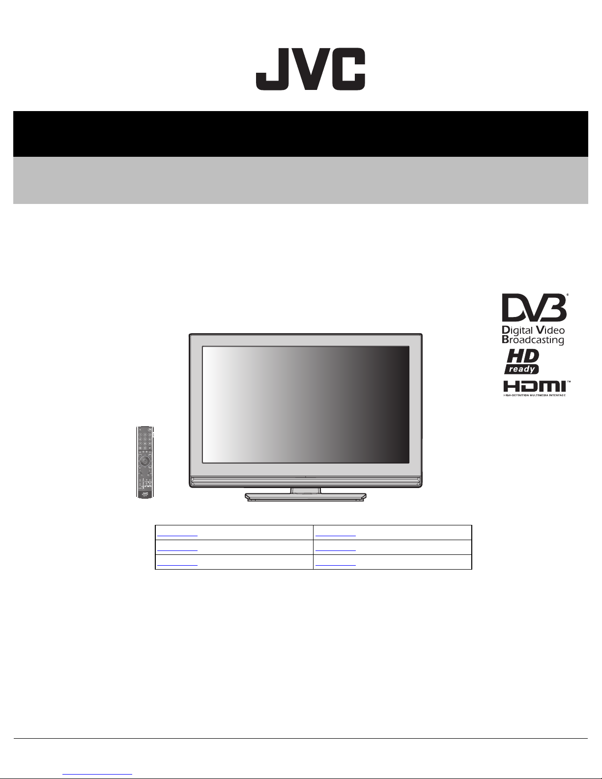
SERVICE MANUAL
INTEGRATED DIGITAL TERRESTRIAL LCD TELEVISION
YA608<Rev.002>20087SERVICE MANUAL
LT-42DA9BJ, LT-42DA9BN,
LT-42DA9BU
COPYRIGHT © 2008 Victor Company of Japan, Limited
No.YA605: LT-19DA9/19DB9 series No.YA606: LT-26DA9/26DB9 series
No.YA607
No.YA609
1 PRECAUTION. . . . . . . . . . . . . . . . . . . . . . . . . . . . . . . . . . . . . . . . . . . . . . . . . . . . . . . . . . . . . . . . . . . . . . . . . 1-3
2 SPECIFIC SERVICE INSTRUCTIONS . . . . . . . . . . . . . . . . . . . . . . . . . . . . . . . . . . . . . . . . . . . . . . . . . . . . . . 1-6
3 DISASSEMBLY . . . . . . . . . . . . . . . . . . . . . . . . . . . . . . . . . . . . . . . . . . . . . . . . . . . . . . . . . . . . . . . . . . . . . . . 1-8
4 ADJUSTMENT . . . . . . . . . . . . . . . . . . . . . . . . . . . . . . . . . . . . . . . . . . . . . . . . . . . . . . . . . . . . . . . . . . . . . . . 1-13
5 TROUBLESHOOTING . . . . . . . . . . . . . . . . . . . . . . . . . . . . . . . . . . . . . . . . . . . . . . . . . . . . . . . . . . . . . . . . . 1-18
: LT-32DA9/32DB9 series No.YA608: LT-42DA9/42DB9 series
: LT-26DE9 series No.YA610: LT-32DE9 series
COPYRIGHT © 2008 Victor Company of Japan, Limited
<MODEL LINEUP>
TABLE OF CONTENTS
No.YA608<Rev.002>
2008/7
SPECIFICATION
Contents
Items
Dimensions ( W × H × D ) 101.4 cm × 69.4 cm × 29.6 cm [101.4 cm × 64.7 cm × 10.9 cm (Without stand)]
Mass 22.5 kg [20.2 kg (Without stand)]
Power Input AC220V - AC240 V, 50 Hz
Power Consumption 240 W (Standby: 0.9 W)
TV RF System Analog CCIR (B/G, I, D/K, L)
Digital DVB-T
Colour System PAL, SECAM, NTSC 3.58/4.43 [EXT only]
Stereo System NICAM (B/G, I, D/K, L), A2 (B/G, D/K)
Receiving
Frequency
Intermediate
Frequency
Colour Sub
Carrier
Frequency
Teletext System
LCD panel 42-inch wide aspect (16 : 9)
Screen Size Diagonal : 106.7 cm (H: 93.0 cm × V: 52.3 cm)
Display Pixels Horizontal : 1366 dots × Vertical : 768 dots
Audio Power Output 10 W + 10 W
Speaker 4.0 cm × 20.0 cm, oval type × 2
Aerial terminal (VHF/UHF) 75 Ω unbalanced, coaxial × 1
EXT-1 / EXT-2 (Input/Output) 21-pin Euro connector (SCART socket ) × 2
EXT-3
(Input)
EXT-4
(Input)
EXT-5 / EXT-6
/ EXT-7
(Digital Input)
Digital Audio Optical Output Digital SPDIF × 1
Headphone 3.5 mm stereo mini jack × 1
Remote Control Unit RM-C1892B (AA/R6 dry cell battery × 2)
Component Video
625p / 525p / 625i / 525i
Analog VHF: 46.25 MHz - 470MHz
UHF: 470 MHz - 855.25 MHz
CATV: 116MHz - 172MHz / 220MHz - 469MHz
Digital UHF:474 MHz - 858 MHz
VIF 38.9MHz (B/G, I, D/K, L)
SIF 33.4MHz (5.5MHz:B/G)
32.9MHz (6.0MHz:I)
32.4MHz (6.5MHz:D/K)
PAL 4.43MHz
SECAM 4.40625MHz / 4.25MHz
NTSC 3.58MHz / 4.43MHz
Analog FLOF (Fastext), TOP
Digital MHEG 5 UK profile EBU TEXT
RCA pin jack × 3
750p / 1125i
S-Video Mini-DIN 4 pin × 1
Video / Audio HDMI 2-row 19pin connector × 3
Y: 1 V (p-p) (Sync signal: ±0.35V(p-p), 3-value sync.), 75Ω / Pb/Pr: ±0.35V(p-p), 75 Ω
Y: 1 V (p-p), Positive (Negative sync.), 75 Ω / Cb/Cr: 0.7V(p-p), 75 Ω
Audio 500 mV(rms) (-4dBs), high impedance, RCA pin jack × 2
Y: 1 V (p-p), Positive (Negative sync provided), 75 Ω
C: 0.286 V (p-p) (Burst signal), 75 Ω
Video 1V (p-p), Positive (Negative sync provided), 75 Ω, RCA pin jack × 1
Audio 500 mV (rms), High impedance, RCA pin jack × 2
(Digital-input terminal is not compatible with picture signals of personal computer)
576i(625i),576p(625p),480i(525i),480p(525p),720p(750p),1080i(1125i) signals are available.
LT-42DA9BJ
LT-42DA9BN
LT-42DA9BU
Design & specifications are subject to change without notice.
1-2 (No.YA608<Rev.002>)

SECTION 1
PRECAUTION
1.1 SAFETY PRECAUTIONS [EXCEPT FOR UK]
(1) The design of this product contains special hardware,
many circuits and components specially for safety
purposes. For continued protection, no changes should be
made to the original design unless authorized in writing by
the manufacturer. Replacement parts must be identical to
those used in the original circuits. Service should be
performed by qualified personnel only.
(2) Alterations of the design or circuitry of the products should
not be made. Any design alterations or additions will void
the manufacturer's warranty and will further relieve the
manufacturer of responsibility for personal injury or
property damage resulting therefrom.
(3) Many electrical and mechanical parts in the products have
special safety-related characteristics. These
characteristics are often not evident from visual inspection
nor can the protection afforded by them necessarily be
obtained by using replacement components rated for
higher voltage, wattage, etc. Replacement parts which
have these special safety characteristics are identified in
the parts list of Service manual. Electrical components
having such features are identified by shading on the
schematics and by ( ) on the parts list in Service
manual. The use of a substitute replacement which does
not have the same safety characteristics as the
recommended replacement part shown in the parts list of
Service manual may cause shock, fire, or other hazards.
(4) Don't short between the LIVE side ground and
ISOLATED (NEUTRAL) side ground or EARTH side
ground when repairing.
Some model's power circuit is partly different in the GND.
The difference of the GND is shown by the LIVE : ( ) side
GND, the ISOLATED (NEUTRAL) : ( ) side GND and
EARTH : ( ) side GND.
Don't short between the LIVE side GND and ISOLATED
(NEUTRAL) side GND or EARTH side GND and never
measure the LIVE side GND and ISOLATED (NEUTRAL)
side GND or EARTH side GND at the same time with a
measuring apparatus (oscilloscope etc.). If above note will
not be kept, a fuse or any parts will be broken.
(5) When service is required, observe the original lead dress.
Extra precaution should be given to assure correct lead
dress in the high voltage circuit area. Where a short circuit
has occurred, those components that indicate evidence of
overheating should be replaced. Always use the
manufacturer's replacement components.
(6) Isolation Check (Safety for Electrical Shock Hazard)
After re-assembling the product, always perform an isolation check on the exposed metal parts of the cabinet (antenna terminals, video/audio input and output terminals,
Control knobs, metal cabinet, screw heads, earphone jack,
control shafts, etc.) to be sure the product is safe to operate
without danger of electrical shock.
a) Dielectric Strength Test
The isolation between the AC primary circuit and all metal
parts exposed to the user, particularly any exposed metal
part having a return path to the chassis should withstand a
voltage of 3000V AC (r.m.s.) for a period of one second. (.
. . . Withstand a voltage of 1100V AC (r.m.s.) to an appliance rated up to 120V, and 3000V AC (r.m.s.) to an appliance rated 200V or more, for a period of one second.)
This method of test requires a test equipment not generally
found in the service trade.
b) Leakage Current Check
Plug the AC line cord directly into the AC outlet (do not use
a line isolation transformer during this check.). Using a
"Leakage Current Tester", measure the leakage current
from each exposed metal part of the cabinet, particularly
any exposed metal part having a return path to the chassis,
to a known good earth ground (water pipe, etc.). Any leakage current must not exceed 0.5mA AC (r.m.s.).
However, in tropical area, this must not exceed 0.2mA AC
(r.m.s.).
Alternate Check Method
Plug the AC line cord directly into the AC outlet (do not
use a line isolation transformer during this check.). Use
an AC voltmeter having 1000Ω per volt or more
sensitivity in the following manner. Connect a 1500Ω
10W resistor paralleled by a 0.15µF AC-type capacitor
between an exposed metal part and a known good earth
ground (water pipe, etc.). Measure the AC voltage
across the resistor with the AC voltmeter. Move the
resistor connection to each exposed metal part,
particularly any exposed metal part having a return path
to the chassis, and measure the AC voltage across the
resistor. Now, reverse the plug in the AC outlet and
repeat each measurement. Any voltage measured must
not exceed 0.75V AC (r.m.s.). This corresponds to
0.7mA AC (r.m.s.).
However, in tropical area, this must not exceed 0.35V
AC (r.m.s.). This corresponds to 0.3mA AC (r.m.s.).
AC VOLTMETER
(HAVING 1000 /V,
OR MORE SENSITIVITY)
0.15 F AC-TYPE
GOOD EARTH GROUND
1500 10W
PLACE THIS PROBE
ON EACH EXPOSED
ME TAL PAR T
(No.YA608<Rev.002>)1-3
1.2 SAFETY PRECAUTIONS [FOR UK]
(1) The design of this product contains special hardware and many circuits and components specially for safety purposes. For
continued protection, no changes should be made to the original design unless authorized in writing by the manufacturer.
Replacement parts must be identical to those used in the original circuits. Service should be performed by qualified personnel
only.
(2) Alterations of the design or circuitry of the product should not be made. Any design alterations or additions will void the
manufacturer's warranty and will further relieve the manufacturer of responsibility for personal injury or property damage
resulting therefrom.
(3) Many electrical and mechanical parts in the product have special safety-related characteristics. These characteristics are often
not evident from visual inspection nor can the protection afforded by them necessary be obtained by using replacement
components rated for higher voltage, wattage, etc. Replacement parts which have these special safety characteristics are
identified in the Parts List of Service Manual. Electrical components having such features are identified by shading on the
schematics and by ( ) on the Parts List in the Service Manual. The use of a substitute replacement which does not have the
same safety characteristics as the recommended replacement part shown in the Parts List of Service Manual may cause shock,
fire, or other hazards.
(4) The leads in the products are routed and dressed with ties, clamps, tubing’s, barriers and the like to be separated from live parts,
high temperature parts, moving parts and / or sharp edges for the prevention of electric shock and fire hazard. When service is
required, the original lead routing and dress should be observed, and it should be confirmed that they have been returned to
normal, after re-assembling.
WARNING
(1) The equipment has been designed and manufactured to meet international safety standards.
(2) It is the legal responsibility of the repairer to ensure that these safety standards are maintained.
(3) Repairs must be made in accordance with the relevant safety standards.
(4) It is essential that safety critical components are replaced by approved parts.
(5) If mains voltage selector is provided, check setting for local voltage.
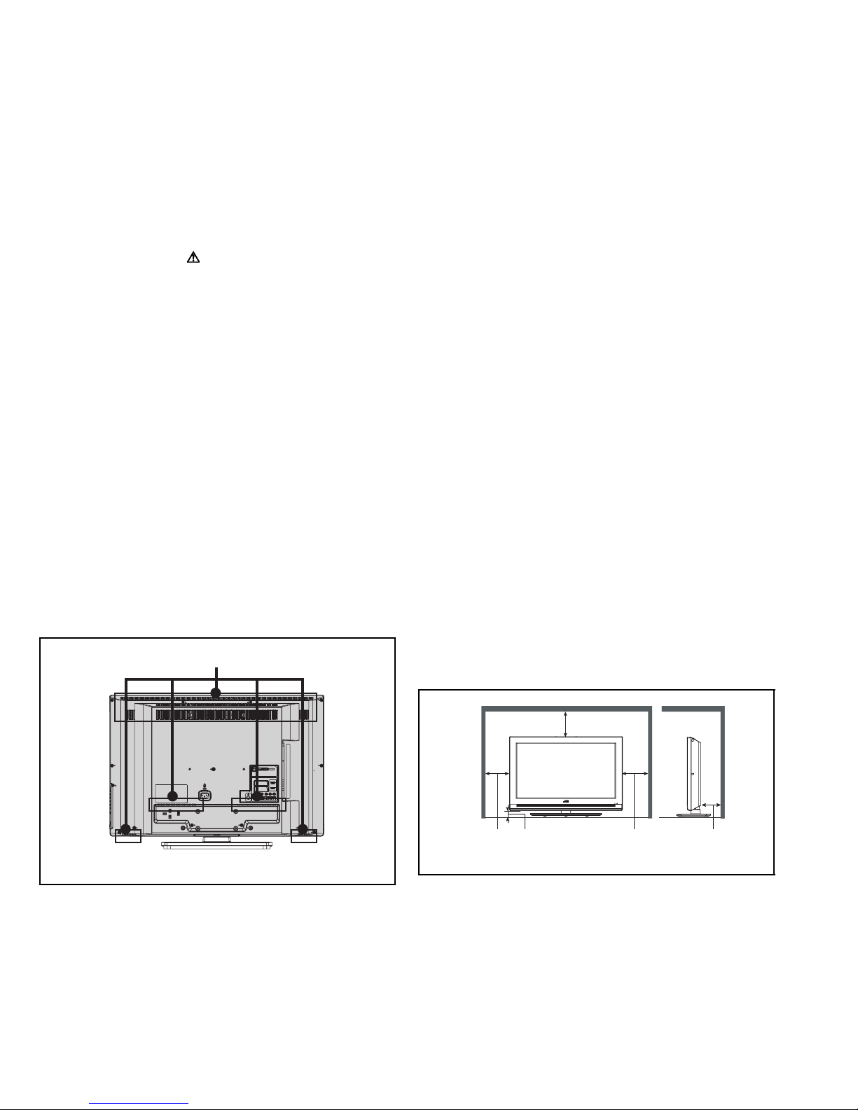
1.3 INSTALLATION
1.3.1 HEAT DISSIPATION
If the heat dissipation vent behind this unit is blocked, cooling
efficiency may deteriorate and temperature inside the unit will
rise. The temperature sensor that protects the unit will be
activated when internal temperature exceeds the pre-determined
level and power will be turned off automatically.Therefore,
please make sure pay attention not to block the heat dissipation
vent as well as the ventilation outlet behind the unit and ensure
that there is room for ventilation around it.
Ventilation hole
*Diagram differs from actual appearance.
1.3.2 NOTES ON HANDLING
When taking the unit out of a packing case, do not grasp the
upper part of the unit. If you take the unit out while grasping the
upper part, the LCD PANEL may be damaged because of a
pressure. Instead of grasping the upper part, put your hands on
the lower backside or sides of the unit.
1.3.3 INSTALLATION REQUIREMENTS
Ensure that the minimal distance is maintained, as specified
below, between the unit with and the surrounding walls, as well
as the floor etc.Install the unit on stable flooring or stands.Take
precautionary measures to prevent the unit from tipping in order
to protect against accidents and earthquakes.
200 mm
150 mm 50
*Diagram differs from actual appearance.
mm
150 mm 50 mm
1-4 (No.YA608<Rev.002>)
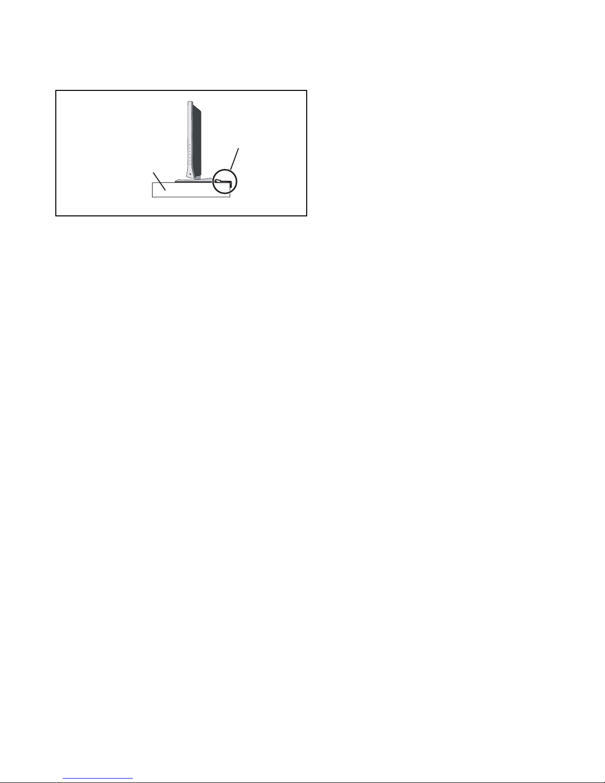
1.3.4 INSTALLATION REQUIREMENTS
To ensure safety in an emergency such as an earthquake, and
to prevent accidents, ensure that measures are taken to prevent
the TV dropping or falling over.
It fixes in a band.
TV STAND
*Diagram differs from actual appearance.
1.4.2 OPTICAL FILTER (ON THE FRONT OF THE LCD PANEL)
(1) Avoid placing the unit under direct sunlight over a
prolonged period of time. This may cause the optical filter
to deteriorate in quality and COLOUR.
(2) Clean the filter surface by wiping it softly and lightly with a
soft and lightly fuzz cloth (such as outing flannel).
(3) Do not use solvents such as benzene or thinner to wipe the
filter surface. This may cause the filter to deteriorate in
quality or the coating on the surface to come off. When
cleaning the filter, usually use the neutral detergent diluted
with water. When cleaning the dirty filter, use water-diluted
ethanol.
(4) Since the filter surface is fragile, do not scratch or hit it with
hard materials. Be careful enough not to touch the front
surface, especially when taking the unit out of the packing
case or during transportation.
1.4 HANDLING LCD PANEL
1.4.1 PRECAUTIONS FOR TRANSPORTATION
When transporting the unit, pressure exerted on the internal LCD
panel due to improper handling (such as tossing and dropping)
may cause damages even when the unit is carefully packed. To
prevent accidents from occurring during transportation, pay
careful attention before delivery, such as through explaining the
handling instructions to transporters.
Ensure that the following requirements are met during
transportation, as the LCD panel of this unit is made of glass and
therefore fragile:
(1) USE A SPECIAL PACKING CASE FOR THE LCD PANEL
When transporting the LCD panel of the unit, use a special
packing case (packing materials). A special packing case
is used when a LCD panel is supplied as a service spare
part.
(2) ATTACH PROTECTION SHEET TO THE FRONT
Since the front (display part) of the panel is vulnerable,
attach the protection sheet to the front of the LCD panel
before transportation. Protection sheet is used when a LCD
panel is supplied as a service spare part.
(3) AVOID VIBRATIONS AND IMPACTS
The unit may be broken if it is toppled sideways even when
properly packed. Continuous vibration may shift the gap of
the panel, and the unit may not be able to display images
properly. Ensure that the unit is carried by at least 2
persons and pay careful attention not to exert any vibration
or impact on it.
(4) DO NOT PLACE EQUIPMENT HORIZONTALLY
Ensure that it is placed upright and not horizontally during
transportation and storage as the LCD panel is very
vulnerable to lateral impacts and may break. During
transportation, ensure that the unit is loaded along the
traveling direction of the vehicle, and avoid stacking them
on one another. For storage, ensure that they are stacked
in 2 layers or less even when placed upright.
1.4.3 PRECAUTIONS FOR REPLACEMENT OF EXTERIOR
PARTS
Take note of the following when replacing exterior parts (REAR
COVER, FRONT PANEL, etc.):
(1) Do not exert pressure on the front of the LCD panel (filter
surface). It may cause irregular COLOUR.
(2) Pay careful attention not to scratch or stain the front of the
LCD panel (filter surface) with hands.
(3) When replacing exterior parts, the front (LCD panel) should
be placed facing downward. Place a mat, etc. underneath
to avoid causing scratches to the front (filter surface).
(No.YA608<Rev.002>)1-5
SECTION 2
SPECIFIC SERVICE INSTRUCTIONS
2.1 FEATURES
DIGITAL TUNER
This TV can receive both DVB-T (Digital terrestrial broadcasting),
DVB-S(Digital satellite broadcasting: DB9 only) and Analogue
terrestrial broadcasting.
HDMI INPUT
By connecting a HDMI compatible device, high definition
pictures can be displayed on your TV in their digital form.
2.2 MAIN DIFFERENCE LIST
Contents
Items
LT-42DA9BJ
Teletext System (Digital) MHEG 5 UK profile EBU TEXT
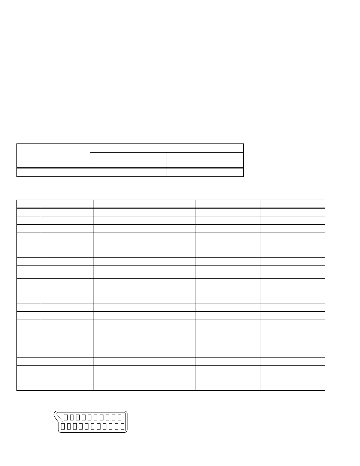
2.3 21-PIN EURO CONNECTOR (SCART) : EXT-1 / EXT-2
PICTURE MODE
This function can adjust the picture settings automatically.
There are BRIGHT, STANDARD, SOFT and MANUAL in the
PICTURE MODE.
ZOOM
This function can change the screen size according to the
picture aspect ratio.
HYPER SOUND
You can enjoy sounds with a wider ambience.
LT-42DA9BN
LT-42DA9BU
Pin No. Signal designation Matching value EXT-1 EXT-2
1 AUDIO R output 500mV(rms) (Nominal), Low impedance Used (TV OUT) Used (LINE OUT)
2 AUDIO R input 500mV(rms) (Nominal), High impedance Used (R1) Used (R2)
3 AUDIO L output 500mV(rms) (Nominal), Low impedance Used (TV OUT) Used (LINE OUT)
4 AUDIO GND Used Used
5 GND (B) Used Used
6 AUDIO L input 500mV(rms) (Nominal), High impedance Used (L1) Used (L2)
7 B input 700mV
8 FUNCTION SW
(SLOW SW)
9 GND (G) Used Used
10 SCL Not used Used (SCL2)
11 G input 700mV
12 SDA Not used Used (SDA2)
13 GND (R) Used Used
14 GND (YS) Used Not used
15 R / C input R : 700mV
16 Ys input (FAST SW) Low : 0V-0.4V, High : 1V-3V, 75Ω Used Not used
17 GND (VIDEO output) Used Used
18 GND (VIDEO input) Used Used
19 VIDEO output 1V
20 VIDEO / Y input 1V
21 COMMON GND Used Used
Low : 0V-3V
High : 8V-12V, High impedance
C : 300mV
(P-P)
(P-P)
, 75Ω Used Not used
(B-W)
Used Used
, 75Ω Used Not used
(B-W)
, 75Ω
(B-W)
, 75Ω
(P-P)
(Negative sync), 75Ω Used (TV OUT) Used (LINE OUT)
(Negative sync), 75Ω Used Used
Used (R) Used (C2)
(P-P= Peak to Peak, B-W= Blanking to white peak)
[Pin assignment]
20 18 16 14 12 10 8 6 4 2
21 19 17 15 13 11 9 7 5 3 1
1-6 (No.YA608<Rev.002>)
2.4 TECHNICAL INFORMATION
2.4.1 LCD PANEL
This unit uses the flat type LCD (Liquid Crystal Display) panel that occupies little space, instead of using the conventional
CRT(Cathode Ray Tube). This panel adopts "normally white" mode where the transmittance or reflective rate is maximum, and the
screen is white when no voltage is applied.
2.4.1.1 SPECIFICATIONS
The following table shows the specifications of this unit.
Item Specifications
Maximum dimensions ( W × H × D ) 98.3 cm × 57.6 cm × 5.1 cm
Weight 10.5 kg
Effective screen size Diagonal : 106.7 cm (H: 93.0 cm × V: 52.3 cm)
Aspect ratio 16 : 9
Drive device / system a-Si-TFT active matrix system
Resolution Horizontally 1366 × Vertically 768 × RGB < W-XGA > 3147264 dots in total
Pixel pitch (pixel size) Horizontally: 0.227 mm, Vertically: 0.681 mm
Displayed color 16777216 colors 256 colors for R G and B
Brightness 500 cd/m2
Contrast ratio 1000 : 1
Response time 6.5 ms
View angle (Horizontally) 178°
View angle (Vertically) 178°
Surface polarizer Anti-Glare type Low reflective coat
Color filter Vertical stripe
Backlight Cold cathode fluorescent lamp × 20
Power supply voltage in LCD 12 V
Power supply voltage in inverter 24 V
Panel interface system LVDS (Low Voltage Differential Signaling)
2.4.1.2 PIXEL FAULT
There are three pixel faults - bright fault , dark fault and flicker fault - that are respectively defined as follows.
BRIGHT FAULT
In this pixel fault, a cell that should not light originally is lighting on and off.
For checking this pixel fault, input ALL BLACK SCREEN and find out the cell that is lighting on and off.
DARK FAULT
In this pixel fault, a cell that should light originally is not lighting or lighting with the brightness twice as brighter as originally lighting.
For checking this pixel fault, input 100% of each R/G/B colour and find out the cell that is not lighting.
FLICKER FAULT
In the pixel fault, a cell that should light originally or not light originally is flashing on and off.
For checking this pixel fault, input ALL BLACK SCREEN signal or 100% of each RGB colour and find out the cell that is flashing on
and off.
(No.YA608<Rev.002>)1-7

SECTION 3
DISASSEMBLY
3.1 CAUTION AT DISASSEMBLY
• Make sure that the power cord is disconnected from the outlet.
• Pay special attention not to break or damage the parts.
• Make sure that there is no bent or stain on the connectors before inserting, and firmly insert the connectors.
• Be sure to reattach the wire clamps removed during the procedure to the original positions. (Attaching the wire clamps in wrong
positions may affect the performance.)
REFERENCE:
When removing each board, remove the connector if necessary. The operation is easier if you write down the connection points
(connector numbers) of the connector. For connection of each board, refer to the "WIRING DIAGRAM" of the Standard Circuit
Diagram.
3.2 DISASSEMBLY PROCEDURE
3.2.1 REMOVING THE REAR COVER (Fig.3-1)
(1) Remove the 16 screws [A].
(2) Remove the REAR COVER.
3.2.2 REMOVING THE POWER UNIT (Fig.3-1)
• Remove the REAR COVER.
(1) Remove the 4 screws [B].
(2) Remove the POWER UNIT.
3.2.7 REMOVING THE SPEAKER (Fig.3-1)
• Remove the REAR COVER.
(1) Remove the SPEAKER.
3.2.8 REMOVING THE IR PWB (Fig.3-1)
• Remove the REAR COVER.
(1) Remove the 1 screw [L].
(2) Remove the IR PWB.
3.2.3 REMOVING THE MAIN PWB / MPEG PWB (Fig.3-1)
• Remove the REAR COVER.
(1) Remove the 2 screws [C].
(2) Remove the SIDE SHIELD.
(3) Remove the 4 screws [D] and 4 screws [E].
(4) Remove the MAIN PWB and MPEG PWB together.
(5) Remove the connector connecting the MAIN PWB and
MPEG PWB to separate each board.
3.2.4 REMOVING THE KEY PWB / CONTROL BASE (Fig.3-1)
• Remove the REAR COVER.
(1) Remove the 1 screw [F].
(2) Remove the KEY PWB.
(3) Remove the 1 screw [G].
(4) Remove the CONTROL BASE.
3.2.5 REMOVING THE INVERTER PWB (Fig.3-1)
• Remove the REAR COVER.
(1) Remove the 5 screws [H].
(2) Remove the INVERTER PWB COVER.
(3) Remove the INVERTER PWB(MASTER).
(4) Follow the same steps when removing the other hand
INVERTER PWB(SLAVE).
3.2.9 REMOVING THE SUPPORT BRACKET (Fig.3-1)
• Remove the REAR COVER.
(1) Remove the 4 screws [M].
(2) Remove the SUPPORT BRACKET.
3.2.10 REMOVING THE STAND (Fig.3-1)
(1) Remove the 2 screws [N].
(2) Remove the STAND.
3.2.11 REMOVING THE LCD CONTROL PWB (Fig.3-1)
• Remove the REAR COVER.
• Remove the STAND.
(1) Remove the 7 screws [P] and 4 screws [Q].
(2) Remove the MAIN SHIELD.
(3) Remove the 4 screws [R].
(4) Remove the LCD CONTROL PWB COVER.
(5) Remove the LCD CONTROL PWB.
3.2.12 REMOVING THE LED PWB (Fig.3-1)
• Remove the REAR COVER.
• Remove the STAND.
• Remove the MAIN SHIELD.
(1) Remove the 2 screws [S].
(2) Remove the LED PWB.
3.2.6 REMOVING THE POWER BRACKET (Fig.3-1)
• Remove the REAR COVER.
(1) Remove the 2 screws [J].
(2) Remove the POWER BRACKET.
1-8 (No.YA608<Rev.002>)
3.2.13 REMOVING THE LCD PANEL UNIT (Fig.3-1)
• Remove the REAR COVER.
• Remove the STAND.
• Remove the MAIN SHIELD.
(1) Remove the LCD PANEL UNIT.
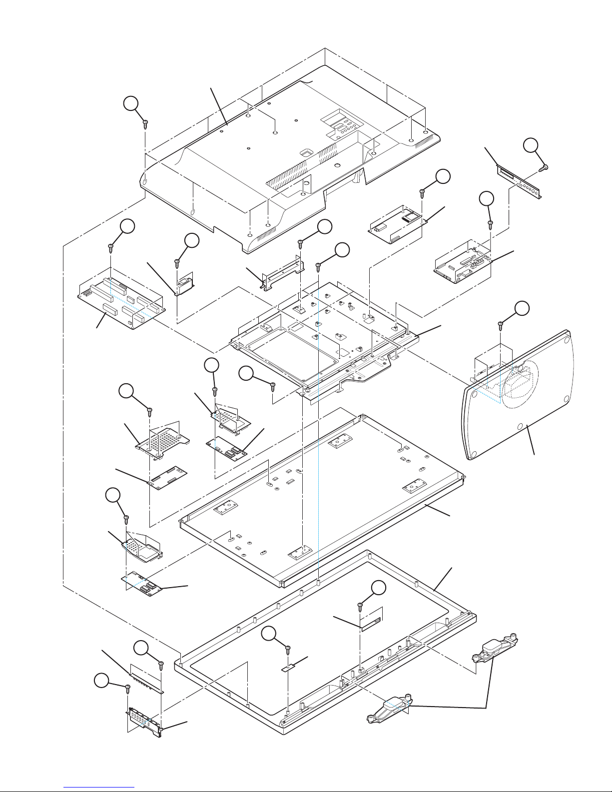
REAR
COVER
A
SIDE
SHIELD
C
D
B
BRACKET
POWER
UNIT
R
LCD CONTROL
PWB COVER
LCD CONTROL
PWB
POWER
INVERTER
PWB
COVER
J
SUPPORT
BRACKET
H
Q
INVERTER
PWB(SLAVE)
TUNER
E
PWB
M
P
MAIN
PWB
N
MAIN
SHIELD
STAND
H
INVERTER
PWB
COVER
INVERTER
PWB(MASTER)
KEY PWB
F
G
CONTROL
KNOB
LCD PANEL
FRONT
CABINET
S
LED
MODULE
L
IR PWB
SPEAKER
Fig.3-1
(No.YA608<Rev.002>)1-9
3.3 MEMORY IC REPLACEMENT
Service
Hardware Ver : REV X.X
Sub MCU SW Ver : REV X.X
ATV SW Ver : XXXXXX X.XX.XX
DTV SW Ver : XXXXXX X.XX.XX
Sub MCU Loader Ver : XX.XX
DTV Loader Ver : XX.XX
ATV Loader Ver : X. X. X
System ID : XXXX.XXXX
Update Date : XXXX XX XXXX
Right:Enter Back:Return Exit:OK
Video Setup
White Balance
Spread Spectrum
Panel Select <XXXXX>
Reset TV-set
Factory Default
Right:Enter Back:Return Exit:OK
• This model uses the memory IC.
• This memory IC stores data for proper operation of the video and drive circuits.
• When replacing, be sure to use an IC containing this (initial value) data.
3.3.1 MEMORY IC REPLACEMENT PROCEDURE
1. Power off
Switch off the power and disconnect the power plug from the AC outlet.
2. Replace the memory IC
Be sure to use the memory IC written with the initial setting values.
3. Power on
Connect the power plug to the AC outlet and switch on the power.
4. Receiving channel setting
Refer to the OPERATING INSTRUCTIONS and set the receive channels (Channels Preset) as described.
5. User setting
Check the user setting items according to the given in page later. Where these do not agree, refer to the OPERATING
INSTRUCTIONS and set the items as described.
6. FACTORY MODE setting
Verify what to set in the FACTORY MODE, and set whatever is necessary.
3.3.2 FACTORY MODE SETTING
FACTORY MODE SCREEN SETTING ITEM
FACTORY MODE SCREEN-1
Service
Hardware Ver : REV X.X
Sub MCU SW Ver : REV X.X
ATV SW Ver : XXXXXX X.XX.XX
DTV SW Ver : XXXXXX X.XX.XX
Sub MCU Loader Ver : XX.XX
DTV Loader Ver : XX.XX
ATV Loader Ver : X. X. X
System ID : XXXX.XXXX
Update Date : XXXX XX XXXX
Right:Enter Back:Return Exit:OK
Press [ ] key
FACTORY MODE SCREEN-2
Video Setup
White Balance
Spread Spectrum
Panel Select <XXXXX>
Reset TV-set
Factory Default
Right:Enter Back:Return Exit:OK
Setting items Settings
Video Setup [Do not adjust]
White Balance Adjust
Spread Spectrum [Do not adjust]
Panel Select [Do not adjust]
Reset TV-set ---
Factory Default ---
1-10 (No.YA608<Rev.002>)

3.3.3 SETTINGS OF FACTORY SHIPMENT
3.3.3.1 BUTTON OPERATION 3.3.3.2 REMOTE CONTROL DIRECT OPERATION
Setting item Setting position
POWER Off
CHANNEL PR1
VOLUME 10
AV TV
3.3.3.3 REMOTE CONTROL MENU OPERATION
(1) Picture
Setting item Setting position
Mode Bright
Fleshtone Off
Colour Temperature Cool
Noise Reduction High
Backlight High
(2) Sound
Setting item Setting position
Bass 0
Treble 0
Balance 0
AVL On
Hyper Sound Off
(3) Install
Setting item Setting position
Country BJ MODEL: UK
BU/ MODEL: Germany
BN MODEL: Finland
Antenna Power Off
Auto Search ---
Manual Search ---
Edit Channels ---
Setting item Setting position
CHANNEL PR1
VOLUME 10
ZOOM AUTO
SUB POWER OFF
(4) Feature
Setting item Setting position
Language BJ MODEL: English
BU MODEL: German
BN MODEL: Finnish
Time Setting
Power On Time
Power Off Time
Auto Power Off
Off
Off
Off
Parental Control Disable
OSD Transparency 30
Blue Back Off
Power Lamp On
4 : 3 Aspect Setting Panoramic
(5) APS (in Analog tV Mode only)
Setting item Setting position
Language BJ MODEL: English
BU MODEL: German
BN MODEL: Finnish
Antenna Power Off
Country BJ MODEL: UK
BU/ MODEL: Germany
BN MODEL: Finland
Channel Search ---
(No.YA608<Rev.002>)1-11
3.4 REPLACEMENT OF CHIP COMPONENT
3.4.1 CAUTIONS
(1) Avoid heating for more than 3 seconds.
(2) Do not rub the electrodes and the resist parts of the pattern.
(3) When removing a chip part, melt the solder adequately.
(4) Do not reuse a chip part after removing it.
3.4.2 SOLDERING IRON
(1) Use a high insulation soldering iron with a thin pointed end of it.
(2) A 30w soldering iron is recommended for easily removing parts.
3.4.3 REPLACEMENT STEPS
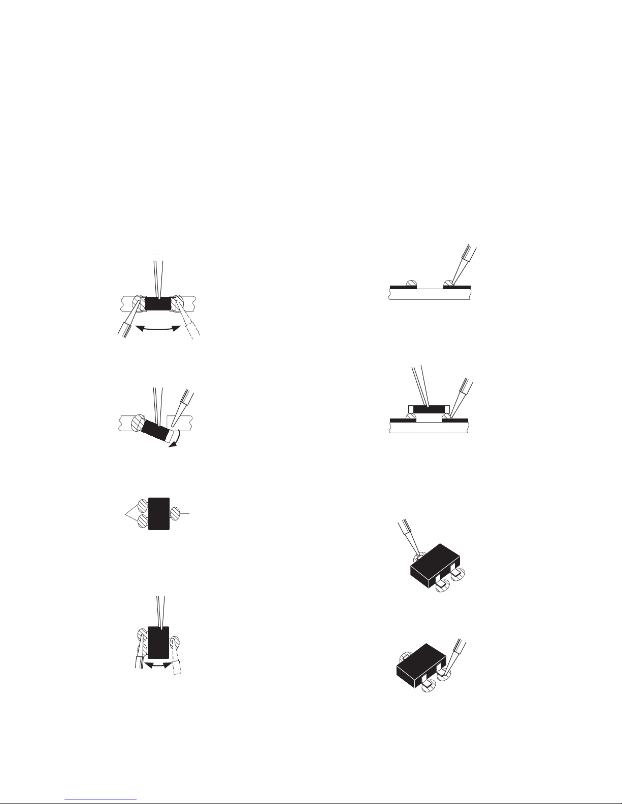
1. How to remove Chip parts
2. How to install Chip parts
[Resistors, capacitors, etc.]
(1) As shown in the figure, push the part with tweezers and
alternately melt the solder at each end.
(2) Shift with the tweezers and remove the chip part.
[Transistors, diodes, variable resistors, etc.]
(1) Apply extra solder to each lead.
SOLDER
SOLDER
[Resistors, capacitors, etc.]
(1) Apply solder to the pattern as indicated in the figure.
(2) Grasp the chip part with tweezers and place it on the
solder. Then heat and melt the solder at both ends of the
chip part.
[Transistors, diodes, variable resistors, etc.]
(1) Apply solder to the pattern as indicated in the figure.
(2) Grasp the chip part with tweezers and place it on the
solder.
(3) First solder lead A as indicated in the figure.
(2) As shown in the figure, push the part with tweezers and
alternately melt the solder at each lead. Shift and remove
the chip part.
NOTE :
After removing the part, remove remaining solder from the
pattern.
1-12 (No.YA608<Rev.002>)
A
B
C
(4) Then solder leads B and C.
A
B
C
SECTION 4
Service
Hardware Ver : REV X.X
Sub MCU SW Ver : REV X.X
ATV SW Ver : XXXXXX X.XX.XX
DTV SW Ver : XXXXXX X.XX.XX
Sub MCU Loader Ver : XX.XX
DTV Loader Ver : XX.XX
ATV Loader Ver : X. X. X
System ID : XXXX.XXXX
Update Date : XXXX XX XXXX
Right:Enter Back:Return Exit:OK
Video Setup
White Balance
Spread Spectrum
Panel Select <XXXXX>
Reset TV-set
Factory Default
Right:Enter Back:Return Exit:OK
ADJUSTMENT
4.1 ADJUSTMENT PREPARATION
(1) This TV is adjusted by using REMOTE CONTROL UNIT.
(2) The adjustment using the REMOTE CONTROL UNIT is made on the basis of the initial setting values. The setting values
which adjust the screen to the optimum condition can be different from the initial setting values.
(3) Make sure that connection is correctly made AC to AC power source.
(4) Turn on the power of the TV and measuring instruments for warming up for at least 30 minutes before starting adjustments.
(5) If the receive or input signal is not specified, use the most appropriate signal for adjustment.
(6) Never touch the parts (such as variable resistors, transformers and condensers) not shown in the adjustment items of this service
adjustment.
4.2 PRESET SETTING BEFORE ADJUSTMENTS
Unless otherwise specified in the adjustment items, preset the
following functions with the REMOTE CONTROL UNIT.
Setting item Settings position
Picture Mode Standard
Colour Temperature Normal
4.4 ADJUSTMENT ITEMS
VIDEO CIRCUIT
• WHITE BALANCE adjustment
4.5 BASIC OPERATION OF FACTORY MODE
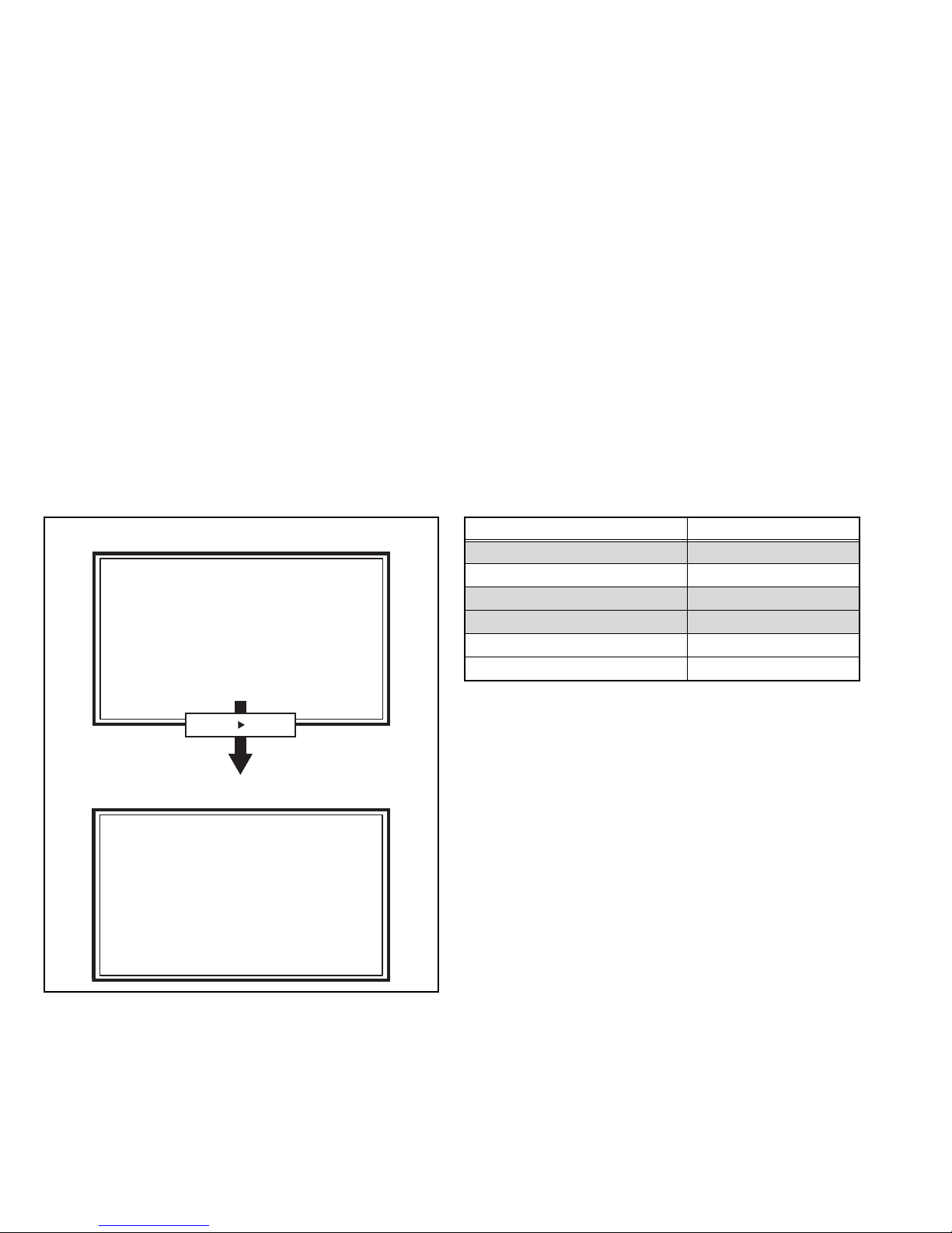
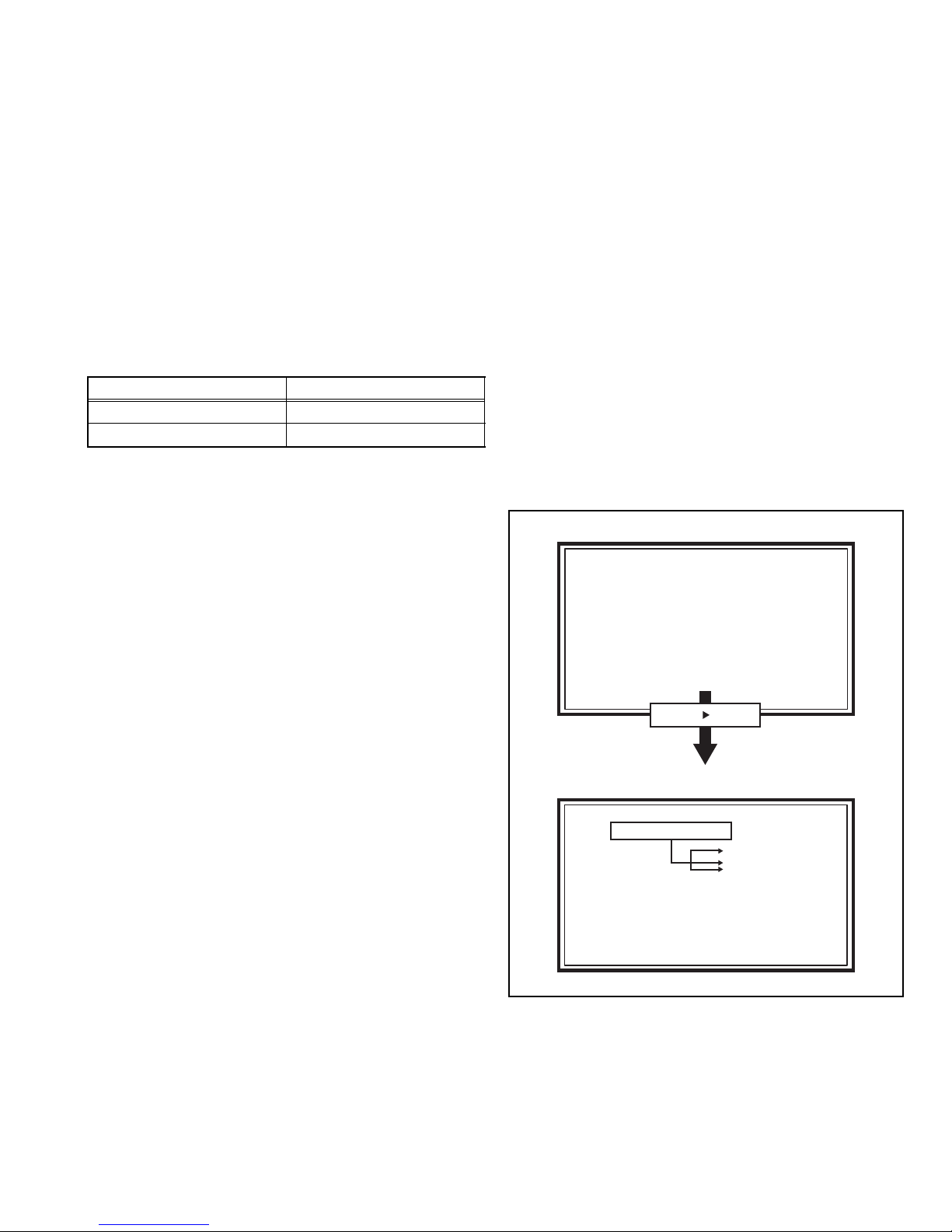
4.5.1 HOW TO ENTER THE FACTORY MODE
(1) Press [INFORMATION] key and [MUTING] key on the
remote control unit simultaneously to enter the FACTORY
MODE SCREEN-1. (Fig.4-1)
(2) Press [] key on the remote control unit simultaneously to
enter the FACTORY MODE SCREEN-2. (Fig.4-1)
4.5.2 HOW TO EXIT THE FACTORY MODE
Press the [OK] key to exit the factory mode.
4.3 MEASURING INSTRUMENT AND FIXTURES
• Signal generator (Pattern generator)[PAL]
• Remote control unit
FACTORY MODE SCREEN-1
Service
Hardware Ver : REV X.X
Sub MCU SW Ver : REV X.X
ATV SW Ver : XXXXXX X.XX.XX
DTV SW Ver : XXXXXX X.XX.XX
Sub MCU Loader Ver : XX.XX
DTV Loader Ver : XX.XX
ATV Loader Ver : X. X. X
System ID : XXXX.XXXX
Update Date : XXXX XX XXXX
Right:Enter Back:Return Exit:OK
Press [ ] key
FACTORY MODE SCREEN-2
DO NOT ADJUST
Video Setup
White Balance
Spread Spectrum
Panel Select <XXXXX>
Reset TV-set
Factory Default
Right:Enter Back:Return Exit:OK
Fig.4-1
(No.YA608<Rev.002>)1-13
4.5.3 CHANGE AND MEMORY OF SETTING VALUE
SELECTION OF SETTING ITEM
• [FUNCTION /] key.
For scrolling up / down the setting items.
• [FUNCTION /] key.
For select the setting items.
CHANGE OF SETTING VALUE (DATA)
• [FUNCTION /] key.
For scrolling up / down the setting values.
MEMORY OF SETTING VALUE (DATA)
The setting value will be stored automatically when release the
REMOTE CONTROL UNIT keys.
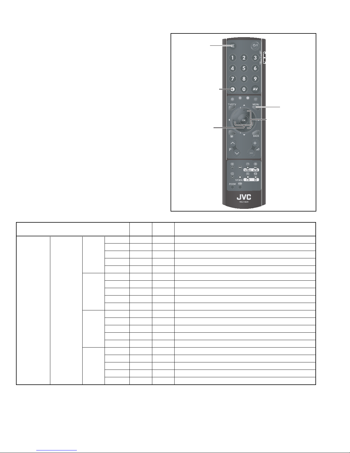
4.5.4 FACTORY MODE SELECT KEY LOCATION
[MUTING] key
[INFORMATION] key
[MENU] key
[FUNCTION /] key
[Function/] key
4.6 SETTING ITEM IN THE FACTORY MODE
Swetting item
Brightness 0 - 100 41 Adjust the Brightness value of Standard mode in Analog TV.
Contrast 0 - 100 68 Adjust the Contrast value of Standard mode in Analog TV.
Standard
Bright
Video Setup RF(Analog TV)
Game
Soft
Sharpness 0 - 100 65 Adjust the Sharpness value of Standard mode in Analog TV.
Colour 0 - 100 58 Adjust the Colour value of Standard mode in Analog TV.
Farbton 0 - 100 0 Adjust the Farbton value of Standard mode in Analog TV.
Brightness 0 - 100 41 Adjust the Brightness value of Bright mode in Analog TV.
Contrast 0 - 100 73 Adjust the Contrast value of Bright mode in Analog TV.
Sharpness 0 - 100 65 Adjust the Sharpness value of Bright mode in Analog TV.
Colour 0 - 100 59 Adjust the Colour value of Bright mode in Analog TV.
Farbton 0 - 100 0 Adjust the Farbton value of Bright mode in Analog TV.
Brightness 0 - 100 43 Adjust the Brightness value of Game mode in Analog TV.
Contrast 0 - 100 63 Adjust the Contrast value of Game mode in Analog TV.
Sharpness 0 - 100 65 Adjust the Sharpness value of Game mode in Analog TV.
Colour 0 - 100 58 Adjust the Colour value of Game mode in Analog TV.
Farbton 0 - 100 0 Adjust the Farbton value of Game mode in Analog TV.
Brightness 0 - 100 42 Adjust the Brightness value of Soft mode in Analog TV.
Contrast 0 - 100 63 Adjust the Contrast value of Soft mode in Analog TV.
Sharpness 0 - 100 65 Adjust the Sharpness value of Soft mode in Analog TV.
Colour 0 - 100 58 Adjust the Colour value of Soft mode in Analog TV.
Farbton 0 - 100 0 Adjust the Farbton value of Soft mode in Analog TV.
Variable
range
Default
Value
Comment
1-14 (No.YA608<Rev.002>)
Video Setup
Video Setup
Swetting item
CVBS(EXT-4)
RGB(Digital TV
EXT-1 EXT-2)
Standard
Bright
Game
Soft
Standard
Bright
Game
Soft
Variable
range
Brightness 0 - 100 41 Adjust the Brightness value of Standard mode in CVBS(EXT-4).
Contrast 0 - 100 68 Adjust the Contrast value of Standard mode in CVBS(EXT-4).
Sharpness 0 - 100 65 Adjust the Sharpness value of Standard mode in CVBS(EXT-4).
Colour 0 - 100 58 Adjust the Colour value of Standard mode in CVBS(EXT-4).
Farbton 0 - 100 0 Adjust the Farbton value of Standard mode in CVBS(EXT-4).
Brightness 0 - 100 41 Adjust the Brightness value of Bright mode in CVBS(EXT-4).
Contrast 0 - 100 73 Adjust the Contrast value of Bright mode in CVBS(EXT-4).
Sharpness 0 - 100 65 Adjust the Sharpness value of Bright mode in CVBS(EXT-4).
Colour 0 - 100 59 Adjust the Colour value of Bright mode in CVBS(EXT-4).
Farbton 0 - 100 0 Adjust the Farbton value of Bright mode in CVBS(EXT-4).
Brightness 0 - 100 43 Adjust the Brightness value of Bright mode in CVBS(EXT-4).
Contrast 0 - 100 63 Adjust the Contrast value of Bright mode in CVBS(EXT-4).
Sharpness 0 - 100 65 Adjust the Sharpness value of Bright mode in CVBS(EXT-4).
Colour 0 - 100 58 Adjust the Colour value of Bright mode in CVBS(EXT-4).
Farbton 0 - 100 0 Adjust the Farbton value of Bright mode in CVBS(EXT-4).
Brightness 0 - 100 42 Adjust the Brightness value of Soft mode in CVBS(EXT-4).
Contrast 0 - 100 63 Adjust the Contrast value of Soft mode in CVBS(EXT-4).
Sharpness 0 - 100 65 Adjust the Sharpness value of Soft mode in CVBS(EXT-4).
Colour 0 - 100 58 Adjust the Colour value of Soft mode in CVBS(EXT-4).
Farbton 0 - 100 0 Adjust the Farbton value of Soft mode in CVBS(EXT-4).
Brightness 0 - 100 41 Adjust the Brightness value of Standard mode in RGB(Digital TV EXT-1 EXT-2).
Contrast 0 - 100 68 Adjust the Contrast value of Standard mode in RGB(Digital TV EXT-1 EXT-2).
Sharpness 0 - 100 65 Adjust the Sharpness value of Standard mode in RGB(Digital TV EXT-1 EXT-2).
Colour 0 - 100 58 Adjust the Colour value of Standard mode in RGB(Digital TV EXT-1 EXT-2).
Farbton 0 - 100 0 Adjust the Farbton value of Standard mode in RGB(Digital TV EXT-1 EXT-2).
Brightness 0 - 100 41 Adjust the Brightness value of Bright mode in RGB(Digital TV EXT-1 EXT-2).
Contrast 0 - 100 73 Adjust the Contrast value of Bright mode in RGB(Digital TV EXT-1 EXT-2).
Sharpness 0 - 100 65 Adjust the Sharpness value of Bright mode in RGB(Digital TV EXT-1 EXT-2).
Colour 0 - 100 59 Adjust the Colour value of Bright mode in RGB(Digital TV EXT-1 EXT-2).
Farbton 0 - 100 0 Adjust the Farbton value of Bright mode in RGB(Digital TV EXT-1 EXT-2).
Brightness 0 - 100 43 Adjust the Brightness value of Game mode in RGB(Digital TV EXT-1 EXT-2).
Contrast 0 - 100 63 Adjust the Contrast value of Game mode in RGB(Digital TV EXT-1 EXT-2).
Sharpness 0 - 100 65 Adjust the Sharpness value of Game mode in RGB(Digital TV EXT-1 EXT-2).
Colour 0 - 100 58 Adjust the Colour value of Game mode in RGB(Digital TV EXT-1 EXT-2).
Farbton 0 - 100 0 Adjust the Farbton value of Game mode in RGB(Digital TV EXT-1 EXT-2).
Brightness 0 - 100 42 Adjust the Brightness value of Soft mode in RGB(Digital TV EXT-1 EXT-2).
Contrast 0 - 100 63 Adjust the Contrast value of Soft mode in RGB(Digital TV EXT-1 EXT-2).
Sharpness 0 - 100 65 Adjust the Sharpness value of Soft mode in RGB(Digital TV EXT-1 EXT-2).
Colour 0 - 100 58 Adjust the Colour value of Soft mode in RGB(Digital TV EXT-1 EXT-2).
Farbton 0 - 100 0 Adjust the Farbton value of Soft mode in RGB(Digital TV EXT-1 EXT-2).
Default
Value
Comment
(No.YA608<Rev.002>)1-15
Swetting item
Video Setup YC(EXT-4S)
Video Setup COMP(EXT-3)
Standard
Bright
Game
Soft
Standard
Bright
Game
Soft
Variable
range
Brightness 0 - 100 41 Adjust the Brightness value of Standard mode in YC(EXT-4S).
Contrast 0 - 100 68 Adjust the Contrast value of Standard mode in YC(EXT-4S).
Sharpness 0 - 100 65 Adjust the Sharpness value of Standard mode in YC(EXT-4S).
Colour 0 - 100 58 Adjust the Colour value of Standard mode in YC(EXT-4S).
Farbton 0 - 100 0 Adjust the Farbton value of Standard mode in YC(EXT-4S).
Brightness 0 - 100 41 Adjust the Brightness value of Bright mode in YC(EXT-4S).
Contrast 0 - 100 73 Adjust the Contrast value of Bright mode in YC(EXT-4S).
Sharpness 0 - 100 65 Adjust the Sharpness value of Bright mode in YC(EXT-4S).
Colour 0 - 100 59 Adjust the Colour value of Bright mode in YC(EXT-4S).
Farbton 0 - 100 0 Adjust the Farbton value of Bright mode in YC(EXT-4S).
Brightness 0 - 100 43 Adjust the Brightness value of Game mode in YC(EXT-4S).
Contrast 0 - 100 63 Adjust the Contrast value of Game mode in YC(EXT-4S).
Sharpness 0 - 100 65 Adjust the Sharpness value of Game mode in YC(EXT-4S).
Colour 0 - 100 58 Adjust the Colour value of Game mode in YC(EXT-4S).
Farbton 0 - 100 0 Adjust the Farbton value of Game mode in YC(EXT-4S).
Brightness 0 - 100 42 Adjust the Brightness value of Soft mode in YC(EXT-4S).
Contrast 0 - 100 63 Adjust the Contrast value of Soft mode in YC(EXT-4S).
Sharpness 0 - 100 65 Adjust the Sharpness value of Soft mode in YC(EXT-4S).
Colour 0 - 100 58 Adjust the Colour value of Soft mode in YC(EXT-4S).
Farbton 0 - 100 0 Adjust the Farbton value of Soft mode in YC(EXT-4S).
Brightness 0 - 100 49 Adjust the Brightness value of Standard mode in COMP(EXT-3).
Contrast 0 - 100 70 Adjust the Contrast value of Standard mode in COMP(EXT-3).
Sharpness 0 - 100 65 Adjust the Sharpness value of Standard mode in COMP(EXT-3).
Colour 0 - 100 60 Adjust the Colour value of Standard mode in COMP(EXT-3).
Farbton 0 - 100 0 Adjust the Farbron value of Standard mode in COMP(EXT-3).
Brightness 0 - 100 49 Adjust the Brightness value of Bright mode in COMP(EXT-3).
Contrast 0 - 100 77 Adjust the Contrast value of Bright mode in COMP(EXT-3).
Sharpness 0 - 100 65 Adjust the Sharpness value of Bright mode in COMP(EXT-3).
Colour 0 - 100 60 Adjust the Colour value of Bright mode in COMP(EXT-3).
Farbton 0 - 100 0 Adjust the Farbron value of Bright mode in COMP(EXT-3).
Brightness 0 - 100 51 Adjust the Brightness value of Game mode in COMP(EXT-3).
Contrast 0 - 100 61 Adjust the Contrast value of Game mode in COMP(EXT-3).
Sharpness 0 - 100 65 Adjust the Sharpness value of Game mode in COMP(EXT-3).
Colour 0 - 100 60 Adjust the Colour value of Game mode in COMP(EXT-3).
Farbton 0 - 100 0 Adjust the Farbron value of Game mode in COMP(EXT-3).
Brightness 0 - 100 50 Adjust the Brightness value of Soft mode in COMP(EXT-3).
Contrast 0 - 100 61 Adjust the Contrast value of Soft mode in COMP(EXT-3).
Sharpness 0 - 100 65 Adjust the Sharpness value of Soft mode in COMP(EXT-3).
Colour 0 - 100 60 Adjust the Colour value of Soft mode in COMP(EXT-3).
Farbton 0 - 100 0 Adjust the Farbron value of Soft mode in COMP(EXT-3).
Default
Value
Comment
1-16 (No.YA608<Rev.002>)
Video Setup
White Balance
Spread Spectrum
Reset TV-Set
Factory Default
Swetting item
Brightness 0 - 100 49 Adjust the Brightness value of Standard mode in HDMI(EXT-5 EXT-6 EXT7)
Contrast 0 - 100 70 Adjust the Contrast value of Standard mode in HDMI(EXT-5 EXT-6 EXT7)
Standard
Bright
HDMI(EXT-5
EXT-6 EXT7)
Game
Soft
Normal R 0 - 100 50 Adjust Red value of Normal Colour Temperature.
Normal
Cool
Warm
SS Enable Yes/No Yes Turn on or off the Spread Spectrum operation
SS Width 0 - 100 15 Adjusting the Width of Spread Spectrum
SS Frequency 0 - 100 100 Adjusting the frequency of Spread Spectrum
Initialize NVM From ROM
Press green key to contrinue...
Initialize the set --- --- Initialize the set.
Normal G 0 - 100 31 Adjust Green value of Normal Colour Temperature.
Normal B 0 - 100 26 Adjust Blue value of Normal Colour Temperature.
Cool R 0 - 100 50 Adjust Red value of Cool Colour Temperature.
Cool G 0 - 100 34 Adjust Green value of Cool Colour Temperature.
Cool B 0 - 100 38 Adjust Blue value of Cool Colour Temperature.
Warml R 0 - 100 39 Adjust Red value of Warm Colour Temperature.
Warm G 0 - 100 24 Adjust Green value of Warm Colour Temperature.
Warm B 0 - 100 0 Adjust Blue value of Warm Colour Temperature.
Sharpness 0 - 100 65 Adjust the Sharpness value of Standard mode in HDMI(EXT-5 EXT-6 EXT7)
Colour 0 - 100 60 Adjust the Colour value of Standard mode in HDMI(EXT-5 EXT-6 EXT7)
Farbton 0 - 100 0 Adjust the Farbton value of Standard mode in HDMI(EXT-5 EXT-6 EXT7)
Brightness 0 - 100 49 Adjust the Brightness value of Bright mode in HDMI(EXT-5 EXT-6 EXT7)
Contrast 0 - 100 77 Adjust the Contrast value of Bright mode in HDMI(EXT-5 EXT-6 EXT7)
Sharpness 0 - 100 65 Adjust the Sharpness value of Bright mode in HDMI(EXT-5 EXT-6 EXT7)
Colour 0 - 100 60 Adjust the Colour value of Bright mode in HDMI(EXT-5 EXT-6 EXT7)
Farbton 0 - 100 0 Adjust the Farbton value of Bright mode in HDMI(EXT-5 EXT-6 EXT7)
Brightness 0 - 100 51 Adjust the Brightness value of Game mode in HDMI(EXT-5 EXT-6 EXT7)
Contrast 0 - 100 61 Adjust the Contrast value of Game mode in HDMI(EXT-5 EXT-6 EXT7)
Sharpness 0 - 100 65 Adjust the Sharpness value of Game mode in HDMI(EXT-5 EXT-6 EXT7)
Colour 0 - 100 60 Adjust the Colour value of Game mode in HDMI(EXT-5 EXT-6 EXT7)
Farbton 0 - 100 0 Adjust the Farbton value of Game mode in HDMI(EXT-5 EXT-6 EXT7)
Brightness 0 - 100 50 Adjust the Brightness value of Soft mode in HDMI(EXT-5 EXT-6 EXT7)
Contrast 0 - 100 61 Adjust the Contrast value of Soft mode in HDMI(EXT-5 EXT-6 EXT7)
Sharpness 0 - 100 65 Adjust the Sharpness value of Soft mode in HDMI(EXT-5 EXT-6 EXT7)
Colour 0 - 100 60 Adjust the Colour value of Soft mode in HDMI(EXT-5 EXT-6 EXT7)
Farbton 0 - 100 0 Adjust the Farbton value of Soft mode in HDMI(EXT-5 EXT-6 EXT7)
Variable
range
Default
Value
--- --- Initialize Nvram data from ROM.
(When push green key it will start the initializing. When push back key it will
returns to previous.)
(When push right arrown key it will start the initializing. When push back key it
will returns to previous.)
Comment
(No.YA608<Rev.002>)1-17
4.7 ADJUSTMENT PROCEDURE
4.7.1 VIDEO CIRCUIT
Item
WHITE
BALANCE
Measuring
instrument
Remote
control unit
Signal
generator
[WHITE BALANCE SETTING]
Setting Item Initial setting value
Normal R
Normal G
Normal B
Test point Adjustment part Description
[White Balance]
Normal R
Normal G
Normal B
50
31
26
(1) Set COLOUR TEMP. to "Normal".
(2) Select "White Balance" from the FACTORY
MODE.
(3) Receive a PAL 75% all white signal.
(4) Set the setting values of <Normal R>,
<Normal G> and <Normal B> to the values in
the left table.
(5) Adjust the setting values of <Normal R> and
<Normal R> so that the screen becomes
maximum white.
NOTE:
When the normal mode is adjusted, other modes
(cool/ warm) are automatically adjusted.
SECTION 5
TROUBLESHOOTING
This service manual does not describe TROUBLESHOOTING.
Victor Company of Japan, Limited
Display category 12, 3-chome, Moriya-cho, Kanagawa-ku, Yokohama-city, Kanagawa-prefecture, 221-8528, Japan
(No.YA608<Rev.002>)
Printed in Japan
VPT
SCHEMATIC DIAGRAMS
INTEGRATED DIGITAL TERRESTRIAL LCD TELEVISION
LT-42DA9BJ, LT-42DA9BU
DVD-ROM No.SML2008Q2
COPYRIGHT © 2008 Victor Company of Japan, Limited.
No.YA608<Rev.001>
2008/7
LT-42DA9BJ, LT-42DA9BU
STANDARD CIRCUIT DIAGRAM
NOTE ON USING CIRCUIT DIAGRAMS
1.SAFETY
The components identified by the symbol and shading are
critical for safety. For continued safety replace safety ciritical
components only with manufactures recommended parts.
2.SPECIFIED VOLTAGE AND WAVEFORM VALUES
The voltage and waveform values have been measured under the
following conditions.
(1)Input signal : Colour bar signal
(2)Setting positions of
each knob/button and
variable resistor
(3)Internal resistance of tester
(4)Oscilloscope sweeping time
(5)Voltage values
Since the voltage values of signal circuit vary to some extent
according to adjustments, use them as reference values.
: Original setting position
when shipped
: DC 20kΩ/V
: H
: V
: Othters
: All DC voltage values
20µs / div
5ms / div
Sweeping time is
specified
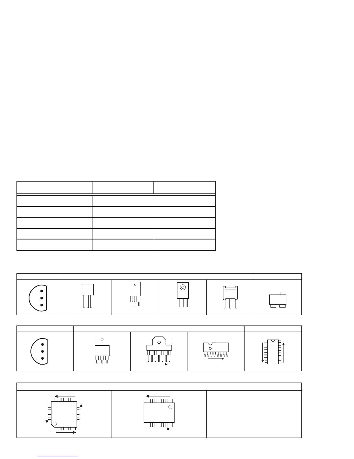
3.INDICATION OF PARTS SYMBOL [EXAMPLE]
In the PW board
: R1209
R209
Type
No indication
MM
PP
MPP
MF
TF
BP
TAN
(3)Coils
No unit
Others
(4)Power Supply
Respective voltage values are indicated
(5)Test point
: Test point
(6)Connecting method
: Ceramic capacitor
: Metalized mylar capacitor
: Polypropylene capacitor
: Metalized polypropylene capacitor
: Metalized film capacitor
: Thin film capacitor
: Bipolar electrolytic capacitor
: Tantalum capacitor
: [µH]
: As specified
: B1
: 9V
: Connector
: Receptacle
: Only test point display
: Wrapping or soldering
: B2 (12V
: 5V
)
4.INDICATIONS ON THE CIRCUIT DIAGRAM
(1)Resistors
Resistance value
No unit : [Ω]
K
M
Rated allowable power
No indication : 1/16 [W]
Others : As specified
Type
No indication
OMR
MFR
MPR
UNFR
FR
Composition resistor 1/2 [W] is specified as 1/2S or Comp.
(2)Capacitors
Capacitance value
1 or higher : [pF]
less than 1
Withstand voltage
No indication : DC50[V]
Others : DC withstand voltage [V]
AC indicated
Electrolytic Capacitors
47/50[Example]: Capacitance value [µF]/withstand voltage[V]
: [kΩ]
: [MΩ]
: Carbon resistor
: Oxide metal film resistor
: Metal film resistor
: Metal plate resistor
: Uninflammable resistor
: Fusible resistor
: [µF]
: AC withstand voltage [V]
(7)Ground symbol
: LIVE side ground
: ISOLATED(NEUTRAL) side ground
: EARTH ground
: DIGITAL ground
5.NOTE FOR REPAIRING SERVICE
This model's power circuit is partly different in the GND. The
difference of the GND is shown by the LIVE : ( ) side GND and the
ISOLATED(NEUTRAL) : ( ) side GND. Therefore, care must be
taken for the following points.
(1)Do not touch the LIVE side GND or the LIVE side GND and the
ISOLATED(NEUTRAL) side GND simultaneously. if the above
caution is not respected, an electric shock may be caused.
Therefore, make sure that the power cord is surely removed from
the receptacle when, for example, the chassis is pulled out.
(2)Do not short between the LIVE side GND and ISOLATED(NEUTRAL
side GND or never measure with a measuring apparatus measure
with a measuring apparatus ( oscilloscope, etc.) the LIVE side GND
and ISOLATED(NEUTRAL) side GND at the same time.
If the above precaution is not respected, a fuse or any parts will be broken.
Since the circuit diagram is a standard one, the circuit and
circuit constants may be subject to change for improvement
without any notice.
NOTE
Due improvement in performance, some part numbers show
in the circuit diagram may not agree with those indicated in
the part list.
When ordering parts, please use the numbers that appear
in the Parts List.
)
(No.YA608<Rev.001>)2-1
CONTENTS
SEMICONDUCTOR SHAPES ......................................................................2-2
WIRING DIAGRAM .......................................................................................2-3
BLOCK DIAGRAM ........................................................................................2-5
CIRCUIT DIAGRAMS ...................................................................................2-7
MAIN PWB CIRCUIT DIAGRAM ................................................................................................................. 2-7
MPEG PWB CIRCUIT DIAGRAM ............................................................................................................. 2-51
IR PWB CIRCUIT DIAGRAM .................................................................................................................... 2-87
KEY PWB CIRCUIT DIAGRAM................................................................................................................. 2-89
LED PWB CIRCUIT DIAGRAM................................................................................................................. 2-91
PATTERN DIAGRAMS .............................................................................. 2-93
MAIN PWB P ATTERN .............................................................................................................................. 2-93
MPEG PWB P ATTERN............................................................................................................................. 2-97
IR PWB P ATTERN.................................................................................................................................. 2-101
KEY PWB P ATTERN .............................................................................................................................. 2-101
LED PWB P ATTERN .............................................................................................................................. 2-102
USING P.W. BOARD
P.W.B ASS㵭Y name LT-42DA9BJ
MAIN P.W. BOARD
MPEG P.W. BOARD
IR P.W. BOARD
KEY P.W. BOARD
LED P.W. BOARD
HU-71200010
HU-71200005
HU-72200004
HU-72200003
HU-72200017 φ
LT-42DA9BU
φ
φ
φ
φ
SEMICONDUCTOR SHAPES
TRANSISTOR
BOTTOM VIEW FRONT VIEW TOP VIEW
CHIP TR
E
C
B
ECB
IC
BOTTOM VIEW FRONT VIEW TOP VIEW
OUT
E
IN
IN OUTE
B
(G)E(S)C(D)
1 N
ECB
ECB
1
1 N
C
BE
N
CHIP IC
N
1
2-2(No.YA608<Rev.001>)
TOP VIEW
1
N
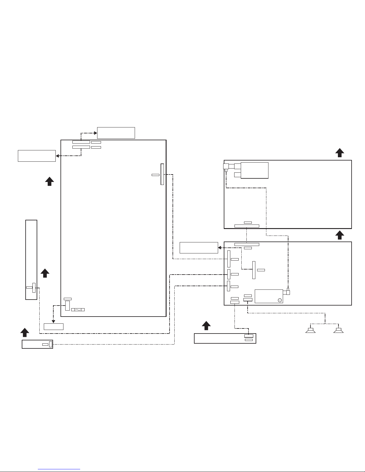
2-4(No.YA608<Rev.001>)(No.YA608<Rev.001>)2-3
TOP
TOP
TOP
FRONT
TOP
TOP
MAIN PWB
LED PWB
POWER UNIT
IR PWB
KEY PWB
LCD PANEL UNIT
[INVERTER PWB(MASTER)]
LCD PANEL UNIT
[INVERTER PWB(SLAVE)]
LCD PANEL UNIT
[LCD CONTROL PWB]
15
1
5
1
6
1
JP680
15
1
CN003-2
CN002
JP681
JP682
JP581
1
6
JP1
JP2
31
1
1
40
1
4
JP683
JP3
1
4
1
5
1
14
CN003-1
1
14
5
1
CN001
N
L
JP630
JP710
AC INLET
F1
250V/6.3A
ANALOG TUNER
SPEAKER(R)SPEAKER(L)
40
1
JP900
MPEG PWB
DIGITAL TUNER
WIRING DIAGRAM
(No.YA608<Rev.001>)2-5 2-6(No.YA608<Rev.001>)
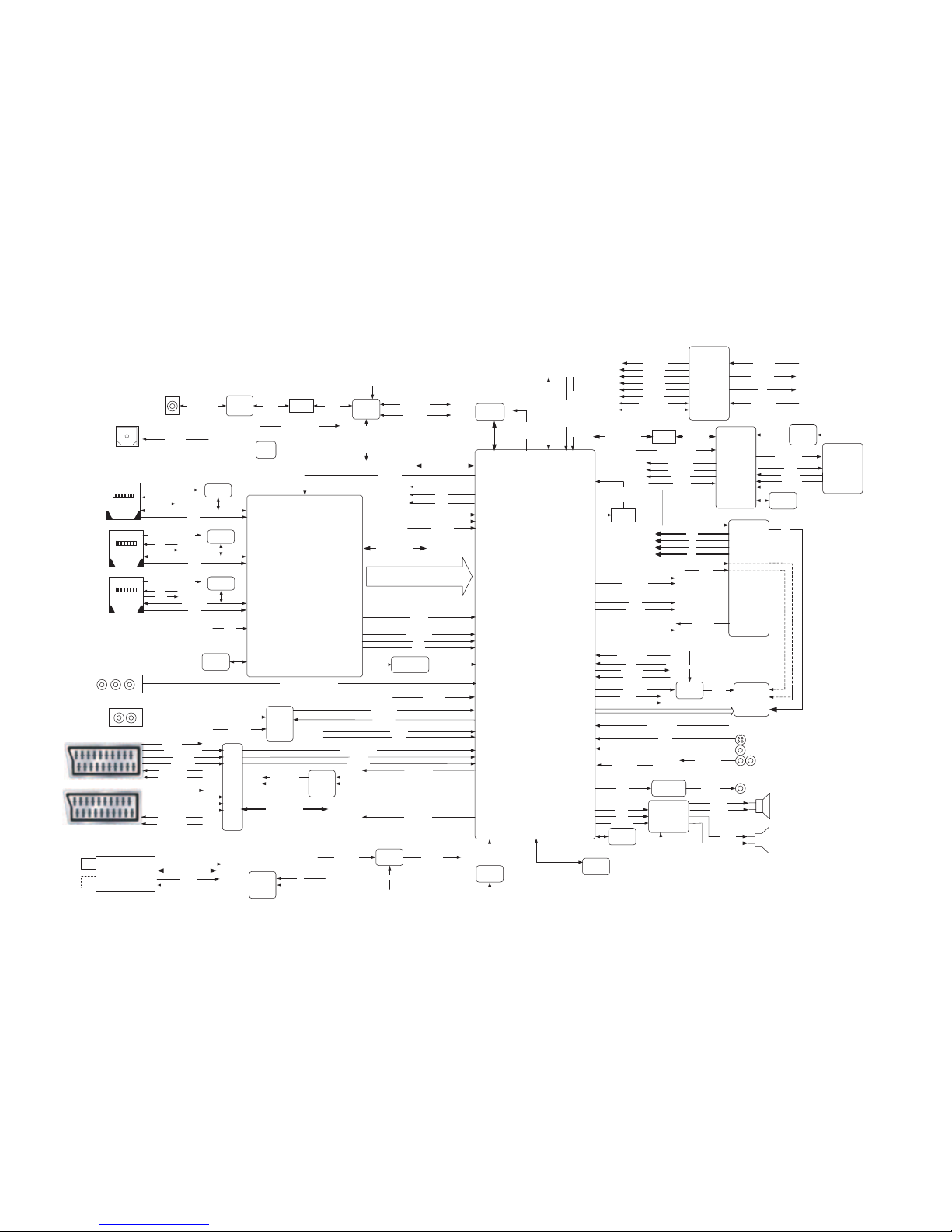
SCL/SDA
VIN11/12/13
VIN2
MPEG_R_Pr/G_Y/B_Pb
MPEG_CVBS
161Pin
181,180,
179Pin
190Pin
COM_RXD/TXD
P2.4/TDI
P2.5/TMS
91/92Pin
83/84Pin
208Pin
105Pin
P3.3
ROM_WP
COM_RXD/TXD
HDMI RECEIVER
U470
U1
SCALER
V
OSDFW
SDPIF_OUT
TXD_PC/RXD_PC
RS232C
DRIVER
U660
SERVICE PORT
DIGITAL AUDIO
EXT-5
EXT-6
EXT-7
EXT-3
EXT-4
EXT-1
EXT-2
L/S
X-TAL
14.318
MHz
U661
RS232_SW
HDMI1_PWR(HDMI1_DET)
HPD1
CEC_A
D1SDA/D1SCL
TMDS1
EEPROM
EEPROM
HDMI
HDMI
HDMI
HDMI3_PWR(HDMI3_DET)
HPD3
CEC_A
D3SDA/D3SCL
EEPROM
TA1/RA1_Sub MICOM
TA2/RA2TA1/RA1
DIGITAL VIDEO INPUT PORT
50 ~ 73 Pin
P3.2
P3.4
P2.1
P2.0
P4.1
HDMI3_DET
HDMI2_DET
HDMI1_DET
2Pin
100Pin
109Pin
160Pin
159Pin
1Pin
HPD1
HPD2
HPD3
CTP_SCL/SDA_3V3
HDMI_INT
HSYNC/VSYNC
IN0DE
IN0CLK
11/12Pin
187/184/182Pin
AIN3R/L
MPEG_GPIO
MUX_AUD_R/L
SELECTION1
CVBS_TIN
HDMI2_PWR(HDMI2_DET)
HPD2
CEC_A
D2SDA/D2SCL
TMDS2
COM_Pr/Y/Pb (MUX_RO/GO/BO)
COMP_RI/LI
AL/AR_CVBS
SCART1_ID
SCART1_R/G/B/CVBS
SCART1_FB
SCART1_RI/LI
SCART1_RO/LO
SCART1_CVBSO
SCART2_ID
SCART2_R/G/B/CVBS
SCART2_FB
SCART2_RI/LI
SCART2_RO/LO
SCART2_CVBSO
Analog Tuner
ANT_SIF
VCTP_SCL/SDA_3V3
(AT_SCL/SDA)
+5V_ANT
CVBS_TIN
+7V
ANT_PWR_EN
VCTP_SCL/SDA_3V3
SCART2_CVBSO
SCART1_CVBSO
U200
SWITCH
U580
U120
(OP AMP)
MPEG PWB
MICOM
U801
U800
Y800
VOLTAGE
DET
LED&KEY PWB
16MHz
X-TAL
IR_IN
KEY_ADC2
KEY_ADC1
LED_R
FRONT_LED_B
+5VSTRESETn
IR_SCART_TV
SBTV
MPEG_GPIO
DTT_RESETDTT_AUD_R/L
MPEG_B_Pb
MPEG_G_Y
MPEG_R_Pr
MPEG_CVBS
MPEG_RXD/TXD
SPDIF_OUT
COMU_RX/TX
SCL/SDA_STB
TA1/RA1_Sub MICOM
MSP_ENABLE
IR_SCART_TV
VCTP_INT
VCTP_Fail
R,C
filter
98Pin
OSDR/
P3.0
OSDFW
SECAM-L
106Pin
102Pin
88Pin
87Pin
117Pin
RS232_SW
DEBUG
POWER UNIT
BLT_EN
BRT_ADJ
+12V
+7V
+5V
+5VST
STBY_EN
+24V
L/S
VCTP_SCL/SDA_3V3
110Pin
EEPROM
COMU_RX/TX
MPEG_RXD/TXD
TMDS3
CEC_A
HDMI_RESET
RGB(24Bits)
VCTP_SCL/SDA_3V3
115,116Pin
SCART_R/G/B/CVBS
SCART_FB
SCART_RI/LI
SCART1_RO/LO
SCART1_CVBS_OUT
SCART2_CVBS_OUT
SCART2_RO/LO
VSUP5.0SIF,
VSUP8.0AU
/RESET
MCP100T
VSUP3.3COM
+5V+8V ,
MSP_ENABLE U630
U770
AUDIO DAC+OP
AMP
U560
HDMI_I2S HDMI_AUD_R/L
VIN6/7/9
13,14Pin
101Pin
P3.5
VOUT2
VOUT1
AOUT1R/L
AIN1R/L
VIN18
VIN15/16/17/3
SIFIN+
VIN1
P4.4
AOUT2R/L
RESETQ
8Pin
21/22Pin
194Pin
195Pin
23/24Pin
9/10Pin
175Pin
178/177/176/189Pin
31Pin
191Pin
3Pin
ANT_SIF
Debeg
JTAG
20.25MHz
X-TAL
Y60
XTAL
P4.0
SPEAKERR
SPEAKERL
HEADPHONEL/R
AIN4L/R
VIN21
VIN19/20
P3.6
HEADPHONE_ID
SV_C/Y
CVBS
HPO_L/R
AMP_R+
AMP_L-
AMP_L+
AC_DETECT
(AUDIO AMP)
U580
OP AMP
25/26Pin
HP_L/R
27Pin
R_SPK
L_SPK
MUTE_CTRL
28Pin
118Pin
P2.2
VIN22/DVS
DEN
DCLK
AIN2R/L
171,47Pin
48Pin
49Pin
89Pin
Analog MUX
AC_DETECT
+12V or +5V
POWER
LCD
PANEL
UNIT
SPEAKER(R)
SPEAKER(L)
U2
LVDS_OUT
AL/AR_CVBS
AMP_R-
DTT_AUD_R/L
15,16Pin
172Pin
173/174Pin
99Pin
ANT_PWR_CTRL
167Pin
SBTV
DTT_RESET
P1.1
P1.4
P1.5
P1.2
P2.3
P4.3
P4.2
VCTP_Fail
ANT_PWR_EN
162Pin
90Pin
119Pin
120Pin
166Pin
VCTP_INT
PANEL_PWR
BRT_ADJ
BLT_EN
P3.1
P3.7
P4.5
P1.6
P1.7
P4.6
P4.7
P2.7
P2.6
REG
U771
YPbLRPr
X-TAL
Y470
14.31818MHz
BLOCK DIAGRAM
2-8(No.YA608<Rev.001>)(No.YA608<Rev.001>)2-7
MAIN PWB ASS'Y (1/22)
[Analog Tuner]
HU-71200010
lt-32da9bj_scaler-20_0602_20/23_0.0
5
5
4
4
3
3
2
2
1
1
D D
C C
B B
A A
L/T outpur Phono type
Input - IEC type
I2C AS : 0xC0
All location are from 770 to 799
LOW
ONHIGH
+5V_ANT
OFF
ANT_PWR_EN
IF ANT_PWR_CTRL is L --> ANT_PWR_EN L
+7V
12
12345678910111213141516171819
20
BB(CTR)
ANT (5V)
+B(+5V)NCRF_AGC
TP_+33VNCGND
SDA
SCLASNC
CVBS
AFT
AUDIO
SIFNCNCNCNC
12345
6
/INH
VIN
GND
VOUT
ADJ
GND
1
23
1
2
45
6
7
8
3
ANT_SIF
CVBS_TIN
750/F/1005
R780
R776
R777
330/1005
330/1005
2.2uF/50V/MVK/S
C780
+5V_ANT_A
000/1005R779
R770 000/1005
21
22
23
24
GND1
GND2
GND3
GND4
TAUT-S711D
U770
+5V_ANT
AGC
C771
OPEN_2.2uF/50V/MVK/S
Q773
KST4401
101/1005
R784
SECAM-L
152/1005
R785
+5V_Analog_Tuner
472/1005
R773
AGC
470uF/16V/MVK/S
C772
+5V_Analog_Tuner
C770
104p/1005
330p
C781 C782
330p OPEN-330p
C783 C784
OPEN-330p
OPEN-000/1005
000/1005
000/1005
OPEN-000/1005R790
R791
R792
R793
VCTP_SDA_3V3
VCTP_SCL_3V3
+5.29V
+5V_ANT_A
MAX 1.5A
LD29150PT/P-PAK 5P
U771
ANT_PWR_EN
ANT_PWR_CTRL
R781
103/1005
+3V3D
U772
MIC2544-1YMMPOWER SW
OPEN_103/1005
R778
NC
GND
FLG
EN OUT
IN
OUT
ILIM
152/1005
R789
104p/1005
C774
106p/2012
C777 C778
104p/1005
+5V_ANT
106p/2012
C773 OPEN-ZMMC5V6
D770C776
104p
C775
106p/2012
101p/1005
C779
R786
333/F/1005
R787
103/F/1005
MAIN PWB
(3/22)
MAIN PWB(3/22)
MAIN PWB(4/22)
MAIN PWB(3/22),(6/22),(13/22),(21/22)
CIRCUIT DIAGRAMS
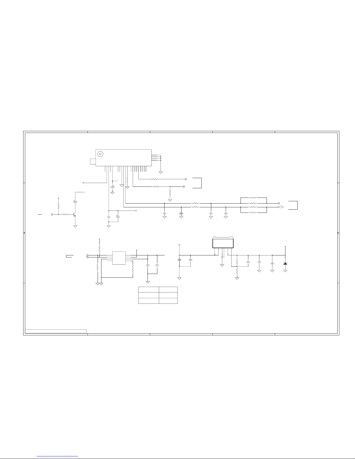
MAIN PWB CIRCUIT DIAGRAM (1/22) [Analog Tuner]
(No.YA608<Rev.001>)2-9 2-10(No.YA608<Rev.001>)
MAIN PWB ASS'Y (2/22)
[VCTP Power]
HU-71200010
lt-32da9bj_scaler-01_0602_1/23_0.0
1
1
2
2
3
3
4
4
5
5
6
6
D D
C C
B B
A A
VCT-P POWER
All location are from 1 to 59.
MSP_ENABLE H ON
L OFF
Sequence : STBY_EN --> +3V3_VCTP --> MSP_ENABLE
12
197
192
185
169
170
164
127
142
124
1149686777545363318
17
196
163
153
147
144
136
130
123
113958576744635342019186
143
209
133
139
150
156
VSUP3.3IO3
VSUP3.3VO
VSUP1.8FE
VSUP1.8FE
VSUP3.3FE
VSUP3.3DAC
VSUP3.3LVDS
VSUP3.3LVDS
VSUP3.3LVDS
VSUP3.3LVDS
VSUP3.3LVDS
VSUP1.8LVDS
VSUP1.8DIG
VSUP3.3IO1
VSUP3.3IO1
VSUP3.3FL
VSUP3.3COM
VSUP3.3DRI
VSUP3.3RAM
VSUP3.3DIG
VSUP5.0SIF
VSUP8.0AU
VREFAU
GND3.3IO3
GND3.3DAC
GND3.3LVDS
GND3.3LVDS
GND3.3LVDS
GND3.3LVDS
GND3.3LVDS
GND1.8DIG
GND3.3IO1
GND3.3IO1
GND3.3FL
GND3.3COM
GND3.3DRI
GND3.3RAM
GND3.3DIG
GNDA
SGND
GNDA
GNDA
REXT
IC_GND
123
45
678
S1G1S2
G2 D2
D2D1D1
1
23
106p/2012
C42C43
104p/1005
VSUP8.0AU_A
VSUP5.0SIF
VSUP3.3DIG
VSUP3.3RAM
VSUP3.3DRI
R5
622/F/1005
VCT7993P-FA-A1-H-500
U1D
102p/1005
C31
104p/1005
C33
104p/1005
C34
104p/1005
C32C30
102p/1005
C29
106p/2012
L11
BLM18PG300SN1D
+3V3_VCTP
C28
106p/2012
C27
104p/1005
VSUP3.3DAC
VSUP3.3FE
VSUP1.8FE
VSUP3.3VO
VSUP3.3IO3
VSUP3.3LVDS
VSUP1.8LVDS
VSUP1.8DIG
VSUP3.3IO1
VSUP3.3FL
VSUP3.3COM
+3V3_VCTP
+3V3_VCTP
BLM18PG300SN1D
L5
C21
106p/2012
+3V3_VCTP VSUP3.3DIG
C4
104p/1005
C3
106p/2012
VSUP3.3FL
C14
104p/1005
C13
106p/2012
104p/1005
C22
BLM18PG300SN1D
L2
VSUP3.3LVDS
BLM18PG300SN1D
L8
VSUP3.3COM
+3V3_VCTP
L3
BLM18PG300SN1D
VSUP3.3IO1
C7
104p/1005104p/1005
C6C5
106p/2012
VSUP3.3DRI
C16
104p/1005106p/2012
C15
BLM18PG300SN1D
L6
+3V3_VCTP
+3V3_VCTP
BLM18PG300SN1D
L9
VSUP3.3RAM
C24
104p/1005
C23
106p/2012
+1V8_VCTP
L12
VSUP1.8LVDS
VSUP5.0SIF
106p/2012
C35
104p/1005
C36
BLM18PG300SN1D
+5V
L16
BLM31PG121SN1L
VSUP8.0AU_A
SI4925DY
106p/2012
C37 C38
104p/1005
+3V3_VCTP
L13
BLM18PG300SN1D
VSUP3.3DAC
104p/1005
C26C25
106p/2012
BLM18PG300SN1D
L10
+3V3_VCTP
+3V3_VCTP
L4
BLM18PG300SN1D
VSUP3.3FE
C9
104p/1005
C8
106p/2012
VSUP3.3VO
L7
BLM18PG300SN1D
+3V3_VCTP
C17
106p/2012 104p/1005
C18
VSUP3.3IO3
+12V
VSUP8.0AU
471/1005
471/1005
471/1005
471/1005R4
R3
R2
R1
D1
ZMM5237B
C11
104p/1005
C12
101p/1005
C10
106p/3216
+1V8_VCTP_A VSUP1.8DIG
C20
104p/1005
C19
106p/2012
VSUP1.8FE
C41
104p/1005
C40
104p/1005
C39
106p/2012
HH-1M3216-501JT
L14
+1V8_VCTP
MSP_ENABLE
104/1005
R6
BLM31PG121SN1L
L15
VSUP8.0AU
Q1
KST4401
R7 472/1005
C46
106p/3216
C47
106p/3216
U2
106p/3216
C44 C45
104p
MAIN PWB(21/22)
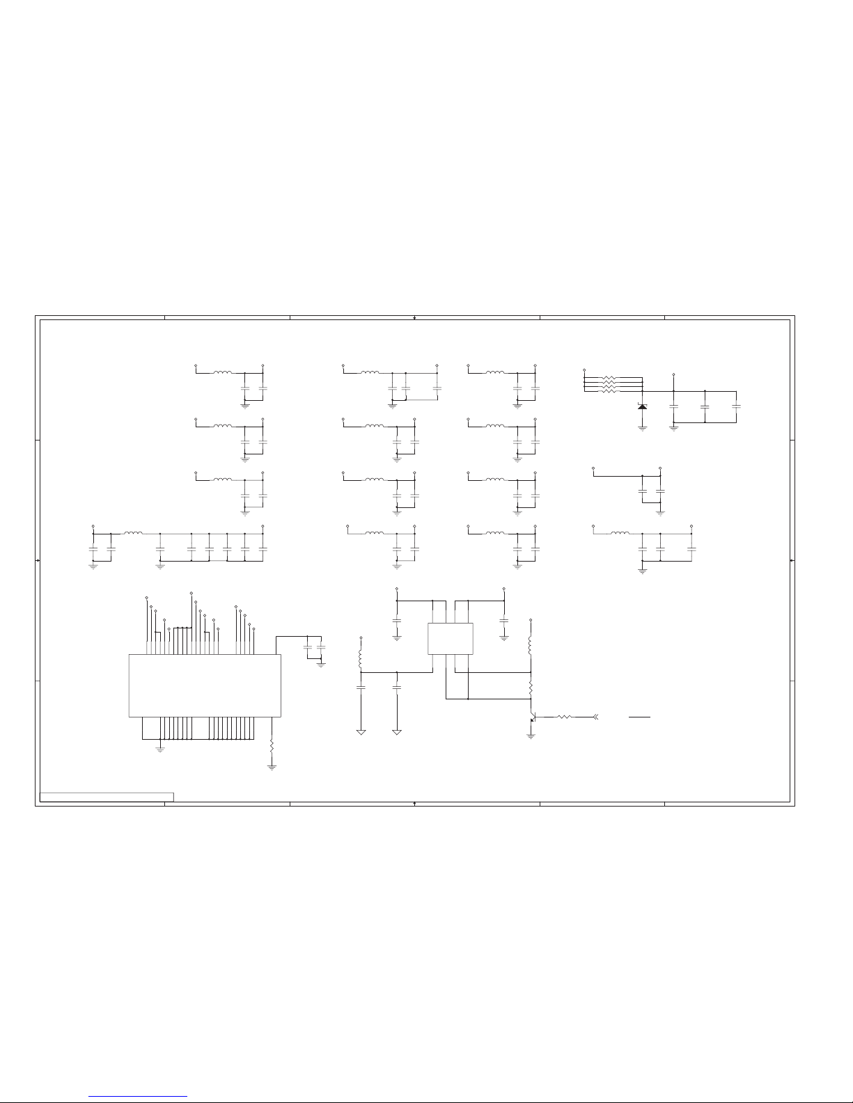
MAIN PWB CIRCUIT DIAGRAM (2/22) [VCTP Power]
 Loading...