

Page 1
49758200209
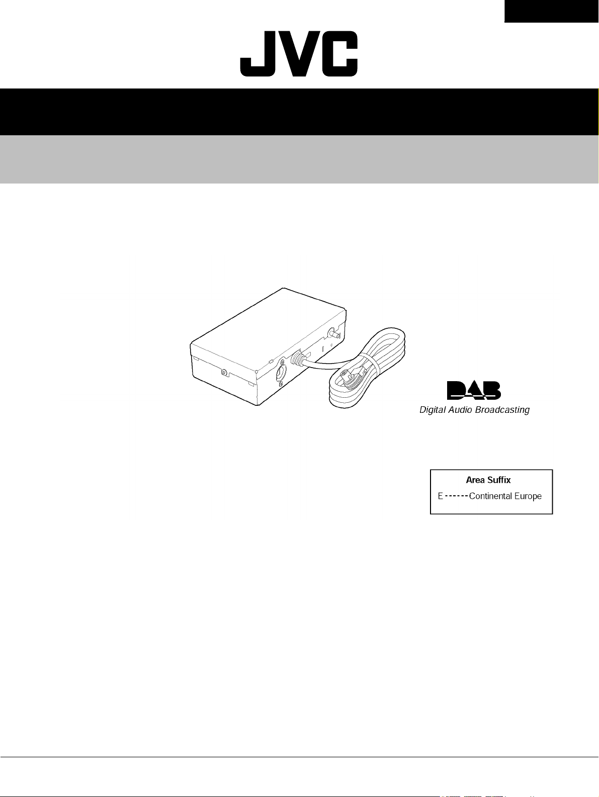
KT-DB1000
SERVICE MANUAL
DAB Tuner Unit
KT-DB1000
TABLE OF CONTENTS
Safety precaution . . . . . . . . . . . . . . . . . . . . . . . . . . . . . . . . . . . . . . . . . . . . . . . . . . . . . . . . . . . . . . . . . . . . . . . 2
Disassembly method . . . . . . . . . . . . . . . . . . . . . . . . . . . . . . . . . . . . . . . . . . . . . . . . . . . . . . . . . . . . . . . . . . . . 3
Description of major ICs . . . . . . . . . . . . . . . . . . . . . . . . . . . . . . . . . . . . . . . . . . . . . . . . . . . . . . . . . . . . . . . . . 4
COPYRIGHT © 2002 VICTOR COMPANY OF JAPAN, LTD.
No.49758
2002/09
Page 2

KT-DB1000
SECTION 1
Safety precaution
CAUTION
Burrs formed during molding may be left over on some parts of the chassis. Therefore, pay attention to such burrs in
the case of preforming repair of this system.
2
Page 3
SECTION 2
Disassembly method
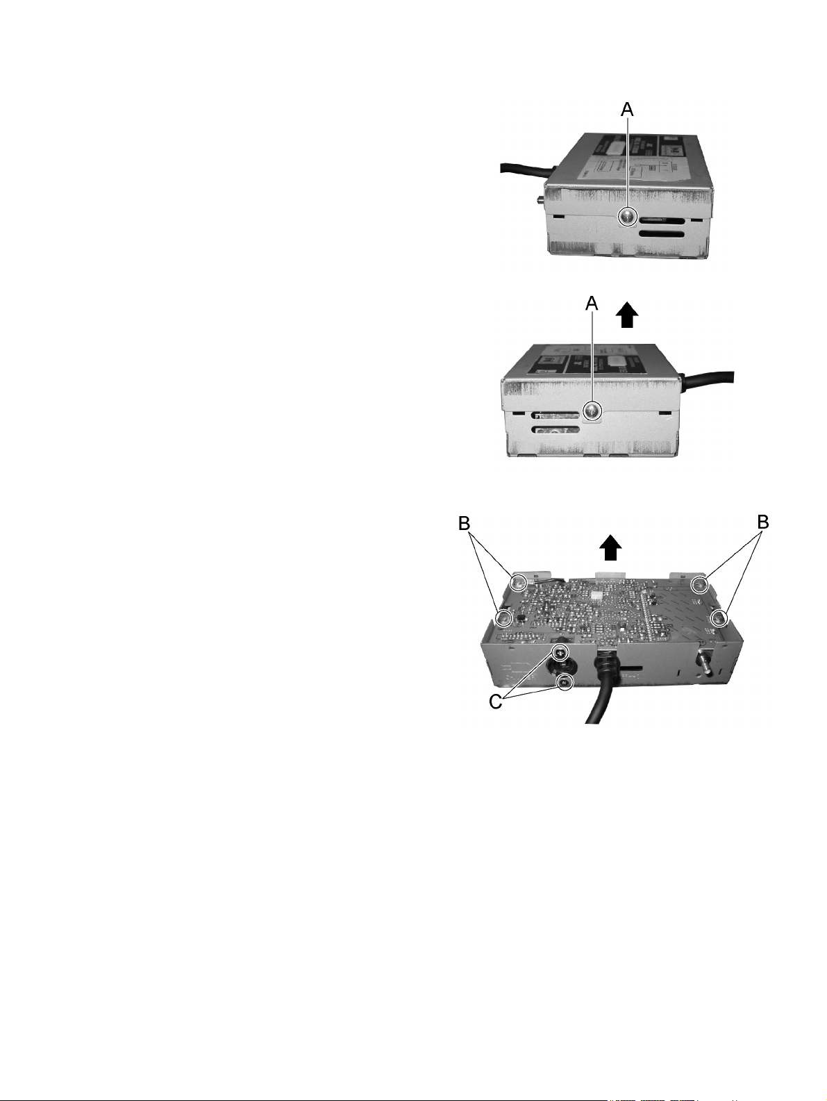
2.1 Main body
2.1.1 How to remove a top cover (See Figure 1 and 2.)
(1) Screw A attaches a top cover to the main body. Remove
the two screws A from the both sides of the main body.
(2) Raise the top cover in a direction that the arrow indicates.
And the top cover will be removed.
KT-DB1000
Fig.1
2.1.2 How to remove a main board (See Figure 3.)
(1) Remove the four screws B and the two screws C that at-
tach the main board to the main body.
(2) Raise the main board in a direction that the arrow indi-
cates. And the main board will be removed.
Fig.2
Fig.3
3
Page 4
KT-DB1000
3.1 MN102H60KCB (IC701) : Controller
• Pin layout
• Pin functions
No. Symbol I/O Function
1 - - Not use
2 LCDRS O Resistor select output terminal for LCD module
3 LCDR/W O Read/Write select output terminal for LCD module
4 LCDE O Data read/write start up output for LCD module
5~12 LCDDB0~7 O Data bus output 0 terminal for LCD module
13 JBUSCK I/O JBUS clock input/output terminal
14 JBUSDAI I JBUS data input terminal
15 JBUSDAO O JBUS data output terminal
16 JBUSI/O O JBUS input/output select output terminal
17 VDD - Powersupply terminal
18 SYSCKO O System clock(19.6608MHz) output terminal
19 GND - Connect to GND
20 XI I Connect to GND
21 NC O Open
22 VDD - Power supply trerminal
23 OSCI I X'tal connect terminal(19.6608MHz)
24 OSCO O X'tal connect terminal(19.6608MHz)
25 MODE I Mode setting input terminalpull up(single chip mode)
26 EEPRMDI I EEPROM(for preset data save)data input terminal
27 EEPRMDO O EEPROM(for preset data save)data output terminal
28 EEPRMCK O EEPROM(for preset data save)clock output terminal
29 EEPRMCS O EEPROM(for preset data save)chip select terminal
30~32 - - Not use
33 CKSEL O SYSCK output enable select terminal, "H" output enable
34 AVDD - Analogue power supply terminal
35 DAISEL O DAI output enable select terminal, "H" output enable
36 RDISEL O RDI output enable select terminal, "H" output enable
37 CIRSEL I CIR monitor output enable select terminal, "H" output enable
38 AGCSEL I AGC internal/external select terminal, "H" external(AGC outpput enable)
39 OPMODE0 I Operation mode setting terminal 0
40 OPMODE1 I Operation mode setting terminal 1
41 DUMMY I Dummy mode select terminal, "H" dummy mode
42 - - Not use
43 VREF- - Analogue reference power supply terminal, connect to GND
44 KEY0 I Test key analogue voltage onput 0
45 KEY1 I Test key analogue voltage input 1
46 KEY2 I Test key analogue voltage input 2
47 KEY3 I Test key analogue voltaeg input 3
48 TUSDA O Tuner PLL data output terminal
49 TUSCL O Tuner PLL clock output terminal
50 MPUCK O DAB MPU interface clock output terminal
51 MPUDAI I DAB MPU interface data input terminal
52 MPUDAO O DAB MPU interface data outut terminal
53 DABRST O DAB LSI/TUNER reset output terminal, "L" reset
54 VREF+ - Analogue reference poser supply terminal, connect to AVDD
55 DABDARX I FIC packet data stream output data input terminal
SECTION 3
Description of major ICs
4
Page 5
No. Symbol I/O Function
56 DABDATX O FIC packet data stream outout data output terminal
57 MPUEN O DAB MPU interface chip enable output terminal
58 MPUMOD O DAB MPU interface mode signal outpout terminal
59 DZFINL I DZFL input terminal from DAC, "H" outout AMUTEL
60 DZFINR I DZFL input terminal from DAC, "H" outout AMUTER
61 AGND - Analogue GND terminal
62 AUDSEL O Audio signal select output terminal, "L" DAB "H" CD changer
63 AMUTEL O L-CH mute output terminal, "H" L-CH mute
64 AMUTER O R-CH mute output terminal, "H" R-CH mute
65 ANT+BIN I Antenna power supply voltage monitoer input terminal
66 VDD - Power supply
67 - - Not use
68 DACRST O DAC rest resr output terminal, "L" reset
69 - - Not use
70 SDCK I DAB serial data clock input terminal
71 SDDA I DAB serial data input terminal
72 SDWD I DAB sericl data window input terminal
73 SIFDA I/O On board serial write data input/output terminal pullup
74 SIFCK I On board serial write clock input terminal pullup
75 - - Not use
76 WFIC I Interrupt inout from DAB LSI, "L" triger detect
77 NIRQ I DDOWFIC input terminal from DABSEL
78 JBUSINT I JBUS interrupt input
79 PSAVE1 I PSAVE1(power off)input interrupt triger detect at "L" level
80 PSAVE2 O PSAVE2(STOP mode) input
81 POWOUT O Power on output terminal, "H" power on
82 RESET I Reset input terminal, "L" reset
83 VDD - POwer supply terminal
84 INDOUT0 O Indicator output 0 for test
85 INDOUT1 O Indicator output 1 for test
86 INDOUT2 O Indicator output 2 for test
87 INDOUT3 O Indicator output 3 for test
88 INDOUT4 O Indicator output 4 for test
89 INDOUT5 O Indicator output 5 for test
90 INDOUT6 O Indicator output 6 for test
91 INDOUT7 O Indicator output 7 for test
92 GND - GND terminal
93 DACCDTO O DAC chip select output
94 DACCCLK O DAC control clock output
95 DACCSN O DAC control data output
96~100 - - Not use
KT-DB1000
5
Page 6

KT-DB1000
3.2 AK4382AVT-X (IC501) : D/A converter
• Pin layout
• Block diagram
• Pin function
Pin No. Symbol I/O Function
1 MCLK I Master Clock Input Pin
2 BICK I Audio Serial Data Clock Pin
3 SDTI I Audio Serial Data Input Pin
4 LRCK I L/R Clock Pin
5 PDN I Power-Down Mode Pin
6 CSN I Chip Select Pin
7 CCLK I Control Data Input Pin
8 CDTI I Control Data Input Pin
9 AOUTR- O Rch Negative Analog Output Pin
10 AOUTR+ O Rch Positive Analog Output Pin
11 AOUTL- O Lch Negative Analog Output Pin
12 AOUTL+ O Lch Positive Analog Output Pin
13 VSS - Ground Pin
14 VDD - Power Supply Pin
15 DZFR O Rch Data Zero Input Detect Pin
16 DZFL O Lch Data Zero Input Detect Pin
6
Page 7

3.3 MN66720UC (IC1) : DAB baseband signal processer
• Pin layout
• Block diagram
KT-DB1000
7
Page 8

KT-DB1000
• Pin functions
Pin No. Symbol I/O Function
1,2 TESTIN0,TESTIN1 I Input terminal for test.
3 AVDD - Analogue VDD terminal.
4
5 ADIN - Analogue IF signal input terminal.
6 ADVRB - Reference voltage terminal for AD converter bottom side.
7 AVSS - Analogue VSS.
8 TESTMD - Test mode setting terminal.
9 ADCINT I AD converter internal/external select terminal.
10~19 DIN0~DIN9 I External AD converter data input terminal.
20 NADCPD I Internal AD converter power down control input terminal.
21 VSS0 - Digital VSS.
22 ADCK O AD converter clock signal output terminal.(8.192MHz)
23 ADCOVER O AD converter overflow detection ooutput terminal.
24 NADCPSC O AD converter power save control signal output terminal.
25 NULMON O NULL signal detection output terminal.
26 FSYO O Flame synchronization monitor signal output terminal.
ADVRT
- Reference voltage terminal for AD concerter top side.
27 CIRSYN O CIR monitor synchronization signal output terminal.
28 CTLCLK O CIR DA converter bit clock output terminal.(1.536MHz)
29 CTLLR O CIR DA converter LR clock output terminal.
30 CTLDAT O CIR DA converter data output terminal.
31 AGCDAT O External AGC control signal output terminal.(ADC output level)
32 LVDD0 - Internal digital VDD terminal.
33 VSS1 - Digital VSS terminal.
34 SMCK O Audio DA converter master clock output terminal.(256 Fs)
35 SLRCK O Audio DA converter LR clock output terminal.(Fs:48 kHz)
36 SCLK O Audio DA converter serial clock output terminal.(64 Fs)
37 SDAT1 O Audio DA converter serial data output 1 terminal.
38 SDAT2 O Audio DA converter serial data output 2 terminal.
39 MP2CLK O External DAB audio(MP2) clock output terminal.(2.048MHz)
40 MP2IN I External DAB audio(MP2) data input terminal.
41 MP2W I External DAB audio(MP2) window signal input terminal.
42 DAOUT O Digital audio interface output terminal. (IEC958)
43 VDD0 - External digital VDD terminal.
44 VSS2 - Digital VSS terminal.
45 RDIOUT O RDI data output terminal.
46 SDOWD O Serial data output window output terminal.
47 SDODT O Serial data output data output terminal.
48 SDOCK O Serial data output clock output terminal.(2.048 MHz)
49 DDODAT O Direct data output serial data output terminal.
50 DDOCLK O Direct data output serial clock output terminal.(2.048MHz)
51 DDOERF O Direct data output error flug output terminal. (H:error)
8
Page 9

Pin No. Symbol I/O Function
52 DDOWMSC O Direct data output MSC window output terminal.
53 LVDD1 - Internal digital VDD terminal.
54 VSS3 - Digital VSS terminal.
55~60 DDOMNO0~DDOMNO5 O DIrect data output MSC sub channel ID output terminal.
61 DDOWFIC O Direct data output FIC window output terminal.
62 VDD1 - External digital VDD terminal.
63 VSS4 - Digital VSS terminal.
64 NIRQ O Interllupt request output terminal.
65 MPUTX O MPU interface serial data output terminal.
66 MPURX I MPU interface serial data input terminal.
67 MPUCLK I MPU interface serial clock input terminal.
68 NMPUEN I MPU interface chip enable input terminal.
69 MPUMOD I MPU interface mode signal input terminal.
70 MDSPMO0 O MDSP status monitor output 0 terminal.
71 MDSPMO1 O MDSP status monitor output 1 terminal.
72 MVDD0 - DRAM VDD terminal.
KT-DB1000
73 MVSS0 - DRAM VSS terminal.
74 MDSPMO2 O MDSP status monitor output 2 terminal.
75 MDSPMO3 O MDSP status monitor output 3 terminal.
76~79 SDSPMO0~SDSPMO3 O SDSP status monitor output terminal.
80 MVDD1 - DRAM VDD terminal.
81 MVSS1 - DRAM VSS terminal.
82 VSS5 - Digital VSS terminal.
83 LON - Internal onchip power switch input terminal.
84 VDD2 - External digital VDD terminal.
85 VDD3 - External digital VDD terminal.
86 VOUT0 - Onchip power supply output terminal.
87 VOUT1 - Onchip power supply output terminal.
88 NRST I Master reset input terminal.
89 MCLKEN I Master clock enable input terminal.
90 MCLK24 I Mster clock input terminal.(24.576 MHz)
91 MCLKO O Master clock oscillation output terminal.
92 PWMVCXO O PWM output terminal for mastewr clock VCXO.
93 LVDD2 - Internal digital VDD terminal.
94 VSS6 - Digital VSS terminal.
95~100 TEST0~TEST5 I Test mode setting terminal.
9
Page 10

KT-DB1000
3.4 BR93LC66F-X (IC702) : EEPROM
• Terminal layout • Pin Functions
Symbol I/O Function
VCC - Power supply
GND - Connect to GND
CS I Chip select input
SK I Serial clock input
DI I Start bit, OP-code,address, serial data input
DO O
3.5 S-81250SGUP-X (IC805) : Regulator
• Pin layout • Block diagram
Serial data output
Internal state display output of READY/BUSY
3.6 NJM4580V-X (IC901) : Ope amp.
• Pin layout & Block diagram
3.7 TA48033F-X (IC806) : Reglator
• Pin layout
10
Page 11

3.8 UPC7805AHF (IC803) : Regulator
• Pin layout
• Block diaglam
KT-DB1000
3.9 NJM2370U09-X (IC801) : Regulator
• Pinlayout
• Block diagram
• Pin function
Pin No Function
1 Control
2GND
3 Noise bypass
4Vout
5Vin
11
Page 12

KT-DB1000
3.10 BA033FP-X (IC804) : Regilator
• Pin layput
3.11 TC7WT241FU-X (IC771,IC772) : Buffer
• Pin layotu & Blocl diagram
• Block Diagram
3.12 NJM2750M-X (IC911) : Audio selector
• Pin layout & Block diagram • Pin function
Pin No Function Pin No Function
1IN1a 9IN3b
2 CNT1 10 (N.C.)
3IN2a 11OUTb
4 CNT2 12 Vref
5 IN4a 13 IN3a
6IN1b 14V+
7IN2b 15OUTa
8IN4b 16GND
12
Page 13

3.13 PST9121N-X (IC851) : System reset
• Pin layout
• Block diagram
3.14 SI-8050JF-F1 (IC802) : Regulator
• Pin layout • Pin function
Pin No. Pin function
1Vin
2 SW out
3GND
4Vos
5ON/OFF
KT-DB1000
• Block diagram
13
Page 14

KT-DB1000
VICTOR COMPANY OF JAPAN, LIMITED
MOBILE ELECTRONICS BUSINESS DIVISION
PERSONAL & MOBILE NETWORK BUSINESS UNIT. 10-1,1chome,Ohwatari-machi,Maebashi-city,371-8543,Japan
(No.49758)
Printed in Japan
2002/09
 Loading...