

Page 1
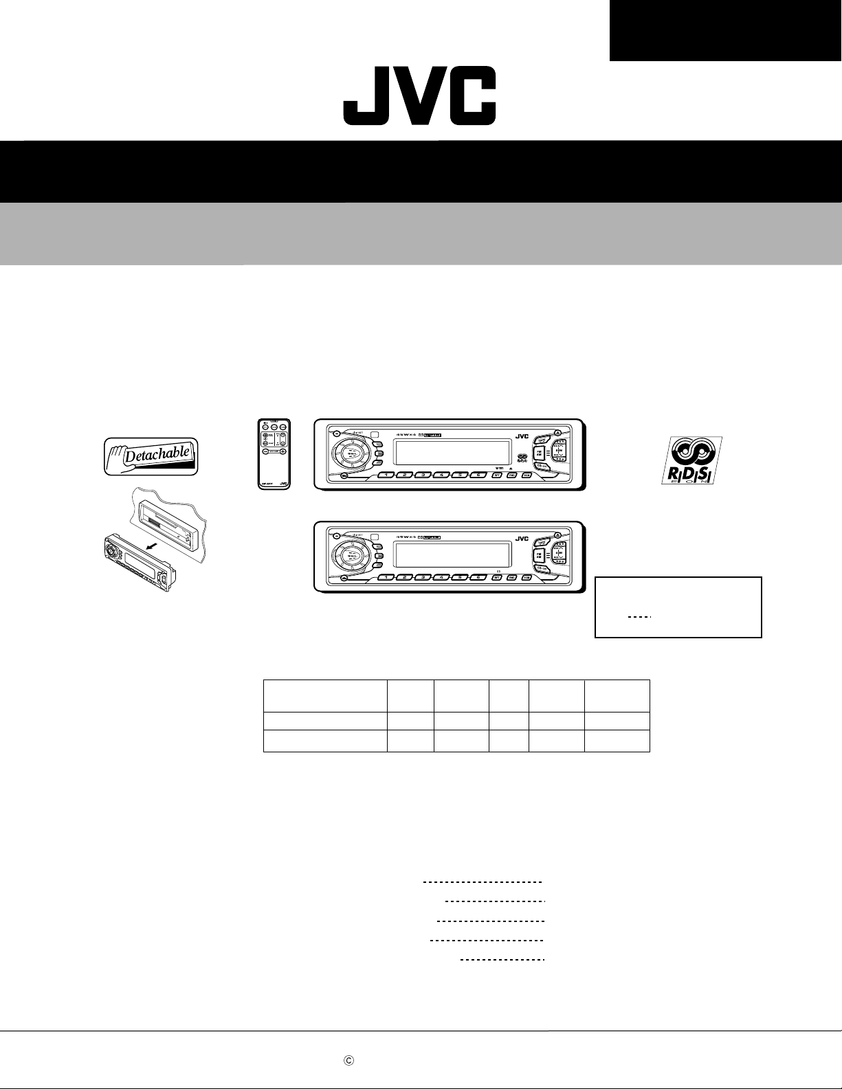
KS-FX915R/KS-FX815
SERVICE MANUAL
CASSETTE RECEIVER
KS-FX915R/KS-FX815
KS-FX915R
KS-FX815
Difference point
KS-FX915R
KS-FX815
DISPDISP
TP TP
RDSRDS
PTYPTY
LOUDLOUD
DISPDISP
SCANSCAN
8 9 10 11 127
8 9 10 11 127
RDS
O
X
Dimmer
O
X
KS-FX915R
KS-FX815
Beep
O
X
DAB
MO
MO
Area Suffix
Russian Federation
O
X
LCD
Color
Nega
EE
Remocon
Contents
Safety precaution 1- 2
Location of main parts 1- 3
Disassembly method 1- 4
Adjustment method
Description of major ICs 1-14
COPYRIGHT 2001 VICTOR COMPANY OF JAPAN, LTD.
1-11
No.49613
Feb. 2001
Page 2
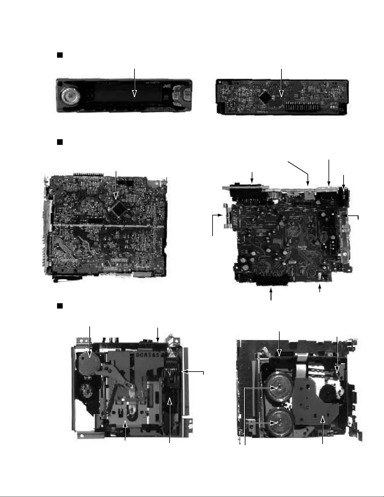
Location of main parts
Control unit
Display
Main unit
Main board
Changer control
I/O connector
Control unit
connector
KS-FX915R/KS-FX815
RCA jack
Antenna
jack
Cassette mechanism
Cassette mechanism
C.motor assembly
Mechanism control board assembly
Power IC
Head relay board
Main board assembly
Main board assembly
Connector to controller
Connector to controller
Mechanism control board assembly
Capstan motor assembly
Tuner
pack
Cassette housing
Head
Flywheel assembly
Reel board
1-3
Page 3
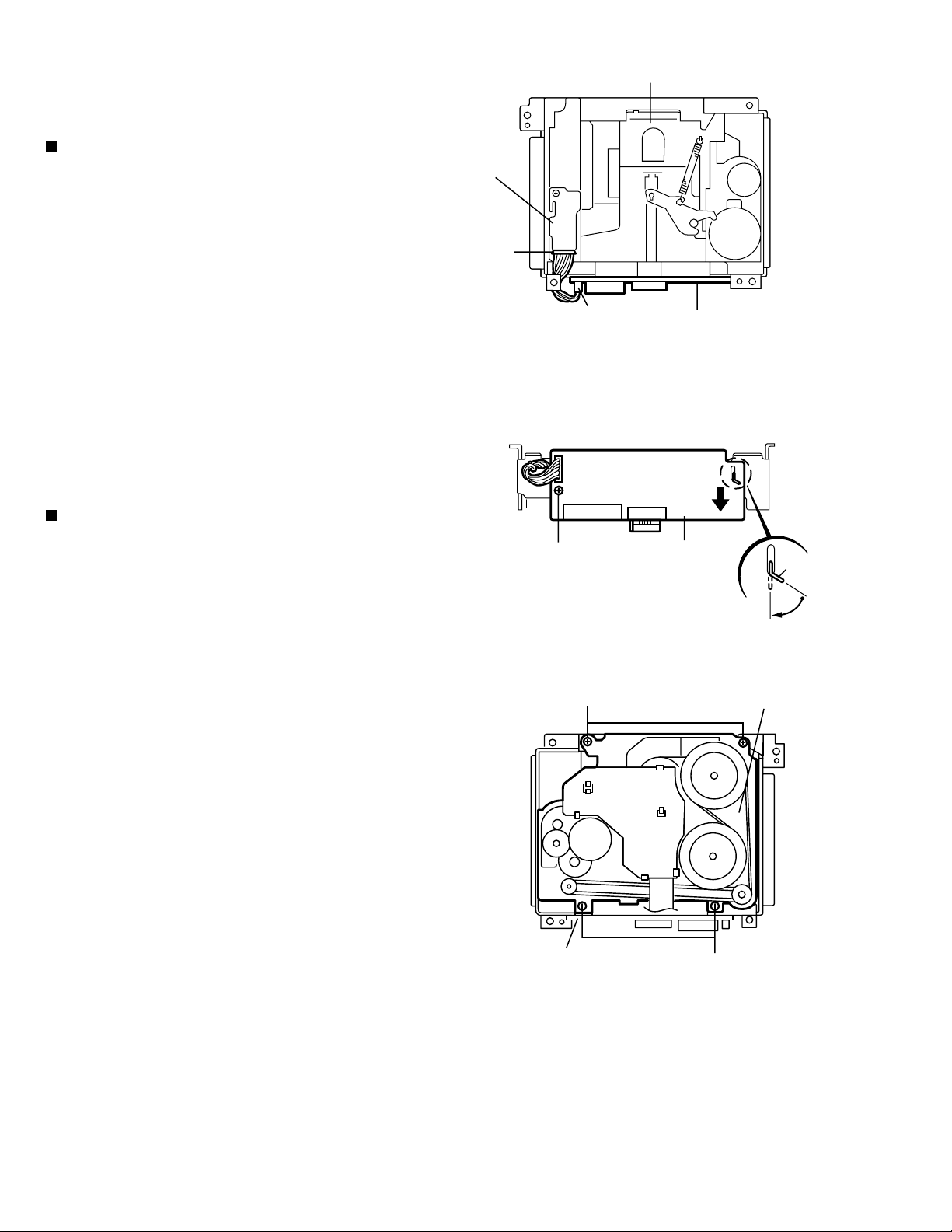
KS-FX915R/KS-FX815
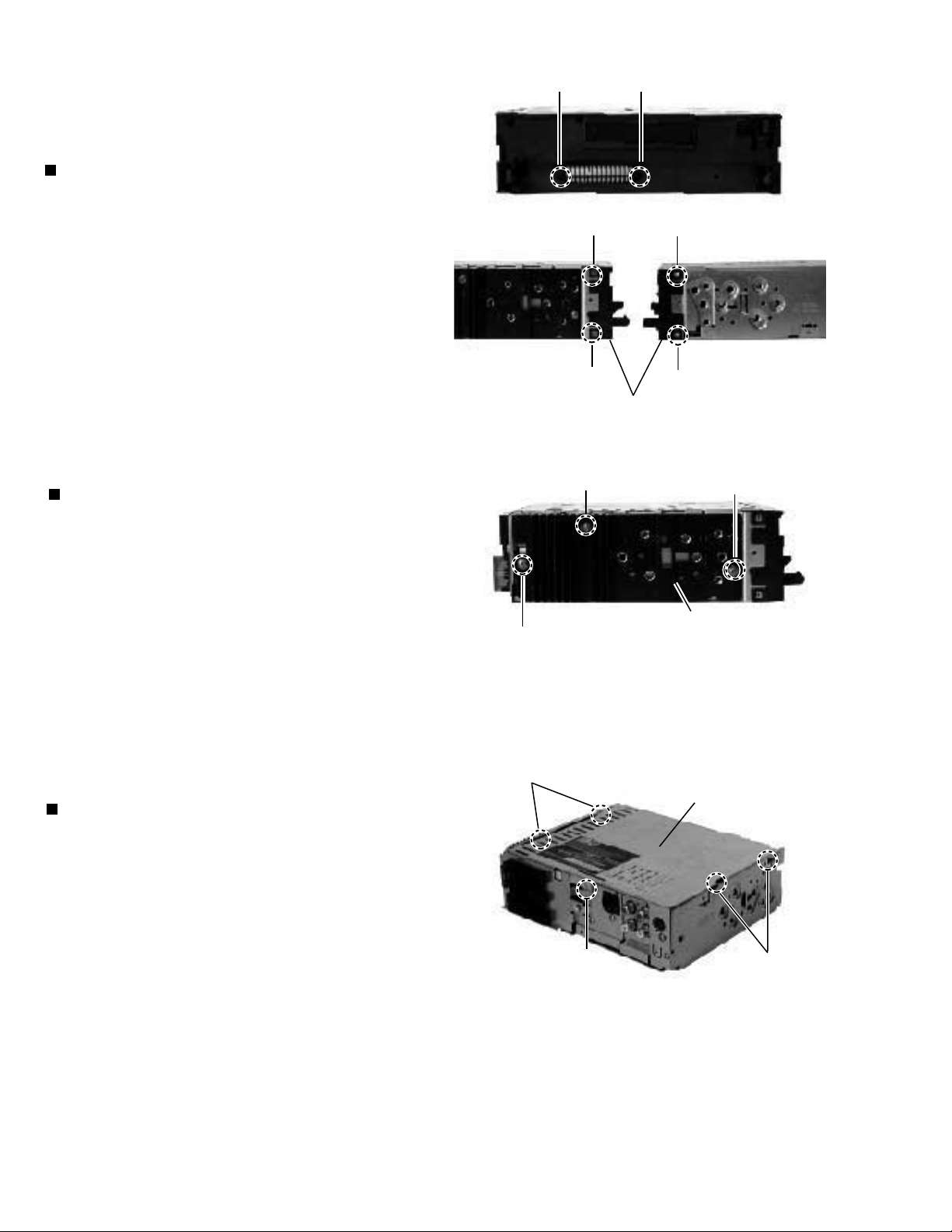
Disassembly method
Removing the front chassis (See Fig.1)
1. Remove two screws A and insert a screwdriver to the
joints a on the side of the front chassis and two joints b
on the right side, then detach the front chassis toward the
front side.
Removing the heat sink (See
1. Remove the three screws B attaching the heat sink on
the left side of the body, and remove the heat sink.
Fig.2 )
A
B
A
a
a
Front chassis
Fig.1
b
b
B
Removing the bottom cover (See
1.2.Turn the body upside down.
Insert a screwdriver to the two joints c and two joints d on
both sides of the body and the joint e on the back of the
body, then detach the bottom cover from the body.
Fig.3 )
Heat sink
B
Fig.2
c
Regulator board
e
d
Fig. 3
1-4
Page 4
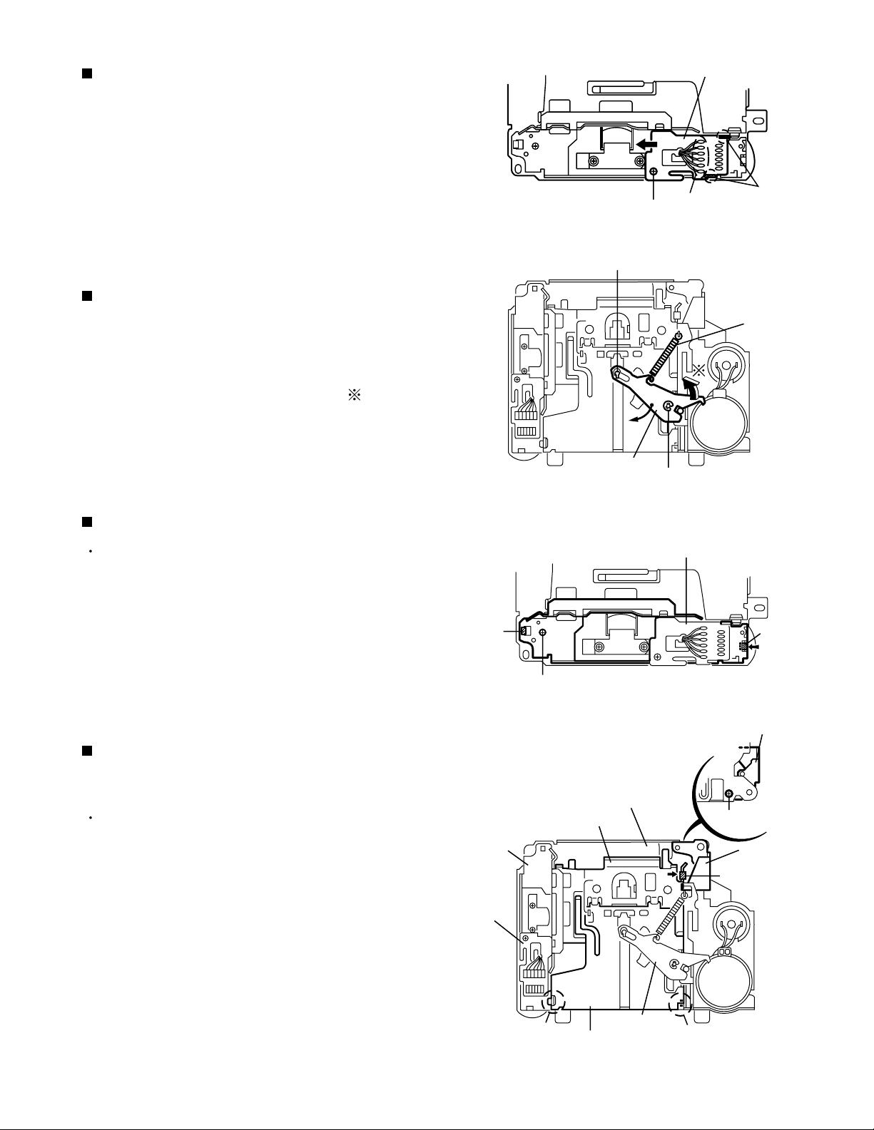
Removing the main amplifier board assembly
(See Fig.4 and 5)
1.
Remove the front chassis.
2.
Remove the bottom cover.
3.
Remove the two screws C attaching the main amplifier
board assembly on the bottom of the body.
KS-FX915R/KS-FX815
CP401
Main amplifier board
4.
Remove the three screws D attaching the main amplifier
board assembly on the back of the body.
5.
Disconnect connector CP401 on the main amplifier board
assembly from the cassette mechanism assembly.
Removing the Cassette mechanism assembly
(See
Fig.6 )
Remove the front chassis.
1.
Remove the bottom cover.
2.
Remove the main amplifier board assembly.
3.
Remove the four screws E attaching the Cassette
4.
mechanism assembly from the top cover.
D
C
C
Fig.4
D
Fig. 5
E
Removing the control switch board
Fig.7 and 8 )
(See
1.
Remove the front chassis.
2.
Remove the four screws F attaching the rear cover on the
back of the front panel unit.
Remove the control switch board from the front panel
3.
unit.
Fig. 6
F
F
Fig. 7
Control switch board
Fig. 8
E
F
F
1-5
Page 5
KS-FX915R/KS-FX815
<Removal of the cassette mechanism>
Cassette mechanism ass’y
Removing the head amplifier board.
(See Fig.1 and 2)
1.
For the 6pin wire extending from connector CN402
on the head amplifier board, disconnect it from the
head relay board.
2.
Disconnect the card wire from connector CN403 on
the head amplifier board.
3.
Remove the screw A attaching the head amplifier
board.
4.
Move the tab a as shown in Fig.2 and remove the
head amplifier board while moving it in the direction
of the arrow.
Removing the cassette mechanism
assembly (See Fig.1 to 3)
1.
Disconnect the 6pin wire from connector CN402 and
the card wire from CN403 on the head amplifier
board (Refer to Fig.1 and 2).
Head relay
board
6pin
wire
CN402
A
CN403
CN402
Fig.1
CN403
Head amplifier board
Fig.2
Head amplifier board
Tab a
2.
Remove the four screws B on the bottom of the
cassette mechanism.
Head amplifier board
B
Cassette mechanism ass’y
B
Fig.3
1-6
Page 6
KS-FX915R/KS-FX815
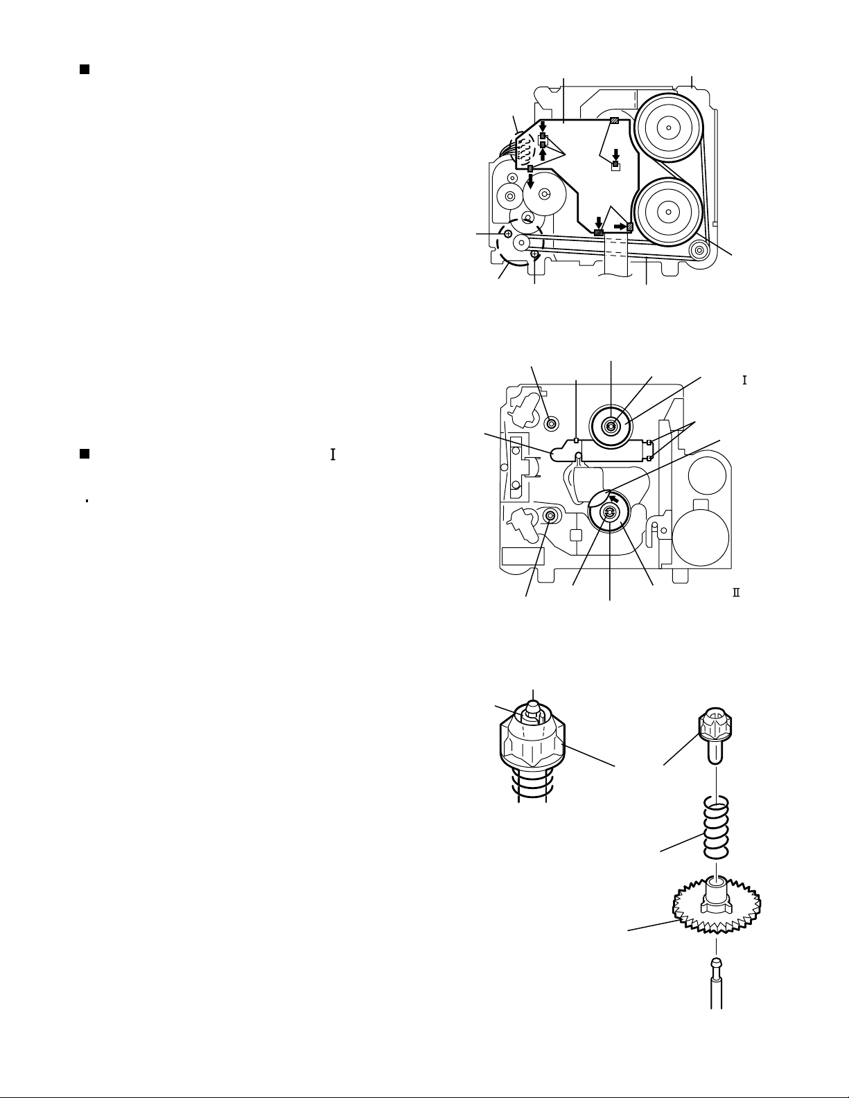
Removing the head relay board
(See Fig.4)
1.
Unsolder the soldering b on the head relay board.
2.
Remove the screw C attaching the head relay board.
3.
Remove the head relay board in the direction of the
arrow while releasing the two joints c.
Removing the load arm (See Fig.5)
1.
Remove the E washer attaching the load arm using
a pincette or something like that and remove the
spring d.
2.
Move the part of the load arm marked upwards to
release it from the axis of rotation. Then rotate the
load arm in the direction of the arrow to remove it
from the cach.
Fig.4
Cach
Load arm
Fig.5
Head relay board
Soldering b
C
E washer
Joint c
Spring d
Removing the sub chassis (See Fig.6)
Prior to performing the following procedure, remove
the head relay board.
1.
Remove the screw D attaching the sub chassis.
2.
Push the tab e in the direction of the arrow to detach
the one side of the sub chassis. Then release the
sub chassis from the tab f.
Removing the cassette holder and the
holder arm in the eject mode
(See Fig.7 and 8)
Prior to performing the following procedure, remove
the head relay board, the load arm and the sub
chassis.
1.
Remove the screw E attaching the reinforce bracket.
2.
Remove the reinforce bracket.
Tab f
Sub chassis
Head relay
board
D
Cassette mecha chassis
Cassette holder
Fig.6
Head relay board
Tab e
Reinforce bracket
E
Reinforce
bracket
tab g
3.
Push the tab g fixing the cassette holder in the
direction of the arrow and open the cassette holder
and the holder arm upward until they stop at an
angle of 45 degrees. Move the two joints h to the
side and remove the cassette holder and the holder
arm from the shaft.
Joint h
Load arm
Holder arm
Fig.7
Joint h
1-7
Page 7
KS-FX915R/KS-FX815
Removing the play head (See Fig.9)
Prior to performing the following procedure, remove
the head relay board and the sub chassis.
1.
Remove the two screws F attaching the play head
(The spring under the play head comes off at the
same time).
Shaft
Joint h
Pinch roller ass’y
Fig.8
Play head
Cassette holder
and holder arm
Joint h
Shaft
Pinch roller ass’y
Removing the pinch roller ass’y
(See Fig.9)
Prior to performing the following procedure, remove
the head relay board and the sub chassis.
1.
Push each tab i in the direction of the arrow and pull
out the pinch rollers on both sides.
Removing the reel disc board
(See Fig.10)
1.
Unsolder the soldering j on the reel disc board.
2.
Push the seven tabs k on the bottom of the cassette
mechanism assembly in the direction of the arrow.
Removing the motor and the sub motor
(See Fig.10 and 11)
Tab i
Tab i
Soldering j
G
Motor
F
Pinch roller ass’y
Fig.9
Reel disc board
Tabs k
Tabs k
G
Tab i
Spring
Tab i
Cassette mechanism ass’y
Flyhwheel
Belt
Fig.10
1.
Unsolder the two soldering l of the motor and the sub
motor.
2.
Release the sub motor from the three tabs m. Push
the sub motor upward and pull out it.
3.
Remove the belt on the bottom of the cassette
mechanism assembly and remove the two screws G
attaching the motor.
ATTENTION:
The motors can be detached before
removing the load arm.
1-8
Sub motor
Tab m
Load arm
Soldering j
Tab m
Soldering l
Tab m
Soldering l
Motor
Fig.11
Page 8
KS-FX915R/KS-FX815
Removing the flywheel
(See Fig.10 and 12)
1.
Prior to performing the following procedure, remove
the head relay board, the load arm, the sub chassis,
the cassette holder, the holder arm and the reel disc
board.
2.
Remove the belt on the bottom of the cassette
mechanism ass’y.
3.
Remove the slit washer attaching the flywheel on the
upper side of the cassette mechanism ass’y and pull
out the flywheel downward. Then remove another
flywheel in the same way.
ATTENTION:
When reassembling, make sure to use
a new slit washer.
Removing the reel disc ass’y( )
(See Fig.12 to 14)
Soldering j
G
Motor
Plate
Reel disc board
G
Slit washer
Tab k
Tab o
Cassette mechanism ass’y
Tab k
Belt
Fig.10
Reel driver
The part n
Tabs o
Flyhwheel
Reel disc
ass’y( )
Push aside
the gear
Prior to performing the following procedure, remove
the head relay board, the load arm, the sub chassis,
the cassette holder and the holder arm.
1.
Disengage the part n inside of the reel driver which
engages with the shaft, using a pincette or
something like that. Then remove the reel driver from
the shaft.
2.
Remove the reel driver spring and the reel table.
The part n
Slit washer
Shaft
Fig.13
The part n
Reel driver
Fig.12
Reel driver spring
Reel disc ass’y( )
Reel driver
Reel table
Fig.14
1-9
Page 9

KS-FX915R/KS-FX815
Removing the reel disc ass’y( )
(See Fig.12 to 15)
ATTENTION:
1.
Release the plate from the three tabs o.
2.
Push aside the gear over the reel table using a
pincette or something like that.
3.
Remove the reel disc ass’y ( ) as with the reel disc
ass’y ( ).
ATTENTION:
Prior to performing the following
procedure, remove the reel disc ( ).
Do not break the front panel tab fitted
to the metal cover.
Push aside the gear and reattach the reel disc Ass’y( ).
Reel disc ass’y( )
Fig.15
1-10
Page 10

Adjustment method
KS-FX915R/KS-FX815
Test Instruments reqired for adjustment
1.Digital osclloscope(100MHz)
2.Frequency Counter meter
3.Electric voltmeter
4.Wow & flutter meter
5.Test Tapes
VT724
VT739
VT712
VT703
6.Torque gauge
Power supply voltage
Load impedance
Line out
For playback frequency measurement
For wow flutter & tape speed measurement
Measuring conditions(Amplifier section)
for DOLBY level measurement
For head azimuth measurement
Cassette type for CTG-N
(mechanism adjustment)
DC14.4V(10.5~16V)
4 (2Speakers connection)
20k
Tuner section
BAND STEP
FM : 100kHz (Seek), 50kHz (Manual)
AM : 9kHz step
Preset Memory Initialization
Band
FM(MHz)
AM(kHz)
DUMMY LOAD
Exclusive dummy load should be used for AM
and FM dummy load,there is a loss of 6dB
between SSG output and antenna input. The
loss of 6dB need not be considered since
direct reading of figures are applied in this
working standard.
M1
87.5
153
Preset Memory
M2
M3
89.9
97.9
216
603
M4
105.9
999
M5
108.0
1404
M6
87.5
1620
Standard volume position
Balance and Bass,Treble volume .Fader
:Center(Indication"0")
Loudness,Dolby NR,Sound,Cruise:Off
Volume position is about 2V at speaker output with
following conditions.Playback the test tape VT721.
AM mode 999kHz/62dB,INT/400Hz,30%
modulation signal on receiving.
FM mono mode 97.9MHz/66dB,INT/400Hz,22.5kHz
deviation pilot off mono.
FM stereo mode 1kHz,67.5kHz dev. pilot7.5kHz dev.
Output level 0dB(1 V,50 /open terminal).
Arrangement of Adjusting
Cassette Mechanism Section
Capstan motor
Cassette mechanism
(Surface)
Azimuth screw
(Forward side)
Playback head
Tape speed adjust
Azimuth screw
(Reverse side)
1-11
Page 11

KS-FX915R/KS-FX815
Main board
Arrangment of adjusting
Head amplifier board section (Reverse side)
VR402:Rch
(Dolby NR level adj)
VR401:Rch
(Dolby NR Frequency response adj)
B402
E
Q401
D401
B401
CP401
1
R420
B408
1
R423
R421
R422
Q402
B409
Q403
D402
FSMW1101A
VR402
C417
D403
C418
R424
IC402
R425
C419
C414
B403
B410
B404
C410
C412
C411
R413
1
C415
R416
R415
C416
R418
R419
CP403
C409
R411
B415
C413
1
11
B411
IC401
B412
17
VR401
B416
R412
R410
C405
R408
31
C407
21
C408
R417
R414
B413
R404
B406
B414
R409
C406
R407
1
B405
TPP
C404
CP402
1
R402
C401
2
R405
C403
R401
R406
R403
C402
B407
Information for using a car audio service jig
1. We're advancing efforts to make our extension cords common for all car audio products.
Please use this type of extension cord as follows.
2. As a U-shape type top cover is employed, this type of extension cord is needed to check operation of the
mechanism assembly after disassembly.
3. Extension cord : EXTKSRT002-18P ( 18 pin extension cord ) For connection between mechanism assembly
and main board assembly.
Check for mechanism driving section such as motor ,etc..
Cassette mechanism
Disassembly method
1. Remove the bottom cover.
2. Remove the front panel assembly.
3. Remove the top cover .
4. Install the front panel.
5. Confirm that current is being carried by connecting
an extension cord jig.
Note
Available to connect to the CP701 connector when installing the front panel.
Extension cord
EXTKSRT002-18P
to Cassette mechanism
EXTKSRT002-18P
1-12
Main board
Front panel assembly
to Main board
Page 12

KS-FX915R/KS-FX815
Item
Head
1.
azimuth
adjustment
Conditions
Test tape:
SCC-1659
VT703(10kHz)
Adjustment and Confirmation methods
Head height adjustment
Adjust the azimuth directly. When you
adjust the height using a mirror tape,
remove the cassette housing from the
mechanism chassis. After installing the
cassette housing, perform the azimuth
adjustment.
Load the SCC-1659 mirror tape. Adjust with
1.
height adjustment screw A and azimuth
adjustment screw B so that line A of the
mirror tape runs in the center between Lch
and Rch in the reverse play mode.
After switching from REV to FWD then to
2.
REV, check that the head position set in
procedure 1 is not changed. (If the position
has shifted, adjust again and check.)
Adjust with azimuth adjustment screw B so
3.
that line B of the mirror tape runs in the
center between Lch and Rch in the forward
play mode.
Head azimuth adjustment
Load VTT724 (VT724) (1kHz) and play it
1.
back in the reverse play mode. Set the Rch
output level to max.
Load VTT703 (VT703) (10kHz) and play it
2.
back in the forward play mode. Adjust the
Rch and Lch output levels to max, with
azimuth adjustment screw B. In this case,
the phase difference should be within 45 .
Engage the reverse mode and adjust the
3.
output level to max, with azimuth
adjustment screw C.
(The phase difference should be 45 or
more.)
When switching between forward and
4.
reverse modes, the difference between
channels should be within 3dB. (Between
FWD L and R, REV L and R.)
S.Values Adjust
A line
Head shield
The head is at low position
during.
B line
Head shield
The head is at High position
during REV.
Output
level:
Maximum
PBHead
FWD Adj B
REV Adj C
(0 ) (45 )
HEIGHT Adj A
phase
Tape speed
2.
and wow
flutter
confirmation
Play back
3.
frequency
response
confiramation
When VTT721 (VT721) (315Hz) is played
5.
back, the level difference between channels
should be within 1.5dB.
Test tape: VTT712
(3kHz)
Test tape: VTT724
(1kHz)
VTT739
(63Hz / 1kHz / 10kHz)
The tuner section is of an adjustment-freedesign. In case the tuner is in trouble, replace the tuner pack.
Check to see if the reading of the F, counter /
1.
wow flutter meter is within 3015 3045(FWD
/ REV), and less than 0.35% (JIS RMS).
In case of out of specification, adjust the
2.
motor with a built-in volume resistor.
Play test tape VTT724, and set the volume
1.
position at 2V.
Play test tape VTT739 and confirm.
2.
1kHz / 10kHz: -1 3dB,
1kHz / 63Hz: 0 3dB,
When 10kHz is out of specification, it will be
3.
necessary to read adjust the azimuth.
Tape speed:
3015
3045Hz
Wow
flutter: less
than 0.35%
Speaker out
1kHz / 63Hz
: 0 3db
1kHz / 10kHz
: -1 3db
Built-in volume
resistor
1-13
Page 13

KS-FX915R/KS-FX815
Descrption of major ICs
TEA6320T-X (IC161) : E.volume
1.Pin layout
2.Block diagram
10 8 9 7 6
5
12
SDA
1
GND
2
OUTLR
OUTLF
MUTE
TL
B2L
B1L
IVL
ILL
QSL
IDL
ICL
IMD
IBL
IAL
3
4
5
6
7
8
9
10
11
12
13
14
15
16
3.Pin functions
Pin
Symbol
No.
SDA
1
SCL
32
VCC
31
OUTRR
30
OUTRF
29
TR
28
B2R
27
B1R
26
IVR
25
ILR
24
QSR
23
IDR
22
Vref
21
ICR
CD-CH
TAPE
TUNER
20
19
18
17
CAP
IBR
IAR
I/O
Serial data input/output.
I/O
MUTE
21
31
2
19
16
15
13
11
14
22
20
18
17
Functions Functions
POWER
SUPPLY
SOURCE
SELECTOR
23 25 24 26 27 28
VOLUME 1
+20 to -31 dB
LOUDNESS
LEFT
VOLUME 1
+20 to -31 dB
LOUDNESS
RIGHT
Pin
No.
17
Symbol
IAR
BASS
LEFT
+15 dB
LOGIC
BASS
RIGHT
+15 dB
I/O
I
Input A right source.
TREBLE
LEFT
+12 dB
TREBLE
RIGHT
+12 dB
FUNCTION
ZERO CROSS
DETECTOR
VOLUME 2
0 to 55 dB
BALANCE
FENDER REAR
VOLUME 2
0 to 55 dB
BALANCE
FENDER FRONT
HC BUS
REC
VOLUME 2
0 to -55dB
BALANCE
FENDER FRONT
VOLUME 2
0 to -55dB
BALANCE
FENDER REAR
3
4
32
1
29
30
2
3
4
5
6
7
8
9
10
11
12
13
14
15
16
GND
OUTLR
OUTLF
TL
B2L
B1L
IVL
ILL
QSL
IDL
MUTE
ICL
IMO
IBL
IAL
Ground.
-
output left rear.
O
output left front.
O
Treble control capacitor left channel or
I
input from an external equalizer.
Bass control capacitor left channel or
-
output to an external equalizer.
Bass control capacitor left channel.
-
Input volume 1. left control part.
I
Input loudness. left control part.
I
Output source selector. left channel.
O
Not used
-
Not used
-
Input C left source.
I
Not used
-
Input B left source.
I
Input A left source.
I
18
19
20
21
22
23
24
25
26
27
28
29
30
31
32
IBR
CAP
ICR
Vref
IDR
QSR
ILR
IVR
B1R
B2R
TR
OUTRF
OUTRR
Vcc
SCL
I
Input B right source.
-
Electronic filtering for supply.
I
Input C right source.
-
Reference voltage (0.5Vcc)
-
Not used
O
Output source selector right channel.
I
Input loudness right channel.
I
Input volume 1. right control part.
-
Bass control capacitor right channel
Bass control capacitor right channel or
O
output to an external equalizer.
Treble control capacitor right channel or
I
input from an external equalizer.
O
Output right front.
O
Output right rear.
-
Supply voltage.
I
Serial clock input.
1-14
Page 14

SAA6579T-X(IC71):RDS Detector
KS-FX915R/KS-FX815
1.Terminal Layout
QUAL
RDDA
MUX
VDDA
GND
SCOUT
Vref
CIN
1
2
3
4
5
6
7
8
16
15
14
13
12
11
10
9
RDCL
T75
OSCO
OSC1
VDD
GND
TEST
MODE
2.Pin Function
Pin
No.
1
2
3
4
5
6
7
8
9
10
11
12
13
14
15
16
QUAL
RDDA
Vref
MUX
VDDA
GND
CIN
SCOUT
MODE
TEST
GND
VDD
OSC1
OSC0
T75
RDCL
FunctionI/OSymbol
Non connect
RDS data output
O
Reference voltage output
O
Multiplex signal input
I
+5V Supply voltage for analog
Ground for analog part (0V)
Sub carrier output of reconstruction filter
I
Ground for digital part (0V)
O
Ground for digital part (0V)
Ground for digital part (0V)
Ground for digital part (0V)
+5V supply voltage for digital part
Oscillator input
I
Oscillator output
O
Non connect
RDS clock output
O
3.Block Diagram
4
8
7
5
3
ANI-
ALLUDING
FILTER
CLOCKED
COMPARATOR
REFERENCE
VOLTAGE
1413
5kHz
BAND PASS
(8th ORDER)
COSTAS LOOP
VARIABLE AND
FIXWD DIVIDER
CLOCK
REGENERATION
AND SYNC
6
RECONSTRUCTION
FILTER
BIPHASE
SYMBOL
DECODER
TEST LOGIC AND OUTPUT
OSCILLATOR
AND
DIVIDER
SELECTOR SWITCH
9
10
12
DUALITY BIT
GENERATOR
DIFFERENTIAL
DECODER
11
1
2
16
15
1-15
Page 15

KS-FX915R/KS-FX815
LA4743K(IC301):Power AMP
1.Block diagram
IN 1
TA B
IN 2
+
2.2 F
+
2.2 F
11
1
12
Vcc 1/2 Vcc 3/4
6 20
-
+
Protective
circuit
-
+
2200 F 0.047 F
+
9
-
7
+
OUT 1+
OUT 1-
PWR GND1
8
+
OUT 2+
5
-
OUT 2-
3
PWR GND2
2
ST BY
R.F
47 F
IN 3
PRE GND
IN 4
+5V
ST ON
+
2.2 F
N.C
+
2.2 F
4
Stand by
Switch
Mute
10
+
Ripple
Filter
Mute
22
circuit
4.7 F
+
15
-
+
-
17
19
4.7K
+
OUT 3+
OUT 3-
Low Level
Mute ON
25
18
21
23
PWR GND3
OUT 4+
OUT 4-
13
14
Protective
circuit
-
+
+
-
1-16
ON TIME C
22 F
Muting &
16
+
ON Time Control
Circuit
PWR GND4
24
Page 16

2.Terminal layout
3.Pin function
KS-FX915R/KS-FX815
SymbolPin No. Function
1
2
3
4
5
6
7
8
9
10
11
12
13
14
15
16
17
18
19
20
21
22
23
24
25
TA B
GND
OUTRRSTBY
OUTRR+
VCC1/2
OUTRFGND
OUTRF+
RIPPLE
INRF
INRR
SGND
INLR
INLF
ONTIME
OUTLF+
GND
OUTLFVCC3/4
OUTLR+
MUTE
OUTLRGND
NC
Header of IC
Power GND
Outpur(-) for front Rch
Stand by input
Output (+) for front Rch
Power input
Output (-) for rear Rch
Power GND
Output (+) for rear Rch
Ripple filter
Rear Rch input
Front Rch input
Signal GND
Front Lch input
Rear Lch input
Power on time control
Output (+) for rear Lch
Power GND
Output (-) for rear Lch
Power input
Output (+) for front
Muting control input
Output (-) for front
Power GND
Non connection
1-17
Page 17

KS-FX915R/KS-FX815
UPD178018AGC-586 (IC701) : Main system control CPU
UPD178018AGC-604 (IC701) : Main system control CPU
1. Pin layout
80 ~ 61
1
60
2. Pin function
Pin No.
1
2
3
4
5
6
7
8
9
10
11
12
13
14
15
16
17
18
19
20
21
22
23
24
25
26
27
28
29
30
31
32
33
34
35
36
37
38
39
40
~
20
21 ~ 40
~
41
Port Name I/O Descriptions
KEY 0
KEY 1
KEY 2
LEVEL
SM
SQ
LCDCE
LCDDA
LCDSCK
BUSI/O
OPEN
BUSSI
BUSSO
BUSSCK
NC
NC
NC
NC
INLOCK
NC
GNDPORT
VDDPORT
NC
AFCK
MONO
FM/AM
SEEK/STP
NC
IFC
VDDPLL
FMOSC
NC
GNDPLL
AMEO
FMEO
IC
SD/ST
STAGE0
NC
MOTOR
I
I
I
I
I
I
O
O
O
I
I
I
O
I/O
-
-
-
-
-
-
-
O
O
O
O
O
I
I
-
I
-
O
O
-
I
I
O
Key input 0
Key input 1
Key input 2
Level meter input
S.meter level input
S.Quality level input
CE output to LCD driver
Data output to LCD driver
Clock output to LCD driver
I/O selector output for J-BUS, H : OUT, L: INPUT
Door open detect input
J-BUS Data input
J-BUS Data output
J-BUS Clock in/output
Non connect
Non connect
Non connect
Non connect
Non connect
Non connect
Port GND
Port Vdd
Non connect
AF check output, L: AF check
Monaural on /off selecting output, H:mono on
FM/AM switching output L : FM H : AM
Auto seek /stop selecting output, H: Seek, L:Stop
Pulse signal input port for Cruise control
FM/AM midle frequency counter input
PLL Vdd
FM/AM limited generator frequency input
None connect
PLL GND
AM error out output
FM error out output
GND
Station detector, Stereo signal input, H:Find Station, L:Stereo
Pull up
Non connect
Main motor output
1-18
Page 18

UPD178018AGC-551 (IC701) : Main system control CPU
UPD178018AGC-551 (IC701) : Main system control CPU
Pin No.
41
42
43
44
45
46
47
48
49
50
51
52
53
54
55
56
57
58
59
60
61
62
63
64
65
66
67
68
69
70
71
72
73
74
75
76
77
78
79
80
Port Name I/O Descriptions
FF/REW
F/R
DOLBY
MSIN
I2CCLK
I2CDAO
I2CDAI
REEL
SUBMO1
SUBMO2
MODE
TAPEIN
STANDBY
NC
NC
NC
NC
NC
BEEP
MUTE
PCNT
TELMUTE
DIMIN
DIMOUT
ENC1
ENC2
ACCDET
POWER
RDSSCK
RDSDA
REMOCON
DETACH
J-BUSINT
REGCPU
GND
X2
X1
REGOSC
VDD
RESET
I
O
O
I
O
O
I
O
I
O
O
O
I
-
-
-
-
O
O
O
I
I
O
I
I
I
O
I
I
I
I
I
-
-
-
I
-
-
-
Output for input signal level switching for MS L : FF,REW H : PLAY
FWD,REV running direction switch signal input
Dolby on "H" output
MS input
I2C information clock output
I2C information data output
I2C information clock input
Switch for detecting tape end position
Sub motor clock direction input
Sub motor clock opposite detection drive output
Mechanism mode position detection input
Cassette in detection input H : cassette in L : cassette out
Standby position detection input H : eject side L : operation side
Non connect
Non connect
Non connect
Non connect
Non connect
Touch tone output
Mute output , L : mute on
Power ON /OFF switching output , H : power on
Telephone mute signal detection input
Dimmer signal detection input L : dimmer
Dimmer control output , Dimmer off L output
Rotary volume signal 1 input Power save : L
Rotary volume signal 2 input
Power save 1 Working togethe ACC Power save : L
Power save 2, Working together Back up by H input, stop mode
Clock input for RDS
RDS data input
Remocom input
Detach signal input H : Power save
Cut-in input for J-BUS signal
Regulator for CPU power supply, Connect the GND with0.1 F.
Ground
Connecting the crystal oscillator for system clock
Connecting the crystal oscillator for system clock
Regulator for oscillator circuit.Connect the GND with 0.1 F.
Vdd
Pull up
KS-FX915R/KS-FX815
1-19
Page 19

KS-FX915R/KS-FX815
HD74HC126FP-X (IC801) : Buffer
1.Terminal layout
1
2
3
4
5
6
7
2.Block diagram
Input
14
13
12
11
10
9
8
Vcc Vcc
1A
2A
3A
4A
1C
2C
3C
See Function Table
4C
3.Pin function
Output
1Y
2Y
Output
2Y
Output
3Y
Output
4Y
Input Outout
C
A
L
X
H
L
H
H
1k
CL
Sample as Load Circuit 1
Sample as Load Circuit 1
Sample as Load Circuit 1
Y
Z
H
L
S1
1k
1-20
Page 20

HA13164(IC901):REGULATOR
1.Terminal layout
123456789101112131415
KS-FX915R/KS-FX815
2.Block diagram
ANT OUT
C3
0.1u
EXT OUT
C4
0.1u
ANT CTRL
CTRL
CD OUT
C5
0.1u
AUDIO OUT
C6
10u
11
12
10
BATT.DET OUT
9
COMPOUT
6
VDD OUT
4
SW5VOUT
5
14
UNIT R:
+B
ACC
ILMOUT
R1
C7
0.1u
0.1u
C8
C1
100u
VCC ACC
8
2
1
7
Surge Protector
BIAS TSD
15
3
note1) TAB (header of IC)
connected to GND
ILM AJGND
13
C2
0.1u
C:F
3.Pin function
Pin No. Symbol Function
1
2
EXTOUT
ANTOUT
Output voltage is VCC-1 V when M or H level applied to CTRL pin.
Output voltage is VCC-1 V when M or H level to CTRL pin and H level
to ANT-CTRL.
3
4
5
6
7
8
9
10
11
12
13
14
15
ACCIN
VDDOUT
SW5VOUT
COMPOUT
ANT CTRL
VCC
BATT DET
AUDIO OUT
CTRL
CD OUT
ILM AJ
ILM OUT
GND
Connected to ACC.
Regular 5.7V.
Output voltage is 5V when M or H level applies to CTRL pin.
Output for ACC detector.
L:ANT output OFF , H:ANT output ON
Connected to VCC.
Low battery detect.
Output voltage is 9V when M or H level applied to CTRL pin.
L:BIAS OFF, M:BIAS ON, H:CD ON
Output voltage is 8V when H level applied to CTRL pin.
Adjustment pin for ILM output voltage.
Output voltage is 10V when M or H level applies to CTRL pin.
Connected to GND.
1-21
Page 21

1
AB C
2
3
4
5
Block diagram
MAIN
MOTOR
SUB
MOTOR
SWITCH
PLAYBACK
HEAD
SUBMO+
SUBMO-
CJ403 CJ402
METAL
FWD_L
FWD_R
REV_L
REV_R
IC602
REMOCON
REMOCON
IC601
LCD
DRIVER
S1~S68
COM1~COM3
LCD
IC402
DRIVER
TAPEIN,MODE,REEL
MOTOR,STANDBY
IC401
EQ AMP
EN601
ENCODER
LCDCL,LCDCE,LCDDA
ENC1
ENC2
KEY0~KEY2
KEY
MATRIX
SUBMO+
SUBMO-
FF/REW
F/R
DOLBY
MSOUT
Lch,Rch
J1
ANT
CJ401
CN601
MUX
IC71
RDS
DETECTOR
CP401
TAPE_L,TAPE_R
CJ601
TU1
TUNER
PAC K
TU_L
TU_R
EO,FM/AMOSC
IFC,MONO,SD/ST
IFREQ,S.METER
RDSCK
RDSDA
IC701
CPU
JBUS.SI
JBUS.SO
JBUS.IO
JBUS.INT
JBUS.SCK
IC801
J-BUS
CP801
CD-CH
IC161
E.VOL
EVOLCLK
EVOLDA
CH_L
CH_R
OUTLF
OUTLR
OUTRF
OUTRR
OUTLF
OUTLR
OUTRF
OUTRR
to
each
BLOCK
IC901
REG
CJ321
IC301
POWER
AMP
CP901
SPK
BATT
LINE
OUT
KS-FX915R/KS-FX815
2-1
Page 22

Standard schematic diagrams
Main amp section
TU1
5
J1
QNB0100-001
L1
4.7u
D5
D6
1SS133-T2
1SS133-T2
C43
C33
150P
R34
R44
C32
0.082
10V
10K
D706
MTZJ5.6B-T2
STANDBY
TAPEIN
MODE
SUB02
SUB01
REEL
MS
DOLBY
FR
FFREW
MOTOR
10K
10K
D707
D708
MTZJ5.6B-T2
MTZJ5.6B-T2
1k
R31
R752
510
R703
R702
R701
D709
MTZJ5.6B-T2
J801
QNZ0095-001
2SC2412K/R/-X
2SC2412K/R/-X
SLR-56MC3F
LCDCE
LCDDA
LCDCK
R744
10K
D710
MTZJ5.6B-T2
R43
10k
R42
1k
Q41
REMOCON
0R0
0R0
0R0
C41
0.001
DIMOUT
Q42
S5V
D712
EC1
EC2
KEY2
KEY1
KEY0
R33
1k
R32
1.5K
C31
0.082
2SC3661-X
2SC3661-X
R748
Q32
Q31
24K
Q701
2SC2412K/R/-X
4
3
CP401
QGB1214J1-18S
2
QNZ0007-002
R706
R705
R704
CJ601
D702
D701
MTZJ5.6B-T2
MTZJ5.6B-T2
D703
D704
MTZJ5.6B-T2
MTZJ5.6B-T2
D705
MTZJ5.6B-T2
1
0.47/50
1k
1k
C42
2.2/50
1.5k
R41
C1
100/16
R1
33
AMEO
FM/AM
FMEO
10V
9V
C77
47/16
C76
0.01
C75
47p
R73
X71
QAX0263-001Z
C74
82p
R750
47K
R59
470
C55
0.47/50
R807
100k
R808
100k
R809
100
CH.R
330k
R810
CH.L
2SA1037AK/RS/-X
R2
4.7k 47k
Q1
DTC114EKA-X
2.2k
2.2k
R72
RDSCK
R58
2SC2412K/R/-X
R806
C2
Q2
R3
IC71
SAA6579T-X
15K
Q52
2SC2412K/R/-X
R57
IC801
HD74HC126FP-X
KS-FX915R/KS-FX815
LA4743K
QNN0175-001
J321
C321
0.22
2.2/50
390p
C303
390p
C313
Q781
DTA114EKA-X
220/10
C982
10/16
390p
C304
390p
C314
Q782
DTA114EKA-X
C782
CRS03-W
D982
C322
0.22
100
100
1K
R341
R321
C301
R305
Q341
2SD1048/6-7/-X
Q321
10k
R902
CRS03-W
0.1
C981
D981
4.7/25
0.1
4.7/25
C305
C307
47k
R881
Q881
C881
DTC114EKA-X
2.2
C910
R352
1K
D783
Q351
R781
Q784
DTC114EKA-X
0.1/50
C905
R342
1K
R322
2SD1048/6-7/-X
4.7K
4.7K
R903
R301
27K
C308
C309
R302
2.2/50
27K
C318
R311
2.2/50
27K
R312
27K
2.2/50
1SS355-X
1SS355-X
D781
4.7K
D343
D323
MTZJ11C-T1
HA13164
R910
100/16
C906
R343
2.2k
R323
2.2k
2SD1048/6-7/-X
C781
100/16
IC901
C319
1K
RR
RL
R351
R331
100
FR
FL
4.7/50
FL
4.7/50
4.7/50
4.7/50
STAGE0
RL
SDA
PCNT
DIMIN
SCL
270
9V
RR
FR
MUTE
LMETER
Q976
UN2211-X
POWER
R976
ACCDET
9V
10V
PCNT
SD/ST
47K
R711
FMEO
AMEO
C702
FMOSC
0.1
TELMUTE
1SS355-X
68K
0.001
C713
LMETER
C243
D242
0.047
D241
1SS355-X
22/16
FM/AM
MONO
AFCK
SK/ST
R247
100K
Q241
2SD601A/R/-X
C242
B903
330P
C714
R243
12k
100
R245
1K
R246
0R0
Q977
2SA1037AK/RS/-X
47u
L903
L902
C703
220/10
R242
180K
C241
1/50
22K
R244
R307R6R308
47K
27K
R977
R978
47u
R241
R306
R309
47K
47K
47K
12K
47K
2SA1706/ST/-T
Q904
2SA1037AK/RS/-X
R891
47K
D891
Q891
UN2211-X
R908 R909
DTC114EKA-X
R892
1SS355-X
C891
1SS355-X
1SS355-X
0R0
B904
Q902
47k
DTC114EKA-X
2.2k
Q903
1K
1SS355-X
D892
0.1
100
1K
R907
1K
R906
R353
2.2K
R333
2.2K
2SD1048/6-7/-X
C909
D902
D903
2200/6.3
R332
Q331
R782
47K
D782
1SS355-X
1SS355-X
1SS355-X
1SS355-X
R905
10k
18k
1/50
220/10
C907
C908
R904
D353
D333
47k
Q901
TAPE.L
TAPE.R
TU.R
CH.R
0.1
10k
X701
100/6.3
R81
10K
R82
10K
C7
Q7
4.7k
4.7k
R9
Q10
0.1
DTA114EKA-X
C4
C164
R162
1/50
0R0
0R0
R164
0R0
R163
R161
C163
0R0
1/50
C162
1/50
C161
2.2/50
C710
ACCDET
0.1
0.1
MODE
47k
47k
R733
R732
QAX0406-002Z
R726
MOTOR
47k
R734
MTZJ5.6B-T2
R728
R727
S702
DIMOUT
MS
47k
R735
R730
S703
C711
QSW0451-001
SUB01
SUB02
47k
47k
R737
R736
D711
4.7k
4.7k
4.7k
2SC2412K/R/-X
4.7k
R10
QSW0451-001
POWER
DIMIN
STANDBY
47k
R738
390
S701
TELMUTE
R729
47K
R749
100
PCNT
R718
R719
R720
R721
R722
R723
R724
R725
Q6
2SC2412K/R/-X
100k
R739
22k
R83
TU.R
TU.L
820P
820P
22k
C83
C84
R84
R168
TU.L
C166
C165
1/50
C167
47/16
MUTE
10k
10k
10k
10k
10k
4.7k
4.7k
4.7k
2.2K
CH.L
22K
R167
2.2/50
C168
TEA6320T-X
100/16
47k
R747
C173
C172
0.15
0.0082
C178
0.0056
C176
0.033
C174
0.22
IC161
C171
0.22
C175
0.033
0.15
2.2K
47K
R741
4.7k
R716
JBUSSI
C177
0.0056
R169
220K
1SS355-X
220K
R170
R742
REEL
4.7k
4.7k
R715
R714
JBUSSCK
JBUSSO
1SS355-X
56K
R743
FR
SCL
SDA
DOLBY
Q841
R841
1k
C841
0.1/50
C169
C170
0.0082
22K
R165
R166
47k
47k
R740
R746
STAGE0
FFREW
TAPEIN
IC701
4.7k
R717
JBUSIO
C181
C183
270
R173
R172
C184
C182
10
C179
D161
D162
47k
R171
0.082
C180
100/16
47k
R745
9V
R707
4.7K
R708
4.7K
R712
47K
C701
0.001
R713
SEEK/STOP
10k
C244
R842
2.2K
BZ841
0.22/50
QAN0009-001Z
DTC114EKA-X
C5
1/50
C6
R12
0R0
C9
220/10
47p
C54
0.1
C53
10K
0.0047
10k
0.047
C3
D7
R55
R11
2SA1037AK/RS/-X
Q3
D3
D2
1SS355-X
R4
3.3k
C72
560P
C73
2.2/50
R71
2.2k
R53
10K
Q51
R56
2.2K
R803
100
C801
0.047
1SS355-X
0.022
C71
47K
R54
R805
22K
R5
1SS355-X
47K
100K
JBUSSCK
R804R802
330k
Q9
JBUSSI
JBUSSO
JBUSIO
22k
47k
SM
SK/ST
RDSDA
Q53
DTC114EKA-X
R709
100k
R801
47K
47K
MONO
R751
47K
TAPE.L
TAPE.R
C52
0.01
R60
DTC114EKA-X
SD/ST
SEEK/STOP
330P
C51
9V
EC1
EC2
KEY0
KEY1
KEY2
LCDCE
LCDDA
LCDCK
1/50
0.1/50
Q8
47p
0.018
0.018
C8
C81
C82
2SC2412K/R/-X
R8
Q4
DTA114EKA-X
D4
1SS355-X
Q5
8.2
DTA114EKA-X
AFCK
FMOSC
SM
RDSDA
RDSCK
C709
R731
REMOCON
C708
C707
27P
C706
27P
C705
C704
22/16
47/16
C302
C327
0.1
C306
R882
4.7K
C882
0.1
22/16
0.047
C904
2200/16
C903
1N5401-TU-15
D901
L901
QQR0703-001
10/16
0.047
C901
C902
TUNER SIGNAL
TAPE SIGNAL
CD CHANGER SIGNAL
FRONT SIGNAL
REAR SIGNAL
IC301
0.10.1
150P
C911
47
R901
CP901
QNZ0112-001
C323C324
0.1
C325C326
0.1
AB C D E F G
2-3
Page 23

KS-FX915R/KS-FX815
Mecha control section
Q403
2SB1322/RS/-T
5
47K
R423
3.3K
R422
DSK10C-T1
390
CJ403
QGF1219F1-10S
4
R401
0.015
C411
R410
R411
24K
12K
33K
VR402
D402
18K
0.1
0.10.1
C413C412
R413
C417
Q402
DTC114EKA-X
Q401
100P
C408
C409
100P
22/16
100P
C407
C406
180 180
IC401
R406 R407
R417
R418
15K
10K
3
100P
CJ402
100P
C401
100K
R402
100P
C402
100K
R403
100P
C403
100K
R404
100P
C404
100K
R405
2
C405
0.015
C410
R408
24K
R409
12K
33K
VR401
22/16
C414
100
R412
0.1
220P
C418
C416
QGB1214K1-18S
CJ401
3.9K
R414
0.47/50
C419
22K
0.01
C421
R415
DTC114EKA-X
R416
910K
0.1
C422
3.3K
R420
IC402
LB1641
D401
MA3047/H/-X
3.3K
R424
10/16
C423
C425
0.01
0.1
C424
33
R425
1
TAPE SIGNAL
2-4
HAB C DE FG
Page 24

LCD & Key control section
5
4
KS-FX915R/KS-FX815
QNZ0449-001
COM3S3COM2
S26
S51
S50
S49
S57
S56
S55
S54
S53
S52
S63
S62
S61
S60
S59
S58
S48
S47
S46
S45
S44
S43
S42
S41
S40
S39
S38
S37
S36
S35
S34
S33
S32
S31
S30
S29
S28
S27
3
S14
S10
S11
S12
S13
S15
S16
S17
S18
S19
S20
S21
S22
S23
S24
S25
R601R602R603R604R605
2
R611
2.7K
S613
S620
R617
3.9K
R614R615R616
1.2K1.8K2.7K
S617S618S619
8208201.2K1.8K2.7K
S608
R606R607R609 R608
R612
S615
S601S602
8208201.8K 1.2K
S607
D601
B601B602B603
S614
SML-310LT/MN/-X
R620
470( 1/8W)
820
S603S604S605S606
S609S610S611
R613
820
S616
R621
270( 1/8W)
R622
D602
D603
D604
QNZ0450-001
270( 1/8W)
R623
D605
D606
D607
270( 1/8W)
R624
D608
D609
D610
390( 1/8W)
S64
R625
D611
D612
S66
S65
430( 1/8W)
S67
R626
D628
D614
D615
COM1
S68
270( 1/8W)
S2S1S3S4S5S6S7S8S9
R627
D616D618
D617
LCD1
390( 1/8W)
R628
D619
D620
560( 1/8W)
D629
D622
D623
R629
510( 1/8W)
D621
R630
510( 1/8W)
D613
D624
B604
R641
470( 1/8W)
D641
NSPW310BS/BRS/
R642
470( 1/8W)
D642
NSPW310BS/BQ/
EN601
QSW0928-001
R643
470( 1/8W)
D643
NSPW310BS/BRS/
R650
470( 1/8W)
Q641
2SB815/7/-X
Q642
100
R646
UN2211
R644
1K( 1/8W)
R652
R651
47K
47K
ACC5V
R645
IC602
RPM6938-SV4
CN601
R661
R662
R663
3.3K
3.3K
3.3K
QNZ0006-001
R657
10K
REMOCON
ACC5V
ACC5V
10V
R658
C606
4.7/6.3
47
ENC1
ENC2
LCDCE
LCDDA
LCDCL
KEY2
KEY1
DIMMER
GND
ENC2
ENC1
KEY1
KEY2
KEY0
10V
LCDCE
LCDCL
LCDDA
47K
D654
1SS355-X
1SS355-X
D653
1SS355-X
1SS355-X
D658 D659
R653
1K( 1/8W)
D656
1SS355-X
D655
1SS355-X
R655
R654
220
D651
UDZS5.1B-X
330K
R656
R669
10K
390K
1SS355-X
C601
4.7/6.3
C604
D652
0.01220P
C602C603
R670 R671
10K 10K
C605
0.22
S64
S65
S66
S67
S68
COM1
COM2
COM3
0.22
S1
S62
IC601
LC75873NW
S2
S4S5S6S7S8S9S10
S11
S12
S13
S14
S15
S16
S17
S18
S19
S20
S21
S22 S43
D657
UDZD6.58-X
S42S63
S41 KEY0
S40
S39
S38
S37
S36
S35
S34
S33
S32
S31
S30
S29
S28
S27
S26
S25
S24
S23
S44
S45
S46
S47
S48
S49
S50
S51
S52
S53
S54
S55
S56
S57
S58
S59
S60
S61
1
AB CD E F G
2-5
Page 25

Printed circuit boards
Main board
5
KS-FX915R/KS-FX815
Front board
(
Front side)
D641
D624
S608
EN601
R611
R629
R643
D612
D642
D643
D611
C601
IC602
S605
D618
S615
D617
S609
D616
D605
S616
R642
C602
R609
R655
R641
R671
C603
R656
R614
S617
D606
R615
C604
C605
R670
80
1
20
T1A
GEB10013A
D607
S618 S619
R616
61
60
21
D608
S620
R617
41
IC601
40
D609
R654
R661
R662
R663
CN601
15
D619
D610
S610
S601
R653
D651
C606
R613
R612
D641
D642
D643
LCD1
D620
S611
D657
R626
R627
R658
R657
R608
1
R622
R621
D621
S604
S602
IC602
R624
B604
D628
D614
D615
R625
R623
R651R652
D629
S613
R605
R604
S1B
D623
D622
S606
S603
R628
R620
R630
D601
R606
B601
B602
S614
D613
B603
S607
D602
D603
D604
Front board
(Reverse side)
Q641
R644
R646
R645
Q642
R603
R669
D656
D659
D658
D654
D653
R607
R602
R650
D652
R601
D655
R748
Q701
R173
IC901
R910
L-CH
TP01
R162
R164
TP02
R-CH
R161
R172
R707
R708
IC701
61
C708
C707
R803
R804
D712
R714
R717
R805
1
R808
14
R806
T1A
J321
C321
RL
R341
J1
4
L1
D5
B901
C33
D6
C3
10
C2
C8
3
C82
R11
C51
C81
R54
C52
C53
R56
Q51
R55
R57
C54
Q52
Q53
C710
2
Q341
R342
R352
R322
R343
R353
TU1
C32
1
R32
R34
Q32
Q31
Q3
D3
R5
R12
C9
15
C43
C6
B911
R81
C84
20
C5
B803
R53
R84
R721
C71
Q9
R58
R60
R8
R59
R722
C55
S702
FL
R321
R351
Q351
Q331
R323
D353
D343
C31
R33
D1
R43
R42
R31
C42
B801
C41
R41
B902
R4
R44
D2
D7
B804
B807
R9
R83
C83
R82
Q6
Q10
C4
R711
R741
Q5
D4
C73
C7
Q8
Q4
R810
R809
D711
S703
R749
J801
C322
Q321
R331R332
C906
R333
C1
D333
D323
B920
R1
B810
Q1
Q42
R2
R3
Q41
R6
Q7
C702
C165
C162
R710
C701
R713
R10
R740
R734
C77
R751
C72
R747
R716
R732
R733
R738
R73
C74
X71
C75
Q11
R746
1
3
2
8
7
4
6
5
2
1
CP401
B802
Q2
C161
C166
C714
C703
B805
R743
C76
IC71
21
R712
41
R736
R742
R735
R745
R737
R72
R71
1
16
IC801
R750
C163
R802
R715
R807
C801
C713
R801
R730
X701
1
1
C905
2
C904
R903
R904
Q901
R163
1
R752
B955
C907
C164
R167
R168
16
IC161
17
C167
R170
R169
D161
D162
Q241
R241
C168
R729
R246
C705
C706
C704
D710
R744
B816
R902
R905
R906
B904
C244
R245
R701
C908
R739
D704
R907
R728
C241
D705
C242
R718
D901
C172
C183
Q902
R719
R901
C173
R165
C169
D242
R702
L901
R727
C174
R703
C176
Q891
B806
R726
C982
B930
R247
D706
C178
C901
C181
R720
C881
D982
5
C891
9
R302
C309
D892
D891
C882
Q881
C319
R891
R892
C902
R312
R306
C182
1
C184
32
C171
C175
C170
C180
R166
C179
R244
R242
R881
R171
R243
C243
D707
D708
R724
D709
R782
R723
R725
D241
13
R303
C177
Q904
R704
CP901
1
C303
Q903
D701
R781
R309
D783
R308
B903
Q781
10
R705
R882
3
2
7
C981
C910
14
15
11
R314
C314
R313
R307
C318
R311
R301
R909
D903
R908
Q976
R977
Q977
R976
C781
D781
C782
Q782
D782
R709
D702
D703
R706
C841
1
CJ601
12
C308
C302
C903
R841
Q841
D981
C313
R305
D902
C304
Q784
C911
R304
18
17
4
8
19
16
R731
C709
C909
BZ841
C326
R842
C327
C306
25
C323
24
C324
C325
C301
C307
R978
L903
L902
C711
IC301
2
1
C305
S701
1
2-6
HAB C DE FG
Page 26

KS-FX915R/KS-FX815
VICTOR COMPANY OF JAPAN, LIMITED
MOBILE ELECTRONICS DIVISION
PERSONAL & MOBILE NETWORK BUSINESS UNIT. 10-1,1Chome,Ohwatari-machi,Maebashi-city,Japan
(No.49613SCH)
Printed in Japan
200102(V)
 Loading...