

Page 1

SERVICE MANUAL
CASSETTE RECEIVER
KS-FX8R
KS-FX8R
Contents
Safety precaution
Disassembly method
Adjustment method
Description of major ICs
A
T
T
/
/I
SCM
40Wx4
DISP
RDS
TP
PTY
789101112
KS-FX8RKS-FX8R
DOLBY B NR
CD
MO
RND
SSM
RPT
DAB
TAPE
FM/AM
-CH
Area Suffix
E Continental Europe
1-2
1-3
1-10
1-14
COPYRIGHT 2001 VICTOR COMPANY OF JAPAN, LTD.
No.49580
Jan. 2001
Page 2

KS-FX8R
Safety precaution
!
Burrs formed during molding may be left over on some parts of the chassis. Therefore,
pay attention to such burrs in the case of preforming repair of this system.
1-2
Page 3
Disassembly method
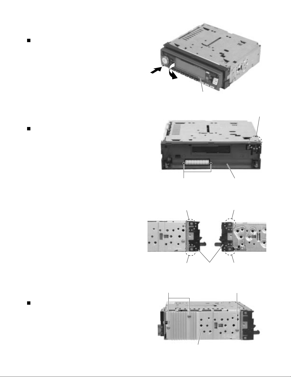
Removing the front panel unit
(See Fig.1)
1.
Press the release switch and remove the front panel
unit in the direction of the arrow.
Removing the front chassis (See Fig.2~3)
1.
Remove the two screws A attaching the front chassis.
KS-FX8R
Front panel unit
Fig.1
Joint c
2.
Insert a screwdriver to the two joints a on the left
side of the front chassis, two joints b on the right side
and one joint c from upside, then detach the front
chassis toward the front side.
B
A
Joint a
Joint a
Fig.2
Front chassis
Fig. 3
Front chassis
Joint b
Joint b
B
Removing the heat sink (See Fig.4)
1.
Remove the three screws B attaching the heat sink
on the left side of the body, and remove the heat
sink.
Heat sink
Fig. 4
1-3
Page 4

KS-FX8R
Removing the bottom cover (See Fig.5)
Prior to performing the following procedure, remove
the front chassis and the heat sink.
1.
Turn the body upside down.
2.
Insert a screwdriver to the two joints d and two joints
e on both sides of the body and the joint f on the
back of the body, then detach the bottom cover from
the body.
Removing the rear panel (See Fig.6 )
Prior to performing the following procedure, remove
the front chassis, the heat sink and bottom cover.
Joints d
Bottom cover
Joints e
Joint f
Fig. 5
D
1.
Remove the five screws C attaching the rear panel
and one screw D attaching the pine jack on the back
of the body.
C
Rear panel
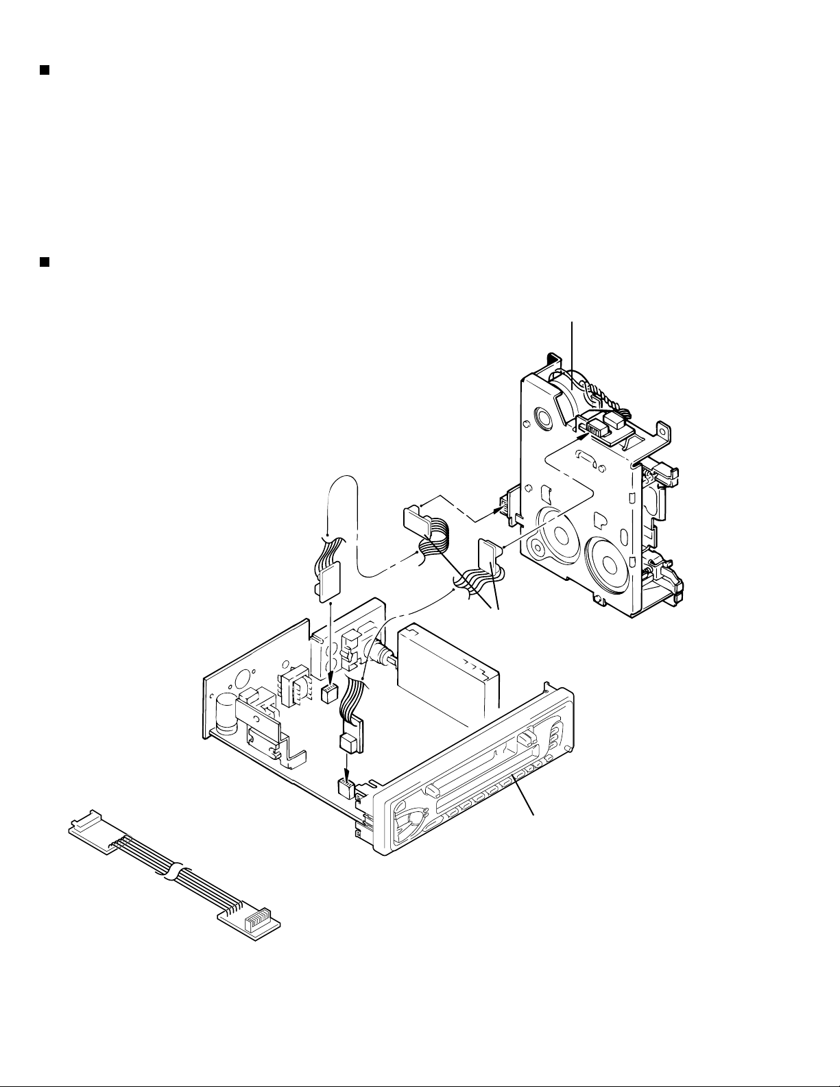
Removing the main amplifier board assembly
(See Fig.7)
Prior to performing the following procedure, remove
the front chassis, the heat sink, bottom cover and the
rear panel.
1.
Remove the two screws E attaching the main
amplifier board assembly on the top cover.
C
C
Fig. 6
CP401
2.
Disconnect connector CP401 on the main amplifier
board assembly from the cassette mechanism
assembly.
1-4
E
E
Main board assembly
Fig. 7
Page 5
Removing the cassette mechanism assembly
(See Fig.8)
Prior to performing the following procedure, remove
the front chassis, the heat sink, bottom cover and the
main amplifier board assembly.
1.
Remove the four screws F attaching the cassette
mechanism assembly from the top cover.
Cassette mechanism assembly
F
KS-FX8R
F
Removing the (LCD & key) control switch
board (See Fig.9 and 10 )
1.
Remove the front panel unit from the main body.
2.
Remove the five screws G attaching the rear cover
on the back of the front panel unit.
3.
Remove the control switch board from the front panel
unit.
F
Fig. 8
G
G
LCD & Key control board
Fig. 9
F
Top cover
G
G
Fig. 10
1-5
Page 6
KS-FX8R
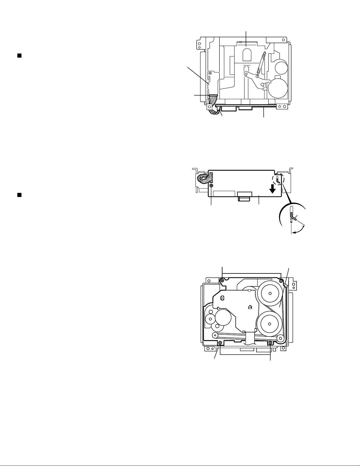
<Removal of the cassette mechanism>
Cassette mechanism ass’y
Removing the head amplifier board.
(See Fig.1 and 2)
1.
For the 6pin wire extending from connector CN402
on the head amplifier board, disconnect it from the
head relay board.
2.
Disconnect the card wire from connector CN403 on
the head amplifier board.
3.
Remove the screw A attaching the head amplifier
board.
4.
Move the tab a as shown in Fig.2 and remove the
head amplifier board while moving it in the direction
of the arrow.
Removing the cassette mechanism
assembly (See Fig.1 to 3)
1.
Disconnect the 6pin wire from connector CN402 and
the card wire from CN403 on the head amplifier
board (Refer to Fig.1 and 2).
Head relay
board
6pin
wire
CN402
A
CN403
CN402
Fig.1
CN403
Head amplifier board
Fig.2
Head amplifier board
Tab a
2.
Remove the four screws B on the bottom of the
cassette mechanism.
Head amplifier board
B
Cassette mechanism ass’y
B
Fig.3
1-6
Page 7

KS-FX8R
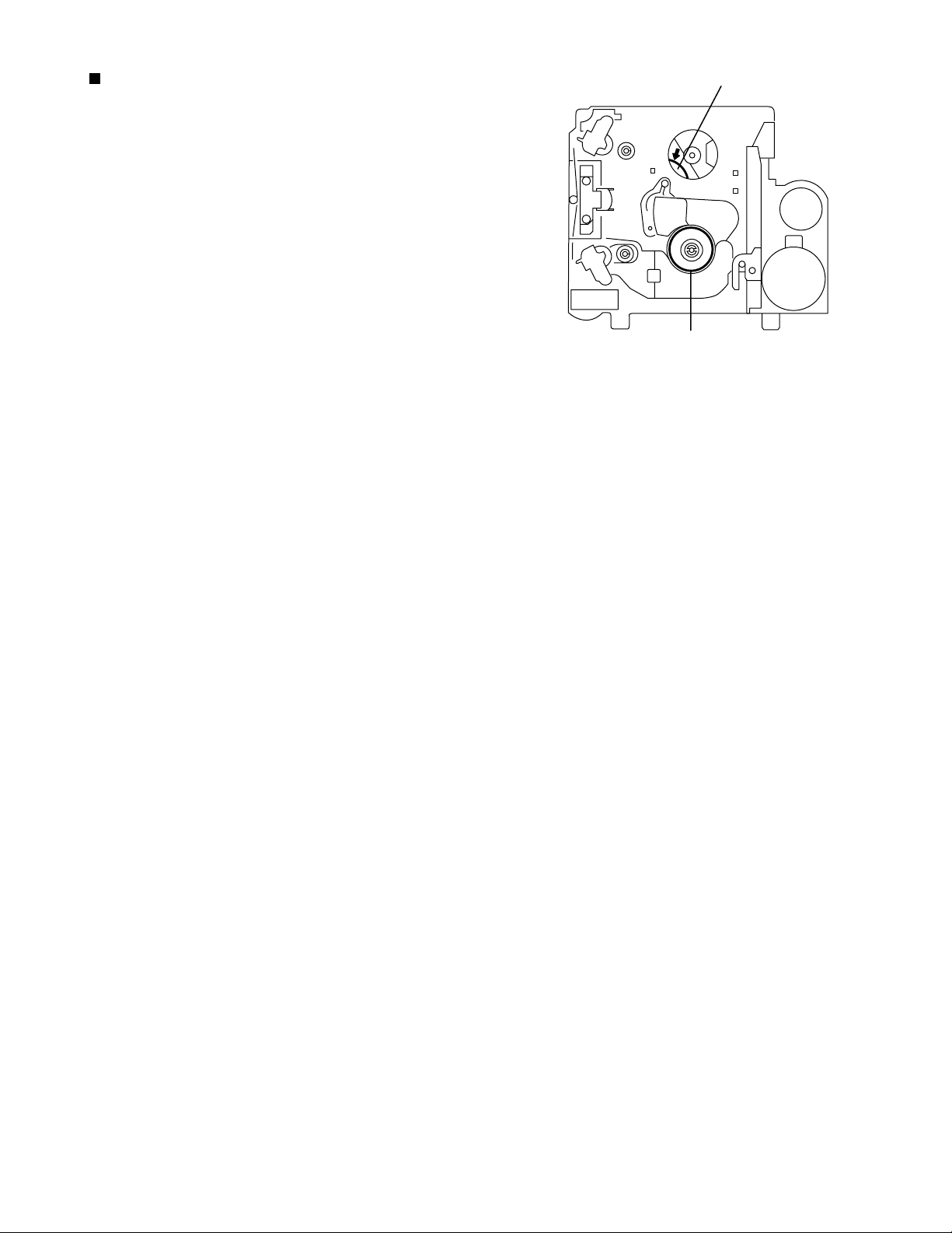
Removing the head relay board
(See Fig.4)
Unsolder the soldering b on the head relay board.
Remove the screw C attaching the head relay board.
Remove the head relay board in the direction of the
arrow while releasing the two joints c.
Removing the load arm (See Fig.5)
Remove the E washer attaching the load arm using
a pincette or something like that and remove the
spring d.
Move the part of the load arm marked upwards to
release it from the axis of rotation. Then rotate the
load arm in the direction of the arrow to remove it
from the cach.
Fig.4
Cach
Load arm
Fig.5
Head relay board
Soldering b
C
E washer
Joint c
Spring d
Removing the sub chassis (See Fig.6)
Prior to performing the following procedure, remove
the head relay board.
Remove the screw D attaching the sub chassis.
Push the tab e in the direction of the arrow to detach
the one side of the sub chassis. Then release the
sub chassis from the tab f.
Removing the cassette holder and the
holder arm in the eject mode
(See Fig.7 and 8)
Prior to performing the following procedure, remove
the head relay board, the load arm and the sub
chassis.
Remove the screw E attaching the reinforce bracket.
Remove the reinforce bracket.
Tab f
Sub chassis
Head relay
board
D
Cassette mecha chassis
Cassette holder
Fig.6
Head relay board
Tab e
Reinforce bracket
E
Reinforce
bracket
tab g
Push the tab g fixing the cassette holder in the
direction of the arrow and open the cassette holder
and the holder arm upward until they stop at an
angle of 45 degrees. Move the two joints h to the
side and remove the cassette holder and the holder
arm from the shaft.
Joint h
Load arm
Holder arm
Fig.7
Joint h
1-7
Page 8

KS-FX8R
Removing the flywheel
(See Fig.10 and 12)
1.
Prior to performing the following procedure, remove
the head relay board, the load arm, the sub chassis,
the cassette holder, the holder arm and the reel disc
board.
2.
Remove the belt on the bottom of the cassette
mechanism ass’y.
3.
Remove the slit washer attaching the flywheel on the
upper side of the cassette mechanism ass’y and pull
out the flywheel downward. Then remove another
flywheel in the same way.
ATTENTION:
When reassembling, make sure to use
a new slit washer.
Removing the reel disc ass’y( I )
(See Fig.12 to 14)
Soldering j
G
Motor
Plate
Reel disc board
G
Slit washer
Tab k
Tab o
Cassette mechanism ass’y
Tab k
Belt
Fig.10
Reel driver
The part n
Tabs o
Flyhwheel
Reel disc
ass’y( I )
Push aside
the gear
Prior to performing the following procedure, remove
the head relay board, the load arm, the sub chassis,
the cassette holder and the holder arm.
Disengage the part n inside of the reel driver which
engages with the shaft, using a pincette or
something like that. Then remove the reel driver from
the shaft.
Remove the reel driver spring and the reel table.
The part n
Slit washer
Shaft
Fig.13
The part n
Reel driver
Fig.12
Reel driver
Reel driver spring
Reel disc ass’y( II )
1-8
Reel table
Fig.14
Page 9
KS-FX8R
Removing the reel disc ass’y( II )
(See Fig.12 to 15)
ATTENTION:
1.
Release the plate from the three tabs o.
2.
Push aside the gear over the reel table using a
pincette or something like that.
3.
Remove the reel disc ass’y ( II ) as with the reel disc
ass’y ( I ).
ATTENTION:
Prior to performing the following
procedure, remove the reel disc ( I ).
Do not break the front panel tab fitted
to the metal cover.
Push aside the gear and reattach the reel disc Ass’y( I ).
Reel disc ass’y( II )
Fig.15
1-9
Page 10

KS-FX8R
Adjustment method
Test Instruments reqired for adjustment
1. Digital osclloscope(100MHz)
2. Frequency Counter meter
3. Electric voltmeter
4. Wow & flutter meter
5. Test Tapes
VT724 ....................... for DOLBY level measurement
VT739 ............ For playback frequency measurement
VT712 ....For wow flutter & tape speed measurement
VT703 ..................... For head azimuth measurement
6. Torque gauge .................... Cassette type for CTG-N
(mechanism adjustment)
Measuring conditions(Amplifier section)
Power supply voltage .............. DC14.4V (10.5 - 16V)
Load impedance ........... 4 (2Speakers connection)
Line out............................................................ 20k
Standard volume position
Balance and Bass,Treble volume .Fader
:Center(Indication"0")
Loudness,Dolby NR,Sound,Cruise:Off
Volume position is about 2V at speaker output with
following conditions.Playback the test tape VT721.
AM mode 999kHz/62dB,INT/400Hz,30%
modulation signal on recieving.
FM mono mode 97.9MHz/66dB,INT/400Hz,22.5kHz
deviation pilot off mono
FM stereo mode 1kHz,67.5kHz dev. pilot7.5kHz dev.
Output level 0dB(1 V,50 /open terminal)
1-10
Page 11

Arrangement of adjusting & test points
Cassette mechanism
(Surface)
Motor assembly
Tape speed adjust
KS-FX8R
Playback head
Head section view
Azimuth screw
Head azimuth screw
Fixed screw
Playback head
Height adjusting screw c
Height adjusting screw b
Height adjusting screw a
1-11
Page 12
KS-FX8R
Information for using a car audio service jig
1. For 1995 and 1996 , we're advancing efforts to make our extension cords common for all car audio products.
Please use this type of extension cord as follows.
2. As a U-shape type top cover is employed, this type of extension cord is needed to check operation of the
mechanism assembly after disassembly.
3. Extension cord : EXTKSRT002-6P ( 6 pin extension cord ) For connection between mechanism assembly
and main board assembly.
Check for mechanism driving section such as motor ,etc..
Disassembly method
1. Remove the bottom cover.
2. Remove the front panel assembly.
3. Remove the top cover .
4. Install the front panel.
5. Confirm that current is being carried by connecting
an extension cord jig.
Note
Available to connect to the CN701 connector when installing the front panel.
Cassette mechanism
EXTKSRT002-6P
Extension cord
: EXTKSRT002-6P
Main board
Front panel assembly
1-12
Page 13
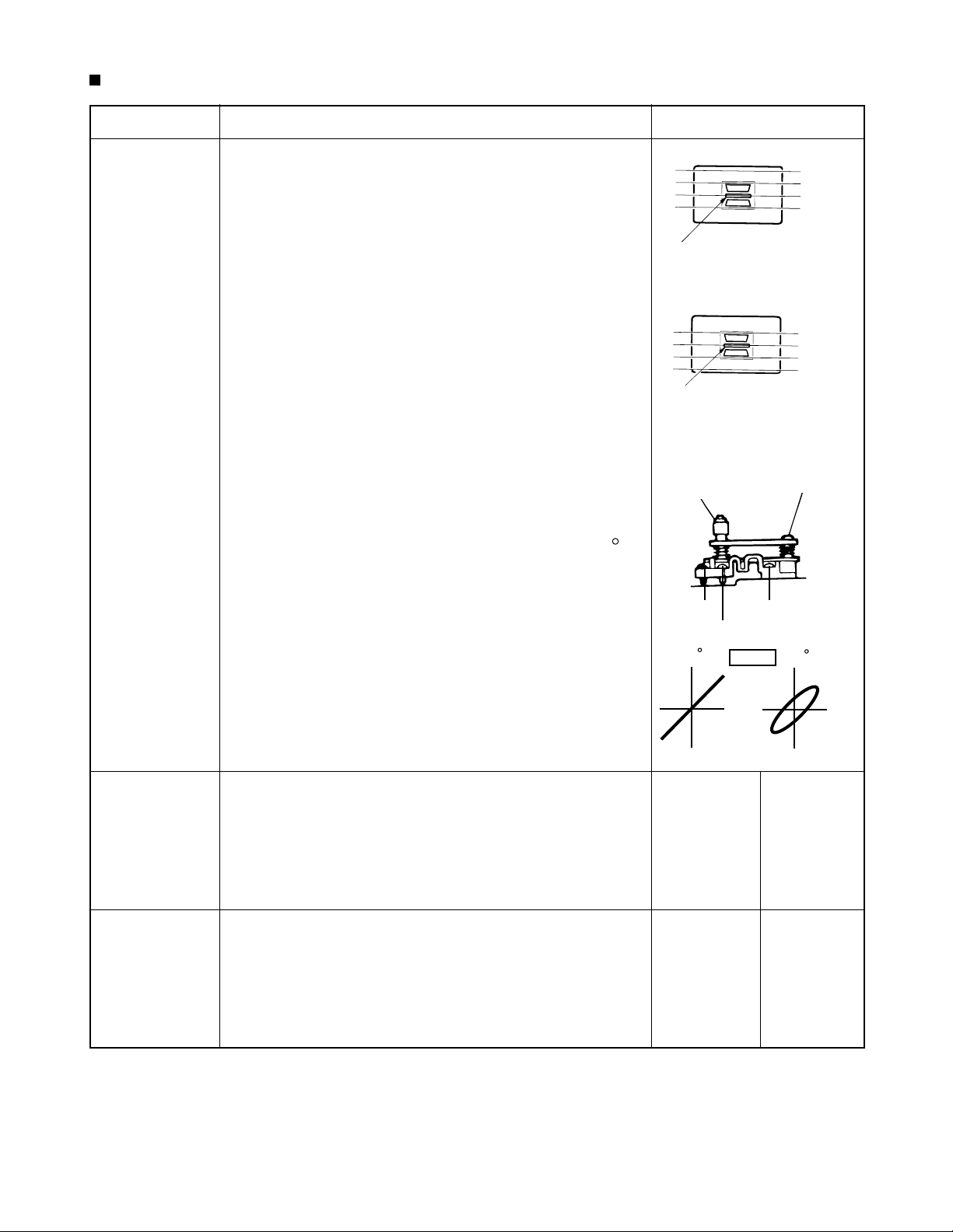
Mechanism adjustment section
Item Adjusting & Confirmation Methods Adjust Std. Value
1.Head azimuth
"Head Height Adjustment"
Note
Adjust the azimuth directly. When you adjust the height using a mirror tape, remove the cassette housing from the
mechanism chassis.
After installing the cassette housing, perform the azimuth
adjustment.
1.load the mirror tape ( SCC-1659 ). Adjust with height
adjustmentscrew (a) and azimuth adjustment screw (b) so
that line "A" of the mirror tape runs in the center between
Lch and Rch in the reverse play mode.
2.After switching from REV to FWD then to REV, check that
the head position set in procedure "1" is not changed.
*If the position has shifted, adjust again and check.
3.Adjust the azimuth screw (b) so that line "B" of the mirror
tape runs in the center between Lch and Rch in the forward
play mode.
"Head Azimuth Adjustment"
1.Load the test tape ( VT724: 1kHz ) and play it back in the
reverse play mode. set the Rch output level to maximum.
2.Load the test tape ( VT703: 10kHz ) and play it back in the
forward play mode. Adjust the Rch and Lch output levels
tomaximum, with azimuth adjustment screw (b).
In this case, the phase difference should be within 45 .
3.Engage the reverse mode and adjust the output level to
maximum, with azimuth adjustment screw (c).
*The phase difference should be 45_Kor more.
4.When switching between forward and reverse modes, the
difference between channels should be within 3dB.
*Between FWD Lch and Rch, REV Lch and Rch.
5.When the test tape ( VT721 : 315Hz ) is played back, the
level difference between channels should be within 1.5dB.
Head shield
The head is at low position
during FWD.
Head shield
The head is at height position
during REV.
Head azimuth
screw
screw (c)
screw (b)
0
Phase
KS-FX8R
A Line
B Line
Fixed screw
screw (a)
45
2.Tape Speed and
Wow & Flutter
3.Playback
Frequency
response
1.Check to see if the reading of the frequency counter & Wow
flutter meter is within 2940-3090 Hz( FWD/REV ), and less
than 0.35% ( JIS RMS ).
2.In case of out of specification, adjust the motor with a builtin volume resistor.
1.Play the test tape ( VT724 : 1kHz ) back and set the volume
position at 2V.
2.Play the test tape ( VT739 )back and confirm 0 + 3dB at1kHz/
-
8kHz and -4+2dB at 1kHz/125Hz.
3.When 8kHz is out of specification, it will be necessary to
read adjust the azimuth.
Built-in
volume resistor
Tape Speed
2940-3090Hz
Wow&Flutter
Less than
0.35%
(JIS RMS)
Speaker out
1kHz/8kHz
: 0dB_}3dB,
125Hz/1kHz
: -4dB+2dB,
1-13
Page 14
KS-FX8R
Description of major ICs
UPD178018AGC-551 (IC701) : Main system control CPU
1. Pin layout
80 ~ 61
1
60
2. Pin function
Pin No.
1
2
3
4
5
6
7
8
9
10
11
12
13
14
15
16
17
18
19
20
21
22
23
24
25
26
27
28
29
30
31
32
33
34
35
36
37
38
39
40
~
20
21 ~ 40
~
41
Port Name I/O Descriptions
KEY 0
KEY 1
KEY 2
LEVEL
SM
SQ
LCDCE
LCDDA
LCDSCK
BUSI/O
UNLOCK
BUSSI
BUSSO
BUSSCK
NC
NC
NC
NC
NC
NC
GNDPORT
VDDPORT
AM
AFCK
MONO
FM
SEEK/STP
NC
IFC
VDDPLL
FMOSC
AMOSC
GNDPLL
AMEO
FMEO
IC
SD/ST
STAGE0
NC
F/R
O
O
O
O
I/O
O
O
O
O
O
O
O
O
I
I
I
I
I
I
Key input 0
Key input 1
Key input 2
Level meter input
S.meter level input
S.Quality level input
CE output to LCD driver
Data output to LCD driver
Clock output to LCD driver
I
I
I/O selector output for J-BUS, H : OUT, L: INPUT
Non connect
J-BUS Data input
J-BUS Data output
J-BUS Clock in/output
-
-
-
-
-
-
-
-
Non connect
Non connect
Non connect
Non connect
Non connect
Non connect
Port GND
Port Vdd
Non connect
AF check output, L: AF check
Monaural on /off selecting output, H:mono on
FM/AM switching output L : FM H : AM
Auto seek /stop selecting output, H: Seek, L:Stop
I
I
I
-
-
Pulse signal input port for Cruise control
FM/AM midle frequency counter input
PLL Vdd
FM/AM limited generator frequency input
None connect
PLL GND
AM error out output
FM error out output
I
I
-
GND
Station detector, Stereo signal input, H:Find Station, L:Stereo
Pull up
Non connect
Main motor output
1-14
Page 15

KS-FX8R
Pin No.
41
42
43
44
45
46
47
48
49
50
51
52
53
54
55
56
57
58
59
60
61
62
63
64
65
66
67
68
69
70
71
72
73
74
75
76
77
78
79
80
Port Name I/O Descriptions
O
O
O
O
O
O
-
-
I
I
-
-
-
-
-
-
-
-
-
-
-
-
-
-
-
-
I
I
I
I
I
I
-
-
I
-
-
-
Non connect
Non connect
Telephone mute signal detection input
TAPE input
I2C information clock output
I2C information data output
I2C information clock input
Non connect
Non connect
Non connect
Non connect
Non connect
Non connect
Non connect
Non connect
Non connect
Non connect
Non connect
Non connect
Mute output
Power ON /OFF switching output , H : power on
Non connect
Non connect
Non connect
Non connect
Non connect
CPU power supply
STOP signal output terminal
Clock input for RDS
RDS data input
Remocom input
Detach signal input H : Power save
Cut-in input for J-BUS signal
Regulator for CPU power supply, Connect the GND with0.1 F.
Ground
Connecting the crystal oscillator for system clock
Connecting the crystal oscillator for system clock
Regulator for oscillator circuit.Connect the GND with 0.1 F.
Vdd
Pull up
NC
NC
TELMUTE
TAPEIN
I2CCLK
I2CDAO
I2CDAI
NC
NC
NC
NC
NC
NC
NC
TAPE
TUNER
CD
NC
NC
MUTE
POWER
NC
NC
NC
NC
NC
ON
STOP
RDSCK
RDSDA
REMOCON
DETACH
BUSINT
REGCPU
GND
X2
X1
REGOSC
VDD
RESET
1-15
Page 16

KS-FX8R
BA4905-V3 (IC901) : Regulator
1.Pin layout
12 34 56 78 9101112
2.Block diagram
REGULATOR
EXT
OIVPC
RESET
1 2 3 4 5 6 7 8 9 10 11 12
RESET COMP VDD 5.7V CD 8V VCC AJ
EXT ACC AUDIO 9V CTRL ILM 10V GND
37K
5K
1-16
Page 17

KS-FX8R
3.Pin function
1
2
2
4
5
6
7
8
9
RESET
EXT output
COMP output
ACC
VDD output
AUDIO output
CD output
CTRL
VCC
BA4905-V3
If VDD voltage becomes 4V or less, RESET output becomes low level.
This outout voltage is approximately 0.5V lower than VCC, and max
output current is 300mA.
A voltage supply for ACC block this outout voltage is approximately
0.7V lower than VDD'S. The max output current is 100mA.
Control of the COMP output by inputting voltage.
This output voltage is 5.7V, and max output current is 100mA.
This voltage supply is for microcomputer. Whenever block up voltage
supply is connected. the output keeps on running.
This output voltage is 9.0V, and max output current is 500mA.
This voltage supply for AUDIO.
This output voltage is 8.0V, and max output current is 1A.
This voltage supply for CD.
Output selector of CD, AUDIO,ILM and EXT.
To be connected with the BACK UP of car.
10
11
12
ILM output
AJ
GND
LB1641 (IC402) : DC motor driver
1. Pin layout
1 2 3 4 5 6 7 8 9
GND OUT1 P1
2. Pin function
VZ IN1 IN2
VCC1
VCC2 P2
This output voltage is 10V, and max output current is 500mA.
Output voltage is adjustable.
Putting a resistance between ILM and AJ or between AJ and GND
makes ILM output voltage adjustable.
Ground.
10
OUT2
Input Output
IN1 IN2 OUT1 OUT2
0 0 0 0
1 0 1 0
0 1 0 1
1 1 0 0
Mode
Brake
CLOCKWISE
COUNTER-CLOCKWISE
Brake
1-17
Page 18

KS-FX8R
CXA2560Q (IC401) : Dolby B type noise reduction system with play back equalizer amp.
1.Pin layout & block diagram
PBTC2
30 29 28
7k/12k
31
PBFB2
32
PBRIN2
PBGND
PBFIN2
VCT
PBREF
PBFIN1
PBGND
PBRIN1
PBFB1
2. Pin function
300k
33
F2
34
30k
35
45k
36
30k
37
F1
38
300k
39
7k/12k
40
12345
PBTC1
PBOUT2
+
+
-
PBOUT1
OUTREF2
27
70 /120
70 /120
OUTREF1
TAPEIN2
100k
1
1
100k
TAPEIN1
GND
26
25
T2
LPF
T1
Vcc
+
BIAS
MUTE
TAPE EQ
FWD/RVS
Vcc
+
-
6
NC
23 22 21
24
OFF/B
-
F3
OFF/B
-
+
8910
7
LINEOUT1
NR
NR
TCH1
MS MODE
NR MODE
MS ON/
OFF
DET
NC
MSSW
MSLPF
20
19
18
17
16
15
14
13
12
11
MSMODE
DRSW
TAPESW
MUTESW
NRSW
NC
MSOUT
MSTC
G1FB
G2FB
TCH2
NC
LINEOUT2
DIREF
Pin No. Symbol
1
2
3
4
5
6
7
8
9
10
11
12
13
14
15
16
17
18
19
20
21
22
23
24
PBTC1
PBOUT1
OUTREF1
TAPEIN1
Vcc
NC
LINEOUT1
TCH1
NC
MSLPF
G2FB
G1FB
MSTC
MSOUT
NC
NRSW
MUTESW
TAPESW
DRSW
MSMODE
MSSW
NC
TCH2
LINEOUT2
I/O Function
Playback equalizer amplifier
capacitance
Playback equalizer amplifier
O
output
Output reference
O
TAPE input
I
Power supply
-
Line output
O
Time constant for the HLS
-
Cut-off frequency adjustment
of the music sensor LPF
Music signal interval detection
Music signal interval detection
Time constant for detecting
music signal interval
Music sensor out
O
No use
Dolby NR control
I
Mute function control
I
Playback equalizer amplifier
I
control
Head select control
I
Music sensor mode control
I
Music sensor control
I
Time constant for the HLS
Line output
O
Pin No. Symbol
25
26
27
28
29
30
31
32
33
34
35
36
37
38
39
40
DIREF
GND
TAPEIN2
OUTREF2
PBOUT2
PBTC2
PBFB2
PBRIN2
PBGND
PBFIN2
VCT
PBREF
PBFIN1
PBGND
PBRIN1
PBFB1
I/O Function
-
Resistance for setting the
reference
-
Ground
I
TAPE input
O
Output reference
O
Playback equalizer amplifier
output
-
Playback equalizer amplifier
capacitance
I
Playback equalizer amplifier
feedback
I
Playback equalizer amplifier
input
-
Playback equalizer amplifier
ground
I
Playback equalizer amplifier
input
O
Center
O
Playback equalizer amplifier
reference
I
Playback equalizer amplifier
input
-
Playback equalizer amplifier
ground
I
Playback equalizer amplifier
input
I
Playback equalizer amplifier
feedback
1-18
Page 19

HA13158A (IC301) : Power amp
1. Pin layout
1 ~ 23
2. Block diagram
14 18 6
INVCC
INPUTBUFFER1
IN1
2
STBY
1
PVCC1PVCC2
AMP1
KS-FX8R
3
+
4
-
5
IN2
IN3
IN4
11
13
23
10
MUTE
INPUTBUFFER2
INPUTBUFFER3
INPUTBUFFER4
PROTECTOR (ASO
SURGE, TSD)
12 22
AMP2
AMP3
AMP4
TA B
7
+
8
-
9
15
+
16
-
17
19
+
20
-
21
1-19
Page 20

KS-FX8R
HD74HC126FP-X (IC801) : Buffer
1.Pin layout
1
2
3
4
5
6
7
3.Block diagram
14
13
12
11
10
9
8
Vcc Vcc
1A
2A
3A
Input
4A
1C
2C
3C
See Function Table
4C
2.Pin function
Output
1Y
2Y
Output
2Y
Output
3Y
Output
4Y
Input Outout
C
A
L
X
H
L
H
H
Y
Z
H
L
1k
S1
CL
1k
Sample as Load Circuit 1
Sample as Load Circuit 1
Sample as Load Circuit 1
1-20
Page 21

LC75873NW (IC601) : LCD driver
1.Block Diagram
COM3
COM2
COM1
S68
S67
S5
S4/P4
S3/P3
S2/P2
S1/P1
KS-FX8R
VDD1
VDD2
INH
OSC
VDD
VSS
COMMOM
DRIVER
CLOCK
GENERATOR
SEGMENT DRIVER
SHIFT REGISTER
ADDRESS
DETECTOR
2.Pin Functions
Pin No. Symbol Description
1~66
67~69
70
71
S3~S68
COM1~3
VDD
VDD1
I/O
Segment Output.
O
Common Driver Output.
O
Power Supply Connection.
Used for applying the LCD drive 2/3 bias voltage externally.
I
Must be connected to VDD2 when a 1/2 bias drive scheme in used.
72
VDD2
Used for applying the LCD drive 1/3 bias voltage externally.
I
Must be connected to VDD1 when a 1/2 bias drive scheme in used.
73
74
VSS
OSC
Power supply connection.
Oscillator connection. An oscillator circuit is formed by connecting an
I/O
external resistor and capacitor to this pin.
75
76
77
78
79
80
INH
CE
CLOCK
DI
DIMMER
NC
Display off control input.
I
Chip enable input.
I
Synchronization clock input.
I
Serial data input.
I
DIMMER Control signal output.
O
Non connect.
-
1-21
Page 22

KS-FX8R
SAA6579T-X(IC71):RDS detector
1.Terminal Layout
QUAL
RDDA
MUX
VDDA
GND
SCOUT
Vref
CIN
1
2
3
4
5
6
7
8
16
15
14
13
12
11
10
9
RDCL
T75
OSCO
OSC1
VDD
GND
TEST
MODE
2.Pin Function
Pin
No.
1
2
3
4
5
6
7
8
9
10
11
12
13
14
15
16
QUAL
RDDA
Vref
MUX
VDDA
GND
CIN
SCOUT
MODE
TEST
GND
VDD
OSC1
OSC0
T75
RDCL
FunctionI/OSymbol
Non connect
RDS data output
O
Reference voltage output
O
Multiplex signal input
I
+5V Supply voltage for analog
Ground for analog part (0V)
Sub carrier output of reconstruction filter
I
Ground for digital part (0V)
O
Ground for digital part (0V)
Ground for digital part (0V)
Ground for digital part (0V)
+5V supply voltage for digital part
Oscillator input
I
Oscillator output
O
Non connect
RDS clock output
O
3.Block Diagram
4
8
7
5
3
ANI-
ALLUDING
FILTER
CLOCKED
COMPARATOR
REFERENCE
VOLTAGE
1413
5kHz
BAND PASS
(8th ORDER)
COSTAS LOOP
VARIABLE AND
FIXWD DIVIDER
CLOCK
REGENERATION
AND SYNC
6
RECONSTRUCTION
FILTER
BIPHASE
DECODER
TEST LOGIC AND OUTPUT
OSCILLATOR
AND
DIVIDER
SYMBOL
SELECTOR SWITCH
9
10
12
DUALITY BIT
GENERATOR
DIFFERENTIAL
DECODER
11
1
2
16
15
1-22
Page 23

TEA6320T-X (IC161) : E.volume
KS-FX8R
1.Pin layout
SDA
1
GND
2
OUTLR
OUTLF
MUTE
TL
B2L
B1L
IVL
ILL
QSL
IDL
ICL
IMD
IBL
IAL
3
4
5
6
7
8
9
10
11
12
13
14
15
16
3.Pin functions
CD-CH
TAPE
TUNER
32
31
30
29
28
27
26
25
24
23
22
21
20
19
18
17
SCL
VCC
OUTRR
OUTRF
TR
B2R
B1R
IVR
ILR
QSR
IDR
Vref
ICR
CAP
IBR
IAR
2.Block diagram
10 8 9 7 6
21
31
2
19
16
15
13
11
14
22
20
18
17
POWER
SUPPLY
SOURCE
SELECTOR
23 25 24 26 27 28
VOLUME 1
+20 to -31 dB
LOUDNESS
LEFT
VOLUME 1
+20 to -31 dB
LOUDNESS
RIGHT
BASS
LEFT
+15 dB
LOGIC
BASS
RIGHT
+15 dB
5
TREBLE
LEFT
+12 dB
TREBLE
RIGHT
+12 dB
12
MUTE
FUNCTION
ZERO CROSS
DETECTOR
VOLUME 2
0 to 55 dB
BALANCE
FENDER REAR
VOLUME 2
0 to 55 dB
BALANCE
FENDER FRONT
HC BUS
REC
VOLUME 2
0 to -55dB
BALANCE
FENDER FRONT
VOLUME 2
0 to -55dB
BALANCE
FENDER REAR
3
4
32
1
29
30
Pin
No.
1
2
3
4
5
6
7
8
9
10
11
12
13
Symbol
SDA
GND
OUTLR
OUTLF
TL
B2L
B1L
IVL
ILL
QSL
IDL
MUTE
ICL
I/O
Serial data input/output.
I/O
Ground.
-
output left rear.
O
output left front.
O
Treble control capacitor left channel or
I
input from an external equalizer.
Bass control capacitor left channel or
-
output to an external equalizer.
Bass control capacitor left channel.
-
Input volume 1. left control part.
I
Input loudness. left control part.
I
Output source selector. left channel.
O
Not used
-
Not used
-
Input C left source.
I
Functions Functions
Pin
No.
17
18
19
20
21
22
23
24
25
26
27
28
29
Symbol
IAR
IBR
CAP
ICR
Vref
IDR
QSR
ILR
IVR
B1R
B2R
TR
OUTRF
I/O
I
Input A right source.
I
Input B right source.
-
Electronic filtering for supply.
I
Input C right source.
-
Reference voltage (0.5Vcc)
-
Not used
O
Output source selector right channel.
I
Input loudness right channel.
I
Input volume 1. right control part.
-
Bass control capacitor right channel
Bass control capacitor right channel or
O
output to an external equalizer.
Treble control capacitor right channel or
I
input from an external equalizer.
O
Output right front.
14
15
16
IMO
IBL
IAL
Not used
-
Input B left source.
I
Input A left source.
I
30
31
32
OUTRR
Vcc
SCL
O
Output right rear.
-
Supply voltage.
I
Serial clock input.
1-23
Page 24

KS-FX8R
VICTOR COMPANY OF JAPAN, LIMITED
MOBILE ELECTRONICS DIVISION
PERSONAL & MOBILE NETWORK BUSINESS UNIT. 10-1,1Chome,Ohwatari-machi,Maebashi-city,Japan
(No.49850)
Printed in Japan
200101(O)
Page 25

Block diagram
FLOUT
FROUT
IC941
RLOUT
RROUT
KS-FX8R
REARL
REARR
J9301
LINE OUTPUT
TU_L,TU_R
TU1
TUNER PACK
MUX
POWER AMP.
FL,FR
RL,RR
IC911
E.VOLUME
RDS
IC761
SK/ST
DETECTOR
CH_L
CH_R
SM
MONO
RDSDA
RDSCK
SD/ST
SEEK/STOP
SCL
AFCK
FMEO
FMOSC
J751
SDA
AMEO
IC701
FM/AM
CPU
JBUSSI
JBUSSO
SCK
JBUSIO
SI/SO
JBUSSCK
IC751
JVC BUS
TAPE-L,TAPE-R
F/R
TAPEIN
CN901CN902
CP902
CJ902
MOTOR
MUTE SW
T-MUTE
MOTOR
IC901
HEAD AMP
L-CH
R-CH
PB
HEAD
CN901
CJ901
S8~S52
LCD
LCDCE
LCDCL
LCDDA
COM1~COM3
LCD
IC651
DRIVER
ENC1,ENC2,KEY0,KEY1,KEY2
LCDCE,LCDDA,LCDCK,REMOCON
CJ601
CN601
KEY0
~KEY2
KEY SWITCH
2-1
Page 26

KS-FX8R
< MEMO >
2-2
Page 27

Standard schematic diagrams
g
Main amp section
Main amp section
KS-FX8R
6
5
4
3
2
Parts are safety assurance parts.
When replacing those parts make
sure to use the specified one.
TUNER SIGNAL
1
BC
DE
F
G
TAPE SIGNAL
CD-CH SIGNAL
FRONT SIGNAL
REAR SIGNAL
HA
I
2-3
Page 28

LCD & Key control section
6
5
KS-FX8R KS-FX8R
4
3
2
1
BC
DE
2-4
F
G
HA
I
Page 29

Mecha control & Head amp section
6
5
KS-FX8R
4
3
2
1
BC
DE
F
G
HA
TAPE SIGNAL
I
2-5
Page 30

Printed circuit boards
KS-FX8R KS-FX8R
Printed circuit boards
Main board
T03
R11
C51
R54
C52
C53
R56
Q51
FSMW1091A
B906
B907
B908
R57
Q52
J321
C321
RL
R341
J1
L1
D5
B901
C33
D6
C3
10
C2
C8
C81
B910
Q53
C710
Q341
R342
R352
R322
R343
R353
TU1
C32
1
R32
R34
Q32
D3
Q3
R12
C82
C9
15
C43
C6
B911
R81
C84
20
C5
B803
R53
R84
R721
R55
C54
Q9
C4
B952
R58
B954
R60
C71
R59
C7
R722
S702
C55
R8
B814
FL
R351
R321
C322
Q321
Q351
R331R332
Q331
R323
D322
C31
R33
R31
B801
C41
R41
Q31
R5
B902
D2
R9
R83
R82
Q4
C74
C75
R333
D1
R43
C1
R1
R42
C42
Q42
Q41
R2
R44
B905
R4
B928
B904
Q7
R711
C244
C83
C714
C162
B919
Q6
B920
B916
R10
B915
Q10
Q5
R716
D4
B805
B912
Q8
C73
R810
C77
C72
R73
IC71
X71
C76
6
5
4
3
2
1
3
J801
7
8
4
5
6
2
C906
1
CP401
B802
R748
D321
R6
Q1
R3
Q2
R713
B914
R732
R71
R717
R805
B813
R742
R735
R745
R743
R734
R746
B903
C702
B926
C703
B925
R741
B923
B922
B921
B917
R714
B913
B941
B942
B808
1
R804
R803
B809
16
R801
R808
C161
C712
B924
R712
C701
1
B940
B811
B943
R802
B810
IC801
R904
L-CH
TP01
R-CH
C167
R740
C706
R729
R72
R809
1
14
C705
PL701
R905
R162
Q701
R164
TP02
R161
C163
B929
C713
R172
R707
B932
R173
R708
IC701
C708
R730
C707
X701
C704
R715
R807
C801
R806
1
IC901
C905
C904
B927
R907
C907
R163
C164
C166
C165
C168
B931
IC161
C242
R247
D241
R246
B938
B939
B816
B955
L901
R902
R903
D901
R901
C982
Q902
C901
C908
R245
B807
R728
R169
R165
C169
Q241
R727
D705
D704
R702 R703
Q891
C902
C173
C172
C174
C176
C183
B806
C181
B930
1
R166
C241
B933
R747
R738
R726
D706
R718
R906
Q901
R167
R168
B815
R170
D242
D161
R241
C243
R739
D710
R744
R701
C881
D982
C891
9
B817
D891
R302
R303
C303
C882
Q881
C319
B818
R892
R312
R891
C178
C182
C184
R171
B934
C179
C170
C171
C175
C180
R242
R243
R736
R244
R881
B935
B944
R733
R737
B937
B936
R719
R720
D708
D707
R725
R724
R882
CP901
1
5
13
C309
R306
B951
B949
Q903
C177
B946
Q781
R782
D709
R706
3
2
7
C981
C910
14
15
10
11
C314
C313
R314
C318
B819
R308
R309
B820
R909
B812
R908
Q904
Q976
R977
C781
R976
B945
D781
D783
C782
Q782
D782
R781
R704
R723
D702
D701
R705
C841
D703
1
CJ601
18
17
4
8
D981
C911
12
R313
R307
R311
R304
C304
C308
R301
B950
Q977
Q784
C903
Q841
19
16
D902
B948
R731
C709
C909
R841
BZ841
C315
IC301
C302
C305
2
1
C306
R305
C301
C307
R978
B947
L903
L902
C711
R842
S701
Front board (Foerward side)
D601
S614
D612
D611
EN601
S607
D602
D614
D604
D603
D624
IC602
D613
S615
D618
S616
D617
D615
S617
D616
S618
LCD1
D606
D605
S608
S619
Front board (Reverse side)
C602
R669
Q641
R645
R628
R611
R630
R644
D641
R646
R627
R603
T01
D642
R643
R642
D643
D656
D654
FSMW1081-001QX
Q642
C604
R671
R641
D652
D655
D653
C605
C603
R670
80
R656
R655
1
C601
Reel board
D621
S605
D641
D642D643
R607
D607
60
61
20
R608
S609 S610
41
40
IC601
21
D608
R609
R610
D609
S611
R606
R612
Main
D625
R623
D.Gnd
R658
C606
R657
Anode
R601
S602
R614
R616
CN601
1
D610
S601
S612
D651
R653
R654
R661
R662
R663
Sub
St.BY
D620
S01
R604
D619
S604
D626
D657
R613
R629
D627
R602
R615
R651
R622
D658
S613
D623
R605
D622
S606
S603
R620
R650
R652
R624
R625
R626
R621
Mecha control board
CA-IN
C418
B407
C425
R410
Q401
C424
B406
R401
D402
R416
C419
C422
C414
B408
C421
B403
C416
R420
Q403
R415
R417
C413
C423
D401
R426
VR402
B409
R425
R411
1
T02
R424
IC402
2
FSMW1093A
1
BC
B410
B413
B411
1
R412
11
R414
R418
R413
C417
21
C412
31
IC401
1
B402
C411
R423
B404
CJ403
2
B405
B412
VR401
C410
CJ401
R408
B401
C409
C405
R407
C406
C408
C402
R406
C407
R403
R405
C403
R402
1
1
CA-IN
3
C404
R404
R422
C401
2
Q402
Main:Main:+
Sub: Sub:+
ST-BY
CrO2
DE
F
G
Main+
MODE
Sub+
MODE
HA
Pho- T r
M
CrO2
J
I
2-6
Page 31

PARTS LIST
[ KS-FX8R ]
* All printed circuit boards and its assemblies are not available as service parts.
KS-FX8R
Area suffix
E ----------- Continental Europe
- Contents -
Exploded view of general assembly and parts list
Cassette mechanism assembly and parts list
Electrical parts list
Packing materials and accessories parts list
3- 2
3- 5
3-10
3-14
3-1
Page 32

KS-FX8R
Exploded view of general assembly and parts list
Block No.
13
73
72
72
M
M
1
M
13
12
71
74
68
A
70
67
69
14
10
20
34
21
35
36
33
28
23
15
Main board
B
18
14
8
32
12
22
29
24
17
31
16
57
30
27
25
26
56
57
55
75
Front board
19
57
9
65
62
63
59
64
60
66
LCD1
61
3-2
44
53
39
52
43
45
51
46
42
37
58
38
5
A
Mecha control
7
B
board
2
6
11
4
11
11
40
3
50
11
6
6
1
6
47
48
49
54
41
Page 33

Item Parts number Parts name Area
Parts list (General assembly)
M1MM
)
)
)
)
)
)
)
)
)
)
)
)
)
F.CHASSIS+CONECTER
A
1 --------------- CASETTE MECHA 1 CDS-801
2 FSYH4036-050 SPACER 1
3 FSKL2001-002 MECHA BRACKET(R
4 FSKL2002-001 MECHA BRACKET(L
5 QYSDST2606Z SCREW 1 PCB + MECHA
6 QYSDST2606Z SCREW 4 MECHA+M.BRACKET
7 FSJC1056-002 TOP CHASSIS 1
8 FSMH3001-202 SIDE PANEL 1
9 FSKM3011-002 BOTTOM COVER 1
10 FSMA3005-001 INSULATOR 1
11 QYSDST2604Z SCREW 4 CHASSIS+MECHA.BKT
12 FSKZ4005-001 SCREW 3
13 QYSDST2604Z SCREW 2 CHASSIS+REAR BKT
14 QYSDST2606Z SCREW 2 CHASSIS+MAIN PWB
15 QYSDSF2006M SCREW 2
16 FSJC1060-002 FRONT CHASSIS 1
17 VJK3707-001 LIGHT LENS 1
18 QYSPSGU1745N MINI SCREW 2 FOR LIGHT LENS
19 FSYH4036-057 SHEET 1
20 FSKS3014-001 OPEN LEVER 1
21 FSKS3015-001 LOCK LEVER(O.L
22 VKS3798-002 RELEASE LEVER 1
23 VKS3793-001 LOCK LEVER(TOP
24 VKS3794-003 LOCK LEVER(L
25 VKS3795-002 LOCK LEVER(R
26 VKS5563-001 GEAR 1
27 VKZ4786-002 OIL DAMPER 1
28 FSKW4012-002 T.SPRING 1 FOR L.LEVER(TOP
29 VKW5264-005 T.SPRING 1 FOR RELEASE LEVER
30 VKW5262-001 T.SPRING 1 FOR L.LEVER(R
31 QYSDSF2006M SCREW 1 DAMPER+L.LEVER(R
32 VKW5263-002 T.SPRING 1 FOR L.LEVER(L
33 VKZ4777-001 MINI SCREW 1 LOCK LEVER(O.L.
34 FSKW4013-002 T.SPRING 1 FOR OPEN LEVER
35 FSJC3014-001 CASSETTE LID 1 NO PRINTING
36 VKW4947-002 DOOR SPRING 1
37 FSJC1058-001 FRONT PANEL 1
38 FSJD3024-01M FINDER ASSY 1
39 FSXP2045-012 PRESET BUTTON 1 1-6 LASER CUT
40 FSYH4036-031 SHEET 1
41 FSXP3053-002 POWER BUTTON 1
42 FSXP2038-001 D.FUNC BUTTON 1
43 FSXP4006-001 SCM BUTTON 1
44 FSXP2041-003 PUSH BUTTON(L
45 FSXP3062-001 PUSH BUTTON(R
46 FSXP2043-001 UP DOWN BUTTON 1
47 FSXK3003-005 VOL.KNOB 1 JOG DIAL
48 FSXP3061-001 SEL BUTTON 1
Q'ty Description
1
1
1
1
1
1
CH,FM/AM,TAPE
1
DISP,TP,PTY
1
MO/RND,RPT
KS-FX8R
Block No.
3-3
Page 34

KS-FX8R
Parts list (General assembly)
Item Parts number Parts name Area
A
49 FSYH4036-032 SHEET 1
50 FSJK3027-001 RIM LENS 1 FOR KNOB
51 FSXP3058-001 EJECT BUTTON 1
52 VKW3001-330 COMP.SPRING 1 FOR EJECT BUTTON
53 FSXP3059-001 DETACH BUTTON 1
54 VKW3001-330 COMP.SPRING 1 FOR DETACH BUTTON
55 FSJC1059-001 REAR COVER 1
56 FSYH4036-035 SHEET 1 SLIDING SHEET
57 VKZ4777-001 MINI SCREW 5 FRONT+REAR
58 GE40112-001A LIGHT COVER 1
59 QNZ0449-001 RUBBER CONNECTOR 1
60 QNZ0450-001 RUBBER CONNECTOR 1
61 FSYH3024-001 LCD CASE 1
62 FSJK3028-001 LCD LENS 1
63 FSYH4061-001 LIGHTING SHEET 1
64 FSYH4061-002 LIGHTING SHEET 1
65 FSKS3013-001 LENS CASE 1
66 GE30135-002A NAME PLATE 1 FOR MP USE
67 VMA4652-001SS EARTH PLATE 1
68 FSKL4018-00B IC BRACKET 1
69 FSKL4023-001 REG.BRACKET 1
70 FSKL4014-001 HEAT SINK 1
71 FSKM3012-011 REAR BRACKET 1
72 QYSDST2606Z SCREW 3
73 QYSDSF3006Z SCREW 1 REAR BKT+PIN JACK
74 QMFZ021-100-J1 FUSE
A
75 FSKS3017-002 LED HOLDER 1
LCD 1 QLD0147-001 LCD MODULE 1
Q'ty Description
1
Block No. M1MM
3-4
Page 35

Cassette mechanism assembly and parts list
CDS-801
Block No.
M
KS-FX8R
2
M
M
28
63
64
27
LEN-315Y2
30
85
48
50
5
68
4
LEN-315Y2
107
3
SW-522B
67
LEN-315Y2
33
111
CFD-409
16
SW-522B
25
12
FG-84M
114
94
95
117
CFD-409
FG-84M
FG-84M
93
96
106
38
CFD-409
49
108
55
17
SW-902
CFD-409
42
40
FG-84M
75
34
FG-84M
41
46
44
113
10
39
66
43
FG-84M
65
105
24
SW-902
CFD-409
109
110
113
111
40
66
39
FG-84M
75
FG-84M
32
76
91
26
FG-84M
11
1
73
LEN-315Y2
106
51
61
37
74
107
23
FG-84M
FG-84M
103
99
100 101 102
FG-84M
47
2
35
13
104
9897
59
60
36
72
9
82
84
86
87
45
22
FG-84M
71
FG-84M
21
SW-522B
FG-84M
3-5
Page 36

KS-FX8R
)
Parts list (Cassette mechanism)
Item Parts number Parts name Area
A
1 X-0801-1003S MAIN CHASSIS AS 1
2 X-0801-1002S SLIDE CHASSIS A 1
3 X-0801-1008S SIDE BKT ASS'Y 1
4 X-0801-1010S EJECT CAM LIMIT 1
5 X-0801-1013S CASSETTE HANGER 1
9 1-0801-6002S FLYWHEEL ASSY F 1
10 X-0801-2003S GEAR BASE ASS'Y 1
11 X-0801-2021S PINCH ARM F ASS 1
12 X-0801-2022S PINCH ARM R ASS 1
13 1-0801-6003S FLYWHEEL ASSY R 1
16 X-0801-7006S SUB MOTOR ASS'Y 1
17 X-0801-7057S MAIN MOTOR ASSY 1
21 1-0801-1003S DIRECTION PLATE 1
22 1-0801-1004S DIRECTION LINK 1
23 1-0801-1005S PINCH SPG ARM 1
24 1-0801-1006S CASSETTE GUIDE 1
25 1-0801-1007S LOAD ARM 1
26 1-0801-1009S HEAD SUPT SPG 1
27 1-0801-1011S EJECT CAM PLATE 1
28 1-0801-1012S CASSETTE HOLDER 1
30 1-0801-1020S REINFORCE BRKT 1
32 1-0101-2056S IDLE PULLEY(A1
33 1-0801-2004S REDUCTION GEARA 1
34 1-0801-2005S REDUCTION GEARB 1
35 1-0801-2006S SPG HOLDER F 1
36 1-0801-2007S FRICTION GEARPL 1
37 1-0801-2008S FRICTION GEARFF 1
38 1-0801-2009S MODE GEAR 1
39 1-0801-2010S REEL SPINDLE 2
40 1-0801-2011S REEL DRIVER 2
41 1-0801-2014S GEAR BASE ARM 1
42 1-0801-2015S GEAR BASE LINK 1
43 1-0801-2016S TAKE UP GEAR 1
44 1-0801-2017S REFLECTOR GEAR 1
45 1-0801-2018S MODE RACK 1
46 1-0801-2019S MODE SW ACTUATR 1
47 1-0801-2020S TAPE GUIDE 1
48 1-0801-2023S LOAD RACK 1
49 1-0801-2024S RACK LINK 1
50 1-0801-2025S CASSETTE CATCH 1
51 1-0801-2030S SPG HOLDER R 1
55 1-0801-3005S RACK COLLAR 1
59 1-0801-4001S PINCH ARM SPG 1
60 1-0801-4002S TU SPG 1
61 1-0801-4003S FF SPG 1
63 1-0801-4005S EJECTCAM PLT SP 1
64 1-0801-4006S HOLDER CUSH SPG 1
65 1-0801-4007S GEAR BASE SPG 1
Q'ty Description
1
Block No. M2MM
3-6
Page 37

Item Parts number Parts name Area
Parts list (Cassette mechanism)
M2MM
)
)
)
)
)
)
A
66 1-0801-4008S REEL DRIVER SPG 2
67 1-0801-4009S LOAD ARM SPG 1
68 1-0801-4011S HOLDER STAB SPG 1
71 1-0801-5001S BELT 1
72 1-0801-5002S FELT 1 7.5*18.5*1.0
73 1-0801-5003S AZIMUTH SCR 2
74 1-0801-5004S FELT 1 11*18.5*1.0
75 1-0801-5005S REEL WASHER 2
76 21732-6280-36S LUG PLATE 1
82 1-0801-7001S REEL PCB DL 1
84 1-0801-7003S SW(MATSUSHITA
85 1-0801-7005S SW 1(ALPS SPPB64
86 1-0801-7024S PHOTO SENSOR 1(ON2170-QR FS
87 1-0801-7026S FLAT CABLE 10P 1
91 1-0801-7014S HEAD 1(MITSUMIP-5544
93 10801-7009-0S M.MOTOR WIRE 1 BLACK
94 10801-7009-1S M.MOTOR WIRE 1 RED
95 10801-7010-0S S.MOTOR WIRE 1 ORANGE
96 10801-7010-1S S.MOTOR WIRE 1 BROWN
97 10801-7015-0S HEAD WIRE BLACK 1
98 10801-7015-1S HEAD WIRE BROWN 1
99 10801-7015-2S HEAD WIRE RED 1
100 10801-7015-3S HEAD WIRE ORANG 1
101 10801-7015-4S HEAD WIRE YELLO 1
102 10801-7015-5S HEAD WIRE WHITE 1
103 1-0801-7016S HEAD PCB 1
104 1-0801-7025S CONN S6B-PH-K-S 1
105 21382-3060-C2S +PLAIN B-TYPE 1 M2.3*6.0
106 2-1032-0025-C2S +SCREW PLAIN 2 M2*2.5
107 21332-0035-P1S S-TYPE PRECISIO 2 M2*3.5
108 21112-6035-C2S +SCREW PLAIN 1 M2.6*3.5
109 2-1816-0032-E8S LMW-S 2 1.6*3.2*0.35
110 21812-0032-D2S PSW-S 1 1.2*3.2*0.25
111 1-0036-5024S PSW-S(REEL B
113 2-1821-0040-D1S PSW 2 2.1*4.0*0.25
114 21821-0040-D2S PSW-S 1 2.1*4.0*0.25
117 2-1711-5040-16S E-RING 1 1.5
KS-FX8R
Block No.
Q'ty Description
2(ESE22MH2L
2 1.5*3.2*0.25
3-7
Page 38

KS-FX8R
Grease point 1/2
SW-902
FG-84M
SW-902
SW-522B
FG-84M
CFD-409
LEN-315Y2
FG-84M
SW-902
SW-902
FG-84M
FG-84M
SW-902
SW-902
FG-84M
FG-84M
3-8
Page 39

Grease point 2/2
KS-FX8R
3-9
Page 40

KS-FX8R
Electrical parts list (Main board)
Item
A
C 1 QERF1CM-107Z E CAPACITOR 100MF 20% 16V
C 2 NDC21HJ-470X C CAPACITOR
C 3 NCB21EK-473X C CAPACITOR
C 4 NCB21EK-104X C CAPACITOR
C 5 QEKJ1HM-105Z E CAPACITOR 1.0MF 20% 50V
C 6 QEKJ1HM-105Z E CAPACITOR 1.0MF 20% 50V
C 7 QEKJ1HM-104Z E CAPACITOR 0.1MF 20% 50V
C 8 NDC21HJ-470X C CAPACITOR
C 9 QERF1AM-227Z E CAPACITOR 220MF 20% 10V
C 31 NCB21EK-123X C CAPACITOR
C 32 NCB21EK-563X C CAPACITOR
C 33 NDC21HJ-151X C CAPACITOR
C 41 NCB21HK-102X C CAPACITOR
C 42 QEQF1HM-225Z E CAPACITOR 2.2MF 20% 50V
C 43 QEKJ1HM-474Z E CAPACITOR 0.47MF 20% 50V
C 51 NDC21HJ-331X C CAPACITOR
C 52 NCB21EK-103X C CAPACITOR
C 53 NCB21HK-472X C CAPACITOR
C 54 NCB21EK-104X C CAPACITOR
C 55 QERF1HM-474Z E CAPACITOR 0.47MF 20% 50V
C 71 NCB21EK-223X C CAPACITOR
C 72 NCB21HK-561X C CAPACITOR
C 73 QERF1HM-225Z E CAPACITOR 2.2MF 20% 50V
C 74 NDC21HJ-820X C CAPACITOR
C 75 NDC21HJ-470X C CAPACITOR
C 76 NCB21HK-103X C CAPACITOR
C 77 QERF1CM-476Z E CAPACITOR 47MF 20% 16V
C 81 NCB21EK-183X C CAPACITOR
C 82 NCB21HK-183X C CAPACITOR
C 161 QERF1HM-225Z E CAPACITOR 2.2MF 20% 50V
C 162 QERF1HM-105Z E CAPACITOR 1.0MF 20% 50V
C 163 QERF1HM-105Z E CAPACITOR 1.0MF 20% 50V
C 164 QERF1HM-105Z E CAPACITOR 1.0MF 20% 50V
C 165 QERF1HM-105Z E CAPACITOR 1.0MF 20% 50V
C 166 QERF1HM-225Z E CAPACITOR 2.2MF 20% 50V
C 167 QERF1CM-476Z E CAPACITOR 47MF 20% 16V
C 168 QERF1CM-107Z E CAPACITOR 100MF 20% 16V
C 169 NCB21HK-822X C CAPACITOR
C 170 NCB21CK-154X C CAPACITOR
C 171 NCB21CK-224X C CAPACITOR
C 172 NCB21HK-822X C CAPACITOR
C 173 NCB21CK-154X C CAPACITOR
C 174 NCB21CK-224X C CAPACITOR
C 175 NCB21EK-333X C CAPACITOR
C 176 NCB21EK-333X C CAPACITOR
C 177 NCB21HK-562X C CAPACITOR
C 178 NCB21HK-562X C CAPACITOR
C 180 QERF1CM-107Z E CAPACITOR 100MF 20% 16V
C 181 QERF1HM-225Z E CAPACITOR 2.2MF 20% 50V
C 182 QERF1HM-225Z E CAPACITOR 2.2MF 20% 50V
C 183 QERF1HM-225Z E CAPACITOR 2.2MF 20% 50V
C 184 QERF1HM-225Z E CAPACITOR 2.2MF 20% 50V
C 241 QERF1HM-105Z E CAPACITOR 1.0MF 20% 50V
C 242 QERF1CM-226Z E CAPACITOR 22MF 20% 16V
C 243 NCB21EK-473X C CAPACITOR
C 244 QERF1HM-224Z E CAPACITOR 0.22MF 20% 50V
C 301 QERF1CM-106Z E CAPACITOR 10MF 20% 16V
C 302 QERF1CM-106Z E CAPACITOR 10MF 20% 16V
C 303 NCS21HJ-471X C CAPACITOR
C 304 NCS21HJ-471X C CAPACITOR
C 305 NCB21EK-104X C CAPACITOR
C 306 NCB21EK-104X C CAPACITOR
C 307 QERF1HM-475Z E CAPACITOR 4.7MF 20% 50V
Parts number Parts name Area
Block No. 01
Remarks
Item
A
C 308 QERF1HM-225Z E CAPACITOR 2.2MF 20% 50V
C 309 QERF1HM-225Z E CAPACITOR 2.2MF 20% 50V
C 313 NCS21HJ-471X C CAPACITOR
C 314 NCS21HJ-471X C CAPACITOR
C 315 NCB21EK-104X C CAPACITOR
C 318 QERF1HM-225Z E CAPACITOR 2.2MF 20% 50V
C 319 QERF1HM-225Z E CAPACITOR 2.2MF 20% 50V
C 701 NCB21HK-102X C CAPACITOR
C 702 NCB21EK-104X C CAPACITOR
C 703 QERF1AM-227Z E CAPACITOR 220MF 20% 10V
C 704 QERF0JM-107Z E CAPACITOR 100MF 20% 6.3V
C 705 NCB21EK-104X C CAPACITOR
C 706 NDC21HJ-270X C CAPACITOR
C 707 NDC21HJ-270X C CAPACITOR
C 708 NCB21EK-104X C CAPACITOR
C 709 NCB21EK-104X C CAPACITOR
C 712 NCB21EK-473X C CAPACITOR
C 713 NCB21HK-102X C CAPACITOR
C 714 NCB21HK-331X C CAPACITOR
C 781 QERF1CM-107Z E CAPACITOR 100MF 20% 16V
C 782 QERF1AM-227Z E CAPACITOR 220MF 20% 10V
C 801 NCB21EK-473X C CAPACITOR
C 891 NCB21EK-104X C CAPACITOR
C 901 QERF1CM-106Z E CAPACITOR 10MF 20% 16V
C 902 NCB21EK-473X C CAPACITOR
C 903 QETB1CM-228 E CAPACITOR 2200MF 20% 16V
C 904 NCB21EK-473X C CAPACITOR
C 905 QEKJ1HM-104Z E CAPACITOR 0.1MF 20% 50V
C 906 QEKJ1CM-107Z E CAPACITOR 100MF 20% 16V
C 907 QERF1HM-105Z E CAPACITOR 1.0MF 20% 50V
C 908 QERF1AM-227Z E CAPACITOR 220MF 20% 10V
C 909 QETN0JM-228Z E CAPACITOR 2200MF 20% 6.3V
C 911 NCS21HJ-151X C CAPACITOR
C 981 NCB21EK-104X C CAPACITOR
C 982 QERF1CM-106Z E CAPACITOR 10MF 20% 16V
CJ601 QNZ0007-002 CAR CONNECTOR
CP401 QGB1214J1-18S CONNECTOR
CP901 QNZ0112-001 CAR CONNECTOR
D 2 MA152WK-X SI DIODE
D 3 MA152WK-X SI DIODE
D 4 MA152WK-X SI DIODE
D 5 1SS133-T2 SI DIODE
D 6 1SS133-T2 SI DIODE
D 161 MA152WK-X SI DIODE
D 241 MA152WA-X DIODE
D 242 MA152WA-X DIODE
D 321 MA152WA-X DIODE
D 322 MA152WA-X DIODE
D 701 MA3056/M/-X ZENER DIODE
D 702 MA3056/M/-X ZENER DIODE
D 704 MA3056/M/-X ZENER DIODE
D 705 MA3056/M/-X ZENER DIODE
D 706 MA3056/M/-X ZENER DIODE
D 707 MA3056/M/-X ZENER DIODE
D 708 MA3056/M/-X ZENER DIODE
D 709 MA3056/M/-X ZENER DIODE
D 781 MTZJ11C-T2 ZENER DIODE
D 782 MA152WA-X DIODE
D 783 MA152WA-X DIODE
D 891 MA152WA-X DIODE
D 901 1N5401-TU-15 DIODE
D 902 MA152WA-X DIODE
D 981 CRS03-W SB DIODE
Parts number Parts name Area
Remarks
3-10
Page 41

KS-FX8R
Q
Q
Q
Q
Q
Q
Q
Q
Q
Q
Q
Q
Q
Q
Q
Q
Q
Q
Q
Q
Q
Q
Q
Q
Q
Q
Q
Q
Q
Q
Q
Electrical parts list (Main board)
Item
A
D 982 CRS03-W SB DIODE
IC 71 SAA6579T-X IC
IC161 TEA6320T-X IC
IC301 HA13158A IC
IC701 UPD178018AGC551 IC
IC801 HD74HC126FP-X IC
IC901 BA4905-V3 IC
J 1 QNZ0009-001 CAR ANT JACK
J 321 QNN0170-001 PIN JACK (REEL)
J 801 QNZ0095-001 CONNECTOR
L 1 QQL231K-4R7Y INDUCTOR
L 901 QQR0703-001 CHOKE COIL
L 902 QQL231K-470Y INDUCTOR
L 903 QQL231K-470Y INDUCTOR
PL701 QLL0033-001 LAMP
R 1 NRS181J-330X MG RESISTOR
R 2 NRSA02J-472X MG RESISTOR
R 3 NRSA02J-473X MG RESISTOR
R 4 NRSA02J-332X MG RESISTOR
R 5 NRSA02J-473X MG RESISTOR
R 6 NRS181J-8R2X MG RESISTOR
R 8 NRSA02J-472X MG RESISTOR
R 9 NRSA02J-472X MG RESISTOR
R 10 NRSA02J-472X MG RESISTOR
R 11 NRS181J-223X MG RESISTOR
R 12 NRSA02J-0R0X MG RESISTOR
R 31 NRSA02J-102X MG RESISTOR
R 32 NRSA02J-392X MG RESISTOR
R 33 NRSA02J-102X MG RESISTOR
R 34 NRSA02J-102X MG RESISTOR
R 41 NRSA02J-152X MG RESISTOR
R 42 NRSA02J-102X MG RESISTOR
Parts number Parts name Area
1 DTC114EKA-X TRANSISTOR
2 2SA1037AK/RS/-X TRANSISTOR
3 2SA1037AK/RS/-X TRANSISTOR
4 DTA114EKA-X TRANSISTOR
5 DTA114EKA-X TRANSISTOR
6 2SC2412K/R/-X TRANSISTOR
7 2SC2412K/R/-X TRANSISTOR
8 2SC2412K/R/-X TRANSISTOR
9 DTC114EKA-X TRANSISTOR
10 DTA114EKA-X TRANSISTOR
31 2SC3661-X TRANSISTOR
32 2SC3661-X TRANSISTOR
41 2SC2412K/R/-X TRANSISTOR
42 2SC2412K/R/-X TRANSISTOR
51 2SC2412K/R/-X TRANSISTOR
52 2SC2412K/R/-X TRANSISTOR
53 DTC114EKA-X TRANSISTOR
241 2SD601A/R/-X TRANSISTOR
341 2SD1048/6-7/-X TRANSISTOR
351 2SD1048/6-7/-X TRANSISTOR
701 2SC2412K/R/-X TRANSISTOR
781 DTA114EKA-X TRANSISTOR
782 DTA114EKA-X TRANSISTOR
784 DTC114EKA-X TRANSISTOR
891 UN2211-X TRANSISTOR
901 DTC114EKA-X TRANSISTOR
902 2SA1706/ST/-T TRANSISTOR
903 DTC114EKA-X TRANSISTOR
904 2SA1037AK/RS/-X TRANSISTOR
976 UN2211-X TRANSISTOR
977 2SA1037AK/RS/-X TRANSISTOR
Block No. 01
Remarks
Item
A
R 43 NRSA02J-103X MG RESISTOR
R 44 NRS181J-102X MG RESISTOR
R 53 NRSA02J-473X MG RESISTOR
R 54 NRSA02J-473X MG RESISTOR
R 55 NRSA02J-103X MG RESISTOR
R 56 NRSA02J-222X MG RESISTOR
R 57 NRSA02J-103X MG RESISTOR
R 58 NRSA02J-153X MG RESISTOR
R 59 NRSA02J-471X MG RESISTOR
R 60 NRSA02J-473X MG RESISTOR
R 71 NRS181J-222X MG RESISTOR
R 72 NRSA02J-222X MG RESISTOR
R 73 NRSA02J-222X MG RESISTOR
R 81 NRSA02J-103X MG RESISTOR
R 82 NRSA02J-103X MG RESISTOR
R 83 NRSA02J-223X MG RESISTOR
R 84 NRSA02J-223X MG RESISTOR
R 161 NRSA02J-0R0X MG RESISTOR
R 162 NRS181J-0R0X MG RESISTOR
R 165 NRSA02J-223X MG RESISTOR
R 166 NRSA02J-222X MG RESISTOR
R 167 NRSA02J-223X MG RESISTOR
R 168 NRSA02J-222X MG RESISTOR
R 169 NRSA02J-224X MG RESISTOR
R 170 NRSA02J-224X MG RESISTOR
R 171 NRS181J-100X MG RESISTOR
R 172 NRSA02J-271X MG RESISTOR
R 173 NRSA02J-271X MG RESISTOR
R 241 NRSA02J-473X MG RESISTOR
R 242 NRS181J-184X MG RESISTOR
R 243 NRS181J-123X MG RESISTOR
R 244 NRSA02J-223X MG RESISTOR
R 245 NRSA02J-101X MG RESISTOR
R 246 NRSA02J-102X MG RESISTOR
R 247 NRSA02J-274X MG RESISTOR
R 301 NRSA02J-273X MG RESISTOR
R 302 NRSA02J-273X MG RESISTOR
R 303 NRSA02J-823X MG RESISTOR
R 304 NRS181J-823X MG RESISTOR
R 305 NRSA02J-472X MG RESISTOR
R 306 NRSA02J-473X MG RESISTOR
R 307 NRS181J-473X MG RESISTOR
R 308 NRSA02J-473X MG RESISTOR
R 309 NRSA02J-473X MG RESISTOR
R 311 NRSA02J-273X MG RESISTOR
R 312 NRSA02J-273X MG RESISTOR
R 313 NRSA02J-823X MG RESISTOR
R 314 NRSA02J-823X MG RESISTOR
R 341 NRSA02J-101X MG RESISTOR
R 342 NRSA02J-102X MG RESISTOR
R 343 NRSA02J-222X MG RESISTOR
R 351 NRS181J-101X MG RESISTOR
R 352 NRSA02J-102X MG RESISTOR
R 353 NRSA02J-222X MG RESISTOR
R 701 NRSA02J-0R0X MG RESISTOR
R 702 NRSA02J-0R0X MG RESISTOR
R 703 NRSA02J-0R0X MG RESISTOR
R 704 NRSA02J-103X MG RESISTOR
R 705 NRSA02J-103X MG RESISTOR
R 707 NRSA02J-472X MG RESISTOR
R 708 NRSA02J-472X MG RESISTOR
R 709 NRSA02J-473X MG RESISTOR
R 711 NRS181J-473X MG RESISTOR
Parts number Parts name Area
Remarks
3-11
Page 42

KS-FX8R
Q
Q
Electrical parts list (Main board)
Item
A
R 712 NRSA02J-473X MG RESISTOR
R 713 NRSA02J-103X MG RESISTOR
R 714 QRE141J-472Y C RESISTOR 4.7K 5% 1/4W
R 715 NRSA02J-472X MG RESISTOR
R 716 NRS181J-472X MG RESISTOR
R 717 NRSA02J-472X MG RESISTOR
R 718 NRSA02J-103X MG RESISTOR
R 719 NRSA02J-103X MG RESISTOR
R 720 NRSA02J-103X MG RESISTOR
R 721 NRS181J-103X MG RESISTOR
R 722 NRSA02J-103X MG RESISTOR
R 723 NRSA02J-472X MG RESISTOR
R 724 NRSA02J-472X MG RESISTOR
R 725 NRSA02J-472X MG RESISTOR
R 726 NRSA02J-472X MG RESISTOR
R 727 NRSA02J-472X MG RESISTOR
R 728 NRSA02J-472X MG RESISTOR
R 729 NRSA02J-473X MG RESISTOR
R 730 NRSA02J-391X MG RESISTOR
R 731 NRSA02J-103X MG RESISTOR
R 732 NRSA02J-473X MG RESISTOR
R 733 NRS181J-473X MG RESISTOR
R 735 NRS181J-473X MG RESISTOR
R 738 NRSA02J-473X MG RESISTOR
R 739 NRSA02J-104X MG RESISTOR
R 740 NRSA02J-473X MG RESISTOR
R 742 NRS181J-563X MG RESISTOR
R 743 NRSA02J-473X MG RESISTOR
R 745 NRSA02J-473X MG RESISTOR
R 747 NRSA02J-473X MG RESISTOR
R 748 NRS181J-243X MG RESISTOR
R 781 NRSA02J-102X MG RESISTOR
R 782 NRSA02J-273X MG RESISTOR
R 801 NRSA02J-104X MG RESISTOR
R 802 NRSA02J-334X MG RESISTOR
R 803 NRSA02J-101X MG RESISTOR
R 804 NRSA02J-223X MG RESISTOR
R 805 NRSA02J-104X MG RESISTOR
R 806 NRSA02J-103X MG RESISTOR
R 807 NRSA02J-104X MG RESISTOR
R 808 NRSA02J-104X MG RESISTOR
R 809 NRSA02J-101X MG RESISTOR
R 810 NRSA02J-334X MG RESISTOR
R 891 NRSA02J-473X MG RESISTOR
R 892 NRSA02J-102X MG RESISTOR
R 901 QRE141J-470Y C RESISTOR 47 5% 1/4W
R 902 NRS181J-103X MG RESISTOR
R 903 NRS181J-472X MG RESISTOR
R 904 NRS181J-183X MG RESISTOR
R 905 NRS181J-103X MG RESISTOR
R 906 NRS181J-102X MG RESISTOR
R 907 NRS181J-473X MG RESISTOR
R 908 NRSA02J-222X MG RESISTOR
R 909 NRSA02J-473X MG RESISTOR
R 976 NRSA02J-104X MG RESISTOR
R 977 NRSA02J-273X MG RESISTOR
R 978 NRS181J-123X MG RESISTOR
S 701 QSW0451-001 DETECT SWITCH
S 702 QSW0451-001 DETECT SWITCH
TU 1 QAU0156-002 TUNER
X 71 QAX0263-001Z CRYSTAL
X 701 QAX0406-002Z CRYSTAL
Parts number Parts name Area
Block No. 01
Remarks
Electrical parts list (Mecha control board)
Item
A
C 401 NDC21HJ-101X C CAPACITOR
C 402 NDC21HJ-101X C CAPACITOR
C 403 NDC21HJ-101X C CAPACITOR
C 404 NDC21HJ-101X C CAPACITOR
C 405 NDC21HJ-101X C CAPACITOR
C 406 NDC21HJ-101X C CAPACITOR
C 407 NDC21HJ-101X C CAPACITOR
C 408 NDC21HJ-101X C CAPACITOR
C 409 QEKJ1CM-226Z E CAPACITOR 22MF 20% 16V
C 410 QFV61HJ-153Z MF CAPACITOR 0.015MF 5% 50V
C 411 QFV61HJ-153Z MF CAPACITOR 0.015MF 5% 50V
C 412 NCB21EK-104X C CAPACITOR
C 413 NCB21EK-104X C CAPACITOR
C 414 QEKJ1CM-226Z E CAPACITOR 22MF 20% 16V
C 416 QFV61HJ-104Z MF CAPACITOR 0.1MF 5% 50V
C 417 QFV61HJ-104Z MF CAPACITOR 0.1MF 5% 50V
C 418 NDC21HJ-221X C CAPACITOR
C 419 QEKJ1HM-474Z E CAPACITOR 0.47MF 20% 50V
C 421 NCB21HK-103X C CAPACITOR
C 422 NCB21EK-104X C CAPACITOR
C 423 QERF1CM-106Z E CAPACITOR 10MF 20% 16V
C 424 NCB21EK-104X C CAPACITOR
C 425 NCB21HK-103X C CAPACITOR
CN401 QGB1214K1-18S CONNECTOR
CN402 VMP3501-001 CONNECTOR
CN403 QGF1219F1-10S CONNECTOR
D 401 MA3047/H/-X ZENER DIODE
D 402 DSK10C-T1 DIODE
IC401 CXA2560Q IC
IC402 LB1641 IC
R 401 NRS181J-391X MG RESISTOR
R 402 NRSA02J-104X MG RESISTOR
R 403 NRSA02J-104X MG RESISTOR
R 404 NRSA02J-104X MG RESISTOR
R 405 NRSA02J-104X MG RESISTOR
R 406 NRSA02J-181X MG RESISTOR
R 407 NRSA02J-181X MG RESISTOR
R 412 NRSA02J-101X MG RESISTOR
R 413 NRSA02J-183X MG RESISTOR
R 414 NRSA02J-392X MG RESISTOR
R 415 NRSA02J-223X MG RESISTOR
R 416 NRSA02J-125X MG RESISTOR
R 417 NRSA02J-103X MG RESISTOR
R 418 NRSA02J-153X MG RESISTOR
R 422 NRSA02J-332X MG RESISTOR
R 423 NRS181J-473X MG RESISTOR
R 424 NRSA02J-332X MG RESISTOR
R 425 NRS181J-330X MG RESISTOR
VR401 QVP0009-333Z SEMI V RESISTOR
VR402 QVP0009-333Z SEMI V RESISTOR
Parts number Parts name Area
402 DTC114EKA-X TRANSISTOR
403 2SB1322/RS/-T TRANSISTOR
Block No. 02
Remarks
3-12
Page 43

KS-FX8R
Electrical parts list (Front board)
Item
A
C 601 NBE20JM-475X TS E CAPACITOR
C 602 NCB21HK-103X C CAPACITOR
C 603 NCS21HJ-221X C CAPACITOR
C 604 NCB21CK-224X C CAPACITOR
C 605 NCB21CK-224X C CAPACITOR
CN601 QNZ0006-001 CAR CONNECTOR
D 601 SML-310LT/MN/-X LED
D 602 SML-310VT/JK/-X LED
D 603 SML-310VT/JK/-X LED
D 604 SML-310VT/JK/-X LED
D 605 SML-310VT/JK/-X LED
D 606 SML-310VT/JK/-X LED
D 607 SML-310VT/JK/-X LED
D 608 SML-310VT/JK/-X LED
D 609 SML-310VT/JK/-X LED
D 610 SML-310VT/JK/-X LED
D 611 SML-310VT/JK/-X LED
D 612 SML-310VT/JK/-X LED
D 613 SML-310VT/JK/-X LED
D 614 SML-310VT/JK/-X LED
D 615 SML-310VT/JK/-X LED
D 616 SML-310VT/JK/-X LED
D 617 SML-310VT/JK/-X LED
D 618 SML-310VT/JK/-X LED
D 619 SML-310VT/JK/-X LED
D 620 SML-310VT/JK/-X LED
D 621 SML-310VT/JK/-X LED
D 622 SML-310VT/JK/-X LED
D 623 SML-310VT/JK/-X LED
D 624 LNJ308G81/1-3/X LED
D 625 SML-310VT/JK/-X LED
D 626 SML-310VT/JK/-X LED
D 627 SML-310VT/JK/-X LED
D 641 NSPW310BS/BRS/ LED
D 642 NSPW310BS/BRS/ LED
D 643 NSPW310BS/BRS/ LED
D 651 MA3051/M/-X ZENER DIODE
D 652 MA152WK-X SI DIODE
D 653 MA152WA-X DIODE
D 654 MA152WK-X SI DIODE
D 655 MA152WA-X DIODE
D 656 MA152WK-X SI DIODE
EN601 QSW0863-001 JOG SHUTTLE SW
IC601 LC75873NW IC
R 601 NRSA02J-821X MG RESISTOR
R 602 NRSA02J-821X MG RESISTOR
R 603 NRSA02J-122X MG RESISTOR
R 604 NRSA02J-182X MG RESISTOR
R 605 NRSA02J-272X MG RESISTOR
R 606 NRS181J-821X MG RESISTOR
R 607 NRSA02J-821X MG RESISTOR
R 608 NRSA02J-122X MG RESISTOR
R 609 NRSA02J-182X MG RESISTOR
R 610 NRSA02J-272X MG RESISTOR
R 611 NRSA02J-392X MG RESISTOR
R 612 NRSA02J-821X MG RESISTOR
R 613 NRSA02J-821X MG RESISTOR
R 614 NRSA02J-122X MG RESISTOR
R 615 NRSA02J-182X MG RESISTOR
R 616 NRSA02J-272X MG RESISTOR
R 620 NRS181J-561X MG RESISTOR
R 621 NRS181J-271X MG RESISTOR
R 622 NRS181J-271X MG RESISTOR
Parts number Parts name Area
Block No. 03
Remarks
Item
A
R 623 NRS181J-271X MG RESISTOR
R 624 NRS181J-271X MG RESISTOR
R 625 NRS181J-431X MG RESISTOR
R 626 NRS181J-271X MG RESISTOR
R 627 NRS181J-271X MG RESISTOR
R 628 NRS181J-561X MG RESISTOR
R 629 NRS181J-561X MG RESISTOR
R 630 NRS181J-271X MG RESISTOR
R 641 NRS181J-102X MG RESISTOR
R 642 NRS181J-102X MG RESISTOR
R 643 NRS181J-102X MG RESISTOR
R 644 NRS181J-0R0X MG RESISTOR
R 650 NRSA02J-101X MG RESISTOR
R 651 NRSA02J-473X MG RESISTOR
R 652 NRSA02J-473X MG RESISTOR
R 653 NRS181J-102X MG RESISTOR
R 654 NRSA02J-221X MG RESISTOR
R 655 NRSA02J-394X MG RESISTOR
R 656 NRSA02J-334X MG RESISTOR
R 661 NRSA02J-332X MG RESISTOR
R 662 NRSA02J-332X MG RESISTOR
R 663 NRSA02J-332X MG RESISTOR
R 669 NRSA02J-103X MG RESISTOR
R 670 NRSA02J-103X MG RESISTOR
R 671 NRSA02J-103X MG RESISTOR
S 601 NSW0066-001X TACT SWITCH
S 602 NSW0066-001X TACT SWITCH
S 603 NSW0066-001X TACT SWITCH
S 604 NSW0066-001X TACT SWITCH
S 605 NSW0066-001X TACT SWITCH
S 606 NSW0066-001X TACT SWITCH
S 607 NSW0066-001X TACT SWITCH
S 608 NSW0066-001X TACT SWITCH
S 609 NSW0066-001X TACT SWITCH
S 610 NSW0066-001X TACT SWITCH
S 611 NSW0066-001X TACT SWITCH
S 612 NSW0066-001X TACT SWITCH
S 613 NSW0066-001X TACT SWITCH
S 614 NSW0066-001X TACT SWITCH
S 615 NSW0066-001X TACT SWITCH
S 616 NSW0066-001X TACT SWITCH
S 617 NSW0066-001X TACT SWITCH
S 618 NSW0066-001X TACT SWITCH
S 619 NSW0066-001X TACT SWITCH
Parts number Parts name Area
Remarks
3-13
Page 44

KS-FX8R
Packing materials and accessories parts list
P2
P4
A1
A7
P1
Block No.
Block No.
M
M
3
4
P5
M
M
M
M
A15
P3
KIT:A10 A14
A8
A9
P5
P2
A2 A6
P6
3-14
A16
P7
Page 45

KS-FX8R
Parts list (Packing)
Item Parts number Parts name Area
A
P 1 QPC03004315P POLY BAG 1 SET
P 2 FSPG4002-001 POLY BAG 2 INSTRUCTIONS
P 3 QPA00801205 POLY BAG 1 KIT
P 4 GE30123-033A CARTON 1
P 5 GE10008-001A CUSHION 2
P 6 FSYH4036-068 SHEET 1
P 7 QPA01003003 POLY BAG 1 HARD CASE
Q'ty Description
Parts list (Accessories)
Item Parts number Parts name Area
A
A 1 GET0006-001A INSTRUCTIONS 1
A 2 GET0006-002A INSTRUCTIONS 1
A 3 GET0006-005A INSTALL MANUAL 1
GET0006-003A INSTALL MANUAL 1
GET0006-004A INSTALL MANUAL 1
A 4 BT-54013-1 WARRANTY CARD 1
A 5 VND3046-001 SERIAL TICKET 1
A 6 VND3050-002 IDENTITY CARD 1
A 7 LV40978-001A CAUTION SHEET 1
A 8 FSJD2034-001 TRIM PLATE 1
A 9 FSKM2004-202 MOUNTING SLEEVE 1
A 10 VKZ4027-202 PLUG NUT 1
A 11 VKH4871-001SS MOUNT BOLT 1
A 12 VKZ4328-001 LOCK NUT 1
A 13 WNS5000Z WASHER 1
A 14 FSKL4010-002 HOOK 2
A 15 QAM0175-001 POWER CORD 1
A 16 FSJB3001-30C HARD CASE 1
KIT KDGS717K-SCREW1 SCREW PARTS KIT 1 A10-A14
Q'ty Description
ENG,GER,FRE,DUT
SPA,ITA,SWE,FIN
SWE,FIN
ENG,GER,FRE
DUT,SPA,ITA
Block No. M3MM
Block No. M4MM
3-15
 Loading...