

Page 1
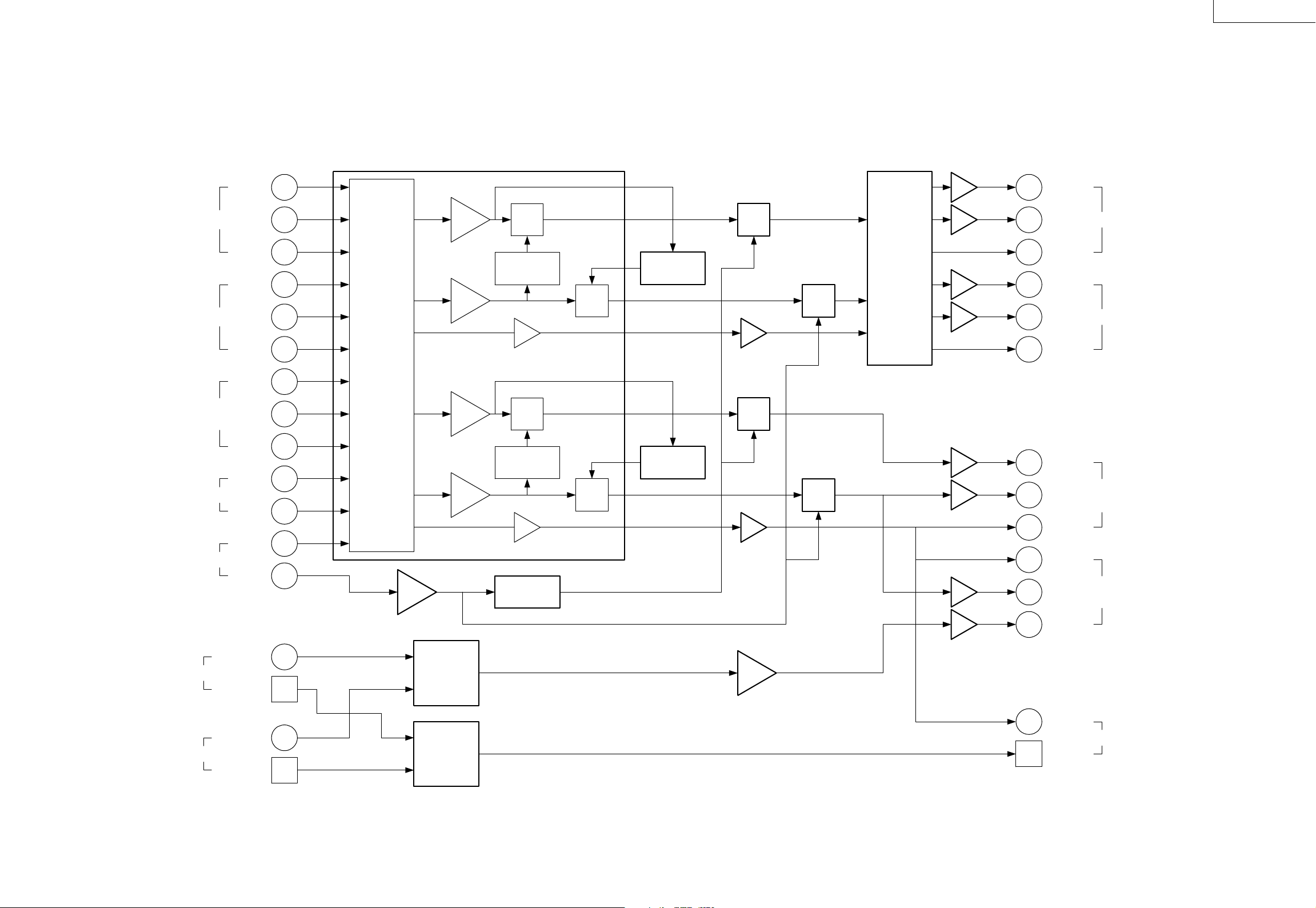
Block Diagrams
JX-S555(J)
IC101
INPUT1
INPUT2
INPUT3
(FRONT)
INPUT4
INPUT5
COMPONENT
INPUT4
VIDEO
S-VIDEO
AUDIO
VIDEO
S-VIDEO
AUDIO
VIDEO
S-VIDEO
AUDIO
S-VIDEO
AUDIO
S-VIDEO
AUDIO
VIDEO
OPTICAL
AUDIO
SOURCE
SELECT
VIDEO
S-VIDEO
AUDIO
VIDEO
(MONITOR)
S-VIDEO
(MONITOR)
AUDIO
(MONITOR)
6dB
IC401-402
SOURCE
SELECT
6dB
6dB
6dB
6dB
S/V
Y/C MIXER
S/V
Y/C MIXER
Y/C MIXER
COMPONENT VIDEO
(MONITOR)
S/V
S/V
1-4 VIDEO
M101
Y/C
SEPARATOR
AUDIO
1-4 VIDEO
(MONITOR)
M102
Y/C
SEPARATOR
AUDIO
(MONITOR)
5 VIDEO
5 S-VIDEO
IC103
1-4
/5
5VIDEO
1-4 S-VIDEO
IC103
1-4
/5
5VIDEO
1-4 S-VIDEO
(MONITOR)
6dB
VIDEO
IC102
IC104
S-VIDEO
1-4
/5
AUDIO
5S-VIDEO
IC102
IC104
1-4
/5
5S-VIDEO
COMPONENT VIDEO
(MONITOR)
LOOP
PROTECT
IC106-108
IC808-809
VIDEO
(MONITOR)
S-VIDEO
(MONITOR)
AUDIO
(MONITOR)
VIDEO
S-VIDEO
S-VIDEO
S-VIDEO
S-VIDEO
COMPONENT
OUTPUT1
AUDIO
VIDEO
OUTPUT2
AUDIO
VIDEO
MONITOR
OUTPUT1
AUDIO
AUDIO
MONITOR
OUTPUT2
VIDEO
COMPONENT
INPUT5
VIDEO
OPTICAL
AUDIO
IC403
SOURCE
SELECT
OPTICAL AUDIO
(MONITOR)
AUDIO
AUDIO
OPTICAL
AUDIO
(No. 70251SCH) 1
Page 2
JX-S555(J)
Notes on this schematic diagram
1. Values are voltages measured with a circuit tester (internal resistance: 20 k /V)
at respective points of the circuits with the power switch turned on.
2. The circuit diagram printed in this service manual is just a standard. The circuitry
and circuit constants are subject to change for improvement without notice.
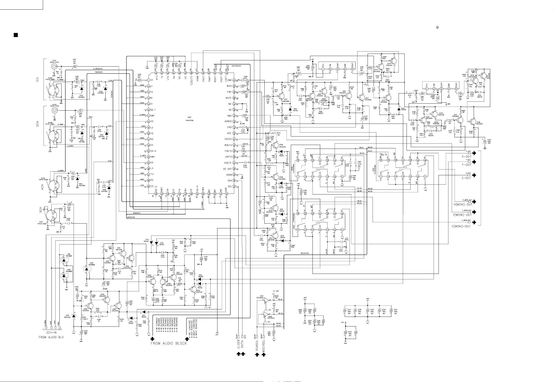
Schematic Diagrams
VIDEO 1 BLOCK
M101
J46729-002
4.5V
4.0V
4.5V
4.5V
4.0V
4.5V
4.3V0V3.2V
4.0V
4.5V
4.0V
4.5V
4.4V
0.3V
5.0V
4.0V
4.5V
4.0V
4.5V
4.4V
0.3V
5.0V
4.0V
4.5V
4.0V
4.5V
4.4V
3.7V
4.5V
3.6V
4.5V
4.4V
4.5V
4.0V
0V
0V
0V
4.0V
0V
4.2V
9.0V
3.6V
4.5V
3.2V
4.5V
4.3V
0V
0V
3.5V
3.5V
1.7V
1.7V
5.7V
1.7V
1.1V
5.7V
1.1V
5.9V
5.7V
1.1V
1.6V
9.1V 3.7V 1.6V 0V 6.1V
5.3V
-2.3V
-2.9V
5.9V
5.9V
1.6V
1.6V
-5.7V
5.9V
1.3V
1.6V -5.7V
-6.0V
-6.0V
1.3V
-6.0V
5.7V
3.4V
0.7V
-0.7V
-1.3V
5.9V
2.8V
5.9V
5.3V
3.4V
M102
J46729-002
5.6V
1.6V
1.0V
5.9V
5.9V
5.9V
1.6V
1.6V
1.6V
1.6V
-5.7V
9.1V 3.7V 1.6V 0V 6.1V
5.9V
5.3V
1.6V
-6.0V
-2.3V
-2.9V
1.6V
-6.0V
1.2V
-5.7V
-6.0V
-0.7V
5.7V
1.2V
3.4V
0.6V
-1.3V
5.9V
5.3V
3.4V
5.9V
2.7V
-1.7V
-2.3V
0.3V
5.0V
4.0V
4.5V
4.0V
4.5V
4.4V
5.9V
5.3V
-1.5V
-2.1V
5.9V
5.3V
1.5V
5.9V
1.7V
1.0V
4.9V
0.4V
-0.2V
5.9V
0.9V
4.2V
-0.9V
-0.3V
0.8V
0.2V-0.2V
-3.6V
0V0V0V
0.3V
5.0V
0V
5.7V
-6.0V
1.7V
1.1V
5.7V
1.7V
1.1V
-6.0V
5.9V
-6.0V
5.9V
-6.0V
5.9V
5.9V
5.9V
1.6V
1.6V
1.6V
1.6V -5.7V
1.6V
-5.7V
-6.0V
-6.0V
-6.0V
C223
4700u
10v
TO VIDEO 2 BLK
2 (No. 70251SCH)
FROM CPU-BLOCK
Page 3
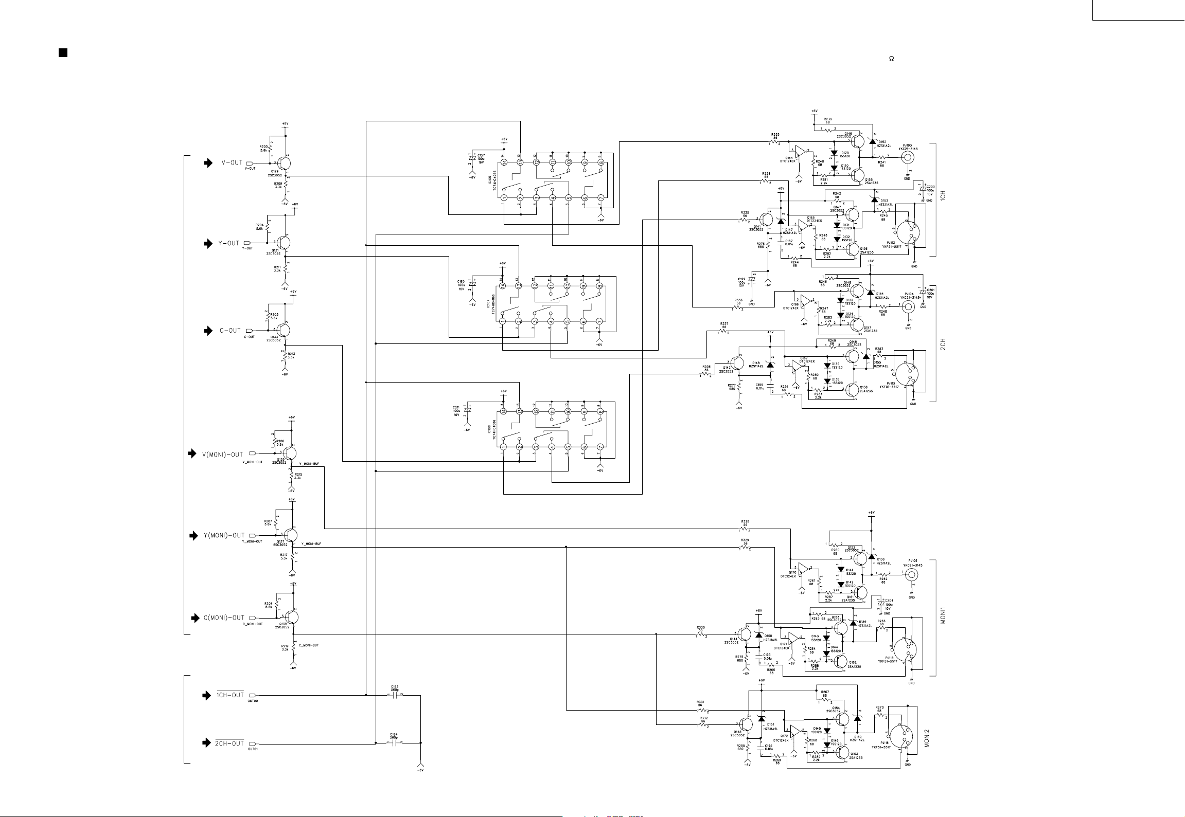
VIDEO 2 BLOCK
Notes on this schematic diagram
1. Values are voltages measured with a circuit tester (internal resistance: 20 k /V)
at respective points of the circuits with the power switch turned on.
2. The circuit diagram printed in this service manual is just a standard. The circuitry
and circuit constants are subject to change for improvement without notice.
JX-S555(J)
FROM VIDEO 1 BLOCK
-0.5V
5.9V
0V
0V
0V
5.9V
0V
0V
0V
5.7V
0V
-0.6V
-5.6V
5.7V
0.1V
-5.5V
-5.9V
5.9V
1.6V
0.9V
5.9V
1.6V
1.0V
5.9V
1.6V
0.9V
5.9V
1.6V
0.8V
5.9V
-5.9V
5.9V
-5.9V
5.9V
-3.7V
-6.0V
1.0V
-6.0V
0.9V
-6.0V
0.9V
0.9V
1.0V
0.9V
-6.0V
0.8V
5.2V
-6.0V
-6.0V
0.9V
5.2V
-6.0V
0.9V
-6.0V
0.9V
5.2V
-6.0V
5.9V
-3.7V
-4.1V
5.9V
0.3V
0V
-6.0V
-5.9V
0V
-6.0V
0.7V
-5.9V
-6.0V
0.8V
-5.9V
-6.0V
FROM CPU BLOCK
5.9V
1.6V
0.8V
0.8V
-5.9V
-6.0V
5.9V
1.6V
1.0V
5.9V
1.0V
0.3V
5.9V
1.0V
0.3V
-6.0V
0.8V
-6.0V
-5.9V
-0.5V
0.8V
-5.9V
-0.5V
5.7V
0.1V
-0.5V
-5.5V
5.7V
0.1V
-5.5V
5.7V
0.1V
-5.5V
(No. 70251SCH) 3
Page 4
JX-S555(J)
Notes on this schematic diagram
1. Values are voltages measured with a circuit tester (internal resistance: 20 k /V)
at respective points of the circuits with the power switch turned on.
2. The circuit diagram printed in this service manual is just a standard. The circuitry
and circuit constants are subject to change for improvement without notice.
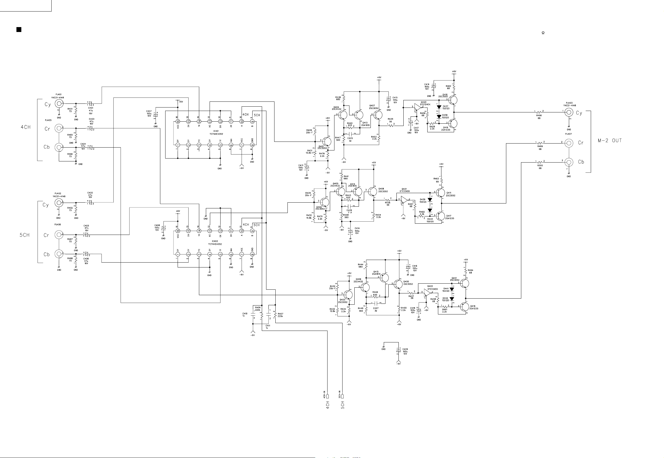
COMPONENT BLOCK
5.9V
0V
5.5V
5.2V
5.9V
0V
0V
0V
0V
0V
0V
0V
0V
0V
0V
0V
0V
0V
-6.0V
0V
5.9V
-0.7V
-1.4V
3.0V
5.9V
2.3V
2.1V
-6.0V
-5.9V
2.1V
1.5V
0.9V
-5.4V
5.9V
0V
5.2V
5.9V
0V
0V
0V
0V
0V
0V
0V
0V
0V
0V
0V
0V
-6.0V
0V
0V
-1.4V
-0.7V
3.0V
5.9V
0V
-0.7V
5.9V
-1.4V
2.3V
5.2V
5.9V
3.0V
5.9V
2.3V
2.1V
-6.0V
5.9V
-5.9V
2.1V
-6.0V
5.5V
2.1V
1.5V
0.9V
-5.4V
5.5V
-5.9V
0.9V
-5.4V
4 (No. 70251SCH)
FROM CPU BLK
Page 5

AUDIO BLOCK
Notes on this schematic diagram
1. Values are voltages measured with a circuit tester (internal resistance: 20 k /V)
at respective points of the circuits with the power switch turned on.
2. The circuit diagram printed in this service manual is just a standard. The circuitry
and circuit constants are subject to change for improvement without notice.
3. Parts marked with A (in the shaded area) are important as safety parts.
When replacing them, make sure to use the specified parts to ensure safety.
-6.0V
JX-S555(J)
5.9V
0V
0V
0V
0V
0V
5.1V
-6.0V
0.2V
0V
0V
0V
0V
0V
0V
0V
5.9V
0V
-6.0V
0V
0V
0V
0V
0V
5.9V
-5.9V
0V
0V
0V
0V
0V
0V
0V
0V
0V
FROM AUDIO 1 BLOCKFROM JACK P.W.B.
-6.0V
-6.0V
0V
0V
0V
0V
0V
5.8V
5.9V
0V
0V
0V
0V
0V
5.1V
0.2V
TO AUDIO 2 BLOCK
0V
0V
0V
0V
0V
-6.0V
0V
0V
0V
0V
0V
0V
0V
-6.0V
0V
A
-5.9V
0V
0V
0V
0V
5.9V
0V
0V
0V
0V
0V
5.9V
0V
0V
0V
5.9V
0V
0V
0V
0V
5.8V
A
9.1V
5.1V
0V
4.5V
1.8V
0V
4.5V
1.8V
5.1V
0V
A
FROM CPU BLK
0V
0V
0V
0V
0V
0V
0V
(No. 70251SCH) 5
Page 6

JX-S555(J)
Notes on this schematic diagram
1. Values are voltages measured with a circuit tester (internal resistance: 20 k /V)
at respective points of the circuits with the power switch turned on.
2. The circuit diagram printed in this service manual is just a standard. The circuitry
and circuit constants are subject to change for improvement without notice.
3. Parts marked with A (in the shaded area) are important as safety parts.
When replacing them, make sure to use the specified parts to ensure safety.
CPU BLOCK
5.1V
5.9V
5.3V
0.5V
0V
5.9V
0V
0V
5.9V
0V
5.9V
4.9V
0V
0V
0.7V
0V
5.3V
0V
5.9V
5.3V
0V
0V
5.3V
5.3V
5.9V
0V
5.5V
0V
5.9V
0V
0V
TO COMPONENT BLK
0V
1.3V
5.2V
5.3V
0V
0V
5.3V
5.3V
5.3V
0V
0V
5.2V
0V
0V
0V
0V
0V
2.8V
3.1V
0V
5.3V
0.2V
5.2V
5.3V
IC2
UPD780021ACWW01
5.3V
0.5V
2.6V
0.5V
5.3V
0.5V
0.5V
0.5V
0.5V
0.5V
0.5V
0V
TO FRONT 1 BLOCK TO FRONT 2 BLOCK
6 (No. 70251SCH)
5.2V
5.2V
5.2V
3.9V
3.9V
3.9V
1.7V
0V
1.7V
A
5.3V
5.3V
5.9V
1.7V
1.7V
1.7V
C5
C4
10u
10u
16V
16V
5.3V
5.2V
0V
5.3V
-6.0V
5.3V
-6.0V
5.3V
-6.0V
5.3V
0V
0V
0V
0V
5.3V
0V
0V
3.6V
3.6V
0V
0V
0V
0V
0V
0V
0V
0V
0V
5.3V
TO VIDEO 1 BLK
Page 7

POWER BLOCK
3. Parts marked with A (in the shaded area) are important as safety parts.
When replacing them, make sure to use the specified parts to ensure safety.
Notes on this schematic diagram
1. Values are voltages measured with a circuit tester (internal resistance: 20 k /V)
at respective points of the circuits with the power switch turned on.
2. The circuit diagram printed in this service manual is just a standard. The circuitry
and circuit constants are subject to change for improvement without notice.
JX-S555(J)
AC IN
120V/60Hz
AC120V
163V
4.8V
9.5V
0V 3.0V
9.5V
8.7V
6.8V
161V
0V
0V
0V
9.5V
0V
-9.8V
6.6V
6.6V
1.8V
-0.2V
-6.6V
9.1V
5.9V
6.8V
0V
0V
0V
0V
TO CPU -BLK
-6.6V
-9.8V
-6.0V
4.8V
-0.5V
0V
6.3V
-0.5V
9.0V
8.0V
9.5V
5.8V
2.5V
0V
5.8V
5.3V
2.5V
0V
(No. 70251SCH) 7
Page 8

JX-S555(J)
FRONT 1 BLOCK FRONT 2 BLOCK
5.2V
5.3V
0V
5.9V
5.9V
0V
AUDIO 1 BLOCK
1.7V
1.7V
5.3V
1.7V
1.7V
5.3V
1.7V
1.7V
5.3V
1.7V
1.1V
0V
2.1V
0V
0V
AUDIO 2 BLOCK
1.4V
1.7V
0V
JACK P.W.B.
8 (No. 70251SCH)
4.5V
0V
5.1V
4.5V
0V
5.1V
C422
10u
16V
0V
5.1V
1.8V
Page 9

Circuit Boards
MAIN BOARD (J22026-001)
JX-S555(J)
(No. 70251SCH) 9
Page 10

JX-S555(J)
MAIN BOARD
Symbol
Address
No.
IC
IC1 C4
IC101 I 2
IC102 H4
IC103 H5
IC104 G4
IC106 C2
IC107 C2
IC108 D2
IC2 C5
IC3 D4
IC4 C4
IC401 E1
IC402 F1
IC403 C3
IC404 E5
IC801 F3
IC802 F3
IC803 F4
IC804 F4
IC805 F4
IC806 E4
IC807 E4
IC808 E3
IC809 D3
IC901 A5
IC902 B5
IC903 B6
IC904 A6
Transistor
Q101 F1
Q102 G1
Q103 G1
Q104 G2
Q105 G2
Q106 G1
Q107 I3
Q108 H3
Q109 G3
Q110 H3
Q111 G3
Q112 I4
Q113 I3
Q114 I4
Q115 H3
Q116 I5
Q117 I4
Q118 I5
Q119 F1
Q120 G1
Q121 G2
Q122 G2
Q124 I4
Q125 I5
Q127 G5
Q128 G5
Q129 H5
Q131 H4
Q133 G4
Q135 H5
Q137 H4
Q139 G4
Q141 E1
Q142 D1
Q144 C1
Q145 B1
Q146 D1
Q147 D1
Q148 C1
Q149 D1
Q152 C1
Q153 C1
Q154 B1
Q155 D1
Q156 D1
Q157 C1
Q158 D1
Q161 C1
Q162 C1
Q163 B1
Q164 D1
Q165 D1
Q166 C1
Q167 C1
Q170 C1
Q171 C1
Q172 B1
Q173 I4
Q174 I4
Q175 I5
Q176 I5
Q2 C4
Q3 C4
Q4 C4
Q401 E2
Q402 E2
Q403 F2
Q404 E2
Q405 E2
Q406 F2
Q407 E2
Q408 E2
Q409 F2
Q410 B1
Q411 A1
Q412 A1
Q413 E2
Q414 E2
Q415 F2
Q416 B1
Q417 A1
Q418 A1
Q420 B1
Q421 A1
Q422 A1
Q5 D4
Q901 A4
Q902 B4
Q903 B4
Q904 B5
Q905 A5
Q906 A6
Q907 A5
Q908 B5
Diode
D1 B5
D10 E5
D101 I1
D102 I1
D103 H1
D104 I1
D107 G1
D108 H1
D109 F1
D11 E5
D110 F1
D112 G1
D113 G1
D114 G2
D115 G2
D116 G2
D117 G2
D118 I3
D119 H3
D120 G3
D121 H3
D122 G3
D123 H3
D129 D1
D130 D1
D131 D1
D132 D1
D133 C1
D134 C1
D135 D1
D136 D1
D141 C1
D142 C1
D143 C1
D144 C1
D145 B1
D146 B1
D147 D1
D148 D1
D150 C1
D151 B1
D152 D1
D153 D1
D154 D1
D155 D1
D158 C1
D159 C1
D160 B1
D161 H1
D162 H1
D3 D4
D4 D4
D437 B1
D438 B1
D439 A1
D440 A1
D441 A1
D442 A1
D5 C4
D6 C4
D901 A3
D903 B4
D904 B4
D905 B4
D906 A5
D907 A5
D908 A5
D909 A4
Resistor
R1 C5
R10 C5
R101 I1
R102 I1
R103 H1
R104 H1
R106 G1
R107 F1
R108 I1
R109 H1
R11 C5
R111 H1
R112 G1
R12 D4
R120 H5
R121 H5
R123 G2
R124 G2
R125 G1
R126 F1
R127 F1
R128 G1
R129 G1
R13 C5
R130 G2
R131 G1
R132 G1
R133 F1
R134 G2
R135 G2
R138 G1
R139 G1
R14 C5
R140 G2
R141 F1
R142 F1
R143 G2
R145 G1
R146 G2
R147 G2
R148 G2
R149 G2
R15 C5
R151 G2
R152 G2
R153 G1
R154 G1
R155 G2
R156 G2
R157 G1
R158 G2
R16 C5
R160 I3
R161 H3
R162 G3
R163 H3
R164 G3
R165 I4
R166 I3
R167 I3
R168 I5
R169 I5
R17 C5
R170 I3
R171 I3
R172 I3
R173 H3
R174 G3
R175 H3
R176 H3
R177 I3
R178 I4
R179 I5
R18 C5
R180 I4
R181 H3
R182 I3
R183 H3
R184 G3
R185 H3
R186 G3
R187 H3
R188 I4
R189 I5
R19 C5
R190 I4
R191 I5
R193 I4
R194 I5
R195 I4
R196 I5
R197 I3
R198 I4
R199 I4
R2 D5
R20 D5
R200 I5
R201 H3
R202 H3
R203 H5
R204 H4
R205 G4
R206 H5
R207 H4
R208 G4
R209 H5
R21 D5
R211 H4
R213 G4
R215 H5
R217 H4
R219 G4
R22 D5
R23 D5
R239 D1
R24 D5
R240 D1
R241 D1
R242 D1
R243 D1
R244 E1
R245 D1
R246 D1
R247 C1
R248 D1
R249 D1
R25 D5
R250 D1
R251 D1
R252 D1
R253 G3
R254 G3
R26 D5
R260 C1
R261 C1
R262 C1
R263 C1
R264 C1
R265 C1
R266 C1
R267 B1
R268 B1
R269 B1
R27 D5
R270 B1
R276 E1
R277 D1
R279 C1
R28 D5
R280 B1
R281 D1
R282 D1
R283 D1
R284 D1
R287 C1
R288 C1
R289 B1
R29 D5
R290 H3
R291 H3
R292 H3
R293 G3
R294 H3
R295 I3
R296 I4
R297 I5
R3 D5
R30 C5
R301 I4
R302 I4
R303 I4
R304 I4
R305 I4
R306 I5
R307 I5
R308 I5
R309 I5
R31 C5
R310 I5
R32 C5
R328 C2
R329 C2
R33 C4
R330 C2
R331 B2
R332 B2
R333 D2
R334 D2
R335 E2
R336 C2
R337 D2
R338 D2
R34 C4
R35 H5
R36 H5
R37 D5
R38 D4
R4 D5
R401 G1
R402 F1
R406 E3
R407 E3
R408 C3
R409 C3
R410 C3
R411 C3
R428 E2
R429 E2
R430 F2
R431 E2
R432 E2
R433 F2
R434 F2
R435 B2
R436 A2
R437 A2
R438 E2
R440 E2
R441 E2
R443 E2
R444 F2
R446 F2
R447 E2
R448 E2
R449 F2
R453 E2
R454 E2
R455 F2
R456 B1
R457 A1
R458 A1
R459 B1
R460 A1
R461 A1
R462 B1
R463 A1
R464 A1
R465 G1
R466 G1
R467 F1
R468 F1
R478 E2
R479 E2
R496 B1
R499 A1
R5 D5
R500 B1
R6 D5
R7 D5
R8 D5
R811 F3
R812 F3
R813 F4
R814 F4
R815 F3
R816 F4
R817 F3
R818 E3
R819 F3
R820 F4
R821 F3
R822 F3
R823 F4
R824 F4
R825 F3
R826 F4
R827 F3
R828 F3
R829 F3
R830 F4
R831 E4
R832 E4
R833 E4
R834 E4
R847 E4
R848 E4
R850 E5
R851 E4
R853 E4
R854 E4
R855 F4
R856 F4
R857 F4
R858 F4
R9 C5
R901 A3
R902 A3
R903 A4
R904 A4
R905 B4
R906 B4
R907 B4
R908 B4
R909 B4
R910 B4
R911 B4
R912 A5
R913 A5
R914 B5
R915 A5
R916 A5
R917 A5
R918 A5
R919 B4
R920 B4
R921 B5
R922 B4
R923 B5
R924 A6
R926 B5
R927 B6
R928 B5
Condenser
C1 C5
C10 C5
C101 I1
C102 I1
C103 H1
C104 H1
C106 H1
C107 F1
C11 C5
C118 I1
C119 H1
C12 D5
C121 H1
C122 F1
C123 I2
C125 G1
C127 G1
C128 G2
C129 H2
C13 D5
C130 H2
C131 H2
C132 H2
C133 H2
C134 H2
C136 I2
C137 I3
C138 I3
C14 D5
C140 G2
C141 G2
C142 G1
C143 F1
C145 I5
C146 H3
C147 I4
C148 H5
C149 H4
C15 D5
C150 I2
C151 H3
C152 I4
C153 F1
C154 G2
C155 I4
C156 I5
C157 C2
C159 G4
C16 D5
C160 I3
C161 H3
C162 G1
C163 D2
C164 I5
C165 I4
C167 I4
C168 I5
C169 G5
C17 D5
C170 G5
C171 F5
C172 F5
C175 I3
C176 I4
C18 D5
C183 C3
C184 C2
C187 E1
C189 D1
C19 D5
C193 C1
C195 B1
C196 H3
C197 I4
C198 I5
C199 E1
C20 C5
C200 D2
C201 D2
C204 C2
C205 I3
C206 H4
C207 I3
C21 C5
C210 H4
C211 D2
C213 I4
C214 I5
C215 I5
C216 I4
C217 H5
C218 H4
C219 H3
C22 C5
C220 G3
C221 H4
C222 I2
C223 I2
C23 C5
C24 C5
C25 C5
C26 B5
C27 B5
C28 C5
C29 C5
C31 D5
C4 B5
C401 G1
C402 E1
C403 G1
C404 G1
C405 E1
C406 F1
C407 E2
C408 F2
C409 B3
C410 E2
C411 E2
C412 D5
C413 E1
C414 F2
C415 F2
C416 F2
C417 B1
C418 A1
C419 B2
C425 E2
C426 E2
C427 F2
C428 F2
C5 D4
C6 D5
C7 C5
C8 C5
C811 F3
C812 F3
C813 F4
C814 F4
C815 F3
C816 F4
C817 F3
C818 F3
C819 F3
C820 F4
C821 E4
C822 E4
C824 E4
C825 E4
C838 F3
C839 F4
C840 E3
C841 F4
C843 F3
C844 F3
C845 F4
C846 E4
C848 E5
C849 E4
C850 I1
C851 I1
C852 H1
C853 F2
C854 F2
C855 F2
C856 H1
C857 F2
C858 F3
C859 F3
C860 F4
C861 F4
C862 F4
C863 F4
C864 E4
C865 E4
C9 C5
C901 B3
C902 A3
C903 A3
C904 A4
C905 B4
C906 B4
C907 B4
C908 A5
C909 A5
C910 A5
C911 A6
C912 B5
C913 A6
C914 B5
C915 A5
C916 B4
C917 A5
C918 B6
C919 A4
C920 B5
C921 A6
Oters
CJ101 I1
CJ102 I1
CJ103 H1
CJ104 H1
CJ105 G2
CJ106 I3
CJ107 H5
CJ108 H5
CJ110 H4
CJ111 H4
CJ112 G4
CJ113 G4
CJ116 G5
CJ117 F5
CJ118 F4
CJ119 F4
CJ120 F4
CJ121 F4
CJ122 F4
CJ123 F4
CJ124 F4
CJ125 E3
CJ126 E4
CJ127 E4
CJ128 E3
CJ129 E3
CJ130 D3
CJ131 D3
CJ132 D3
CJ133 D3
CJ134 D3
CJ135 D3
CJ138 F1
CJ139 E2
CJ140 B1
CJ147 C3
CJ148 C3
CJ149 D4
CJ150 D5
CJ151 C5
CJ152 C5
CJ154 E1
CJ155 C6
CJ156 C4
CJ157 I3
CJ158 C3
CJ159 D5
CJ160 D5
CJ161 D5
CJ162 C5
CJ163 C5
CJ164 C5
CJ165 C5
CJ167 D4
CN1 B5
CN3 C5
CN804 F4
CN805 E3
CN806 D3
CN811 H1
CN812 F3
CN813 E3
CN901 B3
F901 A3
J102 A1
J103 A1
J105 A2
J107 A1
J108 B2
J109 B1
J110 B1
J111 B1
J112 B1
J113 B1
J114 B2
J115 C1
J116 C2
J117 B2
J118 B2
J119 B2
J120 B2
J121 C2
J122 C1
J123 C2
J125 C2
J126 C2
J127 C2
J128 C2
J129 C2
J130 C2
J131 D2
J132 C2
J133 C2
J134 C2
J135 D2
J136 D2
J137 D2
J138 D2
J139 D2
J140 D2
J141 E2
J142 E2
J143 E1
J144 D2
J145 D2
J146 D2
J147 D2
J148 A4
J149 A4
J150 A5
J151 A5
J152 B5
J153 B5
J154 A5
J155 A6
J156 B6
J157 B6
J158 B6
J159 B6
J160 B5
J161 B5
J162 C6
J163 C6
J164 C3
J165 C3
J166 C3
J167 C3
J168 C3
J169 D3
J170 D3
J171 D3
J172 C3
J173 C3
J174 C3
J175 D3
J176 C3
J177 D3
J178 C4
J179 C4
J180 C4
J181 D4
J182 D3
J183 D4
J184 C4
J185 C4
J186 C4
J187 C4
J188 C4
J189 C4
J190 C4
J191 C4
J192 C4
J193 C4
J194 B4
J195 B4
J196 B5
J197 C5
J198 B5
J199 B5
J200 B5
J201 C5
J202 D5
J203 C5
J204 D5
J205 D5
J206 D4
J207 D4
J208 E4
J209 E4
J210 E4
J211 E4
J212 E4
J213 E4
J214 E5
J215 E5
J216 E5
J217 E5
J220 D6
J221 D6
J222 D6
J223 E5
J224 E4
J225 E4
J226 F4
J227 F4
J228 F4
J229 F4
J230 F5
J231 F5
J232 F5
J233 F6
J236 E2
J237 F2
J238 F2
J239 E2
J240 E2
J241 E2
J242 F2
J243 F2
J244 E2
J245 E2
J246 F2
J247 E2
J248 E2
J249 E2
J250 D3
J251 E3
J252 E3
J253 E3
J254 E3
J255 E3
J256 E3
J257 E3
J258 E3
J259 E3
J260 F3
J261 F3
J262 F3
J263 F3
J264 F3
J265 F3
J266 F3
J267 E3
J268 E3
J269 F3
J270 E4
J271 F4
J272 F4
J273 E4
J274 F1
J275 F1
J276 F1
J277 F1
J278 F1
J279 F1
J280 G2
J281 H1
J282 H1
J283 H1
J284 H1
J285 I1
J286 I2
J287 G2
J288 G2
J289 H2
J290 G2
J291 H2
J292 G2
J293 G2
J294 G2
J295 G2
J296 G2
J297 G2
J298 G3
J299 G3
J300 G3
J301 G3
J302 G3
J303 I2
J304 I2
J305 I2
J306 H2
J307 H2
J308 I2
J309 I2
J310 I3
J311 I3
J312 H2
J313 H2
J314 H2
J315 H2
J316 H3
J317 G3
J318 H3
J319 I3
J320 H3
J321 H3
J322 H3
J323 H3
J325 H3
J327 G3
J328 G3
J329 G3
J330 G4
J331 G4
J332 H3
J333 H4
J334 H4
J335 H4
J336 H4
J337 H4
J338 G5
J339 G4
J340 G4
J341 G4
J342 G4
J343 G5
J344 G5
J345 G5
J346 G4
J347 G5
J348 G5
J349 G4
J350 G4
J351 G5
J352 G5
J353 G5
J354 G5
J355 G5
J356 G5
J357 H5
J358 G4
J359 H5
J360 H5
J361 H4
J362 H5
J363 H4
J364 H4
J365 H4
J366 H4
J367 H5
J368 H5
J369 I5
J370 H5
J371 I5
J372 I4
J373 I5
J374 F1
J375 F1
J376 C3
J377 I4
J378 D6
J379 D6
L102 I3
L103 I4
L901 A3
L902 B4
L903 A5
L904 A5
M101 I4
M102 I5
PC901 B4
PJ101 I1
PJ102 H1
PJ103 D1
PJ104 D1
PJ106 C1
PJ107 I1
PJ108 H1
PJ110 H1
PJ111 F1
PJ112 E1
PJ113 D1
PJ115 C1
PJ116 B1
PJ401 G1
PJ402 F1
PJ403 B1
PJ405 G1
PJ406 F1
PJ407 B1
RF1 B5
RF401 E4
RF402 E3
T901 A4
VD901 B3
VR101 I3
VR102 I5
X1 C5
10 (No. 70251SCH)
Page 11

SUB BOARD (J33641-001)
• FRONT 2 BOARD
• AUDIO 2 BOARD
• AUDIO 1 BOARD
JACK BOARD (J33642-001)
• FRONT 1 BOARD
PARTS SIDE SOLDER SIDE
SUB BOARD
Symbol
Address
No.
IC
IC701 A2
Transistor
Q701 B1
Q702 C1
Q703 E1
Q704 D1
Q705 D1
Q706 F1
Q707 A2
Diode
D701 B1
D702 C1
D703 E1
D704 C1
D705 D1
D706 F1
D707 A1
D708 B1
D709 B1
D710 C1
D711 D1
D712 F1
D713 E1
D714 A2
D715 A2
D716 B2
Resistor
R701 A1
R702 B1
R703 C1
R704 C1
R705 D1
R706 F1
R707 E1
R708 A2
R709 A2
R710 A2
R801 B3
R802 C3
R803 C3
R804 D3
R805 D3
R806 D3
R807 E3
R808 F3
R835 B2
R836 B2
R837 C2
R838 C2
R839 D2
R840 D2
R841 D2
R842 E2
R843 F2
R844 F2
Condenser
C422 D2
C429 E3
C430 F3
C701 A2
C801 B3
C802 C3
C803 C3
C804 D3
C805 D3
C806 D3
C807 E3
C808 F3
C826 B2
C827 C2
C828 C2
C829 C2
C830 D2
C831 D2
C832 D2
C833 E2
C834 F2
C835 F2
JX-S555(J)
Others
CN701 A1
CN702 A2
CN807 C2
CN808 C2
CN809 D3
CN810 E3
J1001 A1
J1002 A1
J1003 A1
J1004 A1
J1005 A1
J1006 A1
J1007 B1
J1008 B1
J1009 B1
J1010 C1
J1011 C1
J1012 C1
J1013 C1
J1014 D1
J1015 D1
J1016 D1
J1017 E1
J1018 A2
J1019 E2
J1020 E2
J1021 E3
J1022 E3
J1023 E3
J1024 F3
OPT401 E3
OPT402 F3
OPT403 E2
PJ801 C3
PJ802 C3
PJ803 D3
PJ804 E3
PJ807 C2
PJ808 D2
PJ809 E2
PJ810 F2
PJ811 B2
SW701 A1
SW702 C1
SW703 F1
SW704 B1
SW705 D1
SW706 A2
SW707 B1
SW708 E1
(No. 70251SCH) 11
 Loading...