

Page 1
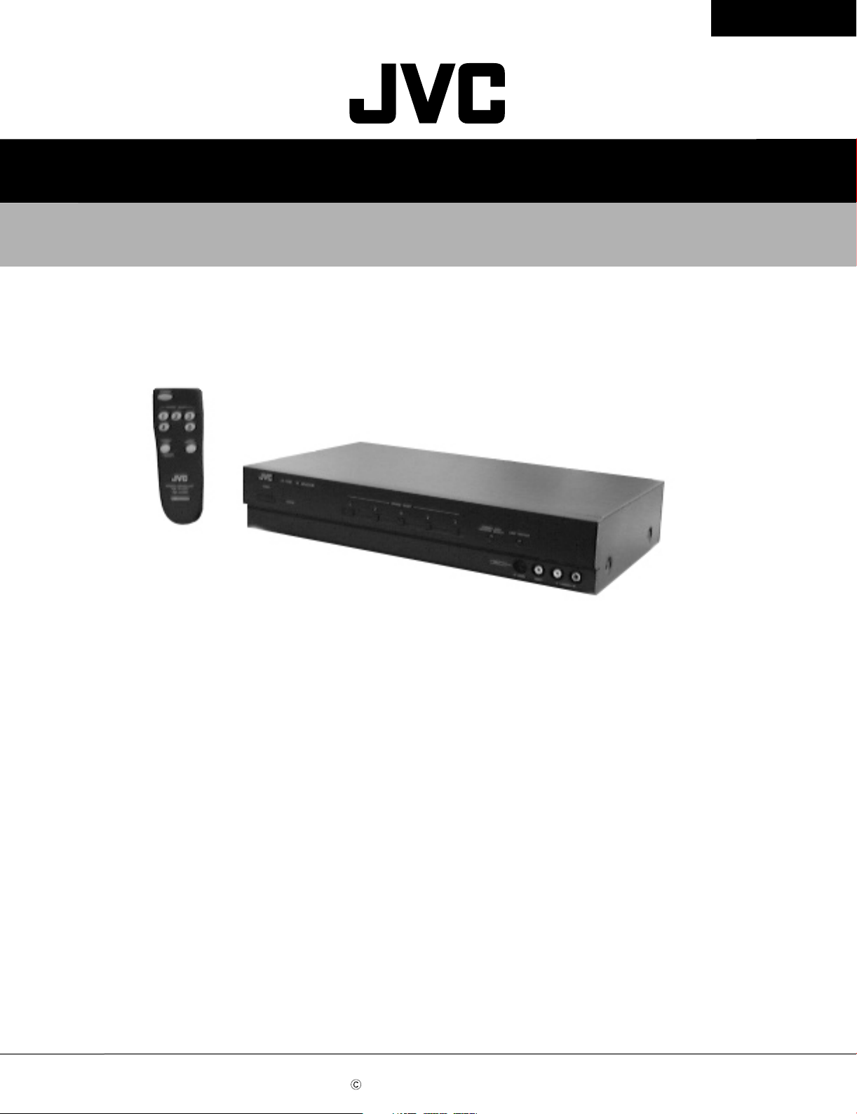
SERVICE MANUAL
AV SELECTOR
JX-S555 (J)
JX-S555(J)JX-S555(J)
Contents
Safety Precautions ............................... 2
Main Parts Locations ............................ 3
Disassembly of Parts ............................ 4
Connection Diagram ............................. 6
Circuit Description ................................ 7
Design and specifications are subject to change without notice.
COPYRIGHT 2001 VICTOR COMPANY OF JAPAN, LTD.
Adjustments ......................................... 11
Position of ICs and Adjustment Points
Servicing Guidelines ............................ 13
Block View Inside IC ............................. 17
....... 12
No.70251
Mar. 2001
Page 2
JX-S555(J)
1. This design of this product contains special hardware and many circuits and components specially
2. Alterations of the design or circuitry of the product should not be made. Any design alterations of
3. Many electrical and mechanical parts in the products have special safety-related characteristics.
Safety Precautions
for safety purposes. For continued protection, no changes should be made to the original design
unless authorized in writing by the manufacturer. Replacement parts must be identical to those
used in the original circuits. Services should be performed by qualified personnel only.
the product should not be made. Any design alterations or additions will void the manufacturer`s
warranty and will further relieve the manufacture of responsibility for personal injury or property
damage resulting therefrom.
These characteristics are often not evident from visual inspection nor can the protection afforded
by them necessarily be obtained by using replacement components rated for higher voltage,
wattage, etc. Replacement parts which have these special safety characteristics are identified in
the Parts List of Service Manual. Electrical components having such features are identified by
shading on the schematics and by ( ) on the Parts List in the Service Manual. The use of a
substitute replacement which does not have the same safety characteristics as the recommended
replacement parts shown in the Parts List of Service Manual may create shock, fire, or other
hazards.
4. The leads in the products are routed and dressed with ties, clamps, tubings, barriers and the
like to be separated from live parts, high temperature parts, moving parts and/or sharp edges
for the prevention of electric shock and fire hazard. When service is required, the original lead
routing and dress should be observed, and it should be confirmed that they have been returned
to normal, after re-assembling.
5. Leakage currnet check (Electrical shock hazard testing)
After re-assembling the product, always perform an isolation check on the exposed metal parts
of the product (antenna terminals, knobs, metal cabinet, screw heads, headphone jack, control
shafts, etc.) to be sure the product is safe to operate without danger of electrical shock.
Do not use a line isolation transformer during this check.
Plug the AC line cord directly into the AC outlet. Using a "Leakage Current Tester", measure
the leakage current from each exposed metal parts of the cabinet , particularly any exposed
metal part having a return path to the chassis, to a known good earth ground. Any leakage
current must not exceed 0.5mA AC (r.m.s.)
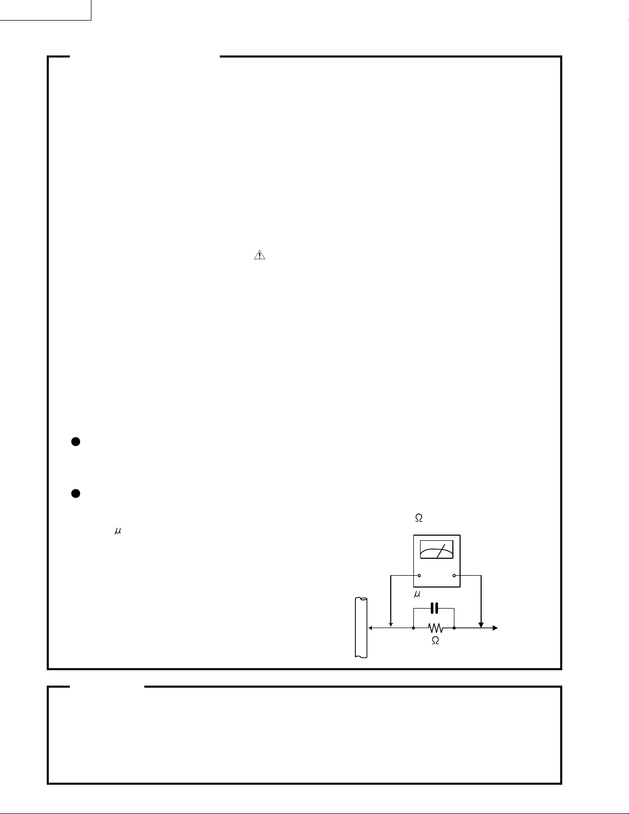
Alternate check method
Plug the AC line cord directly into the AC outlet. Use an AC voltmeter having, 1,000 ohms
per volt or more sensitivity in the following manner. Connect a 1,500 10W resistor paralleled by
a 0.15 F AC-type capacitor between an exposed
metal part and a known good earth ground.
Measure the AC voltage across the resistor with the
AC voltmeter.
Move the resistor connection to eachexposed metal
part, particularly any exposed metal part having a
return path to the chassis, and meausre the AC
voltage across the resistor. Now, reverse the plug in
the AC outlet and repeat each measurement. voltage
measured Any must not exceed 0.75 V AC (r.m.s.).
This corresponds to 0.5 mA AC (r.m.s.).
0.15 F AC TYPE
1500 10W
Good earth ground
AC VOLTMETER
(Having 1000
ohms/volts,
or more sensitivity)
Place this
probe on
each exposed
metal part.
Warning
1. This equipment has been designed and manufactured to meet international safety standards.
2. It is the legal responsibility of the repairer to ensure that these safety standards are maintained.
3. Repairs must be made in accordance with the relevant safety standards.
4. It is essential that safety critical components are replaced by approved parts.
5. If mains voltage selector is provided, check setting for local voltage.
2 (No. 70251)
Page 3
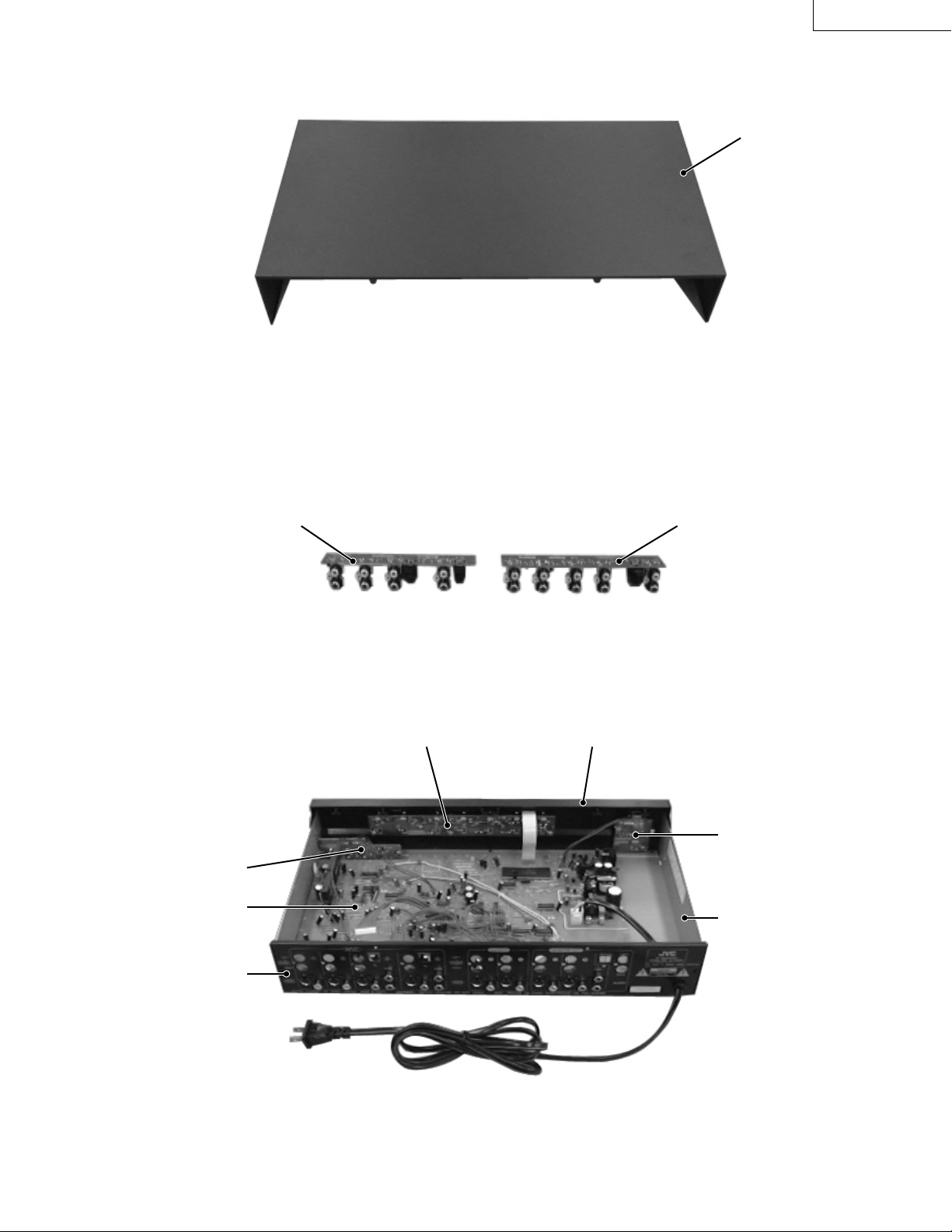
Main Parts Locations
JX-S555(J)
Top cover
Jack board
MAIN board
AUDIO 2 boardAUDIO 1 board
Front panel ass'yFront 2 board
Front 1 board
Bottom chassis
Rear panel
(No. 70251) 3
Page 4
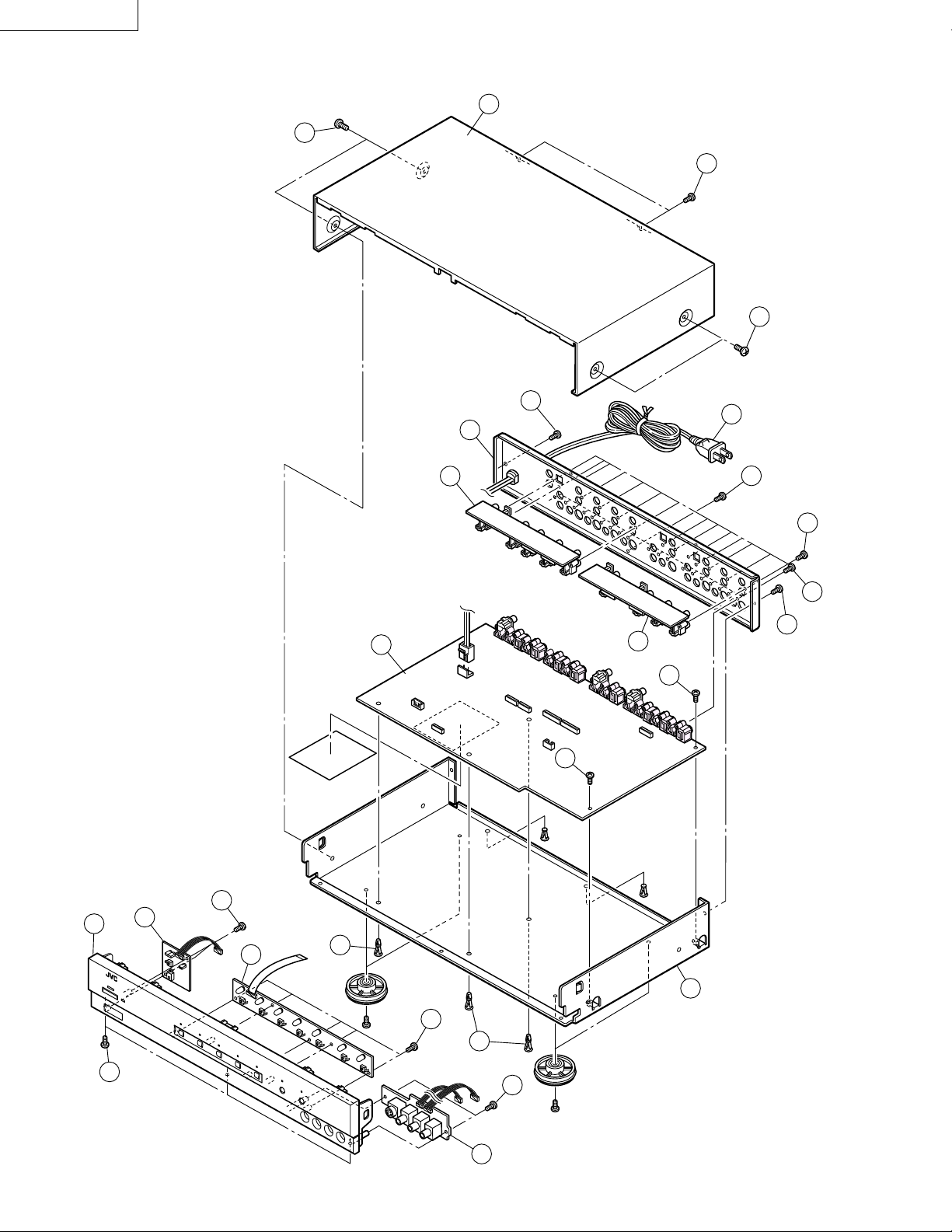
JX-S555(J)
Disassembly of Parts
4
1
3
4
17
2
6
18
17
7
13
20
22
21
15
11
12
17
5
14
14
16
22
15
19
4 (No. 70251)
9
8
Page 5
Note : For the positions of the connectors, see the connection
II
I
I
diagram (page 6).
JX-S555(J)
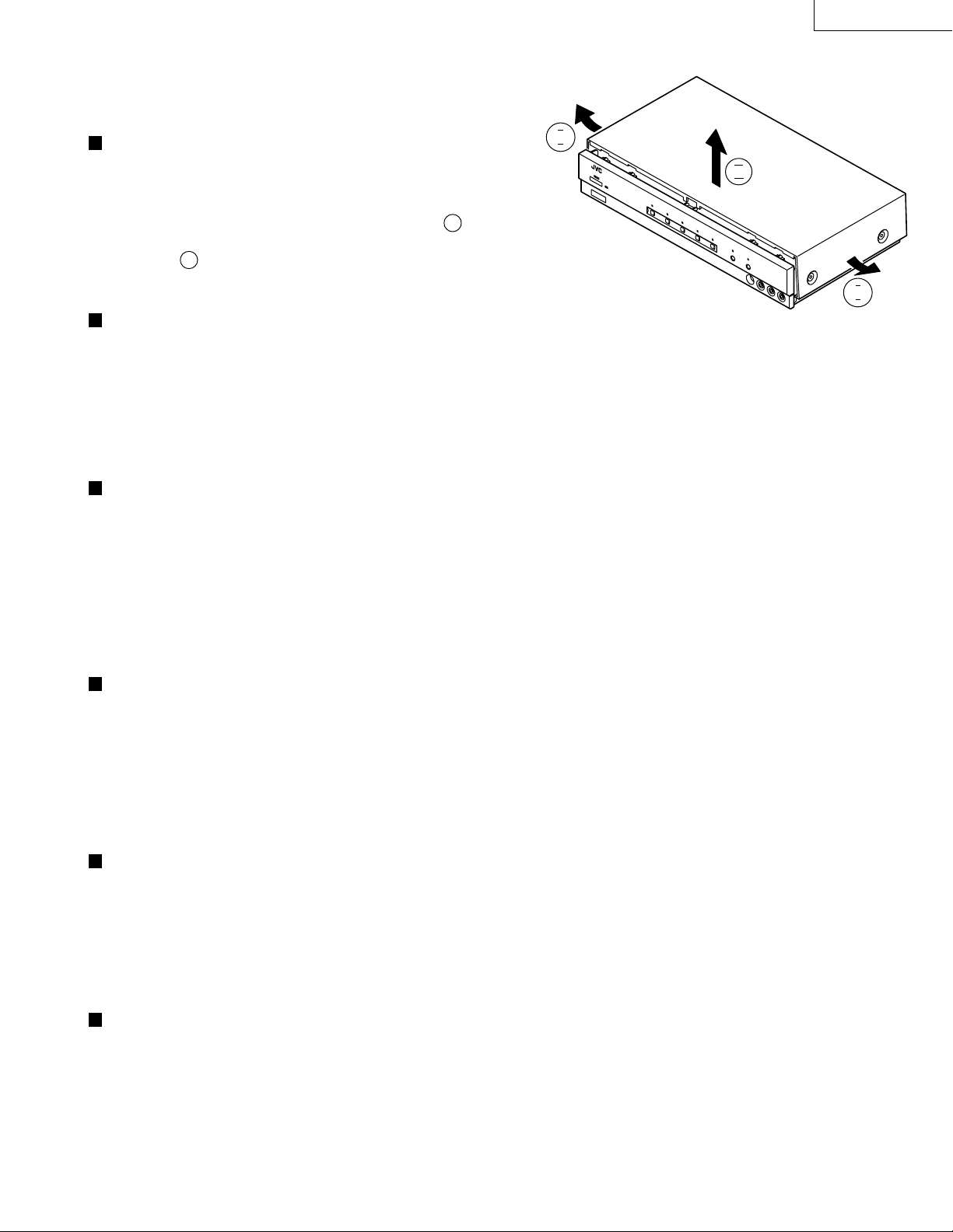
Removing the top cover
1. Remove the two screws 3 retaining the top cover 1 from the
rear panel 2, then remove the four screws 4 retaining the
top cover from the side panels.
2. Slightly open out the bottoms of the side skirts I of the top
cover 1 as shown in the figure, then pull the top cover straight
upward II . Do not remove the top cover by pulling it up in an
oblique direction.
Removing the Audio 1 Board
Board
1. Remove the top cover 1.
2. From the rear panel 2, remove the six screws 7 retaining the Audio 1 board 5 and the six screws 7 retaining the
3. Gently remove the Audio 1 board 5 and then unplug the connectors CN809 and CN810 from it.
4. Gently remove the Audio 2 board 6 and then unplug the connectors CN807 and CN808 from it.
66
6
66
Audio 2 board 6.
Removing the Main Board
1. Remove the top cover 1, then the Audio 1 board 5 and finally the Audio 2 board 6.
2. From the rear panel 2, remove the nineteen screws C retaining the Main board B.
3. Unplug the connectors CN1, CN3, CN804 and CN811 (and the wire from the Front Panel Assembly D )on the Main
board B .
4. Unplug the connector CN901 (in the power supply circuit) on the Main board B.
5. Remove the two clamping screws E on the Main board B.
6. Disengage the three claws of the locking card spacer F on the Main board B, then remove the Main board by lifting
it in an oblique direction.
11
1
11
BB
B
BB
55
5 and Audio 2
55
Removing the Rear Panel
1. Remove the top cover 1.
2. Unplug the connector CN901 (in the power supply circuit) on the Main board B.
3. Remove the twelve screws 7 retaining the Audio 1 board 5 and the Audio 2 board 6, then remove the nineteen screws
C retaining the Main board B.
4. Remove the three screws H retaining the bottom chassis G and the rear panel 2.
5. Gently remove the rear panel 2.
(Take care of the AC power cord I connected to the rear panel 2.)
Removing the Front Panel Assembly
1. Remove the top cover 1.
2. Remove the three retaining screws J from the bottom of the Front Panel Assembly D.
3. Disengage the fittings between the side panels of the Front Panel Assembly D with the bottom chassis G, then
gently pull out the Front Panel Assembly D from the bottom chassis G toward the front.
4. Unplug the connectors CN1, CN3, CN804 and CN811 from the Main board B.
5. Remove the Front Panel Assembly D.
Removing the Front 1 Board
1. Remove the top cover 1 and the Front Panel Assembly D.
2. Remove the two screws M retaining the Front 1 board K, five screws M retaining the Front 2 board L and the two screws
9 retaining the Jack board 8.
3. Remove the Front 1 board K, the Front 2 board L and the Jack board 8.
22
2
22
DD
D
DD
KK
K, Front 2 Board
KK
LL
L and Jack Board
LL
88
8
88
(No. 70251) 5
Page 6
JX-S555(J)
Connection Diagram
Rear
CN809
CN810
AUDIO 1 board
CN807CN808
CN811
CN812
CN813
CN804
Front
CN805
CN806
6 (No. 70251)
AUDIO 2 board
MAIN board
CN901
CN1
CN3
CN701
CN702 CN703 CN101
Front 1 board Front 2 board Jack board
Page 7
Circuit Description
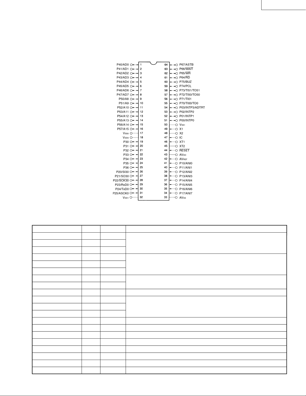
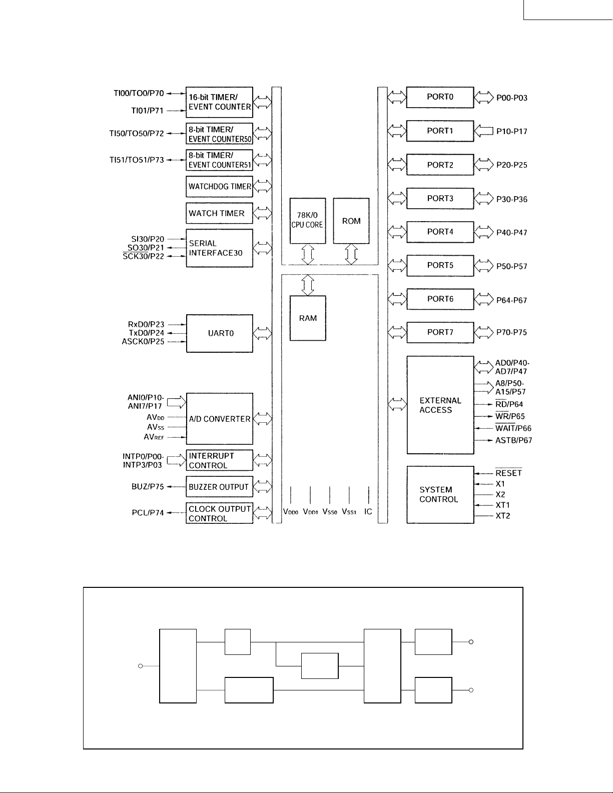
1. IC2 (µPD780021ACWW01)
The µPD780021ACWW01 is a 64-pin, 8-bit single-chip microcomputer with an 8K-byte ROM and 512-byte RAM.
JX-S555(J)
Pin Name
P40/AD0
P41/AD1
P42/AD2
P43/AD3
P44/AD4
P45/AD5
P46/AD6
P47/AD7
P50/A8
P51/A9
P52/A10
P53/A11
P54/A12
P55/A13
P56/A14
P57/A15
Vss
0
VDD0
P30
P31
Pin No.
1
2
3
4
5
6
7
8
9
10
11
12
13
14
15
16
17
18
19
20
I/O
I/O
I/O
I/O
I/O
I/O
I/O
I/O
I/O
I/O
I/O
I/O
I/O
I/O
I/O
I/O
I/O
—
I/O
I/O
Function
Key scan inputs.
Key scan outputs.
Scan signal outputs for LED lighting.
Dubbing lock ON/OFF. H = ON. L = OFF.
Scan signal outputs for LED lighting.
CH1 INHIBIT ON/OFF. H = ON. L = OFF.
Not used.
Not used.
Not used.
Port grounding potential.
I
Port positive potential.
CH2 INHIBIT ON/OFF. H = ON. L = OFF.
CH3 INHIBIT ON/OFF. H = ON. L = OFF.
(No. 70251) 7
Page 8
JX-S555(J)
Pin Name
P32
P33
P34
P35
P36
P20/SI30
P21/SO30
P22/SCK30
P23/RxD0
P24/TxD0
P25/ASCK0
V
DD1
AVss
P17/AN17
P16/AN16
P15/AN15
P14/AN14
P13/AN13
P12/AN12
P11/AN11
P10/AN10
AV
REF
AV
DD
RESET
XT2
XT1
IC
X2
X1
Vss
1
P00/INTP0
P01/INTP1
P02/INTP2
P03/INTP3/ADTRT
P70/T100/TO0
P71/TI01
P72/TI50/TO50
P73/TI51/TO51
P74/PCL
P75/BUZ
P64/RD
P65/WR
P66/WAIT
P67/ASTB
Pin No.
21
22
23
24
25
26
27
28
29
30
31
32
33
34
35
36
37
38
39
40
41
42
43
44
45
46
47
48
49
50
51
52
53
54
55
56
57
58
59
60
61
62
63
64
I/O
I/O
I/O
I/O
I/O
I/O
I/O
I/O
I/O
I/O
I/O
I/O
—
—
—
—
I/O
I/O
I/O
I/O
I/O
I/O
I/O
I/O
I/O
I/O
I/O
I/O
I/O
I/O
Function
I2C path Data signal.
2
I
C path Clock signal
Not used.
Not used.
Not used.
Not used.
Not used.
Not used.
Not used.
Not used.
Not used.
I
Positive potential (except for the port).
AD converter grounding potential.
I
I
I
I
I
I
I
I
I
I
I
I
Not used.
Not used.
Not used.
Not used.
Not used.
Not used.
CH5 S1/S2 signal input.
Not used.
A/D converter reference voltage input.
Analog power supply for A/D converter
System reset input.
Sub-system clock oscillation.
Internally connected. To be connected to VSS0 or VSS1.
X'tal oscillator connection terminals for Main
I
I
system clock oscillation.
Grounding potential (except for the port).
CH3 D4 plug insertion detection.
CH4 D4 plug insertion detection.
CH5 D4 plug insertion detection.
Not used.
Remote control light signal input.
Component video switching signal output.
Component video switching signal output.
Main unit ON/OFF. H = OFF. L = ON.
S1/S2 signal inputs.
Component video switching signal output.
CH5 monitor signal output.
Main unit ON/OFF. H = OFF. L = ON.
Power switch detection.
8 (No. 70251)
Page 9
JX-S555(J)
2. M101, M102 (J46729-002)
• Comb filter module
BufferVIDEO-IN Matrix
BPF
Delay
Line
1H-GDL
Buffer
Buffer
C-OUT
Y-OUT
(No. 70251) 9
Page 10
JX-S555(J)
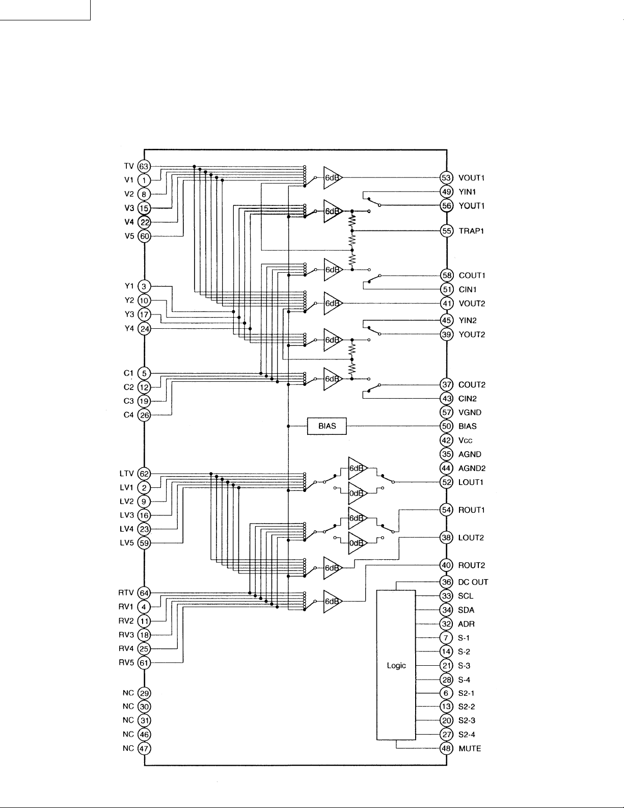
3. IC101 (CXA2079Q)
The CXA2079Q is an AV switcher IC with 5 video inputs, 2 video outputs, 5 stereo audio inputs and 2 stereo audio outputs,
featuring the I2C bus compatibility for TV. Among the 5 video inputs, 4 inputs are compatible with the S2 and S-Video
standards.
The outputs (each audio output uses a pair of lines for the L and R channels) can be selected independently by the control
through the I2C bus. However, the second video and audio outputs are always based on the same video and audio input
system.
10 (No. 70251)
Page 11
Adjustments
Instruments required for adjustments
1. Oscilloscope
2. TV signal generator (NTSC)
JX-S555(J)
Test Point
2CH C output
1
MONITOR OUT
2
C output
Connection
NTSC
color bar
Adjustment Point
VR101
VR102
1CH
V input
C output level
C output level
JX-S555
2CH
C outputs
Condition ConditionName
Apply color bar signal to
1CH video input (V).
Apply color bar signal to
1CH video input (V).
Oscillo
scope
Adjust VR101 so that the C output level at 2CH is
0.642 0.02 Vp-p.
Adjust VR102 so that the C output level at
MONITOR OUT is 0.642 0.02 Vp-p.
(No. 70251) 11
Page 12
JX-S555(J)
Position of ICs and Adjustment Points
MAIN board
IC402
IC101
CXA2079Q
74HC4052AP
M101
VR101
NJM
IC801
NJM
IC802
4580D
4580D
NJM
IC804
NJM
IC805
J46729-002
IC104
4580D
IC803
4580D
M102
VR102
IC102
74HC4066AP
NJM
4580D
J46729-002
IC103
74HC4066AP
74HC4066AP
IC401
74HC4052AP
IC108
74HC4066AP
IC107
74HC4066AP
IC106
74HC4066AP
IC808
IC809
IC403
74HC4052AP
74HC4052AP
74HC126AP
IC806
4580D
NJM
IC807
IC3
4580D
NJM
74HC04AP
UPD780021ACW-W01
IC2
12 (No. 70251)
Page 13
Servicing Guidelines
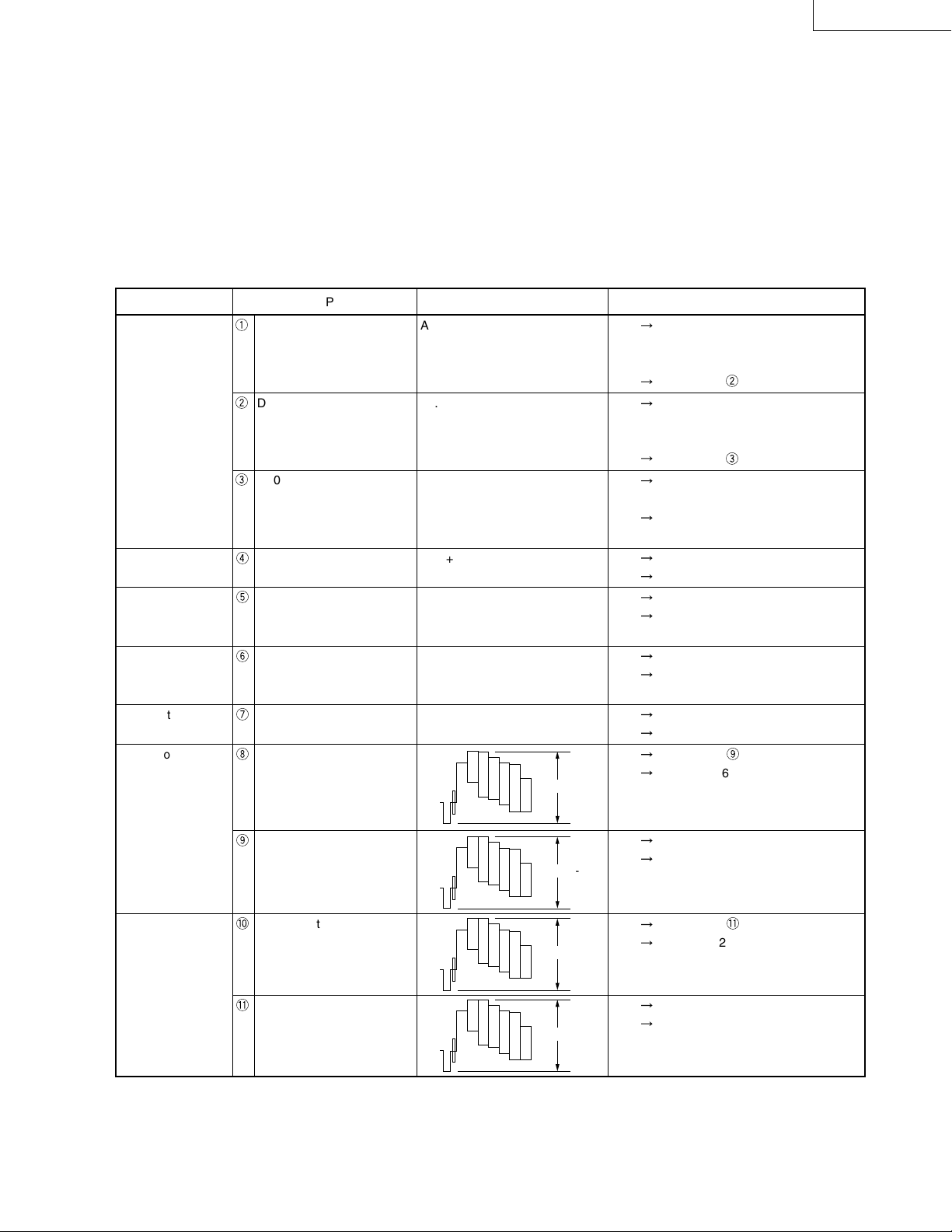
1. Reference input signals
Video signals
V → Full-field color bar (white 100%), 1.0 Vp-p
Y → 1.0 Vp-p (with sync)
C → Burst level 0.286 Vp-p, chroma only
Audio signal
1 kHz, -10 dBV sine wave
2. YES → Normal
NO → The normal voltage and waveform are not output.
Symptom Check Points Normal Voltage/Waveform Check Results and Failures
1. Power cannot be
turned ON.
2. Display LED
lighting failure.
3. Switch operation
failure.
C903: Across +/- leads
1
D906: Cathode
2
D907: Anode
Q904: Emitter,
3
Q905: Emitter,
Q906: Emitter,
IC904: Pin 2
CN3: Pins 3 to 7
4
CN3: Pins 8 to 14 0 or +5 V DC NO
5
Approx. 164 V DC NO
+9.5 V DC
–9.8 V DC
–6 V DC
+6 V DC
+5 V DC
+9 V DC
0 or +5 V DC NO
Check power cord and C901.
If the fuse is blown, check Q901,
T901, D901 and their surroundings.
YES
Go to check 2.
NO
NO R Check voltage at IC902 and
surroundings.PC901 and IC902
may be defective.
YES
Go to check 3.
NO
IC901, IC903, IC904 or Q904 to
Q906 defective.
YES
Check CN1,. CN3 and wires.
IC2 defective.
YES
Q701 to Q706 or wire is defective.
IC2 defective.
YES
CN701, tack switch or wire defective.
JX-S555(J)
4. S/V switching
failure
5. Remote control
malfunction
6.
The composite
video inputs at
CH1 and CH2
are not displayed.
7. The composite
video inputs at
CH1 and CH2
are not output at
the Monitor
output.
IC101: Pins 7, 14, 21 and 28
6
IC2: Pin 55 + 5 V DC at remote control
7
Q129: Emitter NO
8
Q107: emitter NO
9
Q135: Emitter NO
A
Q115: Emitter NO
B
0 V when S-Video plug is inserted.
+5 V when S-Video plug is not
inserted.
code (See TM.)
2.0 Vp-p
2.0 Vp-p
2.0 Vp-p
2.0 Vp-p
NO
PJ107 to PJ110 defective.
YES
Check IC101 and the surroundings.
NO
IC701, CN1, CN702 or wire defective.
YES
IC2 defective.
Go to check 9.
YES
Check IC106, output buffer and their
surroundings.
Check IC101 and surroundings.
YES
Check IC103 and their surroundings.
Go to check B.
YES
Check Q152, Q161, Q170 and
their surroundings.
Check IC101 and surroundings.
YES
Check IC103 and their surroundings.
(No. 70251) 13
Page 14
JX-S555(J)
Symptom Check Results and Failures
8. The S-Video
C
inputs at CH1 to
CH4 are not
Check Points Normal Voltage/Waveform
(Y) Q131: Emitter
(Y)
(C) Q133: Emitter
2.0 Vp-p
NO
Go to check D.
YES
Check IC107, IC108, output buffer
and their surroundings.
displayed.
(C)
1.28 Vp-p
(Y) Q108: Emitter
D
(C) Q109: Emitter
(Y)
2.0 Vp-p
NO
Check IC101 and surroundings.
YES
Check IC102, IC104 and their
surroundings.
(C)
1.28 Vp-p
9. The S-Video
inputs at CH1 to
CH4 are not
(Y) Q137: Emitter
E
(C) Q139: Emitter
(Y)
2.0 Vp-p
NO
Go to check F.
YES
Check output buffer and
surroundings.
output at the
Monitor output.
10. The S-Video
input at CH5 is
not displayed.
(Y) Q110: Emitter
F
(C) Q111: Emitter
(Y) Q104: Emitter
G
(C) Q102: Emitter
(C)
(Y)
(C)
(Y)
(C)
1.28 Vp-p
2.0 Vp-p
1.28 Vp-p
2.0 Vp-p
1.28 Vp-p
NO
Check IC101 and surroundings.
YES
Check IC102, IC104 and their
surroundings.
NO
Check Q101 to Q104, Q119, Q120
and their surroundings.
YES
Go to check C.
14 (No. 70251)
Page 15

JX-S555(J)
Symptom Check Results and Failures
11. The S-Video
H
input at CH5 is
not output at the
Check Points Normal Voltage/Waveform
(Y) Q104: Emitter
(Y)
(C) Q102: Emitter
2.0 Vp-p
NO
Check Q101 to Q104, Q119, Q120
and their surroundings.
YES
Go to check E.
Monitor output.
(C)
1.28 Vp-p
12. Malfunction in
Y/C separation.
(Y) Q114: Emitter
I
(C) Q113: Emitter
(Y)
2.0 Vp-p
NO
Go to check J.
YES
Check IC101 and surroundings.
(C)
1.28 Vp-p
(Y) M101: Pin 5
J
(C) M101: Pin 3
(Y)
1.0 Vp-p
NO
M101 defective.
YES
Check Q112 to Q114, Q173, Q174
and their surroundings.
13. Malfunction in
Y/C separation
for monitor
output.
(Y) Q118: Emitter
K
(C) Q117: Emitter
(Y) M102: Pin 5
L
(C) M102: Pin 3
(C)
(Y)
(C)
(Y)
(C)
0.64 Vp-p
2.0 Vp-p
1.28 Vp-p
1.0 Vp-p
0.64 Vp-p
NO
Go to check L.
YES
Check IC101 and surroundings.
NO
M101 defective.
YES
Check Q116, Q117, Q175, Q176
and their surroundings.
(No. 70251) 15
Page 16

JX-S555(J)
Symptom Check Results and Failures
14. Malfunction in
M
Y/C mixing of
CH1 to CH4
Check Points Normal Voltage/Waveform
Q107: Emitter
(Monitor output: Q115 emitter)
2.0 Vp-p
NO
Check IC101 and surroundings.
YES
Check IC103 and their surroundings.
inputs.
15. Malfunction in
Y/C mixing of
CH5 input.
16. Component
video signal is
not output.
Q122: Emitter NO
N
2.0 Vp-p
(Y) Q401: Emitter
O
(Y)
(Pb) Q402: Emitter
(Pr) Q403: Emitter
1.0 Vp-p
Check Q105, Q106, Q121,
Q122 and their surroundings.
YES
Check IC103 and their surroundings.
NO
Check IC401, IC402 and their
surroundings.
YES
Check 6 dB amp (Q404 to Q409,
Q413 to Q415), output buffer and
their surroundings.
(Cb)
0.7 Vp-p
(Cr)
0.7 Vp-p
17. Audio signals
are not output.
18. Audio signals
are not output
at the Monitor.
(L) IC806: Pins 6 & 7
P
(R) IC806: Pins 1 & 2
(L) IC801 to IC805: Pins 7
Q
(R) IC801 to IC805: Pins 1
(L) IC807 pins 6 & 7
R
(R) IC807 pins 1 & 2
–10 dBV
(0.32 Vrms)
–10 dBV
(0.32 Vrms)
–10 dBV
(0.32 Vrms)
NO
Go to check Q.
YES
Check IC808, IC809 and their
surroundings.
NO
Check IC801 to IC805 and
their surroundings.
YES
Check IC101 and surroundings.
NO
Check IC807 and surroundings.
YES
Check CN806 and wire.
16 (No. 70251)
Page 17

Block View Inside IC
JX-S555(J)
IC1 M51957AL [MITSUBISHI]
IC4 HD74HC375FP [HITACHI]
1D
1
1Q
2
1Q
3
G1·2
4
2Q
5
2Q
6
2D
7
GND
8
(TOP VIEW)
TRUE TABLE
INPUTS
D
L
H
X
X: Don’t care
16
V
CC
4D
15
14
13
12
11
10
9
4Q
4Q
G3·4
3Q
3Q
3D
G1·2
G3·4
1D
2D
3D
4D
OUTPUTS
G
H
H
L
Q
H
Qn
L
Qn LATCH
Q
H
H
(12)
(15)
(1)
(4)
(7)
(9)
1D
C1
C2
2D
3D
C3
C4
4D
FUNCTION
(3)
(2)
(5)
(6)
(11)
(10)
(13)
(14)
1Q
1Q
2Q
2Q
3Q
3Q
4Q
4Q
IC2 uPD780021ACWW01
(No. 70251) 17
Page 18

JX-S555(J)
IC101 CXA2079Q IC102-108 TC74HC4066AP [TOSHIBA]
IC801-807 NJM4580D [JRC]
18 (No. 70251)
Page 19

JX-S555(J)
IC401-402, 808-809 TC74HC4052AP
[TOSHIBA]
IC701 GP1U261R [SHARP]
LIMITER B.P.F
MODULATOR
COMPARATOR
INTEGRATOR
IC901 M5230L [MITSUBISHI]
8
OUTPUT CONTROL
7
INPUT (+)
6
OUTPUT (+)
5
VOLTAGE ADJUSTMENT
4
M5230L
INPUT (-)
3
OUTPUT (-)
2
BALANCE ADJUSTMENT
1
GND
OUTPUT
CONTROL
7
8
OVERHEAT
PROTECTOR
START
CIRCUIT
REFERENCE
VOLTAGE
GENERATOR
ERROR
AMPLIFIER
ERROR
AMPLIFIER
OVER
CURRENT
PROTECTOR
OVER
CURRENT
PROTECTOR
INPUT (+)
6
OUTPUT (+)
5
VOLTAGE ADJUSTMENT
1
GND
2
BALANCE ADJUSTMENT
3
OUTPUT (-)
4
INPUT (-)
(No. 70251) 19
Page 20

JX-S555(J)
1 2 3 4
2
21
3
4
3
1
4
DC input (Vin)
DC output (Vout)
GND
Spesific IC
ON/OFF control terminal (Vc)
IC902-903 uPC1093J [NEC]
TO-92 PACKAGE
MARKED
SURFACE
IC904 PQ09RD08 [SHARP]
IC3 TC74HC04AP [TOSHIBA]
AY
IC404 TA78L005AP [TOSHIBA]
OUTPUT
COMMON
IC403 TC74HC126AP [TOSHIBA]
Q10
R15
R14
Q9
R17
14 Vcc
13 6A
12 6Y
11 5A
10 5Y
94A
84Y
R1
Q1
1G 1
1A 2
1Y 3
2G 4
2A 5
2Y 6
GND 7
14 Vcc
13 4G
12 4A
11 4Y
10 3G
93A
83Y
(TOP VIEW)
INPUTS OUTPUTS
Q12
R11
R12
R7
R6
(1) INPUT
Q14
R10
(2) OUTPUT
GA Y
LX Z
HL L
HH H
X : Don't Care
Z : High Impedance
Q6
R5
Q8
R4
R2
Q2
Q4
Q3
R3
Q5
Q13
R9
C1
Q11
Q7
R8
1A 1
1Y 2
2A 3
2Y 4
3A 5
3Y 6
GND 7
(TOP VIEW)
Schematic Diagram
R13
D1
2
3
1
INPUT
R16
20 (No. 70251)
TA78L005AP 5V
TA78L012AP 12V
(3) COMMON
Page 21

VICTOR COMPANY OF JAPAN, LIMITED
COMMUNICATION NETWORK BUSINESS UNIT, 1644, SHIMOTSURUMA, YAMATO-SHI, KANAGAWA-KEN, 242-8514, JAPAN
No.70251
Printed in Japan
0103(S)
Page 22

Electric Parts List
MAIN P.W. Board Ass’y
A
Ref. No. Parts No. Parts Name, Description
PWBA J22034-001
IC1 M51957AL IC MITSUBISHI
IC 2 UPD780021ACWW01 IC NE C
IC3 TC74HC04AP IC TOSHIBA
IC4 HD74HC375FPEL IC HITACHI
IC101 CXA2079Q IC SONY
IC102 TC74HC4066AP IC TOSHIBA
IC103 TC74HC4066AP IC TOSHIBA
IC104 TC74HC4066AP IC TOSHIBA
IC106 TC74HC4066AP IC TOSHIBA
IC107 TC74HC4066AP IC TOSHIBA
IC108 TC74HC4066AP IC TOSHIBA
IC401 TC74HC4052AP IC TOSHIBA
IC402 TC74HC4052AP IC TOSHIBA
IC403 TC74HC126AP IC TOSHIBA
A IC404 TA78L005AP IC TOSHIBA
IC801 NJM4580D IC JRC
IC802 NJM4580D IC JRC
IC803 NJM4580D IC JRC
IC804 NJM4580D IC JRC
IC805 NJM4580D IC JRC
IC806 NJM4580D IC JRC
IC807 NJM4580D IC JRC
IC808 TC74HC4052AP IC TOSHIBA
IC809 TC74HC4052AP IC TOSHIBA
A IC901 M5230L IC MITSUBISHI
A IC902 UPC1093J IC NEC
A IC903 UPC1093J IC NEC
A IC904 PQ09RD08 IC SHARP
D1 1SS120 Diode HITACHI
D3 1SS120 Diode HITACHI
D4 1SS120 Diode HITACHI
D5 1SS120 Diode HITACHI
D6 1SS120 Diode HITACHI
D10 1SS120 Diode HITACHI
D11 1SS120 Diode HITACHI
D101 HZS7B2L ZenerDiode HITACHI
D102 HZS7B2L ZenerDiode HITACHI
D103 HZS7B2L ZenerDiode HITACHI
D104 HZS7B2L ZenerDiode HITACHI
D107 HZS7B2L ZenerDiode HITACHI
D108 HZS7B2L ZenerDiode HITACHI
D109 RD10MB2 ZenerDiode NEC
D110 HZS11A2L ZenerDiode HITACHI
D112 1SS120 Diode HITACHI
D113 1SS120 Diode HITACHI
D114 1SS120 Diode HITACHI
D115 1SS120 Diode HITACHI
D116 1SS120 Diode HITACHI
D117 1SS120 Diode HITACHI
D118 1SS120 Diode HITACHI
D119 1SS120 Diode HITACHI
Main Board Assembly
The partwill not be supplied
as an assembly.
JX-S555(J)
A
Ref. No. Parts No. Parts Name, Description
D120 1SS120 Diode HITACHI
D121 1SS120 Diode HITACHI
D122 1SS120 Diode HITACHI
D123 1SS120 Diode HITACHI
D129 1SS120 Diode HITACHI
D130 1SS120 Diode HITACHI
D131 1SS120 Diode HITACHI
D132 1SS120 Diode HITACHI
D133 1SS120 Diode HITACHI
D134 1SS120 Diode HITACHI
D135 1SS120 Diode HITACHI
D136 1SS120 Diode HITACHI
D141 1SS120 Diode HITACHI
D142 1SS120 Diode HITACHI
D143 1SS120 Diode HITACHI
D144 1SS120 Diode HITACHI
D145 1SS120 Diode HITACHI
D146 1SS120 Diode HITACHI
D147 HZS11A2L ZenerDiode HITACHI
D148 HZS11A2L ZenerDiode HITACHI
D150 HZS11A2L ZenerDiode HITACHI
D151 HZS11A2L ZenerDiode HITACHI
D152 HZS11A2L ZenerDiode HITACHI
D153 HZS11A2L ZenerDiode HITACHI
D154 HZS11A2L ZenerDiode HITACHI
D155 HZS11A2L ZenerDiode HITACHI
D158 HZS11A2L ZenerDiode HITACHI
D159 HZS11A2L ZenerDiode HITACHI
D160 HZS11A2L ZenerDiode HITACHI
D161 RD10MB2 ZenerDiode NEC
D162 RD10MB2 ZenerDiode NEC
D437 1SS120 Diode HITACHI
D438 1SS120 Diode HITACHI
D439 1SS120 Diode HITACHI
D440 1SS120 Diode HITACHI
D441 1SS120 Diode HITACHI
D442 1SS120 Diode HITACHI
A D901 DF06M-G45 Diode G.I.
A D903 ERA18-04-T1 Diode FUJIELECTRIC
A D904 ERA18-04-T1 Diode FUJIELECTRIC
A D905 ERA18-04-T1 Diode FUJIELECTRIC
A D906 SB340L-5009 Diode G.I.
A D907 SB340L-5009 Diode G.I.
A D908 1N4742A ZenerDiode G.I.
A D909 RD10JSAB1 ZenerDiode NEC
Q2 DTA124EK DigitalTransistor ROHM
Q3 DTA124EK DigitalTransistor ROHM
Q4 DTA124EK DigitalTransistor ROHM
Q5 DTA124EK DigitalTransistor ROHM
Q101 2SC3052 Transistor MITSUBISHI
Q102 2SC3052 Transistor MITSUBISHI
Q103 2SC3052 Transistor MITSUBISHI
Q104 2SC3052 Transistor MITSUBISHI
Q105 2SC3052 Transistor MITSUBISHI
(No. 70251) 1
Page 23

JX-S555(J)
A
Ref. N o. Parts No. Parts Name, Description
Q106 2SC3052 Transistor MITSUBISHI
Q107 2SC3052 Transistor MITSUBISHI
Q108 2SC3052 Transistor MITSUBISHI
Q109 2SC3052 Transistor MITSUBISHI
Q110 2SC3052 Transistor MITSUBISHI
Q111 2SC3052 Transistor MITSUBISHI
Q112 2SC3052 Transistor MITSUBISHI
Q113 2SC3052 Transistor MITSUBISHI
Q114 2SC3052 Transistor MITSUBISHI
Q115 2SC3052 Transistor MITSUBISHI
Q116 2SC3052 Transistor MITSUBISHI
Q117 2SC3052 Transistor MITSUBISHI
Q118 2SC3052 Transistor MITSUBISHI
Q119 2SA1235 Transistor MITSUBISHI
Q120 2SA1235 Transistor MITSUBISHI
Q121 2SA1235 Transistor MITSUBISHI
Q122 2SA1235 Transistor MITSUBISHI
Q124 2SA1235 Transistor MITSUBISHI
Q125 2SA1235 Transistor MITSUBISHI
Q127 DTC124EK DigitalTransistor ROHM
Q128 DTC124EK DigitalTransistor ROHM
Q129 2SC3052 Transistor MITSUBISHI
Q131 2SC3052 Transistor MITSUBISHI
Q133 2SC3052 Transistor MITSUBISHI
Q135 2SC3052 Transistor MITSUBISHI
Q137 2SC3052 Transistor MITSUBISHI
Q139 2SC3052 Transistor MITSUBISHI
A
Ref. No. Parts No. Parts Name, Description
Q402 2SC3052 Transistor MITSUBISHI
Q403 2SC3052 Transistor MITSUBISHI
Q404 2SC4432 Transistor SANYO
Q405 2SC4432 Transistor SANYO
Q406 2SC4432 Transistor SANYO
Q407 2SC3052 Transistor MITSUBISHI
Q408 2SC3052 Transistor MITSUBISHI
Q409 2SC3052 Transistor MITSUBISHI
Q410 2SC3052 Transistor MITSUBISHI
Q411 2SC3052 Transistor MITSUBISHI
Q412 2SC3052 Transistor MITSUBISHI
Q413 2SA1815 Transistor SANYO
Q414 2SA1815 Transistor SANYO
Q415 2SA1815 Transistor SANYO
Q416 2SA1235 Transistor MITSUBISHI
Q417 2SA1235 Transistor MITSUBISHI
Q418 2SA1235 Transistor MITSUBISHI
Q420 DTC124EK DigitalTransistor ROHM
Q421 DTC124EK DigitalTransistor ROHM
Q422 DTC124EK DigitalTransistor ROHM
A Q901 2SK3326 FET NEC
A Q902 2SC5395 Transistor MITSUBISHI
A Q903 2SC5395 Transistor MITSUBISHI
A Q904 2SB1094 Transistor NEC
A Q905 2SD1585 Transistor NEC
A Q906 2SC3246 Transistor MITSUBISHI
A Q907 DTC124EK DigitalTransistor ROHM
A Q908 DTC124EK DigitalTransistor ROHM
Q141 2SC3052 Transistor MITSUBISHI
Q142 2SC3052 Transistor MITSUBISHI
Q144 2SC3052 Transistor MITSUBISHI
Q145 2SC3052 Transistor MITSUBISHI
Q146 2SC3052 Transistor MITSUBISHI
Q147 2SC3052 Transistor MITSUBISHI
Q148 2SC3052 Transistor MITSUBISHI
Q149 2SC3052 Transistor MITSUBISHI
Q152 2SC3052 Transistor MITSUBISHI
Q153 2SC3052 Transistor MITSUBISHI
Q154 2SC3052 Transistor MITSUBISHI
Q155 2SA1235 Transistor MITSUBISHI
Q156 2SA1235 Transistor MITSUBISHI
Q157 2SA1235 Transistor MITSUBISHI
Q158 2SA1235 Transistor MITSUBISHI
Q161 2SA1235 Transistor MITSUBISHI
Q162 2SA1235 Transistor MITSUBISHI
Q163 2SA1235 Transistor MITSUBISHI
Q164 DTC124EK DigitalTransistor ROHM
Q165 DTC124EK DigitalTransistor ROHM
Q166 DTC124EK DigitalTransistor ROHM
Q167 DTC124EK DigitalTransistor ROHM
Q170 DTC124EK DigitalTransistor ROHM
Q171 DTC124EK DigitalTransistor ROHM
Q172 DTC124EK DigitalTransistor ROHM
Q173 2SC3052 Transistor MITSUBISHI
Q174 2SA1235 Transistor MITSUBISHI
Q175 2SC3052 Transistor MITSUBISHI
Q176 2SA1235 Transistor MITSUBISHI
Q401 2SC3052 Transistor MITSUBISHI
R1 NRSA02J-105NY M.G.Resistor 1MΩ,1/10W
R2 NRSA02J-105NY M.G.Resistor 1MΩ,1/10W
R3 NRSA02J-105NY M.G.Resistor 1MΩ,1/10W
R4 NRSA02J-105NY M.G.Resistor 1MΩ,1/10W
R5 NRSA02J-105NY M.G.Resistor 1MΩ,1/10W
R6 NRSA02J-105NY M.G.Resistor 1MΩ,1/10W
R7 NRSA02J-105NY M.G.Resistor 1MΩ,1/10W
R8 NRSA02J-105NY M.G.Resistor 1MΩ,1/10W
R9 NRSA02J-104NY M.G.Resistor 100kΩ,1/10W
R10 NRSA02J-104NY M.G.Resistor 100kΩ,1/10W
R11 NRSA02J-104NY M.G.Resistor 100kΩ,1/10W
R12 NRSA02J-104NY M.G.Resistor 100kΩ,1/10W
R13 NRSA02J-104NY M.G.Resistor 100kΩ,1/10W
R14 NRSA02J-103NY M.G.Resistor 10kΩ,1/10W
R15 NRSA02J-104NY M.G.Resistor 100kΩ,1/10W
R16 NRSA02J-104NY M.G.Resistor 100kΩ,1/10W
R17 NRSA02J-104NY M.G.Resistor 100kΩ,1/10W
R18 NRSA02J-102NY M.G.Resistor 1kΩ,1/10W
R19 NRSA02J-102NY M.G.Resistor 1kΩ,1/10W
R20 NRSA02J-104NY M.G.Resistor 100kΩ,1/10W
R21 NRSA02J-104NY M.G.Resistor 100kΩ,1/10W
R22 NRSA02J-104NY M.G.Resistor 100kΩ,1/10W
R23 NRSA02J-104NY M.G.Resistor 100kΩ,1/10W
R24 NRSA02J-104NY M.G.Resistor 100kΩ,1/10W
R25 NRSA02J-104NY M.G.Resistor 100kΩ,1/10W
R26 NRSA02J-104NY M.G.Resistor 100kΩ,1/10W
R27 NRSA02J-104NY M.G.Resistor 100kΩ,1/10W
R28 NRSA02J-104NY M.G.Resistor 100kΩ,1/10W
R29 NRSA02J-105NY M.G.Resistor 1MΩ,1/10W
2 (No. 70251)
Page 24

A
Ref. No. Parts No. Parts Name, Description
R30 NRSA02J-103NY M.G.Resistor 10kΩ,1/10W
R31 NRSA02J-103NY M.G.Resistor 10kΩ,1/10W
R32 NRSA02J-103NY M.G.Resistor 10kΩ,1/10W
R33 NRSA02J-472NY M.G.Resistor 4.7kΩ,1/10W
R34 NRSA02J-472NY M.G.Resistor 4.7kΩ,1/10W
R35 NRSA02J-472NY M.G.Resistor 4.7kΩ,1/10W
R36 NRSA02J-472NY M.G.Resistor 4.7kΩ,1/10W
R37 NRSA02J-101NY M.G.Resistor 100Ω,1/10W
R38 NRSA02J-104NY M.G.Resistor 100kΩ,1/10W
R101 NRSA02J-750NY M.G.Resistor 75Ω,1/10W
R102 NRSA02J-750NY M.G.Resistor 75Ω,1/10W
R103 NRSA02J-750NY M.G.Resistor 75Ω,1/10W
R104 NRSA02J-750NY M.G.Resistor 75Ω,1/10W
R106 NRSA02J-750NY M.G.Resistor 75Ω,1/10W
R107 NRSA02J-750NY M.G.Resistor 75Ω,1/10W
R108 NRSA02J-750NY M.G.Resistor 75Ω,1/10W
R109 NRSA02J-750NY M.G.Resistor 75Ω,1/10W
R111 NRSA02J-750NY M.G.Resistor 75Ω,1/10W
R112 NRSA02J-750NY M.G.Resistor 75Ω,1/10W
R120 NRSA02J-103NY M.G.Resistor 10kΩ,1/10W
R121 NRSA02J-103NY M.G.Resistor 10kΩ,1/10W
R123 NRSA02J-473NY M.G.Resistor 47kΩ,1/10W
R124 J46567-6040 M.G.Resistor 604Ω,1/10W
R125 NRSA02J-113NY M.G.Resistor 11kΩ,1/10W
R126 J46567-1132 M.G.Resistor 11.3kΩ,1/10W
R127 NRSA02J-681NY M.G.Resistor 680Ω,1/10W
R128 NRSA02J-561NY M.G.Resistor 560Ω,1/10W
R129 NRSA02J-681NY M.G.Resistor 680Ω,1/10W
R130 NRSA02J-561NY M.G.Resistor 560Ω,1/10W
R131 NRSA02J-561NY M.G.Resistor 560Ω,1/10W
R132 NRSA02J-511NY M.G.Resistor 510Ω,1/10W
R133 NRSA02J-471NY M.G.Resistor 470Ω,1/10W
R134 NRSA02J-511NY M.G.Resistor 510Ω,1/10W
R135 NRSA02J-511NY M.G.Resistor 510Ω,1/10W
R138 NRSA02J-393NY M.G.Resistor 39kΩ,1/10W
R139 NRSA02J-363NY M.G.Resistor 36kΩ,1/10W
R140 NRSA02J-333NY M.G.Resistor 33kΩ,1/10W
R141 NRSA02J-183NY M.G.Resistor 18kΩ,1/10W
R142 NRSA02J-203NY M.G.Resistor 20kΩ,1/10W
R143 NRSA02J-393NY M.G.Resistor 39kΩ,1/10W
R145 NRSA02J-821NY M.G.Resistor 820Ω,1/10W
R146 NRSA02J-221NY M.G.Resistor 220Ω,1/10W
R147 NRSA02J-363NY M.G.Resistor 36kΩ,1/10W
R148 NRSA02J-471NY M.G.Resistor 470Ω,1/10W
R149 NRSA02J-681NY M.G.Resistor 680Ω,1/10W
R151 NRSA02J-104NY M.G.Resistor 100kΩ,1/10W
R152 NRSA02J-104NY M.G.Resistor 100kΩ,1/10W
R153 NRSA02J-104NY M.G.Resistor 100kΩ,1/10W
R154 NRSA02J-104NY M.G.Resistor 100kΩ,1/10W
R155 NRSA02J-104NY M.G.Resistor 100kΩ,1/10W
R156 NRSA02J-104NY M.G.Resistor 100kΩ,1/10W
R157 NRSA02J-152NY M.G.Resistor 1.5kΩ,1/10W
R158 NRSA02J-152NY M.G.Resistor 1.5kΩ,1/10W
R160 NRSA02J-152NY M.G.Resistor 1.5kΩ,1/10W
R161 NRSA02J-152NY M.G.Resistor 1.5kΩ,1/10W
R162 NRSA02J-152NY M.G.Resistor 1.5kΩ,1/10W
R163 NRSA02J-152NY M.G.Resistor 1.5kΩ,1/10W
JX-S555(J)
A
Ref. No. Parts No. Parts Name, Description
R164 NRSA02J-152NY M.G.Resistor 1.5kΩ,1/10W
R165 NRSA02J-102NY M.G.Resistor 1kΩ,1/10W
R166 NRSA02J-681NY M.G.Resistor 680Ω,1/10W
R167 NRSA02J-152NY M.G.Resistor 1.5kΩ,1/10W
R168 NRSA02J-102NY M.G.Resistor 1kΩ,1/10W
R169 NRSA02J-681NY M.G.Resistor 680Ω,1/10W
R170 NRSA02J-123NY M.G.Resistor 12kΩ,1/10W
R171 NRSA02J-223NY M.G.Resistor 22kΩ,1/10W
R172 NRSA02J-680NY M.G.Resistor 68Ω,1/10W
R173 NRSA02J-680NY M.G.Resistor 68Ω,1/10W
R174 NRSA02J-680NY M.G.Resistor 68Ω,1/10W
R175 NRSA02J-680NY M.G.Resistor 68Ω,1/10W
R176 NRSA02J-680NY M.G.Resistor 68Ω,1/10W
R177 NRSA02J-102NY M.G.Resistor 1kΩ,1/10W
R178 NRSA02J-680NY M.G.Resistor 68Ω,1/10W
R179 NRSA02J-102NY M.G.Resistor 1kΩ,1/10W
R180 NRSA02J-680NY M.G.Resistor 68Ω,1/10W
R181 NRSA02J-680NY M.G.Resistor 68Ω,1/10W
R182 NRSA02J-104NY M.G.Resistor 100kΩ,1/10W
R183 NRSA02J-104NY M.G.Resistor 100kΩ,1/10W
R184 NRSA02J-104NY M.G.Resistor 100kΩ,1/10W
R185 NRSA02J-104NY M.G.Resistor 100kΩ,1/10W
R186 NRSA02J-104NY M.G.Resistor 100kΩ,1/10W
R187 NRSA02J-104NY M.G.Resistor 100kΩ,1/10W
R188 NRSA02J-273NY M.G.Resistor 27kΩ,1/10W
R189 NRSA02J-273NY M.G.Resistor 27kΩ,1/10W
R190 NRSA02J-123NY M.G.Resistor 12kΩ,1/10W
R191 NRSA02J-123NY M.G.Resistor 12kΩ,1/10W
R193 NRSA02J-471NY M.G.Resistor 470Ω,1/10W
R194 NRSA02J-471NY M.G.Resistor 470Ω,1/10W
R195 NRSA02J-511NY M.G.Resistor 510Ω,1/10W
R196 NRSA02J-511NY M.G.Resistor 510Ω,1/10W
R197 NRSA02J-222NY M.G.Resistor 2.2kΩ,1/10W
R198 NRSA02J-222NY M.G.Resistor 2.2kΩ,1/10W
R199 NRSA02J-222NY M.G.Resistor 2.2kΩ,1/10W
R200 NRSA02J-222NY M.G.Resistor 2.2kΩ,1/10W
R201 NRSA02J-123NY M.G.Resistor 12kΩ,1/10W
R202 NRSA02J-223NY M.G.Resistor 22kΩ,1/10W
R203 NRSA02J-562NY M.G.Resistor 5.6kΩ,1/10W
R204 NRSA02J-562NY M.G.Resistor 5.6kΩ,1/10W
R205 NRSA02J-562NY M.G.Resistor 5.6kΩ,1/10W
R206 NRSA02J-562NY M.G.Resistor 5.6kΩ,1/10W
R207 NRSA02J-562NY M.G.Resistor 5.6kΩ,1/10W
R208 NRSA02J-562NY M.G.Resistor 5.6kΩ,1/10W
R209 NRSA02J-332NY M.G.Resistor 3.3kΩ,1/10W
R211 NRSA02J-332NY M.G.Resistor 3.3kΩ,1/10W
R213 NRSA02J-332NY M.G.Resistor 3.3kΩ,1/10W
R215 NRSA02J-332NY M.G.Resistor 3.3kΩ,1/10W
R217 NRSA02J-332NY M.G.Resistor 3.3kΩ,1/10W
R219 NRSA02J-332NY M.G.Resistor 3.3kΩ,1/10W
R239 NRSA02J-680NY M.G.Resistor 68Ω,1/10W
R240 NRSA02J-680NY M.G.Resistor 68Ω,1/10W
R241 NRSA02J-680NY M.G.Resistor 68Ω,1/10W
R242 NRSA02J-680NY M.G.Resistor 68Ω,1/10W
R243 NRSA02J-680NY M.G.Resistor 68Ω,1/10W
R244 NRSA02J-680NY M.G.Resistor 68Ω,1/10W
R245 NRSA02J-680NY M.G.Resistor 68Ω,1/10W
R246 NRSA02J-680NY M.G.Resistor 68Ω,1/10W
R247 NRSA02J-680NY M.G.Resistor 68Ω,1/10W
(No. 70251) 3
Page 25

JX-S555(J)
A
Ref. N o. Parts No. Parts Name, Description
R248 NRSA02J-680NY M.G.Resistor 68Ω,1/10W
R249 NRSA02J-680NY M.G.Resistor 68Ω,1/10W
R250 NRSA02J-680NY M.G.Resistor 68Ω,1/10W
R251 NRSA02J-680NY M.G.Resistor 68Ω,1/10W
R252 NRSA02J-680NY M.G.Resistor 68Ω,1/10W
R253 NRSA02J-123NY M.G.Resistor 12kΩ,1/10W
R254 NRSA02J-223NY M.G.Resistor 22kΩ,1/10W
R260 NRSA02J-680NY M.G.Resistor 68Ω,1/10W
R261 NRSA02J-680NY M.G.Resistor 68Ω,1/10W
R262 NRSA02J-680NY M.G.Resistor 68Ω,1/10W
R263 NRSA02J-680NY M.G.Resistor 68Ω,1/10W
R264 NRSA02J-680NY M.G.Resistor 68Ω,1/10W
R265 NRSA02J-680NY M.G.Resistor 68Ω,1/10W
R266 NRSA02J-680NY M.G.Resistor 68Ω,1/10W
R267 NRSA02J-680NY M.G.Resistor 68Ω,1/10W
R268 NRSA02J-680NY M.G.Resistor 68Ω,1/10W
R269 NRSA02J-680NY M.G.Resistor 68Ω,1/10W
R270 NRSA02J-680NY M.G.Resistor 68Ω,1/10W
R276 NRSA02J-681NY M.G.Resistor 680Ω,1/10W
R277 NRSA02J-681NY M.G.Resistor 680Ω,1/10W
R279 NRSA02J-681NY M.G.Resistor 680Ω,1/10W
R280 NRSA02J-681NY M.G.Resistor 680Ω,1/10W
R281 NRSA02J-222NY M.G.Resistor 2.2kΩ,1/10W
R282 NRSA02J-222NY M.G.Resistor 2.2kΩ,1/10W
R283 NRSA02J-222NY M.G.Resistor 2.2kΩ,1/10W
R284 NRSA02J-222NY M.G.Resistor 2.2kΩ,1/10W
R287 NRSA02J-222NY M.G.Resistor 2.2kΩ,1/10W
R288 NRSA02J-222NY M.G.Resistor 2.2kΩ,1/10W
R289 NRSA02J-222NY M.G.Resistor 2.2kΩ,1/10W
R290 NRSA02J-123NY M.G.Resistor 12kΩ,1/10W
R291 NRSA02J-223NY M.G.Resistor 22kΩ,1/10W
R292 NRSA02J-123NY M.G.Resistor 12kΩ,1/10W
R293 NRSA02J-223NY M.G.Resistor 22kΩ,1/10W
R294 NRSA02J-123NY M.G.Resistor 12kΩ,1/10W
R295 NRSA02J-223NY M.G.Resistor 22kΩ,1/10W
R296 NRSA02J-102NY M.G.Resistor 1kΩ,1/10W
R297 NRSA02J-102NY M.G.Resistor 1kΩ,1/10W
R301 NRSA02J-273NY M.G.Resistor 27kΩ,1/10W
R302 NRSA02J-223NY M.G.Resistor 22kΩ,1/10W
R303 NRSA02J-681NY M.G.Resistor 680Ω,1/10W
R304 NRSA02J-471NY M.G.Resistor 470Ω,1/10W
R305 NRSA02J-511NY M.G.Resistor 510Ω,1/10W
R306 NRSA02J-273NY M.G.Resistor 27kΩ,1/10W
R307 NRSA02J-223NY M.G.Resistor 22kΩ,1/10W
R308 NRSA02J-681NY M.G.Resistor 680Ω,1/10W
R309 NRSA02J-471NY M.G.Resistor 470Ω,1/10W
R310 NRSA02J-511NY M.G.Resistor 510Ω,1/10W
R328 NRSA02J-560NY M.G.Resistor 56Ω,1/10W
R329 NRSA02J-560NY M.G.Resistor 56Ω,1/10W
R330 NRSA02J-560NY M.G.Resistor 56Ω,1/10W
R331 NRSA02J-560NY M.G.Resistor 56Ω,1/10W
R332 NRSA02J-560NY M.G.Resistor 56Ω,1/10W
R333 NRSA02J-560NY M.G.Resistor 56Ω,1/10W
R334 NRSA02J-560NY M.G.Resistor 56Ω,1/10W
R335 NRSA02J-560NY M.G.Resistor 56Ω,1/10W
R336 NRSA02J-560NY M.G.Resistor 56Ω,1/10W
R337 NRSA02J-560NY M.G.Resistor 56Ω,1/10W
R338 NRSA02J-560NY M.G.Resistor 56Ω,1/10W
A
Ref. No. Parts No. Parts Name, Description
R401 NRSA02J-750NY M.G.Resistor 75Ω,1/10W
R402 NRSA02J-750NY M.G.Resistor 75Ω,1/10W
R406 NRSA02J-224NY M.G.Resistor 220kΩ,1/10W
R407 NRSA02J-224NY M.G.Resistor 220kΩ,1/10W
R408 NRSA02J-103NY M.G.Resistor 10kΩ,1/10W
R409 NRSA02J-103NY M.G.Resistor 10kΩ,1/10W
R410 NRSA02J-222NY M.G.Resistor 2.2kΩ,1/10W
R411 NRSA02J-222NY M.G.Resistor 2.2kΩ,1/10W
R428 J46567-2002 M.G.Resistor 20kΩ,1/10W
R429 J46567-2002 M.G.Resistor 20kΩ,1/10W
R430 J46567-2002 M.G.Resistor 20kΩ,1/10W
R431 J46567-1582 M.G.Resistor 15.8kΩ,1/10W
R432 J46567-1582 M.G.Resistor 15.8kΩ,1/10W
R433 J46567-1582 M.G.Resistor 15.8kΩ,1/10W
R434 NRSA02J-222NY M.G.Resistor 2.2kΩ,1/10W
R435 NRSA02J-560NY M.G.Resistor 56Ω,1/10W
R436 NRSA02J-560NY M.G.Resistor 56Ω,1/10W
R437 NRSA02J-560NY M.G.Resistor 56Ω,1/10W
R438 NRSA02J-681NY M.G.Resistor 680Ω,1/10W
R440 NRSA02J-621NY M.G.Resistor 620Ω,1/10W
R441 NRSA02J-681NY M.G.Resistor 680Ω,1/10W
R443 NRSA02J-621NY M.G.Resistor 620Ω,1/10W
R444 NRSA02J-681NY M.G.Resistor 680Ω,1/10W
R446 NRSA02J-621NY M.G.Resistor 620Ω,1/10W
R447 NRSA02J-561NY M.G.Resistor 560Ω,1/10W
R448 NRSA02J-561NY M.G.Resistor 560Ω,1/10W
R449 NRSA02J-561NY M.G.Resistor 560Ω,1/10W
R453 NRSA02J-222NY M.G.Resistor 2.2kΩ,1/10W
R454 NRSA02J-222NY M.G.Resistor 2.2kΩ,1/10W
R455 NRSA02J-222NY M.G.Resistor 2.2kΩ,1/10W
R456 NRSA02J-680NY M.G.Resistor 68Ω,1/10W
R457 NRSA02J-680NY M.G.Resistor 68Ω,1/10W
R458 NRSA02J-680NY M.G.Resistor 68Ω,1/10W
R459 NRSA02J-222NY M.G.Resistor 2.2kΩ,1/10W
R460 NRSA02J-222NY M.G.Resistor 2.2kΩ,1/10W
R461 NRSA02J-222NY M.G.Resistor 2.2kΩ,1/10W
R462 NRSA02J-680NY M.G.Resistor 68Ω,1/10W
R463 NRSA02J-680NY M.G.Resistor 68Ω,1/10W
R464 NRSA02J-680NY M.G.Resistor 68Ω,1/10W
R465 NRSA02J-750NY M.G.Resistor 75Ω,1/10W
R466 NRSA02J-750NY M.G.Resistor 75Ω,1/10W
R467 NRSA02J-750NY M.G.Resistor 75Ω,1/10W
R468 NRSA02J-750NY M.G.Resistor 75Ω,1/10W
R478 NRSA02J-222NY M.G.Resistor 2.2kΩ,1/10W
R479 NRSA02J-222NY M.G.Resistor 2.2kΩ,1/10W
R496 NRSA02J-680NY M.G.Resistor 68Ω,1/10W
R499 NRSA02J-680NY M.G.Resistor 68Ω,1/10W
R500 NRSA02J-680NY M.G.Resistor 68Ω,1/10W
R811 NRSA02J-561NY M.G.Resistor 560Ω,1/10W
R812 NRSA02J-561NY M.G.Resistor 560Ω,1/10W
R813 NRSA02J-561NY M.G.Resistor 560Ω,1/10W
R814 NRSA02J-561NY M.G.Resistor 560Ω,1/10W
R815 NRSA02J-561NY M.G.Resistor 560Ω,1/10W
R816 NRSA02J-561NY M.G.Resistor 560Ω,1/10W
R817 NRSA02J-561NY M.G.Resistor 560Ω,1/10W
R818 NRSA02J-561NY M.G.Resistor 560Ω,1/10W
R819 NRSA02J-561NY M.G.Resistor 560Ω,1/10W
R820 NRSA02J-561NY M.G.Resistor 560Ω,1/10W
R821 NRSA02J-473NY M.G.Resistor 47kΩ,1/10W
4 (No. 70251)
Page 26

A
Ref. No. Parts No. Parts Name, Description
R822 NRSA02J-473NY M.G.Resistor 47kΩ,1/10W
R823 NRSA02J-473NY M.G.Resistor 47kΩ,1/10W
R824 NRSA02J-473NY M.G.Resistor 47kΩ,1/10W
R825 NRSA02J-473NY M.G.Resistor 47kΩ,1/10W
R826 NRSA02J-473NY M.G.Resistor 47kΩ,1/10W
R827 NRSA02J-473NY M.G.Resistor 47kΩ,1/10W
R828 NRSA02J-473NY M.G.Resistor 47kΩ,1/10W
R829 NRSA02J-473NY M.G.Resistor 47kΩ,1/10W
R830 NRSA02J-473NY M.G.Resistor 47kΩ,1/10W
R831 NRSA02J-222NY M.G.Resistor 2.2kΩ,1/10W
R832 NRSA02J-222NY M.G.Resistor 2.2kΩ,1/10W
R833 NRSA02J-472NY M.G.Resistor 4.7kΩ,1/10W
R834 NRSA02J-472NY M.G.Resistor 4.7kΩ,1/10W
R847 NRSA02J-102NY M.G.Resistor 1kΩ,1/10W
R848 NRSA02J-102NY M.G.Resistor 1kΩ,1/10W
R850 NRSA02J-222NY M.G.Resistor 2.2kΩ,1/10W
R851 NRSA02J-222NY M.G.Resistor 2.2kΩ,1/10W
R853 NRSA02J-472NY M.G.Resistor 4.7kΩ,1/10W
R854 NRSA02J-472NY M.G.Resistor 4.7kΩ,1/10W
R855 NRSA02J-220NY M.G.Resistor 22Ω,1/10W
R856 NRSA02J-220NY M.G.Resistor 22Ω,1/10W
R857 NRSA02J-220NY M.G.Resistor 22Ω,1/10W
R858 NRSA02J-220NY M.G.Resistor 22Ω,1/10W
A R901 J46568-224 M.G.Resistor 220kΩ,1/10W
A R902 J46568-224 M.G.Resistor 220kΩ,1/10W
A R903 QRD121J-474 CarbonResistor 470kΩ,1/2W
R904 NRSA02J-223NY M.G.Resistor 22kΩ,1/10W
R905 NRSA02J-473NY M.G.Resistor 47kΩ,1/10W
A R906 QRD141J-221 CarbonResistor 220Ω,1/4W
A R907 J46570-R10 Resistor 0.1Ω,1W
A R908 J46572-470 Resistor 47Ω,2W
A R909 J46943-101 Resistor 100Ω,2W
R910 NRSA02J-332NY M.G.Resistor 3.3kΩ,1/10W
R911 NRSA02J-331NY M.G.Resistor 330Ω,1/10W
R912 NRSA02J-105NY M.G.Resistor 1MΩ,1/10W
R913 NRSA02J-561NY M.G.Resistor 560Ω,1/10W
R914 NRSA02J-561NY M.G.Resistor 560Ω,1/10W
A R915 J46567-1102 M.G.Resistor 11kΩ,1/10W
A R916 J46567-1102 M.G.Resistor 11kΩ,1/10W
A R917 J46567-1102 M.G.Resistor 11kΩ,1/10W
A R918 J46567-4701 M.G.Resistor 4.7kΩ,1/10W
R919 NRSA02J-331NY M.G.Resistor 330Ω,1/10W
R920 NRSA02J-102NY M.G.Resistor 1kΩ,1/10W
R921 NRSA02J-102NY M.G.Resistor 1kΩ,1/10W
A R922 J46567-2801 M.G.Resistor 2.8kΩ,1/10W
A R923 J46567-1001 M.G.Resistor 1kΩ,1/10W
R924 NRSA02J-102NY M.G.Resistor 1kΩ,1/10W
A R926 J46567-1101 M.G.Resistor 1.1kΩ,1/10W
A R927 J46567-1001 M.G.Resistor 1kΩ,1/10W
A R928 J46568-331 M.G.Resistor 330Ω,1/4W
A RF401 J46579-100 FuseResistor 10Ω
A RF402 J46579-100 FuseResistor 10Ω
A RF1 J46579-100 FuseResistor 10Ω
VR101 JVPC602-331 Trim.Resistor φ6,330Ω
VR102 JVPC602-331 Trim.Resistor φ6,330Ω
C1 J46973-104 Cer.Capacitor 0.1uF,25V
JX-S555(J)
A
Ref. No. Parts No. Parts Name, Description
C4 QER51CM-106G E.Capacitor 10uF,16V
C5 QER51CM-106G E.Capacitor 10uF,16V
C6 QETB1AM-107 E.Capacitor 100uF,10V
C7 NCB31HK-103AY Cer.Capacitor 0.01uF,50V
C8 NCB31HK-103AY Cer.Capacitor 0.01uF,50V
C9 NCB31HK-103AY Cer.Capacitor 0.01uF,50V
C10 NCB31HK-103AY Cer.Capacitor 0.01uF,50V
C11 NCB31HK-103AY Cer.Capacitor 0.01uF,50V
C12 NCB31HK-103AY Cer.Capacitor 0.01uF,50V
C13 NCB31HK-103AY Cer.Capacitor 0.01uF,50V
C14 NCB31HK-103AY Cer.Capacitor 0.01uF,50V
C15 NCB31HK-103AY Cer.Capacitor 0.01uF,50V
C16 NCB31HK-103AY Cer.Capacitor 0.01uF,50V
C17 NCB31HK-103AY Cer.Capacitor 0.01uF,50V
C18 NCB31HK-103AY Cer.Capacitor 0.01uF,50V
C19 NCB31HK-103AY Cer.Capacitor 0.01uF,50V
C20 NCB31HK-103AY Cer.Capacitor 0.01uF,50V
C21 NCB31HK-103AY Cer.Capacitor 0.01uF,50V
C22 NCB31HK-103AY Cer.Capacitor 0.01uF,50V
C23 NCB31HK-103AY Cer.Capacitor 0.01uF,50V
C24 NCB31HK-103AY Cer.Capacitor 0.01uF,50V
C25 NCB31HK-103AY Cer.Capacitor 0.01uF,50V
C26 NCB31HK-103AY Cer.Capacitor 0.01uF,50V
C27 NCB31HK-103AY Cer.Capacitor 0.01uF,50V
C28 NCT06CH-330AY Cer.Capacitor 33pF,50V
C29 NCT06CH-330AY Cer.Capacitor 33pF,50V
C31 QER51CM-106G E.Capacitor 10uF,16V
C32 QER51CM-107 E.Capacitor 100uF,16V
C101 QER51CM-476 E.Capacitor 47uF,16V
C102 QER51CM-476 E.Capacitor 47uF,16V
C103 QER51CM-476 E.Capacitor 47uF,16V
C104 QER51CM-476 E.Capacitor 47uF,16V
C106 QER51CM-476 E.Capacitor 47uF,16V
C107 QER51CM-476 E.Capacitor 47uF,16V
C118 NCB31HK-103AY Cer.Capacitor 0.01uF,50V
C119 NCB31HK-103AY Cer.Capacitor 0.01uF,50V
C121 NCB31HK-103AY Cer.Capacitor 0.01uF,50V
C122 NCB31HK-103AY Cer.Capacitor 0.01uF,50V
C123 NCB31HK-103AY Cer.Capacitor 0.01uF,50V
C125 NCB31HK-103AY Cer.Capacitor 0.01uF,50V
C127 NCT06CH-3R0AY Cer.Capacitor 3pF,50V
C128 NCT06CH-3R0AY Cer.Capacitor 3pF,50V
C129 NCB31HK-103AY Cer.Capacitor 0.01uF,50V
C130 QER51CM-476 E.Capacitor 47uF,16V
C131 QER51CM-476 E.Capacitor 47uF,16V
C132 QER51CM-476 E.Capacitor 47uF,16V
C133 QER51CM-476 E.Capacitor 47uF,16V
C134 QER51CM-476 E.Capacitor 47uF,16V
C136 QER51CM-106G E.Capacitor 10uF,16V
C137 QER51CM-106G E.Capacitor 10uF,16V
C138 QER51CM-106G E.Capacitor 10uF,16V
C140 QETB1AM-107 E.Capacitor 100uF,10V
C141 QER51CM-476 E.Capacitor 47uF,16V
C142 QETB1AM-107 E.Capacitor 100uF,10V
C143 QETB1AM-107 E.Capacitor 100uF,10V
C145 QETB1AM-107 E.Capacitor 100uF,10V
C146 QER51CM-476 E.Capacitor 47uF,16V
C147 QETB1AM-107 E.Capacitor 100uF,10V
(No. 70251) 5
Page 27

JX-S555(J)
A
Ref. N o. Parts No. Parts Name, Description
C148 QER51CM-107 E.Capacitor 100uF,16V
C149 QER51CM-107 E.Capacitor 100uF,16V
C150 NCB31HK-103AY Cer.Capacitor 0.01uF,50V
C151 NCB31HK-103AY Cer.Capacitor 0.01uF,50V
C152 QETB1CM-108 E.Capacitor 1000uF,16V
C153 QETB1AM-107 E.Capacitor 100uF,10V
C154 QETB1AM-107 E.Capacitor 100uF,10V
C155 QETB1AM-107 E.Capacitor 100uF,10V
C156 QETB1CM-108 E.Capacitor 1000uF,16V
C157 QER51CM-107 E.Capacitor 100uF,16V
C159 QER51CM-107 E.Capacitor 100uF,16V
C160 QER51CM-476 E.Capacitor 47uF,16V
C161 QER51CM-476 E.Capacitor 47uF,16V
C162 QETB0JM-108 E.Capacitor 1000uF,6.3V
C163 QER51CM-107 E.Capacitor 100uF,16V
C164 QER51CM-476 E.Capacitor 47uF,16V
C165 QER51CM-476 E.Capacitor 47uF,16V
C167 NCB31HK-103AY Cer.Capacitor 0.01uF,50V
C168 NCB31HK-103AY Cer.Capacitor 0.01uF,50V
C169 NCB31HK-103AY Cer.Capacitor 0.01uF,50V
C170 NCB31HK-103AY Cer.Capacitor 0.01uF,50V
C171 NCB31HK-103AY Cer.Capacitor 0.01uF,50V
C172 NCB31HK-103AY Cer.Capacitor 0.01uF,50V
C175 NCT06CH-470AY Cer.Capacitor 47pF,50V
C176 NCT06CH-470AY Cer.Capacitor 47pF,50V
C183 NCT06CH-561AY Cer.Capacitor 560pF,50V
C184 NCT06CH-561AY Cer.Capacitor 560pF,50V
C187 NCB31HK-103AY Cer.Capacitor 0.01uF,50V
C189 NCB31HK-103AY Cer.Capacitor 0.01uF,50V
A
Ref. No. Parts No. Parts Name, Description
C405 QER51CM-476 E.Capacitor 47uF,16V
C406 QER51CM-476 E.Capacitor 47uF,16V
C407 QETB1AM-107 E.Capacitor 100uF,10V
C408 QETB1AM-107 E.Capacitor 100uF,10V
C409 QETB1AM-107 E.Capacitor 100uF,10V
C410 J46974-105 Cer.Capacitor 1uF
C411 J46974-105 Cer.Capacitor 1uF
C412 QETB1AM-107 E.Capacitor 100uF,10V
C413 QETB1AM-107 E.Capacitor 100uF,10V
C414 QETB1AM-107 E.Capacitor 100uF,10V
C415 QETB1AM-107 E.Capacitor 100uF,10V
C416 QETB1AM-107 E.Capacitor 100uF,10V
C417 QER51CM-107 E.Capacitor 100uF,16V
C418 QETB1AM-107 E.Capacitor 100uF,10V
C419 QETB1AM-107 E.Capacitor 100uF,10V
C425 NCT06CH-3R0AY Cer.Capacitor 3pF,50V
C426 NCT06CH-3R0AY Cer.Capacitor 3pF,50V
C427 NCT06CH-3R0AY Cer.Capacitor 3pF,50V
C428 QETB1AM-107 E.Capacitor 100uF,10V
C811 NCT06CH-220AY Cer.Capacitor 22pF,50V
C812 NCT06CH-220AY Cer.Capacitor 22pF,50V
C813 NCT06CH-220AY Cer.Capacitor 22pF,50V
C814 NCT06CH-220AY Cer.Capacitor 22pF,50V
C815 NCT06CH-220AY Cer.Capacitor 22pF,50V
C816 NCT06CH-220AY Cer.Capacitor 22pF,50V
C817 NCT06CH-220AY Cer.Capacitor 22pF,50V
C818 NCT06CH-220AY Cer.Capacitor 22pF,50V
C819 NCT06CH-220AY Cer.Capacitor 22pF,50V
C820 NCT06CH-220AY Cer.Capacitor 22pF,50V
C193 NCB31HK-103AY Cer.Capacitor 0.01uF,50V
C195 NCB31HK-103AY Cer.Capacitor 0.01uF,50V
C196 QER51CM-476 E.Capacitor 47uF,16V
C197 QETB1CM-226 E.Capacitor 22uF,16V
C198 QETB1CM-226 E.Capacitor 22uF,16V
C199 QETB1AM-107 E.Capacitor 100uF,10V
C200 QETB1AM-107 E.Capacitor 100uF,10V
C201 QETB1AM-107 E.Capacitor 100uF,10V
C204 QETB1AM-107 E.Capacitor 100uF,10V
C205 QETB1AM-107 E.Capacitor 100uF,10V
C206 QETB1AM-107 E.Capacitor 100uF,10V
C207 QETB1AM-107 E.Capacitor 100uF,10V
C210 QETB1AM-107 E.Capacitor 100uF,10V
C211 QER51CM-107 E.Capacitor 100uF,16V
C213 NCT06CH-6R0AY Cer.Capacitor 6pF,50V
C214 NCT06CH-6R0AY Cer.Capacitor 6pF,50V
C215 NCT06CH-6R0AY Cer.Capacitor 6pF,50V
C216 NCT06CH-6R0AY Cer.Capacitor 6pF,50V
C217 QER51CM-107 E.Capacitor 100uF,16V
C218 QER51CM-107 E.Capacitor 100uF,16V
C219 QER51CM-107 E.Capacitor 100uF,16V
C220 QER51CM-107 E.Capacitor 100uF,16V
C221 QER51CM-107 E.Capacitor 100uF,16V
C222 QER51CM-107 E.Capacitor 100uF,16V
C223 QETB1AM-478 E.Capacitor 4700uF,10V
C401 QER51CM-476 E.Capacitor 47uF,16V
C402 QER51CM-476 E.Capacitor 47uF,16V
C403 QER51CM-476 E.Capacitor 47uF,16V
C404 QER51CM-476 E.Capacitor 47uF,16V
C821 NCT06CH-561AY Cer.Capacitor 560pF,50V
C822 NCT06CH-561AY Cer.Capacitor 560pF,50V
C824 QER51CM-106G E.Capacitor 10uF,16V
C825 QER51CM-106G E.Capacitor 10uF,16V
C838 QETB1AM-107 E.Capacitor 100uF,10V
C839 QETB1AM-107 E.Capacitor 100uF,10V
C840 QETB1AM-107 E.Capacitor 100uF,10V
C841 QETB1AM-107 E.Capacitor 100uF,10V
C843 QETB1AM-107 E.Capacitor 100uF,10V
C844 QETB1AM-107 E.Capacitor 100uF,10V
C845 QETB1AM-107 E.Capacitor 100uF,10V
C846 QETB1AM-107 E.Capacitor 100uF,10V
C848 QER51CM-106G E.Capacitor 10uF,16V
C849 QER51CM-106G E.Capacitor 10uF,16V
C850 QER51CM-106G E.Capacitor 10uF,16V
C851 QER51CM-106G E.Capacitor 10uF,16V
C852 QER51CM-106G E.Capacitor 10uF,16V
C853 QER51CM-106G E.Capacitor 10uF,16V
C854 QER51CM-106G E.Capacitor 10uF,16V
C855 QER51CM-106G E.Capacitor 10uF,16V
C856 QER51CM-106G E.Capacitor 10uF,16V
C857 QER51CM-106G E.Capacitor 10uF,16V
C858 QER51CM-106G E.Capacitor 10uF,16V
C859 QER51CM-106G E.Capacitor 10uF,16V
C860 NCB31HK-102AY Cer.Capacitor 0.001uF,50V
C861 NCB31HK-102AY Cer.Capacitor 0.001uF,50V
C862 NCB31HK-102AY Cer.Capacitor 0.001uF,50V
C863 NCB31HK-102AY Cer.Capacitor 0.001uF,50V
C864 QETBICM-108 E.Capacitor 1000uF,16V
C865 QETBICM-108 E.Capacitor 1000uF,16V
6 (No. 70251)
Page 28

A
Ref. No. Parts No. Parts Name, Description
A C901 J46829-104 FilmCapacitor 0.1uF,AC250V
A C902 J46829-104 FilmCapacitor 0.1uF,AC250V
A C903 J46578-157 E.Capacitor 150uF,200V
A C904 QCZ0115-102A Cer.Capacitor 1000pF,1kV
A C905 NCB31HK-103AY Cer.Capacitor 0.01uF,50V
A C906 NCT06CH-471AY Cer.Capacitor 470pF,50V
A C907 NCB31HK-103AY Cer.Capacitor 0.01uF,50V
A C908 J46945-108 E.Capacitor 1000uF,16V
A C909 J46945-108 E.Capacitor 1000uF,16V
A C910 QER51CM-106G E.Capacitor 10uF,16V
A C911 J46574-477 E.Capacitor 470uF,10V
A C912 J46574-477 E.Capacitor 470uF,10V
A C913 QER51CM-107 E.Capacitor 100uF,16V
A C914 QER51CM-107 E.Capacitor 100uF,16V
A C915 QER51CM-107 E.Capacitor 100uF,16V
A C916 QEGL1HM-225 E.Capacitor 2.2uF,50V
A C917 QER51CM-107 E.Capacitor 100uF,16V
A C918 QER51CM-107 E.Capacitor 100uF,16V
A C919 QCZ9031-222U Cer.Capacitor 2200pF,AC400V
A C920 QER51CM-107 E.Capacitor 100uF,16V
A C921 QER51CM-107 E.Capacitor 100uF,16V
JX-S555(J)
A
Ref. No. Parts No. Parts Name, Description
CN1 J45085-001 P.W.B.Connector
CN3 JNV7S14-8001 P.W.B.Connector
CN804 J44705-005 P.W.B.Connector
CN811 J45081-001 P.W.B.Connector
A CN901 JMV5S02-9001 P.W.B.Connector
JWS0108-0412 Conn.WireAssy For CN805
JWS0108-0412 Conn.WireAssy For CN806
JWS0110-0312 Conn.WireAssy For CN812
JWS0110-0312 Conn.WireAssy For CN813
J46947-001 Clamp
J46589-001 HeatSink For Q901
J46589-001 HeatSink For Q904
J46589-001 HeatSink For Q905
L102 JQL6017-1R0K Inductor 1uH
L103 JQL6017-1R0K Inductor 1uH
A L901 JQL1219-253 LineFilter
A L902 J46582-001 Inductor
A L903 JQL2020-100K Inductor 10uH
A L904 JQL2020-100K Inductor 10uH
M101 J46729-002 Y.CModule TDK
M102 J46729-002 Y.CModule TDK
A PC901 J46587-001 PhotoCoupler NEC
A VD901 J46586-001 Barister
A F901 J46830-001 Fuse 1A 125V
A for F901 J46595-001 FuseClip
A T901 J46831-001 SwitchingTrans
X1 JXC0004-000KH X-TAL TDK
PJ101 J46916-001 PinJack 1P YELLOW
PJ102 J46916-001 PinJack 1P YELLOW
PJ103 J46916-001 PinJack 1P YELLOW
PJ104 J46916-001 PinJack 1P YELLOW
PJ106 J46916-001 PinJack 1P YELLOW
PJ107 J46914-001 MiniConnector 1P
PJ108 J46914-001 MiniConnector 1P
PJ110 J46914-001 MiniConnector 1P
PJ111 J46914-001 MiniConnector 1P
PJ112 J46915-001 MiniConnector 1P
PJ113 J46915-001 MiniConnector 1P
PJ115 J46915-001 MiniConnector 1P
PJ116 J46915-001 MiniConnector 1P
PJ401 JMN0YV0-1065G PinJack 1P GREEN
PJ402 JMN0YV0-1065G PinJack 1P GREEN
PJ403 JMN0YV0-1065G PinJack 1P GREEN
PJ405 JMN0TV0-201NG PinJack 2P RED/BLUE
PJ406 JMN0TV0-201NG PinJack 2P RED/BLUE
PJ407 JMN0TV0-201NG PinJack 2P RED/BLUE
(No. 70251) 7
Page 29

JX-S555(J)
FRONT 1/FRONT 2/AUDIO 1/AUDIO 2 PCB Ass’y
A
Ref. N o. Parts No. Parts Name, Description
PWBA J33650-001
IC701 GP1U261R IC SHARP
Sub Board Assembly
The partwill not be supplied
as an assembly.
A
Ref. No. Parts No. Parts Name, Description
R841 NRSA02J-561NY M.G.Resistor 560W,1/10W
R842 NRSA02J-561NY M.G.Resistor 560W,1/10W
R843 NRSA02J-561NY M.G.Resistor 560W,1/10W
R844 NRSA02J-561NY M.G.Resistor 560W,1/10W
OPT401 GP1F32R OpticalJack SHARP
OPT402 GP1F32R OpticalJack SHARP
OPT403 GP1F32T OpticalJack SHARP
D701 1SS120 Diode HITACHI
D702 1SS120 Diode HITACHI
D703 1SS120 Diode HITACHI
D704 1SS120 Diode HITACHI
D705 1SS120 Diode HITACHI
D706 1SS120 Diode HITACHI
D707 GL5HD41 LED SHARP(RED)
D708 GL5HD41 LED SHARP(RED)
D709 GL5HD41 LED SHARP(RED)
D710 GL5HD41 LED SHARP(RED)
D711 GL5HD41 LED SHARP(RED)
D712 GL5ZE43 LED SHARP(GREEN)
D713 GL5ZE43 LED SHARP(GREEN)
D714 GL8KG21 LED SHARP(GREEN)
D715 GL8KG21 LED SHARP(GREEN)
D716 GL8PR21 LED SHARP(RED)
Q701 2SC3052 Transistor MITSUBISHI
Q702 2SC3052 Transistor MITSUBISHI
Q703 2SC3052 Transistor MITSUBISHI
Q704 DTC124EK Digital Transistor ROHM
Q705 DTC124EK Digital Transistor ROHM
Q706 DTC124EK Digital Transistor ROHM
Q707 DTA124EK Digital Transistor ROHM
R701 NRSA02J-391NY M.G.Resistor 390W,1/10W
R702 NRSA02J-391NY M.G.Resistor 390W,1/10W
R703 NRSA02J-391NY M.G.Resistor 390W,1/10W
R704 NRSA02J-391NY M.G.Resistor 390W,1/10W
R705 NRSA02J-391NY M.G.Resistor 390W,1/10W
R706 NRSA02J-301NY M.G.Resistor 300W,1/10W
R707 NRSA02J-821NY M.G.Resistor 820W,1/10W
R708 NRSA02J-561NY M.G.Resistor 560W,1/10W
R709 NRSA02J-331NY M.G.Resistor 330W,1/10W
R710 NRSA02J-561NY M.G.Resistor 560W,1/10W
R801 NRSA02J-473NY M.G.Resistor 47kW,1/10W
R802 NRSA02J-473NY M.G.Resistor 47kW,1/10W
R803 NRSA02J-473NY M.G.Resistor 47kW,1/10W
R804 NRSA02J-473NY M.G.Resistor 47kW,1/10W
R805 NRSA02J-473NY M.G.Resistor 47kW,1/10W
R806 NRSA02J-473NY M.G.Resistor 47kW,1/10W
R807 NRSA02J-473NY M.G.Resistor 47kW,1/10W
R808 NRSA02J-473NY M.G.Resistor 47kW,1/10W
C422 QER51CM-106G E.Capacitor 10uF,16V
C429 QER51CM-106G E.Capacitor 10uF,16V
C430 QER51CM-106G E.Capacitor 10uF,16V
C701 QEPA1CM-106 E.Capacitor 10uF,16V
C801 QER51CM-106G E.Capacitor 10uF,16V
C802 QER51CM-106G E.Capacitor 10uF,16V
C803 QER51CM-106G E.Capacitor 10uF,16V
C804 QER51CM-106G E.Capacitor 10uF,16V
C805 QER51CM-106G E.Capacitor 10uF,16V
C806 QER51CM-106G E.Capacitor 10uF,16V
C807 QER51CM-106G E.Capacitor 10uF,16V
C808 QER51CM-106G E.Capacitor 10uF,16V
C826 QER51CM-106G E.Capacitor 10uF,16V
C827 QER51CM-106G E.Capacitor 10uF,16V
C828 QER51CM-106G E.Capacitor 10uF,16V
C829 QER51CM-106G E.Capacitor 10uF,16V
C830 QER51CM-106G E.Capacitor 10uF,16V
C831 QER51CM-106G E.Capacitor 10uF,16V
C832 QER51CM-106G E.Capacitor 10uF,16V
C833 QER51CM-106G E.Capacitor 10uF,16V
C834 QER51CM-106G E.Capacitor 10uF,16V
C835 QER51CM-106G E.Capacitor 10uF,16V
PJ801 J46913-001 Pin Jack 2P
PJ802 J46913-001 Pin Jack 2P
PJ803 J46913-001 Pin Jack 2P
PJ804 J46913-001 Pin Jack 2P
PJ807 J46913-001 Pin Jack 2P
PJ808 J46913-001 Pin Jack 2P
PJ809 J46913-001 Pin Jack 2P
PJ810 J46913-001 Pin Jack 2P
PJ811 J46913-001 Pin Jack 2P
SW701 JSQ1A23-J01 Tact Switch
SW702 JSQ1A23-J01 Tact Switch
SW703 JSQ1A23-J01 Tact Switch
SW704 JSQ1A23-J01 Tact Switch
SW705 JSQ1A23-J01 Tact Switch
SW706 JSQ1A23-J01 Tact Switch
SW707 JSQ1A23-J01 Tact Switch
SW708 JSQ1A23-J01 Tact Switch
CN701 JMV7S14-8001P P.W.B. Connector
CN807 J45564-001 P.W.B. Connector
CN808 J45564-001 P.W.B. Connector
CN809 J44711-001 P.W.B. Connector
CN810 J44711-001 P.W.B. Connector
JWS0105-0312 Conn. Wire Assy For CN702
R835 NRSA02J-561NY M.G.Resistor 560W,1/10W
R836 NRSA02J-561NY M.G.Resistor 560W,1/10W
R837 NRSA02J-561NY M.G.Resistor 560W,1/10W
R838 NRSA02J-561NY M.G.Resistor 560W,1/10W
R839 NRSA02J-561NY M.G.Resistor 560W,1/10W
R840 NRSA02J-561NY M.G.Resistor 560W,1/10W
8 (No. 70251)
Page 30

JX-S555(J)
Jack P.W. Board Ass’y
A
Ref. No. Parts No. Parts Name, Description
PWBA J33651-001
D105 HZS7B2L Zener Diode HITACHI
D106 HZS7B2L Zener Diode HITACHI
R711 NRSA02J-750NY M.G.Resistor 75W,1/10W
R712 NRSA02J-750NY M.G.Resistor 75W,1/10W
R713 NRSA02J-750NY M.G.Resistor 75W,1/10W
R714 NRSA02J-473NY M.G.Resistor 47kW,1/10W
R715 NRSA02J-473NY M.G.Resistor 47kW,1/10W
C105 QER51CM-476 E.Capacitor 47uF,16V
C120 NCB31HK-103AY Cer.Capacitor 0.01uF,50V
C135 QER51CM-476 E.Capacitor 47uF,16V
PJ701 JMN0YP0-1024G Pin Jack 1P YELLOW
PJ702 JMD04P0-1020G Mini Connector 1P
PJ703 JMN0YP0-1042G Pin Jack 1P RED
PJ704 JMN0YP0-1039G Pin Jack 1P WHITE
Jack Board Assembly
The partwill not be supplied
as an assembly.
WIRE
A
Ref. No. Parts No. Parts Name, Description
A J46972-001 AC Cord
JWR1407-10BB Flat Wire For CN3,CN701
JWS0106-0221 Conn. Wire Assy For CN101
JWS0104-0415 Conn. Wire Assy For CN703
Parts marked (A) are safety parts. When replacing, be sure to use the specified one.
*
(No. 70251) 9
Page 31

JX-S555(J)
Exploded Views
12
3
8
AUDIO 2 board
11
11
2
12
AC cord
11
Front 1 board
1
10
Front 2 board
14
9
MAIN board
6
11
AUDIO 1 board
7
7
4
11
11
10 (No. 70251)
10
6
9
10
11
Jack board
Page 32

Mechanical Parts List
JX-S555(J)
M1MM
Item No.
A
1 J11527-001SA Front Panel Ass'y 1
2 J21104-002T Top Cover 1
3 J33585-001 Rear Panel 1
4 J33523-002 Bottom Chassis 1
5 J46912-001 Spacer 3 Front 1 board, 2mm
6 J44036-001 Locking Card Spacer 3 KGLS-8RT, Bottom chassis
7 J46264-001 Board Spacer 2 KGPS-8RF, Main board
A 8 J46742-001 Cord Stopper 1 KF-41
9 E74185-002 Foot 4
10 QYSPSF3008Z Tapping Screw 9 Front 1 board, Front 2 board and
11 SPSG3008MY Tapping Screw 45 Rear panel, bottom chassis
12 SXST4008M Tapping Screw 4 Top cover
13 QYSPSPL3008Z Screw 3 Heart sink of power unit
A 14 J46960-001 Shield Sheet 1 Reverse side of main board
Parts marked (A) are safety parts. When replacing, be sure to use the specified one.
*
Parts No. Parts Name Q'ty Remarks
Jack board
(No. 70251) 11
Page 33

JX-S555(J)
Packing
5
Taping
14
3
Main unit
12
11
10
9
8
6
4
12 (No. 70251)
7
1
7
2
3
Front marking
Page 34

Packing Materials
JX-S555(J)
M2MM
Item No.
A
1 PK-JXS555J Packing Case 1 J11520-002 (with POS Label)
2 J44407-111 POS Label 1 046838352027
3 J33586-001 Packing Pad 2
4 J33341-001 Envelope 1 For main unit
A 5 QPC02503530P Envelope 1 For printed matters
6 J46543-001 Envelope 1 For power cord
7 J43109-001SA Serial Label 3 Large x 2, small x 1
Parts marked (A) are safety parts. When replacing, be sure to use the specified one.
*
Parts No. Parts Name Q'ty Remarks
Accessories List
Item No.
A
A 8 J5500-105A Instructions 1 English, French and Spanish
9 BT-51005-4 Warranty Card 1
10 BT-51006-1 Registration Card 1
11 PU33941-3-3 JVC Safety Guide 1
12 RM-AJ555 Remote Control Unit 1 Enveloped with battery cover.
13 J33017-002 Battery Cover 1 For RM-AJ555
14 Battery 2 R6/AA
Parts No. Parts Name Q'ty Remarks
M3MM
Parts marked (A) are safety parts. When replacing, be sure to use the specified one.
*
(No. 70251) 13
Page 35

JX-S555(J)
MEMO
14 (No. 70251)
Page 36

Block Diagrams
JX-S555(J)
IC101
INPUT1
INPUT2
INPUT3
(FRONT)
INPUT4
INPUT5
COMPONENT
INPUT4
VIDEO
S-VIDEO
AUDIO
VIDEO
S-VIDEO
AUDIO
VIDEO
S-VIDEO
AUDIO
S-VIDEO
AUDIO
S-VIDEO
AUDIO
VIDEO
OPTICAL
AUDIO
SOURCE
SELECT
VIDEO
S-VIDEO
AUDIO
VIDEO
(MONITOR)
S-VIDEO
(MONITOR)
AUDIO
(MONITOR)
6dB
IC401-402
SOURCE
SELECT
6dB
6dB
6dB
6dB
S/V
Y/C MIXER
S/V
Y/C MIXER
Y/C MIXER
COMPONENT VIDEO
(MONITOR)
S/V
S/V
1-4 VIDEO
M101
Y/C
SEPARATOR
AUDIO
1-4 VIDEO
(MONITOR)
M102
Y/C
SEPARATOR
AUDIO
(MONITOR)
5 VIDEO
5 S-VIDEO
IC103
1-4
/5
5VIDEO
1-4 S-VIDEO
IC103
1-4
/5
5VIDEO
1-4 S-VIDEO
(MONITOR)
6dB
VIDEO
IC102
IC104
S-VIDEO
1-4
/5
AUDIO
5S-VIDEO
IC102
IC104
1-4
/5
5S-VIDEO
COMPONENT VIDEO
(MONITOR)
LOOP
PROTECT
IC106-108
IC808-809
VIDEO
(MONITOR)
S-VIDEO
(MONITOR)
AUDIO
(MONITOR)
VIDEO
S-VIDEO
S-VIDEO
S-VIDEO
S-VIDEO
COMPONENT
OUTPUT1
AUDIO
VIDEO
OUTPUT2
AUDIO
VIDEO
MONITOR
OUTPUT1
AUDIO
AUDIO
MONITOR
OUTPUT2
VIDEO
COMPONENT
INPUT5
VIDEO
OPTICAL
AUDIO
IC403
SOURCE
SELECT
OPTICAL AUDIO
(MONITOR)
AUDIO
AUDIO
OPTICAL
AUDIO
(No. 70251SCH) 1
Page 37

JX-S555(J)
Notes on this schematic diagram
1. Values are voltages measured with a circuit tester (internal resistance: 20 k /V)
at respective points of the circuits with the power switch turned on.
2. The circuit diagram printed in this service manual is just a standard. The circuitry
and circuit constants are subject to change for improvement without notice.
Schematic Diagrams
VIDEO 1 BLOCK
M101
J46729-002
4.5V
4.0V
4.5V
4.5V
4.0V
4.5V
4.3V0V3.2V
4.0V
4.5V
4.0V
4.5V
4.4V
0.3V
5.0V
4.0V
4.5V
4.0V
4.5V
4.4V
0.3V
5.0V
4.0V
4.5V
4.0V
4.5V
4.4V
3.7V
4.5V
3.6V
4.5V
4.4V
4.5V
4.0V
0V
0V
0V
4.0V
0V
4.2V
9.0V
3.6V
4.5V
3.2V
4.5V
4.3V
0V
0V
3.5V
3.5V
1.7V
1.7V
5.7V
1.7V
1.1V
5.7V
1.1V
5.9V
5.7V
1.1V
1.6V
9.1V 3.7V 1.6V 0V 6.1V
5.3V
-2.3V
-2.9V
5.9V
5.9V
1.6V
1.6V
-5.7V
5.9V
1.3V
1.6V -5.7V
-6.0V
-6.0V
1.3V
-6.0V
5.7V
3.4V
0.7V
-0.7V
-1.3V
5.9V
2.8V
5.9V
5.3V
3.4V
M102
J46729-002
5.6V
1.6V
1.0V
5.9V
5.9V
5.9V
1.6V
1.6V
1.6V
1.6V
-5.7V
9.1V 3.7V 1.6V 0V 6.1V
5.9V
5.3V
1.6V
-6.0V
-2.3V
-2.9V
1.6V
-6.0V
1.2V
-5.7V
-6.0V
-0.7V
5.7V
1.2V
3.4V
0.6V
-1.3V
5.9V
5.3V
3.4V
5.9V
2.7V
-1.7V
-2.3V
0.3V
5.0V
4.0V
4.5V
4.0V
4.5V
4.4V
5.9V
5.3V
-1.5V
-2.1V
5.9V
5.3V
1.5V
5.9V
1.7V
1.0V
4.9V
0.4V
-0.2V
5.9V
0.9V
4.2V
-0.9V
-0.3V
0.8V
0.2V-0.2V
-3.6V
0V0V0V
0.3V
5.0V
0V
5.7V
-6.0V
1.7V
1.1V
5.7V
1.7V
1.1V
-6.0V
5.9V
-6.0V
5.9V
-6.0V
5.9V
5.9V
5.9V
1.6V
1.6V
1.6V
1.6V -5.7V
1.6V
-5.7V
-6.0V
-6.0V
-6.0V
C223
4700u
10v
TO VIDEO 2 BLK
2 (No. 70251SCH)
FROM CPU-BLOCK
Page 38

VIDEO 2 BLOCK
Notes on this schematic diagram
1. Values are voltages measured with a circuit tester (internal resistance: 20 k /V)
at respective points of the circuits with the power switch turned on.
2. The circuit diagram printed in this service manual is just a standard. The circuitry
and circuit constants are subject to change for improvement without notice.
JX-S555(J)
FROM VIDEO 1 BLOCK
-0.5V
5.9V
0V
0V
0V
5.9V
0V
0V
0V
5.7V
0V
-0.6V
-5.6V
5.7V
0.1V
-5.5V
-5.9V
5.9V
1.6V
0.9V
5.9V
1.6V
1.0V
5.9V
1.6V
0.9V
5.9V
1.6V
0.8V
5.9V
-5.9V
5.9V
-3.7V
5.9V
-5.9V
1.0V
-6.0V
-6.0V
0.9V
-6.0V
0.9V
0.9V
1.0V
0.9V
-6.0V
0.8V
5.2V
-6.0V
-6.0V
0.9V
5.2V
-6.0V
0.9V
-6.0V
0.9V
5.2V
-6.0V
5.9V
-3.7V
-4.1V
5.9V
0.3V
0V
-6.0V
-5.9V
0V
-6.0V
0.7V
-5.9V
-6.0V
0.8V
-5.9V
-6.0V
FROM CPU BLOCK
5.9V
1.6V
0.8V
0.8V
-5.9V
-6.0V
5.9V
1.6V
1.0V
5.9V
1.0V
0.3V
5.9V
1.0V
0.3V
-6.0V
0.8V
-6.0V
-5.9V
-0.5V
0.8V
-5.9V
-0.5V
5.7V
0.1V
-0.5V
-5.5V
5.7V
0.1V
-5.5V
5.7V
0.1V
-5.5V
(No. 70251SCH) 3
Page 39

JX-S555(J)
Notes on this schematic diagram
1. Values are voltages measured with a circuit tester (internal resistance: 20 k /V)
at respective points of the circuits with the power switch turned on.
2. The circuit diagram printed in this service manual is just a standard. The circuitry
and circuit constants are subject to change for improvement without notice.
COMPONENT BLOCK
5.9V
0V
5.5V
5.2V
5.9V
0V
0V
0V
0V
0V
0V
0V
0V
0V
0V
0V
0V
0V
-6.0V
0V
5.9V
-0.7V
-1.4V
3.0V
5.9V
2.3V
2.1V
-6.0V
-5.9V
2.1V
1.5V
0.9V
-5.4V
5.9V
0V
5.2V
5.9V
0V
0V
0V
0V
0V
0V
0V
0V
0V
0V
0V
0V
-6.0V
0V
0V
-1.4V
-0.7V
3.0V
5.9V
0V
-0.7V
5.9V
-1.4V
2.3V
5.2V
5.9V
3.0V
5.9V
2.3V
2.1V
-6.0V
5.9V
-5.9V
2.1V
-6.0V
5.5V
2.1V
1.5V
0.9V
-5.4V
5.5V
-5.9V
0.9V
-5.4V
4 (No. 70251SCH)
FROM CPU BLK
Page 40

AUDIO BLOCK
Notes on this schematic diagram
1. Values are voltages measured with a circuit tester (internal resistance: 20 k /V)
at respective points of the circuits with the power switch turned on.
2. The circuit diagram printed in this service manual is just a standard. The circuitry
and circuit constants are subject to change for improvement without notice.
3. Parts marked with A (in the shaded area) are important as safety parts.
When replacing them, make sure to use the specified parts to ensure safety.
-6.0V
JX-S555(J)
5.9V
0V
0V
0V
0V
0V
5.1V
-6.0V
0.2V
0V
0V
0V
0V
0V
0V
0V
5.9V
0V
-6.0V
0V
0V
0V
0V
0V
5.9V
-5.9V
0V
0V
0V
0V
0V
0V
0V
0V
0V
FROM AUDIO 1 BLOCKFROM JACK P.W.B.
-6.0V
-6.0V
0V
0V
0V
0V
0V
5.8V
5.9V
0V
0V
0V
0V
0V
5.1V
0.2V
TO AUDIO 2 BLOCK
0V
0V
0V
0V
0V
-6.0V
0V
0V
0V
0V
0V
0V
0V
-6.0V
0V
A
-5.9V
0V
0V
0V
0V
5.9V
0V
0V
0V
0V
0V
5.9V
0V
0V
0V
5.9V
0V
0V
0V
0V
5.8V
A
9.1V
5.1V
0V
4.5V
1.8V
0V
4.5V
1.8V
5.1V
0V
A
FROM CPU BLK
0V
0V
0V
0V
0V
0V
0V
(No. 70251SCH) 5
Page 41

JX-S555(J)
Notes on this schematic diagram
1. Values are voltages measured with a circuit tester (internal resistance: 20 k /V)
at respective points of the circuits with the power switch turned on.
2. The circuit diagram printed in this service manual is just a standard. The circuitry
and circuit constants are subject to change for improvement without notice.
3. Parts marked with A (in the shaded area) are important as safety parts.
When replacing them, make sure to use the specified parts to ensure safety.
CPU BLOCK
5.1V
5.9V
5.3V
0.5V
0V
5.9V
0V
0V
5.9V
0V
5.9V
4.9V
0V
0V
0.7V
0V
5.3V
0V
5.9V
5.3V
0V
0V
5.3V
5.3V
5.9V
0V
5.5V
0V
5.9V
0V
0V
TO COMPONENT BLK
0V
1.3V
5.2V
5.3V
0V
0V
5.3V
5.3V
5.3V
0V
0V
5.2V
0V
0V
0V
0V
0V
2.8V
3.1V
0V
5.3V
0.2V
5.2V
5.3V
IC2
UPD780021ACWW01
5.3V
0.5V
2.6V
0.5V
5.3V
0.5V
0.5V
0.5V
0.5V
0.5V
0.5V
0V
TO FRONT 1 BLOCK TO FRONT 2 BLOCK
6 (No. 70251SCH)
5.2V
5.2V
5.2V
3.9V
3.9V
3.9V
1.7V
0V
1.7V
A
5.3V
5.3V
5.9V
1.7V
1.7V
1.7V
C5
C4
10u
10u
16V
16V
5.3V
5.2V
0V
5.3V
-6.0V
5.3V
-6.0V
5.3V
-6.0V
5.3V
0V
0V
0V
0V
5.3V
0V
0V
3.6V
3.6V
0V
0V
0V
0V
0V
0V
0V
0V
0V
5.3V
TO VIDEO 1 BLK
Page 42

POWER BLOCK
3. Parts marked with A (in the shaded area) are important as safety parts.
When replacing them, make sure to use the specified parts to ensure safety.
Notes on this schematic diagram
1. Values are voltages measured with a circuit tester (internal resistance: 20 k /V)
at respective points of the circuits with the power switch turned on.
2. The circuit diagram printed in this service manual is just a standard. The circuitry
and circuit constants are subject to change for improvement without notice.
JX-S555(J)
AC IN
120V/60Hz
AC120V
163V
4.8V
9.5V
0V 3.0V
9.5V
8.7V
6.8V
161V
0V
0V
0V
9.5V
0V
-9.8V
6.6V
6.6V
1.8V
-0.2V
-6.6V
9.1V
5.9V
6.8V
0V
0V
0V
0V
TO CPU -BLK
-6.6V
-9.8V
-6.0V
4.8V
-0.5V
0V
6.3V
-0.5V
9.0V
8.0V
9.5V
5.8V
2.5V
0V
5.8V
5.3V
2.5V
0V
(No. 70251SCH) 7
Page 43

JX-S555(J)
FRONT 1 BLOCK FRONT 2 BLOCK
5.2V
5.3V
0V
5.9V
5.9V
0V
AUDIO 1 BLOCK
1.7V
1.7V
5.3V
1.7V
1.7V
5.3V
1.7V
1.7V
5.3V
1.7V
1.1V
0V
2.1V
0V
0V
AUDIO 2 BLOCK
1.4V
1.7V
0V
JACK P.W.B.
8 (No. 70251SCH)
4.5V
0V
5.1V
4.5V
0V
5.1V
C422
10u
16V
0V
5.1V
1.8V
Page 44

Circuit Boards
MAIN BOARD (J22026-001)
JX-S555(J)
(No. 70251SCH) 9
Page 45

JX-S555(J)
MAIN BOARD
Symbol
Address
No.
IC
IC1 C4
IC101 I2
IC102 H4
IC103 H5
IC104 G4
IC106 C2
IC107 C2
IC108 D2
IC2 C5
IC3 D4
IC4 C4
IC401 E1
IC402 F1
IC403 C3
IC404 E5
IC801 F3
IC802 F3
IC803 F4
IC804 F4
IC805 F4
IC806 E4
IC807 E4
IC808 E3
IC809 D3
IC901 A5
IC902 B5
IC903 B6
IC904 A6
Transistor
Q101 F1
Q102 G1
Q103 G1
Q104 G2
Q105 G2
Q106 G1
Q107 I3
Q108 H3
Q109 G3
Q110 H3
Q111 G3
Q112 I4
Q113 I3
Q114 I4
Q115 H3
Q116 I5
Q117 I4
Q118 I5
Q119 F1
Q120 G1
Q121 G2
Q122 G2
Q124 I4
Q125 I5
Q127 G5
Q128 G5
Q129 H5
Q131 H4
Q133 G4
Q135 H5
Q137 H4
Q139 G4
Q141 E1
Q142 D1
Q144 C1
Q145 B1
Q146 D1
Q147 D1
Q148 C1
Q149 D1
Q152 C1
Q153 C1
Q154 B1
Q155 D1
Q156 D1
Q157 C1
Q158 D1
Q161 C1
Q162 C1
Q163 B1
Q164 D1
Q165 D1
Q166 C1
Q167 C1
Q170 C1
Q171 C1
Q172 B1
Q173 I4
Q174 I4
Q175 I5
Q176 I5
Q2 C4
Q3 C4
Q4 C4
Q401 E2
Q402 E2
Q403 F2
Q404 E2
Q405 E2
Q406 F2
Q407 E2
Q408 E2
Q409 F2
Q410 B1
Q411 A1
Q412 A1
Q413 E2
Q414 E2
Q415 F2
Q416 B1
Q417 A1
Q418 A1
Q420 B1
Q421 A1
Q422 A1
Q5 D4
Q901 A4
Q902 B4
Q903 B4
Q904 B5
Q905 A5
Q906 A6
Q907 A5
Q908 B5
Diode
D1 B5
D10 E5
D101 I1
D102 I1
D103 H1
D104 I1
D107 G1
D108 H1
D109 F1
D11 E5
D110 F1
D112 G1
D113 G1
D114 G2
D115 G2
D116 G2
D117 G2
D118 I3
D119 H3
D120 G3
D121 H3
D122 G3
D123 H3
D129 D1
D130 D1
D131 D1
D132 D1
D133 C1
D134 C1
D135 D1
D136 D1
D141 C1
D142 C1
D143 C1
D144 C1
D145 B1
D146 B1
D147 D1
D148 D1
D150 C1
D151 B1
D152 D1
D153 D1
D154 D1
D155 D1
D158 C1
D159 C1
D160 B1
D161 H1
D162 H1
D3 D4
D4 D4
D437 B1
D438 B1
D439 A1
D440 A1
D441 A1
D442 A1
D5 C4
D6 C4
D901 A3
D903 B4
D904 B4
D905 B4
D906 A5
D907 A5
D908 A5
D909 A4
Resistor
R1 C5
R10 C5
R101 I1
R102 I1
R103 H1
R104 H1
R106 G1
R107 F1
R108 I1
R109 H1
R11 C5
R111 H1
R112 G1
R12 D4
R120 H5
R121 H5
R123 G2
R124 G2
R125 G1
R126 F1
R127 F1
R128 G1
R129 G1
R13 C5
R130 G2
R131 G1
R132 G1
R133 F1
R134 G2
R135 G2
R138 G1
R139 G1
R14 C5
R140 G2
R141 F1
R142 F1
R143 G2
R145 G1
R146 G2
R147 G2
R148 G2
R149 G2
R15 C5
R151 G2
R152 G2
R153 G1
R154 G1
R155 G2
R156 G2
R157 G1
R158 G2
R16 C5
R160 I3
R161 H3
R162 G3
R163 H3
R164 G3
R165 I4
R166 I3
R167 I3
R168 I5
R169 I5
R17 C5
R170 I3
R171 I3
R172 I3
R173 H3
R174 G3
R175 H3
R176 H3
R177 I3
R178 I4
R179 I5
R18 C5
R180 I4
R181 H3
R182 I3
R183 H3
R184 G3
R185 H3
R186 G3
R187 H3
R188 I4
R189 I5
R19 C5
R190 I4
R191 I5
R193 I4
R194 I5
R195 I4
R196 I5
R197 I3
R198 I4
R199 I4
R2 D5
R20 D5
R200 I5
R201 H3
R202 H3
R203 H5
R204 H4
R205 G4
R206 H5
R207 H4
R208 G4
R209 H5
R21 D5
R211 H4
R213 G4
R215 H5
R217 H4
R219 G4
R22 D5
R23 D5
R239 D1
R24 D5
R240 D1
R241 D1
R242 D1
R243 D1
R244 E1
R245 D1
R246 D1
R247 C1
R248 D1
R249 D1
R25 D5
R250 D1
R251 D1
R252 D1
R253 G3
R254 G3
R26 D5
R260 C1
R261 C1
R262 C1
R263 C1
R264 C1
R265 C1
R266 C1
R267 B1
R268 B1
R269 B1
R27 D5
R270 B1
R276 E1
R277 D1
R279 C1
R28 D5
R280 B1
R281 D1
R282 D1
R283 D1
R284 D1
R287 C1
R288 C1
R289 B1
R29 D5
R290 H3
R291 H3
R292 H3
R293 G3
R294 H3
R295 I3
R296 I4
R297 I5
R3 D5
R30 C5
R301 I4
R302 I4
R303 I4
R304 I4
R305 I4
R306 I5
R307 I5
R308 I5
R309 I5
R31 C5
R310 I5
R32 C5
R328 C2
R329 C2
R33 C4
R330 C2
R331 B2
R332 B2
R333 D2
R334 D2
R335 E2
R336 C2
R337 D2
R338 D2
R34 C4
R35 H5
R36 H5
R37 D5
R38 D4
R4 D5
R401 G1
R402 F1
R406 E3
R407 E3
R408 C3
R409 C3
R410 C3
R411 C3
R428 E2
R429 E2
R430 F2
R431 E2
R432 E2
R433 F2
R434 F2
R435 B2
R436 A2
R437 A2
R438 E2
R440 E2
R441 E2
R443 E2
R444 F2
R446 F2
R447 E2
R448 E2
R449 F2
R453 E2
R454 E2
R455 F2
R456 B1
R457 A1
R458 A1
R459 B1
R460 A1
R461 A1
R462 B1
R463 A1
R464 A1
R465 G1
R466 G1
R467 F1
R468 F1
R478 E2
R479 E2
R496 B1
R499 A1
R5 D5
R500 B1
R6 D5
R7 D5
R8 D5
R811 F3
R812 F3
R813 F4
R814 F4
R815 F3
R816 F4
R817 F3
R818 E3
R819 F3
R820 F4
R821 F3
R822 F3
R823 F4
R824 F4
R825 F3
R826 F4
R827 F3
R828 F3
R829 F3
R830 F4
R831 E4
R832 E4
R833 E4
R834 E4
R847 E4
R848 E4
R850 E5
R851 E4
R853 E4
R854 E4
R855 F4
R856 F4
R857 F4
R858 F4
R9 C5
R901 A3
R902 A3
R903 A4
R904 A4
R905 B4
R906 B4
R907 B4
R908 B4
R909 B4
R910 B4
R911 B4
R912 A5
R913 A5
R914 B5
R915 A5
R916 A5
R917 A5
R918 A5
R919 B4
R920 B4
R921 B5
R922 B4
R923 B5
R924 A6
R926 B5
R927 B6
R928 B5
Condenser
C1 C5
C10 C5
C101 I1
C102 I1
C103 H1
C104 H1
C106 H1
C107 F1
C11 C5
C118 I1
C119 H1
C12 D5
C121 H1
C122 F1
C123 I2
C125 G1
C127 G1
C128 G2
C129 H2
C13 D5
C130 H2
C131 H2
C132 H2
C133 H2
C134 H2
C136 I2
C137 I3
C138 I3
C14 D5
C140 G2
C141 G2
C142 G1
C143 F1
C145 I5
C146 H3
C147 I4
C148 H5
C149 H4
C15 D5
C150 I2
C151 H3
C152 I4
C153 F1
C154 G2
C155 I4
C156 I5
C157 C2
C159 G4
C16 D5
C160 I3
C161 H3
C162 G1
C163 D2
C164 I5
C165 I4
C167 I4
C168 I5
C169 G5
C17 D5
C170 G5
C171 F5
C172 F5
C175 I3
C176 I4
C18 D5
C183 C3
C184 C2
C187 E1
C189 D1
C19 D5
C193 C1
C195 B1
C196 H3
C197 I4
C198 I5
C199 E1
C20 C5
C200 D2
C201 D2
C204 C2
C205 I3
C206 H4
C207 I3
C21 C5
C210 H4
C211 D2
C213 I4
C214 I5
C215 I5
C216 I4
C217 H5
C218 H4
C219 H3
C22 C5
C220 G3
C221 H4
C222 I2
C223 I2
C23 C5
C24 C5
C25 C5
C26 B5
C27 B5
C28 C5
C29 C5
C31 D5
C4 B5
C401 G1
C402 E1
C403 G1
C404 G1
C405 E1
C406 F1
C407 E2
C408 F2
C409 B3
C410 E2
C411 E2
C412 D5
C413 E1
C414 F2
C415 F2
C416 F2
C417 B1
C418 A1
C419 B2
C425 E2
C426 E2
C427 F2
C428 F2
C5 D4
C6 D5
C7 C5
C8 C5
C811 F3
C812 F3
C813 F4
C814 F4
C815 F3
C816 F4
C817 F3
C818 F3
C819 F3
C820 F4
C821 E4
C822 E4
C824 E4
C825 E4
C838 F3
C839 F4
C840 E3
C841 F4
C843 F3
C844 F3
C845 F4
C846 E4
C848 E5
C849 E4
C850 I1
C851 I1
C852 H1
C853 F2
C854 F2
C855 F2
C856 H1
C857 F2
C858 F3
C859 F3
C860 F4
C861 F4
C862 F4
C863 F4
C864 E4
C865 E4
C9 C5
C901 B3
C902 A3
C903 A3
C904 A4
C905 B4
C906 B4
C907 B4
C908 A5
C909 A5
C910 A5
C911 A6
C912 B5
C913 A6
C914 B5
C915 A5
C916 B4
C917 A5
C918 B6
C919 A4
C920 B5
C921 A6
Oters
CJ101 I1
CJ102 I1
CJ103 H1
CJ104 H1
CJ105 G2
CJ106 I3
CJ107 H5
CJ108 H5
CJ110 H4
CJ111 H4
CJ112 G4
CJ113 G4
CJ116 G5
CJ117 F5
CJ118 F4
CJ119 F4
CJ120 F4
CJ121 F4
CJ122 F4
CJ123 F4
CJ124 F4
CJ125 E3
CJ126 E4
CJ127 E4
CJ128 E3
CJ129 E3
CJ130 D3
CJ131 D3
CJ132 D3
CJ133 D3
CJ134 D3
CJ135 D3
CJ138 F1
CJ139 E2
CJ140 B1
CJ147 C3
CJ148 C3
CJ149 D4
CJ150 D5
CJ151 C5
CJ152 C5
CJ154 E1
CJ155 C6
CJ156 C4
CJ157 I3
CJ158 C3
CJ159 D5
CJ160 D5
CJ161 D5
CJ162 C5
CJ163 C5
CJ164 C5
CJ165 C5
CJ167 D4
CN1 B5
CN3 C5
CN804 F4
CN805 E3
CN806 D3
CN811 H1
CN812 F3
CN813 E3
CN901 B3
F901 A3
J102 A1
J103 A1
J105 A2
J107 A1
J108 B2
J109 B1
J110 B1
J111 B1
J112 B1
J113 B1
J114 B2
J115 C1
J116 C2
J117 B2
J118 B2
J119 B2
J120 B2
J121 C2
J122 C1
J123 C2
J125 C2
J126 C2
J127 C2
J128 C2
J129 C2
J130 C2
J131 D2
J132 C2
J133 C2
J134 C2
J135 D2
J136 D2
J137 D2
J138 D2
J139 D2
J140 D2
J141 E2
J142 E2
J143 E1
J144 D2
J145 D2
J146 D2
J147 D2
J148 A4
J149 A4
J150 A5
J151 A5
J152 B5
J153 B5
J154 A5
J155 A6
J156 B6
J157 B6
J158 B6
J159 B6
J160 B5
J161 B5
J162 C6
J163 C6
J164 C3
J165 C3
J166 C3
J167 C3
J168 C3
J169 D3
J170 D3
J171 D3
J172 C3
J173 C3
J174 C3
J175 D3
J176 C3
J177 D3
J178 C4
J179 C4
J180 C4
J181 D4
J182 D3
J183 D4
J184 C4
J185 C4
J186 C4
J187 C4
J188 C4
J189 C4
J190 C4
J191 C4
J192 C4
J193 C4
J194 B4
J195 B4
J196 B5
J197 C5
J198 B5
J199 B5
J200 B5
J201 C5
J202 D5
J203 C5
J204 D5
J205 D5
J206 D4
J207 D4
J208 E4
J209 E4
J210 E4
J211 E4
J212 E4
J213 E4
J214 E5
J215 E5
J216 E5
J217 E5
J220 D6
J221 D6
J222 D6
J223 E5
J224 E4
J225 E4
J226 F4
J227 F4
J228 F4
J229 F4
J230 F5
J231 F5
J232 F5
J233 F6
J236 E2
J237 F2
J238 F2
J239 E2
J240 E2
J241 E2
J242 F2
J243 F2
J244 E2
J245 E2
J246 F2
J247 E2
J248 E2
J249 E2
J250 D3
J251 E3
J252 E3
J253 E3
J254 E3
J255 E3
J256 E3
J257 E3
J258 E3
J259 E3
J260 F3
J261 F3
J262 F3
J263 F3
J264 F3
J265 F3
J266 F3
J267 E3
J268 E3
J269 F3
J270 E4
J271 F4
J272 F4
J273 E4
J274 F1
J275 F1
J276 F1
J277 F1
J278 F1
J279 F1
J280 G2
J281 H1
J282 H1
J283 H1
J284 H1
J285 I1
J286 I2
J287 G2
J288 G2
J289 H2
J290 G2
J291 H2
J292 G2
J293 G2
J294 G2
J295 G2
J296 G2
J297 G2
J298 G3
J299 G3
J300 G3
J301 G3
J302 G3
J303 I2
J304 I2
J305 I2
J306 H2
J307 H2
J308 I2
J309 I2
J310 I3
J311 I3
J312 H2
J313 H2
J314 H2
J315 H2
J316 H3
J317 G3
J318 H3
J319 I3
J320 H3
J321 H3
J322 H3
J323 H3
J325 H3
J327 G3
J328 G3
J329 G3
J330 G4
J331 G4
J332 H3
J333 H4
J334 H4
J335 H4
J336 H4
J337 H4
J338 G5
J339 G4
J340 G4
J341 G4
J342 G4
J343 G5
J344 G5
J345 G5
J346 G4
J347 G5
J348 G5
J349 G4
J350 G4
J351 G5
J352 G5
J353 G5
J354 G5
J355 G5
J356 G5
J357 H5
J358 G4
J359 H5
J360 H5
J361 H4
J362 H5
J363 H4
J364 H4
J365 H4
J366 H4
J367 H5
J368 H5
J369 I5
J370 H5
J371 I5
J372 I4
J373 I5
J374 F1
J375 F1
J376 C3
J377 I4
J378 D6
J379 D6
L102 I 3
L103 I 4
L901 A3
L902 B4
L903 A5
L904 A5
M101 I4
M102 I5
PC901 B4
PJ101 I1
PJ102 H1
PJ103 D1
PJ104 D1
PJ106 C1
PJ107 I1
PJ108 H1
PJ110 H1
PJ111 F1
PJ112 E1
PJ113 D1
PJ115 C1
PJ116 B1
PJ401 G1
PJ402 F1
PJ403 B1
PJ405 G1
PJ406 F1
PJ407 B1
RF1 B5
RF401 E4
RF402 E3
T901 A4
VD901 B3
VR101 I3
VR102 I5
X1 C5
10 (No. 70251SCH)
Page 46

SUB BOARD (J33641-001)
• FRONT 2 BOARD
• AUDIO 2 BOARD
• AUDIO 1 BOARD
JACK BOARD (J33642-001)
• FRONT 1 BOARD
PARTS SIDE SOLDER SIDE
SUB BOARD
Symbol
Address
No.
IC
IC701 A2
Transistor
Q701 B1
Q702 C1
Q703 E1
Q704 D1
Q705 D1
Q706 F1
Q707 A2
Diode
D701 B1
D702 C1
D703 E1
D704 C1
D705 D1
D706 F1
D707 A1
D708 B1
D709 B1
D710 C1
D711 D1
D712 F1
D713 E1
D714 A2
D715 A2
D716 B2
Resistor
R701 A1
R702 B1
R703 C1
R704 C1
R705 D1
R706 F1
R707 E1
R708 A2
R709 A2
R710 A2
R801 B3
R802 C3
R803 C3
R804 D3
R805 D3
R806 D3
R807 E3
R808 F3
R835 B2
R836 B2
R837 C2
R838 C2
R839 D2
R840 D2
R841 D2
R842 E2
R843 F2
R844 F2
Condenser
C422 D2
C429 E3
C430 F3
C701 A2
C801 B3
C802 C3
C803 C3
C804 D3
C805 D3
C806 D3
C807 E3
C808 F3
C826 B2
C827 C2
C828 C2
C829 C2
C830 D2
C831 D2
C832 D2
C833 E2
C834 F2
C835 F2
JX-S555(J)
Others
CN701 A1
CN702 A2
CN807 C2
CN808 C2
CN809 D3
CN810 E3
J1001 A1
J1002 A1
J1003 A1
J1004 A1
J1005 A1
J1006 A1
J1007 B1
J1008 B1
J1009 B1
J1010 C1
J1011 C1
J1012 C1
J1013 C1
J1014 D1
J1015 D1
J1016 D1
J1017 E1
J1018 A2
J1019 E2
J1020 E2
J1021 E3
J1022 E3
J1023 E3
J1024 F3
OPT401 E3
OPT402 F3
OPT403 E2
PJ801 C3
PJ802 C3
PJ803 D3
PJ804 E3
PJ807 C2
PJ808 D2
PJ809 E2
PJ810 F2
PJ811 B2
SW701 A1
SW702 C1
SW703 F1
SW704 B1
SW705 D1
SW706 A2
SW707 B1
SW708 E1
(No. 70251SCH) 11
 Loading...