

Page 1
SERVICE MANUAL
AV SELECTOR
XC03120053
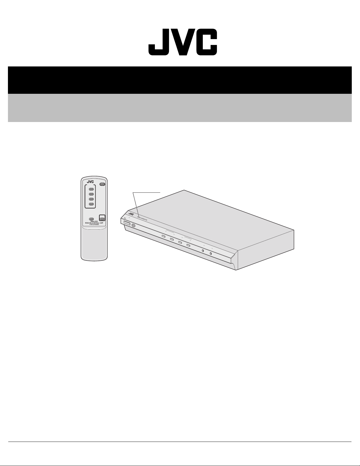
JX-S333-J
POWER
SOURCE
SELECT
1
2
3
4
DUBBING LOCK
(MONITOR SELECT)
LINK
Model No.
ST
ANDBY/ON
1
SOURCE SELECT
2
3
4
DUBBING
(MONITOR SELECT)
LOCK
LINK
TABLE OF CONTENTS
1 PRECAUTION. . . . . . . . . . . . . . . . . . . . . . . . . . . . . . . . . . . . . . . . . . . . . . . . . . . . . . . . . . . . . . . . . . . . . . . . . 1-3
2 SPECIFIC SERVICE INSTRUCTIONS . . . . . . . . . . . . . . . . . . . . . . . . . . . . . . . . . . . . . . . . . . . . . . . . . . . . . . 1-4
3 DISASSEMBLY . . . . . . . . . . . . . . . . . . . . . . . . . . . . . . . . . . . . . . . . . . . . . . . . . . . . . . . . . . . . . . . . . . . . . . . 1-5
4 ADJUSTMENT . . . . . . . . . . . . . . . . . . . . . . . . . . . . . . . . . . . . . . . . . . . . . . . . . . . . . . . . . . . . . . . . . . . . . . . . 1-6
5 TROUBLESHOOTING . . . . . . . . . . . . . . . . . . . . . . . . . . . . . . . . . . . . . . . . . . . . . . . . . . . . . . . . . . . . . . . . . . 1-7
COPYRIGHT © 2005 Victor Company of Japan, Limited
No.XC031
2005/3
Page 2
SPECIFICATION
Product name AV selector
Input/output connectors Inputs:4 lines (Component, S-VIDEO, AUDIO L/R) x 4
Outputs:2 lines (S-VIDEO, AUDIO L/R) x 2
Monitor outputs:1 line (Component, S-VIDEO, AUDIO L/R) x 1
Video inputs Reference level
S-VIDEO Y:Vp-p = 1.0 V (75 Ω)
C: Vp-p = Burst 0.286 V/ Cyan 0.642 V (75 Ω)
Component signals
Y: Vp-p = 1.0 V (75Ω)
Cb/Pb: Vp-p = 0.7 V (75 Ω)
Cr/Pr: Vp-p = 0.7 V (75 Ω)
Maximum input
S-VIDEO V: Vp-p = 1.5 V (75Ω)
C: Vp-p = Burst 0.429 V/ Cyan 0.963 V (75Ω)
Component signals
Y: Vp-p = 1.5 V (75Ω)
Cb/Pb: Vp-p = 1.05 V (75Ω)
Cr/Pr: Vp-p = 1.05 V (75Ω)
Video outputs
(Reference level)
Video crosstalk 50 dB or more (45 dB or more between Y/C and Y/Pb/Pr in the same channel)
Video S/N ratio 50 dB or more
Video frequency response S-VIDEO: 10 MHz, Component signals: 30 MHz
Audio inputs Reference level: -10 dBV (47 kΩ)
Audio outputs -10 dBV (with reference input, 1 kHz)
Audio crosstalk 80 dB or more (1 kHz)
Audio S/N ratio 80 dB or more
Audio frequency response 5 Hz to 50 kHz
Distortion Less than 0.03% (with reference input, 1 kHz)
Power requirements AC 120 V ~, 60 Hz
Power consumption 6 W (less than 2.0 W in standby mode)
Dimensions (W) 435 mm x (H) 64 mm x (D) 282 mm (including knobs, jacks, and feet)
Main body weight 2.4 kg (5.3 lbs)
Accessories Remote control unit (RM-AJ333), “AA” (R6/UM-3) battery x 2 (for operation testing)
S-VIDEO Y: Vp-p = 1.0 V (75Ω)
C: Vp-p = Burst 0.286 V/ Cyan 0.642 V (75Ω)
Component signals
Y: Vp-p = 1.0 V (75Ω)
Cb/Pb: Vp-p = 0.7 V (75Ω)
Cr/Pr: Vp-p = 0.7 V (75Ω)
Maximum level:+6 dBV (1 kHz, 1% distortion)
(17-3/16" x 2-9/16" x 11-1/8")
1-2 (No.XC031)
Page 3
SECTION 1
PRECAUTION
1.1 Safety Precautions
(1) This design of this product contains special hardware and
many circuits and components specially for safety purposes. For continued protection, no changes should be made
to the original design unless authorized in writing by the
manufacturer. Replacement parts must be identical to
those used in the original circuits. Services should be performed by qualified personnel only.
(2) Alterations of the design or circuitry of the product should
not be made. Any design alterations of the product should
not be made. Any design alterations or additions will void
the manufacturers warranty and will further relieve the
manufacture of responsibility for personal injury or property
damage resulting therefrom.
(3) Many electrical and mechanical parts in the products have
special safety-related characteristics. These characteristics are often not evident from visual inspection nor can the
protection afforded by them necessarily be obtained by using replacement components rated for higher voltage, wattage, etc. Replacement parts which have these special
safety characteristics are identified in the Parts List of Service Manual. Electrical components having such features
are identified by shading on the schematics and by ( ) on
the Parts List in the Service Manual. The use of a substitute
replacement which does not have the same safety characteristics as the recommended replacement parts shown in
the Parts List of Service Manual may create shock, fire, or
other hazards.
(4) The leads in the products are routed and dressed with ties,
clamps, tubings, barriers and the like to be separated from
live parts, high temperature parts, moving parts and/or
sharp edges for the prevention of electric shock and fire
hazard. When service is required, the original lead routing
and dress should be observed, and it should be confirmed
that they have been returned to normal, after reassembling.
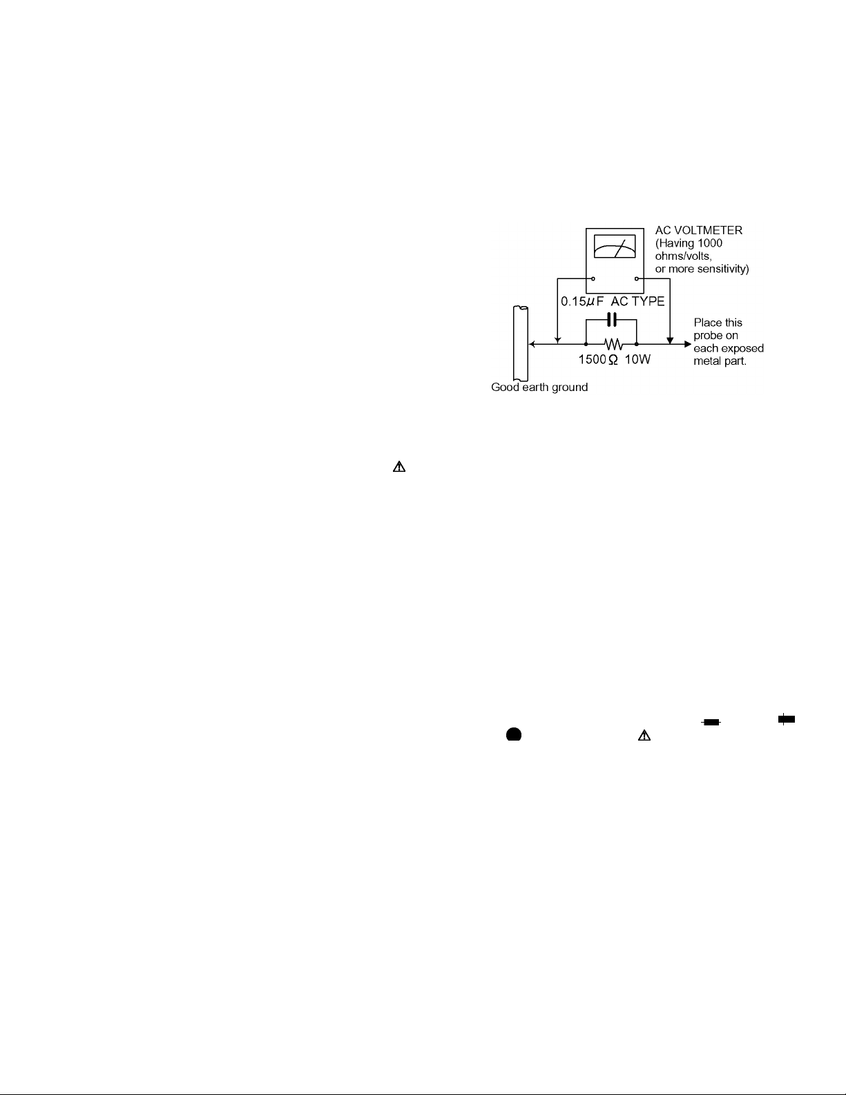
(5) Leakage shock hazard testing)
After reassembling the product, always perform an isolation check on the exposed metal parts of the product (antenna terminals, knobs, metal cabinet, screw heads,
headphone jack, control shafts, etc.) to be sure the product
is safe to operate without danger of electrical shock.Do not
use a line isolation transformer during this check.
• Plug the AC line cord directly into the AC outlet. Using a
"Leakage Current Tester", measure the leakage current
from each exposed metal parts of the cabinet, particularly any exposed metal part having a return path to the
chassis, to a known good earth ground. Any leakage current must not exceed 0.5mA AC (r.m.s.).
• Alternate check method
Plug the AC line cord directly into the AC outlet. Use an
AC voltmeter having, 1,000 ohms per volt or more sensitivity in the following manner. Connect a 1,500 ohm 10W
resistor paralleled by a 0.15 F AC-type capacitor between an exposed metal part and a known good earth
ground.
Measure the AC voltage across the resistor with the AC
voltmeter.
Move the resistor connection to each exposed metal
part, particularly any exposed metal part having a return
path to the chassis, and measure the AC voltage across
the resistor. Now, reverse the plug in the AC outlet and
repeat each measurement. Voltage measured any must
not exceed 0.75 V AC (r.m.s.). This corresponds to 0.5
mA AC (r.m.s.).
1.2 Warning
(1) This equipment has been designed and manufactured to
meet international safety standards.
(2) It is the legal responsibility of the repairer to ensure that
these safety standards are maintained.
(3) Repairs must be made in accordance with the relevant
safety standards.
(4) It is essential that safety critical components are replaced
by approved parts.
(5) If mains voltage selector is provided, check setting for local
voltage.
1.3 Caution
Burrs formed during molding may be left over on some parts
of the chassis.
Therefore, pay attention to such burrs in the case of preforming repair of this system.
1.4 Critical parts for safety
In regard with component parts appearing on the silk-screen
printed side (parts side) of the PWB diagrams, the parts that are
printed over with black such as the resistor ( ), diode ( )
and ICP ( ) or identified by the " " mark nearby are critical for
safety. When replacing them, be sure to use the parts of the
same type and rating as specified by the manufacturer. (Except
the JC version)
(No.XC031)1-3
Page 4
SECTION 2
SPECIFIC SERVICE INSTRUCTIONS
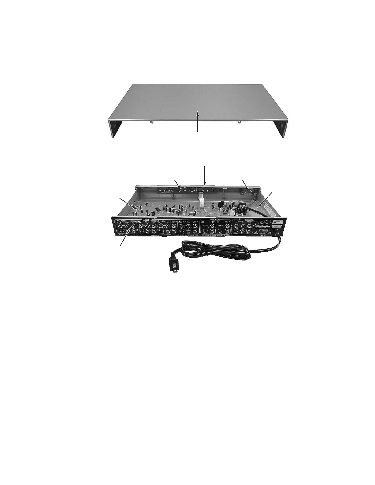
Location of major parts
Top cover
Front panel assembly
Main board
Rear panel
Switch board
Remote control board
Bottom chassis
1-4 (No.XC031)
Page 5
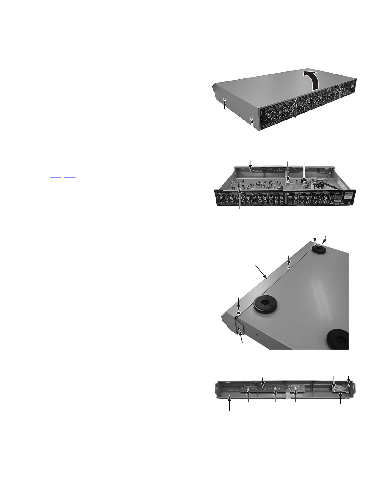
SECTION 3
TOP COVER
BOTTOM
DISASSEMBLY
3.1 Main body section
3.1.1 Removing the top cover (See Figure 1)
(1) Remove the four screws [A] attaching the top cover on
both sides of the main body.
(2) Remove the two screws [B] attaching the top cover on the
back of the main body.
(3) Raise the both sides and lower part of the rear of the top
cover, with opening them slightly in an outward direction.
And the top cover will be removed.
3.1.2 Removing the front panel assembly (See Figure 2, Figure 3)
• Prior to performing the following procedure, remove the top
cover.
(1) Disconnect the card wire and socket wire from connectors
, CN2 on the main board respectively.
CN1
(2) Remove the three screws [C] attaching the front panel as-
sembly on the bottom of the main body.
(3) Hook [a] is removed, and the front panel assembly is re-
moved.
TOP COVER
TOP COVER
A
x 2
A
x 2
Front panel assembly
Main board
B
Fig.1
CN1 CN2
Fig.2
C
B
Hook a
Front panel assembly
3.1.3 Removing the switch board and remote control board (See Figure 4)
• Prior to performing the following procedure, remove the top
cover, front panel assembly.
(1) Remove the five screws [D] attaching the switch board and
remote control board.
Front panel assembly
C
Hook a
Fig.3
Switch board
Fig.4
C
BOTTOM
DDD
DD
Remote control
board
(No.XC031)1-5
Page 6
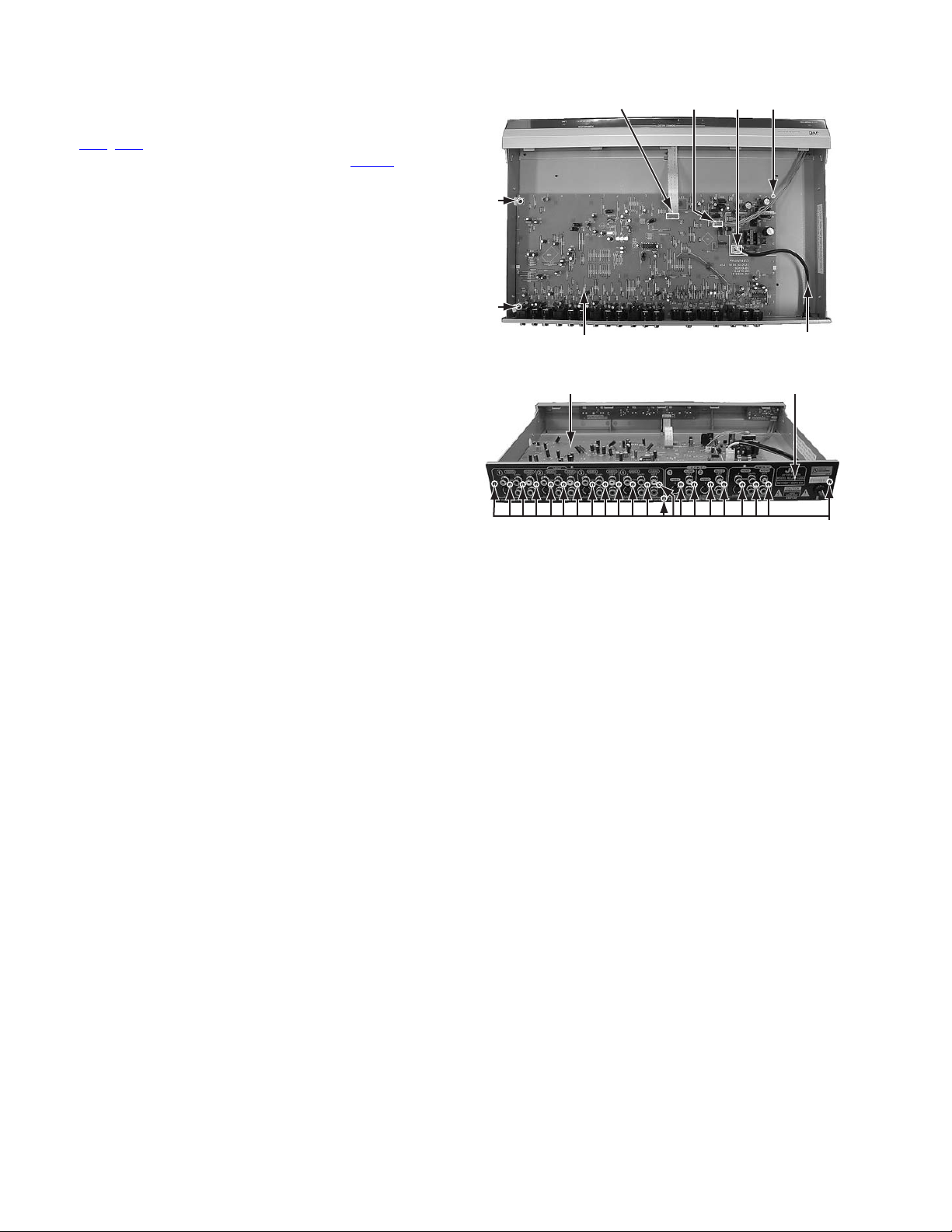
3.1.4 Removing the rear panel and main board (See Figure 5, Figure 6)
• Prior to performing the following procedure, remove the top
cover.
(1) Disconnect the card wire and socket wire from connector
CN1, CN2 on the main board respectively.
(2) Disconnect the power cord from connector CN901
main board.
(3) Remove the twenty-two screws [E] attaching the rear pan-
el.
(4) Remove the two screws [F] attaching the main board.
(5) The fastener one place where the main board is fixed is re-
moved.
on the
F
F
CN1
CN2 CN901
Fastener
Main board
Fig.5
Main board Rear panel
Fig.6
SECTION 4
ADJUSTMENT
This service manual does not describe ADJUSTMENT.
Power cord
E
1-6 (No.XC031)
Page 7
SECTION 5
TROUBLESHOOTING
5.1 Circuit explanation
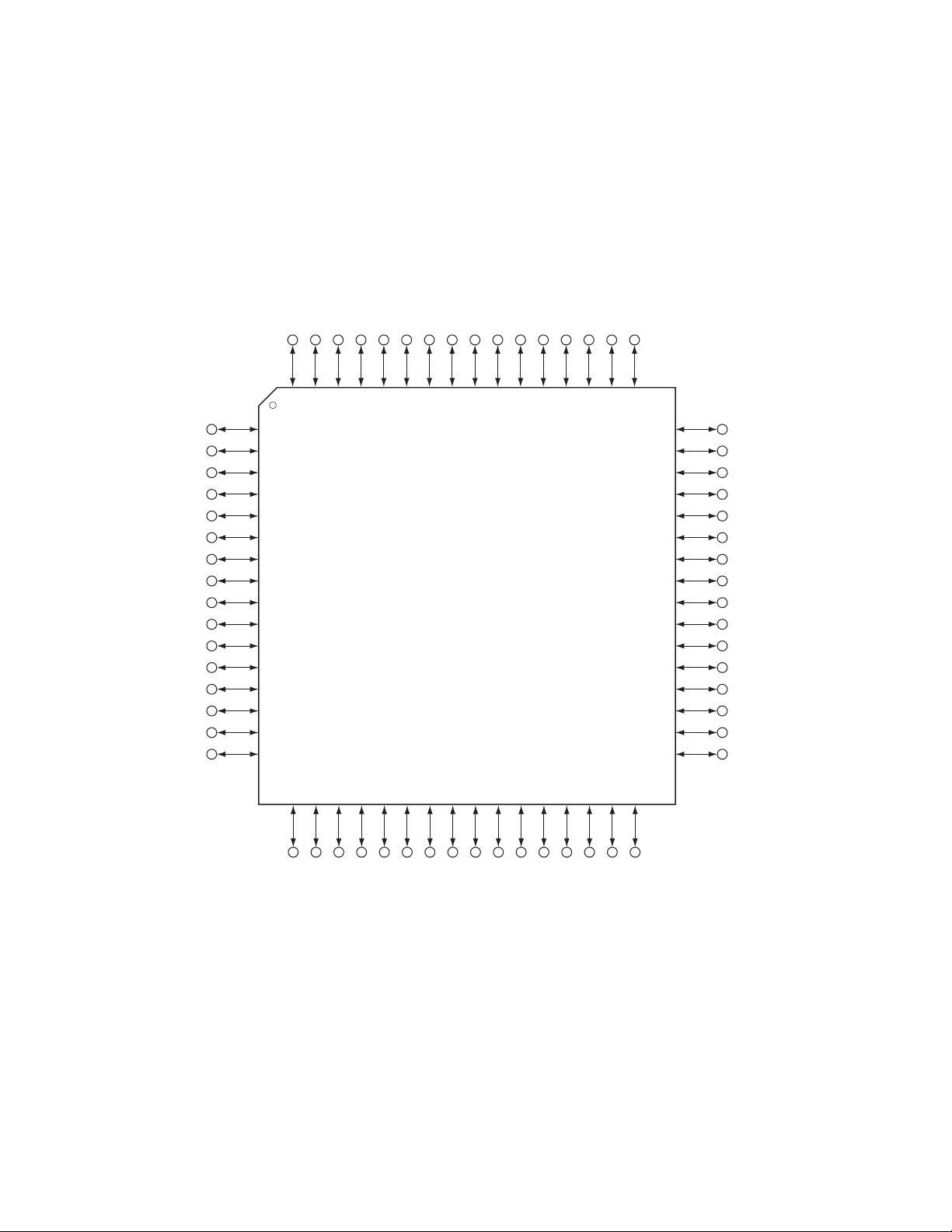
5.1.1 IC1(uPD780021AYGKN1)
uPD780021AYGKN1 is single chip microcomputer of 64 pin 8 bit equipped with the memory of ROM:8k byte / RAM:512 byte
* Pin layout
P47/AD7
P46/AD6
P45/AD5
P44/AD4
P43/AD3
P42/AD2
P41/AD1
P40/AD0
P67/ASTB
P66/WAIT
P65/WR
P64/RD
P75/BUZ
P74/PCL
P73/TI51/TO51
P72/TI50/TO50
64 555657585960616263 54 4950515253
P50/A8
P51/A9
P52/A10
P53/A11
P54/A12
P55/A13
P56/A14
P57/A15
Vsso
Vddo
P30
P31
P32
P33
P34/SI31
P35/SO31
1
2
3
4
5
6
7
8
9
10
11
12
13
14
15
16
17 262524232221201918 27 3231302928
48
47
46
45
44
43
42
41
40
39
38
37
36
35
34
33
P71/TI01
P70/TI00/TO00
P03/INTP3/ADTRG
P02/INTP2
P01/INTP1
P00/INTP0
Vss1
X1
X2
IC(Vpp)
XT1
XT2
RESET
AVdd
AVref
P10/ANI0
P20/SI30
P20/SO30
P36/SCK31
P24/TxD0
P23/RxD0
P22/SCK30
AVss
Vdd1
P25/ASCK0
P17/NI7
P16/AIN6
P14/ANI4
P13/ANI3
P15/ANIN5
P12/ANI2
P11/ANI1
(No.XC031)1-7
Page 8
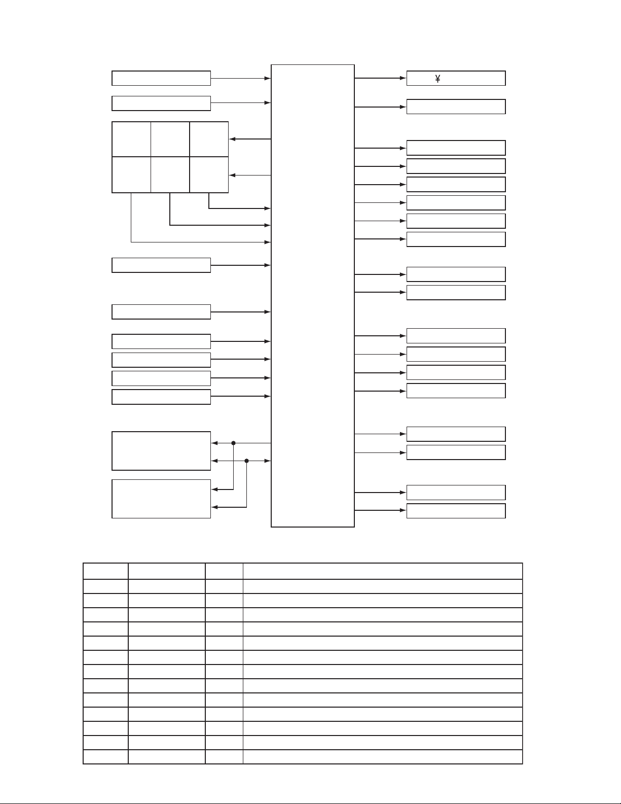
* Block diagram
KEY
1ch
KEY
2ch
P-SW
HD
KEY
3ch
KEY
4ch
REMO
D-SW
S-SW 1
S-SW 2
S-SW 3
S-SW 4
P-ON
P-ON
LOCK
LED_1CH
LED_2CH
LINK
LED_3CH
LED_4CH
LED_LOCK
LED_LINK
D-OFF1
D-OFF2
CH-SEL1
CH-SEL2
CH-SEL3
CH-SEL4
CXA2079Q
CXA2019Q
* Pin function (1/2)
Pin No.
1
2
3
4
5
6
7
8
9
10
11
12
13
SONY/
SONY/
Symbol
P50
P51
P52
P53
P54
P55
P56
P57
Vsso
Vddo
P30
P31
P32/SDA0
I/O
O
O
O
O
O
O
O
O
I/O
D-SELA
D-SELB
PCT1
PCT2
Description
LED lighting output
LED lighting output
LED lighting output
LED lighting output
LED lighting output
LED lighting output
Switch of D and S
Switch of D and S
-
-
-
-
Ground of port
Positive power supply of port
Not use
Not use
I2C Bus communication (data)
1-8 (No.XC031)
Page 9

* Pin f
(2/2)
unction
Pin No.
14
15
16
17
18
19
20
21
22
23
24
25
26
27
28
29
30
31
32
33
34
35
36
37
38
39
40
41
42
43
44
45
46
47
48
49
50
51
52
53
54
55
56
57
58
59
60
61
62 to 64
Symbol
P33/SCL0
P34
P35
P36
P20
P21
P22
P23
P24
P25
Vdd1
AVss
P17/ANI7
P16/ANI6
P15/ANI5
P14/ANI4
P13/ANI3
P12/ANI2
P11/ANI1
P10/ANI0
AVr ef
AVdd
RESET
XT2
XT1
IC(Vpp)
X2
X1
Vss1
P00/INTP0
P01/INTP1
P02/INTP2
P03/INTP3
P70/TI00
P71
P72
P73
P74
P75
P64
P65
P66
P67
P40
P41
P42
P43
P44
P45 to P47
I/O
O
O
O
O
O
O
O
O
O
O
O
O
O
I/O
I/O
Description
I2C Bus communication (clock)
-
I
I
I
I
I
-
-
I
I
I
I
I
I
I
I
-
-
I
I
I
-
-
-
I
I
-
-
I
-
I
I
I
-
Not use
Power-ON output
Reversing of power-ON output
D detection input
S detection input
S detection input
S detection input
S detection input
Not use
Positive power supplies other than port
Ground terminal
Not use (Connect to Vsso)
Not use (Connect to Vsso)
Not use (Connect to Vsso)
Not use (Connect to Vsso)
Not use (Connect to Vsso)
Not use (Connect to Vsso)
Not use (Connect to Vsso)
Not use (Connect to Vsso)
Connect to Vsso (A/D Standard power supply)
Connect to Vddo (A/D power supply)
Reset
Open (Not use)
Connect to Vddo (Not use)
Connect to Vsso
Main clock 4MHz
Main clock 4MHz
Ground terminal other than port
Horizontal synchronizing signal detection input
Power ON/OFF input
Not use
Not use
Remote control reception
Not use
Output of input CH
Output of input CH
Output of input CH
Output of input CH
Output of input CH
Output of input CH
Output of protect CH CH1
Output of protect CH CH2
Key matrix (2 x 3) input
Key matrix (2 x 3) input
Key matrix (2 x 3) input
Key matrix (2 x 3) output
Key matrix (2 x 3) output
Not use
(No.XC031)1-9
Page 10

5.1.2 IC107(CXA2019AQ)
CXA2019AQ is bipolar IC that accumulates the brightness signal processing, the color signal processing, and the synchronous signal
processing of NTSC and PAL in single-chip. It corresponds to the I2C bus.
Various adjustments and the controls are possible according to two bus lines of SCL and SDA.
* Pin layout
SECAM REF
APC
X 443/358
X 358
X NTSC
SVcc
-(R_Y)OUT
-(B_Y)OUT
-(B_Y)IN
-(R_Y)IN
30 212223242526272829
S GND
CIN
A PED
CVBS/Y IN
ADRS
SCL
SDA
V SYNC
H SYNC
V HOLD
31
32
33
34
35
36
37
38
39
40
20
19
18
17
16
15
14
13
12
11
V OUT
U OUT
Y OUT
SGND2
SCP
H TIM
V TIM
V2 IN
U2 IN
Y2 IN
1 1098765432
AFC
JVcc
CREA
IREF
J GND
V2 OUT
Y2 OUT
U2 OUT
CP IN
ABLFILIN
* Block diagram
ADRS
SDA
SCL
IREF
H SYNC
J GND
J Vcc
AFC
CERA
SCP
H TIM
V SYNC
CVBS/Y IN
CIN
S GND
35 37 36 39 16 15 38 40 14
2
I C BUS
DECODER
CV/YC
SUB CONT
34
VIDEO
SW
32
ACC
31
45321 6 7 8
32/H
VCO
H.SYNC
IREF
SEP
SECAM
SUB
CONT
SUB COLOR
TRAP
ACC
DET.
TOT
DELAY
SECAM
30 25 29 28 27 26 33 23 24 22 21
TOT ON
KILLER
SECAM REF
TRAP
BST AMP
COLOR
KILLER
SVcc
PHASE
DET.
AFC HLOCK
TRAP ON
PHASE
DET.
LPF
APC
H.DRIVE
1/32
2/H
SHP 10
DELAY
PRE OVER
DELAY SHARPNESS CLAMP
SUB HUE
NT/PAL
HUE
PAL I D
ID AXIS
HUE
CHROMA
VCO
4.43/3.58
SW
X 358
X 443/358
X NTSC
V HOLD
V.S YN C
SEP
SHARPNESS
DC TRAN
NT/PAL
2fH
F.F
DEM
AXIS
PHASE
SHIFT
X'TAL PIN
V TIM
V.COUNT
DOWN
C MODE
V2 OUT
V2 PED
50/60
V2 PED V2 DRIVE
AUTO
PEDESTAL
CHROMA
DET.
A PED
(B_Y) OUT
V2 DRIVE
COLOR
CLAMP
(R_Y) OUT
U2 OUT
U2 PED
U2 DRIVE
U2 PED U2 DRIVE
Y DRIVE
Y DRIVE
COLOR
DET
SW
NT/PAL
EXT COLOR
(R_Y) IN
(B_Y) IN
U PED
U PED
Y2 OUT
Y2 DRIVE
Y2 DRIVE
V PED
V PED
ABL CENT
ABL
9
11
12
13
10
17
18
19
20
ABLFILIN
Y2 IN
U2 IN
V2 IN
CP IN
SGND2
Y OUT
U OUT
V OUT
* The sub picture bright and white balance can be adjusted
by receiving BGP or SCP output from the main picture Y/C/J,
clamping the PINP PROC. output, and varying the DC of the
clamped portion.
1-10 (No.XC031)
Page 11

5.1.3 IC101(CXA-2079Q)
CXA-2079Q is AV switch IC for I2CBus for TV of "Six video system input two outputs" and "Six audio system
stereo input two outputs". Four input corresponds to the S2 standard and S standard among six video system input.
Each output (The audio system treats Lch and Rch as a couple) can select an arbitrary independently input,
and this is done by the I2CBus control.
However, the output of the second system selects the same input system as the video system and the audio system.
* Pin layout * Block diagram
VGND
57
27
S2-4
YOUT1
TRAP1
55
56
29
28
NC
S-4
ROUT1
54
30
NC
NC
VOUT1
LOUT1
52
53
32
31
ADR
51
50
49
48
47
46
45
44
43
42
41
40
39
38
37
36
35
34
33
CIN1
BIAS
YIN1
MUTE
NC
NC
YIN2
AGND2
CIN2
CC
V
VOUT2
ROUT2
YOUT2
LOUT2
COUT2
DC OUT
AGND
SDA
SCL
TV
V1
V2
V3
V4
V5
Y1
Y2
Y3
Y4
C1
C2
C3
C4
LTV
LV1
LV2
LV3
LV4
LV5
63
1
8
15
22
60
3
10
17
24
5
12
19
26
62
2
9
16
23
59
LV1
RV1
S2-1
S-1
LV2
RV2
S2-2
S-2
LV3
RV3
RV5
61
23
LV4
COUT1
LV5
V5
59
58
60
26
25
24
C4
RV4
Y4
RTV
LTV
TV
62
64
63
1
V1
2
3
Y1
4
5
C1
6
7
8
V2
9
10
Y2
11
12
C2
13
14
15
V3
16
17
Y3
18
19
C3
20
21
22
V4
S-3
S2-3
6dB
6dB
6dB
6dB
6dB
6dB
BIAS
6dB
0dB
6dB
0dB
53
49
56
55
58
51
41
45
39
37
43
57
50
42
35
44
52
54
38
VOUT1
YIN1
YOUT1
TRAP1
COUT1
CIN1
VOUT2
YIN2
YOUT2
COUT2
CIN2
VGND
BIAS
V
CC
AGND
AGND2
LOUT1
ROUT1
LOUT2
RTV
RV1
RV2
RV3
RV4
RV5
NC
NC
NC
NC
NC
40
36
33
34
32
7
14
21
28
6
13
20
27
48
ROUT2
DC OUT
SCL
SDA
ADR
S-1
S-2
S-3
S-4
S2-1
S2-2
S2-3
S2-4
MUTE
6dB
64
4
6dB
11
18
25
61
Logic
29
30
31
46
47
(No.XC031)1-11
Page 12

5.2 Troubleshooting
5.2.1 Standard input signal
Vedeo signal
V→Full field color bar(White100%)1.0Vp-p
Y→1.0Vp-p(With synchronous signal)
C→Burst level 0.286Vp-p Only chroma signal
Pb / Pr →0.7Vp-p
Audio signal
1kHz,- 10dBV Sine wave
YES→Normality
NO→Neither the voltage nor the shape of waves are nomal.
Symptom Check point Voltage and shape of waves
Check and locating fault
when it is normal
1.The power supply
doesn't enter
1 Between C903+ and C903- Approx DC 164V NO→Check of power cord and
CN901
Please check Q901,T901,D901
surrounding enough when the
fuse has been disconnected.
YES →Check of 2
2 Cathode of D906
Anode of D908
DC + 9.4 V
DC - 9.8 V
NO→The IC905 surrounding is
checked. or Defect of PC901
YES →Check of 3
3 Emitter of Q904
Emitter of Q905
3 pin of IC902
2 pin of IC903
DC + 6.4 V
DC - 6.4 V
DC + 5 V
DC +9 V
NO→Defective IC902 and IC903.
Defective Q904 to Q906.
YES→Check of CN1, CN2 and
wire
2.Lighting failure LED 4 1 pin to 6 pin of CN1 DC 0 V or + 5 V NO→Defective Q1 to Q6.
YES→Check of CN1, CN701 and
wire
3.Defective operation of
switch
5 8 pin to 12 pin of CN1 DC 0 V or + 5 V NO→Defective IC2.
YES→Check of CN1, CN701 and
wire Defective tact switch
4.The remote control
operation is abnormal
6 47 pin of IC1 DC + 5 V Remote control code
(Refer to TM.)
NO→Defective IC701, CN1,
CN701 and wire.
YES →Defective IC1.
5.Link function defective
operation
7 8 pin of IC106 DC + 5 V NO→Check of 8
YES→IC1, Q909, and the circum-
ference circuit are checked.
8 2 pin of IC106 NO→IC105 and the circumfer-
ence circuit are checked.
1.0 Vp-p
YES→IC106 and the circumfer-
ence circuit are checked.
Notice (When component terminals are used)
When S-Video signals are input to the JX-S333 from VCR and Video Camcorder, and JX-S333 is connected to TV through component output terminals, the phenomena of distortions or image disorders may occur on some TV sets.
As the phenomena are caused by specifications of the TV, when these are occurred, they cannot be avoid or improved.
Please note that the JX-S333 does not have functions of stabilizing or improving video image although JX-S333 can convert video
signal formats.
When these phenomena happen, connection by S Video cord between JX-S333 and TV is recommended without a component signal line..
1-12 (No.XC031)
Page 13

Symptom Check point Voltage and shape of waves
when it is normal
6.The S-VIDEO signal
input from 1 to 4CH is
not output from terminal
S-VIDEO.
9 (Y) Base of Q110, Q114
(C) Base of Q108, Q112
(Y)
2.0 Vp-p
(C)
1.28 Vp-p
Check and locating fault
NO→Check of 10
YES→Output buffer and the cir-
cumference circuit are checked.
7.The S-VIDEO signal
input from 1 to 4CH is
not output from terminal
monitor.
10 (Y) Emitter of Q103
(C) Emitter of Q104
11 (Y) Emitter of Q101
(C) Emitter of Q102
(Y)
(C)
(Y)
(C)
2.0 Vp-p
1.28 Vp-p
2.0 Vp-p
1.28 Vp-p
NO→IC101 and the circumfer-
ence circuit are checked.
YES→Defective IC103, IC108.
NO→IC101 and the circumfer-
ence circuit are checked.
YES→Output buffer and the cir-
cumference circuit are checked.
(No.XC031)1-13
Page 14

Symptom Check point Voltage and shape of waves
when it is normal
8.The component signal
conversion function
doesn't operate.
12 (Y) 6 pin of IC206
(Pb) 5 pin of IC206
(Pr) 3 pin of IC206
(Y)
1.0 Vp-p
(Pb)
0.7 Vp-p
(Pr)
0.7 Vp-p
Check and locating fault
NO→Check of 13
YES→IC207 and the circumfer-
ence circuit are checked.
13 (Y) Emitter of Q124
(Pb) Emitter of Q123
(Pr) Emitter of Q122
14 (Y) Emitter of Q126
(C) Emitter of Q125
(Y)
(Pb)
(Pr)
(Y)
(C)
1.0 Vp-p
0.7 Vp-p
0.7 Vp-p
2.0 Vp-p
1.28 Vp-p
NO→Check of 14
YES→IC206 and the circumfer-
ence circuit are checked.
NO→IC101 and the circumfer-
ence circuit are checked.
YES→IC107, Q122 to Q124 and
the circumference circuit are
checked.
1-14 (No.XC031)
Page 15

Symptom Check point Voltage and shape of waves
when it is normal
9.The component signal
is not output.
15 (Y) 6 pin of IC206
(Pb) 5 pin of IC206
(Pr) 3 pin of IC206
(Y)
1.0 Vp-p
(Pb)
0.7 Vp-p
(Pr)
0.7 Vp-p
Check and locating fault
NO→Check of 16
YES→IC207 and the circumfer-
ence circuit are checked.
16 (Y) 13 pin of IC201
(Pb) 3 pin of IC202
(Pr) 13 pin of IC202
17 (Y) Emitter of Q201,204,207,210
(Pb)Emitter of Q203,206,209,212
(Pr) Emitter of Q202,205,208,211
(Y)
(Pb)
(Pr)
(Y)
(Pb)
1.0 Vp-p
0.7 Vp-p
0.7 Vp-p
1.0 Vp-p
0.7 Vp-p
NO→Check of 17
YES→IC206 and the circumfer-
ence circuit are checked.
NO→Q201 to Q212 and the cir-
cumference circuit are checked.
YES→IC201 to IC202 and the cir-
cumference circuit are checked.
10.The audio signal is
not output.
11.The audio signal is
not output to the monitor
output terminal.
18 (L) 9, 11 pin of IC104
(R) 2, 3 pin of IC104
19 (L) 52 pin of IC101
(R) 54 pin of IC101
(Pr)
–10 dBV
(0.32 Vrms)
–10 dBV
(0.32 Vrms)
0.7 Vp-p
NO→IC101 and the circumfer-
ence circuit are checked.
YES→Defective IC104.
NO→IC101 and the circumfer-
ence circuit are checked.
YES→The substrate pattern
around PJ117 is checked.
(No.XC031)1-15
Page 16

5.3 Description of major ICs
5.3.1 IC107(CXA-2019AQ)
* Pin layout
SECAM REF
APC
X 443/358
X 358
30 212223242526272829
S GND
31
CIN
32
A PED
ADRS
SCL
SDA
V SYNC
H SYNC
V HOLD
33
34
35
36
37
38
39
40
CVBS/Y IN
1 1098765432
AFC
JVcc
IREF
CREA
* Block diagram
ADRS
SDA
SCL
IREF
45321 6 7 8
IREF
SUB
CONT
TRAP
ACC
DET.
TOT
DELAY
SECAM
30 25 29 28 27 26 33 23 24 22 21
SECAM REF
CVBS/Y IN
CIN
S GND
35 37 36 39 16 15 38 40 14
2
I C BUS
DECODER
CV/YC
SUB CONT
34
VIDEO
SW
32
SUB COLOR
ACC
31
X NTSC
SVcc
J GND
V2 OUT
H SYNC
H.SYNC
SEP
SECAM
TOT ON
KILLER
-(R_Y)OUT
-(B_Y)OUT
-(B_Y)IN
Y2 OUT
U2 OUT
ABLFILIN
J GND
AFC HLOCK
TRAP
BST AMP
COLOR
KILLER
SVcc
-(R_Y)IN
20
19
18
17
16
15
14
13
12
11
CP IN
J Vcc
AFC
PHASE
DET.
TRAP ON
PHASE
DET.
LPF
APC
V OUT
U OUT
Y OUT
SGND2
SCP
H TIM
V TIM
V2 IN
U2 IN
Y2 IN
CERA
SCP
H TIM
32/H
VCO
H.DRIVE
1/32
2/H
SHP 10
NT/PAL
PAL I D
ID AXIS
X NTSC
SHARPNESS
NT/PAL
PHASE
SHIFT
X'TAL PIN
DELAY
PRE OVER
DELAY SHARPNESS CLAMP
SUB HUE
HUE
HUE
CHROMA
VCO
4.43/3.58
SW
X 358
X 443/358
V SYNC
V HOLD
V.S YN C
SEP
DC TRAN
2fH
F.F
DEM
AXIS
V TIM
V.COUNT
DOWN
C MODE
V2 OUT
V2 PED
50/60
V2 PED V2 DRIVE
AUTO
PEDESTAL
CHROMA
DET.
A PED
(B_Y) OUT
V2 DRIVE
COLOR
CLAMP
(R_Y) OUT
U2 OUT
U2 PED
U2 DRIVE
U2 PED U2 DRIVE
Y DRIVE
Y DRIVE
COLOR
DET
SW
NT/PAL
EXT COLOR
(R_Y) IN
(B_Y) IN
U PED
U PED
Y2 OUT
Y2 DRIVE
Y2 DRIVE
V PED
V PED
ABL CENT
ABL
9
11
12
13
10
17
18
19
20
ABLFILIN
Y2 IN
U2 IN
V2 IN
CP IN
SGND2
Y OUT
U OUT
V OUT
* The sub picture bright and white balance can be adjusted
by receiving BGP or SCP output from the main picture Y/C/J,
clamping the PINP PROC. output, and varying the DC of the
clamped portion.
1-16 (No.XC031)
Page 17

5.3.2 IC101 CXA-2079Q [SONY]
* Pin layout
COUT1
YOUT1
VGND
LV5
V5
59
58
57
60
24
Y4
25
RV4
56
26
27
28
S-4
S2-4
C4
LV1
RV1
S2-1
S-1
LV2
RV2
S2-2
S-2
LV3
RV3
RTV
RV5
LTV
TV
62
64
63
61
1
V1
2
3
Y1
4
5
C1
6
7
8
V2
9
10
Y2
11
12
C2
13
14
15
V3
16
17
Y3
18
19
C3
20
23
21
22
LV4
V4
S-3
S2-3
TRAP1
55
29
NC
ROUT1
VOUT1
53
54
30
31
NC
NC
LOUT1
52
32
ADR
51
50
49
48
47
46
45
44
43
42
41
40
39
38
37
36
35
34
33
CIN1
BIAS
YIN1
MUTE
NC
NC
YIN2
AGND2
CIN2
CC
V
VOUT2
ROUT2
YOUT2
LOUT2
COUT2
DC OUT
AGND
SDA
SCL
* Block diagram
TV
63
V1
1
V2
8
V3
15
V4
22
V5
60
Y1
3
Y2
10
Y3
17
Y4
24
C1
5
C2
12
C3
19
C4
26
LTV
62
LV1
2
LV2
9
LV3
16
LV4
23
LV5
59
6dB
6dB
6dB
6dB
6dB
6dB
BIAS
6dB
0dB
6dB
0dB
53
49
56
55
58
51
41
45
39
37
43
57
50
42
35
44
52
54
38
VOUT1
YIN1
YOUT1
TRAP1
COUT1
CIN1
VOUT2
YIN2
YOUT2
COUT2
CIN2
VGND
BIAS
V
CC
AGND
AGND2
LOUT1
ROUT1
LOUT2
RTV
RV1
RV2
RV3
RV4
RV5
NC
NC
NC
NC
NC
40
36
33
34
32
7
14
21
28
6
13
20
27
48
ROUT2
DC OUT
SCL
SDA
ADR
S-1
S-2
S-3
S-4
S2-1
S2-2
S2-3
S2-4
MUTE
6dB
64
4
6dB
11
18
25
61
Logic
29
30
31
46
47
(No.XC031)1-17
Page 18

5.3.3 IC106,IC205 LA7217M [SANYO]
* Pin layout and block diagram
NC
14
Vcc AFC CTL VCO OUT VCO IN HD OUT DET OUT
13 12 11 10 89
12
NC VIDEO IN F.B CLAMP SYNC OUT VD OUT GND EXC
5.3.4 IC2 M51957AL [MITSUBISHI]
* Pin layout * Block diagram
M51957A/BL
AFC
SYNC
SEP
5
Output
4
Delay capacity
3
Ground
2
Input
1
Power supply
COUNT
DOWN
34
Input
32fH
VCO
Power supply
-
+
1.25V
LOCK
DET
V.SE P
5
A : With fixed current load
B : Open corrector
5 A
Standard Standard
25 A
-
76
Output
5.3.5 IC207 NJM2581D
* Pin layout and block diagram
1
VIN1
BIAS
VIN2
2
3
VEE1
BIAS
VIN3
4
5
VEE2
BIAS
VEE3
Power Save
6
7
6dB
AMP
6dB
AMP
6dB
AMP
75
Driver
75
Driver
75
Driver
REF
Delay capacityGround
14
V+1
13
VOUT1
12
V+2
11
VOUT2
10
V+3
9
VOUT3
8
GND
1-18 (No.XC031)
Page 19

5.3.6 IC206 NJM2584D
* Pin layout and block diagram
1
IN1B
2
NC
NC
IN3A
3
4
5
6
7
8
OUT1
GND2
OUT2
OUT3
5.3.7 IC103, IC104, IC108, IC109 TC74HC4066AFEL [TOSHIBA]
* Pin layout
11I/O
1O/I
14
13
Vcc
1C
BIAS
CLAMP
BIAS
16
15
14
13
12
11
10
9
IN1A
GND1
IN2B
V+
CTL
IN2A
GND3
IN3B
2O/I23
2I/O
4
2C
5
3C
6
GND
7
* Truth table
CONTROL SWITCH FUNCTION
(TOP VIEW)
H
L
ON
OFF
12
11
10
9
8
4C
4I/O
4O/I
3O/I
3I/O
(No.XC031)1-19
Page 20

5.3.8 IC903 PQ09RD08 [SHARP]
* Pin layout * Block diagram
2
1 43
5.3.9 IC701 RPM7138 [ROHM]
* Block diagram
1
DC Input (Vin)
2
DC Output (Vo)
3
Ground
ON/OFF Control terminal (Vc)
4
1 2
Special IC
4
3
VCC
LimiterAMP
I/V
5.3.10 IC105, IC201, IC202 TC74HC4052AFEL [TOSHIBA]
* Pin layout
0Y 1
2Y 2
Y - COM 3
3Y 4
1Y 5
INH 6
EE 7
V
GND 8
16 V
cc
15 2X
14 1X
13 X - COM
12 0X
11 3X
10 A
9 B
* Truth table
INHIBIT
* Block diagram
BPF
L
L
L
L
L
L
L
L
H
Demodulator
and integrator
C*
L
L
L
L
H
H
H
H
X
I / OCO / I
Comparator
B
L
L
H
H
L
L
H
H
X
X-COM
0X
A
L
H
L
H
L
H
L
H
X
22K
R
OUT
"ON" CHANNELCONTROL INPUTS
HC4052A
0X, 0Y
1X, 1Y
2X, 2Y
3X, 3Y
-- --
-- --
-- --
-- --
NONE
A
B
INH
1-20 (No.XC031)
Logic Level Converter
I / OCO / I
1X
2X
3X
0Y
1Y
2Y
3Y
Y-CO M
Page 21

5.3.11 IC905 uPC1093J [NEC]
* Pin layout * Block diagram
12 3
1 : REF
2 : A
3 : K
REF
D
K
Q
12
R
5
Q
1
R
1
1
R
2
R
3
Q
5
Q
2
C
1
R
6
Q
13
Q
14
C
15
2
Q
10
R
9
R
10
Q
11
Q
6
Q
7
R
7
Q
8
Q
Q
16
Q
17
5.3.12 IC902 uPC7805AHF [NEC]
* Pin layout * Block diagram
R4 R18
IN GND OUT
D1
Q13
R5
R6
R7
Q
3
R8 R9
Q8 Q9
Q10
Q6
Q5
R1
R2
Q12
R10
Q7
Q1
R3 R14
Q2
C1
Q
4
R
4
R
8
Q
9
A
INPUT
OUTPUT
GND
Q4
Q14
R16
Q15
Q3
R13
Q11
Q16
R15
R12R17
Q17
R11
R20
R19
(No.XC031)1-21
Page 22

5.3.13 IC1 uPD780021AYGKN1
* Pin layout
* Block diagram
P50/A8
P51/A9
P52/A10
P53/A11
P54/A12
P55/A13
P56/A14
P57/A15
Vsso
Vddo
P30
P31
P32
P33
P34/SI31
P35/SO31
P47/AD7
P46/AD6
P45/AD5
P44/AD4
P43/AD3
P42/AD2
P41/AD1
P40/AD0
P67/ASTB
64 555657585960616263 54 4950515253
1
2
3
4
5
6
7
8
9
10
11
12
13
14
15
16
17 262524232221201918 27 3231302928
AVss
Vdd1
P20/SI30
P36/SCK31
P23/RxD0
P20/SO30
P22/SCK30
P24/TxD0
P25/ASCK0
P66/WAIT
P65/WR
P64/RD
P17/NI7
P16/AIN6
P15/ANIN5
P75/BUZ
P74/PCL
P14/ANI4
P13/ANI3
P73/TI51/TO51
P72/TI50/TO50
48
47
46
45
44
43
42
41
40
39
38
37
36
35
34
33
P12/ANI2
P11/ANI1
P71/TI01
P70/TI00/TO00
P03/INTP3/ADTRG
P02/INTP2
P01/INTP1
P00/INTP0
Vss1
X1
X2
IC(Vpp)
XT1
XT2
RESET
AVdd
AVref
P10/ANI0
TI00/TO0/P70
TI01/P71
TI50/TO50/P72
TI51/TO51/P73
SI30/P20
SO30/P21
SCK30/P22
RxD0/P23
TxD0/P24
ASCK0/P25
SDA0/P32
SCL0/P33
ANI0/P10-
ANI7/P17
INTP0/P00-
INTP3/P03
BUZ/P75
PCL/P74
1-22 (No.XC031)
AVd d
AVs s
AVr ef
16-bit TIMER/
EVENT COUNTER0
8-bit TIMER/
EVENT COUNTER50
8-bit TIMER/
EVENT COUNTER51
WATCHDOG TIMER
WATCH TIMER
SERIAL
INTERFACE SIO30
UART0
I2C BUS
8
A/D CONVERTER
4
INTERRUPT
CONTROL
CLOCK/BUZZER
OUTPUT CONTROL
78K/0
CPU
CORE
ROM
(FLASH
MEMORY)
RAM
Vdd0 Vdd1 Vss0 Vss1 IC
(Vpp)
PORT0
PORT1
PORT2
PORT3
PORT4
PORT5
PORT6
PORT7
EXTERNAL
ACCESS
SYSTEM
CONTROL
8
4
6
7
8
8
4
6
8
8
P00-P03
P10-P17
P20-P25
P30-P36
P40-P47
P50-P57
P64-P67
P70-P75
AD0/P40AD7/P47
A8/P50A15/P57
RD/P64
WR/P65
WAIT/P66
ASTB/P67
RESET
X1
X2
XT1
XT2
Page 23

(No.XC031)1-23
Page 24

Victor Company of Japan, Limited
AV & MULTIMEDIA COMPANY ACCESSORIES CATEGORY 1644, Shimotsuruma, Yamato, Kanagawa 242-8514, Japan
(No.XC031)
Printed in Japan
VPT
 Loading...