

Page 1
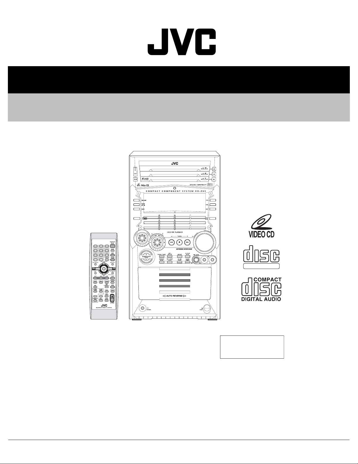
SERVICE MANUAL
COMPACT COMPONENT SYSTEM
2204120036
HX-Z9V
COMPACT
DIGITAL VIDEO
SELECT
E
M
D
N
O
M
U
U
D
N
B
E
D
O
E
R
C
S
V
S
E
E
R
T
P
M
U
L
O
V
COMPACT
DIGITAL VIDEO
CA-HXZ9V
Area Suffix
US ------------ Singapore
TABLE OF CONTENTS
1 Precautions . . . . . . . . . . . . . . . . . . . . . . . . . . . . . . . . . . . . . . . . . . . . . . . . . . . . . . . . . . . . . . . . . . . . . . . . . . 1-3
2 Disassembly method . . . . . . . . . . . . . . . . . . . . . . . . . . . . . . . . . . . . . . . . . . . . . . . . . . . . . . . . . . . . . . . . . . 1-5
3 Adjustment. . . . . . . . . . . . . . . . . . . . . . . . . . . . . . . . . . . . . . . . . . . . . . . . . . . . . . . . . . . . . . . . . . . . . . . . . . 1-34
4 Description of major ICs. . . . . . . . . . . . . . . . . . . . . . . . . . . . . . . . . . . . . . . . . . . . . . . . . . . . . . . . . . . . . . . 1-40
COPYRIGHT © 2003 VICTOR COMPANY OF JAPAN, LIMITED
No.22041
2003/5
Page 2
SPECIFICATION
Amplifier section Output Power (IEC 268-3) SUBWOOFERS 75 W per channel, min. RMS, both
channels driven into 6 Ω at 63 Hz with no
more than 0.9% total harmonic distortion.
MAIN SPEAKERS 30 W per channel, min. RMS, both channels driven into 6 Ω at 1 kHz
with no more than 0.9% total harmonic distortion.
Audio input sensitivity/Impedance (Measured at 1 kHz, with tape recording signal 300 mV)
AUX 390 mV/50 kΩ
MIX 1/2 1.5 mV/5 kΩ
Speakers/Impedance SUBWOOFERS 6 Ω - 16 Ω
MAIN SPEAKERS 6 Ω - 16 Ω
SURROUND SPEAKERS 16 Ω - 32 Ω
Tuner FM tuning range 87.50 MHz - 108.00 MHz
AM tuning range At 9 kHz intervals 531 kHz - 1 710 kHz
At 10 kHz intervals 530 kHz - 1 710 kHz
CD player CD capacity 3 CDs
Dynamic range 85 dB
Signal-to-noise ratio 90 dB
Wow and flutter Immeasurable
MP3 recording format MPEG 1/2 Audio Layer 3
Max. Bit rate 320 kbps
Cassette deck Frequency response Normal (type I) 50 Hz - 14 000 Hz
Wow and flutter 0.15% (WRMS)
General Power requirement AC 110 V / AC 127 V / AC 220 V /AC 230 V - AC 240 V (adjustable with
the voltage selector), 50 Hz / 60 Hz
Power consumption 205 W (in operation) 23 W (on standby with Ecology Mode off)
Less than 3.5 W (on standby with Ecology Mode on)
Dimensions (approx.) 205 mm × 370 mm × 370 mm (W/H/D)
Mass (approx.) 10.0 kg
Design and specifications are subject to change without notice.
1-2 (No.22041)
Page 3
1.1 Safety Precautions
Good earth ground
d
AC VOLTMETER
SECTION 1
Precautions
(1) This design of this product contains special hardware and
many circuits and components specially for safety purposes. For continued protection, no changes should be made
to the original design unless authorized in writing by the
manufacturer. Replacement parts must be identical to
those used in the original circuits. Services should be performed by qualified personnel only.
(2) Alterations of the design or circuitry of the product should
not be made. Any design alterations of the product should
not be made. Any design alterations or additions will void
the manufacturers warranty and will further relieve the
manufacture of responsibility for personal injury or property
damage resulting therefrom.
(3) Many electrical and mechanical parts in the products have
special safety-related characteristics. These characteristics are often not evident from visual inspection nor can the
protection afforded by them necessarily be obtained by using replacement components rated for higher voltage, wattage, etc. Replacement parts which have these special
safety characteristics are identified in the Parts List of Service Manual. Electrical components having such features
are identified by shading on the schematics and by ( ) on
the Parts List in the Service Manual. The use of a substitute
replacement which does not have the same safety characteristics as the recommended replacement parts shown in
the Parts List of Service Manual may create shock, fire, or
other hazards.
(4) The leads in the products are routed and dressed with ties,
clamps, tubings, barriers and the like to be separated from
live parts, high temperature parts, moving parts and/or
sharp edges for the prevention of electric shock and fire
hazard. When service is required, the original lead routing
and dress should be observed, and it should be confirmed
that they have been returned to normal, after reassembling.
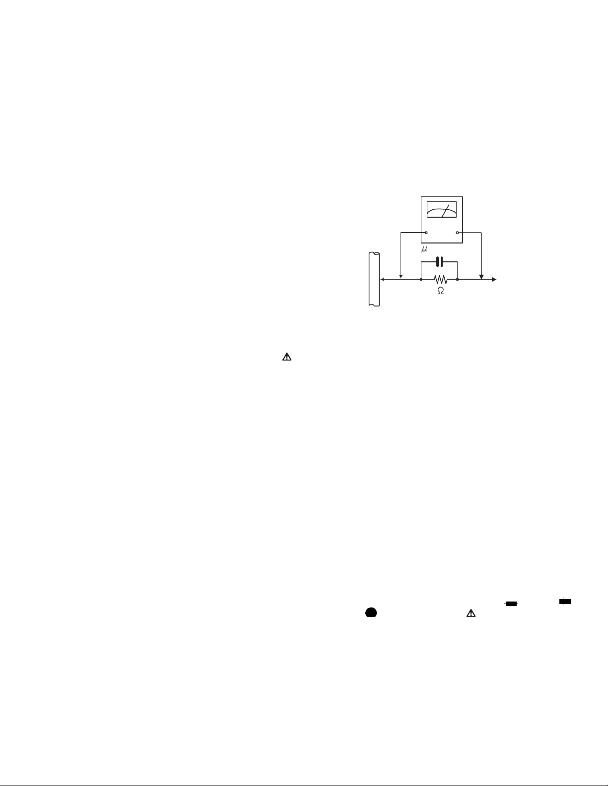
(5) Leakage shock hazard testing
After reassembling the product, always perform an isolation check on the exposed metal parts of the product (antenna terminals, knobs, metal cabinet, screw heads,
headphone jack, control shafts, etc.) to be sure the product
is safe to operate without danger of electrical shock.Do not
use a line isolation transformer during this check.
• Plug the AC line cord directly into the AC outlet. Using a
"Leakage Current Tester", measure the leakage current
from each exposed metal parts of the cabinet, particularly any exposed metal part having a return path to the
chassis, to a known good earth ground. Any leakage current must not exceed 0.5mA AC (r.m.s.).
• Alternate check method
Plug the AC line cord directly into the AC outlet. Use an
AC voltmeter having, 1,000Ω per volt or more sensitivity
in the following manner. Connect a 1,500Ω 10W resistor
paralleled by a 0.15µF AC-type capacitor between an ex-
posed metal part and a known good earth ground.
Measure the AC voltage across the resistor with the AC
voltmeter.
Move the resistor connection to each exposed metal
part, particularly any exposed metal part having a return
path to the chassis, and measure the AC voltage across
the resistor. Now, reverse the plug in the AC outlet and
repeat each measurement. Voltage measured any must
not exceed 0.75 V AC (r.m.s.). This corresponds to 0.5µ
mA AC (r.m.s.).
(Having 1000
ohms/volts,
or more sensitivity)
0.15 F AC TYPE
Place this
probe on
1500 10W
1.2 Warning
(1) This equipment has been designed and manufactured to
meet international safety standards.
(2) It is the legal responsibility of the repairer to ensure that
these safety standards are maintained.
(3) Repairs must be made in accordance with the relevant
safety standards.
(4) It is essential that safety critical components are replaced
by approved parts.
(5) If mains voltage selector is provided, check setting for local
voltage.
1.3 Caution
Burrs formed during molding may be left over on some parts
of the chassis.
Therefore, pay attention to such burrs in the case of preforming repair of this system.
1.4 Critical parts for safety
In regard with component parts appearing on the silk-screen
printed side (parts side) of the PWB diagrams, the parts that are
printed over with black such as the resistor ( ), diode ( )
and ICP ( ) or identified by the " " mark nearby are critical
for safety. When replacing them, be sure to use the parts of the
same type and rating as specified by the manufacturer.
(This regulation dose not Except the J and C version)
each expose
metal part.
(No.22041)1-3
Page 4
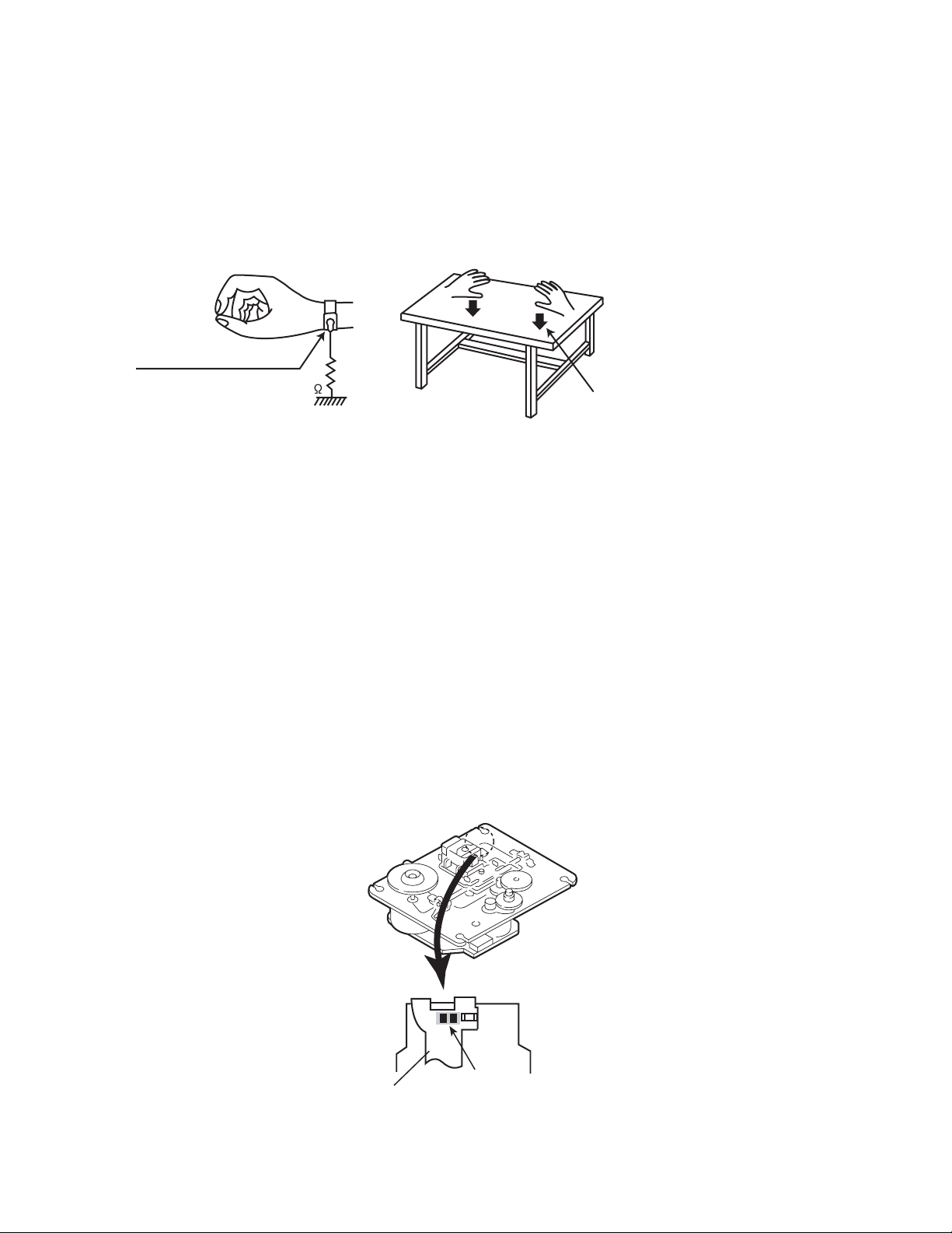
1.5 Preventing static electricity
Electrostatic discharge (ESD), which occurs when static electricity stored in the body, fabric, etc. is discharged, can destroy the laser
diode in the traverse unit (optical pickup). Take care to prevent this when performing repairs.
1.5.1 Grounding to prevent damage by static electricity
Static electricity in the work area can destroy the optical pickup (laser diode) in devices such as CD players.
Be careful to use proper grounding in the area where repairs are being performed.
(1) Ground the workbench
Ground the workbench by laying conductive material (such as a conductive sheet) or an iron plate over it before placing the
traverse unit (optical pickup) on it.
(2) Ground yourself
Use an anti-static wrist strap to release any static electricity built up in your body.
(caption)
Anti-static wrist strap
1M
Conductive material
(conductive sheet) or iron palate
(3) Handling the optical pickup
• In order to maintain quality during transport and before installation, both sides of the laser diode on the replacement optical
pickup are shorted. After replacement, return the shorted parts to their original condition.
(Refer to the text.)
• Do not use a tester to check the condition of the laser diode in the optical pickup. The tester's internal power source can easily
destroy the laser diode.
1.6 Handling the traverse unit (optical pickup)
(1) Do not subject the traverse unit (optical pickup) to strong shocks, as it is a sensitive, complex unit.
(2) Cut off the shorted part of the flexible cable using nippers, etc. after replacing the optical pickup. For specific details, refer to the
replacement procedure in the text. Remove the anti-static pin when replacing the traverse unit. Be careful not to take too long
a time when attaching it to the connector.
(3) Handle the flexible cable carefully as it may break when subjected to strong force.
(4) I t is not possible to adjust the semi-fixed resistor that adjusts the laser power. Do not turn it.
1.7 Attention when traverse unit is decomposed
*Please refer to "Disassembly method" in the text for the CD pickup unit.
• Apply solder to the short land sections before the flexible wire is disconnected from the connector CN101 on the CD servo board.
(If the flexible wire is disconnected without applying solder, the CD pickup may be destroyed by static electricity.)
• In the assembly, be sure to remove solder from the short land sections after connecting the flexible wire.
1-4 (No.22041)
CD traverse
mechanism unit
Flexible cable
Fig.1
Soldering
Fig.2
Page 5
SECTION 2
A
Disassembly method
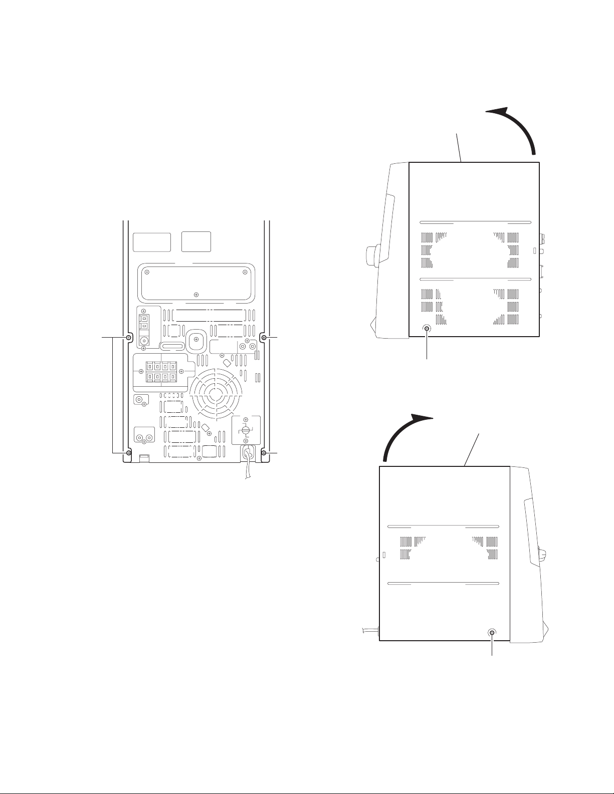
2.1 Main body
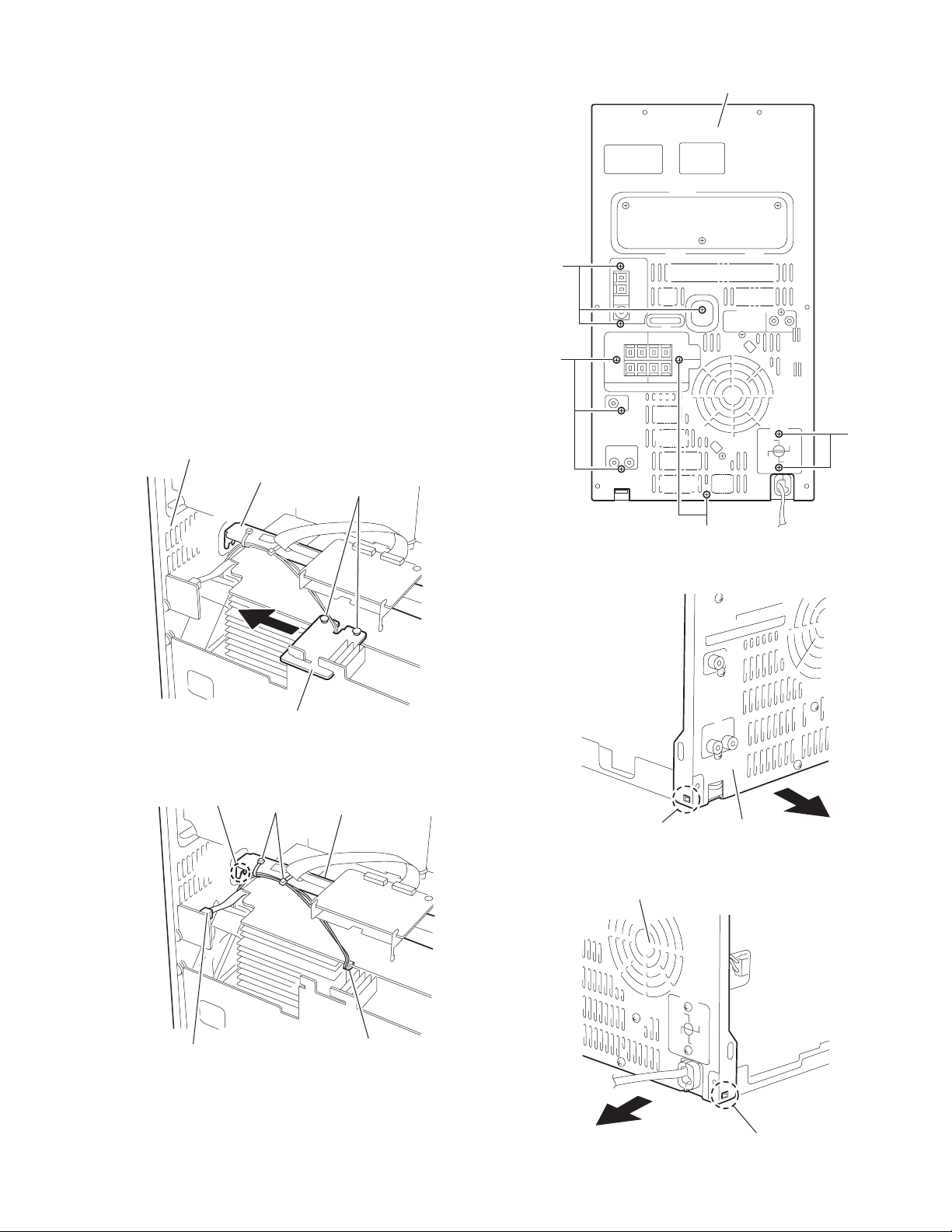
2.1.1 Removing the metal cover
(See Fig.1~3)
(1) Remove the six screws A on the back of the body.
(2) Remove the screw B on each side of the body.
(3) Remove the metal cover from the body by lifting the rear
part of the cover.
CAUTION:
Do not break the front panel tab fitted to the metal cover.
Metal cover
B
Fig.2
Metal cover
Fig.1
B
Fig.3
(No.22041)1-5
Page 6
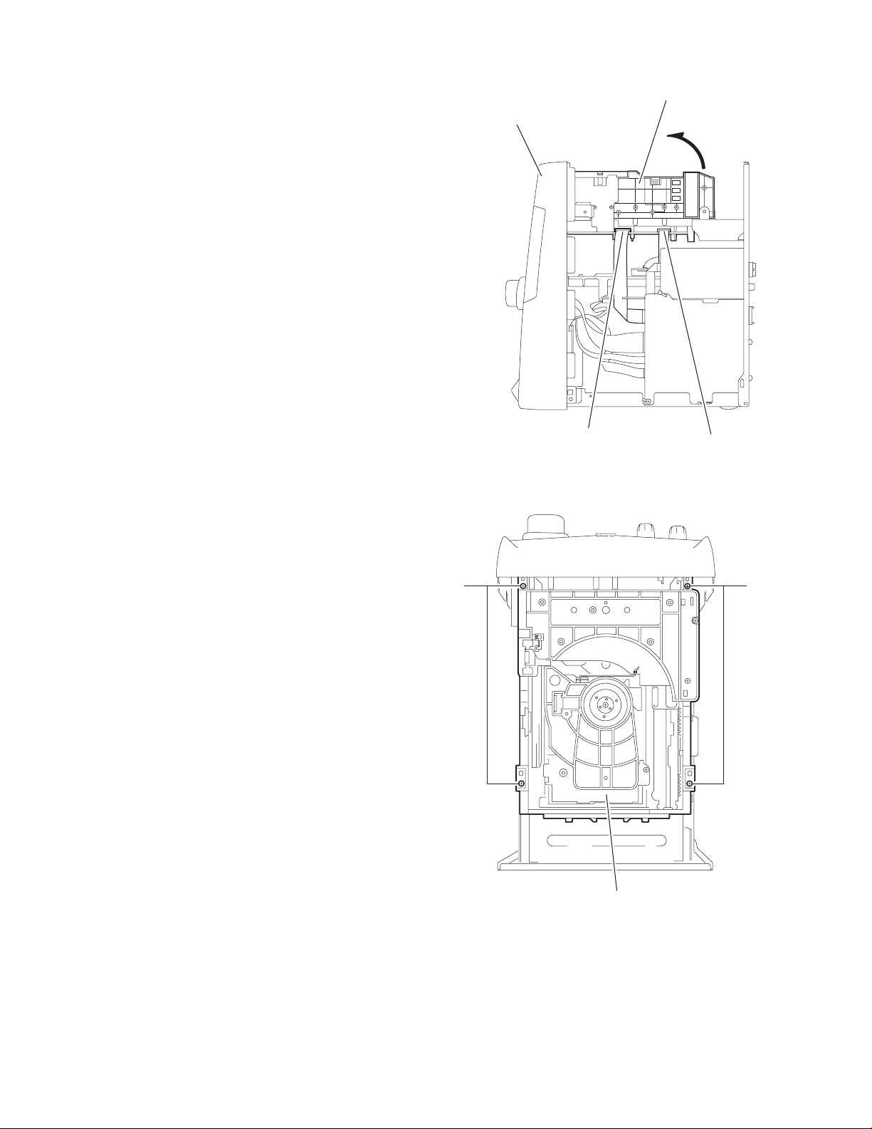
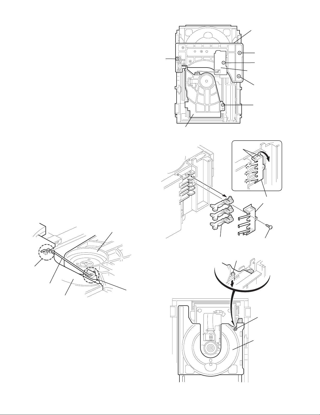
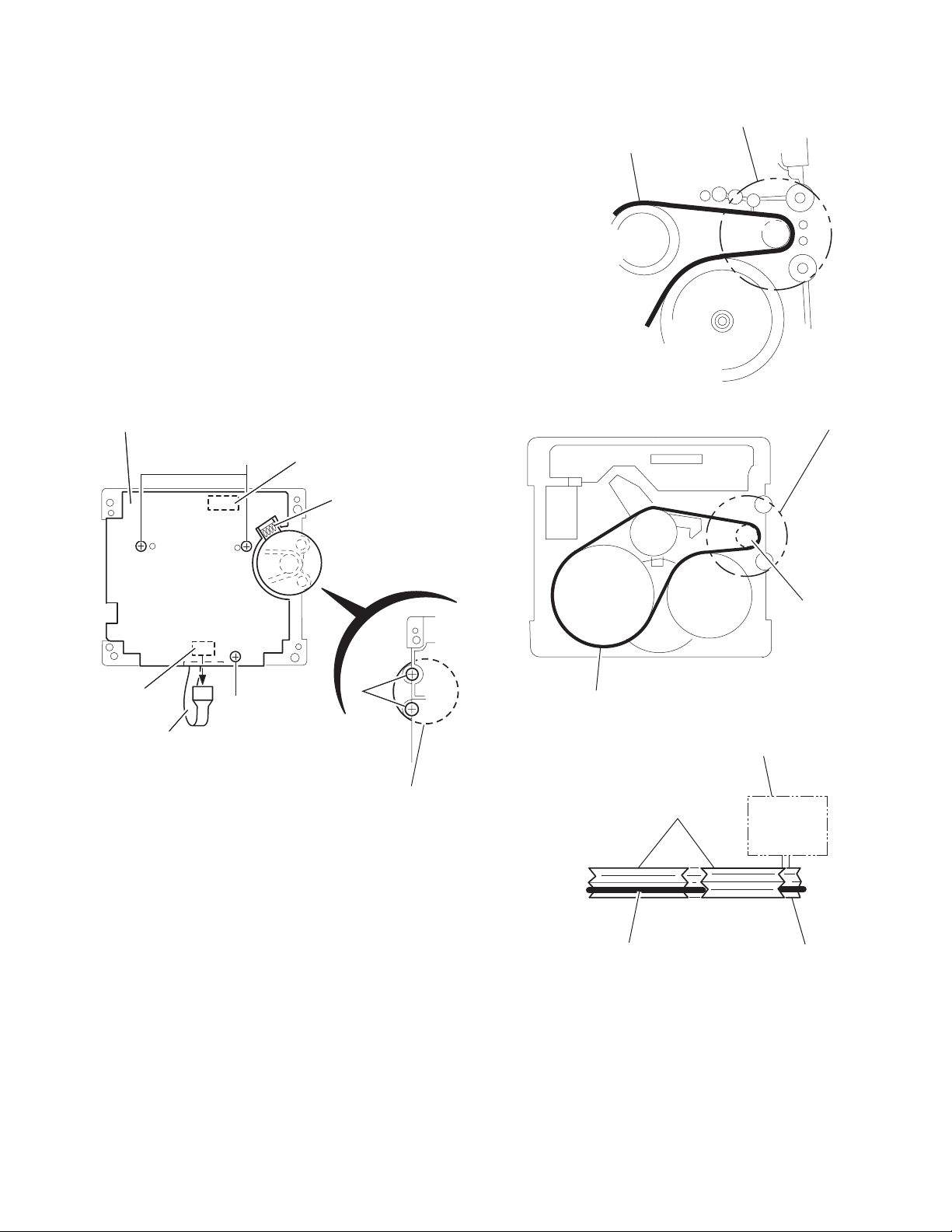
2.1.2 Removing the CD changer mechanism assembly
(See Fig.4, 5)
• Prior to performing the following procedure, remove the metal
cover.
(1) Disconnect the card wires from connector CN151 and
CN651 on the CD servo control board on the right bottom
of the CD changer mechanism assembly.
(2) Remove the four screws C attaching the CD changer
mechanism assembly on top of the body.
(3) Remove the CD changer mechanism assembly while lifting
the rear part.
CAUTION:
Do not damage the CD fitting when removing the CD changer
mechanism assembly.
CD changer
mechanism assembly
Front panel assembly
C
CD servo control board
CN651
Fig.4
CN151
C
1-6 (No.22041)
CD changer mechanism assembly
Fig.5
Page 7
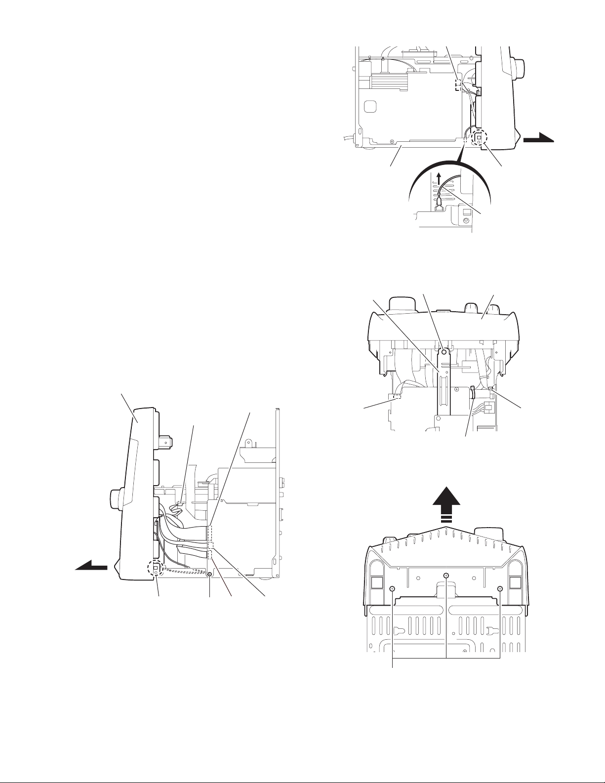
2.1.3 Removing the front panel assembly
(See Fig.6~9)
• Prior to performing the following procedure, remove the metal
cover and the CD changer mechanism assembly.
(1) Disconnect the card wires from connector CN44 and
CN870, disconnect the flat wire from connector CN922 on
the main board on the right side of the body. Remove the
screw D attaching the wire from extending from the underside of the front panel assembly.
(2) Disconnect the wire from connector CN701 on the bridge
board.
(3) Cut the band.
(4) Disconnect the wires from connector CN231 and CN232
on the primary board on the left side of the body.
(5) Remove the plastic rivet attaching the inner bar in the cen-
ter of the front panel assembly.
REFERENCE:
Keep the plastic rivet for reuse.
(6) Remove the three screws E attaching the front panel as-
sembly at the bottom of the body.
(7) Disconnect the ground wire extending from the phone
board from bottom chassis.
(8) Release the two joints a on the lower left and right sides of
the front panel assembly using a screwdriver, and remove
the front panel assembly toward the front.
REFERENCE:
Front panel need to be tilt little bit as release from bottom
chassis.
Bottom chassis
Inner bar
Plastic rivet
Joint a
Ground wire
Fig.7
Front panel assembly
Front panel assembly
Joint a
Bridge board
CN701
D
Fig.6
Main board
CN870
CN922CN44
Bridge board
CN701
Primary board
CN231,CN232
Band
Fig.8
E
Fig.9
(No.22041)1-7
Page 8
2.1.4 Removing the antenna board
(See Fig.10, 11)
• Prior to performing the following procedure, remove the metal
cover.
(1) Disconnect the card wire from connector CN1 on the an-
tenna board on the right side of the body.
(2) Remove the band attaching the antenna board.
(3) Remove the two screws F on the rear panel on the back of
the body.
Antenna board
CN1
Band
Fig.10
Rear panel
Rear panel
F
Fig.11
1-8 (No.22041)
Page 9
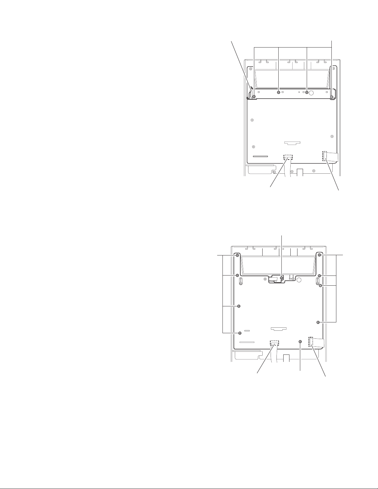
2.1.5 Removing the rear panel
(See Fig.12~16)
• Prior to performing the following procedure, remove the metal
cover and the CD changer mechanism assembly.
(1) Remove holding board by remove two plastic rivets and
then slide out the holding board as shown in fig.12.
(2) Disconnect fan wire from connector CN206 on the bridge
board.
(3) Disconnect the flat wire from connector CN91 on the sur-
round speakers jack board.
(4) Cut off the band that fixing fan wire on inner bar.
(5) Remove ten screws G from rear panel.
(6) Detach joint b to release rear panel from inner bar.
(7) Release joints c which on right bottom and left bottom of
rear panel. The joint can be release by pull outward the
side of rear panel.
REFERENCE:
Fan assembly and surround speaker jack board will come off
with rear panel.
Rear panel
G
G
Rear panel
Joint b
Inner bar
Holding board
Fig.12
Band
Plastic rivets
Inner bar
Joint c
G
G
Fig.14
Rear panel
Fig.15
Surround speakers
jack board
CN91
Rear panel
Bridge board
CN206
Fig.13
Joint c
Fig.16
(No.22041)1-9
Page 10
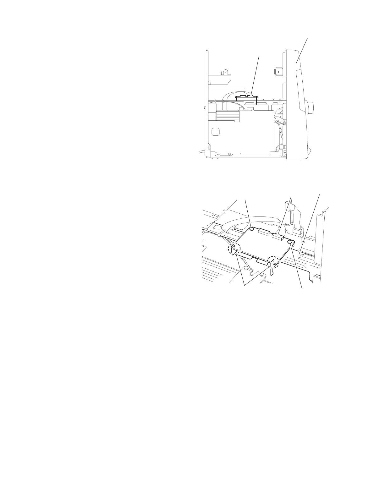
2.1.6 Removing the T.flux board
r
(See Fig.17, 18)
• Prior to performing the following procedure, remove the metal
cover and the CD changer mechanism assembly .
(1) Disconnect the card wire from connector CN102 on the
T.flux board.
(2) Remove the two plastic rivets attaching the T.flux board.
(3) Remove the T.flux board from the bracket which is located
on the inner bar. (two joints d)
Front panel assembly
T.flux board
Fig.17
Plastic rivet
d
Fig.18
T.flux board
CN102
Plastic rivet
Inner ba
1-10 (No.22041)
Page 11
2.1.7 Removing the fan assembly
(See Fig.19, 20)
• Prior to performing the following procedure, remove the metal
cover, the CD changer mechanism assembly and the rear panel.
(1) Remove two screws H on the rear panel.
(2) Rotate fan assembly in clockwise direction to release fan
assembly from rear panel (joints e).
H
Rear panel
Fig.19
e
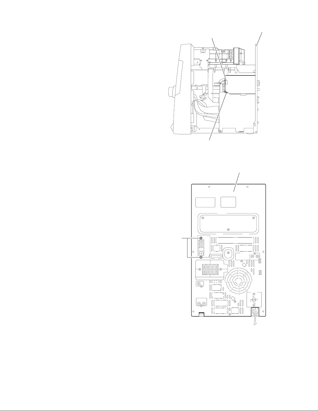
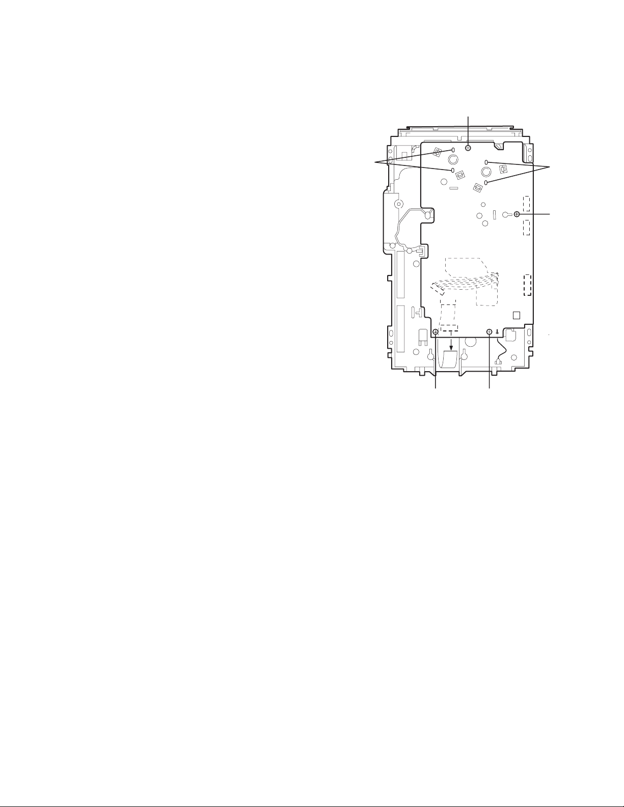
2.1.8 Removing the main board
(See Fig.21)
• Prior to performing the following procedure, remove the metal
cover, the CD changer mechanism assembly, the antenna
board and the rear panel.
(1) Disconnect the card wires from connector CN44, CN504
and CN870 on the main board.
(2) Disconnect the flat wire from connector CN922 on the main
board.
(3) Remove the screw D attaching the main board.
(4) Disconnect connector CN217 and CN311 on the main
board outward and release from the base chassis (joint f)
upward.
CN870
CN922
CN44
D
Fig.20
CN311
Fig.21
Fan assembly
e
CN217
f
CN504
Main board
(No.22041)1-11
Page 12
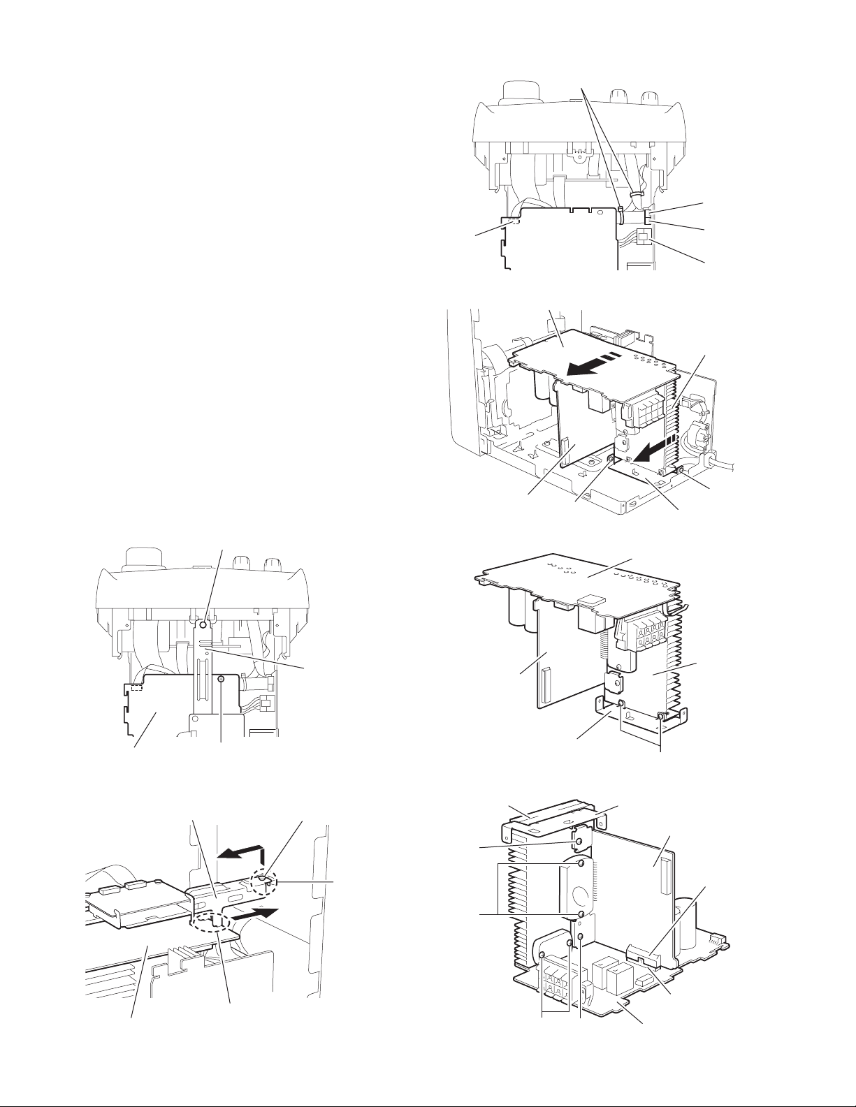
2.1.9 Removing the bridge board / regulator board / heat sink
r
(See Fig.22~27)
• Prior to performing the following procedure, remove the metal
cover, the CD changer mechanism assembly, the rear panel,
the antenna board and main board.
(1) Remove the plastic rivet attaching the stay inner bar and
remove the screw I on the bridge board.
(2) Move the inner bar forward and upward to release from the
front section (joint g) and from the bridge board (two joints
h) respectively.
(3) Disconnect the wires from connector CN212, CN213 and
CN214 on the primary board respectively and remove the
band fixing the wires.
(4) Disconnect the wire from connector CN701 on the bridge
board.
(5) Remove the two screws J attaching the heat sink bracket
and move the heat sink in the direction of the arrow to release from the base chassis. The bridge board and the reg-
ulator board come off with the heat sink.
(6) Remove the two screws K attaching the heat sink bracket.
(7) Remove the two screws L, detach bridge board from regu-
lator board by disconnect connector CN205.
(8) Remove the two screws M and two screws N to detach
regulator board from heat sink.
CAUTION:
As assembly back the regulator board and bridge board to
heat sink.
Regulator board must be assembling to heat sink first and
screws M and N must be screwed before bridge board attach
to regulator board.
Plastic rivet
Bridge board
CN701
Regulator board
Band
Bridge board
J
Primary board
CN213
CN212
CN214
Fig.24
Heat sink
J
Heat sink bracket
Fig.25
Bridge board
Bridge board
Bridge board
Fig.22
Inner bar
Fig.23
I
Inner ba
Regulator board
Heat sink bracket
Heat sink
K
Fig.26
Plastic rivet
Heat sink
Heat sink bracket
Regulator board
N
g
CN215
M
h
LN
Fig.27
CN205
Bridge board
1-12 (No.22041)
Page 13
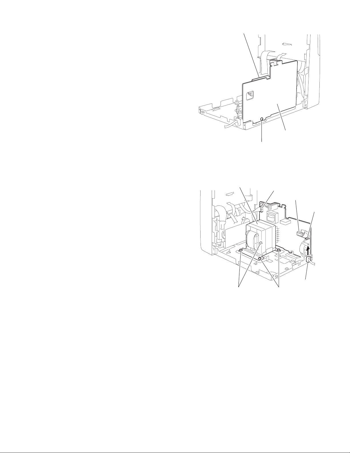
2.1.10 Removing the power transformer assembly
(See Fig.28,29)
• Prior to performing the following procedure, remove the metal
cover, the CD changer mechanism assembly, the rear panel,
the main board and the bridge board / regulator board.
(1) Remove the screw O attaching the primary board.
(2) Disconnect the wire from connector CN231 and CN232 on
the primary board.
(3) Remove the four screws P attaching the power transform-
er assembly.
(4) Detach the cord stopper from the base chassis upward.
REFERENCE:
When disconnecting the power cord from connector CN250 on
the primary board, remove the fixing band.
Power transformer assembly
Primary board
O
Fig.28
Power transformer
assembly
P P
Primary board
CN231,CN232
CN250
Band
Cord stopper
Fig.29
(No.22041)1-13
Page 14
2.2 Front panel assembly
• Prior to performing the following procedure, remove the metal
cover, the CD changer mechanism assembly and front panel
assembly.
Head amplifier & mechanism control board
CN33
2.2.1 Removing the cassette mechanism assembly
(See Fig.30)
(1) Disconnect the card wire from connector CN33 on the head
amplifier & mechanism control board.
(2) Remove the two screws Q, and the two screws R attaching
the cassette mechanism assembly.
2.2.2 Removing the headphone board
(See Fig.30)
(1) Remove the screw S and pull out the headphone board
backward.
(2) Cut off the band.
2.2.3 Removing the mic volume board
(See Fig.31, 32)
(1) Pull the mic volume knob toward the front.
(2) Remove the three screws T attaching the holding board.
(3) Remove the holding board from mic volume board.
Q
Cassette mechanism assembly
Fig.30
Front panel assembly
R
Headphone board
SR
1-14 (No.22041)
Mic volume board
T
Mic volume knob
Fig.31
T
Holding board
Fig.32
Page 15
2.2.4 Removing the display system control board
(See Fig.33, 34)
(1) Remove the four screws U attaching the stay bracket (1).
(2) Disconnect the card wires from connector CN43 and
CN880 on the display system control board.
(3) Remove the ten screws V attaching the display system
control board.
Stay bracket (1)
U
V
Display system control board
CN43
Fig.33
V
CN880
V
Display system control board
CN43
Fig.34
V
CN880
(No.22041)1-15
Page 16

2.2.5 Removing the button board
(See Fig.35~39)
• Prior to performing the following procedure, remove the dis-
play system control board.
(1) Pull out preset knob, sound mode knob on the front panel
toward the front.
(2) Pull out the volume knob and remove the two screws W at-
taching the knob holder. Remove the nut from the front
panel.
(3) Remove the four screws X attaching the stay bracket (2).
(4) Remove the eight screws Y attaching the button board.
Front panel assembly
Sound mode knob
Nut
Fig.37
X
Knob holder
Fig.35
Fig.36
Volume knobPreset knob
Button board
W
Y
Stay bracket (2)
Fig.38
Y
Y
Fig.39
1-16 (No.22041)
Page 17
2.3 CD Changer Mechanism
A
• Remove the CD changer mechanism assembly.
2.3.1 Removing the CD Servo control board
(See Fig.1)
(1) From bottom side the CD changer mechanism assem-
bly,remove the four screws A retaining the CD servo control board.
(2) Absorb the four soldered positions a of the right and left
motors with a soldering absorber.
(3) Pull out the earth wire on the CD changer mechanism as-
sembly.
(4) Disconnect the connector CN854 on the CD servo control
board.
(5) Disconnect the card wire CN601 and the connector CN801
on the CD servo control board.
A
a
CN854
CN651
CD servo control board
CN801
CN151
CN601
a
AA
Fig.1
(No.22041)1-17
Page 18
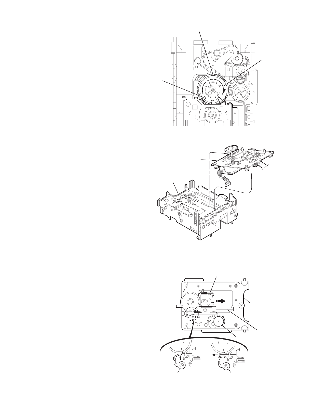
2.3.2 Removing the CD tray assembly
(See Fig.2~9)
(1) Remove the CD servo control board.
(2) Remove the screw B retaining the lod stopper.
(3) From the T.bracket section b and clamper base section c ,
remove both of the edges fixing the rod.
(4) Remove the three screws C retaining the T.bracket.
(5) Remove the screw D retaining the clamper assembly.
(6) From the left side face of the chassis assembly, remove the
one screw E retaining both of the return spring and lock le-
ver.
(7) By removing the pawl at the section d fixing the return
spring, dismount the return spring.
(8) Remove the three lock levers.
(9) Check whether the lifter unit stopper has been caught into
the hole at the section e of CD tray assembly as shown in
Fig.5.
(10) Make sure that the driver unit elevator is positioned as
shown in Fig.6 from to the second or fifth hole on the left
side face of the CD changer mechanism assembly.
CAUTION:
In case the driver unit elevator is not at above position,
set the elevator to the position as shown in Fig.7 by manually turning the pulley gear as shown in Fig.8.
(11) Manually turn the motor pulley in the clockwise direction
until the lifter unit stopper is lowered from the section e of
CD tray assembly.
(12) Pull out all of the three stages of CD tray assembly in the
arrow direction f until these stages stop.
(13) At the position where the CD tray assembly has stopped,
pull out the CD tray assembly while pressing the two pawls
g and g' on the back side of CD tray assembly. In this
case, it is easy to pull out the assembly when it is pulled out
first from the stage CD tray assembly.
C
Clamper assembly
T.Braket
C
B
Lod stopper
(C/J version only)
C
D
Fig.3
d
Return spring
Clamper base
Lock lever
Fig.4
Stopper
E
b
Rod
c
T.Braket
Fig.2
e
CD tray
assembly
1-18 (No.22041)
Fig.5
Page 19
f
Chassis assembly
r
A
Refer to Fig.7
Pawl
g
Fig.6
Drive unit of elevato
Fig.7
CD tray assembly
Pulley gear
Motor pulley
Fig.8
CD
3
CD
2
CD
1
CD tray assembly
Pawl g, g'
Fig.9
2.3.3 Removing the CD loading mechanism assembly
(See Fig.10)
(1) While turning the cams R1 and R2 assembly in the arrow
direction h ,align the shaft i of the CD loading mechanism
assembly to the position shown in Fig.10.
(2) Remove the four screws F retaining the CD loading mech-
anism assembly.
rrow
Cams R1, R2 assembly
h
i
F
F
F
CD loading mechanism assembly
Fig.10
(No.22041)1-19
F
Page 20
2.3.4 Removing the CD traverse mechanism
j
(See Fig.11 and 12)
(1) For dismounting only the CD traverse mechanism without
removing the CD loading mechanism assembly, align the
shaft j of the CD loading mechanism assembly to the position shown Fig.11 while turning the cam R1 and R2 assembly in the arrow direction k .
(2) By raising the CD loading mechanism assembly in the ar-
row direction l , remove the assembly from the lifter unit.
Cam R1, R2 assembly
Fig.11
Arrow
k
CD traverse mechanism
2.3.5 Removing the CD pick unit
(See Fig.13)
(1) Move the cam gear in the arrow direction m . Then, the CD
pickup unit will be moved in the arrow direction n .
(2) According to the above step, shift the CD pickup unit to the
center position.
(3) While pressing the stopper retaining the shaft in the arrow
direction o , pull out the shaft in the arrow direction p .
(4) After dismounting the shaft from the CD pickup unit, re-
move the CD pickup unit.
Lifter unit
Fig.12
CD Pickup unit
n
m
Arrow
l
CD loading
mechanism
1-20 (No.22041)
Cam gear
Shaft
Shaft
p
o
Stopper Stopper
Fig.13
Shaft
Page 21

2.3.6 Removing the try select switch board
r
(See Fig.14)
(1) Remove the two screws G retaining the tray select switch
board.
(2) Disconnect the tray select switch board from connector
CN854 on the CD servo control board.
Chassis assembly
Tray select
switch board
CN854
CN851
CD servo
control board
2.3.7 Removing the cam unit
(See Fig.15 ~17)
• Remove the CD loading mechanism assembly.
(1) While turning the cam gear q , align the Paul r position of
the drive unit to the notch position on the cam gear q .
(2) Pull out the drive unit and cylinder gear .
(3) While turning the cam gear q , align the Paul s position
of the select lever to the notch position on the cam gear q .
(4) Remove the four screws H retaining the cam unit(cam
gear q and cams R1/R2 assembly).
Drive unit
Cam gear q
r
Fig.14
Drive unit
Cylinder gea
CN804
G
Fig.16
Cams R1, R2 assembly
Cam unit
Fig.15
H
Cam gear q
H
s
Select lever
Fig.17
(No.22041)1-21
Page 22
2.3.8 Removing the actuator motor and belt
r
(See Fig.18~21)
(1) Remove the two screws I retaining the gear bracket.
(2) While pressing the pawl t fixing the gear bracket in the ar-
row direction, remove the gear bracket.
(3) From the notch u section on the chassis assembly fixing
the edge of gear bracket, remove and take out the gear
bracket.
(4) Remove the belts respectively from the right and left actu-
ator motor pulleys and pulley gears.
(5) After turning over the chassis assembly, remove the actu-
ator motor while spreading the four pawls v fixing the right
and left actuator motors in the arrow direction.
ATTENTION:
When the chassis assembly is turned over under the conditions wherein the gear bracket and belt have been removed,
then the pulley gear as well as the gear, etc. constituting the
gear unit can possibly be separated to pieces. In such a case,
assemble these parts by referring to the assembly and configuration diagram in Fig. 21.
Gear bracket
Pulley gear
Belt
Motor pulley
Chassis assembly
u
Gear bracket
Fig.19
Actuator motor
v
v
Fig.20
Pulley gear
Belt
Motor pulley
I
Pawl
t
I
Fig.18
Assembly and Configuration Diagram
Pulley gear
Pulley gear
Gear B
Gear C
Select gear
Gross gear L
Fig.21
Gear B
Cylinder gea
Gross gear U
Gear C
1-22 (No.22041)
Page 23
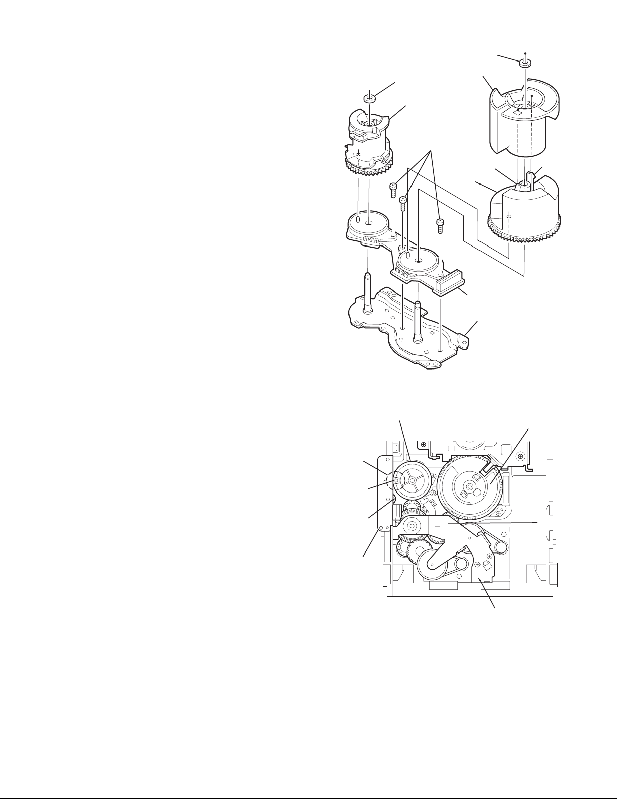
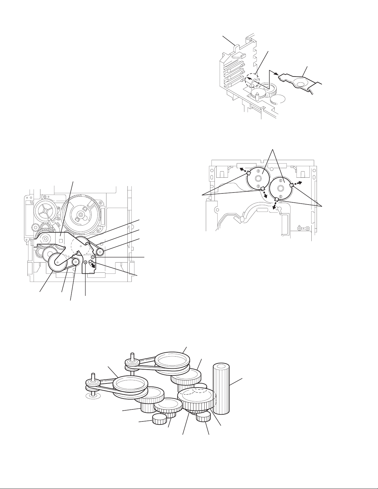
2.3.9 Removing the cams R1/R2 assembly and cam gear q
(See Fig.22)
(1) Remove the slit washer fixing the cams R1 and R2 assem-
bly.
(2) By removing the two pawls w fixing the cam R1, separate
R2 from R1.
(3) Remove the slit washer fixing the cam gear q .
(4) Pull out the cam gear q from the C.G. base assembly.
2.3.10 Removing the C.G. base assembly
(See Fig.22 and 23)
(1) Remove the three screws J retaining the C.G. base as-
sembly.
CAUTION:
To reassemble the cylinder gear, etc.with the cam unit (cam
gear and cans R1/R2 assembly), gear unit and drive unit, align
the position of the pawl x on the drive unit to that of the notch
on the cam gear q . Then, make sure that the gear unit is engaged by turning the cam gear q .
Slit washer
Cam gear q
J
Slit washer
Cam R2
Pawl
w
Cam R1
Cam switch board
C.G. base assembly
Pawl
w
Notch
Pawl
x
Cylinder
gear
Drive unit
Fig.22
Cam gear q
Cam R1, R2 assembly
Gear unit
Gear bracket
Fig.23
(No.22041)1-23
Page 24
2.3.11 Removing the Pickup unit
(See Fig.24 and 25)
(1) Turn the cam gear in the direction of the arrow to move the
pickup unit toward the center.
(2) Extend the guide shaft stopper in the direction of the arrow,
move the guide shaft and pull out as shown in the figure.
(3) Pull out the pickup unit from the joint a.
CAUTION:
When reassenbling, attch the pickup unit to the chassis
base firmly at the joint a.
(4) Release the four joint b on the back on the pickup unit to
remove the CD rack.
Joint a
Pickup unit
Pickup unit
Chassis base
Guide shaft
Cam gear
Guide shaft stopper
Guide shaft
Joint b
Guide shaft
Guide shaft stopper
Fig.24
Pickup unit
Joint b
Joint b CD rack
Fig.25
1-24 (No.22041)
Page 25
2.3.12 Removing the CD mechanism board
(See Fig.26)
(1) On the back of the CD mechanism assembly, unsolder the
four soldering c attaching the CD mechanism board, the
spindle motor and the feed motor.
(2) Removing the screw A.
2.3.13 Removing the Spindle motor/Feed motor
(See Fig.27)
• Prior to performing the following procedure,remove the CD
mechanism board.
(1) Form the top side of the CD mechanism assembly, remove
the two screws B and two screws C attaching the spindle
motor and the feed motor respsctively.
Soldering c
Spindle motor
Soldering c
Spindle motor
CD mechanism board
A
Feed motor
Fig.26
B
Feed motor
Fig.27
C
(No.22041)1-25
Page 26
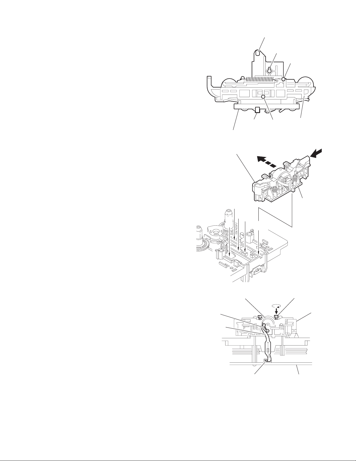
2.4 Cassette mechanism assembly
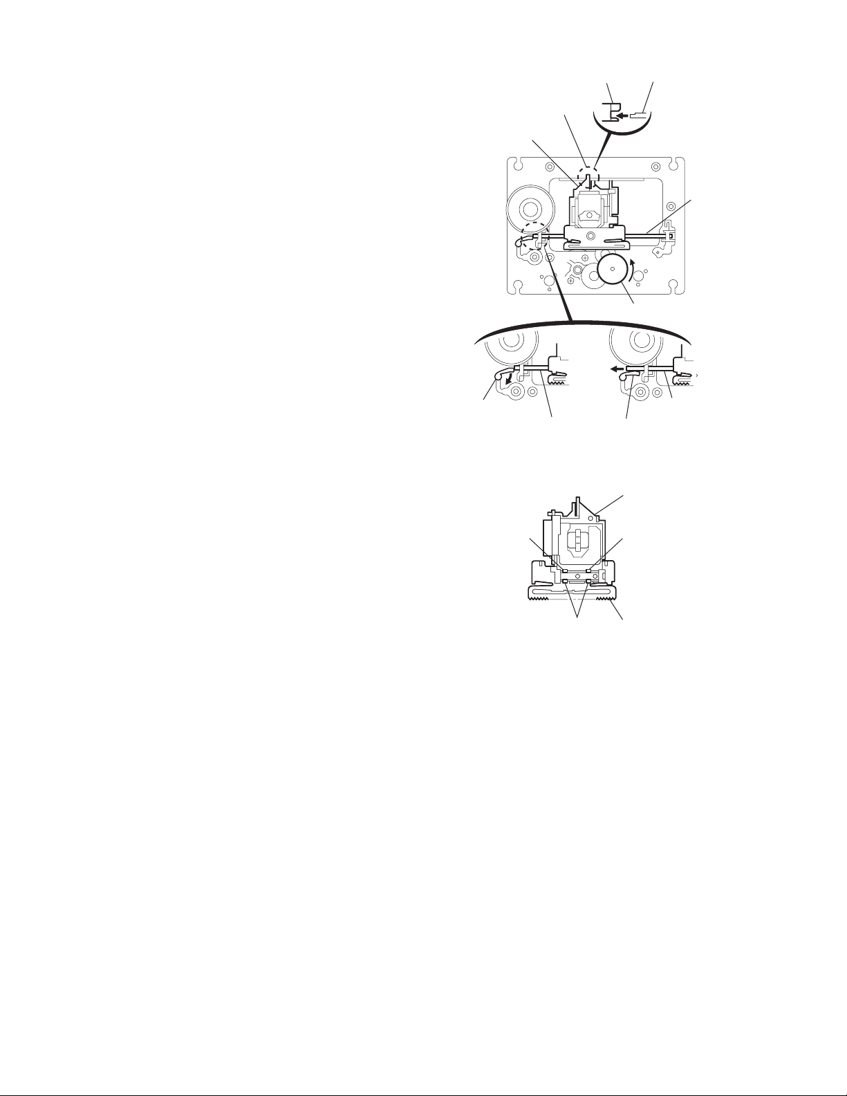
2.4.1 Removing the Play/Record & Clear head
(See Fig.1~3)
(1) While moving the trigger arm on the right side of the head
mount in the direction of the arrow, turn the flywheel R
counterclockwise until the head mount comes ahead and
clicks.
(2) The head turns counterclockwise as you turn the flywheel
R counterclockwise (See Fig.2 and 3).
(3) Disconnect the flexible wire from connector CN31 on the
head amplifier & mechanism control board.
(4) Remove the spring from the back of the head.
(5) Loosen the azimuth screw for reversing attaching the head.
(6) Remove the head on the front side of the head mount.
Cassette mechanism assembly
Fig.1
Head
Fly wheelR
Trigger armHead mount
Flexible wire
Fly wheel R
Fig.2
Azimuth screw
Head
for reversing
Spring
CN31
Head amplifer & mecha control board
Fig.3
1-26 (No.22041)
Page 27
2.4.2 Removing the head amplifier & mechanism control board
(See Fig.4)
(1) Turn over the cassette mechanism assembly and remove
the three screws A attaching the head amplifier & mechanism control board.
(2) Disconnect the flexible wire from connector CN31 on the
head amplifier & mechanism control board.
(3) Disconnect connector CN32 of the head amplifier & mech-
anism control board from connector CN1 on the reel pulse
board.REFERENCE: If necessary, unsolder the 4-pin wire
soldered to the main motor.
2.4.3 Removing the main motor
(See Fig.4~7)
(1) Remove the two screws B .
(2) Half raise the motor and remove the capstan belt from the
motor pulley.
ATTENTION:
Be careful to keep the capstan belt from grease. When reassembling, refer to Fig.6 and 7 for attaching the capstan belt.
Head amplifier & mecha control board
Main motor assembly
Capstan belt
Fig.5
Main motor assembly
CN31
Flexible wire
A
AA
Fig.4
CN32
4pin wire
B
Main motor assembly
Motor pulley
Capstan belt
Fig.6
Main motor assembly
Fly wheel
Capstan belt
Motor pulley
Fig.7
(No.22041)1-27
Page 28
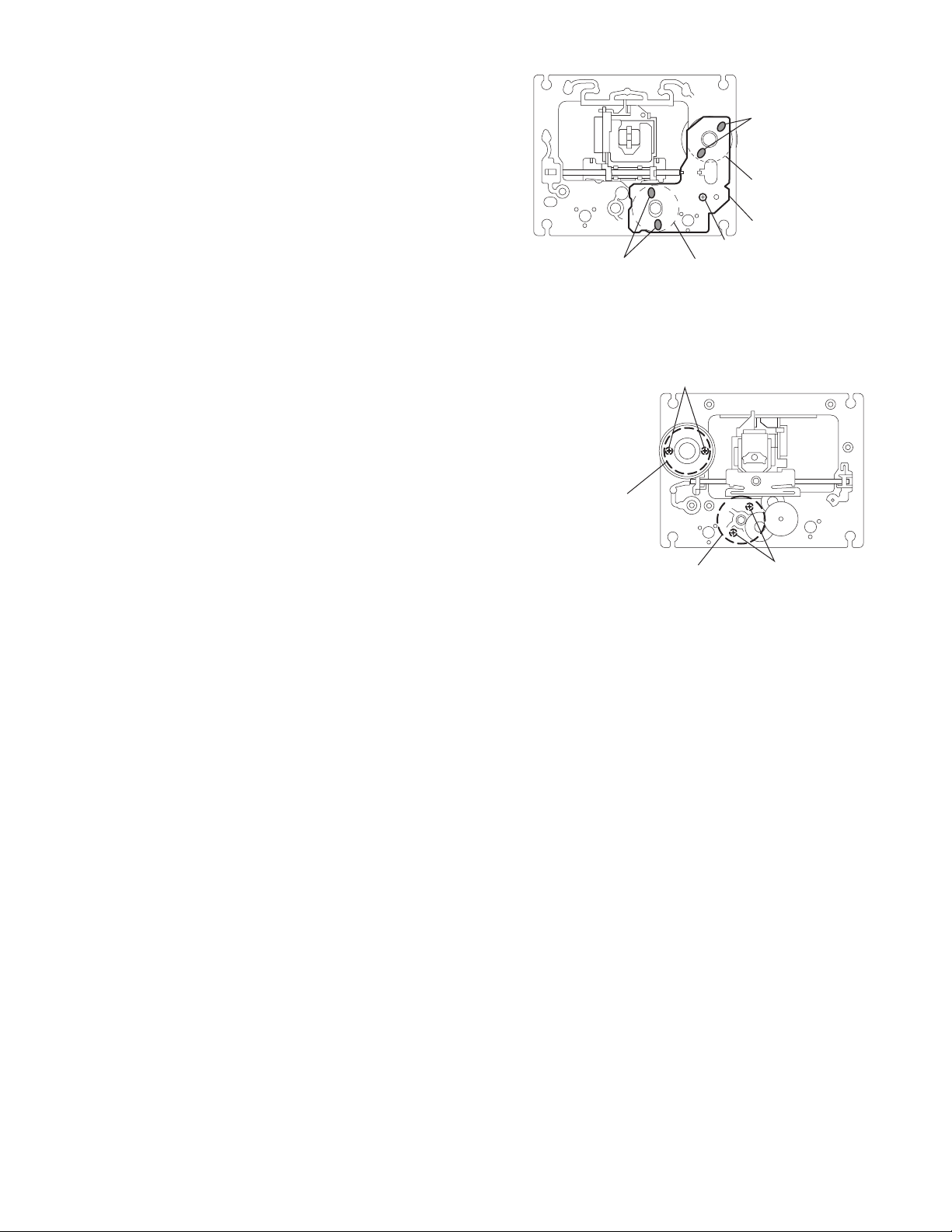
2.4.4 Removing the flywheel
(See Fig.8, 9)
• Prior to performing the following procedure, remove the head
amplifier & mechanism control board and the main motor assembly.
(1) From the front side of the cassette mechanism, remove the
slit washers attaching the capstan shaft L and R. Pull out
the flywheels backward.
Fly wheel R Fly wheel L
Fig.8
Fly wheel R
Capstan shaft R Capstan shaft L
Slit washer
Fig.9
2.4.5 Removing the reel pulse board and solenoid
(See Fig.10)
• Prior to performing the following procedure, remove the head amplifier & mechanism control board.
(1) Remove the screw C.
(2) Release the tab a, b, c, d and e retaining the reel pulse board.
(3) Release the tab f and g attaching the solenoid on the reel pulse board.
(4) The reel pulse board and the solenoid come off.
Fly wheel L
bc
a
Solenoid
g
f
d
Reel pulse board
C
e
Fig.10
1-28 (No.22041)
Page 29
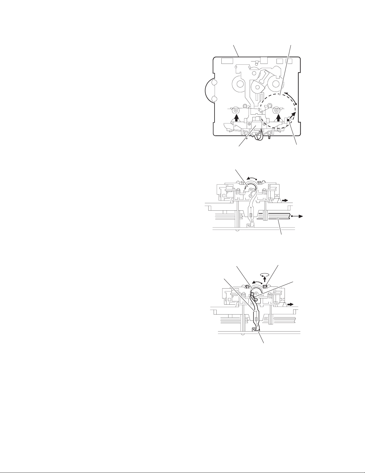
2.4.6 Reattaching the Play/ Record & Clear head
r
r
(See Fig.11~13)
(1) Reattaching the head mount assembly.
a) Change front of the direction cover of the head
mount assembly to the left (Turn the head forward).
b) Fit the bosses O', P', Q', U' and V' on the head mount
assembly to the holes P and V, the slots O, U and Q
of the mechanism sub assembly (See Fig.11 to 13).
CAUTION:
To remove the head mount assembly, turn the direction
cover to the left to disengage the gear. If the gear can not
be disengaged easily, push up the boss Q' slightly and
raise the rear side of the head mounts slightly to return
the direction lever to the reversing side.
(2) Tighten the azimuth screw for reversing.
(3) Reattach the spring from the back of the Play/ Record &
Clear head.
(4) Connect the flexible wire to connector CN31 on the head
amplifier & mechanism control board.
U' Q'
Head mount assembly
Head mount assembly
O'
Fig.11
P'
P'
V'
V'
Direction cove
Spring
Flexible wire
V
O
P
Q
Head
Direction cove
U
Fig.12
Azimuth screw for reversing
Head mount
CN31
Fig.13
Head amplifier &
mechanism control board
(No.22041)1-29
Page 30
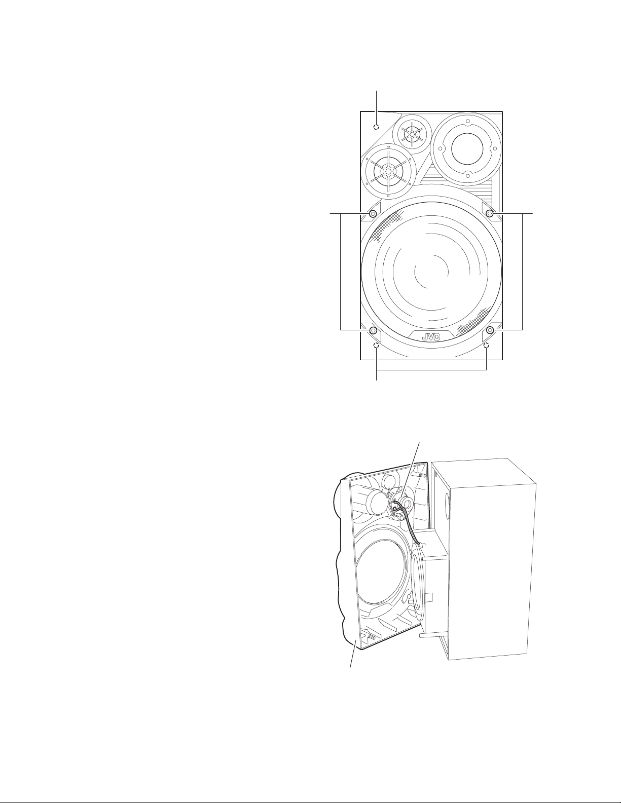
2.5 Speaker section
AA
2.5.1 Main speaker
2.5.1.1 Removing the front cover
(See Fig.1, 2)
CAUTION:
Do not break or damage the front panel and body that are
glued at the joints a. (See Fig.1)
(1) Remove the four screws A on the front of the body respec-
tively.
(2) Remove the front cover toward the front and disconnect the
yellow and black wires from the two tweeter speaker terminals.
Joint a
Joint a
Fig.1
Tweeter speaker
Front cover
Fig.2
1-30 (No.22041)
Page 31

2.5.1.2 Removing the woofer speaker
(See Fig.3)
• Prior to performing the following procedure, remove the front
cover.
(1) Remove the four screws B on the front of the body.
(2) Pull out the woofer speaker toward the front and discon-
nect the wire (yellow and black, red and black) from the two
speaker terminals.
2.5.1.3 Removing the tweeter speaker
(See Fig.4)
• Prior to performing the following procedure, remove the front
cover.
(1) Disconnect the blue and white wires from the two tweeter
speaker terminals.
(2) Remove the two screws C attaching the tweeter speaker
on the back of the front cover.
B
B
Woofer speaker
Fig.3
Tweeter speaker
C
Front cover
Fig.4
(No.22041)1-31
Page 32

2.5.2 Sub woofer
2.5.2.1 Removing the front cover
(See Fig.5)
CAUTION:
Do not break or damage the front panel and body that are
glued at the joints b. (See Fig.5)
(1) Remove the front cover toward the front.
2.5.2.2 Removing the sub woofer speaker
(See Fig.6)
• Prior to performing the following procedure, remove the front
cover.
(1) Remove the six screws E on the front of the body.
(2) Pull out the woofer speaker toward the front and discon-
nect the red and black wires from the four speaker terminals.
Joint bJoint b
Fig.5
E
E
Sub woofer speaker
E
E
Fig.6
1-32 (No.22041)
Page 33

2.5.3 Surround speaker
2.5.3.1 Removing the rear cover
(See Fig.7~9)
(1) Remove the four screws F on the back of the body.
(2) Disconnect the wires from the two terminals on the rear of
the surround speaker.
(3) Remove the four screws G on the back of the front cover.
Rear cover
FF
Fig.7
Front cover Rear cover
Speaker terminal
Surround speaker
Fig.8
Front cover
GG
Fig.9
(No.22041)1-33
Page 34

SECTION 3
Adjustment
3.1 Measurement Instruments Required for Adjustment
(1) Low frequency oscillator
This oscillator should have a capacity to output 0dBs to
600Ω at an oscillation frequency of 50Hz-20kHz.
(2) Attenuator impedance : 600Ω
(3) Electronic voltmeter
(4) Distortion meter
(5) Frequency counter
(6) Wow & flutter meter
(7) Test tape
VT703L : Head azimuth
VT712 : Tape speed and running unevenness (3kHz)
VT724 : Reference level (1kHz)
(8) Blank tape
TYPE l : AC-225
TYPE ll : AC-514
(9) Torque gauge : For play and back tension
FWD(TW2111A), REV(TW2121a) and FF/REW(TW2231A)
(10) Test disc: CTS-1000
3.2 Measurement conditons
Power supply voltage AC 110V/AC127V/AC220V
AC 230V·AC240V (adjustable with the
voltage selector), ~50Hz/60Hz
Reference output Speaker : 0.775V/6Ω
Headphone : 0.077V/32Ω
Reference frequency and input level 1kHz, AUX : -8dBs
Measurement output terminal at Speaker J3002
Load resistance 6Ω
3.2.1 Radio Input signal
AM frequency 400Hz
AM modulation 30%
FM frequency 400Hz
FM frequency deviation 22.5kHz
3.2.2 Tuner section
Voltage applied to tuner +B : DC5.7V
VT : DC 12V
Reference measurement output 26.1mV(0.28V)/3Ω
Input positions AM : Standard loop antenna
FM : TP1 (hot) and TP2 (GND)
3.2.3 Standard measurement position of volume
Function switch to Tape
Beat cut switch to Cut
Super Bass/Active hyper Bass to OFF
Bass Treble to Center
Adjustment of main volume to reference output VOL : 0.775V
Precautions for measurement
(1) Apply 30pF and 33kΩ to the IF sweeper output side and
0.082µ F and 100kΩ in series to the sweeper input side.
(2) The IF sweeper output level should be made as low as
possible within the adjustable range.
(3) Since the IF sweeper is a fixed device, there is no need
to adjust this sweeper.
(4) Since a ceramic oscillator is used, there is no need to
perform any MIX adjustment.
(5) Since a fixed coil is used, there is no need to adjust the
FM tracking.
(6) The input and output earth systems are separated. In
case of simultaneously measuring the voltage in both of
the input and output systems with an electronic voltmeter
for two channels, therefore, the earth should be connected particularly carefully.
(7) In the case of BTL connection amp., the minus terminal
of speaker is not for earthing. Therefore, be sure not to
connect any other earth terminal to this terminal. This
system is of an BTL system.
(8) For connecting a dummy resistor when measuring the
output, use the wire with a greater code size.
(9) Whenever any mixed tape is used, use the band pass fil-
ter (DV-12).
1-34 (No.22041)
Page 35

3.3 Cassette mechanism adjustment
Head azinuth
adjustment screw
(Forward side)
Mecha control board
Head azinuth
adjustment screw
(Reverse side)
SW1
SW2
Head azinuth
adjustment screw
(Forward side)
Head azinuth
adjustment screw
(Reverse side)
CN31
R/P head, Erase head
P1
D1
VR37
R371
CN1
FW100
SW5
Motor speed
VR37
BIAS adjust
VR31
C308
R327
VR31
R313
Q302
R315
C316
C319
C221
R314
L301
C121
C314
R104
Q305
C313
D340
C310
R304
R310
C107
L303
R102
R121
R221
R303
R335
R353
R339
R108
C113
R302
Q343
C103
C207
R301
C301
Q342
C304
R208
C105
C205
C106
R101
C104
R306
R106
C306
Q344
CN34
R344
R105
C102
R205
R110
Q345
R345
C307
R336
C340
R346
R206
C206
W1
R107
Q346
R210
R305
C300
C341
C110
R109
R372
Q372
C371
CN33
IC32
R116
C109
CN31
Q371
C101
C374
R216
Q375
R376
C376
R204
R201
C202
C204
C201
W1
R375
C342
D375
Q376
C213
R207
C209
IC1
R338
R337
CN32
C203
R202
C210
R340
C331
R342
R347
Q347
SW6
R343
R341
IC33
(No.22041)1-35
Page 36

3.4 Mechanism section
Item Condition Measurement method Ref. value
Head azimuth Test tape
:VT703L (8kHz)
Output terminal
:Speaker out
Tape speed Test tap
:VT712 (3kHz)
Output terminal
:Speaker out or
Headphone out
Item Condition Measurement method Ref. value
Tape speed
diviation at
FWD/REV
Wow & Flutter Test tape
Test tape
: VT712 (3kHz)
Output terminal
:Speaker out or
Headphone out
: VT712 (3kHz)
Output terminal
:Speaker out or
Headphone out
(1) Playback the test tape VT703L (8kHz).
(2) Adjust to maximum output level by azimuth ad-
justment screw for forward side and reverse
side.
(3) This adjustment is adjust by adjustment screw
of forward side and adjustment screw of reverse side.
Playback the test tape VT712 (3kHz) at end of
forward side,adjust to 2,940~3,90Hz indication of
frequency counter by VR37.
Playback the test tape VT712 (3kHz) at end of
forward and reverse, tape speed deviation should be
less than 6.0Hz.
Playback the test tape VT712 (3kHz) at start of
forward and reverse, Wow & Flutter are should be
less than 0.25%(WRMS).
Adjustment
position
Maximum output Only adjust at
changed head
2,940 ~ 3,090Hz VR37
Adjustment
position
Leass than
6.0Hz
Less than 0.25%
(WRMS)
VR31
1-36 (No.22041)
Page 37

3.4.1 Electrical adjustment
Item Condition Measurement method Ref. value
Recording BIAS
adjustment
R/P playback
frequency
response
3.4.2 Electrical response confirmation
Item Condition Measurement method Ref. value
Recording bias
current
Erase current
(reference
value)
• Forward or Reverse
• Test tape
: AC-514 TYPE ll
: AC-225 TYPE l
• Output terminal
Recording head
• Reference frequency
: 1kHz / 10kHz
(Reference: -20dB)
• Test tape
: AC-514 TYPE ll
• Input terminal
: OSC IN
• Forward or Reverse
• Test tape
: TYPE ll (AC-514)
• Measurement
terminal
: BIAS test point on
printed circuit board
• Forward or Reverse
• Rec condition
Test tape
: AC-514 TYPE ll
: AC-225 TYPE l
• Measurement
terminal
Both side of Erase
head
(1) Set the test tape(AC-514 TYPE ll and AC-225
TYPE l), then make REC/PAUSE condition.
(2) Connect 100Ω to recording head by series,
then connect to VTVM for measurement the
current.
(3) After setting, start the recording by release the
PAUSE, in this time bias current adjust to next
fig. by VR31 for Lch and VR32 for Rch.
4.0 µA (TYPE ll) and 4.20 µA (TYPE l).
(1) Set the test tape (AC-514 TYPE ), then make
REC/PAUSE condition.
(2) Release the PAUSE, then start recording the
1kHz and 10kHz of reference frequency from
oscillator.
(3) Playback the recorded position, 1kHz and
10kHz output deviation should -1dB 2dB to
readjust by VR31 for Lch and VR32 for Rch.
(1) Change BIAS1 and 2, confirm the frequency
should be change.
(2) Set the test tape (AC-514 TYPE ll), then make
REC/PAUSE condition.
(3) Confirm the frequency should 100Hz ± 6kHz at
BIAS test point on printed circuit board.
(1) Set the test tape (AC-514 TYPE ll and AC-225
TYPE l), then make REC/PAUSE condition.
(2) Release the PAUSE to REC condition, connect
1W to ERASE head by series, then confirm the
erase current at both side of erase head.
AC-225
: 4.20µA
AC-514
: 4.0µA
Output deviation
1kHz/10kHz
: -1dB ± 2dB
100 kHz ± 6 kHz
TYPE ll
: 120 mA
TYPE l
: 75 mA
Adjustment
position
VR31
VR31
Adjustment po-
sition
If change the CD mechanism or printed circuit board, should done the initialize operation for write the mechanism position to E2PROM.
Initialize operation is done to next operation.
Set to standby condition
Press together the cassette Reverse key and clock key of main body.
Keep this condition, then power switch to ON.
Initialize operation is automatically to start and stop.
Complete the initialize operation.
Initialize operation is release by power switch to OFF.
(No.22041)1-37
Page 38

3.5 Flow of functional operation untill TOC read (CD)
Power ON
Power Key
Slider turns REST
SW ON.
Automatic tuning
of TE offset
Check Point
Check that the voltage at the pin 5
of CN801 is 0V?
VREF
Tracking error waveform at TOC reading
pin 20 of
IC601(TE)
Approx
1.7V
Tracking
servo
Disc start
to rotate
off
Automatic measurement
of TE amplitude and
automatic tuning of
TE balance
Approx.1sec
Tracking
servo ON
Disc to be
braked to stop
TOC reading
finishes
500mv/div
2ms/div
Fig.1
Laser ON
Detection of disc
Automatic tuning of
Focus offset
Automatic measurement of
Focus S-curve amplitude
Disc is rotated
Focus servo ON
(Tracking servo ON)
Automatic measurement of
Tracking error amplitude
Automatic tuning of
Tracking error balance
Check that the voltage at the
pin2 of IC601 is 4.4V?
Confirm that the Focus error
S-cuve, ie at the pin23 of
IC601 is approx.2Vp-p
Confirm that the siganl from
pin 5,6 of IC801 is a 2V
accelerated pulse with approx.
700ms.
Confirm the waveform of
the Tracking error signal
at the pin20 of IC601
(See fig-1)
1-38 (No.22041)
Automatic tuning of
Focus error balance
Automatic tuning of
Focus error gain
Automatic tuning of
Tracking error gain
TOC reading
Play a disc
Confirm the eye-pattern
at the lead of TP1
Page 39

3.6 Maintenance of laser pickup (CD)
(1) Cleaning the pick up lens
Before you replace the pick up, please try to clean the lens
with a alcohol soaked cotton swab.
(2) Life of the laser diode
When the life of the laser diode has expired, the following
symptoms will appear.
• The level of RF output (EFM output : ampli tude of eye
pattern) will below.
3.7 Replacement of laser pickup (CD)
Turn off the power switch and, disconnect the
power cord from the ac outlet.
Replace the pickup with a normal one.(Refer
to "Pickup Removal" on the previous page)
Is the level of
RFOUT under
1.25V 0.22Vp-p?
NO
Replace it.
YES
O.K
(3) Semi-fixed resistor on the APC PC board
The semi-fixed resistor on the APC printed circuit board
which is attached to the pickup is used to adjust the laser
power. Since this adjustment should be performed to
match the characteristics of the whole optical block, do not
touch the semi-fixed resistor.
If the laser power is lower than the specified value, the laser diode is almost worn out, and the laser pickup should
be replaced.
If the semi-fixed resistor is adjusted while the pickup is
functioning normally, the laser pickup may be damaged
due to excessive current.
Plug the power cord in, and turn the power on.
At this time, check that the laser emits for
about 3seconds and the objective lens moves
up and down.
Note: Do not observe the laser beam directly.
Play a disc.
Check the eye-pattern at TP1.
Finish.
(No.22041)1-39
Page 40

4.1 AN22000A-W (IC601) : RF head amp.
• Terminal layout
ACBDPDF
323130292827262524232221201918
123456789
LD
PD
VCC
RFN
PDE
RFIN
RFOUT
TBAL
FBAL
GCTRL
FEOUT
10111213141516
ARF
CEA
CAGC
3TOUT
FEN
TEN
BDO
CBDO
• Block diagram
32
31
30
29
27
28
RFOUT
RF_EQ
AMP
AMP
AMP
AMP17GCA BCA
+
-
624754 8
RFIN
AGC
NRFDET
GCA BCA
GCA BCA
GCA BCA
11 12
BDO
SUBT
SUBT
SECTION 4
Description of major ICs
• Pin function
Pin
Symbol I/O Function
TEOUT
TEBPF
OFTR
COFTR
VDET
VREF
17
GND
RFDET
13 14
OFTR
3TENV
VDET
9
10
15
22
-
+
-
+
-
+
23
21
20
19
18
2
LD
No.
1 PD I APC Amp. input terminal
2 LD O APC Amp. output terminal
3 VCC - Power supply terminal
4 RFN I RF adder Amp. inverting input terminal
5 RFOUT O RF adder Amp. output terminal
6 RFIN I AGC input terminal
7 CAGC I Input terminal for AGC loop filter capacitor
8 ARF O AGC output terminal
9 CEA I Capacitor connecting terminal
10 3TOUT O 3 TENV output terminal
11 CBDO I Capacitor connecting terminal for envelope
12 BDO O BDO output terminal
13 COFTR I Capacitor connecting terminal for envelope
14 OFTR O OFTR output terminal
15 NRFDET O NRFDET output terminal
16 GND - Ground
17 VREF O VREF output terminal
18 VDET O VDET output terminal
19 TEBPF I VDET output terminal
20 TEOUT O TE Amp. output terminal
21 TEN I TE Amp. inverting input terminal
22 FEN I FE Amp. inverting input terminal
23 FEOUT O FE Amp. output terminal
24 GCTL O GCTL & APC terminal
25 FBAL O FBAL control terminal
26 TBAL O TBAL control terminal
27 E I Tracking signal input terminal 1
28 F I Tracking signal input terminal 2
29 D I Focus signal input terminal 4
30 B I Focus signal input terminal 3
31 C I Focus signal input terminal 2
32 A I Focus signal input terminal 1
for HPF-Amp.
detection on the darkness side
detection on the light side
1-40 (No.22041)
GCTL26TBAL
25 16 3
FBAL
PD
1
Page 41

4.2 AN4801SB-W (IC801) : MD/CD driver
• Pin Layout • Pin function
26 21 20 14
16 7 13
Pin
No.
1 Driver 2 input 15 Driver 3 forward output
2 Power Cut input
(channel 2 mute)
3 Driver 1 input 17 Driver 4 forward output
4 Power Cut input
(channel 1 mute)
5 Reset output 19 Ground 2 for driver
6 N. C. 20 Standby input
7 N. C. 21 N. C.
8 Ground 1 for driver 22 N. C.
9 Power supply 1 for driver 23 Power supply
10 Driver 1 inverted output 24 VREF input
11 Driver 1 forward output 25 Driver 4 input
12 Driver 2 inverted output 26 Driver 3 input
13 Driver 2 forward output fin Ground
14 Driver 3 inverted output
Function
Pin
No.
16 Driver 4 inverted output
18 Power supply 2 for driver
Function
• Block Diagram
L :All mute
H:Active
Standby
SVCC
RESET
out
PGND2 PVCC2
PVCC/2
20
Standy
Band-gap
VCC/VREF
Reset Circuit
5
FIN
23 25 26 2 1 3 4
VO4
Focus
-
Direction
Detector
- +
VO4+VO3
Tracking Spindle Traverse
-
Direction
Detector
- +
VO3+VO2
M
-
+ -- ++ -- ++ -- +
Direction
Detector
- +
VO2+VO1
M
-
+ -- +
Direction
Detector
- +
PVCC1 PGND1
+
VO1
PVCC/2
8911101312151417161819
VREF
24
SGND
SVCC
PC2 PC1
IN4 IN3 IN2
L :Active
H:Power Cut
IN1
L :Active
H:Power Cut
(No.22041)1-41
Page 42

4.3 AT27C020-70JC6 (IC102) : OTP EPROM 2M bit
A
• Pin Layout • Pin function
Pin No. Function
A0-A17 Addresses
O0-O7 Outputs
CE Chip Enable
OE Output Enable
PGM Program Strobe
O0
A7
5
A6
6
A5
7
A4
8
A3
9
A2
10
A1
11
A0
12
13
A12
A15
A16
VPP
VCC
PGM
432
1
323130
14151617181920
01
02
030405
GND
A17
29
28
27
26
25
24
23
22
21
06
A14
A13
A8
A9
A11
OE
A10
CE
07
• Block Diagram
VCC
GND
VPP
OE
CE
PGM
A0-A7
DDRESS
INPUTS
OE,CE AND
PROGRAM LOGIC
Y DECODER
X DECODER
DATA OUTPUTS
O0-O7
OUTPUT
BUFFERS
Y-GATING
CELL MATRIX
IDENTIFICATION
1-42 (No.22041)
Page 43

4.4 BU2092 (IC811) : Port expander
• Terminal layout
1
Vss
DATA
CLOCK
LCK
• Pin Function
Pin No. Symbol I/O Function
1 Vss - Connect to GND
2 DATE I Serial Date input
3 CLOCK I Shift Clock of Date
4 LCK I Latch Clock of Date
5~16 Q0~Q11 O Parallel Date Output
Q0
Q1
Q2
Q3
Q4
2
3
4
5
6
7
8
9
CONTROL
CIRCUIT
12BIT SHIFT RESISTER
12BIT STRAGE RESISTER
OUTPUT BUFFER(OPEN DRAIN)
17
16
15
14
13
12
11
10
18
Vdd
OE
Q11
Q10
Q9
Q8
Q7
Q6
Q5
Latch Data L H
OUTPUT ON OFF
17 OE
18 Vdd - Power Supply
I Output Enable
(No.22041)1-43
Page 44

4.5 BH3874AKS2 (IC434) : Audio sound processor
• Pin Layout
48 ~ 33
• Block Diagram
-9dB
47INLD
INLC
45
INLB
43
INLA
41
INRA
42
INRB
44
INRC
46
INRD
48
-9dB
RECR
52
VFC1
MODE SELECTOR
49
~
64
VFC2
1 ~ 16
MIC
11dB
+
+
+
19dB
+
-
11dB
+
+
-
+
+
-
32
~
17
BASS4
BASS3
BASS2
DPLR2
DPLR1
DPLL2
+
+
EFFECT
-
+
DPLL1
+
+
F2L2
F2L1
F1L2
F1L1
5 BAND EQ
5 BAND EQ
F3L1
F3L2
F4L1
F4L2
F5L
-30dB~-
RECL
PS1
PS2
0~30dB
+
10K
-
+
10K
+
L-R
+
+
+
L+R
+
PS
PS
10.5Hz
HPFL1
+
DET
10.5Hz
DET
10.5Hz
DET
MPX
10.5Hz
DET
10.5Hz
DET
HPFL2
HPP
VCA
HPP
HPFL3
1918171563 64 3 4 7 8 11 1258576059626151565553
BASS1
FILTER
ALC
26252423
1
2
Vcc
Vcc
+
+
+
-
+
-
DIGITAL
CONTROL
30
VCC
-
+
28
FILTER
54
GND
32
OUTL
27
BASS5
29
CAP
31
OUTR
35
SCK
34
SI
33
STEPC
1-44 (No.22041)
22K
40 36 37 38 39 1 2 5 6 9 10 13 14 16 20 21 22 50 49
BPNF
BPOUT
C
B
A
F1R1
F1R2
F2R1
F2R2
F3R1
F3R2
F4R1
F4R2
F5R
HPFR1
HPFR2
HPFR3
ALCB
ALCC
Page 45

• Pin function
Pin No. Name Function
1 F1R1 Rch GREQ f1 filter setting pin
2 F1R2 Rch GREQ f1 filter setting pin
3 F2L1 Lch GREQ f2 filter setting pin
4 F2L2 Lch GREQ f2 filter setting pin
5 F2R1 Rch GREQ f2 filter setting pin
6 F2R2 Rch GREQ f2 filter setting pin
7 F3L1 Lch GREQ f3 filter setting pin
8 FAL2 Lch GREQ f3 filter setting pin
9 F3R1 Rch GREQ f3 filter setting pin
10 F3R2 Rch GREQ f3 filter setting pin
11 F4L1 Lch GREQ f4 filter setting pin
12 F4L2 Lch GREQ f4 filter setting pin
13 F4R1 Rch GREQ f4 filter setting pin
14 F4R2 Rch GREQ f4 filter setting pin
15 F5L Lch GREQ f5 filter setting pin
16 F5R Rch GREQ f5 filter setting pin
17 HPFL1 Lch high-pass filter setting pin
18 HPFL2 Lch high-pass filter setting pin
19 HPFL3 Lch high-pass filter setting pin
20 HPFR1 Rch high-pass filter setting pin
21 HPFR2 Rch high-pass filter setting pin
22 HPFR3 Rch high-pass filter setting pin
23 BASS1 Dynamic bass filter setting pin
24 BASS2 Dynamic bass filter setting pin
25 BASS3 Dynamic bass filter setting pin
26 BASS4 Dynamic bass filter setting pin
27 BASS5 Biamp output pin
28 FILTER VCC/2 pin
29 CAP ALC trap frequency setting pin
30 VCC Power supply pin
31 OUTR Rch output pin
32 OUTL Lch output pin
33 STEPC Time conatant attachment for switching shook
protection
Pin No. Name Function
34 SI Serial data larch receiving pin
35 SCK Serial clook receiving pin
36 A Parallel data receiving pin
37 B Parallel data receiving pin
38 C Parallel data receiving pin
39 BPOUT Output pin for spectrum analyzer
40 BPNF Spectrum analyzer level setting pin
41 INLA Lch input pin A
42 INRA Rch input pin A
43 INLB Lch input pin B
44 INRB Rch input pin B
45 INLC Lch input pin C
46 INRC Rch input pin C
47 INLD Lch input pin D
48 INRD Rch input pin D
49 ALCC Time constant of ALC setting pin
50 ALCR ALC level setting pin
51 RECL Lch RECOUT output pin
52 REOR Rch RECOUT output pin
53 VFC1 Vocal fade filter setting pin
54 GND Ground pin
55 VFC2 Vocal fade filter setting pin
56 MIC Input pin for microphone
57 DPLL1 Lch output pin for DPL
58 DPLL2 Lch input pin for DPL
59 DPLR1 Rch output pin for DPL
60 DPLR2 Rch input pin for DPL
61 PS1 Surround setting pin
62 PS2 Surround setting pin
63 F1L1 Lch GREQ f1 filter setting pin
64 F1L2 Lch GREQ f1 filter setting pin
(No.22041)1-45
Page 46

4.6 BU9253AS (IC901) : LPF & Echo mix.
T
• Pin layout & block diagram
1
GND
ECHO VR
BIAS
DAINT IN
2
3
4
5
OSC
COUNTER
18
17
16
15
14
CR
MUTE
VCC
ADINT IN
DAINT OUT
DALPF IN
DALPF OUT
MIX OUT
• Pin function
6
7
8
9
Pin No.
D/A
- +
SRAM
MIX
Symbol I/O Description
A/D
- +
13
ADINT OUT
12
ADLPF OU
11
ADLPF IN
10
MIX IN
1 GND - Connect GND
2 ECHO VR I Echo level control
3 - Non connect
4 BIAS - Analog part DC bias
5 DAINT IN I DA side integrator input
6 DAINT OUT O DA side integrator output
7 DALPF IN I DA side LPF input
8 DALPF OUT O DA side LPF output
9 MIX OUT O Mix AMP output for original tone & echo tone
10 MIX IN I Mix AMP input pin for original tone
11 ADLPF IN I AD side LPF input
12 ADLPF OUT O AD side LPF output
13 ADINT OUT O AD side integrator output
14 ADINT IN I AD side integrator input
15 VCC - Power supply
16 NC2 - Non connect
17 MUTE I Mute control signal input
18 CR - CR pin for oscillator
1-46 (No.22041)
Page 47

4.7 GLT44016-35J4-X (IC103) : Dram
A
A
A
A
•Pin layout •Pin function
A
A1
A2
A3
1
1
2
3
4
4
5
6
5
7
8
6
9
7
10
8
11
12
13
14
15
16
0
17
18
19
20
40
39
38
37
36
35
34
33
32
31
30
29
28
27
26
25
24
23
22
21
Vss
16
DQ
DQ
15
14
DQ
13
DQ
Vss
DQ
12
DQ
11
10
DQ
DQ9
NC
LCAS
UCAS
OE
A
8
7
A
A
6
5
A
4
A
Vss
Pin Name Function
A
0~A8
RAS
UCAS
LCAS
WE
OE
~DQ16Dara inputs / outputs
DQ
1
Vcc +5V power supply
Vss Ground
NC No connection
Vcc
DQ
DQ2
DQ3
DQ
Vcc
DQ
DQ
DQ
DQ
NC
NC
WE
RAS
NC
Vcc
• Block diagram
OE
WE
UCAS
LCAS
RAS
RAS
CLOCK
GENERATOR
CAS
CLOCK
GENERATOR
WE
CLOCK
GENERATOR
Address inpits
Row address strobe
Columu address strobe / upperbyte control
Columu address strobe / lower byte control
Write enable
Output enable
OE
CLOCK
GENERATOR
Vcc
Vss
Data I/O BUS
COLUMN DECODERS
REFRESH
COUNTER
Y
9
0
1
7
8
ADDRESS BUFFWRS
AND PREDECODERS
X0 - X
8
SeNSE AMPLIFIERS
- Y
0
8
512 16
512 16
ROW
DECODERS
MEMORY
ARRAY
512
I/O
BUFFER
I/O1
I/O2
I/O3
I/O4
I/O5
I/O6
I/O7
I/O8
I/O9
I/O10
I/O11
I/O12
I/O13
I/O14
I/O15
I/O16
(No.22041)1-47
Page 48

4.8 ES3880F (IC104) : Video CD processor
• Pin Layout
75 ~ 51
76
50
• Block Diagram
100
~
1 ~ 25
Serial Audio
TDM
Interface
Interface
~
26
Transport
Parser
32-Bit
RISC Processor
8KB cache
On-Screan
Display
Gateway and
DMA Controller
CRT
Controller
Huffman
Decoder
DRAM
Interface
Video
Processor
• Pin function
Pin No. Symbol I/O Descriptions
1 VDD I 2.85V power supply.
2 RAS# O Memory row address strobe (active-low).
3 DWE# O Memory write enable (active-low).
4~12 MA[8:0] O Multiplexed memory row and column address.
13~28 DBUS[0:15] I/O Memory data.
29 RESET# I System reset (active-low)
30 VSS I Ground.
31 VDD I 2.85V power supply.
32~39 YUV[0:7] O B-bit YUV output.
40 VSYNC I/O Vertical sync; programmable for rising or falling edge.
41 HSYNC I/O Horizontal sync; programmable for rising or falling edge.
42 CPUCLK I RISC and system clock input.
43 PCLK2X I/O Doubled pixel clock I/O for screen video interface.
44 PCLK I/O 27-MHz pixel clock qualifier I/O for screen video interface.
45~49 AUX[0:7] I/O Auxillary control (AUX0 and AUX1 are open collectors).
50 VSS I Ground.
51 VDD I 2.85V power supply.
52~54 AUX[0:7] I/O Auxillary control (AUX0 and AUX1 are open collectors).
55~62 LD[0:7] I/O RISC interface data.
1-48 (No.22041)
Page 49

Pin No. Symbol I/O Descriptions
63 LWR# O RISC interface write enable (active-low).
64 LOE# O RISC interface output enable (active-low).
65~67 LCS[3,1,0]# O RISC interface chip select (active-low).
68~79 LA[0:17] O RISC interface address.
80 VSS I Ground.
81 VPP I 5.0V power supply.
82~87 LA[0:17] O RISC interface address.
88 ACLK I/O Master clock for external audio DAC (8.192MHz, 11.2896MHz,
12.288MHz, 16.9344MHz, and 18.432MHz).
89 AOUT O Audio interface serial data.
SEL_PLL0 I Used with SEL_PLL1 pin 91 to select phase-lock loop (PLL) clock
frequency of CPUCLK pin 42:
00 = bypass PLL.
01 = 54MHz PLL.
10 = 67.5MHz PLL.
11 = 81MHz PLL.
90 ATCLK I/O Audio transmit bit clock.
91 ATFS O Audio interface transmit frame sync.
SEL_PLL1 I Used with SEL_PLL0 pin 89 to select phase-lock loop (PLL) clock
frequency of CPUCLK pin 42,
92 MA9 O Multiplexed memory row and column address.
DOE# O Memory output enable (active-low).
93 AIN I Audio interface serial data.
94 ARFS I Audio receive bit clock.
95 ARCLK I Audio interface receive frame sync.
96 TDMCLK I TDM serial clock.
97 TDMDR I TDM serial data receive.
98 TDMFS I TDM frame sync.
99 CAS# O Memory colomn address strobe (active-low).
100 VSS I Ground.
(No.22041)1-49
Page 50

4.9 ES3883F(IC104):VCD Companion chip
• Pin function
• Blockdiagram
CD ROM
ROM
81
~
100
Kit
80
~
51
50
~
31
1
30~
CD-ROM Controller
Vista ES3880
(Video CD)
Remote
Control
DSC
Interrupt
Control
Audio DAC
NTSC/PAL Video
Remote
receiver
Speakers
Television
PLL
Echo/Surround/Vocal Assist
Preamp
Volume Control
Preamp
Volume Control
VFD
Driver
VFD
Panel
DRAM
Mic 1
Mic 2
• Pin function
Pin No. Symbol I/O Function
1,25:26,31,72,75,77,91,100 VSS I Ground.
5,16,32,66,73,78,90 VCC I Voltage supply 5v.
6 DSC_C I Clock programming to access internal registers.
7 AUX0 I/O Servo Foward or Control Pin.
9 AUX1 I/O Servo Reverse or Control Pin.
11 AUX2 I/O Servo LDON or Control Pin.
70 AUX3 I/O Servo CW/Limit or Control Pin.
69 AUX4 I/O Servo CCW/Close or Control Pin.
68 AUX5 I/O Servo Data or Control Pin.
67 AUX6 I/O Servo XLAT or Control Pin/VFD_DO.
14 AUX7 I/O Servo BRKM/Sense or Control Pin/VFD_DI.
18 AUX8 I/O Servo Mute/Open or Control Pin/VFD_CLK.
20 AUX9 I/O Servo SQS0 or Control Pin.
34 AUX10 I/O Servo SQCK or Control Pin.
35 AUX11 I/O 3880 IRQ or Interrupt Output or Control Pin.
36 AUX12 I/O CD C2PO or Interrupt input or Control Pin.
38 AUX13 I/O Serial Interrupt/CD-Mute or Control Pin.
39 AUX14 I/O Servo SCOR(S0S1) or Interrupt Input or Control Pin.
40 AUX15 I/O Interrupt Input or Control Pin.
81,83,85,93,95,97,99,8 DSC_D[7:0] I/O Data for programming to access Internal registers.
10 DSC_S I Strobe for programming to access Internal registers.
12 DCLK O Dual-purpose pin DCLK is the MPEG decoder clock.
EXT_CLK I EXT_CLK is the external clock EXT_CLK is an input during bypass PLL mode.
13 RESET_B I Video reset(active-low).
15 MUTE O Audio mute.
17 MCLK I Audio master clock.
19 TWS I Dual-purpose pin TWS is the transmit audio frame sync.
SPLL_OUT O SPLL_OUT is the select PLL output.
21 TSD I Transmit audio data input.
1-50 (No.22041)
Page 51

Pin No. Symbol I/O Function
22 TBCK I Transmit audio bit clock.
23 RWS O Dual-purpose pin RWS is the audio frame sync.
SEL_PLL1 I Pins SEL_PLL[1.0] select the PLL clock frequency for the DCLK output.
SEL_PLL1 SEL_PLL0 DCLK
0 0 Bypass PLL(input mode)
0 0 27 MHz(output mode)
1 0 32.4 MHz(output mode)
1 1 40.5 MHz(output mode)
24 RSTOUT_B O Reset output(active-low).
2:4,27:30,76 NC No connect.Do not connect to these pins.
33 RSD O Dual-purpose pin. RSD is the receive audio data input.
SEL_PLL0 I SEL_PLL0 along with SEL_PLL1 select the PLL clock frequency for the
DCLK output.See the table for pin number 23.
37 RBCK O Dual-purpose pin.RBCK is the receive audio bit clock.
SER_IN I SER_IN is the serial input DSC mode.
0-Parallel DSC mode.
1-Serial DSC mode.
41,51 VSSAA I Audio Analog Ground.
42 VCM I ADC Common Mode Reference(CMR) buffer output.CMR is approximately
2.25V.Bypass to analog ground with 47µF electrolytic in parallel with 0.1µF.
43 VREFP I DAC and ADC maximum reference.
Bypass to VCMR with 10µF in parallel with 0.1µF.
44 VCCAA I Analog VCC, 5V.
45:46 AOR+,AOR- O Right channel output.
47:48 AOL-,AOL+ O Left channel input.
49 MIC1 I Microphone input 1.
50 MIC2 I Microphone 2.
52 VREF I Internal resistor divider generates Common Mode Reference(CMR) voltage.
Bypass to analog ground with 0.1µF.
53 VREFM I DAC and ADC minimum reference.
Bypass to VCMR with 10µF in parallel with 0.1µF.
54 RSET I Full scale DAC current adjustment.
55 COMP I Compensation pin.
56:57,62:63 VSSAV I Video Analog Ground
58 CDAC O Modulates chrominance output.
59,60 VCCAV I Video VCC, 5V
61 YDAC O Y Iuminance data bus for screen video port.
64 VDAC O Composite video output.
65 ACAP I Audio CAP.
71 XOUT O Crystal output.
74 XIN I 27 MHz crystal input.
79 PCLK I/O 13.5 MHz pixel clock.
80 2XPCLK I/O 27 MHz(2 times pixel clock).
82 HSYN_B O Horizontal sync(active-low).
84 VSYN_B O Vertical sunc(active-low).
86:89,92,94,96,98 YUV[7:0] I YUV data bus for screen video port.
(No.22041)1-51
Page 52

4.10 GP1UM271XK (IC901) : Dual operation amplifier
R
L
Amp
4.11 HA17758A (IC501,IC502,IC571) : Dual operational amp
• Pin layout
Vout1
Vin(-)1
Vin(+)1
VEE
1
1
- +
2
+ -
3
4
8
7
2
6
5
B.P.FLimiter
VCC
Vout2
Vin(-)2
Vin(+)2
Demodulator
Integrator
Comparator
GND Vcc Vout
1-52 (No.22041)
Page 53

4.12 KIA7805API (IC303, IC360) : Regulator
•Pin layout
1.VCC
2.GND
3.OUTPUT
1 2 3
• Block diagram
1
INPUT
Z1
R1
Q12
R12
R11
R13
Q13
Q2
Q18
R18
R4
R22
Q11
Q1
Q17
R2
R3
Q3
Q4
R5
Q14
Q6
R19
R7
Q5
R6
C1
Q9
Q7
R8
R17
Q19
R26
Q11-1
R10
R9
Q8
Q10
Q15
R15
R14
Q16
R16
R20
R21
3
OUTPUT
2 COMMON (GND)
(No.22041)1-53
Page 54

4.13 KIA7809API (IC305) : Regulator
• Pin layout
1.INPUT
2.COMMON
3.OUTPUT
1 2 3
• Block diagram
1
INPUT
Z1
R1
Q12
R12
R11
R13
Q13
Q2
Q18
R18
R4
R22
Q11
Q17
Q1
R2
R3
Q3
Q4
R5
Q14
R19
Q6
R7
Q5
R6
C1
Q9
Q7
R8
R17
Q19
R23
Q11-1
R10
R9
Q8
Q10
Q15
R15
R14
Q16
R16
R20
R21
3
OUTPUT
2 COMMON (GND)
1-54 (No.22041)
Page 55

4.14 KIA7812API (IC240) : Regulator
•Pin layout
1 2 3
• Block diagram
1.VCC
2.GND
3.OUTPUT
1
INPUT
Z1
R1
Q12
R12
R11
R13
Q13
Q2
Q18
R18
R4
R22
Q11
Q1
Q17
R2
R3
Q3
Q4
R5
Q14
Q6
R19
R7
Q5
R6
C1
Q9
Q7
R8
R17
Q19
R26
Q11-1
R10
R9
Q8
Q10
Q15
R15
R14
Q16
R16
R20
R21
3
OUTPUT
2 COMMON (GND)
(No.22041)1-55
Page 56

4.15 LA1838 (IC1): FM AM IF AMP&detector, FM MPX Decoder
• Block Diagram
30
ALC
BUFF
FM
S-METER
FM IF
1
29
AM
OSC
S-CLRVE
PM
DET
2
28
REG
AM
MIX
SD
COMP
3
AM/FM
IF-BUFF
27
FM
RF.AMP
AM IF
4
26
AGC
AM
S-METER
GND
25
24
DET
TUNING
DRIVE
5
6
STEREO
DRIVE
7
22
23
P-DET
VCC
89
VCO
384KHz
21
DECODER
ANIT-BIRDIE
STEREO
5N
SW
10
20
FF
38k
11
18
19
MUTE
FF
/
19k
2
12 13
FF
19k
17 16
/LS
14
PILOT
DET
15
• Pin Function
Pin No. Symbol I/O Function
1 FM IN I This is an input terminal of FM IF signal.
2 AM MIX O This is an out put terminal for AM mixer.
3 FM IF I Bypass of FM IF
4 AM IF I Input of AM IF Signal.
5 GND - This is the device ground terminal.
6
7
TUNED
STEREO
O When the set is tunning,this terminal becomes "L".
O Stereo indicator output. Stereo "L", Mono: "H"
8 VCC - This is the power supply terminal.
9 FM DET - FM detect transformer.
10 AM SD - This is a terminal of AM ceramic filter.
11 FM VSM O Adjust FM SD sensitivity.
12 AM VSM O Adjust AM SD sensitivity.
13 MUTE I/O When the signal of IF REQ of IC121(LC72131) appear, the signal of FM/AM IF output. //Muting
control input.
14
15
FM/AM
MONO
/ST
I Change over the FM/AM input. "H" :FM, "L" : AM
O Stereo : "H", Mono: "L"
16 L OUT O Left channel signal output.
17 R OUT O Right channel signal output.
18 L IN I Input terminal of the Left channel post AMP.
19 R IN I Input terminal of the Right channel post AMP.
20 RO O Mpx Right channel signal output.
21 LO O Mpx Left channel signal output.
22 MPX IN I Mpx input terminal
23 FM OUT O FM detection output.
24 AM DET O AM detection output.
25 AM AGC I This is an AGC voltage input terminal for AM
26 AFC - This is an output terminal of voltage for FM-AFC.
27 AM RF I AM RF signal input.
28 REG O Register value between pin 26 and pin28 besides the frequency width of the input signal.
29 AM OSC - This is a terminal of AM Local oscillation circuit.
30 OSC BUFFER O AM Local oscillation Signal output.
1-56 (No.22041)
Page 57

4.16 LB1641 (IC851,IC852) : DC Motor driver
•Pin layout •Truth table
Input Output Mode
IN1 IN2 OUT1 OUT2
0000 Brake
1 2 3 4 5 6 7 8 9
GND OUT1 P1
VZ IN1 IN2
VCC1
VCC2 P2
10
OUT2
1 0 1 0 CLOCKWISE
0 1 0 1 COUNTER-CLOCKWISE
1100 Brake
4.17 TC7W08FU-X (IC107) : Nand gate
• Pin layout & Block diagram • Truth table
1A
1B
2Y
GND
1
8
Vcc
ABY
LLL
2
3
4
7
1Y
6
2B
5
2A
LHL
HLL
HHH
(No.22041)1-57
Page 58

4.18 LC72136N (IC2) : PLL frequency synthesizer
• Pin layout
1
XT
FM/AM
CE
DI
CLOCK
DO
FM/ST/VCO
AM/FM
SDIN
2
3
4
5
6
7
8
9
10
11
22
21
20
19
18
17
16
15
14
13
12
XT
GND
LPFOUT
LPFIN
PD
VCC
FMIN
AMIN
IFCONT
IFIN
• Block diagram
1
22
16
15
3
4
5
6
17
21
1/2
C
I/F
2B
Power
on
Reset
Data Shift Register & Latch
7821113
• Pin function
Pin
Symbol I/O Function
No.
1 XT I X'tal oscillator connect (75kHz)
2FM
/AM O LOW:FM mode
3 CE I When data output/input for 4pin(input)
and 6pin(output): H
4 DI I Input for receive the serial data from
controller
5 CLOCK I Sync signal input use
6 DO O Data output for Controller Output port
7 FM/ST/VCO O Low: MW mode
8AM
/FM O Open state after the power on reset
9 LW I/O Input/output port
10 MW I/O Input/output port
11 SDIN I/O Data input/output
12 IFIN I IF counter signal input
Reference
Driver
Swallow Counter
Swallow Counter
1/16,1/17 4bit
1/16,1/17 4bit
12bit
Programmable
DriverS
Phase
Detector
Charge Pump
Unlock
Detector
Universal
Counter
Pin
Symbol I/O Function
No.
18
19
20
12
13 IFCONT O IF signal output
14 - Not use
15 AMIN I AM Local OSC signal output
16 FMIN I FM Local OSC signal input
17 VCC - Power suplly(VDD=4.5-5.5V)
When power ON:Reset circuit move
18 PD O PLL charge pump output (H: Local
OSC frequency Height than Reference frequency.L: Low Agreement:
Height impedance)
19 LPFIN I Input for active lowpassfilter of PLL
20 LPFOUT O Output for active lowpassfilter of PLL
21 GND - Connected to GND
22 XT
I X'tal oscillator(75KHz)
1-58 (No.22041)
Page 59

4.19 MN101C30AET1 (IC251) : CD micon
• Pin Layout
48 ~ 33
49
32
~
~
17
46
1 ~ 16
• Pin function
Pin No. Symbol I/O Function
1 MX/UX I Connect to GND
2~5 NC - Connect to GND
6 VREF+ - Reference voltage
7 VDD - Power supply
8 OSC2 - X'tal oscillator
9 OSC1 - X'tal oscillator
10 VSS - GND
11 XI - GND
12 XO I Not use
13 NC - Connect to GND
14 MSTAT O Output Status to Sys-con in UART for-
mat
15 KCMND I Receive command from Sys-con in
UART format
16,17 NC - Connect to GND
18 SUBQ I Subcode Q Data Input
19 SQCK O Clock input for Sub Q register
20 /VCDRST O VCD Board RESET
21 /CDMRST I CD micon RESET
22 /P.ON O CD LSI Supply Enable
23 UDSASTB I/O VCD strobe
24 UDSADAT I/O VCD data
25 UDSAACK I/O VCD clock
26 MCS I/O Mode Check Pin
27 BLKCK I Subcode Block Clock Signal
28 PON I Detection of /P.ON status
29 FLAG I CD LSI flag status
30,31 NC - Connect to GND
32 DSASTB I/O VCD strobe
33 DSADAT I/O VCD data
34 DSAACK I/O VCD clock
Pin No. Symbol I/O Function
35 CAM0 I/O LCAM control signal
36 CAM1 I/O LCAM control signal
37 CAM2 I/O LCAM control signal
38 CAM3 I/O LCAM control signal
39 CAM4 I/O RCAM control signal
40 CAM5 I/O RCAM control signal
41 CAM6 I/O RCAM control signal
42 CAM7 I/O RCAM control signal
43 1SSW I/O SW1 ON signal
44 2SSW I/O SW2 ON signal
45 3SSW I/O SW3 ON signal
46 3MSW I/O SW4 ON signal
47 2MSW I/O SW5 ON signal
48 1MSW I/O SW6 ON signal
49 /REST I Rest Switch input
50 DRMUTE O Mute for BTL Driver IC
51 LMUP O L motor up signal output
52 LMDOWN O L motor down signal output
53 RMUP O R motor up signal output
54 RMDOWN O R motor down signal output
55 DISC O Disc select
56 /LSI RST I CD LSI reset
57 STAT I Status input from CD LSI
58 MDATA O CD LSI MDATA (Serial Data)
59 MCLK O CD LSI MCLK (Serial Clock)
60 MLD O Command Load Signal Output
61 VREF- - Reference voltage
62 /TLOCK I Tracking Servo Lock
63 /FLOCK I Focus Servo Lock
64 SENSE I Sense Signal Input
(No.22041)1-59
Page 60

4.20MN6627482WA (IC651) : DSP & DAC
A
R
• Pin layout
20 ~ 1
• Block diagram
LRCKIN(MSEL)
BCLK(SSEL)
SRDATAIN
(PSEL)
IOSEL
CLVS
CRC
BLKCK
CLDCK
SBCK
SUBC
DEMPH
RESY
FLAG6(RESY)
SSEL
SQCK
SUBQ
AVDD2
AVDD2
PCK
EFM
PLLF
DSLF
IREF
DRF
ARF
RSEL
PSEL
MLD
MCLK
MDATA
CK384(EFM)
VCOF
BYTCK
SMCK
FCLK
CSEL
MSEL
X2
X1
ÊSTAT
21
~
40
41 ~ 60
DIGITAL
DEEMPHSIS
SUB
CODE
BUFFER
DSL.
PLL
VCO
VCO
ITUNING
GENERATION
PITCH
CONTROL
80
~
61
8TIMES
OVER SAMPUNC
DIGITAL FILTER
EFM
DEMODULATION
SYNC
INTERPOLATION
SUBCODE
DEMODULATION
MICRO
COMPUTER
INTERFACE
A/D
COVERTER
1BIT
DAC
LOGIC
S
16k
SRAM
CIRC
ERROR
CORRECTION
DEINTERLEVE
CLV
SERVO
INPUT
PEM
(R)
PEM
(L)
D/A
CONVERTER
OUTPUT
DIGITAL
AUDIO
INTERFASE
DIGITAL
AUDIO
INTERFASE
INTER POLATION
SOFT MUTING DIGITAL
ATTENUATION
PEAK DETECTIVE
AUTO CUE
PORT
SERVO
TIMING GENERATOR
AVSS1
AVDD1
OUTR
OUTL
FLAG
IPFLAG
TX
ECM
PC
LRCK
SRDAT
BCLK
DMUTE
TRKV
KICK
VREF
TRVST
ECS
TVD
TRD
FOD
TBAL
FBAL
TOFS
TES
/TLOCK
/FLOCK
PLAY
LDON
WVEL
SENSE
1-60 (No.22041)
D
/
D
V
V
V
S
D
D
S
D
D
1
/
R
V
T
S
S
E
T
S
S
1
T
F
E
R
T
F
E
E
N
V
T
R
C
R
S
B
V
D
D
O
E
T
/
R
F
D
E
O
F
T
Page 61

• Pin function
Pin No. Symbol I/O Function
1 BCLK O Not used
2 LRCK O Not used
3 SRDATA O Not used
4 DVDD1 - Power supply (Digital)
5 DVSS1 - Connected to GND
6 TX O Not used
7 MCLK I CPU command clock signal input(Data is
latched at signal's rising point)
8 MDATA I CPU command data input
9 MLD I CPU command load signal input
10 SENSE O Sense signal output
11 FLOCK O Focus lock signal output Active: Low
12 TLOCK O Tracking lock signal output Active: Low
13 BLKCK O sub-code/block/clock signal output
14 SQCK I Outside clock for sub-code Q resister in-
put
15 SUBQ O Sub-code Q -code output
16 DMUTE Connected to GND
17 STAT O Status signal(CRC,CUE,CLVS,
TTSTOP,ECLV,SQOK)
18 RST I Reset signal input (L:Reset)
19 SMCK - Not used
20 PMCK - Not used
21 TRV O Traverse enforced output
22 TVD O Traverse drive output
23 PC - Not used
24 ECM O Spindle motor drive signal (Enforced
mode output) 3-State
25 ECS O Spindle motor drive signal (Servo error
signal output)
26 KICK O Kick pulse output
27 TRD O Tracking drive output
28 FOD O Focus drive output
29 VREF - Reference voltage input pin for D/A out-
put block (TVD,FOD,FBA,TBAL)
30 FBAL O Focus Balance adjust signal output
31 TBAL O Tracking Balance adjust signal output
32 FE I Focus error signal input (Analog input)
33 TE I Tracking error signal input (Analog input)
34 RF ENV I RF envelope signal input (Analog input)
35 VDET I Vibration detect signal input (H:detect)
36 OFT I Off track signal input (H:off track)
37 TRCRS I Track cross signal input
38 RFDET I RF detect signal input (L:detect)
39 BDO I BDO input pin (L:detect)
Pin No. Symbol I/O Function
40 LDON O Laser ON signal output (H:on)
41 PLLF2 - Not used
42 TOFS O Tracking error shunt signal output
(H:shunt)
43 WVEL - Not used
44 ARF I RF signal input
45 IREF I Reference current input pin
46 DRF I Bias pin for DSL
47 DSLF I/O Loop filter pin for DSL
48 PLLF I/O Loop filter pin for PLL
49 VCOF - Not used
50 AVDD2 - Power supply (Analog)
51 AVSS2 - Connected to GND (Analog)
52 EFM - Not used
53 PCK - Not used
54 VCOF2 - PLL data slice output
55 SUBC - Not used
56 SBCK - Not used
57 VSS - Connected to GND (for X'tal oscillation
circuit)
58 XI I Input of 16.9344MHz X'tal oscillation cir-
cuit
59 X2 O Output of X'tal oscillation circuit
60 VDD - Power supply (for X'tal oscillation circuit)
61 BYTCK - Not used
62 CLDCK - Not used
63 FCLK - Not used
64 IPFLAG - Not used
65 FLAG - Not used
66 CLVS - Not used
67 CRC - Not used
68 DEMPH - Not used
69 RESY - Not used
70 IOSEL - pull up
71 TEST - pull up
72 AVDD1 - Power supply (Digital)
73 OUT L O Lch audio output
74 AVSS1 - Connected to GND
75 OUT R O Rch audio output
76 RSEL - pull up
77 CSEL - Connected to GND
78 PSEL - Connected to GND
79 MSEL - Connected to GND
80 SSEL - Pull up
(No.22041)1-61
Page 62

4.21 NJM4580L (IC902) : Dual Operational Amplifier
• Terminal layout
123 4 5678
4.22 RT9161 / A-27CG-X (IC105) : Regulator
• Pin layout • Block diagram
A
-+
B
+-
1. A OUTPUT
2. A -INPUT
3. A +INPUT
-
4. V
5. B +INPUT
6. B -INPUT
7. B OUTPUT
+
8. V
123
GND VIN
VOUT
(TAB)
• Pin function
Pin Name Function
VOUT Output Voltage
GND Ground
VIN Power Input
4.23 STK402-070 (IC602) : 2-ch audio power amplifier
• Terminal layout
VIN
Error Amp
1.2V
Reference
VOUT
+
-
GND
• Block diagram
1-62 (No.22041)
PRE-VCC
IN 1
NF 1
SUB G
BIAS
OUT 1-
PRE-VSS
OUT 1+
OUT 2+
OUT 2-
NF 2
VCC
VSS
IN 2
Page 63

4.24 STK412-410 (IC701) : Power amp
A
• Pin Layout
118
• Block Diagram
R3
D2
TR6
C1
C2
R4
TR4
R5
R6
D1
TR9
TR8
TR10
TR7
R7
14
TR3
15
16
TR1 TR2
R1
TR5
R2
18
R12
TR11
R11
TR13
17
TR41
D41
D51
TR51
R41
Comparator
D42
D43
SUB
D53
D52
Comparator
R51
1
3
2
7
5
4
6
13
R16
R14
R15
C12
D12
TR12
C11
TR14
TR15
R13
TR16
TR19
TR18
TR20
TR17
R17
12
98
11
10
4.25 TC7S08F-W (IC106) : Input nand gate
• Pin layout • Block diagram
Vcc
Vss
1
2
3
5 4VDD
OUT X
Y
B
IN B
IN A
GND
(No.22041)1-63
Page 64

4.26 UPD784975AGF312 (IC810) : Main micon
• Pin Layout
100 ~ 81
1
~
30
80
~
51
31 ~ 50
• Pin function
Pin No. Name I/O Function
1 AVDD - AD VDD, same as VDD1
2 SPIDTI I SPI analog input
3 MSI I Music scan input
4 MPX I Tuner stereo indicator
5 H/P I SW vol IC btw bi-amp & dyn & off
relay
6 KEY1 I Key 1 input
7 KEY2 I Key 2 input
8 KEY3 I Key 3 input
9 VOL- I Volume decrease
10 VOL+ I Volume increase
11 SLCPLAY I SLC detect play
12 SLCKEY I SLC key input
13 PHOTO I SLC photo
14 AVSS - AD VDD, same as VSS1
15 VSS1 - GND
16 X1 I Oscillation
17 X2 - Oscillation
18 VDD1 - Powersupply
19 ICVPP - Connect to VSS1
20 VC3RESET I/O VC3 reset
21 MSTAT I/O VC3 status input
22 KCMND I/O VC3 KCMND(serial data)
23 SCKO O Serial clock output
24 NC - Not used
25 BUZZER I/O Buzzer on
26 REMIN INT Remocon input
27 SMUTE I/O System mute
28 SLCCE I/O SLC chip enable
29 CK I/O SLC / tuner clock
30 DATAOUT I/O SLC / tuner data out
31 DATAIN I/O Tuner data in
32 SM- I/O Soundmode reverse
33 SM+ I/O Soundmode forward
Pin No. Name I/O Function
34 ECHO1 I/O Echo 1 data
35 ECHO2 I/O Echo 2 data
36 SPI A I/O SPI A data
37 SPI B I/O SPI B data
38 SPI C I/O SPI C data
39 PBMUTE I/O Playback mute
40 VSS0 - GND
41 VDD0 - Power supply
42 RESET I Micom reset
43 INH I/O Back-up mode detect
44 LATCH I/O Latch for vol IC
45 VOLDA I/O Volume data
46 VOLCK I/O Volume clock
47 RELAY I/O Relay out
48 POUT I/O Power on
49 ECON I/O Ecology mode
50 PRT I/O Protector in
51 NC - Not used
52 TUCE O Tuner chip enable
53 NC O Available pin
54 NC O Available pin
55 EXTDA O External IC data
56 EXTCK O External IC clock
57 EXTCE O External IC strobe
58 OEEXT O Output enable for external IC
59 VOLLED I/O Volume led
60 FSEARCH I/O Forward skip
61 RSEARCH I/O Reverse skip
62~78 S21~S5 I/O FL segment
79 VDD2 - Power supply
80 VLOAD I/O Negative power supply(-30V)
81~84 S4~S1 I/O FL segment
85~100 G16~G1 I/O FL display grid
1-64 (No.22041)
Page 65

(No.22041)1-65
Page 66

VICTOR COMPANY OF JAPAN, LIMITED
AV & MULTIMEDIA COMPANY AUDIO/VIDEO SYSTEMS CATEGORY 10-1,1chome,Ohwatari-machi,Maebashi-city,371-8543,Japan
(No.22041)
Printed in Japan
WPC
Page 67

SCHEMATIC DIAGRAMS
COMPACT COMPONENT SYSTEM
HX-Z9V
CD-ROM No.SML200305
COMPACT
DIGITAL VIDEO
SELECT
Contents
1. Block diagram
2. Standard schematic diagrams
3. Printed circuit boards
M
D
N
O
U
D
O
E
S
M
U
N
B
E
D
R
C
V
S
E
E
R
T
P
CA-HXZ9V
E
M
U
L
O
V
COMPACT
DIGITAL VIDEO
Area Suffix
US ------------ Singapore
2-1
2-2
2-11 to 14
COPYRIGHT 2003 VICTOR COMPANY OF JAPAN, LTD.
No.22041SCH
2003/5
Page 68

In regard with component parts appearing on the silk-screen printed side (parts side) of
the PWB diagrams, the parts that are printed over with black such as the resistor ( ),
diode ( ) and ICP ( ) or identified by the " " mark nearby are critical for safety.
(This regulation does not correspond to J and C version.)
Page 69

Block diagram
HX-Z9V
5
4
3
2
1
R/P HEAD
OPEN/
CLOSE
SWITCH
REST SW
FEED
MOTOR
SPINDLE
MOTOR
ANT
M
LCAM
RCAM
/REST
FMFM+
SMSM+
PICKUP
ASS'Y
Tuner section
AM ANT
J1
FM ANT
CN31
FW100
CN804
CN854
CN804
CN855
CN805
CN801
P011
CN601
MW RF& OSC
IF OUT
TU1
FM IF
OSCOUT
FM RF
IC32
AUDIO SIGNAL
PROCESSOR
REC/PLAY
FREQUENCY
RESPONSE ADJ.
L301
BIAS
OSC
RREC,FREC
PLAY,TAPE
MOTOR
SPEED
ADJ.
CD servo control section
CN854
M
CAM0 to CAM 7
1SSW to 3SSW,1MSW to 3MSW
/REST
REEL
PULSE
LM+,LMRM+,RM-
BIAS
OSC/
CONT.
IC1
IC851, IC852
L/R MOTOR
/DR_MUTE
IC801
FM+,FMSM+,SM-
FOCUS/
SPINDLE/
FEED/
TRACKING
BTL DRIVER
T+,TF+,F-
A,B,C
D,E,F
LD,PD
IC601
RF
& SERVO
AMP
L1
AMP
IC2
PLL
RECL,RECR
PBL,PBR
PBMUTE
RECH
RECB
SOLENOID
PHOTO
PHOTO+B
DRIVER
TRV,TRD
KICK,TVD
ECM,FOD
ECS
ARF,TE
FE,RFENV
VDET,TBAL
FBAL,LDON
OFT,/RFDET
BDO,WVEL
AM RF,AFC,AM OSC
FM IN
FM/AM IF,ST/MONO
IF REQ,AM OSC
SDIN
IC33
SERIAL TO PARALLEL
PORT EXTENSION
SOLCTRL,MOTOR
MB
CN42
MB
CN32
SOL,KEY1,PLAY,PHOTO
Cassette control section
8MHZ
LMUP
RMUP
RMDOWN
LMDOWN
OSC1
IC251
MICON
BLKCK
SUBQ
SQCK
/LSIRST
STAT
MDATA
MCLK
MLD
SENSE
/TLOCK
FLAG
/FLOCK
IC651
DIGITAL SERVO
& PROCESSOR
IC1
FM DET/
AM DET
SOLENOID
& MOTOR
DRIVE
X251
OSC2
UNIT
/VCDRST
UDSASTB
UDSADAT
UDSAACK
DSADAT
DSASTB
DSAACK
STEREO
CK,CE,DATA
SDATA
SCK
STTA
SOL
MCS
MSTAT
/CDMRST
KCMND
OUTL
OUTR
TX
LRCK,BCLK
SRDATA
AC
INPUT
LOUT
ROUT
J411
AUX
CN1
CN34
CN33
CN651
CN151
IN
CN11
CN44
CN661
VCD section
CN101
CDBCLK
CN250
AUXL,AUXR
TUL,TUR
SDATA,CK
TUCE,MPX
PBL,PBR
RECL,RECR
MSI
CDL,CDR
VC3RESETS
KCMND
MSTAT
IC102
DTP
EPROM
IC106
AND
/VCDRST
S500
VOLTAGE
SELECTOR
T1002
TRANS.
MS
AMP
VCDL
VCDR
LD0 to LD7
CDLRCK
CDDATA
DSAACK
DSADAT
DSASTB
UDSAACK
UDSADAT
UDSASTB
MSI2
CN504
CN102
LA0 to LA17
/LOE
/LROMCE
SCLK
PROCESSOR
T1001
TRANS.
Main amp section
IC501
IC502
HARMONIC
GENERATOR
BASS4
IC434
VOLUME-IC
VOLDA
CV OUT
VOLCLK
SPIDTI
SPIA
SPIB
SPIC
BASS 1 to
BASS 5
AHB
CTRL
JA524
VIDEO OUT
CVOUT,MIC,CDL+
CDL-,CDR-,CDR+
YUV0 to YUV7,135M10
PCKCSCN,MPUCLK,HSYNC
VSYNC,AUDIOCLK,LR
IC101
VCD
ARFS,AIN,ARCLK,
/RSTOUT,/LCS1
IC107
AUDATA
BCLK
DA0 to DA8
DBUS0 to DBUS15
/RAS,/DWE,/DOE,DCAS0
AND
TSD
TBCK
IC103
DRAM
CN214 CN212 CN231
S1,S2
S3CT
CN213
S4
DIODE
BRIDGE
Power Supply section
MIC IN
ECHO1
ECHO2
BASS1
BASS2
HPMUTE
RELAY
MAINL
MAINR
P.ON
SLCCE,DATA,CK
IC104
VCD
COMPANION
CHIP
H/P
FL1,FL2
ECO
POUT
PRT
SW
CN922
CN217 CN311
CN870
MIC
FW912
ECHO1
ECHO2
TO FAN
CN206
FAN
DRIVE
CN207
HPMUTE
FW204
S1,S2
S4
FW202
CTS3
HPSW
CN301
SW
POUT
IC STANDBY
CTRL
CN860
ECHO1
ECHO2
POUT
TUCE
DATA,CK
VOLCK
VOLDA
SPIDTI
SPIA,SPIB
SPIC
CN43
DATA
SLCCE,CK
SLCKEY
SLCPLAY
PHOTO
FW221
ECON
HPSW
FL1,FL2
FL801
BUZZER
X801
12MHz
Micom section
MIX OUT
IC901
COMPANDER,
LPF & ECHO MIX.
IC602
MAIN POWER IC
HPL
H/P
HPR
MUTE
VL,-VL
VOLTAGE
REGULATOR
&
BRIDGE
IC701
SW POWER IC
PRT
-VH
VH
IC810
-VH
PROTECTOR
DEEXT,EXTCE
EXTCK,EXTDA
CD1L to CD3L
DCLUBL,STL
RECL,BASSL
ROCKL,HALL
POPL,STADIUML
CLASSICL
FSEARCH,KEY3,VOLLED,
VOL+,VOL-,SM+,SMRSEARCH
KEY2
MICOM
POWER SWITCH
KEY1
CD
DISC1 to DISC3
EJECT1 to EJECT3
SWITCH
REMIN
SI0,SCK0,RESET,SO0
IC902
MIC
AMP & ALC
MAINL
MAINR
POUT
IMP
VH,-VH
VL ,-VL
SWR,SWL
VL,-VL
-VH,VH
-VH
IC811
EXT IC
AUX,TAPE
SOUND TURBO
TUNER,ECON
STANDBY
LED
SWL,SWR
CN205
CN215
KEY21
RELAY
CN701
-VH
VH
CN890
CN880
FW800
FW800
CN990
MICOM FLASH
CONNECTOR
J1021,J1022
MIC
JACK
RELAY
CTRL
FW91
CN91
LEFT
RIGHT
FW711
IMP
VOLUME LED
MAIN VOLUME
SOUND MODE
SEARCH KNOB
OPERATION
SWITCH
IC951
REMOCON
RECEIVER
J81
SPEAKER
TERMINAL
SUB
WOOFER
L/R
MAIN L/R
J91
J1001
HEADPHONE
ABC DEFGH
2-1
Page 70

HX-Z9V
HX-Z9V
Standard schematic diagrams
Primary section
5
CN214
QGA3901C1-05
CN212
QGD2504C1-03Z
F102
T6.3AL
F101
T6.3AL
2A02-M
2A02-M
D234
D236
4
CN213
QGD2504C1-04Z
CN231
QGD2504C1-03Z
R250
3.3K
3
CN232
QGD2504C1-03Z
F103
D235
2A02-M
D233
2A02-M
KTC1027/OY/-T
Q251
Q250
C255
D256
470/6.3
2SC2785/FE/-T
T001
C253
C250
MTZJ6.2C-T2
QQT0392-001
1SS119-041-T2
R253
0.0047
47/50
2SD1266/P/
Q252
680
S500
QSW0812-001
F003
T2.5AL
F001
T4AL
C252
0.0047
RY3
D254
D250
MTZJ11B-T2
QSK0124-001
D252
R252
2.2
C254
0.0047
R254
C257
1N4003S-T5
10K
8.2K
R251
470/63
T002
QQT0370-011
C251
47/50
CN250
QGA7901F2-02
2
Parts are safety assurance parts.
When replacing those parts make
sure to use the specified one.
1
ABC DEFGH
2-2
Page 71

HX-Z9V
Bridge section
J81
QNN0420-001
J91
C92
220P
0.001
C91
C93
R91
220P
1SS119-041-T2
2.2K 220
QGD2504C1-03Z
R667
STDBY
CN91
R668
10K
10K
RY1
Q690
R680
1k
10K
R690
5
R675
1K
R676
1K
C609
10P
R607
56K
4
QGB2510K2-07
CN207
C607
47/63
R605
1.2K
IC602
STK402-070
C621
10/35
C603
220P
C604
220P
10/35
R615
10
C613C615
0.0470.047
C639
1/50
C605
220P
R603
56K
56K
R604
C622
R617
C601
10
R613
0.022
L601
0.39
Q601
KTA1268/GL/-T
10K
R621
R619
C612
220
D619
1SS119-041-T2
2.2K
R653
0.22
R654
0.22
R652
MTZJ9.1B-T2
D622
R602
100
33K
R666
C623
C608
47/63
R606
1.2K
C624
10/35
10/35
C610 C602
10P 0.022
R608
56K
C614C616
0.0470.047
47/50
C606
0.22
R655
0.22
220P
Q612
KRC102M-T
Q613
R601
C611
47/50
10
R614
R616
10
2SA1175/FE/-T
100
10
R674
L602
0.39
Q602
D620
KTA1268/GL/-T
10K
R623
R620 R618
QSK0109-001
KTC3203/OY/-T
QUM153-12DGZ4
FW91
C741
0.001
C740
0.001
C736
0.001
C737
0.001
C735
0.001
C734
0.001
D725
1SS119-041-T2
R738
R737
120( 1/2W)
R745
3
3K
3K
5.6K
R262
R261
R263
D263
D261
D262
1SS119-041-T2
1SS119-041-T2
C260
4.7K
47/25
1SS119-041-T2
D264
MTZJ5.1B-T2
IC240
KIA7812API
R240
C240
D240
10/50
MTZJ13B-T2
Q202
C221
4.7/50
D220
2SC2785/FE/-T
MTZJ6.8B-T2
R205
100K
C222
4.7/50
1N4003S-T5
D227
1N4003S-T5
C216
R202
47
D218
100/35
D217
1N4003S-T5
Q201
2SB1274/RS/
C219
7.5K
R203
C217
0.01
47/100
D219
C218
22/50
MTZJ33B-T2
22K
R204
C220
22/50
CN206FW204
QGA2501F1-02QJK015-050604
FAN( +V)
FAN( -V)
R682
3.3K
R683
Q260
KTC3203/OY/-T
KTC3203/OY/-T
10K
5.6K
R260
D260
1SS119-041-T2
Q682
R265
QNB0151-001
L1002
L1001
L1003
C1004
C652
0.001
C651
0.001
D650
RY2
R638
QSK0109-001
R637
120( 1/2W)
HPLHPHPR
1SS119-041-T2
1000P
AGND
FW711
QUM154-33DGZ4
CN701
QGD2503F1-04
KRA111M-T
-VL
VL
POUT
IMP
VH
-VH
SWL
SWR
DC
C1001
C1005
C1006
1000P
1000P
Q737
R640
820
R639
CN205
QGB2510J1-15
J1001
QNS0204-001
C1003
C1002
2200P
D1003
MTZJ2.4B-T2
D704D703
MTZJ15B-T2
MTZJ15B-T2
D723
6.8K
6.8K
R741
R723
R736
Q736
2SC3576-JVC-T
4.7K
R734
Q734
2SC3576-JVC-T
4.7K
R733
Q733
2SC3576-JVC-T
4.7K
R735
Q735
2SC3576-JVC-T
4.7K
82K
R725
R726
820
CN215
QGB2510K2-15
B4
-VL
VL
PAGND
MGND
POUT
DGND
VH
-VH
SWL
SWR
DC
100K
2SD1991A/RS/-T
KRA102M-T
R376
Q373
R375 R374
200
1.2K
200
R373
680
10K
R377
D372
Q374
KRC102M-T
MTZJ6.8C-T2
MTZJ36B-T2
D371
Q371
R372
22/50
MTZJ4.3B-T2
IC305
KIA7809API
R724
KTC2026/Y/
330
Q372
C371
0.01
C372
KTC3199/GL/-T
R753
0.22
10
R774
6.8K
6.8K
R742
D724
MTZJ36B-T2
C709 C731 C730 C710
4.7P
R707
56K
C707
47/63
820
R705
C713C715
0.0470.047
Q370
330
R371
R370
330
C370
D370
100/6.3
MTZJ6.8C-T2
10
R754
0.22
R713
0.39
L701
C705
220P
R717
0.022 0.022
Q701
KTA1268/GL/-T
D719
R721
10K
R719
1K
1SS119-041-T2
5.6K
R766
R718
D720
R720
33K
1K
R762R761
Q702
1SS119-041-T2
5.6K
PRT
IC701
STK412-410
Q710
KTA1023/OY/-T
C706
220P
Q713
KTC1027/OY/-T
R704R703
1K1K
L702
0.39
KTA1268/GL/-T
10K
R722
CN301
QGB2510K2-14
9V
5.6V
8V
SW
SWGND
R778
10K
10K
R777
C722
47/16
56K56K
C703
C721
47/16
4.7P
R708
56K
10
R714
C708
R716R715
1010
C714C716
R706
0.0470.047
R740
100K
R739
82K
R786
10K
10K
R787
C712
0.1
C711
470P
R775
1K
C739
1/50
47/63
820
KTC3200/GL/-T
Q711
D726
1SS119-041-T2
R768
R769
100K
2.2K
0.1
KTA1268/GL/-T
Q712
C723
100/10
47
47
R702
R701
C726
R730
10K
10/25
KTC3200/GL/-T
Q726
R728
R727
100K
10K
Q728
Q727
KTA1268/GL/-T
2SC2785/FE/-T
R729
C729
100K
D728
47/16
1SS119-041-T2
2
S2
S2
S1
S1
47K
R216
4700/63
C205
D203
0.1/250
D201
C201
0.1/250
FW202
QUM157-07DGZ4
R215
R217
27K
2200/50
C236
6800/25
C214
D214
C212
0.1/100
C211
D211
D212
0.1/100
C213
0.1/100
D213
47K
R218
27K
4700/63
2200/50
C215
D204
C204
C202
0.1/250
C203
D202
C311
10/50
C312
D315
10/50
MTZJ11B-T2
Parts are safety assurance parts.
When replacing those parts make
sure to use the specified one.
MAIN SIGNAL
KIA7805API
1SS119-041-T2
IC303
KIA7808API
C308
D313
10/50
MTZJ10C-T2
IC360
1K
R362
C362
D362
D360
10/50
MTZJ8.2C-T2
1
EP201
QNZ0136-001Z
ABC DEFGH
2-3
Page 72

HX-Z9V
HX-Z9V
Main section
CN870
QGF1205F1-23
PRT
POUT
TUCE
VOLCK
CK
MPX
MSTAT
KCMND
VC3RESET
HPMUTE
MSI2
100
2SC2785/FE/-T
SPIA
F4L1
SPIDTI
C576
Q571
R580
R581
220K
51k
1/50
C578
SPIC
SPIB
F4R1
F4L2
47/16
100K
R576
D572 D571
C577
47/16
R579
180k
100K
R577
C587
C598
VOLCK
F4R2
0.01
VOLDA
C479
0.22
STEPC
OUTL
OUTR
VCC
FILTER
HPFR3
HPFR2
HPFR1
HPFL3
HPFL2
HPFL1
F5L
F5R
1K
QQR1277-001Z
R401
R402
1K
3.9K
R405
R411
36K
R412
36K
L551
10/25
10/25
0.047
R437
R436
6.8k
2.2/50
100
C441
51k
C442
R438
0.0068
10/25
C444
10/25
C445
0.1
C446
0.0047
C447
0.39
R413
R435
68K
C435
C436
C437
0.1
C565
0.01
C438
C439
C448
0.39
C401
220P
5
CN44
QGF1201F3-10
D411
D412
QGF1036F1-19
220/10
C554
10/25
C556
10/25
C415
0.001
C551
C552
0.1
C553
R553
7.5K
R554
7.5K
D.OUT
VC3RESET
4
J411
QNN0420-001
CN661
3
CN922
2
QGD2503F1-05
ECHO1
ECHO2
C407
0.022
C402
220P
C403
0.01
0.01
CDR
R551
R552
C555
0.01
C557
0.1
P.ON
MSTAT
KCMND
RECL
RECR
MSI
PBR
PBL
3.9K
R406
100
R583
R582
AUXL
12K
R414
12K
ALCR
RECR
VFC2
MIC
PS1
FIL1
FIL2
AUXR
PBL
PBR
AUXR
AUXL
2.2/50
C488
INRD
RECL
VFC1
PS2
10/25
2.2/50
10/25
C487
C486
INRC
INLD
F1R1
F1R2
10/25
10/35
10/25
C485
INLC
F2L2
F2L1
C482
C484
C483
INLB
INRB
F2R2
F2R1
Q572
2SC2785/FE/-T
SPIDTI
10/35
C480
10/50
C481
R440
9.1k
INRA
INLA
IC434
BH3874AKS2
F3L2
F3L1
F3R2
F3R1
RELAY
SPIA
PBMUTE
SPIC
SPIB
VOLDA
CN11
QGF1205F1-09
TUCE
CK
MPX
R458
TUL
1K
R459
TUR
1K
CN504
QGF1036F1-15
C520
R554
4.7k
10/25
C554
R553
10/25
4.7k
L504
QQR1277-001Z
C597
JA524
0.001
QNN0017-002
CN311
POUT
0.01
C594
SW
SW.GND
PRT
SWOUT
5V.VCD
P.ON
QGB2510J1-14
TUNER SIGNAL
CD SIGNAL
CASSETTE SIGNAL
R497
22k
AUX IN SIGNAL
MIC SIGNAL
MAIN SIGNAL
CN217
MAINL
A.GND
MAINR
C596
RELAY
HPMUTE
0.001
QGB2510J1-07
0.01
Q493
C527
C534
0.015
C525
0.022
2SC3576-JVC-T
C533
100/10
L533
QQR1277-001Z
MSI2
MSI
0.0015
C528
1000/6.3
C529
SMUTE
C508
0.027
QQR1277-001Z
L505
82K
R510
C409
100/6.3
R588
100
R587
IC571
HA17355A
R575 R572
47K
47K
C575
100/16
100P
2SC2785/FE/-T
11K
R573
R446
18k
R477
12k
C478
R442
8.2k
47/16
R480
10K
C477
10/35
C476
10/35
R481
D448
C475
470/10
R450
120K
C472
C471
0.1
0.1
R451
15K
C469
0.1
R453
R454
51k
100k
C468
0.047
C467
0.047
R455
R456
51k
100k
C466
0.047
C465
0.047
1K
R585
100K
C585
47/50
R571
Q573
12k
R447
R478
1.2k
R443
R482
22K
R444
8.2k
10K
R445
C473
220/25
C489
47/16
C470
0.1
R452
8.2K
C570
R570
10K
47/63
1K
270
C588
C571
R589
2.2/50
C599
0.01
Q533
2SC2785/FE/-T
C536
1/50
220/10
L523
QQR1277-001Z
MTZJ6.8B-T2
C524
470/10
1K
1/50
C497
R496
C502
C501
R501
100K
R502
100K
4.7/50
IC501
HA17355A
D409
MTZJ5.1B-T2
R533
4.7
R534
47K
R535
2.2M
C538
C539
0.0018
33P
Q534
2SC2785/FE/-T
680P
100K
47P
MTZJ6.8B-T2
QQR1277-001Z
Q496
D501
C537
QQR1277-001Z
D524
L526
R505
22K
22
R537
L524
L525
QQR1277-001Z
R495
Q495
10K
R493
10K
2SC3576-JVC-T
R494
10K
Q494
2SC3576-JVC-T
D502
C503
0.22
R506
22K
IC502
HA17355A
D535
R536
C523
D523
R523
100K
KRA102M-T
0.015
R511
100K
C455
1
C559
0.01
C560
0.022
C449
0.39
C450
0.39
C453
C451
0.082
0.082
C454
C452
0.12
0.12
C457
0.018
0.018
C458
C456
0.027
0.027
C461
C459
0.0082
C460
0.012
0.001
0.0082
0.001
C463
C464
C462
0.012
C504
0.0082
C509
10/16
30K
R507
R508
270K
R503
30K
C510
R509
100
R504
100K
100/10
C505
0.27
R514
R515
8.2K
110K
C514
470P
56K
R512
R513
8.2K
ABC DEFGH
2-4
Page 73

HX-Z9V
Micon section
IC951
GP1UM271XK
2SD1991A/RS/-T
R837
100K
P156PP18
10G
11G
DATA
Q858
14P
12G
1K
R849
RESET
D810
CK
2SD1991A/RS/-T
100K
R836
P14
13G
14G
1K
R838
INH
QLF0096-001
Q823
11P
15G
15K
R851
VOLDA
SLCKEY
FL801
2SD1991A/RS/-T
100K
P11
1PP62P3P4P
16G
220
R972
R850
VOLCK
RELAY
VOLDA
10K
R917
SLCPLAY
PHOTO
R835
Q822
2SD1991A/RS/-T
10P
1K
R973
ECON
CN43
QGF1210G1-09
10G
11G
G12
G13
G14
G154GG16
ICP-N15-T
Q819
Q820
Q821
100K
R834
P10
8P
1K
R827
PRT
SPIA
10K
R971
R805
10K
2SD1991A/RS/-T
100K
R833
P8
SPIB
R970
10K
2SD1991A/RS/-T
100K
P6
R855
R854
R978
R861
R975
R976
R839
SPIC
10K
R899
2SD1991A/RS/-T
R832
100K
P5
5P
FSEARCH
10K
R882
KTA1267/YG/-T
G12G3G4G5G6G7G8G9G
L806
QQL244K-100Z
Q813
Q814
Q815
Q816
Q817
Q818
2SD1991A/RS/-T
R831
4P
5P
6P
7P
8P
9P
10P
11P
12P
13P
14P
15P
16P
17P
18P
19P
20P
21P
1K
1K
1K
1K
1K
1K
1K
RSEARCH
10K
R883
C823
Q916
R916
22k
100K
P4
RSEARCH
FSEARCH
VOLLED
R802
KRC102M-T
2SD1991A/RS/-T
2SD1991A/RS/-T
R830
R826
R825
100K
100K
2P
3P
P3
P2
16G
L807
QQL231K-220Y
OEEXT
EXTCE
EXTCK
EXTDA
TUCE
TUCE
EXTDA
10K
10K
27
R886
R841
0.33MY
1K
R807
Q917
2SD1991A/RS/-T
100K
G16
R954
D944
ROCKL
R911
D901
RECL
EXTCK
10K
R892
R824
200
L-192ZSRD-T
200
L-192ZSRD-T
EXTCE
10K
R896
15G
OEEXT
R897
2SD1991A/RS/-T
R823
100K
G15
R955R912
D945
STADIUML
D902
BASSL
10K
2SD1991A/RS/-T
100K
14G
200
L-192ZSRD-T
200
L-192ZSRD-T
22/50
C817CP1
L815
C815
QQR0621-001Z
22/50
Q810
Q812
Q811
2SD1991A/RS/-T
2SD1991A/RS/-T
2SD1991A/RS/-T
R816
R822
R821
100K
100K
G13
200
L-192ZSRD-T
200
L-192ZSRD-T
12G
R957
D947
DCLUBL
R952
D942
CLASSICL
G12
200
L-192ZSRD-T
200
L-192ZSRD-T
100K
G1
JS958
QSW0984-001
200
200
R958
D948
L-192ZSRD-T
CD1L
200
R953
L-192ZSRD-T
D943
POPL
200
R959
R960
C958
D951
D950
L-192ZSRD-T
L-192ZSRD-T
CD3L
CD2L
R929
R950
RSEARCH
FSEARCH
VOLLED
SMSM+
VOLVOL+
KEY21
KEY31
KEY22
CN880
QGF1210G1-13
CN890
0.01
QGF1205F1-13
JS960
QSW0983-001
C960
C959
0.01
0.01
R946R947R948
2.7K3.9K5.6K
S946
S947
S948
10K
R949
S949
JS962
QSW0862-001
C963
C961
0.01
0.01
100
R963
D972
LC503MUR1-30Q
D973
Q962
KRC102M-T
C962
0.01
S920
S921
S922
S923
S924
S925
S926
S927
S928
LC503MUR1-30Q
1K2.7K3.9K5.6K 2.2K 1.2K
R920R925R926R927 R924 R922
1.5K 1K
R923 R921
10K
R928
13G
G14
R956
D946
HALL
R913
D903
STL
C835
1000p
C836
10/25
QUM023-05Z4Z4
FW800
QUM023-05Z4Z4
FW800
D962
L-192ZSRD-T
R961
100
R962
4.7K
4.7K
R969
330
R848
5
Q961
KTA1267/YG/-T
QAN0054-001
S940
S941
S942
S943
S944
S945
BZ801
S900
1K
R941
R942
R943
R944
R945
S901
1K
S902
1.2K
S903
1.5K
S904
2.2K
S905
S906
R909
C801
0.01MY
4
CN990
REMIN
QGF1210G1-07
VDD
VPP
VSS
RESET
CN860
3
FW221
QUM156-13DGZ4
2
SPIDTI
MSI
R887
R888
R889
MPX
220
VC3RESET
MSTAT
220
220
KCMND
SMUTE
CK
DATA
VOLCK
VOLDA
SPIA
SPIB
SPIC
PBMUTE
RELAY
POUT
VCC
TUCE
DGND
PRT
ECHO2
ECHO1
RESET
-30V
HP
FL1
ECON
FL2
INH
C825
0.001
330
R801
D802
D803
C806
STANDBY
D806
QQR0621-001Z
10K
R876
D801
Q833
KRA111M-T
R884
C840
100/6.3
D833
MTZJ4.3B-T2
R900
1K
1K
R901
1.2K
R902
1.5K
R903
R904
2.2K
R905R906
2.7K3.9K
16K
R907
L801
QQL244K-100Z
L803
QQL29BJ-100Z
D804
C804
220/6.3
C803
0.047F/5.5
D807
L812
C837
100/10
C889
4.7/50
R908
10K
D875
100K
R995
11P
C901
C805
0.001
C902
ROCKL
STADIUML
HALL
DCLUBL
CD1L
CD2L
CD3L
OEEXT
Q875
KRC102M-T
100K
100K
R996
1P
5P
10P
13K
13K
13K
R868
R918
R987
R877
P2
P3P4P5P67PP89P
R814
R910
220
C903
0.001
100K
13K
R982
R986
QAX0724-001Z
QQL244K-100Z
100K
13K
R993
R988
5.6K
C809
30P
C808
27P
L805
100K
R994
L872
IC811
BU2092
13K
100K
R989
R991
P10
P11
X801
QQR0621-001Z
21P
20P
19P
P18
17P
13K
13K
100K
100K
R992
R990
R984
R983
12P
13P
P14
P15
R810
R811
R812
R815
R808
C821
0.01
100K
100K
100K1K100K
100K
100K
100K
100K
13K
100K
R940
R985
R879
R880
R878
R980
R891
R890
R981
17PP5P18
19P
20P
G1
21P
2G
3G
16P
KEY1
10K
10K
KEY2
10K
10K
SLCKEY
100K
PHOTO
L813
QQR0621-001Z
C820
1.5MY
10K
R998
POPL
CLASSICL
STL
BASSL
RECL
R813
EXTCE
EXTCK
220
EXTDA
C838
0.001
16P
P15
100K
R935
R934
4G
5G6G7G8G9G
SPIDTI
MSI
MPX
HP
KEY1
KEY2
KEY3
VOLVOL+
SLCPLAY
SLCKEY
PHOTO
VC3RESET
MSTAT
KCMND
REMIN
SMUTE
SLCCE
CK
10K
R885
9P1GP10
P11
12P
13P
P14
L802
100K
100K
100K
100K
100K
100K
100K
100K
100K
R937
R939
R932
R931
R933
R930
R919
R938
R936
10G
11G
G12
G13
G14
R856
1K
R857
D805
SM-
SM+
HPMUTE
10K
10K
10K
10K
10K
10K
R829
R881
R817
R828
R818
R840
R806
10K
7P
P8
QQL231K-220Y
100K
100K
R852
R853
G16
G15
R858
R859
R860
R865
R820
R819
R866
R867
R869
R871
R872
R873
R847
R845
1K
1P
P2
P3
P4
Q879
Q890
2SD1991A/RS/-T
R844
R842
100K
15P
18P
1G
2G
3G
5G
6G
7G
8G
9G
1K
1K
1K
1K
1K
1K
1K
1K
1K
1K
1K
1K
1K
1K
R846
1K
DATA
INH
RESET
0.01
C832
C831
D831
MTZJ5.1B-T2
IC810
UPD78F4976AGF
1K
1K
1K
1K1K1K
1K
1K
R875
R894
R874
R862
R895
R893
R863
ECHO1
ECHO2
PBMUTE
SPIA
SPIB
SPIC
SM+
SM-
0.01
D832
MTZJ5.1B-T2
SLCCE
1
ABC DEFGH
2-5
Page 74

Mic section
HX-Z9V
HX-Z9V
5
C1069
4.7/50
10K
R1034
C1038
R1038
4700P
C1040
3300P
KRA111M-T
R1073
20K
R1031
R1032
20K
R1033
C1039
8.2K
0.01
IC901
R1037
15K
0.01
10K
4.7K
C1044
1.5K
R1074
0.1
C1035
C1034
D1021
100/10
MTZJ5.1B-T2
4
3
R1042
100P
C1036
R1035
33K
2.7K
R1040
R1041
20K
Q1021
KRA111M-T
220
C1042
C1037
0.01
C1041
0.01
22/25
10K
R1039
C1043
0.47
Q1022
R1072
4.7K
BU9253AS
2.2/50
C1067
2.2/50
0.22/50
R1071
C1068
R1036C1045
2SC3576-JVC-T
4.7K
4.7K
R1069
R1070
NJM4580L
IC902
D1061
4.7/50
R1065
1SS119-041-T2
100
C1062
100/10
ECHO2
ECHO1
MIC
9V
AGND
R1064
FW912
R1062
1.5K
C1061
QUM155-17DGZ4
R1063
12K
390
R1061
220/10
QVQ0309-B54
10K
VR901
R1021
4.7K
R1022
4.7K
QUB220-21DMHP
1000P
C1022
C1023
1000P
TW802
C1021
0.01
J1021
QNS0170-001
J1022
QNS0170-001
R1068
1K
Q1061
560
C1065
20K
C1066
330P
R1067
150P
4.7M
C1063
51
C1064
R1066
150P
5.6K
R1044
Q1023
KRA111M-T
1K
R1045
HP
HPL
AGND
2
HPR
FW711
QUM154-33DGZ4
R1043
20K
TW801
J1001
QNS0204-001
MIC SIGNAL
MAIN SIGNAL
C1004
1000P
L1003
QQL231K-2R2Y
C1005
1000P
C1006
1000P
QQL231K-470Y
C1001
L1001
3900P
C1002
L1002
QQL231K-470Y
3900P
C1003
2200P
D1003
MTZJ2.4B-T2
QUB220-09HPDT
1
ABC DEFGH
2-6
Page 75

CD servo control section
HX-Z9V
CN805
5
SW1
SW2
SW3
SW4
SW5
SW6
CN804
CN855
QGG2002M4-10
MSN-5D257A
MSN-5D257A
CN854
QGB2016K1-07
M851
M852
CAM0
1K
R887
CAM1
R886
1K
CAM2
R885
1K
CAM3
1K
R884
CAM4
R883
1K
CAM5
1K
R882
CAM6
1K
R881
CAM7
1K
R880
C859
C860
1SSW
1K
R861
2SSW
1K
R862
3SSW
1K
R863
3MSW
1K
R866
2MSW
1K
R865
1MSW
R864
1K
LM-
1
LM+
RM-
1
RM+
C853
0.01
D851
DZ5.6BSB-T2
LMUPFM+
LM+
LMDOWN
R855
NI
LM-
IC852IC851
LB1641LB1641
0.01
C854
RMUP
RMDOWN
RM+
C855
C852
0.1/25
10/16
1K
1K
1K
RM-
1K
22K
R871
22K
R872
22K
R873
22K
R876
22K
R875
22K
R874
22K
R811
R851
R852
R853
R854
4
220K
R601
270K
R602
0
R607
C604
0.022
C603
F
E
C
A
D
B
C633
QGF1016F3-15
CN601
QGF1016F1-16
E
22k
R623
D
R626
4.7k
A
4.7k
R625
4.7k
B
3
R624
C
4.7k
R627
22k
F
R622
F+
T+
T-
F-
W601
0.022
C632
120
1
R635
R632
10
R634
12
Q631
2SB709A/RS/-X
2
0.022
C602C601
0.00220.0022
IC601
AN22000A-W
100/6.3
C624
NI
R633
R631
2.2
C631
10/16
R801
20k
C612
0.1/50
1
C623
NI
C611
0.1
C613
R610
NI
3.3k
R613
R611
5.1K
R609
2.7K
C619
NI
T+
R810
43K
330p
51K
C605
R603
R614
15K
150p
110K
C606
R604
C617
330P
0.01
0.027
0.0047
C614
C620
56p
R617
T-
F-
22p
C814
NI
C615
R616
C616
C618
NI
C610
0.027
Q632
NI
NI
N.I.
R812
F+
0.0039
C815
N.I.
C802
R804
22p
R813
NI
C801
0.0068
C816
NI
C811
C821 C822
1 220/10
TBAL
FBAL
LDON
0
FE
R608
TE
150k
R641
C641
C642
0.027
4700p
C608
R642
1200p
470k
VDET
1
C621
TP2
/RFDET
C622
0.047
OFT
R628
2.2M
BDO
RFENV
ARF
TP1
R615
WVEL
NI
R803
3.9K
TRD
KICK
430k
R802
FOD
3.9K
R606
62k
GCTRL
NI
C607
TRV
TVD
ECM
ECS
KICK
TRD
FOD
FBAL
TBAL
FE
R682
TE
RFENV
1K
VDET
OFT
C676
0.1/25
/RFDET
BDO
R661
LDON
39k
1M
R683
WVEL
C661
470P
R667
4.7
0.1/25
100/6.3
C680
C679
QAX0246-001Z
STAT
/LSIRST
1K
1K
R651
R652
C653
0.1/25
ARF
68K
R662
NI
R264
C663
C664
0.022
1SSW
2SSW
3SSW
3MSW
2MSW
1MSW
IC251
MN101C30AET1
R251
1.5M
R668
SQCK
1K
R656
68k
BLKCK
1K
R647
MN6627482WA
R664
C665
/TLOCK
/FLOCK
1K1K1K
R648
R649
IC651
330
0.33
NI
MLD
MCLK
MDATA
SENSE
1K
1K
1K
100
R657
R658
R654
R659
R650
560k
R684
2.7K
R672
NI
5.6K
R669
1
C666
0.047
C667
0.33
C672
C668
X251
SUBQ
1K
R653
R685
120K
R663
0.022
22K
R888
R889
22K
22K
R890
22K
R891
22K
R892
22K
R893
R894
22K
R895
22K
P.ON
1K
R253
100
R254
100
R255
100
R256
1K
R257
1K
R252
SQCK
SUBQ
1K
1K
R259
R258
CDBCK
CDLRCK
CDDATA
DABCK
DALRCK
DADAT
10K
R660
NI
R676
QAX0750-001Z
270
R665
NI
C671
C651
7p
R670
100
X651
0.1/25
C656
C652
7p
C253
0.1/25
0.1/25
C655
NI
NI
NI
R687
R688
R674
R686
NI
NI
R675
NI
R673
NI
C677
C673
0.1/25
220/10
C669
/P.ON
C254
47/10
220/10
C657
1K
R294
P.ON
Q291
2SA952/LK/-T
R292
10K
/P.ON
R291
1.2K
100
R677
100
R679
100
R678
R261
R262
R263
NI
R692
R691
NI
C694
NI
C693
NI
R293
C291
47/10
C660
330p
R680
N.I.
100
100
100
C659
1000P
CN151
QGF1016F3-15
C658
0.1/25
CN651
QGF1016F3-19
1K
CN801
P011
QGA2001F1-06
E406784+001
ESB110-005
1
E406783-001
QGA2001C1-06
FM-
SM+
R832
10K
SM-
FM+
R831
150
22p
C812
SM-
SM+
R808
ECM
91k
R807
8.2k
22p
R805
C813
R806
FM-
ECS
TVD
47k
TRV
150k
CD SIGNAL
ABC DEFGH
2-7
Page 76

Cassette section
HX-Z9V
HX-Z9V
5
IC1
SG-105F3
QSW0832-001
SW1
Q347
SW2
QSW0832-001
C371
SW6
QSW0859-001
QSW0832-001
QGF1205F1-09
QGF1205F1-09
R340
680
R338
3.3K
R337
3.3K
4.7/25
1SR139-400-T2
CN42
CN32
24K
R342
C374
100/10
R347
10K
22/16
C331
D340
MTZJ5.1B-T
2.2K
R303
R302
2.2K
Q342
KRA111M-T
R306
4.7K
R344
4.7K
R345
4.7K
4
QAH0101-001
QGF1205F1-06
CN31
C220
4.7P
4.7P
C120
R346
4.7K
R301
100/10
C301
Q343
2SC3576-JVC-T
Q344
2SC3576-JVC-T
Q345
2SC3576-JVC-T
Q346
2SC3576-JVC-T
220
R207
9.1K
R107
9.1K
1K
R116
C109
4.7/25
C210
0.0068
C110
0.0068
C201
C101
C209
4.7/25
1K
R216
820P
C104
C102
0.01
220p
C340
47/50V
C341
1/50V
C342
47/50V
C204
C202
0.01
220p
820P
R102
R101
HA12238F
R201
R202
R104
5.1K
5.1K
0.1
0.1
C113
C106
2.2/50V
C103
IC32
C203
0.1
C213
C206
2.2/50V
0.1
5.1K
5.1K
R204
3
QVP0008-203Z
VR31
L301
QQR1118-001
100/10
C313
TP100
C121
R121
15K
330P
C221
R221
15K
330P
R327
470K
2.2K
R106
11K
R206
11K
2.2K
L303
VQP0033-100Z
1.5
C314
100K
R105
C105
390P
R336
22K
R339
100K
C304
10/16V
C306
R210
10k
C205
R205
390P
100K
R353
10
Q302
2SK2001
R315
R314
100
C308
0.0015
2.2
R313
0.022
C310
220/10V
15K
270P
C107
R108
RECL
27K
PRL
R110
10k
R304
100
R305
10K
C300
1/50V
C307
RECR
R208
27K
PBR
C207
270P
0.001
Q375
2SB562/C/
Q376
KTC3199/GL/-T
150
R375
MSI-5U2LWA
C376
0.01
D375
MTZJ5.1B-T
4.7K
R376
KRC107M-T
FW100
Q371
Q372
2
0.0047
0.022
C319
C316
4.7
2SK2001
R310
R335
Q305
2.2K
R371
12K
QVP0077-103Z
KTA1271/OY/-T
1K
R372
IC33
SW5
VR37
CD4094BC
KRC107M-T
VKZ3174-00B
D1
12K
R341
18K
R343
CN34
QGF1201F3-10
1
Parts are safety assurance parts.
When replacing those parts make
QGF1205F1-09
CN33
sure to use the specified one.
CASSETTE SIGNAL
ABC DEFGH
2-8
Page 77

HX-Z9V
Tuner section
5
TU1
*R1
4
QNB0014-001
D1
J1
1SS133-T2
1SS133-T2
R8( D2)
1SS133-T2
D3
D4
1SS133-T2
C1
0.022
*R5
R3
*R4
220K
Q1
C3
10/16
VCF2L3B-105Z
C2
CF1
R2
C4
*R6
2SC2814/4-5/-X
0.01
0.01
330
100/10
C25
C15
12P
X1
C16
12P
3
L1
QQR0796-002
C12
C13
0.047
R13
10K
R15
3.3k
C11
0.1
2
12P
R14
100K
R16
4.7K
C14
100/10
R17
68( 1/4W) F.RES.
C7
0.001
QAX0402-001
C22
C23
C24
IC2
150P
150P
150P
R23
1.8k
R10
2.2K
LC72136N
0.0039
C17
C18
0.47/50
C53
C54
0.047
C20
1000P
0.047
C19
R26
2.2K
R25
4.7k
R22
1K
1K
1K
R18
R19
R20
330
R21
5.6K
Q5
DTA114YKA-X
R30
1.2K
R29
10K
10K
R24
R27
R28
10K
10K
C6
0.001
T1
QQR0793-001
D11
1SS133-T2
C52
22/16
0.27
C51
1/50
C57
0.001
R41
3.3K
LA1838
IC1
CF2
VCF2L3B-105Z
C48
0.0022
C49
470P
C58
C50
0.047
22/16
C32
0.047
C31
22/16
C21
0.022
0
R60
C60
R40
24K
C47
C46
1/50
0.027
0.047
C33
47
R34C34
0.022
0.047
C35
CF3
QAX0610-001Z
R33
330
R38
C45
10/16
56K
56K
C44
10/16
R39
*C43
*C42
C41
10/16
C40
10/16
R37
10K
R36
3.3K
C38
1/50
0.22/50
C37
1/50
5.6k
R35
C39
C36
1/50
C30
100/10
R32
1K
C26
0.001
C27
0.001
R31
1K
DATA
GND
QGF1205F1-09
CN1
5.6V
LOUT
ROUT
STEREOCE9V
CK
Parts are safety assurance parts.
When replacing those parts make
1
sure to use the specified one.
TUNER SIGNAL
ABC DEFGH
2-9
Page 78

HX-Z9V
HX-Z9V
VCD section
VCC
LA14
LA17
IC102
LA11
LA9
LA8
LA13
5
LA16
LA15
LA12
LA7
C107
0.1/16
4
4.7k
4.7k
4.7k
4.7k
4.7k
4.7k
R105
R104
R103
R112
R113
R111
3
DGND
CN101
QGF1016F3-15
VCC
10/16
C106
DGND
4.7k
4.7k
4.7k
4.7k
R107
R108
R106
R109
AUDIOCLK
AUDATA
BCLK
LR
AIN
VCC
ARCLK
ARFS
IC106
TC7S08F-W
C139
NI
NI
C143
DGND
R145
220
220
R147
220
R146
NI
NI
R144
AUX0
C108
AUX1
AUX3
AUX7
AUX2
AUX6
SCLK
DATA
WCLK
SCLK
NI
R149
WCLK
DATA
/DOE
LA3
LA4
LA5
LA6
LA11
C105
0.1
LA12
LA13
LA14
LA15
LA16
LA17
C101
0.1
DGND
/DCAS0
/RAS
/DWE
2
LD7
LA10
/LOE
/LROMCE
LD6
LD5
LD4
LD3
LD2
LD1
LD0
LA0
LA1
LA2
R118
D102
DGND
/LOE
/LCS1
/LROMCE
LD6
LD7
LD5
LA7
LA8
LA9
LA10
DA0
DA1
DA2
LA0
LA1
LA2
LA3
LA4
LA5
LA6
DA3
DA4
4.7k
R101
IC101
ES3880FL
DA5
DA6
DA7
DA8
DBUS0
DBUS1
DBUS2
DBUS3
DBUS4
DBUS5
DBUS6
DBUS7
DBUS8
AUX5
LD0
LD1
LD2
LD3
LD4
AUX6
AUX7
VDD3
C103
0.1/16
DGND
R128
R130
R135
R136
YUV7
YUV6
YUV5
YUV4
YUV3
YUV2
YUV1
YUV0
0.1
C102
C104
10/16
DGND
DBUS9
DBUS10
DBUS11
DBUS12
DBUS13
DBUS14
DBUS15
/RSTOUT
AUX3
AUX2
AUX1
AUX0
33
135M10
33
PCKCSCN
MPUCLK
10
HSYNC
10
VSYNC
HSYNC
VSYNC
DGND
LD7
LD6
LD5
LD3
LD2
LD1
YUV7
YUV6
YUV5
YUV4
C126
0.1
YUV3
LD4
YUV2
YUV1
YUV0
C127
0.1
LD0
/LCS1
27p
C113
X101
C115
27p
C114 L102
1000p
PCKCSCN
135M10
C129
0.1
QAX0700-001Z
R121
3.3u
100k
C120
0.1
VDAC
IC104
ES3883F
33
4.7k
R102
R139
MPUCLK
AUX5
R148
1K
C137
0.01/16
DGND
C140
AUDIOCLK
R141
D103
NI
NI
D101
NI
0.1/16
75
75
C116
R134
R133
22P
22P
R142
R138
C141
4.7k
NI
C142
220
LR
TC7W08FU-X
IC107
ARFS
BCLK
AUDATA
NI
L101R119
3.3U0
Q101
NI
75
R120
C131
0.1/16
0.1
C121
270
C118
0.1/16
R132
MIC1
AOL+
AOLAOR-
AOR+
C112C111
470p470p
VCC
K101
C130
100/10
K102
VGND
DGND
47/6.3
C117
C123 C132
0.1/16
ARCLK
AIN
4.7k
4.7k
C128
0.1
R137
R140
C124 C125
VDD3
RT9161/A-27CG-X
NRSA02J-180X
0.1/16
C133
0.1/1647/6.3
VCCVCC
IC105
C135
47/6.3
100/10
C122
K103
100/10
K104
NRSA02J-102X
DGND
CN102
QGF1016F3-15
C136
0.1
DGND
VCC
VCC
0.1/16
C109
C138
100/10
DGND
DBUS0
DBUS1
DBUS2
DBUS3
DBUS4
DBUS5
DBUS6
DBUS7
/DWE
/DRAS
DA0
1
DA1
DA2
DA3 DA4
C134
10/16
IC103
GLT44016-35J
C110
0.1
DBUS15
DBUS14
DBUS13
DBUS12
DBUS11
DBUS10
DBUS9
DBUS8
/DCAS0
/DOE
DA8
DA7
DA6
DA5
ABC DEFGH
2-10
Page 79

Printed circuit boards
HX-Z9V
CD board
Main board
R407
R546
C489
C479
R408
R554
C474
R497
C563
C497
D448
C481
R458
C554
C473
C476
R477
C478
R459
CN217
C596
R481
R446
C482
C487
R552
R551
Q496
R450
R452
Q402
R553
R447
C470
C477
C485
R445
R495
C469
R478
C475
R440
C488
R451
R406
C471
C406
C484
C483
C564
C404
R404
Q494
R494
R444
C591
Q495
C472
R515
C595
C480
C520
C486
R443
R442
C468
Q493
C467
C597
IC434
C436
C435
C599
R453
R493
C590
R454
L505
C466
R435
C465
R456
IC502
C438
C457
R434
C434
C459
R436
C455
R455
C461
C578
C442
C439
L504
C464
C462
R571
CN504
R513
R514
R510
C448
C437
C458
C463
C451
C460
C453
C444
C441
C571
R572
R512
C575
C449
C585
R437
R570
R509
C456
C508
C447
C452
C445
R575
C454
R438
L524
R503
C514
R585
R577
D502
D572
R580
C527
R501
C446
R579
C525
R507
C504
D501
C450
IC571
C528
C577
C570
C587
C502
R508
IC501
C501
C565
R413
C524
R587
R581
C503
Q573
L525
C505
C411
D412
R576
R502
R511
C427
J426
TW2
TW1
R411
C576
R505
R506
D411
R573
L523
C509
D571
Q571
C510
C529
C523
R414
R588
R523
D523
R426
C412
R589
L526
D524
TW3
R504
JA524
J411
C415
Q572
D426
R583
C426
R412
R582
C588
Tuner board
C70
C71
B71
R72
R73
CN1
CN3
C8
C72
X70
C27
C6
C25
C73
C75
C74
R70
R71
C26
C59
B61
B59
B60
C23
C24
B57
C7
R17
R16
C14
C17
R23
C9
C45
R38
C76
IC3
B70
C39
R31
R32
L70
R37
C38
C37
R27
C22
R29
C16
X1
C19
C15
R22
C18
R39
B63
C43
C41
C40
C42
C34
R35
C36
R36
R21
B56
R28
R20
R19
R18
R10
D11
C47
C44
R60
C60
R34
C35
CF3
IC2
R26
C50
B66
R40
C46
C49
C33
R33
C30
R25
C20
C51
C48
C58
C31
C21
T1
C57
B64
B51
B52
R24
B67
C56
L2
B65
C53
C52
R41
C54
C32
CF1
B49
C55
B39
IC1
B46
B43
B34
CF2
Q2
B42
R11
Q1
R6
R4
C2
R2
R3
C4
C11
B58
B48
R15
B31
L1
B32
B33
C12
B35
B45
R30
Q5
R13
Q4
B37
C3
TU1
C1
R5
B47
B44
D4
L3
D3
C10
R14
C13
B36
B41
J1
Q3
B40
R12
D1
CN661
L533
CN11
R560
R556
R558
C533
C556
C551
R559
C409
R555
C552
C553
C555
R538
D409
R533
R496
C557
C598
5
4
CN870
D545
Q545
CN922
R545
R460
L551
R482
R480
CN311
3
CN44
R402
C401
C408
C403
C407
C402
R401
Q533
C534
C536
C560
Q534
R537
C559
C538
C539
D535
C537
C558
R535
R536
R534
C594
Q401
R405
C405
R403
R409
2
1
ABC DEFGH
2-11
Page 80

Micon board
HX-Z9V
HX-Z9V
C825
R820
R962
D806
D962
R945
S942
S943
R969
R943
R961
R942
R818
Q961
C801
R944
R883
CN880
S940
S941
CN890
R929
C832
R950
R941
D832
C961
R838
C831
C960
R878
D831
R879
JS960
L801
R890
R891
R985
R880
S920
R920
S921
L805
R910
R921
R912
C889
C903
R913
R897
R844
R861
FW221
D901
R911
D903
R973
D902
C958
C959
C823
D815
R842
C840
D875
R896
R995
R992
R975
R837
Q875
R892
R836
R976
Q890
R996
D816
Q879
R990
R813
R908
R835
R886
Q858
C838
R884
Q833
R849
Q823
R834
Q822
R991
IC811
D833
Q821
R833
D801
C837
Q820
JS958
L812
R802
L807
R832
Q819
S949
S925
R839
R952
R954
R974
R988
R989
R949
R827
R982
R956
D942
R953
R983
R986
D944
D943
R984
R987
S948
S926
IC810
BZ801
R862
IC951
C836
S924
R948
C835
R926
R957
R846
R993
R994
R924
R845
FW800
R825
R826
R830
R831
C804
C803
C806
CN43
R824
D804
D946
R801
C902
C805
R946
R927
R925
R923
R805
D945
D947
D803
C821
FW800
L803
Q916
D802
R848
S923
R916
Q814
Q815
Q816
Q817
Q818
S947
S927
R972
R873
R807
C820
R850
X801
R852
R853
R868
R877
R918
R851
R872
S946
Q917
C809
D810
R871
C808
R843
R928
R955
R875
R922
R870
R947
S928
R821
R822
R823
R919
R930
R931
R932
R933
R874
R917
R960
S922
CP1
R893
R959
L806
R860
R938
R841
R958
R934
R935
R936
R937
R939
C817
R859
C901
R876
R865
Q811
Q812
Q813
D951
R867
J91
R840
D948
D950
R899
R869
R819
L872
R808
C963
R881
R816
R940
R980
C91
C962
R998
R815
R858
R894
FL801
R817
R885
R91
Q962
Q810
R963
R971
CN990
D972
R970
R895
R889
R981
CN91
L813
R888
D973
R847
S903
S902
S901
R887
R806
JS962
R903
R902
R901
R866
S900
CN860
R904
S904
R906
R909
R907
R905
R900
R811
R810
R812
R856
R857
L802
D805
R814
S905
S906
FW711
C1004
C1002
CN206
L1002
J1001
FW202
C1006
C1005
Q260
D240
C1001
C240
L1003
L1001
R265
FW204
C260
TW801
C1003
D1003
D264
D266
IC240
IC602
D214
C241
D212
C203
R604
TW682
D202
D203
D201
R682
C212
R652
R653
R654
C606
R240
R603
C605
C610
C609
R676
Q682
C604
D204
C621
C608
C622
C612
R655
R675
R602
D622
R683
R608
R674
C201
C603
C213
D213
R606
C618
R607
R666
TW618
C623
C211
C611
FW91
C615
D620
R620
C624
C613
R605
R601
C202
R615
C616
Q613
TW91
C639
C607
R613
R619
D211
D619
C614
L602
R668
R614
R617
R618
Q202
R621
C601
R616
Q601
C602
Q612
C221
D260
L601
R667
C651
R731
R623
R218
D219
C733
R217
D220
R260
C236
R205
R651
R745
Q602
TW200
Q201
C222
C735
C653
C215
TW700
C214
C220
C741
C219
C740
R203
C218
R204
J81
C217
C737
C736
D217
C732
D725
Q690
D265
CN205
C204
D218
R732
R690
C734
RY2
D263
C205
R216
C654
R737
D227
C652
R202
R637
R215
R263
R726
R638
C216
Q735
R650
D262
D261
R725
Q737
Q736
RY1
R734
CN207
R639
Q734
CN701
R738
D650
R680
R261
R640
Q733
R735
R262
R733
R736
R855
R882
R854
R978
R828
R863
L815
R829
D807
C815
5
4
3
S944
2
S945
1
ABC DEFGH
2-12
Page 81

VCD board (Forward side)
HX-Z9V
R111
R113
R112
C104
R128
R130
R135
R136
IC104
IC105
C129
C110
C127
X101
C114
C126
C115
L102
C134
C136
C135
R139
R102
K101
R121
R148
C137
K102
C113
C120
CN101
R105
5
R145
R146
R147
R103
IC102
C105
R109
R107
4
R106
C138
R108
C109
R101
C101
IC103
C107
C106
IC101
R104
C103
C102
C131
C130
D102
R132
R134
R133
CN102
C112
D101
C116
C118
C121
R138
R141
L101
C111
Q101
C117
C124
C128
C125
R137
R140
R118
R119
R120
K103
C122
C133
C123
C132
K104
3
VCD board (Reverse side)
2
1
A
BC
D
2-13
Page 82

HX-Z9V
Cassette mecha (switch) board
5
SW1
4
Q305
R310
C107
C310
L303
R304
R108
R335
R353
R339
R313
Q302
R315
R327
R314
C316
C319
C314
C313
L301
3
C308
SW2
D1
Cassette mecha board
CN34
R105
R208
C207
C105
C205
R205
R106
R301
C307
R110
C106
C304
C306
R336
C301
C102
R101
R206
C206
VR37
R210
R305
C300
2
C103
D340
R102
R303
R121
R221
C113
R302
Q343
Q342
C104
R306
Q344
R344
Q345
R345
C340
R346
W1
C341
R109
C110
R107
Q346
VR31
R104
C121
C221
R372
Q372
CN33
C371
R116
P1
Q371
IC32
C109
CN31
C101
R371
C374
Q375
R376
R216
C376
R204
R201
C202
C204
C201
W1
D375
Q376
R375
C213
C342
R207
C209
FW100
IC1
R338
R337
CN32
C203
R202
CN1
C210
R340
C331
R342
R347
Q347
SW6
R343
SW5
R341
IC33
1
2-14
A
BC
D
Page 83

< MEMO >
Page 84

VICTOR COMPANY OF JAPAN, LIMITED
AV & MULTIMEDIA COMPANY AUDIO/VIDEO SYSTEMS CATEGORY 10-1,1chome,Ohwatari-machi,Maebashi-city,371-8543,Japan
(No.22041SCH)
Printed in Japan
WPC
Page 85

PARTS LIST
[ HX-Z9V ]
* All printed circuit boards and its assemblies are not available as service parts.
Area suffix
HX-Z9V
US ---------------------- Singapore
- Contents -
Exploded view of general assembly and parts list (Block No.M1)
Speaker assembly and parts list (Main) (Block No.M2)
Speaker assembly and parts list (Surround) (Block No.M6)
Speaker assembly and parts list (Subwoofer) (Block No.M7)
CD changer mechanism assembly and parts list (Block No.MA)
CD mechanism assembly and parts list (Block No.MB)
Cassette mechanism assembly and parts list (Block No.MP)
Electrical parts list (Block No.01~09)
Packing materials and accessories parts list (Block No.M3)
3- 2
3- 5
3- 6
3- 7
3- 8
3-10
3-11
3-13
3-24
No. 22041 3-1
Page 86

HX-Z9V
g
C
3
3
1
Exploded view of general assembly and parts list
Block No.
50
96
94
B
96
96
51
47
P
48
49
M
p
52
M
1
M
84
80
P
80
95
11
11
11
32
11
35
36
A
100
35
100
10
27
102
95
25
104
5
6
26
4
7
24
102
34
103
96
46
47
55
FL board
95
31
15
O
C
30
D
E
G
a
137
b
19
19
19
53
18
q
99
97
19
136
48
19
J1
19
98
21
54
2
20
21
Q
Q
d
J2
14
G
19
12
O
8
F
9
9
110
101
1
C
3
D
E
F
c
Switch board
a
124
13
Headphone board
30
22
17
17
42
16
37
28
17
120
2
J2
1
c
e
f
t
38
39
r
29
109
H
2
75
75
75
2
29
3-2
Page 87

HX-Z9V
21
80
84
P
Q
54
21
Q
45
q
CD servo board
54
21
127
112
84
122
h
79
83
56
138
114
76
126
125
114
58
111
125
s
i
115
u
p
128
k
54
54
i
57
113
J1
u
76
106
81
107
118
105
k
B
85
91
89
85
82
90
92
88
86
59
82
87
93
93
Tuner board
K
119
s
62
108
L
o
129
7
17
120
c
23
J2
17
g
121
41
44
23
40
23
42
n
j
f
44
m
Speaker board
o
64
65
66
70
Power amplifier
board
64
68
135
132
j
71
133
130
n
67
63
72
131
e
b
67
134
38
9
43
116
A
H
33
61
123
74
78
72
h
Main board
d
t
g
M
69
r
m
117
L
73
K
60
61
M
77
78
3-3
Page 88

HX-Z9V
General assembly
Block No. [M][1][M][M]
Symbol No.
1 GV10115-007A FRONT PANEL
2 GV40313-001A FELT SPACER (x2)
3 GV40077-002A JVC BADGE
4 GV30293-003A FUNCTION LENS A
5 GV30294-002A FUNCTION LENS B
6 GV30295-002A FUNCTION LENS C
7 GV30296-001A FL LENS
8 GV10114-004A WINDOW FRAME
9 QYSDSF2608Z SCREW 2.6mm x 8mm(x2)
10 GV20171-006A WINDOW SCREEN
11 LV40744-001A SOCKET BOLT (x4)
12 GV30309-004A POWER BTTN.ASSY
13 GV30288-001A CD EJECT BTTN.
14 GV30290-002A CD BUTTON
15 GV30289-002A FUNCTION BUTTON
16 GV20169-001A CONTROL BUTTON
17 QYSDSF2608Z SCREW 2.6mm x 8mm(x8)
18 QYSDSF2608Z SCREW 2.6mm x 8mm
19 QYSDSF2608Z SCREW 2.6mm x 8mm(x9)
20 GV30082-002A STAY BRACKET
21 QYSDSF2608Z SCREW 2.6mm x 8mm(x4)
22 GV30301-001A SUPPORT BRACKET
23 QYSDSF2608Z SCREW 2.6mm x 8mm(x4)
24 GV30303-001A PRESET RING
25 GV30302-001A SOUND MODE RING
26 QYSDSF2608Z SCREW 2.6mm x 8mm
27 QYSDSF2608Z SCREW 2.6mm x 8mm
28 E65923-003 TAPPING SCREW
29 QYSDSF2608Z SCREW 2.6mm x 8mm(x3)
30 GV40342-001A FL SHEET (x2)
31 GV40343-001A VINYL TUBE
32 GV30315-001A CASS.HOLD.ASSY.
33 GV30311-002A EJECT SYS.ASSY.
34 GV40034-001A DAMPER ASSY.
35 VKY4180-401 CASSETTE SPRING (x2)
36 GV40317-001A HOLDER SPRING
37 ------------------ C.MECHA ASSY
38 VKL7850-002 EJECT SAFTY(R)
39 VKW5258-003 TORSION SPRING
40 GV30124-001A TRANS SHIELD
41 GV40170-003A SPACER
42 QYSBSF3012Z TAP SCREW 3mm x 12mm(x2)
43 QYSBSF3010Z TAP SCREW 3mm x 10mm(x2)
44 QYSBSG3010Z TAPPING SCREW 3mm x 10mm(x2)
45 ------------------- CD MECHA ASSY
46 ------------------- TRAVERSE MECHA
47 LV40761-003A INSULATOR (x2)
48 LV40761-003A INSULATOR (x2)
49 VKS3703-00Q CLAMPER ASSY
50 QYSPST2606Z SCREW 2.6mm x 6mm
51 VKW5187-001 ROD
52 QUQ610-1609AJ FLAT WIRE
53 VDM1001-M002AV WIRE&TUBE
54 QYSBSF2608Z TAP SCREW 2.6mm x 8mm(x4)
55 VYSA1R2-033 SPACER
56 GV30223-001A BRACKET
57 E310243-002 PLASTIC RIVET (x2)
58 QYSBSG3008Z TAPPING SCREW 3mm x 8mm
59 VYSA1R3-003 SPACER
60 GV10111-002A CHASSIS BASE
61 GV40313-002A FELT SPACER (x2)
62 GV30279-002A HEAT SINK
63 GV30281-001A BASE BRACKET
64 QYSBSG3014E TAPPING SCREW 3mm x 14mm(x4)
65 GV40297-002A LEAF SPRING
66 QYSBSG3014E TAPPING SCREW 3mm x 14mm
67 QYSDSTL4008Z ASSY SCREW 4mm x 8mm(x4)
68 QYSBSFG3016Z SCREW 3mm x 16mm
69 QYSBSGG3008E TAPPING SCREW 3mm x 8mm
70 GV40300-002A BRACKET
71 QYSBSG3014E TAPPING SCREW 3mm x 14mm
72 QYSBSG3014E TAPPING SCREW 3mm x 14mm(x2)
73 QYSBSG3008E TAP SCREW 3mm x 8mm(x2)
74 QZW0033-001 STRAIN RELIEF
Part No. Part Name Description Local
Symbol No.
75 QYSBSGY3008E SPECIAL SCREW 3mm x 8mm(x3)
76 GV40248-002A PANEL SPACER (x2)
77 GV40222-001A BOTTOM SHEET
78 QYSBSG3008E TAP SCREW 3mm x 8mm(x2)
79 GV10112-014A REAR PANEL
80 QYSBSG3010Z TAPPING SCREW 3mm x 10mm(x2)
81 GV30278-001A FAN BRACKET
82 QYSBSGY3008E SPECIAL SCREW 3mm x 8mm(x2)
83 GV30277-001A REAR BRACKET
84 QYSBSG3010Z TAPPING SCREW 3mm x 10mm(x2)
85 QYSBSGY3008E SPECIAL SCREW 3mm x 8mm(x3)
86 QYSBSGY3008E SPECIAL SCREW 3mm x 8mm
87 QYSBSGY3008E SPECIAL SCREW 3mm x 8mm
88 QYSBSGY3008E SPECIAL SCREW 3mm x 8mm(x2)
89 QYSBSGY3008E SPECIAL SCREW 3mm x 8mm(x2)
90 QYSBSGY3008E SPECIAL SCREW 3mm x 8mm
91 QYSBSGY3008E SPECIAL SCREW 3mm x 8mm
92 QYSBSGY3008E SPECIAL SCREW 3mm x 8mm
93 QYSBSF3012E SPECIAL SCREW 3mm x 12mm(x2)
94 GV10110-001A/S/ METAL COVER
95 QYSDSG3006M T. SCREW 3mm x 6mm(x3)
96 QYSBSGY3008E SPECIAL SCREW 3mm x 8mm(x5)
97 GV20166-001A CD FITTING (1)
98 GV20167-001A CD FITTING (2)
99 GV20168-001A CD FITTING (3)
100 GV30299-001A SOUND MODE KNOB (x2)
101 GV30297-002A VOLUME LENS
102 QYSDSF2608Z SCREW 2.6mm x 8mm(x2)
103 GV30262-003A VOLUME ORNAMENT
104 GV30260-003A VOLUME KNOB
105 GV40121-006A SPACER
106 GV30286-001A INNER BAR
107 GV40121-004A SPACER
108 LV30225-079A SPACER
109 GV40321-001A MIC VOL.KNOB
110 GV40186-001A NUT
111 E406507-001 MECHA C. LABEL
112 QYSBSGG3008E TAPPING SCREW 3mm x 8mm
113 E310243-002 PLASTIC RIVET
114 E310243-002 PLASTIC RIVET (x2)
115 QYSBSGY3008E SPECIAL SCREW 3mm x 8mm
116 QQT0392-001 POWER TRANSF T 001
117 QMPK200-200-JD POWER CORD(EU) 2m BLACK
118 QAR0246-001 FAN
119 QUQH12-0907BJ CARD WIRE
120 QUQH12-0908BJ CARD WIRE
121 QUQH12-1020BJ CARD WIRE
122 QUQH10-1918AJ CARD WIRE
123 QUQH12-2320BJ CARD WIRE
124 QUQH12-1309BJ CARD WIRE
125 QQR1259-002 FERRITE CORE (x2)
126 VYSA1R3-003 SPACER (x2)
127 QUQH10-1514BJ WIRE
128 LV30225-079A SPACER
129 QUQH10-1525BJ WIRE
130 QMF51W2-4R0-J8 FUSE
131 QMF51W2-2R5-J8 FUSE
132 QMF51W2-6R3-J8 FUSE
133 QMF51W2-6R3-J8 FUSE
134 QMF51W2-3R15-J8 FUSE
135 QYSBSGY3008E SPECIAL SCREW 3mm x 8mm
136 GV30280-001A FL HOLDER
137 E3400-439 SPACER (x2)
138 LV30225-071A FELT SPACER
Part No. Part Name Description Local
F 001 4A
AC250V
F 003 2.5A
AC250V
F 101 6.3A
AC250V
F 102 6.3A
AC250V
F 103 3.15A
AC250V
3-4
Page 89

Speaker assembly and parts list
(Main)
11
Block No.
M
HX-Z9V
M
2
M
12
2
12
10
8
9
5
6
6
6
7
7
4
7
3
1
Main speaker
Block No. [M][2][M][M]
Symbol No.
1 J200-XZ7VL0G-40
1 J200-XZ7VR0G-40
2 300-J0XZ9V1600 WOOFER (x2)
3 302-J0G7500500 TWEETER (x2)
4 348-201007-10 PIEZO ASSY (x2)
5 411-B140080P1 SCREW (x4)
Part No. Part Name Description Local
FRONT PANEL
ASSY(L)
FRONT PANEL
ASSY(R)
Symbol No.
6 411-B840120P1 SCREW (x8)
7 411-N54020AB1 SCREW (x8)
8 435-120304-00 PIEZO CAP (x2)
9 436-T00270-00 D.SIDE TAPE (x2)
10 436-T25300-00 DOUBLE SIDE TAP (x2)
11 600-L0Z9VU-00 SPEC LABEL(L)
11 600-R0Z9VU-00 SPEC LABEL(R)
12 441-802104-00 LEG CUSHION (x8)
Part No. Part Name Description Local
3-5
Page 90

HX-Z9V
Speaker assembly and parts list
(Surround)
Block No.
M
M
6
M
7
5
5
5
2
5
6
8
8
8
4
4
4
4
1
3
Surround speaker
Block No. [M][6][M][M]
Symbol No.
1 J227HXZ9V00G40 FRONT CASE ASSY (x2)
2 J227HXZ9V01G10 BACK CASE ASSY (x2)
3 305-080006-00 FULLRANGE-REAR (x2)
4 411-B140080P1 SCREW (x8)
5 411-B840140B1 SCREW (x8)
Part No. Part Name Description Local
Symbol No.
6 443-910503-00 SOUND ABSORBER (x2)
7 600-00XSZ9-00 SPEC LABEL (x2)
8 441-915102-00 LEG CUSHION (x8)
Part No. Part Name Description Local
VC
J
3-6
Page 91

Speaker assembly and parts list
(Subwoofer)
6
1
Block No.
M
5
HX-Z9V
M
7
M
4
4
7
4
4
4
4
7
2
3
3
3
3
3
3
Subwoofer
Block No. [M][7][M][M]
Symbol No.
1 304-J0XZ9V2000 SUBWOOFER
2 J200-XZ9V00G-10 FRONT PANEL ASSY
3 411-B140100P1 SCREW (x6)
Part No. Part Name Description Local
Symbol No.
4 411-B84020AB1 SCREW (x6)
5 600-00Z9VU-00 SPEC LABEL
6 720-00Z9VU-00 DUCT RING
7 441-803102-00 LEG CUSHION (x4)
Part No. Part Name Description Local
3-7
Page 92

HX-Z9V
CD changer mechanism assembly and parts list
C3BASE-2M
Block No.
M
M
M
A
Grease = EM-30L
= EBS0006-009B
= FL-7750E
FIG B
FIG C
Opposite side
the same.
FIG B
45
29
30
40
39
31
36
41
37
51
51
50
49
34
32
42
33
42
35
48
28
42
A
38
16
12
9
7
24
6
20
27
10
H
5
11
FIG C
B
14
C
13
4
3
E
43
17
8
4
5
6
D
3
25
26
23
21
19
6
27
18
22
FIG A
46
3-8
47
47
47
44
15
C
B
H
A
1
2
2
E
FIG A
D
15
The axes of each gear
to apply grease:Half face
52
CAUTION
Page 93

CD changer mechanism
Block No. [M][A][M][M]
Symbol No.
1 VKS1144-004 CHASSIS
2 VKS3698-003 TRAY GUIDE (x2)
3 VKS5532-003 PULLEY GEAR (x2)
4 VKB3000-164 BELT (x2)
5 VKS5505-003 GEAR B (x2)
6 VKS5506-002 GEAR C (x3)
7 VKS5507-002 CROSS GEAR U
8 VKS5508-002 CROSS GEAR L
9 VKS5510-003 SELECT LEVER
10 VKH5769-001 S.G.SHAFT
11 VKS5511-002 SELECT GEAR
12 VKW5155-003 COMP.SPRING
13 VKM3846-003 GEAR BRACKET
14 VKS5509-002MM CYLINDER GEAR
15 MSN-5D257A D. C MOTOR (x2)
16 QYSPSPD2616Z SCREW 2.6mm x 16mm(x2)
17 LV40612-001A COMP.SPRING
18 VKM3825-00B C.G.BASE ASSY
19 VKZ3172-00ASS CAM SW. R ASSY
20 VKZ3173-00ASS CAM SW. R ASSY
21 QYSPST2606Z TAP SCREW 2.6mm x 6mm(x3)
22 VKS2263-002MM CAM R1
23 VKS2264-002MM CAM R2
24 VKS2265-002MM CAM GEAR L
25 WDL316050MM SLIT WASHER
26 WDL316050MM SLIT WASHER
27 QYSBSF2608Z TAP SCREW 2.6mm x 8mm(x4)
28 VKS3702-00FMMVT DRIVE UNIT
29 VKS2247-005 MECHA HOLDER A
30 VKL7767-00D BRACKET ASSY
31 QYSBSF2606Z SCREW 2.6mm x 6mm(x2)
32 VKM3860-00E M.HOLDER B AS'Y
33 VKL7802-00D M.HOLDER C AS'Y
34 QYSDST2604Z SCREW 2.6mm x 4mm(x2)
35 VKL7810-00B LIFTER ASSY R
36 VKL7811-00B LIFTER ASSY L
37 VKL7812-00B LIFTER ASSY H
38 VKL2745-003 LIFTER BASE
39 VKM3857-002 LIFTER BRACKET
40 QYSDST2604Z SCREW 2.6mm x 4mm
41 WDL266035-2 SLIT WASHER
42 QYSBSF2608Z TAP SCREW 2.6mm x 8mm(x4)
43 VKS5514-002MM LOCK LEVER (x3)
44 VKY3133-002MM RETURN SPRING
45 QYSBSF2608Z TAP SCREW 2.6mm x 8mm
46 VKY3134-003MM CLICK SPRING
47 VKS2252-00N TRAY ASSY (x3)
48 VKS2250-004 TOP BRACKET
49 VKS5515-002 S.TRAY STOPPER
50 VKW5156-004 TORSION SPRING
51 QYSBSF2608Z TAP SCREW 2.6mm x 8mm(x3)
52 QYSBSF2608Z TAP SCREW 2.6mm x 8mm(x2)
Part No. Part Name Description Local
HX-Z9V
3-9
Page 94

HX-Z9V
CD mechanism assembly and parts list
Grease & Bond
= JVG-31N
15
2
4
Block No.
M
M
B
M
3
5
7
6
1
8
10
CD mechanism
Block No. [M][B][M][M]
Symbol No.
1 LV10723-001A CD MECHA BASE A
2 OPTIMA-73B1 C.D PICK
3 E406777-002SM C.D SHAFT
4 LV31002-001A CD RACK
5 E307745-441SM C.D GEAR 3
6 QYSDSP2003N SCREW 2mm x 3mm(x4)
7 E406750-442SM PINION
8 EPB309173PKA T.T PACKING
Part No. Part Name Description Local
6
9
13
12
11
FXL-M73T-1M
14
Symbol No.
9 QAR0253-001 FEED MOTOR
10 QAR0130-001 SP MOTOR
11 EMW10190-441 CIR BOARD
12 QGA2001F1-06 CONNECTOR W-B (1-6)
13 QSW0506-001 LEAF SW
14 E75832-221SS SPECIAL SCREW
15 QYSDSF2006Z SCREW 2mm x 6mm
Part No. Part Name Description Local
3-10
Page 95

Cassette mechanism assembly and parts list
SLC-S302M
Grease
= EM-30L
=UD-24
=LEN-320M
=MOBIL-1
8
15
2
2
10
3
16
14
Block No.
9
M
P
HX-Z9V
M
M
11
34
27
13
12
23
3
4
11
6
5
7
1
29
C
1
The lower side
24
5
Switch board
6
30
25
22
17
18
21
B
A
19
20
C
28
31
26
36
A
32
33
B
Head amplifier
board
35
35
3-11
33
32
0.1
0.15 mm
_
+
8.7
Page 96

HX-Z9V
Cassette mechanism
Block No. [M][P][M][M]
Symbol No.
1 VKS1165-00L CHASSIS B. ASSY
2 VKS2274-002 REEL GEAR (x2)
3 VKW5286-002 B.T. SPRING (x2)
4 VKS5559-001 PLAY IDLE GEAR
5 VKS5595-002 BLIND
6 VKS5560-003 FR IDLE GEAR
7 LV42013-001A EARTH SPRING
8 SLC-RP3SVM HEAD MOUNT ASSY
9 VKY3149-002 CASSETTE SP.
10 LV31786-001A PLAY LEVER
11 VKS1166-004 CONTROL CAM
12 VKW5279-002 HEAD BASE SP(R)
13 VKW5280-001 HEAD BASE SP(L)
14 LV41584-001A BRAKE(R)
15 LV41585-003A BRAKE(L)
16 QYSBSF2005Z SCREW 2mm x 5mm
17 VKS5603-00G MAIN PULLEY ASS
18 VKS3785-001MM FR ARM
19 VKW5284-002 SWING SPRING
20 VKS2278-003 TRIGGER ARM
21 VKW5301-001 FR SPRING
22 VKW5266-001 ELEVATOR SPRING
23 WDL214025 WASHER
24 QYSBSF2005Z SCREW 2mm x 5mm
25 VKS3786-00G CLUTCH ASSY
26 VKF3205-00B F.WHEEL ASSY(R)
27 WDL183425 SLIT WASHER
28 VKF3207-00C F.WHEEL ASSY(L)
29 WDL173525-6 SLIT WASHER
30 VKZ3174-00B DC SOLENOID
31 LV42836-001A CAPSTAN BELT
32 MSI-5U2LWA D.C.MOTOR
33 VKR4761-003 MOTOR PULLEY
34 QYSPSP2604Z SCREW 2.6mm x 4mm(x2)
35 QYSBSF2608Z TAPPING SCREW 2.6mm x 8mm(x3)
36 QUQH12-0906BF WIRE
Part No. Part Name Description Local
3-12
Page 97

Electrical parts list
Power board
Block No. [0][1][0][0]
Symbol No.
IC303 KIA7808API IC
IC305 KIA7809API IC
IC360 KIA7805API IC
IC701 STK412-410 POWER I.C
IC901 BU9253AS IC
IC902 NJM4580L IC
Q250 2SC2785/FE/-T TRANSISTOR
Q251 KTC1027/OY/-T TRANSISTOR
Q252 2SD1266/P/ TRANSISTOR
Q370 KTC2026/Y/ TRANSISTOR
Q371 2SD1991A/RS/-T TRANSISTOR
Q372 KTC3199/GL/-T TRANSISTOR
Q373 KRA102M-T DIGI TRANSISTOR
Q374 KRC102M-T DIGI TRANSISTOR
Q701 KTA1268/GL/-T TRANSISTOR
Q702 KTA1268/GL/-T TRANSISTOR
Q710 KTA1023/OY/-T TRANSISTOR
Q711 KTC3200/GL/-T TRANSISTOR
Q712 KTA1268/GL/-T TRANSISTOR
Q713 KTC1027/OY/-T TRANSISTOR
Q726 KTC3200/GL/-T TRANSISTOR
Q727 KTA1268/GL/-T TRANSISTOR
Q728 2SC2785/FE/-T TRANSISTOR
Q1021 KRA111M-T DIGI TRANSISTOR
Q1022 KRA111M-T DIGI TRANSISTOR
Q1023 KRA111M-T DIGI TRANSISTOR
Q1061 2SC3576-JVC-T TRANSISTOR
D233 2A02-M DIODE
D234 2A02-M DIODE
D235 2A02-M DIODE
D236 2A02-M DIODE
D250 MTZJ11B-T2 Z DIODE
D252 1N4003S-T5 SI DIODE
D254 1SS119-041-T2 DIODE
D256 MTZJ6.2C-T2 Z DIODE
D313 MTZJ10C-T2 Z DIODE
D315 MTZJ11B-T2 Z DIODE
D360 1SS119-041-T2 DIODE
D362 MTZJ8.2C-T2 Z DIODE
D370 MTZJ6.8C-T2 Z DIODE
D371 MTZJ4.3B-T2 Z DIODE
D372 MTZJ6.8C-T2 Z DIODE
D703 MTZJ15B-T2 Z DIODE
D704 MTZJ15B-T2 Z DIODE
D719 1SS119-041-T2 DIODE
D720 1SS119-041-T2 DIODE
D723 MTZJ36B-T2 Z DIODE
D724 MTZJ36B-T2 Z DIODE
D726 1SS119-041-T2 DIODE
D728 1SS119-041-T2 DIODE
D1021 MTZJ5.1B-T2 Z DIODE
D1061 1SS119-041-T2 DIODE
C250 QETN1HM-476Z E CAPACITOR 47uF 50V M
C251 QETM1JM-477 E CAPACITOR 470uF 63V M
C252 QCZ9105-472 C CAPACITOR 4700pF 250V M
C253 QFLC1HJ-472Z M CAPACITOR 4700pF 50V J
C254 QFLC1HJ-472Z M CAPACITOR 4700pF 50V J
C255 QETN0JM-477Z E CAPACITOR 470uF 6.3V M
C257 QETN1HM-476Z E CAPACITOR 47uF 50V M
C308 QEKC1HM-106Z E CAPACITOR 10uF 50V M
C311 QETN1HM-106Z E CAPACITOR 10uF 50V M
C312 QETN1HM-106Z E CAPACITOR 10uF 50V M
C362 QETN1HM-106Z E CAPACITOR 10uF 50V M
C370 QETN0JM-107Z E CAPACITOR 100uF 6.3V M
C371 QDYB1CM-103Y C CAPACITOR 0.01uF 16V M
C372 QETN1HM-226Z E CAPACITOR 22uF 50V M
C703 QCBB1HK-471Y C CAPACITOR 470pF 50V K
C705 QCBB1HK-221Y C CAPACITOR 220pF 50V K
C706 QCBB1HK-221Y C CAPACITOR 220pF 50V K
Part No. Part Name Description Local
Symbol No.
C707 QETN1JM-476Z E CAPACITOR 47uF 63V M
C708 QETN1JM-476Z E CAPACITOR 47uF 63V M
C709 QCSB1HK-4R7Y C CAPACITOR 4.7pF 50V K
C710 QCSB1HK-4R7Y C CAPACITOR 4.7pF 50V K
C711 QFZ0212-104Z M CAPACITOR 0.1uF
C712 QFZ0212-104Z M CAPACITOR 0.1uF
C713 QFLC1HJ-473Z M CAPACITOR 0.047uF 50V J
C714 QFLC1HJ-473Z M CAPACITOR 0.047uF 50V J
C715 QFLC1HJ-473Z M CAPACITOR 0.047uF 50V J
C716 QFLC1HJ-473Z M CAPACITOR 0.047uF 50V J
C721 QTE1C06-476Z E CAPACITOR 47uF 16V
C722 QTE1C06-476Z E CAPACITOR 47uF 16V
C723 QETN1AM-107Z E CAPACITOR 100uF 10V M
C726 QETN1EM-106Z E CAPACITOR 10uF 25V M
C729 QETN1CM-476Z E CAPACITOR 47uF 16V M
C730 FQCF31HZ-223Z D.CAPACITOR
C731 FQCF31HZ-223Z D.CAPACITOR
C739 QETN1HM-105Z E CAPACITOR 1uF 50V M
C1021 QDGB1HK-102Y C CAPACITOR 1000pF 50V K
C1022 QDGB1HK-102Y C CAPACITOR 1000pF 50V K
C1023 QDGB1HK-102Y C CAPACITOR 1000pF 50V K
C1034 QFLC1HJ-104Z M CAPACITOR 0.1uF 50V J
C1035 QETN1AM-107Z E CAPACITOR 100uF 10V M
C1036 QCBB1HK-101Y C CAPACITOR 100pF 50V K
C1037 QDYB1CM-103Y C CAPACITOR 0.01uF 16V M
C1038 QDXB1CM-472Y C CAPACITOR 4700pF 16V M
C1039 QDYB1CM-103Y C CAPACITOR 0.01uF 16V M
C1040 QDXB1CM-332Y C CAPACITOR 3300pF 16V M
C1041 QDYB1CM-103Y C CAPACITOR 0.01uF 16V M
C1042 QETN1EM-226Z E CAPACITOR 22uF 25V M
C1043 QFVJ1HJ-474Z MF CAPACITOR 0.47uF 50V J
C1044 QDYB1CM-103Y C CAPACITOR 0.01uF 16V M
C1045 QETN1HM-225Z E CAPACITOR 2.2uF 50V M
C1061 QER61AM-227Z E CAPACITOR 220uF 10V M
C1062 QEKC1AM-107Z E CAPACITOR 100uF 10V M
C1063 QETC1HM-475Z E CAPACITOR 4.7uF 50V M
C1064 QCBB1HK-151Y C CAPACITOR 150pF 50V K
C1065 QCBB1HK-151Y C CAPACITOR 150pF 50V K
C1066 QCBB1HK-331Y C CAPACITOR 330pF 50V K
C1067 QEKC1HM-225Z E CAPACITOR 2.2uF 50V M
C1068 QEKC1HM-224Z E CAPACITOR 0.22uF 50V M
C1069 QEKC1HM-475Z E CAPACITOR 4.7uF 50V M
R250 QRE141J-332Y C RESISTOR 3.3kΩ 1/4W J
R251 QRE141J-822Y C RESISTOR 8.2k
R252 QRZ9042-2R2X F RESISTOR 2.2
R253 QRE141J-681Y C RESISTOR 680Ω 1/4W J
R254 QRE141J-103Y C RESISTOR 10kΩ 1/4W J
R362 QRE141J-102Y C RESISTOR 1k
R370 QRE141J-331Y C RESISTOR 330
R371 QRE141J-331Y C RESISTOR 330Ω 1/4W J
R372 QRE141J-331Y C RESISTOR 330
R373 QRE141J-681Y C RESISTOR 680Ω 1/4W J
R374 QRE141J-122Y C RESISTOR 1.2k
R375 QRE141J-201Y C RESISTOR 200
R376 QRE141J-201Y C RESISTOR 200Ω 1/4W J
R377 QRE141J-103Y C RESISTOR 10k
R701 QRJ146J-470X UNF C RESISTOR 47Ω 1/4W J
R702 QRJ146J-470X UNF C RESISTOR 47Ω 1/4W J
R703 QRE141J-563Y C RESISTOR 56k
R704 QRE141J-563Y C RESISTOR 56k
R705 FQRJ143J-821X UNF C RESISTOR
R706 FQRJ143J-821X UNF C RESISTOR
R707 QRE141J-563Y C RESISTOR 56k
R708 QRE141J-563Y C RESISTOR 56k
R713 QRJ146J-100X UNF C RESISTOR 10Ω 1/4W J
R714 QRJ146J-100X UNF C RESISTOR 10Ω 1/4W J
R715 FQRJ143J-100X UNF C RESISTOR
R716 FQRJ143J-100X UNF C RESISTOR
R717 QRE141J-102Y C RESISTOR 1kΩ 1/4W J
R718 QRE141J-102Y C RESISTOR 1k
R719 QRE141J-562Y C RESISTOR 5.6k
R720 QRE141J-562Y C RESISTOR 5.6kΩ 1/4W J
R721 QRE141J-103Y C RESISTOR 10k
Part No. Part Name Description Local
Ω
1/4W J
Ω
Ω
1/4W J
Ω
1/4W J
Ω
1/4W J
Ω
1/4W J
Ω
1/4W J
Ω
1/4W J
Ω
1/4W J
Ω
1/4W J
Ω
1/4W J
Ω
1/4W J
Ω
1/4W J
Ω
1/4W J
Ω
1/4W J
HX-Z9V
3-13
Page 98

HX-Z9V
Symbol No.
Part No. Part Name Description Local
Symbol No.
Part No. Part Name Description Local
R722 QRE141J-103Y C RESISTOR 10kΩ 1/4W J
R723 QRE141J-682Y C RESISTOR 6.8kΩ 1/4W J
R724 QRE141J-682Y C RESISTOR 6.8kΩ 1/4W J
R727 QRE141J-104Y C RESISTOR 100kΩ 1/4W J
R728 QRE141J-103Y C RESISTOR 10kΩ 1/4W J
R729 QRE141J-104Y C RESISTOR 100k
R730 QRE141J-103Y C RESISTOR 10k
R739 QRE141J-823Y C RESISTOR 82kΩ 1/4W J
R740 QRE141J-104Y C RESISTOR 100kΩ 1/4W J
R741 QRE141J-682Y C RESISTOR 6.8kΩ 1/4W J
R742 QRE141J-682Y C RESISTOR 6.8kΩ 1/4W J
R753 QRZ0218-R22 EMIT RESISTOR 0.22
R754 QRZ0218-R22 EMIT RESISTOR 0.22
R761 QRE141J-102Y C RESISTOR 1kΩ 1/4W J
R762 QRE141J-102Y C RESISTOR 1kΩ 1/4W J
R766 QRE141J-333Y C RESISTOR 33kΩ 1/4W J
R768 QRE141J-104Y C RESISTOR 100kΩ 1/4W J
R769 QRE141J-222Y C RESISTOR 2.2kΩ 1/4W J
R774 QRJ146J-100X UNF C RESISTOR 10Ω 1/4W J
R775 QRE141J-102Y C RESISTOR 1kΩ 1/4W J
R777 QRE141J-103Y C RESISTOR 10k
R778 QRE141J-103Y C RESISTOR 10k
R786 QRE141J-103Y C RESISTOR 10kΩ 1/4W J
R787 QRE141J-103Y C RESISTOR 10kΩ 1/4W J
R1021 QRE141J-472Y C RESISTOR 4.7kΩ 1/4W J
R1022 QRE141J-472Y C RESISTOR 4.7kΩ 1/4W J
R1031 QRE141J-203Y C RESISTOR 20kΩ 1/4W J
R1032 QRE141J-203Y C RESISTOR 20kΩ 1/4W J
R1033 QRE141J-822Y C RESISTOR 8.2kΩ 1/4W J
R1034 QRE141J-103Y C RESISTOR 10kΩ 1/4W J
R1035 QRE141J-333Y C RESISTOR 33kΩ 1/4W J
R1036 QRE141J-472Y C RESISTOR 4.7kΩ 1/4W J
R1037 QRE141J-153Y C RESISTOR 15kΩ 1/4W J
R1038 QRE141J-472Y C RESISTOR 4.7kΩ 1/4W J
R1039 QRE141J-103Y C RESISTOR 10kΩ 1/4W J
R1040 QRE141J-272Y C RESISTOR 2.7kΩ 1/4W J
R1041 QRE141J-203Y C RESISTOR 20kΩ 1/4W J
R1042 QRE141J-221Y C RESISTOR 220Ω 1/4W J
R1043 QRE141J-203Y C RESISTOR 20kΩ 1/4W J
R1044 QRE141J-562Y C RESISTOR 5.6kΩ 1/4W J
R1045 QRE141J-102Y C RESISTOR 1kΩ 1/4W J
R1061 QRE141J-103Y C RESISTOR 10kΩ 1/4W J
R1062 QRE141J-123Y C RESISTOR 12kΩ 1/4W J
R1063 QRE141J-391Y C RESISTOR 390Ω 1/4W J
R1064 QRE141J-152Y C RESISTOR 1.5kΩ 1/4W J
R1065 QRE141J-101Y C RESISTOR 100Ω 1/4W J
R1066 QRE141J-475Y C RESISTOR 4.7MΩ 1/4W J
R1067 QRE141J-510Y C RESISTOR 51Ω 1/4W J
R1068 QRE141J-203Y C RESISTOR 20kΩ 1/4W J
R1069 QRE141J-102Y C RESISTOR 1k
R1070 QRE141J-561Y C RESISTOR 560Ω 1/4W J
R1071 QRE141J-472Y C RESISTOR 4.7k
R1072 QRE141J-472Y C RESISTOR 4.7k
R1073 QRE141J-103Y C RESISTOR 10kΩ 1/4W J
R1074 QRE141J-152Y C RESISTOR 1.5k
VR901 QVQ0309-B54 V RESISTOR
L701 QQLZ035-R39 COIL 0.39uH
L702 QQLZ035-R39 COIL 0.39uH
T002 QQT0370-011 POWER TRANSF
CN212 QGD2504C1-03Z CONNECTOR (1-3)
CN213 QGD2504C1-04Z CONNECTOR (1-4)
CN214 QGA3901C1-05 CONNECTOR W-B (1-5)
CN215 QGB2510K2-15 CONNECTOR B-B (1-15)
CN231 QGD2504C1-03Z CONNECTOR (1-3)
CN232 QGD2504C1-03Z CONNECTOR (1-3)
CN250 QGA7901F2-02 CONNECTOR W-B (1-2)
CN301 QGB2510K2-14 CONNECTOR B-B (1-14)
FT111 QNG0003-001Z FUSE CLIP
FT112 QNG0003-001Z FUSE CLIP
FT131 QNG0003-001Z FUSE CLIP
FT132 QNG0003-001Z FUSE CLIP
FT511 QNG0003-001Z FUSE CLIP
FT512 QNG0003-001Z FUSE CLIP
FT521 QNG0003-001Z FUSE CLIP
FT522 QNG0003-001Z FUSE CLIP
FT531 QNG0003-001Z FUSE CLIP
Ω
Ω
1/4W J
Ω
Ω
Ω
1/4W J
Ω
1/4W J
Ω
1/4W J
Ω
1/4W J
Ω
1/4W J
Ω
1/4W J
1/4W J
FT532 QNG0003-001Z FUSE CLIP
FW912 QUM155-17DGZ4 FLAT WIRE
H500 LV40057-H30B HEAT SINK
J1021 QNS0170-001 HEADPHONE JACK
J1022 QNS0170-001 HEADPHONE JACK
RY3 QSK0124-001 RELAY
S500 QSW0812-001 VOLTAGE SWITCH
TW802 QUB220-21DMHP FLAT WIRE
Input board
Block No. [0][2][0][0]
Symbol No.
IC434 BH3874AKS2 VOLUME IC
IC501 HA17558A IC
IC502 HA17558A IC
IC571 HA17558A IC
Q493 2SC3576-JVC-T TRANSISTOR
Q494 2SC3576-JVC-T TRANSISTOR
Q495 2SC3576-JVC-T TRANSISTOR
Q496 KRA102M-T DIGI TRANSISTOR
Q533 2SC2785/FE/-T TRANSISTOR
Q534 2SC2785/FE/-T TRANSISTOR
Q571 2SC2785/FE/-T TRANSISTOR
Q572 2SC2785/FE/-T TRANSISTOR
Q573 2SC2785/FE/-T TRANSISTOR
D409 MTZJ5.1B-T2 Z DIODE
D411 1SS119-041-T2 DIODE
D412 1SS119-041-T2 DIODE
D448 1SS119-041-T2 DIODE
D501 1SS119-041-T2 DIODE
D502 1SS119-041-T2 DIODE
D523 MTZJ6.8B-T2 Z DIODE
D524 MTZJ6.8B-T2 Z DIODE
D535 1SS119-041-T2 DIODE
D571 1SS119-041-T2 DIODE
D572 1SS119-041-T2 DIODE
C401 QCBB1HK-221Y C CAPACITOR 220pF 50V K
C402 QCBB1HK-221Y C CAPACITOR 220pF 50V K
C403 FQCF31HP-103Z D.CAPACITOR
C407 QFLC1HJ-223Z M CAPACITOR 0.022uF 50V J
C409 QETN0JM-107Z E CAPACITOR 100uF 6.3V M
C415 QDGB1HK-102Y C CAPACITOR 1000pF 50V K
C435 QETN1EM-106Z E CAPACITOR 10uF 25V M
C436 QETN1EM-106Z E CAPACITOR 10uF 25V M
C437 QFLC1HJ-104Z M CAPACITOR 0.1uF 50V J
C438 QFLC1HJ-473Z M CAPACITOR 0.047uF 50V J
C439 QETN1HM-225Z E CAPACITOR 2.2uF 50V M
C441 QFLC1HJ-682Z M CAPACITOR 6800pF 50V J
C442 QETN1EM-106Z E CAPACITOR 10uF 25V M
C444 QETN1EM-106Z E CAPACITOR 10uF 25V M
C445 QFLC1HJ-104Z M CAPACITOR 0.1uF 50V J
C446 QFLC1HJ-472Z M CAPACITOR 4700pF 50V J
C447 QFVJ1HJ-394Z MF CAPACITOR 0.39uF 50V J
C448 QFVJ1HJ-394Z MF CAPACITOR 0.39uF 50V J
C449 QFVJ1HJ-394Z MF CAPACITOR 0.39uF 50V J
C450 QFVJ1HJ-394Z MF CAPACITOR 0.39uF 50V J
C451 QFLC1HJ-823Z M CAPACITOR 0.082uF 50V J
C452 QFVJ1HJ-124Z MF CAPACITOR 0.12uF 50V J
C453 QFLC1HJ-823Z M CAPACITOR 0.082uF 50V J
C454 QFVJ1HJ-124Z MF CAPACITOR 0.12uF 50V J
C455 QFLC1HJ-183Z M CAPACITOR 0.018uF 50V J
C456 QFLC1HJ-273Z M CAPACITOR 0.027uF 50V J
C457 QFLC1HJ-183Z M CAPACITOR 0.018uF 50V J
C458 QFLC1HJ-273Z M CAPACITOR 0.027uF 50V J
C459 QFLC1HJ-822Z M CAPACITOR 8200pF 50V J
C460 QFLC1HJ-123Z M CAPACITOR 0.012uF 50V J
C461 QFLC1HJ-822Z M CAPACITOR 8200pF 50V J
C462 QFLC1HJ-123Z M CAPACITOR 0.012uF 50V J
C463 QFLC1HJ-102Z M CAPACITOR 1000pF 50V J
Part No. Part Name Description Local
3-14
Page 99

Symbol No.
Part No. Part Name Description Local
Symbol No.
HX-Z9V
Part No. Part Name Description Local
C464 QFLC1HJ-102Z M CAPACITOR 1000pF 50V J
C465 QFLC1HJ-473Z M CAPACITOR 0.047uF 50V J
C466 QFLC1HJ-473Z M CAPACITOR 0.047uF 50V J
C467 QFLC1HJ-473Z M CAPACITOR 0.047uF 50V J
C468 QFLC1HJ-473Z M CAPACITOR 0.047uF 50V J
C469 QFLC1HJ-104Z M CAPACITOR 0.1uF 50V J
C470 QFLC1HJ-104Z M CAPACITOR 0.1uF 50V J
C471 QFLC1HJ-104Z M CAPACITOR 0.1uF 50V J
C472 QFLC1HJ-104Z M CAPACITOR 0.1uF 50V J
C473 QETN1EM-227Z E CAPACITOR 220uF 25V M
C475 QETN1AM-477Z E CAPACITOR 470uF 10V M
C476 QTE1V06-106Z E CAPACITOR 10uF 35V
C477 QTE1V06-106Z E CAPACITOR 10uF 35V
C478 QTE1C06-476Z E CAPACITOR 47uF 16V
C479 QFVJ1HJ-224Z MF CAPACITOR 0.22uF 50V J
C480 QETN1HM-106Z E CAPACITOR 10uF 50V M
C481 QTE1V06-106Z E CAPACITOR 10uF 35V
C482 QTE1V06-106Z E CAPACITOR 10uF 35V
C483 QETN1EM-106Z E CAPACITOR 10uF 25V M
C484 QETN1EM-106Z E CAPACITOR 10uF 25V M
C485 QETN1EM-106Z E CAPACITOR 10uF 25V M
C486 QETN1EM-106Z E CAPACITOR 10uF 25V M
C487 QETN1HM-225Z E CAPACITOR 2.2uF 50V M
C488 QETN1HM-225Z E CAPACITOR 2.2uF 50V M
C489 QTE1C06-476Z E CAPACITOR 47uF 16V
C497 QETN1HM-105Z E CAPACITOR 1uF 50V M
C501 QETN1HM-475Z E CAPACITOR 4.7uF 50V M
C502 QFLC1HJ-153Z M CAPACITOR 0.015uF 50V J
C503 QFVJ1HJ-224Z MF CAPACITOR 0.22uF 50V J
C504 QFLC1HJ-822Z M CAPACITOR 8200pF 50V J
C505 QFVJ1HJ-274Z MF CAPACITOR 0.27uF 50V J
C508 QFLC1HJ-273Z M CAPACITOR 0.027uF 50V J
C509 QEKC1CM-106Z E CAPACITOR 10uF 16V M
C510 QEKC1AM-107Z E CAPACITOR 100uF 10V M
C514 QFLC1HJ-471Z M CAPACITOR 470pF 50V J
C520 QETN1EM-106Z E CAPACITOR 10uF 25V M
C523 FQCS31HJ-470Z D.CAPACITOR
C524 QETN1AM-477Z E CAPACITOR 470uF 10V M
C525 QDVB1EZ-223Y C CAPACITOR 0.022uF 25V Z
C527 QDYB1CM-103Y C CAPACITOR 0.01uF 16V M
C528 QETN0JM-108Z E CAPACITOR 1000uF 6.3V M
C529 QDXB1CM-152Y C CAPACITOR 1500pF 16V M
C533 QETN1AM-107Z E CAPACITOR 100uF 10V M
C534 QFLC1HJ-153Z M CAPACITOR 0.015uF 50V J
C536 QETN1HM-105Z E CAPACITOR 1uF 50V M
C537 QDGB1HK-681Y C CAPACITOR 680pF 50V K
C538 QDXB1CM-182Y C CAPACITOR 1800pF 16V M
C539 QCSB1HJ-330Y C CAPACITOR 33pF 50V J
C551 QETN1AM-227Z E CAPACITOR 220uF 10V M
C552 QFLC1HJ-104Z M CAPACITOR 0.1uF 50V J
C553 QFLC1HJ-103Z M CAPACITOR 0.01uF 50V J
C554 QETN1EM-106Z E CAPACITOR 10uF 25V M
C555 QFLC1HJ-103Z M CAPACITOR 0.01uF 50V J
C557 QFLC1HJ-104Z M CAPACITOR 0.1uF 50V J
C559 FQCF31HP-103Z D.CAPACITOR
C560 QFLC1HJ-223Z M CAPACITOR 0.022uF 50V J
C565 QDYB1CM-103Y C CAPACITOR 0.01uF 16V M
C570 QETN1JM-476Z E CAPACITOR 47uF 63V M
C571 QETN1HM-225Z E CAPACITOR 2.2uF 50V M
C575 QCBB1HK-101Y C CAPACITOR 100pF 50V K
C576 QETN1CM-476Z E CAPACITOR 47uF 16V M
C577 QETN1CM-476Z E CAPACITOR 47uF 16V M
C578 QETN1HM-105Z E CAPACITOR 1uF 50V M
C585 QETN1HM-476Z E CAPACITOR 47uF 50V M
C587 QETN1CM-107Z E CAPACITOR 100uF 16V M
C588 QETN1AM-227Z E CAPACITOR 220uF 10V M
C594 QDYB1CM-103Y C CAPACITOR 0.01uF 16V M
C596 QDGB1HK-102Y C CAPACITOR 1000pF 50V K
C597 QDGB1HK-102Y C CAPACITOR 1000pF 50V K
C598 QDYB1CM-103Y C CAPACITOR 0.01uF 16V M
C599 QDYB1CM-103Y C CAPACITOR 0.01uF 16V M
R401 QRE141J-102Y C RESISTOR 1kΩ 1/4W J
R402 QRE141J-102Y C RESISTOR 1k
R405 QRE141J-392Y C RESISTOR 3.9k
R406 QRE141J-392Y C RESISTOR 3.9kΩ 1/4W J
R411 QRE141J-363Y C RESISTOR 36k
R412 QRE141J-363Y C RESISTOR 36k
Ω
1/4W J
Ω
1/4W J
Ω
1/4W J
Ω
1/4W J
R413 QRE141J-123Y C RESISTOR 12kΩ 1/4W J
R414 QRE141J-123Y C RESISTOR 12kΩ 1/4W J
R435 QRE141J-683Y C RESISTOR 68kΩ 1/4W J
R436 QRE141J-682Y C RESISTOR 6.8kΩ 1/4W J
R437 QRE141J-101Y C RESISTOR 100Ω 1/4W J
R438 QRE141J-513Y C RESISTOR 51k
R440 QRE141J-912Y C RESISTOR 9.1k
R442 QRE141J-822Y C RESISTOR 8.2kΩ 1/4W J
R443 QRE141J-103Y C RESISTOR 10kΩ 1/4W J
R444 QRE141J-822Y C RESISTOR 8.2kΩ 1/4W J
R445 QRE141J-103Y C RESISTOR 10kΩ 1/4W J
R446 QRE141J-183Y C RESISTOR 18kΩ 1/4W J
R447 QRE141J-123Y C RESISTOR 12kΩ 1/4W J
R450 QRE141J-124Y C RESISTOR 120kΩ 1/4W J
R451 QRE141J-153Y C RESISTOR 15kΩ 1/4W J
R452 QRE141J-822Y C RESISTOR 8.2kΩ 1/4W J
R453 QRE141J-513Y C RESISTOR 51kΩ 1/4W J
R454 QRE141J-104Y C RESISTOR 100kΩ 1/4W J
R455 QRE141J-513Y C RESISTOR 51kΩ 1/4W J
R456 QRE141J-104Y C RESISTOR 100kΩ 1/4W J
R458 QRE141J-102Y C RESISTOR 1k
R459 QRE141J-102Y C RESISTOR 1k
R477 QRE141J-123Y C RESISTOR 12kΩ 1/4W J
R478 QRE141J-122Y C RESISTOR 1.2kΩ 1/4W J
R480 QRE141J-103Y C RESISTOR 10kΩ 1/4W J
R481 QRE141J-103Y C RESISTOR 10kΩ 1/4W J
R482 QRE141J-103Y C RESISTOR 10kΩ 1/4W J
R493 QRE141J-103Y C RESISTOR 10kΩ 1/4W J
R494 QRE141J-103Y C RESISTOR 10kΩ 1/4W J
R495 QRE141J-103Y C RESISTOR 10kΩ 1/4W J
R496 QRE141J-102Y C RESISTOR 1kΩ 1/4W J
R497 QRE141J-223Y C RESISTOR 22kΩ 1/4W J
R501 QRE141J-104Y C RESISTOR 100kΩ 1/4W J
R502 QRE141J-104Y C RESISTOR 100kΩ 1/4W J
R503 QRE141J-303Y C RESISTOR 30kΩ 1/4W J
R504 QRE141J-104Y C RESISTOR 100kΩ 1/4W J
R505 QRE141J-223Y C RESISTOR 22kΩ 1/4W J
R506 QRE141J-223Y C RESISTOR 22kΩ 1/4W J
R507 QRE141J-303Y C RESISTOR 30kΩ 1/4W J
R508 QRE141J-274Y C RESISTOR 270kΩ 1/4W J
R509 QRE141J-101Y C RESISTOR 100Ω 1/4W J
R510 QRE141J-823Y C RESISTOR 82kΩ 1/4W J
R511 QRE141J-104Y C RESISTOR 100kΩ 1/4W J
R512 QRE141J-563Y C RESISTOR 56kΩ 1/4W J
R513 QRE141J-822Y C RESISTOR 8.2kΩ 1/4W J
R514 QRE141J-822Y C RESISTOR 8.2kΩ 1/4W J
R515 QRE141J-114Y C RESISTOR 110kΩ 1/4W J
R523 QRE141J-104Y C RESISTOR 100kΩ 1/4W J
R533 QRZ9006-4R7X F.RESISTOR 4.7Ω 1/4W J
R534 QRE141J-473Y C RESISTOR 47k
R535 QRE141J-225Y C RESISTOR 2.2MΩ 1/4W J
R536 QRE141J-104Y C RESISTOR 100k
R537 QRE141J-220Y C RESISTOR 22
R551 QRE141J-472Y C RESISTOR 4.7kΩ 1/4W J
R552 QRE141J-472Y C RESISTOR 4.7k
R553 QRE141J-472Y C RESISTOR 4.7k
R554 QRE141J-472Y C RESISTOR 4.7kΩ 1/4W J
R570 QRE141J-103Y C RESISTOR 10k
R571 QRE141J-271Y C RESISTOR 270Ω 1/4W J
R572 QRE141J-473Y C RESISTOR 47k
R573 QRE141J-113Y C RESISTOR 11k
R575 QRE141J-473Y C RESISTOR 47kΩ 1/4W J
R576 QRE141J-104Y C RESISTOR 100k
R577 QRE141J-104Y C RESISTOR 100k
R579 QRE141J-184Y C RESISTOR 180kΩ 1/4W J
R580 QRE141J-513Y C RESISTOR 51k
R581 QRE141J-224Y C RESISTOR 220k
R582 QRE141J-101Y C RESISTOR 100
R583 QRE141J-101Y C RESISTOR 100
R585 QRE141J-104Y C RESISTOR 100kΩ 1/4W J
R587 QRE141J-101Y C RESISTOR 100
R588 QRE141J-102Y C RESISTOR 1k
R589 QRE141J-102Y C RESISTOR 1kΩ 1/4W J
L504 QQR1277-001Z COIL
L505 QQR1277-001Z COIL
L523 QQR1277-001Z COIL
L524 QQR1277-001Z COIL
Ω
1/4W J
Ω
1/4W J
Ω
1/4W J
Ω
1/4W J
Ω
1/4W J
Ω
1/4W J
Ω
1/4W J
Ω
1/4W J
Ω
1/4W J
Ω
1/4W J
Ω
1/4W J
Ω
1/4W J
Ω
1/4W J
Ω
1/4W J
Ω
1/4W J
Ω
1/4W J
Ω
1/4W J
Ω
1/4W J
Ω
1/4W J
Ω
1/4W J
3-15
Page 100

HX-Z9V
Symbol No.
Part No. Part Name Description Local
Symbol No.
Part No. Part Name Description Local
L525 QQR1277-001Z COIL
L526 QQR1277-001Z COIL
L533 QQR1277-001Z COIL
L551 QQR1277-001Z COIL
CN11 QGF1205F1-09 CONNECTOR FFC/FPC (1-9)
CN44 QGF1201F3-10 CONNECTOR FFC/FPC (1-10)
CN217 QGB2510J1-07 CONNECTOR B-B (1-7)
CN311 QGB2510J1-14 CONNECTOR B-B (1-14)
CN504 QGF1036F1-15 CONNECTOR FFC/FPC (1-15)
CN661 QGF1036F1-19 CONNECTOR FFC/FPC (1-19)
CN870 QGF1205F1-23 CONNECTOR FFC/FPC (1-23)
CN922 QGD2503F1-05 CONNECTOR (1-5)
J411 QNN0420-001 SURROUND JACK
JA524 QNN0017-002 SURROUND JACK
SP434 GV40205-001A IC HOLDER
TW3 QUB230-13HPHP WIRE
Front board
Block No. [0][3][0][0]
Symbol No.
IC240 KIA7812API IC
IC602 STK402-070 IC
IC810 UPD784975AGF312 IC
IC811 BU2092 IC
IC951 GP1UM271XK RM RECEIVER 38kHz
Q201 2SB1274/RS/ TRANSISTOR
Q202 2SC2785/FE/-T TRANSISTOR
Q260 KTC3203/OY/-T TRANSISTOR
Q601 KTA1268/GL/-T TRANSISTOR
Q602 KTA1268/GL/-T TRANSISTOR
Q612 2SA1175/FE/-T TRANSISTOR
Q613 KRC102M-T DIGI TRANSISTOR
Q682 KTC3203/OY/-T TRANSISTOR
Q690 KTC3203/OY/-T TRANSISTOR
Q733 2SC3576-JVC-T TRANSISTOR
Q734 2SC3576-JVC-T TRANSISTOR
Q735 2SC3576-JVC-T TRANSISTOR
Q736 2SC3576-JVC-T TRANSISTOR
Q737 KRA111M-T DIGI TRANSISTOR
Q810 2SD1991A/RS/-T TRANSISTOR
Q811 2SD1991A/RS/-T TRANSISTOR
Q812 2SD1991A/RS/-T TRANSISTOR
Q813 2SD1991A/RS/-T TRANSISTOR
Q814 2SD1991A/RS/-T TRANSISTOR
Q815 2SD1991A/RS/-T TRANSISTOR
Q816 2SD1991A/RS/-T TRANSISTOR
Q817 2SD1991A/RS/-T TRANSISTOR
Q818 2SD1991A/RS/-T TRANSISTOR
Q819 2SD1991A/RS/-T TRANSISTOR
Q820 2SD1991A/RS/-T TRANSISTOR
Q821 2SD1991A/RS/-T TRANSISTOR
Q822 2SD1991A/RS/-T TRANSISTOR
Q823 2SD1991A/RS/-T TRANSISTOR
Q833 KRA111M-T DIGI TRANSISTOR
Q858 2SD1991A/RS/-T TRANSISTOR
Q875 KRC102M-T DIGI TRANSISTOR
Q879 2SD1991A/RS/-T TRANSISTOR
Q890 2SD1991A/RS/-T TRANSISTOR
Q916 KTA1267/YG/-T TRANSISTOR
Q917 KRC102M-T DIGI TRANSISTOR
Q961 KTA1267/YG/-T TRANSISTOR
Q962 KRC102M-T DIGI TRANSISTOR
D201 1N5402M-20 DIODE
D202 1N5402M-20 DIODE
D203 1N5402M-20 DIODE
D204 1N5402M-20 DIODE
D211 1N5402M-20 DIODE
D212 1N5402M-20 DIODE
D213 1N5402M-20 DIODE
Part No. Part Name Description Local
D214 1N5402M-20 DIODE
D217 1N4003S-T5 SI DIODE
D218 1N4003S-T5 SI DIODE
D219 MTZJ33B-T2 Z DIODE
D220 MTZJ6.8B-T2 Z DIODE
D227 1N4003S-T5 SI DIODE
D240 MTZJ13B-T2 Z DIODE
D260 1SS119-041-T2 DIODE
D261 1SS119-041-T2 DIODE
D262 1SS119-041-T2 DIODE
D263 1SS119-041-T2 DIODE
D264 MTZJ5.1B-T2 Z DIODE
D619 1SS119-041-T2 DIODE
D620 1SS119-041-T2 DIODE
D622 MTZJ9.1B-T2 Z DIODE
D650 1SS119-041-T2 DIODE
D725 1SS119-041-T2 DIODE
D801 1SS119-041-T2 DIODE
D802 1SS119-041-T2 DIODE
D803 MA723-T2 SI DIODE
D804 1SS119-041-T2 DIODE
D805 1SS119-041-T2 DIODE
D806 1SS119-041-T2 DIODE
D807 RB721Q-40-T2 DIODE
D810 1SS119-041-T2 DIODE
D831 MTZJ5.1B-T2 Z DIODE
D832 MTZJ5.1B-T2 Z DIODE
D833 MTZJ4.3B-T2 Z DIODE
D875 1SS119-041-T2 DIODE
D901 L-192ZSRD-T LED
D902 L-192ZSRD-T LED
D903 L-192ZSRD-T LED
D942 L-192ZSRD-T LED
D943 L-192ZSRD-T LED
D944 L-192ZSRD-T LED
D945 L-192ZSRD-T LED
D946 L-192ZSRD-T LED
D947 L-192ZSRD-T LED
D948 L-192ZSRD-T LED
D950 L-192ZSRD-T LED
D951 L-192ZSRD-T LED
D962 L-192ZSRD-T LED
D972 LC503MUR1-30Q LED
D973 LC503MUR1-30Q LED
D1003 MTZJ2.4B-T2 Z DIODE
C91 QDGB1HK-102Y C CAPACITOR 1000pF 50V K
C201 QFKC2EK-104 MM CAPACITOR 0.1uF 250V K
C202 QFKC2EK-104 MM CAPACITOR 0.1uF 250V K
C203 QFKC2EK-104 MM CAPACITOR 0.1uF 250V K
C204 QEZ0581-478 E CAPACITOR 4700uF
C205 QEZ0581-478 E CAPACITOR 4700uF
C211 QFKC2EK-104Z MM CAPACITOR 0.1uF 250V K
C212 QFKC2EK-104Z MM CAPACITOR 0.1uF 250V K
C213 QFKC2EK-104Z MM CAPACITOR 0.1uF 250V K
C214 QETM1HM-228 E CAPACITOR 2200uF 50V M
C215 QETM1HM-228 E CAPACITOR 2200uF 50V M
C216 QETN1VM-107Z E CAPACITOR 100uF 35V M
C217 QETN2AM-476Z E CAPACITOR 47uF 100V M
C218 QETN1HM-226Z E CAPACITOR 22uF 50V M
C219 QDYB1CM-103Y C CAPACITOR 0.01uF 16V M
C220 QETN1HM-226Z E CAPACITOR 22uF 50V M
C221 QETN1HM-475Z E CAPACITOR 4.7uF 50V M
C222 QETN1HM-475Z E CAPACITOR 4.7uF 50V M
C236 QETM1EM-688 E CAPACITOR 6800uF 25V M
C240 QETN1HM-106Z E CAPACITOR 10uF 50V M
C260 QETN1EM-476Z E CAPACITOR 47uF 25V M
C601 FQCF31HZ-223Z D.CAPACITOR
C602 FQCF31HZ-223Z D.CAPACITOR
C603 QCBB1HK-221Y C CAPACITOR 220pF 50V K
C604 QCBB1HK-221Y C CAPACITOR 220pF 50V K
C605 QCBB1HK-221Y C CAPACITOR 220pF 50V K
C606 QCBB1HK-221Y C CAPACITOR 220pF 50V K
C607 QETN1JM-476Z E CAPACITOR 47uF 63V M
C608 QETN1JM-476Z E CAPACITOR 47uF 63V M
C609 QCSB1HJ-100Y C CAPACITOR 10pF 50V J
C610 QCSB1HJ-100Y C CAPACITOR 10pF 50V J
C611 QETN1HM-476Z E CAPACITOR 47uF 50V M
3-16
 Loading...