

Page 1
22015200304
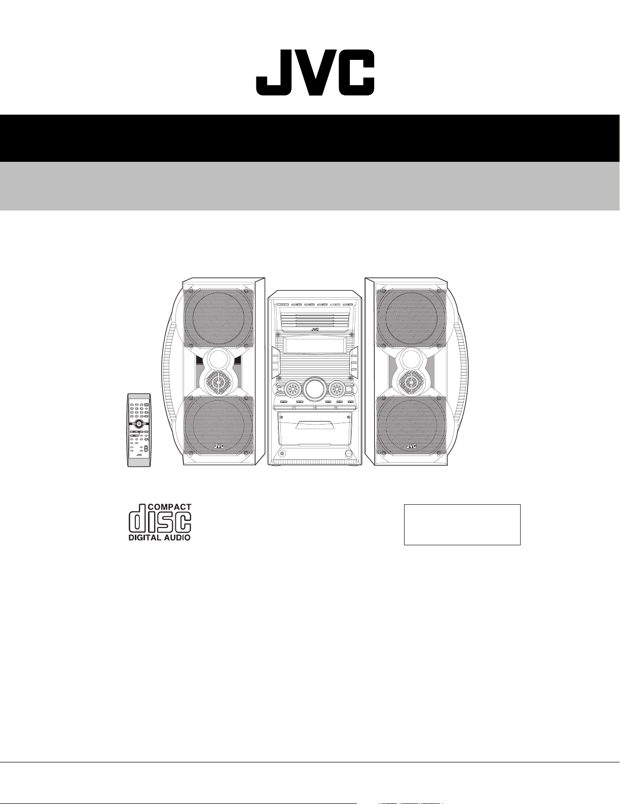
HX-Z10
SERVICE MANUAL
COMPACT COMPONENT SYSTEM
HX-Z10
SP-HXZ10 SP-HXZ10CA-HXZ10
Area Suffix
J ---------------------- U.S.A.
C ------------------- Canada
TABLE OF CONTENTS
1 Important Safety Precautions . . . . . . . . . . . . . . . . . . . . . . . . . . . . . . . . . . . . . . . . . . . . . . . . . . . . . . . . . . . 1-2
2 Disassembly method . . . . . . . . . . . . . . . . . . . . . . . . . . . . . . . . . . . . . . . . . . . . . . . . . . . . . . . . . . . . . . . . . . 1-5
3 Adjustment. . . . . . . . . . . . . . . . . . . . . . . . . . . . . . . . . . . . . . . . . . . . . . . . . . . . . . . . . . . . . . . . . . . . . . . . . . 1-35
4 Description of major ICs. . . . . . . . . . . . . . . . . . . . . . . . . . . . . . . . . . . . . . . . . . . . . . . . . . . . . . . . . . . . . . . 1-41
COPYRIGHT © 2003 VICTOR COMPANY OF JAPAN, LTD.
No.22015
2003/04
Page 2
HX-Z10
Important Safety Precautions
1.1 Safety Precautions
(1) This design of this product contains special hardware and
many circuits and components specially for safety purposes.
For continued protection, no changes should be made to the
original design unless authorized in writing by the manufacturer. Replacement parts must be identical to those
used in the original circuits. Services should be performed by qualified personnel only.
(2) Alterations of the design or circuitry of the product should
not be made. Any design alterations of the product should
not be made. Any design alterations or additions will void
the manufacturers warranty and will further relieve the
manufacture of responsibility for personal injury or property
damage resulting therefrom.
(3) Many electrical and mechanical parts in the products have
special safety-related characteristics. These characteristics are often not evident from visual inspection nor can the
protection afforded by them necessarily be obtained by using replacement components rated for higher voltage, wattage, etc. Replacement parts which have these special safety
characteristics are identified in the Parts List of Service Manual. Electrical components having such features ar e i dentified by shading on the schematics and by ( ) on the
Parts List in the Service Manual. The use of a substitute replacement which does not have the same safety characteristics as the recommended replacement parts shown in the
Parts List of Service Manual may create shock, fire, or other hazards.
(4) The leads in the products are routed and dressed with ties,
clamps, tubings, barriers and the like to be separated from
live parts, high temperature parts, moving parts and/or
sharp edges for the prevention of electric shock and fire
hazard. When service is required, the original lead routing
and dress should be observed, and it should be confirmed
that they have been returned to normal, after reassembling.
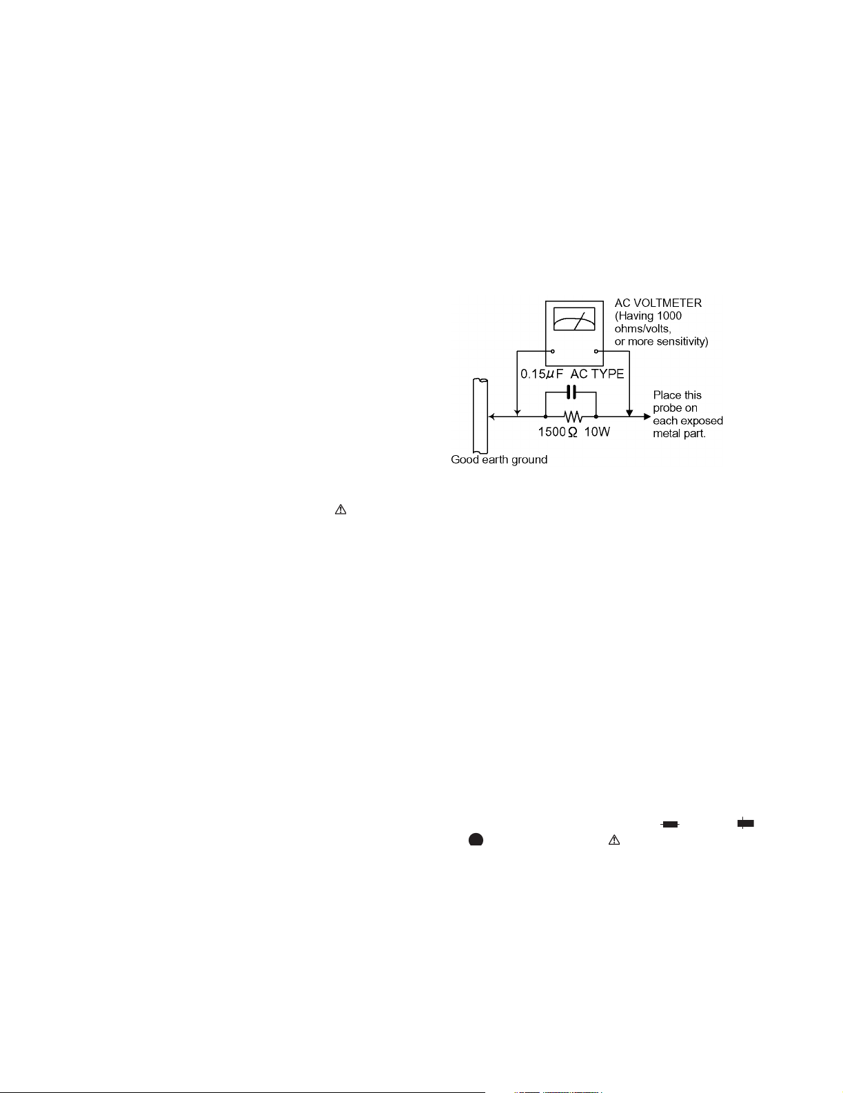
(5) Leakage shock hazard testing)
After reassembling the product, always perform an isolation
check on the exposed metal parts of the product (antenna
terminals, knobs, metal cabinet, screw heads, headphone
jack, control shafts, etc.) to be sure the product is safe to
operate without danger of electrical shock.
Do not use a line isolation transformer during this check.
• Plug the AC line cord directly into the AC outlet. Using a
"Leakage Current Tester", measure the leakage current
from each exposed metal parts of the cabinet, particularly any exposed metal part having a return path to the
chassis, to a known good earth ground. Any leakage current must not exceed 0.5mA AC (r.m.s.).
• Alternate check method
Plug the AC line cord directly into the AC outlet. Use an AC
voltmeter having, 1,000 ohms per volt or more sensitivity in
the following manner. Connect a 1,500 ohm 10W resistor
paralleled by a 0.15 µF AC-type capacitor between an
SECTION 1
exposed metal part and a known good earth ground.
Measure the AC voltage across the resistor with the AC
voltmeter.
Move the resistor connection to each exposed metal part,
particularly any exposed metal part having a return path to
the chassis, and measure the AC voltage across the resistor.
Now, reverse the plug in the AC outlet and repeat each
measurement. Voltage measured any must not exceed 0.75
V AC (r.m.s.). This corresponds to 0.5 mA AC (r.m.s.).
1.2 Warning
(1) This equipment has been designed and manufactured to
meet international safety standards.
(2) It is the legal responsibility of the repairer to ensure that
these safety standards are maintained.
(3) Repairs must be made in accordance with the relevant
safety standards.
(4) It is essential that safety critical components are replaced
by approved parts.
(5) If mains voltage selector is provided, check setting for local
voltage.
1.3 Caution
Burrs formed during molding may be left over on some parts
of the chassis.
Therefore, pay attention to such burrs in the case of preforming repair of this system.
1.4 Critical parts for safety
In regard with component parts appearing on the silk-screen
printed side (parts side) of the PWB diagrams, the parts that are
printed over with black such as the resistor ( ), diode ( )
and ICP ( ) or identified by the " " mark nearby are critical
for safety.
When replacing them, be sure to use the parts of the same type
and rating as specified by the manufacturer. (Except the JC version)
1-2 (No.22015)
Page 3
1.5 Importance administering point on the safety
HX-Z10
B2005
CN212
CN213
C258
B2104
CN233
CN231
CN232
B2204
R1002
D236
FT532
FT531
B2004
B2602
C259
C256
B2401
D235
D233
B2203
CN214
FT511
FT512
B2700
D234
D253
R250
Q250
C253
C255
FT521
FT522
T001
B2101
Q251
Q252
R253
T002
R1001
C250
R252
C251
D256
B2003
B2001
R254
B2202
R251
B2006
C257
C254
D252
D250
B2002
D254
B2601
B2103
B2201
RY3
B2501
FT132
B2801
B2802
B2502
FT131
FT111
C252
B2102
FT112
CN250
B2951
S500
B2400
B2952
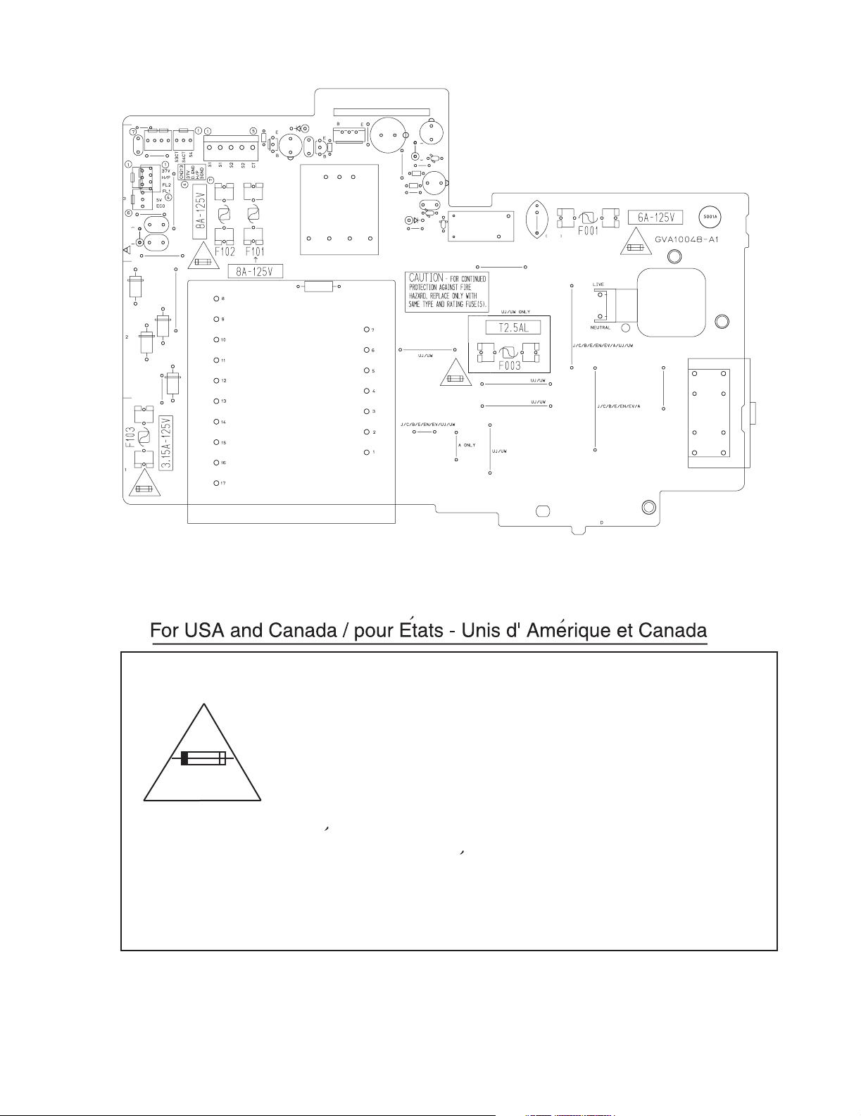
Caution: For continued protection against risk of
fire, replace only with same type 6A/125V for F001,
3.15A/125V for F103, 8A/125V for F101 and F102.
This symbol specifies type of fast operating fuse.
Precaution: Pour eviter risques de feux, remplacez
le fusible de surete de F001 comme le meme type
que 6A/125V, de F103 que 3.15A/125V, et 8A/250V
pour F101 et F102.
Ce sont des fusibles suretes qui functionnes rapide.
^
(No.22015)1-3
Page 4
HX-Z10
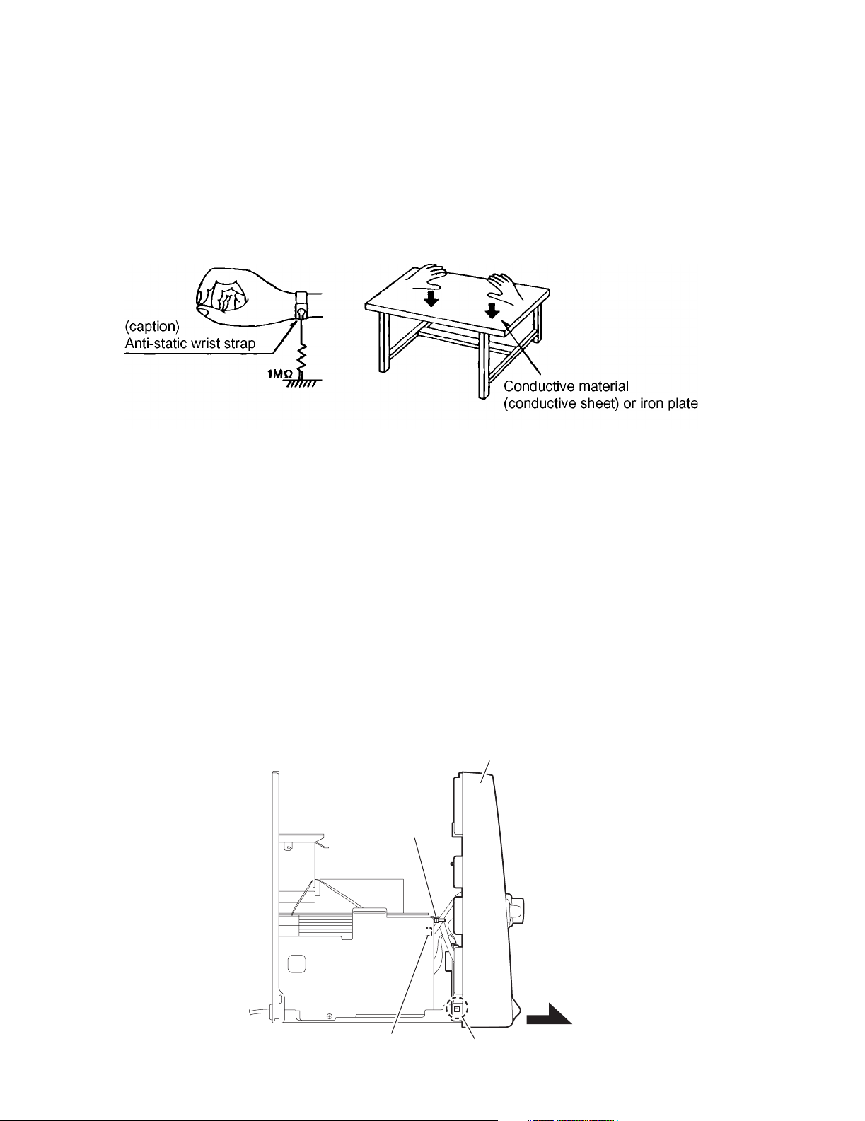
1.6 Preventing static electricity
Electrostatic discharge (ESD), which occurs when static electricity stored in the body, fabric, etc. is discharged,
can destroy the laser diode in the traverse unit (optical pickup). Take care to prevent this when performing repairs.
1.6.1 Grounding to prevent damage by static electricity
Static electricity in the work area can destroy the optical pickup (laser diode) in devices such as CD players.
Be careful to use proper grounding in the area where repairs are being performed.
(1) Ground the workbench
Ground the workbench by laying conductive material (such as a conductive sheet) or an iron plate over it before placing the
traverse unit (optical pickup) on it.
(2) Ground yourself
Use an anti-static wrist strap to release any static electricity built up in your body.
(3) Handling the optical pickup
• In order to maintain quality during transport and before installation, both sides of the laser diode on the replacement optical
pickup are shorted. After replacement, return the shorted parts to their original condition.
(Refer to the text.)
• Do not use a tester to check the condition of the laser diode in the optical pickup. The tester's internal power source can easily
destroy the laser diode.
1.7 Handling the traverse unit (optical pickup)
(1) Do not subject the traverse unit (optical pickup) to strong shocks, as it is a sensitive, complex unit.
(2) Cut off the shorted part of the flexible cable using nippers, etc. after replacing the optical pickup. For specific details, refer to the replace-
ment procedure in the text. Remove the anti-static pin when replacing the traverse unit. Be careful not to take too long a time
when attaching it to the connector.
(3) Handle the flexible cable carefully as it may break when subjected to strong force.
(4) I t is not possible to adjust the semi-fixed resistor that adjusts the laser power. Do not turn it.
1.8 Attention when traverse unit is decomposed
*Please refer to "Disassembly method" in the text for the CD pickup unit.
• Apply solder to the short land sections before the flexible wire is disconnected from the connector CN101 on the CD servo board.
(If the flexible wire is disconnected without applying solder, the CD pickup may be destroyed by static electricity.)
• In the assembly, be sure to remove solder from the short land sections after connecting the flexible wire.
Front panel assembly
Band
1-4 (No.22015)
Primary board
CN231
a
Page 5
SECTION 2
AA
Disassembly method
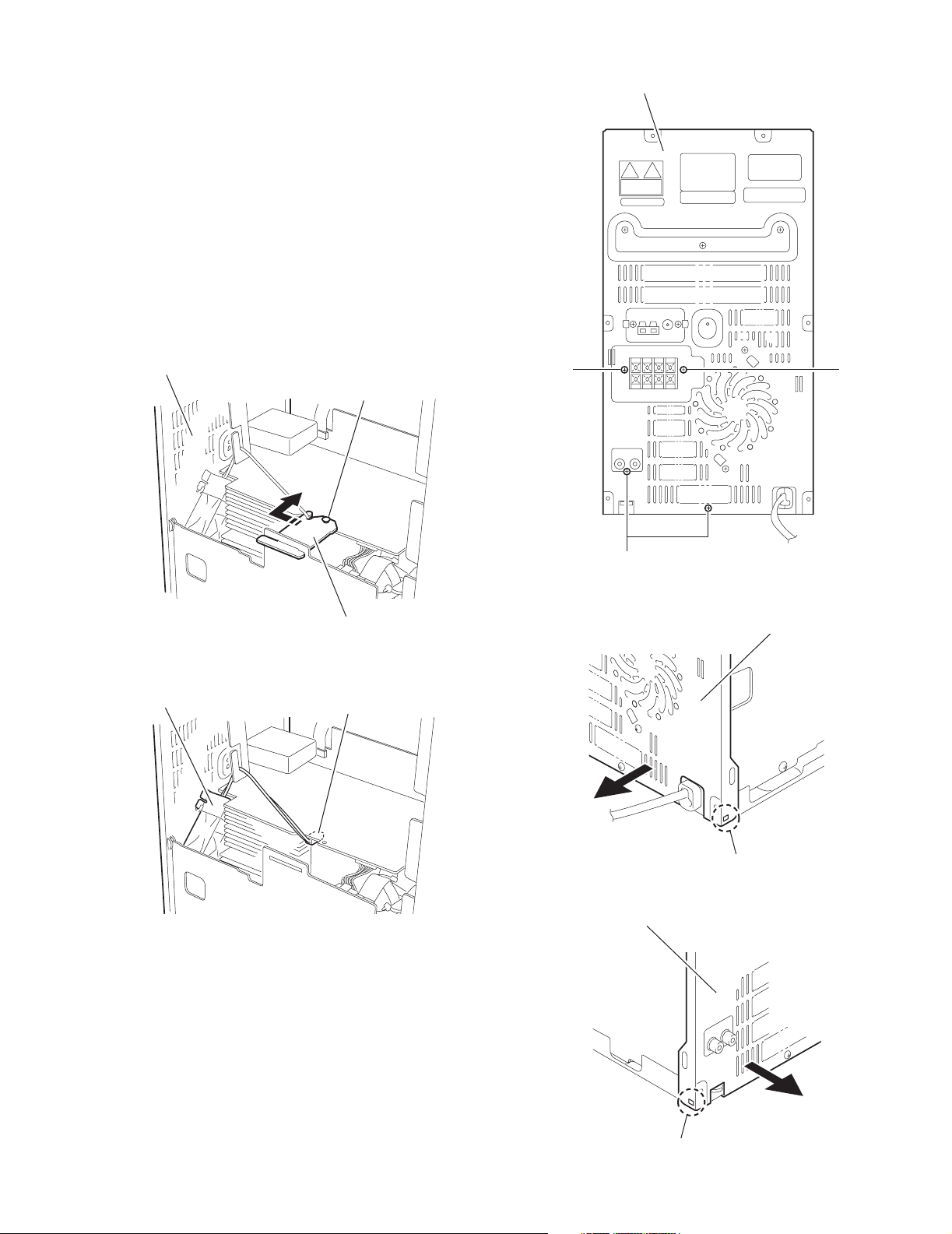
2.1 Main body
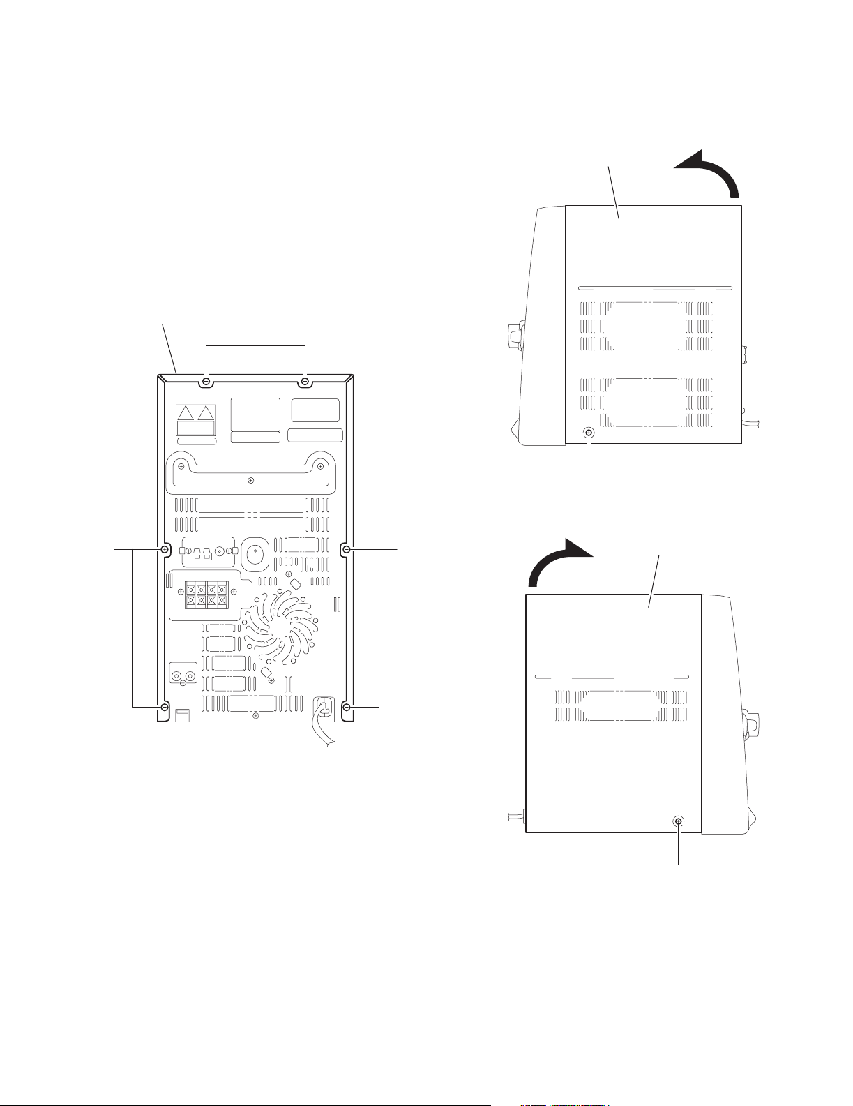
2.1.1 Removing the metal cover
(See Fig.1~3)
(1) Remove the six screws A on the back of the body.
(2) Remove the screw B on each side of the body.
(3) Remove the metal cover from the body by lifting the rear
part of the cover.
CAUTION:
Do not break the front panel tab fitted to the metal cover.
HX-Z10
Metal cover
Metal cover
A
B
Fig.2
Metal cover
Fig.1
B
Fig.3
(No.22015)1-5
Page 6
HX-Z10
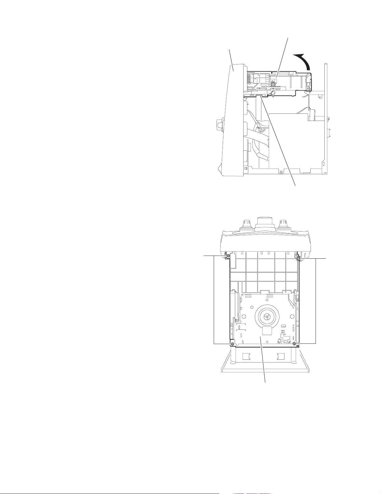
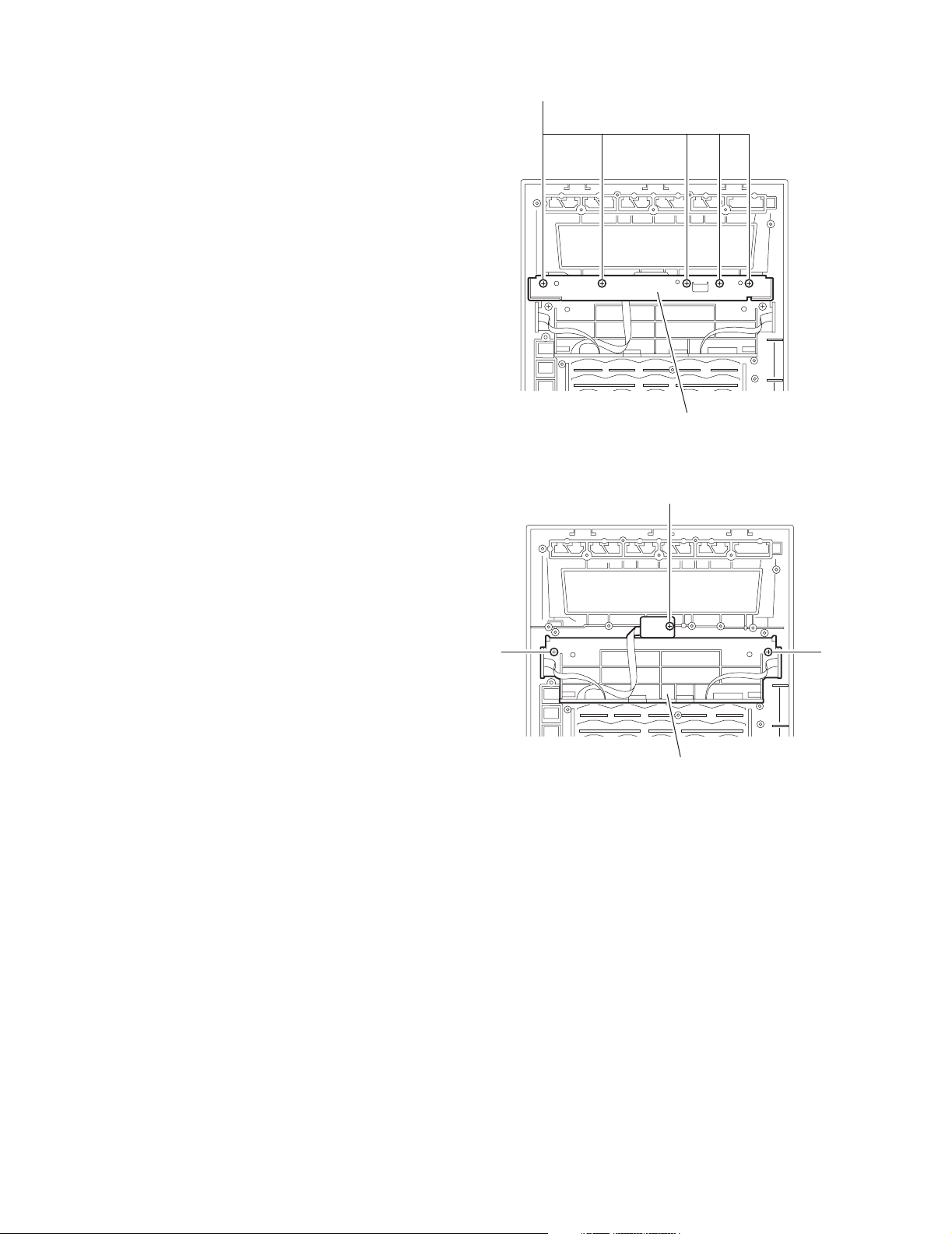
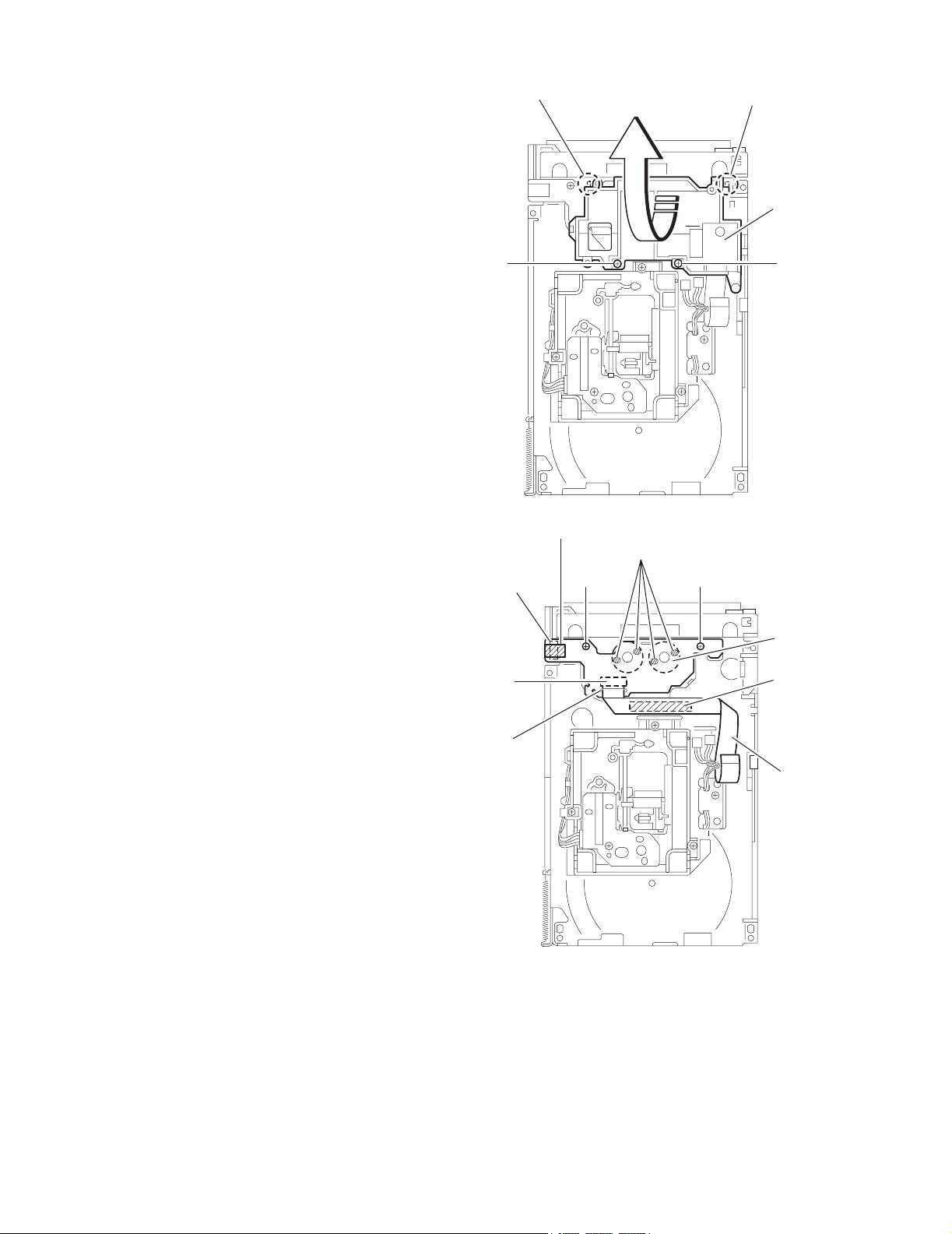
2.1.2 Removing the CD changer mechanism assembly
(See Fig.4, 5)
• Prior to performing the following procedure, remove the metal
cover.
(1) Disconnect the card wire from connector CN651 on the CD
servo control board on the right bottom of the CD changer
mechanism assembly.
(2) Remove the four screws C attaching the CD changer
mechanism assembly on top of the body.
(3) Remove the CD changer mechanism assembly while lifting
the rear part.
CAUTION:
Do not damage the CD fitting when removing the CD changer
mechanism assembly.
CD changer mechanism assembly
Front panel assemby
CD servo control board
CN651
Fig.4
C
C
CD changer
mechanism assembly
Fig.5
1-6 (No.22015)
Page 7
HX-Z10
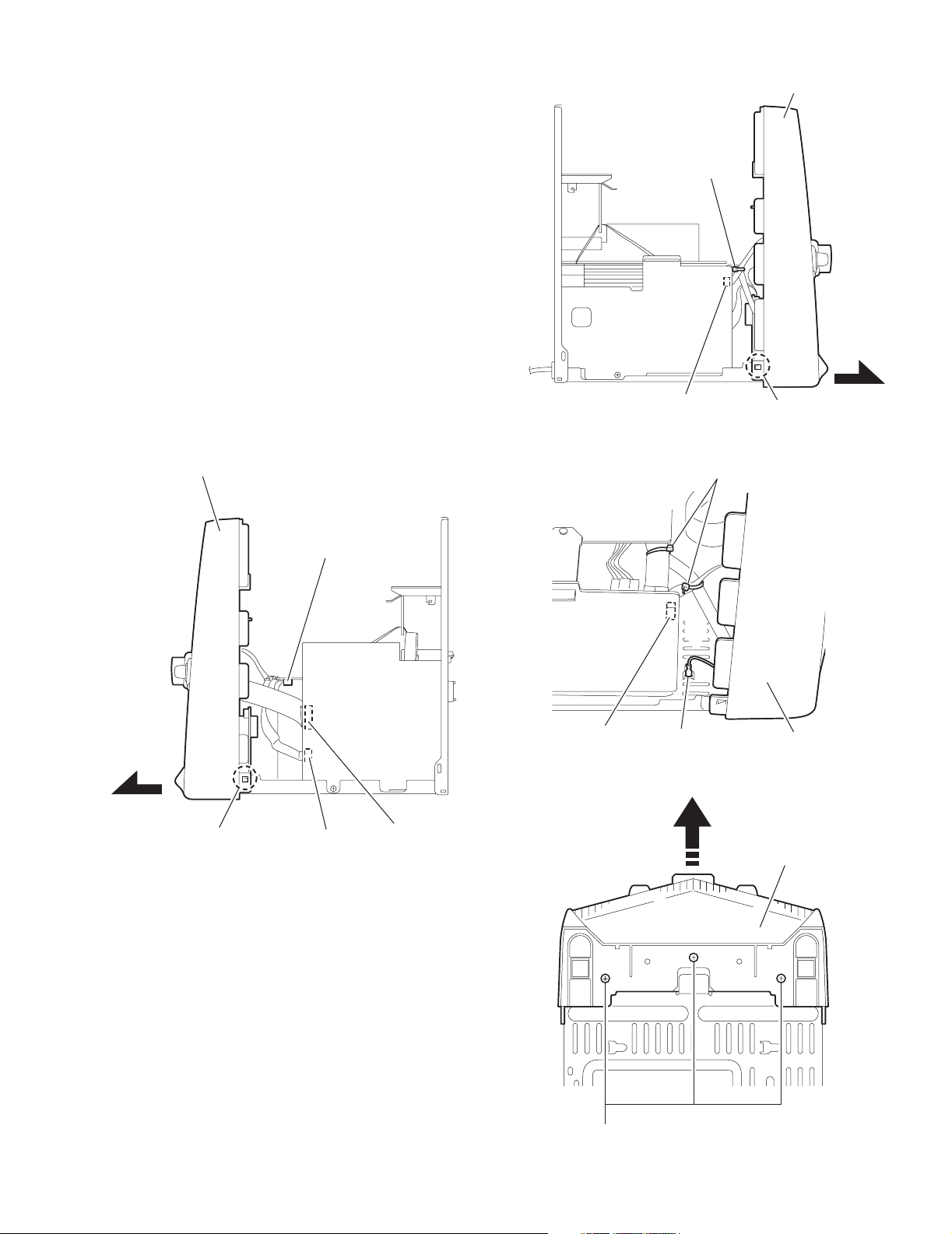
2.1.3 Removing the front panel assembly
(See Fig.6~9)
• Prior to performing the following procedure, remove the metal
cover and the CD changer mechanism assembly.
(1) Disconnect the card wires from connector CN44 and
CN870 on the main board on the right side of the body.
(2) Disconnect the wire from connector CN701 on the bridge
board.
(3) Cut the band.
(4) Disconnect the wire from connector CN231 on the primary
board on the left side of the body and remove the band fix-
ing the wire.
(5) Disconnect the ground wire extending from phones board
from bottom chassis.
(6) Remove the three screws D attaching the front panel as-
sembly at the bottom of the body.
(7) Release the two joints a on the lower left and right sides of
the front panel assembly using a screwdriver, and remove
the front panel assembly toward the front.
REFERENCE:
Front panel need to be tilt a little bit as release from bottom
chassis.
Front panel assembly
Band
Primary board
CN231
Fig.7
Band
Front panel assembly
a
Bridge board
CN701
Primary board
CN231
a
Fig.6
CN44
Main board
CN870
Ground wire
Fig.8
Front panel assembly
Front panel aeembly
D
Fig.9
(No.22015)1-7
Page 8
HX-Z10
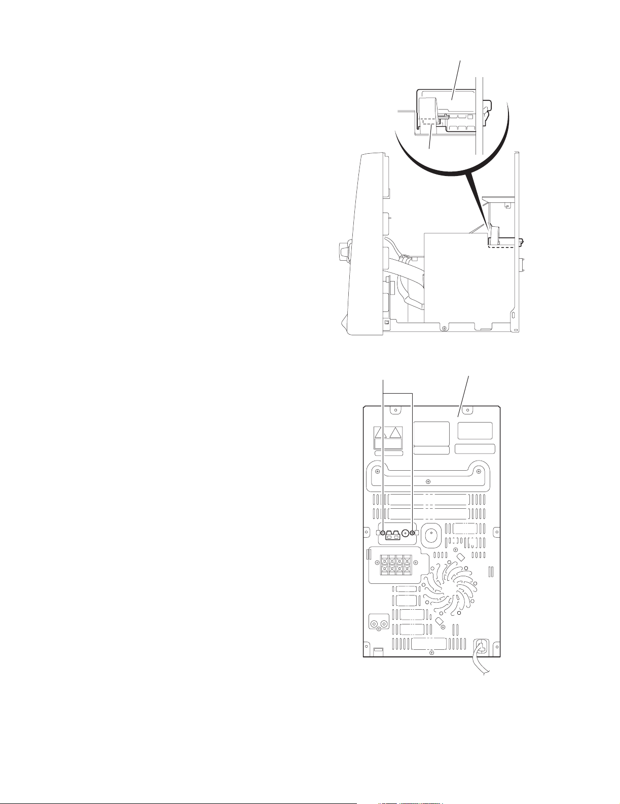
2.1.4 Removing the tuner pack assembly
(See Fig.10, 11)
• Prior to performing the following procedure, remove the metal
cover and the CD changer mechanism assembly.
(1) Disconnect the card wire from connector CN1 on the tuner
pack assembly on the right side of the body.
(2) Remove the two screws E on the rear panel on the back of
the body.
Tuner pack assembly
CN1
Fig.10
E
Rear panel
1-8 (No.22015)
Fig.11
Page 9
HX-Z10
2.1.5 Removing the rear panel
(See Fig.10, 12~16)
• Prior to performing the following procedure, remove the metal
cover and the CD changer mechanism assembly.
(1) Remove holding board by remove a plastic rivet and then
slide out the holding board as shown in fig. 12.
(2) Disconnect the fan wire extending from the fan assembly
from connector CN206 on the bridge board.
(3) Disconnect the card wire from connector CN1 on the tuner
pack.
(4) Remove four screws F from rear panel.
(5) Release joints b which on right bottom and left bottom of
rear panel. The joint can be release by pull outward the
side of rear panel.
REFERENCE:
Fan assembly and tuner pack will come off with rear panel.
Rear panel
Plastic rivet
Rear panel
FF
Fan assembly
Fig.12
Fig.13
Holding board
Bridge board
CN206
F
Fig.14
Rear panel
b
Fig.15
Rear panel
b
Fig.16
(No.22015)1-9
Page 10

HX-Z10
2.1.6 Rmoving the fan assembly
(See Fig.17, 18)
• Prior to performing the following procedure, remove the metal
cover, the CD changer mechanism assembly and the rear panel.
(1) Remove two screws G on the rear panel.
(2) Rotate fan assembly in clockwise direction to release fan
assembly from rear panel (joints c).
G
Rear panel
Fig.17
2.1.7 Removing the main board
(See Fig.19)
• Prior to performing the following procedure, remove the metal
cover, the CD changer mechanism assembly and the rear panel.
(1) Cut off the band.
(2) Disconnect the card wires from connector CN44 and
CN870 on the main board.
(3) Remove the screw H attaching the main board.
(4) Disconnect connector CN217 and CN311 on the main
board outward and release from the base chassis (joint d)
upward.
c
Fan assembly
c
Fig.18
Band
Main board
CN217
1-10 (No.22015)
CN870
CN44
H
Fig.19
CN311
d
Page 11
2.1.8 Removing the bridge board / regulator board / heat sink
(See Fig.20~23)
• Prior to performing the following procedure, remove the metal
cover, the CD changer mechanism assembly, the rear panel
and main board.
(1) Disconnect the wire from connector CN212, CN213 and
CN214 on the primary board respectively and remove the
band attaching the wires.
(2) Disconnect the wire from connector CN701 on the bridge
board.
(3) Disconnect the ground wire extending from the bridge
board from bottom chassis.
(4) Remove the two screws I attaching the heat sink bracket
and move the heat sink in the direction of the arrow to release from the base chassis. The bridge board and the reg-
ulator board come off with the heat sink.
(5) Remove the two screws J attaching the heat sink bracket.
(6) Remove the two screws M, detach bridge board from reg-
ulator board by disconnect connector CN205.
(7) Remove the two screws K and two screws L to detach
regulator board from heat sink.
CAUTION:
As assembly back the regulator board and bridge board to
heat sink.
Regulator board must be assembly to heat sink first and
screws K and L must be screwed before bridge board attach
to regulator board.
Band
Bridge board
Ground wire
Regulator board
Bridge board
I
Fig.21
HX-Z10
Heat sink
I
Heat sink bracket
Heat sink
CN701
Bridge board
Fig.20
Primary board
CN213
CN212
CN214
Regulator board
L
K
Heat sink bracket
Fig.22
Heat sink bracketHeat sink
ML
Fig.23
J
Regulator board
CN215
CN205
Bridge board
(No.22015)1-11
Page 12
HX-Z10
2.1.9 Removing the power transformer assembly
(See Fig 24, 25)
• Prior to performing the following procedure, remove the metal
cover, the CD changer mechanism assembly, the rear panel,
the main board and the bridge board / regulator board.
(1) Remove the screw N attaching the primary board.
(2) Disconnect the wire from connector CN231 on the primary
board.
(3) Remove the four screws O attaching the power transform-
er assembly.
(4) Detach the cord stopper from the base chassis upward.
REFERENCE:
When disconnecting the power cord from connector CN250 on
the primary board, remove the fixing band.
Power transformer
assembly
Power transformer
assembly
Primary board
N
Fig.24
Primary board
CN231
CN250
FIxing band
Fig.25
Cord stopper
O O
1-12 (No.22015)
Page 13
HX-Z10
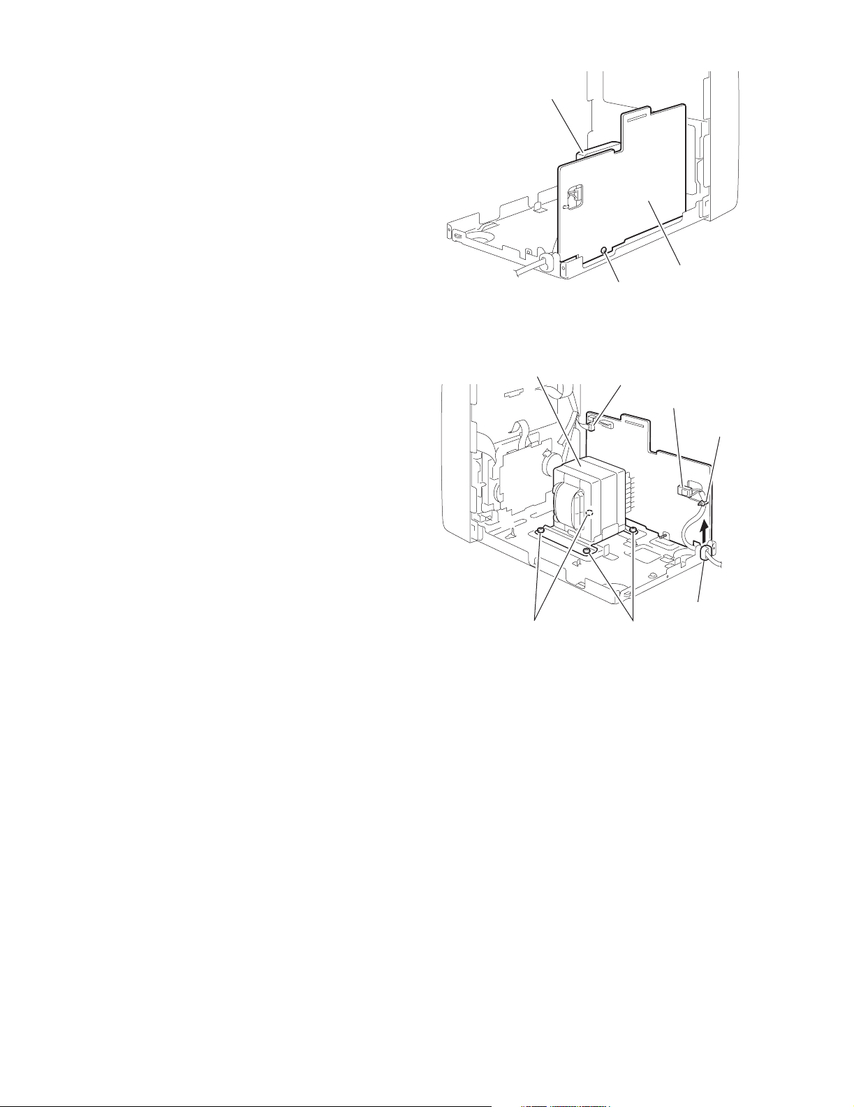
2.2 Front panel assembly
• Prior to performing the following procedure, remove the metal
cover, the CD changer mechanism assembly and the front
panel assembly.
2.2.1 Removing the cassette mechanism assembly
(See Fig.26)
(1) Disconnect the card wire from connector CN33 on the head
amplifier & mechanism control board.
(2) Remove the two screws P, and the two screws Q attach-
ing the cassette mechanism assembly.
2.2.2 Removing the headphone board
(See Fig.26)
(1) Remove the screw R and pull out the headphone board
backward.
(2) Cut off the band.
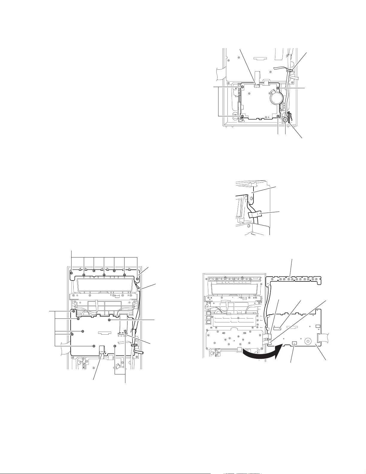
2.2.3 Rmoving the switch / micon board
(See Fig.27~29)
• Prior to performing the following procedure, disconnect the
card wire from CN43 on the micon board.
(1) Disconnect the card wire from connector CN840 on the mi-
con board.
(2) Remove the fifteen screws S attaching the switch / micon
board.
(3) Remove the spacer fixing the wire.
(4) Move the switch /micon board in the direction of the arrow
to disconnect the wire from connector CN880 and CN900
on the micon board.
S
Switch board
Head amplifier &
mechanism control board
CN33
P
QR
Fig.26
Switch board
Fig.28
Band
Q
Headphone board
Spacer
Switch board
S
CN43
Fig.27
S
Spacer
S
Micon board
CN840
CN880
Fig.29
CN43
CN840
CN900
Micon board
(No.22015)1-13
Page 14
HX-Z10
2.2.4 Removing the FL board assembly
(See Fig.30, 31)
• Prior to performing the following procedure, remove the switch
/ micon board.
(1) Remove the five screws T attaching the stay bracket (1).
(2) Remove the three screws U attaching the FL board as-
sembly.
T
Stay bracket (1)
Fig.30
U
UU
FL board assembly
Fig.31
1-14 (No.22015)
Page 15
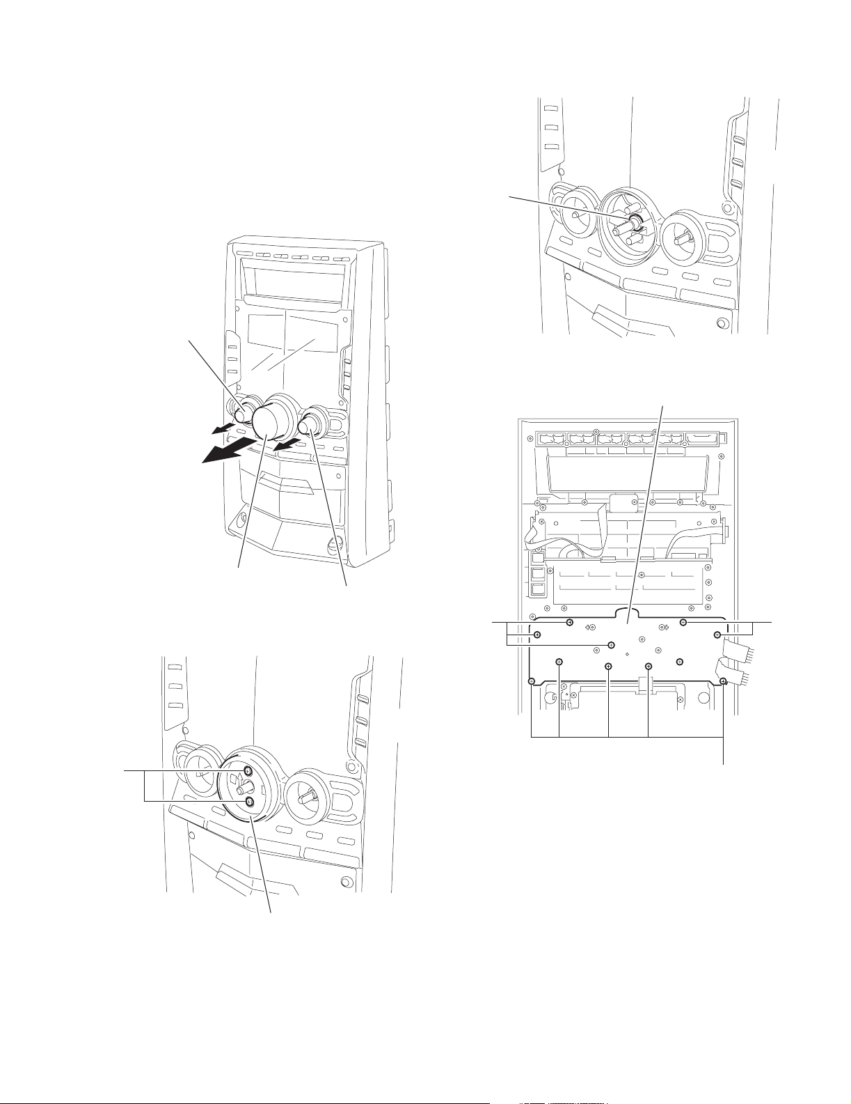
2.2.5 Removing the button board
(See Fig.32~35)
• Prior to performing the following procedure, remove the switch
/micon board.
(1) Pull out the preset knob, the volume knob and the sound
mode knob.
(2) Remove the two screws V attaching the knob holder. Re-
move the nut from the front panel.
(3) Remove the eleven screws W attaching the button board.
Sound mode knob
HX-Z10
Nut
Fig.34
Volume baord
V
Volume knob
Fig.32
Knob holder
Fig.33
Preset knob
W
W
W
Fig.35
(No.22015)1-15
Page 16
HX-Z10
r
2.3 CD changer mechanism
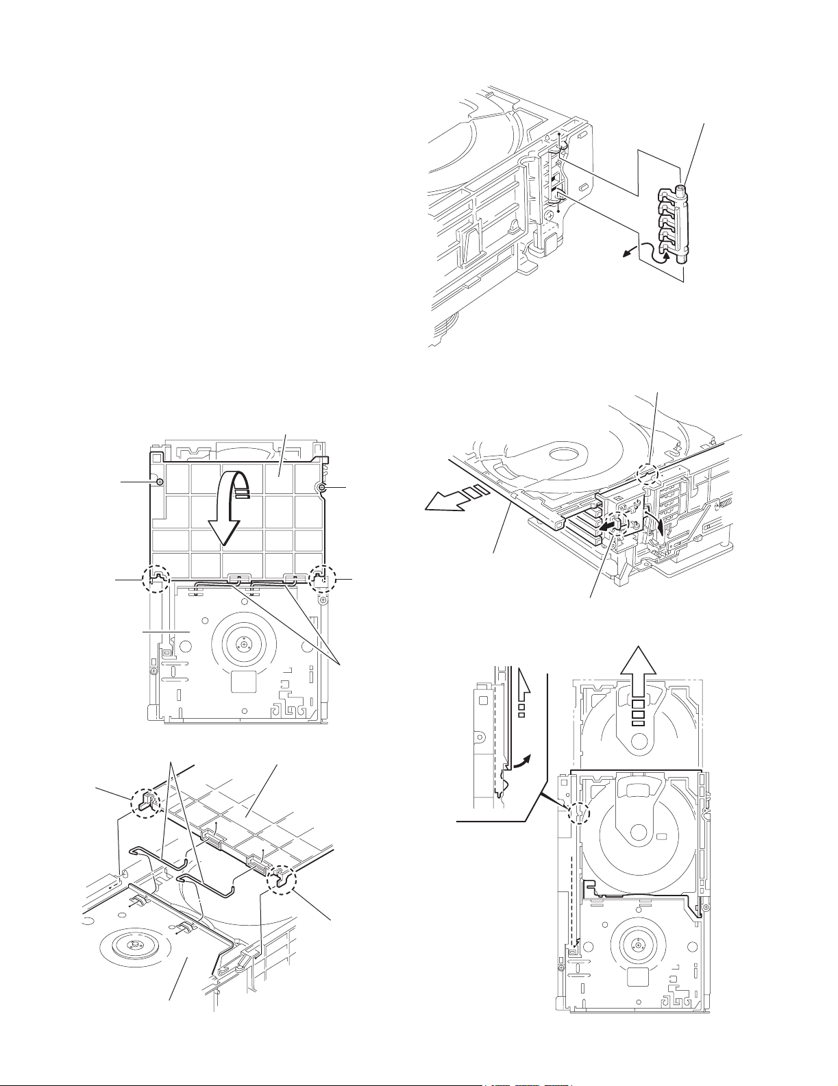
2.3.1 Removing the tray assembly
(See Fig.1 ~ 5)
(1) Remove the two screws A from the top cover and release
the two joints a on both sides of the body.
(2) Remove the top cover with the two rods attached to the top
cover and lifter assembly respectively.
(3) Remove the open det lever on the left side of the body.
(4) Push part b of the slide (R) assembly on the right side of
the body to unlock the tray assembly. Draw out the trays to-
ward the front.
Attention:
The tray can be locked if all tray assemblies are attached.
(5) From top of the body, move the stopper tab c in the direc-
tion of the arrow and release. Pull out the tray assemblies
from the body.
Caution:
Remove the tray assembly from top tray 5 in order.
Attention:
When reattaching the sub tray of the tray assembly, or when
removing the CD remaining inside, refer to another section.
Top cover
Open det leve
Fig.3
c
A
a
Lifter assembly
a
Rod
Fig.1
Top cover
A
Tray assembly
a
(Tray 5)
b
Fig.4
Rod
1-16 (No.22015)
Lifter assembly
Fig.2
a
Fig.5
Page 17
HX-Z10
2.3.2 Removing the servo control board
(See Fig.6 ~ 9)
Caution:
Solder the short-circuit point on the pickup before disconnecting the card wire extending from the pickup. If you do not follow
this instruction, the pickup may be damaged.
(1) Disconnect the card wire from connector CN251 and each
wire from connector CN252, CN253 and CN602 on the servo control board on the bottom of the body. Disconnect the
wire from joint d.
(2) Solder the short round point on the flexible board of the pick
up.
(3) Remove the four screws B and turn the servo control board
as shown in the figure.
(4) Disconnect the card wire from connector CN601 on the
servo control board.
Caution: Unsolder the short-circuit point after reassembling.
Caution:
When reassembling, twist the wires to be connected to connector CN252 and CN253 twice.
2.3.3 Removing the switch board (See Fig.9)
(1) Disconnect the wires from connector CN252 and CN253
on the servo control board.
(2) Remove the screw C attaching the switch board.
(3) Release the wires from the slot e of the switch board.
Caution:
When reassembling, let the wires through the slot e of the
switch board and twist them twice.
Servo control board
B
Card wire
Short round
Flexible board
Pickup
Fig.7
Card wire
CN601
CN602
d
B
Fig.6
CN253
CN252
B
CN251
Switch board
Servo control board
Fig.8
Servo control board
CN253
e
CN252
Switch board
C
Fig.9
(No.22015)1-17
Page 18
HX-Z10
2.3.4 Removing the motor board
(See Fig.10 , 11)
• Prior to performing the following procedure, remove the servo
control board.
(1) Turn over the body and remove the two screws D. Move
the CD module bkt. in the direction of the arrow to release
two joints f.
(2) Unsolder the four soldered parts on the motor of the motor
board.
Caution:
If removing the motor board with the motor, you should
remove the screws attaching the motor from top of the
body(Refer to another section).
(3) Remove the two screws E attaching the motor board.
(4) Remove the spacer fixing the motor board and tray switch
board, and disconnect connector CN2 on the motor board.
(5) Disconnect the card wire from connector CN1 on the motor
board.
Caution:
When reconnecting the card wire, let the card wire through the
slot g of the motor board and attach it to the bottom of the body
using a double tape.
f
f
CD Module
braket
DD
CN2
CN1
g
Spacer
Soldering point
E
Fig.10
E
Motor
Double
face tape
Card wire
Fig.11
1-18 (No.22015)
Page 19

2.3.5 Removing the CD tramecha assembly
(See Fig.12)
• Prior to performing the following procedure, remove the servo
control board.
(1) Turn over the body and remove the three screws F attach-
ing the tramecha.
HX-Z10
F
F
F
CD Tramecha assembly
Fig.12
(No.22015)1-19
Page 20

HX-Z10
2.3.6 Removing the pickup
(See Fig.13 , 14)
• Prior to performing the following procedure, remove the servo
control board and CD tramecha assembly.
(1) From top of the CD tramecha assembly, turn the cam gear
in the direction of the arrow to move the pickup assembly
outward.
(2) Push down the stopper h in the direction of the arrow and
pull out the shaft.
(3) Release the joint i of the pickup assembly and mecha
base.
(4) Remove the screw G attaching the CD rack. Release the
four tabs j at the bottom of the CD rack.
Mecha base
h
Stopper
i
Pickup assembly
Shaft
Cam gear
ShaftShaft
Stopper
Fig.13
CD lack
G
Pickup
j
j
1-20 (No.22015)
j
Fig.14
Page 21

2.3.7 Removing the side (L)/ tray switch board
(See Fig.15 ~ 17)
• Prior to performing the following procedure, remove the tray
assembly.
(1) Remove the two screws H attaching the side (L) on top of
the body.
(2) From the side of the body, remove the spacer fixing the tray
switch board and motor board. Disconnect connector CN3
on the tray switch board and detach the side (L) upward.
(3) Remove the screw J attaching the tray switch board.
(4) Push the joint tab k of the side (L) in the direction of the ar-
row and remove the tray switch board outward, then re-
lease joint l.
H
HX-Z10
H
H
CN3
Spacer
Side (L)
Fig.15
Side (L)
H
Fig.16
k
Side (L)
l
J
Tray switch board
Fig.17
(No.22015)1-21
Page 22

HX-Z10
2.3.8 Removing the side (R) assembly
(See Fig.18 ~ 22)
• Prior to performing the following procedure, remove the tray
assembly.
(1) Push and release the two tabs m of the gear cover through
the two notches inside the side (R) assembly. Remove the
gear cover outward.
(2) Remove the spring attached to part n of the hook on the
right side of the body.
(3) From top of the body, turn the 1 gear clockwise to move the
elevator cam rearward.
Move the two slots o and joint p of the elevator cam as
shown in Fig.21 and remove the elevator cam outward.
(4) Remove the three screws K and detach the side (R) up-
ward.
Caution:
When reattaching the side (R) assembly, make sure to fit the
shaft(part q) into the slot of the select lever.
K
q
Side (R) assembly
Fig.20
Spring
m
n
Elevator cam
K
Side (R)
assembly
K
Side (R) assembly
o
o
p
Fig.21
K
Side (R) assembly
Fig.18
1 gear
Sprihg
K
Gear cover
1-22 (No.22015)
n
Fig.22
Elevator com
Fig.19
Page 23

HX-Z10
2.3.9 Removing the lifter assembly
(See Fig.23 ~ 27)
• Prior to performing the following procedure, remove the tray
assembly and side (L)/ side (R) assembly.
(1) From top of the body, turn the 1 gear clockwise to move the
lifter assembly upward as shown in Fig.24.
(2) From top of the body, turn the 2 gear clockwise to move the
hook toward the front until it stops.
(3) Move the hook stopper in the direction of the arrow while
pushing the tab r of the hook stopper to unlock it. Release
four joints s to detach from the rack holder.
Release the rod from part t.
(4) Turn the 1 gear clockwise again to move the lifter assembly
upward.
(5) Remove the lifter assembly from the body upward at posi-
tion u where the four pins on the right and left sides of the
lifter assembly fit to the notches of the v.
Move the lifter assembly toward the front and release from
the hook.
2 gear
1 gear
Hook
t
s
Rod
s
s
r
s
Hook stopper
Fig.25
Lifter assembly
1 gear
u u
Hook stopper
Hook
2 gear
Fig.23
1 gear
Lifter
assembly
Lifter assembly
v
Lifter assembly
Fig.26
u
u
Hook stopper
Hook
Fig.24
v
Fig.27
(No.22015)1-23
Page 24

HX-Z10
2.3.10 Removing the rack holder assembly/ sensor assembly
(See Fig.28 ~ 33)
• Prior to performing the following procedure, remove the tray
assembly, side (L)/ side (R) assembly, lifter assembly.
Attention:
If the slide gear of the body places at joint w of the rack holder
assembly, turn the 1 gear counterclockwise to move the slide
gear toward the front. Remove the rack holder assembly.
(1) Remove the three screws J attaching the rack holder as-
sembly. Release joint w from the notch.
Caution:
When reattaching the rack holder assembly, do not nip
the wire x extending from the sensor assembly.
(2) Remove the two screws M attaching the sensor assembly.
(3) Move the sensor assembly in the direction of the arrow to
release from the slot at joint y.
(4) Remove the spring attached to the bottom of the sensor as-
sembly from the boss z on the sensor slider.
(5) Remove the screw N and O attaching the sensor board and
SV resister respectively.
If necessary, unsolder the sensor board.
Caution:
When reattaching the SV resister, attach the sensor slider to
the sensor bracket and fit the lever on the bottom of the SV resister into slot a’ of the sensor slider.
Caution:
When reattaching the rack holder assembly, turn the 1 gear
clockwise to move the slide gear and slide lever inside the
body rearward.
• Let the wire extending from the sensor assembly through notch
x to the bottom of the body.
• Fit pin c’of the slide lever into hole b’ of the sensor slider on
the bottom of the sensor assembly while attaching the spring
to the boss z of the sensor slider.
• Engage joint y of the sensor assembly to the notch of the body.
Rack holder
assembly
L
w
L
1 gear
x
L
Fig.28
w
Rack holder
assembly
Rack holder
assembly
w
Fig.29
1-24 (No.22015)
Page 25

HX-Z10
M
M
x
Sensor assembly
SV resister
O
Soldering
N
Sensor board
point
z
Sensor braket
a'
Sensor slider
Fig.32
y
a'
Fig.30
b'
Spring
Sensor assembly
M
M
Sensor slider
Spring
Slide gear
y
b'
z
z
Fig.31
c'
Spring
Fig.33
Slide lever
(No.22015)1-25
Page 26

HX-Z10
r
2.3.11 Removing the motor
(See Fig.34 ,35)
• Prior to performing the following procedure, remove the servo
control board and top cover.
Attention:
You need not to remove the tray assembly, and in such case,
move it.
(1) Remove the two belts on top of the body.
(2) Remove the four screws N attaching the motor.
(3) Remove the motor board from the bottom of the body.
(Refer to the section “Removing the motor board”.)
Attention:
When removing the motor board with the motor, you need not
to unsolder four soldered parts.
Caution:
When reattaching the motor, turn the side where the label
should be put to the front side.
Motor
Moto
NN
Belt
Fig.34
Belt
Label
Fig.35
1-26 (No.22015)
Page 27

HX-Z10
r
2.3.12 Taking out the CD in play mode
(See Fig.36 ~ 39)
Attention:
Refer to “Removing the tray assembly”.
(1) Remove the top cover upward.
(2) Unlock the tray assembly and draw out the tray assembly
toward the front.
(3) From top of the body, turn the 1 gear clockwise to move the
lifter assembly upward.
(4) From top of the body, turn the 2 gear clockwise to move the
sub tray remaining inside the lifter assembly toward the
front, then pull out.
(5) Take out the CD on the sub tray.
(6) After clearing away the CD, insert the sub tray into the main
tray.
Caution:
When reattaching the sub tray, move the tray stopper on
the bottom of the main tray in the direction of the arrow
to lock the sub tray certainly.
(7) Push the tray assembly toward the body and reattach.
Tray assembly
Tray assembly
Tray stopper
Sub tray
Fig.37
Main tray
2 gear
1 gear
Sub tray
Sub tray
Fig.38
Fig.36
Tray stoppe
Fig.39
(No.22015)1-27
Page 28

HX-Z10
2.4 Cassette mechanism assembly
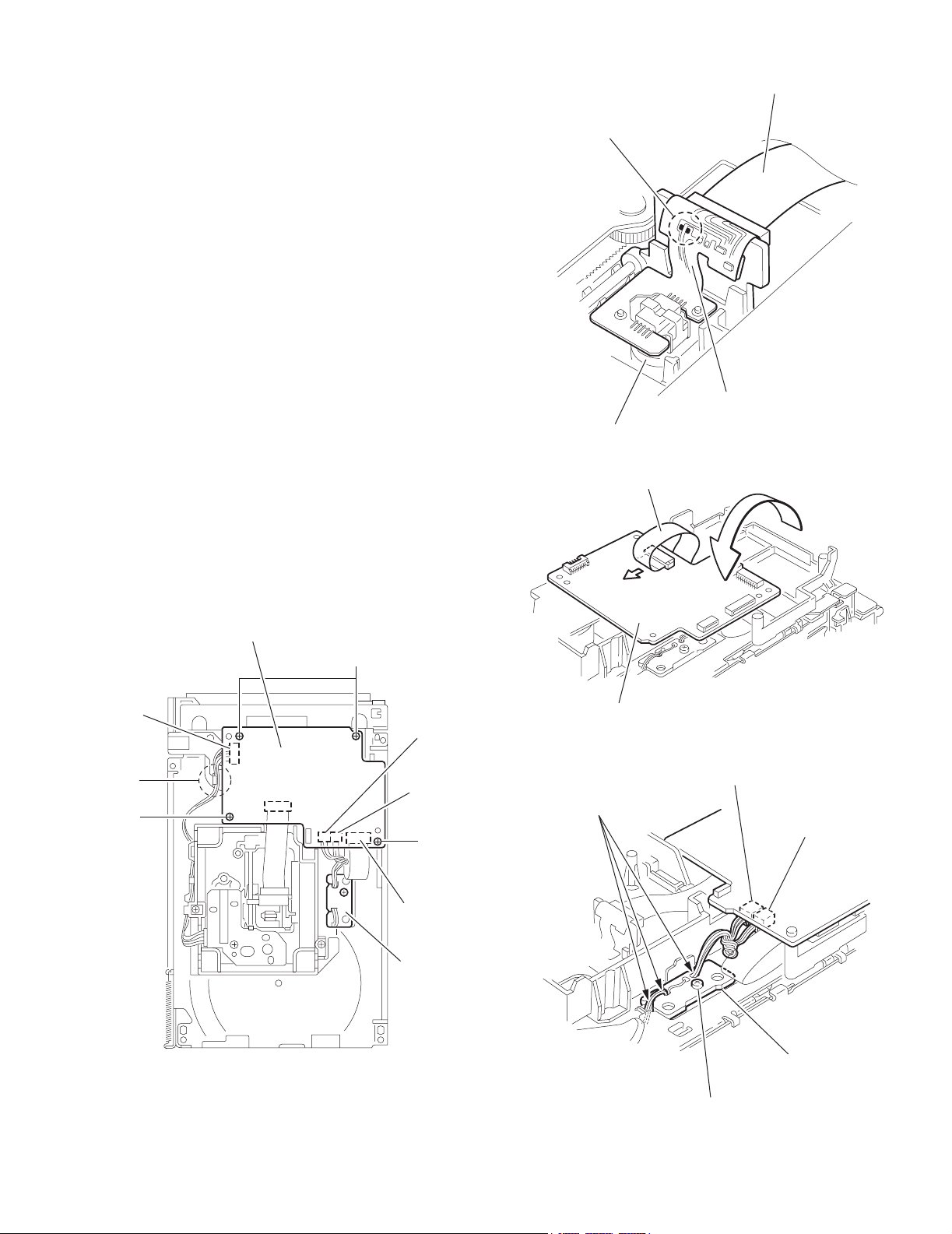
2.4.1 Removing the Play/Record & Clear head
(See Fig.1~3)
(1) While moving the trigger arm on the right side of the head
mount in the direction of the arrow, turn the flywheel R
counterclockwise until the head mount comes ahead and
clicks.
(2) The head turns counterclockwise as you turn the flywheel
R counterclockwise (See Fig.2 and 3).
(3) Disconnect the flexible wire from connector CN31 on the
head amplifier & mechanism control board.
(4) Remove the spring from the back of the head.
(5) Loosen the azimuth screw for reversing attaching the head.
(6) Remove the head on the front side of the head mount.
Cassette mechanism assembly
Fig.1
Head
Fly wheelR
Trigger armHead mount
Flexible wire
Fly wheel R
Fig.2
Azimuth screw
Head
for reversing
Spring
CN31
Head amplifer & mecha control board
Fig.3
1-28 (No.22015)
Page 29

2.4.2 Removing the head amplifier & mechanism control board
(See Fig.4)
(1) Turn over the cassette mechanism assembly and remove
the three screws A attaching the head amplifier & mechanism control board.
(2) Disconnect the flexible wire from connector CN31 on the
head amplifier & mechanism control board.
(3) Disconnect connector CN32 of the head amplifier & mech-
anism control board from connector CN1 on the reel pulse
board.REFERENCE: If necessary, unsolder the 4-pin wire
soldered to the main motor.
2.4.3 Removing the main motor
(See Fig.4~7)
(1) Remove the two screws B .
(2) Half raise the motor and remove the capstan belt from the
motor pulley.
ATTENTION:
Be careful to keep the capstan belt from grease. When reassembling, refer to Fig.6 and 7 for attaching the capstan belt.
Head amplifier & mecha control board
HX-Z10
Main motor assembly
Capstan belt
Fig.5
Main motor assembly
CN31
Flexible wire
A
AA
Fig.4
CN32
4pin wire
B
Main motor assembly
Motor pulley
Capstan belt
Fig.6
Main motor assembly
Fly wheel
Capstan belt
Motor pulley
Fig.7
(No.22015)1-29
Page 30

HX-Z10
2.4.4 Removing the flywheel
(See Fig.8, 9)
• Prior to performing the following procedure, remove the head
amplifier & mechanism control board and the main motor assembly.
(1) From the front side of the cassette mechanism, remove the
slit washers attaching the capstan shaft L and R. Pull out
the flywheels backward.
Fly wheel R Fly wheel L
Fig.8
Fly wheel R
Capstan shaft R Capstan shaft L
Fly wheel L
Slit washer
Fig.9
2.4.5 Removing the reel pulse board and solenoid
(See Fig.10)
• Prior to performing the following procedure, remove the head amplifier & mechanism control board.
(1) Remove the screw C.
(2) Release the tab a, b, c, d and e retaining the reel pulse board.
(3) Release the tab f and g attaching the solenoid on the reel pulse board.
(4) The reel pulse board and the solenoid come off.
bc
a
Solenoid
g
f
d
Reel pulse board
C
e
1-30 (No.22015)
Fig.10
Page 31

2.4.6 Reattaching the Play/ Record & Clear head
r
r
(See Fig.11~13)
(1) Reattaching the head mount assembly.
a) Change front of the direction cover of the head
mount assembly to the left (Turn the head forward).
b) Fit the bosses O', P', Q', U' and V' on the head mount
assembly to the holes P and V, the slots O, U and Q
of the mechanism sub assembly (See Fig.11 to 13).
CAUTION:
To remove the head mount assembly, turn the direction
cover to the left to disengage the gear. If the gear can not
be disengaged easily, push up the boss Q' slightly and
raise the rear side of the head mounts slightly to return
the direction lever to the reversing side.
(2) Tighten the azimuth screw for reversing.
(3) Reattach the spring from the back of the Play/ Record &
Clear head.
(4) Connect the flexible wire to connector CN31 on the head
amplifier & mechanism control board.
U' Q'
Head mount assembly
Head mount assembly
O'
Fig.11
P'
P'
V'
V'
Direction cove
HX-Z10
Spring
Flexible wire
V
O
P
Q
Head
Direction cove
U
Fig.12
Azimuth screw for reversing
Head mount
CN31
Fig.13
Head amplifier &
mechanism control board
(No.22015)1-31
Page 32

HX-Z10
A
2.5 Speaker section
2.5.1 Removing the Side cover
(See Fig.1)
(1) Removing the eight screws A on the side of the body.
A
A
Fig.1
2.5.2 Removing the sub woofer
(See Fig.2)
• Prior to performing the following procedure, remove the side
cover.
(1) Remove the four screws B attaching the sub woofer on the
side of the body.
(2) Disconnect the red and black wires from the two terminals
on the sub woofer.
B
B
Sub woofer
Fig.2
1-32 (No.22015)
Page 33

2.5.3 Removing the Front panel
(See Fig.3, 4)
• Prior to performing the following procedure, remove the side
cover.
CAUTION:
When removing the front panel from the body, do not break or
damage them that are glued at the joint a (See Fig.3).
(1) Remove the four screws C attaching the front panel.
(2) Release the four joints a.
(3) Disconnect the yellow and black wires from the two termi-
nals on the tweeder on the back of the front panel.
2.5.4 Removing the tweeter
(See Fig.4)
• Prior to performing the following procedure, remove the side
cover and the front panel.
(1) Remove the two screws D attaching the tweeter on the
back of the front panel.
Front cover
Joint a
HX-Z10
C
Joint a
C
Fig.3
Fig.4
C
Tweeter
C
(No.22015)1-33
Page 34

HX-Z10
2.5.5 Removing the woofer
(See Fig.5)
• Prior to performing the following procedure, remove the side
cover and the front panel.
(1) Remove the four screws E attaching the woofer.
(2) Disconnect the red and black wires from the two terminals
on the woofer.
2.5.6 Removing the woofer
(See Fig.5)
• Prior to performing the following procedure, remove the side
cover and the front panel.
(1) Remove the four screws F attaching the woofer.
(2) Disconnect the three black wires and the black, red and
blue wires from the two terminals on the woofer respectively.
Woofer
EE
FF
Woofer
Fig.5
1-34 (No.22015)
Page 35

3.1 Adjustment method
V
HX-Z10
SECTION 3
Adjustment
Measurement Instruments Required for
Adjustment
1. Low frequency oscillator
This oscillator should have a capacity to output
0dBs to 600 at an oscillation frequency of
50Hz-20kHz.
2. Attenuator impedance : 600
3. Electronic voltmeter
4. Distortion meter
5. Frequency counter
6. Wow & flutter meter
7. Test tape
VTT703L : Head azimuth
VT712 : Tape speed and running unevenness
(3kHz)
VT724 : Reference level (1kHz)
8. Blank tape
TYPE : AC-225
TYPE : AC-514
9. Torque gauge : For play and back tension
FWD(TW2111A), REV(TW2121a) and
FF/REW(TW2231A)
10. Test disc: CTS-1000
Measurement conditions
Power supply voltage
AC120V (60Hz)
Reference output : Speaker : 0.775V/4
: Headphone : 0.077V/32
Reference frequency and
input level ------------------------------ 1kHz, AUX : -8dBs
Measurement output terminal ------- at Speaker J3002
Load resistance --------------------------- 4
Radio Input signal
AM frequency --------------------------------------- 400Hz
AM modulation ---------------------------------------- 30%
FM frequency --------------------------------------- 400Hz
FM frequency deviation ------------------------ 22.5kHz
Tuner section
FM Band cover: 87.5~108.0MHz
MW Band cover: 530~1,710kHz
Voltage applied to tuner +B : DC5.7V
VT : DC 12
Reference measurement
output 26.1mV(0.28V)/3
Input positions AM : Standard loop antenna
FM : TP1 (hot) and TP2 (GND)
Standard measurement position of volume
Function switch to Tape
Beat cut switch to Cut
Super Bass/Active hyper Bass to OFF
Bass Treble to Center
Adjustment of main volume to reference output
VOL : 28
Precautions for measurement
1. Apply 30pF and 33k to the IF sweeper output
side and 0.082 F and 100k in series to the
sweeper input side.
2. The IF sweeper output level should be made as
low as possible within the adjustable range.
3. Since the IF sweeper is a fixed device, there is no
need to adjust this sweeper.
4. Since a ceramic oscillator is used, there is no need
to perform any MIX adjustment.
5. Since a fixed coil is used, there is no need to adjust
the FM tracking.
6. The input and output earth systems are separated.
In case of simultaneously measuring the voltage in
both of the input and output systems with an
electronic voltmeter for two channels, therefore, the
earth should be connected particularly carefully.
7. In the case of BTL connection amp., the minus
terminal of speaker is not for earthing. Therefore, be
sure not to connect any other earth terminal to this
terminal. This system is of an BTL system.
8. For connecting a dummy resistor when measuring
the output, use the wire with a greater code size.
9. Whenever any mixed tape is used, use the band
pass filter (DV-12).
(No.22015)1-35
Page 36

HX-Z10
3.2 Cassette mechanism adjustment
Head azinuth
adjustment screw
(Forward side)
Mecha control board
Head azinuth
adjustment screw
(Reverse side)
SW1
SW2
Head azinuth
adjustment screw
(Forward side)
Head azinuth
adjustment screw
(Reverse side)
CN31
R/P head, Erase head
P1
VR37
D1
R371
CN1
FW100
SW5
Motor speed
VR37
BIAS adjust
VR31
C308
R327
VR31
R313
Q302
R315
C316
C319
R314
C121
C221
C314
L301
C313
R104
Q305
D340
C310
R304
R310
C107
L303
R102
R121
R221
R303
R335
R353
R339
R108
C113
R302
Q343
C103
R301
C301
Q342
C207
C304
R208
C105
C205
C106
R306
R106
R101
C104
CN34
C306
Q344
R105
C102
R344
R205
R110
Q345
R345
C307
R336
C340
R346
R206
C206
R107
W1
Q346
R210
R305
C300
C341
C110
R109
R372
Q372
C371
CN33
IC32
R116
C109
CN31
Q371
C101
C374
R216
Q375
R376
C376
R204
R201
C202
C204
C201
W1
R375
C342
D375
C213
R207
Q376
C209
IC1
R338
R337
CN32
R202
C203
C210
R340
C331
R342
R347
Q347
SW6
R343
R341
IC33
1-36 (No.22015)
Page 37

3.2.1 Mechanism section
HX-Z10
Item Condition Measurement method Ref.value
Head
azimuth
Test tape
: VT703L (8kHz)
Output terminal
: Speaker out
1.Playback the test tape VT703L (8kHz).
2.Adjust to maximum output level by azimuth
adjustment screw for forward side and reverse
side.
Maximum
output
3.This adjustment is adjust by adjustment screw
of forward side and adjustment screw of reverse
side.
Tape speed
Test tap
: VT712 (3kHz)
Output terminal
Playback the test tape VT712 (3kHz) at end of
forward side,adjust to 2,940~3,90Hz indication
of frequency counter by VR37.
2,940 ~
3,090Hz
: Speaker out or
Headphone out
Adjustment
position
Only adjust
at changed
head
VR37
Item Condition Measurement method Ref.value
Tape speed
diviation at
FWD/REV
Test tape
: VT712 (3kHz)
Output terminal
Playback the test tape VT712 (3kHz) at end
of forward and reverse, tape speed deviation
should be less than 6.0Hz.
Leass than
6.0Hz
: Speaker out or
Headphone out
Wow & Flutter Playback the test tape VT712 (3kHz) at
Test tape
: VT712 (3kHz)
Output terminal
start of forward and reverse,Wow & Flutter
are should be less than 0.25%(WRMS).
Less than
0.25%
(WRMS)
: Speaker out or
Headphone out
Adjustment
position
VR31
(No.22015)1-37
Page 38

HX-Z10
3.2.2 Electrical adjustment
Item Condition Measurement method Ref.value
Recording
BIAS
adjustment
Forward or Reverse
Test tape
:AC-514 TYPE
:AC-225 TYPE
Output terminal
Recording head
1.Set the test tape(AC-514 TYPE and
AC-225 TYPE ), then make REC/PAUSE
condition.
2.Connect 100 to recording head by series,
then connect to VTVM for measurement the
current.
AC-225
:4.20 A
AC-514
:4.0 A
3.After setting, start the recording by release
the PAUSE, in this time bias current adjust
to next fig. by VR31 for Lch and VR32 for
Rch.
4.0 A (TYPE ) and 4.20 A (TYPE ).
R/P
playback
frequency
response
Reference frequency
: 1kHz / 10kHz
(Reference: -20dB)
Test tape
: AC-514 TYPE
Input terminal
: OSC IN
1.Set the test tape (AC-514 TYPE ), then
make REC/PAUSE condition.
2.Release the PAUSE, then start recording
the 1kHz and 10kHz of reference frequency
from oscillator.
3.Playback the recorded position, 1kHz and
10kHz output deviation should -1dB 2dB
Output
deviation
1kHz/10kHz
:-1dB 2dB
to readjust by VR31 for Lch and VR32 for
Rch.
Adjustment
position
VR31
VR31
3.2.3 Electrical response confirmation
Item Condition Measurement method Ref.value
Recording
bias
current
Forward or Reverse
Test tape
: TYPE (AC-514)
Measurement
terminal
: BIAS test point on
printed circuit board
Erase
current
(reference
value)
Forward or Reverse
Rec condition
Test tape
: AC-514 TYPE
: AC-225 TYPE
Measurement
terminal
: Both side of Erase
head
1.Change BIAS1 and 2, confirm the frequency
should be change.
2.Set the test tape (AC-514 TYPE ), then
make REC/PAUSE condition.
3.Confirm the frequency should 100Hz 6kHz
at BIAS test point on printed circuit board.
1.Set the test tape (AC-514 TYPE and
AC-225 TYPE ), then make REC/PAUSE
condition.
2.Release the PAUSE to REC condition,
connect 1W to ERASE head by series, then
confirm the erase current at both side of
erase head.
Adjustment
position
100 kHz
6 kHz
TYPE
: 120 mA
TYPE
: 75 mA
1-38 (No.22015)
Page 39

3.3 Flow of functional operation until TOC read
Power ON
Play Key
Slider turns REST
SW ON.
Automatic tuning
of TE offset
HX-Z10
Check Point
Confirm that the voltage at the pin5
of CN801 is "H"\"L"\"H".
Tracking error waveform at TOC reading
Approx.3sec
Tracking
servo
off states
Automatic measurement
of TE amplitude and
automatic tuning of
TE balance
VREF
pin 25 of
IC601(TE)
Approx
1.8V
Disc states
to rotate
Tracking
servo
on states
Disc to be
braked to stop
TOC reading
finishes
500mv/div
2ms/div
Fig.1
Laser ON
Detection of disc
Automatic tuning of
Focus offset
Automatic measurement of
Focus S-curve amplitude
Disc is rotated
Focus servo ON
(Tracking servo ON)
Automatic measurement of
Tracking error amplitude
Automatic tuning of
Tracking error balance
Check that the voltage at the
pin40 of IC651 is + 5V?
Confirm that the Focus error
S-cuve signal at the pin28 of
IC651 is approx.2Vp-p
Confirm that the signal from
pin24 IC651 is 0V as a
accelerated pulse during
approx.400ms.
Confirm the waveform of
the Tracking error signal.
at the pin 25 of IC601 (R604)
(See fig-1)
Automatic tuning of
Focus error balance
Automatic tuning of
Focus error gain
Automatic tuning of
Tracking error gain
TOC reading
Play a disc
Confirm the eys-pattern
at the lead of TP1
(No.22015)1-39
Page 40

HX-Z10
3.4 Maintenance of laser pickup (CD)
(1) Cleaning the pick up lens
Before you replace the pick up, please try to clean the lens
with a alcohol soaked cotton swab.
(2) Life of the laser diode
When the life of the laser diode has expired, the following
symptoms will appear.
• The level of RF output (EFM output : ampli tude of eye
pattern) will below.
Is the level of
RFOUT under
1.25V 0.22Vp-p?
NO
Replace it.
YES
O.K
(3) Semi-fixed resistor on the APC PC board
The semi-fixed resistor on the APC printed circuit board
which is attached to the pickup is used to adjust the laser
power. Since this adjustment should be performed to
match the characteristics of the whole optical block, do not
touch the semi-fixed resistor.
If the laser power is lower than the specified value, the laser diode is almost worn out, and the laser pickup should
be replaced.
If the semi-fixed resistor is adjusted while the pickup is
functioning normally, the laser pickup may be damaged
due to excessive current.
3.5 Replacement of laser pickup (CD)
Turn off the power switch and, disconnect the
power cord from the ac outlet.
Replace the pickup with a normal one.(Refer
to "Pickup Removal" on the previous page)
Plug the power cord in, and turn the power on.
At this time, check that the laser emits for
about 3seconds and the objective lens moves
up and down.
Note: Do not observe the laser beam directly.
Play a disc.
Check the eye-pattern at TP1.
Finish.
1-40 (No.22015)
Page 41

SECTION 4
Description of major ICs
4.1 A42l2604V-45 (IC671) : DRAM
• Pin Layout • Pin function
VCC
I/O0
I/O1
I/O2
WE
RAS
A10
A0
A1
A2
A3
VCC
1
2
3
4
5
6
8
9
10
11
12
13
26
25
24
23
22
21
19
18
17
16
15
14
VSS
I/O3
I/O2
CAS
OE
A9
A8
A7
A6
A5
A4
VSS
Pin No. Symbol Function
1 VCC 3.3V Power Supply
2 I/O0 Data Input/Output
3 I/O1 Data Input/Output
4WE
5RAS
6 NC No conection
8 A10 Address Inputs (2K product)
9 A0 Address Inputs (2K product)
10 A1 Address Inputs (2K product)
11 A2 Address Inputs (2K product)
12 A3 Address Inputs (2K product)
13 VCC 3.3V Power Supply
14 VSS Ground
15 A4 Address Inputs (2K product)
16 A5 Address Inputs (2K product)
17 A6 Address Inputs (2K product)
18 A7 Address Inputs (2K product)
19 A8 Address Inputs (2K product)
21 A9 Address Inputs (2K product)
22 OE
23 CAS
24 I/O2 Data Input/Output
25 I/O3 Data Input/Output
26 VSS Ground
HX-Z10
Write Enable
Row Address Strobe
Output Enable
Column Address Strobe
(No.22015)1-41
Page 42

HX-Z10
4.2 AN4801SB-W (IC801) : 4 channel power of amp system driver
• Pin Layout • Pin function
26 21 20 14
16 7 13
Pin
No.
1 Driver 2 input 15 Driver 3 forward output
2 Power Cut input
3 Driver 1 input 17 Driver 4 forward output
4 Power Cut input
5 Reset output 19 Ground 2 for driver
6 N. C. 20 Standby input
7 N. C. 21 N. C.
8 Ground 1 for driver 22 N. C.
9 Power supply 1 for driver 23 Power supply
10 Driver 1 inverted output 24 VREF input
11 Driver 1 forward output 25 Driver 4 input
12 Driver 2 inverted output 26 Driver 3 input
13 Driver 2 forward output fin Ground
14 Driver 3 inverted output
Function
(channel 2 mute)
(channel 1 mute)
Pin
No.
16 Driver 4 inverted output
18 Power supply 2 for driver
Function
• Block Diagram
L : All mute
H:Active
Standby
SVCC
RESET
out
PGND2 PVCC2
PVCC/2
20
Standy
Band-gap
VCC/VREF
Reset Circuit
5
FIN
23 25 26 2 1 3 4
VO4
Focus
-
Direction
Detector
- +
VO4+VO3
Tracking Spindle Traverse
-
Direction
Detector
- +
VO3+VO2
M
-
+ -- ++ -- ++ -- +
Direction
Detector
- +
VO2+VO1
M
-
+ -- +
Direction
Detector
- +
PVCC1 PGND1
+
VO1
PVCC/2
8911101312151417161819
VREF
24
1-42 (No.22015)
SGND
SVCC
PC2 PC1
IN4 IN3 IN2
L :Active
H:Power Cut
IN1
L :Active
H:Power Cut
Page 43

4.3 BA033T (IC415) : Regurator
• Pin Layout • Pin function
Pin No. Function
1VCC
2GND
3OUT
231
• Block Diagram
HX-Z10
VCC
GND
1pin
2pin
Vref
VCC
-
+
3pin
OUT
(No.22015)1-43
Page 44

HX-Z10
4.4 BR24C08FV-X (IC201) : EEPROM
• Pin Layout • Pin function
VCC WP SCL
SDA
Pin name I/O Functions
BR24C08/F/FV
A0 A1 A2
• Block Diagram
GND
*1 An open drain output requires a pull-up resister.
VCC - Power Supply
GND - Ground(0V)
A0,A1 - Out of Use. Please Connect to GND.
A2 I Slave Address Set
SCL I Serial Clock Input
SDA I/O Slave and Word Address, Serial Data Input,
Serial Data Output *1
WP I Write Protect Input
A0 1
A1 2
A2 3
GND 4
8 kbit EEPROM ARRAY
10bit
ADDRESS
DECODER
10bit
START
CONTROL LOGIC
HIGH VOLTAGE GEN.
SLAVE . WORD
ADDRESS REGISTER
STOP
ACK
VCC LEVEL DETECT
8bit
DATA
REGISTER
8
7
6
5
VCC
WP
SCL
SDA
1-44 (No.22015)
Page 45

4.5 CD4094BC (IC33) : Serial to parallel port extension
S
E
S
O
E
T
•Pin layout
HX-Z10
TROBE
CLOCK
• Block diagram
DATA
Q1
Q2
Q3
Q4
Vss
1
2
3
4
5
6
7
8
16
15
14
13
12
11
10
9
DATA
CLOCK
TROBE
Vdd
OUTPUT ENABL
Q5
Q6
Q7
Q8
Q's
Qs
2
3
1
8-STAGE
SHIFT REGISTER
8-BIT
LATHES
10
Q's
9
Qs
SERIAL
OUTPU
UTPUT
NABLE
15
Q1
3-STATE
OUTPUTS
Q8
PARALLEL OUTPUT
(No.22015)1-45
Page 46

HX-Z10
4.6 HA12238F (IC32) : R/P Equalizer
• Pin layout
PB-NF1(L)
TEST 2
RIP
PBIN(l)
REC Return
GND
PBIN(R)
NC
TEST 3
PB-NF1(R)
31
32
33
34
35
36
37
38
39
40
PB-NF2(L)
PB-EQ(L)
30
29
+
Return SW
Return SW
+
-
EQ OUT(L)
TAI(L)
28
27
MUTE
MUTE
NC
PB OUT(L)
26
25
REC IN(L)
ALC(L)
24
23
NC
22
EQ
EQ
REC OUT(L)
21
ALC
TEST
20
(Open for nomal use)
19
Iraf
18
GND
ALC DET
17
16
Vcc
REC MUTE OFF/ON
15
MUTO ON/OFF
14
REC RETURN ON/OFF
13
TEST 4
12
ALC ON/OFF
11
1
2
PB-EQ(R)
PB-NF2(R)
3
4
TAI(R)
EQOUT(R)
5
6
NC
PB OUT(R)
7
8
ARC(R)
REC IN(R)
9
10
NC
REC OUT(R)
1-46 (No.22015)
Page 47

• Pin function
Pin No. Symbol Function
1 PB-NF2(R) PB EQ feed back
2 PB-EQ(R) NAB output
3 EQOUT(R) EQ output
4 TAI(R) Tape input
5 PBOUT(R) PB output
6 NC NC pin
7 REC IN(R) REC-EQ input
8 ALC(R) ALC(R) signal out put
9 NC NC pin
10 REC OUT(R) REC output
11 ALC ON/OFF Mode control input
12 TEST4 TEST pin
13 REC Return ON/OFF Mode control input
14 MUTE ON/OFF Mode control input
15 REC Return ON/OFF Mode control input
16 Vcc Vcc Pin
17 ALC DET ALC detection signal out put
18 GND GND pin
19 I REF Equalizer reference current input
20 Test mode Test modepin
21 REC OUT(L) REC output
22 NC NC pin
23 ALC(L) ALC(L) signal out put
24 REC IN(L) REC-EQ input
25 NC NC pin
26 PBOUT(L) PB output
27 TAI(L) Tape input
28 EQOUT(L) EQ output
29 PB-EQ(L) NAB output
30 PB-NF2(L) PB EQ feed back
31 PB-NF1(L) PB EQ feed back
32 TEST2 TEST pin
33 RIP Ripple fillter
34 PBIN(L) PB input
35 REC-RETURN REC Return
36 GND GND pin
37 PBIN(R) PB input
38 NC NC pin
39 TEST3 TEST pin
40 PB-NF1(R) PB EQ feed back
HX-Z10
(No.22015)1-47
Page 48

HX-Z10
4.7 GP1UM271XK (IC951) : Dual operation amplifier
R
L
Amp
4.8 HA17758A (IC466,IC467,IC491,IC492) : Dual operation amp
• Pin layout
Vout1
Vin(-)1
Vin(+)1
VEE
1
1
- +
2
+ -
3
4
8
7
2
6
5
B.P.FLimiter
VCC
Vout2
Vin(-)2
Vin(+)2
Demodulator
Integrator
Comparator
GND Vcc Vout
4.9 LB1641 (IC1,IC2) : DC motor driver
• Pin layout • Truth table
Input Output Mode
IN1 IN2 OUT1 OUT2
0000 Brake
1 2 3 4 5 6 7 8 9
GND OUT1 P1
VZ IN1 IN2
VCC1
VCC2 P2
10
OUT2
1010 CLOCKWISE
0 1 0 1 COUNTER-CLOCKWISE
1100 Brake
1-48 (No.22015)
Page 49

4.10 KIA7805API (IC304,IC360) : Regulator
•Pin layout
1.VCC
2.GND
3.OUTPUT
1 2 3
• Block diagram
1
HX-Z10
INPUT
Z1
R1
Q12
R12
R11
R13
Q13
Q2
Q18
R18
R4
R22
Q11
Q1
Q17
R2
R3
Q3
Q4
R5
Q14
R19
Q6
R7
Q5
R6
C1
Q9
Q7
R8
R17
Q19
R26
Q11-1
R10
R9
Q8
Q10
Q15
R15
R14
Q16
R16
R20
R21
3
OUTPUT
2 COMMON (GND)
(No.22015)1-49
Page 50

HX-Z10
4.11 KIA7808API (IC303) : Regulator
• Pin layout
1 2 3
• Block diagram
1.VCC
2.GND
3.OUTPUT
1
INPUT
Z1
R1
Q12
R12
R11
R13
Q13
Q2
Q18
R18
R4
R22
Q11
Q1
Q17
R2
R3
Q3
Q4
R5
Q14
R19
Q6
R7
Q5
R6
C1
Q9
Q7
R8
R17
Q19
R26
Q11-1
R10
R9
Q8
Q10
Q15
R15
R14
Q16
R16
R20
R21
3
OUTPUT
2 COMMON (GND)
1-50 (No.22015)
Page 51

4.12 KIA7809API (IC305) : Regulator
•Pin layout
1.INPUT
2.COMMON
3.OUTPUT
1 2 3
• Block diagram
1
HX-Z10
INPUT
Z1
R1
Q12
R12
R11
R13
Q13
Q2
Q18
R18
R4
R22
Q11
Q1
Q17
R2
R3
Q3
Q4
R5
Q14
R19
Q6
R7
Q5
R6
C1
Q9
Q7
R8
R17
Q19
R23
Q11-1
R10
R9
Q8
Q10
Q15
R15
R14
Q16
R16
R20
R21
3
OUTPUT
2 COMMON (GND)
(No.22015)1-51
Page 52

HX-Z10
4.13 KIA7812API (IC240) : Regulator
• Pin layout
1 2 3
• Block diagram
1.VCC
2.GND
3.OUTPUT
1
INPUT
Z1
R1
Q12
R12
R11
R13
Q13
Q2
Q18
R18
R4
R22
Q11
Q1
Q17
R2
R3
Q3
Q4
R5
Q14
R19
Q6
R7
Q5
R6
C1
Q9
Q7
R8
R17
Q19
R26
Q11-1
R10
R9
Q8
Q10
Q15
R15
R14
Q16
R16
R20
R21
3
OUTPUT
2 COMMON (GND)
1-52 (No.22015)
Page 53

4.14 MN101C61GMB1 (IC251) : Driver
• Pin Layout
60 41
61
HX-Z10
40
80
21
120
• Pin function
PinNo. Symbol I/O Function
1VREF-IGND
2 ANO:3.3VMON I 3.3v monitor
3 AN1:L.SENSOR I Linier sensor
4 AN2:1.8VMON I 1.8v monitor
5~7 NC I No use
8NC-No use
9 NC(VPP) - No use
10 VREF+ - Reference Voltage
11 VDD - Reference Voltage
12 OSC2 O Main oscillator
13 OSC1 I Main oscillator
14 VSS - GND
15 XI I GND
16 XO O No use
17 MMOD I GND
18 MDATA;SB01 O command data
19 STAT:SBI1 I status
20 MCLK SBT1 O somannd data
21 SB02;SIO I/O serial I/O
22 BUSY I/O busy
23 SBT2:SCLK I/O serial colock
24 P06/MLD O command data
25 /RESET I reset
26 TRAY_CLOSE O main tray close
27 TRAY_OPEN O main tray open
28 POSITION_UP O position main up
29 POSITION_DOWN O position main down
30 P14;/P.ON O power
31 IRQ0;BLKCK I subQ clock for block
32 IRQ1;DQSY I CD-TEXT pack for data
33 IRQ2;FLAG/MON2 I FLAG/MON2(/TXNCLDCK)
34 IRQ3;MON I MON(/NCAS1/A11)
PinNo. Symbol I/O Function
35 P30;/AST_DSP O reset
36 CDEMP O CD emphasis
37 P31;TXTD I CD-TEXT data
38 P32;TXTCK O CD-TEXT clock
39 CDCOPY O CD copy
40 CDTNO O CD TNo
41 CDINDEX O CD index
42~43 NC I/O No use
44 TXDO O status out
45 RXDO I command in
46~59 NC I/O No use
60 E2PSCL O clock
61 E2PSDA I/O data I/O
62 PC1 O driver mute ch1
63 PC2 O driver mute ch2
64 /DR_MUTE O driver mute
65 EQX5 O eqsw x5
66 EQX2 O eqsw x2
67 EQX4 O eqsw x4
68 /RESET_SW(PUP) I rest switch
69 NC I/O No use
70 STEND(PUP) I sub tray end switch
71 MTOPEN(PUP) I main tray open switch
72 CLOSE5(PUP) I tray5 close sw
73 CLOSE4(PUP) I tray4 close sw
74 CLOSE3(PUP) I tray3 close sw
75 CLOSE2(PUP) I tray2 close sw
76 CLOSE1(PUP) I tray1 close sw
77 STSAT(PUP) I sub tray start switch
78 RAS_CONT O ras control
79 CAS_CONT O cas control
80 WE_CONT O we control
(No.22015)1-53
Page 54

HX-Z10
4.15 M61519FP (IC425) : Audio signal proccessor with surround
• Pin layout & Block diagram
V 1
REF
MIC
REF
1
2
V 2
S 1
S 2
42
SUR/DPL1
41
SUR/DPL2
INA1
INB1
INC1
IND1
RECA/INex1
RECB1
TMI1
TMO1
TCA1
TCB1
TCC1
TOUT1
VOLIN1
BB_A1
3
4
5
6
7
8
9
10
11
12
13
14
15
16
Bass&
Treble
SW4
Mid
A
-6/-3/0/+3dB
B
SW3
V 1
- +
- +
-5/0/+3.5dB
AA
SW1
-5/0/+3.5dB
BB
SW1
-6/-3/0/+3dB
S 2
S 1
+ - - +
B
A
Surround or
B
A
SW3
Dolby Pro Logic Buffer
A
SW2
- +
B
+
0/-13dB
- +
BC
SW2
0/-13dB
A
C
V 2
VOL(0to -87dB, - )
Mid
Bass&
Treble
A
B
- +
SW4
40
INA2
39
INB2
38
INC2
37
IND2
36
RECA2/INex2
35
RECB2
34
TMI2
33
TMO2
32
TCA2
31
TCB2
30
TCC2
29
TOUT2
28
VOLIN2
VOL(0to -87dB, - )
+
27
BB_A2
AA
BB_B1
OUT1
SAOUT
VCC
DATA
1-54 (No.22015)
17
18
19
20
21
26
25
24
23
22
BB_B2
OUT2
SWOUT
GND
CLOCK
BB
SW5
- +
- +
SW5
MCU I/F
Page 55

• Pin function
Pin No. Symbol Function
1 REF Input pin of internal reference(REF=4.5V)
2 MIC Input pin of MIC Mixing
3-6 INA to IND Input selector
7-8 RECA/INex,RECB Output pins for REC,RECA can switch mute function and external Input pins
(At external input,RECA switchis fixed mute position.)
9-10 TMI,TMO External pins for Mid(sympathetic vibration type)
11-13 TCA,TCB,TCC External pins for Bass/Treble(Shelving type)
14 TOUT Output pins for tone control
15 VOLIN Input pins of electoronic volume
16-17 BB_A,BB_B External pins for Bass boost
18 OUT Output pins
19 SAOUT Mix pin for spectrum Analyzar(L+R/2)
20 VCC Internal analog,power pin for digital circuit
21-22 DATA,CLOCK DATA for serial data, CLOCK input pin
23 GND Internal analog,GND pin for digital circuit
24 SWOUT Mix pin for super woofer
25 OUT Output pins
26-27 BB_A,BB_B External pins for Bass boost
28 VOLIN Input pins of electoronic volume
29 TOUT Output pins for tone control
30-32 TCA,TCB,TCC External pins for Bass/Treble(Shelving type)
33-34 TMI,TMO External pins for Mid(sympathetic vibration type)
35-36 RECA/INex,RECB Output pins for REC,RECA can switch mute function and external Input pins
(At external input,RECA switchis fixed mute position.)
37-40 INA to IND Inuput selector
41-42 SUR/DPL External pins for surround, switching mute function use with DPL Input pin
HX-Z10
(No.22015)1-55
Page 56

HX-Z10
A
A
4.16 MN6627911AC1 (IC651) : DSP & DAC
• Block diagram
PMCK
SMCK
X2
X1
STAT
MLD
MDATA
MCLK
PLLF0
PLLF
RFSW
DSLF
ARF
IREF
AVSS2
VDD2
DVDD
DVSS
DPVCC
FE
TE
RFENV
OFT
NRFDET
BDO
PWMSEL
SPPOL
TIMING
GENERATOR
A/D
CONVERTER
DSV
INPUT
PORT
OUTPUT PORT
TBAL
FBAL
LDON
FOM
FOP
SERVO
CPU
TRP
TRM
SPINDLE
SERVO
TRVP
TRVM
SPOUT
MICROCOMPUTER
INTERACE
MP3
DECORDER
FS
CONVERTOR
DIGITAL FILTER
D/A CONVERTER
digital out
ANALOG
LOW PASS FILTER
TX
AVDD1
AVSS1
OUTL
OUTR
DSL,PLL,VCO
EFM DEMODULATION
SYNC INTERPOLATION
CIRC ECC
CDROM ECC
BUS CONTROL
UNIT(BCU)
SERIAL OUTPUT
INTERFACE(DA0)
LRCKIN(EXT1)
BCLKIN(EXT2)
SRDATAIN(EXT0)
ADPCM
LRCK(TXTCK/EXT1)
BCLK(DQSY/EXT2)
SRDATA(TXTD/EXT0)
IPFLAG(FLAG)
SUBCODE
INTERFACE
CTRC
RAM
DRAM
INTERACE
TXTCK
TXTD
DQSY
SBCK
SUBC(TXTD/SMCK)
NCLDCK(DQSY)
FLAG
BLKCK
DRVDD
A9~A0
NRAS
NCAS0
NCAS1
NWE
D3~D0
1-56 (No.22015)
Page 57

4.17 STK432-070 (IC602) : 2ch AF power amp
• Pin Layout
• Block Diagram
HX-Z10
8
9
15
R13
TR15
TR16
R14
14
TR14
TR9
TR11
C2 R11
TR12
R8
TR10
R12
TR13
R10
R9
11
10
6
7
12
TR7 TR8
R7
R6
TR5
TR4
TR6
R5
R4R3C1
D1
TR2
R1
R2TR3
TR1
412
5
13
SUB
(No.22015)1-57
Page 58

HX-Z10
4.18 STK432-420 (IC602) : power amp
• Pin Layout
• Block Diagram
1
3 2 7 5 4 6
D42
D43 D53 D52
SUB
Comparator Comparator
R41
D41 D51
TR41
17
18
TR11
TR13
R11
C11
R12
TR15
TR12
TR16
TR14
C12
R14
R15
R16
D12
R13
TR17
R51
TR51
1-58 (No.22015)
13
R3
D2
TR2
TR1
TR6
TR19
TR9
C2
TR3
TR10
R4 R5
C1
R3
TR18
TR20
TR4
R17
10
11
8
9
12
R7
TR7
R6
D1
TR5
R2
161514
Page 59

4.19 TC74VHC08FT-X (IC682) : NAND gate
• Pin layout & Block diagram
HX-Z10
1A 1
1B 2
1I 3
2A 4
2B 5
2Y 6
GND 7
14 Vcc
13 4B
12 4A
11 4Y
10 3B
9 3A
8 3Y
4.20 TC7SH32FU-X (IC681) : 2 Input single or gat
• Terminal layout
Vcc
Y
54
123
A B GND
(No.22015)1-59
Page 60

HX-Z10
4.21 UPD784215AGF531 (IC810) : Micon
• Pin Layout
75 51
76
50
100
125
26
• Pin function
PinNo. Symbol I/O Function
1 DLED1 - Disc 1 LED
2 STBLED I Sound Turbo LED
3 SWRLED I Subwoofer LED
4 DLED2 I Disc 2 LED
5 SMDLED I Sound Mode LED
6 RECLED I Recording LED
7 DLED3 I Disc 3 LED
8 DCLLED I Dance Club LED
9 +B5.0V I Back-up +5.0V
10 RCKLED - Rock LED
11 DLED4 - Disc 4 LED
12 HALLED O Hall LED
13 POPLED I Pop LED
14 DLED5 - Disc 5 LED
15 BUZZER I Buzzer Output
16 NC O No Connection
17 STDLED I Stadium LED
18 CLSLED O Classic LED
19 NC I No Connection
20 NC I No Connection
21 NC O No Connection
22 Vpp O Flash Connector
23 BLED1 O FL Back-light LED 1
24 BLED2 O FL Back-light LED 2
25 BLED3 O FL Back-light LED 3
26 BLED4 I FL Back-light LED 4
27 SBYLED I Stand-by LED (direct)
28 VOLLED I Volume LED (direct)
29 SMUTE I System Mute
30 HPMUTE I Headphone mute
31 NC I No Connection
32 RELAY - Relay Control
33 POUT I Power On
34 BASS1 I Subwoofer Level 1
35 BASS2 - Subwoofer Level 2
36 NC - No Connection
37 +B5.0V - Back-up +5.0V
38 OSC O 12MHz Crystal OSC
39 OSC O 12MHz Crystal OSC
40 GND O GND
41 NC - No Connection
42 GND O GND
43 RESET O Micom Reset (Pull-up to +B5.0V)
44 INH O Back-up Mode Detect
45 HPSW O Headphone Detect switch
46 REMIN I Remocon Input
PinNo. Symbol I/O Function
47 PRT I Protector Input
48 RDS CK I RDS Clock
49 MSI I Music Scan Input
50 PUP I Pull Up
51 +5.0V +5.0V
52 +5.0V +5.0V
53 KEY1 I KEY1 Input
54 KEY2 I KEY2 Input
55 KEY3 I KEY3 Input
56 KEY4 I KEY4 Input
57 SLCPLAY I SLC Detect Play
58 SLCKEY I SLC Key Input
59 PHOTO A I SLC Photo A
60 SPI I SPI Analog Input
61 GND GND
62 RDS DATA I RDS Data Input
63 TUCE O Tuner Chip Enable
64 GND GND
65 MSTAT I FMU-SC6 Status Input
66 KCMND O FMU-SC6 KCMND (serial data)
67 VC3RESET O FMU-SC6 Reset
68 TDATA I Tuner Data Input
69 DATA O SLC / Tuner Data Output
70 CK O SLC / Tuner Clock
71 SLCCE O SLC Chip Enable
72 FLSTB O FL Latch
73 GND I GND
74 FLDATA O FL Data Output
75 FLCLK O FL Clock
76 FLBLK O FL Blanking
77 NC O No Connection
78 VOLCLK O Volume IC CLK Output
79 VOLDATA O Volume IC DATA Output
80 ECHO1 O Echo Data 1
81 ECHO2 O Echo Data 2
82 NC O NC
83 ECON O Ecology Mode
84 VOL- I Volume Jog Input +
85 VOL+ I Volume Jog Input 86 SM- I S.Mode Jog Input +
87 SM+ I S.Mode Jog Input 88 RSEARCH I Search Jog Input 89 FSEARCH I Search Jog Input +
90-99 NC O No Connection
100 GND GND
1-60 (No.22015)
Page 61

4.22 XC6206P182M-X (IC691) : Regulator
• Pin Layout • Pin funciton
3
PIN No. Symbol Function
1 VSS Ground
2 VOUT Output
3 VIN Power Input
HX-Z10
Block Diagram
1
VIN
2
VOUT
Current
Limit
+
-
Voltage
Reference
VSS
(No.22015)1-61
Page 62

HX-Z10
VICTOR COMPANY OF JAPAN, LIMITED
AV & MULTIMEDIA COMPANY AUDIO/VIDEO SYSTEMS CATEGORY 10-1,1chome,Ohwatari-machi,Maebashi-city,371-8543,Japan
(No.22015)
Printed in Japan
200304WPC
 Loading...