

Page 1
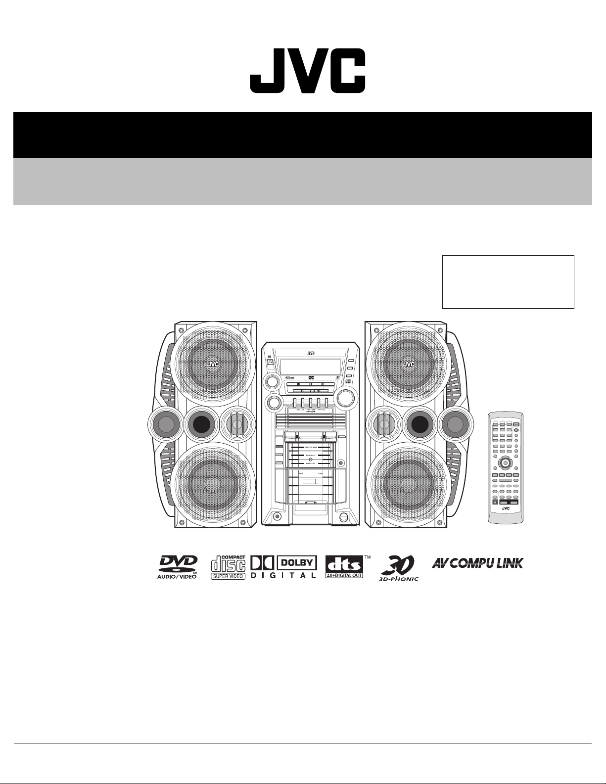
SERVICE MANUAL
COMPACT COMPONENT SYSTEM
MB18820044
HX-GD8
Area suffix
J ----------------------------- U.S.A.
C -------------------------- Canada
CA-HXGD8 SP-HXGD8SP-HXGD8
TABLE OF CONTENTS
1 PRECAUTION. . . . . . . . . . . . . . . . . . . . . . . . . . . . . . . . . . . . . . . . . . . . . . . . . . . . . . . . . . . . . . . . . . . . . . . . . 1-3
2 SPECIFIC SERVICE INSTRUCTIONS . . . . . . . . . . . . . . . . . . . . . . . . . . . . . . . . . . . . . . . . . . . . . . . . . . . . . . 1-6
3 DISASSEMBLY . . . . . . . . . . . . . . . . . . . . . . . . . . . . . . . . . . . . . . . . . . . . . . . . . . . . . . . . . . . . . . . . . . . . . . . 1-7
4 ADJUSTMENT . . . . . . . . . . . . . . . . . . . . . . . . . . . . . . . . . . . . . . . . . . . . . . . . . . . . . . . . . . . . . . . . . . . . . . . 1-39
5 TROUBLESHOOTING . . . . . . . . . . . . . . . . . . . . . . . . . . . . . . . . . . . . . . . . . . . . . . . . . . . . . . . . . . . . . . . . . 1-55
COPYRIGHT © 2004 VICTOR COMPANY OF JAPAN, LIMITED
No.MB188
2004/4
Page 2
SPECIFICATION
Amplifier section CA-HXGD8
Output Power SUBWOOFERS 195 W per channel, min. RMS, driven into 6 Ω at 63 Hz with no more than 10 % total harmonic
MAIN SPEAKERS 80 W per channel, min. RMS, driven into 6 Ω at 1 kHz with no more than 10 % total harmonic
Audio input sensitivity/impedance (Measured at 1 kHz, with
tape recording signal 300 mV)
Digital output OPTICAL DIGITAL OUTPUT -21 dBm to -15 dBm (660 nm ± 30 nm)
VIDEO OUT Color system NTSC
VIDEO (composite) 1 V(p-p)/75 Ω
S-VIDEO Y (luminance):1 V(p-p)/75 Ω
COMPONENT
(interlace/ progressive)
Speaker
Terminals
Others AV COMPU LINK × 2 (Ø 3.5)
Tuner section FM tuning range 87.5 MHz - 108.0 MHz
AM tuning range 530 kHz - 1 710 kHz
Disc player section Playable disc DVD VIDEO/DVD AUDIO
Dynamic range 90 dB
Horizontal resolution 500 lines
Wow and flutter Immeasurable
Cassette deck section Frequency
response
General Power requirement AC 120 V , 60 Hz
Power consumption 265 W/ 325 VA (at operation)
Dimensions (approx.) (W/H/D) 205 mm × 370 mm × 432 mm
Mass (approx.) 11 kg (24.3 lbs)
Type 3-Way 4-Speaker Bass-Reflex Type
Speakers Subwoofer 20 cm (7 7/8 in.)cone × 1
Power handling capacity Subwoofer 195 W
Impedance Subwoofer 6 Ω
Frequency range Subwoofer 30 Hz - 970 Hz
Sound pressure level Subwoofer 83 dB/W·m
Dimensions (approx.) (W/H/D) 240 mm × 457 mm × 407 mm
Mass (approx.) 10 kg (22.1 lbs) each
MAIN SPEAKERS 6 Ω - 16 Ω ()
SUBWOOFERS 6 Ω - 16 Ω ()
Normal (type I) 50 Hz - 14 000 Hz
Wow and flutter 0.15 % (WRMS)
Woofer 13.5 cm (5 3/8in.) cone × 2
Tweeter 5 cm (2 in.) cone × 1
Main speaker 80 W
Main speaker 6 Ω
Main speaker 75 Hz 25 000 Hz
Main speaker 88 dB/W·m
Design and specifications are subject to change without notice.
distortion.
distortion.
AUX:300 mV/47 kΩ
C (chrominance, burst):0.286 V(p-p)/75 Ω
(Y):1 V(p-p)/75 Ω
(P B/PR):0.7 V(p-p)/75 Ω
CD/VCD/SVCD
CD-R/CD-RW (recorded in Audio CD/ Video CD/ Super Video CD/ MP3/ WMA/ JPEG format)
DVD-R/DVD-RW (recorded in video format)
30 W (on standby)
(8 1/8 in. × 14 5/8 in. × 17 1/16 in.)
Speaker section SP-HXGD8
(9 1/2 in. × 18 in. × 16 1/16 in.)
1-2 (No.MB188)
Page 3

SECTION 1
PRECAUTION
1.1 Safety Precautions
(1) This design of this product contains special hardware and
many circuits and components specially for safety purposes. For continued protection, no changes should be made
to the original design unless authorized in writing by the
manufacturer. Replacement parts must be identical to
those used in the original circuits. Services should be performed by qualified personnel only.
(2) Alterations of the design or circuitry of the product should
not be made. Any design alterations of the product should
not be made. Any design alterations or additions will void
the manufacturers warranty and will further relieve the
manufacture of responsibility for personal injury or property
damage resulting therefrom.
(3) Many electrical and mechanical parts in the products have
special safety-related characteristics. These characteristics are often not evident from visual inspection nor can the
protection afforded by them necessarily be obtained by using replacement components rated for higher voltage, wattage, etc. Replacement parts which have these special
safety characteristics are identified in the Parts List of Service Manual. Electrical components having such features
are identified by shading on the schematics and by ( ) on
the Parts List in the Service Manual. The use of a substitute
replacement which does not have the same safety characteristics as the recommended replacement parts shown in
the Parts List of Service Manual may create shock, fire, or
other hazards.
(4) The leads in the products are routed and dressed with ties,
clamps, tubings, barriers and the like to be separated from
live parts, high temperature parts, moving parts and/or
sharp edges for the prevention of electric shock and fire
hazard. When service is required, the original lead routing
and dress should be observed, and it should be confirmed
that they have been returned to normal, after reassembling.
(5) Leakage shock hazard testing
After reassembling the product, always perform an isolation check on the exposed metal parts of the product (antenna terminals, knobs, metal cabinet, screw heads,
headphone jack, control shafts, etc.) to be sure the product
is safe to operate without danger of electrical shock.Do not
use a line isolation transformer during this check.
• Plug the AC line cord directly into the AC outlet. Using a
"Leakage Current Tester", measure the leakage current
from each exposed metal parts of the cabinet, particularly any exposed metal part having a return path to the
chassis, to a known good earth ground. Any leakage current must not exceed 0.5mA AC (r.m.s.).
• Alternate check method
Plug the AC line cord directly into the AC outlet. Use an
AC voltmeter having, 1,000Ω per volt or more sensitivity
in the following manner. Connect a 1,500Ω 10W resistor
paralleled by a 0.15µF AC-type capacitor between an ex-
posed metal part and a known good earth ground.
Measure the AC voltage across the resistor with the AC
voltmeter.
Move the resistor connection to each exposed metal
part, particularly any exposed metal part having a return
path to the chassis, and measure the AC voltage across
the resistor. Now, reverse the plug in the AC outlet and
repeat each measurement. Voltage measured any must
not exceed 0.75 V AC (r.m.s.). This corresponds to 0.5
mA AC (r.m.s.).
AC VOLTMETER
(Having 1000
ohms/volts,
or more sensitivity)
0.15 F AC TYPE
Place this
probe on
1500 10W
Good earth ground
1.2 Warning
(1) This equipment has been designed and manufactured to
meet international safety standards.
(2) It is the legal responsibility of the repairer to ensure that
these safety standards are maintained.
(3) Repairs must be made in accordance with the relevant
safety standards.
(4) It is essential that safety critical components are replaced
by approved parts.
(5) If mains voltage selector is provided, check setting for local
voltage.
1.3 Caution
Burrs formed during molding may be left over on some parts
of the chassis.
Therefore, pay attention to such burrs in the case of preforming repair of this system.
1.4 Critical parts for safety
In regard with component parts appearing on the silk-screen
printed side (parts side) of the PWB diagrams, the parts that are
printed over with black such as the resistor ( ), diode ( )
and ICP ( ) or identified by the " " mark nearby are critical
for safety. When replacing them, be sure to use the parts of the
same type and rating as specified by the manufacturer.
(This regulation dose not Except the J and C version)
each exposed
metal part.
(No.MB188)1-3
Page 4
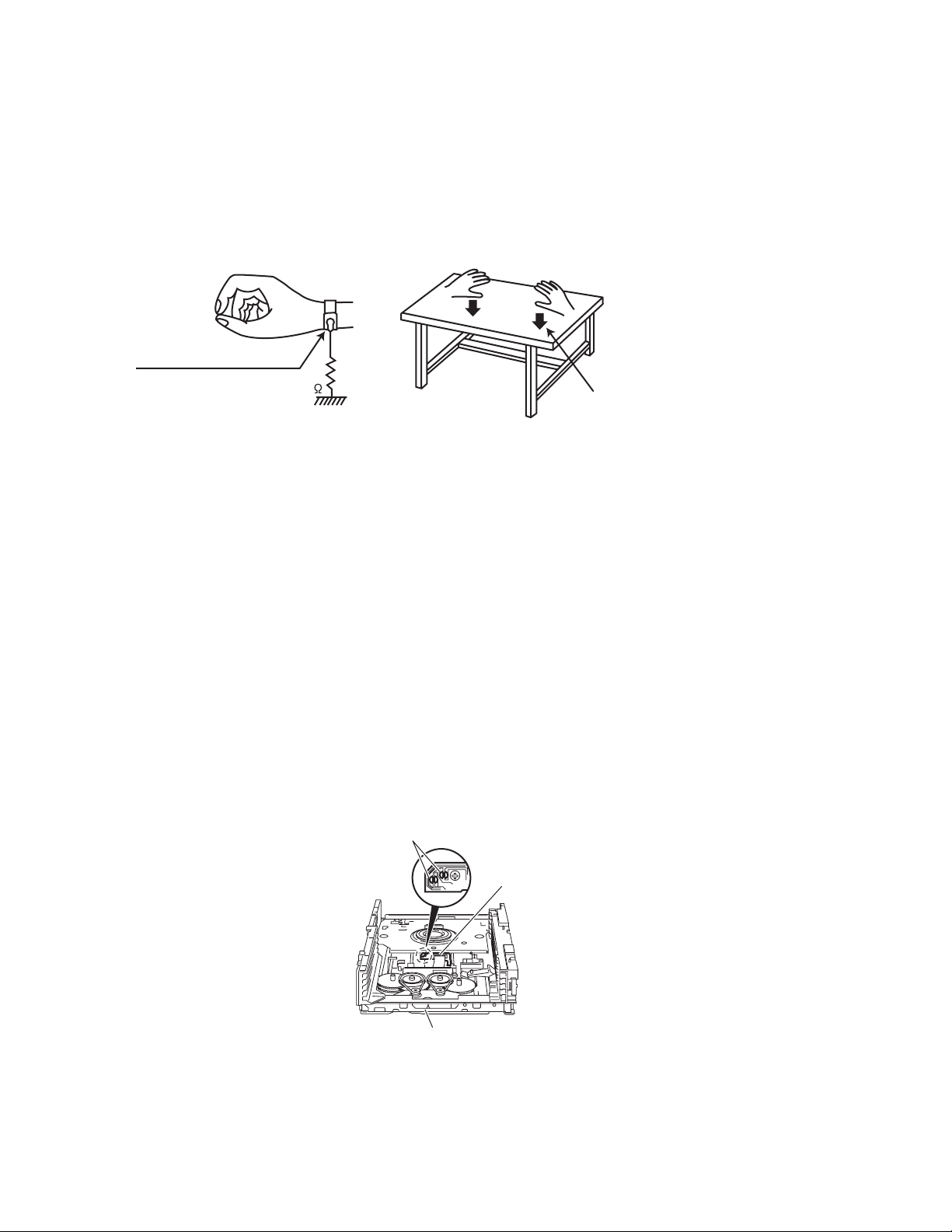
1.5 Preventing static electricity
Electrostatic discharge (ESD), which occurs when static electricity stored in the body, fabric, etc. is discharged, can destroy the laser
diode in the traverse unit (optical pickup). Take care to prevent this when performing repairs.
1.5.1 Grounding to prevent damage by static electricity
Static electricity in the work area can destroy the optical pickup (laser diode) in devices such as laser products.
Be careful to use proper grounding in the area where repairs are being performed.
(1) Ground the workbench
Ground the workbench by laying conductive material (such as a conductive sheet) or an iron plate over it before placing the
traverse unit (optical pickup) on it.
(2) Ground yourself
Use an anti-static wrist strap to release any static electricity built up in your body.
(caption)
Anti-static wrist strap
1M
Conductive material
(conductive sheet) or iron palate
(3) Handling the optical pickup
• In order to maintain quality during transport and before installation, both sides of the laser diode on the replacement optical
pickup are shorted. After replacement, return the shorted parts to their original condition.
(Refer to the text.)
• Do not use a tester to check the condition of the laser diode in the optical pickup. The tester's internal power source can easily
destroy the laser diode.
1.6 Handling the traverse unit (optical pickup)
(1) Do not subject the traverse unit (optical pickup) to strong shocks, as it is a sensitive, complex unit.
(2) Cut off the shorted part of the flexible cable using nippers, etc. after replacing the optical pickup. For specific details, refer to the
replacement procedure in the text. Remove the anti-static pin when replacing the traverse unit. Be careful not to take too long a
time when attaching it to the connector.
(3) Handle the flexible cable carefully as it may break when subjected to strong force.
(4) I t is not possible to adjust the semi-fixed resistor that adjusts the laser power. Do not turn it.
1.7 Attention when traverse unit is decomposed
*Please refer to "Disassembly method" in the text for the pickup unit.
• Apply solder to the short land sections before the flexible wire is disconnected from the connecto on the servo board. (If the flexible
wire is disconnected without applying solder, the pickup may be destroyed by static electricity.)
• In the assembly, be sure to remove solder from the short land sections after connecting the flexible wire.
Short land sections
1-4 (No.MB188)
DVD pickup
DVD changer mechanism assembly
Page 5
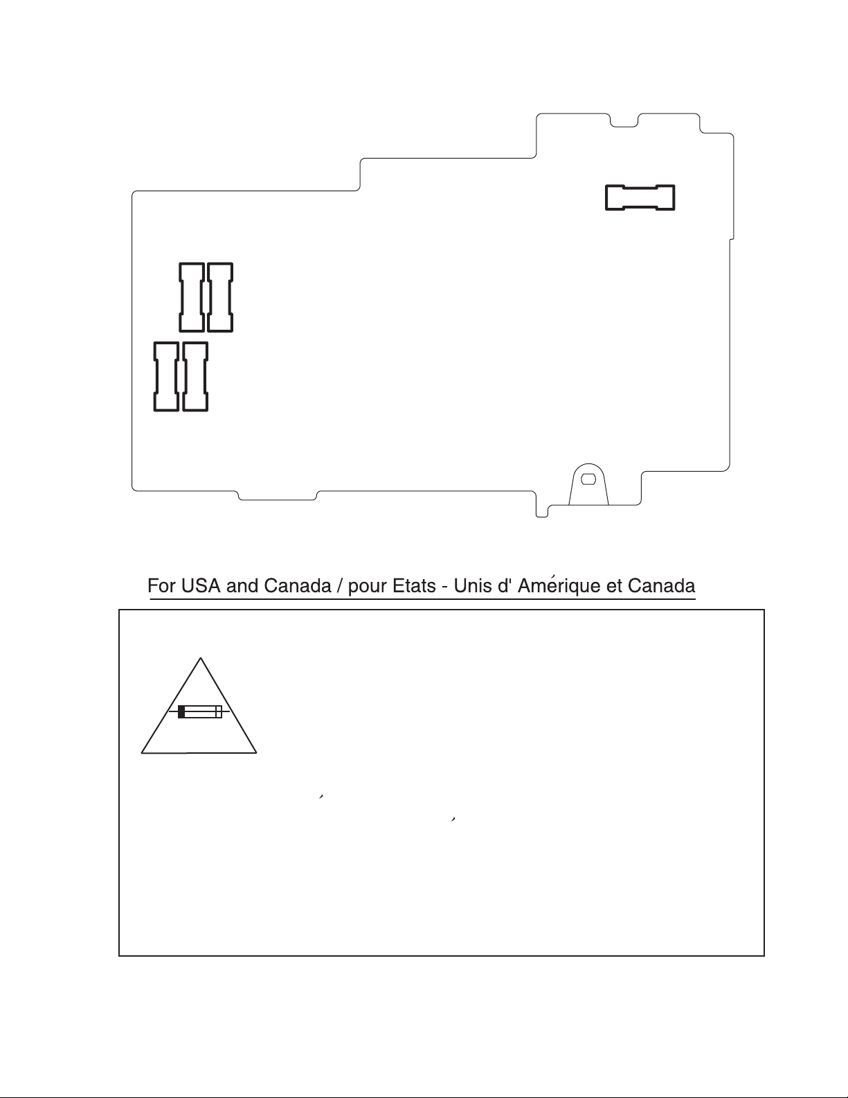
1.8 Importance administering point on the safety
Primary board (Forward side)
F102
F101
8A-125V
8A-125V
1.6A-125V
3.15A-125V
F104
F103
F001
6.3A-125V
Caution: For continued protection against risk of
fire, replace only with same type 6.3 A/125 V for
F001, 8 A/125 V for F101 and F102, 3.15 A/125 V
for F103, 1.6 A/125 V for F104.
This symbol specifies type of fast operating fuse.
Precaution: Pour eviter risques de feux, remplacez
le fusible de surete de F001 comme le meme type
que 6,3 A/125 V, 8 A/125 V pour F101 et F102, et
3,15 A/125 V pour F103, et 1,6 A/125V pour F104.
Ce sont des fusibles suretes qui functionnes rapide.
^
(No.MB188)1-5
Page 6

SECTION 2
SPECIFIC SERVICE INSTRUCTIONS
This service manual does not describe ADJUSTMENT.
1-6 (No.MB188)
Page 7
SECTION 3
r
DISASSEMBLY
3.1 Main body section
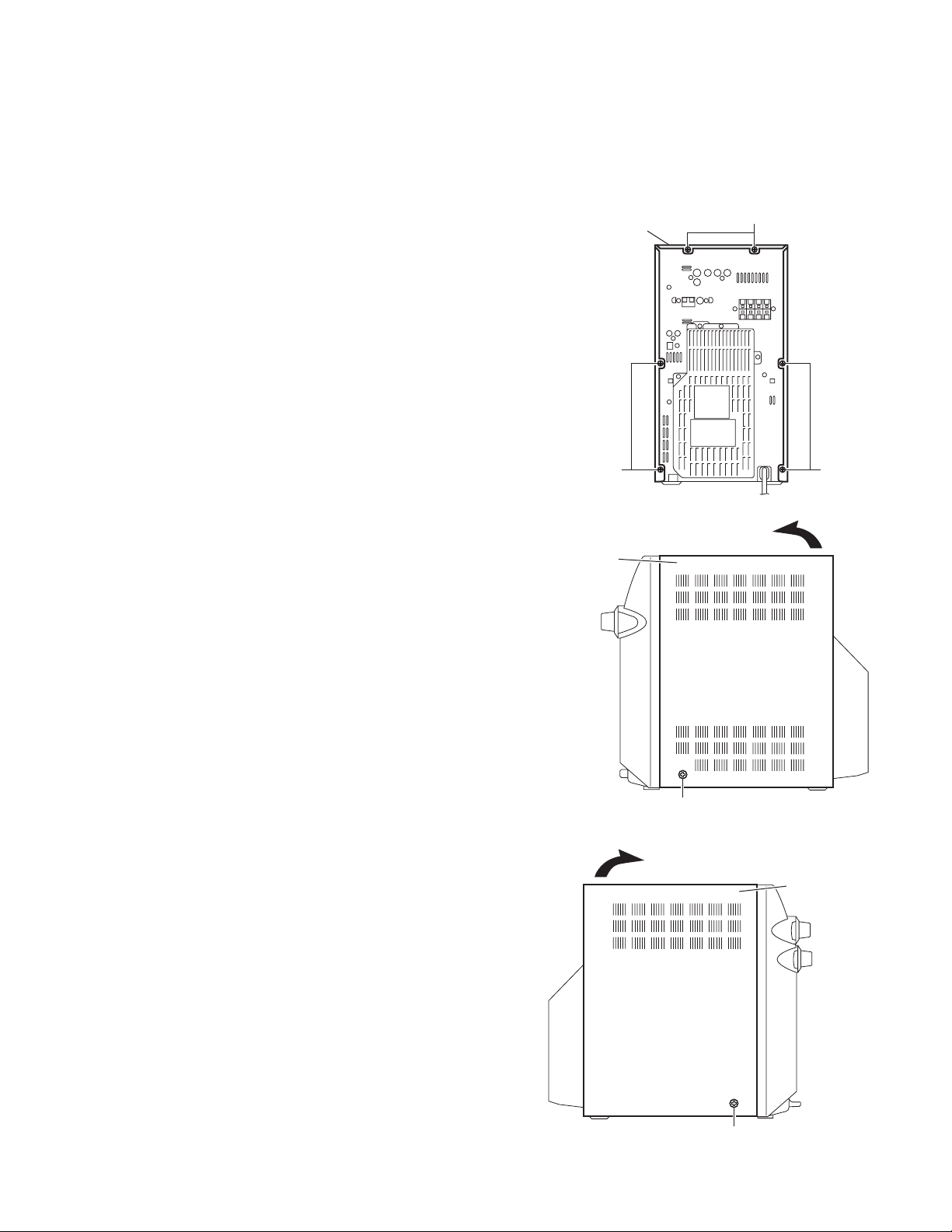
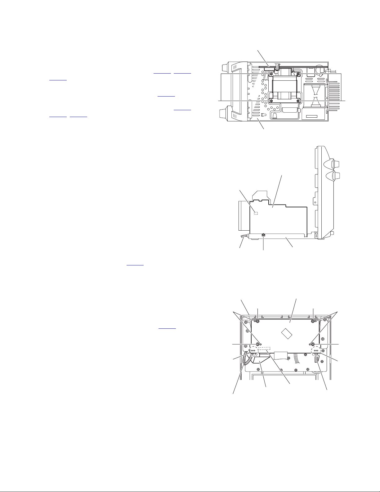
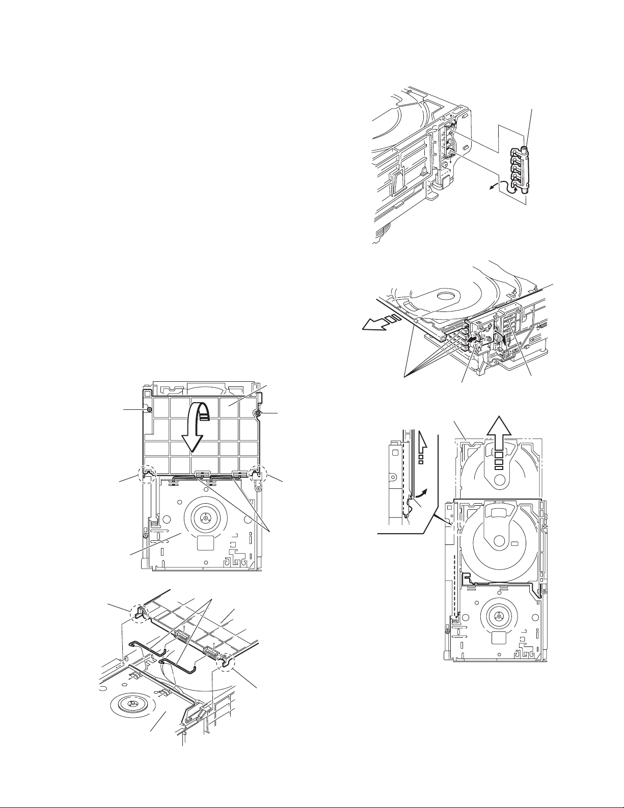
3.1.1 Removing the metal cover
(See Figs.1 to 3)
(1) From the back side of the main body, remove the six
screws A attaching the metal cover. (See Fig.1.)
(2) From the both sides of the main body, remove the two
screws B attaching the metal cover. (See Figs.2 and 3.)
(3) Remove the metal cover from the main body while lifting
the rear section of the metal cover in the direction of the arrow. (See Figs.2 and 3.)
Metal cover
A
Metal cover
A
A
Fig.1
B
Fig.2
Metal cove
B
Fig.3
(No.MB188)1-7
Page 8
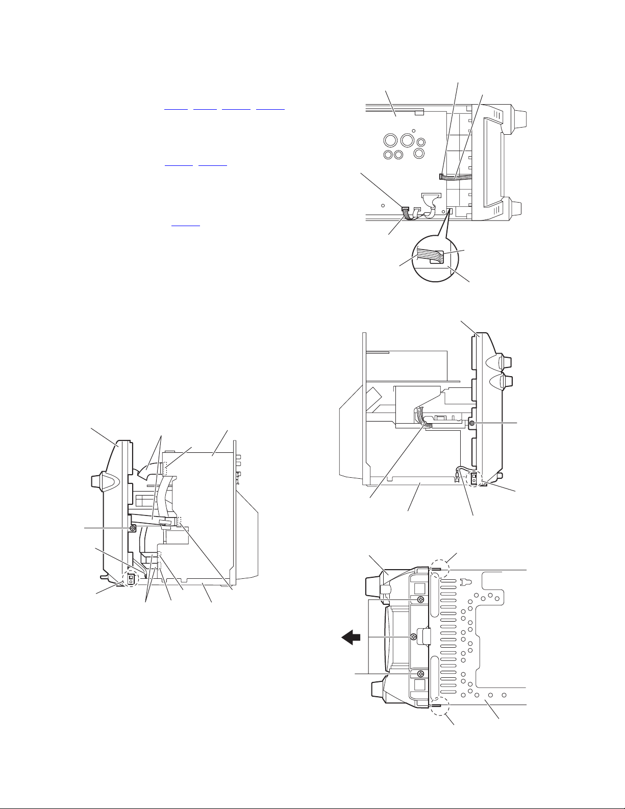
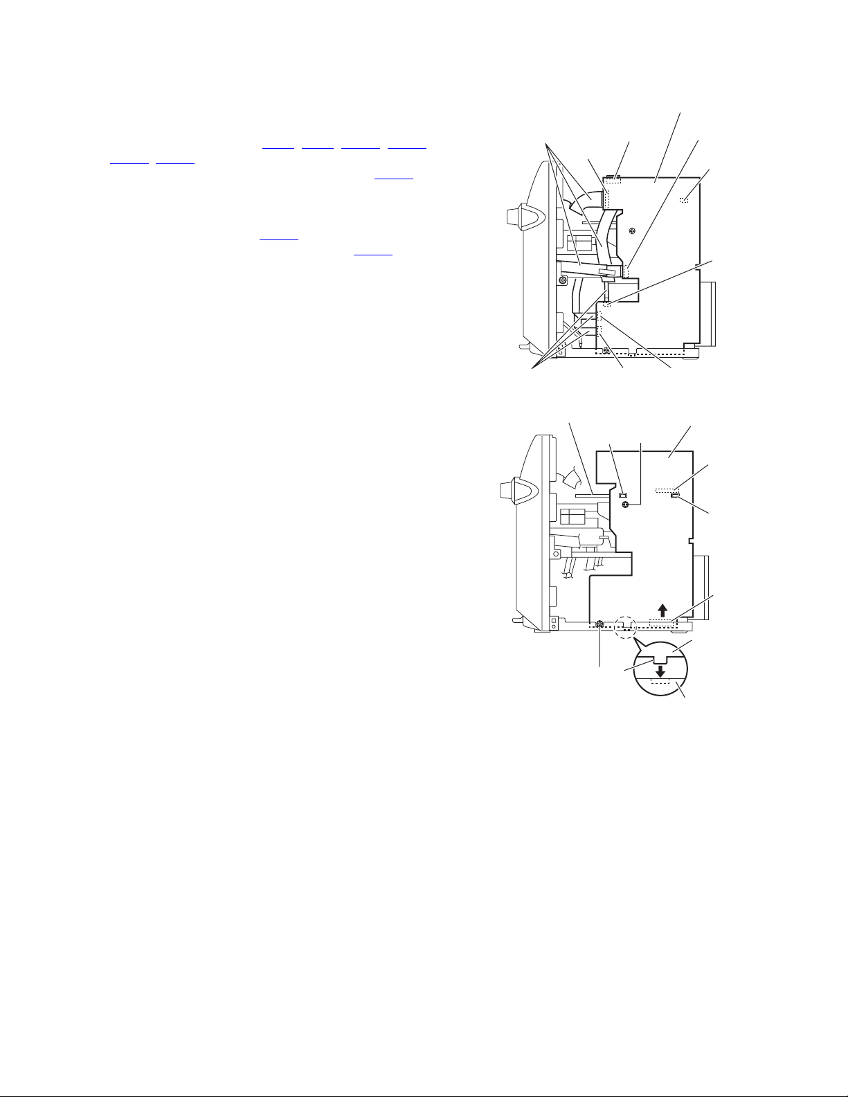
3.1.2 Removing the front panel assembly
(See Figs.4 to 7)
• Prior to performing the following procedures, remove the metal
cover.
(1) From the right side of the main body, disconnect the card
wires from the connectors (CN43
on the main board. (See Fig.4.)
(2) Disconnect the earth wire from the chassis base. (See
Fig.4.)
(3) From the top side of the main body, disconnect the parallel
wires from the connectors (CN201
board. (See Fig.5.)
Reference:
When reassembling, pass the parallel wire through the
hole a on the plastic chassis before connecting the parallel wire to the connector CN201
(See Fig.5.)
(4) From the left side of the main body, remove the tie band
bundling the wires. (See Fig.16.)
Reference:
After reassembling, bundle the wires with the new tie
band as before. (See Fig.16.)
(5) Disconnect the earth wire from the chassis base. (See
Fig.6.)
(6) From the both sides of the main body, remove the two
screws C attaching the front panel assembly. (See Figs.4
and 6.)
(7) From the bottom side of the main body, remove the three
screws D attaching the front panel assembly. (See Fig.7.)
(8) Release the joints b of the front panel assembly from the
chassis base and remove the front panel assembly in the
direction of the arrow. (See Figs.4, 6 and 7.)
Front panel assembly
Card wires
, CN44, CN802, CN803)
, CN205) on the bridge
on the bridge board.
Main board
CN802
Bridge board
CN201
Parallel wire
Parallel wire
CN205
Parallel wire
a
Plastic chassis
Fig.5
Front panel assembly
C
C
Earth wire
1-8 (No.MB188)
b
Card wires
Fig.4
CN43
CN44
CN803
Chassis base
Tie band
Chassis base
Front panel assembly
D
Fig.6
Fig.7
Earth wire
b
Chassis base
b
b
Page 9
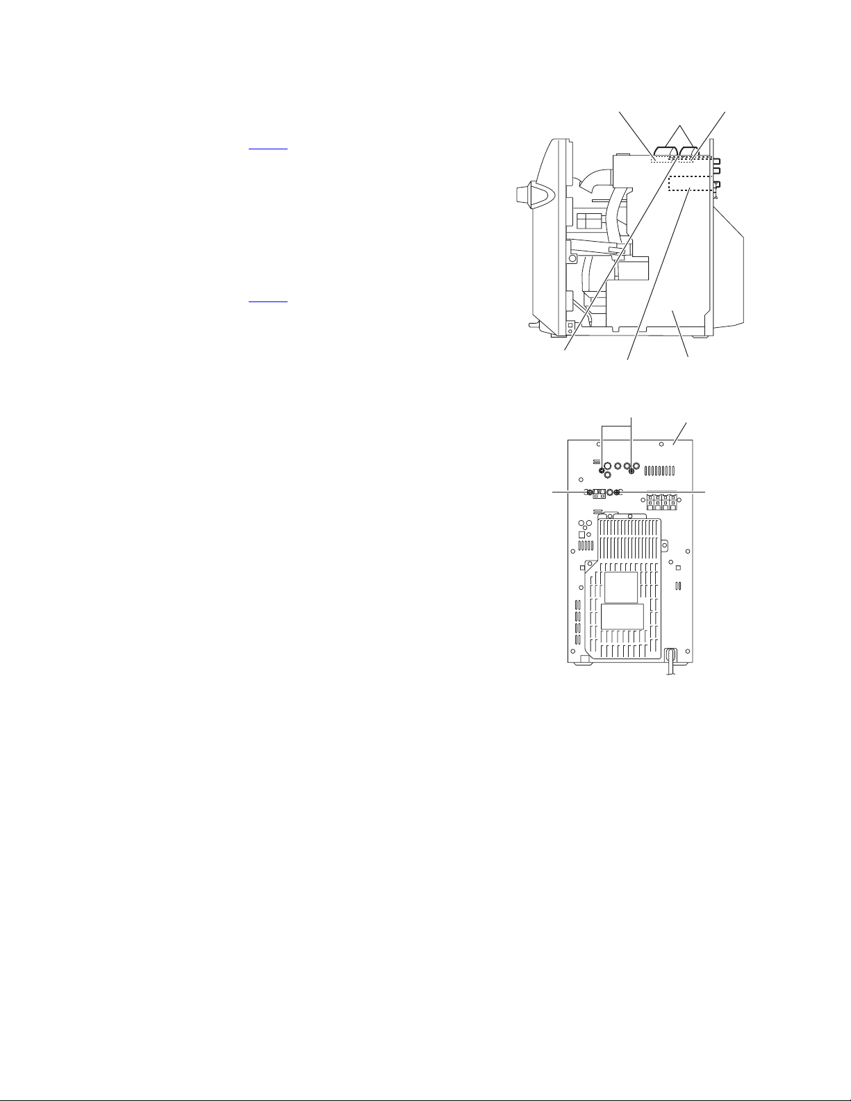
3.1.3 Removing the tuner
(See Figs.8 and 9)
• Prior to performing the following procedures, remove the metal
cover.
(1) From the right side of the main body, disconnect the card
wire from the connector CN560
Fig.8.)
(2) From the back side of the main body, remove the two
screws E attaching the tuner to the rear panel. (See Fig.9.)
3.1.4 Removing the video board
(See Figs.8 and 9)
• Prior to performing the following procedures, remove the metal
cover.
(1) From the right side of the main body, disconnect the card
wire from the connector CN502
Fig.8.)
(2) From the back side of the main body, remove the two
screws F attaching the video board to the rear panel. (See
Fig.9.)
on the main board. (See
on the main board. (See
Video board
CN502
Tuner
Fig.8
F
Card wires
CN560
Main board
Rear panel
E E
Fig.9
(No.MB188)1-9
Page 10
3.1.5 Removing the rear panel
r
(See Figs.10 to 12)
• Prior to performing the following procedures, remove the metal
cover.
(1) From the top side of the main body, remove the tie band
bundling the wires. (See Fig.10.)
Reference:
After reassembling, bundle the wires with the new tie
band as before. (See Fig.10.)
(2) Disconnect the wire from the connector CN202
bridge board. (See Fig.10.)
(3) From the back side of the main body, remove the two
screws G and screw H attaching the rear cover. (See
Fig.11.)
(4) Release the sections c and remove the rear cover. (See
Fig.11.)
(5) Remove the sixteen screws J attaching the rear panel.
(See Fig.12.)
(6) From the both sides of the main body, release the joints d
attaching the rear panel to the chassis base and remove
the rear panel with the fan. (See Fig.12.)
on the
Tie band
Bridge board
CN202
Wires
3.1.6 Removing the fan
(See Figs.10 to 12)
• Prior to performing the following procedures, remove the metal
cover.
(1) From the top side of the main body, remove the tie band
bundling the wires. (See Fig.10.)
Reference:
After reassembling, bundle the wires with the new tie
band as before. (See Fig.10.)
(2) Disconnect the wire from the connector CN202
bridge board. (See Fig.10.)
(3) From the back side of the main body, remove the two
screws G and screw H attaching the rear cover. (See
Fig.11.)
(4) Remove the two screws K attaching the fan. (See Fig.12.)
(5) Take out the fan from the main body.
on the
H
c
Rear panel
J
Fig.10
G
c
c
Fig.11
Rear cove
J
Fan
1-10 (No.MB188)
KK
J
J
dd
J
Fig.12
Page 11
3.1.7 Removing the main board
(See Figs.13 and 14)
• Prior to performing the following procedures, remove the metal
cover, tuner, video board and rear panel.
(1) From the right side of the main body, disconnect the card
wires from the connectors (CN43
, CN803) on the main board. (See Fig.13.)
CN802
(2) Disconnect the parallel wires from the connector CN715 on
the forward side of the main board. (See Fig.13.)
(3) Remove the two screws L attaching the main board. (See
Fig.14.)
(4) Disconnect the connector CN217
ward this side and disconnect the connector CN501
main board in the direction of the arrow. (See Fig.14.)
Reference:
• When attaching the main board, insert the sections e of the
bridge board in the hole of the main board. (See Fig.14.)
• Insert the section f of the main board in the hole of the chassis base before attaching the screws L.
, CN44, CN110, CN111,
on the main board to-
on the
Card wires
CN802
CN110
Main board
CN803
CN715
CN111
Card wires
Bridge board
L
CN44
Fig.13
e
f
Fig.14
CN43
Main board
L
CN217
e
CN501
Main board
Chassis base
(No.MB188)1-11
Page 12
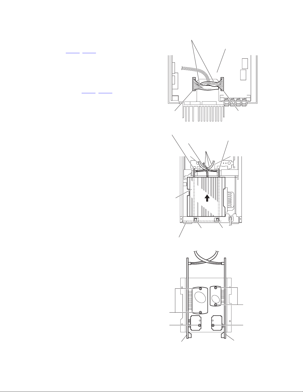
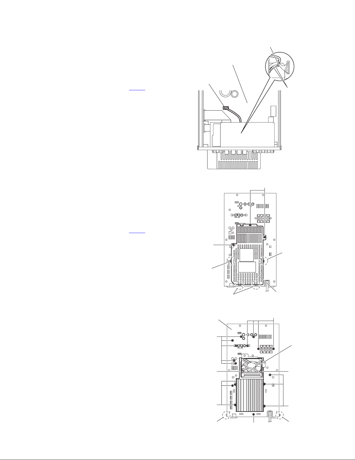
3.1.8 Removing the main amplifier board/subwoofer amplifier boards
(See Figs.15 to 17)
• Prior to performing the following procedures, remove the metal
cover, tuner, video board, rear panel and main board.
(1) From the top side of the main body, disconnect the wires
from the connector (CN206
(See Fig.15.)
(2) From the back side of the main body, remove the tie band
bundling the wires. (See Fig.16.)
Reference:
After reassembling, bundle the wires with the new tie
band as before. (See Fig.16.)
(3) Disconnect the connectors (CN600
amplifier/subwoofer amplifier boards from the connection
board in the direction of the arrow. (See Fig.16.)
(4) Remove the two screws M and screw N attaching the main
amplifier board. (See Fig.17.)
(5) Removing the two screws P and screw Q attaching the
subwoofer amplifier board. (See Fig.17.)
, CN208) on the bridge board.
, CN700) on the main
Wires
Main amplifier board
Tie band
Bridge board
CN206CN208
Fig.15
Subwoofer amplifier board
Wires
Heat sink
CN600 CN700
Connection board
Fig.16
P
Q
Subwoofer amplifier board
Fig.17
M
N
Main amplifier board
1-12 (No.MB188)
Page 13
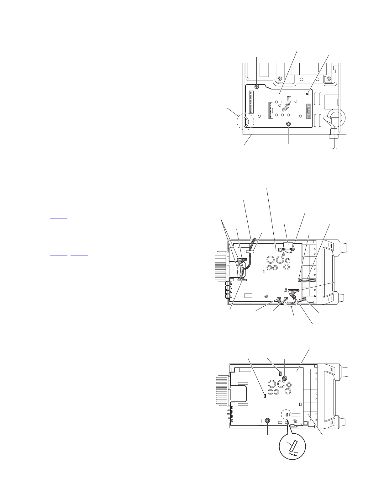
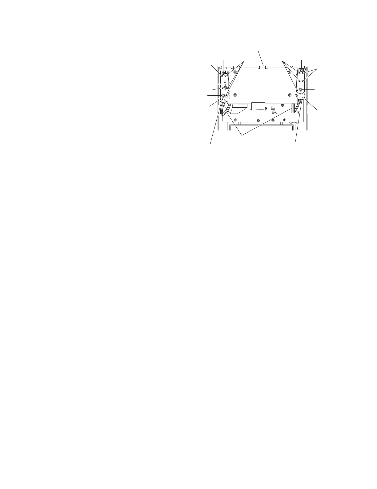
3.1.9 Removing the connection board
r
(See Fig.18.)
• Prior to performing the following procedure, remove the metal
cover, tuner, video board, rear panel, main board and main
amplifier/subwoofer amplifier boards.
(1) From the top side of the main body, remove the two screws
R attaching the connection board on the chassis base.
Reference:
When reassembling, attach the connection board to the section g and align the projection h of the chassis base to the hole
of the connection board.
R
Connection board
g
h
3.1.10 Removing the bridge board
(See Figs.19 and 20)
• Prior to performing the following procedures, remove the metal
cover, tuner, video board, rear panel and main board.
(1) From the top side of the main body, release the wire holder
bundling the wire. (See Fig.19.)
(2) Disconnect the wires from the connectors (CN206
) on the bridge board. (See Fig.19.)
CN214
Reference:
After connecting the wire to the connector CN214
wire with the wire holder. (See Fig.19.)
(3) Disconnect the parallel wires from the connectors (CN201
CN205, CN213) on the bridge board. (See Fig.19.)
(4) Release the wire holder holding the card wire. (See
Fig.19.)
(5) Remove the spacer fixing the wire on the bridge board.
(See Fig.19.)
(6) Remove the two screws S attaching the bridge board on
the 5DVD changer mechanism assembly. (See Fig.20.)
(7) Bend the claw i in the direction of the arrow and remove the
bridge board in an upward direction. (See Fig.20.)
Reference:
• When attaching the bridge board, align the projections (j, k)
in the hole of the bridge board. (See Fig.20.)
• When reassembling, pass the wires through the sections
(m, n) of the plastic chassis. (See Fig.19.)
, CN208,
, fix the
Chassis base
Bridge board
Wire
Wires
CN208
,
CN206
j
Spacer
CN213CN201
k
R
Fig.18
Wire holder
Card wire
m
Fig.19
Bridge board
S
Parallel wire
CN205
CN214
n
Wire holder
S
i
Fig.20
5DVD change
mechanism
assembly
(No.MB188)1-13
Page 14
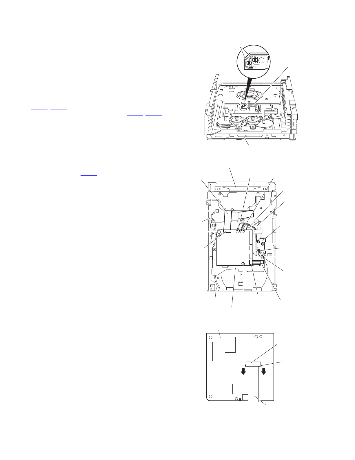
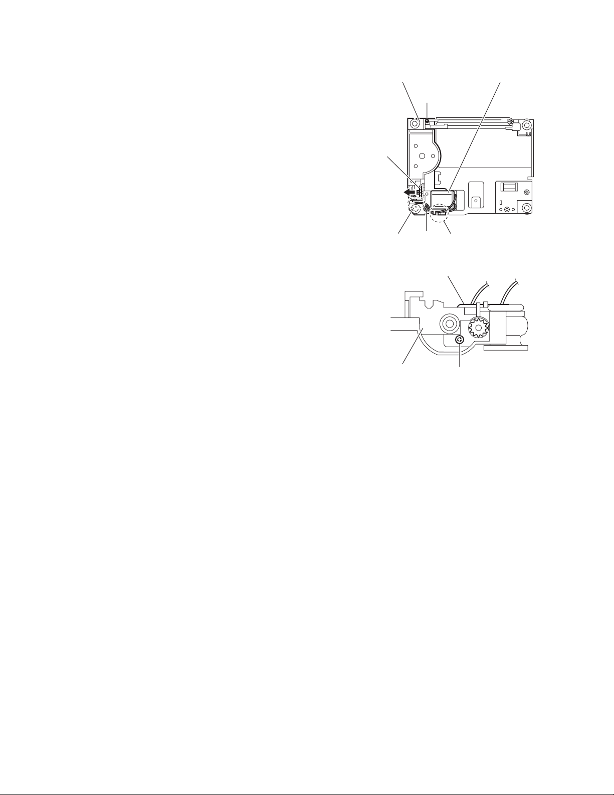
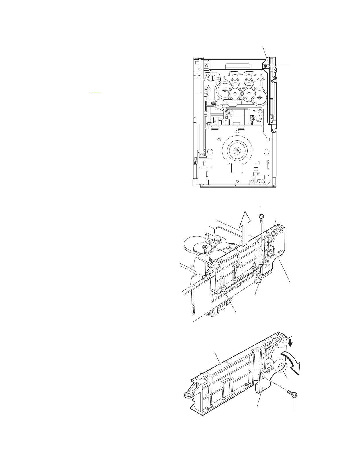
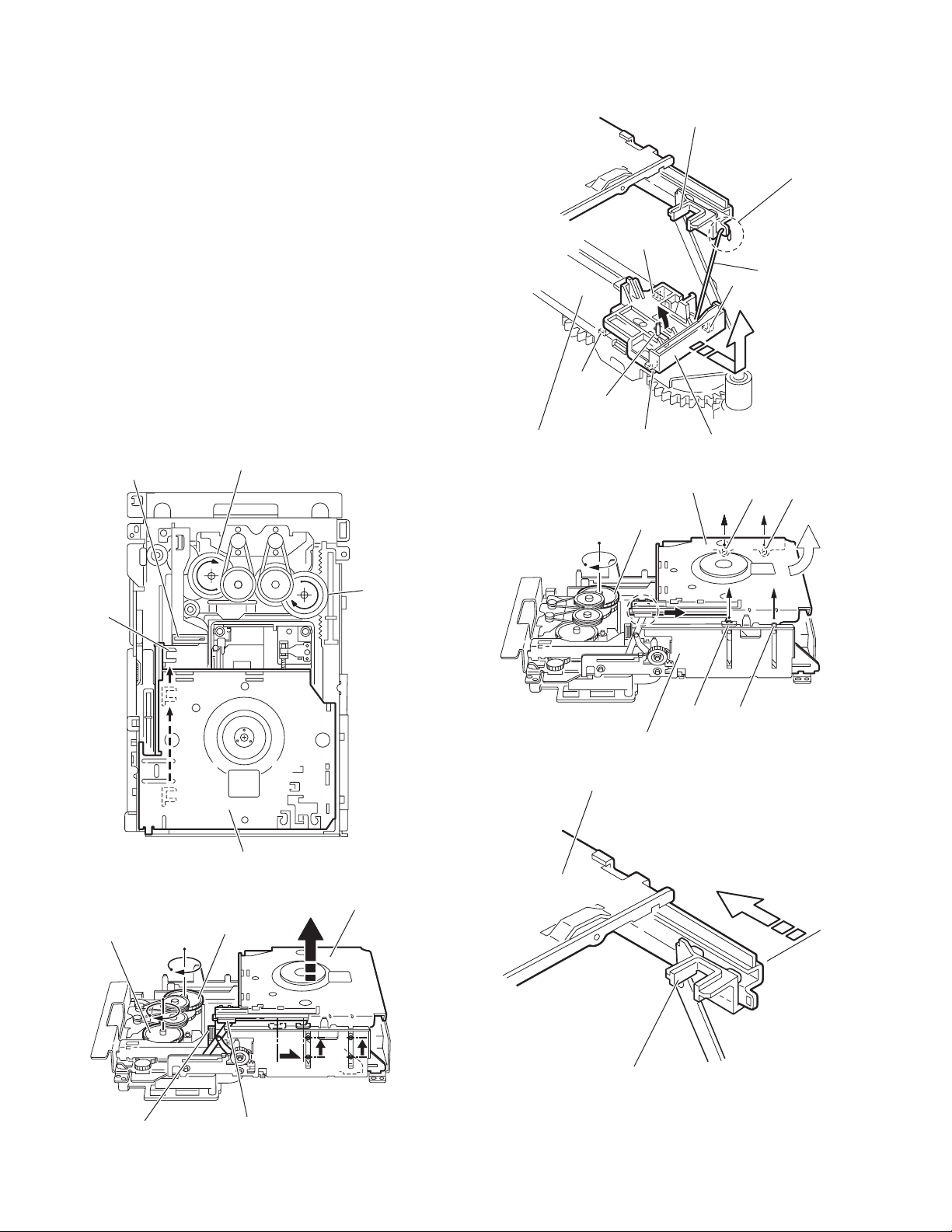
3.1.11 Removing the 5DVD changer mechanism assembly
(See Figs.21 to 23)
• Prior to performing the following procedures, remove the metal
cover, tuner, video board, rear panel, main board and bridge
board.
(1) From the both sides of the main body, remove the two
screws T attaching the 5DVD changer mechanism assembly to the front panel assembly. (See Figs.21 and 22.)
(2) From the left side of the main body, remove the tie band
bundling the wire and parallel wires. (See Fig.22.)
Reference:
After reassembling, bundle the wire and parallel wires
with the new tie band as before. (See Fig.22.)
(3) Take out the 5DVD changer mechanism assembly from the
main body.
Reference:
When attaching the 5CD changer mechanism assembly,
pass the wires through the sections (m, n) of the plastic
chassis. (See Fig.22.)
(4) From the both and top sides of the 5DVD changer mecha-
nism assembly, remove the two screws U and screw U' attaching the main chassis. (See Fig.23.)
Reference:
• Align the projections s of the plastic chassis to the
holes of the main chassis before attaching the screw
U'. (See Fig.23.)
• When attaching the screw U', attach the earth wire
with it. (See Fig.23.)
(5) Take out the main chassis.
(6) From the top side of the 5DVD changer mechanism as-
sembly, remove the three screws V and screw V' attaching
the 5DVD changer mechanism assembly on the plastic
chassis.
Reference:
• When reassembling, align the projections (p, q, r) of the
plastic chassis to the holes of the 5DVD changer mechanism
assembly before attaching the screws V and V'. (See
Fig.23.)
• When attaching the screw V', attach the earth wire with it.
(See Fig.23.)
Front panel assembly
5DVD changer mechanism assembly
T
5DVD changer
mechanism assembly
m
Fig.21
Front panel assembly
Tie band
Wires
T
n
Fig.22
1-14 (No.MB188)
5DVD changer
mechanism assembly
V
Main chassis
V
r
V
U
U
Fig.23
p
V
Plastic chassis
s
U'
s
Earth wire
V'
q
Page 15
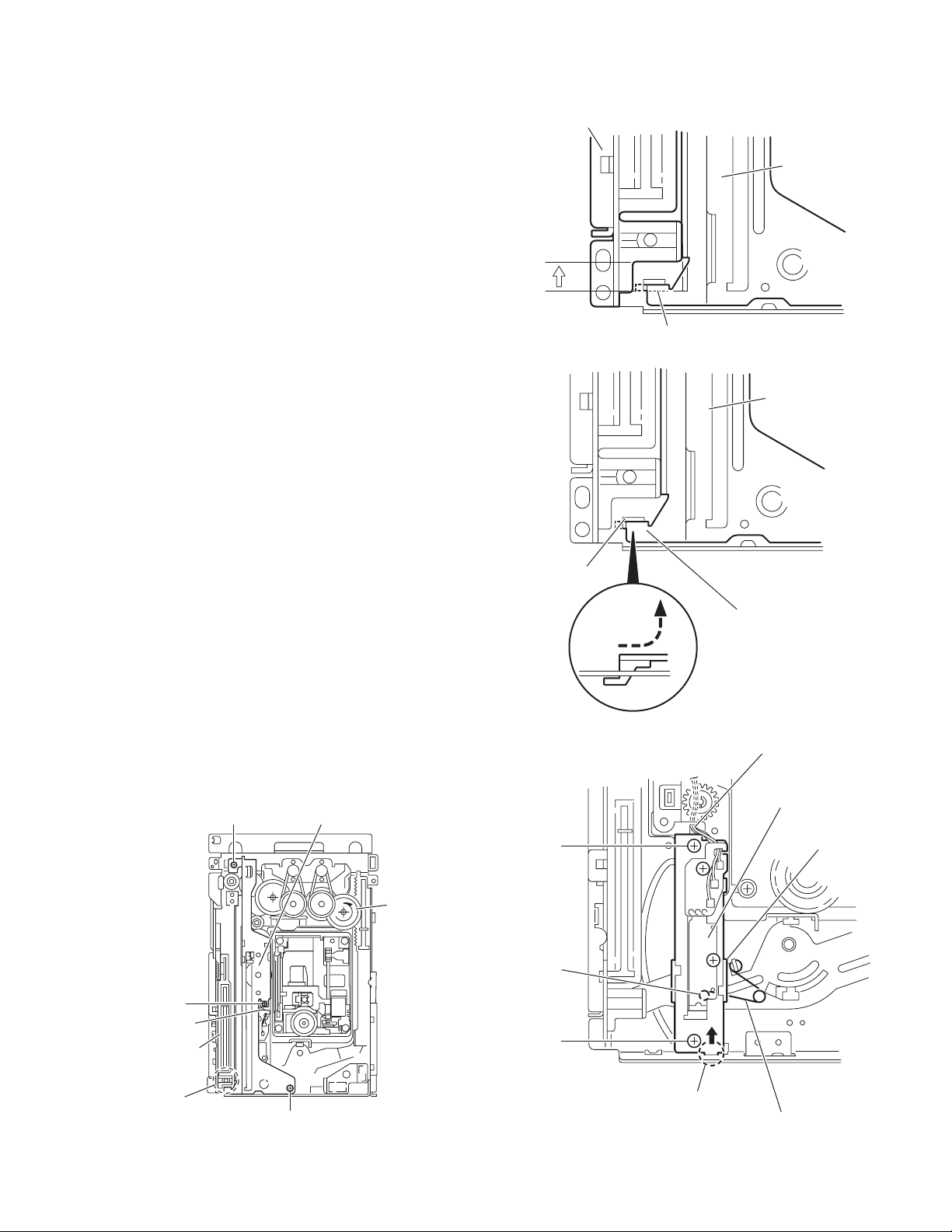
3.1.12 Removing the primary board
Y
(See Figs.19, 21, 22, 24 and 25)
• Prior to performing the following procedures, remove the metal
cover, tuner, video board, rear panel and main board.
(1) From the top side of the main body, release the wire holder
bundling the wire. (See Fig.19.)
(2) Disconnect the wires from the connectors (CN206
CN214) on the bridge board. (See Fig.19.)
Reference:
After connecting the wire to the connector CN214
wire with the wire holder. (See Fig.19.)
(3) Disconnect the parallel wires from the connectors (CN201
, CN213) on the bridge board. (See Fig.19.)
CN205
(4) Release the wire holder holding the card wire. (See
Fig.19.)
(5) Remove the spacer fixing the wire on the bridge board.
(See Fig.19.)
(6) From the both sides of the main body, remove the two
screws T attaching the 5DVD changer mechanism assembly to the front panel assembly. (See Figs.21 and 22.)
Reference:
It is not necessary to remove the bridge board from the
5DVD changer mechanism assembly.
(7) Take out the 5DVD changer mechanism assembly with the
bridge board from the main body.
Reference:
When attaching the 5DVD changer mechanism assembly, pass the wires through the sections (m, n) of the
5DVD changer mechanism assembly. (See Fig.22.)
(8) From the top and left sides of the main body, remove the
four screws W and screw X attaching the primary board on
the chassis base. (See Figs.24 and 25.)
(9) From the forward side of the primary board, disconnect the
power cord from the connector CN200
. (See Fig.25.)
, CN208,
, fix the
Primary board
,
W
Chassis base
Fig.24
Primary board
CN200
Chassis basePower cord
W
X
Fig.25
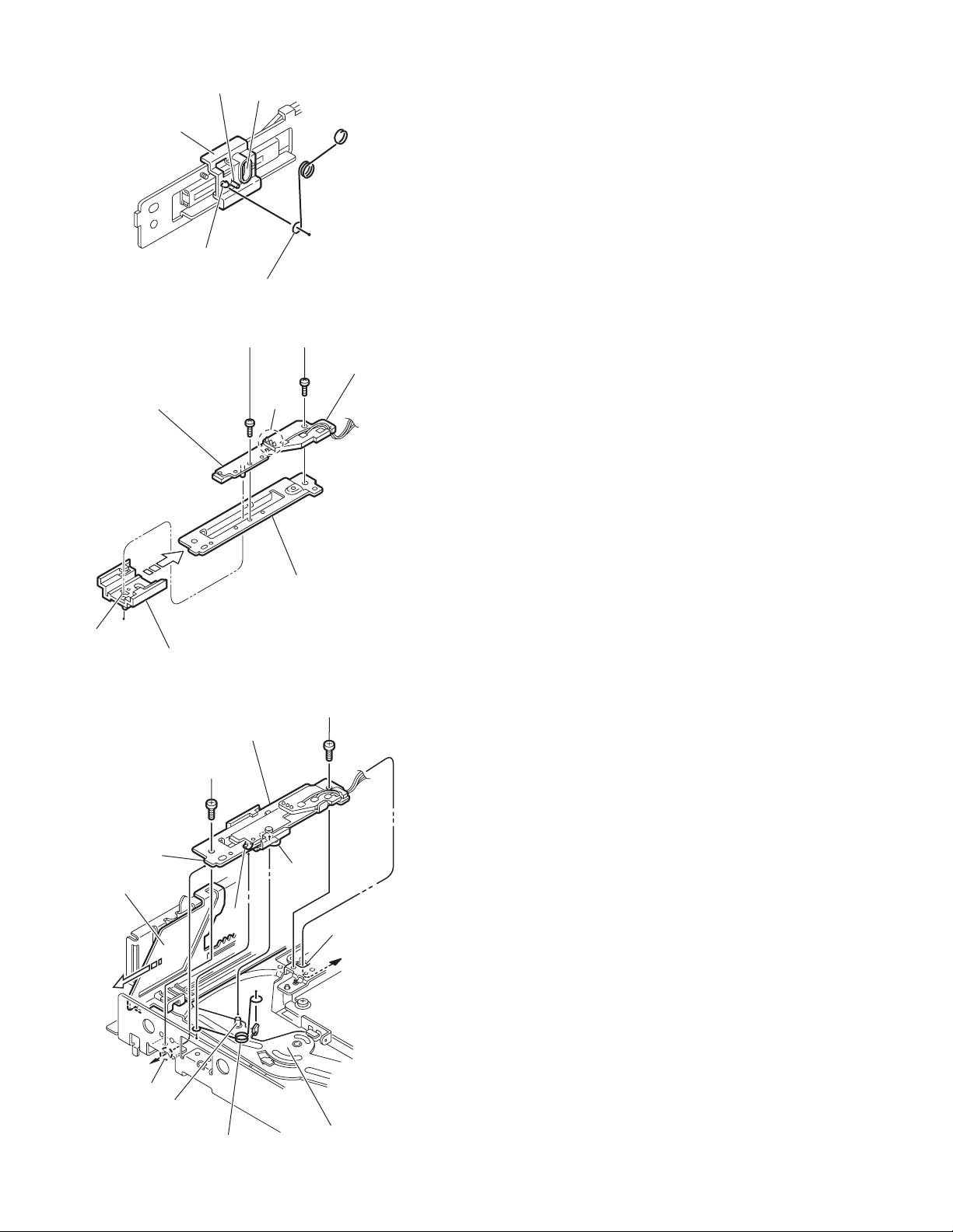
3.1.13 Removing the FL board
(See Fig.26)
• Prior to performing the following procedures, remove the metal
cover and front panel assembly.
(1) From the inside of the front panel assembly, remove the
soldered sections (t, u) on the FL board to remove the parallel wires.
(2) Disconnect the card wire from the connector CN902
FL board.
(3) Remove the four screws Y attaching the FL board.
Reference:
When attaching the FL board, align the projections v of the
front panel assembly in the holes of the FL board before attaching the screws Y.
on the
Front panel assembly
v
Y
Y
t
Card wire
Parallel wire
CN902
Fig.26
FL board
Y
Parallel wire
v
u
(No.MB188)1-15
Page 16
3.1.14 Removing the switch board
(See Fig.27)
• Prior to performing the following procedures, remove the metal
cover and front panel assembly.
(1) From the inside of the front panel assembly, remove the
three screws Z attaching the switch board.
(2) Take out the switch board and remove the soldered section
w on the switch board to remove the parallel wire.
Reference:
When attaching the switch board, align the projections x in the
holes of the switch board before attaching the screws Z.
3.1.15 Removing the standby LED board
(See Fig.27)
• Prior to performing the following procedures, remove the metal
cover and front panel assembly.
(1) From the inside of the front panel assembly, remove the
two screws AA attaching the standby LED board.
(2) Take out the standby LED board and remove the soldered
section y on the standby LED board to remove the parallel
wire.
Reference:
When attaching the standby LED board, align the projections
z in the holes of the standby LED board before attaching the
screws AA.
Z
x
Z
x
Z
w
Parallel wires
Switch board
Front panel assembly
x
Fig.27
z
Standby LED board
AA
z
AA
y
1-16 (No.MB188)
Page 17
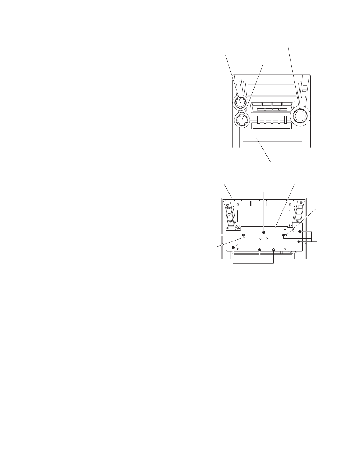
3.1.16 Removing the encoder board
(See Figs.26 to 29)
• Prior to performing the following procedures, remove the metal
cover and front panel assembly.
(1) From the outside of the front panel assembly, pull out the
knobs toward this side. (See Fig.28.)
(2) From the inside of the front panel assembly, disconnect the
card wire from the connector CN902
Fig.26.)
(3) Remove the four screws Y, three screws Z and two screws
AA attaching the each board. (See Figs.26 and 27.)
(4) Take out the FL board with the switch and standby LED
boards.
Reference:
It is not necessary to remove the parallel wires.
(5) Remove the eight screws AB attaching the encoder board.
(See Fig.29.)
Reference:
When attaching the encoder board, align the projections aa of
the front panel assembly in the holes of the encoder board before attaching the screws AB. (See Fig.29.)
on the FL board. (See
Volume knob
Sound mode knob
Preset knob
Front panel assembly
Fig.28
Encoder boardFront panel assembly
AB
AB
aa
aa
AB
AB
Fig.29
(No.MB188)1-17
Page 18
3.1.17 Removing the microphone board
r
(See Fig.30)
• Prior to performing the following procedure, remove the metal
cover and front panel assembly.
From the inside of the front panel assembly, remove the seven
screws AC and screw AC' attaching the microphone board.
Reference:
• When attaching the microphone board, align the projections
ab of the front panel assembly in the holes of the microphone board before attaching the screws AC and AC'.
• When attaching the screw AC', attach the wire holder with it.
Microphone board
AC AC AC
ab
ab
Wire holde
AC'AC
Wire
3.1.18 Removing the headphone board
(See Fig.31)
• Prior to performing the following procedures, remove the metal
cover and front panel assembly.
(1) From the inside of the front panel assembly, remove the
screw AD attaching the headphone board.
(2) Remove the wire holder fixing the wire and take out the
headphone board.
Reference:
After attaching the headphone board, fix the wire with the wire
holder.
3.1.19 Removing the cassette mechanism assembly
(See Fig.31)
• Prior to performing the following procedure, remove the metal
cover and front panel assembly.
(1) From the inside of the front panel assembly, remove the
two screws AE and two screws AF attaching the cassette
mechanism assembly.
Reference:
When attaching the cassette mechanism assembly, align the
projections (ac, ad) in the holes of the cassette mechanism as-
sembly.
ab
Front panel assembly
AE
ad
AE
Front panel assembly
Fig.30
Cassette mechanism assembly
Wire holder
ac
AF
Wire
AD
Headphone board
AF
Fig.31
1-18 (No.MB188)
Page 19
3.2 DVD changer mechanism assembly section
r
r
r
3.2.1 Removing the tray assemblies
(See Figs.1 to 5)
(1) From the top side of the main body, remove the two screws
A from the top cover and release the two joints a on the
both sides of the DVD changer mechanism assembly. (See
Figs.1 and 2.)
(2) Remove the two rods from the top cover and remove the
top cover from the lifter assembly. (See Figs.1 and 2.)
(3) Remove the open det. lever on the left side of the DVD
changer mechanism assembly. (See Fig.3.)
(4) From the right side of the DVD changer mechanism as-
sembly, draw out the tray assemblies toward the front while
pushing the part b of the side (R) assembly. (See Figs.4
and 5.)
Note:
The tray can be locked if all tray assemblies are attached.
(5) From the topside of the DVD changer mechanism assem-
bly, move the stopper tabs c in the direction of the arrow
and release them. Pull out the tray assemblies from the
DVD changer mechanism assembly. (See Fig. 5.)
Note:
Remove the tray assembly from top tray 5 in order.
Reference:
When reattaching the tray assembly, or when removing the
disc remaining inside, refer to another section"3.2.15 Taking
out the disc in the play mode".
Top cove
A
A
Tray assemblies
Tray assembly
Fig.3
b
Fig.4
Open det. leve
Side(R) assembly
a
Lifter assembly
a
Lifter assembly
Fig.1
Fig.2
a
c
Rods
Rods
Top cove
Fig.5
a
(No.MB188)1-19
Page 20
3.2.2 Removing the DVD servo board
(See Figs.6 to 8)
Caution:
Solder the short land sections d on the DVD pickup before disconnecting the card wire extending from the DVD pickup. If
you do not follow this instruction, the DVD pickup may be damaged.
(1) From the topside of the DVD changer mechanism assem-
bly, solder the short land sections d on the DVD pick up.
(See Fig.6.)
(2) From the bottom side of the DVD changer mechanism as-
sembly, disconnect the card wire from the connectors
(CN201
(3) Disconnect the wires from the connectors (CN452
on the DVD servo board. (See Fig.7.)
(4) Remove the screw B attaching the earth wire. (See Fig.7.)
Reference:
(5) Remove the two screws C attaching the DVD servo board.
(See Fig.7.)
(6) From the reverse side of the DVD servo board, release the
lock of the connector CN101
and disconnect the card wire. (See Fig.8.)
Caution:
Unsolder the solders from the short land sections d after reassembling. (See Fig.6.)
, CN451) on the DVD servo board. (See Fig.7.)
, CN453)
After attaching the earth wire, fix it with the spacer as before. (See Fig.7.)
in the direction of the arrow
Short land sections d
DVD changer mechanism assembly
Fig.6
DVD changer mechanism assembly
Card wire
CN452
CN453
DVD pickup
Wires
g
3.2.3 Removing the switch board
(See Fig.7)
• Prior to performing the following procedures, remove the DVD
servo board.
(1) From the bottom side of the DVD changer mechanism as-
sembly, remove the screw D attaching the switch board to
the DVD changer mechanism assembly.
(2) Loosen the screw E attaching the DVD traverse mecha-
nism assembly and take out the switch board while lifting
the section e of the DVD traverse mechanism assembly.
(3) Release the wires from the slots f of the switch board.
Reference:
When reassembling, pass the wire through the section g of the
DVD traverse mechanism assembly.
B
Earth wire
C
CN451
DVD servo board
DVD servo board
Switch board
f
e
CN201
C
DVD traverse mechanism assembly
Fig.7
Card wire
CN101
Lock
D
E
1-20 (No.MB188)
Card wire
Fig.8
Page 21
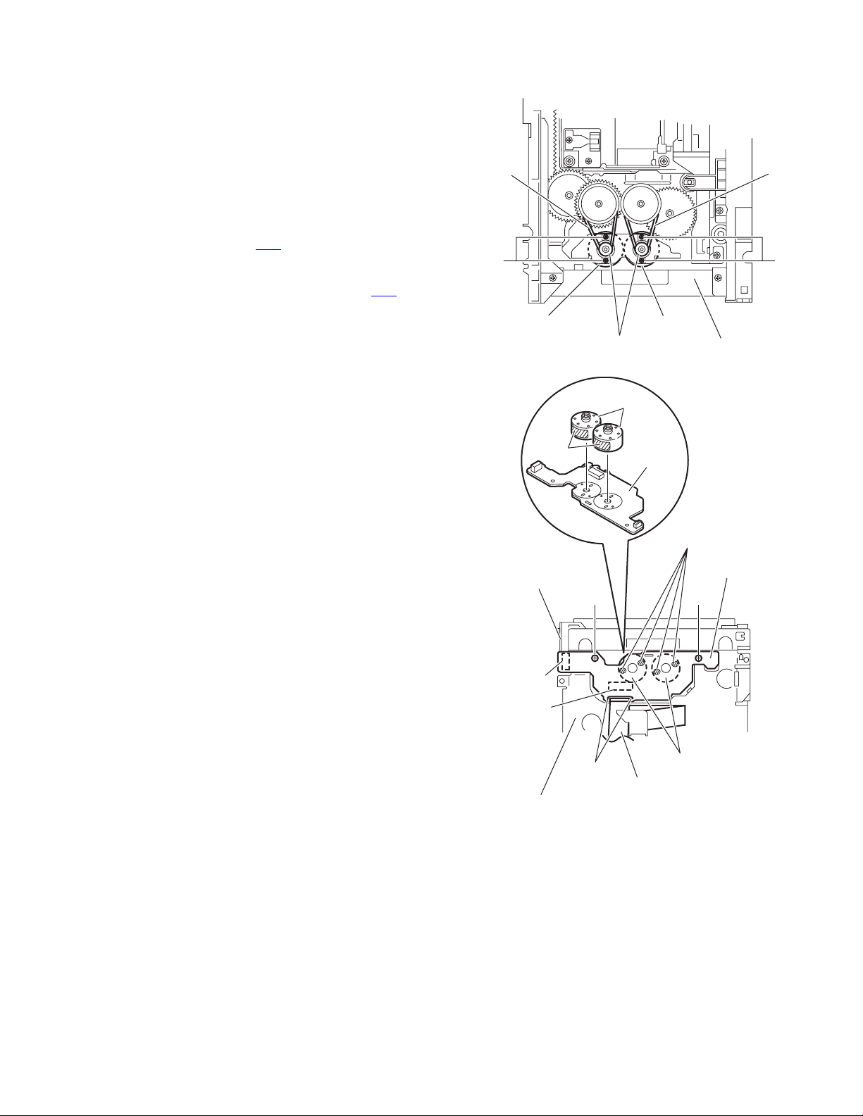
3.2.4 Removing the motor board
(See Figs.9 and 10)
(1) From the top side of the DVD changer mechanism assem-
bly, remove the two belts from the motor pulleys. (See
Fig.9.)
Note:
Take care not to attach grease on the belt.
(2) Remove the four screws F attaching the motors to the load-
er assembly. (See Fig.9.)
(3) From the bottom side of the DVD changer mechanism as-
sembly, remove the two screws G. (See Fig.10.)
(4) Disconnect the connector CN2
tray switch board and remove the motor board. (See
Fig.10.)
(5) Disconnect the card wire from the connector CN1
motor board. (See Fig.10.)
Note:
When connecting the card wire, let the card wire through the
slots g of the motor board. (See Fig.10.)
Reference:
You need not to remove the tray assemblies, and in such case,
move it.
on the motor board from the
on the
Belt
F
Motor Motor
Motor pulleys
Belt
F
Loader assembly
Fig.9
Motors
3.2.5 Removing the motor
(See Fig. 10)
• Prior to performing the following procedures, remove the motor
board.
(1) From the reverse side of the motor board, unsolder the four
soldered sections h on the motor board.
(2) From the forward side of the motor board, remove the mo-
tors.
Note:
When reattaching the motor, turn the side where the label
should be put to the front side.
Label
Tray switch
board
CN2
CN1
DVD changer mechanism assembly
Motor board
G
g
Card wire
Soldered sections h
G
Motors
Fig.10
Motor board
(No.MB188)1-21
Page 22
3.2.6 Removing the DVD traverse mechanism assembly
(See Fig.11)
• Prior to performing the following procedures, remove the tray
assemblies and DVD servo board.
(1) From the bottom side of the DVD changer mechanism as-
sembly, remove the three screws H attaching the DVD
traverse mechanism assembly.
(2) Remove the card wire from the section i.
(3) Remove the wire from the section j.
(4) Take out the DVD traverse mechanism assembly from the
DVD changer mechanism assembly.
DVD changer mechanism assembly
i
j
H
H
DVD traverse mechanism assembly
Fig.11
1-22 (No.MB188)
Page 23

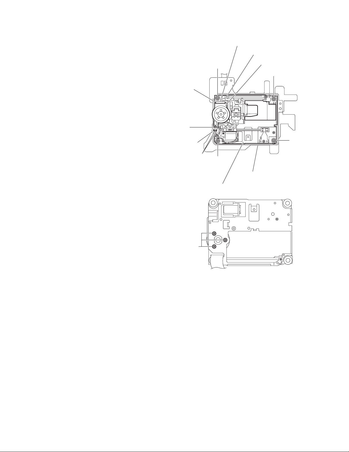
3.2.7 Removing the DVD pickup
r
(See Figs.12 to 14)
• Prior to performing the following procedures, remove the tray
assemblies, DVD servo board and DVD traverse mechanism
assembly.
(1) From top side of the DVD traverse mechanism assembly,
release the lock of the connector on the DVD pickup and
disconnect the card wire in the direction of the arrow. (See
Fig.12.)
(2) Turn the screw shaft gear in the direction of the arrow 1 to
move the DVD pickup in the direction of the arrow 2. (See
Fig.12.)
(3) Remove the screw J attaching the gear holder. (See
Fig.12.)
(4) Remove the screw K attaching the SS adj. spring. (See
Fig.12.)
(5) Move the DVD pickup in the direction of the arrow and re-
move the screw shaft from the section k on the screw shaft
holder. (See Fig.13.)
(6) Remove the section m of the DVD pickup from the guide
shaft. (See Fig.13.)
(7) Remove the two screws L attaching the rack arm to the
DVD pickup. (See Fig.14.)
(8) Pull the screw shaft from the DVD pickup in the direction of
the arrow. (See Fig.14.)
3.2.8 Attaching the DVD pickup
(See Figs.12 to 14)
(1) Attach the screw shaft to the DVD pickup and attach the
rack arm with the screws L. (See Fig.14.)
Reference:
After attaching the screw shaft to the DVD pickup, attach
the screw shaft collor to the screw shaft. (See Fig.14.)
(2) Attach the section m of the DVD pickup to the guide shaft
first and attach the screw shaft to the section k on the
screw shaft holder. (See Fig.13.)
(3) Attach the gear holder and SS adj. spring with the screws
J and K. (See Fig.12.)
(4) Turn the screw shaft gear to move the DVD pickup toward
the left. (See Fig.12.)
(5) Connect the card wire to the connector on the DVD pickup.
(See Fig.12.)
Screw shaft gear
1
Gear holder
Screw shaft
DVD traverse mechanism assembly
Connector
Card wire
2
KJ
DVD pickup
Fig.12
DVD pickup
m
Screw shaft holder
Fig.13
DVD pickup
SS adj. spring
Guide shaft
k
Rack arm
Screw shaft collo
L
Screw shaft
Fig.14
(No.MB188)1-23
Page 24
3.2.9 Removing the spindle motor board
(See Figs.15 and 16)
• Prior to performing the following procedures, remove the tray
assemblies and DVD traverse mechanism assembly.
(1) From the top side of the DVD traverse mechanism assem-
bly, remove the four screws M attaching the DVD traverse
mechanism assembly to the DVD traverse mechanism
base 3. (See Fig.15.)
(2) Remove the wires from the soldered section n on the spin-
dle motor board. (See Fig.15.)
(3) Remove the screw N attaching the spindle motor board.
(See Fig.15.)
(4) From the bottom side of the DVD traverse mechanism as-
sembly, remove the three screws P attaching the spindle
motor board. (See Fig.16.)
Reference:
When attaching the spindle motor board, let the card wire
through the hole p on the SF motor base. (See Fig.15.)
N
Card wire
SF motor base
M
Spindle motor board
M
p
n
M
Wires
M
DVD traverse mechanism base
DVD traverse mechanism assembly
Fig.15
P
Fig.16
1-24 (No.MB188)
Page 25
3.2.10 Removing the motor
(See Figs.17 and 18)
• Prior to performing the following procedures, remove the tray
assemblies, DVD traverse mechanism assembly, DVD pickup
and spindle motor board.
• Remove the wires of the motor as required.
(1) Remove the middle gear in the direction of the arrow. (See
Fig.17.)
(2) Remove the screw Q and screw R attaching the SF motor
base. (See Fig.17.)
(3) Remove the screw S attaching the motor to the SF motor
base. (See Fig.18.)
(4) Take out the motor from the motor base.
Reference:
After attaching the feed motor, let the wires through the sections q and r on the SF motor base. (See Fig.17.)
SF motor base
Q
Middle
gear
R
Motor
rq
Fig.17
Motor
SF motor base
S
Fig.18
(No.MB188)1-25
Page 26
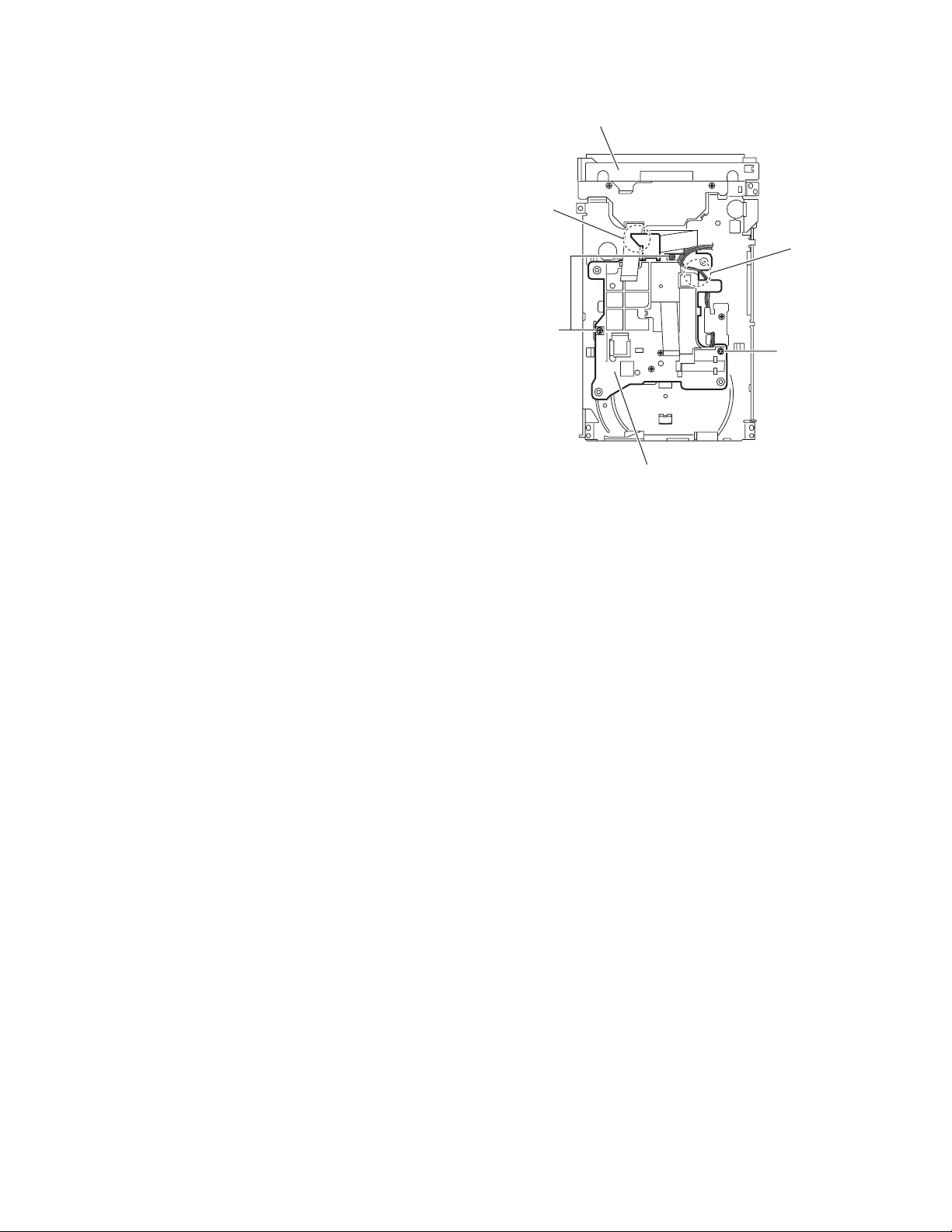
3.2.11 Removing the side (L) assembly and tray switch board
(See Figs.19 to 21)
• Prior to performing the following procedures, remove the tray
assemblies.
(1) From the topside of the DVD changer mechanism assem-
bly, remove the two screws T attaching the side (L). (See
Fig.19.)
(2) From the left side of the DVD changer mechanism assem-
bly, remove the spacer fixing the tray switch board and motor board. (See Fig.20.)
(3) Disconnect the connector CN3
from the motor board and detach the side (L) in an upward
direction. (See Fig.20.)
(4) Remove the screw U attaching the tray switch board to the
side (L). (See Fig.21.)
(5) Release the joint tab s of the side (L) in the direction of the
arrow 1 and release the joint tab t while removing the tray
switch board in the direction of the arrow 2. (See Fig.21.)
on the tray switch board
SIde(L)
T
T
Fig.19
T
Side(L)
T
CN3
Tray switch board
Motor board
Side(L)
Fig.20
s
1
1-26 (No.MB188)
2
t
Tray switch board
U
Fig.21
Page 27
3.2.12 Removing the side (R) assembly
(See Fig.22 to 26)
• Prior to performing the following procedures, remove the tray
assemblies and DVD servo board.
(1) From the inside of the side (R) assembly, release the two
tabs u of the gear cover and remove the gear cover outward. (See Figs.22 and 23.)
(2) From the right side of the DVD changer mechanism as-
sembly, remove the elevator spring attached to the hook v
of the loader assembly. (See Figs.23 and 24.)
(3) From the top side of the DVD changer mechanism assem-
bly, turn the gear 1 clockwise to move the elevator cam
rearward. (See Fig.24.)
(4) Move the two slots w and joint x of the elevator cam and
remove the elevator cam outward. (See Fig.24.)
(5) Remove the three screws V and detaches the side (R) as-
sembly upward. (See Figs.25 and 26.)
Note:
When reattaching the side (R) assembly, make sure to fit the
shaft (part y) into the slot of the select lever. (See Fig.25.)
Side(R) assembly
u
V
Elevator spring
ww
V
x
Fig.24
y
Select lever
v
Elevator cam
Side(R) assembly
Gear cover
Elevator cam
Loader assembly
Fig.22
Elevator
Fig.23
Gear 1
v
V
Side(R) assembly
Fig.25
V
V
Side(R) assembly
Fig.26
(No.MB188)1-27
Page 28
3.2.13 Removing the lifter assembly
(See Figs.27 to 31)
• Prior to performing the following procedures, remove the tray
assemblies, DVD servo board, side (L) and side (R) assembly.
(1) From the top side of the DVD changer mechanism assem-
bly, turn the gear 1 clockwise to move the lifter assembly
upward. (See Figs.27 and 28.)
(2) Turn the gear 2 clockwise to move the hook toward the
front until it stops. (See Figs.27 and 28.)
(3) Move the hook stopper in the direction of the arrow 2 while
pushing the tab z of the hook stopper to unlock it in the direction of the arrow 1 and release four joints aa to detach
from the rack holder. (See Fig.29.)
(4) Release the rod from part ab. (See Fig.29.)
(5) Turn the gear 1 clockwise again to move the lifter assembly
upward. (See Fig.30.)
(6) Remove the lifter assembly from the DVD changer mecha-
nism assembly upward at the positions ac where the four
pins on the both sides of the lifter assembly fit to the notch-
es of the loader assembly. (See Fig.30.)
(7) Move the lifter assembly in the direction of the arrow and
release it from the hook. (See Fig.31.)
Gear 2
Hook stopper
aa
Rack holder
aa
z
aa
Lifter assembly
Gear 1
1
Hook stopper
Fig.29
Hook
aa
2
Rod(L)
ac
ab
ac
Hook
Gear 2
Lifter assembly
Fig.27
Gear 1
Gear 1
Lifter assembly
Loader assembly
Lifter assembly
Fig.30
ac
ac
Hook stopper
1-28 (No.MB188)
Hook
Fig.31
Hook
Fig.28
Page 29
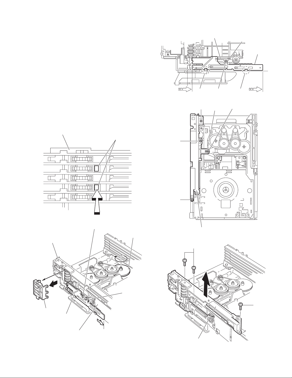
3.2.14 Removing the rack holder and sensor assembly
r
r
(See Figs.32 to 38)
• Prior to performing the following procedures, remove the tray
assemblies, side (L), side (R) assembly and lifter assembly.
Reference:
If the slide gear of the DVD changer mechanism assembly
places at joint ad of the rack holder, turn the gear 1 counterclockwise to move the slide gear in the direction of the arrow.
Then Remove the rack holder. (See Figs.32 and 33.)
(1) Remove the three screws W attaching the rack holder and
release joint ad from the notch ae. (See Figs.32 and 34.)
Note:
When reattaching the rack holder, do not nip the wires
extending from the sensor assembly. (See Fig.32.)
(2) Remove the two screws X attaching the sensor assembly.
(See Figs.35 and 38.)
(3) Move the sensor assembly in the direction of the arrow to
release from the joint section af. (See Figs.35 and 38.)
(4) Remove the sensor spring attached to the bottom of the
sensor assembly from the boss ag on the slider. (See
Figs.35 and 36.)
(5) Remove the screw Y and Z attaching the sensor board and
SV. resister respectively. (See Fig.37.)
Reference:
Remove the soldered section aj on the sensor board as required. (See Fig.37.)
Note:
• When reattaching the SV. resister, attach the slider to the
sensor bracket and fit the lever on the bottom of the SV. resister into slot ak of the sensor slider. (See Figs.36 and 37.)
• When reattaching the rack holder, turn the gear 1 clockwise
to move the slide gear and slide lever inside the body in the
direction of the arrow. (See Figs.32 and 38.)
• Let the wire extending from the sensor assembly through
notch ah to the bottom of the DVD changer mechanism assembly. (See Figs.35 and 38.)
• Fit pin am of the slide lever into hole ai of the slider on the
bottom of the sensor assembly while attaching the sensor
spring to the boss ag of the slider. (See Figs.36 and 38.)
• Joint section af of the sensor assembly to the notch an of the
DVD changer mechanism assembly. (See Fig.38.)
W
Rack holder
Slide gear
X
Rack holde
ad
Fig.33
Rack holde
ae
ad
Fig.34
ah
Sensor assembly
Slider
W
Wire
Slide gear
ad
W
Fig.32
Gear 1
ag
X
af
Sensor spring
Fig.35
(No.MB188)1-29
Page 30
Slider
ak
ag
Sensor spring
Fig.36
ai
YZ
Sensor board
ak
SV. resister
Slider
aj
Sensor bracket
Fig.37
X
Sensor assembly
X
Sensor gear
an
1-30 (No.MB188)
af
am
Sensor spring
ai
ag
ah
Slide lever
Fig.38
Page 31

3.2.15 Taking out the disc in the play mode
r
(See Fig.39 to 42)
Reference:
Refer to "Removing the tray assemblies".
(1) From the top side of the DVD changer mechanism assem-
bly, remove the top cover.
(2) Unlock the tray assemblies and draw out the tray assem-
blies toward the front.
(3) From the top side of the DVD changer mechanism assem-
bly, turn the gear 1 clockwise to move the lifter assembly
upward. (See Fig.39.)
(4) Turn the gear 2 clockwise to move the sub tray remaining
inside the lifter assembly toward the front, then pull out.
(See Fig.39.)
(5) Take out the disc on the sub tray. (See Fig.40.)
(6) After clearing away the disc, insert the sub tray into the
main tray. (See Fig.41.)
Note:
When reattaching the sub tray, move the tray stopper on
the bottom of the main tray in the direction of the arrow
to lock the sub tray certainly. (See Figs.41 and 42.)
(7) Push the tray assembly toward the DVD changer mecha-
nism assembly and reattach.
Tray assembly
Tray stopper
Tray assembly
Disc
Sub tray
Fig.40
Main tray
Gear 2
Gear 1
Sub tray
Sub tray
Fig.41
Tray stoppe
Fig.39
Fig.42
(No.MB188)1-31
Page 32

3.3 Cassette mechanism assembly
3.3.1 Removing the Play/Record & Clear head
(See Fig.1~3)
(1) While moving the trigger arm on the right side of the head
mount in the direction of the arrow, turn the flywheel R
counterclockwise until the head mount comes ahead and
clicks.
(2) The head turns counterclockwise as you turn the flywheel
R counterclockwise (See Fig.2 and 3).
(3) Disconnect the flexible wire from connector CN31
head amplifier & mechanism control board.
(4) Remove the spring from the back of the head.
(5) Loosen the azimuth screw for reversing attaching the head.
(6) Remove the head on the front side of the head mount.
on the
Cassette mechanism assembly
Fig.1
Head
Fly wheelR
Trigger armHead mount
Flexible wire
Fly wheel R
Fig.2
Azimuth screw
Head
for reversing
Spring
CN31
Head amplifer & mecha control board
Fig.3
1-32 (No.MB188)
Page 33

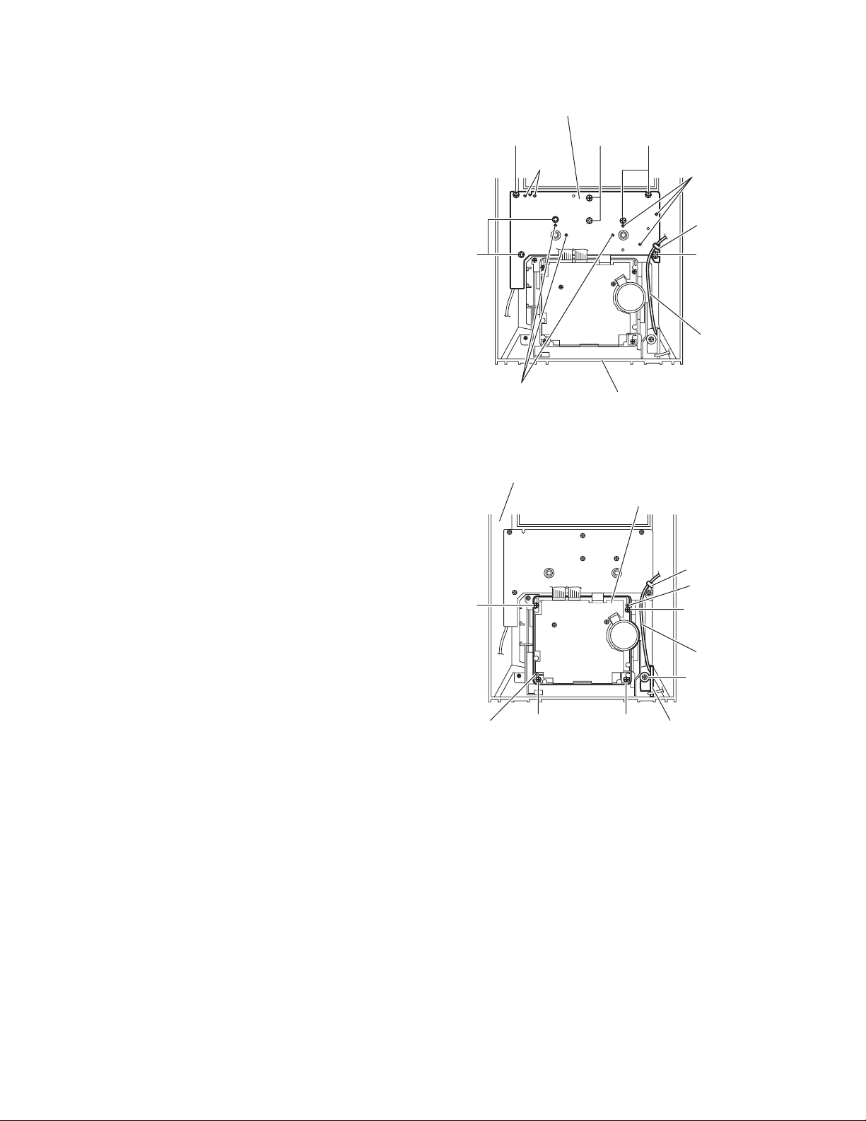
3.3.2 Removing the head amplifier & mechanism control board
(See Fig.4)
(1) Turn over the cassette mechanism assembly and remove
the three screws A attaching the head amplifier & mechanism control board.
(2) Disconnect the flexible wire from connector CN31
head amplifier & mechanism control board.
(3) Disconnect connector CN32
anism control board from connector CN1
board.REFERENCE: If necessary, unsolder the 4-pin wire
soldered to the main motor.
3.3.3 Removing the main motor
(See Fig.4~7)
(1) Remove the two screws B .
(2) Half raise the motor and remove the capstan belt from the
motor pulley.
ATTENTION:
Be careful to keep the capstan belt from grease. When reassembling, refer to Fig.6 and 7 for attaching the capstan belt.
Head amplifier & mecha control board
of the head amplifier & mech-
on the reel pulse
on the
Main motor assembly
Capstan belt
Fig.5
Main motor assembly
CN31
Flexible wire
A
AA
Fig.4
CN32
4pin wire
B
Main motor assembly
Motor pulley
Capstan belt
Fig.6
Main motor assembly
Fly wheel
Capstan belt
Motor pulley
Fig.7
(No.MB188)1-33
Page 34

3.3.4 Removing the flywheel
(See Fig.8, 9)
• Prior to performing the following procedure, remove the head
amplifier & mechanism control board and the main motor assembly.
(1) From the front side of the cassette mechanism, remove the
slit washers attaching the capstan shaft L and R. Pull out
the flywheels backward.
Fly wheel R Fly wheel L
Fig.8
Fly wheel R
Capstan shaft R Capstan shaft L
Slit washer
Fig.9
3.3.5 Removing the reel pulse board and solenoid
(See Fig.10)
• Prior to performing the following procedure, remove the head amplifier & mechanism control board.
(1) Remove the screw C.
(2) Release the tab a, b, c, d and e retaining the reel pulse board.
(3) Release the tab f and g attaching the solenoid on the reel pulse board.
(4) The reel pulse board and the solenoid come off.
Fly wheel L
bc
a
Solenoid
g
f
d
Reel pulse board
C
e
Fig.10
1-34 (No.MB188)
Page 35

3.3.6 Reattaching the Play/ Record & Clear head
r
r
(See Fig.11~13)
(1) Reattaching the head mount assembly.
a) Change front of the direction cover of the head
mount assembly to the left (Turn the head forward).
b) Fit the bosses O', P', Q', U' and V' on the head mount
assembly to the holes P and V, the slots O, U and Q
of the mechanism sub assembly (See Fig.11 to 13).
CAUTION:
To remove the head mount assembly, turn the direction
cover to the left to disengage the gear. If the gear can not
be disengaged easily, push up the boss Q' slightly and
raise the rear side of the head mounts slightly to return
the direction lever to the reversing side.
(2) Tighten the azimuth screw for reversing.
(3) Reattach the spring from the back of the Play/ Record &
Clear head.
(4) Connect the flexible wire to connector CN31
amplifier & mechanism control board.
on the head
U' Q'
Head mount assembly
Head mount assembly
O'
Fig.11
P'
P'
V'
V'
Direction cove
Spring
Flexible wire
V
O
P
Q
Head
Direction cove
U
Fig.12
Azimuth screw for reversing
Head mount
CN31
Fig.13
Head amplifier &
mechanism control board
(No.MB188)1-35
Page 36

3.4 Speaker section
3.4.1 Removing the side panel assembly
(See Fig.1)
(1) From the side of the speaker main body, remove the four
screws A and two screws B attaching the side panel assembly.
A
BB
3.4.2 Removing the subwoofer
(See Fig.2)
• Prior to performing the following procedures, remove the side
panel assembly.
(1) Remove the six screws C attaching the subwoofer.
(2) From the back side of the subwoofer, disconnect the red
and black wires from the terminal.
Side panel assembly
C
A
Fig.1
Terminal
Red wire
Black wire
1-36 (No.MB188)
C
Subwoofer
Fig.2
Page 37

3.4.3 Removing the front panel assembly
(See Figs.3 and 4)
Reference:
Remove the side panel assembly as required.
(1) Remove the four screws D attaching the front panel as-
sembly. (See Fig.3.)
(2) Release the two joints a. (See Fig.3.)
Caution:
When removing the front panel assembly from the
speaker main body, do not break or damage them that
are glued at the joints a. (See Fig.3.)
(3) From the inside of the front panel assembly, disconnect the
yellow and black wires from the two terminals on the tweeter. (See Fig.4.)
3.4.4 Removing the tweeter
(See Fig.4)
• Prior to performing the following procedure, remove the front
panel assembly.
(1) From the inside of the front panel assembly, remove the
two screws E attaching the tweeter.
D
a
Front panel assembly
a
D
Front panel assembly
Fig.3
E
Tweeter
E
Yellow wire
Black wire
Terminals
Fig.4
(No.MB188)1-37
Page 38

3.4.5 Removing the top woofer
(See Fig.5)
• Prior to performing the following procedures, remove the front
panel assembly.
(1) Remove the four screws F attaching the top woofer.
(2) From the back side of the top woofer, disconnect the red
and black wires from the terminal.
3.4.6 Removing the bottom woofer
(See Fig.6)
• Prior to performing the following procedures, remove the side
panel and front panel assemblies.
(1) Remove the four screws G attaching the bottom woofer.
(2) From the back side of the bottom woofer, disconnect the
black, red and blue wires from the terminal respectively.
Top woofer
FF
Terminal
Red wireBlack wire
Fig.5
Bottom woofer
GG
Red wire
Blue wire
Black wire
Black wire
Terminal
Fig.6
1-38 (No.MB188)
Page 39

SECTION 4
ADJUSTMENT
4.1 Measurement Instruments Required for Adjustment
(1) Low frequency oscillator
This oscillator should have a capacity to output 0dBs to
600Ω at an oscillation frequency of 50Hz-20kHz.
(2) Attenuator impedance : 600Ω
(3) Electronic voltmeter
(4) Distortion meter
(5) Frequency counter
(6) Wow & flutter meter
(7) Test tape
VT703L : Head azimuth
VT712 : Tape speed and running unevenness (3kHz)
VT724 : Reference level (1kHz)
(8) Blank tape
TYPE l : AC-225
TYPE ll : AC-514
(9) Torque gauge : For play and back tension
FWD(TW2111A), REV(TW2121a) and FF/
REW(TW2231A)
(10) Test disc: VT-501, CTS-1000
4.2 Measurement conditons
Power supply voltage AC 120V ~, 60Hz
Reference output Speaker : 0.775V/4Ω
Headphone : 0.077V/32Ω
Reference frequency and input level 1kHz, AUX : -8dBs
Measurement output terminal at Speaker J200
Load resistance 4Ω
4.2.1 Radio Input signal
AM frequency 400Hz
AM modulation 30%
FM frequency 400Hz
FM frequency deviation 22.5kHz
4.2.2 Tuner section
FM Band cover 87.5~108.0MHz
AM Band cover 530~1,710kHz
Voltage applied to tuner +B : DC5.7V
VT : DC 12V
Reference measurement output 26.1mV(0.28V)/3Ω
Input positions AM : Standard loop antenna
FM : TP1 (hot) and TP2 (GND)
4.2.3 Standard measurement position of volume
Function switch to Tape
Beat cut switch to Cut
Super Bass/Active hyper Bass to OFF
Bass Treble to Center
Adjustment of main volume to reference output VOL : 28
Precautions for measurement
(1) Apply 30pF and 33kΩ to the IF sweeper output side and
0.082µ F and 100kΩ in series to the sweeper input side.
(2) The IF sweeper output level should be made as low as
possible within the adjustable range.
(3) Since the IF sweeper is a fixed device, there is no need
to adjust this sweeper.
(4) Since a ceramic oscillator is used, there is no need to
perform any MIX adjustment.
(5) Since a fixed coil is used, there is no need to adjust the
FM tracking.
(6) The input and output earth systems are separated. In
case of simultaneously measuring the voltage in both of
the input and output systems with an electronic voltmeter
for two channels, therefore, the earth should be connected particularly carefully.
(7) In the case of BTL connection amp., the minus terminal
of speaker is not for earthing. Therefore, be sure not to
connect any other earth terminal to this terminal. This
system is of an BTL system.
(8) For connecting a dummy resistor when measuring the
output, use the wire with a greater code size.
(9) Whenever any mixed tape is used, use the band pass fil-
ter (DV-12).
(No.MB188)1-39
Page 40

4.3 Cassette mechanism adjustment
Head azimuth
adjustment screw
(Forward side)
Mecha control board
Motor speed
VR37
Head azimuth
adjustment screw
(Reverse side)
Head azimuth
adjustment screw
(Forward side)
R/P head, Erase head
Head azimuth
adjustment screw
(Reverse side)
CN31
BIAS adjust
VR31
C308
R327
R315
VR31
R313
Q302
C316
C319
R314
C121
C221
L301
SW1
C314
R104
Q305
C313
PP300
D340
C310
R121
R221
R310
C107
L303
R102
R303
R335
R353
R108
R304
C113
R302
Q343
R339
C301
C103
C207
R110
Q342
C304
R208
C105
C205
R301
SW2
C106
R306
D1
R106
R101
C104
CN34
C306
Q344
R105
C102
R344
R205
Q345
R345
C307
R336
C340
R346
R107
R206
C206
W1
Q346
VR37
R210
R305
C300
C341
C110
R109
R372
Q372
C120
C371
P1
CN33
IC32
R116
C109
CN31
Q371
C101
R371
C374
C220
Q375
R376
R216
C376
C202
C204
C201
W1
R201
C342
D375
R204
C213
R207
Q376
R375
C209
IC1
FW100
R338
R337
CN32
C203
R202
CN1
C210
R340
C331
R342
R347
Q347
SW6
R343
SW5
R341
IC33
1-40 (No.MB188)
Page 41

4.3.1 Mechanism section
Item Condition Measurement method Ref. value Adjust-
Head azimuth Test tape
:VT703L (8kHz)
Output terminal
:Speaker out
Tape speed Test tap
:VT712 (3kHz)
Output terminal
:Speaker out or Headphone out
Item Condition Measurement method Ref. value Adjust-
Tape speed diviation at FWD/REV
Wow & Flutter Test tape
Test tape
: VT712 (3kHz)
Output terminal
:Speaker out or Headphone out
: VT712 (3kHz)
Output terminal
:Speaker out or Headphone out
(1) Playback the test tape VT703L (8kHz).
(2) Adjust to maximum output level by azi-
muth adjustment screw for forward side
and reverse side.
(3) This adjustment is adjust by adjustment
screw of forward side and adjustment
screw of reverse side.
Playback the test tape VT712 (3kHz) at end of
forward side,adjust to 2,940~3,90Hz indication
of frequency counter by VR37.
Playback the test tape VT712 (3kHz) at end of
forward and reverse, tape speed deviation
should be less than 6.0Hz.
Playback the test tape VT712 (3kHz) at start of
forward and reverse, Wow & Flutter are should
be less than 0.25%(WRMS).
ment posi-
tion
Maximum output Only adjust
at changed
head
2,940 ~ 3,090Hz VR37
ment posi-
tion
Leass than
6.0Hz
Less than 0.25%
(WRMS)
VR31
(No.MB188)1-41
Page 42

4.3.2 Electrical adjustment
Item Condition Measurement method Ref. value Adjust-
Recording BIAS
adjustment
R/P playback frequency response
4.3.3 Electrical response confirmation
• Forward or Reverse
•Test tape
: AC-514 TYPE ll
: AC-225 TYPE l
• Output termina
Recording head
• Reference frequency
: 1kHz / 10kHz
(Reference: -20dB)
•Test tape
: AC-514 TYPE ll
• Input terminal
: OSC IN
(1) Set the test tape(AC-514 TYPE ll and
AC-225 TYPE l), then make REC/
PAUSE condition.
(2) Connect 100Ω to recording head by se-
ries, then connect to VTVM for measurement the current.
(3) After setting, start the recording by re-
lease the PAUSE, in this time bias current adjust to next fig. by VR31
and VR32 for Rch.
4.0 µA (TYPE ll) and 4.20 µA (TYPE l).
(1) Set the test tape (AC-514 TYPE ), then
make REC/PAUSE condition.
(2) Release the PAUSE, then start recording
the 1kHz and 10kHz of reference frequency from oscillator.
(3) Playback the recorded position, 1kHz
and 10kHz output deviation should -1dB
2dB to readjust by VR31
VR32 for Rch.
for Lch
for Lch and
AC-225
: 4.20µA
AC-514
: 4.0µA
Output deviation
1kHz/10kHz
: -1dB ± 2dB
ment posi-
tion
VR31
VR31
Item Condition Measurement method Ref. value Adjust-
Recording bias current
Erase current (reference value)
• Forward or Reverse
•Test tape
: TYPE ll (AC-514)
• Measurement terminal
: BIAS test point on printed
circuit board
• Forward or Reverse
• Rec condition
Test tape
: AC-514 TYPE ll
: AC-225 TYPE l
• Measurement terminal
Both side of Erase head
(1) Change BIAS1 and 2, confirm the fre-
quency should be change.
(2) Set the test tape (AC-514 TYPE ll), then
make REC/PAUSE condition.
(3) Confirm the frequency should 100Hz ±
6kHz at BIAS test point on printed circuit
board.
(1) Set the test tape (AC-514 TYPE ll and
AC-225 TYPE l), then make REC/
PAUSE condition.
(2) Release the PAUSE to REC condition,
connect 1W to ERASE head by series,
then confirm the erase current at both
side of erase head.
100 kHz ± 6 kHz
TYPE ll
: 120 mA
TYPE l
: 75 mA
ment posi-
tion
1-42 (No.MB188)
Page 43

4.4 Service mode
4.4.1 Confirming contents
(1) System micon reset
(2) System micon cold start
(3) FL display check
(4) Micon version check
(5) DVD region check
(6) DVD test mode
4.4.2 Confirming methods
1. System micon reset
When CD mechanism stuck, this may solve the problem without removing/inserting power cord.
Press the
STANDBY/ON, CANCEL
and PAUSE buttons on the main unit
simultaneously.
System micon is initialized.
2. System micon cold start
This function clears all user setting, and return to initial setting.
Daily timer, REC timer
Tuner preset
SEA preset
Last condition (Source, Volume)
Press the SET UP, "4" and "0" buttons
twice on the remote controller at standby.
FL indication
" COLD SET "
This unit returns to initial setting.
3. FL display check
This enables all FL segment light up.
Press the SET UP, "4" and "+10" buttons
on the remote controller at standby.
All of the FL displays light up.
(No.MB188)1-43
Page 44

4. Micon version check
r
You can confirm Micon version and destination.
Insert the power cord in an outlet.
Press the SET UP, "4" and DIMMER
buttons on the remote controller.
System micon version is indicated on
the FL display.
Press the SET UP, "4" and DIMMER
buttons on the remote controller.
DVD mechanism micon version is indicated
on the FL display.
Press the SET UP, "4" and DIMMER
buttons on the remote controller.
DVD backend firmware version is indicated
on the FL display.
Press the SET UP, "4" and DIMMER
buttons on the remote controller.
Model number is indicated
on the FL display.
Press the SET UP, "4" and DIMMER
buttons on the remote controller.
Destination is indicated on the FL display.
5. DVD region check
You can confirm DVD region number.
Press the POWER and DVD LEVEL
buttons on the main unit at standby.
FL indication
REGION
DVD region number is indicated on the on screen display.
(Example) "JC ver.0334 HX-GD8 / FMU-SD7-11"
DVD unit numbe
Firmware model
Firmware version
DVD destination
1-44 (No.MB188)
Page 45

6. DVD test mode
Insert the power cord in an outlet while
pressing the SET and buttons on
the main unit.
Status: You can check DVD unit condition
DVD unit condition is indicated on the FL
display.
Initialize (Normal):
Initialize user setting
Press the PAUSE button on the main unit.
(Example) "TEST JC 13"
FL indication
(Example)
Press the STANDBY/ON button on the
main unit or remote controller.
Disconnect the power cord in an outlet.
Insert the power cord in an outlet.
Press the STANDBY/ON button on the
main unit or remote controller.
Initialization is complete.
Disc reading preset condition
0: DVD/CD learned
1: only CD learned
2: only DVD learned
3: DVD/CD not learned
DVD region number
DVD destination
"TEST JC130"
Initialize (Permanent):
Initialize "QUICK PLAY" setting
Press the button on the main unit for two seconds.
FL indication
(Example)
"TEST JC133"
Press the STANDBY/ON button on the
main unit or remote controller.
Disconnect the power cord in an outlet.
Insert the power cord in an outlet.
Press the STANDBY/ON button on the
main unit or remote controller.
Insert a new VT-501 disc, play this disc.
Eject the VT-501 disc.
Insert a new CTS-1000 disc, play this disc.
Eject the CTS-1000 disc.
Press the STANDBY/ON button on the
main unit or remote controller.
1
Initialization is complete.
(No.MB188)1-45
Page 46

1
Device key:
Program DEVICE KEY code
Press the button on the main unit.
Device key check:
Check device key checksum
Press the MENU button twice on the remote controller.
Micon version check:
Check micon version number
Press the MENU button on the remote controller.
STANDBY/ON LED blink.
PC application run.
Automatically power off
Wait until PC application complete
FL indication
(Example) " "
Device key check is complete.
FL indication
(Example) " SSSS "
Press the MENU button on
the remote controller.
FL indication
(Example) " MMMM BBBB "
Micon version check is complete.
Reference:
If never programmed, "FFFF"
will appear.
S: System micon version
M: Mechanism micon version
B: Backend firmware
FL display check:
Check all FL segments
Press the MENU button on the remote controller.
Check mode
Press the MENU button on the remote controller.
FL indication
" CHECK "
START PLAY:
Start playing
Press the "1" button on the remote controller.
WOBBLE:
WOBBLE display (No use)
Press the "2" button on the remote controller.
CD laser:
CD laser current display
Press the "4" button on the remote controller.
DVD laser:
DVD laser current display
Press the "5" button on the remote controller.
All of the FL displays light up.
FL display check is complete.
FL indication
" CHECK "
FL indication
" "
FL indication
" "
FL indication
" "
1-46 (No.MB188)
2
Page 47

2
DVD jitter:
DVD single-layer jitter display
Press the "6" button on the remote controller.
EEPROM (B):
EEPROM data display (Backward)
Press the "7" button on the remote controller.
EEPROM (F):
EEPROM data display (Forward)
Press the "8" button on the remote controller.
Temperature:
Pickup temperature display
Press the "9" button on the remote controller.
DVD jitter:
DVD jitter (D/L - S/L) display
Press the "10" button on the remote controller.
EEPROM ini.:
EEPROM initialize
Press the "+10" button on the remote controller.
Monitor:
Monitor change
Press the "0" button on the remote controller.
FL indication
" "
FL indication
" "
FL indication
" "
FL indication
" "
FL indication
" "
FL indication
" FFFF FFFF "
FL indication
" "
STOP:
Disc stop
Press the STOP button on the remote controller.
FL indication
" CHECK "
PLAY:
Laser & jitter display
Press the PLAY button on the remote controller.
Check mode is complete.
Press the STANDBY/ON button
on the main unit or remote controller.
FL indication
" "
(No.MB188)1-47
Page 48

4.4.3 Indicating check for FL display
No. Function FL display Note
1 SOURCE
DVD-VIDEO
DVD-AUDIO
CD
MP3
WMA
VCD
SVCD
DVD (JPEG)
TAPE
AUX
AM
FM
2 TUNER
PRESET MEMOERY
PRESET MEMOERY
PRESET MEMOERY
3 TAPE
PLAY
REVERSE
FF/REW
MUSIC SCAN
REC
DISC REC
DISC REC STOP
1
2.
3
4
1:
1
2:
3
4
1
2.
3
4
1:
1
2:
3
4
C
D
1
2.
1:
1
2:
3
4
1
2.
1
2
2.
1
2:
3
4
If MP3 time is over 100 minutes, show "--:--".
1
2.
1
2
2.
1
2:
3
4
If WMA time is over 100 minutes, show "--:--".
V
D
1
2.
1:
1
2:
3
4
without PBC
V
D
1
2.
S
V
1
2.
S
V
1
2.
1
2.
1
2
2.
T
A
A
U
X
A
M
F
M
TTU
N
E
U
N
E
S
E
P
S
T
O
T
A
T
A
E
V
T
A
T
A
T
A
DRI
S
C
1:
P
1
1
R
R
T
1R2
P
P
E
P
P
P
P
1
2:
P
J
P
E
I
N
6
0
0
8.
F
A
E
D
E
E
R
E
E
E
RSEEC
B
C
with PBC
3
4
without PBC
B
C
with PBC
E
G
2
: PRESET NUMBER
0
0
: PRESET NUMBER
M
M
BLINKING
BLINKING
"DISC REC FINISHED" SCROLL
4 VOLUME
UP/DOWN
MAX
MIN
RHYTHM AX
ON
OFF
SUBWOOFER
LEVEL CHANGE
LEVEL CHANGE
LEVEL CHANGE
LEVEL CHANGE
AT LEVEL 0
AT LEVEL 2
SOUND MODE
DANCE
HALL
STADIUM
ROCK
POP
CLASSIC
USER1
USER2
USER3
OFF
V
O
L
U
M
E
3
0
V
O
L
U
M
E
M
A
X
V
O
L
U
M
E
M
I
N
R
H
Y
T
H
M
A
X
O
N
O
F
F
S
U
B
W
O
O
F
E
R
S.
W
O
O
F
E
R
0
S.
W
O
O
F
E
R
1
S.
W
O
O
F
E
R
2
M
I
N
L
E
V
E
L
M
A
X
L
E
V
E
L
D
A
N
C
E
H
A
L
L
S
T
A
D
I
U
M
R
O
C
K
P
O
P
C
L
A
S
S
I
C
U
S
E
R
1
U
S
E
R
2
U
S
E
R
3
O
F
F
1-48 (No.MB188)
Page 49

No. FL display
Function Note
4 3D PHONIC
3
D
A
3D ACTION
3D DRAMA
3D THEATER
3D PHONIC OFF
3
D
3
D
3
D
C
D
R
T
H
E
O
F
Note: DVD-A cannot be activated 3D-Phonic.
Also at Karaoke condition, 3D-PHONIC is
S
E
A
TONE SETTING
TONE MEMORY
TONE MEMORY
TONE MEMORY
TONE MEMORY
B
A
T
U
M
C
S
S
R
E
S
E
R
E
M
O
TONE MEMORY
DVD LEVEL
D
V
D
L
LEVEL 1
LEVEL 2
LEVEL 3
D
V
D
D
V
D
E
L
E
L
E
5 SLEEP
S
L
E
E
SLEEP 10 120
P
CLOCK
ADJUST
SET
SET
M
A
M
C
1
2:
1
2.
L
O
C
K
A
DAILY TIMER
D
A
I
L
Y
SELECT
SET
SET
SET
SET
SET
SET
SET
SET
SET
O
N
O
N
O
F
F
O
F
F
A
T
U
T
U
D
1
G
D
1
G
D
1
G
V
O
L
T
A
M
A
M
S
E
T
A
M
A
M
S
E
T
D
I
S
T
A
P
U
X
N
E
R
N
E
R
S
E
T
1
S
E
T
1
S
E
T
1
S
E
T
U
M
E
S
E
T
T
I
O
N
A
M
A
A
T
E
R
F
O
N
T
0
0
1
R
Y
V
E
V
E
V
E
RANGE: -3 0 +3
RANGE: -3 0 +3
NUMBER BLINKING
L
1
L
2
L
3
RANGE: 10/20/30/60/90/120
0
0
0
0
O
I
M
1
2:
1
2:
1
2:
1
2:
C
E
I
N
F
A
T
T
T
HOUR BLINKING
MINUTE BLINKING
K
E
R
0
0
HOUR BLINKING
0
0
MINUTE BLINKING
0
0
HOUR BLINKING
0
0
MINUTE BLINKING
BLINKING (ALL)
BLINKING
BLINKING
M
BLINKING
M
BLINKING
1
BLINKING DISC (D )
1
BLINKING GROUP (G )
1
BLINKING TRACK (T )
--/5/10/15
O
K
(No.MB188)1-49
Page 50

No. FL display
Function Note
5 REC TIMER
SELECT
SET
SET
SET
SET
SET
SET
R
E
C
T
O
N
O
N
O
F
O
F
T
T
F
M
A
M
A
M
S
E
T
F
A
M
F
A
M
S
E
T
U
N
E
R
U
N
E
R
S
E
T
3
0
1
S
E
T
6 TEST (ROM) by Remocon
S
Y
S
C
O
"B332"
M
M
O
D
B
A
K
D
L
V
E
R
N
U
L
E
E
N
D
TEST (REGION)
R
E
G
I
O
N
I
M
E
R
1
2:
0
1
2:
0
1
2:
0
1
2:
0
F
M
A
M
0
8.
0
O
K
HOUR BLINKING
0
MINUTE BLINKING
0
HOUR BLINKING
0
MINUTE BLINKING
0
BLINKING
BLINKING
BLINKING
0
ROM correction +3 CHARACTORS
4 CHARACTORS (including ROM CORR)
BACKEND VERSION 4 CHARACTORS
J / E / A / US / UW / UX
0/1/2/3/4/5/6
7 DVD STATUS
OPEN
CLOSE
NO DISC
DISC CHANGE
TOC READING
ROM CORRECTION
(SYSCON)
ROM CR. OK
ROM CR. NG
ROM CORRECTION
(MECHA MICON)
ROM CR. OK
ROM CR. NG
BACKEND "UPGRADE"
"UNKNOWN" DISC
REGION ERROR
8 DVD VIDEO
STOP
+10KEY INPUT
PLAY
PLAY (MENU)
PAUSE
SEARCH
RESUME STOP
RESUME PLAY
M
M
O
P
E
N
C
L
O
S
E
N
O
S
Y
S
Y
E
E
C
A
R
E
.
1
.
1
2.
1.
1
2.
1
2.
.
1
2.
D
I
S
C
D
I
S
C
2
R
E
A
D
I
N
G
U
P
G
R
A
D
E
S
C
O
N
S
C
O
N
U
P
G
R
C
H
O
C
H
E
U
P
G
R
N
'
T
G
I
O
N
3
4.
1:
3
4.
1:
3
4.
:
3
4.
1:
O
E
R
A
D
E
K
R
R
O
A
D
E
P
L
A
E
R
S
T
O
2
3:
4
P
L
A
2
3:
4
:
S
T
O
2
3:
4
SOURCE CD and CURRENT ONLY
SOURCE CD and CURRENT ONLY
1
SOURCE CD and CURRENT ONLY
SOURCE CD and CURRENT ONLY
SOURCE CD and CURRENT ONLY
SOURCE CD and CURRENT ONLY
K
SOURCE CD and CURRENT ONLY
R
SOURCE CD and CURRENT ONLY
SOURCE CD and CURRENT ONLY
SOURCE CD and CURRENT ONLY
R
SOURCE CD and CURRENT ONLY
SOURCE CD and CURRENT ONLY
Y
SOURCE CD and CURRENT ONLY
R
SOURCE CD and CURRENT ONLY
P
After TOC READING
5
Y
5
TIME BLINKING
P
5
RESUME OFF BEFORE PLAY
1-50 (No.MB188)
Page 51

No. FL displayFunction Note
9 DVD AUDIO
STOP
+10KEY INPUT
PLAY
PLAY (MENU)
PAUSE
SEARCH
RESUME STOP
RESUME PLAY
DOWNMIX PROHIBITED
WATERMARK
.
.
1
.
1
2.
3
4.
.
.
1
2.
3
4.
1
2.
3
4.
.
.
1
2.
3
4.
L
R
N
O
S
T
O
P
After TOC READING
S
T
O
P
1:
2
3:
4
5
P
L
A
Y
1:
2
3:
4
5
TIME BLINKING
:
:
S
T
O
P
RESUME
1:
2
3:
4
5
RESUME OFF BEFORE PLAY
O
N
L
Y
A
U
D
I
O
.
10 VCD
V
D
1
2.
1:
2
3:
4
5
STOP (without PBC)
STOP (with PBC)
PLAY (PBC OFF)
PLAY (PBC ON)
PAUSE (PBC OFF)
PAUSE (PBC ON)
SEARCH (NORMAL)
SEARCH (PBC DISC)
+10KEY INPUT
V
D
V
D
1
2.
V
D
1
2.
V
D
1
2.
V
D
1
2.
V
D
1
2.
:
V
D
1
2.
V
D
1
.
1:
1:
1:
P
B
2
3:
4
P
B
2
3:
4
P
B
:
P
B
2
3:
4
DISPLAY TOTAL TIME
C
5
C
5
TIME BLINKING
C
C
5
VCD
S
V
1
2.
1:
2
3:
4
5
STOP (without PBC)
STOP (with PBC)
PLAY (PBC OFF)
PLAY (PBC ON)
PAUSE (PBC OFF)
PAUSE (PBC ON)
SEARCH (NORMAL)
SEARCH (PBC DISC)
+10KEY INPUT
S
V
S
V
1
2.
S
V
1
2.
S
V
1
2.
S
V
1
2.
S
V
1
2.
:
S
V
1
2.
S
V
1
.
1:
1:
1:
P
B
2
3:
4
P
B
2
3:
4
P
B
:
P
B
2
3:
4
DISPLAY TOTAL TIME
C
5
C
5
TIME BLINKING
C
C
5
11 MP3/WMA
STOP
STOP
GROUP SEARCH
GROUP SEARCH
PLAY
PLAY
PLAY
PLAY
PLAY
PAUSE
SEARCH (GROUP)
SEARCH (TRACK)
12 JPEG
STOP
PLAY
SEARCH
1.
2.
1.
1.
2.
1.
1.
1.
1.
GROUP FILE NAME SCROLL
1.
SST
O
P
GROUP FILE NAME SCROLL
1.
T
O
P
TRACK FILE NAME SCROLL
TRACK "SONG TITLE" SCROLL
TRACK "PERFORMER" SCROLL
TRACK "ALBUM TITLE" SCROLL
2
3.
2
3.
1.
2
4.
1.
2
3.
2
3.
SJT
3:
3:
:
:
P
:
4
4
OEP
5
5
TIME BLINKING
G
(No.MB188)1-51
Page 52

No. FL display
Function Note
13 PROGRAM
PROGRAM MODE
DISC INPUT (10key)
GROUP INPUT
TRACK INPUT
STOP
PR
D
1.
.
D
1.
1.
D
1.
1.
D
1.
1.
PLAY
FULL MEMORY
FOUGLRL
14 RANDOM
RANDOM MODE
RANRDAONM
SEARCH
PLAY
15 REPEAT
REPEAT 1 track
REPEAT 1 track
REPEAT 1 chapter
REPEAT 1 title
REPEAT 1 group
1.
1.
1.
1.
2.
2.
2.
2.
2.3.3.
1:
1:
1:
REPEAT 1 disc
REPEAT ALL
REPEAT A-B
16 PROGRESSIVE
INTERLACE
IPNRTOEGRRLEASCSE
PROGRESSIVE
A
:
:
:
:
DOM
2
3:
3:
2
3:
2
3:
3:
M
1
1
4
5
4
5
4
5
4
5
4
5
IV
Group # Blink, 10-key and ENTER key input
Track # Blink, 10-key and ENTER key input
DEPEND ON DISC TYPE
: MOVING
DEPEND ON DISC TYPE
CD/VCD case
MP3/WMA case
DVD case
DVD case
MP3/WMA case
DEPEND ON DISC TYPE
DEPEND ON DISC TYPE
DEPEND ON DISC TYPE
17 DEMO
DEMO START
D
E
M
O
S
T
A
R
T
W
E
L
C
O
M
E
T
O
J
V
C
M
P
3
P
L
A
Y
D
I
S
C
1
P
L
A
D
I
S
C
W
M
A
P
L
A
Y
D
I
S
C
2
P
L
A
D
I
S
C
Random select from DVD/MP3/JPEG/WMA/CD
Y
Random select from DVD/MP3/JPEG/WMA/CD
Y
1-52 (No.MB188)
Page 53

No. FL displayFunction Note
J
P
E
G
P
L
A
17
DEMO OFF
D
I
S
C
3
D
I
S
C
C
D
P
D
I
S
C
4
D
I
S
C
D
V
D
P
D
I
S
C
5
D
I
S
C
F
M
T
U
N
E
R
A
M
T
U
N
E
R
T
A
P
A
U
X
A
U
X
3
D
P
H
D
A
N
C
H
A
L
S
T
A
D
I
R
O
C
P
O
P
C
L
A
S
S
U
S
E
R
U
S
E
R
U
S
E
R
S.
W
O
O
F
S.
W
O
O
F
M
A
X
L
S.
W
O
O
F
S.
W
O
O
F
M
I
N
L
R
H
Y
T
H
M
O
N
D
E
M
O
Y
P
L
A
Y
L
A
Y
P
L
A
Y
L
A
Y
P
L
A
Y
F
M
A
M
E
I
N
O
N
I
C
E
L
U
M
K
I
C
1
2
3
E
R
1
E
R
2
E
V
E
L
E
R
1
E
R
0
E
V
E
L
A
X
O
F
F
BEEP
B
E
E
P
O
BEEP ON
BEEP OFF
B
E
E
P
N
O
F
F
TRAY LOCK
L
O
C
K
E
LOCK
UNLOCK
U
N
L
O
D
C
K
E
D
(No.MB188)1-53
Page 54

No. FL display
18
DVD TEST MODE
TEST START
Function Note
T
S
E
T
(Version info)
T
S
E
A. EEPROM INITIALIZE
(NORMAL)
B. EEPROM INITIALIZE
(FULL)
T
T
S
E
T
T
S
E
T
T
S
E
T
@
#
By AC cord on with holding SET and
: VERSION
@: FE learning condition
#: REGION
@
#
@
#
@
#
3
#
By pressing PAUSE (Front)
0
By pressing and holding (Front) for 2-sec
3
DEVICE KEY DISPLAY
VERSION DISPLAY
VERSION DISPLAY
FL ALL ON
CHECK MODE
START PLAY
WOBBLE
CD LASER current
DVD LASER current
DVD-SL jitter
EEPROM (BWD)
EEPROM (FWD)
Temperature
DVD-DL/SL jitter
EEPROM initialize
Monitor change
STOP
OPEN/CLOSE
PLAY
REGION CHANGE
DEVICE KEY
WRITING MODE
WRITING
COMPLETE (OK)
By pressing MENU (Remote)
a
a
a
a
By pressing MENU (Remote)
aaaa: Syscon
c
c
b
b
b
b
c
c
By pressing MENU (Remote)
bbbb: Mechacon, cccc: Backend
By pressing MENU (Remote)
H
E
C
C
H
C
K
E
C
K
By pressing MENU (Remote)
By pressing 1 (Remote)
By pressing 2 (Remote)
By pressing 4 (Remote)
By pressing 5 (Remote)
By pressing 6 (Remote)
By pressing 7 (Remote)
By pressing 8 (Remote)
By pressing 9 (Remote)
By pressing 10 (Remote)
F
F
F
F
F
F
F
F
By pressing +10 (Remote)
By pressing 0 (Remote)
H
E
C
C
K
By pressing STOP (Front or Remote)
By pressing OPEN/CLOSE (Front)
By pressing PLAY (Front or Remote)
O
A
N
G
H
C
E
K
By AV COMPULINK
By pressing (Front)
By DEVICE KEY (AV COMPULINK) JIG
Automatically power off
1-54 (No.MB188)
Page 55

SECTION 5
TROUBLESHOOTING
This service manual does not describe TROUBLESHOOTING.
(No.MB188)1-55
Page 56

VICTOR COMPANY OF JAPAN, LIMITED
AV & MULTIMEDIA COMPANY AUDIO/VIDEO SYSTEMS CATEGORY 10-1,1chome,Ohwatari-machi,Maebashi-city,371-8543,Japan
(No.MB188)
Printed in Japan
WPC
Page 57

SCHEMATIC DIAGRAMS
COMPACT COMPONENT SYSTEM
HX-GD8
CD-ROM No.SML200404
Area suffix
J ----------------------------- U.S.A.
C -------------------------- Canada
Contents
Block diagram
Standard schematic diagrams
Printed circuit boards
COPYRIGHT 2004 VICTOR COMPANY OF JAPAN, LTD.
CA-HXGD8 SP-HXGD8SP-HXGD8
2-1
2-3
2-19 to 27
No.MB188SCH
2004/4
Page 58

In regard with component parts appearing on the silk-screen printed side (parts side) of the PWB diagrams, the
parts that are printed over with black such as the resistor ( ), diode ( ) and ICP ( ) or identified by the " "
mark nearby are critical for safety.
(This regulation does not correspond to J and C version.)
Page 59

< MEMO >
Page 60

Block diagram
8
8
5
0
1
1
U
Q
TRA
MECHA
ASS'Y
LOADER
ASS'Y
REC/PB
ERASE
HEAD
FW100
M
DVD servo / DVD system control section
A,B,C,D,E,F,RF+,LPC1,LPC2
LPCO1
LPCO2
Q101
CDLDCUR
DVDLDCUR
Q102
Q103
Q104
SPDRV,TRSDRV
FODRV,TRDRV
/DRVMUTE
/SPMUTE
FG,VHALF
IC451
IC32
AUDIO SIGNAL
PROCESSOR
Q302,Q305
BIAS OSC/CONT.
IC1
SOLENOID
PHOTO
PHOTO+B
TRVSW
MA0 to 11
BA0, BA1
MDQ0 to 15
DQM0, DQM1
NCSM,NRAS
NCAS, NWE
MCK
SOL
CN451CN452CN453CN101 CN201
MOTOR
SPEED Adj.
MB
LD(CD)
LD(DVD)
FM+/WOUT
VOUT
UOUT
COM
F+/T+/-
IC201
DRVER
S2UDT,U2SDT
SCLK,SCS,UCS
LSENSOR
DISCSET
DISCSTP
IC452
STEDSW
CLSWT1 to 5
STSTSW
MTOPSW
POSMUP
POSMDN
MTOP, MTCL
EEPROM
EPDI
EPDO
EPCS
EPSK
MECHA
CONTROLLOR
Pre-amplifier and bias / Tape deck mechanism control section
CN31
REC/PLAY
FREQUENCY
RESPONSE Adj.
L301
BIAS OSC
SW1,SW2
SW5,SW6
SWITCH
RREC,FREC
PLAY,TAPE
REEL
PULSE
IC301
DV2 .1
IC505
SDRAM
CN42
X351
27MHz
DISPRST
DISPBUSY
DISPCS
DISPCK
DISPD2S
DISPS2D
CPURST
RECB
CN32
EXDAT0 to 15
EXADT0 to 15
EXADR16 to 20
NEXCE,NEXOE
NEXWE
FLASH ROM
CPURST
CPURST
IC453
AOUT 0
LRCLK
DACPDN
DAC0CS
DCLK, DDATA
DAC1OUT
DAC2OUT
DAC3OUT
DAC4OUT
DAC5OUT
TX
AOUT0
LRCLK
DACPDN
DAC0CS
DCLK
D DATA
RESET
CPURST
IC701
DAC
PBMUTE,RECH
IC33
SERIAL TO PARALLEL
PORT EXTENSION
SOLCTRL
Q375,Q376
SOLENOID
DRIVE
SOL
MOTOR
Q371,Q372
MOTOR
DRIVE
MB
IC509
TX(SPDIF)
DAC1OUT(YOUT)
DAC2OUT(CbOUT)
DAC3OUT(CrOUT)
DAC4OUT(COMPOUT)
DAC5OUT(COUT)
DISPS2D,DISPD2S
DISPCK,DISPCS
DISPBUSY,DISPRST
LRMUTE
FAOUTL
FAOUTR
PBL,PBR
RECL,RECR
SDATA
SCK
STTA
PLAY
PHOTO
KEY1
CN501CN503
CN33CN34
TUNER
CN1
CN560
TDATA
SDATA
TUCLK
TUCE
CN110
CN111
Q543 to Q545
MUTE
PBL,PBR
IC442
PHYTHM
AX
CN44
CN43
RECL
RECR
AVC,TDATA,SDATA
TUCLKTUCE
S/TDATA,S/TCLK,SLCCE
SLCPLAY,PHOTO,SLCKEY
CN803
FL display
System
control
section
TUL,TUR
DI,BK
CLKB
OPT
O
J1
SPDIF
FL,F
CN
CN
IC95
INV.
2-1
MIC 2/AUX IN
MIC 1
User control keys section
J900J910
IC956
ECHO1,ECHO2
AMP.
User control keys section
JS958,JS960,JS962
ROTARY ENCODER
S908 to S925
SWITCH
D908 to D912
D1LED to D5LED
D900 to D907
MIC
SOUNDMODE+/PRESET+/-,VOL+/-
KEY1,KEY2,KEY2X
D1LED to D5LED
S900 to S907
SWITCH
REMIN
IC951
REMOCON
RECEIVER
CN903
CN813
KEY3LED1 to LED5
G1,G12
CN902
FL DRV.
Q950
Q951
KEY4
SBYLED
IC954
FL9
DIS
FW90
FW90
D913
STANDBY
LED
S929
S930
SWITC
Page 61

C
Video output
section
CN512
CN511
9V
IC760
9V
REG.
FW216
YO,CO
CB,CR
VIDEO-RGB
VIDEO-LPF
Y/C-MIX
MUTE1,MUTE2
MSAFETY
MPON
IC100
VIDEO
DRV.
Y,Cb,Cr
FW706
CN700
Audio
main amplifier
output section
M9V
IC750
Q750
Q751
Q752
MOTOR
8V
S4H
MSAFETY
MPON
VH,-VH
VL,-VL
SWL,SWR
HPMUTE
SWIN
POUT
IMP,DC
IC700
SW
POWER
AMP.
S4L
DVDPON
VL,-VL,DC
S4H,S4L
SURROUND
Q230 to Q234
H/P MUTE
HPSW
-VH,DC
PRT
Q220 to Q222
PROTECTOR
FANSPD
S4H
IC200,Q210
FANCTRL
LEVEL
Q212
FAN DRV.
CCT
FAN REG.
Primary with main transformer section
S4
F104
FW202FW204
S2
S1
FL1,FL2
F101
F102
OPTICAL
OUT
J108 J123
SPDIF
COMPU
AV LINK
AVC
CN502
Yout
Cout
CrOUT
CbOUT
COMPOUT
MAINL
MAINR
Q515 to Q517
SW VOLUME
SWIN
External input
Source select
switch section
9V,M9V
S5V,5.6V
BASS1
BASS2
POUT
CN501
CN715
& MUTE
Audio
sub woofer
amplifier
output section
UR
Q541
Q542
MUTE
IC526
IC485
BOOST
AMP.
Q540
SMUTE
HPF
45
FL,FR
IC401
VOLUME
IC534
SWITCH
VOLDA
VOLCLK
VOLCE1
IC466
IC467
LPF &
MIX
AMP.
IC802
EEPROM
EEDA
EECLK
S1100
SWITCH
REMIN,ECHO1,ECHO2,LATB
E
KEY
KEY1 to KEY4,S/WLED,SMLED
SURRLED,SB1LED,SB2LED
FLDATA,FLCLK,BK,SM+,SMRSEARCH,FSEARCH,BUZZER
D1LED to D5LED,VOL+,VOL-
MIC_MUTE
AUXL
AUXR
Q425
Q426
MIC
MUTE
MIC
IC801
MICON
DC regulator
Speaker terminal
section
CN802
CN812
ay
DI,BK
LKB
IC955
INV.
954
BUZZER
BZ900
SBYLED
Q952
SBYLED
LATB
DRV.
P1 to P36
G2 to G11
FL900
FL1
FL2
+37V
FW900
CN205
FL1
FL2
37V
BRIDGE
DISP.
4
LED
FW901 FW902
FW901
S929
S930
SWITCH
KEY2X
FW904
S926
S927
S928
SWITCH
CN213 CN214
NTSCPAL
FSPEED,SURR
HPMUTE,HPSW
STATUS,PRT
FCTRL,LEVEL
CN217
CN207
FANSPD
SURROUND
HPMUTE
STATUS
Q206
37V
HPSW,PRT
FANCTRL
LEVEL
REG.
VH
VH
-VH
D204
D205
D206
D207
+/- VH
S1 S4
VL
-VL
D208
D209
D210
D211
+/- VL
BRIDGE
S2
BRIDGE
S4H
VH,-VH
VL,-VL
S4H
S4H
S4L
D212
D213
D214
D215
S4
J1101 J1102
S5V
MICOM
B5V
IC650
DVD5V
REG.
VL,-VL
SURROUND
FW218
CN208CN206
T001
Trans.
S-VIDEO OUT
&
COMPOSITE
VIDEO OUT
COMPONENT
VIDEO OUT
CN610CN710
CN600
5.6V
IC670
5.6V
S4H
DC
IC600
MAIN
ML
POWER
MR
AMP.
SPEAKER
TERMINAL
ML
MR
J200
SWL
SWR
CN201
HPL
HPR
FAN-
FAN+
CN202
STATUS
F001
MAINL
MAINR
POUT
IMP
MAIN
SUB WOOFER
Headphone
jack section
FW711
FAN
M
CN200
J1001
AC IN
2-2
Page 62

Standard schematic diagrams
r
e
Primary with main transformer section
FW204
QJK015-082614
CT
S1
(SHEET 2)
(SHEET 2)
S1
S2
S2
S4CT
S4
S4
FW202
QUM154-21DGZ4
FL1
SGND
FL2
S3CT
F103
3.15A-125V
F104
1.6A-125V
F101
8A-125V
F102
8A-125V
5R6
5R6
R275
R277
T001
QQT0425-001
C205
0.1
Parts a
When r
sure to
2-3
Page 63

F001
6.3A-125V
R200
3.3M
CN200
QGA7901C1-02
Parts are safety assurance parts.
When replacing those parts make
sure to use the specified one.
SHEET 1
2-4
Page 64

DC regulators / Audio output section
R624
J200
QNB0193-002
(SHEET 4)
CN201
QGD2504C1-04Z
HPR
HPL
HPSW
KRA111M-T
L250
4.7uH
470
R254
470
R255
R211
100K
C225
47/50
R212
47
D221
MTZJ6.8B-T2
KTC3199/GL/-T
C227
10/25
B2952
B2108
C215
R207
100K
D209
D208
0.01/100
C216
0.1/250
D210
D211
C270
1000P
C271
1000P
22K
R231
D229
FAN+
FAN-
STATUS
CN202
QGA2510C1-03
CN214
QGA3901C1-08
CT
S1
S1
S2
S2
S4CT
S4
S4
(SHEET 1)
C208
CN212
QGD2504C1-03Z
SUB5V
ECO
FL1
FL2
S3CT
(SHEET 1)(SHEET 4)
CN213
QGD2504C1-04Z
CN205
QGD2504C1-03Z
37V
R232
D230
0.01/100
D226
C207
0.01/100
1N5402M-20
1N5402M-20
22K
R229
D227
MTZJ5.1B-T2
D212
D214
C268
1000P
C269
1000P
Q210
R220
270
R223
KRC102M-T
C267
R269
4R7
0.1uF
C265
C263
R267
4R7
0.1uF
C261
D260
RY1
R265
QSK0109-001
R264
R263
Q216
1K
KTC3199/GL/-T
R234
IC201
KIA7812API
IC200
KIA317PI
R221
10
3.3K
R225
2.4K
R224
C237
10/50
R222
R206
100K
C212
C214
0.01/100
C266
R268
4R7
0.1uF
C264
C262
R266
4R7
0.1uF
C260
D261
RY2
R262
QSK0109-001
R261
R260
15K
15K
R230
R236
4.7K
R237
4.7K
R238
4.7K
R239
4.7K
D228
C238
D237
KTC3203/OY/-T
Q212
R226
1K
C232
R228
47K
47/25
10K
R227
D213
1N5402M-20
D215
1N5402M-20
B2612
R204
47
R205
47
10/50
MTZJ13B-T2
C209
8200/25
C210
8200/16
(SHEET 3)
PRT
HPSW
S12V
LEVEL
HPMUTE
FANSPD
Q234
R250
Q230
2SC3576-JVC-T
4.7K
R251
Q231
2SC3576-JVC-T
4.7K
R252
Q232
2SC3576-JVC-T
4.7K
Q233
R253
2SC3576-JVC-T
4.7K
10K
10/50
C240
R240
KTC3199/GL/-T
Q220
R214
EP201
QNZ0136-001Z
Q222
100K
100K
R241
KTA1267/YG/-T
R242
10K
Q221
KTC3199/GL/-T
R243
100K
C241
D240
47/16
Q215
KTC3200/GL/-T
1K
C235
R233
0.0047
D235
C236
10/16
D204
0.01/250
KTC2026/OY/
R213
C229
D206
MTZJ15C-T2
Q206
C230
0.01
D224
MTZJ18B-T2
C231
22/50
D225
MTZJ20B-T2
22/50
100K
C218
R209
D205
C220
0.1/250
D207
C221
0.01/250
D234
C234
100/25
MTZJ12C-T2
D231
D220
1N4003S-T5
1N4003S-T5
C226
D222
100/63
D223
C228
Q205
1N4003S-T5
R208
100K
C213
C219
C217
Parts are safety assurance parts.
When replacing those parts make
sure to use the specified one.
FANCTRL
CN207
QGB2510K1-13
FW218
QJK015-111814
CN208
QGA3901C1-11
DGND
PAGND
ML
S4L
-VH
-VL
SWL
SWR
S4H
DC
MR
CN206
VH
VL
QGA3901C1-10
R751
KRA110M-T
D751
ML
SURROUND
DC
MR
-VL
VL
QJK015-101814
FW216
VH
-VH
VL
-VL
PAGND
SWL
SWR
AGND
MTR.GND
R750
Q751
MTZJ5.1B-T2
STK412-400
R752
10K
R753
10K
R754
SURROUND
B2502
IC700
KRC102M-T
R600
R603
C611
C620
0.082
R620
C622
1/50
D700
R700
MTZJ36B-T2
B7005
IC750
KTA1046/Y/
Q750
R755
10K
1K
R756
C750
10/50
Q752
IC600
STK432-070
C600
1K
10/35
220P
47K
C602
R601
47K
220P
C603
R602
C604
1K
10/35
C610
10P
R615
56K
47/63
1.2K
R635
10K
R636
20K
R701
C612
C613
D603
MTZJ2.4B-T2
MTZJ15B-T2
MTZJ15B-T2
R702
C751
0.047
0.22/50
C650
D702D703
220/16
R617
10
R618 R619
1M 3.9K
0.047
R621
C621
R623
15K
0.33
R703
C712
820
R731
D750
Q604
2SK301/PQ/-T
4.7M
D650
R760
MTZJ10B-T2
R616
R622
47K
IC650
PQ05RD21
MTZJ5.6C-T2
R704
D701
4.7P
R729
47/63
R761
C708
56K
10
C651
10
MTZJ36B-T2
L601
0.39
470/25
R705
0.22
R725
R727
10
C715C714
0.0470.047
IC760
KIA7809API
C760
10/50
2-5
Page 65

TK432-070
10/35
220P
220P
10/35
604
SK301/PQ/-T
IC600
C600
C604
R616
R619
3.9K
R622
47K
IC650
PQ05RD21
MTZJ5.6C-T2
0.22
C601
220P
47K
R601
47K
R602
10
L601
0.39
KTC3199/GL/-T
R624
C651
470/25
R604
0.22
0.22
R606
R605
D600
MTZJ9.1B-T2
R609
100
C607
10/50
33K
R608
C605
100/50
10/50
C606
220
R614
C614
0.022
Q602
D601
47K
R625
2.2K
C660
IC660
KIA7805API
10/50
C615
R627
R661
D661
C616
10P 0.022
R626
56K
47/63
C617C618
1.2K
1K
C661
10/50
C609
R607
0.22
220P
QGB2510K1-11
QGB2510K1-12
S5V/B5V
CN600
MAINL
AGND
MAINR
DVDPON
5.6V
POUT
IMP
CN700
SWIN
SWGND
DC
POUT
IMP
M9V
9V
Q601
100
L602
KIA7805API
KTA1267/YG/-T
R613
10K
10K
R612
10
R611
R630
C619
0.39
Q603
KTC3199/GL/-T
D602
47K
2.2K 220
R631
R632
R633
82K
R634
100K
IC670
1K
R671
C671
D671
D670
220/10
C670
10/50
MTZJ6.8B-T2
KRC102M-T
Q600
R610
C608
100/50
10
R629
R628
10
0.0470.047
B6110
D660
MTZJ8.2B-T2
CN610
MAINL
AGND
MAINR
DVDPON
5.6V
POUT
IMP
DVD.GND
DGND
S5V/B5V
DC
SWIN
SWGND
SWFB
MTR.GND
M9V
AGND
9V
QGB2510J1-11
CN710
QGB2510J1-12
FW705
CN511
QGB2510J1-16
(SHEET 3)
(SHEET 3)
R725
0.22
R706
10
L701
C761
0.022 0.022
0.39
Q704
47K
R721
KTC3199/GL/-T
D760
MTZJ10B-T2
10/50
C700 C701
220P 220P
33K
R707
R718
1K
R717
Q705
KTC3199/GL/-T
D705
5.6K
R724
R723
1K
D706
R720R719
1K1K
5.6K
KTC1027/OY/-T
R722
Q700
R708R709
L702
0.39
47K
R705
0.22
10
R704
D701
MTZJ36B-T2
C708 C710 C711 C709
4.7P
R729
56K
47/63
C715C714
0.0470.047
R760
IC760
KIA7809API
R761
C760
10/50
R726
56K56K
R728R727
KTA1023/OY/-T
10/35
10/35
10
1010
R714
Q701
R712
10K
R711
C702
C703
4.7P
R730
56K
C717C716
0.0470.047
10K
10K
R713
10K
0.1
C705
C704
470P
R710
1K
C718
1/50
C713
47/63
820
R732
KTC3200/GL/-T
Q702
D704
100K
R715
2.2K
C719
R735
10K
KTA1268/GL/-T
Q703
R716
C707
100/10
Q706
KTA1267/YG/-T
R738
100K
0.1
C706
47
47
R734
R733
10/50
R736
82K
R737
100K
SHEET 2
2-6
Page 66

External input / Source selector switch section
2
R
CN110
QGF1036F1-26
Yout
Cout
CrOUT
COMP_OUT
SPDIF
DISPS2D
DISPD2S
DISPCK
DISPCS
DISPBUSY
DISPRST
QGF1036F1-06
LRMUTE
FAOUTR
FAOUTL
(SHEET 7) (SHEET 7)
CN503
QGB2510J1-05
QNN0420-001
QGF1205F1-10
(SHEET 8)
QGF1205F1-09
(SHEET 8)
CbOUT
CN111
FMDET
RDSDATA
RDSCLK
C580
470/10
C581
470/6.3
C593
2200/10
L580
QQL231K-221Y
R589
R588
10K
Q581
UN2211-X
UN2211-X
Q580
10K
R591
R592
4.7K
Q583
Q582
UN2211-X
UN2211-X
R577
18k
220p
C577
R579
220P
R578
C578
R576
18k
J576
D576
D577
C576
CN44
C571
470/10
CN43
R573
10K
2200p
C567
220p
R567
C568
R574
1K
R568
220p
1K
R569
1K
R570
1K
C572
0.022
R571
C569
100k
Q567
KTA1267/YG-T
1K
R575
22K
Q568
UN2211-X
C574
C1999
1.5
D580
2.2K
S/TDATA
R584
SLCPLAY
MTZJ3.9B-T2
R1164
R580
1.0K
R581
1.0K
R582
1.0K
R583
1.0K
2.2K
R1165
1K
AUXL
AUXR
RECL
RECR
PBL
PBR
MSIN
SLCCE
S/TCLK
SLCKEY
PHOTO
POUT
220
R1163
220
R564
1.2K
DVDPON
Q585
UN2213-X
C555
FAOUTL
10/35
C556
FAOUTR
10/35
FL
FR
PBL
TUL
CDR
CDL
R407
15K
R409
470p
C421
2.2/50
10/25
10/25
C419
C415
C417
IC401
LC75342M-X
C418
C416
C420
10/25
10/25
2.2/50
R406
PBR
TUR
D581
1N4003S-T5
R586
R587
R585
4.7K
2.2K
2.2K
R590
100K
R593
100K
82k
82k
C570
R572
100k
0.001
0.001
D567
0.01
C575
1000P
IC580
PQ033EF02SZ
C583
C582
10/25
10/25
DVDPON
QRZ9006-4R7X
Q584
UN2115-X
R545
4.7K
R544
4.7K
AUXL
20K
3.6K
R405
10/25
47/25
10/25
2700p
0.1
0.1
C413
C403
C409
C405
C411
C407
C410
C404
C414
C412
C408
C406
0.1
0.1
2700p
10/25
10/25
47/25
15K
470p
3.6K
R404
20K
R408
C422
AUXR
D582
MTZJ3.9B-T2
R563
IC582
KTC3200/GL/-T
C588
0.01
D585
0.01
C589
D583
MTZJ5.6B-T2
UN2113-X
4.7K
C549
R555
C550
4.7K
R554
R412
R413
100k
VOLDA
VOLCE1
R403
1K
1K
R401
C401
B5174
C433
470p
100p
C432
100p
1K
R402
C402
C423
100/25
VOLCLK
Q545
B5109
C584
R565
MTZJ6.8B-T2
47p
2SD1328/ST/-X
47p
2SD1328/ST/-X
100k
100/25
(SHEET 4)
CN803
QGF1205F1-15
1
1
1
1
MIC
AUXR
AUXL
D586
IC581
BA33BC0T
0.1
0.1
C585
C586
470/6.3
5.6K
0.47/50
R558
1K
C464
10/25
C553
1/50
R458
R557
10k
Q543
R556
10k
Q544
FR
R429
10K
R426
30K
R425
30K
R430
10K
RECL
RECR
S/WLED
ECHO2
ECHO1
C461
6.8K
R459
10K
10K
R446
R447
R443
4.7K
R442
4.7K
10/25
0
C451
47/25
C450
R415
R414
100k
100k
R432
SA
C546
C462
0.22/50
R450
R445
6.2K
R444
6.2K
R448
R449
10/25
10/25
4.7/50
4.7/50
10/25
10/25
4.7/50
C454
C446
C453
C456
C458
C447
C459
100
470K
R454
R452
10/25
10/25
R456
C455
R453
470K
C452
2.2/50
R455
0.027
2.2M
C443
C442
R435
10K
C427
10K
R427
10K
R433
47/25
NJM4565M-WE
R436
10K
10K
10K
R434
47K
R438
R439
C430
Q425
0.0068
2SD1328/ST/-X
MIC
SB1LED
SB2LED
SURRLED
SMLED
KEY3
REMIN
1
C425
C543
C545
C544
LRMUTE
C463
JVC8011-X
Q442
KTC3199/GL/-T
IC426
NJM4565M-WE
R441
47/25
R451
10K
10K
10K
R1160
R1161
VS1
VSW
R485
120K
HPFOFF
IC466
NJM4565M-WE
3.3k
3.3k
C431
10/25
R467
R468
R466
1K
C467
4.7/50
4.7/50
100K
5.6K
10/25
C460
IC442
15K
C457
10/25
IC425
C428
47/25
R428
30K
10K
R440
10K
Q426
UN2115-X
MIC_MUTE
(SHEET 4)
QGF1
FLDATA
D4LED
D5LED
VOL-
FLCLK
VOL+
BK
KEY1
KEY2
LATB
BUZZER
KEY4
SBYLED
C810
0.22
D813
Q803
UN2115-X
D809
R865
1K
MTZJ4.3B-T2
C811
100/6.3
10K
10K
R1158
R1159
VS3
BCTRL
C499
0.0027
R472
4.7/50
43K
R469
0.22
C468
C466
100/16
10K
10K
10K
10K
10K
10K
10K
R879
R883
R882
R884
R881
R880
R1157
TUCE
PRT
100K
C472
43K
C477
MSI
STATUS
HPSW
C485
0.039
R470
C469
FSEARCH
TDATA
C487
R487
5.6K
0.1
C488
C489
0.1
47/16
22k
R486
C486
0.082
C476
0.015
D466
R473
100K
R478
22K
100K
R474
C470
C471
0.0082
4.7/50
270K
100K
R471
0.047
R891
R864
D806
10K
R878
RSEARCH
8.2K
R488
NJM4565M-WE
D3LED
10K
R877
SM+
IC485
D2LED
1K
2.2K
10K
R876
SM-
R489
R490
22k
NJM4565M-WE
D467
IC467
SM-
FSEARCH
SM+
RSEARCH
D1LED
Q802
UN2211-X
C809
4.7/50
D811
D807D808
10K
10K
10K
R873
R874
R875
NTSC/PAL
VOL-
VOL+
Q485
2SD601A/
R492
22k
R491
C473
0.22
R479
22K
R475
220k
R476
220k
56K
R477
R480
2-7
Page 67

To TUNER
R876
1K
NJM4565MWE
10K
SM
D2LED
(SHEET 2)
2SD1328/ST/-X
M.SAFETY
CN715
QGD2504C1-03Z
1N4003S-T5
C111
0.01
C110
DISPD2S
CN502
QGF1205F1-21
Yout
Cout
CrOUT
CbOUT
COMPOUT
VMUTE2
YCMIX
INT/PRG
VRGB
VMUTE2
VSW
VS1
VS3
BCTRL
J123
QNS0089-001
L123
2.2uH
AVC
R123
R124
220
L124
470
2.2uH
C124
C123
220p
J108
GP1FA553TZ
SPDIF
5V
C108
100/6.3
C114C115
220/10
0.1
C116
0.1
C112
1k
R120
CDR
10/50
R122
100k
R119
CDL
1k
C113
R121
10/50
100k
0.1
DISPCK
R118
R834
1.2k
R117
0
R835
R115
2.2K
R116
1.2k
CN661
QGF1036F1-17
SUB_5V
ECO1
HPSW
RELAY
FCTRL
LEVEL
D805
STATUS
HPMUTE
SURR
FSPEED
CN217
QGB2510J1-13
MGND
SWFB
5.6V
DVDPON
MAINL
MAINR
CN501
QGB2510K1-16
(SHEET 5)
220p
0
2.2K
PRT
(SHEET 2)
9V
S5V
POUT
(SHEET 2)
M.P.ON
D108
CN802
QGF1205F1-23
S/TCLK
TUCE
TDATA
S/TDATA
TUL
INT/PRG
YC_MIX
M.SAFETY
EECLK
EEDA
TUCE
INH
HPSW
REMIN
PRT
RDSCLK
MSI
DISPBUSY
NJM4565M-WE
R499
TUR
D595
R597
Q595
100k
D594
R595
C803
0.022
R860
R859
R858
R855
X801
QAX0724-001Z
C802
30P
27P
C801
RESET
R854
R853
R852
R851
R850
R849
R847
VPP
D803
330
R846
C806
220/6.3
C807
470/6.3
R504
10K
47k
C493
100p
C529
0.015
220K
R529
R528
220K
C528
0.015
R527
100K
R526
100K
C527
10/35
SM-
FSEARCH
RSEARCH
D1LED
SM+
47k
R598
C597
33p
R599
Q594
2.2M
2SD601A/RS/-X
C595
1/50
6.8k
C594
1/50
R594
SA
INH
RESET
Q802
UN2211-X
C809
4.7/50
D811
D807
1K
1K
1K
1K
10K
10K
10K
10K
R871
R870
R873
R872
R869
Q485
2SD601A/RS/-X
56K
R480
R492
AVCI
Q486
2SD601A/RS/-X
100
C474
0.027
C475
2200p
R493
KEY1
KEY3
Q487
2SD601A/RS/-X
100
R481
8.2K
R868
KEY4
KEY2
R494
220k
C490
R874
R875
NTSC/PAL
VOL-
VOL+
489
90
2k
22k
R491
C473
0.22
R479
22K
IC467
-WE
R475
220k
R476
220k
R477
1K
R863
C808
0.22
RELAY
MRELAY
Q804
UN2111-X
ECO1
ECO
Q805
UN2111-X
D814
D804
10K
100K
R866
R867
PHOTO
SLCKEY
C496
47/16
C491
R495
47/16
D486
R498
100k
IC486
D485
1/50
C492
47/16
R496
100k
R497
Q535
UN2213-X
82k
R482
C526
10/35
10k
UN2215-X
220
220
220
4.7K
100/16
CN560
QGF1205F1-11
100k
C596
R596
1/50
AVC
Q801
UN2211-X
220
220
220
220
1K
1K
1K
R845
100K
1
C805
C804
SWFB
R502
100k
R503
C498
47/25
270
R501
R500
47k
C531
0.015
C530
0.015
C536
C100
SPI
MSI
VS1
VS3
VSW
VRGB
VMUTE2
D802
1K1K1K
1K
R861
R802
R803
1K
1K
1K
R848
R826
R844
0.01
KEY3
KEY4
KEY2
C495
47/50
10K
22K
R536
R537
2.2/50
Q534
C494
UN2213-X
C533
R531
10k
10/35
R530
IC526
NJM4565M-WE
C532
10/35
TW02
EEDA
R532
2SD601A/RS/-X
VPP
MRELAY
1K
R804
1k
1K
R841
R840
LEVEL
PHOTO
Q100
FCTRL
R805
1K
R839
SPI
R533
15K
D100
STATUS
SLCPLAY
1K
1K
R807
R806
UPD78F4218AGF
220
R838
FSPEED
15K
R540
SMUTE
RESET
HPMUTE
220
R808
220
R837
SBYLED
UN2113-X
1K
DISPD2S
R103
47K
0.0018
R100
100K
SURR
AVCI
BUZZER
1K
1K
220
R810
R809
R892
IC801
DISPD2D
DISPD2S
R535
Q540
C540
10/25
VPP
1/50
ECO
B_CTRL
1K
1K
R885
R886
1k
1k
R842
R843
KEY1
SLCKEY
10k
CN801
TW01
QGF1210G1-07
EECLK
DISPCK
DISPS2D
R102
2.2M
C104
C103
33P
Q101
2SD601A/RS/-X
22
C102
R101
0.022
D801
C101
680P
MTZJ5.1B-T2
MSIN
POUT
BASS2
BASS1
SMUTE
VOLCLK
DVDPON
SAFETY
RDSDATA
MIC_MUTE
1K
1K
1K
R812
R857
R856
1k
1k
1K
1K
1K
1K
1K
1K
R833
R824
R831
R832
R830
R829
R827
R828
S/TDATA
TDATA
DISPCK
BK
SLCCE
FLDATA
M.P.ON
NTSC/PAL
FLCLK
S/TCLK
51K
R534
IC534
CD4066BM-X
51K
C534
47/16
R541
10K
R542
10K
Q542
2SD1328/ST/-X
R890
10K
VOLDA
VOLCE1
HPFOFF
R813
1K
R887
100K
R816
R817
R818
R893
R894
R895
R896
R897
R898
R899
R1150
R1151
R1152
R1153
R1154
R1155
R819
R820
R821
1K
1K
1K
R823
R822
R825
VOL+
VOL-
LATB
D125
C125
470/6.3
MTZJ3.9B-T2
R516
5.1K
R515
22K
D515
BASS1
MTZJ3.9B-T2
Q541
2SD1328/ST/-X
1k
220
220
1K
1K
1K
1K
1K
1K
1K
1K
1K
1K
1K
1k
1K
1K
1K
1K
BA33BC0T
C126
Q515
2SD1328/ST/-X
S1100
QSW0454-001
NTSC/PAL
IC802
BR24L01AF-W-X
C812
0.01
1K
1K
R889
R888
EEDA
EECLK
S.BOOST
DISPRST
DISPCS
SB1LED
SB2LED
SURRLED
SMLED
S/WLED
ECHO2
ECHO1
SM-
SM+
RSEARCH
FSEARCH
D1LED
D2LED
D3LED
D4LED
D5LED
R521
1k
R522
1.3K
C497
10k
R111
R112
IC125
0.1
R518
2.7K
R517
22K
D516
MTZJ3.9B-T2
BASS2
10k
Q110
UN2211-X
Q111
UN2213-X
0.1
C127
R110
100K
R836
DISPD2D
1K
10k
R519
Q516
2SD1328/ST/-X
Q517
R520
10K
Parts are safety assurance parts.
When replacing those parts make
sure to use the specified one.
SHEET 3
2-8
Page 68

FL display / System control / User control keys section
0
CN813
VCC
LED1
LED2
LED3
LED4
LED5
REMIN
5V1
KEY3
DGND
(SHEET 3)(SHEET 3)(SHEET 2)
MIC
9V
QGF1205F1-15
R990
220
Q900
SLR-342VC-T
R901
220
SLA-362LT-T
D902
D901
Q930
UN2211-X
R900
SLR-342VC-T
D900
UN2211-X
100/6.3
C900
220
UN2211-X
R902
R1900
220
SLA-362LT-T
SLA-362LT-T
D904
D903
Q901
C901
1000P
220
UN2211-X
Q902
GP1UM271XK
R903
R1901
IC951
220
D905
SLA-362LT-T
SLA-362LT-T
R1907
10K
R1902
220
220
SLA-362LT-T
D907
D906
Q903
UN2211-X
C902
100/6.3
R997
100
S900
R904
S901
R905
S902
R906
S903
C915
R911
4.7K
C914
4.7/50
R915
0.1
C905
Q910
UN2113-X
1.5K
D917
100/10
MTZJ5.1B-T2
C904
100P
R923
10K
R925
C906
0.01
33K
4700P
C909
C910
0.01 3300P
22/50
C911
10K
R934
R935
4.7K
C912
0.47/50
UN2113-X
Q911
20K
R933
1K
R931
R907
220
S904
100150
120
270
R908R910 R909
S905
390
S906
560
S907
C903
R930
2.7K20K
R929
UN2113-X
5.6K
R928
220
R932
0.22/50
R914
10K
C916
2.2/50
2SD1328/ST/-X
R916
4.7K
20K8.2K
R927
R924
20K
0.01
C907
C908
R926
IC952
BU9253FS-X
R936
15K
C913
0.01
C930
Q912
R937
2.2/50
C917
20K
R912
C918
15
R913
1K
330P
Q909
51
R945
R944
560
B9002
0R0
B9000
4.7K
0R0
B9001
0R0
CN812
QGF1210G1-23
SOUNDMODE-
SOUNDMODE+
PRESET-
PRESET+
D1LED
D2LED
D3LED
D4LED
D5LED
VOL-
VOL+
DI
CLKB
LATB
BK
BUZZER
KEY1
KEY2
KEY4
SBYLED
5.6V
FW900
QUM023-10DGZ3
FL1
FL2
+37V
FW901
QUM153-10Z4Z4
D913
R978
220
SLR-342VC-T
DGND
KRA102M-T
FW901
KEY4
QUM153-10Z4Z4
KEY4
VCC
R997 R998
P32
P33
P31
P30
P35
P34
G4G3G2
P36
100K
R983
P35
P36
G1
1K
R947
R946
P25
P26
P27
P28
P29
P30
P31
P32
P33
P34
IC954
PT6305
1K1K1K
R948
R950
LATB
G11
G12
FL1
Q951
Q950
KTC3199/GL/-T
KTC3199/GL/-T
R996
R995
100K
100K
L900
QQL244K-100Z
L901
QQL244K-100Z
BZ900
QAN0055-001
C931
22/50
Q952
IC955
SN74HCU04N
S929
R980
100
S930
R999
C932
22/50
G1
G9
G8G7G6
G3G4G5
G10
G2
G5
G6
G7
G8
G9
G10
G11
G12
R982
100K
C943
10/50
P20
P24
P26
P27
P29
P25
P28
P24
P23
P22
P21
P20
P19
P18
P17
P16
P15
P14
P1
P2
P3
P4
P5
P6
P7
P8
P9
P10
P11
P12
P13
10/50
P14P1P2
P15
P16
P17
P18
P21
P22
P19
P23
C942
P12
P10
P9P8P7
P4
P6
P5
P13
P11
P3
2-9
Page 69

IC953
HA17558AF-X
C917
20K
R912
C918
150P
R913
1K
330P
Q909
28/ST/-X
4
0
51
R945
150P
C919
B9003
0R0
B9002
0R0
B9000
0R0
B9001
0R0
P12
P10
P9
P13
P11
FL2
1SS119-041-T2
D916
R920
390
R921
R917
4.7M
4.7/50
C920
C962
4.7/50
C963
4.7/50
12K
100
R919
1.5K
100/10
C921
R918
R1904
1K
C964
220/10
IC956
NJM4565M-WE
R1903
1K
220/10
C922
QVQ0299-B54
QUM022-10Z3Z3
10K
R922
VR900
4.7/50
R1905
51K
R1906
51K
C961
4.7/50
C960
R942
QGF1205F1-18
GND1
QUB220-21DMHP
D915
C923
2200P
D918
R938
4.7K
C924
1000P
C925
1000P
R939
B9006
4.7K
82K
R943
0R0
B9007
0R0
0R0
B9004
R940
18K
R941
18K
82K
C928
220P
220P
C929
CN902
SOUNDMODE-
SOUNDMODE+
PRESET-
PRESET+
KEY1
KEY2
D1LED
D2LED
D3LED
D4LED
D5LED
VOL-
VOL+
+5V
DGND
DGND
KEY2X
FW902
FW904
QUM022-10Z3Z3
KEY2X
S926
S927
1K
R975
0R0
B9005
CN903
SOUNDMODE-
SOUNDMODE+
PRESET-
PRESET+
DGND
KEY1
KEY2
D1LED
D2LED
D3LED
D4LED
D5LED
VOL-
VOL+
VCC
KEY2X
QNS236-001
QNS236-001
QGF1205F1-18
J900
J910
KRC102M-T
D1LED
Q904
KRC102M-T
D2LED
Q905
KRC102M-T
Q906
D3LED
KRC102M-T
Q907
D4LED
KRC102M-T
Q908
D5LED
HP
(SHEET 2)
D908
SLA-362LT-T
SLA-362LT-T
SLA-362LT-T
SLA-362LT-T
SLA-362LT-T
C941
100/6.3
L1003
2.2uH
HPL
HPR
AGND
R951
220
D909
R952
220
D910
R953
220
D911
R954
220
D912
R955
220
FW711
QUM154-33DGZ4
C935
L1002
47uH
47uH
L1001
1000p
1000p
C1002
C1001
C1006
1000P
1000P
C1004
1000P
C1005
MTZJ2.4B-T2
0.01
C938
0.01
0.01
C936
R956
100
S908
S909
S910
S911
S912
S913
S914
S915
S916
S917
0.01
C937
100
R957
R958R959R960R961
120
150220270
390
R962
R963R964R965
560
1K1.8K
J1001
QNSO204-001
C1003
2200P
GND2
D1003
QUB220-21DMHP
JS962JS960JS958
QSW0857-001QSW1056-001QSW1057-001
0.01
C939
C940
0.01
S918
100
R967
S919
R968
100
S920
120150220270390
R969R970R971R972
S921
S922
S923
S924
R973
S925
560
R974
1.8K
S928
R976
SHEET 4
2-10
Page 70

Video output circuit section
R1100
330
R1101
330
R1102
330
R1103
330
R1105
330
R1106
330
R1107
120
R1108
200
C1106
1/6.3
C1109
0.01/16
B3006
IC101
MM1111XS
C1108
0.1/50
C1107
470/10
R1104
10K
MUTE1
Y/C-MIX
VIDEO-RGB
MUTE2
C1100
0.01/16
C1131
1/50
C1101
1/50
C1103
22/16
C1104
1/50
C1105
1/50
C1102
1/50
(SHEET 3)
CN512
QGF1205C1-21
BCTL
VS3
VS1
AGND
B3000
VIDEO-SW
MUTE2
VIDEO-RGB
VIDEO-LPF
Y/C-MIX
MUTE1
CB
CR
5V
CO
YO
VGND
S12V
120
R1112
R1113
R1130
200
150
Q1104
KRC102M-T
VIDEO-SW
2-11
Page 71

J1102
QNN0579-001
180P
R1123
75
IC100
MM1623XF-X
1
C1124
470/6.3
C1126
470/6.3
C1128
470/6.3
C1118
470/6.3
C1119
1/50
C1122
470/6.3
R1124
75
R1125
75
R1120
75
R1121
75
C1129 C1127 C1125
C1120
R1122
75
180P 180P
C1121
180P
C1123
J1101
QNN0434-001
180P
180P
R1109
1K
KRC102M-T
Q1102
R1110
820
R1111
12K
Q1103
KRC102M-T
Q1100
KRA102M-T
Q1101
KRC102M-T
470/6.3
C1112
470/6.3
470/6.3
C1116
470/6.3
C1110
C1114
R1126
R1128
100
10K
R1116
75
R1117
75
R1118
75
R1119
75
75
75
R1115
R1114
J1100
QNZ0528-002
C1111
33P
C1113
33P
C1115
33P
C1117
33P
SHEET 5
2-12
Page 72

DVD servo / DVD system control section
MDQ6
DQM1
NRAS
NCAS
DQM0
R303
MCK
NWE
MDQ7
MDQ8
C107
C103
CN101
QGF0523F1-24W
CN201
QGF1016F2-08W
TP99
TP19
0.1
0.1
C104
TP4
TP3
TP2
TP1
TP27
TP28
FM+
FM-
WOUT
VOUT
UOUT
COM
TP24
TP22
TP23
TP21
C908
NI
C907
0.01
C101
0.1
VREFH
C102
E
0.1
F
D
A
B
C
RF+
R101
100
R102
1000.1
F+
F-
T+
T-
TP9
TP7
TP6
TP5
TP8
TP10
TP25
TP26
M9V
K101
NRSA02J-0R0X
TP11
NRSA02J-0R0X
C111
0.1
C263
R260
4.7k
LPC2
LPC1
CDLDCUR
NI
NI
C109
C110
NI
R121
R124
0
R123
R120
R122
0
0
R119
K102
R126
180
D101
NRSA63J-0R0X
COM
C260
0.022
0.022
C261
C262
0.022
NI
0.1
C217
4.7k
R256
R251
0.47
27
R113
R112
30k
0
KTA1001/Y/-X
2SC4617/R/-X
24k
R111
UN2119-X
Q105
FM+
VOUT
WOUT
UOUT
R252
2.2
LPCO2
DVDLDCUR
C108
47/6.3
2.2
470
R116
R114
R118
R115
Q104
330
R117
T-
T+
F+
F-
FM-
IC201
LA6502-X
C106
27
R105
0
R104
2.2
R106
30k
R107
Q101Q103
KTA1001/Y/-X
2SC4617/R/-X
24k
R103
M5V
NI
C204
C264
0.1
C205
NI
270p
R204 R208
27k 22k
R206
30k
K201
R219
TP12
TP13
TP14
TP15
TP20
TP16
TP17
TP18
S5V
LPCO1
1
R125
47/6.3
0
470
R110
R108
100100
Q102
470
R109
TP330
C208
560p
18k
AD4
C105
47/6.3
/HFMON
TRVSW
TRDRV
EXADR20
NEXWE
EXADT0
EXADT4
EXADT8
EXADT12
EXADR16
EXADR18
EXADT14
EXADT10
EXADT6
EXADT2
NEXCE
EXADT1
EXADT5
EXADT9
EXADT13
EXADR17
EXADR19
EXADT15
EXADT11
EXADT7
EXADT3
NEXOE
MDQ9
MDQ5
MDQ10
MDQ4
MDQ11
MDQ3
MDQ12
MDQ2
MDQ13
MDQ1
MDQ14
MDQ0
MDQ15
DAC2CS
DCLK
DDATA
DAC1CS
DAC0CS
DACPDN
C307
0.1
R356
330
330
R355
2-13
C910
TP98
NI
C909
NI
DGND
MGND
R259
0
R257
TP310
R255 C255
SPDRV
6.8k
R221
10k
R213
0.0082
R215
TRSDRV
0.47
10k
C211
C257
C251
0.022
10k
R214
NI
TP326
C256
0.1
C212
0.01
NI 0.015
TP311
24k
R220
R207
0.015
0.015
47k
C206
150p
C258
C259
560p
27k
C253
TP331
R205
20k
R254
FG
FODRV
/DRVMUTE
/SPMUTE
R384
1k
1k
1
C371
R385
NI
R201
VHALF
UCS
SWMUTE
/TALK
TP332
0.1
C308
100k
R309
C310
CPURST
0.1
LRMUTE
R381
R320
R354
R353
100
100
C329
SCS
U2SDT
SCLK
S2UDT
NI
TP304
TP327
10k
R308
NI
10k
10kNINI
NI
R372
R371
R373
R374
/HFMON
TRSDRV
FG
SPDRV
Page 73

NWE
NRAS
NCAS
DQM0
BA0
BA1
NCSM
MA11
MA10
DQM2
DQM3
EXDAT0
EXDAT15
EXDAT1
EXDAT14
EXDAT2
EXDAT13
EXDAT3
EXDAT12
EXDAT4
EXDAT11
EXDAT5
EXDAT10
EXDAT6
EXDAT9
EXDAT7
EXDAT8
D3.3V
MA3
MA4
MA2
MA5
MA1
MA6
MA0
MA7
MA8
MA9
MCK
D1.2V
NQR0354-001X
47/4
C303
47/4
X351
R345
R315
R316
0.1
R318
NAD0025-103X
330
0
NI
NI
27
0
C325
NAX0550-001X
C326
3.6k
33k
TH301
R301
R302
TP318
R341
0
DVDLDCUR
NI24
220
0
0
R343
0
R317
TP300
CDLDCUR
IC302
LM1117MP-ADJ-X
NI
C359
TP316
18p
15p
PCMCLK
VGND
FODRV
TRDRV
TP301
AD4
A
B
C
D
E
F
AOUT0
AOUT1
AOUT2
LRCLK
DAC5OUT
DAC4OUT
DAC3OUT
DAC2OUT
DAC1OUT
CN301
(SHEET 7)
NI
R310
0.47
R311
NI
1
C304
TX
BCK
R319
0
R392
10k
TP305
CPURST
27
R303
0.1
C306
IC301
MN2DS0003AA-H
0.1
C305
C316
0
R393
P3.3V
K301
C302
0.1
0.1
C361
NI
C313
C339
R348
1
R342 C318
30k
0.1
1
R334
R335
R336
R337
R338
R339
C391
DGND
R307
1k
R306
1k
R362
R361
R360
R359
R358
R357
R351
680
1M
R352
0.1
0.1
6.8
2.2k
C312
R333
16k
0.1
C317
150
150
150
150
0
0
0.1
R395
4.7k
TP325
TP324
TP323
TP322
TP321
TP320
TP319
TP317
C315
C311
C341
R340
C356
0.1
0
R394
TP327
HAGUP
R372
TRSDRV
10kNI10k
R373
SPDRV
R374
/HFMON
22k
R308
NI
NI
NI
NI
R375
R376
R377
DISCSET
DISCSTP
/SPMUTE
/DRVMUTE
TRVSW
10k
NI
R371
FG
0.1
C309
NI
NI
R382
R383
TP313
TP312
TP328
TP329
INDEX
TRACK
COPY
TP306
TP309
TP308
TP307
0.033
C331
C333
C332
0.1
0.1
C334
TP302
TP303
C335
0.1
0
R314
DEMP
TP314
TP315
C337
0.018
0.1
C338
0.1
C348
0.1
0.1
C330
C350
0.0056
NI
C358
0
150
R363
R313
RF+
0.1
0.1
0.1
0.1
0.1
0.1
0.1
C314
C347
C320
C319
C321
C322
C323
0.1
C349
R312
0
LPC2
LPCO1
LPC1
1
1
C340
C324
C346
NI
C345
NI
C344
NI
C343
NI
LPCO2
VREFH
VHALF
S3.3V
C301
220/4
SHEET 6
2-14
Page 74

DVD changer mechanism control section
EXADT15
EXADT14
(SHEET 6)
EXADT13
EXADT12
EXADT11
EXADT10
EXADT9
EXADT8
EXADR19
R532
EXADR20
NEXWE
R533
CPURST
R534
NI
R535
EXADR18
47k
EXADR17
EXADT7
EXADT6
EXADT5
EXADT4
EXADT3
EXADT2
EXADT1 EXADT0
CPURST
IC505
IC509
NI
NI
1k
R458
C455
0.01
IC453
S-80827CNNB-W
EXADR16
NI
R531
C554
EXDAT15
0.1
EXDAT7
EXDAT14
EXDAT6
EXDAT13
EXDAT5
EXDAT12
EXDAT4
EXDAT11
EXDAT3
EXDAT10
EXDAT2
EXDAT9
EXDAT1
EXDAT8
EXDAT0
NEXOE
R530
NEXCE
NI
P3.3V
C553
22/6.3
C551
MDQ0
MDQ1
MDQ2
MDQ3
MDQ4
MDQ5
MDQ6
MDQ7
DQM0
NWE
NCAS
NRAS
NCSM
BA0
BA1
MA10
MA0
MA1
MA2
MA3
DQM3
DQM2
0.1
C552
0.1
TP341
C555
TP340
0.1
K4S641632F-TC75AT49LV1614T90TC
MDQ15
MDQ14
MDQ13
C556
MDQ12
0.1
MDQ11
MDQ10
MDQ9
C557
MDQ8
1
DQM1
MCK
MA11
MA9
MA8
MA7
MA6
MA5
MA4
TP473
TP474
LSENSOR DISCSET
CN453
TP472
QGA2001F2-03XQGA2001F2-02X
CN452
CN451
QGF1016F2-15W
STEDSW
TP471
TP456
TP457
TP454
TP455
TP452
TP453
TP451
CLSWT3
CLSWT2
CLSWT4
CLSWT1
CLSWT5
STSTSW
MTOPSW
TP458
MGND
POSMUP
MTOP
POSMDN
MTCL
TP459
TP462
TP461
TP460
X451
NAX0248-001X
C454
0.01
IC451
R453
10k
NI
R451
0.1
C451
K566
DISPS2D
DISPD2S
0
DISPCK
0
R457
U2SDT
S2UDT
TP416
MN101C61GNC
EPCS
0
K562
DISPRST
DISPBUSY
DISPCS
0.1
2.2k
TP412
C452
SCLK
SCS
TP414
TP413
TP411
R452
UCS
CPURST
TP417
EPSK
DISCSTP
POSMDN
POSMUP
STEDSW
MTOPSW
CLSWT5
CLSWT4
CLSWT3
CLSWT2
CLSWT1
STSTSW
CN401
NI
MTCL
MTOP
EPCS
EPSK
EPDI
EPDO
EPDI
EPDO
R455
10k
R454
10k
2-15
Page 75

AOUT0
LRCLK
AOUT1
AOUT2
PCMCLK
TP701
TP702
TP703
TP705
TP706
R713
220
R712
220
DACPDN
DAC0CS
DCLK
DDATA
DAC1CS
DAC2CS
R710
0
IC704
NI
NI
C713
IC701
TP704
AK4384VT-X
TP501
TP502
C701
0.1
10/16
R718
47k
IC702
NI
IC703
NI
R711
0
IC705
NI
NI
C715
C706
0.1/16
C707C709C711
220/6.3
C704
C702
NI
NINI
C703
NI
NI
R702
C502
R507
NI
R701
2.2
R741
R742
R505
R743
R506
R744
R501
470
R502
TP506
470
C503
NI
NI
R503
R504
TP523
NI
IC501
C501
NI
NI
TP522
TP525
NI
NI
NI
NI
NI
NI
100
NQR0251-004X0NQR0251-004X
NQR0251-004X
K721
R728
K723
R723
K722
TP503
QGF1016F2-06W
CN501
LRMUTE
SWMUTE
TP504
NI
TP528
100
R724
TP505
TP521
TP524
TP526
TP527
100
100
R727
R725
CN502
(SHEET 3)
QGF1016F2-08W
C712
NI
M9V
R456
10k
IC452
BR93L56RFV-W-X
EPCS
EPSK
EPDI
EPDO
K451
0
0.1
C453
C714
NI
BCK
C721
0.001
NI
0.1
R721
C722
DAC1OUT
DAC5OUT
DAC3OUT
MGND DGND
VGND
DAC2OUT
DAC4OUT
TX
DISPS2D
DISPD2S
DISPCK
DISPCS
DISPBUSY
DISPRST
D3.3V
S3.3V
S5V
M5V
C901
NI
C902
0.1
C903
0.1
C904
0.1
C905
NI
NI
C906
K551
K552
K553
K554
K556
L501
NQL044K-100X
K555
K565
K564
K563
R561
NQR0129-002X
NQR0129-002X
NQR0129-002X
NQR0129-002X
NQR0129-002X
NQR0022-005X
1k
LRCLK
AOUT0
DEMP
COPY
INDEX
TRACK
TP545
TP544
TP543
TP546
TP553TP531
TP552
TP551
TP549
TP548
TP550
TP547
(SHEET 3)
NI
NI
NI
CN503
TP538
TP539
TP541
TP542
TP540
TP532
TP533
TP534
TP535
TP536
TP537
QGF1016F2-26W
SHEET 7
2-16
Page 76

Tape circuit such as pre-amp. and bias / Tape deck mechanism control section
3
3
0
1
1
0
0
K
k
QAH0101-001
CN31
TP100
C220
4.7P
QGF1205F1-06
4.7P
C120
R327
470K
C301
R306
R344
R345
R346
Q342
4.7K
4.7K
4.7K
4.7K
100/10
R301
D340
MTZJ5.1B-T
2.2K
R303
R302
2.2K
KRA111M-T
Q343
2SC3576-JVC-T
Q344
2SC3576-JVC-T
Q345
2SC3576-JVC-T
Q346
2SC3576-JVC-T
220
R207
9.1K
R107
9.1K
R121
15K
R221
15K
C209
R216
R116
C109
1K
4.7/25
C121
330P
C221
330P
1K
4.7/25
0.0068
0.0068
C210
C110
C101
820P
QVP0008-203Z
VR31
C201
820P
1/50V
47/50V
C104
220p
C340
47/50V
C341
C342
C204
220p
C102
0.01
C202
0.01
L301
QQR1118-001
R102
5.1K
R101
HA12238F
R201
5.1K
R202
C103
C203
R104
5.1K
0.1
0.1
C113
C106
2.2/50V
IC32
0.1
C213
C206
2.2/50V
0.1
5.1K
R204
100/10
C313
2.2K
R106
11K
R206
11K
2.2K
L303
VQP0033-100Z
1.5
C314
R105
R205
100K
100K
C105
C205
R313
390P
390P
Q302
2SK2001
2.2
270P
C107
R
27
R1
10
R336
22K
R339
100K
C304
10/16V
C306
R210
10k
R353
10
R315
100
0.022
C310
R314
C308
0.0015
220/10V
15K
1/50V
C207
270P
C300
R
1
R
1
R2
27
2-17
0.0047
C319
0.022
C316
R310
4.7
2SK2001
Q305
R335
2.2K
QGF
Page 77

C107
B
270P
R110
10k
R108
27K
RECL
PRL
MSI-5U2LWA
FW100
R371
12K
QVP0077-103Z
QSW0832-001
SW5
VR37
SW1
QSW0832-001
SW2
QSW0859-001
QSW0832-001
SW6
QGF1205F1-09
QGF1205F1-09
CN42
CN32
IC1
SG-105F3
D1
1SR139-400-T2
VKZ3174-00
1/50V
C207
270P
C300
R208
27K
R304
R305
100/10
C374
24K
R342
12K
R341
18K
R343
100
10K
C307
RECR
PBR
0.001
KTC3199/GL/-T
Q375
Q376
R375
2SB562/C/
150
C376
R376
R340
680
Q371
KTA1271/OY/-T
0.01
D375
MTZJ5.1B-T
KRC107M-T
4.7K
Q372
R372
1K
IC33
CD4094BC
KRC107M-T
Q347
C371
R338
3.3K
3.3K
4.7/25
R337
R347
10K
22/16
C331
CN34
QGF1201F3-10
(SHEET 3)
Parts are safety assurance parts.
When replacing those parts make
sure to use the specified one.
CN33
QGF1205F1-09
(SHEET 3)
SHEET 8
2-18
Page 78

Printed circuit boards
Power board
FT210
FT211
S200
T002
CN200
R200
C200
D200
FT201
FT200
C201
D201
RY3
EP202
R233
C235
Q215
Q220
C240
R240
CN207
C236
D235
C234
D234
R242
R241
Q221
D240
Q222
R243
C241
C206
C205
R275
R277
R276
R274
C222
FT241
FT251
FT240
FT250
FT220 FT221
FT230
FT231
T001
Q201
R203
R201
FW202
C202
D202
FW204
D203
C204
R202
C203
Q200
D226
R221
Q211
C232
R228
R220
R223
PP201
R224
C238
D237
Q210
R226
IC201
IC200
R227
Q212
EP201
C237
R208
R222
R225
2-19
(Primary board)
Page 79

C241
Q222
R243
CN208
CN206
C260
R266
C261
R267
C262
R238
C263
C271
C270
R236
C268
C269
C266
R239
C267
D261
C264
R268
R237
C265
R269
R231
D229
J200
D230
R232
D228
R230
R229
D227
EP201
R208
CN202
R209
C217
C218
C210
C209
C212
C213
R206
C216
R207
D210
C220
C215
D208
D209
D212
D214
D216
C221
C214
D211
D206
D213
D207
C219
D204
D205
R263
R260
R264
R261
R265
R262
Q234 Q234
R255
R253
R252
RY1
D260
Q233
EP200
L250
RY2
Q232
R234
Q216
R254
R251
R250
Q231
Q230
CN201
CN212
CN213
R204
R205
D215
C207
C211
CN214
CN205
C208
C230
D225
D224
R213
R214
C229
C228
D221
C231
Q205
R211
C225
C227
212
R222
7
D231
C237
R225
R212
C226
D220
D223
Q206
D222
PP200
R271
R273
R272
R270
(Bridge board)
2-20
Page 80

Input board
R
R1160
R883
R1161
CN560
CN502
B5101
C583
IC580
HS580
D580
B5102
D586
R580
R583
C586
IC581
C585
CN110
C584
D582
R587
R584
R586
B5104
C580
C581
EP402
R1159
R1158
CN715
CN503
CN801
Q582
Q583
C582
R1164
Q581
R582
R591
R585
C593
B5113
B5114
R592
R590
R588 R589
Q580
R581
B5111
B5112
C1002
C1001
J1001
CN802
C1003
C1004
R593
D1003
L1002
B5147
FW211
(Headphone board)
L1001
R1163
L1003
GND2
C1005
R1165
L580
C1006
R868
R884
D808
B5107
R1157
R837
R869
R870
FW402
B5115
D805
B5105
R844
Q805
S903
S902
S901
S900
Q804
CN217
B5190
R826
R906
C811
,
R829
R907
R904
B5125
R905
B5106
B5116
B5108
B5110
R825
R997
R851
R845
C809
B5188
R881
D811
R828
D814
R864
S1100
D803
C810
B5121
R827
C807
R880
L124
D804
R846
B5195
S904
R850
J123
R852
C900
R891
R830
C806
R843
R838
D809
B5123
R124
C124
C123
L123
R123
C812
C802
R890
IC802
R854
R853
R849
B5187
R822
R863
R865
C805
B5117
Q802
R841
D806
C808
R873
R875
R874
R833
R834
B5130
X801
C801
D813
Q803
B5163
R1900
D900
D108
R860
R855
R859
R861
R803
R889
R858
R888
C804
IC801
R832
R824
R840
R836
R835
R839
R1153
R1152
R823
R819
R879
R821
R878
R1155
R820
R1154
D906
R1902
R903
Q903
D904
R902
Q902
R901
D902
R908 R909
R900
C108
R885
J108
R804
Q901
R806
R802
C902
R847
R886
R877
R805
R876
R576
R807
R893
R1151
R1901
C577 C578
R578 R579
B5119
R809
R810
R808
R812
R866
R842
R867
R882
R899
R848
R1150
R898
C901
R1907
S905
R856
R857
R818
R871
R897
D807
Q801
R892
R894
R577
D801
R817
R831
IC951
(Main board)
J576
D576
D577
C576
R872
D802
C803
R887
B5122
D816
R813
R816
FW402
C425
C543
R895
C544
C546
B5124
B5194
C904
C911
Q900
D907
D905
D903
Q930
IC486
D901
B5144
R499
C493
IC485
R896
CN803
R489
C499
R488
B5160
C545
C488
B5161
C486
C495
R990
R502
R500
S906
B5162
R497
R486
R498
C487
R485
C492
IC425
C485
R490
R487
R436
R491
B5159
C491
B5175
B5189
D485
R494
C498
B5118
R503
R496
D486
R495
R432
R435
R433
C489
R493
B5170
J910
R910
2-21
(Microphone board)
Page 81

R119
R485
R121
C467
B5179
R452
R111
R112
CN43
R520
B5151
C457
R563
Q517
R519
B5139
C455
B5150
B5152
B5132
B5133
R574
Q534
C442
Q535
R455
R573
R533
C529
R532
Q567
R531
R530
D567
C533
C413
C420
C417
R575
IC534
C532
C531
C568
R568
C416
R406
C415
C419
C418
B5140
Q568
IC526
IC401
R408
C422
CN44
C102
R534
R535
R529
R407
Q100
R537
B5120
R536
R528
C421
C534
C530
R413
C570
C414
R572
B5149
R526
R527
D100
C528
R409
B5185
C410
R412
R100
R569
C411
C407
C100
B5148
R102
C569
R571
C405
C412
C101
C103
Q540
R541
C526
C527
C403
Q101
B5141
R542
B5146
R405
C401
R570
FW401
R404
R101
C536
C104
C571
C567
L543
R540
C409
R103
R567
R401
R402
C408
Q542
C433
C406
D581
C540
R403
C402
C404
Q541
C432
C572
B5143
C423
B5145
B5186
C575
CN501
C574
EP401
86
R491
C489
R522
R501
C485
C497
C498
B5118
R490
B5191
B5189
B5159
R487
498
C492
2
7
R436
IC425
C491
B5175
D485
D486
R494
R495
R503
R496
B5170
R432
R435
R433
J910
R493
C490
R596
R439
C494
Q485
R434
R427
B5171
B5157
Q487
Q486
FW401
R430
R428
R521
B5158
IC467
C473
R479
IC426
R492
R438
B5165
R444
B5166
C461
C429
B5126
C427
B5167
R941
R940
C964
B5168
C428
C596
R597
C475
R481
R477
B5128
C929
C474
R595
C446
C431
R429
B5100
B5164
Q595
C430
D915
C921
R942
C963
R480
R482
R478
B5173
R442
R447
R446
R459
C454
D595
R1906
R1905
D594
R594
C595
IC956
R474
R473
B5103
R445
Q425
R441
C961
R1904
R1903
B5156
C477
C463
C453
R458
C928
B9008
C471
B5172
C464
C960
C962
C470
B5177
Q594
Q426
GND1
D918
C496
B5155
R443
C923
B5109
R440
R943
R450
R598
C594
Q442
C447
C597
B5174
R504
R470
C456
R599
C469
R516
R472
IC466
IC442
R414
C468
R426
B5183
C452
C450
C110
CN661
C556
R558
C588
D585
R471
B5154
CN111
C472
R449
C458
C125
D515
R515
Q515
B5153
R425
C112
R544
Q545
R448
R118
R554
Q543
C549
R565
C589
C451
B5181
B5180
R415
R115
C114
D467
R453
R555
R469
R468
R117
B5131
IC582
R518
R116
C113
C115
C550
D583
C127
C553
R564
D466
R120
D516
R517
Q516
R456
D125
C126
C111
C555
C476
C459
R466
C466
IC125
R476
C116
Q544
R557
R122
B5169
C462
Q111
R556
R545
R467
R475
B5182
C460
R454
C443
R110
Q110
Q584
Q585
R910
S907
CN813
2-22
Page 82

Front board
(Video board)
R1103
C1122
C1118
Q681
R681
Q683
R680
R1102
Q680
D680
R683
R1113
J1101
D681
C681
R1112
R1122
R1120
C1123
C1121
C680
R682
CN512
R1107
R686
R685
R684
R1108
R1100
C1104
C1105
R1105
R1106
R1123
C1125
C1119
C1120
R1121
R633
R634
R610
D603
R636
C621
(Main amplifier board)
R623
R635
R1101
C1102
C1106
C618
R622
R651
R650
C1124
R621
L601
C612
R618
L602
C617
D600
R1124
C1127
R609
R617
C613
R613
C605
Q604
R660
R612
C608
R616
CN600
Q601
R629
C650
C1126
FW218
R631
D601
R625
C622
R627
C614
Q602
R670
R624
D660
C1129
R619
C619
C606
Q600
R620
D671
C607
C602
R600
D650
R602
C615
Q603
C671
R611
C661
C660
R671
R1125
C603
R607
R606
R605
R604
R608
R614
C610
C620
R615
R601
R603
D670
C670
C604
R632
D602
R630
C611
C600
C651
R661
D661
J1102
R626
C601
C609
IC660
C1128
IC650
IC670
C616
IC600
IC100
C1101
R1126
R1127
C936
R1128
R1129
C1111
R957
R959
R958
C1100
C1103
C1110
JS958
R1116
S908
C1113
R1117
JS958
CN912
R1104
C1112
S911
S909 S910
C1115
C1108
S914
R1118
S912
S913
S915
R1115
C935
R1114
C1114
R961
R962
R963
Q904
R960
R956
C1107
C1117
R1119
C937
S918
S920
S922
S917
S916
R964
C1109
C1116
C939
L1100
Q1100
J1100
R951
C938
Q907
C940
R952
Q1101
R1109
R1111
Q1103
Q905
D908
D909 D910
D911
D912
R953
Q1102
IC101
R1110
JS960
JS962
R967
R968
R970
R971
Q906
R954
Q908
S921
S919
R969
S923 S924
R972
S925
R955
(Standby
LED board)
R999 B1022
R998
R997
R965
C941
R973
R974
FW216
R980
R978
FW901
FW901
D913
S929
C931
B1020
S930
B1021
C942
D700
Q952
R701
R700
CN511
2-23
(Encoder board)
Page 83

R701
R700
D700
CN511
D703
R703
R702
D701
D702
C714
C716
C715
C717
R723
R727 R728
(Subwoofer amplifier board)
R734
R705
R726
C711
R706
R733
R720
R711 R712
D705
R704
Q704
CN610
R721
R719
R717
D706
R718
R722
R724
Q705
C710
L702
L701
R725
IC700
C706
Q703
Q700
C705
R713
Q706
Q702
C707
Q701
R736
R735
R714
R737
R707
C719
R715
C703
R709
C700
R738
C718
C718
C708
C709
R716
D704
C702
R708
C701
R729
R730
C704
C712
C713
R710
R731
R732
CN710
R750
R751
R761
C750
C751 C760
D750
IC750
CN700
R760
C761
D760
IC760
(Switch board)
FW902
Q952
L901
BZ900
C944
R948
R950
C943
FW215
(Connection board)
CN812
4
5
9
IC
R947
R946
R983
R982
CN902
Q950 Q951
R995 R996
S928
R976
R975
S927
S926
FW902
C932
IC955
L900
(FL board)
FL900
2-24
Page 84

Loading board
(Motor board)
CN2
(Tray switch board)
CN3
SW1
M2
C1
CN1
C7
C5
IC2
M1
IC1
C3
C6
D1
C2
SW7
(Switch board) (Sensor board)
R1
TP3
TP4
SW8
SW6
SW4 SW3 SW2
SW5
TP1
TP2
TP5
2-25
Page 85

DVD servo board
C264
C263
R260
R256
C260
C329
IC509
IC505
C261
C262
R204
R219
C208
C205
R206
R371
R385
R252
R309
R384
C308
R220
R381
R724
R723
R744
R743
R221
C256
R213
R214
C212
C258
C259
R372
R375
R725 R727
R257
C255
C211
R201
R215
R376
R377
R308
C557
R728
R259
Q104
R118
C251
R207
C253
C350
C349
C309
R382
R383
R741
R742
R105
R117
C257
C206
R205
C314
R531
C554
R530
R353
C106
R314
R374
R354
D101
Q105
R254
C316
R341
R317
R356
R457
Forward side
C722
C108
R114
R111
R116
R115
R112
C109
R124
C110
R121
R119
C111
CN101
C340
C334
C320
C321
C322
C323
R208
C312
R348
C341
R355
R318
R333
C318
R342
R340
C315
R351
R352
C553
C556
Q103
R120
R394
X351
R721
R113
R122 R123
R393
C358
C356
C301
C502
IC501
C325
C326
C105
C503
R701
R395
C346
C345
C344
C343
R392
R319
R316
R310
R343
K551
C304
K552
C901 C902
C721
K556
K554
K553
K723
K722
TH301
C333
C335
C338
C331
R451
R452
C303
C903
R125
L501
C713
C706
C348
R313
C330
C337
C712
K301
C704
IC704
R702
C906
R710
R456
R713
K721
CN452
C907
C908
C302
R712
IC451
CN453
CN503
TP533
TP531
TP532
TP534
CN451
R561
K565
K555
TP535
TP537
TP538
TP536
TP539
TP540
TP455
TP451
TP474
TP473
TP541
CN401
TP542
TP472
TP471
R455
R454
TP459
TP454
TP453
TP452
TP99
R458
C905
K563
TP543
TP544
TP546
TP461
TP458
TP457
C453
TP456
IC453
K451
K564
TP545
TP547
TP548
TP701
TP462
TP460
K562
C455
TP549
TP550
TP552
TP703
TP702
IC452
TP704
K566
R453
TP705
C454
C451
C452
TP329
TP328
TP411 TP412
C904
IC702
TP706
TP314
TP315
R711
C715
IC302
TP413 TP414
IC701
IC703
C332
TP318
TP316
TP320
R361
R306
R307
C359
R718
TP309
TP306
TP317
TP319
TP321
X451
TP303
IC705
R345
R357
R358
TP551
TP313
C714
C391
C317
R301
Reverse side
TP501
R502
TP502
TP506
C501
TP504 TP521
R501
TP18
TP19
TP20
R507
TP553
C701
R504
C703
C711
TP300
R315
C709
TP301
C339
R311
C707
C702
R338
R337
R336
R335
R334
R302
TP14
TP10
R503
R102
R505
R339
C313
R360 R362
R359
TP322
TP323
TP17
TP12
TP13
TP8
TP9
R101
R363
TP305
IC301
C361
C311
TP325
TP324
TP16
TP11
TP4
C324
TP15
C101
TP3
C319
C305
K101
C102
TP2
C555
R104
TP1
CN502
CN501
TP523 TP524
TP503
TP522
TP505
Q102
Q101
C107
C103
C104
TP6
TP7
C347
R312
TP340
TP341
TP5
TP525
R109
R103
K102
R126
TP308
TP307
C306
C552
R506
TP310
R110
IC201
R107
R106
TP331
TP312
TP302
R251
R108
TP327
R255
R373
R303
TP311
CN201
C551
TP326
C310
C371
TP528
TP21
TP22
C204
K201
C217
TP304
R534
C307
TP526
TP527
TP25
TP23
TP27
TP24
CN301
R532
R535
C909
TP417
TP332
TP98
TP26
TP28
R320
TP330
TP416
R533
C910
2-26
Page 86

Cassette switch board
SW1
Head amplifier board
PP300
Q305
R310
C207
R314
C121
C314
L301
R104
C313
D340
C310
C107
L303
R102
R121
R221
R303
R108
R335
R353
R304
C113
R302
Q343
R339
C103
R110
C301
Q342
R301
C304
C308
R327
VR31
R313
Q302
R315
C316
C319
C221
R208
C105
C205
SW2
C106
R101
C104
R306
R106
Q344
D1
CN34
C306
R344
R105
C102
Q345
R205
R345
C307
R336
C340
R346
R107
R206
C206
W1
Q346
R305
C341
C110
VR37
R210
C300
R109
R372
Q372
C120
C371
CN33
R116
IC32
C109
CN31
P1
Q371
C101
R371
C374
C220
Q375
R376
R216
C376
C202
C204
C201
R201
W1
R204
C213
C342
D375
Q376
R375
R207
C209
IC1
R338
R337
FW100
CN32
C203
R202
CN1
C210
R340
C331
R342
R347
Q347
SW6
R343
SW5
R341
IC33
2-27
Page 87

< MEMO >
Page 88

VICTOR COMPANY OF JAPAN, LIMITED
AV & MULTIMEDIA COMPANY AUDIO/VIDEO SYSTEMS CATEGORY 10-1,1chome,Ohwatari-machi,Maebashi-city,371-8543,Japan
(No.MB188SCH)
Printed in Japan
WPC
Page 89

PARTS LIST
[ HX-GD8 ]
* All printed circuit boards and its assemblies are not available as service parts.
Area suffix
J ----------------------------- U.S.A.
C -------------------------- Canada
- Contents -
Exploded view of general assembly and parts list (Block No.M1)
Speaker assembly and parts list (Block No.M2)
DVD mechanism assembly and parts list (Block No.MJ)
DVD changer mechanism assembly and parts list (Block No.MK)
Cassette mechanism assembly and parts list (Block No.MP)
Electrical parts list (Block No.01~07)
Packing materials and accessories parts list (Block No.M3)
No. MB188 3-1
3- 2
3- 5
3- 6
3- 8
3-10
3-12
3-22
Page 90

Exploded view of general assembly and parts list
6
9
Block No.
M
M
1
M
85
84
A
92
93
10
13
B
e
f
42
43
86
44
46
44
44
c
b
a
d
48
Bridge board
g
91
90
28
FL board
89
88
87
28
117
4
Standby LED board
25
86
39
85
27
14
FL900
d
h
K
i
Switch board
24
9
1
23
21
22
i
3-2
30
8
33
26
18
40
19
K
20
17
11
16
95
12
3
5
32
4
3
7
6
G
H
Microphone board
40
20
29
c
j
15
3
20
109
m
35
k
34
94
J
65
2
Headphone board
Page 91

42
102
70
117
39
15
0
109
44
42
m
44
s
49
118
i
110
Encoder board
36
105
104
H
p
42
49
103
47
q
n
22
106
44
Video board
41
36
38
99
111
62
113
50
97
t
a
115
114
66
r
107
Primary board
b
116
j
B
78
76
74
C
72
E
D
Subwoofer amplifier board
57
60
58
59
59
112
61
61
100
52
80
64
52
58
68
83
79
81
82
75
74
f
u
101
69
e
Main amplifier board
Main board
108
h
F
Connection board
m
98
p
q
g
71
73
69
77
96
67
D
u
54
r
t
s
C
45
n
F
35
34
31
53
E
63
56
55
3-3
37
J
A
G
k
51
Page 92

General assembly
Block No. [M][1][M][M]
Symbol No.
1 GV10177-005A FRONT PANEL
2 GV40313-001A FELT SPACER (x2)
3 GV40464-001A ARM SPRING (x2)
4 GV40492-001A COMP.SPRING (x2)
5 GV40483-001A BUTTON ASSY.(L)
6 GV40484-001A BUTTON ASSY.(R)
7 GV40482-001A SOUND BUTT.ASSY
8 GV20260-003A WINDOW SCREEN
9 GV30532-001A PRESET ORNAMENT
10 QYSDSF2608Z SCREW 2.6mm x 8mm
11 GV30534-001A VOLUME ORNAMENT
12 QYSDSF2608Z SCREW 2.6mm x 8mm
13 QYSDSF2608Z SCREW 2.6mm x 8mm
14 GV30571-001A SOUND MODE ORNA
15 GV30542-001A FUNCTION BUTTON
16 GV30541-001A BUTTON
17 GV40461-001A FUNCTION INDICA
18 GV40462-001A DISPLAY LENS (x2)
19 LV30225-011A SPACER (x2)
20 QYSDSF2608Z SCREW 2.6mm x 8mm(x8)
21 GV30570-002A CONTROL BUTT.A
22 QYSDSF2608Z SCREW 2.6mm x 8mm(x8)
23 GV30528-003A POWER BUTTON
24 GV40459-001A STANDBY INDICAT
25 QYSDSF2608Z SCREW 2.6mm x 8mm(x2)
26 GV30529-002A DISPLAY BUTTON
27 QYSDSF2608Z SCREW 2.6mm x 8mm(x3)
28 QYSDSF2608Z SCREW 2.6mm x 8mm(x4)
29 E65923-003 TAPPING SCREW
30 GV30588-001A CASS.HOLD.ASSY.
31 GV30572-001A CASS.EJECT SYS.
32 GV40034-001A DAMPER ASSY.
33 GV40398-001A SPRING
34 VKL7850-002 EJECT SAFTY(R)
35 VKW5258-003 TORSION SPRING
36 QYSBSF3012Z TAP SCREW 3.0mm x 12mm(x2)
37 QYSBSF3008Z SCREW 3mm x 8mm(x2)
38 QYSBSG3010Z TAPPING SCREW 3mm x 10mm(x2)
39 GV10179-001A PLASTICS CHASS
40 QYSSSF3010Z TAP SCREW M3 x 10mm(x2)
41 GV10182-001A MAIN CHASSIS
42 QYSSSF3010Z TAP SCREW M3 x 10mm(x3)
43 QYSBSGG3008E TAPPING SCREW 3mm x 8mm(x2)
44 QYSBSF3008Z SCREW 3mm x 8mm(x4)
45 QYSBSGG3008E TAPPING SCREW 3mm x 8mm
46 LV30225-079A SPACER
47 E310243-002 PLASTIC RIVET
48 LV30225-011A SPACER
49 LV30225-011A SPACER (x2)
50 QAU0346-001 TUNER
51 GV10181-001A CHASSIS BASE
52 QYSBSG3006Z TAPPING SCREW 3mm x 6mm(x2)
53 GV40313-002A FELT SPACER (x2)
54 GV30547-002A HEAT SINK
55 QYSBSGG3008Z TAP SCREW 3mm x 8mm
56 GV30545-001A SUPPORT BRAC.
57 QYSBSG3020E TAP SCREW 3mm x 20mm(x2)
58 GV40297-003A LEAF SPRING (x2)
59 QYSBSG3014E TAP SCREW 3mm x 14mm(x2)
60 QYSBSG3020E TAP SCREW 3mm x 20mm(x2)
61 QYSDSTL4008Z ASSY SCREW 4mm x 8mm(x4)
62 QYSBSGG3008Z TAP SCREW 3mm x 8mm
63 QYSBSGG3008E TAPPING SCREW 3mm x 8mm
64 QZW0033-001 STRAIN RELIEF
65 QYSBSGY3008E SPECIAL SCREW 3mm x 8mm(x3)
66 GV10183-012A REAR PANEL
67 GV10199-002A REAR COVER
68 GV30544-001A FAN BRACKET
69 LV30225-011A SPACER (x2)
70 QYSBSG3030Z TAP SCREW M3 x 30mm(x2)
71 QYSBSGY3008E SPECIAL SCREW 3mm x 8mm(x2)
72 QYSBSGY3008E SPECIAL SCREW 3mm x 8mm
73 QYSBSGY3008E SPECIAL SCREW 3mm x 8mm(x2)
74 QYSBSGY3008E SPECIAL SCREW 3mm x 8mm(x4)
Part No. Part Name Description Local
Symbol No.
75 QYSBSGY3008E SPECIAL SCREW 3mm x 8mm(x2)
76 QYSBSGY3008E SPECIAL SCREW 3mm x 8mm
77 QYSBSF3012E SPECIAL SCREW 3mm x 12mm
78 QYSBSGY3008E SPECIAL SCREW 3mm x 8mm(x2)
79 QYSBSGY3008E SPECIAL SCREW 3mm x 8mm(x2)
80 QYSBSGY3008E SPECIAL SCREW 3mm x 8mm
81 QYSBSGY3008E SPECIAL SCREW 3mm x 8mm
82 QYSBSGY3008E SPECIAL SCREW 3mm x 8mm
83 QYSBSGY3008E SPECIAL SCREW 3mm x 8mm
84 GV10110-003A/S/ METAL COVER
85 QYSDSG3006M TAP SCREW 3mm x 6mm(x2)
86 QYSBSGY3008E SPECIAL SCREW 3mm x 8mm(x6)
87 GV20261-001A CD FITTING (1)
88 GV20261-002A CD FITTING (2)
89 GV20261-003A CD FITTING (3)
90 GV20261-004A CD FITTING (4)
91 GV20261-005A CD FITTING (5)
92 GV30531-002A PRESET KNOB
93 GV30604-002A SND.MODE KNOB
94 GV30540-001A FRONT LENS
95 GV30533-002A VOLUME KNOB
96 GV30589-007A RATING LABEL
97 LV41843-002A LASER CAUTION
98 GV30349-003A SPACER
99 VYSH101-009 SPACER
100 QQT0425-001 POWER TRANSF T 001
101 QMPD380-200-JN
102 QAR0317-001 FAN
103 QUQH10-2632AJ CARD WIRE
104 QUQH10-0611AJ CARD WIRE
105 QUQH12-0922BJ CARD WIRE
106 QUQH12-1016BJ CARD WIRE
107 QUQH12-1109AJ CARD WIRE FC 1
108 QUQH12-2315BJ CARD WIRE
109 QUQH12-1520BJ CARD WIRE
110 QUQH12-1811BJ CARD WIRE
111 QUQH12-2110BJ CARD WIRE
112 QMF51U1-6R3-J8 FUSE
113 QMF51U1-8R0-J8 FUSE
114 QMF51U1-8R0-J8 FUSE
115 QMF51U1-3R15-J8 FUSE
116 QMF51U1-1R6-J8 FUSE
117 VYSA1R4-050 SPACER
118 QQR1525-001 FERRITE CORE
Part No. Part Name Description Local
POWER CORD(US/CA)
2m BLACK
F 001 6.3A
AC125V
F 101 8A
AC125V
F 102 8A
AC125V
F 103 3.15A
AC125V
F 104 1.6A
AC125V
3-4
Page 93

Speaker assembly and parts list
6
12
12
Block No.
M
M
2
M
8
3
9
Speaker
Symbol No.
14
4
5
12
1
9
Part No. Part Name Description Local
9
Block No. [M][2][M][M]
13
2
13
10
13
13
11
7
7
10
1 829929752019 F.PANEL ASSY L.
1 829929752020 F.PANEL ASSY R.
2 439929418530 SIDE PANEL LEFT
2 439929418526 SIDE PANEL RIGH
3 249929786106 "8SUBWOOFER"" (x2)
4 249929723606 5CM TWEETER (x2)
5 249929757002 "51/4WOOFER"" (x2)
6 249929756100 "51/4WOOFER"" (x2)
7 439929484013 LEG CUSHION (x8)
8 439929461533 RATING LABEL R.
8 439929461534 RATING LABEL L.
9 439929453571 SCREW M4X16 (x8)
10 439929498005 SCREW (x8)
11 439929498006 SCREW (x4)
12 439929498007 SCREW (x16)
13 439929453561 SCREW M4X20 (x12)
14 439929453791 SCREW (x4)
3-5
Page 94

DVD mechanism assembly and parts list
FXL-D52-1M
Grease
=JVG-31N
=JVS-1003
21
22
Block No.
OOrOO
M
J
M
M
10
11
28
27
24
20
23
19
18
26
17
a
29
25
9
6
9
3
8
15
a
16
7
3-6
OOrOO
12
5
14
13
1
30
30
4
2
30
Page 95

DVD mechanism
Block No. [M][J][M][M]
Symbol No.
1 LV10751-001A TM CHASSIS
2 LV10752-003A SF MOTOR BASE
3 QAR0308-001 SPINDLE MOTOR
4 LV43461-001A SPECIAL SCREW (x3)
5 QAR0144-003 MOTOR
6 VKS5557-001 F.M. GEAR
7 QYSPSPT2030M SCREW M2 x 3mm
8 LV33985-001A MIDDLE GEAR
9 QYSDST2008Z TAP SCREW M2 x 8mm(x2)
10 LV33989-001A S.SHAFT HOLDER
11 QYSDST2008Z TAP SCREW M2 x 8mm
12 LV33990-001A G.SHAFT HOLDER
13 QYSDST2008Z TAP SCREW M2 x 8mm
14 LV43291-002A GUIDE SHAFT
15 LV33991-001A ADJUST SPRING
16 QYSPST2008Z TAP SCREW M2 x 8mm
17 QAL0507-001 PICK UP
18 LV33983-001A PS SPRING
19 QYSPSFT1730Z TAP SCREW M1.7 x 3mm
20 LV33984-002A RACK ARM
21 QYSPSFT1730Z TAP SCREW M1.7 x 3mm(x2)
22 LV33986-001A S.SHAFT GEAR
23 LV43293-001A SCREW SHAFT
24 LV43290-001A S.SHAFT COLLOR
25 LV33987-001A GEAR HOLDER
26 QYSPSFT2040Z TAP SCREW M2 x 4mm
27 LV33988-001A SS ADJ SPRING
28 QYSDST2008Z TAP SCREW M2 x 8mm
29 LV43702-001A PICK FFC
30 LV43292-002A ADJUST SCREW (x3)
Part No. Part Name Description Local
3-7
Page 96

DVD changer mechanism assembly and parts list
Grease
=JVG-31N
=JVS-1003
CH5-BASE-1M
FMU-SD7-15M
35
13
8
37
36
Block No.
M
M
M
K
27
B
25
22
29
24
23
d
g
45
23
21
B
7
26
26
E
27
9
A
10
6
1
E
G
F
34
C
12
11
F
3
31
33
c
C
b
32
2
16
15
G
14
30
20
20
A
18
20
17
3-8
5
d
4
28
4
38
a
40
39
g
44
40
39
f
43
b
a
40
19
41
39
4243
e
43
f
c
e
44
Page 97

DVD changer mechanism
Block No. [M][K][M][M]
Symbol No.
1 LV10743-004A CHASSIS ASSY
1 LV10913-001A LOADER ASSY
2 QVY0027-B14 S V RESISTOR
3 QYSDST2004Z SCREW 2mm x 4mm
4 QAR0164-001 MOTOR (x2)
5 LV42340-001A MOTOR PULLEY (x2)
6 LV41431-002A BELT (x2)
7 QYSPSPU1725N SCREW 1.7mm x 2.5mm(x2)
8 LV33965-004A LIFTER ASSY
9 LV33963-001A HOOK
10 LV33964-002A HOOK STOPPER
11 LV43285-001A ROD (L)
12 LV21408-002A RAIL(R)
13 LV21409-002A RAIL(L)
14 LV21520-004A SIDE(R) ASSY
15 LV33974-001A SELECT LEVER
16 LV33977-002A CLICK SPRING
17 LV33975-001A GEAR COVER
18 LV33976-001A ELEVATOR CAM
19 LV43287-001A ELEVATOR SPRING
20 QYSDST2605Z SCREW 2.6mm x 5mm(x3)
21 LV10749-002A SIDE(L)
22 LV33980-001A OPEN DET.LEVER
23 QYSDST2605Z SCREW 2.6mm x 5mm(x2)
24 LV10746-003A TRAY ASSY (x5)
25 LV10750-003A TOP COVER
26 LV43289-002A ROD (x2)
27 QYSDSF2608Z SCREW 2.6mm x 8mm(x2)
28 QYSDST2605Z SCREW 2.6mm x 5mm(x2)
29 QYSDSF2608Z SCREW 2.6mm x 8mm
30 QYSDST2605Z SCREW 2.6mm x 5mm
31 QYSDST2004Z SCREW 2mm x 4mm
32 WJM0330-002A E-SI C WIRE C-F
33 WJM0331-001A E-SI C WIRE C-F
34 LV32417-001A CLAMPER
35 LV42930-003A P.C.MAGNET
36 LV33992-001A DVD YOKE
37 LV41741-001A SPECIAL SCREW
38 QUQ110-1508BJ FFC WIRE
39 LV41659-002A INSULATOR (x4)
40 LV43245-001A SPECIAL SCREW (x4)
41 ------------------- TRAVERSE MECHANISM
42 LV10872-002A DVD TM BASE 3
43 QYSDST2605Z SCREW 2.6mm x 5mm(x3)
44 QYSDSF2606Z SCREW 2.6mm x 6mm(x2)
45 QYSDST2605Z SCREW 2.6mm x 5mm
Part No. Part Name Description Local
3-9
Page 98

Cassette mechanism assembly and parts list
Block No.
M
M
M
P
Grease
= EM-30L
=UD-24
=LEN-320M
=MOBIL-1
34
1
27
A
19
B
3
13
SLC-S302M
8
15
2
2
10
14
9
16
12
23
3
4
11
6
5
7
29
C
1
The lower side
24
5
6
Switch board
3-10
30
25
18
22
11
21
28
20
26
31
17
C
36
A
32
33
B
35
Head amplifier
board
35
33
32
0.1
_
+
8.7
0.15 mm
Page 99

Cassette mechanism
Block No. [M][P][M][M]
Symbol No.
1 VKS1165-00N CHASSIS B. ASSY
2 VKS2274-002 REEL GEAR (x2)
3 VKW5286-002 B.T. SPRING (x2)
4 VKS5559-001 PLAY IDLE GEAR
5 VKS5595-002 BLIND
6 VKS5560-003 FR IDLE GEAR
7 LV42013-001A EARTH SPRING
8 SLC-RP4SVM HEAD MOUNT ASSY
9 VKY3149-002 CASSETTE SP.
10 LV31786-002A PLAY LEVER
11 VKS1166-003 CONTROL CAM
12 VKW5279-002 HEAD BASE SP(R)
13 VKW5280-001 HEAD BASE SP(L)
14 LV41584-001A BRAKE(R)
15 LV41585-003A BRAKE(L)
16 QYSBSF2005Z SCREW 2mm x 5mm
17 VKS5603-00G MAIN PULLEY ASS
18 VKS3785-001MM FR ARM
19 VKW5284-002 SWING SPRING
20 VKS2278-003 TRIGGER ARM
21 VKW5301-001 FR SPRING
22 VKW5266-001 ELEVATOR SPRING
23 WDL214025 WASHER
24 QYSBSF2005Z SCREW 2mm x 5mm
25 VKS3786-00G CLUTCH ASSY
26 VKF3205-00B F.WHEEL ASSY(R)
27 WDL183425 SLIT WASHER
28 VKF3207-00C F.WHEEL ASSY(L)
29 WDL173525-6 SLIT WASHER
30 VKZ3174-00B DC SOLENOID
31 LV42836-001A CAPSTAN BELT
32 MSI-5U2LWA D.C.MOTOR
33 VKR4761-003 MOTOR PULLEY
34 QYSPSP2604Z SCREW 2.6mm x 4mm(x2)
35 QYSBSF2608Z TAPPING SCREW 2.6mm x 8mm(x3)
36 QUQH12-0906BF WIRE
Part No. Part Name Description Local
3-11
Page 100

Electrical parts list
Power board
Block No. [0][1][0][0]
Symbol No.
IC200 KIA317PI IC
Q205 KTC3199/GL/-T TRANSISTOR
Q206 KTC2026/OY/ TRANSISTOR
Q210 KRC102M-T DIGI TRANSISTOR
Q212 KTC3203/OY/-T TRANSISTOR
Q216 KTC3199/GL/-T TRANSISTOR
Q220 KTC3199/GL/-T TRANSISTOR
Q221 KTC3199/GL/-T TRANSISTOR
Q222 KTA1267/YG/-T TRANSISTOR
Q230 2SC3576-JVC-T TRANSISTOR
Q231 2SC3576-JVC-T TRANSISTOR
Q232 2SC3576-JVC-T TRANSISTOR
Q233 2SC3576-JVC-T TRANSISTOR
Q234 KRA111M-T DIGI TRANSISTOR
D204 1N5402M-20 DIODE
D205 1N5402M-20 DIODE
D206 1N5402M-20 DIODE
D207 1N5402M-20 DIODE
D208 1N5402M-20 DIODE
D209 1N5402M-20 DIODE
D210 1N5402M-20 DIODE
D211 1N5402M-20 DIODE
D212 1N5402M-20 DIODE
D213 1N5402M-20 DIODE
D214 1N5402M-20 DIODE
D215 1N5402M-20 DIODE
D221 MTZJ6.8B-T2 Z DIODE
D224 MTZJ18B-T2 Z DIODE
D225 MTZJ20B-T2 Z DIODE
D226 MTZJ5.1B-T2 Z DIODE
D227 1SS133-T2 DIODE
D228 1SS133-T2 DIODE
D229 1SS133-T2 DIODE
D230 1SS133-T2 DIODE
D231 1SS133-T2 DIODE
D237 MTZJ13B-T2 Z DIODE
D240 1SS133-T2 DIODE
D260 1SS133-T2 DIODE
D261 1SS133-T2 DIODE
C207 QFLC2AJ-103Z M CAPACITOR 0.01uF 100V J
C208 QFLC2AJ-103Z M CAPACITOR 0.01uF 100V J
C209 QETM1EM-828 E CAPACITOR 8200uF 25V M
C210 EETB1CM-828JC E CAPACITOR
C212 EETB1HM-228JC E CAPACITOR
C213 EETB1HM-228JC E CAPACITOR
C214 QFLC2AJ-103Z M CAPACITOR 0.01uF 100V J
C215 QFLC2AJ-103Z M CAPACITOR 0.01uF 100V J
C216 QFKC2EK-104Z MM CAPACITOR 0.1uF 250V K
C217 QEZ0613-478 E CAPACITOR 4700uF
C218 QEZ0613-478 E CAPACITOR 4700uF
C219 QFKC2EK-103Z MM CAPACITOR 0.01uF 250V K
C220 QCE22HP-103 C CAPACITOR 0.01uF 500V P
C221 QFKC2EK-103Z MM CAPACITOR 0.01uF 250V K
C225 QETN1HM-476Z E CAPACITOR 47uF 50V M
C227 QETN1HM-106Z E CAPACITOR 10uF 50V M
C228 QETN2AM-476Z E CAPACITOR 47uF 100V M
C229 QETN1HM-226Z E CAPACITOR 22uF 50V M
C230 QDYB1CM-103Y C CAPACITOR 0.01uF 16V M
C231 QETN1HM-226Z E CAPACITOR 22uF 50V M
C232 QETN1EM-476Z E CAPACITOR 47uF 25V M
C237 QETN1HM-106Z E CAPACITOR 10uF 50V M
C238 QETN1HM-106Z E CAPACITOR 10uF 50V M
C240 QETN1HM-106Z E CAPACITOR 10uF 50V M
C241 QETN1EM-476Z E CAPACITOR 47uF 25V M
R200 QRZ9037-335 COMP RESISTOR 3.3MΩ 1/2W K
R204 QRK126J-470X UNF C RESISTOR 47Ω 1/2W J
R205 QRK126J-470X UNF C RESISTOR 47Ω 1/2W J
R206 QRE141J-104Y C RESISTOR 100k
Part No. Part Name Description Local
Ω
1/4W J
Symbol No.
R207 QRE141J-104Y C RESISTOR 100kΩ 1/4W J
R208 QRE141J-104Y C RESISTOR 100kΩ 1/4W J
R209 QRE141J-104Y C RESISTOR 100k
R211 QRE141J-104Y C RESISTOR 100k
R212 QRJ146J-470X UNF C RESISTOR 47Ω 1/4W J
R213 QRE141J-752Y C RESISTOR 7.5kΩ 1/4W J
R214 QRE141J-104Y C RESISTOR 100kΩ 1/4W J
R220 QRE141J-271Y C RESISTOR 270Ω 1/4W J
R221 QRE141J-100Y C RESISTOR 10Ω 1/4W J
R222 QRJ146J-4R7X UNF C RESISTOR 4.7Ω 1/4W J
R223 QRE141J-332Y C RESISTOR 3.3kΩ 1/4W J
R224 QRE141J-242Y C RESISTOR 2.4kΩ 1/4W J
R225 QRZ9006-5R6X FUSI RESISTOR 5.6
R226 QRE141J-102Y C RESISTOR 1kΩ 1/4W J
R227 QRE141J-103Y C RESISTOR 10kΩ 1/4W J
R228 QRE141J-473Y C RESISTOR 47kΩ 1/4W J
R229 QRE141J-153Y C RESISTOR 15kΩ 1/4W J
R230 QRE141J-153Y C RESISTOR 15k
R231 QRE141J-223Y C RESISTOR 22k
R232 QRE141J-223Y C RESISTOR 22kΩ 1/4W J
R234 QRE141J-102Y C RESISTOR 1kΩ 1/4W J
R236 QRE141J-472Y C RESISTOR 4.7kΩ 1/4W J
R237 QRE141J-472Y C RESISTOR 4.7kΩ 1/4W J
R238 QRE141J-472Y C RESISTOR 4.7kΩ 1/4W J
R239 QRE141J-472Y C RESISTOR 4.7kΩ 1/4W J
R240 QRE141J-103Y C RESISTOR 10kΩ 1/4W J
R241 QRE141J-104Y C RESISTOR 100kΩ 1/4W J
R242 QRE141J-103Y C RESISTOR 10kΩ 1/4W J
R243 QRE141J-104Y C RESISTOR 100kΩ 1/4W J
R250 QRE141J-472Y C RESISTOR 4.7kΩ 1/4W J
R251 QRE141J-472Y C RESISTOR 4.7kΩ 1/4W J
R252 QRE141J-472Y C RESISTOR 4.7kΩ 1/4W J
R253 QRE141J-472Y C RESISTOR 4.7kΩ 1/4W J
R254 QRL01DJ-471X OMF RESISTOR 470Ω 1W J
R255 QRL01DJ-471X OMF RESISTOR 470Ω 1W J
R260 QRK126J-331X UNF C RESISTOR 330Ω 1/2W J
R261 QRK126J-331X UNF C RESISTOR 330Ω 1/2W J
R262 QRK126J-331X UNF C RESISTOR 330Ω 1/2W J
R263 QRK126J-331X UNF C RESISTOR 330Ω 1/2W J
R264 QRK126J-331X UNF C RESISTOR 330Ω 1/2W J
R265 QRK126J-331X UNF C RESISTOR 330Ω 1/2W J
R275 QRZ9006-5R6X FUSI RESISTOR 5.6
R277 QRZ9006-5R6X FUSI RESISTOR 5.6
L250 QQL231K-470Y COIL 47uH K
CN200 QGA7901C1-02 CONNECTOR W-B (1-2)
CN201 QGD2504C1-04Z CONNECTOR (1-4)
CN202 QGA2501C1-03 CONNECTOR W-B (1-3)
CN205 QGD2504C1-03Z CONNECTOR (1-3)
CN206 QGA2501C1-10 CONNECTOR W-B (1-10)
CN207 QGB2510K1-13 CONNECTOR B-B (1-13)
CN208 QGA2501C1-11 CONNECTOR W-B (1-11)
CN213 QGD2504C1-04Z CONNECTOR (1-4)
CN214 QGA3901C1-08 CONNECTOR W-B (1-8)
EP200 QNZ0136-001Z EARTH PLATE
EP201 QNZ0136-001Z EARTH PLATE
FT200 QNG0003-001Z FUSE CLIP
FT201 QNG0003-001Z FUSE CLIP
FT220 QNG0003-001Z FUSE CLIP
FT221 QNG0003-001Z FUSE CLIP
FT230 QNG0003-001Z FUSE CLIP
FT231 QNG0003-001Z FUSE CLIP
FT240 QNG0003-001Z FUSE CLIP
FT241 QNG0003-001Z FUSE CLIP
FT250 QNG0003-001Z FUSE CLIP
FT251 QNG0003-001Z FUSE CLIP
FW202 QUM154-20DGZ4 FLAT WIRE
FW204 QJK015-082614 FLAT WIRE
J200 QNB0193-002 SPK.TERMINAL
PP200 QZW0038-001 WIRE CLAMP
PP201 QZW0038-001 WIRE CLAMP
RY1 QSK0109-001 RELAY
RY2 QSK0109-001 RELAY
Part No. Part Name Description Local
Ω
Ω
Ω
Ω
1/4W J
Ω
1/4W J
Ω
Ω
1/4W J
1/4W J
3-12
 Loading...