

Page 1
SERVICE MANUAL
HDD & S-VHS VIDEO RECORDER
VICTOR COMPANY OF JAPAN, LIMITED
VIDEO DIVISION
S40894
HM-HDS1EK/EU
SPECIFICATIONS
GENERAL
Power requirement : AC 220 V – 240 V ` , 50 Hz/60 Hz
Power consumption
Temperature
Operating position : Horizontal only
Dimensions (WxHxD) : 435 mm x 124 mm x 385 mm
Weight : 7.3 kg
Input/Output : 21-pin SCART connectors:
HDD DECK VIDEO/AUDIO
Video format : MPEG2 (VBR)
Audio format : MPEG1 Layer2
Maximum recording time (approx.)
VHS DECK VIDEO/AUDIO
No. 82887
Signal system : PAL-type colour signal and CCIR monochrome
Recording system :
Format : S-VHS/VHS PAL standard
Signal-to-noise ratio : 45 dB
Horizontal resolution
HM-HDS1EK/EU
1
2
123
4 56
789
0
<
ñ
(The specifications shown pertain specifically to the model HM-HDS1EU)
Power on : 41 W
Power off : 16 W
Operating : 5°C to 40°C
Storage : –20°C to 60°C
IN/OUT x 1, IN/DECODER x 1
RCA connectors:
VIDEO IN x 1, AUDIO IN x 1,
AUDIO OUT x 1
S-Video connectors: IN x 1, OUT x 1
(SP) : 14 hours
(LP) : 20 hours
(EP) : 28 hours
(SEP) : 40 hours
signal, 625 lines 50 fields
DA4 (Double Azimuth) head helical scan system
(SP/LP) : 250 lines (VHS)
(EP) : 220 lines (VHS)
400 lines (S-VHS)
350 lines (S-VHS)
3
4
>
+
Frequency range : 70 Hz to 10,000 Hz (Normal audio)
Maximum recording time
(SP) : 240 min. with E-240 video cassette
(LP) : 480 min. with E-240 video cassette
(EP) : 720 min. with E-240 video cassette
F - 1
20 Hz to 20,000 Hz (Hi-Fi audio)
TUNER/TIMER
TV channel storage capacity
Tuning system : Frequency synthesized tuner
Channel coverage : VHF 47 MHz – 89 MHz/
Aerial output : UHF channels 22 – 69 (Adjustable)
Memory backup time : Approx. 60 min.
ACCESSORIES
Provided accessories : RF cable,
Specifications shown are for SP mode unless otherwise specified.
E. & O.E. Design and specifications subject to change without notice.
: 99 positions (+AUX position)
104 MHz – 300 MHz/
302 MHz – 470 MHz
UHF 470 MHz – 862 MHz
21-pin SCART cable,
Satellite Controller,
Infrared remote control unit,
“R6” battery x 2
Printed in Japan
This service manual is printed on 100% recycled paper.
COPYRIGHT © 2001 VICTOR COMPANY OF JAPAN, LTD.
No. 82887
July 2001
Page 2
Hard Disk Drive (HDD)
1. Hard Disk Drive (HDD) Handling Precautions
The HDD is a precision device for use in reading and writing a large amount of data on or from a disk rotating at
a high speed. If it is not handled carefully, either abnormal operation may result or it may not be possible to read
data. The HDD is sensitive to the following items and special care is required in safeguarding against them when
handling an HDD. Also take care in handling a set incorporating an HDD.
1. Vibrations and impacts
2. Static electricity
3. Rough handling
1.1 Handling in transport, etc.
s Be sure to place the HDD in the manufacturer's specified package
carton before transport.
s When receiving a package containing an HDD, check that the pack-
age carton is not damaged (such as having holes in the carton,
crushed corners, etc.).
s Do not impact the packaging carton when loading or unloading it.
s It is not permitted to use the inner package carton only for transport-
ing an HDD.
s Do not stack package cartons one upon another.
Be sure to package and
transport the HDDs correctly.
HDD
Do not throw or
drop packages.
1.2 Handling an HDD in the stand-alone status
s When handling an HDD on a hard workbench, place an antistatic
mat (rubber sheet) or similar object on the hard surface (to prevent
any impacts occurring between the HDD and bench).
s Do not stack the HDDs one upon another.
s Do not knock an HDD with a hard object (such as a screwdriver).
s Do not place an HDD on its side panel without using a support (do
not place an HDD in an unstable position).
1.3 Handling the installation of an HDD
s Place antistatic mats or similar sheets on all of the surfaces on which work is conducted or when the HDD
is transported.
s Do not permit the HDD to knock against the set's brackets.
s When screwing the brackets, be careful not to knock the HDD. When using a power screwdriver, use a low-
shock model and arrange the tightening torque properly.
s When mounting an HDD in a HDD/VHS DUAL RECORDER, take care not to apply excessive force to the
brackets.
1
Page 3
2. In Case of an HDD Failure
When a HDD/VHS DUAL RECORDER AC cord is plugged into a power outlet, the boot loader is read from the
IC8204 (8M FLASH ROM), which activates the HDD and reads the system files in the HDD before getting ready
for operation. In consequence, the HDD/VHS DUAL RECORDER cannot be turned on if the HDD fails.
In case a failure of the HDD is in doubt, use the following procedure to switch the main power of the set ON using
the VHS section alone, by bypassing the HDD operation check.
(1) With the HDD/VHS DUAL RECORDER in the remote control
standby status, transmit code AE from the remote jig for more
than 2 seconds.
(2) The REC LINK button on the HDD/VHS DUAL RECORDER
blinks, indicating that the power supply can be switched ON.
(3) When the code AE is transmitted again from the remote jig,
the button stops blinking and its function is canceled.
<Reference>
VHS
SYSCON
KBUS_IN
KBUS_OUT
E:08 is displayed in the
case of a
communication error
with the VHS SYSCON
HOSTDATA
40GB
HDD
AD 4:19
Firmware
HDD driver
Navigation information
AD 0:15
IDE 40PIN
AD 16:31
DVD 0_:7_
IC8204
8M FLASH
boot loader
VHS Navi
back up
OPEN
IC8205
Custom code
43: A code
52: B code
6F: C code
7F: D code
Data code
POWER
HM-HDS1
IC8206
LADO
4:11
LADO
12:19
IC8207
Latch
Address
Latch
Address
OK
AD 4:11
AD 12:19
Initial mode
BS DIGIATL
HDD
Blinks.
CHANNEL
AD 0:31
IC8201IC8001
ASIC_IF MPEG_DEC
VIO 0:7
2
Page 4

TABLE OF CONTENTS
Section Title Page Section Title Page
Hard Disk Drive (HDD)
Important Safety Precautions
INSTRUCTIONS
1. DISASSEMBLY
1.1 HOW TO REMOVE THE MAJOR PARTS ..................................................... 1-1
1.1.1 Introduction .................................................................................... 1-1
1.2 HOW TO READ THE DISASSEMBLY AND ASSEMBLY .............................. 1-1
1.3 DISCONNECTION OF CONNECTORS (WIRES) ........................................ 1-1
1.4 SCREWS USED CABINET COMPONENTS AND BOARD ASSEMBLIES .. 1-1
1.5 HOW TO REMOVE THE MAJOR PARTS <COM section> ........................... 1-2
1.5.1 Disassembly flow chart .................................................................. 1-2
1.5.2 Disassembly/assembly method <COM section>............................ 1-2
1.6 HOW TO REMOVE THE MAJOR PARTS <VHS section> ............................ 1-4
1.6.1 Disassembly flow chart .................................................................. 1-4
1.6.2 DIsassembly/assembly method <VHS section> ............................ 1-4
Hard Disk Drive (HDD) Handling Precautions ...................................................... 1-6
1.7 HOW TO REMOVE THE MAJOR PARTS <HDD section> ............................ 1-6
1.7.1 Disassembly flow chart .................................................................. 1-6
1.7.2 DIsassembly/assembly method <HDD section> ............................1-6
1.8 SERVICE POSITIONS .................................................................................. 1-7
1.8.1 Service position <VHS SIDE> ........................................................ 1-7
1.8.2 Service position <HDD SIDE> ....................................................... 1-8
1.9 MECHANISM SERVICE MODE .................................................................... 1-9
1.9.1 How to set the "MECHANISM SERVICE MODE" .......................... 1-9
1.10 CONNECTION ........................................................................................... 1-10
1.11 EMERGENCY DISPLAY FUNCTION ........................................................ 1-12
1.11.1 Displaying the emergency information ................................................. 1-12
1.11.2 Clearing the emergency history ........................................................... 1-12
1.11.3 Emergency content description ............................................................ 1-13
1.11.4 Emergency detail information 1 ......................................................... 1-14
1.11.5 Emergency detail information 2 ......................................................... 1-15
2. MECHANISM ADJUSTMENT (VHS)
2.1 Before starting repair and adjustment ............................................................ 2-1
2.1.1 Precautions .................................................................................... 2-1
2.1.2 Checking for proper mechanical operations ................................... 2-1
2.1.3 Manually removing the cassette tape............................................. 2-1
2.1.4 Jigs and tools required for adjustment ........................................... 2-2
2.1.5 Maintenance and inspection .......................................................... 2-3
2.2 Replacement of major parts .......................................................................... 2-6
2.2.1
Before starting disassembling (Phase matching between mechanical parts) ..
2.2.2 How to set the “Mechanism assembling mode” ............................. 2-6
2.2.3 Cassette holder assembly .............................................................. 2-6
2.2.4 Pinch roller arm assembly .............................................................. 2-8
2.2.5 Guide arm assembly and press lever assembly .............................2-8
2.2.6 A/C head ........................................................................................ 2-8
2.2.7 Loading motor ................................................................................ 2-8
2.2.8 Capstan motor................................................................................ 2-9
2.2.9 Pole base assembly (supply or take-up side) .................................2-9
2.2.10 Rotary encoder ............................................................................ 2-10
2.2.11 Clutch unit .................................................................................... 2-10
Change lever assembly, direct gear, clutch gear and coupling gear .
2.2.12
2.2.13 Link lever ......................................................................................2-11
2.2.14 Cassette gear, control cam and worm gear ................................. 2-11
2.2.15 Control plate .................................................................................2-11
Loading arm gear (supply or take-up side) and loading arm gear shaft ..
2.2.16
2.2.17 Take-up lever, take-up head and control plate guide .................... 2-13
2.2.18 Capstan brake assembly .............................................................. 2-13
2.2.19 Sub brake assembly (take-up side) .............................................. 2-13
2.2.20 Main brake assembly (take-up side), reel disk (take-up side) and
main brake assembly (supply side) ..............................................2-13
Tension brake assembly, reel disk (supply side) and tension arm assembly .
2.2.21
2.2.22 Idler lever, idler arm assembly ..................................................... 2-14
2.2.23 Stator assembly ........................................................................... 2-14
2.2.24 Rotor assembly ............................................................................ 2-14
2.2.25 Upper drum assembly .................................................................. 2-15
2.3 Compatibility adjustment ............................................................................. 2-16
2.3.1 FM waveform linearity .................................................................. 2-16
2.3.2 Height and tilt of the A/C head ..................................................... 2-17
2.3.3 A/C head phase (X-value) ............................................................ 2-17
2.3.4 Standard tracking preset ..............................................................2-18
2.3.5 Tension pole position .................................................................... 2-18
3. ELECTRICAL ADJUSTMENT (VHS)
3.1 PRECAUTION............................................................................................... 3-1
3.1.1 Required test equipments .............................................................. 3-1
3.1.2 Required adjustment tools ............................................................. 3-1
3.1.3 Color (colour) bar signal,Color (colour) bar pattern ....................... 3-1
3.1.4 Switch settings and standard precautions...................................... 3-1
3.1.5 EVR Adjustment ............................................................................. 3-1
2-6
2-10
2-12
2-14
3.2 SERVO CIRCUIT .......................................................................................... 3-2
3.2.1 Switching point ...............................................................................3-2
3.2.2 Slow tracking preset ....................................................................... 3-2
3.3 VIDEO CIRCUIT ........................................................................................... 3-2
3.3.1 D/A level ......................................................................................... 3-2
3.3.2 EE Y level ....................................................................................... 3-3
3.3.3 PB Y level (S-VHS / VHS) .............................................................. 3-3
3.3.4 REC color (colour) level .................................................................3-3
3.3.5 Video EQ (Frequency response) .................................................... 3-4
3.3.6 AUTO PICTURE initial setting ........................................................ 3-4
3.4 DIGITAL CIRCUIT ......................................................................................... 3-4
3.4.1 HDD EE Y level .............................................................................. 3-4
3.4.2 HDD PB Y level .............................................................................. 3-5
3.4.3 HDD PB C burst level ..................................................................... 3-5
3.5 AUDIO CIRCUIT ........................................................................................... 3-5
3.5.1 Audio REC FM ...............................................................................3-5
3.6 SYSCON CIRCUIT [HM-HDS1EU] ............................................................... 3-6
3.6.1 Timer clock ..................................................................................... 3-6
4. CHARTS AND DIAGRAMS
NOTES OF SCHEMATIC DIAGRAM ................................................................... 4-1
CIRCUIT BOARD NOTES .................................................................................... 4-2
4.1 BOARD INTERCONNECTIONS ................................................................... 4-3
4.2
SWITCHING REGULATOR AND REGULATOR SCHEMATIC DIAGRAMS ...........
4.3 VIDEO/AUDIO SCHEMATIC DIAGRAM ....................................................... 4-7
4.4 SYSTEM CONTROL SCHEMATIC DIAGRAM ............................................. 4-9
4.5 VIDEO I/O SWITCH SCHEMATIC DIAGRAM ............................................ 4-13
4.6 AUDIO I/O SCHEMATIC DIAGRAM ............................................................ 4-15
4.7 CONNECTION SCHEMATIC DIAGRAM .................................................... 4-17
4.8 TUNER SCHEMATIC DIAGRAM ................................................................ 4-19
4.9 3D DIGITAL/2M SCHEMATIC DIAGRAM ................................................... 4-21
4.10 TERMINAL SCHEMATIC DIAGRAM ........................................................ 4-23
4.11 DEMODULATOR SCHEMATIC DIAGRAM ............................................... 4-25
4.12 S-SUB SCHEMATIC DIAGRAM ............................................................... 4-27
4.13 ON SCREEN SCHEMATIC DIAGRAM ..................................................... 4-29
EJECT SW, DISPLAY, JACK, LED/SW AND LED SCHEMATIC DIAGRAMS ..
4.14
4.15 DIGITAL P.SUP SCHEMATIC DIAGRAM .................................................. 4-33
4.16 DIGITAL VIDEO SCHEMATIC DIAGRAM ................................................. 4-35
4.17 DIGITAL AUDIO SCHEMATIC DIAGRAM ................................................ 4-37
4.18 DIGITAL MPEG DEC SCHEMATIC DIAGRAM ......................................... 4-39
4.19 DIGITAL MPEG ENC SCHEMATIC DIAGRAM ......................................... 4-41
4.20 DIGITAL ASIC IF SCHEMATIC DIAGRAM ............................................... 4-43
4.21 SWITCHING REGULATOR AND REGULATOR CIRCUIT BOARDS ....... 4-45
4.22 3D DIGITAL/2M AND S-SUB CIRCUIT BOARDS .................................... 4-47
4.23 TERMINAL CIRCUIT BOARD .................................................................. 4-48
4.24 EJECT SW, DISPLAY, JACK, LED/SW, AND LED CIRCUIT BOARDS .... 4-49
4.25 MAIN CIRCUIT BOARD ........................................................................... 4-51
4.26 DEMODULATOR AND ON SCREEN CIRCUIT BOARDS........................ 4-54
4.27 DIGITAL CIRCUIT BOARD ....................................................................... 4-55
4.28 FDP GRID ASSIGNMENT AND ANODE CONNECTION ........................ 4-58
4.29 DIGITAL SUB SCHEMATIC DIAGRAM .................................................... 4-59
4.30 DIGITAL SUB CIRCUIT BOARD .............................................................. 4-61
4.31 REMOTE CONTROL SCHEMATIC DIAGRAM ........................................ 4-62
4.32 WAVEFORMS ........................................................................................... 4-63
4.33 VOLTAGE CHARTS .................................................................................. 4-65
4.34 CPU PIN FUNCTION................................................................................ 4-68
4.35 SYSTEM CONTROL BLOCK DIAGRAM (VHS) ....................................... 4-69
4.36 AUDIO BLOCK DIAGRAM ........................................................................ 4-71
4.37 VIDEO BLOCK DIAGRAM(VHS) .............................................................. 4-73
4.38 VIDEO/AUDIO BLOCK DIAGRAM (HDD) ................................................ 4-77
5. PARTS LIST
5.1 PACKING AND ACCESSORY ASSEMBLY <M1> ....................................... 5-1
5.2 FINAL ASSEMBLY <M2> ............................................................................. 5-2
5.3 MECHANISM ASSEMBLY <M4> .................................................................. 5-4
5.4 ELECTRICAL PARTS LIST ........................................................................... 5-6
SW.REG BOARD ASSEMBLY <01> ......................................................... 5-6
REG BOARD ASSEMBLY <02> ............................................................... 5-7
MAIN BOARD ASSEMBLY <03> .............................................................. 5-8
3D DIGITAL/2M BOARD ASSEMBLY <05> ............................................ 5-15
TERMINAL BOARD ASSEMBLY <06> ................................................... 5-17
A/C HEAD BOARD ASSEMBLY <12> .................................................... 5-18
DEMOD BOARD ASSEMBLY <14> ........................................................ 5-18
S-SUB BOARD ASSEMBLY <15> .......................................................... 5-19
ON SCREEN BOARD ASSEMBLY <17> ................................................ 5-20
EJECT SW BOARD ASSEMBLY <27> ................................................... 5-20
SW/DISPLAY BOARD ASSEMBLY <28> ................................................ 5-20
JACK BOARD ASSEMBLY <36> ............................................................ 5-21
LED/SW BOARD ASSEMBLY <47> ....................................................... 5-22
DIGITAL SUB BOARD ASSEMBLY <49> ............................................... 5-22
DIGITAL BOARD ASSEMBLY <50> ........................................................ 5-22
LOADING MOTOR BOARD ASSEMBLY <55> ....................................... 5-27
LED BOARD ASSEMBLY <90> .............................................................. 5-27
4-5
4-31
The following table lists the differing points between Models ( HM-HDS1EK and HM-HDS1EU) in this series.
HM-HDS1EK HM-HDS1EU
VIDEO SYSTEM PAL/NTSC ON PAL TV PAL/MESECAM(MANUAL)/NTSC ON PAL TV
BROADCASTING STANDARD I B/G,D/K
STEREO DECODER NICAM NICAM/A2
VCR PLUS+ VIDEOPLUS+ DELUXE SHOWVIEW DELUXE
VPS(AUTO) NOT USED USED
INITIAL (TIMER) OFF GER,AUS,SWISS:ON, OTHER:OFF
LANGUAGE [INITIAL] (ON SCREEN DISPLAY)
POWER PLUG 3PIN CEE
ENG 10 LANG. [E]
Page 5
Important Safety Precautions
Prior to shipment from the factory, JVC products are strictly inspected to conform with the recognized product safety and electrical codes of the
countries in which they are to be sold. However, in order to maintain such compliance, it is equally important to implement the following precautions
when a set is being serviced.
Precautions during Servicing
•
1. Locations requiring special caution are denoted by labels and inscriptions on the cabinet, chassis and certain parts of the product.
When performing service, be sure to read and comply with these
and other cautionary notices appearing in the operation and service manuals.
2. Parts identified by the ! symbol and shaded ( ) parts are
critical for safety.
Replace only with specified part numbers.
Note: Parts in this category also include those specified to com-
ply with X-ray emission standards for products using
cathode ray tubes and those specified for compliance
with various regulations regarding spurious radiation
emission.
3. Fuse replacement caution notice.
Caution for continued protection against fire hazard.
Replace only with same type and rated fuse(s) as specified.
4. Use specified internal wiring. Note especially:
1) Wires covered with PVC tubing
2) Double insulated wires
3) High voltage leads
5. Use specified insulating materials for hazardous live parts. Note
especially:
1) Insulation Tape 3) Spacers 5) Barrier
2) PVC tubing 4) Insulation sheets for transistors
6. When replacing AC primary side components (transformers, power
cords, noise blocking capacitors, etc.) wrap ends of wires securely
about the terminals before soldering.
12. Crimp type wire connector
In such cases as when replacing the power transformer in sets
where the connections between the power cord and power transformer primary lead wires are performed using crimp type connectors, if replacing the connectors is unavoidable, in order to prevent
safety hazards, perform carefully and precisely according to the
following steps.
1) Connector part number : E03830-001
2) Required tool : Connector crimping tool of the proper type which
will not damage insulated parts.
3) Replacement procedure
(1) Remove the old connector by cutting the wires at a point
close to the connector.
Important : Do not reuse a connector (discard it).
cut close to connector
Fig.3
(2) Strip about 15 mm of the insulation from the ends of the
wires. If the wires are stranded, twist the strands to avoid
frayed conductors.
15 mm
Fig.1
7. Observe that wires do not contact heat producing parts (heatsinks,
oxide metal film resistors, fusible resistors, etc.)
8. Check that replaced wires do not contact sharp edged or pointed
parts.
9. When a power cord has been replaced, check that 10-15 kg of
force in any direction will not loosen it.
Power cord
Fig.2
10. Also check areas surrounding repaired locations.
11. Products using cathode ray tubes (CRTs)
In regard to such products, the cathode ray tubes themselves, the
high voltage circuits, and related circuits are specified for compliance with recognized codes pertaining to X-ray emission.
Consequently, when servicing these products, replace the cathode ray tubes and other parts with only the specified parts. Under
no circumstances attempt to modify these circuits.
Unauthorized modification can increase the high voltage value and
cause X-ray emission from the cathode ray tube.
Fig.4
(3) Align the lengths of the wires to be connected. Insert the
wires fully into the connector.
Metal sleeve
Connector
Fig.5
(4) As shown in Fig.6, use the crimping tool to crimp the metal
sleeve at the center position. Be sure to crimp fully to the
complete closure of the tool.
1
.2
5
2
.0
5
.5
Fig.6
(5) Check the four points noted in Fig.7.
Not easily pulled free
Wire insulation recessed
more than 4 mm
Fig.7
Crimping tool
Crimped at approx. center
of metal sleeve
Conductors extended
I
S40888-01
Page 6
Safety Check after Servicing
•
Examine the area surrounding the repaired location for damage or deterioration. Observe that screws, parts and wires have been returned
to original positions, Afterwards, perform the following tests and confirm the specified values in order to verify compliance with safety
standards.
1. Insulation resistance test
Confirm the specified insulation resistance or greater between power cord plug prongs and externally exposed parts of the set (RF terminals, antenna terminals, video and audio input and output
terminals, microphone jacks, earphone jacks, etc.). See table 1 below.
2. Dielectric strength test
Confirm specified dielectric strength or greater between power cord plug prongs and exposed accessible parts of the set (RF terminals, antenna terminals, video and audio input and output terminals,
microphone jacks, earphone jacks, etc.). See table 1 below.
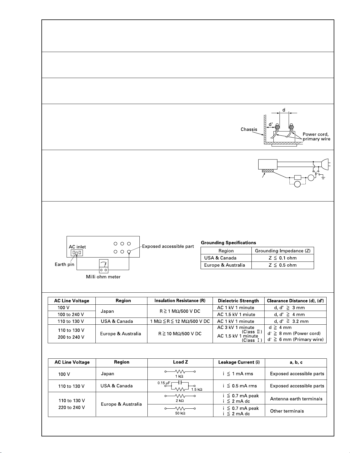
3. Clearance distance
When replacing primary circuit components, confirm specified clearance distance (d), (d’) between soldered terminals, and between terminals and surrounding metallic parts. See table 1
below.
Fig. 8
4. Leakage current test
Confirm specified or lower leakage current between earth ground/power cord plug prongs and
externally exposed accessible parts (RF terminals, antenna terminals, video and audio input and
output terminals, microphone jacks, earphone jacks, etc.).
Measuring Method : (Power ON)
Insert load Z between earth ground/power cord plug prongs and externally exposed accessible
parts. Use an AC voltmeter to measure across both terminals of load Z. See figure 9 and following
table 2.
Externally
exposed
accessible part
Fig. 9
Z
V
ab
A
c
5. Grounding (Class 1 model only)
Confirm specified or lower grounding impedance between earth pin in AC inlet and externally exposed accessible parts (Video in, Video out,
Audio in, Audio out or Fixing screw etc.).
Measuring Method:
Connect milli ohm meter between earth pin in AC inlet and exposed accessible parts. See figure 10 and grounding specifications.
Fig. 10
Table 1 Specifications for each region
Table 2 Leakage current specifications for each region
Note: These tables are unofficial and for reference only. Be sure to confirm the precise values for your particular country and locality.
II
S40888-01
Page 7
SECTION 1
DISASSEMBLY
1.1 HOW TO REMOVE THE MAJOR PARTS
1.1.1 Introduction
This set is a double-deck video recorder integrating a HDD
(Hard Disk Drive) and a VHS deck. Its internal structure is divided into three sections that include the power supply, VHS
and HDD sections. Therefore, the removal of major parts will
also be described under three separate sections as listed below.
1. COMMON section
2. VHS section
3. HDD section
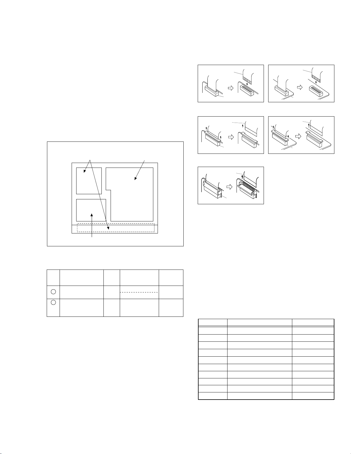
< TOP VIEW >
1. COMMON section
3. HDD section
2. VHS section
Fig. 1-1-1
1.2 HOW TO READ THE DISASSEMBLY AND ASSEMBLY
Step/
Loc No.
1
Top cover, Bracket COM1
Front panel
2
assembly
Fig. No.
4(S1), 3(S2), 2(L1), (L2)
2(S3)
COM2 8(L3),
CN7507(WR1),
CN3011(WR2)
Point NotePart name
—
<Note
1,2,3,4>
§§ §§ §
(1) (2) (3) (4) (5)
(1) Order of steps in Procedure
When reassembling, perform the step(s) in the reverse order.
These numbers are also used as the identification (location) No.
of parts Figures.
(2) Part name to be removed or installed.
(3) Fig. No. showing procedure or part location.
(4) Identification of part to be removed, unhooked, unlocked,
released, unplugged, unclamped or unsoldered.
P= Spring, W= Washer, S= Screw, L= Locking tab, SD= Solder,
CN**(WR**)= Remove the wire (WR**) from the connector
(CN**).
Note:
• The bracketed ( ) WR of the connector symbol are as-
signed nos. in priority order and do not correspond to
those on the spare parts list.
(5) Adjustment information for installation
1.3 DISCONNECTION OF CONNECTORS (WIRES)
FPC
CONNECTOR
FPC
CONNECTOR
Fig. 1-3-1 Fig. 1-3-2
FPC
CONNECTOR
FPC
CONNECTOR
Fig. 1-3-3 Fig. 1-3-4
FPC
CONNECTOR
Fig. 1-3-5
1.4 SCREWS USED CABINET COMPONENTS AND
BOARD ASSEMBLIES
Table 1-4-1 below shows the symbols, shapes, colors and
part numbers of screw that are used in the cabinet components and board assemblies and are appearing in the disassembling/reassembling diagrams in this manual.
When screwing them again in reassembling, be sure to use
them correctly referring to the following table.
Notes:
• Screw that are asterisked (marked with*) in the shape col-
umn are fixed with screw lock agent. If such the screw is
once removed, never use it again.
• The Screw symbols are assigned nos. in priority order and
do not correspond to those on the spare parts list.
SYMBOL PARTS NO. COLOR
S1 QYTDST3006R SILVER BLACK
S2 QYTDST3006M BLACK
S3 QYTDSF3010Z GOLD
S4 QYTDSF2606Z GOLD
S5 QYTDST3006Z GOLD
S6 QYTDSF3008M BLACK
S7 QYTDST2610Z GOLD
S8 PQ40413 BLACK
S9 LP40700-001A BLACK
S10 LP40738-001A GOLD
Table 1-4-1
1-1
Page 8
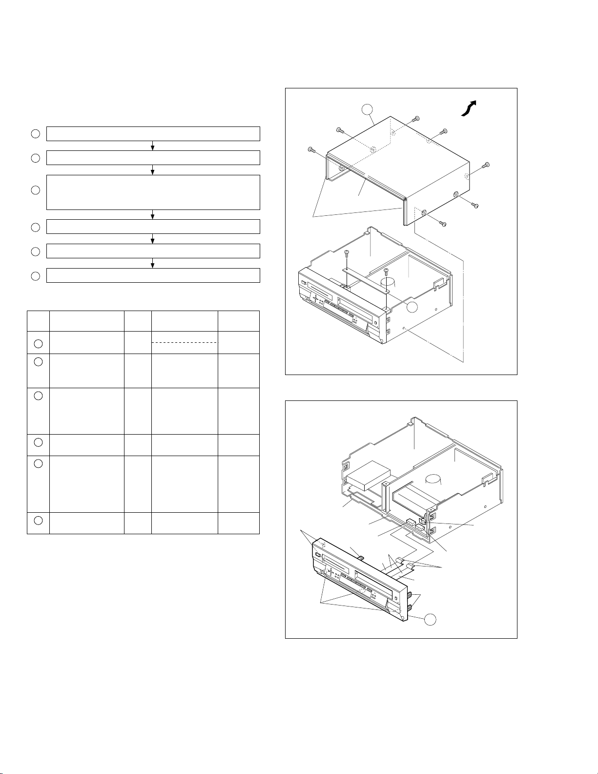
HOW TO REMOVE THE MAJOR PARTS <COM section>
1.5
1.5.1 Disassembly flow chart
This flowchart shows the disassembly procedure for the exterior parts and electrical parts.
Basically, reverse this procedure when assembling them.
1 Top cover, Bracket
2 Front panel assembly
Display board assembly, LED/SW board assembly,
3
Eject SW board assembly, Jack board assembly,
LED board assembly
4 SW REG board assembly
5 Regulator board assembly
6 Rear cover
Disassembly/assembly method <COM section>
1.5.2
Step/
Loc No.
Top cover, Bracket COM1
1
Front panel
2
assembly
Fig. No.
4(S1), 3(S2), 2(L1), (L2)
2(S3)
COM2 8(L3),
CN7507(WR1),
Point NotePart name
—
<Note
1,2,3,4>
CN3011(WR2)
Display board assembly,
3
LED/SW board assembly,
Eject SW board assembly,
COM3 15(S4)
—
Jack board assembly,
LED board assembly
SW REG board
4
assembly
Regulator board
5
assembly
COM4 2(S5), 2(L4), (L5)
CN5301(WR3),
COM5 3(L6),
CN5322(WR4),
CN5321(WR5),
<Note 1,
4>
<Note 1,
4>
CN5325(WR6),
CN5326(WR7),
CN5323(WR8)
6
COM6 4(S2), 6(S6),
Fan motor
<Note 5>Rear cover
<Note 1>
When attaching the FPC, be sure to connect it in the correct orientation.
<Note 2>
When attaching the front panel assy, make sure that the
door openers of cassette housing assembly is in the down
position.
<Note 3>
When attaching the FPC take care that it is not caught.
Pass the two VHS-side FPCs below the base (1).
<Note 4>
When removing the SW REG board assembly or Regulator board assembly, unhook the several spacers connecting it with pliers from the top side.
<Note 5>
Perform the work by leaving fan motor attached to the rear
cover except when replacing the fan motor.
When attaching the rear cover, please be careful with the
wiring.
1
(S1)
(L3)
(L1)
(L3)
2
(S1)
Digital board
assembly
Base (1)
(L3)
(L2)
8
(S3)
Top cover
1
CN3011
<Note 3>
WR2
(S2)
9
(S3)
1
Fig. COM1
Fig. COM2
6
Bracket
WR1
(L3)
2
5
(S2)
3
(S1)
CN7507
<Note 1>
Supporing
tape side
(S2)
4
(S1)
<Note 2>
7
1-2
Page 9
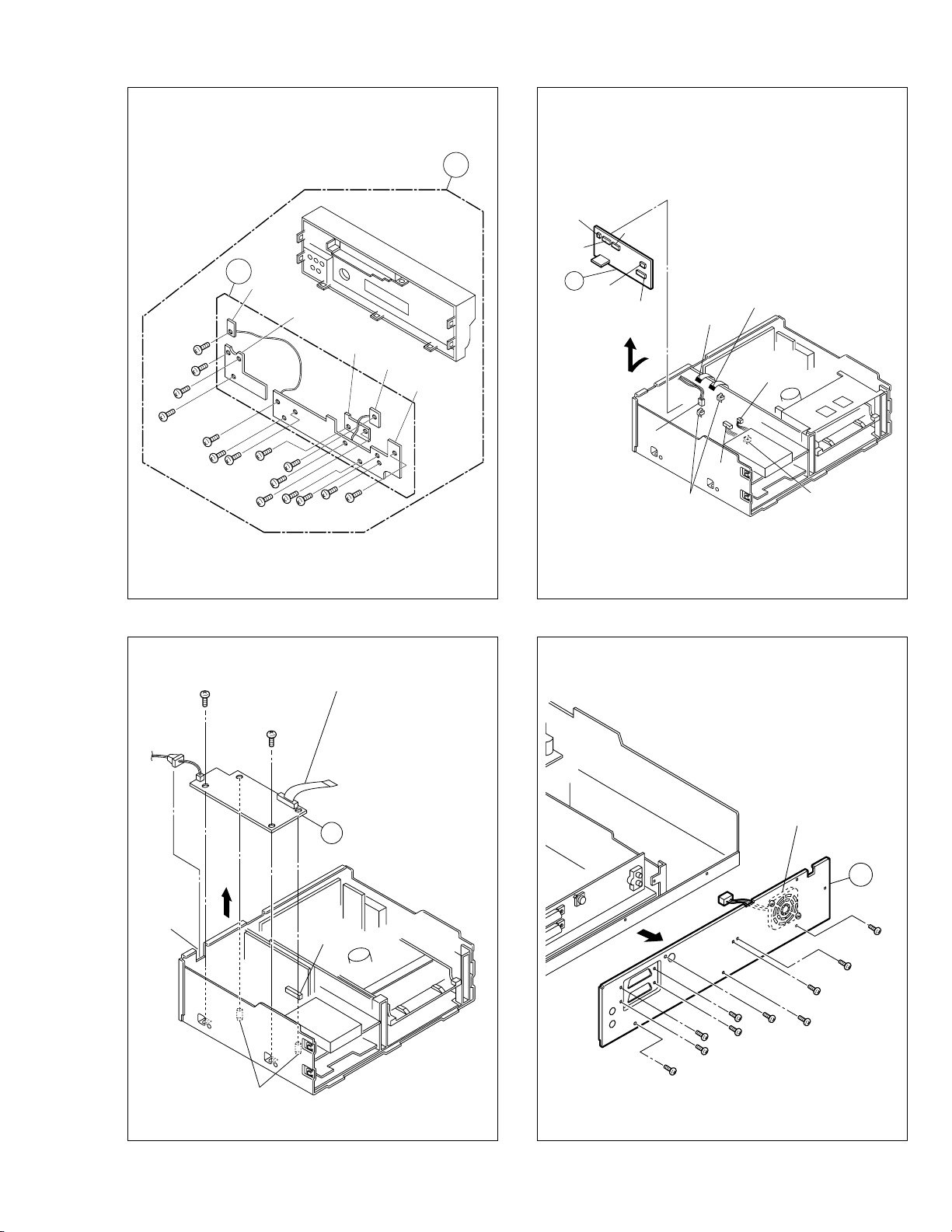
24
5
CN5325
CN5326
WR8
WR5
Foil side
<Note 1>
WR4
Foil side
<Note 1>
WR6
WR7
CN5321
CN5322
(L6)
Spacer
<Note 4>
(L6)
Spacer
<Note 4>
CN5323
(S4)
23
(S4)
(S4)
22
(S4)
2
3
Eject SW
board assembly
Jack
board assembly
12
(S4)
LED/SW
board assembly
11
10
(S4)
(S4)
LED board assembly
Display board
assembly
21
17
(S4)
16
(S4)
15
(S4)
(S4)
18
(S4)
19
20
(S4)
14
(S4)
13
(S4)
(L5)
26
(S5)
Spacer
<Note 4>
(L4)
Fig. COM3
27
(S5)
Fig. COM4
WR3
Supporting
tape side
<Note 1>
4
CN5301
28
(S2)
Fig. COM5
32
(S6)
(S6)
33
(S6)
Fig. COM6
35
34
(S6)
36
(S6)
<Note 5>
Fan Motor
37
(S6)
29
(S2)
30
(S2)
6
31
(S2)
1-3
Page 10
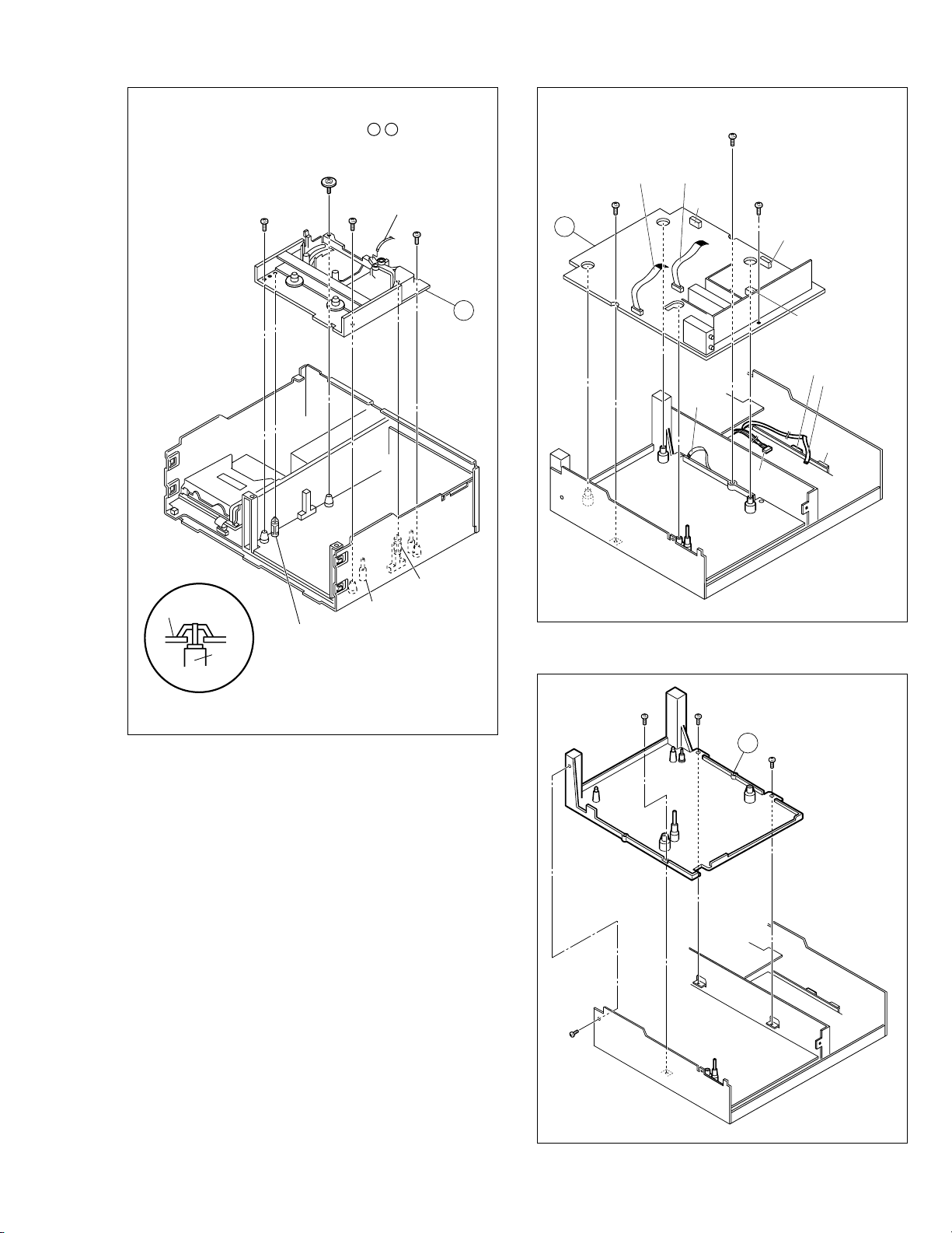
HOW TO REMOVE THE MAJOR PARTS <VHS section>
1.6
1.6.1 Disassembly flow chart
This flowchart shows the disassembly procedure for the exterior parts and electrical parts.
Basically, reverse this procedure when assembling them.
However, it is required to remove the common section parts
as far as 1 “Top cover Bracket” and 2 “Front panel assembly” in advance. (See section 1.5.)
1 Drum assembly
2 Mechanism assembly
3 Main board assembly
4 Base (1)
Procedures for Lowering the Cassette holder assembly
As the mechanism of this unit is integrated with the Housing
assembly, the holder must be lowered and the two screws unscrewed when removing the Mechanism assembly.
Fig. 2
Fig. 1
1.6.2 DIsassembly/assembly method <VHS section>
Step/
Loc No.
Drum assembly
1
(Inertia plate)
(Roller arm assy)
2
Mechanism
assembly
Main board
3 <Note 2>
assembly
Base (1) V4 (S3), 3(S5)4 —
Fig. No.
V1
3(S7), CON1(WR9),
CN1(WR10)
4(L1)
(P1), (L2)
V2
2(S3), (S8), (S9),
(L3), (L4),
CN1(WR11),
V3 2(S3), (S5),
CN5321(WR5),
CN5322(WR4),
CN3014(WR14),
CN703(WR15),
CN2601(WR16)
Point NotePart name
<Note 1,2>
<Note 2,4>
<Note 1>
When attaching or removing the FPC, take care not to disconnect any of the wires.
<Note 2>
When attaching the FPC, be sure to connect it in the correct orientation.
<Note 3>
When attaching wires, connect them in the correct orientation.
Fig. 3
Turn the loading motor pulley in the direction as indicated by
Fig.2. As both A and B levers are lodged twice, push the
levers in the direction as indicated by Fig.3 to release them.
When pushing the levers, do it in the order of A , B , B , A .
When the holder has been lowered, turn the pulley until the
cassette holder is securely in place without allowing any up/
down movement.
Procedures for Lowering the Cassette holder assembly
Note: When installing the Drum assembly, secure the
screws (S7) in the order of a , b , c .
Roller arm
assy
Inertia plate
(L1)
(P1)
(L2)
(S7)
1
a
2
(S7)
WR9
Foil side
c
<Note 2>
CON1
3
(S7)
b
WR10
Foil side
<Note 1,2>
1
Cleaner assy
<Note 4>
• When it is required to remove the screws (S3) retaining the
Mechanism assembly, please refer to the “Procedures for
Lowering the Cassette holder assembly”(See on page 1-5).
• When removing the Mechanism assembly only, unhook the
two spacers connecting it with the Main board assembly with
pliers from the back side of the Main board assembly first,
and then remove the Mechanism assembly.
• When reattaching the Mechanism assembly to the Main
board assembly, take care not to damage the sensors on
the Main board assembly (D3001: LED, Q3002: Start sensor, Q3003: End sensor, S3002: S cassette switch).
1-4
Not use
CN1
Fig. V1
Page 11
8
(S3)
10
(S5)
9
(S3)
WR16 Foil side
<Note 2>
CN5322
CN703
WR15
CN2601
CN3014
WR4
Foil side
<Note 2>
WR5
Foil side
<Note 2>
WR14
Foil side
<Note 2>
CN5321
3
Note: When installing the Mechanism assembly, secure
the screws (S8) in the order of a , b .
6
5
(S3)
<Note 4>
(S8)
4
(S3)
<Note 4>
WR11
Foil side
<Note 2>
(S9)
7
2
(L4)
Spacer
<Note 4>
12
(S5)
Fig. V3
13
(S5)
4
14
(S5)
Mechanism assy
<Note 4>
Spacer
(L3)
Spacer
<Note 4>
Fig. V2
S3002
S cassette switch
<Note 4>
11
(S3)
Fig. V4
1-5
Page 12
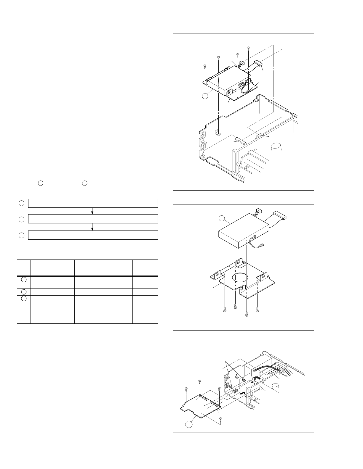
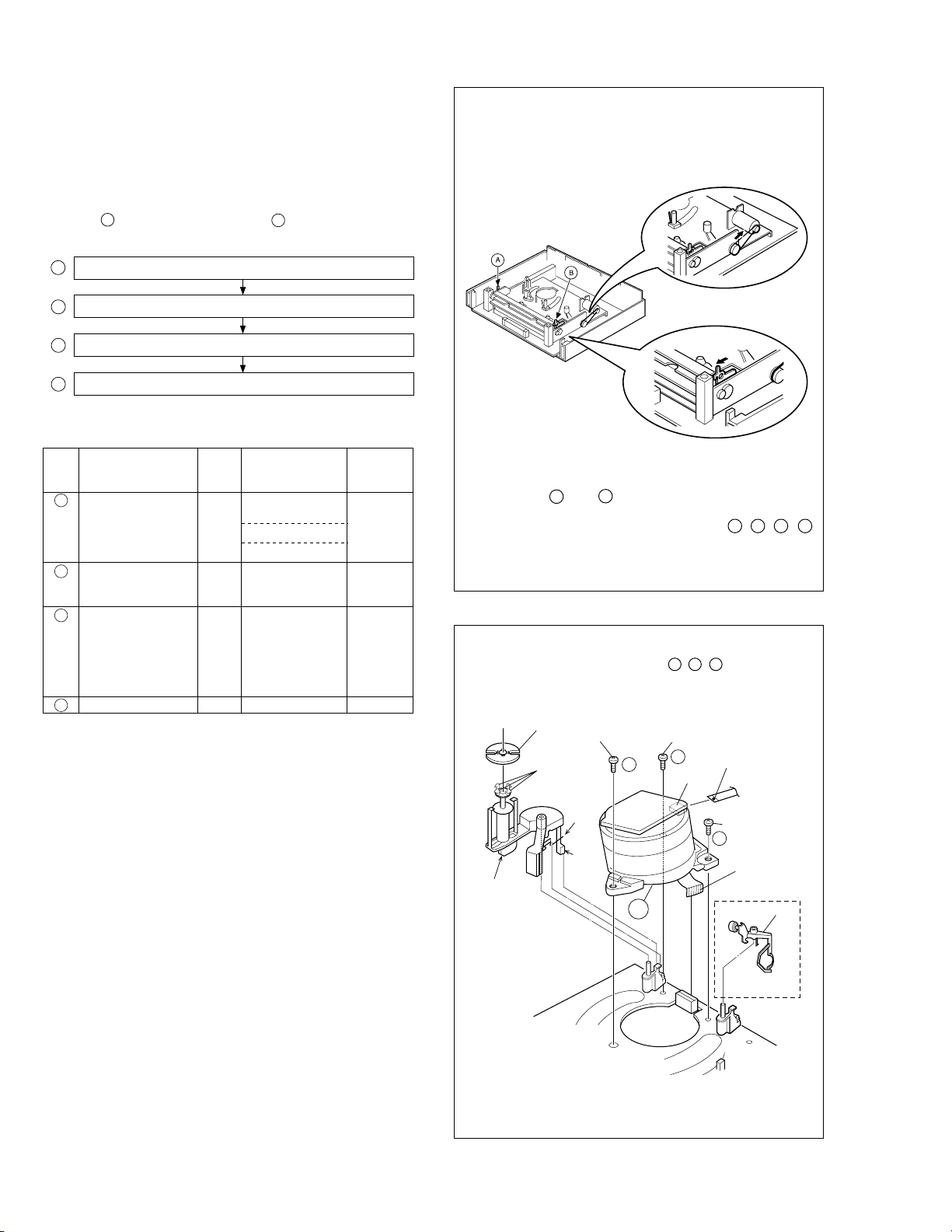
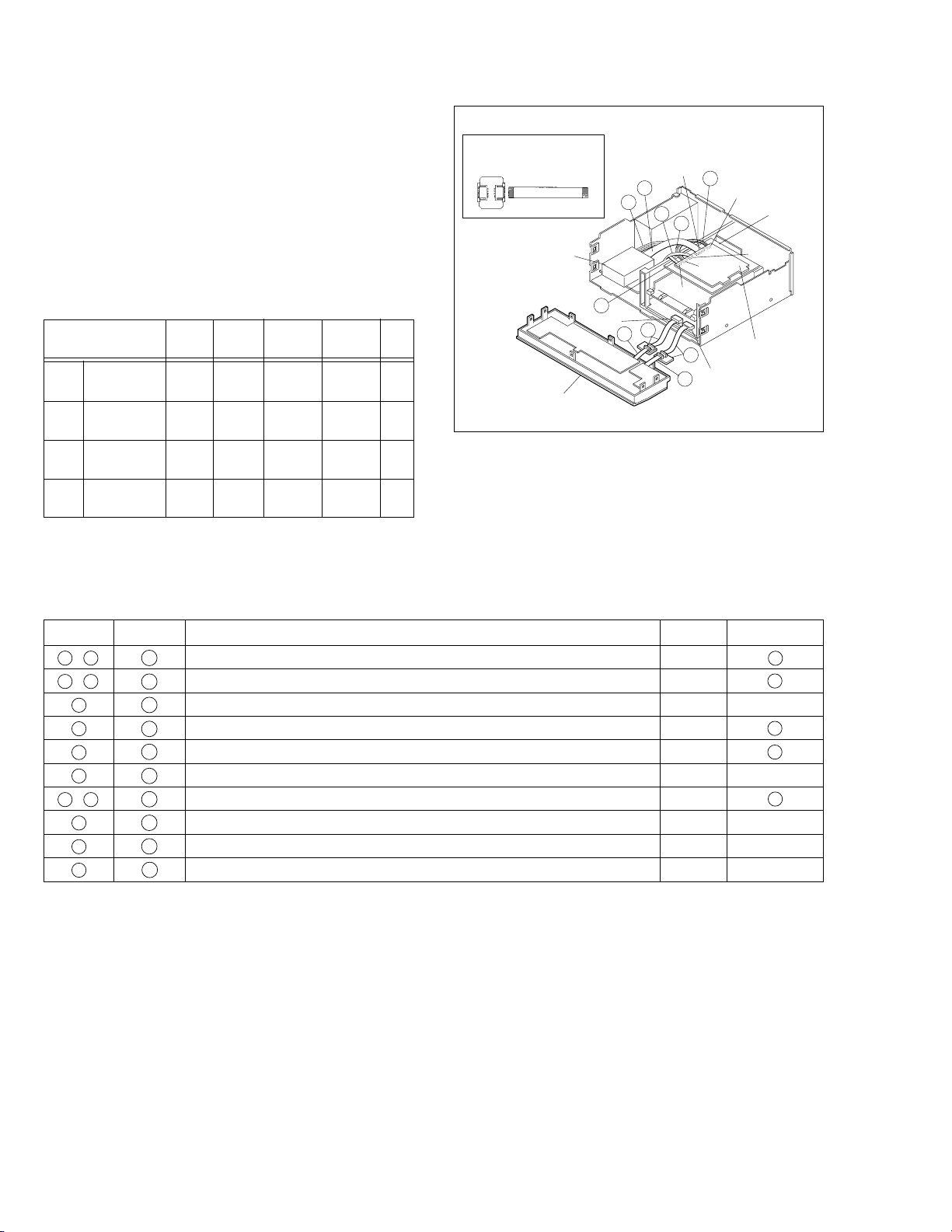
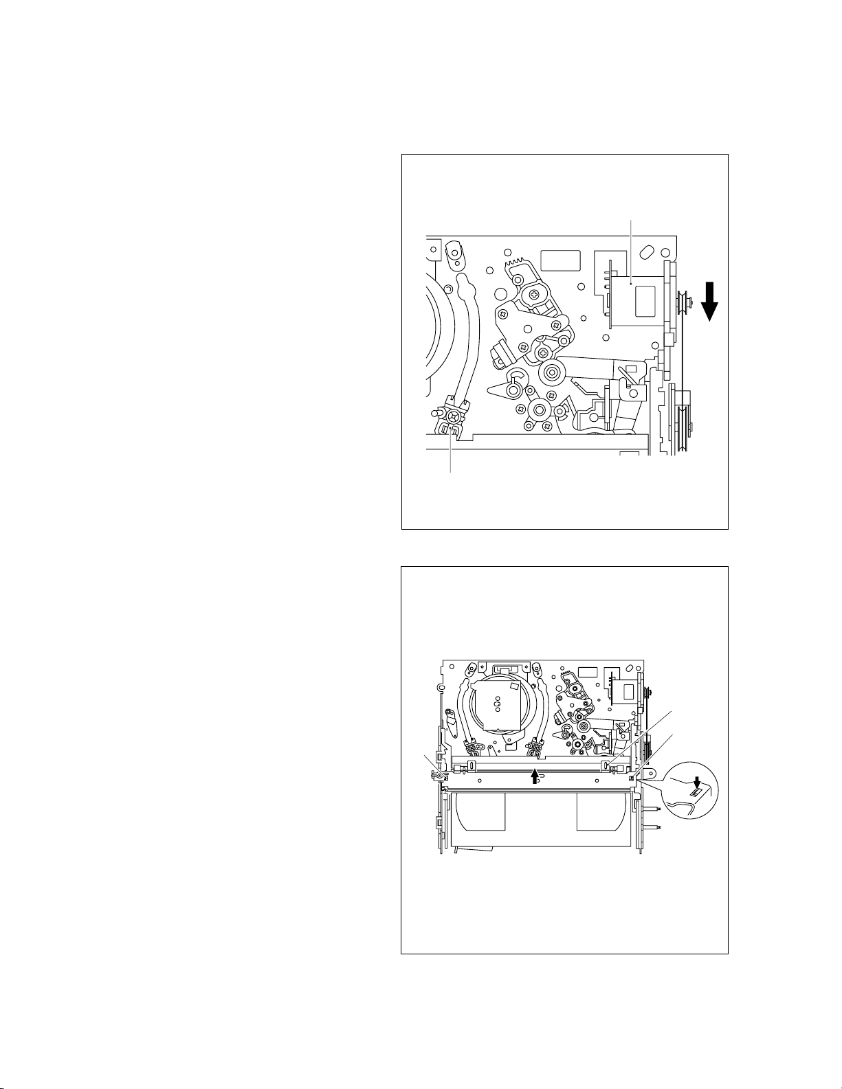
Hard Disk Drive (HDD) Handling Precautions
The HDD is a precision device for use in reading and writing
a large amount of data on or from a disk rotating at a high
speed. If it is not handled carefully, either abnormal operation may result or it may not be possible to read data. The
HDD is sensitive to the following items and special care is
required in safeguarding against them when handling an
HDD. Also take care in handling a set incorporating an HDD.
1 Hard disk drive assembly
2 Hard disk
3 Digital board assembly
1.7
HOW TO REMOVE THE MAJOR PARTS <HDD section>
1.7.1 Disassembly flow chart
This flowchart shows the disassembly procedure for the exterior parts and electrical parts.
Basically, reverse this procedure when assembling them.
However, it is required to remove the common section parts
as far as 1 “Top cover” and 2 “Front panel assembly” in advance. (See section 1.5.)
1 Hard disk drive assembly
1
(S5)
1
<Note 1>
(S5)
2
WR7
Frame
CN8001
3
(S5)
Fig. H1
(S5)
4
WR15
Earth
wire
<Note 2>
CN5326
2 Hard disk drive
3 Digital board assembly
1.7.2 DIsassembly/assembly method <HDD section>
Step/
Loc No.
1
Hard disk drive
assembly
2
Hard disk drive H2
3
Digital board
assembly
Fig. No.
H1 4(S5),
H3 4(S5),
Point NotePart name
<Note 1,2>
CN5326(WR15)
4(S10)
<Note 3,4>
CN8901(WR8),
CN8002(WR12),
CN8601(WR13),
CN8801(WR14)
<Note 1>
With due regard to operational considerations, remove the
parts located on the frame (Hard disk drive) together before removing the major parts.
<Note 2>
When attaching the hard disk drive assembly, be sure to
connect the earth wire.
<Note 3>
• When connecting or disconnecting the connector or wire,
take care not to damage them.
• When connecting the flat wire to the connector, be sure
to connect it in the correct orientation.
<Note 4>
When removing the board assembly, take care not to damage it.
(S5)
9
3
10
(S5)
CN8901
CN8002
Frame
CN8601
<Note 4>
12
(S5)
CN8801
2
5
(S10)
11
(S5)
6
(S10)
Fig. H2
7
(S10)
8
(S10)
WR13
WR8
WR12
Foil side
<Note 3>
WR14
Supporting
tape side
<Note 3>
1-6
Fig. H3
Page 13
1.8 SERVICE POSITIONS
The servicing locations for use in troubleshooting or servicing of the set are provided separately for the VHS and HDD.
I SERVICE POSITIONS <VHS SIDE>
II SERVICE POSITIONS <HDD SIDE>
1.8.1 Service position <VHS SIDE>
<Removal>
(1) Remove the top cover and bracket.
(2) Remove the front panel assembly.
(3) Remove the MAIN board assembly together with the
mechanism assembly.
Fig. No.
(Page)
(1)
Top cover,
COM1 9 2 + 1
Bracket (1-3) (No.1-9) (L1,2)
(2) Front
panel
COM2 0 8 2
(1-3) (L3) (CN7507/ —
assembly
(3) Rear
cover
(4) Main
board
COM6 10 0 1
(1-3)
V2, V3 7 0 5
(1-6) (No.4-10) (CN5321/
assembly
(etc.)
Screw Hook, etc. Connector Note
0 —
CN3011)
(No.28-37)
(CN5325)
CN5322/
CN3014/
—
—
CN703/
CN2601)
< Installation >
(1) Stand up the bottom chassis assembly so that the Regu-
lator side is in the lower position.
(2) Connect the PATCH CORD to the three FPCs then con-
nect CN3014, CN7508 and CN7509.
(3) By connecting a total of two FPCs and wires (CN703/
CN2601), carry out the installation so that the Main board
assembly comes in the upper position.
Point: • Take care that the FPCs and wires are not
subjected to stress in this positioning.
(4) Connect the PATCH CORDS to the two FPCs of the front
panel assembly, then connect the CORDS to the
CN7507/CN3011.
For the PATCH CORD is required, see Table 1-8-2.
Board to Board WIRE
A PTU94022-10 QUQ112-1040CG
B PTU94022-18 QUQ112-1840CG
C PTU94022-13 QUQ212-1340CG
D PTU94022-15 QUQ212-1540CG
E YTU94072-06 QUQ210-0640CG
Table 1-8-2
Table 1-8-1
PATCH CORD
PTU94017B
Front panel assembly
Main board assembly
CN7509
CN7507
A
1
CN3011
CN3014
B
2
CN703
E
CN7508
CN2601
6
7
D
C
3
CN8801
4
CN5322
5
CN5321
CN8601
CN8002
Fig. 1-8-1 Service position <VHS side>
1-7
Page 14
1.8.2 Service position <HDD SIDE>
(1) Remove the exterior parts (Top cover and front panel as-
sembly).
(2) Remove the hard disk drive(HDD) together with the frame.
(3) Remove the digital board assembly together with the wires
attached to it, and place the assembly upside down on
an insulated mat that is placed on the mechanism (VHS)
assembly.
(4) Mount the HDD that was removed in (2) to its original
position on the bottom chassis assembly, and connect
the wires to the connector CN8001 on the digital board
assembly and to the connector CN5326 on the regulator
board assembly.
Fig. No.
(Page)
Screw
(No.)
Hooks,
etc. (No.)
Connectors
Note
(1) Top cover, COM1 9 2 + 1 0 —
Brackets (1-3) (No.1-9) (L1, L2)
(2) Front panel COM2 0 8 (L3)
2(CN7507,
—
assembly (1-3) CN3011)
Hard disk drive
(3)
H1 4 0
2 (CN8001,
—
assembly (1-6) (No.1-4) CN5326)
(4) Digital board H3 4 0 0 —
assembly
(No.9-12)
Table 1-8-3
PATCH CORD
PTU94017B
Hard disk drive
assembly
Front panel assembly
6
CN3011
CN8001
7
CN8801
3
A
1
10
CN8601
CN7507
8
9
B
2
Fig. 1-8-2 Service position <HDD side>
CN8901
Insulation sheet
CN8002
Digital board
assembly
Note :
•
The symbol numbers in the following table are special numbers indicating the service positions. They do not coincide with the symbol numbers used in Fig. 1-10-1 (1-10) or Table 1-10-1 (1-11).
SYMBOL CONNECTOR (WIRE) CONNECTIONS
PIN No
PATCH CORD
I / II 1 MAIN CN7507 — JACK CN7002 10 A
I / II 2 MAIN CN3011 — DISPLAY CN7001 18 B
I 3 TERMINAL CN703 — DIGITAL CN8601 6 —
I 4 MAIN CN7508 — REGULATOR CN5322 13 C
I 5 MAIN CN7509 — REGULATOR CN5321 15 D
I 6 MAIN CN2601 — DIGITAL CN8801 8 —
I / II 7 MAIN CN3014 — DIGITAL CN8002 6 E
II 8 DIGITAL CN8001 — HARD DISK DRIVE 40 —
II 9 REGULATOR CN5326 — HARD DISK DRIVE 4 —
II 10 REGULATOR CN5323 — DIGITAL CN8901 9 —
Table 1-8-4 Connection of Connectors
1-8
Page 15
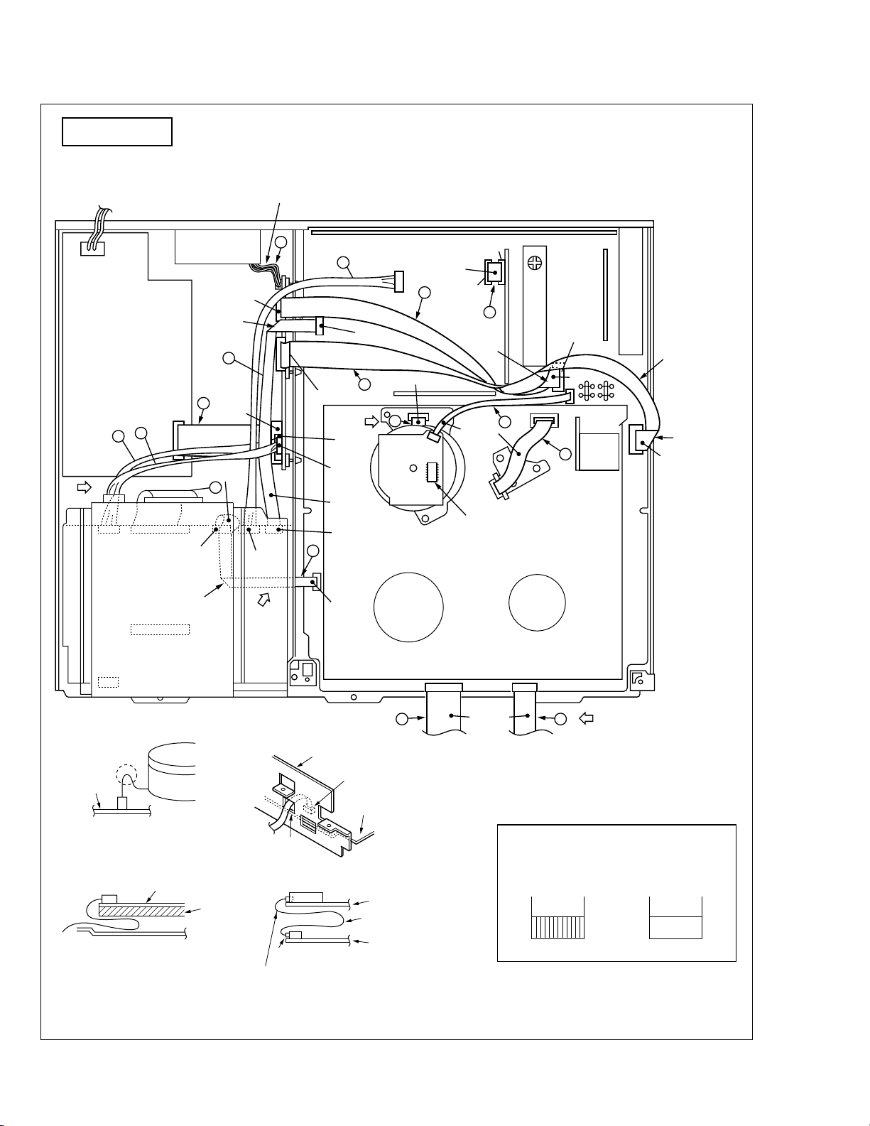
1.9 MECHANISM SERVICE MODE
This model has a unique function to enter the mechanism
into every operation mode without loading of any cassette
tape. This function is called the “MECHANISM SERVICE
MODE”.
1.9.1 How to set the "MECHANISM SERVICE MODE"
(1) Disconnect VCR from AC.
(2) Connect TPGND and TP7001 (TEST) on the Display
board assembly with a jump wire.
(3) Connect VCR to AC.
(4) Press the POWER button.
(5) With lock levers A B on the left and right of the Cassette
holder assembly pulled toward the front, slide the holder
in the same direction as the cassette insertion direction.
(For the positions of lock levers A B , refer to the “Pro-
cedures for Lowering the Cassette holder assembly” on
page 1-5 of 1.6 HOW TO REMOVE THE MAJOR PARTS
<VHS section>
(6) The cassette holder lowers and, when the loading has
completed, the mechanism enters the desired mode.
Swithing regulator
board assembly
Hard disk drive
(HDD)
Fan motor
Regulator
board assembly
Main board assembly
TPGND
Terminal board assembly
S-Sub
board assembly
VR701
DV AG C
TP701
On screen
D AGC
board assembly
TP106
PB FM
VHS mechanism
CN3011 CN7507
3D Digital
/2M board
assembly
VR1401
D/A
LEVEL ADJ
Demodulator
board
assembly
TP2253
A.PB FM
TP4001
CTL.P
TP111
D.FF
TP7001
TEST
TPGND
PATCH CORD
PTU94022-18
QUQ112-1840CG
LED SW
board assembly
LED board assembly
<Front panel assembly>
Display board assembly
Fig. 1-9-1
Supporting
tape side
PATCH CORD
PTU94022-10
QUQ112-1040CG
Jack board assembly
Eject SW board assembly
1-9
Page 16
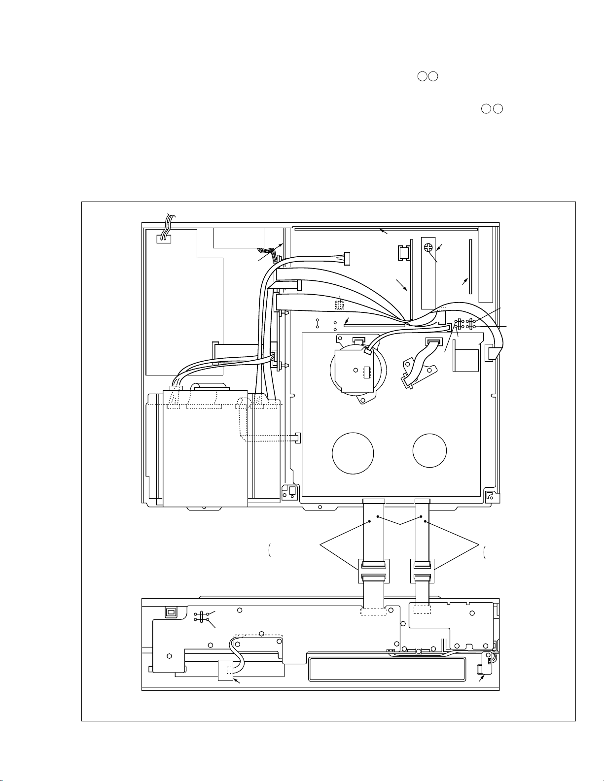
1.10 CONNECTION
TOP VIEW
Treat wire so as not to come to the FAN motor.
CN5325
CN8601
C
6
Foil side
Foil side
CN5321
Foil side
Make a
crease.
12
CN3014
13
CN5323
(Middle)
CN5326
(Upper)
Foil side
CN8801
Foil side
CN2601
Supporting
5
tape side
A
CN703
10
DRUM
Supporting
tape side
4
CON1
FAN motor
CN5322
Make a
crease.
14
3
CN5301
Supporting
tape side
Supporting
tape side
Supporting
tape side
CN8002
(Lower)
15
CN5201
7
8
D
CN8901
CN8001
Make a crease.
CN8201
CN512
CN7506
16
Make a
crease.
CN1
Foil side
CN1
A/C HEAD
Should be confirmed that wire
not touch to IC of the Stator
board assembly.
CN7508
Treat the wire
CN7509
Supporting
tape side
according to the
figure not to
overlap in TP.
Make a crease.
Foil side
CN2001
9
CN3001
11
CN8202
DETAIL "A" DETAIL "C"
DRUM
Chassis
B
Main board
assembly
Absorb the looseness of
the wire in the B part.
DETAIL "B"
Treat the front wires
according to the figure.
CN1
Main board assembly
Base(1)
Treat the wire
through the hole.
DETAIL "D"
HDD
CN8001
The wire should be
does not touch from edge.
CN3011 CN7507
CN3014
Main board
assembly
Frame
The excessive length portion of
wire should be treat as figure.
Digital board
assembly
Fig. 1-10-1 Top view
Foil side
12
B
[CAUTION]
Insert the FPC wires as shown below.
Foil side Supporting tape side
1-10
Page 17
Fig.
No.
Symbol
Connection
Pin No.
Connected point ←→ Connected point
Type
(FPC/
WIRE)
1 WR1 MAIN CN7507 ←→ JACK CN7002 10 FPC
2 WR2 MAIN CN3011 ←→ DISPLAY CN7001 18 FPC
3 WR3 REGULATOR CN5301 ←→ SW REG CN5201 19 FPC
4 WR4 REGULATOR CN5322 ←→ MAIN CN7508 13 FPC
5 WR5 REGULATOR CN5321 ←→ MAIN CN7509 15 FPC
6 WR6 REGULATOR CN5325 ←→ FAN MOTOR — 2 WIRE
7 WR7 REGULATOR CN5326 ←→ HDD — 4 WIRE
8 WR8 REGULATOR CN5323 ←→ DIGITAL CN8901 9 WIRE
9 WR9 DRUM MOTOR CON1 ←→ MAIN CN3001 5 FPC
10 WR10 MAIN CN1 ←→ UPPER DRUM — 11 FPC
11 WR11 A/C HEAD CN1 ←→ MAIN CN2001 7 FPC
12 WR12 MAIN CN3014 ←→ DIGITAL CN8002 6 FPC
13 WR13 MAIN CN703 ←→ DIGITAL CN8601 6 WIRE
14 WR14 MAIN CN2601 ←→ DIGITAL CN8801 8 FPC
15 WR15 DIGITAL CN8001 ←→ HDD — 40 WIRE
16 — MAIN CN7506 ←→ S-SUB CN512 14 FPC
—— DIGITAL CN8201 ←→ Jig CONN. CABLE — 100 WIRE
—— DIGITAL CN8202 ←→ Jig CONN. CABLE — 6 FPC
Table 1-10-1 Connection
1-11
Page 18
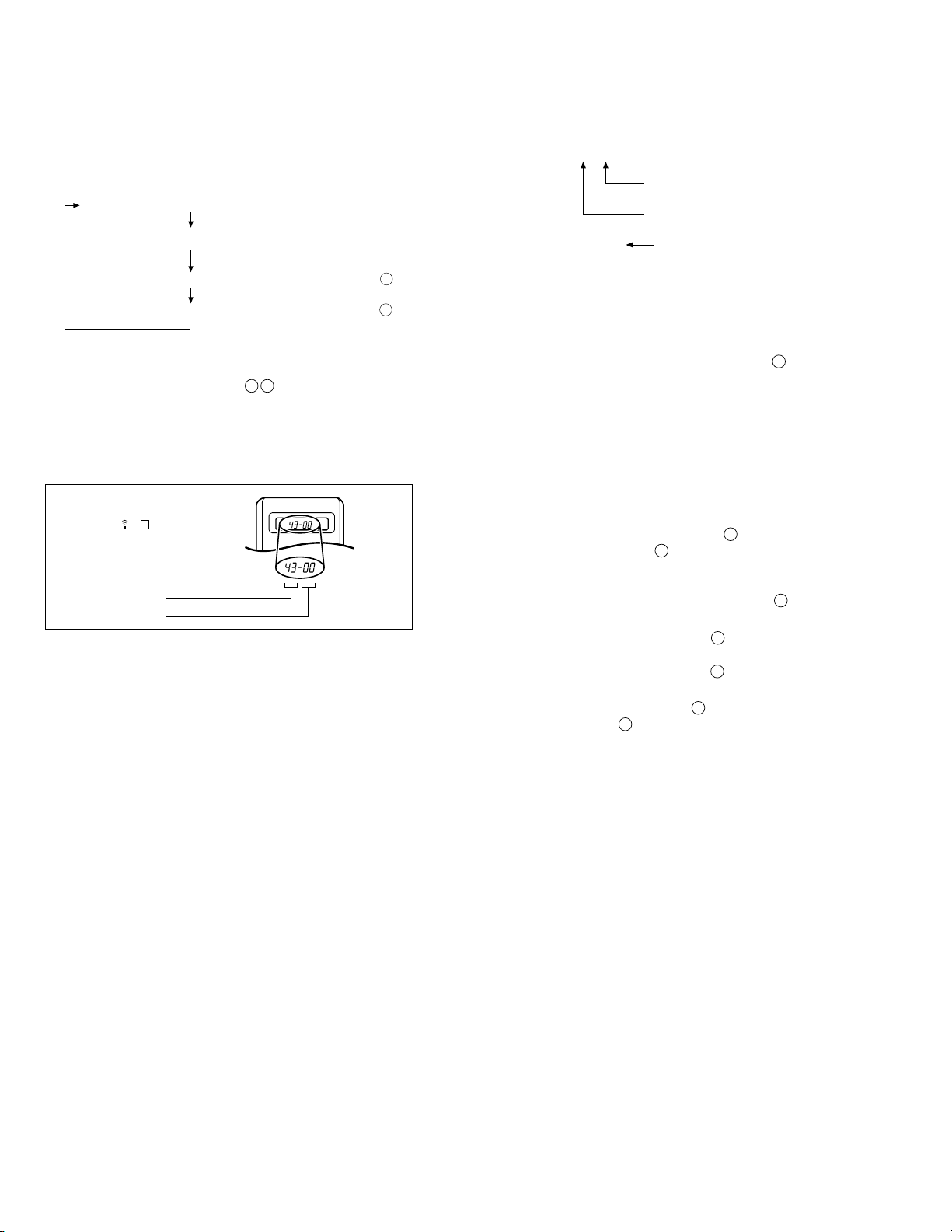
1.11 EMERGENCY DISPLAY FUNCTION
This unit has a function for storing the history of the past two
emergencies (EMG) and displaying them on each FDP. With
the status of the VCR and mechanism at the moment an emergency occurred can also be confirmed.
FDP display switching
FDP display
Notes:
•
The emergency detail display
on the latest emergency.
It becomes “ – – : – – : – –” when there is no latest emergency record.
•
When using the Jig RCU, set its custom code to match
the custom code of the VCR.
Jig RCU
[Data transmitting method]
Depress the “ ” ( 3 ) button
after the data code is set.
0 : 00 : 00
E: **:
1: *2 : 34
*
5: *6 :
*
CUSTOM CODE
43: A CODE
53: B CODE
6F: C CODE
7F: D CODE
DATA CODE
Fig. 1-11-1 Jig RCU [PTU94023B]
Normal display
Emergency content display
**
(E:Latest:Previous)
Emergency detail display
Emergency detail display
7
*
1 2
show the information
1
2
INITIAL MODE
1.11.1 Displaying the emergency information
(1) Transmit the code “59” from the Jig RCU.
The FDP shows the emergency content in the form of
“E:
:**”.
**
Example 1 E : 01 :
Example 2 E : –– :
Note:
For the emergency content, see “1.11.3 Emergency content description”.
(2) Transmit the code “59” from the Jig RCU again.
The FDP shows the emergency detail information 1 in the
form of “
*
*
3 – : Mechanism sensor information at the moment of
– 4 : Mechanism mode position at the moment of emer-
Note:
•
For the emergency detail information
Emergency detail information
(3) Transmit the code “59” from the Jig RCU once again.
The FDP shows the emergency detail information 2 in the
form of “
*
*
*
Note:
•
For the emergency detail information 2 , see “1.11.5 Emergency detail information
1 : *2 : 34”.
*
1 : Deck operation mode at the moment of emergency
2 : Mechanism operation mode at the moment of emer-
gency
emergency
gency
5 : *6 :
*
5 : Type of the cassette tape in use 1 .
6 : Winding position of the cassette tape in use
7 : Type of the cassette tape in use 2 (Winding area)
03
Previous emergency
Latest emergency
––
No emergency record
1
, see “1.11.4
1
”.
7 ”.
*
2
”.
1-12
(4) Transmit the code “59” from the Jig RCU once again to re-
set the display.
1.11.2 Clearing the emergency history
(1) Display the emergency history.
(2) Transmit the code “36” from the Jig RCU.
(3) Reset the emergency display.
Page 19
1.11.3 Emergency content description
Emergency contents “E08/E09” are for the model with Dynamic Drum (DD).
Note:
FDP CONTENT CAUSE
1
E01: Loading EMG
E02:
Unloading EMG
E03: Take Up Reel
Pulse EMG
E04: Drum FG
EMG
E05: Cassette Eject
EMG
E06: Capstan FG
EMG
E07: SW Power
Short-Circuit
EMG
E08:
HDD
Communication EMG
E09: DD FG EMG
E0A:Supply Reel
Pulse EMG
EC1 or EU1:
Head clog warning
When the mechanism mode cannot be changed to another mode even when the loading motor has rotated
for more than 4 seconds in the loading direction, [E:01]
is identified and the power is turned off.
When the mechanism mode cannot be changed to another mode even when the loading motor has rotated
for more than 4 seconds in the unloading direction, [E:02]
is identified and the power is turned off.
When the take-up reel pulse has not been generated for
more than 4 seconds in the capstan rotating mode, [E:03]
is identified, the pinch rollers are turned off and stopped,
and the power is turned off. However, the reel EMG is
not detected in STILL/SLOW modes.
When the drum FG pulse has not been input for more
than 3 seconds in the drum rotating mode, [E:04] is identified, the pinch rollers are turned off and stopped, and
the power is turned off.
When the eject operation does not complete in 3 seconds after the start, [E:05] is identified, the pinch rollers
are turned off and stopped, and the power is turned off.
When the cassette insertion operation does not complete
in 3 seconds after the start, the cassette is ejected. In
addition, when the operation does not complete within
3 seconds after the start, [E:05] is also identified and the
power is turned off immediately.
When the capstan FG pulse has not been generated for
more than 1 second in the capstan rotating mode, [E:06]
is identified, the pinch rollers are turned off and stopped,
and the power is turned off.However, the capstan EMG
is not detected in STILL/SLOW/FF/REW modes.
When short-circuiting of the SW power supply with GND
has lasted for 0.5 second or more, [E:07] is identified,
all the motors are stopped and the power is turned off.
When the KBUS_DATA signal did not reach the pin-46
of the System controller CPU (IC3001) on the main board
assembly, [E:08] is identified, "POWER ON" operation
is rejected.
When the DD FG pulse is not generated within 2.5 seconds, [E:09] is identified, the tilt motor is stopped and
the power is turned off.
When the supply reel pulse has not been generated for
more than 10 seconds in the capstan rotating mode,
[E:0A] is identified and the cassette is ejected (but the
power is not turned off). However, note that the reel EMG
is not detected in the SLOW/STILL mode.
Presupposing the presence of the control pulse output in the PLAY mode, when the value obtained by mixing the two V.FM output
channels (without regard to the A.FM output) has remained below a certain threshold level for more than 10 seconds, [E:C1] or [E:U1]
is identified and recorded in the emergency history. During the period in which a head clog is detected, the FDP and OSD repeat the
“3-second warning display” and “7-second noise picture display” alternately.
EMG code : “E:C1” or “E:U1” / FDP : “U:01” / OSD : “Try cleaning tape.” or “Use cleaning cassette.”
The head clog warning is reset when the above-mentioned threshold has been exceeded for more than 2 seconds or the mode is
changed to another mode than PLAY.
The mechanism is locked in the middle of mode transition.
2
The mechanism is locked at the loading end due to the encoder position
reading error during mode transition.
3
Power is not supplied to the loading MDA.
1
The mechanism is locked in the middle of mode transition.
2
The mechanism is locked at the unloading end due to the encoder position reading error during mode transition.
3
Power is not supplied to the loading MDA.
1
The take-up reel pulse is not generated in the FWD transport modes (PLAY/
FWD SEARCH/FF, etc.) because;
1) The idler gear is not meshed with the take-up reel gear;
The idler gear is meshed with the take-up reel gear, but incapable of wind-
2)
ing due to too large mechanical load (abnormal tension);
3) The take-up reel sensor does not output the FG pulse.
2
The supply reel pulse is not generated in the REV transport modes (REV
SEARCH/REW, etc.) because;
1) The idler gear is not meshed with the supply reel gear.
2) The idler gear is meshed with the supply reel gear, but incapable of wind-
ing due to too large a mechanical load (abnormal tension);
3) The supply reel sensor does not output the FG pulse.
3
Power is not supplied to the reel sensors.
1
The drum could not start or the drum rotation has stopped due to too large
a load on the tape, because;
1) The tape tension is abnormally high;
2)
The tape is damaged or a foreign object (grease, etc.) adheres to the tape.
2
The drum FG pulse did not reach the System controller CPU because;
1) The signal circuit is disconnected in the middle;
2) The FG pulse generator (hall device) of the drum is faulty.
3
The drum control voltage (DRUM CTL V) is not supplied to the MDA.
4
Power is not supplied to the drum MDA.
1
The cassette cannot be ejected due to a failure in the drive mechanism of
the housing.
2
When the housing load increases during ejection, the loading motor is
stopped because of lack of headroom in its drive torque.
Housing load increasing factors: Temperature environment (low temperature, etc.), mechanism wear or failure.
3
The sensor/switch for detecting the end of ejection are not functioning normally.
4
The loading motor drive voltage is lower than specified or power is not supplied to the motor (MDA).
5
When the user attempted to eject a cassette, a foreign object (or perhaps
the user's hand) was caught in the opening of the housing.
1
The capstan could not start or the capstan rotation has stopped due to too
large a load on the tape, because;
1) The tape tension is abnormally high (mechanical lock);
2) The tape is damaged or a foreign object (grease, etc.) is adhered to the
tape (occurrence of tape entangling, etc.).
2
The capstan FG pulse did not reach the System controller CPU because;
1) The signal circuit is disconnected in the middle;
2) The FG pulse generator (MR device) of the capstans is faulty.
3
The capstan control voltage (CAPSTAN CTL V) is not supplied to the MDA.
4
Power is not supplied to the capstan MDA.
1
The SW 5 V power supply circuit is shorted with GND.
2
The SW 12 V power supply circuit is shorted with GND.
1 HDD is defective
2 KBUS_DATA signal is disconnected in the middle.
1 The FG sensor is defective. (The soldered parts have separated.)
2 The pull-up resistor at the FG sensor output is defective. (The soldered parts have
separated.)
3 Contact failure or soldering failure of the pins of the connector (board-to-board) to the FG sensor.
4 The power to the sensor is not supplied. (Connection failure/soldering failure)
5 The FG pulse is not sent to the System Controller CPU.
The tilt motor is defective. (The soldered parts have separated.)
6
7 The drive power to the tilt motor is not supplied. (Connection failure/soldering failure)
8 The tilt motor drive MDA - IC is defective.
9 Auto-recovery of the DD tilting cannot take place due to overrun.
1
The supply reel pulse is not generated in the FWD transport mode (PLAY/
FWD SEARCH/FF, etc.) because;
1) PLAY/FWD or SEARCH/FF is started while the tape in the inserted cassette is cut in the middle;
2) A mechanical factor caused tape slack inside and outside the supply
reel side of the cassette shell. In this case, the supply reel will not rotate
until the tape slack is removed by the FWD transport, so the pulse is not
generated until then;
3) The FG pulse output from the supply reel sensor is absent.
2
The take-up reel pulse is not generated in the REV transport mode (REV
SEARCH/REW, etc.).
1) REV SEARCH/REW is started when the tape in the inserted cassette
has been cut in the middle;
2) A mechanical factor caused tape slack inside and outside the take-up
reel side of the cassette shell. In this case, the supply reel will not rotate
until the tape slack is removed by the REV transport, so the pulse will
not be generated until that time;
3) The FG pulse output from the take-up reel sensor is absent.
3
The power to a reel sensor is not supplied.
Table 1-11-1
1-13
Page 20
1.11.4 Emergency detail information 1
The status (electrical operation mode) of the VCR and the status (mechanism operation mode/sensor information) of the
mechanism in the latest emergency can be confirmed based on
the figure in EMG detail information 1 .
[FDP display]
1 : *2 : 34
*
1 : Deck operation mode at the moment of emergency
*
2 :
Mechanism operation mode at the moment of emergency
*
3 –
: Mechanism sensor information at the moment of emergency
– 4 :
Mechanism mode position at the moment of emergency
Note:
•
In the Deck operation mode/Mechanism operation mode/
Mechanism mode position, the contents of the code that
is shown on the FDP differs depending on the parts
number of the System Control microprocessor (IC3001)
of the VCR.
For the microprocessor parts number that starts with the
two letters “MN”, refer to the Table of MN and for parts
number with “HD”, refer to the Table of HD.
2 : Mechanism Operation Mode
*
[Table of MN]
Display
00 Command standby (Status without executing command)
02 POWER OFF by EMG occurrence
04 Moving to the adjacent position in the LOAD direction
06 Moving to the adjacent position in the UNLOAD direction
08 Cassette ejection being executed
0A Cassette insertion being executed
0C Tape being loaded
0E Tape being unloaded
10 Mode transition to STOP with pinch roller compression ON
12 Mode transition to STOP with pinch roller compression OFF
14 Mode transition to STOP with pinch roller compression OFF as a result
of POWER OFF
16 Mode transition to STOP with pinch roller compression ON as a result of
POWER ON
18 Mode transition to PLAY
1A Mode transition to FWD SEARCH
1C Mode transition to REC
1E Mode transition to FWD STILL/SLOW
20 Mode transition to REV STILL/SLOW
22 Mode transition to REV SEARCH
24 Mode transition from FF/REW to STOP
26 Mode transition to FF
28 Mode transition to REW
2A 4 sec. of REV as a result of END sensor going ON during loading
2C Short FF/REV as a result of tape sensor going ON during unloading
2E Mechanism position being corrected due to overrun
80 Mechanism in initial position (Dummy command)
Mechanism Operation Mode
1 : Deck Operation Mode
*
[Table of MN]
Display
00 Mechanism being initialized
01 STOP with pinch roller pressure off (or tape present with P.OFF)
02 STOP with pinch roller pressure on
03 POWER OFF as a result of EMG
04 PLAY
0C REC
10 Cassette ejected
20 FF
21 Tape fully loaded, START sensor ON, short FF
22
Cassette identification FWD SEARCH before transition to FF (SP x7-speed)
24 FWD SEARCH (variable speed) including x2-speed
2C INSERT REC
40 REW
42
Cassette identification REV SEARCH before transition to REW (SP x7-speed)
44 REV SEARCH (variable speed)
4C AUDIO DUB
6C INSERT REC (VIDEO + AUDIO)
84 FWD STILL/SLOW
85 REV STILL/SLOW
8C REC PAUSE
8D Back spacing
8E Forward spacing (FWD transport mode with BEST function)
AC INSERT REC PAUSE
AD INSERT REC Back spacing
CC AUDIO DUB PAUSE
CD AUDIO DUB Back spacing
EC INSERT REC (VIDEO + AUDIO) PAUSE
ED INSERT REC (VIDEO + AUDIO) Back spacing
Deck Operation Mode
[Table of HD]
Display
00 STOP with pinch roller pressure off (or tape present with P.OFF)
01 STOP with pinch roller pressure on
04 PLAY
0E REC
11 Cassette ejected
22 FF
26 FWD SEARCH (variable speed) including x2-speed
2E INSERT REC
43 REW
47 REV SEARCH (variable speed)
4C AUDIO DUB
6E INSERT REC (VIDEO+AUDIO)
84 FWD STILL/SLOW
85 REV STILL/SLOW
8F REC PAUSE
AF INSERT REC PAUSE
CD AUDIO DUB PAUSE
EF INSERT REC (VIDEO+AUDIO) PAUSE
Deck Operation Mode
[Table of HD]
Display
00 STOP with pinch roller pressure off
01 STOP with pinch roller pressure on
02 U/L STOP (or tape being loaded)
04 PLAY
05 PLAY (x1-speed playback using JOG)
0E REC
11 Cassette ejected
22 FF
26 FWD SEARCH (variable speed) including x2-speed
2E INSERT REC
43 REW
47 REV SEARCH
4C AUDIO DUB
6E INSERT REC (VIDEO + AUDIO)
84 FWD STILL/SLOW
85 REV STILL/SLOW
8F REC PAUSE
AF INSERT REC PAUSE
C7 REV SEARCH (x1-speed reverse playback using JOG)
CD AUDIO DUB PAUSE
EF INSERT REC (VIDEO + AUDIO) PAUSE
F0 Mechanism being initialized
F1 POWER OFF as a result of EMG
F2 Cassette being inserted
F3 Cassette being ejected
F4 Transition from STOP with pinch roller pressure on to STOP with pinch
roller pressure off
F5 Transition from STOP with pinch roller pressure on to PLAY
F6 Transition from STOP with pinch roller pressure on to REC
F7 Cassette type detection SEARCH before FF/REW is being executed
F8 Tape being unloaded
F9 Transition from STOP with pinch roller pressure off to STOP with pinch
roller pressure on
FA Transition from STOP with pinch roller pressure off to FF/REW
FB Transition from STOP with pinch roller pressure off to REC.P (T.REC,etc.)
FC Transition from STOP with pinch roller pressure off to cassette type de-
tection SEARCH
FD Short REV being executed after END sensor on during unloading
FE Tension loosening being executed after tape loading (STOP with pinch
roller pressure on)
Mechanism Operation Mode
1-14
Page 21
3 – : Mechanism Sensor Information
[Common table of MN and HD]
Display
0– VHS Tab broken ON ON
1– VHS Tab broken ON OFF
2– VHS Tab broken OFF ON
3– VHS Tab broken OFF OFF
4– VHS Tab present ON ON
5– VHS Tab present ON OFF
6– VHS Tab present OFF ON
7– VHS Tab present OFF OFF
8– S-VHS Tab broken ON ON
9– S-VHS Tab broken ON OFF
A– S-VHS Tab broken OFF ON
B– S-VHS Tab broken OFF OFF
C– S-VHS Tab present ON ON
D– S-VHS Tab present ON OFF
E– S-VHS Tab present OFF ON
F– S-VHS Tab present OFF OFF
– 4 : Mechanism Mode Position
Mechanism Sensor Information
S-VHS SW
REC SAFETY SW
START SENSOR
END SENSOR
[Table of MN]
Display
-0 Initial value
-1 EJECT position
-2 Housing operating
-3 U/L STOP position
Tape being loaded/unloaded (When the pole base is located on the front
-4
side of the position just beside the drum)
-5 Tape being loaded/unloaded (When the pole base is located on the rear
side of the position just beside the drum)
-6 Pole base compressed position
-7 FF/REW position
-8 Between FF/REW and STOP with pinch roller compression ON
-9 STOP with pinch roller compression OFF
-A Between STOP with pinch roller compression OFF and REV
-B REV (REV STILL/SLOW) position
-C Between REV and FWD
-D FWD (FWD STILL/SLOW) position
-E Between FWD and PLAY
-F PLAY position
Mechanism Mode Position
[Table of HD]
Display
–0 EJECT position
–1 U/L STOP position
–2 Tape being loaded/unloaded (When the pole base is located on the rear
side of the position just beside the drum)
–3 FF/REW position
–4 STOP with pinch roller pressure off
–5 REV (REV STILL/SLOW) position
–6 FWD (FWD STILL/SLOW) position, PLAY position
–7 Intermediate position during transition between other mechanism modes
Mechanism Mode Position
Note:
As the display is always “–7” at any intermediate position
•
between mechanism modes, the position of transitory
EMG may sometimes not be locatable.
1.11.5 Emergency detail information 2
The type of the cassette tape and the cassette tape winding position can be confirmed based on the figure in EMG detail information 2 .
[FDP display]
5 : *6 :
*
*
*
*
Note:
•
EMG detail information 2 is the reference information
7
*
5 : Type of the cassette tape in use 1
6 : Winding position of the cassette tape in use
7 :
Type of the cassette tape in use
2
(Winding area)
stored using the remaining tape detection function of the
cassette tape. As a result, it may not identify cassette correctly when a special cassette tape is used or when the
tape has variable thickness.
5 : Cassette tape type 1
*
Display Cassette Tape Type 1
00 Cassette type not identified
16
Large reel/small reel (T-0 to T-15/T-130 to T-210) not classified
82 Small reel, thick tape (T-120) identified/thin tape (T-140) identified
84 Large reel (T-0 to T-60) identified
92
Small reel, thick tape (T-130) identified/thin tape (T-160 to T-210) identified
93
Small reel, thick tape/C cassette (T-0 to T-100/C cassette) not classified
C3
Small reel, thick tape/C cassette (T-0 to T-100/C cassette) being classified
D3
Small reel, thick tape/C cassette (T-0 to T-100/C cassette) being classified
E1 C cassette, thick tape (TC-10 to TC-20) identified
E2 Small reel, thick tape (T-0 to T-100) identified
E9 C cassette, thin tape (TC-30 to TC-40) identified
C cassette, thick tape/thin tape (TC-10 to TC-40) not classified
F1
Notes:
Cassette tape type 1 is identified a few times during mode
•
transition and the identification count is variable depending on
the cassette tape type. If an EMG occurs in the middle of identification, the cassette tape type may not be able to be identified.
•
If other value than those listed in the above table is displayed,
the cassette tape type is not identified.
6 : Cassette tape winding position
*
The cassette tape winding position at the moment of EMG is
displayed by dividing the entire tape (from the beginning to the
end) in 22 sections using a hex number from “00” to “15”.
“00” : End of winding
“15” : Beginning of winding
“FF” : Tape position not identified
7 : Cassette tape type 2 (Winding area)
*
Display Cassette Tape Type 2
00
Cassette type not identified
07
08 - 0E
0A - 0B
0A - 16
0A - 16
0D - 0F
17 - 1A
19 - 1D
1D - 21
1E - 1F
1F - 23
29 - 2B
2D - 2F
Small reel, thick tape T-5
C cassette, thick tape TC-10
09 - 15
C cassette, thick tape TC-20P
Small reel, thick tape T-20
C cassette, thin tape TC-30
C cassette, thin tape TC-40
Small reel, thick tape T-40
11 - 14
Small reel, thick tape T-60
15 - 18
Small reel, thick tape T-80/DF-160
Small reel, thick tape T-80/DF-180
Small reel, thick tape T-100
Small reel, thick tape T-120/DF-240
Small reel, thin tape T-140
Small reel, thick tape T-130
21 - 23
Small reel, thin tape T-160
21 - 23
Small reel, thin tape T-168
22 - 24
Small reel, thick tape DF-300
22 - 24
Small reel, thin tape T-180/DF-380
22 - 24
Small reel, thin tape T-210/DF-420
22 - 23
Large reel T-5
23 - 24
Large reel T-10
25 - 26
Large reel T-20
27 - 29
Large reel T-30
Large reel T-40
Large reel T-60
Note:
•
The values of cassette tape type 2 in the above table are
typical values with representative cassette tapes.
1-15
Page 22
SECTION 2
MECHANISM ADJUSTMENT
2.1 Before starting repair and adjustment
2.1.1 Precautions
(1) Unplug the power cord plug of the VCR before using your
soldering iron.
(2) Take care not to cause any damage to the conductor
wires when plugging and unplugging the connectors.
(3) Do not randomly handle the parts without identifying
where the trouble is.
(4) Exercise enough care not to damage the lugs, etc. dur-
ing the repair work.
(5) When reattaching the front panel assembly, make sure
that the door opener of the cassette holder assembly is
lowered in position prior to the reinstallation. (See SECTION 1 DISASSEMBLY.)
(6) When using the Jig RCU, it is required to set the VCR to
the Jig RCU mode (the mode in which codes from the
Jig RCU can be received). (See SECTION 1 DISASSEMBLY.)
Loading motor
2.1.2 Checking for proper mechanical operations
Enter the mechanism service mode when you want to operate the mechanism when no cassette is loaded. (See SECTION 1 DISASSEMBLY.)
2.1.3 Manually removing the cassette tape
1. In case of electrical failures
If you cannot remove the cassette tape which is loaded because of any electrical failure, manually remove it by taking
the following steps.
(1) Unplug the power cord plug from the power outlet.
(2) Refer to the disassembly procedure and perform the dis-
assembly of the major parts before removing the drum
assembly.
(3) Unload the pole base assembly by manually turning the
loading motor of the mechanism assembly toward the
front. In doing so, hold the tape by the hand to keep the
slack away from any grease. (See Fig.2-1-3a.)
(4) Bring the pole base assembly to a pause when it reaches
the position where it is hidden behind the cassette tape.
(5) Move the top guide toward the drum while holding down
the lug (A) of the bracket retaining the top guide. Likewise hold part (B) down and remove the top guide.
Section (C) of the top guide is then brought under the
cassette lid. Then remove the top guide by pressing the
whole cassette tape down. (See Fig.2-1-3b.)
(6) Remove the cassette tape by holding both the slackened
tape and the cassette lid.
(7) Take up the slack of the tape into the cassette. This com-
pletes removal of the cassette tape.
Note:
• For the disassembly procedure of the major parts and
details of the precautions to be taken, see “SECTION
1 DISASSEMBLY”.
Pole base assembly
Fig. 2-1-3a
(C)
(A)
(B)
Press
Fig. 2-1-3b
2-1
Page 23
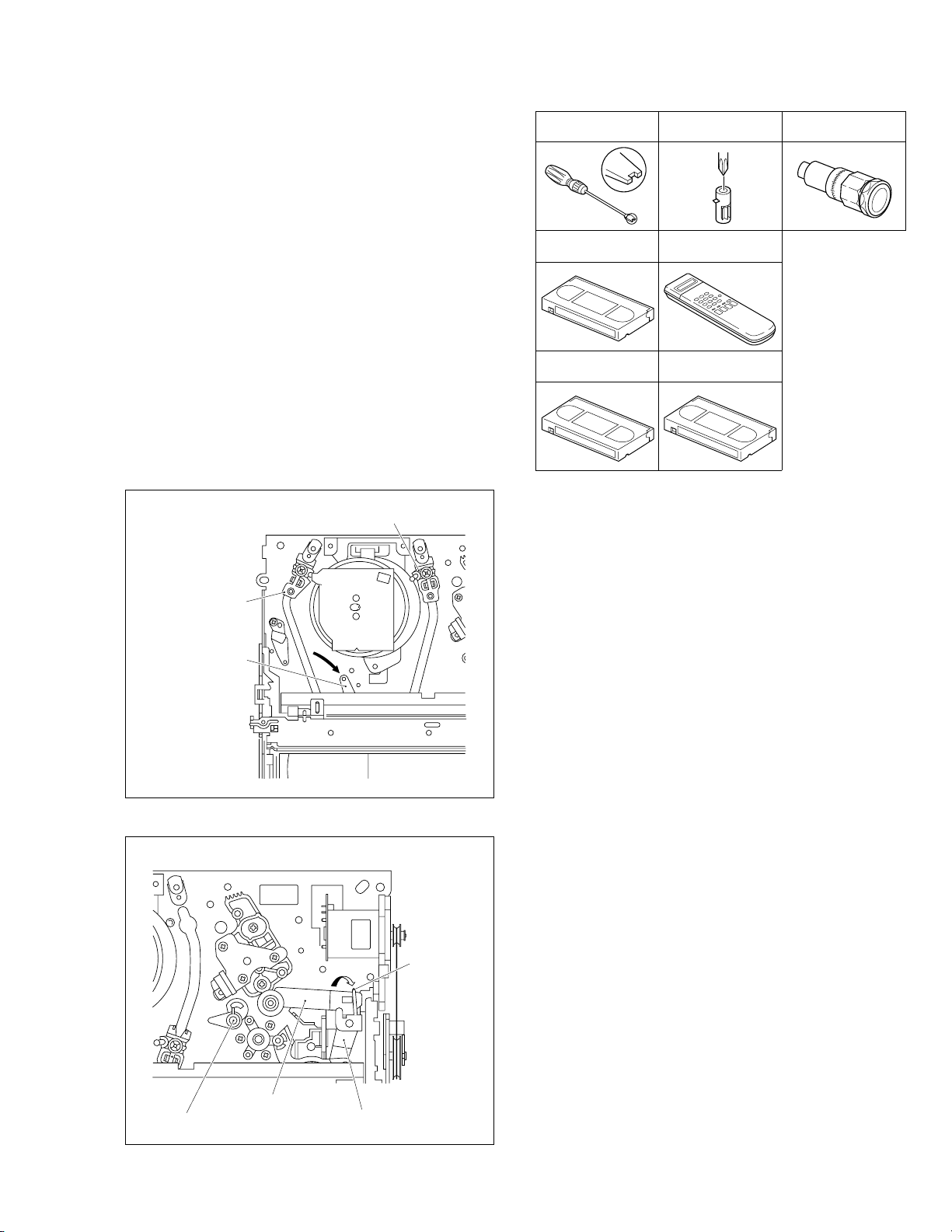
2. In case of mechanical failure
Roller driver
PTU94002
A/C head positioning tool
PTU94010
Back tension cassette gauge
PUJ48076-2
Jig RCU
PTU94023B
Torque gauge
PUJ48075-2
Alignment tape
(SP, stairstep, PAL)
MHPE
Alignment tape
(LP, stairstep, PAL)
MHPE-L
If you cannot remove the cassette tape which is loaded because of any mechanical failure, manually remove it by taking the following steps.
(1) Unplug the power cable and remove the top cover, front
panel assembly and others so that the mechanism assembly is visible. (See SECTION 1 DASASSEMBLY.)
(2) While keeping the tension arm assembly of the mecha-
nism assembly free from tension, pull the tape on the pole
base assembly (supply or take-up side) out of the guide
roller. (See Fig.2-1-3c.)
(3) Take the spring of the pinch roller arm assembly off the
hook of the press lever assembly, and detach it from the
tape. (See Fig.2-1-3d.)
(4) In the same way as in the electrical failure instructions in
2.1.3-1(5), remove the top guide.
(5) Raise the cassette tape cover. By keeping it in that posi-
tion, draw out the cassette tape case from the cassette
holder and take out the tape.
(6) By hanging the pinch roller arm assembly spring back
on the hook, take up the slack of the tape into the cassette.
Pole base assembly (take-up side)
2.1.4 Jigs and tools required for adjustment
Pole base assembly
(supply side)
Tension arm assembly
Fig. 2-1-3c
Take the spring
off the hook, and
detach it from the
tape.
Guide pole guard
Pinch roller arm assembly
Press lever assembly
Fig. 2-1-3d
2-2
Page 24
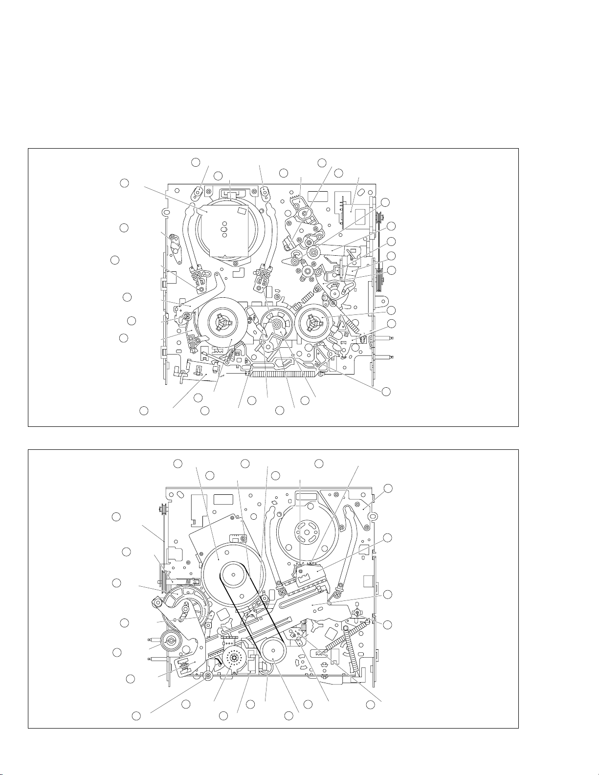
2.1.5 Maintenance and inspection
1. Location of major mechanical parts
In this chapter, the two mechanism speeds are described by comparing the speeds of the standard type and the high-speed
FF/REW type.
It is possible to distinguish between these two types of mechanism by the diameters of their capstan pulleys.
The capstan pulley diameter for the standard type is approx. 32 mm.
The capstan pulley diameter for the high-speed FF/REW type is approx. 43 mm.
For information on the different parts used in the two mechanism types, please refer to the “Replacement of major parts”.
UV catcher2 (supply and take-up side)
Stator assembly
T2
Full erase head
T26
Pole base assembly
T25
(supply side)
Tension arm
T24
assembly
T23
Tension brake
T22
assembly
Adjust pin
T1
T5 T7
T3
Drum assembly
Head base
T6
A/C head
Loading motor
Guide pole guard
T8
Pinch roller arm
T9
assembly
Lid guide
T10
Press lever
T11
assembly
Guide arm
T12
assembly
Reel disk
T13
(take-up side)
Sub brake assembly
T14
(take-up side)
Belt
B22
(loading motor)
B21
Control cam
B20
B19
Cassette gear
B18
Worm gear
Brake lever
Rec safety lever
B1
Reel disk
T20
(supply side)
Main brake assembly
(supply side)
Idler lever
T17T19T21
Idler arm assembly
T16T18
Pole base assembly (take-up side)
Fig. 2-1-5a Mechanism assembly top side
Capstan motor
B2
Capstan brake assembly
B3 B5
Belt (capstan)
Loading arm gear (take-up side)
B4
Loading arm gear (supply side)
Main brake assembly
T15
(take-up side)
Plate
B6
(supply side)
Control
B7
bracket1
Control plate
B8
Tension arm
B9
bearing
2-3
Link lever
B17
Rotary encoder guide
B16
Rotary encoder
B15
B14
Direct gear
B13
Change lever assembly
B12
B10
Clutch unit
Take-up head
Fig. 2-1-5b Mechanism assembly bottom side
Take-up lever
B11
Page 25
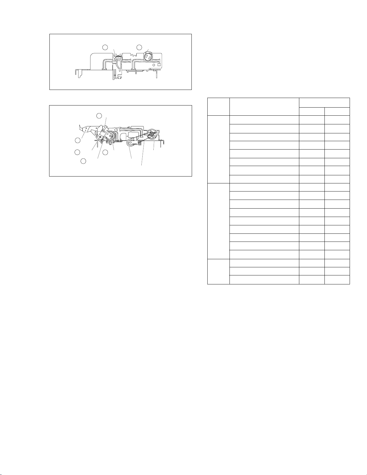
Guide rail Roller cam assembly
L2L1
Fig. 2-1-5c Mechanism assembly left side
R1
Opener guide
Door
R2
opener
Drive gear
R3
Cassette housing bracket
R4
R5
Limit gear
Loading motor
Worm gear
Belt (loading motor)
Fig. 2-1-5d Mechanism assembly right side
2. Cleaning
Regular cleaning of the transport system parts is desirable
but practically impossible. So make it a rule to carry out cleaning of the tape transport system whenever the machine is
serviced.
When the video head, tape guide and/or brush get soiled,
the playback picture may appear inferior or at worst disappear, resulting in possible tape damage.
(1) When cleaning the upper drum (especially the video
head), soak a piece of closely woven cloth or Kimu-wipe
with alcohol and while holding the cloth onto the upper
drum by the fingers, turn the upper drum
counterclockwise.
Note:
• Absolutely avoid sweeping the upper drum vertically
as this will cause damage to the video head.
(2) To clean the parts of the tape transport system other than
the upper drum, use a piece of closely woven cloth or a
cotton swab soaked with alcohol.
(3) After cleaning, make sure that the cleaned parts are com-
pletely dry before using the video tape.
3. Lubrication
With no need for periodical lubrication, you have only to lubricate new parts after replacement. If any oil or grease on
contact parts is soiled, wipe it off and newly lubricate the
parts.
Note:
• See the “mechanism assembly” diagram of the parts
list for the lubricating or greasing spots, and for the
types of oil or grease to be used.
4. Suggested servicing schedule for main components
The following table indicates the suggested period for such
service measures as cleaning,lubrication and replacement.
In practice, the indicated periods will vary widely according
to environmental and usage conditions.However, the indicated components should be inspected when a set is brought
for service and the maintenance work performed if necessary. Also note that rubber parts may deform in time,even if
the set is not used.
System Parts Name
Upper drum assembly
A/C head
Lower drum assembly
Pinch roller arm assembly
Full erase head
Tension arm assembly
Tape transport
Capstan motor (Shaft)
Guide arm assembly
Capstan motor
Capstan brake assembly
Main brake assembly
Belt (Capstan)
Belt (Loading motor)
Loading motor
Clutch unit
Worm gear
Control plate
Brush
Tension brake assembly
Other Drive
Rotary encoder
: Cleaning
¤
: Inspection or replacement if necessary
R
Operation Hours
~1000H ~2000H
¤R R
¤R ¤R
¤¤R
¤¤
¤¤
¤¤
¤¤
¤¤
R
R
R
RR
R
R
R
R
R
¤R ¤R
RR
R
Table 2-1-5a
5. Disassembling procedure table
The following table indicates the order in which parts are removed for replacement. To replace parts, remove them in
the order of 1 to 18 as shown in the table. To install them,
reverse the removal sequence.
The symbols and numbers preceding the individual part
names represent the numbers in the “Location of major mechanical parts” table. Also, the “T”, “B”, and “T/B” on the right
of each part name shows that the particular part is removed
from the front, from the back, and from both sides of the
mechanism, respectively.
2-4
Page 26
R4 R1 R3 T 9 T1 2 T11 B15 B12 B14 B13 B17 B21 B 7 B8 B5 B4 B11 T14 T15 T13 T22 T24 T18 B19
Symbols and numbers
Removal parts
(Reference items)
Replacement parts
Symbols and numbers
2.2.3 Guide rail T 1
L2
2.2.3 Roller cam assembly T 1
R4
2.2.3 Cassette housing bracket T 1
R1
2.2.3 Opener guide T 2
R2
2.2.3 Door opener T 3
2.2.3 Relay gear T 3
R5
2.2.3 Limit gear T 3
2.2.3 Cassette holder assembly T 6
R3
2.2.3 Drive gear T 4
2.2.3 Drive arm T 8
T9
2.2.4 Pinch roller arm assembly T 1
T12
2.2.5 Guide arm assembly T 1
T11
2.2.5 Press lever assembly T 3
T6
2.2.6 A/C head T 1
T7
2.2.7 Loading motor T 1
B1
2.2.8 Capstan motor T/B 1
T1
2.2.9 UV catcher2 T 1
T17
Pole base assembly (take-up side)
2.2.9
T25
2.2.9
Pole base assembly (supply side)
B15
2.2.10 Rotary encoder B 1
B12
2.2.11 Clutch unit B 1
B14
2.2.12 Change lever assembly B 3
B13
2.2.12 Direct gear B 4
2.2.12 Coupling gear B 5
2.2.12 Clutch gear B 6
B17
2.2.13 Link lever B 1
2.2.14 Cassette gear B 2
B18
B20
2.2.14 Control cam B 2
B21
2.2.14 Worm gear B 1
T10
- Lid guide T/B 5
B7
2.2.15 Control bracket1 B 1
B8
2.2.15 Control plate B 6
B5
2.2.16 Loading arm gear (supply side) B 7
B4
Loading arm gear (take-up side)
2.2.16
2.2.16 Loading arm gear shaft B 9
2.2.17 Take-up lever T/B 7
B11
B10
2.2.17 Take-up head T/B 8
2.2.17 Control plate guide T/B 8
B3
2.2.18 Capstan brake assembly T/B 7
T14
Sub brake assembly(take-up side)
2.2.19
T15
Main brake assembly(take-up side)
2.2.20
T19
2.2.20
Main brake assembly(supply side)
T13
2.2.20 Reel disk (take-up side) T/B 16
T22
2.2.21 Tension brake assembly T/B 9
T20
2.2.21 Reel disk (supply side) T/B 10
T24
2.2.21 Tension arm assembly T/B 10
B9
2.2.21 Tension arm bearing T/B 10
T18
2.2.22 Idler lever T/B 17
T16
2.2.22 Idler arm assembly T/B 18
B19
- Brake lever (
B16
- Rotary encoder guide T/B 19
1
) T/B 18
*
L1L1L2
Number of removal steps
Guide rail
Roller cam assembly
Cassette housing bracket
Opener guide
Front (T)/Back (B) of mechanism
1 2 3 4 5
12
T/B 2
T/B 2
B8
T/B 15
1 2 3 4
T/B 16
1 2 3 4 5 6 7 8
T/B 9
1 2 3 4 5 6 7 8
1 2 3 4 5 6 7 8
1 2 3 4 5 6 7 8
1 2 3 4 5 6 7 8
1 2 3 4 5 6 7 8
1 2 3 4 5 6 7 8
1 2 3 4 5 6 7 8
1 2 3 4 5 6 7 8
1 2 3 4 5 6 7 8
1 2 3 4 5 6 7 8
Relay gear
112
12
12
12 3
3
4 5
5 6
6 7
Cassette holder assembly
Drive gear
7
8
Table 2-1-5b
Note:
• The parts with marked (
nisms (standard type or high-speed FF/REW type).
1 : Uses the standard type mechanism only.
*
2 : Uses the high-speed FF/REW type mechanism only.
*
) have different types of mecha-
*
T1
Drive arm
Pinch roller arm assembly
Guide arm assembly
Press lever assembly
UV catcher2
Rotary encoder
Clutch unit
Change lever assembly
Direct gear
Coupling gear
Link lever
Worm gear
Control bracket1
Control plate
Loading arm gear (supply side)
Loading arm gear (take-up side)
1
2
1
1
1
2
12
3
12
3
1 2 3 4 5
12
3 4
1 2 3 4
1 2 3 4 5
1 2 3 4 5 6
1 2 3 4 5 6 7
1 2 3 4 5 6
1 2 3 4 5 6
1 2 3 4 5 6
1 2 3 4 5 6
9 10 11 12 13 14
9 10 11 12 13 14 15
9 10 11 12 13 14 15
9 10 11 12 13 14 15 16
9 10 11 12 13 14 15 16 17
9 10 11 12 13 14 15 16 17
9 10 11 12 13 14 15 16 17 18
4
1
1
5
6
7
8
)
1
(
Take-up lever
Sub brake assembly (take-up side)
Main brake assembly (take-up side)
Reel disk (take-up side)
Tension brake assembly
Tension arm assembly
Idler lever
Brake lever
7
7
9
9
9
*
2-5
Page 27
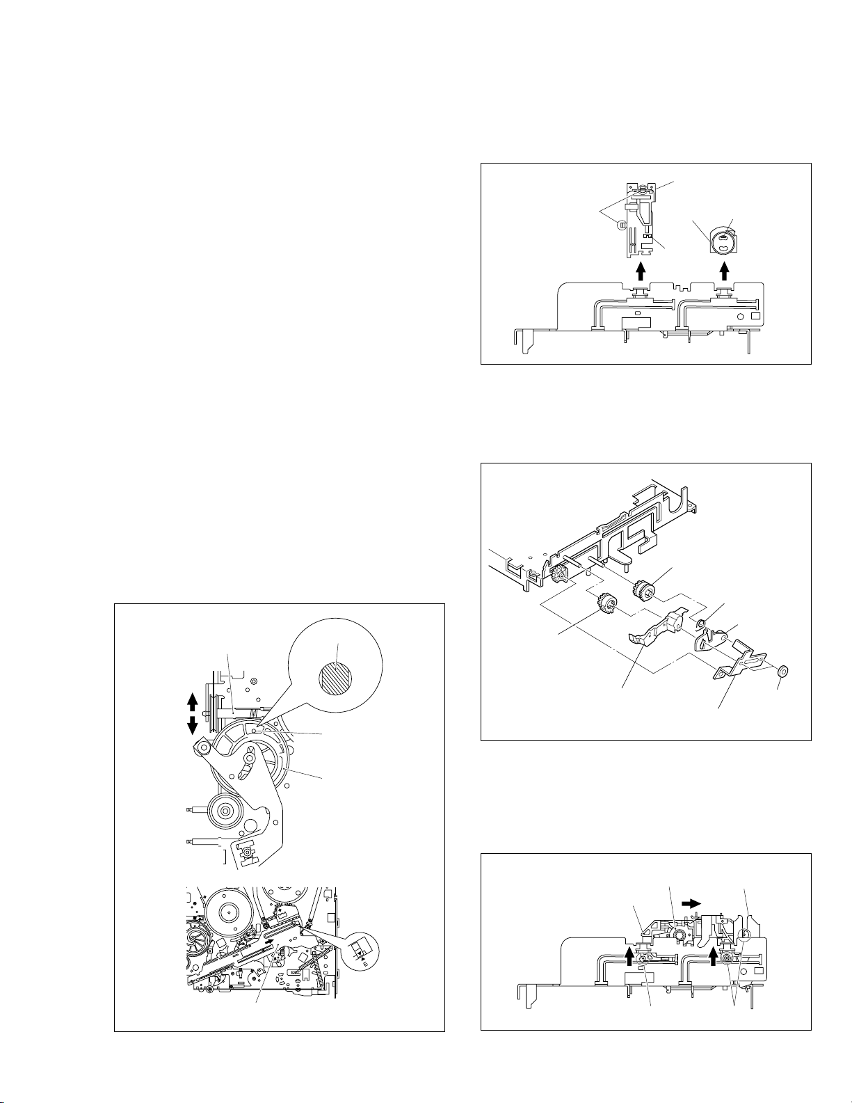
g
2.2 Replacement of major parts
2.2.1 Before starting disassembling (Phase matching
between mechanical parts)
The mechanism of this unit is closely linked with the rotary
encoder and system controller circuits.
Since the system controller detects the status of mechanical operation in response to phases of the rotary encoder
(internal switch positions), the mechanism may not operate
properly unless such parts as the rotary encoder, control
plate, loading arm gear, control cam, cassette gear, limit gear,
relay gear and drive gear are installed in their correct positions.
Especially, this model is not provided with any cassette housing assembly, so that cassette loading and unloading must
be accomplished by operation of the cassette holder assembly. The latter is in turn driven by such parts as the drive
gear, relay gear and limit gear. Exercise enough care, therefore, to have the phases of all this gear matching one another. (For information on phase matching of the mechanism,
see the instructions on how to install individual parts.)
This unit is provided with a mechanism assembly mode. It is
therefore necessary to enter this mode for assembling and
disassembling procedures.
This mode is usually not in use, manually set it when it is
required.
2.2.3 Cassette holder assembly
1. How to remove
(1) Remove the guide rail and roller cam assembly. (See
Fig.2-2-3a.)
(3 lugs on the guide rail and one lug on the roller cam
assembly)
Guide rail
Lugs
Roller cam
assembly
Lug
Lug
Fig. 2-2-3a
(2) Remove the two slit washers and remove the cassette
housing bracket. (See Fig.2-2-3b.)
(3) Remove the opener guide, spring(A), door opener, relay
gear and limit gear. (See Fig.2-2-3b.)
2.2.2 How to set the “Mechanism assembling mode”
Remove the mechanism assembly and place it bottom side
up. (See SECTION 1 DISASSEMBLY.) Turn the worm gear
toward the front so that the guide hole of the control cam is
brought into alignment with the hole at the mechanism assembly chassis. This position renders the mechanism assembling mode operational. Make sure that the control plate is
located in alignment with the mark E. (See Fig.2-2-2a.)
Worm gear
Chassis hole
Guide hole
Control cam
Limit gear
Spring(A)
Opener guide
Relay gear
Door opener
Cassette housing bracket
Slit washers
Fig. 2-2-3b
(4) While swinging the lock levers (R) and (L) of the cassette
holder assembly toward the front, slide the cassette
holder assembly until its legs come to where the guide
rail and the roller cam assembly have been removed (so
that the drive arm is upright). (See Fig.2-2-3c.)
Lock lever (L)
Cassette holder assembly
Drive arm
(Upright)
Mark E
Control plate
Fig. 2-2-2a
Le
Fig. 2-2-3c
Legs
2-6
Page 28
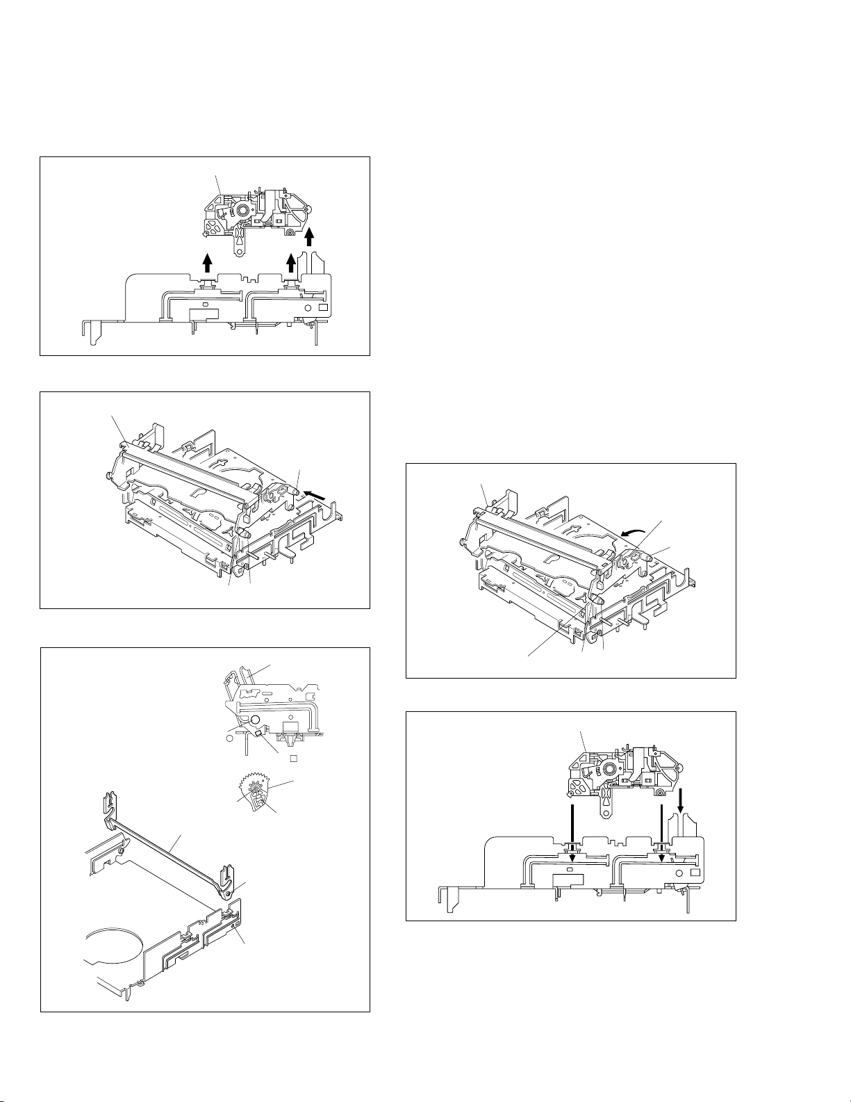
While holding the left side of the cassette holder, lift the
(5)
cassette holder assembly so that the three legs on the
left side are all released. Then pull the legs (A) and (B)
on the right side out of the rail and also pull up the leg(C).
(See Fig.2-2-3d and Fig.2-2-3e.)
(6) Draw out the drive gear, and remove the drive arm.
Cassette holder assembly
Fig. 2-2-3d
Cassette holder assembly
(A)
2. How to install (Phase matching)
(1) Insert the section (A) of the drive arm into the section (B)
of the main deck.
(2) Insert the section (1) of the drive gear into the round hole,
and the section (2) into the square hole on the drive arm.
(See Fig.2-2-3f.)
(3) Hold the drive arm upright and fit the leg (C) on the right
side of the cassette holder assembly into the groove. (See
Fig.2-2-3g.)
(4) While swinging the lock lever (R) of the cassette holder
assembly toward the front, put the legs (A) and (B) into
the rail. (See Fig.2-2-3g.)
(5) Drop the three legs on the left side of the cassette holder
assembly into the groove at one time. (See Fig.2-2-3h.)
(6) Slide the whole cassette holder assembly toward the front
to bring it to the eject end position.
(7) Install the limit gear so that the notch on the outer cir-
cumference of the limit gear is brought into alignment with
the guide hole on the main deck. (See Fig.2-2-3i.)
(8) Install so that the notch on the periphery of the relay gear
is aligned with the notch of the main deck and that hole
A of the relay gear is aligned with the hole A of the limit
gear and that hole B of the relay gear is aligned with the
hole B of the drive gear. (See Fig.2-2-3i.)
(9) Install the door opener, opener guide, spring(A) and cas-
sette housing bracket and fasten the two slit washers.
Cassette holder assembly
Fig. 2-2-3e
Main deck right side
Drive arm
Hole
(C)
Lock lever (R)
(A)
(B)
(B)
Drive arm
Drive arm
(C)
Fig. 2-2-3g
Cassette holder assembly
Hole
Drive gear
(1)
(2)
(A)
2-7
Fig. 2-2-3f
(B)
Fig. 2-2-3h
Page 29
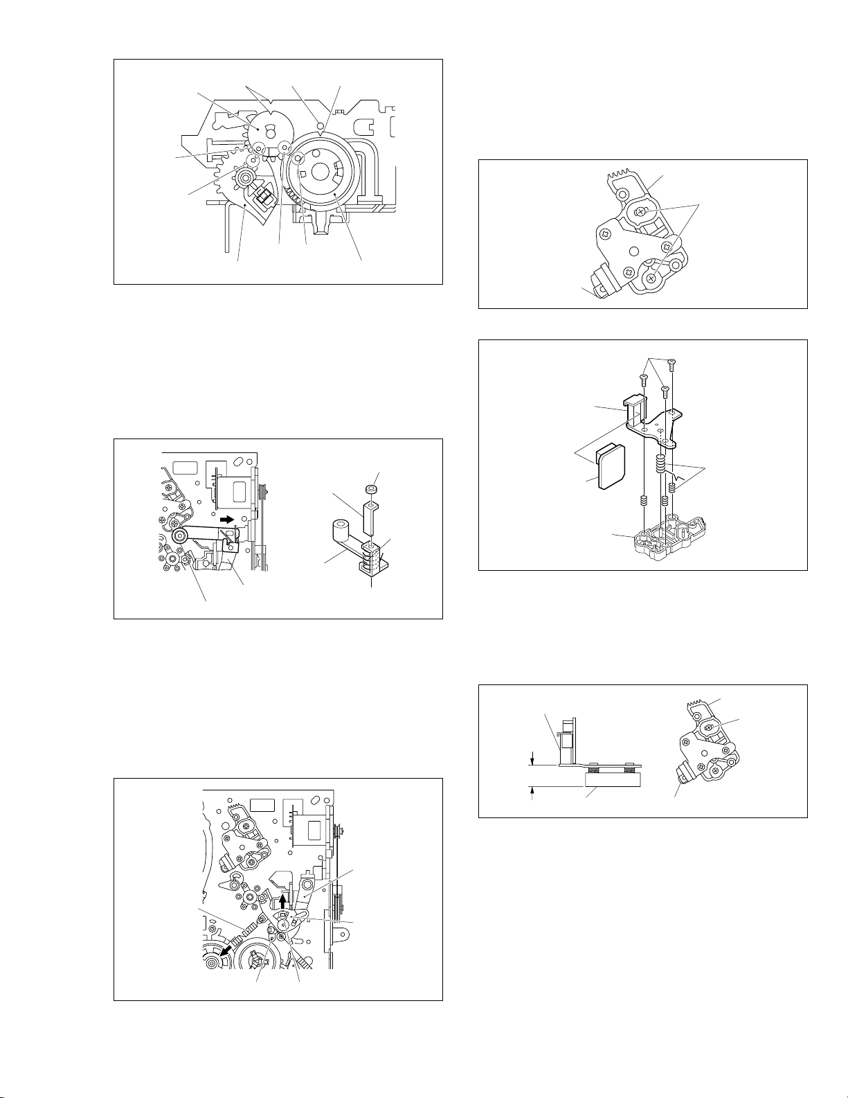
Relay gear
B
Guide holeNotches Notch
2.2.6 A/C head
1. How to remove
(1) Remove the two screws (A) and remove the A/C head
together with the head base.
(2) When replacing only the A/C head, remove the three
screws (B) while controlling the compression spring.
Head base
B
AA
Drive gear Limit gear
Fig. 2-2-3i
2.2.4 Pinch roller arm assembly
1. How to remove
(1) Remove the spring from the hook of the press lever as-
sembly.
(2) Remove the slit washer and remove the pinch roller seat
2. (See Fig.2-2-4a.)
(3) Remove the pinch roller arm assembly by pulling it up.
Slit washer
Pinch roller seat2
Spring
Pinch roller arm
Press lever assembly
Pinch roller arm assembly
assembly
Fig. 2-2-4a
2.2.5 Guide arm assembly and press lever assembly
1. How to remove
(1) Remove the spring and expand the lug of the lid guide in
the arrow-indicated direction. Then remove the guide arm
assembly by pulling it up.
(2) Remove the press lever assembly by pulling it up. (See
Fig.2-2-5a.)
Screws(A)
A/C head
Fig. 2-2-6a
Screws(B)
A/C head
Compression
A/C head board
assembly
Head base
springs
Fig. 2-2-6b
2. How to install
(1) To make the post-installation adjustment easier, set the
temporary level as indicated in Fig.2-2-6c. Also make sure
that the screw center (centre) is brought into alignment
with the center (centre) position of the slot.
A/C head
12.4 mm
Head base
Screw
Tension
spring
LugLid guide
Fig. 2-2-5a
Press lever
assembly
Guide arm
assembly
Head base
A/C head
Fig. 2-2-6c
2.2.7 Loading motor
1. How to remove
(1) Remove the belt wound around the worm gear.
(2) Open the two lugs of the motor guide and remove the
loading motor, loading motor board assembly and motor
guide altogether by pulling them up.
(3) When replacing the loading motor board assembly, take
care with the orientation of the loading motor. (Install so
that the loading motor label faces upward.)
(4) When the motor pulley has been replaced, choose the
fitting dimension as indicated in Fig.2-2-7a.
2-8
Page 30
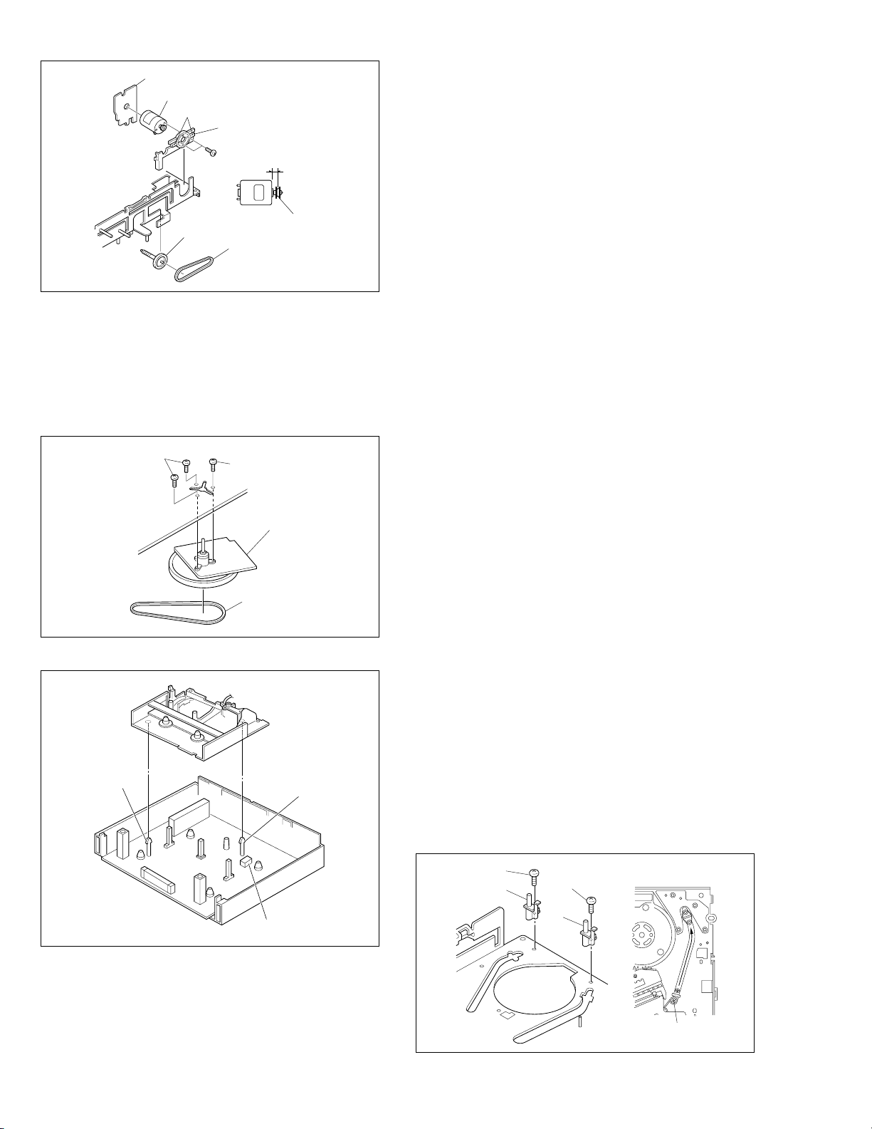
Loading motor board assembly
Loading motor
Lugs
Motor guide
6.5 ± 0.2 mm
LABEL
Motor pulley
Worm gear
Belt
Fig. 2-2-7a
2.2.8 Capstan motor
1. How to remove
(1) Remove the belt (capstan) on the mechanism assembly
back side.
(2) Remove the three screws (A) and remove the capstan
motor.
Screws(A)
Screw(A)
Capstan motor
Belt
Fig. 2-2-8a
Spacer
Spacer
2. How to install (Centering the mounting position)
When the capstan motor has once been removed and then
reinstalled out of the initial correct position in the rotational
direction, the capstan motor current may be unstable during
operation in high or low temperatures. This may result in
greater Wow & Flutter and occasionally in power breakdown
because of current over - load. Install the capstan motor while
following the procedure given below.
(The capstan motor is centrally located when the unit is
shipped from the factory.)
(1) Provisionally tighten the three screws (A) securing the
capstan motor.
(2) Install the mechanism assembly to which the capstan
motor is provisionally fastened on the bottom chassis
which incorporates the Main board assembly. (No need
to tighten the screws for mounting the mechanism.)
Make sure that all the connectors for the mechanism assembly and the Main board assembly are correctly installed as indicated in Fig. 2-2-8b.
(3) Making sure that the connector for the capstan motor is
correctly mounted, and securely tighten the three screws
(A).
Note:
• When the capstan motor has been replaced with a new
one, perform recording in the EP(or LP) mode for at
least 2 minutes at normal temperatures immediately before starting the FF/REW or SEARCH operations (Aging).
2.2.9 Pole base assembly (supply or take-up side)
1. How to remove
(1) Remove the UV catcher 2 on the removal side by loos-
ening the screw (A).
(2) Remove the pole base assembly on the supply side from
the mechanism assembly by loosening the screw (B) on
the mechanism assembly back side and sliding the pole
base assembly toward the UV catcher 2.
(3) As for the pole base assembly on the take-up side, turn
the pulley of the loading motor to lower the cassette
holder because the screw (B) is hidden under the control plate. (See the “Procedures for Lowering the Cassette
holder assembly” of 1.3 DISASSEMBLY/ASSEMBLY
METHOD.) Further turn the motor pulley to move the cassette holder until the screw (B) is no longer under the control plate (in the half-loading position). Then remove it as
done for the supply side by removing the screw (B).
Note:
• After reinstalling the Pole base assembly and the UV
catcher2, be sure to perform compatibility adjustment.
2-9
Fig. 2-2-8b
Connector for
the capstan motor
Screw(A)
UV catcher2
Screw(A)
UV catcher2
Screw(B)
Fig. 2-2-9a
Page 31
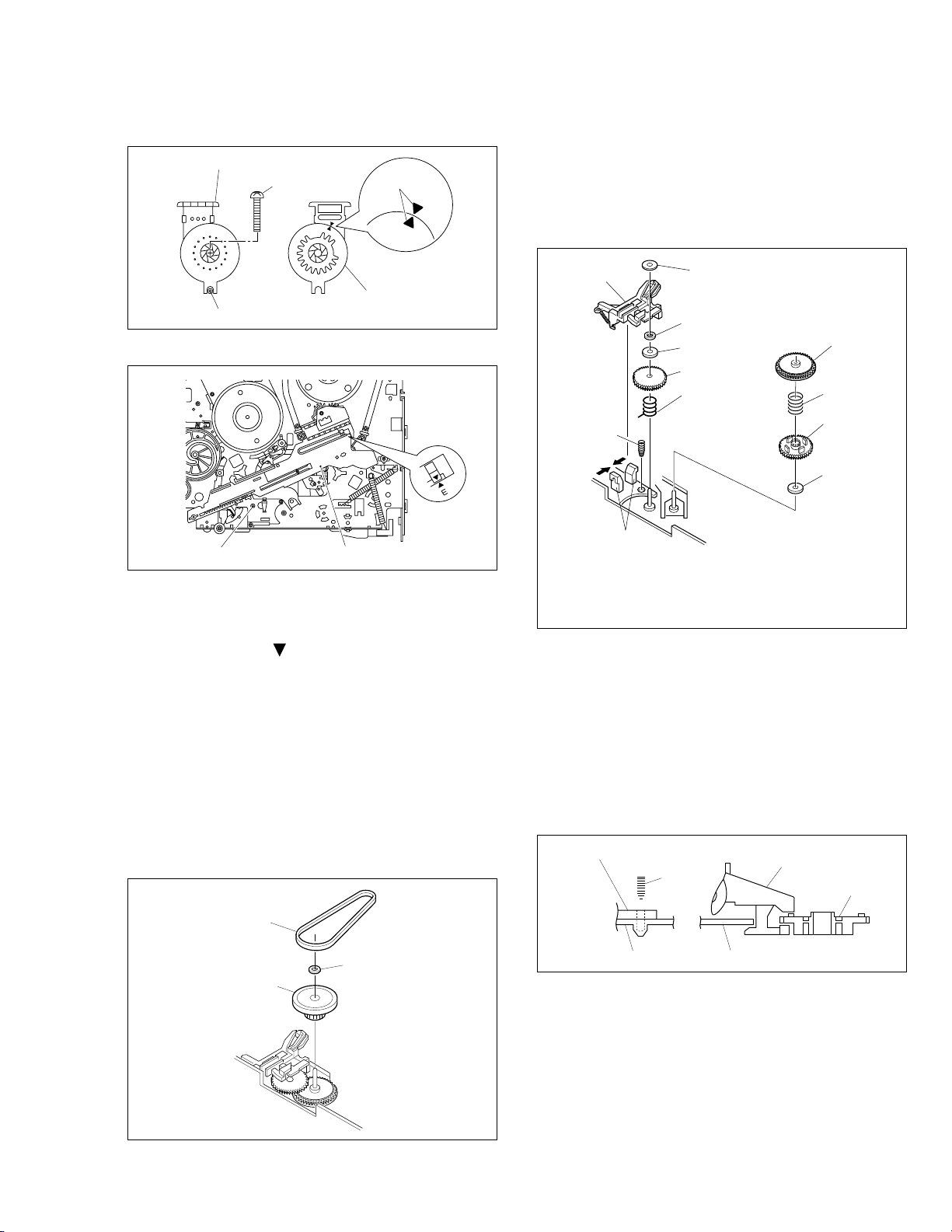
Spacer
Change lever
assembly
Direct gear
Clutch gear
Spring (C)
Slit washer
Lugs
Spring(A)
Position the projecting
side down.
Spring(B)
Washer (*1)
Spacer
Coupling gear
2.2.10 Rotary encoder
1. How to remove
(1) Remove the screw (A) and remove the rotary encoder
by pulling it up. (See Fig. 2-2-10a.)
Rotary encoder (Front side)
Screw(A)
Positioning pin of the rotary encoder
Guide marks
Rotary encoder (Back side)
Fig. 2-2-10a
Mark E
2.2.12 Change lever assembly, direct gear, clutch gear
and coupling gear
1. How to remove
(1) Release the two lugs of the rotary encoder guide in the
arrow-indicated direction and remove the change lever
assembly.
(2) Remove the slit washer retaining the direct gear and re-
move the latter.
Take care so as not to lose the washer and spring. (See
Fig.2-2-12a.)
Shaft of the rotary encoder guide
Control plate
Fig. 2-2-10b
2. How to install (Phase matching)
(1) Make sure that the mark E of the control plate is in align-
ment with the mark
of the loading arm gear shaft and
bring the guide marks on the rotary encoder into alignment as indicated in Fig.2-2-10a. (See Fig. 2-2-10a and
Fig. 2-2-10b.)
(2) Turn over the rotary encoder with its guide marks kept in
alignment and install it by fitting on the shaft of the rotary
encoder guide and the positioning pin.
(3) Tighten the screw (A) to complete the installation.
2.2.11 Clutch unit
(1) Remove the belt wound around the capstan motor and
the clutch unit.
(2) Remove the slit washer and remove the clutch unit.
Belt
Clutch unit
Slit washer
Note:
• The parts with marked (
speed FF/REW type).
1 : Uses the standard type mechanism only.
*
2:
Uses the high-speed FF/REW type mechanism only.
*
) have different types of mechanisms (standard type or high-
*
Fig. 2-2-12a
2. How to install
(1) Install the clutch gear, spring (A), spring (C), direct gear,
spacer and others to the individual shafts of the main
deck, and finally the slit washer. (See Fig.2-2-12a.)
(2) Let the spring (B) drops into the rotary encoder guide hole
and install the change lever assembly.(Take care not to
mistake a direction of the spring.) The point is to slightly
lift the coupling gear and catch it from the both sides with
the assembly. (See Fig.2-2-12b.)
Rotary encoder guide
Spring(B)
Main deck Main deck
Change lever assembly
Coupling gear
Fig. 2-2-12b
Fig. 2-2-11a
2-10
Page 32
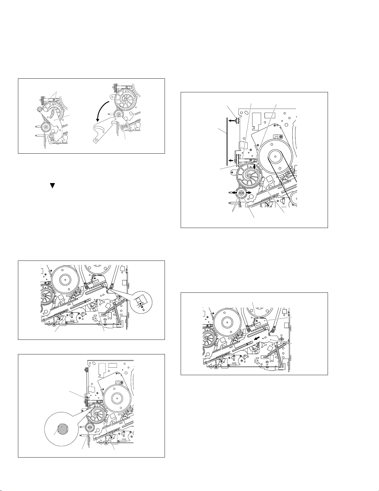
2.2.13 Link lever
1. How to remove
(1) Remove the two slit washers.
(2) Remove the link lever by lifting it from the shaft retained
by the slit washers. Then swing the link lever
counterclockwise and remove it from the locking section
of the control plate.
Slit washers
2.2.14 Cassette gear, control cam and worm gear
1. How to remove
(1) Remove the control cam by lifting it.
(2) Open the two lugs of the cassette gear outward and pull
the latter off.
(3) Remove the belt wound around the worm gear and the
loading motor.
(4) Open the lug of the lid guide outward and remove the
worm gear.
Link lever
Locking section of the
control plate
Fig. 2-2-13a
2. How to install (Phase matching)
(1) Slide the control plate so that its mark E is aligned with
the mark
on the loading arm gear shaft. (See Fig.2-2-
13b.)
(2) Rotate the worm gear until the guide hole of the control
cam is aligned exactly with the guide hole of the main
deck. (See Fig.2-2-13c.)
(3) Insert the link lever into the locking section of the control
plate. (See Fig.2-2-13a.)
(4) Rotate the link lever clockwise so that it is installed on
the shafts in the center (centre) and on the left of the control cam.
(5) Fasten the slit washers at these two points.
Loading motor
Belt
Lug
Worm gear
Lugs
Cassette gear
Lid guide
Control cam
Fig. 2-2-14a
2.2.15 Control plate
1. How to remove
(1) Remove the screw (A) retaining the control bracket 1 and
remove the latter.
(2) Slide the control plate as indicated by the arrow and re-
move the control plate. (See Fig.2-2-15a.)
Shaft of the rotary encoder guide
Fig. 2-2-13b
Worm gear
Main deck
guide hole
Control cam
guide hole
Cassette gear
Fig. 2-2-13c
Control plate
Control cam
Mark E
Screw(A)
Control
bracket1
Control
plate
Fig. 2-2-15a
2. How to install (Phase matching)
(1) Adjust the position of the idler arm assembly pin as indi-
cated in Fig.2-2-15b (to the left of center (centre) of the
R section).
(2) Bring the guide hole of the take-up lever into alignment
with the hole at the control plate guide and fix the position by inserting a 1.5 mm hexagonal wrench.
2-11
Page 33

(3) Install the control plate so that the section A of the load-
ing arm gear shaft fits into the hole (A) of the control plate,
the section B of the control plate guide into the hole (B),
and the control plate comes under the section C of the
rotary encoder guide and the section D of the loading arm
gear shaft while press-fit the pole base assmebly (supply side) as indicated by the arrow. It is important that
the tension arm assembly shaft is positioned closer toward you than the control plate. (See Fig.2-2-15c.)
(4) Make sure that the mark E of the control plate is in align-
ment with the mark
of the loading arm gear shaft. (See
Fig.2-2-15c.)
(5) Pull off the hexagonal wrench for positioning.
(3) Turn the loading arm gear (take-up side) clockwise so
that the notch of the loading arm gear (take-up side) is
in alignment with the projection of the loading arm gear
shaft and lift it.
Likewise, turn the loading arm counterclockwise so that
the notch is in alignment with the projection and remove
the loading arm gear (take-up side). (See Fig.2-2-16a and
Fig. 2-2-16b.)
(4) When removing the loading arm gear shaft, be sure of
first removing the screw retaining the drum assembly (on
the back side of the loading arm gear shaft). Then remove the screw (C) and remove the loading arm gear
shaft by sliding it.
Idler arm assembly
pin
R section
Guide hole of the
control plate guide
Section D
1.5mm hexagonal wrench
Fig. 2-2-15b
Section A
Section D
Hole A
Pressfit
Take-up lever
Insert
Pole base assembly
(supply side)
Section A
Hole A
Pole base assembly
(take-up side)
Screw(B)
Torsion arm
Loading arm gear
(take-up side)
Projection B
Guide marks
Projection A
Pole base assembly
(supply side)
Screw(A)
Loading arm gear
(supply side)
Fig. 2-2-16a
Loading arm gear shaft
Loading arm gear (take-up side)
Notch
Screw(C)
Loading arm gear shaft
Section C
Section C
Section B
Hole B
Hole B
Section B
Control plate
Tension arm assembly
shaft
Fig. 2-2-15c
2.2.16 Loading arm gear (supply or take-up side) and
loading arm gear shaft
1. How to remove
(1) Remove the loading arm gear (supply side) by loosen-
ing the screw (A). (See Fig. 2-2-16a.)
(2) Remove the screw (B) and remove the torsion arm from
the pole base assembly (take-up side). (See Fig.2-2-16a.)
Fig. 2-2-16b
2. How to install
(1) Align the notch of the loading arm gear (take-up side) to
the projection B of the loading arm gear shaft and slip it
over. Then rotate it clockwise for alignment with the projection A and slip it down to the bottom. (See Fig.2-216b.)
(2) Then turn the loading arm gear (take-up side)
counterclockwise. Hang the torsion arm on the pole base
assembly (take-up side) and tighten the screw (B).
(3) Install the loading arm gear (supply side) so that the guide
mark of the loading arm gear (take-up side) is in alignment with the guide mark of the loading arm gear (supply side). Then hang the torsion arm on the pole base
assembly (supply side) and tighten the screw (A). (See
Fig.2-2-16a.)
2-12
Page 34

2.2.17 Take-up lever, take-up head and control plate
guide
(1) Remove the spring of the take-up lever from the main
deck.
(2) Remove the lug (A) of the take-up lever from the main
deck and pull out the take-up lever and the take-up head
together.
(3) Remove the screw (A).
(4) Align the idler arm assembly pin in the center (centre) of
the R section of the control plate guide, remove the con-
trol plate guide lugs (B) and (C) from the main deck, and
remove the control plate guide.
Idler arm assembly pin
Lug(C)
Screw(A)
Take-up lever
Take-up head
Lug(A)
Lug(B)
Control plate guide
Fig. 2-2-17a
2.2.18 Capstan brake assembly
1. How to remove
(1) Move the lug (A) of the capstan brake assembly in the
arrow-indicated direction so that it comes into alignment
with the notch of the main deck. (See Fig. 2-2-18a.)
(2) Remove the lug (B) of the capstan brake assembly from
the main deck and remove the capstan brake assembly.
Spring
Sub brake
Lug(A)
Lug(B)
assembly
(take-up side)
Lug(C)
Fig. 2-2-19a
2.2.20 Main brake assembly (take-up side), reel disk
(take-up side) and main brake assembly (supply
side)
1. How to remove
(1) Move the main brake assembly (take-up side) in the ar-
row-indicated direction and remove the reel disk (takeup side).
Remove the spring attached to the main brake assembly.
(2)
(3) Remove the lug (A) of the main brake assembly (take-
up side) and pull out the lug (B) after bringing it into alignment with the main deck notch.
(4) Remove the lugs (C), (D) and (E) of the main brake as-
sembly (supply side) from the main deck and pull them
off. (See Fig.2-2-20a.)
(5) When installing the main brake assembly (take-up side),
slide the brake lever in the direction as indicated by the
arrow to prevent it from hitting the projection of the main
brake assembly (take-up side). (See Fig.2-2-20b.)
Main brake assembly
(supply side)
Reel disk
(take-up side)
Main brake assembly
(take-up side)
Lug(B)
Lug(A)
Capstan brake assembly
Fig. 2-2-18a
2.2.19 Sub brake assembly (take-up side)
1. How to remove
(1) Remove the spring attached to the lid guide and sub
brake assembly (take-up side).
(2) Bring the lug (A) of the sub brake assembly (take-up side)
into alignment with the notch of the main deck.
(3) Remove the lugs (B) and (C) of the sub brake assembly
(take-up side) from the main deck and remove the sub
brake assembly (take-up side).
2-13
Lug(B)
Lug(C)
Lug(D)
SpringLug(E)
Lug(A)
Notch
Fig. 2-2-20a
(
1)
*
Brake
lever
Note:
• The parts with marked ( *) have different types of mechanisms (standard type
or high-speed FF/REW type).
1 : Uses the standard type mechanism only.
*
Rotary encoder guide
Projection of the main
brake assembly
(take-up side)
Fig. 2-2-20b
Page 35

2.2.21 Tension brake assembly, reel disk (supply side)
(
)
and tension arm assembly
1. How to remove
(1) Remove the three lugs of the tension brake assembly
from the main deck and pull them off.
(2) Remove the reel disk (supply side) by loosening in the
arrow-indicated direction the main brake assembly (supply side).
(3) Remove the tension spring on the back of the main deck.
Then release the lug of the tension arm bearing in the
arrow-indicated direction and draw out the tension arm
assembly. (See Fig. 2-2-21a.)
Lug of the tension
arm bearing
Tension arm
assembly
Reel disk
(supply side)
2.2.23 Stator assembly
(1) Remove the flat cable.
(2) Remove the two screws (A), (B) and remove the lug wire.
(3) Remove the stator assembly by lifting in the arrow-indi-
cated direction. (Take care that the brush spring does not
jump out.)
Notes:
• Be careful not to lose the brush and spring.
• There are some models that do not use the lug wire.
Refer to the parts list for these models.
• When tightening the screw (B), place the caulked part
of the lug terminal near to the shaft of the drum and
then tighten it.
• After installation, be sure to perform the switching
point adjustment according to the electrical adjustment
procedure.
Tension brake
assembly
Lugs
Tension spring Main brake assembly
supply side
Fig. 2-2-21a
2.2.22 Idler lever, idler arm assembly
1. How to remove
(1) Remove the lug of the idler lever from the main deck and
remove the hook fitted in the idler arm assembly hole by
lifting it.
(2) Remove the slit washer and pull out the idler arm assem-
bly.
Lug Idler lever
Hook
Idler arm
assembly
Slit washer
Screw (A)
Stator assembly
Screw (B)
Lug wire
(Note)
Drum
shaft
Flat cable
(Take care not to mix up the
polar faces when installing.)
Lug wire
Screw (A)
Fig. 2-2-23a
2.2.24 Rotor assembly
1. How to remove
(1) Remove the stator assembly.
(2) Remove the two screws (B) and remove the rotor assem-
bly.
2. How to install
(1) Match the phases of the upper drum assembly and the
rotor assembly as indicated in Fig.2-2-24a.
(2) Place the upper drum assembly hole (a) over the rotor
assembly holes (b) (with three holes to be aligned) and
tighten the two screws (B). (See Fig.2-2-24a.)
Screws (B)
Hole(a)
Fig. 2-2-22a
Screw holes
Upper drum
assembly
Rotor assembly
The hole is not in
line but is offset
toward the right.
Hole(b)
Fig. 2-2-24a
2-14
Page 36
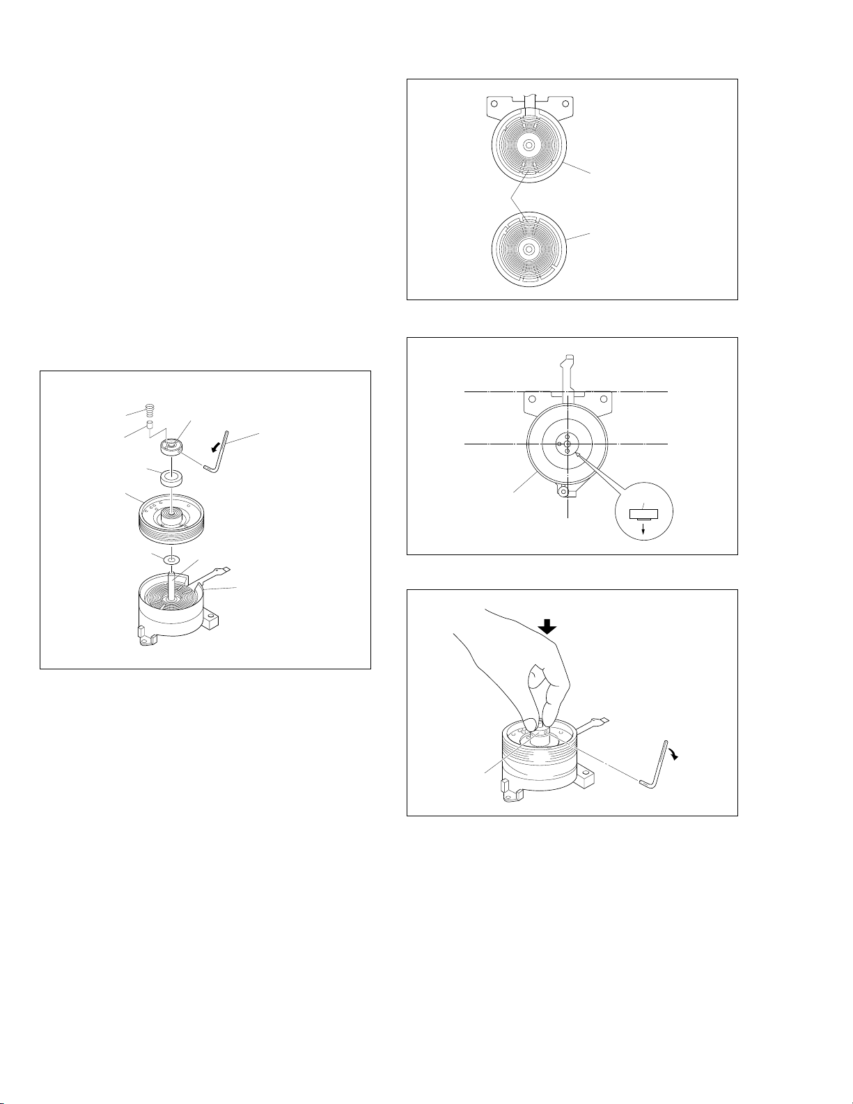
2.2.25 Upper drum assembly
Notes:
• To replace the upper drum assembly only may not be
possible with some models. For upper drum assembly replacement, refer to the parts list. (When the parts
number of the upper drum assembly is not listed on
the parts list, then this cannot be replaced.)
• When replacement is required, control the up- down
movement of the brush. Never apply grease.
• When replacing the upper drum assembly, replace it
the together with the washer.
1. How to remove
(1) Remove the stator assembly and rotor assembly.
(2) Loosen the screw of the collar assembly using a 1.5 mm
hexagonal wrench and remove the collar assembly. Also
remove the brush, spring and cap at one time.
(3) Remove the upper drum assembly and remove the
washer using tweezers.
Lower drum assembly
Coil parts
Upper drum assembly
Fig. 2-2-25b
Spring
Brush
Upper drum
assembly
Washer
Collar
assembly
Loosen
Cap
1.5 mm
hexagonal wrench
Shaft
Lower drum assembly
Fig. 2-2-25a
2. How to install
(1) Clean the coil parts of the lower drum assembly and the
newly installed upper drum assembly with an air brush
in advance. (See Fig.2-2-25b.)
(2) Install a new washer and upper drum assembly on the
drum shaft. (See Fig.2-2-25a.)
(3) Install the cap to the upper drum assembly.
(4) Position the collar assembly as indicated in Fig.2-2-25c
while controlling its up- down movement.
(5) Secure the collar assembly in position with a hexagonal
wrench while pressing its top with the fingers.
(6) After installation, gently turn the upper drum assembly
with your hand to make sure that it turns normally. Then
install the brush and the spring.
(7) Install the rotor assembly and stator assembly according
to Fig 2-2-23a and 2-2-24a.
(8) When installation is complete, clean the upper drum as-
sembly and lower drum assembly and carry out the fol-
lowing adjustments.
• PB switching point adjustment
• Slow tracking adjustment
• Compatibility adjustment (Be sure to check for compat-
ibility for the EP (or LP) mode.)
Upper drum
assembly
Collar
assembly
Fig. 2-2-25c
Press
Fig. 2-2-25d
Collar
assembly
Tighten
2-15
Page 37

2.3 Compatibility adjustment
Notes:
• Although compatibility adjustment is very important,
it is not necessary to perform this as part of the normal servicing work. It will be required when you have
replaced the A/C head, drum assembly or any part of
the tape transport system.
• To avoid any damage to the alignment tape while performing the compatibility adjustment, get a separate
cassette tape (for recording and play back) ready to
be used for checking the initial tape running behavior.
• Unless otherwise specified, all measuring points and
adjustment parts are located on the Main board.
• When using the Jig RCU, it is required to set the VCR
to the Jig RCU mode (the mode in which codes from
the Jig RCU can be received). (See SECTION 1 DISASSEMBLY.)
Jig RCU
[Data transmitting method]
Depress the “ ” ( 3 ) button
after the data code is set.
CUSTOM CODE
43: A CODE
53: B CODE
6F: C CODE
7F: D CODE
DATA CODE
INITIAL MODE
Fig. 2-3a Jig RCU [PTU94023B]
(7) Unload the cassette tape once, play back the alignment
tape (A1) again and confirm the V.PB FM waveform.
(8) After adjustment, confirm that the tape wrinkling does not
occur at the roller upper or lower limits. (See Fig. 2-31d.)
[Perform adjustment step (9) only for the models
equipped with SP mode and EP (or LP) mode.]
(9) Repeat steps (1) to (8) by using the alignment tape (A2).
Max level
Proper waveform variation
Improper waveform variation
Min level
2.3.1 FM waveform linearity
Signal (A1) •
(A2) •
Mode (B) • PB
Equipment (C) • Oscilloscope
Measuring point (D) • TP106 (PB. FM)
External trigger (E) • TP111 (D.FF)
Adjustment part (F) • Guide roller [Mechanism assembly]
Specified value (G) • Flat V.PB FM waveform
Adjustment tool (H) • Roller driver [PTU94002]
Alignment tape(SP, stairstep, PAL) [MHPE]
Alignment tape(LP, stairstep, PAL) [MHPE-L]
(1) Play back the alignment tape (A1).
(2) Apply the external trigger signal to D.FF (E), to observe
the V.PB FM waveform at the measuring point (D).
(3) Set the VCR to the manual tracking mode.
(4) Make sure that there is no significant level drop of the
V.PB FM waveform caused by the tracking operation, with
its generally parallel and linear variation ensured. Per-
form the following adjustments when required. (See Fig.
2-3-1a.)
(5) Reduce the V.PB FM waveform by the tracking opera-
tion. If a drop in level is found on the left side, turn the
guide roller of the pole base assembly (supply side) with
the roller driver to make the V.PB FM waveform linear.
If a drop in level is on the right side, likewise turn the guide
roller of the pole base assembly (take-up side) with the
roller driver to make it linear. (See Fig. 2-3-1c.)
(6) Make sure that the V.PB FM waveform varies in parallel
and linearly with the tracking operation again. When re-
quired, perform fine-adjustment of the guide roller of the
pole base assembly (supply or take-up side).
Fig. 2-3-1a
Roller driver
Guide roller (supply side)
Fig. 2-3-1b
2-16
Page 38

A
(2)
(3)
(1)
AUDIO OUT
Head base
A/C head
CTL. P
Level drop at the guide roller (supply side)
C
Level drop at the guide roller (take-up side)
• Proper waveform variation: Always flat
B
waveform by turning the screws (1), (2) and (3) little by
little until both waveforms reach maximum. The screw (1)
and (3) are for adjustment of tilt and the screw (2) for azimuth.
D
(4) Adjust the AUDIO OUT waveform and Control pulse
• Improper waveform variation:
Higher Lower
Fig. 2-3-1c
Improper
(a) Guide roller
(b) Guide pole
Proper
Fig. 2-3-1d
2.3.2 Height and tilt of the A/C head
Note:
• Set a temporary level of the height of the A/C head in
advance to make the adjustment easier after the A/C
head has been replaced. (See Fig.2-2-6c.)
Signal (A) •
Mode (B) • PB
Equipment (C) • Oscilloscope
Measuring point (D1) • AUDIO OUT terminal
(D2) • TP4001 (CTL. P)
External trigger (E) • TP111 (D.FF)
Adjustment part (F) • A/C head [Mechanism assembly]
Specified value (G) • Maximum waveform
Alignment tape(SP, stairstep, PAL) [MHPE]
Fig. 2-3-2a
2.3.3 A/C head phase (X-value)
Signal (A1) •
Mode (B) • PB
Equipment (C) • Oscilloscope
Measuring point (D) • TP106 (PB. FM)
External trigger (E) • TP111 (D.FF)
Adjustment part (F) •
Specified value (G) • Maximum V.PB FM waveform
Adjustment tool (H) • A/C head positioning tool [PTU94010]
Alignment tape(SP, stairstep, PAL) [MHPE]
A/C head base [Mechanism assembly]
(1) Play back the alignment tape (A1).
(2) Apply the external trigger signal to D.FF (E), to observe
the V.PB FM waveform at the measuring point (D).
(3) Set the VCR to the manual tracking mode.
(4) Loosen the screws (4) and (5), then set the A/C head
positioning tool to the innermost projected part of the A/
C head. (See Fig. 2-3-3a.)
(5) Turn the A/C head positioning tool fully toward the cap-
stan. Then turn it back gradually toward the drum and
stop on the second peak point position of the V.PB FM
waveform output level. Then tighten the screws (4) and
(5).
(6) Perform the tracking operation and make sure that the
V.PB FM waveform is at its maximum.
If it is not at maximum, loosen the screws (4) and (5),
and turn the A/C head positioning tool to bring the A/C
head to a position, around where the waveform reaches
its maximum for the first time. Then tighten the screws
(4) and (5).
(1) Play back the alignment tape (A).
(2) Apply the external trigger signal to D.FF (E), to observe
the AUDIO OUT waveform and Control pulse waveform
at the measuring points (D1) and (D2) in the ALT mode.
(3) Set the VCR to the manual tracking mode.
2-17
Page 39

[Perform adjustment steps (7) to (10) only for 2 Head
0.5 mm
Hole (A)
Edge
Marker
Tension arm
assembly
Adjust pin
Tension brake assembly
Tension arm assembly
models equipped with LP mode.]
(7) Then play back the alignment tape (A2).
(8) Set the VCR to the manual tracking mode.
(9) Perform the tracking operation and make sure that the
V.PB FM waveform is at its maximum.
(10)
If it is not at maximum, loosen the screws (4) and (5),
and turn the A/C head positioning tool to bring the A/C
head to a position, around where the waveform reaches
its maximum for the first time. Then tighten the screws
(4) and (5).
Note:
• After adjusting, always perform the confirmation and
re-adjustment of the item 2.3.4.
Toward the drum
A/C head positioning tool
To the drum
A/C head
Toward the capstan
Head base
Screw
Screw
To the capstan
(4)
(5)
Fig. 2-3-3a
(4) Set the VCR to the Auto adjust mode by transmitting the
code (F) twice from the Jig RCU. When the VCR enters
the stop mode, the adjustment is completed.
(5) If the VCR enters the eject mode, perform adjustment for
the audio control head phase (X-value) again.
2.3.5 Tension pole position
Signal (A) • Back tension cassette gauge
Mode (B) • PB
Adjustment part (F) • Adjust pin [Mechansim assembly]
Specified value (G)
[PUJ48076-2]
• 25 - 51 gf•cm (2.45 – 5 × 10
-3
Nm]
(1) Play back the back tension cassette gauge (A).
(2) Check that the indicated value on the left side gauge is
within the specified value (G).
(3) If the indicated value is not within the specified value (G),
perform the adjustment in a following procedure.
1) Set the VCR to the mechanism service mode. (See
SECTION 1 DISASSEMBLY.)
2) Set the VCR to the play back mode and adjust by turning adjustment pin to align the tension arm assembly
edge with the main deck hole (A) on the right edge
marker. (See Fig. 2-3-5a)
Alignment tape
[SP, stairstep]
played with the
SP head
Waveform output
X-value adjustment point
Drum side Control head position Capstan side
Alignment tape
[EP(LP), stairstep]
played with the
EP(LP) head
Maximum
Fig. 2-3-3b
2.3.4 Standard tracking preset
Signal (A) •
Mode (B) • PB ¥ Auto adjust
Equipment (C) • Oscilloscope
Measuring point (D) • TP106 (PB. FM)
External trigger (E) • TP111 (D.FF)
Adjustment part (F) • Jig RCU: Code “50”
Specified value (G) • STOP mode
Adjustment tool (H) • Jig RCU [PTU94023B]
(1) Play back the alignment tape (A).
(2) Apply the external trigger signal to D.FF (E), to observe
Alignment tape(LP, stairstep, PAL) [MHPE-L]
(Maximum V.PB FM waveform)
the V.PB FM waveform at the measuring point (D).
(3) Confirm that the automatic tracking operation is com-
pleted.
Fig. 2-3-5a
2-18
Page 40

Mechanism Timing Chart
Mechanism mode
Control plate mark
Rotary encoder
Control cam angle
EJECT
END
E U CI
HIGH
C CH
LOW
HIGH
B CH
LOW
HIGH
A CH
LOW
0
CASS-
UP
69 136 370 412.
CASS-INS
FF/REW
FR
230
STOP
ST
264.
REV
R
7
318.
7
SLOW/STILLPPLAY
SL
42
Rotary encoder
angle
Pole base
Pinch roller
Guide arm
Tension arm
Main brake S
Main brake T
Sub brake S
Sub brake T
Capstan brake
Direct gear
Change lever 2
Idler position
Take-up lever
Rec safety switch
Operation mode
HALF PRESS
CONTACT
ON PLAY
ON REV
CONTACT
(C-INS)
HALF REV
HALF FF/REW
CONTACT
CONTACT
IN FF/REW
OUT PLAY
SUPPLY
CENTER
TAKE-UP
READY
RESET
OFF
OFF
OFF
OFF
OFF
OFF
OFF
OFF
OFF
OFF
OFF
0
20 42.652.
ON
ON
ON
ON
ON
ON
ON
ON
ON
ON
6
6
114.
150.4167.8178.
8
Timer REC
(drum at stop)
POWER OFF
(cassette loaded)
207.2218.2240.2251.
standby
STOP
Backspace Slow FOR
Search REW
Slow REW
2
293.2304.2320.4335
REC pause
REC
Search FF
STOP
(
drum
in motion)
2-19
Page 41

SECTION 3
ELECTRICAL ADJUSTMENT
3.1 PRECAUTION
The following adjustment procedures are not only necessary
after replacement of consumable mechanical parts or board
assemblies, but are also provided as references to be referred to when servicing the electrical circuitry.
In case of trouble with the electrical circuitry, always begin a
service by identifying the defective points by using the measuring instruments as described in the following electrical adjustment procedures. After this, proceed to the repair, replacement and/or adjustment. If the required measuring instruments
are not available in the field, do not change the adjustment
parts (variable resistor, etc.) carelessly.
3.1.1 Required test equipments
• Color (colour) television or monitor
• Oscilloscope: wide-band, dual-trace, triggered delayed
sweep
• Frequency counter
• Signal generator: RF / IF sweep / marker
• Signal generator: stairstep, color (colour) bar [PAL]
• Recording tape
• Digit-key remote controller(provided)
3.1.2 Required adjustment tools
Jig RCU
PTU94023B
Alignment tape
(SP, stairstep, PAL)
MHPE
Alignment tape
(LP, stairstep, PAL)
MHPE-L
Jig RCU
[Data transmitting method]
Depress the “ ” ( 3 ) button
after the data code is set.
CUSTOM CODE
43: A CODE
53: B CODE
6F: C CODE
7F: D CODE
DATA CODE
INITIAL MODE
Fig. 3-1-4a Jig RCU [PTU94023B]
• Set the switches as shown below unless otherwise
specified on the relevant adjustment chart. The
switches that are not listed below can be set as desired.
If the VCR is not equipped with the functions detailed
below, setup is not required.
AUTO PICTURE/VIDEO CALIBRATION/
B.E.S.T./D.S.P.C.
PICTURE CONTROL/SMART PICTURE
VIDEO STABILIZER OFF
TBC ON
Digital 3R ON
VIDEO NAVIGATION/TAPE MANAGER
OFF
NORMAL/NATURAL
OFF
• Unless otherwise specified, all measuring points and
adjustment parts are located on the Main board.
• In the Signal column of the adjustment chart, “Ext. Sinput” means the Y/C separated video signal and “Ext.
input” means the composite video signal input.
Burst
LPF
PTU93006
0.3 V
Alignment tape
(S-VHS, SP/LP, color (colour) bar)
MH-2H
s
Colour bar pattern [PAL]
(75%)
Green
Magenta
Red
Cyan
White
Yellow
White
U Black
V
100%
Blue
Alignment tape
(SP stairstep, NTSC)
MHP
3.1.3
Color (colour) bar signal,Color (colour) bar pattern
s
Colour bar signal [PAL]
White(100%)
White(75%)
0.7 V
1V
0.3 V
Horizontal sync
Yellow
Cyan
Green
Magenta
Red
VU
V(R-Y)
U(B-Y)
Blue
3.1.4 Switch settings and standard precautions
The SW settings of the VCR and the standard precautions
for the electrical adjustments are as follows.
• When using the Jig RCU, set its custom code to match
the custom code of the VCR.
3.1.5 EVR Adjustment
Some of the electrical adjustments require the adjustment
performed by the EVR system. The Main board assembly
have EEPROMs for storing the EVR adjustment data and
user setups.
Notes:
• In the EVR adjustment mode, the value is varied with
the channel buttons (+, –). The adjusted data is stored
when the setting mode changes (from PB to STOP,
when the tape speed is changed, etc.). Take care to
identify the current mode of each adjustment item
when making an adjustment.
• When changing the address setting in the EVR adjustment mode, use the Jig RCU or the remote controller
having numeric keypad with which a numeric code can
be directly input.
The remote control code of the Jig RCU corresponds
to each of the digit keys on the remote controller as
follows.
Digit-key 0 1 2 3 4 5 6 7 8 9
Code 20 21 22 23 24 25 26 27 28 29
• As the counter indication and remaining tape indication are not displayed FDP during the EVR adjustment
mode, check them on the TV monitor screen.
• When performing the EVR adjustment, confirm that the
FDP indication is changed to the EVR mode, as shown
below.
3-1
Page 42

FDP
Fig. 3-1-5a EVR mode
3.2 SERVO CIRCUIT
3.2.1 Switching point
Signal (A1) • Stairstep signal
Mode (B) • PB
(A2)
(A3) •
•
Alignment tape(SP, stairstep, PAL) [MHPE]
Alignment tape(SP, stairstep, NTSC) [MHP]
• TBC: OFF
Equipment (C) • Oscilloscope
Measuring point (D1) •
(D2) • TP106 (PB FM)
External trigger (E) • TP111 (D.FF)/slope : –
Adjustment part (F) • Jig RCU: Code “51” or “52”
Specified value (G) • 8.0 ± 0.5H [MHPE]
VIDEO OUT terminal (75Ø terminated)
• 7.5 ± 0.5H [MHP]
Adjustment tool (H) • Jig RCU [PTU94023B]
(1) Play back the signal (A1) of the alignment tape (A2).
(2) Apply the external trigger signal to D.FF (E) to observe
the VIDEO OUT waveform and V.PB FM waveform at the
measuring points (D1) and (D2).
(3) Press the channel buttons (+, –) simultaneously to enter
the manual tracking mode. This also brings tracking to
the center (centre).
(4) Adjust tracking by pressing the channel buttons (+, –) so
that the V.PB FM waveform becomes maximum.
(5) Transmit the code (F) from the Jig RCU to adjust so that
the trigger point of the VIDEO OUT waveform is changed
from the trailing edge of the V.sync signal becomes the
specified value (G).
(6) Set the VCR to the stop mode or eject mode.
(7) Play back the signal (A1) of the alignment tape (A3).
(8) Repeat steps (2) to (6).
Trigger point
Switching point
V.sync
(1) Record the signal (A2) in the mode (B1), and play back
the recorded signal.
(2) Press the channel buttons (+, –) simultaneously to enter
the manual tracking mode. This also brings tracking to
the center (centre).
(3) Set the VCR to the FWD slow (+1/6×) mode.
(4) Transmit the code (F) from the Jig RCU to adjust so that
the noise bar becomes the specified value (G) on the TV
monitor in the slow mode.
(5) Set the VCR to the Stop mode.
(6) Confirm that the noise bar is (G) on the TV monitor in
the slow mode.
(7) Repeat steps (3) to (6) in the REV slow (–1/6×) mode.
(8) Repeat steps (1) to (7) in the mode (B2).
Note:
• For FWD slow (+1/6×) playback, transmit the code “08”
from the Jig RCU to enter the slow playback mode, and
transmit the code “D0” for REV slow (–1/6×) mode.
3.3 VIDEO CIRCUIT
3.3.1 D/A level
Signal (A1) • Ext. S-input / Ext. input
Mode (B) • S-VHS
(A2) • Color (colour) bar signal [PAL]
(A3) • S-VHS tape
• EE
Equipment (C) • Oscilloscope
Measuring point (D) •
Adjustment part (F) • VR1401 (D/A LEVEL ADJ)
Specified value (G) • 1.00 ± 0.015 Vp-p (reference value)
(Note)
(1) Insert the cassette tape (A3) to enter the mode (B).
(2) Observe the Y OUT waveform at the measuring point (D).
(3) Check the Y level value when the External S-input (Y/C
separated video signal).
(4) Switch the input signal to the External input (composite
video signal), and adjust the adjustment part (F) so that
the Y level becomes the same value observed in step
(3).
Note:
• The specified value (G) is just a reference value to be
obtained when the External S-Video (Y/C separated
video) signal is input. In actual adjustment, set it to
the value observed in step (3).
Y OUT terminal (75Ø terminated)
[3D DIGITAL/2M board]
Fig. 3-2-1a Switching point
3.2.2 Slow tracking preset
Signal (A1) • Ext. input
(A2) • Color (colour) bar signal [PAL]
Mode (B1) • S-VHS SP
(B2) • S-VHS LP
Measuring point (D) • TV-Monitor
Adjustment part (F) • Jig RCU: Code “71“ or “72”
Specified value (G) • Minimum noise
Adjustment tool (H) • Jig RCU [PTU94023B]
3-2
V. rate
Specified
value (G)
H. rate
Fig. 3-3-1a D/A level
Page 43

1 kØ 39 µH 180 µH
120 pF 180 pF
PB. FM
629 [kHz]
PB COLOR
(PB COLOUR)
3.3.2 EE Y level
Signal (A1) • Ext. input
Mode (B) • EE
Equipment (C) • Oscilloscope
Measuring point (D) • Y OUT terminal (75Ø terminated)
EVR mode (F1)
EVR address (F2) •
Specified value (G) • 1.00 ± 0.03 Vp-p
Adjustment tool (H) • Jig RCU [PTU94023B]
(1) Observe the Y OUT waveform at the measuring point (D).
(2) Set the VCR to the EVR mode by transmitting the code
(F1) from the Jig RCU.
(3) Set the EVR address to (F2) by pressing the button of
the digit-key remote controller.
(4) Adjust with the channel buttons (+, –) on the VCR (or on
the remote controller) so that the Y level of the Y OUT
waveform becomes the specified value (G).
(5) Release the EVR mode of the VCR by transmitting the
code (F1) from the Jig RCU again. (When the EVR mode
is released, the adjusted data is memorized.)
3.3.3 PB Y level (S-VHS / VHS)
Signal (A1) • Ext. input
Mode (B1) • S-VHS SP
Equipment (C) • Oscilloscope
Measuring point (D) • Y OUT terminal (75Ø terminated)
EVR mode (F1) • Jig RCU: Code “57”
EVR address (F2) • A:11 (Press remote controller
Specified value (G) • 1.00 ± 0.03 Vp-p
Adjustment tool (H) • Jig RCU [PTU94023B]
(1) Observe the Y OUT waveform at the measuring point (D).
(2) Record the signal (A2) in the mode (B1), and play back
the recorded signal.
(3) Press the channel buttons (+, –) simultaneously to enter
the manual tracking mode. This also brings tracking to
the center (centre).
(4) Set the VCR to the EVR mode by transmitting the code
(F1) from the Jig RCU.
(5) Set the EVR address to (F2) by pressing the button of
the digit-key remote controller.
(6) Adjust with the channel buttons (+, –) on the VCR (or on
the remote controller) so that the Y level of the Y OUT
waveform becomes the specified value (G).
(A2) • Color (colour) bar signal [PAL]
• Jig RCU: Code “57”
A:11 (Press remote controller “1” key twice)
• Digit-key remote controller
Specified
value (G)
H. rate
Fig. 3-3-2a EE Y level
(A2) • Color (colour) bar signal [PAL]
(B2) • VHS SP
“1” key twice)
• Digit-key remote controller
(7) Release the EVR mode of the VCR by transmitting the
code (F1) from the Jig RCU again. (When the EVR mode
is released, the adjusted data is memorized.)
(8) Repeat steps (2) to (7) in the mode (B2).
Specified
value (G)
H. rate
Fig. 3-3-3a PB Y level
3.3.4 REC color (colour) level
Signal (A1) •
(A2) • Ext. input
(A3) • Color (colour) bar signal [PAL]
Mode (B1) • S-VHS SP
(B2) • S-VHS LP
Equipment (C) • Oscilloscope
Measuring point (D1) • TP106 (PB FM)
(D2) • PB color (colour) output of the LPF
External trigger (E) • TP111 (D.FF)
EVR mode (F1) • Jig RCU: Code “57”
EVR address (F2) • A:02 (Press remote controller
Specified value (G) • SP: “B” x 125 ± 5%
Alignment tape(S-VHS, SP/LP, Color(colour)
bar) [MH-2H]
“0” and “2” keys)
• LP: “B” x 125 ± 5%
Adjustment tool (H1) • Jig RCU [PTU94023B]
(1)
Connect the adjustment tool (H3) to the measuring point (D1).
(2)
Apply the external trigger signal to D.FF (E) to observe the
PB color (colour) waveform at the measuring point (D2).
(3) Play back the signal (A3) in the mode (B1) of the align-
ment tape (A1).
(4) Press the channel buttons (+, –) simultaneously to enter
the manual tracking mode. This also brings tracking to
the center (centre).
(5) Adjust tracking by pressing the channel buttons (+, –) so
that the PB color (colour) waveform becomes maximum.
Make a note of the higher PB color (colour) level as “B”
at this time.
(6) Record the signal (A3) in the mode (B1), and play back
the recorded signal.
(7) Set the VCR to the EVR mode by transmitting the code
(F1) from the Jig RCU.
(8) Set the EVR address to (F2) by pressing the button of
the digit-key remote controller.
(H2) • Digit-key remote controller
(H3) • LPF [PTU93006] (See Fig. 3-3-4a.)
Fig. 3-3-4a LPF
3-3
Page 44
(9) Adjust with the channel buttons (+, –) on the VCR (or on
the remote controller) so that the higher level channel becomes the specified value (G) of the note "B" level as
shown in Fig. 3-3-4b. (Adjust before recording, then confirm it by playing back.)
(10)
After adjustment, record the signal (A3) then playing it
back again. At this time, confirm that there is no inverting phenomenon or noise appearing on the playback
screen.
(11)
Release the EVR mode of the VCR by transmitting the
code (F1) from the Jig RCU again. (When the EVR mode
is released, the adjusted data is memorized.)
(12)
Repeat steps (3) to (11) in the mode (B2).
Note:
• After adjusting, always perform the confirmation and
re-adjustment of the item 3.4.1.
Specified
value (G)
V. rate
Fig. 3-3-4b REC color (colour) level
3.3.5 Video EQ (Frequency response)
Signal (A1) • Ext. S-input
Mode (B1) • S-VHS SP
Equipment (C) • Oscilloscope
Measuring point (D1) • Y OUT terminal (75Ø terminated)
Frequency marker(D2) • 3 [MHz]
External trigger (E) • TP111 (D.FF)
EVR mode (F1) • Jig RCU: Code “57”
EVR address (F2) • A:03 (Press remote controller
Specified value (G) • SP: 3.6 ± 0.4 div. (–1 ± 1 dB)
(A2) • Video sweep signal
(B2) • S-VHS LP
(B3) • Picture Control / Smart Picture
REC : Normal / Natural
PB : Edit / Distinct
“0” and “3” keys)
• LP: 3.2 ± 0.4 div. (–2 ± 1 dB)
Adjustment tool (H) • Jig RCU [PTU94023B]
• Digit-key remote controller
(1) Apply the external trigger signal to D.FF (E) to observe
the Y OUT waveform at the measuring point (D1).
(2) Record the signal (A2) in the mode (B1), and play back
the recorded signal.
(3) Press the channel buttons (+, –) simultaneously to enter
the manual tracking mode. This also brings tracking to
the center (centre).
(4) Set the VCR to the EVR mode by transmitting the code
(F1) from the Jig RCU.
(5) Set the EVR address to (F2) by pressing the button of
the digit-key remote controller.
(6) Set the slope of the oscilloscope to the channel having
higher (D2) marker level of the Y OUT waveform [signal
(A2)]. Then set the 100 kHz marker level to the “4” scale
on the oscilloscope. In this condition, adjust with the channel buttons (+, –) on the VCR (or on the remote controller) so that the (D2) marker level reaches the specified
value (G).
3-4
(7) Release the EVR mode of the VCR by transmitting the
code (F1) from the Jig RCU again. (When the EVR mode
is released, the adjusted data is memorized.)
(8) Repeat steps (2) to (7) in the mode (B2).
Scale 4
(4 div.)
Specified
value (G)
Four scale
100 kHz
1 MHz
2 MHz
Frequency
marker (D2)
5 MHz
V. rate
Fig. 3-3-5a Video EQ (Frequency Response)
3.3.6 AUTO PICTURE initial setting
Signal (A1) • Ext. input
Mode (B) •
Adjustment part (F) • Jig RCU : Code “58”
Specified value (G) • STOP mode
Adjustment tool (H) • Jig RCU [PTU94023B]
(A2)
• Video: Optional
(A3) • VHS tape
EE ¥ Auto adjust (SP/LP REC ¥ PB)
(1) Insert the cassette tape (A3).
(2) Set the VCR to the Auto adjust mode by transmitting the
code (F) from the Jig RCU. When the VCR enters the
stop mode, the adjustment is completed. When the VCR
enters the eject mode, repeat steps (1) to (2) again.
3.4 DIGITAL CIRCUIT
Note:
• When performing this adjustment, set the VCR to the
HDD mode.
3.4.1 HDD EE Y level
Signal (A1) • Ext. input
Mode (B) • EE
Equipment (C) • Oscilloscope
Measuring point (D) •
Adjustment part (F) • VR701(DV AGC)
Specified value (G) • 1.00 ± 0.02 Vp-p
(A2) • Color(colour) bar signal [PAL]
VIDEO OUT terminal (75 Ø terminaled)
(1) Observe the VIDEO OUT waveform at the measuring
point (D).
(2) Adjust the adjustment part (F) so that the Y level of the
VIDEO OUT waveform becomes the specified value (G).
Y level
H. rate
Fig. 3-4-1a HDD EE Y level
Page 45

3.4.2 HDD PB Y level
Signal (A1) • Ext. input
(A2) • Color(colour) bar signal[PAL]
Mode (B) • SP
Equipment (C) • Oscilloscope
Measuring point (D) • TP8602 or CN8601 pin 1
[Digital board]
Adjustment part (F) • VR8604
[Digital board]
Specified value (G) • 1.02 ± 0.05 Vp-p
(1) Record the signal (A2) in the mode (B), and play back
the recorded signal.
(2) Observe the waveform at the measuring point (D).
(3) Adjust the adjustment part (F) so that the Y level becomes
the specified value (G).
Y level
H. rate
3.5 AUDIO CIRCUIT
Notes:
• This adjustment should be done after the “REC color
(colour) level adjustment” for the video circuit has
been completed.
• GND (Ground) should be taken from the Tuner shield
case.
3.5.1 Audio REC FM
Signal (A1) • Ext. input
Mode (B) • S-VHS EP
Equipment (C) • Oscilloscope
Measuring point (D) • TP2253 (A. FM)
External trigger (E) • TP111 (D.FF)
EVR mode (F1) • Jig RCU: Code “57”
EVR address (F2) • A: 30 (Press remote controller “3”
Specified value (G1) • 400 ± 100 mVp-p
Adjustment tool (H) • Jig RCU [PTU94023B]
• Audio: No signal
(A2)
(A3) •
(G2) • More than 250 mVp-p
Video: Color (colour) bar signal [PAL]
and “0” keys.)
• Digit-key remote controller
Fig.3-4-2a HDD PB Y level
3.4.3 HDD PB C burst level
Signal (A1) • Ext. input
(A2) • Color(colour) bar signal [PAL]
Mode (B) • SP
Equipment (C) • Oscilloscope
Measuring point (D) • TP8601 or CN8601 pin 3
[Digital board]
Adjustment part (F) • VR8603
[Digital board]
Specified value (G) • 300 ± 30mVp-p
(1) Record the signal (A2) in the mode (B), and play back
the recorded signal.
(2) Observe the waveform at the measuring point (D).
(3) Adjust the adjustment part (F) so that the burst level be-
comes the specified value (G).
Burst level
H. rate
Fig.3-4-3a HDD PB C burst level
(1) Apply the external trigger signal to D.FF (E) to observe
the Audio PB FM waveform at the measuring point (D).
(2) Record the signal (A3) with no audio signal input in the
mode (B), and play back the recorded signal.
(3) Press the channel buttons (+, –) simultaneously to enter
the manual tracking mode. This also brings tracking to
the center (centre).
(4) If the A.PB FM level is not within the specified value (G1),
perform the adjustment in a following procedure.
(5) Set the VCR to the EVR mode by transmitting the code
(F1) from the Jig RCU.
(6) Set the EVR address to (F2) by pressing the button of
the digit-key remote controller.
(7) Adjust with the channel buttons (+, –) on the VCR (or on
the remote controller) so that the A.PB FM level of the
higher channel level becomes the specified value (G1).
(Adjust before recording, then confirm it by playing back.)
(8) If the specified value (G1) is not obtained, adjust with the
channel buttons (+, –) so that the waveform level of the
lower channel level becomes the specified value (G2).
(Adjust before recording, then confirm it by playing back.)
(9) Release the EVR mode of the VCR by transmitting the
code (F1) from the Jig RCU again. (When the EVR mode
is released, the adjusted data is memorized.)
Specified
value (G2)
V. rate
Specified
value (G1)
Fig. 3-5-1a Audio REC FM
3-5
Page 46

3.6 SYSCON CIRCUIT [HM-HDS1EU]
Note:
•
When perform this adjustment, remove the Mechanism
assembly.
3.6.1 Timer clock
Signal (A) • No signal
Mode (B) • EE
Equipment (C) • Frequency counter
Measuring point (D1) • IC3001 pin 61
Short point (D2) • IC3001 pin 24
Adjustment part (F) • C3025 (TIMER CLOCK)
Specified value (G) • 1024.008 ± 0.001 Hz
(D3) • C3026 + and –
(976.5549 ± 0.0010 µsec)
(1) Connect the frequency counter to the measuring point
(D1).
(2) Connect the short wire between the short point (D2) and
Vcc (5V).
(3) Short the leads of capacitor (D3) once in order to reset
the microprocessor of the SYSCON.
(4) Disconnect the short wire between the short point (D2)
and Vcc then connect it again.
(5) Adjust the Adjustment part (F) so that the output fre-
quency becomes the specified value (G).
3-6
Page 47

SECTION 4
24
C331
11/10
22201816
WF25
C329
0.1/50
C330
0.1/50
R344
47K
R343
18K
R345
10K
R346
15K
Measurement point
Waveform number
CHARTS AND DIAGRAMS
NOTES OF SCHEMATIC DIAGRAM
Safety precautions
The Components identified by the symbol are
critical for safety. For continued safety, replace safety
critical components only with manufacturer's recommended parts.
1. Units of components on the schematic diagram
Unless otherwise specified.
1) All resistance values are in ohm, 1/6 W, 1/8 W (refer to
parts list).
Chip resistors are 1/16 W.
K: K
(1000 ), M: M (1000K )
2) All capacitance values are in µF, (P: PF).
3) All inductance values are in µH, (m: mH).
4) All diodes are 1SS133, MA165 or 1N4148M (refer to parts
list).
2. Indications of control voltage
AUX : Active at high
AUX or AUX(L) : Active at low
3. Interpreting Connector indications
1
2
Removable connector
3
1
2
Wire soldered directly on board
3
4) Indication on schematic diagram
Voltage Indications for REC and PB mode on the schematic diagram are as shown below.
REC mode
12 3
2.5
(5.0)
PB mode
1.8
PB and REC modes
(Voltage of PB and REC modes
are the same)
Note: If the voltages are not indicated on the schematic
diagram, refer to the voltage charts.
5. Waveform measurement
1) Video circuits
REC : Colour bar signal in SP mode, normal VHS mode
PB : Alignment tape, colour bar SP mode, normal VHS
mode
2) Audio circuits
REC : 1KHz, –8 dBs sine wave signal in SP mode, normal
VHS mode
PB : REC then playback it
3) Movie Camera circuits
Measured using a correctly illuminated gray scale or colour
bar test chatrs in the E-E mode
4) Indication on schematic diagram
Waveform indications on the schematic diagram are as
shown below.
1
Non-removable Board connector
2
3
1
2
4
Board to Board
3
Connected pattern on board
The arrows indicate signal path
4. Voltage measurement
1) Video circuits
REC : Colour bar signal in SP mode, normal VHS mode
PB : Alignment tape, colour bar SP mode, normal VHS
mode
— : Unmeasurable or unnecessary to measure
2) Audio circuits
REC : 1KHz, –8 dBs sine wave signal in SP mode, Nor-
mal VHS mode
PB : REC then playback it
3) Movie Camera circuits
Measured using a correctly illuminated gray scale or colour
bar test charts in the E-E mode
5) Waveform indications
Waveform number
WF25
REC/PB 1.2 Vp-p
50 mV/2 msec/DIV
Oscilloscope Volts and Time/Division, Probe 10 : 1
Mode : REC or PB modes
Waveform name or
measurement point
ALC OUT
Level : 1.2 Vp-p
4-1
Page 48

6. Signal path Symbols
The arrows indicate the signal path as follows.
Playback signal path
Playback and recording signal path
Recording signal path
(including E-E signal path)
Capstan servo path
CIRCUIT BOARD NOTES
1. Foil and Component sides
1) Foil side (B side) :
Parts on the foil side seen from foil face (pattern face)
are indicated.
2) Component side (A side) :
Parts on the component side seen from component face
(parts face) indicated.
Drum servo path
(Example)
R-Y
Playback R-Y signal path
Y
Recording Y signal path
7. Indication of the parts for adjustments
The parts for the adjustments are surrounded with the circle as
shown below.
8. Indication of the parts not mounted on the circuit board
“OPEN” is indicated by the parts not mounted on the circuit
board.
R216
OPEN
2. Parts location guides
Parts location are indicated by guide scale on the circuit board.
REF No. LOCATION
Category: IC
Horizontal “A” zone
Vertical “6” zone
(A : Component side)
(D : Discrete component)
B : Foil side
C : Chip component
IC
IC101 B C 6 A
Note:
For general information in service manual, please refer
to the Service Manual of GENERAL INFORMATION Edition 4 No. 82054D (January 1994).
4-2
Page 49
5
4
3
2
1
LED90
S/P CONVERTER
87
DRUM MOTOR
58
CAP MDA
57
LOADING MOTOR55
50 DIGITAL
49
DIGITAL SUB
47
LED/SW
U.DRUM
41
JACK
36
28
DISPLAY
27
EJECT SW
ON SCREEN
17
S-SUB
15
DEMODU
14
A/C HEAD
12
06
TERMINAL
05
3D DIGITAL/2M
MAIN
REGULATOR
02
SW REGULATOR01
NO NAME
OPEN
BOARD INTERCONNECTIONS4.1
DOM
US
AC 100V
AC 120V
50/60Hz
60Hz
LIVE
CN5001
NEUTRAL
0 1 SW REGULATOR
(Page 4-5)
5
0
CN8202
D5V
TXD
RXD
CTS
RTS
GND
SYSRST-
GND
CN8001
EIDE_connector
PAL/MS
AC 110~240V
50/60Hz
CN5201
DC3.5V[-]
GND
DC3.5V[+]
GND
GND
S.PROTECT
GND
48V
12V
4V
4V
BT2
4V
-29V
6V[DV]
AUDIO[-]
6V
6V
17V
DIGITAL
(P.SUP Page 4-33)
(VIDEO AD/DA Page 4-35)
(AUDIO AD/DA Page 4-37)
(MPEG DEC. Page 4-39)
(MPEG ENC. Page 4-41)
(ASIC I/F Page 4-43)
DD7
DD8
DD6
DD9
DD5
DD10
DD4
DD11
DD3
DD12
DD2
DD13
DD1
DD14
CN5301
DC3.5V[-]
GND
DC3.5V[+]
GND
GND
S.PROTECT
GND
48V
12V
4V
4V
BT2
4V
-29V
6V[DV]
AUDIO[-]
6V
6V
17V
DD0
DD15
GND
CN8401
[KEY]
M
FAN MOTOR
0032 REGULATOR
12V
GND
GND
CN5326
49
CN1 CN2
DVIDEO0
DVIDEO1
DVIDEO2
DVIDEO3
DVIDEO4
DVIDEO5
DVIDEO6
DVIDEO7
D3.3V
D3.3V
D3.3V
CLK27M
DGND
DGND
DGND
DMARQ
GND
DIOW-
GND
DIOR-
GND
CN5325
(Page 4-6)
5V
CN5323
CN8901
DIGITAL SUB
IORDY
CSEL
DMACK-
GND
GND
FAN12V
AUDIO(-)7V
AL5V
AL5V
AUDIO(-)7V
INTRQ
RESERVED
AL3.3V
GND
GND
AL3.3V
DVIDEO_7
DVIDEO_6
DVIDEO_5
DVIDEO_4
DVIDEO_3
DVIDEO_2
DVIDEO_1
DVIDEO_0
DA1
PDIAG-
MS MODEL ONLY
87
S/P CONVERTER
SW5VNCGND
GND
GND
FROM PS C
TO PS Y
0
GND
FROM PS C
7
CN851
CN704
5
TO PS C
GND
GND
TO PS Y
TO PS C
ON SCREEN
(Page 4-29)
2fsc
OSD_CS
S.CLK
S.DATA_ERSYS
EDS[H]/I2C_CLK2
EDS_CS/I2C_DATA2
3D DIGITAL/2M
(Page 4-21)
fsc
GND
C_TO_DIGI
SW5V[2]
CN1401
CN501
CN3001
CN1
COMMON
FMA CH1
CN701
FMA CH2
FLY. E
SW5V
FLY. E
NC
1
GND
GND
D_C_IN
D_Y/V_IN
CN703
CN5321
BS_SW5V
AL17V
AL6V
P.SAVE[L]
V.UP[H]
P.CTL(H)
GND
DC3.5V(+)
-29V
DC3.5V(-)
GND
GND
M12/17V
DRUM12V
M12V
CN5322
CH+12V
RF5V
BT2
GND
GND
GND
SW12V
AL12V
AUDIO(-)
SW5V
SW5V(2)
48V
AL5.8V
AL3.3V
GND
AL2.5V
AL2.5V
GND
GND
GND
AL3.3V
AL2.5V
AL2.5V
CN8601
D_C_IN
GND
D_Y/V_IN
D_C_OUT
GND
D_Y_OUT
CN8602
A5V
A5V
GND
GND
CN8801
GND
D_A_PB[R]
GND
D_A_PB[L]
GND
D_A_REC[R]
GND
D_A_REC[L]
CN8002
KBUS_DATA
GND
KBUS_CLK
KBUS_REQ
GND
GND
DA0
DA2
CS0
CS1
DASP-
GND
CN7509
BS_SW5V
AL17V
AL6V
P.SAVE[L]
V.UP[H]
P.CTL[H]
GND
DC3.5V[+]
-29V
DC3.5V[-]
GND
GND
M12/17V
DRUM12V
M12V
CN7508
CH+12V
RF5V
BT2
GND
GND
GND
SW12V
AL12V
AUDIO(-)
SW5V
SW5V(2)
48V
AL5.8V
44444444444444
CN2601
GND
D_A_PB[R]
GND
D_A_PB[L]
GND
D_A_REC[R]
GND
D_A_REC[L]
CN3014
KBUS_DATA
NC
KBUS_CLK
KBUS_REQ
NC
NC
EP CH1
CN1
OPEN
EP CH1
EP CH2
EP CH2
D_C_OUT
SP CH1
SP CH1
D_Y_OUT
SP CH2
SP CH2
SWD_S.DATA
Y/V_TO_DIGI
DRUM_12V
CHARA_DATA
EE[L]
GND(M)
P.MUTE[L]
V_FROM_OSD
Y_FROM_DIGI
GND
DRUM_CTL_V
D.PG
0
6 TERMINAL
(Page 4-23)
GND
SWD_Y
CN7101[NTSC]
GND
TUNER_VIDEO
SWD_Y
GND
CN7101[PAL]
4444444
CN7501
1 4 DEMODU
(Page 4-25)
SYNC_DET[H]
OSD-IN
GND
V_TO_OSD
SW5V
OSD_C
OSD_Y
KILLER_DET
I2C_CLK_A/V
I2C_DATA_A/V
V.P.C T L
D.FF
V.R E F
C_FROM_DIGI
D.FG
SWD_C
GND
TERM_D_C
GND
TERM_D_Y
SWD_C
GND
TERM_D_C
GND
TERM_D_Y
I2C_DATA
I2C_CLK
/NC
BIL_SEL
LED
JUST_CLK
JPN / PAL/MS
///////////
US
NC
I2C_DATA
I2C_CLK
CN1501
4444444
CN6701
SW12V
D_P.MUTE[H]
D_Y/V_IN/A_SEA[H]
TRICK[H]
SLOW_PULSE
LDM1
LDM2
CN3002
GND
TERM_C_OUT
GND
TERM_C_OUT
TU_MUTE
TU_MUTE
TU_MUTE
GND
TERM_Y_OUT
GND
TERM_Y_OUT
DEMOD[R]
DEMOD[L]
DEMOD[R]
DEMOD[L]
DEMOD[R]
DEMOD[L]
GND
GND
SW5V
SW9V
SW9V
CHARA_DATA
CHARA_DATA
GND
GND
GND
CN7102[NTSC]
CN7102[PAL]
CN7502
COMP
SIF
/////////
COMP
X
COMP
X
CN3004
REAR2_V_IN
REAR2_V_IN
4444444
03
LSB
LSC
GND
REAR1_V_IN
GND
REAR1_V_IN
LSA
GND[C]
J7107
DECODER_IN
V_IN A_IN(R)
A_IN(L) OUT(M-N) IN
GND
REAR1_C_IN
GND
REAR1_Y_IN
GND
REAR1_C_IN
CH+12V
I2C_CLK2
I2C_DATA2
CN7103[PAL]
GND
CN7503
REAR1_Y_IN
MAIN
(VIDEO/AUDIO Page 4-7)
(SYSCON Page 4-9)
(VIDEO I/O SW Page 4-13)
(AUDIO I/O Page 4-15)
(CONNECTION Page 4-17)
(TUNER Page 4-19)
GND
GND
CN512
REAR2_Y_IN
REAR1_Y_IN
REAR1_C_IN
1
5
S-SUB
(Page 4-27)
Fsc
SW5V
EE[L]
I2C_DATA_A/V
I2C_CLK_A/V
CN511
CN502
RCU5V
AL5V
CN3011
CN7103[NTSC]
SCR[H]
P50_I/O
SECAM/MESECAM[H]
GND
GND
REAR2_C_IN
SW5V
GND
GND
S.CLK
S. DATA _ TO S YS
S>DATA_FRSYS
OSD_P.CTL
OSD_P.CTL[L]
Y_OUT
C_TO_DIGI
STB
J7108
DET_IN/OUT
B.BACK[H]
OUT1_L2[H]
B.BACK[H]
OUT1_L2[H]
GND
C_OUT
Y/V_TO_DIGI
Y_FROM_DIGI
RC_IN
GND
OUT1_D[H]
C.BOX/SAT_CTL
OUT1_D[H]
C.BOX/SAT_CTL
BS TUNER
TUNER
GND
C_FROM_DIGI
B.UP_GND
S1_DC or NC
NC
J7109
GND
CN7104[NTSC]
GND
CN7104[PAL]
OUT(M) AFC_IN BIT_IN
SYS_GND
SW5V
SW12V
SYS_GND
SW5V
SW12V
CN7504
NC[OPEN]
/
/
MB[SW5V]
[PAL/MS] [NTSC]
CN513
V_FROM_OSD
BAIS_FOR_C_OUT
PB_COLOR
V.PULSE
MAIN_ALC_DET
SECAM_PB_COLOR
Y_TO_SUB
P.MUTE[L]
WIDE_DET
FRONT_Y_IN
FRONT_C_IN
LED1
LED2
LED3
LED4
LED5
DC3.5V[-]
DC3.5V[+]
-29V
LED6
BIT_OUT V_IN A_IN(R)
LINE_OUT[R]
A.IN1[R]
A.IN1[L]
NC
NC
LINE_OUT[R]
A.IN1[R]
A.IN1[L]
RCA_A.OUT[R]
RCA_A.OUT[L]
BIT OUT
SCL
SDA
NC
AFT
[SIF OUT]
VIDEO OUT
AUDIO OUT
/
///
/
AFT
SW 2
SIF OUT
VIDEO OUT
AUDIO OUT
GND
GND
TO PS Y
FROM PS Y
FROM PS C
V_TO_OSD
FRONT_V_IN
GND
REAR2_V_IN
CHARA_DATA
REAR_IN
A.IN2[R]
A.IN2[L]
LINE_OUT[L]
A.IN2[R]
A.IN2[L]
LINE_OUT[L]
AL
B5[S5V]
AR
NC
IF IN
IF OUT
/////
IF IN
SW 1
IF OUT
GND
SW5V
TO PS C
GND
V_FROM_A/V
Y_TO_V
J7104
A_IN(L) V_OUT A_OUT(R)
DEC_OUT[R]
DEC_OUT[L]
DEC_OUT[R]
DEC_OUT[L]
CN7105[NTSC]
CN7505
V OUT
BIT IN
DET IN
C/N OUT
MUTE
NC
TU[30V]
LOCK[L]
PLL DATA
MB[SW5V]
/
/
TU[30V]
LOCK[L]
PLL DATA
MB[SW5V]
SW5V
REC_COLOR
FRONT_Y_IN
GND
FRONT_C_IN
CN7507
REAR_1_OUT
J7101
S-OUT
DET_OUT[M_N]
GND
BIT DET
B7[A5V]
TU CE
PLL CLK
///
TU CE
PLL CLK
GND
FRONT_V_IN
J7105
A_OUT(L) V_OUT A_OUT(R)
J7102
REAR_S1_OUT
GND
GND
DET_OUT
DET_IN
B4[S5V]
DET[MUSE]
TU[S12V]
DET[JSB]
(BT)
[RF AGC]
/
///
NCNCNCNCNCNCNC
[BT]
RF AGC
GND
PAUS E
FRONT_A[L]
FRONT_A[R]
GND
AFC_IN
KEYED IN
/
GND
REAR_S2_OUT
BIT_IN
BIB[A15V]
B2[S5V]
/
V_FROM_OSD
CAP REV(L)
FULL ERASE
CTL HEAD(+)
J7106
REAR_2_OUT
J7103
GND
BIT_OUT
BIA[A15V]
B3[A5V]
NCNCNCNCNCNCNC
/
/
CN7506
GND
C_OUT
GND
Y_OUT
GND
REAR2_C_IN
GND
REAR2_Y_IN
GND
REAR1_C_IN
GND
REAR1_Y_IN
CN702
SW5V
SW5V
TO PS C
GND
FROM PS C
GND
TO PS Y
GND
FROM PS Y
CN3003
GND(C)
CAP FG
CAP CTL V
SW5V
GND(M)
NC
M12/17V
CN2002
GND
CN2001
REC
GND(C)
A.ERASE
GND(C)
CTL HEAD(-)
A_OUT(L)
NC
PB
OPEN
OUT
BS-IF
IN
RF OUT
RF IN
MS MODEL ONLY
57
CAP MDA
CN1
12
M
F.E
R/P
A.E
CTL
A/C HEAD
ROTARY
ENCODER
FW7006
27
EJECT SW
(Page 4-31)
FW7005
RCU5V
CN7001
FW7003
FW7004
4
7
AL5V
S.CLK
S.DATA_TOSYS
LED/SW
(Page 4-31)
S>DATA_FRSYS
STB
GND
RC_IN
DC3.5V[-]
DC3.5V[+]
B.UP_GND
2 8 DISPLAY
(Page 4-31)
-29V
LED1
LED2
FW7001
FW7002
90
(Page 4-31)
LED3
LED4
LED5
LED
LED6
GND
GND
GND
GND
FRONT_C_IN
JACK
FRONT_V_IN
PAUS E
FRONT_A[L]
FRONT_A[R]
CN7002
FRONT_Y_IN
36
(Page 4-31)
J7001 J7002 J7003J7004 J7005
L IN R IN R.PAUSES IN V IN
HARD DISK DRIVER
41
EP CH1
EP CH2
U.DRUM
SP CH2
SP CH1
FMA CH1
FMA CH2
58
M
DRUM MOTOR
M
FLY. E
55
LOADING
MOTOR
p10315001a_rev0
ABCD EFGH
4-3 4-4
Page 50

SWITCHING REGULATOR AND REGULATOR SCHEMATIC DIAGRAMS
4.2
5
DANGEROUS VOLTAGE
1
0
F5001
CN5001
T2AL
/250
4
##
R5001
4.7M
1/2W
3
2
SW.REG
LF5001
PELN1204-01-01
QQR0977-001
##
B5002
MY
##
VA5001
C5001
0.068
/250
B5001
##
##
SG5001
QAF0046-242
##
VA5002
IC5101
STR-F6552
OCP/FB VCC GND
SD
K5101
QQR0678-001
QQR0621-001
R5104
680
C5104
470p
/50
C5004
2200p
/250
GROUND POINT FOR
PRIMARY VOLTAGE
R5103
3.3k
R5105
0.47
MY
1W
LF5002
QQR1031-001
C5103
33p
/1kV
D5103
1SS133
1SS270A
MY
R5101
68k
2W
Q5301
2SD1819A/RS/
2SC4081/RS/
2PC4081/R/
C5002
0.033
/250
R5313
R5314
R5302
560
10k
4.7k
C5007
82
/400
R5107
C5105
0.022
R5307
220
MY
IC5301
L5431
MM1431AT
C5304
47
/25
D5001
RBV-406
##
C5006
680k
##
R5106
C5106
0.0047
C5101
/1k
R5108
47
1/2W
D5101
SARS01
D5102
AU01Z
1SR153-400
10ELS2
ERA18-02
PG104RS
C5102
27
/35
/25
PC5101
PC123F2
ON3171/R/
PS2561L1-1/WL/
C5302
0.047
R5305
22k
C5303
/50
0.033
##
R5318
D5306
RD2.7ES/B2/
MTZJ2.7B
1/4W
##
MY
R5102
The Parts Number,value and rated voltage etc. in the Schematic Diagram are for references only.
Note :
When replacing the parts,refer to the Parts List.
##
ICP-N20
470
47k
B5307
R5339
Q5328
C5322
L5321
100µ
R5343
47k
PQ15RW11
CP5324
1k
2SD1450/ST/
2SD1302/ST/
C5323
100
/16
10
/50
R5336
4.7k
CP
B5306
##
D5337
MTZJ12A
RD12ES/B1/
B5305
R5344
220
C5334
220
/16
1SS270A
R5337
1.5k
Q5333
2SD1450/ST/
2SD1302/ST/
D5331
1SS133
##
B5308
Q5332
DTC114EUA
UN5211
RN1302
PDTC114EU
##
C5335
D5336
MTZJ12A
RD12ES/B1/
##
##
CP
CP5321
ICP-N25
100
/16
D5330
1SS133
1SS270A
D5323
11ES2
ERA15-02
##
Q5338
DTC114EUA
UN5211
RN1302
PDTC114EU
##
##
2SA1267/YG/
2SA933AS/RS/
##
R5332
10k
##
R5333
1k
D5324
11ES2
ERA15-02
1A3G
Q5323
##
B5304
D5329
1SS133
1SS270A
##
Q5324
DTC114EUA
UN5211
RN1302
PDTC114EU
##
CP5323
ICP-N251A3G
CP
##
C5331
100
/10
REGULATOR02
D5201
AK04
CP5301
11EQS04
ICP-N25
1S4
T5001
QQS0092-001
D5202
FML-12S
FCF06A20
YG901C2
SF5LC20U
ER602FCT
10
/50
R5303
12k
##
R5312
R5317
33k
R5304
3k
Q5302
DTA114EUA
UN5111
RN2302
PDTA114EU
##
R5315
C5305
0.01
/50
MY
D5206
FMB-24
FSQ05A04B
YG801C04
SF5SC4
SB640FCT
D5203
FMB-24
FSQ05A04B
YG801C04
SF5SC4
SB640FCT
##
##
D5205
FML-12S
FCF06A20
YG901C2
SF5LC20U
ER602FCT
D5204
1SR153-400
10ELS2
ERA18-02
PG104RS
D5308
1SS133
1SS270A
D5210
AU01Z
1SR153-400
ERA18-02
10ELS2
PG104RS
D5211
AU01Z
1SR153-400
ERA18-02
10ELS2
PG104RS
CP
##
D5207
FMB-24
FSQ05A04B
YG801C04
SF5SC4
SB640FCT
C5202
820
/16
D5208
C5204
2200
/10
D5301
RD15ES/B1/
MTZJ15A
C5212
2700
/10
##
L5204
33µ
B5003
D5311
1SS133
1SS270A
D5313
1SS133
1SS270A
C5206
180
/25
D5310
1SS133
1SS270A
D5309
1SS133
1SS270A
C5207
4.7
/100
C5208
/50
18
C5201
220
/6.3
R5306
47
1/4W
R5308
1k
R5311
47k
##
C5210
680
/10
FR
L5203
##
D5312
1SS133
1SS270A
R5316
1k
33µ
##
C5211
L5202
33µ
L5201
33µ
C5203
220
/16
C5213
220
/10
L5205
33µ
D5307
1SS133
1SS270A
R5309
1.2k
RD7.5ES/B1/
D5304
1SS133
1SS270A
D5305
RD27ES/B3/
MTZJ27C
220
/10
C5205
220
/10
D5303
MTZA7.5A
R5310
820
C5301
0.01
/50
2W
CN5201
DC3.5V[-]
GND
DC3.5[+]
GND
GND
S.PROTECT
GND
48V
12V
4V
4V
BT2
4V
-29V
6V[DV]
AUDIO[-]
6V
6V
17V
CN5301
Q5326
2SD2375/QP/
Q5327
2SD1819A/RS/
2PC4081/R/
2SC4081/RS/
B5303
##
Q5339
2SD2144S/UV/
##
R5351
2.2k
##
Q5340
UN5111
DTA114EUA
RN2302
PDTA114EU
D5333
1SS133
1SS270A
CP5322
CP
ICP-N25
R5327
B5301
##
Q5337
2SB1239
##
R5347
4.7k
##
R5352
1k
Q5321
2SD2528/QP/
R5326
470
C5325
0.001
/50
D5327
RD5.1JS/B2/
MA4051N/M/
470
##
D5322
1SS133
1SS270A
R5323
470
Q5322
2SD1819A/RS/
2SC4081/RS/
2PC4081/R/
R5328
1k
R5329
10k
##
R5348
2.2k
##
Q5341
UN5211
DTC114EUA
RN1302
PDTC114EU
R5322
470
C5324
0.001
/50
D5325
RD5.1JS/B2/
MA4051N/M/
##
B5309
D5328
1SS133
1SS270A
C5326
100
/10
R5324
1k
##
VR5321
R5325
10k
1SS133
1SS270A
C5321
100
/10
R5340
100
Q5335
R5345
4.7k
R5346
2.2k
D5326
D5321
R5341
R5342
FML-12S
FCF06A20
YG901C2
SF5LC20U
ER602FCT
B5302
IC5322
IN OUT GND REF ON/OFF
C5327
0.01
/50
1W
2SB1256
Q5336
UN5215
DTC114TUA
RN1311
PDTC114TU
510
470
PQ5EV3
R5335
4.7k
D5334
11ES2
ERA15-02
1A3G
Q5330
2SD2144S/UV/
R5334
4.7k
R5353
10k
R5338
10k
C5332
22
/16
Q5331
2SB1068/KU/
Q5329
DTA114EUA
UN5111
RN2302
PDTA114EU
C5333
100
/10
D5335
1SS133
1SS270A
##
Q5334
UN5111
DTA114EUA
RN2302
PDTA114EU
R5330
R5331
IC5321
IN OUT GND REF
##
B5310
C5329 C5330
C5328
0.01 100
100
/50 /10
/10
CN5321
BS_SW5V
AL17V
AL6V
P.SAVE[L]
V.UP[H]
P.CTL[H]
GND
DC3.5V[+]
-29V
DC3.5V[-]
GND
GND
M12/17V
DRUM12V
M12V
CN5325
FAN12V
GND
CN5322
CH+12V
RF5V
BT2
GND
GND
GND
SW12V
AL12V
AUDIO[-]
SW5V
SW5V[2]
48V
AL5.8V
CN5326
12V
GND
GND
5V
CN5323
AUDIO[-]7V
AL5V
GND
AL3.3V
AL3.3V
GND
AL2.5V
AL2.5V
GND
NC
##
CN5324
4.5V[M]
FF/REW_6V
6V[DV]
AL5V[DV]
GND[M]
GROUND POINT FOR
SECONDARY VOLTAGE
## MARK ELEMENTS ARE NOT MOUNTED
p20229001a_rev0
1
4-5 4-6
HGFEDCBA
Page 51

The Parts Number, value and rated voltage etc. in the Schematic Diagram are for references only.
4.3 VIDEO/AUDIO SCHEMATIC DIAGRAM
Note :
When replacing the parts, refer to the Parts List.
MAIN (VIDEO/AUDIO)0 3
TO
CONNECTION
AUDIO I/O
FMA_OUT[L]
FMA_OUT[R]
DEC_OUT[L]
DEC_OUT[R]
A.IN1[L]
TO
TUNER
AUDIO I/O
TO SYSCON
EDS_CS/PAL_PB[H]
TO CONNECTION
TO U. DRUM
FLY.E
FMA_CH2
FMA_CH1
SP_CH2
SP_CH1
LP/EP_CH2
LP/EP_CH1
TO A/C HEAD
CN1
TO F.E. HEAD
TO SYSCON
MS
MODEL
ONLY
A.IN1[R]
A.IN2[L]
A.IN2[R]
A.SEL_IN[L]
A.SEL_IN[R]
TU_AUDIO
DEMOD[L]
DEMOD[R]
A.ENV/ND[L]
A.MUTE[H]
H.REC_ST[H]
SW12V
CN2001
P/R
A.E
CTL
TO SYSCON
CTL[+]
CN2002
FE
FULL_E_ON[L]
N.REC[L]
N.REC_ST[H]
TO
SECAM
SECAM_DET
PB_FM
REC_COLOR
SECAM[H]
C.SYNC
TO_PS_C
PB_COLOR
TO
VIDEO I/O SW
TO_PS_C
GND
GND
A.FF
GND
SW5V
C402
0.022
C401
0.01
R401 R402
220 680
C403
130p 47p
CN1
B42
SP_SHORT[H]
LP_SHORT[H]
R21 R22
2.2k 2.2k
Q1
2SC4081/S/
C69
0.1
C2051
330p
R2052
CTL[-]
GND
OPEN
10µ
L15
#
B56
EE[L]
fsc
GND
SW5V
#
#
B57
L26
SHORT
L25
#
SHORT
R61
OPEN
B22
#
Q31
OPEN
#
IC2
MM1113XF
#
C76
0.01
2Fsc
B44
OPEN
0Ø
Q2
2SC4081/S/
Q4
2SC4081/S/
Q3
2SC4081/S/
C70
0.1
R2051
OPEN
MY
R2053
4.7k
C2052
0.033
C2061
0.033
C59
C60
B4
OPEN
#
#
C77
0.01
C78
0.01
C129
OPEN
H
H
VHS[H]
#
B46
C75
OPEN
B2
OPEN
5
4
3
2
C405
OPEN
Q401
R403 R405
560 68k
C404
D1
OPEN
0.01
C1
0.01
C2
0.01
C3
0.01
C4
T2051
PELN0860
MY
T2052
PELN0861
0.1
220
/6.3
#
Q14
EE[H]/5_PB[H]
FLY_ON[H]
FLY_REC[H]
R409
10k
L402
Q405
SHORT
R406
39k
R404
47k
C406
0.001
Q402
C2053
R2054
C2064
10
C2055
10
C2062
R2061
/16
L401
15µ
C407
15p
0.0047
15k
/16
EE[L]/5_PB[L]
Q403
L1
10µ
C5
330
/6.3
C2054
0.0033
27k
TP106
B49 B48
0Ø
R24
330
C409
OPEN
0.001
0.1
C7
C8
Q2051
0.01
R2055
3.3
Q2061
C2063
0.01
PB FM
OPEN
B50
#
B1
OPEN
L17
5.6µ
C93
22p
R2062
3.3
R2056
100
R2063
150
R407
4.7k
Q404
TO SHEELD
TP111
D.FF
R2057
Q2052
R2064
47k
Q2062
R65
OPEN
R23
1.8k
R408
47k
Q2251
R2252
4.7k
C2003
C2256
/6.3 /16
47 47 0.010.01
OPEN
L2251
10µ
L2001
10µ
R77
10k
47k
R2058
18k
Q2053
R2059
47k
R2060
18k
Q2054
R2065
18k
R113
B5
100
OPEN
Q5
R68
2.2k
C130
OPEN
C71
OPEN
C103
0.01
R2011
10k
R2020
1k
D2001
1SS355
Q2004
R25
R27
10k
220
R29
680
Q7
C72 L18
47p 22µ
R26 R28
6.8k 220
L19
12µ
C74
OPEN
L2252
150µ
C2255
180p
Q2252
DTC114EUA
Q2003
Q8
TP2253
R2251
1k
C2251 C2252C2004
Q2001
R2018
4.7k
R2019
4.7k
Q2002
B3
0Ø
R32
470
C73
12p
Q9
R30
0Ø
R31
1.5k
OPEN
C51
R2012
15k
C2227
0.1
K2251
0.1
C2253
K2252
0.1
K2253
C2254
C87
OPEN
C88
OPEN
C89
OPEN
C90
OPEN
4.7
C2005
/25
R2014
220k
R2015C2007
18022
/16
C2006
0.012
4.7
0.001
C2008
C2009
R2016
R2017
OPEN
0Ø
B2012
B2011
/25
39k
0.0015
C2010
18k
4.7
C2011
1
/50
C65
#
C2021
0.01
#
Q2011
JCP8020-MSD-2
5_PB[H]
VHS[H]
R2207
R2217
R2218
R2219
R2220
/16
C2226
10
SHORT
SHORT
SHORT
C6
0.1
R2013
6.8k
C2013
OPEN
/25
IC1
C61
Q16
OPEN
SP[H]
Q17
R34
39p
R92
1.5k
C109
0.22
R2003
0Ω
R2206
0Ω
100
R2208
100
R2209
R2004
R2005
0Ω
R2006
39k
R2007
39k
R2213
0Ω
39k
39k
39k
/25
C2225
4.7
R2226
12k
R2222
R2223
R2224
R2225
12k
12k
12k
15k
C2224
0.01
R
R2227
12k
/50
/50
/25
/16
C2221
0.01
C2223
C2222
C2220
C2219
0.47
0.47
4.7
10
L
R
L
R
Y
39k
12k
12k
12k
15k
/50
C2218
0.47
R2009
R2008
R2010
R2215
C2228
0.1
100p
C2230
/16
/16
C2217
C2002
10
10
L
L
R
L
R
C
C
C
Y
Y
Y
Y
Y
C15
0.1
0.01
C84
R1
OPEN
6.8k
0.5
6.8k
L20
68µ
R35
OPEN
R33
8p
R93
2.2k
L2
C10
150p
C12
2
OPEN
OPEN
/25
C11
C14
0.1
C13
0.1
4.7
OPEN
R2
1.5k
0.5
C2012
R3
R104
6.8k
B54
OPEN
Q38
C110
82p
L24
27µ
C106
L28
820p
68µ
C62
OPEN
C91
OPEN
0.1
R75
C17 C52 C19C18
C63
R70
C16
0.1
3.3 2.21
0Ω
/50
B8
R62
100
R90
390
ET_PB[H]
C2216
C
OPEN
OPEN
C82
OPEN
Q28
OPEN
R2210
R2211
C2213
C2214
/50
0.47
C9
OPEN
2.2
/50
R54
1.5k
Q18
10k
10k
10
/16
10
/16
100p
C2229
/25
C2215
4.7
L
R
HIFI MODEL HIFI MODEL
C
C23
0.1
C92
OPEN
L22
OPEN
C21C20
0.11
/50
/50/50
C2208 C2001
4.7 4.7
/50 /50
C2121
C38
330
/6.3
R39
R38
R7
R6
C29
C28
C27
3.58NTSC[H]
C31
B37
0Ø
C39
0.1
OPEN
1k
C34
680
27k
0.033
3.3
0.022
R66
OPEN
C.SYNC/V.REF
47
L5
QQR0657-019
C45
OPEN
C54
OPEN
C53
100p
0.1
C33
100
/6.3
C30
/50
Q25
Q32
OPEN
AGC_CTL
OPEN
R2230
R2231
OPEN
C2207
D2201
47
/16
11ES2
R
L
C
C
C
C
C
Ω
0
Ω
R5
0
R4
#
220
/6.3
C22
C.SYNC
#
D8
SHORT
L3
10µ
SB_GAIN
C81
OPEN
0.01
R69
C24
C80
0.1
OPEN
820
#
L14
100µ
R47
#
R91
OPEN
1
/50
C2205
C2204
10
/16
0.001
C2203
R2228 R2229
10k 56k
R9
R8
C104
OPEN
B18
0Ø
R80
OPEN
#
B26
Q34
OPEN
B35B55
OPEN
#
C79
39p
Q37
OPEN
C2201
0.1
10
/16
C40
C2231
0.001
C2202
0.033
0Ω
I2C _D ATA
0Ω
I2C_CLK
R36
0Ø
B38
R48
1k
Q21
R73
OPEN
C95
SECAM[H]
6p
C25
D3
SHORT
OPEN
OPEN
C114
180p
B45
OPEN
C32
OPEN
R72
V.PULSE
C36
4.7
/25
1.8K
L11
L12
QQR0967-001
C96
R76
R114
C94
L27
33µ
C108
68p
C113
OPEN
Q40
OPEN
R79
C37
OPEN
1
X2
OPEN
C131
C35
0.01
0.01
X1
QAX0576
OPEN
0.1
C26
OPEN
OPEN
100k
L4
10µ
L13
33µ
C64
22p
Q41
MESECAM[H]
OPEN
R46
270
B59
C.SYNC
V.REF
C112
OPEN
Q39
OPEN
C105
OPEN
0Ω
R2121
B2101
150
0Ω
D2121
/16
MTZJ8.2C
D6
MTZJ5.1C
C41
C42
OPEN
OPEN
R88
0Ω
Q24
B19
OPEN
R42
680
3.58NTSC[H]
ET_PB[H]/AGC_CTL
EE[L]/5_PB[L]
SP[H]
2Fsc
R51
1.2k
Fsc
R44
OPEN
Q12
OPEN
R45
R43
OPEN
OPEN
Q11
OPEN
3.58NTSC[H]
TO SYSCON
LP_SHORT[H]
SP_SHORT[H]
D.FF
VIDEO_ENV
FLY.ON[H]/VHS[H]
FLY.REC[H]
I2C_DATA_A/V
I2C_CLK_A/V
3.58NTSC[H]
SEC.DET/KIL/BIT_IN
V.PULSE
NORM/MESEC/S
C.SYNC/V.REF
SB_GAIN
SP[H]
EE[L]/5_PB[L]
JUST/EDS[H]/SECAM
ET_PB[H]/AGC_CTL
BS_P.CTL/MESECAM[H]
5_PB[H]
TRICK[H]/M_TRICK[L]
B58
OPEN
2.2
/50
0.47
R41
3.9k
Q10
R40
2.2k
R81
OPEN
R-Y_REV
EE[L]
R82
OPEN
R84
OPEN
R85
OPEN
fsc
DIFFERENCE TABLE
1
#
SYMBOL
MODEL
: Used
: Not used
IC2 Q14 D8
R4 R47
C76-C79
L14 L25
B22 B26 B46 B50 B55-B57
TO
SYSCON
VHS[H]
FRONT_V_IN
TO
CONNECTION
BS_VIDEO
REAR1_V_IN
TUNER_VIDEO
MAIN_ALC_DET
TO
CONNECTION
REC_COLOR
EU/EK
Y_TO_AV
V_FROM_AV
C.SYNC/V.REF
SECAM_PB_COLOR
Y_TO_SUB
PB_COLOR
KILLER_DET
GND
2SC4081/QRS/.
2SA1576A/QR/.
DTC144WUA.
DTA144WUA.
p10304001a_rev0
MS
DCBA
4-7 4-8
HGFE
Page 52

SYSTEM CONTROL SCHEMATIC DIAGRAM
4.4
The Parts Number,value and rated voltage etc. in the Schematic Diagram are for references only.
Note :
When replacing the parts,refer to the Parts List.
Q3009
DTC144WU
R3256
10K
C3603
10k
2.2k
2.2k
2.2k
2.2k
2.2k
2.2k
2.2k
2.2k
2.2k
2.2k
2.2k
10k
C3604
OPEN#OPEN
#
VCC
DEC[H]
OUT2D
BIL_SEL/
AUDIO/VIDEO
CONTROL
VSS
CLK
DATA1
OUT1D
FRONT
MAIN (SYSCON)0 3
D_YV
OUT1L2
FLY_REC[H]
D_VHS/SEP
D_VHS
D_R2/R1Y/FV
SPCONV/DBS/DF D_TU
#
R3616
#
R3618
#
R3617
IC3651
#
BU2090FS
0.1
VCC
C3652
FULL_E_ON
#
TUNER/REG
VSS
DATA2
OPEN#OPEN
C3653
C3654
#
p10290001a_rev3.1
LED4
CLK
LED2
LED3
CONTROL
N.REC[L]
EE[L]/5PB[L]
P.SAVE
P.MUTE[L]
PAUSE
SCR_ID[H]/WIDE_DET
SUB_BUSY/WIDE_DET2
OUT1_D[H]
OUT1_L2[H]
TO
I2C_CLK2
CONNECTION
I2C_DATA2
EDS_CS/PAL_PB[H]
JUST/EDS[H]/SECAM
FF/REW[L] (NC)
S1_DC
S2_DC
SECAM/MESECAM[H]
P50_I/O
ANT_CTL[H]/RMO
OSD_CS2 (NC)
SECAM/MESECAM[H]
S2_DC
S1_DC
3.58NTSC[L]
FLY_REC[H]
VHS[H]
BIL_SEL/DEC[H]
OUT2_D[H]
OUT1_D[H]
OUT1_L2[H]
D_VHS[H]
D_TU[H]
SP_CONV/D_BS/D_F
D_R2/D_R1Y/D_FV
D_VHS[H]/D_SEPA[H]
SP_CONV[H]/BS[H]
NC
D_P.MUTE[H]
B3022
#
B3021
#
B3023
#
W30
B3020
#
LED1
LED6
SW1
SW2
P.CTL[H] LED5
SYNC_DET[H]
OSD_CS
S.CLK2
S.DATA_FRSYS
SWD_S.DATA
OUT2_D[H]
D_YV[H]
D_VHS[H]
D_TU[H]
SP_CONV/D_BS/D_F
D_R2/D_R1Y/D_FV
D_VHS[H]/D_SEPA[H]
SP_CONV[H]/BS[H]
TO BS_TUNER
BS_P.CTL(H)/MESECAM[H]
BS_ANT_CTL[H]/RMO
SEC.DET/KIL/BIT_IN(H)
BS_ANT/AFC
I2C_DATA2
I2C_CLK2
JUST_CLK
LOCK[L]
SW1
SW2
RF_AGC/LED
BS_ANT/AFC
TU_SYNC[H]
I2C_DATA2
I2C_CLK2
BIL_SEL/DEC[H]
TU_V_MUTE[H]
TU_A_MUTE[H]
TU_DATA
TU_CLK
TU_CE
AL5V
BIL_SEL/DEC[H]
OUT2_D[H]
OUT1_D[H]
D_A.MUTE[H]
D_YV[H]
D_VHS[H]
D_TU[H]
SP_CONV/D_BS/D_F
D_R2/D_R1Y/D_FV
SP_CONV[H]/BS[H]
FRONT[H]
TO_SUB_CPU
SW2
SW1
EE[L]/5_PB[L]
N.REC[L] (NC)
SUB_RESET/EXP_CLK
SUB_CS/EXP2_DATA
SUB_CLK/KBUS_CLK
SUB_OUT/KBUS_OUT
SUB_IN/KBUS_IN
SUB_OSD_ON
SUB_BUSY/WIDE_DET2
AL5V
S.CLK
D.A MUTE(H)
S.DATA2_FRSYS(NC)
GND
B_UP5V
P.DOWN
LED1
LED2
LED3
LED4
LED5
FULL_E_ON[H]
P.CTL[H]
P.SAVE[L]
V_UP[H]
RXD
TXD
DIAL_PLAY[L]
DIAL_OFF[L]
DIAL_AUTO[L]
HOUSING_SW
TO
VIDEO_I/O,
CONNECTION
NC
TO
TUNER
TO
AUDIO_I/O
NC
I2C_CLK_A/V
TO
CONNECTION
5
TO
VIDEO/AUDIO
4
3
2
TO
DIGITAL (ASIC IF)
CN8002
TRICK[H]/M_TRICK[L]
JUST/EDS[H]/SECAM
TRICK[H]/M_TRICK[L]
BS_P.CTL/MESECAM[H]
TO
DRUM MOTOR
TO
LOADING MOTOR
TO
ROTARY ENCODER
TO CONNECTION
TO
CONNECTION
TO
DISPLAY
CN7001
DIAL_PLAY[L]/KBUS_CLK
DIAL_OFF[L]/KBUS_REQ
HOUSING_SW/NC
I2C_DATA_A/V
V.P_CTL
SLOW_P/CNR_CTL
V.PULSE
N.REC_ST[H]
A.MUTE[H]
EDS_CS/PAL_PB[H]
3.58NTSC[H]
FLY.REC[H]
I2C_DATA_A/V
I2C_CLK_A/V
FULL_E_ON[L]
EE[L]/5_PB[L]
N.REC[L]
SP_SHORT[H]
LP_SHORT[H]
FLY.ON[H]/VHS[H]
H.REC_ST[H]
C.SYNC/V.REF
V.PULSE
NORM/MESEC/S
SEC.DET/KIL/BIT_IN
VIDEO_ENV
A.ENV/ND[L]
ET_PB[H]/AGC_CTL
SB_GAIN
CN3001
DRUM_12V
GND[M]
DRUM_CTL_V
D.PG
D.FG
CN3002
LDM1
LDM2
TO
CAP MDA
CN3003
GND[C]
CAP_FG
CAP_CTL_V
SW5V
GND[M]
CAP_REV[L]
M12/17V
CN3004
LSB
LSC
LSA
GND[C]
GND[M]
M12/17V
DRUM12V
SW12V
DC3.5V[+]
DC3.5V[-]
P.SAVE[L]
P.CTL[H]
V_UP[H]
JSA/SHUTTLE_A
JSB/SHUTTLE_B
SHUTTLE[L]/NC
J2/JOG_A
J1/JOG_B
CN3011
RCU5V
AL5V
S.CLK
S.DATA_TOSYS
S.DATA-FRSYS
RC_IN
B.UP_GND
DC3.5V[-]
DC3.5V[+]
LED1
LED2
LED3
LED4
LED5
LED6
CN3014
RXD/KBUS_D
TXD/NC
RESET
D.FF
SP[H]
VHS[H]
A.FF
D.FF
GND
CTL[+]
CTL[-]
NC
AL5.8V
M12V
SW5V
GND
48V
-29V
AL 5V
GND
#
STB
GND
-29V
#
L3011
SHORT
C3001
L3012
0.1
SHORT
C3004
0.1
CP
CP3003
ICP-N25
GND[M]
COMMON_USE_M12/DRUM12V
D4001
1SS355
#
Q3011
#
Q3010
2SC4081/QRS/
DTC144WU
2SD1819A/QRS/
R4019
10K
R4021
10k
DRUM_CTL_V
D.PG
D.FG
B3004
OPEN
CP
CP3002
ICP-N25
CP
CP4001
C3010
QEZ0244-229
C3011
OPEN
R3205
180
D3001
LNB2301L01VI
D3011
#
1SS133
R3251
10k
R3614
OPEN
R3201
ICP-N15
R3206 R3207
18k 18k
Q3002
PTZ-NV16
START
SENSOR
[for_EDL]
10k
CP3004
CP
C3042
470
IC3004
Vref
PTZ-NV16
SENSOR
C3007
/6.3
#
1SS133
BA6956AN
LDM1
LDM2
C3002
0.01
L3001
SHORT
C3003
10
/16
Q3003
END
OPEN
R3214
R3215 R3216
10k 10k
10k
ICP-N15
D3004 D3005
11ES2 11ES2
R3237 R3238 R3239
10k 10k 10k
D3012
#
B3003
B3002
B3001
VCC
GND
LMC1
LMC2
Q3001
2SD1819A/QRS/
2SC4081/QRS/
2PC4081/R/
R3202
4.7k 10k
LMC1
LMC2
R3208 R3210
PC3001 PC3002
GP3S123 GP3S123
SUPPLY TAKE UP
REEL SENSOR REEL SENSOR
C3008
OPEN
Q3005
2SD1819A/QRS/
2SC4081/QRS/
2PC4081/R/
R3222
4.7k
C3012
100
/6.3
Q3004
2SD1819A/QRS/
2SC4081/QRS/
2PC4081/R/
D3003
##
RD33ES/B2
R3219R3218
4.7k4.7k
R3244
OPEN
JSA
JSB
OPEN
OPEN
STL[L]
Q4003
#
DTC114EU
TP4001
C4017
CTL.P
#
R3204
2.2k
LMC3
R3203
R3217
5.6k
R3211R3209
R3212
470k180 180
27k27k
D3002
1SS133
1N4148M
R3213
330k
B4001
OPEN
R3220
100k
#
S3001
QSW0602-004
REC_SAFETY
R3241
100k
Q3302
DTC144EU
R3247
4.7k
0.0022
Q4001
#
DTC114EU
#
C4010
0.022
#
C4005
0.0022
R4007
C3014
C3015
R3252
#
R3258
#
4.7K
OPEN
#
##
10K
R4020
OPEN
C4001
DTC114EU
0.1
C4002
C4003
0.001
C4004
22
/16
C4006
T
C4007
R4005
C4008
5.6k
C4009
1k
OPEN
0.1
R3011
R3012
R3013
R3014
R3015
R3016
R3245
#
R3017
OPEN
#
R3018
R3019
#
R3246
R3020
R3021
OPEN
R3022 C3024
R3025
R3026
R3027
R4008
R3233
10K
D3007
1SS355
# R3107
6.8k
100p
0.056
0.1
C4014
C4013
C3033
R4018
1k
R4017
1k
R4001
4.7k
#
C4016
560p
TP3910
#
C4015
0.001
Q4002
#
560
560
R4003
R4004
CTL[+]
SVss
CTL[-]
47
/6.3
CTLBIAS
T
0.01
CTLFB
CTLAMPOUT
1
CTLSMTIN
0.056
CFG
SVcc
AVcc
0
NORM/MESEC/S
0
SEC.DET/KIL/BIT_IN
0
PAUSE
OPEN
START_SENSOR
OPEN
END_SENSOR
0
TU_SYNC
4.7k
SUB_BUSY/WIDE_DET2
4.7k
RF_AGC/LED
SCR_ID[H]/WIDE_DET
OPEN
BS_ANT/AFC
0
VIDEO_ENV
0
A.ENV/ND[L]
AVss
CTL_GAIN
0
LSA
0
LSB
0
LSC
1k
CAP_REV[L]
TP3911
C3049
OPEN
R3234
#
10k
0
1k
1k
R4013
R3105
R3106
R3104
#
Vcc
Vss
DFG
DPG
SP[H]
CTLREF
V.PULSE
P.MUTE[L]
SUB_CS/EXP2_DATA
HD6432194BA28F
/M_PULSE
RC
P50_IN
P50_OUT
LMC1
LMC2
LMC3
LOCK[L]
ET_PB[H]/AGC_CTL
FRONT[H]/EXP1_DATA
0
0
OPEN
OPEN
OPEN
4.7k
4.7k
R3032
R3030
R3031
R3029
R3035
R3036
R3033
R3034
#
#
#
10K
R3257
#
D3008
1SS355
Q3007
#
DTC144WU
R4016
10k
0.22
0.0047
B3025
#
C4011
C4012
0
R4014
#
22k
R4015
2.2k
4.7k1k1k00001k00000
1k
1SS355
R4012
D4002
R3103
DRUMPWM
R4011
#
V.FF
CAPPWM
OPEN
R4010
R4009
R3097
R3096
R3095
R3094
R3093
A.FF
RESET
VHS[H]
SHTL[L]
C.SYNC
S_CASS[H]
SUB_OSD_ON/V_UP[H]
IC3001
SP_CONV/BS/KBUS_REQ
JUST/EDS[H]/SECAM
KBUS_DATA_IN
KBUS_DATA_OUT
POWER_DET
SB_G[PWM]
STB/TEST
Vss
Vcc
PROTECT
REC_SAFTY
RMO/ANT_CTL[H]
SUB_DATA_IN/
SUB_DATA_OUT/
0
1.5k00
OPEN
TP3901
TP3902
R3038
C3040
1k1k220
R3039
R3040
R3041
R3042
R3044
#
0.01
0.1
R3047
R3048
R3046
#
C3016
COMPU_OUT
OPEN
OPEN
R3090
R3092
R3091
R3089
OSD_CS
SYNC_DET[H]
S/P CONV[H]/P.SAVE[L]
BS_P.CTL[H]/MESECAM[H]
DV_A.MUTE/FF/REW[L]
FLY_ON[H]
LP_SHORT[H]
SP_SHORT[H]
KBUS_CLK
S.DATA_TOSYS
I2C_DATA_A/V
I2C_CLK_A/V
SUB_CLK/
00470
470
R3049
R3050
R3051
R3052
OPEN
C3039
R3088
R3087
R3086
R3085
#
#
#
#
SLOW_P/
CNR_CTL
EDS_CS/
PAL_PB[H]
TRICK[H]/M_TRICK[L]
V.P.C T L
SUB_RESET/
EXP_CLK
DV_P.MUTE[H]
I2C_DATA2
I2C_CLK2
A.MUTE[H]
TU_V_MUTE[H]
TU_A_MUTE[H]
OSC2
OSC1
TU_DATA
TU_CLK
N.REC_ST[H]
TU_CE
S.DATA_FRSYS
S.CLK H.REC_ST[H]
TU_FG
SP_FG
0
0
470
1k
R3053
R3054
R3055
R3056
C3017
#
C3018
C3019
C3020
C3021
R3235
R3236
B3024
#
S3002
QSW0695-001
OPEN
10k
R3225
C3038
S.CASS
#
CNR_CTLSLOW_P/
IC3601
#
BU2090FS
R3613
R3605
R3604
R3603
R3602
R3601
#
B3016
#
#
B3015
R3606
R3607
R3608
R3609
R3610
R3611
R3612
#
C3602
0.1
0
OPEN
OPEN
10k
OPEN
R3076
470
R3075
470
R3074
OPEN
R3073
0
R3072
0
X3002
100
QAX05271/4W
C3037
R3229
1M
C3036
X3001
#
C3041
C3025
#
#
10k 470
R3060
#
R3059
#
R3058
R3057
#
SDA
SCLWPVCCA0
A1A2VSS
IC3003
#
AT24C08-10PC
OPEN
R3255
#
R3254
#
C3054
0.1
12p
18p
R3066
4.7k
C3026
OPEN
30p
S-80727AN-DQ-X
##
C3028 C3029
470
1k
1k
R3259
OPEN
OPEN
C3050
OPEN
R3260
C3032
OPEN
OPEN
R3231R3230
1k4.7k
IC3002
C3027
T
10
/6.3
100p 100p
VCCWPSCL
SDA
A0A1A2
VSS
IC3005
OPEN
0.1
C3031
0.1
T
C3030
/16
22
R3261
OPEN
R3262
OPEN
#
IC3006
TC7S04F
B3026
#
B3018
#
B3019
#
B3017
B3014
B3011
B3012
B3013
#
#
#
#
#
Vss
R3083
Vcc
R3081
R3080
R3079
#
R3078
#
R3077
TP3904
R3071
MODE
10k
R3069
Vcc
[OUT]
Vss
TP3905
[IN]
RES
#
X1
R3063
##
X2
4.7k
NMI
FWE
R3062 R3061
## #
TP3903
TP3908
TP3907
R3223
4.7k
R3224
TP3906
4.7k
OPEN
0.1
OPEN
OPEN
OPEN
C3022
OPEN
1k
1k
C3035
C3034
OPEN
1
## Marked elements may differ depending on the model.
Be sure to check the Parts List.
4-9 4-10
HGFEDCBA
Page 53

#DIFFERENCE TABLE
ITEM
JOG/S
CTL_GAIN
SEC.DET/KIL/BIT_IN
SUB_BUSY/W.DET2
RF_AGC/LED
SCR_ID/WIDE
P50_IN
RMO/ANT_CTL
JUST/EDS/SECAM
EEPROM
TU_CE/CLK/DATA
SP_CONV/BS/KBUS_REQ
TU_CLK
TU_DATA
CRYSTAL
EXPANDA
FRONT[H]/EXP1_DATA
SP_CONV/BS/KBUS_REQ
JUST_CLK
BS_P.CTL
SUB_D.IN/KBUS
D.IN/RXD
SUB_D.OUT/KBUS
D.OUT/TXD
SUB_CLK/KBUS
CLK/DIAL_PLAY
SP_CONV/BS/KBUS_REQ
/DIAL_OFF
CN3014
KBUS_DATA
SUB_OSD_ON/V.UP
D_P.MUTE
D_A.MUTE/FF/REW
EDS
OSD
JBS/STLB/S1_DC/VHS(H)
CN3011
SUB_RESET/EXP.CLK
FF/REW
SUB_CLK/KBUS_CLK
S/P CONV./P.SAVE
IN_SELA/EXP1_DATA
SUB_CS/EXP2_DATA
M_PULSE
P50_OUT/M_PULSE
V.FF
VHS(H)
FLY_REC(H)
B3003
D3011
D3012
C4010
Q4001
R3252
R3245
R3017
R3018
R3247
R3019
R3258
R3234
Q3007
D3008
R3257
R3044
R3056
IC3003
R3057
R3060
R3061
R3059
C3028
C3029
X3001
C3025
C3041
C3024
IC3601
IC3651
C3602
C3603
C3604
C3652
C3653
C3654
B3015
B3016
B3020
R3256
B3011
B3019
B3012
B3013
B3014
CN3014
IC3006
B3026
B3017
R3078
R3255
R3254
B3024
Q3009
B3021
B3022
B3023
B3025
CN3011
R3079
C4015
Q4002
C4016
Q4003
C4017
C4005
R3048
B3018
R3033
R3104
Q3010
Q3011
R3107
R3034
R4011
R4014
R3616
R3617
R3618
: Used
X : Not used
HR-DVS2
/SR-VS20
EU/EK
OPEN
X
4.7k
4.7k
X
6.8k
4.7k
10k
X
0Ω
1k
16k
1k
OPEN
OPEN
QAX0445
X
22p
X
X
X
X
X
X
X
1-6pin
X
X
1k (10kΩ)
OPEN
OPEN
X
X
X
X
1-18pin
1k
680p (330p)
X
220
X
0Ω
4.7k
X
0Ω 0Ω 4.7k 4.7k
4.7k (2.2k) 4.7k 1k 1k
0Ω (2.2k) 0Ω 1.8k 1.8k
MS
OPEN OPEN OPEN
XXX
4.7k
4.7k 4.7k
X
6.8k X 4.7k
4.7k X X
10k X X
XXX
0Ω X1k
16k 8k 8k
1k 1k 1k
OPEN OPEN OPEN
OPEN OPEN OPEN
QAX0444 QAX0444 QAX0444
XXX
10p 10p 10p
12p 12p 12p
XXX
XX
XXX
XXX
XXX
XXX
XXX
1-6pin 1-6pin 1-6pin
XXX
XXX
1k 1k 1k
OPEN OPEN OPEN
OPEN OPEN OPEN
XXX
XX
XXX
XXX
1-18pin 1-18pin 1-18pin
1k 1k 1k
680p 680p0.001
XXX
220 220
XXX
0Ω 0Ω 0Ω
4.7k 4.7k 4.7k
X XX
US
4.7k
4.7k
4.7k
XX
X
220
HM-HDS1
DOM
4.7k
XXX
1k1k1k
XXXX 1k 1k 1k 1k
DOM
XXXX
OPEN OPEN OPEN
XXX
4.7k 4.7k 4.7k 4.7k
4.7k 4.7k 4.7k
4.7k 6.8k 6.8k X
X 4.7k 4.7k
XX10k 10k
XX
XXXX
1k 0Ω 0Ω
1k 1k 1k 1k
8k
470 470 470 470
OPEN
OPEN
QAX0444 QAX0445 QAX0444 QAX0444
10p X 10p 10p
12p 22p 12p 12p
X
XXXX
XXXX
XXXX
1-6pin 1-6pin 1-6pin 1-6pin
XXXX
1k 1k 1k 1k
OPEN
OPEN OPEN OPEN OPEN
X
1-18pin 1-18pin 1-18pin 1-18pin
1k 1k 1k 1k
680p 680p 680p 0.001
220
1k
1k
4.7k
2.7k
0Ω
X
X
EU/EK
8k 8k 8k
OPEN OPEN OPEN
OPEN OPEN OPEN
XXX
OPEN OPEN OPEN
X
XXXX
220 220 220
1k 1k 1k
1k 1k 1k
0Ω 0Ω
2.2k 2.2k
2.2k 2.2k
X
MS
X
X
X
4.7k
4.7k
4.7k
4.7k
4.7k
2.7k
The Parts Number, value and rated voltage etc. in the Schematic Diagram are for references only.
US
0Ω
XXX
XXX
X
X
X
(1k)
0Ω
(1.8k)
X
p10290001a_rev3
Note :
When replacing the parts, refer to the Parts List.
4-11 4-12
Page 54

VIDEO I/O SWITCH SCHEMATIC DIAGRAM
4.5
0 3 VIDEO I/O SW
The Parts Number,value and rated voltage etc. in the Schematic Diagram are for references only.
Note :
When replacing the parts,refer to the Parts List.
5
L701
4.7µ
IC701
OPEN
Vcc NC
12dB
C701
OPEN
GND
C702 C703
OPEN
OPEN OPEN
B734
B707
OPEN
B710
L712
#
4.7µ
#
Q726
#
R779
#
R778
1k
TO
CONNECTION[MAIN]
REAR2_Y_IN/TERM_D_Y
V_FROM_OSD
TERM_Y_OUT
REAR2_C_IN/TERM_D_C
TERM_C_OUT
Y_OUT
C_OUT
CHARA_DATA
V_TO_OSD
TO
CONNECTION[MAIN]
OUT2_D[H]
B.BACK[H]
I2C_DATA2
EDS_CS/
I2C_CLK2
EDS[H]/
P.MUTE[L]
CN704
2Fsc
OSD_CS
S.CLK
S. DATA _ FR S Y S
EDS[H]/
I2C_CLK2
EDS_CS/
I2C_DATA2
SWD_S.DATA
CHARA_DATA
P.MUTE[L]
V_FROM_OSD
SYNC_DET[H]
OSD_IN
GND
V_TO_OSD
SW5V
OSD_C
OSD_Y
SW12V
D_P.MUTE[H]
D_Y/V_IN
TO
SYSCON
D_P.MUTE[H]
SWD_S.DATA
SYNC_DET[H]
OSD_CS
S.CLK
S.DATA_FRSYS
D_YV[H]
TO
SUB_CPU
OSD_CSB
OSD_CLK
OSD_DATA
FROM/TO
2Fsc
TO_PS_C
CN701
#
TO_PS_C
GND
TO_PS_Y
GND
FROM_PS_C
GND
SW5V
CN702
FROM_PS_Y
GND
TO_PS_Y
TO
GND
S_SUB
FROM_PS_C
GND
TO_PS_C
SW5V
SW5V
GND
B732
B733
B731
OPEN
OPEN
AV
N.C
4
TO
ON SCREEN
3
2
TO
S/P_CONV.
Q701
OPEN
##
FL701 FL702
PELN1199 PELN1198
1k
R701
OPEN
Q702
OPEN
R702
OPEN
R703
OPEN
R704
33k
C704
0.01
Q703
R705
22k
#
C779
15p
#
L713
100µ
R708 R709 R710
OPEN OPEN
Q704
OPEN
R706
270
±0.5%
R707
560
±0.5%
#
R781
1k
#
R782
100
#
Q727
#
R780
1.2k
560
R712
6.8k
R711
82
##
C780 C781
0.01 47
Q706
C706
47
R713
/6.3
3.9k
R714
680
#
C783
10
/6.3
#
C782
0.01
C705
OPEN
Q705
#
Q728
#
R783
1k
R715
OPEN
Q707
OPEN
C707
OPEN
C756 C762
OPEN
#
IC709
MM1031XM
Vcc
6dB
GND
/16
#
R784
0Ω
C708 C709
0.01 47
IC705
MM1117XF
B721
2.2
B723
OPEN
C784
2.2
IC710
MM1117XF
C785
OPEN
R716
1.5k
Q708
/6.3
H
C757
/50
C758
100p
/50
C786
10
/16
C787 C788
OPEN
R720 R721
2.2k 2.2k
R717
0Ω
R718
270
Q709
±0.5%
R719
470
±0.5%
R767
0Ω
N
C759
2.2
/50
H
Vcc GND
C760
0.01
B724
OPEN
H
Vcc GND
0.01
Q710
R768
0Ω
C761
/50
2.2
C789
OPEN
C790
0.1
Q711
100p
OPEN
B725
B701
R722
470
±0.5%
Q712
R723
470
±0.5%
B713
OPEN
IN
D706
1SS355
C763 C764
1 100
/50 /6.3
OPEN
B726
C791
47
/6.3
L714
4.7µ
R724
1k
IC706
ON/OFF
MM1117XF
C792
OPEN
B735
OPEN
PQ05TZ1U
OUTNCGND
IC711
C793
OPEN
IC702
MM1113XF
C795
2.2
/50
H
HH
Vcc GND
C794
2.2
C796
0.01
C710
0.1
/50
H
Vcc GND
C711
OPEN
TPGND
C797
2.2
/50
C712 C714
0.01 0.01
H
C713
0.01
B.G.
LPF
H.Sync
Sep.
0.0033
0.01
C765
C766
B727
OPEN
C798
OPEN
IC707
Ref
Sync
Clamp
C767
0.047
C720C718
2.22.2
H
6dB
Vcc GND
C719
0.01
#
VR701
50k
D AGC
/50/50
Q730
Q713
OPEN
R730
R727
1M
C721
100p
C722
0.01
10
C774
/16
R776
#
0Ω
IC708
#
MM1115XF
#
B722
#
C775
OPEN
C804
#
0.01
IC713
#
MM1111XF
NC
B728
#
NC
C805
#
0.01
B729
#
B730
OPEN
R728
Q714
OPEN
OPEN
R729
OPEN
B714
C777
#
10
/16
NC
H
NC
R777
0Ω
#
C776
0.01
#
C806
0.01
H
R786
OPEN
OPEN
R785
Q729
OPEN
B739
OPEN
B738
OPEN
OPEN
OPEN
B717
B716
B715
#
C778
OPEN
Q731
OPEN
OPEN
CN703
D_C_IN
GND
TO
D_Y/V_IN
D_MAIN
D_C_OUT
GND
D_Y_OUT
B737
TO
SYSCON
D_R2/D_R1Y/D_FV
D_TU[H]
SP_CONV[H]/BS[H]
SP_CONV/D_BS/D_F
D_VHS[H]
D_VHS[H]/D_SEPA[H]
OPEN
B718
TO
CONNECTION[MAIN]
SW5V
SW12V
AL5.8V
SWD_C
SWD_Y
BS_VIDEO
REAR1_Y_IN
REAR2_V_IN
REAR1_V_IN
TUNER_VIDEO
FRONT_Y_IN
FRONT_V_IN
REAR1_C_IN
FRONT_C_IN
IC703
MM1228XF
C716R725
OPEN
1M
H
C715L702
224.7µ
AN3916
KEYED/
PEAK
Def.
LH
/16
/6.3
C768
C769
C770
22
10
C807
/16
GCA Amp
Di
Clamp
C771
4.7
/25
/16OPEN
R769
10
MM1113XF
1.2k
IC712
L715
4.7µ
R726
0.1
C717
OPEN
TP701
D AGC
R772
1k
R773
22k
R770
470
R775
18k
Q725
R774
C772
0.01
R771
470
270k
C773
47p
C801 C803
0.01 0.01
H
H
Vcc GND
C802
0.01
#
C799
C800
47
0.01
/6.3
1
# DIFFERENCE TABLE
HM-HDS1EU/EK
HM-HDS1MS
MODEL
IC708,
Q726~
S.NO
R776,
C774~
C804,C805,C806
L712
FL701,
CN701
IC709 B722
IC713
Q728
R778~ R784
C778, C779~ C783,
FL702
NOT USED
USED
B729
USED
NOT USED
4-13 4-14
2SC4081/QRS/.
2SA1576A/QR/.
p10371001a_rev0
HGFEDCBA
Page 55

AUDIO I/O SCHEMATIC DIAGRAM4.6
The Parts Number, value and rated voltage etc. in the Schematic Diagram are for references only.
Note :
When replacing the parts, refer to the Parts List.
03
MAIN (AUDIO I/O)
TO
SYSCON
DV_A.MUTE[H]
IN_SEL_B
0Ω
220
IN_SEL_A
D_R2/D_R1Y/D_FV
SP_CONV/D_BS/D_F
D_VHS[H]
D_TU[H]
FRONT[H]
SP_CONV[H]/BS[H]
OUT1_D[H]
OUT2_D[H]
BIL_SEL/DEC[H]
D_YV[H]
TO CONNECTION
AL5.8V
AL12V
AUDIO[-]
GND
B2607
#
B2608
R2691
R2692
#
B2609
#
#
B2610
D2602
OPEN
C2607
/50
1
C2606
/50
R2626
22k
C2610
100p
R2624
5.6K
C2611
100p
R2625
5.6K
-VCC
1
#
R2636
10k
BAX2 X1 X X0 X3VDD
/16
#
IC2604
BA15218F
C2604
47
/16
#
R2640
100k
#
R2621
5.6K
#
R2622
22k
VCC
#
R2619
22k
#
C2608
100p
#
R2620
5.6K
-VCC
#
R2639
100k
#
C2609
100p
IC2603
BU4052BCF
R2618
1k
Y0 Y2 Y Y3 Y1 INH VEE VSS
R2611 R2614
R2610 R2613
1k 10k1k 1k
R2612
1k
#
R2615
R2616R2617
1k
1k1k
BAX2 X1 X X0 X3VDD
VCC
IC2602
BA15218F
#
C2605
/16
10
R2638
100k
C2603
100p
-VCC
C2602
100p
C2683
R2637
/16
100k
47
R2609
1k
Y0 Y2 Y Y3 Y1 INH VEE VSS
IC2601
BU4052BCF
R2601
R2602
1k
1k
R2603
1k
R2604
1k
R2607R2608
R2606
1k
1k1k
BAX2 X1 X X0 X3VDD
Y0 Y2 Y Y3 Y1 INH VEE VSS
IC2606
BU4052BCF
R2628
R2627 R2630
1k1k1k 1k
C2682
47
R2605
10k
R2689
0Ω
C2601
10
/16
D2601
/16
OPEN
R2690
OPEN
R2629
1k
R2632R2635
R2633R2634
1k1k
1k1k
C2612
R2631
10k
10
5
B2604
IC2610
BU4053BCF
TO DV MAIN
(AUDIO AD/DA)
CN3701
CN2601
DV_A_REC[L]
GND
DV_A_REC[R]
4
DV_A_PB[L]
DV_A_PB[R]
GND
GND
GND
B2603
R2684
10k
OPEN
R2685
2.2k
Q2601
2SC4081/QRS/
OPEN
VDD Y
XX1X0ABC
220
10k
R2681
R2682
Q2602
2SC4081/QRS/
R2683
2.2k
10k
R2686
C2681
10
R2687
220
VCC
VSSVEEINHZ0ZZ1Y0Y1
/16
R2688
220
IC2605
BA15218F
R2623
22k
11
00
3
TO
CONNECTION
GND
RCA_A.OUT[R]
RCA_A.OUT[L]
A.IN1[R]
A.IN1[L]
LINE_OUT[R]
LINE_OUT[L]
A.IN2[R]
A.IN2[L]
DEC_OUT[R]
DEC_OUT[L]
2
TO
CONNECTION
F.AUDIO[R]
F.AUDIO[L]
TO
TUNER
DEMOD[R]
DEMOD[L]
FROM
BS_AUDIO[R]
BS_AUDIO[L]
NC
BS
R2661
10k
10k
R2665
10k
R2667
R2660
220
R2662
##
220
R2663
B2602 B2601
10k
R2664
220
R2666
220
#
C2614
1
#
C2613
1
C2660
C2661
#
IC2609
LA7151
/16#
10
C2656
/16#
10
/16#
10
/16#
10
C2657
VccGND NC
/16#
10
C2658
#
C2659
10
C2655
10
/16
/16
IC2608
BA15218F
C2652
10
/16
C2654
100p
VCC
–VCC
C2653
100p
R2659
Y0 Y2 Y Y3 Y1 INH VEE VSS
IC2607
BU4052BCF
R2651 R2654
R2652
1k1k 1k
R2656
R2657R2658
1k
1k1k
BAX2 X1 X X0 X3VDD
#
C2651
10
R2668
10k
/16
TO
VIDEO/AUDIO
A.SEL_IN[R]
A.SEL_IN[L]
FMA_OUT[R]
FMA_OUT[L]
GND
DEMOD[R]
DEMOD[L]
A.IN1[R]
A.IN1[L]
DEC_OUT[R]
DEC_OUT[L]
A.IN2[R]
A.IN2[L]
R2655R2653
10k1k
p10336001a_rev0
1
B2601,B2602
B2607,B2608
Used
Not used
IC2609
C2656-C2661
MODEL
NTSC
PAL/MS
SYMBOL
B2609 B2610
R2636R2668
MODEL
With BS
W/O BS
IC2604
,R2612,R2615SYMBOL
R2619-R2622,R2639,R2640
C2608,C2609,C2613,C2614
4-15 4-16
# DIFFERENCE TABLE
SYMBOL
MODEL
With DVC
With HDD
ABCD EFGH
Page 56

4.7 CONNECTION SCHEMATIC DIAGRAM
The Parts Number, value and rated voltage etc. in the Schematic Diagram are for references only.
Note :
When replacing the parts, refer to the Parts List.
REAR2_V_IN
CN7503
#
##
B7515B7514
S2_DC
OPEN
S1_DC
TO TERMINAL
CN7103
C.BOX/SAT_CTL
SW5V
SW12V
SYS_GND
#
R7507
10
1/2W
#
R7506
4.7k
OUT1_L2[H]
OUT1_D[H]
#
Q7501
2SC1317/RS/
P50_I/O
SECAM/MESECAM[H]
OSD_P.CTL[L]
B.BACK[H]
6.8k
R7514
#
#
R7505
220
SCR[H]
L7501
#
100µ
#
C7503
470
/6.3
I2c_DATA2
CH+12V
I2C_CLK2
DEC_OUT[L]
CN7504
TO TERMINAL
CN7104
A.IN2[L]
DEC_OUT[R]
R7508
#
5.6k
LINE_OUT[L]
A.IN2[R]
Q7502
#
DTC144WU
A.IN1[R]
A.IN1[L]
LINE_OUT[R]
GND
RCA_A.OUT[R]
RCA_A.OUT[L]
#
R7512
OPEN
CN7505
GND
BIT_IN
BIT_OUT
TO TERMINAL
#
C7505
#
OPEN
#
C7506
OPEN
#
C7507
OPEN
#
C7508
OPEN
#
C7509
OPEN
#
C7510
OPEN
#
C7511
OPEN
#
C7512
OPEN
#
C7513
OPEN
#
C7514
OPEN
#
B7511
5.6k
#
Q7503
DTC144WU
GND
GND
GND
GND
AFC_IN
DET_IN
DET_OUT[W]
DET_OUT[M-N]
TO
BS
GND
DET_OUT[M-N]
DET_IN
DET_OUT[W]
AFC_IN
BIT_IN
BIT_OUT
BS_VIDEO
BS_SW5V
AL17V
AL6V
AUDIO
TO
GND
RCA_A.OUT[R]
RCA_A.OUT[L]
A.IN1[R]
A.IN1[L]
LINE_OUT[R]
LINE_OUT[L]
A.IN2[R]
A.IN2[L]
DEC_OUT[R]
DEC_OUT[L]
F.AUDIO[L]
F.AUDIO[R]
AUDIO[-]
TO
TUNER
TUNER_VIDEO
RF5V
BT2
SW12V
SW5V
GND
TO
VIDEO/AUDIO
TUNER_VIDEO
REAR1_V_IN
BS_VIDEO
fsc
KILLER_DET
C.SYNC/V.REF
PB_COLOR
SECAM_PB_COLOR
MAIN_ALC_DET
Y_TO_SUB
Y_TO_AV
V_FROM_AV
REC_COLOR
SW5V
SW12V
FRONT_V_IN
GND
AL5V(NC)
JUST/EDS[H]/SECAM
EDS_CS/PAL_PB[H]
S1_DC
S2_DC
PAUSE
I2C_CLK2
I2C_DATA2
SCR_ID[H]/WIDE_DET
P50_I/O
SECAM/MESECAM[H]
B.BACK[H]/P.SAVE
OUT1_L2[H]
OUT1_D[H]
AL5V
ANT_CTL[H]/RMO
OUT2_D[H]
GND
I2C_CLK_A/V
I2C_DATA_A/V
V.P_CTL
D.FF
TRICK[H]/M_TRICK[L]
SLOW_P/CNR_CTL
V.PULSE
P.MUTE[L]
SUB_BUSY/WIDE_DET2
P.SAVE[L]
V_UP[H]
P.CTL[H]
DC3.5V[+]
-29V
DC3.5V[-]
GND[M]
M12/17V
DRUM12V
M12V
SW12V
AL12V
SW5V
48V
AL5.8V
NC
I/O
TO
SYSCON
TO
SYSCON
# DIFFERENCE TABLE
B7501
B7502
B7503
B7504
B7505
B7506
B7507
B7508
B7509
B7510
B7511
B7512
B7513
B7514
B7515
B7516
B7517
B7518
B7519
R7513
R7501
R7502
R7503
R7504
C7501
C7502
D7501
D7502
C7505
~C7514
C7515
Q7501
R7505
R7506
R7507
L7501
C7503
R7508
Q7502
R7512
Q7503
R7509
R7510
R7511
C7504
CN7510
D7503
CN7501
CN7502
CN7503
CN7505
CN7507
CN7508
CN7509
D7505
R7514
## Marked elements may differ depending on the model.
Be sure to check the Parts List.
TO
SYSCON
TO
SYSCON
AUDIO I/O
X
DVS2/VS20
EK
EU MS
XXX
XXX
XXXXX
X
X
X
X
X
X
X
X
X
X
X
XXXX
X
X
X
XXXX
XXXXXXX
XXX
XXXXXX
1 -15 1 -15X1 -15 3 -15
1 -5X1 -5X1 -5X1 -7X1 -7 1 -7
1 -14 1 -14 1 -14 7 -16 7 -16 8 -15
X X X 1 -11 1 -11X
1 -16 1 -16 1 -16 1 -16 1 -16 1 -10
1 -13 1 -13 1 -13 3 -13 3 -13 3 -13
3 -15 3 -15 3 -15 1 -15 3 -15 1 -15
Used
Not used
DOM US
XX
XXX
XXX
X
X
X
X
X
X
X
X
X
X
X
X
X
XXXXX
XXXXX
HM-HDS1
XX
X
X
X
X
X
X
X
XX
XXX
3 -15 3 -6
DOM
X
X
X
X
X
X
X
X
X
X
X
X
X
X
EU/EK MS
US
X
X
X
X
XXX
X
X
X
X
X
X
X
X
X
X
X
X
X
X
X
X
X
X
X
3 -15
1 -7
7 -16
X
1 -10
3 -13
3 -15
X
X
X
X
X
X
X
X
X
X
X
X
X
X
X
X
X
X
X
X
X
X
X
X
X
X
X
X
1 -15
1 -15
1 -5
1 -5
1 -14
1 -14
X
X
1 -10
1 -10
1 -13
1 -13
1 -15
1 -15
X
X
X
X
TO S_SUB CN511
I2C_CLK_A/V
Fsc
SW5V
SW5V
GND
GND
C_TO_DIGI
Y/V_TO_DIGI
Y_FROM_DIGI
C_FORM_DIGI
PB_COLOR
V.PULSE
SECAM_PB_COLOR
MAIN_ALC_DET
Y_TO_SUB
P.MUTE[L]
WIDE_DET
FRONT_Y_IN
FRONT_C_IN
FRONT_V_IN
REAR2_V_IN
GND
V_TO_OSD
CHARA_DATA
Y_TO_AV
GND
V_FROM_AV
REC_COLOR
CN502
R7513
5
B7516
#
TO
VIDEO_I/O SW
TERM_Y_OUT
TERM_C_OUT
REAR2_Y_IN/TERM_D_Y
REAR2_C_IN/TERM_D_C
REAR1_Y_IN
REAR1_C_IN
REAR1_V_IN
REAR2_V_IN
SWD_C
SWD_Y
BS_VIDEO
TUNER_VIDEO
B.BACK[H]
P.MUTE[L]
SW12V
AL5.8V
SW5V
FRONT_V_IN
FRONT_C_IN
TO
S-SUB
CN512
TO JACK
CN7002
TO SYSCON
OPEN
TO
REGULATOR
CN5321
TO
REGULATOR
CN5322
FRONT_Y_IN
CHARA_DATA
V_TO_OSD
V_FROM_OSD
C_OUT
Y_OUT
I2C_CLK2
I2C_DATA2
OUT2_D[H]
CN7506
REAR1_Y_IN
REAR1_C_IN
REAR2_Y_IN
REAR2_C_IN
Y_OUT
C_OUT
V_FROM_OSD
#
CN7510
OPEN
CN7507
#
FRONT_Y_IN
FRONT_C_IN
FRONT_V_IN
PAUSE
FRONT_A(L)
FRONT_A(R)
J1/JOG_B
J2/JOG_A
SHUTTLE[L]/NC
GND/NC
JSB/SHUTTLE_B
JSA/SHUTTLE_A
JSA/SHUTTLE_A
JSB/SHUTTLE_B
SHUTTLE[L]/NC
J2/JOG_A
J1/JOG_B
#
CN7509
BS_SW5V
AL17V
AL6V
P.SAVE[L]
V.UP[H]
P.CTL[H]
DC3.5V[+]
DC3.5V[-]
M12/17V
DRUM12V
M12V
#
CN7508
CH+12V
RF5V
SW12V
AL12V
AUDIO[-]
SW5V
SW5V[2]
AL5.8V
GND
GND
GND
GND
GND
GND
GND
NC
GND
##
D7504
GND
1SS355
#
D7503
1SS355
#
GND
GND
GND
GND
GND
GND
-29V
GND
GND
BT2
GND
GND
GND
48V
R7510
75
#
R7511C7504
#
75
SHORT
R7509
#
75
#
C7515
0.1
4
3
2
1
B7501
#
B7519
#
B7512
#
#
B7502
#
2.2k
B7513
#
#
B7518
B7517
OPEN
I2C_DATA_A/V
EE[L]
CN501
TO 3D DIGITAL/2M CN1401
KILLER_DET
I2C_CLK_A/V
I2C_DATA_A/V
V.P.CTL
V.REF
D.FF
TRICK[H]
SLOW_PULSE
fsc
GND
C_TO_DIGI
SW5V[2]
Y/V_TO_DIGI
EE[L]
Y_FROM_DIGI
GND
C_FROM_DIGI
#
D7501
1SS355
#
R7501
B7508
10k
##
##
R7502 R7504
C7501 C7502
0.01 0.01
TO TERMINAL
CN7101
CN7501
GND
GND
GND
TERM_C_OUT
TERM_Y_OUT
CARA_DATA
#
#
#
R7503 D7502
10k
100k 100k
GND
TERM_D_Y
#
1SS355
TERM_D_C
SW'D_C
GND
TO TERMINAL
CN7102
OPEN
CN7502
GND
GND
SW'D_Y
TUNER_VIDEO
D7505
#
1SS355
#
B7510
B7509
#
#
B7504
#
B7505
#
GND
REAR1_Y_IN
GND
GND
REAR1_V_IN
REAR1_C_IN
B7503
#
##
B7506 B7507
0
3 MAIN(CONNECTION)
DCBA
4-17 4-18
p10308001a_rev0.1
HGFE
Page 57
The Parts Number, value and rated voltage etc. in the Schematic Diagram are for references only.
TUNER SCHEMATIC DIAGRAM4.8
0
3 MAIN (TUNER)
#
TU6001
ANT IN ANT OUT
MATSUSHITA
5
4
OPEN
3
2
TO
SYSCON
LOCK [L]
TU_CE
TU_DATA
TU_CLK
I2C_CLK2
I2C_DATA2
BS_ANT/AFC
TU_A_MUTE[H]
TU_V_MUTE[H]
BIL_SEL/DEC/[H]
RF_AGC/LED
JUST_CLK
SW1
SW2
TU_SYNC[H]
PAL/MS
BB(AL5V)
AUDIO IN
MOD SDA
MOD B(AL5V)
MOD SCL
VIDEO IN
RF AGC
PLL CLK
PLL DATA
MB(SW5V)
LOCK(L)
TU(30V)
IF OUT
AUDIO OUT
SIF OUT
VIDEO OUT
MB(SW5V)
TU CE
NTSC
NC(GND)
AUDIO IN
CH SW
MOD B(SW5V)
CONV.CTL(H)
VIDEO IN
NC
NC(GND)
(RF AGC)
(BT)
(BT)
TU CE
PLL CLK
PLL DATA
NC(5V)
NC
MB(SW5V)
LOCK(L)
TU(30V)
IF OUT
IF IN
IF IN
NC
SW 1
NC
SW 2
AUDIO OUT
(SIF OUT)
AFT
AFT
VIDEO OUT
NC(OPEN)
ANT IN ANT OUT
TU6001
#
ALPS
PAL/MS NTSC
BB(AL5V)
MOD SDA CH SW
MOD B(AL5V)
MOD SCL CONV.CTL(H)
VIDEO IN VIDEO IN
TU(30V)
RF AGC (RF AGC)
NC
MB(SW5V)
SW 1
SW 2
AUDIO OUT AUDIO OUT
SIF OUT SIF OUT
AFT AFT
AUDIO INAUDIO IN
MOD B(SW5V)
TU CETU CE
PLL CLKPLL CLK
PLL DATAPLL DATA
MB(SW5V)
LOCK(L)LOCK(L)
TU(30V)TU(30V)
IF OUTIF OUT
VIDEO OUTVIDEO OUT
B6001
#
NC
NCNC
TPTP
#
L6002
10
#
L6005
10
R6025
#
10k
C6014
#
#
R6024
#
R6023
#
R6022
0
#
R6020
0
#
R6021
#
L6001
10
#
C6027
220p
CH
#
C6028
220p
CH
#
R6060
10k
R6061
#
10k
0
#
C6023
#
C6006
D6002
Note :
When replacing the parts, refer to the Parts List.
# DIFFERENCE TABLE
TUNER
TO
CONNECTION
GND
RF5V
SW5V
SW12V
#
B6035
#
R6601
#
C6555
SIF
COMP
BT2
TO
SYSCON
AL5V
TO VIDEO/AUDIO, AUDIO I/O
DEMOD[L]
GND
DEMOD[R]
TO VIDEO/AUDIO
TU_AUDIO
TO DEMOD
CN6701
CN6701
#
PAL/MS
/ARC
US JPN
NC
I2C
_DATA
I2C
_CLK
TU
_MUTE
DEMOD
_[R]
DEMOD
_[L]
SW9V
GND
COMP
JUST
_CLK
LED
BIL
_SEL
TU
_MUTE
DEMOD
_[R]
DEMOD
_[L]
SW9V
GND
COMP
KOREA
NC
I2C
_DATA
I2C
_CLK
TU
_MUTE
DEMOD
_[R]
DEMOD
_[L]
SW5V
GND
COMP
SIF
TO
CONNECTION
TU_VIDEO
GND
NC
LED
MODE
_SEL
NC
DEMOD
_[R]
DEMOD
_[L]
SW12V
GND
SIF
#
Q6551
2SC3243/DE
#
#
C6551
/16
47
#
R6508
#
R6509
#
L6032
SHORT
C6040
0.1
R6511
#
R6510
CF6031
OPEN
5.07MHz
#
C6037
/16
10
#
B6034
#
R6044
8.2k
#
Q6040
2SC4081/RS
#
R6043
22k
0.01
#
C6022
#
C6020
#
C6021
#
C6007
C6008
#
0.01
#
C6005
/50
10
HZ30-2L
#
R6038
5.6k
#
C6024
0.056
R6031
0
B6033
#
B6032
#
##
R6040 R6041
470 180k
#
#
C6041
#
R6551
R6552
270
100
##
D6551C6552
MTZJ10B
0.01
#
Q6501
DTC143T
#
C6519
#
Q6502
DTC143T
#
C6520
#
K6080
600
#
R6034 R6030
1M 1k
#
C6033
#
Q6031
DTC144E
2SB1218A/QR
2SA1576A/QR
2PA1576/R
#
R6032
R6033
#
R6042
#
2.7k
#
R6045
470
#
Q6041
2SA1576/RS
#
#
C6042
T6040
PELN0806
470p
#
B6030
#
Q6030
#
Q6032
DTC144E
#
C6032
0.047
#
C6043
0.022
#
C6554
0.01
#
#
B6607
B6566
#
B6510
#
R6553
I2C_DATA
470
LED/RF_AGC
#
B6552
#
R6554
I2C_CLK
470
BIL_SEL
#
B6554
C6553
#
#
B6563
B6565
#
#
#
R6046
10k
Q6042
#
D6040
#
DTC114EU
DA204U
#
C6044
/50
2.2
TUNER
ATS+ K6080
VIDEO BUFFER
TU_V_MUTE
TU_A_MUTE
AUDIO OUT
AFC
MB(SW5V)
PLL CLK
PLL DATA
TU CE
SYSTEM SW R6060,R6061
SYNC DET
DEMOD
DEMOD PWB ASSY
9V REG
DEMOD REG
PASS CON
SW12V B6607
DEMOD OUT
MUTE Q6501,Q6502
TUNER MONO B6510
DEMOD
SELECTION
Used
Not Used
SYMBOL EU/EK
TU6001
R6025,B6035
R6030,Q6030
B6030
Q6031
R6034
C6033
B6032
Q6032
B6033
R6032
R6033
R6038
C6032
B6034
C6037
B6001
C6024
C6027,C6028CENELEC
C6005
C6006TU(30V)
L6005 10 10
C6007
C6008
L6001
C6014,L6002BB(AL5V)
R6020
R6023
C6020
R6024
C6021
R6022
C6022
C6023LOCK
R6040~R6046,
C6040~C6044,
Q6040~Q6042,
D6040,T6040
SYMBOL EU/EK
CN6701
R6551,R6552,
Q6551,D6551
C6551,C6552
C6553
C6554
C6555
R6508,R6510
R6509,R6511
C6519,C6520
R6553,R6554
B6552,B6554
B6563
B6565
B6566
R6601
FRANCE
MS
3.3k
1.8k
FRANCE
MS
DVS2
0.0047
SHORT SHORT
SHORT SHORT
DVS2
00
1k 1k
1k 1k
1k 1k
00 0
ALPS ALPS MATSUSHITA MATSUSHITA
QAU0151 QAU0152 QAU0198 QAU0198
00
3.9k
1.8k
0.047
330/10 330/10
470 470
470 470R6021
470 470
LPA10094* LPA10094* PB11087* PB11087* PB11076* PB11076*
33/16 33/16
0.01 0.01
00
00
JAPAN
JAPAN
HDS1
HDS1
DVS2/VS20
ALPS
QAU0163
12k
SHORT
SHORT
1k
1k
1k
DVS2/VS20
0
US
HDS1
ALPS
QAU0163
12k
SHORT
SHORT
1k
1k
1k
US
HDS1
0
0
1
ABCD EFGH
4-19 4-20
p10306001a_rev0
Page 58
The Parts Number,value and rated voltage etc. in the Schematic Diagram are for references only.
3D DIGITAL/2M SCHEMATIC DIAGRAM
4.9
Note :
When replacing the parts,refer to the Parts List.
0 5 3D DIGITAL/2M
R1447
1k
CHCHCHCH
C1459
1k
1k
QQR0657-010
1k
470
470
##
1k
C1460
C1461
C1462
C1464
C1465
C1467
C1466
C1468
##
C1469
CH
CH
Q1419
DTC124T
C1463
33
/6.3
R1460
27k
47p
47p
47p
47p
47p
47p
47p
47p
100p
47p
R1446
1k
R1441
6.8k
R1442
6.8k
##
B1409
Q1414
Q1401
2SC1317(RS)
R1401
180
R1402
100
C1401 C1402
33
/16
D1401
RD4.3ESB2
MTZJ4.3B-T2
MCO0
VRBY
R1427
R1428
39k
0.1
C1473
33k
MCO1
VRTC
0.1
C1438
MCO3
MCO2
IC1401
JCP8026
VRBC
CIN
VSS
AVSS2
C1439
0.1
C1454
CWE
FSCIN
0.1
C1440
1
0.1
C1455
TS1
MON3
VSS25
VDD25
MON2
DRAMTE
MON1
0.1
C1430
MON0
##
D1404
##
D1403
1SS355
C1403
330
/6.3
L1401
10µ
0.01
1SS355
R1404
##
1.8k
R1405
2.2k
C1406
0.01
##
Q1422
DTC124T
C1410
4.7
/25
C1411
0.1
R1459
680
Q1420 Q1421
R1463
100
Q1418
Q1402
C1404
0.1
R1411
1.5k
Q1406
##
R1461 R1462
1K 10K
##
R1412
2.2k
##
CH
C1407
68p
CH
C1412
68p
C1416
10
/16
R1416
100k
Q1417
R1458
680
C1405
C1408
CH
33p
R1406
470
L1402
6.8µ
##
C1409
CH
39p
C1413
33p
CH
L1403
#
R1413
6.8µ
##
CH
C1414
39p
2SC4081(S)
R1417
100
#
R1421
C1420
0.1
C1415
0.1
Q1408
R1418
470
CH##CH
R1407
2.7k
Q1403
C1423
0.1
#
R1410
L1405
C1432
C1433
0.1
##
C1434
R1415
220
R1434
15k
VR1401
D/A LEVEL ADJ.
10µ
C1429
330
/6.3
#
R1408
#
Q1404
R1414
820
Q1407
C1417
0.1
C1421
33p
CH
Q1410
L1404
6.8µ
##
R1425
C1422
R1426
68p
560
VDD33
SLOWP
TRICK
DFFI
VR
VPLS
VSS
SDATA
SCLK
KILLER
VDD25
COMP
1
AVDD1
COUT
AVSS1
YOUT
IREF
0.1
##
B1416
R1435
R1436
AVDD2
VREF
CLAMP
YVIN
VRTY
0.1
C1435
0.1
C1436
C1424
0.01
0.1
C1472
0.1
C1437
22k
10k
VR1401
6.8k
VDD33
AVDD3
MCO4
PFSC
MCO5
TCPOUT
C1425
0.01
C1471
0.1
C1453
VSS
RSTW
MCO7
MCO6
SWRCK
VDD33
RSTR
MCI7
MCI6
MCI5
MCI4
CRE
MCI3
MCI2
MCI1
MCI0
MINTEST
TCLK
CKMODE
MTO
VDD25
RST
VDD33
VSS
VOUT
VDD33
AVSS3
PVREF
PIREF
PCOMP
RFSC
AVDD4
1
47k
R1438
C1442
3.9k
0.1
0.1
C1443
C1441
R1437
##
R1430
2.2k
##
C1427
6p
CH
Q1412
0.1
L1406
33µ
R1429
1.5k
R1439
1SS133
27k
D1402
C1445
0.1
C1444
0.1
0Ø
B1412
R1432
1.8k
R1431
820
Q1413
CHCH
C1428C1426
22p39p
R1440
47k
R1433
51
C1452
C1451
C1450
C1449
C1447
0.1
4.7
/25
0.1
0.1
C1448
/6.3
330
0.1
C1446
/6.3
100
L1407
10µ
R1448
R1449
5
4
TO MAIN
(CONNECTION)
CN501
CN1401
SLOW_PULSE
TRICK[H]
V.P_CTL
I2C_DATA
I2C_CLK
KILLER_DET
C_FROM_DIGI
Y_FROM_DIGI
V/Y_TO_DIGI
SW5V[2]
C_TO_DIGI
V.REF
EE[L]
D.FF
GND
GND
Fsc
LC1402
R1450
##
R1451
R1452
R1453
R1454
1k
3
LC1401
QQR0657-013
2
CH
#
#
C1470
L1409
33p
1µ
R1455
680
p10276001a_rev1
1
## MARK ELEMENTS ARE NOT MOUNTED.
ALL SINGLE DIODE:1SS133 OR 1N4148.
ALL PNP TRANSISTOR:2SA1576A(QR) OR 2SB1218A(QR) OR 2PA1576(R)
ALL NPN TRANSISTOR:2SC4081(QRS) OR 2SD1819A(QRS) OR 2PC4081(R)
ALL NPN DIGITAL TRANSISTOR:DTC144WUA OR UN521E OR RN1309
# DIFFERENCE TABLE
Q1404 R1408 R1410 R1421
PAL/MS
NTSC
4-21 4-22
Used
Not used
R1413
1.2k 390 390
330 33p 1u
470
330240OPEN
C1470 L1409
OPEN OPEN
HGFEDCBA
Page 59

TERMINAL SCHEMATIC DIAGRAM4.10
The Parts Number,value and rated voltage etc. in the Schematic Diagram are for references only.
Note :
5
TERMINAL
06
When replacing the parts,refer to the Parts List.
C7104 C7108
0.01 0.01
IC7101
MM1224XF
C7105
0.01
V.GNDY/V.IN
RAPID SW
Q7121
RAPID SW
D7104
OPEN
H
Vcc GND
C7106
0.1
GND
GND
R7159
75
H
6dB
R7124
75
±0.5%
C7107
0.01
R7137
L7105
0Ω
SHORT
J7102
AV1
FUNC.SW
L7116
SHORT
J7104
AV2
/DECODER
SCRAMBLE
(H)
GB
L7101
4.7µ
R7104
560
±0.5%
Q7102
R7105
470
±0.5%
Q7103
L7110
SHORT
R7102
1k
C7119C7118
0.01100
IC7103
MM1024AF
C7139C7138
100100
/16/16
N
C7120
0.47
/50
CLAMP
R7126
C7121
27p
C7122
0.01
C7142 C7150
0.1 0.01
CLAMP
CLAMP
IC7104
BH7636S
C7141
C7140
OPEN
0.1
L7111
OPEN
L7103
4.7µ
/6.3
FROM
CONNECTION[MAIN]
CN7101
CHARA_DATA
GND
TERM_Y_OUT
GND
4
3
2
TERM_C_OUT
GND
TERM_D_Y
GND
TERM_D_C
GND
SWD_C
GND
SWD_Y
GND
TUNER_VIDEO
FROM/TO
CONNECTION[MAIN]
CN7102
REAR1_C_IN
GND
REAR1_V_IN
GND
REAR2_V_IN
FROM/TO
CONNECTION[MAIN]
CN7103
SYS_GND
SW12V
SW5V
C.BOX/SAT_CTL
OUT1_D[H]
OUT1_L2[H]
B.BACK[H]
OSD_P.CTL[L]
SECAM/MESECAM[H]
P50_I/O
SCR[H]
I2C_DATA2
I2C_CLK2
CH+12V
Q7104
OPEN
R7107
OPEN
REG_2.5V
100
C7123
0.01
DRIVER
6dB 6dB
C7143
0.1
C7144
OPEN
L7112
OPEN
R7143
100
R7108
OPEN
R7109
OPEN
V
Y
6dB
Y/C_MIC-6dB
4dB
C
R7145
100
BUFFER
BUFFER
CLAMP CLAMP
C7145 C7148
C7147
0.1 0.1
0.1
C7146
33p
L7113
1µ
R7144 R7146
100 100
Q7105 Q7106
OPEN OPEN
12dB
6dB
G
DRIVER
C7149
OPEN
C7151
10
L7114
OPEN
D7101
OPEN
R7127
560
±0.5%
Q7115
C7124 C7168
R7128
470
±0.5%
Q7114
R7129
1k
R7168
270
CLK
DATA
BUFFER
BUFFER
BUFFER
I2C-BUS
CONTROL
CURRENT
LIMITER
EXP1
EXP2
C7152 C7153
10 10
/16 /16
/16
R7148
100
R7147
100
R7114
OPEN
R7112
OPEN
R7113
R7110
OPEN
OPEN
Q7108
OPEN
Q7107
OPEN
R7111
OPEN
R7167
4.7k
0.01 47
R7115
OPEN
R7116
OPEN
/6.3
C7125 C7126
47 0.01
/16
L7115
1µ
Q7122
R7119
OPEN
R7117
OPEN
R7120
OPEN
R7118
OPEN
Q7110
OPEN
Q7109
OPEN
R7131
15k
R7130 Q7116
0Ω
C7127
33p
R7132
10k
L7104
SHORT
R7150 R7153
1k 4.7k
Q7118
Q7119
C7154
1
R7152
2.7k
R7149 R7151
6.8k 470
Q7111
OPEN
R7169
6.8k
R7133
330
1/2W
Q7117
DTC114EU
Q7123 Q7124
Q7120
R7155
3.3k
R7154
0Ω
R7121
560
±0.5%
Q7113
R7122
470
±0.5%
C7129
330
/6.3
R7134
68
±0.5%
R7170
4.7k
R7171
33k
C7169
0.01
R7172
10k
C7155
47
/6.3
C7101 C7102
0.01 47
Q7112
R7123
1k
R7173
3.3
L7102
4.7µ
/6.3
C7103
47
/16
R7136
75
Y/V.OUT
GND
R7135
75
±0.5%
D7103
OPEN
R7158
1k
R7157
75
Y.IN V.GND
GND GND GND
V.OUT V.GND C/R GND
R7156
75
C7109
OPEN
C7132
C7130
680p
680p
L7106
4.7µ
L7107
4.7µ
A.INA.IN A.GND
(R)(L)
A.OUT A.OUT
GNDGNDGNDC/RV.GND
BG
(L) (R)
L7108
4.7µ
L7109
4.7µ
C7133C7131
0.0010.001
C7156
680p
C7158
680p
L7117
4.7µ
L7118
4.7µ
A.INA.IN A.GND
(R)(L)
A.OUT A.OUT
(L) (R)
L7119
4.7µ
L7120
4.7µ
C7170
0.001
0.001
IC7102
MM1228XF
C7134
OPEN OPEN
C7160
OPEN OPEN
C7136
C7137C7135
OPENOPEN
C7162
C7163C7161C7159C7157
OPENOPENOPEN
H
6dB
H
Vcc GND
C7112C7111C7110
100.1
/16OPEN
R7138
100
R7139
100
R7140
100
R7141
100
R7160
100
R7161
100
R7162
100
R7163
C7113
0.01
100
C7115
OPEN
C7166
0.001
C7167
0.001
FROM/TO
CONNECTION[MAIN]
CN7104
J7101
S-OUT
GND
RCA_A.OUT[R]
RCA_A.OUT[L]
A.IN1[R]
A.IN1[L]
LINE_OUT[R]
LINE_OUT[L]
A.IN2[R]
A.IN2[L]
DEC_OUT[R]
DEC_OUT[L]
YC
34
12
J7103
SAT_CTL
RCA_A.OUT[R]
J7105
RCA_A.OUT[L]
C7116
330
/6.3
R7125
75
±0.5%
C7117
C7114
330
R7164
R7165
100
100
L7123
SHORT
/6.3
R7142
100
L7121
4.7µ
C7164
OPEN
L7122
4.7µ
C7165
OPEN
0.1
p10372001a_rev0
1
2SC4081/QRS/.
2SA1576A/QR/.
MY
ABCD EFGH
4-23 4-24
LAST NO VACANT NO
7101~
R
7173
7101,
C
L
D
Q
IC
J
7103, 7106, 7166
7170
7128
7123
7104
7102
7124
7101
7104
7105
Page 60

DEMODULATOR SCHEMATIC DIAGRAM
4.11
The Parts Number, value and rated voltage etc. in the Schematic Diagram are for references only.
Note :
When replacing the parts, refer to the Parts List.
5
4
TO MAIN (TUNER)
CN6701
CN6701
NC
I2C_DATA
I2C_CLK
3
TU_A_MUTE
DEMOD_[R]
DEMOD_[L]
SW5V
GND
COMP
SIF
2
1 4 DEMOD
L6701
C6701
0.01
R6702
6.8k
R6701
3.9k
1µ
Q6701
2SC3936/BC
R6703
47
C6702
0.0022
L6702
3.3µ
#
C6705
0.001
R6705
270
R6704
# DIFFERENCE TABLE
SYMBOL
R6713R6715
22k22k
C6714C6716 C6715C6717
DACM_L
R6719
10k
R6712R6714
DACM_R
0.00680.0068 2.22.2
1k1k
VREF2
D_CTR_OUT0
CAPL_M
AHVSS
AGNDC
NC
NC
NC
SC1_IN_L
SC1_IN_R
VREFTOP
MONO_IN
AVSS
K6701
600
R6716C6718
470.01
K6706
600
AHVSUP
AVSUP
K6702
#
R6707
NC
ANA_IN1+
600
SC1_OUT_L
ANA_IN-
CH CHCH
C6707
47p
VREF1
SC1_OUT_R
MSP34VCDT
TESTEN
XTAL_IN
C6708
8p
TP
IC6701
XTAL_OUTTPD_CTR_OUT1
X6701
18.432MHz
C6709
1p
#
R6720
C6719
10
/16
5.6k
C6720
10
/16
0.01
R6721
5.6k
C6722
#
10
/16
#
C6703
C6704
0.01
#
#
C6724
2.2600
R6718
A GND
D GND
C6723
0.01
#
C6706
0.01
/50
K6707
#
1k
#
R6706
150
TP
ADR_SEL
/50/50
TP
RESETQ
STANDBYQ
DVSS
DVSUP
I2C_DA
I2C_CL
R6711
680k
0.22
C6713
TP
TP
TP
TP
TP
TP
K6705
K6704
600
K6703
600
D6701
1SS133
1N4148M
R6710C6721
#
600
C6712
#
0.01
C6711
#
100p
CH
R6709
100
R6708
100
CH
C6710
#
100p
PRE AMP
MONO IN
ANALOG
Vcc
I2C_bus
DIGITAL
Vcc
DAC Vcc C6718
R6706
C6705
C6703
C6724
K6707
R6718
R6707
C6706
C6710
C6711
R6710
C6712
C6722
STEP UP EU/EK
Used
Not used
FRANCE MS
22 47 47 47
10 12 12 12
BASIC
EU/EK
3SYSTEM 4SYSTEM
180p 220p
ARC
p20162001a_rev2
1
4-25 4-26
HGFEDCBA
Page 61

The Parts Number, value and rated voltage etc. in the Schematic Diagram are for references only.
S-SUB SCHEMATIC DIAGRAM4.12
TO MAIN
(CONNECTION)
CN502
CN511
EE[L]
I2C_DATA
I2C_CLK
Fsc
SW5V
5
SECAM_PB_COLOR
4
SW5V
GND
GND
C_TO_DIGI
Y/V_TO_DIGI
Y_FROM_DIGI
C_FROM_DIGI
PB_COLOR
V.PULSE
MAIM_ALC_DET
Y_TO_SUB
P.MUTE[L]
WIDE_DET
FRONT_Y_IN
FRONT_C_IN
FRONT_V_IN
REAR2_V_IN
GND
V_TO_OSD
CHARA_DATA
Y_TO_AV
GND
V_FROM_AV
REC_COLOR
B503
0Ω
L501
10µ
R501
OPEN
C514
0.01
C515
0.01
#
C566
0.01
R526
OPEN
R525
1.2M
C516
C517
C518
0.01
0.1
0.1
3
2.2
/50
C538
OPENOPEN
R518B501
OPEN
C519
C520
4.7
/25
JCP8018
IC501
Q501
0Ω
R516
0Ω
R517
0Ω
#
C509
10
/16
BAND GAP
CONV
CONV
PB*CONV
VCA
C3
S1/S2 DET
PB*D15
C.K.
C572 C573C570 C571
100p 100p100p 100p
V4
V3
R527 C535
3.3K 0.01
CONV
REC
N.C.
REC
EE/PB SP/EP
BF1
PB
CONV
PB*CONV
PB
TRAP
+-
A5
BB
BB
R536
100
N/S-LPF
C508C513
0.474.7
/50
PB
REC
A4
BB
BB
Pre LPF2
CL2
A7
/25
Pre LPF1
Pre LPF1
C512
0.01
CR
ADJ
OPEN
C537
IIC LOGIC
ATT9
DIGI/PB
EXT PB Y
OPEN
CLK DATA
EXT PB Y
C536
A9
A8
220
/6.3
0.01
C511
C510
GND1
DIGI/PB
PB
REC
DIGI
BF2
DIGI
REC REC
VCC1
A6
Pre LPF2
EXT PB C
EXT PB C
CL1 ATT7
GCL
COMP IN
REC
AGC
Y/C IN
PB
AGC DET
S.SEP
ATT6
ATT1 ATT2 ATT3 ATT4 ATT5
R531 R534 R535
100 100 100
C568
C569
100p
100p
PB
REC
V5
V3/V4
Y1
R533R532
100100
C1
C2
Y3
Y2
CL3
Note :
When replacing the parts, refer to the Parts List.
1 5 S-SUB
#
C564
0.01
L505
N
REC
GND2
OPEN
C575
OPEN
S-VHS
PB
EQ
V MUTEV FBC
C MUTE
Y FBC
Y MUTE
VHS
A12
A13
A10
A11
A14
ATT8 CL6
D16
REC
VCC2
D7&D8
BIAS
L503
10µ
C521
/25
PB
CL4
CL5
L502
R503
A1
A2
C501
2.2
A3
C507
220
C506
0.1
4.7
C505
/25
4.7
C562
#
C563
#
1
/50
0.01
C504
OPEN
0.01
C522
C523
220
C503
2.2
/50
C502
4.7
/25
/50
/6.3
L504
10µ
100p
180p
R507
R509
CH
C524
C525
270p
300p
CH
300p
CH
1.2k
1.6k
±2%
3.3k
R504
3.9k
IC502
VC2076DP
SP
SP
R
/50
2.2
/50
2.2
PP
NON LINEAR
PROCESS
R505
R510
1k
R506
390
R508
150
±0.5%
C526
C527
CH
CH
C528
R
C534
C533
C529
R
SP
470
R511
±0.5%
SP
3.3k
0.01
470
/6.3
R515
±0.5%
3.3k
R514
C530
R513
CH
±0.5%
±2%
82p
R512
±0.5%
1k
220p
±2%
CH
±0.5%
1.5k
C531
300p
±2%
CH
C532
±2%
300p
CH
±2%
±2%
TO MAIN (P/S CONV)
#
CN513
SW5V
SW5V
TO_PS_C
GND
FROM_PS_C
GND
TO_PS_Y
GND
FROM_PS_Y
MS MODEL ONLY
TO MAIN
(CONNECTION)
CN7506
C551
1
C553
/50
0.01
10K
## ## ##
R522
C552
0.01
C554
1
C556
0.01
/50
C555
0.01
10K
R523
C557
1
C559
C560 C561
0.01
/50
C558
0.01
11
10K
R524
/50 /50
C576
OPEN
CN512
2
REAR1_Y_IN
GND
REAR1_C_IN
GND
REAR2_Y_IN
GND
REAR2_C_IN
GND
Y_OUT
GND
C_OUT
GND
V_FROM_OSD
BIAS_FOR_C_OUT
p20168001a_rev0
Used
DIFFERENCE TABLE
1
#
CN513
C562 C563
C564
C566
Not used
R527
MS
OTHERS
ABCD EFGH
## Marked elements may differ depending on the model.
Be sure to check the Parts List.
4-27 4-28
Page 62
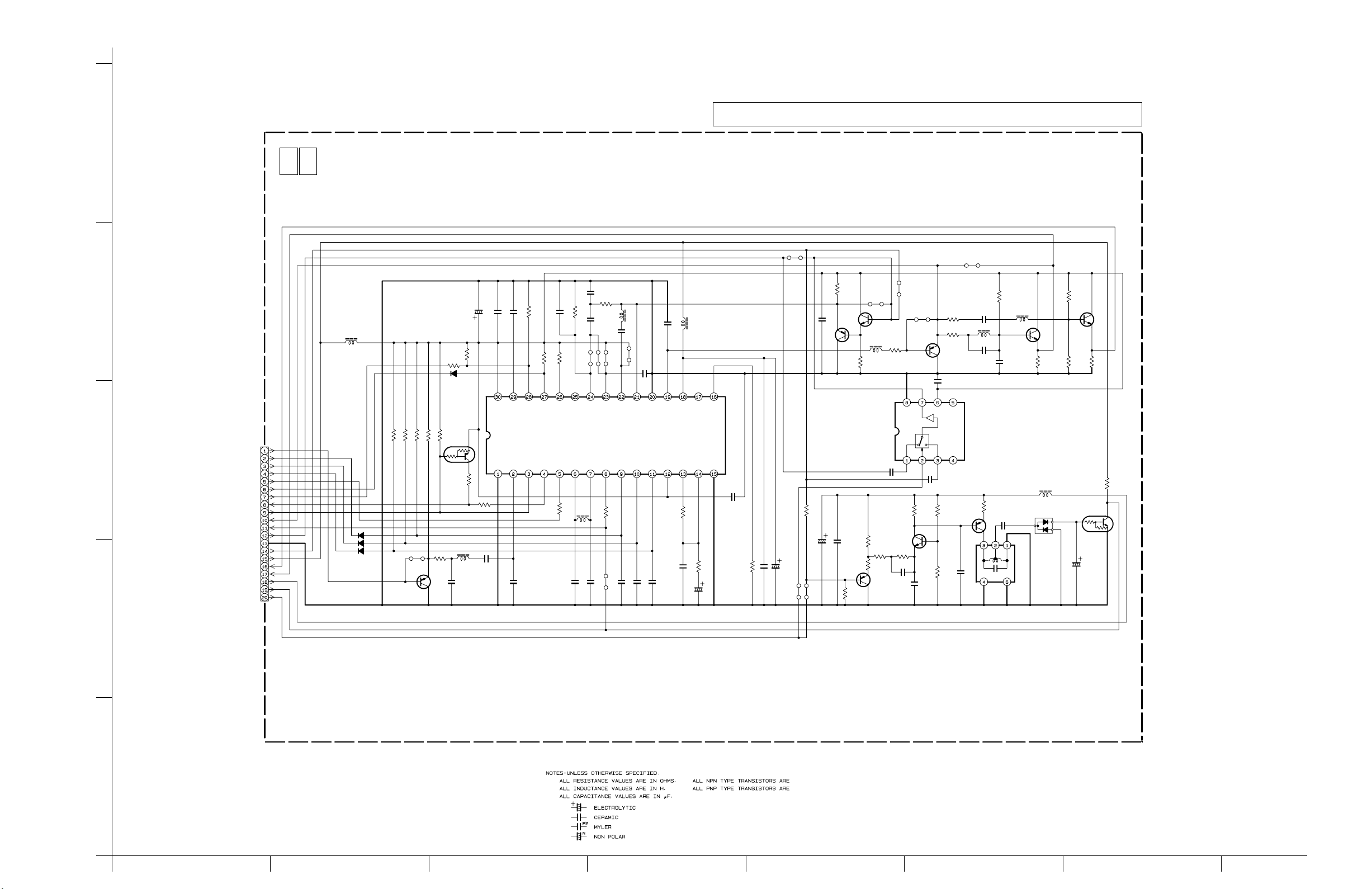
ON SCREEN SCHEMATIC DIAGRAM
4.13
The Parts Number,value and rated voltage etc. in the Schematic Diagram are for references only.
Note :
When replacing the parts,refer to the Parts List.
5
1 7 ON SCREEN
B859
C886
OPEN
R861
OPEN
R862
0Ω
OPEN
C861 L856
OPEN
L855
SHORT
C862
OPEN
R863
330
C863
OPEN
OPEN
Q854
OPEN
R864
OPEN
R865
OPEN
R866
OPEN
Q855
OPEN
R867
OPEN
B856
OPEN
C860
0.1
R858
OPEN
Q851
OPEN
B855
Q852
OPEN
L854 R860
SHORT
R859
OPEN
B857
B858
OPEN
Q853
0Ω
C855
OPEN
B851
C856
R857
0Ω
L852
1
B852
OPEN
C857
22µ
56p
B854
OPEN
B853
C858
0.47
C859
OPEN
L853
10µ330
IC851
LC74775-9750
R856
4
C851
C852 C853 R853
0.22 1 10k
L851
1µ
R851
OPEN
D851
SHORT
R852
OPEN
/6.3
OPEN
C854
OPEN
R854 R855
OPEN OPEN
(13)(14)(15)(16)(17)(18)(19)(20)(21)(22)(23)(24)
NC
NC
RST
VDD1
CPDT
XTAL_IN
C866
OPENOPEN
MUTE
(CDLR)
(BEP_IN)
CHABLK
TO
VIDEO I/O
CN851
2Fsc
3
OSD_CS
S.CLK
S.DATA_FRSYS
EDS[H]/
I2C_CLK2
EDS_CS/
I2C_DATA2
SWD_S.DATA
CHARA_DATA
P.MUTE[L]
V_FROM_OSD
SYNC_DET[H]
OSD_IN
GND
V_TO_OSD
SW5V
OSD_C
OSD_Y
SW12V
D_P.MUTE[H]
D_YV_IN/A_SEA[H]
D852
D853
D854
OPEN
Q861
OPEN
R872
R871
R870
R869
R868
VSS1
R890
OPEN
R891
0Ω
1.5k
100
100
Q856
OPEN
B860
C864
L857R873
C865
33µ0Ω
10p
10k
10k
OPEN
OPEN
SEP_IN
(SEP_OUT)
LN21
R874
0Ω
CDLR
(BEP_C)
SEO_OUT
OSC_IN
OSC_OUT
L858
22µ
C867 C868
33p 33p
SYN_IN
(SYN_IN)
SYNC_DET
B861
OPEN
R875
0Ω
(VDD1)
VSS2
VDD1
CV_IN
(CVCR)
CS1
SCLK
SD ATA
C869 C870 C871
100 100
OPEN
CVOUT
VDD2NCNC
R876
5.1k
C872
0.1
R877
1.8k
C873
47
/25
NC
C874
0.22
/6.3
5.6k
0.22
220
R878
C875
C876
OPEN
R889
OPEN
C877 C878
47 0.01
/16
C884
OPEN
R883 R884
8.2k 2.7k
R879
3.3k
R882
180k
R881
R880
470
0Ω
Q857
C879
R888B862 B863
4.7k
0.1
CS2
NC
C880
OPEN
Q858
NC
IC852
OPEN
H
NC
R887
Q860
DTC114EU
C883
2.2
/50
10k
C885
OPEN
R885
15k
C881
470p
Q859
R886
680
T851
PELN0806
C882
0.022
L859
4.7µ
D855
DA204U
2
p20228001a_rev0
1
4-29 4-30
2SC4081/QRS/.
2SA1576A/QR/.
HGFEDCBA
Page 63
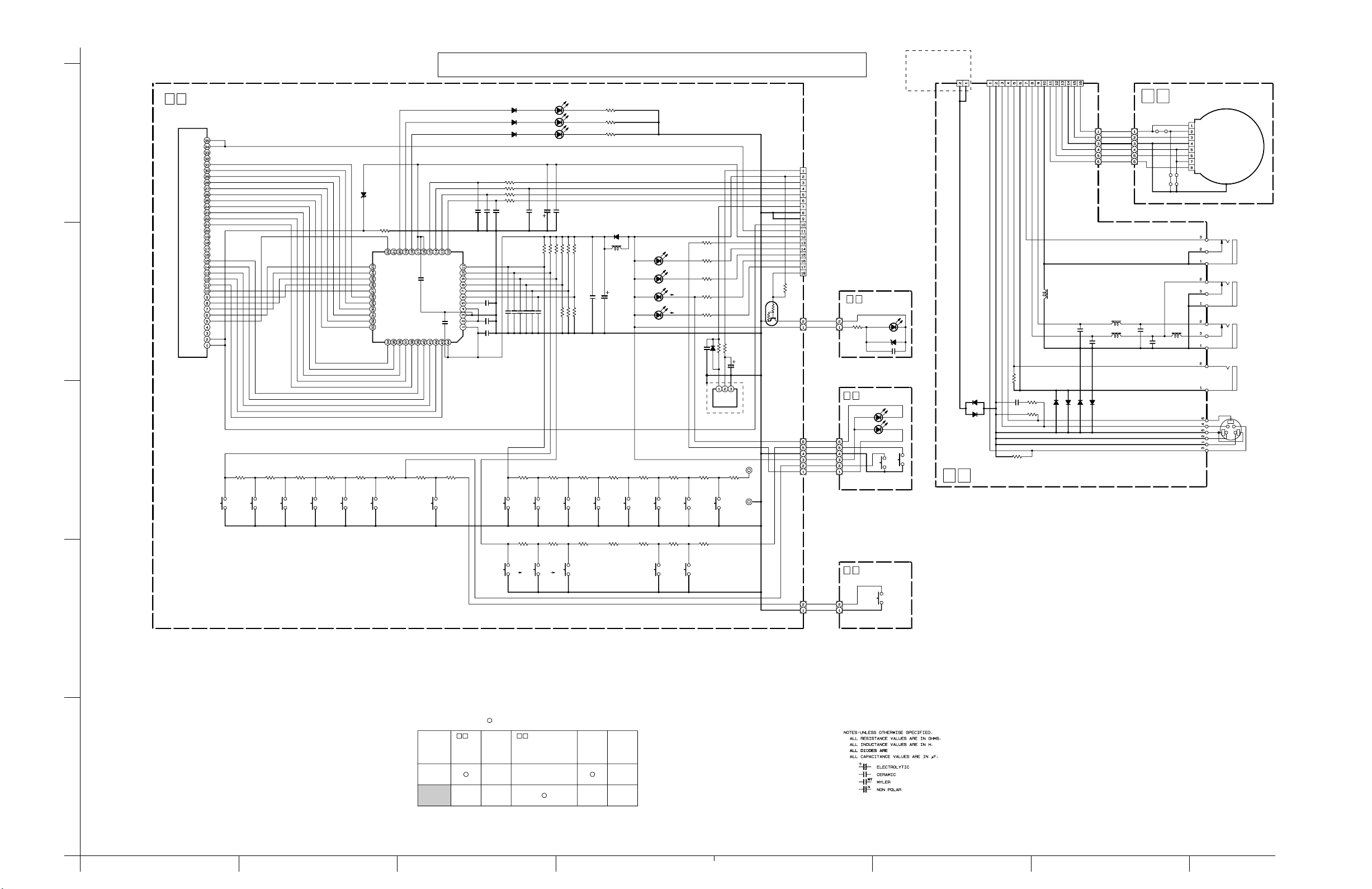
EJECT SW, DISPLAY, JACK, LED/SW AND LED SCHEMATIC DIAGRAMS4.14
D7017
OPEN
CN7002
CN7003
(CONNECTION)
MAIN
TO
##
0.01
C7022
#
GND
GND
##
D7061
##
D7062
Y1_IN
GND
C1_IN
#
TO MAIN (CONNECTION)
CN7507
GND
V1_IN
GND
R7061
75
C7061 R7063
0.01 75
R.PAUSE
0Ω
FRONT_A[L]
FRONT_A[R]
GND
J1/JOG_B
L7064
SHORT
D7066
GND/NC
SHUTTLE[L]/NC
J2/JOG_A
D7065
JSA/SHUTTLE_A
JSB/SHUTTLE_B
C7063
OPEN
C7065
OPEN
D7063
D7064
#
FW7007
L7061
L7062
#
#
FW7008
10
10
85JOG
#
UN7091
PEMC0786-02
B7094
#
####
B7092B7093
C7062
680p
L7063
SHORT
C7064
680p
JOG/SHUTTLE
UNIT
J7005
R.PAUSE
J7004
L_IN
J7003
R_IN
J7002
V_IN
J7001R7062
S_IN
The Parts Number, value and rated voltage etc. in the Schematic Diagram are for references only.
Note :
When replacing the parts, refer to the Parts List.
DISPLAY28
DI7001
QLF0031
QLF0033
F+
5
4
F+
NP
NC
P1
P2
P3
P4
P5
P6
P7
P8
P9
P10
P11
NC
NC
NC
NC
NC
P12
P13
P14
P15
P16
1G
2G
3G
4G
5G
6G
NC
NP
F-
F-
D7002
RD9.1ES/B2/
MTZJ9.1B
G5
G4
G3
G2
G1
S1
S2
S3
S4
S5
S6
R7013
10k
G6
G7
S7S8S9
LED3
IC7001
M35500BGP
CS
Sin
VEE
VEE
Sout
SCLK
LED1
LED2
C7020
##
S11
S10
AN0
AN1
AN2
AN3
AN4
AN5
RESET
Xin
VSS
C7021
##
Xout
VDD
S16
VDD
S15
S14
S13
S12
33p
C7006
##
D7006
D7005
D7004
R7001
R7002
R7003
R7004
33p
33p
C7004
C7005
##
##
C7010
0.1
C7013
C7009
15p
######
##
C7008
0.022
C7014
D7011
D7010
D7009
470
470
470
470
33p
/50
C7003
##
10
0.001
C7002
C7001
10k
10k
10k
R7040
R7020
R7030
C7016
C7017
C7018
C7015
##
##
##
10k
R7006
15k
R7010
###
VHS-REC
VHS-PLAY
VHS
10k
R7007
15k
R7011
10k
R7008
15k
R7012
R7059
R7058
R7057
330
330
330
TO MAIN (SYSCON)
CN3011
CN7001
RCU_5V
AL5V
S_CLK
S_DATA_TOSYS
S_DATA_FRSYS
STB
RC_IN
GND[C]
BU_GND
#
#
Q7001
DTC114E
R7060
10K
DC[-]
DC[+]
-28V
LED1
LED2
LED3
LED4
LED5
LED6
#
FW7001
#
FW7003
#
FW7002
#
FW7004
9 0 LED#
#
HDR-LED
SELU5E20C
R7056
#
100
D7019
#
10kΩ
4 7 LED/SW
D7018
#
RECLINK
D7012
DV/HDR
##
D7001
11ES2
R7051
330
D/H
PLAY
R7052
330
D/H
REC
R7053
330
DV
VHS
R7054
330
VHS
DV
R7055
#
330
0Ω
R7014
0Ω
D7003
R7015
C7012
C7011
10
##
##
/6.3
VCC
GND
V.OUT
IC7002
PNA4652M00XB
C7007C7019
470.022
L7001
SHORT
/6.3
D7013
D7014
D7015
#
D7016
#
3
R7021
1.2k
S7001
S7002 S7007
POWER
CH+
R7024
R7022
R7023
1.8k
2.2k
PAU SE S T OP CH- REC PLAY
R7025
4.7k
2.7k
#
S7012S7005 S7014
DV
S-VHS
EJECT
R7027
R7026
6.8k
ET
R7028
15k
39k
S7013
VHS
S7003
S7021
DV VHS DUB/OK
/LEFT
R7032
R7031
1.8k1.2k
S7004 S7015
R7042
R7041
1.2k
1.8k
S7022
VHS DV
/RIGHT
R7034
S7018
/A.DUB
R7035
4.7k
R7036
R7037
6.8k
15k
S7016
S7019
/FF
/MENU /NAVI
##
S7026 S7027
UP DOWN
R7033
2.2k 2.7k
S7006
RAE IN.OUT START INSERT A.DUB
/REW
#####
R7043 R7044 R7045 R7046 R7047
2.2k 2.7k 4.7k 6.8k 15k
S7023
S7017
R7038
TP7001
TEST
39k
TPGND
S7010
#
DV/HDR RECLINK
S7028
36JACK
2 7 EJECT SW
FW7005
FW7006
VHS
EJECT
S7011
R7064
75
2
p10309001a_rev1
Used
Not used
# DIFFERENCE TABLE
DVS2
1
/VS20
HDS1
8
UN7091
B7094
FW7007
FW7008
5
JOG
X
X
CN70029D7017
FW7001
FW7002
R7060 S7028 R7046
Q7001
1-16
1-10
0
LED
D7018 R7043
S7026 R7044
S7027 R7045
R7047
X
S7014
D7015
D7016
R7055
FW7003
FW7004
1-4
1-6
X
##:NOT USED
1N4148M OR 1SS133
ABCD EFGH
4-31 4-32
Page 64

DIGITAL P.SUP SCHEMATIC DIAGRAM
4.15
The Parts Number,value and rated voltage etc. in the Schematic Diagram are for references only.
Note :
When replacing the parts,refer to the Parts List.
5
DIGITAL(P.SUP)50
TO REGULATOR
CN5323
CN8901
AUDIO[-]
K8901
NQR0339-001
TO AUDIO AD/DA
AUDIO[-]
A5V
D3.3V
DGND
AL5V
GND
AL3.3V
AL3.3V
GND
AL2.5V
4
AL2.5V
GND
3
C8901 C8902 C8903 C8904
100 0.1 100 0.1
/16 /16
K8902
NQR0339-001
C8905 C8906
100 0.1
/6.3
T
C8917
10
100
/6.3
C8907
/6.3
K8904
K8905
K8906
K8907
C8918
0.1
K8903
NQR0339-001
NQR0339-001
C8909 C8910
100 0.1
/6.3
NQR0339-001
C8912C8911
/6.3
NQR0339-001
C8914C8913
/6.3
NQR0339-001
C8915
100
/6.3
IC8901
SI-3018LS
IN
NC
IN
Vc
C8908
0.1
0.1100
0.1100
C8916
0.1
VOUT
VOUT
GND
GND
T
C8919
10
/6.3
K8908
NQR0339-001
C8920
0.1 0.1100
TL8901
/6.3
TO VIDEO AD/DA
A5V
A3V/A3.3V
D1.8V
DGND
TO MPEG ENC.
D3.3V
D2.5V
A2.5V
DGND
TO MPEG DEC.
D5V
D3.3V
D2.5V
DGND
TO ASIC IF
D5V
C8922C8921
D3.3V
DGND
IC8902
OPEN
2
T
C8923
OPEN
C8924
T
C8925
OPENOPEN
K8909
OPEN
C8926
OPEN
C8928C8927
OPENOPEN
p30080001a_rev2
LAST NO VACANT NO
CK8928
1
8909
1~8900
1~8900
4-33 4-34
HGFEDCBA
Page 65

DIGITAL VIDEO SCHEMATIC DIAGRAM4.16
The Parts Number,value and rated voltage etc. in the Schematic Diagram are for references only.
Note :
When replacing the parts,refer to the Parts List.
5
5 0 DIGITAL(VIDEO AD/DA)
2SA1774/RS/-X
#
R8679
180
C8601
#
/6.3
10
T
#
R8682
15k
#
R8680
2.2k
#
R8681
1.5k
C8658
#
#
D8601
1SS355
1
4
L8603
L8606
NQR0339-001X
TL8601
C_OUT
TL8602
Y_OUT
NQR0339-001X
C8609
100
/6.3
C8618
0.01
C8610
0.01
TO MAIN(VIDEO I/O SW)
CN703
CN8601
C_IN
AGND
Y/V_IN
C_OUT
AGND
Y_OUT
3
TO P.SUP.
D1.8V
DGND
A3V/A3.3V
A5V
2
#
R8601
33k
R8602
22k
R8604
2SC4617/RS/-X
2SC4617/RS/-X
R8618
22k
R8619
27k
C8620
0.1 820
C8619
100
/6.3
C8627
0.1 820
Q8601
820
Q8606
R8603 R8606
820 390
Q8602
R8605
Q8603
1.8k
_0.5
R8607
OPEN
R8608
OPEN
VR8601
OPEN
2SC4617/RS/-X
C8612
0.1
R8621
OPEN
C8611
R8622
0.01
750
R8620
1k
C8613 C8615 C8616
8p 39p 33p
R8631
2SA1774/RS/-X
Q8610
R8632 C8621 C8622 C8624
2.2k 33p 39p 8p
R8646
2SA1774/RS/-X
Q8615
R8647 C8628 C8629 C8631
2.2k 33p 39p 8p
C8602
0.1
R8610
750
R8611
OPEN
R8609
1k
C8614
15p
CH
L8604 L8605
15µ 33µ
CH CH CH
C8623
15p
CH
L8607 L8608
33µ 15µ
CH CH CH
C8630
12p
CH
L8609 L8610
33µ 15µ
CH CH CH
C8604
15p
CH
L8601 L8602
15µ 33µ
CH CH CH
C8603 C8605 C8606 R8612
8p 39p 33p 2.2k
R8625
4.7k
Q8607
2SC4617/RS/-X
R8623
2.2k
R8629
27k
R8624
1.5k
_0.5
VR8602
OPEN
C8625
0.1
R8633
750
R8634
OPEN
2SC4617/RS/-X
C8632
0.1
R8648
750
R8649
OPEN
Q8604
2SA1774/RS/-X
Q8608 Q8609
2SC4617/RS/-X 2SC4617/RS/-X
R8626
1k
2SA1774/RS/-X 2SC4617/RS/-X
Q8612
Q8611
R8635
1k
2SA1774/RS/-X 2SC4617/RS/-X
Q8617
Q8616
R8650
1k
2SC4617/RS/-X
R8613
470
R8627
R8628
330
330
R8636 R8638
390 820
Q8613
R8637
1k
VR8603
1k
R8639
820
R8651
390
R8652
2.2k
VR8604
R8678
560
R8640
22k
C8626
0.01
R8641
27k
R8653
820
Q8618
10k
R8654
820
C8607
C8617
4.7
0.01
R8655
27k
R8656
27k
C8633
10
TL8604
/6.3
2SC4617/RS/-X
Q8605
R8616
680k
C_IN
R8643
1k
Q8614
2SA1774/RS/-X
R8658
1k
T
Q8619
2SA1774/RS/-X
R8617
220
R8644
200
R8659
200
C8608
0.01
TL8603
V/Y_IN
NQR0129-002X
L8612
C8644
L8611
10µ
T
C8635
C8634
0.01
/6.3
10
R8676
R8677
2.7k
R8660
2.7k
1.5k
R8661
0.1
C8636
820
R8662
220
R8666
100
R8663
0.1
C8637
0.1
C8638
0.1
C8639
0.1
C8640
0.1
C8641
0.1
C8645
10
/6.3
T
C8642
C8643
0.1
0.1
L8613
NQR0339-001X
NQR0339-001X
TT
C8647C8646 C8648 C8649
100.1 0.1 10
/6.3 /6.3
L8614
1.5k
AVSS[D/A]
AVDD[D/A]
IREF1
YCOUT
ABAR1
COMP1
YSOUT
VREF1
AVSS[D/A]
AVDD[D/A]
CLPY
VYIN
AVSS[A/D]
AVDD[A/D]
VRM
VRL
VRH
CIN
AVSS[A/D]
SCANMODE
SCANEN
COUT
C8650
220
R8668
VREF2
VSS
0.1
C8656C8657
0.10.1
100
R8675
ABAR2
CBOUT
COMP2
VDD[CDRE]
OUTH
OUTV
220
R8667
CROUT
CSO0
820
R8674
IREF2
CSO1
BLK2
VBLK
AVSS
AVDD
IC8601
JCP8029
CSO2
CSO3
VSS
VDD[I/O]
C8651
0.1
BLK1
YSO0
VB
YSO1
VR
VG
YSO2
YSO3
R8664 R8665
47k 47k
C8654C8655
0.10.1
TO ASIC IF
DGND
XRSTVDEC
CLK27MV
CSYNC
JVCS
VC1
VC2
VSS
VDOUT
VDD[I/O]
CLKOSD
HDOUT
CSYNC
AMUTE
ZCNT
RST
CLK
VDD[CORE]
VSS
CS
SCLK
SDIN
SDOUT
ADDATEST
RAMTEST
YSI3
YSI2
YSI1
YSI0
CSI3
INH
INV
CSI0
CSI1
CSI2
R8672
R8673
C8652
0Ω
0Ω
0.1
#
RA8602
0Ω
#
RA8601
0Ω
OUTY3
OUTY2
OUTY1
OUTY0
OUTC3
OUTC2
OUTC1
OUTC0
FIELDIN
HSYNCIN
TO MPEG DEC.
JVSDO
JVSDI
JVCLK
TO MPEG ENC.
DVIDEO0
DVIDEO1
DVIDEO2
DVIDEO3
DVIDEO4
DVIDEO5
DVIDEO6
DVIDEO7
DGND
DIFFERENCE TABLE
#
C8601
R8601
HDS1
USED
NOT USED
DD2
R8679-8682
C8658,D8601
NOT USED
USED
DOM
US
EU/EK/MS
RA8601
RA8602
USED
USED
NOT USED
CN8602
NOT USED
NOT USED
USED
TO
CN8602
#
DIGITAL_SUB
GND
DVIDEO_4
DVIDEO_3
DVIDEO_2
DVIDEO_1
GND
DVIDEO_0
A5V
A5V
DVIDEO_5
DVIDEO_6
DVIDEO_7
p10313001a_rev4
1
LAST NO VACANT NO
R
C
Q
L
TL
VR
ABCD EFGH
4-35 4-36
8614,8615,8630,8642,8645,8657,8669~8671
1~8600,
8682
,8653
1~8600
8658
1~8600
8619
1~8600
8614
1~8600
8604
1~8600
8604
Page 66

DIGITAL AUDIO SCHEMATIC DIAGRAM
4.17
The Parts Number,value and rated voltage etc. in the Schematic Diagram are for references only.
Note :
When replacing the parts,refer to the Parts List.
50
5
TO MAIN (AUDIO I/O)
4
CN2601
3
CN8801
A_IN[L]
AGND
A_IN[R]
AGND
A_OUT[L]
AGND
A_OUT[R]
AGND
DIGITAL(AUDIO AD/DA)
R8822
OPEN
C8816
1
C8820
1
C8821
OPEN
C8817
OPEN
R8819
C8818
OPEN
220
/50
IC8803
BA15218F
R8824
/50
C8822
OPEN
220
VCC
R8825
R8826
1k
R8820
2.2k
R8823
3k
C8819
OPEN
IC8802
BA15218F
VEE
C8823
OPEN
2.2k
1k
R8827
OPEN
R8828
3k
C8834
VCC
0.1
C8829
C8830
0.0033
OPEN
C8835
47
C8825
0.0033
C8826
0.0068
C8824
OPEN
VEE
R8833 R8835
C8831
0.0068
/16
C8836
0.1
1k 0Ω
R8830
R8834
C8837
47
C8827R8821
OPEN
R8831R8829
1k
1k
C8832
OPEN
L8803
L8801
NQR0339-001X
L8802
10µ
/16
R8810
10
DEM0
PWAD
0Ω
R8805
R8815R8816
OPENOPEN
R8814
R8813
DEM1
PWDA
0Ω
R8806
0Ω
R8812
CMODE
MCLK
0Ω
R8807
R8811C8811
OPEN
0Ω
0Ω
SDTIVDDGND
LRCK
SCLK
0Ω
0Ω
R8808
R8809
T
C8809
SDTO
C8810C8812
/6.3/6.3
224.7
0.1
R8832
10k
C8828
10
0Ω1k
/6.3
T
R8817
R8818
C8813
OPEN
0Ω
0.1
VA
IC8801
C8833
10
/6.3
T
AK4518
VRDA
T
R8836
10k
10µ
C8815
0.1
C8814
22
/6.3
VB
VRAD
AGND
AINR
T
VCOM
VCMR
AOUTR
VCML
0.1
AOUTL
AINL
TO P.SUP
A5V
AUDIO[-]
D3.3V
DGND
TO ASIC IF
DEM0
DEM1
TO MPEG DEC.
DA_SDTI
XRSTDEC
MCLK
DA_LRCLK
DA_SCLK
TO MPEG ENC,
ASIC IF
DA_SDTO
XRSTENC
1
15k
R8801
R8802
15k
2
R8803 R8804
8.2k 8.2k
/50
C8801
/50
1
C8802
C8804 C8808
150p 150p
T
C8803
4.7
/6.3
C8805 C8806
0.1 0.1
T
C8807
4.7
/6.3
p20193001a_rev0
1
4444444
4-37 4-38
LAST NO VACANT NO
R
C
L
1~8800
8836
1~8800
8837
8803 1~8800
HGFEDCBA
Page 67

DIGITAL MPEG DEC SCHEMATIC DIAGRAM4.18
50
DIGITAL(MPEG DEC.)
OPEM
CN8203
QGF0503C1-30
GND
STEANABLE
The Parts Number,value and rated voltage etc. in the Schematic Diagram are for references only.
Note :
GND
GND
GND
GND
GND
GND
GND
GND
GND
STD0
STD1
STD2
STD3
STD4
STD5
STD6
STD7
AVTRM
STVALID
STCLK
SSPCLK0
GND
XRSTPDVD
SSPOUT0
XTXREQ
SSPIN0
XWAIT
XTXENABLE
TL8209 TL8208 TL8207
FRASHSDRAM
R8205
R8204
0Ω
OPEN
When replacing the parts,refer to the Parts List.
5
B8201
IC8208
OPEN
T T
C8279
OPEN /6.3
OPEN
C8243
0.1
Vdd
DQ0
C8244
0.1
Vdd
DQ1
DQ2
Vss
4
3
TO P.SUP
D2.5V
D3.3V
D5V
DGND
TO AUDIO AD/DA
2
XRSTDEC
DA_LRCLK
DA_SCLK
MCLK
DA_SDTI
TO VIDEO AD/DA
JVCLK
JVSDI
JVSDO
TO MPEG ENC.
CLK27M
DA_LRCLK
DA_SCLK
MCLK
UART0
CN8202
QGF1016F2-06W
D5V
TXD
RXD
CTS
RTS
DGND
DQ3
DQ4
C8245
0.1
Vdd
DQ5
DQ6
Vss
DQ7
C8246
0.1
Vdd
LDQM
WE
CAS
RAS
CS
BA0
BA1
A10/AP
A0
A1
A2
A3
Vdd
C8250
0.1
Vdd
DQ0
C8251
0.1
Vdd
DQ1
DQ2
Vss
DQ3
DQ4
C8252
0.1
Vdd
DQ5
DQ6
Vss
DQ7
C8253
0.1
Vdd
LDQM
WE
CAS
RAS
CS
BA0
BA1
A10/AP
A0
A1
A2
A3
Vdd
NQR0339-001X
C8280
0.1
IC8202
K4S641632D-TC1H
UDQM
0.1
C8247
IC8203
K4S641632D-TC1H
DQ15
DQ14
DQ13
DQ12
DQ11
DQ10
UDQM
0.1
C8254
K8210
C8283C8282C8278 C8281
0.110022
/6.3
Vss
DQ15
Vss
DQ14
DQ13
C8249
0.1
Vdd
DQ12
DQ11
Vss
DQ10
DQ9
C8248
0.1
Vdd
DQ8
TL8213
Vss
N.C.
CLK
CKE
N.C.
A11
A9
A8
A7
A6
A5
A4
Vss
Vss
Vss
Vdd
Vss
DQ9
Vdd
DQ8
Vss
N.C.
CLK
CKE
N.C.
A11
A9
A8
A7
A6
A5
A4
Vss
TL8212
C8256
0.1
C8255
0.1
C8222
22
/6.3
T
C8201
Vddio
0.1
MD10
MD11
C8202
Vdd
0.1
MD12
Vssio
MD13
MD14
MD15
C8203
Vddio
0.1
DQM1
MA9
MA8
Vssio
MA7
MA6
Vss
MA5
C8204
Vddio
0.1
MA4
MA3
R8230
MCLK
22Ω
Vssio
CKE
MA2
MA1
C8205
Vddio
0.1
MA0
MA10
MA11
Vssio
MA12
MA13
C8206
Vdd
0.1
CS0-
C8207
Vddio
0.1
RAS-
CAS-
WE-
Vssio
DQM0
DQM2
MD16
C8208
Vddio
0.1
MD17
MD18
Vss
MD19
Vssio
MD20
MD21
MD22
C8209
Vddio
0.1
MD23
MD24
MD25
Vssio
MD26
MD27
MD28
C8218
T
C8210
22
/6.3
0.1
0.1
C8242
MD3
MD4
MD5
MD6
MD7
MD8
MD9
Vssio
Vddio
Vddio
MD29
MD30
MD31
Vss
Vssio
CS1-
DQM3
SPDIF
100
C8289
R8242
0.1
1M
R8241
0Ω
0.1
C8275
OPEN
C8241
R8229
OPEN
Vss
MD0
MD1
MD2
Vssio
Vddio
DVD3
DVD4
DVD5
DVD6
DVD7
Vddio
Vdd
AOUT0
AOUT1
AOUT2
AOUT3
ACLK
PCMCLK
AIN
RA8212
0Ω
C8287
/6.3
LRCLK
SRST-
0.1
0.1
C8211
C8212
C8288
0.1
Vcc
R8248
Vssio
DVD1
DVD2
Vssio
RXD1
RSTP-
GND
OPEN
TL8215
R8245
C8277
OPEN
0.1
OPEN
C8276
OPEN
OPEN
C8240
R8227
R8228
DVD0
DCLK
DSTB
DREQ
DSYNC
NDV8501VWB
Vss
SSPCLK1/CTS1-
SSPOUT1/DTR1-
SSPIN1/BAUD1
SSPCLK0/RTS1
0.1
C8213
IC8210
TC7WU04FU
10K
R8244TL8204
10K
0.1
C8239
Vdd
Vddio
XIO14
IC8201
Vddio
Vdd
SSPIN0/BAUD0
0.1
C8214
R8243
0Ω
TL8203
XIO11
XIO12
XIO13
RXD0
TXD0
SSPOUT0/DTR0
R8231
OPEN
OPEN
OPEN
0Ω
0Ω
RA8214
RA8213
0Ω
0Ω
0Ω
0.1
0.1
C8237
C8238
R8224
R8225
R8226
Vss
XIO3
XIO4
XIO5
XIO6
XIO7
XIO8
XIO9
Vssio
XIO10
Vssio
CXI
CXO
OSCVdd
OSCVss
MVCKVdd
MVCKVss
SCEN
RTS0
CTS0
0Ω
0.1
0.1
C8217
C8215
R8247
TL8214
R8203
0Ω
TL8211
Vddio
ACLKVss
RD-
Vdd
LA3
XIO1
XIO2
Vssio
LHLD
PCS0
LHLDA
ACLKVdd
SCMD
0.1
C8219
Y/G
C/Cb/B
CVBS2/Cr/R
IOM
Vdddac
Vssdac
Vaa3
0.1
0.1
C8221
C8223
R8206
39
OPEN
R8218
R8219
10K
R8221
R8220
R8222
R8223
0.1
C8236
LA0
LA1
LA2
ALE
Vddio
PWE0-
PWE1-
PWE2-
PWE3-
HSYNC
VSYNC
VIOCLK
CVBS/C
VREF
RSET
COMP
Vaa
Vssa
0.1
0.1
C8229
C8227
R8215
R8246
75
1.1k
OPEN
T
C8220
22
/6.3
AD0
AD1
AD2
Vssio
AD3
AD4
AD5
AD6
AD7
Vss
Vddio
AD8
AD9
AD10
AD11
AD12
AD13
Vssio
ACK-
SCLK
Vdd
AD14
AD15
AD16
Vddio
AD17
AD18
AD19
AD20
AD21
AD22
Vssio
AD23
AD24
AD25
AD26
AD27
Vddio
AD28
AD29
AD30
AD31
Vdd
VIO0
VIO1
Vssio
VIO2
VIO3
VIO4
VIO5
VIO6
VIO7
Vddio
Vss
TL8205
C8216
22
TEST V OUT
R8216
OPEN
C8235
0.1
C8290
TL8201
OPEN
R8217
22Ω
C8234
0.1
C8233
0.1
C8232
0.1
C8231
0.1
C8230
0.1
T
/6.3
R8232 R8233
OPEN
OPEN 3.3K
TO ASIC IF
DVD7_
K8209
NQR0129-002X
C8272
22
/6.3
T
C8273
R8201
0Ω
R8202
0Ω
5V
5V
5V
5V
3.3V
3.3V
0.1
C8268
0.1
C8267
3.3V
SPARE1
SPARE2
GND
AD30
AD28
AD26
AD24
AD23
AD22
AD21
AD19
AD17
AD16
AD15
AD14
AD13
AD12
AD11
AD10
AD8
AD7
AD6
AD5
AD3
AD1
GND
PWE0
GND
LA0
LA2
GND
RD
GND
LHLD
GND
SRAMCS
GND
XIO3
GND
XIO5
GND
XIO7
GND
XIO9
GND
XIO11
CN8201
CN8201
3.3V
SPST
RSTP
GND
AD31
AD29
AD27
AD25
GND
PWE3
GND
AD20
AD18
GND
PWE2
GND
SCLK
GND
ACK
GND
AD9
GND
PWE1
GND
AD4
AD2
AD0
GND
ALE
GND
LA1
LA3
GND
LHLDA
GND
PCS0
GND
XIO1
GND
XIO4
GND
XIO6
GND
XIO8
GND
XIO10
GND
OPEN
IC8204
R8234
OPEN
R8235
OPEN
R8237
OPEN
R8238
OPEN
39VF800A7CEK04A
A15
A14
*/BYTE
A13
A12
A11
A10
A9
A8
A19
NC
/WE
*/RST
NC
NC
*R/B
A18
A17
A7
A6
A5
A4
A3
A2
A1
IC8205
OPEN
A15
A14
*/BYTE
A13
A12
A11
A10
A9
A8
A19
NC
/WE
*/RST
NC
NC
*R/B
A18
A17
A7
A6
A5
A4
A3
A2
A1 A0
A16
R8236
OPEN
VSS
D15
D7
D14
D6
D13
D5
D12
D4
VCC
D11
D3
D10
D2
D9
D1
D8
D0
OE
TL8202
VSS
/CE
A0
C8269
0.1
A16
R8239
OPEN
VSS
D15
D7
D14
D6
D13
D5
D12
D4
VCC
D11
D3
D10
D2
D9
D1
D8
D0
OE
VSS
/CE
C8270
0.1
C8271
22
/6.3
T
K8208
OPEN
K8207
NQR0129-002X
0.1
IC8206
SN74LV573APW
OE
VCC
D0
D1
D2
D3
D4
D5
D6
D7
GND
C8274
0.1
IC8207
SN74LV573APW
OE
VCC
D1 Q1
D3 Q3
D4 Q4
D6 Q6
GND
Q0
Q1
Q2
Q3
Q4
Q5
Q6
Q7
LE
Q0D0
Q2D2
Q5D5
Q7D7
LE
R8240
OPEN
DVD6_
DVD5_
DVD4_
DVD3_
DVD2_
DVD1_
DVD0_
DSTB_
DCLK_
DREQ_
DSYNC_
XIO2
XRD
ALE
XPWE0
AD0
AD1
AD2
AD3
AD4
AD5
AD6
AD7
AD8
AD9
AD10
AD11
AD12
AD13
XACK
SCLK
AD14
AD15
AD16
AD17
AD18
AD19
AD20
AD21
AD22
AD23
AD24
AD25
AD26
AD27
AD28
AD29
AD30
AD31
VIO0
VIO1
VIO2
VIO3
VIO4
VIO5
VIO6
VIO7
VIOCLK
XRSTDEC
1
LAST NO VACANT NO
R
8248
1~8200
C
K
TL
IC
4444444
ABCD EFGH
4-39 4-40
,8207~8214
8290
1~8200
,8224~8226,8228,8257~2866,8284~8286
8210
1~8206
8215
1~8200,8206,8210
8210
1~8200,8209
p10311001a_rev1
Page 68

DIGITAL MPEG ENC SCHEMATIC DIAGRAM
4.19
The Parts Number,value and rated voltage etc. in the Schematic Diagram are for references only.
Note :
CN8401
TO
DIGITAL SUB
CN1
DGND
#
5
4
3
2
D3.3V
TO
D2.5V
P.SUP.
DGND
A2.5V
D1.8V
DIGITAL(MPEG ENC.)
50
IC8402
KM416S1120DT-G8
C8434
0.1
VDD
DQ0
DQ1
VSSQ
DQ2
C8441
0.1
DQ3
VDDQ
DQ4
DQ5
VSSQ
DQ6
DQ7
VDDQ
LDQM
WE
CAS
RAS
CS
BA
A10/AP
A0
A1
A2
A3
VDD
KM416S1120DT-G8
VDD
DQ0
DQ1
VSSQ
DQ2
DQ3
VDDQ
DQ4
DQ5
VSSQ
DQ6
DQ7
VDDQ
LDQM
WE
CAS
RAS
CS
BA
A10/AP
A0
A1
A2
A3
VDD
IC8403
L8402
#
K8404
#
C8435
0.1
C8436
0.1
C8437
0.1
C8442
0.1
C8443
0.1
C8444
0.1
C8440
10
/6.3
T
C8447
10
T
NQR0339-001
NQR0339-001X
N.C/RFU
UDQM
/6.3
N.C/RFU
UDQM
DQ15
DQ14
VSSQ
DQ13
DQ12
VDDQ
DQ11
DQ10
VSSQ
VDDQ
DQ15
DQ14
VSSQ
DQ13
DQ12
VDDQ
DQ11
DQ10
VSSQ
VDDQ
VSS
C8426
C8439
0.1
DQ9
DQ8
C8438
0.1
CLK
CKE
N.C
A9
A8
A7
A6
A5
A4
VSS
VSS
C8446
0.1
DQ9
DQ8
C8445
0.1
R8408
CLK
CKE
N.C
A9
A8
A7
A6
A5
A4
VSS
#
C8462
22
/6.3
200
TL8411
T
C8427
0.1
C8428
0.1
R8406
C8429
200
0.1
C8430
0.1
C8431
0.1
C8432
0.1
R8407
3.3k
R8410
0Ω
L8401
NQR0339-001
L8403
NQR0339-001
0.1
SDDATA26
VDDI
SDDATA24
SDDATA25
TSPSSYNC
STEN
VDDI
SDDATA5
SDDATA4
SDDATA3
SDDATA2
SDDATA1
SDDATA0
ST DATA 7
ST DATA 6
ST DATA 5
ST DATA 4
AVDD
AVSS
ST DATA 3
VDDE
VSS
SDDATA27
SDDATA28
SDDATA29
SDDATA30
SDDATA31
SDDATA23
SDDATA22
VDDI
SDDATA21
SDDATA20
SDDATA19
SDDATA18
SDDATA17
SDDATA16
VSS
VDDE
SDDQM
XSDWE
XSDCAS
XSDRAS
XSDCS
SDCKE
SDCLK
VDDI
SDADRS3
SDADRS4
SDADRS5
SDADRS6
SDADRS7
SDADRS8
VDDE
VSS
SDADRS9
SDADRS2
SDADRS1
SDADRS0
SDADRS10
SDADRS11
VSS
VDDE
ASCLK
ADATA
VPDX
TESTMODE
ALRCK
ACLK
STREQ
XTST
VDDE
C8433
VSS
0.1
#
T
T
C8401
22
C8404
22
C8403
C8402
/6.3
0.1
10
/6.3
T
C8405
0.1
/6.3
VSS
VDDE
SDDATA7
SDDATA6
SDDATA14
SDDATA15
ST DATA 2
ST DATA 1
ST DATA 0
VSS
VDDE
STCLK
C8408
0.1
C8424C8425
0.10.1
VSS
VDDE
SDDATA8
SDDATA9
SDDATA10
SDDATA11
SDDATA12
SDDATA13
#
IC8401
MB86390
SDATAOUT
SDATAIN
SCLK
VDDI
XREADY
XRDWR
XAS
AVSS
C8409 C8412
0.1 0.1
C8407
0.1
DGND
VCLK
AVDD
DGND
TL8410
XHSYNC
MCLKI
CLK27M
TL8409
XVSYNC
PLLTHR
R8401
5.1k
D3.3V
FIELD
CLKSEL
D3.3V
XVALID
XBREQ
R8402
5.1k
DVIDEO7
D3.3V
VDDI
DVIDEO7
XBMREQ
IRQ8
DVIDEO0
DVIDEO1
DVIDEO2
DVIDEO3
DVIDEO4
DVIDEO5
DVIDEO6
VSS
VDDE
ADRS14
DVIDEO0
DVIDEO1
DVIDEO2
DVIDEO3
DVIDEO4
DVIDEO5
DVIDEO6
IRQ9
XRESET
VDDE
VSS
XBGRNT
BUSDIR
XBUSEN
XEXTIRPT
XERROR
XCS0
C8410 C8411
0.1 0.1
ADRS13
XCS4
ADRS12
XCS5
When replacing the parts,refer to the Parts List.
C8421C8422
0.10.1
C8420C8423
0.10.1
VSS
VDDI
VDDE
ADRS9
ADRS4
ADRS3
ADRS2
BCLK
ADRS10
ADRS11
ADRS8
ADRS7
ADRS6
ADRS5
C8419
VDDE
0.1
VSS
SPCKE
SPSDCLK
VDDI
XSPWE
XSPCAS
XSPRAS
ADRS15
ADRS16
ADRS17
ADRS26
ADRS27
VSS
VDDE
D0
D1
D2
VDDI
D3
D4
D5
VDDE
VSS
D6
D7
D15
D14
D13
D12
D11
D10
D9
D8
VDDI
D16
D17
D18
VSS
VDDE
D19
D20
D21
D22
D23
D31
D30
VSS
VDDE
D29
D24
D25
VDDI
D26
D27
D28
200
R8403
C8418
0.1
C8417
0.1
C8416
0.1
C8415
0.1
C8414
0.1
C8413
0.1
TO
VIDEO AD/DA
ASIC IF
DVIDEO0
DVIDEO1
DVIDEO2
DVIDEO3
DVIDEO4
IC8404
KM416S1120DT-G8
C8448
0.1
C8449
0.1
C8450
0.1
C8451
0.1
IC8405
KM416S1120DT-G8
C8455
0.1
C8456
0.1
C8457
0.1
C8458
0.1
VDD
DQ0
DQ1
VSSQ
DQ2
DQ3
VDDQ
DQ4
DQ5
VSSQ
DQ6
DQ7
VDDQ
LDQM
WE
CAS
RAS
CS
BA
A10/AP
A0
A1
A2
A3
VDD
VDD
DQ0
DQ1
VSSQ
DQ2
DQ3
VDDQ
DQ4
DQ5
VSSQ
DQ6
DQ7
VDDQ
LDQM
WE
CAS
RAS
CS
BA
A10/AP
A0
A1
A2
A3
VDD
C8454
10
TT
C8461
OPEN
/6.3
VSSQ
VDDQ
VSSQ
VDDQ
N.C/RFU
UDQM
VSSQ
DQ13
DQ12
VDDQ
DQ11
DQ10
VSSQ
VDDQ
N.C/RFU
UDQM
VSS
DQ15
DQ14
DQ13
DQ12
DQ11
DQ10
DQ9
DQ8
CLK
CKE
N.C
VSS
VSS
DQ15
DQ14
DQ9
DQ8
CLK
CKE
N.C
VSS
C8453
0.1
C8452
0.1
A9
A8
A7
A6
A5
A4
C8460
0.1
C8459
0.1
R8409
200
A9
A8
A7
A6
A5
A4
DVIDEO5
DVIDEO6
DVIDEO7
CLK27M
TO
ASIC IF
XHSYNC
FIELD
XRSTENC
PLLTHR
TSCLK
TSDATAIN
TSDATAOUT
STDATA0
STDATA1
STDATA2
STDATA3
STDATA4
STDATA5
STDATA6
STDATA7
STEN
TSPSSYNC
TL8412
TL8413
TO AUDIO AD/DA
MPEG_DEC
DA_SCLK
DA_LRCLK
DA_SDTO
CLK27M
MCLK
CLK27M
TL8414
p10312001a_rev2
1
DIFFERENT TABLE
#
IC8401
MB86390
MB86391
L8402
C8402
USED
NOT USED
K8404
C8462
NOT USED
USED
DOM
US
EU/EK/MS
CN8401
NOT USED
NOT USED
USED
4-41 4-42
LAST NO VACANT NO
R
84108410
1~8400
C
L
IC
TL
,8404,8405
8462
1~8400
,8406
8403
1~8400
8405
1~8400
1~84008414
HGFEDCBA
Page 69
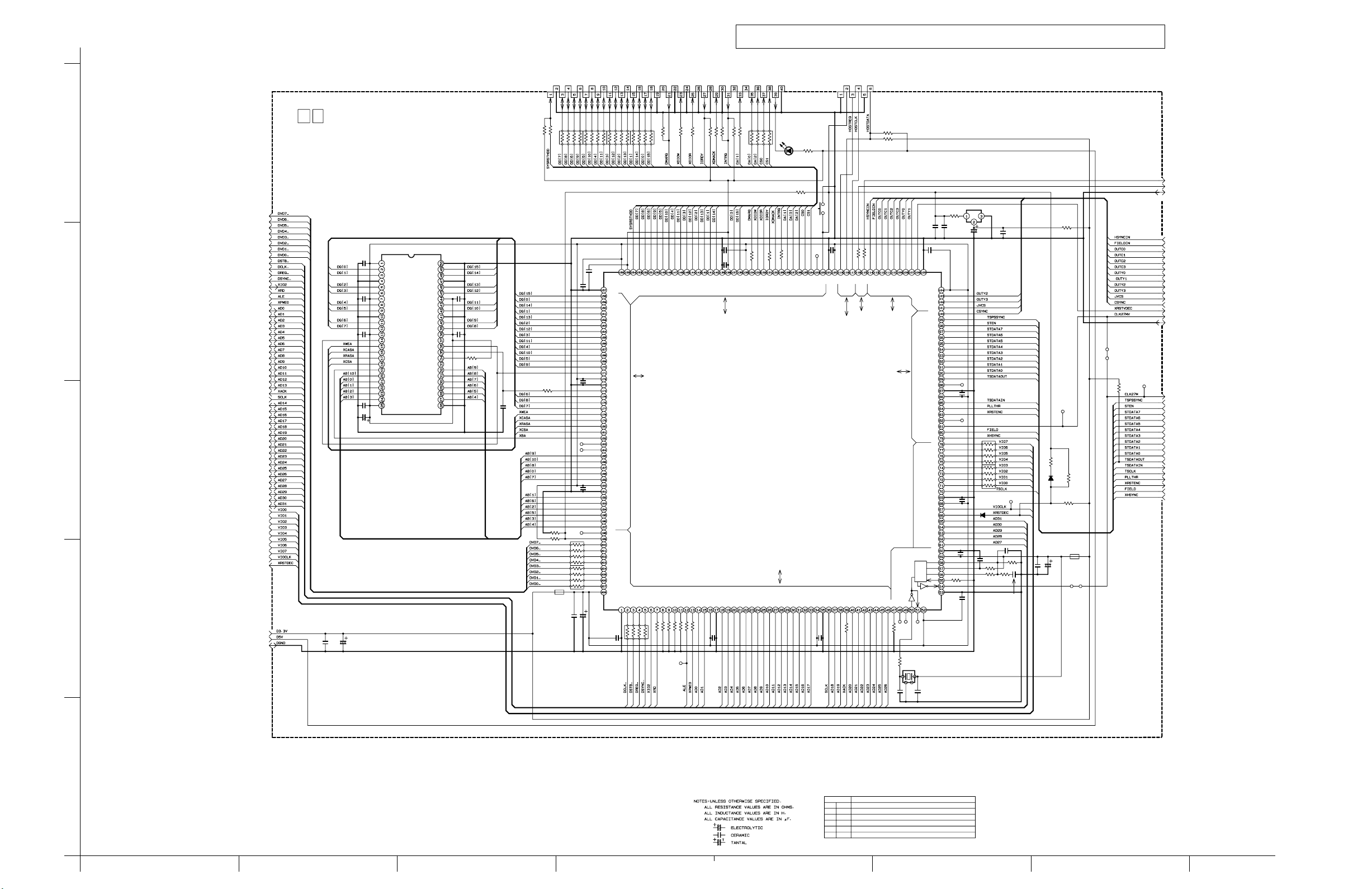
The Parts Number,value and rated voltage etc. in the Schematic Diagram are for references only.
IORDY
CSEL
DMACK-
1k
33
R8026
R8016
C8023
C8030
DD[1]
DD[14]
FROM_TO_HDD
Vss
Vdd
C8014
0.1
Note :
When replacing the parts,refer to the Parts List.
GND
INTRQ
RESERVED
DA1
PDIAG-
DA0
DA2
CS0
CS1
DASP-
GND
33
33
10k
RA8008
OPEN
R8029
R8027
R8020
R8028
0.1
0.1
82
R8017
R8015
Vss
Vdd
DD[0]
DD[15]
IORDY
XDIOR
XDIOW
DMAQR
VDD[5V]
OPEN
D8001
OPEN
R8045
OPEN
82
82
R8014
CS0
DA[1]
DA[0]
DA[2]
INTRQ
XDMACK
IC8001
JCP8043-2
FROM_TO_MPEG.DEC
AD2
AD3
AD4
AD5
AD6
AD7
AD8
AD9
AD10
AD11
AD12
AD13
AD14
AD15
AD16
TO MAIN
SW8001
NSW0100-001X
TL8006
CS1
GPO3
Vdd
AD17
C8015
0.1
(SYSCON)
CN3014
CN8002
HOSTRST
OPEN
0.1
C8022
Vss
Vdd
XSYSRST
FROM_TO_HOST_S-CTL
Vss
AD18
SCLK
N.C.
SYS RST
HOSTDATA
HOSTDREQ
AD19
XACK
0Ω
R8040
HOSTCLK
DGND
HOSTDATA
HOSTREQ
R8031
R8032
0Ω
0 Ω
R8012
R8013
DEM1
DEM0
HSYNCIN
HOSTCLK
TO_AUDIO_DA
FROM_TO_MPEG.ENC
AD20
AD21
AD22
AD23
OUTC0
FIELDIN
TO_VIDEO_DA
AD24
AD25
OUTC1
AD26
C8016
33k
OPEN
TO AUDIO AD/DA
DEM1
DEM0
DGND
R8005
0.1
OPEN
C8026
0Ω
IC8003
MN1382/K/
C8034
C8038
22
T
0.1
C8019
TL8005
C8020
0.1
TL8004
0.1
D8003
/6.3
OPEN
C8033
C8032
0.1
R8008
5.6k
R8006 R8007
7.5k 39
1
TL8012
R8009
1M
C8027
RA8003
0Ω
RA8002
0Ω
47p
0.22
C8028
R8048
560
B8002
0Ω
R8011
330
TL8003
R8043
OPEN
D8002
R8047
0Ω
OPEN
R8042
10k
K8001
T
C8029
B8001
10
0.1
OPEN
/6.3
TL8011
TO VIDEO AD/DA
HSYNCIN
FIELDIN
OUTC0
OUTC1
OUTC2
OUTC3
OUTY0
OUTY1
OUTY2
OUTY3
JVCS
CSYNC
XRSTVDEC
CLK27MV
DGND
TO MPEG ENC.
ASIC IF
CLK27M
TSPSSYNC
STEN
STDATA7
STDATA6
STDATA5
STDATA4
STDATA3
STDATA2
STDATA1
STDATA0
TSDATAOUT
TSDATAIN
TSCLK
PLLTHR
XRSTENC
FIELD
XHSYNC
R8044
2.2k
C8036
C8035
0.1
C8021
0.1
Vss
OUTY1
OUTY0
OUTC2
OUTC3
Vdd
XRSTVDEC
OUTY2
OUTY3
JVCS
XNOSYNC
TSPSSYNC
STEN
STDATA7
STDATA6
STDATA5
STDATA4
STDATA3
STDATA2
STDATA1
STDATA0
TSDATAIN
GPO2
Vss
Vdd
TSDATAOUT
PLLTHR
XRSTENC
GPO1
GPO0
FIELD
XHSYNC
VIO7
VIO6
VIO5
VIO4
VIO3
VIO2
VIO1
VIO0
TSCLK
Vss
Vdd
VIOCLK
XRSTDEC
AD31
AD30
AD29
AD28
AD27
PLL_Vss
PLL_Vdd
PLL
Vss
C8018
Vdd
SCANEN
SELCLK
TESTMODE
0Ω
TL8001
TL8013
TL8002
R8041
R8004
0Ω
X8001X8001X8001X8001
NAX0304-001xNAX0304-001xNAX0304-001xNAX0304-001x
12p
C8017
0.01
DIGITAL ASIC IF SCHEMATIC DIAGRAM4.20
GND
DD7
DD8
DD6
DD9
DD5
DD10
DD4
DD11
DD3
DD12
DD2
DD13
DD1
DD14
DD0
DD15
GND
[KEY]
DMARQ
GND
DIOW-
GND
DIOR-
OPEN
R8036
DD[10]
LA2
0Ω
R8037
TL8010
GND
33
33
R8023
R8024
DD[2]
DD[3]
DD[4]
DD[11]
DD[13]
DD[12]
LA1
LA0
AD0
ALE
XPWE0
AD1
0Ω
0Ω
OPEN
R8039
R8038
R8002
SYSRST-
TO HARD
DISK
DRIVER
CN8001
5
0
DIGITAL(ASIC IF)
5
10k
R8019
33
R8022
RA8004
RA8005
33
RA8006
33
33
RA8007
5.6k
33
R8018
TO MPEG DEC.
DVD7_
DVD6_
DVD5_
DVD4_
DVD3_
DVD2_
DVD1_
DVD0_
DSTB_
DCLK_
DREQ_
DSYNC_
XIO2
XRD
4
3
2
XPWE0
AD0
AD1
AD2
AD3
AD4
AD5
AD6
AD7
AD8
AD9
AD10
AD11
AD12
AD13
XACK
SCLK
AD14
AD15
AD16
AD17
AD18
AD19
AD20
AD21
AD22
AD23
AD24
AD25
AD26
AD27
AD28
AD29
AD30
AD31
VIO0
VIO1
VIO2
VIO3
VIO4
VIO5
VIO6
VIO7
VIOCLK
XRSTDEC
TO P.SUP
D3.3V
DGND
ALE
D5V
C8024
C8001
0.1
C8002
0.1
C8003
0.1
C8004
0.1
C8005
100
/6.3
C8025
0.1
/6.3
100
IC8002
KM416S1120DT-G8
VDD
DQ0
DQ1
VSSQ
DQ2
DQ3
VDDQ
DQ4
DQ5
VSSQ
DQ6
DQ7
VDDQ
LDQM
N.C/RFU
WE
CAS
RAS
CS
BA
A10
A0
A1
A2
A3
VDD
DQ15
DQ14
VSSQ
DQ13
DQ12
VDDQ
DQ11
DQ10
VSSQ
VDDQ
UDQM
VSS
C8007
0.1
DQ9
DQ8
CLK
CKE
N.C
A9
A8
A7
A6
A5
A4
VSS
C8006
0.1
R8021
10K
C8009
0.1
0Ω
R8046
C8037
OPEN
TL8007
TL8008
R8033
10k
R8034
OPEN
RA8009
RA8010
L8001
NQR0339-001X
C8031
0.1
0.1
C8008
C8010
0.1
TL8009
0Ω
0Ω
Vdd
DD[7]
DD[8]
DD[9]
DD[6]
SYSRSTHDD
FROM_TO_SRAM
DSTB
DREQ
DSYNC
DD[5]
XIO2
XRD
LA3
0Ω
OPEN
R8035
R8001
VDD[5V]
Vss
DQ[15]
DQ[0]
DQ[14]
DQ[1]
DQ[13]
DQ[2]
DQ[12]
DQ[3]
DQ[11]
DQ[4]
DQ[10]
DQ[5]
DQ[9]
DQM
Vdd
Vss
CLKSDRAM
DQ[6]
DQ[8]
DQ[7]
XWE
XCAS
XRAS
XCS
BA0
BA1
A[11]
A[9]
A[10]
A[8]
A[0]
A[7]
Vdd
Vss
A[1]
A[6]
A[2]
A[5]
A[3]
A[4]
GPO4
SEL_54
DVD7
DVD6
DVD5
DVD4
DVD3
DVD2
DVD1
DVD0
Vdd
Vss
DVDCLK
C8012C8011
1000.1
0Ω
/6.3
RA8001
C8013
0.1
p10310001a_rev3.1
1
LAST NO VACANT NO
1~8000
8047
R
C
D
RA
TL
4444444
ABCD EFGH
4-43 4-44
,8003,8010,8025,8030
1~8000
8037
1~8000
8003
1~8000
8010
1~8000
8013
Page 70

DIGITAL SUB SCHEMATIC DIAGRAM
4.29
There are currently two types of Digital board assemblies in used, these
are the LPA10121-04B and the LPA10121-04C.
These two boards have different Schematic Diagrams and Parts Lists.
Be sure to check the board number.
The Parts Number,value and rated voltage etc. in the Schematic Diagram are for references only.
LPA10121-04B LPA10121-04C
Digital sub board assembly<49>
5
RA8601, RA8602
K8701, OT1, J1, J2
Not used
Used
Not used
Used
Not used
Used
TCK
TL1
GND
TL2
TDO
TMS
VccNCNC
TL3
TL4
TL5
TDO
GND
NC
TL6
TL7
TL8
TL9
TL10
Note :
When replacing the parts,refer to the Parts List.
GND
COMB_ON
SYSRST
TL13
TL12
TL11
49
R5
1k
DIGITAL_SUB
4
C7
0.1
TO
MPEG ENC.
CN8401
CN1
DVIDEO0
DVIDEO1
DVIDEO2
DVIDEO3
DVIDEO4
DVIDEO5
3
DVIDEO6
DVIDEO7
D3.3V
D3.3V
D3.3V
CLK27M
DGND
DGND
DGND
RA1
0½
RA2
K1
NQR0339-001X
C1
0.1
0Ω
C3
T
C2
10
/6.3
0.1
1k
R1
1k
R2
TDI
IN1
OUT3
GND
OUT4
OUT5
TMS
OUT0
Vcc
fr_ff7
GND
C4
0.1
Vcc
IN0
OUT6
IN3
fr_ff5
IC1
EPM3064ATC44-10
fr_ff1
fr_ff0
OUT2
OUT1
GND
GND
IN6
clk
Vcc
OUT7
ff_rst
C5
0.1
R4
10k
fr_ff4
comb_on
IN5
TDO
sysrst
GND
Vcc
fr_ff2
IN2
TCK
fifo_en
GND
IN7
IN4
fr_ff6
fr_ff3
10k
R3
C6
0.1
IC2
uPD485505G-25
Dout0
Dout1
Dout2
Dout3
RE
RSTR
GND
RCK
Dout4
Dout5
Dout6
Dout7
C8
C9
T
C10
0.1
10
0.1
Din0
Din1
Din2
Din3
RSTW
WCK
Din4
Din5
Din6
Din7
/6.3
WE
Vcc
K2
NQR0339-001X
2
A5V
A5V
CN2
DVIDEO_6
DVIDEO_7
DVIDEO_4
DVIDEO_5
DVIDEO_2
DVIDEO_3
p30094001a_rev0
TO
VIDEO AD/DA
CN8602
LAST NO VACANT NO
5
IC
RA
R
10
C
2
2
K
2
1
4-59 4-60
DVIDEO_0
DVIDEO_1
GND
GND
HGFEDCBA
Page 71

REMOTE CONTROL SCHEMATIC DIAGRAM
4.31
(
)
5
VDD
)
VCC(3V
R2
R5
C4
LCD
1
2
3
4
5
S0
6
S1
7
S2
8
S3
9
S4
10
S5
11
S6
COM0
COM1
COM2
COM3
12
S7
13
S8
14
S9
15
S10
16
S11
17
S12
18
S13
19
S14
20
S15
21
S16
22
S17
23
S18
24
S19
25
26
27
28
4
80 79 78 77 76 75 74 73 72 71 70 69 68 67 66 65 64 63 62 61
S9
S10
S11
1
S12
S13
2
S14
3
4
S15
S16
5
S17
6
S18
7
S19
8
9
S20
S21
10
S22
11
S23
12
S24
13
S25
14
15
S26
S27
16
S28
17
18
S29
19
S30
S31
20
COM0
COM1
COM2
COM3
VCL0
VCL1
VCL2
BIAS
21 22 23 24 25 26 27 28 29 30 31 32 33 34 35 36 37 38 39 40
VDD
C1
R8R6
R7
R10
p70
p71
p63
p62
p61
S0S1S2S3S4S5S6S7S8
RESET
U1
P40
P41
P42
P43
VSS
P50
P62/KR2
P61/KR1
P63/KR3
P70/KR4
P71/KR5
P60/KR0
X2
X1
NC
XT2
XT1
VDD
P33
P32
P31/SYNC
P30/LCDCL
P23/BCZ
P22/PCL/PT02
P21/PT01
P20/PT00
P13/T10
P12/INT2
P11/INT1
P10/INT0
P03/SI/SB1
P51
P52
P53
P01/SCR
P00/INT4
P02/SO/SB0
J1 J6J5J3J4J2
X1
60
59
58
57
56
55
54
53
52
51
50
49
48
47
46
45
44
43
42
41
2
1
3
C2
C3
R4
X2
(3V)
VCC
D1
R3
Q1
VDD
R1
VDDVDD
46 4 8 20 28
44 35 7 12 16 31
36 3 11 24 32
43 33 6 18 19 29
42 39 2 10 23 27
45 34 13 14 15 30
41 38 5 17 22 26
40 37 1 9 21 25
p60
p40
p41
p42
p43
p50
p51
p52
p53
3
LP20873-009#
1
2
3
4
5
6
7
8
9
10
11
12
13
14
15
16
17
18
19
20
21
22
23
24
25
26
27
28
29
30
31
32
33
34
35
36
37
38
39
40
41
42
43
44
45
46
DOUBLE KEYS
40 + 38
40 + 42
KEY NAMEKEY No.
TV/CABLE/SAT
HDD
SVHS
(
/
POWER
LCD PROG
/
AUDIO/
- - : - -
TV/VCR
1
2
3
NAVIGATION
4
5
6
(
)
TRANS
7/VPS/PDC
8/DAILY
9/WEEKLY
(
)
TIMER
X/0000 (CANCEL
0/AUX
/(SP/LP/EP
MENU
PROG
?(PROG CHECK
MEMO
OK
START
STOP
DATE
PR
START
STOP
DATE
PR
(
)
REW
(
)
PLAY
(FF)
(
)
REC
(
)
STOP
(
)
PAUSE
/TV PROG
-
/TV
/TV
+
/TV PROG
REC START
REC PAUSE
)
)
)
)
2
1
4-62
ABCD
Page 72
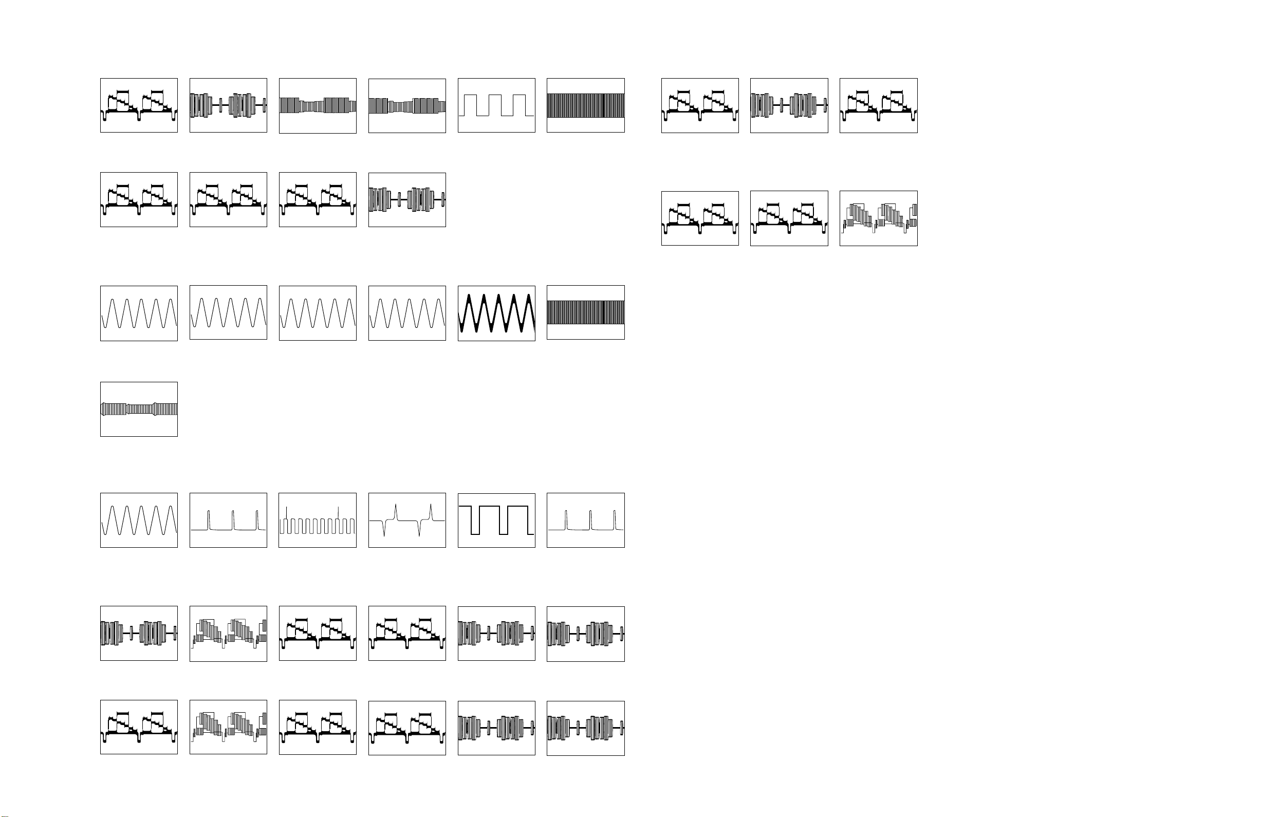
WAVEFORMS4.32
< VIDEO >
WF1
IC1-27
WF2
IC1-30
WF3
TP106
PB FM
WF4
IC1-1
WF5
TP111
D.FF
WF6
IC1-105
WF12
CN512-6
WF13
CN512-12
WF14
CN512-14
PB 2.3 Vp-p
50 mV/20 µsec/DIV
WF7
PB 0.54 Vp-p
20 mV/20 µsec/DIV
< AUDIO >
WF1
REC 0.4 Vp-p
5 mV/0.5 msec/DIV
WF7
IC1-14
IC1-80
TP2253
A.PB FM
PB 0.88 Vp-p
20 mV/20 µsec/DIV
WF8
REC/PB 0.54 Vp-p
20 mV/20 µsec/DIV
WF2
REC/PB 2.0 Vp-p
20 mV/0.5 msec/DIV
IC1-13
IC1-62
PB 0.52 Vp-p
20 mV/5 msec/DIV
WF9
REC/PB 0.54 Vp-p
20 mV/20 µsec/DIV
WF3
REC 0.22 Vp-p
2 mV/0.5 msec/DIV
IC1-11
IC1-52
PB 0.3 Vp-p
20 mV/5 msec/DIV
WF10
REC 0.8 Vp-p
20 mV/20 µsec/DIV
WF4
PB 0.48 Vp-p
10 mV/0.5 msec/DIV
IC1-16
IC1-48
REC/PB 4.3 Vp-p
0.1 V/10 msec/DIV
WF5
REC 0.7 Vp-p
20 mV/0.5 msec/DIV
IC1-119
REC 2.0 Vp-p
0.1 V/1 msec/DIV
WF6
REC 1.4 Vp-p
0.1 V/5 msec/DIV
IC1-97
REC/PB 2.2 Vp-p
50 mV/20 µsec/DIV
< ON SCREEN >
WF1
REC/PB 2.0 Vp-p
50 mV/20 µsec/DIV
IC851-15
CV_IN
REC 0.7 Vp-p
20 mV/20 µsec/DIV
WF2
REC/PB 2.0 Vp-p
50 mV/20 µsec/DIV
IC851-13
CVOUT
REC 1.0 Vp-p
20 mV/20 µsec/DIV
WF3
REC/PB 2.2 Vp-p
50 mV/20 µsec/DIV
CN851-14
V_TO_OSD
PB 0.6 Vp-p
50 mV/5 msec/DIV
< SYSCON >
WF1
REC/PB 3.2 Vp-p
50 mV/0.5 msec/DIV
CN3003-2
CAP_FG
< S-SUB >
WF1
50 mV/20 µsec/DIV
WF6
CN511-9
PB 1.8 Vp-p
CN511-17
WF2
REC/PB 4.5 Vp-p
0.1 V/10 msec/DIV
WF2-1
50 mV/20 µsec/DIV
WF7
CN3001-4
CN511-10
REC 1.7 Vp-p
CN511-25
D.PG
WF3
REC/PB 4.5 Vp-p
0.1 V/10 msec/DIV
WF2-2
REC/PB 1.7 Vp-p
50 mV/20 µ
WF8
CN3001-5
CN511-10
CN511-27
D.FG
sec/DIV
WF4
PB 2.6 Vp-p
0.1 V/10 msec/DIV
WF3
REC/PB 0.8 Vp-p
20 mV/20 µsec/DIV
WF9
CN511-11
CN511-29
TP4001
CTL.P
WF5
REC 3.5 Vp-p
0.1 V/10 msec/DIV
WF4
REC 0.6 Vp-p/PB 0.96 V p-p
20 mV/20 µsec/DIV
WF10
IC3001-1
CTL(+)
CN511-12
CN511-30
WF6
REC/PB 4.0 Vp-p
0.1 V/20 µsec/DIV
WF5
20 mV/20 µsec/DIV
WF11
IC3001-98
C.SYNC
CN511-13
PB 0.6 Vp-p
CN512-4
PB 2.2 Vp-p
50 mV/20 µsec/DIV
REC/PB 2.2 Vp-p
50 mV/20 µsec/DIV
REC/PB 0.52 Vp-p
20 mV/20 µsec/DIV
PB 0.5 Vp-p
20 mV/20 µsec/DIV
REC 0.76 Vp-p
20 mV/20 µsec/DIV
REC/PB 1.6 Vp-p
50 mV/20 µsec/DIV
4-63 4-64
Page 73

4.33 VOLTAGE CHARTS
<SW REGULATOR>
MODE
REC PLAY
PIN NO.
IC5101
1 0.3 0.3
200
3 302.2 302.2
4 14.6 14.6
500
IC5301
1 2.4 2.4
200
3 10.6 10.6
CN5201
1 -19.3 -19.3
200
3 -15.6 -15.6
400
500
6 2.2 2.2
70
8 43.3 43.3
9 12.3 12.3
10 4.3 4.3
11 4.3 4.3
12 31.7 31.7
13 4.3 4.3
14 -28.3 -28.3
15 7.2 7.2
16 -7.2 -7.2
17 6.4 6.4
18 6.4 6.4
19 21.4 21.4
<REGULATOR>
MODE
REC PLAY
PIN NO.
IC5321
1 4.3 4.3
2 3.2 3.2
300
4 2.6 2.6
IC5322
1 3.4 3.4
2 2.4 2.4
300
4 1.2 1.2
5 3.4 3.4
CN5301
1 19.1 19.1
2 6.4 6.4
3 6.4 6.4
4 -7.2 -7.2
5 7.2 7.2
6 -28.3 -28.3
7 4.3 4.3
8 31.7 31.7
9 4.3 4.3
10 4.3 4.3
11 12.3 12.3
12 43.3 43.3
13 0 0
14 2.2 2.2
15 0 0
16 0 0
17 -15.6 -15.6
18 0 0
19 -19.3 -19.3
CN5321
1 12.2 12.2
2 11.6 11.6
3 11.5 11.5
400
500
6 -19.3 -19.3
7 -28.4 -28.4
8 -15.8 -15.8
900
10 2.7 2.7
11 0 0
12 4.8 4.8
13 6.2 6.2
14 19.0 19.0
15 5.0 5.0
CN5322
1 5.6 5.6
2 43.3 43.3
3 5.0 5.0
4 4.9 4.9
5 -7.3 -7.3
6 12.2 12.2
7 11.4 11.4
800
900
10 0 0
11 31.9 31.9
12 5.2 5.2
13 10.9 10.9
CN5323
1 -7.2 -7.2
2 5.0 5.0
300
4 3.3 3.3
5 3.3 3.3
600
7 2.4 2.4
8 2.4 2.4
900
MODE
REC PLAY
PIN NO.
CN5325
1 11.2 11.2
200
CN5326
1 12.2 12.2
200
300
4 5.0 5.0
<VIDEO/AUDIO>
MODE
REC PLAY
PIN NO.
IC1
1 4.2 2.1
2 2.8 2.8
3 2.6 2.6
4 1.9 1.4
5 1.9 1.4
6 2.4 2.4
7 2.1 0.7
800
9 2.7 2.7
10 2.2 2.2
11 3.1 3.1
12 2.8 2.8
13 3.1 3.1
14 3.5 2.4
15 0 0
16 2.8 2.8
17 1.5 1.5
18 2.8 2.8
19 2.9 4.7
20 0 2.8
21 0 1.9
22 2.8 2.8
23 0 2.9
24 4.8 4.8
25 0.3 0.3
26 0 0
27 1.3 2.3
28 2.3 2.3
29 0 1.9
30 2.1 2.1
31 0 0
32 2.6 2.6
33 4.9 4.9
34 2.7 2.2
35 4.8 4.8
36 2.6 2.6
37 2.3 2.3
38 - 39 1.2 1.2
40 - 41 2.5 2.5
42 - 43 0 0
44 2.1 2.1
45 4.6 4.6
46 4.2 4.2
47 2.9 2.9
48 2.6 2.6
49 4.9 4.9
50 2.5 2.5
51 2.8 2.8
52 2.3 2.3
53 2.3 2.3
54 2.5 2.5
55 2.1 2.1
56 0.5 0.5
57 2.3 2.3
58 8.4 8.4
59 4.6 4.6
60 4.2 4.2
61 4.2 4.2
62 4.2 4.2
63 2.3 2.3
64 2.3 2.3
65 1.4 1.7
66 2.8 3.2
67 4.2 4.2
68 4.2 4.2
69 2.3 2.3
70 0 0
71 0.3 0.3
72 0.2 0.2
73 0.2 0.2
74 2.2 2.2
75 2.4 2.4
76 0 0
77 2.5 2.5
78 0.3 0.3
79 0.2 0.2
80 0.2 0.2
81 2.2 2.2
82 0.7 0.7
83 0 0
84 2.3 2.3
85 2.3 2.3
86 2.2 2.2
87 1.5 1.5
88 2.2 2.2
89 2.2 2.2
90 2.3 2.3
91 0.1 0.1
92 0 0
93 0 2.6
MODE
REC PLAY
PIN NO.
94 0 1.4
95 0 0
96 2.4 2.4
97 2.7 2.3
98 2.4 2.4
99 4.9 4.9
100 4.9 4.9
101 0 0
102 0 0
103 0 0
104 2.4 2.4
105 2.3 2.3
106 2.3 2.3
107 4.9 4.9
108 0 0
109 0 0
110 0 0
111 0 2.5
112 2.6 2.6
113 0.5 0.5
114 0 0
115 2.5 2.5
116 2.5 2.5
117 2.5 2.5
118 0 0
119 2.4 2.4
120 4.6 4.6
CN1
100
200
300
400
5 2.3 2.3
6 2.3 2.3
7 2.3 2.3
8 2.3 2.3
9 2.7 2.3
10 2.7 2.3
11 2.7 2.3
12 0 0
13 0 0
CN2001
100
200
300
400
500
6 2.1 2.4
7 2.4 2.4
CN2002
100
200
<SYSCON>
MODE
REC PLAY
PIN NO.
IC3001
1 2.7 2.7
200
3 1.8 2.4
4 2.4 2.4
500.6
6 2.5 2.5
7 2.4 2.4
8 2.4 2.4
9 4.9 4.9
10 4.8 4.8
11 0 0
12 0 0
13 0 0
14 4.3 4.3
15 4.4 4.4
16 0.6 0.6
17 0 0
18 5.0 5.0
19 0 0
20 0 0
21 0 2.5
22 0 1.4
23 0 0
24 4.8 4.8
25 0 0
26 4.9 4.9
27 4.9 4.9
28 4.8 4.8
29 4.8 4.8
30 4.8 0
31 4.8 4.8
32 0 0
33 0 0
34 0 0
35 0 0
36 0 0
37 0 0
38 0 4.8
39 4.2 4.2
40 0 0
41 4.7 4.7
42 4.5 4.5
43 0 0
44 0 0
45 4.8 4.8
46 4.7 4.7
47 0 0
48 4.8 4.8
49 4.2 4.2
MODE
REC PLAY
PIN NO.
50 4.6 4.6
51 4.8 4.8
52 4.4 3.8
53 4.3 4.3
54 - 55 - 56 4.9 4.9
57 0 0
58 4.8 0
59 4.8 4.8
60 0 0
61 0 0
62 0 0
63 0 0
64 - 65 - 66 - 67 - 68 0 0
69 - 70 4.8 4.8
71 4.8 4.8
72 4.8 4.8
73 0 0
74 0 0
75 4.5 4.5
76 4.5 4.5
77 4.8 4.8
78 4.8 4.8
79 4.8 4.8
80 0 0
81 4.8 4.8
82 4.8 4.8
83 2.5 2.5
84 0 0
85 0 0
86 4.5 4.5
87 4.8 4.8
88 4.8 4.8
89 0 0
90 5.0 5.0
91 2.7 2.8
92 5.0 5.0
93 5.0 5.0
94 0 0
95 0 0
96 0 0
97 4.9 4.9
98 0.4 0.4
99 0 2.7
100 2.5 2.5
101 2.5 2.5
102 1.2 1.2
103 0 0
104 0 0
105 4.8 4.8
106 4.8 4.8
107 0.1 0.1
108 1.5 1.5
109 4.8 4.8
110 0 0
111 0 0
112 2.4 2.4
IC3002
1 4.8 4.8
2 4.8 4.8
300
IC3003
100
200
300
400
5 4.5 4.5
6 4.5 4.5
700
8 4.9 4.9
IC3004
1 12.2 12.2
200
300
400
5 12.2 12.2
6 12.2 12.2
700
800
900
IC3006
100
200
300
4 5.0 5.0
5 5.0 5.0
IC3601
100
200
3 0.2 0
400
500
600
700
800
9 4.5 4.5
10 4.0 4.0
11 0 0
12 0 0
13 0 0
14 0 0
MODE
REC PLAY
PIN NO.
15 0 0
16 5.0 5.0
IC3651
100
200
3 0.2 0.2
403.9
500
600
700
8 2.7 2.7
9 0.4 0.2
10 2.9 2.9
11 3.7 3.7
12 3.5 3.5
13 3.8 3.8
14 3.5 3.5
15 0 3.9
16 5.0 5.0
CN3001
1 11.6 11.6
200
3 1.4 1.4
4 0.1 0.1
5 1.5 1.5
CN3002
100
200
CN3003
100
2 2.4 2.4
3 2.5 2.4
4 4.9 4.9
500
6 4.8 4.8
7-8 11.4 11.4
CN3004
1 4.9 4.9
2 4.9 4.9
300
400
CN3011
1 4.9 4.9
2 4.9 4.9
3 4.3 4.3
4 4.8 4.8
5 4.4 3.7
6 4.2 4.2
7 4.8 4.8
800
900
10 -19.3 -19.3
11 -15.8 -15.8
12 -28.4 -28.4
13 3.8 3.8
14 3.5 3.5
15 3.8 3.8
16 3.5 3.5
17 0 0
18 3.0 0
CN3014
1 5.0 5.0
200
3 5.0 5.0
4 5.0 5.0
500
600
<TUNER>
MODE
REC PLAY
PIN NO.
CN6701
100
2 4.5 4.5
3 4.5 4.5
4 4.8 4.8
5 0.3 0.3
6 0.3 0.3
7 4.9 4.9
800
9 1.2 1.2
10 0 0
<VIDEO I/O SW>
MODE
REC PLAY
PIN NO.
IC702
1 6.4 6.4
200
3 6.4 6.4
400
5 6.4 6.4
6 11.3 11.3
7 5.6 5.6
800
IC703
1 3.1 3.1
200
3 3.1 3.1
400
5 3.0 3.0
6 11.4 11.4
7 3.4 3.4
800
MODE
REC PLAY
PIN NO.
IC705
1 1.7 1.7
200
3 1.6 1.6
400
5 1.6 1.6
6 4.9 4.9
7 1.0 1.0
800
IC706
1 5.6 5.6
2 4.9 4.9
3 4.9 4.9
400
500
IC707
1 4.5 4.5
2 2.9 2.9
3 5.0 5.0
4 1.9 1.9
5 1.5 1.5
6 2.1 2.1
7 2.9 2.9
800
9 2.9 2.9
10 0 0
11 2.5 2.5
12 3.1 3.1
13 2.9 2.9
14 2.2 2.2
IC712
1 2.7 2.7
200
3 2.7 2.7
400
500
6 4.9 4.9
7 4.1 4.1
800
CN703
100
200
300
4 1.7 1.7
500
6 4.1 4.1
CN704
1 2.8 2.8
2 2.9 2.9
3 4.3 4.3
4 4.4 3.8
5 4.4 4.8
6 4.5 4.8
700
800
9 4.8 4.8
10 2.2 2.2
11 0 0
12 1.5 1.5
13 0 0
14 2.3 2.3
15 4.9 4.9
16 1.8 1.8
17 2.9 2.9
18 11.4 11.4
19 0 0
20 1.2 1.2
<AUDIO I/O>
MODE
REC PLAY
PIN NO.
IC2601
1 0.2 0.2
200
3 0.2 0.2
4 - 6 0 0
7 -4.9 -4.9
8 - 15 0 0
16 5.6 5.6
IC2602
1 0.2 0.2
2 0.2 0.2
3 0.2 0.2
4 -4.9 -4.9
5 - 7 0 0
8 12.2 12.2
IC2603
100
2 0.3 0.3
3 0.2 0.2
4 - 6 0 0
7 -4.9 -4.9
800
9 4.5 4.5
10 - 14 0 0
15 0.3 0.3
16 5.6 5.6
IC2604
100
2 - 3 0 0
4 -5.4 -5.4
5 - 7 0 0
8 12.2 12.2
IC2605
1 0.3 0.3
2 0.3 0.3
MODE
REC PLAY
PIN NO.
3 0.3 0.3
4 -4.9 -4.9
5 0.3 0.3
6 0.3 0.3
7 0.3 0.3
8 12.2 12.2
IC2606
1 - 6 0 0
7 -4.9 -4.9
8 - 15 0 0
16 5.6 5.6
IC2607
1 - 6 0 0
7 -4.9 -4.9
8 - 15 0 0
16 5.6 5.6
IC2608
100
200
300
4 -4.9 -4.9
500
600
700
8 12.2 12.2
CN2601
1 - 8 0 0
<CONNECTION>
MODE
REC PLAY
PIN NO.
CN501
1 2.4 2.4
200
3 2.3 2.3
4 5.0 5.0
5 2.1 2.1
6 0.3 4.5
7 3.3 3.3
800
9 2.8 2.8
10 0 0
11 4.6 4.6
12 4.2 4.2
13 0 0
14 0.8 0.8
15 2.5 2.5
16 0 0
17 2.5 2.5
CN502
1 0.3 4.5
2 4.2 4.2
3 4.6 4.6
4 2.4 2.4
5 4.9 4.9
6 4.9 4.9
700
800
9 0.4 2.3
10 2.1 2.1
11 3.3 3.3
12 2.9 2.9
13 2.8 2.8
14 0 0
15 0 0
16 2.4 2.1
17 1.3 0
18 4.8 0
19 - 24 0 0
25 2.3 2.3
26 0 0
27 2.5 2.5
28 0 0
29 3.4 2.4
30 2.8 2.8
CN7501
3 2.7 2.7
400
5 5.6 5.6
600
7 1.3 1.3
800
9 1.3 1.3
10 0 0
11 1.6 1.6
12 0 0
13 3.3 3.3
14 0 0
15 3.3 3.3
CN7502
1 0.7 0.7
200
3 0.7 0.7
400
5 0.7 0.7
600
700
CN7503
7 - 11 0 0
12 5.0 5.0
13 11.4 11.4
14 - 16 0 0
CN7504
1 - 4 0 0
5 0.2 0.2
6 - 11 0 0
MODE
REC PLAY
PIN NO.
CN7505
1 2.4 2.4
2 - 4 0 0
5 2.3 2.3
6 - 10 0 0
11 2.5 2.5
CN7507
1 - 10 0 0
CN7508
1 10.9 10.9
2 5.2 5.2
3 31.9 31.9
4 - 6 0 0
7 11.4 11.4
8 12.2 12.2
9 -7.3 -7.3
10 4.9 4.9
11 5.0 5.0
12 43.3 43.3
13 5.6 5.6
CN7509
1 5.0 5.0
2 19.0 19.0
3 6.2 6.2
4 4.8 4.8
500
6 2.7 2.7
700
8 -15.8 -15.8
9 -28.4 -28.4
10 -19.3 -19.3
11 - 12 0 0
13 11.5 11.5
14 11.6 11.6
15 12.2 12.2
<3D DIGITAL/2M>
MODE
REC PLAY
PIN NO.
IC1401 - CN1401
1 2.4 2.4
200
3 2.3 2.3
4 5.0 5.0
5 2.1 2.1
6 0.3 4.5
7 3.3 3.3
800
9 2.8 2.8
10 0 0
11 4.6 4.6
12 4.2 4.2
13 0 0
14 0.8 0.8
15 2.5 2.5
16 0 0
17 2.5 2.5
<TERMINAL>
MODE
REC PLAY
PIN NO.
IC7101
1 5.2 5.2
200
3 5.2 5.2
4 4.3 4.3
5 5.1 5.1
6 11.4 11.4
7 6.8 6.8
800
IC7102
1 3.2 3.2
200
3 3.3 3.3
4 4.3 4.3
5 3.2 3.2
6 11.4 11.4
7 3.6 3.6
800
IC7103
1 0.3 0.3
2 1.1 1.1
3 1.9 1.9
400
500
600
7 2.0 0
800
9 2.0 2.0
10 2.0 2.0
11 2.0 2.0
12 2.0 2.0
13 0 0
14 0 0
15 2.4 2.4
16 4.9 4.9
IC7104
1 1.6 1.6
200
3 1.6 1.6
4 10.8 10.8
5 1.9 1.9
600
7 4.8 4.8
4-65
MODE
REC PLAY
PIN NO.
8 10.8 10.8
9 4.8 4.8
10 0.1 0.1
11 4.8 4.8
12 0 0
13 4.5 4.5
14 4.4 4.4
15 4.8 4.8
16 4.8 4.8
17 4.8 4.8
18 4.8 4.8
19 10.8 10.8
20 2.3 2.3
21 1.3 1.3
22 1.4 1.4
23 2.6 2.6
24 2.0 2.0
CN7101
1 1.1 1.1
200
3 2.0 2.0
400
5 5.6 5.6
600
7 1.3 1.3
800
9 1.1 1.1
10 0 0
11 1.5 1.5
12 0 0
13 3.3 3.3
14 0 0
15 0 0
CN7102
100
200
300
400
5 0.7 0.7
CN7103
1 10.9 10.9
2 4.4 4.8
3 4.5 4.5
400
5 4.9 4.9
600
700
800
9 4.3 4.3
10 0 0
11 0 0
12 4.9 4.9
13 11.4 11.4
14 0 0
CN7104
100
200
300
400
5 0.2 0.2
600
700
800
900
10 0 0
11 0 0
<DEMODULATOR>
MODE
REC PLAY
PIN NO.
IC6701
1 4.3 4.3
2 1.5 1.5
3 1.5 0
400
5 2.0 2.0
6 1.9 1.9
7 0.2 0.2
800
900
10 3.6 3.6
11 3.6 3.6
12 4.5 4.5
13 4.5 4.5
14 2.2 2.2
15 2.1 2.2
16 0 0
17 0.3 0.3
18 0.3 0.3
19 4.5 4.5
20 0 0
21 0.3 0.3
22 4.7 4.7
23 0 0
24 0 0
25 0 0
26 0 0
27 0 0
28 0 0
29 0 0
30 2.4 2.4
31 2.4 2.4
32 0 0
33 4.7 4.7
34 3.8 3.8
35 0 0
4-66
MODE
REC PLAY
PIN NO.
36 2.4 2.4
37 0 0
38 0 0
39 0 0
40 0 0
41 0 0
42 2.5 2.5
43 2.4 2.4
44 0 0
CN6701
100
2 4.6 4.6
3 4.5 4.5
4 4.8 4.8
5 0.3 0.3
6 0.3 0.3
7 5.0 5.0
800
900
10 0.1 0
<S-SUB>
MODE
REC PLAY
PIN NO.
IC501 - IC502
1 2.0 2.0
2 0.3 4.5
3 3.3 3.3
4 3.4 3.4
5 4.9 4.9
6 2.2 2.2
7 2.0 2.0
8 4.9 4.9
9 1.4 1.4
10 2.9 2.9
11 2.9 2.9
12 2.9 2.9
13 0 0
14 2.8 2.8
15 2.8 2.8
16 1.9 1.9
17 1.9 1.9
18 1.9 1.9
CN511
1 0.3 4.5
2 4.2 4.2
3 4.6 4.6
4 2.4 2.4
5 4.9 4.9
6 4.9 4.9
700
800
9 2.3 2.3
10 2.1 2.1
11 3.3 3.3
12 2.9 2.9
13 2.8 2.8
14 - 15 0 0
16 2.4 2.1
17 1.3 2.3
18 4.8 4.8
19 - 24 0 0
25 2.3 2.3
26 0 0
27 2.5 2.5
28 0 0
29 3.4 2.4
30 2.8 2.8
CN512
100
2 2.4 2.4
300
4 2.4 2.4
500
6 2.3 2.3
700
8 1.3 1.3
900
10 1.1 1.1
11 0 0
<ON SCREEN>
MODE
REC PLAY
PIN NO.
IC851
100
2 2.5 2.5
3 4.8 4.8
400
5 4.4 4.4
6 2.4 2.4
7 2.5 2.5
8 4.9 4.9
903.2
10 4.3 4.3
11 4.4 3.8
12 4.9 4.9
13 2.9 2.9
14 2.9 2.9
15 0 0
16 1.2 1.2
17 0 0
18 4.9 4.9
19 1.6 1.6
20 0 0
MODE
REC PLAY
PIN NO.
21 1.6 1.5
22 0.4 0.2
23 4.9 4.9
24 2.9 2.9
25 2.5 2.5
26 4.9 4.9
27 4.5 4.5
28 0 3.5
29 4.9 4.9
30 4.9 4.9
IC852 - CN851
1 2.8 2.8
2 2.9 2.9
3 4.3 4.3
4 4.4 3.8
5 4.4 4.8
6 4.5 4.8
700
800
9 4.8 4.8
10 2.2 2.2
11 0 0
12 1.5 1.5
13 0 0
14 2.3 2.3
15 4.9 4.9
16 1.8 1.8
17 2.9 2.9
18 11.4 11.4
19 0 0
20 1.2 1.2
<DISPLAY>
MODE
REC PLAY
PIN NO.
IC7001
1 4.8 4.8
2 2.2 2.2
300
4 2.2 2.2
5 4.8 4.8
6 4.8 4.8
7 4.8 4.8
8 4.9 4.9
9 4.8 4.8
10 4.9 4.9
11 4.8 4.8
12 4.2 4.2
13 0 1.2
14 4.8 4.8
15 0 4.6
16 -28.3 -28.3
17 -28.3 -28.3
18 4.6 4.6
19 -28.1 4.6
20 4.6 -28.0
21 -23.9 -23.9
22 - 43 - -
44 4.9 4.9
IC7002
1 4.8 4.8
2 4.8 4.8
300
CN7001
1 4.9 4.9
2 4.9 4.9
3 4.3 4.3
4 4.8 4.8
5 4.4 3.7
6 4.2 4.2
7 4.8 4.8
8 - 9 0 0
10 -19.3 -19.3
11 -15.8 -15.8
12 -28.4 -28.4
13 3.8 3.8
14 3.5 3.5
15 3.8 3.8
16 3.5 3.5
17 0 0
18 3.0 3.0
FW7001
1 5.1 5.1
200
FW7003
1 3.6 3.6
2 4.8 4.8
3 4.8 4.8
400
5 5.0 5.0
6 3.6 3.6
FW7005
100
2 4.8 4.8
<VIDEO AD/DA>
MODE
REC PLAY
PIN NO.
IC8601
100
2 3.3 3.3
3 1.2 1.2
4 0.2 0.3
5 0.8 0.8
6 2.0 2.0
7 0.2 0.3
8 1.2 1.2
900
10 3.3 3.3
11 1.9 1.9
12 1.2 1.2
13 0 0
14 3.3 3.3
15 1.6 0
16 0.5 0
17 2.7 1.9
18 1.5 1.5
19 - 22 0 0
23 1.8 1.8
24 3.3 3.3
25 1.7 1.5
26 1.3 1.3
27 1.0 1.0
28 1.0 1.0
29 1.0 0.9
30 0 0
31 3.3 3.3
32 1.6 1.6
33 1.0 1.0
34 0.8 0.8
35 1.5 1.5
36 - 37 0 0
38 1.2 1.3
39 0.5 1.2
40 0.5 1.2
41 0.2 1.2
42 0.2 1.8
43 0.2 1.2
44 0 1.3
45 1.6 1.8
46 - 48 0 0
49 0.8 0
50 0 0
51 3.3 3.3
52 0 0
53 1.8 1.8
54 1.1 1.1
55 3.3 3.3
56 3.3 3.3
57 0 0
58 3.3 3.3
59 3.1 3.1
60 3.3 3.3
61 1.6 3.3
62 0 1.6
63 3.3 0
64 0 3.3
65 - 72 0 0
73 3.3 3.3
74 1.2 1.2
75 3.3 3.3
76 1.0 0
77 2.0 2.0
78 3.3 3.3
79 1.2 1.2
80 0.6 0.6
CN8601
1 2.2 2.2
200
3 1.8 1.8
4 1.8 1.8
500
6 2.0 2.0
<AUDIO AD/DA>
MODE
REC PLAY
PIN NO.
IC8801
1 3.3 3.3
2 3.3 3.3
3 1.5 1.5
4 1.5 1.5
5 1.5 1.5
6 1.5 1.5
7 3.3 3.3
8 3.3 3.3
9 1.6 1.6
10 1.6 1.6
11 1.6 1.6
12 0.8 1.0
13 0 0
14 3.3 3.3
15 0 0.8
16 0 0
17 0 0
18 3.3 3.3
19 1.5 1.5
20 1.5 1.5
21 1.5 1.5
22 0 0
23 3.3 3.3
24 3.3 3.3
MODE
REC PLAY
PIN NO.
IC8802
1 - 3 0 0
4 -7.2 -7.2
5 - 7 0 0
8-5.05.0
IC8803
1 - 3 0 0
4 -7.2 -7.2
5 - 7 0 0
8-5.05.0
CN8801
1 - 8 0 0
<MPEG DEC.>
MODE
REC PLAY
PIN NO.
IC8201
1 3.3 3.3
2 1.2 1.2
3 1.2 1.2
4 2.3 2.3
5 1.3 1.3
600
7 1.2 1.4
8 1.4 1.4
9 1.4 1.4
10 3.3 3.3
11 0 0
12 0 0
13 0 0
14 0 0
15 1.9 1.5
16 1.9 1.5
17 0 0
18 1.9 1.6
19 3.3 3.3
20 1.9 1.6
21 1.9 1.7
22 1.6 1.7
23 0 0
24 3.3 3.3
25 2.4 1.0
26 2.7 1.0
27 3.3 3.3
28 0.6 0.6
29 0 0
30 0 0
31 0 0
32 0 0
33 1.8 1.8
34 2.3 2.3
35 2.5 2.1
36 3.3 3.3
37 3.1 3.1
38 3.3 2.4
39 0 3.1
40 0 0
41 0 0
42 2.6 0
43 3.3 1.3
44 1.4 3.3
45 1.4 1.2
46 0 1.2
47 1.4 0
48 0 1.5
49 1.4 0
50 1.5 1.5
51 1.6 1.6
52 1.4 1.1
53 3.3 3.3
54 1.8 1.5
55 1.8 1.5
56 1.5 1.5
57 0 0
58 1.5 1.5
59 1.5 1.5
60 1.5 1.5
61 1.2 1.5
62 3.3 3.3
63 1.3 1.8
64 1.5 1.8
65 0 0
66 0 0
67 0 0
68 1.6 1.6
69 0 0
70 3.3 3.3
71 0.9 0
72 0 0
73 0 0
74 0.9 0
75 3.3 3.3
76 1.6 1.6
77 2.3 2.3
78 1.6 1.6
79 1.7 1.7
80 3.3 3.3
81 3.3 3.3
82 0 0
83 3.3 3.3
84 0 0
85 0 0
86 1.1 1.1
87 0 0
88 3.3 3.3
89 2.3 2.3
MODE
REC PLAY
PIN NO.
90 3.3 3.3
91 3.3 3.3
92 3.3 3.3
93 3.3 3.3
94 3.3 3.3
95 0 0
96 0 0
97 0 0
98 0.9 0.9
99 1.1 1.1
100 0 0
101 2.3 2.3
102 3.3 3.3
103 0 0
104 0 0
105 0 0
106 0 0
107 3.3 3.3
108 2.3 2.3
109 0 0
110 0 0
111 0.8 1.0
112 0 0
113 3.3 3.3
114 0 0
115 0 0
116 1.3 1.3
117 2.3 2.3
118 0.9 0.9
119 1.3 1.3
120 2.2 2.2
121 0 0
122 1.7 1.7
123 0 0
124 3.1 3.1
125 3.3 3.3
126 1.5 1.5
127 1.0 1.0
128 1.3 1.3
129 2.0 2.0
130 1.0 1.0
131 1.1 1.1
132 0 0
133 1.1 1.1
134 1.2 1.2
135 1.4 1.4
136 2.3 2.3
137 3.3 3.3
138 3.3 3.3
139 3.3 3.3
140 3.3 3.3
141 3.3 3.3
142 3.3 3.3
143 3.3 3.3
144 3.3 3.3
145 3.3 3.3
146 3.3 3.3
147 0 0
148 3.3 3.3
149 3.3 3.3
150 3.3 3.3
151 3.3 3.3
152 3.3 3.3
153 3.3 3.3
154 3.3 3.3
155 3.3 3.3
156 3.3 3.3
157 3.3 3.3
158 3.3 3.3
159 3.3 3.3
160 2.3 2.3
161 1.6 1.6
162 3.3 3.3
163 0 0
164 3.3 3.3
165 3.3 3.3
166 3.3 3.3
167 3.3 3.3
168 3.3 3.3
169 3.3 3.3
170 0 0
171 3.3 3.3
172 3.3 3.3
173 3.3 3.3
174 3.3 3.3
175 3.3 3.3
176 3.3 3.3
177 0 0
178 3.3 3.3
179 3.3 3.3
180 3.3 3.3
181 3.3 3.3
182 3.3 3.3
183 0 0
184 3.3 3.3
185 0 0
186 0 0
187 3.3 3.3
188 0 0
189 3.3 3.3
190 0 0
191 0 0
192 2.4 2.4
193 3.3 3.3
194 3.3 3.3
195 0 0
196 3.3 3.3
MODE
REC PLAY
PIN NO.
197 3.3 3.3
198 3.3 3.3
199 3.3 3.3
200 3.3 3.3
201 0 0
202 3.3 3.3
203 3.3 3.3
204 0 0
205 3.3 3.3
206 3.3 3.3
207 3.3 3.3
208 3.3 3.3
209 3.3 3.3
210 3.3 3.3
211 2.0 2.0
212 2.3 2.3
213 0 0
214 0.1 0.1
215 1.5 1.5
216 0 0
217 3.3 3.3
218 0 0
219 3.3 3.3
220 3.3 3.3
221 3.3 3.3
222 3.3 3.3
223 3.3 3.3
224 3.3 3.3
225 3.3 3.3
226 3.3 3.3
227 3.3 3.3
228 0 0
229 1.1 1.1
230 0 0
231 1.5 1.3
232 3.3 1.7
233 1.4 3.3
234 1.0 1.4
235 1.0 1.5
236 0 1.3
237 0 0
238 3.3 1.6
239 1.4 1.7
240 1.1 1.4
IC8202
1 3.3 3.3
2 1.3 1.3
3 3.3 3.3
4 1.1 1.1
5 1.1 1.1
600
7 1.4 1.7
8 1.4 1.4
9 3.3 3.3
10 1.1 1.5
11 1.1 1.3
12 0 0
13 1.5 1.5
14 3.3 3.3
15 0 0
16 3.0 3.3
17 2.4 2.7
18 3.1 3.1
19 2.1 2.5
20 1.7 1.7
21 0 0
22 0.1 0.1
23 0.6 0.3
24 0.8 0.8
25 0.9 0.6
26 1.7 1.7
27 3.3 3.3
28 0 0
29 1.6 1.6
30 1.6 1.6
31 1.6 1.6
32 1.6 1.6
33 0 0
34 0 0
35 0 0
36 0 0
37 3.3 3.3
38 1.6 1.6
39 0 0
40 0 0
41 0 0
42 1.4 1.7
43 3.3 3.3
44 1.1 1.4
45 1.1 1.4
46 0 0
47 1.1 1.3
48 1.3 1.3
49 3.3 3.3
50 1.2 1.2
51 1.3 1.6
52 0 0
53 1.5 1.5
54 0 0
IC8203
1 3.3 3.3
2 1.2 1.2
3 3.3 3.3
4 1.1 1.1
5 1.1 1.1
600
7 1.3 1.3
MODE
REC PLAY
PIN NO.
8 1.3 1.3
9 3.3 3.3
10 1.3 1.3
11 1.1 1.1
12 0 0
13 1.4 1.4
14 3.3 3.3
15 0 0
16 3.0 3.0
17 2.4 2.4
18 3.1 3.1
19 2.1 2.1
20 1.9 1.9
21 0 0
22 0 0
23 0.5 0.5
24 0.9 0.9
25 1.0 1.0
26 1.7 1.7
27 3.3 3.3
28 0 0
29 1.5 1.5
30 1.5 1.5
31 1.5 1.5
32 1.5 1.5
33 0 0
34 0 0
35 0 0
36 0.1 0.1
37 3.3 3.3
38 0 1.7
39 1.7 0
40 0 0
41 0 0
42 1.5 1.5
43 3.3 3.3
44 1.1 1.3
45 1.4 1.4
46 0 0
47 0 1.3
48 1.3 1.3
49 3.3 3.3
50 1.2 1.2
51 1.2 1.2
52 0 0
53 1.5 1.5
54 0 0
IC8204
1-200
300
400
500
600
700
800
9 3.3 3.3
10 0 0
11 3.3 3.3
12 0 0
13 0 0
14 0 0
15 0 0
16 3.3 3.3
17 0 0
18 0 0
19 0 0
20 0 0
21 0 0
22 0 0
23 - 24 - 25 3.3 3.3
26 3.3 3.3
27 0 0
28 3.3 3.3
29 3.3 3.3
30 3.3 3.3
31 3.3 3.3
32 3.3 3.3
33 3.3 3.3
34 3.3 3.3
35 3.3 3.3
36 3.3 3.3
37 3.3 3.3
38 3.3 3.3
39 3.3 3.3
40 3.3 3.3
41 3.3 3.3
42 3.3 3.3
43 3.3 3.3
44 3.3 3.3
45 3.3 3.3
46 0 0
47 0 0
48 1.0 1.0
IC8205
1-200
300
400
500
600
700
800
9 3.3 3.3
10 0 0
Page 74

MODE
REC PLAY
PIN NO.
11 3.3 3.3
12 0 0
13 0 0
14 0 0
15 0 0
16 3.3 3.3
17 0 0
18 0 0
19 0 0
20 0 0
21 0 0
22 0 0
23 - 24 0 0
25 3.3 3.3
26 3.3 3.3
27 0 0
28 3.3 3.3
29 3.3 3.3
30 3.3 3.3
31 3.3 3.3
32 3.3 3.3
33 3.3 3.3
34 3.3 3.3
35 3.3 3.3
36 3.3 3.3
37 3.3 3.3
38 3.3 3.3
39 3.3 3.3
40 3.3 3.3
41 3.3 3.3
42 3.3 3.3
43 3.3 3.3
44 3.3 3.3
45 3.3 3.3
46 0 0
47 0 0
48 1.0 1.0
IC8206
100
2 3.3 3.3
3 3.3 3.3
4 3.3 3.3
5 3.3 3.3
6 3.3 3.3
7 3.3 3.3
8 3.3 3.3
9 3.3 3.3
10 0 0
11 0 0
12 0 0
13 0 0
14 0 0
15 0 0
16 0 0
17 0 0
18 0 0
19 0 0
20 3.3 3.3
IC8207
100
2 3.3 3.3
3 3.3 3.3
4 3.3 3.3
5 3.3 3.3
6 3.3 3.3
7 3.3 3.3
8 3.3 3.3
9 3.3 3.3
10 0 0
11 0 0
12 3.3 2.9
13 3.3 2.9
14 0 0
15 - 16 - 17 0 0
18 0 0
19 0 0
20 3.3 3.3
<MPEG ENC.>
MODE
REC PLAY
PIN NO.
IC8401
1 2.4 2.4
200
300
4 3.3 3.3
5 3.3 3.3
6 3.3 3.3
7 3.3 3.3
8 2.4 2.4
900
10 3.3 3.3
11 3.3 3.3
12 3.3 3.3
13 3.3 3.3
14 0 0
15 3.3 3.3
16 3.3 3.3
17 3.3 3.3
18 3.3 3.3
19 3.3 3.3
20 2.4 2.4
21 - 3.3
MODE
REC PLAY
PIN NO.
22 - 3.3
23 - 3.3
24 0 0
25 2.4 2.4
26 1.1 1.0
27 3.3 3.3
28 3.3 3.3
29 3.3 3.3
30 3.3 3.3
31 - 3.3
32 - 3.3
33 3.3 3.3
34 3.3 3.3
35 0 3.3
36 - 3.3
37 - 3.3
38 - 3.3
39 - 3.3
40 - 0
41 - 3.3
42 - 3.3
43 - 3.3
44 - 1.6
45 0 0
46 3.3 3.3
47 0 3.3
48 0 3.3
49 2.4 2.4
50 0 3.0
51 0 3.0
52 0 3.0
53 0 3.0
54 0 3.0
55 0 3.0
56 0 3.0
57 0 3.0
58 0 3.0
59 0 3.0
60 0 3.0
61 3.3 3.0
62 0 0
63 0 3.3
64 0 3.3
65 0 3.3
66 2.4 2.4
67 0 3.0
68 0 3.0
69 0 3.0
70 0 3.0
71 0 3.0
72 0 3.0
73 0 3.0
74 0 3.0
75 0 3.0
76 0 3.0
77 0 0
78 3.3 3.3
79 0 3.0
80 0 3.0
81 0 3.0
82 2.4 2.4
83 0 3.0
84 0 3.0
85 0 3.0
86 3.3 3.3
87 0 0
88 0 3.3
89 3.3 3.3
90 0 3.3
91 0 3.3
92 0 3.3
93 3.3 3.3
94 3.3 3.0
95 3.3 3.0
96 2.4 2.4
97 1.4 1.4
98 3.3 3.3
99 0 0
100 3.3 3.3
101 0 3.0
102 0 3.0
103 0 3.0
104 0 3.0
105 0.2 3.0
106 0.2 3.0
107 0.3 3.0
108 2.4 2.4
109 3.3 3.3
110 0 0
111 0.2 3.0
112 0.2 3.0
113 0.2 3.0
114 0.2 3.0
115 0.2 3.2
116 - 3.0
117 0 0
118 3.3 3.3
119 1.2 1.2
120 1.0 1.0
121 1.0 1.0
122 1.0 0.7
123 1.5 1.7
124 1.0 1.0
125 1.0 0.8
126 1.5 1.5
127 2.4 2.4
128 3.3 3.3
MODE
REC PLAY
PIN NO.
129 2.4 1.7
130 3.3 3.3
131 1.7 3.0
132 3.3 1.0
133 0 3.3
134 2.1 0
135 1.9 3.3
136 1.9 3.3
137 0 3.3
138 2.2 3.3
139 2.0 3.3
140 0 3.3
141 0 0
142 3.3 3.3
143 3.3 3.3
144 3.3 3.3
145 3.3 3.3
146 3.3 3.3
147 3.3 3.3
148 3.3 3.3
149 3.3 3.3
150 2.4 2.4
151 3.3 3.3
152 3.3 3.3
153 3.3 3.3
154 3.3 3.3
155 3.3 3.3
156 3.3 3.3
157 3.3 3.3
158 0 0
159 1.7 3.3
160 2.0 3.3
161 1.7 3.3
162 3.3 3.3
163 3.3 3.3
164 3.3 3.3
165 3.3 3.3
166 2.4 2.4
167 3.3 3.3
168 3.3 3.3
169 3.3 3.3
170 3.3 3.3
171 3.3 3.3
172 3.3 3.3
173 0 0
174 3.3 3.3
175 0 0
176 3.3 3.3
177 3.3 3.3
178 3.3 3.3
179 3.3 3.3
180 0 0
181 1.6 1.4
182 2.4 2.4
183 3.3 3.3
184 3.3 3.3
185 3.3 3.3
186 3.3 3.3
187 3.3 3.3
188 3.3 3.3
189 3.3 3.3
190 0 0
191 3.3 3.3
192 3.3 3.3
193 3.3 3.3
194 3.3 3.3
195 3.3 3.3
196 3.3 3.3
197 0 0
198 3.3 3.3
199 1.7 1.7
200 1.0 0.8
201 0 0
202 0 0
203 1.7 1.7
204 1.7 1.7
205 3.3 3.3
206 3.3 3.3
207 3.3 3.3
208 0 0
IC8402
1 3.3 3.3
2 3.3 3.3
3 3.3 3.3
400
5 3.3 3.3
6 3.3 3.3
7 3.3 3.3
8 3.3 3.3
9 3.3 3.3
10 0 0
11 3.3 3.3
12 3.3 3.3
13 3.3 3.3
14 3.3 0
15 0 3.3
16 3.3 3.3
17 3.3 3.3
18 3.3 0
19 3.3 3.3
20 3.3 3.3
21 3.3 0
22 3.3 0
23 3.3 3.3
24 3.3 0
25 3.3 3.3
26 0 0
MODE
REC PLAY
PIN NO.
27 3.3 3.3
28 3.3 3.3
29 3.3 3.3
30 3.3 3.3
31 3.3 3.3
32 3.3 3.3
33 0 0
34 0 0
35 1.7 1.7
36 0 0
37 0 0
38 3.3 3.3
39 3.3 3.3
40 3.3 3.3
41 0 0
42 3.3 3.3
43 3.3 3.3
44 3.3 3.3
45 3.3 3.3
46 3.3 3.3
47 0 0
48 3.3 3.3
49 3.3 3.3
50 0 0
IC8403
1 3.3 3.3
2 3.3 3.3
3 3.3 3.3
400
5 3.3 3.3
6 3.3 3.3
7 3.3 3.3
8 3.3 3.3
9 3.3 3.3
10 0 0
11 3.3 3.3
12 3.3 3.3
13 3.3 3.3
14 3.3 0
15 0 3.3
16 3.3 3.3
17 3.3 3.3
18 3.3 3.3
19 3.3 3.3
20 3.3 3.3
21 3.3 3.3
22 3.3 3.3
23 3.3 3.3
24 3.3 3.3
25 3.3 3.3
26 0 0
27 3.3 3.3
28 3.3 3.3
29 3.3 3.3
30 3.3 3.3
31 3.3 3.3
32 3.3 3.3
33 0 0
34 0 0
35 1.8 1.8
36 0 0
37 0 0
38 3.3 3.3
39 3.3 3.3
40 3.3 3.3
41 0 0
42 3.3 3.3
43 3.3 3.3
44 3.3 3.3
45 3.3 3.3
46 3.3 3.3
47 0 0
48 3.3 3.3
49 3.3 3.3
50 0 0
IC8404
1 3.3 3.3
2 3.3 3.3
3 3.3 3.3
400
5 3.0 3.0
6 3.0 3.0
7 3.3 3.3
8 3.2 3.2
9 3.1 3.1
10 0 0
11 3.0 3.0
12 3.0 3.0
13 3.3 3.3
14 0 0
15 3.0 3.0
16 3.0 3.0
17 3.3 3.3
18 0 0
19 3.3 3.3
20 3.0 3.0
21 3.2 3.2
22 0 0
23 0 0
24 3.1 3.1
25 3.3 3.3
26 0 0
27 3.1 3.1
28 3.1 3.1
29 3.2 3.2
30 3.2 3.2
31 3.0 3.0
MODE
REC PLAY
PIN NO.
32 3.0 3.0
33 0 0
34 3.3 3.3
35 1.7 1.7
36 0 0
37 0 0
38 3.3 3.3
39 3.0 3.0
40 3.0 3.0
41 0 0
42 3.0 3.0
43 3.0 3.0
44 3.3 3.3
45 3.0 3.0
46 3.0 3.0
47 0 0
48 3.0 3.0
49 3.2 3.2
50 0 0
IC8405
1 3.3 3.3
2 3.2 3.2
3 3.0 3.0
400
5 3.0 3.0
6 3.2 3.2
7 3.3 3.3
8 3.2 3.2
9 3.0 3.0
10 0 0
11 3.0 3.0
12 3.0 3.0
13 3.3 3.3
14 0 0
15 0 0
16 0 0
17 0 3.3
18 0 0
19 3.3 3.3
20 3.0 3.0
21 3.2 3.2
22 3.1 3.1
23 3.1 3.1
24 3.1 3.1
25 3.3 3.3
26 0 0
27 3.1 3.1
28 3.1 3.1
29 3.1 3.1
30 3.1 3.1
31 3.1 3.1
32 3.1 3.1
33 0 0
34 3.3 3.3
35 1.7 1.7
36 0 0
37 0 0
38 3.3 3.3
39 3.0 3.0
40 3.0 3.0
41 0 0
42 3.0 3.0
43 3.0 3.0
44 3.3 3.3
45 3.0 3.0
46 3.0 3.0
47 0 0
48 3.0 3.0
49 3.2 3.2
50 0 0
<ASIC IF>
MODE
REC PLAY
PIN NO.
IC8001
100
2 1.5 1.5
300
4 0.2 0.2
500
600
7 3.3 3.3
800
900
10 0 0
11 3.3 3.3
12 0 0
13 3.3 3.3
14 3.3 3.3
15 3.3 3.3
16 3.3 3.3
17 0 0
18 3.3 3.3
19 3.3 3.3
20 3.3 3.3
21 3.3 3.3
22 3.3 3.3
23 3.3 3.3
24 3.3 3.3
25 3.3 3.3
26 3.3 3.3
27 3.3 3.3
28 3.3 3.3
29 3.3 3.3
30 3.3 3.3
31 3.3 3.3
MODE
REC PLAY
PIN NO.
32 3.3 3.3
33 3.3 3.3
34 3.3 3.3
35 0 0
36 1.6 1.6
37 3.3 3.3
38 3.3 3.3
39 3.3 3.3
40 3.3 3.3
41 3.3 3.3
42 3.3 3.3
43 3.3 3.3
44 3.3 3.3
45 3.3 3.3
46 3.3 3.3
47 0 0
48 0 0
49 0 0
50 1.6 1.6
51 1.6 1.6
52 3.3 3.3
53 0 0
54 1.5 1.5
55 0 0
56 1.2 1.2
57 1.5 1.5
58 1.1 1.1
59 3.3 3.3
60 0 0
61 3.3 3.3
62 3.3 3.3
63 3.3 3.3
64 3.3 3.3
65 3.3 3.3
66 3.3 3.3
67 1.7 1.7
68 3.3 3.3
69 0 0
70 3.3 3.3
71 1.4 1.4
72 1.2 1.2
73 1.1 1.1
74 1.0 1.0
75 1.9 1.9
76 1.2 1.2
77 1.0 1.0
78 1.4 1.4
79 3.3 3.3
80 1.7 1.7
81 1.0 1.0
82 1.2 1.2
83 3.3 3.3
84 3.3 3.3
85 3.3 3.3
86 3.3 3.3
87 0 0
88 3.3 3.3
89 3.3 3.3
90 3.3 0
91 3.3 0
92 3.3 0
93 3.3 0
94 0 0
95 3.3 3.3
96 3.3 0
97 3.3 0
98 0 0
99 0 0
100 3.3 3.3
101 3.3 3.3
102 1.3 1.3
103 0.9 0.9
104 3.3 3.3
105 0 0
106 3.3 3.3
107 1.0 1.0
108 1.7 1.7
109 1.0 1.0
110 1.1 1.1
111 1.2 1.2
112 1.2 1.2
113 1.7 1.7
114 3.3 3.3
115 0 0
116 3.3 3.3
117 5.0 5.0
118 5.0 5.0
119 5.0 5.0
120 3.3 3.3
121 0 0
122 3.3 3.3
123 0 0
124 3.3 3.3
125 3.3 3.3
126 1.0 1.0
127 0 0
128 0 0
129 0 0
130 3.3 3.3
131 5.0 5.0
132 3.3 3.3
133 3.3 3.3
134 0 0
135 3.3 3.3
136 5.0 5.0
137 5.0 5.0
138 5.0 5.0
MODE
REC PLAY
PIN NO.
139 0 0
140 5.0 5.0
141 5.0 5.0
142 5.0 5.0
143 5.0 5.0
144 5.0 5.0
145 5.0 5.0
146 5.0 5.0
147 5.0 5.0
148 5.0 5.0
149 5.0 5.0
150 5.0 5.0
151 5.0 5.0
152 5.0 5.0
153 5.0 5.0
154 5.0 5.0
155 5.0 5.0
156 3.3 3.3
157 0 0.2
158 0.4 0.4
159 0.3 0.3
160 0.4 0
161 0.3 0
162 0.3 0
163 0.3 0
164 0.3 0
165 0.3 0
166 0.3 0
167 0.3 0
168 0.3 169 0.3 3.3
170 0.3 3.3
171 3.3 0
172 3.3 1.3
173 0 0
174 1.4 0
175 0.2 0
176 0.2 3.3
177 0.2 3.3
178 3.3 3.3
179 3.3 3.3
180 3.3 3.3
181 3.3 3.3
182 0 0
183 0 0
184 0 0
185 0 0
186 3.3 3.3
187 0 0
188 0 0
189 0 0
190 3.3 3.3
191 0 3.3
192 0 3.3
193 0 3.3
194 0 3.3
195 0 1.4
196 0 0
197 0 1.4
198 0 0
199 0 1.4
200 3.3 1.7
201 3.3 3.3
202 3.3 1.4
203 3.3 1.4
204 3.3 1.4
205 3.3 0
206 3.3 1.5
207 3.3 1.5
208 3.3 1.2
IC8002
1 3.3 3.3
200.2
300.2
400
500.1
600.2
7 3.3 3.3
800.1
900.2
10 0 0
11 0 0
12 0 0
13 3.3 3.3
14 3.3 3.3
15 3.3 3.0
16 3.3 3.2
17 3.3 3.2
18 3.3 3.3
19 0 0
20 3.3 3.2
21 0 0
22 0 0
23 0 0
24 0 0
25 3.3 3.3
26 0 0
27 0 0
28 0 0
29 0 0
30 0 0
31 0 0
32 0 0
33 0 0
34 3.3 3.3
35 1.5 1.5
36 3.3 0
MODE
REC PLAY
PIN NO.
37 0 0
38 3.3 3.3
39 0 1.0
40 0 1.0
41 0 0
42 0 0.2
43 0 0.2
44 3.3 3.3
45 0 0.3
46 0 0.2
47 0 0
48 0 0.2
49 0 0.2
50 0 0
CN8001
1 5.0 5.0
200
3 5.0 5.0
4 5.0 0
5 5.0 5.0
6 5.0 0
7 5.0 5.0
8 5.0 5.0
9 5.0 5.0
10 5.0 5.0
11 5.0 0
12 5.0 0
13 5.0 5.0
14 5.0 5.0
15 5.0 5.0
16 5.0 5.0
17 5.0 5.0
18 5.0 5.0
19 0 0
20 0 0
21 0 0
22 0 0
23 3.3 3.3
24 0 0
25 3.3 3.3
26 0 0
27 5.0 5.0
28 0 0
29 0 3.3
30 0 0
31 0 0
32 5.0 5.0
33 0 0
34 0 0
35 0 0
36 - 37 3.3 3.3
38 3.3 3.3
39 5.0 5.0
40 0 0
CN8002
100
200
3 5.0 5.0
4 5.0 5.0
500
6 5.0 5.0
<P.SUP>
MODE
REC PLAY
PIN NO.
IC8901
1 2.4 2.4
2-3 2.4 2.4
4 2.4 2.4
500
600
7 1.8 1.8
8 1.8 1.8
CN8901
1 -7.2 -7.2
2 5.0 5.0
300
4 3.3 3.3
5 3.3 3.3
600
7 2.4 2.4
8 2.4 2.4
900
4-67 4-68
CPU PIN FUNCTION4.34
<SYSCON IC3001>
PIN NO. LABEL IN/OUT FUNCTION
1 CTL(+) IN/OUT CTL(+) SIGNAL
2 SVSS - GND
3 CTL(-) IN/OUT CTL(-) SIGNAL
4 CTLBIAS - CTL BIAS VOLTAGE
5 CTLFB IN CTL PULSE FEEDBACK
6 CTLAMPOUT OUT CTL PULSE OUTPUT
7 CTLSMTIN IN CTL PULSE INPUT
8 CFG IN CAPSTAN FG PULSE INPUT
9 SVCC - SYSTEM POWER
10 AVCC - SYSTEM POWER FOR ANALOG CIRCUIT
11 NORM/MESEC/S IN SVHS MODE:H
12
SECAM_DET(H)/KILLER_DET/BIT_IN(H)
13 PAUSE IN
14 START_SENSOR IN START SENSOR
15 END_SENSOR IN END SENSOR
16 TU_SYNC - NC
17 SUB_BUSY/WIDE_DET2 IN SERIAL TRANSMISSION SIGNAL FOR SUB CPU/NC
18 RF_AGC/LED IN
19 SCR_ID(H)/WIDE_DET IN SCRAMBLECONTROL INPUT (SCRAMBLE:H)/NC
20 BS_ANT/AFC IN NC/TUNING CLOCK
21 VIDEO_ENV IN
22 A.ENV/ND(L) IN AUDIO PB FM ENV.INPUT/NON HiFi MODE:L
23 AVSS - GND FOR ANALOG CIRCUIT
24 CTL_GAIN OUT CONTROL AMP OUT FREQUENCY RESPONSE SWITCHING
25 LSA IN MECHANISM MODE DETECT(A)
26 LSB IN MECHANISM MODE DETECT(B)
27 LSC IN MECHANISM MODE DETECT(C)
28 CAP_REV(L) OUT CAPSTAN MOTOR REVERSE CONTROL (FWD:H/REV:L)
29 RC IN REMOTE CONTROL DATA INPUT
30 LOCK(L) IN TUNING PLL LOCK DETECT:L
31 P50_IN IN CONTROL SIGNAL FOR TV LINK
32 ET_PB(H)/AGC_CTL IN NC
33 FRONT(H)/EXP1_DATA OUT FRONT INPUT:H/NC
34 P50_OUT/M_PULSE OUT CONTROL SIGNAL FOR TV LINK/NC
35 LMC1 OUT LOADING MOTOR DRIVE(1)
36 LMC2 OUT LOADING MOTOR DRIVE(2)
37 LMC3 OUT LOADING MOTOR DRIVE(3)
38 SB_G(PWM) OUT
39 STB/TEST OUT STROBE SIGNAL (FOR FDP DRIVER)
40 POWER_DET IN DETECTION SIGNAL FOR POWER DOWN OF AC POWER SUPPLY
41 REC_SAFETY IN REC SAFETY SWITCH DETECT (SW ON:L)
42 PROTECT IN DETECTION SIGNAL FOR SW POWER SUPPLY
43 VSS - GND
44 RMO/ANT_CTL(H) OUT REMOTE CONTROL OUTPUT FOR SATELLITE RECEIVER/NC
45 VCC - SYSTEM POWER
46
SUB_DATA_IN/KBUS_DATA_IN
47
SUB_DATA_OUT/KBUS_DATA_OUT
48 SUB_CLK/KBUS_CLK OUT SERIAL DATA TRANSFER CLOCK FOR SUB CPU/NC
49 I2C_DATA_A/V IN/OUT SERIAL DATA TRANSFER OUTPUT FOR THE VIDEO/AUDIO IC
50 I2C_CLK_A/V OUT SERIAL DATA TRANSFER CLOCK FOR THE VIDEO/AUDIO IC
51 S.DATA_TOSYS IN
52 S.DATA_FRSYS OUT
53 S.CLK OUT
54 SP_FG IN
55 TU_FG IN
56 JUST/EDS(H)/SECAM IN NC
IN NC/COLOR KILLER DETECT/NC
PAUSE CONTROL
CHANGES IN ATS+IC OUTPUT AS CAUSED BY CHANGES IN RECEIVER SENSITIVITY
WHEN THE SAME CHANNEL IS RECEIVED MORE THAN ONCE ARE INPUT./NC
AUTO TRACKING DETECT/INPUT THE AVERAGE OF PLAYBACK VIDEO SIGNAL
VOLTAGE CONTROL SIGNAL FOR VIDEO FREQUENCY RESPONSE
IN/OUT SERIAL DATA TRANSFER INPUT FOR SUB CPU/NC
IN/OUT SERIAL DATA TRANSFER OUTPUT FOR SUB CPU/NC
SERIAL DATA TRANSFER OUTPUT FROM THE ON-SCREEN IC TO THE FDP DRIVER
SERIAL DATA TRANSFER OUTPUT FROM THE FDP DRIVER TO THE ON-SCREEN IC
SERIAL DATA TRANSMISSION CLOCK FROM THE FDP DRIVER TO THE ON-SCREEN IC
DETECTION SIGNAL FOR SUPPLY REEL ROTATION/TAPE REMAIN
DETECTION SIGNAL FOR TAKE-UP REEL ROTATION/T
APE REMAIN
PIN NO. LABEL IN/OUT FUNCTIONPIN NO. LABEL IN/OUT FUNCTION
57 TU_CE OUT CHIP ENABLE OF THE TUNER UNIT
58 N.REC_ST(H) OUT NORMAL AUDIO SOUND RECORDING START
59 SP_CONV/BS/KBUS_REQ IN AUDIO INPUT SWITCHING FOR DV
60 TU_CLK OUT CLOCK FOR DATA TRANSFER TO THE TUNER UNIT
61 TU_DATA OUT TUNING DATA
62 FWE - NC
63 NMI(L) - NC
64 X2 - TIMER CLOCK (32.768KHz)
65 X1 - TIMER CLOCK (32.768KHz)
66 RES(L) - RESET TERMINAL (RESET ON:L)
67 OSC1(IN) - MAIN SYSTEM CLOCK(10MHz)
68 VSS - GND
69 OSC2(OUT) - MAIN SYSTEM CLOCK(10MHz)
70 VCC - SYSTEM POWER
71 MODE - NC
72 TU_A_MUTE(H) OUT TUNER AUDIO MUTE CONTROL (MUTE:H)
73 TU_V_MUTE(H) OUT TUNER VIDEO CONTROL (MUTE:H)
74 A.MUTE(H) OUT AUDIO MUTE CONTROL (MUTE:H)
75 I2C_CLK2 OUT SERIAL DATA TRANSFER CLOCK FOR MEMORY IC
76 I2C_DATA2 IN/OUT SERIAL DATA TRANSFER OUTPUT FOR MEMORY IC
77 DV_A.MUTE/FF/REW(L) OUT DV AUDIO MUTE CONTROL (MUTE:H)/NC/NC
78 DV_P.MUTE(H) OUT DV PICTURE MUTE CONTROL (MUTE:H)
79 SUB_RESET/EXP_CLK OUT SUB CPU RESET/NC
80 V.P.CTL OUT
81 EDS_CS/PAL.PB(H)
82 VCC - SYSTEM POWER
83 SLOW_P/CNR_CTL OUT MEMORY TIMING CONTROL IN THE SLOW MODE / NC
84 VSS - GND
85 SP_SHORT(H) OUT MODE SELECT
86 LP_SHORT(H) OUT MODE SELECT
87 FLY_ON(H) OUT FLYING ERASE ON:H
88 H.REC_ST(H) OUT HIFI AUDIO SOUND RECORDING START
89 TRICK(H)/M_TRICK(L) OUT
90 S/P CONV.(H)/P.SAVE(L) OUT
91 OSD_CS OUT CHIP SELECT FOR THE ON-SCREEN IC
92 SYNC_DET(H) IN DETECTION OF VIDEO SYNC SIGNAL (DETECTED:H)
93 BS_P.CTL(H)/MESECAM(H) OUT NC/MESECAM:H
94 VHS(H) IN VHS MODE(H)
95 SHTL(L)/JOGA IN INPUT FOR THE JOG SHUTTLE
96 S_CASS(H) IN DETECTION SIGNAL FOR S VHS CASSETTE(S VHS:H)
97 RESET(H) IN RESET
98 C.SYNC IN COMPOSITE SYNC
99 A.FF OUT AUDIO FF OUTPUT
100 V.FF OUT
101 CAPPWM OUT CAPSTAN MOTOR CONTROL
102 DRUMPWM OUT DRUM MOTOR CONTROL
103 SUB_OSD_ON/V_UP(H) OUT OSD IC CONTROL FOR MULTI DUBBING DISPLAY MODE:H/NC
104 SUB_CS/EXP2_DATA OUT TRANSMISSION START SIGNAL TO SUB CPU/NC
105 SP(H) - NC
106 P.MUTE(L) OUT PICTURE CONTROL (MUTE:L)
107 DPG IN DRUM PICKUP PULSE INPUT (SWITCHING PULSE)
108 DFG IN DRUM FG PULSE INPUT
109 VCC - SYSTEM POWER
110 V.PULSE OUT V.PULSE ADDITION TIMING CONTROL
111 VSS - GND
112 CTLREF - CTL REFERENCE VOLTAGE
V.PULSE CONTROL, V COMPENSATION DURING SPECIAL PLAYBACK
OUT
NC/PLAYBACK MODE FOR PAL:H
SPECIAL PLAYBACK: H/REC AFC FILTER, PB APC FILTER, BURST
ACC FILTER, COLOR KILLER DET FILTER
S/P CONV. MODE(H)/P.SAVE(L)
ROTATION DETECTION SIGNAL FOR DRUM MOTOR/TIMING
CONTROL SIGNAL FOR REC
Page 75

SYSTEM CONTROL BLOCK DIAGRAM (VHS)
4.35
MAIN(SYSCON
30
)
IC3001
(
SYSTEM CONTROL MICRO PROCESSOR
5
DRUM MOTOR
CAP
M
CON1
MDA
3
2
1
CAP_REV(L
CAP_CTL_V
CAP_FG
DRUM_CTL_V
D.PG
D.FG
M
4
55
LOADING
M
3
12
HEAD
A/C
HEAD
CTL
2
1
A/C
CN1
2
1
TO
VIDEO/AUDIO
MOTOR
AR YROT
ENCODER
CTL HEAD(-
CTL HEAD(+
VIDEO_ENV
C.SYNC/VREF
H.REC_ST(H)
N.REC_ST(H)
LDM2
LDM1
)
)
.
A.MUTE(H)
FLY_ON(H)
)
CN3001
CN3002
CN3004
LSB
LSC
LSA
CN2001
D.FF
PULSEV
A.FF
VHS(H)
6
2
3
4
5
1
1
3
6
7
CN3003
3
2
2
WF1
WF2
WF3
IC3004
(
LOADING MOTOR
VOLTAGE CONTROL
2
LDM2
4
LDM1
LMC1
LMC2
Vref
)
9
7
1
TP3903
D.FF
AL5.8V
PC3001
PHOTO
SENSOR
D3004
Vcc
PC3002
PHOTO
SENSOR
DRIVE
CONTROL
TP3904
Q3001
2
AGEVO L T
RESET
3
WF4
WF6
1
IC3002
(
RESET
TP4001
CTL.P
TP3905
)
WF5
28
101
8
102
107
108
54
55
35
36
37
26
27
25
6
3
1
100
110
21
98
74
99
88
58
94
87
66
71
62
CAP REV(L
CAPPWM
CFG
DRUMPWM
DPG
DFG
SP_FG
TU_FG
LMC1
LMC2
LMC3
LSB
LSC
LSA
CTLAMPOUT
)
CTL(-
)
CTL(+
.FF
V
V.PULSE
VIDEO_ENV
C. SYNC
A.MUTE(H)
A.FF
H.REC_ST(H)
N.REC_ST(H)
VHS(H)
FLY_ON(H)
RES
MODE
FWE
)
OSC2(OUT
S.DATA_TOSYS
S.DATA_FRSYS
KBUS_DATA_IN
KBUS_CLK
REC_SAFETY
S_CASS(H)
END_SENSOR
START_SENSOR
I2C_DATA_A/V
I2C_CLK_A/V
FRONT(H)/EXP1_DATA
SUB_CS/EXP2_DATA
SUB_RESET/EXP_CLK
I2C_DATA2
I2C_CLK2
OSC1(IN
S.CLK
OSD CS
V_UP(H)
TU_DATA
TU_CLK
RMO
)
C3025
S3001
REC_SAFETY
S3002
S.CASS
END
SENSOR
STAR
SENSOR
FRONT
D_TU
D_TU
D_VHS
D_YV
OUT2D
5
SDA
6
SCL
Timer clock
ONLY USED
FOR EU MODEL
Q3003
T
Q3002
)
4
9
7
8
9
10
11
14
15
IC3651
(
TUNER/REG CTL
FULL_E_ON
2
DATA2
3
CLK
IC3003
(
SERIAL MEMORY
Q7501
BUF
P.CTL(H)
N.REC(L)
SW1
SW2
)
CN3011
CN3014
D.FF
)
8
15
4
6
7
65
X1
64
X2
69
)
67
)
53
51
52
46
48
41
96
15
14
49
50
91
103
104
79
61
60
76
75
44
X3001
CLOCK
TIMER
(32KHz)
X3002
SYSTEM
MAIN
CLOCK
(10MHz)
IC3601
(
AUDIO/VIDEO CTL
D_R2/R1Y/FV
FLY_REC(H)
233
DATA 1
CLK
3
BIL_SEL/DEC(H)
TO
VIDEO I/O SW
CN704
S.DATA_FRSYS
S.CLK
TO
DISPLAY
CN7001
3
S.CLK
4
S.DATA_TOSYS
5
S.DATA_FRSYS
1
KBUS_DATA_IN
3
KBUS_CLK
D.FF
I2C_CLK_A/V
I2C_DATA_A/V
I2C_DATA_A/V
I2C_CLK_A/V
OSD CS
FRONT(H)
D_TU(H)
D_R2/D_R1Y/D_FV
FLY_REC(H)
D_TU(H)
D_VHS(H)
D_YV(H)
OUT2_D(H)
BIL_SEL/DEC(H)
V_UP(H)
P.CTL(H)
FULL_E_ON(L)
)
N.REC(L
SW_1
SW_2
TU_DATA
TU_CLK
BIL_SEL/DEC(H)
I2C_CLK2
I2C_DATA2
CN7503
I2C
3
DATA 2
2
CLK2
I2C
11
SAT_CTL
TO
DIGITAL(ASIC IF)
CN8002
TO
CONNECTION
CN501
TO
VIDEO/AUDIO
TO
AUDIO I/O,
VIDEO I/O SW
VIDEO/AUDIO
TO
SW.REG
TO
VIDEO/AUDIO
TO
TUNER
TO
TERMINAL
Note : For the waveforms in this block diagram, refer to page 4-63.
4-69 4-70
HGFEDCBA
Page 76

AUDIO BLOCK DIAGRAM (VHS)4.36
TO
TUNER
DEMOD(R)
DEMOD(L)
TU_AUDIO
6
CKAJ
CN7002
FRONT_A(R)
9
FRONT_A(L)
8
TO DV MAIN
(AUDIO AD/DA)
3
FRONT IN
5
J7003
R_IN
J7004
L_IN
2
3
1
2
3
1
CN3701
DV_A_PB(R)
4
DV_A_PB(L)
DV_A_REC(R)
DV_A_REC(L)
3
2
REAR OUT
J7105
A.OUT(R)
1
A.OUT(L)
TERMINAL06
J7104
AV2 IN/DECODER
6
)
A.IN(L
4
A.GND
3
)
A.OUT(L
2
)
A.IN(R
1
)
A.OUT(R
J7102
AV1 IN/OUT
6
(L)
A.IN
4
A.GND
3
(L)
A.OUT
2
(R)
A.IN
1
)
A.OUT(R
4
3
R
2
L
1
L
L
R
CN7104
R
CN7507
9
8
CN2601
2
4
6
8
CN7504
11
10
9
8
7
6
5
4
3
2
0
3
MAIN ( VIDEO/AUDIO, AUDIO I/O, CONNECTION )
R
L
573
L
NOT
USED
NOT
USED
NOT
USED
NOT
USED
L
AMP
1
IC2605
R
IC2606
15
NOT
USED
11
14
12
5
1
4
NOT
2
USED
2
R
1
L
12
13
BIL_SEL
OUT2_D(H)
573
9
10
13
3
IC2608
/DEC(H)
L
R
AMP
1
R
L
13
3
9
10
IC2610
DV_A.MUTE(H)
IC2607
INPUT_SEL_A
INPUT_SEL_B
13
3
9
10
IC2601
31
57
IC2603
13
3
9
10
D_VHS(H)
D_TU(H)
FRONT(H)
15
14
9,10,11
11
USED
12
14
15
5
4
USED
1
2
IC2602
AMP
NOT
NOT
11
12
14
15
5
4
1
2
11
12
14
15
5
4
1
2
R
WF1
NOT
USED
WF2
R
NOT
USED
L
NOT
USED
NOT
USED
WF3
WF4
IC1
( VIDEO & AUDIO SIGNAL PROCESSOR )
77
+
TU
78
R
FR
79
L1
80
R
81
L2
)
DEC(R
68
)
DEC(L
67
MIX
57
NA IN
53
LINE OUT(R
62
64
LINE OUT(L
61
MIX
)
)
63
NA REC
52
)
LOG(L
65
)
LOG(R
66
82
NA EXT IN
71
TU
L
72
FR
L1
73
L
L2
74
NORMAL
INPUT
SELECT
75
INPUT
SELECT
( R-CH )
INPUT
SELECT
( L-CH )
OUTPUT
SELECT
NA
PB
CHR
RCH
CHL
CHL
EVR
EVR
NOISE
REDUCTION
( R-CH )
NOISE
REDUCTION
( L-CH )
DET
VCA
HIFI
FM
P
REC/PB
MON
R
LOGIC
PRE
ENV+DET
NOR DET
PRE/REC
COMMON
ONSP
-
+
AMP
A.MUTE(H
TDA A
CLK
AMP
CH1
CH2
+
INPUT
SELECT
HIFI
HIFI
50
48
REC
EQ
REC ON
EP(LP)ON
A.FF
92
)
93
60
59
94
TP2253
A.PB_FM
87
WF7
SW
Q2251
Q2252
Q403-
Q405
Q401
Q402
POWER
SW
AMP
12
13
98
97
96
10
11
WF6
POWER
Q2062
SW
Q2061
OSC
115
116
117
6
TRANS
TER
FIL
+
T2052
4
Q2051
POWER
SW
Q2052Q2054
CN2002
1
OSC
118
TRANS
5
6
CN20011CN1
T2051
119
FIL
TER
)
A.MUTE(H
A.FF
I2C_DATA_A/V
I2C_CLK_A/V
)
A.ENV/ND(L
H.REC_ST(H)
PAL_PB(H)
FULL_E_ON(L)
N.REC_ST(H)
)
N.REC(L
FLY_ON(H)
FLY_REC(H)
U.DRUM
13
14
9
44
3
2
1
10
11
12
FULL ERASE
2
A/C HEAD
5
6
7
9
HEAD
2
TO
SYSCON
13
14
9
10
11
12
FL
YING
ERASE HEAD
FL .EY
FMA_CH1
FMA_CH2
A
HEADUDIO
.F
ERASE
A.
ERASE
REC/PB
WF5
Note : For the waveforms in this block diagram, refer to page 4-63.
ABCD EFGH
4-71 4-72
Page 77
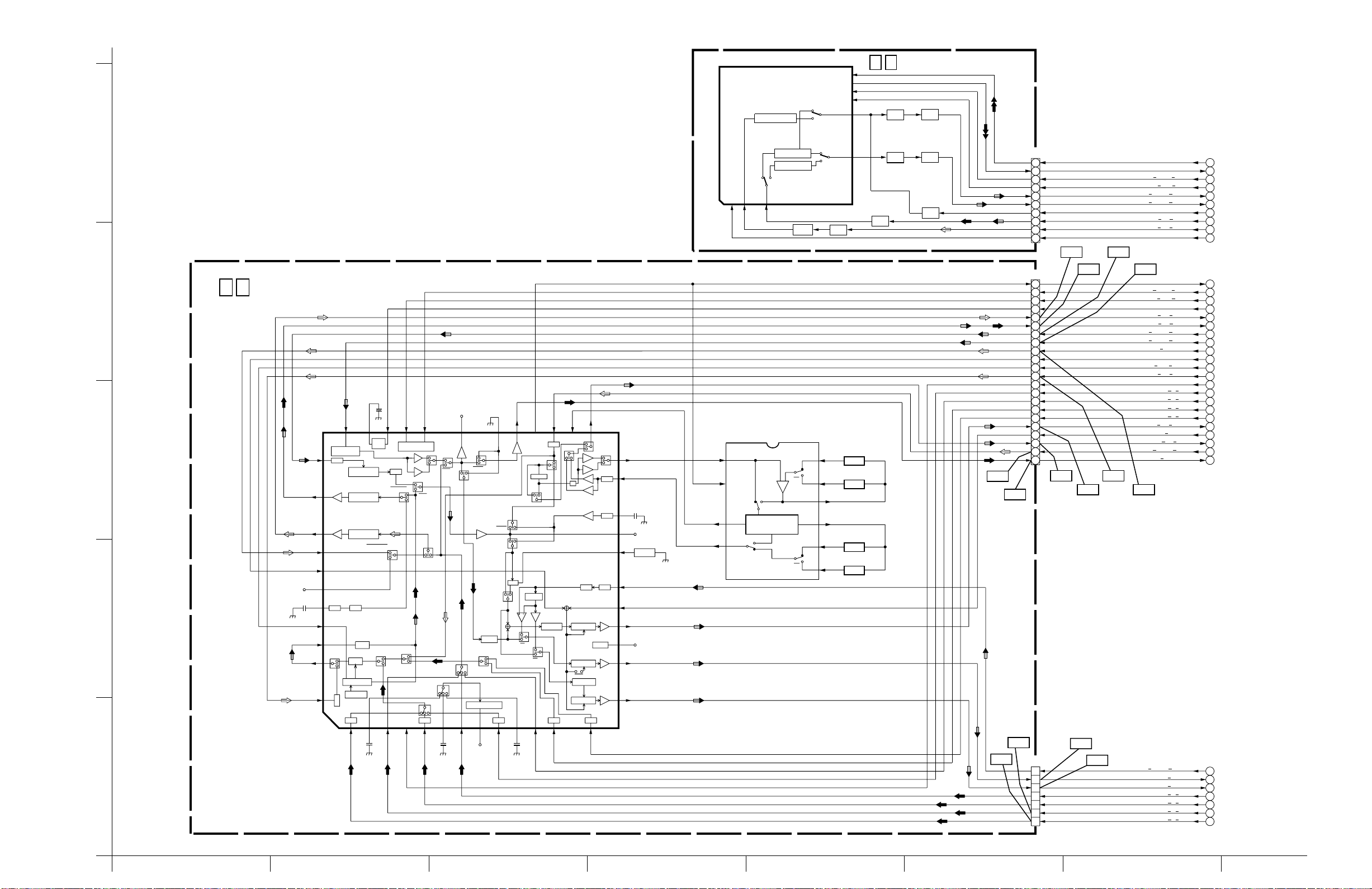
VIDEO BLOCK DIAGRAM (VHS)
4.37
(
IC1401
Y/C SEP & MIX
com/CNRPS
5
COMB3L
Y COMB
REC
PB
FSCIN
YVIN
CIN
29
31
24
1 5 S-SUB
4
C
Y
C
Y
Y
REC
REC
V FBC
C
)
SP/EP(LP
VHS
CLAMP
S-VHS
PB
REC
PB
REC
PB
EQ
ATT
V MUTE
D7&D8
BIAS
C MUTE
D16
Y FBC
Y MUTE
12
14
+
C
Y
43
3
Y
45
47
C
48
C
49
50
NOT
USED
51
2
52
53
Y
54
56
Y
IC501
(
Y/C SWITCH
42 41 40 39 38
CR
PRE LPF
CLAMP
ADJ
PRE LPF
PRE LPF
PRE LPF
EXT PB C
EXT PB C
CLAMP
ATT
GCL
AGC
S.SEP
Y
COMP IN
L
21
REC
PB
AGC DET
ATT
ATT
)
EXT PB Y
C
Y/C IN
C
CLK DATA
IIC LOGIC
PB
REC
ATT
DIGI/PB
DIGI
EXT PB Y
PB
Y
V5
V3/V4
Y1
ATT ATT ATT ATT
4
3
NOT
USED
36
CONV
DIGI/PB
REC
DIGI
Y
REC
C
Y
C1
C2
Y3
Y2
6
Y
C
CONV
PB*CONV
VCA
C
PB*D15
C.K.
V4
V3
C3
S1/S2 DET
85
NOT
USED
34 33 32 30 2931
EE/PB
N/S-LPF
PB
CONV
CONV
REC
PB*CONV
N.C.
PB
REC
TRAP
BB
BB
BB
BB
97
1110
CLAMP
CLAMP
CLAMP
Y
EE(L
)
IC502
PB
REC
NON LINEAR
PROCESSOR
PB
REC
SP
SP
SP
SP
(
S-VHS & SVHS-ET SWITCH
28
27
25
24
NOT
USED
23
FILTERFILTER
21
1
2
5
6
Y
20
19
18
NOT
USED
17
15
C
Y
1
BPF
REC
)
SD ATA
SCLK
COUT
DFFI
05
7
8
VR
11
12
17
PB
REC
YOUT
19
PB
Q1408
BUF
Q1418,Q1420
BUF
Q1417
)
18
EQ
17
EQ
16
BPF
LPF
DIGITAL/2M
3D
Q1402
Q1406
Q1404
Q1414
BUF
BUF
SW
CN1401
15
14
12
11
C
WF10
9
7
6
5
3
1
CN511
1
2
3
4
9
10
11
12
13
14
16
17
18
20
21
22
23
25
26
27
29
30
WF1
WF2
WF8
WF7 WF5
WF3
WF6
Y
Y
C
Y
C
Y
Y
C
C
Y
Y
Y
C
WF9
D.FF
V.REF
I2C DATA A/V
I2C CLK A/V
C FROM DIGI
Y FROM DIGI
EE(L
Y/V TO DIGI
C TO DIGI
WF4
EE(L
I2C DATA A/V
I2C CLK A/V
C TO DIGI
Y/V TO DIGI
Y FROM DIGI
C FROM DIGI
PB COLOR
V.PULSE
MAIN ALC DET
YTO SUB
P.MUTE(L
FRONT Y IN
FRONT C IN
FRONT V IN
REAR2 V IN
V TO OSD
CHARA DATA
YTO AV
VFROMAV
REC COLOR
1
2
3
4
5
6
)
7
8
Fsc
Fsc
9
10
)
11
12
13
14
15
16
17
18
19
20
21
22
)
23
24
25
26
27
28
29
30
31
32
12
11
EQ
10
EQ
Y
C
Y
C
Y
C
Y
WF14
WF13
CN512
2
4
6
8
10
12
14
WF11
WF12
V FROM OSD
COUT
Y OUT
REAR2 C IN
REAR2 Y IN
REAR1 C IN
REAR1 Y IN
33
34
35
36
37
38
39
Note : For the waveforms in this block diagram, refer to page 4-63.
4-73 4-74
HGFEDCBA
Page 78
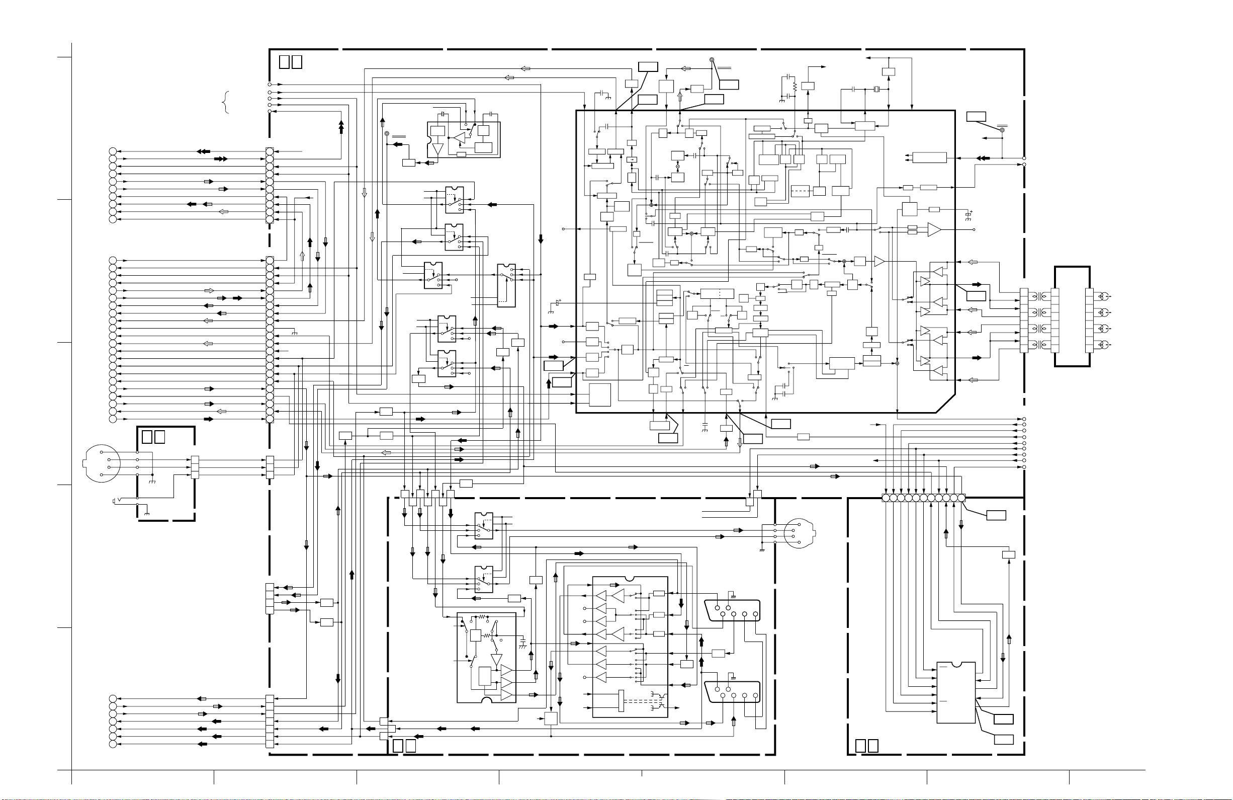
FM GCA
2Fsc
DET
PB/REC
Discri
4234
1/2
2FL
VCO
LPF2M
Main Emph
ier OffsetCarr
Fsc
VCO/OSC
REC
MUTE
629
TRAP
.C.C/DW
P.MUTE(L)
40
X-tal
P
R
REC
Filter
FM MOD
vo/Def Adj
S-DET
CN704
CN851
71
Q10
BUF
X1
55
38
SW1Head
SW2Head
HPF
SECAM
DET
SP
EP
)LP(
YCA
CH2
CH1
CH2
CH1
8
2
1
3
ON SCREEN
INfsc
ME
DET
Comp
DET
+
SP2
-
-
SP1
+
+
LP2
-
-
LP1
+
568910
4
27
11
10
IC1
(
VIDEO & AUDIO
SIGNAL PROCESSOR
WF5
D.FF
112
CTLD.F F
111
DETENV
120
TANC
101
104
SP2
105
Y
IC851
106
108
109
110
11
14
CHABLK
SYNC_DET
WF6
MUTE
CV_IN
CVOUT
SP1
LP2
LP1
( ON_SCREEN
DISPLAY)
CS2
5
LN21
SD ATA
SCLK
9
CS1
2
XTAL_IN
NOT
USED
4
3
8
21
19
WF3
Q853
TP111
D.FF
WF1
WF2
AMP
Y
)
Y
TO
SYSCON
D.FF
VIDEO_ENV
CN1
8
7
6
5
4
3
2
1
NORM/MESEC/S
OSD_CSB2Fsc
OSD_CLK
VHS(H)
OSD_DATA
I2C_CLK2
I2C_DATA2
P.MUTE(L)
SYNC_DET(H)
U.DRUM
8
7
6
5
4
3
2
1
8
7
6
5
4
3
2
1
TO
SYSCON, SUB CPU
VIDEO
HEAD
SP CH2
SP CH1
EP(LP) CH1
EP(LP) CH1
BDL
C
SQPB
R
P
EQ
Q5
BUF
VCA
R
CLPF
RP
Main
P
R
SQPB SQPB
RP
Q7118-Q7120
P
N.L.
Y
WF4
v1Con
.EmphDe
P
Q18
Y.IN
Y/V.OUT
P
.IN
V.OUT
.OUTV
AMP
.INY/V
TP106
PB FM
FBC/ALC
20
20
20
Y
ET ET
WF3
N.L.
Emph
Clamp
UFB
Y
CN7503
CN7103
C
V.GND
.GNDV
18
18
19
19
15
15
C/R B
.GNDV
18
19
15
C/R B
C
2fsc VCO
fH LOCK CTL
yDela
APC
SW
Pulse
Gen.
TRAP
G
EQ
DO
DLIM
Det
DeMOD
ET
LPF
Sub LPF
Main
.EmphDe
RP
LPFY
PR
7
WF8
Y
3
2
Y
J7104
V2A
IN/DECODER
7
7
11
11
BC/R
G
G
J7102
V1A
IN/OUT
7
11
G
ACC Det
CTL
Q24
BUF
44
LPF
CR Det
2fsc
R
P
COMP
SQPB
DL
REC
REC
AFC
APC
1/2
DOWN
.
Conv
.
SWPhase
4Phase
Gen.
P
ACC
R
HPF
L-SECAM
LPF
L-SECAM
.
SEP
P
EQ
PB
KillerColor
APC
Det.ID
TRAP
HPFfH
P
R
SQPB
SQPB
WF7
SW
Q17
Y
1
3
4
2
J7101
Y
S_OUT
C
30
MAIN (VIDEO, VIDEO I/O SW, CONNECTION)
TO
TO
SYSCON
5
D.FF
1
V.REF
2
I2C_DATA_A/V
3
I2C_CLK_A/V
4
C_FROM_DIGI
5
Y_FROM_DIGI
6
EE(L)
7
Y/V_TO_DIGI
8
C_TO_DIGI
9
Fsc
10
EE(L)
11
I2C_DATA_A/V
12
4
3
13
14
15
16
17
18
19
20
21
22
23
24
25
26
27
28
29
30
31
32
I2C_CLK_A/V
Fsc
C_TO_DIGI
Y/V_TO_DIGI
Y_FROM_DIGI
C_FROM_DIGI
PB_COLOR
V.PULSE
MAIN_ALC_DET
Y_TO_SUB
P.MUTE(L)
FRONT_Y_IN
FRONT_C_IN
FRONT_V_IN
REAR2_V_IN
V_TO_OSD
CHARA_DATA
Y_TO_AV
V_FROM_AV
REC_COLOR
J7001
63
S_IN
J7002
V_IN
Y
C
JACK
1
3
4
2
2
1
CN7002
1
3
5
2
V_FROM_OSD
1
33
C_OUT
34
Y_OUT
35
REAR2_C_IN
36
REAR2_Y_IN
37
REAR1_C_IN
38
REAR1_Y_IN
39
Y
Y
TUNER_VIDEO
TUNER
C
Y
C
Y
C
Y
Y
C
I2C_DATA_A/V
I2C_CLK_A/V
C.SYNC/V.REF
Y
C
Y
C
Y
FRONT_Y_IN
FRONT_C_IN
FRONT_V_IN
V.PULSE
TO
DV MAIN (DV V OUT)
CN3501
D_C_IN
D_Y/V_IN
D_C_OUT
D_Y_OUT
C
Y
C
C
CN501
15
14
12
11
9
7
6
5
3
1
CN502
1
2
3
4
9
10
11
12
13
14
16
17
18
20
21
22
23
25
26
27
29
30
CN7507
1
3
5
CN703
6
4
3
1
CN7506
2
4
6
8
10
12
14
C
D.FF
Fsc
C
P.MUTE(L)
Y
C
Y
D_VHS(H)/D_SEPA(H)
Y
TP701
D AGC
Q725
BUF
12 11 10
D1
CLAMP
Y
+
9
75 4
SYNC
Clamp
GCA
KEYED
LPF
PEAK Def.
IC707
AMP
14
IC711
SP_CONV/D_BS/D_F
D_VHS(H)/D_SEPA(H)
C
BUF
BUF
Y
D_YV(H)
OUT2_D(H)
B.BACK(H)
C
C
Y
Y
Y
C
Q711, Q712
Q708
BUF
Q710
Y
13
C
Y
C
Q703
BUF
Q706
BUF
C
CN7502 CN7102
Y
1
3
5
60
2
4
7
D_R2/D_R1Y/D_FV
IC702
4
2
7
IC703
4
2
7
BUF
Q713
C
5
7911
Y
C
C
C
TERMINAL
4
2
7
IC712
4
2
7
IC710
5
1
3
3
Y
D_TU(H)
Y
1
15
14
13
5
1
3
5
1
3
NOT
USED
1
3
5
NOT
USED
1
3
5
NOT
USED
Y
Y
BUF
CN7501
CN7101
Y
1
3
5
Y
1
3
5
C
REG
2.5V
Y
C
Q714
IC7102
IC7101
Y/C:MIC
IC7103
-6dB
IC705
7
4
2
C
Q709
BUF
Y
4
2
7
4
2
7
Q7112, Q7113
4dB
6dB
6dB
12dB
Y
Q705
Y
BUF
C
5
3
1
BUF
C
OUT1_L2(H)
OUT1_D(H)
Q7102
Q7103
3
5
C
7
Y
11
V
10
YCIN(H)
AV1
WF1
NOT
USED
NOT
USED
WF11
C
WF10
Q21
BUF
26
29
6dB AMP
25
Clamp
6dB AMP
UELCH.SQC
UELCHSQ
WHITE
LIMITER
CLEAR
SYNC
L-SECAM L-SECAM
3027
.KC
.EB
B.D
.Sync.Sep
MIX
LEVEL
ADJ
21
P
22
TTA
(
)
-10dB
20
ATT
)
(
-10dB
18
ATT
)
(
-10dB
16
ATT
)
(
-10dB
I2C
LOGIC
46
ATAD
45
CLK
CTLAPT
R
Video
GCA
BUF
&EQ
WF2
21
BDL
LPF
LEVEL
10
PILOT
Y
BDL
BDL
LPF
FILTER
Det1
LEVEL
Det2
CLPF
Main
P
BPF
ADD
REC
GCA Det
PB
ALC
.E.D
.N.C
YNR
DO
Clamp
11
v2Con
RR
DO
/REC
R
6121314
PN
EXT
INT
.KC
WF9
I2C_CLK2
I2C_DATA2
Y
BUF
24
23
22
NOT
21
USED
20
18
C
C
17
16
Y
BUF
&SW
C
I2C_DATA2
Y
I2C_CLK2
Q7116
Q7117
NOT
USED
15
13
14
IC7104
6dB&
BUF
BUF
6dB&
BUF
BUFBUFBUF
BUF
BUF
BUF
DATA
BUS
CTLI2C
CLK
1
CLAMP
3
CLAMP
5
CLAMP
7
9
BUF
Q7114
Q7115
11
Y
12
EXP2EXP1
AV1
YCIN(H)
Note : For the waveforms in this block diagram, refer to page 4-63.
DCBA
4-75 4-76
HGFE
Page 79

VIDEO/AUDIO BLOCK DIAGRAM (HDD)
4.38
50
DIGITAL (VIDEO AD/DA, AUDIO AD/DA, MPEG DEC, MPEG ENC, ASIC IF )
16
IC8001
5
IC8206
IC8207
TO
VHS MAIN
20
19
3
6
IC8801
AOUTR
AOUTL
AINR
AINL
16 bit
ADC & DAC
15
SDTI
D/A
12
SDTO
A/D
(AUDIO I/O)
CN2601
4
A_OUT(R)
A_OUT(L)
A_IN(R)
A_IN(L)
CN8801
2
4
6
8
IC8802
IC8803
R
L
AMP
R
L
R
L
AUDIO AD/DA
D0 - D7
Q0 - Q7
D-LATCH
DIGITAL AUDIO
IC8202
IC8203
A0 - A11
BA0, BA1
DQ0 -DQ15
SDRAM
TO
JIG
(For ADJ.)
3
TXD
RXD
CTS
RTS
CN8202
2
3
4
5
TO
VHS MAIN
(VIDEO I/O SW)
CN703
2
Y_OUT
C_OUT
Y_IN
C_IN
CN8601
1
3
4
6
TL8602
Y_OUT
TL8601
C_OUT
TL8603
V/Y_IN
TL8604
C_IN
Y
C
7
80
12
Y
18
C
TO
SYSCON
CN3014
CN8002
KBUS_CLK
KBUS_DATA_IN
4
6
IC8601
YSOUT
COUT
VYIN
CIN
CSI0 - CSI3
YSI0 - YSI3
CSO0 - CSO3
YSO0 - YSO3
CLK
VIDEO AD/DA
ENDEC
38 - 41
42 - 45
26 - 29
32 - 35
54
C
Y
C
Y
A4 - A19
FLASH ROM
20 - 26
29 - 35
2, 4, 5, 7
8, 10, 11, 13
42, 44, 45, 47
48, 50, 51, 53
DIGITAL AUDIO
IC8404
IC8405
DQ0 - DQ15
BA,A0 - A10
SDRAM
DVIDEO0 - DVIDEO3
4
DVIDEO4 - DVIDEO7
4
DIGITAL VIDEO
IC8204
D0 - D15
14
32
2, 3, 5, 6,
8, 9, 11, 12
39, 40, 42, 43
45, 46, 48, 49
19 - 24
27 - 32
74
12, 13, 15
16, 18, 20
21, 25, 26
28, 29, 30
32, 33
2, 3, 5, 7 - 9
43, 45, 46, 48
50 - 52, 54 - 56
58 - 61, 63, 64
227, 229, 231, 232
234 - 236, 238 - 240
93
94
95
96
OUTC0 - OUTC3
OUTY0 - OUTY3
47,48,50-60
63-65,67-76
79-81,83-85
16
101 - 107
12
111 - 115
119 - 122
123 - 126
MPEG DEC
AOUT0
MA0 - MA13
MD0 - MD31
TXD0
RXD0
CTS0
RTS0
4
4
MPEG ENC
200
AD ATA
D[0] - DQ[30]
ADRS[2] - ADRS[13]
DVIDEO0 - DVIDEO3
DVIDEO4 - DVIDEO7
IC8201
AD0 - AD31
VIO0 - VIO7
DVD0 - DVD7
CXI
DIGITAL VIDEO
IC8401
STDATA0 - STDATA7
SDDATA0 -SDDATA31
SDARDS0 - SDARDS11
VCLK
MCLKI
136 - 139, 141 - 144, 146
148 - 153, 155, 157, 158
163 - 168, 172 - 176, 178 - 180
126 - 131
133, 134
217, 219 - 223
225, 226
DIGITAL VIDEO
MPEG-2 STREM DATA
IC8002
DQ0 - DQ15
A0 - A10
SDRAM
TL8214
98
4 - 7
10 - 13
2, 3, 5, 6,
8, 9, 11, 12
39, 40, 42, 43
45, 46, 48, 49
19 - 24
27 - 32
132
26
27MHz
2
1
STDATA0 - STDATA7
MPEG-2 PS DATA
134 - 140
143 - 149
151 - 156
159 - 165
16
167 - 172
183 - 188
12
191 - 196
2, 3, 5, 6,
8, 9, 11, 12
39, 40, 42, 43
45, 46, 48, 49
20 - 24
27 - 32
IC8210
BUFF
C
Y
IC8402
IC8403
DQ0 - DQ15
A0 - A10,BA
32
8
8
6
7
SDRAM
14, 15, 18 - 33
37, 38, 40 - 46
71 - 78
200 - 207
158 - 170
16
175 - 177
185 - 189
11
192 - 197
109 - 112
102, 103
107, 108
90 - 97
8
AD0 - AD31
VIO0 - VIO7
DVD0 - DVD7
DQ[0] - DQ[15]
A[0] - A[10]
OUTC0 - OUTC3
OUTY0 - OUTY3
STDATA0 - STDATA7
ASIC_IF
IDE IF
DO[0] - DO[15]
50
59
CLK27M
HOSTDATA
HOSTCLK
136, 137
140 - 154
SYSTEM
CLOCK
X8001
54
118
117
(27MHz)
TL8011
CN8001
3
4
5
6
7
8
9
10
11
12
13
14
15
16
17
18
DD7
DD8
DD6
DD9
DD5
DD10
DD4
DD11
DD3
DD12
DD2
DD13
DD1
DD14
DD0
DD15
HARD DISK DRIVER
3
4
5
6
7
8
9
10
11
12
13
14
15
16
17
18
1
4-77 4-78
E. & O. E. No. 82887
(
Sanwa)-V13HV4
HGFEDCBA
Page 80
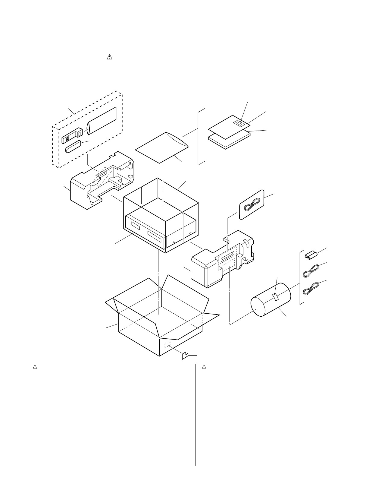
SECTION 5
SPEC OF BARCODE
301
FINAL ASSY <M2>
ADHESIVE TAPE
307
308
306
306A
302
303
302
311
312
316 (HDS1EU)
317 (HDS1EK)
SPEC OF BARCODE
310
315
314
PARTS LIST
SAFETY PRECAUTION
Parts identified by the symbol are critical for safety. Replace only with specified part numbers.
5.1 PACKING AND ACCESSORY ASSEMBLY <M1>
The instruction manual to be provided with this product will differ according to the destination.
# REF No. PART No. PART NAME, DESCRIPTION # REF No. PART No. PART NAME, DESCRIPTION
--------------- ----------------------- ----------------------------------------------------- ---------------- ----------------------- ------------------------------------------------------
******************************
PACKING AND ACCESSORY ASSEMBLY <M1>
301 LP30823-012A PACKING CASE,HDS1EU
LP30823-014A PACKING CASE,HDS1EK
302 LP30868-001B CUSHION ASSY
303 PQM30021-95 POLY BAG,HDS1EU
PQM30021-105 POLY BAG,HDS1EK
306 LP20873-009B REMOTE CONTROLLER
306A LP40254-007A COVER(BATTERY)
307 – BATTERY,X2(“R6”TYPE)
308 QPC02202230P POLY BAG
!
310 LPT0606-001A INST.BOOK(EN),HDS1EU
!
!
!
!
!
!
!
311 QPC02503530P POLY BAG
312 PEAC0300-02 RF CABLE
314 QAM0020-001 PERI CABLE
315 QAL0095-005 LED CABLE ASSY(Satellite Comtrol)
316 BT-54013-2 WARRANTY CARD,HDS1EU
317 BT-54008-2 GUARANTY CARD,HDS1EK
LPT0606-002A INST.BOOK(GE),HDS1EU
LPT0606-003A INST.BOOK(FR),HDS1EU
LPT0606-004A INST.BOOK(DU),HDS1EU
LPT0606-005A INST.BOOK(SP),HDS1EU
LPT0606-006A INST.BOOK(IT),HDS1EU
LPT0606-007A INST.BOOK(SW),HDS1EU
LPT0607-001A INST.BOOK(EN),HDS1EK
5-1
Page 81

5.2 FINAL ASSEMBLY <M2>
BEWARE OF BOGUS PARTS
Parts that do not meet specifications may cause
trouble in regard to safety and performance. We
recommend that genuine JVC parts be used.
509
566
564
DIGITAL SUB
BOARD ASSY
<49>
542
DIGITAL
BOARD ASSY
<50>
557
557A
558
542
WR19
WR18
G
SW/DISPLAY
BOARD
ASSY <28>
R
566
565
WR20
563
C
510
542
C
WR
M
R
4
N
O
535
WR2
505F
505E
D
508
507
531
M
G
L
542
567
553
553
LED
BOARD
ASSY <90>
MECHANISM
ASSY <M4>
WR17
LED/SW BOARD
ASSY <47>
WR6
F
507
506
505
K
WR8
A
J
553
B
WR1
WR10
Z
535
510
532
REGULATOR
BOARD ASSY
<02>
511E
JACK BOARD
ASSY <36>
E
568
S-SUB
BOARD
ASSY <15>
Y
511B
WR16
503
569
H
WR100
< Incl <03> >
Q
ON SCREEN
BOARD
ASSY <17>
MAIN BOARD
ASSY <03>
511E
511B
553
EJECT SW BOARD
ASSY <27>
553
548
551
550
551
550
3D DIGITAL/2M BOARD
ASSY <05>
538
X
N
533
556
F
E
511A
511C
511D
Z
V
561
WR7
D
X
533
538
520
TERMINAL
BOARD ASSY
<06>
O
H
Q
V
A
B
K
526
526
511C
539
J
W
T
WR9
504
RATING LABEL
(SERIAL)
S
DEMOD
BOARD
ASSY <14>
549
555
543
L
SW REG BOARD
ASSY <01>
W
519
503
521
530
504
502
LEBEL
(PATENT)
523
T
S
Y
528
504
503
521
521
525
522
521
534
554
526
517
511
5-2
501
501E
501J
501B
501A
527
529
529
Page 82

# REF No. PART No. PART NAME, DESCRIPTION # REF No. PART No. PART NAME, DESCRIPTION
--------------- ----------------------- ----------------------------------------------------- ---------------- ----------------------- ------------------------------------------------------
561 LP40253-001B STOPPER
******************************
FINAL ASSEMBLY <M2>
!
501 LP10331-012A FRONT PANEL ASSY,HDS1EU
!
501A LP20968-007A CASSETTE DOOR
501B PQ46448 TORSION SPRING
501E LP30763-001A DOOR(JACK),HDS1EU
501J PU60109 CATCHER
!
502 LP10128-006A TOP COVER
503 QYTDST3006R SCREW,X4 TOP COVER(SIDE)
504 QYTDST3006M SCREW,X3 TOP COVER(REAR)
505 LP20617-016A DRUM SUB ASSY
505E LP40323-001A CONTACT
505F LP30004-014A COMPRESION SPRING
506 PDZ0179-1-4 ROTOR ASSY
507 QYSPSP3006Z SCREW,X2
!
508 QAR0119-001 STATOR ASSY
509 QYSPSPH2606Z SCREW,X2
510 QYTDST2610Z SCREW,X3 DRUM
!
511 LP10156-003B BOTTOM CHASSIS ASSY
511A LP10130-002B BRACKET(1)
511B PEME0834 SPACER (BOARD),X3
511C LP40696-001A HOLDER(BOARD),X2
511D LP40696-002A HOLDER(BOARD)
511E QYTDST3006Z SCREW,X4
517 LP20939-001C BASE(1)
519 QYTDSF3010Z SCREW,BOTTOM CHASSIS
!
520 LP10339-004A REAR COVER
521 QYTDST3006M SCREW,X4 REAR COVER
522 QYTDSF3008M SCREW,X4 PERI
523 QYTDSF3008M SCREW,JACK
525 QYTDSF3008M SCREW,S JACK
526 QYTDST3006Z SCREW,X3 BASE(1)
527 PQ46617C FOOT ASSY,X2
528 PQ35504 FOOT(2),X2
529 QYTDST3006Z SCREW,X4
!
530 QMP4A10-170 POWER CORD,HDS1EU
!
531 PQ40413 SPECIAL SCREW,MECHA
532 LP40700-001A SPECIAL SCREW,MECHA
533 LP40226-001A PC SUPPORT,X2
534 PQ21623-2-5 EARTH PLATE(RF)
535 QYTDSF3010Z SCREW,X2 MECHA
538 QYTDSF3010Z SCREW,X2 MAIN
539 QYTDST3006Z SCREW,MAIN
542 QYTDST3006Z SCREW,X4 DIGITAL
543 QYTDST3006Z SCREW,X2 SW.REG
548 QAR0121-001 FAN MOTOR
549 QYTDSP4030M SCREW,X2
550 QYNNS4000Z NUT,X2
551 QYWLS4277A0Z SPRING WASHER,X2
553 QYTDSF2608Z SCREW,X15 FRONT
554 LP30312-001B BRACKET(CHASSIS)
555 QYTDSF3010Z SCREW,X2
556 LP40407-001A KNOB ASSY
557 LP40370-001E ROLLER ARM ASSY
557A PDM4311A-1 ROLLER ASSY
558 PQ45160 INERTIA PLATE
LP10331-013A FRONT PANEL ASSY,HDS1EK
LP30763-002A DOOR(JACK),HDS1EK
QMP51K0-170-K POWER CORD,HDS1EK
563 LPH30379-003B HDD (without Digital sub board assembly)
LPH30379-004A HDD (with Digital sub board assembly)
564 LP40738-001A SCREW,X4
565 LP20962-001A FRAME(HDD)
566 QYTDST3006Z SCREW,X4
567 PU49485-4 WIRE CLAMP
568 LP30356-003A DRUM SHIELD
569 QYTDST2606Z SCREW,X2
WR1 WJT0005-002A E-CARD WIRE,A/C HEAD CN2001
WR2 QUQ210-0826CC FFC WIRE,DIGITAL CN2601
WR4 QUQ210-0620CC FFC WIRE,DIGITAL CN3014
WR6 QUQ112-1810CG FFC WIRE,FRONT CN3011
WR7 QJN019-063011 SHI CR C-C WIRE,MAIN CN8601
WR8 QUQ212-0516CG FFC WIRE,DRUM CN3001
WR9 QUQ212-1910CG FFC WIRE,SW/REG CN5301
WR10 QUQ212-1328CG FFC WIRE,REG CN7508
WR16 QUQ112-1010CG FFC WIRE,FRONT CN7507
WR17 QUQ212-1536CG FFC WIRE,REG CN7509
WR18 QJJ001-091704 SIN CR C-C WIRE,DIGITAL CN5323
WR19 QJJ032-041504 SIN CR C-C WIRE,HDD CN5326
WR20 WJS0018-001A E-FL/RB WIRE,DIGITAL CN8001
5-3
Page 83

5.3 MECHANISM ASSEMBLY <M4>
124
128
120
104
89
88
142
134
78
122
143
130
75
74
AA
AA
73
135
76
141
AA
139
138
139
129
137
140
143
123
105
121
10
72
7
132
AA
107
BB
106
21
5
6
4
AA
51
40
13
BB
AA
13
11
AA
86
12107
26
AA
14
3
AA
49
39
1A
1B
127
43
44
42
AA
AA
58
55
53
AA
AA
46
A/C HEAD
BOARD ASSY <12>
57
52
AA
54
82
1
LOADING MOTOR
BOARD ASSY <55>
83
AA
59
61
60
62
91
85
5-4
AA
81
AA
34
37
35
103
36
38
69
Classification drawing
Part No.
102
32
AA
AA
31
Symbol in
Grease KYODO-SH-P AA
Oil COSMO-HV56 BB
111
113
114
AA
1
112
151
116
115
117
118
63
97
80
93
AA
20
19
95
94
108
109
90
92
22
99
96
BB
100
AA
15
110
84
24
18
16
87
25
27
70
71
67
AA
23
64
65
AA
119
66
AA
68
NOTE:This section indicates that the grease and oil are to be
applied on locations marked with AA and BB.
During checking and servicing, check if grease has been
applied on the locations marked with AA and oil on the locations marked with BB.
Page 84

# REF No. PART No. PART NAME, DESCRIPTION # REF No. PART No. PART NAME, DESCRIPTION
--------------- ----------------------- ----------------------------------------------------- ---------------- ----------------------- ------------------------------------------------------
******************************
1 LP20821-002F MAIN DECK ASSY
1A LP40275-004B PLATE(SUPPLY)
1B QYTDST2605Z SCREW,X4
3 LP30492-002B GIDE POLE GUARD
4 NAH0001-001 FULL ERASE HEAD
5 LP40098-001B GUIDE POLE(SUPPLY)
6 QYTDST2608Z SCREW
7 LP40637-002A TENSION STUD BASE ASSY
10 QYTDST2606Z SCREW
11 LP30409-002C UV CATCHER 2(SUPPLY)
12 LP30409-002C UV CATCHER 2(TAKE UP)
13 QYTPST2606Z SCREW,X2
14 PQ40919-10 SPACER(TAKE UP)
15 LP30223-003C LOADING ARM GEAR SHAFT
16 QYTDST2606Z SCREW
18 LP30224-001B LOADING ARM GEAR(SUPPLY)
19 LP40099-001A TORSION ARM
20 LP40100-001A PIN
21 LP40101-006A POLE BASE ASSY(SUPPLY)
22 QYSPSTG2606Z SCREW
23 LP40103-002B LOADING ARM GEAR(TAKE UP)
24 LP40099-001A TORSION ARM
25 LP40100-001A PIN
26 LP40104-006A POLE BASE ASSY(TAKE UP)
27 QYSPSTG2606Z SCREW
31 LP20233-004B ROTARY ENCODER GUIDE
32 QYTPST2606Z SCREW
34 LP30226-004E CONTROL PLATE GUIDE
35 QYTPST2605Z SCREW
36 LP30249-003B TAKE UP LEVER
37 LP30003-006A TENSION SPRING
38 LP40119-002A T.UP HEAD
39 LP20234-004B LID GUIDE
40 QYTDST2606Z SCREW,X2
42 LP40105-003A PINCH ROLLER ARM ASSY
43 LP40753-001A PINCH ROLLER SHEET 3
44 LP40148-002A TORSION SPRING
46 LP40149-001C PRESS LEVER ASSY
49 LP40106-007A GUIDE ARM ASSY
51 LP40134-001C TENSION SPRING
52 QAH0010-005 AC HEAD
53 LP30228-001C HEAD BASE
54 LP30004-013A COMPRESSION SPRING,X3
55 LP40236-001A COMPRESSION SPRING
57 LP40213-002B SPECIAL SCREW,X3
58 QYTDST2608Z SCREW,X2
59 QAR0023-001 LOADING MOTOR
60 PQ43546-1-2 MOTOR PULLEY
61 LP30230-003D MOTOR GUIDE
62 QYTPSP3003Z SCREW,X2
63 LP30005-003A BELT,LOADING MOTOR
64 LP20791-002D CONTROL CAM
65 PQM30017-24 SLIT WASHER
66 LP40120-001A WORM GEAR
67 LP40107-002A LINK LEVER ASSY
68 PQM30017-24 SLIT WASHER
69 LP10284-002E CONTROL PLATE
70 LP40379-001B CONTROL BRACKET(1)
71 QYTDSF2608M SCREW
72 LP40108-002A TENSION ARM ASSY
MECHANISM ASSEMBLY <M4>
73 LP30003-010A TENSION SPRING
74 LP40109-003D TENSION BRAKE ASSY
75 PQ46302-1-3 ADJUST PIN
76 LP30232-002A TENSION ARM BEARING
78 LP40532-009B MAIN BRAKE ASSY (SUPPLY)
80 LP40111-014C MAIN BRAKE ASSY (TAKE UP)
81 LP30003-029A TENSION SPRING
82 LP40112-001F SUB BRAKE ASSY(TAKE UP)
83 LP40357-001B TENSION SPRING
84 LP40461-001A CAPSTAN BRAKE ASSY
85 QAR0132-001 CAPSTAN MOTOR
86 QYTDSF2606M SCREW,X3
87 LP30005-008A BELT,CAPSTAN MOTOR
88 LP40114-011B IDLER ARM ASSY
89 LP30016-001A SLIT WASHER
90 LP40593-003B CLUTCH UNIT 3
91 LP30002-097A SPACER,CAPSTAN MOTOR
92 PQM30017-47 SLIT WASHER
93 LP30696-002A CLUTCH GEAR 4
94 LP30697-003A COUPLING GEAR
95 LP40554-002A COMPRESSION SPRING
96 LP40442-001A DIRECT GEAR
97 LP30017-019A SPACER,C.GEAR4
99 LP40483-002A COMPRESSION SPRING,D.GEAR
100 LP30016-001A SLIT WASHER,D.GEAR
102 LP40484-003B CHANGE LEVER ASSY
103 LP40512-002B COMPRESSION SPRING
104 LP30236-002C IDLER LEVER
105 LP20237-003B REEL DISK ASSY(SUPPLY)
106 LP20238-003B REEL DISK ASSY(TAKE UP)
107 LP30017-015A SPACER,X2
108 QSW0554-003 ROTARY ENCODER
109 LP40746-001A SPECIAL SCREW
110 LP30237-002B CASSETTE GEAR
111 LP30239-002G LIMIT GEAR(1)
112 LP30240-002G LIMIT GEAR(2)
113 LP40136-001E TORSION SPRING
114 LP30242-002A RELAY GEAR
115 LP30339-002E OPENER GUIDE
116 LP40545-001A TORSION SPRING
117 LP40214-001B C.H.BRACKET
118 PQM30017-47 SLIT WASHER,X2
119 LP30243-002A DRIVE GEAR
120 LP20240-001G DRIVE ARM
121 LP40137-001A TORSION SPRING
122 LP10081-002P SIDE HOLDER(L)
123 LP10082-002U SIDE HOLDER(R)
124 LP30255-006B LOCK LEVER(L)
127 LP30256-001H LOCK LEVER(R)
128 LP40168-003A TORSION SPRING(L)
129 LP40218-001B TORSION SPRING(R)
130 LP30257-001G CASSETTE HOLDER
131 PQ40919-30 SPACER,EARTH PLATE
132 LP30244-002G GUIDE RAIL
134 LP30245-002F REC SAFETY LEVER
135 LP30003-004A TENSION SPRING
137 LP20578-001C TOP GUIDE
138 LP30500-001C HOLD PLATE
139 LP40450-003A PAD,X2
140 LP30003-025B TENSION SPRING
141 LP30003-024A TENSION SPRING
142 LP40481-003A ROLLER CAM ASSY
143 LP30019-014A PAD,X2
151 LP20324-003B DOOR OPENER
5-5
Page 85

5.4 ELECTRICAL PARTS LIST
# REF No. PART No. PART NAME, DESCRIPTION # REF No. PART No. PART NAME, DESCRIPTION
--------------- ----------------------- ----------------------------------------------------- ---------------- ----------------------- ------------------------------------------------------
or 1SS270A DIODE
******************************
SW.REG BOARD ASSEMBLY <01>
PW1 LPA10119-06A1 SW.REG BOARD ASSY
IC5101 STR-F6552 IC
IC5301 L5431 IC
or MM1431AT IC
Q5301 2SD1819A/RS/-X TRANSISTOR
or 2SC4081/RS/-X TRANSISTOR
or 2PC4081/R/-X TRANSISTOR
Q5302 DTA114EU TRANSISTOR
or PDTA114EU TRANSISTOR
or RN2302 TRANSISTOR
or UN5111 TRANSISTOR
D5001 D3SBA60 BRIDGE DIODE
D5101 SARS01 DIODE
D5102 AU01Z FR DIODE
or ERA18-02-T2 FR DIODE
or PG104RS FR DIODE
or 1SR153-400-T2 FR DIODE
or 10ELS2 FR DIODE
D5103 1SS133 DIODE
or 1SS270A DIODE
D5201 AK04 DIODE
or 1S4 SB DIODE
or 11EQS04 SB DIODE
D5202 FML-12S FR DIODE
or SF5LC20U FR DIODE
or ER602FCT FR DIODE
or YG901C2 FR DIODE
or FCF06A20 FR DIODE
D5203 FMB-24 BARRIER DIODE
or FSQ05A04B SB DIODE
or SB640FCT SB DIODE
or SF5SC4 SB DIODE
or YG801C04 SB DIODE
D5204 1SR153-400-T2 FR DIODE
or 10ELS2 FR DIODE
or ERA18-02-T2 FR DIODE
or PG104RS FR DIODE
D5206 FMB-24 BARRIER DIODE
or FSQ05A04B SB DIODE
or SB640FCT SB DIODE
or SF5SC4 SB DIODE
or YG801C04 SB DIODE
D5210 AU01Z FR DIODE
or ERA18-02-T2 FR DIODE
or PG104RS FR DIODE
or 1SR153-400-T2 FR DIODE
or 10ELS2 FR DIODE
D5211 AU01Z FR DIODE
or ERA18-02-T2 FR DIODE
or PG104RS FR DIODE
or 10ELS2 FR DIODE
or 1SR153-400-T2 FR DIODE
D5301 MTZJ15A ZENER DIODE
or RD15ES/B1/-T2 ZENER DIODE
D5303 MTZJ7.5A ZENER DIODE
or RD7.5ES/B1/-T2 ZENER DIODE
D5304 1SS133 DIODE
D5305 MTZJ27C ZENER DIODE
or RD27ES/B3/-T2 ZENER DIODE
D5306 MTZJ2.7B ZENER DIODE
or RD2.7ES/B2/-T2 ZENER DIODE
D5307 1SS133 DIODE
or 1SS270A DIODE
D5308 1SS133 DIODE
or 1SS270A DIODE
D5309 1SS133 DIODE
or 1SS270A DIODE
D5310 1SS133 DIODE
or 1SS270A DIODE
D5311 1SS133 DIODE
or 1SS270A DIODE
D5312 1SS133 DIODE
or 1SS270A DIODE
D5313 1SS133 DIODE
or 1SS270A DIODE
R5101 QRG02GJ-683 OMF RESISTOR 68kØ,2W
R5102 QRE141J-100Y RESISTOR 10Ø,1/4W
R5103 NRSA02J-332X MG RESISTOR 3.3kØ,1/10W
R5104 QRE141J-681Y RESISTOR 680Ø,1/4W
R5105 QRT01DJ-R47X MF RESISTOR 0.47Ø,1W
R5107 QRE141J-684Y RESISTOR 680kØ,1/4W
R5108 QRE121J-470Y RESISTOR 47Ø,1/2W
R5302 NRSA02J-472X MG RESISTOR 4.7kØ,1/10W
R5303 NRVA02D-123X CMF RESISTOR 12kØ,1/10W
R5304 NRVA02D-302X CMF RESISTOR 3kØ,1/10W
R5305 NRSA02J-223X MG RESISTOR 22kØ,1/10W
!
R5306 QRZ9005-470X FUSI RESISTOR 47Ø,1/4W
R5307 NRSA02J-221X MG RESISTOR 220Ø,1/10W
R5308 NRSA02J-102X MG RESISTOR 1kØ,1/10W
R5309 NRSA02J-122X MG RESISTOR 1.2kØ,1/10W
R5310 QRL02DJ-821X OMF RESISTOR 820Ø,2W
R5311 NRSA02J-473X MG RESISTOR 47kØ,1/10W
R5313 NRSA02J-561X MG RESISTOR 560Ø,1/10W
R5314 NRSA02J-103X MG RESISTOR 10kØ,1/10W
R5316 NRSA02J-102X MG RESISTOR 1kØ,1/10W
R5317 NRSA02J-333X MG RESISTOR 33kØ,1/10W
B5003 QUY160-100Y IM BUS WIRE
!
C5001 QFZ9073-683 F CAPACITOR 0.068µF,250V
!
C5002 QFZ9051-333 F CAPACITOR 0.033µF,250V
!
C5004 QCZ9071-222 CAPACITOR 0.0022µF,250V
C5007 QEZ0374-826 E CAPACITOR 82µF,400V
C5102 QEMU1VM-276 E CAPACITOR 27µF,35V
C5103 QCZ0302-330Z CAPACITOR 33pF,1kV
C5104 QFLC1HJ-471Z F CAPACITOR 470pF,50V
C5105 NCB21HK-223X CAPACITOR 0.022µF,50V
C5106 QCZ0212-472 CAPACITOR 0.0047µF,1kV
C5201 QEMU0JM-227 E CAPACITOR 220µF,6.3V
C5202 QEMT1CM-827 E CAPACITOR 820µF,16V
C5203 QETN1CM-227 E CAPACITOR 220µF,16V
C5204 QEMT1AM-228 E CAPACITOR 2200µF,10V
C5205 QETN1AM-227 E CAPACITOR 220µF,10V
C5206 QEMU1EM-187 E CAPACITOR 180µF,25V
C5207 QETN2AM-475 E CAPACITOR 4.7µF,100V
C5208 QEMU1HM-186 E CAPACITOR 18µF,50V
C5212 QEMT1AM-278 E CAPACITOR 2700µF,10V
C5213 QETN1AM-227 E CAPACITOR 220µF,10V
C5301 QFLC1HJ-103Z F CAPACITOR 0.01µF,50V
5-6
Page 86

# REF No. PART No. PART NAME, DESCRIPTION # REF No. PART No. PART NAME, DESCRIPTION
--------------- ----------------------- ----------------------------------------------------- ---------------- ----------------------- ------------------------------------------------------
C5302 QFLC1HJ-473Z F CAPACITOR 0.047µF,50V
C5303 QFLC1HJ-333Z F CAPACITOR 0.033µF,50V
C5304 QETN1EM-476 E CAPACITOR 47µF,25V
C5305 QFLC1HJ-103Z F CAPACITOR 0.01µF,50V
L5201 PELN1184 COIL 33µH
L5202 PU60944-330K COIL 33µH
L5205 PELN1184 COIL 33µH
K5101 QQR0678-001Z FERRITE BEAD
!
PC5101 PC123F2 PH COUPLER
!
T5001 QQS0092-001 SW TRANSFORMER
HS2 LP40515-001B HEAT SINK,D5206
FC5001 QNG0006-001Z FUSE CLIP,F5001
FC5002 QNG0006-001Z FUSE CLIP,F5001
!
LF5001 PELN1204-01-01 LINE FILTER
!
LF5002 QQR1031-001 LINE FILTER
!
CN5001 QGA7901C3-02 CONNECTOR,(1-2)AC IN
CN5201 QGF1208C1-19 FPC CONNECTOR,(1-19)REG
!
CP5301 ICP-N25 CIRCUIT PROTECTOR
!
F5001 QMF51E2-2R0J1 FUSE T2.0A,AC250V
******************************
REG BOARD ASSEMBLY <02>
PW2 LPA10119-06A2 REG BOARD ASSY
IC5321 PQ15RW11 IC
IC5322 PQ5EV3 IC
Q5321 2SD2528/QP/ TRANSISTOR
Q5322 2SD1819A/RS/-X TRANSISTOR
or 2SC4081/RS/-X TRANSISTOR
or 2PC4081/R/-X TRANSISTOR
Q5326 2SD2375/QP/ TRANSISTOR
Q5327 2SD1819A/RS/-X TRANSISTOR
or 2SC4081/RS/-X TRANSISTOR
or 2PC4081/R/-X TRANSISTOR
Q5328 2SD1302/ST/-T TRANSISTOR
or 2SD1450/ST/-T TRANSISTOR
Q5329 DTA114EU TRANSISTOR
or PDTA114EU TRANSISTOR
or UN5111 TRANSISTOR
or RN2302 TRANSISTOR
Q5330 2SD2144S/UV/-T TRANSISTOR
Q5331 2SB1068/KU/-T TRANSISTOR
Q5332 DTC114EU TRANSISTOR
or PDTC114EU TRANSISTOR
or RN1302 TRANSISTOR
or UN5211 TRANSISTOR
Q5333 2SD1450/ST/-T TRANSISTOR
or 2SD1302/ST/-T TRANSISTOR
Q5335 2SB1256 TRANSISTOR
Q5336 DTC114TU TRANSISTOR
or PDTC114TU TRANSISTOR
or UN5215 TRANSISTOR
or RN1311 TRANSISTOR
D5321 FML-12S FR DIODE
or SF5LC20U FR DIODE
or YG901C2 FR DIODE
or FCF06A20 FR DIODE
or ER602FCT FR DIODE
D5325 RD5.1JS/B2/-T2 ZENER DIODE
or MA4051N/M/-T2 ZENER DIODE
D5326 1SS133 DIODE
or 1SS270A DIODE
D5327 RD5.1JS/B2/-T2 ZENER DIODE
or MA4051N/M/-T2 ZENER DIODE
D5328 1SS133 DIODE
or 1SS270A DIODE
D5329 1SS133 DIODE
or 1SS270A DIODE
D5331 1SS133 DIODE
or 1SS270A DIODE
D5333 1SS133 DIODE
or 1SS270A DIODE
D5334 11ES2 DIODE
or ERA15-02-T2 DIODE
or 1A3G DIODE
D5335 1SS133 DIODE
or 1SS270A DIODE
D5336 MTZJ12A ZENER DIODE
or RD12ES/B1/-T2 ZENER DIODE
R5322 NRSA02J-471X MG RESISTOR 470Ø,1/10W
R5323 NRSA02J-471X MG RESISTOR 470Ø,1/10W
R5324 NRSA02J-102X MG RESISTOR 1kØ,1/10W
R5325 NRSA02J-103X MG RESISTOR 10kØ,1/10W
R5326 NRSA02J-471X MG RESISTOR 470Ø,1/10W
R5327 NRSA02J-471X MG RESISTOR 470Ø,1/10W
R5328 NRSA02J-102X MG RESISTOR 1kØ,1/10W
R5329 NRSA02J-103X MG RESISTOR 10kØ,1/10W
R5330 NRSA02J-471X MG RESISTOR 470Ø,1/10W
R5331 NRSA02J-473X MG RESISTOR 47kØ,1/10W
R5334 NRVA02D-472X CMF RESISTOR 4.7kØ,1/10W
R5335 NRVA02D-472X CMF RESISTOR 4.7kØ,1/10W
R5336 NRVA02D-472X CMF RESISTOR 4.7kØ,1/10W
R5337 NRVA02D-152X CMF RESISTOR 1.5kØ,1/10W
R5338 NRSA02J-103X MG RESISTOR 10kØ,1/10W
R5339 NRSA02J-102X MG RESISTOR 1kØ,1/10W
R5340 QRL01DJ-101X OMF RESISTOR 100Ø,1W
R5341 NRSA02J-511X MG RESISTOR 510Ø,1/10W
R5342 NRSA02J-471X MG RESISTOR 470Ø,1/10W
R5343 NRSA02J-473X MG RESISTOR 47kØ,1/10W
R5344 NRSA02J-221X MG RESISTOR 220Ø,1/10W
R5345 NRSA02J-472X MG RESISTOR 4.7kØ,1/10W
R5346 NRSA02J-222X MG RESISTOR 2.2kØ,1/10W
R5353 NRSA02J-103X MG RESISTOR 10kØ,1/10W
B5301 NRSA02J-0R0X MG RESISTOR 0Ø,1/10W
B5302 NRSA02J-0R0X MG RESISTOR 0Ø,1/10W
B5303 NRSA02J-0R0X MG RESISTOR 0Ø,1/10W
B5305 NRSA02J-0R0X MG RESISTOR 0Ø,1/10W
B5306 QUY153-050Y IM BUS WIRE
B5307 QUY153-050Y IM BUS WIRE
C5321 QETN1AM-107 E CAPACITOR 100µF,10V
C5322 QETN1HM-106 E CAPACITOR 10µF,50V
C5323 QETN1CM-107 E CAPACITOR 100µF,16V
C5324 QFLC1HJ-102Z F CAPACITOR 0.001µF,50V
C5325 QFLC1HJ-102Z F CAPACITOR 0.001µF,50V
C5326 QETN1AM-107 E CAPACITOR 100µF,10V
C5327 NCB21HK-103X CAPACITOR 0.01µF,50V
C5328 QETN1AM-107 E CAPACITOR 100µF,10V
C5329 NCB21HK-103X CAPACITOR 0.01µF,50V
5-7
Page 87

# REF No. PART No. PART NAME, DESCRIPTION # REF No. PART No. PART NAME, DESCRIPTION
--------------- ----------------------- ----------------------------------------------------- ---------------- ----------------------- ------------------------------------------------------
C5330 QETN1AM-107 E CAPACITOR 100µF,10V
C5332 QETN1CM-226 E CAPACITOR 22µF,16V
C5333 QETN1AM-107 E CAPACITOR 100µF,10V
C5334 QETN1CM-227 E CAPACITOR 220µF,16V
C5335 QETN1CM-107 E CAPACITOR 100µF,16V
L5321 QQL01BK-101Z COIL 100µH
HS1 LP40090-001A HEAT SINK,IC5322
HS2 LP40090-001A HEAT SINK,Q5321
OT1 QYTDST3006Z SCREW,IC5322
OT2 QYTDST3006Z SCREW,Q5321
CN5301 QGF1208C1-19 FPC CONNECTOR,(1-19)SW/REG
CN5321 QGF1208F1-15 FPC CONNECTOR,(1-15)MAIN
CN5322 QGF1208F1-13 FPC CONNECTOR,(1-13)MAIN
CN5323 QGA2001C1-09 CONNECTOR,(1-9)DIGITAL
CN5325 QGA2001F1-02 CONNECTOR,(1-2)FAN MOTOR
CN5326 QGA2501C1-04 CONNECTOR,(1-4)HDD
!
CP5322 ICP-N25 CIRCUIT PROTECTOR
******************************
MAIN BOARD ASSEMBLY <03>
PW1 LPA10113-08A MAIN BOARD ASSY,HDS1EU
LPA10113-10A MAIN BOARD ASSY,HDS1EK
IC1 JCP8050-MSA IC
IC702 MM1113XF IC
IC703 MM1117XF IC
IC705 MM1117XF IC
IC706 PQ05TZ1U IC
IC707 AN3916 IC
IC710 MM1117XF IC
IC711 MM1117XF IC
IC712 MM1113XF IC
IC2601 BU4052BCF IC
IC2602 BA15218F-XE IC
IC2603 BU4052BCF IC
IC2605 BA15218F-XE IC
IC2606 BU4052BCF IC
IC2607 BU4052BCF IC
IC2608 BA15218F-XE IC
IC2610 BU4053BCF IC
IC3001 HD6432194BA28F IC(MCU)
IC3002 S-80727AN-DQ-X IC
or S-80827ANUP-W IC
IC3003 AT24C16-10PC IC
or 24LC16B/P IC
IC3004 BA6956AN IC
IC3006 TC7S04F IC(DIGITAL)
IC3601 BU2090FS IC
IC3651 BU2090FS IC
Q1 2SC4081/S/-X TRANSISTOR
Q2 2SC4081/S/-X TRANSISTOR
Q3 2SC4081/S/-X TRANSISTOR
Q4 2SC4081/S/-X TRANSISTOR
Q5 2SB1218A/QR/-X TRANSISTOR
or 2SA1576A/QR/-X TRANSISTOR
or 2PA1576/R/-X TRANSISTOR
Q7 2SD1819A/QRS/-X TRANSISTOR
or 2PC4081/R/-X TRANSISTOR
or 2SC4081/QRS/-X TRANSISTOR
Q8 2SD1819A/QRS/-X TRANSISTOR
or 2SC4081/QRS/-X TRANSISTOR
or 2PC4081/R/-X TRANSISTOR
Q9 2SB1218A/QR/-X TRANSISTOR
or 2PA1576/R/-X TRANSISTOR
or 2SA1576A/QR/-X TRANSISTOR
Q10 2SB1218A/QR/-X TRANSISTOR
or 2SA1576A/QR/-X TRANSISTOR
or 2PA1576/R/-X TRANSISTOR
Q17 DTC144WU TRANSISTOR
or PDTC144WU TRANSISTOR
or RN1309 TRANSISTOR
or UN521E TRANSISTOR
Q21 2SB1218A/QR/-X TRANSISTOR
or 2SA1576A/QR/-X TRANSISTOR
or 2PA1576/R/-X TRANSISTOR
Q24 2SA1576A/QR/-X TRANSISTOR
or 2PA1576/R/-X TRANSISTOR
or 2SB1218A/QR/-X TRANSISTOR
Q25 DTC144WU TRANSISTOR
or PDTC144WU TRANSISTOR
or RN1309 TRANSISTOR
or UN521E TRANSISTOR
Q38 2SD1819A/QRS/-X TRANSISTOR
or 2PC4081/R/-X TRANSISTOR
or 2SC4081/QRS/-X TRANSISTOR
Q41 DTC144WU TRANSISTOR
or PDTC144WU TRANSISTOR
or RN1309 TRANSISTOR
or UN521E TRANSISTOR
Q401 2SA1576A/QR/-X TRANSISTOR
Q402 2SA1576A/QR/-X TRANSISTOR
Q403 DTC144WU TRANSISTOR
or PDTC144WU TRANSISTOR
or RN1309 TRANSISTOR
or UN521E TRANSISTOR
Q404 DTC144WU TRANSISTOR
or PDTC144WU TRANSISTOR
or RN1309 TRANSISTOR
or UN521E TRANSISTOR
Q405 2SA1576A/QR/-X TRANSISTOR
Q703 2SC4081/QRS/-X TRANSISTOR
or 2PC4081/R/-X TRANSISTOR
or 2SD1819A/QRS/-X TRANSISTOR
Q705 2SA1576A/QR/-X TRANSISTOR
or 2PA1576/R/-X TRANSISTOR
or 2SB1218A/QR/-X TRANSISTOR
Q706 2SC4081/QRS/-X TRANSISTOR
or 2SD1819A/QRS/-X TRANSISTOR
or 2PC4081/R/-X TRANSISTOR
Q708 2SA1576A/QR/-X TRANSISTOR
or 2SB1218A/QR/-X TRANSISTOR
or 2PA1576/R/-X TRANSISTOR
Q709 2SA1576A/QR/-X TRANSISTOR
or 2PA1576/R/-X TRANSISTOR
or 2SB1218A/QR/-X TRANSISTOR
Q710 2SA1576A/QR/-X TRANSISTOR
or 2SB1218A/QR/-X TRANSISTOR
or 2PA1576/R/-X TRANSISTOR
5-8
Page 88

# REF No. PART No. PART NAME, DESCRIPTION # REF No. PART No. PART NAME, DESCRIPTION
--------------- ----------------------- ----------------------------------------------------- ---------------- ----------------------- ------------------------------------------------------
Q711 2SA1576A/QR/-X TRANSISTOR
or 2PA1576/R/-X TRANSISTOR
or 2SB1218A/QR/-X TRANSISTOR
Q712 2SC4081/QRS/-X TRANSISTOR
or 2SD1819A/QRS/-X TRANSISTOR
or 2PC4081/R/-X TRANSISTOR
Q725 2SA1576A/QR/-X TRANSISTOR
or 2PA1576/R/-X TRANSISTOR
or 2SB1218A/QR/-X TRANSISTOR
Q2001 2SC4081/QRS/-X TRANSISTOR
or 2PC4081/R/-X TRANSISTOR
or 2SD1819A/QRS/-X TRANSISTOR
Q2002 2SC4081/QRS/-X TRANSISTOR
or 2SD1819A/QRS/-X TRANSISTOR
or 2PC4081/R/-X TRANSISTOR
Q2003 DTA144WU TRANSISTOR
or RN2309 TRANSISTOR
or UN511E TRANSISTOR
or PDTA144WU TRANSISTOR
Q2004 DTC144WU TRANSISTOR
or PDTC144WU TRANSISTOR
or RN1309 TRANSISTOR
or UN521E TRANSISTOR
Q2011 DTC144WU TRANSISTOR
or PDTC144WU TRANSISTOR
or RN1309 TRANSISTOR
or UN521E TRANSISTOR
Q2051 2SC4081/QRS/-X TRANSISTOR
or 2PC4081/R/-X TRANSISTOR
or 2SD1819A/QRS/-X TRANSISTOR
Q2052 2SA1576A/QR/-X TRANSISTOR
or 2SB1218A/QR/-X TRANSISTOR
or 2PA1576/R/-X TRANSISTOR
Q2053 DTC144WU TRANSISTOR
or PDTC144WU TRANSISTOR
or RN1309 TRANSISTOR
or UN521E TRANSISTOR
Q2054 2SA1576A/QR/-X TRANSISTOR
or 2PA1576/R/-X TRANSISTOR
or 2SB1218A/QR/-X TRANSISTOR
Q2061 2SC4081/QRS/-X TRANSISTOR
or 2SD1819A/QRS/-X TRANSISTOR
or 2PC4081/R/-X TRANSISTOR
Q2062 2SA1576A/QR/-X TRANSISTOR
or 2PA1576/R/-X TRANSISTOR
or 2SB1218A/QR/-X TRANSISTOR
Q2251 DTA144WU TRANSISTOR
or RN2309 TRANSISTOR
or UN511E TRANSISTOR
or PDTA144WU TRANSISTOR
Q2252 DTC114EU TRANSISTOR
or PDTC114EU TRANSISTOR
or RN1302 TRANSISTOR
or UN5211 TRANSISTOR
Q2601 2SC4081/QRS/-X TRANSISTOR
Q2602 2SC4081/QRS/-X TRANSISTOR
Q3001 2SD1819A/QRS/-X TRANSISTOR
or 2SC4081/QRS/-X TRANSISTOR
or 2PC4081/R/-X TRANSISTOR
Q3002 PTZ-NV16 PHOTO TRANSISTOR
or PTZ-NV16A PHOTO TRANSISTOR
Q3003 PTZ-NV16 PHOTO TRANSISTOR
or PTZ-NV16A PHOTO TRANSISTOR
Q3004 2SD1819A/QRS/-X TRANSISTOR
or 2SC4081/QRS/-X TRANSISTOR
or 2PC4081/R/-X TRANSISTOR
Q3005 2SD1819A/QRS/-X TRANSISTOR
or 2PC4081/R/-X TRANSISTOR
or 2SC4081/QRS/-X TRANSISTOR
Q3007 DTC144WU TRANSISTOR
or PDTC144WU TRANSISTOR
or RN1309 TRANSISTOR
or UN521E TRANSISTOR
Q3302 DTC144WU TRANSISTOR
or PDTC144WU TRANSISTOR
or RN1309 TRANSISTOR
or UN521E TRANSISTOR
Q4001 UN5211 TRANSISTOR
or RN1302 TRANSISTOR
or DTC114EU TRANSISTOR
Q4002 UN5211 TRANSISTOR
or RN1302 TRANSISTOR
or DTC114EU TRANSISTOR
Q4003 UN5211 TRANSISTOR
or RN1302 TRANSISTOR
or DTC114EU TRANSISTOR
Q6030 2SB1218A/QR/-X TRANSISTOR
or 2SA1576A/QR/-X TRANSISTOR
or 2PA1576/R/-X TRANSISTOR
Q6031 DTC144EU TRANSISTOR
Q6032 DTC144EU TRANSISTOR
Q7501 2SC1317/RS/-T TRANSISTOR
Q7503 DTC144WU TRANSISTOR
D3 NRSA02J-0R0X MG RESISTOR 0Ø,1/10W
D6 MTZJ5.1C ZENER DIODE
D706 1SS355 DIODE
D2001 1SS355 DIODE
D2121 MTZJ8.2C ZENER DIODE
D2201 11ES2 DIODE
or 1A3G DIODE
D3001 LNB2301L01VI LE DIODE
D3002 1SS133 DIODE
D3003 RD33ES/B2/-T2 ZENER DIODE
or MTZJ33C ZENER DIODE
D3004 11ES2 DIODE
or 1A3G DIODE
D3005 11ES2 DIODE
or 1A3G DIODE
D3007 NRSA02J-0R0X MG RESISTOR 0Ø,1/10W
D3008 1SS355 DIODE
D4001 1SS355 DIODE
D4002 1SS355 DIODE
D6002 HZ30-2L-T2 ZENER DIODE
or HZ30-2LTD Z DIODE (M)
R1 NRVA02D-682X CMF RESISTOR 6.8kØ,1/10W
R2 NRVA02D-152X CMF RESISTOR 1.5kØ,1/10W
R5 NRSA02J-0R0X MG RESISTOR 0Ø,1/10W
R6 NRSA02J-273X MG RESISTOR 27kØ,1/10W
R7 NRSA02J-681X MG RESISTOR 680Ø,1/10W
R8 NRSA02J-0R0X MG RESISTOR 0Ø,1/10W
R9 NRSA02J-0R0X MG RESISTOR 0Ø,1/10W
R21 NRSA02J-222X MG RESISTOR 2.2kØ,1/10W
5-9
Page 89

# REF No. PART No. PART NAME, DESCRIPTION # REF No. PART No. PART NAME, DESCRIPTION
--------------- ----------------------- ----------------------------------------------------- ---------------- ----------------------- ------------------------------------------------------
R22 NRSA02J-222X MG RESISTOR 2.2kØ,1/10W
R23 NRSA02J-182X MG RESISTOR 1.8kØ,1/10W
R24 NRSA02J-331X MG RESISTOR 330Ø,1/10W
R25 NRSA02J-103X MG RESISTOR 10kØ,1/10W
R26 NRSA02J-682X MG RESISTOR 6.8kØ,1/10W
R27 NRSA02J-221X MG RESISTOR 220Ø,1/10W
R28 NRSA02J-221X MG RESISTOR 220Ø,1/10W
R29 NRSA02J-681X MG RESISTOR 680Ø,1/10W
R30 NRSA02J-0R0X MG RESISTOR 0Ø,1/10W
R31 NRSA02J-152X MG RESISTOR 1.5kØ,1/10W
R32 NRSA02J-471X MG RESISTOR 470Ø,1/10W
R33 NDC21HJ-8R0X CAPACITOR 8pF,50V
R34 NDC21HJ-390X CAPACITOR 39pF,50V
R36 NRSA02J-182X MG RESISTOR 1.8kØ,1/10W
R38 NRSA02J-102X MG RESISTOR 1kØ,1/10W
R40 NRSA02J-222X MG RESISTOR 2.2kØ,1/10W
R41 NRSA02J-392X MG RESISTOR 3.9kØ,1/10W
R42 NRSA02J-681X MG RESISTOR 680Ø,1/10W
R46 NRSA02J-271X MG RESISTOR 270Ø,1/10W
R48 NRSA02J-102X MG RESISTOR 1kØ,1/10W
R51 NRSA02J-122X MG RESISTOR 1.2kØ,1/10W
R68 NRSA02J-222X MG RESISTOR 2.2kØ,1/10W
R70 NRSA02J-0R0X MG RESISTOR 0Ø,1/10W
R77 NRSA02J-103X MG RESISTOR 10kØ,1/10W
R84 NRSA02J-103X MG RESISTOR 10kØ,1/10W
R88 NRSA02J-0R0X MG RESISTOR 0Ø,1/10W
R90 NRSA02J-391X MG RESISTOR 390Ø,1/10W
R92 NRSA02J-152X MG RESISTOR 1.5kØ,1/10W
R93 NRSA02J-222X MG RESISTOR 2.2kØ,1/10W
R104 NRSA02J-682X MG RESISTOR 6.8kØ,1/10W
R113 NRSA02J-101X MG RESISTOR 100Ø,1/10W
R114 NRSA02J-104X MG RESISTOR 100kØ,1/10W
R401 NRSA02J-221X MG RESISTOR 220Ø,1/10W
R402 NRSA02J-681X MG RESISTOR 680Ø,1/10W
R403 NRSA02J-561X MG RESISTOR 560Ø,1/10W
R404 NRSA02J-473X MG RESISTOR 47kØ,1/10W
R405 NRSA02J-683X MG RESISTOR 68kØ,1/10W
R406 NRSA02J-393X MG RESISTOR 39kØ,1/10W
R407 NRSA02J-472X MG RESISTOR 4.7kØ,1/10W
R408 NRSA02J-473X MG RESISTOR 47kØ,1/10W
R409 NRSA02J-103X MG RESISTOR 10kØ,1/10W
R704 NRSA02J-333X MG RESISTOR 33kØ,1/10W
R705 NRSA02J-223X MG RESISTOR 22kØ,1/10W
R706 NRVA02D-271X CMF RESISTOR 270Ø,1/10W
R707 NRVA02D-561X CMF RESISTOR 560Ø,1/10W
R710 NRSA02J-561X MG RESISTOR 560Ø,1/10W
R711 NRSA02J-820X MG RESISTOR 82Ø,1/10W
R712 NRSA02J-682X MG RESISTOR 6.8kØ,1/10W
R713 NRSA02J-392X MG RESISTOR 3.9kØ,1/10W
R714 NRSA02J-152X MG RESISTOR 1.5kØ,1/10W
R716 NRSA02J-152X MG RESISTOR 1.5kØ,1/10W
R717 NRSA02J-0R0X MG RESISTOR 0Ø,1/10W
R718 NRVA02D-271X CMF RESISTOR 270Ø,1/10W
R719 NRVA02D-471X CMF RESISTOR 470Ø,1/10W
R720 NRSA02J-222X MG RESISTOR 2.2kØ,1/10W
R721 NRSA02J-222X MG RESISTOR 2.2kØ,1/10W
R722 NRVA02D-471X CMF RESISTOR 470Ø,1/10W
R723 NRVA02D-471X CMF RESISTOR 470Ø,1/10W
R724 NRSA02J-102X MG RESISTOR 1kØ,1/10W
R725 NRSA02J-105X MG RESISTOR 1MØ,1/10W
R726 NCB21HK-103X CAPACITOR 0.01µF,50V
R727 NRSA02J-105X MG RESISTOR 1MØ,1/10W
R767 NRSA02J-0R0X MG RESISTOR 0Ø,1/10W
R768 NRSA02J-0R0X MG RESISTOR 0Ø,1/10W
R769 NRSA02J-122X MG RESISTOR 1.2kØ,1/10W
R770 NRSA02J-471X MG RESISTOR 470Ø,1/10W
R771 NRSA02J-471X MG RESISTOR 470Ø,1/10W
R772 NRSA02J-102X MG RESISTOR 1kØ,1/10W
R773 NRSA02J-223X MG RESISTOR 22kØ,1/10W
R774 NRSA02J-274X MG RESISTOR 270kØ,1/10W
R775 NRSA02J-183X MG RESISTOR 18kØ,1/10W
R777 NRSA02J-0R0X MG RESISTOR 0Ø,1/10W
VR701 QVP0039-333Z TRIM RESISTOR,DV AGC
R2003 NRSA02J-101X MG RESISTOR 100Ø,1/10W
R2004 NRSA02J-332X MG RESISTOR 3.3kØ,1/10W
R2005 NRSA02J-0R0X MG RESISTOR 0Ø,1/10W
R2006 NRSA02J-393X MG RESISTOR 39kØ,1/10W
R2007 NRSA02J-393X MG RESISTOR 39kØ,1/10W
R2008 NRSA02J-123X MG RESISTOR 12kØ,1/10W
R2009 NRSA02J-123X MG RESISTOR 12kØ,1/10W
R2010 NRSA02J-123X MG RESISTOR 12kØ,1/10W
R2011 NRSA02J-103X MG RESISTOR 10kØ,1/10W
R2012 NRSA02J-153X MG RESISTOR 15kØ,1/10W
R2013 NRSA02J-682X MG RESISTOR 6.8kØ,1/10W
R2014 NRSA02J-224X MG RESISTOR 220kØ,1/10W
R2015 NRSA02J-181X MG RESISTOR 180Ø,1/10W
R2016 NRSA02J-393X MG RESISTOR 39kØ,1/10W
R2017 NRSA02J-153X MG RESISTOR 15kØ,1/10W
R2018 NRSA02J-472X MG RESISTOR 4.7kØ,1/10W
R2019 NRSA02J-472X MG RESISTOR 4.7kØ,1/10W
R2020 NRSA02J-102X MG RESISTOR 1kØ,1/10W
R2053 NRSA02J-332X MG RESISTOR 3.3kØ,1/10W
R2054 NRSA02J-153X MG RESISTOR 15kØ,1/10W
R2055 NRSA02J-3R3X MG RESISTOR 3.3Ø,1/10W
R2056 NRSA02J-101X MG RESISTOR 100Ø,1/10W
R2057 NRSA02J-473X MG RESISTOR 47kØ,1/10W
R2058 NRSA02J-183X MG RESISTOR 18kØ,1/10W
R2059 NRSA02J-473X MG RESISTOR 47kØ,1/10W
R2060 NRSA02J-183X MG RESISTOR 18kØ,1/10W
R2061 NRSA02J-273X MG RESISTOR 27kØ,1/10W
R2062 NRSA02J-3R3X MG RESISTOR 3.3Ø,1/10W
R2063 NRSA02J-151X MG RESISTOR 150Ø,1/10W
R2064 NRSA02J-473X MG RESISTOR 47kØ,1/10W
R2065 NRSA02J-183X MG RESISTOR 18kØ,1/10W
R2121 QRE141J-151Y RESISTOR 150Ø,1/4W
R2206 NRSA02J-101X MG RESISTOR 100Ø,1/10W
R2207 NRSA02J-332X MG RESISTOR 3.3kØ,1/10W
R2208 NRSA02J-101X MG RESISTOR 100Ø,1/10W
R2209 NRSA02J-101X MG RESISTOR 100Ø,1/10W
R2210 NRSA02J-103X MG RESISTOR 10kØ,1/10W
R2211 NRSA02J-103X MG RESISTOR 10kØ,1/10W
R2213 NRSA02J-393X MG RESISTOR 39kØ,1/10W
R2215 NRSA02J-153X MG RESISTOR 15kØ,1/10W
R2217 NRSA02J-0R0X MG RESISTOR 0Ø,1/10W
R2218 NRSA02J-393X MG RESISTOR 39kØ,1/10W
R2219 NRSA02J-393X MG RESISTOR 39kØ,1/10W
R2220 NRSA02J-393X MG RESISTOR 39kØ,1/10W
R2222 NRSA02J-123X MG RESISTOR 12kØ,1/10W
R2223 NRSA02J-123X MG RESISTOR 12kØ,1/10W
R2224 NRSA02J-123X MG RESISTOR 12kØ,1/10W
R2225 NRSA02J-153X MG RESISTOR 15kØ,1/10W
R2226 NRSA02J-123X MG RESISTOR 12kØ,1/10W
5-10
Page 90

# REF No. PART No. PART NAME, DESCRIPTION # REF No. PART No. PART NAME, DESCRIPTION
--------------- ----------------------- ----------------------------------------------------- ---------------- ----------------------- ------------------------------------------------------
R2227 NRSA02J-123X MG RESISTOR 12kØ,1/10W
R2228 NRSA02J-103X MG RESISTOR 10kØ,1/10W
R2229 NRSA02J-563X MG RESISTOR 56kØ,1/10W
R2251 NRSA02J-102X MG RESISTOR 1kØ,1/10W
R2252 NRSA02J-472X MG RESISTOR 4.7kØ,1/10W
R2601 NRSA02J-102X MG RESISTOR 1kØ,1/10W
R2602 NRSA02J-102X MG RESISTOR 1kØ,1/10W
R2603 NRSA02J-102X MG RESISTOR 1kØ,1/10W
R2604 NRSA02J-102X MG RESISTOR 1kØ,1/10W
R2605 NRSA02J-103X MG RESISTOR 10kØ,1/10W
R2606 NRSA02J-102X MG RESISTOR 1kØ,1/10W
R2607 NRSA02J-102X MG RESISTOR 1kØ,1/10W
R2608 NRSA02J-102X MG RESISTOR 1kØ,1/10W
R2609 NRSA02J-102X MG RESISTOR 1kØ,1/10W
R2610 NRSA02J-102X MG RESISTOR 1kØ,1/10W
R2611 NRSA02J-102X MG RESISTOR 1kØ,1/10W
R2613 NRSA02J-102X MG RESISTOR 1kØ,1/10W
R2614 NRSA02J-103X MG RESISTOR 10kØ,1/10W
R2616 NRSA02J-102X MG RESISTOR 1kØ,1/10W
R2617 NRSA02J-102X MG RESISTOR 1kØ,1/10W
R2618 NRSA02J-102X MG RESISTOR 1kØ,1/10W
R2623 NRSA02J-223X MG RESISTOR 22kØ,1/10W
R2624 NRSA02J-562X MG RESISTOR 5.6kØ,1/10W
R2625 NRSA02J-562X MG RESISTOR 5.6kØ,1/10W
R2626 NRSA02J-223X MG RESISTOR 22kØ,1/10W
R2627 NRSA02J-102X MG RESISTOR 1kØ,1/10W
R2629 NRSA02J-102X MG RESISTOR 1kØ,1/10W
R2630 NRSA02J-102X MG RESISTOR 1kØ,1/10W
R2631 NRSA02J-103X MG RESISTOR 10kØ,1/10W
R2632 NRSA02J-102X MG RESISTOR 1kØ,1/10W
R2633 NRSA02J-102X MG RESISTOR 1kØ,1/10W
R2634 NRSA02J-102X MG RESISTOR 1kØ,1/10W
R2636 NRSA02J-103X MG RESISTOR 10kØ,1/10W
R2637 NRSA02J-105X MG RESISTOR 1MØ,1/10W
R2638 NRSA02J-105X MG RESISTOR 1MØ,1/10W
R2651 NRSA02J-102X MG RESISTOR 1kØ,1/10W
R2652 NRSA02J-102X MG RESISTOR 1kØ,1/10W
R2653 NRSA02J-102X MG RESISTOR 1kØ,1/10W
R2654 NRSA02J-102X MG RESISTOR 1kØ,1/10W
R2655 NRSA02J-103X MG RESISTOR 10kØ,1/10W
R2656 NRSA02J-102X MG RESISTOR 1kØ,1/10W
R2657 NRSA02J-102X MG RESISTOR 1kØ,1/10W
R2658 NRSA02J-102X MG RESISTOR 1kØ,1/10W
R2659 NRSA02J-102X MG RESISTOR 1kØ,1/10W
R2660 NRSA02J-221X MG RESISTOR 220Ø,1/10W
R2661 NRSA02J-103X MG RESISTOR 10kØ,1/10W
R2662 NRSA02J-221X MG RESISTOR 220Ø,1/10W
R2663 NRSA02J-103X MG RESISTOR 10kØ,1/10W
R2664 NRSA02J-221X MG RESISTOR 220Ø,1/10W
R2665 NRSA02J-103X MG RESISTOR 10kØ,1/10W
R2666 NRSA02J-221X MG RESISTOR 220Ø,1/10W
R2667 NRSA02J-103X MG RESISTOR 10kØ,1/10W
R2681 NRSA02J-221X MG RESISTOR 220Ø,1/10W
R2682 NRSA02J-103X MG RESISTOR 10kØ,1/10W
R2683 NRSA02J-222X MG RESISTOR 2.2kØ,1/10W
R2684 NRSA02J-103X MG RESISTOR 10kØ,1/10W
R2685 NRSA02J-222X MG RESISTOR 2.2kØ,1/10W
R2686 NRSA02J-103X MG RESISTOR 10kØ,1/10W
R2687 NRSA02J-221X MG RESISTOR 220Ø,1/10W
R2688 NRSA02J-221X MG RESISTOR 220Ø,1/10W
R2689 NRSA02J-0R0X MG RESISTOR 0Ø,1/10W
R2691 NRSA02J-221X MG RESISTOR 220Ø,1/10W
R2692 NRSA02J-121X MG RESISTOR 120Ø,1/10W
R3011 NRSA02J-0R0X MG RESISTOR 0Ø,1/10W
R3012 NRSA02J-0R0X MG RESISTOR 0Ø,1/10W
R3013 NRSA02J-0R0X MG RESISTOR 0Ø,1/10W
R3016 NRSA02J-0R0X MG RESISTOR 0Ø,1/10W
R3018 NRSA02J-472X MG RESISTOR 4.7kØ,1/10W
R3019 NRSA02J-682X MG RESISTOR 6.8kØ,1/10W
R3021 NRSA02J-0R0X MG RESISTOR 0Ø,1/10W
R3022 NRSA02J-0R0X MG RESISTOR 0Ø,1/10W
R3025 NRSA02J-0R0X MG RESISTOR 0Ø,1/10W
R3026 NRSA02J-0R0X MG RESISTOR 0Ø,1/10W
R3027 NRSA02J-0R0X MG RESISTOR 0Ø,1/10W
R3029 NRSA02J-472X MG RESISTOR 4.7kØ,1/10W
R3030 NRSA02J-472X MG RESISTOR 4.7kØ,1/10W
R3031 NRSA02J-0R0X MG RESISTOR 0Ø,1/10W
R3033 NRSA02J-102X MG RESISTOR 1kØ,1/10W
R3034 NRSA02J-0R0X MG RESISTOR 0Ø,1/10W
R3038 NRSA02J-152X MG RESISTOR 1.5kØ,1/10W
R3040 NRSA02J-0R0X MG RESISTOR 0Ø,1/10W
R3041 NRSA02J-0R0X MG RESISTOR 0Ø,1/10W
R3042 NRSA02J-0R0X MG RESISTOR 0Ø,1/10W
R3044 NRSA02J-0R0X MG RESISTOR 0Ø,1/10W
R3046 NRSA02J-102X MG RESISTOR 1kØ,1/10W
R3047 NRSA02J-102X MG RESISTOR 1kØ,1/10W
R3048 NRSA02J-221X MG RESISTOR 220Ø,1/10W
R3049 NRSA02J-0R0X MG RESISTOR 0Ø,1/10W
R3050 NRSA02J-0R0X MG RESISTOR 0Ø,1/10W
R3051 NRSA02J-471X MG RESISTOR 470Ø,1/10W
R3052 NRSA02J-471X MG RESISTOR 470Ø,1/10W
R3053 NRSA02J-471X MG RESISTOR 470Ø,1/10W
R3054 NRSA02J-0R0X MG RESISTOR 0Ø,1/10W
R3055 NRSA02J-0R0X MG RESISTOR 0Ø,1/10W
R3056 NRSA02J-102X MG RESISTOR 1kØ,1/10W
R3057 NRSA02J-102X MG RESISTOR 1kØ,1/10W
R3058 NRSA02J-102X MG RESISTOR 1kØ,1/10W
R3059 NRSA02J-471X MG RESISTOR 470Ø,1/10W
R3060 NRSA02J-471X MG RESISTOR 470Ø,1/10W
R3061 NRSA02J-471X MG RESISTOR 470Ø,1/10W
R3062 NRSA02J-103X MG RESISTOR 10kØ,1/10W
R3063 NRSA02J-472X MG RESISTOR 4.7kØ,1/10W
R3066 NRSA02J-472X MG RESISTOR 4.7kØ,1/10W
R3069 NRSA02J-101X MG RESISTOR 100Ø,1/10W
R3071 NRSA02J-103X MG RESISTOR 10kØ,1/10W
R3072 NRSA02J-0R0X MG RESISTOR 0Ø,1/10W
R3073 NRSA02J-0R0X MG RESISTOR 0Ø,1/10W
R3075 NRSA02J-471X MG RESISTOR 470Ø,1/10W
R3076 NRSA02J-471X MG RESISTOR 470Ø,1/10W
R3078 NRSA02J-102X MG RESISTOR 1kØ,1/10W
R3079 NRSA02J-102X MG RESISTOR 1kØ,1/10W
R3083 NRSA02J-0R0X MG RESISTOR 0Ø,1/10W
R3085 NRSA02J-0R0X MG RESISTOR 0Ø,1/10W
R3086 NRSA02J-0R0X MG RESISTOR 0Ø,1/10W
R3087 NRSA02J-0R0X MG RESISTOR 0Ø,1/10W
R3088 NRSA02J-0R0X MG RESISTOR 0Ø,1/10W
R3089 NRSA02J-0R0X MG RESISTOR 0Ø,1/10W
R3091 NRSA02J-102X MG RESISTOR 1kØ,1/10W
R3094 NRSA02J-0R0X MG RESISTOR 0Ø,1/10W
R3095 NRSA02J-0R0X MG RESISTOR 0Ø,1/10W
R3096 NRSA02J-0R0X MG RESISTOR 0Ø,1/10W
R3097 NRSA02J-0R0X MG RESISTOR 0Ø,1/10W
5-11
Page 91

# REF No. PART No. PART NAME, DESCRIPTION # REF No. PART No. PART NAME, DESCRIPTION
--------------- ----------------------- ----------------------------------------------------- ---------------- ----------------------- ------------------------------------------------------
R3103 NRSA02J-102X MG RESISTOR 1kØ,1/10W
R3104 NRSA02J-102X MG RESISTOR 1kØ,1/10W
R3105 NRSA02J-0R0X MG RESISTOR 0Ø,1/10W
R3106 NRSA02J-102X MG RESISTOR 1kØ,1/10W
R3107 NRSA02J-682X MG RESISTOR 6.8kØ,1/10W
R3201 NRSA02J-103X MG RESISTOR 10kØ,1/10W
R3202 NRSA02J-472X MG RESISTOR 4.7kØ,1/10W
R3203 NRSA02J-103X MG RESISTOR 10kØ,1/10W
R3204 NRSA02J-222X MG RESISTOR 2.2kØ,1/10W
R3205 QRE141J-181Y RESISTOR 180Ø,1/4W
R3206 NRSA02J-183X MG RESISTOR 18kØ,1/10W
R3207 NRSA02J-183X MG RESISTOR 18kØ,1/10W
R3208 NRSA02J-181X MG RESISTOR 180Ø,1/10W
R3209 NRSA02J-273X MG RESISTOR 27kØ,1/10W
R3210 NRSA02J-181X MG RESISTOR 180Ø,1/10W
R3211 NRSA02J-273X MG RESISTOR 27kØ,1/10W
R3212 NRSA02J-474X MG RESISTOR 470kØ,1/10W
R3213 NRSA02J-334X MG RESISTOR 330kØ,1/10W
R3214 NRSA02J-103X MG RESISTOR 10kØ,1/10W
R3215 NRSA02J-103X MG RESISTOR 10kØ,1/10W
R3216 NRSA02J-103X MG RESISTOR 10kØ,1/10W
R3217 NRSA02J-562X MG RESISTOR 5.6kØ,1/10W
R3218 QRE141J-472Y RESISTOR 4.7kØ,1/4W
R3219 NRSA02J-472X MG RESISTOR 4.7kØ,1/10W
R3220 NRSA02J-104X MG RESISTOR 100kØ,1/10W
R3222 NRSA02J-472X MG RESISTOR 4.7kØ,1/10W
R3223 NRSA02J-472X MG RESISTOR 4.7kØ,1/10W
R3224 NRSA02J-472X MG RESISTOR 4.7kØ,1/10W
R3225 NRSA02J-103X MG RESISTOR 10kØ,1/10W
R3229 NRSA02J-105X MG RESISTOR 1MØ,1/10W
R3230 NRSA02J-472X MG RESISTOR 4.7kØ,1/10W
R3231 NRSA02J-102X MG RESISTOR 1kØ,1/10W
R3233 NRSA02J-103X MG RESISTOR 10kØ,1/10W
R3234 NRSA02J-103X MG RESISTOR 10kØ,1/10W
R3235 NRSA02J-102X MG RESISTOR 1kØ,1/10W
R3236 NRSA02J-102X MG RESISTOR 1kØ,1/10W
R3238 NRSA02J-103X MG RESISTOR 10kØ,1/10W
R3241 NRSA02J-104X MG RESISTOR 100kØ,1/10W
R3245 NRSA02J-472X MG RESISTOR 4.7kØ,1/10W
R3251 NRSA02J-103X MG RESISTOR 10kØ,1/10W
R3258 NRSA02J-472X MG RESISTOR 4.7kØ,1/10W
R3381 NRSA02J-0R0X MG RESISTOR 0Ø,1/10W
R3601 NRSA02J-222X MG RESISTOR 2.2kØ,1/10W
R3602 NRSA02J-222X MG RESISTOR 2.2kØ,1/10W
R3603 NRSA02J-222X MG RESISTOR 2.2kØ,1/10W
R3604 NRSA02J-222X MG RESISTOR 2.2kØ,1/10W
R3605 NRSA02J-222X MG RESISTOR 2.2kØ,1/10W
R3606 NRSA02J-222X MG RESISTOR 2.2kØ,1/10W
R3607 NRSA02J-222X MG RESISTOR 2.2kØ,1/10W
R3608 NRSA02J-222X MG RESISTOR 2.2kØ,1/10W
R3609 NRSA02J-222X MG RESISTOR 2.2kØ,1/10W
R3610 NRSA02J-222X MG RESISTOR 2.2kØ,1/10W
R3611 NRSA02J-222X MG RESISTOR 2.2kØ,1/10W
R3612 NRSA02J-103X MG RESISTOR 10kØ,1/10W
R3613 NRSA02J-103X MG RESISTOR 10kØ,1/10W
R3616 NRSA02J-0R0X MG RESISTOR 0Ø,1/10W
R3618 NRSA02J-102X MG RESISTOR 1kØ,1/10W
R4001 NRSA02J-472X MG RESISTOR 4.7kØ,1/10W
R4003 NRSA02J-561X MG RESISTOR 560Ø,1/10W
R4004 NRSA02J-561X MG RESISTOR 560Ø,1/10W
R4005 NRSA02J-562X MG RESISTOR 5.6kØ,1/10W
R4007 NRSA02J-102X MG RESISTOR 1kØ,1/10W
R4008 NRSA02J-102X MG RESISTOR 1kØ,1/10W
R4009 NRSA02J-102X MG RESISTOR 1kØ,1/10W
R4010 NRSA02J-102X MG RESISTOR 1kØ,1/10W
R4011 NRSA02J-222X MG RESISTOR 2.2kØ,1/10W
R4012 NRSA02J-222X MG RESISTOR 2.2kØ,1/10W
R4013 NRSA02J-102X MG RESISTOR 1kØ,1/10W
R4014 NRSA02J-222X MG RESISTOR 2.2kØ,1/10W
R4015 NRSA02J-223X MG RESISTOR 22kØ,1/10W
R4016 NRSA02J-103X MG RESISTOR 10kØ,1/10W
R4017 NRSA02J-102X MG RESISTOR 1kØ,1/10W
R4018 NRSA02J-102X MG RESISTOR 1kØ,1/10W
R4019 NRSA02J-103X MG RESISTOR 10kØ,1/10W
R4020 NRSA02J-103X MG RESISTOR 10kØ,1/10W
R4021 NRSA02J-103X MG RESISTOR 10kØ,1/10W
R6020 NRSA02J-471X MG RESISTOR 470Ø,1/10W
R6021 NRSA02J-471X MG RESISTOR 470Ø,1/10W
R6022 NRSA02J-471X MG RESISTOR 470Ø,1/10W
R6030 NRSA02J-102X MG RESISTOR 1kØ,1/10W
R6031 NRSA02J-0R0X MG RESISTOR 0Ø,1/10W
R6032 NRSA02J-332X MG RESISTOR 3.3kØ,1/10W
R6033 NRSA02J-182X MG RESISTOR 1.8kØ,1/10W
R6060 NRSA02J-103X MG RESISTOR 10kØ,1/10W
R6061 NRSA02J-103X MG RESISTOR 10kØ,1/10W
R6508 NRSA02J-0R0X MG RESISTOR 0Ø,1/10W
R6510 NRSA02J-0R0X MG RESISTOR 0Ø,1/10W
R6553 NRSA02J-0R0X MG RESISTOR 0Ø,1/10W
R6554 NRSA02J-0R0X MG RESISTOR 0Ø,1/10W
R7505 NRSA02J-221X MG RESISTOR 220Ø,1/10W
R7506 NRSA02J-472X MG RESISTOR 4.7kØ,1/10W
R7507 QRE121J-100Y RESISTOR 10Ø,1/2W
R7512 NRSA02J-562X MG RESISTOR 5.6kØ,1/10W
B3 NRSA02J-0R0X MG RESISTOR 0Ø,1/10W
B8 NRSA02J-0R0X MG RESISTOR 0Ø,1/10W
B18 NRSA02J-0R0X MG RESISTOR 0Ø,1/10W
B37 NRSA02J-0R0X MG RESISTOR 0Ø,1/10W
B38 NRSA02J-0R0X MG RESISTOR 0Ø,1/10W
B42 NRSA02J-0R0X MG RESISTOR 0Ø,1/10W
B49 NRSA02J-0R0X MG RESISTOR 0Ø,1/10W
B701 NRSA02J-0R0X MG RESISTOR 0Ø,1/10W
B710 NRSA02J-0R0X MG RESISTOR 0Ø,1/10W
B714 NRSA02J-0R0X MG RESISTOR 0Ø,1/10W
B717 NRSA02J-0R0X MG RESISTOR 0Ø,1/10W
B722 NRSA02J-0R0X MG RESISTOR 0Ø,1/10W
B729 NRSA02J-0R0X MG RESISTOR 0Ø,1/10W
B730 NRSA02J-0R0X MG RESISTOR 0Ø,1/10W
B734 NRSA02J-0R0X MG RESISTOR 0Ø,1/10W
B737 NRSA02J-0R0X MG RESISTOR 0Ø,1/10W
B740 NRSA02J-0R0X MG RESISTOR 0Ø,1/10W
B2011 NRSA02J-0R0X MG RESISTOR 0Ø,1/10W
B2601 NRSA02J-0R0X MG RESISTOR 0Ø,1/10W
B2602 NRSA02J-0R0X MG RESISTOR 0Ø,1/10W
B2607 NRSA02J-0R0X MG RESISTOR 0Ø,1/10W
B2608 NRSA02J-0R0X MG RESISTOR 0Ø,1/10W
B2610 NRSA02J-0R0X MG RESISTOR 0Ø,1/10W
B3011 NQR0227-003X FERRITE CORE
B3013 NRSA02J-101X MG RESISTOR 100Ø,1/10W
B3014 NQR0227-003X FERRITE CORE
B3017 NRSA02J-0R0X MG RESISTOR 0Ø,1/10W
B3018 NRSA02J-0R0X MG RESISTOR 0Ø,1/10W
B3019 NRSA02J-102X MG RESISTOR 1kØ,1/10W
5-12
Page 92

# REF No. PART No. PART NAME, DESCRIPTION # REF No. PART No. PART NAME, DESCRIPTION
--------------- ----------------------- ----------------------------------------------------- ---------------- ----------------------- ------------------------------------------------------
B3021 NRSA02J-0R0X MG RESISTOR 0Ø,1/10W
B3022 NRSA02J-0R0X MG RESISTOR 0Ø,1/10W
B3023 NRSA02J-0R0X MG RESISTOR 0Ø,1/10W
B3025 NRSA02J-0R0X MG RESISTOR 0Ø,1/10W
B3027 NRSA02J-0R0X MG RESISTOR 0Ø,1/10W
B6001 NRSA02J-0R0X MG RESISTOR 0Ø,1/10W
B6032 NRSA02J-0R0X MG RESISTOR 0Ø,1/10W
B6566 NRSA02J-0R0X MG RESISTOR 0Ø,1/10W
B7501 NRSA02J-0R0X MG RESISTOR 0Ø,1/10W
B7503 NRSA02J-0R0X MG RESISTOR 0Ø,1/10W
B7509 NRSA02J-0R0X MG RESISTOR 0Ø,1/10W
B7510 NRSA02J-0R0X MG RESISTOR 0Ø,1/10W
B7512 NRSA02J-0R0X MG RESISTOR 0Ø,1/10W
B7514 NRSA02J-0R0X MG RESISTOR 0Ø,1/10W
B7518 NRSA02J-0R0X MG RESISTOR 0Ø,1/10W
B7519 NRSA02J-0R0X MG RESISTOR 0Ø,1/10W
C1 NCB21EK-103X CAPACITOR 0.01µF,25V
C2 NCB21EK-103X CAPACITOR 0.01µF,25V
C3 NCB21EK-103X CAPACITOR 0.01µF,25V
C4 NCB21EK-103X CAPACITOR 0.01µF,25V
C5 QEKJ0JM-476 E CAPACITOR 47µF,6.3V
C6 NCB11EK-104X CAPACITOR 0.1µF,25V
C7 NCB21HK-102X CAPACITOR 0.001µF,50V
C8 NCB21EK-104X CAPACITOR 0.1µF,25V
C9 QEKJ1HM-225 E CAPACITOR 2.2µF,50V
C10 NDC21HG-151X CAPACITOR 150pF,50V
C11 NCB21EK-104X CAPACITOR 0.1µF,25V
C14 NCB21EK-104X CAPACITOR 0.1µF,25V
C15 NCB21EK-103X CAPACITOR 0.01µF,25V
C16 NCB11EK-104X CAPACITOR 0.1µF,25V
C17 QEKJ1HM-335 E CAPACITOR 3.3µF,50V
C19 QEKJ1HM-225 E CAPACITOR 2.2µF,50V
C20 QEKJ1HM-105 E CAPACITOR 1µF,50V
C21 NCB21EK-104X CAPACITOR 0.1µF,25V
C22 QEKJ0JM-476 E CAPACITOR 47µF,6.3V
C23 NCB21EK-104X CAPACITOR 0.1µF,25V
C24 NCB21EK-104X CAPACITOR 0.1µF,25V
C25 NDC21HJ-6R0X CAPACITOR 6pF,50V
C26 NCB21EK-104X CAPACITOR 0.1µF,25V
C27 NCB21HK-223X CAPACITOR 0.022µF,50V
C28 QEKJ1HM-335 E CAPACITOR 3.3µF,50V
C29 NCB21EK-333X CAPACITOR 0.033µF,25V
C30 NCB21CK-474X CAPACITOR 0.47µF,16V
C31 QEKJ0JM-476 E CAPACITOR 47µF,6.3V
C33 QEKJ1HM-225 E CAPACITOR 2.2µF,50V
C34 NCB21EK-104X CAPACITOR 0.1µF,25V
C35 NCB21HK-103X CAPACITOR 0.01µF,50V
C36 QEKJ1EM-475 E CAPACITOR 4.7µF,25V
C37 NCB21AK-105X CAPACITOR 1µF,10V
C38 QEKJ0JM-476 E CAPACITOR 47µF,6.3V
C39 NCB21EK-104X CAPACITOR 0.1µF,25V
C40 QEKJ1CM-106 E CAPACITOR 10µF,16V
C53 NDC21HJ-101X CAPACITOR 100pF,50V
C59 NCB21EK-104X CAPACITOR 0.1µF,25V
C60 QEKJ0JM-476 E CAPACITOR 47µF,6.3V
C61 NCB21HK-103X CAPACITOR 0.01µF,50V
C63 NCB21EK-104X CAPACITOR 0.1µF,25V
C64 NDC21HJ-220X CAPACITOR 22pF,50V
C65 QEKJ1HM-105 E CAPACITOR 1µF,50V
C69 NCB21EK-104X CAPACITOR 0.1µF,25V
C70 NCB21EK-104X CAPACITOR 0.1µF,25V
C72 NDC21HJ-470X CAPACITOR 47pF,50V
C73 NDC21HJ-120X CAPACITOR 12pF,50V
C80 NCB21HK-103X CAPACITOR 0.01µF,50V
C84 NRSA02J-682X MG RESISTOR 6.8kØ,1/10W
C93 NDC21HJ-220X CAPACITOR 22pF,50V
C94 NRSA02J-0R0X MG RESISTOR 0Ø,1/10W
C103 NCB21HK-103X CAPACITOR 0.01µF,50V
C106 NCB21HK-821X CAPACITOR 820pF,50V
C108 NDC21HJ-680X CAPACITOR 68pF,50V
C109 NCB21CK-224X CAPACITOR 0.22µF,16V
C110 NDC21HJ-820X CAPACITOR 82pF,50V
C114 NDC21HJ-181X CAPACITOR 180pF,50V
C131 NCB21HK-103X CAPACITOR 0.01µF,50V
C401 NCB21HK-103X CAPACITOR 0.01µF,50V
C402 NCB21HK-223X CAPACITOR 0.022µF,50V
C403 NDC21HJ-131X CAPACITOR 130pF,50V
C404 NDC21HJ-470X CAPACITOR 47pF,50V
C406 NCB21HK-102X CAPACITOR 0.001µF,50V
C407 NDC21HJ-150X CAPACITOR 15pF,50V
C704 NCB21HK-103X CAPACITOR 0.01µF,50V
C706 QEKJ0JM-476 E CAPACITOR 47µF,6.3V
C708 NCB21HK-103X CAPACITOR 0.01µF,50V
C709 QEKJ0JM-337 E CAPACITOR 330µF,6.3V
C710 NCB21HK-103X CAPACITOR 0.01µF,50V
C712 NCB21HK-103X CAPACITOR 0.01µF,50V
C713 NCB21HK-103X CAPACITOR 0.01µF,50V
C714 NCB21HK-103X CAPACITOR 0.01µF,50V
C715 QEKJ1CM-226 E CAPACITOR 22µF,16V
C718 QEKJ1HM-225 E CAPACITOR 2.2µF,50V
C719 NCB21HK-103X CAPACITOR 0.01µF,50V
C720 QEKJ1HM-225 E CAPACITOR 2.2µF,50V
C721 NDC21HJ-101X CAPACITOR 100pF,50V
C722 NCB21HK-103X CAPACITOR 0.01µF,50V
C757 QEKJ1HM-225 E CAPACITOR 2.2µF,50V
C758 NDC21HJ-101X CAPACITOR 100pF,50V
C759 QEPF1HM-225 NP E CAPACITOR 2.2µF,50V
C760 NCB21HK-103X CAPACITOR 0.01µF,50V
C761 QEKJ1HM-225 E CAPACITOR 2.2µF,50V
C762 NDC21HJ-101X CAPACITOR 100pF,50V
C763 QEKJ1HM-105 E CAPACITOR 1µF,50V
C764 QEKJ0JM-107 E CAPACITOR 100µF,6.3V
C765 NCB21HK-332X CAPACITOR 0.0033µF,50V
C766 NCB21HK-103X CAPACITOR 0.01µF,50V
C767 NCB21HK-473X CAPACITOR 0.047µF,50V
C768 QEKJ1EM-475 E CAPACITOR 4.7µF,25V
C769 QEKJ1CM-106 E CAPACITOR 10µF,16V
C770 QEKJ1CM-106 E CAPACITOR 10µF,16V
C771 QEKJ1EM-475 E CAPACITOR 4.7µF,25V
C772 NCB21HK-103X CAPACITOR 0.01µF,50V
C773 NDC21HJ-470X CAPACITOR 47pF,50V
C784 QEKJ1HM-225 E CAPACITOR 2.2µF,50V
C785 NDC21HJ-680X CAPACITOR 68pF,50V
C786 QEKJ1CM-106 E CAPACITOR 10µF,16V
C788 NCB21HK-103X CAPACITOR 0.01µF,50V
C790 NCB21HK-103X CAPACITOR 0.01µF,50V
C791 QEKJ0JM-476 E CAPACITOR 47µF,6.3V
C794 QEKJ1HM-225 E CAPACITOR 2.2µF,50V
C795 QEKJ1HM-225 E CAPACITOR 2.2µF,50V
C796 NCB21HK-103X CAPACITOR 0.01µF,50V
C797 QEKJ1HM-225 E CAPACITOR 2.2µF,50V
C799 QEKJ0JM-476 E CAPACITOR 47µF,6.3V
5-13
Page 93

# REF No. PART No. PART NAME, DESCRIPTION # REF No. PART No. PART NAME, DESCRIPTION
--------------- ----------------------- ----------------------------------------------------- ---------------- ----------------------- ------------------------------------------------------
C800 NCB21HK-103X CAPACITOR 0.01µF,50V
C801 NCB21HK-103X CAPACITOR 0.01µF,50V
C802 NCB21HK-103X CAPACITOR 0.01µF,50V
C803 NCB21HK-103X CAPACITOR 0.01µF,50V
C2001 QETJ1HM-475 E CAPACITOR 4.7µF,50V
C2002 QEKJ1CM-106 E CAPACITOR 10µF,16V
C2003 QEKJ0JM-476 E CAPACITOR 47µF,6.3V
C2004 NCB21HK-103X CAPACITOR 0.01µF,50V
C2005 QEKJ1EM-475 E CAPACITOR 4.7µF,25V
C2006 NCB21HK-123X CAPACITOR 0.012µF,50V
C2007 QEKJ1CM-226 E CAPACITOR 22µF,16V
C2008 QEKJ1EM-475 E CAPACITOR 4.7µF,25V
C2009 NCB21HK-122X CAPACITOR 0.0012µF,50V
C2010 NCB21HK-152X CAPACITOR 0.0015µF,50V
C2011 QEKJ1EM-475 E CAPACITOR 4.7µF,25V
C2012 QEKJ1EM-475 E CAPACITOR 4.7µF,25V
C2013 NCB21HK-331X CAPACITOR 330pF,50V
C2021 NCB21HK-103X CAPACITOR 0.01µF,50V
C2051 NCB21HK-331X CAPACITOR 330pF,50V
C2052 QFLC1HJ-333Z F CAPACITOR 0.033µF,50V
C2053 NCB21HK-472X CAPACITOR 0.0047µF,50V
C2054 NCB21HK-103X CAPACITOR 0.01µF,50V
C2055 QEKJ1CM-106 E CAPACITOR 10µF,16V
C2061 QFLC1HJ-333Z F CAPACITOR 0.033µF,50V
C2062 NCB21HK-332X CAPACITOR 0.0033µF,50V
C2063 NCB21HK-103X CAPACITOR 0.01µF,50V
C2064 QEKJ1CM-106 E CAPACITOR 10µF,16V
C2121 QEKJ1CM-476 E CAPACITOR 47µF,16V
C2201 NCB21EK-104X CAPACITOR 0.1µF,25V
C2202 NCB21EK-333X CAPACITOR 0.033µF,25V
C2203 QEKJ1CM-106 E CAPACITOR 10µF,16V
C2204 NCB21HK-102X CAPACITOR 0.001µF,50V
C2205 QEKJ1HM-105 E CAPACITOR 1µF,50V
C2207 QEKJ1CM-476 E CAPACITOR 47µF,16V
C2208 QETJ1HM-475 E CAPACITOR 4.7µF,50V
C2213 QEKJ1CM-106 E CAPACITOR 10µF,16V
C2214 QEKJ1CM-106 E CAPACITOR 10µF,16V
C2215 QERF1EM-475 E CAPACITOR 4.7µF,25V
C2216 QEKJ1HM-474 E CAPACITOR 0.47µF,50V
C2217 QEKJ1CM-106 E CAPACITOR 10µF,16V
C2218 QEKJ1HM-474 E CAPACITOR 0.47µF,50V
C2219 QEKJ1CM-106 E CAPACITOR 10µF,16V
C2220 QEKJ1EM-475 E CAPACITOR 4.7µF,25V
C2221 NCB21HK-103X CAPACITOR 0.01µF,50V
C2222 QEKJ1HM-474 E CAPACITOR 0.47µF,50V
C2223 QEKJ1HM-474 E CAPACITOR 0.47µF,50V
C2224 NCB21HK-103X CAPACITOR 0.01µF,50V
C2225 QEKJ1EM-475 E CAPACITOR 4.7µF,25V
C2226 QEKJ1CM-106 E CAPACITOR 10µF,16V
C2227 NCB21CK-104X CAPACITOR 0.1µF,16V
C2228 NCB21CK-104X CAPACITOR 0.1µF,16V
C2229 NDC21HJ-101X CAPACITOR 100pF,50V
C2230 NDC21HJ-101X CAPACITOR 100pF,50V
C2231 NCB21HK-222X CAPACITOR 0.0022µF,50V
C2251 QEKJ1CM-476 E CAPACITOR 47µF,16V
C2252 NCB21HK-103X CAPACITOR 0.01µF,50V
C2253 NCB21CK-104X CAPACITOR 0.1µF,16V
C2254 NCB21CK-104X CAPACITOR 0.1µF,16V
C2255 NDC21HJ-181X CAPACITOR 180pF,50V
C2601 QEKJ1CM-106 E CAPACITOR 10µF,16V
C2602 NDC21HJ-101X CAPACITOR 100pF,50V
C2603 NDC21HJ-101X CAPACITOR 100pF,50V
C2604 QEKJ1CM-476 E CAPACITOR 47µF,16V
C2605 QEKJ1CM-106 E CAPACITOR 10µF,16V
C2606 QEKJ1HM-105 E CAPACITOR 1µF,50V
C2607 QEKJ1HM-105 E CAPACITOR 1µF,50V
C2610 NDC21HJ-101X CAPACITOR 100pF,50V
C2611 NDC21HJ-101X CAPACITOR 100pF,50V
C2612 QEKJ1CM-106 E CAPACITOR 10µF,16V
C2651 QEKJ1CM-106 E CAPACITOR 10µF,16V
C2652 QEKJ1CM-106 E CAPACITOR 10µF,16V
C2653 NDC21HJ-101X CAPACITOR 100pF,50V
C2654 NDC21HJ-101X CAPACITOR 100pF,50V
C2655 QEKJ1CM-106 E CAPACITOR 10µF,16V
C2681 QEKJ1CM-106 E CAPACITOR 10µF,16V
C2682 QEKJ1CM-476 E CAPACITOR 47µF,16V
C2683 QEKJ1CM-476 E CAPACITOR 47µF,16V
C3001 NCB21EK-104X CAPACITOR 0.1µF,25V
C3002 NCB21HK-103X CAPACITOR 0.01µF,50V
C3003 QEKJ1CM-106 E CAPACITOR 10µF,16V
C3004 NCB21EK-104X CAPACITOR 0.1µF,25V
C3008 NCB21HK-102X CAPACITOR 0.001µF,50V
C3010 QEZ0244-229 EDL CAPACITOR 0.0022F,5.5V
C3012 QEKJ0JM-107 E CAPACITOR 100µF,6.3V
C3015 NCB21EK-104X CAPACITOR 0.1µF,25V
C3016 NCB21EK-104X CAPACITOR 0.1µF,25V
C3022 NCB21EK-104X CAPACITOR 0.1µF,25V
C3024 NDC21HJ-120X CAPACITOR,HDS1EK 12pF,50V
NDC21HJ-220X CAPACITOR,HDS1EU 22pF,50V
C3025 QAT3725-300Z
TRIM CAPACITOR,TIMER CLOCK,HDS1EU
C3027 QERF1CM-106 E CAPACITOR 10µF,16V
C3030 QERF1CM-226 E CAPACITOR 22µF,16V
C3031 NCB21EK-104X CAPACITOR 0.1µF,25V
C3032 NCB21EK-104X CAPACITOR 0.1µF,25V
C3033 NCB21EK-104X CAPACITOR 0.1µF,25V
C3036 NDC21HJ-180X CAPACITOR 18pF,50V
C3037 NDC21HJ-120X CAPACITOR 12pF,50V
C3040 NCB21HK-103X CAPACITOR 0.01µF,50V
C3041 NDC21HJ-100X CAPACITOR,HDS1EK 10pF,50V
C3042 QETJ0JM-477 E CAPACITOR 470µF,6.3V
C3054 NCB21EK-104X CAPACITOR 0.1µF,25V
C3602 NCB21EK-104X CAPACITOR 0.1µF,25V
C3652 NCB21EK-104X CAPACITOR 0.1µF,25V
C4002 NCB21EK-104X CAPACITOR 0.1µF,25V
C4003 NCB21HK-102X CAPACITOR 0.001µF,50V
C4004 QERF1CM-226 E CAPACITOR 22µF,16V
C4006 QERF0JM-476 E CAPACITOR 47µF,6.3V
C4007 NCB21HJ-102X CAPACITOR 0.001µF,50V
C4008 NCB21AK-105X CAPACITOR 1µF,10V
C4009 NCB21HK-563X CAPACITOR 0.056µF,50V
C4010 NCB21EK-223X CAPACITOR 0.022µF,25V
C4011 NCB21EK-104X CAPACITOR 0.1µF,25V
C4012 NCB21EK-224X CAPACITOR 0.22µF,25V
C4013 NCB21HK-563X CAPACITOR 0.056µF,50V
C4014 NDC21HJ-101X CAPACITOR 100pF,50V
C4015 NDC21HJ-331X CAPACITOR 330pF,50V
C4016 NCB21HK-681X CAPACITOR 680pF,50V
C4017 NCB21HK-222X CAPACITOR 0.0022µF,50V
C6007 QEKJ0JM-337 E CAPACITOR 330µF,6.3V
C6014 NCB21HK-103X CAPACITOR 0.01µF,50V
C6023 NCB21HK-103X CAPACITOR 0.01µF,50V
C6032 NCB21HK-473X CAPACITOR 0.047µF,50V
5-14
Page 94

# REF No. PART No. PART NAME, DESCRIPTION # REF No. PART No. PART NAME, DESCRIPTION
--------------- ----------------------- ----------------------------------------------------- ---------------- ----------------------- ------------------------------------------------------
C6033 NRSA02J-0R0X MG RESISTOR 0Ø,1/10W
C6037 QEKJ1CM-106 E CAPACITOR 10µF,16V
C6553 QEKJ0JM-337 E CAPACITOR 330µF,6.3V
C6555 NCF21EZ-104X CAPACITOR 0.1µF,25V
C7503 QETJ0JM-477 E CAPACITOR 470µF,6.3V
C7515 NCB21EK-104X CAPACITOR 0.1µF,25V
C7516 NDC21HJ-101X CAPACITOR 100pF,50V
L1 QQL29BJ-100Z COIL 10µH
L3 QQL29BJ-100Z COIL 10µH
L4 QQL29BJ-100Z COIL 10µH
L5 QQR0521-012Z NOISE FILTER
L12 QQR0967-001 COIL 12µH
L13 QQL231J-330Y COIL 33µH
L15 QQL29BJ-100Z COIL 10µH
L17 QQL231J-5R6Y COIL 5.6µH
L18 QQL231J-220Y COIL 22µH
L19 QQL231J-120Y COIL 12µH
L20 QQL231J-680Y COIL 68µH
L24 QQL231J-270Y COIL 27µH
L26 QUY153-050Y IM BUS WIRE
L27 QQL231J-330Y COIL 33µH
L28 QQL231J-680Y COIL 68µH
L401 QQL071J-150Y COIL 15µH
L402 QUY153-050Y IM BUS WIRE
L701 QQL29BJ-4R7Z COIL 4.7µH
L702 QQL29BJ-4R7Z COIL 4.7µH
L714 QQL29BJ-4R7Z COIL 4.7µH
L715 QQL29BJ-4R7Z COIL 4.7µH
L2001 QQL29BJ-100Z COIL 10µH
L2251 QQL29BJ-100Z COIL 10µH
L2252 QQL29BJ-151Z COIL 150µH
L3001 QRE141J-0R0Y RESISTOR 0Ø,1/4W
L3011 QRE141J-0R0Y RESISTOR 0Ø,1/4W
L3012 QRE141J-0R0Y RESISTOR 0Ø,1/4W
L6001 QQL29BJ-100Z COIL 10µH
L6002 QQL29BJ-100Z COIL 10µH
L6005 QQL29BJ-100Z COIL 10µH
L6032 QUY153-050Y IM BUS WIRE
L7501 QQL29BJ-101Z COIL 100µH
X1 QAX0576-001 CRYSTAL RESONATOR
X3001 QAX0444-001 CRYSTAL RESONATOR,HDS1EK
QAX0445-001 CRYSTAL RESONATOR,HDS1EU
X3002 QAX0527-001 CRYSTAL RESONATOR
S3001 QSW0602-004 PUSH SWITCH,REC SAFETY
S3002 QSW0695-001 PUSH SWITCH,S.CASS.SW
K2001 NQL092M-47NX COIL
K2002 NQL092M-47NX COIL
K2251 NRSA02J-0R0X MG RESISTOR 0Ø,1/10W
K2252 NRSA02J-0R0X MG RESISTOR 0Ø,1/10W
K2253 NRSA02J-0R0X MG RESISTOR 0Ø,1/10W
K6080 NRSA02J-103X MG RESISTOR 10kØ,1/10W
PC3001 GP3S123 IC(PHOTO SENSOR
PC3002 GP3S123 IC(PHOTO SENSOR
T2051 PELN0860 OSC TRANSFORMER
T2052 PELN0861 OSC TRANSFORMER
TU6001 QAU0150-002 TUNER
SD1 LP30644-001A SHIELD CASE(PRE)
OT1 LP40229-002A PLATE,TU6001
OT2 PU59915-105 #500SPACER0.01,PLATE
OT3 PU59915-105 #500SPACER0.01,WR3002
WR100 QUQ112-1414CG FFC WIRE,S-SUB
WR3002 QUB351-15A4A4 SIN TWIST WIRE
CN1 QGF1028C1-13 FPC CONNECTOR,(1-13)U.DRUM
CN703 QGA2001C1-06 CONNECTOR,(1-6)DIGITAL
CN2001 QGF1207C1-07 FPC CONNECTOR,(1-7)A/C HEAD
CN2002 QGB2532J1-02 CONNECTOR,(1-2)FE HEAD
CN2601 QGF1016C3-08 FFC/FPC CONNECTOR,(1-9)DIGITAL
CN3001 QGF1207C1-05 FPC CONNECTOR,(1-5)DRUM
CN3002 QGB2532J1-02 CONNECTOR,(1-2)LOADING MOTOR
CN3003 QGB2015M2-08 CONNECTOR,(1-8)CAPSTAN MOTOR
CN3004 QGB2534J2-04 CONNCTOR,(1-4)ROTARY ENCODER
CN3011 QGF1209F2-18
CN3014 QGF1016C3-06 FFC/FPC CONNECTOR,(1-6)DIGITAL
CN7501 QGB2024K1-15S CONNECTOR,(1-15)TERMINAL
CN7502 QGB2024K1-05S CONNECTOR,(1-5)TERMINAL
CN7503 QGB2024K1-14S CONNECTOR,(1-14)TERMINAL
CN7504 QGB2024K1-11S CONNECTOR,(1-11)TERMINAL
CN7506 QGF1207C1-14 FPC CONNECTOR,(1-14)S-SUB
CN7507 QGF1209F2-10 FFC/FPC CONNECTOR,(1-10)JACK
CN7508 QGF1207C1-13 FPC CONNECTOR,(1-13)REG
CN7509 QGF1207C1-15 FPC CONNECTOR,(1-15)REG
!
CP3002 ICP-N15 CIRCUIT PROTECTOR
!
CP3003 ICP-N25 CIRCUIT PROTECTOR
!
CP3004 ICP-N15 CIRCUIT PROTECTOR
!
CP4001 ICP-N25 CIRCUIT PROTECTOR
FFC/FPC CONNECTOR,(1-18)SW/DISPLAY
******************************
3D DIGITAL/2M BOARD ASSEMBLY <05>
PW1 LPA10105-03A 3D DIGITAL/2M BOARD ASSY
IC1401 JCP8026 IC
Q1401 2SC1317/RS/-T TRANSISTOR
Q1402 2SA1576A/QR/-X TRANSISTOR
or 2PA1576/R/-X TRANSISTOR
Q1403 2SA1576A/QR/-X TRANSISTOR
or 2PA1576/R/-X TRANSISTOR
Q1404 DTC144WU TRANSISTOR
or RN1309 TRANSISTOR
or UN521E TRANSISTOR
Q1406 2SA1576A/QR/-X TRANSISTOR
or 2PA1576/R/-X TRANSISTOR
Q1407 2SA1576A/QR/-X TRANSISTOR
or 2PA1576/R/-X TRANSISTOR
Q1408 2SC4081/S/-X TRANSISTOR
Q1410 2SC4081/QRS/-X TRANSISTOR
or 2PC4081/R/-X TRANSISTOR
Q1412 2SC4081/QRS/-X TRANSISTOR
or 2PC4081/R/-X TRANSISTOR
Q1413 2SA1576A/QR/-X TRANSISTOR
or 2PA1576/R/-X TRANSISTOR
Q1414 DTC144WU TRANSISTOR
or RN1309 TRANSISTOR
or UN521E TRANSISTOR
Q1417 2SC4081/QRS/-X TRANSISTOR
or 2PC4081/R/-X TRANSISTOR
Q1418 2SA1576A/QR/-X TRANSISTOR
or 2PA1576/R/-X TRANSISTOR
Q1419 DTC124TU TRANSISTOR
5-15
Page 95

# REF No. PART No. PART NAME, DESCRIPTION # REF No. PART No. PART NAME, DESCRIPTION
--------------- ----------------------- ----------------------------------------------------- ---------------- ----------------------- ------------------------------------------------------
Q1420 2SC4081/QRS/-X TRANSISTOR
or 2PC4081/R/-X TRANSISTOR
D1401 RD4.3ES/B2/-T2 ZENER DIODE
or MTZJ4.3B ZENER DIODE
D1402 1SS133 DIODE
or 1N4148M DIODE
R1401 NRSA02J-181X MG RESISTOR 180Ø,1/10W
R1402 NRSA02J-101X MG RESISTOR 100Ø,1/10W
R1404 NRSA02J-182X MG RESISTOR 1.8kØ,1/10W
R1406 NRSA02J-471X MG RESISTOR 470Ø,1/10W
R1407 NRSA02J-272X MG RESISTOR 2.7kØ,1/10W
R1408 NRSA02J-122X MG RESISTOR 1.2kØ,1/10W
R1410 NRSA02J-391X MG RESISTOR 390Ø,1/10W
R1411 NRSA02J-152X MG RESISTOR 1.5kØ,1/10W
R1413 NRSA02J-331X MG RESISTOR 330Ø,1/10W
R1414 NRSA02J-821X MG RESISTOR 820Ø,1/10W
R1415 NRSA02J-221X MG RESISTOR 220Ø,1/10W
R1416 NRSA02J-104X MG RESISTOR 100kØ,1/10W
R1417 NRSA02J-101X MG RESISTOR 100Ø,1/10W
R1418 NRSA02J-471X MG RESISTOR 470Ø,1/10W
R1421 NRSA02J-391X MG RESISTOR 390Ø,1/10W
R1426 NRSA02J-561X MG RESISTOR 560Ø,1/10W
R1427 NRSA02J-333X MG RESISTOR 33kØ,1/10W
R1428 NRSA02J-393X MG RESISTOR 39kØ,1/10W
R1429 NRSA02J-152X MG RESISTOR 1.5kØ,1/10W
R1430 NRSA02J-222X MG RESISTOR 2.2kØ,1/10W
R1431 NRSA02J-821X MG RESISTOR 820Ø,1/10W
R1432 NRSA02J-182X MG RESISTOR 1.8kØ,1/10W
R1433 NRSA02J-510X MG RESISTOR 51Ø,1/10W
R1434 NRSA02J-153X MG RESISTOR 15kØ,1/10W
R1435 NRSA02J-223X MG RESISTOR 22kØ,1/10W
R1436 NRSA02J-682X MG RESISTOR 6.8kØ,1/10W
R1437 NRSA02J-392X MG RESISTOR 3.9kØ,1/10W
R1438 NRSA02J-473X MG RESISTOR 47kØ,1/10W
R1439 NRSA02J-273X MG RESISTOR 27kØ,1/10W
R1440 NRSA02J-473X MG RESISTOR 47kØ,1/10W
R1441 NRSA02J-682X MG RESISTOR 6.8kØ,1/10W
R1442 NRSA02J-682X MG RESISTOR 6.8kØ,1/10W
R1446 NRSA02J-102X MG RESISTOR 1kØ,1/10W
R1447 NRSA02J-102X MG RESISTOR 1kØ,1/10W
R1448 NRSA02J-102X MG RESISTOR 1kØ,1/10W
R1449 NRSA02J-102X MG RESISTOR 1kØ,1/10W
R1450 NRSA02J-102X MG RESISTOR 1kØ,1/10W
R1452 NRSA02J-471X MG RESISTOR 470Ø,1/10W
R1453 NRSA02J-102X MG RESISTOR 1kØ,1/10W
R1454 NRSA02J-102X MG RESISTOR 1kØ,1/10W
R1455 NRSA02J-681X MG RESISTOR 680Ø,1/10W
R1458 NRSA02J-681X MG RESISTOR 680Ø,1/10W
R1459 NRSA02J-681X MG RESISTOR 680Ø,1/10W
R1460 NRSA02J-273X MG RESISTOR 27kØ,1/10W
R1461 NRSA02J-121X MG RESISTOR 120Ø,1/10W
R1463 NRSA02J-101X MG RESISTOR 100Ø,1/10W
VR1401 QVZ3521-103Z V RESISTOR,D/A LEVEL ADJ
B1412 NRSA02J-0R0X MG RESISTOR 0Ø,1/10W
C1401 QEKJ1CM-336 E CAPACITOR 33µF,16V
C1402 NCB21HK-103X CAPACITOR 0.01µF,50V
C1403 QEKJ0JM-337 E CAPACITOR 330µF,6.3V
C1404 NCF21EZ-104X CAPACITOR 0.1µF,25V
C1405 NCF21EZ-104X CAPACITOR 0.1µF,25V
C1406 NCB21HK-103X CAPACITOR 0.01µF,50V
C1407 NDC21HJ-680X CAPACITOR 68pF,50V
C1408 NDC21HJ-330X CAPACITOR 33pF,50V
C1410 QEKJ1EM-475 E CAPACITOR 4.7µF,25V
C1411 NCF21EZ-104X CAPACITOR 0.1µF,25V
C1412 NDC21HJ-680X CAPACITOR 68pF,50V
C1413 NDC21HJ-330X CAPACITOR 33pF,50V
C1415 NCF21EZ-104X CAPACITOR 0.1µF,25V
C1416 QEKJ1CM-106 E CAPACITOR 10µF,16V
C1417 NCF21EZ-104X CAPACITOR 0.1µF,25V
C1421 NDC21HJ-330X CAPACITOR 33pF,50V
C1422 NDC21HJ-680X CAPACITOR 68pF,50V
C1423 NCF21EZ-104X CAPACITOR 0.1µF,25V
C1424 NCB21HK-103X CAPACITOR 0.01µF,50V
C1425 NCB21HK-103X CAPACITOR 0.01µF,50V
C1426 NDC21HJ-390X CAPACITOR 39pF,50V
C1428 NDC21HJ-220X CAPACITOR 22pF,50V
C1429 QEKJ0JM-337 E CAPACITOR 330µF,6.3V
C1430 NCF21EZ-104X CAPACITOR 0.1µF,25V
C1432 NCF21CZ-105X CAPACITOR 1µF,16V
C1433 NCF21EZ-104X CAPACITOR 0.1µF,25V
C1435 NCF21EZ-104X CAPACITOR 0.1µF,25V
C1436 NCF21EZ-104X CAPACITOR 0.1µF,25V
C1437 NCF21EZ-104X CAPACITOR 0.1µF,25V
C1438 NCF21EZ-104X CAPACITOR 0.1µF,25V
C1439 NCF21CZ-105X CAPACITOR 1µF,16V
C1440 NCF21EZ-104X CAPACITOR 0.1µF,25V
C1441 NCF21EZ-104X CAPACITOR 0.1µF,25V
C1442 NCF21CZ-105X CAPACITOR 1µF,16V
C1444 NCF21EZ-104X CAPACITOR 0.1µF,25V
C1445 NCF21EZ-104X CAPACITOR 0.1µF,25V
C1446 QEKJ0JM-107 E CAPACITOR 100µF,6.3V
C1447 NCF21EZ-104X CAPACITOR 0.1µF,25V
C1448 QEKJ0JM-337 E CAPACITOR 330µF,6.3V
C1449 NCF21EZ-104X CAPACITOR 0.1µF,25V
C1450 NCF21EZ-104X CAPACITOR 0.1µF,25V
C1451 QEKJ1EM-475 E CAPACITOR 4.7µF,25V
C1452 NCF21EZ-104X CAPACITOR 0.1µF,25V
C1453 NCF21EZ-104X CAPACITOR 0.1µF,25V
C1454 NCF21EZ-104X CAPACITOR 0.1µF,25V
C1455 NCF21EZ-104X CAPACITOR 0.1µF,25V
C1459 NDC21HJ-470X CAPACITOR 47pF,50V
C1460 NDC21HJ-470X CAPACITOR 47pF,50V
C1461 NDC21HJ-470X CAPACITOR 47pF,50V
C1462 NDC21HJ-470X CAPACITOR 47pF,50V
C1463 QEKJ0JM-336 E CAPACITOR 33µF,6.3V
C1465 NDC21HJ-470X CAPACITOR 47pF,50V
C1466 NDC21HJ-470X CAPACITOR 47pF,50V
C1467 NDC21HJ-470X CAPACITOR 47pF,50V
C1468 NDC21HJ-101X CAPACITOR 100pF,50V
C1470 NDC21HJ-330X CAPACITOR 33pF,50V
C1471 NCF21EZ-104X CAPACITOR 0.1µF,25V
C1472 NCF21EZ-104X CAPACITOR 0.1µF,25V
C1473 NCF21EZ-104X CAPACITOR 0.1µF,25V
L1401 QQL29BJ-100Z COIL 10µH
L1402 QQL071J-6R8Y COIL 6.8µH
L1403 QQL071J-6R8Y COIL 6.8µH
L1404 QQL071J-6R8Y COIL 6.8µH
L1405 QQL29BJ-101Z COIL 100µH
L1406 QQL071J-330Y COIL 33µH
L1407 QQL29BJ-101Z COIL 100µH
L1409 QQL071J-1R0Y COIL 1.0µH
LC1401 QQR0521-007Z NOISE FILTER
5-16
Page 96

# REF No. PART No. PART NAME, DESCRIPTION # REF No. PART No. PART NAME, DESCRIPTION
--------------- ----------------------- ----------------------------------------------------- ---------------- ----------------------- ------------------------------------------------------
LC1402 QQR0521-006Z NOISE FILTER
SD1 LP30706-001C SHIELD FRAME(S-VHS)
SD2 LP30684-001A SHIELD CASE(S-VHS)
CN1401 QGG2502K1-17 HEADER PIN,(1-7)MAIN
******************************
TERMINAL BOARD ASSEMBLY <06>
PW1 LPA10114-03A TERMINAL BOARD ASSY
IC7101 MM1224XF IC
IC7102 MM1228XF IC
IC7103 MM1024AF IC
IC7104 BH7636S IC
Q7102 2SC4081/QRS/-X TRANSISTOR
or 2SD1819A/QRS/-X TRANSISTOR
or 2PC4081/R/-X TRANSISTOR
Q7103 2SA1576A/QR/-X TRANSISTOR
or 2PA1576/R/-X TRANSISTOR
or 2SB1218A/QR/-X TRANSISTOR
Q7112 2SA1576A/QR/-X TRANSISTOR
or 2SB1218A/QR/-X TRANSISTOR
or 2PA1576/R/-X TRANSISTOR
Q7113 2SC4081/QRS/-X TRANSISTOR
or 2PC4081/R/-X TRANSISTOR
or 2SD1819A/QRS/-X TRANSISTOR
Q7114 2SA1576A/QR/-X TRANSISTOR
or 2SB1218A/QR/-X TRANSISTOR
or 2PA1576/R/-X TRANSISTOR
Q7115 2SC4081/QRS/-X TRANSISTOR
or 2PC4081/R/-X TRANSISTOR
or 2SD1819A/QRS/-X TRANSISTOR
Q7116 2SA1576A/QR/-X TRANSISTOR
or 2SB1218A/QR/-X TRANSISTOR
or 2PA1576/R/-X TRANSISTOR
Q7117 DTC114EU TRANSISTOR
or PDTC114EU TRANSISTOR
or RN1302 TRANSISTOR
or UN5211 TRANSISTOR
Q7118 2SC4081/QRS/-X TRANSISTOR
or 2PC4081/R/-X TRANSISTOR
or 2SD1819A/QRS/-X TRANSISTOR
Q7119 2SC4081/QRS/-X TRANSISTOR
or 2SD1819A/QRS/-X TRANSISTOR
or 2PC4081/R/-X TRANSISTOR
Q7120 2SC4081/QRS/-X TRANSISTOR
or 2PC4081/R/-X TRANSISTOR
or 2SD1819A/QRS/-X TRANSISTOR
Q7121 2SA1576A/QR/-X TRANSISTOR
or 2SB1218A/QR/-X TRANSISTOR
or 2PA1576/R/-X TRANSISTOR
Q7122 2SC4081/QRS/-X TRANSISTOR
or 2PC4081/R/-X TRANSISTOR
or 2SD1819A/QRS/-X TRANSISTOR
Q7123 2SA1576A/QR/-X TRANSISTOR
or 2SB1218A/QR/-X TRANSISTOR
or 2PA1576/R/-X TRANSISTOR
Q7124 2SA1576A/QR/-X TRANSISTOR
or 2PA1576/R/-X TRANSISTOR
or 2SB1218A/QR/-X TRANSISTOR
R7102 NRSA02J-102X MG RESISTOR 1kØ,1/10W
R7104 NRVA02D-561X CMF RESISTOR 560Ø,1/10W
R7105 NRVA02D-471X CMF RESISTOR 470Ø,1/10W
R7121 NRVA02D-561X CMF RESISTOR 560Ø,1/10W
R7122 NRVA02D-471X CMF RESISTOR 470Ø,1/10W
R7123 NRSA02J-102X MG RESISTOR 1kØ,1/10W
R7124 NRVA02D-750X CMF RESISTOR 75Ø,1/10W
R7125 NRVA02D-750X CMF RESISTOR 75Ø,1/10W
R7126 NRSA02J-101X MG RESISTOR 100Ø,1/10W
R7127 NRVA02D-561X CMF RESISTOR 560Ø,1/10W
R7128 NRVA02D-471X CMF RESISTOR 470Ø,1/10W
R7129 NRSA02J-102X MG RESISTOR 1kØ,1/10W
R7130 NRSA02J-0R0X MG RESISTOR 0Ø,1/10W
R7131 NRSA02J-153X MG RESISTOR 15kØ,1/10W
R7132 NRSA02J-103X MG RESISTOR 10kØ,1/10W
R7133 QRE121J-331Y RESISTOR 330Ø,1/2W
R7134 QRE141J-680Y RESISTOR 68Ø,1/4W
R7135 NRVA02D-680X CMF RESISTOR 68Ø,1/10W
R7136 NRSA02J-750X MG RESISTOR 75Ø,1/10W
R7137 NRSA02J-0R0X MG RESISTOR 0Ø,1/10W
R7138 NRSA02J-101X MG RESISTOR 100Ø,1/10W
R7139 NRSA02J-101X MG RESISTOR 100Ø,1/10W
R7140 NRSA02J-101X MG RESISTOR 100Ø,1/10W
R7141 NRSA02J-101X MG RESISTOR 100Ø,1/10W
R7142 NRSA02J-101X MG RESISTOR 100Ø,1/10W
R7143 NRSA02J-101X MG RESISTOR 100Ø,1/10W
R7144 NRSA02J-101X MG RESISTOR 100Ø,1/10W
R7145 NRSA02J-101X MG RESISTOR 100Ø,1/10W
R7146 NRSA02J-101X MG RESISTOR 100Ø,1/10W
R7147 NRSA02J-101X MG RESISTOR 100Ø,1/10W
R7148 NRSA02J-101X MG RESISTOR 100Ø,1/10W
R7149 NRSA02J-682X MG RESISTOR 6.8kØ,1/10W
R7150 NRSA02J-102X MG RESISTOR 1kØ,1/10W
R7151 NRSA02J-471X MG RESISTOR 470Ø,1/10W
R7152 NRSA02J-272X MG RESISTOR 2.7kØ,1/10W
R7153 NRSA02J-472X MG RESISTOR 4.7kØ,1/10W
R7154 NRSA02J-0R0X MG RESISTOR 0Ø,1/10W
R7155 NRSA02J-332X MG RESISTOR 3.3kØ,1/10W
R7156 NRSA02J-750X MG RESISTOR 75Ø,1/10W
R7157 NRSA02J-750X MG RESISTOR 75Ø,1/10W
R7158 NRSA02J-102X MG RESISTOR 1kØ,1/10W
R7159 NRSA02J-750X MG RESISTOR 75Ø,1/10W
R7160 NRSA02J-101X MG RESISTOR 100Ø,1/10W
R7161 NRSA02J-101X MG RESISTOR 100Ø,1/10W
R7162 NRSA02J-101X MG RESISTOR 100Ø,1/10W
R7163 NRSA02J-101X MG RESISTOR 100Ø,1/10W
R7164 NRSA02J-101X MG RESISTOR 100Ø,1/10W
R7165 NRSA02J-101X MG RESISTOR 100Ø,1/10W
R7167 NRSA02J-472X MG RESISTOR 4.7kØ,1/10W
R7168 NRSA02J-271X MG RESISTOR 270Ø,1/10W
R7169 QRE141J-682Y RESISTOR 6.8kØ,1/4W
R7170 NRSA02J-472X MG RESISTOR 4.7kØ,1/10W
R7171 NRSA02J-333X MG RESISTOR 33kØ,1/10W
R7172 NRSA02J-103X MG RESISTOR 10kØ,1/10W
R7173 NRSA02J-3R3X MG RESISTOR 3.3Ø,1/10W
C7101 NCB21HK-103X CAPACITOR 0.01µF,50V
C7102 QEKJ0JM-476 E CAPACITOR 47µF,6.3V
C7103 QEKJ1CM-476 E CAPACITOR 47µF,16V
C7104 NCB21HK-103X CAPACITOR 0.01µF,50V
C7105 NCB21HK-103X CAPACITOR 0.01µF,50V
5-17
Page 97

# REF No. PART No. PART NAME, DESCRIPTION # REF No. PART No. PART NAME, DESCRIPTION
--------------- ----------------------- ----------------------------------------------------- ---------------- ----------------------- ------------------------------------------------------
C7106 NCB21EK-104X CAPACITOR 0.1µF,25V
C7107 NCB21HK-103X CAPACITOR 0.01µF,50V
C7108 NCB21HK-103X CAPACITOR 0.01µF,50V
C7110 NCB21HK-103X CAPACITOR 0.01µF,50V
C7112 QEKJ1CM-106 E CAPACITOR 10µF,16V
C7113 NCB21HK-103X CAPACITOR 0.01µF,50V
C7114 NCB21HK-103X CAPACITOR 0.01µF,50V
C7116 QEKJ0JM-337 E CAPACITOR 330µF,6.3V
C7117 QEKJ0JM-337 E CAPACITOR 330µF,6.3V
C7118 QEKJ0JM-107 E CAPACITOR 100µF,6.3V
C7119 NCB21HK-103X CAPACITOR 0.01µF,50V
C7120 QEPF1HM-474 NP E CAPACITOR 0.47µF,50V
C7121 NDC21HJ-270X CAPACITOR 27pF,50V
C7122 NCB21HK-103X CAPACITOR 0.01µF,50V
C7123 NCB21HK-103X CAPACITOR 0.01µF,50V
C7124 NCB21HK-103X CAPACITOR 0.01µF,50V
C7125 QEKJ1CM-476 E CAPACITOR 47µF,16V
C7126 NCB21HK-103X CAPACITOR 0.01µF,50V
C7127 NDC21HJ-330X CAPACITOR 33pF,50V
C7129 QEKJ0JM-337 E CAPACITOR 330µF,6.3V
C7130 NCB21HK-681X CAPACITOR 680pF,50V
C7131 NCB21HK-102X CAPACITOR 0.001µF,50V
C7132 NCB21HK-681X CAPACITOR 680pF,50V
C7133 NCB21HK-102X CAPACITOR 0.001µF,50V
C7138 QEKJ1CM-107 E CAPACITOR 100µF,16V
C7139 QEKJ1CM-107 E CAPACITOR 100µF,16V
C7140 NCB21EK-104X CAPACITOR 0.1µF,25V
C7142 NCB21EK-104X CAPACITOR 0.1µF,25V
C7143 NCB21EK-104X CAPACITOR 0.1µF,25V
C7145 NCB21EK-104X CAPACITOR 0.1µF,25V
C7146 NDC21HJ-330X CAPACITOR 33pF,50V
C7147 NCB21EK-104X CAPACITOR 0.1µF,25V
C7148 NCB21EK-104X CAPACITOR 0.1µF,25V
C7150 NCB21HK-103X CAPACITOR 0.01µF,50V
C7151 QEKJ1CM-106 E CAPACITOR 10µF,16V
C7152 QEKJ1CM-106 E CAPACITOR 10µF,16V
C7153 QEKJ1CM-106 E CAPACITOR 10µF,16V
C7154 NCB21CK-105X CAPACITOR 1µF,16V
C7155 QEKJ0JM-476 E CAPACITOR 47µF,6.3V
C7156 NCB21HK-681X CAPACITOR 680pF,50V
C7158 NCB21HK-681X CAPACITOR 680pF,50V
C7159 NCB21HK-102X CAPACITOR 0.001µF,50V
C7166 NCB21HK-102X CAPACITOR 0.001µF,50V
C7167 NCB21HK-102X CAPACITOR 0.001µF,50V
C7168 QEKJ0JM-476 E CAPACITOR 47µF,6.3V
C7169 NCB21HK-103X CAPACITOR 0.01µF,50V
C7170 NCB21HK-102X CAPACITOR 0.001µF,50V
L7101 QQL29BJ-4R7Z COIL 4.7µH
L7102 QQL29BJ-4R7Z COIL 4.7µH
L7103 QQL29BJ-4R7Z COIL 4.7µH
L7104 QUY153-050Y IM BUS WIRE
L7105 QUY153-050Y IM BUS WIRE
L7106 QQL071J-4R7Y COIL 4.7µH
L7107 QQL071J-4R7Y COIL 4.7µH
L7108 QQL071J-4R7Y COIL 4.7µH
L7109 QQL071J-4R7Y COIL 4.7µH
L7110 QUY153-050Y IM BUS WIRE
L7113 QQL071J-1R0Y COIL 1.0µH
L7115 QQL29BK-1R0Z COIL 1.0µH
L7116 QUY153-050Y IM BUS WIRE
L7117 QQL071J-4R7Y COIL 4.7µH
L7118 QQL071J-4R7Y COIL 4.7µH
L7119 QQL071J-4R7Y COIL 4.7µH
L7120 QQL071J-4R7Y COIL 4.7µH
L7121 QQL071J-4R7Y COIL 4.7µH
L7122 QQL071J-4R7Y COIL 4.7µH
L7123 QUY153-050Y IM BUS WIRE
ET1 QNZ0431-001Z EARTH TERMINAL
J7101 QND0009-001 S JACK,S_OUT
J7102 QNZ0418-001 21P CONNECTOR,AV1
J7103 PU60659 MINI JACK,SAT_CTL
J7104 QNZ0418-001 21P CONNECTOR,AV2
J7105 QNN0295-002 PIN JACK,A.OUT(L/R)
CN7101 QGB2024J1-15S CONNECTOR,(1-15)MAIN
CN7102 QGB2024J1-05S CONNECTOR,(1-5)MAIN
CN7103 QGB2024J1-14S CONNECTOR,(1-14)MAIN
CN7104 QGB2024J1-11S CONNECTOR,(1-11)MAIN
******************************
A/C HEAD BOARD ASSEMBLY <12>
PW1 LPA10010-01A1 A/C HEAD BOARD ASSY
CN1 QGF1208F1-07 FPC CONNECTOR
******************************
DEMOD BOARD ASSEMBLY <14>
PW1 LPA10094-04A DEMOD BOARD ASSY
IC6701 MSP3417D IC
or MSP3417DG3 IC
Q6701 2SC3936/BC/-X TRANSISTOR
D6701 1SS133 DIODE
or 1N4148M DIODE
R6701 NRSA02J-392X MG RESISTOR 3.9kØ,1/10W
R6702 NRSA02J-682X MG RESISTOR 6.8kØ,1/10W
R6703 NRSA02J-0R0X MG RESISTOR 0Ø,1/10W
R6704 NRSA02J-102X MG RESISTOR 1kØ,1/10W
R6705 NRSA02J-271X MG RESISTOR 270Ø,1/10W
R6707 NQR0200-003X FERRITE BEAD
R6708 NQR0200-003X FERRITE BEAD
R6709 NQR0200-003X FERRITE BEAD
R6710 NQR0200-003X FERRITE BEAD
R6711 NRSA02J-684X MG RESISTOR 680kØ,1/10W
R6712 NRSA02J-102X MG RESISTOR 1kØ,1/10W
R6714 NRSA02J-102X MG RESISTOR 1kØ,1/10W
R6716 NQR0200-003X FERRITE BEAD
R6719 QRE141J-103Y RESISTOR 10kØ,1/4W
R6720 NRSA02J-562X MG RESISTOR 5.6kØ,1/10W
R6721 NRSA02J-562X MG RESISTOR 5.6kØ,1/10W
C6701 NCB21HK-103X CAPACITOR 0.01µF,50V
C6704 NCB21HK-103X CAPACITOR 0.01µF,50V
C6707 NDC21HJ-470X CAPACITOR 47pF,50V
C6708 NDC21HJ-7R0X CAPACITOR 7pF,50V
5-18
Page 98

# REF No. PART No. PART NAME, DESCRIPTION # REF No. PART No. PART NAME, DESCRIPTION
--------------- ----------------------- ----------------------------------------------------- ---------------- ----------------------- ------------------------------------------------------
C6709 NDC21HJ-3R0X CAPACITOR 3pF,50V
C6713 NCF21CZ-224X CAPACITOR 0.22µF,16V
C6714 NCB21HK-222X CAPACITOR 0.0022µF,50V
C6715 QEKJ1HM-225 E CAPACITOR 2.2µF,50V
C6716 NCB21HK-222X CAPACITOR 0.0022µF,50V
C6717 QEKJ1HM-225 E CAPACITOR 2.2µF,50V
C6719 QEKJ1EM-106 E CAPACITOR 10µF,25V
C6720 QEKJ1EM-106 E CAPACITOR 10µF,25V
C6721 NCB21HK-103X CAPACITOR 0.01µF,50V
C6723 NCB21HK-103X CAPACITOR 0.01µF,50V
L6701 QUY153-050Y IM BUS WIRE
X6701 QAX0443-001 CRYSTAL RESONATOR
K6701 NRSA02J-330X MG RESISTOR 33Ø,1/10W
K6702 NQR0200-003X FERRITE BEAD
K6703 NRSA02J-102X MG RESISTOR 1kØ,1/10W
K6704 NRSA02J-102X MG RESISTOR 1kØ,1/10W
K6705 NRSA02J-100X MG RESISTOR 10Ø,1/10W
K6706 NRSA02J-470X MG RESISTOR 47Ø,1/10W
BK1 LP40425-001A BRACKET(PWB)
CN6701 QGG2502K1-10 HEADER PIN
******************************
S-SUB BOARD ASSEMBLY <15>
PW1 LPA10103-01A S-SUB BOARD ASSY
IC501 JCP8018 IC
or JCP8028-01 IC
or JCP8038 IC
or JCP8028 IC
IC502 VC2076DP IC
R503 NRSA02J-221X MG RESISTOR 220Ø,1/10W
R504 NRSA02J-332X MG RESISTOR 3.3kØ,1/10W
R505 NRSA02J-392X MG RESISTOR 3.9kØ,1/10W
R506 NRSA02J-391X MG RESISTOR 390Ø,1/10W
R507 NRSA02J-122X MG RESISTOR 1.2kØ,1/10W
R508 NRSA02J-151X MG RESISTOR 150Ø,1/10W
R509 NRSA02J-162X MG RESISTOR 1.6kØ,1/10W
R510 NRVA02D-102X CMF RESISTOR 1kØ,1/10W
R511 NRVA02D-471X CMF RESISTOR 470Ø,1/10W
R512 NRVA02D-102X CMF RESISTOR 1kØ,1/10W
R513 NRVA02D-152X CMF RESISTOR 1.5kØ,1/10W
R514 NRVA02D-332X CMF RESISTOR 3.3kØ,1/10W
R515 NRVA02D-332X CMF RESISTOR 3.3kØ,1/10W
R516 NRSA02J-0R0X MG RESISTOR 0Ø,1/10W
R517 NRSA02J-0R0X MG RESISTOR 0Ø,1/10W
R525 NRSA02J-125X MG RESISTOR 1.2MØ,1/10W
R527 NRSA02J-332X MG RESISTOR 3.3kØ,1/10W
R531 NRSA02J-101X MG RESISTOR 100Ø,1/10W
R532 NRSA02J-101X MG RESISTOR 100Ø,1/10W
R533 NRSA02J-101X MG RESISTOR 100Ø,1/10W
R534 NRSA02J-101X MG RESISTOR 100Ø,1/10W
R535 NRSA02J-101X MG RESISTOR 100Ø,1/10W
R536 NRSA02J-101X MG RESISTOR 100Ø,1/10W
B501 NRSA02J-0R0X MG RESISTOR 0Ø,1/10W
B503 NRSA02J-0R0X MG RESISTOR 0Ø,1/10W
C501 QEKJ1HM-225 E CAPACITOR 2.2µF,50V
C502 QEKJ1EM-475 E CAPACITOR 4.7µF,25V
C503 QEKJ1HM-225 E CAPACITOR 2.2µF,50V
C504 NCB21EK-104X CAPACITOR 0.1µF,25V
C505 QEKJ1EM-475 E CAPACITOR 4.7µF,25V
C506 NCB21EK-104X CAPACITOR 0.1µF,25V
C507 QEKJ0JM-227 E CAPACITOR 220µF,6.3V
C508 QEPF1HM-474 NP E CAPACITOR 0.47µF,50V
C509 QEKJ1CM-106 E CAPACITOR 10µF,16V
C510 QEKJ0JM-227 E CAPACITOR 220µF,6.3V
C511 NCB21HK-103X CAPACITOR 0.01µF,50V
C512 NCB21HK-103X CAPACITOR 0.01µF,50V
C513 QEKJ1EM-475 E CAPACITOR 4.7µF,25V
C514 NCB21HK-103X CAPACITOR 0.01µF,50V
C515 NCB21HK-103X CAPACITOR 0.01µF,50V
C516 NCB21HK-103X CAPACITOR 0.01µF,50V
C517 NCF21EZ-104X CAPACITOR 0.1µF,25V
C518 NCB21EK-104X CAPACITOR 0.1µF,25V
C519 QEKJ1HM-225 E CAPACITOR 2.2µF,50V
C520 QERF1EM-475 E CAPACITOR 4.7µF,25V
C521 QEKJ1EM-475 E CAPACITOR 4.7µF,25V
C522 QEKJ1HM-225 E CAPACITOR 2.2µF,50V
C523 QEKJ1HM-225 E CAPACITOR 2.2µF,50V
C524 NDC21HG-301X CAPACITOR 300pF,50V
C525 NDC21HG-301X CAPACITOR 300pF,50V
C526 NDC21HJ-101X CAPACITOR 100pF,50V
C527 NDC21HJ-181X CAPACITOR 180pF,50V
C528 NDC21HG-271X CAPACITOR 270pF,50V
C529 NDC21HG-820X CAPACITOR 82pF,50V
C530 NDC21HG-221X CAPACITOR 220pF,50V
C531 NDC21HG-301X CAPACITOR 300pF,50V
C532 NDC21HG-301X CAPACITOR 300pF,50V
C533 NCB21HK-103X CAPACITOR 0.01µF,50V
C534 QETJ0JM-477 E CAPACITOR 470µF,6.3V
C535 NCB21HK-103X CAPACITOR 0.01µF,50V
C551 QEKJ1HM-105 E CAPACITOR 1µF,50V
C552 NCB21HK-103X CAPACITOR 0.01µF,50V
C553 NCB21HK-103X CAPACITOR 0.01µF,50V
C554 QEKJ1HM-105 E CAPACITOR 1µF,50V
C555 NCB21HK-103X CAPACITOR 0.01µF,50V
C556 NCB21HK-103X CAPACITOR 0.01µF,50V
C557 QEKJ1HM-105 E CAPACITOR 1µF,50V
C558 NCB21HK-103X CAPACITOR 0.01µF,50V
C559 NCB21HK-103X CAPACITOR 0.01µF,50V
C560 QEKJ1HM-105 E CAPACITOR 1µF,50V
C561 QEKJ1HM-105 E CAPACITOR 1µF,50V
C563 NCB21HK-103X CAPACITOR 0.01µF,50V
C568 NDC21HJ-680X CAPACITOR 68pF,50V
C569 NDC21HJ-680X CAPACITOR 68pF,50V
C570 NDC21HJ-680X CAPACITOR 68pF,50V
C571 NDC21HJ-680X CAPACITOR 68pF,50V
C572 NDC21HJ-680X CAPACITOR 68pF,50V
C573 NDC21HJ-680X CAPACITOR 68pF,50V
L501 QQL29BJ-100Z COIL 10µH
L503 QQL29BJ-100Z COIL 10µH
L504 QQL29BJ-100Z COIL 10µH
BK1 LP40077-001A BRACKET(BOARD)
CN511 QGG2503K2-30 HEADER PIN,(1-30)MAIN
CN512 QGF1209F2-14 FFC/FPC CONNE,(1-14)MAIN
5-19
Page 99

# REF No. PART No. PART NAME, DESCRIPTION # REF No. PART No. PART NAME, DESCRIPTION
--------------- ----------------------- ----------------------------------------------------- ---------------- ----------------------- ------------------------------------------------------
C857 NDC21HJ-560X CAPACITOR 56pF,50V
******************************
ON SCREEN BOARD ASSEMBLY <17>
PW1 LPA10127-06A ON SCREEN BOARD ASSY
IC851 LC74775-9750 IC
Q853 2SA1576A/QR/-X TRANSISTOR
or 2PA1576/R/-X TRANSISTOR
or 2SB1218A/QR/-X TRANSISTOR
Q857 2SA1576A/QR/-X TRANSISTOR
or 2PA1576/R/-X TRANSISTOR
or 2SB1218A/QR/-X TRANSISTOR
Q858 2SC4081/QRS/-X TRANSISTOR
or 2SD1819A/QRS/-X TRANSISTOR
or 2PC4081/R/-X TRANSISTOR
Q859 2SA1576A/QR/-X TRANSISTOR
or 2PA1576/R/-X TRANSISTOR
or 2SB1218A/QR/-X TRANSISTOR
Q860 DTC114EU TRANSISTOR
or PDTC114EU TRANSISTOR
or RN1302 TRANSISTOR
or UN5211 TRANSISTOR
D851 QUY153-050Y IM BUS WIRE
D852 QRE141J-152Y RESISTOR 1.5kØ,1/4W
D853 QRE141J-101Y RESISTOR 100Ø,1/4W
D854 QRE141J-101Y RESISTOR 100Ø,1/4W
D855 DA204U DIODE
R853 NRSA02J-103X MG RESISTOR 10kØ,1/10W
R857 NRSA02J-0R0X MG RESISTOR 0Ø,1/10W
R860 NRSA02J-0R0X MG RESISTOR 0Ø,1/10W
R862 NRSA02J-0R0X MG RESISTOR 0Ø,1/10W
R863 NRSA02J-331X MG RESISTOR 330Ø,1/10W
R870 NRSA02J-103X MG RESISTOR 10kØ,1/10W
R872 NRSA02J-103X MG RESISTOR 10kØ,1/10W
R873 NRSA02J-0R0X MG RESISTOR 0Ø,1/10W
R874 NRSA02J-0R0X MG RESISTOR 0Ø,1/10W
R875 NRSA02J-0R0X MG RESISTOR 0Ø,1/10W
R876 NRSA02J-512X MG RESISTOR 5.1kØ,1/10W
R877 NRSA02J-182X MG RESISTOR 1.8kØ,1/10W
R878 NRSA02J-562X MG RESISTOR 5.6kØ,1/10W
R879 NRSA02J-332X MG RESISTOR 3.3kØ,1/10W
R880 NRSA02J-0R0X MG RESISTOR 0Ø,1/10W
R881 NRSA02J-471X MG RESISTOR 470Ø,1/10W
R882 NRSA02J-184X MG RESISTOR 180kØ,1/10W
R883 NRSA02J-822X MG RESISTOR 8.2kØ,1/10W
R884 NRSA02J-272X MG RESISTOR 2.7kØ,1/10W
R885 NRSA02J-153X MG RESISTOR 15kØ,1/10W
R886 NRSA02J-681X MG RESISTOR 680Ø,1/10W
R887 NRSA02J-103X MG RESISTOR 10kØ,1/10W
R888 NRSA02J-472X MG RESISTOR 4.7kØ,1/10W
R891 NRSA02J-0R0X MG RESISTOR 0Ø,1/10W
B851 NRSA02J-0R0X MG RESISTOR 0Ø,1/10W
B853 NRSA02J-0R0X MG RESISTOR 0Ø,1/10W
B855 NRSA02J-0R0X MG RESISTOR 0Ø,1/10W
B857 QUY153-050Y IM BUS WIRE
B860 NRSA02J-0R0X MG RESISTOR 0Ø,1/10W
B863 NRSA02J-0R0X MG RESISTOR 0Ø,1/10W
C851 QEKJ0JM-337 E CAPACITOR 330µF,6.3V
C852 NCB21EK-224X CAPACITOR 0.22µF,25V
C853 NCB21CK-105X CAPACITOR 1µF,16V
C856 NCB21CK-105X CAPACITOR 1µF,16V
C858 NCB21CK-474X CAPACITOR 0.47µF,16V
C860 NCB21HK-103X CAPACITOR 0.01µF,50V
C865 NDC21HJ-100X CAPACITOR 10pF,50V
C867 NDC21HJ-330X CAPACITOR 33pF,50V
C868 NDC21HJ-330X CAPACITOR 33pF,50V
C870 NDC21HJ-101X CAPACITOR 100pF,50V
C871 NDC21HJ-101X CAPACITOR 100pF,50V
C872 NCB21EK-104X CAPACITOR 0.1µF,25V
C873 QEKJ1EM-475 E CAPACITOR 4.7µF,25V
C874 NCB21EK-224X CAPACITOR 0.22µF,25V
C875 NCB21EK-224X CAPACITOR 0.22µF,25V
C876 QEKJ0JM-227 E CAPACITOR 220µF,6.3V
C877 QEKJ1CM-476 E CAPACITOR 47µF,16V
C878 NCB21HK-103X CAPACITOR 0.01µF,50V
C879 NCB21EK-104X CAPACITOR 0.1µF,25V
C881 NCB21HK-471X CAPACITOR 470pF,50V
C882 NCB21HK-223X CAPACITOR 0.022µF,50V
C883 QEKJ1HM-225 E CAPACITOR 2.2µF,50V
L851 QQL01BK-1R0Z COIL 1.0µH
L852 QQL071J-220Y COIL 22µH
L853 QQL29BJ-100Z COIL 10µH
L854 QUY153-050Y IM BUS WIRE
L855 QUY153-050Y IM BUS WIRE
L857 QQL071J-330Y COIL 33µH
L858 QQL37CJ-220Z COIL 22µH
L859 QQL29BJ-4R7Z COIL 4.7µH
T851 PELN0806 LC TRAP
BK1 LP40077-001A BRACKET(BOARD)
CN851 QGG2502K1-20 HEADER PIN
******************************
EJECT SW BOARD ASSEMBLY <27>
PW5 LPA10126-01C5 EJECT SW BOARD ASSY
S7011 QSW0456-002Z TACT SWITCH,VHS EJECT
FW7005 QUM022-15A4A4 PARA RIBON WIRE
******************************
SW/DISPLAY BOARD ASSEMBLY <28>
PW1 LPA10126-04A1 SW/DISPLAY BOARD ASSY
IC7001 M35500BGP IC
or M35500AGP IC
or M35500BFP IC
IC7002 PNA4652M00XB IR DETECT UNIT
or GP1U281X IR DETECT UNIT
Q7001 DTC114ES TRANSISTOR
D7002 RD9.1ES/B2/-T2 ZENER DIODE
or UZ9.1BSB ZENER DIODE
or MTZJ9.1B ZENER DIODE
D7004 1SS133 DIODE
or 1N4148M DIODE
D7005 1SS133 DIODE
or 1N4148M DIODE
5-20
Page 100

# REF No. PART No. PART NAME, DESCRIPTION # REF No. PART No. PART NAME, DESCRIPTION
--------------- ----------------------- ----------------------------------------------------- ---------------- ----------------------- ------------------------------------------------------
D7006 1SS133 DIODE
or 1N4148M DIODE
D7009 SLR-342DU3F LE DIODE
D7010 SLR-342MG3F LE DIODE
D7011 SLR-342VR3F LE DIODE
D7013 SLR-342MG3F LE DIODE
D7014 SLR-342VR3F LE DIODE
R7001 QRE141J-471Y RESISTOR 470Ø,1/4W
R7002 QRE141J-471Y RESISTOR 470Ø,1/4W
R7003 QRE141J-471Y RESISTOR 470Ø,1/4W
R7004 QRE141J-471Y RESISTOR 470Ø,1/4W
R7006 QRE141J-103Y RESISTOR 10kØ,1/4W
R7007 QRE141J-103Y RESISTOR 10kØ,1/4W
R7008 QRE141J-103Y RESISTOR 10kØ,1/4W
R7013 QRE141J-103Y RESISTOR 10kØ,1/4W
R7014 QUY153-050Y IM BUS WIRE
R7015 QUY153-050Y IM BUS WIRE
R7020 QRE141J-103Y RESISTOR 10kØ,1/4W
R7021 QRE141J-122Y RESISTOR 1.2kØ,1/4W
R7022 QRE141J-182Y RESISTOR 1.8kØ,1/4W
R7023 QRE141J-222Y RESISTOR 2.2kØ,1/4W
R7024 QRE141J-272Y RESISTOR 2.7kØ,1/4W
R7025 QRE141J-472Y RESISTOR 4.7kØ,1/4W
R7026 QRE141J-682Y RESISTOR 6.8kØ,1/4W
R7027 QRE141J-153Y RESISTOR 15kØ,1/4W
R7028 QRE141J-393Y RESISTOR 39kØ,1/4W
R7030 QRE141J-103Y RESISTOR 10kØ,1/4W
R7031 QRE141J-122Y RESISTOR 1.2kØ,1/4W
R7032 QRE141J-182Y RESISTOR 1.8kØ,1/4W
R7033 QRE141J-222Y RESISTOR 2.2kØ,1/4W
R7034 QRE141J-272Y RESISTOR 2.7kØ,1/4W
R7035 QRE141J-472Y RESISTOR 4.7kØ,1/4W
R7036 QRE141J-682Y RESISTOR 6.8kØ,1/4W
R7037 QRE141J-153Y RESISTOR 15kØ,1/4W
R7038 QRE141J-393Y RESISTOR 39kØ,1/4W
R7040 QRE141J-103Y RESISTOR 10kØ,1/4W
R7041 QRE141J-122Y RESISTOR 1.2kØ,1/4W
R7042 QRE141J-182Y RESISTOR 1.8kØ,1/4W
R7043 QRE141J-222Y RESISTOR 2.2kØ,1/4W
R7044 QRE141J-272Y RESISTOR 2.7kØ,1/4W
R7045 QRE141J-472Y RESISTOR 4.7kØ,1/4W
R7046 QRE141J-682Y RESISTOR 6.8kØ,1/4W
R7047 QRE141J-153Y RESISTOR 15kØ,1/4W
R7051 QRE141J-331Y RESISTOR 330Ø,1/4W
R7052 QRE141J-331Y RESISTOR 330Ø,1/4W
R7053 QRE141J-331Y RESISTOR 330Ø,1/4W
R7054 QRE141J-331Y RESISTOR 330Ø,1/4W
R7057 QRE141J-331Y RESISTOR 330Ø,1/4W
R7058 QRE141J-331Y RESISTOR 330Ø,1/4W
R7059 QRE141J-331Y RESISTOR 330Ø,1/4W
R7060 QRE141J-103Y RESISTOR 10kØ,1/4W
C7001 QCFB1HZ-104 CAPACITOR 0.1µF,50V
C7002 QETN1HM-106 E CAPACITOR 10µF,50V
C7007 QEKC0JM-476 E CAPACITOR 47µF,6.3V
C7009 QCSB1HJ-150 CAPACITOR 15pF,50V
C7010 QCFB1HZ-104 CAPACITOR 0.1µF,50V
C7011 QEKC1AM-227 E CAPACITOR 220µF,10V
C7019 QDVB1EZ-223Y CAPACITOR 0.022µF,25V
L7001 QUY153-050Y IM BUS WIRE
S7001 QSW0456-002Z TACT SWITCH,POWER
S7002 QSW0456-002Z TACT SWITCH,CH+
S7003 QSW0456-002Z TACT SWITCH,CHS7004 QSW0456-002Z TACT SWITCH,REC
S7005 QSW0456-002Z TACT SWITCH,PAUSE
S7006 QSW0456-002Z TACT SWITCH,PLAY
S7007 QSW0456-002Z TACT SWITCH,STOP
S7012 QSW0456-002Z TACT SWITCH,SVHS ET
S7013 QSW0456-002Z TACT SWITCH,VHS
S7015 QSW0456-002Z TACT SWITCH,REW
S7016 QSW0456-002Z TACT SWITCH,MENU
S7017 QSW0456-002Z TACT SWITCH,NAVI
S7018 QSW0456-002Z TACT SWITCH,A.DUB
S7019 QSW0456-002Z TACT SWITCH,FF
S7021 QSW0456-002Z TACT SWITCH,LEFT
S7022 QSW0456-002Z TACT SWITCH,RIGHT
S7023 QSW0456-002Z TACT SWITCH,OK
S7026 QSW0456-002Z TACT SWITCH,UP
S7027 QSW0456-002Z TACT SWITCH,DOWN
DI7001 QLF0031-002 FL TUBE
HD1 PQ34949 FDP HOLDER(L),DI7001
HD2 PQ34950 FDP HOLDER(R),DI7001
HD3 PQ40795-2-2 LED HOLDER,D7009
HD4 PQM30038-1-2 LED HOLDER,D7010
HD5 PQM30038-1-2 LED HOLDER,D7011
HD6 PQM30038-1-2 LED HOLDER,D7013
HD7 PQM30038-1-2 LED HOLDER,D7014
CN7001 QGF1207F1-18 FPC CONNECTOR,(1-18)MAIN
******************************
JACK BOARD ASSEMBLY <36>
PW2 LPA10126-04A2 JACK BOARD ASSY
D7063 1SS133 DIODE
or 1N4148M DIODE
D7064 1SS133 DIODE
or 1N4148M DIODE
D7065 1SS133 DIODE
or 1N4148M DIODE
D7066 1SS133 DIODE
or 1N4148M DIODE
R7061 QRE141J-750Y RESISTOR 75Ø,1/4W
R7062 QUY153-050Y IM BUS WIRE
R7063 QRE141J-750Y RESISTOR 75Ø,1/4W
R7064 QRE141J-750Y RESISTOR 75Ø,1/4W
C7061 QDYB1CM-103Y CAPACITOR 0.01µF,16V
C7062 QCBB1HJ-681 CAPACITOR 680pF,50V
C7064 QCBB1HJ-681 CAPACITOR 680pF,50V
L7061 QQL071J-100Y COIL 10µH
L7062 QQL071J-100Y COIL 10µH
L7063 QUY153-050Y IM BUS WIRE
L7064 QUY153-050Y IM BUS WIRE
J7001 QND0084-001 S JACK,S VIDEO
J7002 PEMC1009-04 PIN JACK,V IN
J7003 PEMC1010-02 PIN JACK(SW),R IN
J7004 PEMC1010-03 PIN JACK(SW),L IN
J7005 PU60659 MINI JACK,R.PAUSE
OT1 PU59915-102 #500SPACER0.010
CN7002 QGF1207F1-10 FPC CONNECTOR,(1-10)MAIN
5-21
 Loading...