

Page 1

SERVICE MANUAL
D-VHS DIGITAL RECORDER
JVC SERVICE & ENGINEERING COMPANY OF AMERICA
DIVISION OF JVC AMERICAS CORP.
Head office
East Coast
Midwest
West Coast
Atlanta
Hawaii
1700 Valley Road Wayne, New Jersey 07470-9976
:
10 New Maple Avenue Pine Brook, New Jersey 07058-9641
:
705 Enterprise Street Aurora, Illinois 60504-8149
:
5665 Corporate Avenue Cypress, California 90630-0024
:
1500 Lakes Parkway Lawrenceville, Georgia 30043-5857
:
2969 Mapunapuna Place Honolulu, Hawaii 96819-2040
:
(973)315-5000
(973)396-1000
(630)851-7855
(714)229-8011
(770)339-2582
(808)833-5828
JVC CANADA INC.
Head office
Montreal
Vancouver
:
21 Finchdene Square Scarborough, Ontario M1X 1A7
:
16800 Rte Trans-Canadienne, Kirkland, Quebec H9H 5G7
:
13040 Worster Court Richmond, B.C. V6V 2B3
(416)293-1311
(514)871-1311
(604)270-1311
S40895-03
HM-DH30000U
SPECIFICATIONS
GENERAL
Power requirement : AC 120 V`, 60 Hz
Power consumption
Temperature
Operating position : Horizontal only
Dimensions (W x H x D) : 435 mm x 105 mm x 383 mm
Weight : 5.7 kg (12.6 lbs)
Maximum recording time
VIDEO/AUDIO (D-VHS)
Video format : MPEG2 standard
Audio format : Encode MPEG1 Layer2
Track composition
No. 82894
Recording specification
Interface : IEEE1394 compliant
HM-DH30000U
A.MONITOR
VCR TVCABLE/DBS
POWER
A/B DISPLAY
TV/VCR
ENTER/OSD
123
. , ?
ABC DEF
2
456
GHI JKL MNO
DBS
DAILY(M-F)
WEEKLY
89
7
PQRS TUV WXYZ
C. RESET
AUX
0
4
CANCEL
TIMER
START STOP DATE
CH
EXPRESS PROGRAMMING
PROG.
HS/STD/LS3
SKIP SEARCH
PROG.
1
CHECK
SP/EP
BACK
PLAY
F
F
REW
>
<
STOP
P
A
U
C
S
E
R
E
TV CH +
TV
TV
VOL
VOL
+
–
M
TV CH –
E
N
U
3
N
O
I
T
O
A
G
K
I
V
A
N
JOG/
SHUTTLE
POWER
PULL-OPEN
Power on : 55 W
Power off : 18 W
Operating : 5°C to 40°C (41°F to 104°F)
Storage : –20°C to 60°C (–4°F to140°F)
(17-3/16" x 4-3/16" x 15-1/8")
D-VHS (HS) : 210 min. with DF-420 video cassette
D-VHS (STD) : 420 min. with DF-420 video cassette
D-VHS (LS3) : 1260 min. with DF-420 video cassette
S-VHS/VHS (SP) : 210 min. with ST-210 video cassette
S-VHS/VHS (EP) : 630 min. with ST-210 video cassette
Decode MPEG1 Layer2
Dolby Digital
Tape speed : 33.4 mm/sec (HS mode)
16.67 mm/sec (STD mode)
5.55 mm/sec (LS3 mode)
Head azimuth : ±30 deg
Drum rotation : 1800 rpm
Tracking system : CTL track system
Main data input rate : 28.2 Mbps (HS mode)
14.1 Mbps (STD mode)
4.7 Mbps (LS3 mode)
DTCP digital copy protection compatible
REC LINK
TIMER STOP/EJECT PLAY
MTP
NTSC
VIDEO/AUDIO (S-VHS/VHS)
Format : S-VHS/VHS NTSC standard
Signal system : NTSC-type color signal and EIA monochrome
signal, 525 lines/60 fields
Recording/
Playback system :
DA-4 (Double Azimuth) head helical scan system
Signal-to-noise ratio : 45 dB
Frequency range
Normal audio : 70 Hz to 10,000 Hz
Hi-Fi audio : 20 Hz to 20,000 Hz
TUNER
Tuning system : Frequency-synthesized tuner
Channel coverage
VHF : Channels 2–13
UHF : Channels 14–69
CATV : 113 Channels
TIMER
Clock reference : Quartz
Program capacity : 1-year programmable timer/24 programs
Memory backup time : Approx. 60 min.
CONNECTORS
Input/Output : i.LINK IN/OUT, DV IN x 2 (4-pin, S200)
RCA connectors (IN x 3, OUT x 2)
S-video connectors (IN x 3, OUT x 2)
Component video OUT (Y, PB/CB, PR/CR) x 1
Digital OUT (optical) x 1
ACCESSORIES
Provided accessories :
Infrared remote control unit, “AA” battery x 2,
Audio cable, RF cable (F-type),
S-video cable (4-pin), Controller
䡲 Manufactured under license from Dolby Laboratories.
"Dolby", "Pro Logic", and the double-D symbol are trademarks of Dolby
Laboratories. Confidential unpublished works. Copyright 1992-1997
Dolby Laboratories. All rights reserved.
Specifications shown are for SP mode unless specified otherwise.
E. & O.E. Design and specifications subject to change without notice.
Printed in Japan
This service manual is printed on 100% recycled paper.
COPYRIGHT © 2001 VICTOR COMPANY OF JAPAN, LTD.
No. 82894
August 2001
Page 2

TABLE OF CONTENTS
Section Title Page Section Title Page
Important Safety Precautions
INSTRUCTIONS
1. DISASSEMBLY
1.1 Disassembly flow chart ................................................................ 1-1
1.2 How to read the disassembly and assembly ................................ 1-1
1.3 Disassembly/assembly method.................................................... 1-1
1.4 Service position ............................................................................ 1-5
1.4.1 How to set the “Service position” ........................................... 1-5
1.4.2 Precautions for cassette loading in the “Service position” ..... 1-5
1.4.3
Cassette loading and ejection methods in the “Service position”
1.5 Mechanism service mode ............................................................ 1-6
1.5.1 How to set the “Mechanism service mode” ............................ 1-6
1.6 Jig RCU mode ............................................................................. 1-6
1.6.1 Setting the Jig RCU mode ..................................................... 1-6
1.6.2 Setting the User RCU mode .................................................. 1-6
1.7 Opening on the chassis ................................................................ 1-6
1.8 Emergency display function ......................................................... 1-7
1.8.1 Displaying the EMG information ............................................. 1-7
1.8.2 Clearing the EMG histor y ....................................................... 1-7
1.8.3 EMG content description ........................................................ 1-8
1.8.4 EMG detail information <1> ................................................... 1-9
1.8.5 EMG detail information <2> ................................................. 1-10
2. MECHANISM ADJUSTMENT
2.1 Before starting repair and adjustment ......................................... 2-1
2.1.1 Precautions ............................................................................ 2-1
2.1.2 Checking for proper mechanical operations ........................... 2-1
2.1.3 Manually removing the cassette tape ..................................... 2-1
2.1.4 Jigs and tools required for adjustment ................................... 2-2
2.1.5 Maintenance and inspection .................................................. 2-3
2.2 Replacement of major parts ......................................................... 2-6
2.2.1 Before starting disassembling (Phase matching between
mechanical parts) ................................................................... 2-6
2.2.2 How to set the “Mechanism assembling mode” ..................... 2-6
2.2.3 Cassette holder assembly ...................................................... 2-6
2.2.4 Pinch roller arm assembly...................................................... 2-8
2.2.5 Guide arm assembly and press lever assembly ..................... 2-8
2.2.6 A/C head ................................................................................ 2-8
2.2.7 Loading motor ........................................................................ 2-8
2.2.8 Capstan motor ....................................................................... 2-9
2.2.9 Pole base assembly (supply or take-up side) ......................... 2-9
2.2.10 Rotary encoder .................................................................. 2-10
2.2.11 Clutch unit .......................................................................... 2-10
2.2.12
Change lever assembly, direct gear, clutch gear and coupling gear..
2.2.13 Link lever ............................................................................ 2-11
2.2.14 Cassette gear, control cam and worm gear ....................... 2-11
2.2.15 Control plate ....................................................................... 2-11
2.2.16 Loading arm gear (supply or take-up side) and
loading arm gear shaft ....................................................... 2-12
2.2.17 Take-up lever, take-up head and control plate guide .......... 2-13
2.2.18 Capstan brake assembly .................................................... 2-13
2.2.19 Sub brake assembly (take-up side) .................................... 2-13
2.2.20
Main brake assembly (take-up side), reel disk (take-up side) and
main brake assembly (supply side) ................................................
2.2.21 Tension brake assembly, reel disk (supply side) and
tension arm assembly ........................................................ 2-14
2.2.22 Idler lever, idler arm assembly ........................................... 2-14
2.2.23 Stator assembly .................................................................. 2-14
2.2.24 Rotor assembly .................................................................. 2-14
2.2.25 Upper drum assembly ........................................................ 2-15
2.3 Compatibility adjustment ............................................................ 2-16
2.3.1 FM waveform linearity .......................................................... 2-16
2.3.2 Height and tilt of the A/C head ............................................. 2-17
2.3.3 A/C head phase (X-value) .................................................... 2-17
2.3.4 Standard tracking preset ...................................................... 2-18
2.3.5 Tension pole position............................................................ 2-18
3. ELECTRICAL ADJUSTMENT
3.1 Precaution ................................................................................... 3-1
3.1.1 Required test equipments ..................................................... 3-1
3.1.2 Required adjustment tools ..................................................... 3-1
3.1.3 Color (colour) bar signal,Color (colour) bar pattern ............... 3-1
3.1.4 Switch settings and standard precautions ............................. 3-1
3.1.5 EVR Adjustment ..................................................................... 3-1
3.2 Servo circuit ................................................................................. 3-2
3.2.1 Switching point ....................................................................... 3-2
3.2.2 D-VHS switching point ........................................................... 3-2
3.2.3 Slow tracking preset ............................................................... 3-2
1-5
2-10
2-13
3.3 Video circuit .................................................................................. 3-3
3.3.1 D/A level ................................................................................. 3-3
3.3.2 EE Y/PB Y (S-VHS/VHS) level ............................................... 3-3
3.3.3 REC color (colour) level ......................................................... 3-3
3.3.4 Video EQ (Frequency response) ............................................ 3-4
3.3.5 Auto picture initial setting ....................................................... 3-4
3.4 Audio circuit .................................................................................. 3-4
3.4.1 Audio REC FM ....................................................................... 3-4
3.5 Demodulator circuit ...................................................................... 3-5
3.5.1 Input level ............................................................................... 3-5
3.5.2 Stereo VCO ............................................................................ 3-5
3.5.3 Stereo filter ............................................................................. 3-5
3.5.4 Separation - 1 ......................................................................... 3-6
3.5.5 Separation - 2 ......................................................................... 3-6
3.5.6 SAP VCO ............................................................................... 3-6
3.6 Digital circuit ................................................................................. 3-6
3.6.1 D-VHS REC level ................................................................... 3-6
3.6.2 PLL f0 ..................................................................................... 3-7
4. CHARTS AND DIAGRAMS
NOTES OF SCHEMATIC DIAGRAM ................................................. 4-1
CIRCUIT BOARD NOTES .................................................................. 4-2
4.1 BOARD INTERCONNECTIONS .................................................. 4-3
4.2
REGULATOR AND SUB REGULATOR SCHEMATIC DIAGRAMS ......
4.3 MAIN (VIDEO/AUDIO) SCHEMATIC DIAGRAM .......................... 4-7
4.4 MAIN (SYSCON) SCHEMATIC DIAGRAM .................................. 4-9
4.5 MAIN (TUNER/DEMOD) SCHEMATIC DIAGRAM ..................... 4-11
4.6 MAIN (AUDIO I/O) SCHEMATIC DIAGRAM .............................. 4-13
4.7 MAIN (SYNCDET) SCHEMATIC DIAGRAM .............................. 4-15
4.8 MAIN (MAIN-TERMINAL) SCHEMATIC DIAGRAM ................... 4-17
4.9 3D DIGITAL/4M SCHEMATIC DIAGRAM................................... 4-19
4.10 TERMINAL-NTSC SCHEMATIC DIAGRAM............................. 4-21
4.11 S-SUB SCHEMATIC DIAGRAM............................................... 4-23
4.12 DISPLAY, REC SAFETY/D.CASS SW AND
JACK SCHEMATIC DIAGRAMS .............................................. 4-25
4.13 D-PRE/REC SCHEMATIC DIAGRAM ...................................... 4-27
4.14 DIGITAL(HOST) SCHEMATIC DIAGRAM ................................ 4-29
4.15 DIGITAL(DMAIN) SCHEMATIC DIAGRAM .............................. 4-31
4.16 DIGITAL(D-VHS IF) SCHEMATIC DIAGRAM .......................... 4-33
4.17 DIGITAL(DVX) SCHEMATIC DIAGRAM ................................... 4-35
4.18 DIGITAL(VIDEO IF) SCHEMATIC DIAGRAM .......................... 4-37
4.19 DIGITAL(HD DEC) SCHEMATIC DIAGRAM ............................ 4-39
4.20 DIGITAL(LAPRAS) SCHEMATIC DIAGRAM............................ 4-41
4.21 DIGITAL(DSP) SCHEMATIC DIAGRAM .................................. 4-43
4.22 DIGITAL(AUDIO AD/DA) SCHEMATIC DIAGRAM ................... 4-45
4.23 DIGITAL(DECRIPTER) SCHEMATIC DIAGRAM ..................... 4-47
4.24 REGULATOR AND SUB REGULATOR CIRCUIT BOARDS .... 4-49
4.25 3D DIGITAL/4M AND S-SUB CIRCUIT BOARDS.................... 4-51
4.26 TERMINAL CIRCUIT BOARD .................................................. 4-52
4.27 DISPLAY, REC SAFETY AND JACK CIRCUIT BOARDS ........ 4-53
4.28 D-PRE/REC CIRCUIT BOARD ................................................ 4-55
4.29 DIGITAL CIRCUIT BOARD ...................................................... 4-57
4.30 MAIN CIRCUIT BOARD ........................................................... 4-61
4.31 VOLTAGE CHARTS .................................................................. 4-64
4.32 FDP GRID ASSIGNMENT AND ANODE CONNECTION ........ 4-65
4.33 REMOTE CONTROLLER SCHEMATIC DIAGRAM ................. 3-66
4.34 WAVEFORMS .......................................................................... 4-67
4.35 CPU PIN FUNCTION ............................................................... 4-68
4.36 SYSTEM CONTROL BLOCK DIAGRAM ................................. 4-69
4.37 AUDIO BLOCK DIAGRAM ....................................................... 4-71
4.38 VIDEO BLOCK DIAGRAM ....................................................... 4-73
4.39 D-VHS BLOCK DIAGRAM ....................................................... 4-77
5. PARTS LIST
5.1 PACKING AND ACCESSORY ASSEMBLY <M1> ....................... 5-1
5.2 FINAL ASSEMBLY <M2> ............................................................ 5-2
5.3 MECHANISM ASSEMBLY <M4> ................................................ 5-4
5.4 ELECTRICAL PARTS LIST .......................................................... 5-6
SW.REG BOARD ASSEMBLY <01> ................................................ 5-6
SUB REG BOARD ASSEMBLY <02> .............................................. 5-7
MAIN BOARD ASSEMBLY <03> ..................................................... 5-8
3D DIGITAL/4M BOARD ASSEMBLY <05> ................................... 5-14
TERMINAL BOARD ASSEMBLY <06> .......................................... 5-16
A/C HEAD BOARD ASSEMBLY <12> ........................................... 5-16
S-SUB BOARD ASSEMBLY <15> ................................................. 5-16
DISPLAY BOARD ASSEMBLY <28> .............................................. 5-17
REC SAFETY BOARD ASSEMBLY <32> ...................................... 5-18
JACK BOARD ASSEMBLY <36> ................................................... 5-18
D-PRE/REC BOARD ASSEMBLY <43> ......................................... 5-18
DIGITAL BOARD ASSEMBLY <50> ............................................... 5-22
LOADING MOTOR BOARD ASSEMBLY <55> .............................. 5-32
4-5
Page 3

Important Safety Precautions
Prior to shipment from the factory, JVC products are strictly inspected to conform with the recognized product safety and electrical codes of the
countries in which they are to be sold. However, in order to maintain such compliance, it is equally important to implement the following precautions
when a set is being serviced.
Precautions during Servicing
•
1. Locations requiring special caution are denoted by labels and inscriptions on the cabinet, chassis and certain parts of the product.
When performing service, be sure to read and comply with these
and other cautionary notices appearing in the operation and service manuals.
2. Parts identified by the ! symbol and shaded ( ) parts are
critical for safety.
Replace only with specified part numbers.
Note: Parts in this category also include those specified to com-
ply with X-ray emission standards for products using
cathode ray tubes and those specified for compliance
with various regulations regarding spurious radiation
emission.
3. Fuse replacement caution notice.
Caution for continued protection against fire hazard.
Replace only with same type and rated fuse(s) as specified.
4. Use specified internal wiring. Note especially:
1) Wires covered with PVC tubing
2) Double insulated wires
3) High voltage leads
5. Use specified insulating materials for hazardous live parts. Note
especially:
1) Insulation Tape 3) Spacers 5) Barrier
2) PVC tubing 4) Insulation sheets for transistors
6. When replacing AC primary side components (transformers, power
cords, noise blocking capacitors, etc.) wrap ends of wires securely
about the terminals before soldering.
12. Crimp type wire connector
In such cases as when replacing the power transformer in sets
where the connections between the power cord and power transformer primary lead wires are performed using crimp type connectors, if replacing the connectors is unavoidable, in order to prevent
safety hazards, perform carefully and precisely according to the
following steps.
1) Connector part number : E03830-001
2) Required tool : Connector crimping tool of the proper type which
will not damage insulated parts.
3) Replacement procedure
(1) Remove the old connector by cutting the wires at a point
close to the connector.
Important : Do not reuse a connector (discard it).
cut close to connector
Fig.3
(2) Strip about 15 mm of the insulation from the ends of the
wires. If the wires are stranded, twist the strands to avoid
frayed conductors.
15 mm
Fig.1
7. Observe that wires do not contact heat producing parts (heatsinks,
oxide metal film resistors, fusible resistors, etc.)
8. Check that replaced wires do not contact sharp edged or pointed
parts.
9. When a power cord has been replaced, check that 10-15 kg of
force in any direction will not loosen it.
Power cord
Fig.2
10. Also check areas surrounding repaired locations.
11. Products using cathode ray tubes (CRTs)
In regard to such products, the cathode ray tubes themselves, the
high voltage circuits, and related circuits are specified for compliance with recognized codes pertaining to X-ray emission.
Consequently, when servicing these products, replace the cathode ray tubes and other parts with only the specified parts. Under
no circumstances attempt to modify these circuits.
Unauthorized modification can increase the high voltage value and
cause X-ray emission from the cathode ray tube.
Fig.4
(3) Align the lengths of the wires to be connected. Insert the
wires fully into the connector.
Metal sleeve
Connector
Fig.5
(4) As shown in Fig.6, use the crimping tool to crimp the metal
sleeve at the center position. Be sure to crimp fully to the
complete closure of the tool.
1
.2
5
2
.0
5
.5
Fig.6
(5) Check the four points noted in Fig.7.
Not easily pulled free
Wire insulation recessed
more than 4 mm
Fig.7
Crimping tool
Crimped at approx. center
of metal sleeve
Conductors extended
I
S40888-01
Page 4

Safety Check after Servicing
•
Examine the area surrounding the repaired location for damage or deterioration. Observe that screws, parts and wires have been returned
to original positions, Afterwards, perform the following tests and confirm the specified values in order to verify compliance with safety
standards.
1. Insulation resistance test
Confirm the specified insulation resistance or greater between power cord plug prongs and externally exposed parts of the set (RF terminals, antenna terminals, video and audio input and output
terminals, microphone jacks, earphone jacks, etc.). See table 1 below.
2. Dielectric strength test
Confirm specified dielectric strength or greater between power cord plug prongs and exposed accessible parts of the set (RF terminals, antenna terminals, video and audio input and output terminals,
microphone jacks, earphone jacks, etc.). See table 1 below.
3. Clearance distance
When replacing primary circuit components, confirm specified clearance distance (d), (d’) between soldered terminals, and between terminals and surrounding metallic parts. See table 1
below.
Fig. 8
4. Leakage current test
Confirm specified or lower leakage current between earth ground/power cord plug prongs and
externally exposed accessible parts (RF terminals, antenna terminals, video and audio input and
output terminals, microphone jacks, earphone jacks, etc.).
Measuring Method : (Power ON)
Insert load Z between earth ground/power cord plug prongs and externally exposed accessible
parts. Use an AC voltmeter to measure across both terminals of load Z. See figure 9 and following
table 2.
Externally
exposed
accessible part
Fig. 9
Z
V
ab
A
c
5. Grounding (Class 1 model only)
Confirm specified or lower grounding impedance between earth pin in AC inlet and externally exposed accessible parts (Video in, Video out,
Audio in, Audio out or Fixing screw etc.).
Measuring Method:
Connect milli ohm meter between earth pin in AC inlet and exposed accessible parts. See figure 10 and grounding specifications.
Fig. 10
Table 1 Specifications for each region
Table 2 Leakage current specifications for each region
Note: These tables are unofficial and for reference only. Be sure to confirm the precise values for your particular country and locality.
II
S40888-01
Page 5

SECTION 1
DISASSEMBLY
1.1 Disassembly flow chart
This flowchart lists the disassembling steps for the cabinet
parts and P.C. boards in order to gain access to item(s) to
be serviced. When reassembling, perform the step(s) in reverse order. Bend, route and dress the flat cables as they
were originally laid.
[1]
[2]
[3]
[4]
[5]
[6]
[7]
Top cover, Bracket
Front panel assembly
SW.REG board assembly
Digital board assembly
D-PRE/REC board assembly
Drum assembly
Mechanism assembly
REC safety board assembly,
[8]
Display board assembly,
Jack board assembly
[9]
[10]
1.2
How to read the disassembly and assembly
Main board assembly
Bottom cover
<Example>
Step/
Loc No.
[1] Top cover, D1
(1) (2) (3) (4) (5)
Part Name
Bracket 2(S1c)
Fig.
No.
Point Note
4(S1a),(S1b),3(L1a), <Note 1a>
2(SD1a),(P1a),(W1a),
CN1(WR1a),
1.3 Disassembly/assembly method
Step/
Loc No.
[1] Top cover, D1
[2] Front panel assembly D2 CN8201(WR2a), <Note 2a>
[3] SW.REG board D3 CN5302(WR3a), <Note 2a>
[4]
[5] D-PRE/REC board D5 (S5a), L5a(WR5a), <Note 2a>
[6] Drum assembly, D6 CON1(WR6a), <Note 2a>
[7] Mechanism assembly D7 CN1(WR7a), (S7a), <Note 2a>
[8] REC safety board D8 (S8a) <Note 2a>
[9] Main board assembly D9 2(S9a)
[10] Bottom cover, D10
Part Name
Bracket 2(S1d)
assembly CN5502(WR3b),
Digital board assembly
assembly Shield case(PRE), <Note 5a>
(Inertia plate), 4(L6a)
(Roller arm assembly),
(Cleaner assembly) (L6c)
assembly,
Display board assembly,
Jack board assembly CN7191(WR8b)
(Foot(2)), 4(L10a)
(Foot assembly) 4(L10b)
Fig.
No.
D4 CN601(WR4a), <Note 2a>
Point Note
2(S1a), 2(S1b), (S1c)
-----------------
2(S2a), 4(L2a), 2(L2b),
3(L2c)
CN5504(WR3c),
CN5303(WR3d),
CN5503(WR3e),
2(S3a)
CN603(WR4b), <Note 4a>
CN8803(WR4c),
CN9801(WR4d),
CN8002(WR4e),
2(S4a), (S4b),
Earth plate
CN606(WR5b),
CN3011
CN1(WR6b), <Note 6a>
(S6a), (S6b), (S6c)
-----------------
-----------------
(P6a), (L6b)
-----------------
(S7b), (S7c), (S7d), <Note 7a>
S7e(WR7b), 2(L7a)
-----------------
CN7002(WR8a), <Note 8a>
4(L8a)
-----------------
<Note 2b>
-----------------
-----------------
-----------------
(S10a), 2(S10b),
4(L10c), 3(L10d)
(1) Order of steps in Procedure
When reassembling, perform the step(s) in the reverse order.
These numbers are also used as the identification (location) No.
of parts Figures.
(2) Part name to be removed or installed.
(3) Fig. No. showing procedure or part location.
(4) Identification of part to be removed, unhooked, unlocked,
released, unplugged, unclamped or unsoldered.
P= Spring, W= Washer, S= Screw, L= Locking tab, SD= Solder,
CN**(WR**)= Remove the wire (WR**) from the connector
(CN**).
Note:
•
The bracketed ( ) WR of the connector symbol are assigned nos. in priority order and do not correspond to
those on the spare parts list.
(5) Adjustment information for installation
1-1
Page 6

<Note 2a>
• Be careful not to damage the connector and wire etc. during
connection and disconnection.
• When connecting the flat wire to the connector, be careful
with the wire direction.
<Note 2b>
• When reattaching the Front panel assembly, make sure that
the door opener “a” of the Cassette holder assembly is lowered in position prior to the reinstallation.
<Note 4a>
• When securing the screw (S4b), be sure to attach the earth
plate together it.
<Note 5a>
• When securing the screw (S5a), be sure to connect the lug
wire (WR5a) together it.
<Note 6a>
• When installing the drum assembly, secure the screws (S6a
to S6c) in the order of a,b,c.
<Note 7a>
• When it is required to remove the screws (S7a to S7b) retaining the Mechanism assembly, please refer to the “Procedures for Lowering the Cassette holder assembly”(See
on page 1-2).
• When reattaching the Mechanism assembly to the Main
board assembly, take care not to damage the sensors and
switch on the Main board assembly.
• When removing the Mechanism assembly only, unhook the
two spacers connecting it with the Main board assembly with
pliers from the back side of the Main board assembly first,
and then remove the Mechanism assembly.
<Note 8a>
• After removing the REC safety board assembly, remove the
display board assembly.
(S1a)
(S1d)
[1] Top cover
(S1c)
(S1b)
(S1d)
[1] Bracket
Fig. D1
Procedures for Lowering the Cassette holder assembly
As the mechanism of this unit is integrated with the Housing
assembly, the holder must be lowered and the two screws unscrewed when removing the Mechanism assembly.
(A)
Fig. 1
(B)
Fig. 2
Fig. 3
Turn the loading motor pulley in the direction as indicated by
Fig.2. As both (A) and (B) levers are lodged twice, push the
levers in the direction as indicated by Fig.3 to release them.
When pushing the levers, do it in the order of (A), (B), (B),
(A). When the holder has been lowered, turn the pulley until
the cassette holder is securely in place without allowing any
up/down movement.
(S2a)
(L2a)
(L2b)
(L2c)
[2] Front panel
assembly
(
WR2a
<Note 2a>
Detail C
)
CN8201
Detail B
(S2a)
(L2a)
Treatment of 1394 cable
Digital
board
assembly
Front panel
assembly
Detail B
(L2b)
a <Note 2b>
Detail C
Display board
assembly
1394 cable
Procedures for Lowering the Cassette holder assembly
1-2
Fig. D2
Page 7

[3] SW. REG
board assembly
CN5302
CN5504
CN5502
CN5503
CN5303
WR3a
<Note 2a>
<Note 2a>
(S3a)
WR3b
WR3e
<Note 2a>
WR3d
<Note 2a>
(S3a)
WR3c
<Note 2a>
(S5a)
Shield case (PRE)
(L5a)
WR5a
<Note 5a>
[5]
D-PRE/REC
board assembly
WR5b
<Note 2a>
CN606
CN605
(CN3011)
Fig. D5
Note:
When installing the Drum assembly, secure the screws (S6a to
S6c) in the order of a, b, c.
Earth plate
CN8803
(S4a)
(S4a)
CN8002
CN9801
WR4d
<Note 2a>
Fig. D3
(S4b)
<Note 4a>
(WR4b)
<Note 2a>
(WR4a)
<Note 2a>
[4] Digital board assembly
WR4e
<Note 2a>
CN603
WR4c
<Note 2a>
CN601
(L6a)
Inertia plate
Roller arm
assembly
[6] Drum assembly
Not used
Spacer
(P6a)
(L6b)
(S6a)
<Note 6a>
(W6)
Not used
(S6c)
<Note 6a>
CON1
Drum shield
(S6b)
WR6a
<Note 2a>
(S6b)
<Note 6a>
WR6b
<Note 2a>
Cleaner
assembly
(L6c)
Fig. D4
CN1
Fig. D6
1-3
Page 8

Note:
When installing the Mechanism assembly, secure the screws
(S7a to S7b) in the order of a, b.
(S9a)
(S7b)
<Note 7a>
Q3003
End sensor
<Note 7a>
(L7a)
Spacer
<Note 7a>
D3001
LED
<Note 7a>
(S7d)
(S7a)
<Note 7a>
S3002
S cassette switch
<Note 7a>
Fig. D7
CN1
WR7a
<Note 2a>
(S7e)
WR7b
<Note 7b>
(S7c)
[7] Mechanism
assembly
[9] Main board assembly
(L7a)
Spacer
<Note 7a>
Q3002
Start sensor
<Note 7a>
Fig. D9
(L8a)
WR8b
<Note 2a>
CN7191
[8] Jack board assembly
(S8a)
[8] REC safety
board assembly
<Note 8a>
(L8a)
CN7002
WR8a
<Note 2a>
[8] Display board
assembly
Foot
assembly
(L10b)
(L10c)
[10]
Bottom cover
(L10d)
(L10b)
(L10a)
(S10b)
Foot(2)
(L10c)
(L10a)
(S10a)
1-4
Fig. D8
Fig. D10
Page 9

1.4 Service position
This unit has been designed so that the Mechanism and
Main board assemblies can be removed together from the
chassis assembly. Before diagnosing or servicing the circuit boards, take out the major parts from the chassis assembly.
• In order to diagnose the playback or recording of the
cassette tape, set the Mechanism assembly to the required mode before placing it upside down. If the
mechanism mode is changed (including ejection) while
it is in an upside down position the tape inside may
be damaged.
1.4.1 How to set the “Service position”
(1) Refer to the disassembly procedure and perform the dis-
assembly of the major parts before removing the D-PRE/
REC board assembly.
(2) Remove the screws attaching the mechanism assembly
with the chassis assembly. Remove the screws attaching the board assembly, if necessary.
(3) Remove the combined Mechanism and Main board as-
semblies.
(4) Connect the wires and connectors of the major parts that
have been removed in step (1). (Refer to Fig.1-4-1a.)
(5) Place the combined Mechanism and Main board assem-
blies upside down.
(6) Insert the power cord plug into the power outlet and then
proceed with the diagnostics and servicing of the board
assembly.
Notes:
• Before inserting the power cord plug into the power
outlet, make sure that none of the electrical parts are
able to short-circuit between the workbench and the
board assembly.
• For the disassembly procedure of the major parts and
details of the precautions to be taken, see “1.3 Disassembly/assembly method”.
• If there are wire connections from the Main board and
Mechanism assemblies to the other major parts, be
sure to remove them ( including wires connected to the
major parts ) first before performing step (2).
• When carrying out diagnosis and repair of the Main
board assembly in the “Service position”, be sure to
ground both the Main board and Mechanism assemblies. If they are improperly grounded, there may be
noise on the playback picture or FDP counter display
may move even when the mechanism is kept in an inoperative status.
1.4.2 Precautions for cassette loading in the “Service
position”
The REC safety board assembly detects cassette loading as
well as cassette tabs. Therefore, after the assembly has been
removed in the “Service position”, it is required to set the
switch manually on the REC safety board assembly when a
cassette is loaded.
1.4.3 Cassette loading and ejection methods in the
“Service position”
(1) Insert a cassette halfway in the Cassette holder assem-
bly.
(2) Set the switch on the REC safety board assembly to on
(by pressing the switch).
(3) As soon as the cassette starts to be loaded, set the
switch on the REC safety board assembly to off (by releasing the switch).
(4) Now the desired operation (recording, playback, fast for-
ward, rewind, etc.) is possible in this status.
(5) The switch on the REC safety board assembly does not
have to be operated when ejecting a tape. But be sure
to turn the set to the normal position before ejecting the
tape.
Note:
•
In the “Service position”, the cassette tabs cannot be detected and recording becomes possible even with a cassette with broken tabs such as the alignment tape. Be very
careful not to erase important tapes.
Digital board assembly
CN8002
CN9801
Main
TP106 PB-FM
TP2253 A.PB-FM
TP4001 CTL.P
TP7101 Y OUT
D-PRE/REC
TP111 Video/STD/HS1 FF
TP112 A/HS2 FF
TP601 REC level 1
TP602 REC level 2
TP606 PB data 1
TP616 PB data 2
CN8803
CN8801
CN8802
To D-PRE/REC
CN603
CN601
To Digital
CN8002
CN9801
CN7191
Jack board assembly
To Digital
CN8803
CN7107
TP7101
CP6201
CN3009
TP7001
(MECHA1)
CN901
CN7104
TP616 TP112
TP602 TP601 TP606 TP111
VR6601
Separation
TP7002
(MECHA2)
Fig. 1-4-1a
S-Sub board assembly
TP106
TP4001
TP2253
CN601CN603
D-PRE/REC
board
assembly
REC Safety board assembly
CP4001
CP3002
Display board assembly
Terminal board assembly
3D Digital/4M
board assembly
Main board
assembly
VR1401
D/A level
CN5601
CN7005
CN7002
CN3008
To Digital
CN8801
CN8802
CN5302
CN5303
CN5504
CN5502
CN5503
Sub Reg board assembly
SW. Reg board assembly
1-5
Page 10
1.5 Mechanism service mode
This model has a unique function to enter the mechanism
into every operation mode without loading of any cassette
tape. This function is called the “Mechanism service mode”.
1.5.1 How to set the “Mechanism service mode”
(1) Unplug the power cord plug from the power outlet.
(2) Remove the front panel assembly.
(3) Connect TP7001(MECHA 1) and TP7002(MECHA 2) on
the Display board assembly with a jump wire.
(4) Insert the power cord plug into the power outlet.
(5) With lock levers (A) (B) on the left and right of the Cas-
sette holder assembly pulled toward the front, slide the
holder in the same direction as the cassette insertion di-
rection. (For the positions of lock levers (A) (B), refer to
the “Procedures for lowering the Cassette holder assem-
bly” of 1.3 Disassembly/assembly method.)
(6) The cassette holder lowers and, when the loading has
completed, the mechanism enters the desired mode.
1.6 Jig RCU mode
This unit uses the following two modes for receiving remote
control codes.
1) User RCU mode : Ordinary mode for use by the user.
2) Jig RCU mode : Mode for use in production and serv-
icing.
When using the Jig RCU, it is required to set the VCR to
the Jig RCU mode (the mode in which codes from the Jig
RCU can be received). As both of the above two modes
are stored in the EEPROM, it is required to set the VCR
back to the User RCU mode each time that an adjustment
is made or to check that the necessary operations have
been completed. These modes can be set by the operations described below.
1.7 Opening on the chassis
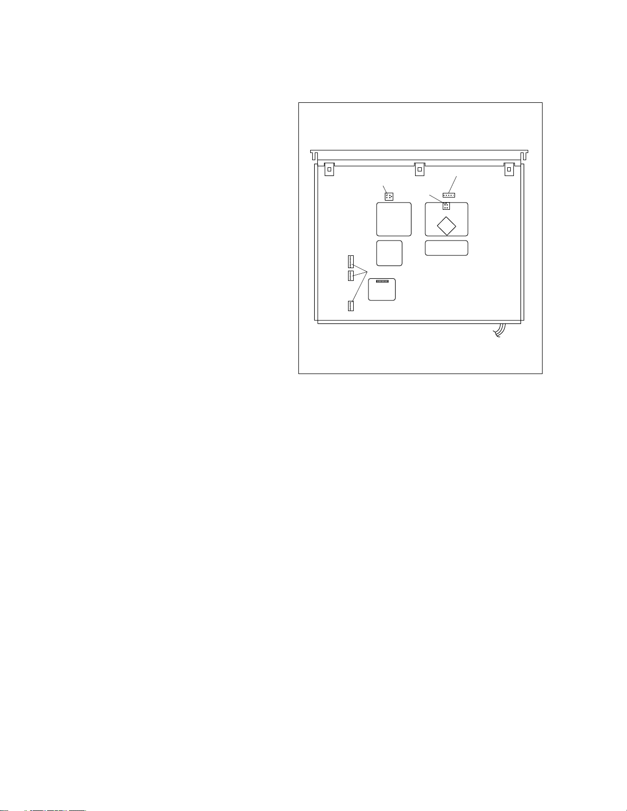
The chassis of this VCR has openings for diagnosis of some
parts on the board assembly.
Reel sensor
(Supply)
TU6001
CN3011
Reel sensor
(Take-up)
Rotary encoder
IC3001
Fig. 1-7-1a
1.6.1 Setting the Jig RCU mode
(1) Unplug the power cord plug from the power outlet.
(2) Press and hold the “REC” and “PAUSE” buttons on the
VCR simultaneously, while plugging the power cord plug
into the power outlet.
When the VCR is set to the Jig RCU mode, the symbols
( “ : ” ) in the time display of the FDP are turned off.
1.6.2 Setting the User RCU mode
(1) Turn off the power.
(2) Press the “REC” and “PAUSE” buttons of the VCR si-
multaneously. Alternatively, transmit the code “80” from
the Jig RCU.
1-6
Page 11
1.8 Emergency display function
This unit has a function for storing the history of the past two
emergencies (EMG) and displaying them on each FDP (or
OSD). With the status of the VCR and mechanism at the moment an emergency occurred can also be confirmed.
FDP display model
[FDP display]
0 : 00 : 00
E:** :**
*1 : *2 : 34
*5: *6 : *7
FDP (7segment LED) display model
[FDP display]
0: 00
E: **
1: **
2: *1
3: *2
4: 34
5: *5
6: *6
7: *7
OSD display model
[OSD display]
Normal display
EMG content display
(E:Latest:Previous)
EMG detail information <1>
EMG detail information <2>
Normal display
EMG content display (Latest)
EMG content display (Previous)
EMG detail information <1>
[Deck operation mode]
EMG detail information <1>
[Mechanism operation mode]
EMG detail information <1>
[Mechanism sensor information and Mechanism mode position]
EMG detail information <2>
[Type of the cassette tape in use <1>]
EMG detail information <2>
[Winding position of the cassette tape in use]
EMG detail information <2>
[Type of the cassette tape in use <2> (Winding area)]
EMG
E: **:**
*1 : *2 : 34
*5: *6 : *7
EMG content display
(E:Latest:Previous)
EMG detail information <1>
EMG detail information <2>
Notes:
•
The EMG detail information <1><2> show the information
on the latest EMG.
It becomes “ – – : – – : – –” when there is no latest EMG
record.
•
When using the Jig RCU, it is required to set the VCR to
the Jig RCU mode (the mode in which codes from the Jig
RCU can be received).
Jig RCU
[Data transmitting method]
Depress the “ ” ( 3 ) button
after the data code is set.
CUSTOM CODE
43: A CODE
53: B CODE
DATA CODE
INITIAL MODE
Fig. 1-8a Jig RCU [PTU94023B]
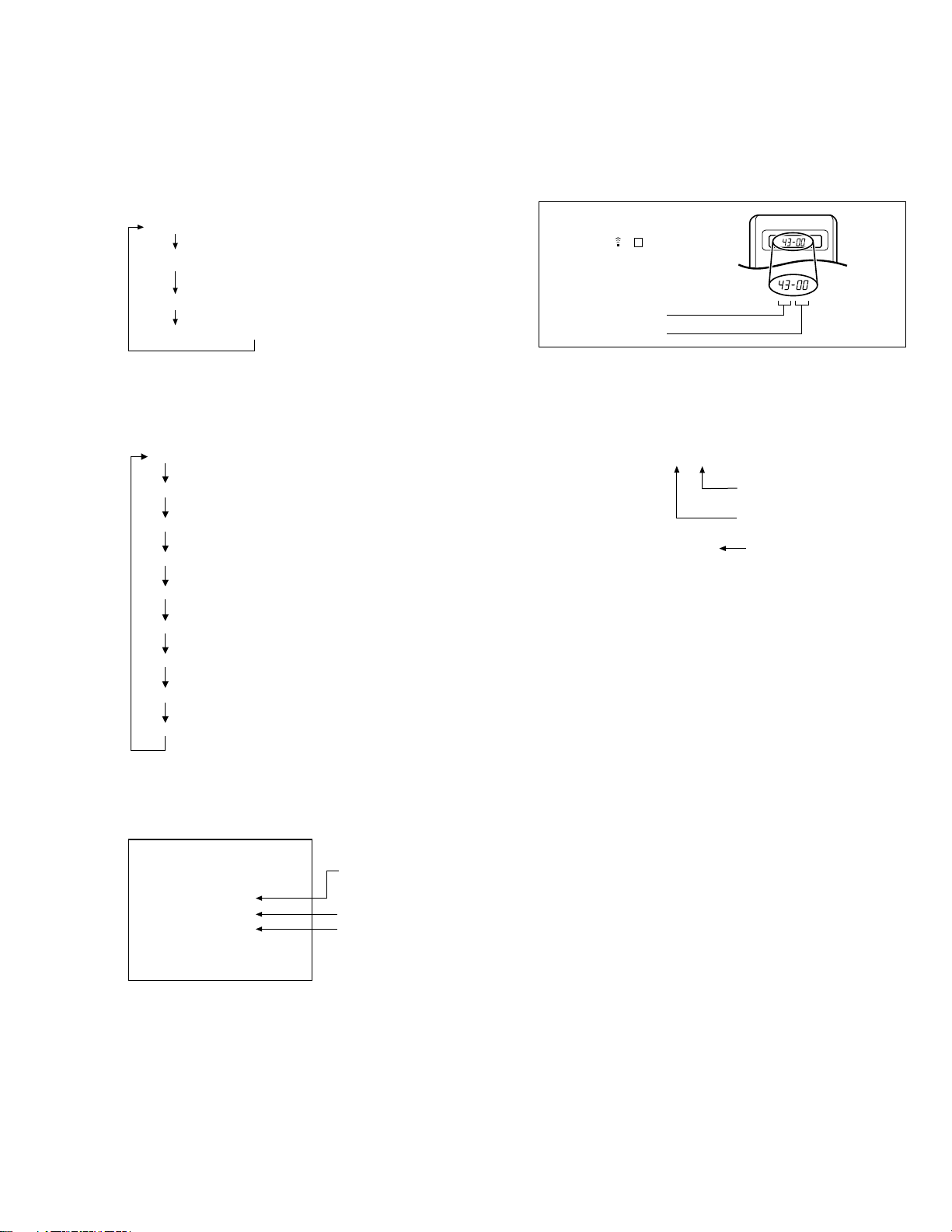
1.8.1 Displaying the EMG information
(1) Transmit the code “59” from the Jig RCU.
The FDP shows the EMG content in the form of “E:**:**”.
<Example 1> E : 01 : 03
Previous EMG
Latest EMG
<Example 2> E : –– : ––
No EMG record
(2) Transmit the code “59” from the Jig RCU again.
The FDP shows the EMG detail information <1> in the form
of “ * 1 : * 2 : 34 ”.
* 1 : Deck operation mode at the moment of EMG
* 2 : Mechanism operation mode at the moment of EMG
3– : Mechanism sensor information at the moment of
EMG
–4 : Mechanism mode position at the moment of EMG
(3) Transmit the code “59” from the Jig RCU once again.
The FDP shows the EMG detail information <2> in the form
of “ *5 : *6 : *7 ”.
* 5 : Type of the cassette tape in use <1> .
* 6 : Winding position of the cassette tape in use
* 7 : Type of the cassette tape in use <2> (Winding area)
(4) Transmit the code “59” from the Jig RCU once again to re-
set the display.
Notes:
•
For the OSD display model, all EMG information are
showed by transmitting first code from the Jig RCU.
•
For the EMG content, see “1.8.3 EMG content description”.
•
For the EMG detail information <1> , see “1.8.4 EMG detail information <1> ”.
•
For the EMG detail information <2> , see “1.8.5 EMG detail information <2>”.
1.8.2 Clearing the EMG history
(1) Display the EMG history.
(2) Transmit the code “36” from the Jig RCU.
(3) Reset the EMG display.
(EMG-02e)
1-7
Page 12

1.8.3 EMG content description
Note:
EMG contents “E08/E09” are for the model with Dynamic Drum (DD).
FDP CONTENT CAUSE
E01: Loading EMG
E02:
Unloading EMG
E03: Take Up Reel
Pulse EMG
E04: Drum FG
EMG
E05: Cassette Eject
EMG
E06: Capstan FG
EMG
E07: SW Power
Short-Circuit
EMG
E08:
DD Initialized
(Absolute
Position
Sensor)
EMG
E09: DD FG EMG
E0A:Supply Reel
Pulse EMG
EC1 or EU1:
Head clog warning
When the mechanism mode cannot be changed to another mode even when the loading motor has rotated
for more than 4 seconds in the loading direction, [E:01]
is identified and the power is turned off.
When the mechanism mode cannot be changed to another mode even when the loading motor has rotated
for more than 4 seconds in the unloading direction, [E:02]
is identified and the power is turned off.
When the take-up reel pulse has not been generated for
more than 4 seconds in the capstan rotating mode, [E:03]
is identified, the pinch rollers are turned off and stopped,
and the power is turned off. However, the reel EMG is
not detected in STILL/SLOW modes.
When the drum FG pulse has not been input for more
than 3 seconds in the drum rotating mode, [E:04] is identified, the pinch rollers are turned off and stopped, and
the power is turned off.
When the eject operation does not complete in 3 seconds after the start, [E:05] is identified, the pinch rollers
are turned off and stopped, and the power is turned off.
When the cassette insertion operation does not complete
in 3 seconds after the start, the cassette is ejected. In
addition, when the operation does not complete within
3 seconds after the start, [E:05] is also identified and the
power is turned off immediately.
When the capstan FG pulse has not been generated for
more than 1 second in the capstan rotating mode, [E:06]
is identified, the pinch rollers are turned off and stopped,
and the power is turned off.However, the capstan EMG
is not detected in STILL/SLOW/FF/REW modes.
When short-circuiting of the SW power supply with GND
has lasted for 0.5 second or more, [E:07] is identified,
all the motors are stopped and the power is turned off.
When DD tilting does not complete in 4 seconds, [E:08]
is identified, the tilt motor is stopped and the power is
turned off.
When the DD FG pulse is not generated within 2.5 seconds, [E:09] is identified, the tilt motor is stopped and
the power is turned off.
When the supply reel pulse has not been generated for
more than 10 seconds in the capstan rotating mode,
[E:0A] is identified and the cassette is ejected (but the
power is not turned off). However, note that the reel EMG
is not detected in the SLOW/STILL mode.
Presupposing the presence of the control pulse output in the PLAY mode, when the value obtained by mixing the two V.FM output
channels (without regard to the A.FM output) has remained below a certain threshold level for more than 10 seconds, [E:C1] or [E:U1]
is identified and recorded in the emergency history. During the period in which a head clog is detected, the FDP and OSD repeat the
“3-second warning display” and “7-second noise picture display” alternately.
EMG code : “E:C1” or “E:U1” / FDP : “U:01” / OSD : “Try cleaning tape.” or “Use cleaning cassette.”
The head clog warning is reset when the above-mentioned threshold has been exceeded for more than 2 seconds or the mode is
changed to another mode than PLAY.
1.
The mechanism is locked in the middle of mode transition.
2
. The mechanism is locked at the loading end due to the encoder position
reading error during mode transition.
3.
Power is not supplied to the loading MDA.
1.
The mechanism is locked in the middle of mode transition.
2.
The mechanism is locked at the unloading end due to the encoder position reading error during mode transition.
3.
Power is not supplied to the loading MDA.
1.
The take-up reel pulse is not generated in the FWD transport modes (PLAY/
FWD SEARCH/FF, etc.) because;
1) The idler gear is not meshed with the take-up reel gear;
2)
The idler gear is meshed with the take-up reel gear, but incapable of wind-
ing due to too large mechanical load (abnormal tension);
3) The take-up reel sensor does not output the FG pulse.
2.
The supply reel pulse is not generated in the REV transport modes (REV
SEARCH/REW, etc.) because;
1) The idler gear is not meshed with the supply reel gear.
2) The idler gear is meshed with the supply reel gear, but incapable of winding due to too large a mechanical load (abnormal tension);
3) The supply reel sensor does not output the FG pulse.
3.
Power is not supplied to the reel sensors.
1.
The drum could not start or the drum rotation has stopped due to too large
a load on the tape, because;
1) The tape tension is abnormally high;
2)
The tape is damaged or a foreign object (grease, etc.) adheres to the tape.
2.
The drum FG pulse did not reach the System controller CPU because;
1) The signal circuit is disconnected in the middle;
2) The FG pulse generator (hall device) of the drum is faulty.
3.
The drum control voltage (DRUM CTL V) is not supplied to the MDA.
4.
Power is not supplied to the drum MDA.
1.
The cassette cannot be ejected due to a failure in the drive mechanism of
the housing.
2.
When the housing load increases during ejection, the loading motor is
stopped because of lack of headroom in its drive torque.
Housing load increasing factors: Temperature environment (low temperature, etc.), mechanism wear or failure.
3.
The sensor/switch for detecting the end of ejection are not functioning normally.
4.
The loading motor drive voltage is lower than specified or power is not supplied to the motor (MDA).
5.
When the user attempted to eject a cassette, a foreign object (or perhaps
the user's hand) was caught in the opening of the housing.
1.
The capstan could not start or the capstan rotation has stopped due to too
large a load on the tape, because;
1) The tape tension is abnormally high (mechanical lock);
2) The tape is damaged or a foreign object (grease, etc.) is adhered to the
tape (occurrence of tape entangling, etc.).
2.
The capstan FG pulse did not reach the System controller CPU because;
1) The signal circuit is disconnected in the middle;
2) The FG pulse generator (MR device) of the capstans is faulty.
3.
The capstan control voltage (CAPSTAN CTL V) is not supplied to the MDA.
4.
Power is not supplied to the capstan MDA.
1.
The SW 5 V power supply circuit is shorted with GND.
2.
The SW 12 V power supply circuit is shorted with GND.
1. The absolute value sensor is defective. (The soldered parts have separated.)
2. The pull-up resistor at the absolute sensor output is defective. (The soldered parts
have separated.)
3. Contact failure or soldering failure of the pins of the connector (board-to-board) to the
absolute value sensor.
4.
The absolute value sensor data is not sent to the System Controller CPU.
1. The FG sensor is defective. (The soldered parts have separated.)
2. The pull-up resistor at the FG sensor output is defective. (The soldered parts have
separated.)
3. Contact failure or soldering failure of the pins of the connector (board-to-board) to the FG sensor.
4. The power to the sensor is not supplied. (Connection failure/soldering failure)
5. The FG pulse is not sent to the System Controller CPU.
6.
The tilt motor is defective. (The soldered parts have separated.)
7. The drive power to the tilt motor is not supplied. (Connection failure/soldering failure)
8. The tilt motor drive MDA - IC is defective.
9. Auto-recovery of the DD tilting cannot take place due to overrun.
1.
The supply reel pulse is not generated in the FWD transport mode (PLAY/
FWD SEARCH/FF, etc.) because;
1) PLAY/FWD or SEARCH/FF is started while the tape in the inserted cas-
sette is cut in the middle;
2) A mechanical factor caused tape slack inside and outside the supply
reel side of the cassette shell. In this case, the supply reel will not rotate
until the tape slack is removed by the FWD transport, so the pulse is not
generated until then;
3) The FG pulse output from the supply reel sensor is absent.
2.
The take-up reel pulse is not generated in the REV transport mode (REV
SEARCH/REW, etc.).
1) REV SEARCH/REW is started when the tape in the inserted cassette
has been cut in the middle;
2) A mechanical factor caused tape slack inside and outside the take-up
reel side of the cassette shell. In this case, the supply reel will not rotate
until the tape slack is removed by the REV transport, so the pulse will
not be generated until that time;
3) The FG pulse output from the take-up reel sensor is absent.
3.
The power to a reel sensor is not supplied.
1-8
Table 1-8-3a
Page 13

1.8.4 EMG detail information <1>
The status (electrical operation mode) of the VCR and the status (mechanism operation mode/sensor information) of the
mechanism in the latest EMG can be confirmed based on the
figure in EMG detail information <1> .
[FDP/OSD display]
* 1 : * 2 : 34
* 1 : Deck operation mode at the moment of EMG
* 2 : Mechanism operation mode at the moment of EMG
3– : Mechanism sensor information at the moment of EMG
–4 : Mechanism mod
e position at the moment of EMG
Note:
•
For EMG detailed information <1>, the content of the code
that is shown on the FDP (or OSD) differs depending on
the parts number of the system control microprocessor
(IC3001) of the VCR. The system control microprocessor
parts number starts with two letters, refer these to the corresponding table.
* 1 : Deck operation mode
[Common table of MN*, HD* and M3*]
Display
MN*/M3* HD*
00 - Mechanism being initialized
01 00 STOP with pinch roller pressure off (or tape present with P.OFF)
02 01 STOP with pinch roller pressure on
03 - POWER OFF as a result of EMG
04 04 PLAY
0C 0E REC
10 11 Cassette ejected
20 22 FF
21 - Tape fully loaded, START sensor ON, short FF
22 - Cassette identification FWD SEARCH before transition to FF (SP
24 26 FWD SEARCH (variable speed) including x2-speed
2C 2E INSERT REC
40 43 REW
42 - Cassette identification REV SEARCH before transition to REW (SP
44 47 REV SEARCH (variable speed)
4C 4C AUDIO DUB
6C 6E INSERT REC (VIDEO + AUDIO)
84 84 FWD STILL / SLOW
85 85 REV STILL / SLOW
8C 8F REC PAUSE
8D - Back spacing
8E - Forward spacing (FWD transport mode with BEST function)
AC AF INSERT REC PAUSE
AD - INSERT REC back spacing
CC CD AUDIO DUB PAUSE
CD - AUDIO DUB back spacing
EC EF INSERT REC (VIDEO + AUDIO) PAUSE
ED - INSERT REC (VIDEO + AUDIO) back spacing
x7-speed)
x7-speed)
Deck operation mode
* 2 : Mechanism operation mode
[Common table of MN* and M3*]
Display
MN* M3*
00 00 Command standby (Status without executing command)
02 02 POWER OFF by EMG occurrence
04 04 Moving to the adjacent position in the LOAD direction
06 06 Moving to the adjacent position in the UNLOAD direction
08 08 Cassette ejection being executed / Cassette housing ejection being
- 0A Mode transition to STOP with cassette ejection end
0A 0C Cassette insertion being executed
0C 0E Tape being loaded
0E 10 Tape being unloaded
10 12 Mode transition to STOP with pinch roller compression ON
12 14 Mode transition to STOP with pinch roller compression OFF
14 16
16 18
18 1A Mode transition to PLAY
1A 1C Mode transition to FWD SEARCH
1C 1E Mode transition to REC
1E 20 Mode transition to FWD STILL / SLOW
20 22 Mode transition to REV STILL / SLOW
22 24 Mode transition to REV SEARCH
24 26 Mode transition from FF / REW to STOP
26 28 Mode transition to FF
28 2A Mode transition to REW
2A 2C 4 sec. of REV as a result of END sensor going ON during loading
2C 2E
2E 30 Mechanism position being corrected due to overrun
80 80 Mechanism in initial position (Dummy command)
executed
Mode transition to STOP with pinch roller compression OFF as a result
of POWER OFF
Mode transition to STOP with pinch roller compression ON as a result
of POWER ON
Short FF / REV as a result of END sensor going ON during unloading
Mechanism operation mode
[Table of HD*]
Display
00 STOP with pinch roller pressure off
01 STOP with pinch roller pressure on
02 U/L STOP (or tape being loaded)
04 PLAY
05 PLAY (x1-speed playback using JOG)
0E REC
11 Cassette ejected
22 FF
26 FWD SEARCH (variable speed) including x2-speed
2E INSERT REC
43 REW
47 REV SEARCH
4C AUDIO DUB
6E INSERT REC (VIDEO + AUDIO)
84 FWD STILL/SLOW
85 REV STILL/SLOW
8F REC PAUSE
AF INSERT REC PAUSE
C7 REV SEARCH (x1-speed reverse playback using JOG)
CD AUDIO DUB PAUSE
EF INSERT REC (VIDEO + AUDIO) PAUSE
F0 Mechanism being initialized
F1 POWER OFF as a result of EMG
F2 Cassette being inserted
F3 Cassette being ejected
F4 Transition from STOP with pinch roller pressure on to STOP with pinch
roller pressure off
F5 Transition from STOP with pinch roller pressure on to PLAY
F6 Transition from STOP with pinch roller pressure on to REC
F7 Cassette type detection SEARCH before FF/REW is being executed
F8 Tape being unloaded
F9 Transition from STOP with pinch roller pressure off to STOP with pinch
roller pressure on
FA Transition from STOP with pinch roller pressure off to FF/REW
FB Transition from STOP with pinch roller pressure off to REC.P (T.REC,etc.)
FC Transition from STOP with pinch roller pressure off to cassette type de-
tection SEARCH
FD Short REV being executed after END sensor on during unloading
FE Tension loosening being executed after tape loading (STOP with pinch
roller pressure on)
Mechanism operation mode
1-9
Page 14

3– : Mechanism sensor information
[Common table of MN*, HD* and M3*]
Display
MN* / HD* M3* REC safety Start End
S-VHS SW CASS SW SW sensor sensor
0- VHS Cassette insertion Tab broken ON ON
1- VHS Cassette insertion Tab broken ON OFF
2- VHS Cassette insertion Tab broken OFF ON
3- VHS Cassette insertion Tab broken OFF OFF
4- VHS Cassette insertion Tab present ON ON
5- VHS Cassette insertion Tab present ON OFF
6- VHS Cassette insertion Tab present OFF ON
7- VHS Cassette insertion Tab present OFF OFF
8- S-VHS Cassette ejection Tab broken ON ON
9- S-VHS Cassette ejection Tab broken ON OFF
A- S-VHS Cassette ejection Tab broken OFF ON
B- S-VHS Cassette ejection Tab broken OFF OFF
C- S-VHS Cassette ejection Tab present ON ON
D- S-VHS Cassette ejection Tab present ON OFF
E- S-VHS Cassette ejection Tab present OFF ON
F- S-VHS Cassette ejection Tab present OFF OFF
Mechanism sensor information
–4 : Mechanism mode position
[Common table of MN*, HD* and M3*]
Display Mechanism mode position
MN* HD* M3*
-0 -7 - Initial value
-1 -0 - EJECT position
- - -0 EJECT position (Cassette housing drive mode)
-2 -7 - Housing operating
- - -1 Between EJECT and U / L STOP
-3 -1 -2 U / L STOP position
- - -3 Guide arm drive position
-4 -7 -4 Tape being loaded / unloaded (When the pole base is
-5 -2 -5 Tape being loaded / unloaded (When the pole base is
-6 -7 -6 Pole base compressed position
-7 -3 -F FF / REW position
-8 -7 -F Between FF / REW and STOP with pinch roller compres-
-9 -4 -F STOP with pinch roller compression OFF
-A -7 -E Between STOP with pinch roller compression OFF and
-B -5 - REV (REV STILL / SLOW) position
- - -D REV position
- - -C Between REV and REV STILL / SLOW
- - -B REV STILL / SLOW position
-C -7 - Between REV and FWD
- - -A Between REV STILL / SLOW and FWD STILL / SLOW
-D -6 - FWD (FWD STILL / SLOW) position
- - -9 FWD STILL / SLOW position
-E -7 - Between FWD and PLAY
- - -8 Between FWD STILL / SLOW and PLAY
-F -6 -7 PLAY position
located on the front side of the position just beside the
drum)
located on the rear side of the position just beside the
drum)
sion ON
REV
Note:
• In the case of the "HD*” microprocessor, as the display is
always "-7” at any intermediate position between modes,
the position of transitory EMG may sometimes not be located.
1.8.5 EMG detail information <2>
The type of the cassette tape and the cassette tape winding position can be confirmed based on the figure in EMG detail information <2> .
[FDP/OSD display]
*5 : *6 : *7
* 5 : Type of the cassette tape in use <1>
* 6 : Winding position of the cassette tape in use
* 7 : Type of th
e cassette tape in use
<2>
(Winding area)
Note:
• EMG detail information <2> is the reference information
stored using the remaining tape detection function of the
cassette tape. As a result, it may not identify cassette correctly when a special cassette tape is used or when the
tape has variable thickness.
* 5 : Cassette tape type <1>
Display Cassette tape type <1>
00 Cassette type not identified
16
Large reel/small reel (T-0 to T-15/T-130 to T-210) not classified
82 Small reel, thick tape (T-120) identified/thin tape (T-140) identified
84 Large reel (T-0 to T-60) identified
92
Small reel, thick tape (T-130) identified/thin tape (T-160 to T-210) identified
93
Small reel, thick tape/C cassette (T-0 to T-100/C cassette) not classified
C3
Small reel, thick tape/C cassette (T-0 to T-100/C cassette) being classified
D3
Small reel, thick tape/C cassette (T-0 to T-100/C cassette) being classified
E1 C cassette, thick tape (TC-10 to TC-20) identified
E2 Small reel, thick tape (T-0 to T-100) identified
E9 C cassette, thin tape (TC-30 to TC-40) identified
C cassette, thick tape/thin tape (TC-10 to TC-40) not classified
F1
Notes:
Cassette tape type
•
<1>
is identified a few times during mode
transition and the identification count is variable depending on
the cassette tape type. If an EMG occurs in the middle of identification, the cassette tape type may not be able to be identified.
•
If other value than those listed in the above table is displayed,
the cassette tape type is not identified.
* 6 : Cassette tape winding position
The cassette tape winding position at the moment of EMG is
displayed by dividing the entire tape (from the beginning to the
end) in 22 sections using a hex number from “00” to “15”.
“00” : End of winding
“15” : Beginning of winding
“FF or ––” : Tape position not identified
* 7 : Cassette tape type <2> (Winding area)
Display Cassette tape type <2>
00 Cassette type not identified
07 Small reel, thick tape T-5
08 - 0E C cassette, thick tape TC-10
09 - 15 C cassette, thick tape TC-20P
0A - 0B Small reel, thick tape T-20
0A - 16 C cassette, thin tape TC-30
0A - 16 C cassette, thin tape TC-40
0D - 0F Small reel, thick tape T-40
11 - 14 Small reel, thick tape T-60
15 - 18 Small reel, thick tape T-80 / DF-160
17 - 1A Small reel, thick tape T-90 / DF-180
19 - 1D Small reel, thick tape T-100
1D - 21 Small reel, thick tape T-120 / DF-240
1E - 1F Small reel, thin tape T-140
1F - 23 Small reel, thick tape T-130
21 - 23 Small reel, thin tape T-160
21 - 23 Small reel, thin tape T-168
22 - 24 Small reel, thick tape DF-300
22 - 24 Small reel, thin tape T-180 / DF-360
22 - 24 Small reel, thin tape T-210 / DF-420
22 - 23 Large reel T-5
23 - 24 Large reel T-10
25 - 26 Large reel T-20
27 - 29 Large reel T-30
29 - 2B Large reel T-40
2D - 2F Large reel T-60
Note:
•
The values of cassette tape type <2> in the above table
are typical values with representative cassette tapes.
1-10
Page 15
SECTION 2
Press
(C)
(A)
(B)
MECHANISM ADJUSTMENT
2.1 Before starting repair and adjustment
2.1.1 Precautions
(1) Unplug the power cord plug of the VCR before using your
soldering iron.
(2) Take care not to cause any damage to the conductor
wires when plugging and unplugging the connectors.
(3) Do not randomly handle the parts without identifying
where the trouble is.
(4) Exercise enough care not to damage the lugs, etc. dur-
ing the repair work.
(5) When reattaching the front panel assembly, make sure
that the door opener of the cassette holder assembly is
lowered in position prior to the reinstallation. (See SECTION 1 DISASSEMBLY.)
(6) When using the Jig RCU, it is required to set the VCR to
the Jig RCU mode (the mode in which codes from the
Jig RCU can be received). (See SECTION 1 DISASSEMBLY.)
Loading motor
2.1.2 Checking for proper mechanical operations
Enter the mechanism service mode when you want to operate the mechanism when no cassette is loaded. (See SECTION 1 DISASSEMBLY.)
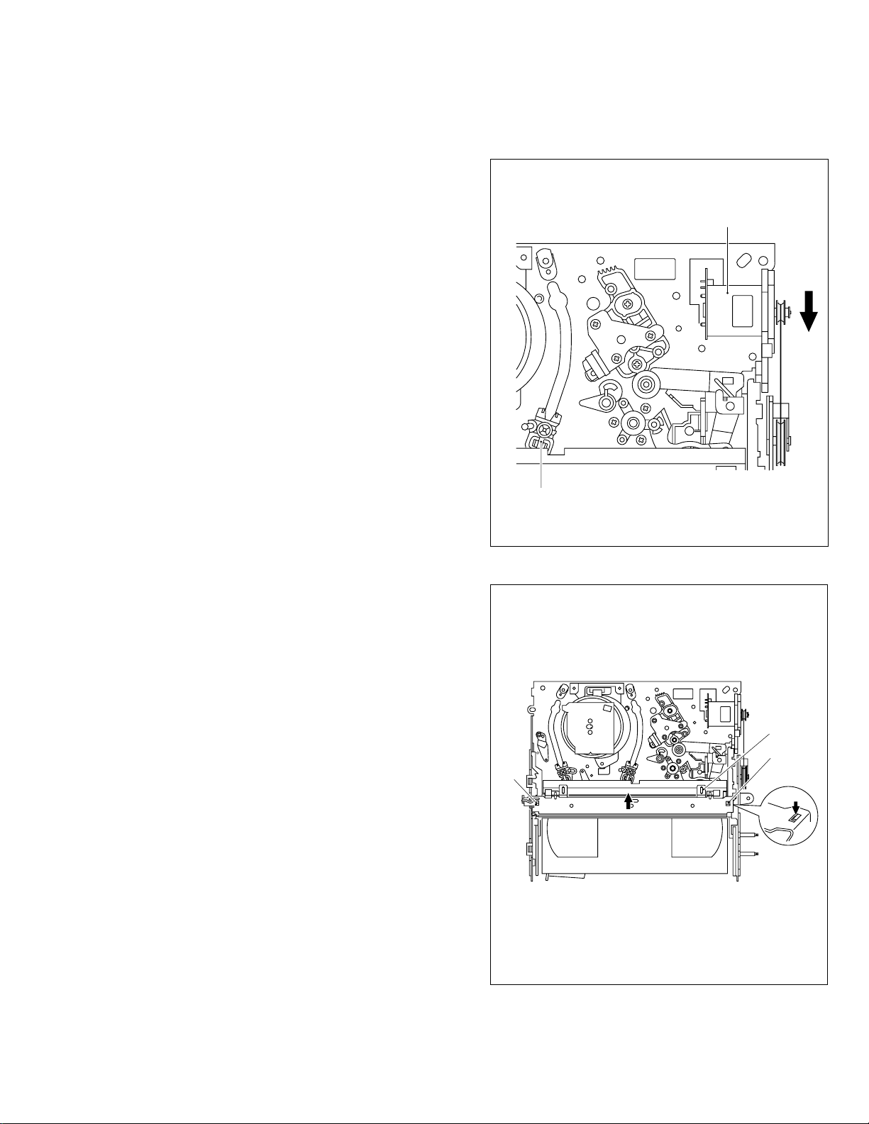
2.1.3 Manually removing the cassette tape
1. In case of electrical failures
If you cannot remove the cassette tape which is loaded because of any electrical failure, manually remove it by taking
the following steps.
(1) Unplug the power cord plug from the power outlet.
(2) Refer to the disassembly procedure and perform the dis-
assembly of the major parts before removing the drum
assembly.
(3) Unload the pole base assembly by manually turning the
loading motor of the mechanism assembly toward the
front. In doing so, hold the tape by the hand to keep the
slack away from any grease. (See Fig.2-1-3a.)
(4) Bring the pole base assembly to a pause when it reaches
the position where it is hidden behind the cassette tape.
(5) Move the top guide toward the drum while holding down
the lug (A) of the bracket retaining the top guide. Likewise hold part (B) down and remove the top guide.
Section (C) of the top guide is then brought under the
cassette lid. Then remove the top guide by pressing the
whole cassette tape down. (See Fig.2-1-3b.)
(6) Remove the cassette tape by holding both the slackened
tape and the cassette lid.
(7) Take up the slack of the tape into the cassette. This com-
pletes removal of the cassette tape.
Note:
• For the disassembly procedure of the major parts and
details of the precautions to be taken, see “SECTION
1 DISASSEMBLY”.
Pole base assembly
Fig. 2-1-3a
Fig. 2-1-3b
2-1
Page 16

2. In case of mechanical failure
If you cannot remove the cassette tape which is loaded because of any mechanical failure, manually remove it by taking the following steps.
(1) Unplug the power cable and remove the top cover, front
panel assembly and others so that the mechanism assembly is visible. (See SECTION 1 DASASSEMBLY.)
(2) While keeping the tension arm assembly of the mecha-
nism assembly free from tension, pull the tape on the pole
base assembly (supply or take-up side) out of the guide
roller. (See Fig.2-1-3c.)
(3) Take the spring of the pinch roller arm assembly off the
hook of the press lever assembly, and detach it from the
tape. (See Fig.2-1-3d.)
(4) In the same way as in the electrical failure instructions in
2.1.3-1(5), remove the top guide.
(5) Raise the cassette tape cover. By keeping it in that posi-
tion, draw out the cassette tape case from the cassette
holder and take out the tape.
(6) By hanging the pinch roller arm assembly spring back
on the hook, take up the slack of the tape into the cassette.
Pole base assembly (take-up side)
2.1.4 Jigs and tools required for adjustment
Roller driver
PTU94002
Back tension cassette gauge
PUJ48076-2
Alignment tape
(SP, stairstep, NTSC)
MHP
A/C head positioning tool
PTU94010
Jig RCU
PTU94023B
Alignment tape
(EP, stairstep, NTSC)
MHP-L
Torque gauge
PUJ48075-2
Pole base assembly
(supply side)
Tension arm assembly
Fig. 2-1-3c
Take the spring
off the hook, and
detach it from the
tape.
Guide pole guard
2-2
Pinch roller arm assembly
Press lever assembly
Fig. 2-1-3d
Page 17

2.1.5 Maintenance and inspection
1. Location of major mechanical parts
In this chapter, the two mechanism speeds are described by comparing the speeds of the standard type and the high-speed
FF/REW type.
It is possible to distinguish between these two types of mechanism by the diameters of their capstan pulleys.
The capstan pulley diameter for the standard type is approx. 32 mm.
The capstan pulley diameter for the high-speed FF/REW type is approx. 43 mm.
For information on the different parts used in the two mechanism types, please refer to the “Replacement of major parts”.
UV catcher2 (supply and take-up side)
Stator assembly
T2
Full erase head
T26
Pole base assembly
T25
(supply side)
Tension arm
T24
assembly
T23
Tension brake
T22
assembly
Adjust pin
T1
T5 T7
T3
Drum assembly
Head base
T6
A/C head
Loading motor
Guide pole guard
T8
Pinch roller arm
T9
assembly
Lid guide
T10
Press lever
T11
assembly
Guide arm
T12
assembly
Reel disk
T13
(take-up side)
Sub brake assembly
T14
(take-up side)
Belt
B22
(loading motor)
B21
Control cam
B20
B19
Cassette gear
B18
Worm gear
Brake lever
Rec safety lever
B1
Reel disk
T20
(supply side)
Main brake assembly
(supply side)
Idler lever
T17T19T21
Idler arm assembly
T16T18
Pole base assembly (take-up side)
Fig. 2-1-5a Mechanism assembly top side
Capstan motor
B2
Capstan brake assembly
B3 B5
Belt (capstan)
Loading arm gear (take-up side)
B4
Loading arm gear (supply side)
Main brake assembly
T15
(take-up side)
Plate
B6
(supply side)
Control
B7
bracket1
Control plate
B8
Tension arm
B9
bearing
Link lever
B17
Rotary encoder guide
B16
Rotary encoder
B15
B14
Direct gear
B13
Change lever assembly
B12
B10
Clutch unit
Take-up head
Fig. 2-1-5b Mechanism assembly bottom side
Take-up lever
B11
2-3
Page 18

Guide rail Roller cam assembly
L2L1
Fig. 2-1-5c Mechanism assembly left side
R1
Opener guide
Door
R2
opener
Drive gear
R3
Cassette housing bracket
R4
R5
Limit gear
Loading motor
Worm gear
Belt (loading motor)
Fig. 2-1-5d Mechanism assembly right side
2. Cleaning
Regular cleaning of the transport system parts is desirable
but practically impossible. So make it a rule to carry out cleaning of the tape transport system whenever the machine is
serviced.
When the video head, tape guide and/or brush get soiled,
the playback picture may appear inferior or at worst disappear, resulting in possible tape damage.
(1) When cleaning the upper drum (especially the video
head), soak a piece of closely woven cloth or Kimu-wipe
with alcohol and while holding the cloth onto the upper
drum by the fingers, turn the upper drum
counterclockwise.
Note:
• Absolutely avoid sweeping the upper drum vertically
as this will cause damage to the video head.
(2) To clean the parts of the tape transport system other than
the upper drum, use a piece of closely woven cloth or a
cotton swab soaked with alcohol.
(3) After cleaning, make sure that the cleaned parts are com-
pletely dry before using the video tape.
3. Lubrication
With no need for periodical lubrication, you have only to lubricate new parts after replacement. If any oil or grease on
contact parts is soiled, wipe it off and newly lubricate the
parts.
Note:
• See the “mechanism assembly” diagram of the parts
list for the lubricating or greasing spots, and for the
types of oil or grease to be used.
4. Suggested servicing schedule for main components
The following table indicates the suggested period for such
service measures as cleaning,lubrication and replacement.
In practice, the indicated periods will vary widely according
to environmental and usage conditions.However, the indicated components should be inspected when a set is brought
for service and the maintenance work performed if necessary. Also note that rubber parts may deform in time,even if
the set is not used.
System Parts Name
Upper drum assembly
A/C head
Lower drum assembly
Pinch roller arm assembly
Full erase head
Tension arm assembly
Tape transport
Capstan motor (Shaft)
Guide arm assembly
Capstan motor
Capstan brake assembly
Main brake assembly
Belt (Capstan)
Belt (Loading motor)
Loading motor
Clutch unit
Worm gear
Control plate
Brush
Tension brake assembly
Other Drive
Rotary encoder
: Cleaning
¤
: Inspection or replacement if necessary
R
Operation Hours
~1000H ~2000H
¤R R
¤R ¤R
¤¤R
¤¤
¤¤
¤¤
¤¤
¤¤
R
R
R
RR
R
R
R
R
R
¤R ¤R
RR
R
Table 2-1-5a
5. Disassembling procedure table
The following table indicates the order in which parts are removed for replacement. To replace parts, remove them in
the order of 1 to 18 as shown in the table. To install them,
reverse the removal sequence.
The symbols and numbers preceding the individual part
names represent the numbers in the “Location of major mechanical parts” table. Also, the “T”, “B”, and “T/B” on the right
of each part name shows that the particular part is removed
from the front, from the back, and from both sides of the
mechanism, respectively.
2-4
Page 19

R4 R1 R3 T9 T12 T11 B15 B12 B14 B13 B17 B21 B7 B8 B5 B4 B11 T14 T15 T13 T22 T24 T18 B19
Symbols and numbers
Removal parts
(Reference items)
Replacement parts
Symbols and numbers
2.2.3 Guide rail T 1
L2
2.2.3 Roller cam assembly T 1
R4
2.2.3 Cassette housing bracket T 1
R1
2.2.3 Opener guide T 2
R2
2.2.3 Door opener T 3
2.2.3 Relay gear T 3
R5
2.2.3 Limit gear T 3
2.2.3 Cassette holder assembly T 6
R3
2.2.3 Drive gear T 4
2.2.3 Drive arm T 8
T9
2.2.4 Pinch roller arm assembly T 1
T12
2.2.5 Guide arm assembly T 1
T11
2.2.5 Press lever assembly T 3
T6
2.2.6 A/C head T 1
T7
2.2.7 Loading motor T 1
B1
2.2.8 Capstan motor T/B 1
T1
2.2.9 UV catcher2 T 1
T17
Pole base assembly (take-up side)
2.2.9
T25
2.2.9
Pole base assembly (supply side)
B15
2.2.10 Rotary encoder B 1
B12
2.2.11 Clutch unit B 1
B14
2.2.12 Change lever assembly B 3
B13
2.2.12 Direct gear B 4
2.2.12 Coupling gear B 5
2.2.12 Clutch gear B 6
B17
2.2.13 Link lever B 1
2.2.14 Cassette gear B 2
B18
B20
2.2.14 Control cam B 2
B21
2.2.14 Worm gear B 1
T10
- Lid guide T/B 5
B7
2.2.15 Control bracket1 B 1
B8
2.2.15 Control plate B 6
B5
2.2.16 Loading arm gear (supply side) B 7
B4
Loading arm gear (take-up side)
2.2.16
2.2.16 Loading arm gear shaft B 9
2.2.17 Take-up lever T/B 7
B11
B10
2.2.17 Take-up head T/B 8
2.2.17 Control plate guide T/B 8
B3
2.2.18 Capstan brake assembly T/B 7
T14
Sub brake assembly(take-up side)
2.2.19
T15
Main brake assembly(take-up side)
2.2.20
T19
2.2.20
Main brake assembly(supply side)
T13
2.2.20 Reel disk (take-up side) T/B 16
T22
2.2.21 Tension brake assembly T/B 9
T20
2.2.21 Reel disk (supply side) T/B 10
T24
2.2.21 Tension arm assembly T/B 10
B9
2.2.21 Tension arm bearing T/B 10
T18
2.2.22 Idler lever T/B 17
T16
2.2.22 Idler arm assembly T/B 18
B19
- Brake lever (
B16
- Rotary encoder guide T/B 19
1
) T/B 18
*
L1L1L2
Number of removal steps
Guide rail
Roller cam assembly
Cassette housing bracket
Opener guide
112
12
12
12 3
3
4 5
5 6
Relay gear
6 7
Front (T)/Back (B) of mechanism
1 2 3 4 5
12
T/B 2
T/B 2
B8
T/B 15
1 2 3 4
T/B 16
1 2 3 4 5 6 7 8
T/B 9
1 2 3 4 5 6 7 8
1 2 3 4 5 6 7 8
1 2 3 4 5 6 7 8
1 2 3 4 5 6 7 8
1 2 3 4 5 6 7 8
1 2 3 4 5 6 7 8
1 2 3 4 5 6 7 8
1 2 3 4 5 6 7 8
1 2 3 4 5 6 7 8
1 2 3 4 5 6 7 8
Cassette holder assembly
Drive gear
7
8
Table 2-1-5b
Note:
• The parts with marked (
nisms (standard type or high-speed FF/REW type).
1 : Uses the standard type mechanism only.
*
2 : Uses the high-speed FF/REW type mechanism only.
*
) have different types of mecha-
*
T1
Drive arm
Pinch roller arm assembly
Guide arm assembly
Press lever assembly
UV catcher2
Rotary encoder
Clutch unit
Change lever assembly
Direct gear
Coupling gear
Link lever
Worm gear
Control bracket1
Control plate
Loading arm gear (supply side)
Loading arm gear (take-up side)
1
2
1
1
1
2
12
3
12
3
1 2 3 4 5
12
3 4
1 2 3 4
1 2 3 4 5
1 2 3 4 5 6
1 2 3 4 5 6 7
1 2 3 4 5 6
1 2 3 4 5 6
1 2 3 4 5 6
1 2 3 4 5 6
9 10 11 12 13 14
9 10 11 12 13 14 15
9 10 11 12 13 14 15
9 10 11 12 13 14 15 16
9 10 11 12 13 14 15 16 17
9 10 11 12 13 14 15 16 17
9 10 11 12 13 14 15 16 17 18
4
1
1
5
6
7
8
)
1
(
Take-up lever
Sub brake assembly (take-up side)
Main brake assembly (take-up side)
Reel disk (take-up side)
Tension brake assembly
Tension arm assembly
Idler lever
Brake lever
7
7
9
9
9
*
2-5
Page 20

g
2.2 Replacement of major parts
2.2.1 Before starting disassembling (Phase matching
between mechanical parts)
The mechanism of this unit is closely linked with the rotary
encoder and system controller circuits.
Since the system controller detects the status of mechanical operation in response to phases of the rotary encoder
(internal switch positions), the mechanism may not operate
properly unless such parts as the rotary encoder, control
plate, loading arm gear, control cam, cassette gear, limit gear,
relay gear and drive gear are installed in their correct positions.
Especially, this model is not provided with any cassette housing assembly, so that cassette loading and unloading must
be accomplished by operation of the cassette holder assembly. The latter is in turn driven by such parts as the drive
gear, relay gear and limit gear. Exercise enough care, therefore, to have the phases of all this gear matching one another. (For information on phase matching of the mechanism,
see the instructions on how to install individual parts.)
This unit is provided with a mechanism assembly mode. It is
therefore necessary to enter this mode for assembling and
disassembling procedures.
This mode is usually not in use, manually set it when it is
required.
2.2.3 Cassette holder assembly
1. How to remove
(1) Remove the guide rail and roller cam assembly. (See
Fig.2-2-3a.)
(3 lugs on the guide rail and one lug on the roller cam
assembly)
Guide rail
Lugs
Roller cam
assembly
Lug
Lug
Fig. 2-2-3a
(2) Remove the two slit washers and remove the cassette
housing bracket. (See Fig.2-2-3b.)
(3) Remove the opener guide, spring(A), door opener, relay
gear and limit gear. (See Fig.2-2-3b.)
2.2.2 How to set the “Mechanism assembling mode”
Remove the mechanism assembly and place it bottom side
up. (See SECTION 1 DISASSEMBLY.) Turn the worm gear
toward the front so that the guide hole of the control cam is
brought into alignment with the hole at the mechanism assembly chassis. This position renders the mechanism assembling mode operational. Make sure that the control plate is
located in alignment with the mark E. (See Fig.2-2-2a.)
Worm gear
Chassis hole
Guide hole
Control cam
Limit gear
Spring(A)
Opener guide
Relay gear
Door opener
Cassette housing bracket
Slit washers
Fig. 2-2-3b
(4) While swinging the lock levers (R) and (L) of the cassette
holder assembly toward the front, slide the cassette
holder assembly until its legs come to where the guide
rail and the roller cam assembly have been removed (so
that the drive arm is upright). (See Fig.2-2-3c.)
Lock lever (L)
Cassette holder assembly
Drive arm
(Upright)
2-6
Control plate
Fig. 2-2-2a
Mark E
Le
Fig. 2-2-3c
Legs
Page 21

While holding the left side of the cassette holder, lift the
Cassette holder assembly
Drive arm
Lock lever (R)
(A)
(C)
(B)
Cassette holder assembly
(5)
cassette holder assembly so that the three legs on the
left side are all released. Then pull the legs (A) and (B)
on the right side out of the rail and also pull up the leg(C).
(See Fig.2-2-3d and Fig.2-2-3e.)
(6) Draw out the drive gear, and remove the drive arm.
Cassette holder assembly
Fig. 2-2-3d
Cassette holder assembly
(A)
2. How to install (Phase matching)
(1) Insert the section (A) of the drive arm into the section (B)
of the main deck.
(2) Insert the section (1) of the drive gear into the round hole,
and the section (2) into the square hole on the drive arm.
(See Fig.2-2-3f.)
(3) Hold the drive arm upright and fit the leg (C) on the right
side of the cassette holder assembly into the groove. (See
Fig.2-2-3g.)
(4) While swinging the lock lever (R) of the cassette holder
assembly toward the front, put the legs (A) and (B) into
the rail. (See Fig.2-2-3g.)
(5) Drop the three legs on the left side of the cassette holder
assembly into the groove at one time. (See Fig.2-2-3h.)
(6) Slide the whole cassette holder assembly toward the front
to bring it to the eject end position.
(7) Install the limit gear so that the notch on the outer cir-
cumference of the limit gear is brought into alignment with
the guide hole on the main deck. (See Fig.2-2-3i.)
(8) Install so that the notch on the periphery of the relay gear
is aligned with the notch of the main deck and that hole
A of the relay gear is aligned with the hole A of the limit
gear and that hole B of the relay gear is aligned with the
hole B of the drive gear. (See Fig.2-2-3i.)
(9) Install the door opener, opener guide, spring(A) and cas-
sette housing bracket and fasten the two slit washers.
Fig. 2-2-3e
Main deck right side
Drive arm
Hole
(C)
(B)
Drive arm
Fig. 2-2-3g
Hole
Drive gear
(1)
(2)
(A)
(B)
Fig. 2-2-3h
Fig. 2-2-3f
2-7
Page 22

Relay gear
B
Guide holeNotches Notch
2.2.6 A/C head
1. How to remove
(1) Remove the two screws (A) and remove the A/C head
together with the head base.
(2) When replacing only the A/C head, remove the three
screws (B) while controlling the compression spring.
Head base
B
AA
Drive gear Limit gear
Fig. 2-2-3i
2.2.4 Pinch roller arm assembly
1. How to remove
(1) Remove the spring from the hook of the press lever as-
sembly.
(2) Remove the slit washer and remove the pinch roller seat
2. (See Fig.2-2-4a.)
(3) Remove the pinch roller arm assembly by pulling it up.
Slit washer
Pinch roller seat2
Spring
Pinch roller arm
Press lever assembly
Pinch roller arm assembly
assembly
Fig. 2-2-4a
2.2.5 Guide arm assembly and press lever assembly
1. How to remove
(1) Remove the spring and expand the lug of the lid guide in
the arrow-indicated direction. Then remove the guide arm
assembly by pulling it up.
(2) Remove the press lever assembly by pulling it up. (See
Fig.2-2-5a.)
Screws(A)
A/C head
Fig. 2-2-6a
Screws(B)
A/C head
Compression
A/C head board
assembly
Head base
springs
Fig. 2-2-6b
2. How to install
(1) To make the post-installation adjustment easier, set the
temporary level as indicated in Fig.2-2-6c. Also make sure
that the screw center (centre) is brought into alignment
with the center (centre) position of the slot.
A/C head
12.4 mm
Head base
Screw
2-8
Tension
spring
LugLid guide
Fig. 2-2-5a
Press lever
assembly
Guide arm
assembly
Head base
A/C head
Fig. 2-2-6c
2.2.7 Loading motor
1. How to remove
(1) Remove the belt wound around the worm gear.
(2) Open the two lugs of the motor guide and remove the
loading motor, loading motor board assembly and motor
guide altogether by pulling them up.
(3) When replacing the loading motor board assembly, take
care with the orientation of the loading motor. (Install so
that the loading motor label faces upward.)
(4) When the motor pulley has been replaced, choose the
fitting dimension as indicated in Fig.2-2-7a.
Page 23

Loading motor board assembly
Loading motor
Lugs
Motor guide
6.5 ± 0.2 mm
LABEL
Motor pulley
Worm gear
Belt
Fig. 2-2-7a
2.2.8 Capstan motor
1. How to remove
(1) Remove the belt (capstan) on the mechanism assembly
back side.
(2) Remove the three screws (A) and remove the capstan
motor.
Screws(A)
Screw(A)
Capstan motor
Belt
Fig. 2-2-8a
Spacer
Spacer
2. How to install (Centering the mounting position)
When the capstan motor has once been removed and then
reinstalled out of the initial correct position in the rotational
direction, the capstan motor current may be unstable during
operation in high or low temperatures. This may result in
greater Wow & Flutter and occasionally in power breakdown
because of current over - load. Install the capstan motor while
following the procedure given below.
(The capstan motor is centrally located when the unit is
shipped from the factory.)
(1) Provisionally tighten the three screws (A) securing the
capstan motor.
(2) Install the mechanism assembly to which the capstan
motor is provisionally fastened on the bottom chassis
which incorporates the Main board assembly. (No need
to tighten the screws for mounting the mechanism.)
Make sure that all the connectors for the mechanism assembly and the Main board assembly are correctly installed as indicated in Fig. 2-2-8b.
(3) Making sure that the connector for the capstan motor is
correctly mounted, and securely tighten the three screws
(A).
Note:
• When the capstan motor has been replaced with a new
one, perform recording in the EP(or LP) mode for at
least 2 minutes at normal temperatures immediately before starting the FF/REW or SEARCH operations (Aging).
2.2.9 Pole base assembly (supply or take-up side)
1. How to remove
(1) Remove the UV catcher 2 on the removal side by loos-
ening the screw (A).
(2) Remove the pole base assembly on the supply side from
the mechanism assembly by loosening the screw (B) on
the mechanism assembly back side and sliding the pole
base assembly toward the UV catcher 2.
(3) As for the pole base assembly on the take-up side, turn
the pulley of the loading motor to lower the cassette
holder because the screw (B) is hidden under the control plate. (See the “Procedures for Lowering the Cassette
holder assembly” of 1.3 DISASSEMBLY/ASSEMBLY
METHOD.) Further turn the motor pulley to move the cassette holder until the screw (B) is no longer under the control plate (in the half-loading position). Then remove it as
done for the supply side by removing the screw (B).
Note:
• After reinstalling the Pole base assembly and the UV
catcher2, be sure to perform compatibility adjustment.
Fig. 2-2-8b
Connector for
the capstan motor
Screw(A)
UV catcher2
Screw(A)
UV catcher2
Screw(B)
Fig. 2-2-9a
2-9
Page 24

2.2.10 Rotary encoder
1. How to remove
(1) Remove the screw (A) and remove the rotary encoder
by pulling it up. (See Fig. 2-2-10a.)
Rotary encoder (Front side)
Screw(A)
Guide marks
2.2.12 Change lever assembly, direct gear, clutch gear
and coupling gear
1. How to remove
(1) Release the two lugs of the rotary encoder guide in the
arrow-indicated direction and remove the change lever
assembly.
(2) Remove the slit washer retaining the direct gear and re-
move the latter.
Take care so as not to lose the washer and spring. (See
Fig.2-2-12a.)
Rotary encoder (Back side)
Positioning pin of the rotary encoder
Fig. 2-2-10a
Mark E
Shaft of the rotary encoder guide
Control plate
Fig. 2-2-10b
2. How to install (Phase matching)
(1) Make sure that the mark E of the control plate is in align-
ment with the mark
of the loading arm gear shaft and
bring the guide marks on the rotary encoder into alignment as indicated in Fig.2-2-10a. (See Fig. 2-2-10a and
Fig. 2-2-10b.)
(2) Turn over the rotary encoder with its guide marks kept in
alignment and install it by fitting on the shaft of the rotary
encoder guide and the positioning pin.
(3) Tighten the screw (A) to complete the installation.
2.2.11 Clutch unit
(1) Remove the belt wound around the capstan motor and
the clutch unit.
(2) Remove the slit washer and remove the clutch unit.
Change lever
assembly
Spring(B)
Lugs
Note:
• The parts with marked (
speed FF/REW type).
1 : Uses the standard type mechanism only.
*
2:
Uses the high-speed FF/REW type mechanism only.
*
Slit washer
Washer (*1)
Spacer
Direct gear
Spring(A)
Position the projecting
side down.
) have different types of mechanisms (standard type or high-
*
Coupling gear
Spring (C)
Clutch gear
Spacer
Fig. 2-2-12a
2. How to install
(1) Install the clutch gear, spring (A), spring (C), direct gear,
spacer and others to the individual shafts of the main
deck, and finally the slit washer. (See Fig.2-2-12a.)
(2) Let the spring (B) drops into the rotary encoder guide hole
and install the change lever assembly.(Take care not to
mistake a direction of the spring.) The point is to slightly
lift the coupling gear and catch it from the both sides with
the assembly. (See Fig.2-2-12b.)
Rotary encoder guide
Spring(B)
Change lever assembly
Coupling gear
2-10
Belt
Clutch unit
Fig. 2-2-11a
Slit washer
Main deck Main deck
Fig. 2-2-12b
Page 25

2.2.13 Link lever
1. How to remove
(1) Remove the two slit washers.
(2) Remove the link lever by lifting it from the shaft re-
tained by the slit washers. Then swing the link lever
counterclockwise and remove it from the locking section of the control plate.
Slit washers
2.2.14 Cassette gear, control cam and worm gear
1. How to remove
(1) Remove the control cam by lifting it.
(2) Open the two lugs of the cassette gear outward and pull
the latter off.
(3) Remove the belt wound around the worm gear and the
loading motor.
(4) Open the lug of the lid guide outward and remove the
worm gear.
Link lever
Locking section of the
control plate
Fig. 2-2-13a
2. How to install (Phase matching)
(1) Slide the control plate so that its mark E is aligned with
the mark
on the loading arm gear shaft. (See Fig.2-2-
13b.)
(2) Rotate the worm gear until the guide hole of the control
cam is aligned exactly with the guide hole of the main
deck. (See Fig.2-2-13c.)
(3) Insert the link lever into the locking section of the control
plate. (See Fig.2-2-13a.)
(4) Rotate the link lever clockwise so that it is installed on
the shafts in the center (centre) and on the left of the control cam.
(5) Fasten the slit washers at these two points.
Loading motor
Belt
Lug
Worm gear
Lugs
Cassette gear
Lid guide
Control cam
Fig. 2-2-14a
2.2.15 Control plate
1. How to remove
(1) Remove the screw (A) retaining the control bracket 1 and
remove the latter.
(2) Slide the control plate as indicated by the arrow and re-
move the control plate. (See Fig.2-2-15a.)
Shaft of the rotary encoder guide
Fig. 2-2-13b
Worm gear
Main deck
guide hole
Control cam
guide hole
Cassette gear
Fig. 2-2-13c
Control plate
Control cam
Mark E
Screw(A)
Control
bracket1
Control
plate
Fig. 2-2-15a
2. How to install (Phase matching)
(1) Adjust the position of the idler arm assembly pin as indi-
cated in Fig.2-2-15b (to the left of center (centre) of the
R section).
(2) Bring the guide hole of the take-up lever into alignment
with the hole at the control plate guide and fix the position by inserting a 1.5 mm hexagonal wrench.
2-11
Page 26

(3) Install the control plate so that the section A of the load-
ing arm gear shaft fits into the hole (A) of the control plate,
the section B of the control plate guide into the hole (B),
and the control plate comes under the section C of the
rotary encoder guide and the section D of the loading arm
gear shaft while press-fit the pole base assmebly (supply side) as indicated by the arrow. It is important that
the tension arm assembly shaft is positioned closer toward you than the control plate. (See Fig.2-2-15c.)
(4) Make sure that the mark E of the control plate is in align-
ment with the mark
of the loading arm gear shaft. (See
Fig.2-2-15c.)
(5) Pull off the hexagonal wrench for positioning.
(3) Turn the loading arm gear (take-up side) clockwise so
that the notch of the loading arm gear (take-up side) is
in alignment with the projection of the loading arm gear
shaft and lift it.
Likewise, turn the loading arm counterclockwise so that
the notch is in alignment with the projection and remove
the loading arm gear (take-up side). (See Fig.2-2-16a and
Fig. 2-2-16b.)
(4) When removing the loading arm gear shaft, be sure of
first removing the screw retaining the drum assembly (on
the back side of the loading arm gear shaft). Then remove the screw (C) and remove the loading arm gear
shaft by sliding it.
Idler arm assembly
pin
R section
Guide hole of the
control plate guide
Section D
1.5mm hexagonal wrench
Fig. 2-2-15b
Section A
Section D
Hole A
Pressfit
Take-up lever
Insert
Pole base assembly
(supply side)
Section A
Hole A
Pole base assembly
(take-up side)
Screw(B)
Torsion arm
Loading arm gear
(take-up side)
Projection B
Guide marks
Projection A
Pole base assembly
(supply side)
Screw(A)
Loading arm gear
(supply side)
Fig. 2-2-16a
Loading arm gear shaft
Loading arm gear (take-up side)
Notch
Screw(C)
Loading arm gear shaft
Section C
Section C
Section B
Hole B
Hole B
Section B
Control plate
Tension arm assembly
shaft
Fig. 2-2-15c
2.2.16 Loading arm gear (supply or take-up side) and
loading arm gear shaft
1. How to remove
(1) Remove the loading arm gear (supply side) by loosen-
ing the screw (A). (See Fig. 2-2-16a.)
(2) Remove the screw (B) and remove the torsion arm from
the pole base assembly (take-up side). (See Fig.2-2-16a.)
2-12
Fig. 2-2-16b
2. How to install
(1) Align the notch of the loading arm gear (take-up side) to
the projection B of the loading arm gear shaft and slip it
over. Then rotate it clockwise for alignment with the projection A and slip it down to the bottom. (See Fig.2-216b.)
(2) Then turn the loading arm gear (take-up side)
counterclockwise. Hang the torsion arm on the pole base
assembly (take-up side) and tighten the screw (B).
(3) Install the loading arm gear (supply side) so that the guide
mark of the loading arm gear (take-up side) is in alignment with the guide mark of the loading arm gear (supply side). Then hang the torsion arm on the pole base
assembly (supply side) and tighten the screw (A). (See
Fig.2-2-16a.)
Page 27

2.2.17 Take-up lever, take-up head and control plate
Lug(D)
Lug(C)
SpringLug(E)
Lug(A)
Lug(B)
Main brake assembly
(take-up side)
Reel disk
(take-up side)
Main brake assembly
(supply side)
Notch
guide
(1) Remove the spring of the take-up lever from the main
deck.
(2) Remove the lug (A) of the take-up lever from the main
deck and pull out the take-up lever and the take-up head
together.
(3) Remove the screw (A).
(4) Align the idler arm assembly pin in the center (centre) of
the R section of the control plate guide, remove the con-
trol plate guide lugs (B) and (C) from the main deck, and
remove the control plate guide.
Idler arm assembly pin
Lug(C)
Screw(A)
Take-up lever
Take-up head
Lug(A)
Lug(B)
Control plate guide
Fig. 2-2-17a
2.2.18 Capstan brake assembly
1. How to remove
(1) Move the lug (A) of the capstan brake assembly in the
arrow-indicated direction so that it comes into alignment
with the notch of the main deck. (See Fig. 2-2-18a.)
(2) Remove the lug (B) of the capstan brake assembly from
the main deck and remove the capstan brake assembly.
Spring
Sub brake
Lug(A)
Lug(B)
assembly
(take-up side)
Lug(C)
Fig. 2-2-19a
2.2.20 Main brake assembly (take-up side), reel disk
(take-up side) and main brake assembly (supply
side)
1. How to remove
(1) Move the main brake assembly (take-up side) in the ar-
row-indicated direction and remove the reel disk (takeup side).
Remove the spring attached to the main brake assembly.
(2)
(3) Remove the lug (A) of the main brake assembly (take-
up side) and pull out the lug (B) after bringing it into alignment with the main deck notch.
(4) Remove the lugs (C), (D) and (E) of the main brake as-
sembly (supply side) from the main deck and pull them
off. (See Fig.2-2-20a.)
(5) When installing the main brake assembly (take-up side),
slide the brake lever in the direction as indicated by the
arrow to prevent it from hitting the projection of the main
brake assembly (take-up side). (See Fig.2-2-20b.)
Lug(B)
Lug(A)
Capstan brake assembly
Fig. 2-2-18a
2.2.19 Sub brake assembly (take-up side)
1. How to remove
(1) Remove the spring attached to the lid guide and sub
brake assembly (take-up side).
(2) Bring the lug (A) of the sub brake assembly (take-up side)
into alignment with the notch of the main deck.
(3) Remove the lugs (B) and (C) of the sub brake assembly
(take-up side) from the main deck and remove the sub
brake assembly (take-up side).
Fig. 2-2-20a
(
1)
*
Brake
lever
Note:
• The parts with marked ( *) have different types of mechanisms (standard type
or high-speed FF/REW type).
1 : Uses the standard type mechanism only.
*
Rotary encoder guide
Projection of the main
brake assembly
(take-up side)
Fig. 2-2-20b
2-13
Page 28

2.2.21 Tension brake assembly, reel disk (supply side)
(
)
and tension arm assembly
1. How to remove
(1) Remove the three lugs of the tension brake assembly
from the main deck and pull them off.
(2) Remove the reel disk (supply side) by loosening in the
arrow-indicated direction the main brake assembly (supply side).
(3) Remove the tension spring on the back of the main deck.
Then release the lug of the tension arm bearing in the
arrow-indicated direction and draw out the tension arm
assembly. (See Fig. 2-2-21a.)
Lug of the tension
arm bearing
Tension arm
assembly
Reel disk
(supply side)
2.2.23 Stator assembly
(1) Remove the flat cable.
(2) Remove the two screws (A), (B) and remove the lug wire.
(3) Remove the stator assembly by lifting in the arrow-indi-
cated direction. (Take care that the brush spring does not
jump out.)
Notes:
• Be careful not to lose the brush and spring.
• There are some models that do not use the lug wire.
Refer to the parts list for these models.
• When tightening the screw (B), place the caulked part
of the lug terminal near to the shaft of the drum and
then tighten it.
• After installation, be sure to perform the switching
point adjustment according to the electrical adjustment
procedure.
Tension brake
assembly
Lugs
Tension spring Main brake assembly
supply side
Fig. 2-2-21a
2.2.22 Idler lever, idler arm assembly
1. How to remove
(1) Remove the lug of the idler lever from the main deck and
remove the hook fitted in the idler arm assembly hole by
lifting it.
(2) Remove the slit washer and pull out the idler arm assem-
bly.
Lug Idler lever
Hook
Idler arm
assembly
Slit washer
Screw (A)
Stator assembly
Screw (B)
Lug wire
(Note)
Drum
shaft
Flat cable
(Take care not to mix up the
polar faces when installing.)
Lug wire
Screw (A)
Fig. 2-2-23a
2.2.24 Rotor assembly
1. How to remove
(1) Remove the stator assembly.
(2) Remove the two screws (B) and remove the rotor assem-
bly.
2. How to install
(1) Match the phases of the upper drum assembly and the
rotor assembly as indicated in Fig.2-2-24a.
(2) Place the upper drum assembly hole (a) over the rotor
assembly holes (b) (with three holes to be aligned) and
tighten the two screws (B). (See Fig.2-2-24a.)
Screws (B)
Hole(a)
2-14
Fig. 2-2-22a
Screw holes
Upper drum
assembly
Rotor assembly
Fig. 2-2-24a
The hole is not in
line but is offset
toward the right.
Hole(b)
Page 29

2.2.25 Upper drum assembly
Notes:
• To replace the upper drum assembly only may not be
possible with some models. For upper drum assembly replacement, refer to the parts list. (When the parts
number of the upper drum assembly is not listed on
the parts list, then this cannot be replaced.)
• When replacement is required, control the up- down
movement of the brush. Never apply grease.
• When replacing the upper drum assembly, replace it
the together with the washer.
1. How to remove
(1) Remove the stator assembly and rotor assembly.
(2) Loosen the screw of the collar assembly using a 1.5 mm
hexagonal wrench and remove the collar assembly. Also
remove the brush, spring and cap at one time.
(3) Remove the upper drum assembly and remove the
washer using tweezers.
Lower drum assembly
Coil parts
Upper drum assembly
Fig. 2-2-25b
Spring
Brush
Upper drum
assembly
Washer
Collar
assembly
Loosen
Cap
Shaft
1.5 mm
hexagonal wrench
Lower drum assembly
Fig. 2-2-25a
2. How to install
(1) Clean the coil parts of the lower drum assembly and the
newly installed upper drum assembly with an air brush
in advance. (See Fig.2-2-25b.)
(2) Install a new washer and upper drum assembly on the
drum shaft. (See Fig.2-2-25a.)
(3) Install the cap to the upper drum assembly.
(4) Position the collar assembly as indicated in Fig.2-2-25c
while controlling its up- down movement.
(5) Secure the collar assembly in position with a hexagonal
wrench while pressing its top with the fingers.
(6) After installation, gently turn the upper drum assembly
with your hand to make sure that it turns normally. Then
install the brush and the spring.
(7) Install the rotor assembly and stator assembly according
to Fig 2-2-23a and 2-2-24a.
(8) When installation is complete, clean the upper drum as-
sembly and lower drum assembly and carry out the fol-
lowing adjustments.
• PB switching point adjustment
• Slow tracking adjustment
• Compatibility adjustment (Be sure to check for compat-
ibility for the EP (or LP) mode.)
Upper drum
assembly
Collar
assembly
Fig. 2-2-25c
Press
Fig. 2-2-25d
Collar
assembly
Tighten
2-15
Page 30
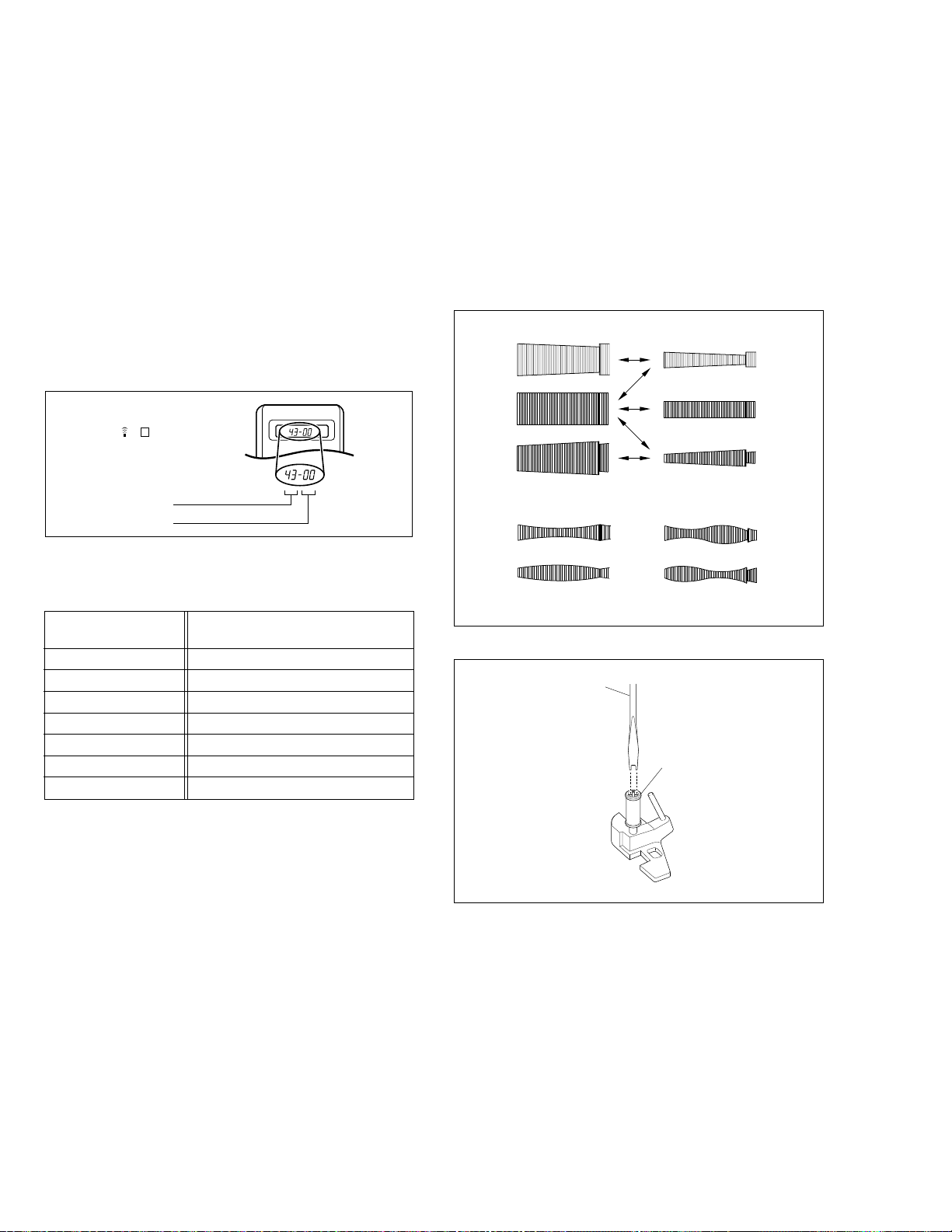
2.3 Compatibility adjustment
Notes:
• Although compatibility adjustment is very important,
it is not necessary to perform this as part of the normal servicing work. It will be required when you have
replaced the A/C head, drum assembly or any part of
the tape transport system.
• To avoid any damage to the alignment tape while performing the compatibility adjustment, get a separate
cassette tape (for recording and play back) ready to
be used for checking the initial tape running behavior.
• Unless otherwise specified, all measuring points and
adjustment parts are located on the Main board.
• When using the Jig RCU, it is required to set the VCR
to the Jig RCU mode (the mode in which codes from
the Jig RCU can be received). (See SECTION 1 DISASSEMBLY.)
Jig RCU
[Data transmitting method]
Depress the “ ” ( 3 ) button
after the data code is set.
pole base assembly (supply or take-up side).
(7) Unload the cassette tape once, play back the alignment
tape (A1) again and confirm the V.PB FM waveform.
(8) After adjustment, confirm that the tape wrinkling does not
occur at the roller upper or lower limits. (See Fig. 2-31d.)
[Perform adjustment step (9) only for the models
equipped with SP mode and EP (or LP) mode.]
(9) Repeat steps (1) to (8) by using the alignment tape (A2).
CUSTOM CODE
43: A CODE
53: B CODE
DATA CODE
INITIAL MODE
Fig. 2-3a Jig RCU [PTU94023B]
2.3.1 FM waveform linearity
Signal (A1) •
(A2) •
Mode (B) • PB
Equipment (C) • Oscilloscope
Measuring point (D) • TP106 (PB. FM)
External trigger (E) • TP111 (D.FF)
Adjustment part (F) • Guide roller [Mechanism assembly]
Specified value (G) • Flat V.PB FM waveform
Adjustment tool (H) • Roller driver [PTU94002]
Alignment tape(SP, stairstep, NTSC) [MHP]
Alignment tape(EP, stairstep, NTSC) [MHP-L]
(1) Play back the alignment tape (A1).
(2) Apply the external trigger signal to D.FF (E), to observe
the V.PB FM waveform at the measuring point (D).
(3) Set the VCR to the manual tracking mode.
(4) Make sure that there is no significant level drop of the
V.PB FM waveform caused by the tracking operation, with
its generally parallel and linear variation ensured. Per-
form the following adjustments when required. (See Fig.
2-3-1a.)
(5) Reduce the V.PB FM waveform by the tracking opera-
tion. If a drop in level is found on the left side, turn the
guide roller of the pole base assembly (supply side) with
the roller driver to make the V.PB FM waveform linear.
If a drop in level is on the right side, likewise turn the guide
roller of the pole base assembly (take-up side) with the
roller driver to make it linear. (See Fig. 2-3-1c.)
(6) Make sure that the V.PB FM waveform varies in parallel
and linearly with the tracking operation again. When re-
quired, perform fine-adjustment of the guide roller of the
Max level
Proper waveform variation
Improper waveform variation
Fig. 2-3-1a
Roller driver
Fig. 2-3-1b
Min level
Guide roller (supply side)
2-16
Page 31

A
(2)
(3)
(1)
AUDIO OUT
Head base
A/C head
CTL. P
Level drop at the guide roller (supply side)
C
Level drop at the guide roller (take-up side)
• Proper waveform variation: Always flat
B
waveform by turning the screws (1), (2) and (3) little by
little until both waveforms reach maximum. The screw (1)
and (3) are for adjustment of tilt and the screw (2) for azimuth.
D
(4) Adjust the AUDIO OUT waveform and Control pulse
• Improper waveform variation:
Higher Lower
Fig. 2-3-1c
Improper
(a) Guide roller
(b) Guide pole
Proper
Fig. 2-3-1d
2.3.2 Height and tilt of the A/C head
Note:
• Set a temporary level of the height of the A/C head in
advance to make the adjustment easier after the A/C
head has been replaced. (See Fig.2-2-6c.)
Signal (A) •
Mode (B) • PB
Equipment (C) • Oscilloscope
Measuring point (D1) • AUDIO OUT terminal
(D2) • TP4001 (CTL. P)
External trigger (E) • TP111 (D.FF)
Adjustment part (F) • A/C head [Mechanism assembly]
Specified value (G) • Maximum waveform
Alignment tape(SP, stairstep, NTSC) [MHP]
Fig. 2-3-2a
2.3.3 A/C head phase (X-value)
Signal (A1) •
Mode (B) • PB
Equipment (C) • Oscilloscope
Measuring point (D) • TP106 (PB-FM)
External trigger (E) • TP111 (D.FF)
Adjustment part (F) •
Specified value (G) • Maximum V.PB FM waveform
Adjustment tool (H) • A/C head positioning tool [PTU94010]
Alignment tape(SP, stairstep, NTSC) [MHP]
A/C head base [Mechanism assembly]
(1) Play back the alignment tape (A1).
(2) Apply the external trigger signal to D.FF (E), to observe
the V.PB FM waveform at the measuring point (D).
(3) Set the VCR to the manual tracking mode.
(4) Loosen the screws (4) and (5), then set the A/C head
positioning tool to the innermost projected part of the A/
C head. (See Fig. 2-3-3a.)
(5) Turn the A/C head positioning tool fully toward the cap-
stan. Then turn it back gradually toward the drum and
stop on the second peak point position of the V.PB FM
waveform output level. Then tighten the screws (4) and
(5).
(6) Perform the tracking operation and make sure that the
V.PB FM waveform is at its maximum.
If it is not at maximum, loosen the screws (4) and (5),
and turn the A/C head positioning tool to bring the A/C
head to a position, around where the waveform reaches
its maximum for the first time. Then tighten the screws
(4) and (5).
(1) Play back the alignment tape (A).
(2) Apply the external trigger signal to D.FF (E), to observe
the AUDIO OUT waveform and Control pulse waveform
at the measuring points (D1) and (D2) in the ALT mode.
(3) Set the VCR to the manual tracking mode.
2-17
Page 32

[Perform adjustment steps (7) to (10) only for 2 Head
models equipped with LP mode.]
(7) Then play back the alignment tape (A2).
(8) Set the VCR to the manual tracking mode.
(9) Perform the tracking operation and make sure that the
V.PB FM waveform is at its maximum.
(10)
If it is not at maximum, loosen the screws (4) and (5),
and turn the A/C head positioning tool to bring the A/C
head to a position, around where the waveform reaches
its maximum for the first time. Then tighten the screws
(4) and (5).
Note:
• After adjusting, always perform the confirmation and
re-adjustment of the item 2.3.4.
Toward the drum
A/C head positioning tool
To the drum
A/C head
Toward the capstan
Head base
Screw
Screw
To the capstan
(4)
(5)
Fig. 2-3-3a
Alignment tape
[SP, stairstep]
played with the
SP head
Alignment tape
[EP(LP), stairstep]
played with the
EP(LP) head
(4) Set the VCR to the Auto adjust mode by transmitting the
code (F) twice from the Jig RCU. When the VCR enters
the stop mode, the adjustment is completed.
(5) If the VCR enters the eject mode, perform adjustment for
the audio control head phase (X-value) again.
2.3.5 Tension pole position
Signal (A) • Back tension cassette gauge
Mode (B) • PB
Adjustment part (F) • Adjust pin [Mechansim assembly]
Specified value (G)
[PUJ48076-2]
• 25 - 51 gf•cm (2.45 – 5 × 10
-3
Nm]
(1) Play back the back tension cassette gauge (A).
(2) Check that the indicated value on the left side gauge is
within the specified value (G).
(3) If the indicated value is not within the specified value (G),
perform the adjustment in a following procedure.
1) Set the VCR to the mechanism service mode. (See
SECTION 1 DISASSEMBLY.)
2) Set the VCR to the play back mode and adjust by turning adjustment pin to align the tension arm assembly
edge with the main deck hole (A) on the right edge
marker. (See Fig. 2-3-5a)
Tension arm
assembly
Hole (A)
Marker
Edge
Waveform output
X-value adjustment point
Drum side Control head position Capstan side
Maximum
Fig. 2-3-3b
2.3.4 Standard tracking preset
Signal (A) •
Mode (B) • PB ¥ Auto adjust
Equipment (C) • Oscilloscope
Measuring point (D) • TP106 (PB-FM)
External trigger (E) • TP111 (D.FF)
Adjustment part (F) • Jig RCU: Code “50”
Specified value (G) • STOP mode
Adjustment tool (H) • Jig RCU [PTU94023B]
Alignment tape(EP, stairstep, NTSC) [MHP-L]
(Maximum V.PB FM waveform)
(1) Play back the alignment tape (A).
(2) Apply the external trigger signal to D.FF (E), to observe
the V.PB FM waveform at the measuring point (D).
(3) Confirm that the automatic tracking operation is com-
pleted.
0.5 mm
Tension arm assembly
Tension brake assembly
Adjust pin
Fig. 2-3-5a
2-18
Page 33

Mechanism Timing Chart
Mechanism mode
Control plate mark
Rotary encoder
Control cam angle
EJECT
END
E U CI
HIGH
C CH
LOW
HIGH
B CH
LOW
HIGH
A CH
LOW
0
CASS-
UP
69 136 370 412.
CASS-INS
FF/REW
FR
230
STOP
ST
264.
REV
R
7
318.
7
SLOW/STILLPPLAY
SL
42
Rotary encoder
angle
Pole base
Pinch roller
Guide arm
Tension arm
Main brake S
Main brake T
Sub brake S
Sub brake T
Capstan brake
Direct gear
Change lever 2
Idler position
Take-up lever
Rec safety switch
Operation mode
HALF PRESS
CONTACT
ON PLAY
ON REV
CONTACT
(C-INS)
HALF REV
HALF FF/REW
CONTACT
CONTACT
IN FF/REW
OUT PLAY
SUPPLY
CENTER
TAKE-UP
READY
RESET
OFF
OFF
OFF
OFF
OFF
OFF
OFF
OFF
OFF
OFF
OFF
0
20 42.652.
ON
ON
ON
ON
ON
ON
ON
ON
ON
ON
6
6
114.
150.4167.8178.
8
Timer REC
(drum at stop)
POWER OFF
(cassette loaded)
207.2218.2240.2251.
standby
STOP
Backspace Slow FOR
Search REW
Slow REW
2
293.2304.2320.4335
REC pause
REC
Search FF
STOP
(
drum
in motion)
2-19
Page 34

SECTION 3
ELECTRICAL ADJUSTMENT
3.1 Precaution
The following adjustment procedures are not only necessary
after replacement of consumable mechanical parts or board
assemblies, but are also provided as references to be referred
to when servicing the electrical circuitry.
In case of trouble with the electrical circuitry, always begin a
service by identifying the defective points by using the measuring instruments as described in the following electrical adjustment procedures. After this, proceed to the repair, replacement and/or adjustment. If the required measuring instruments
are not available in the field, do not change the adjustment
parts (variable resistor, etc.) carelessly.
3.1.1 Required test equipments
• Color (colour) television or monitor
• Oscilloscope:
• Frequency counter
• Audio level meter
• Signal generator: RF / IF sweep / marker
• Signal generator: stairstep, color (colour) bar [NTSC]
• Recording tape
• Digit-key remote controller (provided)
3.1.2 Required adjustment tools
Jig RCU
PTU94023B
LPF
PTU93006
3.1.3
Color (colour) bar signal,Color (colour) bar pattern
s
Color bar signal [NTSC]
White(100%)
White(75%)
100 IRE
1V
40 IRE
Horizontal sync
3.1.4 Switch settings and standard precautions
The SW settings of the VCR and the standard precautions for
the electrical adjustments are as follows.
•
When using the Jig RCU, it is required to set the VCR to
the Jig RCU mode (the mode in which codes from the Jig
RCU can be received). (See SECTION 1 DISASSEMBLY.)
wide-band, dual-trace, triggered delayed sweep
Alignment tape
Yellow
Cyan
Green
Magenta
Red
QI
(SP, stairstep, NTSC)
MHP
Alignment tape
(S-VHS, SP/EP, color (colour) bar)
MH-1H
s
Burst
Blue
40 IRE
(D-VHS STD, color (colour) bar)
(D-VHS HS, color (colour) bar)
Color bar pattern [NTSC]
(75%)
White
Yellow
White
Q I Black
100%
Alignment tape
Alignment tape
Cyan
Green
MD-1
MD-1H
Magenta
Red
Blue
•
Set the switches as shown below unless otherwise
specified on the relevant adjustment chart. The switches
that are not listed below can be set as desired.
If the VCR is not equipped with the functions detailed
below, setup is not required.
AUTO PICTURE/VIDEO CALIBRATION/
B.E.S.T./D.S.P.C.
PICTURE CONTROL/SMART PICTURE
VIDEO STABILIZER OFF
TBC ON
Digital 3R ON
VIDEO NAVIGATION/TAPE MANAGER
•
If there is a reference to a signal input methed in the
OFF
NORMAL/NATURAL
OFF
signal column of the adjustment chart, “Ext. S-input”
means the Y/C separated video signal and “Ext. input”
means the composite video signal input.
•
Unless otherwise specified, all measuring points and
adjustment parts are located on the D-PRE/REC board.
3.1.5 EVR Adjustment
Some of the electrical adjustments require the adjustment
performed by the EVR system. The main unit have EEPROMs
for storing the EVR adjustment data and user setups.
Notes:
• In the EVR adjustment mode, the value is varied with
the channel buttons (+, –). The adjusted data is stored
when the setting mode changes (from PB to STOP,
when the tape speed is changed, etc.). Take care to
identify the current mode of each adjustment item
when making an adjustment.
• When changing the address setting in the EVR adjustment mode, use the Jig RCU or the remote controller
having numeric keypad with which a numeric code can
be directly input.
The remote control code of the Jig RCU corresponds
to each of the digit keys on the remote controller as
follows.
Digit-key 0 1 2 3 4 5 6 7 8 9
Code 20 21 22 23 24 25 26 27 28 29
• As the counter indication and remaining tape indication are not displayed FDP during the EVR adjustment
mode, check them on the TV monitor screen.
• When performing the EVR adjustment, confirm that the
FDP indication is changed to the EVR mode, as shown
below.
FDP
3-1
Jig RCU
[Data transmitting method]
Depress the “ ” ( 3 ) button
after the data code is set.
CUSTOM CODE
43: A CODE
53: B CODE
DATA CODE
Fig. 3-1-4a Jig RCU [PTU94023B]
Fig. 3-1-5a EVR mode
INITIAL MODE
Page 35

3.2 Servo circuit
3.2.1 Switching point
Signal (A1) • Stairstep signal
Mode (B) • PB
(A2) •
Alignment tape(SP, stairstep, NTSC) [MHP]
• TBC: OFF
Equipment (C) • Oscilloscope
Measuring point (D1) •
(D2) • TP106 (PB-FM) [Main board]
External trigger (E) • TP111 (D.FF)/slope : –
Adjustment part (F) • Jig RCU: Code “51” or “52”
Specified value (G) • 8.0 ± 0.5H
Adjustment tool (H) • Jig RCU [PTU94023B]
(1) Play back the signal (A1) of the alignment tape (A2).
(2) Apply the external trigger signal to D.FF (E) to observe
the VIDEO OUT waveform and V.PB FM waveform at the
measuring points (D1) and (D2).
(3) Set the VCR to the manual tracking mode.
(4) Adjust tracking so that the V.PB FM waveform becomes
maximum.
(5) Transmit the code (F) from the Jig RCU to adjust so that
the trigger point of the VIDEO OUT waveform is changed
from the trailing edge of the V.sync signal becomes the
specified value (G).
(6) Set the VCR to the stop mode or eject mode.
Trigger point
VIDEO OUT terminal (75Ø terminated)
Switching point
V.sync
(5) Transmit the code (F) from the Jig RCU to adjust so that
the duration “a” from the waveform end (Hi/Low switching point of D.FF) to the rising edge of subcode area be-
comes the specified value (G).
(6) Set the VCR to the stop mode or eject mode.
(7) Play back the signal (A1) of the alignment tape (A3).
(8) Repeat steps (2) to (6) in the mode (B3).
a
D-VHS
envelope
End of waveform (D.FF signal Hi/Low switching point)
Sub code area
Fig. 3-2-2a D-VHS switching point
3.2.3 Slow tracking preset
Signal (A1) • Ext. input
Mode (B1) • VHS SP
Measuring point (D) • TV-Monitor
Adjustment part (F) • Jig code “71“ or “72”
Specified value (G) • Minimum noise
Adjustment tool (H) • Jig RCU [PTU94023B]
(A2) • Color (colour) bar signal [NTSC]
(B2) • VHS EP
V. rate
Fig. 3-2-1a Switching point
3.2.2 D-VHS switching point
Signal (A1) • Color (colour) bar
(A2) (STD) • Alignment tape [MD-1]
(A3) (HS) • Alignment tape [MD-1H]
Mode (B1) • PB
• TBC: OFF
(B2) • D-VHS STD
(B3) • D-VHS HS
Equipment (C) • Oscilloscope
Measuring point (D) (STD) • TP606 (PB DATA1)
(HS) • TP616 (PB DATA2)
External trigger (E) (STD) • TP111 (VIDEO/STD/HS1 FF)
(HS) • TP112 (A/HS2 FF)
Adjustment part (F) • Jig RCU: Code “51” or “52”
Specified value (G) • 230 ± 20µsec
Adjustment tool (H) • Jig RCU [PTU94023B]
(1) Play back the signal (A1) of the alignment tape (A2).
(2) Apply the external trigger signal to D.FF (E) to observe
the D-VHS envelope waveform at the measuring point
(D).
(3) Set the VCR to the manual tracking mode.
(4) Adjust tracking so that the D-VHS envelope waveform
becomes maximum.
(1) Record the signal (A2) in the mode (B1), and play back
the recorded signal.
(2) Set the VCR to the manual tracking mode.
(3) Set the VCR to the FWD slow (+1/6x) mode.
(4) Transmit the code (F) from the Jig RCU to adjust so that
the noise bar becomes the specified value (G) on the TV
monitor in the slow mode.
(5) Set the VCR to the Stop mode.
(6) Confirm that the noise bar is (G) on the TV monitor in
the slow mode.
(7) Repeat steps (3) to (6) in the REV slow (–1/6x) mode.
(8) Repeat steps (1) to (7) in the mode (B2).
Note:
•
For FWD slow (+1/6x) playback, transmit the code “08”
from the Jig RCU to enter the slow playback mode, and
transmit the code “D0” for REV slow (–1/6x) mode.
3-2
Page 36

3.3 Video circuit
3.3.1 D/A level
Signal (A1) • Ext. S-input / Ext. input
Mode (B) • S-VHS
(A2) • Color (colour) bar signal [NTSC]
(A3) • S-VHS tape
• EE
Equipment (C) • Oscilloscope
Measuring point (D) •
Adjustment part (F) • VR1401 (D/A LEVEL ADJ)
Specified value (G) • 1.00 ± 0.015 Vp-p (reference value)
(Note)
(1) Insert the cassette tape (A3) to enter the mode (B).
(2) Observe the VIDEO OUT waveform at the measuring
point (D).
(3) Check the Y level value when the External S-input (Y/C
separated video signal).
(4) Switch the input signal to the External input (composite
video signal), and adjust the adjustment part (F) so that
the Y level becomes the same value observed in step
(3).
Note:
• The specified value (G) is just a reference value to be
obtained when the External S-Video (Y/C separated
video) signal is input. In actual adjustment, set it to
the value observed in step (3).
3.3.2 EE Y/PB Y (S-VHS/VHS) level
Signal (A1) • Ext. input
(A2) • Color (colour) bar signal [NTSC]
(A3) • S-VHS
Mode (B1) • EE
(B2) • S-VHS SP
(B3) • VHS SP
Equipment (C) • Oscilloscope
Measuring point (D) • TP7101(Y OUT) [Main board]
EVR mode (F1) • Jig code “57”
EVR address (F2) • A : 11
(F3) • Jig code “21” twice
(F4) • Jig code “18” or “19” (Channel +/-)
Specified value (G) • 2.05 ± 0.05 Vp-p
Adjustment tool (H) • Jig RCU [PTU94023B]
(1) Insert the cassette tape (A3) to enter the mode (B1).
(2) Observe the Y OUT waveform at the measuring point (D).
(3) Set the VCR to the EVR mode by transmitting the code
(F1) from the Jig RCU.
(4) Set the EVR address to (F2) by transmitting the code (F3)
from the Jig RCU.
VIDEO OUT terminal (75Ø terminated)
[3D Digital/4M board]
Y level
H. rate
Fig. 3-3-1a D/A level
(5) Transmit the code (F4) from the Jig RCU to adjust so that
the Y level of the Y OUT waveform becomes the specified value (G).
(6) Release the EVR mode of the VCR by transmitting the
code (F1) from the Jig RCU again. (When the EVR mode
is released, the adjusted data is memorized.)
(7) Record the signal (A2) in the mode (B2), and play back
the recorded signal.
(8) Set the VCR to the manual tracking mode.
(9) Repeat steps (2) to (6) in the mode (B2).
(10)
Record the signal (A2) in the mode (B3), and play back
the recorded signal.
(11)
Set the VCR to the manual tracking mode.
(12)
Repeat steps (2) to (6) in the mode (B3).
Y level
H. rate
Fig. 3-3-2a EE/PB Y level
3.3.3 REC color (colour) level
Signal (A1) •
(A2) • Ext. input
(A3) • Color (colour) bar signal [NTSC]
Mode (B1) • S-VHS SP
(B2) • S-VHS EP
Equipment (C) • Oscilloscope
Measuring point (D1) • TP106 (PB-FM) [Main board]
(D2) • PB color (colour) output of the LPF
External trigger (E) • TP111 (D.FF)
EVR mode (F1) • Jig code “57”
EVR address (F2) • A : 02
(F3) • Jig code “20” and “22”
(F4) • Jig code “18” or “19” (Channel +/-)
Specified value (G) • SP: “B” x 125 ± 5%
Alignment tape(S-VHS, SP/EP, Color(colour)
bar) [MH-1H]
• EP: “B” x 125 ± 5%
Adjustment tool (H1) • Jig RCU [PTU94023B]
PB-FM
(1) Connect the adjustment tool (H2) to the measuring point
(D1).
(2)
Apply the external trigger signal to D.FF (E) to observe the
PB color (colour) waveform at the measuring point (D2).
(3) Play back the signal (A3) in the mode (B1) of the align-
ment tape (A1).
(4) Set the VCR to the manual tracking mode.
(5) Adjust tracking so that the PB color (colour) waveform
becomes maximum. Make a note of the higher PB color
(colour) level as “B” at this time.
(6) Record the signal (A3) in the mode (B1), and play back
the recorded signal.
(H2) • LPF [PTU93006] (See Fig. 3-3-3a.)
1 kØ 39 µH 180 µH
120 pF 180 pF
629 [kHz]
PB COLOR
(PB COLOUR)
Fig. 3-3-3a LPF
3-3
Page 37

(7) Set the VCR to the EVR mode by transmitting the code
(F1) from the Jig RCU.
(8) Set the EVR address to (F2) by transmitting the code (F3)
from the Jig RCU.
(9) Transmit the code (F4) from the Jig RCU to adjust so that
the higher level channel becomes the specified value (G)
of the note "B" level as shown in Fig. 3-3-3b. (Adjust before recording, then confirm it by playing back.)
(10)
After adjustment, record the signal (A3) then playing it
back again. At this time, confirm that there is no inverting phenomenon or noise appearing on the playback
screen.
(11)
Release the EVR mode of the VCR by transmitting the
code (F1) from the Jig RCU again. (When the EVR mode
is released, the adjusted data is memorized.)
(12)
Repeat steps (3) to (11) in the mode (B2).
Note:
• After adjusting, always perform the confirmation and
re-adjustment of the item 3.4.1.
Specified
value (G)
V. rate
Fig. 3-3-3b REC color (colour) level
3.3.4 Video EQ (Frequency response)
Signal (A1) • Ext. S-input
Mode (B1) • S-VHS SP
Equipment (C) • Oscilloscope
Measuring point (D1) • Y OUT terminal (75Ø terminated)
Frequency marker(D2) • 3.58 [MHz]
External trigger (E) • TP111 (D.FF)
EVR mode (F1) • Jig code “57”
EVR address (F2) • A : 03
Specified value (G) • SP: 3.2 ± 0.2 div. (–2 ± 0.5 dB)
(A2) • Video sweep signal
(B2) • S-VHS EP
(B3) • Picture Control / Smart Picture
REC : Normal / Natural
PB : Edit / Distinct
(F3) • Jig code “20” and “23”
(F4) • Jig code “18” or “19” (Channel +/-)
• EP: 2.8 ± 0.2 div. (–3 ± 0.5 dB)
Adjustment tool (H) • Jig RCU [PTU94023B]
(1) Apply the external trigger signal to D.FF (E) to observe
the Y OUT waveform at the measuring point (D1).
(2) Record the signal (A2) in the mode (B1), and play back
the recorded signal.
(3) Set the VCR to the manual tracking mode.
(4) Set the VCR to the EVR mode by transmitting the code
(F1) from the Jig RCU.
(5) Set the EVR address to (F2) by transmitting the code (F3)
from the Jig RCU.
(6) Set the slope of the oscilloscope to the channel having
higher (D2) marker level of the Y OUT waveform [signal
(A2)]. Then set the 100 kHz marker level to the “4” scale
on the oscilloscope. In this condition, transmit the code
(F4) from the Jig RCU to adjust so that the (D2) marker
level reaches the specified value (G).
(7) Release the EVR mode of the VCR by transmitting the
code (F1) from the Jig RCU again. (When the EVR mode
is released, the adjusted data is memorized.)
(8) Repeat steps (2) to (7) in the mode (B2).
Scale 4
(4 div.)
Specified
value (G)
Four scale
100 kHz
1 MHz
2 MHz
Frequency
marker (D2)
5 MHz
V. rate
Fig. 3-3-4a Video EQ (Frequency Response)
3.3.5 Auto picture initial setting
Signal (A1) • Ext. input
Mode (B1)
Adjustment part (F) • Jig code “58”
Specified value (G) • STOP mode
Adjustment tool (H) • Jig RCU [PTU94023B]
(A2)
• Video: Optional
(A3) • VHS tape
• VHS
(B2) •
EE ¥ Auto adjust (SP/EP REC ¥ PB)
(1) Insert the cassette tape (A3) to set the mode (B1).
(2) Set the VCR to the Auto adjust mode by transmitting the
code (F) from the Jig RCU. When the VCR enters the
stop mode, the adjustment is completed. When the VCR
enters the eject mode, repeat steps (1) to (2) again.
3.4 Audio circuit
Notes:
• This adjustment should be done after the “REC color
(colour) level adjustment” for the video circuit has
been completed.
• GND (Ground) should be taken from the Tuner shield
case.
3.4.1 Audio REC FM
Signal (A1) • Ext. input
Mode (B) • S-VHS EP
(A2) • Audio: No signal
(A3) •
Video: Color (colour) bar signal [NTSC]
• TBC: OFF
Equipment (C) • Oscilloscope
Measuring point (D) • TP2253 (A. PB-FM) [Main board]
External trigger (E) • TP111 (D.FF)
EVR mode (F1) • Jig code “57”
EVR address (F2) • A : 30
Specified value (G1) • 500 ± 100 mVp-p
Adjustment tool (H) • Jig RCU [PTU94023B]
(1) Apply the external trigger signal to D.FF (E) to observe
the Audio PB FM waveform at the measuring point (D).
(2) Record the signal (A3) with no audio signal input in the
mode (B), and play back the recorded signal.
(3) Set the VCR to the manual tracking mode.
(F3) • Jig code “23” and “20”
(F4) • Jig code “18” or “19” (Channel +/-)
(G2) • More than 350 mVp-p
3-4
Page 38

(4) If the A.PB FM level is not within the specified value (G1),
perform the adjustment in a following procedure.
(5) Set the VCR to the EVR mode by transmitting the code
(F1) from the Jig RCU.
(6) Set the EVR address to (F2) by transmitting the code (F3)
from the Jig RCU.
(7) Transmit the code (F4) from the Jig RCU to adjust so that
the A.PB FM level of the higher channel level becomes
the specified value (G1). (Adjust before recording, then
confirm it by playing back.)
(8) If the specified value (G1) is not obtained, transmit the
code (F4) from the Jig RCU to adjust so that the waveform level of the lower channel level becomes the specified value (G2). (Adjust before recording, then confirm it
by playing back.)
(9) Release the EVR mode of the VCR by transmitting the
code (F1) from the Jig RCU again. (When the EVR mode
is released, the adjusted data is memorized.)
Specified
value (G2)
V. rate
Specified
value (G1)
Fig. 3-4-1a Audio REC FM
3.5 Demodulator circuit
Notes:
• Unless otherwise specified in this demod circuit adjustments, all measuring points and adjustment parts
are located on the Main board.
• Unless otherwise specified,set an audio multiplex TV
signal generator as follows;
RF signal : 70 dBµ / 75Ø, color bar 87.5% modulation.
3.5.1 Input level
Signal (A) • RF signal (Audio: mono 300 Hz)
Mode (B) • Tuner
• EE
Equipment (C) • Audio level meter
Measuring point (D) • IC6501 pin 26
EVR mode (F1) • Jig code “57”
EVR address (F2) • A : 20
Specified value (G) • 500 ± 10 mVrms
Adjustment tool (H) • Jig RCU [PTU94023B]
(1) Set an audio signal mode of the RF signal generator to
mono 300 Hz.
(2) Connect the equipment (C) to the measuring point (D).
(3) Set the VCR to the EVR mode by transmitting the code
(F1) from the Jig RCU.
(4) Set the EVR address to (F2) by transmitting the code (F3)
from the Jig RCU.
(5) Transmit the code (F4) from the Jig RCU to adjust so that
the level of the measuring point (D) becomes the speci-
fied value (G).
(6) Release the EVR mode of the VCR by transmitting the
code (F1) from the Jig RCU again. (When the EVR mode
is released, the adjusted data is memorized.)
(F3) • Jig code “22” and “20”
(F4) • Jig code “18” or “19” (Channel +/-)
3.5.2 Stereo VCO
Signal (A) • No signal
Mode (B) • Tuner
• EE
Equipment (C) • Frequency counter
Measuring point (D1) • IC6501 pin 26
Short point (D2) • C6505(–) terminal
EVR mode (F1)
EVR address (F2)
Specified value (G) • 15.73 ± 0.1 kHz
Adjustment tool (H) • Jig RCU [PTU94023B]
• Jig code “57”
• A : 21
(F3) • Jig code “22” and “21”
(F4) • Jig code “18” or “19” (Channel +/-)
(1) Connect the short wire between the short point (D2) and
the GND (Ground).
(2) Connect the equipment (C) to the measuring point (D1).
(3) Set the VCR to the EVR mode by transmitting the code
(F1) from the Jig RCU.
(4) Set the EVR address to (F2) by transmitting the code (F3)
from the Jig RCU.
(5) Transmit the code (F4) from the Jig RCU to adjust so that
the frequency of the measuring point (D1) becomes the
specified value (G).
(6) Release the EVR mode of the VCR by transmitting the
code (F1) from the Jig RCU again. (When the EVR mode
is released, the adjusted data is memorized.)
(7) Disconnect the short wire between the short point (D2)
and the GND (Ground).
3.5.3 Stereo filter
Signal (A) • RF signal (Audio: No signal)
Mode (B) • Tuner
• EE
Equipment (C) • Oscilloscope
Measuring point (D) • IC6501 pin 26
EVR mode (F1) • Jig code “57”
EVR address (F2) • A : 22
Specified value (G) • Minimum level
Adjustment tool (H) • Jig RCU [PTU94023B]
(1) Set an audio signal mode of the RF signal generator to
no signal.
(2) Connect the equipment (C) to the measuring point (D).
(3) Set the VCR to the EVR mode by transmitting the code
(F1) from the Jig RCU.
(4) Set the EVR address to (F2) by transmitting the code (F3)
from the Jig RCU.
(5) Transmit the code (F4) from the Jig RCU to adjust so that
the level of the measuring point (D) becomes the speci-
fied value (G).
(6) Release the EVR mode of the VCR by transmitting the
code (F1) from the Jig RCU again. (When the EVR mode
is released, the adjusted data is memorized.)
(F3) • Jig code “22” twice
(F4) • Jig code “18” or “19” (Channel +/-)
3-5
Page 39
3.5.4 Separation - 1
Signal (A) • RF signal
Mode (B) • Tuner
(Audio: L-ch 300 Hz 14% modulated)
• EE
Equipment (C) • Audio level meter
Measuring point (D) • IC6501 pin 26
EVR mode (F1) • Jig code “57”
EVR address (F2)
Specified value (G) • Minimum level
Adjustment tool (H) • Jig RCU [PTU94023B]
• A : 23
(F3)
• Jig code “22” and “23”
(F4) • Jig code “18” or “19” (Channel +/-)
3.5.6 SAP VCO
Signal (A) • No. signal
Mode (B) • Tuner
• EE
Equipment (C) • Frequency counter
Measuring point (D1) • IC6501 pin 26
Short point (D2) • C6505 (–) terminal
EVR mode (F1) • Jig code “57”
EVR address (F2)
Specified value (G) • 78.67 ± 0.5 kHz
Adjustment tool (H)
• A : 25
(F3)
• Jig code “22” and “25”
(F4) • Jig code “18” or “19” (Channel +/-)
• Jig RCU [PTU94023B]
(1) Set an audio signal mode of the RF signal generator to
alternate L-ch 300 Hz 14% modulated.
(2) Connect the equipment (C) to the measuring point (D).
(3) Set the VCR to the EVR mode by transmitting the code
(F1) from the Jig RCU.
(4) Set the EVR address to (F2) by transmitting the code (F3)
from the Jig RCU.
(5) Transmit the code (F4) from the Jig RCU to adjust so that
the level of the measuring point (D) becomes the speci-
fied value (G).
(6) Release the EVR mode of the VCR by transmitting the
code (F1) from the Jig RCU again. (When the EVR mode
is released, the adjusted data is memorized.)
3.5.5 Separation - 2
Signal (A) • RF signal
(Audio: L-ch 5 kHz 14% modulated)
Mode (B) • Tuner
• EE
Equipment (C) • Audio level meter
Measuring point (D) • IC6501 pin 26
EVR mode (F1) • Jig code “57”
EVR address (F2) • A : 24
(F3) • Jig code “22” and “24”
(F4) • Jig code “18” or “19” (Channel +/-)
Specified value (G) • Minimum level
Adjustment tool (H) • Jig RCU [PTU94023B]
(1) Set an audio signal mode of the RF signal generator to
alternate L-ch 5 kHz 14% modulated.
(2) Connect the equipment (C) to the measuring point (D).
(3) Set the VCR to the EVR mode by transmitting the code
(F1) from the Jig RCU.
(4) Set the EVR address to (F2) by transmitting the code (F3)
from the Jig RCU.
(5) Transmit the code (F4) from the Jig RCU to adjust so that
the level of the measuring point(D) becomes the speci-
fied value (G).
(6) Release the EVR mode of the VCR by transmitting the
code (F1) from the Jig RCU again. (When the EVR mode
is released, the adjusted data is memorized.)
(1) Connect the short wire between the short point (D2) and
the GND (Ground).
(2) Connect the equipment (C) to the measuring point (D1).
(3) Set the VCR to the EVR mode by transmitting the code
(F1) from the Jig RCU.
(4) Set the EVR address to (F2) by transmitting the code (F3)
from the Jig RCU.
(5) Transmit the code (F4) from the Jig RCU to adjust so that
the frequency of the measuring point (D1) becomes the
specified value (G).
(6) Release the EVR mode of the VCR by transmitting the
code (F1) from the Jig RCU again. (When the EVR mode
is released, the adjusted data is memorized.)
(7) Disconnect the short wire between the short point (D2)
and the GND (Ground).
3.6 Digital circuit
3.6.1 D-VHS REC level
Signal (A1) • Ext. input
(A2) • Optional
(A3) • DF-300
Mode (B1) • D-VHS STD REC
(B2) • D-VHS HS REC
Equipment (C) • Oscilloscope
Measuring point (D) (STD) • TP601 (REC LEVEL1)
(HS) • TP602 (REC LEVEL2)
External trigger (E) (STD) • TP111 (VIDEO/STD/HS1 FF)
(HS) • TP112 (A/HS2 FF)
EVR mode (F1) • Jig code “57”
EVR address (F2) (STD) • A:08
(HS) • A:09
(F3) (STD) • Jig code “20” and “28”
(HS) • Jig code “20” and “29”
(F4) • Jig code “18” or “19” (Channel +/-)
Specified value (G) • 100 (105-110) mVp-p
Adjustment tool (H) • Jig RCU [PTU94023B]
(1) Insert the cassette tape (A3) to enter the mode (B1).
(2) Apply the external trigger signal to D.FF (E) to observe
the waveform appeared at the measuring point (D).
(3) Set the VCR to the EVR mode by transmitting the code
(F1) from the Jig RCU.
(4) Set the EVR address to (F2) by transmitting the code (F3)
from the Jig RCU.
(5) Transmit the code (F4) from the Jig RCU to adjust so that
the waveform signal level “a” becomes the specified value
(G).
3-6
Page 40

(6) Release the EVR mode of the VCR by transmitting the
code (F1) from the Jig RCU again. (When the EVR mode
is released, the adjusted data is memorized.)
(7) Repeat steps (2) to (6) in the mode (B2).
Notes:
• GND (Ground) should be taken from the D-PRE/REC
board shield case.
• The signal level adjustment should be performed by
setting the center (centre) of the darkened section on
the CRT bright line.
• After adjusting, always perform the confirmation and
re-adjustment of the item 3.6.2.
a
Fig. 3-6-1a D-VHS REC level
3.6.2 PLL f0
Notes:
• This adjustment should be done after the “D-VHS REC
level adjustment” for the Digital circuit has been completed.
• Do not connect the probe or any other jig to the TP or
shield case of the D-PRE/REC board during adjustment.
• If auto adjustment is not completed by the above procedure, re-adjust the adjustment item 3.6.1 again.
Signal (A1) • Ext. input
Mode (B1) • D-VHS STD
Adjustment point (F1) (STD) • Jig code “96”
Specified value (G) • STOP mode
Adjustment tool (H) • Jig RCU [PTU94023B]
(A2) • Optional
(A3) • DF-300
(B2) • D-VHS HS
(HS) • Jig code “91”
(F2) • Jig code “9B”
(1) Insert the cassette tape (A3) to enter the mode (B1).
(2) Set the VCR to the Auto adjust mode by transmitting the
code (F1) from the Jig RCU. When the VCR enters the
stop mode, the adjustment is completed. When the VCR
enters the eject mode, insert the cassette tape again.
(3) Release the Auto adjust mode of the VCR by transmit-
ting the code (F2)from the Jig RCU.
(4) Repeat steps (2) to (3) in the mode (B2).
3-7
Page 41

SECTION 4
24
C331
11/10
22201816
WF25
C329
0.1/50
C330
0.1/50
R344
47K
R343
18K
R345
10K
R346
15K
Measurement point
Waveform number
CHARTS AND DIAGRAMS
NOTES OF SCHEMATIC DIAGRAM
Safety precautions
The Components identified by the symbol are
critical for safety. For continued safety, replace safety
critical components only with manufacturer's recommended parts.
1. Units of components on the schematic diagram
Unless otherwise specified.
1) All resistance values are in ohm, 1/6 W, 1/8 W (refer to
parts list).
Chip resistors are 1/16 W.
K or k: k (1000 ), M: M (1000k )
2) All capacitance values are in µF, (P: PF).
3) All inductance values are in µH, (m: mH).
4) All diodes are 1SS133, MA165 or 1N4148M (refer to parts
list).
2. Indications of control voltage
AUX : Active at high
AUX or AUX(L) : Active at low
3. Interpreting Connector indications
1
2
Removable connector
3
1
2
Wire soldered directly on board
3
4) Indication on schematic diagram
Voltage Indications for REC and PB mode on the schematic diagram are as shown below.
REC mode
12 3
2.5
(5.0)
PB mode
1.8
PB and REC modes
(Voltage of PB and REC modes
are the same)
Note: If the voltages are not indicated on the schematic
diagram, refer to the voltage charts.
5. Waveform measurement
1) Video circuits
REC : Colour bar signal in SP mode, normal VHS mode
PB : Alignment tape, colour bar SP mode, normal VHS
mode
2) Audio circuits
REC : 1KHz, –8 dBs sine wave signal in SP mode, normal
VHS mode
PB : REC then playback it
3) Movie Camera circuits
Measured using a correctly illuminated gray scale or colour
bar test chatrs in the E-E mode
4) Indication on schematic diagram
Waveform indications on the schematic diagram are as
shown below.
1
Non-removable Board connector
2
3
1
2
4
Board to Board
3
Connected pattern on board
The arrows indicate signal path
4. Voltage measurement
1) Video circuits
REC : Colour bar signal in SP mode, normal VHS mode
PB : Alignment tape, colour bar SP mode, normal VHS
mode
— : Unmeasurable or unnecessary to measure
2) Audio circuits
REC : 1KHz, –8 dBs sine wave signal in SP mode, Nor-
mal VHS mode
PB : REC then playback it
3) Movie Camera circuits
Measured using a correctly illuminated gray scale or colour
bar test charts in the E-E mode
5) Waveform indications
Waveform number
WF25
REC/PB 1.2 Vp-p
50 mV/2 msec/DIV
Oscilloscope Volts and Time/Division, Probe 10 : 1
Mode : REC or PB modes
Waveform name or
measurement point
ALC OUT
Level : 1.2 Vp-p
4-1
Page 42

6. Signal path Symbols
The arrows indicate the signal path as follows.
Playback signal path
Playback and recording signal path
Recording signal path
(including E-E signal path)
Capstan servo path
CIRCUIT BOARD NOTES
1. Foil and Component sides
1) Foil side (B side) :
Parts on the foil side seen from foil face (pattern face)
are indicated.
2) Component side (A side) :
Parts on the component side seen from component face
(parts face) indicated.
Drum servo path
(Example)
R-Y
Playback R-Y signal path
Y
Recording Y signal path
7. Indication of the parts for adjustments
The parts for the adjustments are surrounded with the circle as
shown below.
8. Indication of the parts not mounted on the circuit board
“OPEN” is indicated by the parts not mounted on the circuit
board.
R216
OPEN
2. Parts location guides
Parts location are indicated by guide scale on the circuit board.
REF No. LOCATION
Category: IC
Horizontal “A” zone
Vertical “6” zone
(A : Component side)
(D : Discrete component)
B : Foil side
C : Chip component
IC
IC101 B C 6 A
Note:
For general information in service manual, please refer
to the Service Manual of GENERAL INFORMATION Edition 4 No. 82054D (January 1994).
4-2
Page 43

BOARD INTERCONNECTIONS4.1
AC INPUT
BLU
BRN
CN5001
CN5302
PS3.3V
PS3.3V
PS2.2V
PS2.2V
AL3.3V
AL5V
GND
GND
GND
GND
PS2.5V
PS2.5V
0
1
CN5301
AUDIO[-]
P.SAVE[L]
P.CTL[H]
AL12V
M12V
GND[M]
GND[M]
GND
GND
AL6V
AL6V
AL5V
48V
AL23V
32
(Page 4-26)
OPEN
#
AC OUTPUT
BRN
CN5002
REG
(Page 4-5)
BLU
CN5303
DC[+]
-29V
DC[-]
GND
AL5V
5
OPEN
AL5V
SIO
MAIN:CN6701
OPEN
CN1
6
SII
BS-IF
OUT IN
#
BS
BIA[15V]
B3[A5V]
BIB[15V]
B2[S5V]
KEYED IN
B4[S5V]
DET[MUSE]
TU[S12V]
DET[JSB]
BIT DET
B7[A5V]
DET IN
C/N OUT
BIT IN
MUTE
V OUT
AL
B5[S5V]
AR
BIT OUT
SCL
SDA
_S
_F
_S5_F
LP/EP_CH1
LP/EP_CH1
LP/EP_CH2
1
#
CN6701
PAL/MS
LP/EP_CH2
SP_CH1_S
NC/BB
AUDIO_IN
CH_SW/MOD_DATA
MOD_B
CONV[H]/MOD_CLK
VIDEO_IN
NC
RF_AGC
(BT)
TU_CE
PLL_CLK
PLL_DATA
NC
MB
LOCK[L]
TU[30V]
IF_OUT
IF_IN
NC/SW1
NC/SW2
AUDIO_OUT
SIF_OUT
AFT
VIDEO_OUT
NC/MB
4
/ARC
NC
I2C_DATA
I2C_CLK
TU_A_MUTE[H]
DEMOD[R]
DEMOD[L]
SW5V
GND
COMP
SIF
SP_CH1_F
SP_CH2_S
SP_CH2_F
MATSUSHITA
NTSC/PAL,MS
DEMOD
FMA_CH1
COMMON
RF OUT RF IN
#
TUNER
FMA_CH2
MAIN:CN3011
CN605
#
STD1/HS1C_F
CN606
#
HS[H]
ALPS
NTSC/PAL,MS
NC/BB
AUDIO_IN
CH_SW/MOD_DATA
MOD_B
CONV[H]/MOD_CLK
VIDEO_IN
NC/TU[30V]
RF_AGC
NC
TU_CE
PLL_CLK
PLL_DATA
NC
MB
LOCK[L]
TU[30V]
TP
IF_OUT
NC/SW1
NC/SW2
AUDIO_OUT
SIF_OUT
AFT
VIDEO_OUT
DVHS[L]
D_REC[L]
CH2_RECST[H]
CH1_RECST[H]
STD1/HS1C_S
STD2_S
STD2_F
HS1D_F
V/STD/HS1_FF
HS1D_S
HS2D_F
OPEN
CN6202
#
DET_OUT
GND
DET_IN
GND
BIT_IN
GND
#
CN1901
6
9
#
BS_P.CTL
AL6V
GR
SW12V
GND
I2C_DATA
0
GND
DIGITAL
GND
PB_DATA_B
I2C_CLK
TU_VIDEO
GR_ON[H]
GR_VIDEO
CN9801
Y_IN
C_IN
A/D_IN[L]
A/D_IN[R]
D/A_OUT[L]
D/A_OUT[R]
CN8002
KBUS_RXD/TXD
KBUS_CLK
KBUS_REQ
HOST_RESET
REF5Hz
SVREF30
DFF/HS1_FF
HS2_FF
AT_ON
REC_AREA
JLIP[L]
DVHSPB[L]
GND
REC_DATA_A
CN401
GND
GND
GND
GND
GND
GND
RXD
TXD
CN8201
PB_DATA_A
OPEN
49
DIGI SUB
J1J2J3J4J5J6J7J8J9
CN8803
G_OUT
GND
C_OUT
GND
Cr_OUT
GND
Cb_OUT
GND
Y_OUT
CN8802
PS3.3V
PS3.3V
PS2.2V
PS2.2V
AL3.3V
AL5V
GND
GND
GND
GND
PS2.5V
PS2.5V
CN8003
FOR_JIG
SBE_A
GND
SBE_B
HS1_FF
HS2_FF
CN8001
FOR_UPDATE
TCK
VSS
(HOST Page 4-29)
(DMAIN Page 4-31)
TDI
(D-VHS IF Page 4-33)
TDO
(DVX Page 4-35)
TMS
(VIDEO IF Page 4-37)
TRST
(HD DEC Page 4-39)
DBI
(LAPRAS Page 4-41)
FVCC
(DSP Page 4-43)
(AUDIO AD/DA Page 4-45)
VCCP
(DECRIPTER Page 4-47)
RESET
MODE
FP
SW12V
GND
SW5V
CN8801
AUDIO[-]
J10(NC)
CN402
#
REC_DATA_B
4
3
2
96
GR
BIT_OUT
CN1901
#
NC
NC
BS_P.CTL
AL6V
SW12V
GND
I2C_DATA
I2C_CLK
NC
NC
NC
NC
NC
NC
TU_VIDEO
GR_ON[H]
GR_VIDEO
CN7107
Y_IN
GND
C_IN
GND
A/D_IN[L]
GND
A/D_IN[R]
GND
D/A_OUT[L]
GND
D/A_OUT[R]
NC
NC
CN3009
KBUS_DATA
GND
KBUS_CLK
KBUS_REQ
HOST_RESET
REF5
REF30
HS1_FF
HS2_FF
AT_ ON
REC_AREA
RXD
TXD
JLIP[L]
DVHSPB[L]
NC
NC
GND
FWE
CN3010
RESET
GND
D/HS1_ENV
D_REC_LEV1
HS2D_S
HS2C_S
GND
HS2C_F
CN7103
#
/CN902
CN7101
#
MAIN:CN7106
SW5V
D_REC_LEV2
CN601
GND
BIT_OUT
SAT_CTL_OUT
PAUSE/COMPU
HS2_ENV
A/HS2_FF
GND
REC_DATA_A
GND
BIT_IN
TXD
GND
HS_RECST[H]
GND
PB_DATA_A
GND
CN7104
DET_IN
DET_OUT
CN901/
#
RXD
JLIP[L]
RCA_IN[R]
RCA_IN[L]
03
(VIDEO/AUDIO
(SYSCON
(TUNER/DEMOD
(AUDIO I/O
(SYNCDET
(MAIN-TERMINAL
3
4
D-PRE/REC
(Page 4-27)
GND
REC_DATA_B
CN603
#
GND
Y_OUT
GND
LINE_OUT[R]
LINE_OUT[L]
GND
PB_DATA_B
Cb_OUT
A.IN1[R]
MAIN
GND
Cr_OUT
A.IN1[L]
GND
A.IN2[R]
C_OUT
A.IN2[L]
DEC_OUT[L]
REC
CN2001
CN1
GND
D-Y_OUT
DEC_OUT[R]
MAIN:CN7105
PB
GND
06
CN710*:DOM/US
CN90*:EU/EK/MS
/CN903
GND
REAR2_Y_IN
REAR2_C_IN
CN7102
#
GND
AUDIO_ERASE
CTL_HEAD[-]
CTLR/P A.E
TERMINAL-NTSC
(Page 4-21)
GND
GND
REAR1_Y_IN
REAR1_C_IN
SCR_ID
REAR2_V_IN/TUNER_V
REAR1_V_IN
Page 4-7)
Page 4-9)
Page 4-11)
Page 4-13)
Page 4-15)
Page 4-17)
GND
12
A/C HEAD
CN2002
FULL_ERASE
F.E
CTL_HEAD[+]
GND
CH+12V/SW5V
P50_I/O
LINE1INFO/I2C_DATA2
LINE2INFO/I2C_CLK2
BIAS_FOR_C_OUT
RF5V/SW12V
DRUM_12V
CN3001CON1
58
FULL ERASE HEAD
DRUM MOTOR
MM
GND[M]
CN7101
#
DRUM_CTL_V
D.PG
#
SW12V
SW12V
D.FG
SW12V
SW12V
87
GND
S-P[H]/P-S[L]
GND
S-P[H]/P-S[L]
GND
GND
GND
GND
P/S CONVERTER
GND
GND
FROM_PS_[Y]
TO_PS_Y
FROM_PS_C
EE[L]
GND
GND
EE[L]
CN7108
#
TO_PS_Y
FROM_PS_C
FROM_PS_[Y]
GND(C)
CAP_FG
CAP_CTL_V
SW5V
GND[M]
CAP_REV[L]NC12/17/22V
CN3003
57
CAP MDA
S-SUB
C_FROM_DIGI
PB_COLOR
V.PULSE
D_CASS_SW
D_CASS_SW
(Page 4-23)
SECAM_PB_COLOR_2
MAIN_ALC_DET
Y_TO_SUB
P.MUTE[L]
WIDE_DET
CN5601
BS_SW5V
AUDIO[-]
P.SAVE[L]
P.CTL[H]
SW12V
SW12V
M12V
M12V
GND[M]
GND[M]
GND
GND
SW5V
SW5V
AL6V
AL6V
AL5V
BT2
48V
AL17V
AL23V
CN7005
DC3.5V[+]
-29V
DC3.5V[-]
GND
AL5V
FW7001
D_CASS_SW
GND
FRONT_Y_IN
FRONT_C_IN
FRONT_V_IN
REAR1_V_IN
GND
V_TO_OSD
02
CN5503
BS_SW5V
AUDIO[-]
P.SAVE[L]
P.CTL[H]
SW12V
SW12V
M12V
M12V
GND[M]
GND[M]
GND
GND
SW5V
SW5V
AL6V
AL6V
AL5V
BT2
48V
AL17V
AL23V
CN5504
GND
GND
Y_TO_AV
SUB REG
(Page 4-6)
FAN11V
GND
V_FROM_AV
REC_COLOR
SW12V
CN5502
CN5501SUB:
GND
SW5V
AUDIO[-]
REC SAFETY
/D.CASS SW
FW7081
D_CASS_SW
GND
REC SAFEREC SAFE
15
I2C_DATA2
I2C_CLK2
GND
TO_PS_C
SW5V[2]
SW5V[2]
FROM_PS_Y
GND
GND
GND
TO_PS_Y
FROM_PS_C
GND
FROM_PS_Y
TO_PS_Y
GND
GND
FROM_PS_C
TO_PS_C
TO_PS_C
CN513
#
GND
TO_PS_C
SW5V[2]
SW5V[2]
I2C_DATA2
I2C_CLK2
CN7102
#
OPEN
05
CN1401
LSA
Fsc
GND
C_TO_DIGI
SW5V[2]
Y/V_TO_DIGI
EE[L]
Y_FROM_DIGI
GND
C_FROM_DIGI
KILLER_DET
I2C_CLK_AV
I2C_DATA_AV
V.P_CTL
V.R E F
D.FF
TRICK[H]
SLOW_PULSE
GND(C)
3D DIGITAL/4M
LDM1
CN3002
MAIN:CN7104
CN3004
LSB
LSC
SW5V[2]
SW5V[2]
CN512
CN7109
SW5V[2]
SW5V[2]
(Page 4-19)
LDM2
GND
BIAS_FOR_C_OUT
V_FROM_OSD
C_OUT
GND
C_OUT
V_FROM_OSD
BIAS_FOR_C_OUT
FRONT_C_IN
CN901
F.C_IN
CN7191
36
GND
GND
Y_OUT
REAR2_C_IN
GND
GND
Y_OUT
REAR2_C_IN
GND
GND
GND
FRONT_Y_IN
GND
GND
GND
F.Y_IN
JACK
(Page 4-26)
GND
REAR2_Y_IN
GND
REAR2_Y_IN
GND
FRONT_V_IN
GND
FRONT_VIDEO
GND
REAR1_C_IN
GND
REAR1_C_IN
GND
F.AUDIO[L]
GND
F.AUDIO[L]
GND
REAR1_Y_IN
GND
REAR1_Y_IN
GND
F.AUDIO[R]
GND
F.AUDIO[R]
EE[L]
CN511
MAIN:CN7103
CN3008
CN7002
28
I2C_DATA_A/V
I2C_CLK_A/V
RCU_5V
RCU5V
LED1
FW7002
#
FSC
SW5V
SW5V
BACK_UP_GND
REC_SAFETY
S_CLK
S_CLK
REC_SAFE
BACK_UP_GND
DISPLAY
GND
GND
S_DATA_TOSYS
S_DATA_TOSYS
GND
C_TO_DIGI
S_DATA_FRSYS
STB
STB
S_DATA_FRSYS
FW7003
#
Y/V_TO_DIGI
Y_FROM_DIGI
RC_IN
GND
GND
RC_IN
(Page 4-25)
GND
LED2
M
ROTARY
ENCODER
55
LOADING
MOTOR
#
IEEE1394
(FRONT)
LED1
FW7082
LED1
#
90
GND
FW7083
#
97
##
LED2
LED2
OPEN
GND
87
58
57
55
50 DIGITAL
49 DIGI SUB
43 D-PRE/REC
41
36
32
28
15 S-SUB
14
1
12
06 TERMINAL-NTSC
05 3D DIGITAL/4M
03 MAIN
02 SUB REG
01
NO NAME
P/S CONVERTER
DRUM MOTOR
CAP MDA
LOADING MOTOR
U.DRUM
JACK
REC SAFETY
DISPLAY
DEMOD
A/C HEAD
REG
EP
CH1 CH2
41
EP
SP
CH1
U.DRUM
SP D D
FMA FMA
CH2 CH1 CH2
CH1 CH2
HS2 HS2 HS1
CH1 CH2 CH2
#OPTION
DH30000
HM-
HM-
DH20000
DH30000U
HM-
DR20000EU&EK
HM-
DR20000MS
HM-
A-HD2000*
7
14
8
P/S_CONV.
DEMOD
CN513
CN7101
CN7102
CN7108
(TERM)
CN901
(TERM)
CN902
(MAIN) (TERM)
(TERM)
CN903
CN6701
96
GR
CN1901
CN6202
CN7103
BS_TUNER
CN603
CN402
AC OUTPUT
CN7101
CN7102
CN7104(MAIN)
(TERM)
(TERM)
(TERM)
CN606
1/10
1/4
1/10
1/4
1/4
1/10
CN605
CN3011
1/14
2/10
1/14
2/10
2/10
1/14
: Used : Not Used
9
19
0
NAVI
LED1
9
7
LED2
FW7002
FW7003
IEEE1394
(FRONT)
FRONT ONLY
FRONT ONLY
p10322001a_rev0
ABCD EFGH
4-3 4-4
Page 44

REGULATOR AND SUB REGULATOR SCHEMATIC DIAGRAMS
4.2
The Parts Number,value and rated voltage etc. in the Schematic Diagram are for references only.
Note :
When replacing the parts,refer to the Parts List.
B5301
##
CP5301
1
0
REG
D5201
AK04
11EQS04
1S4
ICP-N20
CP
C5201
220
/6.3
5
DANGEROUS VOLTAGE
B5001
IC5101
STR-F6555
1W
C5002
0.022
/250
C5103
33p
/1k
R5103
10k
D5103
SHORT
C5004
4700p
/125
##
B5004
SHORT
OPEN
L5001
Q5304
2SD1819A/RS/
2SC4081/RS/
2PC4081/R/
D5001
RBV-404
C5003
330
##
C5105
0.01
PC5101
PS2501-1
PC817
ON3131/RS/
PC817X
R5318
220
R5319
4.7k
MY
MY
IC5301
L5431
MM1431AT
R5325
/200
/50
C5306
0.15
C5307
0.033
R5322
3.9k
10k
R5101
R5320
68k
2W
1.5k
/50
/50
C5106
4700p
/1k
R5106
680k
C5107
SHORT
##
C5101
100p
#
R5107
/1k
D5101
SARS01
D5102
AU01Z
ERA18-02
1SR153-400
10ELS2
PG104RS
R5102
#
C5102
27
/35
GROUND POINT
FOR PRIMARY
VOLTAGE
R5321
#
R5327
#
R5324
680
C5308 D5302
47
/10 MTZJ3.3B
R5326
390
T5001
#
R5323
1.2k
Q5305
DTA114EUA
UN5111
RN2302
PDTA114EU
RD3.3ES/B2/
D5205
FML-12S
FCF06A20
YG901C2
SF5LC20U
ER602FCT
C5210
##
100p
1kV
D5208
AU01Z
ERA18-02
1SR153-400
10ELS2
PG104RS
D5209
AU01Z
ERA18-02
1SR153-400
10ELS2
PG104RS
D5315
FMM-24U
D5206
#
FML-12S
FCF06A20
YG901C2
SF5LC20U
ER602FCT
D5202
SF5SC4
FSQ05A04B
YG801C04
SB640FCT
D5204
SF5SC4
FSQ05A04B
YG801C04
SB640FCT
BRN
LIVE
BLU
NEUTRAL
CN5001
2A
F5001
/250
VA5001
#
C5001
0.068
/250
LF5002
QQR0908-001
QQR0984-001
4
#
OPEN
CN5002
OCP/
FB Vcc GND
SD
3
R5104
680
R5105
C5104
0.27
470p
/50
K5101
QQR0678-001
QQR0621-001
#
SG5001
QAF0046-242
#
B5003
2
##
R5001 VA5003
4.7M
1/2W
C5006
100p
/125
QAF0023-001
C5005
100p
/125
GROUND POINT
FOR SECONDARY
VOLTAGE
#
R5301
R5304
1k
C5202
0.01
/50
L5201
33µ
C5203
C5301
470
4700
/10
/6.3
D5312
FMM-24U
#
#
B5306
B5307
L5203
33µ
#
C5205
L5204
D5301
MTZJ15A
RD15ES/B1/
C5208
4.7
/100
FR
R5317 R5315
4.7 100
1/4W
R5333
10k
C5209
18
/50
C5206
670
/16
33µ
C5304
330
/16
D5207
#
10ELS2
ERA18-04
1SR153-400
PG104RS
#
C5207
D5309
#
1SS133
1SS270A
Q5302
DTA114EUA
UN5111
RN2302
PDTA114EU
Q5301
2SD2144S/UV/
R5306
1k
PQ5EV3
Q5303
DTC114EUA
UN5211
RN1302
PDTC114EU
R5305
2.2k
PS2.5V
IN OUT GND REF ON/OFF
#
R5313
#
C5315 C5316
IC5302
PQ5EV3
R5314
11k
PS3.3V
##
B5304 B5305
SHORT
C5303
330
/10
IN OUT GND REF ON/OFF
#
R5307
#
D5313
#
1SS355
D5304
1SS355
D5303
1SS133
1SS270A
IC5307
PQ15RW21
R5308
C5309 C5310
0.01 100
/50 /10
D5305
##
1SS355
AL12V
OUT GND REFIN
R5331
6.8k
R5332
C5319 C5320
0.01 100
D5310
1SS133
1SS270A
D5311
MTZJ27C
RD27ES/B3/
FR 2W
1/4W
/16
2k
R5316
820
PS2.2V
IN OUT GND REF ON/OFF
##
D5306
C5311 C5312
0.01 100
1SS355
/50 /10
D5308
##
1SS355
AL3.3V
IN OUT GND REF ON/OFF
#
D5307
1SS355
C5313 C5314
0.01 100
/50 /10
AL5V
OUT GND REFIN
C5317
0.01
B5303
##
B5302
#
D5316
1SS355
D5314
MTZJ7.5A
RD7.5ES/B1/
SHORT
IC5303IC5305
PQ5EV3
IC5304
PQ5EV3
C5318
100
R5309
4.7k
R5310
6.8k
R5311
22k
R5312
12k
IC5306
PQ15RW11
R5328
15k
R5329
16k
##MARK ELEMENTS ARE NOT MOUNTED
#DIFFERENCE TABLE 1
B5003
1
JPN
US
HS
STD
HS
STD
US(PH)
B5306 C5205 CN5002 D5206 D5207 R5001 R5301 VA5001C5207
YES
YES
YES
YES
YES
NO
B5501 B5502
B5307
YES
NO YES
YES
YES
NO
NO
NO
NO
NO
YES
NO
YES
NO
YES
4700
NO
/10
3300
NO
/10
3300
YES
/10
3300
YES
/10
3300
YES
/10
C5316
100
220
/10
/35
330
150
/10
/35
100
150
/10
/35
330
150
/10
/35
330
150
/10
/35
YES
NO
NO
NO
D5307
D5309
D5313
L5501 R5307 R5308
D5316
SHORT
YES
NO
SHORT
YES
YES
NO
NO
YES
NO
YES
NO
YES
NONO
0.22µ
0.22µ
NO
0.22µ
NO
R5102
R5107
NO
NO
YES
YES
YES
1/2W
47
1
1/2W
47
56
1/4W
47
56
1/4W
47
56
1/4W
47
1
13k
1
5.6k
1
13k
1.8
FR
5.6k
1.8
FR
5.6k
1.8
FR
R5313
6.8k
6.8k
R5321 R5327 T5001
15k
8.2k
3k
13k
5.6k
15k
5.6k
3k
13k
5.6k
3k
13k
SG5001
NO
12k
68k
68k
68k
68k5.6k
YES
NO
NO
NO
QQS0079-001
QQS0079-001
QQS0106-001
QQS0106-001
QQS0106-001
QAF0023-431
QAF0024-431
QAF0039-431
QAF0023-431
VA5003
NO
NO
NO
NO
YES
MY
4-5 4-6
TO DISPLAY
CN7005
CN5303
DC[+]
-29V
DC[-]
GND
AL5V
TO DIGITAL
(VIDEO IF)
CN8802
CN5302
PS3.3V
PS3.3V
PS2.2V
PS2.2V
AL3.3V
AL5V
GND
GND
GND
GND
PS2.5V
PS2.5V
CN5301
AL23V
48V
AL5V
AL6V
AL6V
GND
GND
GND[M]
GND[M]
M12V
AL12V
P.CTL[H]
P.SAVE[L]
AUDIO[-]
CN5501
02
SUB REG
R5512
39
1W
R5513
10k
R5503
1k
R5504
1k
Q5503
DCT114EUA
UN5211
RN1302
PDTC114EU
Q5504
2SD2375/QP/
R5505 R5506
470 1k
R5509 R5508
470 10k
D5503 D5504 D5505 D5506
11ES2
11ES2
ERA15-02
ERA15-02
1A3G
1A3G
D5507 D5508 D5509
11ES2
ERA15-02
1A3G
R5510
1k
Q5506
2SB1068/KU/
R5514
Q5507
DTC114EUA
UN5211
RN1302
PDTC114EU
Q5502
DTA114EUA
UN5111
RN2302
PDTA114EU
R5502
Q5505
2SD1819A/RS/
2SC4081/RS/
2PC4081/R/
C5504
0.01
/50
D5502
RD5.1JS/B2/
MA4051/M/
11ES2
ERA15-02
1A3G
R5511
1.2k
1k
4.7k
R5507
11ES2
ERA15-02
1A3G
TO FAN
CN5504
FAN11V
GND
Q5501
2SC3616-T
C5501
R5501
100
470
/16
TO DIGITAL
(VIDEO IF)
D5510
MTZJ12A
RD12ES/B1/
D5501
1SS133
1SS270A
0
C5503
100
/16
11ES2
ERA15-02
1A3G
SHORT
L5501
#
B5502
#
B5501
#
CN8801
CN5502
SW12V
GND
SW5V
AUDIO[-]
TO MAIN
(MAIN TERMINAL)
CN5601
CN5503
AL23V
AL17V
48V
BT2
AL5V
AL6V
AL6V
SW5V
SW5V
GND
GND
GND[M]
GND[M]
M12V
M12V
SW12V
SW12V
P.CTL[H]
P.SAVE[L]
AUDIO[-]
BS_SW5V
p20196001a_rev1
HGFEDCBA
Page 45

MAIN (VIDEO/AUDIO) SCHEMATIC DIAGRAM4.3
The Parts Number,value and rated voltage etc. in the Schematic Diagram are for references only.
Note :
When replacing the parts,refer to the Parts List.
5
TO AUDIO I/O
IND.IN[L]
AUDIO_OUT[L]
IND.IN[R]
AUDIO_OUT[R]
FMA_OUT[L]
FMA_OUT[R]
FMA_IN[L]
AUDIO_IN[L]
FMA_IN[R]
AUDIO_IN[R]
GND
TO TUNER/DEMOD
TU_AUDIO
GND
D1
OPEN
TO SYNCDET
2Fsc
GND
TO MAIN-TERMINAL
GND
SW5V
SW12V
R2289
4
3
LP/EP_CH2
LP/EP_CH1
FMA_CH2
FMA_CH1
TO SYSCON
FLY_ON[H]
FLY_REC[H]
GND
TO U.DRUM
CN1
SP_CH2
SP_CH1
TO SYSCON
D_VHS[L]
H.REC[H]
D_REC[L]
TO A/C HEAD
CN1
CN2001
P/R
A.E
0Ω
R2290
0Ω
R2284
2.2k
C2286
OPEN
R2291
0Ω
SHORT
K2003
SHORT
K2004
CTL
TO SYSCON
CTL[+]
CTL[-]
GND
TO FULL ERASE HEAD
CN2002
F.E
TO SYSCON
N.REC[L]
N.REC_ST[H]
2
FROM/TO SECAM
BITIN/SECAMDET[H]
SECAM_REC_COLOR
SECAM[H]
FROM/TO SECAM
C.SYNC/V.REF
SECAM_REC_C_4M
SECAM_PB_COLOR
NC
PB_FM
EE[L]
Fsc
GND[S]
SW5[S]
R61
OPEN
B22
OPEN
Q31
OPEN
L26
C107
OPEN
OPEN
L25
OPEN
B44
OPEN
DA204
2SC4081/S/
R2023
Q2001
Q2002
SHORT
TP2253
A.PB FM
R2251
1k
L2252
OPEN
C2255
OPEN
B2251
OPEN
Q2252
OPEN
C2251 C2252C2004
47 0.01
/16OPEN
0.01
C1
0.01
C133
0.01
C2
0.01
C3
0.01
C134
Q2
Q1
2SC4081/S/
0.01
C4
C8
Q4
Q3
2SC4081/S/
R2022
C2017
1k
10
/16
47k
R2021
0Ω
C2022
OPEN
4.7k
4.7k
Q8
R32
1k
L19
10µ
C73
12p
Q9
R30
0Ω
R31
C74
1.2k
12p
0.1
C7
0.001
C2005
4.7
C2007
22
C2009
R2016
R2017
B3 0Ω
/25
/16
0.001
47k
15k
C2021
Q2011
R2012
1k
C2227
0.1
C2253
0.1
C2258
0.1
C2254
C87
OPEN
C88
OPEN
C89
OPEN
C90
OPEN
D.FF TP111:DELETE(temp.)
R2014
220k
C2006
R2015
0.012
180
C2008
C2010
C2011
C65
OPEN
OPEN
C2012
K2251
K2252
K2253
4.7
/25
0.0022
4.7
/25
OPEN
B42
0Ω
TO SHEELD
Q1704
2SA1576A/QR/
R1708
47k
R1707
4.7k
Q1705
DTC144WUA
R2286
OPEN
C2287
OPEN
Q2280
OPEN
R2051
C2051
OPEN
330p
R2053
4.7k
MY
C2052
0.082
R2052
OPEN
L15
10µ
IC2
MM1113
OPEN
C76
0.01
OPEN
R1706
L1702
39k 39k 680 220
100µ
C1707
C1708
10
0.01
/16
R1705
Q1703
DTC144WUA
L2272
1.8µ
C2282
120p
R2281
R2283
C2283
C2285
OPEN
OPEN
Q2275Q2278
Q2277
2SC4081/QRS/2SC4081/QRS/
2SC4081/QRS/
C2053
R2054
T2051
PELN0832
/16
0.1
C59
/6.3
C60
220
C77
C78
0.01
OPEN
H
H
VHS[H]
B46
C75
OPEN
OPEN
B2
OPEN
R1704 R1702 R1701
C1704 C1701
100p 0.022
C1705
R1703
0.001
68k
Q1702
2SA1576A/QR/
L1701
15µ
C1706
15p
Q2282
Q2281
OPEN
OPEN
Q2279
DTA114EUA
1k2.2k
0.0047
12k
Q2051
2SC4081/QRS/
C2054C2055
0.02210
R2287
R2285
1k
OPEN
Q2052
2SA1576A/QR/
Q2054
2SA1576A/QR/
R2056
R2055
3.3
TP106
Q14
OPEN
R24
OPEN
EE[L]/5_PB[L]
Q2251
B2252
OPEN
DTA114WUA
DTA114WUA
Q2053
D2001
1SS355
Q5
R68
2.2k
DTA144WUA
R2252
OPEN
SP_SHORT[H]
LP_SHORT[H]
C2256
C2003
OPEN
47
/6.3
10µ
L2251
SHORT
L2001
10µ
Q47
Q46
L1
Q48
2SC4081/S/
2SC4081/S/
Q49
2SC4081/S/
C69
0.1
Q2006
2SC4081/QRS/
R2011
10k
Q2003
DTA144WUA
2SC4081/QRS/
R2020
1k
R2018
R2019
Q2004
R113
100
DTC144WUA
2SC4081/QRS/
R25
R27
10k
1k
R29
2.2k
C130
OPEN
Q7
C71
0.01
C72 L18
47p
C103
OPEN
R26 R28
8.2k 1k
C1709
560
C1703
47p
R2288
OPEN
82
B50
OPEN
L17
OPEN
C93
OPEN
0.1
Q1701
2SA1576A/QR/
C1702
47p
Q1706
DTC144WUA
R21 R22
100 100
Q2283
OPEN
C70
0.1
R2057
47k
R2058
18k
DTC144WUA
R2059
47k
R2060
18k
R65
OPEN
R23
1k
PB FM
B1
OPEN
R2004
3.3k
/16
C2226
C2225
10
A.MUTE
ENV DET
A.FF
0.1
C5
47
/6.3
R2013
6.8k
K2002
C2016
SHORT
OPEN
K2001
4.7
/25
VHS[H]
+
NOR DET
PRE/REC GND
SHORT
CH2
SHORT
COMMON
SHORT
CH1
PRE/REC VCC
A.Vcc
BDL GND
COMP
PRE/REC GND
SP2
SP
COMMON
PRE/REC
C6
0.1
AMP
SP1
PRE/REC VCC
LP/EP2
LP/EP
COMMON
PRE/REC
AMP
LP/EP1
ENV OUT
R77
22k
D.FF
DET
A.GND
C2013
OPEN
SHORT
REC
TANK
DC PB
42PIN[L]
IC1
JCP8022-NSD
0.01
C61
C84
22p
L20
SHORT
Q16
OPEN
SP[H]
Q17
DTC144WUA
R34
22k
R92
1.5k
C109
0.22
R2003
100
R2206
100
39k
R2006
39k
R2218
R2207
3.3k
R2226
OPEN
C2228
OPEN
R2227
OPEN
12k
R2223R2224
OPEN
OPEN
/50
/25
C2223
C2224
4.7
0.47
0.01
REC/PB MON
VCA
MUTE
SP
SP
INT
D17
CTL
EXT
42PIN[L]
R1
150p
R35
OPEN
R33
OPEN
R104
6.8k
R93
1k
L24
18µ
R2225
/50
/25
/16
OPEN
C2222
C2220
C2219
C2218
C2221
0.47
4.7
10
0.01
FM MON
CARREA
OFFSET
MAIN
EMPHA.
W.C./D.C
6.2k
C10
2zzzz
R2
1.5k
0.5zzzz
INPUT_SEL INPUT_SEL [L][R]
NR[L]NR[R]
NA EXT IN
EVR
NA INPUT SEL
HIFI FM
SECAM
D1*D18
TRAP
LPF
SECAM
D1*D18
2M LPF
P
ACC
R
HPF
629TRAP
P
R
LPF
MOD
CARR./DEV.ADJ
S-DET
ET
FBC
ALC
ET
ET
LPF
Y
YNR
BDL
R
P
MAIN
DE EMPH.
0.5zzzz
C12
12p
C11
0.1
Q38
C106
56p
DO DO
R
P
LPF
C15
0.01
68µ
L2
OPEN
OPEN
0.1
R75
C14
C13
C16
0.1
1.8k
R3
C110
330p
L28
15µ
R90
470
OPEN
R2222
/16
C2217
10
GND
REC LEV.
R
CTL
P
SECAM SECAM
CTL.P.TRAP
Fh TRAP
COMP
SEP
SUB LPF DE MOD D.LIM.
R
P
SQPB
EQ
N.L.
P
R
&REC
CLAMPCLAMP
Y GND
C62
OPEN
C63
R70
0.1
0Ω
R62
OPEN
/16
C2002
10
Y-LPF
-10dB
D5
OPEN
B8
0Ω
R2215
C2216
P
R
SQPB
SQPB
C91
C17 C52 C19C18
3.3 1 101
/50 /50 /16/50
OPEN
OPEN
INPUT_SEL
C.K.
BPF
FM AGC
D.E.
N.C.
OPEN
12k
R2009
PILOT
DET
DO DET
R
P
CH4
-10dB -10dB
D4
OPEN
Q18
OPEN
OPEN
OPEN
R2008
R2010
GND
1
2233441
(TU)(TU) (FR)(FR) (L1)(L1)(L2) (L2)
EVR
MAIN
CONV.1
RR
PP
LEVEL DET1 LEVEL DET2
BURST
EMPH./DE EMPH.
ADD
P EQ
SQPB DL
SQPB SQPB
G EQ
SB GAIN
P.C.
P
R
AGC
AGC DET
PB ALC
CH1
CH2CH3
#
C9
2.2
/50
/50
R54
OPEN
C2215
C-LPF
CLEAR
SYNC
ALC
FBC
-10dB
1
C2208 C2001
4.7 4.7
/50 /50
/50
/50
C2210
C2209
0.1
0.1
OPENOPEN
R2230R2231
/25
4.7
Vcc/2
LOG
LOG
BS IN[L]
BS IN[R]
DEC OUT[R]
DEC OUT[L]
5
5
OUTPUT SEL
HIFI
HIFI
P
DL
R
CCD LPF
C-LPF
MAIN
CONV.2
DOWN CONV.
C.KILLER
ID DET
APC SW
DISCRI
NT on PAL
CNV.
PULSE
GEN.
C.K.
WHITE
LIM.
4PHASE GEN.
D4
SQUELCH
CLAMP
D4
SYNC SEP
Y VCC
0Ω
R5
C23
0.1
R4
OPEN
C92
OPEN
L22
OPEN
/6.3
47
C21C20
R69
C22
0.1
OPEN
C.SYNC
DATA
LINE OUT[L]
LINE OUT[R]
CLK
9V
DET
fsc IN
CR DET
NA PB
NA REC
BAND_GAP
BDL VCC
BDL DET
VCA
C
BDL
DATA
IIC LOGIC
CLK
LPF2FscVCO
D5 D5
C GND
Fh LOCK CTL
MESECAM
2Fsc OUT
DET
CR DET
X'tal
VCO/XO
1/2
PHASE SW.
ACC DET
REC APC
PB APC
C VCC
R
REC APC
P
1/2
2FL VCO
KILLER
DET OUT
C-SQUELCH
6dB
6dB
D1*D24
D1*D24
0Ω
L3
10µ
B18
0Ω
SB_GAIN
R80
OPEN
0.01
B26
OPEN
C24
C80
0.1
OPEN
Q34
OPEN
L14
OPEN
R47
C79
OPEN
R2228 R2229
0Ω
C2202
0.033
R9
R8
C104
OPEN
R48
1k
B35
R2203
6.8k
R2205
3.3k
C2212 C2211
11
/50 /50
D2201
OPEN
C2205
1
C2203
10
0Ω
I2C_DATA
0Ω
I2C_CLK
R36
OPEN
Q21
R73
C95
OPEN
SECAM[H]
R2202
6.8k
R2204
3.3k
D2121
C2207
MTZJ8.2C
47
/16
/50
C2204
0.001
/16
#
C2201
0.1
OPEN
C40
C2231
0.001
1.8K
C36
4.7
/25
C35
0.1
C32
0.01
12µ
L11
4p
C25
L12
D3
OPEN
OPEN
C105
OPEN
R72
OPEN
C94
0Ω
L13
L27
OPEN
100µ
C64
C108
OPEN
OPEN
12p
C114
OPEN
Q41
OPEN
MESECAM[H]
B45
OPEN
R2121
150
B37
OPEN
/16
10
L5
C37
R79
OPEN
1
C125
OPEN
X2
QAX0575
R94
0Ω
X1
OPEN
0.01
C26
L4
10µ
R46
330
V.REF C.SYNC
10µ
C45
C39
C38
OPEN
0.1
47
/6.3
220p
0Ω
C54
R39
R37
OPEN
OPEN
C53
OPEN
R38
0.1
C34
2.2
C33
R7
1k
C31
R6
C29
C28
C27
10k
0.0047
3.3
0.022
R117
OPEN
R66
OPEN
C.SYNC/V.REF
Q32
OPEN
/50
100
/6.3
C30
0.47
/50
Q25
OPEN
C98
OPEN
Q35
OPEN
AGC_CTL
D6
OPEN
C41
C42
OPEN
OPEN
R88
0Ω
OPEN
Q24
OPEN
B19
2Fsc
OPEN
R51
2.2k
OPEN
Fsc
R42R41
R44
68022k
OPEN
OPEN
OPEN
Q10
OPEN
ET_PB[H]/AGC_CTL
EE[L]/5_PB[L]
SP[H]
47k
Q12
R45
15k
TO SYSCON
A/HS2.FF
A.ENV/ND[L]
A.MUTE[H]
H.REC_ST[H]
BSP_CTL/PALPB[H]
IND[R]
IND[L]
LP/EP_SHORT[H]
SP_SHORT[H]
V/STD/HS1.FF
VIDEO_ENV
I2C_DATA_A/V
I2C_CLK_A/V
TRICK[H]
BITIN/SECAMDET[H]
V.PULSE
NORM/MESEC/S
C.SYNC/V.REF
SB_GAIN
SP[H]
EE[L]
SECAM[H]
ET_PB[H]
GRON/MESECAM[H]
OPEN
R40
33k
OPEN
EE[L]
R82
R84
R85
B47
OPEN
03
MAIN (VIDEO/AUDIO)
Fsc
1
#DIFFERECE TABLE
HM-DH30000
HM-DH20000
BS_IN
C54
OPEN
VHS[H]
3_PB[H]
TO SYSCON
REAR2_V_IN
(NC)BS_VIDEO
TO MAIN-TERMINAL
TU_VIDEO
TO TUNER/DEMOD
:Used
GND
MAIN_ALC_DET
TO MAIN-TERMINAL
REC_COLOR
SECAM_PB_COLOR_2
Y_TO_AV
Y_TO_SUB
PB_COLOR
KILLER_DET
V_FROM_AV
C.SYNC/V.REF
4444444
4444444
2SC4081/QRS/-X,2PC4081/R/-X
2SA1576A/QR/-X,2PA1576/R/-X
p10316001a_rev0
ABCD EFGH
4-7 4-8
Page 46

MAIN (SYSCON) SCHEMATIC DIAGRAM
4.4
The Parts Number,value and rated voltage etc. in the Schematic Diagram are for references only.
Note :
When replacing the parts,refer to the Parts List.
TO
TO
VIDEO/AUDIO
TO VIDEO/AUDIO
TO VIDEO/AUDIO,
MAIN-TERMINAL
HS[H]
DVHS[L]
D_REC[L]
CH2_RECST[H]
CH1_RECST[H]
V/STD/HS1.FF
D/HS1_ENV
GND
SW5V
HS2_ENV
A/HS2.FF
HS_RECST[H]
D_REC_LEV1
C3050
OPEN
D_REC_LEV2
TO
MAIN-TERMINAL
GND
SW5V
D_VHS[L]
I2C_DATA_A/V
I2C_CLK_A/V
D_REC[L]
BSP_CTL/PALPB[H]
GRON/MESECAM[H]
FLY_REC[H]
H.REC[H]
FLY_ON[H]
SP[H]
ET_PB[H]
IC3005
BU2090FS
N.REC[L]
SECAM[H]
NORM/MESEC/S
TO
SYNCDET
S_DATA_FRSYS
S_DATA_TOSYS
S_CLK
SYNC_DET
TO
MAIN-TERMINAL
LINE2INFO/RGB_CTL
WIDE_DET/SCR_ID
LINE1INFO/AV1[H]
TO
VIDEO/AUDIO
CTL[-]
CTL[+]
SB_GAIN
IND[R]
A.ENV/ND[L]
VHS[H]
EE[L]
VIDEO_ENV
IND[L]
V/STD/HS1.FF
BITIN/SECAMDET[H]
A/HS2.FF
C.SYNC/V.REF
TO
VIDEO/AUDIO
N.REC_ST[H]
LP/EP_SHORT[H]
H.REC_ST[H]
TO
D-PRE/REC
CN605
SP_SHORT[H]
3_PB[H]
CN3011
5
3
0
NTSC:SYNC_DET[L]
PAL:SYNC_DET[H]
MAIN[SYSCON]
TO
MAIN-TERMINAL
V_TO_OSD
TO
ALLSET
CN3005
GND
CVIN
AL5V
NC
NC
KBUS_REQ
KBUS_CLK
KBUS_DATA
OPEN
TO
DRUM MOTOR
CN3001
DRUM_12V
4
3
2
GND[M]
DRUM_CTL_V
D.PG
D.FG
TO
LOADING MOTOR
CN3002
LDM1
LDM2
TO
CAP MDA
CN3003
GND[C]
CAP_FG
CAP_CTL_V
SW5V
GND[M]
CAP_REV[L]
NC
12/17/22V
TO
ROTARY ENCODER
CN3004
LSB
LSC
LSA
GND[C]
TO
MAIN-TERMINAL
P.SAVE[L]
P.CTL[H]
AL23V
AL17V
M12V
GND
GND[M]
AL6V
SW5V
SW12V
TO
MAIN-TERMINAL
TO DISPLAY
CN7002
CN3008
RCU_5V
BACK_UP_GND
REC_SAFETY
S_CLK
S_DATA_TOSYS
S_DATA_FRSYS
STB
RC_IN
GND
D_CASS_SW
IC3004
BA6956AN
VCC
Vref
C3001
0.1
R3201
10k
C3003
10
/50
C3004
0.047
CP4001
CP3002
ICP-N25
ICP-N25
CP
CP
#
D3008
D3006
11ES2
D3007
11ES2
11ES2
48V
D3005
11ES2
D3004
11ES2
QETN0JM-108Z
C3011
C3010
QEZ0244-229
GND
LDM2
D3009
LMC1
LMC2
LDM1
Q3001
2SD1819A/QRS/
2SC4081/QRS/
2PC4081/R/
R3202
C3002
4.7k
R3203
10k
Q3007
2SB1256
R3204
2.2k
#
Q3008
DTA114EU
R3239
#
2.2k
R3240
2.2k
Q3009
#
DTC114TU
0.01
R3217
5.6k
R3215
10k
R3216
10k
10k
R3214
11ES2
#
Q3006
2SB1256
R3237
#
4.7k
R3238
4.7k
Q3010
DTC114TU
R3205
IC3007
BU2090FS
180
D3001
LNB2301L01VI
R3218
4.7k
AL5V
1
R3206 R3207
18k 18k
Q3002
PTZ-NV16A
START
SENSOR
#OPTION
DH25000
DH35000
DH30000U
R3281
#
2.7k
Q3003
PTZ-NV16A
END
SENSOR
C3046
OPEN
Q3004
D3003
RD39ES/B3/
MTZJ39C
R3277
#
4.7k
L1INF_B
4.7k
R3276
#
10k
R3275
L2INFO/RGB
L1INF_A/AV1
NC
OPEN
R3286
C3045
OPEN
2SD1819A/QRS/
2SC4081/QRS/
2PC4081/R/
R3219
4.7k
: Used
: Not used
R3287
R3104
10k
R3274
EEL
VHSH
VUP2L
SEHAM[H]
10k
R3278
R3210
180
D3002
R3212
1k
1k
R3272
R3271
CLK
GND
DATA
C3049
NRECL
0.047
VCC
P.SAVEL
P.CTLH
VUPH
10k
10k
R3280
R3279
R3208
R3211 R3209
27k 27k
180
PC3001PC3002
GP3S123GP3S123
1SS133
SUPPLYTAKE UP
Q3005
2SD1819A/QRS/
2SC4081/QRS/
2PC4081/R/
470k
R3222
10k
C3012 C3013
/6.3
47 0.01
R3213
330k
D3008
R3239 R3022
R3270
Q3006
R3276
Q3008
R3277
Q3009
R3281
R3237
REEL SENSOR REEL SENSOR
R3220
100k
R3289 R3096
IC3001 D3011
R3266
R3288
HD6432194SAD29F
HD64F2194CFD29
HD6432194SAD29F
HD64F2194CFD29
HD6432194SXD28F
HD64F2194CFD28
C4001
C3014
Q4001
UN5211
DTC114EUA
PDTC114WU
RN1302
Q4003
DTC114EU
TP4001
CTL.P
C3022
0.047
OPEN
/6.3
47
C4005
OPEN
R4007
A1
R3224
1.5k
S3002
QSW0695-001
S.CASS
R4021
R4019
10k
10k
R4018
R4017
R4001
C4017
Q4002
0.0022
10k
R4020
C4004
22
/16
C4003
0.001
C4010
0.022
1k
C4002
0.01
R3022
#
IC3003
24LC08B/P
AT24C08-10PC
A2
VSS
SDA
SCLWPVCC A0
R3223
1.5k
R4005
5.6k
C4009
0.056
R3011
R3012
R3013
R3014
R3015
R3016
R3017
R3018
R3019
R3020
R3021
4.7k
R3025
R3026
R3027
R4008
DTC114EU
R4003
C4006
/6.3
47
R3225
1k
1k
OPEN
C4016
680p
C4015
330p
560
R4004
560
C4007
OPEN
C4008
1
4.7k
4.7k
4.7k
4.7k
4.7k
4.7k
4.7k
4.7k
4.7k
4.7k
4.7k
OPEN
0
0
0
0
R3241
R3242
Q3011
OPEN
C4014 C4013 C4011
100p 0.056 0.1
Q3012
UN521E
DTC144WUA
PDTC144WU
CTLREF
CTL(+)
SVss
CTL(-)
CTLBIAS
CTLFB
CTLAMPOUT
CTLSMTIN
CFG
SVcc
AVcc
LED/RFAGC/LOCK
BS_ANT/AFC
END SENSOR
IND[L]
IND[R]
A.ENV/ND(L)
START SENSOR
HS2_ENV
VIDEO ENV
D_ENV/HS1_ENV
NORM/MESEC/S
WAID_DET/SCR_ID
AVss
CTL GAIN
LSA
LSB
LSC
RC
CAP REV(L)
10k
OPEN
4.7k
R3029
RN1309
C3033
0.047
C4012
1k
R4013
Vcc
Vss
V.PULSE
BILSEL/P50I/OSDCE
PROTECT
PAUSE/COMPU_IN
0
SHORT
1SS133
R3030
D3010
D3011
#
1
1k
100
R3104
R3105
#
DFG
DPG
REC_AREA
HI_S_FF_REW
M.PULSE/EDSCE
IC3001
#
HD6432194***F
HD64F2194F***
COMPU/P50_OUT/TEST
POWER_DET
LMC1
LMC2
STB
4.7k
0
0
004.7k
0
R3034
R3037
R3033
R3035
R3036
#
100k
R3226
5.6k
R4015
1k
SHORT
R3103
D4002
DRUMPWM
HOST_RESET
LMC3
SB_GAIN
R3038
R3039
0.047
0.047
C3040
100p
SHORT
C4018
D4001
1.8k
R4014
2.2k1k1k
R4012
R4011
R4010
CAPPWM
A.FF/HS2.FF
D.FF/STD.FF/HS1.FF
D_REC_LEVEL1
D_CASS[H]
D_REC_LEVEL2
0101k
4.7k
4.7k
R3040
R3041
R3042
10k
0.047
R3282
C3042
C3043
1k
R4009
C.SYNC
Vss
OPEN
R4016
1k
1k
R3097
R3096
#
SYNC_DET
RMO
R3044
0.047
C3016
1k
100
100
100
100
R3091
R3092
R3095
R3094
R3093
REF5
EXP_CLK
EXP_DATA2
EXP_DATA1
EXP_DATA3
BIT_IN[H]/SECAM_DET
S.DATA TOSYS
S.DATA FRSYS
Vcc
S.CLK
I2C DATA
I2C CLK
100
100
100
100
100
R3046
R3047
R3048
R3049
R3050
3.3k
3.3k
R3235
R3236
1k
100
1k1k1k
R3089
R3088
R3090
REF30
A.MUTE[H]
N.REC_ST[H]
HS_RECST[L]
CH2_RECST[H]
K-BUS_IN
K-BUS_CLK
K-BUS_OUT
100
100
1001k0
R3051
R3052
R3053
10k
10k
R3227
R3228
1k
R3087
R3086
R3085
H.REC_ST[H]
LP_SHORT[H]
FLY_ON[H]
I2C DATA2
I2C CLK2
CH1_RECST[H]
OSC2(OUT)
OSC1(IN)
TU_A_MUTE[H]
JUSTCLK/LN21
TU FG
SP FG
0
0
R3055
R3056
R3054
Vss
SP_SHORT[H]
Vcc
VP_CTL
SLOW_P
AT_ON
TU_DATA
TU_CLK
MODE
Vcc
Vss
RES
NMI
FWE
TU_CE
S_CASS[H]
REC SAFETY
CN3010
X1
X2
K-BUS_REQ
0.047
C3032
1k
R3083
R3081
1k
1k
R3080
R3079
1k
1k
R3078
R3077
1k
100
R3076
R3075
100
R3074
1k
R3073
1k
R3072
1k
B3001
QAX0527-001
QAX0528-001
QAX0532-001
QAX0533-001
QAX0444-001
QAX0445-001
Q3013
UN521E
DTC144WUA
PDTC144WU
RN1309
GND
RESET
OPEN
12p
C3037
18p
C3036
C3025
OPEN
C3041
10p
C3024
12p
10k
1k
1k
0
100
100k
R3231
1k
R3230
IC3002
4.7k
S-80727AN-DQ
S-80727ANUP
C3026
0.01
R3284
OPEN
Q3014
OPEN
Q3015
OPEN
C3027
/6.3
NBE20JM-106X
R3283
10k
/6.3
0.047
47
C3031
C3030
IC3006
BU2090FS
C3048
0.047
R3261
R3262
100
R3069
X3002
(10M)
R3229
1M
R3066
1k
#
X3001
(32k)
R3062
R3061
R3060
R3059
R3058
R3057
R3246
100k
100k
100k
R3243
R3244
R3245
SII
SIO
FWE
AL5V
0.047
C3047
10k
10k
10k
10k
R3268
R3269
R3270
R3273
#
VCC
SP[H]
ETPBH
SDREC
ANTCTL
TRICK[H]
GND
DATA
CLK
SW1
SW2
1k
1k
10k
10k
R3263
R3264
R3247
1k
OPEN
R3285
3PB[H]
VMUTEH
10k
R3265
TO VIDEO/AUDIO,
VCC
GND
NC
NC
BS/PLPBH
GR/MESH
10k
R3266
#
AUDIO I/O
A.MUTE[H]
10k
R3254
ACTL1
FLYRECH
DATA
CLK
R3248
10k
R3267
AV2THROUGH[L]
AUDIO_CTL1
10k
10k
R3255
R3256
AV2TRH
DRECL
1k
10k
R3249
TO AUDIO I/O
A.IN_SEL_B
A.IN_SEL_A
10k
10k
R3257
R3258
INSELA
INSELB
DVHSL
HSH
10k
10k
R3250
R3251
A.DEC_SEL
A.IN_SEL_C
10k
R3259
INSELC
DECSEL
HRECH
S-P
10k
R3252
TO VIDEO/AUDIO,
OPEN
R3260
TO MAIN-TERMINAL
MAIN-TERMINAL
MAIN-TERMINAL
TO VIDEO/AUDIO,
I2C_DATA_A/V
V.PULSE
VP_CTL
TRICK[H]
MAIN-TERMINAL
I2C_CLK_A/V
BSA_CTL/SDREC_SEL
SLOW_PULSE
R3287
#
#
R3288
0
0
R3289
#
I2C_DATA2
I2C_CLK2
BITIN/SECAMDET[H] (NC)
TU_DATA
TU_CLK
BIL_SEL/P50
BSA_CTL/SDREC_SEL (NC)
EDS_CE
OSD_CE
0
LN21
TO
TUNER/DEMOD
TU_CE
TU_A_MUTE[H]
JUSTCLK/LOCK[L]
GRON/MESECAM[H]
BSP_CTL/PALPB[H]
TU_V_MUTE[H]
SW2
SW1
LED/RF_AGC
BS_ANT/AFC
TO DIGITAL (HOST)
CN8002
CN3009
KBUS_DATA
GND
KBUS_CLK
KBUS_REQ
HOST_RESET
REF5
REF30
HS1_FF
HS2_FF
AT_ON
REC_AREA
RXD
TXD
JLIP[L]
P.MUTE[L]
NC
TO
MAIN-TERMINAL
P.MUTE[L]
JLIP[L]
TXD
RXD
BIL_SEL/P50
I2C_CLK2
I2C_DATA2
RMO
PAUSE/COMPU
TO
TUNER/DEMOD
TO
TUNER/DEMOD
TO
SYNCDET
p10382001a_rev0
4-9 4-10
HGFEDCBA
Page 47

MAIN (TUNER/DEMOD) SCHEMATIC DIAGRAM4.5
The Parts Number,value and rated voltage etc. in the Schematic Diagram are for references only.
Note :
When replacing the parts,refer to the Parts List.
L6005
0
3
MAIN[TUNER/DEMOD]
#
ANT IN ANT OUT
TU6001
5
4
3
MATSUSHITA
PAL/MS
BB(AL5V)
AUDIO IN
MOD SDA
MOD B(AL5V)
MOD SCL
VIDEO IN
RF AGC
PLL CLK
PLL DATA
MB(SW5V)
LOCK(L)
TU(30V)
AUDIO OUT
SIF OUT
VIDEO OUT
MB(SW5V)
OPEN
IF OUT
NTSC
NC(GND)
AUDIO IN
CH SW
MOD B(SW5V)
CONV.CTL(H)
VIDEO IN
NC(GND)
NC
(RF AGC)
(BT)
(BT)
TU CE
TU CE
PLL CLK
PLL DATA
NC
NC(5V)
MB(SW5V)
LOCK(L)
TU(30V)
IF OUT
IF IN
IF IN
SW 1
NC
SW 2
NC
AUDIO OUT
(SIF OUT)
AFT
AFT
VIDEO OUT
NC(OPEN)
ANT IN ANT OUT
TU6001
#
ALPS
PAL/MS NTSC
BB(AL5V)
MOD SDA CH SW
MOD B(SW5V)
MOD B(AL5V)
MOD SCL CONV.CTL(H)
VIDEO IN VIDEO IN
TU(30V)
RF AGC (RF AGC)
NC
MB(SW5V)
SW 1
SW 2
AUDIO OUT AUDIO OUT
SIF OUT SIF OUT
AFT AFT
AUDIO INAUDIO IN
PLL CLKPLL CLK
PLL DATAPLL DATA
MB(SW5V)
LOCK(L)LOCK(L)
TU(30V)TU(30V)
IF OUTIF OUT
VIDEO OUTVIDEO OUT
NC
TU CETU CE
NCNC
TPTP
C6027
#
#
C6028
2
TO
SYSCON
TU_CE
TU_DATA
TU_CLK
I2C_CLK2
I2C_DATA2
BS_ANT/AFC
TU_A_MUTE[H]
TU_V_MUTE[H]
BIL_SEL/P50
LED/RF_AGC
JUSTCLK/LOCK[L]
GRON/MESECAM[H]
BSP_CTL/PALPB[H]
SW2
SW1
B6001
#
#
B6035
B6607
B6566
#
#
L6002
#
SHORT
#
22k
R6659
#
22k
R6655
39k
#
R6657
39k
R6656
#
#
R6507C6514
R6505
##
33k10
5.1k
B6503
#
###
#
R6506
C6604
33k 10
/50 /50
####
C6513 C6512 C6510R6504
#
###
C6603
R6502 R6503 C6509
10
/50
330k 120k 0.1
#
C6505
1k
###
C6506 C6508
0.1 0.47
C6507
/50
0.047
#
Q6032
DTC144E
#
C6032
0.047
B6030
#
Q6030
#
2SB1218A/QR
2SA1576A/QR
2PA1576/R
R6660
#
2.2k
IC6651
#
UPD4013BG
VCC
Q1
-
Q1
CLK1
RESET1
3.9k
D1
SET1
R6658
GND
#
B6502
B6603
B6604
#
#
#
#
R6513
C6511
10k
1
#
R6515
1
/50
#
R6603
4.7k
R6602
#
5.6k
/50
B6504
CLK2
RESET2
SET2
#
R6604
10k
B6602
#
#
SEPARATION
B6612
#
Q2
-
Q2
D2
B6610
B6613
#
#
#
R6514
#
VR6601
22k
R6654
#
2.7k
#
R6650
CH
470k
470k
R6651
#
#
C6608
#
0.01
#
IC6501
##
C6501 C6601
22 10
B6601B6501
##
B6611
#
#
R6031
#
B6033
#
B6032
270p
#
R6653
C6652
470k
#
#
R6652
39k
#
C6651C6650
0.010.047
/16 /50
#
C6037
10
/6.3
B6034
#
L6032
SHORT
5.07MHz
R6025
#
10k
#
C6014
0.01
R6024
#
#
R6023
R6022
#
0
C6022
#
R6020
#
0
#
C6020
R6021
#
0
#
L6001
#
600
K6080
220p
#
220p
R6060
#
10k
R6061
#
10k
C6021
#
C6007
#
C6008
B6609
#
#
C6023
C6006
#
0.01
C6005
#
10
/50
D6002
HZ30-2L
R6038
#
5.6k
C6024
#
0.056
VCC
OUT1
OUT2
0
0
0
0
GND
#
IC6650
BA15218F
/16
###
C6516C6517C6518
1010
/50/50
#
C6605
#
#
B6605
1
/50
C6515
1
/50
##
C6502 C6503
0.1 1
/50
R6501
#
#
C6504
/10
4.7
#
C6602
220
/10
L6031 R6032
##
SHORT
#
R6033
R6034 R6030
##
1M 1k
C6033
#
OPEN
Q6031
#
DTC144E
Q6551
#
2SC1740S/QRS/
2SC3199/YG/
#
R6551
#
C6551
47
/16
#
R6508
#
#
#
R6510
R6552
100
270
##
D6551C6552
0.01
MTZJ10B
Q6501
#
DTC143T
#
C6519
R6509
#
Q6502
DTC143T
#
C6520
R6511
#
R6553
470
B6552
#
R6554
#
470
#
B6554
#
#
#
C6553
C6554
0.01
B6510
#
#
B6614
C6555
#
B6563
#
B6565
#
#
B6608
TO
#IC6501
MAIN-TERMINAL
US uPC1854AGT
BT2
RF5V
SW5V
SW12V
AL6V
GND
TO
MAIN-TERMINAL
AL5V
DEMOD[L]
GND
DEMOD[R]
TU_AUDIO
R6601
#
#
NC
I2C
_DATA
I2C
_CLK
TU
_MUTE
DEMOD
_[R]
DEMOD
_[L]
SW5V
GND
COMP
SIF
CN6701
PAL/MS
OPEN
TO
VIDEO/AUDIO,
MAIN-TERMINAL
TU_VIDEO
GND
TO GR
CN1901
CN1901
#
AL17V
BS_P.CTL
AL6V
SW12V
GND(C)
I2C_DATA
I2C_CLK
BIT_IN
ANT_CTL
BS_ANT
TU_VIDEO
GR_ON(H)
GR_VIDEO
MATRIX
off-set
Adsorption
off-set
Absorption
Mode
Selector
L+R
De Em
LPF
Sub
det
1/2
TO AUDIO I/O
TO VIDEO/AUDIO
TO AUDIO I/O
TO VIDEO/AUDIO
# DIFFERENCE TABLE
TUNER
TUNER
ATS+ K6080
VIDEO BUFFER
TU_V_MUTE
TU_A_MUTE
AUDIO OUT
AFC
MB(SW5V)
PLL CLK
PLL DATA
TU CE
SYSTEM SW R6060,R6061
GR
Pilot
DET
PC
SYMBOL
TU6001
R6025,B6035
R6030,Q6030
B6030
Q6031
R6031
R6034
C6033
B6032
Q6032
B6033
R6032
R6033
R6038
C6032
B6034
C6037
B6001
C6024
C6027,C6028CENELEC
C6005
C6006TU(30V)
L6005
C6007
C6008
L6001
C6014,L6002BB(AL5V)
R6020
R6023
C6020
R6021
R6024
C6021
R6022
C6022
C6023LOCK
B6608
CN1901
ST VCO
SAP VCO
Filter
ST/SAP
ST VCO
1/2/00
1/4/00
ST
VCO
VCA
SW
Phase
Wideband
Timing
RMS
Current
Wideband
filter
LPF
Filter
ST
LPF
SAP
BPF
off-set
Absorption
ATT
DET
DH30000 DH20000
MATSUSHITA MATSUSHITA
QAU0198 QAU0198
0.0047
00
SHORT SHORT
1000/6.3 1000/6.3
1
1k 1k
1k 1k
1k 1k
1M 1M
trap
JAPAN
GND
off-set
Absorption
Spectral
RMS
2.1k
LPF
Spectral
V.E.
filter
fH
Phase
det
SAP
det
Noise
BPF
Filter
adjust
400LPF
Loop
SAP
filter
VCO
SAP
LPF
Noise
det
: Used
US
ALPS
QAU0163
01k 1k
0.0047
12k
12k
SHORT
SHORT
1
1k
1k
IIL
1/2/00
SAPVCO
GND
: Not used
JPN CXA2020M
SUBDEEM MAINDEEM
FM
DEMOD
BUFFER
BIAS
CURRENT
BIAS
VOLTAGE
VOLTAGE
IBIAS
REGULATOR
DEMOD USJAPAN
SYMBOL
DEMOD PWB ASSY CN6701
R6551,R6552
Q6551,D6551
9V REG
C6551,C6552
C6553
DEMOD REG
C6554
PASS CON
C6555
C6608
B6607SW12V
R6508
R6509,R6511
MUTE Q6501,Q6502
B6510
TUNER MONO
R6553,R6554
B6552,B6554
B6563
DEMOD
SELECTION
B6565
B6566
R6601
IC6501
IC6650,
R6602-R6604
R6650-R6660
C6601-C6605,
C6650-C6652
B6601-B6606
B6611,B6613
VR6601,D6650
B6612
R6501-R6503,
DEMOD IC
R6505-R6507,
APPLICATION
C6501-C6504,
C6506-C6508,
C6510,C6511,
C6514-C6517,
B6501-B6505
R6504
R6513
R6514,
C6505
C6509
C6512,C6518
C6513
B6610
TU AUDIO B6614
TEST
OUTPUT AMP
MAIN
& OUTPUT SW
MPXSIGNAL
12k
3.3kOUT
5600p
CXA2020M
0.01 µ F
MATRIX
OUT
LR
IIL LOGIC & CONT
3.5fH
952Hz
CLOCK
CLOCK
CUE
CARRIER
3.5fH
VCO
CUE
AM
952Hz
LED
DEMOD
3.9k
1.2kDEMOD
uPC1854AGT
3k
10/5010/50
0.1 µ F2.2k
1/5010/50
3.3/501/50
COMP
BPF
DRIVE
BPF
MAIN
SUB
SUB
DET
SUB
BPF
4.5fH
TRAP
IN AMP
R6510
C6519C6520
IC6651
R6515
OPEN
1
p10323001a_rev0
ABCD EFGH
4-11 4-12
Page 48

MAIN (AUDIO I/O) SCHEMATIC DIAGRAM
4.6
The Parts Number,value and rated voltage etc. in the Schematic Diagram are for references only.
Note :
When replacing the parts,refer to the Parts List.
5
03
NC
TO BS TUNER
TO TUNER/DEMOD
4
3
2
BS_AUDIO[L]
BS_AUDIO[R]
DEMOD[L]
DEMOD[R]
TO
MAIN-TERMINAL
RCA_IN[L]
RCA_IN[R]
A.IN1[L]
A.IN1[R]
A.IN2[L]
A.IN2[R]
F.AUDIO[L]
F.AUDIO[R]
TO
SYSCON
A.DEC_SEL
A.IN_SEL_A
A.IN_SEL_B
A.IN_SEL_C
GND
GND
MAIN (AUDIO I/O)
R2612
R2649
47k
#
C2615
R2621
#
R2622
R2620
1k
C2616
OPEN
R2648
47k
VDDYXX1X0ABC
IC2605
BU4053BCF
R2613
47k
Y
BU4052BCF
R2615
R2616
1k1k1k
C2625
10
C2626
10
#
/16
#
/16
R2619 R2631
10k 10k
VSS VEE INH Z0 Z Z1 Y0 Y1
#
R2627
R2630
OPEN
R2625
R2610
10k
R2626
R2611
47k
#
1k
VSS VEE INH Y1 Y3 Y2 Y0
BA X
R2617
OPEN
R2618
OPEN
X3 X1 X2X0 VDD
R2614
1k
OPEN
C2607
OPEN
VEE
VEE
0.01
C2614
OPEN
C2610
OPEN
C2613
OPEN
R2628
10k
R2629
3.3k
C2609
OPEN
R2623
R2624
C2628
R2653
C2612
0.01
3.3k
10k
OPEN
220
R2652
220
C2627
OPEN
VCC
R2643 R2644
220 220
VCC
C2608
OPEN
IC2606
BA15218F
IC2604IC2603
BA15218F
Q2602
DTA114EUA
R2640
1k
Q2601
DTC144WUA
#
IC2607
BU4053BCF
R2655
D2601
DAN202U
##
VSS VEE INH Z0 Z Z1 Y0 Y1
R2645
OPEN
R2646
47k
R2601
R2603
10k
1k
IC2601
BU4052BCF
1k
VSS VEE INH Y1 Y3 Y2 Y0
BA X
R2608
OPEN
X3 X1 X2X0 VDD
R2609
OPEN
R2637R2636
R2647
15k47k
R2602
22k
Y
R2604
1k
R2632 R2633
47k 15k
VDDYXX1X0ABC
R2605
22k
47k
C2618C2611
OPEN
VEE
C2617
47
C2624
OPEN
VEE
#
Q2603
C2601
47
C2606
OPEN
#
C2622
OPEN
R2651
R2650
#
R2641
#
R2642
#
IC2608
#
BA15218F
IC2602
BA15218F
22k
22k
220
220
R2654
R2606
220
R2607
220
TO MAIN-TERMINAL
DEC_OUT[L]
DEC_OUT[R]
D2602
OPEN
150
R2656
39
FMA_IN[L]
FMA_IN[R]
A/D_IN[L]
A/D_IN[R]
IND.IN[L]
IND_IN[R]
LINE_OUT[L]
LINE_OUT[R]
TO MAIN-TERMINAL
AUDIO[-]
GND
AL5V
TO
VIDEO/AUDIO
FMA_OUT[L]
FMA_OUT[R]
GND
AUDIO_IN[L]
AUDIO_IN[R]
TO
MAIN-TERMINAL
AUDIO_IN[L]
AUDIO_IN[R]
GND
D/A_OUT[L]
D/A_OUT[R]
TO
VIDEO/AUDIO
AUDIO_OUT[L]
AUDIO_OUT[R]
TO
MAIN-TERMINAL
AUDIO_OUT[L]
AUDIO_OUT[R]
TO SYSCON
A.MUTE[H]
AUDIO_CTL1
AV2THROUGH[L]
R2635
/25
3.3k
C2620
OPEN
R2634
10k
#
C2619
/25
47
#
C2629
OPEN
VCC
C2630
OPEN
#
R2638
10k
#
C2623
/25
47
#
#
R2639
C2621
3.3k
/16
C2604
OPEN
/25
47
Q2604
DTC114TUADTC114TUA
C2603
/16
47
VCC
C2605
C2602
/16
/16
47
47
1
#DIFFERENCE TABLE
SYMBOL C2625
MODEL
JPN
US
EU /EK /MS
C2626
R2620
R2625
6.8k 10k
1k 47k
R2621
R2626
: Not used
: Used
IC2607
R2631 ,R2635 C2617 ,C2619
IC2608
,R2634
R2638 ,R2639 ,R2641
R2642 ,R2650
,R2651
C2621
,C2623
p20194001a_rev0
4-13 4-14
HGFEDCBA
Page 49

The Parts Number,value and rated voltage etc. in the Schematic Diagram are for references only.
MAIN (SYNCDET) SCHEMATIC DIAGRAM4.7
Note :
When replacing the parts,refer to the Parts List.
0 MAIN (SYNCDET)3
5
#
L201
TO MAIN-TERMINAL
SW12V
NONBU5V
GND
SHORT
#
C222
#
#
R216
R223
C220
#
SHORT
OPEN
1
#
R217
10k
0.01
R215
#
10k
SHORT
R214
#
#
C217
OPEN
SHORT
R213
C219
#
#
#
C218
1
B210
SHORT
1
#
4
RST
B202
C205
VDD1
VSS1
XTALIN
#
R202
OPEN
C225
#
OPEN
TO MAIN-TERMINAL
V_TO_OSD
2Fsc
TO VIDEO/AUDIO
R206
#
#
B214
SHORT
3
TO SYSCON
S_DATA_TOSYS
SYNC_DET
EDS_CE
GND
DET[L]
#
Q204
OPEN
OPEN
#
R201
SHORT
#
C203
OPEN
SHORT
#
220
C201
/6.3
#
C202
0.22
##
C204L202
0.01
#
SHORT
#
OPEN
LN21
OSD_CE
S_CLK
S_DATA_FRSYS
CS2
CPDT
#
MUTE
CHABLK
#
R204
SHORT
#
R203
OPEN
#MARK:
##MARK: OTHERS
SEPIN
SEPOUT
IC201
LC74785N
LN21
OSCIN
#
R208
10k
CDLR
-9762
OSCOUT
SYNIN
SYNCDET
OPEN
C208
#
VDD1
CS1
OPEN
C210
#
#
Q205
DTC144W
EDS FUNCTION WITH OSD IC MODEL ONLY
CVIN
SCLK
VSS2
SD ATA
OPEN
C211
#
VDD2 CVOUT
#
0.22
C215
(OPEN)
#
220
C216
/6.3
R251
Q252
LF251
####
R252R253
1.5k12k8.2k
##
PELN0806
##
C252
0.01
##
D251
DA204U
R254
##
##
R255
22k
2SA1576/RS
##
C253
470p
R256
100k
##
C255
##
R257
##
330
##
0.1
Q253
2SC4081/RS
##
##
C254
OPEN
Q251
##
DTC144W
##
C251
2.2
/50
##
10k
2
1
p30093001a_rev0
ABCD EFGH
4-15 4-16
Page 50

MAIN (MAIN-TERMINAL) SCHEMATIC DIAGRAM
4.8
The Parts Number,value and rated voltage etc. in the Schematic Diagram are for references only.
Note :
When replacing the parts,refer to the Parts List.
OPEN
FROM_PS_Y
GND
TO_PS_Y
GND
FROM_PS_C
GND
OPEN
TO_PS_C
#
B7104
OPEN
SW5V[2]
L7101
#
C7103
10
SW5V[2]
#
C7105
0.01
#
IC7101
MM1504
/16
CN7109
TO S-SUB
CN512
Q7101
#
#
R7101
220
C7101
#
47
/16
10µ
#
0.01
R7102
#
220
R7103
#
47k
GND
REAR1_C_IN
REAR1_Y_IN
(clanp)
GND
IN2
#
C7106
/25
47
GND
REAR2_Y_IN
2SD2144S/UV/
SWVcc
6dB
#
Q7102
GND
#
100
(clanp)
IN1
REAR2_C_IN
C7102
/16
2SD1450/ST/
2SD1302/ST/
#
D7101
MTZJ11C
RD11ES/B3/
GND
GND
Y_OUT
C_OUT
#
GND
C7107
100
TO S-SUB
BIAS_FOR_C_OUT
V_FROM_OSD
R7120
#
/16
CN511
CN7103
GND
V_FROM_AV
REC_COLOR
GND
FRONT_V_IN
REAR1_V_IN
V_TO_OSD
GND (CHARA_DATA)
Y_TO_AV
R7119
#
FRONT_Y_IN
FRONT_C_IN
P.MUTE[L]
WIDE_DET
SECAM_PB_COLOR_2
MAIN_ALC_DET
Y_TO_SUB
R7124
R7123
V.PULSE
OPEN
C_FROM_DIGI
PB_COLOR
SHORT
Y_FROM_DIGI
B7101
#
IC7102
#
MM1504
#
R7104
#
2.2k
R7105
#
2.2k
#
Y/V_TO_DIGI
0Ω
R7106
10k
C7112
47
GND
C_TO_DIGI
#
C7110
/16
10
#
Q7103
C7109
#
10
/16
/16
TO 3D DIGITAL/4M
CN1401
#
C7111
0.01
SWVcc
6dB
(clanp)
(clanp)
GND
IN1
IN2
#
C7108
10
/16
TRICK[H]
SLOW_PULSE
I2C_CLK_A/V
I2C_DATA_A/V
V.P_CTL
V.REF
D.FF
C_FROM_DIGI
KILLER_DET
#
GND
C7116
47
Y_FROM_DIGI
/16
SW5V[2]
Y/V_TO_DIGI
EE[L]
R7122
#
#
B7102
#
R7107
#
2.2k
#
#
R7108
2.2k
#
C7118
0.01
B7103
#
#
R7110
R7111
#
#
R7121
R7112
#
R7113
#
CN7104
EE[L]
I2C_DATA_A/V
I2C_CLK_A/V
Fsc
SW5V
SW5V
GND
C_TO_DIGI
0Ω
#
Q7104
#
C7117
0.01
IC7103
MM1502
R7109
10k
0Ω
CN7105
Fsc
GND
TO TERMINAL-NTSC
CN7102
#
B7106
#
B7105
0Ω
#
C7115
0.01
SWVcc
6dB
(bias)
GND
IN2
#
C7114
0.01
5
CN7102
#
FROM/TO
S_SUB
FROM/TO
P/S_CONVERTER
#
CN7101
SW12V
SW12V
S-P[H]/P-S[L]
GND
GND
GND
EE[L]
TO AUDIO I/O
TO SYSCON
OPEN
(NC)
TO SUB REG
CN5503
CN5601
TO SYSCON
TO SYSCON
TO TUNER/DEMOD
TO TUNER/DEMOD,
AUDIO I/O
TO SYSCON
TO
SYSCON
LINE2INFO/RGB_CTL
LINE1INFO/AV1[H]
WIDE_DET/SCR_ID
PAUSE/COMPU
BSA_CTL/SDREC_SEL
SW5V
SW12V
AUDIO[-]
BS_SW5V
BS_SW5V
AUDIO[-]
P.SAVE[L]
P.CTL[H]
SW12V
SW12V
M12V
M12V
GND[M]
GND[M]
SW5V
SW5V
AL6V
AL6V
AL5V
AL17V
AL23V
AL23V
AL17V
GND[M]
P.CTL[H]
P.SAVE[L]
I2C_CLK2
I2C_DATA2
BIL_SEL/P50
SLOW_PULSE
TRICK[H]
V/STD/HS1.FF
VP_CTL
I2C_CLK_A/V
I2C_DATA_A/V
P.MUTE(L)
V.PULSE
S-P[H]
GND
GND
BT2
48V
48V
BT2
AL5V
AL6V
GND
M12V
GND
RMO
TO VIDEO/AUDIO, SYSCON
TUNER/DEMOD,
SYNCDET
TO VIDEO/AUDIO, SYSCON
TUNER/DEMOD,
SYNCDET
4
TO SYSCON,
TUNER/DEMOD
TO SYSCON,
TUNER/DEMOD,
AUDIO I/O
3
0 3 MAIN (MAIN-TERMINAL)
GND
GND
2
# OPTION
HM-DH30000
A-HD2000*
HM-DH20000
HM-DH30000U
1
HM-DR20000EU&EK
HM-DR20000MS
C7115
C7103 B7106
C7116
C7104
C7117
C7105
C7118
C7108
CN7101
C7109
CN7102
C7110
CN7108
C7111
IC7101
C7112
IC7102
C7113
IC7103
C7114
TO_PS_Y
TO_PS_C
SW5V[2]
SW5V[2]
FROM_PS_C
FROM_PS_Y
CN7108
#
FROM/TO
P/S_CONVERTER
R7103 C7119
L7101
C7101
Q7103
C7102
Q7104
C7106
R7104
C7107
R7105
D7101
R7106
Q7101
R7107
Q7102
R7108
R7101
R7109
R7102
I2C_CLK2
I2C_DATA2
OPEN
B7103 B7101
B7105
L7102
Q7105
R7115
R7116
R7117
B7102
GND
Y_TO_AV
REC_COLOR
V_FROM_AV
TO
VIDEO/AUDIO
R7110
R7111
V_TO_OSD
TO SYSCON,
SHORT
SYNCDET
Y_TO_SUB
PB_COLOR
MAIN_ALC_DET
TO
VIDEO/AUDIO
SECAM_PB_COLOR_2
: Used
R7120
SHORT
SHORT
R7118
R7113
R7122
R7114
R7119
R7121
SHORT
SHORT
: Not used
B2601R7112
SHORT
SHORT
SHORT
Fsc
KILLER_DET
REAR2_V_IN
C.SYNC/V.REF
TO
VIDEO/AUDIO
GND
BIAS_FOR_C_OUT
RF5V/SW12V
OPEN
(bias)
IN1
C7113
#
0.01
/SW5V
REAR1_V_IN
CH+12V
P50_I/O
LINE1INFO/I2C_DATA2
LINE2INFO/I2C_CLK2
REAR1_Y_IN
REAR1_C_IN
SCR_ID
REAR2_V_IN/TUNER_V
GND
#
R7118
REAR2_C_IN
GND
R7114
#
GND
REAR2_Y_IN
TO TERMINAL-NTSC
CN7106
CN7101
OPEN
TO
NC
AUDIO I/O
DEC_OUT[L]
DEC_OUT[R]
DEC_OUT[L]
DEC_OUT[R]
A.IN2[L]
A.IN2[L]
A.IN2[R]
A.IN2[R]
A.IN1[L]
A.IN1[L]
A.IN1[R]
A.IN1[R]
LINE_OUT[L]
GND
LINE_OUT[L]
LINE_OUT[R]
GND
AUDIO_OUT[L]
RCA_IN[R]
RCA_IN[L]
LINE_OUT[R]
#
RCA_IN[L]
RCA_IN[R]
AUDIO_OUT[R]
R7115
220
#
F.AUDIO[L]
JLIP[L]
R7116
4.7k
RXD
F.AUDIO[R]
SAT_CTL_OUT
PAUSE/COMPU
TXD
GND
TO
TUNER/DEMOD
RF5V
B2601
#
A/D_IN[R]
A/D_IN[L]
100µ
TO DIGITAL(AUDIO AD/DA)
CN9801
CN7107
Y_IN
GND
C_IN
GND
A/D_IN[L]
GND
A/D_IN[R]
GND
D/A_OUT[L]
GND
D/A_OUT[R]
NC
TO
AUDIO I/O
D/A_OUT[R]C7104
D/A_OUT[L]
AUDIO_IN[R]
AUDIO_IN[L]
GND
TO
TUNER/DEMOD
TU_VIDEO
GND
TO
SYSCON
TXD
RXD
JLIP[L]
GND
AL5V
TO JACK
CN7191
CN901
FRONT_C_IN
GND
FRONT_Y_IN
GND
GND
FRONT_V_IN
GND
F.AUDIO[L]
GND
F.AUDIO[R]
GND
TP7101
Y_OUT
#
R7117
10
1/2W
QRE123J-100X
#
Q7105
2SC1317/RS/-T
L7102
#
#
C7119
470
/6.3V
GND
4-17 4-18
p10318001a_rev0
HGFEDCBA
Page 51

The Parts Number,value and rated voltage etc. in the Schematic Diagram are for references only.
3D DIGITAL/4M SCHEMATIC DIAGRAM4.9
Note :
When replacing the parts,refer to the Parts List.
05
5
4
TO MAIN(MAIN-TERMINAL)
CN7104
CN1401
SLOW_PULSE
TRICK[H]
D.FF
V.REF
V.P_CTL
I2C_DATA_A/V
I2C_CLK_A/V
KILLER_DET
C_FROM_DIGI
GND
Y_FROM_DIGI
EE[L]
Y/V_TO_DIGI
SW5V[2]
C_TO_DIGI
GND
Fsc
3
2
3D DIGITAL/4M
1k
LC1402
##
R1447
R1448
R1449
R1450
R1451
R1452
R1453
DTC124T
R1454
LC1401
QQR0657-013
Q1419
1k
1k
QQR0657-010
1k
470
1k
##
1k
1k
C1459
C1460
C1461
C1462
C1464
C1465
C1467
R1460
C1466
C1468
##
C1469
C1463
CHCHCHCH
47p
CH
47p
47p
R1446
1k
47p
CH
47p
##
R1441
R1442
6.8k
Q1401
2SC1317(RS)
##
B1409
R1402
100
D1401
RD4.3ESB2
MTZJ4.3B-T2
D1403
DAP202
6.8k
47p
33
/6.3
27k
47p
47p
47p
47p
R1401
270
C1401 C1402
33
/16
MCO0
VRBY
R1427
R1428
0.1
C1473
33k
39k
MCO1
VRTC
0.1
C1438
MCO2
VRBC
MCO3
CIN
VSS
IC1401
JCP8026
AVSS2
C1439
0.1
C1454
CWE
FSCIN
0.1
C1440
1
0.1
C1455
TS1
MON3
VSS25
VDD25
MON2
DRAMTE
C1432
C1430
MON1
0.1
MON0
VDD33
SLOWP
TRICK
DFFI
VR
VPLS
VSS
SDATA
SCLK
KILLER
0.1
VDD25
1
COMP
AVDD1
COUT
AVSS1
YOUT
IREF
AVDD2
VREF
CLAMP
YVIN
VRTY
0.1
C1435
0.1
C1436
C1424
0.1
C1472
0.1
C1437
0.01
R1435
R1436
10k
10k
VR1401
3.9k
##
B1411
##
R1404
1.8k
Q1406
##
Q1417
B1419
R1462
Q1402
B1418
R1405
2.2k
CH
C1407
68p
##
R1412
2.2k
CH
C1412
68p
0Ω
##
R1461
0Ω
R1458
560
C1406
0.01
##
Q1422
C1410
Q1414
C1403
330
/6.3
L1401
10µ
0.01
R1459
Q1418
680
C1404
0.1
R1411
1.5k
4.7
/25
C1411
0.1
## ##
Q1420 Q1421
##
R1463
C1408
CH
33p
L1402
##
6.8µ
C1409
CH
C1413
33p
CH
L1403
##
6.8µ
CH
C1414
39p
C1416
/16
10
R1416
100k
R1421 L1404
C1405
0.1
R1406
470
39p
R1413
470
C1415
0.1
C1421
33p
330
CH CH
##
C1420 C1422
R1417
6.8µ
100
68p
R1407
2SC4081(S)
CH
R1418
Q1403
Q1408
R1414
2.7k
##
R1408
3.3k
Q1404
820
Q1407
C1417
0.1
470
##
R1425
C1423
0.1
Q1410
R1426
820
240
R1410
L1405
10µ
C1429
330
/6.3
220
R1415
B1420
##
C1433
C1434
R1434
VR1401
D/A LEVEL ADJ.
C1431
##
B1416
0.1
0.1
##
15k
VDD33
AVDD3
MCO4
PFSC
C1425
0.01
C1471
MCO6
MCO5
TCPOUT
AVSS3
0.1
MCO7
RFSC
R1430
Q1412
R1429
1.5k
0.1
C1441
2.2k
VSS
AVDD4
0.1
C1453
1
C1442
VDD33
PCOMP
0.1
##
RSTW
SWRCK
MINTEST
CKMODE
VDD25
VDD33
PVREF
PIREF
R1438
C1443
##
C1427
CH
L1406
33µ
RSTR
MCI7
MCI6
MCI5
MCI4
MCI3
MCI2
MCI1
MCI0
TCLK
VOUT
VDD33
3.9k
R1437
6p
B1407
CRE
MTO
RST
VSS
R1439
27k
47k
C1445
0.1
0.1
C1444
R1431
820
CHCH
C1428C1426
22p39p
Q1413
R1432
1.8k
R1440
R1433
C1452
0.1
##
C1450
0.1
C1449
0.1
C1448
/6.3
330
##
47k
R1457
1.8k
C1447
0.1
C1446
/6.3
100
##
R1456
12k
D1402
L1407
10µ
51
B1406
######
###
#
#
IC1402
MN47V77S
DI7DO7
DI6
DO6
DI5
DO5
DI4
DO4
VDD
VDD
RCK
C1451
4.7
WCK
WRST
RRST
TEST
#
C1458
0.1
##
Q1416
DTC114EUA
UN5211
RN1302
B1417
0Ω
##
Q1415
DTC114EUA
UN5211
RN1302
/25
OE
GND
RE
DO3
DO2
DO1
DO0 DI0
C1456
330
GND
WE
DI3
DI2
DI1
#
/6.3
#
C1457
0.1
#
L1408
4.7µ
B1405
B1404
B1403
B1402
B1401
B1408
##
##
C1470
CH
L1409
1µ
33p
R1455
680
1
## MARK ELEMENTS ARE NOT MOUNTED.
1SS133 OR 1N4148
2SA1576A(QR) OR 2PA1576
2SC4081(QRS) OR 2PC4081
DTC144WUA OR UN521E OR RN1309
SYSTEM
4M
2M
# DIFFERENCE TABLE
C1456,C1457,C1458,
B1401-B1408IC1402,L1408
: Used
: Not used
p10277001a_rev1
ABCD EFGH
4-19 4-20
Page 52

TERMINAL-NTSC SCHEMATIC DIAGRAM
4.10
OPEN
The Parts Number,value and rated voltage etc. in the Schematic Diagram are for references only.
Note :
CN7103
CN6202
TO MAIN (BS TUNER)
GND
GND
GND
DET_IN
BIT_IN
DET_OUT
BIT_OUT
5
#
C7129
OPEN
J7119
DET_IN
J7121
BIT_IN
#
J7120
DET_OUT
J7122
#
BIT_OUT
#
#
R7153
75
#
#
R7152
75
CN8803
TO DIGITAL (VIDEO IF)
CN7104
Y_OUT
R7156 R7155 R7154
OPEN OPEN OPEN
C7128
OPEN
C7130
OPEN
Q7105
OPEN
GND
GND
GND
GND
Cb_OUT
Cr_OUT
C_OUT
D-Y_OUT
L7103
OPEN
Q7103
OPEN
Q7104
OPEN
R7157
OPEN
WR7203
TO TERM SUB
WR7201
OPEN
#
B7118
B7115
B7114
C7108
OPEN
C7109
SHORT
OPEN
4
OPEN
TO
TERM SUB
WR7204
#
J7125
C.BOX
R7151
#
100
R7102 R7113
75 75
R7101
75
J7101
S-IN
YC
43
R7103
75
21
100
100
R7104
R7105
A.IN[L] A.IN[R]
R7106
100
When replacing the parts,refer to the Parts List.
OPEN
#
B7111
#
B7112
#
B7113
R7140
OPEN
R7143
OPEN
#
R7144
C7121
0.1
#
C7120
100
/6.3
#
L7102
C7106
0.01
R7114
75
0Ω
C7117
10 0.01
/16
IC7102
MM1511XN-X
R7137R7136
OPENOPEN
R7138
R7139
OPEN
OPEN
YCGND
NC Vcc
VCC
GND
C7107
1000
C7118
IC7101
BA7623F-X
C7105
1000
/6.3
C7119
47
/6.3
C7104
0.01
C7103
100
/6.3
L7101
SHORT
/6.3
C7122
OPEN
C7123
OPEN
R7141
OPEN
R7142
OPEN
OPEN
GND
VCC
OPEN
TO TERM SUB
WR7202
OPEN
C7124
OPEN
R7145
OPEN
#
IC7103
BA7623F-X
YC
B7103
D7103
OPEN
C7131
OPEN
C7125
#
#
B7117
470
C7126
#
470
C7127
#
470
B7116
OPEN
J7109
S-OUT1
43
21
8.2k
#
R7146
8.2k
R7147
#
10k
#
R7148
OPEN
OPEN
B7104
B7105
Y
Cb Cr
D7102D7101
OPENOPEN
R7121
#
75
/6.3
R7122
#
75
/6.3
#
R7123
75
/6.3
R7115
75
J7110J7102
J7126
#
D1/D3
OPEN
#
J7127
Cr_OUT Cb_OUT
OPEN
R7149
R7150
OPEN
R7117
100
R7116
100
Y_OUT
A_OUT1[R]A_OUT1[L]V_OUT1V_IN
C7101
NC
DEC_OUT[R]
: Used
IC7103
R7121
R7122
R7123
#
R7125
R7126
J7114
NC
P50_I/O
LINE2INFO/I2C_CLK2
LINE1INFO/I2C_DATA2
V_OUT2
SW12V
GND
RF5V/SW12V
BIAS_FOR_C_OUT
100 100
2SD1819A/QRS/-X
2SC4081/QRS/-X
2PC4081/R/-X
2SB1218A/QR/-X
2SA1576A/QR/-X
2PA1576/R/-X
A_OUT2[L]
A_OUT2[R]
R7111
R7110
100 100
R7108
75
YC
43
R7107
75
C7102
#
21
J7106
BSDEC.V_IN
R7109
75
BSDEC.A_IN[L] BSDEC.A_IN[R]
R7112
100
C7110
0.01
R7118
75
R7119
R7124
#
10k
75
#
R7127
10k
0 6 TERMINAL-NTSC
OPEN
TO TERM-NTSC
WR7201
D_Y_IN
TERM SUB52
B7201
OPEN
R7202
2.2K
R7203
R7201
SHORT
Q7201
R7205 R7208
R7204
22K
2.2K
1.8K
Q7203
Q7202
D7202
D7201
R7206
R7207
56
C7201
***6.3V
L7201
C7202
R7209
OPEN
OPEN
OPEN
3.6K
100
Q7204
C7203
OPEN
R7210
R7211
R7212
270
Q7205 Q7206
R7213
1K 330
R7214
470
R7215
680 470
470
R7217 R7218 R7222
10K 27K 2.2K
R7216
C7204
0.01
R7124
: Not used
J7124
C7101
C7102
0.01µ
0.01µ
SHORT
0.01µ
L7102
SHORT
SHORT
SHORT
J7113J7105
S-OUT2BSDEC.S-IN
YC
43
21
GND
GND
CN7102
REAR2_C_IN
REAR1_Y_IN
REAR2_Y_IN
REAR1_C_IN
TO MAIN (MAIN-TERMINAL)
CN7105
Q7207
R7221
100
D7203
(R7223)
0Ω
R7219
330
R7120
75
NC
SW5V
GND
SCR_ID
REAR1_V_IN
CH+12V/SW5V
REAR2_V_IN/TUNER_V
TO TERM-NTSC
WR7203
SW12V
WR7202
D_Y_OUT
Q7208
WR7204
GND
J7124
#
R.PAUSE
3
J7123
JLIP
TXD
RXD
NC
NC
TXD
GND
RXD
CN7101
JLIP[L] NC
RCA_IN[R]
RCA_IN[L]
SAT_CTL_OUT
2
# OPTION
PAUSE/COMPU
TO MAIN (MAIN-TERMINAL)
CN7106
LINE_OUT[R]
J7125J7127
CN7103
R7151 R7127
J7119
J7120
J7121
J7122
J7126
R7146
R7147
R7148
R7152
GND
A.IN1[R]
LINE_OUT[L]
A.IN2[R]
A.IN2[L]
A.IN1[L]
R7153 B7111
NC
DEC_OUT[L]
B7112
B7113
B7117
B7118
C7120
C7121
C7125
C7126
C7127
HM-DH30000
HM-DH20000
HM-DH30000U
A-HD2000*
1
4-21 4-22
p10319001a_rev0.1
HGFEDCBA
Page 53

The Parts Number,value and rated voltage etc. in the Schematic Diagram are for references only.
Note :
S-SUB SCHEMATIC DIAGRAM4.11
TO MAIN (MAIN-TERMINAL)
CN7103
5
SECAM_PB_COLOR_2
4
3
CN511
EE[L]
I2C_DATA_A/V
I2C_CLK_A/V
SW5V
SW5V
GND
GND
C_TO_DIGI
Y/V_TO_DIGI
Y_FROM_DIGI
C_FROM_DIGI
PB_COLOR
V.PULSE
MAIM_ALC_DET
Y_TO_SUB
P.MUTE[L]
WIDE_DET
FRONT_Y_IN
FRONT_C_IN
FRONT_V_IN
REAR1_V_IN
GND
V_TO_OSD
CHARA_DATA
Y_TO_OSD
GND
V_FROM_AV
REC_COLOR
R516
0
R517
0
Fsc
L501
10µ
#
C508C513
10
/16
BAND GAP
CONV
CONV
PB*CONV
VCA
C.K.
C3
S1/S2 DET
PB*D15
C572 C573C570 C571
100p 100p100p 100p
V4
V3
R527 C535
3.3K 0.01
CONV
REC
N.C.
REC
EE/PB SP/EP
BF1
PB
CONV
PB*CONV
PB
TRAP
+-
A5
BB
BB
R536
100
N/S-LPF
0.474.7
/50
N
L505
OPEN
C575
OPEN
VHS
CL3
S-VHS
A12
PB
PB
REC
A13
A10
EQ
REC
A4
A11
A14
ATT8 CL6
V MUTEV FBC
BB
BB
C MUTE
D16
Y FBC
Y MUTE
GND2
B503
220
C512
0.01
/25
0Ω
R501
OPEN
Pre LPF2
C514
0.01
CL2
Pre LPF1
A7
Pre LPF1
OPEN
OPEN
C536
C537
CR
CLK DATA
ADJ
IIC LOGIC
PB
A9
REC
ATT9
A8
DIGI/PB
EXT PB Y
DIGI
EXT PB Y
C509
/6.3
0.01
C511
C510
GND1
BF2
DIGI/PB
DIGI
REC REC
VCC1
A6
C515
0.01
C566
#
0.01
R526
Q501
OPEN
R525
1.2M
C538
OPENOPEN
C516
C517
C518
C519
C520
0.01
0.1
0.1
2.2
/50
4.7
/25
0Ω
R518B501
OPEN
IC501
JCP8038
Pre LPF2
EXT PB C
EXT PB C
CL1 ATT7
GCL
COMP IN
REC
AGC
Y/C IN
PB
AGC DET
S.SEP
ATT6
ATT1 ATT2 AT T3 ATT 4 ATT5
R531 R534 R535
100 100 100
C568
C569
100p
100p
PB
REC
V5
V3/V4
Y1
R533R532
100100
C1
C2
Y3
Y2
When replacing the parts,refer to the Parts List.
C564
#
0.01
L503
10µ
C521
/25
REC
VCC2
D7&D8
BIAS
PB
CL4
CL5
A1
A2
A3
C507
C506
4.7
C505
/25
4.7
#
/50
1
C563
#
0.01
OPEN
220
C504
0.01
/50
2.2
/25
4.7
L502
R503
C503
C502
C501
2.2
/50
220
/6.3
0.1
C522C562
C523
1 5 S-SUB
L504
10µ
R504
3.3k
R505
1k
R510
R506
390
R508
150
±0.5
3.9k
VC2076DP
IC502
SP
SP
R
/50
2.2
/50
2.2
PP
NON LINEAR
PROCESS
C526
C527
C528
C524
300p
CH
C525
300p
CH
R507
1.2k
100p
R509
1.6k
180p
CH CH
±2
270p
CH
±2
±2
TO MAIN (P/S CONV)
#
CN513
SW5V
SW5V
TO_PS_C
GND
FROM_PS_C
GND
TO_PS_Y
GND
FROM_PS_Y
OPEM
R
82p
R514
C530
R513
±0.5
±2
CH
R512
±0.5
1k
±2
220p
CH
±0.5
1.5k
C531
C532
±2
300p
CH
±2
300p
CH
C534
C533
C529
R
SP SP
470
R511
±0.5
3.3k
0.01
/6.3
470
R515
±0.5
3.3k
C553
C551 C554 C557 C560 C561
0.01
/50 /50 /50 /50 /50
11111
TO MAIN (MAIN-TERMINAL)
CN7109
2
1
CN512
REAR1_Y_IN
GND
REAR1_C_IN
GND
REAR2_Y_IN
GND
REAR2_C_IN
GND
Y_OUT
GND
C_OUT
GND
V_FROM_OSD
BIAS_FOR_C_OUT
DIFFERENCE TABLE
#
CN513
C562 C563
C564
R527
C566
: Used
: Not used
10K
## ## ##
R522
C552
0.01
C556
0.01
10K
R523
C555
0.01
## Marked elements may differ depending on the model.
Be sure to check the Parts List.
C559
0.01
C558
0.01
10K
R524
C576
OPEN
MS
OTHERS
p20168001a_rev0
ABCD EFGH
4-23 4-24
Page 54

DISPLAY, REC SAFETY/D.CASS SW AND JACK SCHEMATIC DIAGRAMS
4.12
The Parts Number,value and rated voltage etc. in the Schematic Diagram are for references only.
Note :
When replacing the parts,refer to the Parts List.
#
J7194
QND00**-***
S IN
QNN0372-003
QNN0371-004
QNN002*-***
QNN002*-***
VIDEO IN AUDIO[L] IN AUDIO[R] IN
###
J7193J7192J7191
QNN0372-002
QNN002*-***
5
D7008
D7007
D7006
D7005
D7004
G4G3G2
G5G6G7
D7003
D7002
D7001
C7001
C7008
0.1 220
/6.3
S1S2S3S4S5S6S7S8S9
VSS
VDD
R7002
KEY2
KEY1
STB
CLK
DIN
DOUT
OSC
LED4
LED3
LED2
LED1
VDD
VSS
C7002
0.1
10k
R7001
10k 33k
4
F+
F+
NP
P1
P2
P3
DI7001
QFL0078-001
(Ef=3.5Vdc)
P4
P5
P6
P7
P8
P9
P10
P11
P12
P13
P14
P15
P16
P17
P18
P19
NC
NC
NC
1G
2G
3G
4G
5G
6G
7G
NP
F-
F-
S10
S11
S12
IC7001
S13
UPD16315GB-3BS
S14
S15
S16
VEE
S17
S18
S19
S20
S21
G1
##
C7007
3
2
D7010
S7015
POWER
S7013
DISPLAY
S7011 S7012
S-ET TBC/NR
S7009 S7010
CH- CH+
S7007 S7008
D-VHS REC SPEED
S7005
REW
S7003
REC
S7001
PLAY
S7014
TIMER
S7006
FF
S7004
PAUSE
S7002
STOP/EJECT
##
D7031
(10mm)
SHORT
L7001
R7006
4.7k
R7007
1k
R7015
1k
R7005
4.7k
R7009
10k
R7013
33k
R7014
##
D7034
##
D7033
D7032
##
D7035
##
R7003
82k
C7005
33p
C7004
33p
TP7001
MECHA1
TP7002
MECHA2
R7101
SHORT
D7042
D7041
FR
AUDIO MODE
TBC/NR
IC7002
[38kHz]
GP1U28X
V.OUT
VCC
C7006
R7016
SHORT
B7001
SHORT
R7044
330
R7042
##
R7041
##
R7043
330
GND
220
/6.3
B7002
##
TO MAIN (SYSCON)
CN3008
CN7002
D-CASS-SW
GND
RC_IN
STB
S_DATA_FRSYS
S_DATA_TOSYS
S_CLK
REC_SAFE
BACK_UP_GND
RCU5V
TO REG
CN5303
CN7005
AL5V
GND
DC3.5V[-]
-29V
DC3.5V[+]
FW7001
REC_SAFETY
FW7081
REC_SAFETY
D.CASS_SW
2
3
REC SAFETY
/D.CASS SW
S7061
QSW0602
S7063
QSW0695
#
R7194
82
##
#
D7199
C7196
0.01
#
R7193
75
GND
F.Y_IN
F.C_IN
CN7191
#DIFFERENCE TABLE
CN901
TO MAIN (MAIN-TERMINAL)
HM-DH30000
HM-DH20000
HM-DH30000U
R7192
SHORT
#
D7191
##
##
C7191
GND
GND
GND
GND
F.AUDIO[L]
FRONT_VIDEO
R7191 R7193 R7194 C7192 C7194 C7196 L7191 L7192
XXXXX100Ω 100Ω
R7191
75
F.AUDIO[R]
#
GND
: Used
C7192
680p
##
C7193
L7194
SHORT
L7193
3
SHORT
#
C7194
680p
##
C7195
6
: Not used
##
L7192L7191
JACK
D7011 C7010 C7011 C7003 R7010
RD9.1ES/B2/ /50
##
C7012
0.047 0.047 10 10k
2 8 DISPLAY
1
ALL SWITCHS ARE QSW0381-001 OR QSW0522-002Z.
ALL DIODES ARE 1SS133 OR 1SS270A.
## ARE OPEN.
4-25 4-26
p10321001a_rev0
HGFEDCBA
Page 55

D-PRE/REC SCHEMATIC DIAGRAM4.13
The Parts Number,value and rated voltage etc. in the Schematic Diagram are for references only.
Note :
When replacing the parts,refer to the Parts List.
34
D-PRE/REC
R719
1.5k
TP112
A/HS2_FF
C658
0.01
1dB
330
2SC4226/4/
2SA1532/C/
10
(±0.5%)
Q634
R716
R717
1M
150k
R676
TP602
1k
R662
R663
1k
R718
1M
GND
1k
R720
C618
100
/6.3
L601
100µ
IC601
100µ
L602
REC_LEVEL2
1k
JCP0024
180
R613
R731
OPEN
D605
R732
OPEN
C610
0.1
Q607
2SC4226/4/
TP606
PB_DATA1
C679
100
/6.3
C619
0.01
CH2
1K
R614
Q604
C601
0.1
Q601
Q667Q665
Q668Q666
C680
1000p
R623
IIL
CTL
LOGIC
CH2
CH1
PRE AMP
R615
150k
2SC3936/BC/
2SA1532/C/
10
R601
R721
1k
S1
1k
(±0.5%)
18k
CASCODE
AMP BIAS
Q610
C611
C604
0.01
R607
470
10k
R722
Q613
OFF
ON
AUTO
CH1
PRE AMP
/6.3
C612
100
1
1k
R610
TP601
REC_LEVEL1
R723
R622
C613
C605
1k
R704
Q656
1k
R705
R724
1k
C682
0.01
Q661
C681
1000p
Q662
1k
56
270
R726
R725
TP111
VIDEO/STD/HS1_FF
1k
5dB5dB
DET
S5
LEVEL
COMP
DET
REF
BIAS
1K
0.01
C614
1
1
1
0.01
C606
C607
1k
R611
R608 R609
470 470
R603
R602
470
470
Q669
Q671
R733
C683
0.1
C621
S5
EP
0.1
R617
Q608
Q605
Q602
10
Q663
470p
C684
R625
C620
0.01
VCA
INT
CH3
1K
150k
Q611
2SC4226/4/
1
C608
2SC3936/BC/
2SA1532/C/
0.01
330k
AGC
S3
PRE AMP
R605
OPEN
R728
10k
4.7k
R730
R729
D602
DET
PB/REC
EXT
CH3
CH4
CASCODE
AMP BIAS
1k
R619
R618
C616
1
0.01
C609
1k
R612
470
D606
Q670
D604
47k
R727
SP
C615 C617
180
R616
C602
0.1
R604
R735
Q672
L609
100µ
Q664
1k
1M
0.01
R626
C622
INT/EXT
1dB
S2
CH4
1K
PRE AMP
1k
0.1
150k
R620
Q612
Q609
2SC4226/4/
Q606
2SC3936/BC/
C603
0.1
Q603
2SA1532/C/
10
R606
Q673
0.01
TC74HC08AF
IC604
R734
OPEN
100µ
L604
C687
0.1
IC606
C639
CXA1211M
VCC
0.01
TC74HC02AF
C685
IC603
C643
1
C686
0.1
GND
R661
1k
1k
R659
22k
R746
C637
0.01
150
R621
R655
10k
Q623
R640
10k
Q618
R633
470
Q633
Q631 Q632
0.01
Q629
R656
15k
C634
0.1
R649
R650
4701k
Q624
R646
100
R641
C631
6.8k391
1M
R635
R634
(±0.5%)
Q615
2SC3936/BC/
C628
0.1
C625
1
1k
R630
R660
22k
R747C691
R657
10k
Q625
10k
R642
R636
510
OPEN
L603
100µ
R627
0
C641
0.01
1k
C692
0.01
DTA114E
Q619
2SC4670
Q630
0.1
C635
R651
1k
470
R652
R647
Q626
100
C632
1
6.8k
R643
R637
(±0.5%)
39
Q616
2SC3936/BC/
C629
0.1
C626
1
1k
R631
R653
Q627
Q622
DTA114E
R644
10k
470
R638
Q620
2SC4670
C630
0.1
C638
0.01
Q621
R736
R737
R738
R739
R740
R741
R742
R743
R744
R745
Q614
R629
R628
C623
100
C642
R658
C636
R654
R645
R639
39
Q617
2SC3936/BC/
C627
0.01
R648
6.8k
(±0.5%)
C624
100
0.01
/6.3
R664
75
15k
0.1
470
100
1
150
C640
1k
Q628
C633
1
1k
R632
5
TP616
PB_DATA2
4
L607
100µ
TO
DIGITAL(D-VHS_IF)
CN402
CN603
PB_DATA_B
REC_DATA_B
3
2
R683
75
GND
GND
C659
/6.3
100 0.01
R706
75
C689
0.1
R703
R702
R748
R700
R690
R686
1k
C660
IC607
1k
22k
10k
10k
470
Q647
2SC4670
C670
C673
VCC
Q649
R681
Q644
R682
150
0.01
1
CXA1211M
GND
C665
C663
0.1
R684
0
C669
0.01
C667
Q650
1
R687
Q645
2SC3936/BC/
1k
L608
100µ
100
/6.3
C672
OPEN
C690
L606
100µ
C688
0.1
C671
Q655
Q654
C693
0.01
Q653
R697R696
4701k
0.1
R694
100
R691
6.8k
39
(±0.5%)
C661
1
Q651
R692
10k
Q648
2SC4670 2SC4670
R688
470
0.01
R701
15k
R698
R699
1k
470
C668
0.1
R695
Q652
100
C666
R693
1
6.8k
R689
39
(±0.5%)
Q646
2SC3936/BC/
C664
0.1
C662
1k
1
R685
L605
IC602
JCP0024
100µ
C674
1000p
C655C654
0.01100
/6.3
IIL
CTL
LOGIC
S1
CH2
CH1
CH2
1K
CASCODE
PRE AMP
10k
R708
AMP BIAS
R710
1k
R707
18k
C676
Q657
Q658
1k
270
R711
R709
1k
R677
Q643
OFF
S5
ON
AUTO
LEVEL
COMP
CH1
1K
PRE AMP
/6.3
0.01
100
C648
C649
470
R665
Q659
0.01
D603
C675
1000p
47k
56
470p
R713
R712
C677
1k
R678
C656
0.01
S5
EP
SP
5dB5dB
DET
DET
INT
REF
BIAS
1K
C651 C653
0.1 0.1
1
C650
330
R671
Q639
2SC4226/4/
C646
1
R668
470
Q635
2SA1532/C/
10
R666
0.1
C657
VCA
CH3
PRE AMP
150k
R672
Q637
2SC3936/BC/
C644
0.1
Vcc
IC605
Q660
BA10358F
R715
C678
1.5k
0.01
R714
1k
D601
330k
R680
AGC
DET
INT/EXT
S3
PB/REC
EXT
S2
CH3
CH4
CH4
1K
CASCODE
AMP BIAS
PRE AMP
1k
1k
R674
R673
Q642Q641
R675
C652
1
Q640
C647
0.01
Q638
2SC3936/BC/
C645
R670
0.1
1k
R669
470
Q636
R667
TO
MAIN(SYSCON)
CN3011
CN605
10k
HS_RECST[H]
0
A/HS2_FF
HS2_ENV.
1k
D_REC_LEV2
SW5V
GND
1k
D_REC_LEV1
D/HS1_ENV.
0
V/STD/HS1_FF
10k
CH1_RECST[H]
10k
CH2_RECST[H]
0
D_REC[L]
0
DVHS[L]
0
HS[H]
TO
75
/6.3
DIGITAL(D-VHS_IF)
CN401
CN601
GND
PB_DATA_A
GND
REC_DATA_A
CN606
HS2C_F
TO
1
DRUM
HS2C_S
HS2D_S
HS2D_F
HS1D_S
HS1D_F
STD2_F
STD2_S
STD1/HS1C_S
STD1/HS1C_F
4444444
4444444
4444444
4444444
4444444
1SS355
2SC4081
2SA1576
DTC144W
DTA144W
p10329001a_rev0
ABCD EFGH
4-27 4-28
Page 56

DIGITAL (HOST) SCHEMATIC DIAGRAM
4.14
The Parts Number,value and rated voltage etc. in the Schematic Diagram are for references only.
Note :
When replacing the parts,refer to the Parts List.
TO
0Ω
0Ω
0Ω
220
0Ω
220
220
220
0Ω
0Ω
220
0Ω
0Ω
0Ω
OPEN
OPEN
OPEN
OPEN
MAIN(SYSCON)
CN3009
CN8002
NC
P_MUTE[L]/DVHS_PB[L]
JLIP[L]
TXD
RXD
REC_AREA
AT_ON
HS2_FF
DFF/HS1_FF
SVREF30
REF5HZ
HOST_RESET
KBUS_REQ
KBUS_CLK
GND
KBUS_RXD/TXD
FOR
JIG
CN8003
SBE.A
GND
SBE.B
HS1_FF
HS2_FF
TO VIDEO_IF
GND
AL5V
AL3.3V
AL2.5V
DMAIN
TO
RECAREA
SBE0
SBE1
TO
VIDEO_IF
VIDEO_OSD_CLK
VIDEO_OSD_TXD
VIDEO_OSD_RXD
VIDEO_CS
VIDEO_RESET
OSD_CS
1080_H
P_MUTE_L/DVHSPB_L
MENU_H
TO
DMAIN
HSPB
HSPA
SERVOREF30
TPREF5HZ
AT_ ON
CPS
LPS
DVHS_CS
C_LINKON
HOST_IRQ
BC_WAIT
BC_WS
BC_RS
BC_BCLK
BC_A[1-14]
BC_D[0-15]
TOTODECRIPTER
BC_WS
BC_WS1
BC_RS
PREC_CS
BC_D[0-15]
BC_A[1-13]
MAIN_RESET
DMAIN
REF5
MAIN_RESET
D_REC_L
1394_CNA
PHY_RESET
CLK27SEL
PWRDN
REF60
PB_PLL_A
PB_PLL_B
LAPRASTO
LAPRAS_CS
LAPRAS_RESET
LAPRAS_INT
BC_A[1-8]
BC_D[0-15]
BC_WAIT
BC_WS
BC_RS
BC_BCLK
TO HD_DEC
HD_RESET
HDPLL_RESET
8037_ON_H
Y[7]
TEST[H]
TSINCLK_MUTE
TO D-VHS IF
TO D-VHS IF
TO D-VHS IF
TO LAPRAS, DECRIPTER
TO DMAIN
47p
47p
47p
47p
47p
47p
47p
R68
OPEN
IC8
SN74HCT08APW-X
PON
DMAIN_PON
TSINCLK_MUTE
AN11
AN10
AN9
S-80919ANMP
CD
P161/PPG7
VIDEO_PON
AN8
AN7
IC2
VSSNC
VDD
OUT
VCCP
AN6
C16
0.1
#
R111
10k
P160/PPG6
AN5
C11
OPEN
ZP
P175/DMACK0
P177/DMACK1
P176/DMREQ1
CLK27SEL
P107/MFT03A/MFT02B
P106/MFT02A/MFT01B
P105/MFT01A/MFT00B
PLLCAP
AN4
AN3
AN2
R117
10k
10k
R55
SBI
VSSP
TSCBDET[H]
P_MUTE[L]
DVHS_PB[L]
8037_ON[H]
CLKLOCK[H]
P137/TMT3
P136/TMT2
P134/TMTO
P133/INT11
TPREF5HZ
HOST_IRQ
LAPRUS_INT
KBUS_REQ
Y[7]IN
OPTION
AVCC
R112
0Ω
TRCLK
PWRDWN
1394[H]
1394CNA
VCCP
VSSP
DEC[H]
D_REC[L]
1080[H]
PB_PLL_B
PB_PLL_A
TEST[H]
EVENT1
EVENT0
VCCP
VSSP
TEST7
TEST6
TEST5
TEST4
TEST3
POFF
VSSP
MENU[H]
C_LINKON
VCCP
1394_INT
REF5HZ
REF60HZ
HS2_FF
HS1_FF
RXD_IRPT
VSSP
AVREF
RXD
##
C47
C17
0.1
1k
1k
1k
R56
R57
R58
#
VSS
VCC
VCC
TCK
TMS
0Ω
R21
10k
R31
LAPRUS_RESET
TRST
0Ω
R22
10k
R32
HD_RESET
VIDEO_RESET
DMAIN_RESET
P167/ADTRG
AVSS
AN15
C10
0.0047
VCCP
E2P_CS
AN14
AN13
AN12
NAVI_CLK
MODE
R24R23
33010k
1k
R9
NAVI_RXD
RESET
NAVI_TXD
VSSR
0Ω
R10
IC7
SN74HCT08APW-X
0.1
VSS
VSS
OSD_CS
VIDEO_CS
VIDEO_OSD_CLK
VIDEO_OSD_TXD
VIDEO_OSD_RXD
XCIN
XCOUT
VCCR
OSCVSS
XIN
XOUT
OSCVCC
R25
OPEN
X1
NAX0422
27M
C4C3
C5 C8
10p0.1
10p 0.1
C19
TXD
VCC
BCLK
PREC_CS
10
0Ω
R11
R12
PELN0984-150Y
R26
0Ω
0Ω
R13
C6
0.1
JLIP[L]
LAPRUS_CS
0Ω
R14
KBUS_CLK
KBUS_OUT[L]
HAVI_CS
DVHS_CS
0Ω
R15
K1
C7
0.1
KBUS_RXD
VCCB1
P91/RTS1
KBUS_TXD
#
P66/WS1
P07/HLDA
10k
R27
NAVI_CS
IC1
P06/HOLD
10k
R16
1
0.01
VSS
VSS
VSSB1
PLVSS
M32120FC-109WG
M32120FC-125WG
0Ω
R109
VSS
PLLVCC
C9
0.1
1k
R60
#
FP
LINK_RESET
FVCCFPTDO
220
0Ω
R17
R18
10k
R28
IC1
C18
0.1
1k
R59
PHY_RESET
HDPLL_RESET
TDI
0Ω
0Ω
R19
R20
10k
10k
R29
R30
IC6
5
4
3
RA1401
10K
RA1402
10K
RA1403
10K
RA1404
10K
2
CN8001
OPEN
FP
MODE
RESET
VCCP
FVCC
DBI
TRST
TMS
TDO
TDI
VSS
TCK
SN74HCT08APW-X
R67
OPEN
R65 R66 R70R69
0Ω 0Ω 0Ω0Ω
R61
10K
0Ω
R1
R2
C1
0.1
C2 R33
0.1 0Ω
R4
10k
R5
10k
R6
10k
LPS
CPS
0Ω
VCCB0
VSSB0
A10
A11
A12
A13
A14
A15
VSSB1
VCCB1
A16
A17
A18
A19
A20
A21
A22
A23
VSSB1
A24
A25
A26
A27
A28
A29
A30
VCCB1
D15[LSB]
D14
D13
D12
D11
D10
D9
D8
VSSB1
D7
D6
D5
D4
D3
D2
D1
D0[MSB]
VCCB1
R3
WAIT
0Ω
RS
WS0
DBI
0Ω
0Ω
R8
R7
1
# MARKS
HM-DH30000U
HM-DH25000
: Used
: Not used
R50 R56 R60 R111 R113 R115 R116 R117 C47
IC9
SN74LV08APW-X
C26C25C24C23
0.10.10.10.1
1k
R54
R53
0Ω
0Ω
R52
ZP
1k
R51
R50
#
1k
R49
R113
0Ω
#
R48
OPEN
R47
OPEN
0Ω
R46
RA1
10K
R45
10K
R115
0Ω
#
TP1
OPEN
R114
OPEN
0Ω
R42
0Ω
R41
0Ω
R40
0Ω
R39
0Ω
R38
R37
0Ω
R36
0Ω
R35
0Ω
R34
0Ω
100p
C12
OPEN
R43
#
R116
10k
10k
R62
Q1
DTC144EUA-X
C15
0.1
C14
0.1
C13
0.1
Q2
DTC144EUA-X
R118
4.7k
SI
CS
NCNCNCNCNC
SO
SCK
GND
VCCWPRESET
RDY/BUSY
R110
C46
0.1
10k
IC5
AT45DB011-SC-X
C20
OPEN
A16
VSS
DQ7
DQ6
DQ5
DQ4
BYTE
DQ15
DQ14
A15
A14
A13
A12
A11
A10A9A8
R63
4.7k
DQ13
IC12
OPEN
A19
R120
OPEN
VCC
DQ12
IC3
OPEN
(MBV800TA10PT)
(MBV800TA90PT)
A20WERESET
R121
OPEN
DQ11
C21
SO
GND
SI
SCK
IC4
DQ3
SN74AHCT1G125-X
0.1
WP
VCC
RESET
CS
DQ2
DQ9
DQ1
DQ10
RY/BY
A18
A17A7A6A5A4A3A2
IC10
(AT25080N-10SC-X)(AT45DB011-XC-X)
C27
0.1
K2
C22
SI
OPEN
CLK
VCC
HCLD
SO
VSS
CS
WP
IC11
OPEN
K3
OPEN
C48
OPEN
T
A0
CE
OE
VSS
DQ8
DQ0
A1
R64
OPEN
C49
OPEN
R71
R72
R73
R74
R75
R76
R77
R78
R79
R80
R81
R82
R83
R84
R99
R100
R101
R102
PELN0984-150Y
R103
R104
R105
DIGITAL (HOST)50
C29
C28
220
220
220
0Ω
220
0Ω
470
470
220
220
0Ω
220
220
220
47p
47p
C36
C35
470
470
470
470
OPEN
OPEN
C43
C42
0Ω
0Ω
0Ω
R108 R107 R106
OPEN OPEN OPEN
C33
C30
C31C38
C32
C34
R85
R86
R87
R88
R89
R90
R91
R92
R93
R94
R95
R96
R97
R98
47p
47p
47p
47p
47p
C37
C40
C41
C39
OPEN
OPEN
C45
C44
TP2
TP3
TP4
TP5
4-29 4-30
p10410001a_rev0
HGFEDCBA
Page 57

The Parts Number,value and rated voltage etc. in the Schematic Diagram are for references only.
MONITOR12
VSSIO
MONITOR13
VSSIO
MONITOR14
VSSIO
MONITOR15
VSSIO
TESTCTL1
TESTCTL0
VSSIO
VSSIO
Note :
When replacing the parts,refer to the Parts List.
R272 R273
100k 100k
10k
10k
TESTCTL3
TESTCTL2
VSSIO
VSSIO
TESTCTL5
TESTCTL4
VSSIO
VSSIO
TESTCTL7
TESTCTL6
VSSIO
VSSIO
TDO
VSSIO
TCK
VSSIO
TMS
VSSIO
TDI
VSSIO
TRST
VSSIO
XTEST
VSSIO
DCTEST
VSSIO
PHYMODE2
PHYMODE1
VSSIO
AVSS1
NISO
AVSS1
RA203
LREQ
PHYRESET
AVSS1
AVSS1
10k
EXSYSCK
AVSS1
RA201
RA202
MAINTEST2
HSPA
HSPB
COEFFHOLDB
COEFFHOLDA
SBEA
SBEB
D7D6D5D4D3D2D1
PWRDN
C_LKON
IEC958O
IEC958I
NTPB1
NTPA1
TPBIAS1
NTPB2
NTPA2
TPBIAS2
IEC958CLK
PLLFLT1
PLLFLT2
VCOO
TCPOUT
DIVCLKO
CLK27O
DIV2SEL
XTAL27O
XTAL27I
DA27ON
DA27OP
VCXO27O
VCXO27I
AVSS3
AVSS3
AVSS3
AVSS3
AVSS2
AVSS2
AVSS2
AVSS2
RECAREAB
RECDATAB
RECCLK
RECAREAA
RECDATAA
AVSS1
AVSS1
XTAL19O
XTAL19I
PBDATAB
DISCRIB
CLK19BOUT
ADCKB
VCO19BCTL
DAOUTB
DAOUTREF
COMP
DAOUTA
VCO19ACTL
ADCKA
CLK19AOUT
DISCRIA
PBDATAA
REF60
REF60RES
REF5RES
SERVOREF30
TPREF5
CAN
LPS
PC0
PC1
PC2
CPS
TPB1
TPA1
TPB2
TPA2
XO
LPFI
VCOI
XTAL
AINB
IREF
VREF
AINA
REF5
D0
CTL1
CTL0
AVSS1
AVSS1
AVSS1
10k
10k
OPEN
OPEN
R245
R246
R247
R248
R227
10k
R1
XI
±0.5%
0.1
C242
0.1
C241
OPEN
#
R226
0Ω
100p
C238
0.047
C237
R223
B206
OPEN
B205
OPEN
R210 X201 C222
OPEN
R211
#
C256
R277
B204
C221
OPEN
B203
R262
0Ω
C220
1µ
R264
R207
OPEN
R208
8.2k
R265
B202
0Ω
B201
OPEN
R275
C255
R202
0Ω
R201
0Ω
T
C217 C218
22 0.1
/6.3
OPEN
R249
R238
X213
390k
R250
R242
R241
R240
R239
10k
#
X203R225
R224
OPEN
NAX0373-001X
#
X211
10p
390
10p
R209
R261
150
R263
150
150
R203
C219
10p
390
10p
R204
3.9K
R205
6.8K
R244
OPEN
R243
OPEN
10k
10k
10k
OPEN
1k
C224
0.1
NC Vcc
GND OUT
IC203
13.5MTCXO
#
R276
220
22
220
100
R266
220
22
R274
220
UDZ2.2B-X
C240
12p
C239
12p
NQR0129-002X
#
#
C223
C248
0.1
R206
330
B216
OPEN
D201
CN8201
#
TO IEEE1394
GND
GND
TPA+
TPA-
TPB+
TPB-
L202L202L202L202L202L202L202L202
NQR0444NQR0444NQR0444NQR0444NQR0444NQR0444NQR0444NQR0444
R229
270p
C243
R228
C244
C245
R233
C246
K208
NQR0129-002X
C234
0.01
K213
C235
0.01
K217
C236
0.01
C257
K207
0.01
C250
0.01
R269
OPEN
C251
OPEN
C252
OPEN
5.1k
1µ
270p
5.1k
1µ
Vcc
SN74LVCU04APW-X
NQR0129-002X
Vcc
IC208
SN74LVCU04APW-X
Vcc
IC214
TC7SH08FU
R268
C249
0.01
IC210
TC7SHU04FU
R270
TC7SHU04FU
IC211
IC204
TC7SH08FU
IC205
TC7SHU04FU
R219
1M
R218
47
C230 C231C229
4p0.01
QAX0541-001
X202
IC213
TC7SH04FU-X
C254
0.01
56
R230
56
R231
56
R232
56
NQR0444NQR0444NQR0444NQR0444NQR0444NQR0444NQR0444NQR0444
R234
56
R235
56
R236
56
R237
56
IC207
B211B210
IC209
SN74LVCU04APW-X
B215B214
OPEN
OPEN
B217
C253
OPEN
1M
OPEN
OPEN
D202
UDZ3.0B-X
R212 R213
10k 10k
C226
C225
0.001
1µ
C232
0.001
D203 C233
OPEN MA304
L203L203L203L203L203L203L203L203
0Ω0Ω
R271
IC212
R214
39k
R215
47k
IC206
BA10358F-XE
R220
47k
K209
K210
GND
K211
K212
GND
K214
K215
K216
K225
#
B212
B213
GND
K218
K219
K220
OPEN
OPEN
TC7SH86FU
R216
820
R217
100k
C227
0.01
IC206
BA10358F-XE
1/2
1µ
TPA+
TPA-
TPB+
TPB-
TPA+
TPA-
TPB+
TPB-
0Ω
0Ω
B207
0Ω
0Ω
0Ω
B208
0Ω
B209
0Ω
0Ω
0Ω
0Ω
0Ω
OPENNQR0129-002X
0Ω
OPEN
0Ω0Ω
0Ω
0.01
C228
1/2
R221
47k
R222
10k
D204
OPEN
J201
#
QNZ0486-001
J202
QNZ0486-001
DVX_27M
VIDEO_27M
LAPRAS_27M
DSP_27M
DEC_9MDVX
DEC_9MDEC
DEC_9MHD
TO DVX
ENC_9MDVX
TRICK_9MDVX
TO HOST
TSINCLK_MUTE
TO DVX
TCXO_27M
TO
D-VHS IF
RECDATAB
RECCLK
RECDATAA
DISCRIB
ADCKB
AINB
VCO19BCTL
DAOUTB
DAOUTREF
DAOUTA
VCO19ACTL
AINA
ADCKA
DISCRIA
SW3.3REC
SW12V
TO VIDEO IF
SW12V
TO
HOST
CLK27SEL
RECAREA
REF60
REF5
TPREF5HZ
SERVOREF30
SBE1
SBE0
HSPB
HSPA
OPEN
TO DVX
TO VIDEO IF,
HD DEC, DECRIPTER
TO LAPRAS
TO DSP
TO DVX
TO DECRIPTER
TO HD DEC
DIGITAL (DMAIN) SCHEMATIC DIAGRAM4.15
TO
HOST
C_LINKON
LPS
PWRDN
1394_CNA
PHY_RESET
CPS
5
A9A8A7A6A5
A4
NC
NC
VSS
DQ15
DQ14
DQ13
DQ12
DQ11
DQ10
VSSQ
VCCQ
VCC
DQ0
DQ1
VSSQ
DQ2
DQ3
VCCQ
DQ4
C247
0.1
C258
22µ
/6.3
T
K221
PELN0984-150Y
DQ5
DQ9
DQ8
VSSQ
VCCQ
IC202
K4S161622D-TC80
HY57V161610DTC8
VSSQ
DQ6
DQ7
VCCQ
LDQMWECAS
UDQM
CLK
CKE
RASCSA11
4
TO
DECRIPTER
TSDATA[0-7]
TSPSTART
TO
DVX
TO
DVX
ENCDATA[0-7]
TO
DVX
TRICKDATA[0-7]
ENCST
TRICKST
R252
R253
0Ω
3
TO
HOST
MAIN_RESET
BC_D[0-15]
TO
HOST
BC_A[1-14]
DVHS_CS
TO
VIDEO_IF
BC_RS
BC_WS
BC_WAIT
BC_BCLK
HOST_IRQ
SW3.3V
SW2.5V
SW1.8V
AL2.5V
AL3.3V
GND
2
50
DIGITAL (DMAIN)
1
# MARKS
HM-DH30000U
HM-DH25000
HM-DH35000
VSS
A10A0A1A2A3
VCC
SDRAMADRS09
SDRAMADRS08
SDRAMADRS07
SDRAMADRS06
SDRAMADRS05
SDRAMADRS04
SDRAMADRS03
SDRAMADRS02
SDRAMADRS01
SDRAMADRS00
SDRAMWE
SDRAMRAS
SDRAMDQMU
SDRAMCAS
SDRAMDQML
SDRAMCLK
SDRAMCKE
RA204
TSOUT7
0Ω
TSOUT6
TSOUT5
TSOUT4
TSOUT3
RA205
TSOUT2
0Ω
TSOUT1
TSOUT0
0Ω
R251
R258
OPEN
R254
R255
OPEN
10k
R256
R257
R259
R260
K201
K202
K203
L201
K204
K205
K206
: Used
: Not used
J201 CN8201 X201 X211 X203 X213 K225R211 C222 C223
TSOUTPST
OPEN
DVFRAME
TSOUTCLK
TSINCLK
TSINPST
TSINVALID
TSIN7
TSIN6
TSIN5
TSIN4
TSIN3
TSIN2
TSIN1
TSIN0
TPIN7
TPIN6
TPIN5
TPIN4
TPIN3
TPIN2
TPIN1
TPIN0
TPINPST
XRESET
HOSTDATA15
RA206
HOSTDATA14
0Ω
HOSTDATA13
HOSTDATA12
HOSTDATA11
RA207
HOSTDATA10
0Ω
HOSTDATA09
HOSTDATA08
HOSTDATA07
RA208
HOSTDATA06
0Ω
HOSTDATA05
HOSTDATA04
HOSTDATA03
RA209
HOSTDATA02
0Ω
HOSTDATA01
HOSTDATA00
HOSTADRS13
HOSTADRS12
HOSTADRS11
HOSTADRS10
HOSTADRS09
HOSTADRS08
HOSTADRS07
HOSTADRS06
HOSTADRS05
HOSTADRS04
HOSTADRS03
HOSTADRS02
HOSTADRS01
HOSTADRS00
HOSTCS
HOSTOE
HOSTWE
HOSTALE
HOSTRW
HOSTWAIT
HOSTBUSCLK
HOSTIRQ
10k
HOSTBUSSEL
10k
HOSTLOGICSEL
10k
HOSTWAITSEL
OPEN
PELN0984-150Y
PELN0984-150Y
PELN0984-150Y
10µ
NQR0129-002X
NQR0129-002X
NQR0129-002X
C201
47
/6.3
K222 K223
NAX0423-001X
NAX0423-001X
VDD25
VDD25
C204 C206
C203
0.1
22 22
/6.3 /6.3
OPEN OPEN
NAX0510-001X
VDD25
AVDD1
VDDCORE
VDDCORE
VDDCORE
VDDCORE
AVDD1
C205 C207 C208 C209 C210 C211
0.1 0.1 0.1 0.1 0.1 0.1 0.1 0.1
K224
47
47
200
SDRAMADRS12
SDRAMADRS11
SDRAMADRS10
AVDD1
AVDD1
AVDD2
OPEN
12p5p12p
12p
SDRAMDATA04
SDRAMDATA03
SDRAMDATA02
SDRAMDATA01
SDRAMDATA00
SDRAMADRS13
AVDD2
AVDD3
AVDD3
VDD1394
VDD1394
VDD1394
NAX0336-001X
12p5pNAX0336-001X
RA211 RA212 RA213 RA214 RA215 RA216RA210
0Ω
OPEN OPEN OPEN OPEN OPEN OPEN
0Ω
R267
MONITOR9
MONITOR8
MONITOR7
MONITOR6
MONITOR5
MONITOR4
MONITOR3
MONITOR2
MONITOR1
MONITOR0
TESTMODE4
TESTMODE3
TESTMODE2
TESTMODE1
TESTMODE0
SDRAMDATA15
SDRAMDATA14
SDRAMDATA13
SDRAMDATA12
SDRAMDATA11
SDRAMDATA10
SDRAMDATA09
SDRAMDATA08
SDRAMDATA07
SDRAMDATA06
SDRAMDATA05
IC201
JCP8052
AVDD3
VDDIO
VDDIO
VDDIO
VDDIO
VDDIO
VDDIO
VDDIO
VDDIO
VDDIO
VDDIO
VDDIO
VDDIO
VDDIO
VDDIO
VDDIO
VDDIO
VDDIO
VDDIO
VDDIO
VDDIO
TTT
C212 C213
C202
22
/6.3
C214
0.1
C216C215
0.10.1
VDDIO
VDDIO
VDDIO
VDDIO
VSSIO
MONITOR10
VSSIO
MONITOR11
VSSIO
NAX0509-001X
p10411001a_rev0
ABCD EFGH
4-31 4-32
Page 58

DIGITAL (D-VHS IF) SCHEMATIC DIAGRAM
4.16
The Parts Number,value and rated voltage etc. in the Schematic Diagram are for references only.
Note :
When replacing the parts,refer to the Parts List.
TO HOST
D_REC_L
5
4
3
2
TO HOST
TO DMAIN
TSINCLK_MUTE
TO DMAIN
TO
VIDEO IF
TO DMAIN
VCO19ACTL
TO HOST
PB_PLL_A
TO DMAIN
VCO19BCTL
TO DMAIN
PB_PLL_B
TO DMAIN
TO HOST
DAOUTA
DISCRIA
ADCKA
DAOUTB
DISCRIB
ADCKB
DAOUTREF
TSINCLK
DIVCLK
AINA
AINB
SW3.3REC
RECCLK
RECDATAB
RECDATAA
AT_ON
SW12V
SW5V
SW3.3V
GND
C401
C419
IC401
OPEN
IC403
OPEN
OPEN
0.1
R401 R402
OPEN OPEN
C402 C403
OPEN OPEN
R433 R434
OPEN OPEN
2D
Vcc
2CLR
1CLR1D1CLK
OPEN
B404
C446
TC7SH04FU-X
C420 C421
OPEN OPEN
B403
OPEN
2Q
2PRE
2CLK
1PRE1Q1Q
0.1
R417
OPEN
R419
OPEN
R418
OPEN
R449
OPEN
R451
OPEN
R450
OPEN
GND 2Q
IC405
SN74LV74APW-X
C436
0.1
L409
10µ
L412
10µ
IC402
TLC2932-X
SELECT
VCOOUT
FINA
FINB
PFDOUT
LOGGND NC
IC404
TLC2932-X
SELECT
VCOOUT
FINA
FINB
PFDOUT
LOGGND NC
T
C438
C437
22
0.01
/6.3
T
C448
C447
22
0.01
/6.3
VCOVDDLOGVDD
RBIAS
VCOIN
VCOGND
VCOINH
PFDINH
VCOVDDLOGVDD
RBIAS
VCOIN
VCOGND
VCOINH
PFDINH
R465
390
Q418
2SC4081/QRS/
R481
390
Q423
2SC4081/QRS/
R403
2.2k
R435
2.2k
C404
0.1
C422
0.1
R466
15k
R467
0Ω
R468
56k
R482
15k
R483
0Ω
R484
56k
WR14
WR15
R404
100
C405
OPEN
R436
100
C423
OPEN
TO DIGI SUB2
J14
C439
0.1
TO DIGI SUB2
J15
C449
0.1
R499
OPEN
R500
OPEN
R405
10k
R437
10k
L410
OPEN
OPEN
L413
OPEN
C450
OPEN
OPEN
C440
OPEN
C407
47
/6.3
C408
0.01
C425
47
/6.3
L401
10µ
L405
10µ
R469
330
R485
330
L402
R406
100
C409
1µ
Q401
DTC114EUA-X
R438
100
C426
1µ
C441
0.01
Q419
DTC114EUA-X
R424
R421
10k
R422
4.7k
Q413
R453
10k
R454
4.7k
OPEN
330
330
Q405
2SC4081/QRS/
R472
680
2SC4081/QRS/
R488
680
10K
Q406
2SC4081/QRS/
R456
10K
Q420
Q424
R425
1k
Q407
2SC3930/C/
R426R423 R430
680470 1k
R427
C413L403
6p15µ
Q414
2SC4081/QRS/
R457
1k
Q415
2SC3930/C/
R458R455 R462
680470 1k
R459
C430L407
6p15µ
R473
100
R474
100
Q421
2SA1532/C/
Q422
2SC3930/C/
R475 R480
5.6k 75
R489
100
R490
100
Q425
2SA1532/C/
Q426
2SC3930/C/
R491 R496
5.6k 75
C414
0.012
680
C431
0.012
680
R476
1k
R477
470
R492
1k
R493
470
R428
R460
1k
1k
R429
470
Q408
2SA1532/C/
C415
1µ
R461
470
Q416
2SA1532/C/
C432
1µ
R478
33k
R479
5.6k
R494
33k
R495
5.6k
Q409
2SC4670
2SC4670
C444
0.1
C453
0.1
Q417
<2125>
<2125>
R431
100
R463
100
R432
R464
10µ
C411C410
0.0147
/6.3
R497
0Ω
R498
OPEN
10µ
L406
C428C427
0.0147
/6.3
R409
R407 R414
470
470 10k
R408
2.2k
R439
R440
2.2k
B401
B402
NQR0336-001X
R416
OPEN
Q403
UMX2N
R411R410
1.5k1.5k
R441
470470
Q411
UMX2N
R443R442
1.5k1.5k
R448
OPEN
FL401
10MHz
Q402
UMT2N
R412
0Ω
R413
0Ω
0Ω
0Ω
Q410
UMT2N
R444
0Ω
R445
0Ω
LPF LPF LPF
FL402
10MHz
NQR0336-001X
LPF LPF LPF
C412
0.1
R446 R447
10k 10k
C429
0.1
R470
2.7k
R486IC406
2.7k
R415
10k
Q427
UMT2N
Q404
UMT2N
Q428
UMT2N
Q412
UMT2N
2SC3930/C/
R420
3.9k
2SC3930/C/
R452
3.9k
TO DIGI SUB2
J13
WR13
L411
10µ
C443C442
0.0147
/16
L414
10µ
/16
R471
C452C451
0.0147
R487
75
75
C416 C417
0.1 OPEN
C433 C434
0.1
C445
OPEN
C454
OPEN
L404
OPEN
C418
OPEN
L408
OPEN
OPEN
C435
OPEN
C501
47/16
C502
47 /16
WR11
WR12
TO DIGI SUB2
J11
J12
TO D-PRE/REC
CN601
CN401
REC_DATA_A
GND
PB_DATA_A
GND
TO D-PRE/REC
CN603
CN402
REC_DATA_B
GND
PB_DATA_B
GND
OPEN
5 0 DIGITAL (D-VHS IF)
1
p20183001a_rev0.1
4-33 4-34
HGFEDCBA
Page 59

DIGITAL (DVX) SCHEMATIC DIAGRAM4.17
The Parts Number,value and rated voltage etc. in the Schematic Diagram are for references only.
Note :
When replacing the parts,refer to the Parts List.
TO
TO HD DEC
HD_27MOUT
TO DMAIN
DVX_27M
TCXO_27M
5
R603
1M
R604
47
X611
OPEN
X601
NAX0338
C629 C630
10p 10p
4
TO
DECRIPTER
DECDATA[0-7]
TO
HD DEC
DECDATA[0-7]
DECST
TO DMAIN
TO DECRIPTER
3
TO DMAIN
2
TO LAPRAS
TO DMAIN
TO LAPRAS
TO DMAIN
DEC_9MDVX
TRICK_9MDVX
TRICKDATA[0-7]
LAPRAS_RESET
ENC_9MDVX
ENCDATA[0-7]
TO VIDEO IF
DECST
TRICKST
E4DTACK
E4WR
E4IRQ
E4ADR[0-2]
E4DMAREQ
E4DAT[0-15]
ENCST
SW3.3V
SW2V
RA603
4.7k
RA604
4.7k
E4CS
PELN0984-150Y
NQR0339-001X
NQR0339-001X
GND
R606
OPEN
R607
R613
R614
R619
R621
R623
R624
R625
R626
L601
10µ
K602
K603
K604
0Ω
R628
4.7k
#
R601
#
R602
R656
C627
GND
IC606
TC7SHU04FU-X
C628
GND
IC607
TC7SH04FU-X
R609
R608 R610
75 75
75
C631
0.1
20k
20k
4.7k
OPEN
4.7k
OPEN
4.7k
4.7k
R627C634
OPENOPEN
NQR0129-002X
C601 C602
0.1 22
T
C603
C604
22
0.1
T
/6.3
C605
22
T
T
/6.3
OPEN
DIGITAL (DVX)50
0.1
VCC
OPEN
0.1
R655
VCC
R605
0Ω
C632
R615
OPEN
OPEN
R617
C633
OPEN OPEN
R620
4.7k
RA602
K601
/6.3
C606
22
/6.3
DQM7
DQM6
DQM5
DQM4
DQM3
DQM2
DQM1
DQM0
VDDA
VDDP
GNDA
GNDP
OPEN
R611
VCO_CNTL
BTP_PLL
CLK_25MHz
NC
NC
NC
NC
NC
NC
NC
NC
NC
NC
NC
NC
NC
NC
SECDATA0
SECDATA1
SECDATA2
SECDATA3
SECDATA4
SECDATA5
SECDATA6
SECDATA7
R612
SECACK
4.7k
SBCLK
SECREQ_WR
SECRD
SECFRAME
PIO0
PIO1
R616
TDI
0Ω
TRST
TMS
R618
TDO
0Ω
TCK
TERRD
TERFRAME
TBCLK
TERACK
0Ω
RA601
TERREQ_WR
TERDATA0
TERDATA1
TERDATA2
TERDATA3
TERDATA4
TERDATA5
TERDATA6
TERDATA7
0Ω
RST
0Ω
R622
DTACK
WAIT
CS
(Input)
RW
(Input)
RD
(Input)
HINT
HA0
HA1
HA2
PBCLK
DMAREQ
HD0
HD1
HD2
(Output)
(Output)
RA605
(Input)
(Output)
(Output)
(Input)
(Output)
(Input)
4.7k
(Input)
(Input)
(Output)
MA4
MA3
MA2
MA1
MA0
(Output)
(I/O)
(I/O)
(Output)
HD3
HD4
HD5
RA606
MA9
MA8
MA7
MA6
MA5
HD6
HD7
HD8
HD9
HD10
4.7k
4.7k
RA607
MD2
MD1
MD0
MA11
MA10
HD11
HD12
HD13
HD14
HD15
HD16
HD17
4.7k
RA608
RA609
MD9
MD8
MD7
MD6
MD5
MD4
MD3
MD15
MD14
MD13
MD12
MD11
MD10
MD22
MD21
MD20
MD19
MD18
MD17
MD16
MD24
MD23
MD31
MD30
MD29
MD28
MD27
MD26
MD25
MD38
MD37
MD36
MD35
MD34
MD33
MD32
MD45
MD44
MD43
MD42
MD41
MD40
MD39
MD52
MD51
MD50
MD49
MD48
MD47
MD46
MD53
MD57
MD56
MD55
MD54
IC601
DVXCEL-BA1
(Input)
(Output)
(I/O)
HD18
HD19
HD20
BSD0/HD21
BSD1/HD22
BSD2/HD23
BSD3/HD24
BSD4/HD25
BSD5/HD26
BSD6/HD27
BSD7/HD28
DMARD/HD29
FRAME/HD30
BSACK/HD31
VSS
VSS
VSS
VSS
VSS
VSS
VSS
VSS
VSS
VSS
VSS
VSS
VSS
VSS
VSS
VSS
VSS
VSS
VSS
VSS
VSS
VSS
VSS
VSS
VSS
VSS
VSS
VSS
VSS
VSS
VSS
VSS
VSS
VSS
VSS
VSS
VDDQ
VDDQ
VDDQ
VDDQ
VDDQ
0Ω4.7k
RA610R629
4.7k
0Ω
4.7k
RA611
R631
C607 C608 C609 C610
0.1 0.1 0.1 0.1
C611
C612
C613
4.7k 0Ω
R630 R632
4.7k
4.7k
RA613
RA612
0.1
C615
0.1
C619
0.1
C614
0.1
0.1
0.1
C616
C617
C618
0.1
0.1
0.1
C620
C621
C622
0.1
0.1
0.1
MD63
MD62
MD61
MD60
MD59
MD58
AI_STATUS
AO_STATUS
AO_FSYNC
VO_ACTIVE
VO_HSYNC
VO_VSYNC
VDDQ
VDDQ
VDDQ
VDDQ
VDDQ
VDDQ
C623 C624 C625 C626
0.1 0.1 0.1 0.1
CLKL
CLKR
AI_FSYNC
AOD0
AOD1
AOD2
AOD3
PTSCLK
VOD0
VOD1
VOD2
VOD3
VOD4
VOD5
VOD6
VOD7
VDDQ
VDDQ
VDDQ
CKE
RAS
CAS
WE
ACLK
AID0
AID1
AID2
AID3
R657
10k
R636
VID0
10k
VID1
VID2
VID3
VID4
VID5
VID6
VID7
VID8
VID9
R635
VIE
1k
R634 C635
75 47P
VCLK
1k
R633
VOE
VDD
VDD
VDD
VDD
VDD
VDD
VDD
VDD
VDD
VDD
VDD
VDD
VDD
VDD
VDD
VDD
VDD
VDD
VDD
VDD
VDD
VDD
VDD
VDD
VDD
VDD
VDD
VDD
VDD
VDD
VDD
VDD
75
R637
75
R638
75
R639
75
R640
75
R641
75
R642
75
R643
75
R644
75
R645
75
R646
75
R647
75
R648
C654
C655
VCC
DQ0
DQ1
VSSQ
DQ2
DQ3
VCCQ
DQ4
DQ5
VSSQ
DQ6
DQ7
VCCQ
LDQM
WE
CAS
RAS
CS
A11
A10
A0
A1
A2
A3
VCC
IC602
K4S161622D-TC80
HY57V161610DTC8
C658
C659
VCC
DQ0
DQ1
VSSQ
DQ2
DQ3
VCCQ
DQ4
DQ5
VSSQ
DQ6
DQ7
VCCQ
LDQM
WE
CAS
RAS
CS
A11
A10
A0
A1
A2
A3
VCC
IC604
K4S161622D-TC80
HY57V161610DTC8
47P
C636
47P
C637
47P
C638
47P
C639
47P
C640
47P
C641
47P
C642
47P
C643
47P
C644
47P
C645
47P
C646
47P
C647
0.1
0.01
VSS
DQ15
DQ14
VSSQ
DQ13
DQ12
VCCQ
DQ11
DQ10
VSSQ
DQ9
DQ8
VCCQ
NC
UDQM
CLK
CKE
NC
A9
A8
A7
A6
A5
A4
VSS
0.1
0.01
VSS
DQ15
DQ14
VSSQ
DQ13
DQ12
VCCQ
DQ11
DQ10
VSSQ
DQ9
DQ8
VCCQ
NC
UDQM
CLK
CKE
NC
A9
A8
A7
A6
A5
A4
VSS
75
R649
R650
R651
R652
R653
R654
47P
C648
75
47P
C649
75
47P
C650
75
47P
C651
75
47P
C652
75
47P
C653
470
C662
/16
0.1
C656
0.01
C657
VCC
DQ0
DQ1
VSSQ
DQ2
DQ3
VCCQ
DQ4
DQ5
VSSQ
DQ6
DQ7
VCCQ
LDQM
WE
CAS
RAS
CS
A11
A10
A0
A1
A2
A3
VCC
VCC
DQ0
DQ1
VSSQ
DQ2
DQ3
VCCQ
DQ4
DQ5
VSSQ
DQ6
DQ7
VCCQ
LDQM
WE
CAS
RAS
CS
A11
A10
A0
A1
A2
A3
VCC
IC603
K4S161622D-TC80
HY57V161610DTC8
C660
0.1
C661
0.01
IC605
K4S161622D-TC80
HY57V161610DTC8
VCCQ
VCCQ
UDQM
UDQM
DQ15
DQ14
VSSQ
DQ13
DQ12
DQ11
DQ10
VSSQ
DQ15
DQ14
VSSQ
DQ13
DQ12
VCCQ
DQ11
DQ10
VSSQ
VCCQ
VSS
DQ9
DQ8
NC
CLK
CKE
NC
A9
A8
A7
A6
A5
A4
VSS
VSS
DQ9
DQ8
NC
CLK
CKE
NC
A9
A8
A7
A6
A5
A4
VSS
BCK
AI_D0
AI_D1
AI_FSYNC
AO_D0
AO_D1
VIN[0-7]
VOUT[0-7]
VIN[0-7]
VOUT[0-7]
LAPRAS
TO
VIDEO IF
TO
HD DEC
1
# MARKS
HM-DH30000U
HM-DH25000
HM-DH35000
: Used
: Not used
R601 R602
p10412001a_rev0
ABCD EFGH
4-35 4-36
Page 60

DIGITAL (VIDEO IF) SCHEMATIC DIAGRAM
4.18
The Parts Number,value and rated voltage etc. in the Schematic Diagram are for references only.
Note :
When replacing the parts,refer to the Parts List.
TO
HD_DEC
COMPY
COMPCR
COMPCB
VOUTC
VOUTY
SW3.3V
SW2.5V
SW3.3V
AL3.3V
AL2.5V
SW12V
SW2.5V
SW3.3V
SW1.8V
SW3.3V
SW2V
SW3.3V
SW3.3V
SW2.5V
MENU_H
1080_H
AL3.3V
AL2.5V
SW5V
SW12V
AL3.3V
SW5V
AUDIO[-]
SW3.3V
CN8801
SW12V
GND
SW5V
AUDIO[-]
CN8802
PS3.3V
PS3.3V
PS2.2V
PS2.2V
AL3.3V
AL5V
GND
GND
GND
GND
PS2.5V
PS2.5V
CN8803
G_OUT
GND
C_OUT
GND
Cr_OUT
GND
Cb_OUT
GND
Y_OUT
SW12V_HDIN
CLAMP
Y_IN
C_IN
GND
# #
R807
GND
0Ω 680
GND
L801
GND
AL3V
GND
GND
10µ
C829
C812
47
0.1
/16
#
R819
0Ω
AL5V
GND
GND
AL5V
IC808
GND
T
R947
51k
R946
100k
C805
22
IC814
SI-3012LU-X
IC809
OPEN
C891
0.1
/6.3
VO
ADJ
GND
VC VIN
R950
1k
C804
OPEN
T
GND
VOUT
VOUT
ININNC
LC801
PELN1148-223X
PELN1148-223X
LC804
PELN1148-223X
LC808
PELN1148-223X
VINY
VINC
LC802
C821
0.1
C801
47
/16
C802
C822
100
0.1
/6.3
LC803
PELN1148-223X
LC805
PELN1148-223X
C824
C807
0.1
/6.3
47
T
C808
C825
47
0.1
/6.3
SI-3025LS-X
R949
OPEN
GND
R948
OPEN
ON/OFF
C803 C823
47 0.1
/16
LC806
PELN1148-223X
TTT
C809
C810C826
47
/6.3
C806
22
/6.3
T
VOUT
VOUT
ININNC
VO
ADJ
GND
IC815
OPEN
LC807
PELN1148-223X
C811C827
470.1 470.1 0.1
/6.3
/6.3
GND
GND
ON/OFF
R806
1k
C876
OPEN
VC VIN
R803
1k
L807
10µ
C828
R804
0Ω
VRL
#
R935
3.3k
#
R831
0Ω
#
Q836
C836
0.1
R843
0Ω
R855
0Ω
R892
0Ω
C813
22
/6.3
C842
0.01
C847
C814
0.1
47
/16
DIGITAL (VIDEO IF)50
TO
5
4
LAPRAS
TO
D_MAIN
TO
DVX
TO
DECRIPTER
TO
DSP
TO
HOST
TO
D-VHS_IF
TO
AUDIO
3
TO SUB REG
CN5502
TO REG
CN5302
TO TERMINAL-NTSC
CN7104
2
TO
HD_DEC
TO AUDIO AD/DA
1
##
R809
R811
300
1k
#
Q802
#
C830
0.1
#
#
Q801
R810
1.2k
#
Q803
Q856R898
##
2SC3936
47k
#
R808
150
#
C832
0.1
#
Q805
#
C834
0.1
#
Q809
#
R832
150
Q813
R844
C838
0.1
Q817
R856
R869 R872
1k 2.2k
R867
10k
Q821
R868 R870
15k 2.2k 1k
R879
22k
R880
27k
#
Q806
#
R820
150
#
Q810
Q814
330
Q818
330
R881
1k
#
R812
470
##
R821 R823
330 1k
#
R822
1.2k
#
R824
470
##
R833
R835
330
#
R834
1.2k
#
R836
470
R845 R847
330 1k
R846
1k
L810
22µ
C894
10p
R857
3301k1k
R858
1k
C885
12p
R860
390
R871
220
B806
OPEN
L808
C848
10µ
68p
R893
150
Q825
R882
220
FL807
#
D802
#
C878
1µ
#
#
Q807
R825
100
#
#
Q811
R837
100
Q815
R849
100
R848
390
R859
Q819
Q822
Q823
R936
OPEN
#
R814
#
820
R813
100
#
#
L811
#
D803
C880
#
1µ
#
D804
#
C882
1µ
R873
R883
680
Q831
10µ
#
C895
22p
R815
#
R927
10k
#
C879
1µ
#
R928
10k
#
R826
820
#
Q832
#
R827
680
#
R930
10k
#
C881
1µ
#
R931
10k
#
R838
820
#
Q833
#
R839
680
#
R933
10k
#
C883
1µ
#
R934
10k
R850
1k
Q834
R851
680
C901 C900
OPEN OPEN
R862
1k
R861
1.2k
Q835
L809
10µ
C884
22p
R863
680
Q841
R874
220
FL806
R875
680
R886
R894
1k
10k
C843
Q826
0.01
R885
10k
FL801
#
L813
OPEN
FL804
L812
OPEN
C897 C896
FL805
OPEN OPEN
R943
470
Q840
R887
10k
R897
0Ω
R884
OPEN
Q827
OPEN
R888
OPEN
R817
OPEN
#
R816
220
#
Q804
Q863
OPEN
R829
OPEN
#
R828
220
#
Q808
#
FL802
R841
OPEN
#
R840
220
#
Q812
#
FL803
R853
OPEN
R852
220
##
Q816
R864
220
##
Q820
R937
18k
Q838
D805
C840
4.7
R939R938
1k390
Q839
Q837
L802
Q828
10µ
OPEN
R890
27p
C844
OPEN
R889
OPEN
C892
OPEN
Q851
OPEN
C899
##
OPEN
R818
270
±0.5%
Q852
OPEN
##
R830
150
±0.5%
Q853
OPEN
DTC114EUA-X
##
R842
150
±0.5%
Q854
OPEN
##
R854
200
±0.5%
Q855
OPEN
R865
OPEN
##
R866
300
±0.5%
R895 R896
470 470
C841
0.1
Q824
R940
1.2k
R878
0Ω
R877
470
C846
0.1
R891
680
C893
0.1
#
0Ω
B821
A4A5A6
A7
A12
A15
A16
C851
0.1
IC803
LE28FV2001ATS15
A3A2A1A0D0D1D2
L803
10µ
C852
R901
OPEN
0Ω
R902
R903
10k
R904
0Ω
OPEN
C853
OPEN
R906
R905
10k
10k
C815
100
IC804
IC805
##
##
R913
R912
2.7k
1.5k
C858
##
0.1
C859
0.1
##
##
R944
470
##
C887
4.7
##
Q843
##
Q842
##
R876
470k
##
R945
270
D806
##
R914
820
##
R915
100
##
C860
0.1
##
22
C819
##
/50
C861
0.1
##
0.1
C862
##
##
D801
##
C845
0.1
##
L805
47µ
L806
##
47µ
C863
0.1
##
C864
0.1
##
C865
0.1
R942
OPEN
##
R941
OPEN
T
##
##
C877
C817
47
330
/6.3
/6.3
D0D1D2D3D4D5D6
VSS1
XTALIN
XTALOUT
CTRL1
OSCIN
OSCOUT
MUTE
CDLR
ROUT
GOUT
BOUT
BLKOUT
OUTMOD
CS
SIN
SCLK
VDD2
COUTNCCIN
C855
0.1
/6.3
TC7SH32FU-X##
TC7SH86FU-X##
22
0.1
/6.3
1.5k
R924
##
##
R925
2.7k
##
C866
0.1
C820
C875
##
##
T
##
##
C818
C867
22
0.1
/6.3
A8
NC
VSSD3D4D5D6D7CE
0.1
C874
##
##
C868
0.1
##
RA801
A9
WE
A17
A14
A13
VCC
A10
D7
CE
OE
IC802
LC74731W-9807
CbiasNCYOUTNCYIN
VSS2
R907 R908 R909
10k 10k 10k
##
IC806
TC7SH08FU-X
C857
0.1
820
100
0.1
R922
R923
C873
######
IC801
JCP8029
OPEN
##
C869
0.1
A11
OE
A0A1A2A3A4
CVOUTNCCVIN
CVCr
SEPOUT
HFTIN
##
RA802
A5
VDD1
SEPIN
SYNIN
IC811
OPEN
C888
OPEN
B822
##
B823
0Ω
#
IC812
A6
A7
A8
A9
A10
A11
A12
A13
A14
A15
A16
A17
RST
C856
0.1
R801
R802
##
##
OPEN
0Ω
C872
0.1
##
R921
0Ω
0Ω
##
R911
0Ω
R910
C890
OPEN
C886
1µ
## ##
R918 R919
1k 1k
R917
OPEN
C871
##
OPEN
B824
C889
OPEN
#
0Ω
B825
IC813
OPEN
B826
##
IC810
SN74LV08APW
B808
0Ω
B809
0Ω
B810
0Ω
Q862
OPEN
Q861
OPEN
C898
R899
OPEN
##
R920
##
Q829
DTC144EUA-X
0.1
R916C870
OPEN
OPEN
B815
##
B816
##
B817
##
OPEN
B827
OPEN
##
B811
B812
##
B813
##
B814
##
RA803
##
##
RA804
RA805
OPEN
RA806
OPEN
TO
HD_DEC
BLK
R
B
G
OSD_CLK
VD
HD
TO
HOST
OSD_CS
P_MUTE_L/DVHSPB_L
VIDEO_RESET
VIDEO_27M
VIDEO_CS
VIDEO_OSD_CLK
VIDEO_OSD_TXD
VIDEO_OSD_RXD
TO
DVX
VOUT[0-7]
VIN[0-7]
# MARKS ELEMENTS ARE MOUNTED ONLY HM-DH30000U.
## MARKS ELEMENTS ARE MOUNTED ONLY HM-DH25000.
4-37 4-38
p10413001a_rev0
HGFEDCBA
Page 61

DIGITAL (HD DEC) SCHEMATIC DIAGRAM4.19
The Parts Number,value and rated voltage etc. in the Schematic Diagram are for references only.
Note :
When replacing the parts,refer to the Parts List.
TO HOST
8037_ON[H]
TO VIDEO_IF
COMPY
COMPCB
COMPCR
VOUTY
VOUTC
5
L1002
10µ
C1063
0.1
HDPLL_RESET
TO HOST
HD_RESET
TEST[H]
AHAST
AHDSTB
TO
4
3
2
LAPRAS
TO VIDEO IF
TO DVX
TO
VIDEO IF
E4DAT[0-15]
SW12V_HDIN
TO VIDEO_IF
HD_27MOUT
VIN[0-7]
CLAMP
SW2.5V
SW3.3V
1
C1062
AFCS
AFINT
AWR
R1061
3.9k
±0.5%
C1001
R1062
3.9k
±0.5%
C1003
VRL
VINC
VINY
R1026
1.5k
D1001
UDZ5.1B-X
2SA1576A/RS/
C1060
GND
5 0 DIGITAL (HD DEC)
T
22µ
/6.3
0.1
0.1
C1004
0.1
R1021
100
±0.5% ±0.5%
R1027
8.2k
±0.5%
R1028
2.2k
±0.5%
0.01
NQR0339-001X
K1002
PELN0984-150Y
Q1021
R1001
470
DTA114EUA
Q1001
2SA1576A/RS/
Q1022
R1002
470
DTA114EUA
Q1002
2SA1576A/RS/
Q1023
R1003
470
DTA114EUA
Q1003
2SA1576A/RS/
R1004
470
DTA114EUA
Q1004
2SA1576A/RS/
R1005
470
DTA114EUA
Q1005
2SA1576A/RS/
OPEN
R1008
3.3k
±0.5%
R1009C1002
1.2k0.1
±0.5%
R1014
OPEN
R1015
3.3k
±0.5%
R1016
1.2k
±0.5%
R1020
33
2SC4081/QRS/
R1022
75
R1029
560
Q1010
2SC4081/QRS/
IC1004
TC7SZ04FU-X
R1040
C1016 C1017
22 0.1
/6.3
T
K1001
Q1024
Q1025
R1010R1007
100
Q1006
2SC4081/QRS/
R1011
0Ω
Q1007
2SC4081/QRS/
R1012
0Ω
R1013
33
R1017
100
Q1008
2SC4081/QRS/
R1018
0Ω
Q1009
R1019
0Ω
R1023 R1024 R1025
75 200 150
±0.5% ±0.5% ±0.5%
Q1011
B1011
OPEN
R1030
560
C1006
0.1
OΩ
T
C1018
22
/6.3
C1007
22
/6.3
OPEN
OPEN
OPEN
OPEN
OPEN
OPEN
OPEN
OPEN
OPEN
OPEN
OPEN
R1052
C1051
OPEN
MADR5
VDD1
R1051
C1050
OPEN
R1050
MADR4
VDD1
C1049
MADR3
VDD1
OPEN
C1048
C1047
C1046
C1045
C1044
OPEN
OPEN
OPEN
OPEN
OPEN OPEN
R1045
R1049
R1048
R1047
R1046
MCLKO
MADR0
MADR1
MADR2
MCLKIN
OSDDATA3
OSDDATA2
OSDDATA1
OSDDATA0
TSPSTART
VDD1
VDD2
VDD2
VDD2
VDD2
C1024C1023C1022C1021
0.10.10.10.1
OPEN OPEN
XMWE
XMRAS
XMCAS
OSDVD
OSDHD
OSDCLK
STDATA7
STDATA6
STDATA5
STDATA4
STDATA3
STDATA2
STDATA1
STDATA0
STCLK
TS DATA 7
TS DATA 6
TS DATA 5
TS DATA 4
TS DATA 3
TS DATA 2
TS DATA 1
TS DATA 0
TSCLK
CK27I
VDD2
Y[7]
TSEN
LPFO
VDD2
VDD2
VDD2
VDD2
VDD2
VDD2
VDD2
VDD2
VDD2
VDD2
VDD2
VDD2
C1043
C1042
OPEN OPEN
OPEN OPEN
R1044
R1043
IC1002
K4S643232C-TC70
IC1003
K4S643232C-TC70
DQ15
VSSQ
DQ14
DQ13
VCCQ
DQ12
DQ11
VSSQ
DQ10
VCCQ
DQM1
DQM3
DQ31
VCCQ
DQ30
DQ29
VSSQ
DQ28
DQ27
VCCQ
DQ26
DQ25
VSSQ
DQ24
DQ15
VSSQ
DQ14
DQ13
VCCQ
DQ12
DQ11
VSSQ
DQ10
VCCQ
DQM1
DQM3
DQ31
VCCQ
DQ30
DQ29
VSSQ
DQ28
DQ27
VCCQ
DQ26
DQ25
VSSQ
DQ24
VSS
C1041
0.1
DQ9
DQ8
NC
VSS
NC
NC
R1042
CLK
100
CKE
A9
A8
A7
A6
A5
A4
A3
VSS
NC
C1039
0.1
VSS
VSS
C1035
0.1
DQ9
DQ8
NC
VSS
NC
R1041
NC
100
CLK
CKE
A9
A8
A7
A6
A5
A4
A3
VSS
NC
C1034
0.1
VSS
VCC
DQ0
VCCQ
DQ1
C1040
0.1
C1038
C1036
C1033
C1037
C1032
0.1
0.1
0.1
0.1
0.1
47
R1070
C1061
N.C
OPEN
N.C
N.C
N.C
N.C
N.C
N.C
N.C
N.C
N.C
1k
R1063
1k
R1064
1k
R1065
10k
R1039
0.0022
C1031
VCI
R1036 C1030R1037
1.8k 0.022470
CPO
OPEN
C1028
C1026
C1027
C1025
C1029R1038
OPEN
0.1
0.1
0.1
0.1
DQ2
VSSQ
DQ3
DQ4
VCCQ
DQ5
DQ6
VSSQ
DQ7
NC
VCC
DQM0
WE
CAS
RAS
CS
NC
A12[BA0]
A11[BA1]
A10/AP
A0
A1
A2
DQM2
VCC
NC
DQ16
VSSQ
DQ17
DQ18
VCCQ
DQ19
DQ20
VSSQ
DQ21
DQ22
VCCQ
DQ23
VCC
VCC
DQ0
VCCQ
DQ1
DQ2
VSSQ
DQ3
DQ4
VCCQ
DQ5
DQ6
VSSQ
DQ7
NC
VCC
DQM0
WE
CAS
RAS
CS
NC
A12[BA0]
A11[BA1]
A10/AP
A0
A1
A2
DQM2
VCC
NC
DQ16
VSSQ
DQ17
DQ18
VCCQ
DQ19
DQ20
VSSQ
DQ21
DQ22
VCCQ
DQ23
VCC
TO HOST
Y[7]
TO
VIDEO_IF
BLK
B
G
R
VD
HD
OSD_CLK
VOUT[0-7]
TO DVX
TO DMAIN
VIDEO_27M
TO
DVX
DECDATA[0-7]
DECST
DEC_9MHD TO DMAIN
C1058
C1057
C1056
C1055
C1054
C1053
C1052
OPEN OPEN
OPEN
OPEN
OPEN
OPEN
OPEN
OPEN
R1059
R1058
R1057
R1056
R1055
R1054
R1053
MDQM0
MDQM1
MDQM2
MDQM3
MDQM4
MDQM5
MDQM6
C1013
0.1
C1015
0.1
SMCK
TST
SM
MST
TEST0
TEST1
TEST2
TEST3
TEST4
TEST5
TEST6
TEST7
TEST8
TEST9
TEST10
TEST11
XPLLRST
XRST
XRSTSYNC
XHAS
XHCS
XHDST
XHINT
XRDXWR
HAD0
HAD1
HAD2
HAD3
HAD4
HAD5
HAD6
HAD7
HAD8
HAD9
HAD10
HAD11
HAD12
HAD13
HAD14
HAD15
N.C
N.C
N.C
N.C
VINC
VINY
CLAMP
VRH_C
VRL_C
VRH_Y
VRL_Y
AVD1
AVD2
COMPY
COMPCB
COMPCR
VOUTY
VOUTC
VREF_COMPY
VREF_COMPCB
VREF_COMPCR
VREFY
VREFC
VRO_COMPY
VRO_COMPCB
VRO_COMPCR
VROY
VROC
DAC_COMPY
DAC_COMPCB
DAC_COMPCR
AVD3
AVD4
AVD5_1
AVD5_2
AVD6_1
AVD6_2
AVD7_1
AVD7_2
VOUTCK
VOUTDATA0
VOUTDATA1
VOUTDATA2
VOUTDATA3
VOUTDATA4
VOUTDATA5
VOUTDATA6
VOUTDATA7
MDQM7
VSSP1
VSSP2
MDATA63
AVS1
AVS2
AVS3
AVS4
AVS5_1
AVS5_2
AVS6_1
AVS6_2
AVS7_1
AVS7_2
VSS
VSS
VSS
VSS
VSS
VSS
VSS
VSS
VSS
VSS
VSS
VSS
VSS
VSS
VSS
MDATA38
MDATA39
MDATA40
MDATA41
MDATA42
MDATA43
VSS
VSS
VSS
VSS
VSS
VSS
VSS
MDATA32
MDATA33
MDATA34
MDATA35
MDATA36
MDATA37
VSS
VSS
VSS
VSS
VSS
VSS
MDATA30
MDATA31
IC1001
JCP8037
JCP8037
JCP8037
JCP8037
JCP8037
JCP8037
JCP8037
JCP8037
JCP8037
JCP8037
JCP8037
JCP8037
VSS
VSS
MDATA29
VSS
MDATA27
MDATA28
VSS
VSS
NQR0129-002X
MDATA26
VSS
K1005
MDATA19
MDATA20
MDATA21
MDATA22
MDATA23
MDATA24
MDATA25
VSS
VSS
VSS
VSS
VSS
VSS
VSS
K1004
NQR0129-002X
MDATA44
MDATA45
MDATA46
MDATA47
MDATA48
MDATA49
MDATA50
MDATA51
MDATA52
MDATA53
MDATA54
MDATA55
MDATA56
MDATA57
MDATA58
MDATA59
MDATA60
MDARA61
MDATA62
MDATA13
MDATA14
MDATA15
MDATA16
MDATA17
MDATA18
VSS
VSS
VSS
VSS
VDDP1
VDDP2
VDD1
VDD1
C1020C1019
0.10.1
VDD1
VDD1
VDD1
VDD1
VDD1
VDD1
VDD1
VDD1
VDD1
VDD1
VDD1
VDD1
MADR12
MDATA 0
MDATA 1
MDATA 2
MDATA 3
MDATA 4
MDATA 5
MDATA 6
MDATA 7
MDATA 8
MDATA 9
MDATA10
MDATA11
MDATA12
RA1001
10k
10k
R1066
10k
R1067
0Ω
R1068
0Ω
R1069
10k
RA1003
10k
RA1004
R1060
R1006
0Ω
10k
0.1
C1005
0Ω
B1006
0Ω
B1007
0Ω
B1008
0Ω
B1009
0Ω
B1010
2.7k
R1031
2.7k
R1032
2.7k
R1033
2.7k
R1034
2.7k
R1035
C1008
0.1
C1009
0.1
C1010
0.1
0.1
C1011
T
L1001
10µ
C1012
C1059
22
470
/6.3
/6.3
T
C1014
T
22
/6.3
K1003
NQR0339-001X
WR523
TO DIGI SUB3
J2
OPEN
MADR11
VDD1
MADR10
VDD1
MADR9
VDD1
MADR8
VDD1
MADR7
VDD1
MADR6
VDD1
p10303001a_rev0.1
ABCD EFGH
4-39 4-40
Page 62
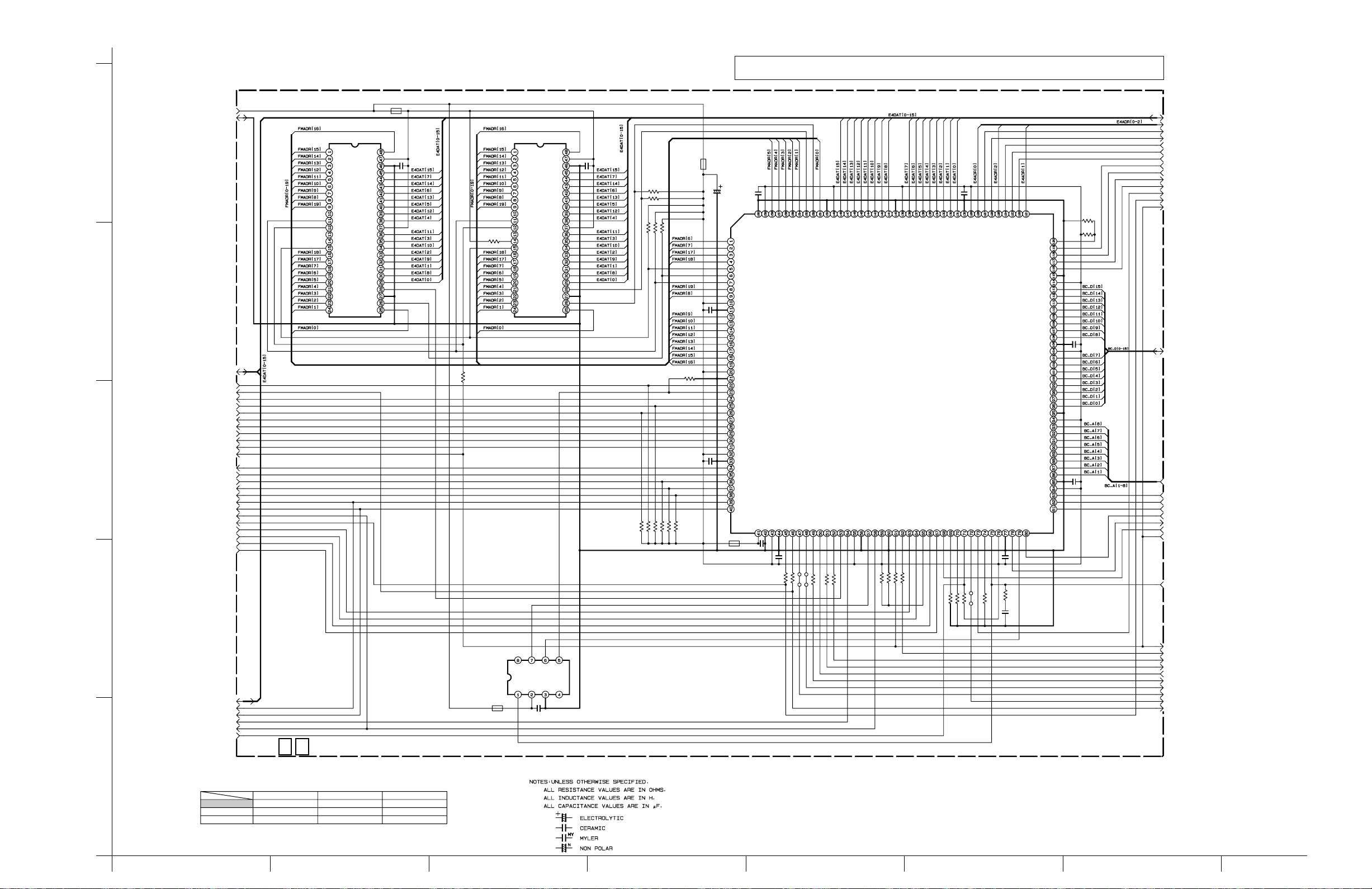
DIGITAL (LAPRAS) SCHEMATIC DIAGRAM
4.20
The Parts Number,value and rated voltage etc. in the Schematic Diagram are for references only.
Note :
When replacing the parts,refer to the Parts List.
K1403
TO VIDEO IF
5
4
TO
DSP
3
SW3.3V
GND
E4DAT[0-15]
APINT
ACLK
ANCS
ARDRDY1
ASPFS
ADR2
ASPFS2
ADX2
LAPRAS_RESET
ANCS2
ARD2RDY1
ARDRDY0
AWRRDY1
AWRRDY0
AHDSTB
AWR
AHAST
APINT2
ARD2RDY0
AWR2RDY1
AWR2RDY0
ADR
ADX
BCK
IC1402
##
A16
A15
BYTE
A14
Vss
A13
DQ15/
A12
DQ7
A11
DQ14
A10
DQ6
A9
DQ13
A8
DQ5
A19
DQ12
N.C.
DQ4
WE
Vcc
RESET
DQ11
N.C.
DQ3
N.C.
DQ10
RY/BY
DQ2
A18
DQ9
A17
DQ1
A7
DQ8
A6
DQ0
A5
A4
A3
A2
A1 A0
OE
Vss
CE
A0
2
TO
HD_DEC
E4DAT[0-15]
AHDSTB
AWR
AFCS
AHAST
AFINT
PELN0984-150Y
C1412
0.1
R1414
0Ω
MK2703-X
R1430
OPEN
IC1404
K1404
NQR0129-002X
IC1403
A16A15
BYTE
A14
Vss
A13
A12
DQ15/
A11
DQ7
A10
DQ14
A9
DQ6
A8
DQ13
A19
DQ5
N.C.
DQ12
WE
DQ4
RESET
Vcc
N.C.
DQ11
N.C.
DQ3
RY/BY
DQ10
A18
DQ2
A17
DQ9
A7
DQ1
A6
DQ8
A5
DQ0
A4
OE
A3
Vss
A2
CE
A1
X2 S0 S1 CLK
X1 Vcc GND 27M
C1414
0.1
C1411
0.1
10k
R1423
R1409
R1410
10k
R1411
10k
R1424
10k
R1412
10k
R1425
10k
10k
10k
R1413
10k
R1426
10k
R1427
R1422
OPEN
10k
R1428
C1402
C1403
K1402
0.1
0.1
PELN0984-150Y
C1401
22
T
/6.3
K1401
NQR0129-002X
C1410
0.1
FMADR6
FMADR7
FMADR17
FMADR18
FMRYBY
FMCE2_
MXWE_
FMADR19
FMADR8
VDD
VSS
FMADR9
FMADR10
FMADR11
FMADR12
FMADR13
FMADR14
FMADR15
FMADR16
VDD
VSS
APINT_
ACLKIN
ANCS_
ARDRDY1
ADR
ADX
ASPFS
ADR2
ASPFS2
ADX2
VDD
VSS
ANCS2_
ARD2RDY1
ARDRDY0
AWRRDY1
AWRRDY0
AHDSTB_
AWR_
C1404
0.1
VSS
AVDD
VDD
AVSS
C1405
FMADR5
VDD
0.1
R1401
0Ω
FMADR3
FMADR4
VSS
BCK
0Ω
R1429
FMADR1
FMADR2
ACLKOUT
ADEM0
0Ω
B1401
FMOE_
ADEM1
0Ω
0Ω0Ω0Ω
B1402
R1415
FMCE_
DADI
VSS
FMADR0
ADDO
ASCLK
R1416
R1417
VDD
ALRCK
E4DAT14
E4DAT15
FMOE2_
AFCS_
E4DAT13
VDD
E4DAT12
VSS
E4DAT10
E4DAT11
#
PLLCTL0
AHAST_
E4DAT8
E4DAT9
IC1401
VDD
VSS
0Ω
OPEN
R1418
R1419
1k
R1402
VSS
MRST
0
R1403
VDD
IEC
E4DAT6
E4DAT7
APINT2_
ARD2RDY0
E4DAT4
E4DAT5
ACLKSEL
AWR2RDY1
TO
DVX
E4DAT[0-15]
E4ADR[0-2]
E4CS
E4WR
E4DMAREQ
E4DTACK
E4IRQ
AO_D1
AO_D0
C1409
0.1
R1421
VSS
VDD
E4CS_
10k
R1407
AFINT_
OPEN
B1403
E4ADR0
ADEM17
E4ID1
10k
R1406
HSTSW
E4WR_
CK27
C1413
E4ADR2
E4DMARQ_
VDD
VSS
0.1
R1408
OPEN
C1406
OPEN
E4DTACK_
HIRQ_
E4ADR1
E4TRQ_
SCANCK
E4IFSYNC
HDATA15
HDATA14
HDATA13
HDATA12
HDATA11
HDATA10
HADDR7
HADDR6
HADDR5
HADDR4
HADDR3
HADDR2
HADDR1
HADDR0
PLLCTL1
HCLK
E4OD1
E4OD0
E4ID0
VDD
HD ATA9
HD ATA8
VDD
HD ATA7
HD ATA6
HD ATA5
HD ATA4
HD ATA3
HD ATA2
HD ATA1
HD ATA0
VDD
VDD
HXCS_
HRD_
HWR_
VSS
VSS
VSS
VSS
E4DAT0
E4DAT1
E4DAT2
E4DAT3
AWR2RDY0
HACK_
SCANEN
TCTL
10k
10k
R1404
R1405
R1420
OPEN
C1408
0.1
C1407
0.1
0Ω
AI_FSYNC
AI_D0
AI_D1
BCK
LAPRAS_RESET
BC_D[0-15]
BC_A[1-8]
LAPRAS_CS
BC_RS
BC_WS
BC_BCLK
LAPRAS_INT
BC_WAIT
LAPRAS_RESET
LAPRAS_27M
LAPRAS_RESET
IEC
ALRCK
ASCLK
ADDO
DADI
DEM1
DEM0
DEM17[H]
ACLK
TO
HOST
TO
HOST
TO
DMAIN
TO
AUDIO AD/DA
DIGITAL (LAPRAS)50
1
# NOTICE
HM-DH30000U
HM-DH25000
HM-DH35000
JCP8034-2
JCP8034
JCP8034-2
IC1402 IC1403IC1401
OPEN
OPEN
MR27V1602E-1STN
SST39VF160-7CEK
MBV800TA90PT
SST39VF160-7CEK
p20262001a_rev0
4-41 4-42
HGFEDCBA
Page 63

DIGITAL (DSP) SCHEMATIC DIAGRAM4.21
The Parts Number,value and rated voltage etc. in the Schematic Diagram are for references only.
Note :
When replacing the parts,refer to the Parts List.
TO
VIDEO_IF
SW3.3V
SW2.5V
5
4
3
2
GND
#
R1601
R1602
R1603
R1604
R1605
OPEN
K1603
#
NQR0129-002X
#
R1606
R1607
OPEN
R1608
#
#
R1609
OPEN
R1634
C1606
OPEN
#
K1602
#
C1604
OPEN
R1633
OPEN
10k
10k
10k
OPEN
OPEN
OPEN
OPEN
R1625 C1616
R1623
VDD3
DO5
DO4
DO3
GND3
DO2
DO1
DO0
VDD2
CKI
DVDD
AVDD
AGND
DGND
VDD3I
LRCKO
BCKO
MCKO
VDD3
GND2
MCK44
MCK48
P10
P11
VDD2
OPEN
R1624
GND2
GND3
BCKI0
P12
R1632
0Ω
OPEN
OPEN
OPEN
C1603
OPEN
0.1
0Ω
#
C1605
0.1
10k
10k
#
C1607
0.1
C1601
#
C1602
#
K1601
#
PELN1984-150Y
0.1
0.1
###
R1626
R1627
R1628
R1629
R1630
R1631
0Ω0Ω0Ω
R1621
R1622
###
0.1
C1615
#
DI0
VDD2
BCKI1
LRCKI0
#
IC1601
uPD61003GC
P13
P14
P15
P16
R1620
LRCKI1
P17
0Ω0Ω0Ω
R1619
###
OPEN
R1618
DI1
BCKI2
VDD2
P00/INTP00
OPEN
OPEN
R1616
R1617
DI2
LRCKI2
P01/INTP01
P02/INTP02
0Ω
0Ω
R1614
R1615
#
#
BCKI3
LRCKI3
P03/INTP03
P04/INTP04
IC
DI3
GND2
P05/INTP05
GND2
P06
GND3
P07
#
R1613
#
C1614
0.1
GND3
PLLCONT
VDD3
HAD0
0Ω
VDD3
HAD1
GND3
HAD2
GND3
RESETB
HAD3
HAD4
GND3
VDD2
DBBRRDY1
DBBRRDY0
DBBWRDY1
DBBWRDY0
EXTDIR
GND2
HDSTB
HR/WB
HCSB
HAST
VDD3
HAD15
HAD14
HAD13
VDD2
HAD12
HAD11
HAD10
GND3
HAD9
HAD8
HAD7
HAD6
VDD3
HAD5
GND3
0Ω
0Ω
00Ω0Ω
C1716
R1725
OPEN
R1724
GND2
GND3
OPEN
R1723
BCKI0
P12
0Ω0Ω0Ω
R1722
LRCKI0
P13
R1721
0.1
C1715
DI0
VDD2
P14
P15
10k
10k
10k
OPEN
OPEN
OPEN
OPEN
OPEN
OPEN
R1726
R1727
R1728
R1729
R1730
R1731
R1732
R1733
R1734
K1701
PELN1984-150Y
K1702
C1613
OPEN
DIR
C1612
#
0.1
#
C1611
0.1
C1610
OPEN
PELN1984-150YPELN1984-150Y
R1701
R1702
R1703
R1704
OPEN
K1703
NQR0129-002X
R1706
R1707
OPEN
C1706
OPEN
R1708
R1709
C1704
C1701
0.1
0Ω
OPEN
OPEN
OPEN
C1702
0.1
C1703R1705
OPEN
0.1
0Ω
C1705
0.1
10k
10k
C1707
0.1
VDD3
DO5
DO4
DO3
GND3
DO2
DO1
DO0
VDD2
CKI
DVDD
AVDD
AGND
DGND
VDD3I
LRCKO
BCKO
MCKO
VDD3
GND2
MCK44
MCK48
P10
P11
VDD2
OPEN
OPEN
OPEN
R1716
R1717
R1718
R1719
R1720
DI2
DI1
BCKI2
BCKI1
LRCKI2
LRCKI1
IC1701
uPD61002GC
P16
P17
VDD2
P00/INTP00
P01/INTP01
P02/INTP02
R1714
R1715
BCKI3
P03/INTP03
DI3
LRCKI3
P04/INTP04
P05/INTP05
GND2
GND2
R1713
0Ω
C1714
0.1
IC
VDD3
GND3
GND3
PLLCONT
P06
P07
VDD3
HAD0
HAD1
GND3
HAD2
GND3
RESETB
HAD3
HAD4
GND3
VDD2
DBBRRDY1
DBBRRDY0
DBBWRDY1
DBBWRDY0
EXTDIR
GND2
HDSTB
HR/WB
HCSB
HAST
VDD3
HAD15
HAD14
HAD13
VDD2
HAD12
HAD11
HAD10
GND3
HAD9
HAD8
HAD7
HAD6
VDD3
HAD5
GND3
C1713
OPEN
DIR
C1712
0.1
C1711
0.1
C1710
OPEN
TO
DSP_27M
TO LAPRAS
ACLK
BCK
LAPRAS_RESET
AHDSTB
AWR
AHAST
E4DAT[0-15]
ADR
ASPFS
ADX
ARDRDY1
ARDRDY0
AWRRDY1
AWRRDY0
ANCS
APINT
ADR2
ASPFS2
ADX2
ARD2RDY1
ARD2RDY0
AWR2RDY1
AWR2RDY0
ANCS2
APINT2
DMAIN
0.1
#
C1609
0Ω
R1610
#
#
10k
R1611
#
R1612
4.7k
RA1701
C1608
OPEN
RA1601
#
#
DIGITAL (DSP)50
1
# MARKS ELEMENTS ARE MOUNTED ONLY HM-DH30000U.
RA1602
10k
RA1603
#
10k
10k
10k
C1708
OPEN
RA1702 RA1703
10k
10k
0Ω
R1710
10k
R1711
R1712
C1709
4.7k
0.1
p20263001a_rev0
ABCD EFGH
4-43 4-44
Page 64

DIGITAL (AUDIO AD/DA) SCHEMATIC DIAGRAM
4.22
The Parts Number,value and rated voltage etc. in the Schematic Diagram are for references only.
Note :
When replacing the parts,refer to the Parts List.
5
50
DIGITAL(AUDIO AD/DA)
#
#
Q1803
R1837
100k
2SC4081/QRS/
R1833
#
10k
#
0.1
#
390
C1830
100p
R1829
220
IC1803
BA15218F
R1827
4.7k
R1825
10k
C1832
0.1
VCC
C1834
OPEN
C1836
OPEN
R1823
10k
C1840
R1835
C1828
470p
R1821
4.7k
C1843
C1819
47
/16 /6.3
C1818
47
R1843
L1803
0Ω
#
DTA144WUA
B1801
OPEN
#
R1839
1k
#
DTC144WUA
10µ
Q1801
Q1802
L1802
10µ
TO DIGI (VIDEO IF)
WR902
R1831
330
L1801
10µ
R1812
OPEN
TO
VIDEO_IF
SW5V
AL5V
AUDIO[-]
SW3.3V
GND
4
VEE
TO DIGI (VIDEO IF)
C1833
0.1
C1827
OPEN
#
R1838
100k
WR901
R1836
#
390
#
C1841
0.1
#
Q1804
2SC4081/QRS/
R1822
4.7k
C1816
10
/16
C1829
470p
R1834
#
10k
R1802
R1801
C1817
/16
10
C1802
1.8k
1.8k
R1803 R1804
1.8k 1.8k
10
C1801
10
AK4522VF
R1830
C1831
100p
R1817
10k
R1813
R1814
R1818
220
10k
10k
10k
IC1802
BA15218F
VEE
C1835
R1826
R1828
4.7k
C1826
C1821
OPEN
10k
OPEN
OPEN
C1837
OPEN
R1819
10k
C1820
OPEN
C1825
100p
R1816
R1824
10k
C1822
100p
R1815
10k
C1824
100p
VCC
10k
TO MAIN(MAIN-TERMINAL)
CN7107
3
CN9801
D/A_OUT[R]
D/A_OUT[L]
A/D_IN[R]
A/D_IN[L]
TO VIDEO IF
C_IN
Y_IN
Y_IN
C_IN
GND
GND
GND
GND
GND
GND
NC
C1838
0.001
R1832
10
C1839
OPEN
2
R1820
C1823
100p
10k
IC1801
/16
/16
C1811
22
T
C1815
C1814
4.7
0.1
/6.3
VCOM
AOUTR
AOUTL
CMODE
VREFH
AINR+
AINR-
AINL+
C1804
C1803
0.0022
0.0022
R1805
R1806
0Ω
0Ω
T
C1810
0.1
/16
T
C1806 C1805
C1808
4.7
0.1 0.1
/6.3
PD
AINL-
C1807
4.7
DGND
VA
T
/6.3
R1810
10
C1813
T
22
/6.3
C1812
0.1
VD
AGND
C1809
0.1
R1809
MCKI
DIF0
R1807R1808
10
DEM1
DEM0
DIF1
LRCK
R1811
10k10k
SMUTE
SCLK
R1842
SDTO
SDTI
1k
0Ω
TO LAPRAS
DEM17[H]
DEM0
DEM1
DADI
ADDO
ASCLK
ALRCK
ACLK
LAPRAS_RESET
IEC
R1840
C1842
0.1
R1841
100k
0Ω
MODEL
OPTICAL
OUT
SYMBOL
: Not used: Used
IC1804
R1840
R1841
C1842
YES
NO
INPUT
VCC
GND
IC1804
GP1F32T
1
#DIFFERENCE TABLE
SYMBOL
MODEL
JPN /US
EU/EK /MS
Q1801 ~Q1804
R1833 ~R1839
C1840 ,C1841
p20182001a_rev0.1
4-45 4-46
HGFEDCBA
Page 65

DIGITAL (DECRIPTER) SCHEMATIC DIAGRAM4.23
The Parts Number,value and rated voltage etc. in the Schematic Diagram are for references only.
Note :
When replacing the parts,refer to the Parts List.
TO
HOST
MAIN_RESET
DIGITAL (DECRIPTER)50
GND
TO DMAIN
VIDEO_27M
5
NC
NC
NC
NC
TO
HOST
BC_A[1-13]
TO HOST
TO HOST
BC_D[0-15]
PREC_CS
BC_BCLK
BC_RS
BC_WS1
BC_WS
IC1202
TC7SH04FU-X
C1207
R1206
0.1
OPEN
4
3
HADDR0
HADDR1
HADDR2
HADDR3
HADDR4
HADDR5
HADDR6
HADDR7
HADDR8
HADDR9
HADDR10
HADDR11
HADDR12
NC
NC
NC
HD ATA 0
HD ATA 1
HD ATA 2
HD ATA 3
HD ATA 4
HD ATA 5
HD ATA 6
HD ATA 7
HD ATA 8
HD ATA 9
HDATA10
GND
HDATA11
GND
HDATA12
GND
HDATA13
GND
HDATA14
GND
HDATA15
GND
HXCS
R1205
GND
HSEL
10k
GND
NC
GND
NC
GND
HCLK
GND
IC1201
JCP8044
HXRE
0Ω
R1201
GND
HXWEL
HXWEH
0Ω
R1202
TDI
TMS
TDO
TRST
HXACK
VCC
NC
VCC
VCC
VCC
TEB
TCK
TOUT
VCC
VCC
VCCNCNCNCNC
C1206C1203
0.10.1
TIN
VCC
NC
SCLK
XRST
NC
OTSDT0
OTSDT1
OTSDT2
OTSDT3
OTSDT4
OTSDT5
OTSDT6
OTSDT7
CMDBSY
OTSV
TCLK
ITSDT0
ITSDT1
ITSDT2
ITSDT3
ITSDT4
ITSDT5
ITSDT6
ITSDT7
ITSV
NC
NC
NC
NC
NC
NC
K1202
PELN0984-150Y
K1201
PELN0984-150Y
C1202C1201
T
220.1
/6.3
R1203
OPEN
TO DVX
DECDATA[0-7]
TO
DMAIN
DECST
TO DMAIN
DEC_9MDEC
TSDATA[0-7]
TO DMAIN
TSPSTART
TO VIDEO IF
AL3V
SW3.3V
GND
2
1
P30098001a_rev0
ABCD EFGH
4-47 4-48
Page 66

4.24 REGULATOR AND SUB REGULATOR CIRCUIT BOARDS
<01> REGULATOR, <02> SUB REGULATOR
LPB10118-001B
4
21
1
10
CN5503
Q5505
CN5502
CN5504
Q5501
E
Q5507
C5501
C5503
R5507
D5501
Q5504
B
D5509
LPB10118 -001B
D5508
D5507
E
R5511
Q5502
D5502
R5510
D5506
D5510
R5501
R5506
R5505
D5505
R5504
R5508
C5504
W5531
D5504
Q5503
CN5501
R5509
D5503
R5502
R5503
1
14
SW.REG PWB
D5305 D5306
15
4
C5202
CN5303
2
1
C5316
C5314
C5312
R5309
C5310
B
R5305
Q5301
E
CN5302
R5311
R5312
2
R5310
2
R5307
R5308
B5301
D5308
D5307
R5313
2
IC5303
5
IC5302
10
2
R5314
1
3
135
Q5302
R5512R5513
Q5506
E
R5514
1
LPA10118 -
0 2
SUB REG PWB ASS'Y
IC5305
IC5304
5
D5303
C5311
C5309
12
1
3
C5313
5
C5315
D5302
Q5305
R5306
TF
D5313
1
3
D5315
Q5304
R5325
R5324
R5326
C5308
R5301
Q5303
CAUTION :
FOR CONTINUED PROTECTION AGAINST FIRE HAZARD,REPLACE ONLY WITH SAME TYPE AND RATED FUSE(S).
FOR CONTINUED PROTECTION AGAINST FIRE HAZARD,REPLACE ONLY WITH SAME TYPE CP(S)MANUFACTURED BY ROHM.
ATTENTION :
REPLACER PAR DES FUSIBLE DE MEME TYPE.
D5312
D5304
D5316
R5323
IC5306
14
C5317
1015
CN5301
R5332
D5314
D5310
D5311
1
C5303
C5320
C5318
C5301
R5328
4
4
R5329
IC5307
R5331
R5304
L5203
1
R5316
C5319
D5309
L5201
C5304
C5201
C5205
L5204
C5207
C5206
C5203
R5333
D5301
D5207
D5208
D5202
C5210
C5208
D5204D5205
CP5301
16
14 15
13
12
11
10
9
R5315
IC5301
D5206
R5320
R5321
D5201
18
17
123
C5306
R5327
R5319
R5318
D5209
LPB10118 -001B
SW.REG PWB
C5307
R5322
2
134
12
3
4
T5001
567
8
R5317
C5209
PC5101
D5103
C5103
C5101
C5105
D5101
R5102
D5102
R5103
C5104
IC5101
R5107
1
5
R5106
0 1
LPA10118 -
R5105
REG PWB ASS'Y
2
4
C5107
C5106
R5104
K5101
C5102
R5101
C5003
C5004
C5006
DANGEROUS VOLTAGE
L5001
D5001
C5005
B5004
C5002
LF5002
C5001
FC5001FC5002
VA5001
SG5001
F5001
BRN
LIVE
BLU
NEUTRAL
B5003
CN5001
CN5002
R5001
VA5003
COMPONENT PARTS LOCATION GUIDE <REGULATOR AND SUB REGULATOR>
CAPACITOR
C5001 A D 17B
C5002 A D 16C
C5003 A D 14C
C5004 A D 14B
C5005 A D 15A
C5006 A D 14A
C5101 A D 11B
C5102 A D 13C
C5103 A D 11C
C5104 A D 12C
C5105 B C 11D
C5106 A D 12A
C5107 A D 13B
C5201 A D 6A
C5202 B C 1E
C5203 A D 7A
C5205 A D 7D
C5206 A D 7B
C5207 A D 7D
C5208 A D 8D
C5209 A D 10A
C5210 A D 9E
C5301 A D 5B
C5303 A D 5C
C5304 A D 6B
C5306 A D 9E
C5307 A D 10E
C5308 A D 3B
C5309 B C 2B
C5310 A D 1A
C5311 B C 2B
C5312 A D 2C
C5313 B C 3C
C5314 A D 2C
C5315 B C 3D
C5316 A D 2D
C5317 B C 5D
C5318 A D 5D
C5319 B C 6B
C5320 A D 5B
CONNECTOR
CN5001 A D 18C
CN5002 A D 18C
CN5301 A D 4B
CN5302 A D 1E
CN5303 A D 1D
DIODE
D5001 A D 14C
D5101 A D 11B
D5102 A D 11D
D5103 A D 11D
D5201 A D 9A
D5202 A D 9B
D5204 A D 9C
D5205 A D 9B
D5206 A D 9E
D5207 A D 9E
D5208 A D 9D
D5209 A D 10A
D5301 A D 8C
D5302 A D 4C
D5303 A D 3B
D5304 B C 4C
D5305 B C 1E
D5306 B C 2E
D5307 B C 3E
D5308 B C 3E
D5309 A D 6B
D5310 A D 4A
D5311 A D 4A
D5312 A D 4E
D5313 B C 3E
D5314 A D 5A
D5315 A D 4D
D5316 B C 4B
IC
IC5101 A D 12C
IC5301 A D 9E
IC5302 A D 2A
IC5303 A D 2C
IC5304 A D 3C
IC5305 A D 3D
IC5306 A D 5D
IC5307 A D 6B
COIL
L5001 A D 17C
L5201 A D 6A
L5203 A D 6C
L5204 A D 7C
TRANSISTOR
Q5301 A D 1A
Q5302 B C 3A
Q5303 B C 3A
Q5304 B C 4C
Q5305 B C 3B
RESISTOR
R5001 A D 18A
R5101 A D 13D
R5102 A D 11D
R5103 B C 12D
R5104 A D 13C
R5105 A D 13D
R5106 A D 12B
R5107 A D 12B
R5301 A D 4A
R5304 B C 6A
R5305 B C 1A
R5306 B C 3A
R5307 B C 2A
R5308 B C 2A
R5309 B C 2B
R5310 B C 2B
R5311 B C 2C
R5312 B C 2C
R5313 B C 2D
R5314 B C 2D
R5315 A D 10A
R5316 A D 6A
R5317 A D 10A
REF.NO.
LOCA
R5318 B C 9D
R5319 B C 9D
R5320 B C 9D
R5321 B C 9D
R5322 B C 10D
R5323 B C 4B
R5324 B C 3C
R5325 B C 3C
R5326 B C 4B
R5327 B C 9D
R5328 B C 5D
R5329 B C 6D
R5331 B C 6B
R5332 B C 5C
R5333 B C 7D
CP5301 A D 9A
F5001 A D 17C
FC5001 A D 17C
FC5002 A D 17E
K5101 A D 12C
LF5002 A D 16A
PC5101 A D 10D
SG5001 A D 17A
T5001 A D 10D
VA5001 A D 17C
VA5003 A D 18A
TIONREF.NO. LOCATIONREF.NO. LOCATIONREF.NO. LOCATIONREF.NO. LOCATION
OTHER
4-49 4-50
Page 67

3D DIGITAL/4M AND S-SUB CIRCUIT BOARDS4.25 TERMINAL CIRCUIT BOARD4.26
<05> 3D DIGITAL/4M
LPB10143-001A
FOIL SIDE(B)
R1436
C1436
R1435
VR1401
C1435
C1455
C1463
3D
IC1401
C1432
C1431
DIGI/4M PWB
LPB10143 -001A
Q1407
C1412
R1406
R1406
L1402
C1408
C1407
C1409
R1447
R1448
R1449
CN1401
14 1
C1456
15
C1458
C1451
D1402
C1401
L1406
L1401
L1409
C1448
R1432
L1408
C1446
L1407
C1403
D1401
<15> S-SUB
LPB10103-001A
5
C524
R506
C526
1
R508
R509
C527
R510
C528
C532
C531
R514
2
R507
R515
R516
C536
C534
CN513
IC502
LPA10103
W528
C510
1
W535
R505
C529
R512
R511
R513
C530
W537
C505
C525
1
C521
R504
05
D/ALEVEL
80
1
20
R1415
L1403
C1434
R1434
R1405
C1404
R1404
Q1402
C1410
LC1402
R1450
17
COMPONENT SIDE(A)
C1457
Q1416
R1457
B1420
Q1413
C1425
R1421
R1458
R1430
Q1412
B1418
Q1417
Q1401
CN1401
1
9
8
C508
W536
C509
C564
C537
R517
C512
W530
L501
W534
W531
C515
C522
C523
R526
W543
R525
C533
W532
L504
W533
2
61
C1416
R1451
L1404
R1459
R1463
LC1401
R1416
R1452
28
C1420
B1419
Q1418
Q1420
C575
C535
C513
C511
1
C1429
W529
LPA10143 -
60
21
R1417
C1406
R1453
IC1402
C1449
C1444
R1427
C1421
C1422
R1428
L505
R527
IC501
42
C514
43
R501
W510
W526
3D DIGI/4M
PWB AY
R1441
C1450
L1405
R1462
Q1414
C506
W541
C518
C566
B501
C538
Q501
W527
C1452
C1440
C1424
L1405
C1467
C1445
56
R518
C1438
R1439
R1461
R1441
29
W524
40
R1426
R1438
Q1408
B1409
10
W523
B1401
41
C1443
R1437
C1442
L1404
R1425
C1423
Q1410
LC1401
Q1418
C1468
R1454
C1433
C1441
C1437
C1473
C1472
R1418
B1411
C1417
C1416
C1429
C1466
C1462
C1464
C1465
C562
L503
W520
W521
C507
28
C563
R522
1
C552
C520
C568
R531
C553
C551 C554
W522W542
R531
C516
C519
C517
B503
W540
W525
B1407
B1402
B1405
B1404
B1403
C1448
R1440
R1433
R1429
R1431
C1471
C1426
Q1401
E
L1401
R1401
R1402
C1469
R1455
1
D/A LEVEL
VR1401
C1453
C1454
B1416
R1408
Q1404
C1414
L1403
R1411
Q1406
Q1419
C1410
LC1402
17515
S-SUB PWB ASS'Y
C504
L502
R503
W538
C502
C503
C501
W515
15
14
C573
C559
R536
R533
C569
R532
W516
W518
W519
W517
CN511
B1408
1
B1406
Q1415
B1417
C1439
R1410
R1413
C1411
C558
C570
R533
29
C1428
C1427
C1430
R1414
C1413
W513
L1406
L1409
2
R524
C1447
C1401
Q1422
L1402
R1460
C1461
CN512
R1456
D1402
D1403
R1412
R1446
W514
C576
C572
W511
C1451
C1446
L1407
C1402
C1470
Q1403
R1407
C1405
C1415
C1460
C1459
W512
C1456
C1403
C556
L1408
D1401
C1463
R535
C561
C555
W509
W506
W508
W507
C560
C557
R523
W505
13
14
S-SUB PWB
C571
R534
W539
LPB10103 -001A
W504
W502
W501
W503
COMPONENT PARTS LOCATION GUIDE
<3D DIGITAL/4M>
REF.NO. LOCATION REF.NO. LOCATION REF.NO. LOCATION
CAPACITOR
C1401 A D 5A
C1402 B C 5A
C1403 A D 5B
C1404 B C 2B
C1405 A C 1C
C1406 B C 3A
C1407 B C 2B
C1408 B C 1B
C1409 B C 1B
C1410 A D 2B
C1411 A C 2B
C1412 B C 2B
C1413 A C 2B
C1414 A C 2B
C1415 A C 1C
C1416 A D 3B
C1417 A C 3B
C1420 A C 4B
C1421 A C 4B
C1422 A C 4B
C1423 B C 4B
C1424 B C 3B
C1425 A C 4C
C1426 B C 5B
C1427 B C 5B
C1428 B C 5C
C1429 A D 3B
C1430 A C 2D
C1431 B C 2C
C1432 B C 2C
C1433 A C 3C
C1434 B C 2B
C1435 B C 1E
C1436 B C 2E
C1437 A C 3C
C1438 B C 3C
C1439 B C 5A
C1440 B C 3C
C1441 A C 3C
C1442 B C 4C
C1443 B C 4C
C1444 A C 4C
C1445 A C 4C
C1446 A D 5C
C1447 B C 5B
C1448 A D 5C
C1449 A C 3D
C1450 A C 4C
C1451 A D 5D
C1452 B C 3D
C1453 A C 2D
C1454 A C 2D
C1455 B C 2D
C1456 A D 5D
C1457 A C 5E
C1458 A C 5D
C1459 A C 1A
C1460 A C 1B
C1461 A C 1B
C1462 A C 2A
C1463 A D 1D
C1464 A C 3A
C1465 A C 3A
C1466 A C 3A
C1467 B C 3A
C1468 B C 4A
C1469 B C 4A
C1470 B C 6A
C1471 B C 5B
C1472 A C 3C
C1473 A C 3C
CONNECTOR
CN1401 A D 5A
DIODE
D1401 A D 6B
D1402 A D 5D
D1403 A C 1C
IC
IC1401 B C 3D
IC1402 A C 4D
COIL
L1401 A D 4B
L1402 A D 1B
L1403 A D 2B
L1404 A D 4C
L1405 A D 4B
L1406 A D 5B
L1407 A D 6B
L1408 A D 6C
L1409 A D 5A
TRANSISTOR
Q1401 A D 5B
Q1402 B C 2B
Q1403 A C 1C
Q1404 A C 2C
Q1406 A C 2B
Q1407 B C 2C
Q1408 A C 3B
Q1410 B C 4B
Q1412 A C 5B
Q1413 A C 5C
Q1414 A C 3A
Q1415 B C 5D
Q1416 A C 4C
Q1417 A C 4B
Q1418 B C 4A
Q1419 A C 2B
Q1420 A C 4A
Q1421 A C 4B
Q1422 A C 1C
RESISTOR
R1401 B C 5B
R1402 B C 5A
R1404 B C 2B
R1405 B C 2B
R1406 B C 1B
R1407 A C 1C
R1408 A C 1C
R1410 A C 2C
R1411 A C 2B
R1412 A C 1B
R1413 A C 2C
R1414 A C 1B
R1415 B C 2C
R1416 B C 3B
R1417 B C 3B
R1418 A C 3C
R1421 A C 4B
R1425 B C 4B
R1426 B C 3C
R1427 A C 3C
R1428 A C 3B
R1429 B C 4B
R1430 A C 5B
R1431 B C 5C
R1432 A C 5C
R1433 B C 5C
R1434 B C 2B
R1435 B C 1E
R1436 B C 1E
R1437 B C 4C
R1438 A C 4C
R1439 A C 4C
R1440 B C 5C
R1441 B C 3A
R1442 A C 3A
R1446 A C 2A
R1447 B C 1A
R1448 B C 1A
R1449 B C 2A
R1450 B C 2A
R1451 B C 3A
R1452 B C 3A
R1453 B C 3A
R1454 B C 4A
R1455 B C 5A
R1456 B C 5C
R1457 A C 4C
R1458 A C 4B
R1459 A C 4B
R1460 A C 1B
R1461 A C 3B
R1462 A C 3B
R1463 A C 4A
VR1401 A D 1E
OTHER
LC1401 A D 4A
LC1402 A D 2A
COMPONENT PARTS LOCATION GUIDE
<S-SUB>
REF.NO.
C501
C502
C504
C505
C506
C507
C508
C510
C511
C512
C513
C514
C516
C517
C518
C519
C520
C522
C523
C524
C525
C526
C528
C529
C530
C531
C532
C534
C535
C536
C537
C538
C552
C553
C554
LOCATION
CAPACITOR
A
A
AC503
B
A
B
A
A
A
B
B
A
B
BC515
B
B
B
A
A
A
A
B
B
B
BC527
B
B
B
B
B
A
B
B
B
B
AC551
B
B
A
D
5D
D
5D
D
4D
C
4E
D
1D
C
4E
D
4E
D
2E
2DDAC509
D
2C
C
3C
C
2D
D
2D
C
3C
C
3B
C
4B
C
4B
C
3C
D
4B
D
3C
1DDAC521
D
2B
D
2B
C
1C
C
1C
C
1C
C
1B
C
1B
C
1B
C
1A
C
1A
C
1B
2ACBC533
D
2A
C
2D
C
2D
C
2D
C
3B
D
4B
C
4B
C
4B
D
5B
REF.NO.
C555
C556
C557
C559
C560
C561
C562
C563
C566
C568
C569
C570
C571
C573
C575
C576
CONNECTOR
CN511
CN512
CN513
IC501
IC502
L501
L502
L503
L504
L505
TRANSISTOR
Q501
RESISTOR
R501
R503
R504
R505
R506
R507
LOCATION
B
B
A
BC558
B
A
A
A
B
BC564
B
B
B
B
B
BC572
B
B
B
A
A
A
IC
B
A
COIL
A
A
A
A
A
B
B
B
B
B
B
B
5CC
5B
DC6C
5C
DC6D
6DD
4E
CD4D
3B
CC4B
4BC
5B
CC5C
5C
CC3D
5DC
D3A
5E
DD1E
4D
DC1C
2B
DD5E
D
3E
D
2A
D
3E
C3B
3C
CC4E
C
1C
C
1C
C
1C
C1C
REF.NO.
R508
R509
R510
R5115CC
R512
R513
R514
R515
R516
R518
R522
R523
R524
R525
R5266CC
R527
R531
R532
R533
R534
R536 5CCB
LOCATION
CB
B
CCB
B
CCB
CB
B
CCB
B
CCB
CB
B
CCB
B
CCB
CB
B
CCB
1C
1C
1B
1BCB
1B
1A
1A
1B
2D
2DCBR5172DC
3B
4B
5C
5C
3B
3BCB
3D
4B
4B
5B
6C
5CCBR535
<06> TERMINAL
LPB10116-001A
C7127
L7103
4-51 4-52
5
3
1
TERMINAL PWB
C7108
C7109
R7139
R7137
R7136
J7126
LPB10116 -001A
W2
W3
7
R7123
1
R7122
R7121
D7102 D7103
C7126
R7142
R7141
R7140
1
IC7103
4
R7144
B7113
B7111
C7122
B7112
C7123
9
8
B7115
CN7104
2
1
C7128
CC
R7156
C7129
7
62
CN7103
1
4
C7118
W1
C7117
6
Y
1
IC7102
3
C7119
5
3
J7127
24
1
Cr Cb
L7101
B7114
1
8
4
R7138
C7107
5 6
IC7101
C7103
C7104
R7114
6
B7103
14
6
13
9
2
8
B7104
34
R7148
R7147
R7146
63
B7105
R7149
R7150
D7101
W4
J7102
B7117
C7131
B7116
C7125
1
L7102
8
R7103
5
C7120
C7121
R7143
R7145
J7101
4
6
3
C7124
B7118
R7157
CC
11
Q7105
Q7104
R7154
R7155
E
B
E
C7130
EBE
Q7103
J7125
DET IN DET OUT
C.BOX
R7151
3
1
J7123
1
2
J7110
"OUT,1"
12
5
87
54
R7105
R7104
C7101
2
1
5
"IN,1"
22
J7119 J7120
2
4
6
4
2
J7109
2
R7101
R7117
R7106
JLIP
3
R7126
RL
6
5
AUDIO
3
4
R7116
R7125
J7114
1
2
VIDEO
R7115
R7120
"OUT,2"
C7105
C7110
C7106
R7119
R7118
R7124
R7127
R7113
43
21
S
J7113
5
87
6
3
J7106
RL
R7112
54
R7111
R7110
5
2
1
0 6
2
VIDEO AUDIO
C7102
J7105
R7107
6 6
1
R7102
3
R7109
4
"IN,2"
11
J7122
BIT OUTBIT INR.PAUSE
R7153
22
J7121
R7152
1
3
J7124
2
17
CN7102
1
TERMINAL PWB ASS'YLPA10116 -
R7108
17
1510
W5
CN7101
5
1 10515
COMPONENT PARTS LOCATION GUIDE
<TERMINAL>
REF.NO. LOCATION REF.NO. LOCATION
CAPACITOR
C7101 B C 5C
C7102 B C 5B
C7103 A D 10D
C7104 B C 10D
C7105 A D 10C
C7106 B C 10C
C7107 A D 11D
C7108 A D 11E
C7109 B C 11E
C7110 B C 10C
C7117 A D 14D
C7118 B C 14E
C7119 A D 14C
C7120 A D 5D
C7121 B C 5D
C7122 A D 5E
C7123 A D 4E
C7124 A D 5D
C7125 A D 7D
C7126 A D 7E
C7127 A D 7E
C7128 B C 3E
C7129 A D 3E
C7130 B C 3D
C7131 B C 7D
CONNECTOR
CN7101 A D 2A
CN7102 A D 10A
CN7103 A D 1E
CN7104 A D 3E
DIODE
D7101 B C 8E
D7102 B C 8E
D7103 B C 8E
IC
IC7101 B C 10D
IC7102 B C 14D
IC7103 B C 6E
JACK
J7101 A D 5C
J7102 A D 7C
J7105 A D 5B
J7106 A D 7B
J7109 A D 9C
J7110 A D 13C
J7113 A D 9B
J7114 A D 13B
J7119 A D 2C
J7120 A D 3C
J7121 A D 2B
J7122 A D 3B
J7123 A D 1C
J7124 A D 1B
J7125 A D 1D
J7126 A D 8D
J7127 A D 13D
COIL
L7101 A D 11D
L7102 A D 6D
L7103 A D 3E
TRANSISTOR
Q7103 B C 3D
Q7104 B C 3D
Q7105 B C 3D
RESISTOR
R7101 B C 5C
R7102 B C 5C
R7103 B C 6C
R7104 B C 6C
R7105 B C 7C
R7106 B C 8C
R7107 B C 5B
R7108 B C 5B
R7109 B C 6B
R7110 B C 6B
R7111 B C 7B
R7112 B C 8B
R7113 B C 10C
R7114 B C 10C
R7115 B C 11C
R7116 B C 12C
R7117 B C 14C
R7118 B C 10B
R7119 A D 10C
R7120 B C 11B
R7121 B C 8E
R7122 A D 8E
R7123 A D 9E
R7124 B C 10B
R7125 B C 12B
R7126 B C 14B
R7127 B C 10B
R7136 B C 10D
R7137 B C 10D
R7138 B C 10D
R7139 B C 11E
R7140 B C 5E
R7141 B C 6E
R7142 B C 6E
R7143 B C 5E
R7144 B C 5E
R7145 B C 5D
R7146 B C 8D
R7147 B C 8D
R7148 B C 9D
R7149 B C 8D
R7150 B C 8D
R7151 B C 1D
R7152 B C 2B
R7153 B C 2C
R7154 A D 3E
R7155 A D 3E
R7156 B C 2E
R7157 B C 3D
Page 68

4.27 DISPLAY, REC SAFETY AND JACK CIRCUIT BOARDS
<28> DISPLAY, <32> REC SAFETY, <36> JACK
LPB10133-001B
24
CN7005
R7101
B7001
L7001
51
D7031
S7002
STOP/
S7001
PLAY
9
1
EJECT
B7002
10
CN7002
2
26
LPA10133 - 1
DISPLAY PWB ASS'Y
C7012
J7193
1
L7192
AUDIO R!
C7011
C7195
C7194
C7010
3
IN
2
R7010
C7003
L7194
L7193
2
36
S7006
FRONT PWB
LPB10133 -001B
AUDIO L! IN
C7192
1
L7191
J7192
JACK PWB ASS'Y
LPA10133 -
FF
3
S7003S7004
S7005
C7193
C7191
D7191
RECPAUSE
J7191
VIDEO IN
1
R7191
2
2
S7008
REC
SPEED
S7007
D-VHSREW
R7192
C7008
1
2
CN7191
J7194
10
S IN
R7193
6
D7199
4
3
5
1
2
C7196
R7194
R7014
R7003
R7013
W7101
D7032
D7033
D7035
C7004
35 34 32 25
11
R7005
D7034
C7005
W7002
R7006
W7001
R7007
30
R7015
R7009
W7005
D7004
R7002
D7002
D7003
R7001
DI7001
22
W7110
D7001
20 15 10 5 4
C7007
23
12
C7001
S7063
43
D-CASS.
AUDIO MODE
S-ET
LPB10133 -001B
FRONT PWB
3
REC-SAFE.
D7041
TBC/NR
R7043
R7041
R7042
R7044
D7042
12
FW7081
3
S7061
31
FW7001
IC7002
31
S7015
POWER
TP7002
MECHA2
MECHA1
TP7001
S7013
1
DISPLAY
D7007
S7014
TIMER
D7008
R7016
C7006
D7010
12
32
LPA10133 REC SAFE. PWB ASS'Y
11
IC7001
3433
44
1
W7201
D7011
2
W7104
1
C7002
D7005
W7102
CH+
S7010
S7009
CH-
D7006
S7012
TBC/NR
S7011
4-53 4-54
Page 69

D-PRE/REC CIRCUIT BOARD4.28
<43> D-PRE/REC
LPB10136-001C
D605
R663
R664
7
8
14
IC604
7
IC603
8
R716
R715
IC605
4
1
C678 C681
5
8
R718
R719
R720
R681
C659
L607
R702
Q653
R697
R696
C667
1
L609
C679
C639
R662
IC606
Q634
R655
R640
14
R633
Q670
R721
Q661
R722
C680
D607
D608
R723
CN603
1
4
L606
C654
C669
L605
R701
14
C643
COMPONENT PARTS LOCATION GUIDE
<D-PRE/REC>
REF.NO. LOCATION REF.NO. LOCATION REF.NO. LOCATION REF.NO. LOCATION
CAPACITOR
C601 A C 7D
FOIL SIDE(B)
TP112
1
C630
R614
2
B7
Q645
TP602
C658
REC LEVEL2
FF
C657
B8
16
C653
R674R676
1
15
R675
Q642
Q640
C664
Q646
C662
10
C663
9
CN605
L608
R684
1
Q641
Q639
C652
C672
R745
R673
C661
R685
R680
R744
Q643
R743
IC602
R672
C671
B3
C650
Q651
R742
R688
C651
R740
R671
R695
R692
R741
R678
C649
C655
C694
R677
Q652
C648
C666
30
R739
PB
DATA 2
R706
1
C654
C668
L605
R693
Q648
R689
D-PRE
R700
R748
1
L606
IC607
C689
/REC
R683
C670
Q649
CN603
R736
R737
C688
4
5
R686
R738
14
R682
4
L607
C673
Q654
Q650
C665
R690
Q647
C693
PWB ASS'Y
1
8
R703
R694
R691
C660
R687
Q644
C659
Q655
C690
PB DATA1
TP606 TP616
B6
R727
C640
Q625
Q619
Q614
C683
R747
C632
C624
R728
R730
R627
R643
Q664
L603
C638
D604
Q627
C642
R637
D603
R644
Q660
TP111
Q659
VIDEO
/STD
/HS1
R705
C676
R639
C675
R638
C633
R645
FF
Q620
C692
R658
R710
Q658
L601
L602
C637
R656
R641
R634R635 R636
C618
R707
R709
R708
B9
C617
R621
4 3
C674
C612
Q657
C622
R713
16
R626
C621
R618
R619
15
R620
C615
Q612
C616
Q609
C677
R714
R712
R711
B1
R630
Q608
R731
LPA10136
Q611
C625
R631
R629
Q623
C631
C687
R724
R725
CN601
Q662
C682
R726
R628
4
C623
1
C686
Q633
R661
Q631
C641
8
R659
R660
Q629
R657
C691
R642
R746
Q663
C684
R749
1
4
5
Q618
R622
R625
R617
IC601
Q615
R616
C614
B2
Q613
C628
C626
R615
Q616
R632
C627
C613
REC
LEVEL1
C619
Q610
C611
C629
Q617
TP601
C610
Q607
A/HS2
30
R613
COMPONENT SIDE(A)
TP606
C612
R612
R605
R704
TP111
DATA 1PBVIDEO
/STD
/HS1
FF
L601
Q622
Q628
C636
R648
B5
B4
R733
Q671
Q669
D606
C635
Q665
L603
R654
R653
D602
R652
Q672
Q626
Q621
Q630
Q632
R647
C624
C640
R650
R651
C634
R649
R646
Q624
L604
Q666
CN601
14
R734
C685
Q668
R732
Q667
L609
C679
Q673
R735
R717
TP616
PB
DATA 2
TP602
REC
C656
LEVEL2
30
IC602
1
R666
C648
R668
R699
R698
Q635
CN605
R669
C644
C646
R665
C672
Q637
Q636
C647
10
9
L608
1
D601
R667
TP112
Q638
A/HS2
TP601
REC
FF
16 30
IC601
1
15
C601
R601
Q604
R670
2
CN606
LPB10136 -001C
D-PRE/REC PWB
R623
R610
R604
C607
Q602
R611
R608
R603
C620
R607
C602
C606
LEVEL1
Q601
C604 C605
1
R606
Q605
R602
Q603
C603
16
15
R609
L602
Q606
C608
C618
C609
Q656
C602 A C 6C
C603 A C 5C
C604 A C 7C
C605 A C 6C
C606 A C 6C
C607 A C 6C
C608 A C 5C
C609 A C 5C
C610 B C 7D
C611 B C 7C
C612 A D 5D
C613 B C 7C
C614 B C 6C
C615 B C 6D
C616 B C 6C
C617 B C 5D
C618 A D 5E
C619 B C 7D
C620 A C 6E
C621 B C 6D
C622 B C 5D
C623 B C 3E
C624 A D 3E
C625 B C 6B
C626 B C 7B
C627 B C 7B
C628 B C 6C
C629 B C 7B
C630 B C 7B
C631 B C 2C
C632 B C 3C
C633 B C 4D
C634 A C 3C
C635 A C 4C
C636 A C 4D
C637 B C 3D
C638 B C 4C
C639 B C 2D
C640 A D 3D
C641 B C 3D
C642 B C 4D
C643 B C 2E
C644 A C 9C
C645 A C 8C
C646 A C 8C
C647 A C 8C
C648 A D 9D
C649 B C 9D
C650 B C 9C
C651 B C 9D
C652 B C 8C
C653 B C 8D
C654 A D 10D
C655 B C 9D
C656 A C 8E
C657 B C 8D
C658 B C 8E
C659 A D 11D
C660 B C 11D
C661 B C 7B
C662 B C 8B
C663 B C 8C
C664 B C 8B
C665 B C 11B
C666 B C 9B
C667 A C 11C
C668 B C 9C
C669 A C 10C
C670 B C 10C
C671 B C 9B
C672 A D 8B
C673 B C 11D
C674 B C 5B
C675 B C 4B
C676 B C 4B
C677 B C 4B
C678 B C 1B
C679 A D 2B
C680 B C 2B
C681 B C 3B
C682 B C 3B
C683 B C 3B
C684 B C 3B
C685 A C 1C
C686 B C 3D
C687 B C 2D
C688 B C 10D
C689 B C 10C
C690 B C 11C
C691 B C 3C
C692 B C 4D
C693 B C 10B
C694 B C 9A
CONNECTOR
CN601 A D 2E
CN603 A D 10E
CN605 A D 8A
CN606 A D 7C
DIODE
D601 A C 8E
D602 A C 4E
D603 B C 4B
D604 B C 3B
D605 B C 2D
D606 A C 5B
D607 B C 2B
D608 B C 2B
IC
IC601 A D 7D
IC602 A D 9D
IC603 B C 1C
IC604 B C 1D
IC605 B C 1B
IC606 B C 2D
IC607 B C 10D
COIL
L601 A D 5D
L602 A D 5D
L603 A D 4E
L604 A D 2D
L605 A D 10D
L606 A D 10D
L607 A D 11D
L608 A D 8B
L609 A D 2C
TRANSISTOR
Q601 A C 7C
Q602 A C 6D
Q603 A C 6C
Q604 A C 7C
Q605 A C 6C
Q606 A C 5D
Q607 B C 7C
Q608 B C 6C
Q609 B C 6C
Q610 B C 7D
Q611 B C 6D
Q612 B C 6D
Q613 B C 7E
Q614 B C 3E
Q615 B C 6B
Q616 B C 7B
Q617 B C 7B
Q618 B C 2C
Q619 B C 4C
Q620 B C 4D
Q621 A C 3C
Q622 A C 4D
Q623 B C 2C
Q624 A C 3C
Q625 B C 3C
Q626 A C 3C
Q627 B C 4D
Q628 A C 4D
Q629 B C 3C
Q630 A C 3D
Q631 B C 3D
Q632 A C 3D
Q633 B C 3D
Q634 B C 2D
Q635 A C 9C
Q636 A C 8D
Q637 A C 8C
Q638 A C 8C
Q639 B C 8C
Q640 B C 8C
Q641 B C 8D
Q642 B C 8D
Q643 B C 9E
Q644 B C 11E
Q645 B C 7B
Q646 B C 8B
Q647 B C 10B
Q648 B C 9B
Q649 B C 10C
Q650 B C 10C
Q651 B C 9B
Q652 B C 9C
Q653 A C 11C
Q654 B C 11D
Q655 B C 11D
Q656 A C 5B
Q657 B C 5B
Q658 B C 5B
Q659 B C 4B
Q660 B C 4B
Q661 B C 2B
Q662 B C 2B
Q663 B C 3B
Q664 B C 3B
Q665 A C 4B
Q666 A C 2C
Q667 A C 2C
Q668 A C 2D
Q669 A C 4B
Q670 B C 2C
Q671 A C 4C
Q672 A C 4C
Q673 A C 1C
RESISTOR
R601 A C 7D
R602 A C 6C
R603 A C 6C
R604 A C 6D
R605 A C 5C
R606 A C 6D
R607 A C 6D
R608 A C 6D
R609 A C 5C
R610 A C 7C
R611 A C 6C
R612 A C 5C
R613 B C 7D
R614 B C 7D
R615 B C 7D
R616 B C 6D
R617 B C 6C
R618 B C 6D
R619 B C 6D
R620 B C 5D
R621 B C 5C
R622 B C 6E
R623 A C 6E
R625 B C 6D
R626 B C 6D
R627 B C 4E
R628 B C 3E
R629 B C 3E
R630 B C 6B
R631 B C 6B
R632 B C 7B
R633 B C 2C
R634 B C 3C
R635 B C 3C
R636 B C 3C
R637 B C 4C
R638 B C 4D
R639 B C 4C
R640 B C 2C
R641 B C 3C
R642 B C 3C
R643 B C 4C
R644 B C 4D
R645 B C 4D
R646 A C 3C
R647 A C 3C
R648 A C 4D
R649 A C 3C
R650 A C 3C
R651 A C 3C
R652 A C 4C
R653 A C 4D
R654 A C 4D
R655 B C 2C
R656 B C 3C
R657 B C 3C
R658 B C 4C
R659 B C 3D
R660 B C 3D
R661 B C 3D
R662 B C 2D
R663 B C 2D
R664 B C 2E
R665 A C 8C
R666 A C 9C
R667 A C 8D
R668 A C 9C
R669 A C 9D
R670 A C 7C
R671 B C 9C
R672 B C 8D
R673 B C 8D
R674 B C 8D
R675 B C 8D
R676 B C 7D
R677 B C 9E
R678 B C 9E
R680 B C 8D
R681 A C 11E
R682 B C 11E
R683 B C 10E
R684 B C 7B
R685 B C 7B
R686 B C 10B
R687 B C 11C
R688 B C 9B
R689 B C 9B
R690 B C 10B
R691 B C 11B
R692 B C 9B
R693 B C 9B
R694 B C 11C
R695 B C 9C
R696 A C 11C
R697 A C 11C
R698 A C 9C
R699 A C 9C
R700 B C 10B
R701 A C 10C
R702 A C 11C
R703 B C 11C
R704 A C 5B
R705 B C 4C
R706 B C 10E
R707 B C 5B
R708 B C 5B
R709 B C 5B
R710 B C 4B
R711 B C 4B
R712 B C 4B
R713 B C 4B
R714 B C 4B
R715 B C 1C
R716 B C 1C
R717 A C 1B
R718 B C 1B
R719 B C 1B
R720 B C 1B
R721 B C 2B
R722 B C 2B
R723 B C 2B
R724 B C 2B
R725 B C 2B
R726 B C 3B
R727 B C 3B
R728 B C 3B
R730 B C 4B
R731 B C 6B
R732 A C 2C
R733 A C 4C
R734 A C 2D
R735 A C 1C
R736 B C 10B
R737 B C 10A
R738 B C 10A
R739 B C 9A
R740 B C 9A
R741 B C 9A
R742 B C 9A
R743 B C 8A
R744 B C 8A
R745 B C 8A
R746 B C 3C
R747 B C 3D
R748 B C 10B
R749 B C 3B
TEST POINT
TP111 A D 4E
TP112 A D 8E
TP601 A D 7E
TP602 A D 8E
TP606 A D 4E
TP616 A D 9E
4-55 4-56
Page 70

4.29 DIGITAL CIRCUIT BOARD
<50> DIGITAL
LPB10125-004B
FOIL SIDE(B)
L406
R450
C222
R451
1
C421
X211
3
R434
1
1
IC1804
R433
X201
R210R211
R445
R444
C420
C223
3
1
K223
C419
2
K224
C215
V1
R449
C428
B202
C221
4
2
IC403
5
1
L405
C220
R209
4
3
R224
D204
6
R203
R238
R242
R247
R250
R248
R249
R241
R240
D203
R261
R239
C219
B203
C401
4
3
5
1
IC401
R266
R265
R208
R262
R220
C403
22
C232
1
B402
4
3
B216
R277
R207
C248
C256
B204
R263
R264
R206
R204
R205
B205
C218
R202
R201
B206
R223
C237
C238
C241
C242
R227
C216
R243
R245
R246
43
RA201 RA202 RA203
R244
C233
C231
K211
K212
1
7
C234
IC207
B207
R218R219
L402
D201
K210
K208
R275
C217
IC406
L401
C446
5
R413
R412
C255
C206
K203
C207
C205
B201
C229
R222
C230
R221
K214
B211
B210
K209
1
14
K215
IC208
8
7
K213 K217
K216
4
3
4
R497
1
1
C27
45
7
13
IC10
R267
RA211 RA212 RA213
C214
RA210
C212
R251
1
5
3
4
IC205
1
IC214
C257
14
B208
B209
8
C235 C236
1
C213
4
C26
R258
R252
R253
IC8
14
1
IC9
7
8
RA216
RA1
R255
R109
RA214RA215
R45
R254
R256
1
R260
Q1
R257
R259
RA206RA207
RA208RA209
C7
K201
C202
C3
K1
R117
IC201
64
CS
RA204RA205
K218
K219
K220
B217
5
B212
B214B215
1
14
IC209
8
7
26 50
B213
9
Q1010
R1028
54
K1003
C1033
R1026
R1027
C1061
C1031
C1060
C1015
C1062
C1063
L1002
R1031
R1034
C1008
R1035
C1009
R1032
C1010
R1033
D1001
C806
R949
8
13
5
R948
IC815
4
C876
R947
1
IC814
R946
IC1004
3
C891
R950
K1001
C1016
R804
1
C1014
R803
R1050
R1051
R1052
C1034C1035
R1053
R1054
44864344
R1055
R1056
R1046
R1045
R1043
R1044
R1058
R1059
R1057
R1047
R1048
R1049
C1032
1
C805
C804
5
4
58
4
R806
IC809
C1049
C1050
C1051
C1052
C1053
C1054
C1055
C1045
C1044
C1042
C1043
C1057
C1058
C1056
C1046
C1047
C1048
5
IC808
4
1
14
12
R86
R88
R90
R91
R87
R89
X601
C635
C629
39
3
1
4
C627
3
4
C628
C601
C620
C621
C622
C624
DIGITAL PWB ASS'Y
IC601
58
1
C661
IC605
25
R92
R621
R622
K601
R85
51
TP4
X1
14
125
IC6
R66
R22
R17
R19
R20
R21
R7
R18
K2
C13
TP2
R27
TP3
PART 123456789
C23
14
R68
8
R1613
C1614
R32
R28
R29
R30
R31
R23
R113
R115
DEC
TP1
CLK
R114
TP5
76
R1714 R1715
R1726
R1713
R1727
C1714
R1728
R1729
R1730
R1731
R1732
R1733
R1734
C1716
125
R1702
C1701
C1715
R1701R1704
76
C1615
R1703
75
R1716
R1717
R1718
R1719
R1720
R1721
R1722
R1723
R1724
R1725
C1702
C1601
C1703
R1614 R1615
R1626
R1627
R1628
R1629
R1630
R1631
R1632
R1633
R1634
C1616
R1602
1
R1604
R1601
IC1701
R1705
C1704
K1703
R1603
IC1601
R1616
R1617
R1618
R1619
R1620
R1621
R1622
R1623
R1624
R1625
R1605
C1602
C1603
R1706
C1705
C1706
C1604
R1606
C1710C1711C1712C1713
R1707
LPB10125 -004B
K1603
5175
R1708
C1609
R1612
C1605
50
26
R1709
C1610C1611C1612C1613
R1611
R1610
C1606
C1707
R99
51
R1607
C1607
R1609
R1608
RA1702
K1702
R100
R101
50
K1601
K1602
C1709
R1711
R1712
R1710
C1708
RA1701
C1608
K1701
R102
5 0
C630
RA1603
RA1601
RA1602
RA1703
R603R604
IC606 IC607
X611
C602
L601
LPA10125 -
R118
1
C25
IC7
8
7
R33
R48
C16
R55
R35
1
R47
R34
C11
C10
IC2
R16
3
R38
R1
R2
R62
C17
R37
R40
R39
R42
R36
R41
R43
R10
R111
1
R14
C18
R12
R112
C47
R116
R13
R15
1
14
R67
7
8
C5
R9
R26
R24
C6
R8
C12
C8C9
C4
R25
28
R61
C19
C14
C15
R46
R56 R57
R59 R60
R58
R52
R53
R54
R50
R51
R49
R11
R5 R6
R3 R4
IC1
C1
C2
R103
R104
R105
R107
R108
R106
R65
C24
R69 R70
14
IC202
C258
C247
K221
DIGITAL PWB
R93
R633
R624
R634
R655
R605
R636
R635
C623
C619
R616
R618
R611
R607
R606
R610
R609
R608
C631
R656
R94
R623
R628
R601
R95
C617C618
R626
RA605
162
R98
R96
R97
R71
R72
R625
RA606
RA608
RA607
RA609 RA610 RA611
C607 C608C609 C610
50
C659 C660
IC604
26
R73
R74
1
25
R75
R77
R76
R78
C613
C614
RA612 RA613
R650
R651
R646
R645
R644
R643
R642
R641
R79
C658
R602
R617
C633
R619
R613
C625
R80
C604
R81
C649
C650
C645
C644
C643
C642
C641
C640
R82
C611
C612
C616
R614
R620
R83
1
20
50
26
R84
C634
R627
RA601
RA602
K604
C605
IC1202
R1206
R630
R632
K603
3
4
1271
R629
R631
C632
R615
R612
R657
C626
RA603
C615
RA604
C1203
C606
1
C1207
1
5
12 23
R1201
R1202
C603
K602
C1202
C1013
R1068
R1205
C1206
C1201
R1069
R1067
R1066
C1059
C817
R1203
K1201
K1202
C1064
RA1003
C1012
L1001
R1060
K1002
RA1004
RA1001
C1018
2
C1003
C1004
R1062 R1061
R1014
R1016
R1015
R1017
76
R1020
R1018
R1019
R1039
C1025 C1026
C1019
K1004
R1038
C1029
IC1201
C1023 C1024C1027 C1028
1
C1041
86
1
C1040
R1009
R1008
R1013
R1042
IC1002
C1002
R1012
C1001
Q1006Q1007Q1008Q1009
R1011
R1010
R1007
C1011
19
12
19
Q1021
Q1022
R1005
B1006
Q1001
R1021
B1007
R1001
C1005
Q1002
R1022
Q1023
R1002
R1023
B1008
Q1003
C1006
Q1024
Q1004
R1024
R1004
R1025
Q1025
Q1005
B1009
B1010
IC1001
C1039
143
C1038
C1037
C1036
IC1003
R1003
R1030
R1029
Q1011
B1011
C1007
R1036
R1006
R1040
C1021
C1017
R1065
R1064
R1063
R1070
C1022
K1005
C1020
R1037
26
R1041
C1030
R857
R859
Q818
R862
Q819
R861
L812
C896
FL805
R864
C884 Q841
L809
41
C821
LC801
CN8801
LC802
LC807
LC803
LC806
LC805
LC804
12 1
LC808
CN8802
R858
Q835
Q817
C885
R856
C838
R860
C801C802
C826 C827 C828
C824
C825
C811
R863
C897
R809
R811
R814
FL801
R816
C829
C863
C822
C803
Q802
R810
R812
R813
Q803
Q831
C812
R941
L801
R914 R915
20
C864
R942
C868
RA801RA802
40
C869
41
C823
RA803
RA804
16
C851
C810
C809
C807
C808
17 32
Q801
L811
D802
R807 R819R831R843R855
R808
C830
R815
R865
B827
IC801
RA805
RA806
IC803
Q820
Q855
R866
C861C862C865
R820
Q805
C832
R822
R824
R827
C881
C814
R930
C847
C843
Q827
R883
R886
R887
Q825
R880
R881
R882
Q840
R875
R943
C840
R940
R877
Q839
IC806
8
5
4
14
C889
C888
IC811 IC812
B821
B823
B822
B824
FL802
D803
IC810
C1838
R1832
C1839
R931
C880
FL806
R937
D805
R939
Q838
C890
B825
B826
CN9801
R1831
Q836
R935
FL807
C842
R879
R873
R874
Q823
R938
7
1
R1820
R1818
R1816
C1059
R872
L808
Q837
IC813
19 112 116
C895
R898
C879
CN8803
R845
R847
R849
R850
FL804
Q856
R852
R927
R817
Q804
Q851
R818
C871
B813
Q814
R928
1
Q815
C900
C878
R919
1
R911
C856
C894
Q816
Q854
R854
C859
R918
33
C886
L810
L813
C899
R853
B811
R916
B814
B815
B816
B817
Q834
61
Q863
C874
R922
C872
R921
Q829
R844
R833
Q813
C836
R835
R846
R848
R838
R851
FL803
C901
R840
R912
C858
R924
C875
C860
R842
Q853
R923
C866
C873
R801
R802
L805
R917
C867
R920
C818
B812
R909
R910
C870
48
49
IC802
12 1
R821
R832
R823
Q809
C834
R836
R839
R828
D804
C882
R934
L807
C820
R894
Q808
C893
L802
R890
C845 C846
R891
C844
C898
Q862
R876
Q843
R945
D801
R878
IC804
3
4
C855
1
17
C853
1
C852
64
R901
C892
R884
C887
R826
Q826
C857
IC805
R904
Q861
R825
R885
R888
R897
Q828
R889
Q842
Q824
B809
R903
R902
Q806
Q807
R944
R895R896
Q832
C841
R899
R837
Q812
C819
R913
R908
Q810
Q811
Q833
R925
R841
C877
L806
D806
R907
B808
B810
R906
R905
R834
C883
R933
R829
Q852
R830
C1819
R1814
C1823
5
C1821
C1825
8
R869R870
Q822
C815
C1826
C1827
Q821
R871
R936
B806
R893
C848
Q1801
R1839
C817
R1801
R1803
C1808
C1807
R868
C653
C652
C651
C647
C646
C636
C637
C638
C639
L1802
R1813
1
IC1802
C1801
R867
R892
L803
CN8001
R1819
C1822
4
C1820
C1824
R1802
R1804
R1805
C1806
R1806
C813
C1843
R1817
R1815
C1802
C1805
1
25
R1843
Q1802
R1834
Q1804
C655
R654
R653
R652
R648
R647
R637
R638
R639
R640
R1826R1828
C1803
C1841
R1838
C1804
C1809
C1831
C1810
1
12
R1830
C1832
C1835
C1837
R1822
IC1801
1
R1824
R1836
4
C1833
C1829
R1812
COMPONENT SIDE(A)
C35
C36
C37
C38
C39
C40
C41
C1818
C1811
C1814
R1829
C1830
8
5
C1815
24
C1812
C662
R1808
R1807
IC1803
C1834
R1827
C1836
R1823
R1835
L1803
B1801
R1811
50
IC602
26
C1414
R1825
C1828
C1817
C1813
C654
R1821
R1842
1
Q1803
C1840
R1810
C662
25
K1404
R1837
R1809
C656
R1833
L1801
B1401
1
4
IC1404
C1816
K1402
CN8002
8
5
121
C1409
160
C1401
C657
PART 123456789
C29
C30
C31
C32
C33
C34
RA1404
120
C1408
R1420
R1421
R1409
R1410
C1410
1
R1413
R1411R1412
C1412
C648
R649
IC603
26 50
C28
RA1403
IC1401
C1402
K1403
R1430
1
R1422
C45
R1424
CN8003
C44
RA1402
RA1401
IC1402
R1425
C43
R1423
15
R402
R419
B401
R416
R401
R226
K205
C210
R409
C211
R414
X202
R232
R231
R230
R229
C246
Q427
C425
R276
R415
R225
C245
C412
C422C423
R435R436
Q404
1
X203
X213
R236
R237
IC404
L202
C209
K204
L203
R234
R233
R1841
R418
R417
R235
R1840
4
5
C254
814
7
C402
R437
C1842
1
C42
R1406
C1413
C1406
R1408
B1403
R1407
R1405
R1418
R1403
R1402
R1417
R1416
R1415
B1402
R1429
R1401
C1405
C1404
K1401
R1426
C1407
R1427
81
R1428
2548
24
C417
L404
C418
R431
R432
R430
Q409
C415
Q408
C413
R427
R428
80
L403
Q405Q406
R1404
R421
R424
R1419
C433
L408
C435
R464
R463
Q417
C430
R459
R460
Q416
L407
41
Q413Q414
C1403
40
C1411
R456
48
1
IC1403
R473
C443
R474
R476
C440
Q422
R475
R477 R478
L410
R465
Q418
C442
C46
1
8
IC5
C436
R472
C416
R471
Q420 Q421
R429
R425
C414
Q407
R426
R423
FL401 FL402
R422
R420
R470
L411
R462
C432
B404
C434
R461
R457
7
C431
R458
Q415
R455
IC405
R454
814
B403
R452R453
25
48
K3
C20
C48
R1414
24
1
IC3
C439
R110
14
C437
17
C441
R469
R468
1
C444
R479
R467
L409
8
IC4
R466
R480
25
14
R486
C438
1
R121
24
C445
C21
C452
R488
R487
C451
Q419
L414
C49
4141
R489 R490
Q424 Q425
5
4
5
IC12
R120
Q2
R63
R64
CN401 CN402
R492
Q426
R491
R493 R494
L413
C450
R481
C449
R483
R484
Q423
C447
L412
C224
14
4
8
IC11
C22
IC203
12
8
C228
14
C227
7
UL MARK
LPB10125 -004B
R485
K207
K225
C454
R496
C453
R495
R498
C404
C405
R403
R404
14
IC402
1
R274
C448
R482
L201
C201
C250
3
3
4
R268
R269
IC212
58
D202
C225
IC206
R212
R213
R214R215
R216R217
DIGITAL PWB
Q401
R405
8
7
1
IC210
R270R271
1
C226
C409
C408
C410
K202
R406
R499
C249
C252
C251
R272
5
4
C239
1
IC211
C204
K222
IC204
R411
C407
C253
R408
Q403
R410
Q402
K206
C203
C411
C208
C244
C243
R228
R273
R407
C240
CN8201
R438
3
IC213
R500
C426
C427
R440
3
R442
R443
IC1804
C429
R439
J201
J202
16
R441
Q411
Q410
R446
Q428
Q412
R447
R448
DIGITAL PWB
LPB10125 -004B
4-57 4-58
Page 71

COMPONENT PARTS LOCATION GUIDE <DIGITAL>
REF.NO. LOCATION REF.NO. LOCATION REF.NO. LOCATION REF.NO. LOCATION REF.NO. LOCATION REF.NO. LOCATION REF.NO. LOCATION REF.NO. LOCATION REF.NO. LOCATION REF.NO. LOCATION REF.NO. LOCATION REF.NO. LOCATION REF.NO. LOCATION REF.NO. LOCATION REF.NO. LOCATION REF.NO. LOCATION
CAPACITOR
C1 B C 11B
C2 B C 11B
C3 B C 12C
C4 B C 11C
C5 B C 11D
C6 B C 11D
C7 B C 12C
C8 B C 11C
C9 B C 11D
C10 B C 12D
C11 B C 12D
C12 B C 11C
C13 B C 11B
C14 B C 11C
C15 B C 11C
C16 B C 12D
C17 B C 12C
C18 B C 12B
C19 B C 11C
C20 A C 11B
C21 A C 12B
C22 A C 12B
C23 B C 10D
C24 B C 11D
C25 B C 12D
C26 B C 13E
C27 B C 13D
C28 A C 8E
C29 A C 8E
C30 A C 8E
C31 A C 8E
C32 A C 8E
C33 A C 8E
C34 A C 8E
C35 A C 8E
C36 A C 8E
C37 A C 7E
C38 A C 7E
C39 A C 7E
C40 A C 7E
C41 A C 7E
C42 A C 9E
C43 A C 9E
C44 A C 9E
C45 A C 9E
C46 A C 11C
C47 B C 12B
C48 A C 11B
C49 A C 12B
C201 A C 13C
C202 B C 12B
C203 A C 13B
C204 A C 13B
C205 B C 13D
C206 B C 13D
C207 B C 13D
C208 A C 14C
C209 A C 14C
C210 A C 13B
C211 A C 13B
C212 B C 13B
C213 B C 13B
C214 B C 13D
C215 B C 14D
C216 B C 14B
C217 B C 14D
C218 B C 14D
C219 B C 14D
C220 B C 14D
C221 B C 14D
C222 B C 15D
C223 B C 14D
C224 A C 12C
C225 A C 13B
C226 A C 13B
C227 A C 12A
C228 A C 12B
C229 B C 13B
C230 B C 13B
C231 B C 14A
C232 B C 14A
C233 B C 14B
C234 B C 14A
C235 B C 13A
C236 B C 13A
C237 B C 14C
C238 B C 14C
C239 A C 13C
C240 A C 14C
C241 B C 14C
C242 B C 14C
C243 A C 14C
C244 A C 14C
C245 A C 14B
C246 A C 14B
C247 B C 11A
C248 B C 14D
C249 A C 13C
C250 A C 13C
C251 A C 13B
C252 A C 13C
C253 A C 13B
C254 A C 14C
C255 B C 13D
C256 B C 14D
C257 B C 13A
C258 B C 11A
C401 B C 14D
C402 A C 14D
C403 B C 14D
C404 A C 13D
C405 A C 13D
C407 A C 13D
C408 A C 13D
C409 A C 13E
C410 A C 13C
C411 A C 14C
C412 A C 14D
C413 A C 10D
C414 A C 10D
C415 A C 10D
C416 A C 10E
C417 A C 9E
C418 A C 10E
C419 B C 14E
C420 B C 14E
C421 B C 15E
C422 A C 14D
C423 A C 14D
C425 A C 14D
C426 A C 14E
C427 A C 14D
C428 B C 14D
C429 A C 15E
C430 A C 10C
C431 A C 10C
C432 A C 10C
C433 A C 10C
C434 A C 10C
C435 A C 10C
C436 A C 11B
C437 A C 11C
C438 A C 12D
C439 A C 11D
C440 A C 11D
C441 A C 11D
C442 A C 11D
C443 A C 10E
C444 A C 11D
C445 A C 12E
C446 B C 13D
C447 A C 12C
C448 A C 13C
C449 A C 12D
C450 A C 12D
C451 A C 12D
C452 A C 12E
C453 A C 13E
C454 A C 13E
C601 B C 8C
C602 B C 8C
C603 B C 6A
C604 B C 6A
C605 B C 6B
C606 B C 6B
C607 B C 7B
C608 B C 7B
C609 B C 7B
C610 B C 7B
C611 B C 6C
C612 B C 6C
C613 B C 7D
C614 B C 7D
C615 B C 6C
C616 B C 6C
C617 B C 7D
C618 B C 7D
C619 B C 8C
C620 B C 8C
C621 B C 8C
C622 B C 8C
C623 B C 8C
C624 B C 8C
C625 B C 6C
C626 B C 6D
C627 B C 8D
C628 B C 8C
C629 B C 8D
C630 B C 8D
C631 B C 8B
C632 B C 6D
C633 B C 6C
C634 B C 6D
C635 B C 8D
C636 A C 6A
C637 A C 6A
C638 A C 6A
C639 A C 6A
C640 B C 6A
C641 B C 6A
C642 B C 6A
C643 B C 6A
C644 B C 6A
C645 B C 6A
C646 A C 6A
C647 A C 6A
C648 A C 8A
C649 B C 6A
C650 B C 6A
C651 A C 6A
C652 A C 6A
C653 A C 6A
C654 A C 7A
C655 A C 6B
C656 A C 7B
C657 A C 8B
C658 B C 6A
C659 B C 7B
C660 B C 7A
C661 B C 8B
C662 A C 7B
C801 A C 2C
C802 A C 2C
C803 A C 2B
C804 B C 2C
C805 B C 1C
C806 B C 2D
C807 A C 2A
C808 A C 2A
C809 A C 2A
C810 A C 2B
C811 A C 2B
C812 A C 2D
C813 A C 6B
C814 A C 4D
C815 A C 5A
C817 A D 5C
C818 A C 4B
C819 A C 3D
C820 A C 4C
C821 A C 1C
C822 A C 2C
C823 A C 2B
C824 A C 2A
C825 A C 2A
C826 A C 2A
C827 A C 2B
C828 A C 2B
C829 A C 2D
C830 A C 3E
C832 A C 5E
C834 A C 4E
C836 A C 3E
C838 A C 2E
C840 A C 5B
C841 A C 5B
C842 A C 5C
C843 A C 5C
C844 A C 4C
C845 A C 4C
C846 A C 4C
C847 A C 5D
C848 A C 5B
C851 A C 2B
C852 A C 4A
C853 A C 4A
C855 A C 4B
C856 A C 3A
C857 A C 4B
C858 A C 3C
C859 A C 3C
C860 A C 3C
C861 A C 3C
C862 A C 3C
C863 A C 2C
C864 A C 2C
C865 A C 2C
C866 A C 3C
C867 A C 4B
C868 A C 2C
C869 A C 2B
C870 A C 3B
C871 A C 3B
C872 A C 3B
C873 A C 3C
C874 A C 3C
C875 A C 3C
C876 B C 2D
C877 A C 4C
C878 A C 3D
C879 A C 3D
C880 A C 5D
C881 A C 5D
C882 A C 4D
C883 A C 4D
C884 A C 2D
C885 A C 2E
C886 A C 3A
C887 A C 4B
C888 A C 5A
C889 A C 5A
C890 A C 5A
C891 B C 2C
C892 A C 4C
C893 A C 4C
C894 A C 3E
C895 A C 3D
C896 A C 1D
C897 A C 2D
C898 A C 4C
C899 A C 3D
C900 A C 3D
C901 A C 3D
C1001 B C 4E
C1002 B C 4E
C1003 B C 4E
C1004 B C 5E
C1005 B C 3D
C1006 B C 3D
C1007 B C 3D
C1008 B C 2E
C1009 B C 2E
C1010 B C 2E
C1011 B C 4D
C1012 B C 5D
C1013 B C 5D
C1014 B C 2B
C1015 B C 2B
C1016 B C 2C
C1017 B C 2C
C1018 B C 5A
C1019 B C 5C
C1020 B C 2C
C1021 B C 2C
C1022 B C 2D
C1023 B C 4B
C1024 B C 3B
C1025 B C 5C
C1026 B C 5C
C1027 B C 4B
C1028 B C 3B
C1029 B C 5C
C1030 B C 2C
C1031 B C 2C
C1032 B C 2A
C1033 B C 2A
C1034 B C 2B
C1035 B C 3B
C1036 B C 3A
C1037 B C 3A
C1038 B C 4A
C1039 B C 4B
C1040 B C 5A
C1041 B C 5B
C1042 B C 1A
C1043 B C 1A
C1044 B C 1A
C1045 B C 1A
C1046 B C 1A
C1047 B C 1A
C1048 B C 1A
C1049 B C 1B
C1050 B C 1B
C1051 B C 1B
C1052 B C 1B
C1053 B C 1B
C1054 B C 1B
C1055 B C 1A
C1056 B C 1A
C1057 B C 1A
C1058 B C 1A
C1060 B C 2C
C1061 B C 2D
C1062 B C 2E
C1063 B C 2E
C1064 B C 5A
C1201 B C 5A
C1202 B C 5A
C1203 B C 6B
C1206 B C 5A
C1207 B C 6B
C1401 A C 8B
C1402 A C 8B
C1403 A C 9B
C1404 A C 10C
C1405 A C 10C
C1406 A C 10D
C1407 A C 9D
C1408 A C 8D
C1409 A C 8D
C1410 A C 8C
C1411 A C 10B
C1412 A C 8B
C1413 A C 10D
C1414 A C 7E
C1601 B C 10C
C1602 B C 10C
C1603 B C 9C
C1604 B C 9C
C1605 B C 9C
C1606 B C 9C
C1607 B C 9C
C1608 B C 9C
C1609 B C 9D
C1610 B C 9D
C1611 B C 9D
C1612 B C 9D
C1613 B C 10D
C1614 B C 10D
C1615 B C 10C
C1616 B C 10C
C1701 B C 10A
C1702 B C 10A
C1703 B C 10A
C1704 B C 10A
C1705 B C 9A
C1706 B C 9A
C1707 B C 9A
C1708 B C 9B
C1709 B C 9B
C1710 B C 9B
C1711 B C 10B
C1712 B C 10B
C1713 B C 10B
C1714 B C 10B
C1715 B C 10A
C1716 B C 11A
C1801 A C 6C
C1802 A C 6C
C1803 A C 6C
C1804 A C 6C
C1805 A C 6C
C1806 A C 6C
C1807 A C 6C
C1808 A C 6C
C1809 A C 6B
C1810 A C 6C
C1811 A C 6C
C1812 A C 7C
C1813 A C 7C
C1814 A C 7C
C1815 A C 7C
C1816 A C 7C
C1817 A C 7C
C1818 A C 6E
C1819 A C 5E
C1820 A C 6D
C1821 A C 5D
C1822 A C 6D
C1823 A C 5D
C1824 A C 6D
C1825 A C 5D
C1826 A C 6D
C1827 A C 6D
C1828 A C 7D
C1829 A C 6D
C1830 A C 7D
C1831 A C 6D
C1832 A C 7D
C1833 A C 7D
C1834 A C 7D
C1835 A C 6D
C1836 A C 7D
C1837 A C 6D
C1838 A C 5E
C1839 A C 5E
C1840 A C 7D
C1841 A C 6D
C1842 A C 14A
C1843 A C 6D
CONNECTOR
CN401 A C 13E
CN402 A C 14E
CN8001 A C 6E
CN8002 A C 8E
CN8003 A C 9E
CN8201 A C 15E
CN8801 A C 1D
CN8802 A C 1C
CN8803 A C 3E
CN9801 A C 4E
DIODE
D201 B C 14D
D202 A C 13B
D203 B C 14A
D204 B C 14A
D801 A C 4B
D802 A C 3D
D803 A C 5D
D804 A C 4D
D805 A C 5B
D806 A C 4B
D1001 B C 2D
IC
IC1 B C 11C
IC2 B C 12D
IC3 A C 11B
IC4 A C 12C
IC5 A C 11C
IC6 B C 11D
IC7 B C 11D
IC8 B C 12D
IC9 B C 13D
IC10 B C 13D
IC11 A C 12C
IC12 A C 12B
IC201 B C 13C
IC202 B C 12A
IC203 A C 13B
IC204 A C 13B
IC205 B C 13B
IC206 A C 13B
IC207 B C 14A
IC208 B C 13A
IC209 B C 13A
IC210 A C 13C
IC211 A C 13B
IC212 A C 13B
IC213 A C 14C
IC214 B C 13A
IC401 B C 14D
IC402 A C 13D
IC403 B C 14E
IC404 A C 14D
IC405 A C 11C
IC406 B C 13D
IC601 B C 7C
IC602 A C 6A
IC603 A C 7A
IC604 B C 6A
IC605 B C 7A
IC606 B C 8D
IC607 B C 8D
IC801 A C 3C
IC802 A C 4A
IC803 A C 3A
IC804 A C 4B
IC805 A C 4B
IC806 A C 4B
IC808 B C 1D
IC809 B C 2B
IC810 A C 5A
IC811 A C 5A
IC812 A C 5A
IC813 A C 5A
IC814 B C 2C
IC815 B C 2D
IC1001 B C 3C
IC1002 B C 4A
IC1003 B C 2A
IC1004 B C 2C
IC1201 B C 5B
IC1202 B C 6B
IC1401 A C 9C
IC1402 A C 9B
IC1403 A C 10B
IC1404 A C 7D
IC1601 B C 9D
IC1701 B C 10B
IC1801 A C 6C
IC1802 A C 6D
IC1803 A C 7D
IC1804 A D 15A
JACK
J201 A D 14C
J202 A D 14B
COIL
L201 A C 13C
L202 A C 14C
L203 A C 14B
L401 B C 13D
L402 B C 14D
L403 A C 10D
L404 A C 10D
L405 B C 14D
L406 B C 15E
L407 A C 10C
L408 A C 10D
L409 A C 12C
L410 A C 11D
L411 A C 11C
L412 A C 12C
L413 A C 12D
L414 A C 12C
L601 B C 8C
L801 A C 2C
L802 A C 4C
L803 A C 6A
L805 A C 4B
L806 A C 4B
L807 A C 4C
L808 A C 5B
L809 A C 1D
L810 A C 3E
L811 A C 3E
L812 A C 2D
L813 A C 3D
L1001 B C 5D
L1002 B C 2E
L1801 A C 7C
L1802 A C 6E
L1803 A C 7C
TRANSISTOR
Q1 B C 12C
Q2 A C 12A
Q401 A C 13E
Q402 A C 13D
Q403 A C 13D
Q404 A C 14D
Q405 A C 10D
Q406 A C 10D
Q407 A C 10D
Q408 A C 10D
Q409 A C 10D
Q410 A C 15D
Q411 A C 14D
Q412 A C 15D
Q413 A C 10C
Q414 A C 10C
Q415 A C 10C
Q416 A C 10C
Q417 A C 10C
Q418 A C 11C
Q419 A C 12D
Q420 A C 11D
Q421 A C 11D
Q422 A C 11E
Q423 A C 12C
Q424 A C 12D
Q425 A C 12D
Q426 A C 12E
Q427 A C 14D
Q428 A C 15D
Q801 A C 2E
Q802 A C 2E
Q803 A C 2E
Q804 A C 3C
Q805 A C 5E
Q806 A C 4E
Q807 A C 4E
Q808 A C 4C
Q809 A C 4E
Q810 A C 4E
Q811 A C 4E
Q812 A C 4C
Q813 A C 3E
Q814 A C 3E
Q815 A C 3E
Q816 A C 3C
Q817 A C 2E
Q818 A C 2E
Q819 A C 1E
Q820 A C 3D
Q821 A C 6C
Q822 A C 5B
Q823 A C 5B
Q824 A C 4B
Q825 A C 5C
Q826 A C 4C
Q827 A C 4C
Q828 A C 4C
Q829 A C 3B
Q831 A C 2D
Q832 A C 4D
Q833 A C 4D
Q834 A C 3D
Q835 A C 2D
Q836 A C 5D
Q837 A C 5B
Q838 A C 5B
Q839 A C 5B
Q840 A C 5B
Q841 A C 2D
Q842 A C 4B
Q843 A C 4B
Q851 A C 3C
Q852 A C 4C
Q853 A C 3C
Q854 A C 3C
Q855 A C 3C
Q856 A C 3D
Q861 A C 4A
Q862 A C 4B
Q863 A C 3D
Q1001 B C 3E
Q1002 B C 3E
Q1003 B C 3E
Q1004 B C 4E
Q1005 B C 3E
Q1006 B C 4E
Q1007 B C 4E
Q1008 B C 4E
Q1009 B C 5E
Q1010 B C 2E
Q1011 B C 2E
Q1021 B C 3E
Q1022 B C 3E
Q1023 B C 3E
Q1024 B C 4E
Q1025 B C 3E
Q1801 A C 6D
Q1802 A C 6D
Q1803 A C 7D
Q1804 A C 6D
RESISTOR
R1 B C 12C
R2 B C 12C
R3 B C 11B
R4 B C 11B
R5 B C 11B
R6 B C 11B
R7 B C 11C
R8 B C 11D
R9 B C 11D
R10 B C 12C
R11 B C 11C
R12 B C 12B
R13 B C 12B
R14 B C 12B
R15 B C 12B
R16 B C 11D
R17 B C 11D
R18 B C 11C
R19 B C 11D
R20 B C 11D
R21 B C 11C
R22 B C 11D
R23 B C 11C
R24 B C 11D
R25 B C 11C
R26 B C 11D
R27 B C 11B
R28 B C 11D
R29 B C 11D
R30 B C 11D
R31 B C 11C
R32 B C 11D
R33 B C 12D
R34 B C 12D
R35 B C 12D
R36 B C 12C
R37 B C 12C
R38 B C 12C
R39 B C 12C
R40 B C 12C
R41 B C 12C
R42 B C 12C
R43 B C 12C
R45 B C 12D
R46 B C 11C
R47 B C 12D
R48 B C 12D
R49 B C 11C
R50 B C 11C
R51 B C 11C
R52 B C 11C
R53 B C 11C
R54 B C 11C
R55 B C 12D
R56 B C 11C
R57 B C 11C
R58 B C 11C
R59 B C 11C
R60 B C 11C
R61 B C 11C
R62 B C 12C
R63 A C 12A
R64 A C 12A
R65 B C 11D
R66 B C 11D
R67 B C 11D
R68 B C 10D
R69 B C 12D
R70 B C 11D
R71 B C 8E
R72 B C 8E
R73 B C 8E
R74 B C 8E
R75 B C 8E
R76 B C 8E
R77 B C 8E
R78 B C 8E
R79 B C 8E
R80 B C 7E
R81 B C 7E
R82 B C 7E
R83 B C 7E
R84 B C 7E
R85 B C 8E
R86 B C 8E
R87 B C 8E
R88 B C 8E
R89 B C 8E
R90 B C 8E
R91 B C 8E
R92 B C 8E
R93 B C 8E
R94 B C 7E
R95 B C 7E
R96 B C 7E
R97 B C 7E
R98 B C 7E
R99 B C 9E
R100 B C 9E
R101 B C 9E
R102 B C 9E
R103 B C 11B
R104 B C 11B
R105 B C 12B
R106 B C 11B
R107 B C 11B
R108 B C 12B
R109 B C 12D
R110 A C 11C
R111 B C 12B
R112 B C 12B
R113 B C 11C
R114 B C 10B
R115 B C 10C
R116 B C 12B
R117 B C 12B
R118 B C 12D
R120 A C 12A
R121 A C 12A
R201 B C 14C
R202 B C 14C
R203 B C 14D
R204 B C 14D
R205 B C 14D
R206 B C 14D
R207 B C 14D
R208 B C 14D
R209 B C 14D
R210 B C 14D
R211 B C 15D
R212 A C 13B
R213 A C 13B
R214 A C 13A
R215 A C 12A
R216 A C 13A
R217 A C 12A
R218 B C 14A
R219 B C 14A
R220 B C 14A
R221 B C 13B
R222 B C 13B
R223 B C 14C
R224 B C 14C
R225 A C 14C
R226 A C 13C
R227 B C 14C
R228 A C 14C
R229 A C 14C
R230 A C 14C
R231 A C 14C
R232 A C 14C
R233 A C 14B
R234 A C 14B
R235 A C 14B
R236 A C 14B
R237 A C 14B
R238 B C 14B
R239 B C 14B
R240 B C 14B
R241 B C 14B
R242 B C 14B
R243 B C 14B
R244 B C 14B
R245 B C 14B
R246 B C 14B
R247 B C 14B
R248 B C 14B
R249 B C 14B
R250 B C 14B
R251 B C 13B
R252 B C 12B
R253 B C 12B
R254 B C 12D
R255 B C 12D
R256 B C 12D
R257 B C 12C
R258 B C 13B
R259 B C 12C
R260 B C 12C
R261 B C 14D
R262 B C 14D
R263 B C 14D
R264 B C 14D
R265 B C 14D
R266 B C 14D
R267 B C 13D
R268 A C 13C
R269 A C 13B
R270 A C 13B
R271 A C 13B
R272 A C 13B
R273 A C 14B
R274 A C 13D
R275 B C 13D
R276 A C 14D
R277 B C 14D
R401 A C 14D
R402 A C 14E
R403 A C 13D
R404 A C 13D
R405 A C 13D
R406 A C 13D
R407 A C 13D
R408 A C 13D
R409 A C 13D
R410 A C 13E
R411 A C 13E
R412 B C 13D
R413 B C 13D
R414 A C 14D
R415 A C 14D
R416 A C 14D
R417 A C 14D
R418 A C 14D
R419 A C 14E
R420 A C 10D
R421 A C 10D
R422 A C 10D
R423 A C 10D
R424 A C 10D
R425 A C 10D
R426 A C 10D
R427 A C 10D
R428 A C 10D
R429 A C 10D
R430 A C 10D
R431 A C 10E
R432 A C 10D
R433 B C 14E
R434 B C 15E
R435 A C 14D
R436 A C 14D
R437 A C 14D
R438 A C 14D
R439 A C 15D
R440 A C 14D
R441 A C 15D
R442 A C 14E
R443 A C 14E
R444 B C 14D
R445 B C 14E
R446 A C 15D
R447 A C 15D
R448 A C 15D
R449 B C 14E
R450 B C 15E
R451 B C 15E
R452 A C 10B
R453 A C 10B
R454 A C 10B
R455 A C 10C
R456 A C 10B
R457 A C 10C
R458 A C 10C
R459 A C 10C
R460 A C 10C
R461 A C 10C
R462 A C 10C
R463 A C 10C
R464 A C 10C
R465 A C 11D
R466 A C 11D
R467 A C 11D
R468 A C 11D
R469 A C 11D
R470 A C 10D
R471 A C 10D
R472 A C 10D
R473 A C 11E
R474 A C 11E
R475 A C 11D
R476 A C 11E
R477 A C 11D
R478 A C 11D
R479 A C 12D
R480 A C 12E
R481 A C 12D
R482 A C 13C
R483 A C 12D
R484 A C 12C
R485 A C 13D
R486 A C 12D
R487 A C 12D
R488 A C 12D
R489 A C 12E
R490 A C 12E
R491 A C 12D
R492 A C 12E
R493 A C 12D
R494 A C 12D
R495 A C 13D
R496 A C 13E
R497 B C 13E
R498 A C 13D
R499 A C 13D
R500 A C 14D
R601 B C 8D
R602 B C 6C
R603 B C 8D
R604 B C 8D
R605 B C 8D
R606 B C 8C
R607 B C 8C
R608 B C 8C
R609 B C 8C
R610 B C 8C
R611 B C 8C
R612 B C 6D
R613 B C 6C
R614 B C 6C
R615 B C 6D
R616 B C 8C
R617 B C 6C
R618 B C 8C
R619 B C 6C
R620 B C 6C
R621 B C 8D
R622 B C 8D
R623 B C 7D
R624 B C 8D
R625 B C 7D
R626 B C 7D
R627 B C 6D
R628 B C 7D
R629 B C 6D
R630 B C 6D
R631 B C 6D
R632 B C 6D
R633 B C 8D
R634 B C 8D
R635 B C 8C
R636 B C 8C
R637 A C 6A
R638 A C 6A
R639 A C 6A
R640 A C 6A
R641 B C 6A
R642 B C 6A
R643 B C 6A
R644 B C 6A
R645 B C 6A
R646 B C 6A
R647 A C 6A
R648 A C 6A
R649 A C 8A
R650 B C 6A
R651 B C 6A
R652 A C 6A
R653 A C 6A
R654 A C 6A
R655 B C 8D
R656 B C 8D
R657 B C 6D
R801 A C 3C
R802 A C 3C
R803 B C 2B
R804 B C 2B
R806 B C 1D
R807 A C 3E
R808 A C 3E
R809 A C 2E
R810 A C 2E
R811 A C 2E
R812 A C 2E
R813 A C 2E
R814 A C 2E
R815 A C 3D
R816 A C 2D
R817 A C 3D
R818 A C 3C
R819 A C 5E
R820 A C 5E
R821 A C 4E
R822 A C 4E
R823 A C 4E
R824 A C 5E
R825 A C 4E
R826 A C 4E
R827 A C 5D
R828 A C 4D
R829 A C 4C
R830 A C 4C
R831 A C 4E
R832 A C 4E
R833 A C 4E
R834 A C 4E
R835 A C 4E
R836 A C 4E
R837 A C 4E
R838 A C 3E
R839 A C 4D
R840 A C 4D
R841 A C 4C
R842 A C 3C
R843 A C 3E
R844 A C 3E
R845 A C 3E
R846 A C 3E
R847 A C 3E
R848 A C 3E
R849 A C 3E
R850 A C 3E
R851 A C 3D
R852 A C 3D
R853 A C 3D
R854 A C 3C
R855 A C 2E
R856 A C 2E
R857 A C 1E
R858 A C 2E
R859 A C 1E
R860 A C 2E
R861 A C 1D
R862 A C 1E
R863 A C 2D
R864 A C 1D
R865 A C 3D
R866 A C 3C
R867 A C 6C
R868 A C 6B
R869 A C 5C
R870 A C 5B
R871 A C 5B
R872 A C 5C
R873 A C 5C
R874 A C 5B
R875 A C 5B
R876 A C 4B
R877 A C 4B
R878 A C 4B
R879 A C 5C
R880 A C 5C
R881 A C 5C
R882 A C 5C
R883 A C 5C
R884 A C 4C
R885 A C 4C
R886 A C 4C
R887 A C 5C
R888 A C 4C
R889 A C 4C
R890 A C 4C
R891 A C 4C
R892 A C 6B
R893 A C 5B
R894 A C 4C
R895 A C 4B
R896 A C 4B
R897 A C 4C
R898 A C 3D
R899 A C 4A
R901 A C 4A
R902 A C 4A
R903 A C 4A
R904 A C 4A
R905 A C 4A
R906 A C 4A
R907 A C 4B
R908 A C 4B
R909 A C 3B
R910 A C 3B
R911 A C 3A
R912 A C 3C
R913 A C 4D
R914 A C 2C
R915 A C 3C
R916 A C 3B
R917 A C 3B
R918 A C 3B
R919 A C 3B
R920 A C 3B
R921 A C 3B
R922 A C 3C
R923 A C 4C
R924 A C 3C
R925 A C 4D
R927 A C 3D
R928 A C 3D
R930 A C 5D
R931 A C 5D
R933 A C 4D
R934 A C 4D
R935 A C 5D
R936 A C 5B
R937 A C 5B
R938 A C 5B
R939 A C 5B
R940 A C 5B
R941 A C 2C
R942 A C 2C
R943 A C 5B
R944 A C 4B
R945 A C 4B
R946 B C 2C
R947 B C 2C
R948 B C 2D
R949 B C 2D
R950 B C 2C
R1001 B C 3E
R1002 B C 3E
R1003 B C 3E
R1004 B C 4E
R1005 B C 3E
R1006 B C 2C
R1007 B C 4E
R1008 B C 4E
R1009 B C 4E
R1010 B C 4D
R1011 B C 4D
R1012 B C 4D
R1013 B C 4D
R1014 B C 4E
R1015 B C 4E
R1016 B C 5E
R1017 B C 4D
R1018 B C 4D
R1019 B C 5D
R1020 B C 5D
R1021 B C 3D
R1022 B C 3D
R1023 B C 3D
R1024 B C 4D
R1025 B C 4D
R1026 B C 2E
R1027 B C 2D
R1028 B C 2D
R1029 B C 3E
R1030 B C 3D
R1031 B C 2E
R1032 B C 2E
R1033 B C 2E
R1034 B C 2E
R1035 B C 2E
R1036 B C 2C
R1037 B C 2C
R1038 B C 5C
R1039 B C 5C
R1040 B C 2C
R1041 B C 3B
R1042 B C 4B
R1043 B C 2A
R1044 B C 2A
R1045 B C 2A
R1046 B C 2A
R1047 B C 2A
R1048 B C 2A
R1049 B C 2A
R1050 B C 2B
R1051 B C 2B
R1052 B C 2B
R1053 B C 2B
R1054 B C 2B
R1055 B C 2B
R1056 B C 2A
R1057 B C 2A
R1058 B C 2A
R1059 B C 2A
R1060 B C 5C
R1061 B C 4E
R1062 B C 4E
R1063 B C 2B
R1064 B C 2B
R1065 B C 2B
R1066 B C 5D
R1067 B C 5D
R1068 B C 5D
R1069 B C 5D
R1070 B C 2D
R1201 B C 5B
R1202 B C 5A
R1203 B C 5B
R1205 B C 5B
R1206 B C 6B
R1401 A C 10C
R1402 A C 10C
R1403 A C 10C
R1404 A C 10D
R1405 A C 10D
R1406 A C 10D
R1407 A C 10D
R1408 A C 10D
R1409 A C 8C
R1410 A C 8C
R1411 A C 8B
R1412 A C 8B
R1413 A C 8B
R1414 A C 11A
R1415 A C 10C
R1416 A C 10C
R1417 A C 10C
R1418 A C 10D
R1419 A C 10D
R1420 A C 8D
R1421 A C 8D
R1422 A C 9B
R1423 A C 9B
R1424 A C 9B
R1425 A C 9B
R1426 A C 9B
R1427 A C 9B
R1428 A C 9B
R1429 A C 10C
R1430 A C 8B
R1601 B C 10C
R1602 B C 10C
R1603 B C 10C
R1604 B C 10C
R1605 B C 9C
R1606 B C 9C
R1607 B C 9C
R1608 B C 9C
R1609 B C 9C
R1610 B C 9D
R1611 B C 9D
R1612 B C 9D
R1613 B C 10D
R1614 B C 10D
R1615 B C 10D
R1616 B C 10D
R1617 B C 10D
R1618 B C 10D
R1619 B C 10C
R1620 B C 10C
R1621 B C 10C
R1622 B C 10C
R1623 B C 10C
R1624 B C 10C
R1625 B C 10C
R1626 B C 10D
R1627 B C 10D
R1628 B C 10D
R1629 B C 10C
R1630 B C 10C
R1631 B C 10C
R1632 B C 10C
R1633 B C 10C
R1634 B C 10C
R1701 B C 10A
R1702 B C 10A
R1703 B C 10A
R1704 B C 10A
R1705 B C 10A
R1706 B C 10A
R1707 B C 9A
R1708 B C 9A
R1709 B C 9A
R1710 B C 9B
R1711 B C 9B
R1712 B C 9B
R1713 B C 10B
R1714 B C 11B
R1715 B C 10B
R1716 B C 10B
R1717 B C 10B
R1718 B C 10B
R1719 B C 10A
R1720 B C 10A
R1721 B C 10A
R1722 B C 10A
R1723 B C 10A
R1724 B C 10A
R1725 B C 10A
R1726 B C 11B
R1727 B C 11B
R1728 B C 11B
R1729 B C 11A
R1730 B C 11A
R1731 B C 11A
R1732 B C 11A
R1733 B C 11A
R1734 B C 11A
R1801 A C 6D
R1802 A C 6D
R1803 A C 6C
R1804 A C 6C
R1805 A C 6C
R1806 A C 6C
R1807 A C 7B
R1808 A C 7B
R1809 A C 7C
R1810 A C 7C
R1811 A C 7C
R1812 A C 6B
R1813 A C 6D
R1814 A C 5D
R1815 A C 6D
R1816 A C 5D
R1817 A C 6D
R1818 A C 5D
R1819 A C 6D
R1820 A C 5D
R1821 A C 7D
R1822 A C 6D
R1823 A C 7D
R1824 A C 6D
R1825 A C 7D
R1826 A C 6D
R1827 A C 7D
R1828 A C 6D
R1829 A C 7D
R1830 A C 6D
R1831 A C 5D
R1832 A C 5E
R1833 A C 7D
R1834 A C 6D
R1835 A C 7D
R1836 A C 6D
R1837 A C 7D
R1838 A C 6C
R1839 A C 6D
R1840 A C 14A
R1841 A C 14A
R1842 A C 7B
R1843 A C 6D
RESISTOR ARRAY
RA1 B C 12D
RA201 B C 14B
RA202 B C 13B
RA203 B C 13B
RA204 B C 13B
RA205 B C 13B
RA206 B C 12C
RA207 B C 12C
RA208 B C 12C
RA209 B C 12C
RA210 B C 13D
RA211 B C 13D
RA212 B C 13D
RA213 B C 12D
RA214 B C 12D
RA215 B C 13D
RA216 B C 12D
RA601 B C 6C
RA602 B C 6C
RA603 B C 6C
RA604 B C 6C
RA605 B C 7D
RA606 B C 7D
RA607 B C 7D
RA608 B C 7D
RA609 B C 7D
RA610 B C 7D
RA611 B C 6D
RA612 B C 7D
RA613 B C 6D
RA801 A C 2C
RA802 A C 2C
RA803 A C 2B
RA804 A C 2B
RA805 A C 3B
RA806 A C 3B
RA1001 B C 5D
RA1003 B C 5D
RA1004 B C 5D
RA1401 A C 9D
RA1402 A C 9E
RA1403 A C 8D
RA1404 A C 8D
RA1601 B C 9C
RA1602 B C 9C
RA1603 B C 9D
RA1701 B C 9A
RA1702 B C 9A
RA1703 B C 9A
TEST POINT
TP1 B C 10C
TP2 B C 11B
TP3 B C 11B
TP4 B C 11B
TP5 B C 10B
OTHER
FL401 A C 11D
FL402 A C 12D
FL801 A C 2D
FL802 A C 4D
FL803 A C 4D
FL804 A C 3D
FL805 A C 2D
FL806 A C 5C
FL807 A C 5C
K1 B C 12C
K2 B C 11B
K3 A C 11B
K201 B C 12C
K202 A C 13B
K203 B C 13D
K204 A C 14C
K205 A C 13B
K206 A C 13B
K207 A C 12C
K208 B C 14A
K209 B C 13A
K210 B C 14A
K211 B C 14A
K212 B C 14A
K213 B C 13A
K214 B C 13A
K215 B C 13A
K216 B C 13A
K217 B C 13A
K218 B C 12A
K219 B C 13A
K220 B C 13A
K221 B C 12A
K222 A C 13B
K223 B C 14B
K224 B C 14B
K225 A C 13A
K601 B C 8C
K602 B C 6A
K603 B C 6B
K604 B C 6B
K1001 B C 2C
K1002 B C 5A
K1003 B C 2B
K1004 B C 5C
K1005 B C 2C
K1201 B C 5A
K1202 B C 5A
K1401 A C 10C
K1402 A C 8C
K1403 A C 8B
K1404 A C 7D
K1601 B C 9C
K1602 B C 9C
K1603 B C 9C
K1701 B C 9A
K1702 B C 9A
K1703 B C 10A
LC801 A C 1C
LC802 A C 1C
LC803 A C 1B
LC804 A C 2A
LC805 A C 2A
LC806 A C 2B
LC807 A C 2B
LC808 A C 2A
X1 B C 11D
X201 B C 15D
X202 A D 13B
X203 A C 14C
X211 B C 15D
X213 A C 14C
X601 B C 8D
X611 B C 8D
4-59 4-60
Page 72

4.30 MAIN CIRCUIT BOARD
<03> MAIN
LPB10135-001C
R7101
R7103
Q3005
R3222
V2
W11
D3005
C3013
C7101
R7102
CN5601
20
C3012
2
21
D3007
10
IC7101
C7105
Q7102
1
C3011
9
Q7101
C7107
C7106
D7101
R3218
R3237
1
17
R3213
C7104
E
D3004
D3003
E
R3238
CN3008
E
R3220
R3239
R3282
R7106
CN7104
D3002
R3219
Q3006
Q7103
IC7102
R3212
Q3009
E
C7102
C7108
B7104
Q3007
C3010
W1
2
W2
C7103
CN3010
6
Q3004
R3240
1
C7110
C7109
C7111
1
Q3008
R7105
R7104
R7109
B7101
R3206
D3008
Q3010
C7116
C3046
R3277
R3274
R3275
D3006
D3009
R7107
2
8
R7121
CP3002
2
1
R3276
C7112
C7113
IC7103
1
9
W5
R7119
Q3002
IC3007
Q7104
CN7108
C3043
8
9
R7111
WR601
D2602
L7101
R7108
C7115
R7112
R7113
CP4001
C3042
R3286
B7105
R7110
R3281
B7102
R2654
1
R3279
R3278
R3280
C7118
C7114
CN3001
1
R3020
R3021
C7117
D3
5
C3002
R3019
C3049
R3272
B7106
24
C3003
R3018
R3271
B7103
R3017
R3022
C4005
IC3004
R3016
R7123
R7124
14
13
CN7109
D6
L5
R2206
C2208
R2207
R2203
R2202
19
R3201
Q3001
R3203
R3204
C3004
R3015
C4010
R3214
R3025
R3215
R3026
R3216
R3027
R3029
R3217
R3030
R3036
R3037
R3038
R3039
R3040
R3041
R3046
14
S3002
32
R2004
R3202
C3014
R3042
R3047
Q4001
R3226
R70
W4
R2003
C3001
CN3002
5
8
C4001
R3225
Q3012
R3033
C3040
R3048
29
30
C41
R3241
C42 C45
C38
C40
C2001
C2211
R2231
W15
D3011
R3044
R3049
R7120
2
1
Q24
D2201
1
CN3003
R3014
D3010
R3034
18
W8
R45
C39
C2202
R2229
1
2
4
R3013
R4008
R3242
R40
R2006
R3012
W9
Q12
R2228
Q3011
R3035
R3050
R3235
W7
C37
C2203
C2212
R2215
R3051
R3236
Q10
B19
R79
C2216
R3011
28
R3052
R3227
CN7105
C54
C2201
C2231
R2204
C4003
C4002
29
R51
C2205
C2215
R3053
R3228
CN7103
R41
R44
R39
R88
R8
R2121
C2002
R2222
R2223
C4006
R4007
C4009
C3016
R3055
R3054
R3211
R42
C53
X2
R9
C2207
R2205
R2010
C2217
C4008
C4007
IC3001
R3243
3
R7118
R7122
L4
1
2
C29
C33
C34
B37
R36
D2121
R2230
R4005
PC3002
C31
R7
R94
Q25
R37
R38
C125
C2210
R2218
R2224
R2225
C4004
C4015 C4016
R4003
56
R3056
4
1
2
CN3004
14
C2218
R2226
1
X1
R4004
R3244
R3245
C35
C36
60
61
Q2252
R2008
C2219
R3210
R2009
C2255
C3033
57
R117
C4017
R3057
L11
C32
W6
C2228
R2227
R2252
Q4002
112
R3062
R3058
W10
R7114
L13
W14
1
C108
B45
C94
R46
C28
19
28
C26
C30
C27
C25
R6
31
IC1
C2225
90
L2252
C2221
C2224
Q2251
C2223
R2251
C2222
R4020
Q4003
R4021
C4014
R4017 R4018
R4013
R3103
R4009
R4011
R3096
R3097
85
84
R3069
X3002
R3229
C3036
R3066
C3024
X3001
R3059
R3060
R3061
C95
C2226
C4013
R3105
R3104
C3037
C3041
L27
C105
CN7102
R69
C24
C80
R4019
C3031
C3026
91
R73
C104
30
R3095
R3230
Q32
C114
R72
C2252
R2012
D4002
R4014
C3032
Q21
B2252
C4012
R3094
R3086
IC3002
R5
Q41
R48
L3
C91
C2227
K2253
K2252
K2251
R4015
R3093
R3078
C98
C23
C6
R66
C64
R80
R4
C2251
R3092
B26B35
R4001
R82 R84
C79
Q34
B18
C21
C22
C2254
C2258
C2253
R3091
R3081
R3231
C3025
C3027
R47
W3
R3083
R3080
W12
L14
D4
C62
C5
R3090
R3085
R302
C20
R54
1
120
C2004
C2285
R3077
Q35
C320
R301
R75
C88
Q2277
Q2278
R3074
Q3013
R3246
R321
C302
L22
D5
C63
C16
C87
C2003
C2286
R3079
L26
B301
Q312
C19
Q18
R2283
1
2
B8
C2013
R2284
L2001
R3205
R3076
R3075
R62
L28
R90
C15
R1
C61
K2001
K2002
C2
C69
D4001
R3089
R3088
R3087
R3073
R3072
Q311
C133
L2272
Q2275
R316
R315
C319
R314
Q302
C322
R312
1
R313
R329
C318
C321
C301
C303
C304
28
IC301
C52
R2281
L2251
D3001
C92
L24
C110
R104
R93
C109
R92
R65
Q1
C1
Q2
C2283
R4012
R4010
C9
Q38
C10
R2013
C2282
C107
C106
C89
R113
Q48
R22
Q2280
R2286
C2287
C12
C2256
C4011
C4018
C3
C18
L20
L2
C84
C14
C13
C11
R2
R2014
Q2281
C3030
L301
R35
C2006
R2287
L25
R328
C306
C17
R3
R33
R34
Q17
R2015
C90
Q2282
R2288
R4016
C305
R31
Q9
Q5
Q2283
L1
C317
L302
C2012
C2007
C4
R311
C316
C308
R21
C93
R28
R26
R30
B3
C134
Q2279
Q46
L303
R310
R306
C307
Q16
C70
Q301
C73C74
R32
R23
C2010
5
4
C315
C309
R303
C59
Q8
R68
R2285
Q1706
IC3003
L201
C314
C60
C76
C72
Q7
R29
R25
C2008C2209
C2021
C8
Q3
Q1701
C1702
R1703
R3223
14
R305
R27
2
R2290
W16
C313
R304
Q4
Q47
R3224
C215
R309
B22
1
C130
C103
1
C1709
R3247
C3022
R307
C77
C75
R77
R3254
C216
C310
L15
Q14
C1701
C1704
8
B44
Q2011
L1702
R1701
C1705
R3255
C3047
Q253
1
C2623
B46
CN1
C1703
R3256
R253
C312
R308
C311
IC2
4
R1702
R3257
R3248
R257
R254
R252
R2641
R2650
R2651
R2642
C2619
20 1
TP2253
K2003
1
B2
R2017
Q2002
Q2004
R2060
C217
Q251
PC3001
IC2603
R2020
R2059
R3260
R2291
C208
Q2052
R2057R2058
R214
R3209
R2630
CN3011
C65
R3268
R3261
R3262
C220
3
R2610
R215
R208
8
8
9
R2614
Q2001
R3285
C3048
4
IC2605
R2619
R2611
R2612
R2018
R2019
Q2003
R2011
Q2054
R3269
1
R3263
R3264
C219
R204
R2626
R2648
R2649
C2022
R3265
R223
R216
2
Q31
TP106
TP4001
CTL.P
R61
A.PB-FM
C78
R85
K2004
26
Q2006
R2023
L17
R2022
B50
C2017
B1
R24
C71
R2016
R2021
C2009
C7
C2011
11
C2005
10
R1708
C1707
Q1704
R1707
Q1705
Q1703
R1705
R1706
R1704
R2289
C1706
Q1702
R3273
R3258
R3259
1
R3249
R3251
R3250
R213
C255
R256
C218
B210
C254
R255
C253
12
Q252
C211
C252
LF251
R251
Q205
1
7
IC3005
13
D251
PB-FM
CN2001
C1708
D2001
Q2053
R3252
C210
C251
C2625 C2626
CN7106
R2620
R2625
R2623
R2621
R2622
C2615
C2613
R2624
C2627
4
1
16
5
C2614
C2628
R2627
C2616
R2629
R2628
R2613
IC2604
C2607
R2643
C2609
4
1
5
16
C2610
R2644
R2615
R2616
R2617
R2618
14
C3050
R2656
R7126
R3270
IC3006
9
IC6651
8
R3267
R6658
R3266
R6660
R3288
B6612
C202
Q204
24
IC201
C225
R202
R3208
B202
R3287
C205
B214
C204
C201
R217
C222
1
R203
1
R2653
R2608
R2609
7
C6650
R6656
R206
IC2606
R2652
1
8
1
9
8
C2611
C2612
C2621
R2603
8
R2647
D2601
IC2601
R6657
R6655
8
R2645
R2604
R201
C203
L202
C2617
R2636
R2640
Q2601
R7115
R2631
R2646
Q2602
IC2607
R2632
R2601
C2051
W17
14
R2637
R2602
1
R2655
B42
R2052
CN2002
R3289
B6603
1
R6651
IC6650
R2639
R2605
B6614
R2051
R7117
R2633
C2604
4
5
C6518
Q2604
D1
1
16
C2624
R2606
C2055
R2053
C6651
R2635
C2620
C2618
5
R2638
Q2603
C6511
R6652
1
8
R2607
C2606
R2056
Q2051
1
R6653
R6654
B6611
C6602
R7116
C2629
R2634
1
IC2602
8
L6005
2
C3045
C6652
R6659
C2603
C6517
R6504
1
IC2608
C2630
R2055
T2051
C2052
C6515
R3207
Q3003
R6602
W13
E
C6007
L6001
L6031
L6032
C2054
R2054
B6604
1
R6650
C6608
11
C7119
C2622
C2605
B6034
C6037
C6514
2
B6501
Q7105
D6002
C6005
R6060
R6032
CF6031
IC6501
28
B6601
C6501
CN7101
10
B6033
B6032
B6608
C2053
C6605
1
L6002
L7102
B6609
R6033
C6032
Q6032
Q5507
C6503
R6501
C6504
7
1
C6516
K6080
R6022
R6025
R6020
R6021
43
44
R6061
C6024
R6031
Q6031
CN1901
C6604
C6502
C6601
6
2
R3283
CN901
26
49
13
1
32
C6033
R5508
B6605
C6506
Q3014
33
B6030
R5509
2
B6503
R6507
R6506
R6034
12
R6505
C6513
1
8
18
19
R6502
C6507
2
7
Q6030
TU6001
R6023
R6024
25
R6030
C6512
B6602
C6505
B6504
VR6601
R3284
1
C6022
R5507
R5505
E
Q5502
C6240
B6502
Q5508
R6604
R6515
C6509
R6603
C6008
C6023
C6006
C6027
C6028
R6038
B6001
Q5505
R5501
B6552
R6514
15
14
1
2
C6014
C6020
C6021
Q5506
D5501
C6238
B6610
C5503
C6231
E
Q5503
B6613
CN6701
C6603
Q3015
L6204
Q5504
R5504
R6503
D6201
LC6201
B6554
R6601
1
C6508
CN3009
C6214
Q5501
10
L6201
C6204
L6203
C6203
L6202
C6212
R5503
C5502
R5506
R5502
CP6201
R6554
D6202
C6202
L6208
E
B6607
R6553
B6563
C6233
C6228
CN6202
C6239
D6203
Q6551
R6552
8
B2601
CN3005
1
15
R6201
R6202
7
1
R6510
16
R6222
C5501
E
B6565
C6555
R7125
R6221
26
B6510
R6508
1
4
5
TU6201
11
12
16
17
20
C6221
D6551
R6551
11
TP7101
C6223
C6222
C6553
1
R6204
IC6201
C6554
2
C6234
C6207
C6209
C6210
C6227
R6203
C6552
C6235
C6230
22
C6208
C6206
C6205
C6551
R6509
C6519
Q6501
R6511R6513
C6520
Q6502
12
CN7107
Y OUT
4-61 4-62
Page 73

COMPONENT PARTS LOCATION GUIDE <MAIN>
REF.NO. LOCATION REF.NO. LOCATION REF.NO. LOCATION REF.NO. LOCATION REF.NO. LOCATION REF.NO. LOCATION REF.NO. LOCATION REF.NO. LOCATION REF.NO. LOCATION REF.NO. LOCATION
CAPACITOR
C1 B C 12J
C2 B C 11K
C3 B C 12K
C4 B C 13K
C5 A D 11K
C6 B C 10K
C7 B C 14K
C8 B C 13K
C9 A D 12N
C10 B C 12L
C11 B C 12L
C12 B C 12M
C13 B C 12L
C14 B C 12L
C15 B C 11L
C16 B C 11L
C17 A D 12N
C18 A D 12N
C19 A D 11N
C20 A D 11N
C21 B C 10N
C22 A D 11M
C23 B C 11M
C24 B C 10M
C25 B C 9M
C26 B C 9N
C27 B C 9M
C28 A D 9N
C29 B C 8N
C30 B C 9N
C31 A D 9N
C32 A D 9M
C33 A D 8N
C34 B C 8N
C35 B C 8M
C36 A D 8M
C37 A D 7M
C38 A D 7M
C39 B C 7M
C40 A D 7L
C41 B C 6M
C42 B C 6M
C45 B C 6L
C52 A D 11N
C53 B C 8M
C54 B C 7M
C59 B C 13N
C60 A D 13N
C61 B C 11L
C62 B C 11L
C63 B C 11M
C64 B C 10P
C65 A D 15K
C69 B C 11J
C70 B C 13K
C71 B C 14L
C72 B C 13M
C73 B C 13L
C74 B C 12L
C75 B C 13M
C76 B C 13M
C77 B C 13N
C78 B C 14N
C79 B C 10O
C80 B C 10M
C84 B C 12M
C87 B C 11K
C88 B C 11K
C89 B C 12K
C90 B C 12K
C91 B C 10M
C92 B C 11N
C93 B C 13M
C94 B C 10O
C95 B C 10O
C98 A D 10P
C103 B C 13L
C104 B C 10N
C105 B C 10N
C106 B C 12M
C107 B C 12N
C108 B C 10P
C109 B C 12L
C110 B C 12M
C114 B C 10P
C125 B C 8L
C130 B C 13M
C133 B C 11K
C134 B C 13K
C201 A D 17B
C202 B C 16C
C203 B C 17B
C204 B C 16B
C205 B C 16B
C208 B C 15B
C210 B C 15B
C211 B C 14B
C215 B C 13B
C216 A D 13B
C217 B C 15C
C218 B C 15C
C219 B C 15C
C220 B C 15C
C222 B C 16C
C225 B C 16B
C251 A D 15B
C252 B C 14A
C253 B C 14B
C254 B C 14C
C255 B C 14C
C301 B C 12O
C302 A D 11O
C303 B C 12O
C304 B C 12O
C305 B C 12O
C306 A D 12O
C307 B C 13N
C308 B C 13O
C309 B C 13O
C310 B C 14O
C311 B C 14O
C312 B C 14P
C313 A D 13P
C314 B C 13O
C315 A D 13P
C316 B C 13O
C317 B C 13P
C318 B C 12O
C319 B C 12P
C320 B C 11P
C321 B C 12O
C322 B C 12P
C1701 B C 13J
C1702 B C 13J
C1703 B C 14I
C1704 B C 14J
C1705 B C 14I
C1706 B C 14I
C1707 B C 15J
C1708 A D 14J
C1709 B C 13I
C2001 A D 6L
C2002 A D 8J
C2003 A D 11J
C2004 B C 11J
C2005 A D 14K
C2006 B C 12K
C2007 A D 13K
C2008 A D 13K
C2009 B C 14K
C2010 B C 13K
C2011 A D 14K
C2012 A D 13N
C2013 B C 11K
C2016 B C 12K
C2017 A D 14L
C2021 B C 13K
C2022 A D 16I
C2051 B C 18H
C2052 A D 19H
C2053 B C 19H
C2054 B C 19I
C2055 A D 18I
C2201 B C 7L
C2202 B C 7L
C2203 A D 7L
C2204 A D 7L
C2205 A D 7L
C2207 A D 8L
C2208 A D 6L
C2209 A D 8K
C2210 A D 8K
C2211 A D 7K
C2212 A D 7K
C2215 A D 7K
C2216 A D 7J
C2217 A D 8J
C2218 A D 8J
C2219 A D 9J
C2220 A D 9J
C2221 B C 9J
C2222 A D 9I
C2223 A D 9J
C2224 B C 10J
C2225 A D 9J
C2226 A D 10J
C2227 B C 10J
C2228 B C 9J
C2231 B C 7L
C2251 A D 10J
C2252 A D 10J
C2253 B C 11I
C2254 B C 11J
C2255 B C 9J
C2256 A D 12H
C2258 B C 11J
C2282 B C 12J
C2283 B C 12I
C2285 B C 11I
C2286 B C 11I
C2287 B C 12I
C2601 A D 18N
C2602 A D 18M
C2603 A D 18N
C2604 B C 18N
C2605 A D 19N
C2606 B C 18M
C2607 A D 16N
C2608 A D 16M
C2609 B C 17N
C2610 B C 16M
C2611 B C 17O
C2612 B C 17N
C2613 B C 16O
C2614 B C 16N
C2615 B C 16O
C2616 B C 16N
C2617 A D 17O
C2618 B C 18O
C2619 A D 14P
C2620 B C 18O
C2621 A D 17O
C2622 B C 19O
C2623 A D 14P
C2624 B C 18N
C2625 A D 16P
C2626 A D 17P
C2627 B C 17O
C2628 B C 17N
C2629 B C 18O
C2630 B C 18N
C3001 B C 6J
C3002 B C 5J
C3003 A D 5I
C3004 B C 5G
C3010 A D 3B
C3011 A D 2C
C3012 A D 2G
C3013 B C 1H
C3014 A D 6F
C3016 B C 8D
C3022 B C 13C
C3024 B C 9C
C3025 A D 10C
C3026 B C 10C
C3027 B C 10C
C3030 A D 12A
C3031 B C 10D
C3032 B C 10D
C3033 B C 9F
C3036 B C 10C
C3037 B C 10D
C3040 B C 6C
C3041 B C 10C
C3042 B C 4G
C3043 B C 4G
C3045 B C 18E
C3046 B C 3E
C3047 B C 14E
C3048 B C 15E
C3049 B C 4D
C3050 B C 16K
C4001 A D 6F
C4002 B C 7E
C4003 B C 7F
C4004 B C 8F
C4005 B C 5E
C4006 B C 8F
C4007 B C 8F
C4008 B C 8F
C4009 B C 7F
C4010 B C 6E
C4011 B C 11F
C4012 B C 10F
C4013 B C 10F
C4014 B C 9F
C4015 B C 8F
C4016 B C 8F
C4017 B C 9F
C4018 B C 11F
C5501 A D 21I
C5502 A D 21J
C5503 A D 20N
C6005 A D 19L
C6006 B C 20M
C6007 A D 19M
C6008 B C 20M
C6014 B C 20P
C6020 B C 20N
C6021 B C 20M
C6022 B C 20N
C6023 B C 20M
C6024 B C 19K
C6027 B C 20L
C6028 B C 20L
C6032 B C 19K
C6033 B C 19J
C6037 A D 19K
C6202 A D 21O
C6203 A D 21M
C6204 A D 21N
C6205 B C 22K
C6206 B C 22K
C6207 B C 22N
C6208 B C 22L
C6209 B C 22L
C6210 B C 22L
C6212 A D 21K
C6214 A D 21L
C6221 A D 22J
C6222 A D 22I
C6223 A D 22J
C6227 B C 22L
C6228 A D 21J
C6230 B C 22N
C6231 A D 21M
C6233 B C 21M
C6234 B C 22O
C6235 B C 22N
C6238 A D 20G
C6239 A D 21H
C6240 B C 20G
C6501 A D 19C
C6502 B C 19D
C6503 A D 20D
C6504 A D 20D
C6505 A D 20D
C6506 A D 20C
C6507 B C 20D
C6508 A D 20C
C6509 B C 20D
C6510 A D 20E
C6511 A D 18E
C6512 A D 20G
C6513 A D 20F
C6514 A D 19F
C6515 A D 19F
C6516 A D 19F
C6517 A D 18F
C6518 A D 18F
C6519 B C 22F
C6520 B C 22F
C6551 A D 22G
C6552 B C 22G
C6553 A D 22F
C6554 B C 22G
C6555 B C 22F
C6601 A D 19C
C6602 A D 18C
C6603 A D 20D
C6604 A D 19F
C6605 A D 19F
C6608 B C 19D
C6650 B C 18D
C6651 B C 18E
C6652 B C 18D
C7101 A D 2P
C7102 A D 3P
C7103 A D 3M
C7104 B C 2O
C7105 B C 2N
C7106 A D 2H
C7107 A D 2I
C7108 A D 3O
C7109 A D 3N
C7110 A D 3N
C7111 B C 3O
C7112 A D 3O
C7113 B C 3O
C7114 B C 4O
C7115 B C 4O
C7116 A D 3P
C7117 B C 4N
C7118 B C 4O
C7119 A D 19O
CONNECTOR
CN1 A D 14K
CN901 A D 20A
CN1901 A D 19G
CN2001 A D 15N
CN2002 A D 18G
CN3001 A D 4L
CN3002 A D 7J
CN3003 A D 6H
CN3004 A D 8A
CN3005 A D 21D
CN3008 A D 3A
CN3009 A D 20B
CN3010 A D 3G
CN3011 A D 15L
CN5601 A D 2F
CN6202 A D 21I
CN6701 A D 21D
CN7101 A D 19B
CN7102 A D 9N
CN7103 A D 9O
CN7104 A D 2N
CN7105 A D 9P
CN7106 A D 17P
CN7107 A D 22D
CN7108 A D 4N
CN7109 A D 6N
DIODE
D1 B C 18L
D3 B C 5M
D4 B C 11M
D5 B C 11M
D6 A D 6M
D251 B C 14B
D2001 B C 15J
D2121 A D 8L
D2201 A D 7L
D2601 B C 17L
D2602 A D 4F
D3001 A D 11D
D3002 A D 2F
D3003 A D 2E
D3004 A D 2E
D3005 A D 1G
D3006 A D 3D
D3007 A D 2D
D3008 A D 3D
D3009 A D 3C
D3010 A D 7D
D3011 A D 6D
D4001 A D 11F
D4002 A D 10F
D5501 A D 20H
D5502 A D 20I
D6002 A D 19M
D6201 A D 21O
D6202 A D 21O
D6203 A D 21H
D6551 A D 22G
D7101 A D 1H
IC
IC1 B C 10L
IC2 B C 13M
IC201 A D 16B
IC301 A D 12P
IC2601 B C 17M
IC2602 B C 18M
IC2603 B C 16M
IC2604 B C 17M
IC2605 B C 16O
IC2606 B C 17O
IC2607 B C 18O
IC2608 B C 18O
IC3001 B C 8D
IC3002 B C 10C
IC3003 A D 13B
IC3004 A D 6J
IC3005 B C 14E
IC3006 B C 16E
IC3007 B C 4D
IC6201 A D 22H
IC6501 B C 20E
IC6650 B C 18D
IC6651 B C 17E
IC7101 B C 2O
IC7102 B C 3O
IC7103 B C 4O
COIL
L1 A D 12H
L2 A D 12M
L3 A D 10N
L4 A D 8O
L5 A D 6L
L11 A D 9N
L12 A D 9M
L13 A D 10P
L14 A D 11P
L15 A D 14N
L17 A D 13M
L18 A D 13M
L19 A D 13M
L20 A D 12M
L22 A D 11N
L24 A D 11M
L25 A D 12N
L26 A D 11P
L27 A D 10O
L28 A D 11M
L201 A D 13B
L202 A D 17B
L301 A D 12N
L302 A D 13O
L303 A D 13P
L1701 A D 14I
L1702 A D 14J
L2001 A D 11H
L2251 A D 11H
L2252 A D 9J
L2272 A D 12J
L6001 A D 19M
L6002 A D 19P
L6005 A D 19L
L6031 A D 19K
L6032 A D 19J
L6201 A D 21N
L6202 A D 21M
L6203 A D 21N
L6204 A D 21K
L6208 A D 21L
L7101 A D 4P
L7102 A D 19O
TRANSISTOR
Q1 B C 12K
Q2 B C 12J
Q3 B C 13K
Q4 B C 13J
Q5 B C 13L
Q7 B C 13M
Q8 B C 13L
Q9 B C 12L
Q10 B C 7N
Q12 B C 7N
Q14 B C 13L
Q16 B C 13M
Q17 B C 12M
Q18 B C 11M
Q21 B C 10O
Q24 B C 7M
Q25 B C 8N
Q31 B C 14O
Q32 B C 10P
Q34 B C 10O
Q35 B C 11P
Q38 B C 12M
Q41 B C 10O
Q46 B C 13H
Q47 B C 13H
Q48 B C 12K
Q49 B C 13K
Q204 B C 16C
Q205 B C 14A
Q251 B C 15B
Q252 B C 14B
Q253 B C 14C
Q301 B C 13O
Q302 B C 12P
Q311 B C 11P
Q312 B C 11O
Q1701 B C 13J
Q1702 B C 14I
Q1703 B C 14J
Q1704 B C 14J
Q1705 B C 15J
Q1706 B C 13I
Q2001 B C 15J
Q2002 B C 15J
Q2003 B C 15J
Q2004 B C 15J
Q2006 B C 14M
Q2011 B C 13K
Q2051 B C 18H
Q2052 B C 15I
Q2053 B C 15I
Q2054 B C 15J
Q2251 B C 9J
Q2252 B C 9J
Q2275 B C 12J
Q2277 B C 11J
Q2278 B C 11I
Q2279 B C 13I
Q2280 B C 12J
Q2281 B C 12J
Q2282 B C 13J
Q2283 B C 13I
Q2601 B C 17L
Q2602 B C 18M
Q2603 B C 18M
Q2604 B C 18L
Q3001 B C 5I
Q3002 A D 3E
Q3003 A D 19E
Q3004 B C 3E
Q3005 B C 1H
Q3006 A D 2D
Q3007 A D 3C
Q3008 B C 3D
Q3009 B C 3D
Q3010 B C 3C
Q3011 B C 7D
Q3012 B C 6D
Q3013 B C 11C
Q3014 B C 20B
Q3015 B C 20B
Q4001 B C 6E
Q4002 B C 9F
Q4003 B C 9F
Q5501 A D 21H
Q5502 B C 20H
Q5503 B C 20H
Q5504 A D 20J
Q5505 B C 20J
Q5506 B C 20J
Q5507 B C 19I
Q5508 A D 20H
Q6030 B C 20J
Q6031 B C 19J
Q6032 B C 19K
Q6501 B C 22F
Q6502 B C 22F
Q6551 A D 21G
Q7101 A D 2P
Q7102 A D 2I
Q7103 B C 3O
Q7104 B C 4O
Q7105 A D 19P
RESISTOR
R1 B C 11L
R2 B C 12L
R3 B C 12M
R4 B C 10N
R5 B C 10M
R6 B C 9M
R7 B C 8N
R8 B C 7M
R9 B C 8M
R21 B C 13J
R22 B C 12J
R23 B C 13L
R24 B C 14L
R25 B C 13L
R26 B C 13M
R27 B C 13L
R28 B C 13M
R29 B C 13M
R30 B C 13L
R31 B C 12L
R32 B C 13L
R33 B C 12M
R34 B C 12M
R35 B C 12M
R36 B C 8M
R37 B C 8M
R38 B C 8M
R39 B C 7M
R40 B C 7N
R41 B C 8N
R42 B C 8N
R44 B C 8N
R45 B C 7M
R46 B C 10N
R47 B C 11O
R48 B C 10O
R51 B C 7M
R54 B C 11M
R61 B C 14N
R62 B C 11M
R65 B C 12L
R66 B C 10P
R68 B C 13L
R69 B C 10M
R70 B C 6O
R72 B C 10O
R73 B C 10O
R75 B C 11M
R77 B C 13K
R79 B C 7M
R80 B C 10O
R82 B C 10P
R84 B C 11P
R85 B C 14N
R88 B C 7M
R90 B C 11M
R92 B C 12L
R93 B C 12M
R94 B C 8N
R104 B C 12M
R113 B C 12L
R117 B C 8M
R201 B C 17C
R202 B C 16B
R203 B C 16B
R204 B C 16B
R206 B C 17C
R208 B C 15B
R213 B C 14C
R214 B C 15C
R215 B C 15C
R216 B C 16C
R217 B C 16C
R223 B C 16C
R251 B C 14A
R252 B C 14B
R253 B C 14C
R254 B C 14B
R255 B C 14C
R256 B C 14C
R257 B C 14C
R301 B C 11O
R302 B C 11O
R303 B C 13N
R304 B C 13N
R305 B C 13O
R306 B C 13O
R307 B C 13O
R308 B C 14O
R309 B C 13P
R310 B C 13O
R311 B C 13P
R312 B C 12P
R313 B C 12O
R314 B C 12P
R315 B C 12P
R316 B C 12P
R321 B C 12O
R328 B C 12P
R329 B C 12O
R1701 B C 14J
R1702 B C 14J
R1703 B C 13J
R1704 B C 14I
R1705 B C 14J
R1706 B C 14I
R1707 B C 14J
R1708 B C 14J
R2003 B C 6L
R2004 B C 6L
R2006 B C 7J
R2008 B C 8K
R2009 B C 8K
R2010 B C 8K
R2011 B C 15J
R2012 B C 10J
R2013 B C 12K
R2014 B C 12K
R2015 B C 12K
R2016 B C 14K
R2017 B C 15K
R2018 B C 15J
R2019 B C 15J
R2020 B C 15J
R2021 B C 15K
R2022 B C 14M
R2023 B C 14M
R2051 B C 18H
R2052 B C 18H
R2053 B C 18H
R2054 B C 19H
R2055 B C 19I
R2056 B C 18H
R2057 B C 15I
R2058 B C 15I
R2059 B C 15I
R2060 B C 15J
R2121 A D 7L
R2202 B C 6K
R2203 B C 6K
R2204 B C 7K
R2205 B C 8K
R2206 B C 6L
R2207 B C 6K
R2215 B C 7J
R2218 B C 8J
R2222 B C 8J
R2223 B C 8J
R2224 B C 8J
R2225 B C 8J
R2226 B C 8J
R2227 B C 9J
R2228 B C 7L
R2229 B C 7L
R2230 B C 8K
R2231 B C 7K
R2251 B C 9I
R2252 B C 9J
R2281 B C 12I
R2283 B C 11I
R2284 B C 11I
R2285 B C 13J
R2286 B C 12I
R2287 B C 12I
R2288 B C 13I
R2289 B C 15I
R2290 B C 13I
R2291 B C 15E
R2601 B C 17N
R2602 B C 18N
R2603 B C 17N
R2604 B C 17M
R2605 B C 18L
R2606 B C 18N
R2607 B C 18N
R2608 B C 17M
R2609 B C 17M
R2610 B C 15N
R2611 B C 16N
R2612 B C 16N
R2613 B C 16N
R2614 B C 15M
R2615 B C 16M
R2616 B C 16M
R2617 B C 17L
R2618 B C 16L
R2619 B C 15O
R2620 B C 16P
R2621 B C 16O
R2622 B C 16O
R2623 B C 17O
R2624 B C 17O
R2625 B C 16P
R2626 B C 16N
R2627 B C 16N
R2628 B C 17N
R2629 B C 16N
R2630 B C 15O
R2631 B C 17O
R2632 B C 18O
R2633 B C 18O
R2634 B C 18O
R2635 B C 18O
R2636 B C 17N
R2637 B C 18N
R2638 B C 18N
R2639 B C 18N
R2640 B C 17L
R2641 A D 15P
R2642 A D 14P
R2643 B C 17N
R2644 B C 17M
R2645 B C 17O
R2646 B C 17N
R2647 B C 17L
R2648 B C 16N
R2649 B C 16M
R2650 B C 15P
R2651 B C 15P
R2652 B C 17O
R2653 B C 17N
R2654 B C 4F
R2655 B C 18M
R2656 A D 16H
R3011 B C 7F
R3012 B C 7F
R3013 B C 7F
R3014 B C 7E
R3015 B C 6F
R3016 B C 6F
R3017 B C 6F
R3018 B C 6F
R3019 B C 6F
R3020 B C 6F
R3021 B C 5F
R3022 B C 5E
R3025 B C 6E
R3026 B C 6E
R3027 B C 6E
R3029 B C 6D
R3030 B C 6D
R3033 B C 6D
R3034 B C 7D
R3035 B C 7D
R3036 B C 6D
R3037 B C 6D
R3038 B C 6C
R3039 B C 5C
R3040 B C 6C
R3041 B C 6C
R3042 B C 6C
R3044 B C 6C
R3046 B C 6C
R3047 B C 6C
R3048 B C 6C
R3049 B C 6C
R3050 B C 7C
R3051 B C 7C
R3052 B C 7C
R3053 B C 7C
R3054 B C 7C
R3055 B C 8C
R3056 B C 8C
R3057 B C 9C
R3058 B C 9C
R3059 B C 9C
R3060 B C 9C
R3061 B C 9C
R3062 B C 9C
R3066 B C 10C
R3069 B C 9D
R3072 B C 11C
R3073 B C 11C
R3074 B C 11C
R3075 B C 11C
R3076 B C 11D
R3077 B C 11D
R3078 B C 10D
R3079 B C 11D
R3080 B C 11D
R3081 B C 10D
R3083 B C 11D
R3085 B C 11E
R3086 B C 10E
R3087 B C 11E
R3088 B C 11E
R3089 B C 11E
R3090 B C 11E
R3091 B C 11E
R3092 B C 10E
R3093 B C 10E
R3094 B C 10E
R3095 B C 10E
R3096 B C 10E
R3097 B C 9E
R3103 B C 9F
R3104 B C 10F
R3105 B C 10F
R3201 B C 5J
R3202 B C 6I
R3203 B C 5I
R3204 B C 5I
R3205 B C 12D
R3206 B C 3E
R3207 B C 19E
R3208 B C 16B
R3209 B C 15A
R3210 B C 8B
R3211 B C 7B
R3212 A D 2F
R3213 B C 2F
R3214 B C 5E
R3215 B C 5E
R3216 B C 5E
R3217 B C 5D
R3218 B C 2E
R3219 B C 2E
R3220 B C 2D
R3222 B C 1G
R3223 B C 13C
R3224 B C 13C
R3225 B C 6E
R3226 B C 6D
R3227 B C 7B
R3228 B C 7B
R3229 B C 9D
R3230 B C 10C
R3231 B C 10C
R3235 B C 7B
R3236 B C 7B
R3237 B C 2D
R3238 B C 2C
R3239 B C 2D
R3240 B C 3C
R3241 B C 6D
R3242 B C 7D
R3243 B C 8C
R3244 B C 8C
R3245 B C 8C
R3246 B C 11C
R3247 B C 14D
R3248 B C 14D
R3249 B C 14D
R3250 B C 14D
R3251 B C 14D
R3252 B C 15D
R3254 B C 14E
R3255 B C 14E
R3256 B C 14E
R3257 B C 14E
R3258 B C 14E
R3259 B C 15E
R3260 B C 15E
R3261 B C 15D
R3262 B C 15D
R3263 B C 16D
R3264 B C 16D
R3265 B C 16D
R3266 B C 16D
R3267 B C 16D
R3268 B C 15E
R3269 B C 15E
R3270 B C 16E
R3271 B C 5D
R3272 B C 5C
R3273 B C 14F
R3274 B C 4D
R3275 B C 4D
R3276 B C 4E
R3277 B C 4D
R3278 B C 4C
R3279 B C 4C
R3280 B C 4C
R3281 B C 4E
R3282 B C 2B
R3283 B C 19B
R3284 B C 20B
R3285 B C 16F
R3286 B C 4E
R3287 B C 16A
R3288 B C 17D
R3289 B C 17F
R4001 B C 10F
R4003 B C 8F
R4004 B C 8F
R4005 B C 8F
R4007 B C 7F
R4008 B C 7E
R4009 B C 10E
R4010 B C 10F
R4011 B C 9E
R4012 B C 10F
R4013 B C 9F
R4014 B C 10F
R4015 B C 10F
R4016 B C 11F
R4017 B C 9F
R4018 B C 10F
R4019 B C 10F
R4020 B C 9F
R4021 B C 10F
R5501 B C 20I
R5502 A D 20I
R5503 B C 21J
R5504 B C 21I
R5505 B C 20J
R5506 B C 21J
R5507 B C 20J
R5508 B C 20I
R5509 B C 20H
R6020 B C 19N
R6021 B C 19N
R6022 B C 19N
R6023 B C 20N
R6024 B C 20N
R6025 B C 19N
R6030 B C 20J
R6031 B C 19J
R6032 B C 19K
R6033 B C 19K
R6034 B C 20J
R6038 B C 20L
R6060 B C 19L
R6061 B C 19L
R6201 B C 21K
R6202 B C 21K
R6203 B C 22H
R6204 B C 22H
R6221 B C 21L
R6222 B C 22N
R6501 B C 20D
R6502 B C 20D
R6503 B C 20C
R6504 B C 18E
R6505 B C 20G
R6506 B C 20E
R6507 B C 20F
R6508 B C 22F
R6509 B C 22G
R6510 B C 22F
R6511 B C 22F
R6513 B C 21F
R6514 B C 20F
R6515 B C 20F
R6551 B C 22G
R6552 B C 21G
R6553 B C 21F
R6554 B C 21F
R6601 B C 21F
R6602 B C 19C
R6603 B C 20D
R6604 B C 20F
R6650 B C 19D
R6651 B C 18E
R6652 B C 18E
R6653 B C 18E
R6654 B C 18D
R6655 B C 18D
R6656 B C 18D
R6657 B C 18D
R6658 B C 17D
R6659 B C 18D
R6660 B C 17D
R7101 B C 2P
R7102 B C 2H
R7103 B C 1I
R7104 B C 3O
R7105 B C 3O
R7106 B C 2O
R7107 B C 3O
R7108 B C 4O
R7109 B C 3O
R7110 B C 4M
R7111 B C 4M
R7112 B C 4N
R7113 B C 4N
R7114 B C 9P
R7115 B C 17P
R7116 B C 18P
R7117 A D 18P
R7118 B C 8P
R7119 B C 3L
R7120 B C 6N
R7121 B C 3M
R7122 B C 8P
R7123 B C 6O
R7124 B C 6N
R7125 B C 21M
R7126 B C 17F
SWITCH
S3002 A D 5A
TEST POINT
TP106 A D 14O
TP2253 A D 14O
TP4001 A D 14O
TP7101 A D 22B
OTHER
CF6031 A D 19J
CP3002 A D 3G
CP4001 A D 4J
CP6201 A D 21H
K2001 B C 11K
K2002 B C 11K
K2003 B C 15M
K2004 B C 14M
K2251 B C 10I
K2252 B C 10J
K2253 B C 10J
K6080 B C 19N
LC6201 A D 21K
LF251 A D 14B
PC3001 A D 15A
PC3002 A D 8C
T2051 A D 19H
TU6001 A D 20P
TU6201 A D 22O
VR6601 A D 20C
WR601 A D 4L
X1 A D 8M
X2 A D 8M
X3001 A D 9C
X3002 A D 9C
4-63 4-64
4.31 VOLTAGE CHARTS
<REG>
MODE
REC PLAY
PIN NO.
CN5301
1 -7.3 -7.3
2 2.6 2.6
3 2.7 2.7
4 11.7 11.7
5 12.6 12.6
6 -0.1 -0.1
7 -0.1 -0.1
8 -0.1 -0.1
9 -0.1 -0.1
10 5.6 5.6
11 5.6 5.6
12 5.0 5.0
13 57.8 57.8
14 26.7 26.7
CN5302
1 3.5 3.5
2 3.5 3.5
3 2.0 2.0
4 2.0 2.0
5 3.4 3.4
6 5.0 5.0
700
800
900
10 0 0
11 2.8 2.8
12 2.8 2.8
CN5303
1 -14.5 -14.5
2 -27.1 -27.1
3 -18.2 -18.2
400
5 5.0 5.0
<SUB REG>
MODE
REC PLAY
PIN NO.
CN5501
1 -7.3 -7.3
2 2.6 2.6
3 2.7 2.7
4 11.7 11.7
5 12.6 12.6
6 -0.1 -0.1
7 -0.1 -0.1
8 -0.1 -0.1
9 -0.1 -0.1
10 5.6 5.6
11 5.6 5.6
12 5.0 5.0
13 57.8 57.8
14 26.7 26.7
CN5502
1 10.8 10.8
200
3 5.0 5.0
4 -7.3 -7.3
CN5503
1 26.5 26.5
2 22.3 22.3
3 57.2 57.2
4 33.5 33.5
5 5.0 5.0
6 5.6 5.6
7 5.6 5.6
8 5.0 5.0
9 5.0 5.0
10 0 0
11 0 0
12 0 0
13 0 0
14 12.5 12.5
15 12.5 12.5
16 10.8 10.8
17 10.8 10.8
18 2.7 2.7
19 2.6 2.6
20 -7.3 -7.3
21 5.2 5.2
CN5504
1-2--
<MAIN>
MODE
REC PLAY
PIN NO.
IC3001
1 2.6 2.4
200
3 2.2 2.4
4 2.4 2.4
500.6
6 2.4 2.4
7 2.4 2.4
8 2.4 2.4
9 4.8 4.8
10 4.8 4.8
11 4.9 4.9
12 0 0
13 4.6 4.6
MODE
REC PLAY
PIN NO.
14 0.6 0.6
15 2.9 0.6
16 0 0
17 4.5 4.5
18 0.2 0.2
19 0 0
20 0.2 0.2
21 0 4.1
22 0 0
23 0 0
24 4.8 4.8
25 0 0
26 4.9 4.9
27 4.8 4.8
28 4.8 4.8
29 5.0 5.0
30 4.4 4.4
31 0 0
32 0.6 0.6
33 0 0
34 4.2 4.2
35 0 0
36 0 0
37 0 0
38 0 0
39 1.8 2.4
40 2.2 2.2
41 2.2 2.2
42 4.9 4.9
43 0 0
44 0 0
45 4.8 4.8
46 5.0 5.0
47 0.2 0.2
48 4.6 4.6
49 4.4 4.4
50 4.5 4.5
51 4.4 4.4
52 4.4 4.4
53 4.9 4.9
54 - 55 - 56 0 0
57 3.6 3.6
58 4.8 4.8
59 0 0
60 4.7 4.7
61 0 0
62 0 0
63 0 0
64 1.4 1.4
65 0.7 0.7
66 4.9 4.9
67 2.4 2.4
68 0 0
69 2.4 2.4
70 4.8 4.8
71 4.8 4.8
72 0 0
73 0 0
74 4.8 4.8
75 4.0 4.0
76 3.8 3.8
77 4.8 4.8
78 0 2.4
79 0 0
80 0 0
81 4.8 0
82 4.8 4.8
83 0 0
84 0 0
85 0 4.8
86 0 0
87 4.8 4.8
88 4.8 0
89 0 0
90 2.5 2.5
91 - 92 0 0
93 - 94 0 0
95 0 0
96 0 0
97 0 0
98 0 0.4
99 2.4 2.4
100 2.4 2.4
101 2.6 2.6
102 1.2 1.2
103 0 0
104 0 0
105 0 0
106 4.7 4.7
107 0 0
108 1.4 1.4
109 4.8 4.8
110 0 0
111 0 0
112 2.4 2.4
MODE
REC PLAY
PIN NO.
CN1
100
200
300
400
5 0.2 0
600
700
800
9 0.2 0
10 0 0
11 0 0
CN901
100
200
300
400
500
600
700
800
900
10 0 0
11 0 0
CN2001
100
200
300
400
500
6 2.2 2.4
7 2.2 2.4
CN2002
100
200
CN3001
1 12.5 12.5
200
3 1.3 1.3
400
5 1.4 1.4
CN3002
100
200
CN3003
100
202.5
3 2.5 2.5
4 4.8 4.8
5 2.6 0
6 4.8 4.8
7-8 11.0 11.0
CN3004
1 4.8 4.8
2 4.8 4.8
300
400
CN3008
1 4.8 4.8
200
3 4.8 4.8
4 4.6 4.6
5 5.0 5.0
600
7 4.2 0
8 5.0 5.0
900
10 4.8 4.8
CN3009
1 4.4 4.4
200
3 4.9 4.9
4 3.7 3.7
500
6-7 2.5 2.5
802.4
9 2.4 2.4
10 4.8 4.8
11 0 0
12 0 0
13 0 0
14 0 0
15 3.1 3.1
16 0 0
CN3010
100
2 4.8 4.8
300
4 4.8 4.8
500
6 5.0 5.0
CN3011
100
200
300
4 4.8 4.8
5 4.8 0
6 2.4 2.4
7 0.4 1.0
MODE
REC PLAY
PIN NO.
8 2.2 0.8
900
10 4.9 4.9
11 0.8 0.8
12 0.4 0
13 2.4 2.4
14 0 0
CN5601
1 5.2 5.2
2 -7.3 -7.3
3 2.6 2.6
4 2.7 2.7
5 10.8 10.8
6 10.8 10.8
7 12.5 12.5
8 12.5 12.5
900
10 0 0
11 0 0
12 0 0
13 5.0 5.0
14 5.0 5.0
15 5.6 5.6
16 5.6 5.6
17 5.0 5.0
18 33.5 33.5
19 57.2 57.2
20 22.3 22.3
21 26.5 26.5
CN7103
104.9
2 4.5 4.5
3 4.5 4.5
4 2.0 2.0
5 4.9 4.9
6 4.9 4.9
700
800
9 4.3 2.4
10 2.1 2.1
11 3.3 3.3
12 2.8 2.8
13 2.8 2.8
14 0 0
15 0 0
16 2.4 2.2
17 1.3 2.3
18 4.5 4.5
19 0 0
20 0 0
21 0.2 0.2
22 0 0
23 0.2 0.2
24 0 0
25 2.3 2.3
26 0 0
27 2.5 2.3
28 0 0
29 3.5 2.4
30 2.8 2.8
CN7104
1 2.0 2.0
200
3 4.3 2.3
4 4.9 4.9
5 2.1 2.1
604.9
7 3.3 3.3
800
9 2.8 2.8
10 0 0
11 4.5 4.5
12 4.5 4.5
13 0 0
14 0.7 0.7
15 2.4 2.4
16 0 0
17 0 0
CN7105
100
200
3 0.2 0.2
400
500
6 0.2 0.2
700
800
900
10 0.2 0.2
11 4.9 4.9
12 0 0
13 0 0
14 0 0
15 0 0
16 0 0
17 0 0
CN7106
100
200
300
400
MODE
REC PLAY
PIN NO.
500
600
700
800
900
10 0 0
11 0 0
12 0 0
13 0 0
14 0 0
15 0 0
16 0 0
17 0 0
CN7107
1 2.2 2.2
200
3 2.4 2.4
400
500
600
700
800
900
10 0 0
11 0 0
12 0 0
CN7109
100
2 2.3 2.0
300
402.4
500
6 2.2 2.2
700
8 0.2 0.2
900
10 0 0
11 0 0
12 0.2 0.2
13 0 0
14 0 0
<3D DIGITAL/4M>
MODE
REC PLAY
PIN NO.
CN1401
1 2.0 2.0
200
3 4.3 2.3
4 4.9 4.9
5 2.1 2.1
604.9
7 3.3 3.3
800
9 2.8 2.8
10 0 0
11 4.5 4.5
12 4.5 4.5
13 0 0
14 0.7 0.7
15 2.4 2.4
16 0 0
17 0 0
<TERMINAL-NTSC>
MODE
REC PLAY
PIN NO.
CN7101
100
200
300
400
500
600
700
800
900
10 0 0
11 0 0
12 0 0
13 0 0
14 0 0
15 0 0
16 0 0
17 0 0
CN7102
100
200
3 0.2 0.2
400
500
6 0.2 0.2
700
800
900
10 0.2 0.2
11 4.9 4.9
12 0 0
13 0 0
14 0 0
15 0 0
MODE
REC PLAY
PIN NO.
16 0 0
17 0 0
CN7104
1 1.7 1.3
200
3 2.0 2.0
400
5 2.0 2.0
600
7 1.6 1.6
800
9 1.9 1.5
<S-SUB>
MODE
REC PLAY
PIN NO.
CN511
104.9
2 4.5 4.5
3 4.5 4.5
4 2.0 2.0
5 4.9 4.9
6 4.9 4.9
700
800
9 4.3 2.4
10 2.1 2.1
11 3.3 3.3
12 2.8 2.8
13 2.8 2.8
14 0 0
15 0 0
16 2.4 2.2
17 1.3 2.3
18 4.5 4.5
19 0 0
20 0 0
21 0.2 0.2
22 0 0
23 0.2 0.2
24 0 0
25 2.3 2.3
26 0 0
27 2.5 2.3
28 0 0
29 3.5 2.4
30 2.8 2.8
CN512
100
2 2.3 2.0
300
402.4
500
6 2.2 2.2
700
8 0.2 0.2
900
10 0 0
11 0 0
12 0.2 0.2
13 0 0
14 0 0
<DISPLAY>
MODE
REC PLAY
PIN NO.
CN7002
1 4.8 4.8
200
3 5.0 5.0
4 4.2 4.2
500
6 5.0 5.0
7 4.6 4.6
8 4.8 4.8
900
10 4.8 4.8
CN7005
1 5.0 5.0
200
3 -18.2 -18.2
4 -27.1 -27.1
5 -14.5 -14.5
FW7001
1 4.8 4.8
200
3 4.8 4.8
<REC SAFETY/D.CASS SW>
MODE
REC PLAY
PIN NO.
FW7081
1 4.8 4.8
200
3 4.8 4.8
<JACK>
MODE
REC PLAY
PIN NO.
CN7191
100
200
300
400
500
600
700
800
900
10 0 0
11 0 0
<D-PRE/REC>
MODE
REC PLAY
PIN NO.
CN601
1 0.6 0.6
200
300
400
CN603
1 0.6 0.6
200
300
400
CN605
100
200
300
4 4.8 4.8
5 4.8 0
6 2.4 2.4
7 0.4 1.0
8 2.2 0.8
900
10 4.9 4.9
11 0.8 0.8
12 0.4 0
13 2.4 2.4
14 0 0
CN606 - -
<DIGITAL.>
MODE
REC PLAY
PIN NO.
CN401
1 0.6 0.8
200
300.8
400
CN402
1 0.6 0.6
200
300
400
CN8001
100
200
300
4 3.4 3.4
5 3.4 3.4
600
7 3.4 3.4
800
9 3.4 3.4
10 2.5 2.5
11 0 0
12 0 0
CN8002
100
2 3.1 3.1
300
400
500
600
7 4.8 4.8
802.4
9 2.4 2.4
10 2.5 2.5
11 - 12 0 0
13 3.7 3.7
14 4.9 4.9
15 0 0
16 4.4 4.4
CN8003
100
200
300
4 2.4 2.4
5 2.4 2.4
CN8201
100
200
300
4 2.2 2.2
5 2.2 2.2
600
MODE
REC PLAY
PIN NO.
CN8801
1 10.8 10.8
200
3 5.0 5.0
4 -7.3 -7.3
CN8802
1 3.5 3.5
2 3.5 3.5
3 2.0 2.0
4 2.0 2.0
5 3.4 3.4
6 5.0 5.0
700
800
900
10 0 0
11 2.8 2.8
12 2.8 2.8
CN8803
1 1.9 1.5
200
3 1.6 1.6
400
5 2.0 2.0
600
7 2.0 2.0
800
9 1.7 1.3
CN9801
100
200
300
400
500
600
700
800
900
10 2.4 2.4
11 0 0
12 2.2 2.2
Page 74

4.32 FDP GRID ASSIGNMENT AND ANODE CONNECTION 4.33 REMOTE CONTROLLER SCHEMATIC DIAGRAM
GRID ASSIGNMENT
7G 6G 5G 4G 3G 2G 1G
0dB
REVIEW
S-VHS
ET
VPS/PDC
NORM
-
15
+
8
1a
1
f
1
e
1
b
1g
1
c
1
h
1d
1a
1j
1
f
1
e
1
1
1
b
h
f
1g
1
1
h
1d
1
c
e
1j
VCR
2a 1a
1a
1
1
b
h
1g
1
1
c
h
1d
2
f
2
e
2
b
2g
2
c
2d 1d
col 1col 2
1
f
1
e
1
b
1h
1g
1
c
1
17 18 19 20 21 22
(1G)(5G)(6G)(7G)
33
B4B10
B8 B4
B6 B6
B4 B8
B2B2 B10
(7G~5G)
S3 S2
(4G)
B2
S1
1
f
1
e
B3B9
B7 B3
B5 B5
B3 B7
B1B1 B9
(7G~5G)
1a
1
h
1g
1
h
1d
(4G)
2a
1
2
b
f
2g
1
2
c
e
2d
1a
2
1
b
f
1g
2
1
c
e
1d
(3G) (2G)
B1
1a
1
1
1
b
f
1
1
e
c
1
h
b
1g
1
1
h
c
1d
(LP20465-013#)
POWER
3
9
DATE
)
PROG(CH
PROG CHECK
PAUSE
/TV VOL
ENTER
6
)
TIMER(2
)
PROG(CH
SKIP
FF
JOG/SHUTTLE
VIEWRE
DISPLAY
5
0
STOP
46
48
2238
738
DATE
PLAY
/TV PROG
NAVIGATION
AUDIO/MUTE
2
8
STOP
(
/SP/EP
STOP
/TV PROG
TV/VCR
1
7
START
PROG.
REC
OK
A/B
4
CANCEL(1
START
REW
MENU
/TV VOL
STARTREC
PAUSEREC
)
)
45
12
11
28 29
2625
27
36
34
35
4241
43
7
16
14
1310329
15
24
23
32
30
40
38
37
48
4644 45
8
6
ANODE CONNECTION
7G
P1
P2
P3
P4
P5
P6
P7
P8
P9
P10
P11
P12
P13
P14
P15
P16
P17
P18
P19
1a
1b
1f
1g
1c
1e
1d
1h
B1
B2
B3
B4
B5
B6
B7
B8
B9
B10
0dB -15
6G
1a
1b
1f
1g
1c
1e
1d
1h
B1
B2
B3
B4
5G
1a
1b
1f
1g
1c
1e
1d
1h
B1
B2
B3
B4
-
-
-
-
1j
-
B5
B6
B7
B8
B9
B10
+8
4G
1a
1b
1f
1g
1c
1e
1d
1h
S1
S2
S3
VCR
NORM
3G
1a
1b
1f
1g
1c
1e
1d
col 2
2a
2b
2f
2g
2c
2e
2d
-
-
-
2G
1a
1b
1f
1g
1c
1e
1d
1h
col 1
-
-
-
-
-
-
REVIEW
-
1G
1a
1b
1f
1g
1c
1e
1d
1h
2a
2b
2f
2g
2c
2e
2d
S-VHS
ET
-
VPS/PDC
4-65 4-66
Page 75

WAVEFORMS4.34 CPU PIN FUNCTION4.35
< SYSCON >
WF1
REC/PB 3.2 Vp-p
50 mV/0.5 msec/DIV
CN3003-2
CAP_FG
< AUDIO >
WF1
REC 0.24 Vp-p
5 mV/0.5 msec/DIV
WF7
PB 0.6 Vp-p
50 mV/5 msec/DIV
IC1-79
TP2253
A.PB FM
< VIDEO (MAIN) >
WF1
PB 2.3 Vp-p
50 mV/20 µsec/DIV
WF7
PB 0.56 Vp-p
20 mV/20 µsec/DIV
WF3
REC/PB 1.3 Vp-p
50 mV/20 µsec/DIV
WF3
REC/PB 0.8 Vp-p
20 mV/20 µsec/DIV
WF9
IC1-27
IC1-14
CN7104-5
CN511-11
CN511-29
WF2
REC/PB 4.8 Vp-p
0.1 V/10 msec/DIV
WF2
REC/PB 1.0 Vp-p
20 mV/0.5 msec/DIV
WF2
20 mV/20 µsec/DIV
WF8
REC/PB 0.56 Vp-p
20 mV/20 µsec/DIV
WF4
REC/PB 2.3 Vp-p
50 mV/20 µsec/DIV
WF4
REC 0.6 Vp-p/PB 0.7 V p-p
20 mV/20 µsec/DIV
WF10
CN3001-4
PB 0.72 Vp-p
CN7104-1
CN511-12
CN511-30
D.P G
IC1-62
IC1-30
IC1-13
WF3
REC/PB 4.6 Vp-p
0.1 V/10 msec/DIV
CN3001-5
WF3
REC 0.22 Vp-p
2 mV/0.5 msec/DIV
WF3
PB 0.7 Vp-p
50 mV/5 msec/DIV
WF9
REC/PB 0.56 Vp-p
20 mV/20 µsec/DIV
WF5
REC/PB 1.2 Vp-p
50 mV/20 µsec/DIV
WF5
20 mV/20 µsec/DIV
CN7104-7
CN511-13
PB 0.7 Vp-p
WF11
D.F G
IC1-52
TP106
PB FM
IC1-11
CN512-4
WF4
PB 2.3 Vp-p
50 mV/10 msec/DIV
WF4
PB 0.76 Vp-p
20 mV/0.5 msec/DIV
WF4
PB 0.7 Vp-p
20 mV/5 msec/DIV
WF10
REC 0.76 Vp-p
20 mV/20 µsec/DIV
TP4001
CTL.P
IC1-48
IC1-1
IC1-16
< VIDEO (S-SUB) >
WF1
50 mV/20 µsec/DIV
WF6
50 mV/20 µsec/DIV
WF12
CN511-9
PB 1.5 Vp-p
CN511-17
PB 2.2 Vp-p
CN512-6
WF5
0.1 V/10 msec/DIV
WF5
REC 0.96 Vp-p
20 mV/0.5 msec/DIV
WF5
REC/PB 0.3 Vp-p
0.1 V/10 msec/DIV
IC3001-1
REC 4.0 Vp-p
IC1-119
IC1-112
CTL(+)
WF6
WF6
WF6
< VIDEO (TERMINAL) >
WF1
REC/PB 2.2 Vp-p
50 mV/20 µsec/DIV
WF2-1
50 mV/20 µsec/DIV
WF7
REC/PB 2.4 Vp-p
50 mV/20 µsec/DIV
WF13
CN7104-9
CN511-10
REC 1.8 Vp-p
CN511-25
CN512-12
WF2
WF2-2
WF8
WF14
REC/PB 4.2 Vp-p
0.1 V/20 µsec/DIV
50 mV/5 msec/DIV
0.1 V/1 msec/DIV
REC/PB 1.2 Vp-p
50 mV/20 µsec/DIV
REC/PB 1.8 Vp-p
50 mV/20 µsec/DIV
REC/PB 0.6 Vp-p
20 mV/20 µsec/DIV
IC3001-98
C.SYNC
REC 1.5 Vp-p
IC1-105
REC 2.4 Vp-p
CN7104-3
CN511-10
CN511-27
CN512-14
IC1-97
<SYSCON IC3001>
PIN NO. LABEL IN/OUT FUNCTION
1 CTL(+) IN/OUT CTL(+) SIGNAL
2 SVSS - GND
3 CTL(-) IN/OUT CTL(-) SIGNAL
4 CTLBIAS - CTL BIAS VOLTAGE
5 CTLFB IN CTL PULSE FEEDBACK
6 CTLAMPOUT OUT CTL PULSE OUTPUT
7 CTLSMTIN IN CTL PULSE INPUT
8 CFG IN CAPSTAN FG PULSE INPUT
9 SVcc - SYSTEM POWER
10 Avcc - ANALOG POWER
11 LED/RFAGC/LOCK IN NC/NC/TUNING PLL LOCK DETECT:L
12 BS_ANT/AFC IN NC/TUNING CHECK
13 END SENSOR IN END SENSOR
14 IND(L) IN AUDIO INPUT(L CH) FOR THE FDP AUDIO INDICATOR
15 IND(R) IN AUDIO INPUT(R CH) FOR THE FDP AUDIO INDICATOR
16 A.ENV/ND(L) IN AUDIO PB FM ENV. INPUT/NON HiFi MODEL:L
17 START SENSOR IN START SENSOR
18 HS2_ENV IN AT DETECTION
19 VIDEO ENV IN
20 D_ENV/HS1_ENV IN PB FM INPUT / AT DETECTION
21 NORM/MESEC/S IN S.VHS MODE:HÅiNORMAL MODE:L/MESECAM MODE:L/NCÅj
22 WAID_DET/SCR_ID IN WIDE ASPECT DETECTION/NC
23 Avss - GND FOR ANALOG CIRCUIT
24 CTL GAIN OUT CONTROL AMP OUT FREQUENCY RESPONSE SWITCHING
25 LSA IN MECHANISM MODE DETECT(A)
26 LSB IN MECHANISM MODE DETECT(B)
27 LSC IN MECHANISM MODE DETECT(C)
28 CAP REV(L) OUT CAPSTAN MOTOR REVERSE CONTROL (FWD:H/REV:L)
29 RC IN REMOTE CONTROL DATA INPUT
30 PROTECT IN DETECTION SIGNAL FOR SWITCHING POWER SUPPLY
31 BILSEL/P50I/OSDCE IN NC/CONTROL SIGNAL FOR TV LINK/NC
32 PAUSE/COMPU_IN IN REMOTE PAUSE CONTROL/NC
33 COMPU/P50_OUT/TEST OUT
34 STB OUT STROBE SIGNAL
35 POWER_DET IN DETECTION SIGNAL FOR POWER DOWN OF AC POWER SUPPLY
36 LMC1 OUT LOADING MOTOR DRIVE(1)
37 LMC2 OUT LOADING MOTOR DRIVE(2)
38 LMC3 OUT LOADING MOTOR DRIVE(3)
39 SB_GAIN OUT
40 D_REC_LEVEL1 OUT LEVEL1 CONTROL SIGNAL OF D-VHS RECORDING
41 D_REC_LEVEL2 OUT LEVEL2 CONTROL SIGNAL OF D-VHS RECORDING
42 D_CASS(H) IN DETECTION SIGNAL FOR D-VHS CASSETTE (DETECTION:H)
43 Vss - GND
44 RMO OUT REMOTE CONTROL OUTPUT FOR SATELLITE RECEIVER
45 Vcc - SYSTEM POWER
46 S.DATA TOSYS IN
47 S.DATA FRSYS OUT
48 S.CLK OUT
49 I2C DATA IN/OUT SERIAL DATA TRANSFER OUTPUT FOR THE VIDEO/AUDIO IC
50 I2C CLK OUT SERIAL DATA TRANSFER CLOCK FOR THE VIDEO/AUDIO IC
51 K-BUS_IN IN SERIAL DATA INPUT FOR THE D-VHS HOST CPU
52 K-BUS_OUT OUT SERIAL DATA OUTPUT FOR THE D-VHS HOST CPU
53 K-BUS_CLK OUT SERIAL DATA TRANSMISSION CLOCK FOR THE D-VHS HOST CPU
54 SP FG IN DETECTION SIGNAL FOR SUPPLY REEL ROTATION/TAPE REMAIN
55 TU FG IN
56 S_CASS(H) IN DETECTION SIGNAL FOR S-VHS CASSETTE
AUTO TRACKING DETECT/INPUT THE AVERAGE OF PLAYBACK VIDEO SIGNAL
CONTROL SIGNAL FOR TV LINK/CONTROL SIGNAL FOR TV LINK/
MECHA TEST MODE
VOLTAGE CONTROL SIGNAL FOR VIDEO FREQUENCY RESPONSE
SERIAL DATA TRANSFER OUTPUT FROM THE ON-SCREEN IC TO
THE FDP DRIVER
SERIAL DATA TRANSFER OUTPUT FROM THE FDP DRIVER TO
THE ON-SCREEN IC
SERIAL DATA TRANSMISSION CLOCK FROM THE FDP DRIVER TO
THE ON-SCREEN IC
DETECTION SIGNAL FOR TAKE-UP REEL ROTATION/TAPE REMAIN
PIN NO. LABEL IN/OUT FUNCTIONPIN NO. LABEL IN/OUT FUNCTION
57 K-BUS_REQ OUT REQUEST OF SERIAL DATA FOR THE D-VHS HOST CPU
58 REC SAFETY IN REC SAFETY SWITCH DETECT (SW ON:L)
59 JUSTCLK/LN21 - NC/NC
60 TU_A_MUTE(H) OUT TUNER AUDIO MUTE CONTROL (MUTE: H)
61 TU_CE OUT CHIP ENABLE OF THE TUNER UNIT
62 FWE - NC
63 NMI - NC
64 X2 - TIMER CLOCK(32kHz)
65 X1 - TIMER CLOCK(32kHz)
66 RES - RESET TERMINAL (RESET ON:L)
67 OSC1(IN) - MAIN SYSTEM CLOCK (10MHZ)
68 Vss - GND
69 OSC2(OUT) - MAIN SYSTEM CLOCK (10MHZ)
70 Vcc - SYSTEM POWER
71 MODE - NC
72 TU_CLK OUT CLOCK FOR DATA TRANSFER TO THE TUNER UNIT
73 TU_DATA OUT TUNING DATA
74 CH1_RECST(H) OUT REC START CONTROL FOR CH1
75 I2C CLK2 OUT SERIAL DATA TRANSFER CLOCK FOR MEMORY IC
76 I2C DATA2 IN/OUT SERIAL DATA TRANSFER OUTPUT FOR MEMORY IC
77 AT_ON OUT D-VHS LS3 REC TIMING CONTROL
78 SLOW_P OUT MEMORY TIMING CONTROL IN THE SLOW MODE
79 FLY_ON (H) OUT FLY REC START: FH
80 VP_CTL OUT
81 CH2_RECST(H) OUT REC START CONTROL FOR CH2
82 Vcc - SYSTEM POWER
83 HS_RECST(L) OUT D-VHS HS RECORDING START
84 Vss - GND
85 SP_SHORT(H) OUT MODE SELECT
86 LP_SHORT(H) OUT MODE SELECT
87 H.REC_ST(H) OUT Hi-Fi AUDIO SOUND RECORDING START
88 N.REC_ST(H) OUT NORMAL AUDIO SOUND RECORDING START
89 A.MUTE(H) OUT AUDIO MUTE CONTROL (MUTE ON: H)
90 REF30 IN REFERENCE SIGNAL INPUT (30HZ)
91 REF5 IN REFERENCE SIGNAL INPUT (5HZ)
92 EXP_CLK OUT
93 EXP_DATA1 IN/OUT SERIAL DATA TRANSFER OUTPUT FOR AUDIO/VIDEO CONTROL
94 EXP_DATA2 IN/OUT SERIAL DATA TRANSFER OUTPUT FOR TUNER/REG CONTROL
95 EXP_DATA3 IN/OUT SERIAL DATA TRANSFER OUTPUT
96 BIT_IN(H)/SECAM_DET - NC/NC
97 SYNC_DET IN DETECTION OF VIDEO SYNC SIGNAL(DETECTED:H)
98 C.SYNC IN COMPOSITE SYNC
99 A.FF/HS2.FF OUT AUDIO FF OUTPUT
100 D.FF/STD.FF/HS1.FF OUT
101 CAPPWM OUT CAPSTAN MOTOR CONTROL
102 DRUMPWM OUT DRUM MOTOR CONTROL
103 HOST_RESET OUT RESET CONTROL FOR D-VHS HOST CPU
104 M.PULSE/EDSCE OUT NC/NC
105 REC_AREA OUT D-VHS REC AREA CTL(STD MODE:H)
106 HI_S_FF_REW OUT DETECTION OF HIGH SPEED FF/REW SIGNAL
107 DPG IN DRUM PICKUP PULSE INPUT (SWITCHING PULSE)
108 DFG IN DRUM FG PULSE INPUT
109 Vcc - SYSTEM POWER
110 V.PULSE OUT V.PULSE ADDITION TIMING CONTROL
111 Vss - GND
112 CTLREF - CTL REFERENCE VOLTAGE
V.PULSE CONTROL,V COMPENSA
PLAYBACK
SERIAL DATA TRANSFER CLOCK FOR AUDIO/VIDEO AND TUNER/
REG CONTROL
ROTATION DETECTION SIGNAL FOR DRUM MOTOR/TIMING
CONTROL SIGNAL FOR REC
TION DURING SPECIAL
PB 0.6 Vp-p
20 mV/20 µsec/DIV
REC 0.76 Vp-p
20 mV/20 µsec/DIV
REC/PB 1.5 Vp-p
50 mV/20 µsec/DIV
REC/PB 2.3 Vp-p
50 mV/20 µsec/DIV
REC 0.7 Vp-p
20 mV/20 µsec/DIV
REC 1.0 Vp-p
20 mV/20 µsec/DIV
4-67 4-68
Page 76

SYSTEM CONTROL BLOCK DIAGRAM
4.36
IC3001
(
SYSTEM CONTROL MICRO PROCESSOR
28
CAP REV(L
101
CAPPWM
8
CFG
102
DRUMPWM
107
DPG
108
DFG
54
SP FG
55
TU FG
36
LMC1
37
LMC2
38
LMC3
6
CTLAMPOUT
26
LSB
27
LSC
25
LSA
106
HI_S_FF_REW
3
CTL(-
1
CTL(+
104
M.PULSE
110
V.PULSE
19
VIDEO_ENV
100
D.FF/STD.FF/HS1.FF
99
A.FF/HS2.FF
87
H.REC_ST(H)
88
N.REC_ST(H)
89
A.MUTE(H)
90
REF30
91
REF5
103
HOST_RESET
57
K-BUS-REQ
53
K-BUS-CLK
52
K-BUS-OUT
51
K-BUS-IN
66
RES
71
MODE
62
FWE
)
)
)
OSC2(OUT
OSC1(IN
REC_SAFETY
S.CLK
S.DATA TOSYS
S.DATA FRSYS
D_CASS(H)
END SENSOR
START SENSOR
I2C DATA
I2C CLK
S_CASS(H)
HS_RECST(H)
HS2_ENV
D_REC_LEVEL2
D_REC_LEVEL1
D_ENV/HS1_ENV
CH1_RECST(H)
CH2_RECST(H)
EXP_DATA1
EXP_CLK
EXP_DATA2
C. SYNC
EXP_DATA3
I2C_DATA2
I2C_CLK2
)
65
X1
64
X2
69
)
67
)
58
48
46
47
42
13
17
49
50
56
83
18
41
40
20
74
81
93
92
94
98
95
76
75
X3001
TIMER
(32KHz)
X3002
MAIN
CLOCK
(10MHz)
SENSOR
SENSOR
S3002
S.CASS
2
DATA
3
CLK
WF6
2
DATA
3
CLK
(
SERIAL MEMORY
5
6
CLOCK
SYSTEM
END
START
DRECL
DVHSL
INSELC
INSELB
INSELA
AV2TRH
ACTL1
FLYRECH
IC3005
IC3007
NRECL
VHSH
L1INF_A/AV1
L1INF_B
L2INF0/RGB
VUP2L
VUPH
P.CTLH
P.SAVEL
IC3003
SDA
SCL
Q3003
Q3002
HSH
SIO
SII
I2C_DATA_A/V
I2C_CLK_A/V
A/HS2.FF
V/STD/HS1.FF
4
5
6
10
11
12
13
14
15
6
2
3
4
5
7
9
8
12
13
14
15
)
VMUTEH
DATA
CLK
TRICK(H)
IC3006
I2C_DATA_A/V
I2C_CLK_A/V
REG.
CONTROL
Q3006-Q3010
12
I2C_CLK2
I2C_DATA2
CN3011
CN7104
CN7103
CN7105
CN3008
3
REC_SAFETY
4
S_CLK
5
S_DATA_TOSYS
6
S_DATA_FRSYS
10
D_CASS_SW
I2C_DATA_A/V
I2C_CLK_A/V
D_VHS(L)
FLY_REC(H)
N.REC(L)
VHS(H)
14
HS_RECST(H)
13
A/HS2.FF
12
HS2_ENV
11
D_REC_LEVEL2
8
D_REC_LEVEL1
7
D/HS1_ENV
6
V/STD/HS1.FF
5
CH1_RECST(H)
4
CH2_RECST(H)
3
D_REC(L)
2
D_VHS(L)
1
HS(H)
A.IN_SEL_C
A.IN_SEL_B
A.IN_SEL_A
AV2THROUGH(L)
AUDIO_CTL1
YU_V_MUTE(H)
16
TRICK(H)
14
C.SYNC/V.REF
12
I2C_DATA_A/V
11
I2C_CLK_A/V
2
I2C_DATA_A/V
3
I2C_CLK_A/V
13
LINE1INF0/I2C_DATA2
14
LINE2INF0/I2C_CLK2
CN5601
4
P.CTL(H)
3
P.SAVE(L)
I2C_DATA2
I2C_CLK2
TO DISPLAY
CN7002
TO
VIDEO/AUDIO
TO DIGITAL
(PRE/REC)
CN605
TO
AUDIO I/O
TO
TUNER
TO 3D DIGITAL/4M
CN1401
TO S-SUB
CN511
TO TERMINAL
CN7102
TO SUB REG
CN5503
TO
SYNC-DET/PDC
SENSOR
DRIVE
CONTROL
)
PC3002
PHOTO
Q3001
D3004
AGEVOL T
Q4002
IC3002
(
RESET
WF4
ES
2
Q3013
ES
)
RESET
3
TP4001
CTL.P
WF5
NOT
USED
1
MAIN(SYSCON, MAIN-TERMINAL
30
5
MDA
DRUM MOTOR
CAP
M
CON1
DRUM_CTL_V
3
2
1
CAP_REV(L
CAP_CTL_V
CAP_FG
D.PG
D.FG
M
4
55
LOADING
M
3
MOTOR
AR YROT
ENCODER
LDM2
LDM1
LSB
LSC
LSA
)
6
2
CN3001
3
4
5
1
1
3
CN3003
3
CN3002
2
CN3004
2
WF1
WF2
WF3
2
4
IC3004
(
LOADING MOTOR
VOLTAGE CONTROL
LDM2
LDM1
LMC1
LMC2
Vref
PC3001
PHOTO
SENSOR
)
9
7
1
12
HEAD
HEAD
A/C
CTL
2
1
A/C
CN1
CTL HEAD(-
2
CTL HEAD(+
1
TO
VIDEO/AUDIO
TO
AUDIO I/O
TO DIGITAL
(HOST)
CN7001
)
)
PULSEV.
VIDEO_ENV
V/STD/HS1.FF
A/HS2.FF
H.REC_ST(H)
N.REC_ST(H)
A.MUTE(H)
HS2_FF
HS1_FF
REF30
REF5
HOST_RESET
KBUS_REQ
KBUS_CLK
KBUS_DATA
For ADJ.
RESET
FWE
SIO
SII
CN2001
6
7
CN3009
9
8
7
6
5
4
3
1
CN3010
2
3
5
6
A/HS2.FF
V/STD/HS1.FF
AL6V
SIO
SII
Note : For the waveforms in this block diagram, refer to page 4-67.
4-69 4-70
HGFEDCBA
Page 77

AUDIO BLOCK DIAGRAM4.37
0
3
MAIN ( VIDEO/AUDIO, AUDIO I/O, MAIN TERMINAL )
5
4
3
2
1
FRONT IN
J7193
AUDIO(R) IN
J7192
AUDIO(L) IN
J7106
BS DECODER
A_IN(L)
A_IN(R)
J7102
REAR_IN
A.IN(L)
A.IN(R)
J7114
REAR_2_OUT
A.OUT2(L)
A.OUT2(R)
J7110
REAR_1_OUT
A.OUT1(L)
A.OUT1(R)
TO
TUNER
DEMOD(R)
DEMOD(L)
3
CKAJ
6
F.AUDIO(R)
F.AUDIO(L)
IND(L)
IND(R)
D/A_OUT(R)
D/A_OUT(L)
A/D_IN(R)
A/D_IN(L)
CN901
CN7107
CN7191
2
4
TO
SYSCON
TO DIGITAL
(AUDIO AD/DA)
CN9801
R
L
NOT
USED
NOT
USED
10
8
11
9
7
5
R
L
IC2604
7
AMP
1
TERMINAL-NTSC06
5
4
3
8
7
6
5
4
3
8
7
6
4
3
6
5
4
3
6
5
L
R
IC2602
7
AMP
L
R
CN7101
15
L
R
13
10
1
L
R
CN7106
14
12
9
5
3
5
3
R
13
12
1
2
9
10
13
3
9
10
13
3
A.IN_SEL_C
L
IC2605
R
L
A.IN_SEL_A
A.IN_SEL_B
IC2603
AUDIO_CTL1
AV2THROUGH(L)
IC2601
L
R
R
14
15
10,11
11
12
15
14
4
1
2
5
11
12
15
14
4
1
2
5
IC2606
7
5
AMP
3
R
R
R
L
L
L
R
R
R
L
L
L
L
R
R
1
L
IC1
( VIDEO & AUDIO SIGNAL PROCESSOR )
77
+
TU
78
FR
79
R
L1
80
L2
81
68
67
57
53
62
64
61
)
DEC(R
)
DEC(L
MIX
NA IN
LINE OUT(R
LINE OUT(L
MIX
)
R
)
L
63
NA REC
52
)
LOG(L
65
)
LOG(R
66
82
NA EXT IN
71
TU
72
FR
L
L1
73
L2
74
NORMAL
INPUT
SELECT
75
INPUT
SELECT
( R-CH )
R
L
INPUT
SELECT
( L-CH )
R
OUTPUT
SELECT
L
NA
PB
CHR
RCH
CHL
CHL
EVR
L
EVR
ENV+DET
NOR DET
PRE/REC
COMMON
TDA A
CLK
AMP
CH1
CH2
LOGIC
REC/PB
NOISE
REDUCTION
( R-CH )
R
R
L
NOISE
REDUCTION
( L-CH )
R
R
HIFI
L
L
MON
FM
ONSP
DET
VCA
P
R
PRE
-
+
AMP
WF1
NOT
USED
NOT
USED
NOT
USED
NOT
USED
WF2
R
R
L
L
WF3
L
R
NOT
USED
+
INPUT
SELECT
HIFI
L
HIFI
50
48
REC
EQ
REC ON
EP(LP)ON
WF4
L
A.MUTE
A.FF
92
93
60
59
94
87
98
97
96
115
116
117
118
119
TP2253
A.PB FM
FIL
+
FIL
WF5
WF7
TER
TER
WF6
SW
Q2251
Q2051
T2051
POWER
SW
OSC
TRANS
Q2052Q2054
5
6
A.MUTE(H)
A/HS2.FF
I2C_DATA_A/V
I2C_CLK_A/V
A.ENV/ND(L)
H.REC_ST(H)
N.REC_ST(H)
N.REC(L)
CN1
9
10
11
FULL ERASE
CN2002
1
2
CN20011CN1
44
3
2
1
TO
SYSCON
U.DRUM
99
10
11
12
10
11
12
HEAD
2
A/C HEAD
5
6
7
AUDIO HEAD
FMA_CH1
FMA_CH2
.F
ERASE
A.
ERASE
REC/PB
Note : For the waveforms in this block diagram, refer to page 4-67.
ABCD EFGH
4-71 4-72
Page 78

VIDEO BLOCK DIAGRAM
4.38
(
Y/C SEP & MIX
IC1401
com/CNRPS
5
COMB3L
Y COMB
REC
PB
FSCIN
YVIN
CIN
29
31
24
1 5 S-SUB
4
Y
3
C
C
NOT
USED
2
Y
Y
IC501
( Y/C SWITCH )
C
Y
C
Y
CLAMP
CLAMP
CLAMP
Y
( S-VHS & SVHS-ET SWITCH )
28
27
25
24
NOT
USED
23
FILTERFILTER
21
NOT
USED
1
2
EE(L
5
6
IC502
)
REC
NON LINEAR
PROCESSOR
PB
REC
SP
SP
PB
SP
SP
20
19
18
NOT
USED
17
15
C
Y
Y
REC
REC
V FBC
C
)
SP/EP(LP
VHS
CLAMP
S-VHS
PB
REC
PB
REC
PB
EQ
ATT
V MUTE
D7&D8
BIAS
C MUTE
D16
Y FBC
Y MUTE
12
14
+
C
42 41 40 39 38
CR
CLK DATA
ADJ
ATT
DIGI/PB
EXT PB Y
C
IIC LOGIC
EXT PB Y
PB
REC
DIGI
PB
PRE LPF
43
Y
CLAMP
PRE LPF
45
47
48
49
PRE LPF
PRE LPF
EXT PB C
EXT PB C
50
51
CLAMP
ATT
52
53
54
GCL
REC
AGC
PB
AGC DET
S.SEP
ATT
56
ATT
21
Y
COMP IN
Y/C IN
Y
C
Y
V5
V3/V4
Y1
ATT ATT ATT ATT
4
3
NOT
USED
36
CONV
DIGI/PB
REC
DIGI
Y
REC
C
Y
C1
C2
Y3
Y2
6
Y
C
CONV
PB*CONV
VCA
C
PB*D15
C.K.
V4
V3
C3
S1/S2 DET
85
34 33 32 30 2931
EE/PB
N/S-LPF
PB
CONV
CONV
REC
PB*CONV
N.C.
PB
REC
TRAP
BB
BB
BB
BB
97
1110
1
BPF
REC
)
DFFI
SD ATA
SCLK
COUT
PB
REC
YOUT
PB
BUF
18
17
16
VR
7
8
11
12
17
19
Q1408, Q1418
Q1417
EQ
EQ
05
BPF
LPF
BUF
3D DIGITAL/4M
BUF
Q1402
BUF
Q1406
C
CN1401
15
14
12
11
C
WF10
9
7
5
3
1
CN511
2
3
4
9
10
11
12
13
14
16
17
18
19
20
21
22
23
25
26
27
29
30
WF1
WF2
WF8
WF7 WF5
WF3
WF4
WF6
Y
Y
C
Y
Y
C
C
Y
Y
Y
C
WF9
D.FF
V.REF
I2C DATA A/V
I2C CLK A/V
C FROM DIGI
Y FROM DIGI
Y/V TO DIGI
C TO DIGI
Fsc
I2C DATA A/V
I2C CLK A/V
Fsc
C TO DIGI
Y/V TO DIGI
Y FROM DIGI
C FROM DIGI
PB COLOR
V.PULSE
MAIN ALC DET
YTOSUB
P.MUTE(L
WIDE_DET
FRONT Y IN
FRONT C IN
FRONT V IN
REAR1 V IN
V TO OSD
CHARA DATA
YTOAV
VFROMAV
REC COLOR
1
2
3
4
5
6
7
8
9
10
11
12
13
14
15
16
17
18
19
20
)
21
22
23
24
25
26
27
28
29
30
31
12
11
EQ
10
EQ
C
Y
C
Y
C
Y
WF14
WF13
CN512
4
6
8
10
12
14
WF11
WF12
COUT
Y OUT
REAR2 C IN
REAR2 Y IN
REAR1 C IN
REAR1 Y IN
32
33
34
35
36
37
Note : For the waveforms in this block diagram, refer to page 4-67.
4-73 4-74
HGFEDCBA
Page 79

5
4
3
VIDEO IN
2
1
J7194
S IN
J7191
C
C
R
P
EQ
Q5
BUF
VCA
R
RP
P
R
SQPB SQPB
RP
CLPF
Main
WF4
P
N.L.
.EmphDe
TP106
PB FM
WF3
44
LPF
Q17
CR Det
2fsc
R
P
REC
REC
AFC
APC
1/2
DOWN
.
Conv
.
SWPhase
4Phase
Gen.
P
ACC
R
HPF
L-SECAM
LPF
L-SECAM
COMP
.
SEP
P
SQPB
DL
FM GCA
EQ
DET
SW
2fsc VCO
fH LOCK CTL
PB
KillerColor
APC
Det.ID
yDela
ACC Det
APC
SW
C
Pulse
Gen.
CTL
TRAP
EQ
DLIM
DeMOD
Sub LPF
Main
.EmphDe
RP
LPFY
PR
WF8
TRAP
HPFfH
P
R
SQPB
G
SQPB
7
WF7
v1Con
P
C
N.L.
Emph
DO
Det
ET
LPF
ET ET
FBC/ALC
Y
Y
P
Clamp
Y
Y
4234
PB/REC
Discri
1/2
2FL
LPF2M
Main Emph
ier OffsetCarr
VCO
TRAP
.C.C/DW
P.MUTE(L)
Q12
X2
40
X-tal
VCO/OSC
BUF
NOT
USED
38
55
Fsc
IC1
(
VIDEO & AUDIO
SIGNAL PROCESSOR
INfsc
)
V/STD/HS1.FF
TO
SW1Head
SW2Head
112
CTLD.FF
WF5
111
DETENV
HPF
TANC
Comp
120
NOT
USED
101
NOT
USED
104
SP2
105
WF6
SP1
WF6
106
108
LP2
109
LP1
110
ME
SECAM
DET
SP
DET
DET
EP
)LP(
REC
YCA
MUTE
P
629
R
REC
Filter
FM MOD
vo/Def Adj
S-DET
+
SP2
-
CH2
CH1
-
SP1
+
+
LP2
-
CH2
CH1
-
LP1
+
8
SYSCON
V/STD/HS1.FF
VIDEO_ENV
CN1
8
7
6
5
4
3
2
1
NORM/MESEC/S
VHS(H)
P.MUTE(L)
U.DRUM
8
7
6
5
4
3
2
1
TO
SYSCON
VIDEO
HEAD
8
SP CH2
7
6
SP CH1
5
4
EP(LP) CH1
3
2
EP(LP) CH1
1
30
MAIN (VIDEO, SYNCDET, MAIN-TERMINAL)
C
V.PULSE
TO
SYSCON
I2C_DATA_A/V
I2C_CLK_A/V
SYNC_DET
WIDE_DET/SCR_ID
C.SYNC/V.REF
Q251-Q253
SYNC
DET
V/STD/HS1.FF
D.FF
1
V.REF
2
I2C_DATA_A/V
3
I2C_CLK_A/V
4
C_FROM_DIGI
5
Y_FROM_DIGI
6
Y/V_TO_DIGI
7
C_TO_DIGI
8
Fsc
9
I2C_DATA_A/V
10
I2C_CLK_A/V
11
Fsc
12
C_TO_DIGI
13
Y/V_TO_DIGI
14
Y_FROM_DIGI
15
C_FROM_DIGI
16
PB_COLOR
17
V.PULSE
18
MAIN_ALC_DET
19
Y_TO_SUB
20
P.MUTE(L)
21
WIDE_DET
22
FRONT_Y_IN
23
FRONT_C_IN
24
FRONT_V_IN
25
REAR1_V_IN
26
V_TO_OSD
27
CHARA_DATA
28
Y_TO_AV
29
V_FROM_AV
30
REC_COLOR
31
63
JACK
1
Y
C
3
4
2
CN7191
9
11
6
Y
Y
C
Y
C
Y
C
C
Y
C
Y
Y
C
FRONT_Y_IN
FRONT_C_IN
FRONT_V_IN
CN7104
15
14
12
11
9
7
5
3
1
CN7103
2
3
4
9
10
11
12
13
14
16
17
18
19
20
21
22
23
25
26
27
29
30
CN901
3
1
6
Fsc
C
P.MUTE(L)
WF11
C
Y
Y
C
Y
C
Y
Y
Y
26
29
Y
6dB AMP
6dB AMP
UELCH.SQC
UELCHSQ
CLEAR
NOT
USED
25
SYNC
Clamp
21
P
TTA
(
)
-10dB
R
ATT
)
(
-10dB
ATT
)
(
-10dB
ATT
)
(
-10dB
I2C
LOGIC
ATAD
CLK
NOT
USED
C
22
20
18
16
46
45
WF10
WF1
BUF
Q21
WF2
3027
C
.KC
PN
.EB
B.D
WHITE
LIMITER
EXT
INT
.Sync.Sep
.KC
L-SECAM L-SECAM
MIX
LEVEL
ADJ
CTLAPT
Video
GCA
C
Y
BDL
BDL
LPF
10
BUF
&EQ
21
BDL
LPF
LEVEL
Det1
LEVEL
Det2
CLPF
Main
C
v2Con
P
RR
PILOT
BPF
ADD
REC
GCA Det
ALC
PB
.E.D
.N.C
Y
YNR
DO
R
Clamp
6121314
11
FILTER
WF9
DO
/REC
BDL
SQPB
Y
IC7103
9
3
5
1
7
88
3
2
6
5
3
2
6
5
60
TERMINAL-NTSC
WF1
WF3
WF4
WF5
WF2
2
3
4
Y
Cb
Cr
Y
C
C
Y
IC7102
4
C
6
Y
Y/C MIC
C
8
7
6
Y
Cb
Cr
IC7101
2
2
3
Y
4
C
8
7
6
Y
6
5
4
3
2
1
2
1
2
1
1
3
Y
4
C
2
1
3
4
2
2
1
2
1
1
4
3
2
1
4
3
2
J7127
Y_OUT
Cb_OUT
Cr_OUT
J7110
V_OUT1
J7114
V_OUT2
J7109
Y
S_OUT1
C
J7113
Y
S_OUT2
C
J7102
V_IN
J7106
BSDEC.V_IN
J7105
C
BSDEC.S_IN
Y
J7101
C
S_IN
Y
2
1
TO
TUNER/DEMOD
TU_VIDEO
TP7101
Y_OUT
TO DIGITAL
(AUDIO AD/DA)
CN9801
C_OUT
32
Y_OUT
33
REAR2_C_IN
34
REAR2_Y_IN
35
REAR1_C_IN
36
REAR1_Y_IN
37
C
Y
C
Y
C
Y
Y_IN
C_IN
CN7107
1
3
CN7109
4
6
8
10
12
14
Y
C
C
Y
TO DIGITAL
(VIDEO IF)
CN8803
D-Y_OUT
Cb_OUT
Cr_OUT
Y_OUT
C_OUT
CN7105 CN7102
CN7104
10 10
Note : For the waveforms in this block diagram, refer to page 4-67.
ABCD EFGH
4-75 4-76
Page 80

4.39
5
TO MAIN
(MAIN-TERMINAL)
CN7107
4
3
TO TERMINAL
CN7104
2
TO
IEEE1394
1
D-VHS BLOCK DIAGRAM
50
DIGITAL (HOST, DMAIN, D-VHS IF, DVX, VIDEO IF, HD DEC, LAPRAS, DSP, AUDIO AD/DA, DECRIPTER)
IC1804
1
D/A_OUT(R)
D/A_OUT(L)
A/D_IN(R)
A/D_IN(L)
C_IN
Y_IN
G_OUT
C_OUT
Cr_OUT
Cb_OUT
Y_OUT
DV I/O
CN9801
2
4
6
8
10
12
CN8803
1
3
5
7
9
CN8201
J202
C
Cr
Y
IC1803
1
R
L
AMP
7
3
R
AMP
5
L
IC1802
C
Q825,Q826
LPF
BUFFER
Y
Q821-Q824,Q840
LPF
BUFFER
Q801-Q803,Q831
Y
LPF
BUFFER
Q813-Q815,Q834
LPF
BUFFER
Q805-Q807,Q832
LPF
BUFFER
Cb
Q809-Q811,Q833
LPF
BUFFER
LPF
BUFFER
Q817-Q819,Q835
8037_ON(H)
3
5
1
7
LAPRAS_27M
IC1801
23
AOUTR
22
AOUTL
2
AINR+
4
AINL+
AUDIO AD/DA
C
IC1002,IC1003
Y
64M SDRAM
ES
Q1021-Q1025
62
IEC
75
CLK
6,7
S0/1
57,79
FMADR(0-19)
23
49
50
CK27
ACLKIN
PLLCTL0/1
DADI
ADDO
FMADR0-19 E4DAT0-15
20
A0-19
IC1404
1
X1
12
SDTI
D/A
13
SDTO
A/D
16M FLASH MEM.
IC1601,IC1701
VMDQ(0-63)
DQ0-31 MDATA0-63
DQM0-3 MDQM0-7
A0-12 MADR0-12
64
VMDQM(0-7)
8
VMAD(0-12)
13
Q1001
BUFFER
Q1005
BUFFER
Q1003
BUFFER
Q1002
BUFFER
Q1004
BUFFER
VIDEO_27M
DEC_9MHD
163
252
159
239
247
182
61
58
91
VINC
VINY
COMPY
VOUTC
COMPCR
COMPCB
VOUTY
CK27I
TSCLK
IC1401
LAPRAS
HADDR0-7
HDATA0-15
E4ADR0-2
DQ0-15
IC1403
HAD0-15
CKI
DSP
IC1001
HD_DEC
HAD0-15
OSDDATA0-3
OSDCLK
VOUTDATA0-7
STDATA0-7
VOUTCK
TSDATA0-7
E4OD0
E4OD1
E4ID0
E4ID1
OSDHD
OSDVD
118
119
116
73
E4ADR(0-2)
16
E4DAT(0-15)
16
10
DSP_27M
16
35,133
223,304
37
134
222
38-40
136,137
225,226
307
32,33
129-131
219-221
135
85-87
179,180
264,266
342
TO MAIN
IC1
IC4
1
SI
2
SCK
IC5
SCK
4
CS
8
SO
14
CS
6
8
SI
7
SO
16
14
8
16
3
HD
VD
OSD_CLK
9-12
32
34
5
DATA BU S
BC_A(1-8)
BC_D(0-15)
BLKOUT
R/G/B OUT
SYNIN
SEPIN
OSCIN
D0-7 A0-17
8 18
D0-7
IC802
OSD
A0-17
SCLK
SIN
CS
ADD. BUS
16
15
14
BC_A(1-14)
2M FLASH MEM.
X601
8
DEC_9MDEC
IC803
IC601
3
16
90
15
155
88
20
DEC_9MDVX
TRICK_9MDVX
8
8
8
11
23
ENC_9MDVX
IC606,IC607
42
50
45-47,116-118
180,181
39-41,111-114
176
43
12
21,92,94
95,158-161
IC1201
OTSDT0-7
HADDR0-12
DECRIPTER
TCLK
IC202
DQ0-15 SDRAMDATA00-15
A0-11 SDRAMADRS00-10,12
HA0-2
HD0-15
AOD0
AOD1
AID0
AID1
SBCLK
TBCLK
PBCLK
CLK25MHz
VID2-9
VOD0-7
VCLK
PTSCLK
SECDATA0-7
MD(0-63)
HDATA0-15
ITSDT0-7
DVX
TERDATA0-7
BSD0-7/HD21-28
MD0-63 MA0-11
64 12
DQ0-15
A0-11
16M SDRAM
IC602-IC605
16
13
IC203
OSC
(13.5MHz)
DMD(0-15)
DMA(0-11)
9,10
84-87
152,153
24,25
97-99
163-165
MA(0-11)
BC_A(1-13)
IC210
16
12
432
X202
8
X201
X203
TRICKDATA(0-7)
16
BC_A(1-14)
14
8
8
IC205
42
16M SDRAM
TPIN0-7
HOSTDATA0-15
HOSTADRS0-13
TSIN0-7
TSOUT0-7
25
XTAL19I
107
XTAL19O
117
XI
189
XO
32
XTAL27I
184
VCXO27I
TPA1/2,TPB1/2
NTPA1/2,NTPB1/2
TPBIAS1/2
8037_ON(H)
PB_PLL_A
TSCLK_MUTE
IC201
DMAIN
26
78
25
159
27
80
160
19
89
138
DIV2SEL
XTAL
HSPB
HSPA
RECAREAA
SERVOREF30
SBEA
SBEB
RECDATAA
RECDATAB
TSOUTCLK
AINA
AINB
CLK27O
DIVCLKO
TSINCLK
NAVI_TXD
NAVI_CLK
NAVI_CS
NAVI_RXD
VIDEO_OSD_CLK
VIDEO_OSD_TXD
OSD_CS
HOST
D0-15
A17-30
8037_ON(H)
PB_PLL_A
TSINCLK_MUTE
33
185
26
247
108
249
30
111
182
109
136
TSOUTCLK
19
23
IC207
114
IC208,IC209
186
270
4
KBUS_REQ
JLIP(L)
KBUS_RXD
HS1_FF
HS2_FF
REF5HZ
KBUS_CLK
RESET
KBUS_TXD
KBUS_OUT(L)
CLK27SEL
IC213
IC405
D-FF
Q418-Q426
BUFFER
IC403
157
TXD
40
23
120
RXD
121
133
168
91
76
163
158
24
18
24
Q405-Q409
Q413-Q417
AMP
LPF
VIDEO_27M
LAPRAS_27M
DSP_27M
DEC_9MDVX
DEC_9MDEC
TSOUTCLK
DEC_9MHD
ENC_9MDVX
TRICK_9MDVX
TRICK_9MDVX
DIVCLK
2
PB_PLL_B
1
TSCLK_MUTE
1
CN401
3
1
CN402
3
1
IC2
RESET
CN601
CN603
AL5V
IC8
9
10
4
5
1
2
8
6
3
IC9
IC6
IC7
5
4
10
9
13
12
2
1
AL3.3V
11
8
6
11
8
6
Q1
ES
AL5V
AL5V
6
8
11
3
12
13
9
10
5
4
12
13
9
10
4
5
IC10
4
2
1
D-PRE/REC34
Q601,Q604
3
13
11
24
11
13
17
TP112
A/HS2_FF
IC605
57
AMP
31
Q607,Q610
Q603,Q606
Q609,Q612
Q602,Q605
Q608,Q611
Q635,Q637
Q639,Q641
Q636,Q638
Q640,Q642
Q614
3
BUF
1
IC606
Q615-Q633
AMP
REC EQ
Q644
3
BUF
1
IC607
Q645-Q655
AMP
REC EQ
IC601
19
VCA
21
23
HEAD
SEL
IC602
19
VCA
21
23
HEAD
SEL
TP111
VIDEO/STD/HS1_FF
Q657-Q660
AMP
TP616
PB_DATA2
Q661-Q664
AMP
TP606
PB_DATA1
AMP
AMP
AMP
AMP
AMP
AMP
AMP
TP601
REC_LEVEL1
TP602
REC_LEVEL2
CN8002
3
4
5
6
8
9
10
11
12
13
14
16
CN8003
1
3
4
5
CN606
1
2
3
4
5
6
7
8
9
10
CN605
13
7
5
14
12
6
4
(SYSCON)
CN3009
JLIP(L)
TXD
RXD
REC_AREA
HS2_FF
DFF/HS1_FF
SVREF30
REF5HZ
HOST_RESET
KBUS_REQ
KBUS_CLK
KBUS_RXD/TXD
For JIG
SBE.A
SBE.B
HS1_FF
HS2_FF
U.
DRUM
13
14
15
16
17
18
19
20
21
22
TO MAIN
(
SYSCON
CN3011
HS_RECST(H)
A/HS2_FF
HS2_ENV.
D/HS1_ENV.
V/STD/HS1_FF
CH1_RECST(H)
CH2_RECST(H)
D-VHS
HEAD
13
D CH1
14
15
D CH2
16
17
HS2 CH1
18
19
HS2 CH2
20
21
HS1 CH2
22
)
4-77 4-78
E. & O. E. No. 82894
(
Sanwa)-V13DS4
HGFEDCBA
Page 81

SECTION 5
PARTS LIST
SAFETY PRECAUTION
Parts identified by the ! symbol are critical for safety. Replace only with specified part numbers.
5.1 PACKING AND ACCESSORY ASSEMBLY <M1>
The instruction manual to be provided with this product will differ according to the destination.
310
306
306A
311
303
304
308
ADHESIVE
TAPE
317
307
312
313
314
315
FINAL ASSY
<M2>
301
# REF No. PART No. PART NAME, DESCRIPTION # REF No. PART No. PART NAME, DESCRIPTION
--------------- ----------------------- ----------------------------------------------------- ---------------- ----------------------- ------------------------------------------------------
******************************
PACKING AND ACCESSORY ASSEMBLY <M1>
301 LP30930-001A PACKING CASE
302 LP30933-001A CUSHION(BOTTOM)
303 LP30934-001A CUSHION(TOP)
304 PQM30021-105 POLY BAG
306 LP20465-013A REMOTE CONTROLLER
306A LP40254-009A COVER(BATTERY)
!
!
302
SPEC OF BARCODE
307 – BATTERY,X2(“AA”TYPE)
308 QPC02202230P POLY BAG
310 LPT0542-001A INST BOOK(EN)
LPT0542-002A INST BOOK(FR)
311 QPC02503530P POLY BAG
312 PEAC0294-04 RF CABLE
313 QAM0004-002 S CABLE
314 QAM0207-001 AUDIO CABLE
315 QAL0095-004 LED CABLE ASSY (Controller)
317 BT-51028-1 REGIST.CARD
5-1
Page 82

5.2 FINAL ASSEMBLY <M2>
BEWARE OF BOGUS PARTS
Parts that do not meet specifications may
cause trouble in regard to safety and performance. We recommend that genuine JVC
parts be used.
557
557A
558
510
J
505F
505E
508
507
509
WR17
507
518B
a
506
WR3
b
518A
518C
B
K
a
505
545
P
510
537
518
O
536
ET1
(Incl.
03
503
)
STICKER(2)
516
502
T
SC1
504
503
SC2
535
SC4
MECHANISM ASSY <M4>
Y
CN8201
CORE FILTER
WR11
WR10
546
<BINDER>
WR16
FRONT PANEL
DIGITAL BOARD ASSY
560
524
501F
501E
532
525
501J
501G
J
Q
WR16
R
A
K
542
WR12
WR13
526
V
WR2
539
531
535
541
T
WR15
542
REC SAFETY
BOARD ASSY<32>
N
DIGITAL
BOARD ASSY
<50>
526
501K
501A
b
e
M
D-PRE/REC
BOARD ASSY
<43>
542
Y
WR10
WR5
H
544
501L
501B
WR8
533
MAIN
BOARD ASSY
<03>
540
V
WR11
O
P
JACK
BOARD
ASSY
<36>
556
560
DISPLAY
BOARD ASSY
<28>
STICKER(1)
WR9
WR14
WR4
556
555
SC3
S-SUB
BOARD ASSY
N
M
H
533
SC4
554
F
E
<15>
WR100
A
e
B
E
515
PATENT
LABEL
548
d
Z
R
F
SW. REG
BOARD ASSY
<01>
SC3
527
511
SC2
514
WR7
L
OT1
(Incl.<03>)
550
SHEET
(CAUTION)
543
543
L
d
Q
Z
CN5601
TERMINAL
BOARD ASSY
<06>
3D DIGITAL/4M
BOARD ASSY
<05>
RATING LABEL
(SIRIAL)
PAT EN T
LABEL
SUB REG
BOARD ASSY
<02>
CN5504SW.REG
SUB REG
MAIN
549
530
CN5302
CN5303
CN5502
CN5503
5-2
523
520
521
522
501
559
528
512
513
513
SC1
528
Page 83

# REF No. PART No. PART NAME, DESCRIPTION # REF No. PART No. PART NAME, DESCRIPTION
--------------- ----------------------- ----------------------------------------------------- ---------------- ----------------------- ------------------------------------------------------
554 LP30312-001B BRACKET(CHASSIS)
******************************
FINAL ASSEMBLY <M2>
!
501 LP10353-003C FRONT PANEL ASSY
501A LP20968-006A CASSETTE DOOR
501B PQ46448 TORSION SPRING
501E LP20970-003A DOOR(JACK)
501F PU60109 CATCHER
501G LP20969-001A DOOR
501J QZW0063-001 MAGNET LATCH,X2
501K QZW0055-003 DAMPER
501L QYTDSF3010Z SCREW
!
502 PQ11922-52-13 TOP COVER
503 QYTDSF3010R SCREW,X4 TOP COVER(SIDE)
504 QYTDSF3010M SCREW,TOP COVER(REAR)
505 LP21000-001A DRUM SUB ASSY
505E LP40323-001A CONTACT
505F LP30004-014A COMPRESSION SPRING
506 PDZ0179-1-4 ROTOR ASSY
507 QYSPSP3006Z SCREW,X2
!
508 QAR0119-001 STATOR ASSY
509 QYSPSPH2606Z SCREW,X2
510 QYTDST2610Z SCREW,X3 DRUM
!
511 LP10140-008B BOTTOM CHASSIS
!
512 PQ11921-1-4 BOTTOM COVER
513 QYTDSF3010Z SCREW,X2
514 QYTDSF3010M SCREW,DIGITAL
515 QYTDSF3010M SCREW,TERMINAL
516 QYTPSFG3010Z SCREW,X2 TERMINAL
518 LP40369-001D CLEANER ASSY
518A PQ46418-1-2 CLEANER ROLLER
518B PQ46419-1-2 CLEANER
518C LP30407-001D CLEANER ARM
520 LP30806-001A WINDOW(DOOR)
521 QYSLSF2040D SCREW
522 LP40588-002A MARK(D-VHS)
523 LP20993-002D COVER ASSY(FRONT)
524 LP40692-001A WINDOW(IR)
525 LP40695-001A EARTH PLATE(1394)
526 QYTDSF2608Z SCREW,X2 WR16
527 PQ46617C FOOT ASSY,X2
528 PQ35504 FOOT(2),X2
!
530 QMPD190-170-K POWER CORD
531 LP40700-001A SPECIAL SCREW,MECHA
532 QYTDSF4012Z SCREW,MECHA
533 LP40226-001A PC SUPPORT,X2
535 QYTDSF3010Z SCREW,X2 MECHA
536 LP20941-001A SHIELD CASE(PRE)
537 QYTDST2606Z SCREW,PRE/REC
539 QYTDST2606Z SCREW,MAIN
540 QQR0917-001 CORE FILTER
541 PQ41556 EARTH PLATE
542 QYTDSF3010Z SCREW,X3 DIGITAL
543 QYTDSF3010Z SCREW,X2 REG
544 QYTDSF3010Z SCREW,REC SAFETY
545 PU59311 WIRE CLAMP
546 PU43192-4 BINDER
548 QAR0174-001 FAN MOTOR
549 LP40587-001A SPECIAL SCREW,X4
550 LP20838-002B COVER(FAN)
555 QYTDSF3010Z SCREW,X2
556 LP40407-001A KNOB ASSY,X2
557 LP40370-001E ROLLER ARM ASSY
557A PDM4311A-1 ROLLER ASSY
558 PQ44230 INERTIA PLATE
559 QPH00702410 POLY SHEET,DOOR
560 QYTDSF3010Z SCREW,X2 FRONT PANEL
WR2 QUQ112-0722CG FFC WIRE,A/C HEAD CN2001
WR3 QUQ212-0524CG FFC WIRE,DRUM CN3001
WR4 QUQ112-1012CG FFC WIRE,DISPLAY CN3008
WR5 QUQ112-1115CG FFC WIRE,JACK CN901
WR7 QUQ212-2111CG FFC WIRE,MAIN CN5503
WR8 QUQ210-1622CC FFC WIRE,MAIN CN8002
WR9 QUQ112-1212CG FFC WIRE,MAIN CN9801
WR10 WJN0051-001A E-SH C WIRE C-C,DIGITAL CN601
WR11 WJN0051-002A E-SH C WIRE C-C,DIGITAL CN603
WR12 QJJ001-046634 SIN CR C-C WIRE,DIGITAL CN5502
WR13 QJJ001-127231 SIN CR C-C WIRE,DIGITAL CN5302
WR14 QUQ212-0510CG FFC WIRE,DISPLAY CN5303
WR15 QUQ210-0932CC FFC WIRE,DIGITAL CN7104
WR16 WJN0049-001A E-SH C WIRE C-C,FRONT
WR17 QUB220-13RLRL GND WIRE,PRE/REC
5-3
Page 84

5.3 MECHANISM ASSEMBLY
124
128
131
143
120
74
104
89
73
88
142
134
78
AA
AA
34
37
35
103
36
38
102
69
<M4>
75
AA
135
32
AA
AA
81
122
130
AA
76
141
AA
139
138
139
129
137
140
143
123
105
49
39
1A
1B
AA
68
106
51
40
13
BB
AA
13
11
AA
14
86
AA
15
84
24
25
27
70
71
67
12107
26
AA
14
3
AA
110
AA
23
64
65
121
10
72
7
132
AA
80
31
94
108
109
90
92
107
BB
21
5
6
4
AA
93
AA
20
19
95
18
22
99
96
BB
16
100
87
127
43
44
42
AA
AA
58
55
53
AA
AA
119
66
52
114
AA
1
111
AA
46
AA
54
82
153
113
1
63
A/C HEAD
BOARD ASSY <12>
57
LOADING MOTOR
BOARD ASSY <55>
83
AA
112
151
116
59
61
60
62
91
85
115
117
118
5-4
Classification drawing
Part No.
Symbol in
Grease KYODO-SH-P AA
Oil COSMO-HV56 BB
NOTE:The section marked in AA and BB
indicate lubrication and greasing areas.
Page 85

# REF No. PART No. PART NAME, DESCRIPTION # REF No. PART No. PART NAME, DESCRIPTION
--------------- ----------------------- ----------------------------------------------------- ---------------- ----------------------- ------------------------------------------------------
73 LP30003-010A TENSION SPRING
******************************
MECHANISM ASSEMBLY <M4>
1 LP20884-002F MAIN DECK ASSY
1A LP40275-002B PLATE(S)
1B QYTDST2606Z SCREW,X4
3 LP30492-002B GIDE POLE GUARD
4 NAH0001-001 FULL ERASE HEAD
5 LP40098-001B GUIDE POLE(SUPPLY)
6 QYTDST2608Z SCREW
7 LP40637-002A TENSION STUD BASE ASSY
10 QYTDST2606Z SCREW
11 LP30409-002C UV CATCHER 2(SUPPLY)
12 LP30409-002C UV CATCHER 2(TAKE UP)
13 QYTPST2606Z SCREW,X2
14 PQ40919-10 SPACER,X2
15 LP30223-003C LOADING ARM GEAR SHAFT
16 QYTDST2606Z SCREW
18 LP30224-001B LOADING ARM GEAR(SUPPLY)
19 LP40099-001A TORSION ARM
20 LP40100-001A PIN
21 LP40101-007A POLE BASE ASSY(SUPPLY)
22 QYSPSTG2606Z SCREW
23 LP40103-002B LOADING ARM GEAR(TAKE UP)
24 LP40099-001A TORSION ARM
25 LP40100-001A PIN
26 LP40104-008A POLE BASE ASSY(TAKE UP)
27 QYSPSTG2606Z SCREW
31 LP20233-004B ROTARY ENCODER GUIDE
32 QYTPST2606Z SCREW
34 LP30226-004E CONTROL PLATE GUIDE
35 QYTPST2605Z SCREW
36 LP30249-003B TAKE UP LEVER
37 LP30003-006A TENSION SPRING
38 LP40119-002A TAKE UP HEAD
39 LP20234-004B LID GUIDE
40 QYTDST2606Z SCREW,X2
42 LP40105-003A PINCH ROLLER ARM ASSY
43 LP40753-001A PINCH ROLLER SHEET 3
44 LP40148-002A TORSION SPRING
46 LP40149-001C PRESS LEVER ASSY
49 LP40106-007A GUIDE ARM ASSY
51 LP40134-002A TENSION SPRING
52 QAH0010-005 AC HEAD
53 LP30228-001C HEAD BASE
54 LP30004-013A COMPRESSION SPRING,X3
55 LP40236-001A COMPRESSION SPRING
57 LP40213-002B SPECIAL SCREW,X3
58 QYTDST2608Z SCREW,X2
59 QAR0023-001 LOADING MOTOR
60 PQ43546-1-2 MOTOR PULLEY
61 LP30230-003D MOTOR GUIDE
62 QYTPSP3003Z SCREW,X2
63 LP30005-003A BELT,LOADING MOTOR
64 LP20791-002D CONTROL CAM
65 PQM30017-24 SLIT WASHER
66 LP40120-001A WORM GEAR
67 LP40107-002A LINK LEVER ASSY
68 PQM30017-24 SLIT WASHER
69 LP10284-002E CONTROL PLATE
70 LP40379-001B CONTROL BRACKET(1)
71 QYTDSF2608M SCREW
72 LP40108-002A TENSION ARM ASSY
74 LP40109-003D TENSION BRAKE ASSY
75 PQ46302-1-3 ADJUST PIN
76 LP30232-002A TENSION ARM BEARING
78 LP40532-009B MAIN BRAKE ASSY (SUPPLY)
80 LP40111-014C MAIN BRAKE ASSY (TAKE UP)
81 LP30003-029A TENSION SPRING
82 LP40112-001F SUB BRAKE ASSY(TAKE UP)
83 LP40357-001B TENSION SPRING
84 LP40461-001A CAPSTAN BRAKE ASSY
85 QAR0132-001 CAPSTAN MOTOR
86 QYTDSF2606M SCREW,X3
87 LP30005-008A BELT,CAPSTAN MOTOR
88 LP40114-011B IDLER ARM ASSY
89 LP30016-001A SLIT WASHER
90 LP40593-003B CLUTCH UNIT 3
91 LP30002-097A SPACER,CAPSTAN MOTOR
92 PQM30017-47 SLIT WASHER
93 LP30696-002A CLUTCH GEAR 4
94 LP30697-003A COUPLING GEAR
95 LP40554-002A COMPRESSION SPRING
96 LP40442-001A DIRECT GEAR
99 LP40483-002A COMPRESSION SPRING
100 LP30016-001A SLIT WASHER
102 LP40484-003B CHANGE LEVER ASSY
103 LP40512-002B COMPRESSION SPRING
104 LP30236-002C IDLER LEVER
105 LP20237-003B REEL DISK (SUPPLY)
106 LP20238-003B REEL DISK (TAKE UP)
107 LP30017-015A SPACER,X2
108 QSW0554-003 ROTARY ENCODER
109 LP40746-001A SPECIAL SCREW
110 LP30237-002B CASSETTE GEAR
111 LP30239-002G LIMIT GEAR(1)
112 LP30240-002G LIMIT GEAR(2)
113 LP40136-001E TORSION SPRING
114 LP30242-002B RELAY GEAR
115 LP30339-002E OPENER GUIDE
116 LP40545-001A TORSION SPRING
117 LP40214-001B C.H.BRACKET
118 PQM30017-47 SLIT WASHER,X2
119 LP30243-002A DRIVE GEAR
120 LP20240-001G DRIVE ARM
121 LP40137-001A TORSION SPRING
122 LP10081-002L SIDE HOLDER(L)
123 LP10082-002U SIDE HOLDER(R)
124 LP30255-006B LOCK LEVER(L)
127 LP30256-001H LOCK LEVER(R)
128 LP40168-001A TORSION SPRING(L)
129 LP40218-001B TORSION SPRING(R)
130 LP30257-001G CASSETTE HOLDER
131 PQ40919-30 SPACER,EARTH PLATE
132 LP30244-002G GUIDE RAIL
134 LP30245-002F REC SAFETY LEVER
135 LP30003-004A TENSION SPRING
137 LP20578-001C TOP GUIDE
138 LP30500-001C HOLD PLATE
139 LP40450-003A PAD,X2
140 LP30003-025B TENSION SPRING
141 LP30003-024A TENSION SPRING
142 LP40481-003A ROLLER CAM ASSY
143 LP30019-014A PAD,X2
151 LP20324-003B DOOR OPENER
153 LP30493-001B START SENSOR CAP
5-5
Page 86

5.4 ELECTRICAL PARTS LIST
# REF No. PART No. PART NAME, DESCRIPTION # REF No. PART No. PART NAME, DESCRIPTION
--------------- ----------------------- ----------------------------------------------------- ---------------- ----------------------- ------------------------------------------------------
******************************
SW.REG BOARD ASSEMBLY <01>
PW1 LPA10118-02B1 SW.REG BOARD ASSY
IC5101 STR-F6555 IC
IC5301 L5431 IC
or MM1431AT IC
or UTCTL431 IC
IC5302 PQ5EV3 IC
IC5303 PQ5EV3 IC
IC5304 PQ5EV3 IC
IC5305 PQ5EV3 IC
IC5306 PQ15RW11 IC
IC5307 PQ15RW21 IC
Q5301 2SD2144S/UV/-T TRANSISTOR
Q5302 DTA114EU TRANSISTOR
or PDTA114EU TRANSISTOR
or RN2302 TRANSISTOR
or UN5111 TRANSISTOR
Q5303 DTC114EU TRANSISTOR
or PDTC114EU TRANSISTOR
or UN5211 TRANSISTOR
or RN1302 TRANSISTOR
Q5304 2SD1819A/RS/-X TRANSISTOR
or 2PC4081/R/-X TRANSISTOR
or 2SC4081/RS/-X TRANSISTOR
Q5305 DTA114EU TRANSISTOR
or PDTA114EU TRANSISTOR
or UN5111 TRANSISTOR
or RN2302 TRANSISTOR
D5001 D3SBA60 BRIDGE DIODE
D5101 SARS01 DIODE
D5102 AU01Z FR DIODE
or ERA18-02-T2 FR DIODE
or PG104RS FR DIODE
or 10ELS2 FR DIODE
or 1SR153-400-T2 FR DIODE
D5103 QUY153-050Y IM BUS WIRE
D5201 AK04 DIODE
or 1S4 SB DIODE
or 11EQS04 SB DIODE
D5202 SB640FCT SB DIODE
or FSQ05A04B SB DIODE
or YG801C04 SB DIODE
or SF5SC4 SB DIODE
D5204 SB640FCT SB DIODE
or FSQ05A04B SB DIODE
or SF5SC4 SB DIODE
or YG801C04 SB DIODE
D5205 FML-12S FR DIODE
or ER602FCT FR DIODE
or YG901C2 FR DIODE
or FCF06A20 FR DIODE
or SF5LC20U FR DIODE
D5207 10ELS2 FR DIODE
or 1SR153-400-T2 FR DIODE
or ERA18-02-T2 FR DIODE
or PG104RS FR DIODE
D5208 AU01Z FR DIODE
or ERA18-02-T2 FR DIODE
!
!
!
!
or PG104RS FR DIODE
or 1SR153-400-T2 FR DIODE
or 10ELS2 FR DIODE
D5209 AU01Z FR DIODE
or PG104RS FR DIODE
or 1SR153-400-T2 FR DIODE
or 10ELS2 FR DIODE
or ERA18-02-T2 FR DIODE
D5301 MTZJ15A ZENER DIODE
or RD15ES/B1/-T2 ZENER DIODE
D5302 MTZJ3.3B ZENER DIODE
or RD3.3ES/B2/-T2 ZENER DIODE
D5303 1SS133 DIODE
or 1SS270A DIODE
D5304 1SS355 DIODE
D5310 1SS133 DIODE
or 1SS270A DIODE
D5311 MTZJ27C ZENER DIODE
or RD27ES/B3/-T2 ZENER DIODE
D5312 FMM-24U DIODE
D5314 MTZJ7.5A ZENER DIODE
or RD7.5ES/B1/-T2 ZENER DIODE
D5315 FMM-24U DIODE
R5001 QRZ9046-475Z RESISTOR 4.7MØ,1/2W
R5101 QRG02GJ-683 OMF RESISTOR 68kØ,2W
R5102 QRE141J-560Y RESISTOR 56Ø,1/4W
R5103 NRSA02J-103X MG RESISTOR 10kØ,1/10W
R5104 QRE141J-681Y RESISTOR 680Ø,1/4W
R5105 QRT01DJ-R27X MF RESISTOR 0.27Ø,1W
R5106 QRE141J-684Y RESISTOR 680kØ,1/4W
R5107 QRZ9052-470Y FUSI RESISTOR 47Ø,1/4W
R5301 QRE141J-1R8Y RESISTOR 1.8Ø,1/4W
R5304 NRSA02J-102X MG RESISTOR 1kØ,1/10W
R5305 NRSA02J-222X MG RESISTOR 2.2kØ,1/10W
R5306 NRSA02J-102X MG RESISTOR 1kØ,1/10W
R5307 NRVA02D-133X CMF RESISTOR 13kØ,1/10W
R5308 NRVA02D-682X CMF RESISTOR 6.8kØ,1/10W
R5309 NRVA02D-472X CMF RESISTOR 4.7kØ,1/10W
R5310 NRVA02D-682X CMF RESISTOR 6.8kØ,1/10W
R5311 NRVA02D-223X CMF RESISTOR 22kØ,1/10W
R5312 NRVA02D-123X CMF RESISTOR 12kØ,1/10W
R5313 NRVA02D-153X CMF RESISTOR 15kØ,1/10W
R5314 NRVA02D-113X CMF RESISTOR 11kØ,1/10W
R5315 QRZ9005-101X FUSI RESISTOR 100Ø,1/4W
R5316 QRL02DJ-821X OMF RESISTOR 820Ø,2W
R5317 QRZ9006-4R7X FUSI RESISTOR 4.7Ø,1/4W
R5318 NRSA02J-221X MG RESISTOR 220Ø,1/10W
R5319 NRSA02J-472X MG RESISTOR 4.7kØ,1/10W
R5320 NRSA02J-152X MG RESISTOR 1.5kØ,1/10W
R5321 NRVA02D-562X CMF RESISTOR 5.6kØ,1/10W
R5322 NRVA02D-392X CMF RESISTOR 3.9kØ,1/10W
R5323 NRSA02J-122X MG RESISTOR 1.2kØ,1/10W
R5324 NRSA02J-681X MG RESISTOR 680Ø,1/10W
R5325 NRSA02J-103X MG RESISTOR 10kØ,1/10W
R5326 NRSA02J-391X MG RESISTOR 390Ø,1/10W
R5327 NRVA02D-563X CMF RESISTOR 56kØ,1/10W
R5328 NRVA02D-153X CMF RESISTOR 15kØ,1/10W
R5329 NRVA02D-163X CMF RESISTOR 16kØ,1/10W
R5331 NRVA02D-682X CMF RESISTOR 6.8kØ,1/10W
R5332 NRVA02D-202X CMF RESISTOR 2kØ,1/10W
R5333 NRSA02J-103X MG RESISTOR 10kØ,1/10W
5-6
Page 87

# REF No. PART No. PART NAME, DESCRIPTION # REF No. PART No. PART NAME, DESCRIPTION
--------------- ----------------------- ----------------------------------------------------- ---------------- ----------------------- ------------------------------------------------------
B5003 QUY160-100Y IM BUS WIRE
B5004 QUY160-100Y IM BUS WIRE
B5302 QUY160-100Y IM BUS WIRE
B5305 QUY153-050Y IM BUS WIRE
B5307 QUY153-050Y IM BUS WIRE
!
C5001 QFZ9073-683 F CAPACITOR 0.068µF,250V
!
C5002 QFZ9051-223 F CAPACITOR 0.022µF,250V
C5003 QEZ0516-337 E CAPACITOR 330µF,200V
!
C5004 QCZ9094-472 CAPACITOR 0.0047µF,125V
!
C5005 QCZ9071-101 CAPACITOR 100pF,250V
!
C5006 QCZ9071-101 CAPACITOR 100pF,250V
C5102 QEMT1VM-276 E CAPACITOR 27µF,35V
C5103 QCZ0302-330Z CAPACITOR 33pF,1kV
C5104 QFLC1HJ-471Z F CAPACITOR 470pF,50V
C5106 QCZ0212-472 CAPACITOR 0.0047µF,1kV
C5107 QUY153-050Y IM BUS WIRE
C5201 QEMU0JM-227 E CAPACITOR 220µF,6.3V
C5202 NCB21HK-103X CAPACITOR 0.01µF,50V
C5203 QECP0JM-478 E CAPACITOR 4700µF,6.3V
C5205 QECP1AM-338 E CAPACITOR 3300µF,10V
C5206 QECP1CM-687 E CAPACITOR 680µF,16V
C5207 QECP1VM-157 E CAPACITOR 150µF,35V
C5208 QETN2AM-475 E CAPACITOR 4.7µF,100V
C5209 QEMU1HM-186 E CAPACITOR 18µF,50V
C5301 QETN1AM-477 E CAPACITOR 470µF,10V
C5303 QETN1AM-337 E CAPACITOR 330µF,10V
C5304 QETN1CM-337 E CAPACITOR 330µF,16V
C5306 QFVF1HJ-154Z F CAPACITOR 0.15µF,50V
C5307 QFLC1HJ-333Z F CAPACITOR 0.033µF,50V
C5308 QETN1EM-476 E CAPACITOR 47µF,25V
C5309 NCB21HK-102X CAPACITOR 0.001µF,50V
C5310 QETN1AM-107 E CAPACITOR 100µF,10V
C5311 NCB21HK-102X CAPACITOR 0.001µF,50V
C5312 QETN1AM-107 E CAPACITOR 100µF,10V
C5313 NCB21HK-102X CAPACITOR 0.001µF,50V
C5314 QETN1AM-107 E CAPACITOR 100µF,10V
C5315 NCB21HK-102X CAPACITOR 0.001µF,50V
C5316 QETN1AM-107 E CAPACITOR 100µF,10V
C5317 NCB21HK-102X CAPACITOR 0.001µF,50V
C5318 QETN1AM-107 E CAPACITOR 100µF,10V
C5319 NCB21HK-102X CAPACITOR 0.001µF,50V
C5320 QETN1AM-107 E CAPACITOR 100µF,10V
L5201 PELN0966-330L COIL 33µH
L5203 PELN0966-330L COIL 33µH
L5204 PELN1184 COIL 33µH
K5101 QQR0678-001Z FERRITE BEAD
!
PC5101 PS2501-1 PH COUPLER
!
T5001 QQS0106-001 SW TRANSFORMER
CL1 PU59311-2 WIRE CLAMP
ET1 PQ44695-1-1 EARTH PLATE,X2
HS1 PEME0889-01-01 HEAT SINK,IC5101
HS2 QZW0059-001 HEAT SINK,D5202,4,5
HS4 QZW0047-002 HEAT SINK,IC5302
HS5 QZW0047-002 HEAT SINK,IC5305
!
OT1 LP40768-001A SPACER,SHIELD CASE
OT2 QYTDST3006Z SCREW,X7 SHIELD CASE
OT4 QYTDST3006Z SCREW,X2 EARTH PLATE
OT5 QYTDST3010Z SCREW,IC5101
OT6 QYTDST3008Z SCREW,X3 D5202,4,5
OT7 QYTDST3008Z SCREW,X3 IC5302,3,5
SD1 LP20942-001A SHIELD CASE(REG)
SD2 LP20943-001A SHIELD COVER(REG)
FC5001 QNG0006-001Z FUSE CLIP,F5001
FC5002 QNG0006-001Z FUSE CLIP,F5001
!
LF5002 QQR0908-001 LINE FILTER
!
VA5001 QAF0023-431Z VARISTOR
!
CN5001 QGA7901C3-02 CONNECTOR,(1-2)AC IN
CN5301 QGB2530K1-14 CONNECTOR,(1-14)SUB REG
CN5302 QGA2001F1-12 CONNECTOR,(1-12)DIGITAL
CN5303 QGF1207C1-05 FPC CONNECTOR,(1-5)DISPLAY
!
CP5301 ICP-N20 CIRCUIT PROTECTOR
!
F5001 QMF51N2-2R0J1 FUSE T2.0A,AC250V
******************************
SUB REG BOARD ASSEMBLY <02>
PW2 LPA10118-02B2 SUB REG BOARD ASSY
Q5501 2SD2375/QP/ TRANSISTOR
Q5502 DTA114EU TRANSISTOR
or PDTA114EU TRANSISTOR
or RN2302 TRANSISTOR
or UN5111 TRANSISTOR
Q5503 DTC114EU TRANSISTOR
or PDTC114EU TRANSISTOR
or UN5211 TRANSISTOR
or RN1302 TRANSISTOR
Q5504 2SD2375/QP/ TRANSISTOR
Q5505 2SD1819A/RS/-X TRANSISTOR
or 2SC4081/RS/-X TRANSISTOR
or 2PC4081/R/-X TRANSISTOR
Q5506 2SB1068/KU/-T TRANSISTOR
Q5507 DTC114EU TRANSISTOR
or PDTC114EU TRANSISTOR
or UN5211 TRANSISTOR
or RN1302 TRANSISTOR
D5501 1SS133 DIODE
or 1SS270A DIODE
D5502 RD5.1JS/B2/-T2 ZENER DIODE
or MA4051N/M/-T2 ZENER DIODE
D5503 11ES2 DIODE
or ERA15-02-T2 DIODE
or 1A3G DIODE
D5504 11ES2 DIODE
or ERA15-02-T2 DIODE
or 1A3G DIODE
D5505 11ES2 DIODE
or ERA15-02-T2 DIODE
or 1A3G DIODE
D5506 11ES2 DIODE
or ERA15-02-T2 DIODE
or 1A3G DIODE
D5507 11ES2 DIODE
or ERA15-02-T2 DIODE
or 1A3G DIODE
D5508 11ES2 IM BUS WIRE
or ERA15-02-T2 DIODE
or 1A3G DIODE
D5509 QUY160-100Y DIODE
5-7
Page 88

# REF No. PART No. PART NAME, DESCRIPTION # REF No. PART No. PART NAME, DESCRIPTION
--------------- ----------------------- ----------------------------------------------------- ---------------- ----------------------- ------------------------------------------------------
D5510 MTZJ12A ZENER DIODE
or RD12ES/B1/-T2 ZENER DIODE
R5501 NRSA02J-471X MG RESISTOR 470Ø,1/10W
R5502 NRSA02J-473X MG RESISTOR 47kØ,1/10W
R5503 NRSA02J-102X MG RESISTOR 1kØ,1/10W
R5504 QRE141J-102Y RESISTOR 1kØ,1/4W
R5505 NRSA02J-471X MG RESISTOR 470Ø,1/10W
R5506 QRE141J-102Y RESISTOR 1kØ,1/4W
R5507 NRSA02J-0R0X MG RESISTOR 0Ø,1/10W
R5508 NRSA02J-103X MG RESISTOR 10kØ,1/10W
R5509 NRSA02J-471X MG RESISTOR 470Ø,1/10W
R5510 NRSA02J-102X MG RESISTOR 1kØ,1/10W
R5511 NRSA02J-122X MG RESISTOR 1.2kØ,1/10W
R5512 QRE123J-390X RESISTOR 39Ø,1/2W
R5513 NRSA02J-103X MG RESISTOR 10kØ,1/10W
R5514 NRSA02J-102X MG RESISTOR 1kØ,1/10W
B5502 QUY160-100Y IM BUS WIRE
C5501 QETN1CM-107 E CAPACITOR 100µF,16V
C5503 QETN1CM-107 E CAPACITOR 100µF,16V
C5504 NCB21HK-103X CAPACITOR 0.01µF,50V
L5501 QQL231J-R22Y COIL 0.22µH
CN5501 QGB2530J1-14 CONNECTOR,(1-14)SW.REG
CN5502 QGA2001F1-04 CONNECTOR,(1-4)DIGITAL
CN5503 QGF1207F1-21 FPC CONNECTOR,(1-21)MAIN
CN5504 QGA2001F1-02 CONNECTOR,(1-2)
******************************
MAIN BOARD ASSEMBLY <03>
PW1 LPA10135-03D MAIN BOARD ASSY
IC1 JCP8022-NSD-2 IC
IC2601 BU4052BCF IC
IC2602 BA15218F-XE IC
IC2603 BU4052BCF IC
IC2604 BA15218F-XE IC
IC2605 BU4053BCF IC
IC2606 BA15218F-XE IC
IC3001 HD6432194SXD28F IC(MCU)
IC3002 S-80727AN-DQ-X IC
or R3111H271A IC
or S-80827ANUP-W IC
IC3003 AT24C08-10PC IC
or 24LC08B/P IC
IC3004 BA6956AN IC
IC3005 BU2090FS IC
IC3006 BU2090FS IC
IC3007 BU2090FS IC
IC6501 UPC1854AGT IC
Q1 2SC4081/S/-X TRANSISTOR
Q2 2SC4081/S/-X TRANSISTOR
Q3 2SC4081/S/-X TRANSISTOR
Q4 2SC4081/S/-X TRANSISTOR
Q5 2SA1576A/QR/-X TRANSISTOR
or 2PA1576/R/-X TRANSISTOR
Q7 2SC4081/QRS/-X TRANSISTOR
or 2PC4081/R/-X TRANSISTOR
Q8 2SC4081/QRS/-X TRANSISTOR
or 2PC4081/R/-X TRANSISTOR
Q9 2SA1576A/QR/-X TRANSISTOR
or 2PA1576/R/-X TRANSISTOR
Q12 2SA1576A/QR/-X TRANSISTOR
or 2PA1576/R/-X TRANSISTOR
Q17 DTC144WU TRANSISTOR
or PDTC144WU TRANSISTOR
or UN521E TRANSISTOR
or RN1309 TRANSISTOR
Q21 2SA1576A/QR/-X TRANSISTOR
or 2PA1576/R/-X TRANSISTOR
Q38 2SC4081/QRS/-X TRANSISTOR
or 2PC4081/R/-X TRANSISTOR
Q46 DTA114WU TRANSISTOR
Q47 DTA114WU TRANSISTOR
Q48 2SC4081/S/-X TRANSISTOR
Q49 2SC4081/S/-X TRANSISTOR
Q251 DTC144WU TRANSISTOR
Q252 2SA1576A/QR/-X TRANSISTOR
Q253 2SC4081/QRS/-X TRANSISTOR
Q1701 2SA1576A/QR/-X TRANSISTOR
Q1702 2SA1576A/QR/-X TRANSISTOR
Q1703 DTC144WU TRANSISTOR
or PDTC144WU TRANSISTOR
or RN1309 TRANSISTOR
or UN521E TRANSISTOR
Q1704 2SA1576A/QR/-X TRANSISTOR
Q1705 DTC144WU TRANSISTOR
or PDTC144WU TRANSISTOR
or RN1309 TRANSISTOR
or UN521E TRANSISTOR
Q1706 DTC144WU TRANSISTOR
or PDTC144WU TRANSISTOR
or RN1309 TRANSISTOR
or UN521E TRANSISTOR
Q2001 2SC4081/QRS/-X TRANSISTOR
or 2SD1819A/QRS/-X TRANSISTOR
or 2PC4081/R/-X TRANSISTOR
Q2002 2SC4081/QRS/-X TRANSISTOR
or 2PC4081/R/-X TRANSISTOR
or 2SD1819A/QRS/-X TRANSISTOR
Q2003 DTA144WU TRANSISTOR
or PDTA144WU TRANSISTOR
or RN2309 TRANSISTOR
or UN511E TRANSISTOR
Q2004 DTC144WU TRANSISTOR
or PDTC144WU TRANSISTOR
or RN1309 TRANSISTOR
or UN521E TRANSISTOR
Q2006 2SC4081/QRS/-X TRANSISTOR
or 2SD1819A/QRS/-X TRANSISTOR
or 2PC4081/R/-X TRANSISTOR
Q2051 2SC4081/QRS/-X TRANSISTOR
or 2SD1819A/QRS/-X TRANSISTOR
or 2PC4081/R/-X TRANSISTOR
Q2052 2SA1576A/QR/-X TRANSISTOR
or 2PA1576/R/-X TRANSISTOR
or 2SB1218A/QR/-X TRANSISTOR
Q2053 DTC144WU TRANSISTOR
or PDTC144WU TRANSISTOR
or RN1309 TRANSISTOR
or UN521E TRANSISTOR
Q2054 2SA1576A/QR/-X TRANSISTOR
5-8
Page 89

# REF No. PART No. PART NAME, DESCRIPTION # REF No. PART No. PART NAME, DESCRIPTION
--------------- ----------------------- ----------------------------------------------------- ---------------- ----------------------- ------------------------------------------------------
or 2SB1218A/QR/-X TRANSISTOR
or 2PA1576/R/-X TRANSISTOR
Q2251 DTA144WU TRANSISTOR
or PDTA144WU TRANSISTOR
or RN2309 TRANSISTOR
or UN511E TRANSISTOR
Q2275 2SC4081/QRS/-X TRANSISTOR
or 2SD1819A/QRS/-X TRANSISTOR
or 2PC4081/R/-X TRANSISTOR
Q2277 2SC4081/QRS/-X TRANSISTOR
or 2PC4081/R/-X TRANSISTOR
or 2SD1819A/QRS/-X TRANSISTOR
Q2278 2SC4081/QRS/-X TRANSISTOR
or 2SD1819A/QRS/-X TRANSISTOR
or 2PC4081/R/-X TRANSISTOR
Q2279 DTA114EU TRANSISTOR
or PDTA114EU TRANSISTOR
or RN2302 TRANSISTOR
or UN5111 TRANSISTOR
Q2601 DTC144WU TRANSISTOR
or PDTC144WU TRANSISTOR
or RN1309 TRANSISTOR
or UN521E TRANSISTOR
Q2602 DTA114EU TRANSISTOR
or PDTA114EU TRANSISTOR
or UN5111 TRANSISTOR
or RN2302 TRANSISTOR
Q2603 DTC114TU TRANSISTOR
or PDTC114TU TRANSISTOR
or RN1311 TRANSISTOR
or UN5215 TRANSISTOR
Q2604 DTC114TU TRANSISTOR
or PDTC114TU TRANSISTOR
or UN5215 TRANSISTOR
or RN1311 TRANSISTOR
Q3001 2SD1819A/QRS/-X TRANSISTOR
or 2SC4081/QRS/-X TRANSISTOR
or 2PC4081/R/-X TRANSISTOR
Q3002 PTZ-NV16 PHOTO TRANSISTOR
or PTZ-NV16A PHOTO TRANSISTOR
Q3003 PTZ-NV16 PHOTO TRANSISTOR
or PTZ-NV16A PHOTO TRANSISTOR
Q3004 2SD1819A/QRS/-X TRANSISTOR
or 2PC4081/R/-X TRANSISTOR
or 2SC4081/QRS/-X TRANSISTOR
Q3005 2SD1819A/QRS/-X TRANSISTOR
or 2SC4081/QRS/-X TRANSISTOR
or 2PC4081/R/-X TRANSISTOR
Q3006 2SB1256 TRANSISTOR
Q3007 2SB1256 TRANSISTOR
Q3008 UN5111 TRANSISTOR
or RN2302 TRANSISTOR
or DTA114EU TRANSISTOR
or PDTA114EU TRANSISTOR
Q3009 DTC114TU TRANSISTOR
or PDTC114TU TRANSISTOR
or UN5215 TRANSISTOR
or RN1311 TRANSISTOR
Q3010 DTC114TU TRANSISTOR
or PDTC114TU TRANSISTOR
or UN5215 TRANSISTOR
or RN1311 TRANSISTOR
Q3012 UN521E TRANSISTOR
or DTC144WU TRANSISTOR
or RN1309 TRANSISTOR
or PDTC144WU TRANSISTOR
Q3013 UN521E TRANSISTOR
or DTC144WU TRANSISTOR
or PDTC144WU TRANSISTOR
or RN1309 TRANSISTOR
Q3014 UN521E TRANSISTOR
or DTC144WU TRANSISTOR
or RN1309 TRANSISTOR
or PDTC144WU TRANSISTOR
Q3015 UN5211 TRANSISTOR
or DTC114EU TRANSISTOR
or RN1302 TRANSISTOR
or PDTC114EU TRANSISTOR
Q4001 UN5211 TRANSISTOR
or DTC114EU TRANSISTOR
or PDTC114EU TRANSISTOR
or RN1302 TRANSISTOR
Q4002 UN5211 TRANSISTOR
or DTC114EU TRANSISTOR
or PDTC114EU TRANSISTOR
or RN1302 TRANSISTOR
Q4003 UN5211 TRANSISTOR
or DTC114EU TRANSISTOR
or RN1302 TRANSISTOR
or PDTC114EU TRANSISTOR
Q6501 DTC143TU TRANSISTOR
Q6502 DTC143TU TRANSISTOR
Q6551 2SC1740S/QRS/-T TRANSISTOR
or 2SC3199/YG/-T TRANSISTOR
Q7105 2SC1317/RS/-T TRANSISTOR
D251 DA204U DIODE
D2001 1SS355 DIODE
D2121 MTZJ8.2C ZENER DIODE
D2601 DAN202U DIODE
D3001 LNB2301L01VI LE DIODE
D3002 1SS133 DIODE
D3003 RD39ES/B3/-T2 ZENER DIODE
or MTZJ39C ZENER DIODE
D3004 11ES2 DIODE
or 1A3G DIODE
D3005 11ES2 DIODE
or 1A3G DIODE
D3006 11ES2 DIODE
or 1A3G DIODE
D3007 11ES2 DIODE
or 1A3G DIODE
D3008 11ES2 DIODE
or 1A3G DIODE
D3009 11ES2 DIODE
or 1A3G DIODE
D3010 QUY153-050Y IM BUS WIRE
D3011 1SS133 DIODE
D4001 QUY153-050Y IM BUS WIRE
D4002 QUY153-050Y IM BUS WIRE
D6002 HZ30-2L-T2 ZENER DIODE
or HZ30-2LTD Z DIODE (M)
D6551 MTZJ10B ZENER DIODE
5-9
Page 90

# REF No. PART No. PART NAME, DESCRIPTION # REF No. PART No. PART NAME, DESCRIPTION
--------------- ----------------------- ----------------------------------------------------- ---------------- ----------------------- ------------------------------------------------------
R1 NRVA02D-622X CMF RESISTOR 6.2kØ,1/10W
R2 NRVA02D-152X CMF RESISTOR 1.5kØ,1/10W
R3 NRSA02J-471X MG RESISTOR 470Ø,1/10W
R5 NRSA02J-0R0X MG RESISTOR 0Ø,1/10W
R6 NRSA02J-103X MG RESISTOR 10kØ,1/10W
R7 NRSA02J-102X MG RESISTOR 1kØ,1/10W
R8 NRSA02J-0R0X MG RESISTOR 0Ø,1/10W
R9 NRSA02J-0R0X MG RESISTOR 0Ø,1/10W
R21 NRSA02J-101X MG RESISTOR 100Ø,1/10W
R22 NRSA02J-101X MG RESISTOR 100Ø,1/10W
R23 NRSA02J-102X MG RESISTOR 1kØ,1/10W
R25 NRSA02J-103X MG RESISTOR 10kØ,1/10W
R26 NRSA02J-822X MG RESISTOR 8.2kØ,1/10W
R27 NRSA02J-102X MG RESISTOR 1kØ,1/10W
R28 NRSA02J-102X MG RESISTOR 1kØ,1/10W
R29 NRSA02J-222X MG RESISTOR 2.2kØ,1/10W
R30 NRSA02J-0R0X MG RESISTOR 0Ø,1/10W
R31 NRSA02J-122X MG RESISTOR 1.2kØ,1/10W
R32 NRSA02J-102X MG RESISTOR 1kØ,1/10W
R34 NRSA02J-223X MG RESISTOR 22kØ,1/10W
R36 NRSA02J-182X MG RESISTOR 1.8kØ,1/10W
R39 NRSA02J-0R0X MG RESISTOR 0Ø,1/10W
R42 NRSA02J-681X MG RESISTOR 680Ø,1/10W
R44 NRSA02J-473X MG RESISTOR 47kØ,1/10W
R45 NRSA02J-153X MG RESISTOR 15kØ,1/10W
R46 NRSA02J-331X MG RESISTOR 330Ø,1/10W
R48 NRSA02J-102X MG RESISTOR 1kØ,1/10W
R68 NRSA02J-222X MG RESISTOR 2.2kØ,1/10W
R70 NRSA02J-0R0X MG RESISTOR 0Ø,1/10W
R77 NRSA02J-223X MG RESISTOR 22kØ,1/10W
R90 NRSA02J-471X MG RESISTOR 470Ø,1/10W
R92 NRSA02J-152X MG RESISTOR 1.5kØ,1/10W
R93 NRSA02J-102X MG RESISTOR 1kØ,1/10W
R94 NRSA02J-0R0X MG RESISTOR 0Ø,1/10W
R104 NRSA02J-682X MG RESISTOR 6.8kØ,1/10W
R113 NRSA02J-101X MG RESISTOR 100Ø,1/10W
R251 NRSA02J-103X MG RESISTOR 10kØ,1/10W
R252 NRSA02J-152X MG RESISTOR 1.5kØ,1/10W
R253 NRSA02J-123X MG RESISTOR 12kØ,1/10W
R254 NRSA02J-822X MG RESISTOR 8.2kØ,1/10W
R255 NRSA02J-223X MG RESISTOR 22kØ,1/10W
R256 NRSA02J-104X MG RESISTOR 100kØ,1/10W
R257 NRSA02J-331X MG RESISTOR 330Ø,1/10W
R1701 NRSA02J-221X MG RESISTOR 220Ø,1/10W
R1702 NRSA02J-681X MG RESISTOR 680Ø,1/10W
R1703 NRSA02J-561X MG RESISTOR 560Ø,1/10W
R1704 NRSA02J-393X MG RESISTOR 39kØ,1/10W
R1705 NRSA02J-683X MG RESISTOR 68kØ,1/10W
R1706 NRSA02J-393X MG RESISTOR 39kØ,1/10W
R1707 NRSA02J-472X MG RESISTOR 4.7kØ,1/10W
R1708 NRSA02J-473X MG RESISTOR 47kØ,1/10W
R2003 NRSA02J-101X MG RESISTOR 100Ø,1/10W
R2004 NRSA02J-332X MG RESISTOR 3.3kØ,1/10W
R2006 NRSA02J-393X MG RESISTOR 39kØ,1/10W
R2009 NRSA02J-123X MG RESISTOR 12kØ,1/10W
R2011 NRSA02J-103X MG RESISTOR 10kØ,1/10W
R2012 NRSA02J-102X MG RESISTOR 1kØ,1/10W
R2013 NRSA02J-682X MG RESISTOR 6.8kØ,1/10W
R2014 NRSA02J-224X MG RESISTOR 220kØ,1/10W
R2015 NRSA02J-181X MG RESISTOR 180Ø,1/10W
R2016 NRSA02J-473X MG RESISTOR 47kØ,1/10W
R2017 NRSA02J-153X MG RESISTOR 15kØ,1/10W
R2018 NRSA02J-472X MG RESISTOR 4.7kØ,1/10W
R2019 NRSA02J-472X MG RESISTOR 4.7kØ,1/10W
R2020 NRSA02J-102X MG RESISTOR 1kØ,1/10W
R2021 NRSA02J-0R0X MG RESISTOR 0Ø,1/10W
R2022 NRSA02J-102X MG RESISTOR 1kØ,1/10W
R2023 NRSA02J-473X MG RESISTOR 47kØ,1/10W
R2053 NRSA02J-472X MG RESISTOR 4.7kØ,1/10W
R2054 NRSA02J-123X MG RESISTOR 12kØ,1/10W
R2055 NRSA02J-3R3X MG RESISTOR 3.3Ø,1/10W
R2056 NRSA02J-820X MG RESISTOR 82Ø,1/10W
R2057 NRSA02J-473X MG RESISTOR 47kØ,1/10W
R2058 NRSA02J-183X MG RESISTOR 18kØ,1/10W
R2059 NRSA02J-473X MG RESISTOR 47kØ,1/10W
R2060 NRSA02J-183X MG RESISTOR 18kØ,1/10W
R2121 QRE141J-151Y RESISTOR 150Ø,1/4W
R2202 NRSA02J-682X MG RESISTOR 6.8kØ,1/10W
R2203 NRSA02J-682X MG RESISTOR 6.8kØ,1/10W
R2204 NRSA02J-332X MG RESISTOR 3.3kØ,1/10W
R2205 NRSA02J-332X MG RESISTOR 3.3kØ,1/10W
R2206 NRSA02J-101X MG RESISTOR 100Ø,1/10W
R2207 NRSA02J-332X MG RESISTOR 3.3kØ,1/10W
R2218 NRSA02J-393X MG RESISTOR 39kØ,1/10W
R2223 NRSA02J-123X MG RESISTOR 12kØ,1/10W
R2228 NRSA02J-0R0X MG RESISTOR 0Ø,1/10W
R2251 NRSA02J-102X MG RESISTOR 1kØ,1/10W
R2281 NRSA02J-102X MG RESISTOR 1kØ,1/10W
R2283 NRSA02J-222X MG RESISTOR 2.2kØ,1/10W
R2284 NRSA02J-222X MG RESISTOR 2.2kØ,1/10W
R2285 NRSA02J-102X MG RESISTOR 1kØ,1/10W
R2289 NRSA02J-0R0X MG RESISTOR 0Ø,1/10W
R2290 NRSA02J-0R0X MG RESISTOR 0Ø,1/10W
R2291 NRSA02J-0R0X MG RESISTOR 0Ø,1/10W
R2601 NRSA02J-103X MG RESISTOR 10kØ,1/10W
R2602 NRSA02J-223X MG RESISTOR 22kØ,1/10W
R2603 NRSA02J-102X MG RESISTOR 1kØ,1/10W
R2604 NRSA02J-102X MG RESISTOR 1kØ,1/10W
R2605 NRSA02J-223X MG RESISTOR 22kØ,1/10W
R2606 NRSA02J-221X MG RESISTOR 220Ø,1/10W
R2607 NRSA02J-221X MG RESISTOR 220Ø,1/10W
R2610 NRSA02J-103X MG RESISTOR 10kØ,1/10W
R2611 NRSA02J-102X MG RESISTOR 1kØ,1/10W
R2612 NRSA02J-102X MG RESISTOR 1kØ,1/10W
R2613 NRSA02J-102X MG RESISTOR 1kØ,1/10W
R2614 NRSA02J-102X MG RESISTOR 1kØ,1/10W
R2615 NRSA02J-102X MG RESISTOR 1kØ,1/10W
R2616 NRSA02J-102X MG RESISTOR 1kØ,1/10W
R2619 NRSA02J-103X MG RESISTOR 10kØ,1/10W
R2621 NRSA02J-103X MG RESISTOR 10kØ,1/10W
R2622 NRSA02J-473X MG RESISTOR 47kØ,1/10W
R2623 NRSA02J-332X MG RESISTOR 3.3kØ,1/10W
R2624 NRSA02J-103X MG RESISTOR 10kØ,1/10W
R2626 NRSA02J-103X MG RESISTOR 10kØ,1/10W
R2627 NRSA02J-473X MG RESISTOR 47kØ,1/10W
R2628 NRSA02J-103X MG RESISTOR 10kØ,1/10W
R2629 NRSA02J-332X MG RESISTOR 3.3kØ,1/10W
R2632 NRSA02J-473X MG RESISTOR 47kØ,1/10W
R2633 NRSA02J-153X MG RESISTOR 15kØ,1/10W
R2636 NRSA02J-473X MG RESISTOR 47kØ,1/10W
R2637 NRSA02J-153X MG RESISTOR 15kØ,1/10W
R2640 NRSA02J-102X MG RESISTOR 1kØ,1/10W
5-10
Page 91

# REF No. PART No. PART NAME, DESCRIPTION # REF No. PART No. PART NAME, DESCRIPTION
--------------- ----------------------- ----------------------------------------------------- ---------------- ----------------------- ------------------------------------------------------
R2643 NRSA02J-221X MG RESISTOR 220Ø,1/10W
R2644 NRSA02J-221X MG RESISTOR 220Ø,1/10W
R2646 NRSA02J-473X MG RESISTOR 47kØ,1/10W
R2647 NRSA02J-473X MG RESISTOR 47kØ,1/10W
R2648 NRSA02J-473X MG RESISTOR 47kØ,1/10W
R2649 NRSA02J-473X MG RESISTOR 47kØ,1/10W
R2652 NRSA02J-221X MG RESISTOR 220Ø,1/10W
R2653 NRSA02J-221X MG RESISTOR 220Ø,1/10W
R2654 NRSA02J-151X MG RESISTOR 150Ø,1/10W
R2655 NRSA02J-102X MG RESISTOR 1kØ,1/10W
R2656 QRE141J-390Y RESISTOR 39Ø,1/4W
R3011 NRSA02J-472X MG RESISTOR 4.7kØ,1/10W
R3012 NRSA02J-472X MG RESISTOR 4.7kØ,1/10W
R3013 NRSA02J-472X MG RESISTOR 4.7kØ,1/10W
R3014 NRSA02J-472X MG RESISTOR 4.7kØ,1/10W
R3015 NRSA02J-472X MG RESISTOR 4.7kØ,1/10W
R3016 NRSA02J-472X MG RESISTOR 4.7kØ,1/10W
R3017 NRSA02J-472X MG RESISTOR 4.7kØ,1/10W
R3018 NRSA02J-472X MG RESISTOR 4.7kØ,1/10W
R3019 NRSA02J-472X MG RESISTOR 4.7kØ,1/10W
R3020 NRSA02J-472X MG RESISTOR 4.7kØ,1/10W
R3021 NRSA02J-472X MG RESISTOR 4.7kØ,1/10W
R3025 NRSA02J-222X MG RESISTOR 2.2kØ,1/10W
R3026 NRSA02J-222X MG RESISTOR 2.2kØ,1/10W
R3027 NRSA02J-222X MG RESISTOR 2.2kØ,1/10W
R3029 NRSA02J-472X MG RESISTOR 4.7kØ,1/10W
R3030 NRSA02J-0R0X MG RESISTOR 0Ø,1/10W
R3033 NRSA02J-0R0X MG RESISTOR 0Ø,1/10W
R3034 NRSA02J-472X MG RESISTOR 4.7kØ,1/10W
R3035 NRSA02J-0R0X MG RESISTOR 0Ø,1/10W
R3036 NRSA02J-222X MG RESISTOR 2.2kØ,1/10W
R3037 NRSA02J-222X MG RESISTOR 2.2kØ,1/10W
R3038 NRSA02J-0R0X MG RESISTOR 0Ø,1/10W
R3039 NRSA02J-472X MG RESISTOR 4.7kØ,1/10W
R3040 NRSA02J-103X MG RESISTOR 10kØ,1/10W
R3041 NRSA02J-103X MG RESISTOR 10kØ,1/10W
R3042 NRSA02J-472X MG RESISTOR 4.7kØ,1/10W
R3044 NRSA02J-102X MG RESISTOR 1kØ,1/10W
R3046 NRSA02J-101X MG RESISTOR 100Ø,1/10W
R3047 NRSA02J-101X MG RESISTOR 100Ø,1/10W
R3048 NRSA02J-101X MG RESISTOR 100Ø,1/10W
R3049 NRSA02J-101X MG RESISTOR 100Ø,1/10W
R3050 NRSA02J-101X MG RESISTOR 100Ø,1/10W
R3051 NRSA02J-101X MG RESISTOR 100Ø,1/10W
R3052 NRSA02J-101X MG RESISTOR 100Ø,1/10W
R3053 NRSA02J-101X MG RESISTOR 100Ø,1/10W
R3054 NRSA02J-0R0X MG RESISTOR 0Ø,1/10W
R3055 NRSA02J-0R0X MG RESISTOR 0Ø,1/10W
R3056 NRSA02J-0R0X MG RESISTOR 0Ø,1/10W
R3057 NRSA02J-101X MG RESISTOR 100Ø,1/10W
R3058 NRSA02J-472X MG RESISTOR 4.7kØ,1/10W
R3059 NRSA02J-102X MG RESISTOR 1kØ,1/10W
R3060 NRSA02J-102X MG RESISTOR 1kØ,1/10W
R3061 NRSA02J-102X MG RESISTOR 1kØ,1/10W
R3062 NRSA02J-103X MG RESISTOR 10kØ,1/10W
R3066 NRSA02J-102X MG RESISTOR 1kØ,1/10W
R3069 NRSA02J-101X MG RESISTOR 100Ø,1/10W
R3072 NRSA02J-102X MG RESISTOR 1kØ,1/10W
R3073 NRSA02J-102X MG RESISTOR 1kØ,1/10W
R3074 NRSA02J-102X MG RESISTOR 1kØ,1/10W
R3075 NRSA02J-101X MG RESISTOR 100Ø,1/10W
R3076 NRSA02J-101X MG RESISTOR 100Ø,1/10W
R3077 NRSA02J-102X MG RESISTOR 1kØ,1/10W
R3078 NRSA02J-102X MG RESISTOR 1kØ,1/10W
R3079 NRSA02J-102X MG RESISTOR 1kØ,1/10W
R3080 NRSA02J-102X MG RESISTOR 1kØ,1/10W
R3081 NRSA02J-102X MG RESISTOR 1kØ,1/10W
R3083 NRSA02J-102X MG RESISTOR 1kØ,1/10W
R3085 NRSA02J-102X MG RESISTOR 1kØ,1/10W
R3086 NRSA02J-102X MG RESISTOR 1kØ,1/10W
R3087 NRSA02J-102X MG RESISTOR 1kØ,1/10W
R3088 NRSA02J-102X MG RESISTOR 1kØ,1/10W
R3089 NRSA02J-101X MG RESISTOR 100Ø,1/10W
R3090 NRSA02J-102X MG RESISTOR 1kØ,1/10W
R3091 NRSA02J-102X MG RESISTOR 1kØ,1/10W
R3092 NRSA02J-101X MG RESISTOR 100Ø,1/10W
R3093 NRSA02J-101X MG RESISTOR 100Ø,1/10W
R3094 NRSA02J-101X MG RESISTOR 100Ø,1/10W
R3095 NRSA02J-101X MG RESISTOR 100Ø,1/10W
R3097 NRSA02J-102X MG RESISTOR 1kØ,1/10W
R3103 NRSA02J-102X MG RESISTOR 1kØ,1/10W
R3105 NRSA02J-102X MG RESISTOR 1kØ,1/10W
R3201 NRSA02J-103X MG RESISTOR 10kØ,1/10W
R3202 NRSA02J-472X MG RESISTOR 4.7kØ,1/10W
R3203 NRSA02J-103X MG RESISTOR 10kØ,1/10W
R3204 NRSA02J-222X MG RESISTOR 2.2kØ,1/10W
R3205 NRSA02J-181X MG RESISTOR 180Ø,1/10W
R3206 NRSA02J-183X MG RESISTOR 18kØ,1/10W
R3207 NRSA02J-183X MG RESISTOR 18kØ,1/10W
R3208 NRSA02J-181X MG RESISTOR 180Ø,1/10W
R3209 NRSA02J-273X MG RESISTOR 27kØ,1/10W
R3210 NRSA02J-181X MG RESISTOR 180Ø,1/10W
R3211 NRSA02J-273X MG RESISTOR 27kØ,1/10W
R3212 QRE141J-474Y RESISTOR 470kØ,1/4W
R3213 NRSA02J-334X MG RESISTOR 330kØ,1/10W
R3214 NRSA02J-103X MG RESISTOR 10kØ,1/10W
R3215 NRSA02J-103X MG RESISTOR 10kØ,1/10W
R3216 NRSA02J-103X MG RESISTOR 10kØ,1/10W
R3217 NRSA02J-562X MG RESISTOR 5.6kØ,1/10W
R3218 NRSA02J-472X MG RESISTOR 4.7kØ,1/10W
R3219 NRSA02J-472X MG RESISTOR 4.7kØ,1/10W
R3220 NRSA02J-104X MG RESISTOR 100kØ,1/10W
R3222 NRSA02J-103X MG RESISTOR 10kØ,1/10W
R3223 NRSA02J-152X MG RESISTOR 1.5kØ,1/10W
R3224 NRSA02J-152X MG RESISTOR 1.5kØ,1/10W
R3226 NRSA02J-104X MG RESISTOR 100kØ,1/10W
R3227 NRSA02J-103X MG RESISTOR 10kØ,1/10W
R3228 NRSA02J-103X MG RESISTOR 10kØ,1/10W
R3229 NRSA02J-105X MG RESISTOR 1MØ,1/10W
R3230 NRSA02J-472X MG RESISTOR 4.7kØ,1/10W
R3231 NRSA02J-102X MG RESISTOR 1kØ,1/10W
R3235 NRSA02J-332X MG RESISTOR 3.3kØ,1/10W
R3236 NRSA02J-332X MG RESISTOR 3.3kØ,1/10W
R3237 NRSA02J-472X MG RESISTOR 4.7kØ,1/10W
R3238 NRSA02J-472X MG RESISTOR 4.7kØ,1/10W
R3239 NRSA02J-222X MG RESISTOR 2.2kØ,1/10W
R3240 NRSA02J-222X MG RESISTOR 2.2kØ,1/10W
R3241 NRSA02J-103X MG RESISTOR 10kØ,1/10W
R3243 NRSA02J-104X MG RESISTOR 100kØ,1/10W
R3244 NRSA02J-104X MG RESISTOR 100kØ,1/10W
R3245 NRSA02J-104X MG RESISTOR 100kØ,1/10W
R3246 NRSA02J-104X MG RESISTOR 100kØ,1/10W
5-11
Page 92

# REF No. PART No. PART NAME, DESCRIPTION # REF No. PART No. PART NAME, DESCRIPTION
--------------- ----------------------- ----------------------------------------------------- ---------------- ----------------------- ------------------------------------------------------
R3247 NRSA02J-102X MG RESISTOR 1kØ,1/10W
R3248 NRSA02J-102X MG RESISTOR 1kØ,1/10W
R3249 NRSA02J-103X MG RESISTOR 10kØ,1/10W
R3250 NRSA02J-103X MG RESISTOR 10kØ,1/10W
R3251 NRSA02J-103X MG RESISTOR 10kØ,1/10W
R3252 NRSA02J-103X MG RESISTOR 10kØ,1/10W
R3254 NRSA02J-103X MG RESISTOR 10kØ,1/10W
R3255 NRSA02J-103X MG RESISTOR 10kØ,1/10W
R3256 NRSA02J-103X MG RESISTOR 10kØ,1/10W
R3257 NRSA02J-103X MG RESISTOR 10kØ,1/10W
R3258 NRSA02J-103X MG RESISTOR 10kØ,1/10W
R3259 NRSA02J-103X MG RESISTOR 10kØ,1/10W
R3261 NRSA02J-102X MG RESISTOR 1kØ,1/10W
R3262 NRSA02J-102X MG RESISTOR 1kØ,1/10W
R3263 NRSA02J-103X MG RESISTOR 10kØ,1/10W
R3264 NRSA02J-103X MG RESISTOR 10kØ,1/10W
R3265 NRSA02J-103X MG RESISTOR 10kØ,1/10W
R3267 NRSA02J-103X MG RESISTOR 10kØ,1/10W
R3268 NRSA02J-103X MG RESISTOR 10kØ,1/10W
R3269 NRSA02J-103X MG RESISTOR 10kØ,1/10W
R3271 NRSA02J-102X MG RESISTOR 1kØ,1/10W
R3272 NRSA02J-102X MG RESISTOR 1kØ,1/10W
R3273 NRSA02J-103X MG RESISTOR 10kØ,1/10W
R3274 NRSA02J-103X MG RESISTOR 10kØ,1/10W
R3275 NRSA02J-103X MG RESISTOR 10kØ,1/10W
R3278 NRSA02J-103X MG RESISTOR 10kØ,1/10W
R3279 NRSA02J-103X MG RESISTOR 10kØ,1/10W
R3280 NRSA02J-103X MG RESISTOR 10kØ,1/10W
R3282 NRSA02J-103X MG RESISTOR 10kØ,1/10W
R3283 NRSA02J-103X MG RESISTOR 10kØ,1/10W
R3284 NRSA02J-103X MG RESISTOR 10kØ,1/10W
R3289 NRSA02J-0R0X MG RESISTOR 0Ø,1/10W
R4003 NRSA02J-561X MG RESISTOR 560Ø,1/10W
R4004 NRSA02J-561X MG RESISTOR 560Ø,1/10W
R4005 NRSA02J-562X MG RESISTOR 5.6kØ,1/10W
R4007 NRSA02J-102X MG RESISTOR 1kØ,1/10W
R4008 NRSA02J-0R0X MG RESISTOR 0Ø,1/10W
R4009 NRSA02J-102X MG RESISTOR 1kØ,1/10W
R4010 NRSA02J-102X MG RESISTOR 1kØ,1/10W
R4011 NRSA02J-102X MG RESISTOR 1kØ,1/10W
R4012 NRSA02J-222X MG RESISTOR 2.2kØ,1/10W
R4013 NRSA02J-102X MG RESISTOR 1kØ,1/10W
R4014 NRSA02J-182X MG RESISTOR 1.8kØ,1/10W
R4015 NRSA02J-562X MG RESISTOR 5.6kØ,1/10W
R4017 NRSA02J-102X MG RESISTOR 1kØ,1/10W
R4018 NRSA02J-102X MG RESISTOR 1kØ,1/10W
R4019 NRSA02J-103X MG RESISTOR 10kØ,1/10W
R4020 NRSA02J-103X MG RESISTOR 10kØ,1/10W
R4021 NRSA02J-103X MG RESISTOR 10kØ,1/10W
R6020 NRSA02J-102X MG RESISTOR 1kØ,1/10W
R6021 NRSA02J-102X MG RESISTOR 1kØ,1/10W
R6022 NRSA02J-102X MG RESISTOR 1kØ,1/10W
R6031 NRSA02J-0R0X MG RESISTOR 0Ø,1/10W
R6032 NRSA02J-123X MG RESISTOR 12kØ,1/10W
R6033 NRSA02J-123X MG RESISTOR 12kØ,1/10W
R6501 NRSA02J-102X MG RESISTOR 1kØ,1/10W
R6502 NRSA02J-334X MG RESISTOR 330kØ,1/10W
R6503 NRSA02J-124X MG RESISTOR 120kØ,1/10W
R6504 NRSA02J-302X MG RESISTOR 3kØ,1/10W
R6505 NRSA02J-512X MG RESISTOR 5.1kØ,1/10W
R6506 NRSA02J-333X MG RESISTOR 33kØ,1/10W
R6507 NRSA02J-333X MG RESISTOR 33kØ,1/10W
R6508 NRSA02J-392X MG RESISTOR 3.9kØ,1/10W
R6509 NRSA02J-122X MG RESISTOR 1.2kØ,1/10W
R6510 NRSA02J-392X MG RESISTOR 3.9kØ,1/10W
R6511 NRSA02J-122X MG RESISTOR 1.2kØ,1/10W
R6551 NRSA02J-271X MG RESISTOR 270Ø,1/10W
R6552 NRSA02J-101X MG RESISTOR 100Ø,1/10W
R6553 NRSA02J-0R0X MG RESISTOR 0Ø,1/10W
R6554 NRSA02J-0R0X MG RESISTOR 0Ø,1/10W
R7115 NRSA02J-221X MG RESISTOR 220Ø,1/10W
R7116 NRSA02J-472X MG RESISTOR 4.7kØ,1/10W
R7117 QRE123J-100X RESISTOR 10Ø,1/2W
R7118 NRSA02J-0R0X MG RESISTOR 0Ø,1/10W
R7122 NRSA02J-0R0X MG RESISTOR 0Ø,1/10W
R7124 NRSA02J-0R0X MG RESISTOR 0Ø,1/10W
B3 NRSA02J-0R0X MG RESISTOR 0Ø,1/10W
B8 NRSA02J-0R0X MG RESISTOR 0Ø,1/10W
B18 NRSA02J-0R0X MG RESISTOR 0Ø,1/10W
B42 NRSA02J-0R0X MG RESISTOR 0Ø,1/10W
B6001 NRSA02J-0R0X MG RESISTOR 0Ø,1/10W
B6030 NRSA02J-0R0X MG RESISTOR 0Ø,1/10W
B6034 NRSA02J-0R0X MG RESISTOR 0Ø,1/10W
B6501 NRSA02J-0R0X MG RESISTOR 0Ø,1/10W
B6502 NRSA02J-0R0X MG RESISTOR 0Ø,1/10W
B6503 NRSA02J-0R0X MG RESISTOR 0Ø,1/10W
B6504 NRSA02J-0R0X MG RESISTOR 0Ø,1/10W
B6565 NRSA02J-0R0X MG RESISTOR 0Ø,1/10W
B6608 NRSA02J-0R0X MG RESISTOR 0Ø,1/10W
B6609 NRSA02J-0R0X MG RESISTOR 0Ø,1/10W
B6610 NRSA02J-0R0X MG RESISTOR 0Ø,1/10W
B7101 NRSA02J-0R0X MG RESISTOR 0Ø,1/10W
B7102 NRSA02J-0R0X MG RESISTOR 0Ø,1/10W
B7103 NRSA02J-0R0X MG RESISTOR 0Ø,1/10W
B7105 NRSA02J-0R0X MG RESISTOR 0Ø,1/10W
C1 NCB21HK-103X CAPACITOR 0.01µF,50V
C2 NCB21HK-103X CAPACITOR 0.01µF,50V
C3 NCB21HK-103X CAPACITOR 0.01µF,50V
C4 NCB21HK-103X CAPACITOR 0.01µF,50V
C5 QETN1CM-476 E CAPACITOR 47µF,16V
C6 NCB11EK-104X CAPACITOR 0.1µF,25V
C8 NCB21EK-104X CAPACITOR 0.1µF,25V
C9 QEKJ1HM-225 E CAPACITOR 2.2µF,50V
C10 NDC21HG-151X CAPACITOR 150pF,50V
C11 NCB21EK-104X CAPACITOR 0.1µF,25V
C12 NDC21HJ-7R0X CAPACITOR 7pF,50V
C14 NCB21EK-104X CAPACITOR 0.1µF,25V
C15 NCB21HK-103X CAPACITOR 0.01µF,50V
C16 NCB21EK-104X CAPACITOR 0.1µF,25V
C17 QEKJ1HM-335 E CAPACITOR 3.3µF,50V
C18 QEKJ1HM-105 E CAPACITOR 1µF,50V
C19 QEKJ1CM-106 E CAPACITOR 10µF,16V
C20 QEKJ1HM-105 E CAPACITOR 1µF,50V
C21 NCB21EK-104X CAPACITOR 0.1µF,25V
C22 QEKJ0JM-476 E CAPACITOR 47µF,6.3V
C23 NCB21EK-104X CAPACITOR 0.1µF,25V
C24 NCB21EK-104X CAPACITOR 0.1µF,25V
C25 NDC21HJ-4R0X CAPACITOR 4pF,50V
C26 NCB21HK-103X CAPACITOR 0.01µF,50V
C27 NCB21HK-223X CAPACITOR 0.022µF,50V
C28 QEKJ1HM-335 E CAPACITOR 3.3µF,50V
C29 NCB21HK-472X CAPACITOR 0.0047µF,50V
5-12
Page 93

# REF No. PART No. PART NAME, DESCRIPTION # REF No. PART No. PART NAME, DESCRIPTION
--------------- ----------------------- ----------------------------------------------------- ---------------- ----------------------- ------------------------------------------------------
C30 NCB21CK-474X CAPACITOR 0.47µF,16V
C31 QEKJ0JM-107 E CAPACITOR 100µF,6.3V
C32 QCBB1HK-103 CAPACITOR 0.01µF,50V
C33 QEKJ1HM-225 E CAPACITOR 2.2µF,50V
C34 NCB21EK-104X CAPACITOR 0.1µF,25V
C35 NCB21EK-104X CAPACITOR 0.1µF,25V
C36 QEKJ1EM-475 E CAPACITOR 4.7µF,25V
C37 QEKJ1HM-105 E CAPACITOR 1µF,50V
C38 QEKJ0JM-476 E CAPACITOR 47µF,6.3V
C39 NCB21EK-104X CAPACITOR 0.1µF,25V
C40 QEKJ1CM-106 E CAPACITOR 10µF,16V
C54 NDC21HJ-221X CAPACITOR 220pF,50V
C59 NCB21EK-104X CAPACITOR 0.1µF,25V
C60 QEKJ0JM-227 E CAPACITOR 220µF,6.3V
C61 NCB21HK-103X CAPACITOR 0.01µF,50V
C63 NCB21EK-104X CAPACITOR 0.1µF,25V
C64 NDC21HJ-120X CAPACITOR 12pF,50V
C69 NCB21EK-104X CAPACITOR 0.1µF,25V
C70 NCB21EK-104X CAPACITOR 0.1µF,25V
C71 NCB21HK-103X CAPACITOR 0.01µF,50V
C72 NDC21HJ-470X CAPACITOR 47pF,50V
C73 NDC21HJ-120X CAPACITOR 12pF,50V
C74 NDC21HJ-7R0X CAPACITOR 7pF,50V
C77 NCB21HK-103X CAPACITOR 0.01µF,50V
C80 NCB21HK-103X CAPACITOR 0.01µF,50V
C84 NDC21HJ-220X CAPACITOR 22pF,50V
C94 NRSA02J-0R0X MG RESISTOR 0Ø,1/10W
C106 NDC21HJ-560X CAPACITOR 56pF,50V
C109 NCB21CK-224X CAPACITOR 0.22µF,16V
C110 NCB21HK-331X CAPACITOR 330pF,50V
C133 NCB21HK-103X CAPACITOR 0.01µF,50V
C134 NCB21HK-103X CAPACITOR 0.01µF,50V
C251 QEKJ1HM-225 E CAPACITOR 2.2µF,50V
C252 NCB21HK-103X CAPACITOR 0.01µF,50V
C253 NCB21HK-471X CAPACITOR 470pF,50V
C255 NCB21CK-104X CAPACITOR 0.1µF,16V
C1701 NCB21EK-223X CAPACITOR 0.022µF,25V
C1702 NDC21HJ-470X CAPACITOR 47pF,50V
C1703 NDC21HJ-470X CAPACITOR 47pF,50V
C1704 NDC21HJ-101X CAPACITOR 100pF,50V
C1705 NCB21HK-102X CAPACITOR 0.001µF,50V
C1706 NDC21HJ-150X CAPACITOR 15pF,50V
C1707 NCB21EK-103X CAPACITOR 0.01µF,25V
C1708 QEKJ1CM-106 E CAPACITOR 10µF,16V
C1709 NCB21EK-104X CAPACITOR 0.1µF,25V
C2001 QETN1HM-475 E CAPACITOR 4.7µF,50V
C2002 QEKJ1CM-106 E CAPACITOR 10µF,16V
C2003 QEKJ0JM-476 E CAPACITOR 47µF,6.3V
C2005 QEKJ1EM-475 E CAPACITOR 4.7µF,25V
C2006 NCB21HK-123X CAPACITOR 0.012µF,50V
C2007 QERF1CM-226 E CAPACITOR 22µF,16V
C2008 QEKJ1EM-475 E CAPACITOR 4.7µF,25V
C2009 NCB21HK-102X CAPACITOR 0.001µF,50V
C2010 NCB21HK-222X CAPACITOR 0.0022µF,50V
C2011 QEKJ1EM-475 E CAPACITOR 4.7µF,25V
C2012 QEKJ1EM-475 E CAPACITOR 4.7µF,25V
C2017 QEKJ1CM-106 E CAPACITOR 10µF,16V
C2051 NCB21HK-331X CAPACITOR 330pF,50V
C2052 QFLC1HJ-823Z F CAPACITOR 0.082µF,50V
C2053 NCB21HK-472X CAPACITOR 0.0047µF,50V
C2054 NCB21EK-223X CAPACITOR 0.022µF,25V
C2055 QEKJ1CM-106 E CAPACITOR 10µF,16V
C2201 NCB21EK-104X CAPACITOR 0.1µF,25V
C2202 NCB21EK-333X CAPACITOR 0.033µF,25V
C2203 QEKJ1CM-106 E CAPACITOR 10µF,16V
C2204 QDGB1HK-102Y CAPACITOR 0.001µF,50V
C2205 QEKJ1HM-105 E CAPACITOR 1µF,50V
C2207 QEKJ1CM-476 E CAPACITOR 47µF,16V
C2208 QETN1HM-475 E CAPACITOR 4.7µF,50V
C2209 QEKJ1HM-104 E CAPACITOR 0.1µF,50V
C2210 QEKJ1HM-104 E CAPACITOR 0.1µF,50V
C2211 QEKJ1HM-105 E CAPACITOR 1µF,50V
C2212 QEKJ1HM-105 E CAPACITOR 1µF,50V
C2215 QEKJ1EM-475 E CAPACITOR 4.7µF,25V
C2217 QEKJ1CM-106 E CAPACITOR 10µF,16V
C2219 QEKJ1CM-106 E CAPACITOR 10µF,16V
C2220 QEKJ1EM-475 E CAPACITOR 4.7µF,25V
C2221 NCB21HK-103X CAPACITOR 0.01µF,50V
C2222 QEKJ1HM-474 E CAPACITOR 0.47µF,50V
C2223 QEKJ1HM-474 E CAPACITOR 0.47µF,50V
C2224 NCB21HK-103X CAPACITOR 0.01µF,50V
C2225 QEKJ1EM-475 E CAPACITOR 4.7µF,25V
C2226 QEKJ1CM-106 E CAPACITOR 10µF,16V
C2227 NCB21CK-104X CAPACITOR 0.1µF,16V
C2231 NCB21HK-102X CAPACITOR 0.001µF,50V
C2251 QETN1CM-476 E CAPACITOR 47µF,16V
C2252 QCBB1HK-103 CAPACITOR 0.01µF,50V
C2253 NCB21CK-104X CAPACITOR 0.1µF,16V
C2254 NCB21CK-104X CAPACITOR 0.1µF,16V
C2258 NCB21CK-104X CAPACITOR 0.1µF,16V
C2282 NDC21HJ-121X CAPACITOR 120pF,50V
C2601 QETN1CM-476 E CAPACITOR 47µF,16V
C2602 QETN1CM-476 E CAPACITOR 47µF,16V
C2603 QETN1CM-476 E CAPACITOR 47µF,16V
C2605 QETN1CM-476 E CAPACITOR 47µF,16V
C2611 NCB21HK-103X CAPACITOR 0.01µF,50V
C2612 NCB21HK-103X CAPACITOR 0.01µF,50V
C3001 NCB21EK-104X CAPACITOR 0.1µF,25V
C3002 NCB21HK-103X CAPACITOR 0.01µF,50V
C3003 QEKJ1HM-106 E CAPACITOR 10µF,50V
C3004 NCB21CK-473X CAPACITOR 0.047µF,16V
C3010 QEZ0244-229 EDL CAPACITOR 0.0022F,5.5V
C3011 QETN0JM-108 E CAPACITOR 1000µF,6.3V
C3012 QEKJ0JM-476 E CAPACITOR 47µF,6.3V
C3013 NCB21HK-103X CAPACITOR 0.01µF,50V
C3014 QEKJ0JM-476 E CAPACITOR 47µF,6.3V
C3016 NCB21CK-473X CAPACITOR 0.047µF,16V
C3022 NCB21CK-473X CAPACITOR 0.047µF,16V
C3024 NDC21HJ-120X CAPACITOR 12pF,50V
C3026 NCB21HK-103X CAPACITOR 0.01µF,50V
C3027 NBE20JM-106X T CAPACITOR 10µF,6.3V
C3030 QEKJ0JM-476 E CAPACITOR 47µF,6.3V
C3031 NCB21CK-473X CAPACITOR 0.047µF,16V
C3032 NCB21CK-473X CAPACITOR 0.047µF,16V
C3033 NCB21CK-473X CAPACITOR 0.047µF,16V
C3036 NDC21HJ-180X CAPACITOR 18pF,50V
C3037 NDC21HJ-120X CAPACITOR 12pF,50V
C3040 NCB21CK-473X CAPACITOR 0.047µF,16V
C3041 NDC21HJ-100X CAPACITOR 10pF,50V
C3042 NCB21CK-105X CAPACITOR 1µF,16V
C3043 NCB21CK-105X CAPACITOR 1µF,16V
C3047 NCB21CK-473X CAPACITOR 0.047µF,16V
5-13
Page 94

# REF No. PART No. PART NAME, DESCRIPTION # REF No. PART No. PART NAME, DESCRIPTION
--------------- ----------------------- ----------------------------------------------------- ---------------- ----------------------- ------------------------------------------------------
C3048 NCB21CK-473X CAPACITOR 0.047µF,16V
C3049 NCB21CK-473X CAPACITOR 0.047µF,16V
C4002 NCB21HK-103X CAPACITOR 0.01µF,50V
C4003 NCB21HK-102X CAPACITOR 0.001µF,50V
C4004 NBE20JM-226X T CAPACITOR 22µF,6.3V
C4006 NBE40JM-476X T CAPACITOR 47µF,6.3V
C4008 NCB21CK-105X CAPACITOR 1µF,16V
C4009 NCB21HK-563X CAPACITOR 0.056µF,50V
C4010 NCB21EK-223X CAPACITOR 0.022µF,25V
C4011 NCB21EK-104X CAPACITOR 0.1µF,25V
C4012 NCB21CK-105X CAPACITOR 1µF,16V
C4013 NCB21HK-563X CAPACITOR 0.056µF,50V
C4014 NDC21HJ-101X CAPACITOR 100pF,50V
C4015 NCB21HK-331X CAPACITOR 330pF,50V
C4016 NCB21HK-681X CAPACITOR 680pF,50V
C4017 NCB21HK-222X CAPACITOR 0.0022µF,50V
C4018 NDC21HJ-101X CAPACITOR 100pF,50V
C6501 QETN1CM-226 E CAPACITOR 22µF,16V
C6502 NCB21EK-104X CAPACITOR 0.1µF,25V
C6503 QEKJ1HM-105 E CAPACITOR 1µF,50V
C6504 QEKJ1EM-475 E CAPACITOR 4.7µF,25V
C6505 QETN1HM-106 E CAPACITOR 10µF,50V
C6506 QEKJ1HM-104 E CAPACITOR 0.1µF,50V
C6507 NCB21EK-473X CAPACITOR 0.047µF,25V
C6508 QETN1HM-474 E CAPACITOR 0.47µF,50V
C6509 NCB21EK-104X CAPACITOR 0.1µF,25V
C6510 QEKJ1HM-105 E CAPACITOR 1µF,50V
C6511 QEKJ1HM-105 E CAPACITOR 1µF,50V
C6512 QEKJ1HM-105 E CAPACITOR 1µF,50V
C6513 QETN1HM-335 E CAPACITOR 3.3µF,50V
C6514 QETN1HM-106 E CAPACITOR 10µF,50V
C6515 QETN1HM-105 E CAPACITOR 1µF,50V
C6516 QEKJ1HM-106 E CAPACITOR 10µF,50V
C6517 QEKJ1HM-106 E CAPACITOR 10µF,50V
C6518 QETN1HM-105 E CAPACITOR 1µF,50V
C7119 QETJ0JM-477 E CAPACITOR 470µF,6.3V
L1 QQL29BJ-100Z COIL 10µH
L2 QQL231J-101Y COIL 100µH
L3 QQL29BJ-100Z COIL 10µH
L4 QQL29BJ-100Z COIL 10µH
L5 QQL29BJ-100Z COIL 10µH
L11 QQL01BJ-120Z COIL 12µH
L13 QQL231J-101Y COIL 100µH
L15 QQL29BJ-100Z COIL 10µH
L18 QUY153-050Y IM BUS WIRE
L19 QQL231J-100Y COIL 10µH
L20 QUY153-050Y IM BUS WIRE
L24 QQL231J-180Y COIL 18µH
L28 QQL231J-150Y COIL 15µH
L1701 QQL071J-150Y COIL 15µH
L1702 QQL29BJ-100Z COIL 10µH
L2001 QUY153-050Y IM BUS WIRE
L2251 QQL29BJ-100Z COIL 10µH
L2272 QQL231J-1R8Y COIL 1.8µH
L6001 QUY153-050Y IM BUS WIRE
L6005 QUY153-050Y IM BUS WIRE
L6031 QUY153-050Y IM BUS WIRE
L6032 QUY153-050Y IM BUS WIRE
L7102 QQL29BJ-101Z COIL 100µH
X2 QAX0575-001 CRYSTAL RESONATOR
X3001 QAX0444-001 CRYSTAL RESONATOR
X3002 QAX0527-001 CRYSTAL RESONATOR
S3002 QSW0695-001 PUSH SWITCH,S.CASS SW
K2001 NRSA02J-0R0X MG RESISTOR 0Ø,1/10W
K2002 NRSA02J-0R0X MG RESISTOR 0Ø,1/10W
K2003 NRSA02J-0R0X MG RESISTOR 0Ø,1/10W
K2004 NRSA02J-0R0X MG RESISTOR 0Ø,1/10W
K2251 NRSA02J-0R0X MG RESISTOR 0Ø,1/10W
K2252 NRSA02J-0R0X MG RESISTOR 0Ø,1/10W
K2253 NRSA02J-0R0X MG RESISTOR 0Ø,1/10W
PC3001 GP3S123 IC(PHOTO SENSOR
PC3002 GP3S123 IC(PHOTO SENSOR
T2051 PELN0832 OSC TRANSFORMER
TU6001 QAU0163-001 TUNER
ET1 PQ21623-1-5 EARTH PLATE(RF)
LF251 PELN0806 LC TRAP
SD1 LP30720-001A SHIELD CASE(PRE/REC)
OT1 QYTDSF3010Z SCREW,X2 TERMINAL
WR100 QUQ112-1413CG FFC WIRE,S-SUB
CN1 QGF1028C1-11 FPC CONNECTOR,(1-11)U.DRUM
CN901 QGF1207C1-11 FPC CONNECTOR,(1-11)FRONT JAC
CN2001 QGF1207C1-07 FPC CONNECTOR,(1-7)A/C HEAD
CN2002 QGB2532J1-02 CONNECTOR,(1-2)FE HEAD
CN3001 QGF1207C1-05 FPC CONNECTOR,(1-5)DRUM MDA
CN3002 QGB2532J1-02 CONNECTOR,(1-2)LOADING MOTOR
CN3003 QGB2015M2-08 CONNECTOR,(1-8)CAPSTAN MOTOR
CN3004 QGB2534J2-04 CONNECTOR,(1-4)ROTARY ENCODER
CN3008 QGF1207C1-10 FPC CONNECTOR,(1-10)DISPLAY
CN3009 QGF1016C3-16 FFC/FPC CONNECTOR,(1-16)DIGITAL
CN3010 QGF1207C1-06 FPC CONNECTOR,(1-6)SYS UPDATE
CN3011 QGB2024K1-14S CONNECTOR,(1-14)PRE/REC
CN5601 QGF1201C2-21 FPC CONNECTOR,(1-21)SW REG
CN7105 QGB2024K1-17S CONNECTOR,(1-17)TERMINAL
CN7106 QGB2024K1-17S CONNECTOR,(1-17)TERMINAL
CN7107 QGF1207C1-12 FPC CONNECTOR,(1-12)DIGITAL
CN7109 QGF1207C1-14 FPC CONNECTOR,(1-14)S-SUB
!
CP3002 ICP-N25 CIRCUIT PROTECTOR
!
CP4001 ICP-N25 CIRCUIT PROTECTOR
******************************
3D DIGITAL/4M BOARD ASSEMBLY <05>
PW1 LPA10143-02A 3D DIGITAL/4M BOARD ASSY
IC1401 JCP8026 IC
IC1402 MN47V77S-XE IC
Q1401 2SC1317/RS/-T TRANSISTOR
Q1402 2SA1576A/QR/-X TRANSISTOR
or 2PA1576/R/-X TRANSISTOR
Q1403 2SA1576A/QR/-X TRANSISTOR
or 2PA1576/R/-X TRANSISTOR
Q1406 2SA1576A/QR/-X TRANSISTOR
or 2PA1576/R/-X TRANSISTOR
Q1407 2SA1576A/QR/-X TRANSISTOR
or 2PA1576/R/-X TRANSISTOR
Q1408 2SC4081/S/-X TRANSISTOR
Q1410 2SC4081/QRS/-X TRANSISTOR
or 2PC4081/R/-X TRANSISTOR
Q1412 2SC4081/QRS/-X TRANSISTOR
or 2PC4081/R/-X TRANSISTOR
5-14
Page 95

# REF No. PART No. PART NAME, DESCRIPTION # REF No. PART No. PART NAME, DESCRIPTION
--------------- ----------------------- ----------------------------------------------------- ---------------- ----------------------- ------------------------------------------------------
Q1413 2SA1576A/QR/-X TRANSISTOR
or 2PA1576/R/-X TRANSISTOR
Q1417 2SA1576A/QR/-X TRANSISTOR
or 2PA1576/R/-X TRANSISTOR
Q1418 2SA1576A/QR/-X TRANSISTOR
or 2PA1576/R/-X TRANSISTOR
Q1419 DTC124TU TRANSISTOR
D1401 RD4.3ES/B2/-T2 ZENER DIODE
or MTZJ4.3B ZENER DIODE
D1402 1SS133 DIODE
or 1N4148M DIODE
R1401 NRSA02J-271X MG RESISTOR 270Ø,1/10W
R1402 NRSA02J-101X MG RESISTOR 100Ø,1/10W
R1404 NRSA02J-182X MG RESISTOR 1.8kØ,1/10W
R1406 NRSA02J-471X MG RESISTOR 470Ø,1/10W
R1407 NRSA02J-272X MG RESISTOR 2.7kØ,1/10W
R1410 NRSA02J-241X MG RESISTOR 240Ø,1/10W
R1411 NRSA02J-152X MG RESISTOR 1.5kØ,1/10W
R1413 NRSA02J-471X MG RESISTOR 470Ø,1/10W
R1414 NRSA02J-821X MG RESISTOR 820Ø,1/10W
R1415 NRSA02J-221X MG RESISTOR 220Ø,1/10W
R1416 NRSA02J-104X MG RESISTOR 100kØ,1/10W
R1417 NRSA02J-101X MG RESISTOR 100Ø,1/10W
R1418 NRSA02J-471X MG RESISTOR 470Ø,1/10W
R1421 NRSA02J-331X MG RESISTOR 330Ø,1/10W
R1426 NRSA02J-821X MG RESISTOR 820Ø,1/10W
R1427 NRSA02J-333X MG RESISTOR 33kØ,1/10W
R1428 NRSA02J-393X MG RESISTOR 39kØ,1/10W
R1429 NRSA02J-152X MG RESISTOR 1.5kØ,1/10W
R1430 NRSA02J-222X MG RESISTOR 2.2kØ,1/10W
R1431 NRSA02J-821X MG RESISTOR 820Ø,1/10W
R1432 NRSA02J-182X MG RESISTOR 1.8kØ,1/10W
R1433 NRSA02J-510X MG RESISTOR 51Ø,1/10W
R1434 NRSA02J-153X MG RESISTOR 15kØ,1/10W
R1435 NRSA02J-103X MG RESISTOR 10kØ,1/10W
R1436 NRSA02J-392X MG RESISTOR 3.9kØ,1/10W
R1437 NRSA02J-392X MG RESISTOR 3.9kØ,1/10W
R1438 NRSA02J-473X MG RESISTOR 47kØ,1/10W
R1439 NRSA02J-273X MG RESISTOR 27kØ,1/10W
R1440 NRSA02J-473X MG RESISTOR 47kØ,1/10W
R1446 NRSA02J-102X MG RESISTOR 1kØ,1/10W
R1447 NRSA02J-102X MG RESISTOR 1kØ,1/10W
R1448 NRSA02J-102X MG RESISTOR 1kØ,1/10W
R1449 NRSA02J-102X MG RESISTOR 1kØ,1/10W
R1450 NRSA02J-102X MG RESISTOR 1kØ,1/10W
R1452 NRSA02J-102X MG RESISTOR 1kØ,1/10W
R1453 NRSA02J-102X MG RESISTOR 1kØ,1/10W
R1455 NRSA02J-681X MG RESISTOR 680Ø,1/10W
R1458 NRSA02J-561X MG RESISTOR 560Ø,1/10W
R1459 NRSA02J-681X MG RESISTOR 680Ø,1/10W
R1460 NRSA02J-273X MG RESISTOR 27kØ,1/10W
R1462 NRSA02J-0R0X MG RESISTOR 0Ø,1/10W
VR1401 QVZ3521-103Z V RESISTOR,D/A LEVEL
B1417 NRSA02J-0R0X MG RESISTOR 0Ø,1/10W
B1419 NRSA02J-0R0X MG RESISTOR 0Ø,1/10W
C1401 QEKJ1CM-336 E CAPACITOR 33µF,16V
C1402 NCB21HK-103X CAPACITOR 0.01µF,50V
C1403 QEKJ0JM-337 E CAPACITOR 330µF,6.3V
C1404 NCF21EZ-104X CAPACITOR 0.1µF,25V
C1405 NCF21EZ-104X CAPACITOR 0.1µF,25V
C1406 NCB21HK-103X CAPACITOR 0.01µF,50V
C1407 NDC21HJ-680X CAPACITOR 68pF,50V
C1408 NDC21HJ-330X CAPACITOR 33pF,50V
C1410 QEKJ1EM-475 E CAPACITOR 4.7µF,25V
C1411 NCF21EZ-104X CAPACITOR 0.1µF,25V
C1412 NDC21HJ-680X CAPACITOR 68pF,50V
C1413 NDC21HJ-330X CAPACITOR 33pF,50V
C1415 NCF21EZ-104X CAPACITOR 0.1µF,25V
C1416 QEKJ1CM-106 E CAPACITOR 10µF,16V
C1417 NCF21EZ-104X CAPACITOR 0.1µF,25V
C1421 NDC21HJ-330X CAPACITOR 33pF,50V
C1422 NDC21HJ-680X CAPACITOR 68pF,50V
C1423 NCF21EZ-104X CAPACITOR 0.1µF,25V
C1424 NCB21HK-103X CAPACITOR 0.01µF,50V
C1425 NCB21HK-103X CAPACITOR 0.01µF,50V
C1426 NDC21HJ-390X CAPACITOR 39pF,50V
C1428 NDC21HJ-220X CAPACITOR 22pF,50V
C1429 QEKJ0JM-337 E CAPACITOR 330µF,6.3V
C1430 NCF21EZ-104X CAPACITOR 0.1µF,25V
C1432 NCF21CZ-105X CAPACITOR 1µF,16V
C1433 NCF21EZ-104X CAPACITOR 0.1µF,25V
C1435 NCF21EZ-104X CAPACITOR 0.1µF,25V
C1436 NCF21EZ-104X CAPACITOR 0.1µF,25V
C1437 NCF21EZ-104X CAPACITOR 0.1µF,25V
C1438 NCF21EZ-104X CAPACITOR 0.1µF,25V
C1439 NCF21CZ-105X CAPACITOR 1µF,16V
C1440 NCF21EZ-104X CAPACITOR 0.1µF,25V
C1441 NCF21EZ-104X CAPACITOR 0.1µF,25V
C1442 NCF21CZ-105X CAPACITOR 1µF,16V
C1444 NCF21EZ-104X CAPACITOR 0.1µF,25V
C1445 NCF21EZ-104X CAPACITOR 0.1µF,25V
C1446 QEKJ0JM-107 E CAPACITOR 100µF,6.3V
C1447 NCF21EZ-104X CAPACITOR 0.1µF,25V
C1448 QEKJ0JM-337 E CAPACITOR 330µF,6.3V
C1449 NCF21EZ-104X CAPACITOR 0.1µF,25V
C1451 QEKJ1EM-475 E CAPACITOR 4.7µF,25V
C1452 NCF21EZ-104X CAPACITOR 0.1µF,25V
C1453 NCF21EZ-104X CAPACITOR 0.1µF,25V
C1454 NCF21EZ-104X CAPACITOR 0.1µF,25V
C1455 NCF21EZ-104X CAPACITOR 0.1µF,25V
C1456 QEKJ0JM-337 E CAPACITOR 330µF,6.3V
C1457 NCF21EZ-104X CAPACITOR 0.1µF,25V
C1458 NCF21EZ-104X CAPACITOR 0.1µF,25V
C1459 NDC21HJ-470X CAPACITOR 47pF,50V
C1460 NDC21HJ-470X CAPACITOR 47pF,50V
C1461 NDC21HJ-470X CAPACITOR 47pF,50V
C1462 NDC21HJ-470X CAPACITOR 47pF,50V
C1463 QEKJ0JM-336 E CAPACITOR 33µF,6.3V
C1465 NDC21HJ-470X CAPACITOR 47pF,50V
C1466 NDC21HJ-470X CAPACITOR 47pF,50V
C1467 NDC21HJ-470X CAPACITOR 47pF,50V
C1468 NDC21HJ-470X CAPACITOR 47pF,50V
C1471 NCF21EZ-104X CAPACITOR 0.1µF,25V
C1472 NCF21EZ-104X CAPACITOR 0.1µF,25V
C1473 NCF21EZ-104X CAPACITOR 0.1µF,25V
L1401 QQL29BJ-100Z COIL 10µH
L1402 QQL071J-6R8Y COIL 6.8µH
L1403 QQL071J-6R8Y COIL 6.8µH
L1404 QQL071J-6R8Y COIL 6.8µH
L1405 QQL29BJ-100Z COIL 10µH
L1406 QQL071J-330Y COIL 33µH
L1407 QQL29BJ-100Z COIL 10µH
5-15
Page 96

# REF No. PART No. PART NAME, DESCRIPTION # REF No. PART No. PART NAME, DESCRIPTION
--------------- ----------------------- ----------------------------------------------------- ---------------- ----------------------- ------------------------------------------------------
L1408 QQL29BJ-4R7Z COIL 4.7µH
LC1401 QQR0521-013Z NOISE FILTER
LC1402 QQR0521-010Z NOISE FILTER
SD1 LP30706-001C SHIELD FRAME(S-VHS)
SD2 LP30684-001A SHIELD CASE(S-VHS)
CN1401 QGG2502K1-17 HEADER PIN
******************************
TERMINAL BOARD ASSEMBLY <06>
PW1 LPA10116-03C TERMINAL BOARD ASSY
IC7101 BA7623F IC
IC7102 MM1511XN IC
IC7103 BA7623F IC
R7101 NRSA02J-750X MG RESISTOR 75Ø,1/10W
R7102 NRSA02J-750X MG RESISTOR 75Ø,1/10W
R7103 NRSA02J-750X MG RESISTOR 75Ø,1/10W
R7104 NRSA02J-101X MG RESISTOR 100Ø,1/10W
R7105 NRSA02J-101X MG RESISTOR 100Ø,1/10W
R7106 NRSA02J-101X MG RESISTOR 100Ø,1/10W
R7107 NRSA02J-750X MG RESISTOR 75Ø,1/10W
R7108 NRSA02J-750X MG RESISTOR 75Ø,1/10W
R7109 NRSA02J-750X MG RESISTOR 75Ø,1/10W
R7110 NRSA02J-101X MG RESISTOR 100Ø,1/10W
R7111 NRSA02J-101X MG RESISTOR 100Ø,1/10W
R7112 NRSA02J-101X MG RESISTOR 100Ø,1/10W
R7113 NRSA02J-750X MG RESISTOR 75Ø,1/10W
R7114 NRSA02J-750X MG RESISTOR 75Ø,1/10W
R7115 NRSA02J-750X MG RESISTOR 75Ø,1/10W
R7116 NRSA02J-101X MG RESISTOR 100Ø,1/10W
R7117 NRSA02J-101X MG RESISTOR 100Ø,1/10W
R7118 NRSA02J-750X MG RESISTOR 75Ø,1/10W
R7119 QRE141J-750Y RESISTOR 75Ø,1/4W
R7120 NRSA02J-750X MG RESISTOR 75Ø,1/10W
R7121 NRSA02J-750X MG RESISTOR 75Ø,1/10W
R7122 QRE141J-750Y RESISTOR 75Ø,1/4W
R7123 QRE141J-750Y RESISTOR 75Ø,1/4W
R7125 NRSA02J-101X MG RESISTOR 100Ø,1/10W
R7126 NRSA02J-101X MG RESISTOR 100Ø,1/10W
R7151 NRSA02J-101X MG RESISTOR 100Ø,1/10W
B7111 NRSA02J-0R0X MG RESISTOR 0Ø,1/10W
B7112 NRSA02J-0R0X MG RESISTOR 0Ø,1/10W
B7113 NRSA02J-0R0X MG RESISTOR 0Ø,1/10W
B7114 NRSA02J-0R0X MG RESISTOR 0Ø,1/10W
B7117 NRSA02J-0R0X MG RESISTOR 0Ø,1/10W
B7118 NRSA02J-0R0X MG RESISTOR 0Ø,1/10W
C7101 NRSA02J-0R0X MG RESISTOR 0Ø,1/10W
C7102 NRSA02J-0R0X MG RESISTOR 0Ø,1/10W
C7103 QEKJ0JM-107 E CAPACITOR 100µF,6.3V
C7104 NCB21HK-103X CAPACITOR 0.01µF,50V
C7105 QETL0JM-108 E CAPACITOR 1000µF,6.3V
C7106 NCB21HK-103X CAPACITOR 0.01µF,50V
C7107 QETL0JM-108 E CAPACITOR 1000µF,6.3V
C7109 NRSA02J-0R0X MG RESISTOR 0Ø,1/10W
C7110 NCB21HK-103X CAPACITOR 0.01µF,50V
C7117 QEKJ1CM-106 E CAPACITOR 10µF,16V
C7118 NCB21HK-103X CAPACITOR 0.01µF,50V
C7119 QEKJ0JM-476 E CAPACITOR 47µF,6.3V
C7120 QEKJ0JM-107 E CAPACITOR 100µF,6.3V
C7121 NCB21HK-103X CAPACITOR 0.01µF,50V
C7125 QETJ0JM-477 E CAPACITOR 470µF,6.3V
C7126 QETJ0JM-477 E CAPACITOR 470µF,6.3V
C7127 QETJ0JM-477 E CAPACITOR 470µF,6.3V
L7101 QUY153-050Y IM BUS WIRE
L7102 QUY153-050Y IM BUS WIRE
J7101 QND0009-001 S JACK,S-IN1
J7102 QNN0364-002 PIN JACK,RCA IN1
J7105 QND0009-001 S JACK,S-IN2
J7106 QNN0364-002 PIN JACK,RCA IN2
J7109 QND0009-001 S JACK,S-OUT1
J7110 QNN0363-002 PIN JACK,RCA OUT1
J7113 QND0009-001 S JACK,S-OUT2
J7114 QNN0363-002 PIN JACK,RCA OUT2
J7123 PEMC1190 MINI JACK,JLIP
J7124 PU60659 MINI JACK,R.PAUSE
J7125 PU60659 MINI JACK,C.BOX
J7127 QNN0363-003 PIN JACK,YCBCR
!
TB1 LP30826-004C TERMINAL BOARD ASSY
OT3 QYTDSF3010Z SCREW,X4
OT4 QYTDSF3010M SCREW,X2
CN7101 QGB2024J1-17S CONNECTOR,(1-17)MAIN
CN7102 QGB2024J1-17S CONNECTOR,(1-17)MAIN
CN7104 QGF1016F5-09 FFC/FPC CONNECTOR,(1-9)DIGITAL
******************************
A/C HEAD BOARD ASSEMBLY <12>
PW1 LPA10010-01A1 A/C HEAD BOARD ASSY
CN1 QGF1208F1-07 FPC CONNECTOR
******************************
S-SUB BOARD ASSEMBLY <15>
PW1 LPA10103-05A S-SUB BOARD ASSY
IC501 JCP8038 IC
IC502 VC2076DP IC
R503 NRSA02J-221X MG RESISTOR 220Ø,1/10W
R504 NRSA02J-362X MG RESISTOR 3.6kØ,1/10W
R505 NRSA02J-392X MG RESISTOR 3.9kØ,1/10W
R506 NRSA02J-391X MG RESISTOR 390Ø,1/10W
R507 NRSA02J-122X MG RESISTOR 1.2kØ,1/10W
R508 NRSA02J-151X MG RESISTOR 150Ø,1/10W
R509 NRSA02J-162X MG RESISTOR 1.6kØ,1/10W
R510 NRVA02D-102X CMF RESISTOR 1kØ,1/10W
R511 NRVA02D-471X CMF RESISTOR 470Ø,1/10W
R512 NRVA02D-102X CMF RESISTOR 1kØ,1/10W
R513 NRVA02D-152X CMF RESISTOR 1.5kØ,1/10W
R514 NRVA02D-332X CMF RESISTOR 3.3kØ,1/10W
R515 NRVA02D-332X CMF RESISTOR 3.3kØ,1/10W
R516 NRSA02J-0R0X MG RESISTOR 0Ø,1/10W
R517 NRSA02J-0R0X MG RESISTOR 0Ø,1/10W
R522 NRSA02J-103X MG RESISTOR 10kØ,1/10W
R523 NRSA02J-103X MG RESISTOR 10kØ,1/10W
5-16
Page 97

# REF No. PART No. PART NAME, DESCRIPTION # REF No. PART No. PART NAME, DESCRIPTION
--------------- ----------------------- ----------------------------------------------------- ---------------- ----------------------- ------------------------------------------------------
R524 NRSA02J-103X MG RESISTOR 10kØ,1/10W
R525 NRSA02J-125X MG RESISTOR 1.2MØ,1/10W
R527 NRSA02J-332X MG RESISTOR 3.3kØ,1/10W
R531 NRSA02J-101X MG RESISTOR 100Ø,1/10W
R532 NRSA02J-101X MG RESISTOR 100Ø,1/10W
R533 NRSA02J-101X MG RESISTOR 100Ø,1/10W
R534 NRSA02J-101X MG RESISTOR 100Ø,1/10W
R535 NRSA02J-101X MG RESISTOR 100Ø,1/10W
R536 NRSA02J-101X MG RESISTOR 100Ø,1/10W
B501 NRSA02J-0R0X MG RESISTOR 0Ø,1/10W
B503 NRSA02J-0R0X MG RESISTOR 0Ø,1/10W
C501 QEKJ1HM-225 E CAPACITOR 2.2µF,50V
C502 QEKJ1EM-475 E CAPACITOR 4.7µF,25V
C503 QEKJ1HM-225 E CAPACITOR 2.2µF,50V
C504 NCB21EK-104X CAPACITOR 0.1µF,25V
C505 QEKJ1EM-475 E CAPACITOR 4.7µF,25V
C506 NCB21EK-104X CAPACITOR 0.1µF,25V
C507 QEKJ0JM-227 E CAPACITOR 220µF,6.3V
C508 QEPF1HM-474 NP E CAPACITOR 0.47µF,50V
C509 QEKJ1CM-106 E CAPACITOR 10µF,16V
C510 QEKJ0JM-227 E CAPACITOR 220µF,6.3V
C511 NCB21HK-103X CAPACITOR 0.01µF,50V
C512 NCB21HK-103X CAPACITOR 0.01µF,50V
C513 QEKJ1EM-475 E CAPACITOR 4.7µF,25V
C514 NCB21HK-103X CAPACITOR 0.01µF,50V
C515 NCB21HK-103X CAPACITOR 0.01µF,50V
C516 NCB21HK-103X CAPACITOR 0.01µF,50V
C517 NCF21EZ-104X CAPACITOR 0.1µF,25V
C518 NCB21EK-104X CAPACITOR 0.1µF,25V
C519 QEKJ1HM-225 E CAPACITOR 2.2µF,50V
C520 QERF1EM-475 E CAPACITOR 4.7µF,25V
C521 QEKJ1EM-475 E CAPACITOR 4.7µF,25V
C522 QEKJ1HM-225 E CAPACITOR 2.2µF,50V
C523 QEKJ1HM-225 E CAPACITOR 2.2µF,50V
C524 NDC21HG-301X CAPACITOR 300pF,50V
C525 NDC21HG-301X CAPACITOR 300pF,50V
C526 NDC21HJ-101X CAPACITOR 100pF,50V
C527 NDC21HJ-181X CAPACITOR 180pF,50V
C528 NDC21HG-271X CAPACITOR 270pF,50V
C529 NDC21HG-820X CAPACITOR 82pF,50V
C530 NDC21HG-221X CAPACITOR 220pF,50V
C531 NDC21HG-301X CAPACITOR 300pF,50V
C532 NDC21HG-301X CAPACITOR 300pF,50V
C533 NCB21HK-103X CAPACITOR 0.01µF,50V
C534 QETJ0JM-477 E CAPACITOR 470µF,6.3V
C535 NCB21HK-103X CAPACITOR 0.01µF,50V
C551 QEKJ1HM-105 E CAPACITOR 1µF,50V
C552 NCB21HK-103X CAPACITOR 0.01µF,50V
C553 NCB21HK-103X CAPACITOR 0.01µF,50V
C554 QEKJ1HM-105 E CAPACITOR 1µF,50V
C555 NCB21HK-103X CAPACITOR 0.01µF,50V
C556 NCB21HK-103X CAPACITOR 0.01µF,50V
C557 QEKJ1HM-105 E CAPACITOR 1µF,50V
C558 NCB21HK-103X CAPACITOR 0.01µF,50V
C559 NCB21HK-103X CAPACITOR 0.01µF,50V
C560 QEKJ1HM-105 E CAPACITOR 1µF,50V
C561 QEKJ1HM-105 E CAPACITOR 1µF,50V
C563 NCB21HK-103X CAPACITOR 0.01µF,50V
L501 QQL29BJ-100Z COIL 10µH
L503 QQL29BJ-100Z COIL 10µH
L504 QQL29BJ-100Z COIL 10µH
BK1 LP40077-001A BRACKET(BOARD)
CN511 QGG2503K2-30 HEADER PIN,(1-30)MAIN
CN512 QGF1209F2-14 FFC/FPC CONNE,(1-14)MAIN
******************************
DISPLAY BOARD ASSEMBLY <28>
PW1 LPA10133-01B1 DISPLAY BOARD ASSY
IC7001 UPD16315GB-3BS IC
IC7002 GP1U281X IR DETECT UNIT
or PNA4652M00XB IR DETECT UNIT
D7001 1SS133 DIODE
or 1SS270A DIODE
D7002 1SS133 DIODE
or 1SS270A DIODE
D7003 1SS133 DIODE
or 1SS270A DIODE
D7004 1SS133 DIODE
or 1SS270A DIODE
D7005 1SS133 DIODE
or 1SS270A DIODE
D7006 1SS133 DIODE
or 1SS270A DIODE
D7007 1SS133 DIODE
or 1SS270A DIODE
D7008 1SS133 DIODE
or 1SS270A DIODE
D7010 1SS133 DIODE
or 1SS270A DIODE
D7011 RD9.1ES/B2/-T2 ZENER DIODE
D7041 SLR-342MC3F LE DIODE
D7042 SLR-342MC3F LE DIODE
R7001 QRE141J-103Y RESISTOR 10kØ,1/4W
R7002 QRE141J-103Y RESISTOR 10kØ,1/4W
R7003 NRSA02J-823X MG RESISTOR 82kØ,1/10W
R7005 QRE141J-472Y RESISTOR 4.7kØ,1/4W
R7006 QRE141J-472Y RESISTOR 4.7kØ,1/4W
R7007 QRE141J-102Y RESISTOR 1kØ,1/4W
R7009 QRE141J-103Y RESISTOR 10kØ,1/4W
R7010 NRSA02J-103X MG RESISTOR 10kØ,1/10W
R7013 NRSA02J-333X MG RESISTOR 33kØ,1/10W
R7014 NRSA02J-333X MG RESISTOR 33kØ,1/10W
R7015 QRE141J-102Y RESISTOR 1kØ,1/4W
R7016 QUY153-050Y IM BUS WIRE
R7043 NRSA02J-331X MG RESISTOR 330Ø,1/10W
R7044 NRSA02J-331X MG RESISTOR 330Ø,1/10W
R7101 QUY153-050Y IM BUS WIRE
B7001 QUY153-050Y IM BUS WIRE
C7001 NCB21EK-104X CAPACITOR 0.1µF,25V
C7002 NCB21EK-104X CAPACITOR 0.1µF,25V
C7003 QEKJ1HM-106 E CAPACITOR 10µF,50V
C7004 NDC21HJ-330X CAPACITOR 33pF,50V
C7005 NDC21HJ-330X CAPACITOR 33pF,50V
C7006 QEKJ0JM-227 E CAPACITOR 220µF,6.3V
C7008 QEKJ0JM-227 E CAPACITOR 220µF,6.3V
C7010 NCB21HK-473X CAPACITOR 0.047µF,50V
C7011 QCFB1HZ-473 CAPACITOR 0.047µF,50V
L7001 QUY153-050Y IM BUS WIRE
5-17
Page 98

# REF No. PART No. PART NAME, DESCRIPTION # REF No. PART No. PART NAME, DESCRIPTION
--------------- ----------------------- ----------------------------------------------------- ---------------- ----------------------- ------------------------------------------------------
S7001 QSW0381-001Z TACT SWITCH,PLAY
S7002 QSW0381-001Z TACT SWITCH,STOP/EJECT
S7003 QSW0381-001Z TACT SWITCH,REC
S7004 QSW0381-001Z TACT SWITCH,PAUSE
S7005 QSW0381-001Z TACT SWITCH,REW
S7006 QSW0381-001Z TACT SWITCH,FF
S7007 QSW0381-001Z TACT SWITCH,D-VHS
S7008 QSW0381-001Z TACT SWITCH,REC SPEED
S7009 QSW0381-001Z TACT SWITCH,CHS7010 QSW0381-001Z TACT SWITCH,CH+
S7011 QSW0381-001Z TACT SWITCH,S-ET
S7012 QSW0381-001Z TACT SWITCH,TBC/NR
S7013 QSW0381-001Z TACT SWITCH,DISPLAY
S7014 QSW0381-001Z TACT SWITCH,TIMER
S7015 QSW0381-001Z TACT SWITCH,POWER
DI7001 QLF0078-001 FL TUBE
HD1 PQM30038-2-2 LED HOLDER,D7041
HD2 PQM30038-2-2 LED HOLDER,D7042
HD3 LP30428-001A FDP HOLDER(L),DI7001
HD4 LP30429-001A FDP HOLDER(R),DI7001
CN7002 QGF1201C2-10 FPC CONNECTOR,(1-10)MAIN
CN7005 QGF1201C1-05 FPC CONNECTOR,(1-5)SW.REG
******************************
REC SAFETY BOARD ASSEMBLY <32>
PW3 LPA10133-01B3 REC SAFETY BOARD ASSY
S7061 QSW0602-004 PUSH SWITCH
S7063 QSW0695-001 PUSH SWITCH,D.CASS SW
FW7081 QUM033-07A4A4 PARA RIBON WIRE
******************************
JACK BOARD ASSEMBLY <36>
PW2 LPA10133-01B2 JACK BOARD ASSY
D7199 RD9.1ES/B2/-T2 ZENER DIODE
R7191 NRSA02J-750X MG RESISTOR 75Ø,1/10W
R7192 NRSA02J-0R0X MG RESISTOR 0Ø,1/10W
R7193 NRSA02J-750X MG RESISTOR 75Ø,1/10W
R7194 NRSA02J-820X MG RESISTOR 82Ø,1/10W
C7196 NCB21EK-103X CAPACITOR 0.01µF,25V
L7191 NRSA02J-101X MG RESISTOR 100Ø,1/10W
L7192 NRSA02J-101X MG RESISTOR 100Ø,1/10W
L7193 NRSA02J-0R0X MG RESISTOR 0Ø,1/10W
L7194 NRSA02J-0R0X MG RESISTOR 0Ø,1/10W
J7191 QNN0371-004 PIN JACK,VIDEO IN
J7192 QNN0372-003 PIN JACK,AUDEO IN(L)
J7193 QNN0372-002 PIN JACK,AUDIO IN(R)
J7194 QND0010-001 S JACK,S VIDEO
CN7191 QGF1207C1-11 FPC CONNECTOR,(1-11)MAIN
******************************
D-PRE/REC BOARD ASSEMBLY <43>
PW1 LPA10136-02A D-PRE/REC BOARD ASSY
IC601 JCP0024 IC
IC602 JCP0024 IC
IC603 TC74HC02AF IC
IC604 TC74HC08AF IC
IC605 BA10358F-XE IC
IC606 CXA1211M IC
IC607 CXA1211M IC
Q601 2SA1532/C/-X TRANSISTOR
Q602 2SA1532/C/-X TRANSISTOR
Q603 2SA1532/C/-X TRANSISTOR
Q604 2SC3936/BC/-X TRANSISTOR
Q605 2SC3936/BC/-X TRANSISTOR
Q606 2SC3936/BC/-X TRANSISTOR
Q607 2SC4226/4/-X TRANSISTOR
Q608 2SC4226/4/-X TRANSISTOR
Q609 2SC4226/4/-X TRANSISTOR
Q610 2SC4081/QRS/-X TRANSISTOR
or 2PC4081/R/-X TRANSISTOR
or 2SD1819A/QRS/-X TRANSISTOR
Q611 2SC4081/QRS/-X TRANSISTOR
or 2SD1819A/QRS/-X TRANSISTOR
or 2PC4081/R/-X TRANSISTOR
Q612 2SC4081/QRS/-X TRANSISTOR
or 2PC4081/R/-X TRANSISTOR
or 2SD1819A/QRS/-X TRANSISTOR
Q613 2SC4081/QRS/-X TRANSISTOR
or 2SD1819A/QRS/-X TRANSISTOR
or 2PC4081/R/-X TRANSISTOR
Q614 2SC4081/QRS/-X TRANSISTOR
or 2PC4081/R/-X TRANSISTOR
or 2SD1819A/QRS/-X TRANSISTOR
Q615 2SC3936/BC/-X TRANSISTOR
Q616 2SC3936/BC/-X TRANSISTOR
Q617 2SC3936/BC/-X TRANSISTOR
Q618 2SC4670 TRANSISTOR
Q619 2SC4670 TRANSISTOR
Q620 2SC4670 TRANSISTOR
Q621 DTA114EU TRANSISTOR
or PDTA114EU TRANSISTOR
or RN2302 TRANSISTOR
or UN5111 TRANSISTOR
Q622 DTA114EU TRANSISTOR
or RN2302 TRANSISTOR
or UN5111 TRANSISTOR
or PDTA114EU TRANSISTOR
Q623 2SC4081/QRS/-X TRANSISTOR
or 2SD1819A/QRS/-X TRANSISTOR
or 2PC4081/R/-X TRANSISTOR
Q624 2SC4081/QRS/-X TRANSISTOR
or 2PC4081/R/-X TRANSISTOR
or 2SD1819A/QRS/-X TRANSISTOR
Q625 2SC4081/QRS/-X TRANSISTOR
or 2SD1819A/QRS/-X TRANSISTOR
or 2PC4081/R/-X TRANSISTOR
Q626 2SC4081/QRS/-X TRANSISTOR
or 2PC4081/R/-X TRANSISTOR
5-18
Page 99

# REF No. PART No. PART NAME, DESCRIPTION # REF No. PART No. PART NAME, DESCRIPTION
--------------- ----------------------- ----------------------------------------------------- ---------------- ----------------------- ------------------------------------------------------
or 2SD1819A/QRS/-X TRANSISTOR
Q627 2SC4081/QRS/-X TRANSISTOR
or 2SD1819A/QRS/-X TRANSISTOR
or 2PC4081/R/-X TRANSISTOR
Q628 2SC4081/QRS/-X TRANSISTOR
or 2PC4081/R/-X TRANSISTOR
or 2SD1819A/QRS/-X TRANSISTOR
Q629 2SA1576A/QR/-X TRANSISTOR
or 2PA1576/R/-X TRANSISTOR
or 2SB1218A/QR/-X TRANSISTOR
Q630 2SA1576A/QR/-X TRANSISTOR
or 2PA1576/R/-X TRANSISTOR
or 2SB1218A/QR/-X TRANSISTOR
Q631 2SA1576A/QR/-X TRANSISTOR
or 2SB1218A/QR/-X TRANSISTOR
or 2PA1576/R/-X TRANSISTOR
Q632 2SA1576A/QR/-X TRANSISTOR
or 2PA1576/R/-X TRANSISTOR
or 2SB1218A/QR/-X TRANSISTOR
Q633 2SA1576A/QR/-X TRANSISTOR
or 2SB1218A/QR/-X TRANSISTOR
or 2PA1576/R/-X TRANSISTOR
Q634 2SA1576A/QR/-X TRANSISTOR
or 2PA1576/R/-X TRANSISTOR
or 2SB1218A/QR/-X TRANSISTOR
Q635 2SA1532/C/-X TRANSISTOR
Q636 2SA1532/C/-X TRANSISTOR
Q637 2SC3936/BC/-X TRANSISTOR
Q638 2SC3936/BC/-X TRANSISTOR
Q639 2SC4226/4/-X TRANSISTOR
Q640 2SC4226/4/-X TRANSISTOR
Q641 2SC4081/QRS/-X TRANSISTOR
or 2SD1819A/QRS/-X TRANSISTOR
or 2PC4081/R/-X TRANSISTOR
Q642 2SC4081/QRS/-X TRANSISTOR
or 2PC4081/R/-X TRANSISTOR
or 2SD1819A/QRS/-X TRANSISTOR
Q643 2SC4081/QRS/-X TRANSISTOR
or 2SD1819A/QRS/-X TRANSISTOR
or 2PC4081/R/-X TRANSISTOR
Q644 2SC4081/QRS/-X TRANSISTOR
or 2PC4081/R/-X TRANSISTOR
or 2SD1819A/QRS/-X TRANSISTOR
Q645 2SC3936/BC/-X TRANSISTOR
Q646 2SC3936/BC/-X TRANSISTOR
Q647 2SC4670 TRANSISTOR
Q648 2SC4670 TRANSISTOR
Q649 2SC4081/QRS/-X TRANSISTOR
or 2SD1819A/QRS/-X TRANSISTOR
or 2PC4081/R/-X TRANSISTOR
Q650 2SC4081/QRS/-X TRANSISTOR
or 2PC4081/R/-X TRANSISTOR
or 2SD1819A/QRS/-X TRANSISTOR
Q651 2SC4081/QRS/-X TRANSISTOR
or 2SD1819A/QRS/-X TRANSISTOR
or 2PC4081/R/-X TRANSISTOR
Q652 2SC4081/QRS/-X TRANSISTOR
or 2PC4081/R/-X TRANSISTOR
or 2SD1819A/QRS/-X TRANSISTOR
Q653 2SA1576A/QR/-X TRANSISTOR
or 2PA1576/R/-X TRANSISTOR
or 2SB1218A/QR/-X TRANSISTOR
Q654 2SA1576A/QR/-X TRANSISTOR
or 2SB1218A/QR/-X TRANSISTOR
or 2PA1576/R/-X TRANSISTOR
Q655 2SA1576A/QR/-X TRANSISTOR
or 2PA1576/R/-X TRANSISTOR
or 2SB1218A/QR/-X TRANSISTOR
Q656 2SA1576A/QR/-X TRANSISTOR
or 2SB1218A/QR/-X TRANSISTOR
or 2PA1576/R/-X TRANSISTOR
Q661 2SC4081/QRS/-X TRANSISTOR
or 2SD1819A/QRS/-X TRANSISTOR
or 2PC4081/R/-X TRANSISTOR
Q662 2SC4081/QRS/-X TRANSISTOR
or 2PC4081/R/-X TRANSISTOR
or 2SD1819A/QRS/-X TRANSISTOR
Q663 2SC4081/QRS/-X TRANSISTOR
or 2SD1819A/QRS/-X TRANSISTOR
or 2PC4081/R/-X TRANSISTOR
Q664 2SC4081/QRS/-X TRANSISTOR
or 2PC4081/R/-X TRANSISTOR
or 2SD1819A/QRS/-X TRANSISTOR
Q665 DTA144WU TRANSISTOR
or PDTA144WU TRANSISTOR
or RN2309 TRANSISTOR
or UN511E TRANSISTOR
Q666 DTC144WU TRANSISTOR
or PDTC144WU TRANSISTOR
or RN1309 TRANSISTOR
or UN521E TRANSISTOR
Q667 DTA144WU TRANSISTOR
or PDTA144WU TRANSISTOR
or UN511E TRANSISTOR
or RN2309 TRANSISTOR
Q668 DTC144WU TRANSISTOR
or PDTC144WU TRANSISTOR
or RN1309 TRANSISTOR
or UN521E TRANSISTOR
Q669 DTA144WU TRANSISTOR
or PDTA144WU TRANSISTOR
or RN2309 TRANSISTOR
or UN511E TRANSISTOR
Q670 DTC144WU TRANSISTOR
or PDTC144WU TRANSISTOR
or RN1309 TRANSISTOR
or UN521E TRANSISTOR
Q671 DTA144WU TRANSISTOR
or RN2309 TRANSISTOR
or UN511E TRANSISTOR
or PDTA144WU TRANSISTOR
Q672 DTA144WU TRANSISTOR
or PDTA144WU TRANSISTOR
or UN511E TRANSISTOR
or RN2309 TRANSISTOR
Q673 DTA144WU TRANSISTOR
or PDTA144WU TRANSISTOR
or RN2309 TRANSISTOR
or UN511E TRANSISTOR
D601 1SS355 DIODE
D602 1SS355 DIODE
D604 1SS355 DIODE
5-19
Page 100

# REF No. PART No. PART NAME, DESCRIPTION # REF No. PART No. PART NAME, DESCRIPTION
--------------- ----------------------- ----------------------------------------------------- ---------------- ----------------------- ------------------------------------------------------
D605 1SS355 DIODE
D606 1SS355 DIODE
D607 DA204U DIODE
D608 1SS355 DIODE
R601 NRVA02D-100X CMF RESISTOR 10Ø,1/10W
R602 NRSA02J-471X MG RESISTOR 470Ø,1/10W
R603 NRSA02J-471X MG RESISTOR 470Ø,1/10W
R604 NRSA02J-100X MG RESISTOR 10Ø,1/10W
R605 NRSA02J-471X MG RESISTOR 470Ø,1/10W
R606 NRSA02J-100X MG RESISTOR 10Ø,1/10W
R607 NRSA02J-471X MG RESISTOR 470Ø,1/10W
R608 NRSA02J-471X MG RESISTOR 470Ø,1/10W
R609 NRSA02J-471X MG RESISTOR 470Ø,1/10W
R610 NRSA02J-102X MG RESISTOR 1kØ,1/10W
R611 NRSA02J-102X MG RESISTOR 1kØ,1/10W
R612 NRSA02J-102X MG RESISTOR 1kØ,1/10W
R613 NRSA02J-181X MG RESISTOR 180Ø,1/10W
R614 NRSA02J-154X MG RESISTOR 150kØ,1/10W
R615 NRSA02J-102X MG RESISTOR 1kØ,1/10W
R616 NRSA02J-181X MG RESISTOR 180Ø,1/10W
R617 NRSA02J-154X MG RESISTOR 150kØ,1/10W
R618 NRSA02J-102X MG RESISTOR 1kØ,1/10W
R619 NRSA02J-102X MG RESISTOR 1kØ,1/10W
R620 NRSA02J-154X MG RESISTOR 150kØ,1/10W
R621 NRSA02J-151X MG RESISTOR 150Ø,1/10W
R622 NRSA02J-102X MG RESISTOR 1kØ,1/10W
R623 NRSA02J-102X MG RESISTOR 1kØ,1/10W
R625 NRSA02J-334X MG RESISTOR 330kØ,1/10W
R627 NRSA02J-0R0X MG RESISTOR 0Ø,1/10W
R628 NRSA02J-151X MG RESISTOR 150Ø,1/10W
R629 NRSA02J-750X MG RESISTOR 75Ø,1/10W
R630 NRSA02J-102X MG RESISTOR 1kØ,1/10W
R631 NRSA02J-102X MG RESISTOR 1kØ,1/10W
R632 NRSA02J-102X MG RESISTOR 1kØ,1/10W
R633 NRSA02J-471X MG RESISTOR 470Ø,1/10W
R634 NRVA02D-330X CMF RESISTOR 33Ø,1/10W
R636 NRSA02J-511X MG RESISTOR 510Ø,1/10W
R637 NRVA02D-330X CMF RESISTOR 33Ø,1/10W
R638 NRSA02J-471X MG RESISTOR 470Ø,1/10W
R639 NRVA02D-330X CMF RESISTOR 33Ø,1/10W
R640 NRSA02J-103X MG RESISTOR 10kØ,1/10W
R641 NRSA02J-682X MG RESISTOR 6.8kØ,1/10W
R642 NRSA02J-103X MG RESISTOR 10kØ,1/10W
R643 NRSA02J-682X MG RESISTOR 6.8kØ,1/10W
R644 NRSA02J-103X MG RESISTOR 10kØ,1/10W
R645 NRSA02J-682X MG RESISTOR 6.8kØ,1/10W
R646 NRSA02J-101X MG RESISTOR 100Ø,1/10W
R647 NRSA02J-101X MG RESISTOR 100Ø,1/10W
R648 NRSA02J-101X MG RESISTOR 100Ø,1/10W
R649 NRSA02J-102X MG RESISTOR 1kØ,1/10W
R650 NRSA02J-471X MG RESISTOR 470Ø,1/10W
R651 NRSA02J-102X MG RESISTOR 1kØ,1/10W
R652 NRSA02J-471X MG RESISTOR 470Ø,1/10W
R653 NRSA02J-102X MG RESISTOR 1kØ,1/10W
R654 NRSA02J-471X MG RESISTOR 470Ø,1/10W
R655 NRSA02J-103X MG RESISTOR 10kØ,1/10W
R656 NRSA02J-153X MG RESISTOR 15kØ,1/10W
R657 NRSA02J-103X MG RESISTOR 10kØ,1/10W
R658 NRSA02J-153X MG RESISTOR 15kØ,1/10W
R659 NRSA02J-102X MG RESISTOR 1kØ,1/10W
R660 NRSA02J-102X MG RESISTOR 1kØ,1/10W
R661 NRSA02J-102X MG RESISTOR 1kØ,1/10W
R662 NRSA02J-102X MG RESISTOR 1kØ,1/10W
R663 NRSA02J-102X MG RESISTOR 1kØ,1/10W
R664 NRSA02J-750X MG RESISTOR 75Ø,1/10W
R665 NRSA02J-471X MG RESISTOR 470Ø,1/10W
R666 NRSA02J-100X MG RESISTOR 10Ø,1/10W
R667 NRVA02D-100X CMF RESISTOR 10Ø,1/10W
R668 NRSA02J-471X MG RESISTOR 470Ø,1/10W
R669 NRSA02J-471X MG RESISTOR 470Ø,1/10W
R670 NRSA02J-102X MG RESISTOR 1kØ,1/10W
R671 NRSA02J-331X MG RESISTOR 330Ø,1/10W
R672 NRSA02J-154X MG RESISTOR 150kØ,1/10W
R673 NRSA02J-102X MG RESISTOR 1kØ,1/10W
R674 NRSA02J-102X MG RESISTOR 1kØ,1/10W
R675 NRSA02J-154X MG RESISTOR 150kØ,1/10W
R676 NRSA02J-331X MG RESISTOR 330Ø,1/10W
R677 NRSA02J-102X MG RESISTOR 1kØ,1/10W
R678 NRSA02J-102X MG RESISTOR 1kØ,1/10W
R680 NRSA02J-334X MG RESISTOR 330kØ,1/10W
R681 NRSA02J-0R0X MG RESISTOR 0Ø,1/10W
R682 NRSA02J-151X MG RESISTOR 150Ø,1/10W
R683 NRSA02J-750X MG RESISTOR 75Ø,1/10W
R684 NRSA02J-102X MG RESISTOR 1kØ,1/10W
R685 NRSA02J-102X MG RESISTOR 1kØ,1/10W
R686 NRSA02J-471X MG RESISTOR 470Ø,1/10W
R687 NRVA02D-330X CMF RESISTOR 33Ø,1/10W
R688 NRSA02J-471X MG RESISTOR 470Ø,1/10W
R689 NRVA02D-330X CMF RESISTOR 33Ø,1/10W
R690 NRSA02J-103X MG RESISTOR 10kØ,1/10W
R691 NRSA02J-682X MG RESISTOR 6.8kØ,1/10W
R692 NRSA02J-103X MG RESISTOR 10kØ,1/10W
R693 NRSA02J-682X MG RESISTOR 6.8kØ,1/10W
R694 NRSA02J-101X MG RESISTOR 100Ø,1/10W
R695 NRSA02J-101X MG RESISTOR 100Ø,1/10W
R696 NRSA02J-102X MG RESISTOR 1kØ,1/10W
R697 NRSA02J-471X MG RESISTOR 470Ø,1/10W
R698 NRSA02J-102X MG RESISTOR 1kØ,1/10W
R699 NRSA02J-471X MG RESISTOR 470Ø,1/10W
R700 NRSA02J-103X MG RESISTOR 10kØ,1/10W
R701 NRSA02J-153X MG RESISTOR 15kØ,1/10W
R702 NRSA02J-102X MG RESISTOR 1kØ,1/10W
R703 NRSA02J-102X MG RESISTOR 1kØ,1/10W
R704 NRSA02J-102X MG RESISTOR 1kØ,1/10W
R705 NRSA02J-102X MG RESISTOR 1kØ,1/10W
R706 NRSA02J-750X MG RESISTOR 75Ø,1/10W
R714 NRSA02J-102X MG RESISTOR 1kØ,1/10W
R715 NRSA02J-152X MG RESISTOR 1.5kØ,1/10W
R716 NRSA02J-102X MG RESISTOR 1kØ,1/10W
R719 NRSA02J-152X MG RESISTOR 1.5kØ,1/10W
R720 NRSA02J-102X MG RESISTOR 1kØ,1/10W
R721 NRSA02J-183X MG RESISTOR 18kØ,1/10W
R722 NRSA02J-103X MG RESISTOR 10kØ,1/10W
R723 NRSA02J-102X MG RESISTOR 1kØ,1/10W
R724 NRSA02J-102X MG RESISTOR 1kØ,1/10W
R725 NRSA02J-271X MG RESISTOR 270Ø,1/10W
R726 NRSA02J-560X MG RESISTOR 56Ø,1/10W
R727 NRSA02J-473X MG RESISTOR 47kØ,1/10W
R728 NRSA02J-103X MG RESISTOR 10kØ,1/10W
R730 NRSA02J-102X MG RESISTOR 1kØ,1/10W
R736 NRSA02J-103X MG RESISTOR 10kØ,1/10W
R737 NRSA02J-0R0X MG RESISTOR 0Ø,1/10W
5-20
 Loading...