

Page 1
SERVICE MANUAL
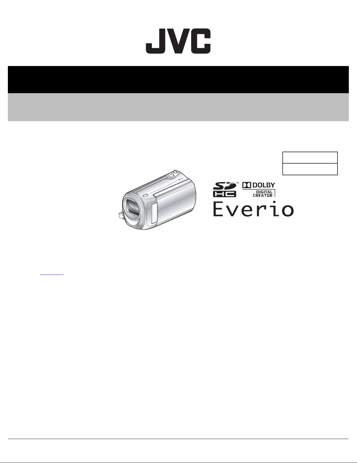
CAMCORDER
YF335<Rev.001>20102SERVICE MANUALEVERIO-S
GZ-MS110BEK, GZ-MS110BEU
SERIES
C0S3
GZ-MS110BEKM, GZ-MS110BEUM [C0S300]
COPYRIGHT © 2010 Victor Company of Japan, Limited
Lead free solder used in the board (material : Sn-Ag-Cu, melting point : 219 Centigrade)
This service manual (No.YF335<Rev.001>) describes only the items which differ from those of already issued service manual
(No.YF334
For details other than those described in this manual, please refer to the service manuals which were already issued.
<Rev.001>)
TABLE OF CONTENTS
1 PRECAUTIONS . . . . . . . . . . . . . . . . . . . . . . . . . . . . . . . . . . . . . . . . . . . . . . . . . . . . . . . . . . . . . . . . . . . . . . . 1-3
2 SPECIFIC SERVICE INSTRUCTIONS . . . . . . . . . . . . . . . . . . . . . . . . . . . . . . . . . . . . . . . . . . . . . . . . . . . . . . 1-5
3 DISASSEMBLY . . . . . . . . . . . . . . . . . . . . . . . . . . . . . . . . . . . . . . . . . . . . . . . . . . . . . . . . . . . . . . . . . . . . . . 1-16
4 ADJUSTMENT . . . . . . . . . . . . . . . . . . . . . . . . . . . . . . . . . . . . . . . . . . . . . . . . . . . . . . . . . . . . . . . . . . . . . . . 1-28
5 TROUBLE SHOOTING. . . . . . . . . . . . . . . . . . . . . . . . . . . . . . . . . . . . . . . . . . . . . . . . . . . . . . . . . . . . . . . . . 1-32
COPYRIGHT © 2010 Victor Company of Japan, Limited
No.YF335<Rev.001>
2010/2
Page 2
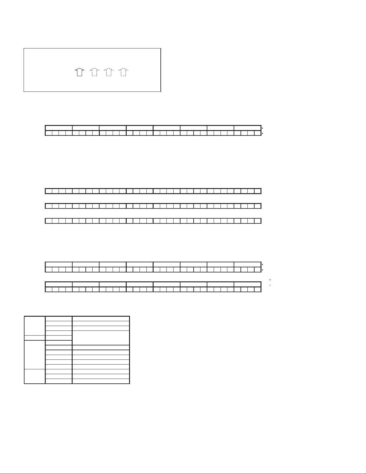
SPECIFICATION
Camera Power supply Using AC adapter: DC 5.2 V, Using battery pack: DC 3.6 V
Power consumption 1.5 W (when LCD backlight is set to “STANDARD”)
Dimensions (mm) 52 × 62 × 110 (W × H × D:excluding grip belt)
Mass Approx. 195 g (camera only), Approx. 220 g (including supplied battery pack)
Operating environment Allowable operating temperature:0°C to 40°C
Allowable storage temperature:-20°C to 50°C
Allowable operating humidity:35% to 80%
Image pickup device 1/6" 800,000 pixels
Recording area (Video) 410,000 pixels (optical zoom),
410,000 pixels to 550,000 pixels (dynamic zoom)
Lens F 1.8 to F 4.3, f = 2.2 mm to 85.8 mm
(35 mm conversion: 41.5 mm to 1619 mm)
Zoom (Video) Optical zoom: Up to 39×
Dynamic zoom: Up to 45×
Digital zoom: Up to 800×
Video recording format SD-VIDEO standard, Video: MPEG-2, Audio: Dolby Digital (2 ch)
Recording media Requires (×1) SDHC card ,sold separately
AC Adapter
(AP-V30M)*
*When using the AC adapter overseas, please prepare a commercially available converter plug for the country or region of visit.
• The specifications and appearance of this product are subject to changes for further improvement without prior notice.
Power supply AC 110 V to 240, 50 Hz/60 Hz
Output DC 5.2 V, 1.8 A
Allowable operating temperature 0°C to 40°C (10°C to 35°C during charging)
Dimensions (mm) 50 × 29 × 100 (W × H × D: excluding cord and AC plug)
Mass Approx. 112 g
1-2 (No.YF335<Rev.001>)
Page 3
SECTION 1
r
PRECAUTIONS
1.1 SAFETY PRECAUTIONS
Prior to shipment from the factory, JVC products are strictly
inspected to conform with the recognized product safety and
electrical codes of the countries in which they are to be
sold.However,in order to maintain such compliance, it is equally
important to implement the following precautions when a set is
being serviced.
1.1.1 Precautions during Servicing
(1) Locations requiring special caution are denoted by labels
and inscriptions on the cabinet, chassis and certain parts of
the product.When performing service, be sure to read and
comply with these and other cautionary notices appearing
in the operation and service manuals.
(2) Parts identified by the symbol and shaded ( ) parts
are critical for safety.
Replace only with specified part numbers.
NOTE :
Parts in this category also include those specified to
comply with X-ray emission standards for products
using cathode ray tubes and those specified for
compliance with various regulations regarding
spurious radiation emission.
(3) Fuse replacement caution notice.
Caution for continued protection against fire hazard.
Replace only with same type and rated fuse(s) as
specified.
(4) Use specified internal wiring. Note especially:
• Wires covered with PVC tubing
• Double insulated wires
• High voltage leads
(5) Use specified insulating materials for hazardous live parts.
Note especially:
• Insulation Tape
• PVC tubing
•Spacers
• Insulation sheets for transistors
• Barrier
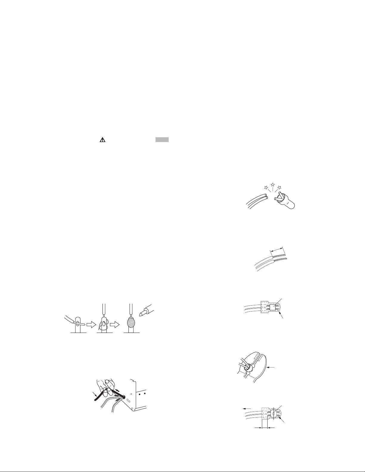
(6) When replacing AC primary side components (transformers,
power cords, noise blocking capacitors, etc.) wrap ends of
wires securely about the terminals before soldering.
emission. Consequently, when servicing these products,
replace the cathode ray tubes and other parts with only the
specified parts. Under no circumstances attempt to modify
these circuits.Unauthorized modification can increase the
high voltage value and cause X-ray emission from the
cathode ray tube.
(12) Crimp type wire connectorIn such cases as when replacing
the power transformer in sets where the connections
between the power cord and power trans former primary
lead wires are performed using crimp type connectors, if
replacing the connectors is unavoidable, in order to prevent
safety hazards, perform carefully and precisely according
to the following steps.
• Connector part number :E03830-001
• Required tool : Connector crimping tool of the proper
type which will not damage insulated parts.
• Replacement procedure
a) Remove the old connector by cutting the wires at a
point close to the connector.Important : Do not
reuse a connector (discard it).
cut close to connector
Fig.1-1-3
b) Strip about 15 mm of the insulation from the ends
of the wires. If the wires are stranded, twist the
strands to avoid frayed conductors.
15 mm
Fig.1-1-4
c) Align the lengths of the wires to be connected.
Insert the wires fully into the connector.
Metal sleeve
Fig.1-1-1
(7) Observe that wires do not contact heat producing parts
(heatsinks, oxide metal film resistors, fusible resistors, etc.)
(8) Check that replaced wires do not contact sharp edged or
pointed parts.
(9) When a power cord has been replaced, check that 10-15
kg of force in any direction will not loosen it.
Power cord
Fig.1-1-2
(10) Also check areas surrounding repaired locations.
(11) Products using cathode ray tubes (CRTs)In regard to such
products, the cathode ray tubes themselves, the high
voltage circuits, and related circuits are specified for
compliance with recognized codes pertaining to X-ray
Connector
Fig.1-1-5
d) As shown in Fig.1-1-6, use the crimping tool to crimp
the metal sleeve at the center position. Be sure to
crimp fully to the complete closure of the tool.
1.2
5
2.0
5.5
Crimping tool
Fig.1-1-6
e) Check the four points noted in Fig.1-1-7.
Not easily pulled free
Wire insulation recessed
more than 4 mm
Crimped at approx. cente
of metal sleeve
Conductors extended
Fig.1-1-7
(No.YF335<Rev.001>)1-3
Page 4
1.1.2 Safety Check after Servicing
Examine the area surrounding the repaired location for damage
or deterioration. Observe that screws, parts and wires have been
returned to original positions, Afterwards, perform the following
tests and confirm the specified values in order to verify
compliance with safety standards.
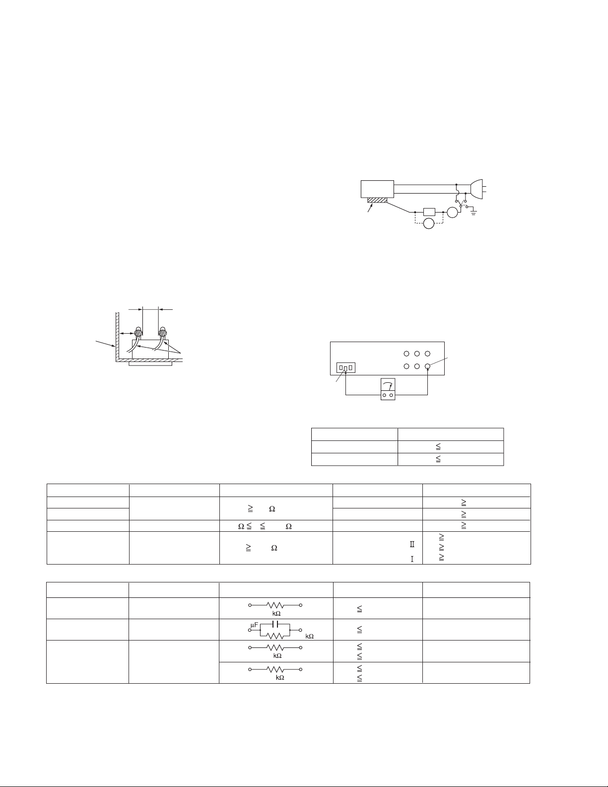
(1) Insulation resistance test
Confirm the specified insulation resistance or greater
between power cord plug prongs and externally exposed
parts of the set (RF terminals, antenna terminals, video and
audio input and output terminals, microphone jacks,
earphone jacks, etc.).See table 1 below.
(2) Dielectric strength test
Confirm specified dielectric strength or greater between
power cord plug prongs and exposed accessible parts of
the set (RF terminals, antenna terminals, video and audio
input and output terminals, microphone jacks, earphone
jacks, etc.). See Fig.1-1-11 below.
(3) Clearance distance
When replacing primary circuit components, confirm
specified clearance distance (d), (d') between soldered
terminals, and between terminals and surrounding metallic
parts. See Fig.1-1-11 below.
d
Chassis
d'
Power cord
primary wire
Fig.1-1-8
(4) Leakage current test
Confirm specified or lower leakage current between earth
ground/power cord plug prongs and externally exposed
accessible parts (RF terminals, antenna terminals, video
and audio input and output terminals, microphone jacks,
earphone jacks, etc.).
Measuring Method : (Power ON)Insert load Z between
earth ground/power cord plug prongs and externally
exposed accessible parts. Use an AC voltmeter to
measure across both terminals of load Z. See Fig.1-1-9
and following Fig.1-1-12.
ab
Externally
exposed
accessible part
Z
V
c
A
Fig.1-1-9
(5) Grounding (Class 1 model only)
Confirm specified or lower grounding impedance between
earth pin in AC inlet and externally exposed accessible
parts (Video in, Video out, Audio in, Audio out or Fixing
screw etc.).Measuring Method:
Connect milli ohm meter between earth pin in AC inlet and
exposed accessible parts. See Fig.1-1-10 and grounding
specifications.
AC inlet
Earth pin
Exposed accessible part
MIlli ohm meter
Grounding Specifications
Region
USA & Canada
Europe & Australia
Grounding Impedance (Z
Z 0.1 ohm
Z 0.5 ohm
)
Fig.1-1-10
AC Line Voltage
100 V
100 to 240 V
110 to 130 V
110 to 130 V
200 to 240 V
Region
Japan
USA & Canada
Europe & Australia
Insulation Resistance (R
R 1 M /500 V DC
1 M R 12 M /500 V DC
R 10 M /500 V DC
)
Dielectric Strength
AC 1 kV 1 minute
AC 1.5 kV 1 minute
AC 1 kV 1 minute
AC 3 kV 1 minute
AC 1.5 kV 1 minute
(
Class
(
Class
Clearance Distance (d), (d'
d, d' 3 mm
d, d' 4 mm
d, d' 3.2 mm
d 4 m m
)
d' 8 m m (Power cord
d' 6 m m (Primary wire
)
Fig.1-1-11
AC Line Voltage
100 V
110 to 130 V
110 to 130 V
220 to 240 V
Region
Japan
USA & Canada
Europe & Australia
Load Z
1
0.15
1.5
2
50
Leakage Current (i)
i 1 mA rms
i 0.5 mA rms
i 0.7 mA peak
i 2 mA dc
i 0.7 mA peak
i 2 mA dc
a, b, c
Exposed accessible parts
Exposed accessible parts
Antenna earth terminals
Other terminals
Fig.1-1-12
NOTE :
These tables are unofficial and for reference only. Be sure to confirm the precise values for your particular country and locality.
)
)
)
1-4 (No.YF335<Rev.001>)
Page 5
SECTION 2
SPECIFIC SERVICE INSTRUCTIONS
2.1 DIFFERENCE LIST The following table indicate main different points between models GZ-MS110BUS, GZ-MS110BEK and GZ-MS110BEU.
MODEL GZ-MS110BUS GZ-MS110BEK GZ-MS110BEU
SIGNAL FORMAT NTSC PAL PAL
USB TERMINAL IN/OUT OUT ONLY OUT ONLY
AC ADAPTER AP-V30U AP-V30M AP-V30E
AC CORD NO YES(BS) NO
BATTERY BN-VG107US BN-VG107EU BN-VG107EU
2.2 CHECKING THE CPU VERSION
To check the CPU version of the model, display the firmware update screen.
Note) Before checking the version, connect both a fully
charged battery and a DC cord to the model.
Procedure
(1) Open the MONITOR ASSY to turn ON the power.
(2) Press the [MENU] button to display the menu screen, se-
lect BASIC SETTINGS > with the SELECT lever, and then
press the [OK] button. Next, select UPDATE with the SELECT lever, and press the [OK] button.
(3) On the monitor screen, CURRENT VERSION: *.** is dis-
played.
(4) After checking the display, press the [MENU] button to exit
from the menu screen.
<Checking screen>
LCD MONITOR
CURRENT VERSION : 1.01
START UPDATE?
Fig.2-1-1
(No.YF335<Rev.001>)1-5
Page 6
2.3 FIRMWARE UPDATE
Connecting Everio to a PC via USB cable enables firmware update.
Connect a battery, capable of operating for 30 minutes or longer, and an AC adapter to Everio for update.
* The following procedure shows the monitor displays of the firmware update from ver. 0.82 to ver. 1.55.
* Use Windows XP or Windows Vista.
1.Preparation
(1)Preparation
Download the firmware update application software from JS-NET.
(2)Connection
Connect a battery that is capable of operating for 30 minutes or longer and an AC adapter to Everio.
* To ensure secure power supply during the update, update is disabled if either of them is not available.
2.Firmware transfer
(1) Select "UPDATE" in the main menu of Everio.
MENU > BASIC SETTINGS > UPDATE
Fig.2-2-1
(2)When the displayed current version is an old one, select "YES", and then press (OK).
Fig.2-2-2
(3)Follow the directions on the monitor to connect Everio to the PC via USB cable.
1-6 (No.YF335<Rev.001>)
Fig.2-2-3
Page 7
(4)Double click the downloaded file to execute it. (The following shows the screen display of the PC.)
Execute the file
㬍
㬍
Click "YES"
㬍
㬍
㬍
Click "OK" to finesh the file.
Fig.2-2-4
(No.YF335<Rev.001>)1-7
Page 8
3.Execute update
(1)Disconnect the USB cable, and remove Everio from the PC.
* In about 30 seconds after the removal, the update start screen appears.
(2)When the displayed current version is an old one, select "YES", and then press (OK).
Fig.2-2-5
(3)When the displayed current version is an old one, select "YES", and then press (OK).
* It takes about 4 minutes and 30 seconds to complete the update.
Fig.2-2-6
(4)Select "OK", and then re-start Everio.
Fig.2-2-7
(5)After the re-start, check that the current firmware is updated in UPDATE.
MENU > BASIC SETTINGS > UPDATE
When the updated firmware version is confirmed, select "NO", and then press (OK).
The firmware update is completed.
1-8 (No.YF335<Rev.001>)
Fig.2-2-8
Page 9
2.4 EMERGENCY DISPLAY FUNCTION
This model has a function to save emergency information in a flash ROM (IC3003).
To obtain the emergency information, read the data using terminal software.
There are types of terminal software including Windows HyperTerminal and freeware Tera Term.
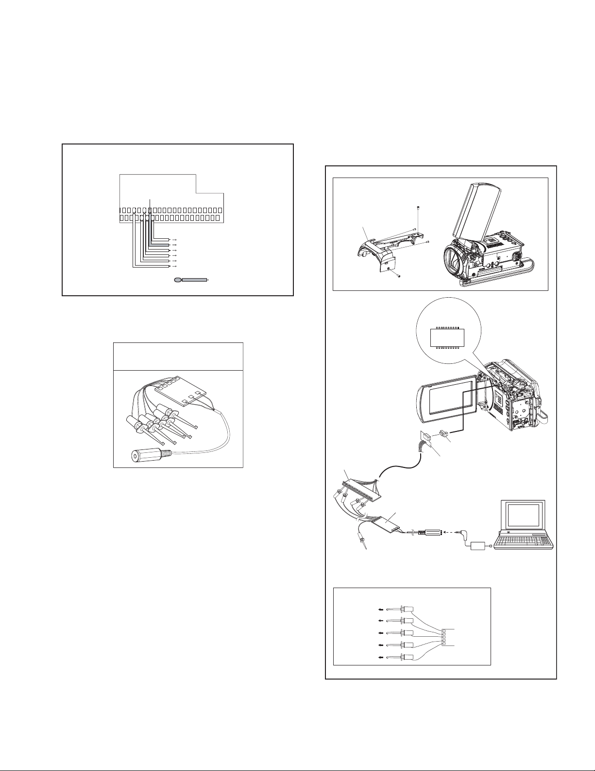
2.4.1 Jig connector cable
Connect the model to the serial port of the PC using the jig connector cable and the serial update jig (or communication cable).
Note) As the jig connector cable (Part No.: YTU93106B) is not extended, adding a wire is required.
How to work on the jig connector cable (YTU93106B)
Connection procedure
·Remove the 4 screws (1-4), and then remove the COV-
<Soldered side>
ER(HIN) ASSY.
11
12 RKPNOT USE
11 RKPUA_TXD0
10 RKPGND
9 RKPGND
8 RKPNOT USE
5 RKPNOT USE
Additional wire
Serial Update Jig
To be used to connect the PC cable and the Jig connector cable for firmware repair and various analyses.
Serial Update Jig
YTU93113A
COVER(HIN) ASSY
JIG CONNECTOR CABLE
(YTU93106B)
1
3
4
2
JIG CONNECTOR
(MAIN CN110)
10
20
JIG CONNECTOR
1
11
CONVERSION CONNECTOR
(YTU94145K-20)
SERIAI UPDATE JIG
(YTU93113A)
NC
(NOT USED)
JIG CONNECTOR
TO AL_2.83V
TO UA_RXD0
TO UA_TXD0
NC(NOT USED)
TO GND
WHITE
YELLOW
BLACK
BLUE
RED
RS232C
COM PORT
PC CABLE
SERIAI UPDATE JIG
(No.YF335<Rev.001>)1-9
TERMINAL
SOFTWARE
PC
Page 10
Jig connector diagrams Conversion Connector
JIG CONNECTOR CABLE (YTU93106B)
JIG CONN. BOARD
MAIN CN110
DSP_RTCK
DSP_TMS
DSP_RST
XDSPTRST
REG_2.83V
OCD_SDA
SYS_RSTL
GND
DSP_TDI
GND
UA_RXD0
UA_TXD0
DSP_TCK
OCD_SCL
IF_RX
IF_TX
AL_2.83V
IRU
KENTO
DSP_TDO
ADDITIONAL WIRE
10
9
8
7
6
5
4
3
2
1
20
19
18
17
16
15
14
13
12
11
11. UA_TXD0
(PIN NO.)
30
29
28
27
26
25
24
23
22
21
20
19
18
17
16
15
14
13
12
11
10
9
8
7
6
5
4
3
2
1
-
AL_2.83V
-
-
UA_RXD0
-
-
-
-
NC
NC
NC
NC
NC
-
-
-
-
UA_TXD0
GND
GND
-
-
NC
NC
NC
NC
NC
KENTO*
AL_2.83V
IF_RX*
DSP_TCK*
UA_RXD0
DSP_TDI*
SYS_RSTL*
REG_2.83V*
DSP_RST*
DSP_RTCK*
NC
NC
NC
NC
NC
*NC
30
29
28
27
26
25
24
23
22
21
20
19
18
17
16
11
12
13
14
15
16
17
18
19
20
10
DSP_TDO*
1
2
3
4
5
6
7
8
9
15
IRU*
14
IF_TX*
13
OCD_SCL*
12
UA_TXD0
11
GND
10
GND
9
OCD_SDA*
8
XDSPTRST
7
DSP_TMS*
6
NC
5
NC
4
NC
3
NC
2
NC
1
*
1-10 (No.YF335<Rev.001>)
Page 11
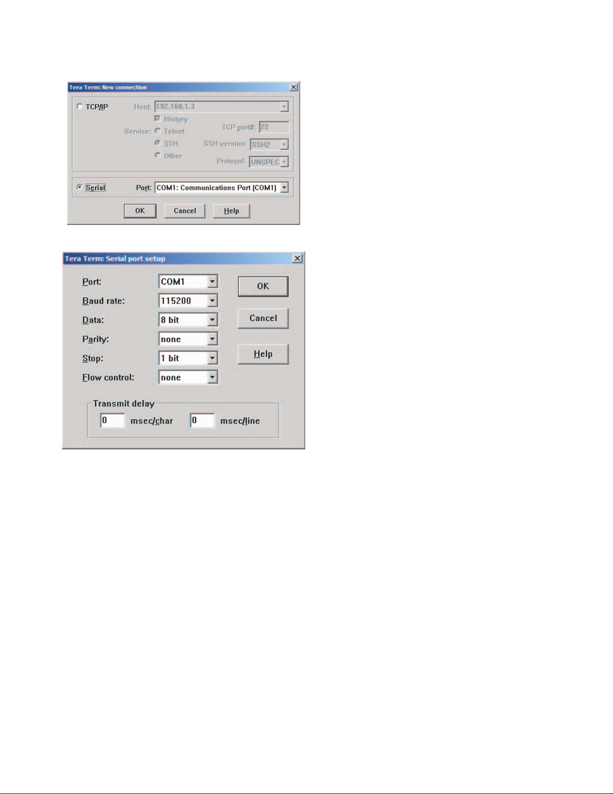
2.4.2 Starting the terminal software
Before starting the terminal software, install the terminal software.
(1) Start Tera Term, select "Serial", and then click "OK".
(2) Select Setup > Serial port. Set each item, and then click "OK".
* Maximizing terminal window size enables better viewing of
output data.
(No.YF335<Rev.001>)1-11
Page 12

2.4.3 Obtaining the emergency information
(1) Turning on the power of the model starts data reading, and the data is displayed in the terminal window. Wait until the data read-
ing finishes.
(2) When the data reading finishes, press Enter. "DBG>" is displayed in the window.
(3) Input the terminal command, and then press Enter.
* Terminal command
DBG>meid 81
The emergency information is displayed in the terminal window.
Note) There are three types of emergency information. (emgergency1/emgergency2/emgergency3)
< Display window >
Note) When emergency information is saved, [data*] is displayed in eight-digit alphanumeric characters.
These 8-digit characters are 4-bit hexadecimal numbers comprising 32-bit data.
As an exception, some product names in emergency2 are indicated using ASCII code.
There are up to four types of data: [data0]/[data1]/[data2]/[data3], and displayed number of data varies depending on the type of
emergency.
[emgergency1] displays [data0] only, and [data1]-[data3] are reserved (not used).
[emgergency2] displays [data0]-[data3].
[emgergency3] displays [data0] and [data2]. [data2] and [data3] are reserved (not used).
Refer to emergency information for data reading.
Display example 1: No Emergency Information
DBG>meid 81
0 emgergency1 data saved
0 emgergency2 data saved
0 emgergency3 data saved
Display example 2: Single Emergency Information for each item
DBG>meid 81
1 emgergency1 data saved
2009/12/11 05:16 ********
1 emgergency2 data saved
2009/01/06 16:02 ******** ******** ******** ********
1 emgergency3 data saved
2009/01/13 14:26 ******** ********
Display example 3: Multiple Emergency Information
DBG>meid 81
2 emgergency1 data saved
2009/12/11 05:16 ********
2009/12/12 06:20 ********
8 emgergency2 data saved
2009/01/06 16:02 ******** ******** ******** ********
2009/01/06 16:05 ******** ******** ******** ********
2009/01/06 17:37 ******** ******** ******** ********
2009/01/06 17:38 ******** ******** ******** ********
2009/01/13 14:02 ******** ******** ******** ********
2009/01/13 14:22 ******** ******** ******** ********
2009/01/13 14:24 ******** ******** ******** ********
2009/01/13 14:26 ******** ******** ******** ********
2 emgergency3 data saved
2009/01/13 14:26 ******** ********
2009/01/15 17:26 ******** ********
1-12 (No.YF335<Rev.001>)
Page 13
2.4.4 Obtaining and reading data written in flash ROM
zemergency1
Note) emergency1 can save up to 32 pieces of data.
When the data exceeds 32 pieces, the data will be erased from the oldest one.
1 emgergency1 data saved
2009/12/11 05:16 90000000
ޓdata[0] data[1]ޓޓdata[2]ޓdata[3]
[data0] bit31-bit28
Example: When [data0] is 9*******
[9] in 9******* is <1001> in binary number.
data[0]
data[0]
bitψ
9*******
1010
31 30 28 27 0
The allocation table below shows the drop detection setting is ON and the drop distance is 21-40 cm.
data[0]
bit31 Drop detection setting
bit28-bit30 Drop distance
Unit:cm
bit0-bit27 Reserved
0: OFF / 1: ON (Indicates the status set on the menu setting screen on the main unit)
0: Drop distance 0-20 / 1: Drop distance 21-40 / 2: Drop distance 41-60 /
3: Drop distance 61-80 / 4: Drop distance 81-100 / 5: Drop distance 101 or more
Reserved/Not used
data[1] Reserved/Not used
data[2] Reserved/Not used
data[3] Reserved/Not used
Hexadecimal number
Binary number
(No.YF335<Rev.001>)1-13
Page 14
zemergency2
Note) Combined with emergency3, emergency2 can save up to 32 pieces of data.
When the data exceeds 32 pieces, the data will be erased from the oldest one.
1 emgergency2 data saved
2009/01/06 16:02 ******** ******** ******** ********
data[1] data[2] data[3]data[0]
[data0] bit31-bit24
Example: When [data0] is 02******
[02] in 02****** is <00000010> in binary number.
data[0]
data[0]
bitψ
The allocation table below shows the media type is NAND.
[data0] bit15-[data2] bit16
[data0] bit15-bit8 save the media manufacturer ID.
[data0] bit15-[data2] bit24 save the media product name in 6-byte ASCII code.
The display varies depending on the manufacturer. Details have not been confirmed.
[data2] bit23-bit16 save the media revision number. The display varies depending on the manufacturer. Details have not been confirmed.
data[0]
bitψ
data[1]
bitψ
data[2]
bitψ
[data2] bit15-[data3] bit8
Example: [data2] is ****09C2, and [data3] is 002004**
[09C2] in ****09C2 is <0000100111000010> in binary number. [002004] in 002004** is <000000000010000000000100> in binary number.
data[2]
data[2]
bitψ
data[3]
data[3]
bitψ
The allocation table below shows the media production date (year/month) is December, 2009; the SD card is inserted in slot A; and the card capacity unit is GB.
The SD card capacity is 32 GB in speed class 4.
data[0]
data[1]
data[2]
data[3]
0
0
0 0 0 0 10 0
31 24 23 16 15 8 7 0
Various displays exist and the display varies depending on the manufacturer. Details have not been confirmed.
31 16 15 8 7 0
31 0
31
****
31
002004
31 16 15 8 7 0
bit24-bit31 Media type
bit16-bit23 Reserved
bit8-bit15
bit0-bit7
bit24-bit31
bit16-bit23
bit4-bit15 Production date (year/month)
bit3
bit2-bit1 Card capacity unit
bit0
bit16-bit31 Card capacity
bit8-bit15 Speed class
bit0-bit7 Reserved
2***
24 23
24 23
0 100000000000000 00001000
Manufacturer ID
Product namebit0-bit31
Product revision number
SD card slot
Reserved
16 15
0 0010001
16 15
0
0: HDD / 1: SDCard / 2: NAND
Reserved/Not used
The upper 8 bits indicate the bottom 2 digits of the year (western calendar). The lower 4 bits indicate the month.
0: A / 1: B (Card slot position)
0: MB / 1: GB / 2: TB
Reserved/Not used
0-1023
Reserved/Not used
***
09C
1000011
31024
**
0
2
0
Hexadecimal number
Binary number
Hexadecimal number
Binary number
Hexadecimal number
Binary number
1-14 (No.YF335<Rev.001>)
Page 15
zemergency3
Note) Combined with emergency2, emergency3 can save up to 32 pieces of data.
When the data exceeds 32 pieces, the data will be erased from the oldest one.
data[0]
bitψ
31 28 27 25 24 23 12 11 0
SDVideo
[data0]
bit28-bit31
bit25-bit27
bit24
bit12-bit23
bit0-bit11
Error type 0: HDD error / 1: Unsupported file / 3: Failed playback file / 4: Unknown error
Media type 0: HDD or NAND / 1: SD card
SDVideo / User MPEG 0: SD Video / 1: User MPEG
Folder number 1-0xFFF
File number 1-0xFFF
User MPEG
Note) User MPEG is the data handled as another file due to no management file.
[data0]
bit28-bit31
bit25-bit27
bit24
bit0-bit23
Error type 0: HDD error / 1: Unsupported file / 3: Failed playback file / 4: Unknown error
Media type 0: HDD or NAND / 1: SD card
SDVideo / User MPEG 0: SD Video / 1: User MPEG
File number 1-9999
data[1]
bitψ
31 0
bit0-bit31 Indicates GOP on the error point only with SDVideo with undefined user MPEG value.
data[2] Reserved
data[3] Reserved
(No.YF335<Rev.001>)1-15
Page 16
SECTION 3
DISASSEMBLY
3.1 BEFORE ASSEMBLY AND DISASSEMBLY
3.1.1 Precautions
• Be sure to disconnect the power supply unit prior to mounting
and soldering of parts.
• Prior to removing a component part that needs to disconnect
its connector(s) and its screw(s), first disconnect the wire(s)
from the connector(s), and then remove the screw(s).
• When connecting/disconnecting wires, pay enough attention
not to damage the connectors.
• When inserting the flat wire to the connector, pay attention to
the direction of the flat wire.
• Be careful in removing the parts to which some spacer or
shield is attached for reinforcement or insulation.
• When replacing chip parts (especially IC parts), first remove
the solder completely to prevent peeling of the pattern.
• Tighten screws properly during the procedures. Unless
otherwise specified, tighten screws at a torque of 0.088N
·cm). However, as this is a required value at the time of
(0.9kgf
production, use the value as a measuring stick when
proceeding repair services. (See "SERVICE NOTE" as for
tightening torque.)
3.1.2 Destination of connectors
Two kinds of double-arrows in connection tables respectively
show kinds of connector/wires.
: Wire: Flat wire : Board to board (B-B)
: The connector of the side to remove
CONN. No. PIN No.CONNECTOR
CN2a
CN2b
MAIN CN101
MAIN CN103
MONI BW CN761
MINI BW CN762
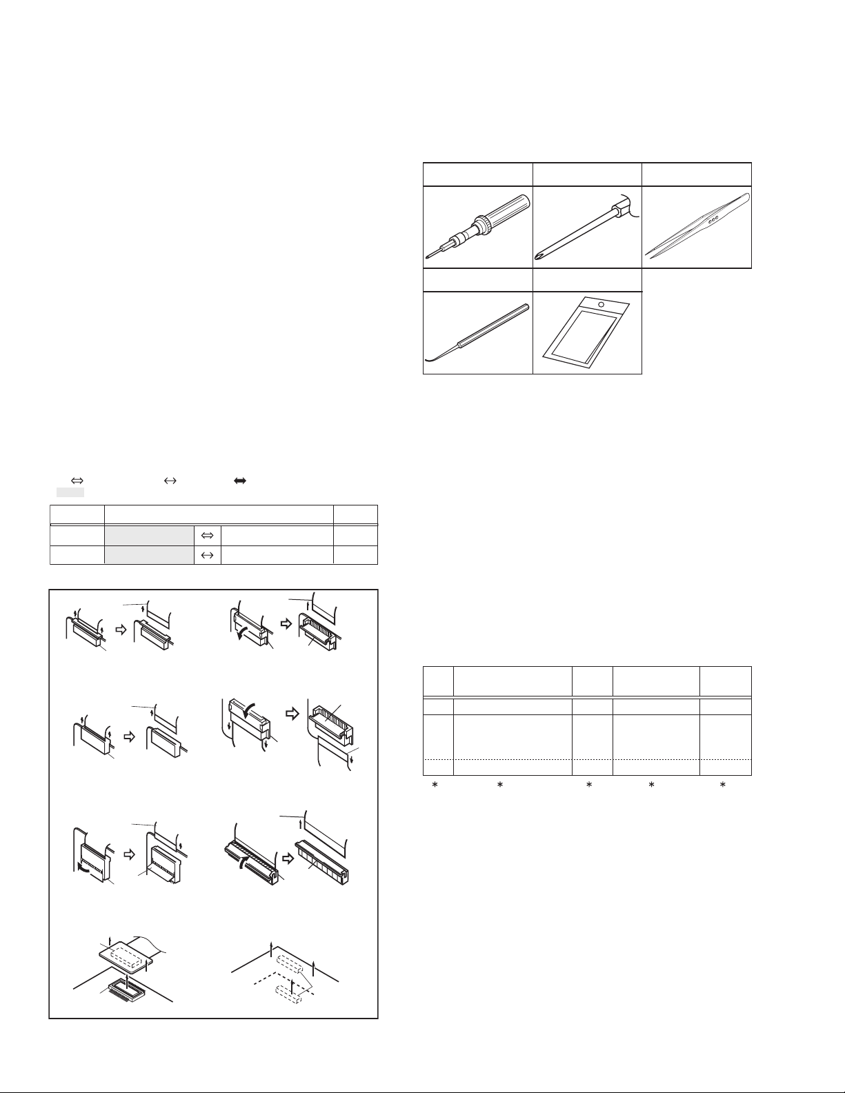
3.1.3 Disconnection of connectors (Wires)
Wire
· Pull both ends of the connector in the arrow
direction, remove the lock and disconnect the flat
wire.
· Pull the both ends of the board in the direction
of the arrow, and remove the B-B Connector.
· Extend the locks in the direction of the arrow for
unlocking and then pull out the wire. After
removing the wire, immediately restore the locks
to their original positions because the locks are
apt to come off the connector.
B-B Connector
B-B Connector
· Pull the both ends of the board in the direction of the arrow, and remove the B-B Connector.
FPC Connector
Wire
FPC Connector
Wire
Lock
FPC Connector
· Extend the locks in the direction of the arrow for
unlocking and then pull out the wire. After
removing the wire, immediately restore the locks
to their original positions because the locks are
apt to come off the connector.
· Extend the locks in the direction of the arrow for
unlocking and then pull out the wire. After
removing the wire, immediately restore the locks
to their original positions because the locks are
apt to come off the connector.
· Extend the locks in the direction of the arrow for
unlocking and then pull out the wire. After
removing the wire, immediately restore the locks
to their original positions because the locks are
apt to come off the connector.
Wire
FPC Connector
FPC
Connector
Wire
FPC Connector
Lock
Lock
Lock
B-B Connector
Fig.3-1-1
·m
40
10
Lock
Wire
3.1.4 Tools required for disassembly and assembly
Torque driver
YTU94088
Chip IC replacement jig
PTS40844-2
Bit
YTU94088-003
Cleaning cloth
KSMM-01
Tweezers
P-895
Fig.3-1-2
• Torque driver
Be sure to use to fastening the mechanism and exterior parts
because those parts must strictly be controlled for tightening
torque.
• Bit
This bit is slightly longer than those set in conventional torque
drivers.
• Tweezers
To be used for removing and installing parts and wires.
• Chip IC replacement jig
To be used for replacement of IC.
• Cleaning cloth
Recommended cleaning cloth to wipe down the video heads,
mechanism (tape transport system), optical lens surface.
3.2 ASSEMBLY AND DISASSEMBLY OF MAIN PARTS
3.2.1 Assembly and disassembly
When reassembling, perform the step(s) in reverse order.
STEP
No.
[1]
[2]
PART
TOP COVER ASSY
UPPER ASSY
(Inc. VF ASSY,
SPEAKER/MONITOR)
[8]
E.VF UNIT(B/W)
(∗1) Order of steps in Procedure
When reassembling, preform the step(s) in the reverseorder.
These numbers are also used as the identification (location)
No. of parts Figures.
(∗2) Part to be removed or installed.
(∗3) Fig. No. showing Procedure or Part Location.
(∗4) Identification of part to be removed, unhooked, unlocked,
released, unplugged, unclamped or unsoldered.
S = Screw L = Lock, Release, Hook
SD = Solder CN = Connector
[Example]
• 4 (S1a) = Remove 4 S1a screws.
• 3 (L1a) = Disengage 3 L1a hooks.
• 2 (SD1a) = Unsolder 2 SD1a points.
• CN1a = Remove a CN1a connector.
(∗5) Adjustment information for installation.
Fig.
No.
4(S1a), 3(L1a),CN1a
C1
(S2a),2(S2b),3(S2c)
C2-1
2(SD1a),
L2,CN2a,b
2(S8),L8,CN8a
C2-2
POINT
( 4) ( 5)( 2) ( 3)( 1)
NOTE
-
-
NOTE 8
1-16 (No.YF335<Rev.001>)
Page 17

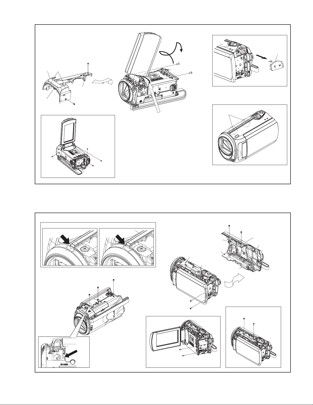
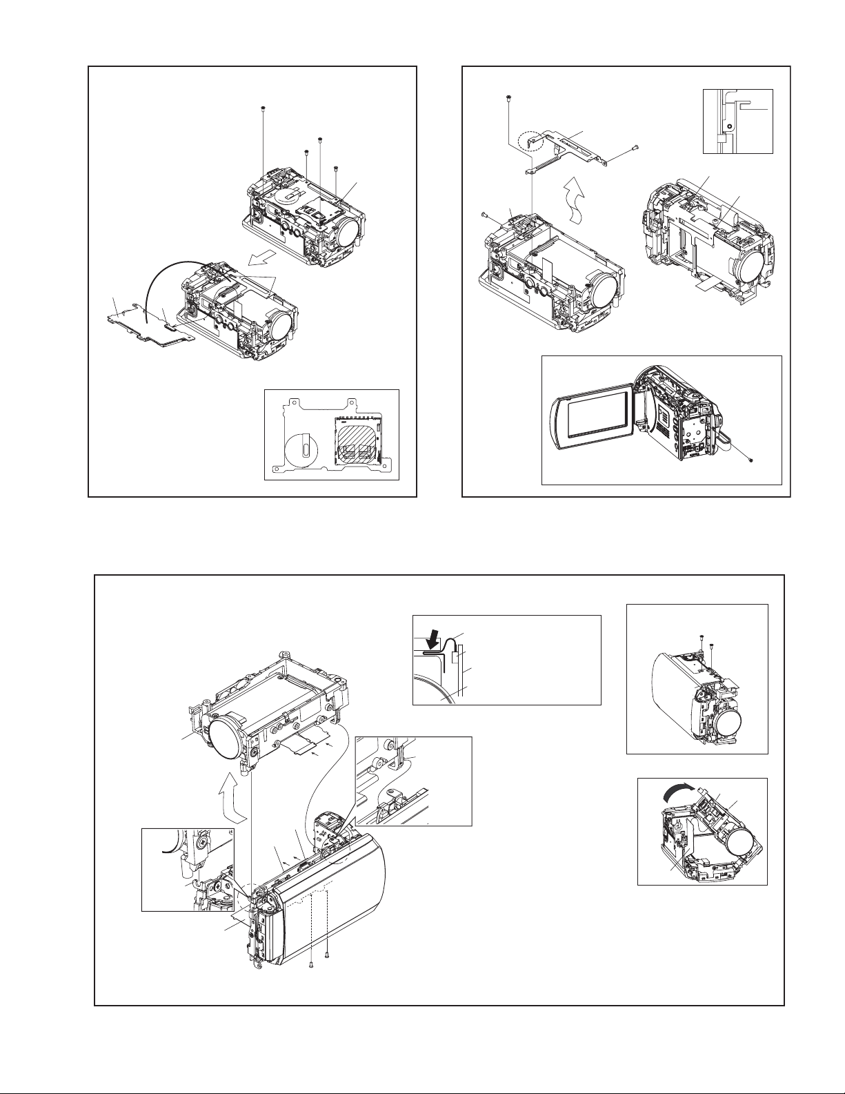
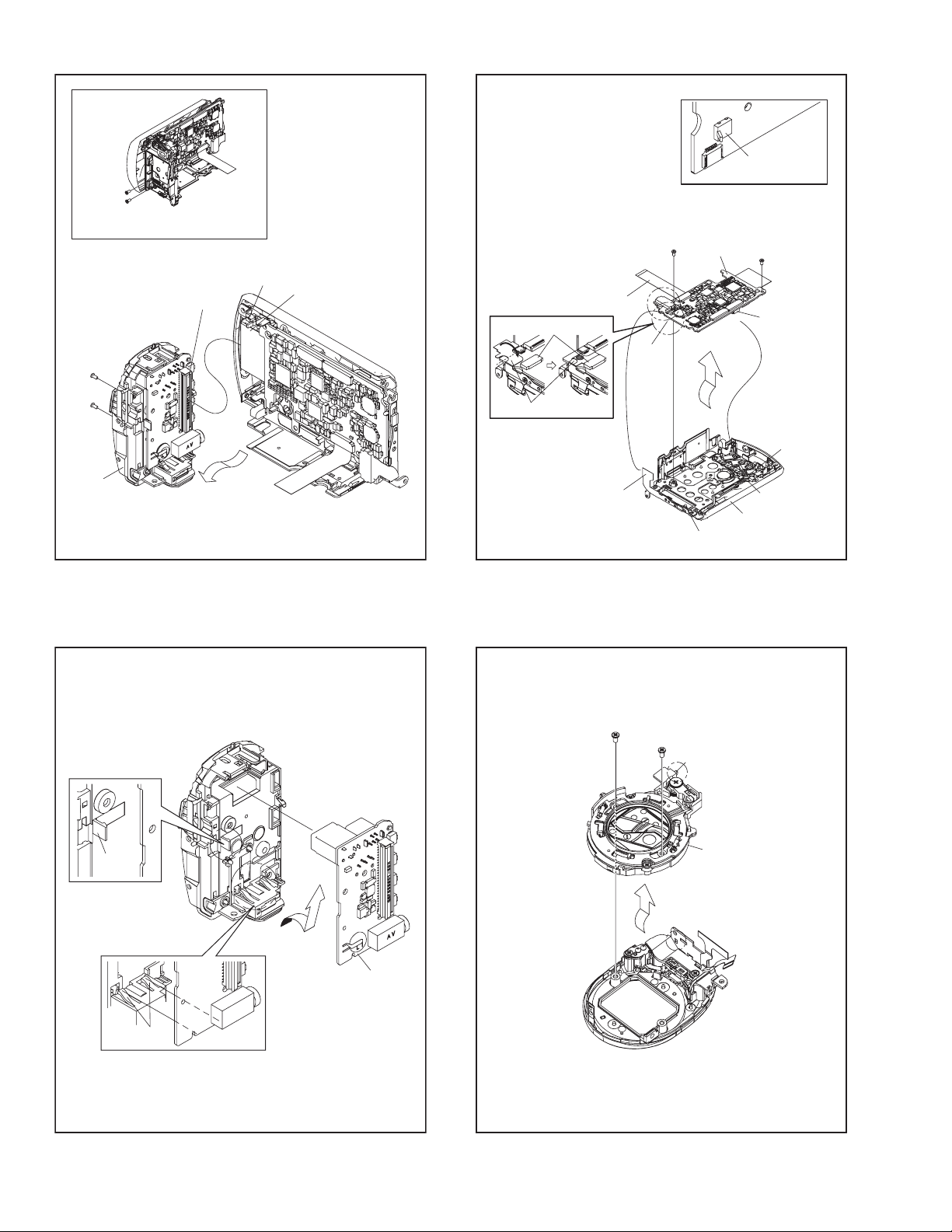
3.2.2 Assembly/Dissambly of cabinet parts and electrical parts
z Disassembly procedure
STEP
PART NAME
No.
[1]
COVER(HIN) ASSY
[2]
LOWER CASE ASSY(S3)
[3]
HOLDER(IND) ASSY
[4]
OPE UNIT
FRONT ASSY
[5]
(Incl. MIC & SHUTTER ASSY)
[6]
SD BOARD ASSY
[7]
SHIELD
OP BLOCK ASSY
[8]
(Incl. CCD BOARD ASSY & HOLDER)
[9]
REAR ASSY
[10]
REAR BOARD ASSY
[11]
MAIN BOARD ASSY
[12]
SHUTTER ASSY
[13]
PLATE(MIC) SD
[14]
MICROPHONE UNIT
[15]
OP BLOCK ASSY
[16]
CCD BOARD ASSY
[17]
MONITOR ASSY
[18]
SPEAKER
Fig.
No.
3-2-1
3-2-2
3-2-3
3-2-4
3-2-5
3-2-6
3-2-7
3-2-8
3-2-9
3-2-10
3-2-11
3-2-12
3-2-13
3-2-14
3-2-15
3-2-16
3-2-17
3-2-18
POINT NOTE
4(S1),L1a,b,c,2(L1d),L1e,f
7(S2),L2a,b,c,d,e,f
S3
CN4,S4,2(L4a),L4b,c,d
CN5,2(S5a),S5b,L5a,b
2(S6a),2(S6b),2(L6),CN6
3(S7),L7a,b,c
2(S8),L8a,b,c,CN8a,b
S9a,b,L9,CN9
L10a,2(L10b)
CN11a,2(S11),L11a,b,CN11b
2(S12),L12
S13,L13a,b
-
3(S15),HOLDER(OPSD) ASSY
2(S16),2(L16),CCD BASE ASSY,
SHEET,OP LPF
S17a,2(L17a),2(S17b),L17b,
2(L17c),UPPER CASE ASSY(SD)
L18a,S18,L18b,BKT(SPK),
2(L18c)
NOTE1a,b,c
NOTE2a,b
-
NOTE4
NOTE5a,b,c
NOTE6
NOTE7a,b
NOTE8a,b,c
-
-
NOTE11a,b,c
NOTE12
NOTE16a,b,c
NOTE17a,b,c
NOTE18a,b,c,d
-
-
-
NOTE1a:
Although the JACK COVER (SD) can be left attached to the
main unit during the procedure, remove the JACK COVER
(SD) if it interferes with the operation.
NOTE1b:
During the procedure, be careful in handling the parts. Be
especially careful as the edge of the tilted MONITOR ASSY
could damage the UPPER CASE surface.
NOTE1c:
Be sure to attach the COVER (HIN) ASSY firmly so that
there is no gap or lift between the parts.
NOTE2a:
When attaching the LOWER CASE ASSY (S3), be careful
not to catch the FPC (MIC) in between.
NOTE2b:
Be sure to attach the LOWER CASE ASSY firmly so that
there is no gap or lift between the parts.
NOTE4:
To remove the OPE UNIT, pull out the FPC from the connector, release the SWITCH (TRIG), and then slide the
SWITCH (ZOOM) toward the OP BLOCK.
NOTE5a:
During the procedure, be careful in handling the parts.
Be very careful not to break the FPC.
When attaching, the FRONT ASSY, be careful in handling
the WIRE (MIC).
NOTE5b:
When the FRONT ASSY is removed, be careful not to bend
or damage the exposed FPC (HINGE).
NOTE5c:
Refer to Fig.3-2-12 and the procedures that follow for disassembly of FRONT ASSY.
NOTE6:
During the procedure, be careful in handling the SD
SLOT(s).
Loading too much weight on the SD SLOT(s) or the SD
BOARD ASSY/NAND BOARD ASSY may cause soldering
points peel off.
NOTE7a:
During the procedure, be careful in handling the parts.
Be very careful not to bend or deform the SHIELD (HDD).
NOTE7b:
To attach the SHIELD, insert the SHIELD between the
REAR BOARD ASSY and the OP HOLDER.
NOTE8a:
During the procedure, be careful in handling the parts.
Disassembly procedure
(1) Remove the 2 screws (24, 25).
(2) Turn open the OP BLOCK ASSY from the bottom as
shown in the figure, and pull out the FPCs.
(3) When the OP BLOCK ASSY is turned 90°, lift and re-
lease the OP BLOCK ASSY from the HOOK (L8b),
and then slide and pull out the STUD (L8c).
(4) Pull out each FPC from the connectors (CN8a, b) in
turn.
NOTE8b:
To attach the OP BLOCK ASSY, insert the FPCs (OP
BLOCK ASSY) into the gap between the HOLDER (OP) before connecting the FPCs to the connector.
NOTE8c:
Refer to Fig. 3-2-15 and the procedures that follow for disassembly of OP BLOCK ASSY.
NOTE11a:
During the procedure, be careful in handling the FPC.
NOTE11b:
During the procedure, be careful not to damage the parts.
Be very careful in handling the SWITCH (MONI SW) lever as
it can easily be damaged.
When attaching the MAIN BOARD ASSY, leave the MONITOR ASSY open to prevent the lever from being damaged.
NOTE11c:
Refer to Fig. 3-2-17 and the procedures that follow for disassembly of UPPER ASSY.
NOTE12:
During the procedure, be careful not to touch the shutter
opening. Opening the shutter during the procedure is recommended.
NOTE16a:
Replace the CCD IMAGE SENSOR as a CCD BASE ASSY,
not as a single part replacement.
For replacement procedure, a 17W soldering iron with the tip
°
temperature around 330
centigrade is recommended.
(No.YF335<Rev.001>)1-17
Page 18
NOTE16b:
When removing the CCD BASE ASSY, be careful in handling as the CCD IMAGE SENSOR may be removed together with the SHEET and the OP LPF attached.
NOTE16c:
Be careful with the attachment direction of the OP LPF.
NOTE17a:
During the procedure, be careful with the wiring of the FPC.
Be very careful not to bend or damage the FPC.
NOTE17b:
To attach the MONITOR ASSY, first, set the screws L17b
and 2 × L17c to the correct positions. Next, tighten the screw
40 first, and then tighten the screw 39.
NOTE17c:
Refer to 3.2.3 DISASSEMBLY OF Disassembly of [17]
MONITOR ASSY.
NOTE18a:
During the procedure, be careful in handling the parts.
NOTE18b:
During the procedure, hold the outer rim of the SPEAKER.
NOTE18c:
When attaching the SPEAKER, be careful so that the
SPEAKER terminal and the BKT (SPK) do not contact.
NOTE18d:
When attaching the SPEAKER, be careful in handling the
WIRE (SPK).
z Destination of connectors
CN.
No.
CONNECTOR
PIN
No.
CN4 MAIN CN104 OPE UNIT - 6
CN5 MAIN CN211 MIC
- 6
CN6 SD CN851 MAIN CN102 40
CN8a MAIN CN4201 CCD CN5001 22
CN8b MAIN CN106 OP BLOCK ASSY - 25
CN9 REAR CN601 MAIN CN103 45
CN11a MAIN CN101 MONITOR CN703 20
CN11b MAIN CN281 SPEAKER - 2
1-18 (No.YF335<Rev.001>)
Page 19
NOTE1a
[1]
L1f
(S1)
L1d
L1e
L1c
L1b
1
(S1)
2
(S1)
L1a
JACK COVER
3
(S1)
4
(S1)
NOTE1c
L1d
(SD)
NOTE1b
2
(S1)
1
4
(S1)
3
(S1)
Fig.3-2-1
NOTE2b
OK
Firmly attached hook Misaligned hook
HOOK
10
(S2)
9
(S2)
NOTE2a
NOTE2a
11
(S2)
NG
7
(S2)
(S2)
(S2)
8
(S2)
5
(S2)
6
(S2)
5
(S2)
[2]
L2a
6
(S2)
L2f
L2c
7
8
L2d
L2b
L2e
Fig.3-2-2
(No.YF335<Rev.001>)1-19
Page 20
12
(S3)
[3]
NOTE4
SW
(TRIG)
L4a
L4b
[4]
L4c
SW(ZOOM)
L4d
CN4
13
(S4)
CN4
NOTE5a
Fig.3-2-3 Fig.3-2-4
CN5
FPC(MIC)
L5b
L5a
NOTE5a
14
(S5a)
[5]
NOTE5c
L5a
15
(S5a)
FPC(MIC)
NOTE5a
NOTE5b
1-20 (No.YF335<Rev.001>)
16
(S5b)
FPC
(HINGE)
Fig.3-2-5
Page 21
19
(S6b)
17
(S6a)
20
(S6b)
(S6a)
18
[6]
NOTE6
21
(S7)
23
(S7)
NOTE7b
L7a
NOTE7a
[7]
NOTE7b
22
(S7)
L7b
L7c
NOTE6
[6]
CN6
L6
Fig.3-2-6 Fig.3-2-7
NOTE8b
FPC(OP BLOCK ASSY)
CN8b
MAIN BOARD ASSY
OP BLOCK ASSY
25
(S8)
21
(S7)
24
(S8)
[8]
NOTE8c
HOOK
(L8b)
FPC
CN8a
CN8b
a
b
a
b
25
(S8)
24
(S8)
STUD
(L8c)
Fig.3-2-8
NOTE8a
L8a
FPC
(No.YF335<Rev.001>)1-21
Page 22
26
(S9a)
26
(S9a)
27
(S9b)
CN9
L9
FPC
NOTE11a
CN11a
FPC
28
(S11)
CN11a
NOTE11b
S101
SW
(MONI SW)
29
(S11)
[11]
CN11b
27
(S9b)
[9]
L10a
Fig.3-2-9
FPC
FPC
30
(S12)
Fig.3-2-11
31
(S12)
L11a
L12
L11b
WIRE(SPK)
UPPER ASSY
NOTE11c
NOTE12
[12]
L10b
1-22 (No.YF335<Rev.001>)
Fig.3-2-10
[10]
Fig.3-2-12
Page 23
[13]
(S13)
L13a
32
35
(S15)
34
(S15)
HOLDER(OPSD)
ASSY
[14]
Fig.3-2-13
FPC
L13b
33
(S15)
[15]
FPC
FPC
0.118 Nm (1.2kgfcm)
Fig.3-2-15
FPC
Fig.3-2-14
(No.YF335<Rev.001>)1-23
Page 24

[15]
CCD BASE ASSY
NOTE16a,b
NOTE16b
OP LPF
NOTE16b,c
L16
SHEET
36
(S16)
[16]
37
(S16)
L16
0.147 Nm (1.5kgfcm)
NOTE17b
39
(S17b)
(S17a)
38
40
(S17b)
[17]
NOTE17c
NOTE17a
38
(S17a)
OP LPF
(OP LENS SIDE)
TRANSPARENT
(CCD BASE SIDE)
BLUE
NOTE16c
Fig.3-2-16
NOTE18c
BKT(SPK)
NOTE18b
41
(S18)
OK NG
NOTE18d
L18c
FPC
NOTE17a
NOTE17b
L17b
L17a
L17c
1-24 (No.YF335<Rev.001>)
L17a
FPC
[18]
NOTE18
a,b,c,d
L18a
UPPER CASE ASSY(SD)
UPPER CASE
ASSY(SD)
0.196 Nm (2.0kgfcm)
Fig.3-2-17 Fig.3-2-18
L18b
NOTE18c,d
WIRE(SPK)
L18a
L18b
NOTE18c
Page 25

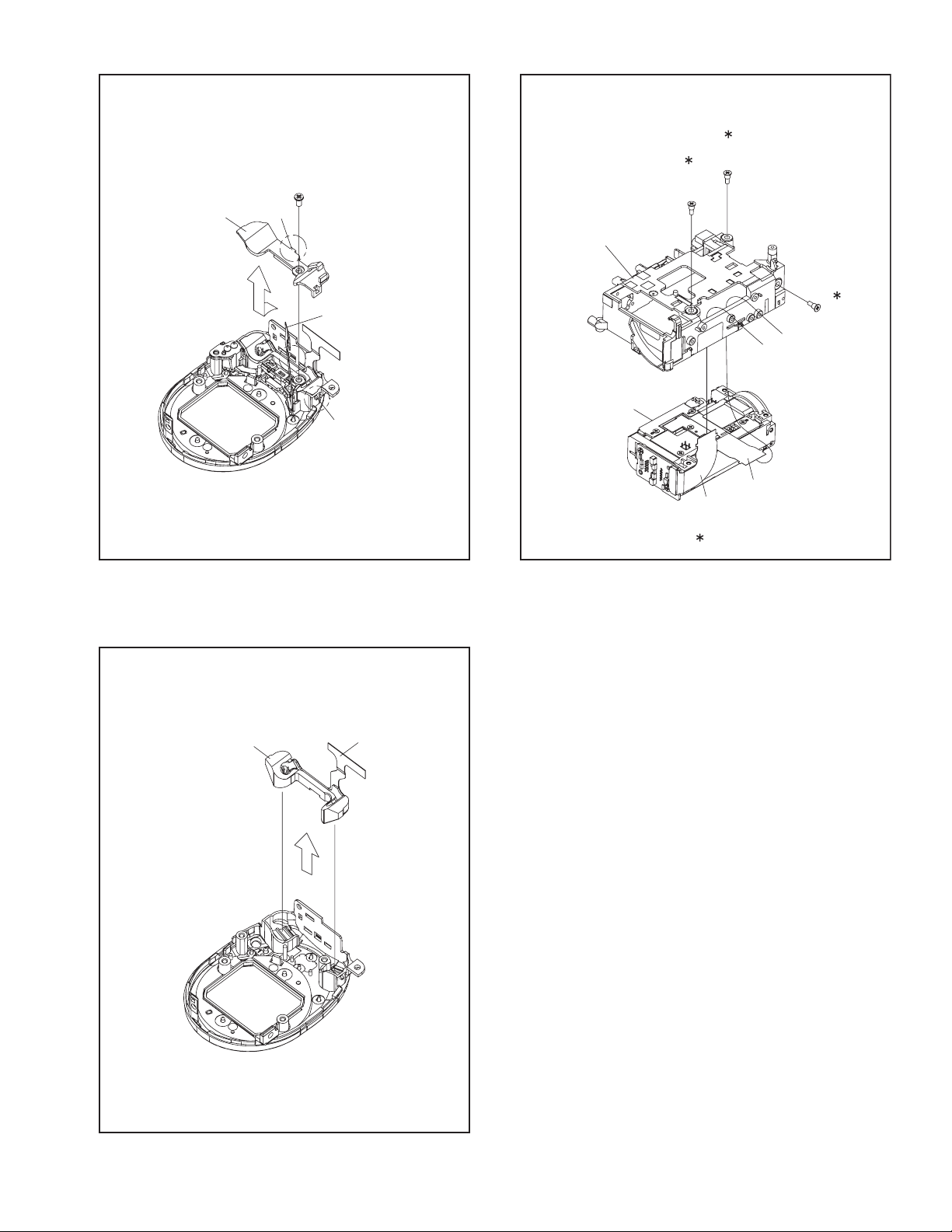
3.2.3 Disassembly of [17] MONITOR ASSY
zCAUTIONS
(1) During the procedure, be careful in handling the parts.
Be very careful not to damage or stain the LCD screen.
If fingerprints are left on the screen, wipe them off with
clean chamois leather or a cleaning cloth.
z Removing MONITOR ASSY
(1) Remove the 2 screws (1, 2).
Turn the HINGE UNIT ASSY 90°, and remove the 2 screws
(2)
(3, 4).
(3) Remove the MONI.COVER ASSY by releasing the 7
hooks (L17a-g).
(4) Release the lock of the connector (CN17a), and remove
the HINGE UNIT ASSY by lifting it up.
During the procedure, be careful in handling the FPC.
(5) Remove the MONITOR BOARD ASSY and the BRACK-
ET (LCD) as one unit.
(6) Release the lock of the connector (CN17b), and pull out
the FPC.
(7) Remove the 2 screws (5,6), and remove the MONITOR
BOARD ASSY .
(8) Refer to the drawing for disassembly of MONI SA.
NOTE17a:
MONI SA consists of the parts on both sides of the
LCD CASE.
On one side of the LCD CASE, the SHEET (BEF),
SHEET (M/DIFF), LIGHT GUIDE, and the SHEET
(M.REF) are assembled toward the MONITOR
BOARD ASSY. On the other side, the SHEET LCD,
LCD MODULE, and the SPACER LCD are assembled
in order between the LCD CASE and the BRACKET
(LCD).
NOTE17b:
During the procedure, be careful in handling the parts.
Be very careful not to damage the FPC.
NOTE17c:
To attach the SHEET (M/DIFF), insert the SHEET (M/
DIFF) under the ribs on the LCD CASE.
zRemoving HINGE UNIT ASSY
(1) Remove the HINGE COVER(U).
(2) Remove the HINGE COVER(L).
NOTE17d:
During the procedure, be careful in handling the FPC.
The FPC, with its connection to the MONITOR BOARD
ASSY facing inward, is rolled around the axis (shaft) of the
HINGE UNIT ASSY rotation 2.5 rounds (2.5times).
(3) Remove the MAGNET.
NOTE17e:
The FPC, with its connection to the MONITOR
BOARD ASSY facing inward, is rolled around the axis
(shaft) of the HINGE UNIT ASSY rotation 2.5 rounds
(2.5times).
During the procedure, be careful in handling the MAGNET.
When attaching, set the N pole outside as shown in
the figure. Be careful when removing as there is no
marking.
(No.YF335<Rev.001>)1-25
Page 26

:0.245 Nm (2.5kgfcm)
3
(S17b)
4
(S17b)
4
(S17b)
3
(S17b)
L17c
L17d
HINGE UNIT ASSY
L17j
L17e
L17h
L17g
L17f
1
(S17a)
MONITOR
COVER ASSY
2
(S17a)
NOTE17d
HINGE UNIT
HINGE UNIT
L17m
L17n
L17p
FPC
FPC
NOTE17d
FPC
L17m
L17n
L17p
L17q
L17r
L17q
HINGE COVER(U)
HINGE UNIT
NOTE17d
HINGE COVER(L)
L17r
MAGNET
NOTE17e
S
L17j
L17h
6
CN17a
L17k
CN17b
N
d
e
f
(S17a)
c
g
h
(S17a)
5
MONITOR
COVER ASSY
MONI SA
NOTE17a,b,c
a
b
j
NOTE17d
<OK> <NG>
1-26 (No.YF335<Rev.001>)
MONITOR CASE ASSY
Fig.3-2-19
Page 27

<MONITOR BOARD ASSY SIDE>
SHEET(B LIGHT)
<BKT(LCD) SIDE>
NOTE17c
c
d
ef
c
d
e f g h j
efg hj
v
w
x
u
g
h
j
a
b
ts
SHEET(M.REF)
a
b
LIGHT GUIDE
SHEET(M/DIFF)
SHEET(BEF)
BKT(LCD)
NOTE17b
r
q
MONI SA
NOTE17a
w
x
w
x
kmn
v
kmn
v
u
u
p
ts
p
ts
BKT(LCD)
r
q
SPACER LCD
LCD MODULE
SHEET LCD
LCD CASE
r
q
kmn
p
Fig.3-2-20
(No.YF335<Rev.001>)1-27
Page 28

SECTION 4
ADJUSTMENT
4.1 PREPARATION
4.1.1 Precaution
Camera system and deck system of this model are specially
adjusted by using PC.
However, if parts such as the following are replaced, an
adjustment is required. The adjustment must be performed in a
Service Center equipped with the concerned facilities.
• OP BLOCK ASSEMBLY
• MONITOR ASSEMBLY
• EEP ROM (IC1005 of MAIN board)
In the event of malfunction with electrical circuits, first find a
defective portion with the aid of proper test instruments as shown
in the following electrical adjustment procedure, and then
commence necessary repair/ replacement/adjustment.
• In observing chip TP, use IC clips, etc. to avoid any stress.
Prior to replacement of chip parts (especially IC), remove the
solder completely to prevent peeling of the pattern.
• Use a patch cord if necessary. As for a patch cord, see the
BOARD INTERCONNECTIONS.
• Since connectors are fragile, carefully handle them in
disconnecting and connecting the FPC.
4.1.3 Tools required for adjustment
Torque Driver
YTU94088
Chip IC Replacement Jig
PTS40844-2
INF Adjustment Lens Holder
YTU94087
Bit
YTU94088-003
Cleaning Cloth
KSMM-01
Mini Stand
YTU93108
Tweezers
P-895
INF Adjustment Lens
YTU92001D
Light Box Assembly
YTU93096B
4.1.2 Required test equipment
• Personal computer (for Windows)
• Color TV monitor
• Oscilloscope (dual-trace type, observable 100MHz or higher
frequency). The one observable 300 MHz or higher frequency
is recommended.
• Digital voltmeter
• DC power supply or AC adapter
• Frequency counter (with threshold level adjuster)
Color Bar Chart
YTU94133C
Communication Cable
YTU93111-1
Jig Connector Cable
YTU93106B
Focus Chart
YTU92001-018
Conversion Connector
YTU94145K-20
Service Support System
YTU94057-122
PC Cable
QAM0099-005
Charing Battery Adjuatment Jig
YTU93112A
1-28 (No.YF335<Rev.001>)
Page 29

• Torque Driver
Be sure to use to fastening the mechanism and exterior parts
because those parts must strictly be controlled for tightening
torque.
• Bit
This bit is slightly longer than those set in conventional torque
drivers.
• Tweezers
To be used for removing and installing parts and wires.
• Chip IC Replacement Jig
To be used for adjustment of the camera system.
• Cleaning Cloth
Recommended the Cleaning cloth to wipe down the video
heads, mechanism (tape transport system), optical lens surface.
• INF Adjustment Lens
To be used for adjustment of the camera system. For the
usage of the INF adjustment lens, refer to the Service Bulletin
No. YA-SB-10035 and No. YA-SB-10223.
• INF Adjustment Lens Holder
To be used together with the Camera stand for operating the
Videocamera in the stripped-down condition such as the status without the exterior parts or for using commodities that are
not yet conformable to the interchangeable ring. For the usage
of the INF lens holder, refer to the Service Bulletin No. YA-SB-
10035.
• Mini Stand
To be used together with the INF adjustment lens holder. For
the usage of the Mini stand, refer to the Service Bulletin No.
YA-SB-10035.
• Light Box Assembly
To be used for adjustment of the camera system. For the
usage of the Light box assembly, refer to the Service Bulletin
No. YA-SB-10035 and No. YA-SB-10218.
• Color Bar Chart
To be used for adjustment of the camera system. For the
usage of the INF adjustment lens, refer to the Service Bulletin
No. YA-SB-10035.
• Focus Chart
To be used for adjustment of the camera system. For the
usage of the INF adjustment lens, refer to the Service Bulletin
No. YA-SB-10035.
• Service Support System
To be used for adjustment with a personal computer. Software
can be downloaded also from JS-net.
• Communication Cable
Connect the Communication cable between the PC cable and
Jig connector cable when performing a PC adjustment.
• PC Cable
To be used to connect the Videocamera and a personal computer
with each other when a personal computer issued for adjustment.
• Jig Connector Cable
Connected to JIG CONNECTOR of the main board and used
for electrical adjustment, etc.
• Conversion Connector
Conversion connector is used to convert the connector part of
the JIG connector cable.
• Charging Battery Adjustment Jig
This Jig is used for the adjustment of the camcorders that have
Main Body battery charging function.
(No.YF335<Rev.001>)1-29
Page 30

4.2 JIG CONNECTOR CABLE CONNECTION
4.2.1 Cautions
(1) Only 9 of 30pins of JIG CONNECTOR CABLE(PN:YTU93106B)
are extended with wires. Additional 2pins (13 and 28) need
to be soldered and extended with the wires for adjustment
and checking.
See Fig. 4-2-1 for details.
Connection procedure
·Remove the 4 screws (1-4), and then remove the COV-
ER(HIN) ASSY.
<COMPONENT SIDE>
29pin AL_2.83V
28pin IF_RX
26pin NOT USED
23pin NOT USED
22pin NOT USED
<FOIL SIDE>
13
1
COVER(HIN) ASSY
3
2
28
4
JIG CONNECTOR
JIG CONNECTOR CABLE
(MAIN CN110)
10
20
JIG CONNECTOR
1
11
CONVERSION CONNECTOR
SERVICE SUPPORT SYSTEM
Fig.4-2-1
13pin IF_TX
12pin NOT USED
10pin GND
9pin GND
8pin NOT USED
5pin NOT USED
: ADDITIONAL WIRE
COMMUNICATION
CABLE
JIG CONNECTOR
TO AL_2.83V
TO IF_RX
TO IF_TX
TO GND
COMMUNICATION
CABLE
BLUE
RED
WHITE
BLACK
or
PC CABLE
Fig.4-2-2
RS232C
COM PORT
MENU
PERSONAL COMPUTER
1-30 (No.YF335<Rev.001>)
Page 31

Jig connector diagrams
JIG CONNECTOR CABLE (YTU93106B)
MAIN CN110
DSP_RTCK
DSP_TMS
DSP_RST
XDSPTRST
REG_2.83V
OCD_SDA
SYS_RSTL
GND
DSP_TDI
GND
UA_RXD0
UA_TXD0
DSP_TCK
OCD_SCL
IF_RX
IF_TX
AL_2.83V
IRU
KENTO
DSP_TDO
ADDITIONAL WIRE
20
10
19
9
18
8
17
7
16
6
15
5
14
4
13
3
12
2
11
1
13. IF_TX
28. IF_RX
JIG CONN. BOARD
(PIN NO.)
30
29
28
27
26
25
24
23
22
21
20
19
18
17
16
15
14
13
12
11
10
9
8
7
6
5
4
3
2
1
-
AL_2.83V
IF_RX
-
-
-
-
-
-
NC
NC
NC
NC
NC
-
-
IF_TX
-
-
GND
GND
-
-
NC
NC
NC
NC
NC
4.3 ELECTRICAL ADJUSTMENT
Electrical adjustment is performed by using a personal computer
and software for SERVICE SUPPORT SYSTEM. Read
README.TXT file to use the software properly.
As for the connection of cables, see "4.2 JIG CONNECTOR
CABLE CONNECTION".
Conversion Connector
KENTO*
AL_2.83V
DSP_TCK*
UA_RXD0*
DSP_TDI*
SYS_RSTL*
REG_2.83V*
DSP_RST*
DSP_RTCK*
IF_RX
NC
NC
NC
NC
NC
30
29
28
27
26
25
24
23
22
21
20
19
18
17
16
Fig.4-2-3
11
12
13
14
15
16
17
18
19
20
10
DSP_TDO*
1
2
3
4
5
6
7
8
9
15
IRU*
14
IF_TX
13
OCD_SCL*
12
UA_TXD0*
11
GND
10
GND
9
OCD_SDA*
8
XDSPTRST
7
DSP_TMS*
6
NC
5
NC
4
NC
3
NC
2
NC
1
*
*NC
Fig.4-2-4
(No.YF335<Rev.001>)1-31
Page 32

5.1 SERVICE NOTE
3-2-10
3-2-6
SECTION 5
TROUBLE SHOOTING
-
a
3-2-5 3-2-83-2-7 3-2-9
3-2-3 3-2-4
3-2-163-2-15
a
-
-
[14][11] [13][12] [15] [16] [17] [18]
[1] [2] [4][3] [5] [6] [7] [8] [9] [10]
CABINET PARTS AND ELECTRICAL PARTS(1)
3-2-1 3-2-2
1 2 3 4 5 6 7 8 9 10 11 12 13 14 15 16 17 18 19 20 21 22 23 24 25 26 27 -
CABINET PARTS AND ELECTRICAL PARTS(2)
28 29 30 31 32 - 33 34 35 36 37 38 39 40 41
3-2-14 3-2-183-2-13
acdaab
3-2-123-2-11 3-2-17
[17]
[17]MONITOR ASSY
Prepare the specified screws and use them in place of the removed screws.
aae
3-2-19
1 2 3 4 5 6
Symbol No.
Place to stick screw
Removing order of screw
1-32 (No.YF335<Rev.001>)
Screw tightening torque
Reference drawing (Fig.No.)
Symbol No.
Place to stick screw
Removing order of screw
Screw tightening torque
Reference drawing (Fig.No.)
Symbol No.
Place to stick screw
Removing order of screw
Screw tightening torque
Reference drawing (Fig.No.)
and tighten the screw manually.
The specified torque value is a recommended value of the initial assembly. Therefore, set the value below the specified torque value in the assembling procedure.
There are setting limits of the torque value for the torque driver. If the value exceeds the setting value, take it as a rough measurement (reference value),
㧞)Tightening torque for the screws
㧝)㧖and㧖㧖 (This mark shows where to attach the screws) : Do not reuse the screws because the screw lock bond was applied to prevent the screws from loosening.
NOTE:
Be careful not to break either the screws or the screw holes.
a㧦0.088N㨯m (0.9kgf㨯cm) b㧦0.118N㨯m (1.2kgf㨯cm) c㧦0.147N㨯m (1.5kgf㨯cm) d㧦0.196N㨯m (2.0kgf㨯cm)
e㧦0.245N㨯m (2.5kgf㨯cm)
Page 33

Victor Company of Japan, Limited
Digital Imaging Products Business Division Imaging Products Operation 12, 3-chome, Moriya-cho, Kanagawa-ku, Yokohama-city, Kanagawa-prefecture, 221-8528, Japan
(No.YF335<Rev.001>)
Printed in Japan
VSE
Page 34

SCHEMATIC DIAGRAMS
30
CAMCORDER
GZ-MS110BEK GZ-MS110BEU
(No.YF335<Rev.001>)1/
Page 35

■ PRECAUTIONS ON SCHEMATIC DIAGRAMS
z Due to the improvement in performance, some part numbers shown in the circuit diagrams
may not agree with those indicated in the Parts List.
z The parts numbers, values and rated voltage etc. in the Schematic Diagrams are for
reference only.
z Since the circuit diagrams are standard ones, the circuits and circuit constants may be
subject to change for improvement without any notice.
■ PRECAUTIONS ON PARTS LIST
z
The parts identified by the symbol are critical for safety. Whenever replacing these parts, be sure to
use specified ones to secure the safety.
z
The parts not indicated in this Parts List and those which are filled with lines --- in the Parts No.
columns will not be supplied.
z
P.W. BOARD Ass'y will not be supplied, but those which are filled with the Parts No. in the Parts No.
columns will be supplied.
z
When ordering chips, screws etc., place bulk orders (unit of tens) whenever possible to improve
shipping efficiency.
z
There are cases where the actual implemented parts in the sets and the service parts are different.
When ordering parts, make sure to refer to the Parts List.
■
PRECAUTIONS ON SERVICE
Certain parts of the power circuits and the GNDs differ according to the models. Care must be
taken for the following points as the differences are indicated separately in the LIVE GND ( ) and
the ISOLATED (NEUTRAL) GND ( ).
1. Do not touch the LIVE GND, or do not touch the LIVE GND and the ISOLATED (NEUTRAL)
GND at the same time. It may cause an electric shock.
Before pulling out the chassis or other parts, make sure to pull out the power cord from the
wall outlet first.
2. Do not short circuit between the LIVE GND and ISOLATED (NEUTRAL) GND, or never
measure the LIVE GND and ISOLATED (NEUTRAL) GND at the same time using measuring
instruments (oscilloscope, etc.). It may blow fuses or damage other parts.
■ DEVIATION TOLERANCE RANGE
DEVIATION TOLERANCE RANGE
F G J K M N R H Z P
± 1% ± 2% ± 5% ±10% ±20% ±30%
+30%
-10%
+50%
-10%
+80%
-20%
+100%
-0%
30
(No.YF335<Rev.001>)2/
Page 36

MONITOR60
SD40
MAIN10
REAR
50
CCD20
REG+CCD
REG
REG+CCD
AUDIO
MONI RGB
CN102/SD PWB
MAIN IF
ELISE
CPU
AU_SIG/LR
SPK+
CN281/SPEAKER
REG
CN211/MIC
AUDIO
CN103/REAR
MONI RGB
CN101/MONITOR
ELISE
AUDIO
LITHIUM
MONI SW
REG
ELISE
CN103/REAR
BATT+
CN103/REAR
CN101/MONITOR
CN110/JIG
CN104/OPE UNIT
OP DRV
ELISE
AUDIO
CPU
MAIN IF
CN101/MONITOR
AEF/TG
OP DRV
ELISE
AUDIO
CN101/MONITOR
ELISE
CN4201/CCD
AEF/TG
REG
REG+CCD
CN110/JIG
CN103/REAR
MAIN IF
CPU
CPU
CPU
CN104/OPE UNIT
CN106/OP BLOCK
REG
CN103/REAR
MAIN IF
CN110/JIG
CN101/MONITOR
LCD_RGT/DWN
ELISE
ELISE
AEF/TGOP DRV
ELISE
REG
CN101/MONITOR CN110/JIG
CN103/REAR
CPU
CPU
AEF/TG
CDS/TG
OPDRV
MAIN IF
REG
CPU ELISE
AEF/TG
CPU
CN4201/CCD
ELISE
REG
ELISE
CPU
CN106/OP BLOCK
OP DRV
HGVCC+
HGOUT+
DRIVE+
JIG CONNECTOR
MIC
LCD MODULE
LED LED
USB
DC
AV JACK
BATTERY TERMINAL
OPE UNIT
TRIG
PHOTO
ZOOM
T
W
SPEAKER
OP BLOCK
AUDIO_CLK
GOUT
REG_2.83V
GND
BOUT
ROUT
REG_8.5V
GIN
RIN
XDSPTRST
AUDIO_CS
AUDIO_OUT
IR_DC
IR_DC
VIDEO_PS
REG_2.83V
REG_1.8V
GND
REG_4.9V
REG-7.5V
AL_2.83V
UNREGCHK
V_BATT
REG_D_IN
REG_CS
REG_D_OUT
REG_RSTL
REG_CLK
DC_CHECK
ADP_L
CH3_CTL
I_MTR
CHRG_EVR
REG_8.5V
F_PTR_AD
Z_PTR_AD
OP_THRMO
GND
REG_2.83V
V_BATT
TRIG_SW
I_MTR
REG_RSTL
KEY_B
CH3_CTL
REG_CS
REG_D_OUT
DC_CHECK
ADP_L
REG_D_IN
UNREGCHK
AL_2.83V
ZOOM_SW
LIT_2.8V
REG_CLK
CHRG_EVR
PWR_LED
ACES_LED
KEY_A
MONI_SW
KENTO
PWR_SW
T_BATT
P_DET
BATT_L
D_BATT
OCD_SCL
OCD_SDA
M_RVS
SYS_RSTL
IF_TX
IF_RX
IRU
LCD_XDSG_CPU
BUZZER
L_MUTE
ADDT15
ADDT14
ADDT13
ADDT12
ADDT11
ADDT10
ADDT09
ADDT08
ADDT07
ADDT06
ADDT05
ADDT04
ADDT03
ADDT02
ADDT01
ADDT00
XDSPTRST
DSP_RST
MOD0
CDWE
CDAS
CDRE
VDIN
OMT
MFLD
MVD
INT_TO_CAM
DSP_CS
FLSH_RST
TVSEL
VBUS1DET
SDWP
REG_DCHG
EEP_CS_INT
EEP_IN
EEP_OUT
EEP_CLK
CDSTG_RST
CAM_CLK
CAM_OUT
CDSTG_CS
OPDRV_RST
VD_FZ
OPDRV_OUT
OPDRV_IN
OPDRV_CLK
OPDRV_CS
REG_1.05V
REG_2.83V
GND
REG_4.9V
BL_CTL
LCD_STH
LCD_ENB
LCD_CKH2
LCD_STV
LCD_CKV
LCD_CKH1
DSP_TCK
LCD_DSG
DSP_TDI
DSP_TDO
DSP_TMS
DSP_RTCK
ADDT01
ADDT02
ADDT13
ADDT10
ADDT14
ADDT00
ADDT04
ADDT15
ADDT03
ADDT09
ADDT06
ADDT11
ADDT05
ADDT08
ADDT07
ADDT12
VBUS1
USBDP
USBDN
REG_1.8V
REG_DCHG
CDWE
TVSEL
DSP_CS
CDAS
CDRE
OMT
MFLD
MVD
VIDEO_PS
FLSH_RST
DSP_RST
VDIN
HDIN
MCLKI
ACHI11
ACHI10
ACHI9
ACHI8
ACHI7
ACHI6
ACHI5
ACHI4
ACHI3
ACHI2
ACHI1
ACHI0
MCLKI
SDWP1
VDIRS
CLK27O
SDDAT1
SDDAT0
SDDAT3
SDDAT2
SDCD1
SDCMD1
SDCLK1
USB_SEL
UA_RXD0
UA_TXD0
DA_AOUT_ENCO
GIN
BIN
RIN
AIBD
AOBD
AIOLRCK
AIOBCK
AOMCLK
INT_TO_CAM
EEP_IN
EEP_CS_INT
EEP_OUT
EEP_CLK
MOD0
SD_WP
GND
REG_2.83V
USB_SEL
AL_2.83V
VBUS1DET
MCLKI
MONI_SW
CDSTG_RST
HDIN
CAM_CLK
CDSTG_CS
CAM_OUT
VDIN
GND
REG_2.83V
REG-7.5V
REG-CCD
V2H2V5
V6
SUB
H1
V1RGV4
V3
CCD_OUT
ACHI5
ACHI8
UNREG
ACHI10
ACHI7
ACHI2
BATT_CHK
ACHI4
ACHI3
VADP
REG_1.05V
MCLKI
ACHI6
GBAT
ACHI0
GADP
ACHI9
ACHI11
ACHI1
GND
REG_4.9V
REG_2.83V
VDIRS
CLK27O
OPDRV_OUT
OPDRV_CLK
OPDRV_CS
VD_FZ
OPDRV_IN
OPDRV_RST
HGVSS-
FOCUS03
HGOUT-
ZOOM01
ZOOM03
Z_LED
FOCUS04
FOCUS02
ZOOM04
F_VCC
DRIVE-
F_LED
ZOOM02
FOCUS01
Z_VCC
LCD_PSIG
BIN
GND
LCD_COM
AUDIO_OUT
REG_4.9V
INT_L
AIOBCK
AUDIO_CLK
AOBD
SPK-
AIOLRCK M_GND
L_MUTE
DA_AOUT_ENCO
AOMCLK
V_OUT
AIBD
AUDIO_CS
BUZZER
REG_2.83V
VBUS145
GND44
USBDN43
USBDP42
GND41
ACES_LED40
PWR_LED39
AL_2.83V38
REG_2.83V37
KEY_A36
BATT_L35
D_BATT34
T_BATT33
BATT_CHK32
BATT+31
BATT+30
BATT+29
BATT+28
BATT+27
UNREG26
UNREG25
UNREG24
UNREG23
UNREG22
UNREG21
UNREG20
UNREG19
UNREG18
UNREG17
GADP16
GBAT15
VADP14
PWR_SW13
GND12
GND11
GND10
GND9
GND8
GND7
GND6
AU_SIG/LR5
AU_SIG/LR4
GND3
V_OUT2
P_DET1
CN103
QGF0534F2-45X
COM 24
CS 23
VST 22
VCK 21
EN 20
DWN 19
VDD 18
VSS 17
NC 16
VSSG 15
XSTBY 14
PCG 13
HST 12
REF 11
TEST1 10
NRW 9
HCK2 8
HCK1 7
PSIG 6
GREEN 5
RED 4
BLUE 3
RGT 2
TEST2 1
CN701
QGF0534F2-24X
22212019181716151413121110
987654321
CN5001
QGF0543F3-22X
GND22
GND21
H120
H219
SUB18
RG17
CCD_CTL16
V615
V514
V413
V212
V311
V110
REG-CCD9
REG+CCD8
GND7
GND6
GND5
CCD_OUT4
GND3
GND2
GND1
CN4201
QGF0543F3-22X
2019181716151413121110
987654321
CN703
QGF0534F2-20X
GND 20
M_RVS 19
REG_2.83V 18
LCD_PSIG 17
LCD_CKH1 16
LCD_CKH2 15
REG_8.5V 14
LCD_STH 13
LCD_DSG 12
LCD_XDSG_CPU
11
LCD_RGT/DWN
10
LCD_ENB 9
LCD_CKV 8
VCD_STV 7
LCD_COM 6
BL_CTL 5
BOUT 4
ROUT 3
GOUT 2
REG_4.9V 1
CN101
QGF0534F2-20X
REG_2.83V 18
REG_2.83V 17
SDCMD1 16
SDCD1 15
SDDAT2 14
SDWP1 13
SDDAT3 12
GND 11
SDDAT0 10
GND 9
SDDAT1 8
GND 7
GND 6
SDCLK1 5
GND 4
GND 3
LIT_2.8V 2
GND 1
CN102
QGF0543F3-18X
181716151413121110
987654321
CN851
QGF0543F3-18X
GND6
HALF_SW5
FULL_SW4
REG_2.83V3
ZOOM_SW2
TRIG_SW1
CN104
QGF0534F3-06X
M_GND 6
M_GND 5
M_GND 4
INT_L 3
M_GND 2
M_GND 1
CN211
QGF0543F3-06X
45
44
43
42
41
40
39
38
37
36
35
34
33
32
31
30
29
28
27
26
25
24
23
22
21
20
19
18
17
16
15
14
13
12
11
10
9
8
7
6
5
4
3
2
1
QGF0566C1-45X
CN601
ZOOM0225
ZOOM0324
ZOOM0423
ZOOM0122
F_VCC21
F_LED20
F_PTR_AD19
OP_THRMO18
GND17
DUMP+16
HGVCC+15
HGOUT+14
DRIVE+13
DRIVE-12
HGVSS-11
HGOUT-10
DUMP-9
GND8
FOCUS027
FOCUS036
FOCUS045
FOCUS014
Z_VCC3
Z_LED2
Z_PTR_AD1
QGF0543F3-25X
CN106
DSP_RTCK 20
DSP_RST 19
REG_2.83V 18
SYS_RSTL 17
DSP_TDI 16
UA_RXDO 15
DSP_TCK 14
IF_RX 13
AL_2.83V 12
KENTO 11
DSP_TMS 10
XDSPTRST 9
OCD_SDA 8
GND 7
GND 6
UA_TXDO 5
OCD_SCL 4
IF_TX 3
IRU 2
DSP_TDO 1
QGB0519J1-20X
CN110
SPK-2
SPK+1
QGA1001F1-02X
CN281
<BOARD INTERCONNECTIONS>
**<FPC or WIRE - 03 -WR1>
(**) indicates the block No. and symbol No. of the WIRE or the FPC.
NOTES: The number of patch cords (*) are indicated by interconnected.
Symbol No.
Block No.
yf335_y10878001a_ver0.1
*
YTU94077-6
YTU94074-6
<FPC-M1-604>
**
*
YTU94077-22
YTU94074-22
<FPC-M1-102>
**
YTU94077-24
YTU94074-24
<FPC-M1-327>
**
*
YTU94077-20
YTU94074-20
*
*
YTU94077-6
YTU94074-6
<FPC-M1-101>
**
*
YTU94077-18
YTU94074-18
created date:2010-02-19No.YF335
30
(No.YF335<Rev.001>)3/
Page 37

SW
Q6701
REG
Q6604
SW
Q6601
Q6404
Q6401
SW
Q601
ADP_L
LOUT82
DOUT22
GADP
GBAT
OUT6
IC6001
DOUT1
LOUT5
OUT4
BATT+
VADP
VPIN22
VPIN32
VPIN5
VPIN82
CH1VDD
VPIN1
OUTA7
VPIN21
PVDD
VPIN31
VPIN81
AVDD
<POWER SYSTEM BLOCK DIAGRAM>
AL_2.83V
REG_2.83V
REG_1.8V
REG_2.83V
BATT+
VADP
BATT_CHK
VADP
REG_1.05V
REG_2.83V
REG_2.83V
LIT_2.8V
REG_2.83V
REG_2.83V
REG_4.9V
REG_2.83V
ADP_L
V_BATT
REG_4.9V
AL_2.83V
REG_2.83V
F_VCC
Z_VCC
REG_2.83V
T_BATT
REG_4.9V
REG_2.83V
REG_4.9V
V_BATT
REG-7.5V
REG+CCD
REG-CCD
REG+CCD
LIT_2.8V
REG+CCD
REG_4.9V
REG_4.9V
REG_2.83V
REG_2.83V
LIT_2.8V
AL_2.83V
REG_2.83V
[-]
AL_2.83V
REG_2.83V
UNREG
F601
GADP
GBAT
GADP
UNREG
ACES_LED
PWR_LED
2
KEY_A
PWR_SW
UNREG
GBAT
BATT+
F602
VBUS1
UNREGCHK
-
REG-7.5V
AL_2.83V
BATT+
BATT_L
REG_2.83V
REG_8.5V
REG_2.83V
REG_8.5V
ADP_L
REG_8.5V
REG+CCD
REG_4.9V
REG_2.83V
REG_1.8V
REG_1.05V
[-]
[D]
[T]
[+]
BT602
SDREG2.83V
4
CN852
LIT_2.8V
REG_2.83V
REG_2.83V
D_BATT
REG_8.5V
REG_8.5V
REG_2.83V
REG_4.9V
REG_4.9V
BATT_L
D_BATT
T_BATT
BATT+/
BATT_CHK
SD/MMC
CONNECTOR
18
JIG CONNECTOR
12
CN110
3
LITTIUM
BATTERY
CN104
172
REG_1.05V
317
OPE UNIT
218
REG_1.8V
CN851CN102
REG_2.83V
REG_4.9V
ELISE
183
REG_2.83V
14
7
18
VDD
REG_2.83V
CN701
VDD
REG_2.83V
REG+CCD
120
REG_4.9V
REG_4.9V
CN101CN703
LCD MODULE
MONI RGBAUDIO
4040
3939
RED
GREEN
D612D611
3838
3737
LIT_2.8V
D603
POWER SWMOVIE/STILL
REG_8.5V
S694S693
REG_4.9V
REG_2.83V
3636
1313
PLAY/REC
MAIN IF
S691
UPLOAD/TITLE
S692
4545
1
J611
REG_2.83V
USB CONNECTOR
REG_4.9V
ADP_L
212
3
T_BATT
35351
CN106
34343
OP DRV
V_BATT
3333
4
3232
5
D_BATT
3131
BT601
BATT_L
BATTERY
TERMINAL
2727
UNREGCHK
1515
REG_2.83V
2626
1
REG_2.83V
LIT_2.8V1717
REG+CCD
REG-7.5V
AL_2.83V
4
1616
3
J602
REG-CCD
99
DC JACK
REG+CCD
88
CPU
1414
CN5001CN4201
AEF/TGREG
CN103CN601
OP BLOCK
0 6
MONITOR
0
4
SD
0 2
CCD
0 1
MAIN
0
5
REAR
created date:2010-02-19No.YF335
30
(No.YF335<Rev.001>)4/
Page 38

MDA
FOCUS/ZOOM
IC4901
AEF/TG
IC4201
(64M)
FLASH ROM
IC3003
(512M)
SDRAM
IC3002
(DSP)
ELISE
IC3001
DSP
VIDEO/AUDIO
IC2201
RTC
IC1006
EEPROM
IC1005
CPU
IC1001
SD CARD
MIC IN
(MONO)
(27MHz)
USB CONNECTOR
SD
4
0
SPEAKER
OP BLOCK
0 6
MONITOR
0
5
REAR
0 1
MAIN
0 2
CCD
(1/6 inch)
CCD
MIC IN
L/R OUT
V OUT,
R/G/B
X4202
(48MHz)
X3001
(32.768kHz)
X1002
(20MHz)
X1001
LCD MODULE
J611
J601
AV JACK
IC5001
<VIDEO/AUDIO SYSTEM BLOCK DIAGRAM>
created date:2010-02-19No.YF335
30
(No.YF335<Rev.001>)5/
Page 39

MAIN(MAIN IF)10
USB SELECT
MONI SW
192~195
SYMBOL NO. 191~
VACANT NO. VACANT NO.
166~168R 198
LAST NO.
R
101
VACANT NO.
SYMBOL NO. 101~
LAST NO.
J
LAST NO.
105,106,108
SYMBOL NO. 161~
ONBOARD CONTACT
D162Q
C
111CN
162
169
191
LIT_2.8V
UNREG
T_BATT
ZOOM_SW
V_OUT
TRIG_SW
KEY_B
BATT_L
P_DET
ACES_LED
PWR_LED
GBAT
GADP
VADP
VBUS1
D_BATT
USBDN
GND
SDWP1
XDSPTRST
REG_2.83V
GND
REG_2.83V
SDCD1
SDDAT1
SDDAT3
AL_2.83V
SDCMD1
GND
AL_2.83V
GND
SDCLK1
LCD_CKH1
REG_8.5V
LCD_CKH2
LCD_PSIG
LCD_STV
LCD_DSG
LCD_RGT/DWN
BL_CTL
LCD_XDSG_CPU
LCD_STH
LCD_ENB
LCD_COM
LCD_CKV
GOUT
BOUT
ROUT
AU_SIG/LR
BATT_CHK
REG_2.83V
REG_2.83V
KENTO
PWR_SW
IRU
SDDAT0
IF_RX
DSP_RST
UA_RXD0
UA_TXD0
GND
IF_TX
REG_2.83V
DSP_RTCK
M_RVS
AL_2.83V
OCD_SCL
SYS_RSTL
DSP_TMS
DSP_TDO
OCD_SDA
DSP_TCK
DSP_TDI
REG_4.9V
SDDAT2
USB_SEL
REG_2.83V
GND
GND
USBDP
MONI_SW
GND
KEY_A
BATT+
!
!
sure to use the specified one.
When replacing those parts make
Parts are safety assurance parts.!
OPEN
NNZ0194-001X
TP6
OPEN
NNZ0194-001X
TP7
43
21
NSW0322-001X
S101
1k
R601
47k
R302
OPEN
R301
OPEN
R184
OPEN
R185
0Ω
R181
3
2
1
OPEN
D601
3
2
1
OPEN
D181
OPEN
D602
MA111-X
D603
OPEN
D604
45
44
43
42
41
40
39
38
37
36
35
34
33
32
31
30
29
28
27
26
25
24
23
22
21
20
19
18
17
16
15
14
13
12
11
10
9
8
7
6
5
4
3
2
1
CN103
QGF0534F2-45X
20
19
18
17
16
15
14
13
12
11
10
9
8
7
6
5
4
3
2
1
CN101
QGF0534F2-20X
181716151413121110
987654321
CN102
QGF0543F3-18X
GND6HALF_SW5FULL_SW4REG_2.83V3ZOOM_SW2TRIG_SW
1
CN104
QGF0534F3-06X
[1005]
OPEN
C602
[2125]
OPEN
C111
[1005]
OPEN
C112
[1005]
OPEN
C603
[1005]
0.1
C601
DSP_RTCK
20
DSP_RST
19
REG_2.83V
18
SYS_RSTL
17
DSP_TDI
16
UA_RXDO
15
DSP_TCK
14
IF_RX
13
AL_2.83V
12
KENTO
11
DSP_TMS
10
XDSPTRST
9
OCD_SDA
8
GND7GND
6
UA_TXDO5OCD_SCL
4
IF_TX
3
IRU
2
DSP_TDO
1
QGB0519J1-20X
CN110
(CN851)
To SD
To ELISE
To CPU
To CPU
<MAIN(MAIN IF) SCHEMATIC DIAGRAM>
2. Be sure to check the PARTS LIST for availability.
NOTES: 1. For the destination of each signal and further line connections that are cut off from this diagram, refer to "BOARD INTERCONNECTIONS".
yf335_y10871001a1/8_ver0.1
(CN601)
To REAR
To ELISE
(CN703)
To MONITOR
To JIG CONNECTOR
To OPE UNIT
To CPU
To AUDIO,ELISE
To AUDIO
To CPU
To ELISE
To CPU
To ELISE
To CPU
To CPU,ELISE
To ELISE
To REG
To REG
To REG
To CPU
To ELISE
To REG
To CPU
To CPU
To MONI RGB
To ELISE
To CPU
To ELISE
To REG,MONI RGB
To CPU
created date:2010-02-19No.YF335
30
(No.YF335<Rev.001>)6/
Page 40

MAIN(CPU)10
REG_2.83V
AL_2.83V
AL_2.83V
AL_2.83V
(TG_RST)
(TG_CS)
REG_2.83V
VBUS1DET
VBUS1DET
F_PTR_AD_
Z_PTR_AD_
AL_2.83V
BATT_L
V_BATT
M_RVS
MONI_SW
VIDEO_PS
ZOOM_SW
KEY_B
T_BATT
AUDIO_CS
AUDIO_OUT
AUDIO_CLK
VIDEO_PS
IRU
IRU
REG_MONITOR
REG_MONITOR
IR_DC
IR_DC
LED__PWM
LED__PWM
REG_D_IN
OPDRV_IN
OPDRV_RST
DB_CLK
DB_CS
REG_DCHG
TRIG_SW
MONI_SW
PWR_SW
KEY_A
ADP_L
KEY_B
DC_CHECK
REG_CLK
CH3_CTL
REG_D_IN
REG_CS
REG_D_OUT
IF_TX1
IF_RX1
EEP_CS
REG_DCHG
CAM_CLK
CAM_OUT
TVSEL
DB_CS
MVD
VD_FZ
EEP_IN
EEP_OUT
EEP_CLK
CHRG_EVR
MFLD
OMT
INT_TO_CAM
IF_RX1
L_MUTE
IF_RX1
IF_TX1
EEP_CS
FLSH_RST
SDWP
RTC_CS
RTC_INT
DC_CHECK
ACES__LED
OCD_SDA
BUZZER
LCD_XDSG_CPU
OSCI
OSCO
SYS_RSTL
ADDT15
ADDT14
ADDT13
ADDT12
ADDT11
ADDT02
DSP_RST
ADDT12
LCD_XDSG_CPU
ADDT15
BATT_L
AUDIO_OUT
OPDRV_OUT
REG_CLK
TRIG_SW
RTC_INT
LCD_RGT/DWN
ADDT07
ADDT11
EEP_OUT
ADDT09
EEP_CS_INT
VDIN
DB_DT
UNREGCHK
INT_TO_CAM
OCD_SCL
SDWP
Z_PTR_AD_
PWR_SW
ADDT05
KENTO
CDRE
DB_DT
OPDRV_IN
DSP_CS
ADDT08
DB_CLK
EEP_CLK
F_PTR_AD_
VDIN
P_DET
TVSEL
P_DET
OPDRV_CS
REG_D_OUT
KENTO
CDSTG_CS
D_BATT
OPDRV_CLK
ADDT10
OPDRV_CS
RTC_CLK
BUZZER
DSP_RST
DB_RST
LCD_RGT/DWN
ADDT07
V_BATT
OMT
CDWE
D_BATT
ADDT01
I_MTR
MOD0
BATTCHECK
XDSPTRST
BATTCHECK
ZOOM_SW
CAM_OUT
ADDT06
AUDIO_CS
ADDT04
OPDRV_RST
CDSTG_CS
T_BATT
RTC_DT
MVD
ADDT00
ADDT02
CH3_CTL
CAM_CLK
L_MUTE
REG_CS
EEP_CLK
ADDT10
VD_FZ
ADDT09
I_MTR
MOD0
CDWE
CDSTG_RST
CDSTG_RST
KEY_A
RTC_DT
OP_THRMO
DB_RST
CDAS
EEP_OUT
XDSPTRST
OPDRV_CLK
ADDT00
ADP_L
EEP_CS_INT
OPDRV_OUT
ADDT03
UNREGCHK
ADDT14
ADDT13
CDRE
EEP_IN
ADDT06
ACES__LED
EEP_IN
CHRG_EVR
OCD_SCL
ADDT03
CDAS
OCD_SDA
DSP_CS
ADDT04
AUDIO_CLK
OP_THRMO
RTC_CLK
ADDT08
ADDT01
RTC_CS
ADDT05
MFLD
SYS_RSTL
FLSH_RST
ADDT02
OCD_SDA
ADDT12
SDWP
OPDRV_OUT
DSP_CS
AUDIO_OUT
CAM_CLK
IRU
MOD0
XDSPTRST
CDSTG_RST
PWR_LED
VIDEO_PS
REG_DCHG
KENTO
L_MUTE
ADDT10
DSP_RST
ADDT09
TVSEL
CDRE
ADDT14
ACES_LED
OPDRV_RST
CDWE
ADDT03
CAM_OUT
ADDT04
INT_TO_CAM
REG_CLK
CH3_CTL
CDSTG_CS
REG_CS
AUDIO_CLK
REG_D_OUT
ADDT11
ADDT00
IF_TX
LCD_XDSG_CPU
BUZZER
CHRG_EVR
ADDT01
FLSH_RST
AUDIO_CS
VD_FZ
ADDT06
ADDT15
OPDRV_CS
OCD_SCL
ADDT07
ADDT08
LCD_RGT/DWN
SYS_RSTL
ADDT13
ADDT05
EEP_IN
OPDRV_CLK
CDAS
P_DET
V_BATT
F_PTR_AD
MVD
MONI_SW
KEY_B
T_BATT
AL_2.83V
VBUS1DET
TRIG_SW
EEP_CS_INT
ADP_L
VDIN
Z_PTR_AD
EEP_OUT
I_MTR
REG_2.83V
IR_DC
OPDRV_IN
PWR_SW
OMT
EEP_CLK
LIT_2.8V
D_BATT
UNREGCHK
OP_THRMO
KEY_A
DC_CHECK
GND
IF_RX
REG_RSTL
ZOOM_SW
M_RVS
BATT_L
MFLD
REG_D_IN
4 3
21
NAX0950-001X
X1002
321
NAX1071-001X
X1001
TL1005
TL1001
TL1006
TL1026
TL1008
TL1002
TL1003
TL1007
TL1017
TL1004
8
7
6
5 4
3
2
1
1k
RA1003
876
54
321
1k
RA1004
876
54
321
100k
RA1001
8
7
6
5 4
3
2
1
1k
RA1005
876
5 4
321
22k
RA1002
1kR1005
47k
R1015
100k
R1033
10k
R1117
47k
R1013
47k
R1092
47k
R1053
1kR1080
1kR1098
1kR1112
330
R1002
1k
R1111
470k
R1018
1kR1076
1kR1061
100
R1094
47k
R1030
1k
R1047
1kR1109
10kR1063
10k
R1072
1kR1113
100k
R1054
47k
R1037
1k
R1088
47k
R1110
1kR1077
1k
R1079
10k
R1011
180
R1083
220k
R1029
10k
R1052
47k
R1038
3.3k
R1031
1k
R1089
15k
R1008
15k
R1009
33k
R1025
1kR1058
33k
R1017
3.3k
R1067
OPEN
R1062
RT1N441U-X
Q1002
RT1N441U-X
Q1007
INT
1
XOUT
2
XIN
3
VSS4CS
5
SCK
6
SIO
7
VDD
8
S-35190A-G-X
IC1006
PGM
1
RESET
2
VSS
3
VCC
4
CNVSS
5
P0O/SCK
6
P0I/SDA
7
P1O/T1IN
8
R5G05001N311N-X
IC1009
CS#
1
SO
2
WP#
3
VSS4SI
5
SCK
6
HOLD#
7
VDD
8
LE25LB643TT-X
IC1005
0.1C1035
0.1
C1009
OPEN
C1010
OPEN
C1006
0.1
C1033
0.1C1030
0.1
C1037
0.1C1036
0.1 C1049
OPEN
C1008
0.1C1040
OPEN
C1003
OPEN
C1031
OPEN
C1012
0.1C1039
OPEN
C1020
(2125)
OPEN
C1014
OPEN
C1022
OPEN
C1015
OPEN
C1011
1
C1013
0.1C1038
0.1C1032
ADM2
235
VDDB
38
EEP_CS
130
4
MN103SFD0RJRA
MN103SFD0RJR
MN103SD0QJR
IC1001
74
ADM15
48
NC
108
RTC_DT
64
REG_CLK
97
DSP_CS
232
178
OCD_SCL
17
VSS
223
TVSEL
41
62
84
IR_DC
69
SDWP(S3 Only)
80
49
VDD18
241
142
ADM5
181
GND
252
18
Vout
211
OPDRV_RST
165
ADM14
119
VDDB
111
VDD33
1
MN103SFD0RJRA
MN103SFD0RJR
MN103SD0QJR
IC1001
VBUS1DET
78
OP_THRMO
139
176
VDDL
58
KENTO2
107
31
99
CDSTG_CS
169
L_MUTE
127
222
67
INT_TO_CAM(From Charis)
109
185
FLSH_RST
174
VDD33
160
VDDL
59
13
(IRU)REMOTE
56
AUDIO_CLK
133
UNREGCHK
254
VDD33
218
68
BATT_L
105
CHRG_EVR
219
MFLD
173
TRCD1
91
VDD18
239
TRCD3
158
VDD33
77
TRCCLK
90
MOD0
88
MVD
214
MVD
230
168
TXD
101
ADM3
180
52
27
NC
191
CDAS
115
187
EXTRG0
215
184
VDDB
231
ADM7
182
151
112
KEY_B
141
12
224
ADM11
46
F_PTR_AD
253
VDDL
244
NC
120
VDDB
40
GND
256
202
EEP_CS_INT
129
TRIG_SW
188
CH3_CTL
199
OPDRV_CS
100
DSP_RST
37
OSCI
10
VSS
85
VDD33
2
I_MTR
140
VD_FZ
28
AVL_CS
55
15
194
NC
196
VDD3376VDD33
20
NC
121
VDDB
39
DC_CHECK
24
P_DET
93
NC
43
CAM_OUT
32
183
REG_CS
25
JLIP_INT
33
ADM6
237
MMOD
152
103
177
EEP_CLK
131
GND
242
(AUDIO_PD_L)
189
164
VIDEO_PS
54
NC
44
144
82
OCD_SDA
156
VDD18
209
LCD_RGT/DWN
245
CDSTG_RST
228
TRCST
16
ADM1
179
MONI_SW
51
NC
66
REG_MONITOR
73
Vout
212
PWR_SW
50
155
65
GND
257
DBATT_OUT
226
138
DB_RST
98
ADM10
117
251
VDD33
94
ADM8
116
NC
110
DB_CLK
95
203
XUSBHOST1
79
147
NC
34
229
V_BATT
71
GND
247
M_RVS
125
VDDL
128
RTC_CS
195
VSS
207
VDD33
205
KENTO1
172
OPDRV_IN
102
6
CDRE
114
ZEROG_SDA
122
DB_CS
163
255
BATTCHECK
200
137
30
NC
136
NC
104
NC
149
EEP_IN
61
CDWE
42
ADM13
47
VSS
227
146
VDDL
57
TRCD0
157
GND
238
NC
148
159
REG_D_OUT
162
186
LON
9
XDSPTRST
35
NC
7
ADP_L
220
VSS
221
REG_DCHG(S3 Only)
92
VSS
233
124
NC
83
249
EXTRG1
89
240
87
NC
113
OPDRV_CLK
29
204
LCD_XDSG_CPU
193
ADM12
118
75
81
ADM9
45
154
VDD33
21
106
132
VDD33
225
VDDL
190
DB_DT
96
ADM0
234
ZOOM_SW
72
VSS
206
OMT
36
NC
171
RTC_CLK
248
NC
8
143
VDD33
19
ACES_LED
197
5
(A_MUTE)
126
VDD18
213
KEY_A
201
208
246
BUZZER
60
NC
210
161
VDD33
250
RTC_INT
134
VDD33
145
SYS_RSTL
86
ADM4
236
Z_PTR_AD
70
OSCO
11
(VDTG)VDIN
14
VSS
216
CAM_CLK
170
EEP_OUT
192
123
RXD
166
135
OPDRV_OUT
167
150
26
REG_D_IN
23
243
T_BATT
198
VREFH
3
53
VDDB
175
TRCD2
217
LED_PWM
22
AUDIO_OUT
63
153
<MAIN(CPU) SCHEMATIC DIAGRAM>
2. Be sure to check the PARTS LIST for availability.
NOTES: 1. For the destination of each signal and further line connections that are cut off from this diagram, refer to "BOARD INTERCONNECTIONS".
yf335_y10871001a2/8_ver0.1
To MAIN IF(CN102)
To REG
To MAIN IF(CN103)
To REG
To REG
To MAIN IF(CN110)
To REG
To MAIN IF(CN110)
To MAIN IF
To MAIN IF(CN103)
To MAIN IF(CN104)
To MAIN IF(CN101)
To AUDIO
To MAIN IF(CN103)
To MAIN IF(CN104)
To OP DRV
To MAIN IF(CN103)
To OP DRV
To AEF/TG
To ELISE
To ELISE
To MAIN IF(CN103)
To MAIN IF(CN101)
To ELISE
To MAIN IF(CN110)
To AUDIO
To ELISE
ELISE
To MAIN IF(CN110),
To ELISE
To ELISE,AEF/TG
To ELISE
To MAIN IF(CN103)
created date:2010-02-19No.YF335
30
(No.YF335<Rev.001>)7/
Page 41

MAIN(AUDIO)10
AU_SIG/LR
AIBD
V_OUT
AIOBCK
AOBD
AUDIO_CS
GND
L_MUTE
AUDIO_OUT
AUDIO_CLK
REG_2.83V
REG_4.9V
BUZZER
AOMCLK
DA_AOUT_ENCO
AIOLRCK
10
R2604
OPEN
R2101
OPEN
R2102
OPEN
R2410
6.8k
R2222
OPEN
R2412
OPEN
R2803
180
R2801
OPEN
R2804
75
R2802
0Ω
R2805
470
R2703
10
R2411
22k
R2407
330k
R2702
4.7k
R2406
3.3k
R2705
10
R2603
2.2k
R2221
4.7k
R2601
47k
R2220
2SC5383/F/-X
Q2402
2SC5383/F/-X
Q2701
10u
L2406
OPEN
L2405
OPEN
L2801
EXPOSED PAD29
MICP28
MICN27
VMID26
AUX25
SPKVDD24
SPKROUTN23
SPKGND22
SPKROUTP21MONOOUT20VBIN19VBREF18VBOUT17VBVDD16SDIN
15
SCLK 14
MODE/GPIO 13
CSB/GPIO 12
MCLK 11
BCLK 10
FRAME 9
DACDAT 8
ADCDAT
7
DGND
6
DBVDD
5
DCVDD
4
AGND
3
AVDD
2
MICBIAS
1
WM8941GEFL/V-W
IC2201
M_GND 6
M_GND 5
M_GND 4
INT_L 3
M_GND 2
M_GND 1
CN211
QGF0543F3-06X
2
1
QGA1001F1-02X
CN281
OPEN
C2102
0.015
C2240
OPEN
C2101
/6.34.7
C2405
OPEN
C2404
0.0047
C2605
/6.34.7
C2801
0.1
C2239
1
C2702
1
C2603
0.0068
C2241
OPEN
C2601
/6.310
C2407
OPEN
C2403
0.0022
C2604
4.7
C2602
<MAIN(AUDIO) SCHEMATIC DIAGRAM>
2. Be sure to check the PARTS LIST for availability.
NOTES: 1. For the destination of each signal and further line connections that are cut off from this diagram, refer to "BOARD INTERCONNECTIONS".
yf335_y10871001a3/8_ver0.1
To MIC
To SPEAKER
To MAIN IF(CN103)
To CPU
To ELISE
To CPU
To ELISE
ELISE
To MAIN IF(CN103),
To CPU
created date:2010-02-19No.YF335
30
(No.YF335<Rev.001>)8/
Page 42

R3050R3047R3051R3048MODESEL1
0Ω0Ω OPENOPENHIGHLOW
OPENOPEN 0Ω0ΩLOWHIGH
MAIN(ELISE)10
(SDCLK)
(SDDAT_3)
(SDDAT_2)
(SDDAT_1)
(SDDAT_0)
(SDWP)
(SDCD)
(SDCMD)
nonMEGA
MEGA
MODESEL2
3.1V
1.0V
SDCLK
REG_2.83V
REG_2.83V
REG_2.83V
VBUS1DET
VBUS1
VBUS1DET
VBUS1
VDDE_PLL
VDDI_USB
VDDE_USB
AIOLRCK
DDR_DQS2 DDR_DQS3
DDR_DQS0
DDR_DQS1
DDR_XCK0
DDR_CK0
MCLKI
DSP_CS
CLK27O
LCD_CKH1
LCD_CKH2
XDSPTRST
SDCMD
AOMCLK
REG_1.05V
REG_1.8V
DA_AOUT_ENCO
MOD0
RIN
GIN
BIN
VDDE_ADDA
SDWP
LCD_PSIG
PWM0
LCD_PSIG PWM0
SDCD
AOBD
SDDAT_1
SDDAT_3
SDDAT_0
SDDAT_2
SDCMD
XPMOE
MVD
XPMCS0
SDCD
SDCLK
DSP_RTCK
DSP_RTCK
REG_2.83V
PMD1
AIOBCK
AIBD
BIN
GIN
RIN
SDWP
SDDAT_3
SDDAT_2
SDDAT_1
SDDAT_0
MOD0
XPMCS0
XPMOE
XPMWE0
DDR_XWE
MCLKI
REG_2.83V
UA_RXD0
UA_TXD0
MVD
DDR_DQ15
DDR_DQ29
DDR_A02
LCD_DSG
LCD_COM
LCD_CKV
LCD_STV
LCD_STH
LCD_ENB
HDIN
VDIN
VDIRS
MFLD
OMT
EEP_CLKA
DDR_A00
INT_TO_CAM
EEP_CS_INT
CDRE
CDAS
CDWE
EEP_INA
EEP_OUTA
EEP_CLKA
ADDT00
ADDT01
ADDT02
ADDT03
ADDT04
ADDT05
ADDT06
ADDT07
ADDT08
ADDT09
ADDT10
ADDT11
ADDT12
ADDT13
ADDT14
ADDT15
ACHI11
ACHI10
ACHI9
ACHI8
ACHI7
ACHI6
ACHI5
ACHI4
ACHI3
ACHI2
ACHI1
ACHI0
PMA22
PMA21
PMA20
PMA19
PMA18
PMA17
PMA16
PMA15
PMA14
PMA13
PMA12
PMA11
PMA10
PMA9
PMA8
PMA7
PMA6
PMA5
PMA4
PMA3
PMA2
PMA1
PMD15
PMD14
PMD13
PMD12
PMD11
PMD10
PMD9
PMD8
PMD7
PMD6
PMD5
PMD4
PMD3
PMD2
PMD1
PMD0
UA_TXD0
UA_RXD0
REG_2.83V
VDDE_ADDA
VDDE_USB
VDDE_PLL
TVSEL
H_GAIN
H_OFFSET
BL_CTL
DDR_DQ17
DDR_DQ22
DDR_DQ16
DDR_DQ23
DDR_DQ20
DDR_DQ21
DDR_DQ19
DDR_DQ18
DDR_DQ26
DDR_DQ30
DDR_DQ24
DDR_DQ27
DDR_DQ25
DDR_DQ31
DDR_DQ28
DDR_DQ11
DDR_DQ12
DDR_DQ10
DDR_DQ14
DDR_DQ09
DDR_DQ13
DDR_DQ08
DDR_DQ07
DDR_DQ03
DDR_DQ04
DDR_DQ06
DDR_DQ00
DDR_DQ02
DDR_DQ05
DDR_DQ01
DDR_A00
DDR_A01
DDR_A02
DDR_A03
DDR_A04
DDR_A05
DDR_A06
DDR_A07
DDR_A08
DDR_A09
DDR_A10
DDR_A11
DDR_A12
DDR_A13
DDR_XCS0
DDR_CKE
DDR_BA0
DDR_BA1
DDR_XCAS
DDR_XRAS
DDR_XWE
DDR_DQM0
DDR_DQM1
DDR_DQM2
DDR_DQM3
LCD_COM
LCD_DSG
PWM3
PWM2
PWM1
DDR_A13
EEP_CS_INT
INT_TO_CAM
PWM3
PWM2
PWM1
H_GAIN
H_OFFSET
BL_CTL
DDR_DQ12
DDR_DQ15
DDR_DQS1
DDR_DQ19
DDR_DQS0
DDR_DQ26
DDR_DQ30
DDR_DQ05
DDR_DQ14
DDR_DQ23
DDR_DQ20
DDR_DQ29
DDR_DQ06
DDR_DQ27
DDR_DQ07
DDR_DQ28
DDR_DQ31
DDR_DQ18
DDR_DQS3
DDR_DQ09
DDR_DQ21
DDR_DQ24
DDR_DQ08
DDR_DQ03
DDR_DQ01
DDR_DQ17
DDR_DQ02
DDR_DQ11
DDR_DQ16
DDR_DQS2
DDR_DQ25
DDR_DQ00
DDR_DQ10
DDR_DQ22
DDR_DQ04
DDR_DQ13
DDR_A12 DDR_XCS0
DDR_DQM1
DDR_DQM3
DDR_XCK0
DDR_A01
DDR_A10
DDR_BA1
DDR_A03
DDR_BA0
DDR_XRAS
DDR_XCAS
DDR_A04
DDR_A05
DDR_A06
DDR_A07
DDR_A08
DDR_A09
DDR_A11
DDR_DQM0
DDR_DQM2
DDR_CK0
DDR_CKE
DSP_CS
LCD_COM
LCD_DSG
XPMWE0
PMD12
PMA16
PMD13
PMD5
PMA7
PMD2
PMD15
PMD9
PMD14
PMA8
PMA13
PMD10
PMA5
PMA19
PMD8
PMA20
PMA10
PMA15
PMA6 PMD0
PMA12
PMA2
PMA9
PMD7
PMA17
PMD6
PMD3
PMA18
PMD11
PMA3
PMA1
PMA11
PMA4
PMA14
PMD4
PMA22
PMA21
REG_1.05V
VDDE_ADDA
VDDI_USB
TVSEL
REG_1.05V
REG_1.05V
VDDE_USB
REG_1.8V
DA_AOUT_ENCO
EEP_OUTA
EEP_INA
ADDT00
ADDT14
ADDT10
ADDT12
CDAS
ADDT05
CDRE
ADDT08
ADDT03
ADDT02
ADDT09
ADDT11
ADDT04
ADDT13
CDWE
ADDT01
ADDT06
ADDT07
ADDT15
CLK27O
AIBD
AOBD
AIOLRCK
AOMCLK
AIOBCK
XDSPTRST
DSP_TCK
DSP_TMS
DSP_TDO
DSP_TDI
DSP_TDI
DSP_TDO
DSP_TMS
DSP_TCK
LCD_STV
OMT
LCD_CKV
MFLD
LCD_CKH1
LCD_CKH2
VDIRS
VDIN
HDIN
ACHI0
ACHI1
ACHI2
ACHI3
ACHI4
ACHI5
ACHI6
ACHI7
ACHI8
ACHI9
ACHI10
ACHI11
LCD_STH
LCD_ENB
UA_TXD0
BIN
GIN
RIN
USBDP
LCD_CKV
OMT
USBDN
DA_AOUT_ENCO
V_OUT
MCLKI
BL_CTL
LCD_STV
LCD_DSG
LCD_COM
DSP_CS
USB_SEL
SDCLK1
MVD
LCD_COM
HDIN
LCD_CKH2
LCD_DSG
EEP_OUT
EEP_CS_INT
LCD_CKH1
EEP_CLK
SDWP1
SDWP
DSP_TDO
CLK27O
LCD_PSIG
AIOLRCK
AIOBCK
VDIRS
LCD_STH
LCD_ENB
AOMCLK
AOBD
VDIN
MFLD
ACHI6
ACHI2
ACHI5
ACHI3
DSP_RST
ACHI4
DSP_TDI
DSP_TMS
XDSPTRST
DSP_TCK
FLSH_RST
ACHI11
REG_2.83V
SDDAT0
AIBD
SDCD1
CDRE
CDAS
CDWE
VIDEO_PS
ADDT11
ADDT06
ADDT09
ADDT07
ADDT12
ADDT08
ADDT15
ADDT05
ADDT13
ADDT04
ADDT14
ADDT03
ADDT10
ADDT01
ADDT00
ADDT02
REG_4.9V
REG_1.8V
ACHI9
ACHI8
ACHI1
EEP_IN
INT_TO_CAM
SDDAT3
SDDAT2
ACHI10
SDDAT1
ACHI7
SDCMD1
ACHI0
REG_DCHG
DSP_RTCK
VBUS1DET
TVSEL
GND
VBUS1
MOD0
REG_1.05V
UA_RXD0
3 2 1
NAX1023-001X
X3001
TL3024
TL3003
TL3023
TL3022
TL3021
TL3002
TL3019
TL3010
TL3009
TL3017
TL3004
TL3005
TL3007
TL3016
TL3015
TL3011
TL3013
TL3012
TL3001
TL3006
TL3014
8
7
6543
2
1
47k
RA3001
8
7
6543
2
1
1.5k
RA3002
5
6
7
8
4
3
2
1
100
RA3015
5
6
7
8
4
3
2
1
100
RA3016
220
R3036
1k
R3075
OPEN
R3076
OPEN
R3077
OPEN
R3014
2.2k
R3032
OPEN
0ΩR3008
39
R3002
1k
R3105
1k
R3023
OPEN
R3114
6.8k
R3009
1kR3083
4.7kR3080
OPEN
R3013
OPEN
0Ω
R3082
0ΩR3006
OPEN
R3071
39k
R3033
100k
R3087
39
R3003
11k
R3070
220
R3034
OPEN
R3104
1kR3025
OPENR3028
1k
R3024
220
R3029
OPEN
0Ω
L3703
0Ω
L3005
10k
R3010
OPEN
R3031
OPEN
0Ω
R3113
OPEN
68
R3702
OPEN
R3103
RT1N432U-X
Q3004
RT1N441U-X
Q3002
S 3
G
2
D 1
Q3003
SSM3K16FV-X
4 3
21
L3009
NQR0603-001X
SHORT
NRSA63J-0R0X
L3003
SHORT
NRSA63J-0R0X
L3012
CP11V+2VIN3PSAVE
4
VOUT
5
GND
6V-7
CP2
8
OPEN
NJW1357RB1-X
IC3702
VIN
4
VOUT3VSS
2
CE
1
XC6213B312NG-X
IC3005
0.1C3021
OPEN
C3019
0.1
C3027
0.1C3032
0.1
C3051
OPEN
C3049
0.1C3048
OPEN
C3047
OPEN
4.7
C3046
OPEN
C3031
OPEN
C3029
OPEN
C3028
OPENC3006
OPENC3017
OPEN
0.1C3018
OPEN
C3040
OPEN
C3039
100p
C3026
OPEN
4.7
C3020
OPEN
4.7
C3710
1
C3007
OPEN
C3005
OPEN
1
C3718
OPEN
1
C3719
OPEN
1
C3708
100p
C3042
OPEN
1
C3720
1
C3030
0.1
C3022
1
C3010
0.1
C3008
0.1
C3011
0.1
C3013
OPEN
C3009
0.1
C3052
0.1
C3038
OPEN
4.7C3002
ADDRMDDR_8AN2
VDDE_1394H6
VDDAD17
VDDV24
VDDT24
VDDE_1394G6
VDDAA24
VDDE_IOMM14
VDDE_IOMM15
VDDE_OTRAD18
VDDE_IOMM13
VDDE_OTRAD19
VDDE_CPU1Y24
VDDE_CAM1M17
VDDE_CPU1W24
VDDE_CAM4M18
VDDE_CLKN5
VDDE_AUD1AD21
VDDE_CLK2R24
VDDE_CAM3M20
VDDE_AUD1AD22
VDDE_CLKK6
VDDE_CAM1M16
VDDE_CLKL6
VDDE_CPU2AC24
VDDE_CAM2U24
VDDE_CPU2AB24
VDDE_AUD2AD23
VDDE_CAM3M19
VDDE_DDRAK15
VDDE_DDRAD16
VDDE_DDRAB6
VDDE_DDRAK12
VDDE_DDRAA6
VDDE_DDRAF6
VDDE_DDRAK11
VDDE_DDRAD15
VDDE_DDRAA12
VDDE_DDRAB12
VDDE_DDRAK16
VDDE_DDRAJ6
VDDE_DDRAK7
VDDE_DDRAE6
VDDE_DDRAL7
VDDE_DDRAK8
VDDI_CAMN24
VDDI_CAMM21
VDDE_SYSM23
VDDI_CAMM22
VDDE_SYSM24
VDDI_CAMP24
VDDE_VIDEOF6
VSSK1
VDDE_USBAD20
VSSAB2
VSSAJ1
VSSAG1
VSSAC6
VSSAL6
VSSAP19
VSSM3
VSSC35
VSSA33
VSSAR18
VSSAK5
VSSV2
VSSAH3
VSSAP20
VSSAR9
VSSAP16
VSSAR11
VSSAR7
VSSY2
VSSAR14
AVSE_CVFG30
AVDE_CVFF30
VSS AC14
VSS F29
VSS W14
VSS P13
VSS Y13
VSS AC21
VSS AH6
VSS F21
VSS AK30
VSS AD24
VSS N20
VSS AK17
VSS AC16
VSS AB13
VSS AA14
VSS AC23
VSS AK9
VSS N14
VSS F11
VSS AP1
PWM4R31
PWM0T31
PWM1R35
PWM2R34
VSSB1
PWM3R33
CLK27ENM2
VSS N22
VSS AD12
VSS P14
VSS R14
VSS N17
VSS AC20
VSS AA13
VSS AC15
VSS V14
BCHI_6E16
BCHI_0B14
BCHI_12 B17
BCHI_5A15
BCHI_3C15
ACHI_5 B19
BCHI_4B15
ACHI_4 A19
ACHI_2 B18
SYS_BUS_15 E35
SYS_RE C30
ACHI_0 E18
BCHI_7C16
CAMOFF F18
SYS_CS A31
BCHI_1A14
SYS_WE B31
ACHI_3 A18
VSS B34
BCHI_13 A17
ACHI_1 C18
VSS AP34
SYS_AS A30
BCHI_2E15
DSP1_TMS P3
DSP2_NTRST L5
CPU_NTRST F1
DSP2_TDO P34
SYS_BUS_6 C32
CPU_TDI J5
DSP1_TDO P35
DSP2_TCK K2
CPU_TCK J2
CPU_RTCK K5
SYS_BUS_12 E33
SYS_BUS_4 B33
SYS_BUS_10 D34
SYS_BUS_0 A32
DSP1_TDI M5
SYS_BUS_2 C31
SYS_BUS_14 E34
DSP2_TDI M1
SYS_BUS_5 E30
CPU_TDO H1
DSP2_TMS L2
SYS_BUS_8 E31
CPU_TMS D1
SYS_BUS_1 E29
SYS_BUS_13 D35
SYS_BUS_7 C33
SYS_BUS_3 B32
DSP1_TCK N3
SYS_BUS_9 C34
DSP1_NTRST R3
SYS_BUS_11 D33
DA_DATA3 AL28
UA_RXD1 AJ31
CSI_SI2 AH31
CPU_ADR_19 AH35
CPU_ADR_21 AF31
CPU_ADR_22 AH34
CPU_ADR_23 AJ35
HD_SEL2AL20
DA_DATA1 AP30
UA_RTS1 AK33
CPU_ADR_16 AF33
LCD_DSG A27
CSI_SO2 AL35
UA_RXD0 AK31
DA_DATA2 AN29
CVF_COM B30
CSI_SCK2 AK34
CSI_CS2 AJ33
CVF_DSG B28
LV100M T1
UA_CTS1 AL34
CPU_ADR_18 AG34
UA_CTS0 AM34
CPU_ADR_20 AG33
RST_N L3
UA_TXD0 AN35
UA_RTS0 AL33
CPU_ADR_17 AE31
LCD_COM B26
CLPY F26
UA_TXD1 AM35
CPU_DREQ AN34
CPU_ADR_9 AE35
CPU_ADR_7 AC31
CPU_ADR_1 AC35
CPU_ADR_11 AD31
CPU_MASTER AH30
VSS AP2
CPU_ADR_12 AE33
VSS B2
CPU_ADR_15 AG35
CPU_ADR_8 AD33
CPU_ADR_14 AF34
CPU_ADR_3 AC34
CPU_ADR_5 AD35
MSP1 AJ34
MSP2 AG31
CPU_ADR_0 AB33
CPU_ADR_10 AE34
CPU_DACK AM33
CPU_ADR_13 AF35
CPU_BMODE AG30
CPU_BSIZE AF30
MSP3 AK35
MSP0 AH33
CPU_ENDIAN AE30
CPU_ADR_2 AB31
CPU_ADR_4 AC33
CPU_ADR_6 AD34
CLKCPUOUT R2
CPU_INT0 AL31
VSS A2
CPU_INT2 AP33
VSS A34
CPU_INT3 AN32
CPU_INT1 AN33
CPU_DATA_10 AA35
XCPU_WRH V31
CPU_DATA_0 V34
XCPU_CS0 T34
XCPU_CS2 U31
CPU_DATA_6 Y35
XCPU_WAIT T33
CPU_DATA_5 W31
XCPU_RD V33
CPU_DATA_7 Y34
CPU_DATA_8 Y33
CPU_DATA_9 Y31
CPU_DATA_14 AB35
CPU_DATA_1 V35
CPU_DATA_3 W34
CPU_ALE U34
XCPU_WRL U35
CPU_DATA_11 AA34
XCPU_CS1 T35
CPU_DATA_13 AA31
CPU_DATA_4 W33
CPU_DATA_12 AA33
CPU_DATA_2 W35
CPU_DATA_15 AB34
XCPU_CS3 U33
CLKABIN AP32
CLK24AIN AR33
CLK_TESTIN_3N33
CLKADB_EXT AL27
DA_DATA0 AR31
CLKAIN AL30
CLKDAM_EXT AP29
AD_LRCK AN31
CLKDAB_EXT AR30
AD_DATA1 AR32
PWM_AUDIO AN30
AD_DATA0 AL29
DA_LRCKO AP31
CLKADM_EXT AN28
AD_VRH_FS1 J33
AD_AIN_FS0 L34
AD_AIN_FS1 K35
AD_VRL_FS0 K34
AD_VRL_FS1 G33
AD_VRH_FS0 H33
DA_VREF_LCD H34
DA_AOUT_ENC1 G35
DA_VREF_CVF J31
DA_AOUT_LCD2 F33
DA_VRO_LCD J34
DA_AOUT_CVF1 G31
DA_AOUT_CVF0 F31
DA_AOUT_ENC0 F35
DA_VREF_ENC H35
DA_AOUT_CVF2 H31
DA_VRO_CVF K31
DA_AOUT_LCD1 G34
DA_AOUT_LCD0 F34
DA_VRO_ENC J35
OTG_ID AK27
APP_PRT_OVRCUR_I AR29
EHCI_PRT_PWR_O AP28
EXT12K AR24
HSDPPAD AR26
HSDMPAD AR25
FSDPPAD AR28
FSDMPAD AR27
CLK48IN N1
HD_SELAN20
CLK48OUT L1
DATAIO_6 G5
DATAIO_7 H3
LINKON F10
PHYPD F7
PHYRST F8
DATAIO_1 H5
VBUS AK26
DATAIO_5 F3
PHYCNA F9
CLK50IN A3
DATAIO_0 H2
DATAIO_2 G3
DATAIO_4 G2
DATAIO_3 J3
LPS K3
EXTCTL_0 AP22
PWMV AR23
LREQ F5
CLK_TESTIN_0N31
IOM_SEL1 AN19
EXTDATA_0 AL23
CTLIO_1 E5
EXTSET AR21
EXTDT AL22
EXTDATA_2 AL21
EXTCTL_2 AN21
EXTCLK AR22
EXTDATA_3 AN22
EXTDATA_1 AN23
EXTCTL_1 AP23
EXTCTL_3 AP21
EXTPT AK23
IOM_SEL0 AL19
PLL1SEL0 U30
CLK_TESTIN_1M34
PLL1SEL1 T30
CTLIO_0 F2
VSS B35
VSS A35
IOM1_ALEE12
IOM1_RB3C9
IOM1_DT_3C13
IOM1_DT_5E14
IOM1_DT_1B12
IOM1_CE3C11
IOM1_RB2A8
IOM1_CLEB11
IOM1_REA11
MDACLKA10
IOM1_CE1A9
IOM1_WEC12
IOM1_RB1B9
MEDIA_BUSYP5
IOM1_DT_4B13
IOM1_DT_2A12
IOM1_RB0E11
IOM1_CE2B10
IOM1_CE0C10
IOM1_DT_0E13
CLK33OUTE1
CLK33INC1
IOM0_DT_1E2
IOM0_DT_4D3
IOM0_RB0E8
IOM1_DT_7C14
IOM0_ALEE9
JVC_TEST_0L31
VPD T3
IOM0_DT_2C3
IOM0_RB3D2
IOM0_RB2B3
CLK27ING1
IOM0_DT_0E3
IOM0_DT_6C4
IOM0_CLEC7
CLK_TESTIN_6N35
IOM0_RB1C5
IOM0_CE3B5
IOM0_DT_3E6
IOM0_DT_7E7
IOM0_REC8
CLK_TESTIN_5P31
IOM0_WEB7
CLK27OUTJ1
CLK_TESTIN_4N34
IOM0_CE0B6
JVC_TEST_2M33
JVC_TEST_1L35
XIS T2
IOM0_CE1C6
IOM1_DT_6A13
IOM0_DT_5C2
IOM0_CTLB8
IOM0_CE2B4
CLKFLS_N_OUTE10
VSS AP35
MACROTEST_2L33
MIONT6
VSSAR35
MACROTEST_1K33
MIOUTP33
MACROTEST_0M31
DQMDDR_58AA1
DQSMDDR_6AB3
DQMDDR_55AC1
XCKMDDR_1Y1
DQMDDR_62W3
DQMDDR_61Y5
DMMDDR_7AB1
DQMDDR_60Y3
DMMDDR_6AB5
DQMDDR_57AA5
DQSMDDR_7AA2
DQMDDR_56AA3
DQMDDR_63W5
DQMDDR_59W2
CKMDDR_1W1
ADDRMDDR_1AP3
ADDRMDDR_0AN6
DMMDDR_4AH2
DMMDDR_5AE5
ADDRMDDR_6AN1
DQMDDR_32AK1
DQMDDR_54AC5
DQMDDR_44AF3
DQMDDR_41AG5
DQMDDR_34AK3
DQSMDDR_4AG2
DQMDDR_48AD2
DQMDDR_46AE1
DQMDDR_47AE2
ADDRMDDR_3AN5
DQMDDR_39AH5
DQMDDR_51AD1
DQMDDR_38AH1
DQMDDR_50AD5
DQMDDR_36AJ3
ADDRMDDR_2AN4
DQMDDR_52AC2
DQMDDR_42AF1
DQMDDR_40AG3
DQMDDR_37AJ5
VSS AR2
DQMDDR_49AD3
DQMDDR_35AJ2
ADDRMDDR_5AN3
DQMDDR_33AK2
DQMDDR_45AF5
DQMDDR_53AC3
DQSMDDR_5AE3
ADDRMDDR_7AL3
VSSAR34
ADDRMDDR_4AM3
DQMDDR_43AF2
VSSAR1
MCLKIU1
DQMDDR_1AL8
DQMDDR_0AP7
ADDRMDDR_13AP5
DQMDDR_2AN8
BAMDDR_0AR3
XCSMDDR_1AL5
VSS N18
ADDRMDDR_12AM1
RASNMDDRAP6
XCSMDDR_0AP4
CKEMDDRAL1
ADDRMDDR_10AN7
BAMDDR_1AR4
CASNMDDRAR6
ADDRMDDR_11AM2
ADDRMDDR_9AL2
WENMDDRAR5
DMMDDR_2AL15
DQMDDR_25AN16
DQMDDR_7AP9
DQMDDR_22AP15
DMMDDR_1AN12
DQMDDR_18AP13
DQMDDR_12AP11
DQMDDR_23AR15
DQSMDDR_2AN15
DQMDDR_8AL10
DQSMDDR_0AP10
DQMDDR_17AN13
DQMDDR_16AL13
DQMDDR_14AR12
DQMDDR_3AP8
DMMDDR_0AR10
DQMDDR_15AR13
DQMDDR_10AL11
DMMDDR_3AP17
DQMDDR_19AL14
DQMDDR_11AN11
DQMDDR_5AL9
DQMDDR_24AL16
DQMDDR_4AR8
DQSMDDR_1AL12
DQMDDR_21AP14
DQMDDR_9AN10
DQSMDDR_3AR16
DQMDDR_13AP12
DQMDDR_20AN14
DQMDDR_6AN9
VDMDAE24
LCD_CKH2C27
FLDCPUE21
VTG_XV6C23
DQMDDR_27AN17
HDTGA26
VTG_XV3E23
VDTGC25
DQMDDR_31AP18
DQMDDR_29AL18
CLK27OPA4
DQMDDR_28AR17
VTG_CH3A23
DQMDDR_26AL17
DQMDDR_30AN18
LCD_ENBC26
XCKMDDR_0AR20
VTG_CH2E22
VTG_VSUBB22
VDCPUA22
VTG_CH4C22
VTG_XV5A24
LCD_CKH1E26
LCD_STVB27
VTG_XV2C24
CKMDDR_0AR19
VTG_CH1B23
LCD_CKVA28
CLK27OA6
LCD_STHE25
VTG_XV4B24
VDIRSB25
CLK27VCOINN2
ACHI_6 C19
ACHI_7 E19
CVF_CKVE27
ACHI_11 E20
ACHI_8 A20
CLK_TESTIN_2M35
CVF_ENBA29
CVF_CKH2E28
CVF_CKH1C29
BCHI_11C17
ACHI_12 A21
OMTC21
ACHI_9 B20
CVF_STVC28
BCHI_9A16
CVF_STHB29
ACHI_10 C20
BCHI_8B16
CLK27VINA5
VTG_XV1A25
BCHI_10E17
ACHI_13 B21
CLK74VINA7 VSSA1
PLL1IR1
ELISE
JCY0243
IC3001
VDDF23
CAM_PLLE4AVD0M12
CAM_PLLE2AVS0W12
AVDF_1AL25
VIDECDRVV5
AVDE_FS0R30
CAM_PLLE6AVD0M6
AVDP_2AN24
VDDF20
CAM_PLLE2AVD0V12
AVSF_3AL26
AVDP_1AP27
AUD1CDRVV1
AVSE_ENCL30
VDDF19
CLK2CDRVV6
CAM_PLLE1AVS0U12
VDDF14
VDDAK20
VDDAK25
VDDAD13
AVSE_FS0P30
MODESEL_2Y30
MODESEL_0V30
CAM_PLLE1AVD0T12
VDDF27
AVSBAP25
CAM_PLL1AVS0AC30
SYSCCDRVV3
VDDJ6
CAM_PLLE5AVS0T5
VDDY6
CAM_PLLE7AVD0P6
VDDAK13
AVDE_ENCK30
AVSF_2AP26
VDDAK14
CAM_PLLE3AVS0R12
AVSE_LCDJ30
CAM_PLLE7AVS0R6
AVSP_2AL24
VDDP2
VDDAD14
AVSE_FS1M30
VDDF22
CAM3CDRVU2
AVSF_4AN26
VDDY12
CAM_PLL1AVD0AD30
CPU2CDRVU6
CAM_PLLE5AVD0R5
VSSP1
CAM4CDRVU3
VDDF15
AVDBAP24
CAM_PLLE3AVD0P12
CAM_PLLE4AVS0N12
VDDF13
VDDAC12
AVDE_LCDH30
AVSP_1AN27
AVSF_1AN25
MODESEL_1W30
CAM_PLLE6AVS0N6
VDDW6
CAM_PLL2AVS0AA30
VDDAK24
CAM_PLL2AVD0AB30
AVDE_FS1N30
CPU1CDRVU5
VDDAK19
VSS R17
VSS V17
VSS U16
VSS T16
VSS W21
VSS T18
VSS AA21
VSS AA15
VSS T22
VSS AB17
VSS P18
VSS AB15
VSS U22
VSS U18
VSS AB20
VSS P19
VSS Y15
VSS AB14
VSS V20
VSS Y22
VSS W19
VSS U21
VSS W16
VSS Y19
VSS AB18
VSS P16
VSS U15
VSS W18
VSS AA19
VSS Y18
VSS R15
VSS U20
VSS Y16
VSS V15
VSS U17
VSS T20
VSS T17
VSS AB21
VSS U19
VSS V21
VSS Y17
VSS Y21
VSS R19
VSS R21
VSS R16
VSS W20
VSS V16
VSS W22
VSS AA22
VSS R18
VSS P21
VSS V19
VSS P17
VSS AA18
VSS T15
VSS P20
VSS T19
VSS AA20
VSS V18
VSS P15
VSS T21
VSS V22
VSS AB16
VSS AA17
VSS P22
VSS AA16
VSS R20
VSS W17
VSS AB19
VSS AB22
VSS R22
VSS Y20
VSS W15
VSS Y23
VSS N15
VSS U14
VSS T13
VSS AC22
VSS AK6
VSS N16
VSS F24
VSS P23
VSS V23
VSS F16
VSS AK10
VSS AB23
VSS R23
VSS V13
VSS AC19
VSS N23
VSS T14
VSS F28
VSS AJ30
VSS AG6
VSS AC13
VSS U13
VSS AK21
VSS N19
VSS N21
VSS AK22
VSS AK18
VSS U23
VSS AC17
VSS AD6
VSS F17
VSS W23
VSS AK28
VSS AC18
VSS T23
VSS R13
VSS N13
VSS F25
VSS AA23
VSS Y14
VSS W13
VSS F12
VSS AK29
NC
F3
DQ11
N2
A3
K9
DQ31
A2
DQ13
P2
DQS1
L2
DQ9
M2
VDD
A9
DQ5
M7
DQ15
R2
DQS0
L8
DQ25
D2
DQ23
E7
VDDQ
L9
VDDQ
D1
VDDQ
C9
VDDQ
A7
DQS3
E2
VDD
R9
BA1
H9
/RAS
G9
A12
H3
/CS
H7
VSS
R1
A4
K1
VDDQ
R7
VSSQ
D9
DQ6
M8
DQ30
B3
DQ21
D7
DQ4
N8
DQ14
P3
VSS
F9
A6
J1
VSSQ
P9
VDDQ
N9
VSSQ
N1
DQ12
N3
A8
J3
NC
F7
DQ20
C8
A11
H2
VDD
F1
DQ19
C7
DQ3
N7
DQ29
B2
VSS
A1
Mobile DDR SDRAM
IC3002
EDD51321DBH-6ET
A9
H1
VSSQ
C1
A1
J9
DM1
K2
DQ0
R8
DQ24
E3
/CAS
G8
A0
J8
A7
J2
DQ1
P7
DM0
K8
CK
G2
DQ27
C2
VSSQ
L1
DM2
F8
A5
K3
DM3
F2
DQ17
B7
DQ10
M3
VSSQ
M9
VSSQ
B9
VSSQ
E1
CKE
G1
DQ18
B8
VDDQ
B1
DQ28
C3
DQ22
D8
VSSQ
R3
BA0
H8
DQ7
L7
VSSQ
A3
A2
K7
DQ8
L3
DQ2
P8
/CK
G3
DQ26
D3
DQS2
E8
A10
J7
DQ16
A8
VDDQ
P1
VDDQ
M1
VDDQ
E9
/WE
G7
DQ7
E5
VSS
H6
DQ6H5DQ4H4DQ3H3DQ1
H2
VSS
H1
DQ15G6DQ13
G5
VCC
G4
DQ11
G3
DQ9
G2OEG1
RFU
F6
DQ14F5DQ12F4DQ10
F3
DQ8
F2
DQ5
E4
A3A1A7A2RY/BY
A3
CE
F1
K8P6415UQB-050
K8P6415UQB-051
[FLASH MEMORY]
K8P6415UQB-052
IC3003
A16
E6
WEA4A9A5A13
A6
A4B1A17B2WP/ACCB3RESETB4A8B5A12
B6
A2C1A6C2A18C3A21
C4
A10C5A14
C6
A1D1A5
D2
A20D3A19D4A11D5A15
D6
A0
E1
DQ0E2DQ2
E3
<MAIN(ELISE) SCHEMATIC DIAGRAM>
2. Be sure to check the PARTS LIST for availability.
NOTES: 1. For the destination of each signal and further line connections that are cut off from this diagram, refer to "BOARD INTERCONNECTIONS".
yf335_y10871001a4/8_ver0.1
To CPU
CPU
To MAIN IF(CN110),
To CPU
To MAIN IF(CN110)
CPU
To MAIN IF(CN110),
To CPU
To MAIN IF(CN101)
To AEF/TG
To AEF/TG
To CPU,AEF/TG
To OP DRV
To CPU
To AEF/TG
To MAIN IF(CN101)
To CPU
To MAIN IF(CN101)
To OP DRV
To CPU
To REG
To MAIN IF
To MAIN IF(CN103),AUDIO
To AUDIO
To MAIN IF(CN103)
To CPU
To MONI RGB
To MAIN IF(CN102)
created date:2010-02-19No.YF335
30
(No.YF335<Rev.001>)9/
Page 43

[H1,H2]
MAIN(AEF/TG)10
4212 4213
4201Q
Non-Mega
4205 4207 4208 4226 4227
4205
CN
D
X
IC
C
L
R
4201
4201
4202
4201
4229
4205
4232
VACANT NoLAST No
[OSC]
[TG_serial]
[TG_serial]
[TG]
[CDS_ANA]
[ADC_ANA]
[ADC_DIGI]
[RG,HL]
[H1,H2]
MCLKI
CDSTG_RST
REG_2.83V
H1
H2
SUB
RG
V4
V2
V3
V1
V3
V2
V4
V1
CAM_CLK
CAM_OUT
CDSTG_CS
CDSTG_RST
CAM_CLK
CAM_OUT
CDSTG_CS
ACHI0
ACHI11
ACHI10
ACHI9
ACHI8
ACHI7
ACHI6
ACHI5
ACHI4
ACHI3
ACHI2
ACHI1
SUB
RG
H1
H2
ACHI6
ACHI7
ACHI8
ACHI9
ACHI10
ACHI11
ACHI0
ACHI1
ACHI2
ACHI3
ACHI4
ACHI5
MCLKI
MCLKI
ACHI10
ACHI4
ACHI1
ACHI7
ACHI3
ACHI9
ACHI11
ACHI6
ACHI2
ACHI0
ACHI8
ACHI5
HDIN
VDIN
GND
CAM_OUT
CDSTG_CS
REG+CCD
CAM_CLK
REG_2.83V
CDSTG_RST
REG-7.5V
43
2 1
NAX1066-001X
X4202
TL4208TL4207
TL4202
TL4203
TL4204
TL4201
TL4205
TL4206
33
R4210
OPEN
100k
R4201
33k
R4209
47
R4208
OPEN
0Ω
R4212
330
R4215
330
R4216
120
R4226
OPEN
10u
L4202
10u
L4201
OPEN
K4203
NQR0599-003X
K4204
MA111-X
D4201
GND 22
GND 21
H1
20
H2 19
SUB 18
RG 17
CCD_CTL 16
V6 15
V5 14
V4 13
V3 12
V2 11
V1 10
REG-CCD 9
REG+CCD 8
GND 7
GND 6
GND 5
CCD_OUT 4
GND 3
GND 2
GND 1
CN4201
QGF0543F3-22X
OPEN
C4221
8p
C4228
8p
C4229
NRSA6AJ-303W
OPEN
C4214
0.1
C4209
OPEN
1
C4202
1
C4201
0.1
C4206
OPEN
C4212
0.001
C4210
0.01
C4211
0.1
C4217
0.1
C4218
0.1
C4222
OPEN
C4219
OPEN
C4224
0.1
C4220
OPEN
0.1
C4225
OPEN
C4203
10
C4204
OPEN
C4215
OPEN
C4213
OPEN
C4216
OPEN
C4223
DVSS4
E2
VRM
H1
AVSS12
H4
V3
C8
V6
G8
VHH
K10
DVSS4
F3
SCAN
A9
D9
C7
HL
D2
VL
H8
DVSS4
D3
NC
J7
NC
J2
DVDD4
D1
D5
E9
SCK
J6
CCD_GND
K1
RESET
B6
ADCK
J8
SHC
J3
OSC_I
A8
D10
B10
VDR_VDD
C3
NC
G2
V1
B7
DVSS3
A5
VD_I/O
C4
FBC
K3
BIAS
J1
NC
H9
NC
A10
D3
F9
DVDD5
A2
D8
C10
D4
D8
DVSS5
B3
DVDD3
A6
DVDD5
B2
ID
J9
OSC_O
A7
DVSS4
E3
SUB
H10
CCD_IN
K4
HD_I/O
C5
VRB
K7
OSC_ON
H2
D7
B8
CS
K9
V5
F8
RG
C1
D1
G9
DVDD1
H6
DVSS4
E1
V2
C9
DVDD1
F1
D2
E10
V4
E8
H2
B1
DVDD1
H5
SDI
J10
TEST_O2
G3
VRT
K6
AVSS12
K5
DVSS1
F2
SHC
K2
VM
D4
D11
B9
DVSS5
B4
MON
H7
DVSS12
G10
DLLC
A4
AVSS12
J5
AVDD1
G1
CLK_O
B5
VDR_VDD
C2
AVSS12
J4
D0
F10
D6
D9
AVSS12
H3
DVSS5
A3
VH
C6
AVDD2
K8
DVDD2
D10
H1
A1
R2J45026BG-X
IC4201
<MAIN(AEF/TG) SCHEMATIC DIAGRAM>
2. Be sure to check the PARTS LIST for availability.
NOTES: 1. For the destination of each signal and further line connections that are cut off from this diagram, refer to "BOARD INTERCONNECTIONS".
yf335_y10871001a8/8_ver0.1
(CN5001)
To CCD
MONI RGB
To REG,
To REG
To CPU,ELISE
To ELISE
To CPU
To ELISE
created date:2010-02-19No.YF335
30
(No.YF335<Rev.001>)10/
Page 44

MAIN(OP DRV)10
W/B INT
Q4901
W/B EXT RPM-012PBT97-X
OPEN
REG_4.9V
ZOOM02
ZOOM01
ZOOM01
FOCUS02
Z_LED
Z_PTR_AD
ZOOM02
F_VCC
DRIVE+
HGVSS-
OP_THRMO
HGVCC+
DRIVE-
F_PTR_AD
Z_LED
HGVSS-
HGVCC+
DRIVE+
DRIVE-
F_LED
FOCUS01
ZOOM03
Z_VCC
F_LED
FOCUS04
ZOOM04
Z_VCC
F_VCC
IR_DC
FOCUS03
FOCUS02
FOCUS03
FOCUS01
ZOOM03
OPDRV_IN
FOCUS04
ZOOM04
OPDRV_CS
GND
OPDRV_RST
OPDRV_OUT
OPDRV_CLK
VD_FZ
REG_4.9V
HGOUT-
HGOUT+
HGOUT+
HGOUT-
GND
REG_2.83V
CLK27O
VDIRS
TL4907
TL4903
TL4906
TL4905
TL4901
TL4909
TL4908
TL4904
10k
R4901
OPEN
15k
R4923
OPEN
6.8k
R4924
OPEN
1.2k
R4925
OPEN
180
R4926
10k
R4922
330R4910
330R4909
100
R4906
150
R4914
10k
R4903
150
R4913
47
R4911
10k
R4902
OPEN
2SC5383/F/-X
Q4902
2
1
Q4901
CPT-290S-C-X
OPEN
NQR0599-004X
K4901
OPEN
NQR0573-005X
K4903
OPEN
NQR0573-005X
K4902
OP4OUT44
OP4INN43
VREF42
CREFIN41
GNDA40
RSTB39
PLS238
PLS137
VD_FZ36
VD_IS35
SIN34
SCK
33CS32
SOUT
31
DVDD
30
OSCIN
29
GNDD
28
LED227LED1
26
OUTA1
25
MGNDA
24
DMP0
23
OUTA2 22
OUTB1 21
MVCCA 20
OUTB2 19
OUTC1 18
MGNDB 17
OUTC2 16
OUTD1 15
MVCCB 14
OUTD2 13
TEST 12
OUTE111GND510VDD59OUTE28DMP17PHTRIN6AVDD35REF4OP3OUT3SENS2OP3INP
1
AN41905A-X
IC4901
OPEN
1
C4932
0.001
C4910
CH
OPEN
NCB20JK-106X
10
C4918
OPEN
0.1
C4903
OPEN
0.1
C4909
0.1
C4905
OPEN
C4920
100pC4907
0.01
C4906
OPEN
/161
C4921
100pC4904
OPEN
4.7
C4901
0.1
OPEN
C4908
OPENC4917
OPEN
4.7
C4902
OPEN
4.7
C4916
1
C4930
1
C4931
ZOOM0225
ZOOM0324
ZOOM0423
ZOOM0122
F_VCC21
F_LED20
F_PTR_AD19
OP_THRMO18
GND17
DUMP+16
HGVCC+15
HGOUT+14
DRIVE+13
DRIVE-12
HGVSS-11
HGOUT-10
DUMP-9
GND8
FOCUS027
FOCUS036
FOCUS045
FOCUS014
Z_VCC3
Z_LED2
Z_PTR_AD1
QGF0543F3-25X
CN106
<MAIN(OP DRV) SCHEMATIC DIAGRAM>
2. Be sure to check the PARTS LIST for availability.
NOTES: 1. For the destination of each signal and further line connections that are cut off from this diagram, refer to "BOARD INTERCONNECTIONS".
yf335_y10871001a5/8_ver0.1
To OP BLOCK
To CPU
To CPU
(A)
(A)
(A)
(A)
To CPU
To CPU
To ELISE
created date:2010-02-19No.YF335
30
(No.YF335<Rev.001>)11/
Page 45

MAIN(REG)10
BATT+
AL_2.83
LSD_2.83
REG+CCD
REG-7.5V
REG_1.05
REG_1.8
REG_4.9
CHRG_EVR
UNREGCHK
BATT_CHK
V_BATT
UNREG
REG_1.05V
REG_1.8V
REG+CCD
REG_8.5V
AL_2.83V
REG_4.9V
REG-7.5V
DC_CHECK
UNREG
I_MTR
REG_RSTL
UNREGCHK
V_BATT
REG_2.83V
REG_D_IN
ADP_L
CHRG_EVR
VADP
GADP
GBAT
REG_CS
REG_CLK
CH3_CTL
BATT_CHK
BATT+
GND
REG_D_OUT
620k
R6007
470k
R6006
OPEN
22k
R6706
OPEN
0Ω
R6016
560k
R6005
47k
R6010
130kR6102
620k
R6004
OPENR6413
22k
R6702
47kR6009
10kR6008
0ΩR6503
0Ω
R6803
510kR6701 68kR6703
27k
R6108
1k
R6019
1M
R6017
56k
R6409
2.2k
R6412
62k
R6614
43kR6402
220kR6401
0ΩR6204
130kR6202
330kR6201
10kR6602
OPENR6405
150k
R6607
33k
R6404
470k
R6605
110kR6601
OPEN
R6704
30kR6501
330kR6101
_0.5%
18k
R6612
100k
R6002
OPENR6604
OPENR6407
OPEN
8.2k
R6608
NRV142F-R20X
NRZ0072-R200X
1/4W
0.2
R6014
OPEN
27k
R6615
24kR6502
16kR6801
100
R6013
OPENR6103
10k
R6705
OPENR6406
OPEN
R6011
51kR6802
OPEN
R6603
OPEN
R6403
654
3 2 1
RT3CLLM/EF/-X
KTC801U/G/-X
XP4501-W
PUMX1-W
OPEN
UMX1N-W
Q6605
2SC5383/F/-X
Q6604
OPEN
2SA1989/QR/-X
Q6606
6 5 4
321
Q6601
SSM6L39TU-X
5 4
321
Q6701
SSM5G10TU-X
3
S
2
G
1
D
Q6404
SSM3J304T-X
3
S
2
G
1
D
Q6401
SSM3J304T-X
3 S
2
G
1 D
Q6402
SSM3J108TU-X
3 S
2
G
1 D
Q6403
SSM3K302T-X
NQLG4EM-4R7X
L6801
21
L6201
NQLJ5EM-100X
2 1
NQLH5EM-2R2X
L6701
21
NQLH5EM-2R2X
L6601
2 1
L6501
NQLJ5EM-4R7X
21
NQLH8GM-100X
L6101
2 1
NQLH7EN-4R7X
L6401
MA22D23-X
D6401
MA2Z720-X
D6601
MA2Z720-X
D6102
OPEN
MA22D23-X
D6801
OPEN
MA2Z720-X
D6501
OPEN
MA22D23-X
D6402
MA22D23-X
D6403
OPEN
MA2Z720-X
D6202
OPEN
MA2Z720-X
D6201
MA2Z720-X
D6101
2
1
22/6.3
C6205
T
2
1
22/10C6403
T
22pC6015
22pC6019
OPENC6016
22pC6020
0.001
C6033
10
C6803
OPEN
C6001
OPENC6018
10
C6031
1
C6702
0.1C6011
1
OPEN
C6603
1
C6023
OPEN
1
C6607
OPENC6022
56pC6021
1
C6802
10
C6801
1
C6602
OPEN
1C6502
1
C6202
OPEN1
C6102
OPEN
C6005
OPEN
C6002
10
C6032
220p
C6026
OPEN
C6003
0.1
C6024
10
C6701
4.7
C6608
0.1C6006
0.1C6008
10C6007
820p
C6010
1
C6103
0.001
C6012
1
OPEN
C6605
10
C6503
10
C6104
1
C6606
10
C6101
10
C6501
10C6201
10C6206
10C6402
10C6401
OPEN
C6405
OPEN
C6601
10
C6404
0.0015
C6009
DTC7
75
ADP_L
7
PVDD
42
VREG
9
II9
17
LOUTA1
99
VPIN32
83
DTC4
25
II2
18
OUTC4
44
LGND
11
LOUTB21
49
LSOUT41
43
II5
21
PGNDA2
51
OUTA7
92
OUTB7
45
VPIN82
79
II3
19
II10
76
VBAT2
4
RST
13
VPIN21
53
LSIN422
89
VPIN582LOUTA32
84
CH1VDD
59
IN10
26
DOUT22
94
OUTA4
91
FB10
77
DOUT1
55
LOUTB32
86
CS
66
FB4-2
78
VPIN31
34
VADP
3
PGNDB3
85
GADP
58
OUT6
46
LSOUT422
88
DATAIN
67
II4-1
22
LSOUT6
93
II6-2
20
FB7
28
SCP
68
DC_CHECK
61
LOUTB31
38
SCPAL
15
LOUTA22
97
101
UPD168852-W
IC6001
VBAT1
60
LOUTB22
95
LOUT82
80
PGNDA3
37
DOUT32
87
VPIN22
98
RT
72
VPIN81
29
CUK
62
VUSB
6
LOUT81
30
LOUTA21
52
VPIN1
54
DOUT31
39
PGNDB2
96
OUT9
63
PGND4
32
AVDD
10
AGND
64
LSIN421
41
CLK
14
VREF
16
GUSB
5
TST2
50
PGND52
81
PGND1
56
CH1_RST
1
DATAOUT
65
LSOUT421
40
II8
73
GBAT
2
II7
24
TST3
36
II4-2-1
74
CH1SEL
8
USBSW2
57
PGND6
47
FB4-1
27
TST1
69
LOUTB1
100
DOUT21
48
II4-2-2
23
II6-1
71
PGND5131LOUT5
33
OUTB4
90
II1
70
CH3_CTL
12
LOUTA31
35
<MAIN(REG) SCHEMATIC DIAGRAM>
2. Be sure to check the PARTS LIST for availability.
NOTES: 1. For the destination of each signal and further line connections that are cut off from this diagram, refer to "BOARD INTERCONNECTIONS".
yf335_y10871001a7/8_ver0.1
To CPU
MONI RGB
To AEF/TG,
MONI RGB
To MAIN IF(CN101),
To AEF/TG
To ELISE
To MAIN IF(CN103)
created date:2010-02-19No.YF335
30
(No.YF335<Rev.001>)12/
Page 46

MAIN(MONI RGB)10
BOUT
ROUT
GOUT
REG_2.83V
REG_8.5V
GIN
REG+CCD
BIN
RIN
GND
8
7
6
5 4
3
2
1
8.2k
RA7802
8
7
6
5 4
3
2
1
8.2k
RA7801
10k
R7813
12k
R7814
6 5 4
321
PUMX1-W
XP4501-W
KTC801U/G/-X
UMX1N-W
RT3CLLM/EF/-X
Q7803
6 5 4
321
PUMX1-W
XP4501-W
KTC801U/G/-X
UMX1N-W
RT3CLLM/EF/-X
Q7802
6 5 4
321
PUMX1-W
XP4501-W
KTC801U/G/-X
UMX1N-W
RT3CLLM/EF/-X
Q7804
OPEN
L7802
100u
L7801
OPEN
L7803
4.7
C7802
OPEN
C7803
0.1
C7804
OPEN
C7801
<MAIN(MONI RGB) SCHEMATIC DIAGRAM>
2. Be sure to check the PARTS LIST for availability.
NOTES: 1. For the destination of each signal and further line connections that are cut off from this diagram, refer to "BOARD INTERCONNECTIONS".
yf335_y10871001a6/8_ver0.1
To MAIN IF(CN101),REG
To AEF/TG,REG
To ELISE
To MAIN IF(CN101)
created date:2010-02-19No.YF335
30
(No.YF335<Rev.001>)13/
Page 47

CCD20
5007
(Bottom View)
5001
5001
5001
5005
5003
CN
IC
Q
C
R
VACANT NoLAST No
TP5002TP5001
OPEN
R5002
OPEN
R5003
0Ω
R5004
OPEN
4.7k
R5001
OPEN
3
2
1
2SC3931/CD/-X
Q5001
V41V32V23V1
4
GND5GND
6
VOUT
7
VDD8RG9SUB10VL11H112H213RCSUB
14
(1/6 Inch_CCD)
ICX641UKM-V
IC5001
GND22
GND21
H120
H219
SUB
18
RG17
CCD_CTL16
V615
V514
V413
V312
V211
V110
REG-CCD9
REG+CCD8
GND7
GND6
GND5
CCD_OUT4
GND3
GND2
GND1
CN5001
QGF0543F3-22X
OPEN
C5004
OPEN
C5002
OPEN
C5003
0.1
C5006
0.0022
C5007
1
C5001
<CCD SCHEMATIC DIAGRAM>
yf335_y40278001a_ver0.1
When IC5001 needs replacement, replace the CCD base assembly in whole because it cannot be replaced alone.
3. IC5001 is incorporated in the CCD base assembly .
2. Be sure to check the PARTS LIST for availability.
NOTES: 1. For the destination of each signal and further line connections that are cut off from this diagram, refer to "BOARD INTERCONNECTIONS".
(CN4201)
To MAIN(AEF/TG)
created date:2010-02-19No.YF335
30
(No.YF335<Rev.001>)14/
Page 48

SD40
SDCD
SDCLK
SDCMD
LIT
GND
SDDAT_1
SDWP
SDDAT_0
SDDAT_3
SDCMD
SDCD
SDDAT_2
SDWP
SDDAT_0
SDCLK
SDDAT_1
SDDAT_3
SDCMD
SDCD
SDDAT_2
SDWP
SDDAT_3
SDDAT_0
SDDAT_1
SDCLK
SDDAT_2
SDDAT_1
SDDAT_2
SDWP
SDCLK
SDDAT_0
SDREG2.83V_1
SDDAT_3
SDCD
SDCMD
SDDAT_1
SDREG2.83V_1
SDCD
GND
SDCLK
GND
SDDAT_2
SDWP
SDDAT_3
SDCMD
SDDAT_0
!
sure to use the specified one.
When replacing those parts make
Parts are safety assurance parts.!
5
6
7
8
4
3
2
1
NRZ0087-101W
100
RA811
567
8
432
1
NRZ0087-473W
47k
RA812
OPEN
R911
47k
R851
100
R858
OPEN
0Ω
R915
47k
R856
47k
R853
OPEN
R913
GND
16
GND
15
GND
14
GND
13
WP_SW
12
TERMINAL
11
CARD_DET
10
DAT2
9
DAT1
8
DAT0
7
VSS2
6
CLK
5
VDD
4
VSS1
3
CMD
2
CD/DAT3
1
NNZ0239-001X
CN852
VDD
4
VOUT
3
VSS
2
CE
1
OPEN
MM3404A28U-X
IC855
10 9 8 7 6
54321
OPEN
DA852
IP4281CZ10-X
10 9 8 7 6
54321
OPEN
DA851
IP4281CZ10-X
3
2
1
OPEN
D851
18
17
16
15
14
13
12
11
10
9
8
7
6
5
4
3
2
1
CN851
QGF0543F3-18X
10
C872
OPEN
10
C874
OPEN
10
C875
OPEN
10
C876
10
C871
OPEN
0.1
C857
OPEN
C855
OPEN
10
C873
OPEN
1
C852
OPEN
1
C851
QAB0025-001
BT602
<SD SCHEMATIC DIAGRAM>
2. Be sure to check the PARTS LIST for availability.
NOTES: 1. For the destination of each signal and further line connections that are cut off from this diagram, refer to "BOARD INTERCONNECTIONS".
yf335_y30470001a_ver0.1
To SD SLOT
(CN102)
To MAIN(MAIN IF)
SD SLOT
To SD SLOT
SD/MMC CONNECTOR
created date:2010-02-19No.YF335
30
(No.YF335<Rev.001>)15/
Page 49

REAR50
[D]
[T]
RED
[+]
[-]
GREEN
[-]
GADP
ACES_LED
KEY_A
VADP
ACES_LED
PWR_SW
AL_2.83V
REG_2.83V
GBAT
PWR_LED
PWR_SW
AL_2.83V
PWR_LED
KEY_A
VBUS
T_BATT
T_BATT
BATT_L
VBUS
P_DET
AU_SIG/L
REG_2.83V
USBDN
P_DET
GADP
AU_SIG/L
AU_SIG/R
V_OUT
VADP
USBDN
BATT_L
D_BATT
D_BATT
USBDP
V_OUT
GBAT
USBDP
AU_SIG/R
!
!
sure to use the specified one.
When replacing those parts make
Parts are safety assurance parts.!
OPEN
D606
2 1
PLAY/REC
NSW0323-001X
S691
2 1
MOVE/STILL
NSW0323-001X
S693
2 1
POWER SW
NSW0323-001X
S694
2 1
UPLOAD/TITLE
NSW0323-001X
S692
470
R601
470
R602
6.8k
R693
15k
R694
8 7 6 5
4321
Q601
TPCP8302-X
5
4
3
2
1
AV JACK
QNS0287-001
J601
7 6
5 4 3 2 1
USB CONNECTOR
QNZ0922-001
J611
5 4 3 2 1
BATTERY TERMINAL
BT601
QNA0053-001
1
4
3
2
DC JACK
QNA0054-001
J602
NMFZ007-2R5X-K
F602
NMFZ007-2R5X-K
F601
OPEN
D602
UDZW6.8B-X
MA8068-X
D613
UDZW6.8B-X
MA8068-X
D601
OPEN
D603
UDZW6.8B-X
MA8068-X
D604
21
D611
LNJ353W83-X
21
D612
LHQ974/LM/-X
0.001
C603
OPEN
C612
0.001
C604
OPEN
C601
0.1
OPENC614
0.1
OPENC609
OPENC607
OPENC608
0.1
C606
OPEN
C611
OPEN
C602
VBUS
45
GND
44
USBDN
43
USBDP
42
GND
41
ACES_LED
40
PWR_LED
39
AL_2.83V
38
REG_2.83V
37
KEY_A
36
BATT_L35
D_BATT34
T_BATT33
BATT+32
BATT+31
BATT+30
BATT+29
BATT+28
BATT+27
UNREG26
UNREG25
UNREG24
UNREG23
UNREG22
UNREG21
UNREG20
UNREG19
UNREG18
UNREG17
GADP16
GBAT15
VADP14
PWR_SW13
GND12
GND11
GND10
GND9
GND8
GND7
GND6
AU_SIG/R5
AU_SIG/L4
GND3
V_OUT2
P_DET1
QGF0566C1-45X
CN601
<REAR SCHEMATIC DIAGRAM>
2. Be sure to check the PARTS LIST for availability.
NOTES: 1. For the destination of each signal and further line connections that are cut off from this diagram, refer to "BOARD INTERCONNECTIONS".
yf335_y30469001a_ver0.1
(CN103)
To MAIN(MAIN IF)
created date:2010-02-19No.YF335
30
(No.YF335<Rev.001>)16/
Page 50

MONITOR60
LCD_B
LCD_R
LCD_G
47k
R7312
OPEN
R7702
47k
R7313
10k
R7307
3.3k
R7306
2.7k
R7305
220
R7304
33
R7706
33
R7705
33
R7704
33
R7703
1M
R7315
1.8k
R7311
OPEN
R7318
2.2k
R7310
OPEN
R7309
2.2k
R7303
27k
R7302
OPEN
R7308
1k
R7301
47k
R7314
6 5 4
321
PUMX1-W
XP4501-W
UMX1N-W
KTC801U/G/-X
RT3CLLM/EF/-X
Q7703
6 5 4
321
PUMX1-W
XP4501-W
UMX1N-W
KTC801U/G/-X
RT3CLLM/EF/-X
Q7702
6 5 4
321
OPEN
Q7304
OPEN
Q7305
OPEN
Q7306
OPEN
Q7701
2SC5383/F/-X
Q7301
2SD2216J/RS/-X
2SC4617/RS/-X
2SC5383/F/-X
Q7303
2SB1462J/RS/-X
2SA1774/RS/-X
2SA1989/RS/-X
Q7302
3
2
1
OPEN
Q7310
OPEN
L7302
OPEN
L7701
OUT
4
VDD3GND
2
NC
1
HGDESN031A-X
IC701
VCC
5
OUT Y
4
GND
3
IN A
2
NC
1
TC7SZ04FU-F-X
IC7301
OPEN
D701
UDZW5.1B-X
MA8051/M/-X
D7301
D7701
NESW006/T386-X
D7702
NESW006/T386-X
D7703
NESW006/T386-X
D7704
NESW006/T386-X
OPEN
D7302
COM24
CS23
VST22
VCK21
EN20
DWN19
VDD18
VSS17
NC16
VSSG15
XSTBY14
PCG13
HST12
REF11
TEST110
NRW9
HCK28
HCK17
PSIG6
GREEN5
RED4
BLUE3
RGT2
TEST21
CN701
QGF0534F2-24X
REG_4.9V 20
LCD_G 19
LCD_R 18
LCD_B 17
BL_CTL 16
LCD_COM 15
LCD_STV 14
LCD_CKV 13
LCD_ENB 12
LCD_RGT/DWN 11
LCD_XDSG_CPU 10
LCD_DSG 9
LCD_STH 8
REG_8.5V 7
LCD_CKH2 6
LCD_CKH1 5
LCD_PSIG 4
REG_2.83V 3
M_RVS 2
GND 1
CN703
QGF0534F2-20X
OPEN
C7312
1
C7302
OPEN
C7303
OPEN
C703
1
C7316
OPEN
C7305
0.1
C7308
4.7
C7315
1
C7309
1
C7310
1
C7314
OPEN
C7313
1C7311
OPEN
C7701
OPEN
C7307
0.1
C7702
<MONITOR SCHEMATIC DIAGRAM>
2. Be sure to check the PARTS LIST for availability.
NOTES: 1. For the destination of each signal and further line connections that are cut off from this diagram, refer to "BOARD INTERCONNECTIONS".
yf335_y20519001a_ver0.1
To LCD MODULE
(CN101)
To MAIN(MAIN IF)
created date:2010-02-19No.YF335
30
(No.YF335<Rev.001>)17/
Page 51

<OPE UNIT SCHEMATIC DIAGRAM>
FULL HALF
W
T
TRIG
OPE UNIT
To MAIN
(MAIN IF)
(CN104)
ZOOM_SW
1
2
3
4
TRIG_SW
FULL_SW
5
6
GND
REG_2.83V
HALF_SW
yf335_ly10657002a_ver0.1
Replace the entire unit only.
3. The schematic diagram is only for reference. Avoid replacing individual parts.
2. Be sure to check the PARTS LIST for availability.
NOTES: 1. For the destination of each signal and further line connections that are cut off from this diagram, refer to "BOARD INTERCONNECTIONS".
created date:2010-02-19No.YF335
30
(No.YF335<Rev.001>)18/
Page 52

<MAIN CIRCUIT BOARD>
LYB10223-001D
<01>MAIN
(Lead free solder used in the board (material : Sn-Ag-Cu, melting point : 219 Centigrade))
PbF
X3001
X1002
X1001
TP7
TP6
S101
RA7802 RA7801
RA3016 RA3015
RA3002
RA3001
RA1005
RA1004
RA1003
RA1002
RA1001
R7814
R7813
R6007
R6006
R6005
R6004
R3702
R3113
R3105
R3104
R3103
R3087
R3083
R3082
R3080
R3077
R3076
R3075
R3071
R3070
R3036
R3034
R3033
R3032
R3031
R3025
R3024
R3023
R3014
R3013
R3008
R3006
R3003
R3002
R1117
R1113
R1112
R1111
R1110
R1109
R1098
R1094
R1092
R1089
R1088
R1083
R1080
R1079
R1077
R1076
R1072
R1067
R1063
R1062
R1061
R1058
R1054
R1053
R1052
R1047
R1038
R1033
R1031
R1030
R1029
R1025
R1018
R1017
R1015
R1013
R1011
R1009
R1008
R1005
R1002
R302
R301
R185 R184
R181
Q7804
Q7803
Q7802
Q4901
Q3003
Q3002
Q1007
Q1002
L7803
L7802
L7801
L3703
L3009
IC3702
IC3003
IC3002
IC3001
IC1009
IC1006
IC1005
IC1001
D604
D602
D601
D181
CN281
CN211
CN110
CN104
CN103
C7804
C7803
C7802
C7801
C6005
C6002
C3720
C3719
C3718
C3710
C3708
C3052
C3051
C3042
C3040
C3039
C3038
C3032
C3026
C3011
C3010
C3009
C3008
C1049
C1040
C1039
C1038
C1037
C1036
C1035
C1033
C1032
C1031
C1030
C1022
C1020
C1015
C1014
C1013
C1012
C1011
C1010
C1009
C1008
C1006
C1003
C603
C602
C601
0 1
LYB10223-001D
LYA10223-
MAIN PWB Ass'y
created date:2010-02-19No.YF335
30
(No.YF335<Rev.001>)19/
Page 53

X4202
R6803
R6802
R6801
R6706
R6705
R6704
R6703
R6702
R6701
R6615
R6614
R6612
R6608
R6607
R6605
R6604
R6603
R6602
R6601
R6503
R6502
R6501
R6413
R6412
R6409
R6407
R6406
R6405
R6404
R6403
R6402
R6401
R6204
R6202
R6201
R6108
R6103
R6102
R6101
R6019
R6017
R6016
R6014
R6013
R6011
R6010
R6009
R6008
R6002
R4926
R4925
R4924
R4923
R4922
R4914
R4913
R4911
R4910
R4909
R4906
R4903
R4902
R4901
R4226
R4216
R4215
R4212
R4210
R4209
R4208
R4201
R3114
R3029
R3028
R3010
R3009
R2805
R2804
R2803 R2802
R2801
R2705
R2703
R2702
R2604
R2603
R2601
R2412
R2411
R2410
R2407
R2406
R2222
R2221
R2220
R2102
R2101
R601
Q6701
Q6606
Q6605
Q6604
Q6601
Q6404
Q6403
Q6402
Q6401
Q4902
Q3004
Q2701
Q2402
L6801
L6701
L6601
L6501
L6401
L6201
L6101
L4202
L4201
L3012
L3005
L3003
L2801
L2406
L2405
K4903
K4902
K4901
K4204
K4203
IC6001
IC4901
IC4201
IC3005
IC2201
D6801
D6601
D6501
D6403
D6402
D6401
D6202
D6201
D6102
D6101
D4201
D603
CN4201CN106
CN102
CN101
C6803
C6802
C6801
C6702
C6701
C6608
C6607
C6606
C6605
C6603
C6602
C6601
C6503
C6502
C6501
C6405
C6404
C6403
C6402
C6401
C6206
C6205
C6202
C6201
C6104
C6103
C6102
C6101
C6033
C6032
C6031
C6026
C6024
C6023
C6022
C6021
C6020C6019
C6018
C6016C6015
C6012
C6011
C6010
C6009
C6008
C6007
C6006
C6003
C6001
C4932
C4931
C4930
C4921
C4920
C4918
C4917
C4916
C4910
C4909
C4908
C4907
C4906
C4905
C4904
C4903
C4902
C4901
C4229
C4228
C4225
C4224
C4223
C4222
C4221
C4220
C4219
C4218
C4217
C4216
C4215
C4214
C4213
C4212
C4211
C4210
C4209
C4206
C4204
C4203
C4202
C4201
C3049
C3048
C3047
C3046
C3031
C3030
C3029
C3028
C3027
C3022
C3021
C3020
C3019
C3018
C3017
C3013
C3007
C3006
C3005
C3002
C2801
C2702
C2605C2604
C2603
C2602
C2601
C2407
C2405
C2404
C2403
C2241
C2240
C2239
C2102
C2101
C112
C111
<MAIN CIRCUIT BOARD>
LYB10223-001D
<01>MAIN
(Lead free solder used in the board (material : Sn-Ag-Cu, melting point : 219 Centigrade))
created date:2010-02-19No.YF335
30
(No.YF335<Rev.001>)20/
Page 54

<CCD CIRCUIT BOARD>
(Lead free solder used in the board (material : Sn-Ag-Cu, melting point : 219 Centigrade))
LYB10221-001C
<02>CCD
R5004
R5003
R5002
R5001
Q5001
PbFPbF
UL MARK
CN5001
C5007
C5006
C5004
C5003
C5002
C5001
-01D
4
CCD PWB Ass'y
20
LYA10221
created date:2010-02-19No.YF335
30
(No.YF335<Rev.001>)21/
Page 55

IC5001
MS110
<CCD CIRCUIT BOARD>
(Lead free solder used in the board (material : Sn-Ag-Cu, melting point : 219 Centigrade))
LYB10221-001C
<02>CCD
created date:2010-02-19No.YF335
30
(No.YF335<Rev.001>)22/
Page 56

<SD CIRCUIT BOARD>
(Lead free solder used in the board (material : Sn-Ag-Cu, melting point : 219 Centigrade))
LYB10221-001C
<04>SD
RA812
RA811
R915
R913
R911
R858
R856
R853
R851
PbFPbF
IC855
DA852DA851
D851
CN851
CN851
C876
C875
C874
C873
C871
C855
C852
C851
3
1
18
40
01D
SD PWB ASS'Y
LYA10221-
created date:2010-02-19No.YF335
30
(No.YF335<Rev.001>)23/
Page 57

CN852
CN852
C872
C872
C857
C857
BT602
BT602
<SD CIRCUIT BOARD>
(Lead free solder used in the board (material : Sn-Ag-Cu, melting point : 219 Centigrade))
LYB10221-001C
<04>SD
created date:2010-02-19No.YF335
30
(No.YF335<Rev.001>)24/
Page 58

REMPLACER LES FUSIBLES PAR UNAAUTRE DE MEME TYPE ET DE MEME TENSION.
POUR UNE PROTECTION PERMANENTE CONTRE LES RISQUE D'INCENDE,
ATTENTION :
FOR CONTINUED PROTECTION AGAINST FIRE HAZARD, REPLACE ONLY WITH SAME TYPE AND RATED FUSE(S).
CAUTION :
!
<REAR CIRCUIT BOARD>
(Lead free solder used in the board (material : Sn-Ag-Cu, melting point : 219 Centigrade))
LYB10221-001C
<05>REAR
PbFPbF
R694 R693
R602
R601
Q601
J611
J602
F602
F602
F601
F601
D613
D
6
1
2
D604
D603
D602
D601
C614
C612C611
C609
C608
C607
C604
C603
C602
C601
BT601
50
2
ASS'Y
REAR PWB
-01D
LYA10221
created date:2010-02-19No.YF335
30
(No.YF335<Rev.001>)25/
Page 59

UL MARK
S694 S693S692 S691
D
6
1
1
D606
CN601
C606
REMPLACER LES FUSIBLES PAR UNAAUTRE DE MEME TYPE ET DE MEME TENSION.
POUR UNE PROTECTION PERMANENTE CONTRE LES RISQUE D'INCENDE,
ATTENTION :
FOR CONTINUED PROTECTION AGAINST FIRE HAZARD, REPLACE ONLY WITH SAME TYPE AND RATED FUSE(S).
CAUTION :
!
<REAR CIRCUIT BOARD>
(Lead free solder used in the board (material : Sn-Ag-Cu, melting point : 219 Centigrade))
LYB10221-001C
<05>REAR
created date:2010-02-19No.YF335
30
(No.YF335<Rev.001>)26/
Page 60

<MONITOR CIRCUIT BOARD>
(Lead free solder used in the board (material : Sn-Ag-Cu, melting point : 219 Centigrade))
LYB10221-001C
<06>MONITOR
UL MARK
PbFPbF
R7706
R7705
R7704
R7703
R7702
R7318
R7315
R7314
R7313
R7312
R7311
R7310
R7309
R7308
R7307
R7306
R7305
R7304
R7303
R7302
R7301
Q7703
Q7702
Q7701
Q7310
Q7306
Q7305
Q7304
Q7303
Q7302
Q7301
L7701
L7302
IC7301
IC701
D7302
D7301
D701
CN703
CN701
C7702
C7701
C7316
C7315
C7314
C7313
C7312
C7311
C7310
C7309
C7308
C7307
C7305
C7303
C7302
C703
0 6
1
PWB ASS'Y
MONITOR
LYA10221-01D
created date:2010-02-19No.YF335
30
(No.YF335<Rev.001>)27/
Page 61

D7704 D7703 D7702 D7701
<MONITOR CIRCUIT BOARD>
(Lead free solder used in the board (material : Sn-Ag-Cu, melting point : 219 Centigrade))
LYB10221-001C
<06>MONITOR
created date:2010-02-19No.YF335
30
(No.YF335<Rev.001>)28/
Page 62

VOLTAGE CHARTS
30
BLOCK SYMBOL PIN NO. REC PLAY EE
01 IC6001 1 2.7 2.7 2.7
01 IC6001 2 5.2 5.2 5.2
01 IC6001 3 5.2 5.2 5.2
01 IC6001 4 0.0 0.0 0.0
01 IC6001 5 5.2 5.2 5.2
01 IC6001 6 1.4 1.4 1.4
01 IC6001 7 0.0 0.0 0.0
01 IC6001 8 5.2 5.2 5.2
01 IC6001 9 2.2 2.2 2.2
01 IC6001 10 5.2 5.2 5.2
01 IC6001 11 0.0 0.0 0.0
01 IC6001 12 - - 01 IC6001 13 2.7 2.7 2.7
01 IC6001 14 2.7 2.7 2.7
01 IC6001 15 0.0 0.0 0.0
01 IC6001 16 1.0 1.0 1.0
01 IC6001 17 2.8 2.8 2.8
01 IC6001 18 0.8 0.8 0.8
01 IC6001 19 2.3 2.3 2.3
01 IC6001 20 1.0 1.0 1.0
01 IC6001 21 0.8 0.8 0.8
01 IC6001 22 0.8 0.8 0.8
01 IC6001 23 0.5 0.5 0.5
01 IC6001 24 0.0 0.0 0.0
01 IC6001 25 4.0 4.0 4.0
01 IC6001 26 0.2 0.2 0.2
01 IC6001 27 1.1 1.1 1.1
01 IC6001 28 0.6 0.6 0.6
01 IC6001 29 5.3 5.2 5.3
01 IC6001 30 1.1 2.1 1.1
01 IC6001 31 0.0 0.0 0.0
01 IC6001 32 0.0 0.0 0.0
01 IC6001 33 1.8 2.5 1.8
01 IC6001 34 5.3 5.2 5.3
01 IC6001 35 1.1 1.2 1.1
01 IC6001 36 5.3 5.2 5.3
01 IC6001 37 0.0 0.0 0.0
01 IC6001 38 0.0 0.1 0.0
01 IC6001 39 0.0 0.0 0.0
01 IC6001 40 0.0 0.0 0.0
01 IC6001 41 4.8 4.8 4.8
01 IC6001 42 5.2 5.2 5.2
01 IC6001 43 0.0 0.0 0.0
01 IC6001 44 0.0 0.0 0.0
01 IC6001 45 5.2 5.2 5.2
01 IC6001 46 0.5 0.5 0.5
01 IC6001 47 0.0 0.0 0.0
01 IC6001 48 2.7 2.7 2.7
01 IC6001 49 2.7 2.3 2.7
01 IC6001 50 5.2 5.2 5.2
01 IC6001 51 0.0 0.0 0.0
01 IC6001 52 3.7 2.9 3.7
01 IC6001 53 5.2 5.2 5.2
01 IC6001 54 5.2 5.2 5.2
01 IC6001 55 2.7 2.7 2.7
01 IC6001 56 0.0 0.0 0.0
01 IC6001 57 - - 01 IC6001 58 - - 01 IC6001 59 - - 01 IC6001 60 - - -
BLOCK SYMBOL PIN NO. REC PLAY EE
01 IC6001 61 - - 01 IC6001 62 - - 01 IC6001 63 - - 01 IC6001 64 - - 01 IC6001 65 - - 01 IC6001 66 - - 01 IC6001 67 - - 01 IC6001 68 - - 01 IC6001 69 - - 01 IC6001 70 - - 01 IC6001 71 - - 01 IC6001 72 - - 01 IC6001 73 - - 01 IC6001 74 - - 01 IC6001 75 - - 01 IC6001 76 - - 01 IC6001 77 - - 01 IC6001 78 - - 01 IC6001 79 - - 01 IC6001 80 - - 01 IC6001 81 - - 01 IC6001 82 - - 01 IC6001 83 - - 01 IC6001 84 - - 01 IC6001 85 - - 01 IC6001 86 - - 01 IC6001 87 - - 01 IC6001 88 - - 01 IC6001 89 - - 01 IC6001 90 - - 01 IC6001 91 - - 01 IC6001 92 - - 01 IC6001 93 - - 01 IC6001 94 - - 01 IC6001 95 - - 01 IC6001 96 - - 01 IC6001 97 - - 01 IC6001 98 - - 01 IC6001 99 - - 01 IC6001 100 - - 01 Q6401 S 5.3 5.3 5.3
01 Q6401 D 5.0 5.0 5.0
01 Q6401 G 0.5 0.5 0.5
01 Q6402 S 4.9 4.9 4.9
01 Q6402 D 4.9 4.9 4.9
01 Q6402 G 0.0 0.0 0.0
01 Q6403 S 0.0 0.0 0.0
01 Q6403 D 4.9 4.9 4.9
01 Q6403 G 0.0 0.0 0.0
01 Q6404 S 4.9 4.9 4.9
01 Q6404 D 4.9 4.9 4.9
01 Q6404 G 0.0 0.0 0.0
01 Q6601 1 0.0 0.0 0.0
01 Q6601 2 0.6 0.6 0.6
01 Q6601 3 5.3 5.3 5.3
01 Q6601 4 5.3 5.3 5.3
01 Q6601 5 0.0 0.0 0.0
01 Q6601 6 5.6 5.6 5.6
01 Q6604 E 8.5 8.5 8.5
01 Q6604 C 12.0 12.0 12.0
(No.YF335<Rev.001>)29/
Page 63

BLOCK SYMBOL PIN NO. REC PLAY EE
30
01 Q6604 B 9.1 9.1 9.1
01 Q6701 1 5.0 5.2 5.0
01 Q6701 2 5.2 5.2 5.2
01 Q6701 3 -7.5 -7.5 -7.5
01 Q6701 4 0.0 0.0 0.0
01 Q6701 5 0.0 0.0 0.0
BLOCK SYMBOL PIN NO. REC PLAY EE
(No.YF335<Rev.001>)30/
Page 64

PARTS LIST
13
CAMCORDER
GZ-MS110BEK GZ-MS110BEU
(No.YF335<Rev.001>)1/
Page 65

■ PRECAUTIONS ON SCHEMATIC DIAGRAMS
z Due to the improvement in performance, some part numbers shown in the circuit diagrams
may not agree with those indicated in the Parts List.
z The parts numbers, values and rated voltage etc. in the Schematic Diagrams are for
reference only.
z Since the circuit diagrams are standard ones, the circuits and circuit constants may be
subject to change for improvement without any notice.
■ PRECAUTIONS ON PARTS LIST
z
The parts identified by the symbol are critical for safety. Whenever replacing these parts, be sure to
use specified ones to secure the safety.
z
The parts not indicated in this Parts List and those which are filled with lines --- in the Parts No.
columns will not be supplied.
z
P.W. BOARD Ass'y will not be supplied, but those which are filled with the Parts No. in the Parts No.
columns will be supplied.
z
When ordering chips, screws etc., place bulk orders (unit of tens) whenever possible to improve
shipping efficiency.
z
There are cases where the actual implemented parts in the sets and the service parts are different.
When ordering parts, make sure to refer to the Parts List.
■
PRECAUTIONS ON SERVICE
Certain parts of the power circuits and the GNDs differ according to the models. Care must be
taken for the following points as the differences are indicated separately in the LIVE GND ( ) and
the ISOLATED (NEUTRAL) GND ( ).
1. Do not touch the LIVE GND, or do not touch the LIVE GND and the ISOLATED (NEUTRAL)
GND at the same time. It may cause an electric shock.
Before pulling out the chassis or other parts, make sure to pull out the power cord from the
wall outlet first.
2. Do not short circuit between the LIVE GND and ISOLATED (NEUTRAL) GND, or never
measure the LIVE GND and ISOLATED (NEUTRAL) GND at the same time using measuring
instruments (oscilloscope, etc.). It may blow fuses or damage other parts.
■ DEVIATION TOLERANCE RANGE
DEVIATION TOLERANCE RANGE
F G J K M N R H Z P
± 1% ± 2% ± 5% ±10% ±20% ±30%
+30%
-10%
+50%
-10%
+80%
-20%
+100%
-0%
13
(No.YF335<Rev.001>)2/
Page 66

202
201
163
163
162
161
146
145
145
144
143
142
141
141
132
111
MARKMODEL
B
A
GZ-MS110BEU
GZ-MS110BEK
FINAL ASSEMBLY<M1>
The instruction manual to be provided with this product will differ according to the destination.
RATING LABEL
created date:2010-02-19No.YF335
13
(No.YF335<Rev.001>)3/
Page 67

699
612
612
612
611
611
605
604
603
602
601
261
253
252
251
223
223
221
148
147
140
139
139
138
137
137
136
136
135
134
134
133
131
131
107
106
104
103
102
101
GZ-MS110BEK
GZ-MS110BEU
A
B
MODEL MARK
<04>
ASSEMBLY
SD BOARD
<02>
<05>
<01>
UPPER ASSEMBLY
BOARD ASSEMBLY
REAR
CCD BOARD ASSEMBLY
ASSEMBLY
BOARD
MAIN
The instruction manual to be provided with this product will differ according to the destination.
FINAL ASSEMBLY<M1>
created date:2010-02-19No.YF335
13
(No.YF335<Rev.001>)4/
Page 68

353
353
352
352
351
351
343
343
342
341
329
327
326
325
324
323
321
316
314
312
311
310
309
308
307
306
305
303
301
GZ-MS110BEK
GZ-MS110BEU
A
B
MODEL MARK
<06>
The instruction manual to be provided with this product will differ according to the destination.
FINAL ASSEMBLY<M1>
UPPER ASSEMBLY
ASSEMBLY
BOARD
MONITOR
created date:2010-02-19No.YF335
13
(No.YF335<Rev.001>)5/
Page 69

MODEL MARK MODEL MARK
13
GZ-MS110BEK A GZ-MS110BEU B
Safe Symbol No. Parts No. Parts Name Description QTY Local
FINAL ASSEMBLY <M1MM>
101 WJT0243-001A-E E-CARD WIRE MAIN-SD/NA 1
102 WJT0246-001A-E E-CARD WIRE MAIN-REAR 1
! 103 LY37209-001D REAR COVER ASSY 1
104 LY37206-001A SHIELD 1
106 LY10657-002A OPE UNIT 1
107 LY37235-001B HOLDER(IND)ASSY 1
111 LY22169-001C L.CASE ASSY(S3- 1
131 LY30031-0P9A SPECIAL SCREW MAIN-UPPER 2
132 LY30031-0P9A SPECIAL SCREW REAR-UPPER 1
133 LY30031-0K7A SPECIAL SCREW REAR-SMAIN 1
134 LY30031-0P9A SPECIAL SCREW SLD-HLD(OP 2
135 LY30031-0K7A SPECIAL SCREW H(IND-SMAI 1
136 LY30031-0K7A SPECIAL SCREW SDPWB-SLD 2
137 LY30031-0P9A SPECIAL SCREW SDPWB-H(OP 2
138 LY30031-0P9A SPECIAL SCREW OPE.U-H(OP 1
139 LY30031-0P9A SPECIAL SCREW FRONT-H(OP 2
140 LY30031-0K7A SPECIAL SCREW FRON-B(HIN 1
141 LY30031-0P9A SPECIAL SCREW OMENT-H(OP 2
142 LY30031-0P9A SPECIAL SCREW LOWER-TPOD 1
143 LY30031-0P9A SPECIAL SCREW LOWER-H(OP 1
144 LY30031-0P9A SPECIAL SCREW LOWER-HD.C 1
145 LY30031-0P9A SPECIAL SCREW REAR-LOWER 2
146 LY30031-0P9A SPECIAL SCREW REAR-H(OP) 1
147 LY30031-0P9A SPECIAL SCREW UPPER-H(OP 1
148 LY30031-0P9A SPECIAL SCREW UPPER-TPOD 1
161 LY30031-0Q3A SPECIAL SCREW C(HIN-REAR 1
162 LY30031-0Q3A SPECIAL SCREW C(HIN-H(OP 1
163 LY30031-0Q3A SPECIAL SCREW UPPE-C(HIN 2
201 LY37213-001A JACK COVER(SD) 1
202 LY37212-004G COVER(HIN)ASSY 1
221 LY30031-0Q3A SPECIAL SCREW MIC-FRONT 1
223 LY30031-0Q3A SPECIAL SCREW BARR-HOOD 2
251 LY37223-009C F COVER ASSY(SD 1
252 LY37227-001A PLATE(MIC)SD 1
253 QAN0102-001 MICROPHONE UNIT 1
261 LY22118-001A SHUTTER ASSY 1
301 LY22166-001B MONI.CASE(S3-) 1
303 LY22103-001A LCD CASE 1
305 LY22104-001A BRACKET(LCD) 1
306 LY37337-001A SPACER LCD 1
307 QLD0538-001 LCD MODULE 1
308 LY37339-001A SHEET (BEF) 1
309 LY35480-001A SHEET(M/DIFF) 1
310 LY35481-001A SHEET(M.REF) 1
311 LY36668-001A LIGHT GUIDE 1
312 LY37338-001A SHEET LCD 1
314 QAS0612-001 SPEAKER 1
316 LY37246-001B BKT(SPK) 1
321 LY22167-001B MONI.COVER(S3-) 1
323 LY21558-004B HINGE UNIT 1
324 LY37188-004A HINGE COV(U)SD 1
325 LY37189-001A HINGE COVER(L) 1
326 LY45427-001A P.C.MAGNET 1
327 QAL1266-001 FPC MONI-MAIN 1
329 LY22108-003C U. CASE ASSY(SD 1
341 LY30031-016A SPECIAL SCREW SPK-B(HIN) 1
342 LY30031-016A SPECIAL SCREW FPC-B(HIN) 1
343 LY30031-0K9A SPECIAL SCREW HING-B(HIN 2
351 LY30031-0N5A SPECIAL SCREW HINGE-MONI 2
352 LY30031-079A SPECIAL SCREW M.COV-BKT 2
353 LY30031-079A SPECIAL SCREW M.PWB-BKT 2
601 LY36126-002A OP BLOCK ASSY 1
602 LY45175-001A SHEET 1
603 LY45275-001A OPTICAL LPF 1
604 QAL1247-001 FPC CCD-MAIN 1
605 LY37198-001E HOLDER(OPSD)ASY 1
611 LY30031-0J7A SPECIAL SCREW 2
612 LY30032-037A SPECIAL SCREW HLD(OP)-OP 3
699 LY45541-002A CCD BASE ASSY 1
(No.YF335<Rev.001>)6/
Page 70

070
068
066
066
063
061
053
052
051
042
023
022
015
012
003
002
(M-TYPE)
(E-TYPE)
GZ-MS110BEK
GZ-MS110BEU
A
B
MODEL MARK
<M1>
PACKING AND ACCESSORY ASSEMBLY <M5>
FINAL ASSEMBLY
created date:2010-02-19No.YF335
13
(No.YF335<Rev.001>)7/
Page 71

MODEL MARK MODEL MARK
13
GZ-MS110BEK A GZ-MS110BEU B
Safe Symbol No. Parts No. Parts Name Description QTY Local
PACKING AND ACCESSORY ASSEMBLY <M5MM>
002 LY37342-019A-S CD ROM ASSY 1
! 003 LYT2185-001A-M INST BOOK (ENGLISH) 1 A
! 003 LYT2186-001A-M INST BOOK (GERMAN/FRENCH/SPANISH/I
! 003 LYT2186-002A-M INST BOOK (DUTCH/PORTUGUESE/RUSSI
! 003 LYT2186-003A-M INST BOOK (DANISH/FINN/SWEDISH/NOR
! 003 LYT2186-004A-M INST BOOK (CZECH/PORTUGUESE/HUNG
012 YU30878 REGISTRATION CARD 1 A
015 LYT0194-001B Q.CARD 1 A
022 LY37431-002A SHEET(ACC GUID) 1
023 LY35208-001A SHEET(E-SHOP) 1 A
042 ------------ WARRANTY CARD BT-54042-1 1
051 LY37265-024B PACKING CASE 1 A
051 LY37275-007B PACKING CASE 1 B
052 LY22135-001B CUSHION 1
053 LY30023-054A POLY BAG 1
061 QAM1264-001 A/V CABLE FILTER,3.5 STEREO-RCA 1
063 QAM1156-001 USB CABLE A TYPE-MINI B TYPE 1
! 066 LY37325-001A AC ADAPTER AP-V30M 1 A
! 066 LY37324-001A AC ADAPTER AP-V30E 1 B
! 068 QMPP430-100-JD POWER CORD(EK) 1m BLACK 1 A
! 070 LY37166-003C BATTERY PACK BN-VG107UE 1
TALIAN)
AN/UKRAINIAN)
WEGIAN)
ARIAN)
1 B
1 B
1 B
1 B
MAIN BOARD ASSEMBLY <01>
PW1001 LYA10223-01C MAIN BOARD ASSY 1
IC1001 MN103SD0QJR IC(MICRO C ROM) 1
IC1001 or MN103SFD0RJR IC(MICRO C ROM) 1
IC1001 or MN103SFD0RJRA IC(MICRO C ROM) 1
IC1005 LE25LB643TT-X IC 1
IC1005 or BR25S640FVJ-W-X IC 1
IC1006 S-35190A-G-X IC 1
IC1009 R5G05001N311N-X IC(MCU) 1
IC2201 WM8941GEFL/V-W IC 1
IC3001 JCY0243 IC 1
IC3002 EDD51321DBH-6ET IC 1
IC3003 K8P6415UQB-052 IC(MICRO C ROM) 1
IC3003 or K8P6415UQB-051 IC(MICRO C ROM) 1
IC3003 or K8P6415UQB-050 IC(MICRO C ROM) 1
IC3005 XC6213B312NG-X IC 1
IC4201 R2J45026BG-X IC 1
IC4901 AN41905A-X IC 1
IC6001 UPD168852-W IC 1
Q1002 RT1N441U-X DIGI TRANSISTOR 1
Q1002 or UN9213J-X DIGI TRANSISTOR 1
Q1002 or KRC404E-P-X DIGI TRANSISTOR 1
Q1002 or DTC144EE-X DIGI TRANSISTOR 1
Q1002 or DTC144EEB-X DIGI TRANSISTOR 1
Q1007 RT1N441U-X DIGI TRANSISTOR 1
Q1007 or UN9213J-X DIGI TRANSISTOR 1
Q1007 or KRC404E-P-X DIGI TRANSISTOR 1
Q1007 or DTC144EE-X DIGI TRANSISTOR 1
Q1007 or DTC144EEB-X DIGI TRANSISTOR 1
Q2402 2SC5383/F/-X TRANSISTOR 1
Q2402 or 2SC4617/RS/-X TRANSISTOR 1
Q2402 or 2SD2216J/RS/-X TRANSISTOR 1
Q2701 2SC5383/F/-X TRANSISTOR 1
Q2701 or 2SC4617/RS/-X TRANSISTOR 1
Q2701 or 2SD2216J/RS/-X TRANSISTOR 1
Q3002 RT1N441U-X DIGI TRANSISTOR 1
Q3002 or UN9213J-X DIGI TRANSISTOR 1
Q3002 or KRC404E-P-X DIGI TRANSISTOR 1
Q3002 or DTC144EE-X DIGI TRANSISTOR 1
Q3002 or DTC144EEB-X DIGI TRANSISTOR 1
Q3003 SSM3K16FV-X MOS FET 1
Q3004 RT1N432U-X DIGI TRANSISTOR 1
Q3004 or UN921FJ-X DIGI TRANSISTOR 1
Q3004 or SRC1219EF-X DIGI TRANSISTOR 1
Q3004 or DTC143XE-X DIGI TRANSISTOR 1
Q3004 or DTC143XEB-X DIGI TRANSISTOR 1
Q4901 CPT-290S-C-X PHOTO TRANSISTOR 1
Q6401 SSM3J304T-X MOS FET 1
Q6402 SSM3J108TU-X POWER MOS FET 1
Q6403 SSM3K302T-X MOS FET 1
Q6404 SSM3J304T-X MOS FET 1
Q6601 SSM6L39TU-X MOS FET 1
Q6604 2SC5383/F/-X TRANSISTOR 1
Q6604 or 2SC4617/RS/-X TRANSISTOR 1
Q6604 or 2SD2216J/RS/-X TRANSISTOR 1
Q6701 SSM5G10TU-X MOS FET 1
Q7802 RT3CLLM/EF/-X TRANSISTOR 1
Q7802 or UMX1N-W PAIR TRANSISTOR 1
Q7802 or KTC801U/G/-X TRANSISTOR 1
Q7802 or XP4501-W TRANSISTOR 1
Q7802 or PUMX1-W PAIR TRANSISTOR 1
Q7803 RT3CLLM/EF/-X TRANSISTOR 1
Q7803 or UMX1N-W PAIR TRANSISTOR 1
Q7803 or KTC801U/G/-X TRANSISTOR 1
Q7803 or XP4501-W TRANSISTOR 1
(No.YF335<Rev.001>)8/
Page 72

MODEL MARK MODEL MARK
13
GZ-MS110BEK A GZ-MS110BEU B
Safe Symbol No. Parts No. Parts Name Description QTY Local
Q7803 or PUMX1-W PAIR TRANSISTOR 1
Q7804 RT3CLLM/EF/-X TRANSISTOR 1
Q7804 or UMX1N-W PAIR TRANSISTOR 1
Q7804 or KTC801U/G/-X TRANSISTOR 1
Q7804 or XP4501-W TRANSISTOR 1
Q7804 or PUMX1-W PAIR TRANSISTOR 1
! D603 MA111-X SI DIODE 1
! D603 or SDS511-X SI DIODE 1
! D603 or 1SS355W-X DIODE 1
D4201 MA111-X SI DIODE 1
D4201 or SDS511-X SI DIODE 1
D4201 or 1SS355W-X DIODE 1
D6101 MA2Z720-X SB DIODE 1
D6102 MA2Z720-X SB DIODE 1
D6401 MA22D23-X SB DIODE 1
D6403 MA22D23-X SB DIODE 1
D6601 MA2Z720-X SB DIODE 1
C601 NCBA1AK-104W C CAPACITOR 0.1uF 10V K 1
C1009 NCBA1AK-104W C CAPACITOR 0.1uF 10V K 1
C1013 NCB31CK-105X C CAPACITOR 1uF 16V K 1
C1030 NCBA1AK-104W C CAPACITOR 0.1uF 10V K 1
C1032 NCBA1AK-104W C CAPACITOR 0.1uF 10V K 1
C1033 NCBA1AK-104W C CAPACITOR 0.1uF 10V K 1
C1035 NCBA1AK-104W C CAPACITOR 0.1uF 10V K 1
C1036 NCBA1AK-104W C CAPACITOR 0.1uF 10V K 1
C1037 NCBA1AK-104W C CAPACITOR 0.1uF 10V K 1
C1038 NCBA1AK-104W C CAPACITOR 0.1uF 10V K 1
C1039 NCBA1AK-104W C CAPACITOR 0.1uF 10V K 1
C1040 NCBA1AK-104W C CAPACITOR 0.1uF 10V K 1
C1049 NCBA1AK-104W C CAPACITOR 0.1uF 10V K 1
C2239 NCBA1AK-104W C CAPACITOR 0.1uF 10V K 1
C2240 NCBA1CK-153W C CAPACITOR 0.015uF 16V K 1
C2241 NCBA1EK-682W C CAPACITOR 6800pF 25V K 1
C2405 NCB20JK-475X C CAPACITOR 4.7uF 6.3V K 1
C2407 NCB20JK-106X C CAPACITOR 10uF 6.3V K 1
C2602 NCB20JK-475X C CAPACITOR 4.7uF 6.3V K 1
C2603 NCB31CK-105X C CAPACITOR 1uF 16V K 1
C2604 NCBA1HK-222W C CAPACITOR 2200pF 50V K 1
C2605 NCBA1EK-472W C CAPACITOR 4700pF 25V K 1
C2702 NCB31CK-105X C CAPACITOR 1uF 16V K 1
C2801 NCB20JK-475X C CAPACITOR 4.7uF 6.3V K 1
C3007 NCB31CK-105X C CAPACITOR 1uF 16V K 1
C3008 NCBA1AK-104W C CAPACITOR 0.1uF 10V K 1
C3010 NCB31CK-105X C CAPACITOR 1uF 16V K 1
C3011 NCBA1AK-104W C CAPACITOR 0.1uF 10V K 1
C3013 NCBA1AK-104W C CAPACITOR 0.1uF 10V K 1
C3021 NCBA1AK-104W C CAPACITOR 0.1uF 10V K 1
C3022 NCBA1AK-104W C CAPACITOR 0.1uF 10V K 1
C3026 NDCA1HJ-101W C CAPACITOR 100pF 50V J 1
C3027 NCBA1AK-104W C CAPACITOR 0.1uF 10V K 1
C3030 NCB31CK-105X C CAPACITOR 1uF 16V K 1
C3032 NCBA1AK-104W C CAPACITOR 0.1uF 10V K 1
C3038 NCBA1AK-104W C CAPACITOR 0.1uF 10V K 1
C3042 NDCA1HJ-101W C CAPACITOR 100pF 50V J 1
C3048 NCBA1AK-104W C CAPACITOR 0.1uF 10V K 1
C3051 NCBA1AK-104W C CAPACITOR 0.1uF 10V K 1
C3052 NCBA1AK-104W C CAPACITOR 0.1uF 10V K 1
C4201 NCB31CK-105X C CAPACITOR 1uF 16V K 1
C4204 NCB20JK-106X C CAPACITOR 10uF 6.3V K 1
C4206 NCB31HK-104X C CAPACITOR 0.1uF 50V K 1
C4209 NCBA1CK-104W C CAPACITOR 0.1uF 16V K 1
C4210 NCBA1HK-102W C CAPACITOR 1000pF 50V K 1
C4211 NCBA1CK-103W C CAPACITOR 0.01uF 16V K 1
C4217 NCBA1AK-104W C CAPACITOR 0.1uF 10V K 1
C4218 NCBA1AK-104W C CAPACITOR 0.1uF 10V K 1
C4220 NCBA1AK-104W C CAPACITOR 0.1uF 10V K 1
C4222 NCBA1AK-104W C CAPACITOR 0.1uF 10V K 1
C4228 NDCA1HJ-8R0W C CAPACITOR 8pF 50V J 1
C4229 NDCA1HJ-8R0W C CAPACITOR 8pF 50V J 1
C4904 NDCA1HJ-101W C CAPACITOR 100pF 50V J 1
C4905 NCBA1AK-104W C CAPACITOR 0.1uF 10V K 1
C4906 NCBA1CK-103W C CAPACITOR 0.01uF 16V K 1
C4907 NDCA1HJ-101W C CAPACITOR 100pF 50V J 1
C4910 NCBA1HK-102W C CAPACITOR 1000pF 50V K 1
C4930 NCB31CK-105X C CAPACITOR 1uF 16V K 1
C4931 NCB31CK-105X C CAPACITOR 1uF 16V K 1
C6006 NCBA1AK-104W C CAPACITOR 0.1uF 10V K 1
C6007 NCB20JK-106X C CAPACITOR 10uF 6.3V K 1
C6008 NCBA1AK-104W C CAPACITOR 0.1uF 10V K 1
C6009 NCBA1HK-152W C CAPACITOR 1500pF 50V K 1
C6010 NCBA1HK-821W C CAPACITOR 820pF 50V K 1
C6011 NCBA1AK-104W C CAPACITOR 0.1uF 10V K 1
C6012 NCBA1HK-102W C CAPACITOR 1000pF 50V K 1
C6015 NDCA1HJ-220W C CAPACITOR 22pF 50V J 1
C6019 NDCA1HJ-220W C CAPACITOR 22pF 50V J 1
C6020 NDCA1HJ-220W C CAPACITOR 22pF 50V J 1
C6021 NDCA1HJ-560W C CAPACITOR 56pF 50V J 1
C6023 NCB31CK-105X C CAPACITOR 1uF 16V K 1
C6024 NCBA1AK-104W C CAPACITOR 0.1uF 10V K 1
C6026 NCBA1HK-221W C CAPACITOR 220pF 50V K 1
C6031 NCB20JK-106X C CAPACITOR 10uF 6.3V K 1
C6032 NCB20JK-106X C CAPACITOR 10uF 6.3V K 1
C6033 NCBA1HK-102W C CAPACITOR 1000pF 50V K 1
(No.YF335<Rev.001>)9/
Page 73

MODEL MARK MODEL MARK
13
GZ-MS110BEK A GZ-MS110BEU B
Safe Symbol No. Parts No. Parts Name Description QTY Local
C6101 NCB20JK-106X C CAPACITOR 10uF 6.3V K 1
C6103 NCB31CK-105X C CAPACITOR 1uF 16V K 1
C6104 NCB20JK-106X C CAPACITOR 10uF 6.3V K 1
C6201 NCB20JK-106X C CAPACITOR 10uF 6.3V K 1
C6202 NCB31CK-105X C CAPACITOR 1uF 16V K 1
C6205 NBG20JM-226X TA E CAPACITOR 22uF 6.3V M 1
C6206 NCB20JK-106X C CAPACITOR 10uF 6.3V K 1
C6401 NCB20JK-106X C CAPACITOR 10uF 6.3V K 1
C6402 NCB20JK-106X C CAPACITOR 10uF 6.3V K 1
C6403 NBG21AM-226X TA E CAPACITOR 22uF 10V M 1
C6404 NCB20JK-106X C CAPACITOR 10uF 6.3V K 1
C6501 NCB20JK-106X C CAPACITOR 10uF 6.3V K 1
C6503 NCB20JK-106X C CAPACITOR 10uF 6.3V K 1
C6602 NCB31CK-105X C CAPACITOR 1uF 16V K 1
C6606 NCB31CK-105X C CAPACITOR 1uF 16V K 1
C6608 NCB21CK-475X C CAPACITOR 4.7uF 16V K 1
C6701 NCB21AK-106X C CAPACITOR 10uF 10V K 1
C6702 NCB31CK-105X C CAPACITOR 1uF 16V K 1
C6801 NCB20JK-106X C CAPACITOR 10uF 6.3V K 1
C6802 NCB31CK-105X C CAPACITOR 1uF 16V K 1
C6803 NCB20JK-106X C CAPACITOR 10uF 6.3V K 1
C7802 NCB11CK-475X C CAPACITOR 4.7uF 16V K 1
C7804 NCBA1AK-104W C CAPACITOR 0.1uF 10V K 1
R181 NRSA6AJ-0R0W MG RESISTOR 0Ω 1/16W J 1
R302 NRSA6AJ-473W MG RESISTOR 47kΩ 1/16W J 1
! R601 NRSA6AJ-102W MG RESISTOR 1kΩ 1/16W J 1
R1002 NRSA6AJ-331W MG RESISTOR 330Ω 1/16W J 1
R1005 NRSA6AJ-102W MG RESISTOR 1kΩ 1/16W J 1
R1008 NRSA6AJ-153W MG RESISTOR 15kΩ 1/16W J 1
R1009 NRSA6AJ-153W MG RESISTOR 15kΩ 1/16W J 1
R1011 NRSA6AD-103W MG RESISTOR 10kΩ 1/16W D 1
R1013 NRSA6AJ-473W MG RESISTOR 47kΩ 1/16W J 1
R1015 NRSA6AJ-473W MG RESISTOR 47kΩ 1/16W J 1
R1017 NRSA6AJ-333W MG RESISTOR 33kΩ 1/16W J 1
R1018 NRSA6AJ-474W MG RESISTOR 470kΩ 1/16W J 1
R1025 NRSA6AJ-333W MG RESISTOR 33kΩ 1/16W J 1
R1029 NRSA6AJ-224W MG RESISTOR 220kΩ 1/16W J 1
R1030 NRSA6AJ-473W MG RESISTOR 47kΩ 1/16W J 1
R1031 NRSA6AJ-332W MG RESISTOR 3.3kΩ 1/16W J 1
R1033 NRSA6AJ-104W MG RESISTOR 100kΩ 1/16W J 1
R1037 NRSA6AJ-473W MG RESISTOR 47kΩ 1/16W J 1
R1038 NRSA6AJ-473W MG RESISTOR 47kΩ 1/16W J 1
R1047 NRSA6AJ-102W MG RESISTOR 1kΩ 1/16W J 1
R1052 NRSA6AJ-103W MG RESISTOR 10kΩ 1/16W J 1
R1053 NRSA6AJ-473W MG RESISTOR 47kΩ 1/16W J 1
R1054 NRSA6AJ-104W MG RESISTOR 100kΩ 1/16W J 1
R1058 NRSA6AJ-102W MG RESISTOR 1kΩ 1/16W J 1
R1061 NRSA6AJ-102W MG RESISTOR 1kΩ 1/16W J 1
R1063 NRSA6AJ-103W MG RESISTOR 10kΩ 1/16W J 1
R1067 NRSA6AJ-332W MG RESISTOR 3.3kΩ 1/16W J 1
R1072 NRSA6AJ-103W MG RESISTOR 10kΩ 1/16W J 1
R1076 NRSA6AJ-102W MG RESISTOR 1kΩ 1/16W J 1
R1077 NRSA6AJ-102W MG RESISTOR 1kΩ 1/16W J 1
R1079 NRSA6AJ-102W MG RESISTOR 1kΩ 1/16W J 1
R1080 NRSA6AJ-102W MG RESISTOR 1kΩ 1/16W J 1
R1083 NRSA6AJ-181W MG RESISTOR 180Ω 1/16W J 1
R1088 NRSA6AJ-102W MG RESISTOR 1kΩ 1/16W J 1
R1089 NRSA6AJ-102W MG RESISTOR 1kΩ 1/16W J 1
R1092 NRSA6AJ-473W MG RESISTOR 47kΩ 1/16W J 1
R1094 NRSA6AJ-101W MG RESISTOR 100Ω 1/16W J 1
R1098 NRSA6AJ-102W MG RESISTOR 1kΩ 1/16W J 1
R1109 NRSA6AJ-102W MG RESISTOR 1kΩ 1/16W J 1
R1110 NRSA6AJ-473W MG RESISTOR 47kΩ 1/16W J 1
R1111 NRSA6AJ-102W MG RESISTOR 1kΩ 1/16W J 1
R1112 NRSA6AJ-102W MG RESISTOR 1kΩ 1/16W J 1
R1113 NRSA6AJ-102W MG RESISTOR 1kΩ 1/16W J 1
R1117 NRSA6AJ-103W MG RESISTOR 10kΩ 1/16W J 1
R2220 NRSA6AJ-473W MG RESISTOR 47kΩ 1/16W J 1
R2221 NRSA6AJ-222W MG RESISTOR 2.2kΩ 1/16W J 1
R2222 NRSA6AJ-682W MG RESISTOR 6.8kΩ 1/16W J 1
R2406 NRSA6AJ-472W MG RESISTOR 4.7kΩ 1/16W J 1
R2407 NRSA6AJ-223W MG RESISTOR 22kΩ 1/16W J 1
R2411 NRSA6AJ-100W MG RESISTOR 10Ω 1/16W J 1
R2601 NRSA6AJ-472W MG RESISTOR 4.7kΩ 1/16W J 1
R2603 NRSA6AJ-100W MG RESISTOR 10Ω 1/16W J 1
R2604 NRSA6AJ-100W MG RESISTOR 10Ω 1/16W J 1
R2702 NRSA6AJ-334W MG RESISTOR 330kΩ 1/16W J 1
R2703 NRSA6AJ-471W MG RESISTOR 470Ω 1/16W J 1
R2705 NRSA6AJ-332W MG RESISTOR 3.3kΩ 1/16W J 1
R2801 NRSA6AD-181W MG RESISTOR 180Ω 1/16W D 1
R2802 NRSA6AD-750W MG RESISTOR 75Ω 1/16W D 1
R2805 NRSA6AJ-0R0W MG RESISTOR 0Ω 1/16W J 1
R3002 NRSA6AJ-390W MG RESISTOR 39Ω 1/16W J 1
R3003 NRSA6AJ-390W MG RESISTOR 39Ω 1/16W J 1
R3006 NRSA6AJ-0R0W MG RESISTOR 0Ω 1/16W J 1
R3009 NRSA6AD-682W MG RESISTOR 6.8kΩ 1/16W D 1
R3010 NRSA6AD-103W MG RESISTOR 10kΩ 1/16W D 1
R3023 NRSA6AJ-102W MG RESISTOR 1kΩ 1/16W J 1
R3024 NRSA6AJ-102W MG RESISTOR 1kΩ 1/16W J 1
R3025 NRSA6AJ-102W MG RESISTOR 1kΩ 1/16W J 1
R3029 NRSA6AJ-221W MG RESISTOR 220Ω 1/16W J 1
R3032 NRSA6AD-222W MG RESISTOR 2.2kΩ 1/16W D 1
(No.YF335<Rev.001>)10/
Page 74

MODEL MARK MODEL MARK
13
GZ-MS110BEK A GZ-MS110BEU B
Safe Symbol No. Parts No. Parts Name Description QTY Local
R3033 NRSA6AD-393W MG RESISTOR 39kΩ 1/16W D 1
R3034 NRSA6AJ-221W MG RESISTOR 220Ω 1/16W J 1
R3036 NRSA6AD-221W MG RESISTOR 220Ω 1/16W D 1
R3070 NRSA6AD-113W MG RESISTOR 11kΩ 1/16W D 1
R3075 NRSA6AJ-102W MG RESISTOR 1kΩ 1/16W J 1
R3080 NRSA6AJ-472W MG RESISTOR 4.7kΩ 1/16W J 1
R3083 NRSA6AJ-102W MG RESISTOR 1kΩ 1/16W J 1
R3087 NRSA6AJ-104W MG RESISTOR 100kΩ 1/16W J 1
R3105 NRSA6AJ-102W MG RESISTOR 1kΩ 1/16W J 1
R4208 NRSA6AJ-470W MG RESISTOR 47Ω 1/16W J 1
R4209 NRSA6AJ-333W MG RESISTOR 33kΩ 1/16W J 1
R4210 NRSA6AJ-330W MG RESISTOR 33Ω 1/16W J 1
R4215 NRSA6AJ-331W MG RESISTOR 330Ω 1/16W J 1
R4216 NRSA6AJ-331W MG RESISTOR 330Ω 1/16W J 1
R4226 NRSA6AJ-121W MG RESISTOR 120Ω 1/16W J 1
R4901 NRSA6AJ-103W MG RESISTOR 10kΩ 1/16W J 1
R4902 NRSA6AJ-103W MG RESISTOR 10kΩ 1/16W J 1
R4903 NRSA6AJ-103W MG RESISTOR 10kΩ 1/16W J 1
R4906 NRSA6AJ-101W MG RESISTOR 100Ω 1/16W J 1
R4909 NRSA6AJ-331W MG RESISTOR 330Ω 1/16W J 1
R4910 NRSA6AJ-331W MG RESISTOR 330Ω 1/16W J 1
R4911 NRSA6AJ-470W MG RESISTOR 47Ω 1/16W J 1
R4913 NRSA6AJ-151W MG RESISTOR 150Ω 1/16W J 1
R4914 NRSA6AJ-151W MG RESISTOR 150Ω 1/16W J 1
R4922 NRSA6AJ-103W MG RESISTOR 10kΩ 1/16W J 1
R6002 NRSA6AJ-104W MG RESISTOR 100kΩ 1/16W J 1
R6004 NRSA6AD-624W MG RESISTOR 620kΩ 1/16W D 1
R6005 NRSA6AD-564W MG RESISTOR 560kΩ 1/16W D 1
R6006 NRSA6AD-474W MG RESISTOR 470kΩ 1/16W D 1
R6007 NRSA6AD-624W MG RESISTOR 620kΩ 1/16W D 1
R6008 NRSA6AD-103W MG RESISTOR 10kΩ 1/16W D 1
R6009 NRSA6AD-473W MG RESISTOR 47kΩ 1/16W D 1
R6010 NRSA6AD-473W MG RESISTOR 47kΩ 1/16W D 1
R6013 NRSA6AJ-101W MG RESISTOR 100Ω 1/16W J 1
R6014 NRZ0072-R200X MG RESISTOR 0.2Ω 1/4W F 1
R6017 NRSA6AJ-105W MG RESISTOR 1MΩ 1/16W J 1
R6019 NRSA6AJ-102W MG RESISTOR 1kΩ 1/16W J 1
R6101 NRSA6AD-334W MG RESISTOR 330kΩ 1/16W D 1
R6102 NRSA6AD-134W MG RESISTOR 130kΩ 1/16W D 1
R6108 NRSA6AJ-273W MG RESISTOR 27kΩ 1/16W J 1
R6201 NRSA6AD-334W MG RESISTOR 330kΩ 1/16W D 1
R6202 NRSA6AD-134W MG RESISTOR 130kΩ 1/16W D 1
R6204 NRSA6AJ-0R0W MG RESISTOR 0Ω 1/16W J 1
R6401 NRSA6AD-224W MG RESISTOR 220kΩ 1/16W D 1
R6402 NRSA6AD-433W MG RESISTOR 43kΩ 1/16W D 1
R6404 NRSA6AJ-333W MG RESISTOR 33kΩ 1/16W J 1
R6409 NRSA6AJ-563W MG RESISTOR 56kΩ 1/16W J 1
R6412 NRSA6AJ-222W MG RESISTOR 2.2kΩ 1/16W J 1
R6501 NRSA6AD-303W MG RESISTOR 30kΩ 1/16W D 1
R6502 NRSA6AD-243W MG RESISTOR 24kΩ 1/16W D 1
R6503 NRSA6AJ-0R0W MG RESISTOR 0Ω 1/16W J 1
R6601 NRSA6AD-114W MG RESISTOR 110kΩ 1/16W D 1
R6602 NRSA6AD-103W MG RESISTOR 10kΩ 1/16W D 1
R6605 NRSA6AJ-474W MG RESISTOR 470kΩ 1/16W J 1
R6607 NRSA6AJ-154W MG RESISTOR 150kΩ 1/16W J 1
R6612 NRSA6AD-183W MG RESISTOR 18kΩ 1/16W D 1
R6614 NRSA6AD-623W MG RESISTOR 62kΩ 1/16W D 1
R6701 NRSA6AD-514W MG RESISTOR 510kΩ 1/16W D 1
R6702 NRSA6AJ-223W MG RESISTOR 22kΩ 1/16W J 1
R6703 NRSA6AD-683W MG RESISTOR 68kΩ 1/16W D 1
R6705 NRSA6AJ-103W MG RESISTOR 10kΩ 1/16W J 1
R6801 NRSA6AD-163W MG RESISTOR 16kΩ 1/16W D 1
R6802 NRSA6AD-513W MG RESISTOR 51kΩ 1/16W D 1
R6803 NRSA6AJ-0R0W MG RESISTOR 0Ω 1/16W J 1
R7813 NRSA6AJ-103W MG RESISTOR 10kΩ 1/16W J 1
R7814 NRSA6AJ-123W MG RESISTOR 12kΩ 1/16W J 1
RA1001 NRZ0087-473W NET RESISTOR 47kΩ 1
RA1002 NRZ0087-223W NET RESISTOR 22kΩ 1
RA1003 NRZ0087-102W NET RESISTOR 1kΩ 1
RA1004 NRZ0087-102W NET RESISTOR 1kΩ 1
RA1005 NRZ0087-102W NET RESISTOR 1kΩ 1
RA3001 NRZ0087-473W NET RESISTOR 47kΩ 1
RA3002 NRZ0087-152W NET RESISTOR 1.5kΩ 1
RA3015 NRZ0087-101W NET RESISTOR 100Ω 1/15W J 1
RA3016 NRZ0087-101W NET RESISTOR 100Ω 1/15W J 1
RA7801 NRZ0087-822W NET RESISTOR 8.2kΩ 1
RA7802 NRZ0087-822W NET RESISTOR 8.2kΩ 1
L2406 NQLC32M-100X COIL 10uH M 1
L3003 NRSA63J-0R0X MG RESISTOR 0Ω 1/10W J 1
L3005 NRSA63J-0R0X MG RESISTOR 0Ω 1/10W J 1
L3009 NQR0603-001X EMI FILTER 1
L3012 NRSA63J-0R0X MG RESISTOR 0Ω 1/10W J 1
L4201 NQLC32M-100X COIL 10uH M 1
L6101 NQLH8GM-100X COIL 10uH M 1
L6201 NQLJ5EM-100X P COIL 10uH M 1
L6401 NQLH7EN-4R7X COIL 4.7uH N 1
L6501 NQLJ5EM-4R7X P COIL 4.7uH M 1
L6601 NQLH5EM-2R2X COIL 2.2uH M 1
L6701 NQLH5EM-2R2X COIL 2.2uH M 1
L6801 NQLG4EM-4R7X COIL 4.7uH M 1
L7801 NQL38DK-101X P COIL 100uH K 1
CN101 QGF0534F2-20X CONNECTOR FFC/FPC (1-20) 1
(No.YF335<Rev.001>)11/
Page 75

MODEL MARK MODEL MARK
13
GZ-MS110BEK A GZ-MS110BEU B
Safe Symbol No. Parts No. Parts Name Description QTY Local
CN102 QGF0543F3-18X CONNECTOR FFC/FPC (1-18) 1
CN103 QGF0534F2-45X CONNECTOR FFC/FPC (1-45) 1
CN104 QGF0534F3-06X CONNECTOR FFC/FPC (1-6) 1
CN106 QGF0543F3-25X CONNECTOR FFC/FPC (1-25) 1
CN110 QGB0519J1-20X CONNECTOR B-B (1-20) 1
CN211 QGF0543F3-06X CONNECTOR FFC/FPC (1-6) 1
CN281 QGA1001F1-02X CONNECTOR W-B (1-2) 1
CN4201 QGF0543F3-22X CONNECTOR FFC/FPC (1-22) 1
K4204 NQR0599-003X FERRITE BEADS 1
S101 NSW0322-001X LEVER SWITCH 1
X1001 NAX1071-001X C RESONATOR 20.000MHz 1
X1002 NAX0950-001X CRYSTAL 32.768KHz 1
X3001 NAX1023-001X C RESONATOR 48.000MHz 1
X4202 NAX1066-001X CRYSTAL 27.000MHz 1
CCD BOARD ASSEMBLY <02>
PW5001 LYA10221-01D4 CCD BOARD ASSY 1
C5001 NCB31CK-105X C CAPACITOR 1uF 16V K 1
C5006 NCBA1CK-104W C CAPACITOR 0.1uF 16V K 1
C5007 NCBA1HK-222W C CAPACITOR 2200pF 50V K 1
R5004 NRSA6AJ-0R0W MG RESISTOR 0Ω 1/16W J 1
CN5001 QGF0543F3-22X CONNECTOR FFC/FPC (1-22) 1
SD BOARD ASSEMBLY <04>
PW801 LYA10221-01D3 SD BOARD ASSY 1
C871 NCB20JK-106X C CAPACITOR 10uF 6.3V K 1
C872 NCB20JK-106X C CAPACITOR 10uF 6.3V K 1
R851 NRSA6AJ-473W MG RESISTOR 47kΩ 1/16W J 1
R853 NRSA6AJ-473W MG RESISTOR 47kΩ 1/16W J 1
R856 NRSA6AJ-473W MG RESISTOR 47kΩ 1/16W J 1
R858 NRSA6AJ-101W MG RESISTOR 100Ω 1/16W J 1
RA811 NRZ0087-101W NET RESISTOR 100Ω 1/15W J 1
RA812 NRZ0087-473W NET RESISTOR 47kΩ 1
! BT602 QAB0025-001 LITHIUM BATTERY CR2032/1F4 3V 220mAh 1
CN851 QGF0543F3-18X CONNECTOR FFC/FPC (1-18) 1
CN852 NNZ0239-001X SD CARD CONNE 1
REAR BOARD ASSEMBLY <05>
PW601 LYA10221-01D2 REAR BOARD ASSY 1
Q601 TPCP8302-X MOS FET ARRAY 1
D601 MA8068-X Z DIODE 1
D601 or UDZW6.8B-X Z DIODE 1
D604 MA8068-X Z DIODE 1
D604 or UDZW6.8B-X Z DIODE 1
D611 LNJ353W83-X LED 1
D612 LHQ974/LM/-X LED 1
D613 MA8068-X Z DIODE 1
D613 or UDZW6.8B-X Z DIODE 1
C603 NCBA1HK-102W C CAPACITOR 1000pF 50V K 1
C604 NCBA1HK-102W C CAPACITOR 1000pF 50V K 1
C606 NCBA1AK-104W C CAPACITOR 0.1uF 10V K 1
R601 NRSA6AJ-471W MG RESISTOR 470Ω 1/16W J 1
R602 NRSA6AJ-471W MG RESISTOR 470Ω 1/16W J 1
R693 NRSA6AJ-682W MG RESISTOR 6.8kΩ 1/16W J 1
R694 NRSA6AJ-153W MG RESISTOR 15kΩ 1/16W J 1
BT601 QNA0053-001 EXT BATT JACK 1
CN601 QGF0566C1-45X CONNECTOR FFC/FPC (1-45) 1
! F601 NMFZ007-2R5X-K FUSE 2.5A 24V 1
! F602 NMFZ007-2R5X-K FUSE 2.5A 24V 1
J601 QNS0287-001 3.5 JACK 1
J602 QNA0054-001 DC JACK 1
J611 QNZ0922-001 USB CONNECTOR 1
S691 NSW0323-001X TACT SWITCH 1
S692 NSW0323-001X TACT SWITCH 1
S693 NSW0323-001X TACT SWITCH 1
S694 NSW0323-001X TACT SWITCH 1
MONITOR BOARD ASSEMBLY <06>
PW701 LYA10221-01D1 MONITOR BOARD ASSY 1
IC701 HGDESN031A-X IC 1
IC7301 TC7SZ04FU-F-X IC(DIGITAL) 1
Q7301 2SC5383/F/-X TRANSISTOR 1
Q7301 or 2SC4617/RS/-X TRANSISTOR 1
Q7301 or 2SD2216J/RS/-X TRANSISTOR 1
Q7302 2SA1989/RS/-X TRANSISTOR 1
Q7302 or 2SA1774/RS/-X TRANSISTOR 1
Q7302 or 2SB1462J/RS/-X TRANSISTOR 1
Q7303 2SC5383/F/-X TRANSISTOR 1
Q7303 or 2SC4617/RS/-X TRANSISTOR 1
Q7303 or 2SD2216J/RS/-X TRANSISTOR 1
Q7702 RT3CLLM/EF/-X TRANSISTOR 1
Q7702 or KTC801U/G/-X TRANSISTOR 1
Q7702 or UMX1N-W PAIR TRANSISTOR 1
Q7702 or XP4501-W TRANSISTOR 1
Q7702 or PUMX1-W PAIR TRANSISTOR 1
Q7703 RT3CLLM/EF/-X TRANSISTOR 1
Q7703 or KTC801U/G/-X TRANSISTOR 1
Q7703 or UMX1N-W PAIR TRANSISTOR 1
Q7703 or XP4501-W TRANSISTOR 1
Q7703 or PUMX1-W PAIR TRANSISTOR 1
D7301 MA8051/M/-X Z DIODE 1
D7301 or UDZW5.1B-X SB DIODE 1
D7701 NESW006/T386-X E CAPACITOR 1
D7702 NESW006/T386-X E CAPACITOR 1
D7703 NESW006/T386-X E CAPACITOR 1
D7704 NESW006/T386-X E CAPACITOR 1
C7302 NCB31CK-105X C CAPACITOR 1uF 16V K 1
(No.YF335<Rev.001>)12/
Page 76

MODEL MARK MODEL MARK
13
GZ-MS110BEK A GZ-MS110BEU B
Safe Symbol No. Parts No. Parts Name Description QTY Local
C7308 NCBA1AK-104W C CAPACITOR 0.1uF 10V K 1
C7309 NCB31CK-105X C CAPACITOR 1uF 16V K 1
C7310 NCB31CK-105X C CAPACITOR 1uF 16V K 1
C7311 NCB31CK-105X C CAPACITOR 1uF 16V K 1
C7314 NCB31CK-105X C CAPACITOR 1uF 16V K 1
C7315 NCB21CK-475X C CAPACITOR 4.7uF 16V K 1
C7316 NCB31CK-105X C CAPACITOR 1uF 16V K 1
C7702 NCBA1AK-104W C CAPACITOR 0.1uF 10V K 1
R7301 NRSA6AJ-102W MG RESISTOR 1kΩ 1/16W J 1
R7302 NRSA6AJ-273W MG RESISTOR 27kΩ 1/16W J 1
R7303 NRSA6AJ-222W MG RESISTOR 2.2kΩ 1/16W J 1
R7304 NRSA6AJ-221W MG RESISTOR 220Ω 1/16W J 1
R7305 NRSA6AJ-272W MG RESISTOR 2.7kΩ 1/16W J 1
R7306 NRSA6AJ-332W MG RESISTOR 3.3kΩ 1/16W J 1
R7307 NRSA6AJ-103W MG RESISTOR 10kΩ 1/16W J 1
R7310 NRSA6AJ-222W MG RESISTOR 2.2kΩ 1/16W J 1
R7311 NRSA6AJ-182W MG RESISTOR 1.8kΩ 1/16W J 1
R7312 NRSA6AJ-473W MG RESISTOR 47kΩ 1/16W J 1
R7313 NRSA6AJ-473W MG RESISTOR 47kΩ 1/16W J 1
R7314 NRSA6AJ-473W MG RESISTOR 47kΩ 1/16W J 1
R7315 NRSA6AJ-105W MG RESISTOR 1MΩ 1/16W J 1
R7703 NRSA6AJ-330W MG RESISTOR 33Ω 1/16W J 1
R7704 NRSA6AJ-330W MG RESISTOR 33Ω 1/16W J 1
R7705 NRSA6AJ-330W MG RESISTOR 33Ω 1/16W J 1
R7706 NRSA6AJ-330W MG RESISTOR 33Ω 1/16W J 1
CN701 QGF0534F2-24X CONNECTOR FFC/FPC (1-24) 1
CN703 QGF0534F2-20X CONNECTOR FFC/FPC (1-20) 1
(No.YF335<Rev.001>)13/
 Loading...