

Page 1
SERVICE MANUAL
HARD DISK CAMCORDER
YF16320068
GZ-MG47EX, GZ-MG47EY,
GZ-MG47EZ, GZ-MG57AA,
GZ-MG57AC, GZ-MG57AG,
GZ-MG57AH, GZ-MG57AS,
GZ-MG57EK, GZ-MG57EX,
GZ-MG57EY, GZ-MG57EZ
Lead free solder used in the board (material : Sn-Ag-Cu, melting point : 219 Centigrade)
1 PRECAUTIONS . . . . . . . . . . . . . . . . . . . . . . . . . . . . . . . . . . . . . . . . . . . . . . . . . . . . . . . . . . . . . . . . . . . . . . . 1-3
2 SPECIFIC SERVICE INSTRUCTIONS . . . . . . . . . . . . . . . . . . . . . . . . . . . . . . . . . . . . . . . . . . . . . . . . . . . . . . 1-5
3 DISASSEMBLY . . . . . . . . . . . . . . . . . . . . . . . . . . . . . . . . . . . . . . . . . . . . . . . . . . . . . . . . . . . . . . . . . . . . . . . 1-6
4 ADJUSTMENT . . . . . . . . . . . . . . . . . . . . . . . . . . . . . . . . . . . . . . . . . . . . . . . . . . . . . . . . . . . . . . . . . . . . . . . 1-15
5 TROUBLE SHOOTING. . . . . . . . . . . . . . . . . . . . . . . . . . . . . . . . . . . . . . . . . . . . . . . . . . . . . . . . . . . . . . . . . 1-18
COPYRIGHT © 2006 Victor Company of Japan, Limited
TABLE OF CONTENTS
GZ-MG47EXM, GZ-MG47EYM, GZ-MG47EZM [M6E355],
GZ-MG47EXM, GZ-MG47EYM, GZ-MG47EZM [M6E355],
GZ-MG57AAM, GZ-MG57ACM, GZ-MG57AGM,
GZ-MG57AAM, GZ-MG57ACM, GZ-MG57AGM,
GZ-MG57AH, GZ-MG57AS, GZ-MG57EKM,
GZ-MG57AH, GZ-MG57AS, GZ-MG57EKM,
GZ-MG57EXM, GZ-MG57EYM, GZ-MG57EZM [M6E357]
GZ-MG57EXM, GZ-MG57EYM, GZ-MG57EZM [M6E357]
No.YF163
2006/8
Page 2
SPECIFICATION
Camcorder
For General Power supply DC 11 V (Using AC Adapter)
DC 7.2 V (Using battery pack)
Power consumption Approx. 3.9 (4.1)* W
* When using the LED light
Dimensions (W × H × D) 68 mm × 69 mm × 109 mm
Weight Approx. 340 g (without battery, lens cap and strap)
Approx. 400 g (incl. battery, lens cap and strap)
Operating temperature 0°C to 40°C
Operating humidity 35% to 80%
Storage temperature -20°C to 50°C
Pickup 1/6" (800,000 pixels) CCD
Lens F 2.0 to 4.5, f = 2.3 mm to 73.6 mm, 32:1 power zoom lens
Filter diameter Ø30.5 mm
LCD monitor 2.7" diagonally measured, LCD panel/TFT active matrix system
Speaker Monaural
Flash Within 1.5 m (recommended shooting distance)
For Video/Audio Format SD-VIDEO
Recording/Playback
format
Signal format PAL standard
Recording mode (video) ULTRA FINE: 720 × 576 pixels, 8.5 Mbps (VBR)
Recording mode (audio) ULTRA FINE: 48 kHz, 384 kbps
For Still image Format JPEG
Image size One mode (640 × 480)
Picture quality 2 modes (FINE/STANDARD)
For Connectors AV S-Video output Y:1.0 V (p-p), 75Ω, analogue, C:0.29V (p-p), 75Ω, analogue
USB Mini USB type A and B, USB 2.0 compliant
Video MPEG-2
Audio Dolby Digital (2 ch)
FINE: 720 × 576 pixels, 5.5 Mbps (VBR)
NORMAL: 720 × 576 pixels, 4.2 Mbps (VBR)
ECONOMY: 352 × 288 pixels, 1.5 Mbps (VBR)
FINE: 48 kHz, 384 kbps
NORMAL: 48 kHz, 256 kbps
ECONOMY: 48 kHz, 128 kbps
Video output 1.0 V (p-p), 75 kΩ, analogue
Audio output 300 mV (rms), 1 kΩ, analogue, stereo
AC Adapter
Power requirement AC 110 V to 240 V~, 50 Hz/60 Hz
Output DC 11 V, 1 A
Remote Control
Power supply DC 3 V
Battery life Approx. 1 year (depending on the frequency of use)
Operating distance Within 5 m
Operating temperature 0°C to 40°C
Dimensions (W × H × D) 45 mm × 13 mm × 105 mm
Weight Approx. 40 g (incl. battery)
Design and specifications subject to change without notice.
1-2 (No.YF163)
Page 3
SECTION 1
r
PRECAUTIONS
1.1 SAFTY PRECAUTIONS
Prior to shipment from the factory, JVC products are strictly
inspected to conform with the recognized product safety and
electrical codes of the countries in which they are to be
sold.However,in order to maintain such compliance, it is equally
important to implement the following precautions when a set is
being serviced.
1.1.1 Precautions during Servicing
(1) Locations requiring special caution are denoted by labels
and inscriptions on the cabinet, chassis and certain parts of
the product.When performing service, be sure to read and
comply with these and other cautionary notices appearing
in the operation and service manuals.
(2) Parts identified by the symbol and shaded ( ) parts
are critical for safety.
Replace only with specified part numbers.
NOTE :
Parts in this category also include those specified to
comply with X-ray emission standards for products
using cathode ray tubes and those specified for
compliance with various regulations regarding
spurious radiation emission.
(3) Fuse replacement caution notice.
Caution for continued protection against fire hazard.
Replace only with same type and rated fuse(s) as
specified.
(4) Use specified internal wiring. Note especially:
• Wires covered with PVC tubing
• Double insulated wires
• High voltage leads
(5) Use specified insulating materials for hazardous live parts.
Note especially:
• Insulation Tape
• PVC tubing
•Spacers
• Insulation sheets for transistors
•Barrier
(6) When replacing AC primary side components (transformers,
power cords, noise blocking capacitors, etc.) wrap ends of
wires securely about the terminals before soldering.
emission. Consequently, when servicing these products,
replace the cathode ray tubes and other parts with only the
specified parts. Under no circumstances attempt to modify
these circuits.Unauthorized modification can increase the
high voltage value and cause X-ray emission from the
cathode ray tube.
(12) Crimp type wire connectorIn such cases as when replacing
the power transformer in sets where the connections
between the power cord and power trans former primary
lead wires are performed using crimp type connectors, if
replacing the connectors is unavoidable, in order to prevent
safety hazards, perform carefully and precisely according
to the following steps.
• Connector part number :E03830-001
• Required tool : Connector crimping tool of the proper
type which will not damage insulated parts.
• Replacement procedure
a) Remove the old connector by cutting the wires at a
point close to the connector.Important : Do not
reuse a connector (discard it).
cut close to connector
Fig.1-1-3
b) Strip about 15 mm of the insulation from the ends
of the wires. If the wires are stranded, twist the
strands to avoid frayed conductors.
15 mm
Fig.1-1-4
c) Align the lengths of the wires to be connected.
Insert the wires fully into the connector.
Metal sleeve
Fig.1-1-1
(7) Observe that wires do not contact heat producing parts
(heatsinks, oxide metal film resistors, fusible resistors, etc.)
(8) Check that replaced wires do not contact sharp edged or
pointed parts.
(9) When a power cord has been replaced, check that 10-15
kg of force in any direction will not loosen it.
Power cord
Fig.1-1-2
(10) Also check areas surrounding repaired locations.
(11) Products using cathode ray tubes (CRTs)In regard to such
products, the cathode ray tubes themselves, the high
voltage circuits, and related circuits are specified for
compliance with recognized codes pertaining to X-ray
Connector
Fig.1-1-5
d) As shown in Fig.1-1-6, use the crimping tool to crimp
the metal sleeve at the center position. Be sure to
crimp fully to the complete closure of the tool.
1.2
5
2.0
5.5
Crimping tool
Fig.1-1-6
e) Check the four points noted in Fig.1-1-7.
Not easily pulled free
Wire insulation recessed
more than 4 mm
Crimped at approx. cente
of metal sleeve
Conductors extended
Fig.1-1-7
(No.YF163)1-3
Page 4
1.1.2 Safety Check after Servicing
Examine the area surrounding the repaired location for damage
or deterioration. Observe that screws, parts and wires have been
returned to original positions, Afterwards, perform the following
tests and confirm the specified values in order to verify
compliance with safety standards.
(1) Insulation resistance test
Confirm the specified insulation resistance or greater
between power cord plug prongs and externally exposed
parts of the set (RF terminals, antenna terminals, video and
audio input and output terminals, microphone jacks,
earphone jacks, etc.).See table 1 below.
(2) Dielectric strength test
Confirm specified dielectric strength or greater between
power cord plug prongs and exposed accessible parts of
the set (RF terminals, antenna terminals, video and audio
input and output terminals, microphone jacks, earphone
jacks, etc.). See Fig.1-1-11 below.
(3) Clearance distance
When replacing primary circuit components, confirm
specified clearance distance (d), (d') between soldered
terminals, and between terminals and surrounding metallic
parts. See Fig.1-1-11 below.
d
Chassis
d'
Power cord
primary wire
Fig.1-1-8
(4) Leakage current test
Confirm specified or lower leakage current between earth
ground/power cord plug prongs and externally exposed
accessible parts (RF terminals, antenna terminals, video
and audio input and output terminals, microphone jacks,
earphone jacks, etc.).
Measuring Method : (Power ON)Insert load Z between
earth ground/power cord plug prongs and externally
exposed accessible parts. Use an AC voltmeter to
measure across both terminals of load Z. See Fig.1-1-9
and following Fig.1-1-12.
ab
Externally
exposed
accessible part
Z
V
c
A
Fig.1-1-9
(5) Grounding (Class 1 model only)
Confirm specified or lower grounding impedance between
earth pin in AC inlet and externally exposed accessible
parts (Video in, Video out, Audio in, Audio out or Fixing
screw etc.).Measuring Method:
Connect milli ohm meter between earth pin in AC inlet and
exposed accessible parts. See Fig.1-1-10 and grounding
specifications.
AC inlet
Earth pin
Exposed accessible part
MIlli ohm meter
Grounding Specifications
Region
USA & Canada
Europe & Australia
Grounding Impedance (Z
Z 0.1 ohm
Z 0.5 ohm
)
Fig.1-1-10
AC Line Voltage
100 V
100 to 240 V
110 to 130 V
110 to 130 V
200 to 240 V
Region
Japan
USA & Canada
Europe & Australia
Insulation Resistance (R
R 1 M /500 V DC
1 M R 12 M /500 V DC
R 10 M /500 V DC
)
Dielectric Strength
AC 1 kV 1 minute
AC 1.5 kV 1 minute
AC 1 kV 1 minute
AC 3 kV 1 minute
AC 1.5 kV 1 minute
(
Class
(
Class
Clearance Distance (d), (d'
d, d' 3 mm
d, d' 4 mm
d, d' 3.2 mm
d 4 m m
)
d' 8 m m (Power cord
d' 6 m m (Primary wire
)
Fig.1-1-11
AC Line Voltage
100 V
110 to 130 V
110 to 130 V
220 to 240 V
Region
Japan
USA & Canada
Europe & Australia
Load Z
1
0.15
1.5
2
50
Leakage Current (i)
i 1 mA rms
i 0.5 mA rms
i 0.7 mA peak
i 2 mA dc
i 0.7 mA peak
i 2 mA dc
a, b, c
Exposed accessible parts
Exposed accessible parts
Antenna earth terminals
Other terminals
Fig.1-1-12
NOTE :
These tables are unofficial and for reference only. Be sure to confirm the precise values for your particular country and locality.
)
)
)
1-4 (No.YF163)
Page 5
SECTION 2
SPECIFIC SERVICE INSTRUCTIONS
2.1 DIFFERENCE LIST
The following table indicate main different points between models GZ-MG47EX, GZ-MG47EY, GZ-MG47EZ, GZ-MG57AA,
GZ-MG57AC, GZ-MG57AG, GZ-MG57AH, GZ-MG57AS, GZ-MG57EK, GZ-MG57EX, GZ-MG57EY and GZ-MG57EZ.
MODEL NAME GZ-MG47EX GZ-MG47EY GZ-MG47EZ
HDD(BUILT-IN) 20GB 20GB 20GB
USB MASS STORAGE CLASS 2.0(OUT only) 2.0(OUT only) 2.0(OUT only)
AC ADAPTER AP-V17E AP-V17E AP-V17E
AC CORD NO NO NO
CONVERSION PLUG NO NO NO
MODEL NAME GZ-MG57AA GZ-MG57AC GZ-MG57AG
HDD(BUILT-IN) 20GB 30GB 30GB
USB MASS STORAGE CLASS 2.0 2.0 2.0
AC ADAPTER AP-V14E AP-V14AC AP-V17E
AC CORD YES(AS/NZS Plug) YES(CCC Plug) NO
CONVERSION PLUG NO NO NO
MODEL NAME GZ-MG57AH GZ-MG57AS GZ-MG57EK
HDD(BUILT-IN) 30GB 30GB 30GB
USB MASS STORAGE CLASS 2.0 2.0 2.0(OUT only)
AC ADAPTER AP-V14E AP-V14A AP-V14E
AC CORD YES(CEE Plug) YES(CEE Plug) YES(BS Plug)
CONVERSION PLUG YES(Fix to AC Cord) NO NO
MODEL NAME GZ-MG57EX GZ-MG57EY GZ-MG57EZ
HDD(BUILT-IN) 30GB 30GB 30GB
USB MASS STORAGE CLASS 2.0(OUT only) 2.0(OUT only) 2.0(OUT only)
AC ADAPTER AP-V17E AP-V17E AP-V17E
AC CORD NO NO NO
CONVERSION PLUG NO NO NO
(No.YF163)1-5
Page 6
SECTION 3
DISASSEMBLY
3.1 BEFORE ASSEMBLY AND DISASSEMBLY
3.1.1 Precautions
• Be sure to disconnect the power supply unit prior to mounting
and soldering of parts.
• Prior to removing a component part that needs to disconnect
its connector(s) and its screw(s), first disconnect the wire(s)
from the connector(s), and then remove the screw(s).
• When connecting/disconnecting wires, pay enough attention
not to damage the connectors.
• When inserting the flat wire to the connector, pay attention to
the direction of the flat wire.
• Be careful in removing the parts to which some spacer or
shield is attached for reinforcement or insulation.
• When replacing chip parts (especially IC parts), first remove
the solder completely to prevent peeling of the pattern.
• Tighten screws properly during the procedures. Unless
otherwise specified, tighten screws at a torque of 0.098N
·cm). However, as this is a required value at the time of
(1.0kgf
production, use the value as a measuring stick when
proceeding repair services. (See "SERVICE NOTE" as for
tightening torque.)
3.1.2 Destination of connectors
Two kinds of double-arrows in connection tables respectively
show kinds of connector/wires.
: Wire: Flat wire : Board to board (B-B)
: The connector of the side to remove
CONN. No. PIN No.CONNECTOR
CN2a
CN2b
MAIN CN101
MAIN CN103
MONI BW CN761
MINI BW CN762
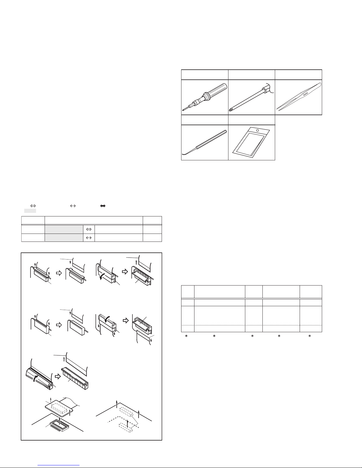
3.1.3 Disconnection of connectors (Wires)
Wire
FPC Connector
· Pull both ends of the connector in the arrow
direction, remove the lock and disconnect the flat
wire.
Wire
FPC Connector
· Pull the both ends of the board in the direction of the
arrow, and remove the Connector.
Wire
Lock
FPC Connector
B-B Connector
B-B Connector
· Pull the both ends of the board in the direction of the arrow, and remove the B-B Connector.
· Extend the locks in the direction of the arrow for
unlocking and then pull out the wire. After
removing the wire, immediately restore the locks
to their original positions because the locks are
apt to come off the connector.
· Extend the locks in the direction of the arrow for
unlocking and then pull out the wire. After
removing the wire, immediately restore the locks
to their original positions because the locks are
apt to come off the connector.
· Extend the locks in the direction of the arrow for
unlocking and then pull out the wire. After
removing the wire, immediately restore the locks
to their original positions because the locks are
apt to come off the connector.
Wire
FPC Connector
FPC
Connector
Lock
B-B Connector
Fig.3-1-1
·m
40
10
Lock
Wire
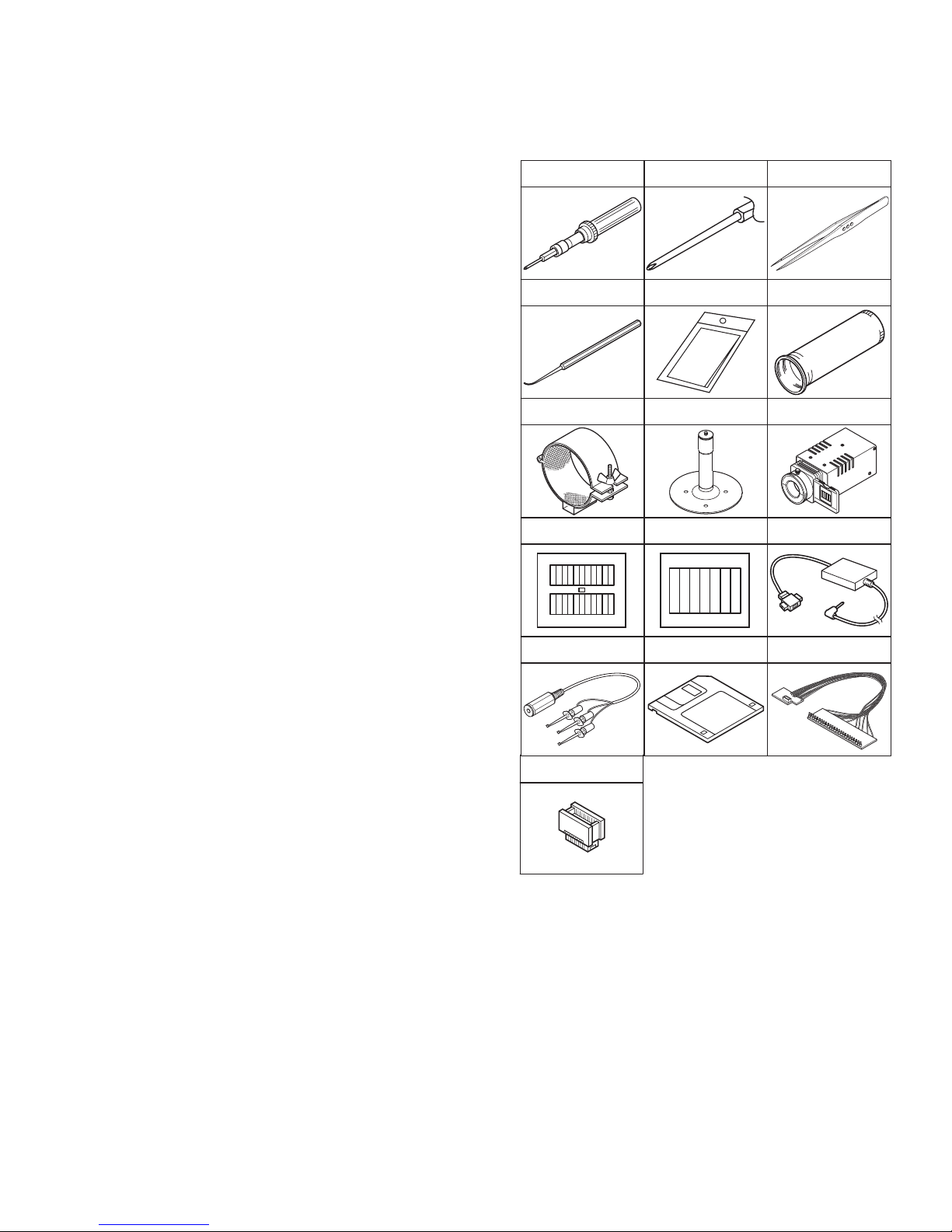
3.1.4 Tools required for disassembly and assembly
Torque driver
YTU94088
Chip IC replacement jig
PTS40844-2
Bit
YTU94088-003
Cleaning cloth
KSMM-01
Tweezers
P-895
Fig.3-1-2
• Torque driver
Be sure to use to fastening the mechanism and exterior parts
because those parts must strictly be controlled for tightening
torque.
• Bit
This bit is slightly longer than those set in conventional torque
drivers.
• Tweezers
To be used for removing and installing parts and wires.
• Chip IC replacement jig
To be used for replacement of IC.
• Cleaning cloth
Recommended cleaning cloth to wipe down the video heads,
mechanism (tape transport system), optical lens surface.
3.2 ASSEMBLY AND DISASSEMBLY OF MAIN PARTS
3.2.1 Assembly and disassembly
When reassembling, perform the step(s) in reverse order.
STEP
No.
[1]
[2]
PART
TOP COVER ASSY
UPPER ASSY
(Inc. VF ASSY,
SPEAKER/MONITOR)
[8]
E.VF UNIT(B/W)
(∗1) Order of steps in Procedure
When reassembling, preform the step(s) in the reverseorder.
These numbers are also used as the identification (location)
No. of parts Figures.
(∗2) Part to be removed or installed.
(∗3) Fig. No. showing Procedure or Part Location.
(∗4) Identification of part to be removed, unhooked, unlocked,
released, unplugged, unclamped or unsoldered.
S = Screw L = Lock, Release, Hook
SD = Solder CN = Connector
[Example]
• 4 (S1a) = Remove 4 S1a screws.
• 3 (L1a) = Disengage 3 L1a hooks.
• 2 (SD1a) = Unsolder 2 SD1a points.
• CN1a = Remove a CN1a connector.
(∗5) Adjustment information for installation.
Fig.
No.
4(S1a), 3(L1a),CN1a
C1
(S2a),2(S2b),3(S2c)
C2-1
2(SD1a),
L2,CN2a,b
2(S8),L8,CN8a
C2-2
POINT
( 4) ( 5)( 2) ( 3)( 1)
NOTE
-
-
NOTE 8
1-6 (No.YF163)
Page 7
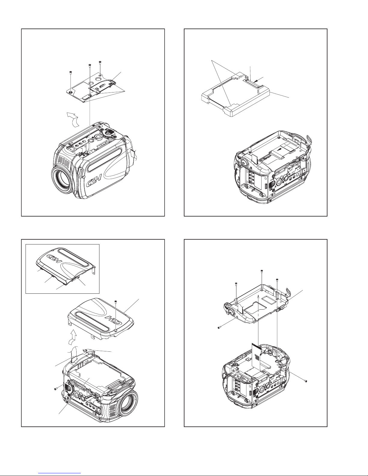
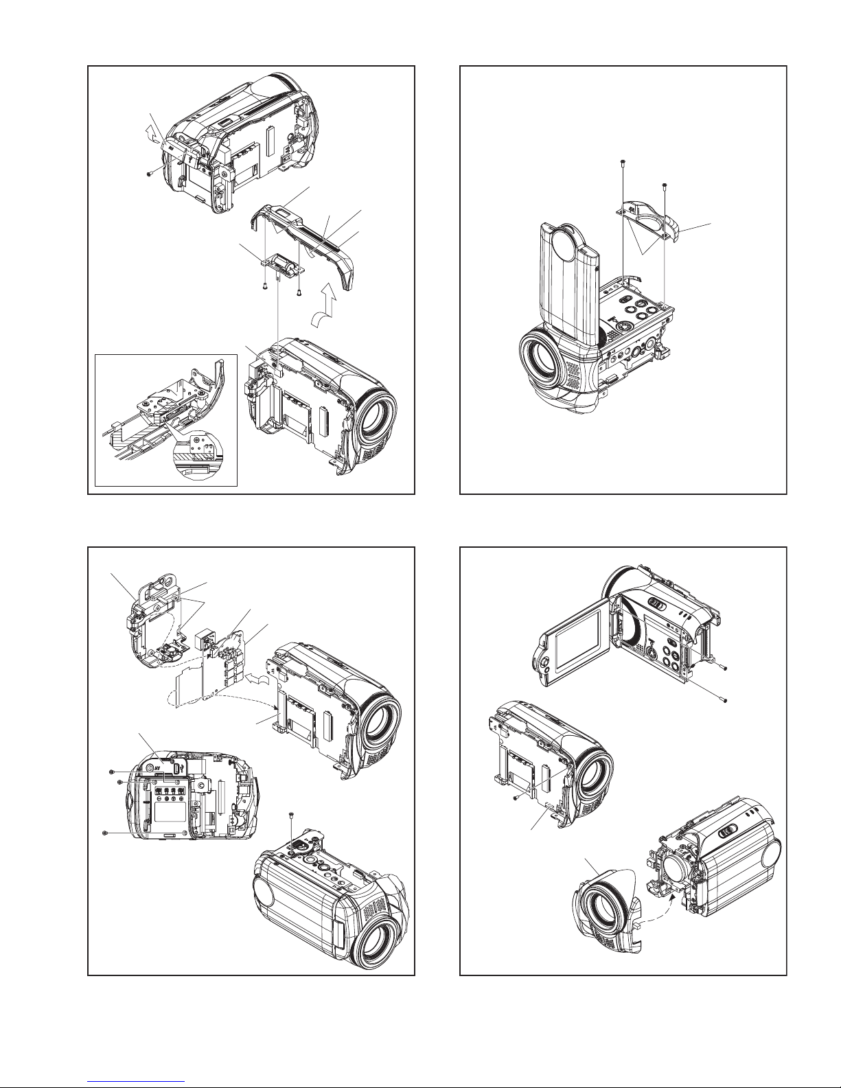
3.2.2 ASSEMBLY/DISASSEMBLY OF CABINET PARTS AND ELECTRICAL PARTS
z Disassembly procedure
STEP
PART NAME
No.
[1]
BOTTOM COVER ASSY
[2]
HDD COVER ASSY
[3]
HDD
[4]
HDD CASE ASSY
[5]
TOP COVER(ZOOM)
[6]
ZOOM UNIT
[7]
REAR BOARD ASSY
[8]
MONI. LOCK CASE ASSY
[9]
FRONT COVER ASSY
[10]
MIC
[11]
UPPER ASSY
[12]
MONITOR ASSY
[13]
OPE BOARD ASSY
[14]
TOP COVER(U) ASSY
[15]
POWER SW ASSY
[16]
SPEAKER
[17]
MAIN BOARD ASSY
[18]
OP BLOCK ASSY
Fig.
No.
CA1
FA1
FA2
FA3
FA4
FA5
FA6
FA7
FA8
FA9
UA1
UA2
UA3
UA4
FA10
FA11
POINT NOTE
3(S1),3(L1)
GRIP BELT,2(S2),
JACK COVER(DC),L2a,b,c,d
CN3
3(S4a),2(S4b)
CN5,JACK COVER(REAR),S5,L5a,b
SHIELD(ZOOM),2(S6),2(L6)
4(S7),2(L7a),JACK COVER(REAR),
CN7a,b,L7b,REAR UNIT
2(S8),2(L8)
2(S9a),S9b,CN9
2(S10),L10,BKT(MIC)
S11,L11a,SHIELD(FRAME),
4(S11),L11b,CN11
S12a,CN12,2(S12b),2(L12)
S13,INTER RUPTER,S13
EARTH PLATE OPE,2(S13),CN13,L13
2(S14),2(L14)
2(S15),2(L15)
4(S16),L16a,b,BKT(UPPER)
CN17a,b,2(S17)
3(S18)
NOTE2a,b,c,d
NOTE3a,b
NOTE5
NOTE6
NOTE7
NOTE10
NOTE12a,b
NOTE13a,b,c
NOTE16
NOTE17
NOTE18a,b
NOTE2a:
During the procedure, leave the GRIP BELT removed from
the hook.
NOTE2b:
When removing the HDD COVER ASSY, leave the JACK
COVER (DC) released.
NOTE2c:
During the procedure, be careful not to damage the tabs.
NOTE2d:
When removing the HDD COVER ASSY, be careful in handling as the HDD may come off.
NOTE3a:
During the procedure, be careful in handling the HDD. Make
sure not to give any shock to the HDD.
NOTE3b:
When attaching the HDD, check the positions of the marks,
and be careful with the GEL lift.
NOTE5:
The screw (No.11) is located under the JACK COVER
-
-
-
-
-
-
-
NOTE12b:
Refer to 3.2.3 ASSEMBLY/DISASSEMBLY OF [12] MONITOR ASSEMBLY for the disassembly of the MONITOR ASSY.
NOTE13a:
During the procedure, be careful in handling the EARTH
PLATE OPE.
NOTE13b:
When attaching the two switches (POWER, MODE), be
careful with the attachment locations. Attach the levers and
switches fixed to one direction as they can be fixed (except
the MODE switch lever). After the attachment, check the operation by moving the switch levers.
NOTE13c:
When attaching the SPEAKER WIRE, be careful in the wiring and not to catch the WIRE in between.
NOTE16:
When attaching the SPEAKER, be careful with the attachment location. Attach the OPE BOARD ASSY first, and then
follow the figure for the SPKEAKER wiring.
NOTE17:
When attaching the MAIN BOARD ASSY, make sure to insert the corner of the MAIN BOARD ASSY into the slit of the
FRAME ASSY.
NOTE18a:
During the procedure, be careful not to damage the EARTH
TERMINAL.
NOTE18b:
Refer to 3.2.4 ASSEMBLY/DISASSEMBLY OF [18] OP
BLOCK ASSEMBLY/CCD BOARD ASSEMBLY.
z Destination of connectors
CN.
No.
CN3 HDD - MAIN CN102 40
CN5 MAIN CN104 ZOOM UNIT - 6
CN7a MAIN CN103 REAR CN6001 53
CN7b REAR CN6002 TRIG SW - 6
CN9 MAIN CN107 MIC - 4
CN11 MAIN CN101 OPERATION CN401 50
CN12 OPERATION CN402 MONI-BL CN7601,7602 24/12,12
CN13 OPERATION CN403 SPEAKER - 2
CN17a MAIN CN105 CCD CN5201 24
CN17b MAIN CN106 OP BLOCK - 22
(REAR).
NOTE6:
Do not disassemble the ZOOM UNIT if not needed as the
SHIELD (ZOOM) is attached to the terminals.
NOTE7:
When removing the REAR UNIT, be careful in handling as
the JACK COVER (REAR) comes off together.
NOTE10:
When attaching the MIC, be careful with the MIC wiring.
NOTE12a:
Remove the screw (No.30), which tightens up the FPC, before connecting/ disconnecting the FPC to/ from the connector.
CONNECTOR
PIN
No.
(No.YF163)1-7
Page 8
1
(S1)
2
(S1)
3
(S1)
[1]
NOTE3b
MARK
CN3
a
L2d
L2d
L2c
L2c
L2b
L2b
Fig.CA1
L2a
L2a
4
4
(S2)
(S2)
L1
NOTE2c
NOTE2c
[2]
[2]
10
(S4b)
Fig.FA2
(S4a)
NOTE3a
[3]
a
7
8
(S4a)
[4]
NOTE2b
NOTE2b
JACK COVER(DC)
JACK COVER(DC)
NOTE2a
NOTE2a
GRIP BELT
GRIP BELT
5
5
(S2)
(S2)
NOTE2d
NOTE2d
Fig.FA1
1-8 (No.YF163)
9
(S4b)
6
(S4a)
Fig.FA3
Page 9
JACK COVER
(REAR)
11
(S5)
NOTE5
<NOTE6>
[6]
NOTE6
CN5
12
(S6)
L6
13
(S6)
[5]
L5b
SHIELD
(ZOOM)
L5a
18
(S8)
19
(S8)
[8]
L8
REAR UNIT
NOTE7
JACK COVER
(REAR)
15
(S7)
16
(S7)
17
(S7)
L7b
L7a
Fig.FA4
CN7b
CN7a
[7]
(S7)
14
22
22
(S9b)
(S9b)
CN9
CN9
[9]
[9]
Fig.FA6
(S9a)
(S9a)
21
21
(S9a)
(S9a)
20
20
Fig.FA5
Fig.FA7
(No.YF163)1-9
Page 10
FPC
CN12
BKT(MIC)
23
(S10)
24
(S10)
SHIELD(FRAME)
25
(S11)
L11a
L10
WIRE
Fig.FA8
[10]
NOTE10
L12
INTERRUPTER
EARTH
PLATE OPE
NOTE13a
34
(S13)
Fig.UA1
33
(S13)
35
(S13)
30
(S12a)
NOTE12a
NOTE12b
[12]
31
(S12b)
32
(S12b)
:
0.245N m(2.5kgf cm)
36
(S13)
29
(S11)
28
(S11)
L11b
27
(S11)
[11]
26
(S11)
Fig.FA9
1-10 (No.YF163)
CN11
26
(S11)
NOTE13b
NOTE13b
[13]
CN13
L13
NOTE13c
Fig.UA2
Page 11
[14]
L15
[15]
45
(S17)
CN17b
46
(S17)
[17]
BKT(UPPER)
L14
Fig.UA3
39
(S15)
40
(S15)
38
(S14)
37
(S14)
CN17b
Fig.FA10
CN17a
NOTE17
CN17a
47
(S18)
(S16)
NOTE16
42
[16]
WIRE
L16a
Fig.UA4
41
(S16)
43
(S16)
44
(S16)
L16b
FRAME ASSY
L18b
FPC
48
(S18)
L18a
FPC
47
(S18)
:
Fig.FA11
NOTE18a
EARTH TERMINAL
48
(S18)
[18]
NOTE18b
0.118N m(1.2kgf cm)
(No.YF163)1-11
Page 12

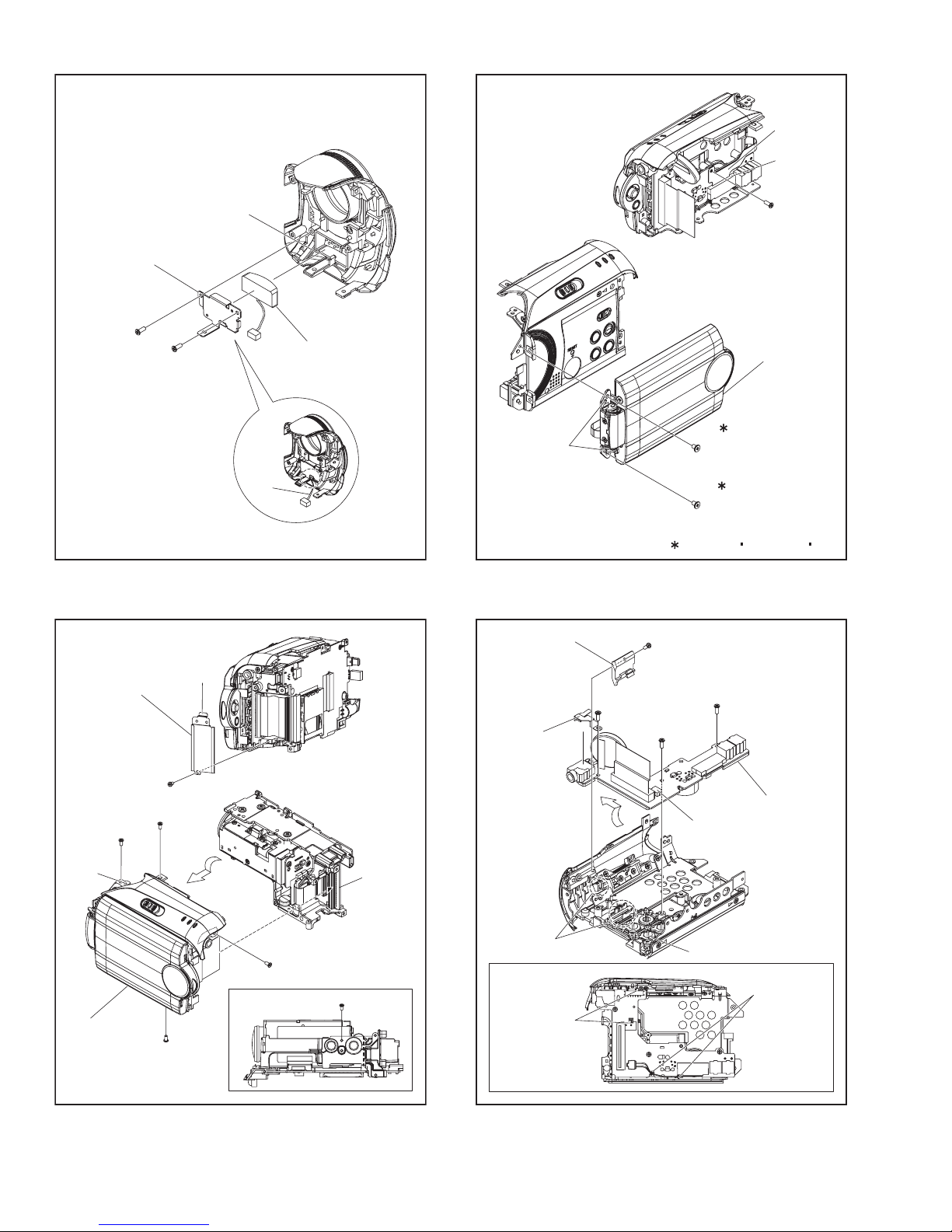
3.2.3 ASSEMBLY/DISASSEMBLY OF [12] MONITOR ASSEMBLY
zCAUTIONS
(1) Remove the MONITOR ASSEMBLY from the UPPER
ASSEMBLY first, as they are removed together in main
parts disassembly, and then proceed to the disassembly
procedure.
(2) During the procedure, be careful in handling the LCD
MODULE and other parts. Pay special attention not to
damage or soil the monitor screen.If fingerprints are left
on the screen, wipe them with clean chamois leather or
a cleaning cloth.
zRemoving MONITOR ASSEMBLY
(1) Turn the HINGE UNIT ASSEMBLY 90°, and remove the
three screws (1-3). Remove the MONITOR COVER ASSEMBLY by removing the six hooks (L12a-f).
(2) Pull out the U/D SWITCH BOARD from the MONITOR
CASE ASSEMBLY.
NOTE12a:
During the procedure, be careful in handling the FPC.
(3) Release the lock of the connector (CN12a,b), and re-
move the HINGE UNIT by lifting it up.
(4) Release the lock of the connector (CN12c,d), and pull
out the FPC.
(5) Remove the two screws (4,5), and Remove the MONI-
BL BOARD ASSEMBLY by removing the hook (L12h).
(6) Remove the BACK LIGHT.
(7) Remove the LCD MODULE.
(8) Remove the LCD BKT.
zRemoving HINGE UNIT ASSEMBLY
(1) Remove the two screws (6,7), and then remove the
HINGE COVER (U,L).
NOTE12b:
During the procedure, be careful in handling the MAGNET and be careful with its attachment direction. Make
sure to attach the MAGNET with its mark facing inward.
NOTE12c:
During the procedure, be careful in handling the FPC.
NOTE12d:
The FPC, with its connection to the MONITOR BOARD
ASSEMBLY facing inward, is rolled around the axis
(shaft) of the HINGE ASSEMBLY rotation 2.5 rounds
(2.5times).
<NOTE12a>
MONI BOARD
ASSY
BACK LIGHT
BL FPC
LCD MODULE
LCD FPC
LCD BKT
U/D SWITCH
FPC
L12h
4
(S12c)
5
(S12c)
MONI.COVER
ASSY
1
(S12a)
HINGE COVER(U)
NOTE12b
MAGNET
NOTE12d
HINGE UNIT
HINGE COVER(L)
6
(S12d)
L12a
2
(S12a)
7
(S12d)
L12c
L12b
FPC
L12g
NOTE12c,d
L12d
3
(S12b)
L12e
L12f
<NOTE12b>
Marking in this side.
HINGE
COVER(U)
b
a
<NOTE12c,d>
MAGNET
MONI.CASE
ASSY
1-12 (No.YF163)
NOTE12a
U/D SWITCH
CN12c
Fig.3-2-3
CN12a
CN12b
CN12d
b
a
0.245N m(2.5kgf cm)
Page 13

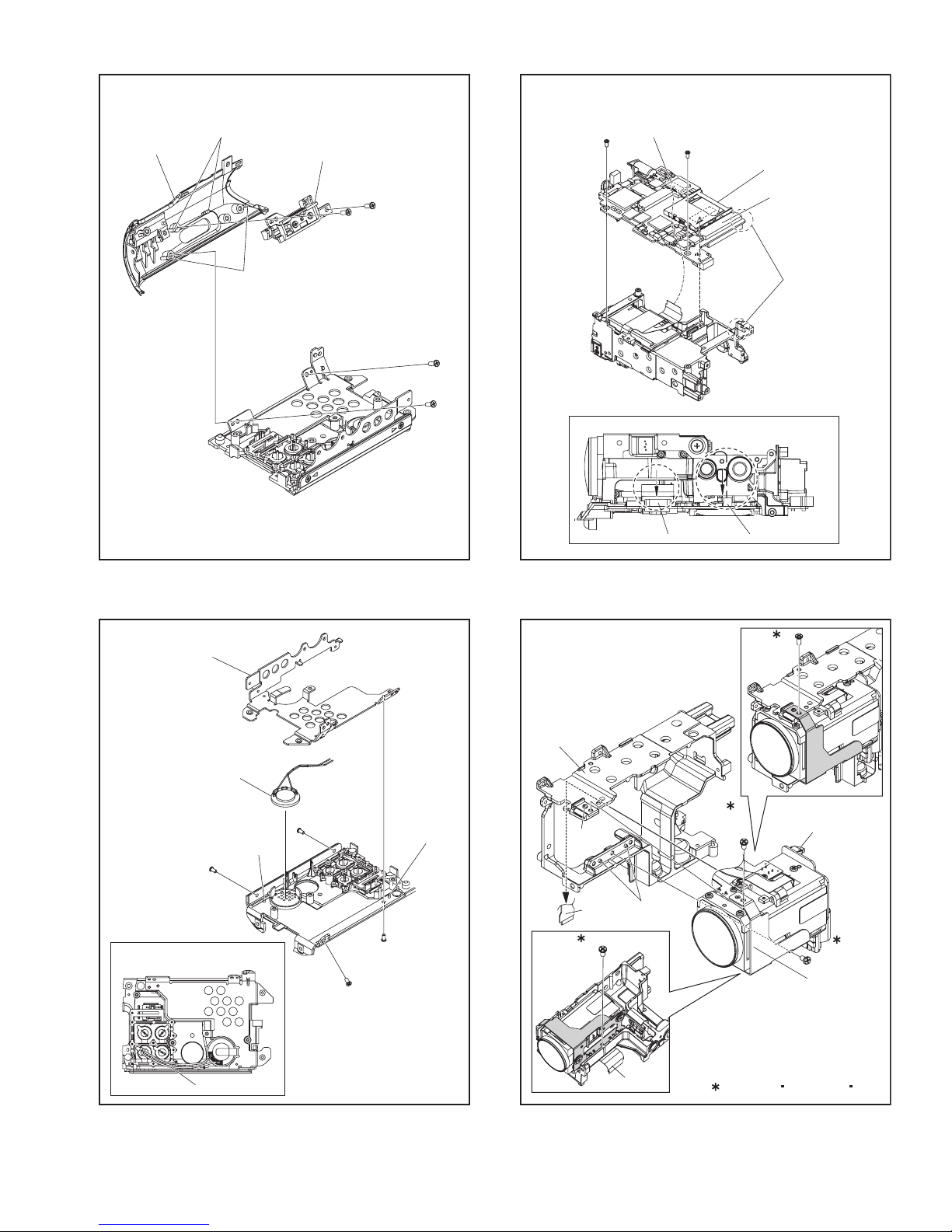
3.2.4 ASSEMBLY/DISASSEMBLY OF [18] OP BLOCK ASSEMBLY/CCD BOARD ASSEMBLY
zPrecautions
(1) Take care in handling the CCD IMAGE SENSOR, OPTICAL
LPF and lens components when performing maintenance
etc., especially with regard to surface contamination, attached dust or scratching. If fingerprints are present on
the surface they should be wiped away using either a silicon paper, clean chamois or the cleaning cloth.
(2) The CCD IMAGE SENSOR may have been shipped with
a protective sheet attached to the transmitting glass.
When replacing the CCD IMAGE SENSOR, do not peel
off this sheet from the new part until immediately before
it is mounted in the OP BLOCK ASSEMBLY.
(3) As the attachment direction of the OPTICAL LPF is im-
portant, be careful when removing it. Make sure to reattach the OP LPF in its original direction.
zDisassembly of OP BLOCK ASSEMBLY / CCD BOARD AS-
SEMBLY
(1) Remove the three screws (1-3),and remove the BKT
(OP) ASSEMBLY.
(2) Unsolder the fourteen soldered points (SD18a) of the
CCD BOARD ASSEMBLY.
(3) Remove the two screws (4, 5), and then remove the CCD
BOARD ASSEMBLY ,BKT(HEAT SINK)MEGA, SHEET,
OPTICAL LPF and the CCD BASE ASSEMBLY.
NOTE18a:
Be careful in handling as there are only the OPTICAL
LPF and the SHEET stored inside the OP BLOCK
ASSY when the CCD BASE ASSY is removed.
NOTE18b:
zAssembly of OP BLOCK ASSEMBLY / CCD BOARD AS-
SEMBLY
(1) Set the OPTICAL LPF first, and then the SHEET to the
OP BLOCK ASSEMBLY.
NOTE18c:
Pay careful attention to the orientation of the OPTICAL
LPF.
(2) Attach the CCD BASE ASSEMBLY first then the
BKT(HEAT SINK)MEGA, CCD BOARD ASSEMBLY so
that the SHEET stays in place, and tighten with the two
screws (4, 5).
(3) Solder the 14 points (SD18a) on the CCD BOARD AS-
SY.
(4) Attach the BKT (OP) ASSEMBLY,and tighten with the
three screws(1-3).
zReplacement of service repair parts
The service repair parts for the OP BLOCK ASSEMBLY are as
listed below.Take special care not to disconnect any of the FPC
wires or cause any damage due to soldering (excessive heating).
(1) FOCUS MOTOR UNIT
(2) ZOOM MOTOR UNIT
(3) AUTO IRIS UNIT
NOTE18d:
When replacing the FOCUS MOTOR UNIT or the ZOOM
MOTOR UNIT, solder the FPC at a space of about 0.5 mm
above the terminal pin.
NOTE 18e:
The AUTO IRIS UNIT includes the FPC ASSEMBLY and
two sensors.
Replace the CCD IMAGE SENSOR as a CCD BASE
ASSEMBLY, not as a single part replacement.
(No.YF163)1-13
Page 14
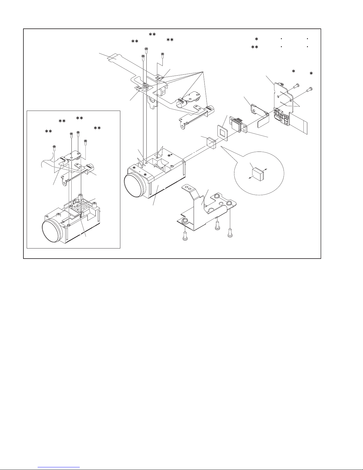
NOTE18d,e
AUTO IRIS UNIT
10
(S18c)
12
(S18c)
11
(S18c)
0.147N m(1.5kgf cm)
0.078N m(0.8kgf cm)
7
(S18c)
6
(S18c)
FOCUS MOTOR
UNIT
NOTE18d
8
(S18c)
(S18c)
ZOOM MOTOR
UNIT
NOTE18d
L18b
9
L18a
SENSOR
L18e
L18c
OP BLOCK ASS'Y
SENSOR
NOTE18a
OPTICAL LPF
L18d
1
(S18a)
SD18b
CCD BOARD ASS'Y
BKT
(HEAT SINK)MEGA
NOTE18a
SHEET
BKT (OP ASSY)
2
(S18a)
(S18a)
NOTE18c
Blue
OP
side
3
4
(S18b)
(S18b)
SD18a
NOTE18a,b
CCD BASE ASS'Y
CCD
side
5
Fig.3-2-4
1-14 (No.YF163)
Page 15
SECTION 4
ADJUSTMENT
4.1 PREPARATION
4.1.1 Precaution
Camera system and deck system of this model are specially
adjusted by using PC.
However, if parts such as the following are replaced, an
adjustment is required. The adjustment must be performed in a
Service Center equipped with the concerned facilities.
• OP BLOCK ASSEMBLY
• MONITOR ASSEMBLY
• EEP ROM (IC4502 of MAIN board)
In the event of malfunction with electrical circuits, first find a
defective portion with the aid of proper test instruments as shown
in the following electrical adjustment procedure, and then
commence necessary repair/ replacement/adjustment.
• In observing chip TP, use IC clips, etc. to avoid any stress.
Prior to replacement of chip parts (especially IC), remove the
solder completely to prevent peeling of the pattern.
• Use a patch cord if necessary. As for a patch cord, see the
BOARD INTERCONNECTIONS.
• Since connectors are fragile, carefully handle them in
disconnecting and connecting the FPC.
4.1.2 REQUIRED TEST EQUIPMENT
• Personal computer (for Windows)
• Color TV monitor
• Oscilloscope (dual-trace type, observable 100MHz or higher
frequency). The one observable 300 MHz or higher frequency
is recommended.
• Digital voltmeter
• DC power supply or AC adapter
• Frequency counter (with threshold level adjuster)
4.1.3 TOOLS REQUIRED FOR ADJUSTMENT
Torque Driver
YTU94088
Chip IC Replacement Jig
PTS40844-2
INF Adjustment Lens Holder
YTU94087
Gray Scale Chart
YTU94133A
Communication Cable
YTU93107B
Service Support System
Bit
YTU94088-003
Cleaning Cloth
KSMM-01
Mini Stand
YTU93108
Color Bar Chart
YTU94133C
YTU94057-97
INF Adjustment Lens
YTU92001B
Light box Assembly
YTU93096A
QAM0099-005
Jig Connector Cable
YTU93106A
Tweezers
P-895
PC Cable
Conversion Connector
YTU94145L-30
• Torque driver
Be sure to use to fastening the mechanism and exterior parts
because those parts must strictly be controlled for tightening
torque.
• Bit
This bit is slightly longer than those set in conventional torque
drivers.
• Tweezers
To be used for removing and installing parts and wires.
• Chip IC replacement jig
To be used for adjustment of the camera system.
• Cleaning cloth
Recommended the Cleaning cloth to wipe down the video
heads, mechanism (tape transport system), optical lens surface.
(No.YF163)1-15
Page 16
• INF adjustment lens
To be used for adjustment of the camera system. For the
usage of the INF adjustment lens, refer to the Service Bulletin
No. YA-SB-10035.
• INF adjustment lens holder
To be used together with the Camera stand for operating the
Videocamera in the stripped-down condition such as the status without the exterior parts or for using commodities that are
not yet conformable to the interchangeable ring. For the usage
of the INF lens holder, refer to the Service Bulletin No. YA-SB-
10035.
• Mini stand
To be used together with the INF adjustment lens holder. For
the usage of the Mini stand, refer to the Service Bulletin No.
YA-SB-10035.
• Light box assembly
To be used for adjustment of the camera system. For the
usage of the Light box assembly, refer to the Service Bulletin
No. YA-SB-10035.
• Gray scale chart
To be used for adjustment of the camera system. For the
usage of the INF adjustment lens, refer to the Service Bulletin
No. YA-SB-10035.
• Color bar chart
To be used for adjustment of the camera system. For the
usage of the INF adjustment lens, refer to the Service Bulletin
No. YA-SB-10035.
• PC cable
To be used to connect the Videocamera and a personal computer
with each other when a personal computer issued for adjustment.
• Communication cable
Connect the Communication cable between the PC cable and
Jig connector cable when performing a PC adjustment.
• Service support system
To be used for adjustment with a personal computer. Software
can be downloaded also from JS-net.
• Jig connector cable
Connected to JIG CONNECTOR of the main board and used
for electrical adjustment, etc.
• Conversion connector
Conversion connector is used to convert the connector part of
the JIG connector cable.
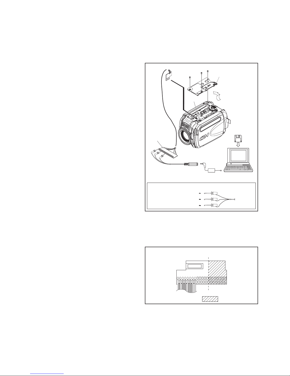
4.2 JIG CONNECTOR CABLE CONNECTION
Connection procedure
NOTE
Be sure to turn the power “OFF”, when connecting the JIG
CONNECTOR CABLE.
If the JIG CONNECTOR CABLE is connected with the power “ON”, communication error may occur.
3
2
JIG CONNECTOR
CABLE
COMMUNICATION CABLE
1
JIG
CONNECTOR
JIG CONNECTOR
TO NU_RX
TO NU_TX
TO GND
PC CABLE
RS232C
COM PORT
COMMUNICATION
CABLE
RED
WHITE
BLACK
COVER(JIG)
SERVICE
SUPPORT
SYSTEM
MENU
PERSONAL COMPUTER
Fig.4-2-1
CAUTION
The JIG CONNECTOR CABLE cannot be connected with
the COVER (JIG) removed because of its structure. It is necessary to cut a part of the connector board as shown below.
Pay special attention during the procedure.
JIG CONNECTOR CABLE [YTU93106A]
1-16 (No.YF163)
: The part to be cut
Page 17
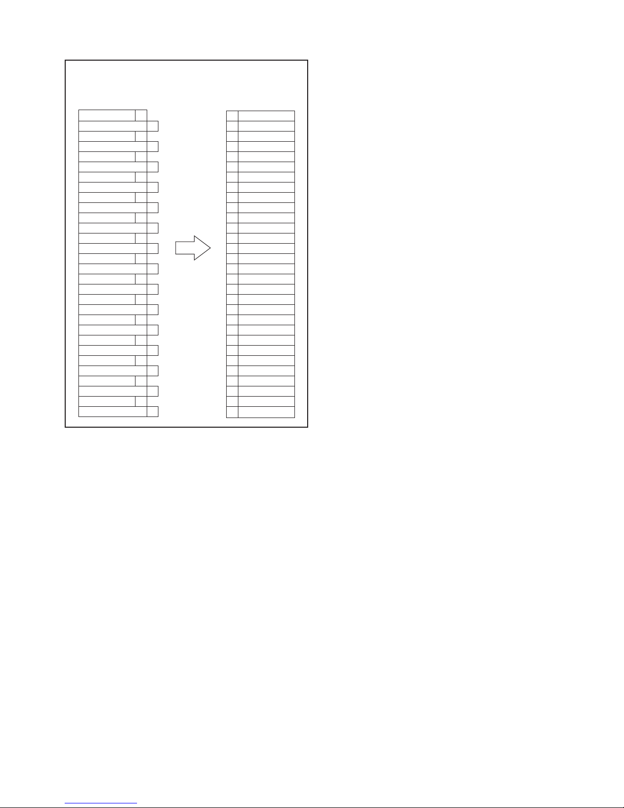
Jig connector diagrams
JIG CONNECTOR CABLE (YTU93106A)
MAIN CN110
ARMTDO
ARMTCK
ARMTMS
ARMTDI
XARMTRST
XJRESET
REG_3.1V
NU_RX
NU_TX
AL_3.1V
SJIG_TX
SJIG_RX
MOD0
SJIG_RST
NC
GND
MON_B
HRP
MON_R
GND
MON_G
NC
VDCVF
NC
NC
ZGH_OUT
ZGH_THRU
SBD5
SBT5
WORD
JIG CONN. BOARD
(PIN NO.)
1
16
2
17
3
18
4
19
5
20
6
21
7
22
8
23
9
24
10
25
11
26
12
27
13
28
14
29
15
30
1
2
3
4
5
6
7
8
9
10
11
12
13
14
15
16
17
18
19
20
21
22
23
24
25
26
27
28
29
30
ARMTDO
ARMTMS
XARMTRST
REG_3.1V
NU_TX
SJIG_TX
MOD0
NC
MON_B
MON_R
MON_G
VDCVF
NC
ZGH_THRU
SBT5
ARMTCK
ARMTDI
XJRESET
NU_RX
AL_3.1V
SJIG_RX
SJIG_RST
GND
HRP
GND
NC
NC
ZGH_OUT
SBD5
WORD
Fig.4-2-2
(No.YF163)1-17
Page 18
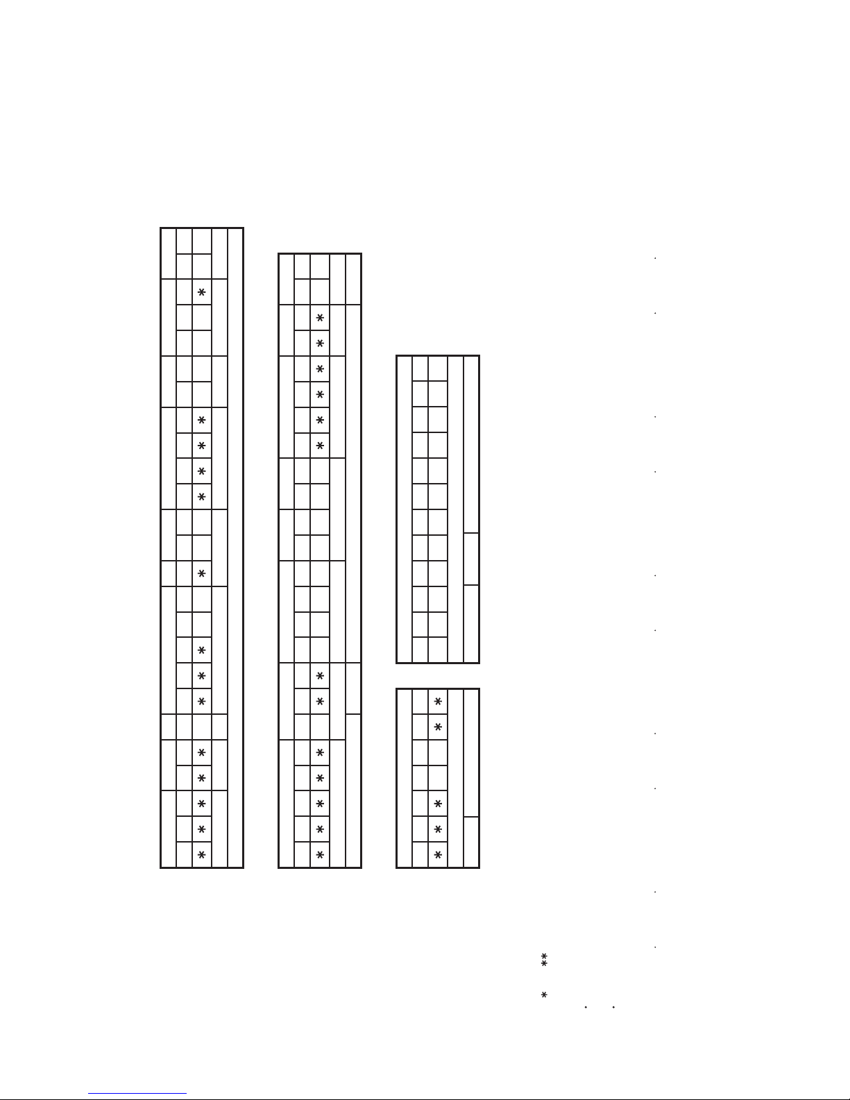
5.1 SERVICE NOTE
SECTION 5
TROUBLE SHOOTING
FA6 FA7 FA8
FA4
FA3 FA5
[18]
c
FA11
eda
aab
a
UA3 UA4 FA10
[18]
3-2-4
UA2
[18]OP BLOCK ASSY/CCD BOARD ASSY
1 2 3 4 5 6 7 8 9 10 11 12
-
[1] [2] [3] [4] [5] [6] [7] [8] [9] [10]
CABINET PARTS AND ELECTRICAL PARTS(1)
Symbol No.
CA1 FA1 FA2
1 2 3 4 5 - 6 7 8 9 10 11 12 13 14 15 16 17 18 19 20 21 22 23 24
Place to stick screw
Removing order of screw
Reference drawing (Fig.No.)
CABINET PARTS AND ELECTRICAL PARTS(2)
Screw tightening torque
1-18 (No.YF163)
[11] [12] [13] [14] [15] [16] [17]
FA9 UA1
25 26 27 28 29 30 31 32 33 34 35 36 37 38 39 40 41 42 43 44 45 46 47 48
Symbol No.
Place to stick screw
Removing order of screw
Screw tightening torque
Reference drawing (Fig.No.)
ab
[12]
[12]MONITOR ASSY
Symbol No.
3-2-3
1 2 3 4 5 6 7
Place to stick screw
Removing order of screw
Screw tightening torque
Reference drawing (Fig.No.)
NOTE:
1 ) and (This mark shows where to attach the screws) : Do not reuse the screws because the screw lock bond was applied to prevent the screws from loosening.
Prepare the specified screws and use them in place of the removed screws.
2 )Tightening torque for the screws
There are setting limits of the torque value for the torque driver. If the value exceeds the setting value, take it as a rough measurement (reference value),
and tighten the screw manually.
The specified torque value is a recommended value of the initial assembly. Therefore, set the value below the specified torque value in the assembling procedure.
Be careful not to break either the screws or the screw holes.
a : 0.098N m (1.0kgf cm) b : 0.245N m (2.5kgf cm) c : 0.118N m (1.2kgf cm) d : 0.147N m (1.5kgf cm) e : 0.078N m (0.8kgf cm)
Page 19

Victor Company of Japan, Limited
Camcorder Category 12, 3-chome, Moriya-cho, kanagawa-ku, Yokohama, kanagawa-prefecture, 221-8528, Japan
(No.YF163)
Printed in Japan
VPT
Page 20

SCHEMATIC DIAGRAMS
HARD DISK CAMCORDER
YF02620042
GZ-MG47EX, GZ-MG47EY,
GZ-MG47EZ, GZ-MG57AA,
GZ-MG57AC, GZ-MG57AG,
GZ-MG57AH, GZ-MG57AS,
GZ-MG57EK, GZ-MG57EX,
GZ-MG57EY, GZ-MG57EZ
CD-ROM No.SML200608
Lead free solder used in the board (material : Sn-Ag-Cu, melting point : 219 Centigrade)
COPYRIGHT © 2006 Victor Company of Japan, Limited
GZ-MG47EXM, GZ-MG47EYM, GZ-MG47EZM [M6E355],
GZ-MG47EXM, GZ-MG47EYM, GZ-MG47EZM [M6E355],
GZ-MG57AAM, GZ-MG57ACM, GZ-MG57AGM,
GZ-MG57AAM, GZ-MG57ACM, GZ-MG57AGM,
GZ-MG57AH, GZ-MG57AS, GZ-MG57EKM,
GZ-MG57AH, GZ-MG57AS, GZ-MG57EKM,
GZ-MG57EXM, GZ-MG57EYM, GZ-MG57EZM [M6E357]
GZ-MG57EXM, GZ-MG57EYM, GZ-MG57EZM [M6E357]
No.YF163SCH
2006/8
Page 21

(No.YF163)2-1 2-2(No.YF163)
!
CHARTS AND DIAGRAMS
NOTES OF SCHEMATIC DIAGRAM
Safety precautions
The Components indentified by the symbol are
critical for safety. For continued safety, replace safety
critical components only with manufacturer's recommended parts.
1. Units of components on the schematic diagram
Unless otherwise specified.
1) All resistance values are in ohm. 1/6 W, 1/8 W (refer to
parts list).
Chip resistors are 1/16 W.
K: KΩ(1000Ω), M: MΩ (1000KΩ)
2) All capacitance values are in µF, (P: PF).
3) All inductance values are in µH, (m: mH).
4) All diodes are 1SS133, MA165 or 1N4148M (refer to parts
list).
2. Indications of control voltage
AUX : Active at high.
AUX or AUX(L) : Active at low.
3. Interpreting Connector indications
Note: If the voltages are not indicated on the schematic
diagram, refer to the voltage charts.
123
2.5
(5.0)
1.8
PB and REC modes
(Voltage of PB and REC modes
are the same)
PB mode
REC mode
4. Voltage measurement
1) Regulator (DC/DC CONV) circuits
REC : Colour bar signal.
PB : Alignment tape (Colour bar).
— : Unmeasurable or unnecessary to measure.
2) Indication on schematic diagram
Voltage indications for REC and PB mode on the schematic diagram are as shown below.
5. Signal path Symbols
The arrows indicate the signal path as follows.
NOTE : The arrow is DVC unique object.
Playback signal path
Playback and recording signal path
Recording signal path
(including E-E signal path)
Capstan servo path
Drum servo path
(Example)
R-Y
Y
Playback R-Y signal path
Recording Y signal path
6. Indication of the parts for adjustments
The parts for the adjustments are surrounded with the circle
as shown below.
7. Indication of the parts not mounted on the circuit board
“OPEN” is indicated by the parts not mounted on the circuit
board.
R216
OPEN
1
2
3
1
2
3
1
2
3
1
4
2
3
Removable connector
Wire soldered directly on board
Non-removable Board connector
Board to Board
Connected pattern on board
The arrows indicate signal path
Note: The Parts Number, value and rated voltage etc. in
the Schematic Diagram are for references only.
When replacing the parts, refer to the Parts List.
Note: For the destination of each signal and further line
connections that are cut off from the diagram,
refer to "BOARD INTERCONNECTIONS"
CIRCUIT BOARD NOTES
1. Foil and Component sides
1) Foil side (B side) :
Parts on the foil side seen from foil face (pattern face)
are indicated.
2) Component side (A side) :
Parts on the component side seen from component face
(parts face) indicated.
2. Parts location guides
Parts location are indicated by guide scale on the circuit board.
rts location are indicated by guide scale on the circuit board.
Note: For general information in service manual, please
refer to the Service Manual of GENERAL INFORMATION Edition 4 No. 82054D (January 1994).
LOCATION
REF No.
IC101 B C 6 A
IC
Category : IC
Horizontal “A” zone
Vertical “6” zone
B : Foil side
(A : Component side)
C : Chip component
D : Discrete component)
Page 22

2-4(No.YF163)(No.YF163)2-3
CCD
GYRO
MAIN IF
TG
CDS
OP DRV
AUDIO
MPEG2 CODEC
3D NR/VIDEO OUT
PREPRCS
DSP
SUB CPU
MONI BL
OPE IF
REAR IF
REG
YTU94074-24
YTU94077-24
YTU94105-40
YTU94077-40
YTU94074-6
YTU94077-6
YTU94074-22
YTU94077-22
YTU94074-24
YTU94077-24
YTU94074-6
YTU94077-6
YTU94074-6
YTU94077-6
YTU94128-4
SIGN00155
VDCPU
DV2OUT3
ANA_IN
MPGFLD
SDR_DQ8
SDR_A8
PMA12
SDR_CS0
ACES_LED
PMA9
SDR_DQ17
PMD14
SDR_DQ3
FOCUS04
XVOEN
DC_CHEK
PMD1
SCPU_CS
REG_1.2V
LCD_RVS
PMA5
SUB
SDR_DQ15
MPGFLD
CDS_CS
PMD11
PMD3
PMA1
SDR_DQ13
PMA20
NCFD7
PMD10
AOBD
GND
PMA0
PMD15
SDR_DQ31
KEY_C
GND
ACHI3
XPMBLS1
DV2OUT0
SDR_A1
PMA13
SDR_DQ30
SDR_DQ3
SDR_A4
SDR_BA1
SDR_CLK
PMA13
SDR_DQ16
BUZZER
PMD13
SDR_DQ2
REG_3.1V
VI1
PMA14
NXCFCE1
REG_4.9V
PMA9
XJRESET
HGout+
SDR_A10
MPGVSYNC
PMA8
PMD4
PMA2
PMD9
PMA16
REG_3.1V
H2
PMA21
NCFD6
AIOBCK
AIOBCK
TG_CS
PMA19
PMA1
ACHI5
GND
PMA0
SDR_DQ26
DV2CKOUT
FLDCPU
ACHI6
SDR_A1
DV2OUT2
SDR_DQ29
SDR_A12
SDR_BA0
F_PTR_AD
SDR_DQM3
SDR_A5
SDR_DQ24
SDR_DQ14
XPMOE
PMA17
SDR_DQ1
CAM_VD
GND
VI0
PMINT
PMD11
V_BATT
VI4
NXCFCE0
CAM_OUT
PMA12
SDR_A3
PMD11
DMACLR
CAM_CLK
SDR_A9
ASPECT
PMA9
PMD3
GND
V2
PMA15
CAM_IN
PMD2
GND
INT_L
SCPU_CS
ARMTMS
VI3
ACHI2
KEY_A
TG_VD
PMA7
SPK-
SDR_DQ25
CN107
123
4
SDR_A3
SDR_DQ28
ACHI7
DV2OUT4
XCACK
SDR_DQ31
SDR_DQM2
PMD14
SDR_WE
SDR_A6
SDR_DQ22
PMA16
SDR_DQ0
SDR_DQ9
PMD12
MPGHSYNC
ZOOM04
PMD2
DV2OUT4
SDR_BA0
PMA18
SDR_CLK
GND
SDR_A8
PMD2
PMD1
GND
REG_4.9V
PMD15
PMD0
SREG_2.5V
NCFD4
AUDIO_CS
TG_HD
ARMTDO
P_GYAMP
CLK27A
VI5
DATA_OUT
ZOOM02
REG_3.1V
PMA6
S_SHUT
SDR_DQ30
SDR_A2
SDR_DQ27
ACHI1
SDR_CKE
SDR_DQ13
DV2OUT5
PMD9
NCFRESET
POFF_SW
SDR_DQM3
SDR_DQM0
SDR_A7
PMA15
PMA1
IR_OUT
PSCTL
ACHI4
CAM_IN
SDR_DQ4
PMD3
REG_4.9V
SDR_A7
PMD1
PMA2
OSD_CS
TG_CS
3AAZEROG
H1
NCFD11
PMD1
SDR_DQM1
ANA_CLK
ACHI6
AOBD
CLK27A
PMD0
PMA5
MPGHSYNC
SDR_DQ26
SDR_DQ28
DMABREQ
SDR_DQ12
VI2
PMD7
CLK27_AT
PMA5
DV2OUT7
SDR_DQM1
PMA5
PMA14
CLK27B
OP_CS
ACHI8
PMA8
REG_3.1V
DV2OUT2
CAM_CLK
CAM_OUT
SDR_DQ10
HGVss-
PMA20
NXCFIORD
PMD8
PMA3
V_OUT
XPMCS7
AIBD
SDR_RAS
REG_1.5V
SDR_A4
5049484746454443424140393837363534333231302928272625242322
21
PMD7
TG_VD
HDCVF
ACHI7
PMA3
SDR_DQ25
PMA4
VI4
SDR_DQ7
SDR_DQ11
SREG2.5V
PMD10
M_REG4.9
PMA6
SDR_DQ27
ACHI4
CN101
2019181716151413121110
987
6
NXCFWAIT
CLK48
REG_4.9V
PMA18
XCREQ
FOCUS02
SDR_DQM2
PMD6
PMA7
DV1IN0
SDR_DQ2
DMASREQ
SDR_A6
NU_TX
PMD12
PMA4
ANA_CLK
C_OUT
XPMWE
V4
OP_CS
GND
SDR_DQM0
ZOOM03
NCFBVD1
CLK27_AT
PMD6
LCD_OPEN
INT_R
VDCVF
PMA2
SDR_DQ24
SDR_DQ10
NXCFIOWR
VI6
VI3
REG_1.5V
SDR_DQ20
DRIVE+
PMA7
A_MUTE
NCFD10
SDR_DQ23
ACHI8
PMA8
SREG2.5V
XPMWE
ASPECT
PMA13
DV1CLKIN
IR_RMC
DV1IN4
AU_SIG/R
CAM_3.1V
SDR_A5
HDIRS
SDR_DQ5
PMD13
PMD3
AIOLRCK
AUDIO_CS
Y_OUT
XPMOE
TG_HD
XPMBLS0
IR_OUT
SDR_WE
MON_B
NCFD15
MCLKI
PMA1
MCLKI
SDR_DQ23
SDR_DQ9
VI7
PMD6
VI2
DMASREQ
SDR_DQ21
PMA10
PMD8
NCFD8
SDR_DQ18
PMD9
PMA15
REG_3.1V
DV1IN2
MOD0
SDR_A0
SCPU_SCK
F_VCC
PMD7
PMD4
SDR_BA1
SDR_DQ11
ANA_OUT
PMD12
ARMTCK
SCPU_SI
PMD5
MON_G
PMA0
NCFBVD2
REG_CS
V1
SDR_DQ22
L_MUTE
SDR_DQ8
PMD5
DV2OUT0
PMD4
NCFRDY
G_RST
VI1
REG_3.1V
CAM_VD
SDR_A2
SDR_CAS
PMD4
NCFD3
PMD11
PMA10
PMA10
DV1IN5
SDR_DQ16
T_BATT
VDCPU
PMA14
ACHI3
SSGFLD
PMD10
FOCUSO3
PMD5
AIBD
SCPU_SI
S_SHUT
DV2CKOUT
VI5
SDR_A10
SDR_DQ12
ANA_CS
AOMCLK
SCPU_SO
SDR_CAS
ACHI0
PMA7
FLSH_RST
TG2_RST
SPK+
NCFD14
MON_R
SDR_DQ21
HDIRS
RG
XPMDE
SDR_DQ7
XCINT
DV2OUT5
PMD15
DV1IN1
SCPU_SCK
MPEG_RST
PMA4
PMD5
PMA6
NCFD9
DV1IN3
I_MTR
FLDCPU
PMA8
SDR_DQ19
PMA21
PMD14
PMD6
VI7
HGout-
AL_3.1V
SCPU_SO
BUZZER
REG_3.1V
VI0
SDR_A9
SDR_DQ1
ANA_RST
AIOLRCK
SDR_RAS
PMA11
SJIG_RST
SDR_DQ20
NCFD12
ZOOM01
SDR_DQ6
DMACLR
XPMWE
XPMCS1
DV2OUT6
PLLSTOP
PLAY_SW
PMD13
PMA11
REG_3.1V
SDR_A11
XPMOE
PMA2
OSD_VD
SDR_DQ29
NCFD2
SDR_A11
PMA3
ACHI9
PMA17
PMD7
DV2CKOUT
ACHI5
DV2OUT6
CLK27B
AU_SIG/L
VI6
SDR_DQ0
SDR_CS0
XCREQ
XARMTRST
PMA10
PMA12
SDR_DQ19
DMABREQ
PMD15
NCFD13
SDR_DQ5
ACHI1
DV2OUT1
Z_PTR_AD
XPMWE
DV1IN6
CHRG_EVR
DRIVE-
SSGFLD
PMD0
L_MUTE
PMD14
PMD10
PMA3
PMA19
A_MUTE
XPMBLS0
ID_LAT
NCFD0
PMD0
PMA9
PMD8
SDR_DQ15
PD_L
XPMCS1
PD_L
HGVcc+
ACHI2
ID_LAT
DV2OUT1
MPGVSYNC
SDR_DQ6
SDR_CKE
LCD_CS
DV2OUT7
ARMTDI
PMA11
CHRG_LED
PMA6
SDR_DQ18
PMD13
SDR_DQ4
ACHI0
FOCUS01
DV2OUT3
XCACK
PMINT
DV1IN7
NU_RX
OP_THRMO
ADP_L
V3
PMA11
ACHI9
DUMP+
REC_SW
GND
PMA4
PMD12
PMD8
SDR_DQ17
SDR_A0
XPMBLS1
SDR_A12
NCFD1
IRIS_PS
PMD9
AOMCLK
PMA2
XPMCS7
SDR_DQ14
REG_3.1V
REG_3.1V
P_GYAMP
Y_GYAMP
GND
G_RST
CN5201
123456789
101112131415161718192021222324
CCD_15V
CCD_-7.5VRGGND
H2
CCD_OUTV1SUBH1V2V3V4
F/Z_RST
CCD__CTL
CCD_CTL
CCD_OUT
CAM_OUT
CAM_CLK
CCD_CTL
REG+CCD
ANA_OUT
INT_GND
ANA_CLK
ANA_OUT
M_REG4.9
XPMWAIT
XPMWAIT
XPMWAIT
HRP
DSP_RST
ANA_IN
OSD_CS
DSP_RST
ANA_RST
OSD_VD
ANA_CS
PSCTL
DSP_RST
CN7601
123456789
101112
CN7602
123456789
101112
CN402
123456789
101112131415161718192021222324
JP7601
JP7602
JP7603
CN103
9
1011121314151617181920212223242526272829303132333435363738
39
40414243444546474849505152
53
CN6001
123456789
101112131415161718192021222324252627282930
31
32333435363738394041424344
45
CN110
30
15
29
14
28
13
27
12
26
11
25
10
24
9
23
8
22
7
21
6
20
5
19
4
18
3
17
2
16
1
CN102
1
2
3
4
5
6
7
8
9
10
11
12
13
14
15
16
17
18
19
20
21
22
23
24
25
26
27
28
29
30
31
32
33
34
35
36
37
38
39
40
NCFA2
NCFA1
NCFA0
NCFD5
V27_OUT
V27_OUT
TVSEL
EEPRM_CK
EEPRM_DI
EEPRM_CS
EEPRM_DO
EEPRM_DO
EEPRM_DI
HOST_LED
TVSEL
AFE_RST
AFE_RST
LAMP_ON
SDWP
SDWP
SDR_VDD SDR_VDD
DV1CLKIN
DV1IN7
DV1IN5
DV1IN0
DV1IN3
PLLSTOP
DV1IN4
DV1IN6
MPEG_RST
NOT USED
NOT USED
(NOT USED)
NOT USED
XCINT
XPMCS0
DV1IN1
DV1IN2
XVOEN
SDDAT0
SDDAT1
SDDAT2
SDDAT3
SDCD
SDCLK
SDCMD
USBDP
USBDN
XCFIORD
XCFIOWR
3AAZEROG
P_DET
S_DET
LITHIUM
INFO_SW
SET_SW
P_MEDIA
LCD_CTL
BL_POWER
UNREGCHK
CLK_OUT
D_BATT
KEY_B
IR_RMC
LIT_3V
LIT_3V
PS_ZEROG
PS_ZEROG
SBT5
SBD5
SJIG_RX
SJIG_TX
WORD
ZEROG_H
ZEROG_H
ZGH_OUT
ZGH_THRU
ZOOM_SW
CN104
12345
6
1
2
3
4
5
6
7
8
9
10
11
12
13
14
15
16
17
18
19
20
21
22
23
24
25
26
27
28
29
30
31
32
33
34
35
36
37
38
39
40
Y_GYAMP
8765432
1
46474849505152
53
54321
54321
2019181716151413121110
987
6
CN401
5049484746454443424140393837363534333231302928272625242322
21
CN7701
12345
6
CN7603
123456789
10111213141516171819202122232425262728293031323334353637383940
3132333435
36
CN7603
123456789
101112131415161718192021222324252627282930
DUMP-
Z_VCC
F_LED
CN403
1
2
SREG1.8V
PPRO8
PPRO4
PPRO1
PPRO11
SOF
PPRO3
PPRO0
PPRO6
PPRO2
PPRO10
VLD_PIX
PPRO5
PPRO9
PPRO7
VCLK
CN6002
12345
6
PMA4
PMA6
PMA2
PMA5
PMA1
PMA8
PMA7
PMA9
PMA3
PMD14
PMD7
PMD13
PMD0
PMD8
PMD11
PMD1
PMD10
PMD4
PMD9
PMD5
PMA2
PMD15
PMD3
PMD12
PMD6
CFBVD1
CFRDY
CFBVD2
PMA20
PMA21
XPMCS0
CLK24_ON
XUSB_CS1
XUSB_CS0
XUSB_RST
NXCFIOWR
NCFA1
NCFD6
NCFD13
NCFD14
NCFD4
NXCFCE0
NCFD7
NCFD9
NCFD3
NCFD11
NCFD0
NCFD12
NXCFCE1
NXCFWAIT
NCFD5
NCFD10
NCFD1
NCFD15
NXCFIORD
NCFD8
NCFD2
NCFA2
NCFA0
NCFRESET
NCFBVD2
NCFBVD1
NCFRDY
SDDAT0
SDCLK
SDDAT2
SDDAT1
SDCMD
SDDAT3
SDCD
SDWP
XCFIOWR
CFA0
CFD4
CFD14
CFD0
CFD5
XCFCE0
CFD11
CFD12
CFD9
CFD13
CFD7
CFD1
XCFCE1
CFRESET
CFD10
CFD2
CFD8
CFD15
XCFIORD
CFD3
CFD6
CFA2
CFA1
CN111
111213
8
7
6
5
4
3
2
1
9
14
10
XBRDMACK
XCFWAIT
BRDMARQ
AL_3.1V
XUSB_INT
CLK48
XPMOE
XPMWE
REG_3.1V
GND
XUSB_CS1
XUSB_CS0
FLSH_RST
SREG1.8V
REG_4.9V
XUSB_RST
XUSB_INT
NTXD_IN
NTXD_OUT
NTXD_IN
NTXD_OUT
VBUS
VBUS
XUSBHOST
XUSBHOST
REG_4.9V
LAMP_ON
LAMP_ON
REG_15V
SDDAT3
SDCD
SDWP
SDDAT2
SDDAT0
SDDAT1
SDCLK
SDCMD
CFA0
CFD8
CFD5
CFRDY
CFRESET
CFD12
CFD7
CFD11
CFBVD2
CFA2
CFD15
XCFWAIT
CFD3
XCFCE0
CFBVD1
CFD0
CFD9
XCFCE1
CFD6
CFD13
CFD2
CFD4
CFD10
CFA1
CFD1
CFD14
USBDN
USBDP
USBDN
USBDP
EEPRM_CS
EEPRM_CK
IRIS_PS
F/Z_RST
CN106
1 F_LED
2 F_PTR_AD
3 F_VCC
4 OP_THRMO
5 GND
6 DRIVE-IS
7 DRIVE+IS
8 HGOUT-IS
9 HGOUT+IS
10 HGVSS-IS
11 HGVCC+IS
12 FOCUS2
13 FOCUS3
14 FOCUS4
15 FOCUS1
16 ZOOM1
17 ZOOM2
18 ZOOM3
19 ZOOM4
20 Z_LED
21 Z_PTR_AD
22 Z_VCC
CN105
1
CCD+15V2CCD+15V3CCD-7.5V4GND5GND6GND7CCD_OUT8GND9GND10GND11GND12RG13H114H215SUB16CCD_CTL17V118V219V320V421Y_GYAMP22G_RST23REG_3.1V24P_GYAMP
PPRO11
SOF
PPRO3
PPRO0
PPRO6
PPRO2
PPRO10
VLD_PIX
PPRO8
PPRO5
PPRO4
PPRO9
PPRO7
PPRO1
VCLK
CAM_CLK
CAM_OUT
CCD_CTL
REG_4.9V
REG_-7.5V
REG+CCD
CAM_3.1V
GND
SHD
TG2_RST
SHP
CPOB
PBLK
ADCLK
PBLK
CPOB
SHD
CDS_CS
SHP
ADCLK
REG_3.1V
REG_14V
REG_14V
ANA_CLK
SUB
ANA_OUT
Vout
GND
DC JACK
REG_1.5V
JIG CONNECTOR
REG_1.5V
123456
REG_1.5V
INT_GND
7
8
INT_L9INT_R
1011121314
BATT_TERM
V4V3V2V1GND
Vdd
RG
TEST
H2
H1
VL
INT_GND
RESET_SW
AU_SIG/L
AU_SIG/R
C_OUT
V_OUT
Y_OUT
MON_B
MON_G
MON_R
HDCVF
B/L(LED)SMS
HRP
SIG_GND
BL_GND
VDCVF
BL_POWER
BL_GND
LCD_CS
LCD_CTL
MON_R
MON_G
HDCVF
REG_4.9V
MON_B
ANA_CLK
ANA_OUT
LCD_RVS
SIG_GND
SIG_GND
BL_POWER
LCD HINGE
REV
SW
M_RVS
REG_3.1V
SIG_GND
LCD_RVS
LCD_CS
LCD_CTL
VDCVF
BL_POWER[15V]
REG_3.1V
REG_3.1V
HRP
GND
LAMP_ON
P_MEDIA
LCD_OPEN
KEY_A
SET_SW
KEY_C
INFO_SW
ACES_LED
CHRG_LED
PLAY_SW
REC_SW
POFF_SW
LITHIUM
S_DET
P_DET
REG_4.9V
REG_4.9V
REG_4.9V
GND
GND
GND
GND
GND
GND
UNREGCHK
I_MTR
V_BATT
CLK_OUT
AL_3.1V
REG_CS
DRV_3.3V
DRV_3.3V
DRV_3.3V
DC_CHEK
REG_1.2V
REG_1.2V
REG_1.2V
D_BATT
GND
GND
GND
GND
GND
GND
GND
GND
GND
T_BATT
ADP_L
REG_4.9V
REG_4.9V
REG_4.9V
CHRG_EVR
CAM_3.1V
CAM_3.1V
DATA_OUT
REG_3.1V
REG_3.1V
REG_3.1V
SJIG_RST
-+TD
XARMTRST
SJIG_RST
XJRESET
GND
REG_3.1V
SBT5
GND
NU_RX
NU_TX
MON_B
HRP
WORD
MON_R
AL_3.1V
MON_G
SJIG_TX
VDCVF
NC
ARMTDO
NC
ARMTCK
ZGH_OUT
ZGH_THRU
ARMTMS
SJIG_RX
ARMTDI
SBD5
MOD0
INT MIC
OP BLOCK
DRV_3.3V
CFBVD2
XCFCE1
XCFCE0
CFA2
CFA0
CFBVD1
CFA1
CFRDY
DMACK-
GND
XCFWAIT
GND
DIOR-
DIOW-
GND
DMARQ
GND
CFD15
CFD0
CFD14
CFD1
CFD13
CFD2
CFD12
CFD3
CFD11
CFD4
CFD10
CFD5
CFD9
CFD6
CFD8
CFD7
GND
CFRESET
HDD
NC
NC
ZOOM_SW
ZOOM_SW
GND
GND
REG_3.1V
REG_3.1V
ZOOM UNIT
WT
OFF
PLAY
REC
TRASH
SW
MENU
SW
LIGHT
SW
INFO
SW
LED RED
POW/CHRG
LED BLUE
ACCESS
LCD OPEN
SW
/DASP-
/CS1-
/CS0-
/DA2
/DA0
/PDIAG-
/GROUND
/GROUND
/GROUND
/DD15
/DD0
/DD14
/DD1
/DD13
/DD2
/DD12
/DD3
/DD11
/DD4
/DD10
/DD5
/DD9
/DD6
/DD8
/DD7
/GROUND
/DA1
/NC
/INTRQ
/GROUND
/IOROY
/RESET-
/NC
/NC
A/V JACK
GND
GND
REG+CCD
GND
GND
REG-CCD
GND
GND
GND
GND
GND
GND
GND
KEY_B
GND
GND
HOST_LED
SPK+
SPK-
KEY_A
INFO_SW
SET_SW
CAM_3.1V
CAM_3.1V
LED GREEN
HOST
CROSS KEY
S JACK
VIDEO
DSC
LITHIUM
AUTO
SW
BL_REGA
NC
LCD_BLK
BL_REGA
LCD_BLK
NC
VB
C12-
C8-V3C1-
AGND
GRB
HSYNC
SCL
VGH
VGoffL
C31+
VCAC
VSYNC
VCCVCC12+
NCNCPGND
VGoffH
NC
C1+
CSB
DFAP
GND1
PVDD
VCOMR
APOL
NC
NC
VA
4:3 LCD MODULE
C8+
ADJ0
VGL
SDA
VCIOUT
ADJ1
NC
C31-
POL
VSS1
C21P
VCOML
VSS
VB[G]
VGL
GCS
VDDA0
VS
C41N
PDO
VCIOUT
VCOMH
C12N
VDD1
C41P
VC[B]
VDD
C21N
GCL
C22P
VA[R]
16:9 LCD MODULE
C31P
HS
GDA
C22N
C11P
C12P
VGH
VDDA1
VCL
VCOIN
C11N
VDDA
C31N
SPEAKER
SPK-
SPK+
USB
LOCK
CU-SD008U
ٕ
SD CARD
XBRDMACK
XCFIORD
XCFIOWR
BRDMARQ
GND
GND
HARF_SW
FULL_SW
GND
GND
TRIG SW
WB_SENS
RMC
MB
SD
8
CCD
20
MAIN
10
USB HOST
DSP MEM
REAR
50
OPERATION
40
MONITOR
60
CLK24_ON
(Page2-35)
(Page2-29)
(Page2-5)
(Page2-27)
(Page2-19)
(Page2-25)
(Page2-17)
(Page2-23)
(Page2-9)
(Page2-11)
(Page2-13)
(Page2-21)
(Page2-15)
(Page2-7)
(Page2-41)
(Page2-41)
(Page2-36)
(Page2-37)
(Page2-31)
(Page2-39)
(Page2-33)
yf163_y10653001a_rev0.1
BOARD INTERCONNECTION
NOTES: The number of patch cords ( ) are indicated by interconnected.
Page 23

(No.YF163)2-5 2-6(No.YF163)
!
!
V_OUT
AU_SIG/L
TO AUDIO
TO 3D NR
TO SUB CPU
TO SUB CPU
TO SUB CPU
P_DET
C_OUT
Y_OUT
S_DET
AU_SIG/R
GND
D191
RB715W-X
2
1
3
R191
1k
LIT_3V
CHRG_LED
PLAY_SW
SET_SW
SJIG_RST
LCD_OPEN
REC_SW
POFF_SW
INFO_SW
KEY_C
LCD_RVS
ACES_LED
KEY_A
P_MEDIA
REG_4.9V
HRP
REG_3.1V
MON_R
MON_B
MON_G
VDCVF
HDCVF
ANA_OUT
LCD_CS
ANA_CLK
LCD_CTL
AL_3.1V
USBDN
VBUS
USBDP
GND
L131
NQR0506-002X
1
43
2
IC171
KSM-2003SN2E
RMC
1
OUT2GND3VCC
R171
IR_RMC
REG_3.1V
GND
T
C171
10/6.3
R172
1.5k
L171
NQR0129-002X
GND
REG_4.9V
T
C172
10/6.3
IR_OUT
CN102
QGF0508F1-40X
TO HDD
USB TERM
0.5mm_FPC_BOTTOM
1
3.3V23.3V33.3V4DASP-5CS1-6CS0-7DA28DA09PDIAG-10DA111INTRQ12DMACK-13GROUND14IORDY15GROUND16DIOR-17DIOW-18GROUND19DMARQ20GROUND21GROUND22DD1523DD024DD1425DD126DD1327DD228DD1229DD330DD1131DD432DD1033DD534DD935DD636DD837DD738GROUND39GROUND40RESET-
C122
0.1
C121
OPEN
[2125]
IC121
NAL0035-001X
1
GND2Tout3AGND4AOZ5AOY
21
6
AOX
7
NC
8
NC
9
NC
10
NC
22
11
STBYB
12
GND
13
AVCC14VREF15DVCC
23
16
GND
17
GND
18
GND
19
ZeroG
20
DGND
24
3AAZEROG
GND
AL_3.1V
L121
SHORT
SDDAT3
R145 47k
R141 47k
REG_3.1V
SDCD
SDDAT1
R148 22
R142
47k
L141
NQR0129-002X
SDCMD
SDCLK
C142 0.1
SDDAT0
GND
R147 10k
R144 47k
R143 47k
R150 22
CN111
NNZ0134-001X
9
SD_DATA2
1
SD_DATA3
2
SD_CMD
3
VSS(GND)
4
VDD(DSC_3V)
5
SD_CLK
6
VSS2
7
SD_DATA0
8
SD_DATA1
R149 22
SDDAT2
R151 22
SDWP
CN104
QGF0508F1-06X
TO ZOOM UNIT
0.5mm_FPC_BOTTOM
1
TELE
234
WIDE
56
WORD
GND
MON_R
SBD5
REG_3.1V
MON_G
R197
MON_B
NU_RX
HRP
ARMTDO
NU_TX
XARMTRST
ARMTDI
TO DSP
TO AUDIO
TO DSP
TO SUB CPU
TO SUB CPU
SUB CPU
TO MAIN IF(CN101,103),
3D NR
TO MAIN IF(CN101,)
ARMTCK
AL_3.1V
XJRESET
ARMTMS
CN110
QGB0512L1-30X
TO JIG CONNECTOR
0.5mm_BtoB
1162173184195206217228239241025112612271328142915
30
R196
R198
SJIG_TX
MOD0
VDCVF
SJIG_RX
SBT5
SJIG_RST
ZOOM_SW
TO SUB CPU
BL_POWER
J101
QNZ0497-001
2
3
4
5
6
7
1
T
C111
47/6.3
L111
SHORT
[2125]
DRV_3.3V
CN107
QGA1001F1-04X
TO MIC
1mm_ML
1234
CFD11
CFBVD2
CFD10
CFD15
TO USB HOST
TO USB HOST
TO DSP,USB HOST
TO PREPRCS,USB HOST
XCFIOWR
CFA1
CFD14
CFD9
CFD4
CFA2
CFD5
XCFCE1
CFD13
CFD3
CFD8
CFRDY
CFD2
XCFCE0
CFD1
CFD7
CFD12
XCFIORD
CFD6
CFD0
CFRESET
CFBVD1
XCFWAIT
CFA0
GND
INT_R
INT_GND
INT_L
REG_3.1V
GND
T
C141
10/6.3
D141
OPEN
123
45
CN111
NNZ0134-001X
10
CARD_DET
CN111
NNZ0134-001X
11
TERMINAL12WP_SW13GND
CN111
NNZ0134-001X
14
GND
D142
OPEN
123
45
R146 47k
Q162
OPEN
R165
OPEN
Q161
OPEN
5412
63
REG_15V
C161
OPEN
[2125]
R163
OPEN
C162
OPEN
R162
OPEN
R164
OPEN
REG+CCD
GND
R161
OPEN
R169
ZGH_OUT
ZGH_THRU
PS_ZEROG
ADP_L
GND
REG_1.2V
KEY_B
CAM_3.1V
REG_1.5V
M_REG4.9
REG_-7.5V
AL_3.1V
CHRG_EVR
L161
NQL38DK-100X
UNREGCHK
DRV_3.3V
REG_CS
SJIG_RST
T_BATT
V_BATT
I_MTR
CLK_OUT
REG_4.9V
REG_3.1V
D_BATT
TO SUB CPU
TO SUB CPU
TO SUB CPU
TO OP DRV
TO CDS,TG
TO TG
TO MAIN IF(CN101,CN110),
SUB CPU
REG_15V
DATA_OUT
CAM_3.1V
R166 OPEN
R167
XUSBHOST
TO USB HOST
TO DSP
46
CAM_3.1V
47 CAM_3.1V
48 GND
49
REG_3.1V
50 REG_3.1V
51 REG_3.1V
52 GND
53 GND
CN103
QGF0508F1-45X
(CN6001)
(CN401)
TO REAR
0.5mm_FPC_BOTTOM
1 GND
2 GND
3
D_BATT
4
KEY_B
5
DC_CHEK
6
CHRG_EVR
7
REG_CS
8 GND
9
CLK_OUT
10 DATA_OUT
11 GND
12 SJIG_RST
13 I_MTR
14 GND
15
V_BATT
16
T_BATT
17 GND
18
ADP_L
19 GND
20
REG-CCD
21 GND
22
REG+CCD
23 GND
24
UNREGCHK
25 GND
26
AL_3.1V
27 GND
28
DRV_3.3V
29 DRV_3.3V
30 DRV_3.3V
31 GND
32
REG_1.2V
33 REG_1.2V
34 REG_1.2V
35 GND
36
GND
37
REG_1.5V
38
REG_1.5V
39
REG_1.5V
40
GND
41
GND
42
REG_4.9V
43
REG_4.9V
44
REG_4.9V
45
GND
DC_CHEK
BL_POWER
R170
R173
OPEN
CN101
QGF0547C2-50X
TO OPE
0.5mm_FPC_VERTICAL
1 GND
2 GND
3
AU_SIG/L
4
AU_SIG/R
5
P_DET
6
V_OUT
7
C_OUT
8
S_DET
9
Y_OUT
10 GND
11 GND
12 LITHIUM
13
POFF_SW
14
REC_SW
15
PLAY_SW
16
CHRG_LED
17
ACES_LED
18
KEY_C
19
INFO_SW
20
SET_SW
21
KEY_A
22
P_MEDIA
23
LCD_OPEN
24
RESET_SW
25 LAMP_ON
26
GND
27 GND
28 GND
29 GND
30
HRP
31
REG_3.1V
32
REG_3.1V
33
REG_4.9V
34 REG_4.9V
35 REG_4.9V
36
BL_POWER
37
MON_B
38
MON_G
39
MON_R
40
HDCVF
41
VDCVF
42
LCD_CTL
43
ANA_CLK
44
ANA_OUT
45
LCD_CS
46
LCD_RVS
47
SPK+
48
SPK-
49
HOST_LED
50 GND
SPK+
SPK-
HOST_LED
XBRDMACK
BRDMARQ
Q422
DTC143XE-X
3
2
1
LAMP_ON
D421
EW5806X/3LMH/
LED_4.9V
GND
R421
1.5k
R101
LED_4.9V
Q171
RPM-22PB
W/B
GND
TP1
NNZ0159-001X
TP2
NNZ0159-001X
TP3
NNZ0159-001X
Q421
UMZ1N-W
5462
13
R424
24
R422
1.8k
R423
391
TL1
STRB_ENV
D181
2
3
GND
Q202
UMX1N-W
5412
63
R206
OPEN
R201
OPEN
C201
1
R205
24k
REG_14V
TO 3D NR
TO MAIN IF
(CN101)
TO TG
R202
27k
R204
1.8k
REG_15V
C202
1
Q201
2SA1577/QR/-X
R203
8.2k
0Ω
0Ω0Ω0Ω
0Ω
0Ω
0Ω
0Ω
_0.5%
_0.5%
110
140,150
190
ONBOARD CONTACT
MAIN(MAIN IF)
10
yf163_y10654001a_rev0.1
TO MAIN IF(CN103,CN110),
TO MAIN IF(CN110),
TO MAIN IF(R170)
TO CDS,TG
SUB CPU
3D NR
TO MAIN IF(CN110),
3D NR
TO MAIN IF(CN110),
3D NR
TO 3D NR
TO SUB CPU
TO SUB CPU
TO SUB CPU
TO SUB CPU,AUDIO,3D NR
TO AUDIO
TO SUB CPU
TO SUB CPU
TO OP DRV
TO PREPRCS
TO DSP
MAIN(MAIN IF) SCHEMATIC DIAGRAM
NOTES: 1. For the destination of each signal and further line connections that are cut off from this diagram, refer to "BOARD INTERCONNECTIONS".
2. The parts with marked ( ) is not used.
Page 24

(No.YF163)2-7 2-8(No.YF163)
PSCTL
EEPRM_CS
TVSEL
SYSSEL1
PD_L
DC_CHEK
SETSW
SCPU_SCK
DIAL_OFF
ACESLED
DC_CHEK
SCPU_SO
FLSH_RST
LCD_CS
CHRG_EVR
SCPU_CS
UNREGCHK
ANA_CLK
SYSSEL0
ZGH_OUT
ZGH_OUT
ZOOMSW
EEPRM_DO
OSD_CS
SCPU_CS
T_BATT
PD_L
PS_ZEROG
EEPRM_DO
ADP_L
A_MUTE
SDET
EEPRM_DI
SCPU_SI
LCD_CS
SCPU_SO
SETSW
ANA_CS
LCD_CTL
DIAL_REC
ANA_IN
T_BATT
KEY_ACH
ANA_OUT
ADP_L
DBATT
CHRGLED
PMEDIA
HOSTLED
BATT_H
ANA_CLK
3AAZEROG
AUDIO_CS
FLSH_RST
BATT_H
LCDRVS
L_MUTE
INFOSW
SCPU_SI
TG2_RST
ANA_RST
AVREF_OF
DIAL_OFF
EEPRM_CK
SBD5
ANA_OUT
CHRGLED
T_BATT
ACESLED
SYSSEL1
V_BATT
V27_OUT
KEY_CCH
UNREGCHK
HOSTLED
INFOSW
ANA_IN
ANA_CLK
SBT5
DBATT
PSCTL
SBT5
OSD_CS
TG2_RST
MONI_SW
I_MTR
I_MTR
KEY_BCH
MONI_SW
ZOOMSW
V_BATT
IR_RMC
A_MUTE
ANA_OUT
ANA_CLK
3AAZEROG
AUDIO_CS
AVREF_OF
PMEDIA
KEY_ACH
ANA_CS
ANA_OUT
REG_CS
SBD5
PDET
SCPU_SCK
ANA_RST
CHRG_EVR
KEY_BCH
ZGH_THRU
EEPRM_DI
SYSSEL0
DIAL_PB
DIAL_REC
KEY_CCH
V27_OUT
TVSEL
PDET
IR_RMC
ZEROG_H
REG_CS
L_MUTE
EEPRM_CK
ZGH_THRU
LCD_CTL
EEPRM_CS
LCDRVS
SDET
DIAL_PB
PS_ZEROG
R1061 100k
EEPRM_DO
HOST_LED
TVSEL
EEPRM_CK
SBD5
R1007
4.7k
R1006
4.7k
ANA_CLK
R1062 100k
REG_3.1V
UNREGCHK
R1031 1k
LIT_3V
TO MAIN IF
TO MAIN IF
R1015
OPEN
TL1030
LCD_CTL
C1006
7p
R1028 1k
R1024 1k
T
C1005
10/6.3
R1045
1k
R1071
100k
R1029 1k
REC_SW
R1069 100k
R1055
10k
R1058 100k
D1001
DA221-X
2
1
3
PSCTL
IC1007
TC75S56FU-X
1
[-]2VSS3[+]
4
OUT5VDD
A_MUTE
V_BATT
CHRG_EVR
DC_CHEK
R1003
2.2K
AL_3.1V
Q1006
DTA124EE-X
R1074
10k
R1008 1K
C1046
0.1
TL1005
R1056
4.7k
TL1031
T_BATT
ZEROG_H
R1014
OPEN
C1045
0.01
FLSH_RST
IR_RMC
R1082 100k
C1034 0.01
R1060 100k
R1023 1k
R1019 1k
EEPRM_DI
C1016 0.01
R1022 1k
R1057 100k
R1086 0R0
SJIG_TX
PLAY_SW
R1083 100k
Q1003
DTA124EE-X
C1008 0.01
R1070 100k
LCD_OPEN
R1046
OPEN
TL1066
L1002
10u
ANA_RST
TL1067
SET_SW
R1051 2.7k
R1017 1k
KEY_B
R1016
2.2k
D1003
OPEN
TL1032
R1065
1k
P_DET
IC1004
SN74AHC1G08DC-X
74AHC1G08GW-X
123
45
LCD_RVS
WORD
R1037
1k
R1076
100k
DSP_RST
DATA_OUT
ANA_CLK
C1026
0.1
C1014 0.01
SJIG_RST
R1059 100k
R1004
2.2K
R1063 47k
IC1003
S-80827CNNB-G-W
1
OUT
2
DET
34
VSS
R1020 1K
C1004
0.1
R1001
100k
IC1002
RS5C314-X
8
VDD
7
XIN
6
XOUT
5
INTR4VSS
3
SIO
2
CLK
1
CS
PS_ZEROG
P_MEDIA
IC1005
SN74AHC1G04DC-X
TC7SH04FU-X
123
45
C1001
0.1
R1064 1k
R1010
680
IC1001
MN102H60GJD
91
LCD_BL89S_DET31DIAL_PB32DIAL_OFF
DIAL_REC
30 5
CHRG_EVR35DC_CHEK42MODE_SW/P_MEDIA12WORD82RESET19VSS20XI21XO24OSCO23OSCI40AUDIO_CS86A_MUTE87RESERVED85L_MUTE4FAN_CTL241PD_L3HOSTLED
75NMI
76JLIP_INT
38INFO_SW
33LCD_OPEN
80BATT_H
36ADP_L
78OSD_VD
77ZEROZINT
533AAZEROG
83VDD
58REMOTE
60ACESLED
81CHRGLED
26ZEROG_H
29DSP_RST
16AFE_RST
48NT_PAL
96RTC_INT
65V_BATT
44T_BATT
62
UNREGCHK
47ZOOM_SW
63KEY_A
64KEY_B
46KEY_C
45I_MTR
54
VREF+
43
VREF-
34
AVDD
66
VDD
61
AVSS
57
SET_SW
59
V27_OUT
7
RESERVED8RESERVED
11
ZDH_THRU
37
RESERVED18RESERVED
98
AVREF_OF
99
PS_ZEROG
100
ZGH_OUT
25
MODE
92
VSS
73
SBD5
74
SBT5
88
P_DET
95
D_BATT
49
KENTO
27
FLSH_RST
71
ANA_IN
72
ANA_OUT
70
ANA_CLK
55
RXD
56
TXD
97 EEP_CS
51 SCPU_IN
52 SCPU_OUT
50 SCPU_CLK
68 DATA_IN
69 DATA_OUT
67 CLK_OUT
79 SCPU_CS
22 VDD
28 RTC_CS
1 REG_CS
39 OSD_CS
14 EEP_IN
15 EEP_OUT
13 EEP_CLK
9 ANA_CS
93 BZ_FREQ
94 BZ_ENV
90 ANA_RST
10 SYTG_RST
2 LCD_CS
17
VDD
6 LCD_RVS
84 PS_CTL
ADP_L
ZOOM_SW
TL1004
LCD_CS
Q1004
2SC5658/QRS/-X
Q1005
2SJ347-X
D
1
G
2
S
3
I_MTR
C1025
0.1
ANA_CS
CHRG_LED
ANA_CLK
Q1002
2SC4617/QR/-X
S_DET
R1085 0R0
AUDIO_CS
R1073
62k
R1043
100k
3AAZEROG
ANA_IN
X1002
NAX0564-001X
R1018 1k
R1036
OPEN
R1025 1k
ANA_OUT
SCPU_SI
BUZZER
R1077
1M
R1075
100k
C1013 0.01
R1005
2.2K
SJIG_RX
Q1001
DTC124EE-X
C1020 0.01
R1084 0R0
SBT5
TL1088
ACES_LED
PD_L
GND
C1018 0.01
CLK_OUT
REG_CS
R1009
680
POFF_SW
ANA_OUT
SCPU_SO
R1053
150k
C1044
0.01
KEY_C
D_BATT
ANA_OUT
EEPRM_CS
OSD_CS
R1072
82k
R1068 100k
TG2_RST
L_MUTE
KEY_A
R1066 1k
AFE_RST
X1001
NAX0784-001X
123
SCPU_SCK
D1002
1SS376-X
C1017 0.01
V27_OUT
C1043
0.01
R1052 18k
C1031
1
OSD_VD
L1001
NQR0129-002x
SCPU_CS
R1054
47k
R1030 1k
INFO_SW
C1015 0.01
ZGH_OUT
ZGH_THRU
TO SIP1280DV
TO LCD
TO ZEROG
TO DSP MEM
TO SIP1280DV FLASH
TO HDD I/F
TO MAIN IF(CN101)
TO PREPRCS
TO AV/S JACK
from RMC
yf163_y10606001a_rev0.1
MAIN(SUB CPU)
10
TO 3D NR,DSP
TO 3D NR
TO DSP
TO 3D NR
TO 3D NR
AUDIO,3D NR
TO MAIN IF(CN101),
(IC121,171,D191)
TO MAIN IF
(IC121,CN103,110)
(CN103)
TO MAIN IF
(CN103)
TO MAIN IF
AUDIO,3D NR
TO MAIN IF
(CN101,103,110)
TO MAIN IF
(CN110)
TO MAIN IF
(CN110)
TO MAIN IF
(CN101)
TO MAIN IF
(CN101)
TO MAIN IF
(CN101)
TO MAIN IF
(CN103)
TO MAIN IF
(CN103)
TO MAIN IF
(CN101)
TO MAIN IF
(CN101)
TO MAIN IF
(CN104)
TO MAIN IF
(IC121)
(CN101),
TO MAIN IF
TO AUDIO
AUDIO,3D NR
(CN101),
MAIN(SUB CPU) SCHEMATIC DIAGRAM
NOTES: 1. For the destination of each signal and further line connections that are cut off from this diagram, refer to "BOARD INTERCONNECTIONS".
2. The parts with marked ( ) is not used.
Page 25

(No.YF163) 2-9 2-10(No.YF163)
yf163_y20403001a_rev0.1
MAIN(AUDIO)
10
L_MUTE
AOBD
C2204 1
AIOBCK
L2401
10u
R2601
2.2k
C2606 0.0047
C2623
10p
T
C2406
10/6.3
Q2401
2SC4617/QR/-X
REG_4.9V
R2235
3.3k
C2214
OPEN
R2233
560k
C2209 1
R2210
820
C2604
0.022
R2234
560k
L2402
10u
C2217
0.1
C2203
1
R2212
2.7
C2233
OPEN
R2217
10
C2602
OPEN
A_MUTE
T
C2402
10/6.3
AU_SIG/L
AUDIO_CS
R2208
22k
R2213
2.7
S_SHUT
TO PREPRCS
R2608 2.2k
R2211
820
BUZZER
T
C2401
10/6.3
C2223
0.1
AOMCLK
L2603
NQR0269-013X
REG_3.1V
R2408
OPEN
ANA_OUT
R2403
18k
C2624
10p
AU_SIG/R
R2607 2.2k
R2207
33k
R2203
39k
R2209
22k
R2206
33k
C2603
0.022
R2602
2.2k
R2407
10
GND
C2235
OPEN
C2224
0.1
C2218
0.1
C2202
1
L2601
NQR0269-013X
AIBD
C2605 0.0047
R2401
4.7k
C2613
1
ANA_CLK
R2202
560k
C2655
0.1
C2205 1
C2612
1
PD_L
R2204
150k
C2611
1
AIOLRCK
C2229
OPEN
L2602
NQR0269-013X
R2609
22k
R2402
4.7k
C2210 1
C2405
0.1
T
C2404
10/6.3
T
C2403
10/6.3
R2610
22k
C2601
OPEN
Q2403
2SC4617/QR/-X
C2656
0.1
C2213
OPEN
IC2201
AK4660VQ
1 2 3 4 5 6 7 8 9 101112
13
14
15
16
17
18
19DVDD
20
21
22
23
24
252627282930313233343536
37
38
39
40
41
42 MVDD
43
44
45
46
47
48
R2241
100k
INT_R
INT_GND
TO MAIN IF
(CN107)
TO MAIN IF
(CN101)
INT_GND
INT_L
SPK+
SPK-
Q2202
UMX18N-W
TO SPEAKER
TO MIC
TO REG
TO AV JACK
-
+
-
+
MIC Power Supply
MPWR
MRF
MVSS
EXTL
INTL
EXTR
INTR
Control
Register
I/F
CDTI
CSN
CCLK
Audio
I/F
Controller
BCLK1
MCLK1
LRCK1
SDTI1
/SDTO2
SDTO1
SDTI2
BCLK2
MCLK2
LRCK2
ROUT1
LOUT1
HPL
HPR
SVSS
SVDD
AVDD
AVSS
HVDD
DVSS
BEEP1
BEEP2
ALC2
DAC
ALC1
EQ
LPF
HPF
ADC
MIX
RIN1
LIN1
MUTETHVCM
VCOM
MUTE
PDN
TO MAIN IF
TO MPEG2
TO SUB CPU
TO SUB CPU
TO SUB CPU
(CN101)
TO MAIN IF
SUB CPU,3D NR
(CN101),
TO MAIN IF
SUB CPU,3D NR
(CN101),
MAIN(AUDIO) SCHEMATIC DIAGRAM
NOTES: 1. For the destination of each signal and further line connections that are cut off from this diagram, refer to "BOARD INTERCONNECTIONS".
2. The parts with marked ( ) is not used.
Page 26

2-12(No.YF163)(No.YF163)2-11
MAIN(MPEG2 CODEC)
10
MDQM
MD31
MD4
MD31
VO0
MA12
MPGFLD
MA4
XVOEN
MD5
VO1
MMCLK
MA1
MPGHSYNC
MA5
MD6
VO2
MA2
MPGVSYNC
MA6
MD7
VO3
MMCLKE
MA3
VI0
MA7
MD8
VO4
XMCS
MD16
VI1
MA8
MD9
VO5
XMRAS
MD17
VI2
MA9
MD10
VO6
XMCAS
MD18
VI3
MA11
MD11
VO7
MD19
VI4
MMCLKE
XMWE
MD12
VOCLK
MD0
MD20
VI5
MMCLK
MDQM
MD13
MD21
VI6
MD25
MD14
MDQM
VI7
MD22
MD15
MD8
MD23
MA0
MD16
MD9
MDQM
MD17
MD10
MA10
MD18
MD11
MD19
VO0
MD12
MA13
MD20
VI0
VO1
MD13
MD21
VI1
VO2
MD14
XMCS
MD22
VI2
VO3
MD15
MD23
VI3
VO4
MD2
MDQM
XMRAS
MD24
VI4
VO5
MD1
MD24
MA12
MD25
VI5
VO6
MD3
MD26
XMCAS
MA13
MD26
VI6
VO7
MD4
MD27
MD0
MD27
VI7
VOCLK
MD5
MD28
XMWE
MD1
MD28
MPGHSYNC
MD6
MD29
MD2
MD29
MPGVSYNC
MD7
MD30
MD3
MD30
MPGFLD
REG_1.5V_L3002
MA0
MA1
MA2
MA3
MA4
MA5
MA6
MA7
MA8
MA9
MA10
MA11
XVOEN
REG_3.1V_L3001
PMD5
DV1IN7
C3008
0.1
XPMWE
PMA5
C3021 0.1
DV2CKOUT
PMD4
DV1CLKIN
REG_1.5V
C3024 0.01
XPMOE
VI1
PMD3
XVOEN
REG_3.1V
XPMWAIT
VI2
PMA3
R3030
4.7k
C3023 0.1
PMD2
MPGFLD
XCINT
TO DSP
TO DSP,PREPRCS
TO DSP,PREPRCS
TO SUB CPU,DSP,
TO USB HOST
TO DSP,DSP MEM
TO PREPRCS
R3040 270
VI3
C3009
0.1
PMA2
R3007 10k
R3027 10k
PMD1
R3017 10k
GND
VI4
PMA4
PMA1
AIBD
PMD0
R3008 10k
R3028 10k
VI5
PMA0
AOBD
R3016 10k
PMA14
C3017 OPEN
VI6
C3012
0.1
PMD10
AIOBCK
R3009
10k
PMA15
CLK27B
TO PREPRCS
TO 3D NR,DSP MEM
TO DSP
TO DSP,3D NR
R3013 270
VI7
R3022 10k
AIOLRCK
PMD11
PMA13
C3010
0.1
C3014
0.1
DV1IN0
C3013
0.01
AOMCLK
XCACK
PMA12
DV1IN1
C3011
0.01
C3015
0.01
R3001 10k
PMA11
C3016
0.1
R3012
10k
XCREQ
DV1IN2
R3035
10k
PMD12
MPEG_RST
PMA10
C3005
0.1
PMD9
DV1IN3
R3002 10k
R3014
C3020 0.01
PMD13
PLLSTOP
PMA9
R3036 10k
PMD8
DV1IN4
L3001
NQR0129-002X
IC3002
K4S28323LF-HN75
[128M FBGA]
46 VDD
75 DQO
5 VDDQ
58 DQ1
90 DQ2
3VSSQ
73 DQ3
89 DQ4
11 VDDQ
72 DQ5
57 DQ6
4VSSQ
71 DQ7
56 VDD
85 DQMO
70 WE_
55 CAS_
84 RAS_
69 CS_
54 BA0
68 BA1
52 A10/AP
67 A0
82 A1
51 A2
36 A3
60 VDD
81 VDD
65 DQ16
29 VDDQ
49 DQ17
64 DQ18
32 VSSQ
77 DQ19
63 DQ20
59 VDDQ
76 DQ21
48 DQ22
44 VSSQ
61 DQ23
87 VDDQ
66 DQM2
40 NC
50 NC
88 VDDQ 86VSSQ
53NC
21DQM3
35NC
80VSSQ
16DQ24
79VDDQ
33DQ25
1DQ26
74VSSQ
18DQ27
2DQ28
78VDDQ
19DQ29
34DQ30
62VSSQ
20DQ31
41VSS
45VSS
7A4
22A5
37A6
8A7
23A8
39A9
83A11
38NC
24CKE
9CLK
10DQM1
25NC
31VSS
26DQ8
47VDDQ
42DQ9
27DQ10
13VSSQ
14DQ11
28DQ12
17VDDQ
15DQ13
43DQ14
12VSSQ
30DQ15
6VSS
C3006
0.01
PMD14
PMA8
R3004
10k
MPGHSYNC
PMD7
DV1IN5
R3029
4.7k
PMD15
PMA7
L3002
NQR0154-003X
R3039
MPGVSYNC
C3007
0.01
PMD6
DV1IN6
L3005
NQR0006-001X
IC3001
UPD61152F1-A03
213
VI075VI1
149
VI276VI3
150
VI477VI5
151
VI678VI7
211
VIHSYNC
148
VIVSYNC74VIFLD/VIVLD
152
VICLK67VO0
206
VO168VO2
207
VO3
142
VO469VO5
143
VO670VO7
141
VOCLK66XVOEN
140
VOHSYNC
205
VOVSYNC
138
AILRCK
204
AIBCK65AIBD
203
AIOLRCK64AIOBCK
137
AIOBD
136
ATX
139
AIMCLK63AOMCLK
174
SIREQ23SICLK/SISTB
173
SISYNC27SIVLD
101
SI0
172
SI124SI2
102
SI325SI4
103
SI526SI6
104
SI732XSOREQ28SOCLK/SOSTB31SOSYNC
109
SOVLD/SORDY
175
SO0
106
SO129SO2
107
SO330SO4
177
SO5
108
SO6
176
SO7
105
XSOEN86MA08MA187MA2
159
MA389MA4
161
MA511MA690MA7
88MA12
10MA13
167MD0
18MD1
96MD2
166MD3
17MD4
95MD5
165MD6
16MD7
97MD8
19MD9
98MD10
20MD11
21MD12
99MD13
22MD14
100MD15
82MD16
3MD17
153MD18
154MD19
2MD20
1MD21
80MD22
81MD23
4MD24
83MD25
5MD26
84MD27
6MD28
157MD29
85MD30
7MD31
14MCLK
13MCLKE
92MCS
93MRAS
164MCAS
15MWE
94MDQM
35HMODE0
113HMODE1
36HMODE2
124CA0
49CA1
191CA2
123CA3
190CA4
48CA5
122CA6
47CA7
46CA8
120CA9
188CA10
45CA11
119CA12
44CA13
187CA14
118CA15
135CD0
60CD1
133CD2
59CD3
132CD4
58CD5
128
CD1453CD15
39
XCCS
50
XCWE
125
XCRE
52
XCWAIT
51
XCREQ0
193
XCACK0
126
XCREQ1
194
XCACK1
245
XCINT
127
CB16
144
XRESET
56
XCBE0
195
XCBE1
192
XCBE2
121
XCBE3
189
IDSEL
43
XREQ
117
XGNT
134
XCLKRUN
186
XPME
42
PCICLK
72
STCLK
210
PWM
209
PSTOP
38
JMOD
115
NMOD/JTMS
116
NCLK/JTCLK
114
XNRST/XJTRST
37
NDI/JTDI
182
NDO/JTDO
110
GPIO0
179
GPIO133GPIO2
111
GPIO334GPIO4
112
GPIO5
243
VDD3
241
VDD3
240
VDD3
237
VDD3
233
VDD3
261
VDD3
264
VDD3
269
VDD3
270
VDD3
198
VDD1
247
VDD1
251
VDD1
242
VDD1
239
VDD1
234
VDD1
171
VDD1
232
VDD1
226
VDD1
224
VDD1
158
VDD1
156
VDD1
255
VDD1
262
VDD1
268
VDD1
271
VDD1
216
VDD1
265
VDD1
222VDDR
225VDDR
227VDDR
230VDDR
169VDDR
199VDDH
256VDDH
254VDDH
252VDDH
248VDDH
246VDDH
249GND
61 GND
62 GND
201GND
202GND
214GND
215GND
263GND
267GND
236GND
231GND
180GND
184GND
181GND
260GND
266GND
258GND
218GND
223GND
250GND
229GND
244GND
238GND
235GND
272GND
155GND
220GND
160GND
163GND
228GND
168GND
170GND
259GND
200GND
257GND
253GND
185GND
208GND
71 GND
79 GND
212GND
178GND
147PVDD
73 PVDD
146PGND
145PGND
183CSCLK
40 CSDI
41 CSDO
162
MA812MA99MA1091MA11
57CD6
131CD7
197CD8
130CD9
55
CD10
129
CD1154CD12
196
CD13
217VDDR
273VDDR
219VDDR
221VDDR
R3003
10k
XUSB_CS1
C3022 0.001
PMA6
VI0
R3041
C3018
OPEN
R3042 10
R304310R3044 10
R3045 10
R3034 4.7k
R3033 4.7k
R3031 4.7k
SREG2.5V
OPEN
C3001
[2125]
OPEN
C3003
[2125]
T
C3004
10/6.3
R3032 47k
OPEN
C3002
[2125]
TL3001
L3006
OPEN
L3007
NQR0129-002X
TL3002
TL3003
TL3004
RA3001
180
1
2
3
4
8
7
6
5
RA3002
180
2
1
4
3
7
8
5
6
R3023 10k
R3024 10k
R3025 10k
R3026 10k
TL3005
R3046
C3019
4.7
TO AUDIO
TO DSP
TO 3D NR
3002
IC 3002
C
VACANT NO.LAST NO.
3024
L 3007
R 3046
RA
3003,3004
3005,3006,3010,3011,3015,3018-3021,3037,3038
0Ω
0Ω
0Ω
0Ω
yf163 _y10607001a_rev0.1
DSP MEM,PREPRCS
TO SUB CPU,DSP,
DSP MEM,PREPRCS
TO SUB CPU,DSP,
DSP MEM,PREPRCS
TO DSP,DSP MEM,
PREPRCS
MAIN(MPEG2 CODEC) SCHEMATIC DIAGRAM
NOTES: 1. For the destination of each signal and further line connections that are cut off from this diagram, refer to "BOARD INTERCONNECTIONS".
2. The parts with marked ( ) is not used.
Page 27

(No.YF163)2-13 2-14(No.YF163)
MON_B
R3218
OPEN
MPGFLD
Q3701
BC847PN-X
5462
13
R3703
68
R3221
C3230
OPEN
R7814
2.2k
R3208 100
DV2CKOUT
C3216 0.1
R3708
10k
V_OUT
C3205 0.1
DV2OUT5
SREG1.8V
R7815
12k
R7805
12k
C3212 SHORT
SREG2.5V
C7801
4.7/16
R7810
12k
C3219
0.1
Q7803
UMX1N-W
2145
36
L7851
SHORT
C3704
0.01
R3225
OSD_CS
ASPECT
Q7801
UMX1N-W
2145
36
DSP_RST
C3705
0.01
DV2OUT3
C3702
0.1
C7805
1/16
ANA_RST
Q7802
UMX1N-W
2145
36
L3206
SHORT
HRP
C3210 0.1
L3701
R3217
820
TL3203
VI7
C7806
1/16
ANA_OUT
C3213 OPEN
C3225
1
R7809
2.2k
C3211 1
R7804
2.2k
C3209 0.1
D3701
UMZ6.8EN-W
123
45
MPGVSYNC
MON_R
R7812
6.8k
DV2OUT2
R3212
18k
ANA_IN
TL3204
OSD_VD
R7813
620
R3709
1.2k
C3220
4.7
VI0
IC3701
BH7612FV-X
16
GND15VCC
14 13
PSCTRL12GND
11 10 9
PVCC
12
GND
345678
PGND
R3219
OPEN
ANA_CS
ANA_CLK
R7807
8.2k
VDCVF
HDCVF
REG_14V
VI6
GND
R7856
36k
R7803
620
C3207
0.01
C3204 0.01
R3214 2.7k
C3215 OPEN
Y_OUT
TO MAIN IF
(CN101)
TO MAIN IF
(CN101)
TO MAIN IF
(CN101,110)
R7817
6.8k
R3216
820
R3710
2.2k
L7801
DV2OUT0
TO DSP
TO MPEG2,
R7851
33k
VI3
C7802
1/16
L3203
NQR0129-002X
DV2OUT4
C3218 0.01
MPGHSYNC
0.1C3217
C_OUT
REG_4.9V
TL3201
R3215 2.7k
C3203 0.01
MON_G
C3206
0.1
REG_3.1V
R7801
33k
R7859
36k
IC3201
JCP8075
1 NC1
2 NC1
13 NC1
14 NC1
54 VSS
3 RST
97 CSO0
55 CSO1
133 CSO2
99 CSO3
4 YSO0
98 YSO1
134 YSO2
56 YSO3
5 VDD(I/O)
100 OUTH
135 OUTV
6 OUTH2
57 OUTV2
101 ZCNT
7 SDOUT
58 VDD(CORE)
102 VSS
136 CLK
8 SDIN
59 SCLK
103 CS
9 VC0
60 VC1
137 VC2
104 VC3
10 BLK1
61 BLK2
138 BLK3
11 HDOUT
62 VDOUT
105 CLKOSD
139 HDCVF
12 VDCVF
63 VSS
161 NC2
162 NC2
163 NC2
164 NC2
165 NC2
15
NC126NC127NC128NC1
106
VDD(I/O)
107
CSYNC
140
SCANMODE65SCANEN16ADDATEST
141
VCC66IPTEST17VDD(I/O)
108
HRP167HRP218VDD(CORE)
142
WYSI0
109
WYSI119WYSI268WYSI3
143
MONI1
110
MONI220VDD(CORE)69VSS
144
WCLK21WCSI070WCSI1
111
WCSI271WCSI322WINV
112
WINH
145
SDR_ONH23VDD(I/O)
146
VSS72VDD(CORE)25RESVD24RESHD73AMUTE
113
SCANI1
114
SCANI274VSS
166
NC2
167
NC2
168
NC2
169
NC2
170
NC2
39NC2
40NC1
41NC1
52NC1
76VDD(CORE)
29SCANI3
30VSS(8DA)
115VDD(8DA)
147COUT
116VREF2
77CBOUT
148COMP2
117ABAR2
78CROUT
31IREF2
149VDD(8DA)
118VSS(8DA)
79NC
32NC
150NC
119NC
33VDD(10DA)
80VSS(10DA)
151VREF1
81YSOUT
34COMP1
120ABAR1
152YCOUT
35IREF1
82CLPY
121VYIN
83VSS(8AD)
36VDD(8AD)
122VRM
153VRL
37VRH
84CIN
123VDD(8AD)
38VSS(8AD)
85VSS
171NC2
172NC2
173NC2
174NC2
175NC2
53
NC164NC175NC186NC1
154
VCCQ
87
CSI042CSI1
124
VSSQ
125
CSI288CSI3
155
VCCQ
43
VDD(I/O)
126
CSI4
89
VSS
44
VDD(CORE)
127
CSI5
156
VSSQ
90
CSI645CSI7
128
INH
91
INV
46
VDD(CORE)
157
VSS
129
VDD(I/O)
158
VCC
47
VSS
92
YSI0
48
VDD(CORE)
93
YSI1
130
VSSQ
49
YSI294YSI3
131
VCCQ
50
YSI495YSI5
159
VSSQ
132
YSI651YSI7
96
VDD(I/O)
160
VCCQ
176
NC2
177
NC2
178
NC2
179
NC2
180
NC2
PSCTL
VI1
C3208 1
Q3202
OPEN
R7854
33k
C7852
OPEN
IC3202
MB90099PFV139EX
20HD
19VD
18VC0
17VC1
16VC2
15BLKA
14VC3
13BLKB
12TSTO
11BLKC10 GND
9 TEST
8 EXD
7NC
6 SDR
5 VDD
4 RST
3SIN
2CS
1 SCLK
C3202 0.01
C3224
1
RA3201
10
3
4
1
2
6
5
8
7
L3201
NQR0129-002X
R7802
8.2k
C3703
1
VI2
VI4
R3222
Short
Q3201
OPEN
2635
41
DV2OUT6
DV2OUT1
C3227
1
C3201 0.01
R3223
IC3204
R1100D251C-X
1
VOUT2VDD3GND
RA3202
10
3
4
1
2
6
5
8
7
R7808
620
R7857
33k
R3213
12k
C3214 OPEN
R7853
36k
VI5
TL3202
C7803
1
T
C3701
10/6.3
DV2OUT7
R3224
(1608)
C7804
1/16
TL3205
_0.5%
0Ω
_0.5%
_0.5%_0.5% _0.5%
0Ω
10µ
_0.5%
_0.5%_0.5%
_0.5%
_0.5%
_0.5%
_0.5%
_0.5%
_0.5%
22µ
_0.5%
_0.5%
_0.5%
_0.5%
OPEN
_0.5%
_0.5%
_0.5%
_0.5%
OPEN
TO JACK
COMP
6dB
7dB
7dB
TO MONITOR
LPF
(L:OUTV,OUTH=HiZ)
20k
1.8k
BPF
(2125)
200k
7dB
TO MPEG2
(2125)
yf163_y10655001a_rev0.1
MAIN(3D NR/VIDEO OUT)
10
DSP
TO MAIN IF
TO SUB CPU
TO SUB CPU
DSP MEM
TO SUB CPU,
TO SUB CPU
TO OP DRV
TO USB HOST
(CN101),
TO MAIN IF
(Q201)
TO MPEG2
DSP MEM
SUB CPU,
AUDIO
MAIN(3D NR/VIDEO OUT) SCHEMATIC DIAGRAM
NOTES: 1. For the destination of each signal and further line connections that are cut off from this diagram, refer to "BOARD INTERCONNECTIONS".
2. The parts with marked ( ) is not used.
Page 28

(No.YF163)2-15 2-16(No.YF163)
SDR_DQM0
SDR_DQ4
SDR_DQ30
SDR_DQ3
SDR_DQ29
SDR_DQ2
SDR_DQ28
SDR_DQ1
SDR_DQ27
SDR_DQ0
SDR_A12
SDR_DQ26
SDR_DQ31
SDR_A11
SDR_DQ25
SDR_CKE
SDR_A10
SDR_DQ24
SDR_A9
SDR_DQ23
SDR_A8
SDR_DQ22
SDR_A7
SDR_DQ21
SDR_A6
SDR_DQ20
SDR_A5
SDR_DQ19
SDR_A4
SDR_DQ18
SDR_A3
SDR_DQ17
SDR_A2
SDR_DQ16
SDR_A1
SDR_DQ15
SDR_A0
SDR_DQ14
SDR_BA1
SDR_DQ13
SDR_BA0
SDR_DQ12
SDR_RAS
SDR_DQ11
SDR_CAS
SDR_DQ10
SDR_CS0
SDR_DQ9
SDR_WE
SDR_DQ8
SDR_DQM3
SDR_DQ7
SDR_CLK
SDR_DQM2
SDR_DQ6
SDR_DQM1
SDR_DQ5
PMA16
SDR_A12
ARMTMS
R4005
OPEN
SDR_BA1
PMD13
SDR_DQ6
R4042
47k
SDR_DQ24
PMA20
SDR_DQ21
R4049
OPEN
151
USBPHYCLK
339
USBVSS
307
USBVDD
338
USBVSS
264
USBVDD
337
USBVSS10USBREXT32USB4XCLK
209
USBDP
210
USBDN
260
USBVDD
261
USBVSS
154
GPIO0
213
GPIO1
167
AUDIN/GPIO13
102
AUDOUT/GPIO12
274
AUDSYNC/GPIO1029AUDBITCLK/GPIO9
225
XAUDRESET/GPIO811GPIO11
106
GPIO4133GPIO40
228
GPIO43
171
GPIO42
227
UART2RXD
170
UART2TXD9VCLKIN
155
GPIO32/PHASEERR84GPIO33/XVRESET
262
GPIO34/ZEBRASKIN
211
GPIO35/CSYNC85GPIO36/HSYNC
152
GPIO37/VSYNC3FSADJp78FSADJn4TVOUTG5TVOUTR6TVOUTB7TVOUTY8TVOUTCHR
110
DV2CLKIN36DV2CLKOUT
172
DV2HSYNC
229
DV2VSYNC
109
DV2UV7
174
DV2UV635DV2UV5
108
DV2UV4
173
DV2UV3
230
DV2UV234DV2UV1
107
DV2UV0
334
CVDD1
333
CVDD2
332
CVDD3
331
CVDD4
303
CVDD5
304
CVDD6
305
CVDD7
306
CVDD8
376
CVDD9
353
CVDD10
322
CVDD11
321
CVDD12
346
CVDD13
347
CVDD14
313
CVDD15
314
CVDD16
105
CVDD17
315
PLLAVSS1
319
PLLAVSS2
317
PLLPVSS
316
PLLDVSS1
318
PLLDVSS2
348
PLLAVDD1
278
PLLAVDD2
350
PLLPVDD
349
PLLDVDD1
277
PLLDVDD2
79
AVSS0
80
AVSS1
81
AVSS2
82
AVSS3
83
AVSS4
146
AVSS5
147
AVSS6
148
AVSS7
149
AVSS8
150
AVSS9
205
AVSS10
206
AVDD0
257
AVDD1
207
AVDD2
258
AVDD3
208
AVDD4
259
AVDD5
301
VDD1
336
VDD2
335
VDD3
330
VDD4
329
VDD5
328
VDD6
302
VDD7
359
VDD8
358
VDD9
327
VDD10
158
VDD
265
VDD13
308
VDD14
375
VDD15
352
VDD16
266
VDD17
309
VDD18
344
VDD19
345
VDD20
351
VDD21
320
VDD22
267
VDD23
310
VDD24
311
VDD25
312
VDD26
380
MVDD1
357
MVDD2
379
MVDD3
356
MVDD4
325
MVDD5
378
MVDD6
355
MVDD7
324
MVDD8
377
MVDD9
354
MVDD10
323
MVDD11
111
XMCS1
39
XMCS2
38
XMCS3
364
VSS2
363
VSS3
362
VSS4
361
VSS5
360
VSS6
365
VSS8
384
VSS9
383
VSS10
382
VSS11
381
VSS12
VSS13
366
VSS14
385
VSS15
396
VSS16
395
VSS17
394
VSS18
340
VSS19
367
VSS20
386
VSS21
397
VSS22
400
VSS23
393
VSS24
120
VSS25
341
VSS26
368
VSS27
387
VSS28
398
VSS29
399
VSS30
392
VSS31
342
VSS32
369
VSS33
388
VSS34
389
VSS35
390
VSS36
391
VSS37
343
VSS38
370
VSS39
371
VSS40
372
VSS41
373
VSS42
374
VSS43
104
VSS44
249
DV1CLKOUT
136
DV1UV067DV1UV1
296
DV1UV2
251
DV1UV3
198
DV1UV4
137
DV1UV568DV1UV6
297
DV1UV7
294
DV1CLKIN
65
DV1HSYNC
250
DV1VSYNC
197
SD_DAT0
138
SD_DAT1
252
SD_DAT2
295
SD_DAT3
199
SD_CMD
135
SD_CD
196
SD_WP
66
SD_CLK
177
SDRAM_A0
114
SDRAM_A143SDRAM_A2
280
SDRAM_A3
233
SDRAM_A4
178
SDRAM_A5
281
SDRAM_A6
234
SDRAM_A7
PMA0
SDR_A11
ARMTDI
C4022
0.1
PMD10
SDR_BA0
SDR_DQ5
PMA13
R4002
3.3k
SDR_DQ23
SDR_DQ20
SSGFLD
PMA1
L4004
NQR0006-001X
R4006
OPEN
PMD15
R4039
SDR_CKE
SDR_DQ4
PMA12
SDR_DQ19
C4020
0.001
DV2OUT0
PMA2
DV2OUT3
R4021
47k
PMD14
R4081
330
SDR_CLK
SDR_DQ3
PMA15
DV1IN5
SDR_DQ18
PMA3
C4018
0.1
DV2OUT5
R4038
180
R4018 47k
PMA11
R4031 220
SDR_A10
C4019
0.1
DV1IN4
PMA21
SDR_DQ2
SDR_DQM1
SDR_DQ17
PMA4
MPEG_RST
XVOEN
PMD11
DV2OUT4
XJRESET
SDR_A9
PMD0
DV1IN3
SDR_DQ1
SDR_DQM0
PMA5
SDR_DQ16
DV2OUT1
R4019 47k
DMABREQ
XPMWE
DV2OUT6
PMD1
SDR_A8
DV1IN2
SDR_DQ0
SDR_WE
PMA8
SDR_DQ15
DV2OUT2
DMASREQ
XPMWAIT
ARMTDO
C4017
0.01
DV2OUT7
PMD3
PLLSTOP
C4027
0.1
DSP_RST
SDR_A7
DV1IN1
SDR_CAS
PMA7
SDR_DQ14
DMACLR
XPMBLS1
DV2CKOUT
R4054
OPEN
C4032
0.01
PMD2
SDR_A6
DV1IN0
PMA6
C4016
0.1
SDR_RAS
SDR_DQ13
XPMCS7
C4026
0.01
R4030 47k
FLDCPU
PMD5
GND
SDR_A5
REG_1.2V
DV1CLKIN
PMA9
R4001
100
SDR_CS0
XPMCS1
SDR_DQ12
R4052
OPEN
PMD7
DV1IN7
SDR_A4
PMA17
C4025
OPEN
XPMOE
SDR_DQ11
R4029 OPEN
PMD4
XCINT
SDR_DQ31
PMA18
DV1IN6
SDR_A3
REG_3.1V
R4016
1k
XPMBLS0
SDR_DQ10
PMD6
ID_LAT
SDR_DQ30
PMA19
R4020
47k
SDR_A2
SIP1280ISD-DVA4 SIP1280ISD-DVA4
115
MCLKIN44NC31AMBACLKIN
217
XRESET15XRESETPERH12SCANE87TESTSCAN
157
TRACESYNC
153
TRACECLK
263
DBGRQ
212
DBQACK
269
PMA0
220
PMA1
163
PMA298PMA325PMA4
270
PMA5
221
PMA6
164
PMA799PMA826PMA9
271
PMA10
222
PMA11
165
PMA12
100
PMA1327PMA14
272
PMA15
223
PMA16
166
PMA17
101
PMA1828PMA19
273
PMA20
224
PMA2119PMD020PMD194PMD221PMD3
160
PMD495PMD522PMD6
218
PMD7
161
PMD896PMD923PMD10
268
PMD11
219
PMD12
162
PMD1397PMD1424PMD1517XPMCS793XPMCS118XPMCS091XPMWE16XPMOE
159
XPMBLS092XPMBLS188XPMWAIT
215
XARMTRST90TCK14TMS
216
TDI
156
AMBATDO1SIO076SIO1
50
SDRAMCLKR
113
SDRAMBS0
176
SDRAMBS1
40
XMCS0
232
XRAS
279
XCAS
42
XMWE
175
DQM0
112
DQM141DQM2
231
DQM3
289
SDRAM_D052SDRAM_D1
123
SDRAM_D2
186
SDRAM_D3
241
SDRAM_D4
288
SDRAM_D551SDRAM_D6
122
SDRAM_D7
185
SDRAM_D8
240
SDRAM_D9
287
SDRAM_D10
326
SDRAM_D11
121
SDRAM_D12
184
SDRAM_D13
239
SDRAM_D14
286
SDRAM_D15
183
SDRAM_D16
238
SDRAM_D17
285
SDRAM_D1848SDRAM_D19
119
SDRAM_D20
182
SDRAM_D21
237
SDRAM_D22
284
SDRAM_D2347SDRAM_D24
118
SDRAM_D25
181
SDRAM_D26
236
SDRAM_D27
283
SDRAM_D2846SDRAM_D29
117
SDRAM_D30
180
SDRAM_D31
37
MCKE
300
AFED0
255
AFED1
202
AFED2
141
AFED372AFED4
256
AFED5
203
AFED6
142
AFED773AFED8
204
AFED9
143
AFED1074AFED11
254
AFECLK
299
3CCDCLK
71
AFEVPIX
140
AFESOF
201
GPIO677GPIO275GPIO3
144
GPIO4
145
GPIO5
200
GPIO25
253
GPIO27
70
GPIO29
132
CFWP
195
XCFWE
128
XCFWAIT
187
CFRESET
58
XCFREG
134
CFRDY
292
XCFOE
133
XCFIOWR
248
XCFIORD
242
CFCSEL
193
CFD0
246
CFD1
291
CFD2
62
CFD3
131
CFD4
192
CFD5
245
CFD6
290
CFD7
61
CFD8
130
CFD9
191
CFD10
244
CFD11
60
CFD12
129
CFD13
190
CFD14
59
CFD15
194
XCFCE0
247
XCFCE1
64
XCFCD1
293
XCFCD2
63
CFBVD1
57
CFBVD2
56
CFA0
127
CFA1
55
CFA2
126
CFA3
189
CFA4
54
CFA5
125
CFA6
188
CFA7
243
CFA8
53
CFA9
124
CFA10
226
PWM0
169
PWM1
276
PWM2
168
PWM3
86
GPIO31
13
NC3
89
NC4
214
GPIO39
69
GPIO24
275
DMASREQ
45
SDRAM_A10
282
SDRAM_A11
235
SDRAM_A12
49
SDRAMCLK
298
GPIO26
139
GPIO28
30
DMABREQ
103
DMACLR
179
SDRAM_A8
116
SDRAM_A9
2
GPIO7
XPMCS0
R4027
OPEN
SDR_DQ9
PMD8
SDR_DQM3
SDR_DQ27
SDR_DQ29
C4015
0.01
PMA10
SDR_A1
R4017
10k
XARMTRST
C4024
0.01
OPEN
R4044
SDR_DQ8
R4023 47k
PMD9
SDR_DQM2
SDR_DQ26
VDCPU
PMA14
SDR_DQ28
SDR_A0
R4028
OPEN
ARMTCK
PMD12
SDR_DQ7
SDR_DQ25
SDR_DQ22
C4023
0.001
C4021
0.01
C4014
0.001
C4013
0.1
C4012
0.01
C4011
0.001
R4026 100
CLK27A
R4074 47k
R4055
OPEN
ZEROG_H
R4043
10k
TL4016
R4079
47k
PMINT
MOD0
TL4019
L4003
NQR0129-002X
L4005
NQR0154-003X
T
C4004
47/4
SDR_VDD
T
C4001
OPEN
T
C4002
10/6.3
T
C4003
10/6.3
C4010
0.1
RA4001
220
341
2
658
7
RA4002
220
432
1
567
8
TL4013
TL4014
TL4015
TL4025
TL4026
TL4027
TL4028
TL4029
TL4030
TL4031
TL4032
TL4006
IC4002
OPEN
1
2
34
5
Q4001
2SC4617/RS/-X
R4084
4.7k
R4085
OPEN
D4002
OPEN
D4003
1SS376-X
C4028
OPEN
NU_TX
NU_RX
R4083
4.7k
X4001
NAX0710-001X
1
ENA2GND
3
OUT4VDD
NCFA1
NCFD5
NCFD11
NCFD3
NCFA0
NCFD9
NCFD12
NCFBVD1
NXCFCE1
NCFD2
NCFD1
NCFA2
NXCFIOWR
NCFD7
NCFRESET
NCFBVD2
NCFD0
NCFD10
NCFD14
NCFD13
NXCFCE0
NCFD6
NCFD4
NCFD15
NXCFIORD
NCFD8
NXCFWAIT
NCFRDY
TL4024
TL4037
TL4002
TL4003
TL4004
TL4005
TL4001
R4086 47k
C4034
0.1
PPRO10
PPRO0
PPRO3
PPRO1
PPRO6
PPRO7
PPRO4
PPRO8
PPRO11
PPRO5
PPRO9
VCLK
VLD_PIX
SOF
PPRO2
XUSB_RST
XUSB_INT
R4036 47k
R4037 47k
XUSBHOST
R4025
47k
TL4007
TL4010
TL4008
TL4011
TL4012
TL4009
TL4017
TL4018
TL4020
SDCD
TL4033
TL4034
TL4035
TL4036
TL4021
TL4022
STRB_ENV
CCD_CTL
NTXD_OUT
NTXD_IN
R4008
TL4040
TL4041
TL4042
TL4043
TL4038
TL4039
RA4003
47k
423
1
576
8
RA4004 47k
412
3
587
6
R4015
R4080
270
CLK48
R4056 180
R4057
180
R4058 180
R4059 180
R4060 180
R4061 180
R4062 180
R4063 180
R4064 180
R4065 180
R4066
180
R4067
180
R4068 180
R4069 180
R4070 180
R4071 180
Operating
Mode
DBETDO
DBETRST
DV1 ITU-R601 16bit OUT
/GPIO55
AFE SSG
/DVCLK
/GPIO14
/GPIO15
/GPIO53
/GPIO52
/GPIO51
/GPIO(option)
/DVVSYNC
/DVHSYNC
/GPIO56
/GPIO57
/DV_SOF
/GPIO46
/DVFIELD
GND for the digital core and I/O
/DVINOUTUV0
Power for memory interface :2.5V
/DVINOUTUV1
Power for I/O :3.3V
/DVINOUTUV2
/DVINOUTUV3
PLL digital power :3.3V
/DVINOUTUV4
AFE Serial
/DVINOUTUV5
AFE Parallel Interface
/DVINOUTUV6
/DVINOUTUV7
/DVDACK
/DVUVSEL
/DVVLD
DV PORT1 IN
UART1
to TCCS
AC'97 Interface
USBDMAJTAG
DV Part2 656+ IO
TV Encoder
Analog Pins
or GPIO
Digital Pins
TV Encoder
/GPIO58
/GPIO59
/GPIO60
/GPIO61
/GPIO62
/GPIO63
/DVINOUTY0
/DVINOUTY1
/DVINOUTY2
/DVINOUTY3
/DVINOUTY4
Power for TV encoder block :3.3V
/DVINOUTY5
GND for TV encoder block
SDRAM
/DVINOUTY6
PLL analog power :3.3V
/DVINOUTY7
PLL digital GND
SDRAM Interface
/GPIO48
PLL analog GND
SD Interface
/GPIO49
Power for the digital core :1.2V
DV Portl 656+ IO
/GPIO47
External Memory Bus
ETM Minimum
PortSCANTEST
NuCORE
DV PORT2 OUT
Q 4001
VACANT NO.
4002
X
LAST NO.
D
4001
4003
IC
4004
C
4086 4003,4004,4007,4009-4014,4022,4024,4032-4035,4040,4041,4045-4048,4050,4051,4053,4072,4073,4075-4078,4082
4034
VACANT NO.
L 4005
R
LAST NO.
4005-4009,4029-4031
RA
4001,4002
4001
0W
0W
0W
TO DSP MEM
TO MPEG2
TO MPEG2
TO PREPRCS
TO PREPRCS
TO MAIN IF
IC4001 IC4001
(CN110)
TO DSP MEM
TO USB HOST
TO USB HOST
TO MPEG2
TO PREROCS
TO MPEG2
TO MAIN IF
TO TG
(TL1)
TO MAIN IF(CN110)
TO 3D NR
TO MPEG2,
3D NR
TO MAIN IF(J101)
TO MAIN IF
TO PREPRCS
TO PREPRCS
TO PREPRCS
TO PREPRCS
TO DSP MEM
TO MPEG2
TO MPEG2,DSP MEM,
TO MPEG2,
TO DSP MEM,
TO DSP MEM
TO MPEG2,DSP MEM
DSP MEM,
TO MPEG2,DSP MEM,
TO MPEG2,DSP MEM,
TO MPEG2,DSP MEM,
TO MAIN IF(CN110)
TO MAIN IF
TO USB HOST
TO SUB CPU,3D NR
(CN110)
TO MPEG2,PREPRCS
TO SUB CPU
TO USB HOST
(111),
USB HOST
TO PREPRCS
PREPRCD,USB HOST
PREPRCD,USB HOST
PREPRCD,USB HOST
PREPRCD
PREPRCD,USB HOST
USB HOST
MAIN(DSP)
10
yf163_y10657001a_rev0.1
MAIN(DSP) SCHEMATIC DIAGRAM
NOTES: 1. For the destination of each signal and further line connections that are cut off from this diagram, refer to "BOARD INTERCONNECTIONS".
2. The parts with marked ( ) is not used.
Page 29

(No.YF163)2-17 2-18(No.YF163)
MAIN(CDS)
10
yf163_y30359001a_rev0.1
IC4201
HD49340HNP-X
[CDS/AGC/AD]
CN105
QGF0503F8-24X
TO CCD (CN5201)
ACHI3
GND
CAM_CLK
CAM_OUT
ACHI6
C4213
0.1
ACHI7
T
C4215
47/4
C4206
1
PBLK
C4202
1
CDS_CS
C4210
1
ADCLK
C4212
0.1
L4201
10
µ
ACHI9
1
D1
2
D2
3
D3
4
D4
5
D5
6
D6
7
D7
8
D8
9
D9
10DRVVDD
11DVSS
12ADCLK
13DVDD
14PBLK
15OBP
16SPBLK
17SPSIG
18AVSS
19
AVDD
20
BLKSH
21
BLKFB
22
CDSIN
23
BLKC
24
BIAS
25
AVDD
26
AVSS
27
ADCIN
28 VRM
29 VRT
30 VRB
31 DVDD
32 DVSS
33 CS
34 SDATA
35 SCK
36 D0
C4211
0.1
ACHI4
R4202
47
TL4202
CCD OUT
TL4203
ADCLK
C4207
0.1
C4214
OPEN
C4209
1
ACHI0
TL4204
SHP
R4201
33k
SHD
CPOB
C4205
0.1
TL4205
SHD
C4203
0.012
CAM_3.1V
TO MAIN IF(CN101,103),TG
ACHI8
C4208
1
ACHI2
SHP
ACHI1
ACHI5
C4201
0.1
CCD+15V
CCD+15V
CCD-7.5V
4
GND
5
GND
6
GND
7
CCD_OUT
8
GND
9
GND
10
GND
11
GND
RG
H1
H2
SUB
CCD_CTL
V1
V2
V3
V4
21
Y_GYAMP
22
G_RST
23
REG_3.1V
24
P_GYAMP
TL4201
GND
P_GYAMP
Y_GYAMP
G_RST
REG_3.1V
4205
4201
LAST NO.
4201
L
4215RC
TL
4202
IC
VACANT NO.
4204
TO TG
TO PREPRCS
TO PREPRCS
TO PREPRCS,OP DRV,TG
MAIN(CDS) SCHEMATIC DIAGRAM
NOTES: 1. For the destination of each signal and further line connections that are cut off from this diagram, refer to "BOARD INTERCONNECTIONS".
2. The parts with marked ( ) is not used.
Page 30

(No.YF163)2-19 2-20(No.YF163)
SDR_DQ13
SDR_A8
SDR_DQ2
SDR_A5
SDR_DQ24
SDR_A2
SDR_DQ28
PMA14
PMA3
SDR_A1
SDR_DQ21
PMD5
SDR_DQ18
SDR_DQ19
SDR_BA0
SDR_DQ20
SDR_DQ29
SDR_A9
PMD2
PMA20
SDR_A2
SDR_DQ28
SDR_RAS
SDR_DQ10
PMD10
SDR_DQ11
SDR_A12
SDR_A11
SDR_A1
SDR_DQ10
XPMWE
PMA11
SDR_DQ5
SDR_DQ6
PMA12
SDR_DQ12
SDR_DQ17
SDR_CAS
PMA6
SDR_A10
PMA1
SDR_DQ13
SDR_RAS
SDR_DQ3
PMA8
PMA13
SDR_DQM0
SDR_CS0
SDR_CKE
SDR_DQM2
SDR_DQ16
SDR_DQ26
SDR_DQ30
SDR_DQ19
PMD13
SDR_CAS
SDR_DQ21
SDR_DQM2
PMD15
SDR_DQ12
SDR_A9
SDR_DQ30
SDR_A6
SDR_DQ25
PMA5
SDR_DQ24
SDR_DQ3
SDR_DQ25
SDR_A3
SDR_DQ22
SDR_DQ22
SDR_DQ14
SDR_DQ31
PMA4
PMD6
SDR_DQ19
PMD3
PMA15
SDR_DQ1
PMD12
SDR_BA1
SDR_DQ30
PMD0
SDR_A6
SDR_BA1
PMA2
SDR_A4
PMD11
SDR_DQ8
SDR_DQ28
SDR_DQ6
SDR_DQ7
PMA9
SDR_DQ4
XPMOE
PMD9
PMA7
SDR_DQM1
SDR_DQ8
SDR_DQM3
SDR_DQ17
SDR_DQM1
SDR_A10
SDR_DQ1
PMA21
SDR_DQ15
SDR_DQ27
SDR_DQ26
SDR_DQ25
PMD14
SDR_DQ26
SDR_DQ22
SDR_A7
SDR_DQ15
SDR_DQ4
PMD7
SDR_DQM3
SDR_DQ23
PMA19
PMA16
SDR_DQ23
SDR_A4
PMD4
SDR_BA0
SDR_DQ11
SDR_CKE
SDR_DQ29
SDR_DQ21
SDR_DQ20
SDR_A5
SDR_A7
PMD1
SDR_WE
SDR_DQ18
SDR_DQ7
SDR_DQM0
SDR_CS0
SDR_DQ9
SDR_DQ31
PMA18
SDR_DQ27
SDR_DQ9
PMA10
SDR_A11
SDR_DQ5
SDR_A0
SDR_DQ0
SDR_WE
SDR_DQ16
SDR_DQ18
SDR_DQ31
SDR_DQ2
PMA17
SDR_A3
SDR_DQ27
SDR_DQ14
SDR_DQ23
SDR_DQ20
SDR_CLK
SDR_DQ24
PMD8
SDR_A8
SDR_DQ29
XPMWE
PMA3
PMD11
PMA21
PMA11
PMA19
PMD13
PMA1
PMD4
PMA2
PMA4
PMA16
PMA6
PMD15
PMD9
PMA13
PMD1
PMA7
PMD3
PMD0
PMA14
PMA15
PMA8
PMD6
PMA5
PMA17
PMD2
PMA10
PMA20
XPMOE
PMD5
PMD10
PMD8
PMA12
PMD12
PMD14
PMA9
PMD7
PMA18
XPMCS7
XUSB_CS0
SDR_DQ17
SDR_DQ16
SDR_CLK
SREG2.5V_L4303
SDR_A0
SDR_DQ0
PMA1
PMD1
PMD13
XPMCS7
PMD2
PMA7
PMD12
PMA6
PMD15
PMA21
XPMOE
PMD6
PMA3
PMA16
PMA4
PMA5
PMD5
PMA11
PMA13
XPMWE
PMD9
PMD0
PMA17
PMD10
PMA10
PMA19
PMA8
PMD8
PMA18
PMD7
PMD11
PMA14
PMD14
PMD4
PMA15
PMA20
PMA12
PMA2
PMA9
PMD3
XUSB_CS0
SDR_A12
SDR_WE
SDR_DQ15
SDR_A3
C4307
0.01
C4306 0.001
C4308 0.1
SDR_DQM3
SDR_DQ26
PMD11
SDR_DQ24
SDR_A0
SDR_DQ1
SDR_CKE
SDR_DQ13
PMA1
TO SUB CPU,MPEG2,DSP,PREPRCS
TO SUB CPU,MPEG2,DSP,PREPRCS
TO SUB CPU,MPEG2,DSP,PREPRCS
TO MPEG2,DSP,PREPRCS
TO MPEG2,DSP
TO DSP
TO DSP
TO USB HOST
TO DSP,USB HOST
TO DSP,USB HOST
PMA16
SDR_DQM2
C4310 0.1
PMA21
SDR_BA0
SDR_A12
SDR_DQ11
SDR_A5
PMA17
SDR_DQ10
PMA2
SDR_A10
SDR_A4
SDR_DQ8
PMA18
PMA12
PMD3
SDR_DQ28
SDR_DQ22
PMA10
PMA13
PMA7
SDR_CAS
SDR_DQ3
PMD0
SDR_DQ19
SDR_CLK
SDR_DQ9
SDR_DQM1
PMA6
SDR_DQ29
SDR_DQ30
PMA15
SDR_DQ25
SDR_A2
PMA4
GND
SDR_DQ0
SDR_A7
PMA20
SDR_DQ4
SDR_DQ12
SDR_DQM0
PMD2
IC4303
E
D
S
2
5
3
2
J
E
B
H
-
7
5
T
[256M FBGA]
46 VDD
75 DQO
5 VDDQ
58 DQ1
90 DQ2
3 VSSQ
73 DQ3
89 DQ4
11 VDDQ
72 DQ5
57 DQ6
4 VSSQ
71 DQ7
56 VDD
85 DQM0
70 WE_
55 CAS_
84 RAS_
69 CS_
54 BA0
68 BA1
52 A10/AP
67 A0
82 A1
51 A2
36 A3
60 VDD
81 VDD
65 DQ16
29 VDDQ
49 DQ17
64 DQ18
32 VSSQ
77 DQ19
63 DQ20
59 VDDQ
76 DQ21
48 DQ22
44 VSSQ
61 DQ23
87 VDDQ
66 DQM2
40 NC
50 NC
88 VDDQ 86VSSQ
53NC
21DQM3
35NC
80VSSQ
16DQ24
79VDDQ
33DQ25
1DQ26
74VSSQ
18DQ27
2DQ28
78VDDQ
19DQ29
34DQ30
62VSSQ
20DQ31
41VSS
45VSS
7A4
22A5
37A6
8A7
23A8
39A9
83A11
38A12
24CKE
9CLK
10DQM1
25NC
31VSS
26DQ8
47VDDQ
42DQ9
27DQ10
13VSSQ
14DQ11
28DQ12
17VDDQ
15DQ13
43DQ14
12VSSQ
30DQ15
6VSS
SDR_DQ18
PMA14
SDR_DQ27
SDR_DQ23
REG_3.1V
PMD10
SDR_DQ20
PMA8
PMD12
SDR_DQ31
SDR_DQ6
SDR_DQ21
SDR_BA1
PMD9
SDR_DQ14
SDR_A9
PMA3
PMD15
SDR_DQ7
PMD1
PMD5
SDR_A6
SDR_DQ16
PMD8
SDR_DQ2
PMA5
PMD4
PMD14
SDR_A8
PMA19
SDR_DQ17
PMA9
SDR_CS0
PMD13
SDR_DQ5
PMA11
PMD7
SDR_A11
C4309 0.01
SDR_RAS
SDR_A1
PMD6
C4303 0.1
SDR_VDD
TO DSP
L4301
NQR0129-002X
C4301
4.7
R4301
47k
L4302
NQR0154-003X
L4303
NQR0154-003X
T
C4304
OPEN
C4305
4.7
RA4301 100k
18
F880[2]
RA4301 100k
27
CF PORT POWERUP
RA4301 100k
36
CF PORT POWERUP
RA4302 100k
36
USB PORT POWERUP
RA4302 100k
18
CF PORT POWERUP
RA4302 100k
45
CF PORT POWERUP
RA4301 100k
45
CPU SELECT
RA4302 100k
27
F89E[6]
RA4304 100k
18
F89E[5:3]
RA4303 100k
45
F89E[5:3]
RA4303 100k
36
RESERVED
RA4303 100k
18
F89E[5:3]
RA4304 100k
36
MEMORY WIDTH FOR FLASH
01: 16bit
RA4303 100k
27
MEMORY WIDTH FOR FLASH
01: 16bit
RA4304 100k
45
F880[0]
RA4304 100k
27
F880[1]
XPMWE
XPMOE
XPMCS7
FLSH_RST
TL4301
TL4302
IC4302
39VF1674CB3KF22
16
A16
15
BYTE
13
VSS
14
DQ15/A-1
35
DQ7
34
DQ14
12
DQ6
33
DQ13
46
DQ5
45
DQ12
11
DQ4
32
VCC
31
DQ11
10
DQ3
44
DQ10
43
DQ230DQ99DQ129DQ828DQ0
7OE8
VSS
6CE5
A0
4A13A21A32A427A526A624A725
A1741A1823RY/BY40WP/ACC48NC39RESET22WE42A2047A1938A821A937A1036A1119A1220A1318A1417A15
IC4301
SP32J55BFI12D22
16
A16
15
BYTE
13
VSS
14
DQ15/A-1
35
DQ7
34
DQ14
12
DQ6
33
DQ13
46
DQ5
45
DQ12
11
DQ4
32
VCC
31
DQ11
10
DQ3
44
DQ10
43
DQ230DQ99DQ129DQ828DQ0
7OE8
VSS
6CE5
A0
4A13A21A32A427A526A624A725
A1741A1823RY/BY40WP/ACC48NC39RESET22WE42A2047A1938A821A937A1036A1119A1220A1318A1417A15
C4302 0.1
XUSB_CS0
C4352
1
IC4304
R1114N251B-X
1 VDD
2 GND
3CE 4NC
5VOUT
C4351
1
SREG2.5V
TO MPEG2,3D NR
R4302
OPEN
R4303
OPEN
TO SUB CPU
C
VACANT NO.
4352
L 4303
R 4303
RA 4304
IC 4304
LAST NO.
[4M FLASH_MEMORY]
[2M FLASH_MEMORY]
4311-4350
MAIN(DSP MEM)
10
yf163_y10658001a_rev0.1
MAIN(DSP MEM) SCHEMATIC DIAGRAM
NOTES: 1. For the destination of each signal and further line connections that are cut off from this diagram, refer to "BOARD INTERCONNECTIONS".
2. The parts with marked ( ) is not used.
Page 31

(No.YF163)2-21 2-22(No.YF163)
IC4501
JCY0209-2
[PREPROCESS]
PMD0
PMA9
TG_HD
ACHI9
PPRO0
V27_OUT
PMD15
PMA8
TG_VD
ACHI8
PPRO1
PMD14
PMA7
ACHI7
PPRO2
PMD13
PMA6
ACHI6
PPRO3
PMD12
PMA5
ACHI5
PPRO4
SCPU_SO
PMD11
PMA4
ACHI4
PPRO5
SCPU_SI
PMD10
PMA3
ACHI3
VDCPU
HDIRS
PPRO6
SCPU_SCK
PMD9
PMA2
ACHI2
FLDCPU
CAM_VD
PPRO7
OP_CS
PMD8
PMA1
ACHI1
PPRO8
PMD7
PMA11
ACHI0
PPRO9
PMD6
PMA10
PPRO10
SOF
PMD5
PMA9
PPRO11
PMD15
PMD4
PMA8
VLD_PIX
VCLK
PMD14
PMD3
PMA7
SOF
VLD_PIX
PMD13
PMD2
PMA6
VCLK
PMD12
PMD1
PMA5
PMD11
PMA4
PMD10
PMA3
CAM_CLK
PMD9
PMA2
CAM_IN
PMD8
PMA1
CAM_OUT
PMD7
PMA0
PMD6
PMD5
PMD4
SCPU_SCK
PMD3
PMD0
PMD2
PMA11
SCPU_SO
PMD1
PMA10
SCPU_SI
PPRO11
PPRO10
PPRO9
PPRO8
PPRO7
PPRO6
PPRO5
PPRO4
PPRO3
PPRO2
PPRO1
EEPRM_CK
EEPRM_DI
EEPRM_DO
F/Z_RST
SDWP
SDWP
S_SHUT
ID_LAT
VDCPU
FLDCPU
SSGFLD
CLK27A
CLK27B
S_SHUT
AFE_RST
MCLKI
MCLKI
TG_HD
TG_VD
CAM_VD
HDIRS
TVSEL
TVSEL
EEPRM_CS
SCPU_CS
XPMCS1
DMACLR
DMABREQ
DMASREQ
XPMBLS1
XPMBLS0
PMINT
XPMWAIT
XPMOE
XPMWE
XPMCS1
DMACLR
XPMBLS1
XPMBLS0
XPMOE
XPMWE
CAM_CLK
CAM_IN
CAM_OUT
F/Z_RST
OP_CS
IRIS_PS
CLK27A
CLK27B
CLK27_AT
CLK27_AT
EEPRM_CS
EEPRM_DI
EEPRM_CK
EEPRM_DO
SCPU_CS
IRIS_PS
V27_OUT
XPMWAIT
PMINT
DMASREQ
DMABREQ
PMA0
AFE_RST
ID_LAT
SSGFLD
G_RST
PPRO0
TG_CS
CDS_CS
G_RST
TG_CS
CDS_CS
ACHI9
ACHI8
ACHI7
ACHI6
ACHI5
ACHI4
ACHI3
ACHI2
ACHI1
ACHI0
CLK24_ON
CLK24_ON
REG_1.5V
C4507
0.1
PMD0
C4528
0.1
C4521
1
C4534
0.1
R4579
100
ACHI8
R4571
VDCPU
C4523
0.1
DMACLR
ACHI1
C4533
0.1
PPRO4
R4510
C4510
0.1
MCLKI
TO TG
TO CDS
TO CDS
TO OP DRV,
TO SUB CPU
TO SUB CPU
TO DSP
TO MPEG2
TO AUDIO
TO SUB CPU
TO USB HOST
TO MAIN IF
(CN111)
TO MAIN IF
(Q422)
PMA11
R4514
TG_CS
XPMBLS1
R4569
PPRO9
PMA1
C4525
4.7/6.3
PMD9CLK27B
PPRO6
CAM_OUT
PMINT
PMA8
PMD13
PPRO2
L4502
NQR0006-001X
XPMCS1
TO DSP
TO DSP
TO MPEG2,DSP
TO MPEG2,DSP
TO SUB CPU,MPEG2,
SOF
R4558 470
PMD6
R4544
OPEN
ACHI5
R4563 1.5k
SCPU_SI
PMA5
R4532
22K
PMD1
IRIS_PS
IC4502
M95320-WDW6-X
[EEPROM]
8
VCC
7
XHOLD
6
SCK
5SI4
VSS
3
XWP
2
SO
1
XCS
ACHI9
Z_PTR_AD
R4524
GND
ID_LAT
R4527
R4502 100
PMD3
R4533 8.2K
ACHI2
V27_OUT
R4503 470
R4529
R4508 470
R4537
R4551
PMA2
L4501
NQR0006-001X
DMABREQ
PMD10
PPRO10
R4554
C4518
0.01
ACHI6
TG_VD
CLK27A
XPMWAIT
PPRO7
C4514
0.01
R4536
CAM_CLK
PMA9
PMD14
C4527
0.1
C4504
0.1
R4580
10K
AFE_RST
VCLK
PPRO3
C4506
0.1
C4529
4.7/6.3
C4522
0.1
C4503
0.01
PMD7
XPMWE
C4501
0.1
C4511
4.7/6.3
R4511
L4503
NQR0006-001X
R4513
C4532
0.1
R4515 1K
PPRO0
PMA6
PMD2
ACHI4
2
VDD68VDD72SCK03SI04SO073SCK174SI175SO170SCK2
130
SI2
129
SO27HSCK71HSI
131
HSO5GND6GND8GND
133
OMT0
134
OMT1
135
VDCPU
186
FLDCPU
185
ENCFLD763.3V_VDD783.3V_GND11CLK27A80CLK27B
188
INH
137
INV32KO
162
CLR10AVDDP277AGNDP279PLLREF2
136
PLLFB29PLLI2
187
PLLSEL2
189
PMD0
138
PMD1
190
PMD2
139
PMD3
191
PMD4
140
PMD581PMD614PMD7
141
PMD882PMD9
143
PMD10
142
PMD1187PMD1286PMD1385PMD1421PMD1512VDD13VDD15VDD843.3V_VDD183.3V_GND
19
GND
20
VDD
17
VDD
16
PMA11
83
PMA10
23
PMA9
24
PMA8
89
PMA7
144
PMA6
145
PMA5
146
PMA4
192
PMA3
193
PMA2
194
PMA1
195
PMA0
100
DMACLR
98
DMAREQ_B
155
DMAREQ
154
PMBLS1
153
PMBLS0
152
PMINT
95
PMWAIT
30
PMOE
96
PMWE
37
PMCS
156
CACK
101
CREQ
22
GND
25
GND
88
VDD
28
AVREFM
91
AVREFP
199
AGNDA
26
AVDDA
150
AIN7
93
AIN6
198
AIN5
27
AIN4
149
AIN3
92
AIN2
197
AIN1
148
AIN0
94
3.3V_GND
90
3.3V_VDD
29
3.3V_VDD
53
TDO
147
TCK
196
TRST
200
TMS
151
TDI
97
GND
31
VDD
33
VDD
34
VDD
99
3.3V_GND
35
3.3V_VDD
38
VCLK
41
SOF
104
VPIX
207
DOUT11
206
DOUT10
159
DOUT9
205
DOUT8
158
DOUT7
103
DOUT6
204
DOUT5
157
DOUT4
102
DOUT3
201
DOUT2
202
DOUT1
203
DOUT0
40
GND42GND
39
VDD
163
MODE
160
JTEST3
105
JTEST2
208
JTESR1
209
JTEST0
210
TMC236TMC1
47
CTRI
110
ADHTEST
161
TVSEL
165
SYSSEL1
164
SYSSEL0
108
3.3V_GND
106
3.3V_VDD
109
3.3V_VDD
43
PLLSEL1
45
PLLI1
107
AGNDP1
44
AVDDP1
112
VDIRS
167
HDIRS
111
VDMDA
48
CLK4M549CLK1M0
168
STROB
113
MSHUT250MSHUT1
46
MCLKI
166ID213
OBCP
212
FLDAFE
211
VDAFE
214
HDAFE
51
VDD
114
3.3V_VDD
52
3.3V_GND
54
ACHI0
115
ACHI1
55
ACHI2
116
ACHI3
56
ACHI4
117
ACHI5
57
ACHI6
118
ACHI7
58
ACHI8
119
ACHI9
59
ACHI10
120
ACHI11
60
ACHI12
121
ACHI13
61
BCHI0
122
BCHI1
62
BCHI2
123
BCHI3
63
BCHI4
124
BCHI5
64
BCHI6
125
BCHI7
65
BCHI8
126
BCHI9
66
BCHI10
127
BCHI11
67
BCHI12
128
BCHI13
169
VDD
173
VDD
177
VDD
171
GND
175
GND
179
GND
182
GPIO0
132
GPIO1
184
GPIO2
170
GPIO3
216
GPIO4
215
GPIO5
172
GPIO6
219
GPIO7
217
GPIO8
218
GPIO9
183
GPIO10
220
GPIO11
221
GPIO12
222
GPIO13
176
GPIO14
174
GPIO15
180
PWMO0
181
PWMO1
223
PWMO2/TO0
224
PWMO3/TO1
178
PWMO4/TO2
69
3.3V_VDD
1
3.3V_GND
REG_3.1V
F_PTR_AD
PMD4
SCPU_SO
R4504 470
HDIRS
C4524
4.7/6.3
PMA3
R4565
OPEN
PMD11
R4543
OPEN
ACHI7
XCREQ
DMASREQ
FLDCPU
PPRO11
TG_HD
ACHI0
PMA10
XPMBLS0
PPRO8
PMD15
CAM_IN
R4534
39K
PMA0
S_SHUT
PMD8
R4501 100
R4525
PPRO5
R4530
47K
XPMOE
R4531 12K
R4507 470
PPRO1
PMA7
R4550
XCACK
PMD12
C4519
0.01
VLD_PIX
PMD5
C4517
0.01
ACHI3
OP_THRMO
CAM_VD
SCPU_SCK
L4505
NQR0006-001X
C4513
0.01
R4535
C4505
4.7/6.3
L4507
NQR0006-001X
OP_CS
PMA4
R4542
R4581
330
R4583
330
R4582
330
EEPRM_CS
EEPRM_CK
EEPRM_DO
EEPRM_DI
Y_GYAMP
P_GYAMP
R4556 100
LAMP_ON
F/Z_RST
SCPU_CS
G_RST
R4555 100
TVSEL
R4587 R4588
TL4536
SDWP
R4589 #
SSGFLD
TL4503
TL4533
R4586
OPEN
R4585
CLK27_AT
R4505
OPEN
R4506
OPEN
R4541
NTXD_OUT
NTXD_IN
TL4504
R4561 470 R4562 47k
TL4502
TL4501
CDS_CS
R4567
OPEN
TL4526
CLK24_ON
#
100
10
100
100
0Ω
100
10
1k
100
10
100
10
100
1k
100
0Ω
0Ω 0Ω
0Ω
47k
TO MPEG2
External Memory Bus
TO DSP
TO REG
TO OP DRV
TO CDS(CN105)
TO OP DRV
4502
C
L
R
IC
4545~4549
LAST NO.
TL 4536
4507
4505-4525
4557
4589 4538~454045264516~4523
4504
4509
4564
4534
VACANT NO.
4506
4527-4532 4534-4535
4512 4528 4552~4553
456845664559~4560 4570 4572~4578 4584
4502 4508~4509 4512 4520 4526 4530~4531
OPEN
EUROPA PAL
47K
0R0
R4589
R4571
SYMBOL
OPEN
NTSC,ASIA PAL
Exchange Parts
TO DSP
TO TG
4515~4516
MAIN(PREPRCS)
10
yf163_y10656001a_rev0.1
DSP,DSP MEM
TO SUB CPU,MPEG2,
DSP,DSP MEM
TO SUB CPU,MPEG2,
DSP,DSP MEM
TO MPEG2,DSP,
DSP MEM
CDS,TG
(CN105)
#:
MAIN(PREPRCS) SCHEMATIC DIAGRAM
NOTES: 1. For the destination of each signal and further line connections that are cut off from this diagram, refer to "BOARD INTERCONNECTIONS".
2. The parts with marked ( ) is not used.
Page 32

(No.YF163)2-23 2-24(No.YF163)
REG_4.9V_IC4901
REG_3.1V_IC4901
L4904
NQL38DK-100X
R4916
10k
TL4914
15k
R4905
T
C4902
10/6.3
OP_CS
L4901
NQR0129-002X
TL4915
T
C4935
10/10
Z_PTR_AD
TO PREPRCS
TO OP BLOCK ASSY
R4928
OPEN
C4926
1u
R4910
100
IRIS_PS
R4907
1M
CH
C4915
120p
F_PTR_AD
REG_3.1V
M_REG4.9
TO MAIN IF
(CN103)
C4916
0.1
C4913
0.1
R4903
8.2k
GND
REG_4.9V
IC4903
OPEN
1
Vout2VDD3GND
C4906
0.1
T
C4903
10/10
C4909
0.01
C4925
1u
R4932
GND
C4905
0.1
C4936
0.01
CAM_CLK
C4912
0.1
L4902
NQL38DK-100X
10u
1
N.C.
37
N.C.
2
N.C.
38
N.C.
66
N.C.
39
DVSS
4
DVDD(3V)
5
RETB
40
SCK
67
TEST0
86
TEST1
98
MONI0
87
TEST2
68
CS
41
SIN
6
CLK
7
VD
42
SOUT
69
PDWNB
8
HD
43
PLS1
9
PLS2
88
MODESEL
70
AVSS1
10 N.C.
44 AVDD1(3V)
11 DAC0
45 DAC1
12 DAC2
71 DAC3
46 DAC4
13 DAC5
14 DAC6
47 DAC7
72 DAC8
89 DAC9
99 N.C.
90 N.C.
73 N.C.
48 N.C.
15 N.C.
16A149
A_VCC74A_GND
17A250B218
B_GND91B_VCC
75
B1
19
N.C.
51
N.C.
20 52
N.C.
21 76
N.C.
53
AVDD2(5V)
22
AVSS2
23 54 77 92
N.C.
100
N.C.
93 78 55 24 25
AVDD3(5V)
56
AVSS3
79
DAC12
26
MONI
57
ADIN2
27
ADIN1
94
N.C.
80
28N.C.5829
59DAC10
30VREF8160
31CREFIN
32REF
61SENS
82N.C.
95
N.C.
97N.C.
96LED1
83LED2
62N.C.
33N.C.
34C163
C_VCC
84
C_GND
35C264D236
D_GND
85
D_VCC
65
D1
IR_OUT
C4910
OPEN
R4919
10K
R4917
33k
R4926
0R0
CAM_VD
R4918
OPEN
L4903
NQL38DK-100X
10u
R4927
OPEN
C4920
OPEN
T
C4932
10/10
C4907
0.1
C4934
OPEN
HDIRS
C4908
0.1
R4925
R4920
10k
R4908
4.7k
R4924 12k
R4931
270
R4906
560k
C4922
0.1
C4933
OPEN
R4911
100
R4904
10k
CAM_OUT
R4944
CLK27_AT
CH
C4911
100p
R4912
OPEN
OP_THRMO
R4909
1M
CAM_IN
F/Z_RST
R4945
OPEN
TL4901
TL4902
TL4903
IC4902
MM1614GN-X
1
Cont2GND3Noise
4
Vout
5
Vin
C4927
0.01u
C4923
1u
C4924
1u
ASPECT
R4948
0R0
R4949
4.7K
R4950
18K
C4921
0.22u
(1608)
R4951
10K
R4993
QGF0549C2-22W
1 F_LED
2 F_PTR_AD
3 F_VCC
4 OP_THRMO
5 GND
6 DRIVE-IS
7 DRIVE+IS
8 HGOUT-IS
9 HGOUT+IS
10 HGVSS-IS
11 HGVCC+IS
12 FOCUS2
13 FOCUS3
14 FOCUS4
15 FOCUS1
16 ZOOM1
17 ZOOM2
18 ZOOM3
19 ZOOM4
20 Z_LED
21 Z_PTR_AD
22 Z_VCC
R4923
0R0
R4933
OPEN
C4937
OPEN
(N3)
(N2)
(N1)
(W4)
(W2)
(W3)
(W1)
(N4)
IC4901
JCY0223-X
CN106
Ach Bch
Dch Cch
100K
0Ω
470
yf163_y10659001a_rev0.1
MAIN(OP DRV)
10
TO PREPRCS
TO PREPRCS
TO PREPRCS
TO PREPRCS,TG
TO PREPRCS,TG
TO MAIN IF
TO 3D NR
(Q171)
MAIN(OP DRV) SCHEMATIC DIAGRAM
NOTES: 1. For the destination of each signal and further line connections that are cut off from this diagram, refer to "BOARD INTERCONNECTIONS".
2. The parts with marked ( ) is not used.
Page 33

(No.YF163)2-25 2-26(No.YF163)
IC5501
CXD3643R
[TG]
CN105
QGF0503F8-24X
C5506
OPEN
T
C5508 1/35
ADCLK
C5502
OPEN
T
C5513
22/6.3
TG2_RST
R5512 10
R5504 10
C5509
0.1
REG_4.9V
1
VDD02N.C3VSS04TEST35CLD6PBLK7CLPOB8XSHP9XSHD10CLPDM11VDD112VSS1
13N.C
14AVS0
15H2
16AVD0
17H1
18AVD1
19RG
20AVS1
21TEST1
22VDD2
23VSS2
24N.C
25
TEST2
26
XAVD
27
XAHD
28ID29
OSCO
30
OSCI
31CL32
CKI
33
RST
34
SEN
35
SSI
36
SSK
37 N.C
38 N.C
39 VM
40 V4
41 V2
42 V3
43 VH
44 V1
45 SUB
46 VL
47 N.C
48 N.C
R5511 10
SHD
C5512
OPEN
GND
TG_VD
R5507 10
REG_-7.5V
TO MAIN IF(CN103)
TO MAIN IF(Q161)
TO PREPRCS
TO PREPRCS
TO SUB CPU
TO CDS,PREPRCS,OP DRV
TO MAIN IF(CN101,103),CDS
R5503 10
CCD_CTL
X5501
NAX0674-001X
[72MHz CXO]
1
CTL
2
GND
3
OUT
4
VDD
R5506 10
L5502
10
µ
R5508 10
REG+CCD
T
C5521
4.7/20
C5524
0.1
SHP
R5510 10
R5509 100k
R5505
10
TL5502
ID
TL5501
GND
PBLK
TL5506
CLPDM
C5514
OPEN
C5503
0.1
CAM_3.1V
CPOB
CAM_CLK
C5505
0.1
C5516
OPEN
L5501
OPEN
R5502 10
D5501
1SS355-X
C5504 0.1
C5507
0.1
TG_CS
TG_HD
L5504
10
µ
MCLKI
L5503
NQR0129-002X
C5520
OPEN
T
C5517
10/16
IC5502
OPEN
1
VDD
2
GND
3
CE4NC
5
VOUT
T
C5515
47/4
C5510
OPEN
R5501 10
L5506
10
µ
CAM_OUT
1CCD+15V
2
CCD+15V
3
CCD-7.5V
GND
GND
GND
CCD_OUT
GND
GND
GND
GND
12
RG
13
H1
14
H2
15SUB
16CCD_CTL
17V1
18V2
19V3
20V4
Y_GYAMP
G_RST
REG_3.1V
P_GYAMP
L5505
NQR0129-002X
H.DRIVER
CDS
V.DRIVER
LAST NO.
5506
5524
5502
L
5501
C
R 5512
IC
D
VACANT NO.
5501 5518~5519 5522~5523
5501
5503~55055506TL
X
5511
TO CCD
TO DSP
TO CDS
MAIN(TG)
10
(CN5201)
yf163_y30360001a_rev0.1
MAIN(TG) SCHEMATIC DIAGRAM
NOTES: 1. For the destination of each signal and further line connections that are cut off from this diagram, refer to "BOARD INTERCONNECTIONS".
2. The parts with marked ( ) is not used.
Page 34

(No.YF163)2-27 2-28(No.YF163)
PRERPCS
IC8301
JCY0225
66
xRESET16CA9
140
CA8
141
CA7
108
CA6
109
CA518CA4
110
CA367CA220CA1
102
CD1560CD149CD13
103
CD12
138
CD11
104
CD1062CD911CD8
139
CD7
105
CD663CD512CD464CD3
106
CD265CD1
107
CD019xCS69xOE68xWE59CA21
137
CA2057xCS0_o
100
xCS1_o
101
xCS0_i
136
xCS1_i6xCS_o8xINT
147HDD10_T
73HDD11_T
72HDD12_T
21HVDD
14NC
27NC
70VSS
37HVDD
84VSS
26LVDD
28HVDD
75VSS
111CSEL_T
157xHPDIAG_T
90xHDASP_T
125xHRESET_T
82HINTRQ_T
80HIORDY_T
154xHDMACK_T
83HDMARQ_T
153xHIOW_T
152xHIOR_T
155xHCS0_T
85xHCS1_T
87HDA0_T
88HDA1_T
89HDA2_T
150HDD0_T
151HDD1_T
79HDD2_T
149HDD3_T
78HDD4_T
148HDD5_T
77HDD6_T
76HDD7_T
114HDD8_T
74HDD9_T
54
SVDD
99
SDWP
56
SDCD
4
SDCMD
134
SDDAT098SDDAT1
46
PVDD
91
PVSS
47R148
UVDD3
92
UVSS
49DM50DP94
UVSS
95
UVDD3
132
VBUS
51
XVDD
96
XVSS
52XI1NC2XO3
P60VSS
53
P60VDD
40NC130
VBUSFLG
129
VBUSEN
142
TSTEN
143
ATPGEN
144
BURNIN
10
HVDD58HVDD17HVDD
159
HVDD
7
VSS61VSS
158
VSS97VSS
45 xHDASP_I
128 xHPDIAG_I
15 VSS
13 LVDD
131 LVDD
156 LVDD
81 LVDD
93 VSS
160 VSS
112 HDD15_I
22 HDD14_I
113 HDD13_I
23 HDD12_I
24 HDD11_I
116 HDD10_I
25 HDD9_I
115 HDD8_I
29 HDD7_I
30 HDD6_I
117 HDD5_I
31 HDD4_I
118 HDD3_I
32 HDD2_I
120 HDD1_I
119 HDD0_I
44 HDA2_I
43 HDA1_I
42 HDA0_I
38 xHCS1_I
126 xHCS0_I
121 xHIOR_I
122 xHIOW_I
36 HDMARQ_I
123 xHDMACK_I
33 HIORDY_I
35 HINTRQ_I
124 xHRESET_I
41
VSS86HVDD39LVDD
146HDD13_T
71HDD14_T
145HDD15_T
55
SDDAT2
133
SDDAT3
5
SDCLK
34 VSS
127 VSS
135 VSS
SDCMD
SDCLK
TO MAIN IF
(CN111)
TO MAIN IF
(L131)
TO MAIN IF
(CN111),DSP
TO MAIN IF
(CN111),
SDCD
SDDAT1
SDWP
SDDAT2
SDDAT3
SDDAT0
R8350 120
R8349 33
C8328
OPEN
NCFD15
NCFD14
NCFD13
NCFD12
NCFD11
NCFD10
NCFD9
NCFD8
NCFD7
NCFD6
NCFD5
NCFD4
NCFD3
NCFD2
NCFD1
NCFD0
NCFA2
NCFA1
NCFA0
NXCFCE1
NXCFCE0
NXCFIORD
NXCFIOWR
NXCFWAIT
NCFRDY
NCFRESET
NCFBVD2
NCFBVD1
REG_3.1V
GND
XUSB_CS1
TO MPEG2
TO DSP MEM
TO DSP,DSP MEM
DSP MEM,PREPRCS
TO MPEG2,DSP
DSP MEM,PREPRCS
TO MPEG2,DSP
TO DSP
TO DSP
XUSB_CS0
PMA20
PMA21
XPMWE
XPMOE
XPMCS0
PMD0
PMD1
PMD2
PMD3
PMD4
PMD5
PMD6
PMD7
PMD8
PMD9
PMD10
PMD11
PMD12
PMD13
PMD14
PMD15
PMA1
PMA2
PMA3
PMA4
PMA5
PMA6
PMA7
PMA8
PMA9
XUSB_RST
CFBVD1
CFBVD2
CFRESET
CFRDY
XCFWAIT
XBRDMACK
BRDMARQ
XCFIOWR
XCFIORD
XCFCE0
XCFCE1
CFA0
CFA1
CFA2
CFD0
CFD1
CFD2
CFD3
CFD4
CFD5
CFD6
CFD7
CFD8
CFD9
CFD10
CFD11
CFD12
CFD13
CFD14
CFD15
R8301 33
R8302 33
R8303 33
R8304 33
R8305 33
R8306 33
R8307 33
R8308 33
R8309 33
R8310 33
R8311 33
R8312 33
R8313 33
R8314 33
R8315 33
R8316 33
R8317 33
R8318 33
R8319 33
R8320 33
R8321 33
R8322 22
R8323 22
R8324 82
R8325 22
R8326 82
R8327 82
R8328 33
IC8303
R1114N181B-X
1 VDD
2 GND
3CE 4NC
5VOUT
C8334
1
C8335
1
IC8304
OPEN
1 VDD
2 GND
3CE 4NC
5VOUT
C8337
1
C8336
OPEN
REG_4.9V
VBUS
TO MAIN IF(L131)
TO DSP
C8332
OPEN
USBDP
USBDN
X8301
OPEN
C8320
OPEN
C8319
OPEN
C8331
0.1
C8329
1
T
C8330
OPEN
R8341
OPEN
R8340 1k
R8356
47k
TL8301
C8311
T
OPEN
C8312
0.1
R8342
6.2k
R8353 5.6k
R8352 10k
R8351
1k
R8354
100k
C8327
0.1
C8326TOPEN
C8302
0.1
C8303 0.1
C8301 0.1
C8304 0.1
C83180.1
C8310
0.1
C8309
0.1
C8306
0.1
C8305
0.1
C8308
0.1
C8307
0.1
C83230.1
C83240.1
C83250.1
C8316
0.1
C8314
0.1 C8313
T
OPEN
C8322
0.1
L8304
NQR0006-001X
C8321TOPEN
L8305
NQR0129-002X
SREG1.8V
D8302
OPEN
T
C8338
47/10
Q8303
EMD2-W
3
5
4
1
2
6
REG_3.1V
R8365
C8339
1
XUSB_INT
TO DSP
R8367
OPEN
IC8302
TPS2055AD-X
5
#FAULT
6
OUT
7
OUT
8
OUT
4
EN
3
IN
2
IN
1
GND
C8333
1
TL8303
TL8304
TL8302
L8301
R8364
C8317
OPEN
R8334
R8335
R8329
CLK48
TO DSP
TO PREPRCS
TO MAIN IF
TO 3D NR
(CN102)
R8330
C8340 1
CLK24_ON
R8332
R8331
OPEN
IC8305
SN74LVC2G74T-X
8
VCC
7
_PRE
6
_CLR
5Q4
GND
3
_Q
2
D
1
CLK
L8302
NQR0006-001X
L8303
HDD
SIP1280
USB IF
SD CARD IF
R8357
0Ω
0Ω
0Ω
0Ω
0Ω
0Ω
0Ω
470
0W
0Ω
yf163_y20419001a_rev0.1
MAIN(USB HOST)
10
MAIN(USB HOST) SCHEMATIC DIAGRAM
NOTES: 1. For the destination of each signal and further line connections that are cut off from this diagram, refer to "BOARD INTERCONNECTIONS".
2. The parts with marked ( ) is not used.
Page 35

(No.YF163)2-29 2-30(No.YF163)
CCD(GYRO)
20
+
-
+
-
+
-
+
-
L5851
NQR0129-002X
C5808
330㨜
R5912
0
C5810
330p
T
C5851
10/6.3
C5910
330p
R5905
47k
R5805
47k
R5808
1M
L5801
NQR0129-002X
R5906
470k
IC5802
SN74AHC1G66K-X
123
45
C5853
0.1
R5907
18k
GND GND
R5908
1M
G_RST
T
C5801
10/6.3
C5907
2.2
C5908
150p
R5806
470k
C5812
0.1
IC5801
TC75S54FU-X
123
45
R5911
12k
R5811
12k
P_GYAMP
IC5952
NAL0038-002X
[ENC-03MA]
12
34
T
C5809
4.7/6.3C5807
2.2
IC5901
TC75S54FU-X
123
45
IC5852
NAL0039-002X
[ENC-03MA]
12
34
IC5902
SN74AHC1G66K-X
123
45
T
C5909
4.7/6.3
C5806
0.01
G_RST
TO CCD
REG_3.1V
Y_GYAMP
R5812
R5807
18k
C5912
0.1
IC5803
TC75S54FU-X
123
45
R5818
47K
C5813
330p
R5819
R5820
R5817
IC5804
TC7W53FU-X
8
Vcc7ch06ch15CTL
4
GND3VEE2INH1COM
R5920
IC5904
TC7W53FU-X
8
Vcc7ch06ch15CTL
4
GND3VEE2INH1COM
IC5903
TC75S54FU-X
123
45
R5918
47K
R5917
R5919
C5913
330p
R5916
R5915
R5815
OPEN
R5816
OPEN
CTL(L):ch0
CTL(H):ch1
CTL(L):ch0
CTL(H):ch1
0Ω
100Ω
10K
0Ω
10K
0Ω
100Ω
yf163_y30345001a_rev0.1
TO CCD
TO CCD
CCD(GYRO) SCHEMATIC DIAGRAM
NOTES: 1. For the destination of each signal and further line connections that are cut off from this diagram, refer to "BOARD INTERCONNECTIONS".
2. The parts with marked ( ) is not used.
Page 36

(No.YF163)2-31 2-32(No.YF163)
!
C451
0.01
D454
OPEN
1
2
3
GND
D455
OPEN
1
2
3
C453
OPEN
L451
NQR0251-004X
R451
100
D453
OPEN
1
2
3
L455
SHORT
L452
NQR0251-004X
V_OUT
AU_SIG/LTO OPE IF(CN401)
TO OPE IF(CN401)
TO OPE IF(J401)
TO OPE IF(J402)
TO OPERATION
TO OPERATION
TO OPERATION
TO OPERATION
TO OPERATION,
TO OPE IF(CN402)
TO OPE IF
TO OPE IF(CN402)
TO OPE IF(CN402)
TO OPE IF(CN403)
OPE IF(CN402)
TO OPE IF(BT401)
D452
UDZS6.8B-X
C455
0.01
L453 SHORT
C452
0.01
P_DET
R452
100
C_OUT
Y_OUT
C454
OPEN
S_DET
D451
UDZS6.8B-X
L454
SHORT
J401
QNS0078-001
1
3
2
5
6
AU_SIG/R
GND
ANA_OUT
MON_R
CN402
QGF0503F4-24X
1
VDCVF2HDCVF3HRP4KEY_A5INFO_SW6SET_SW7CAM_3.1V8CAM_3.1V9SIG_GND10SIG_GND11SIG_GND12REG_4.9V13BL_POWER14BL_POWER15BL_GND16BL_GND17LCD_CTL18ANA_CLK19ANA_OUT20LCD_CS21LCD_RVS22MON_R23MON_G24MON_B
HDCVF
LCD_CS
MON_G
ANA_CLK
VDCVF
REG_3.1V
GND
LCD_CTL
HRP
MON_B
LCD_RVS
REG_4.9V
BT401
QAB0069-001
1
2
LITHIUM
VDCVF
MON_G
LCD_CS
MON_B
ANA_CLK
REG_3.1V
ANA_OUT
HDCVF
LCD_CTL
MON_R
LCD_RVS
HRP
REG_4.9V
BL_POWER
LED_4.9V
CHRG_LED
V_OUT
GND
AU_SIG/R
Y_OUT
ACES_LED
C_OUT
AU_SIG/L
PLAY_SW
LITHIUM
P_MEDIA
S_DET
POFF_SW
LCD_OPEN
REC_SW
SET_SW
KEY_A
SJIG_RST
KEY_C
INFO_SW
P_DET
GND
BL_POWER
SPK-
TO OPE IF(CN401)
TO MONITOR (CN7601)
TO OPE IF(CN401)
TO OPE IF(CN401)
TO OPERATION,
OPE IF(CN401)
CN403
QGA1001F1-02X
TO SPEAKER
1mm_ML
12
SPK+
KEY_A
INFO_SW
SET_SW
CN401
QGF0547C2-50X
TO MAIN(CN1001)
0.5mm_FPC_VERTICAL
1 GND
2 GND
3 AU_SIG/L
4 AU_SIG/R
5 P_DET
6 V_OUT
7 C_OUT
8 S_DET
9 Y_OUT
10 GND
11 GND
12 LITIHIUM
13 POFF_SW
14 REC_SW
15 PLAY_SW
16 CHRG_LED
17 ACES_LED
18 KEY_C
19 INFO_SW
20 SET_SW
21 KEY_A
22 P_MEDIA
23 LCD_OPEN
24 RESET_SW
25 LAMP_ON
26 GND
27 GND
28 GND
29 GND
30 HRP
31 REG_3.1V
32 REG_3.1V
33 REG_4.9V
34 REG_4.9V
35 REG_4.9V
36 BL_POWER
37 MON_B
38 MON_G
39 MON_R
40 HDCVF
41 VDCVF
42 LCD_CTL
43 ANA_CLK
44 ANA_OUT
45 LCD_CS
46 LCD_RVS
47 SPK+
48 SPK-
49 HOST_LED
50 GND
SPK-
SPK+
HOST_LED
C457
330/4
R456
68
R455
68
C456
330/4
J402
QND0078-001
12
3
Y4C
5NC6
R453
open
R454
open
R457
0
(SIG)
(BL/LED)
(BL/LED)
(15V)
AV JACK
S JACK
yf163_y20402001a_rev0.1
OPERATION(OPE IF)
40
(CN401)
OPERATION(OPE IF) SCHEMATIC DIAGRAM
NOTES: 1. For the destination of each signal and further line connections that are cut off from this diagram, refer to "BOARD INTERCONNECTIONS".
2. The parts with marked ( ) is not used.
Page 37

(No.YF163)2-33 2-34(No.YF163)
LCD_OPEN
R401
10k
CHRG_LED
D402
SMLA12BC4T-X
DRV_ACES
R405
10k
R406
3.3k
POFF_SW
KEY_C
D401
SML-A12UT-X
POW/CHRG
S412
NSW0198-001X
TRASH
21
34
REC_SW
PLAY_SW
S411
NSW0198-001X
LIGHT/INFO
21
34
ACES_LED
TO OPE IF(CN401)
TO OPE IF(CN401)
TO OPE IF(CN401)
TO OPE IF(CN401)
TO OPE IF
TO OPE IF(CN401)
TO OPE IF(CN401)
TO OPE IF(CN401)
SJIG_RST
R407
6.8k
P_MEDIA
GND
KEY_A
REG_3.1V
D403
UDZS6.8B-X
S402
NSW0161-001X
LCD_OPEN
12
S403
NSW0099-001X
MOV/STIL
1
2
3
AUTO
NSW0198-001X
S404
21
34
LED_4.9V
S413
QSW1153-001
RESET
12
S401 NSW0260-001X
1
REC
2
PLAY
345
OFF
6
D404
SML-A12UT-X
USB HOST
HOST_LED
MENU
NSW0198-001X
S405
21
34
R408
22k
78
910
45
67
D406
OPEN
D407
OPEN
D405
OPEN
R409
OPEN
FRONT
UPPER
BOTTOM
REAR
yf163_y30343001a_rev0.1
OPERATION
40
(CN401,CN402)
OPERATION SCHEMATIC DIAGRAM
NOTES: 1. For the destination of each signal and further line connections that are cut off from this diagram, refer to "BOARD INTERCONNECTIONS".
2. The parts with marked ( ) is not used.
Page 38

(No.YF163)2-35 2-36(No.YF163)
L5201
10
µ
C5207
2200p
C5201
0.1
14
VL
13
SUB
12H211H110RG9
GND
8
Vout
7
Vdd6RCsub5GND4V13V22V31V4
Q5201
2SC4083/NP/-X
1
2
3
R5205
10k
C5206
0.1
T
C5202
10/20
Q5202
2SC4081/RS/-X
1
2
3
R5201
3.3k
C5205
0.1
R5203
10k
T
C5204
10/16
L5202
10
µ
R5202
3.3k
Q5203
2SC4083/NP/-X
1
2
3
C5203
0.1
R5204
12k
1 CCD+15V
2
CCD+15V
3
CCD-7.5V
4
GND
5
GND
6
GND
7
CCD_OUT
8
GND
9 GND
10 GND
11
GND
12
RG
13
H1
14
H2
15 SUB
16 CCD_CTL
17 V1
18 V2
19 V3
20 V4
21 Y_GYAMP
22 G_RST
23 REG_3.1V
24 P_GYAMP
Y_GYAMP
G_RST
REG_3.1V
P_GYAMP
GND
TL5201
NNZ0094-001
IC5201
[1/5Inch 1.33M CCD]
CN5201
QGF0503F8-24X
TO GYRO
TO MAIN (CN105)
CCD
20
yf163_y40170001a_rev0.1
CCD SCHEMATIC DIAGRAM
NOTES :1. For the destination of each signal and further line connectionsthat are cut off from this diagram, refer to "BOARD INTERCONNECTIONS".
2. The parts with marked () is not used.
3. IC5201 is incorporated in the CCD base assembly .
When IC5201 needs replacement, replace the CCD base assembly in whole because it cannot be replaced alone.
[-]
[D]
[T]
[+]
REG-CCD
SJIG_RST
DRV_3.3V
DATA_OUT
TO REG
TO REG
CAM_3.1V
REG_1.5V
REG_4.9V
ADP_L
CHRG_EVR
GND
D_BATT
REG_1.2V
T_BATT
CLK_OUT
REG_3.1V
AL_3.1V
REG_CS
I_MTR
UNREG
V_BATT
R601 10k
R602
3.3k
TP4
TP3
TP1
LY34726-001A
TP2
D601
EMZ6.8N-X
1
2
3
BATT+
BATT_CHK
R603 0
C601
0.1
C602
OPEN
C603
0.1
CN6001
QGF0508F1-53X
1 GND
2 GND
3 REG_3.1V
4 REG_3.1V
5 REG_3.1V
6 GND
7 CAM_3.1V
8 CAM_3.1V
9 GND
10 REG_4.9V
11 REG_4.9V
12 REG_4.9V
13 GND
14 GND
15 REG_1.5V
16 REG_1.5V
17 REG_1.5V
18 GND
19 GND
20 REG_1.2V
21 REG_1.2V
22 REG_1.2V
23 GND
24 DRV_3.3V
25 DRV_3.3V
26 DRV_3.3V
27 GND
28 AL_3.1V
29 GND
30 UNREGCHK
31 GND
32 REG+CCD
33 GND
34 REG-CCD
35 GND
36 ADP_L
37 GND
38 T_BATT
39 V_BATT
40 GND
41 I_MTR
42 SJIG_RST
43 GND
44 DATA_OUT
45 CLK_OUT
46 GND
47 REG_CS
48 CHRG_EVR
49 DC_CHEK
50 KEY_B
51 D_BATT
52 GND
53 GND
D602
UDZS16B-X
REG+CCD
R605
39k
R604
150k
C604
OPEN
DC_CHEK
CN6002
TO TRIG SW
QGF0534F2-06X
1
GND
2
GND
3
HARF_SW
4
FULL_SW
5
GND
6
GND
BATTERY TERM
_0.5%
_0.5%
yf163_y40166001a_rev0.1
REAR(REAR IF)
50
TO MAIN
(CN103)
REAR(REAR IF) SCHEMATIC DIAGRAM
NOTES: 1. For the destination of each signal and further line connections that are cut off from this diagram, refer to "BOARD INTERCONNECTIONS".
2. The parts with marked () is not used.
Page 39

(No.YF163)2-37 2-38(No.YF163)
!
!
!
!
GND
DATA_OUT
C6201
1
AL_3.1V
REG-CCD
C6505
1
C6508
1
R6703
1M
R6007
47k
C6706
220p
R6518
OPEN
R6504
10k
C6202
10
GND
R6001
1k
C6510
0.047
Q6506
OPEN
L6001
OPEN
R6519
OPEN
C6101
1
C6701
1
C6401
1
C6503
1
R6704
1M
R6718
R6103
8.2k
C6703
OPEN
D6801
RB551V-30-X
L6502
NQL38DK-100X
D6701
RB160M-30-X
L6401
NQL52EM-390X
Q6703
RSR025P03-X
DGS
C6707
820p
R6802
4.7k
C6705
0.01
C6102
10
Q6202
RSR025N03
D
G
S
L6801
NQL79GM-470X
L6002
OPEN
C6504
4.7
R6712
560
R6717
39k
R6104
I_MTR
R6713
220k
R6716
8.2k
L6101
NQL52EM-390X
C6803
0.001
Q6501
RSR025P03-X
DGS
C6801
OPEN
R6008
82k
C6501
1
REG_4.9V
REG_1.2V
R6702
0.2
0.25W
NRV142F-R20X
Q6102
RSR025N03
D
G
S
R6803
1k
R6015
R6710
120k
R6711
OPEN
L6301
NQL52EM-390X
R6715
10k
C6704
4700p
R6009
33k
C6402
10
C6507
OPEN
C6301
1
C6802
10
L6701
NQL52EM-390X
C6104
1000p
R6014
C6007
0.1
R6505
33k
V_BATT
Q6502
2SD2703-X
C6302
10
C6702
10
R6714
4.7k
L6501
NQL52EM-221X
R6513
2.7k
D6502
RB481K-X
4123
C6512
0.1
C6804
3900p
R6502
100k
C6006
0.1
C6011
4.7
C6010
1
IC6001
FA7737F
1
PGND1
2
OUT1P
3
OUT1N
4
OUT2P
5
OUT2N
6
OUT3P
7
OUT4P
8
OUT5P
9
OUT6P
10
OUT6S
11
OUT7S
12
OUT10
13
OUT11
14
OUT12
15
FB12
16
IN12-
17PGND2
18OUT9
19VCC3
20VCC1
21DGND
22ERR
23RST
24CS
25SCLK
26DATA
27VDD
28VIO9
29VREF
30IN8-
31IN8+
32IN7+
33
IN7-
34
FB7
35
IN6C-
36
FB6C
37
IN6-
38
FB6
39
IN5-
40
FB5
41
IN4+
42
IN4-
43
FB4
44
IN3+
45
IN3-
46
FB3
47
IN2-
48
FB2
49 IN1-
50 FB1
51 FB9
52 IN9-
53 GND
54 CP
55 RT
56 VIN1
57 VIN2
58 VIN3
59 VREG
60 VIN4
61 VIN5
62 SD
63 DT
64 VCC2
F6001
NMFZ007-2R5X-K
D6702
RB160M-30-X
CLK_OUT
Q6503
UMT1N-W
HN1A01FU
2635
41
C6204
220p
C6511
1
REG_3.1V
C6009
0.22
R6507
OPEN
SJIG_RST
R6005
30k
REG_CS
C6502
1
REG+CCD
L6201
NQL52EM-680X
C6003
OPEN
C6506
1
R6204
8.2k
R6006
OPEN
REG_1.5V
R6503
100k
C6008
4.7
IC6002
LTC4412ES6-W
1
VI
2
GND
3
CTL4ST
5
G
6
SEN
F6002
NMFZ007-2R5X-K
Q6001
OPEN
8
D
7
S
6
S
5D4
G
3
S
2
S
1
D
D6002
OPEN
Q6004
OPEN
8
D7S6S5D
4G3S2S1
D
J601
QNA0039-001
C6017
0.1
C6018
0.1
C6016
OPEN
R6021
470k
DC_CHEK
ADP_L
CHRG_EVR
T_BATT
R6016 100k
Q6201
RSR025P03-X
DGS
D6201
RB160M-30-X
Q6101
RSR025P03-X
DGS
D6101
RB160M-30-X
R6113
OPEN
R6114
OPEN
R6115
OPEN
C6110
OPEN
R6116
OPEN
D6102
OPEN
Q6105
OPEN
R6302
10k
R6401
10k
Q6301
RSR025P03-X
DGS
D6301
RB160M-30-X
Q6401
RSR025P03-X
DGS
D6402
RB160M-30-X
F6301
NMFZ007-1R25X-K
R6403
8.2k
R6303
8.2k
C6405
220p
C6305
220p
R6404
5.6k
R6305
13k
R6304
30k
R6301C6303
680p
R6402
12k
R6405C6403
680p
R6205
82k
R6203C6203
1000p
R6206
36k
R6112
8.2k
R6111
47k
C6103
220p
C6406
R6407
1.8M
D6401
1SS355-X
R6408
R6409
1k
R6406
47k
Q6403
2SC4617
Q6402
RTF020P02-X
DGS
C6509
0.033
R6512
Q6002
DTC144EE-X
R6023
OPEN
TL6002
R6509
R6004 1k
R6003 1k
R6002 1k
UNREG
R6030
OPEN
R6031
OPEN
R6032
OPEN
R6033
OPEN
D_BATT
D6004
OPEN
1k
R6313
2SC4617
Q6303
1.8M
R6311
C6306
OPEN
R6312
OPEN
RTF020P02-X
Q6302
DGS
1SS355-X
D6302
47k
R6310
IC6004
S-89220ACNC-G-W
1
plus
2
GND
3
minus4out
5
Vcc
R6019
820k
R6018
180k
R6012
560k
R6017
510k
C6019
0.01
C6020
0.01
R6036
OPEN
R6022
100K
Q6701
RSR025P03-X
DGS
Q6702
RSR025P03-X
DGS
DRV_3.3V
TO REAR IF
R6308
OPEN
D6501
RB481K-X
4123
R6034
R6708
15k
R6709
110k
Q6404
RTF020P02-X
DGS
R6412
1.8M
CAM_3.1V
R6413
OPEN
R6010
R6719
D6901
MA8068-X
BATT+
GND
BATT_CHK
T_BATT
D_BATT
R6501
OPEN
R6506
OPEN
Q6104
OPEN
Q6003
SP8J5
8
D1
7
D1
6
D2
5D24
G2
3
S2
2
G1
1
S1
R6102
R6109
R6306
F6501
NMFZ007-R80X-K
(+15V)
(-7.5V)
3
4
2
5
1
1K
_0.5%
0Ω
10µ
39µ
47µ
_0.5%
0Ω
39µ
_0.5%
0Ω
39µ
_0.5%
_0.5%
47µ
0Ω
220µ
_0.5%
_0.5%
68µ
_0.5%
_0.5%
_0.5%
0Ω
_0.5%
0Ω
0Ω
_0.5%
47k
1k
0Ω
_0.5% _0.5%
0Ω
0Ω
0Ω
0Ω
0Ω
yf163_y10613001a_rev0.1
M6E3
M6E6
R6509
R6509 100
REAR(REG)
50
(CN6001)
TO REAR IF
DC JACK
(CN6001)
REAR(REG) SCHEMATIC DIAGRAM
NOTES: 1. For the destination of each signal and further line connections that are cut off from this diagram, refer to "BOARD INTERCONNECTIONS".
2. The parts with marked ( ) is not used.
Page 40

(No.YF163)2-39 2-40(No.YF163)
C7603
1
C7604
1
C7608
1
C7610
1
C7611
1
C7612
1
C7605 1
C7609 1
D7603
OPEN
D7604
OPEN
D7602
OPEN
R7606
0
R7607
3.3K
C7614
0.22
C7613
0.015
C7620
OPEN
L7603
OPEN
C7601
OPEN
R7712
OPEN
TL7601
TL7603
TL7602
TO holl IC FPC
IC7601
DN8797MS-X
C7607 1
IC7602
OPEN
123
45
C7618
OPEN
C7619
OPEN
R7601
0
L7604
OPEN
L7602
D7605
OPEN
C7622
OPEN
R7608
10M
C7621
OPEN
C7602
10
R7603 0
R7604
OPEN
R7711
OPEN
CN7601
TO OPE(CN402)
1VDCVF
2HDCVF
3HRP
4KEY_A
5INFO_SW
6SET_SW
7CAM_3.1V
8CAM_3.1V
9SIG_GND
10SIG_GND
11SIG_GND
12REG_4.9V
CN7602
TO OPE(CN402)
1BL_POWER
2BL_POWER
3BL_GND
4BL_GND
5LCD_CTL
6ANA_CLK
7ANA_OUT
8LCD_CS
9LCD_RVS
10MON_R
11MON_G
12MON_B
C7617
OPEN
Q7702
UMD3N-W
3
5
4
1
2
6
Q7703
UMX1N-W
2145
36
R7706
20
C7704
0.1
T
C7702
OPEN
CN7701
TO BACKLIGHT
1 BL_REGA
2 BL_REGA
3NC
4NC
5 LCD_BLK
6 LCD_BLK
R7705
910
R7703
3.3k
C7703
0.01
TL7701
FLAME GND
R7602
OPEN
R7704
OPEN
R7707
OPEN
C7606
OPEN C7623
OPEN
C7624
OPEN
R7605
0
L7601
OPEN
C7616 OPEN
C7615 OPEN
R7609 0
R7610 0
CN7603
TO LCD MODULE
1 VCOMH
2 VCOML
3 VCL
4 C41N
5 C41P
6 VGH
7 C31P
8 C31N
9 VGL
10 C22P
11 C22N
12 C21P
13 C21N
14 VCOIN
15 PDO
16 VDDA1
17 VDDA
18 VDDA0
19 C12P
20 C12N
21 C11P
22 C11N
23 VCIOUT
24 VSS
25 VDD
26 VDD1
27 VSS1
28 VA(R)
29 VB(G)
30 VC(B)
31 HS
32 VS
33 POL
34 GCL
35 GDA
36 GCS
S7502
INDEX
21
34
R7501 3.3K R7502 6.8K R7503 22K
S7501
NSW0280-001X
1
2
3
4
5
6
87
TL1
onboard contact
100µ
yf163_y20404001a_rev0.1
MONITOR(MONI BL)
60
MONITOR(MONI BL) SCHEMATIC DIAGRAM
NOTES: 1. For the destination of each signal and further line connections that are cut off from this diagram, refer to "BOARD INTERCONNECTIONS".
2. The parts with marked ( ) is not used.
Page 41

(No.YF163)2-41 2-42(No.YF163)
<TRIG SW>
HALF_SW
FULL_SW
<ZOOM UNIT>
TO REAR
(CN6002)
GND
GND
HALF_SW
FULL_SW
GND (NC)
GND (NC)
6
5
4
3
2
1
yf163_ly21491002c_rev0.1
TO MAIN
(CN104)
ZOOM_AD
ZOOM_AD
GND
GND
REG_3.1V
REG_3.1V
6
5
4
3
2
1
yf163_ly34990001e_rev0.1
WT
ZOOM UNIT AND TRIG SW SCHEMATIC DIAGRAMS
NOTE: The schematic diagram is only for reference. Avoid replacing individual parts.
Replace the entire unit only.
Page 42

(No.YF163)2-43 2-44(No.YF163)
<MAIN>
MODE
REC PLAY
PIN NO.
MODE
REC PLAY
PIN NO.
MODE
REC PLAY
PIN NO.
MODE
REC PLAY
PIN NO.
MODE
REC PLAY
PIN NO.
IC121
1 0 0
2 0 0
3 1.6 1.7
4 0 0
5 1.8 1.9
6 1.6 1.5
7 0 0
8 0 1.5
9 0 0
10 0 0
11 0 0
12 0 0
13 0 0
14 3.0 3.0
15 0 0
16 0 3.1
17 1.5 1.5
18 3.1 3.1
19 0 0
20 0 0
21 0 0
22 0 0
23 0 0
24 0 0
IC171
1 3.1 3.1
2 0 0
3 3.1 3.1
IC1001
1 3.0 3.0
2 3.0 3.0
3 3.0 3.1
4 0 0
5 0 0
6 0 0
7 3.0 3.0
8 3.1 3.0
9 2.9 3.0
10 3.0 3.1
11 0 0
12 3.0 3.1
13 3.1 3.1
14 0 0.3
15 3.1 3.1
16 3.0 3.1
17 3.0 3.1
18 0 0
19 0 0
20 0 0
21 0 3.0
22 3.0 3.0
23 1.4 1.4
24 1.4 1.4
25 0 3.0
26 0 0
27 3.0 3.0
28 0 0
29 3.0 3.0
30 0 3.0
31 3.0 0
32 0 0
33 0 0
34 3.0 3.0
35 3.0 3.0
36 0 0
37 0 0
38 3.0 3.0
39 3.0 3.1
40 3.0 3.0
41 3.0 3.1
42 3.0 0
43 0 0
44 0 3.0
45 0 0
46 0 3.1
47 1.5 1.5
48 1.5 0
49 0 0
50 3.1 3.1
51 0.5 1.0
52 3.0 3.1
53 0 0
54 3.0 3.1
55 3.0 3.0
56 3.0 3.0
57 3.0 3.0
58 3.1 3.1
59 3.1 3.1
60 2.8 2.9
61 0 0
62 2.2 2.2
63 3.1 3.1
64 3.1 3.1
65 0 0
66 3.1 3.1
67 3.0 3.0
<REAR>
MODE
REC PLAY
PIN NO.
68 3.0 3.0
69 3.0 3.0
70 3.0 3.1
71 2.1 1.1
72 1.0 3.0
73 3.0 3.1
74 3.0 3.1
75 3.0 3.1
76 3.0 3.0
77 0 0
78 3.0 3.0
79 2.6 2.7
80 0 0
81 0 0
82 3.0 3.0
83 0 3.1
84 0 0
85 0 0
86 0 0
87 0 0
88 3.0 3.1
89 3.0 3.1
90 3.0 3.0
91 3.0 3.0
92 3.0 0
93 0 0
94 0 0
95 0 0
96 0 0
97 3.1 3.1
98 0 0
99 3.0 3.1
100 0 0
IC1002
1 0 0
2 3.0 3.0
3 3.1 3.1
4 0 0
5 0 0
6 0.4 0.4
7 0 0.3
8 3.0 3.0
IC1003
1 0 3.0
2 3.0 3.0
3 0 0
4 0 0
IC1004
1 3.0 3.1
2 0 3.0
3 0 0
4 0 3.0
5 0 3.1
IC1005
1 3.0 3.0
2 3.0 3.0
3 0 0
4 0 0
5 3.0 3.0
IC1007
1 0 1.4
2 0 0
3 1.3 1.3
4 0 0
5 3.0 3.0
IC2201
1 0.4 1.5
2 0 0
3 0.4 1.5
4 0 3.0
5 0 3.1
6 0 0
7 0 1.5
8 0 1.5
9 1.5 1.5
10 2.5 1.7
11 2.9 2.9
12 2.7 2.7
13 0 1.5
14 0 0
15 0 0
16 0 0
17 0 0
18 0 0
19 0 3.1
20 0 0
21 0 0.6
22 0 1.5
23 0 0.6
24 1.5 1.5
25 0 0
26 0 0
27 0 4.9
28 0 0
29 2.4 2.5
30 0 0
31 3.1 3.1
MODE
REC PLAY
PIN NO.
IC6001
1 0 0
2 0 10.0
3 0 8.9
4 9.7 9.8
5 8.6 8.7
6 7.6 7.8
7 7.8 7.9
8 8.0 8.0
9 8.5 6.3
10 0 0
11 10.7 10.7
12 0 11.8
13 0 8.4
14 0 0
15 0 2.7
16 0 0
17 0 0
18 3.0 3.1
19 11.0 11.0
20 11.0 11.0
21 0 0
22 0 0
23 3.0 2.9
24 3.1 3.0
25 3.0 3.0
26 3.0 3.0
27 3.0 3.1
28 3.1 3.0
29 1.0 1.0
30 0 0
31 0 0
32 0 0
33 0 0
34 2.6 2.7
35 0 0
36 0 0
37 1.0 1.0
38 0.7 0.9
39 1.0 0.9
40 0.7 0.6
41 1.0 1.0
42 1.0 1.0
43 0.7 0.8
44 1.0 1.0
45 1.0 1.0
46 0.8 0.8
47 1.0 1.0
48 0.6 0.5
49 0.9 1.0
50 0.6 0.7
51 0.8 0.8
52 1.0 1.0
53 0 0
54 0 0
55 1.0 1.0
56 0 0
57 0 0
58 0 0
59 2.7 2.7
60 0 0
61 15.0 15.0
62 10.8 10.8
63 1.3 1.3
64 11.0 11.0
IC6002
1 0 0
2 0 0
3 0 0
4 5.5 5.5
5 10.9 10.9
6 11.0 11.0
IC6004
1 0 0
2 0 0
3 1.9 2.0
4 0 0
5 0 3.0
Q6002
E 0 0
C 3.0 3.0
B 0 0
Q6003
1 11.0 11.0
2 5.5 5.4
3 10.9 11.0
4 10.9 10.9
5 0 0
6 0 0
7 11.0 11.0
8 11.0 11.0
Q6101
S 10.0 10.0
D 11.0 11.0
G 1.1 1.2
Q6102
S 8.9 9.0
D 0 0
G 1.2 0
Q6201
S 9.6 9.7
D 11.0 11.0
G 1.5 1.5
Q6202
S 8.6 8.6
D 0 0
G 1.5 1.4
Q6301
S 7.6 7.7
D 11.0 11.0
G 3.4 3.3
Q6302
S 0 0
D 0 3.3
G 3.3 3.2
Q6303
E 0 0
C 0 0
B 0.7 0.7
Q6401
S 7.8 7.8
D 11.0 11.0
G 3.2 3.1
Q6402
S 0 0
D 3.1 0
G 3.1 3.1
Q6403
E 0 0
C 0 0
B 0.6 0.7
Q6404
S 0 0
D 3.1 3.1
G 2.7 3.1
Q6501
S 8.0 0
D 10.9 11.0
G 0 0
Q6502
E -14.2 0
C 0 0
B 0 -14.9
Q6503
1 0 0
2 -7.5 -7.5
3 0 0
4 0 0
5 0 -7.6
6 -13.7 -14.9
Q6701
S 8.6 0
D 11.0 11.0
G 4.9 4.9
Q6702
S 9.8 9.8
D 4.7 4.9
G 0 0
Q6703
S 0 0
D 4.9 4.9
G 4.9 4.9
32 0 1.6
33 0.4 1.6
34 0.4 1.6
35 0 1.6
36 1.6 1.6
37 1.5 1.5
38 0 1.6
39 1.5 0
40 0 0
41 0 0
42 4.2 4.5
43 0 0
44 0 4.5
45 1.5 0
46 1.5 0
47 1.5 1.5
48 1.5 1.5
IC3001 - IC3002 - IC3201 - IC3202
1 0 3.0
2 2.3 3.1
3 0 3.0
4 0 3.1
5 3.1 3.1
6 3.1 3.1
7 0 0
8 1.4 1.4
9 0 0
10 0 0
11 0 0
12 0 0
13 0 0
14 0 0
15 0 0
16 0 0
17 0 0
18 0 0
19 3.0 3.0
20 0 2.9
IC3204
1 2.5 2.5
2 3.1 3.1
3 0 0
IC3701
1 0 0
2 0 0
3 0 0
4 0 0
5 0 0
6 0 0
7 0 0
8 0 0
9 4.9 4.9
10 0 0
11 0 0
12 0 0
13 0 0
14 0 0
15 4.9 4.9
16 0 0
IC4001 - IC4201
1 1.2 0
2 0 0
3 0 0
4 0 0
5 0 3.1
6 0 0
7 0 0
8 0 0
9 0 0
10 0 3.1
11 0 0
12 1.4 0
13 0 3.1
14 2.6 0
15 0 0
16 2.3 0
17 2.3 0
18 0 0
19 0 3.1
20 1.9 0
21 1.9 0
22 2.0 1.8
23 0 0
24 1.2 0
25 3.1 0
26 0 0
27 0 0
28 1.4 0
29 1.8 0
30 0 0
31 3.1 3.1
32 0 0
33 0 3.1
34 2.0 0
35 3.0 3.1
36 0 0
IC4301 - IC4302 - IC4303 - IC4304
1 0 3.1
2 0 0
3 0 3.1
4 0 0
5 2.5 2.5
IC4501 - IC4502
1 0 3.1
2 0 0.6
3 3.1 3.1
4 0 0
5 3.1 3.1
6 3.1 3.1
7 3.1 3.1
8 3.1 3.1
IC4901 - IC4902
1 4.9 4.9
2 0 0
3 1.3 1.3
4 0 4.6
5 0 4.9
IC5501
1 0 3.1
2 0 0
3 0 0
4 0 0
5 1.5 0
6 0 0
7 0 0
8 2.4 0
9 0 0
10 0 0
11 0 3.1
12 0 0
13 0 0
14 0 0
15 1.3 0
16 3.1 3.1
17 1.7 0
18 3.1 3.1
19 0.5 0
20 0 0
21 0 0
22 3.1 3.1
23 0 0
24 0 0
25 0 0
26 3.0 3.0
27 0 2.8
28 0 0
29 3.1 3.1
30 0 0
31 1.5 1.6
32 1.5 1.4
33 0 3.0
34 3.0 3.1
35 0 0
36 3.0 3.0
37 0 0
38 0 0
39 0 0
40 -7.1 0
41 -0.3 0
42 -0.3 0
43 14.9 14.9
44 -7.1 0
45 -7.6 -7.6
46 -7.6 -7.6
47 0 0
48 0 0
IC8301 - IC8302
1 0 0
2 4.9 4.9
3 4.9 4.9
4 0 0
5 3.1 3.1
6 0 0
7 0 0
8 0 0
IC8303
1 3.1 3.1
2 0 0
3 3.1 3.1
4 0 0
5 1.8 1.8
IC8305
1 1.4 1.4
2 1.7 1.8
3 1.8 1.8
4 0 0
5 1.8 0
6 0 0
7 0 1.8
8 0 1.8
Q171 - Q201
E 14.9 14.9
C 14.0 14.0
B 14.3 14.3
Q202
1 13.3 13.4
2 0 14.0
3 14.3 14.3
4 13.3 13.4
5 13.9 13.9
6 14.9 14.9
Q421
1 2.3 1.4
2 1.5 1.5
3 0 0
4 0 1.5
5 0 0.9
6 0 2.7
Q422
E 0 0
C 2.0 1.2
B 0 0
Q1001
E 0 0
C 0 0
B 3.0 3.0
Q1002
E 0 0
C 3.1 3.1
B 0 0.5
Q1003
E 3.0 3.0
C 3.0 3.0
B 0 0
Q1004
E 0 0
C 0 0.2
B 0 0
Q1005
S 0 0
D 3.1 3.1
G 0 3.0
Q1006
E 0 3.1
C 0 0
B 3.0 3.0
Q2202
1 0 0
2 0 0
3 0 0
4 0 0
5 0 0
6 0 0
Q2401
E 4.1 4.5
C 0 4.9
B 4.8 4.9
Q2403
E 3.1 3.1
C 4.9 4.9
B 3.8 3.8
Q3701
1 0 0
2 0 0
3 0 0
4 4.9 4.9
5 4.3 4.4
6 4.3 4.3
Q4001
E 0 0
C 0.9 0
B 0 0
Q7801
1 2.1 2.1
2 2.7 2.7
3 14.0 14.0
4 6.3 6.3
5 6.9 6.9
6 6.9 6.9
Q7802
1 2.1 2.1
2 2.6 2.7
3 13.9 14.0
4 6.2 6.2
5 6.8 6.8
6 6.8 6.8
Q7803
1 2.1 2.1
2 2.7 2.7
3 14.0 14.0
MODE
REC PLAY
PIN NO.
4 6.2 6.2
5 6.8 6.8
6 6.8 6.8
Q8303
1 0 0
2 3.1 3.1
3 0 0
4 0 0
5 0 0
6 0 0
<CCD>
MODE
EE
EE
PIN NO.
IC5201
1 0
2 0
3 0
4 0
5 0
6 9.5
7 14.9
8 11.5
9 0
10 12.2
11 0
12 0
13 9.1
14 -7.6
IC5801
1 1.3
2 0
3 1.3
4 1.3
5 3.1
IC5802
1 1.3
2 1.3
3 0
4 0
5 3.1
IC5803
1 1.3
2 0
3 1.4
4 1.4
5 3.1
IC5804
1 1.3
2 0
3 0
4 0
5 0
6 1.3
7 1.3
8 3.0
IC5852
1 1.3
2 0
3 3.1
4 1.1
IC5901
1 1.3
2 0
3 1.4
4 1.2
5 3.1
IC5902
1 0
2 1.3
3 0
4 0
5 3.1
IC5903
1 1.3
2 0
3 1.3
4 0.8
5 3.1
IC5904
1 1.2
2 0
3 0
4 0
5 0
6 0.8
7 1.3
8 3.1
IC5952
1 1.3
2 0
3 3.1
4 1.4
Q5201
E 10.7
C 14.9
B 11.5
Q5202
E 0
C 9.6
B 0
Q5203
E 7.3
C 11.5
B 8.0
<MONITOR>
MODE
PIN NO.
IC7601
1 3.1
2 0
3 0
Q7702
1 0
2 3.0
3 3.1
4 3.0
5 0
6 0
Q7703
1 0.5
2 1.1
3 2.9
4 0
5 1.1
6 1.1
VOLTAGE CHARTS
Page 43

(No.YF163)2-45 2-46(No.YF163)
R422
C121
C141
C161
C171
C172
C3001C3002
C3003
C3004
C3006
C3007
C3008
C3009
C3012
C3013C3014
C3015
C3017 C3018
C3019
C3021
C3022
C3023
C3024
C3201
C3202
C3209
C3210
C3215
C3216 C3217 C3218
C3219
C3220
C3224
C3225
C3230
C4001
C4002
C4004
C4010
C4014
C4015
C4016
C4018
C4024
TL8302
TL8303
TL8304
C4303
TL3205
IC8302
1
4
5
8
R423
C7801
C7803
C7804
C7805
C8301
C8304
C8305
C8306
C8308
C8313
C8314
C8316
C8319
C8320
C8322
C8327
C8328
C8329
C8333
C8334
C8335
C8336 C8337
C8338
C8339
CN111
D4002
D4003
D8302
IC121
15
6
10
11 15
16
20
21
22 23
24
IC171
IC8303
13
45
L111
L131
L141
L3001 L3002
L3006
L3007
L3201
L3203
L4003
L4005
R8329
L4301
R8330
R8331 R8332
L8302
L8303
L8304
Q162
Q171
R145R147 R148
R162
R163
R164
R170
R171
R172
R3014
R3033
R3034
R3035
R3036
R3039
R3041
R3042
R3045
R3208
R3212
R3213
R3214
R3215
R3216
R3222
R3223
R4085
R7801
R7802
R7804
R7807
R7809
R7812
R7814
R7817
R8301
R8302
R8303
R8304
R8305R8306
R8307R8308
R8309
R8311
R8314
R8320
R8321
R8322
R8324
R8334
R8335
R8341
R8349
R8350
R8351
R8352
RA3201 RA3202
IC3201
IC3202
1
10
11
20
IC4301
IC4302
IC8301
TL3001
TL3002
TL3003
TL3004
TL8301
CN104
16
Q422
D421
R3224
R3225
R421
C1006
C111
C122
C142
C162
C3005
C3010
C3011
C3016
C3020
C3203
C3204
C3205
C3206
C3207
C3208C3211
C3212
C3213
C3214
C3227
C4003
C4011
C4012
C4013
C4017
C4022
C4023
C4025
C4026
C4027
C4028
J101
C4301
C4302
IC8305
1
13
4
45
5
8
R424
R3046
R4008
C7802
C7806
C8302
C8303
C8307
C8309
C8310
C8311
C8312
C8317
C8318
C8321
C8323
C8324
C8325
C8326
C8330
C8331
C8332
IC3204
12
3
IC4002
D181
IC8304
13
45
L121
L161
L171
L3005
L3206
L4004
L7801
L8301
L8305
Q161Q3201
Q3202
Q4001
Q7801 Q7802 Q7803
Q8303
C8340
R141
R142
R143
R144
R146
R149
R150
R151
R161
R165
R169
R173
R3001
R3002
R3003
R3004
R3007
R3008 R3009
R3012
R3013
R3016
R3017
R3022
R3023
R3024
R3025
R3026
R3027
R3028
R3029
R3030
R3031
R3032
R3040
R3043R3044
R3217
R3218 R3219
R3221
R4083
R4084
R4301R4302 R4303
R7803
R7805
R7808
R7810
R7813
R7815
R8310
R8312
R8313
R8315
R8316
R8317
R8318
R8319
R8323
R8325
R8326
R8327
R8328
R8340
R8342
R8353
R8354
R8356
R8357
R8364
R8365
R8367
RA3001RA3002
X1002
X8301
CN102
1
40
IC1002
1
4
5
8
IC3002
D141
D142
TL3201
TL3202
TL3203
TL3204
CN103
153
IC3001
Q421
R101
<01>MAIN
LYB10083-001A FOIL SIDE(B)
MAIN CIRCUIT BOARD
Lead free solder used in the board (material : Sn-Ag-Cu, melting point : 219 Centigrade)
Page 44

(No.YF163)2-47 2-48(No.YF163)
CN106
D3701
IC4501
C1005
C1008
C1013
C1016
C1017
C1026
C1044
C2217
C2218
C2223
C2233
C2235
C2401
C2404
C2406
C2601C2602
C2605C2606
C2623
C2624
C3701
C3705
TL5501
TL5502
C4032
C4034
TL5506
R4201
R5501
R5502
R5503
R5504 R5505R5506
R4585
C4304
C4305
C4306
C5510
C4201
C4203
TL4038
C4205
C4503
C4504
C4505
C4507C4510
C4511
C4514
R4948
R4949
C4517
C4519
R4950
C4524
R4951
C4527
C4921
C4206
C4533
C4207
C4902
C4903
C4905
C4908
C4909
C4922
C4923
C4925
C4926
C4934
C4935
C4936
TL4504
TL4039
R4541
TL4040
C4209
C4210
C4212
C4213 C4214
TL4041
C7852
TL4042
D1001
D1002
D1003
TL4043
IC1003
12
34
IC1005
113
3
445
5
IC1007
IC171
TL4501
C5502
L2402
C5503
C5505
L4501
L4502
L4503
L4505
L4507
L4902
L4903
C5508
Q1001
Q1004
Q1006
Q171
Q2403
Q3701
C5515
C5517 C5521
R1008
R1017
R1018
R1022
R1023
R1024
R1025
R1028
R1043
R1045
R1055
R1056
R1057
R1058
R1059
R1060
R1061
R1062
R1064
R1065
R1066
R1083
R2202
R2206R2207 R2208
R2209
R2212
R2213
R2233R2234
R2235
R2241
R2401
R2402 R2403
R2408
R2607
R2608
R2609
R2610
R4933
R3703
L5502
R4015
R4020
R4026
R4029
R4030
R4036
R4042
R4044
R4052
R4055
L5501
R4202
IC5501
1
12
13
24
25
36
37
48
C5513
IC4201
1
9
10
18
19
27
28
36
R4505
R4506TL4502
R4561
R4567
TL4526
TL1
TL4021
TL4022
TL4033
TL4034
TL4035
TL4036
Q201
R4501
R4502
R202
R4507
R4510
R4511
R4513
R4525
R4530
R4534
R4535
R4536
R4537
R4542
R4543
R4544
R4563 R4571
R4580
R4589
R4903
R4912
R4916
R4923
R4927
R4931
R4932
R4944
R7851
R7853
R7854
R7856
R7857
R7859
RA4001RA4002
RA4003RA4004
RA4301 RA4302RA4303 RA4304
CN107
IC2201
1
12
13
24
25
36
37
48
IC4001
IC4303
CN110
1
1
2
22
21
14
16 30
15
TL1005
TL1030
TL1031
TL1032
TL1066
TL1067
TL1088
TL3005
TL4001
TL4002
TL4003
TL4004 TL4005
TL4006
TL4007
TL4008
TL4009
TL4010
TL4011
TL4012
TL4013
TL4014
TL4015
TL4016
TL4017
TL4018
TL4019
TL4020
TL4024
TL4025
TL4026
TL4027
TL4028
TL4029
TL4030
TL4031
TL4032
TL4037
TL4301
TL4302
TL4503
TL4533TL4536
TL4901
TL4902
TL4903
TL4914
TL4915
D421
TL4201
C1001
C1004
C1014
C1015 C1018
C1020
C1025
C1031
C1034
C1043
C1045
C1046
C2202
C2203
C2204 C2205
C2209
C2210
C2213
C2214
C2224
C2229
C2402
C2403
C2405
C2603
C2604
C2611
C2612
C2613
C2655
C2656
C3702
C3703
C3704
TL4203
TL4204
TL4205
C4019
C4020
C4021
R5507 R5508
R5509
R5510
R5511
R5512
R4586
C4202
J101
C4307
C4308
C4309 C4310
C4351
C4352
C5512
C4501
CN101
1
250
49
C4506
C4513
C4518
C4521
C4522
C4523
C4525
C4528
C4529
C4532
C4534
C4906
C4907
C4910
C4911
C4912
C4913
C201
C4915
C4916
C4920
C4924
C4927
C4932
C4933
C4208
C4211
D191
R4993
IC1004
13
45
C4937
IC4304
13
45
IC4902
L1001
L1002
L2401
L2601
L2602
L2603
L3701
C5504
C5506
C5507
L4302
L4303
C5509
C5514
C5516
L4901
L4904
C5520
C5524
L7851
Q1002
Q1003
Q1005
Q2202
Q2401
R4080
R1001
R1003
R1004
R1005
R1006
R1007
R1009
R1014
R1015
R1016
R1019
R1020
R1029
R1030
R1031
R1036
R1037
R1046
R1051
R1052
R1053
R1054
R1063
R1068
R1069
R1070
R1071
R1072
R1073
R1074
R1075
R1076
R1077
R1082
R1084
R1085
R1086
R166
R167
R191
R196
R197
R198
R2203
R2204
R2210
R2211
R2217
R2407
R2601
R2602
L5505
R4056
R4057
R4058R4059
R4060R4061
R4062
IC5502
13
45
13
45
R4063
L4201
R4064
L5504
R4001
R4002
R4065
R4005
R4006
R4016
R4017
R4018
R4019
R4021
R4023
R4025
R4027
R4028
R4031
R4066
R4067
R4068
R4037
R4038
R4039
R4043
R4069
R4049
R4070 R4071
R4054
R4074
R4079
R4081
R4086
L5506
L5503
D5501
C4215
X5501
R4562
TL4202
C202
Q202
R201
R4503
R4504
R203
R4508
R204
R205
R4514
R4515
R206
R4524
R4527
R4529
R4531
R4532
R4533
R4550
R4551
R4554
R4555
R4556
R4558
R4569
R4579
R4581
R4582
R4583
R4587
R4588
R4904
R4905
R4906
R4907
R4908
R4909
R4910
R4911
R4917
R4918 R4919
R4920
R4924
R4925
R4926
R4928
R4945
X1001
X4001
IC3701
1
123
24
8
9
16
IC4502
1
4
5
8
IC1001
1
25
26
50
51
75
76
100
IC4901
R4565
IC4903
TL1004
CN105
R1010
R3708
R3709R3710
<01>MAIN
LYB10083-001A COMPONENT SIDE(A)
MAIN CIRCUIT BOARD
Lead free solder used in the board (material : Sn-Ag-Cu, melting point : 219 Centigrade)
Page 45

(No.YF163)2-49 2-50(No.YF163)
TL7701
S7501
S7502
1
13
45
13
45
24
1
12
49
50
2
13
46
61
13
45
C5204
C5203
C5801
C5809IC5804
1
4
5
8
IC5852
R5201
R5818
R5819
R5820
C5813
R5203 R5204
TL5201
IC5802
C5202
C5201
C5206
L5201
C5205
C5806
C5808
CN5201
L5202
Q5201
IC5803
L5801
Q5202
R5806
R5815
R5816
Q5203
R5202
R5205
C5207
IC5902
C5807
C5853
C5908
C5909
C5912
IC5801
R5917
R5918
R5808
R5811
R5908
R5912
R5920
C5913
IC5201
IC5952
C5810
C5812
C5851
C5907
C5910
IC5901
IC5904
1
1
3
4
4
5
5
1
3
4
5
13
45
13
45
8
L5851
IC5903
R5805
R5807
R5812
R5905
R5906
R5907
R5911
R5915
R5916
R5919
R5817
<02>CCD
LYB10084-001A
COMPONENT SIDE(A)
<04>OPERATION
LYB10085-001A
COMPONENT SIDE(A)
<05>REAR
LYB10068-001B
COMPONENT SIDE(A)
<06>MONITOR
LYB10085-001A
COMPONENT SIDE(A)
C455
D451
J402
R456
S401
CN402
24 1
R454
D454
C456
C457
D401
D402
D404
D452
J401
L454
CN403
R453
CN401
R409
R457
D453
D455
S413
C451 C453
J402
L451
L453
L455
R451
R455
S403
C452 C454
D403
J401
L452
R401
R405 R406R407
R408
R452
S402
S404
S411S412
S405
D405
D406
D407
C7601
C7603
C7604
C7605
C7607
C7608
C7609
C7613
C7614
C7615
C7616
C7617
C7618
C7621
C7622
C7623C7624
C7703
CN7603
IC7602
13
45
L7602
L7603
L7604
Q7702 Q7703
R7502
R7601
R7602
R7603
R7604
R7606
R7607
R7608
R7609R7610
R7703 R7705
R7711
R7712
CN7701
1
1 36
6
TL7601
TL7603
TL1
C7602
C7606
C7610
C7611
C7612
C7619
C7620
C7702
C7704
D7602
D7603
D7604
D7605
L7601
R7501
R7503
R7605
R7704
R7706
R7707
CN7601
CN7602
112
112
TL7602
TL6002
Q6004
C6007
C6008
C601
C6010
C6011
C6101
C6110
C6201
C6301
C6306
C6401
C6406
C6501
C6511
C6512
C6701
C6703
C6706
D6002
D6101
D6201
D6301
D6302
D6401
D6402
D6701
Q6003
Q6101
Q6102
Q6201
Q6202
Q6301
Q6303
Q6401
Q6402
Q6404
Q6501
Q6701
Q6702
Q6703
R6007
R6008
R603
R6102
R6109
R6114
R6306
R6312
R6407
R6702
R6703
R6708
R6709
R6710
R6715
R6716
R6717
R6718
R6719
IC6002
Q6001
C6006
C6009
C6016
C6502 C6505
C6704
C6705
C6707
D6702
J601
Q6104
Q6302
Q6403
R6002
R6006
R6009
R6021
R6113
R6302
R6308
R6310
R6311
R6313
R6401
R6406
R6408
R6409
R6412
R6413
R6704
R6711R6712
R6713
R6714
IC6001
1
1
16
53
17
32
33
48
49
64
CN6001
D6502D6501
IC6004
C6019
C6020
C604
C6103
C6203
C6204
C6402
C6403
C6507
C6702
C6803
D6801
F6001
F6002
Q6105
Q6502
R6001
R6003
R6004
R6005
R601
R6012
R6014
R6015
R6016
R6018
R602
R6022
R6023
R6030
R6031
R6036
R605
R6104
R6111
R6116
R6204
R6303
R6504
R6509
R6518
R6519
R6802
C6003
C6017
C6018
C602
C603
C6102
C6104
C6202C6302
C6303
C6305
C6405
C6503
C6504
C6506
C6508
C6509
C6510
C6801
C6802
C6804
D6004
D601
D602
D6102
D6901
F6301
J601
L6101
L6201
L6301
L6401
L6501
L6502
L6701
L6801
Q6002
Q6503
Q6506
R6010
R6017
R6019
R6032
R6033
R6034
R604
R6103
R6112
R6115
R6203
R6205
R6206
R6301
R6304
R6305
R6402
R6403
R6404
R6405
R6501
R6502
R6503
R6505
R6506
R6507
F6501
R6512
R6513
R6803
CN6002
FOIL SIDE(B) FOIL SIDE(B)
FOIL SIDE(B) FOIL SIDE(B)
CCD,OPERATION,REAR AND MONITOR CIRCUIT BOARDS
!
CAUTION :
FOR CONTINUED PROTECTION AGAINST FIRE HAZARD, REPLACE ONLY WITH SAME TYPE AND RATED FUSE(S).
ATTENTION :
POUR UNE PROTECTION PERMANENTE CONTRE LES RISQUE D'INCENDE,
REMPLACER LES FUSIBLES PAR UNAAUTRE DE MEME TYPE ET DE MEME TENSION.
Lead free solder used in the board (material : Sn-Ag-Cu, melting point : 219 Centigrade)
Page 46

(No.YF163)2-51 2-52(No.YF163)
SPK-
SPK+
SPEAKER
1
2
47
48
CN403
BT401
BL_POWER
REG_3.1V
CN7601
LCD
MODULE
CN7701
IC7601
Q7702
CN402
REG_4.9V
CN401
OPERATION
SW
BL_REGA
33~35
31,32
36
MONITOR
60
OPERATION
40
D402
12
7~8
13,14
12
7,8
1,2
18
CN7603
VDDA0
25
26
VDD
VDD1
1,2
BL_POWER
REG_4.9V
CAM_3.1V
LITHIUM
12
CN7602
B/L(LED)
SMS
IC1002
Q1002
Q1006
IC1001
REG_3.1V
SUB CPU
AL_3.1V
IC1003,IC1004
IC1005,IC1007
Q1003
CN106
22
3
1
Z_VCC
F_VCC
F_LED
REG_1.5V
PREPRCS
IC4501
REG_3.1V
IC4502
47
48
TG
IC5501
IC4901
OP DRV
M_REG_4.9
REG_3.1V
CN5201
CN105
REG+CCD
REG-7.5V
1,2
IC5801 to IC5804
IC5852
IC5901 to IC5904
IC5952
IC5201
CCD+15V
23
3
3
REG_3.1V
Q5201
CCD-7.5V
MAIN
10
REAR
50
CCD
20
CN104
1,2
ZOOM
UNIT
REG_3.1V
CN102
1~3
HDD
DRV_3.3V
CN111
4
SD
CONN.
REG_3.1V
OP BLOCK
1,2
23
CCD
CCD_ GYRO
REG_4.9V
M_REG4.9
CAM_3.1V
CDS
IC4201
REG_3.1V
CAM_3.1V
IC171
REG_3.1V
MAIN IF
D191
Q171
REG_4.9V
IC121
Q201
Q202
AL_3.1V
REG+CCD
BL_POWER
LITHIUM
LIT_3V
REG_3.1V
IC3701
Q3701
D421
IC3201
3DNR/VIDEO OUT
REG_4.9V
LED_4.9V
SW
REG
IC3204
IC3202
Q7801,Q7802
Q7803
REG_14V
CN101
33~35
31,32
36
12
BATT_TERM.
D6502
D6501
SW
REG
Q6501
IC6001
VCC2
V_BATT
ADP_L
T_BATT
DC JACK
REG_1.2V
REG_1.5V
REG+CCD
(+15V)
AL_3.1V
F6001
VCC1
BATT
CHARGE
CONTROL
IC6002
REG-CCD
(-7.5)
SW
REG
Q6401
REG_3.1V
TP2 (T)
TP4 (-)
TP1 (+)
J601
4.9V
REG
Q6703
Q6701
REG_4.9V
M_REG4.9
LED_4.9V
REG-7.5V
CN6001
38
36
39
10~12
REG
-7.5V
Q6502
Q6503
F6501
CAM_3.1V
VCC3
OUT9
CN103
16
18
15
20~22
7~8
3~5
42~44
32~34
37~39
49~51
46,47
SW
Q6003
F6002
1.2V
REG
Q6101
UNREGCHK
30 24
15~17
1.5V
REG
Q6201
3.1V
REG
Q6402
3.3V
REG
Q6302
3.1V
REG
Q6404
32 22
34
28
20
26
D3.3V
REG
Q6301
F6301
DRV_3.3V
24~26 28~30
REG_1.5V
REG_3.1V
IC3002
IC3001
MPEG2 CODEC
SREG_2.5V
IC4902
AUDIO
Q2401
Q2403
IC2201
REG_3.1V
REG_4.9V
DSP
IC4001
REG_3.1V
X4001
REG_1.2V
IC4301
IC4302
REG_3.1V
DSP MEM
IC4303
REG
2.5V
IC4304
SDR_VDD
SREG_2.5V
REG_14V
J101
USB
USBDP
USBDN
VBAS
IC8301
REG_3.1V
REG_4.9V
USB HOST
IC8302
REG
1.8V
IC8303
IC8305
POWER SYSTEM BLOCK DIAGRAM
Page 47

( SUB CPU )
IC1001
( RTC )
IC1002
X1002
32kHz
(3D NR /
VIDEO OUT )
IC3201
RTC_CS
X1001
32MHz
VI (0~7)
DV2OUT (0~7)
( MPEG2 CODEC )
IC3001
SDDAT (0~3)
SDCMD
SDCLK
USBDP
USBDN
VBAS
( PREPRCS )
IC4501
PMD (0~15)
PMA (0~11)
( DSP )
IC4001
( USB HOST )
IC8301
( SDRAM )
IC4303
SDR_DQ (0~31)
SDR_A (0~12)
( FLASH MEMORY )
IC4301,IC4302
PMD (0~15)
PMA (1~21)
DV1IN (0~7)
SD CONN.
J101
USB
3
2
1
CN111
( OSD )
IC3202
EEPRM DO
EEPRM DI
( EEPROM )
IC4502
LCD MODULE
MONITOR
6
0
28
29
30
RED
GREEN
BLUE
CN7603
( RGB SIGNAL
PROCESS )
Q7801~Q7803
CR_OUT
YC_OUT
CB_OUT
10
11
12
CN7602
22
23
24
CN402
CN401
39
38
37
39
38
37
CN101
MON_R
MON_G
MON_B
MON_R
MON_G
MON_B
9
1
2
5
7
8
PMD (0~15)
PMA (0~21)
DSP_RST
PMD (0~15)
PMA (1~9,20,21)
MPEG_RST
SCPU_SO
SCPU_CS
SCPU_SI
YSOUT
COUT
6
9
7
6
9
7
OPERATION
40
( FILTER AMP )
IC3701
V_OUT
Y_OUT
C_OUT
V.OUT
S.OUT
J401
J402
PMD (0~15)
PMA (0~15)
( 128 DDR )
IC3002
MD (0~31)
MA (0~13)
OSD_CS
VC (0~3)
MAIN
10
CFA (0~2)
CFD (0~15)
NCFA (0~2)
NCFD (0~15)
HDD
CN102
7, 8, 10
22~37
( OP DRV )
IC4901
CAM_CLK, CAM_OUT
OP_CS, IRIS_PS
CN106
12~19
6~11
1~4
( CDS )
IC4201
( TG )
IC5501
ACHI (0~9)
TG_CS
TG_VD
TG_HD
CAM_OUT, CAM_CLK
OP BLOCK
CN105
7
H1, H2
( 1/5 Inch CCD
Image sensor )
IC5201
CCD
20
CN5201
7
V1~V4
CCD_OUT
13,14
17~20
13,14
17~20
PPRO
(0~11)
SOF
VLD_PIX
VCLK
VIDEO SYSTEM BLOCK DIAGRAM
(No.YF163)2-53 2-54(No.YF163)
Page 48

Victor Company of Japan, Limited
Camcorder Category 12, 3-chome, Moriya-cho, kanagawa-ku, Yokohama, kanagawa-prefecture, 221-8528, Japan
(No.YF163)
Printed in Japan
VPT
Page 49

PARTS LIST
SAFETY PRECAUTION
Parts identified by the symbol are critical for safety. Replace only with specified part numbers.
BEWARE OF BOGUS PARTS
Parts that do not meet specifications may cause trouble in regard to safety and performance. We recommend that genuine
JVC parts be used.
1. EXPLODED VIEW
1.1 FINAL ASSEMBLY<M1>
The instruction manual to be provided with this product will differ according to the destination.
a
130
135
129
MODEL
GZ-MG47EX
GZ-MG47EY
GZ-MG47EZ C
GZ-MG57AA
202
GZ-MG57AC
GZ-MG57AG
GZ-MG57AH
GZ-MG57AS
GZ-MG57EK
GZ-MG57EX
GZ-MG57EY
GZ-MG57EZ
202
202
F1
163
128
135
b
b
133A
131
128
160
F1
a
134
134A
132
133
MARK
A
B
D
E
F
G
H
J
K
M
N
201
136
136A
138
137
204
203
(No.YF163)3-1
Page 50

104
104
MAIN BOARD
ASSEMBLY
<01>
165
101
165
115
115
114
112
111
111
119
111
113
118
110
117
119
105
117
109
110A
122
126
122
108
122
120
F2
F2
122
REAR BOARD
ASSEMBLY
<05>
105
124
105
125
c
c
106
105
123
125
161
116
107
358
358
358
357
357A
3-2(No.YF163)
351A
351D
351
351D
351C
351D
351D
351D
351B
351D
352
351D
CCD BOARD
ASSEMBLY
<02>
355
353
354
356
356
Page 51

272
291
277
277
250
277
270
266
253
251
255
280
265C
266
281
265B
254
265
e
d
265E
252
265D
F3
273
274
F4
274
265A
290
282
d
267
OPE BOARD
ASSEMBLY
275
MONITOR BOARD
ASSEMBLY
<06>
260
292
259
258
<04>
275
262
263
264
264
271
269
268A
271
268A
271
268
268A
271
278
278
256
256
F3
e
301
303
301B
301A
JVC
301C
302
F4
301D
257
279
300
304
305
306
306
(No.YF163)3-3
Page 52

1.2 PACKING AND ACCESSORY ASSEMBLY <M5>
055
FINAL ASSEMBLY
<M1>
053
051
065
060
064
061
057
072
069
073
063
062
054
052
068
LABEL
(SERIAL)
3-4(No.YF163)
001
002
018
019
030
027
026
025
023
022
021
016
015
014
013
012
011
004
003
Page 53

MODEL MARK
GZ-MG47EX
GZ-MG47EY
GZ-MG47EZ
2. PARTS LIST
FINAL ASSEMBLY <M1>
Symbol No.
101 LY21504-001B-ML FRAME(1.3M) JPN H
101 LY21504-001C FRAME(1.3M)
101 LY21504-001C-ML FRAME(1.3M) G
104 LY30031-0K7A SPECIAL SCREW MAIN-FRM(x2)
105 LY30031-0K7A SPECIAL SCREW UPPER-FRM(x4)
106 LY35256-001A SHIELD(FRAME)
106 LY35256-001A-ML SHIELD(FRAME) G,H
107 LY30031-0K7A SPECIAL SCREW SHIELD-FRM
108 LY35321-001B HOOD(1.3M)
108 LY35321-001B-ML HOOD(1.3M) G,H
109 LY35237-001C RING
109 LY35237-001C-ML RING G,H
110 LY35228-007B F.COVER ASSY
110 LY35228-007A-ML F.COVER ASSY G,H
110A LY30035-031A SPACER(A)
111 LY30031-0L8B SPECIAL SCREW
112 LY30031-0K7A SPECIAL SCREW FRONT-RING
113 LY35303-002A MIC
114 LY35268-001A BKT(MIC)
114 LY35268-001A-ML BKT(MIC) G,H
115 LY30031-0L8B SPECIAL SCREW BKT(MIC-FR)(x2)
116 LY30031-0K7A SPECIAL SCREW FRONT-FRM
117 LY30031-038A SPECIAL SCREW
118 LY35215-011B M.L.CASE ASSY
118 LY35215-011B-ML M.L.CASE ASSY G,H
119 LY30031-0L8B SPECIAL SCREW
119 LY30031-023A SPECIAL SCREW
120 LY21491-001C REAR UNIT
122 LY30031-0K7A SPECIAL SCREW REAR-FRM(x4)
123 LY21485-001A TOP COVER(ZOOM)
123 LY21485-001A-ML TOP COVER(ZOOM) G,H
124 LY34990-001E ZOOM UNIT
125 LY30031-0L8B SPECIAL SCREW
126 LY30031-0K7A SPECIAL SCREW TOP(Z)-FRM
128 LY30031-0K7A SPECIAL SCREW HCASE-FRM(x2)
129 LY30031-0L8B SPECIAL SCREW HCASE-ZOOM
130 LY30031-0L8B SPECIAL SCREW HCASE-REAR
131 LY30031-0K7A SPECIAL SCREW FRONT-HCAS
132 QAL0885-001 HDD 20G A,B,C
132 QAL0885-002 HDD 30G
133 LY35388-001B BKT(HDD)U ASSY
133 LY35388-001B-ML BKT(HDD)U ASSY G,H
133A LY30035-033A SPACER(A)
134 LY35243-001A-ML BKT(HDD)ASSY G,H
134 LY35243-001B BKT(HDD)ASSY
134A LY35244-001A SHEET(HDD) G,H
134A LY35244-001B SHEET(HDD)
135 LY35245-001A GEL (x2)
136 LY35246-015B-ML HDD COVER ASSY G,H
136 LY35246-015C HDD COVER ASSY
136A LY35312-001A STICKER(HDD)
137 LY30031-0K7A SPECIAL SCREW HCOV-HOOK
138 LY30031-0K7A SPECIAL SCREW REAR(B-FRM)
160 LY34189-018A GASCKET SD
161 LY45202-001A SHIELD(ZOOM)
163 LY34189-020A GASCKET FPC
165 LY30031-0K7A SPECIAL SCREW OPBKT-FRM(x2)
201 LY35247-001B B.COVER ASSY
201 LY35247-001B-ML B.COVER ASSY G,H
202 LY30031-0K7A SPECIAL SCREW BOTTOM(x3)
203 LY35239-001A JACK COVER(DC)
203 LY35239-001A-ML JACK COVER(DC) G,H
204 LY35233-001A JACK COVER(REAR)
204 LY35233-001A-ML JACK COVER(REAR) G,H
250 UU06E3W14A U.UNIT ASSY FOR JAPAN
250 UU06E3W15A U.UNIT ASSY FOR JAPAN A,B,C
250 UU06E3W20A U.UNIT ASSY FOR JAPAN D
251 QAL0806-001 FPC MONI-OPE
252 LY35075-001A HINGE UNIT YEM
253 LY35219-011B HINGE COVER(U)
254 LY43413-001A P.C.MAGNET
255 LY35220-001C HINGE COVER(L)
256 LY30031-0K7A SPECIAL SCREW
257 LY35213-014A MONI.CASE ASSY
Part No. Part Name Description Local
A,B,C,D,E,F,J,K,M,N
A,B,C,D,E,F,J,K,M,N
A,B,C,D,E,F,J,K,M,N
A,B,C,D,E,F,J,K,M,N
A,B,C,D,E,F,J,K,M,N
FRONT-HOOD(x3)
A,B,C,D,E,F,J,K,M,N
UPPER-FRON(x2)
A,B,C,D,E,F,J,K,M,N
MLOCK-UPPE(x2)
A,B,C,D,E,F,J,K,M,N
MLOCK-UPPE(x2)
A,B,C,D,E,F,J,K,M,N
ZOOM-TOP(Z)(x2)
D,E,F,G,H,J,K,M,N
A,B,C,D,E,F,G,J,K,M,N
A,B,C,D,E,F,J,K,M,N
A,B,C,D,E,F,J,K,M,N
A,B,C,D,E,F,J,K,M,N
A,B,C,D,E,F,J,K,M,N
A,B,C,D,E,F,J,K,M,N
A,B,C,D,E,F,J,K,M,N
HCOV-HINGE(x2)
G, H
E,F,G,H,J,K,M,N
A
B
C
MODEL MARK
GZ-MG57AA
GZ-MG57AC
GZ-MG57AG
Symbol No.
D
E
F
Part No. Part Name Description Local
MODEL MARK
GZ-MG57AH
GZ-MG57AS
GZ-MG57EK
G
H
J
MODEL MARK
GZ-MG57EX
GZ-MG57EY
GZ-MG57EZ
258 LY21475-001B LCD BKT(WIDE) 16:9
259 QLD0417-002 LCD MODULE 16:9
260 QLL0178-002 BACK LIGHT 16:9
262 LY45193-001A SPACER(CURSOL)
263 LY45166-001C KNOB(CURSOL)
264 LY30031-0L8B SPECIAL SCREW
PWB-M.CASE(x2)
265 LY35221-021A MONI.COVER ASSY
265 LY35221-025A MONI.COVER ASSY A,B,C
265 LY35221-026A MONI.COVER ASSY D
265A LY45165-002A MARK(HDD)
265B LY45126-001B JVC MARK
265C LY35612-001A STICKER(MONI) D
265D LY35260-006A STICKER A,B,C
265D LY35260-005A STICKER
265E LY45216-001A PROTECT SHEET
266 LY30031-0K6A SPECIAL SCREW
MCOV-HINGE(x2)
267 LY30031-0K7A SPECIAL SCREW MCOV-LBKT
268 LY21478-013B U.CASE ASSY
268A LY42350-001A FOOT (x3)
269 QAS0429-001 SPEAKER
270 LY21508-001A BKT(UPPER) 1.3M
271 LY30031-0K7A SPECIAL SCREW UC-BKT(U)(x4)
272 LY35325-004B TCOVER U 1.3 ASSY
273 LY35224-005C POWER SW ASSY
274 LY30031-0L8B SPECIAL SCREW POW-TOP(U)(x2)
275 LY30031-0L8B SPECIAL SCREW BKT(U-TOP)(x2)
277 LY30031-060A SPECIAL SCREW PWB-UPPER(x3)
278 LY30031-0K6A SPECIAL SCREW HING-BKT(U)(x2)
279 LY30031-060A SPECIAL SCREW FPC-UPPER
280 LY35236-001A INTERRUPTER
281 LY30031-0L8B SPECIAL SCREW INTER-TOP
282 LY45215-001A HEAT SHEET
290 LY34189-027A GASCKET EMC
291 LY35424-001A EARTH PLATE OPE EMC
292 LY45252-001A SPACER(MONITOR)
300 CU06E301A C(BELT)UNITASSY FOR JAPAN
301 LY35238-001C HDD CASE ASSY
301A LY35022-201A BKT(BOTTOM)
301B LY35241-001A HOOK(G.B)
301C LY30031-0L6A SPECIAL SCREW BKT(BTM)
301D LY30031-0L6A SPECIAL SCREW HOOK
302 LY21416-001B GRIP BELT
303 LY34997-001A SHAFT(G.B)
304 LY35240-001B BUTTON(TRIG)
305 LY35242-001B HOLDER(SHAFT)
306 LY30031-0L8B SPECIAL SCREW HOLDER(SH)(x2)
351 J4M-105A OP BLOCK ASSY SET030-270
351A LY34842-001A ZOOM MOTOR
351B LY34841-001A FOCUS MOTOR
351C LY34843-004A IRIS MOTOR UNIT
351D QYSPSGU1440ZA TAP SCREW M1.4 x 4mm(x7)
352 LY45183-001A OPTICAL LPF SET010/011
353 LY44653-001A SHEET SET010/011
354 LY34936-001A-ML BKT(HEAT SINK)M JPN
355 LYH30684-001A CCD BASE ASSY
356 QYSPSGT1750RA TAP SCREW
SET010/011 M1.7 x 5mm(x2)
357 LY35323-001B-ML BKT OP ASSY(1.3) JPN
357A LY35324-001B BUSH(OP) 1.3M
358 LY30031-011A SPECIAL SCREW (x3)
PACKING AND ACCESSORY ASSEMBLY <M5>
Symbol No.
001 LY34452-001A POLY BAG DOCUMENT G,H
001 LY34452-001B POLY BAG DOCUMENT
002 LY35273-012A-S CD ROM ASSY
003 LYT1617-001A INST BOOK(EN) (ENGLISH) J
003 LYT1617-002A INST BOOK(GE) (GERMAN) A,B,K,M
003 LYT1617-003A INST BOOK(FR) (FRENCH) A,K
003 LYT1617-004A INST BOOK(DU) (DUTCH) A,K
003 LYT1617-005A INST BOOK(SP) (SPANISH) A,K
003 LYT1617-006A INST BOOK(IT) (ITALIAN) A,K
003 LYT1617-007A INST BOOK(DA) (DANISH) B,M
Part No. Part Name Description Local
K
M
N
E,F,G,H,J,K,M,N
D,E,F,G,H,J,K,M,N
A,B,C,D,E,F,J,K,M,N
(No.YF163)3-5
Page 54

MODEL MARK
GZ-MG47EX
GZ-MG47EY
GZ-MG47EZ
Symbol No.
003 LYT1617-008A INST BOOK(FI) (FINN) B,M
003 LYT1617-009A INST BOOK(SW) (SWEDISH) B,M
003 LYT1617-010A INST BOOK(NO) (NORWEGIAN) B,M
003 LYT1617-011A INST BOOK(RU) (RUSSIAN) C,N
003 LYT1617-012A INST BOOK(CZ) (CZECH) C,N
003 LYT1617-013A INST BOOK(PO) (POLISH) C,N
003 LYT1617-014A INST BOOK(HU) (HUNGARIAN) C,N
003 LYT1617-015A INST BOOK(PT) (PORTUGUESE) A,K
003 LYT1618-001A INST BOOK(EN) (ENGLISH) F,G,H
003 LYT1618-002A INST BOOK(CS)
003 LYT1618-003A INST BOOK(RU) (RUSSIAN) H
003 LYT1618-004A INST BOOK(AR) (ARABIC) F,H
003 LYT1618-005A INST BOOK(GE) (GERMAN) H
003 LYT1618-006A INST BOOK(FR) (FRENCH) H
003 LYT1618-007A INST BOOK(PE) (PERSIAN) H
003 LYT1630-001A INST BOOK(CS)
003 LYT1640-001A INST BOOK(EN) (ENGLISH) D
004 LYT1634-002A
004 LYT1634-003A
004 LYT1634-004A
004 LYT1634-005A
004 LYT1634-006A
004 LYT1634-007A
004 LYT1635-001A
004 LYT1635-002A
004 LYT1635-003A
004 LYT1635-004A
004 LYT1635-005A
004 LYT1635-006A
004 LYT1635-007A
011 ------------ WARRANTY CARD BT-54030-1CAM
Part No. Part Name Description Local
(SIMPLIFIED CHINESE)
(SIMPLIFIED CHINESE)
INST BOOK(SOFT.EN) (SOFT.ENGLISH)
INST BOOK(SOFT.CS)
INST BOOK(SOFT.ENCSAR)
INST BOOK(SOFT.RUGEFR)
INST BOOK(SOFT.AR.PE)
INST BOOK(SOFT.EN.CS)
INST BOOK(SOFT.EN)
INST BOOK(SOFT.GEFRDU)
INST BOOK(SOFT.SPITPT)
INST BOOK(SOFT.GEDAFI)
INST BOOK(SOFT.SW.NO)
INST BOOK(SOFT.RU.CZ)
INST BOOK(SOFT.PO.HU)
(SOFT.SIMPLIFIED CHINESE)
(SOFT.ENGLISH SIMPLIFIED CHINESE ARABIC)
(SOFT.RUSSIAN GERMAN FRENCH)
(SOFT.ARABIC PERSIAN)
(SOFT.ENGLISH SIMPLIFIED CHINESE)
(SOFT.ENGLISH)
(SOFT.GERMAN FRENCH DUTCH)
(SOFT.SPANISH ITALIAN PORTUGUESE)
(SOFT.GERMAN DANISH FINN)
(SOFT.SWEDISH NORWEGIAN)
(SOFT.RUSSIAN CZECH)
(SOFT.POLISH HUNGARIAN)
A,B,C,J,K,M,N
012 LYT0194-001B Q.CARD J
013 YU30878 REGI. CARD J
014 ------------ WARRANTY CARD BT-56016-1 D
015 ------------ WARRANTY CARD BT-56017-1 D
016 BT-59021-7CAM SVC CENTER LIST E
018 BT-59020-1 HOLOGRAM SEAL E
019 ------------ WARRANTY CARD BT-59019-1CAM E
021 LY35385-003A SHEET(ACC GUIDE)
A,B,C,J,K,M,N
021 LY35385-004A SHEET(ACC GUIDE)
022 LYT1621-001A SHEET(DVD.W.M) J
022 LYT1621-002A SHEET(DVD.W) A,K
023 LYT1621-003A SHEET(DVD.M) A,K
022 LYT1621-004A SHEET(DVD.W.M) B,M
022 LYT1621-005A SHEET(DVD.W.M) C,N
022 LYT1621-006A SHEET(DVD.W.M) D,E,F,G
022 LYT1621-007A SHEET(DVD.W) H
023 LYT1621-008A SHEET(DVD.M) H
025 LY35208-001A SHEET(E-SHOP) J
026 LYT1602-001A SHEET(ATT.EN) J
026 LYT1622-001A SHEET(ATT.DVD) A,K
026 LYT1622-002A SHEET(ATT.DVD) B,M
026 LYT1622-003A SHEET(ATT.DVD) C,N
026 LYT1622-004A SHEET(ATT.DVD) H
026 LYT1622-005A SHEET(ATT.DVD) D,E,F,G
027 LYT1607-001A SHEET(ATT.)
030 LY35616-001A SHEET(ESS) D
051 LY30023-034A POLY BAG FOR JVM
052 LY35251-017A PACKING CASE PRODUCTION
A,B,C,D,F,H,J,K,M,N
052 LY35251-020A PACKING CASE PRODUCTION E,G
053 LY21420-001A CUSHION
054 QPA02503505P POLY BAG ACC. 25cm x 35cm G,H
054 QPA02503505PB POLY BAG ACC. 25cm x 35cm
A,B,C,D,E,F,J,K,M,N
055 QAM0508-001 A/V CABLE FILTER
057 QAM0719-001 USB CABLE
060 LY21104-001E AC ADAPTER AP-V14E D,F,G,J
060 LY21104-002C AC ADAPTER AP-V14A H
060 LY21104-003D AC ADAPTER AP-V14AC E
060 LY21343-001B AC ADAPTER AP-V17E
A,B,C,K,M,N
061 QQR0917-004 CORE FILTER DC
062 LY21524-002C REMOTE CTL UNIT RM-V750US
063 LY34647-002B BATTERY PACK BN-VF707U
064 LY21397-002A SHOULDER STRAP
065 LY34811-001B-ML HOOD CAP ASSY G,H
065 LY34811-001C HOOD CAP ASSY
A,C,D,F,J,K,M,N
068 LY45161-002A-ML LABEL JPN
069 QMPH040-190-JR POWER CORD
069 QMPL270-190-JR POWER CORD
AS/NZS 1.9m BLACK
CEE 1.9m BLACK
F, G
D,H
A,K
A,K
B,M
B,M
C,N
C,N
D,E,F,G,H
F, H
MODEL MARK
A
GZ-MG57AA
B
GZ-MG57AC
C
GZ-MG57AG
Symbol No.
069 QMPP210-190-JR POWER CORD
069 QMPS260-190-JR POWER CORD
072 QMPL270-190-JR POWER CORD 1.9m BLACK G
073 QAM0001-001 CONVERSION PLUG G
Part No. Part Name Description Local
D
E
F
MODEL MARK
GZ-MG57AH
GZ-MG57AS
GZ-MG57EK
G
GZ-MG57EX
H
GZ-MG57EY
J
GZ-MG57EZ
BS PLUG 1.9m BLACK
CCC 1.9m BLACK
MODEL MARK
K
M
N
J
E
MAIN BOARD ASSEMBLY <01>
Symbol No.
PW1 LYA10083-01A MAIN BOARD ASSY H
PW1 LYA10083-01C MAIN BOARD ASSY G
E
E
F
H
H
G
J
PW1 LYA10083-02D MAIN BOARD ASSY
PW1 LYA10083-03D MAIN BOARD ASSY D,E,F
IC121 NAL0035-001X SHOCK SENSOR
IC171 KSM-2003SN2E IR DETECT UNIT
IC1001 MN102H60GJD IC(MICRO C ROM) MASK
IC1001 or MN102HF60GJD IC(MICRO C ROM) MP FLASH
IC1002 RS5C314-X IC
IC1003 S-80827CNNB-G-W IC
IC1004 SN74AHC1G08DC-X IC
IC1004 or 74AHC1G08GW-X IC
IC1004 or TC7SH08FU-X IC(DIGITAL)
IC1005 SN74AHC1G04DC-X IC
IC1005 or TC7SH04FU-X IC(DIGITAL)
IC1007 TC75S56FU-X IC
IC1007 or NJU7108F3-X IC
IC2201 AK4660VQ IC 48P0.5
IC2201 or AK4664VQ IC
IC3001 UPD61152F1-A03 IC(MICRO C ROM)
IC3002 K4M28323LH-HN75 IC 128M 32BIT
IC3201 JCP8075 IC
IC3202 MB90099PFV139EX IC(MICRO C ROM)
IC3204 R1100D251C-X IC
IC3701 BH7612FV-X IC
IC4001 SIP1280ISD-DVA4 IC
IC4201 HD49340HNP-X IC CDS/AD
IC4301 SP32J55BFI12D22 IC(MICRO C ROM) 4M FLASH
IC4301 SP32J55BFI12D21 IC(MICRO C ROM) 4M FLASH H
IC4302 39VF1674CB3KF22 IC(MICRO C ROM) 2M FLASH
IC4302 39VF1674CB3KF21 IC(MICRO C ROM) 2M FLASH H
IC4303 EDS2532JEBH-75T IC 256M FBGA
IC4304 R1114N251B-X IC SREG2.5V
IC4501 JCY0209-2 IC PREPROCESS
IC4501 or JCY0209 IC PREPROCESS
IC4502 M95320-WDW6-X IC EEPROM
IC4901 JCY0223-X IC
IC4901 or JCY0223A-X IC
IC4902 MM1614GN-X IC MM1614GN
IC5501 CXD3643R IC TG/V VRV
IC8301 JCY0225 IC EPSON
IC8302 TPS2055AD-X IC USB POWER
IC8303 R1114N181B-X IC SREG 1.8V
IC8305 SN74LVC2G74T-X IC
IC8305 or TC7WZ74FU-X IC
Q171 RPM-22PB PHOTO TRANSISTOR
Q201 2SA1577/QR/-X TRANSISTOR
Q201 or BC807-25W-X TRANSISTOR
Q202 UMX1N-W PAIR TRANSISTOR
Q202 or PUMX1-W PAIR TRANSISTOR
Q202 or BC847S-X PAIR TRANSISTOR
Q202 or XP4501-W TRANSISTOR
Q421 UMZ1N-W PAIR TRANSISTOR LIGHT LED
Q421 or PUMZ1-W PAIR TRANSISTOR LIGHT LED
Q421 or XP4601-W TRANSISTOR LIGHT LED
Q422 DTC143XE-X DIGI TRANSISTOR LIGHT LED
Q422 or UN921FJ-X DIGI TRANSISTOR LIGHT LED
Q422 or KRC419E-X DIGI TRANSISTOR LIGHT LED
Q422 or RT1N432U-X DIGI TRANSISTOR LIGHT LED
Q1001 DTC124EE-X DIGI TRANSISTOR
D
Q1002 2SC4617/RS/-X TRANSISTOR
Q1002 or 2SD2216J/RS/-X TRANSISTOR
Q1002 or BC847BT-X TRANSISTOR
Part No. Part Name Description Local
A,B,C,J,K,M,N
A,B,C,D,E,F,G,J,K,M,N
A,B,C,D,E,F,G,J,K,M,N
3-6(No.YF163)
Page 55

Symbol No.
MODEL MARK
GZ-MG47EX
GZ-MG47EY
GZ-MG47EZ
Part No. Part Name Description Local
A
B
C
MODEL MARK
GZ-MG57AA
GZ-MG57AC
GZ-MG57AG
Symbol No.
D
E
F
MODEL MARK
GZ-MG57AH
GZ-MG57AS
GZ-MG57EK
G
H
J
MODEL MARK
GZ-MG57EX
GZ-MG57EY
GZ-MG57EZ
K
M
N
Part No. Part Name Description Local
Q1003 DTA124EE-X DIGI TRANSISTOR
Q1004 2SC4617/RS/-X TRANSISTOR
Q1004 or 2SD2216J/RS/-X TRANSISTOR
Q1004 or BC847BT-X TRANSISTOR
Q1005 2SJ347-X MOS FET
Q1006 DTA124EE-X DIGI TRANSISTOR
Q2202 UMX18N-W PAIR TRANSISTOR
Q2401 2SC4617/QR/-X TRANSISTOR
Q2401 or BC847BT-X TRANSISTOR
Q2403 2SC4617/QR/-X TRANSISTOR
Q2403 or BC847BT-X TRANSISTOR
Q3701 UMZ1N-W PAIR TRANSISTOR
Q3701 or PUMZ1-W PAIR TRANSISTOR
Q3701 or XP4601-W TRANSISTOR
Q4001 2SC4617/RS/-X TRANSISTOR
Q4001 or BC847BT-X TRANSISTOR
Q4001 or 2SD2216J/RS/-X TRANSISTOR
Q7801 UMX1N-W PAIR TRANSISTOR
Q7801 or BC847S-X PAIR TRANSISTOR
Q7801 or PUMX1-W PAIR TRANSISTOR
Q7801 or XP4501-W TRANSISTOR
Q7802 UMX1N-W PAIR TRANSISTOR
Q7802 or BC847S-X PAIR TRANSISTOR
Q7802 or PUMX1-W PAIR TRANSISTOR
Q7802 or XP4501-W TRANSISTOR
Q7803 UMX1N-W PAIR TRANSISTOR
Q7803 or BC847S-X PAIR TRANSISTOR
Q7803 or PUMX1-W PAIR TRANSISTOR
Q7803 or XP4501-W TRANSISTOR
Q8303 EMD2-W PAIR TRANSISTOR
D191 RB715W-X SB DIODE
D421 NSPW500CS/C0TU/ LED LIGHT LED
D1001 MA133-X SI DIODE
D1002 1SS376-X SI DIODE
D3701 UMZ6.8EN-W Z DIODE
D4003 1SS376-X SI DIODE
D5501 1SS355-X SI DIODE
D5501 or MA111-X SI DIODE
D5501 or 1SS352-X SI DIODE
C111 NBE40JM-476X TA E CAPACITOR 47uF 6.3V M
C122 NCBA1AK-104W C CAPACITOR 0.1uF 10V K
C141 NBE20JM-106X TA E CAPACITOR 10uF 6.3V M
C142 NCBA1AK-104W C CAPACITOR 0.1uF 10V K
C171 NBE20JM-106X TA E CAPACITOR 10uF 6.3V M
C172 NBE20JM-106X TA E CAPACITOR 10uF 6.3V M
C201 NCB21CK-105X C CAPACITOR 1uF 16V K
C202 NCB21CK-105X C CAPACITOR 1uF 16V K
C1001 NCBA1AK-104W C CAPACITOR 0.1uF 10V K
C1004 NCBA1AK-104W C CAPACITOR 0.1uF 10V K
C1005 NBE20JM-106X TA E CAPACITOR 10uF 6.3V M
C1006 NDCA1HJ-5R0W C CAPACITOR 5pF 50V J
C1008 NCBA1CK-103W C CAPACITOR 0.01uF 16V K
C1013 NCBA1CK-103W C CAPACITOR 0.01uF 16V K
C1014 NCBA1CK-103W C CAPACITOR 0.01uF 16V K
C1015 NCBA1CK-103W C CAPACITOR 0.01uF 16V K
C1016 NCBA1CK-103W C CAPACITOR 0.01uF 16V K
C1017 NCBA1CK-103W C CAPACITOR 0.01uF 16V K
C1018 NCBA1CK-103W C CAPACITOR 0.01uF 16V K
C1020 NCBA1CK-103W C CAPACITOR 0.01uF 16V K
C1025 NCBA1AK-104W C CAPACITOR 0.1uF 10V K
C1026 NCBA1AK-104W C CAPACITOR 0.1uF 10V K
C1031 NCF31AZ-105X C CAPACITOR 1uF 10V Z
C1034 NCBA1CK-103W C CAPACITOR 0.01uF 16V K
C1043 NCBA1CK-103W C CAPACITOR 0.01uF 16V K
C1044 NCBA1CK-103W C CAPACITOR 0.01uF 16V K
C1045 NCBA1CK-103W C CAPACITOR 0.01uF 16V K
C1046 NCBA1AK-104W C CAPACITOR 0.1uF 10V K
C2202 NCB30JK-105X C CAPACITOR 1uF 6.3V K
C2203 NCB31HK-103X C CAPACITOR 0.01uF 50V K
C2204 NCB30JK-105X C CAPACITOR 1uF 6.3V K
C2209 NCB30JK-105X C CAPACITOR 1uF 6.3V K
C2210 NCB30JK-105X C CAPACITOR 1uF 6.3V K
C2223 NCBA1AK-104W C CAPACITOR 0.1uF 10V K
C2224 NCBA1AK-104W C CAPACITOR 0.1uF 10V K
C2401 NBE20JM-106X TA E CAPACITOR 10uF 6.3V M
C2402 NBE20JM-106X TA E CAPACITOR 10uF 6.3V M
C2403 NBE20JM-106X TA E CAPACITOR 10uF 6.3V M
C2404 NBE20JM-106X TA E CAPACITOR 10uF 6.3V M
C2405 NCBA1AK-104W C CAPACITOR 0.1uF 10V K
C2406 NBE20JM-106X TA E CAPACITOR 10uF 6.3V M
C2603 NCBA1CK-223W C CAPACITOR 0.022uF 16V K
C2604 NCBA1CK-223W C CAPACITOR 0.022uF 16V K
C2605 NCBA1EK-472W C CAPACITOR 4700pF 25V K
C2606 NCBA1EK-472W C CAPACITOR 4700pF 25V K
C2611 NCB30JK-105X C CAPACITOR 1uF 6.3V K
C2612 NCB30JK-105X C CAPACITOR 1uF 6.3V K
C2613 NCB30JK-105X C CAPACITOR 1uF 6.3V K
C2623 NDCA1HJ-100W C CAPACITOR 10pF 50V J
C2624 NDCA1HJ-100W C CAPACITOR 10pF 50V J
C2655 NCBA1AK-104W C CAPACITOR 0.1uF 10V K
C2656 NCBA1AK-104W C CAPACITOR 0.1uF 10V K
C3004 NBE20JM-106X TA E CAPACITOR 10uF 6.3V M
C3005 NCBA1AK-104W C CAPACITOR 0.1uF 10V K
C3006 NCBA1CK-103W C CAPACITOR 0.01uF 16V K
C3007 NCBA1CK-103W C CAPACITOR 0.01uF 16V K
C3008 NCBA1AK-104W C CAPACITOR 0.1uF 10V K
C3009 NCBA1AK-104W C CAPACITOR 0.1uF 10V K
C3010 NCBA1AK-104W C CAPACITOR 0.1uF 10V K
C3011 NCBA1CK-103W C CAPACITOR 0.01uF 16V K
C3012 NCBA1AK-104W C CAPACITOR 0.1uF 10V K
C3013 NCBA1CK-103W C CAPACITOR 0.01uF 16V K
C3014 NCBA1AK-104W C CAPACITOR 0.1uF 10V K
C3015 NCBA1CK-103W C CAPACITOR 0.01uF 16V K
C3016 NCBA1AK-104W C CAPACITOR 0.1uF 10V K
C3019 NCB20JM-475X C CAPACITOR 4.7uF 6.3V M
C3020 NCBA1CK-103W C CAPACITOR 0.01uF 16V K
C3021 NCBA1AK-104W C CAPACITOR 0.1uF 10V K
C3022 NCBA1HK-102W C CAPACITOR 1000pF 50V K
C3023 NCBA1AK-104W C CAPACITOR 0.1uF 10V K
C3024 NCBA1CK-103W C CAPACITOR 0.01uF 16V K
C3201 NCBA1CK-103W C CAPACITOR 0.01uF 16V K
C3202 NCBA1CK-103W C CAPACITOR 0.01uF 16V K
C3203 NCBA1CK-103W C CAPACITOR 0.01uF 16V K
C3204 NCBA1CK-103W C CAPACITOR 0.01uF 16V K
C3205 NCBA1AK-104W C CAPACITOR 0.1uF 10V K
C3206 NCBA1AK-104W C CAPACITOR 0.1uF 10V K
C3207 NCBA1CK-103W C CAPACITOR 0.01uF 16V K
C3208 NCB30JK-105X C CAPACITOR 1uF 6.3V K
C3209 NCBA1AK-104W C CAPACITOR 0.1uF 10V K
C3210 NCBA1AK-104W C CAPACITOR 0.1uF 10V K
C3211 NCB30JK-105X C CAPACITOR 1uF 6.3V K
C3212 NRSA6AJ-0R0W MG RESISTOR 0Ω 1/16W J
C3216 NCBA1AK-104W C CAPACITOR 0.1uF 10V K
C3217 NCBA1AK-104W C CAPACITOR 0.1uF 10V K
C3218 NCBA1CK-103W C CAPACITOR 0.01uF 16V K
C3219 NCBA1AK-104W C CAPACITOR 0.1uF 10V K
C3220 NCB20JM-475X C CAPACITOR 4.7uF 6.3V M
C3224 NCB30JK-105X C CAPACITOR 1uF 6.3V K
C3225 NCB30JK-105X C CAPACITOR 1uF 6.3V K
C3227 NCB30JK-105X C CAPACITOR 1uF 6.3V K
C3701 NBE20JM-106X TA E CAPACITOR 10uF 6.3V M
C3702 NCBA1AK-104W C CAPACITOR 0.1uF 10V K
C3703 NCB30JK-105X C CAPACITOR 1uF 6.3V K
C3704 NCBA1CK-103W C CAPACITOR 0.01uF 16V K
C3705 NCBA1CK-103W C CAPACITOR 0.01uF 16V K
C4002 NBE20JM-106X TA E CAPACITOR 10uF 6.3V M
C4003 NBE20JM-106X TA E CAPACITOR 10uF 6.3V M
C4004 NBE20GM-476X TA E CAPACITOR 47uF 4V M
C4010 NCBA1AK-104W C CAPACITOR 0.1uF 10V K
C4011 NCBA1HK-102W C CAPACITOR 1000pF 50V K
C4012 NCBA1CK-103W C CAPACITOR 0.01uF 16V K
C4013 NCBA1AK-104W C CAPACITOR 0.1uF 10V K
C4014 NCBA1HK-102W C CAPACITOR 1000pF 50V K
C4015 NCBA1CK-103W C CAPACITOR 0.01uF 16V K
C4016 NCBA1AK-104W C CAPACITOR 0.1uF 10V K
C4017 NCBA1CK-103W C CAPACITOR 0.01uF 16V K
C4018 NCBA1AK-104W C CAPACITOR 0.1uF 10V K
C4019 NCBA1AK-104W C CAPACITOR 0.1uF 10V K
C4020 NCBA1HK-102W C CAPACITOR 1000pF 50V K
C4021 NCBA1CK-103W C CAPACITOR 0.01uF 16V K
C4022 NCBA1AK-104W C CAPACITOR 0.1uF 10V K
C4023 NCBA1HK-102W C CAPACITOR 1000pF 50V K
C4024 NCBA1CK-103W C CAPACITOR 0.01uF 16V K
C4026 NCBA1CK-103W C CAPACITOR 0.01uF 16V K
(No.YF163)3-7
Page 56

Symbol No.
MODEL MARK
GZ-MG47EX
GZ-MG47EY
GZ-MG47EZ
Part No. Part Name Description Local
A
B
C
MODEL MARK
GZ-MG57AA
GZ-MG57AC
GZ-MG57AG
Symbol No.
D
E
F
MODEL MARK
GZ-MG57AH
GZ-MG57AS
GZ-MG57EK
G
H
J
MODEL MARK
GZ-MG57EX
GZ-MG57EY
GZ-MG57EZ
K
M
N
Part No. Part Name Description Local
C4027 NCBA1AK-104W C CAPACITOR 0.1uF 10V K
C4032 NCBA1CK-103W C CAPACITOR 0.01uF 16V K
C4034 NCBA1AK-104W C CAPACITOR 0.1uF 10V K
C4201 NCBA1AK-104W C CAPACITOR 0.1uF 10V K
C4202 NCB21CK-105X C CAPACITOR 1uF 16V K
C4203 NCBA1CK-123W C CAPACITOR 0.012uF 16V K
C4205 NCBA1AK-104W C CAPACITOR 0.1uF 10V K
C4206 NCJA0JK-105W-A C CAPACITOR 1uF 6.3V K
C4207 NCBA1AK-104W C CAPACITOR 0.1uF 10V K
C4208 NCJA0JK-105W-A C CAPACITOR 1uF 6.3V K
C4209 NCJA0JK-105W-A C CAPACITOR 1uF 6.3V K
C4210 NCJA0JK-105W-A C CAPACITOR 1uF 6.3V K
C4211 NCBA1AK-104W C CAPACITOR 0.1uF 10V K
C4212 NCBA1AK-104W C CAPACITOR 0.1uF 10V K
C4213 NCBA1AK-104W C CAPACITOR 0.1uF 10V K
C4215 NBE20GM-476X TA E CAPACITOR 47uF 4V M
C4301 NCB20JM-475X C CAPACITOR 4.7uF 6.3V M
C4302 NCBA1AK-104W C CAPACITOR 0.1uF 10V K
C4303 NCBA1AK-104W C CAPACITOR 0.1uF 10V K
C4305 NCB20JM-475X C CAPACITOR 4.7uF 6.3V M
C4306 NCBA1HK-102W C CAPACITOR 1000pF 50V K
C4307 NCBA1CK-103W C CAPACITOR 0.01uF 16V K
C4308 NCBA1AK-104W C CAPACITOR 0.1uF 10V K
C4309 NCBA1CK-103W C CAPACITOR 0.01uF 16V K
C4310 NCBA1AK-104W C CAPACITOR 0.1uF 10V K
C4351 NCB30JK-105X C CAPACITOR 1uF 6.3V K
C4352 NCB30JK-105X C CAPACITOR 1uF 6.3V K
C4501 NCBA1AK-104W C CAPACITOR 0.1uF 10V K
C4503 NCBA1CK-103W C CAPACITOR 0.01uF 16V K
C4504 NCBA1AK-104W C CAPACITOR 0.1uF 10V K
C4505 NCB20JM-475X C CAPACITOR 4.7uF 6.3V M
C4506 NCBA1AK-104W C CAPACITOR 0.1uF 10V K
C4507 NCBA1AK-104W C CAPACITOR 0.1uF 10V K
C4510 NCBA1AK-104W C CAPACITOR 0.1uF 10V K
C4511 NCB20JM-475X C CAPACITOR 4.7uF 6.3V M
C4513 NCBA1CK-103W C CAPACITOR 0.01uF 16V K
C4514 NCBA1CK-103W C CAPACITOR 0.01uF 16V K
C4517 NCBA1CK-103W C CAPACITOR 0.01uF 16V K
C4518 NCBA1CK-103W C CAPACITOR 0.01uF 16V K
C4519 NCBA1CK-103W C CAPACITOR 0.01uF 16V K
C4521 NCB30JK-105X C CAPACITOR 1uF 6.3V K
C4522 NCBA1AK-104W C CAPACITOR 0.1uF 10V K
C4523 NCBA1AK-104W C CAPACITOR 0.1uF 10V K
C4524 NCB20JM-475X C CAPACITOR 4.7uF 6.3V M
C4525 NCB20JM-475X C CAPACITOR 4.7uF 6.3V M
C4527 NCBA1AK-104W C CAPACITOR 0.1uF 10V K
C4528 NCBA1AK-104W C CAPACITOR 0.1uF 10V K
C4529 NCB20JM-475X C CAPACITOR 4.7uF 6.3V M
C4532 NCBA1AK-104W C CAPACITOR 0.1uF 10V K
C4533 NCBA1AK-104W C CAPACITOR 0.1uF 10V K
C4534 NCBA1AK-104W C CAPACITOR 0.1uF 10V K
C4902 NBE20JM-106X TA E CAPACITOR 10uF 6.3V M
C4903 NBE21AM-106X TA E CAPACITOR 10uF 10V M
C4905 NCBA1AK-104W C CAPACITOR 0.1uF 10V K
C4906 NCBA1AK-104W C CAPACITOR 0.1uF 10V K
C4907 NCBA1AK-104W C CAPACITOR 0.1uF 10V K
C4908 NCBA1AK-104W C CAPACITOR 0.1uF 10V K
C4909 NCBA1CK-103W C CAPACITOR 0.01uF 16V K
C4911 NDCA1HJ-101W C CAPACITOR 100pF 50V J
C4912 NCBA1AK-104W C CAPACITOR 0.1uF 10V K
C4913 NCBA1AK-104W C CAPACITOR 0.1uF 10V K
C4915 NDCA1HJ-121W C CAPACITOR 120pF 50V J
C4916 NCBA1AK-104W C CAPACITOR 0.1uF 10V K
C4921 NCB31CK-224X C CAPACITOR 0.22uF 16V K
C4922 NCBA1AK-104W C CAPACITOR 0.1uF 10V K
C4923 NCB30JK-474X C CAPACITOR 0.47uF 6.3V K
C4924 NCB30JK-105X C CAPACITOR 1uF 6.3V K
C4925 NCB30JK-105X C CAPACITOR 1uF 6.3V K
C4926 NCBA1AK-104W C CAPACITOR 0.1uF 10V K
C4927 NCBA1CK-103W C CAPACITOR 0.01uF 16V K
C4932 NBE21AM-106X TA E CAPACITOR 10uF 10V M
C4935 NBE21AM-106X TA E CAPACITOR 10uF 10V M
C4936 NCBA1AK-104W C CAPACITOR 0.1uF 10V K
C5503 NCBA1AK-104W C CAPACITOR 0.1uF 10V K
C5504 NCBA1AK-104W C CAPACITOR 0.1uF 10V K
C5505 NCBA1AK-104W C CAPACITOR 0.1uF 10V K
C5507 NCB31EK-104X C CAPACITOR 0.1uF 25V K
C5508 NBP21VM-105X TA E CAPACITOR 1uF 35V M
C5509 NCBA1AK-104W C CAPACITOR 0.1uF 10V K
C5513 NBE20JM-226X TA E CAPACITOR 22uF 6.3V M
C5515 NBE20GM-476X TA E CAPACITOR 47uF 4V M
C5517 NBP21CM-106X TA E CAPACITOR 10uF 16V M
C5521 NBZ0003-475X TA E CAPACITOR 4.7uF 20V M
C5524 NCBA1AK-104W C CAPACITOR 0.1uF 10V K
C7802 NCB21CK-105X C CAPACITOR 1uF 16V K
C7803 NCB30JK-105X C CAPACITOR 1uF 6.3V K
C7804 NCB21CK-105X C CAPACITOR 1uF 16V K
C7805 NCB21CK-105X C CAPACITOR 1uF 16V K
C7806 NCB21CK-105X C CAPACITOR 1uF 16V K
C7852 NCBA1CK-103W C CAPACITOR 0.01uF 16V K
C8301 NCBA1AK-104W C CAPACITOR 0.1uF 10V K
C8302 NCBA1AK-104W C CAPACITOR 0.1uF 10V K
C8303 NCBA1AK-104W C CAPACITOR 0.1uF 10V K
C8304 NCBA1AK-104W C CAPACITOR 0.1uF 10V K
C8305 NCBA1AK-104W C CAPACITOR 0.1uF 10V K
C8306 NCBA1AK-104W C CAPACITOR 0.1uF 10V K
C8307 NCBA1AK-104W C CAPACITOR 0.1uF 10V K
C8308 NCBA1AK-104W C CAPACITOR 0.1uF 10V K
C8309 NCBA1AK-104W C CAPACITOR 0.1uF 10V K
C8310 NCBA1AK-104W C CAPACITOR 0.1uF 10V K
C8312 NCBA1AK-104W C CAPACITOR 0.1uF 10V K
C8314 NCBA1AK-104W C CAPACITOR 0.1uF 10V K
C8316 NCBA1AK-104W C CAPACITOR 0.1uF 10V K
C8318 NCBA1AK-104W C CAPACITOR 0.1uF 10V K
C8322 NCBA1AK-104W C CAPACITOR 0.1uF 10V K
C8323 NCBA1AK-104W C CAPACITOR 0.1uF 10V K
C8324 NCBA1AK-104W C CAPACITOR 0.1uF 10V K
C8325 NCBA1AK-104W C CAPACITOR 0.1uF 10V K
C8327 NCBA1AK-104W C CAPACITOR 0.1uF 10V K
C8329 NCB31AK-105X C CAPACITOR 1uF 10V K
C8330 NBE41AM-476X TA E CAPACITOR 47uF 10V M
C8331 NCBA1AK-104W C CAPACITOR 0.1uF 10V K
C8333 NCB31AK-105X C CAPACITOR 1uF 10V K
C8334 NCB30JK-105X C CAPACITOR 1uF 6.3V K
C8335 NCB30JK-105X C CAPACITOR 1uF 6.3V K
C8337 NCB30JK-105X C CAPACITOR 1uF 6.3V K
C8339 NCB31AK-105X C CAPACITOR 1uF 10V K
C8340 NCBA1AK-104W C CAPACITOR 0.1uF 10V K
R101 NRSA63J-0R0X MG RESISTOR 0Ω 1/16W J
R141 NRSA6AJ-473W MG RESISTOR 47kΩ 1/16W J
R142 NRSA6AJ-473W MG RESISTOR 47kΩ 1/16W J
R143 NRSA6AJ-473W MG RESISTOR 47kΩ 1/16W J
R144 NRSA6AJ-473W MG RESISTOR 47kΩ 1/16W J
R145 NRSA6AJ-473W MG RESISTOR 47kΩ 1/16W J
R146 NRSA6AJ-473W MG RESISTOR 47kΩ 1/16W J
R147 NRSA6AJ-103W MG RESISTOR 10kΩ 1/16W J
Ω
R148 NRSA6AJ-220W MG RESISTOR 22
1/16W J
R149 NRSA6AJ-220W MG RESISTOR 22Ω 1/16W J
R150 NRSA6AJ-220W MG RESISTOR 22
R151 NRSA6AJ-220W MG RESISTOR 22
Ω
1/16W J
Ω
1/16W J
R167 NRSA6AJ-0R0W MG RESISTOR 0Ω 1/16W J
R169 NRSA63J-0R0X MG RESISTOR 0
R170 NRSA63J-0R0X MG RESISTOR 0
Ω
1/16W J
Ω
1/16W J
R171 NRSA6AJ-0R0W MG RESISTOR 0Ω 1/16W J
R172 NRSA6AJ-332W MG RESISTOR 3.3k
R191 NRSA63J-102X MG RESISTOR 1kΩ 1/16W J
R196 NRSA6AJ-0R0W MG RESISTOR 0
R197 NRSA6AJ-0R0W MG RESISTOR 0
Ω
1/16W J
Ω
1/16W J
Ω
1/16W J
R198 NRSA6AJ-0R0W MG RESISTOR 0Ω 1/16W J
Ω
R202 NRSA6AJ-273W MG RESISTOR 27k
R203 NRSA6AJ-822W MG RESISTOR 8.2k
1/16W J
Ω
1/16W J
R204 NRSA6AD-182W MG RESISTOR 1.8kΩ 1/16W D
Ω
R205 NRSA6AD-243W MG RESISTOR 24k
R421 NRSA6AJ-152W MG RESISTOR 1.5k
R422 NRSA6AJ-182W MG RESISTOR 1.8k
R423 NRSA6AJ-391W MG RESISTOR 390
1/16W D
Ω
1/16W J
Ω
1/16W J
Ω
1/16W J
R424 NRSA6AJ-220W MG RESISTOR 22Ω 1/16W J
Ω
R1001 NRSA6AJ-104W MG RESISTOR 100k
R1003 NRSA6AJ-222W MG RESISTOR 2.2k
1/16W J
Ω
1/16W J
R1004 NRSA6AJ-222W MG RESISTOR 2.2kΩ 1/16W J
Ω
R1005 NRSA6AJ-222W MG RESISTOR 2.2k
R1006 NRSA6AJ-472W MG RESISTOR 4.7k
1/16W J
Ω
1/16W J
R1007 NRSA6AJ-472W MG RESISTOR 4.7kΩ 1/16W J
Ω
R1008 NRSA6AJ-102W MG RESISTOR 1k
R1009 NRSA6AJ-681W MG RESISTOR 680
1/16W J
Ω
1/16W J
3-8(No.YF163)
Page 57

Symbol No.
MODEL MARK
GZ-MG47EX
GZ-MG47EY
GZ-MG47EZ
Part No. Part Name Description Local
A
B
C
MODEL MARK
GZ-MG57AA
GZ-MG57AC
GZ-MG57AG
Symbol No.
D
E
F
MODEL MARK
GZ-MG57AH
GZ-MG57AS
GZ-MG57EK
G
H
J
MODEL MARK
GZ-MG57EX
GZ-MG57EY
GZ-MG57EZ
K
M
N
Part No. Part Name Description Local
R1010 NRSA6AJ-221W MG RESISTOR 220Ω 1/16W J
R1016 NRSA6AJ-222W MG RESISTOR 2.2kΩ 1/16W J
R1017 NRSA6AJ-102W MG RESISTOR 1kΩ 1/16W J
R1018 NRSA6AJ-102W MG RESISTOR 1kΩ 1/16W J
R1019 NRSA6AJ-102W MG RESISTOR 1kΩ 1/16W J
Ω
R1020 NRSA6AJ-102W MG RESISTOR 1k
R1022 NRSA6AJ-102W MG RESISTOR 1k
1/16W J
Ω
1/16W J
R1023 NRSA6AJ-102W MG RESISTOR 1kΩ 1/16W J
R1024 NRSA6AJ-102W MG RESISTOR 1kΩ 1/16W J
R1025 NRSA6AJ-102W MG RESISTOR 1kΩ 1/16W J
R1028 NRSA6AJ-102W MG RESISTOR 1kΩ 1/16W J
R1029 NRSA6AJ-102W MG RESISTOR 1kΩ 1/16W J
R1030 NRSA6AJ-102W MG RESISTOR 1kΩ 1/16W J
R1031 NRSA6AJ-102W MG RESISTOR 1kΩ 1/16W J
R1037 NRSA6AJ-102W MG RESISTOR 1kΩ 1/16W J
R1043 NRSA6AJ-104W MG RESISTOR 100kΩ 1/16W J
R1045 NRSA6AJ-102W MG RESISTOR 1kΩ 1/16W J
R1051 NRSA6AJ-272W MG RESISTOR 2.7kΩ 1/16W J
R1052 NRSA6AJ-183W MG RESISTOR 18kΩ 1/16W J
R1053 NRSA6AJ-154W MG RESISTOR 150kΩ 1/16W J
Ω
R1054 NRSA6AJ-473W MG RESISTOR 47k
R1055 NRSA6AJ-103W MG RESISTOR 10k
1/16W J
Ω
1/16W J
R1056 NRSA6AJ-472W MG RESISTOR 4.7kΩ 1/16W J
R1057 NRSA6AJ-104W MG RESISTOR 100kΩ 1/16W J
R1058 NRSA6AJ-104W MG RESISTOR 100kΩ 1/16W J
R1059 NRSA6AJ-104W MG RESISTOR 100kΩ 1/16W J
R1060 NRSA6AJ-104W MG RESISTOR 100kΩ 1/16W J
R1061 NRSA6AJ-104W MG RESISTOR 100kΩ 1/16W J
R1062 NRSA6AJ-104W MG RESISTOR 100kΩ 1/16W J
R1063 NRSA6AJ-473W MG RESISTOR 47kΩ 1/16W J
R1064 NRSA6AJ-102W MG RESISTOR 1kΩ 1/16W J
R1065 NRSA6AJ-102W MG RESISTOR 1kΩ 1/16W J
R1066 NRSA6AJ-102W MG RESISTOR 1kΩ 1/16W J
R1068 NRSA6AJ-104W MG RESISTOR 100kΩ 1/16W J
R1069 NRSA6AJ-104W MG RESISTOR 100kΩ 1/16W J
R1070 NRSA6AJ-104W MG RESISTOR 100kΩ 1/16W J
R1071 NRSA6AJ-104W MG RESISTOR 100kΩ 1/16W J
R1072 NRSA6AJ-823W MG RESISTOR 82kΩ 1/16W J
R1073 NRSA6AJ-623W MG RESISTOR 62kΩ 1/16W J
R1074 NRSA6AJ-103W MG RESISTOR 10kΩ 1/16W J
R1075 NRSA6AJ-104W MG RESISTOR 100kΩ 1/16W J
R1076 NRSA6AJ-104W MG RESISTOR 100kΩ 1/16W J
R1077 NRSA6AJ-105W MG RESISTOR 1MΩ 1/16W J
R1082 NRSA6AJ-104W MG RESISTOR 100kΩ 1/16W J
R1083 NRSA6AJ-104W MG RESISTOR 100kΩ 1/16W J
R1084 NRSA6AJ-0R0W MG RESISTOR 0Ω 1/16W J
R1085 NRSA6AJ-0R0W MG RESISTOR 0Ω 1/16W J
R1086 NRSA6AJ-0R0W MG RESISTOR 0Ω 1/16W J
R2202 NRSA6AJ-564W MG RESISTOR 560kΩ 1/16W J
Ω
R2203 NRSA6AJ-393W MG RESISTOR 39k
1/16W J
R2204 NRSA6AJ-154W MG RESISTOR 150kΩ 1/16W J
R2206 NRSA6AJ-333W MG RESISTOR 33k
R2207 NRSA6AJ-333W MG RESISTOR 33k
Ω
1/16W J
Ω
1/16W J
R2208 NRSA6AJ-223W MG RESISTOR 22kΩ 1/16W J
R2209 NRSA6AJ-223W MG RESISTOR 22k
R2210 NRSA6AJ-821W MG RESISTOR 820
Ω
1/16W J
Ω
1/16W J
R2211 NRSA6AJ-821W MG RESISTOR 820Ω 1/16W J
R2217 NRSA6AJ-100W MG RESISTOR 10
Ω
1/16W J
R2233 NRSA6AJ-564W MG RESISTOR 560kΩ 1/16W J
Ω
R2234 NRSA6AJ-564W MG RESISTOR 560k
R2235 NRSA6AJ-332W MG RESISTOR 3.3k
1/16W J
Ω
1/16W J
R2241 NRSA6AJ-104W MG RESISTOR 100kΩ 1/16W J
Ω
R2401 NRSA6AJ-472W MG RESISTOR 4.7k
R2402 NRSA6AJ-472W MG RESISTOR 4.7k
1/16W J
Ω
1/16W J
R2403 NRSA6AJ-183W MG RESISTOR 18kΩ 1/16W J
Ω
R2407 NRSA6AJ-100W MG RESISTOR 10
R2601 NRSA6AJ-222W MG RESISTOR 2.2k
R2602 NRSA6AJ-222W MG RESISTOR 2.2k
R2607 NRSA6AJ-222W MG RESISTOR 2.2k
1/16W J
Ω
1/16W J
Ω
1/16W J
Ω
1/16W J
R2608 NRSA6AJ-222W MG RESISTOR 2.2kΩ 1/16W J
Ω
R2609 NRSA6AJ-223W MG RESISTOR 22k
R2610 NRSA6AJ-223W MG RESISTOR 22k
1/16W J
Ω
1/16W J
R3001 NRSA6AJ-103W MG RESISTOR 10kΩ 1/16W J
Ω
R3002 NRSA6AJ-103W MG RESISTOR 10k
R3003 NRSA6AJ-103W MG RESISTOR 10k
1/16W J
Ω
1/16W J
R3004 NRSA6AJ-103W MG RESISTOR 10kΩ 1/16W J
Ω
R3007 NRSA6AJ-103W MG RESISTOR 10k
R3008 NRSA6AJ-103W MG RESISTOR 10k
1/16W J
Ω
1/16W J
R3009 NRSA6AJ-103W MG RESISTOR 10kΩ 1/16W J
R3012 NRSA6AJ-103W MG RESISTOR 10kΩ 1/16W J
R3013 NRSA6AJ-271W MG RESISTOR 270Ω 1/16W J
R3014 NRSA6AJ-0R0W MG RESISTOR 0Ω 1/16W J
R3016 NRSA6AJ-103W MG RESISTOR 10kΩ 1/16W J
Ω
R3017 NRSA6AJ-103W MG RESISTOR 10k
R3022 NRSA6AJ-103W MG RESISTOR 10k
1/16W J
Ω
1/16W J
R3023 NRSA6AJ-103W MG RESISTOR 10kΩ 1/16W J
R3024 NRSA6AJ-103W MG RESISTOR 10kΩ 1/16W J
R3025 NRSA6AJ-103W MG RESISTOR 10kΩ 1/16W J
R3026 NRSA6AJ-103W MG RESISTOR 10kΩ 1/16W J
R3027 NRSA6AJ-103W MG RESISTOR 10kΩ 1/16W J
R3028 NRSA6AJ-103W MG RESISTOR 10kΩ 1/16W J
R3029 NRSA6AJ-472W MG RESISTOR 4.7kΩ 1/16W J
R3030 NRSA6AJ-472W MG RESISTOR 4.7kΩ 1/16W J
R3031 NRSA6AJ-472W MG RESISTOR 4.7kΩ 1/16W J
R3032 NRSA6AJ-473W MG RESISTOR 47kΩ 1/16W J
R3033 NRSA6AJ-472W MG RESISTOR 4.7kΩ 1/16W J
R3034 NRSA6AJ-472W MG RESISTOR 4.7kΩ 1/16W J
R3035 NRSA6AJ-103W MG RESISTOR 10kΩ 1/16W J
Ω
R3036 NRSA6AJ-103W MG RESISTOR 10k
R3039 NRSA6AJ-0R0W MG RESISTOR 0
1/16W J
Ω
1/16W J
R3040 NRSA6AJ-271W MG RESISTOR 270Ω 1/16W J
R3041 NRSA6AJ-0R0W MG RESISTOR 0Ω 1/16W J
R3042 NRSA6AJ-100W MG RESISTOR 10Ω 1/16W J
R3043 NRSA6AJ-100W MG RESISTOR 10Ω 1/16W J
R3044 NRSA6AJ-100W MG RESISTOR 10Ω 1/16W J
R3045 NRSA6AJ-100W MG RESISTOR 10Ω 1/16W J
R3046 NRSA6AJ-0R0W MG RESISTOR 0Ω 1/16W J
R3208 NRSA6AJ-101W MG RESISTOR 100Ω 1/16W J
R3212 NRSA6AD-183W MG RESISTOR 18kΩ 1/16W D
R3213 NRSA6AD-123W MG RESISTOR 12kΩ 1/16W D
R3214 NRSA6AD-272W MG RESISTOR 2.7kΩ 1/16W D
R3215 NRSA6AD-272W MG RESISTOR 2.7kΩ 1/16W D
R3216 NRSA6AD-821W MG RESISTOR 820Ω 1/16W D
R3217 NRSA6AD-821W MG RESISTOR 820Ω 1/16W D
R3221 NRSA6AJ-0R0W MG RESISTOR 0Ω 1/16W J
R3222 NRSA6AJ-0R0W MG RESISTOR 0Ω 1/16W J
R3225 NRSA6AJ-0R0W MG RESISTOR 0Ω 1/16W J
R3703 NRSA6AD-680W MG RESISTOR 68Ω 1/16W D
R3708 NRSA6AJ-103W MG RESISTOR 10kΩ 1/16W J
R3709 NRSA6AJ-122W MG RESISTOR 1.2kΩ 1/16W J
R3710 NRSA6AJ-222W MG RESISTOR 2.2kΩ 1/16W J
R4001 NRSA6AJ-101W MG RESISTOR 100Ω 1/16W J
R4002 NRSA6AJ-332W MG RESISTOR 3.3kΩ 1/16W J
R4008 NRSA6AJ-0R0W MG RESISTOR 0Ω 1/16W J
R4015 NRSA6AJ-0R0W MG RESISTOR 0Ω 1/16W J
R4016 NRSA6AJ-102W MG RESISTOR 1kΩ 1/16W J
R4017 NRSA6AJ-103W MG RESISTOR 10kΩ 1/16W J
Ω
R4018 NRSA6AJ-473W MG RESISTOR 47k
1/16W J
R4019 NRSA6AJ-473W MG RESISTOR 47kΩ 1/16W J
R4020 NRSA6AJ-473W MG RESISTOR 47k
R4021 NRSA6AJ-473W MG RESISTOR 47k
Ω
1/16W J
Ω
1/16W J
R4023 NRSA6AD-473W MG RESISTOR 47kΩ 1/16W D
R4025 NRSA6AJ-473W MG RESISTOR 47k
R4026 NRSA6AJ-101W MG RESISTOR 100
Ω
1/16W J
Ω
1/16W J
R4027 NRSA6AJ-473W MG RESISTOR 47kΩ 1/16W J
R4030 NRSA6AJ-473W MG RESISTOR 47k
Ω
1/16W J
R4031 NRSA6AJ-221W MG RESISTOR 220Ω 1/16W J
Ω
R4036 NRSA6AJ-473W MG RESISTOR 47k
R4037 NRSA6AJ-473W MG RESISTOR 47k
1/16W J
Ω
1/16W J
R4038 NRSA6AJ-151W MG RESISTOR 150Ω 1/16W J
Ω
R4039 NRSA6AJ-0R0W MG RESISTOR 0
R4042 NRSA6AJ-473W MG RESISTOR 47k
1/16W J
Ω
1/16W J
R4043 NRSA6AJ-103W MG RESISTOR 10kΩ 1/16W J
Ω
R4056 NRSA6AJ-181W MG RESISTOR 180
R4057 NRSA6AJ-181W MG RESISTOR 180
R4058 NRSA6AJ-181W MG RESISTOR 180
R4059 NRSA6AJ-181W MG RESISTOR 180
1/16W J
Ω
1/16W J
Ω
1/16W J
Ω
1/16W J
R4060 NRSA6AJ-181W MG RESISTOR 180Ω 1/16W J
Ω
R4061 NRSA6AJ-181W MG RESISTOR 180
R4062 NRSA6AJ-181W MG RESISTOR 180
1/16W J
Ω
1/16W J
R4063 NRSA6AJ-181W MG RESISTOR 180Ω 1/16W J
Ω
R4064 NRSA6AJ-181W MG RESISTOR 180
R4065 NRSA6AJ-181W MG RESISTOR 180
1/16W J
Ω
1/16W J
R4066 NRSA6AJ-181W MG RESISTOR 180Ω 1/16W J
Ω
R4067 NRSA6AJ-181W MG RESISTOR 180
R4068 NRSA6AJ-181W MG RESISTOR 180
1/16W J
Ω
1/16W J
(No.YF163)3-9
Page 58

Symbol No.
MODEL MARK
GZ-MG47EX
GZ-MG47EY
GZ-MG47EZ
Part No. Part Name Description Local
A
B
C
MODEL MARK
GZ-MG57AA
GZ-MG57AC
GZ-MG57AG
Symbol No.
D
E
F
MODEL MARK
GZ-MG57AH
GZ-MG57AS
GZ-MG57EK
G
H
J
MODEL MARK
GZ-MG57EX
GZ-MG57EY
GZ-MG57EZ
K
M
N
Part No. Part Name Description Local
R4069 NRSA6AJ-181W MG RESISTOR 180Ω 1/16W J
R4070 NRSA6AJ-181W MG RESISTOR 180Ω 1/16W J
R4071 NRSA6AJ-181W MG RESISTOR 180Ω 1/16W J
R4074 NRSA6AJ-473W MG RESISTOR 47kΩ 1/16W J
R4079 NRSA6AJ-473W MG RESISTOR 47kΩ 1/16W J
Ω
R4080 NRSA6AJ-271W MG RESISTOR 270
R4081 NRSA6AJ-331W MG RESISTOR 330
1/16W J
Ω
1/16W J
R4083 NRSA6AJ-472W MG RESISTOR 4.7kΩ 1/16W J
R4084 NRSA6AJ-472W MG RESISTOR 4.7kΩ 1/16W J
R4086 NRSA6AJ-473W MG RESISTOR 47kΩ 1/16W J
R4201 NRSA6AJ-333W MG RESISTOR 33kΩ 1/16W J
R4202 NRSA6AJ-470W MG RESISTOR 47Ω 1/16W J
R4301 NRSA6AJ-473W MG RESISTOR 47kΩ 1/16W J
R4501 NRSA6AJ-101W MG RESISTOR 100Ω 1/16W J
R4502 NRSA6AJ-101W MG RESISTOR 100Ω 1/16W J
R4503 NRSA6AJ-471W MG RESISTOR 470Ω 1/16W J
R4504 NRSA6AJ-471W MG RESISTOR 470Ω 1/16W J
R4507 NRSA6AJ-471W MG RESISTOR 470Ω 1/16W J
R4508 NRSA6AJ-471W MG RESISTOR 470Ω 1/16W J
R4510 NRSA6AJ-101W MG RESISTOR 100Ω 1/16W J
Ω
R4511 NRSA6AJ-101W MG RESISTOR 100
R4513 NRSA6AJ-100W MG RESISTOR 10
1/16W J
Ω
1/16W J
R4514 NRSA6AJ-100W MG RESISTOR 10Ω 1/16W J
R4515 NRSA6AJ-102W MG RESISTOR 1kΩ 1/16W J
R4524 NRSA6AJ-101W MG RESISTOR 100Ω 1/16W J
R4525 NRSA6AJ-101W MG RESISTOR 100Ω 1/16W J
R4527 NRSA6AJ-0R0W MG RESISTOR 0Ω 1/16W J
R4529 NRSA6AJ-101W MG RESISTOR 100Ω 1/16W J
R4530 NRSA6AJ-473W MG RESISTOR 47kΩ 1/16W J
R4531 NRSA6AJ-123W MG RESISTOR 12kΩ 1/16W J
R4532 NRSA6AJ-223W MG RESISTOR 22kΩ 1/16W J
R4533 NRSA6AJ-822W MG RESISTOR 8.2kΩ 1/16W J
R4534 NRSA6AJ-393W MG RESISTOR 39kΩ 1/16W J
R4535 NRSA6AJ-101W MG RESISTOR 100Ω 1/16W J
R4536 NRSA6AJ-100W MG RESISTOR 10Ω 1/16W J
R4537 NRSA6AJ-100W MG RESISTOR 10Ω 1/16W J
R4541 NRSA6AJ-473W MG RESISTOR 47kΩ 1/16W J
R4542 NRSA6AJ-0R0W MG RESISTOR 0Ω 1/16W J
R4550 NRSA6AJ-102W MG RESISTOR 1kΩ 1/16W J
R4551 NRSA6AJ-102W MG RESISTOR 1kΩ 1/16W J
R4554 NRSA6AJ-101W MG RESISTOR 100Ω 1/16W J
R4555 NRSA6AJ-101W MG RESISTOR 100Ω 1/16W J
R4556 NRSA6AJ-101W MG RESISTOR 100Ω 1/16W J
R4558 NRSA6AJ-471W MG RESISTOR 470Ω 1/16W J
R4561 NRSA6AJ-471W MG RESISTOR 470Ω 1/16W J
R4562 NRSA6AJ-473W MG RESISTOR 47kΩ 1/16W J
R4563 NRSA6AJ-152W MG RESISTOR 1.5kΩ 1/16W J
R4569 NRSA6AJ-101W MG RESISTOR 100Ω 1/16W J
R4571 NRSA6AJ-0R0W MG RESISTOR 0Ω 1/16W J
R4579 NRSA6AJ-101W MG RESISTOR 100Ω 1/16W J
R4580 NRSA6AJ-103W MG RESISTOR 10kΩ 1/16W J
R4581 NRSA6AJ-331W MG RESISTOR 330
R4582 NRSA6AJ-331W MG RESISTOR 330
Ω
1/16W J
Ω
1/16W J
R4583 NRSA6AJ-331W MG RESISTOR 330Ω 1/16W J
R4585 NRSA6AJ-0R0W MG RESISTOR 0
R4587 NRSA6AJ-0R0W MG RESISTOR 0
Ω
1/16W J
Ω
1/16W J
R4588 NRSA6AJ-0R0W MG RESISTOR 0Ω 1/16W J
R4589 NRSA6AJ-473W MG RESISTOR 47k
Ω
1/16W J
R4903 NRSA6AJ-822W MG RESISTOR 8.2kΩ 1/16W J
Ω
R4904 NRSA6AJ-103W MG RESISTOR 10k
R4905 NRSA6AJ-153W MG RESISTOR 15k
1/16W J
Ω
1/16W J
R4906 NRSA6AJ-564W MG RESISTOR 560kΩ 1/16W J
Ω
R4907 NRSA6AJ-105W MG RESISTOR 1M
R4908 NRSA6AJ-472W MG RESISTOR 4.7k
1/16W J
Ω
1/16W J
R4909 NRSA6AJ-105W MG RESISTOR 1MΩ 1/16W J
Ω
R4910 NRSA6AJ-101W MG RESISTOR 100
R4911 NRSA6AJ-101W MG RESISTOR 100
R4916 NRSA6AJ-103W MG RESISTOR 10k
R4917 NRSA6AJ-273W MG RESISTOR 27k
1/16W J
Ω
1/16W J
Ω
1/16W J
Ω
1/16W J
R4919 NRSA6AJ-103W MG RESISTOR 10kΩ 1/16W J
Ω
R4920 NRSA6AJ-103W MG RESISTOR 10k
R4923 NRSA6AJ-0R0W MG RESISTOR 0
1/16W J
Ω
1/16W J
R4924 NRSA6AJ-123W MG RESISTOR 12kΩ 1/16W J
Ω
R4925 NRSA6AJ-104W MG RESISTOR 100k
R4926 NRSA6AJ-0R0W MG RESISTOR 0
1/16W J
Ω
1/16W J
R4931 NRSA6AJ-271W MG RESISTOR 270Ω 1/16W J
Ω
R4933 NRSA6AJ-0R0W MG RESISTOR 0
R4944 NRSA6AJ-0R0W MG RESISTOR 0
1/16W J
Ω
1/16W J
D,E,F,G,H
A,B,C,J,K,M,N
R4949 NRSA6AJ-472W MG RESISTOR 4.7kΩ 1/16W J
R4950 NRSA6AJ-183W MG RESISTOR 18kΩ 1/16W J
R4951 NRSA6AJ-103W MG RESISTOR 10kΩ 1/16W J
R4993 NRSA6AJ-471W MG RESISTOR 470Ω 1/16W J
R5501 NRSA6AJ-100W MG RESISTOR 10Ω 1/16W J
Ω
R5502 NRSA6AJ-100W MG RESISTOR 10
R5503 NRSA6AJ-100W MG RESISTOR 10
1/16W J
Ω
1/16W J
R5504 NRSA6AJ-100W MG RESISTOR 10Ω 1/16W J
R5505 NRSA6AJ-100W MG RESISTOR 10Ω 1/16W J
R5506 NRSA6AJ-100W MG RESISTOR 10Ω 1/16W J
R5507 NRSA6AJ-100W MG RESISTOR 10Ω 1/16W J
R5508 NRSA6AJ-100W MG RESISTOR 10Ω 1/16W J
R5509 NRSA6AJ-104W MG RESISTOR 100kΩ 1/16W J
R5510 NRSA6AJ-100W MG RESISTOR 10Ω 1/16W J
R5511 NRSA6AJ-100W MG RESISTOR 10Ω 1/16W J
R5512 NRSA6AJ-100W MG RESISTOR 10Ω 1/16W J
R7801 NRSA6AJ-333W MG RESISTOR 33kΩ 1/16W J
R7802 NRSA6AJ-822W MG RESISTOR 8.2kΩ 1/16W J
R7803 NRSA6AD-621W MG RESISTOR 620Ω 1/16W D
R7804 NRSA6AD-222W MG RESISTOR 2.2kΩ 1/16W D
Ω
R7805 NRSA6AD-123W MG RESISTOR 12k
R7807 NRSA6AJ-682W MG RESISTOR 6.8k
1/16W D
Ω
1/16W J
R7808 NRSA6AD-621W MG RESISTOR 620Ω 1/16W D
R7809 NRSA6AD-222W MG RESISTOR 2.2kΩ 1/16W D
R7810 NRSA6AD-123W MG RESISTOR 12kΩ 1/16W D
R7812 NRSA6AJ-682W MG RESISTOR 6.8kΩ 1/16W J
R7813 NRSA6AD-621W MG RESISTOR 620Ω 1/16W D
R7814 NRSA6AD-222W MG RESISTOR 2.2kΩ 1/16W D
R7815 NRSA6AD-123W MG RESISTOR 12kΩ 1/16W D
R7817 NRSA6AJ-682W MG RESISTOR 6.8kΩ 1/16W J
R7851 NRSA6AD-333W MG RESISTOR 33kΩ 1/16W D
R7853 NRSA6AD-363W MG RESISTOR 36kΩ 1/16W D
R7854 NRSA6AD-333W MG RESISTOR 33kΩ 1/16W D
R7856 NRSA6AD-363W MG RESISTOR 36kΩ 1/16W D
R7857 NRSA6AD-333W MG RESISTOR 33kΩ 1/16W D
R7859 NRSA6AD-363W MG RESISTOR 36kΩ 1/16W D
R8301 NRSA6AJ-330W MG RESISTOR 33Ω 1/16W J
R8302 NRSA6AJ-330W MG RESISTOR 33Ω 1/16W J
R8303 NRSA6AJ-330W MG RESISTOR 33Ω 1/16W J
R8304 NRSA6AJ-330W MG RESISTOR 33Ω 1/16W J
R8305 NRSA6AJ-330W MG RESISTOR 33Ω 1/16W J
R8306 NRSA6AJ-330W MG RESISTOR 33Ω 1/16W J
R8307 NRSA6AJ-330W MG RESISTOR 33Ω 1/16W J
R8308 NRSA6AJ-330W MG RESISTOR 33Ω 1/16W J
R8309 NRSA6AJ-330W MG RESISTOR 33Ω 1/16W J
R8310 NRSA6AJ-330W MG RESISTOR 33Ω 1/16W J
R8311 NRSA6AJ-330W MG RESISTOR 33Ω 1/16W J
R8312 NRSA6AJ-330W MG RESISTOR 33Ω 1/16W J
R8313 NRSA6AJ-330W MG RESISTOR 33Ω 1/16W J
Ω
R8314 NRSA6AJ-330W MG RESISTOR 33
1/16W J
R8315 NRSA6AJ-330W MG RESISTOR 33Ω 1/16W J
R8316 NRSA6AJ-330W MG RESISTOR 33
R8317 NRSA6AJ-330W MG RESISTOR 33
Ω
1/16W J
Ω
1/16W J
R8318 NRSA6AJ-330W MG RESISTOR 33Ω 1/16W J
R8319 NRSA6AJ-330W MG RESISTOR 33
R8320 NRSA6AJ-330W MG RESISTOR 33
Ω
1/16W J
Ω
1/16W J
R8321 NRSA6AJ-330W MG RESISTOR 33Ω 1/16W J
R8322 NRSA6AJ-220W MG RESISTOR 22
Ω
1/16W J
R8323 NRSA6AJ-220W MG RESISTOR 22Ω 1/16W J
Ω
R8324 NRSA6AJ-820W MG RESISTOR 82
R8325 NRSA6AJ-220W MG RESISTOR 22
1/16W J
Ω
1/16W J
R8326 NRSA6AJ-820W MG RESISTOR 82Ω 1/16W J
Ω
R8327 NRSA6AJ-820W MG RESISTOR 82
R8328 NRSA6AJ-330W MG RESISTOR 33
1/16W J
Ω
1/16W J
R8329 NRSA6AJ-0R0W MG RESISTOR 0Ω 1/16W J
Ω
R8330 NRSA6AJ-471W MG RESISTOR 470
R8332 NRSA6AJ-0R0W MG RESISTOR 0
R8334 NRSA6AJ-0R0W MG RESISTOR 0
R8335 NRSA6AJ-0R0W MG RESISTOR 0
1/16W J
Ω
1/16W J
Ω
1/16W J
Ω
1/16W J
R8340 NRSA6AJ-102W MG RESISTOR 1kΩ 1/16W J
Ω
R8342 NRVA6AD-622W CMF RESISTOR 6.2k
R8349 NRSA6AJ-330W MG RESISTOR 33
1/16W D
Ω
1/16W J
R8350 NRSA6AJ-121W MG RESISTOR 120Ω 1/16W J
Ω
R8351 NRSA6AJ-102W MG RESISTOR 1k
R8352 NRSA6AJ-103W MG RESISTOR 10k
1/16W J
Ω
1/16W J
R8353 NRSA6AJ-562W MG RESISTOR 5.6kΩ 1/16W J
Ω
R8354 NRSA6AJ-104W MG RESISTOR 100k
R8356 NRSA6AJ-473W MG RESISTOR 47k
1/16W J
Ω
1/16W J
3-10(No.YF163)
Page 59

Symbol No.
MODEL MARK
GZ-MG47EX
GZ-MG47EY
GZ-MG47EZ
Part No. Part Name Description Local
A
B
C
MODEL MARK
GZ-MG57AA
GZ-MG57AC
GZ-MG57AG
Symbol No.
D
E
F
MODEL MARK
GZ-MG57AH
GZ-MG57AS
GZ-MG57EK
G
H
J
MODEL MARK
GZ-MG57EX
GZ-MG57EY
GZ-MG57EZ
K
M
N
Part No. Part Name Description Local
R8357 NRSA6AJ-0R0W MG RESISTOR 0Ω 1/16W J
R8364 NRSA6AJ-0R0W MG RESISTOR 0Ω 1/16W J
R8365 NRSA6AJ-0R0W MG RESISTOR 0Ω 1/16W J
RA3001 NRZ0034-181W NET RESISTOR 180Ω 1/32W J x4
RA3002 NRZ0034-181W NET RESISTOR 180Ω 1/32W J x4
Ω
RA3201 NRZ0034-100W NET RESISTOR 10
RA3202 NRZ0034-100W NET RESISTOR 10
1/32W J x4
Ω
1/32W J x4
RA4001 NRZ0034-221W NET RESISTOR 220Ω 1/32W J x4
RA4002 NRZ0034-221W NET RESISTOR 220Ω 1/32W J x4
RA4003 NRZ0034-473W NET RESISTOR 47kΩ 1/32W J x4
RA4004 NRZ0034-473W NET RESISTOR 47kΩ 1/32W J x4
RA4301 NRZ0034-104W NET RESISTOR
RA4302 NRZ0034-104W NET RESISTOR
RA4303 NRZ0034-104W NET RESISTOR
RA4304 NRZ0034-104W NET RESISTOR
100kΩ 1/32W J x4
100kΩ 1/32W J x4
100kΩ 1/32W J x4
100kΩ 1/32W J x4
L111 NRSA02J-0R0X MG RESISTOR 0Ω 1/10W J
L121 NRSA63J-0R0X MG RESISTOR 0Ω 1/16W J
L131 NQR0506-002X EMI FILTER
L141 NQR0129-002X FERRITE BEADS
L161 NQL38DK-100X P COIL 10uH K
L171 NQR0129-002X FERRITE BEADS
L1001 NQR0129-002X FERRITE BEADS
L1002 NQLC32M-100X COIL 10uH M
L2401 NQLC32M-100X COIL 10uH M
L2402 NQLC32M-100X COIL 10uH M
L2601 NQR0269-013X FERRITE BEADS
L2602 NQR0269-013X FERRITE BEADS
L2603 NQR0269-013X FERRITE BEADS
L3001 NQR0129-002X FERRITE BEADS
L3002 NQR0154-003X FERRITE CORE
L3005 NQR0006-001X FERRITE BEADS
L3007 NQR0129-002X FERRITE BEADS
L3201 NQR0129-002X FERRITE BEADS
L3203 NQR0129-002X FERRITE BEADS
L3206 NRSA02J-0R0X MG RESISTOR 0Ω 1/10W J
L3701 NQL38DK-100X P COIL 10uH K
L4003 NQR0129-002X FERRITE BEADS
L4004 NQR0006-001X FERRITE BEADS
L4005 NQR0154-003X FERRITE CORE
L4201 NQLC32M-100X COIL 10uH M
L4301 NQR0129-002X FERRITE BEADS
L4303 NQR0154-003X FERRITE CORE
L4501 NQR0006-001X FERRITE BEADS
L4502 NQR0006-001X FERRITE BEADS
L4503 NQR0006-001X FERRITE BEADS
L4505 NQR0006-001X FERRITE BEADS
L4507 NQR0006-001X FERRITE BEADS
L4901 NQR0129-002X FERRITE BEADS
L4903 NQL38DK-100X P COIL 10uH K
L4904 NQL38DK-100X P COIL 10uH K
L5502 NQLC32M-100X COIL 10uH M
L5503 NQR0129-002X FERRITE BEADS
L5504 NQLC32M-100X COIL 10uH M
L5505 NQR0602-001X FERRITE BEADS
A,B,C,D,E,F,J,K,M,N
L5505 NQR0129-002X FERRITE BEADS G,H
L5506 NQLC32M-100X COIL 10uH M
L7801 NRSA02J-0R0X MG RESISTOR 0
Ω
1/10W J
L7851 NRSA02J-0R0X MG RESISTOR 0Ω 1/10W J
Ω
L8301 NRSA63J-0R0X MG RESISTOR 0
1/16W J
L8302 NQR0006-001X FERRITE BEADS
L8303 NRSA02J-0R0X MG RESISTOR 0
Ω
1/10W J
L8304 NQR0006-001X FERRITE BEADS
L8305 NQR0129-002X FERRITE BEADS
CN101 QGF0547C3-50X CONNECTOR
CN102 QGF0508F3-40X CONNECTOR
CN103 QGF0534F2-53X CONNECTOR
CN104 QGF0534F2-06X CONNECTOR
CN105 QGF0547C3-24X CONNECTOR
CN106 QGF0549C2-22W CONNECTOR
CN107 QGA1001F1-04X CONNECTOR
KIN OPE FFC/FPC (1-50)
KIN HDD FFC/FPC (1-40)
KIN REAR FFC/FPC (1-53)
KIN ZOOM FFC/FPC (1-6)
CCD FFC/FPC (1-24)
KIN OP FFC/FPC (1-22)
INT MIC W-B (1-4)
CN110 QGB0512L1-30X CONNECTOR JIG B-B (1-30)
CN111 NNZ0156-001X
SD CARD CONNECTOR
SD
J101 QNZ0847-001 USB CONNECTOR AB USB
TP1 NNZ0163-001X EARTH TERMINAL
TP2 NNZ0163-001X EARTH TERMINAL
TP3 NNZ0163-001X EARTH TERMINAL
X1001 NAX0784-001X C RESONATOR 32.000MHz
X1002 NAX0564-001X CRYSTAL 32.768kHz
X4001 NAX0710-001X CXO 48.000MHz
X5501 NAX0674-001X CXO
72M CXO 72.000MHZ
HD1 LY35255-001A HOLDER(W.B) W.B.HOLD
HD1 LY35255-001A-ML HOLDER(W.B) W.B.HOLD
HD2 LY35258-001A LED HOLDER (1) LED HOLD1
HD2 LY35258-001A-ML LED HOLDER (1) LED HOLD1
HD3 LY35259-001A-ML LED HOLDER (2) LED HOLD2 H
HD3 LY35259-001B LED HOLDER (2) LED HOLD2
HD3 LY35259-001B-ML LED HOLDER (2) LED HOLD2 D,E,F,G
OT1 LY30035-025B SPACER(A) FPC
OT2 LY30035-036A SPACER(A) PWB
SD1 LY45207-001A SHIELD SHEET SD
WR1 QAL0807-001 FPC MAIN-HDD
CCD BOARD ASSEMBLY <02>
Symbol No.
PW1 LYA10084-01A CCD BOARD ASSY
IC5801 TC75S54FU-X IC
IC5801 or NJU7008F3-X IC
IC5801 or S-89120ANC-G-X IC
IC5802 SN74AHC1G66K-X IC
IC5802 or TC7S66FU-X IC(DIGITAL)
IC5802 or 74AHC1G66GW-X IC
IC5803 TC75S54FU-X IC
IC5803 or NJU7008F3-X IC
IC5803 or S-89120ANC-G-X IC
IC5804 TC7W53FU-X IC(DIGITAL)
IC5852 NAL0039-002X GYRO SENSOR
IC5901 TC75S54FU-X IC
IC5901 or NJU7008F3-X IC
IC5901 or S-89120ANC-G-X IC
IC5902 SN74AHC1G66K-X IC
IC5902 or TC7S66FU-X IC(DIGITAL)
IC5902 or 74AHC1G66GW-X IC
IC5903 TC75S54FU-X IC
IC5903 or NJU7008F3-X IC
IC5903 or S-89120ANC-G-X IC
IC5904 TC7W53FU-X IC(DIGITAL)
IC5952 NAL0038-002X GYRO SENSOR
Q5201 2SC4083/NP/-X TRANSISTOR CCD OUT
Q5202 2SC4081/RS/-X TRANSISTOR
Q5203 2SC4083/NP/-X TRANSISTOR
C5201 NCB31CK-104X C CAPACITOR 0.1uF 16V K
C5202 NBZ0018-106X TA E CAPACITOR 10uF 20V M
C5203 NCB31EK-104X C CAPACITOR 0.1uF 25V K
C5204 NBE21AM-106X TA E CAPACITOR 10uF 10V M
C5205 NCB31CK-104X C CAPACITOR 0.1uF 16V K
C5206 NCB31EK-104X C CAPACITOR 0.1uF 25V K
C5207 NCB31HK-222X C CAPACITOR 2200pF 50V K
C5801 NBE90JM-106X TA E CAPACITOR 10uF 6.3V M
C5806 NCB31CK-103X C CAPACITOR 0.01uF 16V K
C5807 NCB21AK-225X C CAPACITOR 2.2uF 10V K
C5808 NDC31HJ-331X C CAPACITOR 330pF 50V J
C5809 NBE20JM-475X TA E CAPACITOR 4.7uF 6.3V M
C5810 NDC31HJ-331X C CAPACITOR 330pF 50V J
C5812 NCB31CK-104X C CAPACITOR 0.1uF 16V K
C5813 NDC31HJ-331X C CAPACITOR 330pF 50V J
C5851 NBE90JM-106X TA E CAPACITOR 10uF 6.3V M
C5853 NCB31CK-104X C CAPACITOR 0.1uF 16V K
C5907 NCB21AK-225X C CAPACITOR 2.2uF 10V K
C5908 NDC31HJ-331X C CAPACITOR 330pF 50V J
C5909 NBE20JM-475X TA E CAPACITOR 4.7uF 6.3V M
C5910 NDC31HJ-331X C CAPACITOR 330pF 50V J
C5912 NCB31CK-104X C CAPACITOR 0.1uF 16V K
C5913 NDC31HJ-331X C CAPACITOR 330pF 50V J
R5201 NRSA63J-332X MG RESISTOR 3.3kΩ 1/16W J
R5202 NRSA63J-332X MG RESISTOR 3.3kΩ 1/16W J
R5203 NRSA63J-103X MG RESISTOR 10k
Part No. Part Name Description Local
Ω
1/16W J
A,B,C,J,K,M,N
D,E,F,G,H
A,B,C,J,K,M,N
D,E,F,G,H
A,B,C,J,K,M,N
(No.YF163)3-11
Page 60

Symbol No.
MODEL MARK
GZ-MG47EX
GZ-MG47EY
GZ-MG47EZ
Part No. Part Name Description Local
A
B
C
MODEL MARK
GZ-MG57AA
GZ-MG57AC
GZ-MG57AG
Symbol No.
D
E
F
MODEL MARK
GZ-MG57AH
GZ-MG57AS
GZ-MG57EK
G
H
J
MODEL MARK
GZ-MG57EX
GZ-MG57EY
GZ-MG57EZ
K
M
N
Part No. Part Name Description Local
R5204 NRSA63J-123X MG RESISTOR 12kΩ 1/16W J
R5205 NRSA63J-103X MG RESISTOR 10kΩ 1/16W J
R5805 NRSA63J-473X MG RESISTOR 47kΩ 1/16W J
R5806 NRSA63J-474X MG RESISTOR 470kΩ 1/16W J
R5807 NRSA63J-183X MG RESISTOR 18kΩ 1/16W J
Ω
R5808 NRSA63J-105X MG RESISTOR 1M
R5811 NRSA63J-123X MG RESISTOR 12k
1/16W J
Ω
1/16W J
R5812 NRSA63J-0R0X MG RESISTOR 0Ω 1/16W J
R5816 NRSA63J-0R0X MG RESISTOR 0Ω 1/16W J
R5817 NRSA63J-0R0X MG RESISTOR 0Ω 1/16W J
R5818 NRSA63J-473X MG RESISTOR 47kΩ 1/16W J
R5819 NRSA63D-104X MG RESISTOR 100kΩ 1/16W D
R5820 NRSA63D-103X MG RESISTOR 10kΩ 1/16W D
R5905 NRSA63J-473X MG RESISTOR 47kΩ 1/16W J
R5906 NRSA63J-474X MG RESISTOR 470kΩ 1/16W J
R5907 NRSA63J-183X MG RESISTOR 18kΩ 1/16W J
R5908 NRSA63J-105X MG RESISTOR 1MΩ 1/16W J
R5911 NRSA63J-123X MG RESISTOR 12kΩ 1/16W J
R5912 NRSA63J-0R0X MG RESISTOR 0Ω 1/16W J
R5915 NRSA63J-0R0X MG RESISTOR 0Ω 1/16W J
Ω
R5917 NRSA63J-0R0X MG RESISTOR 0
R5918 NRSA63J-473X MG RESISTOR 47k
1/16W J
Ω
1/16W J
R5919 NRSA63D-104X MG RESISTOR 100kΩ 1/16W D
R5920 NRSA63D-103X MG RESISTOR 10kΩ 1/16W D
L5201 NQL38DK-100X P COIL 10uH K
L5202 NQL38DK-100X P COIL 10uH K
L5801 NQR0129-002X FERRITE BEADS
L5851 NQR0129-002X FERRITE BEADS
CN5201 QGF0503F8-24X CONNECTOR
TO MAIN FFC/FPC (1-24)
TL5201 NNZ0094-001X EARTH TERMINAL
OT1 LY34957-010A BUSTERAID(A) FPC
WR1 QAL0866-001 FPC TO MAIN
OPE BOARD ASSEMBLY <04>
Symbol No.
PW1 LYA10085-01A1 OPE BOARD ASSY
D401 SML-A12UT-X LED POW/CHG
D402 SMLA12BC4T-X LED DRV_ACCESS
D403 MA8068-X Z DIODE LCD_OPN SW
D403 or UDZS6.8B-X Z DIODE LCD_OPN SW
D404 SML-A12MT-X LED USB_HOST
D452 MA8068-X Z DIODE
D452 or UDZS6.8B-X Z DIODE
C451 NCB31EK-103X C CAPACITOR 0.01uF 25V K
C452 NCB31EK-103X C CAPACITOR 0.01uF 25V K
C455 NCB31EK-103X C CAPACITOR 0.01uF 25V K
C456 NEAF0GM-337X E CAPACITOR 330uF 4V M
C457 NEAF0GM-337X E CAPACITOR 330uF 4V M
R401 NRSA63J-103X MG RESISTOR 10kΩ 1/16W J
R405 NRSA63J-103X MG RESISTOR 10k
R406 NRSA63J-332X MG RESISTOR 3.3kΩ 1/16W J
R407 NRSA63J-682X MG RESISTOR 6.8k
R408 NRSA63J-223X MG RESISTOR 22k
R451 NRSA63J-101X MG RESISTOR 100Ω 1/16W J
R452 NRSA63J-101X MG RESISTOR 100
R455 NRSA63D-680X MG RESISTOR 68Ω 1/16W D
R456 NRSA63D-680X MG RESISTOR 68
R457 NRSA02J-0R0X MG RESISTOR 0Ω 1/10W J
L451 NQR0251-004X FERRITE BEADS
L452 NQR0251-004X FERRITE BEADS
L453 NRSA63J-0R0X MG RESISTOR 0
L454 NRSA63J-0R0X MG RESISTOR 0
L455 NRSA63J-0R0X MG RESISTOR 0
BT401 QAB0069-001 LITHIUM BATTERY
CN401 QGF0508C3-50W CONNECTOR
CN402 QGF0503F8-24X CONNECTOR
CN403 QGA1001F1-02X CONNECTOR
Part No. Part Name Description Local
Ω
1/16W J
Ω
1/16W J
Ω
1/16W J
Ω
1/16W J
Ω
1/16W D
Ω
1/16W J
Ω
1/16W J
Ω
1/16W J
MAIN PWB FFC/FPC (1-50)
MONI FPC FFC/FPC (1-24)
SPEAKER W-B (1-2)
J401 QNS0078-001 3.5 JACK AV JACK
J402 QND0078-001 S JACK S JACK
S401 NSW0260-001X SLIDE SWITCH POWER_CHRG
S402 NSW0161-001X DETECT SWITCH LCD_OPEN
S403 NSW0099-001X SLIDE SWITCH MOV/STILL
S404 NSW0198-001X TACT SWITCH INFO
S405 NSW0198-001X TACT SWITCH BKLIGHT
S411 NSW0198-001X TACT SWITCH NIGHT EYE
S412 NSW0198-001X TACT SWITCH TRASH
S413 NSW0272-001X TACT SWITCH RESET
WR1 WJT0196-001A-E E-CARD WIRE OPE-MAIN
REAR BOARD ASSEMBLY <05>
Symbol No.
PW1 LYA10068-01C REAR BOARD ASSY
IC6001 FA7737F IC
IC6002 LTC4412ES6-W IC
IC6004 S-89220ACNC-G-W IC
Q6002 DTC144EE-X DIGI TRANSISTOR
Q6002 or BCR148T-X DIGI TRANSISTOR
Q6002 or UN9213J-X DIGI TRANSISTOR
Q6002 or PDTC144EE-X DIGI TRANSISTOR
Q6003 SP8J5-X MOS FET SP8J5
Q6101 RSR025P03-X MOS FET
Q6102 RSR025N03-X MOS FET
Q6201 RSR025P03-X MOS FET
Q6202 RSR025N03-X MOS FET
Q6301 RSR025P03-X MOS FET
Q6302 RTF020P02-X MOS FET
Q6303 2SC4617/QR/-X TRANSISTOR
Q6303 or BC847BT-X TRANSISTOR
Q6303 or 2SD2216J/QR/-X TRANSISTOR
Q6303 or 2SC4738/YG/-X TRANSISTOR
Q6303 or 2SC5383/E/-X TRANSISTOR
Q6401 RSR025P03-X MOS FET
Q6402 RTF020P02-X MOS FET
Q6403 2SC4617/QR/-X TRANSISTOR
Q6403 or BC847BT-X TRANSISTOR
Q6403 or 2SD2216J/QR/-X TRANSISTOR
Q6403 or 2SC4738/YG/-X TRANSISTOR
Q6403 or 2SC5383/E/-X TRANSISTOR
Q6404 RTF020P02-X MOS FET
Q6501 RSR025P03-X MOS FET
Q6502 2SD2703-X TRANSISTOR
Q6503 UMT1N-W PAIR TRANSISTOR
Q6503 or HN1A01FU/G/-X PAIR TRANSISTOR
Q6503 or BC856S-X PAIR TRANSISTOR
Q6701 RSR025P03-X MOS FET
Q6702 RSR025P03-X MOS FET
Q6703 RSR025P03-X MOS FET
D601 EMZ6.8N-X Z DIODE BATT
D602 UDZS16B-X Z DIODE
D6101 RB160M-30-X SB DIODE
D6201 RB160M-30-X SB DIODE
D6301 RB160M-30-X SB DIODE
D6302 1SS355-X DIODE C.M
D6302 or MA111-X SI DIODE
D6401 1SS355-X DIODE C.M
D6401 or MA111-X SI DIODE
D6402 RB160M-30-X SB DIODE
D6501 RB481K-X SB DIODE
D6502 RB481K-X SB DIODE
D6701 RB160M-30-X SB DIODE
D6702 RB160M-30-X SB DIODE
D6801 RB551V-30-X SB DIODE
D6901 MA8068-X Z DIODE
C601 NCB31EK-104X C CAPACITOR 0.1uF 25V K
C603 NCB31EK-104X C CAPACITOR 0.1uF 25V K
C6006 NCBA1AK-104W C CAPACITOR 0.1uF 10V K
C6007 NCBA1AK-104W C CAPACITOR 0.1uF 10V K
Part No. Part Name Description Local
3-12(No.YF163)
Page 61

Symbol No.
MODEL MARK
GZ-MG47EX
GZ-MG47EY
GZ-MG47EZ
Part No. Part Name Description Local
A
B
C
MODEL MARK
GZ-MG57AA
GZ-MG57AC
GZ-MG57AG
Symbol No.
D
E
F
MODEL MARK
GZ-MG57AH
GZ-MG57AS
GZ-MG57EK
G
H
J
MODEL MARK
GZ-MG57EX
GZ-MG57EY
GZ-MG57EZ
K
M
N
Part No. Part Name Description Local
C6008 NCJ21CK-475X-R C CAPACITOR 4.7uF 16V K
C6009 NCB21CK-224X C CAPACITOR 0.22uF 16V K
C6010 NCB30JK-105X C CAPACITOR 1uF 6.3V K
C6011 NCJ21CK-475X-R C CAPACITOR 4.7uF 16V K
C6017 NCBA1AK-104W C CAPACITOR 0.1uF 10V K
C6018 NCBA1AK-104W C CAPACITOR 0.1uF 10V K
C6019 NCBA1CK-103W C CAPACITOR 0.01uF 16V K
C6020 NCBA1CK-103W C CAPACITOR 0.01uF 16V K
C6101 NCB21CK-105X C CAPACITOR 1uF 16V K
C6102 NCB10JK-106X C CAPACITOR 10uF 6.3V K
C6103 NCBA1HK-221W C CAPACITOR 220pF 50V K
C6104 NCBA1HK-102W C CAPACITOR 1000pF 50V K
C6201 NCB21CK-105X C CAPACITOR 1uF 16V K
C6202 NCB10JK-106X C CAPACITOR 10uF 6.3V K
C6203 NCBA1HK-102W C CAPACITOR 1000pF 50V K
C6204 NCBA1HK-221W C CAPACITOR 220pF 50V K
C6301 NCB21CK-105X C CAPACITOR 1uF 16V K
C6302 NCB10JK-106X C CAPACITOR 10uF 6.3V K
C6303 NCBA1HK-681W C CAPACITOR 680pF 50V K
C6305 NCBA1HK-221W C CAPACITOR 220pF 50V K
C6401 NCB21CK-105X C CAPACITOR 1uF 16V K
C6402 NCB10JK-106X C CAPACITOR 10uF 6.3V K
C6403 NCBA1HK-681W C CAPACITOR 680pF 50V K
C6405 NCBA1HK-221W C CAPACITOR 220pF 50V K
C6501 NCB21CK-105X C CAPACITOR 1uF 16V K
C6502 NCF21CZ-105X C CAPACITOR 1uF 16V Z
C6503 NCB11EK-105X C CAPACITOR 1uF 25V K
C6504 NCB11CK-475X C CAPACITOR 4.7uF 16V K
C6505 NCF21CZ-105X C CAPACITOR 1uF 16V Z
C6506 NCB11EK-105X C CAPACITOR 1uF 25V K
C6508 NCB21CK-105X C CAPACITOR 1uF 16V K
C6509 NCBA1AK-333W C CAPACITOR 0.033uF 10V K
C6510 NCBA1AK-473W C CAPACITOR 0.047uF 10V K
C6511 NCB21CK-105X C CAPACITOR 1uF 16V K
C6512 NCB31CK-104X C CAPACITOR 0.1uF 16V K
C6701 NCB21CK-105X C CAPACITOR 1uF 16V K
C6702 NCB41CK-106X C CAPACITOR 10uF 16V K
C6704 NCBA1EK-472W C CAPACITOR 4700pF 25V K
C6705 NCBA1CK-103W C CAPACITOR 0.01uF 16V K
C6706 NCBA1HK-221W C CAPACITOR 220pF 50V K
C6707 NCBA1HK-821W C CAPACITOR 820pF 50V K
C6802 NCB10JK-106X C CAPACITOR 10uF 6.3V K
C6803 NCBA1HK-102W C CAPACITOR 1000pF 50V K
C6804 NCBA1HK-392W C CAPACITOR 3900pF 50V K
R601 NRSA6AJ-103W MG RESISTOR 10kΩ 1/16W J
R602 NRSA6AJ-332W MG RESISTOR 3.3kΩ 1/16W J
R603 NRSA6AJ-0R0W MG RESISTOR 0Ω 1/16W J
R604 NRSA6AD-154W MG RESISTOR 150kΩ 1/16W D
Ω
R605 NRSA6AD-393W MG RESISTOR 39k
1/16W D
R6001 NRSA6AJ-102W MG RESISTOR 1kΩ 1/16W J
R6002 NRSA6AJ-102W MG RESISTOR 1k
R6003 NRSA6AJ-102W MG RESISTOR 1k
Ω
1/16W J
Ω
1/16W J
R6004 NRSA6AJ-102W MG RESISTOR 1kΩ 1/16W J
R6005 NRSA6AD-303W MG RESISTOR 30k
R6007 NRSA6AD-473W MG RESISTOR 47k
Ω
1/16W D
Ω
1/16W D
R6008 NRSA6AD-823W MG RESISTOR 82kΩ 1/16W D
R6009 NRSA6AD-333W MG RESISTOR 33k
Ω
1/16W D
R6010 NRSA63J-0R0X MG RESISTOR 0Ω 1/16W J
Ω
R6012 NRSA6AJ-564W MG RESISTOR 560k
R6014 NRSA02J-0R0X MG RESISTOR 0
1/16W J
Ω
1/10W J
R6015 NRSA02J-0R0X MG RESISTOR 0Ω 1/10W J
Ω
R6016 NRSA6AJ-104W MG RESISTOR 100k
R6017 NRSA6AJ-514W MG RESISTOR 510k
1/16W J
Ω
1/16W J
R6018 NRSA6AJ-184W MG RESISTOR 180kΩ 1/16W J
Ω
R6019 NRSA6AJ-824W MG RESISTOR 820k
R6021 NRSA6AJ-474W MG RESISTOR 470k
R6022 NRSA6AJ-104W MG RESISTOR 100k
R6034 NRSA6AJ-0R0W MG RESISTOR 0
1/16W J
Ω
1/16W J
Ω
1/16W J
Ω
1/16W J
R6102 NRSA63J-0R0X MG RESISTOR 0Ω 1/16W J
Ω
R6103 NRSA6AJ-822W MG RESISTOR 8.2k
R6104 NRSA6AJ-0R0W MG RESISTOR 0
1/16W J
Ω
1/16W J
R6109 NRSA6AJ-0R0W MG RESISTOR 0Ω 1/16W J
Ω
R6111 NRSA6AD-473W MG RESISTOR 47k
R6112 NRSA6AD-822W MG RESISTOR 8.2k
1/16W D
Ω
1/16W D
R6203 NRSA6AJ-0R0W MG RESISTOR 0Ω 1/16W J
Ω
R6204 NRSA6AJ-822W MG RESISTOR 8.2k
R6205 NRSA6AD-823W MG RESISTOR 82k
1/16W J
Ω
1/16W D
R6206 NRSA6AD-363W MG RESISTOR 36kΩ 1/16W D
R6301 NRSA6AJ-0R0W MG RESISTOR 0Ω 1/16W J
R6302 NRSA6AJ-103W MG RESISTOR 10kΩ 1/16W J
R6303 NRSA6AJ-822W MG RESISTOR 8.2kΩ 1/16W J
R6304 NRSA6AD-303W MG RESISTOR 30kΩ 1/16W D
Ω
R6305 NRSA6AD-133W MG RESISTOR 13k
R6306 NRSA63J-0R0X MG RESISTOR 0
1/16W D
Ω
1/16W J
R6310 NRSA6AJ-473W MG RESISTOR 47kΩ 1/16W J
R6311 NRSA6AJ-185W MG RESISTOR 1.8MΩ 1/16W J
R6313 NRSA6AJ-102W MG RESISTOR 1kΩ 1/16W J
R6401 NRSA6AJ-103W MG RESISTOR 10kΩ 1/16W J
R6402 NRSA6AD-123W MG RESISTOR 12kΩ 1/16W D
R6403 NRSA6AJ-822W MG RESISTOR 8.2kΩ 1/16W J
R6404 NRSA6AD-562W MG RESISTOR 5.6kΩ 1/16W D
R6405 NRSA6AJ-0R0W MG RESISTOR 0Ω 1/16W J
R6406 NRSA6AJ-473W MG RESISTOR 47kΩ 1/16W J
R6407 NRSA6AJ-185W MG RESISTOR 1.8MΩ 1/16W J
R6409 NRSA6AJ-102W MG RESISTOR 1kΩ 1/16W J
R6412 NRSA6AJ-185W MG RESISTOR 1.8MΩ 1/16W J
R6502 NRSA6AD-104W MG RESISTOR 100kΩ 1/16W D
Ω
R6503 NRSA6AD-913W MG RESISTOR 91k
R6504 NRSA6AJ-103W MG RESISTOR 10k
1/16W D
Ω
1/16W J
R6505 NRSA6AJ-333W MG RESISTOR 33kΩ 1/16W J
R6507 NRSA6AJ-754W MG RESISTOR 750kΩ 1/16W J
R6509 NRSA63J-102X MG RESISTOR 1kΩ 1/16W J
R6512 NRSA6AJ-103W MG RESISTOR 10kΩ 1/16W J
R6513 NRSA6AJ-272W MG RESISTOR 2.7kΩ 1/16W J
R6702 NRV142F-R20X CMF RESISTOR 0.2Ω 1/4W F
R6703 NRSA6AJ-105W MG RESISTOR 1MΩ 1/16W J
R6704 NRSA6AJ-105W MG RESISTOR 1MΩ 1/16W J
R6708 NRSA6AD-133W MG RESISTOR 13kΩ 1/16W D
R6709 NRSA6AD-104W MG RESISTOR 100kΩ 1/16W D
R6710 NRSA6AJ-124W MG RESISTOR 120kΩ 1/16W J
R6712 NRSA6AJ-561W MG RESISTOR 560Ω 1/16W J
R6713 NRSA6AJ-224W MG RESISTOR 220kΩ 1/16W J
R6714 NRSA6AJ-472W MG RESISTOR 4.7kΩ 1/16W J
R6715 NRSA6AD-103W MG RESISTOR 10kΩ 1/16W D
R6716 NRSA6AJ-822W MG RESISTOR 8.2kΩ 1/16W J
R6717 NRSA6AD-393W MG RESISTOR 39kΩ 1/16W D
R6718 NRSA6AJ-0R0W MG RESISTOR 0Ω 1/16W J
R6719 NRSA63J-0R0X MG RESISTOR 0Ω 1/16W J
R6802 NRSA6AJ-472W MG RESISTOR 4.7kΩ 1/16W J
R6803 NRSA6AJ-102W MG RESISTOR 1kΩ 1/16W J
L6101 NQL52EM-390X COIL 39uH M
L6201 NQL52EM-680X COIL 68uH M
L6301 NQL52EM-390X COIL 39uH M
L6401 NQL52EM-390X COIL 39uH M
L6501 NQL52EM-221X COIL 220uH M
L6502 NQL38DK-100X P COIL 10uH K
L6701 NQL52EM-470X COIL 47uH M
L6801 NQL79GM-470X COIL 47uH M
CN6001 QGF0508F3-53X CONNECTOR
CN6002 QGF0534F2-06X CONNECTOR
F6001 NMFZ007-2R5X-K FUSE 2.5A 24V
F6002 NMFZ007-2R5X-K FUSE 2.5A 24V
F6301 NMFZ007-1R25X-K FUSE 1.25A 32V
F6501 NMFZ007-R80X-K FUSE 0.8A 32V
KIN MAIN FFC/FPC (1-53)
KIN TRIG FFC/FPC (1-6)
J601 QNA0039-001 DC JACK DC JACK
BT1 LY35291-001A BATT.TERMINAL BATT TERMI
OT1 QAL0782-002 FPC TO MAIN
MONITOR BOARD ASSEMBLY <06>
Symbol No.
PW2 LYA10085-01A2 MONITOR BOARD ASSY
IC7601 DN8797MS-X IC
Q7702 UMD3N-W DIGI TRANSISTOR
Q7703 UMX1N-W PAIR TRANSISTOR
Q7703 or PUMX1-W PAIR TRANSISTOR
Q7703 or BC847S-X PAIR TRANSISTOR
Q7703 or KTC801U/G/-X PAIR TRANSISTOR
Part No. Part Name Description Local
(No.YF163)3-13
Page 62

Symbol No.
Part No. Part Name Description Local
Q7703 or RT3CLLM/EF/-X PAIR TRANSISTOR
C7602 NCB10JK-106X C CAPACITOR 10uF 6.3V K
C7603 NCB31CK-105X C CAPACITOR 1uF 16V K
C7604 NCB31CK-105X C CAPACITOR 1uF 16V K
C7605 NCB31CK-105X C CAPACITOR 1uF 16V K
C7607 NCB11EK-105X C CAPACITOR 1uF 25V K
C7608 NCB31CK-105X C CAPACITOR 1uF 16V K
C7609 NCB11EK-105X C CAPACITOR 1uF 25V K
C7610 NCB11EK-105X C CAPACITOR 1uF 25V K
C7611 NCB11EK-105X C CAPACITOR 1uF 25V K
C7612 NCB11EK-105X C CAPACITOR 1uF 25V K
C7613 NCB31EK-153X C CAPACITOR 0.015uF 25V K
C7614 NCB31CK-224X C CAPACITOR 0.22uF 16V K
C7703 NCB31EK-103X C CAPACITOR 0.01uF 25V K
C7704 NCB31EK-104X C CAPACITOR 0.1uF 25V K
R7501 NRSA63J-332X MG RESISTOR 3.3kΩ 1/16W J
R7502 NRSA63J-682X MG RESISTOR 6.8kΩ 1/16W J
R7503 NRSA63J-223X MG RESISTOR 22kΩ 1/16W J
R7601 NRSA63J-0R0X MG RESISTOR 0Ω 1/16W J
Ω
R7603 NRSA63J-0R0X MG RESISTOR 0
R7605 NRSA63J-0R0X MG RESISTOR 0
1/16W J
Ω
1/16W J
R7606 NRSA63J-0R0X MG RESISTOR 0Ω 1/16W J
R7607 NRSA63D-332X MG RESISTOR 3.3kΩ 1/16W D
R7608 NRSA63J-106X MG RESISTOR 10MΩ 1/16W J
R7609 NRSA63J-0R0X MG RESISTOR 0Ω 1/16W J
R7610 NRSA63J-0R0X MG RESISTOR 0Ω 1/16W J
R7703 NRSA63J-332X MG RESISTOR 3.3kΩ 1/16W J
R7705 NRSA63J-911X MG RESISTOR 910Ω 1/16W J
R7706 NRSA63J-200X MG RESISTOR 20Ω1/16W J
MODEL MARK
GZ-MG47EX
GZ-MG47EY
GZ-MG47EZ
A
B
C
MODEL MARK
GZ-MG57AA
GZ-MG57AC
GZ-MG57AG
D
E
F
MODEL MARK
GZ-MG57AH
GZ-MG57AS
GZ-MG57EK
G
H
J
MODEL MARK
GZ-MG57EX
GZ-MG57EY
GZ-MG57EZ
K
M
N
L7602 NQL38DK-101X P COIL 100uH K
CN7601 QGF0534F2-12X CONNECTOR
CN7602 QGF0534F2-12X CONNECTOR
CN7603 QGF0534F2-36X CONNECTOR
CN7701 QGF0534F2-06X CONNECTOR
KIN OPE FFC/FPC (1-12)
KIN OPE FFC/FPC (1-12)
KIN LCD FFC/FPC (1-36)
LED BL FFC/FPC (1-6)
S7501 NSW0288-001X TACT SWITCH CROSSKEY
S7502 NSW0198-001X TACT SWITCH MENU
OT1 QAL0687-001 FPC
3-14(No.YF163)
 Loading...