

Page 1

SERVICE MANUAL
HARD DISK CAMCORDER
YF227<Rev.001>20082SERVICE MANUALEVERIO G
GZ-MG330HEK, GZ-MG330HER,
GZ-MG330HEX, GZ-MG330HEZ,
GZ-MG335HEK, GZ-MG335HER,
GZ-MG335HEX, GZ-MG335HEZ,
GZ-MG340HEX, GZ-MG365HEK,
GZ-MG365HER, GZ-MG365HEX,
GZ-MG365HEZ
GZ-MG330HEKM, GZ-MG330HERM, GZ-MG330HEXM,
GZ-MG330HEZM, GZ-MG340HEXM [M8E302]
GZ-MG335HEKM, GZ-MG335HERM
GZ-MG335HEXM, GZ-MG335HEZM [M8E304]
GZ-MG365HEKM, GZ-MG365HERM
COPYRIGHT© 2008 Victor Company of Japan, Limited
Lead free solder used in the board (material : Sn-Ag-Cu, melting point : 219 Centigrade)
TABLE OF CONTENTS
1 PRECAUTIONS . . . . . . . . . . . . . . . . . . . . . . . . . . . . . . . . . . . . . . . . . . . . . . . . . . . . . . . . . . . . . . . . . . . . . . . 1-3
2 SPECIFIC SERVICE INSTRUCTIONS . . . . . . . . . . . . . . . . . . . . . . . . . . . . . . . . . . . . . . . . . . . . . . . . . . . . . . 1-5
3 DISASSEMBLY . . . . . . . . . . . . . . . . . . . . . . . . . . . . . . . . . . . . . . . . . . . . . . . . . . . . . . . . . . . . . . . . . . . . . . . 1-8
4 ADJUSTMENT . . . . . . . . . . . . . . . . . . . . . . . . . . . . . . . . . . . . . . . . . . . . . . . . . . . . . . . . . . . . . . . . . . . . . . . 1-19
5 TROUBLE SHOOTING. . . . . . . . . . . . . . . . . . . . . . . . . . . . . . . . . . . . . . . . . . . . . . . . . . . . . . . . . . . . . . . . . 1-22
GZ-MG365HEXM, GZ-MG365HEZM [M8E308]
COPYRIGHT© 2008 Victor Company of Japan, Limited
No.YF227<Rev.001>
2008/2
Page 2
SPECIFICATION
Camcorder
For General Power supply DC 11 V (Using AC Adapter)
DC 7.2 V (Using battery pack)
Power consumption Approx. 2.7 W*
* When the LED light is off and the monitor backlight is set to [STANDARD] mode.
Dimensions (W × H × D) 133 mm × 68 mm × 54 mm
Weight Approx. 315 g (incl. grip belt)
Approx. 360 g (incl. battery and grip belt)
Operating temperature 0°C to 40°C
Operating humidity 35% to 80%
Storage temperature -20°C to 50°C
Pickup 1/6" (800,000 pixels) CCD
Lens F 1.8 to 4.0, f = 2.2 mm to 77 mm, 35:1 power zoom lens
Filter diameter Ø30.5 mm
LCD monitor 2.7" diagonally measured, LCD panel/TFT active matrix system
Speaker Monaural
LED Light Within 1.5 m (recommended shooting distance)
For Video/Audio Format SD-VIDEO
Recording/Playback
format
Signal format PAL standard
Recording mode (video) ULTRA FINE: 720 × 576 pixels, 8.5 Mbps (VBR)
Recording mode (audio) ULTRA FINE: 48 kHz, 384 kbps
For Still image Format JPEG
Image size 1 mode (640 × 480)
Picture quality 2 modes (FINE/STANDARD)
For connectors USB Camera mini USB type A and B, USB 2.0 compliant
Video MPEG-2
Audio Dolby Digital (2 ch)
FINE: 720 × 576 pixels, 5.5 Mbps (VBR)
NORMAL: 720 × 576 pixels, 4.2 Mbps (VBR)
ECONOMY: 352 × 288 pixels, 1.5 Mbps (VBR)
FINE: 48 kHz, 384 kbps
NORMAL: 48 kHz, 256 kbps
ECONOMY: 48 kHz, 128 kbps
Everio dock mini USB type B, USB 2.0 compliant
AC Adapter
Power requirement AC 110 V to 240 V, 50 Hz/60 Hz
Output DC 11 V, 1 A
Remote Control
Power supply DC 3 V
Battery life Approx. 1 year (depending on the frequency of use)
Operating distance Within 5 m
Operating temperature 0°C to 40°C
Dimensions (W × H × D) 42 mm × 14.5 mm × 91 mm
Weight Approx. 30 g (incl. battery)
Design and specifications subject to change without notice.
* GZ-MG330 model does not include the remote control.
1-2 (No.YF227<Rev.001>)
Page 3
SECTION 1
r
PRECAUTIONS
1.1 SAFTY PRECAUTIONS
Prior to shipment from the factory, JVC products are strictly
inspected to conform with the recognized product safety and
electrical codes of the countries in which they are to be
sold.However,in order to maintain such compliance, it is equally
important to implement the following precautions when a set is
being serviced.
1.1.1 Precautions during Servicing
(1) Locations requiring special caution are denoted by labels
and inscriptions on the cabinet, chassis and certain parts of
the product.When performing service, be sure to read and
comply with these and other cautionary notices appearing
in the operation and service manuals.
(2) Parts identified by the symbol and shaded ( ) parts
are critical for safety.
Replace only with specified part numbers.
NOTE :
Parts in this category also include those specified to
comply with X-ray emission standards for products
using cathode ray tubes and those specified for
compliance with various regulations regarding
spurious radiation emission.
(3) Fuse replacement caution notice.
Caution for continued protection against fire hazard.
Replace only with same type and rated fuse(s) as
specified.
(4) Use specified internal wiring. Note especially:
• Wires covered with PVC tubing
• Double insulated wires
• High voltage leads
(5) Use specified insulating materials for hazardous live parts.
Note especially:
• Insulation Tape
• PVC tubing
•Spacers
• Insulation sheets for transistors
•Barrier
(6) When replacing AC primary side components (transformers,
power cords, noise blocking capacitors, etc.) wrap ends of
wires securely about the terminals before soldering.
emission. Consequently, when servicing these products,
replace the cathode ray tubes and other parts with only the
specified parts. Under no circumstances attempt to modify
these circuits.Unauthorized modification can increase the
high voltage value and cause X-ray emission from the
cathode ray tube.
(12) Crimp type wire connectorIn such cases as when replacing
the power transformer in sets where the connections
between the power cord and power trans former primary
lead wires are performed using crimp type connectors, if
replacing the connectors is unavoidable, in order to prevent
safety hazards, perform carefully and precisely according
to the following steps.
• Connector part number :E03830-001
• Required tool : Connector crimping tool of the proper
type which will not damage insulated parts.
• Replacement procedure
a) Remove the old connector by cutting the wires at a
point close to the connector.Important : Do not
reuse a connector (discard it).
cut close to connector
Fig.1-1-3
b) Strip about 15 mm of the insulation from the ends
of the wires. If the wires are stranded, twist the
strands to avoid frayed conductors.
15 mm
Fig.1-1-4
c) Align the lengths of the wires to be connected.
Insert the wires fully into the connector.
Metal sleeve
Fig.1-1-1
(7) Observe that wires do not contact heat producing parts
(heatsinks, oxide metal film resistors, fusible resistors, etc.)
(8) Check that replaced wires do not contact sharp edged or
pointed parts.
(9) When a power cord has been replaced, check that 10-15
kg of force in any direction will not loosen it.
Power cord
Fig.1-1-2
(10) Also check areas surrounding repaired locations.
(11) Products using cathode ray tubes (CRTs)In regard to such
products, the cathode ray tubes themselves, the high
voltage circuits, and related circuits are specified for
compliance with recognized codes pertaining to X-ray
Connector
Fig.1-1-5
d) As shown in Fig.1-1-6, use the crimping tool to crimp
the metal sleeve at the center position. Be sure to
crimp fully to the complete closure of the tool.
1.2
5
2.0
5.5
Crimping tool
Fig.1-1-6
e) Check the four points noted in Fig.1-1-7.
Not easily pulled free
Wire insulation recessed
more than 4 mm
Crimped at approx. cente
of metal sleeve
Conductors extended
Fig.1-1-7
(No.YF227<Rev.001>)1-3
Page 4
1.1.2 Safety Check after Servicing
Examine the area surrounding the repaired location for damage
or deterioration. Observe that screws, parts and wires have been
returned to original positions, Afterwards, perform the following
tests and confirm the specified values in order to verify
compliance with safety standards.
(1) Insulation resistance test
Confirm the specified insulation resistance or greater
between power cord plug prongs and externally exposed
parts of the set (RF terminals, antenna terminals, video and
audio input and output terminals, microphone jacks,
earphone jacks, etc.).See table 1 below.
(2) Dielectric strength test
Confirm specified dielectric strength or greater between
power cord plug prongs and exposed accessible parts of
the set (RF terminals, antenna terminals, video and audio
input and output terminals, microphone jacks, earphone
jacks, etc.). See Fig.1-1-11 below.
(3) Clearance distance
When replacing primary circuit components, confirm
specified clearance distance (d), (d') between soldered
terminals, and between terminals and surrounding metallic
parts. See Fig.1-1-11 below.
d
Chassis
d'
Power cord
primary wire
Fig.1-1-8
(4) Leakage current test
Confirm specified or lower leakage current between earth
ground/power cord plug prongs and externally exposed
accessible parts (RF terminals, antenna terminals, video
and audio input and output terminals, microphone jacks,
earphone jacks, etc.).
Measuring Method : (Power ON)Insert load Z between
earth ground/power cord plug prongs and externally
exposed accessible parts. Use an AC voltmeter to
measure across both terminals of load Z. See Fig.1-1-9
and following Fig.1-1-12.
ab
Externally
exposed
accessible part
Z
V
c
A
Fig.1-1-9
(5) Grounding (Class 1 model only)
Confirm specified or lower grounding impedance between
earth pin in AC inlet and externally exposed accessible
parts (Video in, Video out, Audio in, Audio out or Fixing
screw etc.).Measuring Method:
Connect milli ohm meter between earth pin in AC inlet and
exposed accessible parts. See Fig.1-1-10 and grounding
specifications.
AC inlet
Earth pin
Exposed accessible part
MIlli ohm meter
Grounding Specifications
Region
USA & Canada
Europe & Australia
Grounding Impedance (Z
Z 0.1 ohm
Z 0.5 ohm
)
Fig.1-1-10
AC Line Voltage
100 V
100 to 240 V
110 to 130 V
110 to 130 V
200 to 240 V
Region
Japan
USA & Canada
Europe & Australia
Insulation Resistance (R
R 1 M /500 V DC
1 M R 12 M /500 V DC
R 10 M /500 V DC
)
Dielectric Strength
AC 1 kV 1 minute
AC 1.5 kV 1 minute
AC 1 kV 1 minute
AC 3 kV 1 minute
AC 1.5 kV 1 minute
(
Class
(
Class
Clearance Distance (d), (d'
d, d' 3 mm
d, d' 4 mm
d, d' 3.2 mm
d 4 m m
)
d' 8 m m (Power cord
d' 6 m m (Primary wire
)
Fig.1-1-11
AC Line Voltage
100 V
110 to 130 V
110 to 130 V
220 to 240 V
Region
Japan
USA & Canada
Europe & Australia
Load Z
1
0.15
1.5
2
50
Leakage Current (i)
i 1 mA rms
i 0.5 mA rms
i 0.7 mA peak
i 2 mA dc
i 0.7 mA peak
i 2 mA dc
a, b, c
Exposed accessible parts
Exposed accessible parts
Antenna earth terminals
Other terminals
Fig.1-1-12
NOTE :
These tables are unofficial and for reference only. Be sure to confirm the precise values for your particular country and locality.
)
)
)
1-4 (No.YF227<Rev.001>)
Page 5
SECTION 2
SPECIFIC SERVICE INSTRUCTIONS
2.1 DIFFERENCE LIST
The following table indicate main different points between models GZ-MG330HEK, GZ-MG330HER, GZ-MG330HEX,
GZ-MG330HEZ, GZ-MG335HEK, GZ-MG335HER, GZ-MG335HEX, GZ-MG335HEZ, GZ-MG340HEX, GZ-MG365HEK,
GZ-MG365HER, GZ-MG365HEX, and GZ-MG365HEZ.
MODEL NAME GZ-MG330HEK GZ-MG330HER GZ-MG330HEX GZ-MG330HEZ GZ-MG335HEK
HDD 30GB 30GB 30GB 30GB 30GB
LED LIGHTNONONONOYES
EVERIO DOCK NO NO NO NO YES(CU-VC4U)
AC-ADAPTER AP-V14E AP-V17E AP-V17E AP-V17E AP-V14E
AC CORD YES(BS) NO NO NO YES(BS)
REMOTE CONTROL UNIT
MODEL NAME GZ-MG335HER GZ-MG335HEX GZ-MG335HEZ GZ-MG340HEX GZ-MG365HEK
HDD 30GB 30GB 30GB 40GB 60GB
LED LIGHT YES YES YES NO YES
EVERIO DOCK YES(CU-VC4U) YES(CU-VC4U) YES(CU-VC4U) NO YES(CU-VC4U)
AC-ADAPTER AP-V17E AP-V17E AP-V17E AP-V17E AP-V14E
AC CORD NO NO NO NO YES(BS)
REMOTE CONTROL UNIT
YES(RM-V751US) YES(RM-V751US) YES(RM-V751US) YES(RM-V751US) YES(RM-V751US)
NO NO NO NO YES(RM-V751US)
MODEL NAME GZ-MG365HER GZ-MG365HEX GZ-MG365HEZ
HDD 60GB 60GB 60GB
LED LIGHT YES YES YES
EVERIO DOCK YES(CU-VC4U) YES(CU-VC4U) YES(CU-VC4U)
AC-ADAPTER AP-V17E AP-V17E AP-V17E
AC CORD NO NO NO
REMOTE CONTROL UNIT
2.2 REPLACING HDD
NOTE1) After HDD replacement, format the HDD first.
When the power is turned on after the HDD replacement, the
below "Warning screen" is displayed.
Be sure to format the HDD following the messages.
Be sure to turn off the power once after the formatting.
If the HDD recording is started without being turned off the
power, normal recording cannot be performed although the recording will start.
NOTE2)
The picture title data needs to be written in the HDD.
Download the data and writing procedure from JS-NET.
Note that the picture title is a thumbnail image used in Creating
Playlist including Titles and saved in the space where users
cannot see.
YES(RM-V751US) YES(RM-V751US) YES(RM-V751US)
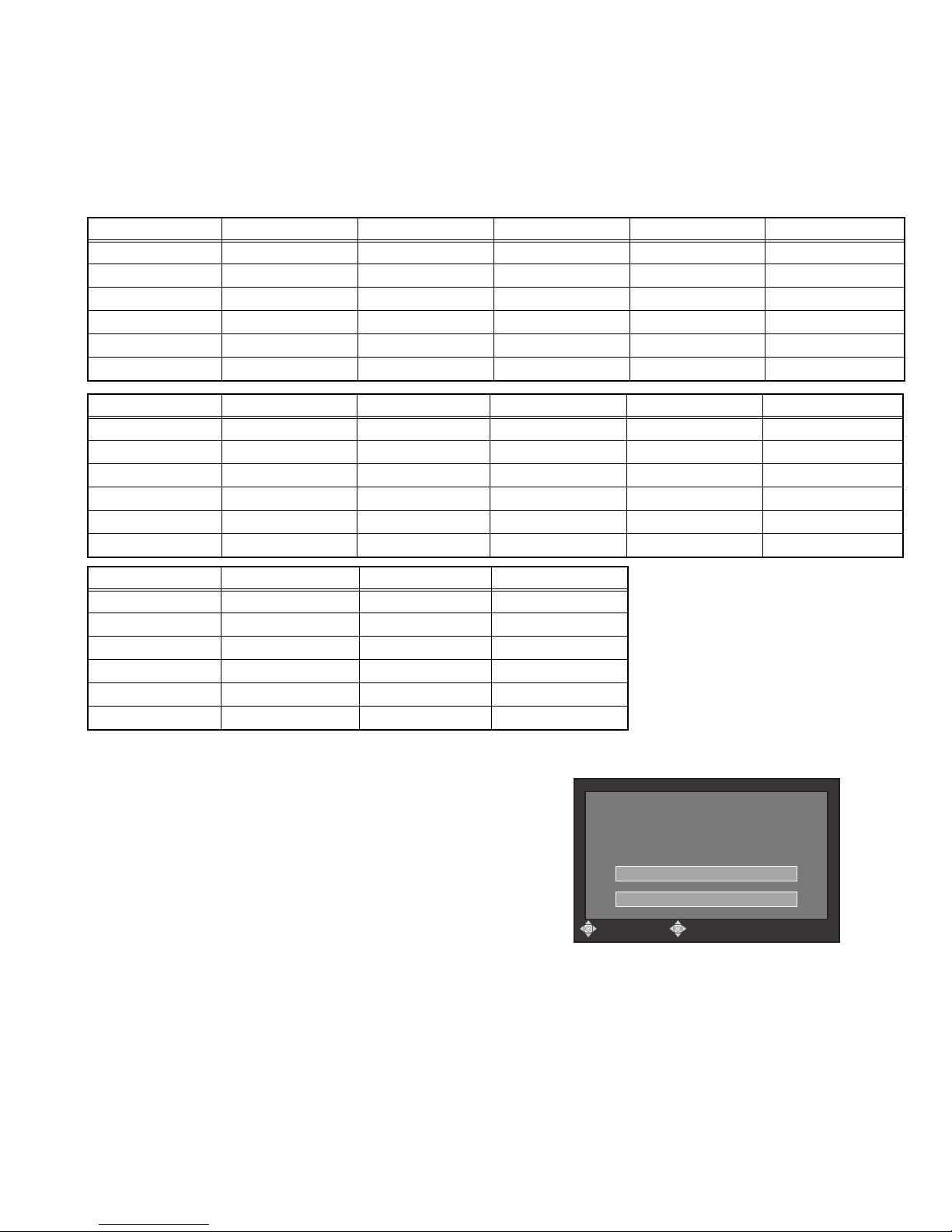
< "Warning screen">
0''&61(14/#6*#4&&+5-&4+8'
#..#9+..$''4#5'&
&1;179#0661(14/#6!
㪜㪯㪜㪚㪬㪫㪜
㪚㪘㪥㪚㪜㪣
㪪㪜㪣㪜㪚㪫 㪪㪜㪫
(No.YF227<Rev.001>)1-5
Page 6

2.3 SERVICE FOR EVERIO DOCK (CU-VD4)
2.3.1 Service repair parts
This unit mainly consists of CABINET PARTS and two BOARD
ASSYS.
The main service repair parts are as follows.
For details of service repair parts, please refer to the parts list.
• CABINET PARTS
• BOARD ASSYS
(CDL JACK BOARD ASSY & CDL CN BOARD ASSY)
• Some electrical parts
2.3.2 Disassembly
1. Removing the TOP CASE (Refer to Fig.2-3-1)
Remove the 4 screws (1-4), and then remove the TOP CASE.
2. Removing the HOLDER (Refer to Fig.2-3-2)
Take out the CDL CN BOARD ASSY from the BOTTOM
CASE.
Pull out the HOLDER from the connector by releasing the 4
hooks holding the HOLDER one by one.
Note) During the procedure, be careful in handling the
SPRING.
3. Removing the SPRING (Refer to Fig.2-3-3)
Release the CDL CN BOARD ASSY as shown in the figure,
and take out the SPRING from the BOTTOM CASE.
4. Removing the CDL CN BOARD ASSY/ CDL JACK BOARD
ASSY (Refer to Fig.2-3-4)
Release the lock of CN2, and remove the CDL CN BOARD
ASSY while pulling out the FPC.
Release one hook, and remove the CDL JACK BOARD ASSY.
1-6 (No.YF227<Rev.001>)
Page 7
TOP CASE
BOTTOM CASE
SPRING
CDL CN BOARD ASSY
1
3
BOTTOM CASE
2
4
0.069Nm (0.7kgfcm)
Fig.2-3-1
HOLDER
CDL CN BOARD ASSY
BOTTOM CASE
CDL CN BOARD ASSY
FPC
Fig.2-3-3
CN2
CDL JACK BOARD ASSY
HOOK
Fig.2-3-2
SPRING
HOOK
BOTTOM CASE
Fig.2-3-4
(No.YF227<Rev.001>)1-7
Page 8
SECTION 3
DISASSEMBLY
3.1 BEFORE ASSEMBLY AND DISASSEMBLY
3.1.1 Precautions
• Be sure to disconnect the power supply unit prior to mounting
and soldering of parts.
• Prior to removing a component part that needs to disconnect
its connector(s) and its screw(s), first disconnect the wire(s)
from the connector(s), and then remove the screw(s).
• When connecting/disconnecting wires, pay enough attention
not to damage the connectors.
• When inserting the flat wire to the connector, pay attention to
the direction of the flat wire.
• Be careful in removing the parts to which some spacer or
shield is attached for reinforcement or insulation.
• When replacing chip parts (especially IC parts), first remove
the solder completely to prevent peeling of the pattern.
• Tighten screws properly during the procedures. Unless
otherwise specified, tighten screws at a torque of 0.088N
·cm). However, as this is a required value at the time of
(0.9kgf
production, use the value as a measuring stick when
proceeding repair services. (See "SERVICE NOTE" as for
tightening torque.)
3.1.2 Destination of connectors
Two kinds of double-arrows in connection tables respectively
show kinds of connector/wires.
: Wire: Flat wire : Board to board (B-B)
: The connector of the side to remove
CONN. No. PIN No.CONNECTOR
CN2a
CN2b
MAIN CN101
MAIN CN103
MONI BW CN761
MINI BW CN762
3.1.3 Disconnection of connectors (Wires)
Wire
FPC Connector
· Pull both ends of the connector in the arrow
direction, remove the lock and disconnect the flat
wire.
Wire
FPC Connector
· Pull the both ends of the board in the direction of the
arrow, and remove the Connector.
Wire
Lock
FPC Connector
B-B Connector
B-B Connector
· Pull the both ends of the board in the direction of the arrow, and remove the B-B Connector.
· Extend the locks in the direction of the arrow for
unlocking and then pull out the wire. After
removing the wire, immediately restore the locks
to their original positions because the locks are
apt to come off the connector.
· Extend the locks in the direction of the arrow for
unlocking and then pull out the wire. After
removing the wire, immediately restore the locks
to their original positions because the locks are
apt to come off the connector.
· Extend the locks in the direction of the arrow for
unlocking and then pull out the wire. After
removing the wire, immediately restore the locks
to their original positions because the locks are
apt to come off the connector.
Wire
FPC Connector
FPC
Connector
Lock
B-B Connector
Fig.3-1-1
·m
40
10
Lock
Wire
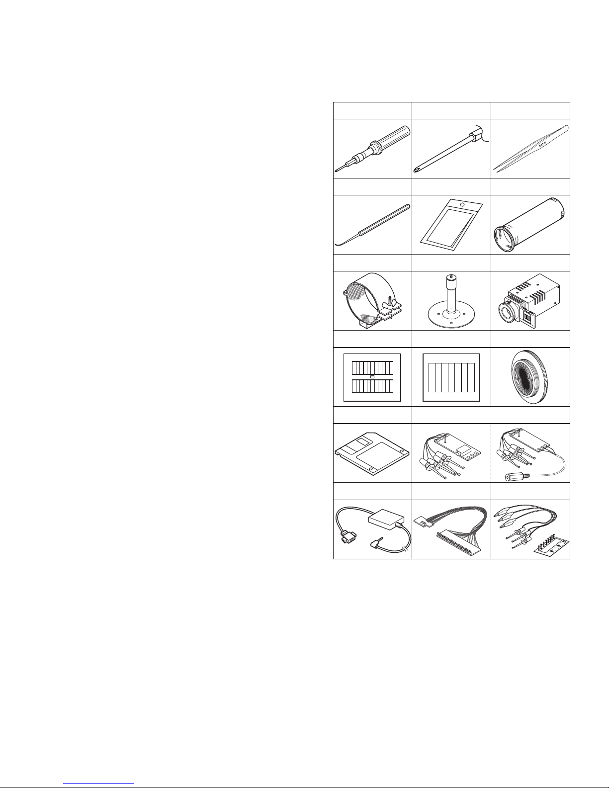
3.1.4 Tools required for disassembly and assembly
Torque driver
YTU94088
Chip IC replacement jig
PTS40844-2
Bit
YTU94088-003
Cleaning cloth
KSMM-01
Tweezers
P-895
Fig.3-1-2
• Torque driver
Be sure to use to fastening the mechanism and exterior parts
because those parts must strictly be controlled for tightening
torque.
• Bit
This bit is slightly longer than those set in conventional torque
drivers.
• Tweezers
To be used for removing and installing parts and wires.
• Chip IC replacement jig
To be used for replacement of IC.
• Cleaning cloth
Recommended cleaning cloth to wipe down the video heads,
mechanism (tape transport system), optical lens surface.
3.2 ASSEMBLY AND DISASSEMBLY OF MAIN PARTS
3.2.1 Assembly and disassembly
When reassembling, perform the step(s) in reverse order.
STEP
No.
[1]
[2]
PART
TOP COVER ASSY
UPPER ASSY
(Inc. VF ASSY,
SPEAKER/MONITOR)
[8]
E.VF UNIT(B/W)
(∗1) Order of steps in Procedure
When reassembling, preform the step(s) in the reverseorder.
These numbers are also used as the identification (location)
No. of parts Figures.
(∗2) Part to be removed or installed.
(∗3) Fig. No. showing Procedure or Part Location.
(∗4) Identification of part to be removed, unhooked, unlocked,
released, unplugged, unclamped or unsoldered.
S = Screw L = Lock, Release, Hook
SD = Solder CN = Connector
[Example]
• 4 (S1a) = Remove 4 S1a screws.
• 3 (L1a) = Disengage 3 L1a hooks.
• 2 (SD1a) = Unsolder 2 SD1a points.
• CN1a = Remove a CN1a connector.
(∗5) Adjustment information for installation.
Fig.
No.
4(S1a), 3(L1a),CN1a
C1
(S2a),2(S2b),3(S2c)
C2-1
2(SD1a),
L2,CN2a,b
2(S8),L8,CN8a
C2-2
POINT
( 4) ( 5)( 2) ( 3)( 1)
NOTE
-
-
NOTE 8
1-8 (No.YF227<Rev.001>)
Page 9
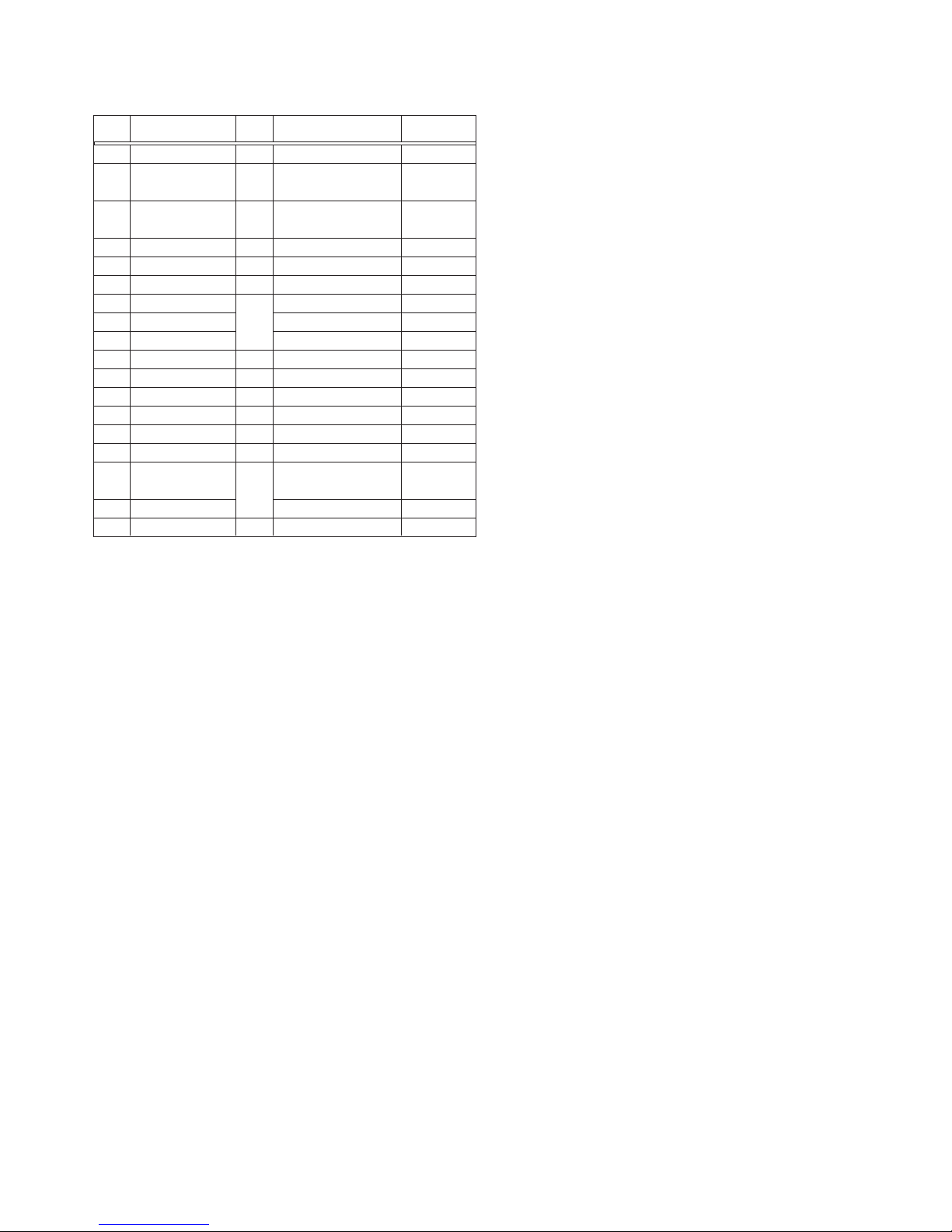
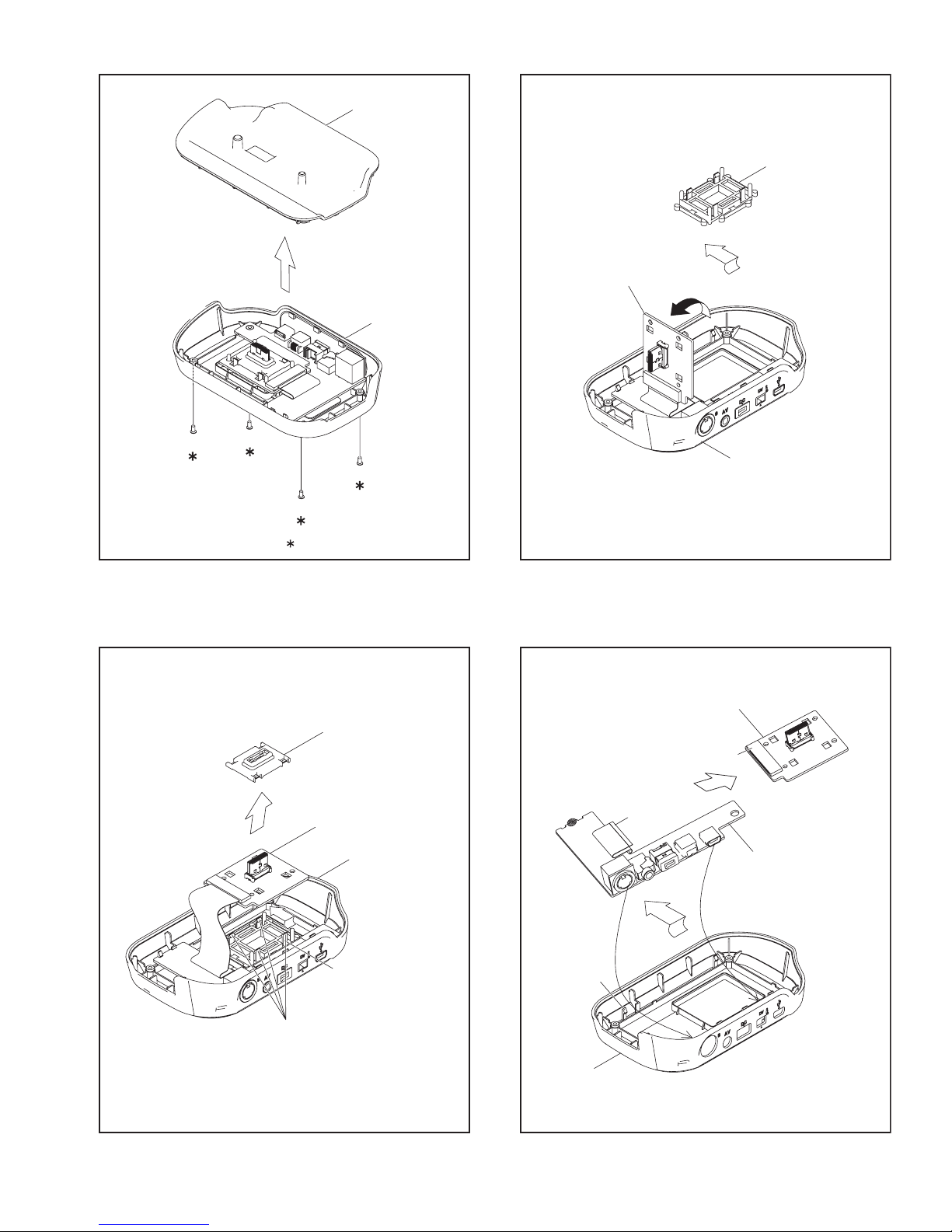
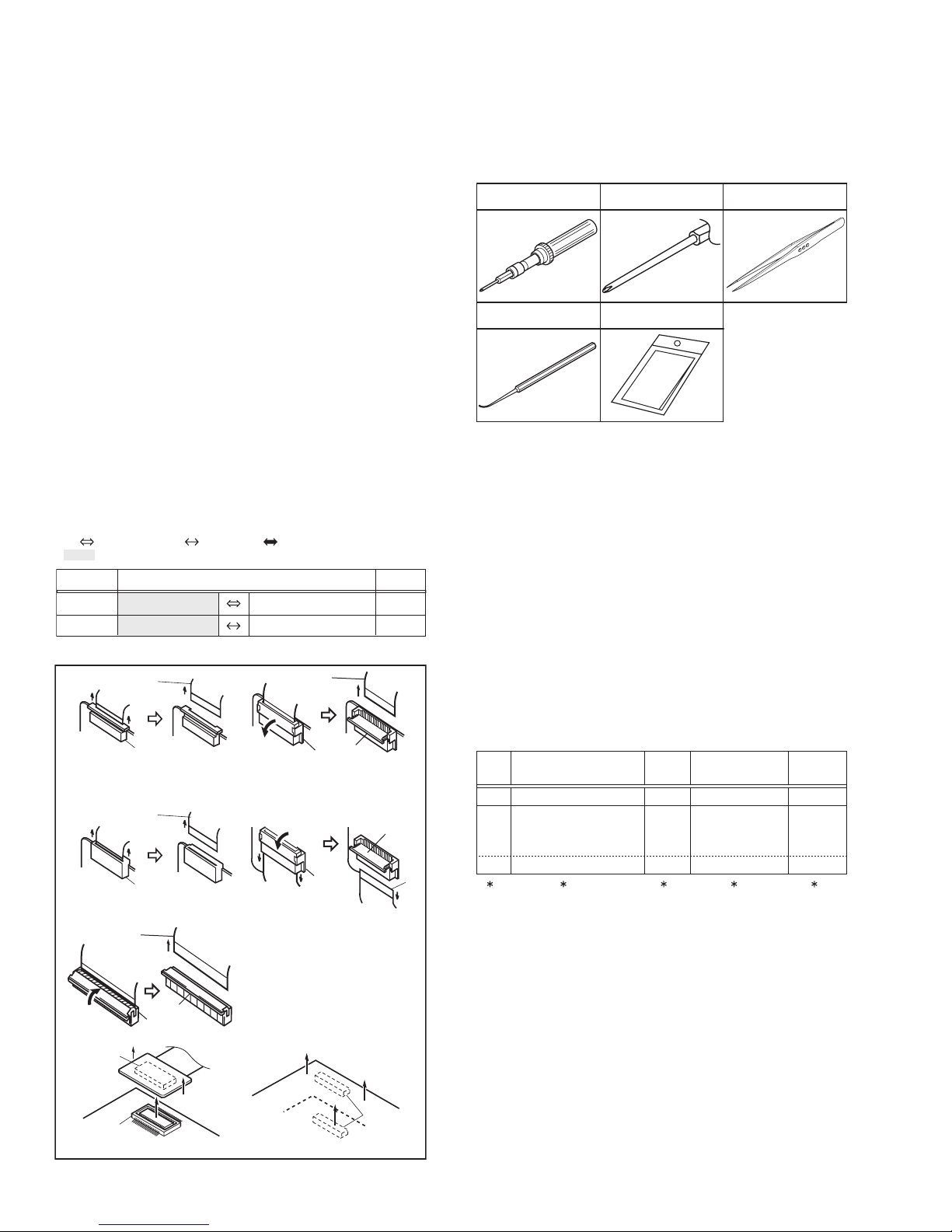
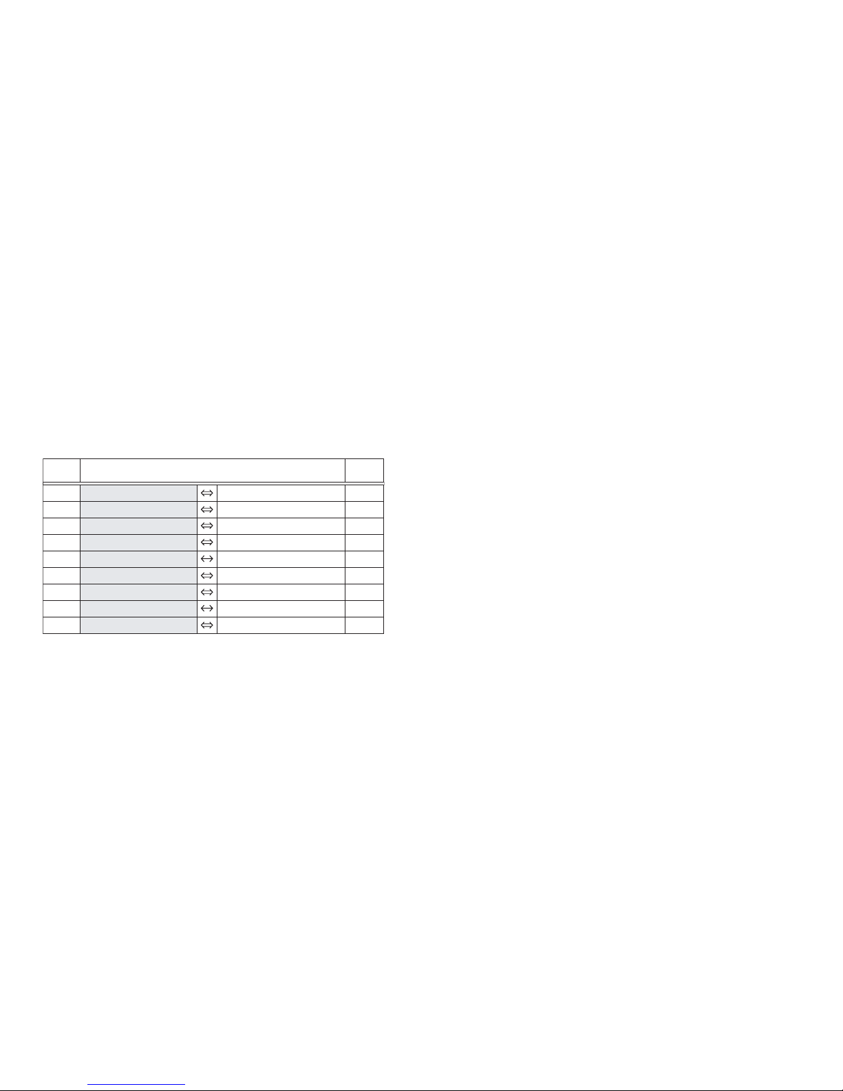
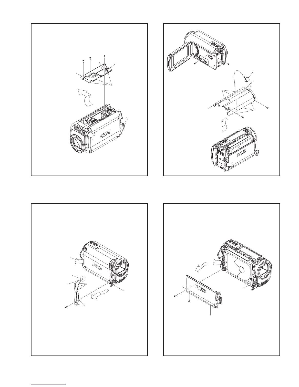
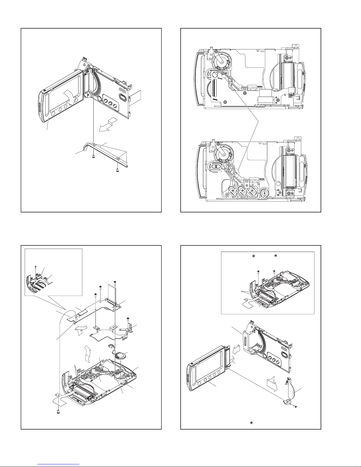
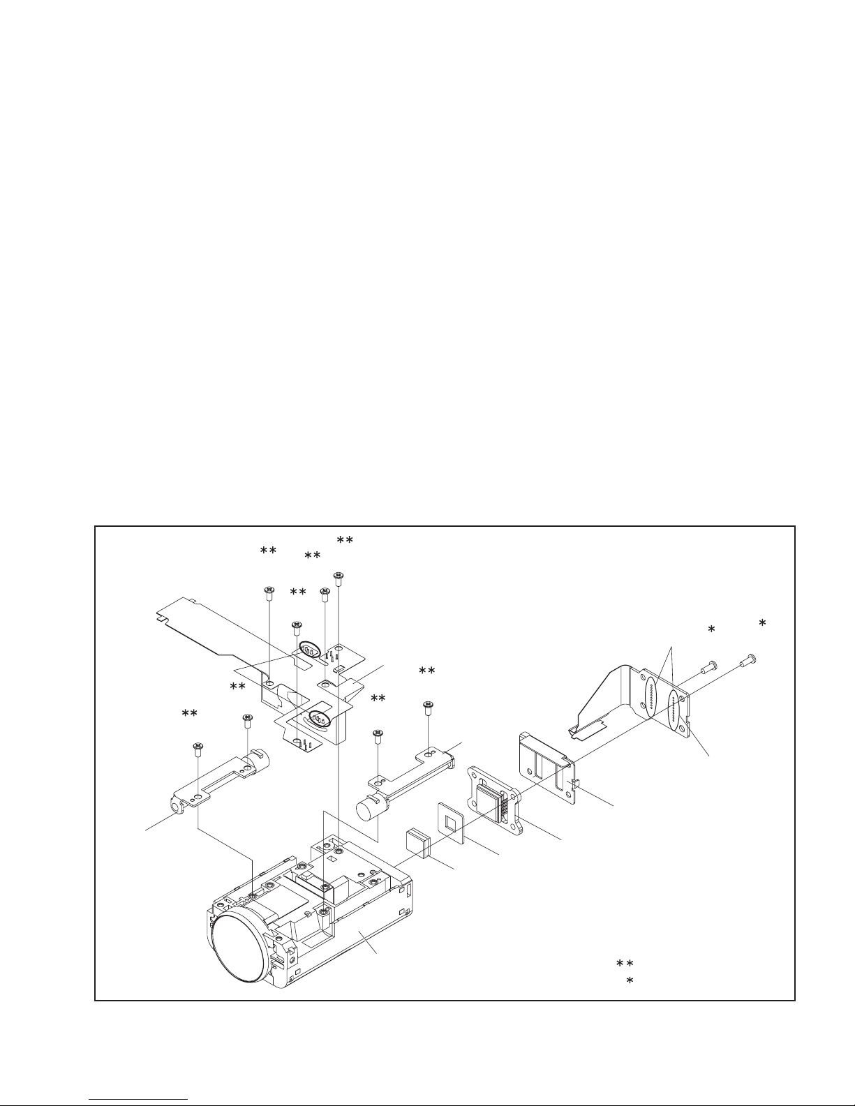
3.2.2 Assembly/Dissambly of cabinet parts and electrical parts
z Disassembly procedure
STEP
PART NAME
No.
[1]
B.COVER ASSY
[2]
WINDOW(IR)
[3]
TOP COVER ASSY
[4]
HDD COVER ASSY
[5]
HDD
[6]
HDD CASE
[7]
REAR COVER ASSY
[8]
ZOOM UNIT
[9]
REAR BOARD ASSY
[10]
UPPER ASSY
[11]
FRONT ASSY
[12]
MIC
[13]
MAIN BOARD ASSY
[14]
OP BLOCK ASSY
[15]
ORNAMENT(TOP)
[16]
OPE BOARD ASSY
[17]
SPEAKER
[18]
MONITOR ASSY
Fig.
No.
3-2-1
3-2-2
3-2-3
3-2-4
3-2-5
3-2-6
3-2-7
3-2-8
3-2-9
3-2-10
3-2-11
3-2-12
3-2-13
3-2-14-1
/3-2-14-2
3-2-15
POINT NOTE
3(S1),2(L1a), 3(L1b)
GRIP BELT,
S2,2(L2a),3(L2b),L2c
3(S3),JACK COVER(AV),
S3,3(L3a),3(L3b),3(L3c)
2(S4), L4a,b
CN5
5(S6),L6a,b
CN7a,b,3(S7),L7a,3(L7b)
2(S8), L8
L9a,2(L9b)
CN10, 2(S10), L10a,b
CN11,S11, L11a,b
S12, L12a, L12b, PLATE(MIC)
CN13a,b, 2(S13)
3(S14)
2(S15), L15a, 3(L15b)
CN16a,b, S16, 2(L16a),
2(L16b), 3(S16)
S17, L17a,b, 2(L17c), BKT(SPK)
S18a, L18a, 2(S18b), 2(L18b)
NOTE1
NOTE2a,b
NOTE3
NOTE5a,b,c,d,e,f
NOTE7
NOTE8
NOTE9
NOTE10a,b
NOTE11a,b
NOTE12
NOTE13
NOTE14a,b
NOTE15a,b
NOTE16a,b
NOTE17
NOTE18
-
-
NOTE1:
When removing the BOTTOM COVER ASSY, open and pull
up the COVER (SD).
NOTE2a:
Pull out the GRIP BELT from the hook and leave it released
before removing the HDD COVER ASSY.
NOTE2b:
During the procedure, be careful not to damage the parts.
NOTE3:
When attaching, be careful not to pinch the parts.
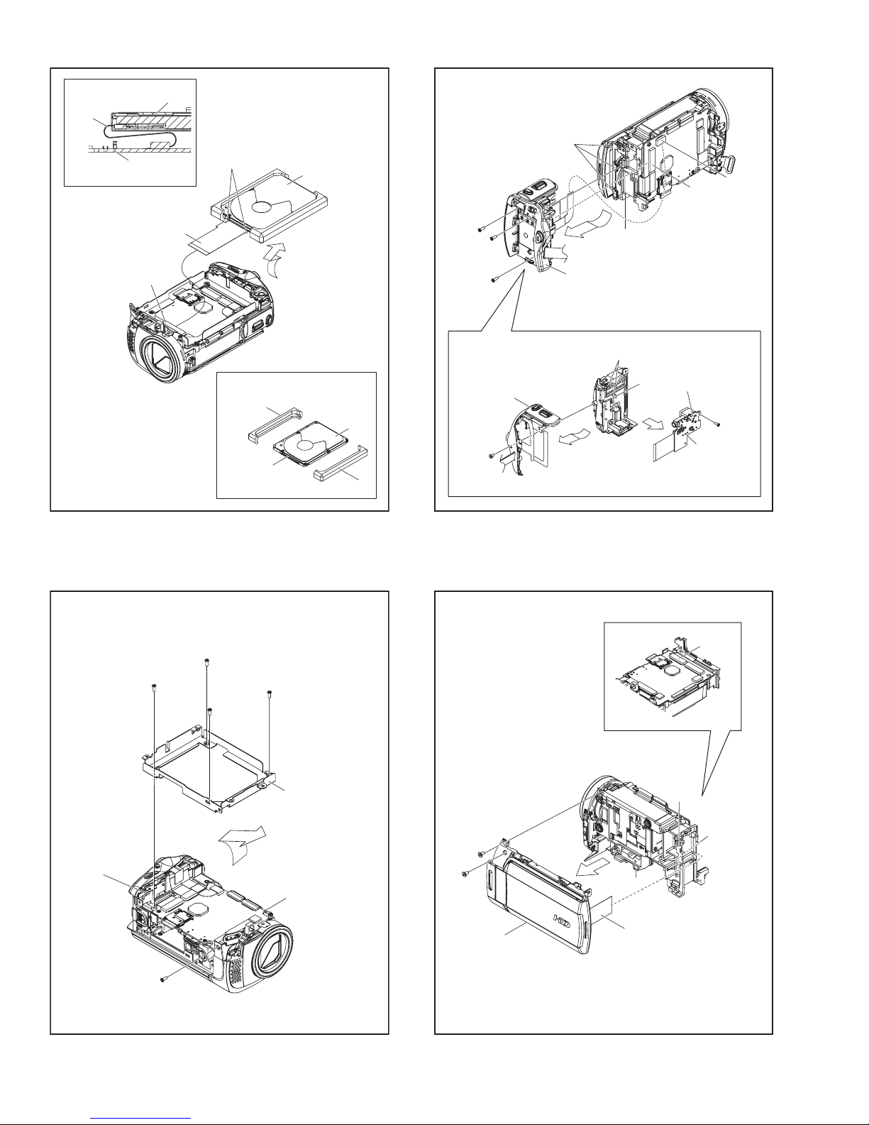
NOTE5a:
During the procedure, be careful in handling the parts.
Pay special attention not to give any external shock to the
HDD.
NOTE5b:
When the HDD is replaced, be sure to refer to Replacing
HDD in "SECTION2 SPECIFIC SERVICE INSTRUCTIONS"
for the procedure after HDD replacement.
NOTE5c:
Be careful as the RUBBER SPACERS on both sides are
easily come off when the HDD is removed from the main
unit.
NOTE5d:
When connecting the FPC to the connector, insert the FPC
straight into the connector. When locking the connector, be
careful not to give so much load that it bends the board.
NOTE5e:
In this procedure, the FPC connected to the HDD connector
is not removed.
If the FPC is removed due to broken wire, be careful in attachment direction.
Pay attention as wrong attachment could damage the HDD.
NOTE5f:
Be careful with the wiring.
NOTE7:
When removing the REAR COVER ASSY, remove the
ZOOM UNIT together with the REAR BOARD ASSY.
NOTE8:
When attaching, first adjust the AV jack position, and then
carefully adjust the DC jack position.
NOTE9:
During the procedure, be careful not to touch or damage the
battery terminal.
NOTE10a:
When removing, release the connector lock, and then pull
out the FPC together with the UPPER ASSY.
NOTE10b:
Please refer to Fig.3-2-13 and the following procedure for removing the UPPER ASSY.
NOTE11a:
When attaching, be careful in handling the JACK COVER
(USB) ASSY.
NOTE11b:
When attaching, be careful with the wiring (MIC).
NOTE12:
When attaching, be careful with the wiring (MIC).
(No.YF227<Rev.001>)1-9
Page 10
NOTE13:
Be careful with the wiring.
NOTE14a:
During the procedure, be careful in handling the parts.
NOTE14b:
Refer to 3.2.3
CCD BOARD ASSY
Assembly/Disambly of [14] OP BLOCK ASSY/
.
NOTE15a:
During the procedure, turn the MONITOR ASSY 90°, so that
it does not interfere with the procedure.
NOTE15b:
During the procedure, be careful not to damage the parts.
NOTE16a:
When removing, remove the screw No.32 first to release the
FPC, and then pull out the FPC from the connector.
NOTE16b:
When attaching, be careful with the wiring.
NOTE17:
When attaching, be careful with the wiring.
NOTE18:
Refer to 3.2.4 Disassembly of [18] MONITOR ASSY.
z Destination of connectors
CN.
No.
CONNECTOR
PIN
No.
CN5 MAIN CN102 HDD - 40
CN7a MAIN CN104 ZOOM UNIT - 12
CN7b MAIN CN103 REAR
CN601 32
CN10 MAIN CN101 OPE CN401 30
CN11 MAIN CN107 MIC - 4
CN13a MAIN CN105 CCD CN5001 22
CN13b MAIN CN106 OP BLOCK - 25
CN16a OPE CN403 SPEAKER - 2
CN16b OPE CN402 MONITOR CN7601 22/23
1-10 (No.YF227<Rev.001>)
Page 11
[1]
1
(S1)
2
(S1)
L1a
3
(S1)
COVER(SD)
NOTE1
L1b
6
(S3)
L3c
5
(S3)
JACK COVER(AV)
L3b
NOTE3
Fig.3-2-1
[3]
Fig.3-2-3
8
(S3)
L3a
7
(S3)
NOTE2a
GRIP BELT
NOTE2a
L2c
[2]
4
(S2)
L2b
L2a
Fig.3-2-2
HOOK
10
(S4)
L4a
L4b
9
(S4)
[4]
Fig.3-2-4
(No.YF227<Rev.001>)1-11
Page 12
NOTE5f
FPC
HDD
MAIN PWB
<CROSS SECTION>
NOTE5e
FPC
NOTE5d
CN5
STOPPER
NOTE5c
RUBBER SPACER
CONNECTOR
Fig.3-2-5
NOTE5a,b
[5]
SHIELD
(HDD)
RUBBER SPACER
17
(S7)
16
(S7)
18
(S7)
NOTE8
20
(S8)
[8]
L7b
[7]
NOTE7
L9b
Fig.3-2-7
L7a
L9a
CN7a
CN7b
NOTE9
[9]
19
(S8)
L8
L6b
14
(S6)
11
(S6)
12
(S6)
13
(S6)
Fig.3-2-6
15
(S6)
[6]
L6a
21
(S10)
22
(S10)
[10]
NOTE10b
CN10
L10b
NOTE10a
CN10
L10a
FPC
Fig.3-2-8
1-12 (No.YF227<Rev.001>)
Page 13
L11b
WIRE(MIC)
NOTE11b
[11]
JACK COVER(USB) ASSY
NOTE11a
23
(S11)
CN11
WIRE(MIC)
NOTE11b
L11a
L11b
25
(S13)
26
(S13)
NOTE13
[13]
CN13a
CN13b
L12a
Fig.3-2-9
L12b
NOTE12
[12]
PLATE(MIC)
24
(S12)
Fig.3-2-11
27
(S14)
28
(S14)
29
(S14)
NOTE14a,b
[14]
Fig.3-2-10
0.118Nm (1.2kgfcm)
Fig.3-2-12
(No.YF227<Rev.001>)1-13
Page 14
NOTE16b
WIRE(SPEAKER)
MONITOR ASSY
NOTE15a
NOTE15b
32
(S16)
OPE PWB
NOTE16a
CN16b
FPC
(MONITOR)
ASSY
[15]
Fig.3-2-13
CN16b
30
(S15)
35
(S16)
33
(S16)
L15a
31
(S15)
34
(S16)
L15b
NOTE16b
CN16a
36
(S17)
BKT(SPK)
NOTE17
Fig.3-2-14-2
L18b
UPPER CASE ASSY
38
(S18b)
L18a
39
(S18b)
[16]
(LCD_OPEN)
1-14 (No.YF227<Rev.001>)
SW
L16b
L16a
L17a
L16b,L17c
32
(S16)
Fig.3-2-14-1
NOTE17
[17]
L17c
L17b
[18]
NOTE18
L18a
37
(S18a)
0.196Nm (2.0kgfcm)
Fig.3-2-15
Page 15
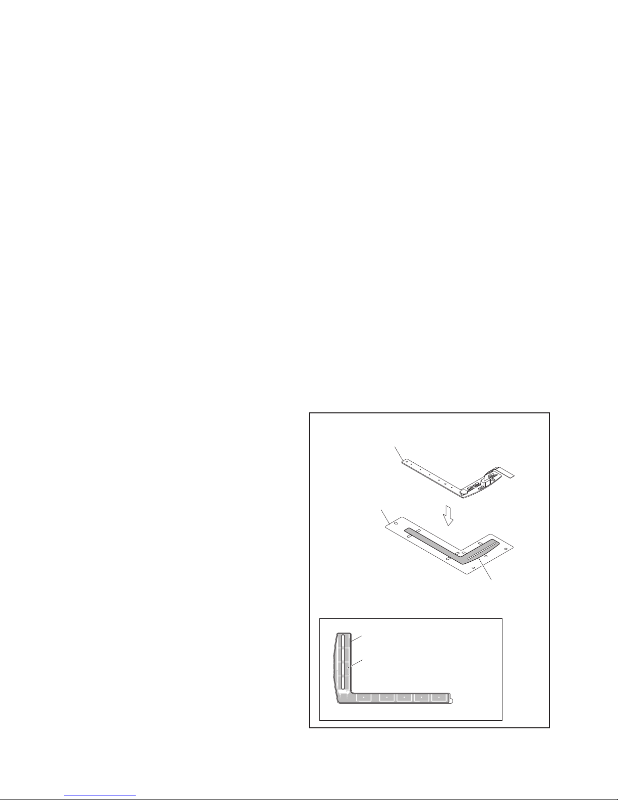
3.2.3 Assembly/Disambly of [14] OP BLOCK ASSY/CCD BOARD ASSY
zPrecautions
(1) Be careful in handling the CCD IMAGE SENSOR, OPTI-
CAL LPF and the LENS components.
Pay special attention to the surfaces to protect them from
stains, dust, or scratches.
If the surfaces are soiled with finger prints or other stains,
wipe them off with silicon paper, clean chamois leather,
or recommended cleaning cloth.
(2) The CCD IMAGE SENSOR may have been shipped with
a protective sheet attached to the transmitting glass.
When replacing the CCD IMAGE SENSOR, do not peel
off this sheet from the new part until immediately before
it is mounted in the OP BLOCK ASSY.
zDisassembly of OP BLOCK ASSY / CCD BOARD ASSY
(1) Unsolder the 20 soldered points (SD14a) of the CCD
BOARD ASSY.
(2) Remove the 2 screws (1,2), and then remove the CCD
BOARD ASSY,SHIELD(CCD) and the CCD BASE ASSY.
NOTE14a:
When removing the CCD BASE ASSY, be careful in
handling as the CCD IMAGE SENSOR may be removed together with the SHEET and the OP LPF attached.
(3) Remove the SHEET and OP LPF.
zAssembly of OP BLOCK ASSY / CCD BOARD ASSY
(1) Set the OP LPF first, and then the SHEET to the OP
(2) Attach the CCD BASE ASSY first, then the SHEET,
(3) Solder the 20 points (SD14a) on the CCD BOARD AS-
zReplacement of service repair parts
The service repair parts for the OP BLOCK ASSY are as listed
below.
When replacing parts, be careful not to cut the FPCs or damage any parts by soldering (excessive heat).
(1) FOCUS MOTOR UNIT
(2) ZOOM MOTOR UNIT
(3) AUTO IRIS UNIT
NOTE 14d:
The IRIS MOTOR UNIT includes the FPC ASSY and two
sensors.
NOTE14b:
Replace the CCD IMAGE SENSOR as a CCD BASE
ASSY, not as a single part replacement.
BLOCK ASSY.
NOTE14c:
Be careful with the attachment direction of the OP
LPF.
SHIELD(CCD) and the CCD BOARD ASSY so that the
SHEET stays in place, and then tighten with the 2 screws
(1,2).
SY.
(S14b)
ZOOM MOTOR
UNIT
SD14b
5
6
(S14b)
10
(S14b)
(S14b)
7
(S14b)
9
8
(S14b)
NOTE14d
AUTO IRIS UNIT
3
(S14b)
4
(S14b)
FOCUS MOTOR
UNIT
SHEET
OP LPF
NOTE14a,c
SD14a
CCD BOARD ASSY
SHIELD(CCD)
NOTE14a,b
CCD BASE ASSY
1
(S14a)
2
(S14a)
OP BLOCK ASSY
Fig.3-2-16
0.078Nm (0.8kgfcm)
0.147Nm (1.5kgfcm)
(No.YF227<Rev.001>)1-15
Page 16
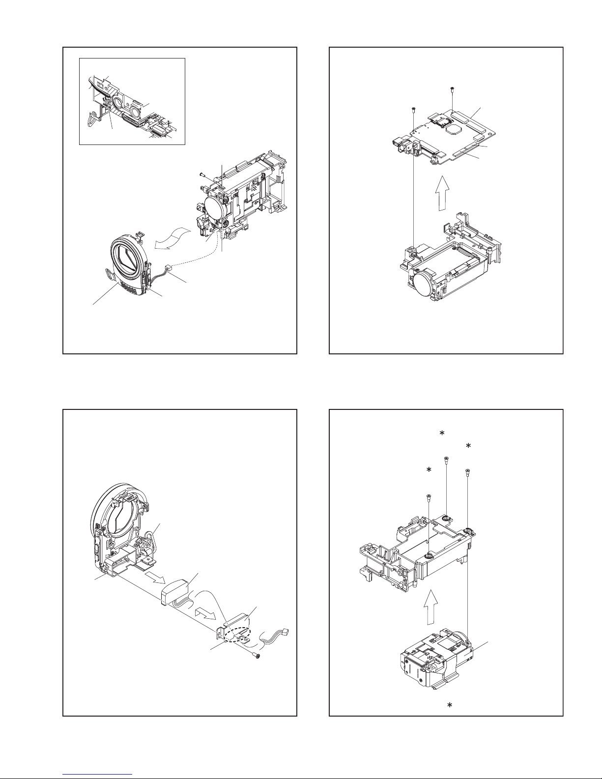
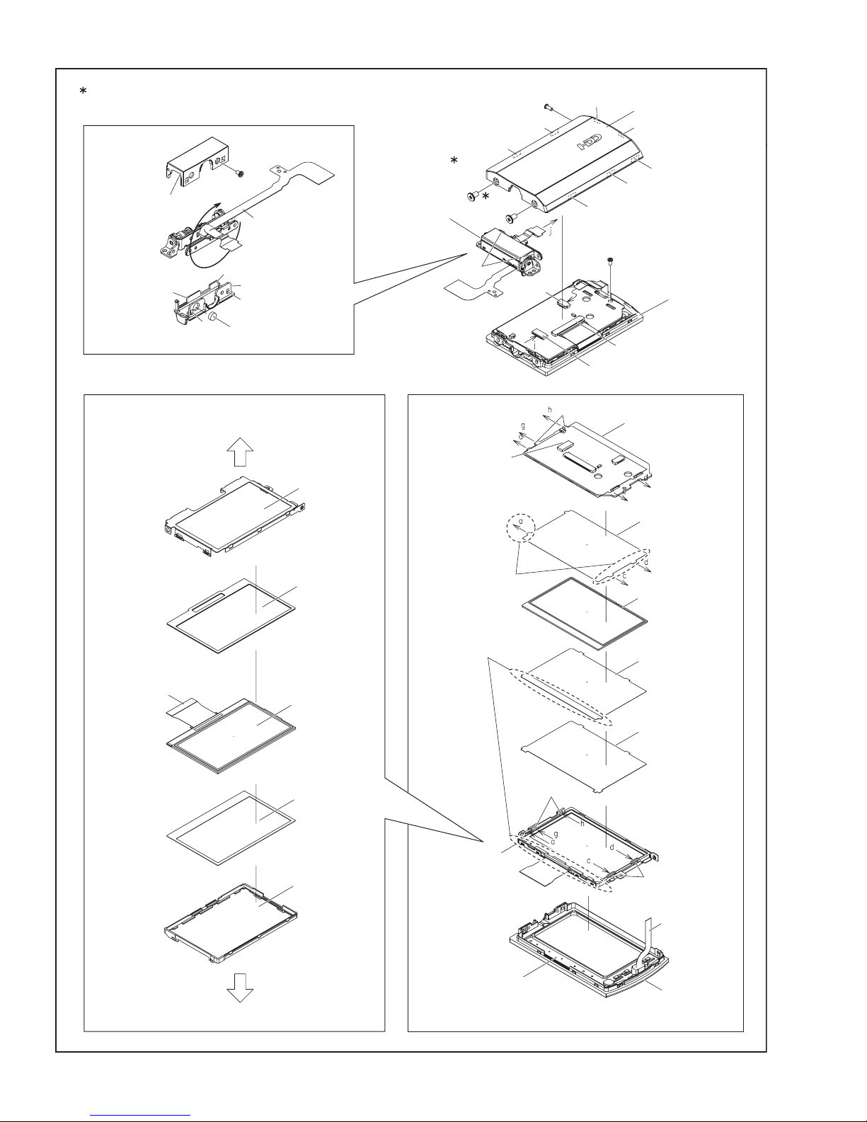
3.2.4 Disassembly of [18] MONITOR ASSY
zCAUTIONS
(1) During the procedure, be careful in handling the LCD
MODULE and other parts. Pay special attention not to
damage or stain the monitor screen.
If fingerprints are left on the screen, wipe them with clean
chamois leather or a cleaning cloth.
z Removing MONITOR ASSY
(1) Remove the screw (1).
(2) Turn the HINGE UNIT ASSY 90°, and remove the 2
screws (2,3).
(3) Remove the MONI.COVER ASSY by removing the 7
hooks (L18a-g).
(4) Release the lock of the connector (CN18a), and remove
the HINGE UNIT by lifting it up.
NOTE18a:
During the procedure, be careful in handling the FPC.
(5) Release the lock of the connectors (CN18b,c), and pull
out the FPC.
(6) Remove the screw (4), and remove the MONITOR
BOARD ASSY .
NOTE18b:
During the procedure, be careful in handling the FPC.
(7) Remove the SHEET (M.REF), LIGHT GUIDE,
SHEET(M/DIFF), and the SHEET(BEF).
NOTE18c:
When attaching, insert one side of the SHEET (M/
DIFF) under the LCD CASE RIB.
NOTE18d:
When attaching, insert each tab on both sides of the
SHEET (M.REF) into the LCD CASE notch.
(8) Remove the LCD CASE, SPACER(LCD), LCD MOD-
ULE, SPACER(LCD) and the LCD BKT ASSY.
NOTE18e:
During the procedure, handle the five parts (LCD
CASE, SPACER(LCD), LCD MODULE, SPACER(LCD) and the LCD BKT ASSY) together.
NOTE18f:
The SENSOR BOARD ASSY is originally affixed to the
MONI.CASE ASSY using jigs and they have structures difficult to replace.
If replacement is required, please refer to the NOTE
and follow the operation procedure.
Assembly/Disambly of MONITOR ASSY/SENSOR BOARD ASSY
z
Operation procedure
• Removing the part which is to be reused
(1) Remove the SENSOR BOARD ASSY from the MO-
NI.CASE ASSY by gradually peeling off from the HINGE
ASSY side.
NOTE18g:
During the procedure, be careful not to break or deform the parts or warp the SENSOR BOARD.
(2) Completely peel off the remaining tape pieces of the D.
FACE TAPE left on the part to be reused (MONI.CASE
ASSY or SENSOR BOARD ASSY).
NOTE18h:
Make sure that there are no D. FACE TAPE pieces or
foreign substances left on the surfaces. If necessary,
clean the surfaces using alcohol etc.
• Affixing the D. FACE TAPE to the SENSOR BOARD
(1) Affix the D. FACE TAPE to the SENSOR BOARD ASSY.
NOTE18j:
Securely fix the D. FACE TAPE, and then affix the
SENSOR BOARD ASSY to the D. FACE TAPE by adjusting the four frames of the SENSOR BOARD ASSY
to the frame of the D. FACE TAPE. Evenly press over
the paper backing of each long / short side of the L
shape.
(2) Peel off the paper backing.
NOTE18k:
When removing the paper backing, check that there
are no foreign substances or air bubbles on the tape.
If there are foreign substances etc., completely remove them and continue the affixing procedure.
• Affixing the SENSOR BOARD ASSY to the MONI. CASE
(1) Affix the SENSOR BOARD ASSY to the MONI. CASE
NOTE18m:
When affixing, adjust the position of the long side of
the L shape to avoid misalignment, and then press
evenly.
Be sure to press hard for 10 seconds or more on each
long/ short side of the L shape for even adhesion.
During the procedure, be careful to prevent foreign
substances or air bubbles from entering.
(2) After the replacement, make sure that there are no bro-
ken or deformed parts or any abnormalities.
Use the service software for the operation check of the
touch sensor sensitivity.
NOTE18g,j,k
SENSOR BOARD ASSY
NOTE18j,k
D.FACE TAPE
DETACHMENT PAPER
NOTE18j,k
SENSOR BOARD ASSY
D.FACE TAPE
Fig.3-2-17
1-16 (No.YF227<Rev.001>)
Page 17

zRemoving HINGE UNIT ASSY
(1) Remove the screw (5), and remove the HINGE COV-
ER(U).
(2) Remove the HINGE COVER(L).
(3) Remove the MAGNET.
NOTE18n:
During the procedure, be careful in handling the FPC.
During the procedure, be careful in handling the MAGNET.
When attaching, set the N pole outside as shown in
the figure. Be careful when removing as there is no
marking.
NOTE18p:
During the procedure, be careful in handling the FPC.
NOTE18q:
The FPC, with its connection to the MONITOR
BOARD ASSY facing inward, is rolled around the axis
(shaft) of the HINGE UNIT ASSY rotation 2.5 rounds
(2.5times).
(No.YF227<Rev.001>)1-17
Page 18
0.118 Nm (1.2kgfcm)
HINGE COVER(U)
L18m
L18k
L18n
5
(S18b)
FPC
NOTE18p,q
HINGE COVER(L)
L18p
MAGNET
NOTE18n
(S18b)
NOTE18a
HINGE UNIT
ASSY
2
L18h
L18a
3
(S18b)
1
(S18a)
L18b
CN18c
L18f
MONI COVER ASSY
L18g
L18d
L18c
4
(S18a)
MONI CASE ASSY
CN18b
CN18a
L18e
NOTE18e
(REINFORCED SIDE)
<MONI CASE SIDE>
LCD BKT ASSY
SPACER(LCD)
LCD MODULE
SPACER(LCD)
CN18b
NOTE18d
NOTE18c
L18j
MONITOR
ASSYBOARD
SHEET(M.REF)
LIGHT GUIDE
SHEET(M/DIFF)
SHEET(BEF)1
NOTE18d
LCD CASE
<MONI COVER SIDE>
1-18 (No.YF227<Rev.001>)
Fig.3-2-18
LCD CASE RIB
NOTE18c
BOARDSENSOR
ASSY
NOTE18g,h,j
NOTE18d
NOTE18b
MONI CASE ASSY
NOTE18h,j
Page 19
SECTION 4
ADJUSTMENT
4.1 PREPARATION
4.1.1 Precaution
Camera system and deck system of this model are specially
adjusted by using PC.
However, if parts such as the following are replaced, an
adjustment is required. The adjustment must be performed in a
Service Center equipped with the concerned facilities.
• EEP ROM (IC1005 of MAIN board)
• OP BLOCK ASSEMBLY
• MONITOR ASSEMBLY
In the event of malfunction with electrical circuits, first find a
defective portion with the aid of proper test instruments as shown
in the following electrical adjustment procedure, and then
commence necessary repair/ replacement/adjustment.
• In observing chip TP, use IC clips, etc. to avoid any stress.
Prior to replacement of chip parts (especially IC), remove the
solder completely to prevent peeling of the pattern.
• Use a patch cord if necessary. As for a patch cord, see the
BOARD INTERCONNECTIONS.
• Since connectors are fragile, carefully handle them in
disconnecting and connecting the FPC.
4.1.2 Required test equipment
• Personal computer (for Windows)
• Color TV monitor
• Oscilloscope (dual-trace type, observable 100MHz or higher
frequency). The one observable 300 MHz or higher frequency
is recommended.
• Digital voltmeter
• DC power supply or AC adapter
• Frequency counter (with threshold level adjuster)
4.1.3 Tools required for adjustment
Torque Driver
YTU94088
Chip IC Replacement Jig
PTS40844-2
INF Adjustment Lens Holder
YTU94087
Gray Scale Chart
YTU94133A
Service Support System
YTU94057-109
Bit
YTU94088-003
Cleaning Cloth
KSMM-01
Mini Stand
YTU93108
Color Bar Chart
YTU94133C
Communication Cable
YTU93111-1
Tweezers
P-895
INF Adjustment Lens
YTU92001B
Light Box Assembly
YTU93096B
Focus Chart
YTU92001-018
PC Cable
QAM0099-005
Jig Connector Cable
YTU93106D
Charing Battery Adjuatment Jig
YTU93112A
• Torque Driver
Be sure to use to fastening the mechanism and exterior parts
because those parts must strictly be controlled for tightening
torque.
• Bit
This bit is slightly longer than those set in conventional torque
drivers.
• Tweezers
To be used for removing and installing parts and wires.
• Chip IC Replacement Jig
To be used for adjustment of the camera system.
• Cleaning Cloth
Recommended the Cleaning cloth to wipe down the video
heads, mechanism (tape transport system), optical lens surface.
(No.YF227<Rev.001>)1-19
Page 20

• INF Adjustment Lens
To be used for adjustment of the camera system. For the
usage of the INF adjustment lens, refer to the Service Bulletin
No. YA-SB-10035.
• INF Adjustment Lens Holder
To be used together with the Camera stand for operating the
Videocamera in the stripped-down condition such as the status without the exterior parts or for using commodities that are
not yet conformable to the interchangeable ring. For the usage
of the INF lens holder, refer to the Service Bulletin No. YA-SB-
10035.
• Mini Stand
To be used together with the INF adjustment lens holder. For
the usage of the Mini stand, refer to the Service Bulletin No.
YA-SB-10035.
• Light Box Assembly
To be used for adjustment of the camera system. For the
usage of the Light box assembly, refer to the Service Bulletin
No. YA-SB-10035.
• Gray Scale Chart
To be used for adjustment of the camera system. For the
usage of the INF adjustment lens, refer to the Service Bulletin
No. YA-SB-10035.
• Color Bar Chart
To be used for adjustment of the camera system. For the
usage of the INF adjustment lens, refer to the Service Bulletin
No. YA-SB-10035.
• Focus Chart
To be used for adjustment of the camera system. For the
usage of the INF adjustment lens, refer to the Service Bulletin
No. YA-SB-10035.
• Service Support System
To be used for adjustment with a personal computer. Software
can be downloaded also from JS-net.
• Communication Cable
Connect the Communication cable between the PC cable and
Jig connector cable when performing a PC adjustment.
• PC Cable
To be used to connect the Videocamera and a personal computer
with each other when a personal computer issued for adjustment.
• Jig Connector Cable
Connected to JIG CONNECTOR of the main board and used
for electrical adjustment, etc.
• Charging Battery Adjustment Jig
This Jig is used for the adjustment of the camcorders that have
Main Body battery charging function.
4.2 JIG CONNECTOR CABLE CONNECTION
Connection procedure
NOTE
• Be sure to turn the power “OFF”, when connecting the JIG
CONNECTOR CABLE.
If the JIG CONNECTOR CABLE is connected with the power “ON”, communication error may occur.
• Remove the 3 screws (1-3), and then remove the B.COV-
ER ASSY.
2
3
B.COVER ASSY
JIG
CONNECTOR
RS232C
COM PORT
PERSONAL COMPUTER
SERVICE
SUPPORT
SYSTEM
MENU
JIG CONNECTOR
CABLE
COMMUNICATION
CABLE
JIG CONNECTOR
TO AL_2.8V
TO IF_RX
TO IF_TX
TO GND
BLUE
WHITE
BLACK
or
COMMUNICATION
CABLE
RED
1
PC CABLE
Fig.4-2-1
JIG CONNECTOR CABLE [YTU93106D]
1630
115
1-20 (No.YF227<Rev.001>)
Fig.4-2-2
Page 21

Jig connector diagrams
JIG CONNECTOR CABLE (YTU93106D)
MAIN CN110
DSP_TDO
DSP_TCK
DSP_TMS
DSP_TDI
XDSPTRST
DSP_RST
REG_2.83V
UARXDO
UATXDO
AL_2.8V
IF_TX
IF_RX
MODO
SYS_RSTL
OCD_SCL
CAPSENS_DT
CAPSENS_WR_L
GND
OCD_SDA
GND
NC
IRU
ISSP_DATA
JSEL0
JSEL1
EXTRGO
MVD
KENTO
GND
KENTO2
JIG CONN. BOARD
(PIN NO.)
1
16
2
17
3
18
4
19
5
20
6
21
7
22
8
23
9
24
10
25
11
26
12
27
13
28
14
29
15
30
DSP_TDO
1
DSP_TMS
2
XDSPTRST
3
REG_2.83V
4
UATXDO
5
IF_TX
6
MODO
7
OCD_SCL
8
CAPSENS_WR_L
9
OCD_SDA
10
11
12
13
14
15
16
17
18
19
20
21
22
23
24
25
26
27
28
29
30
NC
ISSP_DATA
JSEL1
MVD
GND
DSP_TCK
DSP_TDI
DSP_RST
UARXDO
AL_2.8V
IF_RX
SYS_RSTL
CAPSENS_DT
GND
GND
IRU
JSEL0
EXTRGO
KENTO
KENTO2
Fig.4-2-3
(No.YF227<Rev.001>)1-21
Page 22

5.1 SERVICE NOTE
-
[8] [9] [10] [11]
SECTION 5
TROUBLE SHOOTING
-
3-2-7 3-2-8
aaa
15 16 17 18 19 20 - 21 22 23
39
[18]
[18]MONITOR ASSY
-
-
3-2-5 3-2-9
acab
3-2-4 3-2-6
[14]
3-2-2
[1] [2] [4][3] [5] [6] [7]
CABINET PARTS AND ELECTRICAL PARTS(1)
1 2 3 4 5 6 7 8 9 10 - 11 12 13 14
3-2-1 3-2-3
[12] [13] [14] [15] [16] [17] [18]
CABINET PARTS AND ELECTRICAL PARTS(2)
3-2-11 3-2-12 3-2-13 3-2-153-2-14-1
3-2-10
24 25 26 27 28 29 30 31 32 33 34 35 36 37 38
[14]OP BLOCK ASSY/CCD BOARD ASSY
1 2 3 4 5
1 2 3 4 5 6 7 8 9 10
a
bad
3-2-17
e
3-2-16
-
2.3 CRADLE
1 2 3 4
f
2-3-1
Symbol No.
Place to stick screw
Removing order of screw
Screw tightening torque
Reference drawing (Fig.No.)
Symbol No.
Place to stick screw
Removing order of screw
Reference drawing (Fig.No.)
1-22 (No.YF227<Rev.001>)
Symbol No.
Place to stick screw
Screw tightening torque
Removing order of screw
Reference drawing (Fig.No.)
Symbol No.
Place to stick screw
Screw tightening torque
Removing order of screw
Reference drawing (Fig.No.)
Screw tightening torque
NOTE:
㧝)㧖and㧖㧖 (This mark shows where to attach the screws) : Do not reuse the screws because the screw lock bond was applied to prevent the screws from loosening.
Prepare the specified screws and use them in place of the removed screws.
㧞)Tightening torque for the screws
There are setting limits of the torque value for the torque driver. If the value exceeds the setting value, take it as a rough measurement (reference value),
a㧦0.088N㨯m (0.9kgf㨯cm) ޓb㧦0.118N㨯m (1.2kgf㨯cm) ޓc㧦0.196N㨯m (2.0kgf㨯cm)
and tighten the screw manually.
The specified torque value is a recommended value of the initial assembly. Therefore, set the value below the specified torque value in the assembling procedure.
Be careful not to break either the screws or the screw holes.
d㧦0.147N㨯m (1.5kgf㨯cm) ޓe㧦0.078N㨯m (0.8kgf㨯cm)ޓ f㧦0.069N㨯m (0.7kgf㨯cm)
Page 23

Victor Company of Japan, Limited
Camcorder Category 12, 3-chome, Moriya-cho, Kanagawa-ku, Yokohama-city, Kanagawa-prefecture, 221-8528, Japan
(No.YF227<Rev.001>)
Printed in Japan
VPT
Page 24

SCHEMATIC DIAGRAMS
HARD DISK CAMCORDER
YF227SCH<Rev.001>20082SCHEMATIC DIAGRAMSEverio
GZ-MG330HEK, GZ-MG330HER,
GZ-MG330HEX, GZ-MG330HEZ,
GZ-MG335HEK, GZ-MG335HER,
GZ-MG335HEX, GZ-MG335HEZ,
GZ-MG340HEX, GZ-MG365HEK,
GZ-MG365HER, GZ-MG365HEX,
GZ-MG365HEZ
CD-ROM No.SML200802
COPYRIGHT© 2008 Victor Company of Japan, Limited
Lead free solder used in the board (material : Sn-Ag-Cu, melting point : 219 Centigrade)
GZ-MG330HEKM, GZ-MG330HERM, GZ-MG330HEXM,
GZ-MG330HEZM, GZ-MG340HEXM [M8E302]
GZ-MG335HEKM, GZ-MG335HERM
GZ-MG335HEXM, GZ-MG335HEZM [M8E304]
GZ-MG365HEKM, GZ-MG365HERM
GZ-MG365HEXM, GZ-MG365HEZM [M8E308]
COPYRIGHT© 2008 Victor Company of Japan, Limited
No.YF227SCH<Rev.001>
2008/2
Page 25

(No.YF227<Rev.001>)2-1 2-2(No.YF227<Rev.001>)
!
CHARTS AND DIAGRAMS
NOTES OF SCHEMATIC DIAGRAM
Safety precautions
The Components indentified by the symbol are
critical for safety. For continued safety, replace safety
critical components only with manufacturer's recommended parts.
1. Units of components on the schematic diagram
Unless otherwise specified.
1) All resistance values are in ohm. 1/6 W, 1/8 W (refer to
parts list).
Chip resistors are 1/16 W.
K: KΩ(1000Ω), M: MΩ (1000KΩ)
2) All capacitance values are in µF, (P: PF).
3) All inductance values are in µH, (m: mH).
4) All diodes are 1SS133, MA165 or 1N4148M (refer to parts
list).
2. Indications of control voltage
AUX : Active at high.
AUX or AUX(L) : Active at low.
3. Interpreting Connector indications
Note: If the voltages are not indicated on the schematic
diagram, refer to the voltage charts.
123
2.5
(5.0)
1.8
PB and REC modes
(Voltage of PB and REC modes
are the same)
PB mode
REC mode
4. Voltage measurement
1) Regulator (DC/DC CONV) circuits
REC : Colour bar signal.
PB : Alignment tape (Colour bar).
— : Unmeasurable or unnecessary to measure.
2) Indication on schematic diagram
Voltage indications for REC and PB mode on the schematic diagram are as shown below.
5. Signal path Symbols
The arrows indicate the signal path as follows.
NOTE : The arrow is DVC unique object.
Playback signal path
Playback and recording signal path
Recording signal path
(including E-E signal path)
Capstan servo path
Drum servo path
(Example)
R-Y
Y
Playback R-Y signal path
Recording Y signal path
6. Indication of the parts for adjustments
The parts for the adjustments are surrounded with the circle
as shown below.
7. Indication of the parts not mounted on the circuit board
“OPEN” is indicated by the parts not mounted on the circuit
board.
R216
OPEN
1
2
3
1
2
3
1
2
3
1
4
2
3
Removable connector
Wire soldered directly on board
Non-removable Board connector
Board to Board
Connected pattern on board
The arrows indicate signal path
Note: The Parts Number, value and rated voltage etc. in
the Schematic Diagram are for references only.
When replacing the parts, refer to the Parts List.
Note: For the destination of each signal and further line
connections that are cut off from the diagram,
refer to "BOARD INTERCONNECTIONS"
CIRCUIT BOARD NOTES
1. Foil and Component sides
1) Foil side (B side) :
Parts on the foil side seen from foil face (pattern face)
are indicated.
2) Component side (A side) :
Parts on the component side seen from component face
(parts face) indicated.
2. Parts location guides
Parts location are indicated by guide scale on the circuit board.
rts location are indicated by guide scale on the circuit board.
Note: For general information in service manual, please
refer to the Service Manual of GENERAL INFORMATION Edition 4 No. 82054D (January 1994).
LOCATION
REF No.
IC101 B C 6 A
IC
Category : IC
Horizontal “A” zone
Vertical “6” zone
B : Foil side
(A : Component side)
C : Chip component
D : Discrete component)
Page 26

(No.YF227<Rev.001>)2-3 2-4(No.YF227<Rev.001>)
YTU94074-30
YTU94077-30
YTU94074-22
YTU94077-22
YTU94105-40
YTU94077-40
YTU94105-40
YTU94077-40
YTU94074-12
YTU94077-12
YTU94074-22
YTU94077-22
㧨FPC-M1-105㧪
YTU94074-8
YTU94077-8
㧨FPC-03-WR1㧪
㧨FPC-04-WR1㧪
㧨FPC-M1-374㧪
HDIN
PMD14
OMT
ACHI3
XPMOE
MFLD
PHYD5
USBDP
HDD9
ZEROG_PS
OP_THRMO
XHDDMACK
PMA7
CHDD6
OPDRV_IN
CHDINTRQ
PHYSCLK
LCD_CS
CHDD2
P_MEDIA
INT_GND
PMD14
XUSB_RST
HDA2
USBDN
S_IN_L
PMA6
XCHDCS1
OPDRV_RST
VDIRS
BUZZER
GND
FLSH_RST
MOD0
DC_CHECK
MON_G
DSP_RST
PMD5
PHYSCLK
CHDDMARQ
OPDRV_OUT
REG_2.83V
REG_LCD
HDA1
CHDD1
PHYD2
PHYD3
PMD13
CHDA1
PWR_SW
S2_DET
EEP_CS_INT
CHDA1
USBDP
CHDD8
JSEL0
PMD9
TVSEL
CDWE
SDDAT2
PHYLINKON
TPA-
H_GAIN
PMA6
SYS_RSTL
LCD_CTL
MON_R
CDRE
PMD8
HDLCD
GND
PMA8
CHDD7
ACHI4
PHY1394_PD
CLK27O
ACHI10
DSP_CS
PMD7
PMA7
PMD4
CHDD5
F_PTR_AD
XCHDRESET
CHDD11
CDAS
SDCMD
XCRAD_IN
PHYD1
OCD_SCL
TPB-
DSP_CS
SDCD
DSP_TDI
CHDA2
OPDRV_PS
HDA0
REG_4.9V
PMD12
ADDT00
CAM_CLK
ANA_IN_H
VIDEO_PS
REG-CCD(-7.5V)
XCHDIOWR
CHDD14
EEP_CS_INT
ACHI9
ZEROG_PS
SDCLK
VDIN
INT_TO_CAM
DRV_3.3V
HDD8
ACPLLOFF
ADDT01
EXTRG0
ADDT02
HDIORDY
AIBD
FLSH_RST
PHY1394_RST
VD_FZ
A_MUTE
CHDD0
PMA5
CAM_2.83V
CHDD13
AIOLRCK
I_MTR
LED_CTL
CHDD10
INT_L
USBDN
EEP_CLK
GND
BUZZER
REG_2.83V
PMD12
PHYD3
ACHI7
PHYD0
EEP_OUT
PHYD5
PMD3
S_IN_L
CHDD15
REG_RSTL
CHDD14
M_REG4.9
P_DET2
CHDIORDY
DSP_TCK
CHDD2
ADDT03
HDD10
EEP_IN
M_RVS
CHDD9
CAPSENS_IN
SDCD
CHRG_EVR
INT_TO_CAM
CHDINTRQ
ADDT04
DSP_TDO
PMD11
SDDAT0
HDIN
MCLKI
KENTO2
AL_2.8V
XCHDCS0
MONI_SW
H_OFFSET
Z_ZEROG
Y_ZEROG
EEP_CLK
PMD15
OPDRV_OUT
PMA4
CHDIORDY
PHYLINKON
PHYD6
V_OUT
PHYD4
PMD2
ACHI0
GND
ACHI11
CHDD13
AOBD
CHDA2
SPK-
ADDT05
L_MUTE
CDSTG_RST
PMD2
PMD1
Y_OUT
ADDT06
CAPSENS_CS
XCHDIORD
XUSB_INT
CDSTG_CS
AIOBCK
CAPSENS_CLK
ADDT07
ACHI0
CHDD1
ADDT08
OPDRV_CS
ACHI1
XCHDRESET
CHDA0
PHYCTL1
CHDD8
UARXD0
XHDCS1
CAM_OUT
ACHI5
PMD10
PHY1394_PD
CHDD6
CN102
QGF0534F2-40X
1RESET-
2GND
3GND
4DD7
5DD8
6DD6
7DD9
8DD5
9DD10
10DD4
11DD11
12DD3
13DD12
14DD2
15
DD13
16DD1
17DD14
18DD0
19DD15
20GND
21GND
22DMARQ
23GND
24DIOW-
25DIOR-
26GND
27IORDY
28GND
29DMACK-
30INTRQ
31DA1
32PDIAG-
33DA0
34DA2
35CS0-
36CS1-
37DASP-
383.3V
393.3V
403.3V
HDD1
ACHI2
ADDT09
AUDIO_CS
AIBD
LAMP_ONH
REG_4.9V
PHYD4 A_MUTE
ADDT10
CN108
NNZ0184-001X
40ADP_DC
1GND
39ADP_DC
2GND
38ADP_DC
3GND
37ADP_DC
4GND
36ADP_L2
5TPB+
35GND
6TPB-
34V_OUT
7TPA-
33GND
8TPA+
32P_DET2
9GND
31Y_OUT
10IF_TX
30GND
11IF_RX
29C_OUT
12GND
28S_DET
13AL_2.8V
27GND
14GND
26AU_SIG_L
15GND
25GND
16DVDBURN
24AU_SIG_R
17VBUS
23GND
18USBHOST
22USB_DP
19GND
21USB_DN
20GND(CREDLE DETECT)
HDINTRQ
PHY1394_CNA
PMA3
ADDT11
H_OFFSET
XHDCS0
XPMWE
AUDIO_OUT
REG_CLK
SDDAT1
CHDDMARQ
CHDD12
AUDIO_OUT
XCHDDMACK
AOBD
HDD0
XPMCS1
VDIN
CHDD7
DSP_TMS
3AAZEROG
REG_1.2V
C_OUT
AUDIO_CLK
KENTO
REG_2.83V
CDSTG_RST(TG_RST)
PMD1
HDD7
AL_2.8V
3AAZEROG
PMD0
MON_B
AUDIO_PD_L
XCHDDASP
PHYLPS
XHDIORD
REG_CS
MCLKI
Z_PTR_AD
ADP_L2
PHYD2
USBDN_CR
CDSTG_CS(TG_CS)
OPDRV_IN
OPDRV_CLK
PHYD7
REG_2.83V
CAM_OUT
CHDD5
PMD9
LAMP_ONH
VDIRS
REG_1.8V
XUSB_RST
PMD10
XHDIOWR
VDLCD
ACHI6
EEP_IN
SDDAT3
SDDAT2
PMD4
PMA2
XCHDPDIAG1
XHDRESET
ACHI2
PMD8
L_MUTE
AUDIO_CLK
CHDD11
AUDIO_PD_L
GND
REG
PMA9
OCD_SDA
XPMOE
REG_2.83V
PMD3
PHY1394_CNA
PHY1394_RST
CHDD4
DSP_RST
CHDD0
PMD0
LITHIUM
XHDDASP
MVD
ADDT12
XCHDPDIAG1
DR_DVD_SW
AOMCLK
HDD14
OPDRV_RST
X_ZEROG
CHDD4
GND
ADDT13
UNREGCHK
PHYLREQ
ADDT14
TRIG_SW
PMD11
XHDPDIAG
PMD5
PHYD0
PMA5
ACHI3
PMA1
HDDMARQ
ACHI4
ANA_IN_H
AOMCLK
ACHI5
UATXD0
REG_2.83V
PHYCTL0
ACHI6
CHDD10
REG_OUT
VBUS
PHYLREQ
CCD_CTL
XPMWE XUSBHOST
XPMCS1
CLK27O
PMA4
ACHI7
PHYD6
PMA9
HDD3
XCHDCS1
ACHI8
ACHI9
HDD13
Y_ZEROG
AIOLRCK
AIOBCK
CHDD15
XUSB_INT
HDD11
ADDT15
JSEL1
X_ZEROG
H_GAIN
HDD6
LIT_2.8V
IRU
REG_2.83V
CHDD3
HDD12
PMD7
ACHI8
VBUS
OPDRV_CS
PMA3
SDCD
CAM_CLK
SDCLK
S_DET
CHDD3
OMT
XCHDIOWR
HDD_PON_H
PMD15
S2_DET
ACHI10
VIDEO_PS
REG_1.8V
PMA8
ACPLLOFF
KEY_A
Z_ZEROG
XCHDDASP
AUDIO_CS
XCHDCS0
HDD2
USBDP_CR
INT_R
SDCMD
GND
HRPLCD
PMA1
SDDAT1
GND
REG_4.9V
KEY_B
HDD4
M_REG4.9
XCHDIORD
PMD13
ACHI1
CHDD9
SDDAT3
PMD6
BL_CTL
CHDA0
XCHDDMACK
AOMCLK
PMA2
HDD15
PHYLPS
HDD5
EEP_OUT
CHDD12
PHYD7
SDDAT0
MFLD
1NC
2NC
3 RESET-
4 GND
5 DD7
6 DD8
7 DD6
8 DD9
9 DD5
10 DD10
11 DD4
12 DD11
13 DD3
14 DD12
15 DD2
16 DD13
17 DD1
18 DD14
19 DD0
20 DD15
21 GND
22 DMARQ
23 GND
24 DIOW-
25 DIOR-
26 GND
27 IORDY
28 GND
29
DMACK-
30 INTRQ
31 DA1
32 DPDIAG
33 DA0
34 DA2
35 CS0-
36 CS1-
37 DASP-
38 3.3V
39 3.3V
40 NC
PHYD1
CN107
QGA1001F1-04X
1
INT_R2INT_GND3INT_GND4INT_L
PHYCTL1
PHYCTL0
OPDRV_CLK
PMD6
CN110
QGB0512L1-30X
1 DSP_TDO
16 DSP_TCK
2 DSP_TMS
17 DSP_TDI
3 XDSPTRST
18 DSP_RST
4 REG_2.83V
19 UARXD0
5 UATXD0
20 AL_2.8V
6 IF_TX
21 IF_RX
7 MOD0
22 SYS_RSTL
8 OCD_SCL
23 CAPSENS_DT
9 CAPSENS_WR_L
24 GND
10 OCD_SDA
25 GND
11 NC
26 IRU
12 ISSP_DATA
27 JSEL0
13 JSEL1
28 EXTRG0
14 MVD
29 KENTO
15 GND
30 KENTO2
CN7501
QGF0528F4-08X
1 ISSP_DATA
2
3 CAPSENS_DT
4 CAPSENS_CS
5 CAPSENS_CLK
6 CAPSENS_IN
7GND
8 REG_4.9V(LED)
CN403
1 SPK+
2 SPK-
CN402
QGF0534F2-22X
1REG_4.9V
2ISSP_DATA
3BL_CTL
4LCD_CTL
5HDLCD
6VDLCD
7HRPLCD
8LCD_CLK
9LCD_OUT
10LCD_CS
11LED_CTL
12CAPSENS_DT
13CAPSENS_CS
14CAPSENS_CLK
15CAPSENS_IN
16M_RVS
17MON_R
18MON_G
19MON_B
20GND
21GND
22GND
CN301
QGF0549C2-8W
1
2
3
4
5
6
7
8
CN7601
QGF0309F2-23X
123456789
10111213141516171819202122
23
CN401
QGF0549C2-30W
123456789
101112131415161718192021222324252627282930
CN7602
QGF0528F4-40X
1NC
2NC
3VCOMH
4VCOML
5VCL
6C41N
7C41P
8VGH
9C31P
10C31N
11VGL
12C22P
13C22N
14C21P
15C21N
16VCOIN
17PDO
18VDDA1
19VDDA
20VDDA0
21C12P
22C12N
23C11P
24C11N
25VCIOUT
26VSS
27VDD
28VDD1
29VSS1
30VA(R)
31VB(G)
32VC(B)
33HS
34VS
35POL
36GCL
37GDA
38GCS
39NC
40NC
CN101
QGF0534F2-30X
1SPK+
2SPK-
3LITHIUM
4BL_CTL
5REG_4.9V
6LCD_CTL
7ISSP_DATA
8HDLCD
9VDLCD
10HRPLCD
11LCD_CLK
12LCD_OUT
13LCD_CS
14LED_CTL
15CAPSENS_DT
16CAPSENS_CS
17CAPSENS_CLK
18CAPSENS_IN
19M_RVS
20KEY_A
21DR_DVD_SW
22PWR_SW
23MONI_SW
24GND
25MON_R
26GND
27MON_G
28
GND
29MON_B
30GND
CN106
QGF0543F3-25X
1
Z_PTR_AD2Z_LED3Z_VCC4FOCUS015FOCUS046FOCUS037FOCUS028GND9DUMP-10HGOUT-11HGVSS-12DRIVE-13DRIVE+14HGOUT+15HGVCC+16DUMP+17GND18OP_THRMO19F_PTR_AD20F_LED21F_VCC22ZOOM0123ZOOM0424ZOOM0325ZOOM02
CN601
QGF0534F2-32X
1
2
3
4
5
6
7
8
9
10
11
12
13
14
15
16
17
18
19
20
21
22
23
24
25
26
27
28
29
30
31
32
CN103
QGF0534F2-32X
1V_OUT
2GND
3 AU_SIG/L
4 AU_SIG/R
5GND
6GND
7GND
8GND
9GND
10 GND
11 ADP_DC
12 ADP_DC
13 ADP_DC
14 ADP_DC
15 ADP_DC
16 ADP_DC
17 UNREG
18 UNREG
19 UNREG
20
UNREG
21 UNREG
22 UNREG
23 BATT+
24 BATT+
25 BATT+
26 BATT+
27 BATT+
28 BATT+
29 D_BATT
30 T_BATT
31 ADP_L
32 P_DET
CN104
QGF0534F4-12X
1 GND
2 REG_2.83V
3 ZOOM_SW
4 HALF_SW
5 FULL_SW
6 P_MEDIA_SW
7 ACES_LED
8 REG_2.83V
9 PWR_LED
10 AL_2.8V
11 TRIG_SW
12 GND
TVSEL
VD_FZ
VDIN
CDRE
CDAS
CDWE
ADDT00
ADDT01
ADDT02
ADDT03
ADDT04
ADDT05
ADDT06
ADDT07
ADDT08
ADDT09
ADDT10
ADDT11
ADDT12
ADDT13
ADDT14
ADDT15
MVD
CAPSENS_WR_L
T_BATT
P_DETP_DET
ADP_L
D_BATT
LCD_OUT
LCD_CLK
V_BATT
ZOOM_SW
ACES_LED
PWR_LED
SDCD
XDSPTRST
IF_RX
IF_TX
XDSPTRST
REG_CLK
I_MTR
REG_CS
UNREGCHK
REG_OUT
DC_CHECK
V_BATT
REG_RSTL
CHRG_EVR
REG-CCD(-7.5V)
CAM_2.83V
REG_1.2V
REG_LCD
ADP_L
UNREG
BATT_CHK
GND
AL_2.8V
REG_1.8V
REG_4.9V
DRV_3.3V
HDD_PON_H
REG_2.83V
SREG_3.1V
LIT_2.8V
BATT_CHK
XUSBHOST
REG_4.9V
CN5001
123456789
10111213141516171819202122
CN105
QGF0543F3-22X
1 REG-CCD(-7.5V)
2 REG-CCD(-7.5V)
3 GND
4 GND
5H1
6H2
7RG
8SUB
9V4
10 V3
11 V2
12 V1
13 GND
14 GND
15 GND
16 GND
17 CCD_OUT
18 GND
19 GND
20 GND
21 REG+CCD(+12V)
22 REG+CCD(+12V)
ACHI11
SREG_3.1V
T_ZEROG
T_ZEROG
HDD_JUDGE
HDD_JUDGE
Z_LED
Z_VCC
FOCUS01
FOCUS04
FOCUS03
FOCUS02
DUMP-
HGOUT-
HGVSS-
DRIVE-
F_LED
ZOOM02
ZOOM03
ZOOM04
ZOOM01
F_VCC
SUBH1RG
V4
V3
V2
V1
CCD_OUT
H2
CAPSENS_DT
CCD_CTL
1V4
2V3
3V2
4V1
5 GND
6 GND
7 Vout
8Vdd
9RG
10SUB
11VL
12H1
13H2
14TEST
DSP
CPU,JIG/CN110
DSP,CPU,USB HOST
USB HOST
CRADLE/CN108
REG
REG
REG
CRADLE/CN108
CPU
1394PHY
OP DRV
USB HOST
CRADLE/CN108
OPE/CN101
LED
SW
CRADLE/CN108
MAIN I/F
CRADLE/CN108,MAIN I/F
AUDIO
AU_SIG/L
AU_SIG/R
USB HOST
TPA+
TPB+
MAIN I/F
ZOOM
JIG/CN110,DSP
W
T
JIG/CN110
SPK+
OP DRV
REG
REG
IR
DSP
REG
W/B
HDD/CN102
CDS/TG
MAIN I/F
CRADLE/CN108
DSP
OPE/CN101
DSP
CPU
REG
DSP
CPU
MIC/CN107
REG JIG/CN110
CRADLE/CN108
AUDIO
OPE/CN101
CPU
SNAP
LED
USB
OP DRV
OPE/CN101
DSP
MAIN I/F
CPU
LITHIUM
DVD
DIRECT
QUICK
BACK UP
POWER
AUTO/MANUALPLAY/REC
REAR/CN103
ZOOM UNIT/CN104
CRADLE/CN108,JIG/CN110,MAIN I/F,
REG,ZOOM UNIT/CN104
MAIN I/F,CPU,
CRADLE/CN108,
JIG/CN110,
OPE UNIT/CN104
CRADLE/CN108,
JIG/CN110,REG,
OPERACION/CN104
CRADLE/CN108,JIG/CN110
REAR/CN103,
1394PHY,AUDIO
CDS/TG
REG+CCD(+12V)
CPU
REG+CCD(+12V)
CDS/TG
DSP
REAR/CN103
MAIN I/F
DSP,USB HOST
MAIN I/F,AUDIO,DSP,
USB HOST,OPE/CN101
MAIN I/F,CPU,AUDIO,
DSP,OP DRV,USB HOST,
1394PHY,JIG/CN110,
ZOOM UNIT/CN104
Trigger
JVC
micro SD
1GB
micro SD CARD
CRADLE/CN108,JIG/CN110
BATT+
CPU,CDS/TG
DRIVE+
HGOUT+
HGVCC+
DUMP+
OP/CN106
OP/CN106,
OP DRV
C
C
D
/
C
N
1
0
5
OPE/CN101,JIG/CN110
MAIN I/F,HDD/CN102
DC JACK
AV JACK
LED
LED
F_PTR_AD
Z_PTR_AD
OP_THRMO
OPDRV_PS
LCD_2.9V/REG_2.83V
(Page2-5)(Page2-19)
(Page2-30)
(Page2-23)
(Page2-13)
(Page2-15)
(Page2-21)
(Page2-24)
(Page2-25)
(Page2-27)
(Page2-9)
(Page2-11)
(Page2-45)
(Page2-7)
(Page2-17)
(Page2-29)
OP BLOCK (K241)
INT MIC
OP DRV
1394PHY
CDS/TG
USB HOST MAIN I/F REG
CCD
20
REAR
60
MAIN
10
OPE
40
MONITOR
50
SENSOR
30
CPUDSP
AUDIO
LCD MODULE
SPEAKER
HDDCRADLE
ZOOM UNIT
JIG CONNECTOR
BOARD INTERCONNECTION
NOTES: The number of patch cords ( ) are indicated by interconnected.
( ) indicates the block No. and symbol No. of the WIRE or the FPC.
<FPC or WIRE - 03 -WR1>
Block No.
Symbol No.
yf227_y10743001a_rev0.2
Page 27

(No.YF227<Rev.001>)2-5 2-6(No.YF227<Rev.001>)
!
!
CN111
NNZ0189-001X
REG_2.83V
C123
0.1
C124
0.1
C121
OPEN
[2125]
C122
0.01
C125
0.1
C601
0.1
C603
OPEN
C602
OPEN
C142 0.1
CN107
QGA1001F1-04X
TO INT MIC
1234
CN102
QGF0534F2-40X
TO HDD
USB
TO SD CONN.
TO CRADLE
(Everio dock)
40
3.3V393.3V383.3V37DASP-36CS1-35CS0-34DA233DA032PDIAG-31DA130INTRQ29DMACK-28GND27IORDY26GND25DIOR-24DIOW-23GND22DMARQ21GND20GND19DD1518DD017DD1416DD115DD1314DD213DD1212DD311DD1110DD49DD108DD57DD96DD65DD84DD73GND2GND1RESET-
D602
MA8068-X
D421
NSPW500CS/C0TU/
D601
EMZ6.8N-X
1
2
3
L161
NQL38DK-100X
L121
SHORT
L111
SHORT
[2125]
L141
NQR0499-001X
Q422
DTC143XE-X
3
2
1
R149 22
R151 22
R145 47k
R148 22
R423
390
R422
1.8k
R424
22
R150 22
R101
R421
1.5k
R144 47k
R143 47k
R142
47k
R146 47k
R199
OPEN
R147 10k
R601
0
R197
0
GND
GND
AU_SIG/R
XUSBHOST
HDD9
AU_SIG/L
GND
XHDDMACK
HDDMARQ
HDD4
LAMP_ONH
HDD14
LED_4.9V
GND
HDA2
ZEROG_PS
USBDP
GND
USBDN
HDD5
HDA1
XHDCS1
Z_ZEROG
AL_2.8V
HDD13
XHDIOWR
HDD15
HDD10
HDD3
SDDAT1
X_ZEROG
HDD8
XHDDASP
BATT_CHK
BATT+
XCRAD_IN
GND
GND
GND
GND
GND
GND
Y_OUT
ADP_L2
HDD11
DRV_3.3V
ADP_DC
ADP_DC
ADP_DC
Y_ZEROG
REG_2.83V
3AAZEROG
HDINTRQ
SDDAT2
GND
HDA0
HDIORDY
XHDPDIAG
XHDRESET
HDD0
HDD6
SDDAT3
XHDIORD
HDD12
HDD7
GND
SDDAT0
GND
GND
P_DET2
GND
S_DET
V_OUT
C_OUT
XUSBHOST
TPB-
IF_RX
VBUS
TPB+
USBDN_CR
TPA-
USBDP_CR
GND
TPA+
GND
IF_TX
GND
GND
GND
HDD1
AL_2.8V
GND
GND
XHDCS0
UATXD0
IF_RX
DSP_RST
UARXD0
EXTRG0
DSP_TDO
DSP_TCK
MVD
KENTO
DSP_TDI
SYS_RSTL
MOD0
AL_2.8V
XDSPTRST
OCD_SCL
DSP_TMS
JSEL1
KENTO2
OCD_SDA
SDCLKSDCLK
HDD2
IRU
REG_2.83V
IF_TX
GND
SDCMD
ADP_DC
INT_R
INT_GND
D_BATT
SDCD
INT_L
M_REG4.9
T_BATT
REG_4.9V
VBUS
LED_4.9V
TP7
NNZ0163-001X
TP1
NNZ0163-001X
TP5
NNZ0163-001X
TP3
NNZ0163-001X
TP2
NNZ0163-001X
TP6
NNZ0163-001X
TP4
NNZ0163-001X
J101
QNZ0847-001
12345
67
D141
RSA6.1J4-W
OPEN
123
45
D142
RSA6.1J4-W
OPEN
123
45
C141
10/6.3
CN110
QGB0512L1-30X
TO JIG CONNECTOR
123456789
1011121314
15
161718192021222324252627282930
Q421
UMZ1N-W
123
456
L131
NQR0506-002X
1
23
4
MONI_SW
SPK-
VDLCD
LIT_2.8V
M_RVS
PWR_SW
BL_CTL
MON_R
KEY_A
AL_2.8V
LCD_CTL
LCD_CS
HDLCD
LED_CTL
MON_G
CN101
QGF0534F2-30X
TO OPE(CN401)
1 SPK+
2 SPK-
3 LITHIUM
4 BL_CTL
5 REG_4.9V
6 LCD_CTL
7 ISSP_DATA
8 HDLCD
9 VDLCD
10 HRPLCD
11 LCD_CLK
12 LCD_OUT
13 LCD_CS
14 LED_CTL
15 CAPSENS_DT
16 CAPSENS_CS
17 CAPSENS_CLK
18 CAPSENS_IN
19 M_RVS
20 KEY_A
21 DR_DVD_SW
22 PWR_SW
23 MONI_SW
24 GND
25 MON_R
26 GND
27 MON_G
28 GND
29 MON_B
30 GND
SPK+
LCD_CLK
REG_4.9V
MON_B
HRPLCD
CAPSENS_CS
DR_DVD_SW
GND
R191 1k
CAPSENS_CLK
CAPSENS_IN
LCD_OUT
ISSP_DATA
D192
MA2SD31-X
D191
MA111-X
JSEL0
CN104
QGF0534F3-12X
TO ZOOM UNIT
1 GND
2 REG_2.83V
3 ZOOM_SW
4 HALF_SW
5 FULL_SW
6 P_MEDIA_SW
7 ACES_LED
8 REG_2.83V
9 PWR_LED
10 AL_2.8V
11 TRIG_SW
12 GND
D181
EMZ6.8N-X
1
2
3
R183
0
R181
3.3k
R182
OPEN
KEY_B
ADP_DC
UNREG
V_OUT
AU_SIG/L
AU_SIG/R
ADP_L
P_DET
IC121
NAL0069-001X
6 VDD
7LCA
8 XOUT
9 YOUT
10 ZOUT
5TOUT
4INT1
3INT2
2STANBY
1GND
CN108
NNZ0191-001X
1
GND
2
GND
3
GND
4
GND
5
TPB+
6
TPB-
7
TPA-
8
TPA+
9
GND
10
IF_TX
11
IF_RX
12
GND
13
AL_2.8V
14
GND
15
GND
16
DVDBURN
17
VBUS
18
USBHOST
19
GND
20
GND(CREDLE DETECT)
21
USB_DN
22
USB_DP
23
GND
24
AU_SIG_R
25
GND
26
AU_SIG_L
27
GND
28
S_DET
29
C_OUT
30
GND
31
Y_OUT
32
P_DET2
33
GND
34
V_OUT
35
GND
36
ADP_L2
37
ADP_DC
38
ADP_DC
39
ADP_DC
40
ADP_DC
414243
444546
GND
GND
CAPSENS_DT
SD_DATA2
SD_DATA3
SD_CMD
VDD(DSC_3V)
SD_CLK
VSS(GND)
SD_DATA0
SD_DATA1
CARD_DET
GND
GND
GND
GND
GND
GND
ZOOM_SW
P_MEDIA
TRIG_SW
GND
AL_2.8V
ACES_LED
REG_2.83V
PWR_LED
R184
OPEN
R185
OPEN
C111
10
CAPSENS_DT
ISSP_DATA
CAPSENS_WR_L
R602
T_ZEROG
C126
OPEN
CN103
QGF0534F2-32X
TO REAR(CN601)
1 V_OUT
2 GND
3 AU_SIG/L
4 AU_SIG/R
5 GND
6 GND
7 GND
8 GND
9 GND
10 GND
11 ADP_DC
12 ADP_DC
13 ADP_DC
14 ADP_DC
15 ADP_DC
16 ADP_DC
17 UNREG
18 UNREG
19 UNREG
20 UNREG
21 UNREG
22 UNREG
23 BATT+
24 BATT+
25 BATT+
26 BATT+
27 BATT+
28 BATT+
29 D_BATT
30 T_BATT
31 ADP_L
32 P_DET
0Ω
1
2
3
4
5
6
7
8
9
10
11
12
13
14
15
0Ω
169
162
Q 162
C
VACANT NO.
R
LAST NO.
SYMBOL NO. 161~
SYMBOL NO. 101~
VACANT NO.
CN 111
101
LAST NO.
J
105,106,108
198DR
SYMBOL NO. 191~
VACANT NO.LAST NO.
191
166~168
192~195
ONBOARD CONTACT
TELE,WIDE,PHOTO-KEY,LED,
REC/PB,TRIGGER,GND
MAIN(MAIN I/F)
10
TO MAIN I/F(CN108),CPU
TO MAIN I/F(CN108),USB HOST
TO OP DRV
TO USB HOST
TO CPU
TO REG
TO CPU
TO USB HOST
TO CPU
TO CPU
TO USB HOST
TO USB HOST
TO MAIN I/F(J101),CPU
TO MAIN I/F(J101),USB HOST
TO CPU
TO MAIN I/F(CN103),AUDIO
TO MAIN I/F(CN110),CPU
TO MAIN I/F(CN110),CPU
TO MAIN I/F(CN103)
TO MAIN I/F(CN103)
TO MAIN I/F(CN103)
TO MAIN I/F(CN103)
TO MAIN I/F(CN103),AUDIO
TO MAIN I/F(CN103),DSP
TO CPU
TO MAIN I/F(CN110)
TO MAIN I/F(CN110),CPU
TO CPU
TO DSP
TO DSP
TO CPU
TO USB HOST
TO CPU,DSP,USB HOST
TO MAIN I/F(CN108),DSP
TO CPU,REG
TO CPU
TO MAIN I/F(CN108)
TO REG
TO MAIN I/F(CN108),AUDIO
TO CPU
TO CPU
TO REG
TO CPU
TO AUDIO
TO DSP
TO CPU
TO CPU
TO CPU
TO 1394PHY
TO 1394PHY
TO 1394PHY
TO 1394PHY
TO DSP
TO DSP
TO CPU
TO DSP
TO AUDIO
TO CPU,DSP
TO DSP
TO DSP
TO CPU
TO CPU
TO MAIN I/F(CN108),CPU
TO DSP
TO CPU
TO CPU
TO CPU
TO CPU,DSP
TO MAIN I/F(CN101)
TO MAIN I/F(CN101),CPU
MAIN(MAIN I/F) SCHEMATIC DIAGRAM
yf227_y10730001a_rev0.2
NOTE: For the destination of each signal and further line connections that are cut off from this diagram, refer to "BOARD INTERCONNECTIONS".
Page 28

(No.YF227<Rev.001>)2-7 2-8(No.YF227<Rev.001>)
IC1001
IR_SENSOR
IC1001
MN103SD0QFA
MN103SFD0RFA
MN103SD0QFA
MN103SFD0RFA
AL_2.8V
AL_2.8V
AL_2.8V
REG_2.83V
REG_2.83V
S_DET
EXTRG0
LCD_CS
ADDT07
INT_TO_CAM
F_PTR_AD_
DSP_RST
RTC_CLK
ADDT04
KENTO
EEP_CS_INT
KEY_A
REMOTE
ADP_L2
LCD_CLK
ADDT05
Z_ZEROG
KEY_B
EEP_CS_INT
ADDT14
LIT_2.8V
KEY_B
SDCD
ADDT01
P_MEDIA
XCRAD_IN
EEP_CLK
HDD_JUDGE
MFLD
OPDRV_OUT
TRIG_SW
ADDT08
BATT_H
AUDIO_PD_L
BATT_H
CAPSENS_IN
PWR__LED
CAPSENS_IN
CAM_OUT
ADDT06
HDD_JUDGE
ADDT11
OPDRV_CLK
I_MTR
XUSBHOST
CCD_CTL
ACES__LED
RTC_INT
T_ZEROG
D_BATT
ADDT06
OPDRV_CS
ADDT03
PWR_SW
DB_CLK
SYS_RSTL
ADDT15
DB_RST
X_ZEROG
OMT
CDWE
CAPSENS_CS
INT_TO_CAM
ADDT00
EEP_OUT
SDCD
ZEROG_PS
S_IN_L
DB_CS
CDSTG_CS
SYS_RSTL
DR_DVD_SW
Z_ZEROG
DB_CLK
I_MTR
BZ_ENV
Z_PTR_AD_
RTC_INT
MVD
AUDIO_CS
TRIG_SW
Y_ZEROG
CAPSENS_CLK
V_BATT
REMOTE
DC_CHECK
RTC_CLK
LED_CTL
S2_DET
VDIN
ZEROG_PS
DB_CS
ANA_IN_H
AUDIO_OUT
CAPSENS_DT
CDAS
ADDT09
IF_RX1
T_ZEROG
P_MEDIA
CHRG_EVR
MFLD
ADDT12
REG_CS
Y_ZEROG
CAPSENS_DT
ADDT11
REMOTE
CAPSENS_CLK
EEP_CLK
L_MUTE
F_PTR_AD_
ADDT02
D_BATT
MVD
OPDRV_OUT
KENTO
A_MUTE
VDIN
OPDRV_IN
REG_OUT
DSP_RST
OPDRV_IN
LCD_CS
LCD_CTL
KENTO2
AUDIO_OUT
ADDT05
EEP_IN
ZOOM_SW
CAM_CLK
S2_DET
IF_TX1
REG_CLK
ADP_L
ADDT10
REG_CLK
DSP_CS
VIDEO_PS
ADDT00
IF_RX1
CDSTG_RST
OMT
X_ZEROG
CHRG_EVR
3AAZEROG
DSP_CS
BZ_FREQ
CAM_OUT
ADDT13
OPDRV_PS
ADDT08
OPDRV_CLK
HDD_PON_H
KEY_A
OCD_SCL
XDSPTRST
ADDT04
S_IN_L
OCD_SDA
ADDT13
TVSEL
OP_THRMO
HDD_PON_H
FLSH_RST
S_DET
CDSTG_CS
ADDT07
KENTO2
REG_2.8V
CDWE
REG_OUT
DB_DT
REG_2.83V
RTC_CS
3AAZEROG
ZOOM_SW
UNREGCHK
UNREGCHK
RTC_DT
CAPSENS_WR_L
OSCI
LCD_CTL
AUDIO_CS
A_MUTE
OPDRV_CS
EEP_CLK
ANA_IN_H
EXTRG0
V_BATT
P_DET
CAPSENS_WR_L
EEP_OUT
T_BATT
LED_CTL
DC_CHECK
EEP_OUT
IF_RX1
ADDT09
DB_DT
EEP_IN
L_MUTE
ADDT02
ADDT12
ACES__LED
DR_DVD_SW
XCRAD_IN
REG_CS
ACPLLOFF
M_RVS
ADDT15
OSCO
AUDIO_CLK
PWR__LED
EEP_IN
VD_FZ
BZ_ENV
MONI_SW
CDSTG_RST
CDAS
BZ_FREQ
CCD_CTL
CDRE
DB_RST
TVSEL
M_RVS
ADP_L
OPDRV_PS
PWR_SW
IF_TX1
ADDT14
T_BATT
LCD_OUT
EEP_CS
ADDT03
P_DET2
ADDT10
LCD_CLK
MONI_SW
LCD_OUT
ADP_L2
T_BATT
CAM_CLK
VIDEO_PS
OP_THRMO
P_DET2
AUDIO_CLK
OCD_SDA
ADDT01
AUDIO_PD_L
XUSBHOST
OPDRV_RST
ACPLLOFF
CDRE
OCD_SCL
Z_PTR_AD_
XDSPTRST
AL_2.8V
P_DET
FLSH_RST
VD_FZ
EEP_CS
CAPSENS_CS
OPDRV_RST
RTC_DT
RTC_CS
SYS_RSTL
P_DET2
R1048
1k
182
ADM7
C1005
OPEN
D1003
EMZ6.8N-X
1
2
3
R1042
1k
149
NC
202
NC
ADDT11
76
VDD33
R1006
4.7k
231
VDDB
R1010
1k
240
XCRAD_IN
173
MFLD
REG_CLK
R1127
53
NC
R1086
1k
226
DBATT_OUT
174
FLSH_RST
33
JLIP_INT
R1122
34
NC
C1012
OPEN
L_MUTE
R1080 1k
245
NC
R1049
1k
CDSTG_RST(TG_RST)
ADDT09
135
NC
8
NC
BUZZER
AUDIO_CS
179
ADM1
168
CAPSENS_DT
238
GND
R1055
100k
C1030 0.1
R1033
C1022
0.01
24
DC_CHECK
97
REG_CLK
R1129
40
VDDB
EEP_CS_INT
R1059 1k
183
ADP_L2
C1035 0.1
R1011
10k
CAM_CLK
92
NC
38
VDDB
122
P_MEDIA
R1118
CAPSENS_IN
R1009 18k
R1111
R1063 10k
C1032 0.1
I_MTR
126
A_MUTE
189
AUDIO_PD_L
REG_OUT
R1077 1k
215
EXTRG0
111
VDDB
59
VDDL
R1044 1k
C1008
OPEN
LCD_CLK
R1066100
CDRE
P_MEDIA
C1047
0.1
56
REMOTE
OPDRV_RST
ADDT10
TL1076
100
OPDRV_CS
250
VDD33
71
V_BATT
10
OSCI
180
ADM3
214
MVD
44
NC
XUSBHOST
R1104
R1114
R1025
39k
TL1010
R1052
LAMP_ONH
PWR_SW
ADDT05
R1071
62k
94
VDD33
R1005 1k
R1038
10K
75
NC
70
Z_PTR_AD
141
KEY_B
216
VSS
ADP_L2
19
VDD33
INT_TO_CAM
R1067
3.3K
244
VDDL
CDWE
L1002
NQL38DK-100X
C1037
0.1
28
VD_FZ
132
LCD_CLK
83
NC
R1123
R1085
1k
91
TRCD1
VD_FZ
87
STRB_CHG(E8 Only)
LED_CTL
C1046 0.1
42
CDWE
164
ND_O/C
29
OPDRV_CLK
129
EEP_CS_INT
26
ND_DRV1(E8 Only)
207
VSS
50
PWR_SW
C1040 0.1
145
VDD33
69
NC
48
ADM15
35
XDSPTRST
R1112
159
ND_PWM
A_MUTE
HDD_PON_H
R1120 1k
REG_RSTL
36
OMT
1
VDD33
R1014
100k
ADDT08
R1088
1k
103
CAPSENS_CLK
Q1003
DTC143XE-X
R1040
27k
R1020
1k
C1020
OPEN
128
VDDL
203
NC
186
ANA_IN_H
79
XUSBHOST
R1124 OPEN
80
(Normal SD Card Only)
CDAS
43
NC
105
BATT_H
IC1006
S-35190A-G-X
8
VDD
7
SIO
6
SCK
5CS4
VSS
3
XIN
2
XOUT
1
INT
ADDT00
C1042 0.1
R1097 1k
R1046100
XDSPTRST
C1014
10
R1121
112
PREDSP_CS(5Mega,7Mega Only)
YCBCJVSNS8031-X
IC1009
8
P10
7
SDA
6
SCK
5
CNVSS4VCC
3
VSS
2
RESET
1
PGM
125
M_RVS
225
VDD33
C1015
0.1
ADDT04
R1012
100k
AUDIO_CLK
157
TRCD0
Q1002
DTC143XE-X
3
VREFH
S_IN_L
D1002
EMZ6.8N-X
3
236
ADM4
199
STRB_AD(E8 Only)
EXTRG0
ZOOM_SW
OPDRV_PS
C1004
REG_CS
GND
235
ADM2
R1110
OPEN
201
KEY_A
252
GND
46
ADM11
20
VDD33
CCD_CTL
R1060
1k
223
VSS
C1036 0.1
58
VDDL
230
MVD
14
(VDTG)VDIN
63
AUDIO_OUT
TL1007
C1033
0.1
R1022
10k
C1034
OPEN
R1016
100k
UNREGCHK
208
NC
C1001
OPEN
211
Vout
IRU
R1062
47k
KENTO
IF_RX
0.01
C1011
17
OCD_SCL
R1078
R1105
LIT_2.8V
54
VIDEO_PS
Z_PTR_AD
84
ISO50(E8 Only)
ADDT01
R1074
100k
153
NC
188
NC
195
RTC_CS
192
EEP_OUT
51
MONI_SW
224
NC
OPDRV_IN
185
P_DET2
D_BATT
205
VDD33
LCD_CTL
TL1006
R1004 1K
AUDIO_PD_L
133
AUDIO_CLK
2
VDD33
LCD_OUT
R1128
239
VDD18
TL1061
249
PWR_LED
R1028
68k
R1087
1k
DSP_CS
127
L_MUTE
120
NC
228
CDSTG_RST
233
VSS
115
CDAS
IC1004
NJU7108F3-X
1
[-]2VSS3[+]
4
OUT
5
VDD
R1008 18k
204
NC
242
GND
60
NC
12
NC
66
BZ_FREQ
90
TRCCLK
167
OPDRV_OUT
R1035
OPEN
T_BATT
73
KEY_D(E8 Only)
R1061820
99
ND_DRV2(E8 Only)
6
NC
R1116
78
Y_GYAMP
ACPLLOFF
96
DB_DT
220
ADP_L
X1001
NAX0647-001X
123
9
LON
R1115
213
VDD18
S2_DET
55
HDD_JUDGE
AL_2.8V
222
CAPSENS_CS
TL1029
146
P_GYAMP
FLSH_RST
REG_2.83V
163
DB_CS
5
L_LGT_SW(E8 Only)
82
NC
TL1008
R1065
1k
61
EEP_IN
123
S_IN_L
30
CAPSENS_IN(Cypress Only)
41
TVSEL
227
VSS
11
OSCO
176
NC
C1002
OPEN
170
CAM_CLK
R1076 1k
R1013
47k
EEP_IN
EEP_OUT
TL1028
C1039 0.1
121
NC
140
I_MTR
TL1018
Y_ZEROG
LCD_CS
R1094
212
Vout
TL1057
124
S_DET
OPEN
C1013
R1017
39k
39
VDDB
57
VDDL
C1027 0.01
15
CAPSENS_WR_L
255
KEY_C(E8 Only)
PWR_LED
C1016
ACES_LED
210
NC
KEY_B
OPDRV_OUT
R1081
1k
Q1005
DTC124EE-X
ADDT13
TL1005
R1069
1k
R1082
1M
R1095
106
CDSB_CS(2M Only)
241
VDD18
TRIG_SW
191
LCD_CS
3AAZEROG
X_ZEROG
251
Y_ZEROG
248
RTC_CLK
67
ZEROG_PS
C1006
0.1
KSM-2003SN2E
IC1008
1
OUT
2
GND
3
Vcc
DC_CHECK
C1044 0.1
R1019
100k
ADDT06
TL1021
IC1005
AK6512CAM-X
8
VCC
7
HOLD
6
SCK
5SI4
VSS
3
WP
2
SO
1
CS
139
OP_THRMO
49
DR_DVD_SW
21
VDD33
R1003
R1096
4
SDCD
C1009
0.1
165
OPDRV_RST
52
TRIG_SW
R1057
47k
160
VDD33
MFLD
31
CCD_CTL
CAPSENS_DT
R1032
1k
246
AUDIO_CS
R1058 1k
R1075
100k
KENTO2
CDSTG_CS(TG_CS)
175
VDDB
187
LCD_CTL
200
ND_HALLLV
16
TRCST
R1117
8.2k
DSP_RST
Z_ZEROG
IF_TX
R1015
CHRG_EVR
P_DET
154
ISO100(E8 Only)
95
DB_CLK
R1037
47k
197
ACES_LED
R1031
3.3K
181
ADM5
R1056
1k
M_RVS
253
F_PTR_AD
OCD_SCL
237
ADM6
AUDIO_OUT
R1113
C1003
OPEN
R1100
190
VDDL
R1007
100k
198
T_BATT
104
CDS_CS(2Mega Only)
OCD_SDA
DR_DVD_SW
234
ADM0
62
LCD_OUT
130
EEP_CS
CAPSENS_WR_L
136
NC
68
X_ZEROG
R1021
10k
155
NC
ADDT14
V_BATT
ZEROG_PS
109
INT_TO_CAM(From Charis)
TL1062
CAM_OUT
77
VDD33
194
NC
X1002
NAX0950-001X
12
34
47
ADM13
TL1040
R1079
1k
R1098 1K
23
HDD_PON_H
R1106 1k
CAPSENS_CS
247
GND
45
ADM9
D1001
MA133-X
2
1
3
VIDEO_PS
R1043 1k
R1126
100k
TL1031
SYS_RSTL
177
NC
148
NC
ADDT02
254
UNREGCHK
85
VSS
EEP_CLK
T_ZEROG
VDIN
R1093
47k
150
3AAZEROG
172
KENTO1
KEY_A
TL1026
74
NC
R1109 1k
89
EXTRG1
R1002
27
OPDRV_PS
22
LED_CTL
178NC147
G_RESET
OMT
221
VSS
C1010
OPEN
206
VSS
XCRAD_IN
MVD
ADP_L
R1101
256
GND
ANA_IN_H
CAPSENS_CLK
134
RTC_INT
151
STRB_SNS(E8 Only)
13
ISO200(E8 Only)
152
MMOD
219
CHRG_EVR
158
TRCD3
R1030
47k
116
ADM8
R1001
100k
TL1030
TVSEL
ADDT12
229
ACPLLOFF
OPDRV_CS
HDD_JUDGE
R1072
OPEN
R1053
100k
64
RTC_DT
R1091 1k
98
DB_RST
81
NC
SDCD
118
ADM12
R1047
1K
7
NC
R1092
47k
25
REG_CS
257
GND
156
OCD_SDA
88
NC
S_DET
184
NC
F_PTR_AD
C1038 0.1
171
NC
209
VDD18
117
ADM10
101
TXD
108
NC
218
VDD33
162
REG_OUT
86
SYS_RSTL
110
NC
65
BZ_ENV
R1119
100k
72
ZOOM_SW
169
CDSTG_CS
MONI_SW
217
TRCD2
119
ADM14
113
NC
OPDRV_CLK
107
KENTO2
193
NC
R1018
OPEN
144
T_ZEROG
166
RXD
ADDT15
93
P_DET
TL1027
C1031 0.01
R1027
2.7k
137
Z_ZEROG
138
S2_DET
ADDT07
ADDT03
37
DSP_RST
143
NC
131
EEP_CLK
232
DSP_CS
243
NC
161
NC
142
KEY_E(E8 Only)
114
CDRE
R1054
100k
18
LAMP_ONH
R1070
82k
R1023
180k
OP_THRMO
32
CAM_OUT
R1073
10k
102
OPDRV_IN
196
NC
Q1001
2SC4617/RS/-X
IC1007
IC-PST8223U-W
S-80823CNNB-G-W
1
OUT
2
VDD3NC
4
GND
TO JIG CONNECTOR
1M-MODEL #IC1001 NonMega #IC1001
FA
FB
TO G SENSOR
**
FD
NTSC
PAL
NTSC
PAL
**
FC
0Ω
100
100K
1k
100
1K
100
0Ω
10k
100
1K
100
1µ
100
100
100k
100
0Ω
100
1µ
100
560
100
47K
1K
100
330
100
MAIN(CPU)
10
TO MAIN I/F(CN108,CN110)
TO MAIN I/F(CN110)
TO MAIN I/F(CN110)
TO MAIN I/F(CN104)
TO MAIN I/F(CN101)
TO MAIN I/F(CN108)
TO MAIN I/F(CN101)
TO REG
TO MAIN I/F(CN101)
TO MAIN I/F(CN108)
TO MAIN I/F(CN103)
TO MAIN I/F(CN103),REG
TO REG
TO REG
TO MAIN I/F(CN104)
TO MAIN I/F(CN101)
TO AUDIO
TO CDS/TG
TO OP DRV
TO MAIN I/F(IC121)
TO MAIN I/F(CN104)
TO REG
TO REG
TO MAIN I/F(CN103)
TO OP DRV
TO CDS/TG
TO DSP
TO MAIN I/F(CN110)
TO MAIN I/F(CN101)
TO MAIN I/F(CN103)
TO MAIN I/F(CN108)
TO MAIN I/F(CN101)
TO MAIN I/F(CN101)
TO MAIN I/F(CN108,J101)
TO AUDIO
TO DSP
TO AUDIO
TO MAIN I/F(IC121)
TO MAIN I/F(CN110)
TO DSP
TO OP DRV
TO DSP,CDS/TG
TO MAIN I/F(CN101)
TO MAIN I/F(CN101,CN110)
TO MAIN I/F(CN101)
TO MAIN I/F(CN110)
TO MAIN I/F
TO DSP
TO DSP
TO MAIN I/F(CN110),DSP
TO MAIN I/F(CN110),DSP
TO DSP
TO DSP
TO MAIN I/F(CN111),
DSP,USB HOST
TO DSP
MAIN(CPU) SCHEMATIC DIAGRAM
yf227_y10731001a_rev0.1
NOTE: For the destination of each signal and further line connections that are cut off from this diagram, refer to "BOARD INTERCONNECTIONS".
Page 29

(No.YF227<Rev.001>) 2-9 2-10(No.YF227<Rev.001>)
TO MAIN I/F
(CN107)
TO MAIN I/F
(CN103,CN108)
TO DSP
TO CPU
TO DSP,1394PHY
TO DSP
TO MAIN I/F
(CN101)
IC2201
AK4666VQ
AUDIO_OUT
INT_R
INT_GND
AIOLRCK
AUDIO_PD_L
A_MUTE
REG_2.83V
L_MUTE
AUDIO_CS
AIOBCK
AOMCLK
AUDIO_CLK
GND
BUZZER
REG_4.9V
INT_GND
INT_L
AOBD
SPK+
SPK-
AU_SIG/L
AU_SIG/R
AIBD
L2603
NQR0269-013X
L2602
NQR0269-013X
L2601
NQR0269-013X
R2601
R2602
C2624
10p
C2623
10p
C2612
1
C2613
1
C2611
1
C22021C2204
1
C2214
1
C2210
1
C2213
1
C2209
1
C2656
0.1
C2655
0.1
C2405
0.1
C2224
0.1
C2606
0.0047
C2605
0.0047
C2604
0.022
C2603
0.022
C2229
OPEN
R2608
R2607
R2609
R2610
R2401
R2408
OPEN
R2402
R2403
R2204
R2202
OPEN
R2209
R2208
R2207
R2206
R2407
R2217
R2702
R2701
R2703
R2704
R2705
Q2403
2SC4617/RS/-X
Q2401
2SC4617/RS/-X
1
SP0
2
MUTE
3
SP1
4
PDN
5
SVDD
6
SVSS
7
BCLK18MCLK19LRCK110CDTI11CSN12CCLK
13
SDTI1
14
SDTO1
15TST1
16TST2
17TST3
18TST4
19DVDD
20
DVSS
21
LOUT1
22
LIN1
23
ROUT1
24
RIN1
25
TST526TST6
27
HVDD
28
TST7
29
HVCM
30
AVSS
31
AVDD
32
VCOM
33
MOUT
34
MIN
35
BEEP2
36
BEEP1
37
38
39
EXTR
40
INTR
41
MVSS
42 MVDD
43
MPWR
44
MRF
45
INTL
46
EXTL
47
48
T
C2401
10/6.3
T
C2402
10/6.3
T
C2404
10/6.3
T
C2403
10/6.3
T
C2406
10/6.3
L2401
NQLC32M-100X
L2402
NQLC32M-100X
D2701
DA221-X
Q2701
UMX18N-W
C2203
0.01
MIC Power Supply
EQ
-
Controller
Register
Control
-
ALC1
I/F
I/F
+
ADC
DAC
LPF
ALC2
HPF
Audio
MIX
+
2.2k
2.2k
2.2k
2.2k
22k
22k
4.7k
4.7k
18k
220k
22k
22k
33k
33k
10
10
820
820
560k
560k
3.3k
MAIN(AUDIO)
10
TO INT MIC
TO AV JACK
TO REG
TO SPEAKER
MAIN(AUDIO) SCHEMATIC DIAGRAM
yf227_y20455001a_rev0.1
NOTE: For the destination of each signal and further line connections that are cut off from this diagram, refer to "BOARD INTERCONNECTIONS".
Page 30

(No.YF227<Rev.001>)2-11 2-12(No.YF227<Rev.001>)
CHARIS
CHDD5
XPMWE
PMD1
ADDT01
CHDD6
PMA10
ADDT02
PMD0
CHDD7
ADDT03
PMA3
CHDIORDY
PMD9
CHDD8
ADDT04
PMA20
XCHDRESET
CHDD9
ADDT05
PMD11
ACHI0
PMA13
CHDD10
CHDD1
ADDT06
XPMOE
ACHI1
PMA9
ADDT07
CHDD11
CHDD2
PMA21
ACHI2
PMA8
ADDT08
CHDD12
CHDD3
PMD15
PMD5
MVD
ACHI3
PMA7
ADDT09
ACHI2
CHDD13
CHDD4
PMD14
PMA11
XPMCS1
MFLD
ACHI4
PMA6
CHDD14
CHDD5
PMD13
PMD10
ACHI5
HRPLCD
PMA5
CHDD15
CHDD6
PMD12
PMA19
OMT
ACHI6
VDLCD
PMA4
CHDD7
PMD11
PMD8
XPMOE
ACHI7
HDLCD
PMA3
CHDINTRQ
CHDD8
ADDT10
PMD10
PMD13
XPMWE
ACHI8
PMA2
XCHDCS0
CHDD9
ADDT09
PMD9
PMA12
PMD15
PMA4
ACHI9
PMA1
ADDT11
XCHDCS1
CHDD10
ADDT08
PMD8
PMA1
PMD14
PMD7
XCHDDASP
ACHI10
ADDT12
XCHDPDIAG1
CHDD11
ADDT07
PMD7
PMD12
PMD13
PMA16
ACHI11
ADDT13
XCHDIORD
CHDD12
ADDT06
PMD1
PMD6
PMD4
PMD12
PMA18
ADDT14
XCHDIOWR
CHDD13
ADDT05
PMA7
PMD5
PMD14
PMD11
ACHI11
ADDT15
CHDD14
ADDT04
PMD3
PMD4
PMA2
PMD10
ACHI10
PMA6
CHDA0
CHDD15
ADDT03
PMD0
PMD3
PMA9
PMD9
ACHI9
CHDA1
ADDT02
PMA14
PMD2
ADDT10
PMD8
ACHI8
PMD15
CHDA2
ADDT01
PMA15
ADDT11
PMD1
PMD7
ACHI7
CHDD0
XCHDCS0
ADDT12
ADDT00
PMA8
PMD6
ACHI6
CHDD1
XCHDCS1
ADDT13
CDAS
PMD6
PMD5
ACHI5
CHDD2
ADDT14
XCHDDASP
MVD
DSP_CS
PMA5
PMD4
ACHI4
ADDT15
CHDD3
CDRE
PMA17
PMD3
ACHI3
CHDD4
OMT
CDWE
PMD2
PMD2
MCLKI
HDIN
XCHDRESET
XCHDIOWR
VDLCD
HRPLCD
HDLCD
CHDA2
CHDA1
CHDA0
CHDINTRQ
AOBD
AIOBCK
AIOLRCK
AIBD
PMA22
XPMCS0
SDR_DQ26
SDR_DQ24
SDR_DQ7
SDR_DQ27
SDR_RAS
SDR_DQ7
SDR_DQ13
SDR_A1
SDR_DQ9
SDR_DQ8
SDR_CLK0
SDR_DQ29
SDR_DQ3
SDR_BA1
SDR_DQ15
SDR_DQ31
SDR_DQ1
SDR_A3
SDR_A11
SDR_DQ19
SDR_A12
SDR_DQ25
SDR_DQM2
SDR_A10
SDR_DQ11
SDR_DQ0
SDR_DQM0
SDR_DQ10
SDR_DQM3
SDR_A2
SDR_A10
SDR_DQ6
SDR_A9
SDR_DQ14
SDR_DQM1
SDR_DQ3
SDR_DQM0
SDR_DQ16
SDR_A0
SDR_A4
SDR_DQ19
SDR_DQ1
SDR_WE
SDR_BA0
SDR_DQ16
SDR_DQ8
SDR_DQ17
SDR_DQ27
SDR_CS0
SDR_DQ20
SDR_A8
SDR_DQ12
SDR_CLK0
SDR_DQ2
SDR_DQ28
SDR_DQ21
SDR_DQM2
SDR_RAS
SDR_DQ11
SDR_CAS
SDR_DQ30
SDR_DQ6
SDR_DQ18
SDR_DQ23
SDR_DQ26
SDR_CKE
SDR_A1
SDR_DQ18
SDR_DQ12
SDR_A4
SDR_DQ22
SDR_DQ9
SDR_A7
SDR_A9
SDR_A3
SDR_DQ20
SDR_DQ10
SDR_DQ31
SDR_DQ15
SDR_A12
SDR_A6
SDR_CS0
SDR_A5
SDR_A6
SDR_CAS
SDR_DQ13
SDR_DQM3
SDR_DQ24
SDR_A7
SDR_BA0
SDR_A2
SDR_DQ5
SDR_BA1
SDR_A8
SDR_DQ21
SDR_DQ17
SDR_DQ30
SDR_DQ4
SDR_DQ22
SDR_DQ28
SDR_DQ5
SDR_DQ23
SDR_DQ25
SDR_WE
SDR_CKE
SDR_A5
SDR_DQM1
SDR_DQ29
SDR_DQ4
SDR_A11
SDR_DQ2
SDR_DQ14
SDR_A0
PMA17
PMA7
PMA6
PMA10
PMA20
PMA5
PMA18
PMA1
PMA22
PMA4
PMA3
PMA12
PMA15
PMA13
PMA2
PMA8
PMA9
PMA19
PMA14
PMA21
PMA16
PMA11
DSP_RST
EEP_IN
EEP_OUT
PHYD1
PHY1394_PD
PHYLREQ
PHYLINKON
PHYSCLK
PHY1394_RST
PHYLPS
PHYD6
PHYD4
PHYD3
PHYD2
PHYCTL1
PHYD7
PHYLINKON
PHYD0
PHYCTL0
PHYLREQ
PHYCTL0
PHYCTL1
PHY1394_CNA
PHY1394_PD
PHYD5
DSP_RST
PHYLPS
PHYD7
PHYD6
PHYD5
PHYD4
PHYD3
PHYD2
PHYD1
PHYD0
ACHI0
ACHI1
MFLD
XCHDDMACK
CHDDMARQ
XCHDDMACK
CHDDMARQ
VDIN
PHY1394_RST
PMD0
ADDT00
CDWE
CDRE
DSP_CS
CDAS
CHDD0
PHYSCLK
PHY1394_CNA
SDR_DQ0
EEP_CLK
XCHDIORD
CHDIORDY
AOBD
AIOBCK
AIOLRCK
AIBD
AOMCLK
INT_TO_CAM
ACLK27O
XPMWE
XPMOE
XPMCS1
XPMCS0
XCHDPDIAG1
EEP_CS_INT
REG_3.1V_L3001
C3736
0.001
#
C3720
OPEN
#
C3719
OPEN
#
C3718
OPEN
#
C3705
4.7
#
C3710
4.7
C3702
2.2
#
C3707
1
#
C3748
0.01
#
C3059
0.1
C3060
0.1
C3062
0.1
C3063
0.1
C3055
0.1
C3061
0.1
C3051
0.01
C3052
0.1
C3053
0.001
C3054
0.01
C3701
4.7
#
C3709
0.01
#
C3740
1
#
C3706
0.01
#
C3742
0.1
#
C3708
1
C3732
0.001
#
C3747
0.01
#
C3731
0.01
#
C3741
1
#
C3739
0.01
#
C3746
4.7
#
C3073
0.1
C3072
0.1
C3070
0.1
C7004
1
C7002
2.2
C7001
OPEN
C3018
4.7
C3086
0.1
OPEN
C3205
0.01
C3008
0.1
C3010
0.01
C3009
0.1
C3011
0.01
C3046
0.001
C3201
0.1
C3204
0.1
C3203
0.01
C3202
4.7
C3044
0.01
C3027
OPEN
C3026
4.7
C3007
4.7
C3006
4.7
C3005
4.7
C3004
4.7
C3001
1
C3003
OPEN
C3014
0.001
C3013
0.01
C3024
0.1
C3022
0.001
C3028
0.1
C3036
0.001
C3048
0.1
#
C3050
0.001
#
C3049
0.001
#
C3068
0.1
C3047
0.1
#
C3029 0.1
C3067
4.7
C3012
0.1
C3045
0.1
C3031 0.1
C3023
0.001
C3025
0.01
C3038
0.001
C3037
0.01
C3032 0.01
C3035 0.01
C3034 0.1
C30330.001
C3030
0.01
D3702
OPEN
1
2
3
D3703
OPEN
1
2
3
D3701
OPEN
1
2
3
IC3006
S-1112B31MC-W
1
VDD
2
GND
3CE4
NC
5
VOUT
IC3731
MM1503XN-X
#
1
SW
2
OUT
3
VCC4IN2(H)
5
GND
6
IN1(L)
IC3007
AK8111L-W
1
VDD
2
VSS
3
CLKOUT4OE
5
FSEL
6
CLKIN
IC3702
BH76806FVM-W
#
8
CP2
7V-6
GND
5
VOUT
4PS3
VIN2V+1CP1
IC3701
LA73076V-X
#
16
A-GND
15
Y-OUT
14
VCC_A
13
MIX-OUT
12
VCC_NVG
11
-VCC
10ND9
CLK-OUT
8
GND7Y-IN6RIP-FIL5C-IN4C-MUTE-CTL3C-OUT2P-SAV-CTL1S_CTL
L3732
NQL953J-5R6X
5.6
#
L3731
NQL953J-5R6X
5.6
#
L3002 OPEN
L3701
NQL38DK-100X
10
#
L3703
#
L3006
OPEN
L3007
NRSA63J-0R0X
SHORT
Q3735
2SA1774/RS/-X
#
Q3734
2SC4617/RS/-X
#
Q3731
2SC4617/RS/-X
#
Q3702
3LN01SS-X
#
1
2
3
Q3703
3LN01SS-X
#
1
2
3
Q3701
3LN01SS-X#1
2
3
R3709
#
R3058
47K
R3089
OPEN
R3708
OPEN#
R3123
#
OPEN
R3095
R3127
1k
R3060
OPEN
R3070
OPEN
R3075
OPEN
R3033
R3130
R3129
OPEN
R3097
R3054
OPEN
R3128 10
OPEN
R3746
12k
#
R3747
22k
#
R3002
R3093
OPEN
R3001
R3098
R3119OPEN
R3120OPEN
R3065OPEN
R3066
OPEN
R3047
OPEN
R3121OPEN
R3122OPEN
R3118
R3057
OPEN
R3044
47k
R3069
OPEN
R3116
#
R3059
OPEN
R3731
4.7k
#
R3050
OPEN
R3706
82k
#
R3124
#
OPEN
R7004
12k
R3744
560
#
R7003
12k
R7008
3.9k
R7001
39k
R7011
6.8k
R3051
R3052
OPEN
R3704
10k
#
R3754
OPEN
R7010
6.8k
R7006
3.9k
R3737
22k
#
R3730
4.7k
R7005
12k
R3714
#
R3745
1.5k
#
R3753
1k
#
R3045
OPEN
R3072OPEN
R3074OPEN
R3062OPEN
R3064OPEN
R3068OPEN
R3067OPEN
R7007
3.9k
R3080
4.7k
R3046
R3701
68
#
R3040
OPEN
R3041 OPEN
R3043 OPEN
R3750
2.2k
#
R3003
R3732
100
#
R3751
1M
#
R3088
OPEN
R3087
OPEN
R3049 OPEN
R3048
OPEN
R3082
OPEN
R3083
OPEN
R3086
OPEN
R3106
OPEN
R3085
OPEN
R3081
R3053
OPEN
R3042 OPEN
R3114#
R3707
100k
#
R3734
8.2k
#
R3092
R3705
1M
#
R3703
68
#
R3733
560
#
R3736
10k
#
R7009
6.8k
R3735
1.8k
#
R3741
1k
#
R3752
820
#
R3702
68
R3056
OPEN
S_IN_L
MCLKI
VIDEO_PS
ANA_IN_H
CHDINTRQ
REG_1.2V
EEP_IN
UARXD0
XCHDPDIAG1
XCHDDASP
DSP_TDI
DSP_TCK
PHYLINKON
XDSPTRST
DSP_TMS
REG_2.83V
ACPLLOFF
CHDIORDY
PHYSCLK
ACHI11
JSEL1
REG_4.9V
ACHI6
SREG_3.1V
GND
HRPLCD
ACHI1
DSP_TDO
REG_LCD
AIBD
REG_1.8V
ACHI7
ACHI8
ACHI9
ACHI10
ACHI5
ACHI4
ACHI3
FLSH_RST
JSEL0
ACHI0
ACHI2
DSP_RST
CHDDMARQ
PHY1394_CNA
BL_CTL
XCHDDMACK
AOBD
XPMOE
XPMWE
HDLCD
MON_B
PMA2
PMD3
PMD9
PMA9
MON_R
MON_G
PMA6
PMD7
PMD12
XCHDCS0
CHDA2
CHDA1
PMD6
PMD0
PMA5
CHDA0
PMD4
PHYCTL1
PHYCTL0
PHYLREQ
CHDD1
PHY1394_RST
PHY1394_PD
PHYD0
PHYD1
CHDD15
PMD2
Y_OUT
V_OUT
PMA1
PMD10
PHYD2
PHYD3
PHYD4
PHYD5
C_OUT
PHYD6
PMD8
PHYD7
PHYLPS
PMD1
PMD15
PMA3
CHDD14
CHDD13
CHDD0
PMD13
PMA8
PMA4
S2_DET
PMD11
CHDD12
CHDD2
PMD14
XUSB_INT
XUSB_RST
MVD
MFLD
OMT
PMA7
VDIRS
HDIN
VDIN
PMD5
CHDD11
CHDD10
CHDD9
CHDD8
SDCD
XPMCS1
XCHDRESET
AOMCLK
AIOLRCK
AIOBCK
MOD0
TVSEL
CHDD7
CHDD6
XCHDIOWR
CHDD5
XCHDIORD
CLK27O
XCHDCS1
CHDD4
CHDD3
ADDT07
CDAS
INT_TO_CAM
ADDT04
ADDT03
ADDT01
ADDT13
ADDT08
UATXD0
EEP_OUT
EEP_CS_INT
EEP_CLK
CDRE
ADDT05
ADDT02
ADDT14
ADDT09
DSP_CS
ADDT11
ADDT06
ADDT15
ADDT10
CDWE
ADDT00
ADDT12
H_OFFSET
H_GAIN
VDLCD
TL3028
TL3029
TL3033
TL3032
TL3031
TL3030
TL3035
TL3027
TL3015
TL3025
TL3024
TL3023
TL3016
TL3034
TL3018
TL3026
TL3011
TL3009
TL3012
TL3010
TL3005
TL3001
TL3002
TL3003
TL3004
TL3006
TL3013
IC3003
K4M51323PE-HG75
1
DQ26
A1
2
DQ28
B1
3
VSSQ
C1
4
VSSQ
D1
5
VDDQ
E1
6
VSS
F1
7
A4
G1
8
A7
H1
9
CLK
J1
10
DQM1
K1
11
VDDQ
L1
12
VSSQ
M1
13
VSSQ
N1
14
DQ11
P1
15
DQ13
R1
16
DQ24
A2
17
VDDQ
B2
18
DQ27
C2
19
DQ29
D2
20
DQ31
E2
21
DQM3
F2
22
A5
G2
23
A8
H2
24
CKE
J2
25
NC
K2
26
DQ8
L2
27
DQ10
M2
28
DQ12
N2
29
VDDQ
P2
30
DQ15
R2
31
VSS
A3
32
VSSQ
B3
33
DQ25
C3
34
DQ30
D3
35
NC
E3
36
A3
F3
37
A6
G3
38
A12
H3
39
A9
J3
40
NC
K3
41
VSS
L3
42
DQ9
M3
43
DQ14
N3
44
VSSQ
P3
45
VSS
R3
46
VDD
A7
47
VDDQ
B7
48
DQ22
C7
49
DQ17
D7
50
NC
E7
51
A2
F7
52
A10
G7
53
NC
H7
54
BA0
J7
55
CAS
K7
56
VDD
L7
57
DQ6
M7
58
DQ1
N7
59
VDDQ
P7
60
VDD
R7
61
DQ23
A8
62
VSSQ
B8
63
DQ20
C8
64
DQ18
D8
65
DQ16
E8
66
DQM2
F8
67
A0
G8
68
BA1
H8
69
CS
J8
70
WE
K8
71
DQ7
L8
72
DQ5
M8
73
DQ3
N8
74
VSSQ
P8
75
DQO
R8
76
DQ21
A9
77
DQ19
B9
78
VDDQ
C9
79
VDDQ
D9
80
VSSQ
E9
81
VDD
F9
82
A1
G9
83
A11
H9
84
RAS
J9
85
DQM0
K9
86
VSSQ
L9
87
VDDQ
M9
88
VDDQ
N9
89
DQ4
P9
90
DQ2
R9
IC3001
JCY0224-2
1GND
A1
2GND
B1
3AADDATAI1
C1
4DIRPD
D1
5 GND
E1
6 GND
F1
7 VDD18
G1
8 DQSDR_2H19 DQSDR_4J110 DQSDR_5K111 DQSDR_7
L1
12 DQMSDR_0M113 XRASSDRN114 CLKSDR0P115 CLKSDR1
R1
16 ADDRSDR_11
T1
17 ADDRSDR_1
U1
18 DQMSDR_2
V1
19 DQSDR_16W120 DQSDR_18Y121 DQSDR_19
AA1
22 DQSDR_21
AB1
23 VDD18
AC1
24 SDCLK
AD1
25 SCLSD
AE1
26 CLKOSD
AF1
27 GND
AG1
28 VO_CVF0
AH1
29 VO_CVF1
AJ1
30 VO_CVF2
AK1
31 TMC1
AL1
32 TMC2
AM1
33 TEN
AM2
34 VO_YC1
AM3
35 AVDD_YC1
AM4
36 VO_YC0
AM5
37 AVDD_YC0
AM6
38 VO_LCD0
AM7
39 VO_LCD1
AM8
40 VO_LCD2
AM9
41 AVDD_LCD0
AM10
42 AGND3_AD1
AM11
43 AIN_AD1
AM12
44 AGND3_AD0
AM13
45 AIN_AD0
AM14
46 GND
AM15
47VDD12
AM16
48 VF_DSG
AM17
49 VF_XSTH
AM18
50 VF_CKH1
AM19
51 HDCVF
AM20
52 DTCLK
AM21
53 INVOA/CAM_PWM9/INV*
AM22
54 LM_PWM/CAM_PWM13/HDOSD
AM23
55GND
AM24
56 CLK4M5
AM25
57 ACHI_0
AM26
58 ACHI_3
AM27
59 ACHI_6
AM28
60 ACHI_9
AM29
61 ACHI_12
AM30
62 GND
AM31
63 GND
AM32
64 GND
AL32
65 BCHI_12
AK32
66 BCHI_9
AJ32
67 BCHI_6
AH32
68 BCHI_3
AG32
69 BCHI_0
AF32
70 MCLKI
AE32
71VDD12
AD32
72UARTS1/GPO22/PWM2
AC32
73INT30_XATAVS1/GPIO0/PWM0
AB32
74CLK27CAMO
AA32
75CLK27VCOI
Y32
76PWMV
W32
77CLK27MBEO
V32
78AGND_x19P
U32
79CLK27OUT
T32
80CLK27IN
R32
81AVDD_x07P
P32
82CLKDVAI1
N32
83CLKDVAI0
M32
84PWMDVA
L32
85ACLKI
K32
86DCLKO
J32
87GND
H32
88XCPU_CS0
G32
89XCPU_WAIT
F32
90CPU_IRQAI
E32
91CPU_DREQ0
D32
92ACLKO
C32
93GND
B32
94GND
A32
95GND
A31
96ATADT_14
A30
97ATADT_10
A29
98ATADT_5
A28
99ATADT_0
A27
100ATAAD_6
A26
101ATAAD_1
A25
102XATADIOR
A24
103ATAIORDY_CLK
A23
104XDATA
A22
105VDD12
A21
106GND
A20
107VD331
A19
108DM
A18
109DP
A17
110RPU
A16
111PVDDFIL
A15
112RREF
A14
113AVSS_USB
A13
114GND
A12
115USBCLKOUT
A11
116GND
A10
117CLK33OUTA9118CLK33IN
A8
119AGND_AP
A7
120GND
A6
121ABCLKO
A5
122ADATAO
A4
123AADBCLKO(IN)
A3
124GNDA2125GND
B2
126AADDATAI0
C2
127PLLTH
D2
128GND
E2
129GND
F2
130VDD18
G2
131DQSDR_0H2132DQSDR_3J2133DQSDR_1K2134DQSDR_6
L2
135XWESDRM2136XCSSDR0N2137CKESDRP2138BASDR_1
R2
139ADDRSDR_10
T2
140ADDRSDR_0U2141ADDRSDR_2
V2
142DQSDR_17W2143DQSDR_22Y2144DQSDR_20
AA2
145DQSDR_23
AB2
146VDD18
AC2
147SDDAT_0
AD2
148SDASD
AE2
149LM_SIGN_ORG
AF2
150GND
AG2
151AVDD_CVF0
AH2
152AVDD_CVF1
AJ2
153AVDD_CVF2
AK2
154TDI
AL2
155AGND_YC1
AL3
156CBP_YC1
AL4
157AGND_YC0
AL5
158CBP_YC0
AL6
159AGND_LCD0
AL7
160AGND_LCD1
AL8
161AGND_LCD2
AL9
162AVDD_LCD1
AL10
163AGND2_AD1
AL11
164AINN_AD1
AL12
165AGND2_AD0
AL13
166AINN_AD0
AL14
167GND
AL15
168VDD12
AL16
169VF_XDSG
AL17
170VF_STV
AL18
171VF_CKH2
AL19
172VDCVF
AL20
173DTIO_3/CAM_PWM3/BLK2
AL21
174DTIO_7/CAM_PWM7/VC_0
AL22
175LM_SIGN/CAM_PWM12/VDOSD
AL23
176GND
AL24
177CLK1M0
AL25
178ACHI_1
AL26
179ACHI_4
AL27
180ACHI_7
AL28
181ACHI_10
AL29
182ACHI_13
AL30
183GND
AL31
184BCHI_13
AK31
185BCHI_10
AJ31
186BCHI_7
AH31
187BCHI_4
AG31
188BCHI_1
AF31
189UACTS0/SCK0/GPO19
AE31
190VDD12
AD31
191UACTS1/SCK1/INT54
AC31
192INT28/UARTS0/INT57
AB31
193AVDD_P2
AA31
194AGND_P2
Y31
195AVDD_P1
W31
196AGND_P1
V31
197AVDD_x19P
U31
198AGND_P5
T31
199AVDD_P5
R31
200AGND_x07P
P31
201CPU_ADR_1
N31
202CPU_DATA_13
M31
203CPU_DATA_9
L31
204CPU_DATA_5
K31
205CPU_DATA_1
J31
206GND
H31
207XCPU_WR1
G31
208CPU_ALE
F31
209CPU_BSIZE
E31
210CPU_DACK0
D31
211CPU_ENDIAN
C31
212GND
B31
213ATADT_15
B30
214ATADT_11
B29
215ATADT_6
B28
216ATADT_1
B27
217ATAAD_7
B26
218ATAAD_2
B25
219XSELATA
B24
220XATARST
B23
221XWGATE
B22
222VDD12
B21
223GND
B20
224VD331
B19
225RSDM
B18
226RSDP
B17
227PVSS
B16
228AVDD_USB
B15
229AVSS_USB
B14
230COM
B13
231GND
B12
232USBCLKIN
B11
233GND
B10
234AGND_x04PB9235AVDD_x04P
B8
236AVDD_AP
B7
237GND
B6
238LINKON
B5
239PHYCLKI
B4
240ALRO
B3
241AADLRI
C3
242PHYPD
D3
243GND
E3
244GND
F3
245VDD18
G3
246DQSDR_15H3247DQSDR_12J3248DQSDR_14K3249DQSDR_9
L3
250XCASSDRM3251BASDR_0N3252XCSSDR1
P3
253ADDRSDR_12R3254ADDRSDR_6T3255ADDRSDR_5U3256ADDRSDR_3
V3
257DQSDR_30W3258DQSDR_25Y3259DQSDR_27
AA3
260DQSDR_24
AB3
261VDD18
AC3
262SDDAT_1
AD3
263SDWP
AE3
264LM_PWMY_ORG
AF3
265GND
AG3
266CBP_CVF0
AH3
267CBP_CVF1
AJ3
268CBP_CVF2
AK3
269AGND_CVF2
AK4
270TESTMODE
AK5
271TMS
AK6
272CBP_LCD0
AK7
273CBP_LCD1
AK8
274CBP_LCD2
AK9
275AVDD_LCD2
AK10
276AGND1_AD1
AK11
277VCOM_AD1
AK12
278AGND1_AD0
AK13
279VCOM_AD0
AK14
280GND
AK15
281VDD12
AK16
282VF_COM
AK17
283VF_XSTV
AK18
284VF_CKV1
AK19
285HRPLCD
AK20
286DTIO_2/CAM_PWM2/BLK1
AK21
287DTIO_6/CAM_PWM6/VC_1
AK22
288INHOA/CAM_PWM8/INH*
AK23
289GND
AK24
290MODESEL_2
AK25
291ACHI_2
AK26
292ACHI_5
AK27
293ACHI_8
AK28
294ACHI_11
AK29
295FLDCPU
AK30
296BCHI_11
AJ30
297BCHI_8
AH30
298BCHI_5
AG30
299BCHI_2
AF30
300UATXD0/SO0/PWM0
AE30
301VDD12
AD30
302UATXD1/SO1/GPO21
AC30
303SCK2/UACTS0/INT56
AB30
304INT49_XATACD2/GPIO3/PWM3
AA30
305CPU_ADR_23/GPIO7
Y30
306CPU_ADR_20/GPIO4
W30
307CPU_ADR_17
V30
308CPU_ADR_14
U30
309CPU_ADR_11
T30
310CPU_ADR_8
R30
311CPU_ADR_5
P30
312CPU_ADR_2
N30
313CPU_DATA_14
M30
314CPU_DATA_10
L30
315CPU_DATA_6
K30
316CPU_DATA_2
J30
317GND
H30
318XCPU_WR0
G30
319XCPU_CS3
F30
320CPU_BMODE
E30
321XATAPDIAG_CPU_DREQ1
D30
322XATAWE_CPU_DACK1
C30
323ATADT_12
C29
324ATADT_7
C28
325ATADT_2
C27
326ATAAD_8
C26
327ATAAD_3
C25
328XATACS1
C24
329XATAIOCS16
C23
330XATADASP
C22
331VDD12
C21
332GND
C20
333GND1_USB
C19
334GND
C18
335GND2_USB
C17
336GND
C16
337GND
C15
338GND
C14
339GND
C13
340GND
C12
341GND
C11
342GND
C10
343USB_VBUS
C9
344PHYDATAIO_4
C8
345PHYDATAIO_1
C7
346GND
C6
347PHYLPS
C5
348PHYRST
C4
349PHYCNA
D4
350GND
E4
351GND
F4
352VDD18
G4
353DQSDR_13H4354DQSDR_11J4355DQSDR_10K4356DQSDR_8
L4
357DQMSDR_1
M4
358ADDRSDR_9N4359ADDRSDR_13P4360ADDRSDR_8R4361ADDRSDR_7T4362ADDRSDR_4
U4
363DQMSDR_3V4364DQSDR_31W4365DQSDR_29Y4366DQSDR_28
AA4
367DQSDR_26
AB4
368VDD18
AC4
369SDDAT_2
AD4
370SDCD
AE4
371GND
AF4
372GND
AG4
373AGND_CVF0
AH4
374AGND_CVF1
AJ4
375DMA
AJ5
376TCK
AJ6
377JSEL_0
AJ7
378JSEL_2
AJ8
379AVDD2_AD1
AJ9
380AVDD1_AD1
AJ10
381DGND_AD1
AJ11
382REFN_AD1
AJ12
383DGND_AD0
AJ13
384REFN_AD0
AJ14
385GND
AJ15
386VDD12
AJ16
387CLPY
AJ17
388VF_ENB
AJ18
389VF_CKV2
AJ19
390HDLCD
AJ20
391DTIO_1/CAM_PWM1
AJ21
392DTIO_5/CAM_PWM5/VC_2
AJ22
393INVOB/CAM_PWM11/INV*
AJ23
394GND
AJ24
395MODESEL_1
AJ25
396MODESEL_4
AJ26
397PLL1SEL0
AJ27
398OMT0
AJ28
399OMT1
AJ29
400VDIRS
AH29
401VDMDA
AG29
402VDTG
AF29
403UARXD0/SI0/INT52
AE29
404VDD12
AD29
405UARXD1/SI1/INT53
AC29
406SO2/UATXD0/PWM3
AB29
407INT48_XATACD1/GPIO2/PWM2
AA29
408XRESET
Y29
409CPU_ADR_21/GPIO5
W29
410CPU_ADR_18
V29
411CPU_ADR_15
U29
412CPU_ADR_12
T29
413CPU_ADR_9
R29
414CPU_ADR_6
P29
415CPU_ADR_3
N29
416CPU_DATA_15
M29
417CPU_DATA_11
L29
418CPU_DATA_7
K29
419CPU_DATA_3
J29
420GND
H29
421XCPU_RD
G29
422XCPU_CS2
F29
423CPU_MASTER
E29
424ATADT_13
D29
425ATADT_8
D28
426ATADT_3
D27
427ATAAD_9
D26
428ATAAD_4
D25
429XATACS0
D24
430ATAINTRQ
D23
431XATADMACK
D22
432VDD12
D21
433SYS_BUS_14
D20
434SYS_BUS_12
D19
435SYS_BUS_10
D18
436SYS_BUS_8
D17
437SYS_BUS_6
D16
438SYS_BUS_4
D15
439SYS_BUS_2
D14
440SYS_WE
D13
441SYS_BUS_0
D12
442SYS_CS
D11
443PHYCTLIO0
D10
444PHYDATAIO_7
D9
445PHYDATAIO_5
D8
446PHYDATAIO_2
D7
447GND
D6
448PHYDATAIO_0
D5
449GND
E5
450GND
F5
451VDD18G5452VDD18H5453VDD18J5454VDD18K5455VDD18L5456VDD18M5457VDD18N5458VDD18P5459VDD18R5460VDD18T5461VDD18U5462VDD18V5463VDD18W5464VDD18Y5465VDD18
AA5
466VDD18
AB5
467VDD18
AC5
468SDDAT_3
AD5
469SDCMD
AE5
470GND
AF5
471GND
AG5
472XTRST
AH5
473TDO
AH6
474JSEL_1
AH7
475VDD12
AH8
476VDD12
AH9
477AVDD3_AD1
AH10
478IB_AD1
AH11
479REFP_AD1
AH12
480IB_AD0
AH13
481REFP_AD0
AH14
482GND
AH15
483VDD12
AH16
484HRPCVF
AH17
485VF_XENB
AH18
486VF_STH
AH19
487VDLCD
AH20
488DTIO_0/CAM_PWM0
AH21
489DTIO_4/CAM_PWM4/VC_3
AH22
490INHOB/CAM_PWM10/INH*
AH23
491GND
AH24
492MODESEL_0
AH25
493MODESEL_3
AH26
494PLL1SEL1
AH27
495VDCPU
AH28
496HDIRS
AG28
497HDTG
AF28
498PLL1I
AE28
499VDD12
AD28
500UARTS0/PWM1/GPO20
AC28
501SI2/UARXD0/INT55
AB28
502INT31_XATAVS2/GPIO1/PWM1
AA28
503VDD30
Y28
504CPU_ADR_22/GPIO6
W28
505CPU_ADR_19
V28
506CPU_ADR_16
U28
507CPU_ADR_13
T28
508CPU_ADR_10
R28
509CPU_ADR_7
P28
510CPU_ADR_4
N28
511CPU_ADR_0
M28
512CPU_DATA_12
L28
513CPU_DATA_8
K28
514CPU_DATA_4
J28
515GND
H28
516CPU_DATA_0
G28
517XCPU_CS1
F28
518ATADT_9
E28
519ATADT_4
E27
520ATAAD_10
E26
521ATAAD_5
E25
522ATAAD_0
E24
523XATADIOW
E23
524ATADMARQ
E22
525VDD12
E21
526SYS_BUS_15
E20
527SYS_BUS_13
E19
528SYS_BUS_11
E18
529SYS_BUS_9
E17
530SYS_BUS_7
E16
531SYS_BUS_5
E15
532SYS_BUS_3
E14
533SYS_BUS_1
E13
534SYS_RE
E12
535SYS_AS
E11
536PHYLREQ
E10
537PHYCTLIO1
E9
538PHYDATAIO_6
E8
539PHYDATAIO_3
E7
540GND
E6
541GNDF6542GND
G6
543VDD12H6544VDD12J6545VDD12K6546VDD12
L6
547GNDM6548GNDN6549GNDP6550GNDR6551GNDT6552GNDU6553GNDV6554GNDW6555GND
Y6
556VDD12
AA6
557VDD12
AB6
558VDD12
AC6
559VDD30
AD6
560VDD30
AE6
561GND
AF6
562GND
AG6
563VDD12
AG7
564VDD12
AG8
565VDD12
AG9
566DVDD_AD1
AG10
567DVDD_AD0
AG11
568AVDD3_AD0
AG12
569AVDD2_AD0
AG13
570AVDD1_AD0
AG14
571GND
AG15
572VDD12
AG16
573VDD30
AG17
574VDD30
AG18
575VDD30
AG19
576VDD30
AG20
577VDD12
AG21
578VDD12
AG22
579VDD12
AG23
580GND
AG24
581GND
AG25
582GND
AG26
583GND
AG27
584VDD1830
AF27
585VDD1830
AE27
586VDD12
AD27
587VDD12
AC27
588GND
AB27
589GND
AA27
590VDD30
Y27
591VDD30
W27
592VDD30
V27
593VDD30
U27
594GND
T27
595GND
R27
596GND
P27
597GND
N27
598VDD12
M27
599VDD12
L27
600VDD12
K27
601VDD12
J27
602GND
H27
603GND
G27
604GND
F27
605GND
F26
606GND
F25
607GND
F24
608GND
F23
609GND
F22
610VDD12
F21
611VDD30
F20
612VDD30
F19
613VDD30
F18
614VDD30
F17
615VDD12
F16
616VDD12
F15
617VDD12
F14
618VDD12
F13
619VDD12
F12
620VDD12
F11
621VDD12
F10
622VDD12
F9
623GND
F8
624GND
F7
X3001
NAX0931-001X
OPEN
1
ENA2GND
3
OUT
4
VDD
CH
C37333p#
CH
C3734
5p
#
CH
C3735
33p
#
CH
C37433p#
CH
C3744
5p
#
CH
C3745
33p
#
RA3001
#
1
2
3
45
6
7
8
Q3704
UMZ1N-W
#
123
456
Q3738
UMZ1N-W
#
1
23
456
Q3737
UMX1N-W
#
123
456
Q7003
PUMX1-W
123
456
Q7002
PUMX1-W
123
456
Q7001
PUMX1-W
123
456
L3012
NRSA63J-0R0X
SHORT
R3125
C3084
0.1
L7001
NQL38DK-101X
Q3001
3LN01SS-X
123
R3035
R31031k
R3105
1k
R31041k
R3036
OPEN
R3037
C3075
100p
C3083
4.7
C3090
0.1
#
C3091
0.1
#
C3092
0.1
#
C3093
0.1
#
C3094
0.1
#
C3095
0.1
#
C3098
OPEN
#
C3099
100p
C3704
OPEN
#
TL3019
TL3020
TL3014
R3096
OPEN
L3001 NQR0154-004X
L3004 NQR0154-004X
L3003 NQR0154-004X
L3009
NQR0154-004X
OPEN
C3703
10
#
R3110
3.3k
#
R3111
3.3k
#
C3002
1
16
A16
E6
14
DQ15/A-1
G6
45
DQ12
F4
39
RESET
B4
6
CE
F1
31
DQ11
G3
23
RY/BY
A3
46
DQ5
E4
17
A15
D6
7
OE
G1
32
VCC
G4
24
A7
A2
47
A19
D4
18
A14
C6
8
VSS
H1
33
DQ13
G5
25
A17
B2
IC3002
39VF6474IB1KB06
1
A3
A1
48
A21
C3
19
A12
B6
40
WP/ACC
B3
9
DQ1
H2
34
DQ14
F5
26
A6
C2
20
A13
A6
10
DQ3
H3
41
A18
C3
35
DQ7
E5
2
A4
B1
27
A5
D2
21
A9
A5
11
DQ4
H4
42
A20
D3
36
A11
D5
3
A2
C1
28
DQ0
E2
22
WE
A4
12
DQ6
H5
43
DQ2
E3
37
A10
C5
4
A1
D1
29
DQ8
F2
15
NC/BYTE
F6
13
VSS
H6
44
DQ10
F3
38
A8
B5
5
A0
E1
30
DQ9
G2
TL3022
R3076
10k
L3005
NQR0599-001X
L3011
NQR0599-001X
R3022
OPEN
R3021
R3023
C3041
6p
C3040
6p
R3034
OPEN
R3020
R3005
R3006
L3702
#
R3091
R7002
12k
RA3002
#
1
2
3456
7
8
X3002
NAX0959-001X
BY CAMERA IO VOLTAGE
1.8V or 3.0V
C3739,C3740
IC3701
C3731-C3736,
L3701-L3703
with ANALOG_INPUT
# EXCHANGE PARTS LIST
٤
without ANALOG_INPUT
٤
with Cradle
without Cradle without ANALOG_INPUT
NonMega 1.33Mega SONY 1.02Mega SONY
2MegaޓSONY
NTSC PAL
MODESEL_0
MODESEL_1
MODESEL_3
MODESEL_2
MODESEL_4
NTSC PAL NTSC PAL NTSC PAL
PULLDOWN
PULLDOWN
PULLDOWN
PULLDOWN
PULLDOWN PULLUP
PULLDOWN
PULLDOWN
PULLDOWN
PULLDOWN
PULLDOWN PULLUP PULLDOWN PULLUP PULLDOWN PULLUP
PULLDOWN
PULLDOWN
PULLDOWN
PULLUP
PULLDOWN
PULLDOWN
PULLDOWN
PULLUP
PULLUP
PULLUP
PULLUP
PULLDOWN
PULLUP
PULLUP
PULLUP
PULLDOWN
PULLUP
PULLUP
PULLDOWN
PULLUP
PULLDOWN
PULLUP
PULLDOWNPULLDOWN
PULLDOWN = GND
PULLUP = 3.1V
Q3735,Q3737
Q3701-Q3703,
Q3731,Q3734
٤
Q3704
٤
٤
IC3702
IC3731
٤٤
٤
L3731,L3732
٤
with Cradle
without Cradle without ANALOG_INPUT
with ANALOG_INPUT
without ANALOG_INPUT
C3701,C3703
٤
٤
C3704
C3705-C3707,
C3709
C3718,
C3719
٤
٤
C3741-C3748
C3047-C3050,
C3090-C3095 C3098
with Cradle
R6116,R3701,
R3703-R3707
RA3001,RA3002
with ANALOG_INPUT
without ANALOG_INPUTwithout Cradle
without ANALOG_INPUT
0.1uF
٤
٤
٤
R3110,R3111
R3114,R3714,
R3731-R3737,
R3741,R3709,
R3744-R3747,
R3750-R3753
USB PORT:INPUT/OUTPUT
R3058R3057
USB PORT:ONLY INPUT
Q3738
٤
R3708,R3123,
R3124
٤
[FLASH_MEMORY]
10µ
0Ω
10k
0Ω
10k
10k
47k
47k
10k
47k
0Ω
_0.5%
_0.5%
_0.5%
_0.5%
10
_0.5%
_0.5%
0Ω
_0.5%
0Ω
_0.5%
22
0Ω
0Ω
47k
_0.5%
_0.5%
0Ω
10k
100u
1k
OPEN
_0.5%
_0.5%
330
100
0Ω
0Ω
0Ω
22u
22
_0.5%
22
0Ω
0Ω 0Ω
0Ω
0Ω
0Ω
3.3kΩ
0Ω
0Ω
47kΩ
0Ω
MAIN(DSP)
10
TO CPU,CDS/TG
TO CDS/TG
TO OP DRV
TO CDS/TG
TO MAIN I/F(CN110),CPU
TO MAIN I/F
(CN103,CN108)
TO MAIN I/F(CN108)
TO CPU
TO REG
TO REG
TO USB HOST
TO REG,USB HOST
TO MAIN I/F(CN101)
TO CPU
TO CPU
TO MAIN I/F
(CN110)
TO CPU
TO
USB HOST
TO USB HOST
TO MAIN I/F(CN110),CPU
TO MAIN I/F(CN110)
TO CPU
TO CPU
TO MAIN I/F(CN111),
CPU,USB HOST
TO 1394PHY
TO MAIN I/F(CN110)
TO CPU
TO AUDIO
TO AUDIO,
1394PHY
MAIN(DSP) SCHEMATIC DIAGRAM
yf227_y10742001a_rev0.1
NOTE: For the destination of each signal and further line connections that are cut off from this diagram, refer to "BOARD INTERCONNECTIONS".
Page 31

(No.YF227<Rev.001>)2-13 2-14(No.YF227<Rev.001>)
TO REG
CDSTG_RST
V4
V1
CDSTG_CS
CAM_OUT
MCLKI
V3
V2
ACHI5
ACHI4
ACHI3
ACHI2
ACHI1
ACHI0
MCLKI
ACHI11
ACHI10
ACHI9
ACHI8
ACHI7
ACHI6
CDSTG_RST
H2
H1
RG
CAM_CLK
CDSTG_CS
CAM_OUT
V2
V3
V4
SUB
RG
H2
H1
V1
CAM_CLK
SUB
ACHI0
ACHI1
ACHI2
ACHI3
ACHI5
ACHI6
ACHI7
ACHI8
ACHI9
ACHI10
ACHI11
ACHI4
C4224
0.1
C4226
0.1
C4219
0.1
C4216
0.1
C4217
0.1
C4218
0.1
C4205
10/6.3
C4204
10/6.3
C4203
22/6.3
C4202
4.7/16
C4228
0.1
C4223
0.1
C4211
1000p
C4227
0.1
C4210
0.1/16
C4222
0.1
C4225
0.1
C4221
0.1
C4220
0.1
CN105
TO CCD
(CN5001)
QGF0543F3-22X
1REG-CCD
2REG-CCD
3GND
4GND
5H1
6H2
7RG
8SUB
9V4
10V3
11V2
12V1
13GND
14GND
15GND
16GND
17CCD_OUT
18GND
19GND
20GND
21REG+CCD
22REG+CCD
D4201
1SS355-X
R4201
R4205
R4212
R4211
R4210
R4207
R4208
R4206
REG+CCD
CAM_OUT
HDIN
VDIN
GND
CDSTG_CS
CDSTG_RST
CAM_CLK
REG-CCD
CAM_2.83V
ACHI3
ACHI9
ACHI11
ACHI6
ACHI2
ACHI10
ACHI5
MCLKI
ACHI4
ACHI1
ACHI7
ACHI8
ACHI0
TL4201
TL4202
IC4201
R2J45021ABG-X
1
H1
A1
2
H2
B1
3
RG
C1
4
DVdd4
D1
5
DVss4
E1
6
DVdd1
F1
7
AVdd1
G1
8
ADC_in
H1
9
Bias
J1
10
CCD_GND
K1
11
SHC
K2
12
FBC
K3
13
CCD_in
K4
14
AVss12
K5
15
VRT
K6
16
VRB
K7
17
AVdd2
K8
18
CS
K9
19
VHH
K10
20
SDI
J10
21
Sub
H10
22
DVss12
G10
23
D0
F10
24
D2
E10
25
DVdd2
D10
26
D8
C10
27
D10
B10
28
NC
A10
29
Scan
A9
30
OSC_i
A8
31
OSC_o
A7
32
DVdd3
A6
33
DVss3
A5
34
DLLC
A4
35
DVss5
A3
36
DVdd5
A2
37
DVdd5
B2
38
Vdr VDD
C2
39
HL
D2
40
DVss4
E2
41
DVss1
F2
42
Test_o1
G2
43
Test_i1
H2
44
Test_o3
J2
45
SHC
J3
46
AVss12
J4
47
AVss12
J5
48
SCK
J6
49
Test_i2
J7
50
ADCK
J8
51
ID
J9
52
SDO
H9
53
D1
G9
54
D3
F9
55
D5
E9
56
D6
D9
57
V2
C9
58
D11
B9
59
D7
B8
60
V1
B7
61
Reset
B6
62
CLK_o
B5
63
DVss5
B4
64
DVss5
B3
65
Vdr VDD
C3
66
DVss4
D3
67
DVss4
E3
68
DVss4
F3
69
Test_o2
G3
70
AVss12
H3
71
AVss12
H4
72
DVdd1
H5
73
DVdd1
H6
74
MON
H7
75
VL
H8
76
V6
G8
77
V5
F8
78
V4
E8
79
D4
D8
80
V3
C8
81
D9
C7
82
VH
C6
83
HD_I/O
C5
84
VD_I/O
C4
85
VM
D4
L4204
NQL38DK-220X
22µ
L4203
NQL38DK-220X
22µ
L4205
NQL38DK-220X
22µ
L4201
NQL38DK-100X
10µ
L4202
NQL38DK-100X
10µ
TL4204
TL4203
C4212
0.01
L4207
NQR0559-005X
L4208
NQR0559-005X
R4202
R4203
R4204
L4209
NQR0559-005X
R4209
TL4205
C4231
OPEN
CCD_CTL
TL4213
X4201
NAX0954-001X
C4206
1/25
C4201
4.7/16
C4213
0.1/16
C4208
6p
C4209
6p
R4225
[H1,H2]
[H1,H2]
[RG,HL]
[ADC_DIGI]
[ADC_ANA]
[CDS_ANA]
[TG]
[TG_serial]
[TG_serial]
[OSC]
(+12V)
(-7.5V)
LAST No VACANT No
R4225
L4209
C4231
IC4201
X4201
D4201
CN105
C4214,4215
R
L
C
IC
X
D
CN
(+12V)
(-7.5V)
L4206
,4229,4230
,4207
R4213㨪R4224
100K
10
0
0
0
0
47
100
22
22
22
43k
33
MAIN(CDS/TG)
10
TO CPU
TO CPU,DSP
TO DSP
MAIN(CDS/TG) SCHEMATIC DIAGRAM
yf227_y30404001a_rev0.1
NOTE: For the destination of each signal and further line connections that are cut off from this diagram, refer to "BOARD INTERCONNECTIONS".
Page 32

(No.YF227<Rev.001>)2-15 2-16(No.YF227<Rev.001>)
IC4901
AN41904A-X
Ach Bch Cch Dch
OP TypeCN106
K244
K241
DRIVE+
HGOUT+
F_LED
Z_PTR_AD
M_REG4.9
ZOOM01
F_VCC
FOCUS03
ZOOM03
ZOOM04
FOCUS04
F_PTR_AD
ZOOM02
OP_THRMO
HGVSS-
REG_3.1V_IC4901
DUMP-
Z_LED
FOCUS02
M_REG4.9V
DRIVE-
DUMP+
FOCUS01
HGVCC+
HGOUT-
Z_VCC
GND
H_OFFSET
L4904
OPEN
M_REG4.9
C4916
0.1
L4903
NQL38DK-100X
10u
R4916
150k
IC4903
S-1112B29MC-W
1
Vin2GND3ON/OFF
4NC5
Vout
39
GND5A
D2
26
MODESEL
C10
TL4912
31
GNDA
A7
50
MVCCA
J8
R4959
Q4901
ST305R4NV
R4911
100
TL4911
C4907
0.1
23
GNDD
F10
OPDRV_CLK
TL4943
C4941
0.1
10K
R4954
R4901
2.7K
C4912
0.1
R4987
C4942
0.1
37
PLS4
B2
VDIRS
C4925
OPEN
OPDRV_RST
R4931
270
C4914
100p
5
E1
H_GAIN 57
PLS1
C9
TL4938
C4921
0.022
51
MONI1
J9
38
RHTRIN
C2
OPDRV_CS
OPDRV_PS
21
RETB
H10
28
N.C.
A10
OPDRV_OUT
9
LED2
J1
3
AVDD3
C1
22
OSCIN
G10
TL4913
61
B6
C4926
OPEN
GND
46
C2
J4
30
PLS2
A8
R4988
4
IRISOUTA
D1
63
REF
B4
19
N.C.
K10
OP_THRMO
54
VD_FZ
F9
62
B5
VD_FZ
R4950
150K
20
MONI0
J10
35
SENS
A3
R4907
1M
C4923
OPEN
C4932
10
R4961
100K
R4909
OPEN
14
C1
K5
CLK27O
13
MGNDB
K4
52
DVDD
H9
C4902
10
R4923
1.2k
C4909
0.01
60
VREF
B7
16
MGNDA
K7
R4917
470k
C4943
0.1
10K
R4955
C4940
OPEN
17
A1
K8
R4949
10K
C4905
0.1
10
N.C.
K1
IC4902
OPEN
1
Cont2GND3Noise
4
Vout
5
Vin
TL4937
47
MVCCB
J5
C4910
OPEN
OPDRV_IN
R4927
560K
43
LED1
H2
C4955
OPEN
R4903
8.2k
TL4901
C4935
10
C4922
0.1
L4901
OPEN
1
N.C.
A1
CN106
QGF0543F3-25X
1 Z_PTR_AD
2Z_LED
3 Z_VCC
4 FOCUS01
5 FOCUS04
6 FOCUS03
7 FOCUS02
8GND
9 DUMP-
10 HGOUT-
11 HGVSS-
12 DRIVE-
13 DRIVE+
14 HGOUT+
15 HGVCC+
16 DUMP+
17 GND
18 OP_THRMO
19 F_PTR_AD
20 F_LED
21 F_VCC
22 ZOOM01
23 ZOOM04
24 ZOOM03
25 ZOOM02
53
VD_IS
G9
C4927
OPEN
L4902
NQL38DK-100X
10u
8
H1
R4951
150K
44
MVCCC
J2
C4924
OPEN
TL4903
R4986
OPEN
F_PTR_AD
C4908
0.1
33
A5
M_REG4.9
R4904
10k
48
B1
J6
32
A6
Z_PTR_AD
CH
C4911
100p
2
PLS3
B1
59
CREFIN
B8
42
G2
36
TEST2
A2
45
D1
J3
C4913
0.1
TL4920
58
PDWNB
B9
C4903
10
24
CS
E10
12
D2
K3
TL4914
41
F2
25
SIN
D10
27
NT
B10
TL4902
R4953
29
TEST
A9
11
DMP0
K2
TL4951
7
G1
56
SCK
D9
C4933
OPEN
TL4934
R4906
560k
34
A4
R4924
12k
C4934
OPEN
55
SOUT
E9
49
A2
J7
R4962
100k
15
B2
K6
18
DMP1
K9
R4932
270
REG_2.83V
6
AVDD5
F1
64
GAININ
B3
40
E2
R4905
22k
R4933
33k
R4934
47k
C4948
OPEN
(1608)
C4947
OPEN
(1608)
C4915
0.001
CH
(N3)
(N2)
(N4)
(1005)
(W3)
(W4)
(1608)
(1608)
(W1)
(N1)
(W2)
Non Mega
Mega
0Ω
120
120
470
MAIN(OP DRV)
10
TO MAIN I/F
TO MAIN I/F
TO CPU
TO DSP
TO DSP
TO CPU
TO OP BLOCK
MAIN(OP DRV) SCHEMATIC DIAGRAM
yf227_y10733001a_rev0.2
NOTE: For the destination of each signal and further line connections that are cut off from this diagram, refer to "BOARD INTERCONNECTIONS".
Page 33

(No.YF227<Rev.001>)2-17 2-18(No.YF227<Rev.001>)
!
!
C6005 1
C6103
1
C6703
OPEN
C6514
OPEN
C6513
OPEN
C6512
OPEN
C6511
OPEN
C6503
1
C6013
OPEN
C6012
OPEN
C6011
OPEN
C6701
4700p
C6104
10
C6009
OPEN
C6006
0.1
C6007
OPEN
C6010
OPEN
C6203
1
C6201
220p
C6001
OPEN
C6204
10
C6903
1
C6904
10
C6705
10
C6708
10
C6301
220p
C6002
1
C6102
1500p
C6101
220p
C6302
1500p
C6402
1000p
C6401
220p
C6704
1
C6403
1
C6404
10
C6507
1
C6202
1000p
C6506
1
C6501
0.047
C6303
1
C6304
10
C6510
1
C6502
0.033
C6902
3900p
C6509
1
C6901
1000p
C6003
1
C6008
0.047
C6505
1
C6508
OPEN
C6702
0.01
C6707
150p
C6504
1
C6706
1500p
C6004 1
D6901
RB551V-30-X
D6002
OPEN
F6003
NRSA63J-0R0X
0
F6001
NMFZ007-2R5X-K
F6002
NMFZ007-2R5X-K
IC6002
S-80823CNNB-G-W
OPEN
1
OUT
2
DET
34
VSS
L6401
NQL52EM-390X
L6301
NQL52EM-390X
L6901
NQL79GM-470X
L6102
NQL79GM-470X
OPEN
L6201
NQL52EM-680X
L6101
NQL52EM-390X
L6501
NQL52EM-221X
L6502
NQL38DK-100X
L6701
NQL52EM-470X
Q6504
OPEN
Q6506
OPEN
Q6501
2SD2703-X
Q6202
RSR025N03-X
1
1
2
2
3
3
Q6701
RSR025P03-X
123
Q6201
RSR025P03-X
1
1
2
2
3
3
Q6702
RSR025P03-X
123
Q6703
RSR025P03-X
123
R6709
OPEN
R6513
OPEN
R6901
4.7k
R6512
OPEN
R6902
1k
R6509
33k
R6501
2.7k
R6711
4.7k
R6510
10k
R6707
R6705
39k
R6202
R6204
20k
R6401
3.6k
R6710
110k
R6708
15k
R6402
R6101
3.6k
R6302
R6102
R6304
47k
R6103
18k
R6104
10k
R6004
47k
R63037.5k
R6503
110k
R6504
OPEN
R6506
100k
R6903
OPEN
R6704
10k
R6508
OPEN
R6523
OPEN
R6706
8.2k
R6003
30k
R6522
OPEN
R6524
OPEN
R6527
R6525
OPEN
R6526
OPEN
R6715
1M
R6519
R6203
18k
R6714
1M
R6716
0.2
0.25W
NRV142F-R20X
R6301
8.2k
R6702
560
R6517
OPEN
R6518
OPEN
R6516
OPEN
R6201
8.2k
R6010
OPEN
R6001
R6514
OPEN
R6511
R6106
R6712 220k
R6515
OPEN
R6701
OPEN
R6011
82k
R6012
33k
R6205
120k
R6015
OPEN
R6016
OPEN
R6017
OPEN
R6703 OPEN
R6502
6.8k
R6021
150k
R6022
39k
R6002
R6528
CHRG_EVR
BATT_CHK
BATT+
GND
DC_CHECK
REG_RSTL
I_MTR
REG_OUT
REG_CLK
REG_CS
REG_2.83V
REG_4.9V
V_BATT
REG_1.8V
AL_2.8V
REG+CCD
ADP_L
CAM_2.83V
REG_1.2V
HDD_3.3V
REG-CCD
REG_LCD
UNREGCHK
IC6001
FA7736AF
1
OUT5
2
VCC5
3
VCC9
4
OUT9
5
PGND5
6
OUT2P
7
OUT2N
8
VCC2
9
VCC6
10
OUT6P
11
OUT6S
12
OUT7S
13
RST
14
CS
15
CLK
16
DATA
17Gadp
18Gbat
19Vbat
20IN8-
21IN8+
22IN7-
23FB7
24IN7+
25GND
26RT
27CP
28IN6-
29FB6
30IN6C
31FB6C
32CHEK
33
VCH9
34
VCC0
35
VREG
36
FB9
37
IN9-
38
FB5
39
IN5-
40
FB2
41
IN2-
42
FB3
43
IN3-
44
FB4
45
IN4-
46
FB1
47
IN1-
48
RDT
49 VCC1
50 VCC1
51 OUT1
52 OUT1
53 PGND1
54 PGND1
55 VCC4
56 VCC4
57 OUT4
58 OUT4
59 PGND3
60 PGND3
61 OUT3
62 OUT3
63 VCC3
64 VCC3
65 GND
Q6001
SP8J5-X
1234
5678
D6501
RB481K-X
12
34
D6502
RB481K-X
12
34
Q6502
UMT1N-W
123
456
Q6507
OPEN
123
456
Q6505
OPEN
123
456
R6403
_0.5%
R6404
_0.5%
R6405
_0.5%
R6505
_0.5%
R6107
_0.5%
IC6004
S-1112B28MC-W
1
VIN
2
VSS
3
ON/OFF4NC
5
VOUT
C6905
1
C6906
1
R6507
_0.5%
R6008
R6014
R6013
R6521
OPEN
UNREG
L6001
OPEN
L6002
OPEN
D6001
OPEN
Q6503
OPEN
R6407
OPEN
R6408
OPEN
R6406
R6410
OPEN
R6409
OPEN
C6405
OPEN
D6402
OPEN
Q6402
OPEN
HDD_3.3V
DRV_3.3V
HDD_PON_H
Q6401
OPEN
123
R6108
OPEN
R6109
HDD_JUDGE
D6701
MA22D23-X
D6702
MA22D23-X
D6201
MA22D23-X
D6101
MA22D23-X
D6401
MA22D23-X
D6301
MA22D23-X
non MEGA
MEGA
47
L6101R6511R6508R6507R6505R6504
39
150
R6405
0
13k
R6404
10k
30k
R6403
20k
OPEN
R6109
100k
100K
R6108
OPEN
100 750k1k56K
680k
10K
91k
OPEN
3.9k
110K
NTSC
PAL
39µ
39µ
47µ
68µ
39µ
220µ
10µ
47µ
0`
_0.5%
0Ω
_0.5%
_0.5%
_0.5%
0Ω
0Ω
0Ω
_0.5%
_0.5%
_0.5%
_0.5%
_0.5%
_0.5%
_0.5%
_0.5%
_0.5%
_0.5%
0Ω
0Ω
_0.5%
0Ω
1k
0Ω
_0.5%
_0.5%
_0.5%
_0.5%
_0.5%
_0.5%
0Ω
0Ω
30k
13k
150
10k
300
68k
0Ω
100k
10k
0Ω
100k
MAIN(REG)
10
TO MAIN I/F(CN103)
TO MAIN I/F(CN103),CPU
TO MAIN I/F(CN103)
TO MAIN I/F(CN102)
TO CPU
TO CPU
TO CPU
TO CDS/TG
TO DSP
TO CPU
TO DSP,USB HOST
TO CDS/TG
TO DSP
TO CDS/TG
MAIN(REG) SCHEMATIC DIAGRAM
yf227_y10734001a_rev0.1
NOTE: For the destination of each signal and further line connections that are cut off from this diagram, refer to "BOARD INTERCONNECTIONS".
Page 34

(No.YF227<Rev.001>)2-19 2-20(No.YF227<Rev.001>)
IC8301
JCY0225
C8313
OPEN
C8311
OPEN
C8340
1
C8341
1
C8317
OPEN
C8339
1
C8331
0.1
C8328
OPEN
C8322
OPEN
C8314
0.1
C8325
0.1
C8324
0.1
C8323
OPEN
C8307
0.1
C8308
0.1
C8305
OPEN
C8306
0.1
C8309
0.1
C8310
0.1
C8318
0.1
C8304
OPEN
C8301 0.1
C8303 0.1
C8327
OPEN
C8312
0.1
C8329
1
C8326
OPEN
C8332
OPEN
C8336
1
C8337
1
T
C8330
47/10
D8302
OPEN
IC8304
S-1112B31MC-W
1 VDD
2 GND
3CE 4NC
5VOUT
IC8303
S-1112B18MC-W
1 VDD
2 GND
3CE 4NC
5VOUT
IC8302
TPS2055AD-X
8
OUT
7
OUT
6
OUT
5
#FAULT4EN
3
IN
2
IN
1
GND
R8318 33
R8317 33
R8356 47k
R8316 33
R8319 33
R8342 6.2k
R8353
5.6k
R8352
10k
R8354
100k
R8315 33
R8314 33
R8313 33
R8312 33
R8328 33
R8320 33
R8309 33
R8308 33
R8307 33
R8306 33
R8305 33
R8304 33
R8303 33
R8302 33
R8301 33
R8321 33
R8322 22
R8327 82
R8349 33
R8365 OPEN
R8350 10
R8326 82
R8325 22
R8310 33
R8323 22
R8334 OPEN
R8311 33
R8324 82
R8351
1k
CHDD14
SDCD
VBUS
GND
REG_2.83V
XCHDDMACK
CHDDMARQ
REG_1.8V
XCHDIOWR
XCHDPDIAG1
XCHDDASP
CHDD7
CHDD15
CHDD10
CHDD2
CHDA1
CHDD11
PMD0
XPMWE
PMD5
PMD3
PMD1
PMD12
PMD10
PMD13
PMD7
PMA3
PMD2
XPMCS1
XPMOE
CHDD3
PMD11
PMA1
CHDA2
CHDD0
PMA2
PMD8
PMD14
PMD6
PMA9
PMA8
PMD9
XUSB_RST
PMA4
PMD15
PMA5
PMA7
CHDD12
PMA6
PMD4
CHDD6
XCHDCS1
CHDD1
XCHDCS0
XCHDRESET
CHDD13
XCHDIORD
CHDIORDY
CHDA0
CHDINTRQ
CHDD9
CHDD5
CHDD8
CHDD4
REG_4.9V
XUSB_INT
SDDAT1
SDCLK
SDCMD
HDA0
HDDMARQ
HDD5
XHDDMACK
HDD3
XHDCS0
HDA2
HDD13
HDD11
XHDIORD
HDD4
HDA1
HDD2
HDD1
HDD14
XHDCS1
XHDPDIAG
HDD10
SDDAT0
SREG_3.1V
HDD15
XHDRESET
HDINTRQ
HDD6
XHDDASP
HDD0
HDD7
SDDAT3
SDDAT2
HDIORDY
USBDP
USBDN
XHDIOWR
HDD9
HDD8
USBDN_CR
USBDP_CR
HDD12
TL8301
TESTLAND
TL8303
TESTLAND
TL8302
TESTLAND
TL8304
TESTLAND
X8301
NAX0713-001X
L8302
NQR0565-001X
SHORT
1
NC
A1
2
XO
B1
3
P60VSS
C1
4
SDCMD
D1
5
SDCLK
E1
6
xCS_o
F1
7
VSS
G1
8
xINT
H1
9
CD13
J1
10
HVDD
K1
11
CD8
L1
12
CD4
M1
13
LVDD
N1
14
NC
P1
15
VSS
P2
16
CA9
P3
17
HVDD
P4
18
CA4
P5
19
xCS
P6
20
CA1
P7
21
HVDD
P8
22
HDD14_I
P9
23
HDD12_I
P10
24
HDD11_I
P11
25
HDD9_I
P12
26
LVDD
P13
27
NC
P14
28
HVDD
N14
29
HDD7_I
M14
30
HDD6_I
L14
31
HDD4_I
K14
32
HDD2_I
J14
33
HIORDY_I
H14
34
VSS
G14
35
HINTRQ_I
F14
36
HDMARQ_I
E14
37
HVDD
D14
38
xHCS1_I
C14
39
LVDD
B14
40
NC
A14
41
VSS
A13
42
HDA0_I
A12
43
HDA1_I
A11
44
HDA2_I
A10
45
xHDASP_I
A9
46
PVDD
A8
47
R1
A7
48
UVDD3
A6
49
DM
A5
50
DP
A4
51
XVDD
A3
52
XI
A2
53
P60VDD
B2
54
SVDD
C2
55
SDDAT2
D2
56
SDCD
E2
57
xCS0_o
F2
58
HVDD
G2
59
CA21
H2
60
CD14
J2
61
VSS
K2
62
CD9
L2
63
CD5
M2
64
CD3
N2
65
CD1
N3
66
xRESET
N4
67
CA2
N5
68
xWE
N6
69
xOE
N7
70
VSS
N8
71
HDD14_T
N9
72
HDD12_T
N10
73
HDD11_T
N11
74
HDD9_T
N12
75
VSS
N13
76
HDD7_T
M13
77
HDD6_T
L13
78
HDD4_T
K13
79
HDD2_T
J13
80
HIORDY_T
H13
81
LVDD
G13
82
HINTRQ_T
F13
83
HDMARQ_T
E13
84
VSS
D13
85
xHCS1_T
C13
86
HVDD
B13
87
HDA0_T
B12
88
HDA1_T
B11
89
HDA2_T
B10
90
xHDASP_T
B9
91
PVSS
B8
92
UVSS
B7
93
VSS
B6
94
UVSS
B5
95
UVDD3
B4
96
XVSS
B3
97
VSS
C3
98
SDDAT1
D3
99
SDWP
E3
100
xCS1_o
F3
101
xCS0_i
G3
102
CD15
H3
103
CD12
J3
104
CD10
K3
105
CD6
L3
106
CD2
M3
107
CD0
M4
108
CA6
M5
109
CA5
M6
110
CA3
M7
111
CSEL_T
M8
112
HDD15_I
M9
113
HDD13_I
M10
114
HDD8_T
M11
115
HDD8_I
M12
116
HDD10_I
L12
117
HDD5_I
K12
118
HDD3_I
J12
119
HDD0_I
H12
120
HDD1_I
G12
121
xHIOR_I
F12
122
xHIOW_I
E12
123
xHDMACK_I
D12
124
xHRESET_I
C12
125
xHRESET_T
C11
126
xHCS0_I
C10
127
VSS
C9
128
xHPDIAG_I
C8
129
VBUSEN
C7
130
VBUSFLG
C6
131
LVDD
C5
132
VBUS
C4
133
SDDAT3
D4
134
SDDAT0
E4
135
VSS
F4
136
xCS1_i
G4
137
CA20
H4
138
CD11
J4
139
CD7
K4
140
CA8
L4
141
CA7
L5
142
TSTEN
L6
143
ATPGEN
L7
144
BURNIN
L8
145
HDD15_T
L9
146
HDD13_T
L10
147
HDD10_T
L11
148
HDD5_T
K11
149
HDD3_T
J11
150
HDD0_T
H11
151
HDD1_T
G11
152
xHIOR_T
F11
153
xHIOW_T
E11
154
xHDMACK_T
D11
155
xHCS0_T
D10
156
LVDD
D9
157
xHPDIAG_T
D8
158
VSS
D7
159
HVDD
D6
160
VSS
D5
L8301
SHORT
L8303
SHORT
L8305
SHORT
R8331
OPEN
Q8303
XP4312-W
123
456
R8360
R8361
R8337
R8338
C83196pC8320
6p
R8329
R8330
3.1V
1.8V
4.9V
(2125)
(2125)
_0.5%
4.7
4.7
0Ω
0Ω
4.7
4.7
MAIN(USB HOST)
10
TO DSP
TO DSP,REG
TO DSP
TO MAIN I/F(J101)
TO MAIN I/F(CN108)
TO MAIN I/F(CN111)
TO MAIN I/F(CN102)
TO MAIN I/F(CN108,J101)
TO MAIN I/F(CN111),CPU,DSP
TO HDD
TO SD CARD IF
TO USB CONN.
TO CRADLE
TO DSP
MAIN(USB HOST) SCHEMATIC DIAGRAM
yf227_y20456001a_rev0.1
NOTE: For the destination of each signal and further line connections that are cut off from this diagram, refer to "BOARD INTERCONNECTIONS".
Page 35

(No.YF227<Rev.001>)2-21 2-22(No.YF227<Rev.001>)
REG_2.83V
C8803
0.1
C8805
1
C8806
220p
C8804 0.1
C8807
0.1
C8801
4.7
C8808
0.01
C8810
0.01
C8809
C8802
4.7
C8811
0.1
R8814
OPEN
R8812
91k
R8819
OPEN
R8810
5.1k
R8818
OPEN
R8817
OPEN
R8809
56
R8808
56
R8807
56
R8806
56
R8801 100
R8802
10k
R8803 10k
R8804
OPEN
R8805 1k
R8821
OPEN
#
R8822
OPEN
R8813
OPEN
R8811
6.8k
PHYLPS
PHY1394_PD
PHYD7
PHYD6
PHYD5
PHYD4
PHYD3
PHYD2
PHYD1
PHYD0
PHYCTL1
GND
REG_2.83V
AOMCLK
PHY1394_RST
PHYLREQ
PHYCTL0
PHYSCLK
TPB+
TPB-
TPA-
TPA+
PHYLINKON
PHY1394_CNA
TL8801
IC8801
TSB41AB1ZQE-X
1
SYSCLK
A1
2
CTL0
B1
3
D0
C1
4
D2
D1
5
D4
E1
6
D5
F1
7
D7
G1
8
LPS
H1
9
C/LKON
J1
10
PC0
J2
11
PC1
J3
12
PC2
J4
13
CPS
J5
14
TESTM
J6
15
SM
J7
16
AGND
J8
17
TPB-
J9
18
TPB+
H9
19
TPA-
G9
20
TPA+
F9
21
TPBIAS
E9
22
AGND
D9
23
R1
C9
24
AGND
B9
25
AGND
A9
26
RESET
A8
27
FILTER1
A7
28
PLLGND
A6
29
XI
A5
30
XO
A4
31
DVDD
A3
32
LREQ
A2
33
CNA
B2
34
CTL1
C2
35
D1
D2
36
D3
E2
37
D6
F2
38
PD
G2
39
DGND
H2
40
NC3
H3
41
ISO
H4
42
DVDD
H5
43
SE
H6
44
AVDD
H7
45
NC
H8
46
NC
G8
47
NC
F8
48
NC2
E8
49
R0
D8
50
AVDD
C8
51
AVDD
B8
52
FILTER0
B7
53
PLLVDD
B6
54
PLLGND
B5
55
NC1
B4
56
DGND
B3
57
NC1
E4
58
NC3
F4
59
NC3
F5
60
NC2
F6
61
NC2
E6
62
NC2
D6
63
NC1
D5
64
NC2
E5
L8802
NQR0599-001X
RA8801
NRZ0034-0R0W
1
2
3
45
6
7
8
L8801
NQR0154-004X
OPEN
ޓψޓ
0ǡR8821
#EXCHANGE PARTS WITHOUT CRADLE
0.01
_0.5%
_0.5%
_0.5%_0.5%_0.5%_0.5%
_0.5%
0Ω
MAIN(1394PHY)
10
TO DSP
TO AUDIO,DSP
TO MAIN I/F
(CN108)
MAIN(1394PHY) SCHEMATIC DIAGRAM
yf227_y30399001a_rev0.1
NOTE: For the destination of each signal and further line connections that are cut off from this diagram, refer to "BOARD INTERCONNECTIONS".
Page 36

(No.YF227<Rev.001>)2-23 2-24(No.YF227<Rev.001>)
C5003
10/16
OPEN
C5007
2200p
C5002
0.1
C5005
0.1
C5006
0.1
IC5001
ICX640UKM-V
(1/6 Inch_CCD)
14
TEST13H212H111VL10SUB9RG8Vdd
7
Vout
6
GND5GND
4V13V22V31
V4
L5002
10µ
L5001
10µ
2SC5345U/Y/-X
1
2
3
Q5001
R5001
3.3k
CN5001
TO MAIN(CDS/TG)
(CN105)
1 REG+CCD
2 REG+CCD
3 GND
4 GND
5 GND
6 CCD_OUT
7 GND
8 GND
9 GND
10 GND
11 V1
12 V2
13 V3
14 V4
15 SUB
16 RG
17 H2
18 H1
19 GND
20 GND
21 REG-CCD
22 REG-CCD
C5001
4.7/16
C5004
0.1
TP5001 TP5002
R5003
R5002
OPEN
OPEN
ICX640UKM-V
SYMBOL
SYSTEM
SONY
IC5001
NTSC PAL
ICX641UKM-V
(Bottom View)
(+12V)
(-7.5V)
CCD
20
CCD SCHEMATIC DIAGRAM
yf227_y40198001a_rev0.1
NOTES: 1. For the destination of each signal and further line connections that are cut off from this diagram, refer to "BOARD INTERCONNECTIONS".
2. IC5001 is incorporated in the CCD base assembly .
When IC5001 needs replacement, replace the CCD base assembly in whole because it cannot be replaced alone.
!
S406
NSW0198-001X
DIRECT B.UP
21
34
S402
NSW0198-001X
POWER SW
21
34
PLAY/REC
NSW0198-001X
S404
21
34
CN401
QGF0565C1-30W
TO MAIN I/F
(CN101)
TO MONITOR
(CN7601)
TO SPEAKER
30SPK+
29SPK-
28LITHIUM
27BL_CTL
26REG_4.9V
25LCD_CTL
24ISSP_DATA
23HDLCD
22VDLCD
21HRPLCD
20LCD_CLK
19LCD_OUT
18LCD_CS
17LED_CTL
16CAPSENS_DT
15CAPSENS_CS
14CAPSENS_CLK
13CAPSENS_IN
12M_RVS
11KEY_A
10DR_DVD_SW
9PWR_SW
8MONI_SW
7GND
6MON_R
5GND
4MON_G
3GND
2MON_B
1GND
S403
NSW0198-001X
DIRECT DVD
21
34
D401
OPEN
CN403
QGA1001F1-02X
12
CN402
QGF0534F2-22X
22 GND
21 GND
20 GND
19 MON_B
18 MON_G
17 MON_R
16 M_RVS
15 CAPSENS_IN
14 CAPSENS_CLK
13 CAPSENS_CS
12 CAPSENS_DT
11 LED_CTL
10 LCD_CS
9 LCD_OUT
8 LCD_CLK
7 HRPLCD
6 VDLCD
5 HDLCD
4 LCD_CTL
3 BL_CTL
2 ISSP_DATA
1 REG_4.9V
S405
NSW0198-001X
AUTO/MANUAL
21
34
R401
3.3K
BT401
QAB0050-001
LITHIUM BATTERY
R402
6.8K
S401
NSW0294-001X
MONI_SW
4
3
2
1
OPE
40
OPE SCHEMATIC DIAGRAM
NOTE: For the destination of each signal and further line connections that are cut off from this diagram, refer to "BOARD INTERCONNECTIONS".
yf227_y40197001a_rev0.1
Page 37

(No.YF227<Rev.001>)2-25 2-26(No.YF227<Rev.001>)
TP1 TP0
D304
SMLA12BC7/MNP-X
D303
SMLA12BC7/MNP-X
D301
SMLA12BC7/MNP-X
D302
SMLA12BC7/MNP-X
TP6
1
CSA_22CSA_33CSA_44SPI_SS5MISO6SPI_CLK
7MOSI/ISSP_CLK
8NC
9VSS
10ISSP_DATA/TX
11LED_0
12LED_1
13
LED_2
14
XRES
15
LED_3
16
CSA_517CSA_618CSA_7
19 CSA_8
20 VDD
21 CSA_0
22 CSA_1
23 NC
24 CSA_CAP
25 GND
TP5TP8 TP7
TP3 TP2
TL3
DATA
TL4
CLK
TL1INTL2
CS
TP4
C303
4.7
NCB20JK-475X
TL5
TX
C301
1
NCB30JK-105X
C302
0.001
NDC31HJ-102X
L302
NQR0599-003X
L301
NQR0599-003X
CN301
TO MONITOR
(CN7501)
QGF0565C1-08W
1 REG_4.9V(LED)
2GND
3 CAPSENS_IN
4 CAPSENS_CLK
5 CAPSENS_CS
6 CAPSENS_DT
7 REG_2.83V
8 ISSP_DATA
R304R302R301 R303
D305
MA8068-X
OPEN
D306
MA8068-X
OPEN
TP6
D304
D303
TP1 TP2
TP7
TP8
TP3 TP4
TP5
TP0
D302
D301
#
#
M8E8
M8E3
LYA10121-01A1
LYA10121-01B1
㨪
LYA10129-01A1
㨪
NO SYMBOL
OPEN
OPEN
OPEN
OPEN
NO SYMBOL
D305 D306ASS'Y NO.
#:DIFFERENT PARTS
IC301
CP6785AM-X
390390390 390
SENSOR
30
SENSOR SCHEMATIC DIAGRAM
yf227_y30402001a_rev0.1
NOTE: For the destination of each signal and further line connections that are cut off from this diagram, refer to "BOARD INTERCONNECTIONS".
Page 38

(No.YF227<Rev.001>)2-27 2-28(No.YF227<Rev.001>)
C7612 1
C7614
1
C7616
1
C7618
1
C7619
1
C7613 1
C7617 1
C7605
1
C7604
1
C7623
0.22
C7622
0.015
C7603
OPEN
C7624
270p
C7602
OPEN
C7615 1
C7611 1
C7606
OPEN
C7609 1
C7621
OPEN
C7608 1
C7620
OPEN
C7601
OPEN
C7607
0.1
C7610
1
C7701
1
CN7601
QGF0309F2-23X
TO OPE
(CN402)
1GND
2GND
3GND
4GND
5MON_B
6MON_G
7MON_R
8M_RVS
9CAPSENS_IN
10CAPSENS_CLK
11CAPSENS_CS
12CAPSENS_DT
13LED_CTL
14LCD_CS
15LCD_OUT
16LCD_CLK
17HRPLCD
18VDLCD
19HDLCD
20LCD_CTL
21BL_CTL
22ISSP_DATA
23REG_4.9V
CN7602
QGF0528F4-40X
TO LCD MODULE
1NC
2NC
3 VCOMH
4 VCOML
5VCL
6 C41N
7 C41P
8VGH
9 C31P
10 C31N
11 VGL
12 C22P
13 C22N
14 C21P
15 C21N
16 VCOIN
17 PDO
18 VDDA1
19 VDDA
20 VDDA0
21 C12P
22 C12N
23 C11P
24 C11N
25 VCIOUT
26 VSS
27 VDD
28 VDD1
29 VSS1
30 VA(R)
31 VB(G)
32 VC(B)
33 HS
34 VS
35 POL
36 GCL
37 GDA
38 GCS
39 NC
40 NC
D7702
NSSW008D/T205-X
D7701
NSSW008D/T205-X
D7703
NSSW008D/T205-X
L7602
NRSA02J-0R0X
L7604
NRSA02J-0R0X
L7601
NRSA02J-0R0X
L7603
NRSA02J-0R0X
Q7704
PUMX1-W
UMX1N-W
XP4501-W
KTC801U/G/-X
RT3CLLM/EF/-X
2145
36
R7608
3.3K
_0.5%
R7705
47
_0.5%
R7706
47
_0.5%
R7609
0
R7604
33K
_0.5%
R7607
36K
_0.5%
R7603
33K
_0.5%
R7610
10M
R7602
33K
_0.5%
R7605
36K
_0.5%
R7606
36K
_0.5%
TL7603
LCD_CLK
TL7604
HRPLCD
TL7605
VDLCD
TL7602
LCD_OUT
TL7607
MON_B
TL7608
MON_G
TL7609
MON_R
TL7601
LCD_CS
TL7606
HDLCD
CN7501
QGF0528F4-08X
TO SENSOR
(CN301)
1 ISSP_DATA
2 LCD_2.9V
3 CAPSENS_DT
4 CAPSENS_CS
5 CAPSENS_CLK
6 CAPSENS_IN
7 GND
8 REG_4.9V(LED)
R7506 470
R7507 0
R7508 0
Q7702
2SA1774/RS/-X
2SA1989/RS/-X
2SB1462J/RS/-X
Q7703
PUMX1-W
UMX1N-W
XP4501-W
KTC801U/G/-X
RT3CLLM/EF/-X
2145
36
R7703
47
_0.5%
Q7701
UMD3N-W
3
5
4
1
2
6
R7702
1.5K
R7701
OPEN
D7501
#
Q7501
#
2145
36
R7501
#
R7503
#
R7502
#
R7704
47
_0.5%
R7509 0
R7510 100K
L7701
SHORT
D7704
NSSW008D/T205-X
IC7602
S-1112B28MC-W
1
VIN
2
VSS
3
ON/OFF4NC
5
VOUT
R7504
#
D7601
MA8068-X
C7625
OPEN
TP7601
GND
R7611
OPEN
IC7601
HGDSBN001A-X
1
NC
2
GND3VDD
4
OUT
D7502
MA8068-X
D7503
MA8068-X
D7504
MA8068-X
D7505
MA8068-X
D7506
OPEN
with HDD Ilumi 0Ω3.3K 1K
R7504R7501 D7501
39
without HDD Ilumi
R7503
OPEN
SMLA12BC7/NP/-X
# Defference Table
R7502
OPENOPEN OPENOPEN
Q7501
PUMX1-W etc.
OPEN
MONITOR
50
MONITOR SCHEMATIC DIAGRAM
yf227_y30401001a_rev1.2
NOTE: For the destination of each signal and further line connections that are cut off from this diagram, refer to "BOARD INTERCONNECTIONS".
Page 39

(No.YF227<Rev.001>)2-29 2-30(No.YF227<Rev.001>)
C602
OPEN
C601
OPEN
D603
UDZS16B-X
D602
MA8068-X
C606
0.1
C604
0.001
C607
0.1
D601
MA8068-X
D604
EMZ6.8N-X
L602
NQR0251-004X
R601 100
L601
SHORT
C605
0.1
C603
0.001
L603
NQR0251-004X
R602 100
C608
OPEN
BT601
LY35736-001A
BATTERY TERMINAL
4321
J602
QNA0050-001
DC JACK
1
2
3
4
5
J601
QNS0287-001
AV JACK
1
2
3
4
5
CN601
QGF0534F2-32X
1 P_DET
2 ADP_L
3 T_BATT
4 D_BATT
5 BATT
6 BATT
7 BATT
8 BATT
9 BATT
10 BATT
11 UNREG
12 UNREG
13 UNREG
14 UNREG
15 UNREG
16 UNREG
17 ADP_DC
18 ADP_DC
19 ADP_DC
20 ADP_DC
21 ADP_DC
22 ADP_DC
23 GND
24 GND
25 GND
26 GND
27 GND
28 GND
29 AU_SIG/R
30 AU_SIG/L
31 GND
32 V_OUT
[+]
[D]
[T]
[-]
3
1
4
2
5
TO MAIN I/F
(CN103)
REAR
60
REAR SCHEMATIC DIAGRAM
yf227_y40195001a_rev0.1
NOTE: For the destination of each signal and further line connections that are cut off from this diagram, refer to "BOARD INTERCONNECTIONS".
TO MAIN I/F
(CN104)
1
GND
2
REG_2.83V
3
ZOOM_SW
4
HALF_SW
5
FULL_SW
6
P_MEDIA_SW
7
ACES_LED
ACES_LED
8
9
10
REG_2.83V
PWR_LED
PWR_LED
AL_2.8V
11
12
TRIG_SW
GND
HALF FULL
TRIG
T
W
REC/PB
ZOOM UNIT
ZOOM UNIT SCHEMATIC DIAGRAM
yf227_y21750005b_rev0.1
NOTES :1. For the destination of each signal and further line connectionsthat are cut off from this diagram, refer to "BOARD INTERCONNECTIONS".
2.The schematic diagram is only for reference. Avoid replacing individual parts.
Replace the entire unit only.
Page 40

(No.YF227<Rev.001>)2-31 2-32(No.YF227<Rev.001>)
X8301
X4201
TP7
TP6
TP5
TL8304
TL8303
TL8302
TL8301
TL4951
TL4943
TL4938
TL4937
TL4934
TL4920
TL4914
TL4913
TL4912
TL4911
TL4903
TL4902
TL4901
TL4213
TL4205
TL4204
TL4203
TL4202
TL4201
R8365
R8361
R8360
R8356
R8354
R8353 R8352
R8351
R8350
R8349
R8342
R8334
R8331
R8330
R8329
R8328
R8327
R8326
R8325
R8324 R8323
R8322
R8321 R8320
R8319
R8318
R8317
R8316 R8315
R8314 R8313
R8312
R8311
R8310
R8309 R8308
R8307
R8306
R8305
R8304
R8303
R8302
R8301
R6902
R6901
R6712
R6711
R6710
R6709
R6708
R6707
R6706
R6705
R6704
R6703
R6702
R6701
R6527
R6526R6525
R6524
R6523
R6522
R6521
R6519
R6518R6517
R6516
R6515
R6514
R6513
R6512
R6511
R6510R6509
R6508
R6507
R6506
R6505
R6504
R6503
R6502
R6501
R6405
R6404
R6403
R6402
R6401
R6304
R6303
R6302
R6301 R6205
R6204
R6203
R6202
R6201
R6107 R6104
R6103
R6102 R6101
R6015R6014R6013
R6010
R6004
R6003
R4988 R4987
R4986
R4962
R4961
R4959
R4955
R4954
R4953
R4951
R4950
R4949
R4934 R4933
R4932
R4931
R4927
R4924
R4923
R4917
R4916
R4911
R4909
R4907
R4906
R4905
R4904
R4903
R4901
R4225
R4212
R4211
R4210
R4209
R4208
R4207
R4206
R4205
R4204
R4203
R4202
R4201
R3122
R3121
R3120
R3119
R3118
R3066
R3065
R3037
R3036
R1117
R1105
R1104
R1101
R1100
R1066
R1063
R1062
R1061
R1054
R1046
R1025R1017
R1013
R1010
R1009R1008
R1005
R1004
R1003
R1002
R191
R185
R184
R183
R182
R181
R151
R150
R149
R148
R147
R146
R145
R144
R143 R142
Q8303
Q6507
Q6506
Q6505
Q6504
Q6503
Q6502
Q6501
Q4901
Q1003
Q1002
SIDE-
PbF
L8305
L8303
L8302
L8301
L7001
L6901
L6502
L4904
L4903
L4902
L4901
L4209
L4208
L4207
L4205
L4204
L4203
L4202
L4201
L3701
L3005
L3004
L3003
L3002
L3001
L1002
L161
L141
L131
L121
L111
J101
IC8304
IC8303
IC8302
IC8301
IC6001
116
17
32
3348
49
64
IC4903
IC4902
IC4901
IC4201
IC3006
1
3
5
4
IC1009
14
85
85
14
IC1008
1 40
IC1006
IC1005
IC121
1
135
4
1
1
14
85
4
85
354
5106
F6003
D8302
D6901
D6401 D6301
D6201
D6101
D6002
D4201
D601
D421
D192
D191
D181
D142 D141
CN111
CN10
1
3
5
4
1
3
5
4
6
125
122
CN105
CN104
112
CN103
1 32
1 30
CN102
CN101
C8341
C8340
C8339
C8337
C8336
C8332
C8331
C8330
C8329
C8328
C8327
C8326
C8325 C8324
C8323
C8322
C8320
C8319
C8318
C8317
C8314
C8313
C8312
C8311
C8310 C8309
C8308
C8307
C8306
C8305
C8304
C8303
C8301
C7002
C6904
C6903
C6902
C6901
C6707
C6706C6703
C6702
C6701
C6514
C6513
C6512
C6511
C6510
C6509
C6508
C6503
C6502C6501
C6404
C6403
C6402
C6401
C6303
C6302
C6301
C6202
C6201
C6104
C6103
C6102 C6101
C6010
C6008
C6007
C6006
C6003 C6002
C4955
C4948
C4947
C4943
C4942
C4941
C4940
C4935
C4934
C4933
C4932
C4927
C4926
C4925
C4924
C4923
C4922
C4921
C4916
C4915
C4914
C4913
C4912
C4911
C4910
C4909
C4908
C4907
C4905
C4903
C4902
C4231
C4228
C4227
C4226
C4225 C4224
C4223
C4222
C4221
C4220
C4219
C4218
C4217
C4216
C4213
C4212
C4211
C4210
C4209
C4208
C4206
C4205
C4204
C4203
C4202
C4201
C3055
C3054
C3050
C3049
C3048
C3047
C3046
C3045
C3038
C3037
C3030
C3029
C3025
C3023
C3022
C3018
C3014
C3011
C3010
C3009
C3008
C3007
C3006
C3005
C3004
C3003
C3002
C3001
C1022
C1015
C1014
C1013C1011 C1008
C1006
C1005C1002
C1001
C603
C602
C142
C141
C126
C125
C124
C123
C122
C121
C111
79x119.5x1.0
MAIN PWB ASS’Y
LYB10122-001B
F6003
<01>MAIN
LYB10222-001B
FOIL SIDE(B)
MAIN CIRCUIT BOARD
!
CAUTION :
FOR CONTINUED PROTECTION AGAINST FIRE HAZARD, REPLACE ONLY WITH SAME TYPE AND RATED FUSE(S).
ATTENTION :
POUR UNE PROTECTION PERMANENTE CONTRE LES RISQUE D'INCENDE,
REMPLACER LES FUSIBLES PAR UNAAUTRE DE MEME TYPE ET DE MEME TENSION.
Lead free solder used in the board (material : Sn-Ag-Cu, melting point : 219 Centigrade)
Page 41

(No.YF227<Rev.001>)2-33 2-34(No.YF227<Rev.001>)
X3002
X3001
X1002
X1001
TP4
TP3
TP2
TP1
TL8801
TL3035
TL3034
TL3033 TL3032
TL3031TL3030
TL3029
TL3028
TL3027
TL3026
TL3025
TL3024
TL3023
TL3022
TL3020
TL3019
TL3018
TL3016
TL3015
TL3014
TL3013
TL3012
TL3011
TL3010
TL3009
TL3006
TL3005
TL3004
TL3003
TL3002
TL3001
TL1076
TL1061
TL1057
TL1040
TL1031
TL1030
TL1029
TL1028
TL1027
TL1026
TL1021
TL1018
TL1010
TL1008
TL1007
TL1006
TL1005
RA8801
RA3002RA3001
R8822
R8821
R8819
R8818
R8817
R8814
R8813
R8812
R8811
R8810
R8809
R8808 R8807
R8806
R8805
R8804
R8803
R8802
R8801
R8338
R8337
R7011
R7010
R7009
R7008R7007R7006
R7005
R7004
R7003
R7002
R7001
R6903
R6716
R6715
R6714
R6528
R6410
R6409
R6408
R6407
R6406
R6109
R6108
R6106
R6022
R6021
R6017
R6016
R6012
R6011
R6008
R6002
R6001
R3754
R3753
R3752
R3751
R3750
R3747
R3746
R3745
R3744
R3741
R3737
R3736
R3735
R3734
R3733
R3732
R3731
R3730
R3714
R3709
R3708
R3707
R3706
R3705
R3704
R3703
R3702
R3701
R3130
R3129
R3128
R3127
R3125
R3124
R3123
R3116
R3114
R3111
R3110
R3106
R3105
R3104
R3103
R3098
R3097
R3096
R3095
R3093R3092 R3091
R3089
R3088
R3087
R3086
R3085
R3083
R3082
R3081
R3080
R3076
R3075
R3074
R3072
R3070
R3069
R3068
R3067
R3064
R3062
R3060
R3059
R3058
R3057
R3056
R3054
R3053
R3052
R3051
R3050
R3049R3048
R3047
R3046
R3045
R3044R3043
R3042
R3041
R3040
R3035
R3034
R3033
R3023 R3022R3021
R3020
R3006
R3005
R3003
R3002
R3001
R2705
R2704
R2703
R2702
R2701
R2610 R2609
R2608 R2607R2602 R2601
R2408
R2407
R2403
R2402
R2401
R2217
R2209
R2208
R2207
R2206
R2204
R2202
R1131
R1130
R1129
R1128
R1127
R1126
R1124
R1123 R1122
R1121
R1120R1119
R1118
R1116
R1115
R1114
R1113
R1112
R1111
R1110
R1109
R1106
R1098
R1097
R1096
R1095
R1094
R1093
R1092
R1091
R1088
R1087
R1086
R1085
R1082
R1081
R1080
R1079
R1078
R1077
R1076
R1075
R1074
R1073
R1072
R1071
R1070
R1069
R1067
R1065
R1060
R1059
R1058
R1057
R1056
R1055
R1053
R1052
R1049
R1048
R1047
R1044 R1043
R1042
R1040
R1038
R1037
R1035
R1033
R1032
R1031
R1030
R1028
R1027
R1023
R1022
R1021
R1020
R1019
R1018
R1016
R1015
R1014
R1012
R1011
R1007
R1006
R1001
R602
R601
R424
R423
R422
R421
R199
R197
R101
Q7003
Q7002
Q7001
Q6703
Q6702
Q6701
Q6402
Q6401
Q6202
Q6201
Q6001
Q3738 Q3737
Q3735
Q3734
Q3731
Q3704
Q3703
Q3702
Q3701
Q3001
Q2701
Q2403
Q2401
112
13
24
25 36
37
48
Q1005
Q1001
Q422
Q421
1234567890
ABC
131 5 0
L8802
L8801
L6701
L6501
L6401
L6301
L6201
L6102
L6101
L6002
L6001
L3732
L3731
L3703
L3702
L3012
L3011
L3009
L3007
L3006
L2603
L2602
L2601
L2402
L2401
IC8801
IC600
135
4
4
IC6002
IC3731
136
4
IC370
1
18
16 9
4
85
2
IC3701
IC3007
13
64
IC3003
IC3002
IC3001
IC2201
IC1007
1
2
4
3
IC1004
135
4
IC1001
F6002
F6001
D6702
D6701
D6502
D6501
D6402
D6001
D3703
D3702
D3701
D2701
D1003D1002
D1001
D602
CN110
115
16 30
CN10
120
4021
8
CN107
14
C8811
C8810
C8809
C8808
C8807
C8806
C8805
C8804
C8803
C8802
C8801
C7004
C7001
C6906
C6905
C6708
C6705
C6704
C6507
C6506
C6505
C6504
C6405
C6304
C6204
C6203
C6013
C6012
C6011
C6009
C6005
C6004
C6001
C3748
C3747
C3746
C3745
C3744
C3743
C3742
C3741
C3740
C3739
C3736
C3735C3734C3733
C3732
C3731
C3720
C3719
C3718
C3710
C3709
C3708
C3707
C3706
C3705
C3704
C3703
C3702
C3701
C3205
C3204C3203
C3202
C3201
C3099
C3098
C3095
C3094
C3093
C3092
C3091
C3090
C3086
C3084
C3083
C3075
C3073
C3072
C3070
C3068
C3067
C3063
C3062
C3061
C3060
C3059
C3053
C3052
C3051
C3044
C3041
C3040
C3036
C3035
C3034
C3033
C3032
C3031
C3028
C3027
C3026
C3024
C3013
C3012
C2656
C2655
C2624 C2623
C2613
C2612
C2611
C2606 C2605
C2604
C2603
C2406
C2405
C2404
C2403
C2402
C2401
C2229
C2224
C2214
C2213
C2210
C2209
C2204
C2203
C2202
C1047C1046
C1044C1042
C1040
C1039 C1038
C1037
C1036
C1035
C1034
C1033 C1032
C1031
C1030
C1027
C1020
C1016
C1012
C1010
C1009
C1004
C1003
C601
01
F6001
F6002
<01>MAIN
LYB10222-001B
COMPONENT SIDE(A)
MAIN CIRCUIT BOARD
!
CAUTION :
FOR CONTINUED PROTECTION AGAINST FIRE HAZARD, REPLACE ONLY WITH SAME TYPE AND RATED FUSE(S).
ATTENTION :
POUR UNE PROTECTION PERMANENTE CONTRE LES RISQUE D'INCENDE,
REMPLACER LES FUSIBLES PAR UNAAUTRE DE MEME TYPE ET DE MEME TENSION.
Lead free solder used in the board (material : Sn-Ag-Cu, melting point : 219 Centigrade)
Page 42

(No.YF227<Rev.001>)2-35 2-36(No.YF227<Rev.001>)
TL7601
TL7602
TL7603
TL7604
TL7605
TL7606
TL7607 TL7608TL7609
C7601 C7602
C7603
C7621
R7701
D7501
C7605
C7607
C7610
C7614
C7615
C7617
C7619
C7622
C7701
CN7602
1 40
IC7601
12
34
IC7602
13
45
L7701
Q7702
Q7703
R7502
R7503
R7509
R7510
R7608
R7609
R7702
R7703
R7705
R7611
D7502
C7625
D7503D7504D7505D7506
C7606
C7620
C7604
C7608
C7609
C7611
C7612
C7613
C7616
C7618
C7623
C7624
CN7501
18
CN7601
123
22 2
L7601
L7602
L7603
L7604
Q7501
Q7701
Q7704
R7501
R7506
R7507R7508
R7602
R7603
R7604
R7605
R7606
R7607
R7610
R7704
R7706
R7504
D7601
D7701
D7702
D7703
D7704
R402
S402
S403
S404
S405S406
D401
R401
S401
CN402
122
CN401
129
1
2
302
D305
TL1
D306
TL2
TL3
TL4
TL5
IC301
1
6
712
13
18
19 24
C301
C302
D301
D302
D303
D304
R301R302R303R304
L301
L302
C303
CN301
17
82
R5003
C5001
C5002
C5003
L5001
R5001
R5002
L5002
IC5001
C5004
C5005
C5006
C5007
CN5001
122
Q5001
IC5001
1
78
14
<02>CCD
LYB10120-001B
COMPONENT SIDE(A)
FOIL SIDE(B)
<04>OPE
LYB10121-001C
FOIL SIDE(B)
COMPONENT SIDE(A)
<05>MONITOR
LYB10121-001C
COMPONENT SIDE(A)
FOIL SIDE(B)
<03>SENSOR
LYB10121-001C
COMPONENT SIDE(A)
FOIL SIDE(B)
CCD,SENSOR,OPE AND MONITOR CIRCUIT BOARDS
Lead free solder used in the board (material : Sn-Ag-Cu, melting point : 219 Centigrade)
Page 43

(No.YF227<Rev.001>)2-37 2-38(No.YF227<Rev.001>)
BT601
J602
CN601
132
J601
BT601
J602
C602
C603
C606
D601
D602
D604
R601R602
J601
C601
C608
C604
C605
C607
D603
L601
L602
L603
<06>REAR
LYB10121-001C
COMPONENT SIDE(A)
FOIL SIDE(B)
REAR CIRCUIT BOARD
Lead free solder used in the board (material : Sn-Ag-Cu, melting point : 219 Centigrade)
<MAIN>
MODE
REC PLAY
PIN NO.
MODE
REC PLAY
PIN NO.
MODE
REC PLAY
PIN NO.
MODE
REC PLAY
PIN NO.
IC121
1 0 0
2 2.8 2.8
3 0 0
4 0 0
5 1.5 1.5
6 2.8 2.8
7 1.4 1.3
8 1.4 1.3
9 1.3 1.3
10 1.0 1.0
IC1001 - IC1004
1 1.3 1.3
2 0 0
3 1.1 1.1
4 0 0
5 2.8 2.8
IC1005
1 2.7 2.7
2 0 0
3 2.8 2.8
4 0 0
5 0 0
6 0 0
7 2.8 2.8
8 2.8 2.7
IC1006
1 0.1 0
2 0.2 0.2
3 0.5 0.4
4 0 0
5 0 0
6 0 0
7 2.7 2.9
8 2.8 2.8
IC1007
1 2.7 2.8
2 2.8 2.8
3 0 0
4 0 0
IC1008
1 2.8 2.8
2 0 0
3 2.8 2.8
IC1009
1 2.8 2.8
2 2.7 2.8
3 0 0
4 2.7 2.8
5 0 0
6 2.7 2.8
7 2.7 2.8
8 2.8 2.8
IC2201
1 0.5 1.4
2 0 0
3 0.5 1.4
4 2.8 2.7
5 2.7 2.8
6 0 0
7 1.4 1.4
8 1.4 1.5
9 1.4 1.4
10 0 0
11 2.6 2.6
12 2.7 2.8
13 0.9 1.4
14 0 0
15 0 0
16 0 0
17 0 0
18 0 0
19 3.1 3.1
20 0 0
21 0.4 0.4
22 1.5 1.5
23 1.0 1.0
24 1.5 1.5
25 0 0
26 0 0
27 4.9 4.9
28 0 0
29 2.4 2.4
30 0 0
31 3.1 3.1
32 1.5 1.6
33 1.6 1.5
34 1.6 1.5
35 0 1.5
36 1.6 1.5
37 1.5 1.5
38 1.5 1.5
39 1.4 0
40 1.4 0
41 0 0
42 4.2 4.5
43 2.8 0
44 4.1 4.5
45 1.6 0
46 1.5 0
47 1.5 1.5
48 1.5 1.5
IC3001 - IC3002 - IC3003 - IC3006
1 4.9 4.9
2 0 0.1
3 4.9 4.9
4 0 0
5 3.1 3.1
IC3007
1 2.8 2.8
2 0 0
3 1.4 1.4
4 2.8 2.8
5 0 0
6 1.1 1.1
IC3701
1 0 0
2 2.8 2.8
3 0 0
4 0 0
5 0 0
6 0 0
7 0 0
8 0 0
9 0 0
10 0.2 0.1
11 0 0.3
12 0 0
13 0 0
14 2.8 2.8
15 0 0
16 0 0
IC3702
1 0 0
2 2.8 2.8
3 0.3 0.3
4 2.8 2.7
5 0 0
6 0 0
7 0 0
8 0 0
IC4201 - IC4901 - IC4903
1 4.8 4.8
2 0 0
3 4.8 4.8
4 0 0
5 2.9 2.8
IC6001
1 0 0
2 11.0 11.0
3 11.0 11.0
4 3.1 3.1
5 0 0
6 9.6 9.6
7 8.7 8.7
8 11.0 11.0
9 11.0 11.0
10 6.1 6.1
11 0 0
12 10.8 10.8
13 2.8 2.8
14 2.8 2.8
15 2.8 2.8
16 0 0
17 0 0
18 11.0 11.0
19 11.0 11.0
20 0 0
21 0 0
22 0 0
23 3.0 3.0
24 0 0
25 0 0
26 1.0 1.0
27 0 0
28 1.0 1.0
29 0.9 0.9
30 0 0
31 0 0
32 3.0 3.0
33 3.0 3.0
34 11.0 11.0
35 3.0 3.0
36 0.8 0.8
37 1.0 1.0
38 0.5 0.6
39 1.0 1.0
40 0.7 0.7
41 1.0 1.0
42 0.6 0.6
43 1.0 1.0
44 0.8 0.8
45 1.0 1.0
46 0.8 0.7
47 1.0 1.0
48 2.0 2.0
49 11.0 11.0
50 11.0 11.0
51 2.8 2.7
52 2.8 2.8
53 0 0
54 0 0
55 11.0 11.0
56 11.0 11.0
57 3.2 3.2
58 3.3 3.2
59 0 0
60 0 0
61 1.3 1.2
62 1.2 1.1
63 11.0 11.0
64 11.1 11.0
IC6004
1 3.0 3.0
2 0 0
3 3.0 3.0
4 0 0
5 2.8 2.8
IC8301 - IC8302
1 0 0
2 4.8 4.9
3 4.9 4.9
4 0 0
5 3.1 3.1
6 0 0
7 0 0
8 0 0
IC8303
1 2.8 2.8
2 0 0
3 2.8 2.8
4 0 0
5 1.7 1.8
IC8304
1 4.8 4.8
2 0 0
3 4.9 4.9
4 0 0
5 3.1 3.0
IC8801 - Q421
1 1.3 1.3
2 1.5 1.5
3 0 0
4 1.5 1.5
5 0.9 0.8
6 2.7 2.7
Q422
E 0 0
C 1.3 1.3
B 0 0
Q1001
E 0 0
C 2.8 2.8
B 0 0
Q1002
E 0 0
C 1.4 1.5
B 0 0
Q1003
E 0 0
C 0 0
B 2.7 2.7
Q1005
E 0 0
C 0 0
B 0 0
Q2401
E 4.2 4.4
C 4.9 4.9
B 4.8 4.9
Q2403
E 3.1 3.0
C 4.9 4.9
B 3.8 3.8
Q2701
1 0 0
2 -0.1 -0.1
3 0 0
4 0 0
5 -0.2 -0.2
6 0 0
Q3001
S 0 0
D 0 0
G 2.8 2.8
Q3704
1 0 0
2 0 0
3 0 0
4 4.8 4.9
5 4.5 4.5
6 4.5 4.5
Q4901 - Q6001
1 11.0 11.0
2 0 0
3 11.0 11.0
4 11.0 11.0
5 0 0
6 0 0
7 0 0
8 11.0 11.0
Q6201
S 11.0 11.0
D 1.7 1.7
G 9.6 9.6
Q6202
S 0 0
D 1.7 1.7
G 8.7 8.8
Q6501
E -12.0 -12.1
C -7.4 -7.4
B -11.4 -11.6
Q6502
1 -6.9 -6.9
2 -7.3 -7.4
3 -12.1 -12.1
4 -6.9 -6.9
5 -7.4 -7.5
6 -11.4 -11.7
Q6701
S 11.0 11.0
D 4.9 4.9
G 6.1 6.1
Q6702
S 4.9 4.9
D 0 0
G 9.8 9.8
Q6703
S 4.9 4.9
D 4.9 4.9
G 0 0
Q7001
1 2.7 2.7
2 3.1 3.2
3 11.9 11.9
4 7.9 7.9
5 8.5 8.5
6 8.4 8.5
Q7002
1 2.7 2.7
2 3.3 3.3
3 11.9 11.9
4 7.9 7.9
5 8.5 8.5
6 8.5 8.5
Q7003
1 2.7 2.7
2 3.2 3.3
3 11.9 11.9
4 7.7 7.8
5 8.4 8.5
6 8.5 8.5
Q8303
1 0 0
2 3.1 3.1
3 0 0
4 0 0
5 0 0
6 0 0
MODE
REC PLAY
PIN NO.
IC301
1 0 0
2 0 0
3 0 0
4 2.8 2.8
5 2.8 2.8
6 0 2.8
7 - 8 - 9 - 10 - 11 - 12 - 13 - 14 - 15 - 16 - 17 - 18 - 19 - 20 - 21 - 22 - 23 - 24 - 25 - -
MODE
REC PLAY
PIN NO.
Q5001
E 8.5 7.8
C 11.9 11.9
B 9.2 8.5
<CCD>
<SENSOR>
<MONITOR>
MODE
REC PLAY
PIN NO.
IC7601
1 0 0
2 0 0
3 2.8 2.8
4 2.8 2.9
IC7602
1 4.7 4.7
2 0 0
3 4.7 4.7
4 0 0
5 2.8 2.9
Q7701
1 0 0
2 2.8 2.8
3 4.7 4.7
4 4.7 4.7
5 0 0
6 0 0
Q7702
E 1.9 1.9
C 0 0
B 1.3 1.3
Q7703
1 1.2 1.2
2 2.0 2.0
3 1.5 1.5
4 1.2 1.2
5 2.0 1.9
6 1.4 1.5
Q7704
1 1.2 1.3
2 1.9 1.9
3 1.4 1.4
4 1.2 1.2
5 1.9 2.0
6 1.5 1.5
VOLTAGE CHARTS
Page 44

(No.YF227<Rev.001>)2-39 2-40(No.YF227<Rev.001>)
BATTERY
TERMINAL
TO CRADLE
(Everio dock)
[+]
[D]
1
2
3
4
3
-
-
-
-
--
-
-
2
4
30
31
29
D_BATT
GND
ADP_DC
ADP_L
UNREG
BATT_+
CN601BT601 CN103
39
40
2
8
7
1231
28 3
37
36
38
CN108
[T]
T_BATT
ADP_DC
ADP_DC
ADP_L
ADP_DC
ADP_DC
[-]
5-10
23-28
17-22
11-16
-
-
-
---
526
23-28
11-16
17-22
5-10
DC JACK
J602
USB
J101
F6002
F6003
Q6001
Q6201
Q6701,Q6703
F6001
4.9V
REG
Q6502,Q6501
-7.5V
REG
1.8V
REG
D6501
D6502
REG_4.9V
REG_1.8V
REG_1.2V
REG_2.83V
REG_4.9V
REG_4.9V
CAM_2.83V
REG_4.9VREG_4.9V
REG_2.83
/LCD_2.9V
DRV_3.3V
AL_2.8V
LITHIUM/LIT_2.8V
REG_4.9V
LITHIUM/
LIT_ 2.8V
REG+CCD
REG-LCD
REG-CCD
CN106
CN105 CN5001
20
3
21
21,22
1,2
1,2
21,22
ZOOM UNIT
REG_2.83V
CN7601 CN402 CN401 CN101
CN7501CN301
D7701
D7702
D7703
D7704
D301
D302
D303
D304
IC7602
IC7601
IC301
BT401
REG_2.83V
LED_4.9V
REG_2.83V
REG_1.8V
REG_1.8V
VBUS
3.3V
VDD
REG_2.83V
REG_1.2V
REG_4.9V
SREG_3.1V
LITHIUM
AL_2.8V
AL_2.8V
T_BATT
ADP_L
D_BATT
T_BATT
ADP_L
D_BATT
38-40
4
2,8
REAR
60
MONITOR
50
OPE
40
SENSOR
30
MAIN
10
CCD
20
CPUREG
MAIN I/F
DSP
CDS/TG
OP DRV
AUDIO
1394PHY
USB HOST
IC6001
VCC0 OUT6
OUT2
OUT9
OUT5
VCC1
VCC2
VCC3
VCC4
VCC5
VCC6
VCC9
Gbat
Gadp
IC1006
IC1001
LIT_2.8V
IC1004
IC1005
IC1007
IC1009
IC1008
IC121
IC4903
Q4901
(W/B)
D421
D192
D191
IC3001
IC3006
REG_LCD
Q7001
Q7002
Q7003
IC3003
IC8801
IC3002
IC3007
CAM_2.83V
REG+CCD
REG-CCD
IC4201
REG_2.83V
M_REG4.9V
REG_4.9V
REG_2.83V
REG_2.83V
REG_2.83V
IC2201
Q2401
Q2403
IC4901
IC8301
IC8303
HDD
SD CONN.
IC8302
IC8304
CN102
CN111
CN104
10
AL_2.8V
AL_2.8V
Q5001
IC5001
REG-CCD
F_VCC
F_LED
Z_VCC
REG+CCD
OP BLOCK
19
18
20
VDDA0
VDDA1
VDDA
27
28
VDD1
VDD
CN7602
LCD MODULE
POWER SYSTEM BLOCK DIAGRAM
Page 45

(No.YF227<Rev.001>)2-41 2-42(No.YF227<Rev.001>)
DRIVE+/-,DUMP+/-
HG OUT+/ZOOM(01-04)
FOCUS(01-04)
OPDRV_RST
CAPSENS_IN
CAPSENS_CLK
CAPSENS_CS
CAPSENS_DT
CAPSENS_IN
CAPSENS_CLK
CAPSENS_CS
CAPSENS_DT
CAPSENS_IN
CAPSENS_CLK
CAPSENS_CS
CAPSENS_DT
CAPSENS_IN
CAPSENS_CLK
CAPSENS_CS
CAPSENS_DT
EEP_CS
EEP_CLK
EEP_IN/OUT
VO_YC0
VO_YC1
(1394BUS)
CPU BUS
ATA IF
YIN
YIN
YOUT
V_OUT
COUT
MIX_OUT
CIN
CAM_OUT
CDSTG_CS
CAM_CLK
CDSTG_RST
MCLKI
ACHI(0-11)
VD/HD
RTC_CS
RTC_CLK
RTC DT
OPDRV_CLK
DSP_RST
DSP_CS
ADDT(0-15)
OPDRV_CS
OPDRV_PS
OPDRV_IN/OUT
TPA+
TPA-
TPB+
YOUT
COUT
VOUT
TPB-
( CPU )
IC1001
( DSP )
IC3001
MAIN
10
( OP DRIVE)
IC4901
IC301
( EEP ROM )
IC1005
( RTC )
IC1006
( FLASH MEMORY )
IC3002
(DSP )
(V OUT ONLY )
(Y/C,V OUT )
IC3702
( SD RAM )
IC3003
( 1394PHY )
IC8801
CN106
9-16
22-25
4-7
( CDS/TG )
IC4201
( DSP )
IC3701
OP BLOCK
CN105
19
CN108
31
29
34
8
7
5
6
1
2
7
8
3
5
H1, H2
( 1/6 Inch CCD
Image sensor )
IC5001
CCD
20
CN5001
4
V1-V4
CCD_OUT
H1, H2
V1-V6
CCD_OUT
18,19
10-15
31,33,34
4-17,19
4,5
8-13
TO CRADLE
AV JACK
(Everio dock)
V OUT
J601
X1002
X8301
X3002
X4201
X1001
VO_LCD0
VO_LCD1
VO_LCD2
MON_R
MON_G
MON_B
MON_R
MON_G
MON_B
LCD MODULE
MONITOR
5
0
RED
GREEN
BLUE
VA(R)
VB(G)
VB(B)
OPE
4
0
CN401CN402CN7601
CN7602
SENSOR
3
0
CN301
3
4
5
6
6
5
4
9
10
11
18
19
15
14
13
13
14
15
18
17
16
CN101
REAR
6
0
32
CN601
1
CN103
SDDAT (0-3)
SDCMD
SDCLK
USBDP
USBDN
VBUS
( USB)
IC8301
SD CONN.
J101
USB
3
2
1
CN111
HDA (0-2)
HDD (0-15)
HDD
CN102
CPU BUS
151612123
27
29
25
4
2
6
17
6
5
7
31
32
30
CN7501
VIDEO SYSTEM BLOCK DIAGRAM
Page 46

(No.YF227<Rev.001>)2-43 2-44(No.YF227<Rev.001>)
!
D3
QGF0534F2-40X
1GND
2AU_SIG_R
3GND
4AU_SIG_L
5GND
6S_DET
7C_OUT
8GND
9Y_OUT
10P_DET2
11GND
12V_OUT
13GND
14ADP_L
15ADP_DC
16ADP_DC
17ADP_DC
18ADP_DC
19GND
20GND
21GND
22GND
23TPB+
24TPB-
25TPA-
26TPA+
27GND
28IF_TX
29IF_RX
30GND
31AL_3VSYS
32GND
33GND
34GND
35VBUS
36USBHOST
37GND
38USB_ON
39USB_DP
40GND
2D14
F1
NMFZ007-R20X-K
J1
AV JACK
13265
4
D2
1
C3 0.01
5
CN4
QGA1201F2-04X
4
3
2
1
5
D4
7
D6
C2
open
2
L2
NQR0251-004X
D7
1
L3
NQR0251-004X
6
J5
DC JACK
3
C6
0.1
R6
3
C1
open
D8
L1
NQR0506-002X
1
43
2
L4 open
3
21
4
R7
5
D5
TP2
J3
DV JACK
123
4
LF1 NQR0568-005X
431
27
865
J4
6
C8
open
J2
S JACK
12
3
Y
4
C
5
NC
6
4
D9 D10
USB CONN(EPSON)
mini B jack
0R0
0R0
TO CRADLE CN
(CN2)
CN1
CRADLE JACK
18
yf227_y30406001a_rev0.1
CRADLE JACK SCHEMATIC DIAGRAM
NOTES: 1. For the destination of each signal and further line connections that are cut off from this diagram, refer to "BOARD INTERCONNECTIONS".
2. The schematic diagram is only for reference. Avoid replacing individual parts.
Replace the entire unit only.
Page 47

CRADLE CN SCHEMATIC DIAGRAM
CN3
CRADLE CN
28
NNZ0175-002
CN3
17
18
19
GND20GND
VBUS
USBHOST
USB_DN22USB_DP23GND24AU_SIG_R25GND26AU_SIG_L27GND28S_DET29C_OUT30GND31Y_OUT32P_DET233GND34V_OUT35GND36ADP_L37ADP_PC38ADP_PC39ADP_PC40ADP_PC
21
13
14
GND15GND16GND
3VSYS
12
GND
11
IF_RX
10
IF_TX
9
GND
8
TPA+
TO CRADLE JACK
(CN1)
CN2
QGF0534F2-40X
40
GND
39
USB_DP
38
USB_DN
37
GND
36
USBHOST
35
VBUS
34
GND
33
GND
32
GND
31
AL_3VSYS
30
GND
29
IF_RX
28
IF_TX
27
GND
26
TPA+
25
TPA-
24
TPB-
23
TPB+
22
GND
21
5
6
TPB-7TPA-
TPB+
1
GND2GND3GND4GND
CN3
NNZ0175-002
20
19
18
17
16
15
14
13
12
11
10
9
8
7
6
5
4
3
2
1
GND
GND
GND
ADP_DC
ADP_DC
ADP_DC
ADP_DC
ADP_L
GND
V_OUT
GND
P_DET2
Y_OUT
GND
C_OUT
S_DET
GND
AU_SIG_L
GND
AU_SIG_R
GND
NOTES: 1. For the destination of each signal and further line connections that are cut off from this diagram, refer to "BOARD INTERCONNECTIONS".
2. The schematic diagram is only for reference. Avoid replacing individual parts.
Replace the entire unit only.
yf227_y30405001a_rev0.1
(No.YF227<Rev.001>)2-45
Page 48

CRADLE JACK AND CRADLE CN CIRCUIT BOARDS
Lead free solder used in the board (material : Sn-Ag-Cu, melting point : 219 Centigrade)
<81>CRADLE JACK
LYB10117-001B
CDL JACK PWB
LYA10117-B1
CN4
TP2
TP2
CN1
1
PM4 PM1
MARKUL
FOIL SIDE(B)
4
2
6
5
1
5
3
4
4
1
26
3
<82>CRADLE CN
LYB10117-001B
32 1
1
5
FOIL SIDE(B)
LYA10 117- B2
CDL CN PWB
COMPONENT SIDE(A)
L4
LF1
F1
L1
4
51
PM6
L1
R7
LF1
F1
R7
L4
C8
C8
C6
C6
C2C1C1
C2
R6
R6
L2
L2
D10
40
LYA10 117- B1
CDL JACK PWB
D5
R5
R5
R1
R1
D6
D8
D9
C4
L3
C5
D8D7D7
L3
D5
C3
R3
C3
R4R4R3
D6
D1
D3
D4
D2
D3
D1
D4
D2
COMPONENT SIDE(A)
40
CDL CN PWB
LYA1017-B2
MARKUL
CN3
21
CN3
201
1
CN2
40
PM2
2-46(No.YF227<Rev.001>)
Page 49

Victor company of Japan, Limited
Camcorder Category 12, 3-chome, Moriya-cho, Kanagawa-ku, Yokohama-city, Kanagawa-prefecture, 221-8528, Japan
(No.YF227<Rev.001>)
Printed in Japan
VPT
Page 50

PARTS LIST
SAFETY PRECAUTION
Parts identified by the symbol are critical for safety. Replace only with specified part numbers.
BEWARE OF BOGUS PARTS
Parts that do not meet specifications may cause trouble in regard to safety and performance. We recommend that genuine
JVC parts be used.
1. EXPLODED VIEW
1.1 FINAL ASSEMBLY<M1>
The instruction manual to be provided with this product will differ according to the destination.
131
126
108
126
107
103
105
104
103
129
125
a
125
125
125
102
130
MODEL
MARK
GZ-MG330HEK
GZ-MG330HER B
GZ-MG330HEX
GZ-MG330HEZ
GZ-MG335HEK
GZ-MG335HEZ
GZ-MG340HEX
GZ-MG365HEK
GZ-MG365HER
GZ-MG365HEX
GZ-MG365HEZ
RATING LABEL
206
206
204
205
206
A
C
D
E
FGZ-MG335HER
GGZ-MG335HEX
H
J
K
M
N
P
146
140
142
REAR BOARD
ASSEMBLY <06>
141
147
144
143
145
202
132
124
124
124
106
a
128
F1
F1
127
203
(No.YF227<Rev.001>)3-1
Page 51

121
123
123
UPPER ASSEMBLY
122
121
F2
F2
b
b
MAIN BOARD
ASSEMBLY <01>
F4
F3
120
120
120
505
101
201
FRONT ASSEMBLY
501
502
c
511
506
c
601
601D
601D
601D
601D
601D
601D
601B
601C
601D
OP BLOCK ASSEMBLY
601D
601A
602
604
610
603
F3
F4
606
606
CCD BOARD
ASSEMBLY <02>
503
510
3-2(No.YF227<Rev.001>)
Page 52

UPPER ASSEMBLY
370
MONITOR BOARD
ASSEMBLY
<05>
F7
F6
313
341
e
341
305
F6
371
f
306
342
F8
g
311
312
375
e
308
310
309
372
f
374
330
307
304
373
g
OPE BOARD ASSEMBLY
<04>
349
d
F5
348
346
346
346
F7
SENSOR BOARD
ASSEMBLY
<03>
302
d
F5
WR1
347
NOTE)
When attaching the SENSOR BOARD ASSY
to the MONI. CASE ASSY,
be sure to remove the paper backing.
For details, please refer to SECTION 3.
315
303
316
F8
331
301
334
340
WR1
349
333
332
343
344
345
(No.YF227<Rev.001>)3-3
Page 53

1.2 PACKING AND ACCESSORY ASSEMBLY <M5>
752
CRADLE ASSEMBLY
<M8>
FINAL ASSEMBLY
<M1>
702
701
707
703
701
714
720
002
023
022
021
015
012
003
711
713
716
719
717
721
718
704
LABEL
(SERIAL)
3-4(No.YF227<Rev.001>)
704
without CRADLE
LABEL
(SERIAL)
Page 54

1.3 CRADLE ASSEMBLY <M8>
817
818
818
806
807
816
815
801
CDL CN BOARD ASSEMBLY <82>
809
808
809
808
808
CDL JACK BOARD ASSEMBLY <81>
808
804
809
809
805
811
(No.YF227<Rev.001>)3-5
Page 55

MODEL MARK
GZ-MG330HEK
GZ-MG330HER
GZ-MG330HEX
A
B
C
MODEL MARK
GZ-MG330HEZ
GZ-MG335HEK
GZ-MG335HER
2. PARTS LIST
FINAL ASSEMBLY <M1>
Symbol No.
101 LY36056-001B FRAME ASSY
101 LY36056-002B FRAME ASSY
102 LY36226-001A HDD CASE ASSY
103 LY36064-001A RUBBER SPACER (x2)
104 QAL1056-001 HDD 30G
104 QAL1056-002 HDD 40G J
104 QAL1056-003 HDD 60G K,M,N,P
105 QAL0906-003 FPC MAIN-HD
106 LY21752-002F TOP COVER
106 LY36065-006F TOP COVER ASSY
107 LY36074-002A HDD COVER ASSY
108 LY21758-001B WINDOW(IR)
120 LY30032-021A SPECIAL SCREW OP-FRM(x3)
121 LY30031-0D5A SPECIAL SCREW MAINP-FRM(x2)
122 LY30031-0D5A SPECIAL SCREW FRONT-FRM
123 LY30031-0D5A SPECIAL SCREW UPPER-FRM(x2)
124 LY30031-0D5A SPECIAL SCREW
125 LY30031-0D5A SPECIAL SCREW HDDCA-FRM(x4)
126 LY30031-0D5A SPECIAL SCREW HDDCO-FRM(x2)
127 LY30031-0D5A SPECIAL SCREW TOP-HDDCA
128 LY30031-0D5A SPECIAL SCREW TOP-BKT(FR)
129 LY30031-0D5A SPECIAL SCREW UPPER-TOP
130 LY30031-0D5A SPECIAL SCREW COUPR-HING
131 LY30031-0D5A SPECIAL SCREW IRWIN-HOOK
132 LY30031-0D5A SPECIAL SCREW FRONT-HOOK
140 LY21748-002B REAR COVER ASSY
141 LY21750-005C ZOOM UNIT
142 LY21757-002B GRIP BELT
143 LY36063-001A BKT(G.B.)
144 LY36075-001A SHAFT(G.B)
145 LY30031-0L8B SPECIAL SCREW ZOOM-BATTP
146 LY30031-0L8B SPECIAL SCREW ZOOM-REAR
147 LY30031-0F5A SPECIAL SCREW ZOOM-BKTGB
201 LY36066-002C J.COV(USB) ASSY
202 LY36069-002B JACK COVER(DC)
203 LY36070-002A JACK COVER(AV)
204 LY21814-002B B.COVER(PAL)ASSY
205 LY21753-004B B.COVER(N)ASSY
206 LY30031-0D5A SPECIAL SCREW BOTCO-FRM(x3)
301 LY36114-001B MON.CASE ASSY
302 LY36233-001D D FACE TAPE
303 LY36337-001B LIGHT.G.S.ASSY
304 LY21736-001A LCD CASE
305 LY36147-001A LCD BKT ASSY
306 LY35476-001A SPACER(LCD)
307 LY36050-001A SPACER(LCD)
308 QLD0486-002 LCD MODULE
309 LY35478-001A SHEET(BEF)1
310 LY35480-001A SHEET(M/DIFF)
311 LY35481-001A SHEET(M.REF)
312 LY35482-001A LIGHT GUIDE
313 LY36051-002D MONI.COVER ASSY
313 LY36051-017C MONI.COVER ASSY J
313 LY36051-009D MONI.COVER ASSY K,M,N,P
315 LY45291-028A GASKET
316 LY30035-0D3A SPACER(A)
330 LY21744-002G U.CASE ASSY
331 LY36104-001A BKT(SPK)
332 LY36106-002D ORNAMENT(TOP)
333 LY36055-002A COVER(UPPER)
334 QAS0543-001 SPEAKER
340 LY30031-0E3A SPECIAL SCREW MCOV-LCDBK
341 LY30031-079A SPECIAL SCREW
342 LY30031-0E3A SPECIAL SCREW MPWB-LCDBK
343 LY30031-0E3A SPECIAL SCREW COVUP-HING
344 LY30031-0E3A SPECIAL SCREW ORMT-BKTUP
345 LY30031-0E3A SPECIAL SCREW ORMT-BKTSP
346 LY30031-0L6A SPECIAL SCREW OPEPWB-UP(x3)
347 LY30031-0L6A SPECIAL SCREW SPBKT-UP
348 LY30031-0L6A SPECIAL SCREW FPC-UPPER
349 QYSPSGT2050ZA TAP SCREW
370 LY21741-001D HINGE UNIT
371 LY21742-002A HINGE COVER(U)
372 LY21743-001A HINGE COVER(L)
Part No. Part Name Description Local
A,B,C,D,J
E,F,G,H,K,M,N,P
A,B,C,D,J
E,F,G,H,K,M,N,P
REAR-FRAME(x3)
E,F,G,H,K,M,N,P
A,B,C,D,J
A,B,C,D,E,F,G,H
MCOV-HINGE(x2)
HING-UPPER M2 x 5mm(x2)
A,B,C,D,E,F,G,H
MODEL MARK
GZ-MG365HEZ
GZ-MG335HEX
D
GZ-MG335HEZ
E
GZ-MG340HEX
F
Symbol No.
MODEL MARK
G
H
J
MODEL MARK
GZ-MG365HEK
GZ-MG365HER
GZ-MG365HEX
K
M
N
Part No. Part Name Description Local
373 LY45427-001A P.C.MAGNET
374 QAL1037-001 FPC
375 LY30031-0E3A SPECIAL SCREW H.COV.U-L
501 LY36080-002D F.COVER ASSY
502 LY36086-004A WINDOW(LIGHT)
502 LY36086-002A WINDOW(LIGHT)
503 LY36089-001A PLATE(MIC)
505 LY36090-001C HOOD RING(NON)
506 LY36139-001A MIC
510 LY30031-0L6A SPECIAL SCREW PLTMC-FRNT
511 LY30031-0L6A SPECIAL SCREW HOODR-FRNT
601 LY36126-001B OP BLOCK ASSY
601A PTY36126-101 MOTOR UNIT FOCUS
601B PTY36126-101 MOTOR UNIT ZOOM
601C PTY36126-106 AUTO IRIS UNIT
601D PTY36126-530 SCREW (x8)
602 LY45275-001A OPTICAL LPF
603 LY45175-001A SHEET
604 LY36092-001A SHIELD(CCD)
606 LY30031-0J7A SPECIAL SCREW (x2)
610 LY45541-002A CCD BASE ASSY
PACKING AND ACCESSORY ASSEMBLY <M5>
Symbol No.
002 LY35273-027C CD ROM ASSY
002 LY35273-027C-S CD ROM ASSY
003 LYT1835-001A INST BOOK(EN) (ENGLISH) A,E,K
003 LYT1836-001A INST BOOK(RU.UK)
003 LYT1835-002A INST BOOK(GE.DU)
003 LYT1835-003A INST BOOK(FR.IT)
003 LYT1835-004A INST BOOK(SP.PT)
003 LYT1835-005A INST BOOK(DA.FI) (DANISH FINN) D,H,P
003 LYT1835-006A INST BOOK(SW.NO)
003 LYT1835-008A INST BOOK(CZ.HU)
003 LYT1835-009A INST BOOK(PO) (POLISH) D,H,P
012 YU30878 REGI. CARD A,E,K
015 LYT0194-001B Q.CARD A,E,K
021 LYT1908-002A SHEET(ATT.) A,B,C,D
021 LYT1908-001A SHEET(ATT.)
022 LY36230-002A SHEET(ACC GUID)
022 LY36230-003A SHEET(ACC GUID)
023 LY35208-001A SHEET(E-SHOP) A,E,K
701 LY36076-018B PACKING CASE PRODUCTION A,B,C,D
701 LY36078-008B PACKING CASE PRODUCTION E,F,G,H
701 LY36076-022A PACKING CASE PRODUCTION J
701 LY36078-012B PACKING CASE PRODUCTION K,M,N,P
702 LY21759-001B CUSHION
703 LY30023-024A POLY BAG FOR YSK
704 ------------ LABEL
707 LY45602-001A SHEET(G.BELT)
711 QAM0510-001 A/V CABLE FILTER
713 QAM0719-001 USB CABLE
714 QQR0491-002 FERRITE CORE
716 LY21104-001F AC ADAPTER AP-V14E A,E,K
716 LY21343-001B AC ADAPTER AP-V17E
717 QQR0491-002 FERRITE CORE DC TDK (BLACK)
718 QMPP210-190-JR POWER CORD
719 LY21805-002A REMOTE CTL UNIT RM-V751US
720 LY35320-002C BATTERY PACK BN-VF808U
721 LY21397-002A SHOULDER STRAP
752 ------------ WARRANTY CARD BT-54032-1CAM
Part No. Part Name Description Local
(RUSSIAN UKRAINIAN)
(GERMAN DUTCH)
(FRENCH ITALIAN)
(SPANISH PORTUGUESE)
(SWEDISH NORWEGIAN)
(CZECH HUNGARIAN)
USB TDK (BLACK)
BS PLUG 1.9m BLACK
P
E,F,G,H,K,M,N,P
A,B,C,D,J
E,F,G,H,K,M,N,P
A,B,C,D,J
E,F,G,H,K,M,N,P
B,F,M
C,G,J,N
C,G,J,N
C,G,J,N
D,H,P
D,H,P
E,F,G,H,J,K,M,N,P
A,C,E,G,J,K,N
B,D,F,H,M,P
B,C,D,F,G,H,J,M,N,P
A,E,K
E,F,G,H,J,K,M,N,P
3-6(No.YF227<Rev.001>)
Page 56

MODEL MARK
GZ-MG330HEK
GZ-MG330HER
GZ-MG330HEX
A
B
C
MODEL MARK
GZ-MG330HEZ
GZ-MG335HEK
GZ-MG335HER
CRADLE ASSEMBLY <M8>
Symbol No.
Part No. Part Name Description Local
801 LY36144-001A HOLDER
804 LY36143-001B SPRING
805 LY21782-003B BOTTOM CASE
806 LY36145-001A BRACKET
807 LY21813-001B TOP CASE
808 LY45498-001A FOOT (x4)
809 LY30031-038A SPECIAL SCREW (x4)
811 QPA01002503 POLY BAG 10cm x 25cm
815 LY45559-001A SHAFT(1)
816 LY45560-001A SHAFT(2)
817 LY45291-022A GASKET GASKET
818 LY30031-081A SPECIAL SCREW (x2)
MAIN BOARD ASSEMBLY <01>
Symbol No.
PW1 LYA10122-04G MAIN BOARD ASSY
PW1 LYA10122-03G MAIN BOARD ASSY
PW1 LYA10122-04G MAIN BOARD ASSY J
IC121 NAL0069-001X SHOCK SENSOR TH
IC1001 MN103SD0QFA IC(MICRO C ROM) MASK
IC1001 or MN103SFD0RFA IC(MICRO C ROM) MP FLASH
IC1004 NJU7108F3-X IC
IC1005 AK6512CAM-X IC
IC1006 S-35190A-G-X IC
IC1007 IC-PST8223U-W IC
IC1007 or S-80823CNNB-G-W IC
IC1008 KSM-2003SN2E IR DETECT UNIT
IC1009 YCBCJVSNS8031-X IC(MICRO C ROM)
IC2201 AK4666VQ IC 48P0.5
IC2201 or AK4664VQ IC 48P0.5
IC3001 JCY0224-2 IC
IC3002 39VF6474IB1KB06 IC(MICRO C ROM)
IC3003 K4M51323PE-HG75 IC(DIGITAL)
IC3006 S-1112B31MC-W IC
IC3007 AK8111L-W IC
IC3701 LA73076V-X IC
IC3702 BH76806FVM-W IC BH76806FVM
IC4201 R2J45021ABG-X IC NEW2-RENES
IC4901 AN41904A-X IC
IC4903 S-1112B29MC-W IC
IC6001 FA7736AF IC
IC6004 S-1112B28MC-W IC
IC8301 JCY0225 IC
IC8302 TPS2055AD-X IC
IC8302 or BD2055AFJ-X IC
IC8303 S-1112B18MC-W IC S-1112B18M
IC8304 S-1112B31MC-W IC
IC8801 TSB41AB1ZQE-X IC
Q421 UMZ1N-W PAIR TRANSISTOR LIGHT LED
Q421 or PUMZ1-W PAIR TRANSISTOR LIGHT LED
Q421 or XP4601-W TRANSISTOR LIGHT LED
Q422 DTC143XE-X DIGI TRANSISTOR LIGHT LED
Q422 or UN921FJ-X DIGI TRANSISTOR LIGHT LED
Q422 or KRC419E-X DIGI TRANSISTOR LIGHT LED
Q422 or RT1N432U-X DIGI TRANSISTOR LIGHT LED
Q422 or SRC1219EF-X DIGI TRANSISTOR LIGHT LED
Q1001 2SC4617/RS/-X TRANSISTOR
Q1001 or BC847BT-X TRANSISTOR
Q1001 or 2SD2216J/RS/-X TRANSISTOR
Q1001 or 2SC5383/E/-X TRANSISTOR
Q1002 DTC143XE-X DIGI TRANSISTOR
Q1002 or UN921FJ-X DIGI TRANSISTOR
Q1002 or RT1N432U-X DIGI TRANSISTOR
Q1002 or SRC1219EF-X DIGI TRANSISTOR
Q1002 or KRC419E-X DIGI TRANSISTOR
Q1003 DTC143XE-X DIGI TRANSISTOR
Q1003 or UN921FJ-X DIGI TRANSISTOR
Q1003 or RT1N432U-X DIGI TRANSISTOR
Q1003 or SRC1219EF-X DIGI TRANSISTOR
Part No. Part Name Description Local
E,F,G, H,K,M,N,P
E,F,G, H,K,M,N,P
E,F,G, H,K,M,N,P
E,F,G, H,K,M,N,P
E,F,G, H,K,M,N,P
E,F,G, H,K,M,N,P
E,F,G, H,K,M,N,P
E,F,G, H,K,M,N,P
E,F,G, H,K,M,N,P
E,F,G, H,K,M,N,P
E,F,G, H,K,M,N,P
E,F,G, H,K,M,N,P
A,B,C,D
E,F,G, H,K,M,N,P
E,F,G, H,K,M,N,P
A,B,C,D,J
E,F,G, H,K,M,N,P
E,F,G, H,K,M,N,P
E,F,G, H,K,M,N,P
E,F,G, H,K,M,N,P
E,F,G, H,K,M,N,P
E,F,G, H,K,M,N,P
E,F,G, H,K,M,N,P
E,F,G, H,K,M,N,P
E,F,G, H,K,M,N,P
MODEL MARK
GZ-MG365HEZ
GZ-MG335HEX
D
GZ-MG335HEZ
E
GZ-MG340HEX
F
Symbol No.
MODEL MARK
G
H
J
MODEL MARK
GZ-MG365HEK
GZ-MG365HER
GZ-MG365HEX
K
M
N
Part No. Part Name Description Local
Q1003 or KRC419E-X DIGI TRANSISTOR
Q1005 DTC124EE-X DIGI TRANSISTOR
Q1005 or UN9212J-X DIGI TRANSISTOR
Q1005 or RT1N241U-X DIGI TRANSISTOR
Q1005 or SRC1203EF-X DIGI TRANSISTOR
Q1005 or KRC403E-X DIGI TRANSISTOR
Q2401 2SC4617/RS/-X TRANSISTOR
Q2401 or 2SC5383/F/-X TRANSISTOR
Q2401 or 2SD2216J/RS/-X TRANSISTOR
Q2403 2SC4617/RS/-X TRANSISTOR
Q2403 or 2SC5383/F/-X TRANSISTOR
Q2403 or 2SD2216J/RS/-X TRANSISTOR
Q2701 UMX18N-W PAIR TRANSISTOR
Q3001 3LN01SS-X MOS FET
Q3704 XP4601-W TRANSISTOR
Q3704 or PUMZ1-W PAIR TRANSISTOR
Q3704 or UMZ1N-W PAIR TRANSISTOR
Q4901 ST305R4NV
PHOTO TRANSISTOR
Q6001 SP8J5-X MOS FET
Q6201 RSR025P03-X MOS FET
Q6202 RSR025N03-X MOS FET
Q6501 2SD2703-X TRANSISTOR
Q6502 UMT1N-W PAIR TRANSISTOR
Q6502 or PUMT1-W PAIR TRANSISTOR
Q6502 or BC856S-X PAIR TRANSISTOR
Q6502 or KTA701U/G/-X PAIR TRANSISTOR
Q6701 RSR025P03-X MOS FET
Q6702 RSR025P03-X MOS FET
Q6703 RSR025P03-X MOS FET
Q7001 PUMX1-W PAIR TRANSISTOR
Q7001 or XP4501-W TRANSISTOR
Q7001 or KTC801U/G/-X PAIR TRANSISTOR
Q7001 or RT3CLLM/EF/-X TRANSISTOR
Q7001 or UMX1N-W PAIR TRANSISTOR
Q7002 PUMX1-W PAIR TRANSISTOR
Q7002 or XP4501-W TRANSISTOR
Q7002 or KTC801U/G/-X PAIR TRANSISTOR
Q7002 or RT3CLLM/EF/-X TRANSISTOR
Q7002 or UMX1N-W PAIR TRANSISTOR
Q7003 PUMX1-W PAIR TRANSISTOR
Q7003 or XP4501-W TRANSISTOR
Q7003 or KTC801U/G/-X PAIR TRANSISTOR
Q7003 or RT3CLLM/EF/-X TRANSISTOR
Q7003 or UMX1N-W PAIR TRANSISTOR
Q8303 XP4312-W DIGI TRANSISTOR
Q8303 or UMD2N-W DIGI TRANSISTOR
D181 EMZ6.8N-X Z DIODE OPE UNIT
D191 MA111-X SI DIODE LIT_3V
D191 or SDS511-X SI DIODE LIT_3V
D191 or 1SS352-X SI DIODE LIT_3V
D191 or 1SS355-X SI DIODE LIT_3V
D191 or 1SS355W-X DIODE LIT_3V
D192 MA2SD31-X SB DIODE LIT_3V
D192 or RB521S-30-X SB DIODE LIT_3V
D192 or KDR720E-X SB DIODE LIT_3V
D421 NSPW500CS/C0TU/ LED LIGHT LED
D1001 MA133-X SI DIODE
D2701 DA221-X DIODE ARRAY
D4201 1SS355-X SI DIODE
D4201 or MA111-X SI DIODE
D4201 or 1SS352-X SI DIODE
D4201 or SDS511-X SI DIODE
D4201 or 1SS355W-X DIODE
D6101 MA22D23-X SB DIODE
D6201 MA22D23-X SB DIODE
D6301 MA22D23-X SB DIODE
D6401 MA22D23-X SB DIODE
D6501 RB481K-X SB DIODE
D6502 RB481K-X SB DIODE
D6701 MA22D23-X SB DIODE
D6702 MA22D23-X SB DIODE
D6901 RB551V-30-X SB DIODE
C111 NCB11AK-106X C CAPACITOR 10uF 10V K
C122 NCBA1CK-103W C CAPACITOR 0.01uF 16V K
C141 NCB20JK-475X C CAPACITOR 4.7uF 6.3V K
C601 NCB31EK-104X C CAPACITOR 0.1uF 25V K
P
E,F,G,H,K,M,N,P
E,F,G,H,K,M,N,P
E,F,G,H,K,M,N,P
W/B
E,F,G,H,K,M,N,P
(No.YF227<Rev.001>)3-7
Page 57

Symbol No.
MODEL MARK
GZ-MG330HEK
GZ-MG330HER
GZ-MG330HEX
A
B
C
MODEL MARK
GZ-MG330HEZ
GZ-MG335HEK
GZ-MG335HER
Part No. Part Name Description Local
GZ-MG335HEX
D
GZ-MG335HEZ
E
GZ-MG340HEX
F
Symbol No.
MODEL MARK
G
H
J
MODEL MARK
GZ-MG365HEK
GZ-MG365HER
GZ-MG365HEX
K
M
N
MODEL MARK
GZ-MG365HEZ
Part No. Part Name Description Local
P
C1004 NCB30JK-105X C CAPACITOR 1uF 6.3V K
C1006 NCBA1AK-104W C CAPACITOR 0.1uF 10V K
C1009 NCBA1AK-104W C CAPACITOR 0.1uF 10V K
C1011 NCBA1CK-103W C CAPACITOR 0.01uF 16V K
C1014 NCB20JK-106X C CAPACITOR 10uF 6.3V K
C1015 NCBA1AK-104W C CAPACITOR 0.1uF 10V K
C1016 NCB30JK-105X C CAPACITOR 1uF 6.3V K
C1022 NCBA1CK-103W C CAPACITOR 0.01uF 16V K
C1027 NCBA1CK-103W C CAPACITOR 0.01uF 16V K
C1030 NCBA1AK-104W C CAPACITOR 0.1uF 10V K
C1031 NCBA1CK-103W C CAPACITOR 0.01uF 16V K
C1032 NCBA1AK-104W C CAPACITOR 0.1uF 10V K
C1033 NCBA1AK-104W C CAPACITOR 0.1uF 10V K
C1035 NCBA1AK-104W C CAPACITOR 0.1uF 10V K
C1036 NCBA1AK-104W C CAPACITOR 0.1uF 10V K
C1037 NCBA1AK-104W C CAPACITOR 0.1uF 10V K
C1038 NCBA1AK-104W C CAPACITOR 0.1uF 10V K
C1039 NCBA1AK-104W C CAPACITOR 0.1uF 10V K
C1040 NCBA1AK-104W C CAPACITOR 0.1uF 10V K
C1042 NCBA1AK-104W C CAPACITOR 0.1uF 10V K
C1044 NCBA1AK-104W C CAPACITOR 0.1uF 10V K
C1046 NCBA1AK-104W C CAPACITOR 0.1uF 10V K
C1047 NCBA1AK-104W C CAPACITOR 0.1uF 10V K
C2202 NCB30JK-105X C CAPACITOR 1uF 6.3V K
C2203 NCBA1CK-103W C CAPACITOR 0.01uF 16V K
C2204 NCB30JK-105X C CAPACITOR 1uF 6.3V K
C2209 NCB30JK-105X C CAPACITOR 1uF 6.3V K
C2210 NCB30JK-105X C CAPACITOR 1uF 6.3V K
C2224 NCBA1AK-104W C CAPACITOR 0.1uF 10V K
C2401 NBZ0015-106X TA E CAPACITOR 10uF 6.3V M
C2402 NBZ0015-106X TA E CAPACITOR 10uF 6.3V M
C2403 NBZ0015-106X TA E CAPACITOR 10uF 6.3V M
C2404 NBZ0015-106X TA E CAPACITOR 10uF 6.3V M
C2405 NCBA1AK-104W C CAPACITOR 0.1uF 10V K
C2406 NBZ0015-106X TA E CAPACITOR 10uF 6.3V M
C2603 NCBA1CK-223W C CAPACITOR 0.022uF 16V K
C2604 NCBA1CK-223W C CAPACITOR 0.022uF 16V K
C2605 NCBA1EK-472W C CAPACITOR 4700pF 25V K
C2606 NCBA1EK-472W C CAPACITOR 4700pF 25V K
C2611 NCB30JK-105X C CAPACITOR 1uF 6.3V K
C2612 NCB30JK-105X C CAPACITOR 1uF 6.3V K
C2613 NCB30JK-105X C CAPACITOR 1uF 6.3V K
C2623 NDCA1HJ-100W C CAPACITOR 10pF 50V J
C2624 NDCA1HJ-100W C CAPACITOR 10pF 50V J
C2655 NCBA1AK-104W C CAPACITOR 0.1uF 10V K
C2656 NCBA1AK-104W C CAPACITOR 0.1uF 10V K
C3001 NCB31AK-105X C CAPACITOR 1uF 10V K
C3002 NCB30JK-105X C CAPACITOR 1uF 6.3V K
C3004 NCB20JM-475X C CAPACITOR 4.7uF 6.3V M
C3005 NCB20JM-475X C CAPACITOR 4.7uF 6.3V M
C3006 NCB20JM-475X C CAPACITOR 4.7uF 6.3V M
C3007 NCB20JM-475X C CAPACITOR 4.7uF 6.3V M
C3008 NCBA1AK-104W C CAPACITOR 0.1uF 10V K
C3009 NCBA1AK-104W C CAPACITOR 0.1uF 10V K
C3010 NCBA1CK-103W C CAPACITOR 0.01uF 16V K
C3011 NCBA1CK-103W C CAPACITOR 0.01uF 16V K
C3012 NCBA1AK-104W C CAPACITOR 0.1uF 10V K
C3013 NCBA1CK-103W C CAPACITOR 0.01uF 16V K
C3014 NCBA1HK-102W C CAPACITOR 1000pF 50V K
C3018 NCB20JM-475X C CAPACITOR 4.7uF 6.3V M
C3022 NCBA1HK-102W C CAPACITOR 1000pF 50V K
C3023 NCBA1HK-102W C CAPACITOR 1000pF 50V K
C3024 NCBA1AK-104W C CAPACITOR 0.1uF 10V K
C3025 NCBA1CK-103W C CAPACITOR 0.01uF 16V K
C3026 NCB20JM-475X C CAPACITOR 4.7uF 6.3V M
C3028 NCBA1AK-104W C CAPACITOR 0.1uF 10V K
C3029 NCBA1AK-104W C CAPACITOR 0.1uF 10V K
C3030 NCBA1CK-103W C CAPACITOR 0.01uF 16V K
C3031 NCBA1AK-104W C CAPACITOR 0.1uF 10V K
C3032 NCBA1CK-103W C CAPACITOR 0.01uF 16V K
C3033 NCBA1HK-102W C CAPACITOR 1000pF 50V K
C3034 NCBA1AK-104W C CAPACITOR 0.1uF 10V K
C3035 NCBA1CK-103W C CAPACITOR 0.01uF 16V K
C3036 NCBA1HK-102W C CAPACITOR 1000pF 50V K
C3037 NCBA1CK-103W C CAPACITOR 0.01uF 16V K
C3038 NCBA1HK-102W C CAPACITOR 1000pF 50V K
C3040 NDCA1HJ-6R0W C CAPACITOR 6pF 50V J
C3041 NDCA1HJ-6R0W C CAPACITOR 6pF 50V J
C3044 NCBA1CK-103W C CAPACITOR 0.01uF 16V K
C3045 NCBA1AK-104W C CAPACITOR 0.1uF 10V K
C3046 NCBA1HK-102W C CAPACITOR 1000pF 50V K
C3051 NCBA1CK-103W C CAPACITOR 0.01uF 16V K
C3052 NCBA1AK-104W C CAPACITOR 0.1uF 10V K
C3053 NCBA1HK-102W C CAPACITOR 1000pF 50V K
C3054 NCBA1CK-103W C CAPACITOR 0.01uF 16V K
C3055 NCBA1AK-104W C CAPACITOR 0.1uF 10V K
C3059 NCBA1AK-104W C CAPACITOR 0.1uF 10V K
C3060 NCBA1AK-104W C CAPACITOR 0.1uF 10V K
C3061 NCBA1AK-104W C CAPACITOR 0.1uF 10V K
C3062 NCBA1AK-104W C CAPACITOR 0.1uF 10V K
C3063 NCBA1AK-104W C CAPACITOR 0.1uF 10V K
C3067 NCB20JM-475X C CAPACITOR 4.7uF 6.3V M
C3068 NCBA1AK-104W C CAPACITOR 0.1uF 10V K
C3070 NCBA1AK-104W C CAPACITOR 0.1uF 10V K
C3072 NCBA1AK-104W C CAPACITOR 0.1uF 10V K
C3073 NCBA1AK-104W C CAPACITOR 0.1uF 10V K
C3075 NDCA1HJ-101W C CAPACITOR 100pF 50V J
C3083 NCB20JK-475X C CAPACITOR 4.7uF 6.3V K
C3084 NCBA1AK-104W C CAPACITOR 0.1uF 10V K
C3090 NRSA6AJ-0R0W MG RESISTOR 0Ω 1/16W J
C3091 NRSA6AJ-0R0W MG RESISTOR 0Ω 1/16W J
C3092 NRSA6AJ-0R0W MG RESISTOR 0Ω 1/16W J
C3093 NRSA6AJ-0R0W MG RESISTOR 0Ω 1/16W J
C3094 NRSA6AJ-0R0W MG RESISTOR 0Ω 1/16W J
C3095 NRSA6AJ-0R0W MG RESISTOR 0Ω 1/16W J
C3098 NRSA6AJ-0R0W MG RESISTOR 0Ω 1/16W J
C3099 NDCA1HJ-101W C CAPACITOR 100pF 50V J
C3201 NCBA1AK-104W C CAPACITOR 0.1uF 10V K
C3202 NCB20JM-475X C CAPACITOR 4.7uF 6.3V M
C3203 NCBA1CK-103W C CAPACITOR 0.01uF 16V K
C3204 NCBA1AK-104W C CAPACITOR 0.1uF 10V K
C3205 NCBA1CK-103W C CAPACITOR 0.01uF 16V K
C3701 NCB20JM-475X C CAPACITOR 4.7uF 6.3V M
C3702 NCB21AK-225X C CAPACITOR 2.2uF 10V K
C3703 NCB20JK-106X C CAPACITOR 10uF 6.3V K
C3704 NRSA6AJ-0R0W MG RESISTOR 0Ω 1/16W J
C3705 NCB20JM-475X C CAPACITOR 4.7uF 6.3V M
C3706 NCBA1CK-103W C CAPACITOR 0.01uF 16V K
C3707 NCB30JK-105X C CAPACITOR 1uF 6.3V K
C3708 NCB30JK-105X C CAPACITOR 1uF 6.3V K
C3709 NCBA1CK-103W C CAPACITOR 0.01uF 16V K
C3710 NCB20JM-475X C CAPACITOR 4.7uF 6.3V M
C3718 NCB30JK-105X C CAPACITOR 1uF 6.3V K
C3719 NCB30JK-105X C CAPACITOR 1uF 6.3V K
C4201 NCJ21CK-475X-D C CAPACITOR 4.7uF 16V K
C4202 NCJ21CK-475X-D C CAPACITOR 4.7uF 16V K
C4203 NCJ20JM-226X-A C CAPACITOR 22uF 6.3V M
C4204 NCB20JK-106X C CAPACITOR 10uF 6.3V K
C4205 NCB20JK-106X C CAPACITOR 10uF 6.3V K
C4206 NCB21EK-105X C CAPACITOR 1uF 25V K
C4208 NDCA1HJ-6R0W C CAPACITOR 6pF 50V J
C4209 NDCA1HJ-6R0W C CAPACITOR 6pF 50V J
C4210 NCB31CK-104X C CAPACITOR 0.1uF 16V K
C4211 NCBA1HK-102W C CAPACITOR 1000pF 50V K
C4212 NCBA1CK-103W C CAPACITOR 0.01uF 16V K
C4213 NCB31CK-104X C CAPACITOR 0.1uF 16V K
C4216 NCBA1AK-104W C CAPACITOR 0.1uF 10V K
C4217 NCBA1AK-104W C CAPACITOR 0.1uF 10V K
C4218 NCBA1AK-104W C CAPACITOR 0.1uF 10V K
C4219 NCBA1AK-104W C CAPACITOR 0.1uF 10V K
C4220 NCBA1AK-104W C CAPACITOR 0.1uF 10V K
C4221 NCBA1AK-104W C CAPACITOR 0.1uF 10V K
C4222 NCBA1AK-104W C CAPACITOR 0.1uF 10V K
C4223 NCBA1AK-104W C CAPACITOR 0.1uF 10V K
C4224 NCBA1AK-104W C CAPACITOR 0.1uF 10V K
C4225 NCBA1AK-104W C CAPACITOR 0.1uF 10V K
C4226 NCBA1AK-104W C CAPACITOR 0.1uF 10V K
C4227 NCBA1AK-104W C CAPACITOR 0.1uF 10V K
C4228 NCBA1AK-104W C CAPACITOR 0.1uF 10V K
C4902 NCB20JK-106X C CAPACITOR 10uF 6.3V K
C4903 NCB20JK-106X C CAPACITOR 10uF 6.3V K
C4905 NCBA1AK-104W C CAPACITOR 0.1uF 10V K
C4907 NCBA1AK-104W C CAPACITOR 0.1uF 10V K
C4908 NCBA1AK-104W C CAPACITOR 0.1uF 10V K
C4909 NCBA1CK-103W C CAPACITOR 0.01uF 16V K
C4911 NDCA1HJ-101W C CAPACITOR 100pF 50V J
E,F,G,H,K,M,N,P
E,F,G,H,K,M,N,P
E,F,G,H,K,M,N,P
E,F,G,H,K,M,N,P
E,F,G,H,K,M,N,P
E,F,G,H,K,M,N,P
E,F,G,H,K,M,N,P
A,B,C,D,J
A,B,C,D,J
3-8(No.YF227<Rev.001>)
Page 58

Symbol No.
MODEL MARK
GZ-MG330HEK
GZ-MG330HER
GZ-MG330HEX
A
B
C
MODEL MARK
GZ-MG330HEZ
GZ-MG335HEK
GZ-MG335HER
Part No. Part Name Description Local
GZ-MG335HEX
D
GZ-MG335HEZ
E
GZ-MG340HEX
F
Symbol No.
MODEL MARK
G
H
J
MODEL MARK
GZ-MG365HEK
GZ-MG365HER
GZ-MG365HEX
K
M
N
MODEL MARK
GZ-MG365HEZ
Part No. Part Name Description Local
P
C4912 NCBA1AK-104W C CAPACITOR 0.1uF 10V K
C4913 NCBA1AK-104W C CAPACITOR 0.1uF 10V K
C4914 NCBA1HK-222W C CAPACITOR 2200pF 50V K
C4915 NCBA1HK-102W C CAPACITOR 1000pF 50V K
C4916 NCBA1AK-104W C CAPACITOR 0.1uF 10V K
C4921 NCBA1CK-223W C CAPACITOR 0.022uF 16V K
C4922 NCBA1AK-104W C CAPACITOR 0.1uF 10V K
C4932 NCB20JK-106X C CAPACITOR 10uF 6.3V K
C4935 NCB20JK-106X C CAPACITOR 10uF 6.3V K
C4941 NCBA1AK-104W C CAPACITOR 0.1uF 10V K
C4942 NCBA1AK-104W C CAPACITOR 0.1uF 10V K
C4943 NCBA1AK-104W C CAPACITOR 0.1uF 10V K
C6002 NCB21CK-105X C CAPACITOR 1uF 16V K
C6003 NCB21CK-105X C CAPACITOR 1uF 16V K
C6004 NCB31CK-105X C CAPACITOR 1uF 16V K
C6005 NCB31CK-105X C CAPACITOR 1uF 16V K
C6006 NCB31EK-104X C CAPACITOR 0.1uF 25V K
C6008 NCB31EK-473X C CAPACITOR 0.047uF 25V K
C6101 NCBA1HK-221W C CAPACITOR 220pF 50V K
C6102 NCBA1HK-152W C CAPACITOR 1500pF 50V K
C6103 NCB31CK-105X C CAPACITOR 1uF 16V K
C6104 NCB10JK-106X C CAPACITOR 10uF 6.3V K
C6201 NCBA1HK-221W C CAPACITOR 220pF 50V K
C6202 NCBA1HK-102W C CAPACITOR 1000pF 50V K
C6203 NCB31CK-105X C CAPACITOR 1uF 16V K
C6204 NCB20JK-106X C CAPACITOR 10uF 6.3V K
C6301 NCBA1HK-221W C CAPACITOR 220pF 50V K
C6302 NCBA1HK-152W C CAPACITOR 1500pF 50V K
C6303 NCB31CK-105X C CAPACITOR 1uF 16V K
C6304 NCB20JK-106X C CAPACITOR 10uF 6.3V K
C6401 NCBA1HK-221W C CAPACITOR 220pF 50V K
C6402 NCBA1HK-102W C CAPACITOR 1000pF 50V K
C6403 NCB31CK-105X C CAPACITOR 1uF 16V K
C6404 NCB10JK-106X C CAPACITOR 10uF 6.3V K
C6501 NCBA1AK-473W C CAPACITOR 0.047uF 10V K
C6502 NCBA1AK-333W C CAPACITOR 0.033uF 10V K
C6503 NCB31CK-105X C CAPACITOR 1uF 16V K
C6504 NCF21CZ-105X C CAPACITOR 1uF 16V Z
C6505 NCF21CZ-105X C CAPACITOR 1uF 16V Z
C6506 NCB11EK-105X C CAPACITOR 1uF 25V K
C6507 NCB11EK-105X C CAPACITOR 1uF 25V K
C6509 NCB31CK-105X C CAPACITOR 1uF 16V K
C6510 NCB21CK-105X C CAPACITOR 1uF 16V K
C6701 NCBA1EK-472W C CAPACITOR 4700pF 25V K
C6702 NCBA1CK-103W C CAPACITOR 0.01uF 16V K
C6704 NCB31CK-105X C CAPACITOR 1uF 16V K
C6705 NCB11AK-106X C CAPACITOR 10uF 10V K
C6706 NCBA1HK-152W C CAPACITOR 1500pF 50V K
C6707 NDCA1HJ-151W C CAPACITOR 150pF 50V J
C6708 NCB10JK-106X C CAPACITOR 10uF 6.3V K
C6901 NCBA1HK-102W C CAPACITOR 1000pF 50V K
C6902 NCBA1HK-392W C CAPACITOR 3900pF 50V K
C6903 NCB21CK-105X C CAPACITOR 1uF 16V K
C6904 NCB20JK-106X C CAPACITOR 10uF 6.3V K
C6905 NCB21CK-105X C CAPACITOR 1uF 16V K
C6906 NCB21CK-105X C CAPACITOR 1uF 16V K
C7002 NCB11CK-225X C CAPACITOR 2.2uF 16V K
C7004 NCB31CK-105X C CAPACITOR 1uF 16V K
C8301 NCBA1AK-104W C CAPACITOR 0.1uF 10V K
C8303 NCBA1AK-104W C CAPACITOR 0.1uF 10V K
C8306 NCBA1AK-104W C CAPACITOR 0.1uF 10V K
C8307 NCBA1AK-104W C CAPACITOR 0.1uF 10V K
C8308 NCBA1AK-104W C CAPACITOR 0.1uF 10V K
C8309 NCBA1AK-104W C CAPACITOR 0.1uF 10V K
C8310 NCBA1AK-104W C CAPACITOR 0.1uF 10V K
C8312 NCBA1AK-104W C CAPACITOR 0.1uF 10V K
C8314 NCBA1AK-104W C CAPACITOR 0.1uF 10V K
C8318 NCBA1AK-104W C CAPACITOR 0.1uF 10V K
C8319 NDCA1HJ-6R0W C CAPACITOR 6pF 50V J
C8320 NDCA1HJ-6R0W C CAPACITOR 6pF 50V J
C8324 NCBA1AK-104W C CAPACITOR 0.1uF 10V K
C8325 NCBA1AK-104W C CAPACITOR 0.1uF 10V K
C8329 NCB31CK-105X C CAPACITOR 1uF 16V K
C8330 NBE41AM-476X TA E CAPACITOR 47uF 10V M
C8331 NCBA1AK-104W C CAPACITOR 0.1uF 10V K
C8336 NCB31AK-105X C CAPACITOR 1uF 10V K
C8337 NCB31AK-105X C CAPACITOR 1uF 10V K
C8339 NCB31AK-105X C CAPACITOR 1uF 10V K
C8340 NCB30JK-105X C CAPACITOR 1uF 6.3V K
C8341 NCB30JK-105X C CAPACITOR 1uF 6.3V K
C8801 NCB20JM-475X C CAPACITOR 4.7uF 6.3V M
C8802 NCB20JM-475X C CAPACITOR 4.7uF 6.3V M
C8803 NCBA1AK-104W C CAPACITOR 0.1uF 10V K
C8804 NCBA1AK-104W C CAPACITOR 0.1uF 10V K
C8805 NCB30JK-105X C CAPACITOR 1uF 6.3V K
C8806 NDCA1EJ-221W C CAPACITOR 220pF 25V J
C8807 NCBA1AK-104W C CAPACITOR 0.1uF 10V K
C8808 NCBA1CK-103W C CAPACITOR 0.01uF 16V K
C8809 NCBA1CK-103W C CAPACITOR 0.01uF 16V K
C8810 NCBA1CK-103W C CAPACITOR 0.01uF 16V K
C8811 NCBA1AK-104W C CAPACITOR 0.1uF 10V K
R101 NRSA6AJ-0R0W MG RESISTOR 0Ω 1/16W J
R142 NRSA6AJ-221W MG RESISTOR 220Ω 1/16W J
R143 NRSA6AJ-563W MG RESISTOR 56kΩ 1/16W J
R144 NRSA6AJ-563W MG RESISTOR 56kΩ 1/16W J
R145 NRSA6AJ-563W MG RESISTOR 56kΩ 1/16W J
R146 NRSA6AJ-563W MG RESISTOR 56kΩ 1/16W J
Ω
R147 NRSA6AJ-103W MG RESISTOR 10k
R148 NRSA6AJ-220W MG RESISTOR 22
1/16W J
Ω
1/16W J
R149 NRSA6AJ-220W MG RESISTOR 22Ω 1/16W J
R150 NRSA6AJ-220W MG RESISTOR 22Ω 1/16W J
R151 NRSA6AJ-220W MG RESISTOR 22Ω 1/16W J
R181 NRSA6AJ-332W MG RESISTOR 3.3kΩ 1/16W J
R183 NRSA6AJ-0R0W MG RESISTOR 0Ω 1/16W J
R191 NRSA6AJ-102W MG RESISTOR 1kΩ 1/16W J
R197 NRSA6AJ-0R0W MG RESISTOR 0Ω 1/16W J
R199 NRSA6AJ-102W MG RESISTOR 1kΩ 1/16W J
R421 NRSA6AJ-152W MG RESISTOR 1.5kΩ 1/16W J
R422 NRSA6AJ-182W MG RESISTOR 1.8kΩ 1/16W J
R423 NRSA6AJ-391W MG RESISTOR 390Ω 1/16W J
R424 NRSA6AJ-220W MG RESISTOR 22Ω 1/16W J
R601 NRSA6AJ-0R0W MG RESISTOR 0Ω 1/16W J
R1001 NRSA6AJ-104W MG RESISTOR 100kΩ 1/16W J
R1002 NRSA6AJ-331W MG RESISTOR 330Ω 1/16W J
R1003 NRSA6AJ-561W MG RESISTOR 560Ω 1/16W J
R1004 NRSA6AJ-102W MG RESISTOR 1kΩ 1/16W J
R1005 NRSA6AJ-102W MG RESISTOR 1kΩ 1/16W J
R1006 NRSA6AJ-472W MG RESISTOR 4.7kΩ 1/16W J
R1007 NRSA6AJ-104W MG RESISTOR 100kΩ 1/16W J
R1008 NRSA6AJ-183W MG RESISTOR 18kΩ 1/16W J
R1009 NRSA6AJ-183W MG RESISTOR 18kΩ 1/16W J
R1010 NRSA6AJ-102W MG RESISTOR 1kΩ 1/16W J
R1011 NRSA6AJ-103W MG RESISTOR 10kΩ 1/16W J
R1012 NRSA6AJ-104W MG RESISTOR 100kΩ 1/16W J
R1013 NRSA6AJ-473W MG RESISTOR 47kΩ 1/16W J
R1014 NRSA6AJ-104W MG RESISTOR 100kΩ 1/16W J
Ω
R1015 NRSA6AJ-473W MG RESISTOR 47k
1/16W J
R1016 NRSA6AJ-104W MG RESISTOR 100kΩ 1/16W J
R1017 NRSA6AJ-393W MG RESISTOR 39k
R1019 NRSA6AJ-104W MG RESISTOR 100k
Ω
1/16W J
Ω
1/16W J
R1020 NRSA6AJ-102W MG RESISTOR 1kΩ 1/16W J
R1021 NRSA6AJ-103W MG RESISTOR 10k
R1022 NRSA6AJ-103W MG RESISTOR 10k
Ω
1/16W J
Ω
1/16W J
R1023 NRSA6AJ-184W MG RESISTOR 180kΩ 1/16W J
R1025 NRSA6AJ-393W MG RESISTOR 39k
Ω
1/16W J
R1027 NRSA6AJ-272W MG RESISTOR 2.7kΩ 1/16W J
Ω
R1028 NRSA6AJ-683W MG RESISTOR 68k
R1030 NRSA6AJ-473W MG RESISTOR 47k
1/16W J
Ω
1/16W J
R1031 NRSA6AJ-332W MG RESISTOR 3.3kΩ 1/16W J
Ω
R1032 NRSA6AJ-102W MG RESISTOR 1k
R1033 NRSA6AJ-104W MG RESISTOR 100k
1/16W J
Ω
1/16W J
R1037 NRSA6AJ-473W MG RESISTOR 47kΩ 1/16W J
Ω
R1038 NRSA6AJ-103W MG RESISTOR 10k
R1040 NRSA6AJ-273W MG RESISTOR 27k
R1042 NRSA6AJ-102W MG RESISTOR 1k
R1043 NRSA6AJ-102W MG RESISTOR 1k
1/16W J
Ω
1/16W J
Ω
1/16W J
Ω
1/16W J
R1044 NRSA6AJ-102W MG RESISTOR 1kΩ 1/16W J
Ω
R1046 NRSA6AJ-101W MG RESISTOR 100
R1047 NRSA6AJ-102W MG RESISTOR 1k
1/16W J
Ω
1/16W J
R1048 NRSA6AJ-102W MG RESISTOR 1kΩ 1/16W J
Ω
R1049 NRSA6AJ-102W MG RESISTOR 1k
R1052 NRSA6AJ-103W MG RESISTOR 10k
1/16W J
Ω
1/16W J
R1053 NRSA6AJ-104W MG RESISTOR 100kΩ 1/16W J
Ω
R1054 NRSA6AJ-104W MG RESISTOR 100k
R1055 NRSA6AJ-104W MG RESISTOR 100k
1/16W J
Ω
1/16W J
E,F,G,H,K,M,N,P
E,F,G,H,K,M,N,P
E,F,G,H,K,M,N,P
E,F,G,H,K,M,N,P
E,F,G,H,K,M,N,P
E,F,G,H,K,M,N,P
E,F,G,H,K,M,N,P
E,F,G,H,K,M,N,P
E,F,G,H,K,M,N,P
E,F,G,H,K,M,N,P
E,F,G,H,K,M,N,P
E,F,G,H,K,M,N,P
E,F,G,H,K,M,N,P
E,F,G,H,K,M,N,P
E,F,G,H,K,M,N,P
(No.YF227<Rev.001>)3-9
Page 59

Symbol No.
MODEL MARK
GZ-MG330HEK
GZ-MG330HER
GZ-MG330HEX
A
B
C
MODEL MARK
GZ-MG330HEZ
GZ-MG335HEK
GZ-MG335HER
Part No. Part Name Description Local
GZ-MG335HEX
D
GZ-MG335HEZ
E
GZ-MG340HEX
F
Symbol No.
MODEL MARK
G
H
J
MODEL MARK
GZ-MG365HEK
GZ-MG365HER
GZ-MG365HEX
K
M
N
MODEL MARK
GZ-MG365HEZ
Part No. Part Name Description Local
P
R1056 NRSA6AJ-102W MG RESISTOR 1kΩ 1/16W J
R1057 NRSA6AJ-473W MG RESISTOR 47kΩ 1/16W J
R1058 NRSA6AJ-102W MG RESISTOR 1kΩ 1/16W J
R1059 NRSA6AJ-102W MG RESISTOR 1kΩ 1/16W J
R1060 NRSA6AJ-102W MG RESISTOR 1kΩ 1/16W J
Ω
R1061 NRSA6AJ-821W MG RESISTOR 820
R1062 NRSA6AJ-473W MG RESISTOR 47k
1/16W J
Ω
1/16W J
R1063 NRSA6AJ-103W MG RESISTOR 10kΩ 1/16W J
R1065 NRSA6AJ-102W MG RESISTOR 1kΩ 1/16W J
R1066 NRSA6AJ-101W MG RESISTOR 100Ω 1/16W J
R1067 NRSA6AJ-332W MG RESISTOR 3.3kΩ 1/16W J
R1069 NRSA6AJ-102W MG RESISTOR 1kΩ 1/16W J
R1070 NRSA6AJ-823W MG RESISTOR 82kΩ 1/16W J
R1071 NRSA6AJ-623W MG RESISTOR 62kΩ 1/16W J
R1073 NRSA6AJ-103W MG RESISTOR 10kΩ 1/16W J
R1074 NRSA6AJ-104W MG RESISTOR 100kΩ 1/16W J
R1075 NRSA6AJ-104W MG RESISTOR 100kΩ 1/16W J
R1076 NRSA6AJ-102W MG RESISTOR 1kΩ 1/16W J
R1077 NRSA6AJ-102W MG RESISTOR 1kΩ 1/16W J
R1078 NRSA6AJ-101W MG RESISTOR 100Ω 1/16W J
Ω
R1079 NRSA6AJ-102W MG RESISTOR 1k
R1080 NRSA6AJ-102W MG RESISTOR 1k
1/16W J
Ω
1/16W J
R1081 NRSA6AJ-102W MG RESISTOR 1kΩ 1/16W J
R1082 NRSA6AJ-105W MG RESISTOR 1MΩ 1/16W J
R1085 NRSA6AJ-102W MG RESISTOR 1kΩ 1/16W J
R1086 NRSA6AJ-102W MG RESISTOR 1kΩ 1/16W J
R1087 NRSA6AJ-102W MG RESISTOR 1kΩ 1/16W J
R1088 NRSA6AJ-102W MG RESISTOR 1kΩ 1/16W J
R1091 NRSA6AJ-102W MG RESISTOR 1kΩ 1/16W J
R1092 NRSA6AJ-473W MG RESISTOR 47kΩ 1/16W J
R1093 NRSA6AJ-473W MG RESISTOR 47kΩ 1/16W J
R1094 NRSA6AJ-101W MG RESISTOR 100Ω 1/16W J
R1095 NRSA6AJ-101W MG RESISTOR 100Ω 1/16W J
R1096 NRSA6AJ-101W MG RESISTOR 100Ω 1/16W J
R1097 NRSA6AJ-102W MG RESISTOR 1kΩ 1/16W J
R1098 NRSA6AJ-102W MG RESISTOR 1kΩ 1/16W J
R1100 NRSA6AJ-101W MG RESISTOR 100Ω 1/16W J
R1101 NRSA6AJ-101W MG RESISTOR 100Ω 1/16W J
R1104 NRSA6AJ-101W MG RESISTOR 100Ω 1/16W J
R1105 NRSA6AJ-101W MG RESISTOR 100Ω 1/16W J
R1106 NRSA6AJ-102W MG RESISTOR 1kΩ 1/16W J
R1109 NRSA6AJ-102W MG RESISTOR 1kΩ 1/16W J
R1111 N RSA6 AJ -102W MG RESISTOR 1kΩ 1/16W J
R1112 NRSA6AJ-102W MG RESISTOR 1kΩ 1/16W J
R1113 NRSA6AJ-102W MG RESISTOR 1kΩ 1/16W J
R1114 NRSA6AJ-0R0W MG RESISTOR 0Ω 1/16W J
R1115 NRSA6AJ-0R0W MG RESISTOR 0Ω 1/16W J
R1116 NRSA6AJ-101W MG RESISTOR 100Ω 1/16W J
R1117 NRSA6AJ-822W MG RESISTOR 8.2kΩ 1/16W J
Ω
R1118 NRSA6AJ-101W MG RESISTOR 100
1/16W J
R1119 NRSA6AJ-104W MG RESISTOR 100kΩ 1/16W J
R1120 NRSA6AJ-102W MG RESISTOR 1k
R1121 NRSA6AJ-101W MG RESISTOR 100
Ω
1/16W J
Ω
1/16W J
R1122 NRSA6AJ-101W MG RESISTOR 100Ω 1/16W J
R1123 NRSA6AJ-101W MG RESISTOR 100
R1126 NRSA6AJ-104W MG RESISTOR 100k
Ω
1/16W J
Ω
1/16W J
R1127 NRSA6AJ-0R0W MG RESISTOR 0Ω 1/16W J
R1128 NRSA6AJ-104W MG RESISTOR 100k
Ω
1/16W J
R1129 NRSA6AJ-102W MG RESISTOR 1kΩ 1/16W J
Ω
R2204 NRSA6AJ-224W MG RESISTOR 220k
R2206 NRSA6AJ-333W MG RESISTOR 33k
1/16W J
Ω
1/16W J
R2207 NRSA6AJ-333W MG RESISTOR 33kΩ 1/16W J
Ω
R2208 NRSA6AJ-223W MG RESISTOR 22k
R2209 NRSA6AJ-223W MG RESISTOR 22k
1/16W J
Ω
1/16W J
R2217 NRSA6AJ-100W MG RESISTOR 10Ω 1/16W J
Ω
R2401 NRSA6AJ-472W MG RESISTOR 4.7k
R2402 NRSA6AJ-472W MG RESISTOR 4.7k
R2403 NRSA6AJ-183W MG RESISTOR 18k
R2407 NRSA6AJ-100W MG RESISTOR 10
1/16W J
Ω
1/16W J
Ω
1/16W J
Ω
1/16W J
R2601 NRSA6AJ-222W MG RESISTOR 2.2kΩ 1/16W J
Ω
R2602 NRSA6AJ-222W MG RESISTOR 2.2k
R2607 NRSA6AJ-222W MG RESISTOR 2.2k
1/16W J
Ω
1/16W J
R2608 NRSA6AJ-222W MG RESISTOR 2.2kΩ 1/16W J
Ω
R2609 NRSA6AJ-223W MG RESISTOR 22k
R2610 NRSA6AJ-223W MG RESISTOR 22k
1/16W J
Ω
1/16W J
R2701 NRSA6AJ-821W MG RESISTOR 820Ω 1/16W J
Ω
R2702 NRSA6AJ-821W MG RESISTOR 820
R2703 NRSA6AJ-564W MG RESISTOR 560k
1/16W J
Ω
1/16W J
R2704 NRSA6AJ-564W MG RESISTOR 560kΩ 1/16W J
R2705 NRSA6AJ-332W MG RESISTOR 3.3kΩ 1/16W J
R3001 NRSA6AJ-473W MG RESISTOR 47kΩ 1/16W J
R3002 NRSA6AJ-473W MG RESISTOR 47kΩ 1/16W J
R3003 NRSA6AJ-220W MG RESISTOR 22Ω 1/16W J
Ω
R3005 NRSA6AJ-0R0W MG RESISTOR 0
R3006 NRSA6AJ-0R0W MG RESISTOR 0
1/16W J
Ω
1/16W J
R3020 NRSA6AJ-0R0W MG RESISTOR 0Ω 1/16W J
R3021 NRSA6AJ-331W MG RESISTOR 330Ω 1/16W J
R3023 NRSA6AJ-101W MG RESISTOR 100Ω 1/16W J
R3033 NRSA6AJ-0R0W MG RESISTOR 0Ω 1/16W J
R3035 NRSA6AJ-102W MG RESISTOR 1kΩ 1/16W J
R3044 NRSA6AJ-473W MG RESISTOR 47kΩ 1/16W J
R3046 NRSA6AJ-0R0W MG RESISTOR 0Ω 1/16W J
R3051 NRSA6AJ-100W MG RESISTOR 10Ω 1/16W J
R3057 NRSA6AJ-0R0W MG RESISTOR 0Ω 1/16W J
R3076 NRSA6AJ-103W MG RESISTOR 10kΩ 1/16W J
R3080 NRSA6AJ-472W MG RESISTOR 4.7kΩ 1/16W J
R3081 NRSA6AJ-0R0W MG RESISTOR 0Ω 1/16W J
R3091 NRSA6AJ-220W MG RESISTOR 22Ω 1/16W J
Ω
R3092 NRSA6AJ-473W MG RESISTOR 47k
R3095 NRSA6AJ-103W MG RESISTOR 10k
1/16W J
Ω
1/16W J
R3097 NRSA6AJ-103W MG RESISTOR 10kΩ 1/16W J
R3098 NRSA6AJ-103W MG RESISTOR 10kΩ 1/16W J
R3103 NRSA6AJ-102W MG RESISTOR 1kΩ 1/16W J
R3104 NRSA6AJ-102W MG RESISTOR 1kΩ 1/16W J
R3105 NRSA6AJ-102W MG RESISTOR 1kΩ 1/16W J
R3110 NRSA6AJ-0R0W MG RESISTOR 0Ω 1/16W J
R3111 NRSA6AJ-0R0W MG RESISTOR 0Ω 1/16W J
R3116 NRSA6AJ-0R0W MG RESISTOR 0Ω 1/16W J
R3118 NRSA6AJ-473W MG RESISTOR 47kΩ 1/16W J
R3123 NRSA6AJ-0R0W MG RESISTOR 0Ω 1/16W J
R3124 NRSA6AJ-0R0W MG RESISTOR 0Ω 1/16W J
R3125 NRSA6AJ-103W MG RESISTOR 10kΩ 1/16W J
R3127 NRSA6AJ-102W MG RESISTOR 1kΩ 1/16W J
R3130 NRSA6AJ-103W MG RESISTOR 10kΩ 1/16W J
R3701 NRSA6AD-680W MG RESISTOR 68Ω 1/16W D
R3702 NRSA6AD-680W MG RESISTOR 68Ω 1/16W D
R3703 NRSA6AD-680W MG RESISTOR 68Ω 1/16W D
R3704 NRSA6AJ-103W MG RESISTOR 10kΩ 1/16W J
R3705 NRSA6AJ-105W MG RESISTOR 1MΩ 1/16W J
R3706 NRSA6AJ-823W MG RESISTOR 82kΩ 1/16W J
R3707 NRSA6AJ-104W MG RESISTOR 100kΩ 1/16W J
R3708 NRSA6AJ-0R0W MG RESISTOR 0Ω 1/16W J
R3730 NRSA6AJ-472W MG RESISTOR 4.7kΩ 1/16W J
R4201 NRSA6AJ-104W MG RESISTOR 100kΩ 1/16W J
R4202 NRSA6AJ-220W MG RESISTOR 22Ω 1/16W J
R4203 NRSA6AJ-220W MG RESISTOR 22Ω 1/16W J
R4204 NRSA6AJ-220W MG RESISTOR 22Ω 1/16W J
Ω
R4205 NRSA6AJ-100W MG RESISTOR 10
1/16W J
R4206 NRSA6AJ-101W MG RESISTOR 100Ω 1/16W J
R4207 NRSA6AJ-0R0W MG RESISTOR 0
R4208 NRSA6AJ-470W MG RESISTOR 47
Ω
1/16W J
Ω
1/16W J
R4209 NRSA6AJ-433W MG RESISTOR 43kΩ 1/16W J
R4210 NRSA6AJ-0R0W MG RESISTOR 0
R4211 NRSA6AJ-0R0W MG RESISTOR 0
Ω
1/16W J
Ω
1/16W J
R4212 NRSA6AJ-0R0W MG RESISTOR 0Ω 1/16W J
R4225 NRSA6AJ-330W MG RESISTOR 33
Ω
1/16W J
R4901 NRSA6AJ-123W MG RESISTOR 12kΩ 1/16W J
Ω
R4903 NRSA6AJ-822W MG RESISTOR 8.2k
R4904 NRSA6AJ-103W MG RESISTOR 10k
1/16W J
Ω
1/16W J
R4905 NRSA6AJ-333W MG RESISTOR 33kΩ 1/16W J
Ω
R4906 NRSA6AJ-564W MG RESISTOR 560k
R4907 NRSA6AJ-105W MG RESISTOR 1M
1/16W J
Ω
1/16W J
R4911 NRSA6AJ-101W MG RESISTOR 100Ω 1/16W J
Ω
R4916 NRSA6AJ-154W MG RESISTOR 150k
R4917 NRSA6AJ-474W MG RESISTOR 470k
R4923 NRSA6AJ-122W MG RESISTOR 1.2k
R4924 NRSA6AJ-123W MG RESISTOR 12k
1/16W J
Ω
1/16W J
Ω
1/16W J
Ω
1/16W J
R4927 NRSA6AJ-564W MG RESISTOR 560kΩ 1/16W J
Ω
R4931 NRSA6AJ-331W MG RESISTOR 330
R4932 NRSA6AJ-331W MG RESISTOR 330
1/16W J
Ω
1/16W J
R4933 NRSA6AJ-393W MG RESISTOR 39kΩ 1/16W J
Ω
R4934 NRSA6AJ-683W MG RESISTOR 68k
R4949 NRSA6AJ-103W MG RESISTOR 10k
1/16W J
Ω
1/16W J
R4950 NRSA6AJ-154W MG RESISTOR 150kΩ 1/16W J
Ω
R4951 NRSA6AJ-154W MG RESISTOR 150k
R4953 NRSA6AJ-471W MG RESISTOR 470
1/16W J
Ω
1/16W J
E,F,G,H,K,M,N,P
A,B,C,D,J
A,B,C,D,J
E,F,G,H,K,M,N,P
E,F,G,H,K,M,N,P
E,F,G,H,K,M,N,P
E,F,G,H,K,M,N,P
E,F,G,H,K,M,N,P
E,F,G,H,K,M,N,P
A,B,C,D,J
3-10(No.YF227<Rev.001>)
Page 60

Symbol No.
MODEL MARK
GZ-MG330HEK
GZ-MG330HER
GZ-MG330HEX
A
B
C
MODEL MARK
GZ-MG330HEZ
GZ-MG335HEK
GZ-MG335HER
Part No. Part Name Description Local
GZ-MG335HEX
D
GZ-MG335HEZ
E
GZ-MG340HEX
F
Symbol No.
MODEL MARK
G
H
J
MODEL MARK
GZ-MG365HEK
GZ-MG365HER
GZ-MG365HEX
K
M
N
MODEL MARK
GZ-MG365HEZ
Part No. Part Name Description Local
P
R4954 NRSA6AJ-103W MG RESISTOR 10kΩ 1/16W J
R4955 NRSA6AJ-103W MG RESISTOR 10kΩ 1/16W J
R4959 NRSA6AJ-0R0W MG RESISTOR 0Ω 1/16W J
R4961 NRSA6AJ-104W MG RESISTOR 100kΩ 1/16W J
R4962 NRSA6AJ-104W MG RESISTOR 100kΩ 1/16W J
Ω
R4987 NRSA6AJ-121W MG RESISTOR 120
R4988 NRSA6AJ-121W MG RESISTOR 120
1/16W J
Ω
1/16W J
R6001 NRSA02J-0R0X MG RESISTOR 0Ω 1/10W J
R6002 NRSA02J-0R0X MG RESISTOR 0Ω 1/10W J
R6003 NRSA6AD-303W MG RESISTOR 30kΩ 1/16W D
R6004 NRSA6AD-473W MG RESISTOR 47kΩ 1/16W D
R6008 NRSA6AJ-0R0W MG RESISTOR 0Ω 1/16W J
R6011 NRSA6AD-823W MG RESISTOR 82kΩ 1/16W D
R6012 NRSA6AD-333W MG RESISTOR 33kΩ 1/16W D
R6013 NRSA6AJ-103W MG RESISTOR 10kΩ 1/16W J
R6014 NRSA6AJ-104W MG RESISTOR 100kΩ 1/16W J
R6021 NRSA6AD-154W MG RESISTOR 150kΩ 1/16W D
R6022 NRSA6AD-393W MG RESISTOR 39kΩ 1/16W D
R6101 NRSA6AJ-362W MG RESISTOR 3.6kΩ 1/16W J
R6102 NRSA6AJ-0R0W MG RESISTOR 0Ω 1/16W J
Ω
R6103 NRSA6AD-183W MG RESISTOR 18k
R6104 NRSA6AD-103W MG RESISTOR 10k
1/16W D
Ω
1/16W D
R6106 NRSA63J-0R0X MG RESISTOR 0Ω 1/16W J
R6107 NRSA6AD-301W MG RESISTOR 300Ω 1/16W D
R6109 NRSA6AJ-104W MG RESISTOR 100kΩ 1/16W J
R6201 NRSA6AJ-822W MG RESISTOR 8.2kΩ 1/16W J
R6202 NRSA6AJ-0R0W MG RESISTOR 0Ω 1/16W J
R6203 NRSA6AD-183W MG RESISTOR 18kΩ 1/16W D
R6204 NRSA6AD-203W MG RESISTOR 20kΩ 1/16W D
R6205 NRSA6AD-124W MG RESISTOR 120kΩ 1/16W D
R6301 NRSA6AJ-822W MG RESISTOR 8.2kΩ 1/16W J
R6302 NRSA6AJ-0R0W MG RESISTOR 0Ω 1/16W J
R6303 NRSA6AD-752W MG RESISTOR 7.5kΩ 1/16W D
R6304 NRSA6AD-473W MG RESISTOR 47kΩ 1/16W D
R6401 NRSA6AJ-362W MG RESISTOR 3.6kΩ 1/16W J
R6402 NRSA6AJ-0R0W MG RESISTOR 0Ω 1/16W J
R6403 NRSA6AD-203W MG RESISTOR 20kΩ 1/16W D
R6404 NRSA6AD-103W MG RESISTOR 10kΩ 1/16W D
R6405 NRSA6AJ-0R0W MG RESISTOR 0Ω 1/16W J
R6406 NRSA63J-0R0X MG RESISTOR 0Ω 1/16W J
R6501 NRSA6AJ-272W MG RESISTOR 2.7kΩ 1/16W J
R6502 NRSA6AJ-682W MG RESISTOR 6.8kΩ 1/16W J
R6503 NRSA6AD-114W MG RESISTOR 110kΩ 1/16W D
R6505 NRSA6AD-103W MG RESISTOR 10kΩ 1/16W D
R6506 NRSA6AD-104W MG RESISTOR 100kΩ 1/16W D
R6507 NRSA6AD-563W MG RESISTOR 56kΩ 1/16W D
R6508 NRSA6AD-754W MG RESISTOR 750kΩ 1/16W D
R6509 NRSA6AJ-333W MG RESISTOR 33kΩ 1/16W J
R6510 NRSA6AJ-103W MG RESISTOR 10kΩ 1/16W J
Ω
R6511 NRSA63J-101X MG RESISTOR 100
1/16W J
R6519 NRSA63J-0R0X MG RESISTOR 0Ω 1/16W J
R6527 NRSA63J-0R0X MG RESISTOR 0
R6528 NRSA63J-0R0X MG RESISTOR 0
Ω
1/16W J
Ω
1/16W J
R6702 NRSA6AJ-561W MG RESISTOR 560Ω 1/16W J
R6704 NRSA6AD-103W MG RESISTOR 10k
R6705 NRSA6AD-393W MG RESISTOR 39k
Ω
1/16W D
Ω
1/16W D
R6706 NRSA6AJ-822W MG RESISTOR 8.2kΩ 1/16W J
R6707 NRSA6AJ-0R0W MG RESISTOR 0
Ω
1/16W J
R6708 NRSA6AD-153W MG RESISTOR 15kΩ 1/16W D
Ω
R6710 NRSA6AD-114W MG RESISTOR 110k
R6711 NRSA6AJ-472W MG RESISTOR 4.7k
1/16W D
Ω
1/16W J
R6712 NRSA6AJ-224W MG RESISTOR 220kΩ 1/16W J
Ω
R6714 NRSA6AJ-105W MG RESISTOR 1M
R6715 NRSA6AJ-105W MG RESISTOR 1M
1/16W J
Ω
1/16W J
R6716 NRV142F-R20X CMF RESISTOR 0.2Ω 1/4W F
Ω
R6901 NRSA6AJ-472W MG RESISTOR 4.7k
R6902 NRSA6AJ-102W MG RESISTOR 1k
R7001 NRSA6AD-393W MG RESISTOR 39k
R7002 NRSA6AD-153W MG RESISTOR 15k
1/16W J
Ω
1/16W J
Ω
1/16W D
Ω
1/16W D
R7003 NRSA6AD-123W MG RESISTOR 12kΩ 1/16W D
Ω
R7004 NRSA6AD-123W MG RESISTOR 12k
R7005 NRSA6AD-123W MG RESISTOR 12k
1/16W D
Ω
1/16W D
R7006 NRSA6AD-392W MG RESISTOR 3.9kΩ 1/16W D
Ω
R7007 NRSA6AD-392W MG RESISTOR 3.9k
R7008 NRSA6AD-392W MG RESISTOR 3.9k
1/16W D
Ω
1/16W D
R7009 NRSA6AJ-682W MG RESISTOR 6.8kΩ 1/16W J
Ω
R7010 NRSA6AJ-682W MG RESISTOR 6.8k
R7011 NRSA6AJ-682W MG RESISTOR 6.8k
1/16W J
Ω
1/16W J
R8301 NRSA6AJ-330W MG RESISTOR 33Ω 1/16W J
R8302 NRSA6AJ-330W MG RESISTOR 33Ω 1/16W J
R8303 NRSA6AJ-330W MG RESISTOR 33Ω 1/16W J
R8304 NRSA6AJ-330W MG RESISTOR 33Ω 1/16W J
R8305 NRSA6AJ-330W MG RESISTOR 33Ω 1/16W J
Ω
R8306 NRSA6AJ-330W MG RESISTOR 33
R8307 NRSA6AJ-330W MG RESISTOR 33
1/16W J
Ω
1/16W J
R8308 NRSA6AJ-330W MG RESISTOR 33Ω 1/16W J
R8309 NRSA6AJ-330W MG RESISTOR 33Ω 1/16W J
R8310 NRSA6AJ-330W MG RESISTOR 33Ω 1/16W J
R8311 NRSA6AJ-330W MG RESISTOR 33Ω 1/16W J
R8312 NRSA6AJ-330W MG RESISTOR 33Ω 1/16W J
R8313 NRSA6AJ-330W MG RESISTOR 33Ω 1/16W J
R8314 NRSA6AJ-330W MG RESISTOR 33Ω 1/16W J
R8315 NRSA6AJ-330W MG RESISTOR 33Ω 1/16W J
R8316 NRSA6AJ-330W MG RESISTOR 33Ω 1/16W J
R8317 NRSA6AJ-330W MG RESISTOR 33Ω 1/16W J
R8318 NRSA6AJ-330W MG RESISTOR 33Ω 1/16W J
R8319 NRSA6AJ-330W MG RESISTOR 33Ω 1/16W J
R8320 NRSA6AJ-330W MG RESISTOR 33Ω 1/16W J
Ω
R8321 NRSA6AJ-330W MG RESISTOR 33
R8322 NRSA6AJ-220W MG RESISTOR 22
1/16W J
Ω
1/16W J
R8323 NRSA6AJ-220W MG RESISTOR 22Ω 1/16W J
R8324 NRSA6AJ-820W MG RESISTOR 82Ω 1/16W J
R8325 NRSA6AJ-220W MG RESISTOR 22Ω 1/16W J
R8326 NRSA6AJ-820W MG RESISTOR 82Ω 1/16W J
R8327 NRSA6AJ-820W MG RESISTOR 82Ω 1/16W J
R8328 NRSA6AJ-330W MG RESISTOR 33Ω 1/16W J
R8329 NRSA6AJ-4R7W MG RESISTOR 4.7Ω 1/16W J
R8330 NRSA6AJ-4R7W MG RESISTOR 4.7Ω 1/16W J
R8337 NRSA6AJ-0R0W MG RESISTOR 0Ω 1/16W J
R8338 NRSA6AJ-0R0W MG RESISTOR 0Ω 1/16W J
R8342 NRSA6AD-622W MG RESISTOR 6.2kΩ 1/16W D
R8349 NRSA6AJ-330W MG RESISTOR 33Ω 1/16W J
R8350 NRSA6AJ-100W MG RESISTOR 10Ω 1/16W J
R8351 NRSA6AJ-102W MG RESISTOR 1kΩ 1/16W J
R8352 NRSA6AJ-103W MG RESISTOR 10kΩ 1/16W J
R8353 NRSA6AJ-562W MG RESISTOR 5.6kΩ 1/16W J
R8354 NRSA6AJ-104W MG RESISTOR 100kΩ 1/16W J
R8356 NRSA6AJ-473W MG RESISTOR 47kΩ 1/16W J
R8360 NRSA6AJ-4R7W MG RESISTOR 4.7Ω 1/16W J
R8361 NRSA6AJ-4R7W MG RESISTOR 4.7Ω 1/16W J
R8801 NRSA6AJ-101W MG RESISTOR 100Ω 1/16W J
R8802 NRSA6AJ-103W MG RESISTOR 10kΩ 1/16W J
R8803 NRSA6AJ-103W MG RESISTOR 10kΩ 1/16W J
R8805 NRSA6AJ-102W MG RESISTOR 1kΩ 1/16W J
R8806 NRSA6AD-560W MG RESISTOR 56Ω 1/16W D
R8807 NRSA6AD-560W MG RESISTOR 56Ω 1/16W D
R8808 NRSA6AD-560W MG RESISTOR 56Ω 1/16W D
R8809 NRSA6AD-560W MG RESISTOR 56Ω 1/16W D
R8810 NRSA6AD-512W MG RESISTOR 5.1kΩ 1/16W D
R8811 NRSA6AD-682W MG RESISTOR 6.8kΩ 1/16W D
R8812 NRSA6AD-913W MG RESISTOR 91kΩ 1/16W D
R8821 NRSA6AJ-0R0W MG RESISTOR 0Ω 1/16W J
RA3001 NRZ0034-0R0W NET RESISTOR 0Ω 1/32W J x4
RA3002 NRZ0034-220W NET RESISTOR 22Ω 1/32W J x4
RA8801 NRZ0034-0R0W NET RESISTOR 0Ω 1/32W J x4
L111 NRSA02J-0R0X MG RESISTOR 0Ω 1/10W J
Ω
L121 NRSA63J-0R0X MG RESISTOR 0
1/16W J
L141 NQR0154-004X FERRITE CORE
L161 NQL38DK-100X P COIL 10uH K
L1002 NQL38DK-100X P COIL 10uH K
L2401 NQLC32M-100X COIL 10uH M
L2402 NQLC32M-100X COIL 10uH M
L2601 NQR0269-013X FERRITE BEADS
L2602 NQR0269-013X FERRITE BEADS
L2603 NQR0269-013X FERRITE BEADS
L3001 NQR0154-004X FERRITE CORE
L3003 NQR0154-004X FERRITE CORE
L3004 NQR0154-004X FERRITE CORE
L3005 NQR0599-001X FERRITE BEADS
L3007 NRSA63J-0R0X MG RESISTOR 0
Ω
1/16W J
L3011 NQR0599-001X FERRITE BEADS
L3701 NQL38DK-100X P COIL 10uH K
L3702 NQLE42M-220X COIL 22uH M
L3703 NQL302N-100X COIL 10uH N
L4201 NQL38DK-100X P COIL 10uH K
E,F,G,H,K,M,N,P
E,F,G,H,K,M,N,P
E,F,G,H,K,M,N,P
E,F,G,H,K,M,N,P
E,F,G,H,K,M,N,P
E,F,G,H,K,M,N,P
E,F,G,H,K,M,N,P
E,F,G,H,K,M,N,P
E,F,G,H,K,M,N,P
E,F,G,H,K,M,N,P
E,F,G,H,K,M,N,P
A,B,C,D,J
E,F,G,H,K,M,N,P
E,F,G,H,K,M,N,P
E,F,G,H,K,M,N,P
E,F,G,H,K,M,N,P
E,F,G,H,K,M,N,P
E,F,G,H,K,M,N,P
(No.YF227<Rev.001>)3-11
Page 61

Symbol No.
MODEL MARK
GZ-MG330HEK
GZ-MG330HER
GZ-MG330HEX
A
B
C
MODEL MARK
GZ-MG330HEZ
GZ-MG335HEK
GZ-MG335HER
Part No. Part Name Description Local
GZ-MG335HEX
D
GZ-MG335HEZ
E
GZ-MG340HEX
F
Symbol No.
MODEL MARK
G
H
J
MODEL MARK
GZ-MG365HEK
GZ-MG365HER
GZ-MG365HEX
K
M
N
MODEL MARK
GZ-MG365HEZ
Part No. Part Name Description Local
P
L4202 NQL38DK-100X P COIL 10uH K
L4203 NQL38DK-220X P COIL 22uH K
L4204 NQL38DK-220X P COIL 22uH K
L4205 NQL38DK-220X P COIL 22uH K
L4207 NQR0559-005X FERRITE BEADS
L4208 NQR0559-005X FERRITE BEADS
L4209 NQR0559-005X FERRITE BEADS
L4902 NQL38DK-100X P COIL 10uH K
L4903 NQL38DK-100X P COIL 10uH K
L6101 NQL52EM-470X COIL 47uH M
L6201 NQL52EM-680X COIL 68uH M
L6301 NQL52EM-390X COIL 39uH M
L6401 NQL52EM-390X COIL 39uH M
L6501 NQL52EM-221X COIL 220uH M
L6502 NQL38DK-100X P COIL 10uH K
L6701 NQL52EM-470X COIL 47uH M
L6901 NQL79GM-470X COIL 47uH M
L7001 NQL38DK-101X P COIL 100uH K
L8301 NRSA63J-0R0X MG RESISTOR 0Ω 1/16W J
L8302 NRSA02J-0R0X MG RESISTOR 0Ω 1/10W J
Ω
L8303 NRSA02J-0R0X MG RESISTOR 0
L8305 NRSA63J-0R0X MG RESISTOR 0
1/10W J
Ω
1/16W J
L8801 NQR0154-004X FERRITE CORE
L8802 NQR0599-001X FERRITE BEADS
CN101 QGF0534F2-30X CONNECTOR
CN102 QGF0534F2-40X CONNECTOR
CN103 QGF0534F2-32X CONNECTOR
CN104 QGF0534F3-12X CONNECTOR
CN105 QGF0543F3-22X CONNECTOR
CN106 QGF0543F3-25X CONNECTOR
OPE FFC/FPC (1-30)
HDD FFC/FPC (1-40)
REAR FFC/FPC (1-32)
ZOOM FFC/FPC (1-12)
CCD FFC/FPC (1-22)
OP FFC/FPC (1-25)
CN107 QGA1001F1-04X CONNECTOR MIC W-B (1-4)
CN108 NNZ0191-001X CREDLE CONNECTO
CN110 QGB0512L1-30X CONNECTOR JIG B-B (1-30)
CN111 NNZ0189-001X MICRO SD CONNE
F6001 NMFZ007-2R5X-K FUSE 2.5A 24V
F6002 NMFZ007-2R5X-K FUSE 2.5A 24V
F6003 NRSA63J-0R0X MG RESISTOR 0Ω 1/16W J
J101 QNZ0847-001 USB CONNECTOR AB USB
TP1 NNZ0163-001X EARTH TERMINAL
TP2 NNZ0163-001X EARTH TERMINAL
TP3 NNZ0163-001X EARTH TERMINAL
TP4 NNZ0163-001X EARTH TERMINAL
TP5 NNZ0163-001X EARTH TERMINAL
TP6 NNZ0163-001X EARTH TERMINAL
TP7 NNZ0163-001X EARTH TERMINAL
X1001 NAX0647-001X C RESONATOR 20.000MHz
X1002 NAX0950-001X CRYSTAL
X3002 NAX0959-001X CRYSTAL 32.913MHZ
X4201 NAX0954-001X CRYSTAL
X8301 NAX0713-001X CRYSTAL 24.000MHz
HD1 LY36093-001B HOLDER(W.B) HOLDER(WB)
HD2 LY36094-001A HOLDER(I.R) HOLDER(IR)
HD3 LY36095-001B HOLDER(LED) HOLDER(LED
OT1 LY36096-001A CAP(LED) CAP(LED)
E,F,G,H,K,M,N,P
E,F,G,H,K,M,N,P
E,F,G,H,K,M,N,P
E,F,G,H,K,M,N,P
E,F,G,H,K,M,N,P
L5002 NQL315K-100X COIL 10uH K
SENSOR BOARD ASSEMBLY <03>
Symbol No.
Part No. Part Name Description Local
PW1 LYA10121-01C1 SENSOR BOARD ASSY
IC301 CP6785AM-X IC
D301 SMLA12BC7/MNP-X LED
D302 SMLA12BC7/MNP-X LED
D303 SMLA12BC7/MNP-X LED
D304 SMLA12BC7/MNP-X LED
C301 NCB30JK-105X C CAPACITOR 1uF 6.3V K
C302 NDC31HJ-102X C CAPACITOR 1000pF 50V J
C303 NCB20JK-475X C CAPACITOR 4.7uF 6.3V K
R301 NRSA63J-391X MG RESISTOR 390Ω 1/16W J
R302 NRSA63J-391X MG RESISTOR 390Ω 1/16W J
R303 NRSA63J-391X MG RESISTOR 390Ω 1/16W J
R304 NRSA63J-391X MG RESISTOR 390Ω 1/16W J
L301 NQR0599-003X FERRITE BEADS
L302 NQR0599-003X FERRITE BEADS
CN301 QGF0565C1-08W CONNECTOR FFC/FPC (1-8)
WR1 QAL1038-001 FPC MON-SENSOR
OPE BOARD ASSEMBLY <04>
Symbol No.
PW2 LYA10121-01C2 OPE BOARD ASSY
R401 NRSA63J-332X MG RESISTOR 3.3kΩ 1/16W J
R402 NRSA63J-682X MG RESISTOR 6.8kΩ 1/16W J
BT401 QAB0050-001 LITHIUM BATTERY
CN401 QGF0565C1-30W CONNECTOR
CN402 QGF0534F2-22X CONNECTOR
CN403 QGA1001F1-02X CONNECTOR
S401 NSW0294-001X LEVER SWITCH LCD_OPEN
S402 NSW0198-001X TACT SWITCH MENU
S403 NSW0198-001X TACT SWITCH REC/PB
S404 NSW0198-001X TACT SWITCH AT/ML
S405 NSW0198-001X TACT SWITCH EVENT
S406 NSW0198-001X TACT SWITCH DVD DIRECT
WR1 WJT0213-001A-E E-CARD WIRE OPE-MAIN
Part No. Part Name Description Local
CR2032/H1G 3V 220mAh
MAIN PWB FFC/FPC (1-30)
MONI FPC FFC/FPC (1-22)
SPEAKER W-B (1-2)
CCD BOARD ASSEMBLY <02>
Symbol No.
PW1 LYA10120-01B CCD BOARD ASSY
Q5001 2SC5345U/Y/-X TRANSISTOR CCD OUT
Q5001 or 2SC3931/CD/-X TRANSISTOR
Q5001 or 2SC4265JC07-X TRANSISTOR
C5001 NCJ21CK-475X-D C CAPACITOR 4.7uF 16V K
C5002 NCB31CK-104X C CAPACITOR 0.1uF 16V K
C5004 NCB31CK-104X C CAPACITOR 0.1uF 16V K
C5005 NCB31EK-104X C CAPACITOR 0.1uF 25V K
C5006 NCB31CK-104X C CAPACITOR 0.1uF 16V K
C5007 NCB31HK-222X C CAPACITOR 2200pF 50V K
R5001 NRSA63J-332X MG RESISTOR 3.3k
L5001 NQL315K-100X COIL 10uH K
3-12(No.YF227<Rev.001>)
Part No. Part Name Description Local
Ω
1/16W J
MONITOR BOARD ASSEMBLY <05>
Symbol No.
PW3 LYA10121-01C3 MONITOR BOARD ASSY
IC7601 HGDSBN001A-X IC
IC7602 S-1112B28MC-W IC
Q7701 UMD3N-W DIGI TRANSISTOR
Q7701 or XP4311-W TRANSISTOR
Q7701 or RT3T11M-X DIGI TRANSISTOR
Q7701 or KRX201U-X DIGI TRANSISTOR
Q7702 2SA1774/RS/-X TRANSISTOR
Q7702 or 2SB1462J/RS/-X TRANSISTOR
Q7702 or 2SA1989/RS/-X TRANSISTOR
Q7703 UMX1N-W PAIR TRANSISTOR
Q7703 or XP4501-W TRANSISTOR
Q7703 or KTC801U/G/-X PAIR TRANSISTOR
Part No. Part Name Description Local
Page 62

Symbol No.
MODEL MARK
GZ-MG330HEK
GZ-MG330HER
GZ-MG330HEX
A
B
C
MODEL MARK
GZ-MG330HEZ
GZ-MG335HEK
GZ-MG335HER
Part No. Part Name Description Local
GZ-MG335HEX
D
GZ-MG335HEZ
E
GZ-MG340HEX
F
Symbol No.
MODEL MARK
G
H
J
MODEL MARK
GZ-MG365HEK
GZ-MG365HER
GZ-MG365HEX
K
M
N
MODEL MARK
GZ-MG365HEZ
Part No. Part Name Description Local
P
Q7703 or RT3CLLM/EF/-X TRANSISTOR
Q7703 or PUMX1-W PAIR TRANSISTOR
Q7704 UMX1N-W PAIR TRANSISTOR
Q7704 or XP4501-W TRANSISTOR
Q7704 or KTC801U/G/-X PAIR TRANSISTOR
Q7704 or RT3CLLM/EF/-X TRANSISTOR
Q7704 or PUMX1-W PAIR TRANSISTOR
D7502 MA8068-X Z DIODE
D7503 MA8068-X Z DIODE
D7504 MA8068-X Z DIODE
D7505 MA8068-X Z DIODE
D7601 MA8068-X Z DIODE
D7701 NSSW008D/T205-X LED
D7702 NSSW008D/T205-X LED
D7703 NSSW008D/T205-X LED
D7704 NSSW008D/T205-X LED
C7604 NCB30JK-105X C CAPACITOR 1uF 6.3V K
C7605 NCB30JK-105X C CAPACITOR 1uF 6.3V K
C7607 NCB31CK-104X C CAPACITOR 0.1uF 16V K
C7608 NCB21CK-105X C CAPACITOR 1uF 16V K
C7609 NCB21CK-105X C CAPACITOR 1uF 16V K
C7610 NCB21CK-105X C CAPACITOR 1uF 16V K
C7611 NCB31CK-105X C CAPACITOR 1uF 16V K
C7612 NCB31CK-105X C CAPACITOR 1uF 16V K
C7613 NCB31CK-105X C CAPACITOR 1uF 16V K
C7614 NCB31CK-105X C CAPACITOR 1uF 16V K
C7615 NCB21EK-105X C CAPACITOR 1uF 25V K
C7616 NCB21EK-105X C CAPACITOR 1uF 25V K
C7617 NCB21EK-105X C CAPACITOR 1uF 25V K
C7618 NCB21EK-105X C CAPACITOR 1uF 25V K
C7619 NCB21EK-105X C CAPACITOR 1uF 25V K
C7622 NCB31EK-153X C CAPACITOR 0.015uF 25V K
C7623 NCB31CK-224X C CAPACITOR 0.22uF 16V K
C7624 NDC31HJ-271X C CAPACITOR 270pF 50V J
C7701 NCB31CK-105X C CAPACITOR 1uF 16V K
R7506 NRSA63J-471X MG RESISTOR 470Ω 1/16W J
R7507 NRSA63J-0R0X MG RESISTOR 0Ω 1/16W J
R7508 NRSA63J-0R0X MG RESISTOR 0Ω 1/16W J
R7509 NRSA63J-0R0X MG RESISTOR 0Ω 1/16W J
R7510 NRSA63J-104X MG RESISTOR 100kΩ 1/16W J
R7602 NRSA63D-333X MG RESISTOR 33kΩ 1/16W D
R7603 NRSA63D-333X MG RESISTOR 33kΩ 1/16W D
R7604 NRSA63D-333X MG RESISTOR 33kΩ 1/16W D
R7605 NRSA63D-363X MG RESISTOR 36kΩ 1/16W D
R7606 NRSA63D-363X MG RESISTOR 36kΩ 1/16W D
R7607 NRSA63D-363X MG RESISTOR 36kΩ 1/16W D
Ω
R7608 NRSA63D-332X MG RESISTOR 3.3k
1/16W D
R7609 NRSA63J-0R0X MG RESISTOR 0Ω 1/16W J
R7610 NRSA63J-106X MG RESISTOR 10M
R7702 NRSA63J-152X MG RESISTOR 1.5k
Ω
1/16W J
Ω
1/16W J
R7703 NRSA63D-470X MG RESISTOR 47Ω 1/16W D
R7704 NRSA63D-470X MG RESISTOR 47
R7705 NRSA63D-470X MG RESISTOR 47
Ω
1/16W D
Ω
1/16W D
R7706 NRSA63D-470X MG RESISTOR 47Ω 1/16W D
D603 UDZS16B-X Z DIODE
D604 EMZ6.8N-X Z DIODE
C603 NCB31HK-102X C CAPACITOR 1000pF 50V K
C604 NCB31HK-102X C CAPACITOR 1000pF 50V K
C605 NCB31CK-104X C CAPACITOR 0.1uF 16V K
C606 NCB31CK-104X C CAPACITOR 0.1uF 16V K
C607 NCB31CK-104X C CAPACITOR 0.1uF 16V K
R601 NRSA63J-101X MG RESISTOR 100Ω 1/16W J
R602 NRSA63J-101X MG RESISTOR 100Ω 1/16W J
L601 NRSA63J-0R0X MG RESISTOR 0Ω 1/16W J
L602 NQR0251-004X FERRITE BEADS
L603 NQR0251-004X FERRITE BEADS
BT601 LY35736-001A BATT.TERMINAL
CN601 QGF0534F2-32X CONNECTOR FFC/FPC (1-32)
J601 QNS0287-001 3.5 JACK
J602 QNA0050-001 DC JACK
WR1 QAL1036-001 FPC REAR-MAIN
CDL JACK BOARD ASSEMBLY <81>
Symbol No.
Part No. Part Name Description Local
PW1 LYA10123-01A1 CDL JACK BOARD ASSY
F1 NMFZ007-R20X-K FUSE 0.2A 50V
J1 QNS0147-003 3.5 JACK
J2 QND0156-001 S JACK
J3 QNZ0732-001 D CONNECTOR
J4 QNZ0497-001 USB(B) CONNECTOR USB(MINI-B)
J5 QNA0040-001 DC JACK
CDL CN BOARD ASSEMBLY <82>
Symbol No.
PW2 LYA10123-01A2 CDL CN BOARD ASSY
Part No. Part Name Description Local
E,F,G,H,K,M,N,P
E,F,G,H,K,M,N,P
E,F,G,H,K,M,N,P
E,F,G,H,K,M,N,P
E,F,G,H,K,M,N,P
E,F,G,H,K,M,N,P
E,F,G,H,K,M,N,P
E,F,G,H,K,M,N,P
L7601 NRSA02J-0R0X MG RESISTOR 0
L7602 NRSA02J-0R0X MG RESISTOR 0
L7603 NRSA02J-0R0X MG RESISTOR 0
L7604 NRSA02J-0R0X MG RESISTOR 0Ω 1/10W J
L7701 NRSA63J-0R0X MG RESISTOR 0
CN7501 QGF0528F4-08X CONNECTOR
CN7601 QGF0309F2-23X CONNECTOR
CN7602 QGF0528F4-40X CONNECTOR
REAR BOARD ASSEMBLY <06>
Symbol No.
PW4 LYA10121-01C4 REAR BOARD ASSY REAR PANEL
D601 MA8068-X Z DIODE
D602 MA8068-X Z DIODE
Part No. Part Name Description Local
Ω
1/10W J
Ω
1/10W J
Ω
1/10W J
Ω
1/16W J
SENSOR PWB FFC/FPC (1-8)
OPE PWB FFC/FPC (1-23)
LCD PANEL FFC/FPC (1-40)
(No.YF227<Rev.001>)3-13
 Loading...