

Page 1
YF060200411
SERVICE MANUAL
DIGITAL MEDIA CAMERA
GZ-MC100EK, GZ-MC100EX,
GZ-MC100EY, GZ-MC100EZ
GZ-MC100EK, GZ-MC100EX,
GZ-MC100EY, GZ-MC100EZ [M4S327]
TABLE OF CONTENTS
1 PRECAUTIONS . . . . . . . . . . . . . . . . . . . . . . . . . . . . . . . . . . . . . . . . . . . . . . . . . . . . . . . . . . . . . . . . . . . . . . . 1-3
2 SPECIFIC SERVICE INSTRUCTIONS . . . . . . . . . . . . . . . . . . . . . . . . . . . . . . . . . . . . . . . . . . . . . . . . . . . . . . 1-5
3 DISASSEMBLY . . . . . . . . . . . . . . . . . . . . . . . . . . . . . . . . . . . . . . . . . . . . . . . . . . . . . . . . . . . . . . . . . . . . . . 1-21
4 ADJUSTMENT . . . . . . . . . . . . . . . . . . . . . . . . . . . . . . . . . . . . . . . . . . . . . . . . . . . . . . . . . . . . . . . . . . . . . . . 1-28
5 TROUBLE SHOOTING. . . . . . . . . . . . . . . . . . . . . . . . . . . . . . . . . . . . . . . . . . . . . . . . . . . . . . . . . . . . . . . . . 1-30
COPYRIGHT © 2004 Victor Company of Japan, Limited
No.YF060
2004/11
Page 2
SPECIFICATION
1-2 (No.YF060)
Page 3
SECTION 1
r
e
PRECAUTIONS
1.1 SAFTY PRECAUTIONS
Prior to shipment from the factory, JVC products are strictly
inspected to conform with the recognized product safety and
electrical codes of the countries in which they are to be
sold.However,in order to maintain such compliance, it is equally
important to implement the following precautions when a set is
being serviced.
1.1.1 Precautions during Servicing
(1) Locations requiring special caution are denoted by labels
and inscriptions on the cabinet, chassis and certain parts of
the product.When performing service, be sure to read and
comply with these and other cautionary notices appearing
in the operation and service manuals.
(2) Parts identified by the symbol and shaded ( ) parts
are critical for safety.
Replace only with specified part numbers.
NOTE :
Parts in this category also include those specified to
comply with X-ray emission standards for products
using cathode ray tubes and those specified for
compliance with various regulations regarding
spurious radiation emission.
(3) Fuse replacement caution notice.
Caution for continued protection against fire hazard.
Replace only with same type and rated fuse(s) as
specified.
(4) Use specified internal wiring. Note especially:
• Wires covered with PVC tubing
• Double insulated wires
• High voltage leads
(5) Use specified insulating materials for hazardous live parts.
Note especially:
• Insulation Tape
• PVC tubing
•Spacers
• Insulation sheets for transistors
•Barrier
(6) When replacing AC primary side components (transformers,
power cords, noise blocking capacitors, etc.) wrap ends of
wires securely about the terminals before soldering.
emission. Consequently, when servicing these products,
replace the cathode ray tubes and other parts with only the
specified parts. Under no circumstances attempt to modify
these circuits.Unauthorized modification can increase the
high voltage value and cause X-ray emission from the
cathode ray tube.
(12) Crimp type wire connectorIn such cases as when replacing
the power transformer in sets where the connections
between the power cord and power trans former primary
lead wires are performed using crimp type connectors, if
replacing the connectors is unavoidable, in order to prevent
safety hazards, perform carefully and precisely according
to the following steps.
• Connector part number :E03830-001
• Required tool : Connector crimping tool of the proper
type which will not damage insulated parts.
• Replacement procedure
a) Remove the old connector by cutting the wires at a
point close to the connector.Important : Do not
reuse a connector (discard it).
cut close to connector
Fig.1-1-3
b) Strip about 15 mm of the insulation from the ends
of the wires. If the wires are stranded, twist the
strands to avoid frayed conductors.
15 mm
Fig.1-1-4
c) Align the lengths of the wires to be connected.
Insert the wires fully into the connector.
Metal sleeve
Fig.1-1-1
(7) Observe that wires do not contact heat producing parts
(heatsinks, oxide metal film resistors, fusible resistors, etc.)
(8) Check that replaced wires do not contact sharp edged or
pointed parts.
(9) When a power cord has been replaced, check that 10-15
kg of force in any direction will not loosen it.
Power cord
Fig.1-1-2
(10) Also check areas surrounding repaired locations.
(11) Products using cathode ray tubes (CRTs)In regard to such
products, the cathode ray tubes themselves, the high
voltage circuits, and related circuits are specified for
compliance with recognized codes pertaining to X-ray
Connector
Fig.1-1-5
d) As shown in Fig.1-1-6, use the crimping tool to crimp
the metal sleeve at the center position. Be sure to
crimp fully to the complete closure of the tool.
1.2
5
2
.0
5.5
Crimping tool
Fig.1-1-6
e) Check the four points noted in Fig.1-1-7.
Not easily pulled free
Wire insulation recessed
more than 4 mm
Crimped at approx. cente
of metal sleev
Conductors extended
Fig.1-1-7
(No.YF060)1-3
Page 4
1.1.2 Safety Check after Servicing
Examine the area surrounding the repaired location for damage
or deterioration. Observe that screws, parts and wires have been
returned to original positions, Afterwards, perform the following
tests and confirm the specified values in order to verify
compliance with safety standards.
(1) Insulation resistance test
Confirm the specified insulation resistance or greater
between power cord plug prongs and externally exposed
parts of the set (RF terminals, antenna terminals, video and
audio input and output terminals, microphone jacks,
earphone jacks, etc.).See table 1 below.
(2) Dielectric strength test
Confirm specified dielectric strength or greater between
power cord plug prongs and exposed accessible parts of
the set (RF terminals, antenna terminals, video and audio
input and output terminals, microphone jacks, earphone
jacks, etc.). See Fig.1-1-11 below.
(3) Clearance distance
When replacing primary circuit components, confirm
specified clearance distance (d), (d') between soldered
terminals, and between terminals and surrounding metallic
parts. See Fig.1-1-11 below.
d
Chassis
d'
Power cord
primary wire
Fig.1-1-8
(4) Leakage current test
Confirm specified or lower leakage current between earth
ground/power cord plug prongs and externally exposed
accessible parts (RF terminals, antenna terminals, video
and audio input and output terminals, microphone jacks,
earphone jacks, etc.).
Measuring Method : (Power ON)Insert load Z between
earth ground/power cord plug prongs and externally
exposed accessible parts. Use an AC voltmeter to
measure across both terminals of load Z. See Fig.1-1-9
and following Fig.1-1-12.
ab
Externally
exposed
accessible part
Z
V
c
A
Fig.1-1-9
(5) Grounding (Class 1 model only)
Confirm specified or lower grounding impedance between
earth pin in AC inlet and externally exposed accessible
parts (Video in, Video out, Audio in, Audio out or Fixing
screw etc.).Measuring Method:
Connect milli ohm meter between earth pin in AC inlet and
exposed accessible parts. See Fig.1-1-10 and grounding
specifications.
AC inlet
Earth pin
Exposed accessible part
MIlli ohm meter
Grounding Specifications
Region
USA & Canada
Europe & Australia
Grounding Impedance (Z
Z 0.1 ohm
Z 0.5 ohm
)
Fig.1-1-10
AC Line Voltage
100 V
100 to 240 V
110 to 130 V
110 to 130 V
200 to 240 V
Region
Japan
USA & Canada
Europe & Australia
Insulation Resistance (R
R 1 M /500 V DC
1 M R 12 M /500 V DC
R 10 M /500 V DC
)
Dielectric Strength
AC 1 kV 1 minute
AC 1.5 kV 1 minute
AC 1 kV 1 minute
AC 3 kV 1 minute
AC 1.5 kV 1 minute
(
Class
(
Class
Clearance Distance (d), (d'
d, d' 3 mm
d, d' 4 mm
d, d' 3.2 mm
d 4 m m
)
d' 8 m m (Power cord
d' 6 m m (Primary wire
)
Fig.1-1-11
AC Line Voltage
100 V
110 to 130 V
110 to 130 V
220 to 240 V
Region
Japan
USA & Canada
Europe & Australia
Load Z
1
0.15
1.5
2
50
Leakage Current (i)
i 1 mA rms
i 0.5 mA rms
i 0.7 mA peak
i 2 mA dc
i 0.7 mA peak
i 2 mA dc
a, b, c
Exposed accessible parts
Exposed accessible parts
Antenna earth terminals
Other terminals
Fig.1-1-12
NOTE :
These tables are unofficial and for reference only. Be sure to confirm the precise values for your particular country and locality.
)
)
)
1-4 (No.YF060)
Page 5
SECTION 2
SPECIFIC SERVICE INSTRUCTIONS
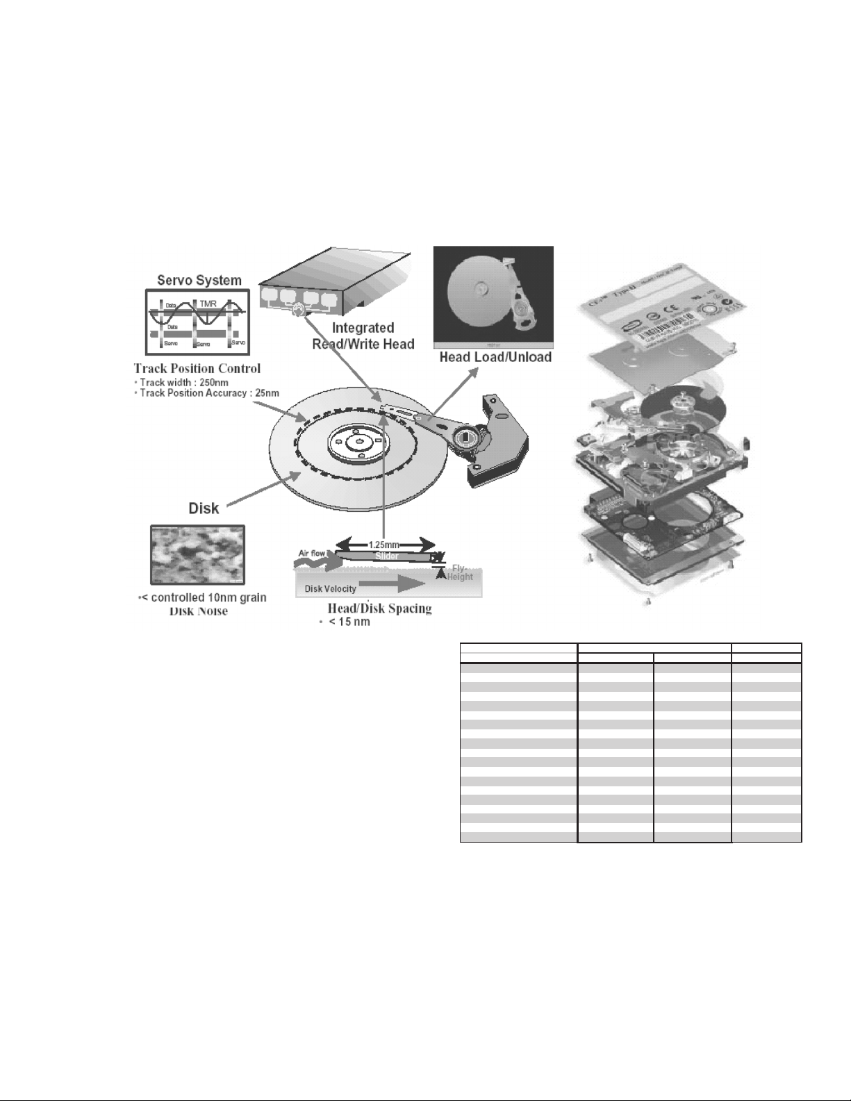
2.1 Handling Microdrives
Microdrives are used in GZ-MC100 and GZ-MC200. Although the appearance is different, a Microdrive is exactly the same as a hard
disc that is used in a PC. Therefore, unlike handling conventional tapes, caution must be paid in handling Microdrives.
The handling of Microdrives is explained in this section.
2.1.1 The structure of Microdrives
The detailed inside structure of Microdrives is not disclosed as it is treated as trade secrets. However, it is essential to have knowledge
of the structure of Microdrives in order to carry out service properly. Some information about Microdrives is given here.
A Microdrive is mainly consisted of the following parts.
• A magnetic recording disk that is coated with magnetic material. (Disk)
• A reading/ writing head. (Head)
• A motor that turns the disk.
• A circuit board that is loaded with electrical circuit which controls the motor, the head positioning, and input/ output of the
signal.
1 head type Microdrives use one side of the disk, and 2 head type
Microdrives use both sides of the disk with heads on each side
of the disk.The disk and the head do not contact and there is
certain space kept between them. The head reads the pre
recorded servo information to control the head itself. When the
head is not in access to the disk, it is kept in a shelter to avoid
damaging the disk with shocks from outside.
The difference between a 2GB Microdrive and a 4GB Microdrive
is only whether it has one head or two heads and there is no
difference in performance, as shown in the specification list. A
2.5 inch hard disk that is used in a note PC is shown as a
reference. As a 2.5 inch hard disk is bigger than a Microdrive, it
has more disks and heads resulting in more capacity. On the
contrary, it seems impossible to increase the disks for a
Microdrive because of size restriction. High capacity will be
achieved by improving the areal density and rotation speed of the
future products.
Microdrive
Model name Microdrive 3K4-2 Microdrive 3K4-4 Travelstar 4K80-80
Model number HMS360402D5CF00 HMS360404D5CF00 HTS428080F9AT00
Capacity 2 GB 4 GB 80 GB
Interface
Form factor 1inch 1inch 2.5inch
System type Consumer electronics Consumer electronics Laptop
Cache buffer 128 KB 128 KB 8 MB
Disks / Heads 1/1 1/2 2/4
Rotational speed (RPM) 3,600 (RPM) 3,600 (RPM) 4,200 (RPM)
Media transfer rate 97.9 Mb/sec max 97.9 Mb/sec max 351 Mb/sec max
Interface transfer rate
Average seek (ms) 12 (ms) 12 (ms) 13 (ms)
Average latency (ms) 8.33 (ms) 8.33 (ms) 7.1 (ms)
Areal density 56.5 Gb/sq. inch 56.5 Gb/sq. inch 68.5 Gb/sq. inch
Typical idle acoustic (Bels) 㧙㧙2.4B
Operating shock (G) 200 G (2ms) 200 G (2ms) 250 (2ms)
Non-operating shock (G) 2000 G (1ms) 2000 G (1ms) 800 (1ms)
Operating ambient temperature ()0 㨪 70 ()0 㨪 70 ()5 㨪 55 ()
Non-operating ambient temperature ()
2GB 4GB 80GB
CompactFlash TypeΤCompactFlash Type
33 MB/sec max 33 MB/sec max 100 MB/sec max
-40 㨪 70 () -40 㨪 70 () -40 㨪 70 ()
hard disk
Τ ATA ATA- 6
Shock tolerance during non-operation is remarkably high. Microdrives are designed to tolerate shock during non-operation as
they are removed or carried out more often than other hard disks.
However, Microdrives are vulnerable to falls and shocks just like
other precision instruments.
Microdrives are made in conformity with the standard of CompactFlash Type II. The thickness of the drive is less than 5.5mm,
thus failures can occur by folding or twisting the disks. The standard for torsional stress is 6kg approx. and for flexing stress is
4kg approx. Be sure to carry Microdrives in protection cases on
the service sites, and strongly recommend the customers to do
so, too.
(No.YF060)1-5
Page 6
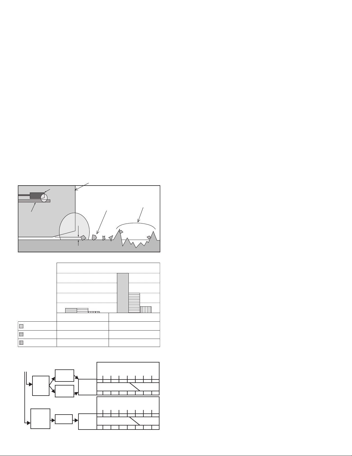
2.1.2 Precautions on handling Microdrives
Shock
Main causes of failures in hard disks including Microdrives are
listed as follows.
(1) Failures caused by shocks
(2) Failures caused by static electricity
(3) Failures caused by power cut during the operation
NOTE:
The shock of 200G(G:Gravity), a maximum impact value in
operation, is equivalent of the impact of dropping from 2030cm above the hard floor. The shock of 2000G, a maximum
impact value in non-operation, is equivalent of the impact of
dropping from 75 - 100cm above the hard floor.
2.1.2.1 Failures caused by shock
One of the causes of the Microdrive failures is a crash between
the disk and the head caused by falls or shocks. The results of
the crash are listed as follows.
• The scratch on the surface of the disk (crash scar) disables
reading/ writing of the damaged part.
• The magnetic material that came off by the crash (disk fragment) causes head reading failure.
• The head distortion deteriorates the read/ write attribute.
• The change in the space between the head and the disk disables the normal read/ write.
Stronger shocks result in the motor axis distortion, causing axial
runout and deterioration in performance such as disabling the
trace of normally recorded signal.
Pay extra caution not to drop or give shocks to the Microdrive
while servicing, and make sure to store the Microdrive in a provided plastic case.
Head
Head
Crash scar
2000
2000
300
Disk
Disk
Impact value (G)
(G):Gravity
Microdrive
2.5 inch HDD
3.5 inch HDD
2500
2000
1500
1000
500
Disk fragment
㧔0.03um㧕
Head floating height
0
Operation Non-operation
200
200
55
2.1.2.2 Failures caused by static electricity
Microdrives are designed to tolerate static electricity up to 15kV
approx. However, head destruction or boot failure will occur as a
result of high static electricity given to the magnetic head of a Microdrive that is very vulnerable to static electricity.
As same as handling other electronic parts, make sure not to
take charge of static electricity before touching a Microdrive for
checking or repairing.
In addition, make sure to store the Microdrive in a provided plastic case when it is not in use.
The voltage of 15kV has enough power to break Microdrives destroying heads etc. Errors in Microdrives may occur with lower
voltage. Asking the customers about the recording condition:
whether it was inside the car in winter, right after getting off the
car or in the carpeted area of a hotel etc., is recommended to investigate failures with poor reproducibility.
2.1.2.3 Failures caused by power cut during the operation
When the power is cut off while writing the data on the Microdrive, writing failure occurs in the writing sector (512 byte). As a
result, an error will occur while reading the data.
The effects on the system, given by the bad writing sector, depend on the types of the written files on the sector.
If it is user data, the recorded movie may not be replayed.
To prevent failure in writing, do not insert/ remove the Microdrive
or cut off the power unless otherwise indicated or needed.
"Read Sequential Error" may be detected if Full Check of the Microdrive is performed with the DDD.
NOTE:
"Read Sequential error" may be detected as a result of defective Microdrive disables the reading. Abnormal reading may
also occur when the user removes the power plug or the battery while the Microdrive is in operation; the writing is not completed and the reading cannot be performed normally.
In the latter case, the failure will be corrected by running the
Full Check after the DDD Clean Disk has been performed.
Running the Clean Disk is recommended when the recorded
movies cannot be read or the Read Sequential Error occurs.
If an error is detected even after running the Full Check, other
causes of the failures are considered.
Shock
Crash
between
the head
and the
disk
Operation
Excessive
power is
generated
in the
mechanism
Operation/ Non-operation
1-6 (No.YF060)
Disk
fragment
Crash scar
on the disk
Disk
shift
50 100 150 200 250 300 350
Read
error
1400 1600 1800 2000 2200 2400 2600
Performance
deterioration
(G):Gravity
Shocks(G)
Shocks(G)
Read error
Performance
deterioration
Normal
Normal
Model:HMS360404D5CF00SERIES
Page 7
2.1.3 Microdrive backup
Unlike the information on tapes, customers' information on
Microdrives can become unreadable in an instant. Backing up
users' record is strongly recommended to avoid any accident.
File Transfer Time Measurement
Recording detail
(Recording Capacity)
FAT32
Normal format
FAT32
Quick format
15m(1GB)
30m(2GB)
45m(3GB)
60m(4GB)
Detection detail
via PCMCIA card
via USB2.0 reade
via PCMCIA card
via USB2.0 reade
transmitted by PCMCIA card
transmitted by USB2.0 reader
transmitted by PCMCIA card
transmitted by USB2.0 reader
transmitted by PCMCIA card
transmitted by USB2.0 reader
transmitted by PCMCIA card
transmitted by USB2.0 reader
Microdrive 1 Microdrive 㧞
N2B12JRA N2HNY1VA
12m31s 12m36s
00m37s 00m40s
00m18s 00m19s
00m10s 00m09s
16m16s 15m46s
07m25s 07m57s
29m30s 29m47s
14m08s 14m49s
41m23s 42m48s
22m47s 23m23s
56m15s 56m34s
30m02s 29m53s
The above data shows: the elapsed time of copying the recorded
information on a Microdrive to a PC and the elapsed time of
formatting the Microdrive with the PC.
From the results of the measurement, it is clear that the data
transfer with a commercial USB2.0 Reader/ Writer is about twice
as quick as transfer with a PCMCIA card.
Using USB2.0 Reader/ Writer is recommended when frequent
data backup or data re-writing on the Microdrive is required.
Backup should be performed all the recorded files on the Microdrive.
Formatting must be done with the main unit that operates normally.
If a Microdrive that is more than 2 GB is formatted with the main
unit, it is formatted as FAT (FAT16), and a drive that is more than
2GB is formatted FAT32.
2.1.4 Checking the main unit/ Microdrive good or bad
In order to repair or check MC100 - 200, judging the cause of the
failures, whether it is the main unit or the Microdrive, is essential.
The product failures that are brought into repair/ check fall into
the following categories.
(1) Microdrive failures caused by the users handling such as
fall, shocks, and submergence.
(2) Main unit operation failures caused by the Microdrive fail-
ures.
(3) Microdrive operation failures caused by the main unit fail-
ures.
NOTE:
Unlike DVC tapes, the Microdrives of MC100 - 200 are recognized as parts of the main unit. It is essential that the main unit
and the Microdrive are brought in as a pair for service. Basically, do not accept the main unit alone for repair or check.
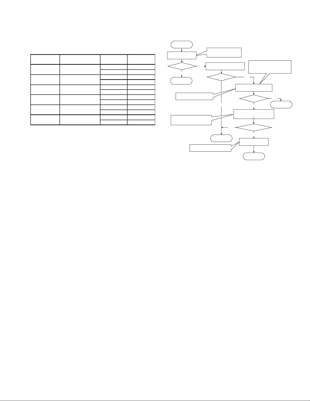
2.1.4.1 Separations of the parts failures
The procedure to identify the causes of the failures whether it is
in the main unit or in the Microdrive is explained in this section.
Start
Check the Water Exposure Seal
Check the appearance
Troubles?
YES
Go to
2.1.4.2
Perform a general operation check
such as record/ replay.
Check whether there is an emergency
record in the main unit, and check the
details of the record.
The failure caused by the user's PC or
by the supplied software is considered.
Check the Water Exposure Seal,
significant scratches on the
exterior, bends, and dents.
Perform a general operation check
NO
using a MD other than the user drive.
Troubles?
YES
YES
Go to
2.1.4.4
Check whether it is a Microdrive failure
or a main unit failure by using the user's
Microdrive. Be sure to make a backup in
case of an accident.
NO
Operate a general operation check
using the user Microdrive.
Troubles?
NO
Check whether there is an emergency
record in the main unit, and check the
details of the record.
With an emergency record?
NO
Recheck the details of
the failure with the user.
YES
Go to 2.1.4.3
End
2.1.4.2 Microdrive failures caused by user handling
As previously explained, Microdrive failures may possibly be
caused by falls or shocks. Further more, dropping Microdrives in
the water causes crucial failures to Microdrives.
Supplied Microdrives (not all the commercial Microdrives) have
the same type of Water Exposure Seal that are used in cellular
phones.
Before checking the failures, check whether there is a Water Exposure Seal display appeared.
In addition, check whether there are any significant scratches,
bends, or dents that shows the sign of falls or shocks.
Other check items are as follows.
(1) Check whether there are any letters written with a pencil or
a pen on the label of the Microdrive. The pen pressure
gives distortion on the Microdrive, resulting in an operation
failure. It is noted in the Instruction Book.
(2) Check whether there are any stickers affixed on the Micro-
drive. The space between the Microdrive and the housing
is very little. Affixing unnecessary stickers may lead loading the Microdrive in a wrong position, resulting in contact
failure or remove disk failure. There is a hole on the reverse
side of the Microdrive for ventilation through special filter.
Sealing the holes gives effect on the operation.
(3) Check whether the Microdrive label is peeled or turned. If
there are peel or turn in the label, the loading failure may
occur. Peels or turns will not occur under normal conditions, thus storage or usage under hot and humid condition, near organic solvent, or exposure to the direct sunlight
are considered.
(No.YF060)1-7
Page 8
When it is submerged, the white
Water Exposure Seal turns to red.
As the center part of the seal turns
to pink, the color seen from the
hole is pink. The 1mm hole
diameter prevents the seal from
getting affected by wet hands
under normal conditions. It is not
affected by the humidity of normal
storage or operational conditions.
Normal condition
Water Exposure Seal
display is appeared
(changes from white to red)
Displays of Water Exposure Seal
6mm
1mm
2mm
1.5mm 1.5mm
4mm
Air is taken into inside
the Microdrive from this
hole through special
filter for ventilation. DO
NOT SEAL THIS HOLE
is displayed.
Location of a Water
Exposure Seal (inside)
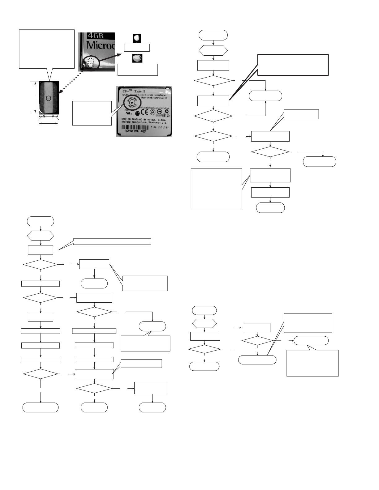
2.1.4.3
Main unit operation failures caused by the main unit/
Reverse side of the Microdrive
Microdrive failures.
2.1.4.2 There is a possibility of a Microdrive being damaged even
though there is no notable failure in appearance.
Main unit failures also result in abnormal operation in a Microdrive.
Identifying the causes of the failures in the main unit is explained
in this section.
In the diagram, MD stands for a Microdrive, CG for a compact
flash card, and SD for a SD card.
2.1.4.3
MD Diagnosis
Backup the record
of the user MD
Can it be
back upped?
YES
Perform the DDD Full Check
Troubles?
YES
Format the MD
with the main unit
Perform the DDD Clean Disk
Perform the DDD Full Check
Return the user backup data.
Troubles?
YES
MD failure
2.1.4.4 Operation failures caused by main unit failures
2.1.4.3 Judging from the separation of the main unit and MD, the
operation failure is more likely to be caused by the main unit failure. However, the main unit failure has not been determined yet,
as there is a possibility of the user MD failure causing the main
unit damage. The following procedure shows how to determine
the main unit failure.
Backup by connecting to the PC via USB or PCMCIA adapter
Read/ write by other
NO
devices is impossible
Go to 2.1.4.5
Check the emergency
NO
record of the main unit
Any record?
Format the MD with the main unit
Perform the DDD Clean Disk
Return the user backup data
Perform a detailed operation
NO
check by using the user MD
Troubles?
Main unit failure
NO
YES
YES
Either the bad data file or the
damaged MD causes the disabled
read/ write is not yet determined
at this point.
Go to 2.1.4.4
Although main unit failure is generally
speculated, the cause of the failure is
not determined whether the main unit/
MD at this point
Perform an operation check on
all items including MD and SD
The failure is resolved by
performing the formatting
NO
and the Clean Disk.
End
2.1.4.4
Main unit
diagnosis
An operation check
with other MD
Troubles?
NO
YES
An operation check
with CF and SD
Troubles in both
SD and CF?
YES
NO
Troubles
only in CF?
YES
NO
Main unit failure
The user MD/ FC may bend the
main unit socket pin(s). Using
defective MD/ FC results in
repeated failures, as they bend the
main unit connector every time
they are used. User MD/ CF should
be checked when abnormal main
unit socket is found.
Ask how many MDs/ CFs the user
has, then check all user MDs/ CFs.
2.1.4.5 Disabled read/ write with other devices
When read/ write cannot be done with the main unit, the main
unit failure is considered in most cases. Recognition failure
caused by the main unit writing bad data can be considered.
The causes of read/ write failures are as listed below.
(1) Damaged mechanism parts or electric parts inside the MD.
(Hardware failure)
(2) Damaged information in the MD. (Software failure)
In the case (1), it seems very difficult to recover, but there is a
possibility of recovery in the case (2) by using commercial software.
The following procedure shows how to figure out whether the
damage is in the hardware or in the software, and whether it is
recoverable or not.
2.1.4.5
Recoverability
diagnosis
An operation check
with other MD
Troubles?
NO
Main unit failure
2.1.4.5.1 Microdrive hardware failure
Although no failure was found in the MD appearance at the time
of the separation of 2.1.4.1, actually there is considerable damage disabling the operation. In this case, "Shipping Damage"
(damage caused by the transportation) is displayed as a result of
DDD diagnosis. Surely, a possibility of the products damaged on
route from the production plants to the shops and then to the consumers cannot be denied.
However, MDs are stored in protection cases or in main units and
the transportation shock that damages only the MDs is unrealistic. A failure cause by the user handling is more likely considered.
YES
Perform an operation check with CF and SD.
Use SD with theoretical value of 10MB/s or more.
Use CF with 40x high speed or more.
For details, refer to 5.
The Combinations of media and the main unit
Main unit failure
Check bend or break
in the socket pin(s).
Check the MD socket
of the main unit.
Troubles?
NO
YES
Check the connector part of
the main unit housing and
user MD/ CF
Carry out the servic
End
A failure caused by the user handling
is considered, and no more recovery
Perform the DDD
Full Check
Troubles?
YES
MD Hardware failure
is expected.
Please explain the user that it is a
MD failure.
NO
The main unit operation failure may be
caused by an unrecognizable MD after
user's editing works such as formatting
and adding/ deleting files or
maintenance works such as
defragmentation and check disk done
with a device other than the main unit.
Main unit failure
MD software failure
1-8 (No.YF060)
Page 9
Recovery method
Asking a data recovery company (a data salvage company)
seems the only way.
Even if the MD is not recognized a drive, a transmission may be
possible with the MD (light hardware failure). In this case, system
recovery software such as Norton Utilities in Norton SystemWorks 2004 (NOTE1: ) may help drive recognition.
Once the drive recognition is recovered, the record may be recovered by the method mentioned in 4.5.2 MD software failure.
However, if it is a hardware failure, banning the use of the MD is
strongly recommended.
2.1.4.5.2 Microdrive software failure
Most of the software failures are caused by the unrecognizable
MD after user's editing works such as formatting and adding/ deleting files or maintenance works such as defragmentation and
check disk done with a device other than the main unit.
Many cases under this condition, recovery can be done by using
recovery software, which can recover MPEG2 data, such as Final
Data 2.0 Premium. It enables the drive recognition and the data
reading. Once the data is recovered, follow the below procedure.
2.1.4.5.2
Countermeasure for
the software failure
Start the data
recovery software
Is the data
recognized
NO
Recommend a data
recovery company
Perform an operation check on
all items including MD and SD.
YES
Backup the user MD record
Format the MD with the main unit
Perform the DDD Clean Disk
Perform the DDD Full Check again
Troubles?
NO
Return the user backup data
Perform a detailed operation
check by using the user MD
Troubles?
YES
Main unit failure
If backup is impossible,
do not proceed to the further works.
Further recovery is not expected.
Please explain the user that it is
a MD failure.
MD failure
YES
Explain the user that the possible cause
of the failure may be the users PC works.
Check again whether the user did a
prohibited or not guaranteed operation
by the Instruction Book.
Performing formatting
NO
and Clean Disk resolve
the failure
End
NOTE1:
Norton SystemWorks 2004 (Latest version on 2004/ 9/ 29)
It is Symantec's data recovery software.
For system requirements and other details, please check their
web site.http://www.symantec.com/region/jp/products/
NOTE2:
Final Data 2.0 Premium Office (Latest version on 2004/9/29)
It is AOS Technologies' data recovery software.
Although there are some kinds of recovery software as FINALDATA series from this company, this is the cheapest one that
can recover MPEG2.
For system requirements and other details, please check their
web site.http://www.finaldata.ne.jp/
2.1.4.5.3 Reusing Microdrives
If a Microdrive of a user is reused for another user, normal data
deletion may not completely erase the previous user's information (images) and the previous user's information may come
back. Unlike hard disks of PCs, most of the recorded contents of
Microdrives are images and audio data, thus there is a little possibility of recorded personal information in Microdrives. However,
proper handling in reusing Microdrives is required as a business
organization.
There are levels in erasing data in disks.
• Level 1: Zero Write method (once)
• Level 2: Random Write method (once)
• Level 3: Random/ Zero Write method (twice)
• Level 4: US Department of Defense (DoD5220.22-M)
• Level 5: US Department of Defense (DoD5220.22-Expanded)
• Level 6: Guttmann method
At least level 3 data erasure is recommended.
Data erasure software is commercially available from software
companies. It seems convenient to use Final Data 2.0 Premium
as there is a data erasing function in it.
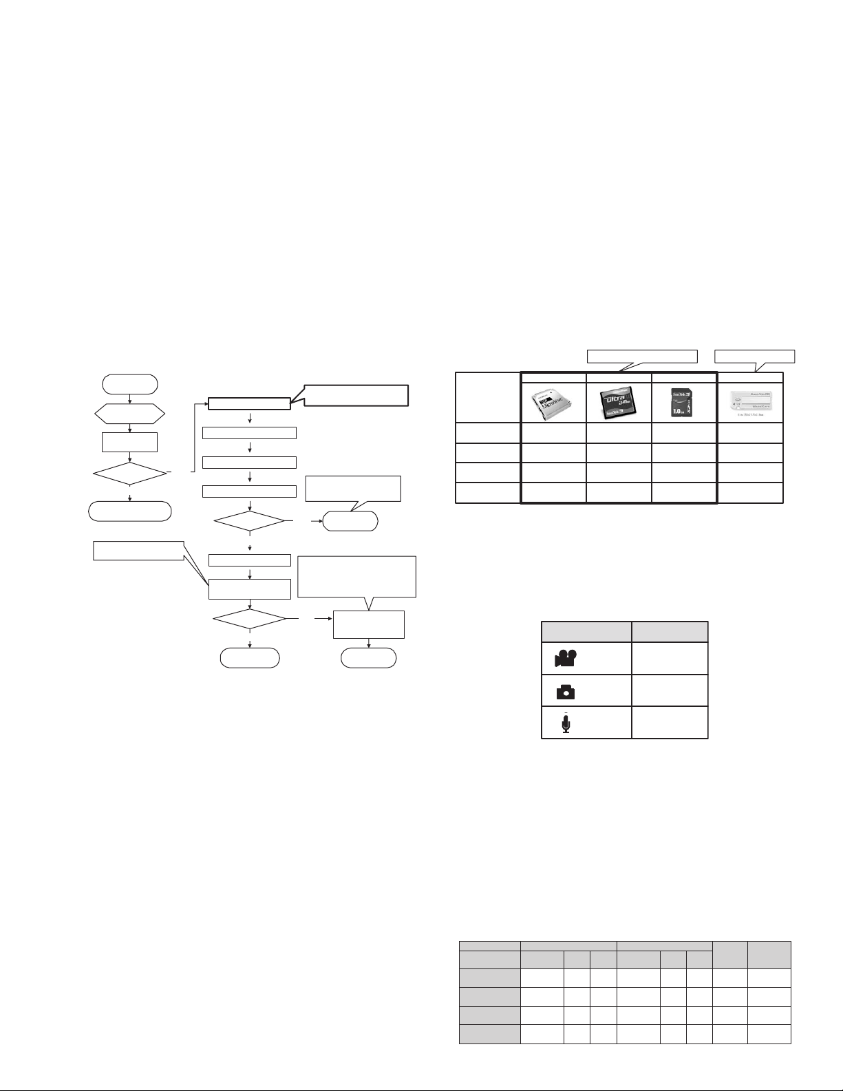
2.1.5 Combinations of media and a main unit
MC100 - 200 can record movies, pictures, and audio on compact
flash cards, SD cards in addition to Microdrives. Recording movies is partially limited. Characteristics of each medium, available
or limited operation items, and available operation time are explained in this section.
2.1.5.1 Types of media
Microdrive
Type
Capacity
Price
Unit price per 1MB
Commercially available
maximum capacity
15yen/㧬MB 52yen/㧬MB58yen/㧬MB
Available media for MC100-200
Compact Flash card
2GB 1GB1GB1GB
33000yen 52000yen58000yen
4GB 1GB1GB1GB
38000yen
38yen/㧬MB
SD card
Data for comparison
Memory stick
Commercially available maximum capacity
MC100 - 200 are basically designed to record movies by using
Microdrives.
MC100 - 200 have 2 types of slots, one for a Microdrive or a
Compact Flash card, and the other for a SD card.
From the menu, movies/ pictures/ audio can be selected for a
medium in either one of the slots.
Recording mode
Movies
Pictures
Audio
Factory setting
MD/CF
SD
SD
As movies, pictures, and audio can separately select the slots,
using one slot for all recording mode is possible. However, as
movies require large capacity and high transmission speed, the
available recording mode (image quality) is limited.
(Refer to 5.2.3 Image quality and support media.)
Recording movies in Microdrive setting is recommended.
2.1.5.2 Movies
Movies are recorded SD-VIDEO1.1 standard, (images) MPEG2-PS (with RDI),(audio) Dolby Digital AC-3, PAL 50 frame aspect
4:3
Movie recording is explained as follows.
2.1.5.2.1 Recording rate
Image Audio
Image quality mode
㧔Image size㧕
Ultra fine
㧔720480㧕
Fine
㧔720480㧕
Normal
㧔720480㧕
Economy
㧔325240㧕
Image quality
(Sensitivity comparison)
Equivalent
to DVC
Equivalent
to DVD cam
Equivalent
to VHS
Equivalent
to video CD
Bit
rate
8.5Mbps
5.5Mbps
4.2Mbps
1.5Mbps
CBR/
VBR
CBR
CBR
VBR
VBR
Sampling
frequency
48 kHz
48 kHz
48 kHz
48 kHz
Bit
rate
384kbps
384kbps
256kbps
128kbps
CBR/
VBR
CBR
CBR
VBR
VBR
RDI
32.768kbps
32.768kbps
32.768kbps
32.768kbps
Total bit rate
8.92 Mbps
5.92 Mbps
4.49 Mbps
1.66 Mbps
(No.YF060)1-9
Page 10
2.1.5.2.2 Recording time (approximately minutes)
Ultra fine
㧔720480㧕
SD㧛CFޓ128MB
SD㧛CFޓ256MB
SD㧛CFޓ512MB
SD㧛CFޓ1GB
MDޓ2GB
MDޓ4GB 60 minutes 90 minutes 120 minutes 300 minutes
2 minutes
4 minutes 6 minutes
8 minutes 12 minutes
16 minutes 24 minutes
30 minutes 45 minutes
Fine
㧔720480㧕
3 minutes
Normal
㧔720480㧕
4 minutes
7 minutes
15 minutes
31 minutes
60 minutes
Economy
㧔352240㧕
10 minutes
21 minutes
43 minutes
86 minutes
150 minutes
2.1.5.2.3 Image quality and support media
Image quality mode
Ultra fine
Fine
Normal
Economy
Microdrive
1GB or less 1GB or more
٤
Not for high speed
transmission
٤
٤
٤
٤
Compact Flash card
For high speed
transmission
٤
٤
٤
٤
٤
SD card
٤
For high speed
transmission
Not for high speed
transmission
٤
٤
٤
٤
As shown above, Microdrives of 1GB or less, Compact Flash
cards, and SD cards that are not for high transmission speed
cannot record movies except in the economy mode.
If a recording mode other than economy mode is selected and
the recording is started, " Recording cannot be done with this
Medium speed" is displayed.
Microdrives can be judged by the capacity whether they are for/
or not for the movie recording. However, Compact Flash cards
and SD cards are difficult to judge from the appearances.
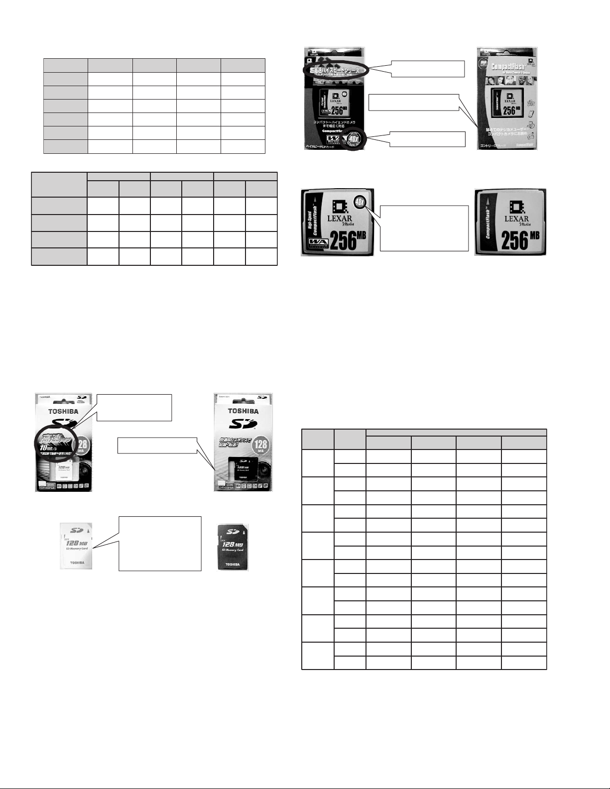
A Toshiba SD card and a LEXAR Compact Flash card are compared below.
On the package of the product,
it is noted as high-speed type.
The transmission speed of this
product is 10MB/S is written.
There is no description on
this product as a high-speed type
Package of the product for high data
transmission speed
It can be judged whether it is a
high-speed type or not by the
appearance as the color is
different.
As there is no description on the
product, a consumer does not
recognize the product of high
speed or normal speed, if he/ she
has no product to compare.
Appearance of the product for
high data transmission speed
Package of the product not for
high data transmission speed
Appearance of the product not for
high data transmission speed
SD card that is operation checked as a high-speed type has
transmission speed of 10MB/s or more. High-speed products
with less capacity (9MB/s etc.) may operate, but operation cannot be guaranteed.
On the package of the product,
it is noted as high-speed type.
There is no prescription of high-speed
type on this product package
Description of the transmission
speed as 40x
Package of the product not for
high data transmission speed
It can be judged whether it is a highspeed type or not by the appearance
as the color and the design are
different. The consumers can see
whether it is a high-speed type or not
as a description of 40x speed is
written on the product.
Appearance of the product for
high data transmission speed
Package of the product not for
high data transmission speed
Package of the product not for
high data transmission speed
Compact flash card that is operation checked as a high-speed
type has transmission speed of 40x or more. High-speed
products with less capacity may operate, but operation cannot be
guaranteed.
2.1.5.3 Pictures
Pictures are recorded as JPEG compression picture Exif2..2,
DCF2.0, PictBridge, DPOF standard conformity. There is no restriction of picture recording media or spec, but equivalent transmission speed as for movies is required for rapid shooting.
Picture recording is explained as follows.
2.1.5.3.1 Image size and recording numbers
%CRCEKV[
32MB
64MB
128MB
256MB
512MB
1GB
2GB
4GB
2KEVWTG
OQFG
(KPG
5VCPFCTF
(KPG
5VCPFCTF
(KPG
5VCPFCTF
(KPG
5VCPFCTF
(KPG
5VCPFCTF
(KPG
5VCPFCTF
(KPG
5VCPFCTF
(KPG
5VCPFCTF
UXGA
(16001200㧕
34
50
65
110
145
245
290
490
699
2285
1398
2797
9142
5595
9999
+OCIGUK\G
SXGA
(1280960㧕
60
120
125
250
280
560
145
245
1094
3555
2188
71104570
4376
9999
8752
9999
(1024768㧕
XGA
95
185
200
375
430
865
865
1735
1706
5565
3412
9999
9999
9999
9999
(Approx. numbers)
VGA
(640480㧕
205
375
425
755
2210
5200
7756
9999
3878
9999
7756
9999
99996826
9999
9999
9999
The value varies slightly according on each medium, Microdrive,
Compact flash card, and SD card. In addition, these values are
theoretical values, and it does not guarantee the recording numbers.
1-10 (No.YF060)
Page 11

2.1.5.4 Audio (Voice memo)
Audio is recorded linear PCM digital recording system (WAV),
stereo.There is no restriction of audio recording media or spec.
Audio recording is explained as follows.
2.1.5.4.1 Recording mode and sampling frequency
Recording mode
Fine
Standard
Economy
Sampling
Frequency Data
48 KHz
16 KHz
8 KHz
16 bit
16 bit
16 bit
Audio mode
Stereo
Stereo
Stereo
Recording
bit rate
1.536 Mbps
512 Kbps
256 Kbps
Data capacity
per minute
11.52 MB
3.84 MB
1.92 MB
2.1.5.4.2 Recording time
(Approx. hours, minutes)
Standard Economy
2h10m
8h40m
17h21m
4h25m
17h21m
34h43m
SD
㧛CFޓ512MB
MDޓ2GB
MDޓ4GB
Fine
44m
2h50m
5h47m
The value varies slightly according to each medium, Microdrive,
Compact flash card, and SD card. In addition, these values are
theoretical values, and it does not guarantee the recording time.
2.1.6 About DDD
CF II compliant 1-inch small hard disk (Microdrive) is used as recording media of this model. For operation check and maintenance of this Microdrive, drive fitness test software: Drive
Diagnostics &Disposition (DDD) is provided from Hitachi Global
Storage Technologies (HGST) with a license agreement. HGST
supplies the Microdrive's parts to JVC.
The handling of this software is explained as follows.
Notice
This software is developed to confirm, analyze, and restore the
various kinds of hard disks. However, JVC is allowed to use
DDD software only to test, confirm, and restore the Microdrive
to the factory setting.
Thus, the use of other functions is prohibited.
Using software other than DDD may damage the installed hard
disk of the PC or may disable the reading of the stored data.
Please understand that we do not at all compensate any damage caused by the usage other than instructed, and that we
cannot accept any inquiry.
If you have any questions or requests, please do not contact
HGST that is displayed when installing the software, but do
contact Camcorder CS Group, AV & Multimedia Company.
2.1.6.1 Platform Requirements
DDD operation requires the following platform requirements. Although it may operate on lower specification platforms, we do not
guarantee the operation under such platforms.
PC/AT compatible models ( It cannot be used with Macintosh)
CPU :Pentium 600 MHz or faster
OS:Windows 98/NT4.0(SP4 minimum)
RAM with 192MB or more (NOET1)
Memory: 100MB or more empty hard disk space
PCMCIA card (PC card) TYPE II slot (NOTE2)
Monitor / graphics: 256 colours or more, 800 x 600 minimum,
(1024 x 768 or more is suggested)
NOTE1:
When DDD is installed to a PC with less RAM capacity, the following symptoms may occur.
• An error occurs during the installation, and the installation
does not complete.
• The operation becomes unstable while starting up the software.
NOTE 2:
There must be PCMCIA card (PC card) TYPE II slot: equipped
to note PCs and some desktop PCs.
DDD cannot be used with CF / Microdrive reader with USB, or
CF direct insert drives.
2.1.6.2 How to get DDD
(1) DDD (DDD.EXE) can be downloaded from JS-NET. After
download, execute DDD.EXE to create DDD SETUP folder.
2.1.6.3 Installation procedure
(1) Double click the SISetup.exe in the DDD SETUP folder to
start up.
Double click this program.
(2) Press Next button to proceed the installation.
Press Next button
(3) Select the PC's start up system for installation.
• IDE, Primary Controller, Master HDD
• IDE, Secondary Controller, Master HDD
• SCSI, First Controller, ID 0
• SCSI, Secondary Controller, ID 0
(No.YF060)1-11
Page 12

Usually IDE, Primary
Controller, Master HDD will
be selected.
(4) Although the error massage on the right may appear on cer-
tain PCs, continue the installation by pressing OK button.
Press OK button
(5) When "Registration Info:" is displayed press Next button to
proceed the installation.
will DESTROY ALL DATA on the drives which are tested.
Do you still want to continue?" is displayed. When you fully
understand the description, press Yes (Y).
Press Yes (Y) button.
(8) When "License Agreement" is displayed. When you fully
understand the description, press YES.
Press YES button
Press Next button
NOTE:
Although Registration Info requires ID registration, there
is no need to register, as it has nothing to do with JVCVICTOR.
(6) Press Next button, to continue the installation.
Press Next button
(9) When "User Information" is displayed, input any letters in
the Company box. Next button is displayed after input,
press Next button.
In the Company box,
input any letters such
as JVC etc.
Next button is displayed after some letters
are input in the Company box.
When Next button is displayed, press the
button.
(10) Select the folder for installation, then press Next button.
Use default folder. (NOTE)
NOTE:
"It is strongly recommended that you quit all Windows
program before running this Setup program" is displayed. Finish all other programs that are running, and
then press Next button to continue the installation.
(7) The caution, "Please understand that this tool is for
Resellers only. The default tests are DESTRUCTIVE and
1-12 (No.YF060)
Press Next button
Page 13

(11) Select the program folder, then press Next button.
Use default folder. (NOTE)
Press Next button
NOTE:
For installation folder name and drive, use default address and drive as long as there is no problem with the
PC. If the default settings are changed, programs following this installation do not operate properly.
(12) When a confirmation "Yes, I want to launch Hitachi DDD-SI
now" is displayed, press Finish button.
(DDD will not be started until the starting up preparation in
4 is completed.)
(3) Double click the My Computer icon, then select Properties.
(4) 4.Click the Hardware tab in System Properties, and then
click Device Manager.
Click the Hardware tab
Press the Device Manager button.
(5) 5.Click IDE ATA/ATAPI controllers in Device Manager.
Do not check (click)
Press finish button
2.1.6.4 Preparation for start up
(1) On the desktop, icons (4 kinds) shown below are created.
Delete those icons, as they are not to be used.
(2) From the DDD SETUP folder, copy the shortcut icons (2
kinds) shown below to the desktop.
(These are the links for the program exclusive to JVC.)
NOTE:
The names of icons, display contents and display parts
differ according to the types of installed OS, their versions, and each PC's settings. The following procedure
is explained using Windows2000 as an example.
Click IDE ATA/ATAPI controllers
(6) Open the PCMCIA IDE ATA/ATAPI controller property,
then click the Resources tab.
Click the Resources tab
(No.YF060)1-13
Page 14

(7) Take notes of the I/O range, then press Cancel button to
close the Property Setting window.
Take notes of the I/O
range shown here
(8) Open the folder where DDD is installed in Explorer etc
(Usually the folder is C:\Program Files\ Hitachi DDD- SI )
(10) Select all the files in the input folder and delete them all.
Select all the files the folder
and delete
NOTE:
These files are used for other hard disks. If they are started up carelessly, it may cause serious impact on the
hard disk or other connected devices.
Therefore, prevent any operation mistakes by deleting all
the files except the one which is used with Microdrive.
(11) From the DDD SETUP folder, copy the two files
"FullCheckMicrodrive__jvc.pid" and "CleanDisk..pif" in the
input folder.
Inside the DDD SETUP folder
(9) Open the input folder in Hitachi DDD- SI.
Open the input folder
1-14 (No.YF060)
Input folder located under the DDD installed folder
(12) Double click the copied icon "FullCheckMicrodrive_jvc" on
the desktop to start DDD.
Page 15

(13) Click File to open Menu, then select "Program Settings
Alt+P" from the Menu and click.
(16) Finish the program either by pressing X button or press Exit
in the File menu.
Click File
Select "Program Settings
Alt+P" from the open Menu
(14) Input the previously noted and partially devised I/O range
into PCI/PCMCIA ATA Addresses item on the DDD
Program Options screen.
Input the original address
which exceeds the I/O range.
Input the address which takes away
1 from the original address
that exceeds the I/O range.
(e.g.) Noted I/O range
FEF0 - FEFF
Input FEF0 in the first column.
Input FEFE, which is -1 from FEFF.
Press OK button
(15) When the PCI/PCMCIA ATA Addresses input is
completed, press OK button.
Press X button
(17) When the reconfirmation "Are you sure you want to end the
application?" is displayed, press Yes (Y) button to finish the
application.
Press Yes (Y) button
2.1.6.5 Uninstall
(1) ninstall the Hitachi DDD- - SI from Add/ Remove Programs
on the Windows.
2.1.6.6 How to use DDD
NOTE:
Before starting DDD, be sure to back up users' all information
on the Microdrive.
Executing DDD may destroy all the user information, and recovery may become impossible.
In DDD there are two definition files (pid files) that have the
information which determines the operation of DDD.
Two pid files are exclusively prepared for JVC.
They are: FullCheckMicrodrive_jvc.pid, CleanDisk.pif
2.1.6.6.1 FullCheckMicrodrive_jvc.pid (FullCheck)
FullCheckMicrodrive_jvc.pid is the confirmation pid file to confirm
the Microdrive. (FullCheck)
It is used to confirm the drive fitness when repair or check is carried out.
(1) Load the PCMCIA card adapter with the Microdrive and in-
sert it into the card slot of the PC.
* If there are two card slots, use the first slot.
CF readers/ writers using USB or drives that can be directly connected CF cards to the PC can be recognized
as drives on the PC.
However, they cannot to be recognized as media on DDD.
Therefore, please use the PCMCIA card adapter.
(2) Click My Computer to check whether the drive is newly rec-
ognized.
Usually when recognized on the PC,a new drive letter is
given.
(3) Double click the FullCheckMicrodrive_jvc.pid icon that has
been copied on the desktop to start up DDD.
(4) Take a check out at the next of SCSI.
(No.YF060)1-15
Page 16

(5) Press the Media Recognition button (shown above) to rec-
ognize the medium.
Click to take off the check
at the next of SCSI
Press the Media
Recognition button
(shown above) to
recognize the medium.
(6) It will take about 20 - 30 seconds to recognize the medium.
NOTE:
Detected and displayed here is the name of Microdrive.
When the recognition is completed
normally, the detected medium is displayed.
NOTE:
Although the usual checking time is about 15-20 minutes, it varies depending on the each PC's performance.
If it takes too long (more than 30 minutes), there may be
a failure in checking. Finish the checking by pressing
Abort button and start the checking again.
(10) Press either Print button or View button to print or display
the checking result.
When confirming the checking is finished, press Exit
button.
Exit button
Print button
(7) Click the recognized media display (Model name) to the
select status (Highlighted) and press go button.
Click the selected media
Press go button
(8) The Window is open to start the checking.
To finish during the procedure, press abort button.
(9) When "Drive Explorer completed successfully." is
displayed here, the checking is finished.
At the same time Print, View, Exit buttons are displayed.
(11) The checking result will be output if the Print button is
pressed.
The checking result will be displayed if the View button is
pressed.
Pressing the Print button located in the bottom right can do
the printing.
When the confirmation is done, press Exit button to finish
the result display.
Print button
Exit button
(12) Press either X button or Exit in the File menu to finish the
program.
1-16 (No.YF060)
Press X button
When "Drive Explorer completed
successfully." is displayed here,
the checking is finished.
Page 17

(13) When " Are you sure you want to end the application?" is
displayed, press Yes (Y) to finish the application.
Press Yes (Y) button
2.1.6.6.2 Test results and countermeasure
1.2.6.6.1Reviewing the test results of FullCheckMicrodrive_jvc.
pid (FullCheck) and the countermeasure are explained here.
drive, model name of the drive and the production place are
also written.
Drive model
name
Production
place
Serial
number
The first 8 digits are serial number.
ԚThis is a serial
number of the
Microdrive and it
is exclusive to
each product.
ԙThe time and date
of the test results
output is recorded here
㨩
ԞThe time and date of the start
and end the testing are displayed here.
ԟThe results are recorded.
ԘThe Microdrive model
name is displayed here.
It shows that the
Microdrive is
HITACHImade 4GB type.
ԘThis is also the
Microdrive model name.
ԛThe capacity of the
disk is displayed here.
ԜThe testing detail is
displayed here.
ԝThe comment
on the testing
results are
displayed here.
As there is more
information
below, check it
with the scroll
bar.
Be careful, as the information
within the dotted line is not shown
in the above display.
1. Drive model name
The HITACHI Microdrive model name is displayed here.
HMS360402D5CF00 :HITACHI(IBM) 2GB type Microdrive
HMS360404D5CF00 :HITACHI(IBM ) 4GB type Microdrive
2. Time and date of the output date
The time and date of the test results output is displayed here.
(e.g.) If it was output at 4:30 p.m. on Monday, September 13th,
2004, it will be shown as below.
File created on Monday ,13 .09.2004 at 14 :30 :09
3.Serial number
The serial number is exclusive to each product. It is the eight
digit numbers of the serial number part (bar code) on the reverse side of the Microdrive. On the reverse side of the Micro-
Reverse side of the Microdrive
4. Disk capacity
The recordable disk capacity is displayed here.
It is shown as below.
2GB type Microdrive: 1952 MB
4GB type Microdrive: 3905 MB
In the actual display, 2GB and 4GB are converted to Byte. So
it is displayed under the Microdrive display of 2G or 4G with
MB.
5. Testing details
When FullCheckMicrodrive_jvc.pid is carried out, the six kinds
of testing are performed.
(1) Drive Initialization
The test checks whether the drive can recognize or not.
Errors will be detected if it cannot recognize at all as a result of fall, shock, or submersion. It is more likely to have
a failure in electrical circuit than a mechanical one (motor).
Checking items:Submersion mark, scratch on the exterior, dent, and bend.
(2) Check Servo Data (DFT)
The test checks whether the disk is decentered or not.
If the motor shaft is decentered as a result of fall or
shock, the interior head cannot pick up the recorded signal on the disk.
Checking items:Scratch on the exterior, dent, and bend.
(3) Check for Scratches on Media
When a cluster error occurred, an alternative area is created to avoid the use of the damaged cluster. This test
checks the distribution of the alternative area. It does not
detect scratches of the user data area caused by fall or
vibration.
Checking items:None
(4) Check Product Internal Error Logs
This test collects the error information that was recorded
at the time of production.
It carries two tasks, checking the Error Logs and the
numbers of the alternative sectors.
Checking items:None
(5) Check GMR Head Amplitude
This test checks the output of the head. Read and write
errors by electrostatic, by shock that changes the distance between the head and the disk may cause errors
on writing or reading.
Checking items:scratch on the exterior, dent, and bend
(6) Media Test(s)
This test checks whether the written information can be
correctly read or not by comparing writing data and read-
(No.YF060)1-17
Page 18

ing data. Randomly select about 300 parts from the user
data area. Read the data and write in other data in that area, then read the data again to check if the correct read/
write can be performed. Two tests, CSO Read- WriteCompare and Read Sequential Test that checks all the
sector including the red\cording area, are performed.
Checking items:scratch on the exterior, dent, and bend.
6. Comment on the results of the test
The comment is displayed by totally judging from the six test
on 5. results, and by speculating the cause of the Microdrive
failure.
If there is no problem at all, a comment "DO NOT RETURN TO
YOUR SUPPLIER" is displayed.
If any failure is found on the Microdrive, a comment "RETURN
THIS DRIVE TO YOUR SUPPLIER" is displayed. In the early
stage, the defected parts are analyzed for modification. Please
follow the instruction from JVC.
7. The time and date of the start and end the testing are displayed here.
The time and date of the start and the end of the test, and the
testing time are displayed here.
(e.g.) If it was started at 4:30:09 p.m. on Monday, September
13th, 2004, and finished at 4:45:23, and the testing time is 15
minutes and 14seconds, it will be shown as below.
Explorer Start : 16:30:09 on Monday, 13.09.2004
End : 16:45:23
Delta :00:15:14
8. Test results
The test results of the six test on 5. are displayed.
If there is no problem at all, "Drive passed Explorer WITHOUT
a problem." Is displayed.
If any failure is found, "READ SEQUENTIAL TEST ERROR" is
displayed to show where the errors are found. Decide the
countermeasure not by this comment but by the comment
sown on 6.
2.1.6.6.3 CleanDisk.pif
The CleanDisk.pif (CleanDisk) is a file which restores the Microdrive to its factory settings. It is use to restore the Microdrive to
its factory settings when it does not operate properly as a result
of a failure in format etc. It can also be used to completely delete
the user information on the Microdrive.
(1) Load the PCMCIA card adapter with the Microdrive to be
clean disked, and insert it into the PC card slot of the PC.
*If there are two PC card slots, use the first slot.
CF readers/ writers using USB or drives that can be directly connected CF cards to the PC can be recognized
as drives on the PC.
However, they cannot to be recognized as media on DDD.
Therefore, please use the PCMCIA card adapter.
(2) Click My Computer to check if the drive is newly recog-
nized.
Usually when recognized on the PC, a new drive letter is
given.
(3) Double click the copied CleanDisk.pif icon on the desktop to
start DDD.
(5) Press the media recognition button ( shown above) to rec-
ognize the medium.
Click to take off the check
at the next of SCSI
Press the Media
Recognition button
(shown above) to
recognize the medium.
(6) It will take for about 20 - 30 seconds to recognize the
medium.
NOTE:
The detected and displayed is the Microdrive model name
When the recognition is completed
normally, the detected medium is displayed.
(7) Click the recognized media display (Model name) for the
selected status ( Highlighted), then press go button.
Click the selected media
Press go button
(8) The window is open to start DiskClean.
To finish during the procedure, press abort button.
(9) The test is completed when "Drive Explorer completed
successfully." is displayed here. Print, View, Exit buttons
are displayed at the same time.
(4) Take off the check at the next of SCSI.
1-18 (No.YF060)
When "Drive Explorer completed
successfully." is displayed here,
the checking is finished.
Page 19

NOTE:
Although the usual checking time is about 15 - 30 minutes. If it takes too long (more than 45 minutes), there
may be a failure in checking. Finish the checking by
pressing Abort button and start the checking again.
(10) Press either the Print button or the View button to print or
display the test results.
When the test results are checked, press Exit button.
Press X button
(13) When asked to finish the program, press Yes button.
Exit button
(11) When the Print button is pressed the test results are output
to the printer, and the View button is pressed the results are
shown as below. Pressing the Print button in the down right
can also print the results. When the checking the result is
finished, press Exit button to finish the display of the test
results.
ԘThe Microdrive model
name is displayed here.
It shows that the
Microdrive is
HITACHImade 4GB type.
ԘThis is also the
Microdrive model name.
ԛThe capacity of the
disk is displayed here.
ԜThe testing detail is
displayed here.
ԞThe time and
date of the start
and end the
testing are
displayed here.
Print button
Exit button
ԚThis is a serial
number of the
Microdrive and it
is exclusive to
each product.
ԙThe time and date
of the test results
output is recorded here.
㨩
ԟThe results are recorded.
When CleanDisk is executed, it performs the following tasks.
Test items Outline
(1) Drive Initialization Test whether the drive recognizes of not.
(2) Set Features Initialize the internal function of the
(3)
Cleanup and/or un-clip
Entire Disk
(4) Media Test(s)
Microdrive.
The following tasks are carried out
1.Delete all data
2.Restore to the original capacity
3.Formatting (Deleting the lacked
information)
4.Clear the error information
5.Deleting other OS settings
Final test in writing/ reading
Press Yes (Y) button
NOTE:
Performing CleanDisk will not change the disk name given by
the user.
If the PC will be returned to the same user, there will be no
problem.
If the user is changed, change the disk name to MICRODRIVE.
This is the status that
the user changes the
disk name to Travel 1.
If the user is changed,
change the disk name to
MICRODRIVE.
(12) Press X button or press Exit in the File menu to finish the
program.
(No.YF060)1-19
Page 20

2.2 WIRING DIAGRAM
LCD
MODULE
24
CN305
CF
4
0
DET SW (OPEN/CLOSE)
USB
3
CN110
MICRO DRIVE
SOCKET
CN9901
60
CN106
TEMP. SENS
20
CN207
MODE SW
INFO
CURSOR KEY
ZOOM SW TRIG
BATTERY
REAR
UNIT
MENU
BATT_TERM
6
CN205
POWER DIAL
STRB
SENSOR
STROBE
STROBE
LCD SUB
5
CN304
0
10
LCD HINGE
30
CN107
CN103
DIGITAL
1
0
WB
MPEG2
DIGI IF
SUB CPU NUCORE
LCD DRV
CDS
CN101
33
TG V.DR
OP DRV
V I/O V OUT
30
SD/MMC
SOCKET
MEMORY
P.PRCS
JIG CONN
CCD
3
0
SD/MMC CARD
30
CCD
OP
CN105
CN104
CN102
CN5201
HEAD
PHONE DC JACK MULTI
45
30
CN204
CN203
LITHIUM BATTERY
REG
AUDIO
ANALOG
2
ANA IF
AC97 GYRO1
0
CN202CN201CN206
2
4
4
CN301
GYRO2
CN202
2
6
0
CN201
4
JUNCTION
1-20 (No.YF060)
MIC
SPEAKER
Page 21

SECTION 3
DISASSEMBLY
3.1 BEFORE ASSEMBLY AND DISASSEMBLY
3.1.1 Precautions
• Be sure to disconnect the power supply unit prior to mounting
and soldering of parts.
• Prior to removing a component part that needs to disconnect
its connector(s) and its screw(s), first disconnect the wire(s)
from the connector(s), and then remove the screw(s).
• When connecting/disconnecting wires, pay enough attention
not to damage the connectors.
• When inserting the flat wire to the connector, pay attention to
the direction of the flat wire.
• Be careful in removing the parts to which some spacer or
shield is attached for reinforcement or insulation.
• When replacing chip parts (especially IC parts), first remove
the solder completely to prevent peeling of the pattern.
• Tighten screws properly during the procedures. Unless
otherwise specified, tighten screws at a torque of 0.118N
·cm). However, as this is a required value at the time of
(1.2kgf
production, use the value as a measuring stick when
proceeding repair services. (See "SERVICE NOTE" as for
tightening torque.)
3.1.2 Destination of connectors
Two kinds of double-arrows in connection tables respectively
show kinds of connector/wires.
: Wire: Flat wire : Board to board (B-B)
: The connector of the side to remove
CONN. No. PIN No.CONNECTOR
CN2a
CN2b
MAIN CN101
MAIN CN103
MONI BW CN761
MINI BW CN762
3.1.3 Disconnection of connectors (Wires)
Wire
· Pull both ends of the connector in the arrow
direction, remove the lock and disconnect the flat
wire.
B-B Connector
B-B Connector
· Pull the both ends of the board in the direction of the arrow, and remove the B-B Connector.
FPC Connector
· Extend the locks in the direction of the arrow for
unlocking and then pull out the wire. After
removing the wire, immediately restore the locks
to their original positions because the locks are
apt to come off the connector.
Wire
FPC Connector
Lock
B-B Connector
Fig.3-1-1
3.1.4 Tools required for disassembly and assembly
Torque driver
YTU94088
Bit
YTU94088-003
Tweezers
P-895
·m
40
10
• Torque driver
Be sure to use to fastening the mechanism and exterior parts
because those parts must strictly be controlled for tightening
torque.
• Bit
This bit is slightly longer than those set in conventional torque
drivers.
• Tweezers
To be used for removing and installing parts and wires.
• Chip IC replacement jig
To be used for replacement of IC.
• Cleaning cloth
Recommended cleaning cloth to wipe down the video heads,
mechanism (tape transport system), optical lens surface.
3.2 ASSEMBLY AND DISASSEMBLY OF MAIN PARTS
3.2.1 Assembly and disassembly
When reassembling, perform the step(s) in reverse order.
STEP
No.
[1]
[2]
[8]
PART
TOP COVER ASSY
UPPER ASSY
(Inc. VF ASSY,
SPEAKER/MONITOR)
E.VF UNIT(B/W)
(*1) Order of steps in Procedure
When reassembling, preform the step(s) in the reverseorder.
These numbers are also used as the identification (location)
No. of parts Figures.
(*2) Part to be removed or installed.
(*3) Fig. No. showing Procedure or Part Location.
C = CABINET
(*4) Identification of part to be removed, unhooked, unlocked,
released, unplugged, unclamped or unsoldered.
S = Screw
L = Lock, Release, Hook
SD = Solder
CN = Connector
[Example]
• 4 (S1a) = Remove 4 S1a screws.
• 3 (L1a) = Disengage 3 L1a hooks.
• 2 (SD1a) = Unsolder 2 SD1a points.
• CN1a = Remove a CN1a connector.
(*5) Adjustment information for installation.
Fig.
No.
4(S1a), 3(L1a),CN1a
C1
(S2a),2(S2b),3(S2c)
C2-1
2(SD1a),
L2,CN2a,b
2(S8),L8,CN8a
C2-2
POINT
(*4) (*5)(*2) (*3)(*1)
NOTE
-
-
NOTE 8
Chip IC replacement jig
PTS40844-2
Cleaning cloth
KSMM-01
Fig.3-1-2
(No.YF060)1-21
Page 22

3.2.2 ASSEMBLY/DISASSEMBLY OF CABINET PARTS AND ELECTRICAL PARTS
zDisassembly procedure
STEP
PART NAME
No.
[1]
COVER(SPK) ASSY
[2]
COVER(REAR)
[3]
OPERATION UNIT
[4]
COVER(BATT.)
[5]
LOWER CASE ASSY
[6]
TOP COVER ASSY
[7]
FRONT COVER ASSY
[8]
DIGITAL BOARD ASSY
[9]
ANALOG BOARD ASSY
[10]
BKT(BOTTOM) ASSY
[11]
CF ASSY
[12]
OP BLOCK ASSY
Fig.
No.
2(S1)
FA1
5(S2)
2(S3),CN3
FA2
L4
FA3
SHEET(BOTTM),6(S5),CN5
S6,CN6
FA4
S7a,(S7b),CN7
FA5
SPACER,CN8a,b,c,d,e,S8, CN8f,g
FA6
2(S9)
FA7
2(S10)
FA8
2(S11),L11a,L11b
FA9
3(S12),L12a,L12b
FA10
POINT NOTE
-
-
NOTE3a,b
NOTE5a,b
NOTE6a,b
NOTE7
NOTE8
NOTE10a,b
NOTE12
NOTE3a:
When removing, be careful not to cut or break the FPC.
NOTE3b:
When removing, be careful not to damage the parts.
NOTE5a:
When removing, be sure to peel off the SHEET(BOTTOM)
carefully.
NOTE5b:
Remove the COVER(USB), and remove the SCREW (No.10).
NOTE6a:
When removing, be careful not to cut or break the WIRE.
NOTE6b:
When attaching, treat the slacken WIRE around this part.
NOTE7:
The STROBE UNIT is attached in the back of the FRONT
COVER ASSEMBLY.During the procedure, be careful with
an electric shock caused by the CAPACITOR.
Replace the entire STROBE UNIT as it is not a subject of
service.Do not touch or turn the ADJUSTING VOLUME on
the STROBE BOARD.
NOTE8:
When removing, remove the SCREW (No.19) first, then remove the CONNECTOR CN8f.
NOTE10a:
When removing, loosen the CATCH as shown in the figure,
as the SLIDER hits the CATCH.
NOTE10b:
During the procedure, be careful of loss of a spring.
NOTE12:
During the procedure, be careful in handling the FPC.
[2]
Fig.FA1
[3]
6
(S2)
L3
NOTE3b
7
(S2)
3
(S2)
5
(S2)
4
(S2)
1
(S1)
[1]
2
(S1)
zDestination of connectors
CN.NO.
CONNECTOR
CN3 OPE UNIT - DIGITAL CN111 20
CN5 BATT_TERM - ANALOG CN205 6
CN6 JUNCTION CN301 ANALOG CN201,202,206 10
CN7 STROBE UNIT - DIGITAL CN103 10
CN8a DIGITAL CN107 LCD UNIT CN304 30
CN8b DIGITAL CN110 LCD HINGE - 3
CN8c DIGITAL CN101 OP BLOCK - 33
CN8d DIGITAL CN102 CCD CN5201 30
CN8e DIGITAL CN106 CF CN9901 60
CN8f DIGITAL CN105 ANALOG CN204 45
CN8g DIGITAL CN104 ANALOG CN203 30
1-22 (No.YF060)
PIN
NO.
8
(S3)
CN3
NOTE3a
9
(S3)
Fig.FA2
Page 23

13
(S5)
L4
14
(S5)
[5]
15
(S5)
(S5)
11
(S5)
M
Fig.FA3
[4]
10
M
12
(S5)
SHEET(BOTTOM)
CN5
NOTE5b
COVER(USB)
NOTE5a
[7]
NOTE7
hh
h
CN7
18
(S7b)
18
(S7b)
0.069Nm (0.7kgfcm)
Fig.FA5
17
(S7a)
16
(S6)
SPACER
[6]
CN6
j
WIRE
NOTE6a
NOTE6b
j
[8]
(S8)
19
CN8e
e
g
CN8g
d
CN8d
d
e
g
CN8c
a
cc
ff
c
b
f
CN8b
CN8a
CN8f
NOTE8
a
b
Fig.FA4
Fig.FA6
(No.YF060)1-23
Page 24

21
(S9)
20
(S9)
[11]
[9]
L9
<NOTE10a,b>
CATCH
Fig.FA7
[10]
NOTE10a
Fig.FA9
L11b
[12]
L11a
25
(S11)
L11c
24
(S11)
[10]
1-24 (No.YF060)
SLIDER
SPRING
NOTE10b
CATCH
22
(S10)
23
(S10)
Fig.FA8
26
(S12)
L12a
27
(S12)
[13]
MONITOR ASSY
NOTE12
L12b
28
(S12)
0.098Nm (1.0kgfcm)
Fig.FA10
Page 25

3.2.3 DISASSEMBLY of [13] MONITOR ASSEMBLY
zCAUTIONS
(1) Remove the MONITOR ASSEMBLY from the UPPER
CASE ASSEMBLY first, as they are removed together in
main parts disassembly, and then proceed to the disassembly procedure.
(2) During the procedure, be careful in handling the LCD
MODULE and other parts. Pay special attention not to
damage or soil the monitor screen. If fingerprints are left
on the screen, wipe them with clean chamois leather or
a cleaning cloth.
zRemoving MONITOR ASSEMBLY
(1) Remove the two screws (1 and 2), and remove the MON-
ITOR ASSEMBLY.
NOTE13a:
During the procedure, be careful not to damage the
parts, or cut/ break the WIRE.
zDisassembly of MONITOR ASSEMBLY
(1) Remove the five SCREWS (3-7), and remove the MON-
ITOR COVER.
(2) Remove the CONNECTOR CN13a.
(3) Peel off the SPACERS, and remove the BRACKETS
(MONI.PWB).
(4) Remove the CONNECTOR CN13b, and remove the
LCD MODULE and the LCD-SUB BOARD ASSEMBLY.
NOTE13b:
The LCD MODULE is single-construction with built-in
BACK LIGHT. Neither the LCD MODULE nor the
BACK LIGHT can be replaced as a single part.
NOTE13c:
Since the LCD MODULE is soldered to the LCD-SUB
BOARD ASSEMBLY (SD13), they should be removed
together except for replacement.
NOTE13d:
During the procedure, be careful not to damage the
parts, or cut/ break the WIRE.
(5) Remove the two SCREWS (8 and 9), and remove the
HINGE UNIT ASSEMBLY.
7
(S13b)
6
(S13b)
5
(S13b)
4
(S13b)
NOTE13b,c,d
LCD MODULE
MONITOR COVER
3
(S13b)
BKT(MONI.PWB)
HINGE UNIT ASSY
LCD SUB BOARD ASSY
b
b
CN13b
CN13a
a
a
LCD MODULE
E-PRIMARY WIRE
B.LIGHT(-)
E-PRIMARY WIRE
B.LIGHT(+)
(RED)(BLACK)
CN13a
BKT(MONI.PWB)
SD13
SPACER
MONITOR CASE
L13a
8
(S13c)
9
(S13c)
L13b
UPPER CASE
ASSY
NOTE13a
1
(S13a)
2
(S13a)
Fig.3-2-3
(No.YF060)1-25
Page 26

3.2.4 DISASSEMBLY of [12] OP BLOCK ASSY/CCD BOARD ASSY
zCAUTIONS
(1) Since the OP BLOCK on this model is more complicated
in structure than previous OP BLOCKS, pay extra
attention to external shocks and vibrations.
(2) During the procedure, be careful in handling the CCD
IMAGE SENSOR, OP LPF and the LENS etc. Pay extra
attention to the soil, dust and scratch on the surface.
If fingerprints are left on the screen, wipe them with clean
chamois leather or a cleaning cloth.
(3) CCD IMAGE SENSORS may sometimes be shipped
from the factory with the protection seal applied on the
transparent glass. After the replacement, do not remove
the protection seal until right before assembling the CCD
IMAGE SENSOR to the OP BLOCK ASSEMBLY.
zDisassembly procedure of OP BLOCK ASSEMBLY/CCD
BOARD ASSEMBLY
(1) Remove the SPACER RUBBER.
(2) Take out the OP LPF.
NOTE12a:
When replacing the CCD IMAGE SENSOR, unsolder
the sixteen soldered parts (SD12a), and remove the
CCD BASE ASSEMBLY from the CCD BOARD
ASSEMBLY.
Replace the CCD IMAGE SENSOR as a CCD BASE
ASSEMBLY, not as a single part replacement.
NOTE12b:
When attaching the OP LOPF, be careful to attach in
the correct direction.
zReplacing service repair parts
The service repair parts of the OP BLOCK ASSEMBLY are as
follows.
When replacing the parts, pay special attention not to break
the FPC, or not to damage the parts by soldering (overheat).
(1) FOCUS MOTOR
(2) ZOOM MOTOR
(3) IRIS MOTOR UNIT
NOTE12c:
When replacing the FOCUS MOTOR or the ZOOM
MOTOR, space the FPC approximately 1 mm above
from the jack and then solder it (SD12b).
NOTE12d:
When assembling, make sure to interlock the slide
part of the OP BLOCK properly to the axis of the
ZOOM MOTOR.
NOTE12e:
When removing the IRIS MOTOR UNIT, fully pull the
slide part which is interlocked to the axis of the
FOCUS MOTOR to the CCD side.
NOTE12f:
IRIS MOTOR UNIT includes the FPC ASSEMBLY and
the SENSOR x 2.
OP
side
NOTE12b
OP BLOCK ASSY
L12b
Blue
CCD
side
CCD BASE
ASSY
OP LPF
Fig.3-2-4-1
SPACER RUBBER
SD12a
NOTE12a
CCD BASE
CCD
CCD BOARD ASSY
1
(S12)
2
(S12)
0.147Nm (1.5kgfcm)
1-26 (No.YF060)
Page 27

6
(S12c)
5
(S12c)
ZOOM MOTOR
NOTE12c,d
(S12d)
SENSOR
OP BLOCK
(S12e)
7
Fig.3-2-4-2
9
8
(S12d)
SD12b
IRIS MOTOR UNIT
NOTE12e,f
FOCUS MOTOR
NOTE12c,d
4
(S12c)
3
(S12c)
: 0.078Nm (0.8kgfcm)
: 0.088Nm (0.9kgfcm)
(No.YF060)1-27
Page 28

SECTION 4
ADJUSTMENT
4.1 PREPARATION
4.1.1 Precaution
Camera system and deck system of this model are specially
adjusted by using PC.
However, if parts such as the following are replaced, an
adjustment is required. The adjustment must be performed in a
Service Center equipped with the concerned facilities.
• OP BLOCK ASSEMBLY
• MONITOR ASSEMBLY
• EEP ROM (IC4502 of DIGITAL board)
In the event of malfunction with electrical circuits, first find a defective portion with the aid of proper test instruments as shown in
the following electrical adjustment procedure, and then commence necessary repair/ replacement/adjustment.
• In observing chip TP, use IC clips, etc. to avoid any stress.
Prior to replacement of chip parts (especially IC), remove the
solder completely to prevent peeling of the pattern.
• Use a patch cord if necessary. As for a patch cord, see the
BOARD INTERCONNECTIONS.
• Since connectors are fragile, carefully handle them in
disconnecting and connecting the FPC.
4.1.2 REQUIRED TEST EQUIPMENT
• Personal computer (for Windows)
• Color TV monitor
• Oscilloscope (dual-trace type, observable 100MHz or higher
frequency). The one observable 300 MHz or higher frequency
is recommended.
• Digital voltmeter
• DC power supply or AC adapter
• Frequency counter (with threshold level adjuster)
4.1.3 TOOLS REQUIRED FOR ADJUSTMENT
Torque Driver
YTU94088
Chip IC Replacement Jig
PTS40844-2
INF Adjustment Lens Holder
YTU94087
Gray Scale Chart
YTU94133A
PC Cable
QAM0099-005
Bit
YTU94088-003
Cleaning Cloth
KSMM-01
Camera Stand
YTU93079
Color Bar Chart
YTU94133C
Communication Cable
YTU93107A
INF Adjustment Lens
YTU92001B
Light box Assembly
YTU93096A
QAL0665-001
Service Support System
YTU94057-84
Tweezers
P-895
HDD
1-28 (No.YF060)
Jig Connector Cable
YTU93106A
Extension Connector
YTU94145B-30
• Torque driver
Be sure to use to fastening the mechanism and exterior parts
because those parts must strictly be controlled for tightening
torque.
• Bit
This bit is slightly longer than those set in conventional torque
drivers.
• Tweezers
To be used for removing and installing parts and wires.
• Chip IC replacement jig
To be used for adjustment of the camera system.
• Cleaning cloth
Recommended the Cleaning cloth to wipe down the video
heads, mechanism (tape transport system), optical lens surface.
Page 29

• INF adjustment lens
To be used for adjustment of the camera system. For the
usage of the INF adjustment lens, refer to the Service Bulletin
No. YA-SB-10035.
• INF lens holder
To be used together with the Camera stand for operating the
Videocamera in the stripped-down condition such as the status without the exterior parts or for using commodities that are
not yet conformable to the interchangeable ring. For the usage
of the INF lens holder, refer to the Service Bulletin No. YA-SB-
10035.
• Camera stand
To be used together with the INF adjustment lens holder. For
the usage of the Camera stand, refer to the Service Bulletin
No. YA-SB-10035.
• Light box assembly
To be used for adjustment of the camera system. For the
usage of the Light box assembly, refer to the Service Bulletin
No. YA-SB-10035.
• Gray scale chart
To be used for adjustment of the camera system. For the
usage of the INF adjustment lens, refer to the Service Bulletin
No. YA-SB-10035.
4.2 JIG CONNECTOR CABLE CONNECTION
Connection procedure
NOTE
Be sure to turn the power "OFF", when connecting the JIG
CONNECTOR CABLE.
If the JIG CONNECTOR CABLE is connected with the power "ON", communication error may occur.
JIG CONNECTOR
JIG CONNECTOR
CABLE
TO NU_RX
TO NU_TX
TO GND
COVER
(JIG CON)
EXTENSION
CONNECTOR
PC CABLE
COMMUNICATION CABLE
FOR
COMMUNICATION CABLE
COMMUNICATION CABLEJIG CONNECTOR OSCILLOSCOPEJIG CONNECTOR
RED
WHITE
BLACK
TO ENV_OUT
RS232C
COM PORT
TO HID1
COVER
(BATTERY)
SERVICE SUPPORT SYSTEM
MENU
PERSONAL COMPUTER
• Color bar chart
To be used for adjustment of the camera system. For the
usage of the INF adjustment lens, refer to the Service Bulletin
No. YA-SB-10035.
• HDD(1-inch hard disk)
To use for operation check.
• PC cable
To be used to connect the Videocamera and a personal computer
with each other when a personal computer issued for adjustment.
• Communication cable
Connect the Communication cable between the PC cable and
Jig connector cable when performing a PC adjustment.
• Service support system
To be used for adjustment with a personal computer. Software
can be downloaded also from JS-net.
• Jig connector cable
Connected to JIG CONNECTOR of the main board and used
for electrical adjustment, etc.
• Extension connector
Connect this extension connector to the connector of the Jig
connector cable for extending the cable connector.
Jig connector diagrams
JIG CONNECTOR CABLE (YTU93106A)
DIGITAL CN108
ARMTDO
ARMTCK
ARMTMS
ARMTDI
nARMTRST
nJRESET
REG_3.1V
NU_RX
NU_TX
AL_3.3V
SJIG_TX
SJIG_RX
MOD0
SJIG_RST
VPP
GND
MON_B
VCOM
MON_R
GND
MON_G
MON_RPD
NC
NC
NC
NC
NC
NC
NC
NC
1
16
2
17
3
18
4
19
5
20
6
21
7
22
8
23
9
24
10
25
11
26
12
27
13
28
14
29
15
30
Fig.4-2-2
JIG CONN. BOARD
(PIN NO.)
ARMTDO
1
ARMTMS
2
nARMTRST
3
REG_3.1V
4
NU_TX
5
SJIG_TX
6
MOD0
7
VPP
8
MON_B
9
MON_R
10
MON_G
11
NC
12
NC
13
NC
14
NC
15
ARMTCK
16
ARMTDI
17
nJRESET
18
NU_RX
19
AL_3.3V
20
SJIG_RX
21
SJIG_RST
22
GND
23
VCOM
24
GND
25
MON_RPD
26
NC
27
NC
28
NC
29
NC
30
Fig.4-2-1
(No.YF060)1-29
Page 30

5.1 SERVICE NOTE
[12,13]
26 27 28
25
[11]
[10]
[9]
c
FA10
FA8FA7
baa
SECTION 5
TROUBLE SHOOTING
[6] [7] [8]
FA4 FA5 FA6 FA9
a
[5][3] [4]
10 11 12 13 14 15 16 17 18 19 20 21 22 23 24
-
-
FA2 FA3FA1
[2]
[1]
123456789-
CABINET PARTS AND ELECTRICAL PARTS
89
[13]
[13]MONITOR ASSEMBLY
a
3-2-3
1234567
89
[12]
1234567
[12]OP BLOCK ASSEMBLY
f
e
f
d
3-2-4-2 3-2-4-3
1-30 (No.YF060)
Symbol No.
Place to stick screw
Screw tightening torque
Removing order of screw
Reference drawing (Fig.No.)
Symbol No.
Place to stick screw
Screw tightening torque
Removing order of screw
Reference drawing (Fig.No.)
Symbol No.
Place to stick screw
Screw tightening torque
Removing order of screw
Reference drawing (Fig.No.)
NOTE:
㧝㧖 (This mark shows where to attach the screws) : Do not reuse the screws because the screw lock bond was applied to prevent the screws from loosening.
Prepare the specified screws and use them in place of the removed screws.
㧞Tightening torque for the screws
There are setting limits of the torque value for the torque driver. If the value exceeds the setting value, take it as a rough measurement (reference value),
and tighten the screw manually.
The specified torque value is a recommended value of the initial assembly. Therefore, set the value below the specified torque value in the assembling procedure.
Be careful not to break either the screws or the screw holes.
ޓa㧦 0.118N㨯m (1.2kgf㨯cm)ޓޓb㧦 0.069N㨯m (0.7kgf㨯cm) ޓޓc㧦 0.098N㨯m (1.0kgf㨯cm)ޓޓd㧦 0.147N㨯m (1.5kgf㨯cm)
ޓe㧦 0.088N㨯m (0.9kgf㨯cm)ޓޓf 㧦 0.078N㨯m (0.8kgf㨯cm)ޓ
Page 31

Victor Company of Japan, Limited
AV & MULTIMEDIA COMPANY CAMCORDER CATEGORY 12, 3-chome, Moriya-cho, kanagawa-ku, Yokohama, kanagawa-prefecture, 221-8528, Japan
(No.YF060)
Printed in Japan
VPT
 Loading...