

Page 1
SERVICE MANUAL
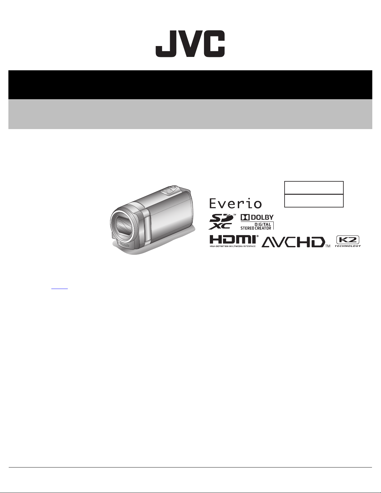
CAMCORDER
YF410<Rev.002>20136SERVICE MANUALEVERIO-S-HD
GZ-E200BUA, GZ-E200BUB,
GZ-E220BUA
SERIES
C2A3
GZ-E200BUAM, GZ-E200BUBM [C2A311]
COPYRIGHT © 2013 JVC KENWOOD Corporation
Lead free solder used in the board (material: Sn-Ag-Cu, melting point: 219 Centigrade)
This service manual (No.YF410< Rev.002 >) describes only the items which differ from those of already issued service manual
(No.YF400
< Rev.004 >)
GZ-E220BUAM [C2A331]
TABLE OF CONTENTS
1 PRECAUTIONS . . . . . . . . . . . . . . . . . . . . . . . . . . . . . . . . . . . . . . . . . . . . . . . . . . . . . . . . . . . . . . . . . . . . . . . 1-2
2 SPECIFIC SERVICE INSTRUCTIONS . . . . . . . . . . . . . . . . . . . . . . . . . . . . . . . . . . . . . . . . . . . . . . . . . . . . . . 1-4
3 DISASSEMBLY . . . . . . . . . . . . . . . . . . . . . . . . . . . . . . . . . . . . . . . . . . . . . . . . . . . . . . . . . . . . . . . . . . . . . . . 1-5
4 ADJUSTMENT . . . . . . . . . . . . . . . . . . . . . . . . . . . . . . . . . . . . . . . . . . . . . . . . . . . . . . . . . . . . . . . . . . . . . . . 1-17
5 TROUBLESHOOTING . . . . . . . . . . . . . . . . . . . . . . . . . . . . . . . . . . . . . . . . . . . . . . . . . . . . . . . . . . . . . . . . . 1-19
COPYRIGHT © 2013 JVC KENWOOD Corporation
No.YF410<Rev.002>
2013/6
Page 2
SECTION 1
r
PRECAUTIONS
1.1 SAFETY PRECAUTIONS
Prior to shipment from the factory, JVC products are strictly
inspected to conform with the recognized product safety and
electrical codes of the countries in which they are to be
sold.However,in order to maintain such compliance, it is equally
important to implement the following precautions when a set is
being serviced.
1.1.1 Precautions during Servicing
(1) Locations requiring special caution are denoted by labels
and inscriptions on the cabinet, chassis and certain parts of
the product.When performing service, be sure to read and
comply with these and other cautionary notices appearing
in the operation and service manuals.
(2) Parts identified by the symbol and shaded ( ) parts
are critical for safety.
Replace only with specified part numbers.
NOTE :
Parts in this category also include those specified to
comply with X-ray emission standards for products
using cathode ray tubes and those specified for
compliance with various regulations regarding
spurious radiation emission.
(3) Fuse replacement caution notice.
Caution for continued protection against fire hazard.
Replace only with same type and rated fuse(s) as
specified.
(4) Use specified internal wiring. Note especially:
• Wires covered with PVC tubing
• Double insulated wires
• High voltage leads
(5) Use specified insulating materials for hazardous live parts.
Note especially:
• Insulation Tape
• PVC tubing
•Spacers
• Insulation sheets for transistors
• Barrier
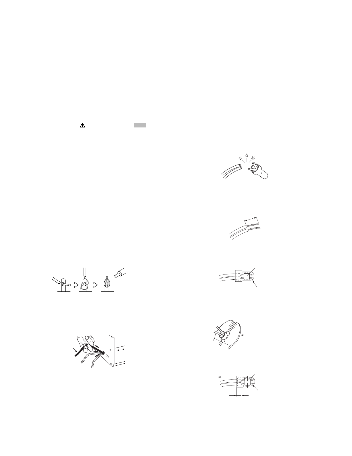
(6) When replacing AC primary side components (transformers,
power cords, noise blocking capacitors, etc.) wrap ends of
wires securely about the terminals before soldering.
can increase the high voltage value and cause X-ray emission from the cathode ray tube.
(12) Crimp type wire connector
In such cases as when replacing the power transformer in
sets where the connections between the power cord and
power trans former primary lead wires are performed using
crimp type connectors, if replacing the connectors is unavoidable, in order to prevent safety hazards, perform
carefully and precisely according to the following steps.
• Connector part number: E03830-001
• Required tool: Connector crimping tool of the proper
type which will not damage insulated parts.
• Replacement procedure
a) Remove the old connector by cutting the wires at a
point close to the connector.Important: Do not
reuse a connector (discard it).
cut close to connector
Fig.1-1-3
b) Strip about 15 mm of the insulation from the ends
of the wires. If the wires are stranded, twist the
strands to avoid frayed conductors.
15 mm
Fig.1-1-4
c) Align the lengths of the wires to be connected.
Insert the wires fully into the connector.
Metal sleeve
(7) Observe that wires do not contact heat producing parts
Fig.1-1-1
(heatsinks, oxide metal film resistors, fusible resistors, etc.)
(8) Check that replaced wires do not contact sharp edged or
pointed parts.
(9) When a power cord has been replaced, check that 10-15
kg of force in any direction will not loosen it.
Power cord
Fig.1-1-2
(10) Also check areas surrounding repaired locations.
(11) Products using cathode ray tubes (CRTs)
In regard to such products, the cathode ray tubes themselves, the high voltage circuits, and related circuits are
specified for compliance with recognized codes pertaining
to X-ray emission. Consequently, when servicing these
products, replace the cathode ray tubes and other parts
with only the specified parts. Under no circumstances attempt to modify these circuits.Unauthorized modification
1-2 (No.YF410<Rev.002>)
Connector
Fig.1-1-5
d) As shown in Fig.1-1-6, use the crimping tool to crimp
the metal sleeve at the center position. Be sure to
crimp fully to the complete closure of the tool.
1.2
5
2.0
5.5
Crimping tool
Fig.1-1-6
e) Check the four points noted in Fig.1-1-7.
Not easily pulled free
Wire insulation recessed
more than 4 mm
Crimped at approx. cente
of metal sleeve
Conductors extended
Fig.1-1-7
Page 3
1.1.2 Safety Check after Servicing
Examine the area surrounding the repaired location for damage
or deterioration. Observe that screws, parts and wires have been
returned to original positions, Afterwards, perform the following
tests and confirm the specified values in order to verify
compliance with safety standards.
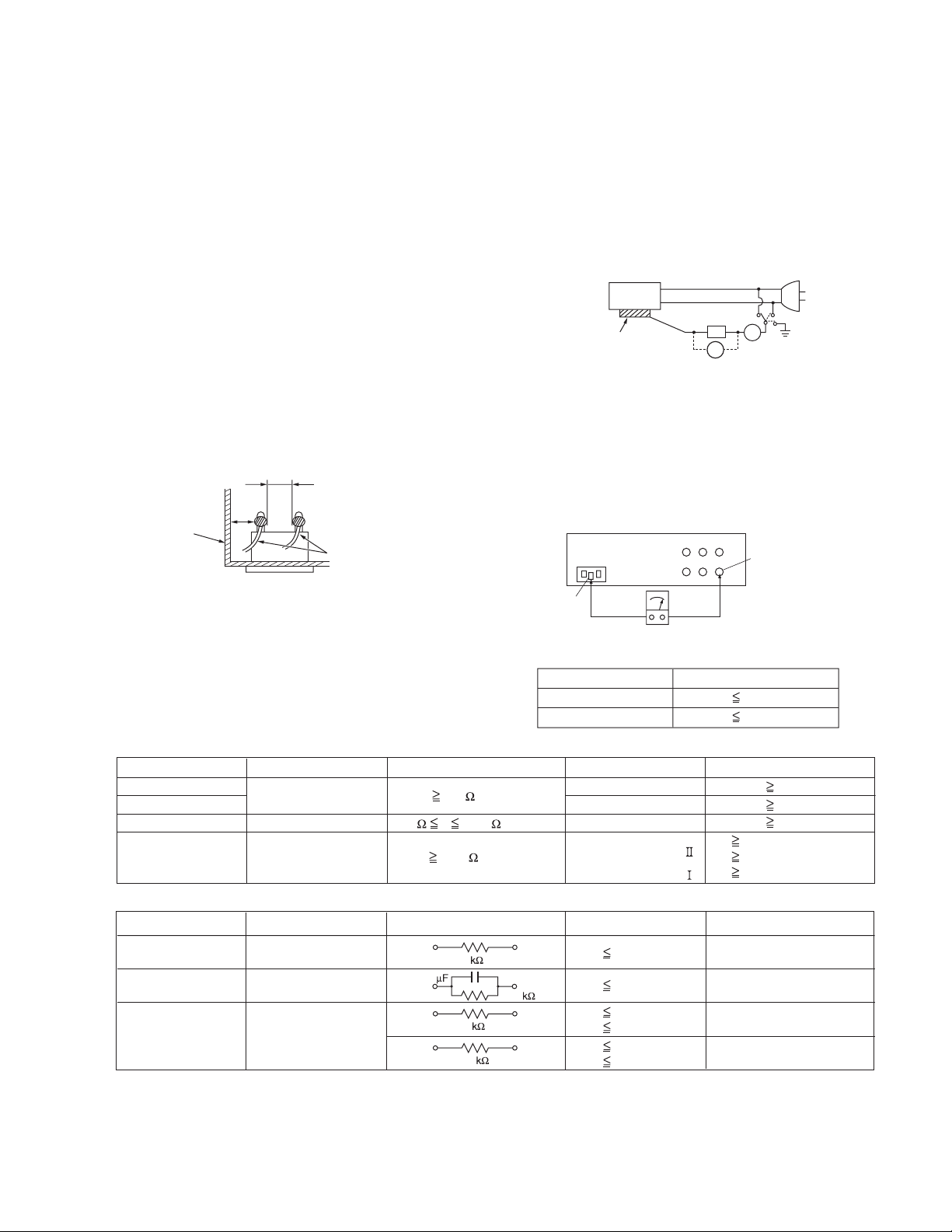
(1) Insulation resistance test
Confirm the specified insulation resistance or greater
between power cord plug prongs and externally exposed
parts of the set (RF terminals, antenna terminals, video and
audio input and output terminals, microphone jacks,
earphone jacks, etc.).See table 1 below.
(2) Dielectric strength test
Confirm specified dielectric strength or greater between
power cord plug prongs and exposed accessible parts of
the set (RF terminals, antenna terminals, video and audio
input and output terminals, microphone jacks, earphone
jacks, etc.). See Fig.1-1-11 below.
(3) Clearance distance
When replacing primary circuit components, confirm
specified clearance distance (d), (d') between soldered
terminals, and between terminals and surrounding metallic
parts. See Fig.1-1-11 below.
d
Chassis
d'
Power cord
primary wire
Fig.1-1-8
(4) Leakage current test
Confirm specified or lower leakage current between earth
ground/power cord plug prongs and externally exposed
accessible parts (RF terminals, antenna terminals, video
and audio input and output terminals, microphone jacks,
earphone jacks, etc.).
Measuring Method: (Power ON) Insert load Z between
earth ground/power cord plug prongs and externally
exposed accessible parts. Use an AC voltmeter to
measure across both terminals of load Z. See Fig.1-1-9
and following Fig.1-1-12.
ab
Externally
exposed
accessible part
Z
V
c
A
Fig.1-1-9
(5) Grounding (Class 1 model only)
Confirm specified or lower grounding impedance between
earth pin in AC inlet and externally exposed accessible
parts (Video in, Video out, Audio in, Audio out or Fixing
screw etc.).Measuring Method:
Connect milliohm meter between earth pin in AC inlet and
exposed accessible parts. See Fig.1-1-10 and grounding
specifications.
AC inlet
Earth pin
Exposed accessible part
MIlli ohm meter
Grounding Specifications
Region
USA & Canada
Europe & Australia
Grounding Impedance (Z
Z 0.1 ohm
Z 0.5 ohm
)
Fig.1-1-10
AC Line Voltage
100 V
100 to 240 V
110 to 130 V
110 to 130 V
200 to 240 V
Region
Japan
USA & Canada
Europe & Australia
Insulation Resistance (R
R 1 M /500 V DC
1 M R 12 M /500 V DC
R 10 M /500 V DC
)
Dielectric Strength
AC 1 kV 1 minute
AC 1.5 kV 1 minute
AC 1 kV 1 minute
AC 3 kV 1 minute
AC 1.5 kV 1 minute
(
Class
(
Class
Clearance Distance (d), (d'
d, d' 3 mm
d, d' 4 mm
d, d' 3.2 mm
d 4 m m
)
d' 8 m m (Power cord
d' 6 m m (Primary wire
)
Fig.1-1-11
AC Line Voltage
100 V
110 to 130 V
110 to 130 V
220 to 240 V
Region
Japan
USA & Canada
Europe & Australia
Load Z
1
0.15
1.5
2
50
Leakage Current (i)
i 1 mA rms
i 0.5 mA rms
i 0.7 mA peak
i 2 mA dc
i 0.7 mA peak
i 2 mA dc
a, b, c
Exposed accessible parts
Exposed accessible parts
Antenna earth terminals
Other terminals
Fig.1-1-12
NOTE:
These tables are unofficial and for reference only. Be sure to confirm the precise values for your particular country and locality.
)
)
)
(No.YF410<Rev.002>)1-3
Page 4
SECTION 2
SPECIFIC SERVICE INSTRUCTIONS
2.1 DIFFERENCE LIST
MODEL GZ-E200BUA GZ-E200BUB GZ-E220BUA
NAND MEMORY NO NO YES(8GB)
AC CORD (TYPE) IRAM BRAZIL IRAM
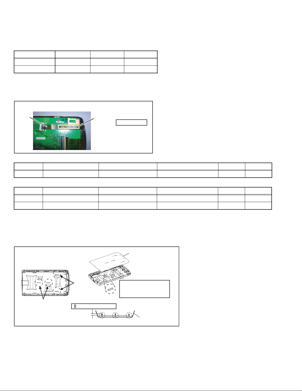
2.2 Change of the MONITOR ASSY
1. Change details
The parts of the TOUCH PANEL have been changed.
NOTE) The part number of a TOUCH PANEL can be checked by FPC.
<MONITOR BOARD ASSY>
FPC
FINAL ASSEMBLY <M1MM>
Symbol No. Parts Name Parts No. <Before> Parts No. <After> Description Local
306 TOUCH PANEL QAL1428-001 QAL1496-001
TOUCH PANEL
Parts No. QAL1428-001
* Following the changed of the TOUCH PANEL, the below parts have also been changed.
Symbol No. Parts Name Parts No. <Before> Parts No. <After> Description Local
307 MONITOR CASE ASSY LY38085-001B LY38085-003B
315 MONITOR COVER ASSY LY38083-001B LY38083-001C
2. Service precautions
When change the TOUCH PANEL, please change the MONITOR CASE ASSY together.
The reuse of the MONITOR COVER ASSY is possible.
But it is necessary to cut lib of the backside of the MONITOR COVER ASSY because there is not Interchangeability.
The length of the rib to cut is 0.5mm or more.
Please refer to follows for the processing contents.
SPACER
MONITOR COVER ASSY
RIB
RIB
Cut material over 0.5mm
<CROSS SECTION>
Cut material over 0.5mm for RIB
height by manual.
It is OK for cutting together with
Wing SPACER.
MONITOR COVER
1-4 (No.YF410<Rev.002>)
Page 5
3.1 Disassembly procedure
SECTION 3
DISASSEMBLY
Fig.3-1-1
(No.YF410<Rev.002>)1-5
Page 6
1-6 (No.YF410<Rev.002>)
Fig.3-1-2
Page 7
Fig.3-1-3
(No.YF410<Rev.002>)1-7
Page 8
1-8 (No.YF410<Rev.002>)
Fig.3-1-4
Page 9
Fig.3-1-5
(No.YF410<Rev.002>)1-9
Page 10
1-10 (No.YF410<Rev.002>)
Fig.3-1-6
Page 11
Fig.3-1-7
(No.YF410<Rev.002>)1-11
Page 12
1-12 (No.YF410<Rev.002>)
Fig.3-1-8
Page 13
Fig.3-1-9
(No.YF410<Rev.002>)1-13
Page 14
1-14 (No.YF410<Rev.002>)
Fig.3-1-10
Page 15
Fig.3-1-11
(No.YF410<Rev.002>)1-15
Page 16

3.2 Quality point
When you assemble the unit, please check the following points for keeping the quality.
OK NG
Do not apply excessive shock to the CMOS ASSY.
(It is 3-demensionally adjusted using adhesive.)
Between the CMOS and the MAIN, insert the FPC before assembly.
Do not fold the FPC at the edges of the reinforcing plate and the
connector.
(The broken terminal will result in disconnection.)
Between the CMOS and the MAIN, run the FPC under the mold.
(Running the FPC over the mold will result in poor contact because of
stress.)
Do not fold the FPC protruded from the HINGE COVER.
(Repeated opening/closing the monitor will break the FPC.)
To replace the BARRIER UNIT, open the BARRIER to check the screws.
(The screws cannot be observed with the BARRIER closed.)
When attaching the TOP COVER, properly set the rear side.
To remove the TOP COVER, remove the screw on the HINGE in
addition to the 3 screws.
When attaching the LOWER CASE, do not damage the parts or patterns on
the MAIN PWB.(Some models have shutter lever that cannot be separated.)
OK NG
When attaching the TOP COVER, properly set the rear side.
(Make sure there is no unevenness. Forcible attachment will result in
breakage.)
When tightening the screw [1] on the TOP side, make sure there is a space
[2].
(Without the space, the TOP COVER cannot be attached.)
1-16 (No.YF410<Rev.002>)
Fig.3-2-1
Page 17
SECTION 4
ADJUSTMENT
4.1 PREPARATION
4.1.1 Precaution
This model is specially adjusted by using PC.
However, if parts such as the following are replaced, an
adjustment is required. The adjustment must be performed in a
Service Center equipped with the concerned facilities.
• OP BLOCK ASSEMBLY
• MONITOR ASSEMBLY
• EEP ROM (IC1003 of MAIN board)
In the event of malfunction with electrical circuits, first find a
defective portion with the aid of proper test instruments as shown
in the following electrical adjustment procedure, and then
commence necessary repair/ replacement/adjustment.
• In observing chip TP, use IC clips, etc. to avoid any stress.
Prior to replacement of chip parts (especially IC), remove the
solder completely to prevent peeling of the pattern.
• Since connectors are fragile, carefully handle them in
disconnecting and connecting the FPC.
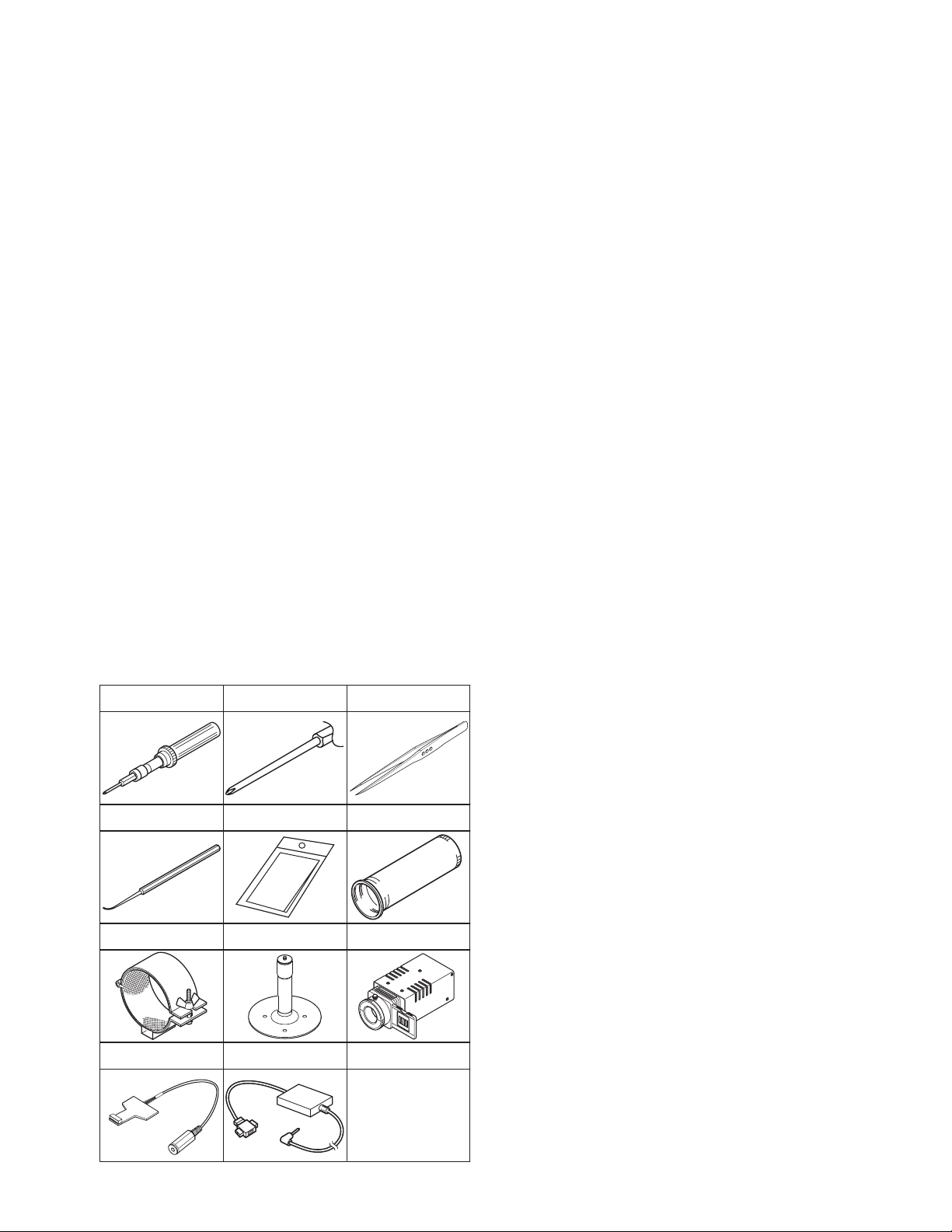
4.1.2 Required test equipment
• Personal computer (for Windows)
• Color TV monitor
• Oscilloscope (dual-trace type, observable 100MHz or higher
frequency). The one observable 300 MHz or higher frequency
is recommended.
• Digital voltmeter
• DC power supply or AC adapter
• Frequency counter (with threshold level adjuster)
4.1.3 Tools required for adjustment
Torque Driver
YTU94088
Chip IC Replacement Jig
PTS40844-2
INF Adjustment Lens Holder
YTU94087
Bit
YTU94088-003
Cleaning Cloth
KSMM-01
Mini Stand
YTU93108
Tweezers
P-895
INF Adjustment Lens
YTU92001E
Light Box Assembly
YTU93096B
• Torque Driver
Be sure to use to fastening the mechanism and exterior parts
because those parts must strictly be controlled for tightening
torque.
• Bit
This bit is slightly longer than those set in conventional torque
drivers.
• Tweezers
To be used for removing and installing parts and wires.
• Chip IC Replacement Jig
To be used for adjustment of the camera system.
• Cleaning Cloth
To be used to wipe down the LCD screen and the optical lens
surface.
• INF Adjustment Lens
To be used for adjustment of the camera system. For the
usage of the INF adjustment lens, refer to the Service Bulletin
No. YA-SB-10035 and No. YA-SB-10223.
• INF Adjustment Lens Holder
To be used together with the Camera stand for operating the
Videocamera in the stripped-down condition such as the status without the exterior parts or for using commodities that are
not yet conformable to the interchangeable ring. For the usage
of the INF lens holder, refer to the Service Bulletin No. YA-SB-
10035.
• Mini Stand
To be used together with the INF adjustment lens holder. For
the usage of the Mini stand, refer to the Service Bulletin No.
YA-SB-10035.
• Light Box Assembly
To be used for adjustment of the camera system. For the
usage of the Light box assembly, refer to the Service Bulletin
No. YA-SB-10035 and No. YA-SB-10218.
• Jig Connector Cable
Connected to JIG CONNECTOR of the main board and used
for electrical adjustment, etc.
• PC Cable
To be used to connect the Videocamera and a personal computer
with each other when a personal computer issued for adjustment.
• Service Support System
To be used for adjustment with a personal computer. Software
can be downloaded also from CUSiS.
Jig Connector Cable
YTU43192
PC Cable
QAM0099-002
Service Support System
YTU94057-134
(Software)
(No.YF410<Rev.002>)1-17
Page 18

4.2 JIG CONNECTOR CABLE CONNECTION
Connection procedure
Remove the 4 screws (1-4), and then remove the TOP COVER
ASSY.
2
3
TOP COVER ASSY
2
3
4
CN9003
SERVICE SUPPORT SYSTEM
(Software)
MENU
PERSONAL COMPUTER
JIG
CONNECTOR
CABLE
1
PC CABLE
1-18 (No.YF410<Rev.002>)
Page 19

SECTION 5
TROUBLESHOOTING
This service manual does not describe TROUBLESHOOTING.
(No.YF410<Rev.002>)1-19
Page 20

<BOARD INTERCONNECTIONS>
INT MIC
SPEAKER
OP BLOCK(A2WN)
QGF0319F1-31X
OPERATION
W
CMOS PWB
CMOS 126 PWB
0
5
CMOS 053 PWB
0
6
4DOP0_A
3DOM0_A
2GND
CN451
1GND
For IMX053
5DOM1_A
6DOP1_A
7DOM0_C
8DOP0_C
9DOM1_C
10DOP1_C
11DOM2_C
12DOP2_C
13DOM3_C
14DOP3_C
15DCKM_A
16DCKP_A
17GND
18CLK_IN
19GND
20HD_CMOS
21VD_CMOS
22CMOS_OUT
23CMOS_CS
24CMOS_CLK
25CMOS_RST
26GND
27CAM_2.7V
28CAM_2.7V
29CAM_1.8V
30CAM_1.8V
31GND
For IMX126
1GND
2DOM2_A
3DOP2_A
4GND
5DOM3_A
6DOP3_A
7GND
8DCKM_A
9DCKP_A
10GND
11SCLK
12
24GND
13
T
ZOOM
Trigger
SNAP
TO LED LIGHT
LED
0
1
MAIN PWB
CN701
37VCOMDC
38VCAC
39VCOM
CN9008
AUDIO
REG_1.8V
REG_5.0V
ZOOM03_SUB
ZOOM02_SUB
REG_2.8V
BL_CTL1/BL_FBI
1 REG_LED/REG_5.0V
2 REG_LED/REG_5.0V
3
32CP4M
33VGH
34VGL
35AGND
36FRP
CP4P
REG_2.8V
ZOOM04_SUB
4 M_RVS
31
REG_5.0V
ZOOM01_SUB
5 GND
30CP3M
FOCUS02_SUB
OP CONNE
GND
6 LCD_DATA
7 LCD_CLK
28VINT1
29CP3P
1 INT_R
2 M_GND
FOCUS03_SUB
FOCUS04_SUB
FOCUS01_SUB
OP DRV
8 LCD_CS
9 LCD_RST
26CP2P
27CP2M
3 M_GND
4 INT_L
INT_L
INT_R
L_MUTE
AUDIO_PD_L
F_VCC_SUB
10 REG_1.8V
11 REG_2.8V
24CP1P
25CP1M
F_LED_SUB
NAND
5 M_GND
6 M_GND
M_GND
SPK-
+
SPK
GND
AU_SIGRM
AU_SIGLM
AUDIO_CLK
AUDIO_CS
AUDIO_OUT
AOMCLK
AIOBCK
AIOLRCK
AOBD
AIBD
V_OUT
SYIN
Z_LED_SUB
z_vcc_SUB
FELIX
OPDRV_PSX
GND
12 LCD_HD0
13 LCD_VD0
14 GND
15 GND
0
4
20VDD
21VDDIO
22DVDD
23NC(GND)
LCD PANEL
W/B_E
OPDRV_IN_F
OPDRV_IN_Z
OPDRV_SDA
OPDRV_SCL
SD2_DAT[0-7]
SD2_CLK
SD2_CMD
REG_3.3V
16 LCD_CLK0
17 GND
18 LCD_GO_7
19 LCD_GO_6
20 LCD_GO_5
MONITOR PWB
15D2
16D1
17D0
18GND
19NC(GND)
21 LCD_GO_4
14D3
2 SPK-
22 LCD_GO_3
13D4
CN9007
1 SPK+
10111213141516171819202122232425262728293031323334
23 LCD_GO_2
24 LCD_GO_1
25 LCD_GO_0
26 GND
27 TP_VDD
8
9NC(GND)
10D7
11D6
12D5
DCLK
28 TP_SEL1
7VSYNC
29 TP_SEL2
6HSYNC
30 TP_X
5SCL
31 TP_Y
32 GND
3CS
4SDA
CN4602
CN9012
123456789
MONI
SWITCH
GND
GND
33 MONI_SW
34 AL_2.8V
1VCOM
2RST
CN702
1 ZOOM02_SUB
2 ZOOM03_SUB
CN703
1
2
3
4
5
6
7
8
3 ZOOM04_SUB
4 ZOOM01_SUB
5 FOCUS02_SUB
6 FOCUS03_SUB
TOUCH
PANEL
7 FOCUS04_SUB
8 FOCUS01_SUB
OP_THRMO
SD0_DAT[0-3]
SD2POWER
AUDIO_OUT
AUDIO_CLK
AUDIO_CS
AUDIO_PD_L
SD2_DAT[0-7]
SD0_DAT[0-3]
OP_THRMO
9 F_VCC_SUB
10 F_LED_SUB
LAMP_ON
REG_SD
SDWP0
SDCD0
SDCMD0
SDCLK0
AOMCLK
AIOBCK
AIOLRCK
AOBD
AIBD
SYIN
SD2_CLK
SD2_CMD
SDCLK0
SDCMD0
SDCD0
REG_SD
LAMP_ON
11 F_PTR_AD
12 Z_VCC_SUB
13 Z_LED_SUB
AUDIO
LCD_DATA
14 Z_PTR_AD
OPDRV_SDA
MAIN IF
NAND
LCD_CS
LCD_CLK
MAIN IF
SD
CN9011
OPDRV_SCL
OPDRV_PSX
OPDRV_IN_F
OP DRV
LCD
LCD_RST
TP_Y
TP_X
TP_VDD
SDWP0
SD2POWER
QGF0321F1-33X
WB_E
Z_PTR_AD
OPDRV_IN_Z
TP_SEL1
TP_SEL2
LCD_GO_[0-7]
LD_KSODE
OP THERMISTOR
GND
F_PTR_AD
LCD_CLKO
LCD_RST
LCD_CS
33
LCD_DATA
LCD_CLK
LCD_VDO
VD_CMOS
LCD_HDO
HD_CMOS
CMOS_RST
DCKP_A
CMOS_CS
CMOS_OUT
CMOS_CLK
REG_1.8V
CN9014
CN203
DCKM_A
FELIX
STEREO
SUBCPU
REG_PEN1
REG_THMEN
CHARGE_ICONT
USUS
REG_PEN1
CHARGE_ICONT
CMOS PWB
MOD_DN
DRXD
DTXD
MOD_DP
CN9015
TO/ FROM WIFI MODULE
CN9002
PEN2
T_CTL1
T_CTL2
PEN2
T_CTL1
T_CTL2
SUBCPU
BL_FBI
QGF0543F3-12X
REG
REG_CEN
REG_SCL
REG_CTL
REG_CEN
REG_LED
SUBCPU
REG_SDA
REG_SCL
REG_CTL
REG_CTL2
REG
OT
REG_DOK
REG_CHG_DET
REG_SDA
REG_DOK
REG_CHG_DET
1
2
3
4
5
6
7
8
9
10
11
12
FLT
OT
MOD_RST
GND
GND
MOD_DN
MOD_DP
GND
GND
MOD_1.5V
MOD_1.5V
MOD_3.3V
MOD_3.3V
MOD_3.3V
DONE
FLT
REG_5.0V
1 GND
V_BATT
UNREGCHK
DONE
UNREGCHK
REAR
1
2
3
4
5
6
7
8
9
10
11
12
2 TRIG_SW
JIG-CON
REG_UOK
V_BATT
REG_2.8V
3 HALF_SW
4 FULL_SW
5 ZOOM_SW
6
REAR
FLASH_T2R_TX
FLASH_T2R_RX
LCD
JACK
AL_2.8V
REG_UOK
REG_2.8V
GND
LI_CHRG
ADP_DC
BATT
+
T_BATT
AL_5.0V
TO/ FROM WIFI MODULE
QGF0543F3-12X
WIFI MODULE
LIT_3.0V
PWR_LED
ACES_LED
D_BATT
BATT_L
T_BATT
SYS_RSTL
SYS_SWCLK
SYS_SWDIO
BOOT
REG_2.8V
AL_2.8V
GND
PWR_SW
M_RVS
MONI_SW
CN9006
1 REG_5.0V
2 LD_KSODE3456
TO MAIN PWB
40
39
38
37
36
35
34
33
32
31
30
29
28
27
26
25
24
23
22
21
20
19
18
17
16
15
14
13
12
11
10
9
8
7
6
5
4
3
2
1
30 AL_2.8V
15 GND
29 SDWP0
CPU_RTCK
14
SFLASH_IF_DO
28
SFLASH_IF_DI
13
27 SFLASH_IF_CLK
12 BOOT_SEL_1
26 FLASH_T2R_RX
11 BOOT
25 GND
10 FLASH_T2R_TX
24 GND
9 SYS_SWCLK
23 SFLASH_IF_CS
8 SYS_SWDIO
22
SYS_RSTL
7
JTAG_SEL1
21
IF_RX
6
IF_TX
20
SD2POWER
5
UATXD0
19
UARXD0
4
REG_2.8V
18 MBE_SRST
3 CPU_NTRST
17 CPU_TDI
2 CPU_TMS
16 CPU_TCK
1 CPU_TDO
CN601
40P_DET_L
39V_OUT
38GND
37AU_SIG/L
36AU_SIG/R
SW
35LIT_3.0V
34GND
SW
33GND
32GND
SW
31GND
30GND
SW
29GND
28GND
27D_GYRO_CLK
26D_GYRO_CS
25REG_2.8V
24D_GYRO_OUT
23D_GYRO_IN
22ADP_DC
21ADP_DC
20ADP_DC
19ADP_DC
18ADP_DC
17BATT+
16BATT+
15BATT+
14BATT+
13BATT+
12BATT+
11BATT+
10BATT+
9LI_CHRG
8T_BATT
7D_BATT
6BATT_L
5KEY_A
4GND
3AL_2.8V
2PWR_LED
1ACES_LED
JIG CONN
CN9003
CN9001
yf400_y10986001a_20111216_ver0.1
VIDEO/
DSC
SILENT
IS
INFO
BTU TERMINAL
LED
POWER ACCESS
DC JACK
A/V JACK
LITHIUM
REAR
PWB
PLAY
UP
DOWN
OK
LED
0
2
GND
HD_CMOS14VD_CMOS15CMOS_OUT16CMOS_CS17CMOS_CLK18CMOS_RST19GND20CAM_2.7V21CAM_2.7V22CAM_1.8V23CAM_1.8V
MOD_3.3V
REG_3.3VCTL
REG_1.0VCTL
WIFI
CN9004
1GND
2GND
CN201
MBE_EEP_OUT
MBE_EEP_CLK
REG_3.3VCTL
REG_1.0VCTL
REG_3.3V
MOD_1.5V
MBE_EEP_IN
MBE_EEP_CS
123456789
CN9013
L_MUTE
MBE_RST
FLSH_RST
MBE_OUT
MBE_IN
MBE_CLK
MBE_CS
REG_1.8V
REG_1.1V
REG_1.2V
REG_3.3V
CAM_1.8V
CAM_2.7V
VBUS
GND
USUS
REG_THMEN
WIFI_RST
WIFI_SPI_CS
WIFI_SPI_DI
WIFI_SPI_DO
WIFI_SPI_CK
WIFI_USBDN
WIFI_USBDPWIFI_ATTACH
DOP0_A
HDMI_SCL
10
GND
DOM0_A
HDMI_SDA
11
HDMI_HP
USBDP
USBDN
12
13
HDMI_SDA
TDMS_REG5V
VBUS
XUSBHOST
14
HDMI_SCL15HDMI_CEC
123456789
123456789
MENU
KEY_A
OPERATION
HDMI_HPD
P_DET_L
REAR
REG_2.8V
REG_1.1V
REG_5.0V
D_GYRO_CS
D_GYRO_IN
D_GYRO_CLK
D_GYRO_OUT
FLSH_RST
SUBCPU
MBE_EEP_IN
MBE_EEP_OUT
MBE_EEP_CLK
MBE_EEP_CS
UATXDO
UARXDO
SFLASH_IF_CS
SFLASH_IF_DO
SFLASH_IF_DI
SFLASH_IF_CLK
JTAG_SEL1
JIGCON
CPU_RTCK
CPU_NTRST
BOOT_SEL_1
MBE_SRST
REG_3.3V
WIFI_RST
WIFI_KENTO
WIFI_USBDN
WIFI_USBDP
WIFI_WKUP
WIFI
WIFI_SPI_DI
WIFI_SPI_DO
WIFI_SPI_CK
WIFI_SPI_CS
WIFI_ATTACH
13GND
14GND
15TMDS_D2-
16TMDS_D2+
17GND
18GND
123456789
MBE_RST
MBE_OUT
MBE_IN
MBE_CLK
MBE_CS
CPU_TMS
CPU_TDO
CPU_TDI
CPU_TCK
IF_RX
IF_TX
GND
TRIG_SW
KEY_B
ZOOM_SW
WIFI_TX
WIFI_RX
12TMDS_D1+
1011121314151617181920212223242526272829303132
SCLK
DOM3_C
DOM1_C
DOM2_A
DOP3_A
DOP0_C
TMDS_D1-
3XUSBHOST
DOM0_C
+
TMDS_D0
4GND
DOM3_A
+
TMDS_D0-
5
USBDN
DOP2_A
JACK PWB
TMDS_CLK
TMDS_CLK-
6USBDP
7GND
1011121314
DOP1_A
HDMI_CEC
8VBUS
DOM1_A
TMDS_REG5V
9VBUS
DOP3_C
DOP2_C
DOM2_C
CMOS PWB
DOP1_C
+
TMDS_D2
TMDS_D2-
1
MENU/POWER_SW
15
+
TMDS_D1
2GND
HDMI
0
3
JACK PWB
USB
WIFI_KENT0
WIFI_WKUP
WIFI_RX
WIFI_TX
MOD_RST
7TMDS_D0-
8TMDS_D0+
9GND
10GND
11TMDS_D1-
101112131415161718
SW
SW
6GND
POWER
MENU
101112131415161718192021222324
5GND
REG_1.8V
3TMDS_CLK-
4TMDS_CLK+
REG_1.2V
1
Page 21

<MAIN(MAIN IF) SCHEMATIC DIAGRAM>
Note : The parts numbers in the schematic diagram are for references only.
When replacing the parts, refer to the PARTS LIST.
# CN9006
QGF0543F3-06X
12345
6
MAIN IF1
IMX053
OPEN
TO CMOS
# CN9011
QGF0321F1-33X
33
32
31
30
29
28
27
26
25
24
23
22
21
20
19
18
17
16
15
14
13
12
11
10
9
8
7
6
5
4
3
2
1
TO JACK PWB
CN9004
QGF0543F3-18X
1
2
TMDS_CLK-
3
TMDS_CLK+
4
5
6
TMDS_D0-
7
TMDS_D0+
8
9
10
TMDS_D1-
11
12
TMDS_D1+
13
14
15
TMDS_D2-
TMDS_D2+
16
17
18
TO JACK PWB
CN9014
QGF0543F3-15X
15
14
13
12
11
10
9
8
7
6
5
4
3
2
1
REG_1.8V
CAM_2.7V
CAM_2.7V
CMOS_RST
CMOS_CLK
CMOS_CS
CMOS_OUT
VD_CMOS
HD_CMOS
SCLK
DCKP_A
DCKM_A
DOP3_C
DOM3_C
DOP2_C
DOM2_C
DOP1_C
DOM1_C
DOP0_C
DOM0_C
DOP1_A
DOM1_A
DOP0_A
DOM0_A
GND
HDMI_CEC
HDMI_SCL
HDMI_SDA
TMDS_REG5V
HDMI_HPD
C9017
0.1
XUSBHOST
GND
# R9043
# R9044
# CN9013
RT3CLLM/EF/-X
VBUS
L9001
NQR0654-001X
OPEN
0`
MENU
PWR_SW
0`
JIG CONN
CN9003
QGB0519J1-30X
to CMOS PWB
IMX126
QGF0543F3-24X
24
23
REG_1.8V
22
21
20
19
18
17
16
15
14
13
12
11
10
9
8
7
6
5
4
3
2
1
LED LIGHT
3.3k
# R9005
456
# Q9001
1 2 3
22
# R9007
1.5k
# R9006
GND
1 2
USBDP
USBDN
34
CPU_TDO
CPU_TDI
CPU_TCK
CPU_TMS
MBE_SRST
CPU_NTRST
OPEN
123456789
161718192021222324252627282930
REG_2.8V
0`
R9010
LD_KSODE
LAMP_ON
GND
UARXD0
REG_1.8V
CAM_2.7V
CAM_2.7V
CMOS_RST
CMOS_CLK
CMOS_CS
CMOS_OUT
VD_CMOS
HD_CMOS
SCLK
DCKP_A
DCKM_A
DOP3_A
DOM3_A
DOP2_A
DOM2_A
UATXD0
DTXD
GND
SYS_SWCLK
JTAG_SEL1
IF_RX
IF_TX
SYS_RSTL
SFLASH_IF_CS
SYS_SWDIO
SYS_SWCLK
FLASH_IF_CS/eMMCDAT7
FLASH_T2R_TX
GND
1011121314
REG_SD
BOOT
SD2POWER
FLASH_T2R_RX
BOOT_SEL_1
FLASH_IF_CLK/eMMCDAT4
SYMBOL NO.
CN9015
REG_5.0V
L9002
NQR0022-004X
SFLASH_IF_DI
SFLASH_IF_CLK
FLASH_IF_DO/eMMCDAT6
FLASH_IF_DI/eMMCDAT5
MODEL
LD_KSODE
SFLASH_IF_DO
CPU_RTCK
DRXD
AL_2.8V
15
WIFI NO WIFI
QGF0543F3-12X OPEN
CN9007
QGA1001F1-02X
SD0_DAT2
SD0_DAT3
SDCMD0
SDCLK0
SD0_DAT0
SD0_DAT1
SDCD0
SDWP0
GND
SD2POWER
SDWP0
R9507
SPK MICLED
1
2SPK-
SPK+
LCD IF
CN9012
QGF0528F4-34X
SYMBOL NO.
Q9001
R9005
R9006
R9007
CN9006 QGF0543F3-06X
MODEL
REG_LED
BL_FBI
LED NO LED
RT3CLLM/EF/-X
NRSA6AJ-332W
NRSA6AJ-220W
NRSA6AJ-152W
12345
INT_R
RA9001
NRB04CJ-473W
LCD_DATA
M_RVS
INT_L
47k
R9037
LCD_CLK
LCD_CS
OPEN
OPEN
OPEN
OPEN
OPEN
6
CN9008
QGF0543F3-06X
M_GND
876
5
123
4
REG_1.8V
OPEN
REG_2.8V
OPEN
R9038
LCD_HDO
LCD_RST
OPEN
C9012
OPEN
C9013
LCD_VDO
R9018
10k
D9005
OPEN
GND
SYMBOL NO.
TELE,WIDE,PHOTO-KEY,TRIGGER,GND
2
1
3
EMZ6.8N-X
D9001
OPEN
C9016
0.1
R9003R9004
100k100k
OPEN
0`
12345
HALF_SW
R9001
R9045
R9002
KEY_B
TRIG_SW
to OPERATION UNIT
6
CN9002
QGF0534F5-06X
FULL_SW
6.8k
22k
ZOOM_SW
REG_2.8V
TO WIFI MODULE
GND
# CN9015
QGF0543F3-12X
THERMISTOR
OP_THRMO
NAD0048-473X
TH9001
1 2
GND
123456789
MOD_DN
GND
MOD_DP
MOD_DN
MOD_RST
101112MOD_3.3V
MOD_1.5V
STAND-OFF SD CN
CN9009
NNZ0255-001X
9
DAT2
1
CD/DAT3
2
CMD
3
VSS1
4
VDD
5
CLK
6
VSS2
7
DAT0
8
DAT1
CARD_DET1
10
16
GND15GND
14
11
12
13
GND
GND
GND
WP_SW1
TO REAR PWB
CN9001
V_OUT
KEY_A
QGF0574F1-40X
D_GYRO_CLK
D_GYRO_OUT
K9001
1 2
NQR0286-009X
D_GYRO_CS
REG_2.8V
D_GYRO_IN
C9006
0.1
40
39
38
37
36
35
34
33
32
31
30
29
28
27
26
25
24
23
22
21
20
19
18
17
16
15
14
13
12
11
10
9
8
7
6
5
4
3
2
1
ADP_DC
D_BATT
T_BATT
BATT+
P_DET_L
AU_SIG/LM
AU_SIG/R
LIT_3.0V
GND
D9002
EMZ6.8N-X
3
1
2
C9002
OPEN
1
C9001
2
D9003
DZ2J068/M/-X
C9003
OPEN
D_GYRO_CLK
D_GYRO_CS
REG_2.8V
D_GYRO_OUT
D_GYRO_IN
LI_CHRG
BATT_L
AL_2.8V
PWR_LED
ACES_LED
R9041
47k
OPEN
C9009
2
3
OPEN
C9004
OPEN
1
C9014
OPEN
C9005
R9011
100
R9012
100
R9013
100
R9014
R9019
0` 0`
R9015
100
R9016
100
R9017
0`
OPEN
C9010
4.7
TP_SEL1
OPEN
R9039
4.7k
ONBOARD CONTACT
TP9004
MONI_SW
AL_2.8V
TP_SEL2
VDDE_2.8V
LCD_GO_3
LCD_GO_4
LCD_GO_0
LCD_GO_5
LCD_GO_6
LCD_GO_7
LCD_GO_1
LCD_CLKO
R9043
R9044
LCD_GO_2
10111213141516171819202122232425262728293031323334
MODEL
TOUCH PANEL NO TOUCH PANEL
OPEN
NRSA6AJ-0R0W
TP_X
TP_Y
NRSA6AJ-0R0W
OPEN
123456789
MODEL
SYMBOL NO.
CN9011 OPEN QGF0321F1-33X
CN9013
GND
IMX126 IMX053
QGF0543F3-24X OPEN
yf400_y10985001a1/8_20120117_ver1.1
2
Page 22

<MAIN(SUB CPU) SCHEMATIC DIAGRAM>
Note : The parts numbers in the schematic diagram are for references only.
When replacing the parts, refer to the PARTS LIST.
To REG
LIT_3.0V
AL_2.8V
REG_2.8V
D_BATT
REG_1.12VCTL
REG_PEN1
REG_CEN
REG_CTL
CHARGE_ICONT
REG_SDA
REG_SCL
REG_THMEN
T_CTL2
REG_1.0VCTL
REG_3.3VCTL
SYS_RSTL
SYS_SWCLK
SYS_SWDIO
FLASH_T2R_TX
FLASH_T2R_RX
LED
ACES_LED
PWR_LED
T_CTL1
TL1029
TL1030
LIT_3.0V
AL_2.8V
REG_2.8V
GND
PEN2
USUS
R1011
1k
R1012
R1013
BOOT
R1017
330
R1018
330
100k
1k
0`
R1063
R1064
C1001
C1002
OPEN
OPEN
R1005
R1006
47k
1k
0`
REG_1.12VCTL
CHARGE_ICONT
REG_1.0VCTL
REG_3.3VCTL
FLASH_T2R_TX_
FLASH_T2R_RX_
C1003
D_BATT_IO
REG_PEN1
REG_CEN
REG_CTL
REG_SDA
REG_SCL
REG_THMEN
SYS_RSTL
SYS_SWCLK
SYS_SWDIO
SUB_KENTO
SUB_KENTO2
ACES_LED_
PWR_LED_
OPEN
T_CTL1
T_CTL2
R1014
10k
C1004
0.1
DB_RST
IC1004
R5G05001N311N-X
8
1
P1O/T1IN
PGM
7
2
P0I/SDA
RESET
3
P0O/SCK
VSS
CNVSS4VCC
OPEN
R1091
6
5
R1028
MBE_EEP_IN
MBE_EEP_OUT
EEP_IN
EEP_OUT
EEP_CLK
EEP_CS
MBE_EEP_CLK
MBE_EEP_CS
FLSH_RST
SYS_SWCLK
SYS_SWDIO
100
DB_CLK
FWEN
R1029
DB_DT_IN
1k
OPEN
DB_DT_OUT
OPEN
R1031
R1030
DB_CS
FLT
REG_CHG_DET
REG_DOK
UNREGCHK
V_BATT
R1002
R1053
470k
C1011
OPEN
10k
R1032
R1034
R1035
R1036
BATT_L
1M
T_BATT
OT
REG_UOK
DONE
MBE_OUT
MBE_CLK
MBE_CS
MBE_IN
MBE_EEP_CS
MBE_EEP_CLK
MBE_EEP_OUT
MBE_EEP_IN
MBE_RST
FLSH_RST
L_MUTE
MONI_SW
1M
PWR_SW
100k
M_RVS
OPEN
FLT
REG_CHG_DET
REG_DOK
UNREGCHK
V_BATT
BATT_L
T_BATT
OT
REG_UOK
DONE
MBE_OUT
MBE_CLK
MBE_CS
MBE_IN
MBE_EEP_CS
MBE_EEP_CLK
MBE_EEP_OUT
MBE_EEP_IN
MBE_RST
FLSH_RST
L_MUTE
MONI_SW
PWR_SW
M_RVS
From REG
MBE
AUDIO
OPE
# IC1003
R1022
EEP_IN
EEP_OUT
EEP_CLK
EEP_CS
10k
R1024
OPEN
R1025
OPEN
R1026
OPEN
R1027
OPEN
R1073
470k
R1074
PEN2
USUS
BOOT
470k
R1075
470k
R1082
470k
R1076
470k
R1077
470k
R1078
470k
R1070
1k
R1071
1k
R1080
470k
R1094
470k
R1095
470k
8
1
7
2
6
3
5
FWEN
4
RA1001
10k
LIT_3.0V_R1014
D8
L11
C11
32
41
REG_3.3VCTL
REG_1.0VCTL
REG_CEN
REG_CTL
DONE
DB_CS
DB_CLK
DB_DT_OUT
DB_DT_IN
REG_SDA
REG_SCL
PWR_LED_
ACES_LED_
RA1002
OPEN
R1092
8
1
7
2
6
3
5
4
1k
C1019
OPEN
DB_RST
T_CTL1
M_RVS
MONI_SW
OPEN
C1021
PWR_SW
BATT_L
BOOT
REG_THMEN
REG_PEN1
X1001
NAX0491-001X
B11
A10
C10
B10
B9
C9
C8
B8
A9
A8
B7
A7
D7
C7
D6
C6
B6
A6
F4
K2
H3
A5
B5
C5
D5
D4
C4
F5
E11
E5
A3
A2
120
22
REG_3.3VCTL
10
REG_1.0VCTL
31
REG_CEN
21
REG_CTL
20
30
DONE
29
DB_CS
19
DB_CLK
9
DB_DT_OUT
8
DB_DT_IN
18
REG_SDA
7
REG_SCL
39
PWR_LED
28
ACES_LED
38
27
DB_RST
17
T_CTL1
6
M_RVS
58
MONI_SW
100
PWR_SW
79
BATT_L
5
BOOT
16
REG_THMEN
26
37
36
25
REG_PEN1
59
DVCC
54
DVSS
48
BVCC
3
XT2
2
XT1
40
DVSS
FLASH_T2R_RX
FLASH_T2R_TX
BVSS
33
13
14
24
23
B3
C2
C1
B2
R1023
OPEN
USUS
D9
E9
D10
42
52
USUS
D_BATT_OUT
CHARGE_ICONT
34
35
D3
D2
D1
PEN2
53
46
R1EX25004ATA-X
1
S
2
Q
3
W
A1
E7
D11
E10
F11
1
50
65
43
DVSS
PEN2
DVCC2
M395FWAGC7K07-X
MBE_RST
MODE
SYS_RSTL
D_BATT_IN
45
12
4
44
A4
E2
E1
B1
E3
R1093
OPEN
OPEN
C1020
0`
R1090
VCC
HOLD
F8
62
63
IC1001
70
57
G5
C
D4VSS
F9
64
56
F3
8
7
6
5
F10
76
SUB_KENTO2
55
F2
F1
C1005
OPEN
220k
R1084
OT
MBE_IN
OPEN
10k
R1083
R1048
H9
G9
G8
E8
J11
G1075G11
85
74
98
73
51
OT
BATTCHECK
DVSS
67
11
G2
A11
MBE_OUT
OPEN
R1047
MBE_IN
H10
86
68
G3
MBE_CLK
OPEN
R1046
H11
87
MBE_OUT
REG_UOK
69
G4
T_CTL2
J9
96
T_CTL2
MBE_CLK
REG_CHG_DET
REG_DOK
80
H4
C1022 0.1
T_BATT
0`
R1085
J10
97
REG_1.12VCTL
78
15
H2
B4
FLT
T_BATT
JLIP_INT
OPEN
R1045
K10
108
FLT
MBE_CS
90
J3
C1009 0.1
C1010 0.1
V_BATT
UNREGCHK
L10
K11
109
119
UNREGCHK
REG_MONITOR
MBE_EEP_IN
MBE_EEP_OUT
MBE_EEP_CLK
MBE_EEP_CS
SYS_SWCLK
SYS_SWDIO
101
89
K3
J2
H8
84
V_BATT
REGVSS
REGVCC
EEP_IN
EEP_OUT
EEP_CLK
EEP_CS
FLSH_RST
G7
72
110
L1
DVSS
AVSS
VREFH
107
K9
DVSS
61
F7
AVCC
118
L9
95
J8
83
H7
106
K8
94
J7
117
L8
93
J6
82
H6
105
K7
116
L7
104
K6
NMI
47
E4
49
E6
71
G6
FVCC
81
H5
FWEN
60
F6
DVCC
92
J5
103
K5
91
J4
102
K4
88
J1
115
L6
114
L5
113
L4
112
L3
111
L2
99
K1
L_MUTE
66
77
SUB_KENTO
G1
H1
C1006
OPEN
MODEL
Face Recognition
eMMC
OneNand
OneNand
WiFi
SYMBOL
NO.
+
+
IC1003
R1EX25004ATA-X
(4kb)
CAT25128YI-G-X
(128kb)
S-25C256A0I-T-X
(256kb)
FLASH_T2R_TX_
FLASH_T2R_RX_
CHARGE_ICONT
D_BATT_IO
MBE_RST
SYS_RSTL
SUB_KENTO2
REG_UOK
REG_DOK
REG_1.12VCTL
FLASH_T2R_RX_
REG_CHG_DET
MBE_CS
L_MUTE
SUB_KENTO
yf400_y10985001a2/8_20111123_ver0.1
3
Page 23

<MAIN(AUDIO) SCHEMATIC DIAGRAM>
Note : The parts numbers in the schematic diagram are for references only.
When replacing the parts, refer to the PARTS LIST.
From INT_MIC
INT_L
INT_R
M_GND
TO Speaker
SPK+
SPK-
K2102
0`
NRSA6AJ-0R0W
K2103
0`
NRSA6AJ-0R0W
K2101
0`
NRSA6AJ-0R0W
C2161
0.015
C2162
0.015
R2161
2.2k
R2162
2.2k
C2264
0.01
C2263
0.01
C2165
1
C2163
0.01
C2164
0.01
C2166
1
Q2462
2SC5383/F/-X
R2462
4.7k
L2461
10u
12
From REG
REG_5.0V
REG_2.8V
REG_1.8V
To IF2
R2463
C2463
18k
C2462
10
C2362
C2361
1
R2662
820
R2661
820
C2661
1
C2363
0.1
1
C2662
A7
B6
B7
7
12
AVSS
BIAS
AVDD
18
C5
NC
24
D4
NC
27
D7
LNFL
19
C6
MICINL2
20
C7
MICINL1
26
D6
MREGL
33
E6
MREGR
41
F7
MICINR1
34
E7
MICINR2
48
G7
LNFR
25
D5
NC
32
E5
NC
A6
6
13
MUTEOUTR
B4
A5
B5
5
10
11
LINEOUTL
MUTEOUTL
LINEOUTR
IC2061
BU76312GUW-X
A4
4
EVROUT
SPIN
A3
3
C4
17
BEEPIN
B3
9
SPNEG
10
A1
1
SPPOS
SPVSS
SPVDD
VOUT
VVDD
VVSS
ADOUT
DAIN
TEST
VIN
PDB
Q2661
R2663
456
123
Q2662
AUDIO_CLK
AUDIO_CS
AUDIO_OUT
AOMCLK
AIOBCK
AIOLRCK
AOBD
AIBD
AUDIO_PD_L
TL2102TL2101
TL2103
R2664
560k
C2464
L2462
C3461
AIBD
AOBD
C3761
1
10u
L3461
10u
A2
2
B2
8
NC
C3
16
R3246
C1
75
14
C2
15
D1
21
D2
22
NC
E4
31
AUDIO_PD_L
D3
23
E2
29
E1
28
E3
30
560k
AU_SIG/R
AU_SIG/LM
From Subcpu
L_MUTE
GND
From/To Felix
AUDIO_CLK
AUDIO_CS
AUDIO_OUT
AOMCLK
AIOBCK
AIOLRCK
AOBD
AIBD
AUDIO_PD_L
47
G6
DMCLK
40
SCLK
DMDAT
46
G5
F6
AUDIO_CLK
CSB
39
45
F5
G4
AUDIO_CS
AUDIO_OUT
SDATA
38
C2465
MCLKO
F4
44
IOVDD
G3
LRCLK
MCLK
BCLK
DVSS
DVDD
35
36
37
43
42
F1
F2
F3
G2
G1
AIOBCK
AIOLRCK
AOMCLK
R2464
10
From/To Felix
V_OUT
SYIN
yf400_y10985001a7/8_20111123_ver0.1
4
Page 24

<MAIN(FELIX) SCHEMATIC DIAGRAM>
Note : The parts numbers in the schematic diagram are for references only.
When replacing the parts, refer to the PARTS LIST.
TL3038TL3039
R3044
OPEN
W/B_E
OPEN
OPEN
OP_THRMO
C3042
Z_PTR_AD_1
F_PTR_AD_1
R3087
R3086
C3041
0.1
0.1
OPEN
OPEN
OPEN
C3003
R3084
R3083
C3002
AH3
AE3
AE5
CC_AD0
CC_ADVRL
CC_ADVRC
P18
P15
P16
P17
VSS
VSS
VSS
VDD
VDD
VDD
L9
K9
M9
L27
LCD_GO_0
DQSMDDR_3
DMMDDR_3
V35
V34
AA27
22
876
R3031
123
DDR_DQS3
DDR_DQM3
LCD_GO_0
SIGN0031253
SIGN0031253
R3088
OPEN
R3085
AF3
AG3
AH1
AF1
AJ1
AJ2
AG2
AE2
AH2
AG1
AF2
CC_AD8
CC_AD4
CC_AD5
CC_AD2
CC_AD1
CC_AD6
CC_AD3
CC_AD7
CC_AD9
CC_AD12
CC_AD10
CC_AD11
P19
R16
P20
P21
P22
P23
P24
R14
R15
R13
VSS
VDD
VDD
M27
LCD_GO_1
AA28
RA3003
LCD_GO_2
LCD_GO_1
R17
VSS
VSS
VSS
VSS
VSS
VSS
VSS
VSS
VSS
VSS
IC3001
JCY0246
VDD
VDD
VDD
VDD
VDD
VDD
VDD
VDD
VDD
VDD
R9
T9
N9
H13
T24
M28
T27
N27
F29
F22
LCD_GO_3
LCD_GO_7
LCD_CLKO
LCD_GO_4
LCD_GO_6
LCD_GO_5
LCD_ENO
LCD_HDO
LCD_VDO
LCD_GO_2
W28
U30
U31
V30
W27
Y28
U28
V28
V27
Y27
1010100`
5
876
5
R3065R3061
R3098
R3079
4
123
4
10
10
RA3002
LCD_HDO
LCD_VDO
LCD_CLKO
LCD_GO_7
LCD_GO_6
LCD_GO_5
LCD_GO_4
LCD_GO_3
OPDRV_SDA
OPDRV_SCL
OPDRV_PSX
OP_THRMO
OPDRV_IN_F
OPDRV_IN_Z
D_GYRO_CS
D_GYRO_IN
D_GYRO_OUT
D_GYRO_CLK
Z_PTR_AD
F_PTR_AD
OPEN
C3079
IF_RX
MENU
MENU
TP_X
TP_X
TP_Y
TP_Y
KEY_A
KEY_A
KEY_B
KEY_B
ZOOM_SW
ZOOM_SW
P_DET_L
P_DET_L
LAMP_ON
W/B_E
IF_RX
IF_TX
R3129
CMOS_RST
CMOS_CLK
CMOS_CS
CMOS_OUT
LAMP_ON
R3134
OPDRV_SDA
2.2k
R3135
2.2k
OPDRV_SCL
OPDRV_PSX
R3133
47k
OP_THRMO
OPDRV_IN_F
OPDRV_IN_Z
D_GYRO_CS
D_GYRO_IN
D_GYRO_OUT
D_GYRO_CLK
W/B_E
R3131
39k
15k
Z_PTR_AD_1
R3130
R3132
15k
39k
F_PTR_AD_1
IF_RX
IF_TX
CMOS_RST
CMOS_CLK
CMOS_CS
CMOS_OUT
TL3040
DCKP_A
DCKP_A
TL3041
DCKM_A
DCKM_A
TL3042
DOP3_A
DOP3_A
TL3043
DOM3_A
DOM3_A
TL3056
DOP2_A
DOP2_A
TL3057
DOM2_A
DOM2_A
TL3058
DOP0_A
DOP0_A
TL3059
DOM0_A
DOM0_A
TL3060
DOP1_A
DOP1_A
TL3061
DOM1_A
DOM1_A
TL3062
DOP0_C
DOP0_C
TL3063
DOM0_C
DOM0_C
TL3064
DOP1_C
DOP1_C
TL3065
DOM1_C
DOM1_C
TL3066
DOP2_C
DOP2_C
TL3067
DOM2_C
DOM2_C
TL3068
DOP3_C
DOP3_C
TL3069
DOM3_C
DOM3_C
TL3070
SCLK
SCLK
R3057
MBE_SRST
MBE_RST
2.2k
FLSH_RST
MBE_SRST
A1
DDR_DQ34
A2
A3
# C3078
0.1
B1
DDR_DQ36
B2
DDR_DQ33
B3
C1
DDR_DQ32
C2
DDR_DQ37
C3
D1
DDR_DQ35
D2
DDR_DQ39
D3
E1
DDR_DQS4
E2
DDR_DQ38
E3
F1
DDR_DQM4
F2
F3
DDR_CKE1
G1
DDR_CK2
G2
DDR_XCK2
G3
DDR_A09
H1
DDR_A11
H2
DDR_A12
H3
DDR_A06
J1
DDR_A07
J2
DDR_A08
J3
DDR_A04
K1
DDR_DQM6
K2
DDR_A05
K3
L1
DDR_DQS6
L2
DDR_DQ54
L3
# C3040
0.1
M1
DDR_DQ50
M2
DDR_DQ55
M3
N1
DDR_DQ48
N2
DDR_DQ53
N3
P1
DDR_DQ51
P2
DDR_DQ52
P3
R1
DDR_DQ49
R2
R3
C3062
OPEN
C3055
OPEN
C3017
OPEN
C3063
OPEN
C3056
OPEN
C3018
OPEN
C3064
OPEN
C3051
OPEN
C3019
OPEN
C3052
OPEN
C3065
OPEN
C3020
OPEN
C3066
OPEN
C3053
OPEN
C3021
OPEN
C3075
10
C3067
OPEN
C3054
10
C3022
OPEN
VDDE_2.8V
OPEN
R3137
K3002
K3001
REG_5.0V
REG_3.3V
REG_2.8V
REG_1.8V
REG_1.1V
NQR0499-001X
NQR0499-001X
REG_3.3V
REG_2.8V
REG_1.8V
GND
C3031
OPEN
VSS
DQ31
VSSQ
VDDQ
DQ29
DQ30
VSSQ
DQ27
DQ28
VDDQ
DQ25
DQ26
VSSQ
DQS3
DQ24
VDD
DM3
NC
CKE
CK
/CK
A9
A11
A12
A6
A7
A8
A4
DM1
A5
VSSQ
DQS1
DQ8
VDDQ
DQ9
DQ10
VSSQ
DQ11
DQ12
VDDQ
DQ13
DQ14
VSS
DQ15
VSSQ
LC3005
NQR0652-001X
OPEN
3
12
IC3002
XC6213B312NG-X
1
CE
2
VSS3VOUT
X3001
NAX1118-001X
VDDQ
DQ16
VDD
DQ17
DQ18
VSSQ
DQ19
DQ20
VDDQ
DQ21
DQ22
VSSQ
DQ23
DQS2
VDDQ
DM2
VSS
/CAS
/RAS
# IC3102
BA0
Mobile DDR SDRAM
BA1
H5MS5122EFR-E3M
A10
DM0
DQ7
DQS0
VDDQ
DQ5
DQ6
VSSQ
DQ3
DQ4
VDDQ
DQ1
DQ2
VSSQ
VDDQ
DQ0
VDD
VDDE_MDDR
K3007
OPEN
NQR0499-001X
VIN
DOP0_A
DOM0_A
DOP1_A
DOM1_A
DOP2_A
DOM2_A
DOP3_A
DOM3_A
DCKP_A
DCKM_A
R3513
OPEN
DOP0_C
DOM0_C
DOP1_C
DOM1_C
DOP2_C
DOM2_C
DOP3_C
DOM3_C
SCLK
123
AOMCLK
R3039
OPEN
AIOBCK
MBE_SRST
C3015
R3037
0.1
OPEN
R3040
OPEN
DDR_DQ63
DDR_DQ62
DDR_DQ61
DDR_DQ60
DDR_DQ59
DDR_DQ58
DDR_DQ57
DDR_DQ56
DDR_DQM7
DDR_DQS7
DDR_DQ55
DDR_DQ54
DDR_DQ53
DDR_DQ52
DDR_DQ51
DDR_DQ50
# C3083
DDR_DQ49
0.1
DDR_DQM6
A7
DDR_DQS6
DDR_DQ43
A8
DDR_DQ48
A9
DDR_DQ47
DDR_DQ42
B7
DDR_DQ46
DDR_DQ41
B8
DDR_DQ45
B9
DDR_DQ44
DDR_DQ45
C7
DDR_DQ43
DDR_DQ47
C8
DDR_DQ42
C9
DDR_DQ41
DDR_DQ40
D7
DDR_DQ40
DDR_DQ46
D8
DDR_DQM5
D9
DDR_DQS5
DDR_DQ44
E7
DDR_DQ39
DDR_DQS5
E8
DDR_DQ38
E9
DDR_DQ37
DDR_A13
A13
F7
DDR_DQ36
DDR_DQM5
F8
DDR_DQ35
F9
DDR_DQ34
DDR_XWE
/WE
G7
DDR_DQ33
DDR_XCAS
G8
DDR_DQ32
DDR_XRAS
G9
DDR_DQM4
DDR_XCS1
/CS
H7
DDR_DQS4
DDR_BA0
H8
DDR_BA1
H9
DDR_A10
J7
DDR_CK2
DDR_A00
A0
J8
DDR_XCK2
DDR_A01
A1
J9
A2
K7
K8
A3
K9
L7
L8
L9
M7
M8
M9
N7
N8
N9
P7
P8
P9
R7
R8
R9
REG_1.1V
4
DDR_BA0
DDR_A02
DDR_BA1
DDR_DQM7
DDR_A03
DDR_XRAS
DDR_DQ56
DDR_XCAS
DDR_DQS7
DDR_CKE0
TL3001
DDR_CKE1
DDR_DQ57
DDR_XCS0
DDR_DQ62
DDR_XCS1
DDR_XWE
DDR_DQ58
DDR_A00
DDR_DQ60
DDR_A01
DDR_A02
DDR_DQ59
DDR_A03
DDR_DQ61
DDR_A04
DDR_A05
DDR_A06
DDR_DQ63
DDR_A07
# C3082
0.1
LC3001
C3068
NQR0652-001X
OPEN
12
3
C3049
REG_SD
OPEN
K3004
NQR0154-004X
R3136
OPEN
R3141
12
3
LC3003
OPEN
OPEN
12
3
LC3002
OPEN
C3028
IC3003
XC8101AA01NG-X
1
2
1
OPEN
C3032
C3033
R3512
OPEN
R3056
TL3032
TL3031
R3038
TL3030
TL3028
# R3016
TL3003
C3059
1
C3025
OPEN
10
C3072
CE
VSS3VOUT
AB6
AC1
AB5
AC3
AC5
AC6
AC8
AB1
AD6
AB2
AB3
AC2
CC_P0
CC_P7
CC_P3
CC_P9
CC_P8
CC_P5
CC_P2
CC_P1
CC_P4
DOP0_A
DOM0_A
DOP1_A
DOM1_A
DOP2_A
DOM2_A
DOP3_A
DOM3_A
DCKP_A
DCKM_A
DOP0_B
DOM0_B
DOP1_B
DOM1_B
DOP2_B
DOM2_B
DOP3_B
DOM3_B
DCKP_B
DCKM_B
DOP0_C
DOM0_C
DOP1_C
DOM1_C
DOP2_C
DOM2_C
DOP3_C
DOM3_C
DCKP_C
DCKM_C
CLK48IN
CLK48OUT
SCLKIN
SCLKOUT
CLKLVDS
CLKOUT_AUX
CLK27OP
CLKAIN
CLK24AIN
CLKDAM_EXT
CLKADM_EXT
CLKABIN
CLKDAB_EXT
CLKADB_EXT
RST_N
MCLK_SEL0
MCLK_SEL1
MCLK_SEL2
MCLK_MODE0
MCLK_MODE1
PWR_GATE_1
PWR_GATE_2
PWR_GATE_3
PLL1I
PLL2I
PLL3I
PLL4I
PLL5I
PLL6I
PLL7I
CDRV2
CDRV1
CRES
VPD
FUSE_EN
VBLOW
DQMDDR_63
DQMDDR_62
DQMDDR_61
DQMDDR_60
DQMDDR_59
DQMDDR_58
DQMDDR_57
DQMDDR_56
DMMDDR_7
DQSMDDR_7
DQMDDR_55
DQMDDR_54
DQMDDR_53
DQMDDR_52
DQMDDR_51
DQMDDR_50
DQMDDR_49
DMMDDR_6
DQSMDDR_6
DQMDDR_48
DQMDDR_47
DQMDDR_46
DQMDDR_45
DQMDDR_44
DQMDDR_43
DQMDDR_42
DQMDDR_41
DQMDDR_40
DMMDDR_5
DQSMDDR_5
DQMDDR_39
DQMDDR_38
DQMDDR_37
DQMDDR_36
DQMDDR_35
DQMDDR_34
DQMDDR_33
DQMDDR_32
DMMDDR_4
DQSMDDR_4
CKMDDR_3
XCKMDDR_3
CKMDDR_2
XCKMDDR_2
BAMDDR_0
BAMDDR_1
BAMDDR_2
RASNMDDR
CASNMDDR
CKEMDDR_0
CKEMDDR_1
XCSMDDR_0
XCSMDDR_1
WENMDDR
ADDRMDDR_0
ADDRMDDR_1
ADDRMDDR_2
ADDRMDDR_3
ADDRMDDR_4
ADDRMDDR_5
ADDRMDDR_6
ADDRMDDR_7
OPEN
C3030
L3003
CC_P6
CC_P11
CC_P10
REG_SD
REG_SD
REG_3.3V
REG_SD
VDDE_3.1V
REG_3.3V
VDDE_2.8V
DQMDDR_0
XCKMDDR_0
ADDRMDDR_11
ADDRMDDR_9
ADDRMDDR_13
ADDRMDDR_12
ADDRMDDR_8
CKMDDR_1
ADDRMDDR_10
CKMDDR_0
XCKMDDR_1
AH33
AK35
AM34
AM35
AL33
AN35
AL34
AJ34
AN31
AJ35
AK34
68
68
R3036
R3035
DDR_DQ00
DDR_XCK0
DDR_CK0
DDR_A13
DDR_A12
DDR_A10
DDR_A11
DDR_A08
DDR_A09
REG_3.3V
0.1
DDR_DQ19
DDR_DQ21
DDR_DQ23
DDR_DQ22
DDR_DQ17
DDR_DQ20
C3101
A7
C7
A8
B7
C8
A9
B8
C9
B9
VDD
DQ21
VDDQ
DQ19
DQ16
DQ17
DQ20
DQ18
VDDQD9VSSQ
VSSQ
VDDE_MDDR
DQ31
VDDQ
DQ27
VSSQ
DQ29
DQ28
DQ30
VSS
VSSQ
A2
B1
C2
A3
B2
C3
B3
A1
C1
0.1
DDR_DQ27
DDR_DQ29
DDR_DQ26
DDR_DQ25
DDR_DQ31
C3104
OPEN
C3069
1
4
CE
VDD
1
2
VSS3VOUT
2
OPEN
OPEN
C3034
C3084
C3085
IC3004
MM3404A12U-X
OPEN
OPEN
C3036
AR3
AP3
AR4
AP4
AR5
AP5
AR6
AP6
AR7
AP7
AN7
AL7
AN8
AL8
AN9
AL9
AN10
AL10
AN11
AL11
AR9
AP9
AR10
AP10
AR11
AP11
AR12
AP12
AR13
AP13
AP15
R3042
OPEN
AR15
AL13
AL14
OPEN
AL16
AN15
AN14
AL17
AL15
AG14
AK14
AK17
OPEN
AH15
AH14
R3097
1k
AN16
AG16
AG17
AH17
AG15
AH16
G5
G2
G1
AD15
AD16
AD17
E24
F24
E23
F23
T12
R12
P12
U12
H19
H18
AP17
AR17
AN18
AL19
AN19
AL20
AN20
AP19
AP18
# R3047
AR18
AP20
AR20
AL21
AN21
AL22
AL23
TL3002
AP22
AP21
# R3003
AR21
AN22
AR23
AP23
AL24
AN23
AL25
AN25
AP25
AN24
AP24
AR24
AR26
AP26
AN26
AL27
AN27
AL28
AP28
AN28
AP27
# R3026
AR27
AP29
AP30
# R3030
AR29
# R3041
AR30
AR33
AP33
AN29
AM33
AN33
AN34
AL29
AP32
AN30
AN32
AP31
AR32
AL31
AL30
AJ33
AJ31
AK33
AK31
VDDE_MDDR
REG_SD
VDDE_2.8V
REG_1.8V
REG_3.3V
VDDE_MDDR
1
C3024
REG_2.8V
VDDE_3.1V
C3071
OPEN
PLL_1.2V
C3060
0.22
REG_1.1V
10
OPEN
OPEN
OPEN
OPEN
C3058
C3070
C3073
C3029
4
VIN
12
OPDRV_IN_F
AD8
CC_P13
CC_P12
VDDE_CLK
VDDE_OP4
VDDE_OP1
VDDE_PRC12
VDDE_PRC11
VDDE_PRC10
VDDE_PRC7
VDDE_PRC5
VDDE_PRC3
VDDE_PRC1
VDDE_JACK
VDDE_AUD
VDDE_HDMI
C3016
0.1
REG_SDO
VDDE_IOM
VDDE_LCD
VDDE_MDDR
REG_1.8V
DQMDDR_1
AH34
DDR_DQ02
DDR_DQ01
DDR_DQ16
D7
D8
DQ22E7DQ23
VDDQE1VSSQ
DQ25
D1
D2
DDR_DQ28
AE6
AF8
AE8
CC_P15
CC_P14
REG_MMC
REG_1.1V
DQMDDR_3
DQMDDR_4
DQMDDR_2
AH31
AF33
AG33
DDR_DQ04
DDR_DQ03
DDR_DQS2
DDR_DQ18
DQS2
Mobile DDR SDRAM
H5MS5122EFR-E3M
# IC3101
DQ26
D3
DDR_DQS3
DDR_DQ24
R3055
OPEN
C3035
OPEN
OPEN
R3102
AF6
AK1
AG6
CC_P16
CC_P18
CC_P17
B34
B20
B15
B2
B1
A35
A34
A2
A1
AA12
Y12
W12
V12
L8
J15
AP14
AP8
AK10
AK11
AK12
AK15
AG13
AK18
AK16
F20
AH10
AF9
AE9
AD9
AB8
AA8
AA9
H11
H12
J13
J14
J8
H8
J9
H9
J10
V8
U8
T8
P9
P8
N8
K8
W8
H10
F18
F19
A20
C21
C24
C22
C23
H21
B26
B29
A27
A29
C26
C27
B27
H25
C25
C28
B25
C29
J28
K28
L28
H28
P27
R27
U27
AR31
AN17
AL35
AL26
AK30
AK29
AK26
AK23
AK22
AK20
AK19
AJ30
AF31
AF30
AD30
AC30
AA30
U33
Y30
K10
PLL_1.2V
DQMDDR_5
DQMDDR_6
AG31
AF35
AF34
DDR_DQ05
DDR_DQ06
DDR_DQ07
DDR_DQM2DDR_DQM3
DDR_A13
F7
E9
E8
A13
VDDQ
DQS3
DQ24
VDD
E2
E3
F1
DDR_DQ30
CMOS_RST
0.1
C3076
OPEN
R3105
OPEN
R3074
R3104
OPEN
AL1
AL2
AK3
AL3
AK2
CC_P20
CC_P22
CC_P21
CC_P23
CC_P19
J11
H20
B35
H35
VSS
VSS
VSS
VSS
VSS
VSS
VSS
VSS
VSS
VSS
VSS
VSS
VSS
MACROTEST_3
MACROTEST_2
MACROTEST_1
MACROTEST_0
VDDE_TEST2
VDDE_TEST1
LVDS_VE
LVDS_VE
LVDS_VE
LVDS_VE
LVDS_VE
VDDE_CLK4
VDDE_CLK3
VDDE_CLK2
VDDE_CLK1_2
VDDE_CLK1_1
VDDE_OP7
VDDE_OP6
VDDE_OP5
VDDE_OP4
VDDE_OP3
VDDE_OP2
VDDE_OP1
VDDE_PRC13
VDDE_PRC12
VDDE_PRC11
VDDE_PRC10
VDDE_PRC9
VDDE_PRC8
VDDE_PRC7
VDDE_PRC6
VDDE_PRC5
VDDE_PRC4
VDDE_PRC4
VDDE_PRC3
VDDE_PRC2
VDDE_PRC2
VDDE_PRC1
VDDE_JTAG
VDDE_JACK
VDDE_AUD
VDDE_SD
VDDE_SD
AVSE_HDMI
AVSE_HDMI
AVSE_HDMI
AVDE_HDMI
AVDE_HDMI
VDDE_HDMI
AVSE_USB2
AVSE_USB1
AVSE_USB1
AVSE_USB1
AVDE_USB2
AVDE_USB1
AVDE_USB1
VDDE_USB
AVSI_USB2
AVSI_USB1
AVDI_USB2
AVDI_USB1
VDDE_IO4
VDDE_IO3
VDDE_IO2
VDDE_IO1
VDDE_IOM
VDDE_IOM
VDDE_LCD
VDDE_MDDR
VDDE_MDDR
VDDE_MDDR
VDDE_MDDR
VDDE_MDDR
VDDE_MDDR
VDDE_MDDR
VDDE_MDDR
VDDE_MDDR
VDDE_MDDR
VDDE_MDDR
VDDE_MDDR
VDDE_MDDR
VDDE_MDDR
VDDE_MDDR
VDDE_MDDR
VDDE_MDDR
VDDE_MDDR
VDDE_MDDR
index
VDD_OFF
VDD_OFF
VDD_OFF
N28
H22
H14
F21
DQMDDR_7
DQMDDR_10
DQMDDR_8
DQMDDR_9
DMMDDR_0
DQSMDDR_0
AE31
AE34
AE33
AG34
AG35
22
R3034
DDR_DQ08
DDR_DQ09
DDR_DQM0
DDR_DQ10
DDR_DQ11
DDR_DQS0
DDR_XCS0
DDR_XCAS
DDR_XRAS
DDR_XWE
TL3208
H7
G7
G8
F8
G9
F9
/CS
/WE
/CAS
DM2H9BA1
/RAS
VSS
NC
CKE
CK
DM3
/CK
F3
H1
G1
G2
F2
G3
DDR_CK0
DDR_XCK0
DDR_A09
DDR_CKE0
AM1
CC_P24
VSS
VDD_OFF
DQMDDR_11
AD33
DDR_BA0
BA0
A9
DDR_A11
IF_TX
CMOS_CS
CMOS_OUT
CMOS_CLK
D_GYRO_CS
D_GYRO_IN
LAMP_ON
D_GYRO_OUT
D_GYRO_CLK
OPDRV_IN_Z
OPEN
R3060
100
R3009
TL3034
R3008
100
AN2
AM2
AN4
AN1
AM3
AN5
AN3
AL5
AL6
CC_P28
CC_P25
CC_P30
CC_P29
CC_P26
CC_P31
CC_P27
CC_P33
CC_P32
K27
J26
J27
J22
J23
J24
J16
J25
J12
VSS
VSS
VSS
VSS
VSS
VSS
VSS
VSS
VSS
MODEL
SYMBOL NO.
R3007
R3010
C3047
C3048
MODEL
SYMBOL NO.
IC3010
R3062 NRSA6AJ-104W OPEN
VDD_OFF
VDD_OFF
VDD_OFF
VDD_OFF
VDD_OFF
VDD_OFF
VDD_OFF
VDD_OFF
VDD_OFF
R8
Y8
AG8
T28
AE28
AB28
AH13
AH18
AF28
DQMDDR_13
DQMDDR_14
DQMDDR_17
DMMDDR_1
DQMDDR_15
DQSMDDR_1
DQMDDR_18
DQMDDR_16
DQMDDR_12
AC33
AC34
AB34
AD34
AC35
AD35
AC31
AB33
AD31
22
R3033
TL3027
DDR_DQ16
DDR_DQ18
DDR_DQ14
DDR_DQ13
DDR_DQM1
DDR_DQ12
DDR_DQ17
DDR_DQS1
DDR_DQ15
DDR_DQM1
DDR_DQS1
DDR_A10
DDR_A00
DDR_BA1
DDR_A03
DDR_A01
DDR_A02
DDR_DQ12
TL3209
J8
K9
H8
J9
L7
K7
J7
K8
A0
A3
A1
A2
DQ7
A10
DM0
DQS0
VSSQ
A4
A6
DM1
A7
A5
A11
A8
A12
L1
K1
J1
K2
J2
K3
H2
J3
H3
DDR_DQS0
DDR_DQM0
DDR_A08
DDR_A12
DDR_A04
DDR_A05
DDR_A06
DDR_A07
OPDRV_SCL
OPDRV_SDA
R3092
R3093
OPEN
OPEN
AH8
AH5
AH6
AH9
AN6
AK5
AH12
AH11
CC_P41
CC_P38
CC_P36
CC_P37
CC_P40
CC_P35
CC_P39
CC_P34
M8
M14
M15
M24
L30
M12
M13
F28
VSS
VSS
VSS
VSS
VSS
VSS
VSS
VSS
TOUCH PANEL NON TOUCH PANEL
NRSA6AJ-102W OPEN
NCBA1AK-104W NRSA6AJ-0R0W
USB HOST NON USB HOST
MOUNT
VDD_OFF
VDD_OFF
VDD_OFF
VDD
VDD
VDD
VDD_OFF
VDD_OFF
H23
H24
H26
AH26
AH23
AH27
AH19
AH22
DQMDDR_21
DQMDDR_19
DQSMDDR_2
DQMDDR_22
DMMDDR_2
DQMDDR_23
DQMDDR_24
DQMDDR_20
Y35
Y34
W34
AA31
AA33
AA35
AA34
AB31
22
R3032
DDR_DQ24
DDR_DQ20
DDR_DQ21
DDR_DQ23
DDR_DQ22
DDR_DQM2
DDR_DQ19
DDR_DQS2
DDR_DQ13
DDR_DQ09
DDR_DQ11
DDR_DQ14
DDR_DQ15
L9
N7
M8
L8
M9
DQ3
DQ1
DQ6
VDDQ
VSSQ
DQ12
VDDQ
DQ9
DQS1
DQ10
DQ8
N3
M1
M2
L2
M3
L3
0.1
C3103
DDR_DQ06
DDR_DQ02
DDR_DQ04
DDR_DQ05
DDR_DQ07
OPDRV_PSX
CC_P42
N12
VDD
H27
DDR_DQ25
P7
R3001
OPEN
0.1
TL3035
TL3007
TL3211
C3001
MVD
AJ6
AK6
AG5
AK7
AF5
AJ5
AD5
CC_P44
CC_P43
CC_P45
AVSE_ADC
AVDE_ADC
CC_ADVRH
N15
N13
P13
N24
P14
N14
VSS
VSS
VSS
VSS
VSS
VSS
VSS
OPEN
VDD
VDD
VDD
VDD
VDD
VDD
J21
J20
J17
E22
J18
J19
DQMDDR_26
DQMDDR_30
DQMDDR_28
DQMDDR_25
DQMDDR_31
DQMDDR_27
DQMDDR_29
Y33
U34
U35
W33
V33
Y31
W31
TL3026
DDR_DQ31
DDR_DQ26
DDR_DQ28
DDR_DQ29
DDR_DQ27
DDR_DQ30
0.1
DDR_DQ10
C3102
DDR_DQ08
R7
R8
P8
R9
P9
DQ0
DQ2N8DQ4M7DQ5
VDD
VDDQ
VSSQN9VDDQ
DQ15P2DQ13N1VSSQ
VSSQP3DQ14N2DQ11
VSSP1VDDQ
R2
R3
R1
DDR_DQ03
DDR_DQ00
DDR_DQ01
R3043
OPEN
OPEN
R3089
C3006
AD2
AE1
AD3
CC_AD13
CC_AD14
R19
R18
VSS
VSS
VDD
VDD
W9
U24
ATAADRS_0/IOM0_CLE
ATAADRS_1/IOM0_RE
P28
R28
T31
OPEN
P_DET_L
OPEN
OPEN
R3091
R3090
R3002
AA6
AD1
CC_AD15
CC_BE_GP0
CC_BE_GP1
R20
R21
R22
VSS
VSS
VSS
VDD
VDD
VDD
Y9
Y24
AA24
ATADT_1/IOM1_DT_1
ATADT_0/IOM1_DT_0
ATAADRS_2/IOM0_WE
M33
M35
VDDE_2.8V
R3012
R3015
OPEN
OPEN
TP_X
TP_Y
R3018
OPEN
22k
MENU
R3005
ZOOM_SW
KEY_B
KEY_A
0.1
0.1
# C3048
# C3047
# R3007
# R3010
C3050
1k
AA5
AA2
CC_BE_GP2
CC_BE_GP3
R23
R24
VSS
VSS
VDD
VDD
AB12
AC12
ATADT_2/IOM1_DT_2
ATADT_3/IOM1_DT_3
N34
M30
R3004 22k
0.1
0.1
C3007
C3008
M5
AA3
KEY_B
KEY_A
T13
T14
VSS
VSS
VDD
VDD
AD28
AC28
ATADT_5/IOM1_DT_5
ATADT_4/IOM1_DT_4
N33
N30
0.1
0.1
C3009
M3
L3
KEY_C
T15
T16
VSS
VSS
VDD
AG10
AG11
ATADT_6/IOM1_DT_6
ATADT_7/IOM1_DT_7
N31
N35
XPMOE
XPMCS0
BT_CTL
123
4
OPEN
R3011
1k
RA3009
TL3009
876
5
M1
L2
KEY_E
KEY_D
T18
T17
VSS
VSS
VDD
VDD
AG12
AG18
ATADT_8/IOM0_DT_0
ATADT_9/IOM0_DT_1
P31
P33
TL3022
C3012 0.1
C3011 0.1
N1
N3
M2
N2
KEY_F
KEY_G
T19
VSS
SYMBOL NO.
IC3101 H5MS5122EFR-E3M H5MS5122EFR-E3M K4X1G323PF-8GD8 K4X1G323PF-8GD8
IC3102 OPEN H5MS5122EFR-E3M OPEN K4X1G323PF-8GD8
C3040
C3078
R3003 R3016
R3026 R3030
R3041 R3047
VDD
VDD
AG19
REG_1.1V
ATADT_10/IOM0_DT_2
R30
P34
W5
L1
N6
Y1
W2
Y2
M6
Y6
N5
KEY_H
BE_ADVR
BE_ADVH
XCPU_RD
BE_ADVL
XCPU_CS2
AVDE_KEY
XCPU_CS1
XCPU_CS0
AVSE_KEY
XCPU_CS3
U2
U9
T34
T35
U15
T21
T22
T20
T23
U13
U14
VSS
VSS
VSS
VSS
VSS
VSS
VSS
VSS
VSS
VSS
VSS
VSS
MODEL
1XDDR_512M
C3082
C3083
OPEN NCBA1AK-104W OPEN NCBA1AK-104W
OPEN NRSA6AJ-101W
MODEL
S-SD 8GB 16GB 32GB
SYMBOL NO.
K3008
R3067
R3078
OPEN NRSA6AJ-0R0W
R3094 ~ R3095
R3103
OPEN NRSA6AJ-101W
R3029
R3058 NRSA6AJ-473W OPEN
R3077 OPEN
R3096 NRSA6AJ-0R0W OPEN
RA3004
NRB04CJ-0R0W
RA3008
RA3010
RA3005 and RA3007
OPEN
RA3006 and RA3012
R3028 NRSA6AJ-680W
MODEL
SYMBOL NO.
IC3005 PI3USB102ZLE-X OPEN
R3075
R3076
MODEL
SYMBOL NO.
C3201 NCBA1AK-104W OPEN
TC58EVG0S8EBAIB OPEN
IC3202
AVD_HPLL1
VDD
VDD
AVDI_PLL1
VDD
VDD
VDD
VDD
AVDI_PLL2
AVDI_PLL3
AVD_HPLL2
M23
M22
AH20
AH24
AD18
AG28
AH28
AH25
AH21
AD19
AD20
R3100
OPEN
C3061
OPEN
ATAIORDY/IOM0_RB1
XATACS0/IOM0_ALE
ATADT_12/IOM0_DT_4
ATADT_13/IOM0_DT_5
ATADT_11/IOM0_DT_3
ATAINTRQ/IOM0_RB0
ATADT_15/IOM0_DT_7
ATADT_14/IOM0_DT_6
XATARST/IOM1_CLE
XATACS1/IOM0_CE0
XATADIOW /IOM1_WE
XATADIOR/IOM1_RE
R35
T33
P35
P30
R31
R34
R33
M34
T30
M31
L35
PMD0
PMD1
PMD2
PMD3
PMD4
PMD5
PMD6
PMD7
PMD8
TL3010
V1
U1
V3
U6
U3
V2
W1
U5
CPU_D0
CPU_D3
CPU_D4
CPU_D7
CPU_D5
CPU_D2
CPU_D1
CPU_D8
CPU_D6
V9
U16
U18
U17
U20
U19
U21
U23
U22
VSS
VSS
VSS
VSS
VSS
VSS
VSS
VSS
2XDDR_512M
NQR0286-009X OPEN
NRSA6AJ-103W
OPEN
NRB04CJ-0R0W
NRB04CJ-101W
NRSA6AJ-101W
WIFI NO WIFI
OPEN NRSA6AJ-0R0W
ONE NAND NO ONE NAND
AVSI_PLL1
AVDI_PLL5
AVDI_PLL4
AVS_HPLL2
AVS_HPLL1
AVDI_PLL8
AVDI_PLL7
AVDI_PLL6
AVDI_PLL9
M20
M21
N22
N23
M17
M18
M19
M16
AC18
SD0DAT_0
XATADMACK/IOM1_CE0
SD0CMD
SD0WP
SD0CD
XWGATE/IOM1_ALE
SD0CLK
ATADMARQ/IOM1_RB0
K31
L31
K33
J31
K35
L34
J35
L33
0`
0`
0`
# RA3007
# K3008
NQR0286-009X
876
# R3067
# R3095
# R3094
100
123
# R3029
SD0_DAT0
SD0_DAT1
SDCMD0
SDWP0
SDCD0
SDCLK0
C3045
0.1
PMD9
PMD10
PMD11
PMD12
PMD13
PMD14
PMD15
T3
R5
R2
R3
R1
T1
T5
T2
T6
CPU_A0
CPU_D9
CPU_D10
CPU_D14
CPU_D15
CPU_D13
CPU_D11
CPU_D12
V19
V15
V14
V16
V18
V20
V13
V17
VSS
VSS
VSS
VSS
VSS
VSS
VSS
VSS
1XDDR_1G
OPEN NRSA6AJ-101W
AVSI_PLL4
AVSI_PLL6
AVSI_PLL5
AVSI_PLL8
AVSI_PLL7
AVSI_PLL9
AVSI_PLL3
AVSI_PLL2
N21
N19
N20
N17
N18
N16
AC20
AC19
SD0DAT_1
SD1CMD
SD0POWER
SD1WP
SD0DAT_2
SD1CD
SD0DAT_3
SD1CLK
J33
H33
G31
K30
H31
K34
G34
J34
G35
0`
5
4
SD0_DAT2
SD0_DAT3
1
8
2
7
3
6
4
5
# RA3010
0`
1
8
2
7
3
6
4
5
# RA3008
0`
PMA1
PMA2
PMA3
PMA4
PMA5
PMA6
PMA7
PMA8
PMA9
PMA10
PMA11
PMA12
PMA13
PMA14
PMA15
TL3011
P1
R6
P2
P3
P5
CPU_A2
CPU_A1
CPU_A3
CPU_A4
CPU_A5
W13
V31
V21
V23
V22
V24
VSS
VSS
VSS
VSS
VSS
VSS
2XDDR_1G
VSS
VSS
VSS
VSS
VSS
AB23
AB30
AR34
AR35
AB24
AB27
SD1DAT_0
SD1DAT_2
SD1DAT_1
SD1DAT_3
SD1POWER
SD2CLK
F31
H34
G33
J30
C35
K3006
NQR0286-009X
# R3028
SD2_CLK
SD2_CMD
# R3096 # R3103
0` 0`
PMA16
CPU_A21
BOOT_SEL_0
H3
BOOT_SEL_1
F30
# R3077
BOOT_SEL_1
CPU_A22
H5
H6
CPU_A23
AVDE_CVF
B30
B31
10k
G6
XCPU_WRL
CPU_A24
XCPU_WRH
XCPU_WAIT
CPU_TYPE
CPU_BMODE
CPU_BSIZE
CPU_ENDIAN
JTAG_SEL1
JTAG_SEL2
CPU_RTCK
CPU_NTRST
DSP_NTRST
PWM_AUDIO
DA_LRCKO
DA_DATA0
DA_DATA1
DA_DATA2
AD_DATA0
AD_DATA1
BE_GPIO8
BE_GPIO12
BE_GPIO51
BE_GPIO52
BE_GPIO57
BE_GPIO58
BE_GPIO59
BE_GPIO60
BE_GPIO61
BE_GPIO62
BE_GPIO63
BE_GPIO42
BE_GPIO43
BE_GPIO44
BE_GPIO34
BE_GPIO35
BE_GPIO36
C_HSYNC2
C_VSYNC2
SDADIN_0
SDADIN_1
SDADIN_2
SDADIN_3
SDADIN_4
SDADIN_5
SDADIN_6
SDADIN_7
SDADIN_8
SDADIN_9
SDADIN_10
SDADIN_11
SDADIN_12
SDADIN_13
SDADIN_14
SDADIN_15
CLK27VIN
CLK148VIN
EXT_SWING
EHCI_PRT_PWR_O
APP_PRT_OVRCUR_I
DA_AOUT_VIDEO0
DA_AOUT_VIDEO1
DA_AOUT_VIDEO2
DA_VREF_VIDEO
DA_VRO_VIDEO
AVSE_CVF
AVSE_CVF
AVSE_CVF
AVDE_CVF
AVDE_CVF
B32
TL3012
XPMWE0
W3
R3014
V5
OPEN
Y5
Y3
OPEN
# R3078
AA1
0`
V6
W6
G3
F3
CPU_TCK
C2
E2
C3074
OPEN
C1
CPU_TDI
C3
CPU_TDO
D2
CPU_TMS
D1
DSP_TCK
E1
F1
DSP_TDI
F2
DSP_TDO
E3
DSP_TMS
D3
A8
F8
C8
E8
C9
AD_LRCK
B8
F9
E9
BE_RXD0
C6
BE_TXD0
F7
BE_CTS0
A6
BE_RTS0
B6
BE_RXD1
E6
BE_TXD1
F6
BE_CTS1
B5
BE_RTS1
A5
BE_SI0
C5
BE_SO0
E5
BE_SCK0
F5
C4
BE_SI1
B4
BE_SO1
B3
BE_SCK1
A3
A4
BE_INT0
A7
BE_INT1
B7
BE_INT2
C7
BE_INT3
E7
BE_SI5
F10
BE_SO5
B9
R3081
10
BE_SCK5
E10
A9
C3013
B10
1k
BE_PWM5
C10
R3017
A10
WIFI_KENT0
C11
B11
E11
F11
F12
A11
BE_SI4
C13
BE_SO4
B12
BE_SCK4
E13
C12
A12
F13
BE_PWM4
E12
BE_SI3
B14
BE_SO3
F14
R3013
BE_SCK3
C14
OPEN
B13
A13
E14
VD_IS
F16
VD_FZ
H15
SD_RST
A14
HD_RST
H17
R3080
HD_CMOS
F17
OPEN
VD_CMOS
H16
R3082
C_CLKO
A15
OPEN
C_HSYNC
C15
C_VSYNC
E16
E15
F15
C19
E21
B19
C18
E20
B18
E17
A18
C17
B17
E19
A17
C16
B16
E18
A16
C20
A19
TX2P
A21
TX2M
B21
TX1P
A22
TX1M
B22
TX0P
A23
TX0M
B23
TXCP
A24
TXCM
B24
CEC
F26
SCL
E25
SDA
F25
HDP
E26
R3019
OPEN
A25
R3020 5.1k
VBUS
E27
_0.5%
R3069
OTG_ID
E29
C3026
1k
0.1
DPPAD
A28
DMPAD
B28
R3021 12k
EXT12K
A26
E28
F27
A31
A32
C3014
A30
0.1
R3023
B33
15kR3024
11kR3025
A33
3.3k
C30
C32
C31
C3037
OPEN
K3005
OPEN
NRSA63J-0R0X
REG_2.8V
JTAG_SEL1
CPU_TCK
CPU_RTCK
CPU_NTRST
CPU_TDI
CPU_TDO
CPU_TMS
R3027
OPEN
WIFI_KENT0
1
2
3
45
1
2
3
45
TRIG_SW
R3054
2.2k
MBE_RST
CPU_NTRST
CPU_TCK
CPU_TCK
CPU_NTRST
CPU_RTCK
CPU_RTCK
CPU_TDI
CPU_TDI
CPU_TDO
CPU_TDO
CPU_TMS
CPU_TMS
JTAG_SEL1
0`
LCD_RST
LCD_CS
LCD_DATA
LCD_CLK
BLLEVEL_CTL
TP_SEL1
TP_SEL2
5
6
7
8
AUDIO_OUT
AUDIO_CLK
AUDIO_PD_L
AUDIO_CS
JTAG_SEL1
AOMCLK
AIOBCK
AIOLRCK
AOBD
AIBD
SFLASH_IF_CLK
SFLASH_IF_DI
SFLASH_IF_DO
SFLASH_IF_CS
UARXD0
UATXD0
TRIG_SW
MBE_OUT
MBE_IN
MBE_CLK
WIFI_ATTACH
WIFI_SPI_CS
WIFI_SPI_CK
WIFI_SPI_DO
WIFI_SPI_DI
WIFI_RX
WIFI_TX
WIFI_RST
WIFI_WKUP
MBE_CS
MBE_EEP_IN
MBE_EEP_OUT
MBE_EEP_CLK
MBE_EEP_CS
LCD_RST
LCD_CS
LCD_DATA
LCD_CLK
BLLEVEL_CTL
TL3214
TP_SEL1
TP_SEL2
AUDIO_OUT
AUDIO_CLK
AUDIO_PD_L
AUDIO_CS
HD_CMOS
HD_CMOS
VD_CMOS
VD_CMOS
TMDS_D2+
TMDS_D2-
TMDS_D1+
TMDS_D1-
TMDS_D0+
TMDS_D0-
TMDS_CLK+
TMDS_CLK-
HDMI_CEC
TMDS_REG5V
HDMI_SCL
HDMI_SDA
HDMI_HPD
USBDP
USBDN
VBUS
XUSBHOST
WIFI_USBDP
WIFI_USBDN
REG_SD
SDWP0
SDCD0
SDCMD0
SDCLK0
SD0_DAT0
SD0_DAT1
SD0_DAT2
SD0_DAT3
SD2POWER
SD2_DAT0
SD2_DAT1
SD2_DAT2
SD2_DAT3
SD2_DAT4
SD2_DAT5
SD2_DAT6
SD2_DAT7
SD2_CLK
SD2_CMD
LCD_GO_0
LCD_GO_1
LCD_GO_2
LCD_GO_3
LCD_GO_4
LCD_GO_5
LCD_GO_6
LCD_GO_7
LCD_CLKO
LCD_VDO
LCD_HDO
SYIN
AOMCLK
AIOBCK
AIOLRCK
AOBD
AIOLRCK
AOBD
AIBD
R3059
OPEN
UARXD0
UATXD0
TP_SEL1
TP_SEL2
WIFI_RX
WIFI_TX
WIFI_RST
WIFI_WKUP
MBE_OUT
MBE_IN
MBE_CLK
MBE_CS
MBE_EEP_IN
MBE_EEP_OUT
MBE_EEP_CLK
MBE_EEP_CS
LCD_RST
BE_INT3
LCD_CS
LCD_DATA
LCD_CLK
BLLEVEL_CTL
A3
A6
A7
A8
WIFI_ATTACH
WIFI_SPI_CS
WIFI_SPI_CK
WIFI_SPI_DO
WIFI_SPI_DI
AUDIO_OUT
AUDIO_CLK
AUDIO_PD_L
AUDIO_CS
HD_CMOS
VD_CMOS
8
L3001
7
NQR0679-003X
6
8
L3002
7
NQR0679-003X
6
R3128
1.5k
R3006
OPEN
Q4502
2SA1774/RS/-X
R3063
150
R3022
OPEN
DPPAD
R3070
DMPAD
R3071
OPEN
# IC3005
PI3USB102ZLE-X
B1
2
3
4
5
6
NC
NC
NC
NC
NC
NC
NC
NC
NC
NC
63
64
65
66
67
K2
K3
K6
K7
K8
BT_CTL
FK330601-X
3S
27k
R3048
876
5
4.7k
RA3011
NRB04CJ-472W
123
4
# R3075
OPEN
# R3076
OPEN
8OE
9VCC
10SEL
1
7
Y+
D+
2
6
Y-
D-
3GND
4M-
5M+
# R3064
OPEN
OPEN
# C3038
XPMWE0
7
62
Q3003
FC694601-W
PMD1
PMD3
PMD4
PMD7
PMD9
PMD8
PMD12
PMD13
PMD14
XPMOE
# C3201
9
RP
NC
60
2
Q3001
RT3T22M-X
123
B4
B5
10
DQ14
NC
59
J6
J7
PMA4
1D
3
NC
4
GND
IC-PST8223U-W
11
VSS
A3
58
PMA3
IC3011
B6
J5
123
OPEN
B7
B8
C1
C2
13
14
12
15
NC
NC
VSS
DQ13
TC58EVG0S8EBAIB
RDY
A4
A5
A2
54
55
56
57
J1
J2
J3
J4
TL3205
PMA5
PMA6
R3052
2.2k
456
456
456
VBUS
USBDP
USBDN
WIFI_USBDP
WIFI_USBDN
VDD
2
OUT
1
C3
16
DQ8
DQ12
# IC3202
NC
NC
53
H8
C4
18
17
DQ1
A6
51
52
H7
PMA11
PMA7
OPEN
R3302
EN
5
IN
TPS2051BDBV-X
TL3207
C5
C6
19
OE
DQ9
NC
A10
50
H5
H6
PMA2
R3053
2.2k
Q3002
RT3T22M-X
123
OPEN
150k
R3303
220k
GND
OUT
# IC3010
B2
B3
8
WE
NC
61
J8
K1
G
Q3004
PMD0
PMA13
PMD15
PMD11
PMD10
C7
C8
D2
D3
D4
D5
D6
D7
E2
E3
E4
21
20
22
23
26
27
29
30
24
25
28
NC
VCC
DQ7
DQ4
DQ3
VCC
A12
DQ11
DQ10
DQ15
[OneNAND]
A14
A13
AVD
A7
A11
A8
NC
INT
A0
A1
39
40
41
43
44
45
46
47
48
49
42
F7
G2
G3
G4
G5
G6
G7
H1
H2
H3
H4
TL3210
PMA1
PMA10
PMA12
PMA8
PMA9
PMA15
PMA14
BE_INT3
R3301
OPEN
R3138
OPEN
3OC4
2
1
OPEN
100k
# R3062
# C3043
AIBD
# RA3005
4
3
2
1
SFLASH_IF_CLK
SFLASH_IF_DI
SFLASH_IF_DO
XPMOE
SFLASH_IF_CS
PMD0
PMD1
UARXD0
XPMCS0
UATXD0
TRIG_SW
MBE_OUT
MBE_IN
MBE_CLK
WIFI_ATTACH
WIFI_SPI_CS
WIFI_SPI_CK
WIFI_SPI_DO
WIFI_SPI_DI
WIFI_RX
WIFI_TX
WIFI_RST
WIFI_WKUP
PMD6
PMA16
PMD5
E5
31
DQ0
A15
NC
A9
38
F6
MBE_CS
MBE_EEP_IN
E6
E7
F2
MBE_EEP_OUT
32
33
34
MBE_EEP_CLK
DQ5
DQ6
CLK
MBE_EEP_CS
CE
DQ2
NC
36
37
35
F3
F4
F5
TL3212
PMD2
XPMCS0
WIFI_USBDP
WIFI_USBDN
SDWP0
SDCD0
SDCMD0
SDCLK0
SD0_DAT0
SD0_DAT1
SD0_DAT2
SD0_DAT3
SD2POWER
SD2_DAT0
SD2_DAT1
SD2_DAT2
SD2_DAT3
SD2_DAT4
SD2_DAT5
SD2_DAT6
SD2_DAT7
SD2_CLK
SD2_CMD
LCD_GO_0
LCD_GO_1
LCD_GO_2
LCD_GO_3
LCD_GO_4
LCD_GO_5
LCD_GO_6
LCD_GO_7
LCD_CLKO
LCD_VDO
LCD_HDO
CPU_A7
W14
W15
W16
VSS
VSS
VSS
VSS
VSS
VSS
VSS
AR22
AR28
AR25
SD2CMD
SD2WP
SD2CD
D34
C33
C34
876
0`
# RA3006
123
SD2_DAT0
CPU_A19
CPU_A11
CPU_A20
CPU_A18
CPU_A10
CPU_A12
CPU_A15
CPU_A16
CPU_A17
CPU_A13
CPU_A14
W17
W18
W19
VSS
VSS
VSS
VSS
W20
VSS
W21
VSS
W22
VSS
W23
VSS
W24
VSS
W30
VSS
W35
VSS
Y13
VSS
Y14
VSS
Y15
VSS
Y16
VSS
Y17
VSS
Y18
VSS
Y19
VSS
Y20
VSS
Y21
VSS
Y22
VSS
Y23
VSS
AA13
VSS
AA14
VSS
AA15
VSS
AA16
VSS
AA17
VSS
AA18
VSS
AA19
VSS
AA20
VSS
AA21
VSS
AA22
VSS
AA23
VSS
AB9
VSS
AB13
VSS
AB14
VSS
AB15
VSS
AB16
VSS
AB17
VSS
AB18
VSS
AB19
VSS
AB20
VSS
AB21
VSS
AB22
VSS
AB35
VSS
AC9
VSS
AC13
VSS
AC14
VSS
AC15
VSS
AC16
VSS
AC17
VSS
AC21
VSS
AC22
VSS
AC23
VSS
AC24
VSS
AC27
VSS
AD12
VSS
AD13
VSS
AD14
VSS
AD21
VSS
AD22
VSS
AD23
VSS
AD24
VSS
AD27
VSS
AE27
VSS
AE30
VSS
AE35
VSS
AF27
VSS
AG9
VSS
AG20
VSS
AG21
VSS
AG22
VSS
AG23
VSS
AG24
VSS
AG25
VSS
AG26
VSS
AG27
VSS
AG30
VSS
AH30
VSS
AH35
VSS
AJ3
VSS
AK8
VSS
AK9
VSS
AK13
VSS
AK21
VSS
AK24
VSS
AK25
VSS
AK27
VSS
AK28
VSS
AL12
VSS
AL18
VSS
AN12
VSS
AN13
VSS
AP1
VSS
AP2
VSS
AP16
VSS
AP34
VSS
AP35
VSS
AR1
VSS
AR2
VSS
AR8
VSS
VSS
VSS
AR16
AR19
AR14
SD2DAT_6
SD2DAT_3
SD2DAT_4
SD2LR
SD2DAT_1
SD2DAT_2
SD2CURDRV
SD2DAT_5
SD2POWER
SD2DAT_7
SD2DAT_0
E33
E34
F33
D33
E35
F34
E30
G30
D35
H30
E31
F35
# R3058
47k
5
876
5
# RA3012
0`
4
1
234
SD2POWER
SD2_DAT1
SD2_DAT2
SD2_DAT3
SD2_DAT7
SD2_DAT6
SD2_DAT5
SD2_DAT4
876
5
# RA3004
0`
123
4
SFLASH_IF_CLK
SFLASH_IF_DI
SFLASH_IF_DO
SFLASH_IF_CS
H1
K3
H2
J6
L6
K1
K2
K5
P6
L5
J2
J3
J5
K6
J1
CPU_A8
CPU_A9
CPU_A6
yf400_y10985001a3/8_20111123_ver0.1
5
Page 25

<MAIN(OP DRV) SCHEMATIC DIAGRAM>
Note : The parts numbers in the schematic diagram are for references only.
When replacing the parts, refer to the PARTS LIST.
REG_2.8V
W/B_E
OPDRV_PSX
OPDRV_IN_F
OPDRV_IN_Z
OPDRV_SDA
OPDRV_SCL
GND
OPEN
C4601
10
1
2
Q4602
CPT-290S-C-X
R4680
10k
E2
E4
E1
D5
E3
PI
OUT2B
OUT2A
OUT1BE5OUT1A
GND
IC4601
OUT4B
OUT4A
OUT3B
OUT3A
SDA
A1
A2
VM
A3
A4
A5
B1
C4604
10
D4
GND
VM
PSX
IN12
GND
GND
R2A30451BM-X
GND
IN34C1SCL
B4
C2VMB5
VM
B3VMB2
D2
D1
C5
C4
C3
R4606
330
R4607
330
Z_LED_SUB
F_LED_SUB
FOCUS02_SUB
FOCUS04_SUB
FOCUS01_SUB
FOCUS03_SUB
ZOOM02_SUB
ZOOM04_SUB
ZOOM01_SUB
ZOOM03_SUB
ZOOM02_SUB
ZOOM03_SUB
ZOOM04_SUB
ZOOM01_SUB
FOCUS02_SUB
FOCUS03_SUB
FOCUS04_SUB
FOCUS01_SUB
F_VCC_SUB
F_LED_SUB
F_PTR_AD
Z_VCC_SUB
Z_LED_SUB
Z_PTR_AD
A2WN
CN4602
QGF0543F3-14X
ZOOM02
1
ZOOM03
2
ZOOM04
3
ZOOM01
4
5
6
7
8
9
10
11
12
13
14
FOCUS02
FOCUS03
FOCUS04
FOCUS01
F_VCC
F_LED
F_PTR_AD
Z_VCC
Z_LED
Z_PTR_AD
REG_5.0V
L4601
NQR0573-005X
R4608
120
R4609
120
Z_VCC_SUB
F_VCC_SUB
yf400_y10985001a5/8_20111123_ver0.1
6
Page 26
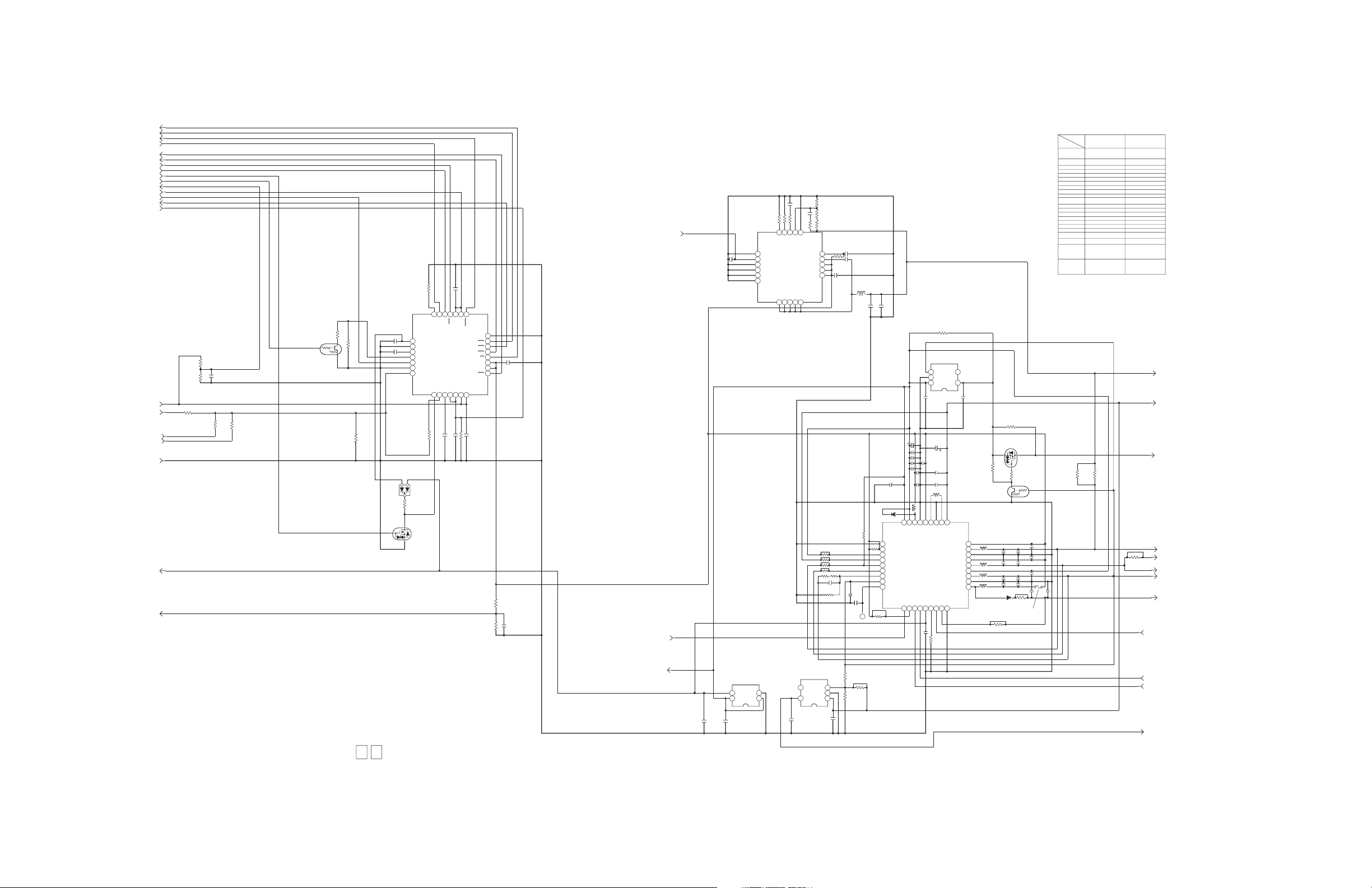
<MAIN(REG) SCHEMATIC DIAGRAM>
Note : The parts numbers in the schematic diagram are for references only.
When replacing the parts, refer to the PARTS LIST.
OT
FLT
DONE
PEN2
REG_CHG_DET
REG_DOK
REG_CEN
REG_PEN1
REG_THMEN
CHARGE_ICONT
V_BATT
ADP_DC
USUS
REG_UOK
VBUS
C6903 4.7
R6902 1.5k
1
2DC3DC4
5
CEN
DONE
Q6904
R6901
100k
FK330601-X
PEN16PEN27PSET
# IC6901
MAX8934AETI-X
THMEN16THMSW17LDO18USB19USB20BATT21BATT
15
C6910 4.7
C6905 1
29
28FLT
27UOK
26DOK
25OT
24SYS
C6901 10
23SYS
22CHG
C6904 4.7
R6905 OPEN
R6002
620k
R6008
560k
BATT+
T_BATT
AL_2.8V
UNREGCHK
T_CTL2
T_CTL1
R6903
13k _0.5%
R6006
430k
C6009
R6007
680k
0.01
# R6914
0`
GND
# R6916
62k
# R6915
V_BATT
180k
REG_THMEN
Q6903
RT1N432U-X
SIGN0071812
R6913 4.3k _0.5%
# R6917
C6906 0.1
8VL
9GND
C6907 1
10 CT
11 ISET
12 USUS
13 GND
14 THM
220k
D6901
DA3S103E-X
123
1M
R6922
1D
2
G
3S
MODEL
SYMBOL NO.
C6107
C6108
C6307~C6308
C6304
C6311
C6305
C6306
C6311
C6310
IC6101
# C6310
0.0033
# C6309
10k
10k
# R6317
# R6316
16 NC
17 EN
18 PGND
19 PGND
20 PGND
21
14
# IC6301
BD91361MUV-X
SW2SW3SW4SW5SW
1
REG_1.12VCTL
# C6311
0.001
C6010
0.01
REG_CTL
# R6313
36k
OPEN
# R6312
15k
4.3k
# R6311
# R6315
OPEN
0`
# R6314
11
GND12ADJ13ITH
VID115VID0
R6105
R6203
R6303
R6403
# C6304
0.001
# R6310
10
10VCC
# C6305
9BST
8PVCC
7PVCC
6PVCC
R6505
360k
C6504
OPEN
0.1
22
# L6302
NQLG4EN-2R3X
# C6306
2.3u
# C6307
10
# C6308
10
C6111
OPEN
C6103
10
C6104
10
C6105
10
C6106
1
C6001
10
L6101
NQLG4EN-2R3X
D6003
DB22320-X
E5
R6318
OPEN
E4
GND
R6005
B5
VOSEL4
OPEN
OPEN
OPEN
OPEN
R6506
15k
R6504
120k
OPEN
D5
VO1
D4
VO2
D3
VO3
E2
VO4
E3
INV5
F4
VINREG
F5
C6003
C6004
2.2
REGOUT
1
R6003
OPEN
TL6001
D6
VCCOUT
T
C6102
C6101
HX1E6LX1
C6203
OPEN
1
F6
C6
PGND1
IC6001
BD9362GUL-X
C6002 1
MG
# IC6101
XC6220B501MG-X
3
CE4NC
2
VSS
1
VIN
# C6107
10
C6204
OPEN
1
C6202
C6201
12
B6
A6
LX21
HX2BAT
10
R6606
OPEN
# R6107
0`
10
10
PGND2
A5
T
LX22
VOUT
L6201
NQLK25N-2R2X
A4
VOUT2
PGND45
PGND6C3VOUT6C2LEDD2INV6C5VDDB3SDAB4SCLB2SEQ_CTLC4STB1234
C1
PGND3
REG_1.1V
5
# C6108
10
# R6115
0`
# Q6101
MTM13124-X
1D
3S
# R6103
100k
A3
HX3
L6301
A2
LX3
NQLG4EN-2R3X
A1
D1
HX4
L6401
12
E1
LX4
NQLK25N-4R7X
F3
HX5
L6501
F2
LX5
NQLJ5EM-2R2X
F1
L6601
B1
LX6
NQLJ5EM-100X
D6601
DB2J407-X
2
G
# R6114
1.8M
# Q6102
RT1N432U-X
C6303
1
C6301
C6302
10
10
C6401
C6402
10
10
C6501
C6502
10
10
C6602
C6601
1
OPEN
C6603
4.7
R6602
OPEN
NMFZ007-R50X-K
R6604
OPEN
IC6301
IC6901
L6302
R6107
R6307
R6306
R6310
R6311
R6312
R6313
R6314
R6315
R6316
R6317
R6115
Q6101
Q6102
R6103
R6114
R6914
R6915
R6916
R6917
C6403
1
C6503
1
4.7
C6604
F6003
WIFI
NCB20JK-106X
NCBA1HK-102W
NCBA1AK-104W
NCJ20JM-226X-R
NCBA1HK-102W
NCBA1HK-332W
XC6220B501MG-X
BD91361MUV-X
MAX8934AETI-X
NQLG4EN-2R3X
OPEN
OPEN
NRSA6AJ-100W
NRSA6AJ-0R0W
NRSA6AD-153W
NRSA6AD-363W
NRSA6AJ-105W
NRSA6AD-432W
NRSA6AJ-103W
NRSA63J-0R0X
OPEN
OPEN
OPEN
OPEN
OPEN
NRSA6AJ-184W
NRSA6AJ-623W
NRSA6AJ-224W
0`
0`
# R6306
OPEN
# R6307
OPEN
NO-WIFI
OPEN
OPEN
OPEN
OPEN
OPEN
OPEN
OPEN
OPEN
MAX8934EETI-X
OPEN
NRSA63J-0R0X
NRSA02J-0R0X
OPEN
OPEN
OPEN
OPEN
OPEN
OPEN
OPEN
OPEN
MTM13124-X
RT1N432U-X
NRSA6AJ-104W
NRSA6AJ-185W
NRSA6AJ-0R0W
OPEN
OPEN
OPEN
R6405
0`
BL_FBI
REG_1.1V
REG_2.8V
REG_5.0V
REG_1.2V
REG_1.8V
(TO CN9011
& CN9013)
REG_1.8V
REG_3.3V
REG_LED
LI_CHRG
1
0
C1 REG ES1
C61101C6109
IC6102
XC6215B282NG-X
4
VIN
1
2
VSS3VOUT
1
CE
XC6220B271MG-X
5
VOUT
C6506
4.7
IC6501
OPEN
R6512
R6508
OPEN
3
CE4NC
2
VSS
OPEN
1
VIN
R6509
C6505
4.7
REG_SDA
REG_SCL
CAM_2.7V
yf400_y10985001a6/8_20111123_ver0.1
7
Page 27
<MAIN(eMMC) SCHEMATIC DIAGRAM>
Note : The parts numbers in the schematic diagram are for references only.
When replacing the parts, refer to the PARTS LIST.
MODEL
REG_3.3V
SD2_DAT7
SD2_DAT6
SD2_DAT5
SD2_DAT4
SD2_DAT3
SD2_DAT2
SD2_DAT1
SD2_DAT0
SD2_CMD
SD2_CLK
GND
# L8055
NRSA6AJ-0R0W
SYMBOL NO.
C8003
C8009
C8007
C8008
CN8001
C8011
C8014
IC8001
IC8002
IC8003
L8055
R8012
R8001
R8010
RA8001
RA8002
S-SD 8GB
OPEN
OPEN
OPEN
OPEN
OPEN
OPEN
OPEN
OPEN
OPEN
OPEN
OPEN
SD2_DAT7
SD2_DAT6
SD2_DAT5
SD2_DAT4
SD2_DAT3
SD2_DAT2
SD2_DAT1
SD2_DAT0
SD2_CMD
SD2_CLK
# C8014
1
16GB
NCBA1AK-104W
OPEN
NCB20JK-475X
NCB31CK-105X
OPEN
OPEN
THGBM4G6D2HBAIR
NRSA6AJ-0R0W
NRSA6AJ-103W
NRSA6AJ-820W NRSA6AJ-820W
NRB04CJ-563W
NCBA1AK-104W NCBA1AK-104W
OPEN OPEN
NCB20JK-475X
NCB31CK-105X
THGBM4G7D2GBAIE
OPEN
OPEN
NRSA6AJ-0R0W
NRSA6AJ-103W
NRB04CJ-563W
32GB
NCB20JK-475X
NCB31CK-105X
THGBM4G8D4GBAIE
OPEN
OPEN
NRSA6AJ-0R0W
NRSA6AJ-103W
NRSA6AJ-820W
NRB04CJ-563W
56k
876
876
56k
123
# RA8001
NRB04CJ-563W
SD2_DAT7 SD2_DAT7
SD2_DAT2
SD2_DAT6
SD2_DAT1
SD2_DAT5
SD2_DAT0
SD2_DAT4
SD2_DAT3
SD2_CLK
5
5
123
4
4
# RA8002
NRB04CJ-563W
# R8001
SD2_CMDSD2_CMD
10k
# CN8001
1
2
SD2_DAT2
3
SD2_DAT6
4
SD2_DAT1
5
SD2_DAT5
6
SD2_DAT0
7
SD2_DAT4
8
SD2_DAT3
# R8012
# R8010
0`
82
NA_CLK
NACMD
# C8011
# C8003
OPEN
0.1
4.7
# C8008
# C8007
OPEN
OPEN
U8
P5
M7
R10
90
81
108
Vss
Vss
Vss
Vss
NC
K5
41
NC
K3
39
NC
K1
37
NC
J14
36
NC
J13
35
NC
J12
34
NC
J11
33
NC
J10
32
NC
J9
31
NC
J8
30
NC
M5
61
NC
J1
23
NC
H14
22
NC
H13
21
DAT7
J6
28
DAT2
H5
13
DAT6
J5
27
DAT1
H4
12
DAT5
J4
26
DAT0
H3
11
DAT4
J3
25
DAT3
J2
24
NC
H12
20
NC
J7
29
CLK
W6
125
CMD
W5
124
NC
H11
19
NC
H10
18
NC
H9
17
NC
H8
16
NC
H7
15
NC
H6
14
NC
H2
10
NC
H1
9
NC
D14
8
NC
D1
7
NC
B13
6
NC
B2
5
NC
A11
4
NC
A9
3
NC
A6
2
NC
A4
1
NC
NC
NC
71
70
72
69
N2
N1
M14
M6
U9
N5
M12
M10
M13
T10
62
98
63
73
67
66
68
NC
NC
NC
109
Vcc
Vcc
Vcc
Vcc
THGBM4G7D2GBAIE
or THGBM4G8D4GBAIE
NC
NC
NC
NC
NC
NC
NC
NC
78
79
74
75
77
80
76
N3
P1
P2
P3
N10
N12
N14
N13
# C8009
OPEN
0.1
OPEN
K2
M8
W4
Y4
M9
K6
AA5
AA3
38
42
64
65
NC
NC
Vccq
NC
123
137
152
150
VDDi
Vccq
Vccq
Vccq
Vccq
# IC8001
[16GB eMMC]
[32GB eMMC]
NC
NC
NC
NC
NC
NC
NC
82
P10
NC
84
85
83
87
88
86
89
R2
R3
R1
R5
P13
P14
P12
K4
M2
Y2
M3
Y5
AA6
AA4
40
59
60
NC
153
151
135
138
Vssq
Vssq
Vssq
Vssq
Vssq
NC
NC
NC
NC
NC
NC
93
95
91
96
92
94
97
T2
T3
T1
T5
R14
R12
R13
L1
L3
L2
M1
L14
K14
K13
L12
L13
57
58
56
NC
NC
NC
NC
NC
NC
101
99
100
T14
T12
T13
K12
50
51
49
53
52
55
48
NC
NC
NC
NC
NC
NC
NC
NC
NC
NC
NC
NC
NC
NC
103
105
104
106
110
107
102
U2
U5
U3
U6
U7
U1
U10
L4
K7
K9
K8
K11
V12
K10
54
47
46
43
45
44
NC
NC
NC
NC
NC
NC
117
NC
AH11
169
NC
NC/A1_index
AH9
168
NC
AH6
167
NC
AH4
166
NC
AG13
165
NC
AG2
164
NC
AE14
163
NC
AE1
162
NC
AA14
161
NC
AA13
160
NC
AA12
159
NC
AA11
158
NC
AA10
157
NC
AA9
156
NC
AA8
155
NC
AA7
154
NC
AA2
149
NC
AA1
148
NC
Y14
147
NC
Y13
146
NC
Y12
145
NC
Y11
144
NC
Y10
143
NC
Y9
142
NC
Y8
141
NC
Y7
140
NC
Y6
139
NC
Y3
136
NC
Y1
134
NC
W14
133
NC
W13
132
NC
W12
131
NC
W11
130
NC
W10
129
NC
W9
128
NC
W8
127
NC
W7
126
NC
W3
122
NC
W2
121
NC
W1
120
NC
V14
119
NC
V13
118
NC
NC
NC
NC
NC
NC
NC
116
111
114
113
115
112
V3
V1
V2
U12
U14
U13
10 MAIN PWB
SD2_DAT7
SD2_DAT2
SD2_DAT6
SD2_DAT1
SD2_DAT5
SD2_DAT0
SD2_DAT4
SD2_DAT3
NA_CLK
NACMD
P5
U8
M7
U9
T10
M12
R10
M13
M10
67
68
66
81
63
90
NC
NC
NC
108
SD2_DAT0
SD2_DAT1
SD2_DAT7
SD2_DAT5
SD2_DAT2
SD2_DAT4
SD2_DAT6
SD2_DAT3
C2
C4
C6
D3
E6
F5
C10NCC11NCC12
NC
K9
J10
NC
VCC
VCC
VCC
VCC
NC
NC
NC
B9
N3
N6NCN7NCN8
B10
P9
N14
NC
NC
P8
NC
P1
NC
K8
VSS
H10
VSS
G5
VSS
E7
VSS
C3
NC
C1
NC
B14
NC
B13
NC
A7
RFU
A6
RFU
B6
DAT7
A5
DAT2
B5
DAT6
A4
DAT1
B4
DAT5
A3
DAT0
B3
DAT4
B2
DAT3
B12
NC
B11
NC
M6
CLK
M5
CMD
B8
NC
B7
NC
B1
NC
A14
NC
A13
NC
A12
NC
A11
NC
A10
NC
A9
NC
A8
NC
A2
NC
A1
NC
N9
NC
P7
RFU
NC
P2
D4
M4
N4
P3
P5
NC
VCCQ
VCCQ
VCCQ
# IC8003
THGBM4G6D2HBAIR
N2
N5
P4
P6
C13NCC14
D12
NC
NC
VDDI
VSSQ
VCCQ
VCCQ
VSSQ
VSSQ
VSSQ
VSSQ
[8GB eMMC v4.41]
NCM1NCM2NCM3NC
NC
NCN1NC
M7NCM8NCM9
M10NCM11NCM12NCM13NCM14
L12NCL13NCL14
NCD1NCD2NC
NCL1NCL2NCL3NC
D13NCD14
NCE1NCE2NCE3NC
RFU
K10
K12NCK13NCK14
C5
C8NCC9
E5
N13
P10
P12
NC
NC
NC
RFU
RFU
RFU
P11
NC
N12
NC
K5
RST_N
C7
NC
E8
RFU
E9
RFU
E10
RFU
E12
NC
E13
NC
E14
NC
F1
NC
F2
NC
F3
NC
F10
RFU
F12
NC
F13
NC
F14
NC
G1
NC
G2
NC
G3
RFU
G10
RFU
G12
NC
G13
NC
G14
NC
H1
NC
H2
NC
H3
NC
H5
RFU
H12
NC
H13
NC
H14
NC
J1
NC
J2
NC
J3
NC
J5
RFU
J12
NC
N11
NC
P13
NC
NCK1NCK2NCK3NC
RFUK7RFU
NC
K6
NC
J13NCJ14
N10
P14
NACMD
NA_CLK
SD2_DAT7
SD2_DAT2
SD2_DAT6
SD2_DAT1
SD2_DAT5
SD2_DAT0
SD2_DAT4
SD2_DAT3
Vss
NC
K5
41
NC
K3
39
NC
K1
37
NC
J14
36
NC
J13
35
NC
J12
34
NC
J11
33
NC
J10
32
NC
J9
31
NC
J8
30
NC
M5
61
NC
J1
23
NC
H14
22
NC
H13
21
DAT7
J6
28
DAT2
H5
13
DAT6
J5
27
DAT1
H4
12
DAT5
J4
26
DAT0
H3
11
DAT4
J3
25
DAT3
J2
24
NC
H12
20
NC
J7
29
CLK
W6
125
CMD
W5
124
NC
H11
19
NC
H10
18
NC
H9
17
NC
H8
16
NC
H7
15
NC
H6
14
NC
H2
10
NC
H1
9
NC
D14
8
NC
D1
7
NC
B13
6
NC
B2
5
NC
A11
4
NC
A9
3
NC
A6
2
NC
A4
1
NC
69
M14
109
Vss
Vcc
Vss
Vss
Vcc
NC
NC
NC
NC
NC
NC
NC
78
72
77
74
71
70
76
75
N3
N2
N1
N14
N10
N13
N12
W4
M9
N5
M6
AA5
65
98
73
62
NC
152
Vcc
Vcc
Vccq
M3
Y4
AA3
137
150
Vccq
Vccq
Vccq
Y5
K6
123
Vccq
Y2
K2
M8
AA6
AA4
60
64
42
38
NC
NC
153
151
138
135
Vssq
Vssq
Vssq
Vssq
VDDi
THGBM2G6D2FBAI9
# IC8002
[8GB eMMC v4.4]
NC
NC
NC
NC
82
80
79
P1
P3
P2
P10
NC
NC
NC
84
83
P13
P12
NC
NC
NC
85
P14
NC
NC
86
R1
NC
NC
NC
95
89
92
88
93
94
91
87
R2
T2
R5
R3
T1
R13
R14
R12
K4
M2
59
40
NC
Vssq
NC
NC
97
96
T5
T3
L1
L3
M1
L2
L14
L13
L12
53
57
56
55
58
52
NC
NC
NC
NC
NC
NC
NC
NC
NC
NC
NC
NC
NC
NC
99
101
105
104
102
103
100
U3
U1
U2
T12
T14
T13
K8
K7
L4
K9
K12
K11
K10
K13
K14
51
49
50
NC
NC
NC
NC
106
107
U5
U6
U7
V12
48
NC
NC
NC
110
U10
54
44
47
46
43
45
NC
NC
NC
NC
NC
NC
117
NC
AH11
169
NC
NC/A1_index
AH9
168
NC
AH6
167
NC
AH4
166
NC
AG13
165
NC
AG2
164
NC
AE14
163
NC
AE1
162
NC
AA14
161
NC
AA13
160
NC
AA12
159
NC
AA11
158
NC
AA10
157
NC
AA9
156
NC
AA8
155
NC
AA7
154
NC
AA2
149
NC
AA1
148
NC
Y14
147
NC
Y13
146
NC
Y12
145
NC
Y11
144
NC
Y10
143
NC
Y9
142
NC
Y8
141
NC
Y7
140
NC
Y6
139
NC
Y3
136
NC
Y1
134
NC
W14
133
NC
W13
132
NC
W12
131
NC
W11
130
NC
W10
129
NC
W9
128
NC
W8
127
NC
W7
126
NC
W3
122
NC
W2
121
NC
W1
120
NC
V14
119
NC
V13
118
NC
NC
NC
NC
NC
NC
112
116
114
111
115
113
V3
V1
V2
U13
U12
U14
yf400_y10985001a4/8_20111123_ver0.1
8
Page 28
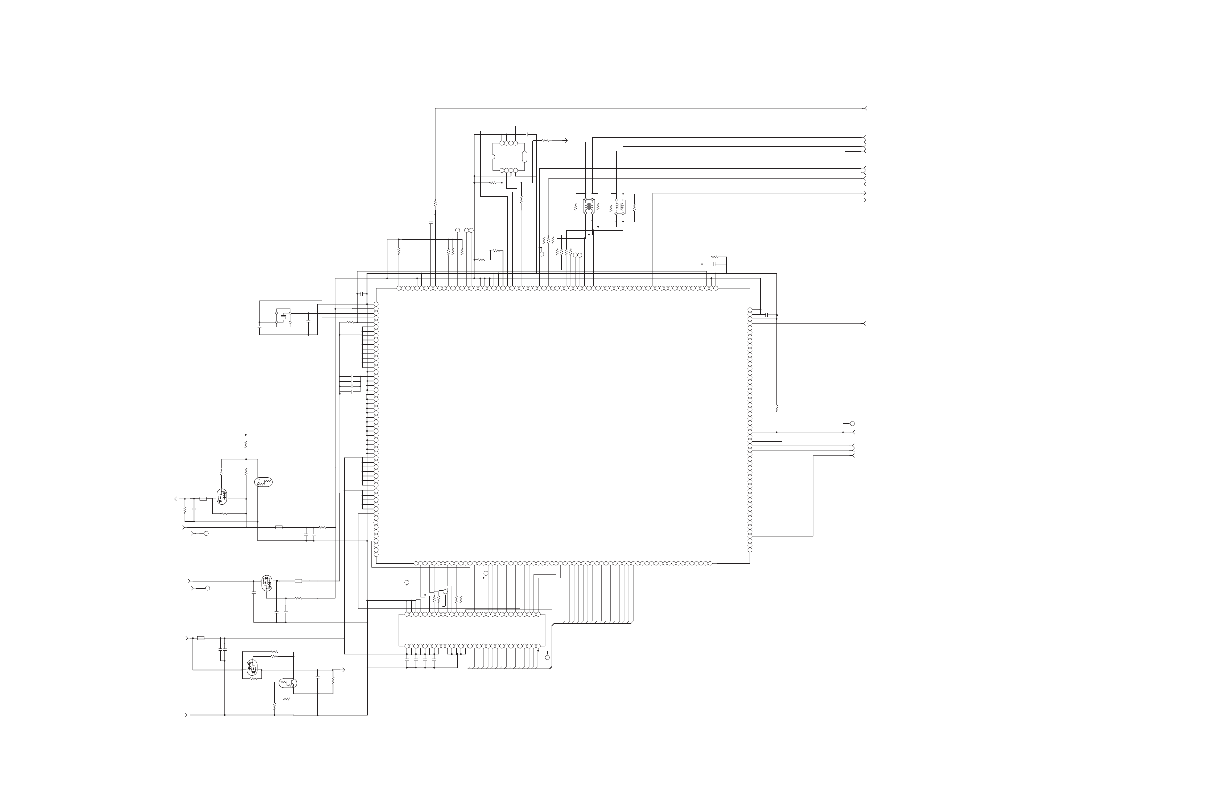
<MAIN(WIFI) SCHEMATIC DIAGRAM> / WIFI model
Note : The parts numbers in the schematic diagram are for references only.
When replacing the parts, refer to the PARTS LIST.
MOD_3.3V
R8626
10k
REG_3.3V
REG_3.3VCTL
REG_1.2V
REG_1.0VCTL
REG_1.8V
# TL8509
MOD_RST
WIFI_RX
WIFI_TX
WIFI_ATTACH
WIFI_RST
MOD_DP
MOD_DN
WIFI_USBDP
WIFI_USBDN
WIFI_SPI_CS
WIFI_SPI_CK
WIFI_SPI_DO
WIFI_SPI_DI
DRXD
DTXD
WIFI_WKUP
yf400_y10985001a8/8_20111123_ver0.1
MOD_3.3V_CTRL
SFL_IN
SFL_SCK
IC8503
3.3V
SFL_SCK
# TL8555
# TL8556
# R8624
100k
P8
P9
R8
V8
U10
VDDIOP0_RSTJTAG_TD0
VDDIOP0_RSTJTAG_TMS
VDDIOP0_RSTJTAG_RTCK
VDDIOP0_RSTJTAG_NTRST
EBI_O_DQS0
EBI_O_A1 / NBS2 / DQM / NWR2
EBI_O_A0 / NBS0
EBI_DQS1
J10
J15
J18
B10
G25_DDR_LDQS
G25_DDR_UDQS
G25_DDR_NCS1
# R8535
# R8536
10
10
E2
E8
F7
H7
UDM
A13
/CS
UDQS
LDQS
VSSQ
A3
G25_DDR_D0
SFL_IN
# R8552
47k
SFL_IN
SFL_SCK
# TL8557
G25_BMS
# R8525
47k
R9
N8
R10
VDDIOP0
VDDIOP1
VDDIOP0
VDDIOP0_RSTJTAG_BMS
EBI_O_A3
EBI_O_A4
EBI_O_A2
H17
H18
J12
J17
G25_DDR_A5
G25_DDR_A3
G25_DDR_A2
G25_DDR_A4
J8A0J9
A1
A3
DQ1B8DQ2B9VSSQC1VSSQ
DQ3C8DQ4
B7
C7
G25_DDR_D1
G25_DDR_D2
G25_DDR_D3
G25_DDR_D4
# R8551
47k
OPEN
J5
GNDIOP
EBI_O_A5
H15
# TL8513
G25_DDR_A6
K2A4K3A5K7A2K8
DQ5D8DQ6E3DQ8E7DQ7
D7
G25_DDR_D5
WIFI_RST
2.2k
# R8519
0.1
C8633
3.3V
# R8520
GNDOSC
V15
VDDOSC
U12
V13
VDDOSC_CLOCK_XIN
VDDOSC_CLOCK_XOUT
V12
VDDPLLA
U13
VDDCORE
U11
VDDCORE
U14
VDDCORE
P17
D17
VDDCORE
F17
VDDCORE
H8
VDDCORE
K9
VDDCORE
M10
VDDCORE
E6
VDDCORE
P13
VDDCORE
GNDCORE
U18
C6
GNDCORE
M11
GNDCORE
L8
GNDCORE
G15
GNDCORE
R11
GNDCORE
GNDCORE
L10
GNDCORE
L11
GNDCORE
K10
GNDIOM
N14
GNDIOM
K12
GNDIOM
K11
GNDIOM
M14
GNDIOM
F13
GNDIOM
G14
GNDIOM
J14
GNDIOM
F15
GNDIOM
F11
GNDIOM
P18
VDDIOM
K13
G12
VDDIOM
H11
VDDIOM
H13
VDDIOM
H14
VDDIOM
J11
VDDIOM
J13
VDDIOM
R13
VDDNF
VDDNF
N12
VDDNF
L12
M13
VDDNF
M12
VDDNF
EBI_O_SDA10
G9
PD0 / EBI_NANDOE
P11
PD1 / NANDWE
U15
PD2 / EBI_A21 / NANDALE
P14
EBI_PD3 / A22 / NANDCLE
R15
EBI_O_NRD
C10
EBI_O_NCS1 / SDCS
C9
EBI_O_NWR0 / NWRE
H9
EBI_O_NWR1 / NBS1
B9
PD5 / EBI_NWAIT
P12
G25_DDR_NCS1
G25_DDR_SDA10
L_1.8V
100k
C8
E9
F8
VDDBU_SYSC_TST
VDDBU_SYSC_WKUP
TL8561
F1
VSS
# IC8502
VDDA9VDD
K9
# C8518
0.1
E8
F9
VDDBU
VDDBU_SYSC_SHDN
VDDBU_SYSC_JTAGSEL
EBI_O_CAS
EBI_O_RAS
C11
G10
G25_DDR_CAS_
G25_DDR_RAS_
A1
K1
VSS
VSS
VDD
F9
# C8517
0.1
MOD_3.3V_CTRL
# C8632
3.3V
3.3V
3.3V
3.3V
R8633
10k
OPEN
G25_CX_IN
G25_CX_OUT
1.0V
# C8539
# C8519
1.0V
# C8541
1.0V
L_1.8V
# C8554
# R8625
0`
L_1.8V
L_1.8V
MOD_1.5V
1
0.1
0.1
0.1
10
OPEN
G25_CX_OUT
# X8500
NAX1167-001X
12
# C8510
12p
34
# C8509
12p
MOD_3.3V_CTRL
# R8514
0`
OPEN
# R8515
# R8508
1.8M
47k
# Q8504
# TL8560
TL8562
REG_1.8V
# C8542
0.1
123
# R8513
0`
OPEN
# C8544
10
RTF020P02-X
OPEN
L8506
NQR0499-001X
C8634
0.1
OPEN
# L8502
NQR0499-001X
GND
# Q8501
REG_3.3V
RT1N432U-X
# L8503
NQR0499-001X
# Q8505
SSM3K302T-X
1D
# C8503
GND
3S
2
G
4.7
R8621
# C8502
4.7
0.1
L_1.8V
R8627
47k
R8628
1.8M
Q8506
RTF020P02-X
123
Q8507
RT1N432U-X
2
R8629
0`
OPEN
# R8507
# R8506
0`
10k
OPEN
# C8536
0.1
# L8501
NQR0499-001X
# R8521
47k
MOD_1.5V
1
3
# C8537
# R8504
0`
1
1.0V
3.3V
# C8504
4.7
# R8623
# R8622
100k
100k
B7
C7
F7
U9
V9
V10
V11
GNDBU
VDDIOP0_DIB_DIBP
VDDIOP0_DIB_DIBN
VDDBU_CLOCK_XIN32
VDDBU_CLOCK_XOUT32
VDDIOP0_RSTJTAG_TDI
VDDIOP0_RSTJTAG_TCK
VDDIOP0_RSTJTAG_NRST
EBI_CLK_#SDCK
EBI_O_DQM0
EBI_DQM1
EBI_O_SDCKE
EBI_CLK_SDCKG8EBI_O_NWR3 / NBS3 / DQM3
EBI_O_SDWE
C12
B11
E10
E11
G11
H10
G25_DDR_UDM
G25_DDR_LDM
G25_DDR_CK_
G25_DDR_CK
G25_DDR_CKE
# R8512
# R8511
10
# TL8558
10
F2
F8
G1
G2CKG3
G8
LDM
CKE
/CKG7/WE
/CASG9/RAS
H5MS1G62BFR-E3M
VDDQB1VDDQ
VDDQD1VDDQ
VSSQE1VSSQA8DQ0
VDDQ
NC
A7
C9
D9
E9
F3
0.1
0.1
# C8511
# C8513
8
VCC
/CS
W25Q80BLUXIG-W
1
J9
M9
P10
GNDIOP
GNDIOP
EBI_O_A6
EBI_O_A8
EBI_O_A7
E19
F18
G25_DDR_A8
G25_DDR_A7
J1A6J2A7J3A8J7
G25_DDR_D6
G25_DDR_D7
7
/HOLD(IO3)
2
SFL_SCK
G25_DDR_A9
G25_DDR_D8
# C8501
1
5
6
CLK
9
DI(IO0)
/WP(IO2)4GND
DO(IO1)
3
SFL_CS
SFL_OUT
470
# R8543
SFL_IN
SFL_OUT
G25_SFL_CS
1.00V
P3
R2
T3
V3
W1
W2
PA14 / SPI0_NPCS0
PA7 / TXD2 / SPI0_NPCS1
PA1 / RXD0 / SPI0_NPCS2
PA13 / SPI0_SPCK / MCI1_CK
PA11 / SPI0_MISO / MCI1_DA0
PA12 / SPI0_MOSI / MCI1_CDA
EBI_O_A12
EBI_O_A11
EBI_O_A16 / BA0
EBI_O_A17 / BA1
EBI_O_A10
EBI_O_A9
B19
D19
E18
F16
G17
G18
G25_DDR_A11
G25_DDR_A10
G25_DDR_BA0
G25_DDR_BA1
H1A9H2
H8
BA0H9BA1
A10
DQ13B3DQ14
DQ11C3DQ12
DQ9
DQ10
B2
C2
D2
D3
G25_DDR_D9
G25_DDR_D10
G25_DDR_D11
G25_DDR_D12
G25_DDR_D13
MOD1.5V_CE_R22K
# R8516
0`
WIFI_KENT0
2
OPEN
R8637
0`
L_MOD_DP
L_MOD_DM
# R8617
39
39
# TL8551
R17
T17
USBFS_HFSDPC
USBFS_HFSDMB
USBFS_HFSDPB
L8504
NQR0654-001X
1
L_MOD_DM
L_MOD_DP
# TL8550
M18
N18
V17
USBFS_HFSDMC
USBHS_HHSDPA / DHSDP
USBHS_HHSDMA / DHSDM
3
4
L_USB_DP
T18
V16
USBHS_HHSDPB
WIFI_SPI_DI
WIFI_SPI_DO
WIFI_SPI_CS
WIFI_SPI_CK
# R8630
# R8537
# R8631
0`
0`
0`
# TL8553
N6
P2
P6
R6
V4
PA23_TIOA2 / SPI1_SPCK
PA8 / RXD2 / SPI1_NPCS0
PA0 / TXD0 / SPI1_NPCS1
PA22 / TIOA1 / SPI1_MOSI
PA21 / TIOA0 / SPI1_MISO
# R8620
# R8619
# R8618
39
39
U16
U17
USBFS_HFSDPA_DFSDP
USBFS_HFSDMA / DFSDM
IC8501
AT91SAM9G25-CFU
EBI_D14
EBI_O_A13
EBI_D13
EBI_O_A14
EBI_O_A19
C18
EBI_O_A15
A18
EBI_D15
A19
G25_DDR_D15
H12
E12
G25_DDR_D14
EBI_D12
A12
B13
G25_DDR_D13
G25_DDR_D12
EBI_D11
EBI_D10
D13
F12
G25_DDR_D11
G25_DDR_D10
EBI_D9
C14
G25_DDR_D9
G25_DDR_D8
EBI_O_NCS0
EBI_NCS3 / PD4
F10
R14
G25_DDR_A13
G25_DDR_A14
A11H3A12
DQ15
A2
G25_DDR_D14
G25_DDR_D15
EBI_O_A18 / BA2
B17
# TL8514
E16
OPEN
OPEN
0`
0`
R8638
R8635
L_USB_DM
L_USB_DP
L_USB_DM
3.3V3.3V
N5
T2
R18
USBHS_HHSDMB
PA4 / SCK0 / MCI1_DA3
PA3 / CTS0 / MCI1_DA2 / ETX1
EBI_D7
EBI_D5
EBI_D6
EBI_D8
A14
A16
B15
E13
G25_DDR_D7
G25_DDR_D6
G25_DDR_D5
2
3
L8500
NQR0654-001X
1
4
M7
U4
U5
V5
PA17 / MCI0_CK
PA19 / MCI0_DA2
PA18 / MCI0_DA1
PA20 / MCI0_DA3
PA2 / RTS0 / MCI1_DA1
EBI_D2
EBI_D3
EBI_D1
EBI_D4
C16
D15
E15
E14
G25_DDR_D3
G25_DDR_D2
G25_DDR_D1
G25_DDR_D4
OPEN
0`
R8636
R3
R5
U3
PA16_MCI0_CDA
PA15_MCI0_DA0
EBI_PD21 / D31 / NCS5
EBI_D0
L13
F14
G25_DDR_D0
P5
U2
V2
L18
PA6 / RXD1
PA9 / DRXD
PA10 / DTXD
EBI_PD15 / D25
EBI_PD20 / D30 / NCS4
EBI_PD19 / D29 / NCS2
EBI_PD18 / D28 / A25
EBI_PD17 / D27 / A24
K14
K17
L14
K18
U7
U8
V1
V7
PA5 / TXD1
PA29 / TIOB2 / RF
PA30 / TWD0 / SPI1_NPCS3
PA31 / TWCK0 / SPI1_NPCS2
EBI_PD12 / D22
EBI_PD14 / D24
EBI_PD13 / D23
EBI_PD11 / D21
EBI_PD16 / D26 / A23
L15
L17
M17
K15
WIFI_SPI_CS
WIFI_SPI_CK
WIFI_SPI_DO
WIFI_SPI_DI
L9
R7
U6
V6
PA26 / TCLK2 / TD
PA28 / TIOB1 / RK
PA25 / TCLK1 / TF
PA27 / TIOB0 / RD
GPIO_CLK_PC15 / ISI_MCK / PCK0
EBI_PD9 / D19
EBI_PD8 / D18
EBI_PD10 / D20
M15
N11
N17
R12
MOD_DP
MOD_DN
WIFI_USBDP
WIFI_USBDN
# R8534
6.8k
_0.5%
# C8533
10p
P7
V18
V19
W18
W19
GNDUTMI
VDDUTMII
VDDUTMIC
VDDANA_ADVREF
VDDUTMIC_VBG
PA24 / TCLK0 / TK
PB18 / IRQ / ADTRG
ANA_PB17 / AD6 / ECOL
ANA_PB16 / AD5 / ECRS
ANA_PB15 / ERXCK
ANA_PB14 / ERX3 / PWM3
ANA_PB13 / ERX2 / PWM2
ANA_PB12 / ETX3 / PWM1
ANA_PB11 / ETX2 / PWM0
ANA_PB10 / AD11 / ETX1 / PCK0
ANA_PB9 / AD10 / ETX0 / PCK1
ANA_PB8 / AD9 / ETXER
ANA_PB7 / AD8 / ETXEN
ANA_PB6 / AD7 / EMDC
PB5 / EMDIO / TWCK2
GPIO_CLK_PB4 / ETXCK / TWD2
PB3 / ERXDV / SPI0_NPCS3
PB2 / ERXER / SCK2
PB1 / ERX1 / CTS2
PB0 / ERX0 / RTS2
PC0 / ISI_D0 / TWD1
PC1 / ISI_D1 / TWCK1
PC2 / ISI_D2 / TIOA3
PC3 / ISI_D3 / TIOB3
PC4 / ISI_D4 / TCLK3
PC5 / ISI_D5 / TIOA4
PC6 / ISI_D6 / TIOB4
PC7 / ISI_D7 / TCLK4
PC8 / ISI_D8 / UTXD0
PC9 / ISI_D9 / URXD0
PC10 / ISI_D10 / PWM0
PC11 / ISI_D11 / PWM1
PC12 / ISI_PCK / TIOA5
PC13 / ISI_VSYNC / TIOB5
PC14 / ISI_HSYNC / TCLK5
GPIO_CLK_PC29 / SCK1
GPIO_CLK2_PC30
PC31 / FIQ / PCK1
NC
NC
EBI_PD7 / D17
EBI_PD6 / D16
B8
N15
V14
P15
3.3V
PC16 / UTXD1
PC17 / URXD1
PC18 / PWM0
PC19 / PWM1
PC20 / PWM2
PC21 / PWM3
PC22 / TXD3
PC23 / RXD3
PC24 / RTS3
PC25 / CTS3
PC26 / SCK3
PC27 / RTS1
PC28 / CTS1
VDDANA
GNDANA
DRXD
DTXD
MOD_3.3V_CTRL
3.3V
B6
# C8512
0.1
E7
F6
D3
C5
A2
B3
A1
B4
E5
B5
B1
C2
B2
C3
C4
F3
D2
E2
E3
G6
F5
F2
H7
G5
H5
G3
H6
G2
H2
J2
H3
K3
J8
J6
J7
J3
K2
K8
K6
L2
K7
M3
K5
L6
L7
M6
L3
M8
M2
L5
N3
M5
N2
MOD_3.3V_CTRL
# R8632
4.7k
WIFI_RX
WIFI_TX
WIFI_ATTACH
MOD1.5V_CE_R22K
WIFI_WKUP
MOD_RST
9
Page 29

<REAR SCHEMATIC DIAGRAM>
Note : The parts numbers in the schematic diagram are for references only.
When replacing the parts, refer to the PARTS LIST.
REG_2.8V
D_GYRO_CS
D_GYRO_CLK
D_GYRO_OUT
D_GYRO_IN
0
GND
P_GYAMP
TL901
Y_GYAMP
TL902
R902
47
R905
47
REAR PWB2
TO MAIN PWB
new SONY GYRO
K901
NQR0129-002X
R910
100k
OPEN
C906
OPEN
R907
0`
0.1
OPEN
R906
0`
C905
0.0022
14
13
12
11
C907
Soy
Fox
DSEL
SCLK
NAL0105-001X
Vcc
Doy
0.1
C901
0.047
16
Vdd
10
17
SDO
IC901
SONY
VddIO
9
OPEN
C908
0.1
L601
R609
OPEN
D609
DB22320-X
1
DZ2J068/M/-X
2
1
D605
NRSA6AJ-0R0W
L602
1 2
NQR0645-001X
L603
NQR0645-001X
C602
0.001
1 D
2
2
2
1
OPEN
D610
DZ2J068/M/-X
R694
12
1 2
G
OPEN
D602
15k
OPEN
Q601
SSM3J327R-X
3 S
2
1
12
OPEN
C603
IC601
XC6215B332NG-X
C609 1
C610 1
NCBA1AK-104W
C607
C608
OPEN
R693
6.8k
OPEN
C604
3
VSS
VOUT
4
VIN
2
1
D603
DZ2J068/M/-X
OPEN
12
CE
R601 100
R602 100
2
1
2
1
D604
DZ2J068/M/-X
KEY_A
D606
DB2J314-X
BATT_L
D_BATT
T_BATT
V_OUT
AU_SIG/L
AU_SIG/R
P_DET
1 2
!
F602
NMFZ028-2R5X-J1
LITHIUM BATTERY
BT602
QAB0088-001
D612
SML-D12V8W/PQ-X
1 2
470
R610
D611
LNJ326W83-X
T_BATT
D_BATT
AL_2.8V
PWR_LED
ACES_LED
BATT_L
1 2
P_DET
V_OUT
AU_SIG/L
AU_SIG/R
D_GYRO_CLK
D_GYRO_CS
REG_2.8V
D_GYRO_OUT
D_GYRO_IN
KEY_A
GREENRED
ACES_LED
REG_2.8V
AV JACK
QNS0297-001X
C902
0.047
DC JACK
J602
QNA0059-001X
1
3
2
4
5
BATTERY TERMINAL
QNA0060-001
[-]
J601
BT601
3
4
5
2
1
DZ2J068/M/-X
!
F601
NMFZ028-2R5X-J1
1 2
C606
OPEN
12345
D601
2
C601
1
0.001
[-]
19
18
20
C903
SDI
Fix
VREF
CS
GND
8
7
0.1
Sox
115
C904
2
NC
Fiy
Adj
Dox
Foy
6
0.0022
3
4
OPEN
5
R911
100k
[D]
[T]
[+]
OPEN
C611
DZ2J068/M/-X
R695
47k
12
CN601
QGF0574F1-40X
40
39
38
37
36
35
34
33
32
31
30
29
28
27
26
25
24
23
22
21
20
19
18
17
16
15
14
13
12
11
10
9
8
7
6
5
4
3
2
1
S694
NSW0323-001X
INFO
OK
S692
NSW0323-001X
S693
NSW0323-001X
USERCAMERA/VIDEO
S691
NSW0323-001X
INTELLIGENT AUTO
PLAYBACK
PWR_LED
AL_2.8V
GND
yf400_y20583001a_20111102_ver0.1
10
Page 30

<JACK SCHEMATIC DIAGRAM>
Note : The parts numbers in the schematic diagram are for references only.
When replacing the parts, refer to the PARTS LIST.
TO MAIN PWB
CN201
QGF0543F3-18X
18
17
16
15
14
13
12
11
10
9
8
7
6
5
4
3
2
1
TMDS_CLK-
TMDS_CLK+
TMDS_D0-
TMDS_D0+
TMDS_D1-
TMDS_D1+
TMDS_D2-
TMDS_D2+
GND
GND
TMDS_D2+
TMDS_D2-
TMDS_D1+
TMDS_D1-
TMDS_D0+
TMDS_D0-
TMDS_CLK+
TMDS_CLK-
HDMI_CEC
HDMI_SCL
HDMI_SDA
TMDS_REG5V
HDMI_PDET
J201
NNZ0212-001X
23
1
GND
2
TMDS Data2+
3
TMDS Data2-
4
GND
5
TMDS Data1+
6
TMDS Data1-
7
GND
8
TMDS Data0+
9
TMDS Data0-
GND
10
TMDS Clock+
11
TMDS Clock-
12
GND
13
CEC
14
SCL
15
SDA
16
NC
17
+5V Power
18
Hot Plug Detect
19
20
21 22
HDMI
TO MAIN PWB
CN203
QGF0543F3-15X
1
2
3
4
5
6
7
8
9
10
11
12
13
14
15
HDMI_CEC
HDMI_SCL
HDMI_SDA
TMDS_REG5V
HDMI_PDET
VBUS
USBDP
USBDN
XUSBHOST
MENU/PWR_SW
MENU/PWR_SW
GND
GND
VBUS
!
F201
NMFZ028-2R5X-J1
1 2
2
OPEN
D201
1
DZ2J068/M/-X
S201
NSW0323-001X
PLAY/REC
PWR_SW
1 2
XUSBHOST
GND
USBDP
USBDN
# J203
NNZ0246-001X
NNZ0251-001X
6
78
1 2 3 4 5
9
USB HOST
NO USB HOST
USB
SYMBOL NO.
MODEL
HOST NON-HOST
NNZ0246-001X NNZ0251-001XJ203
yf400_y20581001a_20111102_ver0.1
11
Page 31

<MONITOR SCHEMATIC DIAGRAM>
Note : The parts numbers in the schematic diagram are for references only.
When replacing the parts, refer to the PARTS LIST.
From Main PWB
CN701
QGF0574F1-34X
GND
TP_SEL2
REG_2.8V
D703
1REG_LED
2REG_LED
3BL_FBI
4M_RVS
5GND
6LCD_DATA
7LCD_CLK
8LCD_CS
9LCD_RST
10REG_1.8V
11REG_2.8V
12LCD_HD0
13LCD_VD0
14GND
15GND
16LCD_CLK0
17
18LCD_GO_7
19LCD_GO_6
20LCD_GO_5
21LCD_GO_4
22LCD_GO_3
23LCD_GO_2
24LCD_GO_1
25LCD_GO_0
26GND
27TP_VDD
28TP_SEL1/KEY_C
29
30TP_X
31TP_Y
32GND
33
34
L723
OPEN
C721
GND
VDDE_2.8V
TP_SEL1/KEY_C
TP_SEL2
TP_X
TP_Y
1
OPEN
R701
REG_2.8V
LCD BACKLIGHT
D721
NSSW206A/T484-X
D722
NSSW206A/T484-X
D723
NSSW206A/T484-X
D725
NSSW206A/T484-X
OPEN
12345
6 7 8 9 10
REG_2.8V
R730
D704
OPEN
12345
D705
1
2
6 7 8 9 10
OPEN
L701
OPEN
L702
OPEN
OPEN
D701
OPEN
D702
MR SENSOR
0`
C723
OPEN
IC722
HGDESM031A-X
GND
3
VDD
4
OUT
D724
C724
OPEN
OPEN
2
NC
1
TP_X
TP_Y
GND
L741
OPEN
C741
R741
OPEN
OPEN
LTA043EEB-X
TOUCH PANEL IF
From Felix
To Felix
TP_SEL1/KEY_C
From Felix
REG_2.8V
TP_SEL2
VDDE_2.8V
MONITOR PWB
R705
R704
R703
R702
2
2
1
1
C701
1
1
1
2
C702
2
2
Q741
LTA043EEB-X
2.2
3
R742
1
Q742
2
Q743
LTA043EEB-X
2
Q744
LTC043EEB-X
2
Q745
LTC043EEB-X
2
100k
C713
1
3
1
C754
C755
C746
C747
C750
1
3
1
3
1
3
1
2
3
4
1
1
1
RA702
2.2
1
1
2.2C748
2
OPEN
2.2
2
2
2.2C749
OPEN
OPEN
OPEN
OPEN
C703
OPEN
OPEN
8
7
6
5
D741
1 2 3
RA701
1
2
3
4
R751
To 3.0' LCD (SHTM)
CN702
QGF0319F1-39X
1 VCOM
2 RST
3 CS
4 SDA
5 SCL
6 HSYNC
OPEN
K709
OPEN
K701
8
K702
7
K703
6
K704
5
K705
K706
K707
K708
2.2
2
C752
1
1
C712
1
C711
C709
1
2.2 C756
1
2
1
2
2.2 C757
45
0.0047
C742
C743
7 VSYNC
0`
8 DCLK
9 NC(GND)
OPEN
10 D7
OPEN
11 D6
OPEN
12 D5
OPEN
13 D4
OPEN
14 D3
OPEN
15 D2
OPEN
16 D1
OPEN
17 D0
18 GND
19 NC(GND)
20 VDD
21 VDDIO
22 DVDD
23 NC(GND)
24 CP1P
C753
OPEN
25 CP1M
26 CP2P
27 CP2M
28 VINT1
29 CP3P
30 CP3M
31 CP4P
32 CP4M
33 VGH
34 VGL
35 AGND
36 FRP
37 VCOMDC
38 VCAC
39 VCOM
To Touch panel unit
OPEN
OPEN
0.0047
C745
C744
R743
R744
R745
R746
R747
R748
R749
R750
OPEN
OPEN
OPEN
OPEN
OPEN
OPEN
OPEN
OPEN
CN703
QGF0528F4-08X
1
2
3
4
5
6
7
8
OPEN
TP701
ONBOARD CONTACT
OPEN
TP702
GND
yf400_y20582001a_20111020_ver0.1
12
Page 32

<CMOS SCHEMATIC DIAGRAM>
Notes : 1. The parts number in the schematic diagram are for references only.
When replacing the parts, refer to the PARTS LIST.
2. The schematic diagram is only for reference. Avoid replacing individual parts.
Replace the entire unit only.
When CMOS BOARD ASSEMBLY needs replacement, replace the CMOS FRAME ASSEMBLY in whole because it cannot be replaced alone
2
# VARIATION TABLE
SERIES
SYMBOL NO.
IC451
L452
C1AB1
IMX102CQK-C
NQR0286-006X
CMOS SENSOR IMX102/IMX126
C2A
IMX126CQK
NQR0286-001X
OPEN
OPEN
OPEN
C465
OPEN
C466
OPEN
C467
C468
C469
OPEN
C470
2
OPEN
1
A1
NC
2
A2
NC
4
A4
VSSHPX
33
D9
VSSHDA
40
F1
NC
45
F9
NC
6
A6
VSSHVS
34
E1
VSSHCP
39
E9
VDDHCM2
46
G1
VDDHCM1
27
C9
VDDHDA
5
A5
VDDHPX
3
A3
VDDSUB1
76
K7
VDDSUB2
7
A7
VDDHVS
28
D1
VDDHCP
9
A9
NC
10
B1
NC
11
B2
NC
3
4
OUTPUT
VDD
ENABLE/DISABLE2CASE GND
1
C454 0.1
C457
C458
Analog Power & GND
X451
NAX1018-001X
OPEN
C8
26
VDDLCN1
VDDLCN2
NC
71
K2
C460
OPEN
E3
C7
36
NC
NC
70
18
K1
B9
OPEN
C455
OPEN
C462
C461
OPEN
D3
F3
30
25
42
NC
VDDLSC2
VDDLSC1
# IC451
NC
TEST3
NC
78
60
12
K9
H9
2.2
C473
C464
OPEN
C463
OPEN
K5
K3
G7
G3
72
49
48
NC
VDDLIO
VDDHPL
Digital Power & GND
2
NC
VRL
INCK
17
52
24
B8
B3
H1
C6
R451
OPEN
74
VSSLCN2
XCLR
38
OPEN
C459
E2
D8
32
VSSLCN1
SCK
16
E8
B7
5
VCC
NC2IN A3GND
1
L451
10u
C451
10
2
C452
# L452
10
OPEN
C453
R457
0`
L453
OPEN
29
SDI
OUT Y
D7
31
NC
XVS
51
G9
G8
F2
50
41
VSSLSC2
VSSLSC1
XHS
TEST4
44
69
F8
J9
OPEN
IC452
TC7SG34FU-X
K6
K4
G2
75
47
73
NC
VSSLIO
VSSHPL
VLOADLM
NC
VEXRES
VBGR
VCP
NC
Analog Output
NC
TEST1
TEST2
SDO
NC
NC
NC
NC
DOAP
DOAM
DOBP
DOBM
NC
Digital Output
NC
NC
NC
DCKP
DCKM
R452
OPEN
TEST5
NC
61
J1
R453
OPEN
C471 2.2
13
B4
13
B5
R454
C456
0.1
C472 0.1
R458
OPEN
47k
DOAP
DOAM
DOBP
DOBM
DCKP
DCKM
XHS
XVS
SDI
XCE
SCK
XCLR
INCK
XCLR
SCK
XCE
SDI
XVS
XHS
INCK
DCKP
DCKM
DOAP
DOAM
DOBP
DOBM
To CONNECTOR
CN451
QGF0534F5-24X
24 GND
23
CAM_1.8V
22
CAM_1.8V
21
CAM_2.7V
20
CAM_2.7V
19
GND
18
CMOS_RST
17
CMOS_CLK
16
CMOS_CS
15
CMOS_OUT
14
VD_CMOS
13
HD_CMOS
12
GND
11 CLK_IN
10 GND
9 DCKP_A
8 DCKM_A
7 GND
6 DOP3_A
5 DOM3_A
4 GND
3 DOP2_A
2 DOM2_A
1 GND
15
B6
21
C3
20
C2
23
C5
19
C1
8
A8
22
C4
43
F7
53
H2
62
J2
54
H3
63
J3
55
H4
64
J4
57
H6
66
J6
58
H7
67
J7
59
H8
68
J8
56
H5
65
J5
77
K8
1
D2
35
NC
XCE
37
E7
4
NOTES :UNLESS OTERWISE SPECIFIED
ALL RESISTANCE VALUES ARE IN OHMS
ALL INDUCTANCE VALUES ARE IN H
ALL CAPACITANCE VALUES ARE IN
T
TANTAL
CERAMIC
u
F
yf400_y10900001a_20111013_ver0.1
13
Page 33

<MAIN CIRCUIT BOARD>
(Lead free solder used in the board (material : Sn-Ag-Cu, melting point : 219 Centigrade))
<01>MAIN
LYB10323-001B
C9016
R9045
R9002
R9004 R9003
D9001
R9001
C9014
C9009
CN9002
R9041
R9017
R9016
R9015
R9019
C9004
R9014
C9005
C9010
CN9007
R9013
RA9001
R9011
R9012
R8638
CN9015
R8637
L8504
L9002
FOIL SIDE(B)
R9018
RA3004
CN9003
RA3012
R8010
L8055
C8014
R8001
C8007
C8003
R9010
C8008
C8011
CN9012
R9038
C9013
R4680
602
4
Q
CN9001
LC3005
R3137
K3002
D9002
C9003C9002
D9003
C9001
K3004
C9006
K9001
C3021
CN9009
C3065
C3064
C3020
C3019
C3067
C3066
C3068
C3049
C3053
C3069
C3030
C3071
C3025
C3018
C3063
C3062
C3017
R3058
R3077
C3056
R8551
R8534
RA3007
R3096
R8525
C8533
R3095
R3094
RA3010
R3103
R3067
C8509
R8012
K3001
C3055
Q8505
R8632
C8510
R8635
R8636
RA3005
C3045
X8500
R8617
L8500
R8618
R8621
RA3006
RA3008
D9005
R8631
R8630
C8503
R8623
R3098
R8537
R8619
R8620
RA8002
RA8001
R8506
R8629
R8622
R9039
Q8507
R8627
R8624
R9507
R8628
CN8001
R8633
Q8506
C8504
C8541
IC8501
C8502
R8507
C8519
L8501
C8539
C8554
IC8503
C8009
R8536
R8535
R8511
R8512
R8625
C8632
R8543
R8516
L8506
C8634
R8626
Q8501
R8552
IC8003IC8002IC8001
IC8502
Q8504
R8514
C8501
R8513
R8515
R8504
R8521
R8508
L8503
C8536
C8537
C8517C8513
C8542
C8511
C8544
C6001
C8518
R2664
R2663
C6111
C6103
C6105
Q2662
Q2661
C6104
R9006
R9007
C6110
R3246
R2464
C2465
C2166
R9037
R9005
C6107
IC6101
IC6102
C3761
C2164
C9012
R6115
C2165
C2264
Q9001
C6503
C6109
C6108
C3461
C2163
C2362
IC2061
C2263
CN9006
C2464
C2361
C2363
R2661
C2661
R2662
C2662
14
Page 34

<MAIN CIRCUIT BOARD>
(Lead free solder used in the board (material : Sn-Ag-Cu, melting point : 219 Centigrade))
CAUTION :
FOR CONTINUED PROTECTION AGAINST FIRE HAZARD, REPLACE ONLY WITH SAME TYPE AND RATED FUSE(S).
ATTENTION :
POUR UNE PROTECTION PERMANENTE CONTRE LES RISQUE D'INCENDE,
!
REMPLACER LES FUSIBLES PAR UNAAUTRE DE MEME TYPE ET DE MEME TENSION.
<01>MAIN
LYB10323-001B
PbF
R2463 R2462
L2461
C2462
Q2462
L2462
R2162
L3461
C4601
C6311
C6305
C2162
K2101
CN9008
TH9001
R1024
C6310
R6317
C2463
C2161
K2102
K2103
C1006
R1023
R6316
IC6301
L6302
C6308
R3064
R1064
C1003
R1022
R6313
R6315
C6307
R2161
R1092
R1071
C3038
IC1004
R1094
R1027
X1001
IC1003
C6309
R6312
C6203
C6403
R6008
C6304
R6307
R6306
C6204
R1074
R1070
R1073
R6310
C6306
C6101
C6102
IC3010
R6002
R6311
L6101
R6005
R1031
R1030
R1029
R1028
R1080
C6010
R6314
C6303
R6003
C6202
R1014
R1017
R1018
C1004
R1077
C1005
R1026
R1025
C9017
R3063R3062
R6318
C1019
C3043
D6003
L6201
C6201
R1076
R1093
R3138
Q6101
C6106
R6506
C6302
R1095
C1021
R6107
R6105
R6504
R6303
R1082
R1013
R1012
R6114
IC6001
C6301
R1078
R1011
R3303
R3301
R6103
R6203
C6004
IC1001
R1034
R1035
R3302
R6403
R1075
R1006
R1036
IC3002
C6504
C6002
L6301
!
R1047
R1046
R1005
R1002
RA1002
IC3011
R6505
C3031
C3032
Q6102
R6606
L6401
R1048
R1045
L6501
C1009
Q3001
K3007
C6003
D6601
C1010
R1032
R1091
IC3003
L6601
R1084
C1022
R1053
C1011
C1002
RA1001
C3033
C6502
C6401
F6003
R1063
C1001
R1090
C1020
Q3002
R1083
R3048
C6602
C6601
R6602
R1085
RA3011
Q3003
C3016
C6501
C6402
R6405
Q3004
C3034
R6508
C6603
R3129
L4601
R3052
R3053
R8520
C8512
R6604
R3130
LC3001
C3073
C6604
R3132
R4606
L8502
C8633
IC6501
C6505
R4608
C4604
R8519
C6506
R6512
K3005
C3072
R3141
R4609
C3024
C3101
R6509
R3134
C3028
R3136
R4607
C3103
C3102
R3021
CN4602
IC4601
LC3002
LC3003
COMPONENT
IC3101
RA3003RA3002
C3037
R3028
R3020
R3019
C3058
R3128
C3061
C3070
C3029
C3083
R3029
R3023
R3025
R3022
R3069
R3006
R3100
R3061
K3006
R3024
Q4502
C3026
TP9004
C3078
C3104
K3008
C3014
R3035R3034R3033
R3036
R3032
R3031
R3079
R3065
R3075
R3071
R3041
R3076
SIDE(A)
IC3102
R3030
L9001
CN9014
R3026
R3016
IC3005
R3003
L3002
IC3001
R3070
R3047
C3082
C3059
C3040
C3075
X3001
C3054
R3038
R3042
R3056
R3039
CN9011
CN9013
R3105
C3041
C3042
C3003
C3002
R3090
C3001
R3078
C3012
C3050
C3009
C3011
R3004
R3059
L3001
R3512
R3513
R3104
R3093
R3060
R3088
R3084 R3083
C3051
R3001
R3014
R3015
R3007
C3047
C3048
C3007
R3005
C3008
RA3009
R3054
C3074
CN9004
R3102
R3131
R3133
C3006
C3052
R3081
R3074
R3089
R3010
R9044
R9043
C3076
R3085
R3044
R3091
R3080
C3079
R3043
IC3202
R3082
R3009
R3008
R3092
R3040
R3087
R3017
R3135
R3037
R3012
R3018
C3013
R3013
R3027
R3097
R3011
R6905
R3057
R3086
C3201
R6901
C6910
C6009
R6007
C3015
C6905
R6006
R3055
C3060
R6917
R6914
Q6903
R6903
R6915
R6916
C6904
R3002
C3035
Q6904
R6913
C6907
IC6901
C6901
IC3004
C3036
R6922
D6901
C6906
R6902
C6903
15
Page 35

<REAR CIRCUIT BOARD>
(Lead free solder used in the board (material : Sn-Ag-Cu, melting point : 219 Centigrade))
CAUTION :
<02>REAR
LYB20112-001A
FOR CONTINUED PROTECTION AGAINST FIRE HAZARD, REPLACE ONLY WITH SAME TYPE AND RATED FUSE(S).
ATTENTION :
POUR UNE PROTECTION PERMANENTE CONTRE LES RISQUE D'INCENDE,
!
REMPLACER LES FUSIBLES PAR UNAAUTRE DE MEME TYPE ET DE MEME TENSION.
FOIL SIDE(B)
J602
CN601
20112
TL902
LYA
COMPONENT SIDE(A)
D611
+
C907
C908
R907
R906
C905
R910
C902
R905
R902
-
D601
C611
REAR PWB
R693
D605
TL901
R911
C904
C903
IC901
C906
ASS'Y
K901
C901
R694
B
T
6
0
2
L601
R695
S694 S693S692 S691
J601
D603
C607
D604
F602
F602
C608
D602
PbFPbF
R602
C604
C603
C601
L603
L602
R601
C602
C606
F601
F601
Q601
UL MARK
PCB
AOI
0
R609
D609
D610
C609
R610
C610
D606
2
<JACK CIRCUIT BOARD>
(Lead free solder used in the board (material : Sn-Ag-Cu, melting point : 219 Centigrade))
CAUTION :
<03>JACK
LYB20112-001A
FOR CONTINUED PROTECTION AGAINST FIRE HAZARD, REPLACE ONLY WITH SAME TYPE AND RATED FUSE(S).
ATTENTION :
POUR UNE PROTECTION PERMANENTE CONTRE LES RISQUE D'INCENDE,
!
REMPLACER LES FUSIBLES PAR UNAAUTRE DE MEME TYPE ET DE MEME TENSION.
FOIL SIDE(B)
PbFPbF
0
AOI
3
PCB
UL MARK
COMPONENT SIDE(A)
S201
J201
LYA20112-
J203
JACK PWB ASS'Y
CN203CN201
D201
F201
F201
16
Page 36

<MONITOR CIRCUIT BOARD>
(Lead free solder used in the board (material : Sn-Ag-Cu, melting point : 219 Centigrade))
<04>MONITOR
LYB20112-001A
D725D723D722D721
FOIL SIDE(B)
PbFPbF
COMPONENT SIDE(A)
IC722
MONI PWB ASS'Y
(3"LCD)
4
0
L723
C721
R705
C724
R704
R703
D705
CN701
D703
D704
R741
C743
Q741
R742
Q742
C742
R730
C723
D724
L741
Q744
C744
D741
C745
Q743
Q745
C741
LYA20112-
R750
R749
R748
R747
R746
R745
CN703
R744
R743
L701
L702
C702
D702
D701
C701
RA701
K701
K702
K703
K704
PCB
AOI
R701
C753
C752
C755
C754
C747
C746
R751
K709
RA702
K705
K706
K707
K708
UL MARK
C757
C756
C749
C748
C709
C750
C711
C712
CN702
C713
R702
C703
<CMOS CIRCUIT BOARD>
(Lead free solder used in the board (material : Sn-Ag-Cu, melting point : 219 Centigrade))
<05>CMOS
LYB20082-001A
The Circuit board is only for reference. Avoid replacing individual parts.
Replace the entire unit only. When CMOS BOARD ASSEMBLY needs replacement,
replace the CMOS FRAME ASSEMBLY in whole because it cannot be replaced alone.
FOIL SIDE(B) COMPONENT SIDE(A)
CN451
PbF
IC451
X451
C454
C472
C455
C471
C473
C467
C469
L453
L452
C452
R457
L451
C451
R451
IC452
R454
C457
C453
C468
R453
R452
C462
C463
C470
C458
C460
C466
C459
R458
C461
C465
C464
C456
17
Page 37

JVC KENWOOD Corporation
Home & Mobile Electronics Business Group, Imaging Products Business Division 12, 3-chome, Moriya-cho, Kanagawa-ku, Yokohama-city, Kanagawa-prefecture, 221-0022, Japan
(No.YF410<Rev.002>)
Printed in Japan
VSE
 Loading...