

Page 1
86721200302
SERVICE MANUAL
COMPACT VHS CAMCORDER
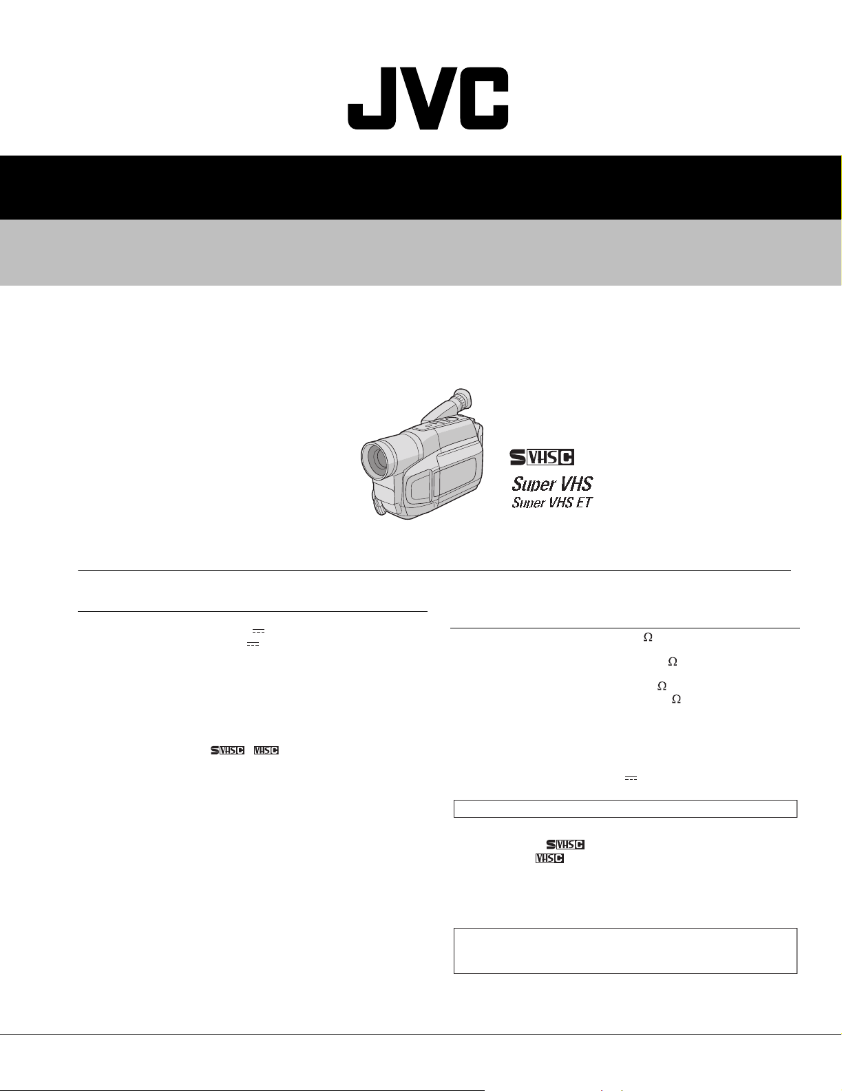
GR-SXM250US,GR-SXM750U
C
GR-SXM750US,GR-SXM755UC,GR-SXM755U
For disassembling and assembling of MECHANISM ASSEMBLY, refer to the SERVICE MANUAL No.86700 (MECHANISM ASSEMBLY).
SPECIFICATION (The specifications shown pertain specifically to the model GR-SXM755)
Camcorder
General
Format : S-VHS/VHS NTSC standard
Power source : DC 11 V (Using AC Adapter)
Power consumption
Viewfinder on :4.5 W
LCD monitor on
Video light :3.0 W
Signal system :NTSC-type
Video recording system
Luminance : FM recording
Colour : Converted sub-carrier direct recording
Cassette : / cassette
Tape speed
SP : 33.35 mm/sec. (1-5/16 ips)
LP : 11.12 mm/sec. (7/16 ips)
Recording time (max.)
SP : 40 minutes
LP : 120 minutes (with TC-40 cassette)
Operating
temperature : 0ºC to 40ºC (32ºF to 140ºF)
Operating humidity : 35% to 80%
Storage temperature : -20ºC to 50ºC (-4ºF to 122ºF)
Weight : Approx. 870 g
Dimensions (W x H x D) : 113 mm x 117 mm x 199 mm
Pickup
Lens : F1.6, f = 2.7 mm to 43.2 mm,
Viewfinder : Electronic viewfinder with 0.5" black/white CRT
White balance
adjustment
DC 6 V (Using battery pack)
:5.0 W
Conforms to VHS standard
(4-1/2" x 4-5/8" x 7-7/8")
: 1/6" format CCD
16:1 power zoom lens with auto iris and
macro control, filter diameter 40.5 mm
: Auto/Manual adjustment
LCD monitor
Speaker
Connectors
Video : 1 V (p-p), 75 unbalanced, analog output
Audio : 300 mV (rms), 1 k , analog output
S-Video
Power requirement
U.S.A and Canada
Other countries : AC 110 V to 240 V ~, 50 Hz/60 Hz
Output : DC 11 V , 1 A
Optional Accessories
• Battery Packs BN-V12U, BN-V20U, BN-V400U
• Compact S-VHS (
• Compact VHS (
• Active Carrying Bag CB-V7U
• Cassette Adapter C-P7U
• A/V (Audio/Video) Cable
• S-Video cable
Some accessories are not available in some areas.
Please consult your nearest JVC dealer for details on accessories and
their availability.
: 3.5" diagonally measured, LCD
: Monaural
(via Video output connector)
(via Audio output connector)
: Y: 1 V (p-p), 75 , analog output
C: 0.29 V (p-p), 75 , analog output
AC Adapter
: AC 120 V ~, 60 Hz
) Cassettes ST-C-40/30/20
) Cassettes TC-40/30/20
S
GR-SXM250US,GR-SXM750UC,GR-SXM750US,GR-SXM755UC,GR-SXM755US M3C623,M3C643
COPYRIGHT © 2003 VICTOR COMPANY OF JAPAN, LTD.
No.86721
2003/02
Page 2

TABLE OF CONTENTS
1 PRECAUTIONS. . . . . . . . . . . . . . . . . . . . . . . . . . . . . . . . . . . . . . . . . . . . . . . . . . . . . . . . . . . . . . . . . . . . . . . . . . . . . . . . . . . 1-3
1.1 SAFTY PRECAUTIONS . . . . . . . . . . . . . . . . . . . . . . . . . . . . . . . . . . . . . . . . . . . . . . . . . . . . . . . . . . . . . . . . . . . . . .1-3
2 SPECIFIC SERVICE INSTRUCTIONS . . . . . . . . . . . . . . . . . . . . . . . . . . . . . . . . . . . . . . . . . . . . . . . . . . . . . . . . . . . . . . . . .1-5
2.1 BEFORE ASSEMBLY AND DISASSEMBLY . . . . . . . . . . . . . . . . . . . . . . . . . . . . . . . . . . . . . . . . . . . . . . . . . . . . . .1-5
2.2 ASSEMBLY AND DISASSEMBLY OF CABINET PARTS . . . . . . . . . . . . . . . . . . . . . . . . . . . . . . . . . . . . . . . . . . . .1-6
2.3 ASSEMBLY AND DISASSEMBLY OF CAMERA SECTION AND BOARD ASSEMBLY . . . . . . . . . . . . . . . . . . . .1-10
2.4 ASSEMBLY AND DISASSEMBLY OF [7]MONITOR ASSEMBLY (CABINET PARTS) . . . . . . . . . . . . . . . . . . . . .1-12
2.5 ASSEMBLY AND DISASSEMBLY OF [2]OP BLOCK ASSEMBLYCCD BOARD ASSEMBLY
(CAMERA SECTION AND BOARD ASSEMBLY). . . . . . . . . . . . . . . . . . . . . . . . . . . . . . . . . . . . . . . . . . . . . . . . . .
2.6 EMERGENCY DISPLAY. . . . . . . . . . . . . . . . . . . . . . . . . . . . . . . . . . . . . . . . . . . . . . . . . . . . . . . . . . . . . . . . . . . . .1-15
2.7 AUTOMATIC DEMONSTRATION . . . . . . . . . . . . . . . . . . . . . . . . . . . . . . . . . . . . . . . . . . . . . . . . . . . . . . . . . . . . .1-15
2.8 TAKE OUT CASSETTE TAPE . . . . . . . . . . . . . . . . . . . . . . . . . . . . . . . . . . . . . . . . . . . . . . . . . . . . . . . . . . . . . . . .1-17
2.9 SERVICE NOTE . . . . . . . . . . . . . . . . . . . . . . . . . . . . . . . . . . . . . . . . . . . . . . . . . . . . . . . . . . . . . . . . . . . . . . . . . . .1-18
3 ADJUSTMENT . . . . . . . . . . . . . . . . . . . . . . . . . . . . . . . . . . . . . . . . . . . . . . . . . . . . . . . . . . . . . . . . . . . . . . . . . . . . . . . . . .1-19
3.1 PREPARATION . . . . . . . . . . . . . . . . . . . . . . . . . . . . . . . . . . . . . . . . . . . . . . . . . . . . . . . . . . . . . . . . . . . . . . . . . . .1-19
3.2 TOOLS REQUIRED FOR ADJUSTMENT . . . . . . . . . . . . . . . . . . . . . . . . . . . . . . . . . . . . . . . . . . . . . . . . . . . . . . .1-19
3.3 MECHANISM ADJUSTMENT . . . . . . . . . . . . . . . . . . . . . . . . . . . . . . . . . . . . . . . . . . . . . . . . . . . . . . . . . . . . . . . . .1-21
3.4 ELECTRICAL ADJUSTMENT. . . . . . . . . . . . . . . . . . . . . . . . . . . . . . . . . . . . . . . . . . . . . . . . . . . . . . . . . . . . . . . . .1-24
CHARTS AND DIAGRAMS
BOARD INTERCONNECTIONS . . . . . . . . . . . . . . . . . . . . . . . . . . . . . . . . . . . . . . . . . . . . . . . . . . . . . . . . . . . . . . . . 2-3
CPU SCHEMATIC DIAGRAM. . . . . . . . . . . . . . . . . . . . . . . . . . . . . . . . . . . . . . . . . . . . . . . . . . . . . . . . . . . . . . . . . . 2-5
M.MDA SCHEMATIC DIAGRAM . . . . . . . . . . . . . . . . . . . . . . . . . . . . . . . . . . . . . . . . . . . . . . . . . . . . . . . . . . . . . . . 2-7
ASP SCHEMATIC DIAGRAM . . . . . . . . . . . . . . . . . . . . . . . . . . . . . . . . . . . . . . . . . . . . . . . . . . . . . . . . . . . . . . . . . . 2-9
DSP SCHEMATIC DIAGRAM. . . . . . . . . . . . . . . . . . . . . . . . . . . . . . . . . . . . . . . . . . . . . . . . . . . . . . . . . . . . . . . . . 2-11
F/Z/I/MDA SCHEMATIC DIAGRAM . . . . . . . . . . . . . . . . . . . . . . . . . . . . . . . . . . . . . . . . . . . . . . . . . . . . . . . . . . . . 2-13
V OUT SCHEMATIC DIAGRAM . . . . . . . . . . . . . . . . . . . . . . . . . . . . . . . . . . . . . . . . . . . . . . . . . . . . . . . . . . . . . . . 2-15
TG/CDS SCHEMATIC DIAGRAM. . . . . . . . . . . . . . . . . . . . . . . . . . . . . . . . . . . . . . . . . . . . . . . . . . . . . . . . . . . . . . 2-17
REG SCHEMATIC DIAGRAM . . . . . . . . . . . . . . . . . . . . . . . . . . . . . . . . . . . . . . . . . . . . . . . . . . . . . . . . . . . . . . . . 2-19
LCD SCHEMATIC DIAGRAM . . . . . . . . . . . . . . . . . . . . . . . . . . . . . . . . . . . . . . . . . . . . . . . . . . . . . . . . . . . . . . . . . 2-21
BW/VF SCHEMATIC DIAGRAM. . . . . . . . . . . . . . . . . . . . . . . . . . . . . . . . . . . . . . . . . . . . . . . . . . . . . . . . . . . . . . . 2-23
JACK SCHEMATIC DIAGRAM . . . . . . . . . . . . . . . . . . . . . . . . . . . . . . . . . . . . . . . . . . . . . . . . . . . . . . . . . . . . . . . . 2-25
SPEAKER SCHEMATIC DIAGRAM . . . . . . . . . . . . . . . . . . . . . . . . . . . . . . . . . . . . . . . . . . . . . . . . . . . . . . . . . . . . 2-27
MONITOR SCHEMATIC DIAGRAM . . . . . . . . . . . . . . . . . . . . . . . . . . . . . . . . . . . . . . . . . . . . . . . . . . . . . . . . . . . . 2-29
E. VF CHEMATIC DIAGRAM . . . . . . . . . . . . . . . . . . . . . . . . . . . . . . . . . . . . . . . . . . . . . . . . . . . . . . . . . . . . . . . . . 2-31
TOP OPE UNIT, ZOOM UNIT, REAR UNIT AND SENSOR SCHEMATIC DIAGRAMS . . . . . . . . . . . . . . . . . . . . 2-33
MAIN CIRCUIT BOARD . . . . . . . . . . . . . . . . . . . . . . . . . . . . . . . . . . . . . . . . . . . . . . . . . . . . . . . . . . . . . . . . . . . . . 2-35
COMPONENT PARTS LOCATION GUIDE <MAIN> YB10400-01-02. . . . . . . . . . . . . . . . . . . . . . . . . . . . . . . . . . 2-37
MAIN CIRCUIT BOARD . . . . . . . . . . . . . . . . . . . . . . . . . . . . . . . . . . . . . . . . . . . . . . . . . . . . . . . . . . . . . . . . . . . . . 2-39
MONITOR CIRCUIT BOARD . . . . . . . . . . . . . . . . . . . . . . . . . . . . . . . . . . . . . . . . . . . . . . . . . . . . . . . . . . . . . . . . . 2-41
CCD CIRCUIT BOARD . . . . . . . . . . . . . . . . . . . . . . . . . . . . . . . . . . . . . . . . . . . . . . . . . . . . . . . . . . . . . . . . . . . . . . 2-45
E.VF CIRCUIT BOARD. . . . . . . . . . . . . . . . . . . . . . . . . . . . . . . . . . . . . . . . . . . . . . . . . . . . . . . . . . . . . . . . . . . . . . 2-45
WAVEFORMS. . . . . . . . . . . . . . . . . . . . . . . . . . . . . . . . . . . . . . . . . . . . . . . . . . . . . . . . . . . . . . . . . . . . . . . . . . . . . 2-46
VOLTAGE CHARTS . . . . . . . . . . . . . . . . . . . . . . . . . . . . . . . . . . . . . . . . . . . . . . . . . . . . . . . . . . . . . . . . . . . . . . . . 2-47
POWER SYSTEM BLOCK DIAGRAM . . . . . . . . . . . . . . . . . . . . . . . . . . . . . . . . . . . . . . . . . . . . . . . . . . . . . . . . . . 2-49
CPU/MDA SYSTEM BLOCK DIAGRAM . . . . . . . . . . . . . . . . . . . . . . . . . . . . . . . . . . . . . . . . . . . . . . . . . . . . . . . . . 2-51
CAMERA AND Y/C SYSTEM BLOCK DIAGRAM . . . . . . . . . . . . . . . . . . . . . . . . . . . . . . . . . . . . . . . . . . . . . . . . . 2-53
MONITOR SYSTEM BLOCK DIAGRAM . . . . . . . . . . . . . . . . . . . . . . . . . . . . . . . . . . . . . . . . . . . . . . . . . . . . . . . . 2-57
PARTS LIST
1. EXPLODED VIEW . . . . . . . . . . . . . . . . . . . . . . . . . . . . . . . . . . . . . . . . . . . . . . . . . . . . . . . . . . . . . . . . . . . . . . . . . . . . . 3-1
1.1 PACKING AND ACCESSORY ASSEMBLY <M1> . . . . . . . . . . . . . . . . . . . . . . . . . . . . . . . . . . . . . . . . . . . . . . 3-1
1.2 FINAL ASSEMBLY <M2> . . . . . . . . . . . . . . . . . . . . . . . . . . . . . . . . . . . . . . . . . . . . . . . . . . . . . . . . . . . . . . . . . 3-2
1.3 MECHANISM ASSEMBLY <M3> . . . . . . . . . . . . . . . . . . . . . . . . . . . . . . . . . . . . . . . . . . . . . . . . . . . . . . . . . . . 3-4
1.4 ELECTRONIC VIEWFINDER ASSEMBLY <M4> . . . . . . . . . . . . . . . . . . . . . . . . . . . . . . . . . . . . . . . . . . . . . . . 3-5
1.5 MONITOR ASSEMBLY (2.5 INCH) <M5> [A] . . . . . . . . . . . . . . . . . . . . . . . . . . . . . . . . . . . . . . . . . . . . . . . . . . 3-6
1.6 MONITOR ASSEMBLY (3.5 INCH) <M5> [B,C,D,E]. . . . . . . . . . . . . . . . . . . . . . . . . . . . . . . . . . . . . . . . . . . . . 3-7
2. PARTS LIST. . . . . . . . . . . . . . . . . . . . . . . . . . . . . . . . . . . . . . . . . . . . . . . . . . . . . . . . . . . . . . . . . . . . . . . . . . . . . . . . . . 3-8
PACKING AND ACCESSORY ASSEMBLY <M1> . . . . . . . . . . . . . . . . . . . . . . . . . . . . . . . . . . . . . . . . . . . . . . . . . . 3-8
FINAL ASSEMBLY <M2> . . . . . . . . . . . . . . . . . . . . . . . . . . . . . . . . . . . . . . . . . . . . . . . . . . . . . . . . . . . . . . . . . . . . . 3-8
MECHANISM ASSEMBLY <M4> . . . . . . . . . . . . . . . . . . . . . . . . . . . . . . . . . . . . . . . . . . . . . . . . . . . . . . . . . . . . . . . 3-8
ELECTRONIC VIEWFINDER ASSEMBLY <M4>. . . . . . . . . . . . . . . . . . . . . . . . . . . . . . . . . . . . . . . . . . . . . . . . . . . 3-9
MONITOR ASSEMBLY (2.5 INCH) <M5> . . . . . . . . . . . . . . . . . . . . . . . . . . . . . . . . . . . . . . . . . . . . . . . . . . . . . . . . 3-9
MONITOR ASSEMBLY (3.5 INCH) <M5> . . . . . . . . . . . . . . . . . . . . . . . . . . . . . . . . . . . . . . . . . . . . . . . . . . . . . . . . 3-9
MAIN BOARD ASSEMBLY <01> . . . . . . . . . . . . . . . . . . . . . . . . . . . . . . . . . . . . . . . . . . . . . . . . . . . . . . . . . . . . . . . 3-9
CCD BOARD ASSEMBLY <02> . . . . . . . . . . . . . . . . . . . . . . . . . . . . . . . . . . . . . . . . . . . . . . . . . . . . . . . . . . . . . . . 3-15
MONITOR BOARD ASSEMBLY <07> . . . . . . . . . . . . . . . . . . . . . . . . . . . . . . . . . . . . . . . . . . . . . . . . . . . . . . . . . . 3-15
E.VF BOARD ASSEMBLY <60>. . . . . . . . . . . . . . . . . . . . . . . . . . . . . . . . . . . . . . . . . . . . . . . . . . . . . . . . . . . . . . . 3-16
1-14
GR-SXM250US GR-SXM750UC/GR-SXM750US GR-SXM755UC/GR-SXM755US
LCD MONITOR 2.5 INCH 3.5 INCH
BODY COLOR SILVER METALLIC BLUE
Page 3
SECTION 1
r
e
PRECAUTIONS
1.1 SAFTY PRECAUTIONS
Prior to shipment from the factory, JVC products are strictly inspected to conform with the recognized product safety and electrical codes of the countries in which they are to be
sold.However,in order to maintain such compliance, it is equally
important to implement the following precautions when a set is
being serviced.
1.1.1 Precautions during Servicing
(1) Locations requiring special caution are denoted by labels
and inscriptions on the cabinet, chassis and certain parts of
the product.When performing service, be sure to read and
comply with these and other cautionary notices appearing in
the operation and service manuals.
(2) Parts identified by the symbol and shaded ( ) parts
are critical for safety.
Replace only with specified part numbers.
NOTE :
Parts in this category also include those specified to
comply with X-ray emission standards for products
using cathode ray tubes and those specified for compliance with various regulations regarding spurious
radiation emission.
(3) Fuse replacement caution notice.
Caution for continued protection against fire hazard.
Replace only with same type and rated fuse(s) as specified.
(4) Use specified internal wiring. Note especially:
• Wires covered with PVC tubing
• Double insulated wires
• High voltage leads
(5) Use specified insulating materials for hazardous live parts.
Note especially:
• Insulation Tape
• PVC tubing
•Spacers
• Insulation sheets for transistors
• Barrier
(6) When replacing AC primary side components (transformers,
power cords, noise blocking capacitors, etc.) wrap ends of
wires securely about the terminals before soldering.
ray tubes and other parts with only the specified parts. Under
no circumstances attempt to modify these circuits.Unauthorized modification can increase the high voltage value and
cause X-ray emission from the cathode ray tube.
(12) Crimp type wire connector
In such cases as when replacing the power transformer in
sets where the connections between the power cord and
power trans former primary lead wires are performed using
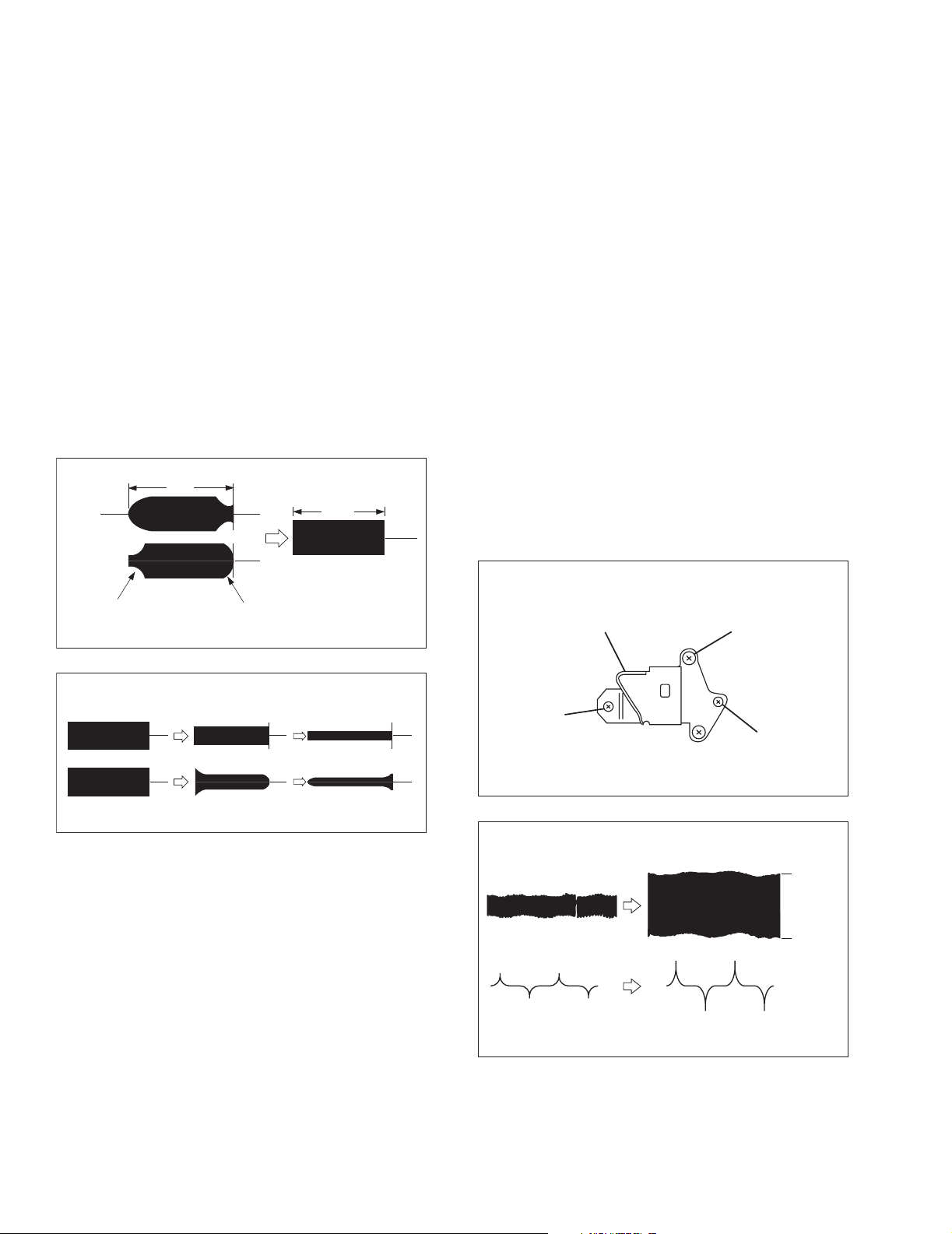
crimp type connectors, if replacing the connectors is unavoidable, in order to prevent safety hazards, perform carefully and precisely according to the following steps.
• Connector part number :E03830-001
• Required tool : Connector crimping tool of the proper
type which will not damage insulated parts.
• Replacement procedure
a) Remove the old connector by cutting the wires at a
point close to the connector.
Important : Do not reuse a connector (discard it).
cut close to connector
Fig.3
b) Strip about 15 mm of the insulation from the ends of
the wires. If the wires are stranded, twist the strands
to avoid frayed conductors.
15 mm
Fig.4
c) Align the lengths of the wires to be connected. Insert
the wires fully into the connector.
Metal sleeve
(7) Observe that wires do not contact heat producing parts
Fig.1
(heatsinks, oxide metal film resistors, fusible resistors, etc.)
(8) Check that replaced wires do not contact sharp edged or
pointed parts.
(9) When a power cord has been replaced, check that 10-15 kg
of force in any direction will not loosen it.
Power cord
Fig.2
(10) Also check areas surrounding repaired locations.
(11) Products using cathode ray tubes (CRTs)In regard to such
products, the cathode ray tubes themselves, the high voltage circuits, and related circuits are specified for compliance
with recognized codes pertaining to X-ray emission. Consequently, when servicing these products, replace the cathode
Connector
Fig.5
d) As shown in Fig.6, use the crimping tool to crimp the
metal sleeve at the center position. Be sure to crimp
fully to the complete closure of the tool.
1.2
5
2
.0
5.5
Crimping tool
Fig.6
e) Check the four points noted in Fig.7.
Not easily pulled free
Wire insulation recessed
more than 4 mm
Crimped at approx. cente
of metal sleev
Conductors extended
Fig.7
(No.86721)1-3
Page 4
1.1.2 Safety Check after Servicing
Examine the area surrounding the repaired location for damage
or deterioration. Observe that screws, parts and wires have been
returned to original positions, Afterwards, perform the following
tests and confirm the specified values in order to verify compliance with safety standards.
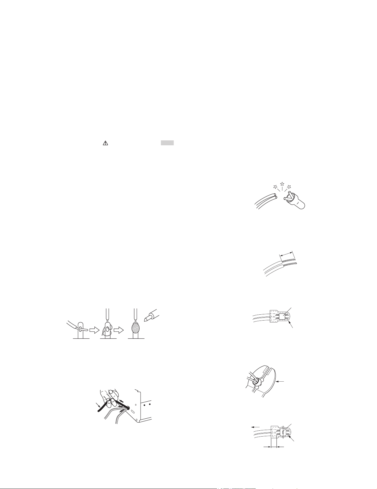
(1) Insulation resistance test
Confirm the specified insulation resistance or greater between power cord plug prongs and externally exposed
parts of the set (RF terminals, antenna terminals, video and
audio input and output terminals, microphone jacks, earphone jacks, etc.).
See table 1 below.
(2) Dielectric strength test
Confirm specified dielectric strength or greater between
power cord plug prongs and exposed accessible parts of
the set (RF terminals, antenna terminals, video and audio
input and output terminals, microphone jacks, earphone
jacks, etc.). See Fig.11 below.
(3) Clearance distance
When replacing primary circuit components, confirm specified clearance distance (d), (d') between soldered terminals, and between terminals and surrounding metallic
parts. See Fig.11 below.
(4) Leakage current test
Confirm specified or lower leakage current between earth
ground/power cord plug prongs and externally exposed accessible parts (RF terminals, antenna terminals, video and
audio input and output terminals, microphone jacks, earphone jacks, etc.).
Measuring Method : (Power ON)
Insert load Z between earth ground/power cord plug
prongs and externally exposed accessible parts. Use an
AC voltmeter to measure across both terminals of load Z.
See Fig.9 and following Fig12.
ab
Externally
exposed
accessible part
Z
V
c
A
Fig.9
(5) Grounding (Class 1 model only)
Confirm specified or lower grounding impedance between
earth pin in AC inlet and externally exposed accessible
parts (Video in, Video out, Audio in, Audio out or Fixing
screw etc.).
Measuring Method:
Connect milli ohm meter between earth pin in AC inlet and
exposed accessible parts. See Fig.10 and grounding specifications.
Fig.8
Fig.10
Fig.11
Fig.12
NOTE :
These tables are unofficial and for reference only. Be sure to confirm the precise values for your particular country and locality.
1-4 (No.86721)
Page 5
SPECIFIC SERVICE INSTRUCTIONS
2.1 BEFORE ASSEMBLY AND DISASSEMBLY
2.1.1 Precautions
1. Be sure to disconnect the power supply unit prior to mounting and soldering of parts.
2. Prior to removing a component part that needs to disconnect
its connector(s) and its screw(s), first disconnect the wire(s)
from the connector(s), and then remove the screw(s).
3. When connecting/disconnecting wires, pay enough attention not to damage the connectors.
4. Be careful in removing or handling the part to which some
spacer or shield is attached for reinforcement or insulation.
5. When replacing chip parts (especially IC parts), first remove
the solder completely to prevent peeling of the pattern.
6. Tighten screws properly during the procedures. Unless
specified otherwise, tighten screws at a torque of
0.196N•m (2.0kgf•cm).
2.1.2 Assembly and disassembly
[Example]
STEP
No.
[1]
[2]
[3]
[4]
PART
LOWER CASE ASSEMBLY
B/W VF ASSEMBLY
TOP OPE UNIT
CASE COVER(S) ASSEMBLY
CASE COVER(M) ASSEMBLY
Fig.
No.
Fig.C1
Fig.C2
POINT
8(S1),CN1a,b,c
3(S2)
CN3,L3a,2(L3b)
(S4),2(L4)
SECTION 2
2.1.4 Disconnection of connectors (Wires)
Pull both ends of the connector in the arrow direction, remove the
lock and disconnect the flat wire.
Flat wire
Connector
Fig.2-1-1
Extend the locks in the direction of the arrow for unlocking and
then pull out the wire. After removing the wire, immediately restore the locks to their original positions because the locks are
apt to come off the connector.
NOTE
Flat wire
-
-
-
-
(4) (5)(2) (3)(1)
(1) Order of steps in Procedure
When reassembling, preform the step(s) in the reverse
order. These numbers are also used as the identification
(location) No. of parts Figures.
(2) Part to be removed or installed.
(3) Fig. No. showing Procedure or Part Location.
C = CABINET
D = CAMERA AND BOARD ASSEMBLY
(4) Identification of part to be removed, unhooked, unlocked,
released, unplugged, unclamped or unsoldered.
P= Spring
W= Washer
S= Screw
* = Unhook, unlock, release, unplug or unsolder.
2(S3) = 2 Screws (S3)
CN = Connector
(5) Adjustment information for installation.
2.1.3 Destination of connectors
Two kinds of double-arrows in connection tables respectively
show kinds of connector/wires.
: Flat wire
: Wire
[Example]
CONN.
No.
CN1a MAIN CN27 2
CONNECTOR
SPEAKER
Pin No.
-
Remove the parts marked in .
Connector
Fig.2-1-2
2.1.5 Tools required for disassembly and assembly
1
3
Torque driver
YTU94088
Cleaning cloth
KSMM-01
2
Bit
YTU94088-003
Fig.2-1-3
1.Torque driver
Be sure to use to fastening the mechanism and exterior parts
because those parts must strictly be controlled for tightening
torque.
2.Bit
This bit is slightly longer than those set in conventional torque
drivers.
3.Cleaning cloth
Recommended cleaning cloth to wipe down the video heads,
mechanism (tape transport system), optical lens surface.
(No.86721)1-5
Page 6
2.2 ASSEMBLY AND DISASSEMBLY OF CABINET PARTS
2.2.1 Disassembly flow chart
This flowchart indicates the disassembly step for the cabinet
parts and board assembly in order to gain access to item(s) to be
serviced. When reassembling, perform the step(s) in reverse order.
[1]
LOWER CASE ASSEMBLY
[2]
[3]
[4]
[4]
CASE COVER(M) ASSEMBLY
[5]
UPPER CASE (S) ASSEMBLY
[5]
UPPER CASE (M) ASSEMBLY
TOP OPE UNIT
CASE COVER(S) ASSEMBLY
B/W VF ASSEMBLY
Inc. MONITOR ASSEMBLY
NOTE:
MONITOR MODEL ONLY
[6]
COVER (UPPER/M) ASSEMBLY
[7]
MONITOR ASSEMBLY
[8]
FRONT COVER ASSEMBLY
Inc. DC LIGHT,MIC
[9]
DC LIGHT ASSEMBLY
[11]
[10]
FRONT FRAME SA
MIC
2.2.2 Disassembly method
STEP
No.
[1]
[2]
[3]
[4]
[5]
[6]
[7]
[8]
[9]
[10]
[11]
CONN.
No.
CN1a
CN1b
CN1c
CN3
CN5
CN8a
CN8b
PART
LOWER CASE ASSEMBLY
B/W VF ASSEMBLY
TOP OPE UNIT
CASE COVER(S) ASSEMBLY
CASE COVER(M) ASSEMBLY
UPPER CASE (S) ASSEMBLY
UPPER CASE (M) ASSEMBLY
Inc. MONITOR ASSEMBLY
COVER (UPPER/M) ASSEMBLY
MONITOR ASSEMBLY
FRONT COVER ASSEMBLY
Inc. DC LIGHT,MIC
DC LIGHT ASSEMBLY
MIC
FRONT FRAME SA
MAIN CN27
MAIN CN13
MAIN CN12
MAIN CN18
MAIN CN16
MAIN CN6
MAIN CN8
Fig.
No.
Fig.C1
Fig.C2
Fig.C3
Fig.C4
Fig.C5
CONNECTOR
POINT
8(S1),CN1a,b,c
3(S2)
CN3,L3a,2(L3b)
(S4),2(L4)
6(S5a),(S5b),(L5)
CN5,6(S5a),(L5)
3(S6),2(L6)
S7a,L7a,SHEET(FPC),2(S7b),L7b
CN8a,CN8b,(S8),L8a,L8b
2(L9)
S10
2(S11)
SPEAKER
ZOOM UNIT
B/W VF ASSEMBLY
TOP OPE UNIT
MONITOR ASSEMBLY
DC LIGHT
MIC
NOTE
-
-
-
-
NOTE 5
-
NOTE 7a,b,c,d
NOTE 8a,b
-
-
NOTE 11
Pin No.
-
2
-
14
3
-
13
-
25
-
2
-
2
Remove the parts marked in .
NOTE 5 :
Take care not to break or damage the FRAME.
NOTE 7a :
Take care not to cut the FPC wire.
NOTE 7b :
Insert and attach the SHEET(FPC) between the MONITOR
FPC and the UPPER CASE(M)ASSEMBLY.
NOTE 7c :
Attachment of the FPC
NOTE 7d :
For disassembly of the MONITOR ASSEMBLY, refer to 2.4
ASSEMBLY AND DISASSEMBLY OF [7]MONITOR ASSEMBLY (CABINET PARTS).
NOTE 8a :
Take care not to damage the OP BLOCK ASSEMBLY when
and after the FRONT CASE ASSEMBLY is removed.
NOTE 8b :
Attachment of the WIRE
NOTE 11 :
There are two types of FRONT FRAME ASSEMBLY.
The two types of the FRONT FRAME ASSEMBLY can be distinguished from each other by their shape.
TYPE B consists of the two parts, namely the tape guide and
the torsion spring.
In exchanging the FRONT FRAME ASSEMBLY, TYPE A can
be exchanged to TYPE B, but TYPE B cannot be exchanged
to TYPE A.
As for the part number, refer to the parts list.
1-6 (No.86721)
Page 7
[3]
L3b
S
E
x
u
t
CN1b
CN1c
D
F
CN1a
10 (S2
11 (S2
L3a
v
D
9 (S2
)
CN3
w
G
z
y
5
(S1)
v
[1]
4
(S1)
y
7
(S1)
w
z
8
(S1)
2
(S1)
p
1
(S1)
E
s1
r
q
F
G
3
(S1)
)
r
)
s
q
p
E
u
t
x
6
(S1)
[2]
Fig.C1
L4
aa
[4]
[4]
<SHOOTING MODEL>
aa
aa
12
(S4)
Fig.C2
<MONITOR MODEL>
(No.86721)1-7
Page 8
<NOTE 5>
[5]
15
(S5a)
16
(S5a)
14
(S5a)
n
m
<SHOOTING MODEL>
g
k
k
24
(S7b)
25
(S7b)
L7b
[7]
<NOTE 7d>
<NOTE 5>
[5]
15
(S5a)
16
(S5a)
e
l
j
17
(S5a)
h
i
j
17
(S5a)
FPC
<NOTE 7a>
23
(S7a)
14
(S5a)
n
18
(S5a)
f
d
c
L7a
<NOTE 7b>
SHEET(FPC)
m
k
[6]
18
(S5a)
g
h
i
e
<MONITOR MODEL>
n
L5
c
C
d
j
Fig.C3
f
c
20
(S6)
21
(S6)
22
(S6)
19
(S5b)
d
L6
m
13
(S5a)
g
C
CN5
k
<MONITOR MODEL>
<NOTE 7c>
DO NOT MAKE FPC
SLACKEN IN THIS PART.
PROCESSED
THROUGH THIS PART.
1-8 (No.86721)
UPPER CASE(M)ASSEMBLY
AS FOR PUSH SW, DON'T BE
BROKEN AND DON'T FLOAT .
(SEE AND CHECK SW AFTER
ATTACHING FPC.)
Fig.C4
INSTALL THE RAINFORCEMENT
BOARD WITH MONITOR OPENED .
( FOR THE DAMAGE PREVENTION
OF PUSH SWITCH .)
Page 9
28
(S11)
<NOTE 11>
26
(S8)
0.118N.m (1.2kgf.cm)
[11]
a
29
OP BLOCK ASSEMBLY
a
(S11)
b
b
SCREWING SEQUENCE
SHOULD BE IN ORDER
HERE FIRST AND OTHERS .
TYPE A TYPE B
<NOTE 8a>
L8a
c
B
CN8b
<NOTE 11>
CN8a
A
L8b
B
c
[8]
A
LIGHT WIRE
SHIELD SHEET
SHOULD BE PUTTED SHIELD
PLATE BETWEEN FRAME TO MECHA .
<NOTE 8b>
MIC WIRE
PASS THE WIRE
BETWEEN
THESE BOSSES.
DO NOT OBSTRUCT
THE RECEIVING
PART OF SENSOR
BY WIRE .
PASS THE WIRE
OUTSIDE OF
THIS BOSS .
[9]
27
(S10)
L9
[10]
Fig.C5
(No.86721)1-9
Page 10
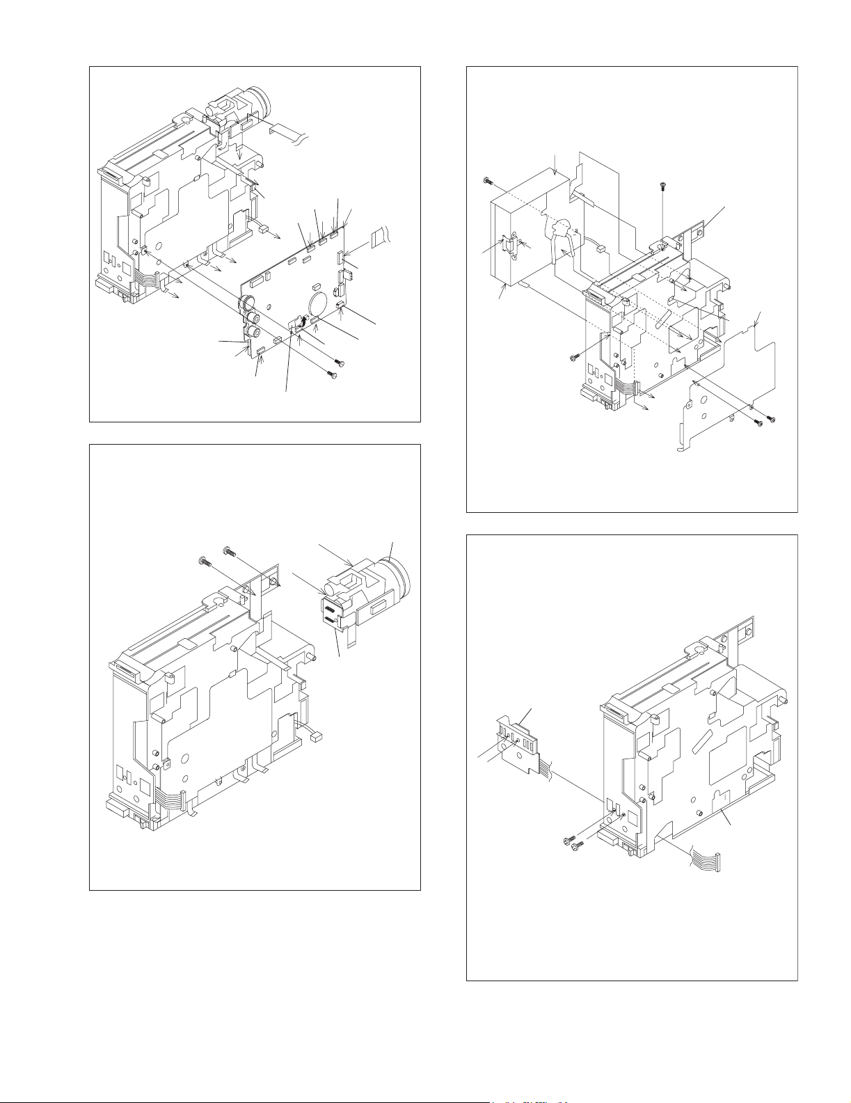
2.3 ASSEMBLY AND DISASSEMBLY OF CAMERA SECTION AND BOARD ASSEMBLY
2.3.1 Disassembly flow chart
This flowchart indicates the disassembly step for the cabinet
parts and board assembly in order to gain access to item(s) to be
serviced. When reassembling, perform the step(s) in reverse order.
NOTE:
Please see Service Manual No. 86700 (MECHANISM ASSY).
[1]
[2]
MAIN BOARD ASSEMBLY
OP BLOCK
ASSEMBLY
[3]
[4]
[5]
MECHANISM
REAR BOARD ASSEMBLY
ASSEMBLY
2.3.2 Disassembly method
STEP
No.
[1]
[2]
[3]
[4]
[5]
CONN.
No.
CN1a
CN1b
CN1c
CN1d
CN1e
CN1f
CN1g
CN1h
CN1j
PART
MAIN BOARD ASSEMBLY
OP BLOCK ASSEMBLY
CCD BOARD ASSEMBLY
MECHANISM ASSEMBLY
REAR BOARD ASSEMBLY
MAIN CN15
MAIN CN4
MAIN CN1
MAIN CN5
MAIN CN2
MAIN CN3
MAIN CN7
MAIN CN22
MAIN CN28
Fig.
No.
Fig.D1
Fig.D2
Fig.D3
Fig.D4
CONNECTOR
Remove the parts marked in .
CCD BOARD ASSEMBLY
POINT
CN1a,b,c,d,e,f,g,h,SHIELD
2(S1),CN1j,L1
2(S2)
(S4a),(S4b),L4
SHIELD CASE(MAIN)
2(S4c),(S4d)
2(S5)
OP BLOCK
LOADING MOTOR
DRUM MOTOR
HEAD(VIDEO,FLY.E)
SENSOR
CAPSTAN MOTOR
A/C HEAD
CCD
REAR UNIT
ASSEMBLY
NOTE
NOTE 3
NOTE 4
Pin No.
-
-
-
-
-
-
-
CN5301
-
-
-
-
24
2
10
11
14
18
11
14
10
NOTE 3 :
For disassembly of the CCD BOARD ASSEMBLY, refer to 2.5
ASSEMBLY AND DISASSEMBLY OF [2]OP BLOCK ASSEMBLY CCD BOARD ASSEMBLY (CAMERA SECTION AND
BOARD ASSEMBLY).
NOTE 4 :
When attaching the MECHANISM ASSEMBLY to S.CASE
(MAIN), pull out the FPC CABLE not to be inserted between
the MECHANISM ASSEMBLY and S.CASE (MAIN).
1-10 (No.86721)
Page 11
A2
G2
CN1j
F2
A2
B2
J
D2
CN1e
SHIELD
Fig.D1
C2
L1
G2
CN1g
CN1f
E2
B2
F2
CN1h
J
C2
D2
CN1d
2
(S1)
E2
(S1)
[1]
CN1a
CN1c
1
CN1b
9
(S4d)
d
[4]
g
c
f
8
(S4c)
7
(S4c)
<NOTE 4>
FRAME ASSEMBLY
c
SHIELD
CASE
(MAIN)
L4
d
f
g
G1
G2
6
5
(S4b)
(S4a)
4
(S2)
3
(S2)
h
Fig.D2
h
j
j
[3]
<NOTE 3>
[2]
Fig.D3
[5]
a
b
a
10
(S5)
b
11
(S5)
FRAME
ASSEMBLY
Fig.D4
(No.86721)1-11
Page 12
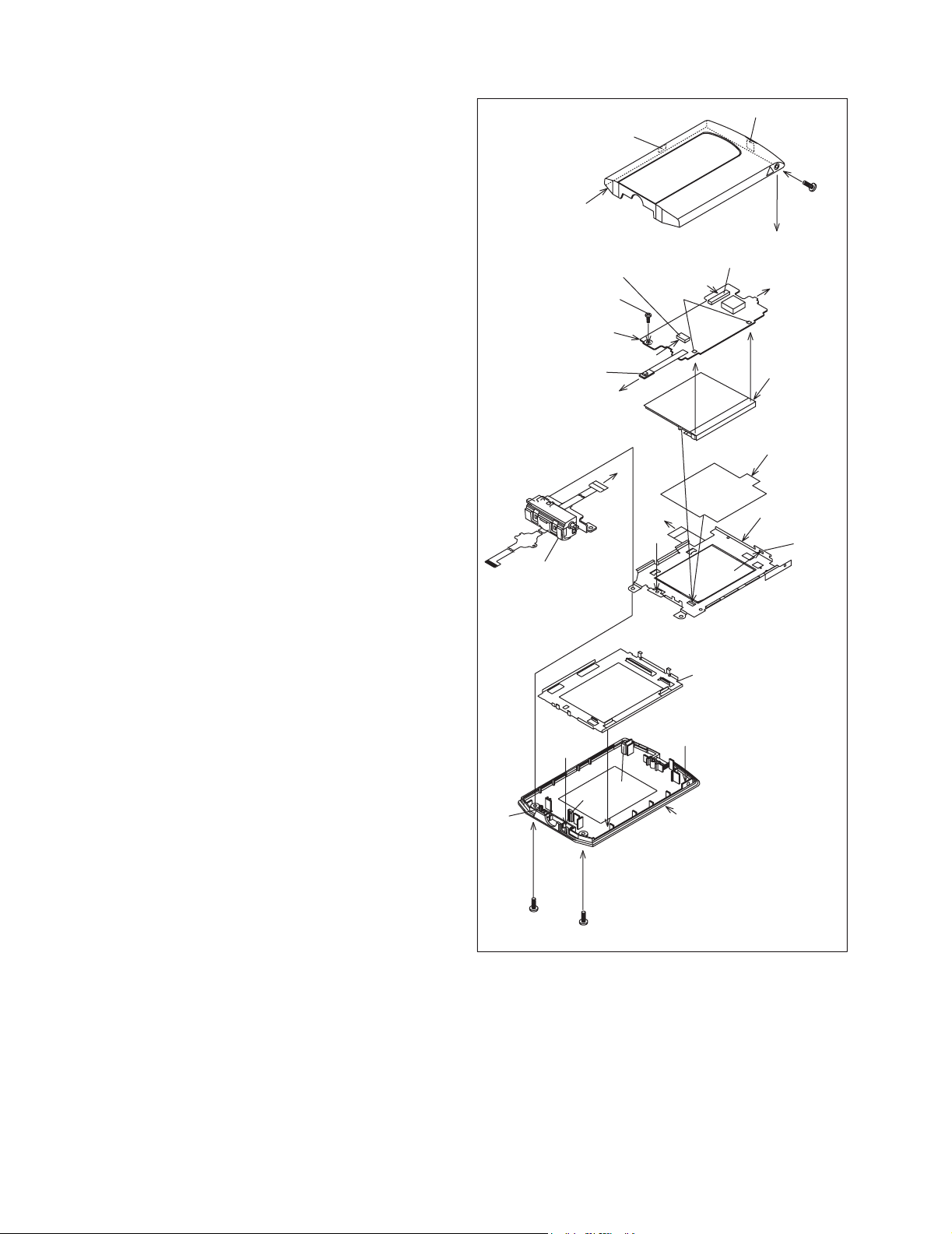
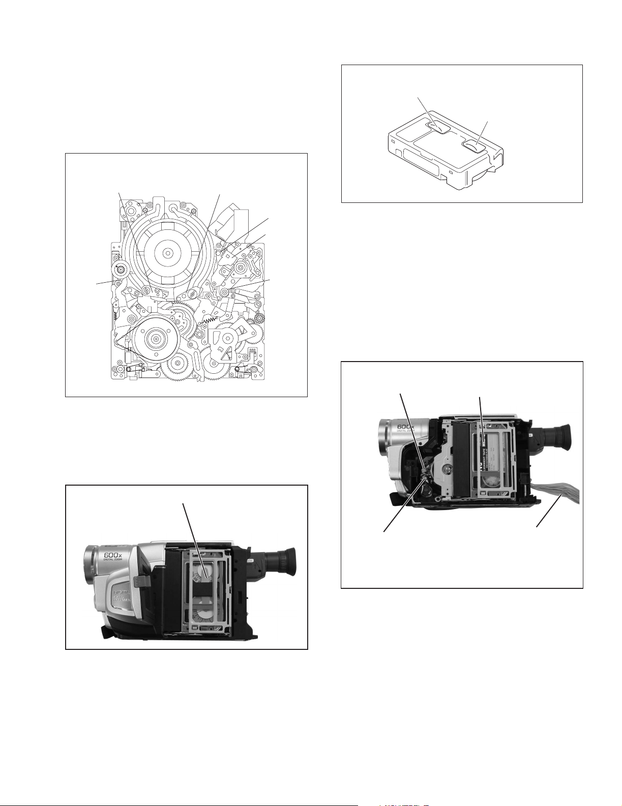
2.4 ASSEMBLY AND DISASSEMBLY OF [7]MONITOR ASSEMBLY (CABINET PARTS)
2.4.1 Disassembly of MONITOR ASSEMBLY <2.5 TYPE>
NOTE :
Be careful not to soil or scratch the monitor screen through the
disassembly/assembly work.
(1) While removing the three screws 1 to 3 in numerical order
and disengaging the two hooks (L7a and L7b) in alphabetical order, remove the MONITOR COVER ASSEMBLY.
NOTE 7a :
After removing the MONITOR COVER ASSEMBLY, be
careful not to damage the FPC and the connector be-
MONITOR COVER
ASSEMBLY
<NOTE 7b>
cause the MONI. HINGE ASSEMBLY moves very easily.
(2) Unlock the connector 7a and then remove the FPC while
lifting the MONI. HINGE ASSEMBLY upwards to remove it
together with the FPC.
NOTE 7b :
When removing the FPC, unlock the connector first and
then lift the MONI. HINGE ASSEMBLY upwards.
MONITOR BOARD
ASSEMBLY
SENSOR BOARD
ASSEMBLY
Accordingly, the FPC is removed together with the
MONI.HINGE ASSEMBLY.
(3) Unsolder the two soldered parts (SD7).
NOTE 7c :
When removing the MONITOR BOARD ASSEMBLY and
the BACK LIGHT together, it is not necessary to unsolder the two soldered parts (SD7).
NOTE 7d :
It depends on the inch size of the monitor assembly
whether the backlight is supplied as an assembly or as
separated parts.
MONI. HINGE
ASSEMBLY
<NOTE 7a>
In replacing the backlight assembly, see the Parts List.
(4) Unlock the connector 7b, and disconnect the FPC from the
connector 7b.
(5) Disconnect the SENSOR BOARD ASSEMBLY from MON-
ITOR CASE ASSEMBLY.
(6) Remove the screw (4), and remove the MONITOR BOARD
ASSEMBLY while lifting the side of MONITOR BOARD AS-
SEMBLY which has been attached with screw (4) upwards.
(7) Remove the BACK LIGHT and DIFF SHEET in this order.
(8) Remove the LCD FRAME&LCD MODULE while disengag-
D1
ing L7e and L7f at the both sides of MONITOR CASE AS-
SEMBLY.
(9) Remove the S.CASE.
L7c
L7e
L7a
CN7a
4
(S7a)
D1
C1
E1
L7f
L7b
<NOTE 7b>
CN7b
<NOTE 7c>
E1
C1
B1
SD7
DIFF SHEET
SHOULD PUT THIS
PART AT RIGHT SIDE .
B1
A1
S.CASE
F1
MONITOR CASE ASSEMBLY
1
(S7a)
F1
A1
<NOTE 7c,d>
BACK LIGHT
ASSEMBLY
LCD FRAME &
LCD MODULE
L7d
1-12 (No.86721)
2
(S7b)
3
(S7b)
Fig.2-4-1
Page 13
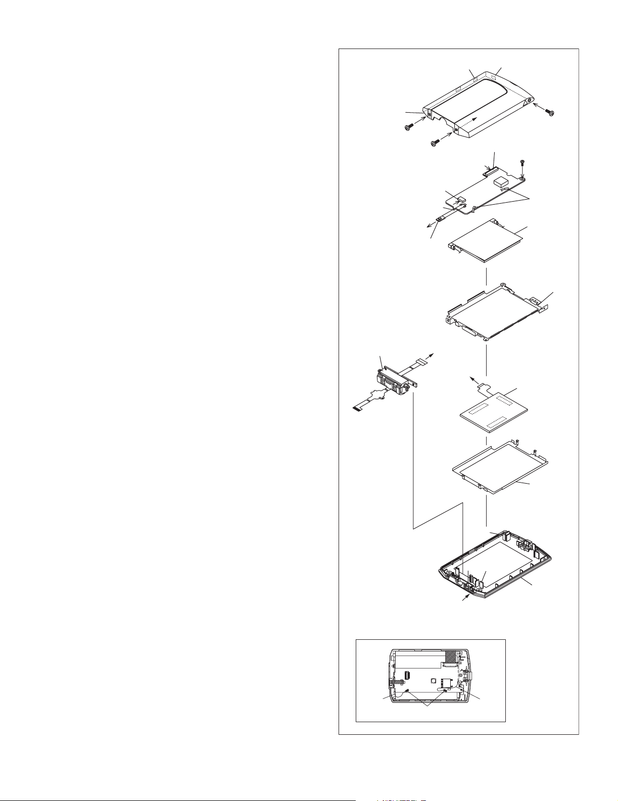
2.4.2 Disassembly of MONITOR ASSEMBLY <3.5 TYPE>
NOTE :
Be careful not to soil or scratch the monitor screen through the
disassembly/assembly work.
(1) While removing the three screws 1 to 3 in numerical order
and disengaging the two hooks (L7a and L7b) in alphabetical order, remove the MONITOR COVER ASSEMBLY.
NOTE 7a :
After removing the MONITOR COVER ASSEMBLY, be
careful not to damage the FPC and the connector because the MONI. HINGE ASSEMBLY moves very easily.
(2) Unlock the connector 7a and then remove the FPC while
lifting the MONI. HINGE ASSEMBLY upwards to remove it
together with the FPC.
NOTE 7b :
When removing the FPC, unlock the connector first and
then lift the MONI. HINGE ASSEMBLY upwards.
Accordingly, the FPC is removed together with the
MONI.HINGE ASSEMBLY.
(3) Unsolder the two soldered parts (SD7).
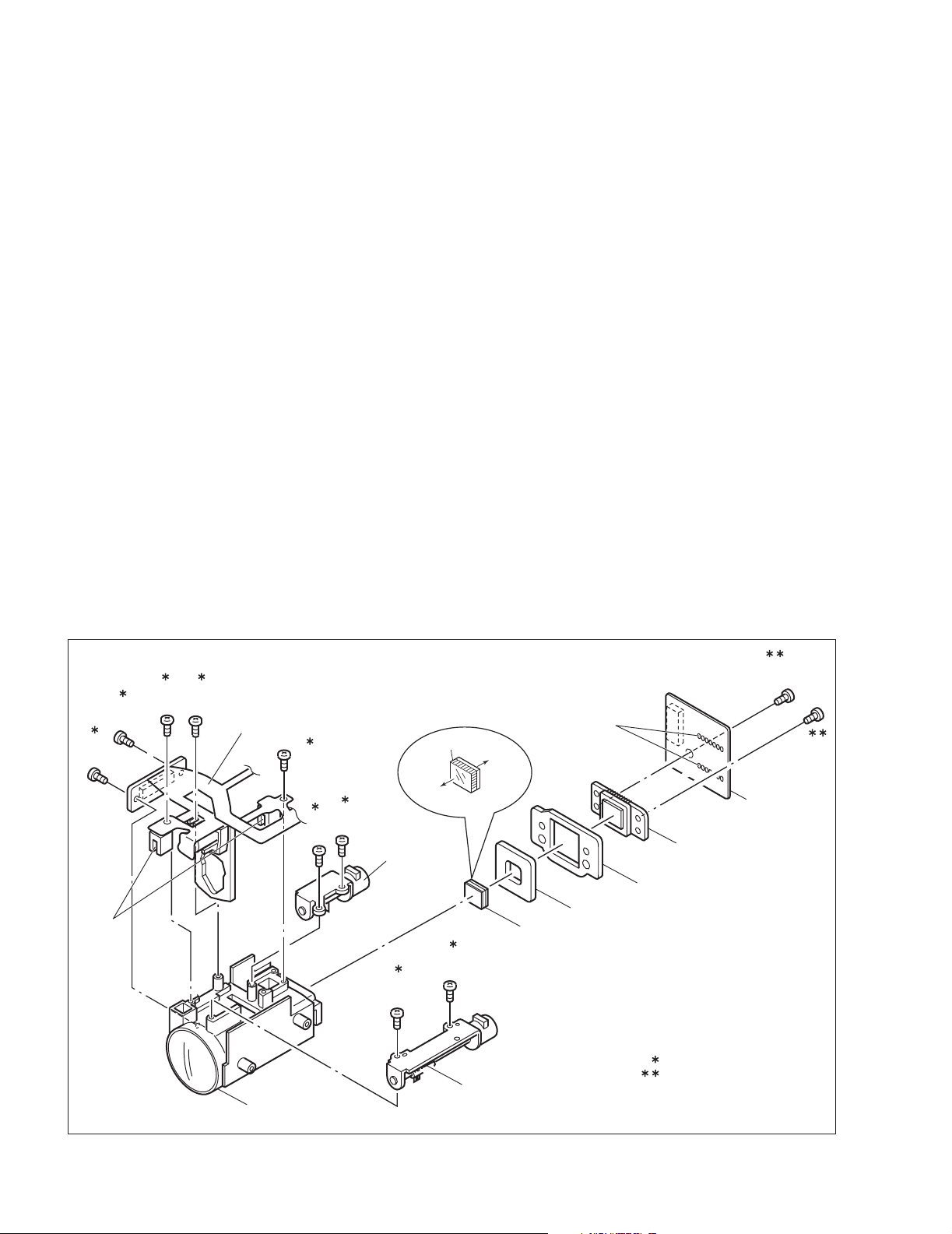
NOTE 7c :
When removing the MONITOR BOARD ASSEMBLY and
the BACK LIGHT together, it is not necessary to unsolder the two soldered parts (SD7).
NOTE 7d :
It depends on the inch size of the monitor assembly
whether the backlight is supplied as an assembly or as
separated parts.
In replacing the backlight assembly, see the Parts List.
NOTE 7e :
Attatchment of the WIRE.
(4) Unlock the connector 7b, and disconnect the FPC from the
connector 7b.
(5) Disconnect the SENSOR BOARD ASSEMBLY from MON-
ITOR CASE ASSEMBLY.
(6) Remove the screw (4), and remove the MONITOR BOARD
ASSEMBLY while lifting the side of MONITOR BOARD AS-
SEMBLY which has been attached with screw (4) upwards.
(7) Remove the BACK LIGHT.
(8) Remove the LCD FRAME&LCD MODULE while disengag-
ing L7e and L7f at the both sides of MONITOR CASE AS-
SEMBLY.
(9) Remove the S.CASE.
MONITOR COVER
ASSEMBLY
2
(S7b)
SENSOR BOARD
ASSEMBLY
<NOTE 7a>
MONI. HINGE
ASSEMBLY
3
(S7b)
<NOTE 7b>
CN7a
L7e
b
a
d
c
L7g
CN7b
L7b
4
(S7a)
f
LCD FRAME
LCD MODULE
1
(S7a)
<NOTE 7c>
SD7
BACK LIGHT
ASSEMBLY
<NOTE 7c,d>
S. CASE
L7a
a
c
<NOTE 7e>
WIRE
SD7
b
d
Fig.2-4-2
L7f
WIRE
MONITOR CASE
ASSEMBLY
(No.86721)1-13
Page 14
2.5 ASSEMBLY AND DISASSEMBLY OF [2]OP BLOCK ASSEMBLY
CCD BOARD ASSEMBLY (CAMERA SECTION AND BOARD ASSEMBLY)
2.5.1 Precautions
2.5.3 Assembly of CCD BASE ASSEMBLY and CCD
(1) Take care in handling the CCD IMAGE SENSOR, OP LPF
and lens components when performing maintenance etc.,
(1) Set the OP LPF to the OP BLOCK ASSEMBLY so that the
especially with regard to surface contamination, attached
dust or scratching. If fingerprints are present on the surface
they should be wiped away using either a silicon paper,
clean chamois or the cleaning cloth.
(2) The CCD IMAGE SENSOR may have been shipped with a
protective sheet attached to the transmitting glass. When
replacing the CCD IMAGE SENSOR, do not peel off this
sheet from the new part until immediately before it is
mounted in the OP BLOCK ASSEMBLY.
(3) The orientation of the OP LPF is an important factor for
installation. If there is some marking on the OP LPF, be
sure to note it down before removing and to reassemble it
very carefully as it was referring to the marking.
2.5.2 Disassembly of CCD BOARD ASSEMBLY and CCD
BASE ASSEMBLY
(1) Unsolder the CCD BOARD ASSEMBLY by the 14 points
(SD2) and then remove it.
(2) Remove the two screws (1, 2) and remove the CCD BASE
ASSEMBLY.
(3) Remove the SPACER.
(4) Remove the SHEET.
(5) Remove the OP LPF.
(2) Set the SHEET to the OP LPF not to come off the right
(3) Attach the SPACER to the OP BLOCK ASSEMBLY.
(4) Fasten them together with the two screws (1, 2).
(5) Set the CCD BOARD ASSEMBLY in the CCD BASE
2.5.4 Replacement of service repair parts
The service repair parts for the OP BLOCK ASSEMBLY are as
listed below.
Before replacement of these parts, remove the BRACKET (OP
BLOCK ASSEMBLY) as required.
Take special care not to disconnect any of the FPC wires or
cause any damage due to soldering (excessive heating).
(1) FOCUS MOTOR
(2) ZOOM MOTOR
(3) IRIS MOTOR UNIT
NOTE 2b:
When replacing the FOCUS MOTOR or the ZOOM MOTOR,
solder the FPC at a space of about 1 mm above the terminal
pin.
NOTE 2c:
The IRIS MOTOR UNIT includes the FPC ASSEMBLY and
two sensors.
BOARD ASSEMBLY
OP side touches the OP BLOCK ASSEMBLY.
NOTE 2a:
Pay careful attention to the orientation of the OP LPF.
position.
ASSEMBLY, and then solder it by the 14 points (SD2).
(S2c)
8
(S2c)
SENSOR
1
11
9
(S2b)
(S2b)
7
IRIS MOTOR UNIT
<NOTE 2b, c>
10
(S2b)
5
(S2b)
OP BLOCK
6
(S2b)
FOCUS MOTOR
<NOTE 2b>
(S2b)
3
<NOTE 2a>
OP LPF
Blue
OP
side
4
(S2b)
CCD
side
OP LPF
ZOOM MOTOR
<NOTE 2b>
(SD2)
SHEET
CCD BASE ASSEMBLY
SPACER
0.078N.m (0.8kgf.cm)
.
0.118N
m (1.2kgf.cm)
(S2a)
2
(S2a)
CCD BAORD
ASSEMBLY
1-14 (No.86721)
Fig.2-5-1
Page 15
2.6 EMERGENCY DISPLAY
Example (in case of the error number E01):
Whenever some abnormal signal is input to the mechacon CPU,
an error number (E01, as an example) is displayed in the electronic view finder. In every error status, such the message as
shown below alternately appear over and over.
E01
UNIT IN
SAFEGUARD MODE
E01
REMOVE AND
REATTACH BATTERY
• In an emergency mode, all operations except turning on/off the
POWER switch are ineffectual.
E. VF Symptom Mode when observed
E07 Short circuit of capstan MDA Power ON
E06 CAPSTAN FG input absent CAPSTAN rotation
E04 DRUM FG input absent DRUM rotation
E03 SUPPLY REEL FG input absent REC, PLAY, SEARCH, FF/REW
E02 Mode control motor rotates for more than 6.0 sec UNLOADING without shift to next
UNLOADING
mode.
E01 Mode control motor rotates for more than 6.0 sec LOADING without shift to next mode. LOADING
E00 Overtime the programming transaction REC, PLAY
2.7 AUTOMATIC DEMONSTRATION
Automatic Demonstration takes place when “DEMO MODE” is
set to “ON” (factory-preset).
(1) Available when the Power Switch is set to “A” or “M” while
pressing down the Lock Button located on the switch.
(2) Performing any operation during the demonstration stops
the demonstration temporarily. If no operation is performed
for more than 1 minute after that, the demonstration will
MENU Wheel
resume.
(3) “DEMO MODE” remains “ON” even if the camcorder power
is turned off.
(4) To cancel Automatic Demonstration, set the Power Switch
to “M” and press the MENU Wheel in while the demo is in
Lock Button
progress. This takes you directly to the demo mode’s Setting Menu (so you will not have to go through the main
Menu Screen). Rotate the MENU Wheel to select “OFF”
and press it.
Power Switch
Fig.2-7-1
NOTE:
• When a tape whose Erase Protection tab is in the position
that allows recording is loaded in the
camcorder, demonstration is not available.
• If you do not detach the Lens Cap, you cannot see the actual
changes of the Automatic Demonstration activated on the
LCD monitor or viewfinder.
* Applicable models only.
(NTSC)
(No.86721)1-15
Page 16
2.7.1 Operation procedure
R
D
N
E
.
ECXZT
M
O
S
O
O
Y
D
M
SETEM ME
SNP
U
TO SCYASMTEERMAMMEEN
N
U
U
TITLE
MO
VIE
EXPOSURE A
UTO
M. W.
B.
A
UTO
1. Set the Power Switch to turn on
the "M".
Press the MENU Wheel once.
The first page of the DISPLAY
appears on the LCD monitor (or in
the viewfinder).
Press the MENU Wheel once.
The second page of the DISPLAY
appears on the LCD monitor (or in
the viewfinder).
2. Press the MENU Wheel once.
The third page of the DISPLAY
appears on the LCD monitor (or in
the viewfinder).
T
O
C
OS
D
OUT P UT O
R
E
C
T
I
N
T
.
T
E
L
E
D
E
M
O
D
A
T
E
Display 1
S
Y
S
T
E
MMMEE
M
A
E
R
A
I
M
E
T
I
M
E
M
A
C
R
O
D
E
M
O
/
T
M
E
I
2.7.2 Flow chart
NOTE:
When demonstration is performed, some of the following functions that a model does not have are omitted.
1. TITLE CALL and FUTURE
2. EASY PC CONNECTION
O
F
F
3. CREATE IMAGES & E-MAIL
4. NIGHT-SCOPE OFF
5. NIGHT-SCOPE ON
6. VHS
7. S-VHS (For S-VHS MODEL ONLY)
N
U
N
U
N
O
F
F
O
F
F
O
F
F
O
F
F
8. SNAP SHOT
9. PROGRAM AE FOG
10. PROGRAM AE ND EFFECT
3. Turn the MENU Wheel in the
direction ofthe arrow to set the
cursor at "DEMO MODE".
Then, press the MENU Wheel
once.
The third page the DEMO
MODE appearson the LCD
monitor (or in the viewfinder).
4. Turn the MENU Wheel in the
direction ofthe arrow to set the
cursor at "ON".
Then, press the MENU Wheel
once.
The fourth page of the DISPLAY
appears on the LCD monitor (or in
the viewfinder).
("DEMO MODE" is switched "ON"
from "OFF" status.)
R
E
T
OFF
ON
EXI T
T
O
C
OS
D
OUT P UT O
R
E
C
T
I
N
T
.
T
E
L
E
M
D
E
O
A
T
E
D
R
E
T
U
U
R
N
Display 2
DEMO MODE
Display 3
S
Y
S
T
E
M
M
A
E
R
A
M
E
I
I
M
T
E
A
C
M
R
O
M
O
D
E
I
T
M
/
E
R
N
Display 4
11. FADE/WIPE BLACK
12. FADE/WIPE MOSAIC
13. FADE/WIPE SHUTTER
14. FADE/WIPE SLIDE
15. FADE/WIPE DOOR
16. FADE/WIPE CORNER
17. FADE/WIPE WINDOW
18. DIGITAL EFFECT NEGA/POSI
19. DIGITAL EFFECT STRETCH
20. DIGITAL EFFECT MOSAIC
21. DIGITAL EFFECT SEPIA
22. DIGITAL EFFECT B/W
23. DIGITAL EFFECT B.FILTER
24. DIGITAL EFFECT R.FILTER
N
U
MEE
U
M
N
N
O
F
F
O
F
F
O
F
F
O
N
25. DIGITAL EFFECT SOLARI
26. DIGITAL EFFECT STROBE
27. DIGITAL EFFECT CLASSIC
28. DIGITAL EFFECT VIDEO ECHO
29. WIDE OFF
30. WIDE ON
5. Press the MENU Wheel once.
The camcorder automatically
enter the DEMONSTRATION
mode and it repeats
demonstration operation.
While the camcorder is performing
demonstration, all operations
except turning on/off the Power
Switch are ineffectual.
1-16 (No.86721)
Fig.2-7-2
Refer to Fig. 2-7-3.
While the DEMONSTRATION
mode is activated, a word of
DEMONSTRATION is appearing
on the screen scrolling from right
to left.
31. WIDE OFF
32. P.STABILIZER OFF
33. P.STABILIZER ON
34. P.STABILIZER OFF
35. P.STABILIZER ON
Fig.2-7-3
Page 17
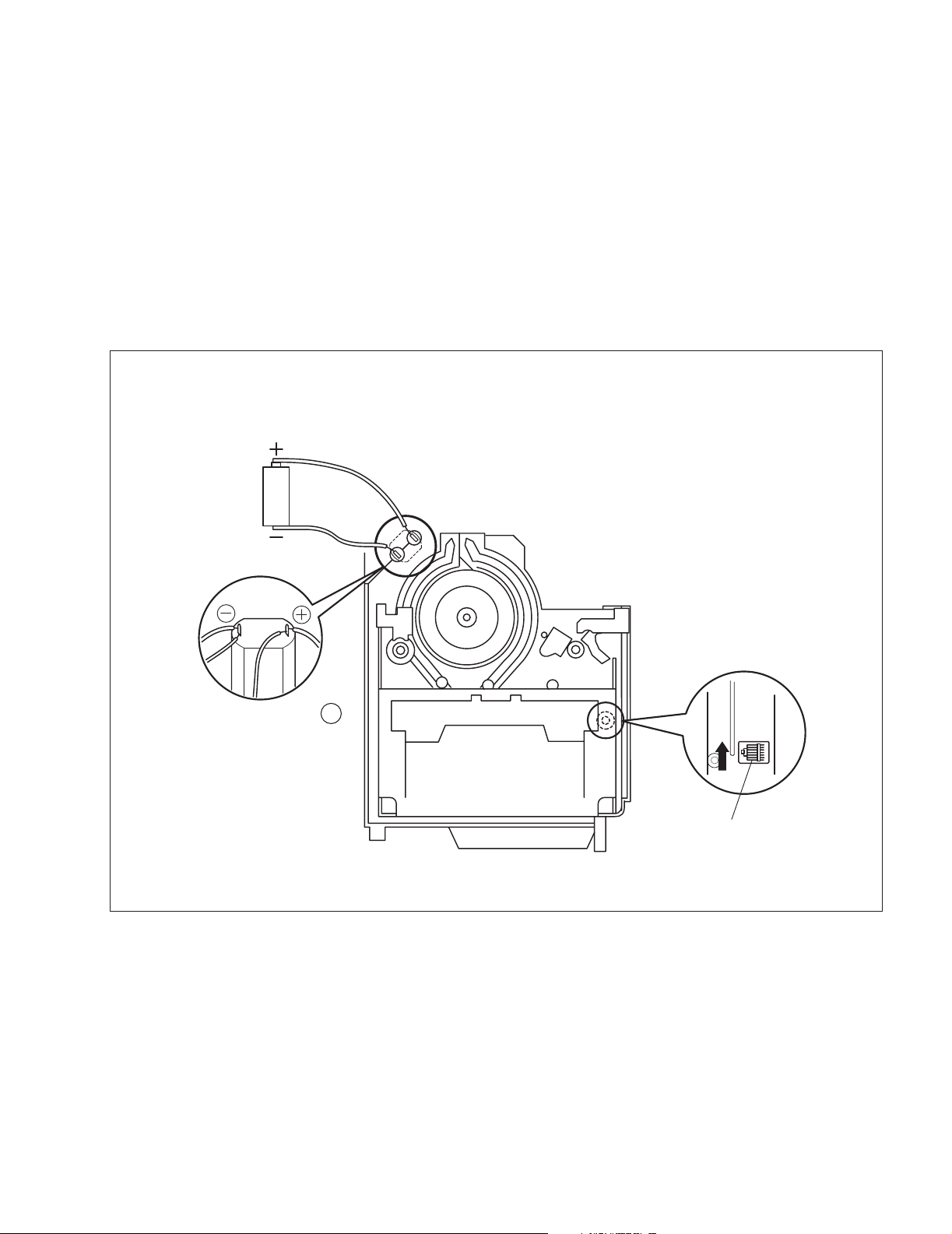
2.8 TAKE OUT CASSETTE TAPE
In the event that the set enters the emergency mode as it is
loaded with a cassette tape and the cassette tape cannot be
ejected with the EJECT button, manually, take it out of the set
according to the following procedure.
NOTE :
• If the mechanism comes into the unloading mode as the cassette tape is not held by hand, it results in tape damage.
(1) Disconnect the set from the power source.
(2) Remove the LOWER CASE ASSEMBLY and TOP OPE
UNIT (see Fig.C1, page 6).
(3) Connect a jumper wire to each pole of the LOADING
MOTOR as shown by the magnified view (Fig. 2-8-1).
BATTERY
(DC1.5V)
(4) While holding down the cassette housing by hand, con-
nect the jumper wires to a battery to run the mechanism
to the EJECT position four unloading. If this unloading
operation is performed as the cassette housing is not
held down by hand, the front lid of the cassette may damage the tape when it is ejected.
(5) For taking in the slack of the tape, run the mechanism to
the EJECT position as the front lid of the cassette is left
open, and turn the TAKE-UP GEAR in the forward direction to wind up the tape. After confirming that the tape
has completely been wound up and the supply reel is
idling, take the cassette tape out of the cassette housing.
MAGNIFIED VIEW
b
TAKE-UP GEAR
Fig.2-8-1
(No.86721)1-17
Page 18
2.9 SERVICE NOTE
Use the following chart to manage screws
[5]
[4]
[3]
[2]
Fig.C3
[2]
Fig.2-5-1
Fig.C2
-
[11]
[5]
Fig.D4
<2.5 OP BLOCK ASSEMBLY>
-
27 28 29
[10]
-
-
-
[9]
[8]
[4]
Fig.D3
Fig.C1
1-18 (No.86721)
[7]
[1]
[6]
<2.2 CABINET PARTS>
Symbol No.
Reference drawing
Place to stick screw -
Screw tightening torque
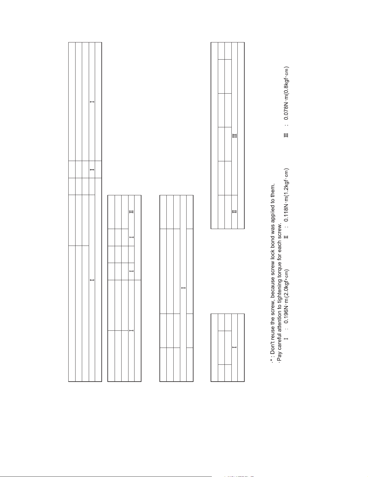
Removing order of screw 1 2 3 4 5 6 7 8 9 10 11 - 12 13 14 15 16 17 18 19
20 21 22 23 24 25 26
Symbol No.
Removing order of screw
**
Fig.C4 Fig.C5
[2]/[3]
[1]
<2.3 CAMERA SECTION AND BOARD ASSEMBLY>
Symbol No.
Reference drawing
Place to stick screw
Screw tightening torque
Removing order of screw 1 2 3 4 5 6 7 8 9 10 11
Fig.D2
[7]
Fig.D1
<2.4 MONITOR ASSEMBLY>
Symbol No. Symbol No.
Reference drawing
Place to stick screw
Screw tightening torque
Removing order of screw 1 2 3 4 Removing order of screw 1 2 3 4 5 6 7 8 9 10 11
Fig.2-4-1,2
<NOTE>
Reference drawing Reference drawing
Place to stick screw Place to stick screw
Screw tightening torque Screw tightening torque
Page 19
SECTION 3
ADJUSTMENT
3.1 PREPARATION
(1) Precaution
This model does not contain adjustment controls (VR).
General deck system, camera system and monitor system
adjustment are not required. However, if MAIN board need
replacement, please use original EEP ROM on to new
board. Then adjustment are not required. And if parts such
as the following need replacement, special computerized
adjustment are required. 3.4.1 ELECTRICAL ADJUSTMENT WITH PERSONAL COMPUTER is setup and it adjusts using a service support system. Please contact to
JVC Service for detail information.
• OP BLOCK
• EEP ROM (IC102 of MAIN board)
• MONITOR
In the event of malfunction with electrical circuits, troubleshooting with the aid of proper test instruments most be
done first, and then commence necessary repair, replacement and adjustment, etc.
a) In case of wiring to chip test points for measurement,
use IC clips, etc. to avoid any stress.
b) Since connectors are fragile, carefully handle them in
disconnecting and connecting.
c) Short circuit between operation unit and DECK chas-
sis.
(2) Required test equipment
a) Color TV monitor.
b) AC power adapter
c) Oscilloscope (dual-trace type, observable 100 MHz
or higher frequency)
• It is recommended to use one observable 300 MHz
or higher frequency.
d) Digital voltmeter
e) Frequency counter (with threshold level adjuster)
f) Personal computer
3.2 TOOLS REQUIRED FOR ADJUSTMENT
Alignment tape
1
Cassette torque meter
3
5
7
9
PUJ50431-2
INF adjustment lens
YTU92001B
Gray scale chart
YTU94133A
INF lens holder
YTU94087
MHP-C
Alignment tape
2
4
6
YTU92001-111
Color bar chart
8
Light box assembly
10
YTU93096A
MHP-LC
Roller driver
PTU94002-2
Conn. ring
YTU94133C
11 12
13
Camera stand
YTU93079
Communication cable
YTU93107A
PC cable
QAM0099-002
14
1615
Fig.3-2-1
Jig connector cable
YTU93082G
Service support system
YTU94057-65
Cleaning cloth
KSMM-01
(No.86721)1-19
Page 20
1,2. Alignment tape
To be used for check and adjustment of interchangeability of
the mechanism.
(Video: Color bar signal, Audio: Non-signal)
3. Cassette torque meter
This is used to cheek the back tension and play torque during
mechanism adjustment.
4. Roller driver
To be used to turn the Roller driver to adjustment of the linearity of playback envelope.
5.INF adjustment lens
To be used for adjustment of the camera system. For the usage of the INF adjustment lens, refer to the Service Bulletin
No. YA-SB-10035.
6.Conn. ring
The connector ring to attach the INF lens to the head of the OP
lens. For the usage of the Conn.ring.
7.Gray scale chart
To be used for adjustment of the camera system. For the usage of the INF adjustment lens, refer to the Service Bulletin
No. YA-SB-10035.
8.Color bar chart
To be used for adjustment of the camera system. For the usage of the INF adjustment lens, refer to the Service Bulletin
No. YA-SB-10035.
9.INF lens holder
To be used together with the Camera stand (11) for operating
the Videocamera in the stripped-down condition such as the
status without the exterior parts or for using commodities that
are not yet conformable to the interchangeable ring. For the
usage of the INF lens holder, refer to the Service Bulletin No.
YA-SB-10035.
10.Light box assembly
To be used for adjustment of the camera system. For the usage of the Light box assembly, refer to the Service Bulletin No.
YA-SB-10035.
11.Camera stand
To be used together with the INF adjustment lens holder. For
the usage of the Camera stand, refer to the Service Bulletin
No. YA-SB-10035.
12. Jig connector cable
To be connected to the Jig connector jack of the main board
and used for measurement and adjustment.
MAIN CN25 JIG BOARD (LABEL)
AL_L3.2V 1 1 AL_L3.2V
MCU_RST 11 2 NC
NC 2 3 DIAL_PB
V_TP_FM 12 4 DIAL_MN
DIAL_PB 3 5 JIGCN_SW
V_FF 13 6 GND
DIAL_MN 4 7 TXD
EJECT_SW 14 8 RXD
JIGCN_SW 5 9 PLI_AD
PB_CTL 15 10 VPP_7.8V
GND 6 11 MCU_RST
GND 16 12 V_TP_FM
TXD 7 13 V_FF
V_OUT 17 14 EJECT_SW
RXD 8 15 PB_CTL
AO_SIG_J 18 16 GND
PLI_AD 9 17 V_OUT
V_OVL 19 18 AO_SIG_J
VPP_7.8V 10 19 V_OVL
DISCHG_L 20 20 DISCHG_L
Fig.3-2-2
13.Communication Cable
Connect the Communication cable between the PC cable and
Jig connector cable when performing a PC adjustment.
14.Service support system
To be used for adjustment with a personal computer. Software
can be downloaded also from JS-net.
15.PC cable
To be used to connect the Videocamera and a personal computer with each other when a personal computer issued for adjustment.
16.Cleaning cloth
Recommended the Cleaning cloth to wipe down the video
heads, mechanism (tape transport system), optical lens surface.
1-20 (No.86721)
Page 21
3.3 MECHANISM ADJUSTMENT
3.3.1 TAPE TRANSPORT ADJUSTMENT
Mechanism adjustment is needed when DRUM ASSEMBLY or a
part of the tape transport system is replaced. To protect tapes
from damage, first clean the tape transport system, next confirm
that nothing is wrong with the tape transport system by using a
tape that can be disposed of, and then perform adjustment with
alignment tape. Some exterior parts should be removed before
some adjustment procedures, depending on the procedures.
BACK TENSION
0.97x10
-3
- 1.71x10⁻³ N•m
(10-17gf·cm)
PLAY TORQUE
1.47x10
-3
- 2.45x10⁻³ N·m
(15-25gf·cm)
POLE BASE (SUP)
(GUIDE ROLLER)
POLE BASE (TU)
(GUIDE ROLLER)
TU GUIDE
POLE
A/C HEAD
ASSEMBLY
TENSION
POLE
PINCH
ROLLER
Fig.3-3-1
3.3.2 Back tension
Remove the exterior parts attached to CASSETTE HOUSING
ASSEMBLY so that scales of CASSETTE TORQUE METER can
be read.
• CASE COVER(S),(M) ASSEMBLY
• C. COVER INSIDE
Fig.3-3-3
3.3.3 Tape pattern
Remove the exterior parts attached to the UPPER CASE
ASSEMBLY so that the guide roller beside the DRUM ASSEMBLY
can be rotated.
• LOWER CASE ASSEMBLY
• TOP OPE UNIT
• CASE COVER(S),(M) ASSEMBLY
• UPPER CASE (S),(M) ASSEMBLY
NOTE:
In performing adjustment, it is recommended that LOWER
CASE ASSEMBLY and TOP OPE UNIT are attached to the
main body for better operation and safety.
POLE BASE (TU)
(GUIDE ROLLER)
ALIGNMENT TAPE
CASSETTE TORQUE METER
Fig.3-3-2
(1) Set a cassette torque meter onto the deck and measure the
back tension in standard PB mode to confirm that the back
tension is 0.97x10
-3
- 1.71x10⁻³ N•m.
(2) If not, replace the tension band.
When the value widely fluctuates in the measurement,
replace the SUPPLY REEL DISK.
(3) With the CASSETTE TORQUE METER, confirm that the
play torque is 1.47x10
-3
- 2.45x10⁻³ N•m.
If necessary, replace the center pulley unit.
POLE BASE (SUP)
(GUIDE ROLLER)
JIG CONNECTOR CABLE
MAIN CN25 - JIG BOARD
12PIN(V_TP_FM)
13PIN(V_FF)
Fig.3-3-4
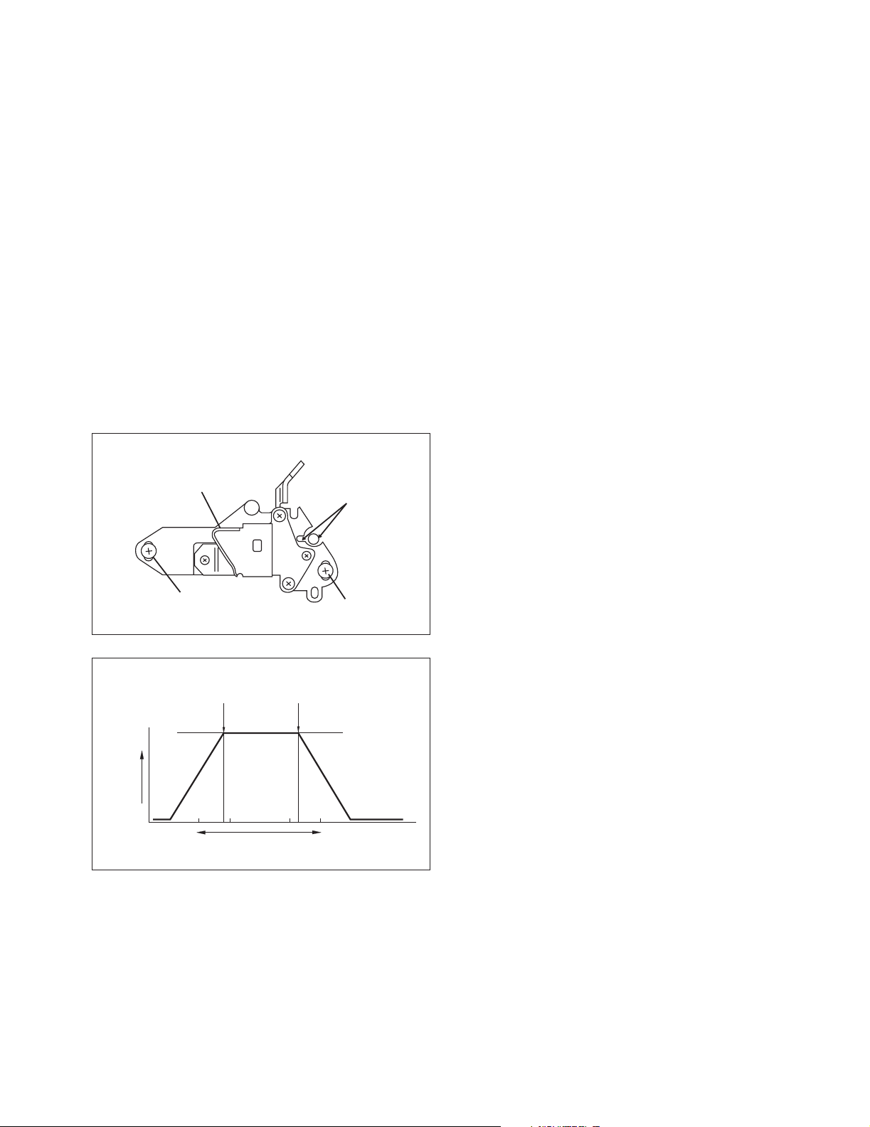
(1) Remove the Cover (JIG) shown on Fig.3-4-1.
(2) Connect the JIG CONNECTOR CABLE to CN25 on the
MAIN BOARD ASSEMBLY as shown on Fig. 3-2-2.
(3) Observe signal at V_TP_FM with external trigger from
V_FF on the JIG CONNECTOR CABLE.
(4) Playback the SP stairstep signal of the alignment tape and
maximize the FM waveform by the tracking button.
(5) Set the tracking control to the center position by simulta-
neously pressing the tracking (-) and (+) buttons and maximize the FM waveform by the tracking button.
(6) If the observed FM waveform is not flat, adjust the height of
the SUPPLY of TAKE-UP GUIDE ROLLER with the roller
driver.
(No.86721)1-21
Page 22
NOTE:
To prevent the tape from damage, turn the guide rollers
slowly.
(7) By operating the tracking button (both in + and - directions)
in the manual tracking mode, vary the output level of the
FM waveform from maximum to minimum and vice versa to
confirm that the waveform varies nearly in a flat shape.
(8) When the FM waveform breaks in the level varying process,
subtly adjust the height of guide rollers at every breaking
point so that the waveform varies as flat as possible.
Repeat the above steps 6. and 7. several times to confirm
that the waveform is flat as a whole.
(9) Playback the SP stairstep signal of alighment tape and ad-
just the tracking control to maximize the FM waveform,
confirm that FM waveform variation is always flat.
(10) Record the signal and play it back in both of the SP and EP
modes, and confirm that the FM waveform is flat in both
modes.
NOTE:
Among the above-mentioned adjustment steps, the
items of No.9 and No.10 are needed for the EP model
only.
CH-2
1 field
FLATTEN WAVEFORM.
3.3.4 A/C head height & azimuth
Remove the exterior parts attached to the UPPER CASE
ASSEMBLY so that the screws around the A/C HEAD
ASSEMBLY can be tighten or loosen.
• LOWER CASE ASSEMBLY
• TOP OPE UNIT
• CASE COVER(S),(M) ASSEMBLY
• UPPER CASE (S),(M) ASSEMBLY
• FRONT FRAME ASSEMBLY
NOTE:
In performing adjustment, it is recommended that LOWER
CASE ASSEMBLY and TOP OPE UNIT are attached to the
main body for better operation and safety.
(1) Remove the Cover (JIG) shown on Fig.3-4-1.
(2) Connect the JIG CONNECTOR CABLE to CN25 on the
MAIN BOARD ASSEMBLY.
(3) Connect the channel-1 scope probe to the audio output
(AO_SIG_J) and connect the channel-2 scope probe to PB
CTL.
(4) Playback the alignment tape.
(5) Set the tracking to its center range by pressing the (+) and
(-) tracking controls simultaneously.
(6) Adjust screws A , B and C approximately 45 degrees in the
same direction to obtain maximum audio output and CTL
signal levels.
(7) As a final fine adjustment, adjust screw B for minimum sig-
nal level fluctuation and screw C for maximum output sig-
nal level.
CAUSER BY WRONG HEIGHT
OF SUPPLY GUIDE ROLLER
CAUSED BY WRONG HEIGHT
OF TAKE-UP GUIDE ROLLER
Fig.3-3-5
CORRECT VARIATION OF WAVEFORM
BAD VARIATION OF WAVEFORM
Fig.3-3-6
(11) Through the above steps, confirm that there occur no wrin-
kling and damage in the tape around the PINCH ROLLER
and TU GUIDE POLE whenever the deck is in operation of
Loading/Unloading, Search Rewind and at mode change
from Search Rewind to play mode. If wrinkling or damage
in the tape occurs around the TU GUIDE POLE, adjust the
angle (slant) of the A/C HEAD to the tape. So that the tape
normally runs along the lower flange of the GUIDE POLE.
SCREW A
A/C HEAD
SCREW C
SCREW B
Fig.3-3-7
Audio
signal
Control
pulse
signal
1-22 (No.86721)
Fig.3-3-8
Page 23
3.3.5 Phase of control head (X value)
Note:
Remove the exterior parts attached to the UPPER CASE
ASSEMBLY so that the screws around the A/C HEAD
ASSEMBLY can be tighten or loosen.
(1) Connect the JIG CONNECTOR CABLE to CN25 on the
MAIN BOARD ASSEMBLY.
(2) Playback the SP stairstep signal of the alignment tape and
observe signal at V_TP_FM with external trigger from
V_FF on the JIG CONNECTOR CABLE.
(3) Operate the tracking button in the center and manual
tracking mode by pressing the tracking (+) and (-) buttons
and confirm that the FM output level is maximum at
the center position as shown in Fig. 3-3-9.
(4) If necessary, slightly loosen the setscrews D and E and
insert the Tweezers into the notch and guide hole to move
the A/C HEAD fully in the direction of the capstan to the
extent.
(5) Gradually move the A/C HEAD toward the drum to find the
position where the FM output level maximum for the first
time (a’ - b’ in Fig. 3-3-9).
(6) Fine adjust the phase of the A/C HEAD and tighten the
screws D and E at the point a.
A/C HEAD
SCREW D
FM OUTPUT
DIRECTION OF CAPSTAN
Fig.3-3-8
A
ADJUSTING
POINT
A/C HEAD PHASE
Fig.3-3-9
INSERT THE
TWEEZERS
SCREW E
B
MAX
ZERO
DIRECTION OF DRUM
(No.86721)1-23
Page 24

3.4 ELECTRICAL ADJUSTMENT
3.4.1 ELECTRICAL ADJUSTMENT WITH PERSONAL COMPUTER
• Electrical adjustment except for B/W VF ASSEMBLY is performed by using PERSONAL COMPUTER. As for the cable
connection, see Fig. 3-4-1. Read README.TXT file to use the
• Remove the COVER (JIG) to perform adjustment.
NOTE:
software for SERVICE SUPPORT SYSTEM properly.
For the connection of the JIG CONNECTOR CABLE, refer to
Fig.3-4-1.
JIG CONNECTOR
CABLE
JIG CONNECTOR COMMUNICATION CABLE
TO 8 PIN
( RXD )
( TXD )
( GND )
RED
WHITE
BLACK
TO 7 PIN
TO 6 OR 16 PIN
CN25
COVER(JIG)
Fig.3-4-1
SERVICE SUPPORT SYSTEM
RS232C
COM PORT
MENU
PC CABLE
PERSONAL COMPUTER
1-24 (No.86721)
Page 25

3.4.2 B/W VF ASSEMBLY (E. VF) ADJUSTMENT
Referring to “SEC. 2 SPECIFIC SERVICE INSTRUCTIONS” and
connect the E. VF WIRE to CN12 of the MAIN BOARD
ASSEMBLY.
(LY20701)
BOTTOM CASE ASSEMBLY
PARTS NO.
LY20701
Fig.3-4-2
NOTE:
• Unless otherwise specified, all measurement points and adjustment parts are located on E. VF BOARD ASSEMBLY.
• After adjustment or replacement of the deflection yoke or the
centering magnet, fix it by the band as shown the figure below.
TOP VIEW
CRT
Fig. 3-4-3
• After adjustment is completed, compare the picture on the E.
VF screen with the monitor TV.
CRT
Fig. 3-4-4
VR7003
CN7002
FOCUS
6 0 E. VF PWB ASSY
VR7001
V. SIZE
CN7001
Fig. 3-4-5
SERIAL NO. LABEL
CENTERING
MAGNET
CENTERING
MAGNET
VR7002
BRIGHT
SCREW
STOPPER
STOPPER
F.B.T
T7001
3.4.2.1 Tilt
Subject • Alignment tape
•Stairstep
Mode • PB
Equipment • E. VF
Measurement point • E. VF screen
Adjusting part • Deflection yoke
Specification • The picture is visible as same as
monitor TV.
(1) Put the deflection yoke to the most inner side of CRT neck
first. Then fix the stopper temporary.
(2) Adjust the tilt of picture on the E. VF screen by tilting the de-
flection yoke.
(3) Fix the stopper completely.
3.4.2.2 Centering
Subject • Alignment tape
•Stairstep
Mode • PB
Equipment • E. VF
Measurement point • E. VF screen
Adjusting part • Centering magnet
(CRT BOARD ASSEMBLY)
Specification • The center of the E. VF screen
(1) While observing the viewfinder screen, adjust the centering
magnet to locate the stairstep in the center of the view-finder screen.
3.4.2.3 Vertical scanning
Subject • Camera picture
Mode • EE
Equipment • E. VF
Measurement point • E. VF screen
Adjusting part • VR7001 (V. SIZE)
Specification • Normal picture amplitude
(1) Observing the viewfinder screen, adjust VR7001 for normal
picture amplitude.
3.4.2.4 Brightness
Subject • Mode • EE
• Lens closed
Equipment • E. VF
Measurement point • E. VF screen
Adjusting part • VR7002 (BRIGHT)
Specification • The CRT raster is just barely visible
(1) Close the lens with the cap and adjust VR7002 so that the
raster of the CRT is just visible in the E. VF.
3.4.2.5 Focus
Subject • Camera picture
Mode • EE
Equipment • E. VF
Measurement point • E. VF screen
Adjusting part • VR7003 (FOCUS)
Specification • The center area is clear and defined
(1) While observing the viewfinder screen, adjust VR7003 so
that the picture at the central area of the screen is clear and
defined.
(No.86721)1-25
Page 26

1-26 (No.86721)
Page 27

JVC SERVICE & ENGINEERING COMPANY OF AMERICA
DIVISION OF JVC AMERICAS CORP.
www.jvcservice.com(US Only)
JVC CANADA INC.
Head office : 21 Finchdene Square Scarborough, Ontario M1X 1A7 (416)293-1311
(No.86721)
Printed in Japan
200302WPC
Page 28

PARTS LIST
SAFETY PRECAUTION
Parts identified by the symbol are critical for safety. Replace only with specified part numbers.
1. EXPLODED VIEW
1.1 PACKING AND ACCESSORY ASSEMBLY <M1>
The instruction manual to be provided with this product will differ according to the destination.
4
23
FINAL ASSEMBLY
<M2>
3
GRIP BELT
(GRIP STRAP)
21
22
2
30
29
8
28
5
14
19
10
13
9
1
LABEL
(SERIAL)
3-1
Page 29

1.2 FINAL ASSEMBLY <M2>
BEWARE OF BOGUS PARTS
Parts that do not meet specifications may cause trouble in
regard to safety and performance. We recommend that
genuine JVC parts be used.
251D
251D
127
121B
F10
135A
251C
123
251C
135C
123
126
123
123
123
121
c
a
121D
CCD BOARD
ASSEMBLY
<02>
F9
255
a
121A
121E
121F
123
256
f
m
W3
W4
g
138
d
W1
123
123
OP BLOCK
SECTION
251
251C
251C
251C
251A
251E
254
253
252
251C
n
135
135D
135B
135G
NOTE:
Using "135G" is a model into which the "137 DC LIGHT" in not built.
251C
251B
135E
137
b
121C
256
135F
135F
135F
125
F1
122
106
136
122
139
105
143
124
125
122
F10
106
ELECTRONIC
VIEWFINDER
ASSEMBLY
125
144
W3
F3
106
125
104D
104D
109
F4
W1
W4
W5
104C
g
F2
s
109
<M4>
F5
F8
104A
g
150
j
b
148
151
F6
MONITOR MODEL
104
104B
104B
SHOOTING MODEL
104
MAIN BOARD
ASSEMBLY
<01>
W2
W6
104B
h
109
109
h
109
k
W2
F9
F1
F7
s
145C
109
109
109
146
d
109
f
109
f
145G
147
c
145
n
145D
103
10
109
104E
104F
3-2
Page 30

k
146
147
110
152
145B
8
c
145
145A
t
145E
152
157
q
159
s
145G
p
n
q
145D
145C
159
145D
t
145D
m
r
145F
145F
h
160
160
RATING
LABEL
MONITOR MODEL
101
101E
101A
09
d
145D
109
109
103
101D
f
109
e
101E
103A
F2
101C
101G
158
W6
485
484
485
F5
p
F7
F4
MECHANISM
ASSEMBLY
481
<M3>
156
e
F8
W5
r
488
MONITOR
ASSEMBLY
<M5>
482
487
F6
482
153
482
482
261B
261A
261
155
155
j
101G
102
101B
L
109
109
109
101E
SHOOTING MODEL
101
101D
101A
F3
108
107
107
101C
101E
e
104E
f
101H
104F
102
3-3
Page 31

1.3 MECHANISM ASSEMBLY <M3>
BEWARE OF BOGUS PARTS
Parts that do not meet specifications may cause trouble in regard to safety
and performance. We recommend that genuine JVC parts be used.
411
451
410
g
439A
404
452
405
414
400
408
410
j
409
AA
440
j
439
457
414
AA
413
412
b
403
402
b
467
461
460
430
429A
428
467
429
420
419
410
h
453
454
g
466
467
425
421
425
418
AA
417
423
416
431
415
BB
BB
AA
467
AA
469B
432
471
469
458
459
470
x
425
423
n
x
AA
AA
469A
AA
469B
y
425
425
AA
423
m
422
h
y
471
472
473
470
426
427
n
m
425
424
BB
407
425
423
AA
468
465
464
401
457
456
406
406B
406A
442
457
455
445
445
441
434
465
c
450
433
a
463
436
435
459
447
446
445
444
442
443
c
d
462
438
437
d
449
450
a
448
3-4
Classification Part No. Symbol in drawing
Grease KYODO-SH-JP AA
Oil YTU94027 BB
NOTE: The section marked in AA and BB indicate
lubrication and greasing areas.
Page 32

1.4 ELECTRONIC VIEWFINDER ASSEMBLY <M4>
350
353
352
351
357A
357
E.VF BOARD
ASSEMBLY
<60>
a
355
356
a
SERIAL NO.
LABEL
354
3-5
Page 33

1.5 MONITOR ASSEMBLY (2.5 INCH) <M5> [A]
501
501A
500
517
504
503
505
519
MONITOR BOARD ASSEMBLY
518
515
f
512
b
a
c
d
a
d
f
510
<07>
e
511
513
507
e
512
514
516
c
520
b
508
509
520
506
502C
502B
502A
502
516
3-6
Page 34

1.6 MONITOR ASSEMBLY (3.5 INCH) <M5> [B, C, D, E]
501
501A
500
516
516
504
d
518
523
a
503
505
517
MONITOR BOARD
ASSEMBLY
b
<07>
a
524
521
507
509
515
f
f
508
525
c
c
506
502D
b
d
502C
502B
502A
502
3-7
Page 35

2. PARTS LIST
PACKING AND ACCESSORY ASSY <M1>
Symbol No.
1 LY33071-001B PACKING CASE
2 LY33075-001B CUSHION
3 LY30023-002A POLY BAG
4 QPA02003506 POLY BAG 20cm x 35cm
5 LYT1073-001A INST BOOK (ENGLISH) D,E
5 LYT1074-001A INST BOOK (ENGLISH) B,C
5 LYT1075-001A INST BOOK (FRENCH) B
5 LYT1078-001A INST BOOK (ENGLISH) A
5 LYT1079-001A INST BOOK (FRENCH) D
8 BT-52006-2 WARRANTY CARD B,D
9 QPA02003506 POLY BAG 20cm x 35cm
10 YQ10629A-4 BATTERY PACK ASSY
13 LY43388-001A LENS CAP ASSY
14 LY20968-001B AC ADAPTER AP-V13U
14 or LY20790-001A AC ADAPTER AP-V11U
19 LY20186-001A SHOULDER STRAP
21 YQ31963B-3 C.ADAPTER ASSY
22 YQ43446 POLY BAG
23 ------------ BATTERY AA(R6)
28 BT-51005-5 WARRANTY INF. A,C,E
29 BT-51028-2 REGIST.CARD A,C,E
30 ------------ SECURITY TAG A
Part No. Part Name Description Local
FINAL ASSEMBLY <M2>
Symbol No.
101 LY20927-006C C.COVER(M) ASSY D,E
101 LY20927-001C C.COVER(M) ASSY A,B,C
101A LY32952-001A P.PLATE(M)
101B LY44124-001B LABEL (CAUTION)
101C LY42883-001B MARK
101D LY43336-001A SPRING
101E YQ43762 SPECIAL SCREW (x2)
101G LY40076-001A SPACER (x2)
102 QYSLSF2060D TAP SCREW 2mm x 6mm
103 LY33068-004C COV.(UPPER/M) ASSY D,E
103 LY33068-001C COV.(UPPER/M) ASSY A,B,C
103A LY20917-001A ORNAMENT
104 LY20950-001C UPPER CASE(M) ASSY
104A LY20918-001B BRACKET(MON.)
104B QYSLSP2020D SCREW 2mm x 2mm(x3)
105 LY43942-001B SHEET(FPC)
106 QYSLSF2060Z TAP SCREW 2mm x 6mm(x3)
107 LY30018-090A SPECIAL SCREW (x2)
108 QYSLSP2030D SCREW 2mm x 3mm
109 QYSLSF2060D TAP SCREW 2mm x 6mm(x6)
110 QYSLSP2030D SCREW 2mm x 3mm
121 LY20925-003F LOWER CASE ASSY
121A LY40081-001A CAP
121B LY20682-001A GRIP BELT
121C LY30018-003A SPECIAL SCREW
121D QAS0061-001 SPEAKER
121E LY42764-001B HOLDER(SPEAKER)
121F QYSLSF2050Z TAP SCREW 2mm x 5mm
122 QYSLSF2050Z TAP SCREW 2mm x 5mm(x3)
123 QYSLSF2060D TAP SCREW 2mm x 6mm(x8)
124 LY10393-001B ZOOM UNIT
125 QYSLSF2050Z TAP SCREW 2mm x 5mm(x4)
126 LY31945-003A COVER(JACK)
127 LY32955-001A COVER(JIG)
135 LY20926-005D F. COVER ASSY D,E
135 LY20926-006D F. COVER ASSY A,B,C
135A LY32951-001C HOOD
135B LY32949-003A RING D,E
135B LY32949-004A RING A,B,C
135C LY32950-001A COVER(HOOD)
135D LY43983-002A STICKER(A)
135E LY44141-001A CAUTION LABEL
135F QYSLSF2070D SPECIAL SCREW 2mm x 7mm(x3)
136 QYSLSF2060D TAP SCREW 2mm x 6mm
137 LY33067-001A DC LIGHT
Part No. Part Name Description Local
MODEL MARK
GR-SXM250US
GR-SXM750UC
GR-SXM750US
Symbol No.
138 LY32981-001A MIC
139 QYSLSF2070D SPECIAL SCREW 2mm x 7mm
143 WJT0086-001A E-CARD WIRE OP BLOCK-MAIN CN15
144 QAL0450-001 FPC MAIN CN22-CCD CN5301
145 LY20949-001D FRAME ASSY
145A LY32972-001A KNOB(BATT.)
145B LY32973-001B HOLDER(KNOB)
145C YQ31843 BASE
145D QYSLSF2060D TAP SCREW 2mm x 6mm(x4)
145E LY30002-053A COMPRES. SPRING
145F LY41082-001A CUSHION(OP) (x2)
145G LY30029-0A4A SPACER(A)
146 LY32966-001B S.CASE(MAIN)
147 QYSPSPU1720Z SCREW 1.7mm x 2mm
148 QYSPSTU1725M TAP SCREW 1.7mm x 2.5mm
150 QYSLSF2060D TAP SCREW 2mm x 6mm
151 QYSLSF2060D TAP SCREW 2mm x 6mm
152 LY41173-001A SPECIAL SCREW (x2)
153 QYSLSF1750D TAP SCREW 1.7mm x 5mm
155 SPSH1725M SCREW (x2)
156 LY32953-001A C.COVER INSIDE
157 LY10392-005D TOP OPE UNIT D,E
157 LY10392-006D TOP OPE UNIT A,B,C
158 LY20952-001D REAR BOARD ASSY
159 QYSLSF2060D TAP SCREW 2mm x 6mm(x2)
160 LY30018-0G9A SPECIAL SCREW (x2)
251 LY33085-001B OP BLOCK ASSY
251A LY30724-001B FOCUS MOTOR
251B LY30723-001B ZOOM MOTOR
251C PTY33085-001 SCERW (x7)
251D PTY31727-116 SCERW (x2)
251E PTY33085-006 IRIS MOTOR UNIT
252 LY44004-001A OP LPF
253 LY44005-001A SHEET
254 LY32975-001A SPACER
255 LYH30437-001 CCD BASE ASSY
256 LY30018-011A SPECIAL SCREW (x2)
261 LY44193-001C FRONT FRAME SA
261A LY33428-001B TAPE GUIDE
261B LY44176-002A TENSION SPRING
Part No. Part Name Description Local
A
B
C
MODEL MARK
GR-SXM755UC
GR-SXM755US
D
E
MECHANISM ASSEMBLY <M3>
Symbol No.
400 YMA0040A-E MECHA(B)ASSY
401 LY20612-001B MAIN DECK ASSY
402 LY31817-001A CASSETTE GUIDE(LEFT)
403 LY31815-001A SW LEVER(LEFT)
404 LY42581-001A TORSION SPRING
405 LY42722-001A SCREW
406 YQ44339A-7 CASSETTE GUIDE ASSY(RIGHT)
406A YQ32162-1-3 SW.LEVER(RIGHT)
406B YQ44340-1-4 TORSION SPRING
407 LY42819-001A SCREW
408 LY31826-001A MOTOR BRACKET ASSY
409 LY20951-001A WORM BRACKET
410 LY42722-001A SCREW (x3)
411 LY31925-001A WHEEL GEAR
412 LY42730-001A MIDDLE GEAR
413 LY42521-001A CANCEL LEVER ASSY
414 LY42754-003A SLIT WASHER (x2)
415 YQ20827-2-1 CONTROL CAM
416 PQM30017-25 SLIT WASHER
417 LY42733-001A LOADING GEAR(T)ASSY
418 LY42754-003A SLIT WASHER
419 LY42732-001A LOADING GEAR(S)ASSY
420 LY42754-003A SLIT WASHER
421 LY42403-001A COVER PLATE
422 LY42452-001A LOADING RING ASSY
423 LY42728-001A SCREW (x4)
424 LY10239-001A GUIDE RAIL
425 LY42728-001A SCREW (x7)
426 LY30161-001B POLE BASE(S)ASSY
Part No. Part Name Description Local
3-8
Page 36

Symbol No.
427 LY30162-002A POLE BASE(T)ASSY
428 LY42523-001A DRIVE LEVER ASSY
429 LY44000-001A SLANT ARM ASSY
429A LY43992-001A TORSION SPRING(S)
430 LY42754-003A SLIT WASHER
431 LY42739-003A ROLLER BASE ASSY
432 LY42722-001A SCREW
433 LY42494-001A LINK ARM ASSY
434 PQM30017-25 SLIT WASHER
435 LY40018-002A PINCH ROLLER ARM ASSY
436 PQM30017-25 SLIT WASHER
437 LY42541-001B TAKE UP GUIDE ARM ASSY
438 LY42754-003A SLIT WASHER
439 LY42571-001A TENSION ARM ASSY
439A LY42669-001A TENSION SPRING
440 LY42754-003A SLIT WASHER
441 YQ20797-1-5 MOTOR BASE
442 LY42722-001A SCREW (x2)
443 YQ44460 SCREW
444 QAR0212-002 CAPSTAN MOTOR
445 YQ44304 TAPPING SCREW (x3)
446 LY42731-001A SLANT POLE BASE ASSY
447 YQ44304 TAPPING SCREW
448 YQ43710-2 TIMING BELT
449 LY42678-003A CENTER PULLEY UNIT
450 LY42722-002A SCREW (x2)
451 LY42670-001A SUPPLY CLUTCH ASSY
452 LY42754-003A SLIT WASHER
453 YQ31861-1-7 REEL DISC
454 LY42755-001A WASHER
455 LY31924-001A TAKE UP GEAR
456 LY42738-001A BRAKE SUB GEAR
457 LY42754-003A SLIT WASHER (x3)
458 LY42544-002A A/C HEAD UNIT
459 SPSN1750Z SCREW (x2)
460 LY42517-001A EJECT LEVER ASSY
461 LY42754-003A SLIT WASHER
462 YQ31833-1-1 LED GUIDE
463 LY42722-001A SCREW
464 LY42729-001A DRUM SPACER
465 LY42722-001A SCREW (x2)
466 QSW0888-002 ROTARY ENCODER
467 LY42722-002A SCREW (x4)
468 LY31814-001A LINK LEVER
469 YDV2098D DRUM FINAL ASSY
469A YDM1003-1-5 CATCHER
469B QYSPSPU1735M SCREW (x2)
470 LY42722-001A SCREW (x2)
471 SPSH1740Z SCREW (x2)
472 LY43542-001A BRUSH
473 LY42722-003A SCREW
481 LY31808-001C CASSETTE HOUSING FINAL ASSY
482 LY42722-003A SCREW (x4)
484 LY32326-001A BRACKET(MECHA)
485 LY42722-003A SCREW (x2)
487 LY31807-001A SIDE BRACKET L
488 LY42722-003A SCREW
Part No. Part Name Description Local
ELECTRONIC VIEWFINDER ASSEMBLY<M4>
Symbol No.
Part No. Part Name Description Local
MODEL MARK
GR-SXM250US
GR-SXM750UC
GR-SXM750US
A
B
C
MODEL MARK
GR-SXM755UC
GR-SXM755US
D
E
MONITOR ASSEMBLY (2.5 INCH) <M5>
Symbol No.
500 LY20947-011A MONITOR ASSY
501 LY33066-008A M.COVER ASSY
501A LY43982-003A STICKER(B)
502 LY33077-001C M.CASE ASSY
502A LY32967-001B KNOB(LOCK)
502B LY32988-001A LOCK SPRING
502C QYSLSF2050Z TAP SCREW 2mm x 5mm
503 LY33005-001C MON.HINGE ASSY
504 NSW0200-001X LEVER SWITCH
505 LY44159-001A WASHER
506 LY20814-001A S.CASE(2.5)
507 LY20798-001B LCD FRAME(2.5)
508 LY30029-0R5A SPACER(A) (x3)
509 QLD0272-001 LCD MODULE
510 LY43938-001A LIGHT SCREEN
511 QLL0142-001 LAMP
512 LY43936-001A HOLDER(LAMP) (x2)
513 LY43396-001A SHEET(REFLECT)
514 LY43362-001A DIFF.SHEET(2.5)
515 QYSLSP2040D SCREW 2mm x 4mm
516 QYSLSF2060D TAP SCREW 2mm x 6mm(x2)
517 QYSLSP2040D SCREW 2mm x 4mm
518 LY44129-001A SHEET(M.SENSOR)
519 LY30030-092A SPACER(A)
520 LY30030-085A SPACER(A) (x2)
Part No. Part Name Description Local
MONITOR ASSEMBLY (3.5 INCH) <M5>
Symbol No.
500 LY20947-007A MONITOR ASSY D,E
500 LY20947-008A MONITOR ASSY B,C
501 LY33359-002C M.COVER(3.5)ASSY D,E
501 LY33359-003C M.COVER(3.5)ASSY B,C
501A LY43982-003A STICKER(B)
502 LY21022-001B M.CASE(3.5)ASSY
502A LY32967-001B KNOB(LOCK)
502B LY32988-001A LOCK SPRING
502C QYSLSF2050Z TAP SCREW 2mm x 5mm
502D LY30030-089A SPACER(A)
503 LY33005-004C MON.HINGE ASSY B,C
503 LY33005-005C MON.HINGE ASSY D,E
504 NSW0200-001X LEVER SWITCH
505 LY44159-001A WASHER
506 LY32960-001B S.CASE (3.5)
507 LY32961-001A LCD FRAME (3.5)
508 LY30029-0R5A SPACER(A) (x3)
509 QLD0263-001 LCD MODULE
515 QYSLSP2040D SCREW 2mm x 4mm
516 LY30018-0F2A SPECIAL SCREW (x2)
517 QYSLSP2040D SCREW 2mm x 4mm
518 LY44129-001A SHEET(M.SENSOR)
521 QLL0141-001 BACK LIGHT
523 LY30030-091A SPACER(A)
524 LY30030-083A SPACER(A)
525 LY30030-084A SPACER(A)
Part No. Part Name Description Local
350 LY20701-011A B/W VF ASSY
351 PEDP0193 CRT
352 QQD0026-001 DEFLECTION YOKE
353 LY10165-001B CASE(L)
354 QYSPSGU1760M TAP SCREW (x2)
355 LY41280-001A SHEET(SHIELD)
356 PTY20701-011 BOTTOM CASE ASSY
357 PTY20374-201 LENS ASSY
357A LY20411-001A EYE CAP
3-9
Page 37

MAIN BOARD ASSEMBLY <01>
Symbol No.
PW1 YB10400UC1-03 MAIN BOARD ASSY A
PW1 YB10400UA1-03 MAIN BOARD ASSY B,C,D,E
IC101 UPD703039-051 IC(MICRO C ROM)
IC101 or UPD70F3040-051 IC(MICRO C ROM)
IC102 CAT25C16SI-X IC
IC102 or 25LC160-I/SN-X IC
IC102 or M95160-WMN6-X IC
IC102 or AT25160N-10SC-X IC
IC103 RS5C314-X IC
IC104 BD4827FVE-W IC
IC1601 LB11955WA-MPB IC
IC1602 TA75S393F-X IC
IC2001 MC74AC04DT-X IC
IC2001 or TC74AC04FT-X IC(DIGITAL)
IC2401 NJM2149V-X IC
IC3501 HA118224F IC
IC4001 JCY0140-3 IC
IC4003 UPD6467GR-529-X IC(MICRO C ROM)
IC4201 BA10324AF-XE IC
IC4201 or LM324AD-X IC
IC4202 BA10324AF-XE IC
IC4202 or LM324AD-X IC
IC4501 UPD16835AGS-X IC
IC4702 BA7665FS-X IC
IC5201 HD49335F IC
IC5202 MN31121SA-X IC
IC6001 FA7706F IC
IC6002 XC6202P33P-X IC
Q101 2SA1774/RS/-X TRANSISTOR
Q101 or 2SA1836/6-7/-X TRANSISTOR
Q101 or BC857BT-X TRANSISTOR
Q102 DTC144EE-X DIGI TRANSISTOR
Q102 or UN9213J-X DIGI TRANSISTOR
Q102 or RN1104-X DIGI TRANSISTOR
Q102 or BCR148T-X DIGI TRANSISTOR
Q103 2SC4617/QR/-X TRANSISTOR
Q103 or 2SC4783/5-6/-X TRANSISTOR
Q105 2SC4617/RS/-X TRANSISTOR
Q105 or BC847BT-X TRANSISTOR
Q110 2SC4617/QR/-X TRANSISTOR
Q110 or 2SC4783/5-6/-X TRANSISTOR
Q111 2SC4617/QR/-X TRANSISTOR
Q111 or 2SC4783/5-6/-X TRANSISTOR
Q112 2SC4617/QR/-X TRANSISTOR
Q112 or 2SC4783/5-6/-X TRANSISTOR
Q113 2SC4617/QR/-X TRANSISTOR
Q113 or 2SC4783/5-6/-X TRANSISTOR
Q114 2SC4617/QR/-X TRANSISTOR
Q114 or 2SC4783/5-6/-X TRANSISTOR
Q115 2SC4617/QR/-X TRANSISTOR
Q115 or 2SC4783/5-6/-X TRANSISTOR
Q116 2SC4617/QR/-X TRANSISTOR
Q116 or 2SC4783/5-6/-X TRANSISTOR
Q117 2SC4617/QR/-X TRANSISTOR
Q117 or 2SC4783/5-6/-X TRANSISTOR
Q1601 2SD1664/QR/-W TRANSISTOR
Q2001 DTA114TE-X DIGI TRANSISTOR
Q2007 PUMX1-W PAIR TRANSISTOR
Q2007 or UMX1N-W PAIR TRANSISTOR
Q2007 or HN1C01FU/G/-X PAIR TRANSISTOR
Q2007 or BC847S-X PAIR TRANSISTOR
Q2008 PUMT1-W PAIR TRANSISTOR
Q2008 or HN1A01FU/G/-X PAIR TRANSISTOR
Q2021 DTC144EE-X DIGI TRANSISTOR
Q2021 or UN9213J-X DIGI TRANSISTOR
Q2021 or RN1104-X DIGI TRANSISTOR
Q2021 or BCR148T-X DIGI TRANSISTOR
Q2022 DTC144EE-X DIGI TRANSISTOR
Q2022 or UN9213J-X DIGI TRANSISTOR
Q2022 or RN1104-X DIGI TRANSISTOR
Q2022 or BCR148T-X DIGI TRANSISTOR
Q2023 2SC4617/QR/-X TRANSISTOR
Q2023 or 2SC4783/5-6/-X TRANSISTOR
Q2023 or BC847BT-X TRANSISTOR
Part No. Part Name Description Local
Symbol No.
MODEL MARK
GR-SXM250US
GR-SXM750UC
GR-SXM750US
A
B
C
Part No. Part Name Description Local
MODEL MARK
GR-SXM755UC
GR-SXM755US
Q2071 2SC4617/QR/-X TRANSISTOR
Q2071 or 2SC4783/5-6/-X TRANSISTOR
Q2071 or BC847BT-X TRANSISTOR
Q2401 DTC144EE-X DIGI TRANSISTOR
Q2401 or UN9213J-X DIGI TRANSISTOR
Q2401 or RN1104-X DIGI TRANSISTOR
Q2401 or BCR148T-X DIGI TRANSISTOR
Q3501 HN1C01FU/G/-X PAIR TRANSISTOR
Q3502 HN1C01FU/G/-X PAIR TRANSISTOR
Q3505 DTC144EE-X DIGI TRANSISTOR
Q3505 or UN9213J-X DIGI TRANSISTOR
Q3505 or RN1104-X DIGI TRANSISTOR
Q3505 or BCR148T-X DIGI TRANSISTOR
Q3901 HN1A01FU/G/-X PAIR TRANSISTOR
Q4001 DTC144EE-X DIGI TRANSISTOR
Q4001 or UN9213J-X DIGI TRANSISTOR
Q4001 or RN1104-X DIGI TRANSISTOR
Q4001 or BCR148T-X DIGI TRANSISTOR
Q4201 2SC4617/QR/-X TRANSISTOR
Q4201 or 2SC4783/5-6/-X TRANSISTOR
Q4201 or BC847BT-X TRANSISTOR
Q4202 2SC4617/QR/-X TRANSISTOR
Q4202 or 2SC4783/5-6/-X TRANSISTOR
Q4202 or BC847BT-X TRANSISTOR
Q4251 RPM-22PB
PHOTO
TRANSISTOR
Q4501 DTC114EE-X DIGI TRANSISTOR
Q4501 or UN9211J-X DIGI TRANSISTOR
Q4501 or RN1102-X DIGI TRANSISTOR
Q4501 or BCR133T-X DIGI TRANSISTOR
Q4701 2SA1774/QR/-X TRANSISTOR
Q4701 or 2SA1836/5-6/-X TRANSISTOR
Q4701 or BC857BT-X TRANSISTOR
Q4702 2SA1774/QR/-X TRANSISTOR
Q4702 or 2SA1836/5-6/-X TRANSISTOR
Q4702 or BC857BT-X TRANSISTOR
Q6101 QS6U24-W MOS FET
Q6201 SSM5G01TU-X MOS FET
Q6301 FDC6506P-X MOS FET
Q6306 2SK3577-X MOS FET
Q6401 SSM5G01TU-X MOS FET
Q6501 SSM5G01TU-X MOS FET
Q6608 DTC144EE-X DIGI TRANSISTOR
Q6608 or UN9213J-X DIGI TRANSISTOR
Q6608 or RN1104-X DIGI TRANSISTOR
Q6608 or BCR148T-X DIGI TRANSISTOR
Q6701 RSQ035P03-W MOS FET
Q6702 2SC4097/QR/-X TRANSISTOR
Q6702 or 2SC4173/3-4/-X TRANSISTOR
Q6702 or BC817-25W-X TRANSISTOR
Q6802 DTA144EUA-X DIGI TRANSISTOR
Q6811 2SA1577/QR/-X TRANSISTOR
Q6811 or 2SA1608/3-4/-X TRANSISTOR
Q6811 or BC807-25W-X TRANSISTOR
Q7001 PUMX1-W PAIR TRANSISTOR
Q7001 or UMX1N-W PAIR TRANSISTOR
Q7001 or HN1C01FU/G/-X PAIR TRANSISTOR
Q7002 PUMX1-W PAIR TRANSISTOR
Q7002 or UMX1N-W PAIR TRANSISTOR
Q7002 or HN1C01FU/G/-X PAIR TRANSISTOR
Q7003 PUMX1-W PAIR TRANSISTOR
Q7003 or UMX1N-W PAIR TRANSISTOR
Q7003 or HN1C01FU/G/-X PAIR TRANSISTOR
Q7301 2SA1774/QR/-X TRANSISTOR
Q7301 or 2SA1836/5-6/-X TRANSISTOR
Q7301 or BC857BT-X TRANSISTOR
Q7302 CPH3101-X TRANSISTOR
Q7303 2SC4617/QR/-X TRANSISTOR
Q7303 or 2SC4783/5-6/-X TRANSISTOR
Q7303 or BC847BT-X TRANSISTOR
Q9101 2SC4617/QR/-X TRANSISTOR
Q9102 2SC4617/QR/-X TRANSISTOR
Q9103 2SC4617/QR/-X TRANSISTOR
Q9104 2SC4617/QR/-X TRANSISTOR
D101 SB007W03Q-X SB DIODE
D101 or RB715F-X SB DIODE
D102 UDZS7.5B-X Z DIODE
D
E
3-10
Page 38

Symbol No.
Part No. Part Name Description Local
Symbol No.
MODEL MARK
GR-SXM250US
GR-SXM750UC
GR-SXM750US
A
B
C
MODEL MARK
GR-SXM755UC
GR-SXM755US
D
E
Part No. Part Name Description Local
D103 1SS355-X SI DIODE
D104 1SS355-X SI DIODE
D4001 DAN222-X SI DIODE
D5201 1SS355-X SI DIODE
D6301 RB160M-30-X SB DIODE
D6601 RB480Y-W SB DIODE
D6602 RB480Y-W SB DIODE
D6616 UDZS7.5B-X Z DIODE
D6701 CRS09-X SB DIODE
D6702 CRS09-X SB DIODE
C103 NBE20JM-106X TA E CAPACITOR 10uF 6.3V M
C104 NCB31EK-103X C CAPACITOR 0.01uF 25V K
C105 NCB21CK-224X C CAPACITOR 0.22uF 16V K
C107 NCB31EK-103X C CAPACITOR 0.01uF 25V K
C108 NBE21AM-225X TA E CAPACITOR 2.2uF 10V M
C109 NBE20JM-106X TA E CAPACITOR 10uF 6.3V M
C110 NDC31HJ-101X C CAPACITOR 100pF 50V J
C112 NEA70JM-226X E CAPACITOR 22uF 6.3V M
C113 NCB31EK-103X C CAPACITOR 0.01uF 25V K
C114 NCB31EK-103X C CAPACITOR 0.01uF 25V K
C115 NCF31EZ-104X C CAPACITOR 0.1uF 25V Z
C116 NCB31EK-103X C CAPACITOR 0.01uF 25V K
C118 NCF31EZ-104X C CAPACITOR 0.1uF 25V Z
C119 NCB31EK-103X C CAPACITOR 0.01uF 25V K
C120 NCB31EK-103X C CAPACITOR 0.01uF 25V K
C121 NCF31EZ-104X C CAPACITOR 0.1uF 25V Z
C122 NCF31EZ-104X C CAPACITOR 0.1uF 25V Z
C123 NDC31HJ-100X C CAPACITOR 10pF 50V J
C124 NDC31HJ-120X C CAPACITOR 12pF 50V J
C125 NCB31EK-103X C CAPACITOR 0.01uF 25V K
C126 NDC31HJ-100X C CAPACITOR 10pF 50V J
C127 NCB31CK-333X C CAPACITOR 0.033uF 16V K
C128 NCB21CK-474X C CAPACITOR 0.47uF 16V K
C129 NCB31CK-333X C CAPACITOR 0.033uF 16V K
C131 NCF31EZ-104X C CAPACITOR 0.1uF 25V Z
C132 NCF31EZ-104X C CAPACITOR 0.1uF 25V Z
C133 NCF31EZ-104X C CAPACITOR 0.1uF 25V Z
C134 NCF31EZ-104X C CAPACITOR 0.1uF 25V Z
C138 NCB31EK-103X C CAPACITOR 0.01uF 25V K
C140 NCB31EK-103X C CAPACITOR 0.01uF 25V K
C142 NDC31HJ-3R0X C CAPACITOR 3pF 50V J
C1201 NCB31HK-102X C CAPACITOR 1000pF 50V K
C1202 NBE20JM-106X TA E CAPACITOR 10uF 6.3V M
C1205 NCB31EK-153X C CAPACITOR 0.015uF 25V K
C1206 NBE20JM-106X TA E CAPACITOR 10uF 6.3V M
C1601 NCB21EK-104X C CAPACITOR 0.1uF 25V K
C1602 NCB30JK-105X C CAPACITOR 1uF 6.3V K
C1603 NCB31HK-472X C CAPACITOR 4700pF 50V K
C1604 NCB31HK-822X C CAPACITOR 8200pF 50V K
C1605 NCB31CK-333X C CAPACITOR 0.033uF 16V K
C1606 NCB21EK-104X C CAPACITOR 0.1uF 25V K
C1607 NCB21CK-474X C CAPACITOR 0.47uF 16V K
C1608 NCB31HK-332X C CAPACITOR 3300pF 50V K
C1609 NBE20JM-106X TA E CAPACITOR 10uF 6.3V M
C1610 NCB31HK-681X C CAPACITOR 680pF 50V K
C1611 NCB31CK-104X C CAPACITOR 0.1uF 16V K
C1612 NCB21CK-224X C CAPACITOR 0.22uF 16V K
C1612 NCB21CK-224C C CAPACITOR 0.22uF 16V K
C1613 NCB31CK-333X C CAPACITOR 0.033uF 16V K
C1614 NCB31CK-104X C CAPACITOR 0.1uF 16V K
C1615 NCB31CK-104X C CAPACITOR 0.1uF 16V K
C1616 NCB31CK-104X C CAPACITOR 0.1uF 16V K
C1617 NCB31CK-104X C CAPACITOR 0.1uF 16V K
C1618 NCB31CK-104X C CAPACITOR 0.1uF 16V K
C1619 NCB31CK-104X C CAPACITOR 0.1uF 16V K
C1620 NBE21AM-106X TA E CAPACITOR 10uF 10V M
C1621 NBP51EM-106X TA E CAPACITOR 10uF 25V M
C1622 NDC31HJ-101X C CAPACITOR 100pF 50V J
C1623 NCB31CK-224X C CAPACITOR 0.22uF 16V K
C1624 NBE20JM-106X TA E CAPACITOR 10uF 6.3V M
C2001 NBE20JM-106X TA E CAPACITOR 10uF 6.3V M
C2002 NFV91HJ-183X MPPS CAPACITOR 0.018uF 50V J
C2003 NDC31HJ-331X C CAPACITOR 330pF 50V J
C2004 NBE20JM-226X TA E CAPACITOR 22uF 6.3V M
C2005 NCB21CK-105X C CAPACITOR 1uF 16V K
C2021 NCB31HK-682X C CAPACITOR 6800pF 50V K
C2022 NBE20JM-106X TA E CAPACITOR 10uF 6.3V M
C2023 NBP21CM-105X TA E CAPACITOR 1uF 16V M
C2024 NCB31HK-122X C CAPACITOR 1200pF 50V K
C2025 NCB21CK-105X C CAPACITOR 1uF 16V K
C2026 NCB31HK-222X C CAPACITOR 2200pF 50V K
C2027 NCB21CK-474X C CAPACITOR 0.47uF 16V K
C2028 NCB21CK-105X C CAPACITOR 1uF 16V K
C2029 NCB21CK-105X C CAPACITOR 1uF 16V K
C2031 NCB31CK-104X C CAPACITOR 0.1uF 16V K
C2032 NCB31HK-472X C CAPACITOR 4700pF 50V K
C2033 NBE20JM-475X TA E CAPACITOR 4.7uF 6.3V M
C2034 NCB31CK-104X C CAPACITOR 0.1uF 16V K
C2035 NBE20JM-226X TA E CAPACITOR 22uF 6.3V M
C2036 NBE20JM-106X TA E CAPACITOR 10uF 6.3V M
C2038 NCB21CK-474X C CAPACITOR 0.47uF 16V K
C2051 NCB31EK-103X C CAPACITOR 0.01uF 25V K
C2071 NBE20JM-106X TA E CAPACITOR 10uF 6.3V M
C2072 NCB31HK-222X C CAPACITOR 2200pF 50V K
C2401 NEA70GM-476X E CAPACITOR 47uF 4V M
C2402 NCB21CK-105X C CAPACITOR 1uF 16V K
C2403 NBE20JM-475X TA E CAPACITOR 4.7uF 6.3V M
C2404 NCF31EZ-104X C CAPACITOR 0.1uF 25V Z
C3506 NCB31EK-103X C CAPACITOR 0.01uF 25V K
C3507 NCB31EK-103X C CAPACITOR 0.01uF 25V K
C3508 NCB31EK-103X C CAPACITOR 0.01uF 25V K
C3510 NCB31CK-104X C CAPACITOR 0.1uF 16V K
C3512 NCB10JK-106X C CAPACITOR 10uF 6.3V K
C3513 NCB31CK-223X C CAPACITOR 0.022uF 16V K
C3514 NCB30JK-105X C CAPACITOR 1uF 6.3V K
C3515 NCB31EK-103X C CAPACITOR 0.01uF 25V K
C3902 NCB31EK-103X C CAPACITOR 0.01uF 25V K
C3903 NDC31HJ-3R0X C CAPACITOR 3pF 50V J
C4002 NCF31EZ-104X C CAPACITOR 0.1uF 25V Z
C4003 NCF31EZ-104X C CAPACITOR 0.1uF 25V Z
C4004 NCF31EZ-104X C CAPACITOR 0.1uF 25V Z
C4005 NCF31EZ-104X C CAPACITOR 0.1uF 25V Z
C4007 NCF31EZ-104X C CAPACITOR 0.1uF 25V Z
C4008 NCF31EZ-104X C CAPACITOR 0.1uF 25V Z
C4009 NDC31HG-100X C CAPACITOR 10pF 50V G
C4010 NDC31HG-100X C CAPACITOR 10pF 50V G
C4012 NCF31EZ-104X C CAPACITOR 0.1uF 25V Z
C4013 NCF31EZ-104X C CAPACITOR 0.1uF 25V Z
C4014 NCB31CK-104X C CAPACITOR 0.1uF 16V K
C4015 NCF31EZ-104X C CAPACITOR 0.1uF 25V Z
C4016 NCB31CK-104X C CAPACITOR 0.1uF 16V K
C4017 NCF31EZ-104X C CAPACITOR 0.1uF 25V Z
C4018 NCF31EZ-104X C CAPACITOR 0.1uF 25V Z
C4019 NCF31EZ-104X C CAPACITOR 0.1uF 25V Z
C4020 NCB31CK-104X C CAPACITOR 0.1uF 16V K
C4021 NCF31EZ-104X C CAPACITOR 0.1uF 25V Z
C4023 NCF31EZ-104X C CAPACITOR 0.1uF 25V Z
C4025 NCB31CK-104X C CAPACITOR 0.1uF 16V K
C4026 NCB10JK-106X C CAPACITOR 10uF 6.3V K
C4027 NCF31EZ-104X C CAPACITOR 0.1uF 25V Z
C4028 NCF31EZ-104X C CAPACITOR 0.1uF 25V Z
C4029 NCB31CK-104X C CAPACITOR 0.1uF 16V K
C4030 NCF31EZ-104X C CAPACITOR 0.1uF 25V Z
C4031 NCB30JK-105X C CAPACITOR 1uF 6.3V K
C4032 NCF31EZ-104X C CAPACITOR 0.1uF 25V Z
C4033 NCF31EZ-104X C CAPACITOR 0.1uF 25V Z
C4034 NCF31EZ-104X C CAPACITOR 0.1uF 25V Z
C4035 NCF31EZ-104X C CAPACITOR 0.1uF 25V Z
C4036 NCF31EZ-104X C CAPACITOR 0.1uF 25V Z
C4037 NCF31EZ-104X C CAPACITOR 0.1uF 25V Z
C4038 NCF31EZ-104X C CAPACITOR 0.1uF 25V Z
C4039 NCF31EZ-104X C CAPACITOR 0.1uF 25V Z
C4040 NCF31EZ-104X C CAPACITOR 0.1uF 25V Z
C4045 NCB30JK-105X C CAPACITOR 1uF 6.3V K
C4046 NDC31HJ-221X C CAPACITOR 220pF 50V J
C4047 NCF31EZ-104X C CAPACITOR 0.1uF 25V Z
C4048 NCF31EZ-104X C CAPACITOR 0.1uF 25V Z
C4049 NCB10JK-106X C CAPACITOR 10uF 6.3V K
C4201 NEA71HM-225X E CAPACITOR 2.2uF 50V M
C4202 NCF31EZ-104X C CAPACITOR 0.1uF 25V Z
C4203 NCB31CK-104X C CAPACITOR 0.1uF 16V K
C4205 NCB31EK-103X C CAPACITOR 0.01uF 25V K
C4206 NCB31CK-104X C CAPACITOR 0.1uF 16V K
C4207 NCB31EK-103X C CAPACITOR 0.01uF 25V K
C4208 NCB31CK-104X C CAPACITOR 0.1uF 16V K
3-11
Page 39

Symbol No.
Part No. Part Name Description Local
Symbol No.
MODEL MARK
GR-SXM250US
GR-SXM750UC
GR-SXM750US
A
B
C
MODEL MARK
GR-SXM755UC
GR-SXM755US
D
E
Part No. Part Name Description Local
C4209 NCB31CK-104X C CAPACITOR 0.1uF 16V K
C4210 NCF21CZ-105X C CAPACITOR 1uF 16V Z
C4211 NCB31CK-104X C CAPACITOR 0.1uF 16V K
C4251 NEA71HM-335X E CAPACITOR 3.3uF 50V M
C4252 NCB31CK-104X C CAPACITOR 0.1uF 16V K
C4253 NCB31EK-153X C CAPACITOR 0.015uF 25V K
C4254 NCB31EK-153X C CAPACITOR 0.015uF 25V K
C4256 NEA71CM-106X E CAPACITOR 10uF 16V M
C4502 NDC31HJ-330X C CAPACITOR 33pF 50V J
C4503 NCB31CK-333X C CAPACITOR 0.033uF 16V K
C4504 NCB31CK-333X C CAPACITOR 0.033uF 16V K
C4505 NCB31EK-103X C CAPACITOR 0.01uF 25V K
C4506 NCB31EK-103X C CAPACITOR 0.01uF 25V K
C4507 NCB31CK-104X C CAPACITOR 0.1uF 16V K
C4508 NCF31EZ-104X C CAPACITOR 0.1uF 25V Z
C4509 NBE21AM-106X TA E CAPACITOR 10uF 10V M
C4510 NCF31EZ-104X C CAPACITOR 0.1uF 25V Z
C4702 NDC31HJ-270X C CAPACITOR 27pF 50V J
C4703 NDC31HJ-5R0X C CAPACITOR 5pF 50V J
C4704 NCB30JK-105X C CAPACITOR 1uF 6.3V K
C4705 NCB31EK-103X C CAPACITOR 0.01uF 25V K
C4706 NEA70GM-107X E CAPACITOR 100uF 4V M
C4707 NEA70JM-226X E CAPACITOR 22uF 6.3V M
C4708 NCF31EZ-104X C CAPACITOR 0.1uF 25V Z
C4709 NBE20JM-106X TA E CAPACITOR 10uF 6.3V M
C4713 NEA70JM-226X E CAPACITOR 22uF 6.3V M
C4714 NEA70GM-107X E CAPACITOR 100uF 4V M
C4715 NCB31EK-103X C CAPACITOR 0.01uF 25V K
C4716 NDC31HJ-270X C CAPACITOR 27pF 50V J
C4717 NDC31HJ-5R0X C CAPACITOR 5pF 50V J
C5201 NCB10JK-106X C CAPACITOR 10uF 6.3V K
C5202 NCB10JK-106X C CAPACITOR 10uF 6.3V K
C5203 NBP21CM-685X TA E CAPACITOR 6.8uF 16V M
C5204 NCB11EK-105X C CAPACITOR 1uF 25V K
C5205 NCF31EZ-104X C CAPACITOR 0.1uF 25V Z
C5207 NCF31EZ-104X C CAPACITOR 0.1uF 25V Z
C5209 NCF31EZ-104X C CAPACITOR 0.1uF 25V Z
C5211 NCF31EZ-104X C CAPACITOR 0.1uF 25V Z
C5212 NCF31EZ-104X C CAPACITOR 0.1uF 25V Z
C5213 NCF31EZ-104X C CAPACITOR 0.1uF 25V Z
C5214 NCF31EZ-104X C CAPACITOR 0.1uF 25V Z
C5215 NDC31HJ-102X C CAPACITOR 1000pF 50V J
C5216 NCB21CK-105X C CAPACITOR 1uF 16V K
C5218 NCB30JK-105X C CAPACITOR 1uF 6.3V K
C5219 NDC31HJ-101X C CAPACITOR 100pF 50V J
C5220 NCF31EZ-104X C CAPACITOR 0.1uF 25V Z
C5221 NCB31EK-103X C CAPACITOR 0.01uF 25V K
C5222 NCF31EZ-104X C CAPACITOR 0.1uF 25V Z
C5223 NCF31EZ-104X C CAPACITOR 0.1uF 25V Z
C5224 NCB11EK-105X C CAPACITOR 1uF 25V K
C5225 NCF31EZ-104X C CAPACITOR 0.1uF 25V Z
C5226 NCF31EZ-104X C CAPACITOR 0.1uF 25V Z
C5231 NCB31CK-104X C CAPACITOR 0.1uF 16V K
C6002 NEA71EM-106X E CAPACITOR 10uF 25V M
C6004 NCF21CZ-105X C CAPACITOR 1uF 16V Z
C6005 NCB21CK-105X C CAPACITOR 1uF 16V K
C6006 NCB31EK-103X C CAPACITOR 0.01uF 25V K
C6007 NCB21CK-105X C CAPACITOR 1uF 16V K
C6008 NCB21CK-105X C CAPACITOR 1uF 16V K
C6009 NDC31HJ-101X C CAPACITOR 100pF 50V J
C6010 NCB21CK-224X C CAPACITOR 0.22uF 16V K
C6011 NCB31EK-103X C CAPACITOR 0.01uF 25V K
C6012 NCB21CK-224X C CAPACITOR 0.22uF 16V K
C6013 NCB21CK-154X C CAPACITOR 0.15uF 16V K
C6014 NCB31CK-104X C CAPACITOR 0.1uF 16V K
C6015 NCB31CK-104X C CAPACITOR 0.1uF 16V K
C6016 NCB31EK-473X C CAPACITOR 0.047uF 25V K
C6017 NCF21CZ-105X C CAPACITOR 1uF 16V Z
C6018 NCB21CK-224X C CAPACITOR 0.22uF 16V K
C6019 NCB11EK-105X C CAPACITOR 1uF 25V K
C6020 NCB21CK-224X C CAPACITOR 0.22uF 16V K
C6021 NCB31EK-103X C CAPACITOR 0.01uF 25V K
C6101 NCB21CK-105X C CAPACITOR 1uF 16V K
C6102 NCB10JK-106X C CAPACITOR 10uF 6.3V K
C6105 NCB31HK-681X C CAPACITOR 680pF 50V K
C6110 NCB31HK-152X C CAPACITOR 1500pF 50V K
C6201 NCB21CK-105X C CAPACITOR 1uF 16V K
C6202 NCB10JK-106X C CAPACITOR 10uF 6.3V K
C6203 NBE40JM-476X TA E CAPACITOR 47uF 6.3V M
C6205 NCB31HK-472X C CAPACITOR 4700pF 50V K
C6210 NCB31HK-472X C CAPACITOR 4700pF 50V K
C6301 NCB11CK-225X C CAPACITOR 2.2uF 16V K
C6302 NCB10JK-106X C CAPACITOR 10uF 6.3V K
C6303 NBE40JM-476X TA E CAPACITOR 47uF 6.3V M
C6305 NCB31HK-561X C CAPACITOR 560pF 50V K
C6307 NEA71CM-106X E CAPACITOR 10uF 16V M
C6310 NCB31HK-102X C CAPACITOR 1000pF 50V K
C6401 NCB21CK-105X C CAPACITOR 1uF 16V K
C6402 NCF21CZ-105X C CAPACITOR 1uF 16V Z
C6501 NCB21CK-105X C CAPACITOR 1uF 16V K
C6502 NCF21CZ-105X C CAPACITOR 1uF 16V Z
C6602 NCF21CZ-105X C CAPACITOR 1uF 16V Z
C6603 NCB11EK-105X C CAPACITOR 1uF 25V K
C6606 NCB11EK-105X C CAPACITOR 1uF 25V K
C6607 NCF21CZ-105X C CAPACITOR 1uF 16V Z
C6610 NCB31EK-103X C CAPACITOR 0.01uF 25V K
C6616 NCB21CK-105X C CAPACITOR 1uF 16V K
C6701 NCB21CK-105X C CAPACITOR 1uF 16V K
C6702 NCB41CK-106X C CAPACITOR 10uF 16V K
C6711 NCB31HK-472X C CAPACITOR 4700pF 50V K
C6802 NCF21CZ-105X C CAPACITOR 1uF 16V Z
C6803 NCB31CK-104X C CAPACITOR 0.1uF 16V K
C6811 NCB21CK-105X C CAPACITOR 1uF 16V K
C7001 NBP41EM-475X TA E CAPACITOR 4.7uF 25V M
C7002 NCB31EK-103X C CAPACITOR 0.01uF 25V K
C7003 NBE20JM-106X TA E CAPACITOR 10uF 6.3V M
C7004 NCB31EK-103X C CAPACITOR 0.01uF 25V K
C7005 NCB31EK-103X C CAPACITOR 0.01uF 25V K
C7006 NCB11EK-105X C CAPACITOR 1uF 25V K
C7007 NCB11EK-105X C CAPACITOR 1uF 25V K
C7008 NCB11EK-105X C CAPACITOR 1uF 25V K
C7301 NDC31HJ-560X C CAPACITOR 56pF 50V J
C7302 NBE20JM-106X TA E CAPACITOR 10uF 6.3V M
C7303 NBE20JM-106X TA E CAPACITOR 10uF 6.3V M
C7304 NDC31HJ-100X C CAPACITOR 10pF 50V J
R101 NRSA63J-104X MG RESISTOR 100kΩ 1/16W J
R102 NRSA63J-331X MG RESISTOR 330Ω 1/16W J
R103 NRSA63J-331X MG RESISTOR 330Ω 1/16W J
R105 NRSA63J-103X MG RESISTOR 10kΩ 1/16W J
R106 NRSA63J-222X MG RESISTOR 2.2kΩ 1/16W J
R107 NRVA63D-153X CMF RESISTOR 15kΩ 1/16W D
R108 NRVA63D-243X CMF RESISTOR 24kΩ 1/16W D
R109 NRVA63D-183X CMF RESISTOR 18kΩ 1/16W D
R110 NRSA63J-103X MG RESISTOR 10kΩ 1/16W J
R111 NRSA63J-273X MG RESISTOR 27kΩ 1/16W J
R112 NRSA63J-331X MG RESISTOR 330Ω 1/16W J
Ω
R113 NRSA63J-103X MG RESISTOR 10k
1/16W J
R114 NRSA63J-332X MG RESISTOR 3.3kΩ 1/16W J
R115 NRSA63J-0R0X MG RESISTOR 0
R117 NRSA63J-102X MG RESISTOR 1k
Ω
1/16W J
Ω
1/16W J
R118 NRSA63J-103X MG RESISTOR 10kΩ 1/16W J
R119 NRSA63J-103X MG RESISTOR 10k
R120 NRSA63J-273X MG RESISTOR 27k
Ω
1/16W J
Ω
1/16W J
R121 NRSA63J-273X MG RESISTOR 27kΩ 1/16W J
R122 NRSA63J-393X MG RESISTOR 39k
Ω
1/16W J
R123 NRSA63J-474X MG RESISTOR 470kΩ 1/16W J
Ω
R124 NRSA63J-222X MG RESISTOR 2.2k
R125 NRSA63J-273X MG RESISTOR 27k
1/16W J
Ω
1/16W J
R126 NRSA63J-153X MG RESISTOR 15kΩ 1/16W J
Ω
R127 NRSA63J-221X MG RESISTOR 220
R128 NRSA63J-102X MG RESISTOR 1k
1/16W J
Ω
1/16W J
R129 NRSA63J-102X MG RESISTOR 1kΩ 1/16W J
Ω
R130 NRSA63J-105X MG RESISTOR 1M
R131 NRSA63J-473X MG RESISTOR 47k
R132 NRSA63J-222X MG RESISTOR 2.2k
R133 NRSA63J-222X MG RESISTOR 2.2k
1/16W J
Ω
1/16W J
Ω
1/16W J
Ω
1/16W J
R134 NRSA63J-331X MG RESISTOR 330Ω 1/16W J
Ω
R135 NRSA63J-333X MG RESISTOR 33k
R136 NRSA63J-474X MG RESISTOR 470k
1/16W J
Ω
1/16W J
R137 NRSA63J-474X MG RESISTOR 470kΩ 1/16W J
Ω
R138 NRSA63J-333X MG RESISTOR 33k
R139 NRSA63J-104X MG RESISTOR 100k
1/16W J
Ω
1/16W J
R140 NRSA63J-753X MG RESISTOR 75kΩ 1/16W J
Ω
R141 NRSA63J-334X MG RESISTOR 330k
R142 NRSA63J-103X MG RESISTOR 10k
1/16W J
Ω
1/16W J
3-12
Page 40

Symbol No.
Part No. Part Name Description Local
Symbol No.
MODEL MARK
GR-SXM250US
GR-SXM750UC
GR-SXM750US
A
B
C
MODEL MARK
GR-SXM755UC
GR-SXM755US
D
E
Part No. Part Name Description Local
R143 NRSA63J-105X MG RESISTOR 1MΩ 1/16W J
R144 NRSA63J-221X MG RESISTOR 220Ω 1/16W J
R145 NRSA63J-222X MG RESISTOR 2.2kΩ 1/16W J
R146 NRSA63J-222X MG RESISTOR 2.2kΩ 1/16W J
R147 NRSA63J-472X MG RESISTOR 4.7kΩ 1/16W J
Ω
R148 NRSA63J-222X MG RESISTOR 2.2k
R149 NRSA63J-222X MG RESISTOR 2.2k
1/16W J
Ω
1/16W J
R150 NRSA63J-222X MG RESISTOR 2.2kΩ 1/16W J
R151 NRSA63J-222X MG RESISTOR 2.2kΩ 1/16W J
R152 NRSA63J-474X MG RESISTOR 470kΩ 1/16W J
R153 NRSA63J-474X MG RESISTOR 470kΩ 1/16W J
R154 NRSA63J-222X MG RESISTOR 2.2kΩ 1/16W J
R155 NRSA63J-104X MG RESISTOR 100kΩ 1/16W J
R156 NRSA63J-102X MG RESISTOR 1kΩ 1/16W J
R157 NRSA63J-0R0X MG RESISTOR 0Ω 1/16W J
R158 NRSA63J-474X MG RESISTOR 470kΩ 1/16W J
R159 NRSA63J-474X MG RESISTOR 470kΩ 1/16W J
R161 NRSA63J-0R0X MG RESISTOR 0Ω 1/16W J
R162 NRSA63J-0R0X MG RESISTOR 0Ω 1/16W J
R163 NRSA63J-103X MG RESISTOR 10kΩ 1/16W J
Ω
R164 NRSA63J-121X MG RESISTOR 120
R165 NRSA63J-560X MG RESISTOR 56
1/16W J
Ω
1/16W J
R166 NRSA63J-105X MG RESISTOR 1MΩ 1/16W J
R167 NRSA63J-183X MG RESISTOR 18kΩ 1/16W J
R168 NRSA63J-562X MG RESISTOR 5.6kΩ 1/16W J
R169 NRSA63J-103X MG RESISTOR 10kΩ 1/16W J
R170 NRSA63J-103X MG RESISTOR 10kΩ 1/16W J
R171 NRSA63J-105X MG RESISTOR 1MΩ 1/16W J
R172 NRSA63J-101X MG RESISTOR 100Ω 1/16W J
R173 NRSA63J-105X MG RESISTOR 1MΩ 1/16W J
R174 NRSA63J-331X MG RESISTOR 330Ω 1/16W J
R175 NRSA63J-472X MG RESISTOR 4.7kΩ 1/16W J
R176 NRSA63J-222X MG RESISTOR 2.2kΩ 1/16W J
R177 NRSA63J-474X MG RESISTOR 470kΩ 1/16W J
R178 NRSA63J-222X MG RESISTOR 2.2kΩ 1/16W J
R179 NRSA63J-474X MG RESISTOR 470kΩ 1/16W J
R180 NRSA63J-0R0X MG RESISTOR 0Ω 1/16W J
R181 NRSA63J-474X MG RESISTOR 470kΩ 1/16W J
R182 NRSA63J-474X MG RESISTOR 470kΩ 1/16W J
R183 NRSA63J-474X MG RESISTOR 470kΩ 1/16W J
R184 NRSA63J-474X MG RESISTOR 470kΩ 1/16W J
R187 NRSA63J-474X MG RESISTOR 470kΩ 1/16W J
R188 NRSA63J-474X MG RESISTOR 470kΩ 1/16W J
R190 NRSA63J-221X MG RESISTOR 220Ω 1/16W J
R1601 NRV142F-R33X CMF RESISTOR 0.33Ω 1/4W F
R1602 NRV142F-R33X CMF RESISTOR 0.33Ω 1/4W F
R1603 NRSA63J-153X MG RESISTOR 15kΩ 1/16W J
R1604 NRSA63J-153X MG RESISTOR 15kΩ 1/16W J
R1605 NRSA63J-102X MG RESISTOR 1kΩ 1/16W J
Ω
R1606 NRSA63J-104X MG RESISTOR 100k
1/16W J
R1607 NRSA63J-471X MG RESISTOR 470Ω 1/16W J
R1608 NRSA63J-154X MG RESISTOR 150k
R1609 NRSA63J-471X MG RESISTOR 470
Ω
1/16W J
Ω
1/16W J
R1610 NRSA63J-104X MG RESISTOR 100kΩ 1/16W J
R1611 NRSA63J-153X MG RESISTOR 15k
R1612 NRSA63J-153X MG RESISTOR 15k
Ω
1/16W J
Ω
1/16W J
R1613 NRSA63J-104X MG RESISTOR 100kΩ 1/16W J
R1615 NRSA63J-152X MG RESISTOR 1.5k
Ω
1/16W J
R1616 NRSA63J-152X MG RESISTOR 1.5kΩ 1/16W J
Ω
R1617 NRSA63J-153X MG RESISTOR 15k
R1618 NRSA63J-153X MG RESISTOR 15k
1/16W J
Ω
1/16W J
R1619 NRSA63J-334X MG RESISTOR 330kΩ 1/16W J
Ω
R1620 NRSA63J-221X MG RESISTOR 220
R1621 NRSA63J-331X MG RESISTOR 330
1/16W J
Ω
1/16W J
R1622 NRSA63J-152X MG RESISTOR 1.5kΩ 1/16W J
Ω
R1624 NRSA63J-333X MG RESISTOR 33k
R1625 NRSA63J-123X MG RESISTOR 12k
R1626 NRSA63J-103X MG RESISTOR 10k
R1627 NRSA63J-223X MG RESISTOR 22k
1/16W J
Ω
1/16W J
Ω
1/16W J
Ω
1/16W J
R1628 NRSA63J-103X MG RESISTOR 10kΩ 1/16W J
Ω
R1643 NRSA63J-0R0X MG RESISTOR 0
R2001 NRSA63J-104X MG RESISTOR 100k
1/16W J
Ω
1/16W J
R2002 NRSA63J-332X MG RESISTOR 3.3kΩ 1/16W J
Ω
R2003 NRSA63J-102X MG RESISTOR 1k
R2004 NRSA63J-681X MG RESISTOR 680
1/16W J
Ω
1/16W J
R2005 NRSA63J-272X MG RESISTOR 2.7kΩ 1/16W J
Ω
R2006 NRSA63J-102X MG RESISTOR 1k
R2011 NRSA63J-101X MG RESISTOR 100
1/16W J
Ω
1/16W J
R2012 NRSA63J-101X MG RESISTOR 100Ω 1/16W J
R2021 NRSA63J-103X MG RESISTOR 10kΩ 1/16W J
R2022 NRSA63J-334X MG RESISTOR 330kΩ 1/16W J
R2023 NRSA63J-151X MG RESISTOR 150Ω 1/16W J
R2024 NRSA63J-133X MG RESISTOR 13kΩ 1/16W J
Ω
R2025 NRSA63J-823X MG RESISTOR 82k
R2027 NRSA63J-102X MG RESISTOR 1k
1/16W J
Ω
1/16W J
R2028 NRSA63J-102X MG RESISTOR 1kΩ 1/16W J
R2030 NRSA63J-104X MG RESISTOR 100kΩ 1/16W J
R2031 NRSA63J-332X MG RESISTOR 3.3kΩ 1/16W J
R2051 NRSA63J-102X MG RESISTOR 1kΩ 1/16W J
R2071 NRSA63J-473X MG RESISTOR 47kΩ 1/16W J
R2072 NRSA63J-103X MG RESISTOR 10kΩ 1/16W J
R2401 NRSA63J-392X MG RESISTOR 3.9kΩ 1/16W J
R2402 NRSA63J-332X MG RESISTOR 3.3kΩ 1/16W J
R2403 NRSA63J-103X MG RESISTOR 10kΩ 1/16W J
R3501 NRSA63J-0R0X MG RESISTOR 0Ω 1/16W J
R3502 NRSA63J-102X MG RESISTOR 1kΩ 1/16W J
R3506 NRSA63J-102X MG RESISTOR 1kΩ 1/16W J
R3507 NRSA63J-0R0X MG RESISTOR 0Ω 1/16W J
Ω
R3508 NRSA63J-153X MG RESISTOR 15k
R3901 NRSA63J-100X MG RESISTOR 10
1/16W J
Ω
1/16W J
R3902 NRSA63J-101X MG RESISTOR 100Ω 1/16W J
R3903 NRSA63J-182X MG RESISTOR 1.8kΩ 1/16W J
R4001 NRSA63J-102X MG RESISTOR 1kΩ 1/16W J
R4002 NRSA63J-105X MG RESISTOR 1MΩ 1/16W J
R4003 NRSA63J-563X MG RESISTOR 56kΩ 1/16W J
R4004 NRSA63D-153X MG RESISTOR 15kΩ 1/16W D
R4009 NRSA63D-103X MG RESISTOR 10kΩ 1/16W D
R4010 NRSA63D-153X MG RESISTOR 15kΩ 1/16W D
R4014 NRSA63J-103X MG RESISTOR 10kΩ 1/16W J
R4016 NRSA63J-0R0X MG RESISTOR 0Ω 1/16W J
R4016 NRSA63J-0R0C MG RESISTOR 0Ω 1/16W J
R4019 NRSA63D-822X MG RESISTOR 8.2kΩ 1/16W D
R4020 NRSA63D-471X MG RESISTOR 470Ω 1/16W D
R4021 NRSA63D-181X MG RESISTOR 180Ω 1/16W D
R4022 NRSA63D-182X MG RESISTOR 1.8kΩ 1/16W D
R4025 NRSA63D-222X MG RESISTOR 2.2kΩ 1/16W D
R4026 NRSA63J-563X MG RESISTOR 56kΩ 1/16W J
R4027 NRSA63J-104X MG RESISTOR 100kΩ 1/16W J
R4028 NRSA63J-104X MG RESISTOR 100kΩ 1/16W J
R4029 NRSA63J-104X MG RESISTOR 100kΩ 1/16W J
R4032 NRSA63J-0R0X MG RESISTOR 0Ω 1/16W J
R4033 NRSA63J-392X MG RESISTOR 3.9kΩ 1/16W J
R4034 NRSA63J-332X MG RESISTOR 3.3kΩ 1/16W J
R4035 NRSA63J-332X MG RESISTOR 3.3kΩ 1/16W J
R4037 NRSA63J-102X MG RESISTOR 1kΩ 1/16W J
R4038 NRSA63J-471X MG RESISTOR 470Ω 1/16W J
R4039 NRSA63J-471X MG RESISTOR 470Ω 1/16W J
Ω
R4040 NRSA63J-121X MG RESISTOR 120
1/16W J
R4201 NRSA63J-103X MG RESISTOR 10kΩ 1/16W J
R4202 NRSA63J-0R0X MG RESISTOR 0
R4203 NRSA63J-223X MG RESISTOR 22k
Ω
1/16W J
Ω
1/16W J
R4204 NRSA63J-331X MG RESISTOR 330Ω 1/16W J
R4205 NRSA63J-105X MG RESISTOR 1M
R4206 NRSA63J-103X MG RESISTOR 10k
Ω
1/16W J
Ω
1/16W J
R4207 NRSA63J-104X MG RESISTOR 100kΩ 1/16W J
R4208 NRSA63J-472X MG RESISTOR 4.7k
Ω
1/16W J
R4209 NRSA63J-104X MG RESISTOR 100kΩ 1/16W J
Ω
R4210 NRSA63J-105X MG RESISTOR 1M
R4211 NRSA63J-243X MG RESISTOR 24k
1/16W J
Ω
1/16W J
R4214 NRSA63J-472X MG RESISTOR 4.7kΩ 1/16W J
Ω
R4215 NRSA63J-683X MG RESISTOR 68k
R4216 NRSA63J-103X MG RESISTOR 10k
1/16W J
Ω
1/16W J
R4217 NRSA63J-102X MG RESISTOR 1kΩ 1/16W J
Ω
R4218 NRSA63J-392X MG RESISTOR 3.9k
R4219 NRSA63J-104X MG RESISTOR 100k
R4220 NRSA63J-152X MG RESISTOR 1.5k
R4221 NRSA63J-334X MG RESISTOR 330k
1/16W J
Ω
1/16W J
Ω
1/16W J
Ω
1/16W J
R4222 NRSA63J-224X MG RESISTOR 220kΩ 1/16W J
Ω
R4223 NRSA63J-333X MG RESISTOR 33k
R4224 NRSA63J-223X MG RESISTOR 22k
1/16W J
Ω
1/16W J
R4251 NRSA63J-182X MG RESISTOR 1.8kΩ 1/16W J
Ω
R4252 NRSA63J-103X MG RESISTOR 10k
R4253 NRSA63J-103X MG RESISTOR 10k
1/16W J
Ω
1/16W J
R4254 NRSA63J-684X MG RESISTOR 680kΩ 1/16W J
Ω
R4255 NRSA63J-222X MG RESISTOR 2.2k
R4256 NRSA63J-824X MG RESISTOR 820k
1/16W J
Ω
1/16W J
3-13
Page 41

Symbol No.
Part No. Part Name Description Local
Symbol No.
MODEL MARK
GR-SXM250US
GR-SXM750UC
GR-SXM750US
A
B
C
MODEL MARK
GR-SXM755UC
GR-SXM755US
D
E
Part No. Part Name Description Local
R4257 NRSA63J-822X MG RESISTOR 8.2kΩ 1/16W J
R4258 NRSA63J-104X MG RESISTOR 100kΩ 1/16W J
R4259 NRSA63J-683X MG RESISTOR 68kΩ 1/16W J
R4262 NRSA63J-302X MG RESISTOR 3kΩ 1/16W J
R4501 NRSA63J-6R8X MG RESISTOR 6.8Ω 1/16W J
R4502 NRSA63J-6R8X MG RESISTOR 6.8Ω 1/16W J
R4503 NRSA63J-6R8X MG RESISTOR 6.8Ω 1/16W J
R4504 NRSA63J-6R8X MG RESISTOR 6.8Ω 1/16W J
R4505 NRSA63J-103X MG RESISTOR 10kΩ 1/16W J
R4507 NRSA63J-103X MG RESISTOR 10kΩ 1/16W J
R4508 NRSA63J-223X MG RESISTOR 22kΩ 1/16W J
R4509 NRSA63J-182X MG RESISTOR 1.8kΩ 1/16W J
R4516 NRSA63J-271X MG RESISTOR 270Ω 1/16W J
R4527 NRSA63J-0R0X MG RESISTOR 0Ω 1/16W J
R4701 NRSA63D-561X MG RESISTOR 560Ω 1/16W D
R4703 NRSA63J-681X MG RESISTOR 680Ω 1/16W J
R4704 NRSA63J-122X MG RESISTOR 1.2kΩ 1/16W J
R4706 NRSA63D-680X MG RESISTOR 68Ω 1/16W D
R4707 NRSA63D-561X MG RESISTOR 560Ω 1/16W D
R4709 NRSA63J-681X MG RESISTOR 680Ω 1/16W J
Ω
R4710 NRSA63J-122X MG RESISTOR 1.2k
R4712 NRSA63D-680X MG RESISTOR 68
1/16W J
Ω
1/16W D
R4713 NRSA63D-680X MG RESISTOR 68Ω 1/16W D
R5201 NRSA63J-0R0X MG RESISTOR 0Ω 1/16W J
R5203 NRSA63J-105X MG RESISTOR 1MΩ 1/16W J
R5204 NRSA63J-105X MG RESISTOR 1MΩ 1/16W J
R5205 NRSA63J-105X MG RESISTOR 1MΩ 1/16W J
R5206 NRSA63J-105X MG RESISTOR 1MΩ 1/16W J
R5208 NRSA63J-333X MG RESISTOR 33kΩ 1/16W J
R5212 NRSA63J-104X MG RESISTOR 100kΩ 1/16W J
R5213 NRSA63J-0R0X MG RESISTOR 0Ω 1/16W J
R5214 NRSA63J-121X MG RESISTOR 120Ω 1/16W J
R5215 NRSA63J-0R0X MG RESISTOR 0Ω 1/16W J
R5218 NQR0360-001X FERRITE BEADS
R5219 NRSA63J-222X MG RESISTOR 2.2kΩ 1/16W J
R5220 NQR0360-001X FERRITE BEADS
R5221 NQR0360-001X FERRITE BEADS
R6001 NRSA63J-104X MG RESISTOR 100kΩ 1/16W J
R6002 NRSA63J-333X MG RESISTOR 33kΩ 1/16W J
R6003 NRVA63D-912X CMF RESISTOR 9.1kΩ 1/16W D
R6004 NRVA63D-681X CMF RESISTOR 680Ω 1/16W D
R6005 NRVA63D-153X CMF RESISTOR 15kΩ 1/16W D
R6008 NRVA63D-103X CMF RESISTOR 10kΩ 1/16W D
R6011 NRSA02J-0R0X MG RESISTOR 0Ω 1/10W J
R6012 NRSA63J-103X MG RESISTOR 10kΩ 1/16W J
R6015 NRSA63J-104X MG RESISTOR 100kΩ 1/16W J
R6021 NRSA63J-222X MG RESISTOR 2.2kΩ 1/16W J
R6024 NRSA63J-224X MG RESISTOR 220kΩ 1/16W J
R6025 NRSA63J-104X MG RESISTOR 100kΩ 1/16W J
Ω
R6026 NRSA63J-104X MG RESISTOR 100k
1/16W J
R6027 NRSA63J-104X MG RESISTOR 100kΩ 1/16W J
R6028 NRSA63J-104X MG RESISTOR 100k
R6029 NRSA63J-104X MG RESISTOR 100k
Ω
1/16W J
Ω
1/16W J
R6036 NRSA63J-0R0X MG RESISTOR 0Ω 1/16W J
R6103 NRVA63D-223X CMF RESISTOR 22k
R6104 NRVA63D-103X CMF RESISTOR 10k
Ω
1/16W D
Ω
1/16W D
R6203 NRVA63D-103X CMF RESISTOR 10kΩ 1/16W D
R6204 NRVA63D-123X CMF RESISTOR 12k
Ω
1/16W D
R6303 NRVA63D-183X CMF RESISTOR 18kΩ 1/16W D
Ω
R6304 NRVA63D-472X CMF RESISTOR 4.7k
R6306 NRSA63J-0R0X MG RESISTOR 0
1/16W D
Ω
1/16W J
R6307 NRSA63J-104X MG RESISTOR 100kΩ 1/16W J
Ω
R6314 NRS12BK-R47W MG RESISTOR 0.47
R6401 NRSA63J-0R0X MG RESISTOR 0
1/2W K
Ω
1/16W J
R6501 NRSA63J-0R0X MG RESISTOR 0Ω 1/16W J
Ω
R6502 NRSA63J-471X MG RESISTOR 470
R6603 NRVA63D-683X CMF RESISTOR 68k
R6604 NRVA63D-392X CMF RESISTOR 3.9k
R6605 NRSA63J-274X MG RESISTOR 270k
1/16W J
Ω
1/16W D
Ω
1/16W D
Ω
1/16W J
R6606 NRSA63J-272X MG RESISTOR 2.7kΩ 1/16W J
Ω
R6612 NRSA63J-823X MG RESISTOR 82k
R6613 NRSA63J-104X MG RESISTOR 100k
1/16W J
Ω
1/16W J
R6614 NRSA63J-153X MG RESISTOR 15kΩ 1/16W J
Ω
R6616 NRSA63J-102X MG RESISTOR 1k
R6702 NRSA63J-330X MG RESISTOR 33
1/16W J
Ω
1/16W J
R6704 NRVA63D-123X CMF RESISTOR 12kΩ 1/16W D
R6706 NRZ0058-R20X MG RESISTOR 0.2
Ω
R6707 NRS016J-121X MG RESISTOR 120
1/2W J
Ω
1W J
R6708 NRS016J-121X MG RESISTOR 120Ω 1W J
R6709 NRS016J-121X MG RESISTOR 120Ω 1W J
R6710 NRVA63D-823X CMF RESISTOR 82kΩ 1/16W D
R6711 NRVA63D-333X CMF RESISTOR 33kΩ 1/16W D
R6713 NRSA63J-562X MG RESISTOR 5.6kΩ 1/16W J
Ω
R6715 NRSA63J-222X MG RESISTOR 2.2k
R6803 NRSA63J-563X MG RESISTOR 56k
1/16W J
Ω
1/16W J
R6804 NRSA63J-333X MG RESISTOR 33kΩ 1/16W J
R6812 NRSA63J-222X MG RESISTOR 2.2kΩ 1/16W J
R6961 NRSA63J-223X MG RESISTOR 22kΩ 1/16W J
R7001 NRSA63D-123X MG RESISTOR 12kΩ 1/16W D
R7002 NRSA63D-103X MG RESISTOR 10kΩ 1/16W D
R7003 NRSA63D-332X MG RESISTOR 3.3kΩ 1/16W D
R7004 NRSA63D-123X MG RESISTOR 12kΩ 1/16W D
R7005 NRSA63J-223X MG RESISTOR 22kΩ 1/16W J
R7006 NRSA63D-332X MG RESISTOR 3.3kΩ 1/16W D
R7007 NRSA63D-123X MG RESISTOR 12kΩ 1/16W D
R7008 NRSA63J-223X MG RESISTOR 22kΩ 1/16W J
R7009 NRSA63D-332X MG RESISTOR 3.3kΩ 1/16W D
R7010 NRSA63D-123X MG RESISTOR 12kΩ 1/16W D
Ω
R7011 NRSA63J-223X MG RESISTOR 22k
R7012 NRSA63D-103X MG RESISTOR 10k
1/16W J
Ω
1/16W D
R7013 NRSA63D-103X MG RESISTOR 10kΩ 1/16W D
R7014 NRSA63D-103X MG RESISTOR 10kΩ 1/16W D
R7015 NRSA63D-103X MG RESISTOR 10kΩ 1/16W D
R7016 NRSA63D-103X MG RESISTOR 10kΩ 1/16W D
R7017 NRSA63D-103X MG RESISTOR 10kΩ 1/16W D
R7301 NRSA63D-102X MG RESISTOR 1kΩ 1/16W D
R7303 NRVA63D-821X CMF RESISTOR 820Ω 1/16W D
R7311 NRSA63J-103X MG RESISTOR 10kΩ 1/16W J
R7312 NRSA63J-152X MG RESISTOR 1.5kΩ 1/16W J
R7313 NRSA63J-473X MG RESISTOR 47kΩ 1/16W J
R9102 NRSA63J-154X MG RESISTOR 150kΩ 1/16W J
R9104 NRSA63J-154X MG RESISTOR 150kΩ 1/16W J
RA101 NRZ0038-222X NET RESISTOR 2.2k
RA102 NRZ0038-222X NET RESISTOR 2.2k
RA103 NRZ0038-222X NET RESISTOR 2.2k
RA104 NRZ0038-222X NET RESISTOR 2.2k
RA107 NRZ0038-222X NET RESISTOR 2.2k
RA108 NRZ0038-222X NET RESISTOR 2.2k
RA109 NRZ0038-474X NET RESISTOR 470k
RA110 NRZ0038-474X NET RESISTOR 470k
RA111 NRZ0038-474X NET RESISTOR 470k
RA112 NRZ0038-104X NET RESISTOR 100k
RA6020 NRZ0038-102X NET RESISTOR 1k
RA9101 NRZ0038-474X NET RESISTOR 470k
L101 NQL365K-220X COIL 22uH K
L1601 NQL144M-1R0X P COIL 1uH M
L1602 NQL144K-100X P COIL 10uH K
L2001 NQL144K-470X P COIL 47uH K
L2003 NQL034K-470X P COIL 47uH K
Ω
L2004 NRSA63J-0R0X MG RESISTOR 0
1/16W J
L2005 NRSA63J-0R0X MG RESISTOR 0Ω 1/16W J
L2005 NRSA63J-0R0C MG RESISTOR 0
Ω
1/16W J
L2021 NQL315K-470X COIL 47uH K
Ω
L2022 NRSA63J-0R0X MG RESISTOR 0
L2023 NRSA63J-0R0X MG RESISTOR 0
1/16W J
Ω
1/16W J
L2051 NRSA63J-0R0X MG RESISTOR 0Ω 1/16W J
Ω
L2052 NRSA63J-0R0X MG RESISTOR 0
L2071 NRSA63J-0R0X MG RESISTOR 0
1/16W J
Ω
1/16W J
L2072 NRSA63J-0R0X MG RESISTOR 0Ω 1/16W J
L2401 NQL315K-470X COIL 47uH K
L3502 NQL315K-220X COIL 22uH K
L4001 NQL365K-220X COIL 22uH K
L4002 NQL365K-220X COIL 22uH K
L4201 NQR0006-001X FERRITE BEADS
L4501 NQR0006-001X FERRITE BEADS
L4502 NQL034K-220X P COIL 22uH K
L4701 NQL365K-220X COIL 22uH K
L5201 NQL315K-220X COIL 22uH K
L5202 NQL315K-220X COIL 22uH K
L5203 NQL315K-220X COIL 22uH K
L5204 NQL315K-220X COIL 22uH K
L5205 NQR0129-002X FERRITE BEADS
L5206 NQR0129-002X FERRITE BEADS
L6001 NQL64EM-100X COIL 10uH M
L6002 NQL64EM-100X COIL 10uH M
Ω
Ω
Ω
Ω
Ω
Ω
Ω
Ω
Ω
Ω
Ω
Ω
3-14
Page 42

Symbol No.
Part No. Part Name Description Local
L6101 NQL64EM-330X COIL 33uH M
L6201 NQL64EM-470X COIL 47uH M
L6301 NQL52EM-220X COIL 22uH M
L6401 NQLZ011-470X COIL 47uH M
L6501 NQLZ011-470X COIL 47uH M
L6601 NQLZ011-221X COIL 220uH M
L6701 NQL73EM-100X COIL 10uH M
L7001 NQL365K-220X COIL 22uH K
L7002 NQL365K-220X COIL 22uH K
L7301 NQL144K-100X P COIL 10uH K
CN1 QGF0507F3-10X CONNECTOR FFC/FPC (1-10)
CN2 QGF0508F1-14X CONNECTOR FFC/FPC (1-14)
CN3 QGF0505F2-18X CONNECTOR FFC/FPC (1-18)
CN4 QGA1201F2-02X CONNECTOR W-B (1-2)
CN5 QGF0507F3-11X CONNECTOR FFC/FPC (1-11)
CN6 QGA1201C2-02X CONNECTOR W-B (1-2)
CN7 QGF0507F3-11X CONNECTOR FFC/FPC (1-11)
CN8 QGA1201C2-02X CONNECTOR W-B (1-2)
CN12 QGA1201F2-03X CONNECTOR W-B (1-3)
CN13 QGF0507F4-14X CONNECTOR FFC/FPC (1-14)
CN15 QGF0507F3-24X CONNECTOR FFC/FPC (1-24)
CN16 QGF0508F1-25X CONNECTOR FFC/FPC (1-25)
CN18 QGF0503C1-13X CONNECTOR FFC/FPC (1-13)
CN22 QGF0507F3-14X CONNECTOR FFC/FPC (1-14)
CN25 QGB0801M1-20X CONNECTOR B-B (1-20)
CN27 QGA1201C2-02X CONNECTOR W-B (1-2)
CN28 QGA1002F1-10X CONNECTOR W-B (1-10)
F6001 NMFZ007-2R5X-K FUSE 2.5A 24V
F6002 NMFZ007-1R25X-K FUSE 1.25A 32V
F6004 NMFZ007-R40X-K FUSE 0.4A 50V
F6005 NMFZ007-1R25X-K FUSE 1.25A 32V
F6006 NMFZ015-2R0X-M FUSE 2A
F6007 NMFZ007-1R25X-K FUSE 1.25A 32V
F6008 NMFZ007-1R25X-K FUSE 1.25A 32V
F7301 NMFZ007-R50X-K FUSE 0.5A 50V
J101 QAB0050-001 LI BATTERY
J504 LY33041-001A JACK UNIT
J505 QND0068-001 S JACK
WR1 WJV0039-001A E-PRIMARY WIRE JP2001/2002-JP2003/2004
X101 NAX0571-001 CRYSTAL 16.000MHz
X102 NAX0267-001X CRYSTAL 32.768KHz
X4001 QAX0709-001 CRYSTAL
OT1 LY30016-049A SPACER-A
OT2 PU59915-105 #500SPACER0.01
OT3 PU59915-105 #500SPACER0.01
SD1 LY43421-001B SHIELD PLATE
CCD BOARD ASSEMBLY <02>
Symbol No.
PW1 YB10400A2-03 CCD BOARD ASSY
Q5301 2SC3931/CD/-X TRANSISTOR
Q5301 or 2SC4774/RS/-X TRANSISTOR
C5301 NCF31EZ-104X C CAPACITOR 0.1uF 25V Z
C5302 NBP21EM-155X TA E CAPACITOR 1.5uF 25V M
C5303 NCB31HK-222X C CAPACITOR 2200pF 50V K
C5304 NCF31EZ-104X C CAPACITOR 0.1uF 25V Z
C5305 NDC31HJ-270X C CAPACITOR 27pF 50V J
R5301 NRSA63J-105X MG RESISTOR 1MΩ 1/16W J
R5302 NRSA63J-562X MG RESISTOR 5.6k
CN5301 QGF0505F1-14X CONNECTOR FFC/FPC (1-14)
Part No. Part Name Description Local
Ω
1/16W J
MODEL MARK
GR-SXM250US
GR-SXM750UC
GR-SXM750US
A
B
C
MODEL MARK
GR-SXM755UC
GR-SXM755US
D
E
MONITOR BOARD ASSEMBLY <07>
Symbol No.
PW1 YB20935B MONITOR BOARD ASSY A
PW1 YB20936B MONITOR BOARD ASSY B,C,D,E
IC7601 MN5814 IC
IC7602 BA4558F-X IC
IC7603 SN74AHC1G04K-X IC
IC7604 DN8797MS-X IC
Q7501 2SD1664/QR/-W TRANSISTOR
Q7502 2SD1664/QR/-W TRANSISTOR
Q7503 DTA144EE-X DIGI TRANSISTOR
Q7503 or UN9113J-X DIGI TRANSISTOR
Q7503 or RN2104-X DIGI TRANSISTOR
Q7503 or BCR198T-X DIGI TRANSISTOR
Q7504 DTC144EE-X DIGI TRANSISTOR
Q7504 or UN9213J-X DIGI TRANSISTOR
Q7504 or RN1104-X DIGI TRANSISTOR
Q7504 or BCR148T-X DIGI TRANSISTOR
Q7601 2SC4617/QR/-X TRANSISTOR
Q7601 or BC847BT-X TRANSISTOR
Q7602 2SA1774/QR/-X TRANSISTOR
Q7602 or BC857BT-X TRANSISTOR
Q7603 2SC4617/QR/-X TRANSISTOR
Q7603 or BC847BT-X TRANSISTOR
Q7604 2SA1774/QR/-X TRANSISTOR
Q7604 or BC857BT-X TRANSISTOR
Q7605 DTA144EE-X DIGI TRANSISTOR
Q7605 or UN9113J-X DIGI TRANSISTOR
Q7605 or RN2104-X DIGI TRANSISTOR
Q7605 or BCR198T-X DIGI TRANSISTOR
Q7606 DTA144EE-X DIGI TRANSISTOR
Q7606 or UN9113J-X DIGI TRANSISTOR
Q7606 or RN2104-X DIGI TRANSISTOR
Q7606 or BCR198T-X DIGI TRANSISTOR
Q7608 DTC144EE-X DIGI TRANSISTOR
Q7608 or UN9213J-X DIGI TRANSISTOR
Q7608 or RN1104-X DIGI TRANSISTOR
Q7608 or BCR148T-X DIGI TRANSISTOR
D7601 MA365-X VARI CAP DIODE
D7602 RB471E-W SB DIODE
D7603 UDZS5.1B-X Z DIODE
D7604 MA741WA-X SB DIODE
C7501 NCZ1016-120X C CAPACITOR 12pF 2kV J
C7502 NCB21EK-273X C CAPACITOR 0.027uF 25V K
C7503 NCB31EK-103X C CAPACITOR 0.01uF 25V K
C7504 NCB10JK-106X C CAPACITOR 10uF 6.3V K
C7601 NBE20JM-106X TA E CAPACITOR 10uF 6.3V M
C7602 NCB31EK-103X C CAPACITOR 0.01uF 25V K
C7606 NCB31EK-103X C CAPACITOR 0.01uF 25V K
C7607 NBP41EM-475X TA E CAPACITOR 4.7uF 25V M
C7608 NCB31EK-103X C CAPACITOR 0.01uF 25V K
C7609 NBP41CM-106X TA E CAPACITOR 10uF 16V M
C7610 NDC31HJ-330X C CAPACITOR 33pF 50V J
C7611 NCB31EK-103X C CAPACITOR 0.01uF 25V K
C7612 NCB31EK-103X C CAPACITOR 0.01uF 25V K
C7613 NCB31EK-103X C CAPACITOR 0.01uF 25V K
C7614 NCB21CK-334X C CAPACITOR 0.33uF 16V K
C7615 NDC31HJ-331X C CAPACITOR 330pF 50V J
C7616 NDC31HJ-560X C CAPACITOR 56pF 50V J
C7617 NDC31HJ-220X C CAPACITOR 22pF 50V J
C7618 NCB31EK-103X C CAPACITOR 0.01uF 25V K
C7619 NDC31HJ-270X C CAPACITOR 27pF 50V J
C7620 NDC31HJ-270X C CAPACITOR 27pF 50V J
C7621 NCB31EK-103X C CAPACITOR 0.01uF 25V K
C7622 NCB11CK-225X C CAPACITOR 2.2uF 16V K
C7624 NCB31EK-103X C CAPACITOR 0.01uF 25V K
C7626 NBP41EM-475X TA E CAPACITOR 4.7uF 25V M
C7627 NCB31EK-103X C CAPACITOR 0.01uF 25V K
R7501 NRSA63J-102X MG RESISTOR 1kΩ 1/16W J
R7502 NRSA63J-102X MG RESISTOR 1k
R7503 NRSA63J-102X MG RESISTOR 1k
R7601 NRSA63D-103X MG RESISTOR 10kΩ 1/16W D
R7602 NRSA63D-822X MG RESISTOR 8.2k
Part No. Part Name Description Local
Ω
1/16W J
Ω
1/16W J
Ω
1/16W D A
3-15
Page 43

Symbol No.
Part No. Part Name Description Local
Symbol No.
MODEL MARK
GR-SXM250US
GR-SXM750UC
GR-SXM750US
A
B
C
MODEL MARK
GR-SXM755UC
GR-SXM755US
D
E
Part No. Part Name Description Local
R7602 NRSA63D-752X MG RESISTOR 7.5kΩ 1/16W D B,C,D,E
R7603 NRSA63D-333X MG RESISTOR 33kΩ 1/16W D
R7604 NRSA63J-123X MG RESISTOR 12kΩ 1/16W J
R7605 NRSA63J-123X MG RESISTOR 12kΩ 1/16W J
R7606 NRSA63D-153X MG RESISTOR 15kΩ 1/16W D
Ω
R7607 NRSA63D-822X MG RESISTOR 8.2k
R7608 NRSA63J-682X MG RESISTOR 6.8k
1/16W D
Ω
1/16W J
R7610 NRSA63J-104X MG RESISTOR 100kΩ 1/16W J
R7611 NRSA63J-223X MG RESISTOR 22kΩ 1/16W J
R7612 NRSA63J-474X MG RESISTOR 470kΩ 1/16W J
R7613 NRSA63J-103X MG RESISTOR 10kΩ 1/16W J
R7615 NRSA63J-0R0X MG RESISTOR 0Ω 1/16W J
R7617 NRSA63J-0R0X MG RESISTOR 0Ω 1/16W J
R7619 NRSA63J-0R0X MG RESISTOR 0Ω 1/16W J
R7620 NRSA63J-0R0X MG RESISTOR 0Ω 1/16W J
R7621 NRSA63J-102X MG RESISTOR 1kΩ 1/16W J
R7622 NRSA63J-103X MG RESISTOR 10kΩ 1/16W J
R7624 NRSA63J-102X MG RESISTOR 1kΩ 1/16W J
R7625 NRSA63J-0R0X MG RESISTOR 0Ω 1/16W J B,C,D,E
R7628 NRSA63J-471X MG RESISTOR 470Ω 1/16W J
Ω
R7629 NRSA63J-471X MG RESISTOR 470
R7630 NRSA63J-471X MG RESISTOR 470
1/16W J
Ω
1/16W J
R7631 NRSA63J-0R0X MG RESISTOR 0Ω 1/16W J
R7632 NRSA02J-0R0X MG RESISTOR 0Ω 1/10W J
R7633 NRSA63J-104X MG RESISTOR 100kΩ 1/16W J
R7635 NRSA63J-223X MG RESISTOR 22kΩ 1/16W J
R7636 NRSA63J-223X MG RESISTOR 22kΩ 1/16W J
R7637 NRSA63J-223X MG RESISTOR 22kΩ 1/16W J
R7638 NRSA63J-223X MG RESISTOR 22kΩ 1/16W J
R7639 NRSA63J-223X MG RESISTOR 22kΩ 1/16W J
R7640 NRSA02J-221X MG RESISTOR 220Ω 1/10W J
R7641 NRSA02J-221X MG RESISTOR 220Ω 1/10W J
R7645 NRSA63J-683X MG RESISTOR 68kΩ 1/16W J
R7646 NRSA63J-393X MG RESISTOR 39kΩ 1/16W J A
R7646 NRSA63J-683X MG RESISTOR 68kΩ 1/16W J B,C,D,E
R7650 NRSA63J-103X MG RESISTOR 10kΩ 1/16W J
R7654 NRSA63J-103X MG RESISTOR 10kΩ 1/16W J
L7501 NQLZ010-680X COIL 68uH
L7502 NQL03BK-100X P COIL 10uH K
L7601 NQL315K-220X COIL 22uH K
L7604 NQL315K-220X COIL 22uH K
L7605 NQL085J-4R7X COIL 4.7uH J
T7501 NQS0056-001X SW TARNSF
CN7601 QGF0303F1-25W CONNECTOR FFC/FPC (1-25)
CN7602 QGF0508F1-24X CONNECTOR FFC/FPC (1-24)
F7501 NMFZ007-R40X-K FUSE 0.4A 50V
WR1 QAL0449-001 FPC J7601-J7603
OT2 LY30030-090A SPACER(A) B,C,D,E
R7017 NRSA02J-472X MG RESISTOR 4.7kΩ 1/10W J
R7018 NRSA02J-223X MG RESISTOR 22kΩ 1/10W J
R7019 NRSA02J-120X MG RESISTOR 12Ω 1/10W J
R7020 NRSA02J-685X MG RESISTOR 6.8MΩ 1/10W J
R7021 NRSA02J-475X MG RESISTOR 4.7MΩ 1/10W J
Ω
R7022 NRSA02J-475X MG RESISTOR 4.7M
R7023 NRSA02J-564X MG RESISTOR 560k
1/10W J
Ω
1/10W J
R7024 NRSA02J-105X MG RESISTOR 1MΩ 1/10W J
R7025 NRSA02J-275X MG RESISTOR 2.7MΩ 1/10W J
R7026 NRSA02J-275X MG RESISTOR 2.7MΩ 1/10W J
VR7001 NVP0001-221X TRIM RESISTOR V.SIZE
VR7002 NVP0001-225X TRIM RESISTOR BRIGHT
VR7003 PERE0595-565 V RESISTOR FOCUS
C7001 QFV11HJ-104A F CAPACITOR 0.1uF 50V J
C7002 QEDP1AM-227 E CAPACITOR 220uF 10V M
C7003 QEDP1AM-227 E CAPACITOR 220uF 10V M
C7004 QEDP1AM-227 E CAPACITOR 220uF 10V M
C7005 NCF21CZ-105X CAPACITOR 1uF 16V Z
C7006 NCB21HK-152X CAPACITOR 0.0015uF 50V K
C7007 NCB11CK-105X CAPACITOR 1uF 16V K
C7008 NCF21CZ-105X CAPACITOR 1uF 16V Z
C7009 PECA1131-A107 E CAPACITOR 100uF 10V
C7010
CM316UJ472J100A
CAPACITOR 0.0056uF 100V
C7011 NDC21HJ-180X CAPACITOR 18pF 50V J
C7012 QEKC1HM-105Z E CAPACITOR 1uF 50V M
C7013 NCF21HZ-104X CAPACITOR 0.1uF 50V Z
C7014 NCF21HZ-104X CAPACITOR 0.1uF 50V Z
C7015 QCZ0212-151 CAPACITOR 150pF 1kV K
C7016 PECA1006 CAPACITOR 330pF 500V
L7001 QQR0970-001 LINEARITY COIL
L7002 PU49994-220 COIL 22uH
L7003 PELN1101-680JY COIL 68uH
T7001 QQH0011-002 FB TRANS
CN7001 B4B-ZR CAP HOUSING
CN7002 WJK0095-005A WIRE ASSY,for NTSC
OT1 PU59915-105 SPACER#500,for L7001
E.VF BOARD ASSEMBLY <60>
Symbol No.
PW1 LY41289-007A E.VF BOARD ASSY
IC7001 BA7149F-XE IC
Q7001 2SD968A(RS) PH TRANSISTOR
Q7002 2SA1748(QR) PH TRANSISTOR
Q7003 2SA1748(QR) PH TRANSISTOR
D7001 MA142WA DIODE
R7002 NRSA02J-3R9X MG RESISTOR 3.9Ω 1/10W J
R7003 NRVA02D-153X CMF RESISTOR 15kΩ 1/10W D
R7005 NRSA02J-102X MG RESISTOR 1k
R7006 NRSA02J-113X MG RESISTOR 11k
R7007 NRSA02J-330X MG RESISTOR 33
R7008 NRSA02J-394X MG RESISTOR 390k
R7009 NRSA02J-103X MG RESISTOR 10kΩ 1/10W J
R7010 NRVA02D-104X CMF RESISTOR 100k
R7011 NRSA02J-223X MG RESISTOR 22k
R7012 NRSA02J-221X MG RESISTOR 220Ω 1/10W J
R7013 NRSA02J-102X MG RESISTOR 1k
R7014 NRSA02J-472X MG RESISTOR 4.7k
R7015 NRSA02J-223X MG RESISTOR 22kΩ 1/10W J
R7016 NRSA02J-122X MG RESISTOR 1.2k
3-16
Part No. Part Name Description Local
Ω
1/10W J
Ω
1/10W J
Ω
1/10W J
Ω
1/10W J
Ω
1/10W D
Ω
1/10W J
Ω
1/10W J
Ω
1/10W J
Ω
1/10W J
GR-SXM250US,GR-SXM750UC,GR-SXM750US,GR-SXM755UC,GR-SXM755US
(WPC)-M3C623,M3C643
Page 44

SCHEMATIC DIAGRAMS
COMPACT VHS CAMCORDER
86721200302
GR-SXM250US,GR-SXM750U
C
GR-SXM750US,GR-SXM755UC,GR-SXM755U
CD-ROM No.SML200303
For disassembling and assembling of MECHANISM ASSEMBLY, refer to the SERVICE MANUAL No.86700 (MECHANISM ASSEMBLY).
SPECIFICATION (The specifications shown pertain specifically to the model GR-SXM755)
Camcorder
General
Format : S-VHS/VHS NTSC standard
Power source : DC 11 V (Using AC Adapter)
Power consumption
Viewfinder on :4.5 W
LCD monitor on
Video light :3.0 W
Signal system :NTSC-type
Video recording system
Luminance : FM recording
Colour : Converted sub-carrier direct recording
Cassette : / cassette
Tape speed
SP : 33.35 mm/sec. (1-5/16 ips)
LP : 11.12 mm/sec. (7/16 ips)
Recording time (max.)
SP : 40 minutes
LP : 120 minutes (with TC-40 cassette)
Operating
temperature : 0ºC to 40ºC (32ºF to 140ºF)
Operating humidity : 35% to 80%
Storage temperature : -20ºC to 50ºC (-4ºF to 122ºF)
Weight : Approx. 870 g
Dimensions (W x H x D) : 113 mm x 117 mm x 199 mm
Pickup
Lens : F1.6, f = 2.7 mm to 43.2 mm,
Viewfinder : Electronic viewfinder with 0.5" black/white CRT
White balance
adjustment
DC 6 V (Using battery pack)
:5.0 W
Conforms to VHS standard
(4-1/2" x 4-5/8" x 7-7/8")
: 1/6" format CCD
16:1 power zoom lens with auto iris and
macro control, filter diameter 40.5 mm
: Auto/Manual adjustment
LCD monitor
Speaker
Connectors
Video : 1 V (p-p), 75 unbalanced, analog output
Audio : 300 mV (rms), 1 k , analog output
S-Video : Y: 1 V (p-p), 75 , analog output
Power requirement
U.S.A and Canada : AC 120 V ~, 60 Hz
Other countries : AC 110 V to 240 V ~, 50 Hz/60 Hz
Output : DC 11 V , 1 A
Optional Accessories
• Battery Packs BN-V12U, BN-V20U, BN-V400U
• Compact S-VHS ( ) Cassettes ST-C-40/30/20
• Compact VHS ( ) Cassettes TC-40/30/20
• Active Carrying Bag CB-V7U
• Cassette Adapter C-P7U
• A/V (Audio/Video) Cable
• S-Video cable
Some accessories are not available in some areas.
Please consult your nearest JVC dealer for details on accessories and
their availability.
: 3.5" diagonally measured, LCD
: Monaural
(via Video output connector)
(via Audio output connector)
C: 0.29 V (p-p), 75 , analog output
AC Adapter
S
GR-SXM250US,GR-SXM750UC,GR-SXM750US,GR-SXM755UC,GR-SXM755US M3C623,M3C643
COPYRIGHT © 2003 VICTOR COMPANY OF JAPAN, LTD.
No.86721SCH
2003/02
Page 45

CHARTS AND DIAGRAMS
NOTES OF SCHEMATIC DIAGRAM
Safety precautions
The Components identified by the symbol are
critical for safety. For continued safety, replace safety
critical components only with manufacturer's recommended parts.
1. Units of components on the schematic diagram
Unless otherwise specified.
1) All resistance values are in ohm, 1/6 W, 1/8 W (refer to
parts list).
Chip resistors are 1/16 W.
K: KΩ (1000Ω), M: MΩ (1000KΩ)
2) All capacitance values are in µF, (P: PF).
3) All inductance values are in µH, (m: mH).
4) All diodes are 1SS133, MA165 or 1N4148M (refer to parts
list).
2. Indications of control voltage
AUX : Active at high
AUX or AUX(L) : Active at low
3. Interpreting Connector indications
1
2
Removable connector
3
1
2
Wire soldered directly on board
3
1
Non-removable Board connector
2
3
1
2
4
Board to Board
3
4) Indication on schematic diagram
Voltage Indications for REC and PB mode on the schematic diagram are as shown below.
REC mode
12 3
2.5
(5.0)
PB mode
1.8
PB and REC modes
(Voltage of PB and REC modes
are the same)
Note: If the voltages are not indicated on the schematic
diagram, refer to the voltage charts.
5. Waveform measurement
1) Video circuits
REC : Colour bar signal in SP mode, normal VHS mode
PB : Alignment tape, colour bar SP mode, normal VHS
mode
2) Audio circuits
REC : 1KHz, -8 dBs sine wave signal in SP mode, normal
VHS mode
PB : REC then playback it
3) Movie Camera circuits
Measured using a correctly illuminated gray scale or colour
bar test chatrs in the E-E mode
4) Indication on schematic diagram
Waveform indications on the schematic diagram are as
shown below.
C329
C330
0.1/50
0.1/50
R344
47K
R343
18K
22201816
C331
11/10
R345
10K
24
WF25
R346
15K
Measurement point
Waveform number
6. Signal path Symbols
The arrows indicate the signal path as follows.
Playback signal path
Playback and recording signal path
Recording signal path
(including E-E signal path)
Capstan servo path
Drum servo path
(Example)
R-Y
Playback R-Y signal path
Y
Recording Y signal path
7. Indication of the parts for adjustments
The parts for the adjustments are surrounded with the circle as
shown below.
8. Indication of the parts not mounted on the circuit board
"OPEN" is indicated by the parts not mounted on the circuit
board.
R216
OPEN
CIRCUIT BOARD NOTES
1. Foil and Component sides
1) Foil side (B side) :
Parts on the foil side seen from foil face (pattern face)
are indicated.
2) Component side (A side) :
Parts on the component side seen from component face
(parts face) indicated.
2. Parts location guides
Parts location are indicated by guide scale on the circuit board.
REF No. LOCATION
IC
IC101 B C 6A
(A : Component side)
(D : Discrete component)
B : Foil side
C : Chip component
Note:
For general information in service manual, please refer
to the Service Manual of GENERAL INFORMATION Edition 4 No. 82054D (January 1994).
Category: IC
Horizontal "A" zone
Vertical "6" zone
Connected pattern on board
The arrows indicate signal path
4. Voltage measurement
1) Video circuits
REC : Colour bar signal in SP mode, normal VHS mode
PB : Alignment tape, colour bar SP mode, normal VHS
mode
: Unmeasurable or unnecessary to measure
2) Audio circuits
REC : 1KHz, -8 dBs sine wave signal in SP mode, Nor-
mal VHS mode
PB : REC then playback it
3) Movie Camera circuits
Measured using a correctly illuminated gray scale or colour
bar test charts in the E-E mode
5) Waveform indications
Waveform number
WF25
REC/PB 1.2 Vp-p
50 mV/2 msec/DIV
Oscilloscope Volts and Time/Division, Probe 10 : 1
Mode : REC or PB modes
Waveform name or
measurement point
ALC OUT
Level : 1.2 Vp-p
S40884-03
2-1 2-2
Page 46

UNIT
UNIT
BOARD INTERCONNECTIONS
NOTES : The number of patch cords are indicated by interconnected.
LCD_MODULE
60
V_OVL
AD11
AD12
AD13
AD11
AD12
AD13
CTL_ERS-
DEW_SENS
YUJ40095A-3
CN12
REG_3.2V
AD14
AD15
ASTB
AD14
AD15
ASTB
E.VF(BW)
GND
REG_2V
R/W_L
OMT
FI
CFM
WAIT_L
FI
OMT
CFM
R/W_L
WAIT_L
DRUM_REF
DRUM_PG
CAP_REF
CAP_STOP
(Page 2-31,32)
BOUT
GOUT
ROUT
VDDSC
DSP_REST
CDS_CLK
CAM_ADCK
DSTB_L
OSD_CLK
OSD_DATA
CAM_Y
CAM_C
HD_H
H_GAIN
HD_H
OSD_CS OSD_CS
DSTB_L
OSD_CLK
OSD_DATA
CAP_FR
DRUM_CLK
LOAD_R
LOAD_F
CVM_DET
DRUM_FG
CAP_FG
DRUM_ON
TAPE_VCC
PBLK
AD_0
VDVHS
AD_1
AD_2
AD_3
AD_4
AD_5
AD_6
AD_7
AD_8
AD_9
TG_CLK
HDTG
VDTG
LHFO
H_OFFSET
CAM_SW_C
R_SAF_SW
(NC)
(NC)
ID
V_FF
(Page 2-5,6)
CAM_SW_B
CAM_SW_A
CAS_SW
SUP_SENS
REEL_LED
REV_SW
PMIRROR
TU_SENS
S_VHS_SW
TAPE_LED
PBLK
AD_0
AD_1
AD_2
AD_3
AD_4
AD_5
AD_6
AD_7
AD_8
AD_9
TG_CLK
CDS_CLK
CAM_ADCK
ID
HDTG
VDTG
LHFO
LCD_CTL
OPEN_SW
EN_SENS
STR_SENS
REG_3.2V
UNREG
YTU93082G
CCD_SCS
CDS_CS
DSGAT
DSGAT
CDS_CS
CCD_SCS
GND
REG4.8V
V_PB_L
V_PB_L
DSP_REST
SCK3
V_PB_C
SO3
YTU94074-14
YTU94077-14
REG_15V
REG-8-5V
V_FF
DIAL_MN
DIAL_PB
CN25
VDVHS
PHOTO_SW
REG_3.2V
DSP_REST
ZOOM_SW
TRIG_SW
FOCUS_SW
CN5301
A_PHASE
B_PHASE
MENU_SW
(Page 2-28)
V1
SUB
CCD_HV
CCD_LV
CCD_OUT
DIAL_AT
DIAL_OF
IR_DC
LENS_CLK
V4V3V2
LENS_CS
IRIS_O/C
H1RGH2
IRIS_PWM
HALL_A/D
LENS_LED
EJECT_SW
GND
IR_FLICK
THERM_AD
AL_L3.2V
JIGCN_SW
VPP_7.8V
LIGHT_SW
RFRSH_SW
BL_GND
HV
(Page 2-29,30)
CN7602
CN7601
5
CN16
4
GOUT
DAC_3.2V
DAC_3.2V
(Page 2-23,24)
BWYOUT
3
CN28
DISCHG_L
BATT_CHK
BATT_+
ADP_DC
TT_BATT
ADP_H
MCU_RST
PLI_AD
LAMP_RTN
LAMP_4.5V
VSS
ROUT
BOUT
MONI_G
MONI_B
MONI_R
MREG_4.8
REG_-15V
REG_4.8V
(Page 2-21,22)
REG_4.8V
REG+12V
REG_4.8V
M_UNREG
MTR_OSC
CAP_CTL
DRM_CTL
DRM_PWR
CAP_PWR
REG_3.2V
REG_-15V
REG_15V
ZF_4.8V
ZF_UNREG
REG-8-5V
V_BATT
AD_REF
AL_3.2V
LAMP_ON
T_BATT
REG_CS
AREG_SO
AREG_CLK
BW_VF_Y
VF_BL4.8
VF_CTL
REG_2V
UNREG
SO3
HRP1
SCK3
VDCVF
HDCVF
BWYOUT
DAC_3.2V
GND
V_PB_F
V_REC_C
V_REC_F
2FSC
S_DET+
SPK_VOL
SH_SIG
GND
V_FF
2FSC
PB_CTL
V_PB_C
REG+12V
REG_4.8V
REG_3.2V
GND
GND
V_OVL
PA_SIG
AH_GND
AH_REC
AH_PB
AE+
AECTL_HED+
CTL_HED-
AO_SIG
AO_GND
V_PB_F
V_TP_FM
V_REC_C
V_REC_F
AO_SIG_J
(Page 2-9,10)
FE_S
V_CH3_F
V_CH3_S
V_CH1_F
V_CH1_S
V_CH4_F
V_CH4_S
V_CH2_F
V_CH2_S
SH_SIG
S_DET+
SPK_VOL
FEH_ON
CTL_OUT
REC_CTL
A_BIAS
APB_EP_H
A_MUTE
MIC_HOT
MIC_GND
SCK3
V_ENV
A_PB
SO3
S_DET_L
S_DET_L
VF_CTL
FEH_ON
V_ENV
V_ASP_CSV_ASP_CS
CTL_OUT
REC_CTL
A_BIAS
A_PB
APB_EP_H
A_MUTE
SDET_CTL
CLKCPU
V_DSP_CSV_DSP_CS
CLKCPU
SDET_CTL
V_OVL_B
V_OVL_A
V_OVL_A
V_OVL_B
V_PLS_ON
V_PLS_ON
(Page 2-11,12) (Page 2-17,18)
VD_HVD_H
AD0
AD2
AD3
AD4
AD1
AD5
AD6
AD7
AD8
AD9
AD2
AD3
LAMP_ON
T_BATT
AD4
AD5
AREG_CLK
V_BATT
AD6
AD7
AD8
AL_3.2V
REG_CS
AREG_SO
AD10
AD9
AD10
AD_REF
V_PULSE
AD0
V_PULSE
ADP_H
AD1
BATT_L
SCK3
SO3
MCU_RST
Z_SENS
F_SENS
LED_R
LED_G
PLI_AD
RXD
TXD
KEY_C
12$.1%-
CN22
KEY_A
ZOOM1
ZOOM3
ZOOM4
ZOOM2
FOCUS2
FOCUS4
FOCUS1
(Page 2-13,14)
DSP_REST
H_GAIN
H_OFFSET
VDVHS
FOCUS3
OP_VCC
LENS_CLK
LENS_CS
DUMP+
DRIVE+
IRIS_O/C
DUMP-
HE_OUT+
HALL_A/D
IRIS_PWM
LENS_LED
HE_IN-
HE_IN+
HE_OUT-
VDDSC
REG_4.8V
REG_3.2V
SCK3
ZF_UNREG
ZF_4.8V
IR_FLICK
IR_DC
ZOOM_LED
GND
SO3
YTU94074-22
YTU94077-22
CN15
YTU94074-14
YTU94077-14
2
1
(Page 2-34)
YUJ40095A-2
A
(Page 2-19,20)
CN13
(Page 2-33)
M_UNREG
DRM_CTL
CN3
DRM_PWR
CAP_PWR
CAP_CTL
MTR_OSC
LOAD_FWD
LOAD_REV
D_PGD_FGCENTER
D_COIL_W
D_COIL_V
D_COIL_U
YTU94074-10
YTU94077-10
CAP_FG
DRUM_FG
DRUM_PG
CAP_REF
DRUM_ON
CAP_STOP
DRUM_REF
(Page 2-7,8)
DRUM_CLK
REG_4.8V
GND
DAC_3.2V
(Page 2-15,16)
CN8
CN27
CN6
CAM_Y
CAM_C
SC_OUT
SY_OUT
V_OUT
YTU94074-11
YTU94077-11
CN4
(Page 2-27)
PA_SIG
A_MUTE
REG_3.2V
GND
YTU94074-11
YTU94077-11
CN7
SPK+
SPK-
CN5
SY_OUT
SC_OUT
(Page 2-25,26)
GND
AO_GND
AO_SIG
V_OUT
CN1
(Page 2-17)
BC
DE
2-3 2-4
CAP_FR
LOAD_F
LOAD_R
CVM_DET
GND
CAPMR_BS
C_FG+
REG_3.2V
C_COIL_U
C_COIL_V
HG_W-
C_COIL_W
HG_UHG_BSHG_BS+
HG_U+
HG_W+
HG_V+
HG_V-
YTU94074-18
YTU94077-18
CN2
(Page 2-34)
YTU94074-14
YTU94077-14
YTU94074-13
CN18
YTU94077-13
(Page 2-33)
F
y10327001a_rev0.1
G
Page 47

CPU SCHEMATIC DIAGRAM
NOTES : For the destination of each signal and further line connections that are cut off from
this diagram, refer to "BOARD INTERCONNECTIONS".
When ordering parts, be sure to order according to the Part Number indicated in the Parts List.
0 1 MAIN(CPU)
UNREG
CN2
GND
CN13
GND
CN13
GND
CN18
GND
CN18
GND
CN9013
TO ASP
TO ASP
TO DSP
TO DSP
TO DSP
TO DSP
TO ASP
TO ASP
TO REG
TO DSP
TO REG
GND
CN9013
GND
AL_3.2V
GND
MCU_RST
REG_3.2V
REG_4.8V
VPP_7.8V
CN18
AL_3.2V
CN18
AL_3.2V
REEL_LED
TU_SENS
SUP_SENS
CN18
REG_3.2V
CN18
REG_3.2V
CN9013
REG_3.2V
(NC)
REG_3.2V
CN9013
JIGCN_SW
REMCON
(NC)
PMIRROR
FOCUS_SW
REC_CTL
REC_CTL
LOAD_F
A_BIAS
FEH_ON
LOAD_R
V_FF
V_OVL_A
V_OVL_B
V_PULSE
V_PLS_ON
V_PLS_ON
SDET_CTL
SDET_CTL
CVM_DET
ADP_H
R_SAF_SW
B_PHASE
A_PHASE
EJECT_SW
BATT_L
VD_H
OMT
CN25
EJECT_SW
FI
CFM
DRUM_FG
CAM_SW_B
CAM_SW_C
STR_SENS
VDVHS
CAP_FG
CTL_OUT
DRUM_PG
MENU_SW
V_ENV
HALL_A/D
IR_DC
DEW_SENS
F_SENS
Z_SENS
EN_SENS
KEY_A
THERM_AD
KEY_C
PLI_AD
ZOOM_SW
PHOTO_SW
S_VHS_SW
CN9013
KEY_A
ZOOM_SW
PHOTO_SW
AD_REF
WAIT_L
ASTB
DSTB_L
CLKCPU
R/W_L
AD15
AD14
AD13
AD12
AD11
AD10
AD9
AD8
AD7
AD6
AD5
AD4
AD3
AD2
AD1
AD0
T_BATT
V_BATT
LCD_CTL
CN9013
CN9013
(NC)
5
TO JIG CONN
TO ZOOM UNIT
TO JIG CONN
TO TOP OPE UNIT
TO SENSOR
TO TOP OPE UNIT
TO JIG CONN
4
TO MONITOR
TO ZOOM UNIT
TO M.MDA
TO M.MDA
TO ASP, DSP JIG CONN
TO M.MDA
TO REG, REAR UNIT
TO SENSOR
TO ZOOM UNIT
TO TOP OPE UNIT
TO REAR UNIT
TO JIG CONN
3
TO M.MDA
TO SENSOR
TO M.MDA
TO M.MDA
TO ZOOM UNIT
TO F/Z/I/MDA
TO A/C HEAD
TO OP BLOCK
TO SENSOR
TO TOP UNIT
TO OP BLOCK
TO TOP OPE UNIT
2
TO REG, JIG CONN
TO ZOOM OPE UNIT
TO SENSOR
1
TO MONITOR
LOAD_F
A_BIAS
FEH_ON
LOAD_R
V_FF
V_OVL_A
V_OVL_B
V_PULSE
C111
CLKCPU
BD4827FVE-W
L101
µ
22
10µ/
R117
1K
D104
1SS355-X
6V
R120
C112
µ/
22
WAIT
ASTB
DSTB
R/W
AD15
AD14
AD13
AD12
AD11
AD10
AD9
AD8
AD7
AD6
AD5
AD4
AD3
AD2
AD1
AD0
VOUTNCNC
IC104
VDDGND
C103
C104
T
10V
0.01µ
R119
R118
10K
10K
D103
1SS355-X
R121
27K
27K
R188 R187
470K 470K
2SC4617/QR/-X
Q116
2SC4617/QR/-X
Q117
R189
R126
15K
C135
C136
27K
R125
C143
#: EXCHANGE PARTS LIST
R101
100K
C105
0.22
R177
470K
1M
R171
R179
470K
18K
R167
5.6K
R168
µ
0.01
C138
C141
C139
R104
2SA1774/RS/-X
Q101
R107 R108
R106
2.2K
Q102
DTC144EE-X
10K
R170
15K 24K
RCU SENSOR
µ
75K
0.01
R140
C113
IC1801
D102
R109
18K
T
C108
10V
µ/
2.2
UDZS7.5B-X
#
GND
VCC
OUT
R122
39K
µ
µ
10K
0.01
0.01
R169
C114
C116
R132
2.2K
RA101
2.2K
R133
2.2K
C118
0.1µ
R105
10K
470K
470K
R153
R152
WF1
2.2K
RA102
R178
R134
330
WF2
R131
47K
RA105
C101
RA112
WF2
220
R127
1K
100K
R128
330K
R141
C102
470K
RA111
1M
1K
R129
33K
R135
R130
2.2K
RA103
2.2K
RA104
2.2K
470K
33K
470K
C106
C140
0.01
R137
R138
R136
C137
10K
R110
P155/RTP15
V_PLS_ON
P156/RTP16
TAPE_LED
P157/RTP17
CVM_DET
P00/NMI
ADP_SW
P01/INTP0
REC_SAFE_SW
P02/INTP1
EJECT_SW
P03/INTP2
RXD
P04/INTP3
BATT_SW
P05/INTP4/ADTRG
VD
P06/INTP5/RTPTRG0
NC
P07/INTP6
OMT
VDD
SYS_3V
VSS
GND
P130/INTCP80
REMOTE_IN
P131/INTCP81
A_PHASE
P132/INTCP82
FI
P133/INTCP83
FRP
P134/TI8
B_PHASE
P135/TCLR8
CAM_SW_A
P136/TO80
CAM_SW_B
P137/TO81
CAM_SW_C
P140/INTCP90
DRUM_FG
P141/INTCP91
VDVHS
P142/INTCP92
CAP_FG
P143/INTCP93
PB_CTL
P144/TI9
DRUM_PG
P145/RTPTRG1
MENU_SW
P146
PHOTO_SW
P147
D_PWR_ON
P70/ANI0
V_ENV
P71/ANI1
START_SENS
P72/ANI2
EN_SENS
P73/ANI3
BATT
P74/ANI4
IR_DC
P75/ANI5
DEW_SENS
P76/ANI6
FOCUS_SENS
P77/ANI7
ZOOM_SENS
P80/ANI8
HOLE
P81/ANI9
KEY_A
P82/ANI10
THERM_AD
P83/ANI11
KEY_C
P84/ANI12
PLI_AD
P85/ANI13
ZOOM_SW
P86/ANI14
T_BATT
P87/ANI15
V_BATT
AVREF
AD_REF
C115
0.1
27K
R111
C109
T
10/
V_PLS_ON
P154/RTP14
AVSS
2SC4617/QR/-X
Q103
10V
FEH_ON
FEH_ON
R153/RTP13
CTL_ERASE
AVDD
SYS_3v
GND
A_BIAS
P152/RTP12
A_BIAS_L
VDD
SYS_3V
C134
0.1µ
R112
330
C110
100p
TL102
V_PULSE
LOAD_R
REC_CTL
LOAD_F
SDET_CTL
C121 C122
0.1
µ 0.1µ
V_OVL_A
VSS
VDD
GND
LOAD_F
SYS_3V
LOAD_R
TBC_VD
P107/RTP07
P106/RTP06
P105/RTP05
P150/RTP10
REC_CTL
P92/RW/WRH
P91/UBEN
P90/LBEN/WRL
HBEN
LBEN
R157
P94/ASTB
P93/DSTB/RD
DSTB_L
R/W_L
R/W
DSTB
0R0
V_PULSE
P95/HLDAK
ASTB
ASTB
P104/RTP04
SDET_CTL
P96/HLDRQ
LCD_CTL
S_VHS_SW
P151/RTP11
VSS
GND
V_OVL_B
2.2K
R176
P103/RTP03
P102/RTP02
FOCUS_SW
P41/AD1
P40/AD0
AD0
AD0
C123 C124
10p
V_FF
P101/RTP01
P100/RTP00
V_OVL_A
V_OVL_BCD
P43/AD3
P42/AD2
AD2
AD1
AD2
AD1
X101
R143
NAX0571-001
VSS
GND
V_FF
P44/AD4
AD4
AD3
AD3
AD4
R114
3.3K
1M
X1
X1
P45/AD5
AD5
2SC4617/RS/-X
R113
10K
12p
220
R144
X2
VDD
X2
SYS_3V
P47/AD7
P46/AD6
AD7
AD6
AD7
AD6
AD5
Q105
10K
R142
1M
R173
R145
XT2
XT1
XT2
XT1
RESET
RESET( L)
IC101
UPD703039-XXX
P50/AD8
BVSS
BVDD
AD8
GND
SYS_3V
C133
0.1
µ
AD8
2.2K
NC/VPP
VPP7.8V
P51/AD9
AD9
Q106
R115
0R0
C128C129
0.033µ
C120
2.2K
R124
PMIRROR
P167/HSOUT1
P166/HSOUT0
LIGHT_SW
#
P53/AD11
P52/AD10
AD11
AD10
AD9
AD11
AD10
470K
R123
C127
0.033
0.47µ
0.01µ
0.01
C119
330
2.2K
R174
R146
P165/VSOUT
JIGCN_SW
P164/CSYNCIN
P55/AD13
P54/AD12
AD12
AD12
R158
R159
R139
R116
µ
µ
P163/PWM3
P162/PWM2
PLI_PWM
IRIS_PWM
REFRESH_SW
P57/AD15
P56/AD14
AD15
AD14
AD13
AD14
AD13
470K
470K
100K
R147
P161/PWM1
DRUM_REF
P60/A16
VF_CTL
AD15
R149
2.2K4.7K
R148
2.2K
P177/KR7
P160/PWM0
CAP_REF
P62/A18
P61/A17
PDATE_SW
R172
100
TL101
P176/KR6
TBC_CTL
RTC_INTR
P63/A19
A_PB
PLED_SIS
R150
2.2K
P175/KR5
SUPSENS
P64/A20
A_MUTE
R151
2.2K
P174/KR4
TUPSENS
P65/A21
NC
R190
P173/KR3
DIAL_MN
CLKOUT
CLKOUT
220
RA109
P172/KR2
DIAL_AT
WAIT
WAIT_L
CLKCPU
470K
2.2K
RA108
P171/KR1
DIAL_OF
P110
PLED_ECT
WAIT
P170/KR0
DIAL_PB
P111
P0LUX_SW
RA110
P197
P196
REV_SW
OPEN_SW
LENS_MDA_CS
LENS_MDA_CLK
P113
P112
S_DET_L
NC
470K
RA107
2.2K
P194
CAS_SW
P195
APB_EP_H
TRIG_SW
V_PB_L
CAP_FR
GND
SYS_3V
CAP_STOP
NC
CCD_CS
CDS_CS
V_DSP_CS
V_ASP_CS
EEPROM_CS
OSD_CS
P127/TI11/TO11
REG_CS
P126/TI10/TO10
P125/TI7/TO7
RTC_CS
P124/TI6/TO6
DRUM_ON
P123/CLO
P122/SCK4
OSD_CLK
P121/SO4
OSD_DATA
P120/SI4
RS232C
P37/TI5/TO5
DRUM_CLK
P36/TI4/TO4
DSGAT
P35/TO1
LAMP_ON
P34/TO0
LED_G
P33/TIO11
LED_R
P32/TIO10
LENS_LED
P31/TIO01
IRIS_O/C
P30/TIO00
GND
SYS_3V
P27/TI3/TO3
IR_FLICK
P26/TI2/TO2
TO2
P25/SCK3/ASCK1
SCK3
P24/SO3/TXD1
SO3
P23/SI3/RXD1
NC
P22/SCK2/SCL1
SCK2
P21/SO2
SO2
P20/SI2/SDA1
SI2
P15/SCK1/ASCK0
DSP_RST
P14/SO1/TXD0
TXD
P13/SI1/RXD0
RXD
P12/SCK0/SCL0
AL_CLK
P11/SO0
P10/SI0/SDA0
AL_SO
AL_SI
J101
R181
R182 R183
470K
470K 470K
Q110
2SC4617/QR/-X
2SC4617/QR/-X
C117
R166
1M
C130
P193
P192
P191
P190
VSS
VDD
P187
P186
P185
P184
P183
P182
P181
P180
NC
HD
VSS
VDD
C131
R175
0.1
µ
4.7K
TL115
R9116
C132
0.1
µ
R163
10K
330
R103
330
R102
0R0
R162
0R0
R161
R180
0R0
1K
R156
IC103
D101
RS5C314-X
R154
2.2K
CE
SCLK
SIO
Vss
C125
OSCIN
OSCOUT
RB715F-X
VDD
X102
INTR
NAX0267-001X
C142
C126
10p
0.01
3p
C107
µ
0.01
IC102
25LC160-I/SN-X
M95160-WMN6-X
AT25160N-10SC-X
100K
R155
CS
Vcc
SO
HOLD
WP
SCK
Vss
SI
R185
Q9102
2SC4617/QR/-X
Q111
Q9104
2SC4617/QR/-X
Q112
2SC4617/QR/-X
2SC4617/QR/-X
R186
Q113
RA9101
470K
Q9101
2SC4617/QR/-X
Q9103
2SC4617/QR/-X
R184
470K
Q115
2SC4617/QR/-X
Q114
2SC4617/QR/-X
CN25
CN25
CN9013
R9104
150K
R9102
150K
56
R165
IC105
TO A/C HEAD
CTL_ERS-
TAPE_VCC
TO SENSOR
TAPE_LED
TO TOP OPE UNIT
LIGHT_SW
DIAL_MN
TO JIG CONN
DIAL_PB
TO M.MDA
DRUM_REF
CAP_REF
RFRSH_SW
TO TOP OPE UNIT
PLI_PWM
(NC)
IRIS_PWM
TO F/Z/I/MDA
DIAL_MN
DIAL_AT
TO ZOOM UNIT
DIAL_OF
DIAL_PB
OPEN_SW
TO MONITOR
REV_SW
TRIG_SW
TO ZOOM UNIT
CAS_SW
TO SENSOR
(NC)
TRIG_SW
APB_EP_H
TO ASP
V_PB_L
TO TG/CDS
CAP_FR
TO M.MDA
LENS_CS
TO F/Z/I/MDA
TO M.MDA
CAP_STOP
CCD_SCS
TO TG/CDS
CDS_CS
V_DSP_CS
TO DSP
V_ASP_CS
TO ASP
OSD_CS
TO DSP
TO REG
REG_CS
DRUM_ONCAM_SW_A
TO M.MDA
OSD_CLK
TO DSP
OSD_DATA
DRUM_CLK
TO M.MDA
DSGAT
TO TG/CDS
LAMP_ON
TO REG
LENS_LED
TO F/Z/I/MDA
IRIS_O/C
HD_H
TO DSP
IR_FLICK
TO F/Z/I/MDA
SCK3
TO ASP, DSP, F/Z/I/MDA, TG/CDS
SO3
DSP_REST
TO F/Z/I/MDA, TG/CDS, DSP, MONITOR
LED_GV
TO TOP OPE UNIT
LED_RV
LED_G
LED_R
120
R164
AL_L3.2V
RXD_DRV
(NC)
TXD
TO JIG CONN
RXD
AREG_CLK
TO REG
AREG_SO
S_DET_L
TO DSP
A_MUTE
TO ASP
A_PB
VF_CTL
TO BWVF
NOTES: 1. The parts with marked ( ) is not used.
2. For CPU waveforms, please refer to page 2-46.
A
BC
DE
2-5 2-6
F
y10328001a_rev1.0
G
Page 48

5
TO LOADING
MOTOR
4
3
2
M.MDA SCHEMATIC DIAGRAM
0
1 MAIN(M.MDA)
TO
CPU
TO
CPU
TO
CPU
CVM_DET
LOAD_REV
LOAD_FWD
D_PG-
D_FG-
CENTER
D_COIL_W
D_COIL_V
D_COIL_U
DRUM_REF
CAP_REF
LOAD_F
LOAD_R
DRUM_ON
DRUM_CLK
CAP_FG
DRUM_PG
DRUM_FG
CN4
CN1
TL1614
TL1613
TL1615
TL1616
C1623
0.1
TL1604
TL1605
TO CPU
TO
DRUM
MOTOR
C1629
TL1606
R1628
10k
15k
R1603
C1628
15k
R1604
IC1602
TA75S393F-X
OUT IN(+)
GND
VCC
IN( - )
C1625
C1626
C1627
R1601
0.33
C1601
C1602
#
C1603
#
C1604
#
C1605
C1606
0.1
1.0
0.01
0.01
0.01
0.1
C1619
0.1
C1618
0.1 0.1
YM3
YMI2
CSW
YCLK
33k12k
R1624R1625
C1617
YM1
YM2
YMI1
LB11955WA-MPB
YGNDFCVCC
C1616
0.1
0.1
C1615
C1614
VB
OUT1
LPGND
IC1601
GND
AGCREF
CFG
C1608 C1610
0.0033
CM1
OUT2
YPG
YFG
100k
R1606
CM3
CM2
YFGO
YFGI
10k
R1626
22k
R1627
YMI3UNREG
YCS
YCOM
YPCI
YVM
YEC
VCONT
IN1
IN2
VREF
YSUL2
YSUL1
AGC
YSTB
YPCS
YSW CFG1I
WF1
0.1
H3-
YPGI
R1608
H2+
H3+
CFG2O
CFG2I
YPGO
CFG1O
150k
R1621
330
R1622
1.5k
CATCYATC
CCS
H2H1H1+
CVM
CPCI
CTL
CEC
CECR
CPCS
CGND
CRSF
680P
TL1602
NOTES : For the destination of each signal and further line connections that are cut off from
this diagram, refer to "BOARD INTERCONNECTIONS".
When ordering parts, be sure to order according to the Part Number indicated in the Parts List.
CN3
REG_4.8V
M_UNREG
REG_3.2V
GND
CAP_PWR
DRM_PWR
HG_VHG_V+
HG_W+
HG_U+
HG_BS+
HG_BSHG_UC_COIL_W
HG_WC_COIL_V
C_COIL_U
CAPMR_BS
C_FG+
GND
CAP_STOP
CAP_FR
TO REG
TO REG
TO
CAPSTAN
MOTOR
TO
CPU
R1629
C1613
C1612
R1610
TL1603
TL1601
R1642
R1602
0.33
C1622
100P
0.033
1.0
100k
R1643
0
Q1601
2SD1664/QR/-W
C1611
R1609
0.1
470
NQL144M-1R0X
/16
T
C1621
10
R1613
R1611
C1630
L1601
R1614R1612
15k
100k
15k
R1615
R1616
15k
R1618
1.5k
1.5k
15k
R1617
T
C1620
L1602
NQL144K-100X
/10
10
R1641R1640
WF2
#: EXCHANGE PARTS LIST
NTSC
1
C1603
C1604
C1605
0.0047
0.0047
0.033
PAL
0.01
0.01
0.01
C1607
0.47
1k
R1605
T
470
R1607
C1609
10
/10
330k
R1619
NOTES: 1. The parts with marked ( ) is not used.
R1620
220
T
C1624
10
/6.3
TL1618
TL1617
TL1619
y20223001a_rev0.1
CAP_CTL
DRM_CTL
MTR_OSC
TO REG
2. For M.MDA waveforms, please refer to page 2-46.
A
BC
DE
2-7 2-8
F
G
Page 49

ASP SCHEMATIC DIAGRAM
NOTES : For the destination of each signal and further line connections that are cut off from
this diagram, refer to "BOARD INTERCONNECTIONS".
When ordering parts, be sure to order according to the Part Number indicated in the Parts List.
0
CN25
V_OVL
AO_SIG_J
TO
JIG CONN
PB_CTL
V_TP_FM
V_FF
5
FEH_ON
V_ENV
V_FF
SCK3
SO3
V_ASP_CS
TO
CTL_OUT
SYSCON
REC_CTL
A_BIAS
A_PB
A_MUTE
APB_EP_H
SPK_VOL
TO
REG
REG_4.8V
REG+12V
REG_3.2V
GND
4
1 MAIN(ASP)
R3508
V_OVL
2FSC
V_PB_F
R3507
#
L3503
#
C3516
#
V_REC_F
V_REC_C
S_DET+
V_PB_C
TO DSP
TO TG/CDS
CYC
R3502
1k
L3502
µ
22
R3901R3902
R3903
1.8k
10100
Q3901
C3901
JP3501
C3507
C3508
0.01
R3501
#
C3510
0.01
Q3505
#
C3509
#
C3903
0.1
3p
C3512
10
C3513
0.022
C3515
0.01
C3514
1.0
15k
C3511
C3902
C3506
0.01
CN7
REG 4.8V
CTL_HED-
CTL_HED+
AH_PB
AH_REC
AH_GND
AE-
L2004
AE+
#
L2005
#
JP2001
JP2002
L2001
µ
47
C2001
10
/6.3
T
DTA114TE
Q2001
R2002
Q2008
PUMT1
R2005
2.7k
C2004 R2012
/6.3
22
T
R2004
6803.3k
C2005
IC2001
TC74AC04FT
C2003
L2003
47
1.0
C2002
R2001
TF
100k
R2006
0.018
1k
330p
µ
R2003
1k
R2011
100
Q2007
PUMX1
100
TO
A/C HEAD
3
2
JP2004
JP2003
R2071
47k
C1201
C1205
C1202
10
R3506
1k
1000p
T
/6.3
C1204
/6.3
10
T
C1206
C2021
#
R2022
330k
T
Q2071
2SC4617/QR/
Q3502
0.01
IC3501
C2071
10
R2023
#
/6.3
R2072
#
R2021
10k
1.0
C2040
C2025
#
L2022
#
L2023
#
C2039
C2023
1.0
T
/6.3
C2022
#
T
C2026
0.0022
R2024
C2024
#
R2025
R2030
100k
#
#
C2027
82k
Q2021
DTC144EE
Q2022
DTC144EE
C2036
#
C2029
C2028
1.0
T
/6.3
C2038
0.47
10
C2031
0.1
R2031
3.3k
C2032
1k 0.0047
R2027
Q2023
2SC4617/QR/
C2033
/6.3
4.7
T
0.1
1k
C2034
R2028
C2035
22
HA118224F
L2021
47
T
/6.3
Q3501
Q2024
C2041
R2032
R2033
T
L2051
R2051
1k
0Ω
C2052 C2051
L2052
0Ω
µ
CN5
GND
FE_S
GND
V_CH2_S
V_CH2_F
TO HEAD
V_CH4_S
V_CH4_F
V_CH1_S
V_CH1_F
V_CH3_S
V_CH3_F
TO
PA_SIG
SPEAKER
TO JACK
AO_SIG
AO_GND
GND
TO DSP
SH_SIG
TO
MIC
1
CN8
MIC_HOT
MIC_GND
NOTES: 1. The parts with marked ( ) is not used.
2. For ASP waveforms, please refer to page 2-46.
A
L2071
0Ω
L2072
C2072
0.0022
0Ω
y20225001a_rev1.1
#: EXCHANGE PARTS LIST
BC
DE
2-9 2-10
F
G
Page 50

DSP SCHEMATIC DIAGRAM
NOTES : For the destination of each signal and further line connections that are cut off from
this diagram, refer to "BOARD INTERCONNECTIONS".
When ordering parts, be sure to order according to the Part Number indicated in the Parts List.
DAC5
BWYGAIN
0
1 MAIN(DSP)
5
SPK_VOL
SH_SIG
S_DET+
V_REC_C
V_REC_F
V_PB_F
CAM_Y
CAM_C
2FSC
CDS_CLK
AD_9
AD_8
AD_7
AD_6
AD_5
AD_4
AD_3
AD_2
AD_1
AD_0
CAM_ADCK
LHFO
HDTG
VDTG
TG_CLK
ID
R4034
3.3k
R4035
3.3k
C4047
0.1
S_DET+
V_OVL_A
V_OVL_B
SH_SIG
D4001
Q4001
#
V_PLS_ON
SDET_CTL
V_PULS
#
X4001
C4009
10p
C4010
10p
R4002
CH CHCH
SCK3
V_DSP_CS
SO3
VFF
CLKCPU
#
S_DET_L
C4031
1
BW_Y
DA_B
CAM_Y
CAM_C
WF3
WF4
WF5
DA_R
DA_G
WF6
C4026
10
L4001
22^
L4002
C4011
C4013
0.1
C4024
C4025
R4009
10k
C4021
0.1
C4015
0.1
C4017
0.1
C4018
0.1
R4010
#
R4003
56k
CDS_CLK
CAM_ADCK
DSP_REST
WF2
B-Y
R4004
15k
C
R-Y
#
C4019
#
#
R4014
C4049
0.1
#
C4008
0.1
C4012
0.1
C4023
0.1
R4013
1M
WF1
Y
C4014
0.1
C4016
0.1
Y
Y
C4020
#
#
CDS_CLK
AD_9
AD_8
AD_7
AD_6
AD_5
AD_4
AD_3
AD_2
TO
AD_1
TG/CDS
AD_0
CAM_ADCK
LHFO
HDTG
VDTG
ID
TG_CLK
TO
V OUT
PBLK
CAM_Y
CAM_C
4
3
SPK_VOL
SH_SIG
TO
S_DET+
ASP
V_REC_C
V_REC_F
2FSC
V_PB_F
V_OVL
TO
V OUT,
DAC_3.2V AD13
MONITOR,
2
BWVF
REG_2V
TO
GND
REG
REG_3.2V
XIN
XOUT
VDD12
SDCK
SLD
STD
GND12
VDD13
SW30
DOCK
DCKI
CLKI
VDD14
CLKCPU
SCLEARI
GND13
AD1_CK
CAMADCK
SVHSOUT
CLR
SCAN
DCTEST
AVBB
AVDD
AVSS
BWYO
BYOUT
IRSETBWY
VREFBWY
CCOMPBWY
AVBB
AVDD
AVSS
AVSS
AVDD
AVBB
CCOMPC
VREFC
IRSETC
YOUT
COUT
AVSS
AVDD
AVBB
AVBB
AVDD
AVSS
RYOUT
Y2OUT
IRSETRY
VREFRY
CCOMPRY
AVBB
AVDD
AVSS
GND
VDD16
KOUT
CSYNC
AD2_CK
TG_CLK
R4040
GND11ACDELAYOUT
GND11B
SCBLKO
120
CAMCK
VDOSD
VDOSD
ADDV
HDOSD
HDOSD
SDPRD
HDMASK
CLKOSD
VC1
CLKOSD
C4048
0.1
AD_9
AD_8
AD_7
AD_6
AD_5
AD_4
AD_3
AD_2
AD_1
AD_0
HDTG
R4037
1k
VDTG
ID
ID
HDTG
VDTG
VDD11
ADIN[0]
VGVBBLK1
VC2
VR
GND14
VDD17
VR
VC_2
VC_1
C4027
0.1
ADIN[1]
ADIN[2]
BLK_1VBVG
ADIN[3]
BLK2
BLK_2
ADIN[4]
VBLK
VBLK
ADIN[5]
TSEL[1]
GND10
TSEL[2]
ADIN[6]
TSEL[3]
ADIN[7]
GND15
C4028
ADIN[8]
VDD18
0.1
LHFO
ADIN[9]
TSEL[0]
R4015
#
WAE
WAE
LHFO
GND16
TVSELO
#
RAE
R4016
FMWE
RAE
VDD19
C4007
0.1
FMRE
GND9
FMRE
FMWE
VDD10
JCY0140-3
AVSS
AVDD
AVBB
CCOMPFMY
C4029
IE
WAD
RAD
IE
WAD
IC4001
IRSETFMY
VREFFMY
0.1
R4019
8.2k
R4020
C4030
0.1
Y
FMWR
RAD
FMOUT
680
C4006
CH
FCLK
TMC_3
R4036
MCLK
FMWR
RECCOUT
AVSS
R4021
180
TMC_2
TMC[3]
AVDD
TMC[2]
AVBB
TMC_1
TMC[1]
AVBB
TMC_0
TMC[0]
AVDD
VDD9
AVSS
R4022
GND8
AINC
1.8k
TMY_7
TMY[7]
PBFMI( AINT)
C4032
TMY_6
0.1
C4033
TMY_5
TMY[6]
REFBOTI
C4034
0.1
TMY[5]
CML
0.1
TMY_4
TMY[4]
REFTOPI
TMY_3
C4035
0.1
TMY[3]
AVSS
R4025
2.2k
C
V_REC_C
V_REC_F
V_PB_F
VDD8
AVDD
TMY_2
TMY[2]
AVBB
TMY_1
R4026
C4036
TMY[1]
STC
0.1
TMY_0
56k
FMC_3
TMY[0]
EOC
R4027
C4037
C4005
FMC_2
FMC[2]
FMC[3]
PWMOUT1
GND17
100k
0.1
H_OFFSET
0.1
C4038
0.1
VDD7
VDD20
R4028
FMC_1
GND7
FMC[1]
PWMOUT2
PWMOUT3
R4029
###
100k
0.1
C4039
C4040
###
H_GAIN
SPK_VOL
FMC_0
FMC[0]
PWMOUT4
R4030
C4041
DAC4
FMY_7
FMY[7]
PWMOUT5
R4031
C4042
DAC5
FMY_6
FMY[6]
GND
FMY_5
FMY_4
FMY[5]
DICK
R4032
C4043
FMY[4]
DCKO
CH
FMY_3
FMY[3]
FLDDSC
CLKDSC
DSC[3]
DSC[2]
DSC[1]
DSC[0]
DSY[7]
DSY[6]
DSY[5]
DSY[4]
DSY[3]
DSY[2]
DSY[1]
DSY[0]
FLDCPU
BUS[15]
BUS[14]
BUS[13]
BUS[12]
BUS[11]
BUS[10]
BUS[9]
BUS[8]
BUS[7]
BUS[6]
BUS[5]
BUS[4]
BUS[3]
BUS[2]
BUS[1]
BUS[0]
FSC2OUT
0
R4033
3.9k
2FSC
FMY_2
FMY[1]
FMY[0]
HDDSC
VDDSC
VDCVF
HDCVF
VDCPU
HDCPU
FMY[2]
VDD6
GND6
GND5
VDD5
PBLK
GND4
BUSY
OMT
VDD4
FRP
VDD3
GND3
VDD2
GND2
VDD1
ASTB
HRP1
GND1
HRP2
DSTB
VREFO
VDVHS
#
C4050
IC4002
VSS
DIN5
DIN4
DIN3
DIN2
DIN1
DIN0
RCLK
RXAD
RADE/RX
RR
RXINC
RE
OE
DO0
DO1
VCC
DO2
DO3
VSS
DO4
DO5 VCC
BLK1
VC1
BLK2
VC2
VBLK
VR
VG
VB
VSYNC
HSYNC
IC4003
#
WADE/RX
CLKOSD
TEST
OSCIN
OSOUT
CKOUT
DATA
DIN10
DIN11
WR/TR
WXINC
GND
VDD
PCL
CLK
DIN6
DIN7
DIN8
DIN9
WCLK
WXAD
DO11
DO10
CS
TMY_6
TMY_7
TMC_0
TMC_1
TMC_2
TMC_3
WAD
WAE
FMWR
C4051
C4044
FMWE
IE
FMC_3
FMC_2
FMC_1
FMC_0
FMY_7
FMY_6
WE
IE
VCC
DO9
DO8
VSS
DO7
DO6
#
C4046
CH
220
C4045
1
DSP_REST
OSD_DATA
OSD_CS
OSD_CLK
FMY_1
FMY_0
TMY_5
TMY_4
TMY_3
C4004
0.1
C4003
0.1
WAIT
R4001
1k
C4001
OMT
FRP
FLDCPU
VDCPU
HDCPU
AD15
AD14
AD13
AD12
AD11
AD10
AD9
AD8
AD7
AD6
AD5
AD4
AD3
AD2
AD1
AD0
STB
RE
DSTB
VDCVF
HDCVF
HRP1
R4039
470
R4038
470
C4002
0.1
RW
TMY_2
TMY_1
TMY_0
FCLK
RAD
RAE
FMRE
FMY_0
FMY_1
FMY_2
FMY_3
FMY_4
FMY_5
BLK_1
VC_1
BLK_2
VC_2
VBLK
VR
VG
VB
VDOSD
HDOSD
DAC4
BW_Y
HDCVF
VDCVF
HRP1
Y
DA_G
B-Y
DA_R
B-Y
DA_B
OSD_CLK
OSD_CS
OSD_DATA
VDVHS
VFF
DSTB
RE
STB
AD0
AD1
AD2
AD3
AD4
AD5
AD6
AD7
AD8
AD9
AD10
AD11
AD12
AD13
AD14
AD15
OMT
FRP
HDCPU
VDCPU
FLDCPU
DSP_REST
WAIT
SCK3
SO3
V_DSP_CS
V_PULS
V_PLS_ON
V_OVL_A
V_OVL_B
S_DET_L
SDET_CTL
CLKCPU
BWBLEVEL
BWYOUT
HDCVF
VDCVF
HRP1
GOUT
ROUT
BOUT
OSD_CLK
OSD_CS
OSD_DATA
VDVHS
V_FF
DSTB_L
R/W_L
ASTB
AD0
AD1
AD2
AD3
AD4
AD5
AD6
AD7
AD8
AD9
AD10
AD11
AD12
AD14
AD15
OMT
CFM
HD_H
VD_H
FI
DSP_REST
WAIT_L
SCK3
SO3
V_DSP_CS
V_PULSE
V_PLS_ON
V_OVL_A
V_OVL_B
S_DET_L
SDET_CTL
CLKCPU
(NC)
TO BWVF
TO MONITOR
TO LCD
TO
CPU
H_OFFSET
H_GAIN
1
NOTES: 1. The parts with marked ( ) is not used.
#: EXCHANGE PARTS LIST
y10329001a_rev0.0
H_OFFSET
H_GAIN
VDDSC
TO
F/Z/I/MDA
2. For DSP waveforms, please refer to page 2-46.
A
BC
DE
2-11 2-12
F
G
Page 51

F/Z/I/MDA SCHEMATIC DIAGRAM
0
1 MAIN(F/Z/I/MDA)
NOTES : For the destination of each signal and further line connections that are cut off from
this diagram, refer to "BOARD INTERCONNECTIONS".
When ordering parts, be sure to order according to the Part Number indicated in the Parts List.
5
4
3
2
1
TO CPU
TO DSP
TO CPU
TO REG
TO CPU
TO CPU, DSP
TO DSP
TO CPU
IRIS_O/C
IRIS_PWM
HALL_A/D
H_OFFSET
IR_FLICK
REG_4.8V
GND
ZF_4.8V
ZF_UNREG
REG_3.2V
LENS_LED
LENS_CS
LENS_CLK
DSP_REST
H_GAIN
IR_DC
VDVHS
VDDSC
SO3
SCK3
R4521
2.2k
Q4502
2SC4097/QR/-X
R4524
0R0
L4201
NQR0006-001X
C4201
2.2
Q4503
2SB1122/S/-X
R4522
1k
R4523
47k
/50
C4202
C4516
100p
Q4504
2SA1577/QR/-X
0.1
R4520
0R0
3K
R4262
R4258
100K
R4259
Q4251
RPM-22PB
R4525
20k
R4526
10k
TO OP BLOCK
R4207R4206
100k10k
1M
R4210
R4211
18k
R4516
270
Q4501
DTC114EE-X/10
R4209
C4206
100k
0.1
R4505
R4506
10K
10k
R4208
4.7k
Q4201
2SC4617/QR/-X
C4501
33p
BA10324AF-XE
IC4202
R4202
0R0
1
22k
330
R4204
R4503R4504 R4502 R4501
6R86R8 6R8 6R8
10K
R4507
R4203
C4210
P_GND
EXTa
EXTb
Vm1
A1
FBa
A2
Vm2
B1
FBb
B2
VD_
VD
LATCH
SDATA
SCLK
OSCin
OSCout
RESET
C4205
0.01
R4205
C4253
0.015
820K
R4256
8.2K
R4257
C4256
10
/16
68K
L4501
NQR0006-001X
C4515
2.2
C4254
0.015
R4251
R4252
10K
R4514
0.1
1.8K
0R0
C4512
R4517
R4518
R4519
0R0
R4515
C4513
10
BA10324AF-XE
IC4201
10K
R4253
R4255
2.2K
R4254
680K
C4251
3.3
/50
0R0
0R0
L4502
22
L4503
0R0
C4514
0.1
R4510
10k
R4201
100
0R0
C4509
/16
10
1M
0.1
C4252
R4214
4.7k
C4203
0.1
C4510
0.1
T
R4215
68k
IC4501
R4216
10k
R4217
C4209
C4208
22k
R4224
R4221
100k
R4222
82k
0.1
1k
0.1
R4223
30k
VREFsel
EXP1
EXP0
C1
FBc
C2
Vm4
D1
FBd
D2
Vm3
Vdd
Vref
FILd
FILc
FILb
FILa
Cosc
GND
R4219
C4211
C4508
0.1
R4218
1
R4220
C4506
33000p
C4504
33000p
C4502
68p
100k
C4212
3.9k
680
1
C4505
33000p
C4503
33000p
Q4202
2SC4617/QR/-X
R4225
C4207
0.01
DUMP+
DRIVE+
DUMP-
HE_OUT+
HE_IN+
HE_OUT-
HE_IN-
GND
GND
OP_VCC
ZOOM_LED
FOCUS2
FOCUS4
FOCUS3
FOCUS1
ZOOM1
ZOOM3
ZOOM4
ZOOM2
NOTE: The parts with marked ( ) is not used.
A
BC
DE
2-13 2-14
F
y20224001a_rev0.1
G
Page 52

5
V OUT SCHEMATIC DIAGRAM
0
1 MAIN(V OUT)
TO REG
REG_4.8V
DAC_3.2V
NOTES : For the destination of each signal and further line connections that are cut off from
this diagram, refer to "BOARD INTERCONNECTIONS".
When ordering parts, be sure to order according to the Part Number indicated in the Parts List.
L4701
22^
V(Y+C)
CN25
V_OUT
TO
JIG CONN.
4
3
TO DSP
CAM_Y
GND
#
IC4701
#
IC4702
Y+C
C4708
0.1
C4709
10
WF3
WF2
T
/6.3V
Y
C4706
/4
100
C4707
/6.3
22
#
C4714
#
C4713
R4706
68
#
R4712
V(Y+C)
D4701
D4702
V_OUT
TO JACK
Y
SY_OUT
R4704
1.2k
C
C4704C4702
127p
R4701
560
C4701
R4703
680
C4703
5p
Q4701
2SA1774
Y
Y
Y
Y+C
2
1
TO DSP
CAM_C
A
C4716
27p
C
NOTES: 1. The parts with marked ( ) is not used.
2. For V OUT waveforms, please refer to page 2-46.
R4709
680
R4707
560
R4710
1.2K
Q4702
2SA1774
C4717
5p
BC
C4705
0.01
C
#: EXCHANGE PARTS LIST
2-15 2-16
WF1
C
#
C4715
DE
#
R4713
F
D4703
D4704
C
y30206001a_rev0.0
SC_OUT
G
Page 53

5
4
3
2
TG/CDS SCHEMATIC DIAGRAM
0
1 MAIN(TG/CDS)
CN22
H1
H2
V4
V3
V2
TO
CCD
CN5301
V1
GND
GND
GND
CCD_OUT
CCD_HV
SUB
CCD_LV
RG
1SS355-X
D5201
C5222
0.1
2.2k
R5216C5230
0.1
R5212
100k
0.1
C5225
Q5201
DTC144EE-X
10k
R5217
NOTES : For the destination of each signal and further line connections that are cut off from
this diagram, refer to "BOARD INTERCONNECTIONS".
When ordering parts, be sure to order according to the Part Number indicated in the Parts List.
C5204
1
/25
CH CH
C5228
C5231 R5218
0.1
0.1
C5209
IC5202
MN31121SA-X
XV1
XV2
XV3AVdd
CH1
CH2
CH3
CH4
XSUB
SUB_SW/ADCLK_IN
SUB_UP_PD
STROB/Vgate
DVss3
AVss
ADC_in
BIAS
VRB
VRT
VRM
C5215
1000p
BLKC
CDS_IN
DVdd3
AVdd
C5217
DVdd4
BLKFB
C5218
1
IV4
CH2
IV3
NC
VH
OV3
OV4
VM24
VHH
C5224
1
/25
ISUBNC
IV2
CH1
IV1
VDC
OV1
VM13
OV2
OSUB
IC5204
VL
0.1
C5223
0.1
C5226
C5211
C5212
C5213
1M
1M
1M
1M
0.1
0.1
0.1
R5203
R5204
R5205
R5206
R5208
33k
WF2
WF1
C5214
0.1
R5219
H2A
1/6CLK
IC5201
HD49335F
BLKSH
AVss
C5227C5219
2.2K
DVss4
DVss4
TEST2
TEST1
1/3CLK
DLL_C
C5220
100p
CH
0.1
C5207
H1A
DVdd4
DVdd1
MONI
0.1
NQR0129-002X
NQR0129-002X
T
C5203
6.8
/16
10
RG
DVdd3
41_CONTCSSdata
TL5204
L5205
L5206
R5201
0
C5206
VD
Reset
CLK_in
DVss3
DVdd2
DVss1,2
Sck
R5202
HDXV4
D9
D8
D7
D6
D5
D4
D3
D2
D1
D0
ID
L5203
L5204
10
22
22
C5202
0.1
10
C5205
L5201
L5202
C5201
22
22
C5229
R5213
0 120
IC5203
R5215
0
R5214
TL5202
TL5201
TL5203
REG_15V
REG-8-5V
REG_3.2V
CCD_SCS (NC)
CAM_ADCK (NC)
DSGAT (NC)
LENS_CLK
TG_CLK
LHFO
VDTG
HDTG
AD_9
AD_8
AD_7
AD_6
AD_5
AD_4
AD_3
AD_2
AD_1
AD_0
ID
PBLK
CDS_CLK
DSP_REST
SCK3
SO3
CDS_CS
V_PB_L
GND
TO
DSP
TO
CPU
C5216
#: EXCHANGE PARTS LIST
1
1
NOTES: 1. The parts with marked ( ) is not used.
2. For TG/CDS waveforms, please refer to page 2-46.
A
BC
DE
2-17 2-18
F
y30205001a_rev0.0
#
C5221
G
V_PB_C
TO
ASP
Page 54

REG SCHEMATIC DIAGRAM
NOTES : For the destination of each signal and further line connections that are cut off from
this diagram, refer to "BOARD INTERCONNECTIONS".
When ordering parts, be sure to order according to the Part Number indicated in the Parts List.
0
1 MAIN(REG)
L6302
R6314
0.47
#
F6002
R6307
100k
CN25
CN6
1
C6616
ADP_H
T_BATT
PLI_AD
PLI_PWM
DISCHG_L
PLI_AD
V_BATT
M_UNREG
UNREG
MCU_RST
AREG_SO
AREG_CLK
REG_CS
REG_3.2V
ZF_UNREG
GND
REG_2V
ZF_4.8V
IR_4.8V
REG_4.8V
LAMP_4.5V
LAMP_RTN
LAMP_ON
NIGHT_ON
REG_15V
REG-8-5V
REG_-15V
AL_3.2V
AD_REF
REG+12V
TO CPU
TO JIG CONN
TO CPU
TO M.MDA
TO CPU
TO DSP
TO F/Z/I/MDA
TO DSP
TO F/Z/I/MDA
TO CPU, ASP, F/Z/I/MDA,
V OUT, LCD, BWVF, MONITOR
TO DC LIGHT
TO CPU
TO TG/CDS, MONITOR
TO TG/CDS
TO LCD
TO ASP
TO ASP, MONITOR
(NOT USED)
BATT_CHK
5
TO
REAR
UNIT
4
3
CN28
BATT_+
BATT_+
TT_BATT
GND
GND
ADP_H
ADP_DC
ADP_DC
R6006
C6024
R6005 R6004 R6003
NMFZ007-2R5X-K
GND
R6031
R6020
R6023
R6022
R6030
15k 680
F6001
9.1k
R6009
Q6004
R6033
Q6001
S
R6010
D
Q6002
S
R6032
R6021
2.2k
R6011
0
R6007
D
D6001
C6110
C6310
R6013
R6713
5.6k
Q6003
1500p
4700p
1000p
R6014
IC6001
FA7706F
G
R6018
C6023
G
R6019
R6034
Q6005
R6002
33k
C6711
4700p
C9601
R9601
C6210
XC6202P33P-X
C6022
R6016
C6008 C6019
11
Q6006
IC6002
NQL64EM-100X
1
C6007
L6001
C6001
0.01
C6006
1
C6005
L6002
NQL64EM-100X
/25
10
C6002
1
C6004
C6003
R6035
C6018
C6020
0.22
0.22
1k
RA6020
100k
R6001
R6024
220k
10k
R6012
C6017
1
R6036
0
R6017
R6702
33
C6701
1
F6005
NMFZ007-1R25X-K
C6101
1
DDD
Q6701
RSQ035P03-W
C6301
2.2
22k
R6961
D
SG
A
S
GD
QS6U24-W
Q6101
C6201
1
Q6301
FDC6506P
G1
S2
G2 D2
F6007
NMFZ007-1R25X-K
L6601
NQLZ011-221X
NQL73EM-100X
D6701
CRS09
Ca
NC
Q6201
G
S
ADCa
L6701
C6702
10
NQL64EM-330X
SSM5G01TU-X
NMFZ015-2R0X-M
D1
S1
C6602
1
C6607
1
L6101
F6006
CRS09
D6702
C6102
10
D6301
RB160M-30-X
D6601
RB480Y-W
D6602
RB480Y-W
R6706
0.2
0.5W
C6703
NQL64EM-470X
1
C6603
1
C6606
C6705
L6201
C6202
C6203
47
L6301
NQL52EM-220X
10 10
C6302
T
R9602
R6704
/6.3
C6303
47
12k
C6305
/6.3
C6601
R9603
680p
C6105
4700p
C6205
560p
R6606
R6608
R6607
R9604
R6103
R6104
R6203
R6204
R6303
R6304
C6605
2.7k
22k
10k
10k
12k
18k
4.7k
R6610
R6609
R6715
2.2k
R6105
R6305
R6707
NRS016J-121X
68k
R6603
3.9k
R6604
Q6606
HN1A01FU
R6708
R6709
NRS016J-121X
NRS016J-121X
Q6702
2SC4097/QR/-X
#
R6306
Q6608
270k
R6605
DTC144EE
C6609
R6611
0
Q6607
2SC4617
82k33k
R6710R6711
D
S
#
0.01
NMFZ007-1R25X-K
C6021
F6003
F6004
NMFZ007-R40X-K
#
Q6306
2SK3577-X
G
C6307
#
/16
10
100k82k
R6613R6612
7.5B
D6616
1k
R6616
2
R6028
R6027
R6026
R6025
R6015
R6614
15k
100k
100k
100k
100k
100k
100p
C6009
10k
R6008
0.22
C6010
0.01
C6011
0.15
C6013
0.22
C6012
0.1
C6014
0.1
C6015
0.047
C6016
R6029
100k
Q6802
DTA144EUA-X
1
C6802
#
R6626
27k
18k
R6627
#
#
#
1
C6622
Q6622
2SA1577
D6621
100k
#
47k
R6623
27k
R6624
8.2k
R6625
#
#
R6622
Q6621
#
HN1c01FU
C6610
0.01
G
MTR_OSC
DRM_PWR
CAP_PWR
CAP_CTL
DRM_CTL
TO M.MDA
#: EXCHANGE PARTS LIST
56k
1
C6811
C6803
1
R6804
R6803
0.1
33k
2.2k
R6812
Q6811
2SA1577/QR/-X
R6402
C6401
F6008
NMFZ007-1R25X-K
R6401
0
1
Q6401
SSM5G01TU-X
G
S
ADCa
NQLZ011-470X
L6401
1
C6402
R6502
470
R6501
C6501
NOTE: The parts with marked ( ) is not used.
A
BC
DE
2-19 2-20
F
0
SSM5G01TU-X
G
S
ADCa
1
Q6501
L6501
NQLZ011-470X
C6502
1
y20226001a_rev0.1
Page 55

LCD SCHEMATIC DIAGRAM
0
1 MAIN(LCD)
NOTES : For the destination of each signal and further line connections that are cut off from
this diagram, refer to "BOARD INTERCONNECTIONS".
When ordering parts, be sure to order according to the Part Number indicated in the Parts List.
CN16
5
4
3
TO CPU
TO DSP
TO REG
OPEN_SW
LCD_CTL
REV_SW
PMIRROR
DSP_REST
HRP1
VDCVF
HDCVF
ROUT
GOUT
BOUT
REG_15V
REG+12V
REG_4.8V
DAC_3.2V
REG_3.2V
GND
REG_-15V
OPEN_SW
LCD_CTL
REV_SW
PMIRROR
DSP_REST
HRP1
VDCVF
HDCVF
22
L7001
/2 5
4. 7
T
C7001
L7002
0.01
C7002
22
10
C7003
/6.3
T
0.01
C7004
12k
R7001
10k
R7002
Q7001 Q7002 Q7003
PUMX1-W PUMX1-W PUMX1-W
3.3k
C7009
R7018
3.3k
C7010
R7019
3.3k
###
R7003
12k
R7004
C7006
22K
R7005
0.01
C7005
R7006
12k
R7007
C7007
22K
R7008
R7009
12k
R7010
R7020
C7008
22K
R7011
C7011
10k10k
R7012R7013
10k10k
R7014R7015
10k10k
R7016R7017
OPEN_SW
LCD_CTL
HDCVF
VDCVF
HRP1
DSP_REST
PMIRROR
REV_SW
OPEN_SW
GND
GND
LCD_CTL
REG_4.8V
REG_4.8V
VSS
REG_15V
MREG_4.8V
MONI_R
REG+12V
MONI_G
REG_3.2V
MONI_B
HDCVF
VDCVF
HRP1
DSP_REST
PMIRROR
GND
GND
GND
GND
GND
REV_SW
TO
MONITOR
#: EXCHANGE PARTS LIST
2
NOTE: The parts with marked ( ) is not used.
y30208001a_rev0.0
1
A
BC
DE
2-21 2-22
F
G
Page 56

5
4
TO JIG CONN
3
BW/VF SCHEMATIC DIAGRAM
0 1 MAIN(BW/VF)
(NC)
BWBLEVEL
MCU_RST
(NC)
TO CPU
TO REG
(NC)
LCD_CTL
GND
REG+12V
VF_CTL
REG_4.8V
BWVFADJ
GND
GND
HDCVF
R9328
R9329
CN25
IC9302
C9324
D9301
C9318
T
C9319
C9320
R9317
L9303
L9302
L9301
R9315
R9316
HOLD_INV_F
NC
VDDH
TEST
SEL_PDR
VBAT
A_VBAT
H_SYNC
C9316
GAMMA
OK
NC
C9315
VBG
C9314
VDD_CAP
IC9301
C9313
NC
C9312
VIDCH
BLACK_LEVEL
NOTES : For the destination of each signal and further line connections that are cut off from
this diagram, refer to "BOARD INTERCONNECTIONS".
When ordering parts, be sure to order according to the Part Number indicated in the Parts List.
R9322
Q9303
CN9012
C9322
VIDLC
VIDL
RENO
V_REF
V_COM
HPLNC
VSS
VDD
VEE
HODL
VPL
RENE
C9311
C9310
C9309
C9308
GND
BWVFADJ
RENON
RENEN
HCLKN
HPLN
VF_BLK
VREF
GND
BW_VDD
REG_4.8V
BW_VEE
BW_COM
HLTOR
HODL
VPLN
VCKN
VIDHI
PDR
GND
(NC)
(NC)
TO DSP
2
TO BWVF
1
VDCVF
V_PLS_ON
BWYGAI
BWYOUT
DAC_3.2V
BW_VF_Y
GND
VF_BL4.8
N
R7301
T
#
T
Q7303
1.0k
2SA1774/QR/-X
820
R7303
#
CN12
F7301
NMFZ007-R50X-K
#
R7310
R7311
#
R7313
#
C7303
10
L7301
#
Q7302
R7312
#
C7302
/6.3
10
NOTE: The parts with marked ( ) is not used.
Q7301
C7301
V_SYNC
VHIO_SEL
SLEEP
R9302
10p
C7304
Q9301
REF_GND
R9303
R9304
R9305
Q9302
HOLD_SEL
#: EXCHANGE PARTS LIST
OSD_I N
R9306
R9307
A_GND
C9302
C9301
VCK
VIDH
CLAMP
VIDEO_IN
C9304
R9308
PLL_FILTER
C9303
C9305
GAIN
C9307
C9306
SYFLTR
R9312
525/625
R9309
D_GND
A_GND
R9313
PDR HCK
y30209001a_rev0.1
A
BC
2-23 2-24
DE
F
G
Page 57

JACK SCHEMATIC DIAGRAM
NOTES : For the destination of each signal and further line connections that are cut off from
this diagram, refer to "BOARD INTERCONNECTIONS".
When ordering parts, be sure to order according to the Part Number indicated in the Parts List.
5
4
J504
LY30041-001A
CN9031
(NC)
(NC)
(NC)
(NC)
0 1 MAIN(JACK)
L9401
#
R9402
R9403
#
#
R9401
#
D9402
#
D9401
#
IC9401
#
L9402
#
T
#
C9407
TXD
RXD_DRV
GND
REG_3.2V
(NC)
(NC)
#: EXCHANGE PARTS LIST
#
C9401
#
C9402
#
C9403
#
C9404
#
C9405
#
C9406
AO_GND
3
#
J505
AO_SIG
V_OUT
SC_OUT
SY_OUT
TO ASP
TO V OUT
2
NOTE: The parts with marked ( ) is not used.
y30207001a_rev0.1
1
A
BC
DE
2-25 2-26
F
G
Page 58

SPEAKER SCHEMATIC DIAGRAM
CCD SCHEMATIC DIAGRAM
5
TO SPEAKER
(MONITOR
MODEL ONLY)
4
3
NOTES : For the destination of each signal and further line connections that are cut off from
this diagram, refer to "BOARD INTERCONNECTIONS".
When ordering parts, be sure to order according to the Part Number indicated in the Parts List.
0 1 MAIN(SPEAKER)
TO ASP
PA_SIG
CN27
SPK-
SPK+
TO REG
REG_3.2V
L2401
47
C2401
47
/6.3
C2404
0.1
IC2401
NJM2149V-X
R2403
10k
R2401
3.9k
R2402
#
C2403
4.7
C2402
1.0
T
/6.3
NOTES : For the destination of each signal and further line connections that are cut off from
this diagram, refer to "BOARD INTERCONNECTIONS".
When ordering parts, be sure to order according to the Part Number indicated in the Parts List.
IC5301 is incorporated in the CCD base assembly.
When IC 5301 needs replacement, replace the CCD base assembly in whole because it cannot
be replaced alone.
5
0
2 CCD
TO MAIN
H1
(TG/CDS)
CN22
H2
V4
V3
CCD_OUT
CN5301
GND
GND
GND
CCD_HV
SUB
CCD_LV
V2
V1
C5307
C5302
C5301
RG
1.5/25
0.1
2SC3931/CD/-X
T
R5302
5.6k
Q5301
WF1
C5305C5306
27p
4
QGF0523F1-14W
3
V4
V3
V2
V1
NC
GND
VO
IC5301
#
SUB
VDD
H2
H1
RG
VL
NC
R5304
C5304
0.1
C5303
2200p
R5301
1M‘
TO CPU
A_MUTE
GND
2
NOTE: The parts with marked ( ) is not used.
Q2401
DTC144EE
y40100001a_rev0.0
2
NOTES: 1. The parts with marked ( ) is not used.
y40101001a_rev0.0
2. For CCD waveforms, please refer to page 2-46.
#: EXCHANGE PARTS LIST
#: EXCHANGE PARTS LIST
1
1
A
BC
D
2-27 2-28
A
BC
D
Page 59

MONITOR SCHEMATIC DIAGRAM
NOTES : For the destination of each signal and further line connections that are cut off from
this diagram, refer to "BOARD INTERCONNECTIONS".
When ordering parts, be sure to order according to the Part Number indicated in the Parts List.
0
7 MONITOR
NMFZ007-R40X-K
5
F7501
NQL03BK-100X
L7502
Q7504
DTC144EE-X
C7504
NCB10JK-106X
Q7503
DTA144EE-X
R7501
1k
C7503
0.01
NQLZ010-680X
L7501
1k
R7502
1k
R7503
NCB21EK-273X
C7502
Q7501Q7502
2SD1664/QR/-W2SD1664/QR/-W
T7501
NQS0056-001X
J7501
C7501
NCZ1016-120X
J7502
#: EXCHANGE PARTS LIST
4
27p
CLK3
STV2
CLK2
CLK1
0.01
C7619
C7620
R7628
R7629
R7630
R7631
D7601
MA365-X
C7616
#
NQL085J-4R7X
27p
47
CPH3
STV2
47
CPH2
RL
47
CPH1
HDOT2
JUST
0
POSSET
PD
QVD
AVDD
VCOI
R7612
L7605
STH2
VCOO
470k
22p
C7617
D7603
Q2H
STH1
AGND
UDZS5.1B-X
QH
RESET
10k
R7613
OEH
HDOT1
STV1
STV1
WH
OEV2
OEV3
HPOS2
HPOS3
##
R7616
CPV
R7617
CPV
HPOS1
#
R7619
INT/EXT
PN1
R7618
POL
VPOS1
VPOS2
VPOS3
VD_OUT
HD_OUT
VDB_IN
QH_SEL
CPH_SEL
HD_IN
SYNC_IN
DVDD
0.01
C7618
UD
BLK
LT
DGND
R7627
R7626
R7625
R7624
R7621
#
R7645 R7646
R7633
100k
0
1k
1k
D7604
MA741WA-X
#
R7643 R7644
Q7606
DTA144EE-X
#
Q7605
#
Q7607
R7654
10k
Q7608
DTC144EE-X
R7623
R7620
C7630
R7650
R7649
R7622
R7648
#
#
#
#
#
CN7602
TO LC D
MODULE
VGL
STV1
#
CPV
OEV
STV2
#
R
G
B
CLK3
CLK2
CLK1
Q2H
J7603
J7602
J7601
VSS
STV1
UD
CPV
OEV
STV2
VDD
VGH
VCOM
VEE
STH2
RL
VB
R
G
B
SIG_GND
CLK3
CLK2
CLK1
Q2H
OEH
STH1
OEV
OEV1
IC7601
MN5814
HPOS4
#
#
R7614
R7615
IC7603
#
C7627
R7642
#
D7602
RB471E-W
#
3
#
R7637R7636
0.01
C7610
R7603
R7602R7601
T
33p
#
10k
C7609
/25
4.7
C7626
/16
10
C7624
T
33k
0.01
C7611
12k
12k
R7605 R7604
22k
22k
R7635
Q7601
22k
R7638
IC7602
BA4558F-X
OPEN_SW
GND
GND
LCD_CTL
REG_4.8V
REG_4.8V
VSS
REG_15V
MREG_4.8
MONI_R
REG+12V
MONI_G
REG_3.2V
MONI_B
HDCVF
VDCVF
HRP1
DSP_REST
PMIRROR
GND
GND
GND
GND
GND
RVS_SW
CN7601
NRSA02J-0R0X
R
G
B
C7629
R7652
R7632
L7604
L7603
L7601
#
#
22
/6.3
10
C7602
0.01
C7606
0.01
C7607
TT
/25
4.7
C7608
0.01
C7601
TO
MAIN CN16
2
22k
R7639
Q7602
2SA1774/QR/-X
2SC4617/QR/-X
#
R7640
#
0.01
C7612
R7641
C7613
Q7603
Q7604
R7610
100k
C7615
R7609
0.01
#
2SC4617/QR/-X2SA1774/QR/-X
C7623
C7614
0.33
330p
R7608
R7607
R7606
15k
R7653
C7622
R7647
NCB11CK-225X
6.8k
#
C7621
R7611
22k
1
NOTES: The parts with marked ( ) is not used.
A
BC
DE
2-29 2-30
F
y20227001a_rev0.0
G
Page 60

E. VF SCHEMATIC DIAGRAM
NOTES : For the destination of each signal and further line connections that are cut off from
this diagram, refer to "BOARD INTERCONNECTIONS".
When ordering parts, be sure to order according to the Part Number indicated in the Parts List.
60
E. VF (B/W)
5
L7002
22
4
Y
3
NC
CRT_SOCKET
DEF. YOKE
NC
2
TO BW/CVF
CN12
VF_BL4.8
BW_VF_Y
Y
1
A
BC
2-31 2-32
DE
F
G
Page 61

TOP OPE UNIT, ZOOM UNIT, REAR UNIT AND SENSOR SCHEMATIC DIAGRAMS
NOTES : For the destination of each signal and further line connections that are cut off from
this diagram, refer to "BOARD INTERCONNECTIONS".
The schematic diagram is only for reference. Avoid replacing individual parts.
-
TOP OPE UNIT
-
Replace the entire unit only.
-
REAR UNIT
-
TOP OPE UNIT
STOP
5
GND
GND
1
2
3
4
5
6
7
8
9
10
11
12
13
KEY A
REG 3.2V
REG 3.2V
KEY C
LED R
TO MAIN
CN18
AL 3.2V
AL 3.2V
LED G
REFRESH
4
EJECT
LIGHT
REW FF PLAY/STILL
EJECT
LIGHT
FADEP.AE DIGIEFFCT
REFRESH
/NIGHT
5
4
DC JACK
REAR UNIT
(5)
(6)
(2)
(4)
(3)
1
2
3
4
5
6
7
8
9
10
ADP_DC
ADP_DC
ADP_H
GND
GND
BATT_L
TT_BATT
BATT_+
BATT_+
BATT_CHK
TO MAIN
CN28
-
-
-
T
++
BATTERY TERMINAL
-
ZOOM UNIT
DIAL MN
3
TO MAIN
CN13
2
DIAL AT
DIAL OFF
DIAL PB
MENU SW
B_PHASE
A_PHASE
TRIG SW
FOCUS SW
PHOTO SW
GND
GND
ZOOM SW
REG 3.2V
-
ZOOM UNIT
14
13
12
11
9
8
7
10
6
5
1
2
3
4
CCW CW
DIAL SW
MULTI FUNCTION SW
FOCUS
PHOTO
<MULTI FUNCTION SW>
ENCODER OUTPUT
SENSOR
-
3
TO MAIN
2
CN2
-
CN2
[1]
[2]
STR
[3]
[4]
[5]
S
[6]
[7]
[8]
SUP
[9]
[10]
CAM
[11]
CAM
[12]
CAM_SW_C
[13]
[14]
R
EN
TAPE
_
VHS_SW
TU
REEL
CAS
_SW_
_SW_
_
SAF_SW
_
SENS
_
SENS
_
_
SENS
_
_
SENS
GND
LED
LED
_
SW
GND
B
A
SENSOR
1
2
3
TAPE LED
CAM
CAM
CAM
SW
SW
SW
GND
B
A
C
FOR SVHS MODEL
S VHS SW
ROTARY ENCODER
4
5
6
7
8
9
10
N.C.
11
12
N.C.
13
14
15
16
START SENSOR END SENSOR
TU SENSOR
2
1
3
4
SW
CASS
SENSOR
SUP
23
14
ON
B_PHASE
OFF
1
ON
A_PHASE
OFF
360270180900
A
BC
D
2-33 2-34
1
FPC
A
17
5
REC SAFE SW
BC
D
Page 62

MAIN CIRCUIT BOARD
CAUTION:
FOR CONTINUED PROTECTION AGAINST
FIRE HAZARD,REPLACE ONLY WITH SAME
TYPE AND RATED FUSE(S).
ATTENTION:
POUR UNE PROTECTION PERMANENTE
CONTRE LES RISQUE D'INCENDE
REMPLACER LES FUSIBLES PAR UN AUTRE
DE MEME TYPE ET DE MEME TENSION.
,
FOIL SIDE (B)<01>MAIN YB10400-01-03
C5211
C5212
C5213
Q4504
L4501
R4513
C4512
R4523
Q4502
R4522
IC1801
Q4251
ZP16-22
C7004
R5203
R5204
L5202
R4524
38
1
C4502
C4503
C4504
C4505 C4506
ZP31-5
R7013
R7015
C7003
F6002
ZP31-4
R7017
L7002
L1601
L5201
R5208
C5201
R9904
R5205
Q9901
ZP16-3
C5217
R6306
R5206
R9905
R9901
R9903
48
C5214
Q9902
C9401
C9404
R1643
C5202
33
R4508
C4507
R4509
C5215
C1621
R4214
C9402
C9403
R1642
R4507
IC4501
R9906
R9902
R4205
C4205
1
8
32
49
R4504
Q9903
Q9904
R4501
C4508
R1622
C5209
C4501
Q1601
C1620
14
C5218
C4510
R4519
1
R5219
R4503
R4211
IC5201
R4502
IC9401
L1602
R1621
R1619
L4201
R1604
C1625
R4528
C5219
R4510
C4514
R4515
R4514
ZP6-1
R4527
IC4201
R1613
R1611
C1622
R1610
R1603
TL1618
C1603
C1606
C5207
R4506
20
19
C4252
R1640
R1641
17
64
C4509
R4521
F6003
R1609
IC5204
R4259
16
C1605
9
R1612
L4502
L4503
R5215
R5201
R4256
C4253
R4257
R4210
R9401
8
7
C1611
C1612
C1604
16
1
R4526
R4525
C4516
R4518
R4517
Q4503
C1602
R4252
R4251
R4254
R4255
R4253
R1614
R167
C5205
R4520
C4254
C1628
C1613
C5230
C5229
R163
TL1606
F6004
C4515
R1602
C1601
IC5203
R5213
C4009
C4010
R7303
L2005
Q5201
R5214
X4001
R4004
L4001
R1629
C1627
R5216
L2004
C1626
TL5201
C4019
C4020
R1617
C1629
TL1604TL1605
R4002
C7301
C2005
C4011
C4014
C4013
C4024
R1618
L2003
Q2007
R4037
C4016
C4021
C4023
TL1616
TL1617
R4009
R4013
121
R4003
C4031
C4015
C4017
R4010
180
TL1615
TL1614
TL1613
R4040
R2004
R2012
R2011
R2003
R2002
Q2008
120
181
L2021
C2002
R2032
Q2024
C2041
Q2022
C2003
R2001
C2004
Q2021
C2027
C2038
Q2001
R2033
C2028
R2005
C2024
R2025
1
7
R2031
C2022
R2024
Q2023
C2025
C2026
C2035
IC2001
R4015
R2028
C2036
C2033
C2071
R2023
L2022
R4016
C2023
R2030
R2027
R2022
C2039
14
8
C2032
R2006
C4007
C2021
L2023
C2034
R2071
C2031
C2001
IC4001
R2021
C2040
Q2071
X102
R185
C6016
C6401
R6015
25
36
F6007
C138
C116
C141
Q6301
R6961
F6008
F6006
24
37
C6606
C6603
C9322
C6607
C6602
R9307
Q9302
C6017
C6003
L9303
L9302
R9306
C6301
L6002
R9601
IC6001
C6302
R9305
D6301
C9601
Q9301
D6601
D6602
R9304
C4707
R6713
D9301
C6711
13
48
C4706
R6002
R6004
R6003
12
1
R6604
R6605
R6603
C6605
L6001
C6601
R6010
L9301
R6005
C6006
C6020
R6610
R6032
C6007
R6608
ZP16-8
Q6802
R6031
R6009
C7304
R9302
RA6020
Q6608
Q6004
R9317
C4713
C6005
ZP28-5
R6035
R6613
D6621
R6622
R6033
Q6006
C9318
C4714
C6018
R6030
R6023
R101
C105
R6612
R6624
R9308
C9301
Q116
R152
R189
Q6005
C9304
R6626
Q6621
R6006
R6607
Q6622
R6034
R9303
C9302
C9303
C9306
C6609
R187
C9307
R6623
C6024
R6020
IC104
Q6606
R6627
R6625
R6012
C6021
C9305
R188
Q6001
R9309
R9312
R9313
Q117
C6616
C6622
R6021
R6022
F6001
C9316
C9319
R9315
C9309
R6001
R6616
ZP16-11
R162
CN28
IC9301
R153
L101
ZP28-1
R6710
C4704
C4705
1
8
ZP28-3
C9310
37
R9316
Q9303
C9315
C9314
C9313
C9312
16
9
C4708
R2051
ZP504-3
ZP505-1
R9322
R9328
C2051
C9324
IC9302
R4712
L4701
D4702
L2052
ZP25-18
R9329
D4701
C2052
ZP504-4
J504
R4706
ZP505-3
C4715
C4709
J505
R4713
D4703
ZP505-4
L2051
ZP504-1
4
D4704
ZP505-2
3
2
36
25
C9311
24
IC4701
IC4702
R121
C120
C119
R150 R151
R120
A
1
48
1
12
13
C9308
C103
R133
R171
D6616
Q6607
R6611
R6609
R6711
10
1
C132
1
C6502
8
C118
Q6701
C6501
R6036
Q6201
C6702
Q6501
IC102
R6017
RA102
C6202
C6201
C126
C142
5
4
RA103 RA104
R6025
R6026
R6027
R6028
C6001
R6401
R6402
R6706
R6029
C6402
D6702
R157
C143
C6102
RA111RA112
C6009
R6008
C6010
C6011
C6013
C6012
C6014
C6101
Q6101
C6015
F6005
Q6401
23
L2001
C4051
IC4002
44
R4036
C1204
42
43
56
1
Q3501
IC3501
C3506
C4005
R4026
29
14
Q3502
22
C4049
C4050
L4002
R136
C4044
C139
C4006
1
61
TL5204
60
C4004
C4003C4002
C4001
1
R4001
240
R3508
C135
28
L3503
R3507
R3502
C3516
Q6306
C3507
C3508
Q3505
15
R134
RA101
R6307
R1624
C122
Q113
RA105
R6702
R4039
D6701
R186
R184
R6501
R183
Q112
R4038
R6502
C6701
G F EDCB
2-35 2-36
Page 63

COMPONENT PARTS LOCATION GUIDE <MAIN> YB10400-01-03 (1/2)
REF.NO. LOCATION REF.NO. LOCATION REF.NO. LOCATION REF.NO. LOCATION REF.NO. LOCATION REF.NO. LOCATION REF.NO. LOCATION REF.NO. LOCATION REF.NO. LOCATION REF.NO. LOCATION REF.NO
CAPACITOR
C101 A C 2D
C102 A C 2D
C103 B C 3B
C104 A C 2D
C105 B C 2B
C106 A C 2D
C107 A C 4C
C108 A C 3A
C109 A C 2C
C110 A C 2C
C111 A C 4F
C112 A C 2D
C113 A C 4D
C114 A C 4D
C115 A C 2E
C116 B C 3C
C117 A C 3B
C118 B C 3C
C119 B C 2A
C120 B C 2A
C121 A C 4D
C122 B C 4C
C123 A C 3C
C124 A C 3C
C125 A C 4C
C126 B C 4C
C127 A C 4C
C128 A C 4C
C129 A C 4C
C130 A C 4C
C131 A C 2D
C132 B C 3C
C133 A C 3E
C134 A C 2E
C135 B C 1D
C136 A C 3B
C137 A C 2D
C138 B C 3C
C139 B C 4D
C140 A C 4F
C141 B C 3C
C142 B C 4C
C143 B C 3C
C1201 A C 1D
C1202 A C 1D
C1204 B C 1D
C1205 A C 1D
C1206 A C 1E
C1601 B C 1F
C1602 B C 1F
C1603 B C 1F
C1604 B C 1F
C1605 B C 1F
C1606 B C 1F
C1607 A C 1G
C1608 A C 1F
C1609 A C 1G
C1610 A C 1G
C1611 B C 1F
C1612 B C 1F
C1613 B C 1F
C1614 A C 1F
C1615 A C 1F
C1616 A C 1F
C1617 A C 1F
C1618 A C 1F
C1619 A C 1F
C1620 B C 1F
C1621 B C 1G
C1622 B C 1F
C1623 A C 1F
C1624 A C 4E
C1625 B C 1F
C1626 B C 1F
C1627 B C 1F
C1628 B C 1F
C1629 B C 1F
C1630 A C 4E
C2001 B C 4E
C2002 B C 4E
C2003 B C 4E
C2004 B C 4E
C2005 B C 4F
C2021 B C 1E
C2022 B C 1E
C2023 B C 1E
C2024 B C 1E
C2025 B C 1E
C2026 B C 1E
C2027 B C 1E
C2028 B C 1E
C2029 A C 1E
C2031 B C 1E
C2032 B C 1E
C2033 B C 1E
C2034 B C 1E
C2035 B C 1E
C2036 B C 1E
C2038 B C 1E
C2039 B C 1E
C2040 B C 1E
C2041 B C 1E
C2051 B C 3A
C2052 B C 3A
C2071 B C 1E
C2072 A C 1E
C2401 A C 3E
C2402 A C 3E
C2403 A C 3E
C2404 A C 3E
C3506 B C 1D
C3507 B C 1D
C3508 B C 1D
C3509 A C 4F
C3510 A C 1D
C3511 A C 1D
C3512 A C 1D
C3513 A C 1D
C3514 A C 1D
C3515 A C 1D
C3516 B C 1D
C3901 A C 1D
C3902 A C 1D
C3903 A C 1D
C4001 B C 2D
C4002 B C 3D
C4003 B C 3D
C4004 B C 4D
C4005 B C 4D
C4006 B C 4D
C4007 B C 4E
C4008 A C 4E
C4009 B C 3F
C4010 B C 3F
C4011 B C 3F
C4012 A C 3E
C4013 B C 2F
C4014 B C 3F
C4015 B C 3F
C4016 B C 3F
C4017 B C 3F
C4018 A C 3F
C4019 B C 2F
C4020 B C 2F
C4021 B C 2F
C4023 B C 2F
C4024 B C 2F
C4025 A C 2E
C4026 A C 3F
C4027 A C 2E
C4028 A C 2E
C4029 A C 2E
C4030 A C 2E
C4031 B C 3F
C4032 A C 2D
C4033 A C 2D
C4034 A C 2D
C4035 A C 2D
C4036 A C 2D
C4037 A C 2D
C4038 A C 2D
C4039 A C 2D
C4040 A C 2D
C4041 A C 2D
C4042 A C 2D
C4043 A C 2D
C4044 B C 4D
C4045 A C 2E
C4046 A C 2E
C4047 A C 4E
C4048 A C 4E
C4049 B C 4D
C4050 B C 4D
C4051 B C 4D
C4201 A C 3G
C4202 A C 3G
C4203 A C 3G
C4205 B C 2F
C4206 A C 3F
C4207 A C 3F
C4208 A C 3F
C4209 A C 3F
C4210 A C 3F
C4211 A C 4F
C4212 A C 3F
C4251 A C 2F
C4252 B C 2F
C4253 B C 2F
C4254 B C 2F
C4256 A C 2F
C4501 B C 3F
C4502 B C 3G
C4503 B C 3G
C4504 B C 3G
C4505 B C 3G
C4506 B C 3G
C4507 B C 3G
C4508 B C 3F
C4509 B C 4F
C4510 B C 3F
C4512 B C 3G
C4513 A C 3F
C4514 B C 3F
C4515 B C 3F
C4516 B C 3F
C4701 A C 3F
C4702 A C 3E
C4703 A C 3F
C4704 B C 3A
C4705 B C 3A
C4706 B C 4B
C4707 B C 4B
C4708 B C 3A
C4709 B C 3A
C4713 B C 4B
C4714 B C 4B
C4715 B C 3A
C4716 A C 3E
C4717 A C 3F
C5201 B C 4G
C5202 B C 4G
C5203 A C 4F
C5204 A C 4F
C5205 B C 4F
C5206 A C 4F
C5207 B C 4F
C5209 B C 4F
C5211 B C 4G
C5212 B C 4G
C5213 B C 4G
C5214 B C 4G
C5215 B C 4G
C5216 A C 4F
C5217 B C 4G
C5218 B C 4F
C5219 B C 4F
C5220 A C 4F
C5221 A C 4F
C5222 A C 4F
C5223 A C 4G
C5224 A C 4F
C5225 A C 4G
C5226 A C 4G
C5229 B C 4F
C5230 B C 4F
C5231 A C 4F
C5301 B C 1A
C5302 B C 1A
C5303 B C 1A
C5304 B C 1A
C5305 B C 1A
C5306 B C 1A
C5307 B C 1A
C6001 B C 1C
C6002 A C 2C
C6003 B C 1C
C6004 A C 2B
C6005 B C 2B
C6006 B C 2B
C6007 B C 3B
C6008 A C 1B
C6009 B C 3C
C6010 B C 2C
C6011 B C 2C
C6012 B C 2C
C6013 B C 2C
C6014 B C 2C
C6015 B C 2C
C6016 B C 2C
C6017 B C 2C
C6018 B C 2B
C6019 A C 1B
C6020 B C 2B
C6021 B C 1B
C6022 A C 1B
C6023 A C 1B
C6024 B C 1B
C6101 B C 2C
C6102 B C 2C
C6105 A C 2B
C6110 A C 3B
C6201 B C 2C
C6202 B C 2C
C6203 A C 2C
C6205 A C 2C
C6210 A C 2C
C6301 B C 2C
C6302 B C 2C
C6303 A C 2C
C6305 A C 2C
C6307 A C 1F
C6310 A C 2C
C6401 B C 1C
C6402 B C 1C
C6501 B C 1C
C6502 B C 1C
C6601 B C 2B
C6602 B C 1C
C6603 B C 1C
C6605 B C 1B
C6606 B C 1C
C6607 B C 1C
C6609 B C 2B
C6610 A C 2C
C6616 B C 2B
C6622 B C 2B
C6701 B C 1C
C6702 B C 1C
C6703 A C 1B
C6705 A C 1B
C6711 B C 3B
C6802 A C 1E
C6803 A C 1F
C6811 A C 1E
C7001 A C 1E
C7002 A C 1E
C7003 B C 1G
C7004 B C 1G
C7005 A C 2F
C7006 A C 2E
C7007 A C 2E
C7008 A C 1E
C7009 A C 1E
C7010 A C 2E
C7011 A C 1E
C7301 B C 3F
C7302 A C 4B
C7303 A C 4B
C7304 B C 4B
C9301 B C 4B
C9302 B C 4B
C9303 B C 4B
C9304 B C 4B
C9305 B C 4B
C9306 B C 4B
C9307 B C 4B
C9308 B C 4B
C9309 B C 4B
C9310 B C 4A
C9311 B C 4A
C9312 B C 4A
C9313 B C 4A
C9314 B C 4A
C9315 B C 4A
C9316 B C 4A
C9318 B C 4B
C9319 B C 4A
C9320 A C 4A
C9322 B C 4C
C9324 B C 4A
C9401 B C 2G
C9402 B C 2G
C9403 B C 2G
C9404 B C 2G
C9405 A C 2F
C9406 A C 2F
C9407 A C 2F
C9601 B C 3C
CONNECTOR
CN1 A C 1E
CN2 A C 1B
CN3 A C 4E
CN4 A C 1G
CN5 A C 1D
CN6 A C 1F
CN7 A C 4F
CN8 A C 1E
CN12 A C 4B
CN13 A C 4D
CN15 A C 3G
CN16 A C 1G
CN18 A C 3E
CN22 A C 4F
CN25 A C 1C
CN27 A C 2E
CN28 B C 1B
CN5301 B C 2A
CN9012 A C 4B
CN9013 A C 4D
CN9031 A C 2G
DIODE
D101 A C 4C
D102 A C 3A
D103 A C 2A
D104 A C 2A
D4001 A C 2E
D4701 B C 4A
D4702 B C 4A
D4703 B C 3A
D4704 B C 4A
D5201 A C 4F
D6001 A C 1B
D6301 B C 2C
D6601 B C 1B
D6602 B C 1B
D6616 B C 2B
D6621 B C 2B
D6701 B C 1C
D6702 B C 1C
D9301 B C 4B
D9401 A C 2F
D9402 A C 2F
FUSE
F6001 B C 1B
F6002 B C 1G
F6003 B C 3F
F6004 B C 3F
F6005 B C 2C
F6006 B C 2C
F6007 B C 1C
F6008 B C 1C
F7301 A C 4C
IC
IC101 A C 3D
IC102 B C 4C
IC103 A C 4C
IC104 B C 2B
IC105 A C 2D
IC1601 A C 1F
IC1602 A C 1D
IC1801 A D 2G
IC2001 B C 4E
IC2401 A C 3E
IC3501 B C 1D
IC4001- B C 2D
IC4001- B C 2E
IC4001 B C 3E
IC4001- B C 4D
IC4001- B C 4E
IC4002 B C 4D
IC4003 A C 2E
IC4201 B C 2F
IC4202 A C 3F
IC4501 B C 3G
IC4701 B C 3A
IC4702 B C 3A
IC5201 B C 4F
IC5202 A C 4G
IC5203 B C 4F
IC5204 B C 4F
IC5301 B D 1A
IC6001 B C 2C
IC6002 A C 1B
IC9301 B C 4A
IC9302 B C 4A
IC9401 B C 2F
COIL
L101 B C 3B
L1601 B C 1G
L1602 B C 1F
L2001 B C 4E
L2003 B C 4F
L2004 B C 4F
L2005 B C 4F
L2021 B C 1E
L2022 B C 1E
L2023 B C 1E
L2051 B C 3A
L2052 B C 3A
L2071 A C 1E
L2072 A C 1E
L2401 A C 3E
L3502 A C 1D
L3503 B C 1D
L4001 B C 3F
L4002 B C 4D
L4201 B C 2F
L4501 B C 3G
L4502 B C 3F
L4503 B C 3F
L4701 B C 3A
L5201 B C 4G
L5202 B C 4G
L5203 A C 4F
L5204 A C 4F
L5205 A C 4F
L5206 A C 4F
L6001 B C 1B
L6002 B C 1C
L6101 A C 2C
L6201 A C 2C
L6301 A C 2C
L6302 A C 2F
L6401 A C 1C
L6501 A C 1C
L6601 A C 1C
L6701 A C 1C
L7001 A C 1E
L7002 B C 1G
L7301 A C 4B
L9301 B C 4B
L9302 B C 4C
L9303 B C 4C
L9401 A C 2F
L9402 A C 2G
TRANSISTOR
Q101 A C 3A
Q102 A C 3A
Q103 A C 2C
Q105 A C 1B
Q106 A C 1B
Q110 A C 4B
Q111 A C 4B
Q112 B C 4C
Q113 B C 4C
Q114 A C 4E
Q115 A C 4E
Q116 B C 3B
Q117 B C 3B
Q1601 B C 1F
Q2001 B C 4E
Q2007 B C 4F
Q2008 B C 4E
Q2021 B C 1E
Q2022 B C 1E
Q2023 B C 1E
Q2024 B C 1E
Q2071 B C 1E
Q2401 A C 3E
Q3501 B C 1D
Q3502 B C 1D
Q3505 B C 1D
Q3901 A C 1D
Q4001 A C 2E
Q4201 A C 3F
Q4202 A C 3F
Q4251 A D 2G
Q4501 A C 4F
Q4502 B C 3G
Q4503 B C 3F
Q4504 B C 4G
Q4701 A C 3F
Q4702 A C 3F
Q5201 B C 4F
Q5301 B C 1A
Q6001 B C 1B
Q6002 A C 1B
Q6003 A C 1B
Q6004 B C 1B
Q6005 B C 1B
Q6006 B C 1B
Q6101 B C 1C
Q6201 B C 2C
Q6301 B C 2C
Q6306 B C 1D
Q6401 B C 1C
Q6501 B C 1C
Q6606 B C 2B
Q6607 B C 2B
Q6608 B C 2B
Q6621 B C 1B
Q6622 B C 2B
Q6701 B C 1C
Q6702 A C 2B
Q6802 B C 1B
Q6811 A C 1E
Q7001 A C 2E
Q7002 A C 2E
Q7003 A C 2E
Q7301 A C 3F
Q7302 A C 4C
Q7303 A C 4C
Q9101 A C 4C
Q9102 A C 4C
Q9103 A C 4C
Q9104 A C 4C
Q9301 B C 4B
Q9302 B C 4C
Q9303 B C 4A
Q9901 B C 2G
Q9902 B C 3G
Q9903 B C 3G
Q9904 B C 2G
RESISTOR
R101 B C 2B
R102 A C 4D
R103 A C 4D
R104 A C 3A
R105 A C 3A
R106 A C 3A
R107 A C 3A
R108 A C 3A
R109 A C 3B
R110 A C 2C
R111 A C 2C
R112 A C 2C
R113 A C 1B
R114 A C 1B
R115 A C 1B
R116 A C 1B
R117 A C 1B
R118 A C 2A
R119 A C 2A
R120 B C 2A
R121 B C 2A
R122 A C 2D
R123 A C 3C
R124 A C 3C
R125 A C 2F
R126 A C 2F
R127 A C 4E
R128 A C 3B
R129 A C 3B
R130 A C 3E
R131 A C 3C
R132 A C 2C
R133 B C 2B
R134 B C 4D
R135 A C 2D
R136 B C 4D
R137 A C 4C
R138 A C 3F
R139 A C 4E
R140 A C 4F
R141 A C 4E
R142 A C 3C
R143 A C 3C
R144 A C 3C
R145 A C 2B
R146 A C 4C
R147 A C 3C
R148 A C 3C
R149 A C 3C
R150 B C 2A
R151 B C 2A
R152 B C 3B
R153 B C 3B
R154 A C 4C
R155 A C 4C
R156 A C 4C
R157 B C 3C
R158 A C 3E
R159 A C 4E
R161 A C 2C
R162 B C 2B
R163 B C 3F
R164 A C 4E
R165 A C 4E
R166 A C 4C
R167 B C 3F
R168 A C 3G
R169 A C 4D
R170 A C 4D
R171 B C 2B
R172 A C 1B
R173 A C 3C
R174 A C 3C
R175 A C 2D
R176 A C 3C
R177 A C 3C
R178 A C 4D
R179 A C 4D
R180 A C 4E
R181 A C 4B
R182 A C 4C
R183 B C 4C
R184 B C 4C
R185 B C 4C
R186 B C 4C
R187 B C 3B
R188 B C 3B
R189 B C 3B
R190 A C 3E
R1601 A C 1F
R1602 B C 1F
R1603 B C 1F
R1604 B C 1F
R1605 A C 1F
R1606 A C 1F
R1607 A C 1G
R1608 A C 1F
R1609 B C 1F
R1610 B C 1F
R1611 B C 1F
R1612 B C 1F
R1613 B C 1F
R1614 B C 1F
R1615 A C 4E
R1616 A C 4E
R1617 B C 1F
R1618 B C 1F
R1619 B C 1F
R1620 A C 4E
R1621 B C 1F
R1622 B C 1F
R1624 B C 1D
R1625 A C 1D
R1626 A C 1D
R1627 A C 1D
R1628 A C 1D
R1629 B C 1F
R1640 B C 1F
R1641 B C 1F
R1642 B C 1G
R1643 B C 1G
R2001 B C 4E
R2002 B C 4E
R2003 B C 4E
R2004 B C 4E
R2005 B C 4E
R2006 B C 4E
R2011 B C 4E
R2012 B C 4E
R2021 B C 1E
R2022 B C 1E
R2023 B C 1E
R2024 B C 1E
R2025 B C 1E
R2027 B C 1E
R2028 B C 1E
R2030 B C 1E
R2031 B C 1E
R2032 B C 1E
R2033 B C 1E
R2051 B C 3A
R2071 B C 1E
R2072 A C 1E
R2401 A C 3E
R2402 A C 3E
R2403 A C 3E
R3501 A C 4F
R3502 B C 1D
R3506 A C 2D
R3507 B C 1D
R3508 B C 1D
R3901 A C 1D
R3902 A C 1D
R3903 A C 1D
R4001 B C 2D
R4002 B C 3F
R4003 B C 3F
R4004 B C 3F
R4009 B C 2F
R4010 B C 2F
R4013 B C 2F
R4014 A C 2E
R4015 B C 2E
R4016 B C 2E
R4019 A C 2E
R4020 A C 2E
R4021 A C 2E
R4022 A C 2D
R4025 A C 2D
R4026 B C 2D
R4027 A C 2D
R4028 A C 2D
R4029 A C 2D
R4030 A C 2D
R4031 A C 2D
R4032 A C 2D
R4033 A C 2D
R4034 A C 3C
R4035 A C 3C
R4036 B C 4D
R4037 B C 4F
R4038 B C 2C
R4039 B C 2C
R4040 B C 4F
R4201 A C 3G
R4202 A C 3F
R4203 A C 3F
R4204 A C 3F
R4205 B C 2F
R4206 A C 3F
R4207 A C 3F
R4208 A C 3F
R4209 A C 3F
R4210 B C 2F
R4211 B C 2F
R4214 B C 2G
R4215 A C 4F
R4216 A C 4F
R4217 A C 3F
R4218 A C 3F
R4219 A C 3F
R4220 A C 3F
R4221 A C 3F
R4222 A C 3F
R4223 A C 3F
R4224 A C 3F
R4225 A C 3F
R4251 B C 3F
R4252 B C 3F
R4253 B C 2F
R4254 B C 3F
R4255 B C 2F
R4256 B C 2F
R4257 B C 2F
R4258 A C 2F
R4259 B C 2F
R4262 A C 2F
R4501 B C 3F
R4502 B C 3F
R4503 B C 3F
R4504 B C 3G
R4505 A C 4F
R4506 B C 4F
R4507 B C 4G
R4508 B C 3G
R4509 B C 3G
R4510 B C 3F
R4513 B C 3G
R4514 B C 3F
R4515 B C 3F
R4516 A C 4F
R4517 B C 3F
R4518 B C 3F
R4519 B C 3F
R4520 B C 3F
R4521 B C 3F
R4522 B C 3G
R4523 B C 3G
R4524 B C 4G
R4525 B C 3F
R4526 B C 3F
R4527 B C 3F
R4528 B C 3F
R4701 A C 3F
R4703 A C 3F
R4704 A C 3F
R4706 B C 3A
R4707 A C 3F
R4709 A C 2F
R4710 A C 3F
R4712 B C 4A
R4713 B C 3A
R5201 B C 4F
R5202 A C 4F
R5203 B C 4G
R5204 B C 4G
R5205 B C 4G
R5206 B C 4G
R5208 B C 4G
R5212 A C 4F
R5213 B C 4F
R5214 B C 4F
R5215 B C 4F
R5216 B C 4F
R5217 A C 4F
R5218 A C 4F
R5219 B C 4F
R5220 A C 4G
R5221 A C 4G
R5301 B C 1A
R5302 B C 1A
R5304 B C 1A
R6001 B C 3B
R6002 B C 3B
R6003 B C 3B
R6004 B C 3B
R6005 B C 3B
R6006 B C 1B
R6007
R6008
R6009
R6010
R6011
R6012
R6013
R6014
R6015
R6016
R6017
R6018
R6019
R6020
R6021
R6022
R6023
R6024
R6025
R6026
R6027
R6028
R6029
R6030
R6031
R6032
R6033
R6034
R6035
R6036
R6103
R6104
R6105
R6203
R6204
R6303
R6304
R6305
R6306
R6307
R6314
R6401
R6402
R6501
R6502
R6603
R6604
R6605
R6606
R6607
R6608
R6609
R6610
R6611
R6612
R6613
R6614
R6616
R6622
R6623
R6624
R6625
R6626
R6627
R6702
R6704
R6706
R6707
R6708
R6709
R6710
R6711
R6713
R6715
R6803
R6804
R6812
R6961
R7001
R7002
R7003
R7004
R7005
R7006
R7007
R7008
2-37
Page 64

.
COMPONENT PARTS LOCATION GUIDE <MAIN> YB10400-01-03 (2/2)
REF.NO. LOCATION REF.NO. LOCATION REF.NO. LOCATION REF.NO. LOCATION REF.NO. LOCATION REF.NO. LOCATION REF.NO. LOCATION REF.NO. LOCATION REF.NO. LOCATION REF.NO. LOCATION REF
R6007 A C 1C
R6008 B C 2C
R6009 B C 1B
R6010 B C 1B
R6011 A C 1B
R6012 B C 1B
R6013 A C 1B
R6014 A C 1B
R6015 B C 3C
R6016 A C 1B
R6017 B C 1C
R6018 A C 1B
R6019 A C 1B
R6020 B C 1B
R6021 B C 1B
R6022 B C 1B
R6023 B C 1B
R6024 A C 2B
R6025 B C 2C
R6026 B C 2C
R6027 B C 2C
R6028 B C 2C
R6029 B C 2C
R6030 B C 1B
R6031 B C 1B
R6032 B C 1B
R6033 B C 1B
R6034 B C 1B
R6035 B C 2B
R6036 B C 1C
R6103 A C 2B
R6104 A C 2B
R6105 A C 2B
R6203 A C 2C
R6204 A C 2C
R6303 A C 2C
R6304 A C 2C
R6305 A C 2C
R6306 B C 1G
R6307 B C 1D
R6314 A C 2F
R6401 B C 1C
R6402 B C 1C
R6501 B C 1C
R6502 B C 1C
R6603 B C 1B
R6604 B C 2B
R6605 B C 2B
R6606 A C 2C
R6607 B C 2B
R6608 B C 2B
R6609 B C 2B
R6610 B C 2B
R6611 B C 2B
R6612 B C 2B
R6613 B C 2B
R6614 A C 2C
R6616 B C 2B
R6622 B C 1B
R6623 B C 1B
R6624 B C 2B
R6625 B C 2B
R6626 B C 2B
R6627 B C 2B
R6702 B C 1D
R6704 A C 1B
R6706 B C 1C
R6707 A C 2B
R6708 A C 2B
R6709 A C 2B
R6710 B C 2B
R6711 B C 2B
R6713 B C 3B
R6715 A C 2B
R6803 A C 1F
R6804 A C 1F
R6812 A C 1F
R6961 B C 2C
R7001 A C 2F
R7002 A C 2F
R7003 A C 2E
R7004 A C 1E
R7005 A C 1E
R7006 A C 2E
R7007 A C 2F
R7008 A C 1E
R7009 A C 2E
R7010 A C 1E
R7011 A C 1E
R7012 A C 2E
R7013 B C 2G
R7014 A C 2E
R7015 B C 1G
R7016 A C 2E
R7017 B C 2G
R7018 A C 1E
R7019 A C 2E
R7020 A C 1E
R7301 A C 2D
R7303 B C 3F
R7310 A C 4C
R7311 A C 4C
R7312 A C 4C
R7313 A C 4B
R9102 A C 4C
R9104 A C 4C
R9116 A C 4D
R9302 B C 4B
R9303 B C 4B
R9304 B C 4B
R9305 B C 4B
R9306 B C 4C
R9307 B C 4C
R9308 B C 4B
R9309 B C 4B
R9312 B C 4B
R9313 B C 4B
R9315 B C 4A
R9316 B C 4A
R9317 B C 4B
R9322 B C 4A
R9328 B C 4A
R9329 B C 4A
R9401 B C 2F
R9402 A C 2F
R9403 A C 2F
R9601 B C 3C
R9602 A C 1B
R9603 A C 1B
R9604 A C 1B
R9901 B C 2G
R9902 B C 2G
R9903 B C 2G
R9904 B C 2G
R9905 B C 2G
R9906 B C 2G
RA101 B C 3D
RA102 B C 3C
RA103 B C 3C
RA104 B C 3C
RA105 B C 2C
RA107 A C 4C
RA108 A C 4C
RA109 A C 4C
RA110 A C 4C
RA111 B C 3C
RA112 B C 3C
RA6020 B C 2B
RA9101 A C 4C
OTHER
J101 A D 1E
J504 A D 3A
J505 A D 4A
JP2001 B C 4F
JP2002 B C 4F
JP2003 B C 1E
JP2004 B C 1E
JP3501 A C 1D
TL101 A C 3C
TL102 A C 3C
TL115 A C 4D
TL1601 A C 1F
TL1602 A C 1G
TL1603 A C 1G
TL1604 B C 1F
TL1605 B C 1F
TL1606 B C 1F
TL1613 B C 1E
TL1614 B C 1F
TL1615 B C 1F
TL1616 B C 1F
TL1617 B C 1F
TL1618 B C 1F
TL1619 A C 1F
TL5201 B C 3F
TL5202 A C 4D
TL5203 A C 4D
TL5204 B C 4D
TL9002 A C 4D
TL9003 A C 4E
TL9004 A C 4E
TL9013 A C 4D
TL9014 A C 2A
TM1 A C 4G
TM2 A C 4A
TM3 A C 4G
TM4 A C 4A
X101 A C 3C
X102 B C 4C
X4001 A D 3F
ZP4-1 A C 1G
ZP4-2 A C 1F
ZP6-1 B C 2F
ZP6-2 A C 2F
ZP8-1 A C 1E
ZP8-2 A C 1E
ZP12-1 A C 4B
ZP12-3 A C 4B
ZP13-1 A C 4D
ZP13-3 A C 4D
ZP13-4 A C 2B
ZP16-3 B C 1G
ZP16-5 A C 2C
ZP16-8 B C 1B
ZP16-9 A C 2G
ZP18-4 A C 3C
ZP18-5 A C 4E
ZP18-6 A C 4C
ZP18-8 A C 4E
ZP25-7 A C 2D
ZP25-8 A C 2D
ZP27-1 A C 2E
ZP27-2 A C 2E
ZP28-1 B C 1A
ZP28-3 B C 2A
ZP28-5 B C 1B
ZP28-8 A C 1B
ZP31-2 A C 2F
ZP31-4 B C 2G
ZP31-5 B C 3G
ZP101-1 A C 4C
ZP101-2 A C 1E
ZP13-11 A C 4C
ZP13-12 A C 4C
ZP13-13 A C 4D
ZP16-11 B C 2B
ZP16-22 B C 2G
ZP18-12 A C 4E
ZP25-13 A C 1C
ZP25-14 A C 1C
ZP25-18 B C 3A
ZP25-19 A C 1C
ZP33-14 A C 4D
ZP33-16 A C 4C
ZP504-1 B C 4A
ZP504-3 B C 3A
ZP504-4 B C 3A
ZP505-1 B C 2A
ZP505-2 B C 3A
ZP505-3 B C 4A
ZP505-4 B C 3A
ZP-CCD1 A C 4G
ZP-CCD2 A C 4F
ZP-CCDG B C 1A
ZPPCN15 A C 3G
ZPPTLOP A C 3E
ZPX101 A C 3C
2-38
Page 65

MAIN CIRCUIT BOARD
CAUTION:
FOR CONTINUED PROTECTION AGAINST
FIRE HAZARD,REPLACE ONLY WITH SAME
TYPE AND RATED FUSE(S).
ATTENTION:
POUR UNE PROTECTION PERMANENTE
CONTRE LES RISQUE D'INCENDE
REMPLACER LES FUSIBLES PAR UN AUTRE
DE MEME TYPE ET DE MEME TENSION.
,
COMPONENT SIDE (A)<01>MAIN YB10400-01-03
R7313
CN12
ZP13-4
C7302C7303
1
ZP12-3
L7301
ZP18-4
C6110
R6104
R6105
R6103
C6105
C6004
TM2
TM4
C9320
J505
R106
J504
TL9014
CN9012
20
R105
Q101
R104
R107
Q102
R108
D102
C108
R109
R129
R128
C136
D103D104
R119
R118
1
ZP12-1
Q110 Q111
R181
C117
R6024
R6715
Q6702
R145
A
R113
R115
R6709
R114
Q106
R116
Q105
1
R6013
R172
R117
CN2
R6707
R6708
R9602R9604
C6705
ZP28-8
C6703
R6704
R9603
D6001
C6008
C6019
IC6002
14
R6019
Q6002
R6018
Q6003
R6011
C6022
R6014
R6016
C6023
R6007
Q7303
R7312
F7301
R7311
R7310
Q7302
R182
R146
R166
R174
R173
R123
R177
R142
C6210
C6310
R6204
R6304
R6203
C6205
R6305
C6002
L6301
L6601
ZP25-13
11 20
1
1
4
ZP101-1
R124
R6614
C6610
R6606
R6303
ZP25-14
C125
R154
C6305
ZP16-5
ZP25-19
CN25
R156
IC103
C128
X101
D101
ZP18-6
C127
R4034
C6303
L6101
L6401
8
5
R155
ZP13-11
C107
RA110
RA107 RA108
C130
C129
R149
R147
R131
C124
R144
C123
R4035
R176
TL102
R132
C109
C6203
10
R110
R111
R137
R148
R9104
TL101
R143
Q103
Q9101
Q9102
10
1
R5221
C4201
TL1602
ZP-CCD1
TM3
TM1
C5223
C5226
IC5202
10
4
1
11
11
R5220
20
C5225
ZPPCN15
CN15
3
R168
R4201
C4203
C4202
IC1801
CN9031
Q4251
TL1603
C1609
2
1
ZP16-9
CN16
R1607
C1610
C1607
ZP4-1
CN4
ZP33-14
R9102
ZP33-16
R1620
ZP18-12
TL9003
Q114
1
ZPPTLOPENSW
R130
R2401
R2402
20
1
R7016
C7011
L7001
R7011
CN8
ZP8-1
CN27
L2072
C2072
C1624
R164
ZP18-8
4
IC2401
5
ZP101-2
TL9004
CN18
R158
R2403
IC4003
C4045
R7020
CN3
ZP18-5
Q2401
1
8
R7010
C7006
L2401
ZP27-1
C7001
R1616
C4048
R165
11
10
R7012
R7003
C7009
R7005
118
R1615
R141
C4008
C4046
R7018
CN1CN5
D4001
R7004
C4025
C7007
C6802
C6811
Q4001
R7014
R4014
R7006R7008
C7010
C4012
C4702
C4716
R7019
13
Q7001 Q7002Q7003
C7002
110
Q9103
R170
R4033
C3515
C3903
R3903
16
TL9002
1
R4031
C4042
R3901
Q3901
R4030
C4041
C121
C4038
C3511
C3510
TL9013
R4029
C4040
C4037
C3901
1
ZP13-1
C106
R4028
C4039
R3902
CN9013
R7301
C3514
R103
C3902
R135
R4027
R102
C4034
C4035
R4022
C3513
ZP13-3
C102
R4025
C3512
C112
C1201
C1630
1
C101
C137
C4036
C4032
C4033
C1205
C1202
L3502
11
C4047
R180
Q115
R159
R139
1
176
R190
C2401
C2403
C2402
C133
C2404
C134
133
ZP27-2
C115
132
C4030
C4029
R4019
C4027
R4021
C4028
R4020
R7009
C7008
C1206
ZP8-2
C2029
L2071
R2072
Q9104
RA9101
RA109
ZP13-12
ZP13-13
TL5202
44
45
88
R112
89
C110
R161
R175
L6201
L6501
L6701
C104
IC105
ZP25-8
ZP25-7
C131
R1628
R1626
R1625
14
R178
TL115
IC1602
CN13
R169
R179
C113
C114
R9116
TL5203
IC101
R122
R4032
C4043
R3506
R1627
CN7
11 14
R140
R127
R7007
R6804
C6803
R6803
R6812
Q6811
R4703
R4701R4707
R4709
TL1619
C1619
R3501
C1618
C140
C4026
C4703
C4717
Q4701
Q4702
C1616
C1615
C111
C3509
X4001
Q7301
R4209
R4704
C4701
C4018
R4710
C1614
49
C1617
64
R1601
ZP-CCD2
R5217
L5204
L5206
C5203
C5220
R5202
C5221
C5206
R4216
R4215
C4212
R4207
R4221
R4206
R4208
C4209
7
IC4202
8
C4206
R4204
R4224
R4203
R4202
C4513
C4251 C4256
R126
R125
R7002
C7005
R7001
C6307
48
IC1601
1
R5218
C5231
D5201
R5212
Q4501
R4222
Q4202
R4258
D9401 D9402
R6314
ZP6-2
33
16
C5222
C4207
C4210
C1623
Q4201
ZP4-2
C5216
C5204
L5205
R4516R4505
C4211
R4225
R4219
R4218
1
14
R4262
C9405
ZP31-2
CN6
32
17
CN22
C5224
C9406
R9403
R9402
R1608
R1605
TL1601
L5203
R4223
R138
R1606
R4217
C4208
R4220
L6302
L9401
C9407
L9402
25
1
C1608
2-39 2-40
GFEDCB
Page 66

MONITOR CIRCUIT BOARD
CAUTION:
FOR CONTINUED PROTECTION AGAINST
FIRE HAZARD,REPLACE ONLY WITH SAME
TYPE AND RATED FUSE(S).
ATTENTION:
POUR UNE PROTECTION PERMANENTE
CONTRE LES RISQUE D'INCENDE
REMPLACER LES FUSIBLES PAR UN AUTRE
DE MEME TYPE ET DE MEME TENSION.
,
<07>MONITOR YB20935
FOIL SIDE (B)
A
COMPONENT PARTS LOCATION GUIDE
<MONITOR> YB20935
<07>MONITOR YB20935
REF.NO. LOCATION REF.NO. LOCATION REF.NO. LOCATION
CAPACITOR
C7501 A C 1A
C7502 A C 2A
C7503 A C 2A
C7504 A C 2A
C7601 A C 3A
C7602 A C 3A
C7606 A C 4B
C7607 A C 3A
C7608 A C 3A
C7609 A C 2A
C7610 A C 2B
C7611 A C 2B
C7612 A C 2B
C7613 A C 2B
C7614 A C 2B
C7615 A C 2B
4
3
C7616 A C 3A
C7617 A C 3A
C7618 A C 3A
C7619 A C 3A
C7620 A C 2A
C7621 A C 3A
C7622 A C 3B
C7623 A C 3B
C7624 A C 3B
C7626 A C 3B
C7627 A C 2B
C7629 A C 4B
C7630 A C 4B
CONNECTOR
CN7601 A C 4B
CN7602 A C 1B
DIODE
D7601 A C 3B
D7602 A C 3B
D7603 A C 3A
D7604 A C 3A
FUSE
F7501 A C 2A
IC
IC7601 A C 3A
IC7602 A C 2B
IC7603 A C 2B
COIL
L7501 A C 2A
L7502 A C 2A
L7601 A C 3A
L7603 A C 3B
L7604 A C 3A
L7605 A C 3B
TRANSISTOR
Q7501 A C 2A
Q7502 A C 2A
Q7503 A C 2A
Q7504 A C 2A
Q7601 A C 3B
Q7602 A C 3B
Q7603 A C 3B
Q7604 A C 3B
Q7605 A C 2A
Q7606 A C 2A
Q7607 A C 3A
Q7608 A C 4A
RESISTOR
R7501 A C 2A
R7502 A C 2A
R7503 A C 2A
R7601 A C 2B
R7602 A C 2B
R7603 A C 2B
R7604 A C 2B
R7605 A C 2B
R7606 A C 2B
R7607 A C 2B
R7608 A C 2B
R7609 A C 2B
R7610 A C 2B
R7611 A C 3B
R7612 A C 3A
R7613 A C 3A
R7614 A C 3A
R7615 A C 3A
R7616 A C 3A
R7617 A C 3A
R7618 A C 3A
R7619 A C 3A
R7620 A C 3A
R7621 A C 3A
R7622 A C 2A
R7623 A C 2A
R7624 A C 3A
R7625 A C 3A
R7626 A C 3A
R7627 A C 3A
R7628 A C 3A
R7629 A C 3A
R7630 A C 3A
R7631 A C 3A
R7632 A C 4B
R7633 A C 3A
R7635 A C 3B
R7636 A C 3B
R7637 A C 3B
R7638 A C 3B
2
R7639 A C 3B
R7640 A C 3B
R7641 A C 3B
R7642 A C 2B
R7643 A C 4B
R7644 A C 3B
R7645 A C 3B
R7646 A C 3B
R7647 A C 3B
R7648 A C 3A
R7649 A C 1B
R7650 A C 2A
R7652 A C 4B
R7653 A C 2B
R7654 A C 4A
OTHER
J7501 A C 1A
J7502 A C 4A
J7601 A C 4A
J7602 A C 4A
J7603 A C 4A
PC06 A C 4B
T7501 A C 1A
TM2 A C 1A
TM3 A C 4B
TM4 A C 4B
ZP1-10 A C 3A
ZP1-11 A C 3A
ZP1-13 A C 3A
ZP1-15 A C 4B
ZP1-17 A C 4B
ZP1-18 A C 3A
ZP1-19 A C 4B
ZP1-2 A C 4B
ZP1-20 A C 2A
ZP1-22 A C 2A
ZP1-23 A C 3A
ZP1-7 A C 2A
ZP1-8 A C 3B
ZP1-9 A C 3A
ZP2 A C 4A
ZP2-1 A C 2B
ZP2-10 A C 3B
ZP2-12 A C 2A
ZP2-13 A C 3A
ZP2-14 A C 2B
ZP2-22 A C 2B
ZP2-23 A C 2B
ZP2-24 A C 1B
ZP2-3 A C 3A
ZP2-4 A C 2A
ZP2-7 A C 2B
ZP2-9 A C 3A
A
J7603
J7602
4
R7654
Q7608
ZP1-13
L7601
C7601
C7602
ZP1-23
3
ZP1-22
2
C7503
R7618
R7619
R7648
C7618
R7621
R7620
R7624
ZP1-10ZP1-11
R7625
R7626
R7627
R7633
Q7504
Q7607
Q7606
R7502
48
1
12
13
D7604
ZP1-7
Q7605
R7650
Q7503
R7501
R7503
Q7501 Q7502
R7617
R7622
ZP2-4
L7501
C7502
R7616
IC7601
R7623
C7504
R7615
ZP2-3
COMPONENT SIDE (A)
TM3
TM4
J7601
ZP1-15
25
ZP2
CN7601
2
4
L7604
C7608
C7607
R7614
37
24
C7619
C7620
D7603
ZP2-12
ZP1-20
R7613
36
25
ZP1-9
F7501
L7502
C7617 C7621
R7631
R7630
R7629
R7628
ZP1-18
ZP2-9
C7609
L7605
R7612
C7616
R7611
ZP2-13
R7645
ZP1-8
D7602
C7612
R7604
R7601
ZP2-7
ZP2-23
D7601
C7623
R7647
R7640
8
1
R7602
R7642
ZP2-22 ZP2-24
ZP1-2
R7636 R7637R7639
C7615
IC7602
C7611
R7603
1
2
L7603
R7609
C7610
IC7603
B
Q7603
5
4
ZP1-17
ZP2-10
Q7601
C7626
R7607R7608
C7622
R7610
C7613
R7653
R7606
R7605
C7627
R7652
C7606
C7629
C7630
R7644
R7646
ZP1-19
R7632
R7643
Q7602
Q7604
R7641
R7638
R7635
C7624
C7614
ZP2-1
ZP2-14
J7501
1
1
C7501
T7501
TM2
R7649
CN7602
124
2-41 2-42
Page 67

MONITOR CIRCUIT BOARD
CAUTION:
FOR CONTINUED PROTECTION AGAINST
FIRE HAZARD,REPLACE ONLY WITH SAME
TYPE AND RATED FUSE(S).
ATTENTION:
POUR UNE PROTECTION PERMANENTE
CONTRE LES RISQUE D'INCENDE
REMPLACER LES FUSIBLES PAR UN AUTRE
DE MEME TYPE ET DE MEME TENSION.
,
<07>MONITOR YB20936
FOIL SIDE (B)
E
D
C
B
COMPONENT PARTS LOCATION GUIDE
<MONITOR> YB20936
REF.NO. LOCATION REF.NO. LOCATION REF.NO. LOCATION
CAPACITOR
C7501 A C 2B
C7502 A C 2B
C7503 A C 2B
C7504 A C 2C
C7601 A C 2D
C7602 A C 2D
C7606 A C 1D
C7607 A C 2D
C7608 A C 2D
C7609 A C 2C
C7610 A C 1B
C7611 A C 1B
C7612 A C 1C
C7613 A C 1C
C7614 A C 1C
C7615 A C 1C
C7616 A C 1C
C7617 A C 2D
C7618 A C 2D
C7619 A C 2C
C7620 A C 2C
C7621 A C 2C
C7622 A C 1D
C7623 A C 1C
C7624 A C 1C
C7626 A C 1C
C7627 A C 1B
C7629 A C 1D
C7630 A C 1D
CONNECTOR
CN7601 A C 1D
CN7602 A C 1A
DIODE
D7601 A C 1D
D7602 A C 1D
D7603 A C 2D
D7604 A C 2C
FUSE
F7501 A C 2C
IC
IC7601 A C 2C
IC7602 A C 1C
IC7603 A C 1B
COIL
L7501 A C 2B
L7502 A C 2B
L7601 A C 2D
L7603 A C 1D
L7604 A C 2D
L7605 A C 1D
TRANSISTOR
Q7501 A C 2B
Q7502 A C 2B
Q7503 A C 2B
Q7504 A C 2B
Q7601 A C 1C
Q7602 A C 1C
Q7603 A C 1C
Q7604 A C 1C
Q7605 A C 2C
Q7606 A C 2C
Q7607 A C 2C
Q7608 A C 2D
RESISTOR
R7501 A C 2B
R7502 A C 2B
R7503 A C 2B
R7601 A C 1B
R7602 A C 1B
R7603 A C 1B
R7604 A C 1C
R7605 A C 1B
R7606 A C 1C
R7607 A C 1B
R7608 A C 1C
R7609 A C 1C
R7610 A C 1C
R7611 A C 1C
R7612 A C 1C
R7613 A C 2D
R7614 A C 2D
R7615 A C 2D
R7616 A C 2D
R7617 A C 2D
R7618 A C 2D
R7619 A C 2D
R7620 A C 2D
R7621 A C 2D
R7622 A C 2C
R7623 A C 2C
R7624 A C 2C
R7625 A C 2C
R7626 A C 2C
R7627 A C 2C
R7628 A C 2C
R7629 A C 2C
R7630 A C 2C
R7631 A C 2C
R7632 A C 1D
R7633 A C 2C
R7635 A C 1C
R7636 A C 1C
R7637 A C 1C
R7638 A C 1C
R7639 A C 1C
R7640 A C 1C
R7641 A C 1C
R7642 A C 1B
R7643 A C 1D
R7644 A C 1D
R7645 A C 1D
R7646 A C 1D
R7647 A C 1C
R7648 A C 2D
R7649 A C 1A
R7650 A C 2C
R7652 A C 1E
R7653 A C 1C
R7654 A C 2D
OTHER
J7501 A C 2B
J7502 A C 2D
J7601 A C 2D
J7602 A C 2D
J7603 A C 2D
T7501 A C 2B
ZP2 A C 2D
ZP1-2 A C 1D
ZP1-7 A C 2C
ZP1-8 A C 1D
ZP1-9 A C 2C
ZP2-1 A C 1B
ZP2-3 A C 2C
ZP2-4 A C 2C
ZP2-7 A C 1B
ZP2-9 A C 2D
ZP1-10 A C 2C
ZP1-11 A C 2D
ZP1-13 A C 2D
ZP1-15 A C 1D
ZP1-17 A C 1D
ZP1-18 A C 2D
ZP1-19 A C 1E
ZP1-20 A C 2C
ZP1-22 A C 2C
ZP1-23 A C 2D
ZP2-10 A C 1D
ZP2-12 A C 2C
ZP2-13 A C 1C
ZP2-14 A C 1B
ZP2-22 A C 1B
ZP2-23 A C 1B
ZP2-24 A C 1B
<07>MONITOR YB20936
E
J7601
J7603
J7602
ZP2
R7654
Q7608
ZP2-4
C7504
L7501
C7502
R7616
IC7601
R7623
ZP2-3
R7615
C7608
C7607
R7614
37
24
C7619
C7620
L7604
D7603
ZP2-12
ZP1-20
D
C
ZP1-23
ZP1-22
C7503
R7621
R7620
R7624
R7625
R7626
R7627
R7633
Q7504
Q7607
ZP1-10ZP1-11
ZP1-7
Q7606
R7502
ZP1-13
L7601
C7601
C7602
R7618
R7617
R7619
R7648
C7618
48
1
12
13
D7604
R7622
Q7605
R7650
Q7503
R7501
R7503
Q7501 Q7502
B
J7501
36
25
F7501
COMPONENT SIDE (A)
R7652
ZP1-2
R7636 R7637R7639
C7615
IC7602
R7603
13
ZP2-22 ZP2-24
L7603
C7611
IC7603
1
2
Q7603
R7609
C7610
ZP1-17
ZP2-10
C7622
Q7601
C7626
5
4
R7607R7608
54
C7627
R7610
C7613
R7653
R7606
R7605
C7606
C7630
R7644
R7646
C7629
Q7604
R7641
C7614
ZP2-14
R7638
R7635
C7624
L7502
R7613
ZP1-9
C7617 C7621
R7631
R7630
R7629
R7628
ZP1-18
ZP2-9
C7609
ZP1-15
25
CN7601
24
ZP1-8
D7602
R7645
D7601
L7605
C7623
R7612
R7647
C7616
R7611
R7640
ZP2-13
C7612
R7604
8
1
R7601
R7602
ZP2-7
R7642
ZP2-23
ZP1-19
R7632
R7643
Q7602
ZP2-1
R7649
24
CN7602
1
C7501
A
A
21
T7501
21
2-43 2-44
Page 68

CCD CIRCUIT BOARD
WAVEFORMS
<02>CCD YB10400-01-03
FOIL SIDE (B) COMPONENT SIDE (A)
IC5301
1
ZP-CCDG3
IC5301
14
R5304
C5304
R5302
C5301
R5301
C5306
C5303
Q5301
7
C5302
8
C5305
C5307
— ASP —
WF1
14
REC 0.11 Vp-p
2 mV/10 µsec/DIV
CN5301
— DSP —
WF1
1
REC/PB 0.29 Vp-p
10 mV/20 µsec/DIV
IC3501-19
IC4001-146
WF2
WF2
REC 0.35 Vp-p
10 mV/10 µsec/DIV
IC4001-147
REC/PB 0.1 Vp-p
PB 0.3 Vp-p
5 mV/10 µsec/DIV
IC3501-20
WF3
WF3
PB 24 mVp-p
1 mV/5 msec/DIV
REC/PB 0.58 Vp-p
10 mV/20 µsec/DIV
IC3501-21
IC4001-160
WF4
WF4
PB 0.26 Vp-p
10 mV/5 msec/DIV
REC 0.36Vp-p
PB 0.36 Vp-p
5 mV/10 µsec/DIV
IC3501-25
IC4001-161
— TG/CDS —
WF5
IC4001-168
WF6
IC4001-169
WF1
IC5201-51
WF2
IC5201-44
E.VF CIRCUIT BOARD
FOIL SIDE (B) COMPONENT SIDE (A)
C7003
C7012
CN7001
L7001
G1
C7001
R7003
R7014
R7013
Q7002
C7002
HK
C7009
H
C7015
R7007
R7017
C7004
L7003
T7001
C7007
R7008
C7016
R7009 R7006
G2
VR7003
C7006
CN7002
L7002
G3
<60>E.VF
CP9
CP10
R7012
C7008
R7005
R7011
C7005
R7010
CP11
CP6
R7016
C7010
R7020
Q7001
CP8
R7021
R7025
R7026
IC7001
C7011
R7022
CP13
D7001
CP3
CP5
VR7002
R7024
C7013
VR7001
C7014
R7019
CP7
R7002
CP14
R7015
R7018
R7023
CP1
CP12
CP4
Q7003
CP2
REC /PB 0.38 Vp-p
5 mV/10 µsec/DIV
— VOUT —
WF1
REC 0.4 Vp-p
PB 0.44 Vp-p
10 mV/10 µsec/DIV
— CPU —
WF1
REC/PB 0.9 Vp-p
20 mV/0.5 msec/DIV
WF2
IC4702-9
IC101-109
IC1601-26
REC 50 mVp-p
5 mV/10µsec/DIV
WF2
REC/PB 0.7 Vp-p
10 mV/10 µsec/DIV
WF2
REC/PB 0.9 Vp-p
20 mV/0.1 msec/DIV
PB 0.2 Vp-p
IC4702-12
IC101-111
5 mV/10 µsec/DIV
WF3
REC/PB 0.58 Vp-p
10 mV/10 µsec/DIV
WF3
REC/PB 0.95 Vp-p
50 mV/5 msec/DIV
REC 0.26 Vp-p
IC4702-15
IC101-113
PB 24 mVp-p
1 mV/5 msec/DIV
— CCD —
WF1
EE 0.28 Vp-p
10 mV/10 µsec/DIV
— M.MDA —
WF1
REC/PB 0.9 Vp-p
20 mV/0.1 msec/DIV
Q5301-B
IC1601-25
2-45 2-46
REC/PB 0.94 Vp-p
50 mV/5 msec/DIV
Page 69

VOLTAGE CHARTS
<CPU>
MODE
REC PLAY
PIN NO.
IC101
1 3.2 3.2
2 3.2 3.2
3 0 0
4 3.2 3.2
5 0 0
6 0 0
7 3.2 0
8 0 1.3
9 0.3 0.6
10 3.2 3.2
11 0 0
12 1.3 1.3
13 3.2 3.2
14 0 0
15 0.3 0.3
16 2.0 1.6
17 0 0
18 3.2 3.2
19 0 0
20 0 0
21 3.2 0
22 1.6 1.6
23 0 0
24 3.0 2.9
25 3.1 3.2
26 1.5 0
27 0 0
28 0 0
29 0 0
30 3.2 3.2
31 2.9 2.7
32 3.2 3.3
33 3.2 3.2
34 3.1 3.2
35 3.1 3.2
36 0.3 0.1
37 0 0
38 3.2 3.2
39 3.2 3.2
40 0 0
41 0 0
42 3.2 3.2
43 3.2 0
44 0 0
45 0 0
46 3.0 3.0
47 3.2 3.1
48 0 0
49 3.0 0
50 3.0 3.1
51 0 3.0
52 3.0 3.0
53 2.9 54 - 55 3.2 3.2
56 0 0
57 1.3 1.3
58 1.7 1.7
59 2.0 0
60 0 0
61 2.9 2.9
62 2.8 1.8
63 3.2 3.2
64 3.0 3.0
65 0 0
66 3.3 3.3
67 3.2 3.2
68 0 0
69 3.2 3.2
70 1.5 1.5
71 0 72 - 0
73 1.6 1.6
74 0 0
75 0 0
76 2.9 2.9
77 0 0
78 0 0.1
79 0 0
80 0 0
81 3.2 3.2
82 0 0
83 2.0 0
84 0 0
85 3.2 0
86 3.2 0
87 3.2 0
88 0 0
89 0.2 0.2
90 3.2 3.2
91 3.3 3.3
92 3.0 3.0
93 3.1 3.1
94 3.2 3.2
95 3.0 3.0
96 0 0
MODE
REC PLAY
PIN NO.
97 0 0
98 0.2 0.2
99 3.2 3.2
100 0 0
101 0 0
102 3.2 3.2
103 1.6 1.6
104 0.6 105 0 0
106 0 0
107 3.1 3.2
108 3.2 3.2
109 1.7 1.7
110 0 0
111 1.6 1.7
112 1.8 0
113 2.9 2.9
114 3.0 3.1
115 3.0 3.1
116 - 117 0 3.0
118 3.2 3.2
119 3.2 3.2
120 3.2 0
121 2.9 2.9
122 0 0
123 0 0
124 0 0
125 2.1 0.6
126 3.2 3.2
127 1.3 1.3
128 3.2 3.2
129 0.7 0.5
130 1.7 1.7
131 3.2 3.2
132 0 0
133 3.2 3.2
134 0 0
135 3.2 3.2
136 3.2 3.2
137 0 0
138 0 0
139 0 0
140 3.2 3.2
141 3.2 3.2
142 3.2 3.2
143 3.1 3.2
144 3.2 3.2
145 1.1 1.2
146 1.2 1.1
147 1.2 1.2
148 1.1 1.1
149 1.1 1.1
150 1.1 1.1
151 1.1 1.1
152 1.1 1.1
153 3.2 3.2
154 0 0
155 1.2 1.1
156 1.2 1.1
157 1.2 1.1
158 1.1 1.1
159 1.2 1.1
160 1.1 1.1
161 1.0 1.1
162 1.1 1.1
163 0 0
164 3.2 3.2
165 0 0
166 3.2 0
167 0 0
168 0 0
169 1.6 1.6
170 3.1 3.1
171 0 0
172 0 0
173 0 0
174 0 3.1
175 0 0
176 0 0
IC102
1 3.2 3.2
2 0 0
3 3.2 3.2
4 0 0
5 0 0
6 3.2 3.2
7 3.3 3.3
8 3.2 3.2
IC103
1 0 0
2 3.2 3.2
3 0 0
4 0 0
5 0 0
6 0.5 0.5
7 0.6 0.6
MODE
REC PLAY
PIN NO.
8 3.1 3.1
IC104
1 3.3 3.3
2 0 0
3 0 0
4 0 0
5 3.2 3.2
IC105 - IC1801 - Q101
E 11.0 11.1
C 11.0 11.0
B 10.3 10.3
Q102
E 0 0
C 0 0
B 3.2 3.2
Q103
E 0 0
C 0 4.8
B 0.6 0
Q105
E 0 0
C 4.3 4.3
B 0 0
Q108
E 0 0
C 0 0
B 3.2 3.2
Q109
E 0 0
C 2.5 2.2
B 0 0
<M.MDA> <ASP>
MODE
REC PLAY
PIN NO.
IC1601
1 0 0
2 0 0
3 1.5 1.5
4 2.6 2.6
5 3.1 3.1
6 1.7 1.8
7 1.6 1.6
8 0 0
9 0 0
10 1.2 1.2
11 0.4 0.3
12 0.3 0.4
13 1.7 1.7
14 0 0
15 1.2 1.2
16 8.8 8.7
17 11.0 11.1
18 10.9 10.9
19 1.6 1.6
20 0 0
21 1.8 1.8
22 3.2 3.2
23 0 0
24 0.4 0.4
25 1.6 1.7
26 2.9 3.0
27 1.7 1.7
28 1.2 1.2
29 1.2 1.1
30 1.2 1.2
31 0.2 0
32 1.2 1.2
33 1.2 1.2
34 1.2 1.2
35 1.2 1.2
36 3.0 3.0
37 0.0 0
38 1.7 1.7
39 0.0 1.6
40 1.3 1.3
41 0.0 3.2
42 2.5 2.5
43 - 44 - 45 - 46 - 47 - 48 - 49 - 50 - 51 - 52 - 53 - 54 - 55 - 56 - 57 0 0
58 0 0
59 0 1.6
60 1.4 1.4
61 1.5 1.6
62 1.4 1.4
63 1.5 1.5
64 1.4 1.4
IC1602
1 0.5 0.5
2 0 0
3 2.2 2.2
4 3.2 3.2
5 3.2 3.2
Q1601
E 1.7 1.8
C 4.7 4.8
B 2.4 2.4
MODE
PIN NO.
IC2001
1 1.5 3.2
2 1.6 0
3 1.5 3.2
4 1.5 3.2
5 1.5 3.2
6 1.5 0
7 0 0
8 1.5 0
9 1.5 3.2
10 1.5 0
11 1.5 3.2
12 1.5 0
13 1.5 3.2
14 3.1 3.2
IC3501
1 2.2 2.2
2 2.2 2.2
3 2.2 2.2
4 2.2 2.2
5 2.2 2.3
6 2.2 2.2
7 4.7 2.2
8 2.2 4.7
9 2.2 2.2
10 2.2 2.2
11 2.1 2.2
12 2.2 2.3
13 2.2 2.2
14 0 0
15 3.2 0
16 2.8 0.7
17 3.9 4.8
18 0 0
19 2.8 0
20 2.8 0.1
21 0.9 2.2
22 0 2.1
23 2.1 2.3
24 4.7 4.7
25 2.4 2.4
26 0 3.0
27 2.6 2.6
28 2.9 2.9
29 0 0
30 1.5 1.5
31 3.2 3.2
32 0.3 0.6
33 3.2 3.2
34 1.9 1.7
35 1.9 0
36 0 0
37 2.5 2.3
38 3.0 3.1
39 4.7 4.7
40 2.4 2.1
41 2.1 2.1
42 2.8 2.8
43 2.7 2.5
44 2.7 2.5
45 2.4 2.4
46 2.4 2.5
47 0.4 0.5
48 2.5 2.5
49 2.4 2.5
50 0 0
51 2.4 2.5
52 2.4 2.5
53 2.4 2.5
54 4.7 4.7
55 2.5 2.5
56 0 1.4
Q2001
E 3.1 3.2
C 1.5 3.2
B 3.2 0
Q2007
1(E) -9.0 0
2(B) -15.2 0.7
3(C) 0 0
4(E) -8.7 0
5(B) -15.2 0.7
6(C) 0 0
Q2008
1(E) 3.1 1.8
2(B) 3.2 1.2
3(C) 3.2 1.2
4(E) 3.1 1.8
5(B) 3.2 1.2
6(C) -15.3 0.8
Q2021
E 0 0
C 0.3 0
B 0 0
Q2022
E 0 0
C 0 0
REC PLAY
MODE
REC PLAY
PIN NO.
B 0 0
Q2023
E 0 0
C 0 0
B 0 0
Q2071
E 4.4 4.4
C 4.7 4.7
B 4.7 4.7
Q3501
1(E) 2.2 2.2
2(B) 2.4 2.3
3(C) 2.2 2.2
4(E) 2.2 2.2
5(B) 2.3 2.2
6(C) 2.2 2.2
Q3502
1(E) 2.2 2.2
2(B) 2.3 2.3
3(C) 2.2 2.1
4(E) 2.1 2.1
5(B) 2.2 2.3
6(C) 2.2 2.2
Q3505
E 0 0
C 2.8 0
B 0 2.7
Q3901
1(E) 4.6 4.7
2(B) 3.9 4.8
3(C) 3.9 0
4(E) 4.5 4.7
5(B) 3.9 4.7
6(C) 0 0
<SPEAKER>
MODE
REC PLAY
PIN NO.
IC2401
1 2.9 2.9
2 1.2 1.3
3 1.2 1.3
4 1.2 1.3
5 1.3 1.3
6 3.2 3.2
7 0 0
8 1.2 1.3
Q2401
E 0 0
C 2.9 2.9
B 0 0
<DSP>
MODE
REC PLAY
PIN NO.
IC4001
1 3.2 3.2
2 0.5 0.8
3 0 0
4 1.6 1.6
5 3.2 3.2
6 3.2 3.2
7 0.7 0.8
8 0.7 0.8
9 0.7 0.9
10 3.1 3.1
11 0.6 0.6
12 0.5 0.8
13 0.6 0.8
14 0.6 0.7
15 0 0
16 0.5 0.7
17 0.6 0.9
18 0.5 0.7
19 1.8 1.8
20 0.5 0.7
21 0.5 0.7
22 0.6 0.7
23 0.5 0.6
24 0.5 0.7
25 0.5 0.6
26 0 0
27 1.8 1.8
28 0.3 0.2
29 0 0
30 1.6 1.6
31 0.6 0.6
32 2.9 2.9
33 1.8 1.8
34 3.0 3.0
35 0.2 0.2
36 3.1 3.1
37 0 0
38 0.5 0
39 1.2 0.6
40 1.2 0.7
41 3.1 3.1
42 1.1 0.7
43 0.9 0.7
44 1.2 0.7
45 0.8 0.7
46 0.8 0.7
47 0.5 0.6
48 0 0
49 0.8 0.7
50 1.0 0.7
51 1.0 0.7
52 1.4 0.8
53 1.5 1.3
54 1.5 1.6
55 0 0
56 0.3 0.2
57 0 0.1
58 3.1 3.1
59 1.2 1.9
60 0 1.1
61 1.0 2.1
62 0.9 1.3
63 0.5 2.0
64 0.8 1.3
65 0.8 1.6
66 0.5 0.7
67 1.0 2.0
68 1.0 1.3
69 0 0
70 1.8 1.8
71 0.9 2.1
72 1.3 1.1
73 1.3 1.7
74 1.3 1.3
75 1.1 1.6
76 1.8 1.8
77 1.0 1.7
78 0.6 1.7
79 0.8 1.7
80 0.8 1.3
81 0.5 0.8
82 0 0
83 1.8 1.8
84 0.9 1.5
85 0.9 1.5
86 0.9 1.5
87 1.5 1.5
88 1.5 1.4
89 0 0
90 0 0
91 0 0
92 3.0 3.0
93 0 0
94 3.2 3.2
95 2.6 2.6
96 2.6 2.6
MODE
REC PLAY
PIN NO.
97 0 0
98 0 0
99 0 0
100 0 1.5
101 0.4 1.6
102 0.7 1.6
103 0.5 1.6
104 0 0
105 2.4 1.6
106 0.8 1.5
107 0.9 1.6
108 0.9 1.6
109 1.4 1.7
110 1.4 1.8
111 3.1 3.1
112 1.6 1.6
113 2.8 0.3
114 3.0 0
115 0 0.1
116 0 0
117 0 0
118 1.5 1.5
119 0 0
120 0 0
121 1.6 1.6
122 1.6 1.6
123 1.8 1.8
124 3.2 3.2
125 3.2 3.2
126 0.2 0.6
127 0 0
128 1.8 1.8
129 1.6 1.6
130 1.5 1.5
131 1.5 1.5
132 1.5 1.4
133 1.8 1.8
134 0 1.5
135 3.0 3.0
136 0 0
137 3.1 1.5
138 1.0 0.9
139 0 3.1
140 3.2 3.2
141 0 0
142 3.1 3.1
143 0 0
144 3.1 3.1
145 0 0
146 0.3 0
147 0.8 0.9
148 0 0.7
149 0 0.7
150 0 2.5
151 0 0
152 3.1 3.1
153 0 0
154 0 0
155 3.1 3.1
156 0 0
157 2.4 2.4
158 0.7 0.7
159 0.8 0.7
160 0.3 0.3
161 0.7 0.6
162 0 0
163 3.1 3.1
164 0 0
165 0 0
166 3.1 3.1
167 0 0
168 0.9 1.0
169 0.7 0.8
170 0 0.7
171 0.7 0.7
172 2.5 2.4
173 0 0
174 3.1 3.1
175 0 0
176 0 0
177 3.1 3.2
178 1.5 1.5
179 0.1 3.1
180 1.5 1.5
181 3.1 3.1
182 0 0
183 3.1 3.1
184 2.9 2.9
185 0 1.3
186 0 0
187 0 0
188 0 0
189 0 0
190 1.8 1.8
191 0 0
192 0 0
193 0 0
MODE
REC PLAY
PIN NO.
194 0 0
195 0 0
196 0 0
197 0 0
198 0 0
199 0 0
200 3.1 3.2
201 0 0
202 3.1 3.1
203 0 0
204 1.7 1.8
205 0 0
206 0 3.1
207 0 0
208 2.4 0
209 0.7 0.7
210 0 0.7
211 0.6 0
212 0.1 0.3
213 0 0
214 3.1 3.1
215 0 0
216 0 0
217 3.0 3.1
218 0 0
219 1.5 1.6
220 0.4 1.5
221 1.2 1.2
222 1.6 1.6
223 1.6 1.7
224 0 0
225 3.1 3.1
226 0 0
227 3.0 3.0
228 0 1.4
229 2.1 2.1
230 0 0
231 3.1 3.1
232 2.9 2.9
233 0 1.4
234 2.3 0
235 1.6 1.6
236 0.1 0
237 1.4 1.4
238 1.4 1.5
239 0 1.5
240 0 0
IC4002
1 0 0
2 0.8 1.6
3 0.5 1.7
4 0.9 1.6
5 1.1 1.5
6 1.3 1.3
7 1.4 1.7
8 1.5 1.5
9 0 0
10 0 0
11 0 0
12 0 0
13 2.6 2.6
14 3.1 3.2
15 1.2 1.9
16 1.1 1.0
17 3.1 3.1
18 1.0 1.8
19 0.9 1.2
20 0 0
21 0.5 2.0
22 0.8 1.2
23 3.1 3.1
24 0.9 1.7
25 0.5 0.8
26 0 0
27 0.8 2.0
28 0 1.3
29 3.1 3.1
30 0.9 1.8
31 1.3 1.2
32 3.0 3.0
33 0 0
34 2.6 2.6
35 0 0
36 0 0
37 0 0
38 1.5 1.5
39 1.5 1.5
40 0.9 1.5
41 1.0 1.5
42 0.8 1.5
43 0.5 0.8
44 0.8 1.3
IC4003
1 3.1 3.1
2 2.9 2.7
3 3.0 3.0
4 3.2 3.2
MODE
REC PLAY
PIN NO.
5 3.1 3.1
6 0 0
7 1.2 1.3
8 1.3 1.3
9 0 0
10 0 0
11 0 0
12 0 0
13 0 0
14 0 0
15 0 0
16 0 0
17 0 0
18 0 0
19 3.0 3.1
20 2.9 2.9
Q4001 - -
MODE
REC PLAY
PIN NO.
IC4201
1 2.0 0.5
2 1.9 1.8
3 1.9 1.9
4 4.7 4.8
5 1.9 1.9
6 1.9 1.9
7 1.9 1.9
8 1.5 1.5
9 1.9 1.9
10 1.9 1.9
11 0 0
12 1.9 1.9
13 1.9 1.9
14 2.8 2.8
IC4202
1 1.9 3.6
2 2.0 0.4
3 1.7 0.4
4 4.8 4.8
5 2.0 0
6 2.1 0.5
7 2.2 0
8 0 1.2
9 0.5 0.5
10 0.5 0.5
11 0 0
12 1.9 2.0
13 1.9 1.9
14 1.9 1.9
Q4501
1 0 0
2 0.6 0.6
3 0 0.3
4 0.3 0
5 0 0.4
6 0.3 0
7 0 0
8 3.2 3.2
9 4.8 4.8
10 0 0
11 0 0
12 0 0
13 4.7 4.8
14 0.3 0
15 0 0
16 0.3 0
17 0 0
18 0 0
19 0 0
20 0 0
21 0 0
22 0 0
23 4.8 4.8
24 0.9 0.2
25 0 0
26 0.9 0.2
27 4.7 4.8
28 0.9 0.2
29 0 0
30 0.9 0.2
31 3.1 3.2
32 0 0
33 0 0
34 0.3 0.6
35 3.1 3.2
36 1.5 1.6
37 1.5 1.6
38 3.2 3.2
Q4201
E 0.5 0.5
C 1.0 1.0
B 1.1 1.2
Q4202
E 1.1 2.9
C 4.8 4.8
B 1.9 3.6
Q4251
E 0 0
C 4.4 4.4
B - Q4501
E 0 0
C 3.8 3.7
B 0 0
Q4502 - Q4503 - Q4504 - -
MODE
REC PLAY
PIN NO.
IC4701 - IC4702
1 0 0
2 2.3 2.3
3 0 0
4 0 0
5 0 0
6 0 0
7 1.9 1.9
8 0 0
9 2.3 2.3
10 0 0
11 2.0 1.9
12 2.1 2.1
13 4.7 4.7
14 1.8 1.8
15 1.8 1.8
16 4.7 4.8
Q4701
E 1.0 1.1
C 0 0
B 0.4 0.4
Q4702
E 0 1.3
C 0 0
B 1.3 0.6
<TG/CDS>
MODE
REC PLAY
PIN NO.
IC5201
1 1.5 1.6
2 0 0
3 1.3 1.8
4 1.3 1.7
5 1.1 1.6
6 0.9 1.6
7 0.7 1.5
8 2.4 1.6
9 0.4 1.6
10 0.5 1.6
11 0.4 1.6
12 0 1.5
13 3.1 3.2
14 0 0
15 1.5 1.6
16 2.8 0.3
17 3.0 0
18 3.2 3.2
19 0 0
20 3.1 3.2
21 3.1 3.2
22 1.7 1.7
23 0 1.0
24 0 0
25 0 0
26 0 1.4
27 1.5 1.5
28 3.1 3.2
29 3.1 3.2
30 0 0
31 0 0
32 2.9 0
33 2.9 0
34 3.1 3.2
35 3.1 3.2
36 3.1 0.3
37 3.1 0.3
38 3.1 0.2
39 3.1 1.5
40 0 0
41 0 0
42 0 0
43 0 0
44 0.3 1.0
45 1.2 1.2
46 0.9 0.9
47 2.0 2.0
48 1.4 1.5
49 3.1 3.2
50 0 0
51 2.0 1.4
52 3.1 3.2
53 2.0 0
54 2.0 0
55 0 0
56 3.2 0
57 0 0
58 1.0 0
59 3.1 3.2
60 0.4 0
61 3.1 3.2
62 3.1 0
63 0.3 0
64 3.1 3.2
IC5202
1 -7.5 14.9
2 -7.5 -7.5
3 -0.2 0
4 0 0
5 -0.1 0
6 3.2 3.2
7 0.1 0
8 3.2 3.2
9 0 0
10 3.1 0.6
11 0 0
12 3.0 0
13 3.1 3.2
14 3.0 0
15 0 0
16 14.8 14.9
17 -7.0 0
18 -7.0 0
19 0 0
20 14.8 14.8
<REG><F/Z/I/MDA> <V_OUT>
MODE
REC PLAY
PIN NO.
IC6001
1 3.2 3.2
2 3.2 3.2
3 0 0
4 - 5 0 0
6 11.1 11.0
7 1.0 1.0
8 1.3 1.3
9 2.1 2.2
10 0 0
11 0 0
12 0 0
13 0.2 0.4
14 0.2 0.2
15 0 0
16 2.2 2.1
17 0 0
18 2.1 2.2
19 1.0 1.0
20 0.6 0.6
21 1.0 1.0
22 0.4 0.5
23 1.0 1.0
24 0.7 0.8
25 1.0 1.0
26 0.6 0.6
27 0.8 0.7
28 0 0
29 1.0 1.0
30 0 0
31 2.4 2.4
32 1.0 1.1
33 0 0
34 2.1 0
35 2.1 0
36 2.2 2.1
37 8.0 8.0
38 0 0
39 11.1 11.0
40 8.2 8.1
41 0 0
42 9.0 9.0
43 7.7 7.7
44 0 0
45 11.1 11.0
46 0 0
47 0 0
48 3.3 3.5
IC6002
1 3.3 3.3
2 0 0
3 11.0 11.1
Q6101
1(A) 0 0
2(S) 11.0 11.0
3(G) 7.7 7.7
4(D) 3.2 3.2
5(NC) 0 0
6(CA) 3.2 3.2
Q6201
1(G) 9.1 9.0
2(S) 11.0 11.1
3(A) 0 0
4(CA) 1.8 1.9
5(D) 1.8 1.8
Q6301
1(G1) 6.0 6.1
2(S2) 11.0 11.0
3(G2) 8.1 8.1
4(D2) 0 0
5(S1) 11.0 11.0
6(D1) 4.8 4.9
Q6306
E 0 0
C 0.3 0
B 0 0
Q6401
1(G) 8.7 8.7
2(S) 11.0 11.1
3(A) 0 0
4)CA) 3.1 3.1
5(D) 3.2 3.2
Q6501
1(G) 11.0 11.0
2(S) 11.0 11.1
3(A) 0 0
4(CA) 1.8 1.8
5(D) 1.8 1.8
Q6606 - Q6607 - Q6608
E 0 0
C 14.8 14.9
B -0.8 -0.8
Q6621 - Q6622 - -
MODE
REC PLAY
PIN NO.
Q6701
1(D) 0 0
2(D) 0 0
3(G) 11.0 11.0
4(S) 11.0 11.0
5(D) 0 0
6(D) 0 0
Q6702
E 0 0
C 0 0
B 0 0
Q6802
E 3.3 3.3
C 3.2 3.2
B 0 0
Q6811 - -
<LCD>
MODE
REC PLAY
PIN NO.
Q7001 - Q7002 - Q7003
1(E) 0.8 0.8
2(B) 1.4 1.4
3(C) 4.8 4.8
4(E) 2.4 2.5
5(B) 3.0 3.0
6(C) 3.0 3.0
<EVF(BW)>
MODE
REC PLAY
PIN NO.
Q7301
E 0.8 0.9
C 0 0
B 0.2 0.2
Q7302
E 4.8 4.8
C 0 0
B 4.8 4.8
Q7303
E 0 0
C 4.8 4.8
B 0 0
<CCD>
MODE
PIN NO.
IC5301
1 -7.0
2 -7.0
3 -0.2
4 -0.1
5 0
6 0
7 10.8
8 14.8
9 0
10 9.9
11 -7.5
12 12.3
13 1.6
14 1.4
Q5301
E 10.1
C 14.8
B 10.9
<MONITOR>
MODE
PIN NO.
IC7601
1 1.0
2 2.9
3 0
4 0
5 3.1
6 2.9
7 3.1
8 0
9 3.1
10 0
11 0
12 0
13 3.2
14 1.6
15 0
16 0.5
17 1.1
18 1.1
19 1.1
20 0
21 0.4
22 1.6
23 0
24 0
EE
EE
MODE
PIN NO.
25 1.4
26 0
27 1.4
28 0
29 1.4
30 0
31 0
32 3.2
33 2.0
34 0
35 3.2
36 1.6
37 1.5
38 0
39 3.2
40 0
41 3.2
42 0
43 3.2
44 0
45 3.2
46 3.2
47 3.2
48 0
IC7602
1 7.5
2 7.5
3 7.5
4 0
5 2.1
6 2.1
7 8.4
8 14.9
IC7603
1 0
2 0.4
3 0
4 2.8
5 3.2
IC7604
1 2 3 Q7501
E 0
C 4.4
B 0.4
Q7502
E 0
C 4.4
B 0.4
Q7503
E 4.5
C 4.5
B 0
Q7504
E 0
C 0.1
B 3.2
Q7601
E -10..2
C 0
B -9.7
Q7602
E -9.2
C -14.5
B -9.7
Q7603
E -9.8
C -1.8
B -9.2
Q7604
E -9.8
C -14.1
B -10.2
Q7605
E 3.2
C 0
B 3.2
Q7606
E 3.2
C 0
B 3.2
Q7607
E 3.1
C 0
B 3.2
Q7608
E 0
C 3.1
B 0
EE
2-47 2-48
Page 70

POWER SYSTEM BLOCK DIAGRAM
REAR UNIT
+
-
BATT. TERM
MAIN10
REG SECTION
UNREG
CN28
BATT_+
BATT_+
12
ADP_DC
2
ADP_DC
1
ADP_H
3
5
4
GND
GND
911
8
2
1
3
5
4
F6001
ADP_H
L6002 F6008
L6001
IC6001-6,39PIN
AREG_SO
AREG_SO
AREG_SO
AREG_SO
F6005
Q6301
6
REG
4.8V
40,41
3
POWER
CTL
IC6001
Q6701
CHARGE
CTL
45
3
POWER
CTL
IC6001
Q6306
ESLAMP_ON
4
23,24
25,26
11, 12
Q6401
DRUM
POWER
DRM_CTL
Q6501
CAP
POWER
CAP_CTL
Q6101
REG
3.2V
IC6001
IC6001
D6601
D6602
R6303
R6603
R6605
R6103
R6203
REG
3.2V
IC6002
3
F6004
1
R6616
D6616
43
POWER
CTL
Q6201
REG
2V
POWER
CTL
F6007
C6602
C6607
19,20
42
21,22
F6006
3
3
F6002
DRM_PWR
CAP_PWR
M_UNREG
UNREG
REG_3.2V
REG_2V
ZF_4.8V
REG_4.8V
AL_3.2V
REG_15V
REG_-15V
REG-8-5V
LAMP_4.5V
LAMP_RTN
AL_3.2V
DRM_PWR
CAP_PWR
DSP SECTION
REG_2V
DAC_3.2V
TG/CDS SECTION
L5201
L5202
REG_3.2V
L4001
REG_3.2V
M. MDA SECTION
M_UNREG REG_3.2V
SPEAKER SECTION
REG_3.2V
ASP SECTION
REG_3.2V
V OUT SECTION
DAC_3.2V
L5203
REG_4.8V
REG_15V
L5204
F/Z/I/MDA SECTION
ZF_REG_4.8V
REG_4.8V
L4701
REG-8-5V
DAC_3.2V
REG_3.2VREG_4.8V
SPK+
SPK-
CCD_HV
CCD_LV
CN3
CN7
CN27
CN22
CN16
CN15
15
8
1
2
11
13
5
6
9
7
8
13
22
REG_4.8V
CAPMR_BS
TO A/C HEAD
CCD_HV
CCD_LV
REG_4.8V
REG_4.8V
MREG_4.8
VSS
REG_15V
REG_3.2V
OP_VCC
CAPSTAN
MOTOR
M
SPEAKER
0 MONITOR7
CN7601
5
6
9
7
8
13
CCD02
CCD_HV
REG_4.8V
L7604
OP BLOCK
CCD_LV
F7501
(HV)
(BL)
HV
HV
(MONI_LCD)
CN7602
11
VEE
VSS
2
VGH
9
VDD
8
JIG CONN.
AL_3.2V
VPP_7.8V
CN25
10
CPU SECTION
D101
J101
LITHIUM
AREG_SO
1
VPP_7.8V
EEP
ROM
2.7V
RESET
RTC
IC101
CPU
IC102
IC104
IC103
ADP_H
UNREG
REG_3.2V
REG_3.2V
LCD SECTION
DAC_3.2V
CN6
LAMP_4.5V
1
LAMP_RTN
2
CN18
2
3
6
7
CN13
4
REG_-15V
REG_4.8V
REG_3.2V
L7002
L7001
DC LIGHT
REG_15V
ONLY FOR
MODEL WITH
DC LIGHT
BW VF SECTION
REG_4.8V
F7301
L7301
263
TOP OPE UNIT
REG_3.2V
7
VF_BL4.8
REG_15V
REG_3.2V
MREG_4.8
VSS
REG_4.8V
AL_3.2V
CN12
6E. VF0
VF_BL4.8
3
ZOOM UNIT
REG_3.2V
2
2-49 2-50
Page 71

CPU/M.MDA SYSTEM BLOCK DIAGRAM
TO ASP
TG/CDS
TO F/Z/I/MDA
TO ASP
TO
DSP
TO
DSP
FROM/TO
DSP
F/Z/I/MDA
LCD
FROM
DEW_SENSOR
FROM
ZOOM UNIT
SENSOR
ROTARY
ENCODER
CASS SW
REC SAFE SW
TU_SENS
SUP SENS
STR SENS
END SENS
TOP OPE UNIT
EJECT SW
CTL HEAD
V_ASP_CS
V_DSP_CS
V_PULSE
V_OVL_A
V_OVL_B
IRIS O/C
IRIS PWM
LENS CS
DSP REST
LENS CLK
HALL A/D
DEW SENS
TRIG_SW
PHOTO_SW
ZOOM_SW
PB CTL
JIG_CONN.
A/C
HEAD
SCK3
SO3
SCK3
SO3
V_FF
SCK3
SO3
V_FF
VD H
CN7
CN13
CN2
CN18
CN25
CN7
11
10
5
3
11
10
12
9
14
6
8
2
1
10
27
6
7
FROM REG
CTL_HED+
0 1 MAIN (CPU)
IC103
(RTC)
OSCIN
OSCOUT
IC102
(EEPROM)
UNREG
(ASP)
IC3501
CTL
CTL_HED-
41 35
AMP
CE
SIO
SCLK
SCK
SO
SI
CS
Q101,Q102
BATTERY
CHECK
MAIN SYSTEM
1
3
2
7
6
X102
32.768KHz
6
2
5
1
CLOCK
(16MHz)
3740
X101
R154
28
175
1
176
32
116
120
10
9
33
34
79
73
74
75
16
59
41
4
26
125
96
122
46
115
130
71
70
106
107
108
45
92
53
54
118
119
93
83
IC101(CPU)
RTC C S
AL SI
AL CLK
AL SO
EEPROM CS
D_PWR_ON
BATT
SCK3
SO3
V_ASP_CS
V_DSP_CS
V_PULSE
V_FF
V_OVL_A
V_OVL_BCD
IRIS O/C
IRIS PWM
LENS MDA CS
DSP RST
LENS MDA CLK
HOLE
VD
DEW SENS
TRIG SW
PHOTO_SW
ZOOM SW
X1
X2
CAM_SW_A
CAM_SW_B
CAM_SW_C
CAS_SW
REC_SAFE_SW
TUPSENS
SUPSENS
START SENS
EN SENS
EJECT SW
REC CTL
DRUM CLK
DRUM ON
DRUM REF
DRUM PG
DRUM FG
CAP_FG
CVM DET
LOAD F
LOAD R
CAP REF
CAP STOP
CAP FR
(M. MDA)
22
27
58
113
109
111
R1610
90
84
80
57
38
42
C1622
R1617
R1618
19
14
42
6
26
27
10
35
34
25
24
REG_3.2V
TO REG
IC1601 DRUM
+
V
CC
-
REFERENCE
VOLTAGE
-
+
R1609
C1611
R1611
R1613
START UP
CONTROL
FORWARD
/STOP
TIMMING
CONTROL
+
-
-
+
PG AMP FG AMP
WAVEFORM
SYNTHEZING
40
39
R1612
41
36
ROTOR POSI
POSITION
SWITCHING
OUTPUT
DRIVE
UPPER/LOWER
SATURATION
PREVENTION
CAPSTAN & DRUM
IC1601
CAPSTAN
CONTROL AMP
+
-
DET
DET
IC1601
DIFFERENTIAL
DISTRIBUTION
&
TORQE RIPPLE
COMPENSATION
V
REF
-
+
-
+
+
+
-
3
59
61
63
5
48
2
R1601
R1608
31
30
C1610
29
R1606
28
C1608
33
32
UPPER VCE
DET
UPPER VCE
DET
LOGARITHMIC
REVERS CONVERSION
&
DIFFERENTIAL
DISTRIBUTION
VB
-
+
C1617
C1618
R1607
R1605
DRUM MOTOR
UNDER LIMIT
DET
C1609
C1607
DRIVE
AMP
C1619
+
-
CAPSTAN
UNDER
LIMIT
DET
V
REF
HALL
INPUT
SYNTHES
(
MATRIX
FOR WARD
REVERSE
SELECTION
8
LFWD
9
L REV
IC1601 LOADING
REG 3.2V
IC1602
3
4
+
-
1
DRUM MOTOR
SHORT CIRCUIT
DET
SW REG
DRIV
SW REG
DRIV
CAPSTAN
SHORT CIRCUIT
PROTECTION DET
HG
AMP
)
R1626
R1627
+
-
+
-
+
-
R1624
R1625
58
DECODERAMP
REG
16
21
18
38
C1612
43
54
53
52
44
45
49
46
50
51
3.2V
R1621
R1622
DIFF
AMP
VOLTAGE
CONTROL
Q1601
FROM REG
MTR_OSC
REG_4.8V
VB
55
56
R1615
REG_3.2V
R1616
CN1
CN1
CN4
CN3
7
1
2
3
4
5
6
10
8
1
2
16
13
14
11
12
8
9
4
7
2
1
3
10
5
6
CENTER
D COIL U
D COIL U
D COIL V
D COIL V
D COIL W
D COIL W
D PG-
D FG-
LOADING MOTOR
LOAD FWD
LOAD REV
DRM PWR
DRM CTL
M UNREG
CAP PWR
CAP CTL
C FG+
C COIL U
C COIL U
C COIL V
C COIL V
C COIL W
C COIL W
HG U+
HG UHG V+
HG VHG W+
HG WHG BS+
HG BS-
DRUM MOTOR
M
M
Q6401
DRUM
POWER CTL
F6002
Q6501
CAPSTAN
POWER CTL
CAPSTAN MOTOR
M
F6001
(REG)
ADP DC
2-51 2-52
Page 72

CAMERA AND Y/C SYSTEM BLOCK DIAGRAM (1/2)
OP BLOCK
JIG_CONN.
F_SENS
Z_SENS
FOCUS3
FOCUS1
FOCUS4
FOCUS2
ZOOM2
ZOOM4
ZOOM3
ZOOM1
HE_IN+
HE_OUT-
HE_IN-
HE_OUT+
DUMPDRIVE+
DUMP+
RXD
TXD
CN15
23
16
18
17
19
13
10
12
14
CN25
7
4
2
1
3
9
6
5
8
7
0 2 CCD
IC5301
CCD
IMAGE
SENSOR
RXD
TXD
CN5301
7
13
14
1
2
3
4
10
91011
3
V1
SUB
654
12
Q5301
CN5301
BUF
1314
12
V4V3V2
H2
H1
21
3
CN22
IC4501(F/Z/I/MDA)
26
BRIDGE
24
DRIVER
28
BRIDGE
30
DRIVER
10
BRIDGE
12
DRIVER
14
BRIDGE
16
DRIVER
5
CCD_OUT
GENERATOR
CCD-HV
PULSE
CN22
10
D5201
51
54
C5218
53 BLKFB
18
17
3
5
1
SERIAL-
PARARELLE
DECODER
MAIN01
IC5201
(TG/CDS)
CDSIN
BLKSH
H1A
OV4
OV3
OV2
OV1
OSUB
C
44
ADCIN
(CDS/AGC/AD/TG)
C
CDS
T. G
DC
OFFSET
IV1
IV2
H2A
30 31 32 3322 26 34 35 38
7
9 14 12 8 13 10
IV1
IV2
IV3
IV4
IV3
IV4
SERIAL INTERFACE
(V_DRIVER)
36
OSCIN
32
VD
35
SCLK
34
SDATA
33
LATCH
38
RESET
REG 4.8V
R4262
Q4251
C4256
WHITE
BALANCE
(
)
SENSOR
C
V_PB_C
a
IC4001(DSP)
100
110
137
118
132
138
113
114
99
112
38
134
169
35
36
21
123
124
26
10
9
41
4
16
125
59
12
121
(DSP)
AD9
AD0
AD1_CK
CAMCK
CLKI
CAMADCK
HDTG
VDTG
LHFO
ID
PBLK
CLKCPU
S03
SCK3
CLKOUT
CDS_CS
CCD_CS
DSGAT
IC101(CPU)
FOCUS_SENS
ZOOM_SENS
LENS_MDA_CLK
SCK3
SO3
LENS_MDA_CS
DSP_RST
IRIS_O/C
HOLE
IRIS_PWM
IR_FLICK
IR_DC
OB
CLAMP
V_DSP_CS
V_PULSE
AD0
AD1
AD2
AD3
AD4
AD5
AD6
AD7
AD8
AD9
AD10
AD11
AD12
AD13
AD14
AD15
R/W(L)
ASTB
DSTB(L)
OMT
WAIT(L)
V_FF
VDVHS
FRP
OSD_CLK
OSD_CS
OSD_DATA
DSP_RST
TXD
RXD
RXD
V/H
APT
CTL
G
IH
DL
IH
DL
HD
VD
FI
X1
X2
34
79
145
146
147
148
149
150
151
152
155
156
157
158
159
160
161
162
140
142
141
98
170
73
110
104
15
96
103
25
31
24
4
71
70
3
94
2
Y/C
SEPA
(3LINE)
R/W_L
ASTB
DSTB_L
OMT
WAIT_L
V_FF
VDVHS
CFM
HD_H
VD_H
FI
OSD_CLK
OSD_CS
OSD_DATA
DSP_REST
X101
MAIN SYSTEM
CLOCK (16MHz)
TXD
RXD
RXD
PROCESS
RGB
SEPA
AD0
AD15
R/W_L
ASTB
DSTB_L
OMT
WAIT_L
V_FF
VDVHS
CFM
HD_H
VD_H
DSP_REST
FI
γ
CTL
γWB
G
MATRIX
CTL
γ
126
STD
124
SDCK
DATA
SLD
BUS0
BUS15
RW
ASTB
DSTB
OMT
BUSY
SW30
VREF0
FRP
HDCPU
VDCPU
FLDCPU
CLR
SET
ADDV
HDMASK
INTERFACE
IC4002
125
117
116
7
8
9
11
12
13
14
16
17
18
20
21
22
23
24
25
5
6
1
35
36
129
240
31
28
29
30
140
(DSP)
C
TMC0YTMY0
TMC3
84 87
73 81
39 3243
42
7
CY
DIN8(CIN0)
DIN11(CIN3)
WRITE BUFFER
WRITE RESISTOR
TMY7
DIN0(YIN0)
DIN7(YIN7)
92
MEMORY CELL ARRAY
WAD
FMWE
IE
96
91
373834
IE
WE
WXAD
(MEMORY)
DSP CONTROL
INTER FACE
C
FMC0
FMC3
FMY0
67 72 59 66
42 39
WCLK
C
D00(YOUT0)
D08(COUT0)
D11(COUT3)
DOUT BUFFER
READ RESISTOR
Y
FMY7
MCLK
RAD
RAE
FMRE
97
88
90
95
13
9
437
8
10
RE
FCLK
D07(YOUT7)
RXAD
RADE/RX
Y
IC4003(DSP)
(OSD)
BLK_1
OSD I/F
BLK1
BLK2
VBLK
VC1
VC2
CLKOSD
193
194
BLK_2
195
192
VB
191
VG
188
VR
186
187
CLKOSD
185
VBLK
VB
VG
VR
VC_1
VC_2
11
BLK1
13
BLK2
15
VBLK
18
VB
17
VG
16
VR
VC1
VC2
OSCIN
PCL
DATA
CLK
12
14
8
DSP_REST
4
OSD_DATA
3
OSD_CS
2
CS
OSD_CLK
1
AD9
AD8
AD7
AD6
AD5
AD4
AD3
AD2
AD1
AD0
CDS_CLK
TG_CLK
TL5201
TL5202
TL5203
AD9
AD0
CH1
PGA
CH2
CONV
XSUB
D9
12
D8
11
D7
10
D6
9
D5
ADCLK
MONI
Sdata
SCK
8
D4
7
D3
6
D2
5
4
D1
D0
3
39
15
HD
16
VD
17
41
ID
1
60
62
CS
63
64
A/D
LATCH
STROB/Vgate
IC5202(TG/CDS)
CH1
CH2
ISUB
REG_3.2V
6
RST
C5226
HALL
AMP
MOTOR
DRIVE
AMP
LENS_CLK
LENS_CS
+
-+
(COMP)
R4209,C4206
LPF
TO DSP
VDVHS
IC4201,IC4202
(F/Z/I/MDA)
IC4201
6
+
AMP
8
2-53 2-54
Page 73

CAMERA AND Y/C SYSTEM BLOCK DIAGRAM (2/2)
a
C
V_PB_C
IC4001(DSP)
BUF
BUF
Y
DSP CONTROL
INTER FACE
D/A
CONV
D/A
CONV
D/A
CONV
BUF
B-Y
R-Y
BUF
BUF
CLAMP
CLAMP
MOD
MOD
LPF
SUB CARRIER
MODULE
+
LIM
DA_R
DA_B
DA_G
BWY0
YOU T
COUT
BLK
PBFMI (AINT)
SVHSOUT
V OUT
JIG_CONN.
18
CN25
J504
Y+C
Y
C
IC3501
(ASP)
SW
C
Y
C3514
PB_C
C
21
PB_FM
25
19
20
31
32
33
28
27
REC_C
REC_FM
CLK
DATA
LOAD
2FSC
CR DET
G. EQ
P. E Q
D/A
LPF
SERIAL
I/O
1/2 CR
FM
AGC
CC
EQ
LPF
C
V_REC_C
V_REC_F
2FSC
C
A/D
LPF
TRAP
YYY
HPF
LPF
SW
REC_C
BUF
Y
+
TRAP
PB AMP
CH4
PB AMP
CH1
PB AMP
CH3
PB AMP
CH2
CURRENT
AMP
CH4
CURRENT
AMP
CH1
CURRENT
AMP
CH3
CURRENT
AMP
CH2
SW2
SW4
SW1
SW3
CT
CT
CT
CT
Q4702
SCK3
SO3
V_ASP_CS
Y+C
12
Y/C MIX
&6dB AMP
2
V_PB_C
S_DET+
9
15
∗
IC4702
(V OUT)
7
VPBF
∗
Q3505
SW
Y+C
Y
C
IC4701
(V OUT)
Q4701
BUF
FROM
CPU
2
Y/C
MIX
6
4
BUF
168
147
169
146
160
161
220
139
TO BW/CVF
BWYOUT
CAM_Y
CAM_C
TO LCD/CVF
S_DET_L
Y+C
Y
C
Q3502
13
12
10
9
6
5
3
2
11
8
4
1
Q3502
Q3501
Q3501
CH2_S
CH2_F
CH4_S
CH4_F
CH1_S
CH1_F
CH3_S
CH3_F
2
1
1
3
4
2
CN5
4
5
6
7
8
9
10
11
A/V OUT
Y
C
R/T
VIDEO HEAD
J505
S OUT
CH2
CH4
CH1
CH3
C_SYNC B
CBI
DICK
NRBIN
CPO0
CPO3
2FSC
S_ET
LPF
Y
Y
FF
CLAMP
DECODER
MAIN EMPH
W/D CLIP
MAIN
DE_EMPH
LNC
PBYNR
PC1
NC/PC2
Y
Y
C
FM
MOD
H SW
MUTE
MUTE
GAIN
CTL
GAIN
CTL
GAIN
CTL
D/A
I/F
DOCK
D/A
REC_FM OUT
C SYNC
REC_C OUT
FSC2OUT
Y
211
∗
Q4001
179
SW
C
212
239
∗
D4001
FROM CPU
V_PLS_ON
V_REC_F
S_DET_L
S_DET+
V_REC_C
2FSC
SYNC
SEP
HiFi
TRAP
Y
REC
PB
Y
PBREC
C
C
COMB
Y
BURST
EMPH
PBREC
DE_EMPH
Y
Y
LPF
Y
C
Chroma
Logic
BURST
Y
PB
REC
C
CLAMP
REC
YNR
LPF
FB
ACC
DET
APC
DET
CNR
N.L EMPH
SUB EMPH
D. E
N.L DE_EMPH
SUB DE_EMPH
REC
C
PB
C
L
DO
DET
Y
C
BURST ADD
P.BURST ADD
Y
DEMO
SYNC
ADD
HPF
FM
GAIN
CTL
SDET
CHROMA
LOGIC
Y
CC
ENCODER
PBREC
CLIP
ACC
C
P.BURST
Y
MUTE
ERASE
A/D HPF
I/F
REC
Y :8bit
C :4bit
PB
(Y+C)
10bit
NRB_OUT
I/F
DOCK
REC_Y
PB_C
C
NOTE)
: For SVHS Model
∗
2-55 2-56
Page 74

MONITOR SYSTEM BLOCK DIAGRAM
FROM REG
REG_4.8V
FROM CPU
LCD_CTL
FROM CPU
DSP_REST
PMIRROR
FROM DSP
HDCVF
VDCVF
FROM CPU
REV_SW
HRP1
TO DSP
T7501
T7501
2
CN7601CN16
REG_4.8V
5
REG_4.8V
6
LCD_CTL
4
DSP_REST
18
PMIRROR
19
20
21
22
8
7
F7501
F7501
Q7501Q7503
37
38
39
40
Q7501Q7503
L7605
R7612
RESET
Q7504 Q7502
Q7504 Q7502
CTL
C7617
OSCCTL
OSC
REG_3.2V
IC7602
R7607
5
+
7
36
VCOI
VCO
34
QVD
-
COUNTER
6
33
PD
IC7601
QVD
SEL
48
QH_SEL
VDB_IN
HD_IN
1
23
4
56
HDCVF
15
VDCVF
16
RVS_S W
25
17
HRP1
11
10
1
9
NC
Q7605
SW
3
4
1
PHASE
COMP
NC
31
HD_OUT
6
10
30
JUST
MODE SEL
EQ
PULSE
CANCEL
SW
HDOT2
CFL
29RL28
CPH1
V.SYNC H.SYNC
7NC812
NC
Q7607
REG_15V
REG_3.2V
MREG_4.8V
VSS(REG_-15V)
CLK1
RL
CLK2
STV2
CLK3
27
POL
CTL
CPH2
26
STV2
LT
25
CPH3
FIELD
DET
ZOOM
CORRECT
INT/EXT 15
STH1 23
QH
OEH
STV1
OEV2
CPV 16
POL 14
UD 13
D7604
24STH2
22
21
20
18
17
NC
REG_15V
R7601,R7602
Q7606
SW
CN7601
R7604
R7605
16
C7609
24
IC7602
2
3
14
12
IC7603
-
-
+
+
STH2
STH1
Q2H
OEH
STV1
OEV
CPV
C7622
Q7601-Q7604
1
AMP
R
G
B
L7604
REG_3.2V
R7645
R7646
MONITOR70
L7601
CN7602
9
8
11
2
21
13
20
7
19
12
24
22
23
3
6
5
10
1
4
15
16
17
VGH
VDD
VEE
VSS
CLK1
RL
CLK2
STV2
CLK3
STH2
STH1
Q2H
OEH
STV1
OEV
CPV
VCOM
VGL
UD
R
G
B
LCD MONITOR
9
8
11
2
21
13
20
7
19
12
24
22
LCD MODULE
23
3
6
5
10
1
4
15
16
17
FROM DSP
ROUT
GOUT
BOUT
MAIN10
LCD (DAC_3.2V)
CVF
Q7001
BUF&SW
Q7003
BUF&SW
Q7002
BUF&SW
Q7001
BUF&SW
Q7003
BUF&SW
Q7005
BUF&SW
CN16
MONI_R
10
CVF_G
CVF_R
CVF_B
MONI_G
12
MONI_B
14
FROM LCD/CVF
FROM/TO
DSP
FROM BW/CVF
FROM CPU
FROM DSP
TO BW/CVF
VF_BLK
REG_4.8V
VF_COM
REG+12V
REG_3.2V
HDCVF
VDCVF
HRP2
CVD_CS
CVF_SCK3
CVF_SO3
BWYGAIN
CN11
VF_BLK
20
REG_4.8V
19
CN7701
VF_COM
18
CVF_G
17
CVF_R
16
CVF_B
15
REG+12V
14
REG_3.2V
13
HDCVF
9
VDCVF
8
7
CVF_CS
5
CVF_SCK3
4
CVF_SO3
3
SI3
2
BWYGAIN
1
HRP2
SI3
18
17
16
15
14
13
9
8
7
5
4
3
2
1
C-VF BL
6
5
3
2
1
06
C-VF
CN7702
COM
16
GREEN
15
RED
14
BULE
13
HCK1
11
HCK2
10
HST
9
RGT
8
DWN
7
EN
6
STB
5
VCK
4
VST
3
VDD
1
GR-SXM250US,GR-SXM750UC,GR-SXM750US,GR-SXM755UC,GR-SXM755US
LCD
MODULE
(WPC)-M3C623,M3C643
06
OPEN
2-57 2-58
Page 75

JVC SERVICE & ENGINEERING COMPANY OF AMERICA
DIVISION OF JVC AMERICAS CORP.
www.jvcservice.com(US Only)
JVC CANADA INC.
Head office : 21 Finchdene Square Scarborough, Ontario M1X 1A7 (416)293-1311
(No.86721)
Printed in Japan
200302WPC
 Loading...