

Page 1
SERVICE MANUAL
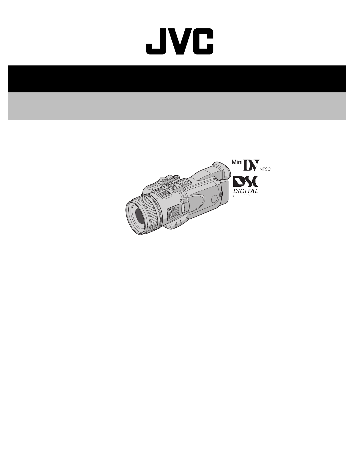
DIGITAL HD VIDEO CAMERA
8677220035
GR-HD1US
GR-HD1US [M3D8L3]
For disassembling and assembling of MECHANISM ASSEMBLY, refer to the SERVICE MANUAL No.86700 (MECHANISM ASSEMBLY).
TABLE OF CONTENTS
1 PRECAUTIONS . . . . . . . . . . . . . . . . . . . . . . . . . . . . . . . . . . . . . . . . . . . . . . . . . . . . . . . . . . . . . . . . . . . . . . . 1-3
2 SPECIFIC SERVICE INSTRUCTIONS. . . . . . . . . . . . . . . . . . . . . . . . . . . . . . . . . . . . . . . . . . . . . . . . . . . . . . 1-5
3 DISASSEMBLY . . . . . . . . . . . . . . . . . . . . . . . . . . . . . . . . . . . . . . . . . . . . . . . . . . . . . . . . . . . . . . . . . . . . . . . 1-6
4 ADJUSTMENT . . . . . . . . . . . . . . . . . . . . . . . . . . . . . . . . . . . . . . . . . . . . . . . . . . . . . . . . . . . . . . . . . . . . . . . 1-19
5 TROUBLE SHOOTING. . . . . . . . . . . . . . . . . . . . . . . . . . . . . . . . . . . . . . . . . . . . . . . . . . . . . . . . . . . . . . . . . 1-22
COPYRIGHT © 2003 VICTOR COMPANY OF JAPAN, LIMITED
No.86772
2003/5
Page 2
SPECIFICATION
Camcorder
For General Power supply DC 6.3 V (Using AC Power Adapter/Charger)
Power consumption LCD monitor off, viewfinder on Approx. 6.8 W (DV)/8.0 W (HD, SD)
LCD monitor on, viewfinder off Approx. 8.5 W (DV)/9.7 W (HD, SD)
Dimensions (W x H x D) 114.5 mm × 99 mm × 271.5 mm
Weight Approx. 1270 g (2.8 lbs)
Operating temperature 0°C to 40°C (32°F to 104°F)
Operating humidity 35% to 80%
Storage temperature -20°C to 50°C (-4°F to 122°F)
Pickup 1/3" CCD
Lens F 1.8, f = 5.2 mm to 52 mm, 10:1 power zoom lens
Filter diameter Ø52 mm
LCD monitor 3.5" diagonally measured, LCD panel/TFT active matrix
Viewfinder Electronic viewfinder with 0.44" color LCD
Speaker Monaural
For Digital
Video Camera
For Digital Still
Camera
For Connectors S/AV S-Video input Y: 0.8 V to 1.2 V (p-p), 75Ω, analog
Signal format NTSC standard
Cassette Mini DV cassette
Tape speed SP: 18.8 mm/s
Maximum recording time
(using 80 min. cassette)
Storage media SD Memory Card/MultiMediaCard
Compression system JPEG (compatible)
File size 2 modes (1280 × 960 pixels/640 × 480 pixels)
Picture quality 2 modes (FINE/STANDARD)
S-Video output Y: 1.0 V (p-p), 75Ω, analog
Video input Y: 0.8 V to 1.2 V (p-p), 75Ω, analog
Video output Y: 1.0 V (p-p), 75Ω, analog
Audio input 300 mV (rms), 50 kΩ, analog, stereo
Audio output 300 mV (rms), 1 kΩ, analog, stereo
Headphone output Stereo
Microphone input Stereo
i.LINK Input/output 4-pin, IEEE 1394 compliant
USB 5-pin
Y/Pb/Pr output Y: 1.0 V (p-p), 75Ω, analog
DC 7.2 V (Using battery pack)
(4-9/16" × 3-15/16" × 10-3/4")
(with the LCD monitor closed and the viewfinder pushed
back in)
(without cassette, memory card and battery)
Approx. 1490 g (3.3 lbs)
(incl. cassette, memory card and battery)
system
LP: 12.5 mm/s
SP: 80 min.
LP: 120 min.
C: 0.2 V to 0.4 V (p-p), 75Ω, analog
C: 0.29 V (p-p), 75Ω, analog
Pb: 0.7 V (p-p), 75Ω, analog
Pr: 0.7 V (p-p), 75Ω, analog
AC Power Adapter/Charger
For General Power requirement U.S.A. and Canada AC 120 Vd, 60 Hz
Other countries AC 110 V to 240 Vd, 50 Hz/60 Hz
Power consumption 23W
Output Charge DC 7.2 V, 1.2 A
VTR DC 6.3 V, 1.8 A
Specifications shown are for SP mode unless otherwise indicated. E & O.E. Design and specification s subject to change without
notice.
1-2 (No.86772)
Page 3
SECTION 1
r
e
PRECAUTIONS
1.1 SAFTY PRECAUTIONS
Prior to shipment from the factory, JVC products are strictly
inspected to conform with the recognized product safety and
electrical codes of the countries in which they are to be
sold.However,in order to maintain such compliance, it is equally
important to implement the following precautions when a set is
being serviced.
1.1.1 Precautions during Servicing
(1) Locations requiring special cauti on are denoted by labels
and inscriptions on the cabinet, chassis and certain parts of
the product.When performing service, be sure to read and
comply with these and other cautionary notices appearing
in the operation and service manuals.
(2) Parts identified by the symbol and shaded ( ) parts
are critical for safety.
Replace only with specified part numbers.
NOTE :
Parts in this category also include those specified to
comply with X-ray emission standards for products
using cathode ray tubes and those specified for
compliance with various regulations regarding
spurious radiation emission.
(3) Fuse replacement caution notice.
Caution for continued protection against fire hazard.
Replace only with same type and rated fuse(s) as
specified.
(4) Use specified internal wiring. Note especially:
• Wires covered with PVC tubing
• Double insulated wires
• High voltage leads
(5) Use specified insulating materials for hazardous live parts.
Note especially:
• Insulation Tape
• PVC tubing
•Spacers
• Insulation sheets for transistors
•Barrier
(6) When replacing AC primary side compon ents (transformers,
power cords, noise blocking capacitors, etc.) wrap ends of
wires securely about the terminals before soldering.
emission. Consequently, when servicing these products,
replace the cathode ray tubes and other parts with only the
specified parts. Under no circumstances attempt to modify
these circuits.Unauthorized modification can increase the
high voltage value and cause X-ray emission from the
cathode ray tube.
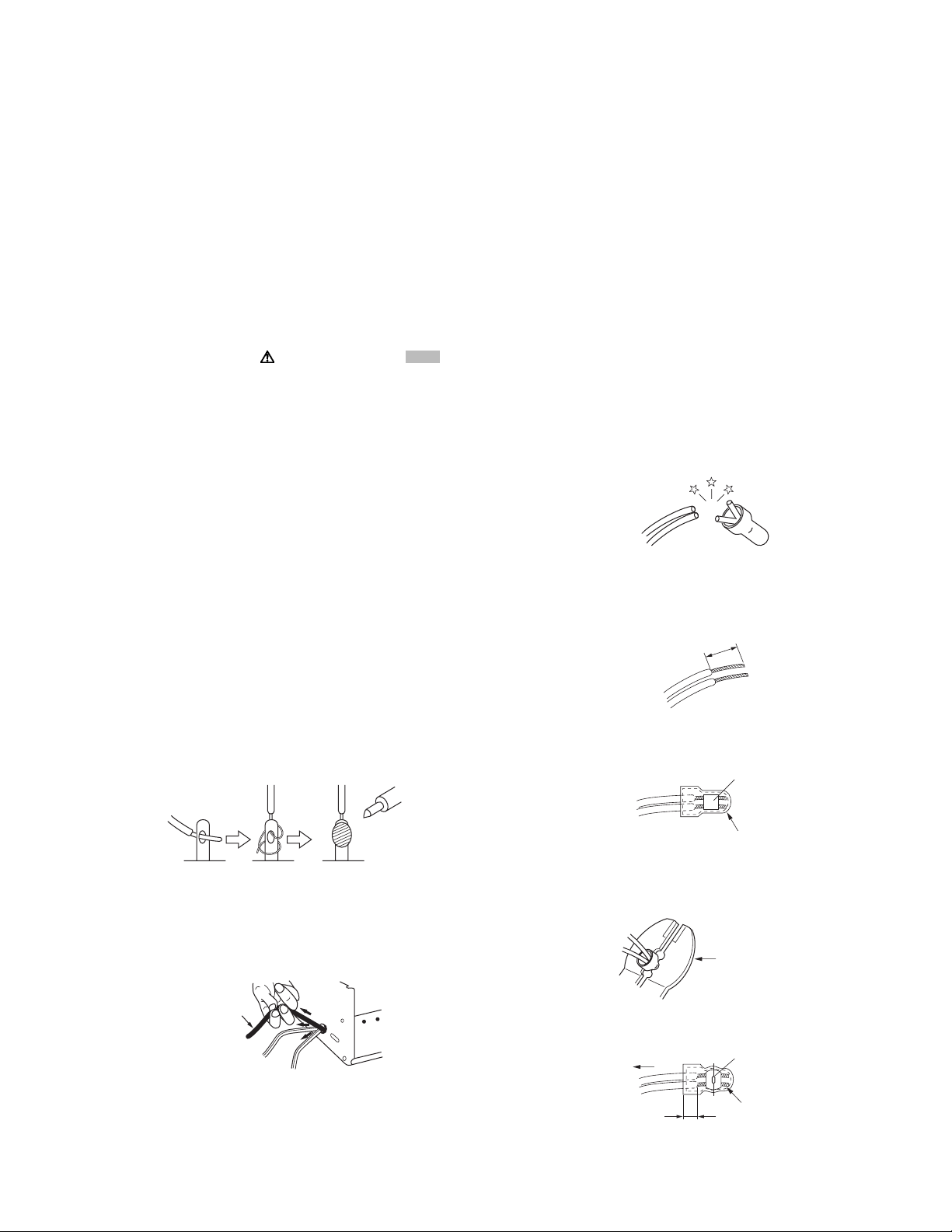
(12) Crimp type wire connectorIn such cases as when replacing
the power transformer in sets where the connections
between the power cord and power trans former primary
lead wires are performed using crimp type connectors, if
replacing the connectors is unavoidable, in order to prevent
safety hazards, perform carefully and precisely according
to the following steps.
• Connector part number :E03830-001
• Required tool : Connector crimping tool of the proper
type which will not damage insulated parts.
• Replacement procedure
a) Remove the old connector by cutting the wires at a
point close to the connector.Important : Do not
reuse a connector (discard it).
cut close to connector
Fig.1-1-3
b) Strip about 15 mm of the insulati on from the ends
of the wires. If the wires are stranded, twist the
strands to avoid frayed conductors.
15 mm
Fig.1-1-4
c) Align the lengths of the wires to be connected.
Insert the wires fully into the connector.
Metal sleeve
Fig.1-1-1
(7) Observe that wires do not contact heat producing parts
(heatsinks, oxide metal film resistors, fusible resistors, etc.)
(8) Check that replaced wires do not contact sharp edged or
pointed parts.
(9) When a power cord has been replaced, check that 10-15
kg of force in any direction will not loosen it.
Power cord
Fig.1-1-2
(10) Also check areas surrounding repaired locations.
(11) Products using cathode ray tubes (CRTs)In regard to such
products, the cathode ray tubes themselves, the high
voltage circuits, and related circuits are specified for
compliance with recognized codes pertaining to X-ray
Connector
Fig.1-1-5
d) As shown in Fig.1-1-6, use the crimping tool to crimp
the metal sleeve at the center position. Be sure to
crimp fully to the complete closure of the tool.
1.2
5
2
.0
5.5
Crimping tool
Fig.1-1-6
e) Check the four points noted in Fig.1-1-7.
Not easily pulled free
Wire insulation recessed
more than 4 mm
Crimped at approx. cente
of metal sleev
Conductors extended
Fig.1-1-7
(No.86772)1-3
Page 4
1.1.2 Safety Check after Servicing
Examine the area surrounding the repaired location for d amage
or deterioration. Observe that screws, parts and wires have been
returned to original positions, Afterwards, perform the following
tests and confirm the specified values in order to verify
compliance with safety standards.
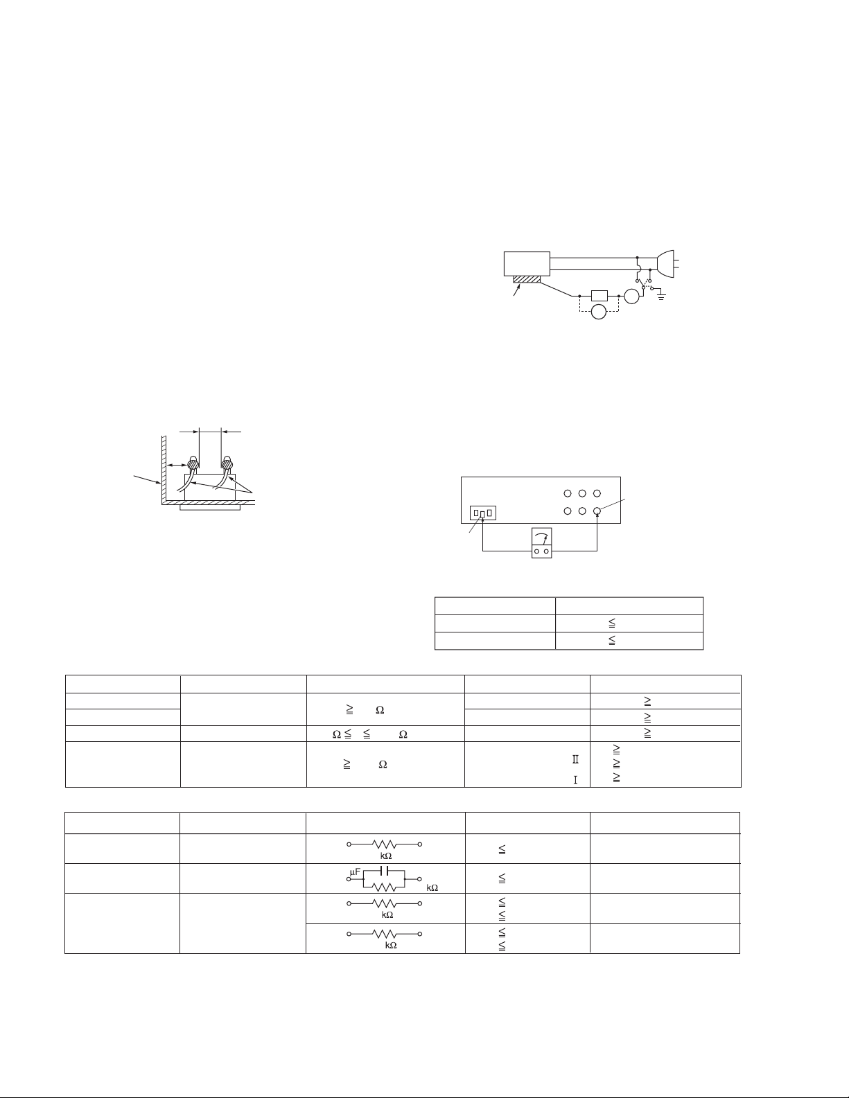
(1) Insulation resistance test
Confirm the specified insulation resistance or greater
between power cord plug prongs and externally exposed
parts of the set (RF terminals, antenna terminals, video and
audio input and output terminals, microphone jacks,
earphone jacks, etc.).See table 1 below.
(2) Dielectric strength test
Confirm specified dielectric strength or greater between
power cord plug prongs and exposed accessible parts of
the set (RF terminals, antenna terminals, video and audio
input and output terminals, microphone jacks, earphone
jacks, etc.). See Fig.1-1-11 below.
(3) Clearance distance
When replacing primary circuit components, confirm
specified clearance distance (d), (d') between soldered
terminals, and between terminals and surrounding metallic
parts. See Fig.1-1-11 below.
d
Chassis
d'
Power cord
primary wire
Fig.1-1-8
(4) Leakage current test
Confirm specified or lower leakage current between earth
ground/power cord plug prongs and externally exposed
accessible parts (RF terminals, antenna terminals, video
and audio input and output terminals, microphone jacks,
earphone jacks, etc.).
Measuring Method : (Power ON)Insert load Z between
earth ground/power cord plug prongs and externally
exposed accessible parts. Use an AC voltmeter to
measure across both terminals of load Z. See Fig.1-1-9
and following Fig.1-1-12.
ab
Externally
exposed
accessible part
Z
V
c
A
Fig.1-1-9
(5) Grounding (Class 1 model only)
Confirm specified or lower grounding impedance between
earth pin in AC inlet and externally exposed accessible
parts (Video in, Video out, Audio in, Audio out or Fixing
screw etc.).Measuring Method:
Connect milli ohm meter between earth pin in AC inlet and
exposed accessible parts. See Fig.1-1-10 and grounding
specifications.
AC inlet
Earth pin
Exposed accessible part
MIlli ohm meter
Grounding Specifications
Region
USA & Canada
Europe & Australia
Grounding Impedance (Z
Z 0.1 ohm
Z 0.5 ohm
)
Fig.1-1-10
AC Line Voltage
100 V
100 to 240 V
110 to 130 V
110 to 130 V
200 to 240 V
Region
Japan
USA & Canada
Europe & Australia
Insulation Resistance (R
R 1 M /500 V DC
1 M R 12 M /500 V DC
R 10 M /500 V DC
)
Dielectric Strength
AC 1 kV 1 minute
AC 1.5 kV 1 minute
AC 1 kV 1 minute
AC 3 kV 1 minute
AC 1.5 kV 1 minute
(
Class
(
Class
Clearance Distance (d), (d'
d, d' 3 mm
d, d' 4 mm
d, d' 3.2 mm
d 4 mm
)
d' 8 mm (Power cord
d' 6 mm (Primary wire
)
Fig.1-1-11
AC Line Voltage
100 V
110 to 130 V
110 to 130 V
220 to 240 V
Region
Japan
USA & Canada
Europe & Australia
Load Z
1
0.15
1.5
2
50
Leakage Current (i)
i 1 mA rms
i 0.5 mA rms
i 0.7 mA peak
i 2 mA dc
i 0.7 mA peak
i 2 mA dc
a, b, c
Exposed accessible parts
Exposed accessible parts
Antenna earth terminals
Other terminals
Fig.1-1-12
NOTE :
These tables are unofficial and for reference only. Be sure to confirm the precise values for your particular country and locality.
)
)
)
1-4 (No.86772)
Page 5

SECTION 2
SPECIFIC SERVICE INSTRUCTIONS
This service manual does not describe SPECIFIC SERVICE INSTRUCTIONS.
(No.86772)1-5
Page 6
SECTION 3
DISASSEMBLY
3.1 BEFORE ASSEMBLY AND DISASSEMBLY
3.1.1 Precautions
• Be sure to disconnect the power supply unit prior to mounting
and soldering of parts.
• Prior to removing a component part that needs to disconnect
its connector(s) and its screw(s), first disconnect the wire(s)
from the connector(s), and then remove the screw(s).
• When connecting/disconnecting wires, pay enough attention
not to damage the connectors.
• When inserting the flat wire to the connector, pay attention to
the direction of the flat wire.
• Be careful in removing the parts to which some spacer or
shield is attached for reinforcement or insulation.
• When replacing chip parts (especially IC parts), first remove
the solder completely to prevent peeling of the pattern.
• Tighten screws properly during the procedures. Unless
specified otherwise, tighten screws at a torque of 0.118N
·cm). However, 0.118N·m (1.2kgf·cm) is a value at the
(1.2kgf
time of production. At the time of service, perform the
procedure at a torque 10% less than 0.118N
·m (1.2kgf·cm).
(See "SERVICE NOTE" as for tightening torque.)
3.1.2 Destination of connectors
Two kinds of double-arrows in connection tables respectively
show kinds of connector/wires.
: Wire: Flat wire : Board to board (B-B)
: The connector of the side to remove
CONN. No. PIN No.CONNECTOR
CN2a
CN2b
MAIN CN101
MAIN CN103
MONI/ BW CN761
MIC CN762
3.1.3 Disconnection of connectors (Wires)
Wire
· Pull both ends of the connector in the arrow
direction, remove the lock and disconnect the flat
wire.
B-B Connector
B-B Connector
· Pull the both ends of the board in the direction of the arrow, and remove the B-B Connector.
FPC Connector
· Extend the locks in the direction of the arrow for
unlocking and then pull out the wire. After
removing the wire, immediately restore the locks
to their original positions because the locks are
apt to come off the connector.
Wire
FPC Connector
Lock
B-B Connector
Fig.2-1-1
3.1.4 Tools required for disassembly and assembly
Torque driver
YTU94088
Chip IC replacement jig
PTS40844-2
Bit
YTU94088-003
Cleaning cloth
KSMM-01
Tweezers
P-895
·m
40
2
• Torque driver
Be sure to use to fastening the mechanism and exterior parts
because those parts must strictly be controlled for tightening
torque.
• Bit
This bit is slightly longer than those set in conventional torque
drivers.
• Tweezers
To be used for removing and installing parts and wires.
• Chip IC replacement jig
To be used for replacement of IC.
• Cleaning cloth
Recommended cleaning cloth to wipe down the video heads,
mechanism (tape transport system), optical lens surface.
3.2 ASSEMBLY AND DISASSEMBLY OF MAIN PARTS
3.2.1 Assembly and disassembly
When reassembling, perform the step(s) in reverse order.
STEP
No.
[1]
[2]
[8]
PART
TOP COVER ASSEMBLY
UPPER ASSEMBLY
(Inc. VF ASSEMBLY,
SPEAKER/MONITOR)
VF ASSEMBLY
(∗1) Order of steps in Procedure
When reassembling, preform th e step(s) in the reverseorder.
These numbers are also used as the identification (location)
No. of parts Figures.
(∗2) Part to be removed or installed.
(∗3) Fig. No. showing Procedure or Part Location.
C = CABINET
(∗4) Identification of part to be removed, unhooked, unlocked,
released, unplugged, unclamped or unsoldered.
S = Screw
L = Lock, Release, Hook
SD = Solder
CN = Connector
[Example]
• 4 (S1a) = Remove four S1a screws.
• 3 (L1a) = Disengage three L1a hooks.
• 2 (SD1a) = Unsolder two SD1a points.
• CN1a = Remove a CN1a connector.
(∗5) Adjustment information for installation.
Fig.
No.
Fig.C1
Fig.C2-1
Fig.C2-2
POINT
S1,2(L1)
S2a,2(S2b),3(S2c)
2(S2d),S2e,S2c
L2,CN2a,b
2(S8),L8,CN8a
( 4) ( 5)( 2) ( 3)( 1)
NOTE
-
-
NOTE 8a
NOTE 8b
1-6 (No.86772)
Fig.2-1-2
Page 7
3.2.2 ASSEMBLY/DISASSEMBLY OF CABINET PARTS AND ELECTRICAL PARTS
zDisassembly procedure
STEP
No.
[1]
[2]
[3]
[4]
[5]
[6]
[21]
[22]
[7]
[8]
[9]
[10]
[11]
[12]
[23]
/[24]
[23]
[24]
[13]
[14]
PART NOTE
SHOE
TOP COVER ASSEMBLY
HOLDER(SHOE)
ORNAMENT
SD COVER ASSEMBLY
UPPER ASSEMBLY
MON/OPE BOARD
ASSEMBLY
MONITOR
ASSEMBLY
VF ASSEMBLY
D4 BOARD ASSEMBLY
HEAT SINK
DIGITAL BOARD ASSEMBLY
ANALOG BOARD ASSEMBLY
GRIP ASSEMBLY
PREMDA BOARD ASSEMBLY
/MECHANISM ASSEMBLY
PREMDA BOARD ASSEMBLY
MECHANISM ASSEMBLY
LOWER CASE ASSEMBLY
REAR ASSEMBLY
Fig.
No.
3(S1)
Fig.C1
3(S2a),(S2b),(L2a),(L2b)
2(S3),2(L3)
Fig.C2
(S5a),(S5b)
Fig.C3-1
JACK COVER,2(S6a),(S6b)
3(S6c),4(S6d),CN6a,b
CN21a,b,c,2(S21)
Fig.C3-2
SPEAKER BRACKET
8(S21),SHIELD,SPEAKER
KNOB(SLIDE)1,2
2(S22a),(S22b),(L22a),
HINGE CASE(U),(S22b),(L22b),
HINGE CASE(L),3(S22c)
(S7a),2(S7b)
Fig.C4
CN8
Fig.C5
4(S9a),2(S9b),SHIELD(D.PWB)
Fig.C6
CN10a,b,c,d,e,(S10),CN10f,g,h
Fig.C7
CN11a,b,c,d,e,f,g,h,3(S11),CN11j,k,m
Fig.C8
4(S12)
Fig.C9-1
2(S23a),4(S23b),CN23a,b,c
Fig.C9-2
ROTARY GRIP ASSEMBLY
CN23d,e,f,g,h,j,2(S23a),4(S23c),
2(S23d),2(S23c)
3(S24),BRACKET(MECHA)ASSEMBLY
3(S13a),2(S13b),2(S13a),(S13c)
Fig.C10
(S13a),(S13d),(L13),HOLDER(SD)
(S14)
Fig.C11
POINT
-
-
-
NOTE4
-
NOTE6a
b,c,d
NOTE21a,b
NOTE22a,b
NOTE7a,b
-
NOTE9a,b
NOTE10
NOTE11
NOTE12
NOTE23a,b
NOTE24
-
NOTE13
-
NOTE4:
This part is attached by using double-side adhesive tape.
In removing the tape, be careful not to damage the reverse
side of the ornament.
NOTE6a:
A screw NO. 21 is beside the tripod base/guide knob hole on
the FRAME ASSEMBLY.
NOTE6b:
After removing the UPPER ASSEMBLY, electrical parts and
board assembly are not covered with anything. Take care
not to damage parts, especially WB sensor and Exposure
Adjustment Wheel.
NOTE6c:
In attaching the UPPER ASSEMBLY, put the lever of the OP
BLOCK ASSEMBLY (MAIN FRAME) in the slot of the
BRACKET (SLIDE) ASSEMBLY.
Note6d:
In attaching the UPPER ASSEMBLY, be careful about the
FPC and the position of D4 BOARD ASSEMBLY.
Note7a:
Since the VF ASSEMBLY is inserted in a narrow space between a part and another part, be careful not to damage or
deform the bracket in removing the VF ASSEMBLY.
Note7b:
For the disassembly procedure of [7] VF ASSEMBLY, see
“3.2.3 DISASSEMBLY/ASSEMBLY OF [7] VF ASSEMBLY”
NOTE9a:
Remove the two screws (No.46 and 47), and remove the
heatsink. In removing the heatsink, peel the shield so that
[15]
BOTTOM BOARD ASSEMBLY
[16]
MIC ASSEMBLY
[17]
FRONT ASSEMBLY
[18]
MIC/WB BOARD ASSEMBLY
[19]
OP BLOCK ASSEMBLY
/[25]
/CCD BOARD ASSEMBLY
[20]
GYRO BOARD ASSEMBLY
2(S15)
Fig.C12
2(S16),CN16
Fig.C13
CN17a,b,2(S17),2(L17a)
Fig.C14
L17b,2(L17c),L17d
2(S18),2(L18)
Fig.C15
4(S19)
Fig.C16
2(S20),2(L20)
Fig.C17
NOTE15
-
NOTE17
NOTE18
NOTE19a,b,c
NOTE20
the heatsink is easy to be removed.
NOTE9b:
Since the heatsink is stuck to the IC on the DIGITAL BOARD
ASSSEMBLY, be careful not to damage the parts in removing the heatsink.
NOTE10:
In removing the DIGITAL BOARD ASSEMBLY, first disconnect some of the connectors, and remove the screws, and
then disconnect the rest of the connectors. Then, remove
the DIGITAL BOARD ASSEMBLY.
Be careful not to damage the B-B connector since B-B connector is connected on the backside of the DIGITAL BOARD
ASSEMBLY.
NOTE11:
Remove the screws, and remove the FPC while removing
the ANALOG BOARD ASSEMBLY since CN212 is on the
backside of the ANALOG BOARD ASSEMBLY.
NOTE12:
In removing the GRIP ASSEMBLY, be careful not to cut or
damage FPC and wires.
NOTE13:
In removing the LOWER CASE ASSEMBLY, remove the
holder (SD) together with the LOWER CASE ASSEMBLY.
NOTE15:
In removing the BOTTOM BOARD ASSEMBLY, first remove the FPC connected to the BOTTOM BOARD ASSEMBLY since it is attached to the frame. Then, remove the
screws, and remove the BOTTOM BOARD ASSEMBLY.
(No.86772)1-7
Page 8
NOTE17:
In removing the FRONT ASSEMBLY, a lens part of the OP
BLOCK ASSEMBLY is not covered with anything. Be careful
not to damage the lens.
NOTE18:
In removing the MIC/WB BOARD ASSEMBLY, first remove
the FPC connected to the MIC/WB BOARD ASSEMBLY
since it is attached to the frame. Then, remove the screws,
and remove the MIC/WB BOARD ASSEMBLY.
NOTE19a:
In removing the OP BLOCK ASSEMBLY/CCD BASE ASSEMBLY, be careful not to damage or cut the FPC, wires,
and lens part.
NOTE19b:
In attaching the OP BLOCK ASSEMBLY/CCD BASE ASSEMBLY, be careful not to damage or cut the FPC and
wires.
NOTE19c:
As for the assembly/disassembly procedures of [19] OP
BLOCK ASSEMBLY /[25] CCD BOARD ASSEMBLY, see
“3.2.5 ASSEMBLY/DISASSEMBLY OF [19] OP BLOCK
ASSMBLY/[25] CCD BOARD ASSEMBLY”.
NOTE20:
Handle the parts on the GYRO BOARD ASSEMBLY carefully since they are easy to be broken.
NOTE21a:
In removing the MON/OPE BOARD ASSEMBLY, be careful
not to damage the shields attached inside the UPPER ASSEMBLY.
NOTE21b:
In removing the MON/OPE BOARD ASSEMBLY, be careful
in handling the knobs (SLIDE) 1 and 2 since they are al so
removed.
In attaching the MON/OPE BOARD ASSEMBLY, be careful
about the position of switch.
Note22a:
In removing the MONITOR ASSSEMBLY, fold the hold plate
inside the UPPER ASSEMBLY in an inner direction.
Note22b:
For the disassembly procedure of [22] MONITOR ASSEMBLY, see “3.2.4 DISASSEMBLY/ASSEMBLY OF [22] MONITOR ASSEMBLY”.
NOTE23a/24
First remove the PREMDA ASSEMBLY together with the
MECHANISM ASSEMBLY inside the GRIP ASSEMBLY,
and then remove the PREMDA ASSEMBLY from the
MECHANISM ASSEMBLY.
NOTE23b:
In removing the ROTARY GRIP ASSEMBLY, disconnect
the wires in the order from short wire to long wire.
zDestination of connectors
CONN.
No.
CONNECTOR
CN6a MON/OPE CN303 VF BL CN703 22
CN6b ANALOG CN209 MON/OPE CN301 51
CN8 DIGITAL CN105 D4 CN806 14
CN10a DIGITAL CN102 CCD - 24
CN10b DIGITAL CN103 CCD - 2
CN10c DIGITAL CN104 BOTTOM CN801 18
CN10d DIGITAL CN106 PREMDA CN411 6
CN10e DIGITAL CN109 REAR CN602 16
CN10f DIGITAL CN108 ANALOG CN208 6
CN10g ANALOG CN201 CONNECT CN502 150
CN10h DIGITAL CN107 PREMDA CN410 22
CN11a ANALOG CN205 GYRO CN804 10
CN11b ANALOG CN202 OP BLOCK - 26
CN11c ANALOG CN207 MIC/WB CN902 6
CN11d ANALOG CN210 PREMDA CN412 5
CN11e ANALOG CN206 MIC/WB CN901 10
CN11f ANALOG CN203 OP BLOCK - 12
CN11g ANALOG CN215 REAR CN603 8
CN11h ANALOG CN214 REAR CN601 6
CN11j ANALOG CN213 PREMDA CN415 14
CN11k ANALOG CN211 PREMDA CN414 20
CN11m ANALOG CN212 PREMDA CN413 15
CN16 MIC - MIC/WB CN903 4
CN17a M.ZOOM RING - MIC/WB CN905 6
CN17b M.FOCUS RING - MIC/WB CN904 6
CN21a MON/OPE CN302 MON BL CN701 39
CN21b MON/OPE CN304 SW CN805 6
CN21c MON/OPE CN305 SPEAKER - 2
CN23a PREMDA CN401
POWER OPERATION
- 11
CN23b PREMDA CN409 ZOOM UNIT - 6
CN23c PREMDA CN408 EJECT CN803 8
CN23d PREMDA CN406 SENSOR - 16
CN23e PREMDA CN405 CAPSTAN MOTOR - 18
CN23f PREMDA CN404 DRUM MOTOR - 11
CN23g PREMDA CN402 HEAD - 8
CN23h PREMDA CN403 LOADING MOTOR - 6
CN23j PREMDA CN407
ROTARY ENCODER
- 6
PIN
No.
1-8 (No.86772)
Page 9

∗
∗
(S1)
2
(S1)
∗
1
3
(S1)
L2a
54
[2]
[1]
6
(S2a)
L2b
∗0.248N
4
(S2a)
7
(S2b)
·
m (2.5kgf·cm)
5
(S2a)
[4]
NOTE4
[3]
(S3)
∗
∗
8
9
(S3)
L3
∗0.248N
·
m (2.5kgf·cm)
[5]
10
(S5a)
Fig.C1 Fig.C2
21
(S6d)
NOTE6a
NOTE6c
NOTE6d
NOTE6b
15
(S6c)
17
(S6c)
(S6c)
L2a
<NOTE6c>
16
(S5b)
[6]
(S6d)
11
CN6b
CN6a
JACK COVER
∗
12
(S6a)
∗
13
(S6a)
14
(S6b)
20
(S6d)
19
(S6d)
18
BKT (SLIDE)
ASSEMBLY
<SCREW LOCATION>
17 11
16
20182119
∗0.248N
·
m (2.5kgf·cm)
10
MAIN FRAME
Fig.C3-1
(No.86772)1-9
Page 10

NOTE21b
∗0.078N
∗∗0.248N
(S22c)
[22]
NOTE22b
·
m (0.8kgf·cm)
·
m (2.5kgf·cm)
∗∗
38
∗∗
(S22c)
37
(S22c)
∗∗
36
HINGE CASE(L)
∗
35
(S22b)
L22b
∗
34
(S22b)
HINGE CASE(U)
L22a
HOLD PLATE
SPEAKER
BOARD ASSEMBLY
NOTE22a
MON/OPE
NOTE21a
SHIELD
CN21c
∗
30
(S21)
24
(S21)
∗
KNOB (SLIDE)1
KNOB (SLIDE)2
NOTE21a
SHIELD
CN21a
CN21b
∗
27
(S21)
∗
∗
25
(S21)
26
(S21)
(S21)
∗
29
(S21)
∗
31
(S21)
SPEAKER BRACKET
∗
28
NOTE21b
(S22a)
∗
22
(S21)
∗
32
∗
33
(S22a)
(S21)
∗
23
Fig.C3-2
41 40
NOTE7a
[7]
NOTE7b
∗
40
(S7b)
∗0.098N
∗
41
(S7b)
39
(S7a)
·
m (1.0kgf·cm)
CN8
[8]
1-10 (No.)
Fig.C4 Fig.C5
Page 11

42
(S9a)
44
(S9a)
43
(S9a)
45
(S9a)
Fig.C6
NOTE9b
46
(S9b)
SHIELD
(D.PWB)
47
(S9b)
[9]
NOTE9b
NOTE9a
<CONNECTOR LOCATION>
CN10b
CN10a
CN10h
CN10c
CN10d
CN10f
CN10e
CN10a
CN10h
<WIRE CONNECTION>
Fig.C7
NOTE10
CN10g
CN10e
CN10b
CN10c
<ANALOG-DIGITAL>
CN10f
<ANALOG-DIGITAL>
CN10g(BACK SIDE)
<REAR-DIGITAL>
CN10e
[10]
CN10f
CN10d
<WIRE CONNECTION>
48
(S10)
<CCD-DIGITAL>
CN10b
<CCD-DIGITAL>
CN10a
<PREMDA-DIGITAL>
CN10h
<BOTTOM-DIGITAL>
CN10c
<PREMDA-DIGITAL>
CN10d
(No.86772)1-11
Page 12

150
75
76
51
20
14
25
CN11h
<CONNECTOR LOCATION>
CN11f
CN11j
CN11e CN11c
CN11d
CN11k
CN11a
CN11m
CN11b
1
6
1
9
1
20
25
14
1
1
CN11e
CN11f
CN11d
CN11m
CN11k
CN11j
CN11g
CN11c
CN11b
CN11a
(S11)
50
(S11)
49
[11]
51
(S11)
NOTE11
<WIRE CONNECTION> <WIRE CONNECTION> <WIRE CONNECTION>
<MIC/WB-ANALOG>
CN11e
<PREMDA-ANALOG>
CN11d
<PREMDA-ANALOG>
CN11k
<PREMDA-ANALOG>
CN11m(BACK SIDE)
<PREMDA-ANALOG>
CN11j
<ANALOG-REAR>
CN11h
<ANALOG-REAR>
CN11g
Fig.C8
1
6
50502
51
150
75
<OP-ANALOG>
CN11f
<MIC/WB-ANALOG>
CN11c
<PREMDA-ANALOG>
CN11d
<GYRO-ANALOG>
CN11a
<OP-ANALOG>
CN11b
1
76
1
CN11h
6
1
CN11g
8
1
[12]
NOTE12
Fig.C9-1
(S12)
∗0.198N
∗
52
(S12)
∗
54
·
m (2.0kgf·cm)
∗
53
(S12)
∗
55
(S12)
1-12 (No.86772)
Page 13

∗0.078N
∗∗0.069N
·
m (0.8kgf·cm)
·
m (0.7kgf·cm)
CN23c
∗
62
(S23a)
∗
63
(S23a)
∗
56
(S23a)
∗
57
(S23a)
ROTARY GRIP ASSEMBLY
NOTE23b
58
(S23b)
61
(S23b)
60
(S23b)
(S23b)
59
SPACER
(GR,WIRE)
[23]
PREMDA BOARD
ASSEMBLY
∗
70
(S23c)
CN23c
CN23j
CN23h
∗
71
(S23c)
∗∗
68
∗∗
(S23d)
69
(S23d)
[23]/[24]
CN23g
NOTE23a,24
BRACKET (MECHA
∗
64
(S23c)
∗
66
(S23c)
CN23b
CN23f
CN23e
ASSEMBLY
∗
72
(S24)
∗
73
(S24)
CN23e
CN23a
CN23d
[24]
MECHANISM
ASSEMBLY
)
CN23h
∗
67
(S23c)
∗
74
(S24)
∗65
(S23c)
Fig.C9-2
CN23j
CN23g
CN23f
CN23d
CN23b
<CONNECTOR LOCATION>
CN23c
CN23j
CN23h
CN23a
CN23b
CN23a
CN23d
CN23e
CN23fCN23g
∗
78
(S13b)
∗
77
(S13a)
(S13a)
HOLDER(SD)
NOTE13
79
(S13b)
∗
80
∗
(S13c)
∗
81
(S13a)
[13]
84
∗
84
(S13d)
∗
83
(S13a)
∗
82
L13
∗0.098N
·
m (1.0kgf·cm)
∗
75
(S13a)
∗
76
(S13a)
Fig.C10 Fig.C11
∗
85
[14]
∗0.098N
·
m (1.0kgf·cm)
85
(S14)
(No.86772)1-13
Page 14

90
(S17)
L17c
L17a
CN17aCN17b
L17b
L17d
NOTE17
[16]
[15]
(S16)
(S15)
∗
88
86
87
(S15)
Fig.C12
∗
89
(S16)
NOTE15
[17]
[18]
92
(S18)
91
(S17)
Fig.C14
93
(S18)
NOTE18
1-14 (No.86772)
CN16
Fig.C13
∗0.059N
·
m (0.6kgf·cm)
L18
Fig.C15
Page 15

[19]
NOTE19a,c
Fig.C16
97
(S19)
NOTE19b
[25]
(S19)
94
(S19)
95
(S19)
96
L20
Fig.C17
99
(S20)
[20]
NOTE20
98
(S20)
(No.86772)1-15
Page 16

3.2.3 DISASSEMBLY/ASSEMBLY OF [7] VF ASSEMBLY
zDisassembly of VF ASSEMBLY
(1) Remove the two screws (1 and 2), and remove th e EYE
CUP.
(2) Remove the four screws (3-6), and make the SWITCH
BOARD ASSEMBLY (PUSH SWITCH) and FPC ASSEMBLY (VF) move easily.
(3) Remove the four screws (7-10), and remo ve the FPC
ASSEMBLY (VF) from the HOLDER ASSEMBLY (VF)
while lifting the VF CASE (TOP COVER and BOTTOM
COVER ASSEMBLY) upwards.
NOTE7a:
During the procedure, be careful not to damage or cut
the FPC ASSEMBLY (VF) since it is attached to the
HOLDER ASSEMBLY (VF).
(4) Remove the two screws (11 an d 12), and remove the
TOP COVER.
(5) Remove the whole LCD UNIT from the BOTTOM COV-
ER ASSEMBLY.
(6) Remove one screw (13), and remove the LEVER
(LENS), HOLDER (LENS) ASSSEMBLY, LINK (LENS),
and SPACER B.
NOTE7b:
When attaching the VF ASSEMBLY, confirm that the
HOLDER (LENS) ASSEMBLY slides properly.
∗∗
3
(S7c)
SWITCH
BOARD
ASSEMBLY
∗∗
4
(S7d)
∗∗
5
(S7d)
FPC ASSEMBLY (VF)
NOTE7a
LCD UNIT
6
(S7d)
TOP COVER
∗∗
7
(S7e)
∗∗
8
(S7e)
∗∗
11
(S7f)
HOLDER (LENS)
ASSEMBLY
∗
1
(S7c)
LINK
(LENS)
SPACER B
BOTTOM COVER ASSEMBLY
∗∗
12
(S7f)
EYE CUP
∗
2
(S7c)
1-16 (No.86772)
∗∗
9
(S7f)
HOLDER (VF) ASSEMBLY
∗∗
10
(S7f)
Fig.3-2-3
(S7g)
∗∗∗
13
LEVER (LENS)
NOTE7b
∗0.069N
∗∗0.078N
∗∗∗0.059N
·
m (0.7kgf·cm)
·
m (0.8kgf·cm)
·
m (0.6kgf·cm)
Page 17

3.2.4 DISASSEMBLY/ASSEMBLY OF [22] MONITOR ASSEMBLY
zCAUTION
(1) Be careful in handling the LCD module, especially not to
damage or soil the monitor screen.If it is soiled with fingerprints, etc., gently clean it with chamois or the cleaning cloth.
(2) Since the BACKLIGHT is soldered to the ASSEMBLY
BOARD, the BACKLIGHT should not be separated from
the ASSEMBLY BOARD except when replacing the
BACKLIGHT.
zDisassembly procedure of MONITOR ASSEMBLY
(1) While removing th e four screws (1-4) i n nu merical order
and disengaging the six hooks (L22a-L22f) in alphabetical order, remove the MONITOR COVER ASSY.
(2) Remove the SENSOR BOARD ASSEMBLY from the
MONITOR CASE ASSEMBLY.
(3) Unlock one connector (CN22a), and then disconnect the
FPC and remove the HINGE ASSEMBLY while lifting the
HINGE ASSEMBLY/FPC ASSEMBLY upwards.
(4) Remove the BRACKET (MONITOR).
(5) Disconnect the FPC of the LCD MODULE from one con-
nector (CN22b).
(6) Remove one screw (5), and remove the MON BL
BOARD ASSEMBLY together with the BACKLIGHT.
(7) Remove the D BEF SHEET.
(8) While disengaging the four hooks (L22g-L22k) in alp ha-
betical order, remove the LCD MODULE.
zDisassembly procedure of HINGE ASSEMBLY/FPC AS-
SEMBLY
(1) While removing the two screws (6 and 7) and disengag-
ing the four hooks (L22m-L22p) in alphabetical order, remove the HINGE COVER (U)
(2) Remove the HINGE COVER (L),
NOTE22a:
Be careful not to lose the magnet.
When attaching magnet, be careful about the attachment direction.
(3) Remove the FPC ASSEBLY from the HINGE ASSEM-
BLY.
NOTE22b:
When attaching the FPC ASSEMBLY, wind the FPC
around the HINGE ASSEMBLY 3.5 times. Be careful
not to cut or damage the FPC.
L22m
HINGE COVER(L)
/FPC ASSEMBLY (MONI)
L22o
HINGE ASSEMBLY
NOTE22b
L22g
L22j
L22h
L22k
SENSOR BOARD
ASSEMBLY
L22n
L22p
MAGNET
NOTE22a
HINGE ASSEMBLY
MONITOR CASE ASSEMBLY
∗∗
5
LCD MODULE
(S22a)
FPC ASSEMBLY
(MONI)
HINGE COVER(U)
∗∗∗
7
(S22d)
a
6
(S22d)
∗∗∗
D BEF SHEET
BACK LIGHT
CN22a
a
MONI BL BOARD ASSEMBLY
BRACKET
(MONITOR)
SD22
CN22b
∗
3
(S22e)
∗
4
(S22e)
(S22d)
MONITOR COVER ASSEMBLY
L22f
1
L22c
L22b
∗∗ 0.098N
∗∗∗ 0.078N
L22a
L22b
2
(S22d)
L22d
∗
0.198N.m (2.0kgf.cm)
.
m (1.0kgf.cm)
.
m (0.8kgf.cm)
NOTE22a
MARKING
NOTE22b
FPC
HINGE
ASSEMBLY
Fig.3-2-4
(No.86772)1-17
Page 18

3.2.5 ASSEMBLY/DISASSEMBLY OF [19] OP BLOCK ASSMBLY/[25] CCD BOARD ASSEMBLY
zCAUTIONS
OP
SIDE
NOTE19c
OP LPF
CCD
SIDE
MAIN FRAME
CCD BOARD ASSEMBLY
SHEET
OP LPF
6
(S19b)
∗
1
(S19a)
(1) Be careful in handling the CCD image sensor, OP LP F,
and lens etc., especially not to damage or soil thei r surface.
If it is soiled with fingerprints, etc., gently clean it with
chamois or the cleaning cloth.
(2) When the CCD image sensor is shipped from the factory,
there are protection seals applied onto the transparent
glass. Leave the protector as it is, and take it off just before assembling the CCD image sensor to the OP block.
zDisassembly procedure of OP BLOCK ASSEMBLY/CCD
BOARD ASSEMBLY
(1) Remove the three screws (1-3), and remove the OP
BRACKET ASSEMBLY.
OP BLOCK ASSEMBLY
(2) Unsolder the sixteen soldered p arts (SD19) on the CCD
BOARD ASSEMBLY, and remove the CCD BOARD ASSEMBLY.
(3) Remove the two screws (4 and 5), and remove the CCD
BASE ASSEMBLY.
NOTE19a
In removing the CCD BASE ASSEMBLY, be careful in
handling a sheet and OP LPF since a sheet or OP LPF
is removed together with the CCD BASE ASSEMBLY.
NOTE19b
∗
3
(S19a)
In replacing the CCD image sensor, donÅft remove
the CCD image sensor from the CCD BASE ASSEMBLY. Instead, replace the whole CCD BASE ASSEM-
∗0.147N
·
m (1.5kgf·cm)
BLY.
(4) Remove the sheet and OP LPF.
Fig.3-2-5
(5) Remove the two screws (6 and 7), and remove the MAIN
FRAME ASSEMBLY.
NOTE19c
When attaching OP LPF to the OP BLOCK ASSEMBLY, be careful about the attachment direction.
(S19b)
∗
2
(S19a)
7
CCD BASE ASSEMBLY
NOTE19a,b
OP BRACKET ASSEMBLY
SD19
4
(S19b)
5
(S19b)
1-18 (No.86772)
Page 19

SECTION 4
ADJUSTMENT
4.1 PREPARATION
4.1.1 Precaution
Camera system and deck system of this model are specially
adjusted by using PC.
However, if parts such as the following are replaced, an
adjustment is required. The adjus tment must be performed in a
Service Center equipped with the concerned facilities.
• OP BLOCK ASSEMBLY
• EEP ROM (IC1003 of DIGITAL board)
In the event of malfunction with electrical circuits, first find a
defective portion with the aid of proper test instruments as shown
in the following electrical adjustment procedure, and then
commence necessary repair/ replacement/adjustment.
• In observing chip TP, use IC clips, etc. to avoid any stress.
Prior to replacement of chip parts (especially IC), remove the
solder completely to prevent peeling of the pattern.
• Use a patch cord if necessary. As for a patch cord, see the
BOARD INTERCONNECTIONS.
• Since connectors are fragile, carefully handle them in
disconnecting and connecting the FPC.
4.1.2 REQUIRED TEST EQUIPMENT
• Personal computer (for Windows)
• Color TV monitor
• Oscilloscope (dual-trace type, observable 100MHz or higher
frequency). The one observable 300 MHz or higher frequency
is recommended.
• Digital voltmeter
• DC power supply or AC adapter
• Frequency counter (with threshold level adjuster)
4.1.3 TOOLS REQUIRED FOR ADJUSTMENT
Torque Driver
YTU94088
Chip IC Replacement Jig
PTS40844-2
INF Adjustment Lens
YTU92001B
Light box Assembly
YTU93096A
Alignment Tape
MC-1
INF Adjustment Lens Holder
Bit
YTU94088-003
Cleaning Cloth
KSMM-01
YTU94087
Gray Scale Chart
YTU94133A
PC Cable
QAM0099-002
Guide Driver (Hexagonal)
D-770-1.27
Camera Stand
Color Bar Chart
YTU94133C
Communication Cable
YTU93107A
Tweezers
P-895
YTU93079
Service Support System
YTU94057-72
Jig Connector Cable
YTU93082C
(No.86772)1-19
Page 20

• Torque driver
Be sure to use to fastening the mechanism and exterior parts
because those parts must strictly be controlled for tightening
torque.
• Bit
This bit is slightly longer than those set in conventional torque
drivers.
• Tweezers
To be used for removing and installing parts and wires.
• Chip IC replacement jig
To be used for adjustment of the camera system.
• Cleaning cloth
Recommended the Cleaning cloth to wipe down the video
heads, mechanism (tape transport system), optical lens surface.
• Guide driver (Hexagonal)
To be used to turn the guide roller to adjustment of the linarity
of playback envelope.
• INF adjustment lens
To be used for adjustment of the camera system. For the
usage of the INF adjustment lens, refer to the Service Bulletin
No. YA-SB-10035.
• INF lens holder
To be used together with the Camera stand for operating the
Videocamera in the stripped-down condition such as the status without the exterior parts or f or usin g commod ities th at are
not yet conformable to the interchangeable ring. For the usage
of the INF lens holder, refer to the Service Bulletin No. YA-SB-
10035.
• Camera stand
To be used together with the INF adjustment lens holder. For
the usage of the Camera stand, refer to the Service Bulletin
No. YA-SB-10035.
• Light box assembly
To be used for adjustment of the camera system. For the
usage of the Light box assembly, refer to the Service Bulletin
No. YA-SB-10035.
• Gray scale chart
To be used for adjustment of the camera system. For the
usage of the INF adjustment lens, refer to the Service Bulletin
No. YA-SB-10035.
• Color bar chart
To be used for adjustment of the camera system. For the
usage of the INF adjustment lens, refer to the Service Bulletin
No. YA-SB-10035.
• Alignment tape
To be used for check and adjustment of interchangeability of
the mechanism.
• PC cable
To be used to connect the Videocamera and a personal computer
with each other when a personal computer issued for adjustment.
• Communication cable
Connect the Communication cable between the PC cable and
Jig connector cable when performing a PC adjustment.
• Service support system
To be used for adjustment with a personal computer. Software
can be downloaded also from JS-net.
• Jig connector cable
Connected to CN110 of the main board and used for electrical
adjustment, etc.
4.2 JIG CONNECTOR CABLE CONNECTION Connection procedure
GUIDE ROLLER (SUP)
GUIDE ROLLER (TU)
JIG CONNECTOR CABLE
COMMUNICATION CABLE
TO GND
RED
WHITE
BLACK
TO JLIP_RX
TO JLIP_TX
COVER
(JIG)
SCREW
COMMUNICATION CABLEJIG CONNECTOR OSCILLOSCOPEJIG CONNECTOR
JIG CONNECTOR
(CN110)
RS232C
PC CABLE
FOR
COMMUNICATION CABLE
COM PORT
TO ENV_OUT
TO HID1
SERVICE SUPPORT SYSTEM
PERSONAL COMPUTER
Jig connector diagrams
JIG CONNECTORCABLE(YTU93082C)
JIG BOARD ASSEMBLY(14PIN)
123456789
Flashwrt
IF_TX
CJIG_RST
SRV_TX
NC
ATFI
FS_PLL
1011121314
HID1
PB CLK
ENV_OUT
MAIN VCO
GND
JIG BOARD ASSEMBLY(15PIN)
123456789
VPPD
JLIP_TX
RX_DSC
TX_DSC
JLIP_RX
AL_3VSYS
SRV_RX
DISCRI
DRST
GND
ADJUST
SCREW
MENU
1011121314
TRST
SPA
SBE
TCK
TMS
TDO
15
TDI
1-20 (No.86772)
Page 21

4.3 MECHANISM COMPATIBILITY ADJUSTMENT
4.3.1 Tape pattern adjustment
NOTE:
Prior to the adjustment, remove the cover (ADJUST).
(1) Play back the compatibility adjustment tape.
(2) While triggering the HID1, observe the waveform of
ENV_OUT.
(3) Set the manual tracking mode (ATF OF F).
(4) Confirm that the waveform is entire ly parallel and straig ht,
and free from remarkable level-down, through the tracking
operation.
Make the confirmation as follows if necessary.
(5) If level-down is observed on the left hand side of the
waveform, straighten the level by turning the GUIDE
ROLLER (SUP).
If level-down is observed on the right hand side of the
waveform, straighten the
level by turning the GUIDE ROLLER (TU).
(6) After the adjustment, try the unl oading motion once, and
confirm that the waveform is flat when the tape has been
played back again.
(7) Play back the self-recordin g.
(8) Confirm that the waveform is flat.
4.4 ELECTRICAL ADJUSTMENT
Electrical adjustment is performed by using a personal computer
and software for SERVICE SUPPORT SYSTEM. Read
README.TXT file to use the software properly.
As for the connection of cables, see "4.2 JIG CONNECTOR
CABLE CONNECTION".
Misalignment of guide
roller height on the
supply side
ENV_OUT
HID1
Flatten the waveform.
Misalignment of guide roller
height on the take-up side
Fig.4-3-1
Fig.4-3-2
(No.86772)1-21
Page 22

5.1 SERVICE NOTE
[21]
SECTION 5
TROUBLE SHOOTING
c
C3-2
b
[20]
b
48
C7
C17C13 C16C15C14
c
f
[24]
b
*
ba
[5] [6]
---
[4]
C2 C3-1
[3]
ba
[2]
C1
a
[1]
1 2 3 4 5 6 7 8 9 10 11 12 13 14 15 16 17 18 19 20 21 22 23 24 25 26 27
CABINET PARTS AND ELECTRICAL PARTS
b
[9] [10]
-
-
[8]
d
ab b
*** ***
[22] [7] [11]
c
[21]
28 29 30 31 32 33 34 35 36 37 38 39 40 41 42 43 44 45 46 47 49 50 51
C6
[23][23]/[24]
C5
C4 C8
C3-2
[12]
52 53 54 55 56 57 58 59 60 61 62 63 64 65 66 67 68 69 70 71 72 73 74
[19]
c
[17] [18]
[16]
[15][14]
85
[13]
75 76 77 78 79 80 81 82 83 84 86 87 88 89 90 91 92 93 94 95 96 97 98 99
bb b
g
bf
f
** ** ** **
e
C9-2
bc
c
d
C9-1
****
[22]
1234567
Symbol No.
Removing order of screw
C11 C12
[7]
C10
1 2 3 4 5 6 7 8 9 10 11 12 13
[7] VF ASSEMBLY [22] MONITOR ASSEMBLY
3-2-4
bd
****
Place to stick screw
Screw tightening torque
Reference drawing (Fig.No.)
g
c
3-2-3
******
e
[19]/[25]
1234567
[19] OP BLOCK ASSEMBLY/[25]CCD BOARD ASSEMBLY
b
h
cm)
cm)
.
.
m (0.8kgf
m (1.0kgf
.
.
: 0.078N
: 0.098N
cm)
cm)
cm)
.
.
.
m (1.2kgf
m (0.7kgf
m (1.5kgf
.
.
.
: 0.069N
: 0.118N
: 0.147N
bc
ef
h
cm)
cm)
cm)
.
.
.
m (2.5kgf
m (2.0kgf
m (0.6kgf
.
.
.
: 0.198N
: 0.248N
3-2-5
Torque setting value of torque driver is limited. At the values over the maximum torque setting value, fasten a screw manually not to damage the screw thread.
1) * : Don't reuse the screw, because screw lock bond was applied to them.
2) Pay careful attention to tightening torque for each screw.
NOTE:
: 0.059N
a
d
g
1-22 (No.86772)
Symbol No.
Place to stick screw
Screw tightening torque
Removing order of screw
Reference drawing (Fig.No.)
Symbol No.
Place to stick screw
Screw tightening torque
Removing order of screw
Reference drawing (Fig.No.)
Symbol No.
Place to stick screw
Screw tightening torque
Removing order of screw
Reference drawing (Fig.No.)
Symbol No.
Place to stick screw
Screw tightening torque
Removing order of screw
Reference drawing (Fig.No.)
Symbol No.
Place to stick screw
Screw tightening torque
Removing order of screw
Reference drawing (Fig.No.)
Symbol No.
Place to stick screw
Screw tightening torque
Removing order of screw
Reference drawing (Fig.No.)
Page 23

5.2 TAKE OUT CASSETTE TAPE
(1) Remove the Power Unit (battery or DC code) from the set.
(2) Remove one screw, and remove a plate (ADJ).
NOTE:
For more efficient operation, loosen and move the grip
belt prior to the procedure (2).
(3) Open the CASSETTE COVER till it is completely opened
and fixed.
(4) Attach a PVC tape as shown in the figure.
NOTE:
Be careful of cassette tape damage caused because the
CASSETTE HOUSING ASSEMBLY is moved upward at
the unloading end (EJECT mode).
(5) To set the SLIDE DECK ASSEMBLY to the unloading end,
apply DC 3V to the electrode (terminal) on the top surface
of the LOADING MOTOR ASSEMBLY that is seen through
a hole under the plate removed in the procedure (2).
NOTE:
Be careful not to attach grease or a similar substance to
the surface of the cassette tape on the tape transport
system.
(6) Wind the cassette tape by directly turning the REEL DISK
ASSEMBLY (SUP) from the backside of the SLIDE DECK
ASSEMBLY by using a sharp tool (Chip IC replacement
tool).
(7) Confirm that the cassette tape is completely woun d, and
then peel off the PVC tape from the CASSETTE HOUSING
ASSEMBLY and take out the cassette tape.
NOTE:
To confirm that the cassette tape is completely wound,
confirm that one REEL DISK ASSEMBLY (TU) rotates
as you rotate the other REEL DISK ASSEMBLY (SUP).
(8) Make sure that grease or a similar substance is not
attached to the surface of the tape taken out in the
procedure (7). Similarly, also make sure that grease or a
similar substance is not attached on the MECHANISM
ASSEMBLY, especially the tape transport system.
(DC3V)
LOADING MOTOR
ASSEMBLY
REEL DISK
ASSEMBLY (SUP)
SLIDE DECK
ASSEMBLY
TAPE
Fig.5-2-1
CASSETTE COVER
CASSETTE HOUSING
ASSEMBLY
(No.86772)1-23
Page 24

5.3 EMERGENCY DISPLAY
Example (in case of the error number E01):
Whenever some abnormal signal is input to the syscon CPU, an
error number (E01, as an example) is displayed on the LCD
monitor or (in the electronic view finder).In every error status,
such the message as shown below alter nately appear over and
E01
UNIT IN
SAFEGUARD MODE
over.
• In an emergency mode, all operations except turning on/off the
POWER switch are ineffectual.
LCD display Emergencymode Details Possible cause
E01 LOADING In the case the encoder position is
not shifted to the next point though
the loading motor has rotated in the
loading direction for 4 seconds or
more. This error is defined as [E01].
E02 UNLOADING In the case the encoder position is
not shifted to the next point though
the loading motor has rotated in the
unloading direction for 4 seconds or
1. The mechanism is locked during mode shift.
2. The mechanism is locked at the mechanism loading end,
because the encoder position is skipped during
mechanism mode shift.
3. No power is supplied to the loading MDA.
1. The mechanism is locked during mode shift.
2. The mechanism is locked at the mechanism loading end,
because the encoder position is skipped during
mechanism mode shift.
more. This error is defined as [E02].
E03 TU & SUP REEL FG In the case no REEL FG is
produced for 4 seconds or more in
the capstan rotation mode after
loading was complete, the
mechanism mode is shifted to
STOP with the pinch roller set off.
This error is defined as
[E03].However, no REEL EMG is
detected in the SLW/STILL mode.
1. The idler gear does not engage with the reel disk well.
2. Though the idler gear and reel disk are engaged with
each other, the tape is not wound because of overload
to the mechanism.
3. No FG pulse is output from the reel sensor.
4. No power is supplied to the reel sensor.
5. Tape transport operation takes place with a cassette
having no tape inside.
6. The tape slackens and no pulse is produced until the
slack is taken up and the tape comes into the normal
status.
E04 DRUM FG In the case there is no DRUM FG
input in the drum rotation mode for
4 seconds or more. This error is
defined as [E04], and the
mechanism mode is shifted to
STOP with the pinch roller set off.
1. The drum cannot be started or drum rotation is stopped
because tape transport load is too high.
1) Tape tension is extremely high.
2) The tape is damaged or soiled with grease, etc.
2. The DRUM FG signal is not received by the syscon CPU.
1) Disconnection in the middle of the signal line.
2) Failure of the DRUM FG pulse generator (hall
element).
3. No drum control voltage is supplied to the MDA.
4. No power is supplied to the DRUM MDA.
E05 - - E06 CAPSTAN FG In the case no CAPSTAN FG is
produced in the capstan rotation
mode for 2 seconds or more. This
error is defined as [E06], and the
mechanism mode is shifted to
STOP with the pinch roller set
off.However, no CAPSTAN EMG is
detected in the STILL/FF/REW
mode.
1. The CAPSTAN FG signal is not received by the syscon
CPU.
1) Disconnection in the middle of the signal line.
2) Failure of the CAPSTAN FG pulse generator (MR
element).
2. No capstan control voltage is supplied to the MDA.
3. The capstan cannot be started or capstan rotation is
stopped because tape transport load is too high.
1) Tape tension is extremely high. (Mechanical locking)
2) The tape is damaged or soiled with grease, etc. (Tape
tangling occurs, etc.)
E01
REMOVE AND
REATTACH BATTERY
1-24 (No.86772)
Fig.5-3-1
Page 25

JVC SERVICE & ENGINEERING COMPANY OF AMERICA
DIVISION OF JVC AMERICAS CORP.
www.jvcservice.com(US Only)
JVC CANADA INC.
Head office : 21 Finchdene Square Scarborough, Ontario M1X 1A7 (416)293-1311
(No.86772)
Printed in Japan
WPC
 Loading...