

Page 1
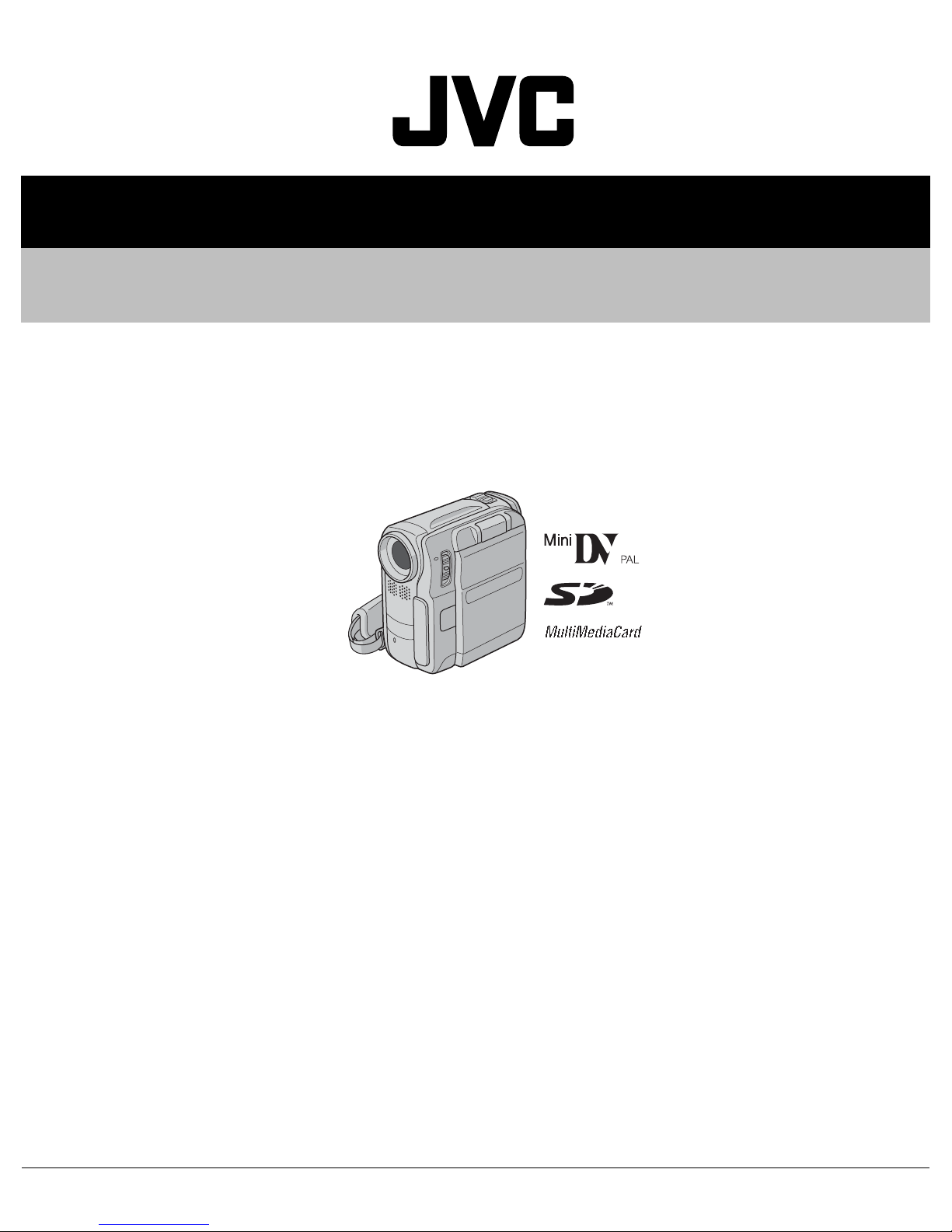
SERVICE MANUAL
DIGITAL VIDEO CAMERA
YF04620044
GR-DX107EK, GR-DX107EX, GR-DX107EY,
GR-DX107EZ, GR-DX307EK, GR-DX307EX,
GR-DX307EY, GR-DX307EZ, GR-DX317EX
GR-DX107EK, GR-DX107EX, GR-DX107EY, GR-DX107EZ[M4D3S9]
GR-DX307EK, GR-DX307EX, GR-DX307EY, GR-DX307EZ, GR-DX317EX[M4D3M9]
For disassembling and assembling of MECHANISM ASSEMBLY, refer to the SERVICE MANUAL No.86700(MECHANISM ASSEMBLY).
1 PRECAUTIONS . . . . . . . . . . . . . . . . . . . . . . . . . . . . . . . . . . . . . . . . . . . . . . . . . . . . . . . . . . . . . . . . . . . . . . . 1-3
2 SPECIFIC SERVICE INSTRUCTIONS. . . . . . . . . . . . . . . . . . . . . . . . . . . . . . . . . . . . . . . . . . . . . . . . . . . . . . 1-5
3 DISASSEMBLY . . . . . . . . . . . . . . . . . . . . . . . . . . . . . . . . . . . . . . . . . . . . . . . . . . . . . . . . . . . . . . . . . . . . . . . 1-6
4 ADJUSTMENT . . . . . . . . . . . . . . . . . . . . . . . . . . . . . . . . . . . . . . . . . . . . . . . . . . . . . . . . . . . . . . . . . . . . . . . 1-15
5 TROUBLE SHOOTING. . . . . . . . . . . . . . . . . . . . . . . . . . . . . . . . . . . . . . . . . . . . . . . . . . . . . . . . . . . . . . . . . 1-18
COPYRIGHT © 2004 VICTOR COMPANY OF JAPAN, LIMITED
TABLE OF CONTENTS
No.YF046
2004/4
Page 2
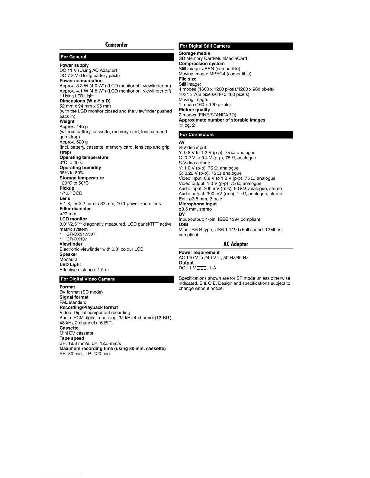
SPECIFICATION
1-2 (No.YF046)
Page 3

SECTION 1
r
e
PRECAUTIONS
1.1 SAFTY PRECAUTIONS
Prior to shipment from the factory, JVC products are strictly
inspected to conform with the recognized product safety and
electrical codes of the countries in which they are to be
sold.However,in order to maintain such compliance, it is equally
important to implement the following precautions when a set is
being serviced.
1.1.1 Precautions during Servicing
(1) Locations requiring special cauti on are denoted by labels
and inscriptions on the cabinet, chassis and certain parts of
the product.When performing service, be sure to read and
comply with these and other cautionary notices appearing
in the operation and service manuals.
(2) Parts identified by the symbol and shaded ( ) parts
are critical for safety.
Replace only with specified part numbers.
NOTE :
Parts in this category also include those specified to
comply with X-ray emission standards for products
using cathode ray tubes and those specified for
compliance with various regulations regarding
spurious radiation emission.
(3) Fuse replacement caution notice.
Caution for continued protection against fire hazard.
Replace only with same type and rated fuse(s) as
specified.
(4) Use specified internal wiring. Note especially:
• Wires covered with PVC tubing
• Double insulated wires
• High voltage leads
(5) Use specified insulating materials for hazardous live parts.
Note especially:
• Insulation Tape
• PVC tubing
•Spacers
• Insulation sheets for transistors
•Barrier
(6) When replacing AC primary side compon ents (transformers,
power cords, noise blocking capacitors, etc.) wrap ends of
wires securely about the terminals before soldering.
emission. Consequently, when servicing these products,
replace the cathode ray tubes and other parts with only the
specified parts. Under no circumstances attempt to modify
these circuits.Unauthorized modification can increase the
high voltage value and cause X-ray emission from the
cathode ray tube.
(12) Crimp type wire connectorIn such cases as when replacing
the power transformer in sets where the connections
between the power cord and power trans former primary
lead wires are performed using crimp type connectors, if
replacing the connectors is unavoidable, in order to prevent
safety hazards, perform carefully and precisely according
to the following steps.
• Connector part number :E03830-001
• Required tool : Connector crimping tool of the proper
type which will not damage insulated parts.
• Replacement procedure
a) Remove the old connector by cutting the wires at a
point close to the connector.Important : Do not
reuse a connector (discard it).
cut close to connector
Fig.1-1-3
b) Strip about 15 mm of the insulati on from the ends
of the wires. If the wires are stranded, twist the
strands to avoid frayed conductors.
15 mm
Fig.1-1-4
c) Align the lengths of the wires to be connected.
Insert the wires fully into the connector.
Metal sleeve
Fig.1-1-1
(7) Observe that wires do not contact heat producing parts
(heatsinks, oxide metal film resistors, fusible resistors, etc.)
(8) Check that replaced wires do not contact sharp edged or
pointed parts.
(9) When a power cord has been replaced, check that 10-15
kg of force in any direction will not loosen it.
Power cord
Fig.1-1-2
(10) Also check areas surrounding repaired locations.
(11) Products using cathode ray tubes (CRTs)In regard to such
products, the cathode ray tubes themselves, the high
voltage circuits, and related circuits are specified for
compliance with recognized codes pertaining to X-ray
Connector
Fig.1-1-5
d) As sh ow n i n Fi g.1-1-6, use the crimping tool to crimp
the metal sleeve at the center position. Be sure to
crimp fully to the complete closure of the tool.
1.2
5
2
.0
5.5
Crimping tool
Fig.1-1-6
e) Check the four points noted in Fig.1-1-7.
Not easily pulled free
Wire insulation recessed
more than 4 mm
Crimped at approx. cente
of metal sleev
Conductors extended
Fig.1-1-7
(No.YF046)1-3
Page 4
1.1.2 Safety Check after Servicing
Examine the area surrounding the repaired location for d amage
or deterioration. Observe that screws, parts and wires have been
returned to original positions, Afterwards, perform the following
tests and confirm the specified values in order to verify
compliance with safety standards.
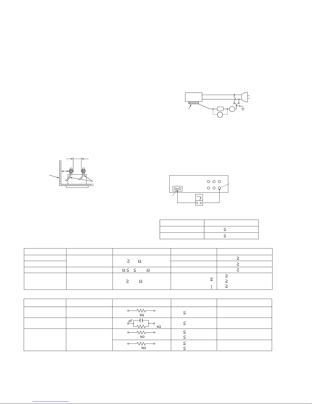
(1) Insulation resistance test
Confirm the specified insulation resistance or greater
between power cord plug prongs and externally exposed
parts of the set (RF terminals, antenna terminals, video and
audio input and output terminals, microphone jacks,
earphone jacks, etc.).See table 1 below.
(2) Dielectric strength test
Confirm specified dielectric strength or greater between
power cord plug prongs and exposed accessible parts of
the set (RF terminals, antenna terminals, video and audio
input and output terminals, microphone jacks, earphone
jacks, etc.). See Fig.1-1-11 below.
(3) Clearance distance
When replacing primary circuit components, confirm
specified clearance distance (d), (d') between soldered
terminals, and between terminals and surrounding metallic
parts. See Fig.1-1-11 below.
d
Chassis
d'
Power cord
primary wire
Fig.1-1-8
(4) Leakage current test
Confirm specified or lower leakage current between earth
ground/power cord plug prongs and externally exposed
accessible parts (RF terminals, antenna terminals, video
and audio input and output terminals, microphone jacks,
earphone jacks, etc.).
Measuring Method : (Power ON)Insert load Z between
earth ground/power cord plug prongs and externally
exposed accessible parts. Use an AC voltmeter to
measure across both terminals of load Z. See Fig.1-1-9
and following Fig.1-1-12.
ab
Externally
exposed
accessible part
Z
V
c
A
Fig.1-1-9
(5) Grounding (Class 1 model only)
Confirm specified or lower grounding impedance between
earth pin in AC inlet and externally exposed accessible
parts (Video in, Video out, Audio in, Audio out or Fixing
screw etc.).Measuring Method:
Connect milli ohm meter between earth pin in AC inlet and
exposed accessible parts. See Fig.1-1-10 and grounding
specifications.
AC inlet
Earth pin
Exposed accessible part
MIlli ohm meter
Grounding Specifications
Region
USA & Canada
Europe & Australia
Grounding Impedance (Z
Z 0.1 ohm
Z 0.5 ohm
)
Fig.1-1-10
AC Line Voltage
100 V
100 to 240 V
110 to 130 V
110 to 130 V
200 to 240 V
Region
Japan
USA & Canada
Europe & Australia
Insulation Resistance (R
R 1 M /500 V DC
1 M R 12 M /500 V DC
R 10 M /500 V DC
)
Dielectric Strength
AC 1 kV 1 minute
AC 1.5 kV 1 minute
AC 1 kV 1 minute
AC 3 kV 1 minute
AC 1.5 kV 1 minute
(
Class
(
Class
Clearance Distance (d), (d'
d, d' 3 mm
d, d' 4 mm
d, d' 3.2 mm
d 4 mm
)
d' 8 mm (Power cord
d' 6 mm (Primary wire
)
Fig.1-1-11
AC Line Voltage
100 V
110 to 130 V
110 to 130 V
220 to 240 V
Region
Japan
USA & Canada
Europe & Australia
Load Z
1
0.15
1.5
2
50
Leakage Current (i)
i 1 mA rms
i 0.5 mA rms
i 0.7 mA peak
i 2 mA dc
i 0.7 mA peak
i 2 mA dc
a, b, c
Exposed accessible parts
Exposed accessible parts
Antenna earth terminals
Other terminals
Fig.1-1-12
NOTE :
These tables are unofficial and for reference only. Be sure to confirm the precise values for your particular country and locality.
)
)
)
1-4 (No.YF046)
Page 5

SECTION 2
SPECIFIC SERVICE INSTRUCTIONS
The following table indicate main different points between models GR-DX107EK, GR-DX107EX, GR-DX107EY, GR-DX107EZ,
GR-DX307EK, GR-DX307EX, GR-DX307EY, GR-DX307EZ and GR-DX317EX.
MODEL GR-DX107EK GR-DX107EX GR-DX107EY GR-DX107EZ GR-DX307EK
LCD MONITOR 2.5INCH 2.5INCH 2.5INCH 2.5INCH 3.0INCH
BODY COLOR Silver & Silver Silver & Black Silver & Black Silver & Black Silver & Black
AC CORD BS PULG CEE PULG CEE PULG CEE PULG BS PULG
BATTERY PACK BN-V107U-S BN-V107U-S BN-V107U-S BN-V107U-S BN-V107U-S
MODEL GR-DX307EX GR-DX307EY GR-DX307EZ GR-DX317EX
LCD MONITOR 3.0INCH 3.0INCH 3.0INCH 3.0INCH
BODY COLOR Silver & Black Silver & Black Silver & Black D.Gray & Black
AC CORD CEE PULG CEE PULG CEE PULG CEE PULG
BATTERY PACK BN-V107U-S BN-V107U-S BN-V107U-S BN-V107U
(No.YF046)1-5
Page 6
SECTION 3
DISASSEMBLY
3.1 BEFORE ASSEMBLY AND DISASSEMBLY
3.1.1 Precautions
• Be sure to disconnect the power supply unit prior to mounting
and soldering of parts.
• Prior to removing a component part that needs to disconnect
its connector(s) and its screw(s), first disconnect the wire(s)
from the connector(s), and then remove the screw(s).
• When connecting/disconnecting wires, pay enough attention
not to damage the connectors.
• When inserting the flat wire to the connector, pay attention to
the direction of the flat wire.
• Be careful in removing the parts to which some spacer or
shield is attached for reinforcement or insulation.
• When replacing chip parts (especially IC parts), first remove
the solder completely to prevent peeling of the pattern.
• Tighten screws properly during the procedures. Unless
specified otherwise, tighten screws at a torque of 0.088N
·cm). However, 0.088N·m (0.9kgf·cm) is a value at the
(0.9kgf
time of production. At the time of service, perform the
procedure at a torque 10% less than 0.088N
·m (0.9kgf·cm).
(See "SERVICE NOTE" as for tightening torque.)
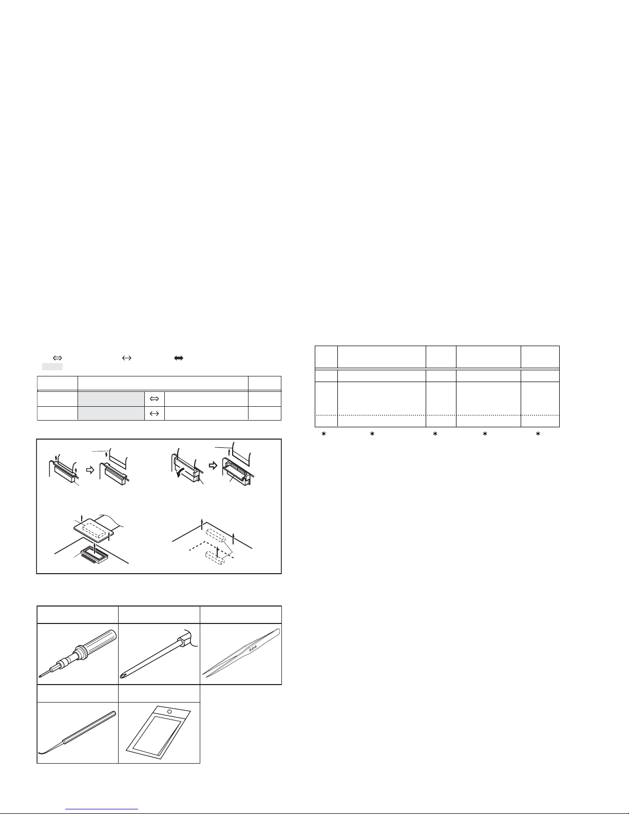
3.1.2 Destination of connectors
Two kinds of double-arrows in connection tables respectively
show kinds of connector/wires.
: Wire: Flat wire : Board to board (B-B)
: The connector of the side to remove
CONN. No. PIN No.CONNECTOR
CN2a
CN2b
MAIN CN101
MAIN CN103
MONI BW CN761
MINI BW CN762
3.1.3 Disconnection of connectors (Wires)
Wire
· Pull both ends of the connector in the arrow
direction, remove the lock and disconnect the flat
wire.
B-B Connector
B-B Connector
· Pull the both ends of the board in the direction of the arrow, and remove the B-B Connector.
FPC Connector
· Extend the locks in the direction of the arrow for
unlocking and then pull out the wire. After
removing the wire, immediately restore the locks
to their original positions because the locks are
apt to come off the connector.
Wire
FPC Connector
Lock
B-B Connector
Fig.3-1-1
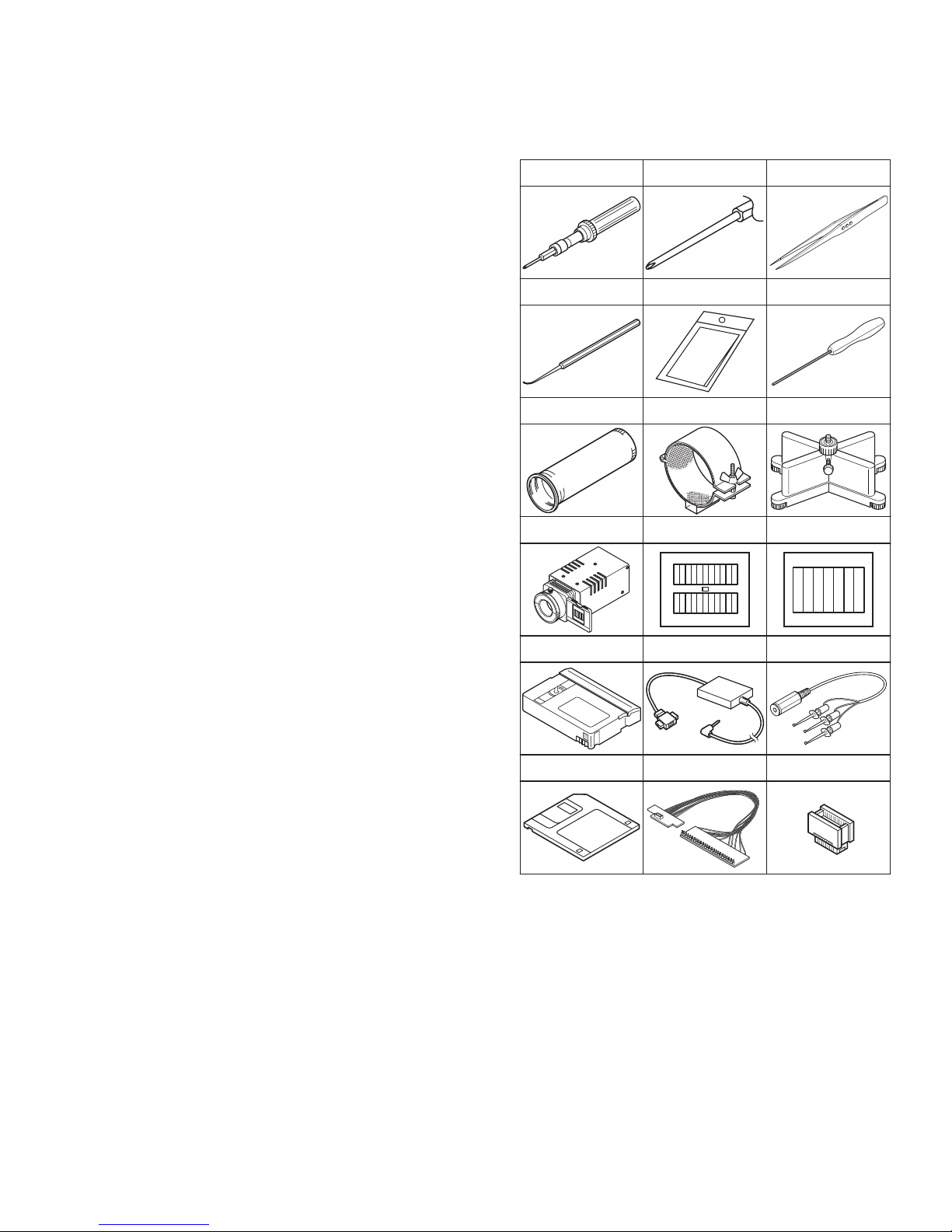
3.1.4 Tools required for disassembly and assembly
Torque driver
YTU94088
Bit
YTU94088-003
Tweezers
P-895
·m
40
10
• Torque driver
Be sure to use to fastening the mechanism and exterior parts
because those parts must strictly be controlled for tightening
torque.
• Bit
This bit is slightly longer than those set in conventional torque
drivers.
• Tweezers
To be used for removing and installing parts and wires.
• Chip IC replacement jig
To be used for replacement of IC.
• Cleaning cloth
Recommended cleaning cloth to wipe down the video heads,
mechanism (tape transport system), optical lens surface.
3.2 ASSEMBLY AND DISASSEMBLY OF MAIN PARTS
3.2.1 Assembly and disassembly
When reassembling, perform the step(s) in reverse order.
STEP
No.
[1]
[2]
[8]
PART
TOP COVER ASSY
UPPER ASSY
(Inc. VF ASSY,
SPEAKER/MONITOR)
E.VF UNIT(B/W)
(∗1) Order of steps in Procedure
When reassembling, preform th e step(s) in the reverseorder.
These numbers are also used as the identification (location)
No. of parts Figures.
(∗2) Part to be removed or installed.
(∗3) Fig. No. showing Procedure or Part Location.
C = CABINET
(∗4) Identification of part to be removed, unhooked, unlocked,
released, unplugged, unclamped or unsoldered.
S = Screw
L = Lock, Release, Hook
SD = Solder
CN = Connector
[Example]
• 4 (S1a) = Remove 4 S1a screws.
• 3 (L1a) = Disengage 3 L1a hooks.
• 2 (SD1a) = Unsolder 2 SD1a points.
• CN1a = Remove a CN1a connector.
(∗5) Adjustment information for installation.
Fig.
No.
4(S1a), 3(L1a),CN1a
Fig.C1
(S2a),2(S2b),3(S2c)
Fig.C2-1
2(SD1a),
L2,CN2a,b
2(S8),L8,CN8a
Fig.C2-2
POINT
( 4) ( 5)( 2) ( 3)( 1)
NOTE
-
-
NOTE 8
Chip IC replacement jig
PTS40844-2
Cleaning cloth
KSMM-01
Fig.3-1-2
1-6 (No.YF046)
Page 7
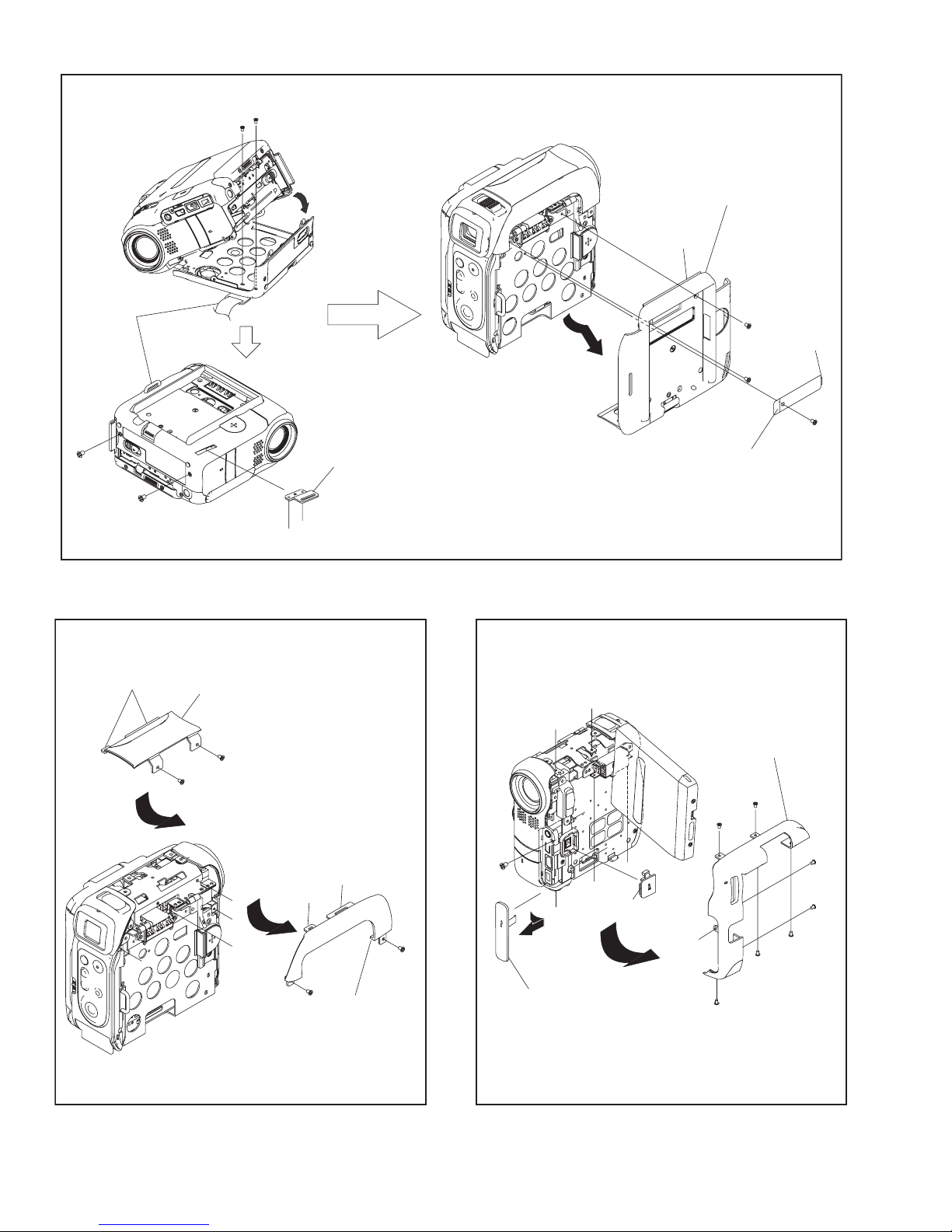
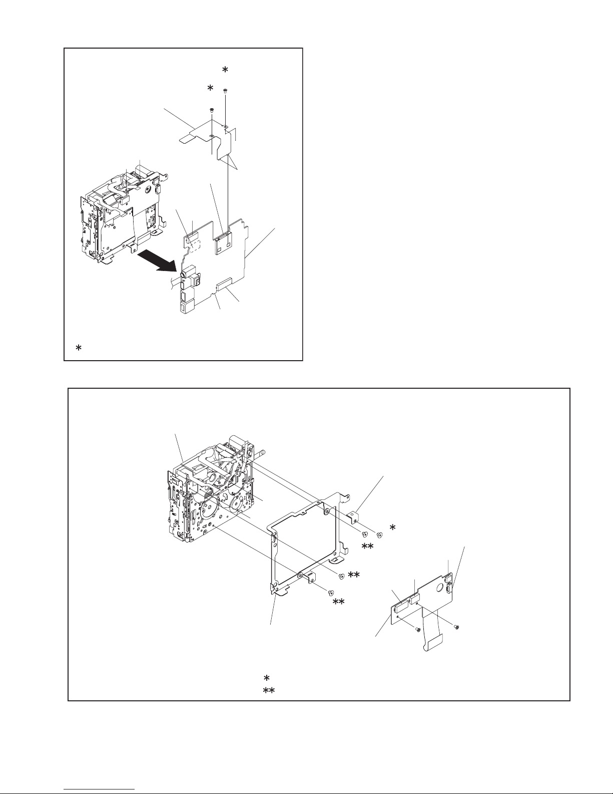
3.2.2 ASSEMBLY/DISASSEMBLY OF CABINET PARTS AND ELECTRICAL PARTS
zDisassembly procedure
STEP
PART NAME
No.
[1]
CASSETTE COVER ASSY
[2]
SIDE COVER(R)
[3]
TOP COVER
[4]
SIDE COVER(L)ASSY
[5]
UPPER CASE ASSY
[6]
FRONT COVER ASSY
[7]
MIC ASSY
[8]
REAR COVER ASSY
[9]
MONITOR BOARD
[10]
SD BOARD ASSY
[11]
LOWER UNIT ASSY
(INCLUDE VF ASSY/OP BLOCK ASSY)
[12]
VF ASSY
[13]
OP BLOCK ASSY/CCD BOARD ASSY
[14]
MAIN BOARD ASSY
[15]
MDA BOARD ASSY
[16]
MECHANISM ASSY
Fig.
No.
GRIP BELT ASSY,2(S1),HOOK(F)
Fig.C1
(S1),L1a,COVER(ADJ),4(S1),L1b
(S2a),(S2b),L2a,L2b
Fig.C2
2(S3),2(L3)
6(S4a),(S4b),(S4c),COVER(DV)ASSY
Fig.C3
JACK COVER ASSY
(S5),L5,COVER(JIG CON),4(S5),CN5
Fig.C4
5(S6),CN6
Fig.C5
2(S7)
2(S8),L8a,2(L8b),L8c,CN8
Fig.C6
2(S9),3(L9a),BKT(TOP)ASSY
Fig.C7
CN9a,b,6(S9),L9b,2(L9c)
CN10,(S10)
Fig.C8
CN11a,b,c,d,e,3(S11)
4(S12)
Fig.C9
(S13),2(L13)
2(S14),2(L14a),SHIELD COVER
Fig.C10
CN14a,b,c,L14b
CN15a,b,c,d,2(S15)
Fig.C11
(S16a),BKT(PRE-REC),3(S16b)
BKT(MECHA)ASSY
POINT NOTE
NOTE1:
Before removing the CASSETTE COVER ASSEMBLY, remove the GRIP BELT ASSEMBLY.
NOTE4a:
During the procedure, be careful in handling the parts.
NOTE4b:
In attaching the SIDE COVER (L) ASSEMBLY, attach the
COVER (JACK, DV) ASSEMBLY at the same time.
NOTE5:
In removing the UPPER CASE ASSEMBLY, be careful not
to damage connectors.
NOTE6:
NOTE1
-
-
NOTE4a, b
NOTE5
NOTE6
NOTE7
NOTE8
NOTE9
-
-
NOTE12a, b
NOTE13
NOTE14
-
NOTE16
NOTE13:
For the disassembly procedure of the OP BLOCK ASSEMBLY/CCD BOARD ASSEMBLY, see "3.2.5 DISASSEMBLY
of [13] OP BLOCK ASSMBLY/CCD BOARD ASSEMBLY"
NOTE14:
In removing the MAIN BOARD ASSEMBLY, remove the SPACER.
NOTE16:
Be careful in handling the parts.
zDestination of connectors
CN.NO.
CN5 MAIN CN115 SUB OPE UNIT - 6
CN6 MAIN CN111 MIC ASSY - 4
CN8 MAIN CN109 CAMERA OPE UNIT - 13
CN9a MAIN CN104 MONITOR
/CN7602 20
CN9b MAIN CN108 POWER OPE UNIT - 7
CN10 MAIN CN114 SD CN701 12
CN11a MAIN CN112 FRONT CN401 12
CN11b MAIN CN107 OP BLOCK ASSY - 28
CN11c MAIN CN102 CCD CN5501 20
CN11d MAIN CN101 BATT. TERM. - 21
CN11e MAIN CN113 VF FPC ASSY - 22/20
CN14a MAIN CN106 SENSOR - 16
CN14b MAIN CN103 MDA CN305 30
CN14c MAIN CN110 HEAD - 8
CN15a MDA CN301 CAPSTAN MOTOR - 18
CN15b MDA CN302 DRUM MOTOR - 11
CN15c MDA CN303
CN15d MDA CN304 LOADING MOTOR - 6
In attaching the FRONT COVER ASSEMBLY, be careful not
to cut or damage wires.
NOTE7:
In attaching the MIC ASSEMBLY, be careful not to cut or
damage wires.
NOTE8:
When attaching the REAR COVER ASSEMBLY, be careful
about the position of switch.
NOTE9:
For the disassembly procedure of the MONITOR ASSEMBLY,
see "3.2 .3 DISASSEMBLY of [9] MONITOR ASSEMBLY"
NOTE12a:
Pull out the VF ASSEMBLY, and remove one screw (No.46).
NOTE12b:
For the disassembly procedure of the VF ASSEMBLY, see
"3.2.4 DISASSMBLY of [12] VF ASSEMBLY"
CONNECTOR
CN7601
ROTARY ENCODER SW
PIN
NO.
39/20,
- 6
(No.YF046)1-7
Page 8
2
DC
A
V
(S1)
b
1
(S1)
a
[1]
L1b
NOTE1
7
(S1)
6
(S1)
L3
4
(S1)
L1a
5
(S1)
3
(S1)
HOOK(F)
COVER(ADJ)
NOTE1
b
a
Fig.C1
[3]
a
b
a
11
(S3)
10
(S3)
a
c
b
L2a
d
9
(S2b)
L2b
[2]
c
8
(S2a)
e
h
19
(S4c)
d
g
JACK COVER ASSEMBLY
NOTE4b
f
c
COVER(DV)
ASSEMBLY
NOTE4b
13
(S4a)
h
18
(S4b)
b
d
b
g
12
(S4a)
a
d
15
(S4a)
[4]
NOTE4a
c
14
(S4a)
e
f
16
(S4a)
17
(S4a)
Fig.C2 Fig.C3
1-8 (No.YF046)
Page 9
b
CN5
NOTE5
[5]
21
a
(S5)
22
(S5)
: 0.078N.m(0.8kgf.cm)
Fig.C4
b
24
(S5)
NOTE6
[6]
a
23
(S5)
20
(S5)
COVER(JIG CON)
L5
25
BKT(MIC) ASSEMBLY
(S6)
[7]
NOTE7
e
30
(S7)
a
31
(S7)
e
CN6
c
a
26
(S6)
b
27
(S6)
c
28
(S6)
d
29
(S6)
b
Fig.C5
d
(No.YF046)1-9
Page 10
L8a
[8]
[10]
42
(S10)
[11]
L9a
35
(S9)
NOTE8
34
(S9)
a
CN9a
CN9b
L8b
L8c
Fig.C6
BKT(TOP)ASSEMBLY
L9a
36
(S9)
b
CN8
32
(S8)
33
(S8)
45
(S11)
44
(S11)
CN11e
43
(S11)
CN10
b
CN11b
CN11c
a
CN11d
b
a
CN11a
NOTE11
CN
Fig.C8
[12]
50
(S13)
(S12)
46
(S12)
a
47
b
NOTE12a, b
48
(S12)
49
(S12)
b
L9b
a
L9c
Fig.C7
1-10 (No.YF046)
41
(S9)
[9]
NOTE9
37
(S9)
39
(S9)
40
(S9)
38
(S9)
[13]
NOTE13
b
a
Fig.C9
L13
Page 11
SHIELD COVER
a
b
NOTE14
SPACER(A)
: 0.069N.m(0.7kgf.cm)
Fig.10
(S14)
CN14c
CN14a
52
(S14)
51
a
b
L14a
[14]
CN14b
L14b
[16]
b
a
BKT(MECHA)ASSEMBLY
: 0.069N.m(0.7kgf.cm)
: 0.078N
Fig.C11
(S16b)
57
(S16b)
58
(S16b)
.
m(0.8kgf.cm)
NOTE16
BKT(PRE-REC)
55
(S16a)
56
CN16b
CN16a
[15]
a
53
(S15)
CN16d
CN16c
b
54
(S15)
(No.YF046)1-11
Page 12
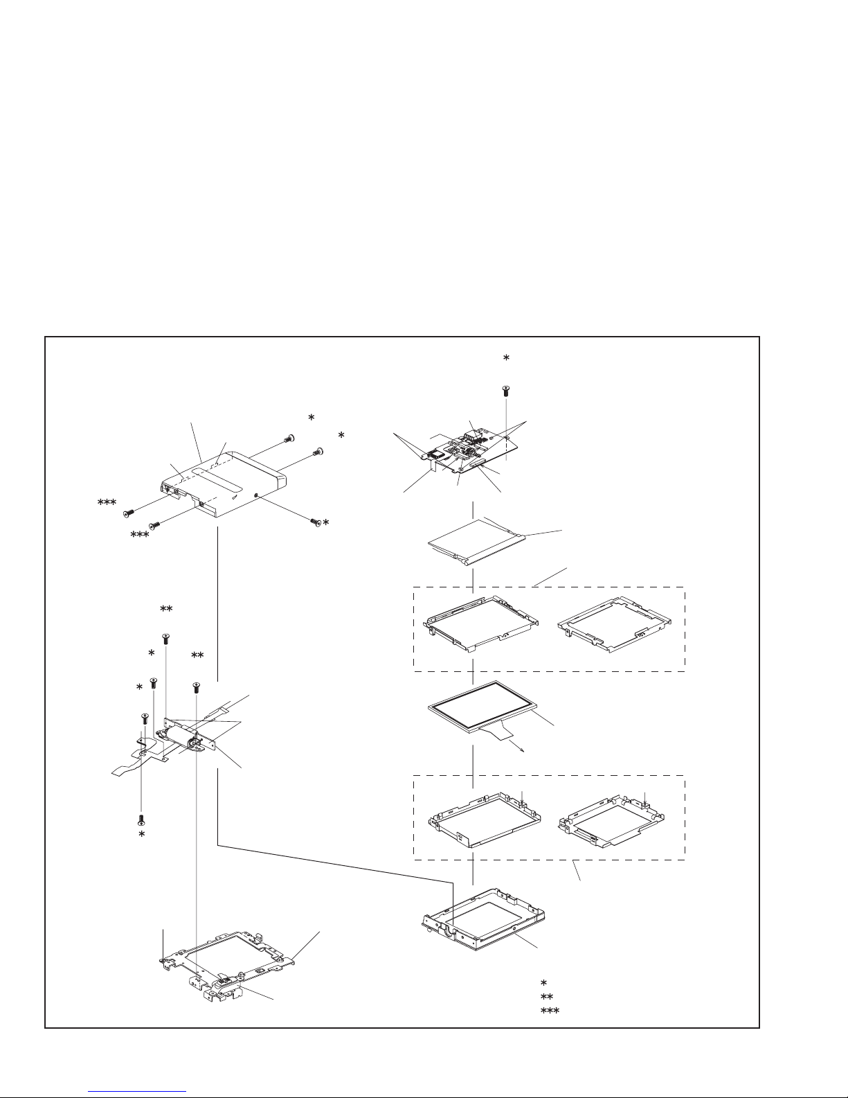
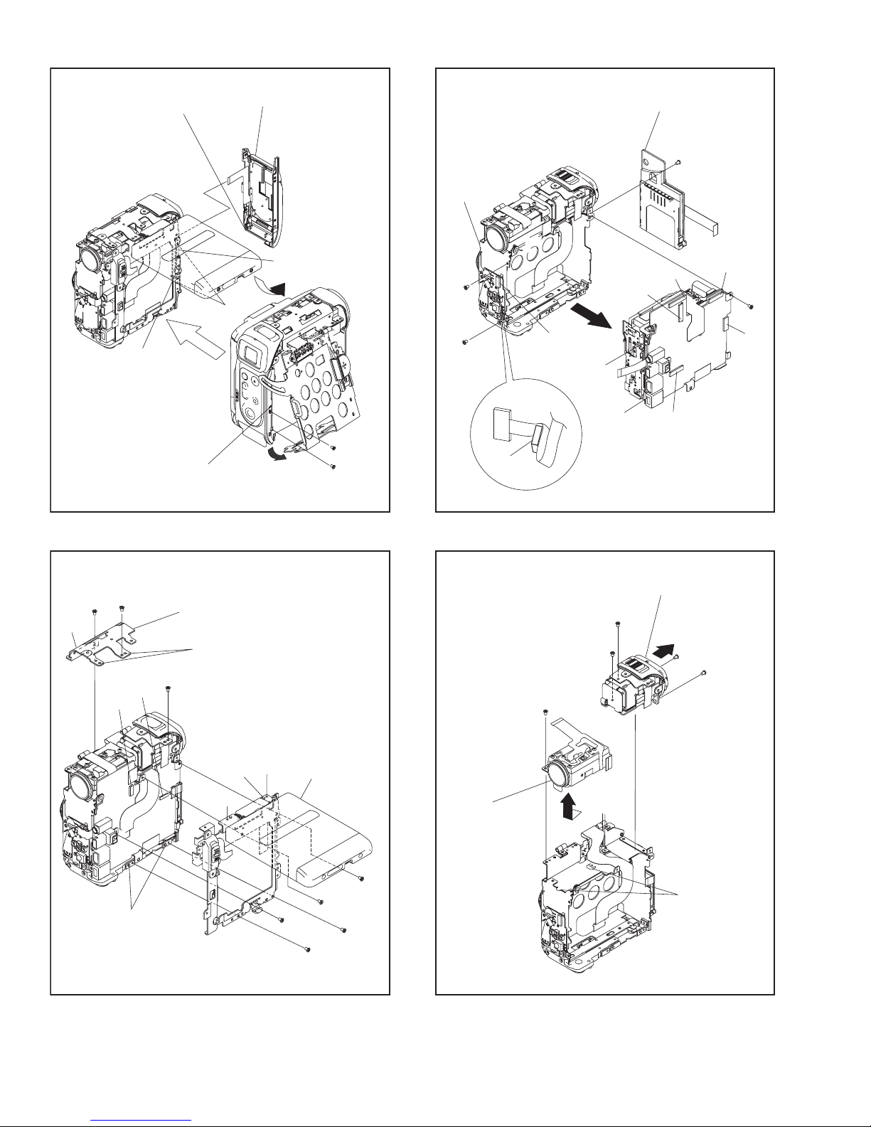
3.2.3 DISASSEMBLY of [9] MONITOR ASSEMBLY
zCAUTIONS
(1) During the procedure, be careful in handling the LCD
MODULE,etc., especially not to damage or soil the monitor screen. If it is soiled with fingerprints, etc., gently
clean it with chamois or the cleaning cloth.
(2) Since the BACKLIGHT is soldered to the BOARD AS-
SEMBLY (SD9), the BACKLIGHT should not be separated from the BOARD ASSEMBLY except when replacing
the BACKLIGHT.
(3) Remove the POWER (OPE) UNIT if necessary.
zDisassembly
(1) Remove the three screws (1-3) so that the FPC moves
easily.
(2) Remove the two screws (4 and 5), and remove the MON-
ITOR ASSEMBLY from the FRAME (UP) ASSEMBLY.
(3) While removing the five screws (6-10) in numerical order
and disengaging the two hooks (L9a and L9b) in alphabetical order, remove the MONITOR COVER ASSY.
(4) Remove the SWITCH BOARD from the MONITOR
CASE.
(5) Unlock the two connectors C N9a and CN9b, and raise
and remove the HINGE UNIT ASSEMBLY.
NOTE9a:
During the procedure, be careful in handling the F PC
ASSEMBLY.
(6) Unlock one connector CN9c, and remove the FPC.
(7) Remove one screw (11), and remove the MONITOR
BOARD ASSEMBLY together with the BACKLIGHT.
(8) Remove the LCD BRACKET (2).
(9) Remove the LCD MODULE.
(10) Remove the LCD BRACKET (1).
11
(S9f)
MONITOR COVER ASSEMBLY
L9a
L9b
e
9
(S9e)
10
(S9e)
4
(S9a)
(S9a)
2
(S9a)
d
3
e
5
(S9a)
F2
F3
L9c
HINGE UNIT ASSEMBLY
NOTE9a
7
(S9d)
(S9c)
(S9d)
6
L9d
8
SWITCH BOARD
ASSEMBLY
F3
F2
CN9a
CN9b
SD9
MONITOR BOARD
a
ASSEMBLY[0][5]
F1
CN9c
For 3.0INCH
F1
a
BACK LIGHT
LCD BKT (2)
For 2.5INCH
LCD MODULE
a
1
(S9a)
d
FRAME(UP)ASSEMBLY
POWER(OPE)UNIT
1-12 (No.YF046)
Fig.3-2-3
For 2.5INCHFor 3.0INCH
LCD BKT (1)
MONITOR CASE
: 0.098N.m(1.0kgf.cm)
: 0.196N
: 0.246N
.
m(2.0kgf.cm)
.
m(2.5kgf.cm)
Page 13
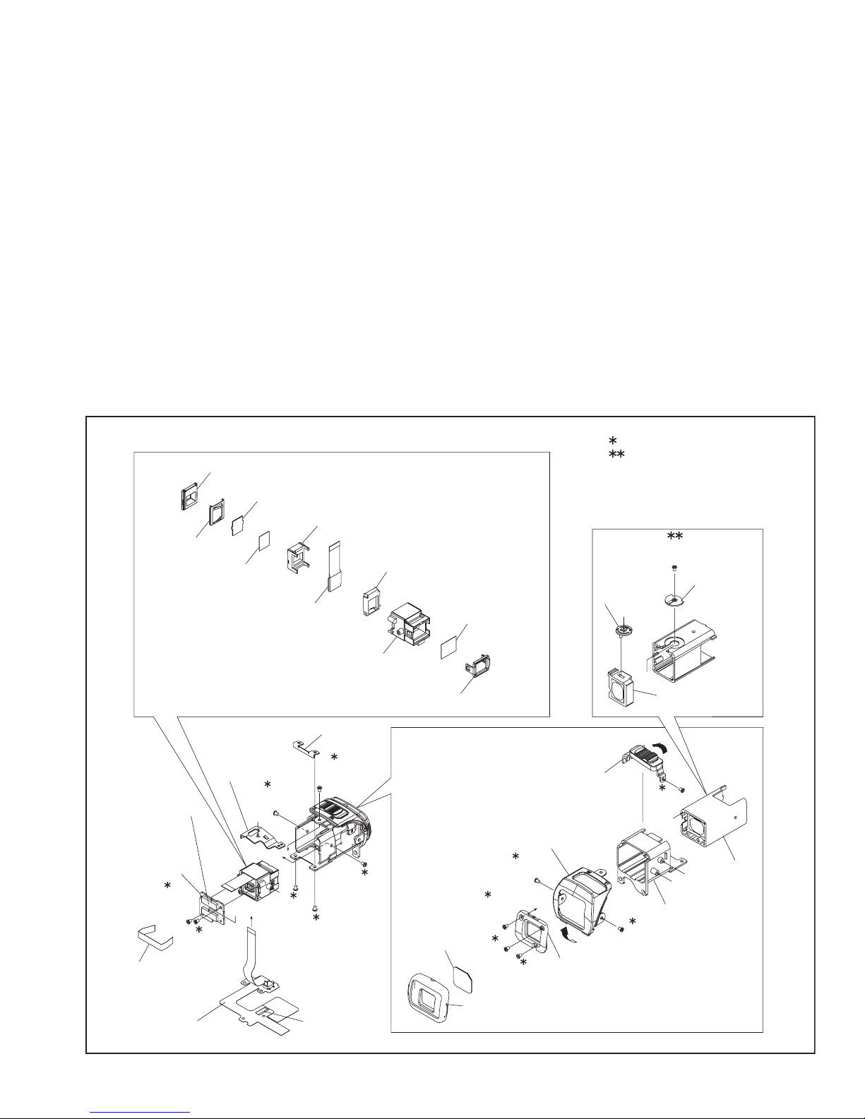
3.2.4 DISASSMBLY of [12] VF ASSEMBLY
zDisassembly
(1) Remove the EYE CUP.
NOTE12a:
After the EYE CUP is removed, be careful of handling
the EYE CUP since the SHEET (LENS) is removed.
NOTE12b:
In attaching the EYE CUP, be careful of the attachment direction of the SHEET (LENS).
(2) Remove the three screws (1-3) and remove the HOLD-
ER (EYE).
(3) Remove one screw (4) and remove the BRACKET
(TOP2).
(4) Remove the two screws (5 and 6), lift the VF COVER in
a direction of arrow, and remove the VF COVER from the
ZOOM UNIT.
(5) Remove the FPC from one connector (CN12a), remove
one screw (7), and remove the ZOOM UNIT.
(6) Remove the two screws (8 and 9), and remove the
BRACKET.
(7) Remove the FPC attached to the GUIDE (OUT ER) little
by little so that the FPC moves easily, and remove the
COVER (VF) from the GUIDE (OUTER).
NOTE12c:
Be careful enough not to cut or damage the removed
FPC since the FPC is attached again.
NOTE12d:
Disassemble the COVER (VF) if necessary. In an attachment procedure, confirm that the LEVER (1)
moves smoothly.
(8) Remove the two screws (10 and 11), and remove the
FRAME ASSEMBLY.
(9) Remove the SPACER (A), and remove the FPC from
one connector (CN12b).
(10) Remove the two screws (12 and 13), and remove the VF
BOARD ASSEMBLY.
NOTE12e:
Disassemble the FRAME ASSEMBLY if necessary. In
an assembly procedure, be careful not to insert foreign
materials inside the VF and not to soil the VF.
< FRAME ASSEMBLY >
CASE(B.LIGHT)
SHEET(DIFF)
SPRING(LCD)
SHEET(POLA)
LCD MODULE
BRACKET(TOP2)
10
CN12b
VF BOARD
ASSEMBLY
[0][6]
12
(S12d)
(S12d)
SPACER(A)
13
(S12d)
g
F1F1
(S12b)
HOLDER(SHEET)
FRAME(VF)
BRACKET
(S12b)
g
f
f
8
9
(S12b)
STOPPER(POLA)
4
11
(S12d)
GUIDE(LCD)
NOTE12a,b
SHEET(LENS)
NOTE12e
SHEET(POLA)
5
(S12a)
1
(S12c)
2
(S12a)
3
(S12a)
< CASE(VF) >
ZOOM UNIT
VF COVER
e
HOLDER(EYE)
: 0.059N.m(0.6kgf.cm)
: 0.049N
.
m(0.5kgf.cm)
14
(S12e)
LEVER(2)
a
a
LENS HOLDER
ASSEMBLY
c
7
(S12c)
e
c
d
d
(S12c)
GUIDE(OUTER)
6
LEVER(1)
NOTE12d
CASE(VF)
FPC
NOTE12c
CN12a
EYE CUP
Fig.3-2-4
(No.YF046)1-13
Page 14
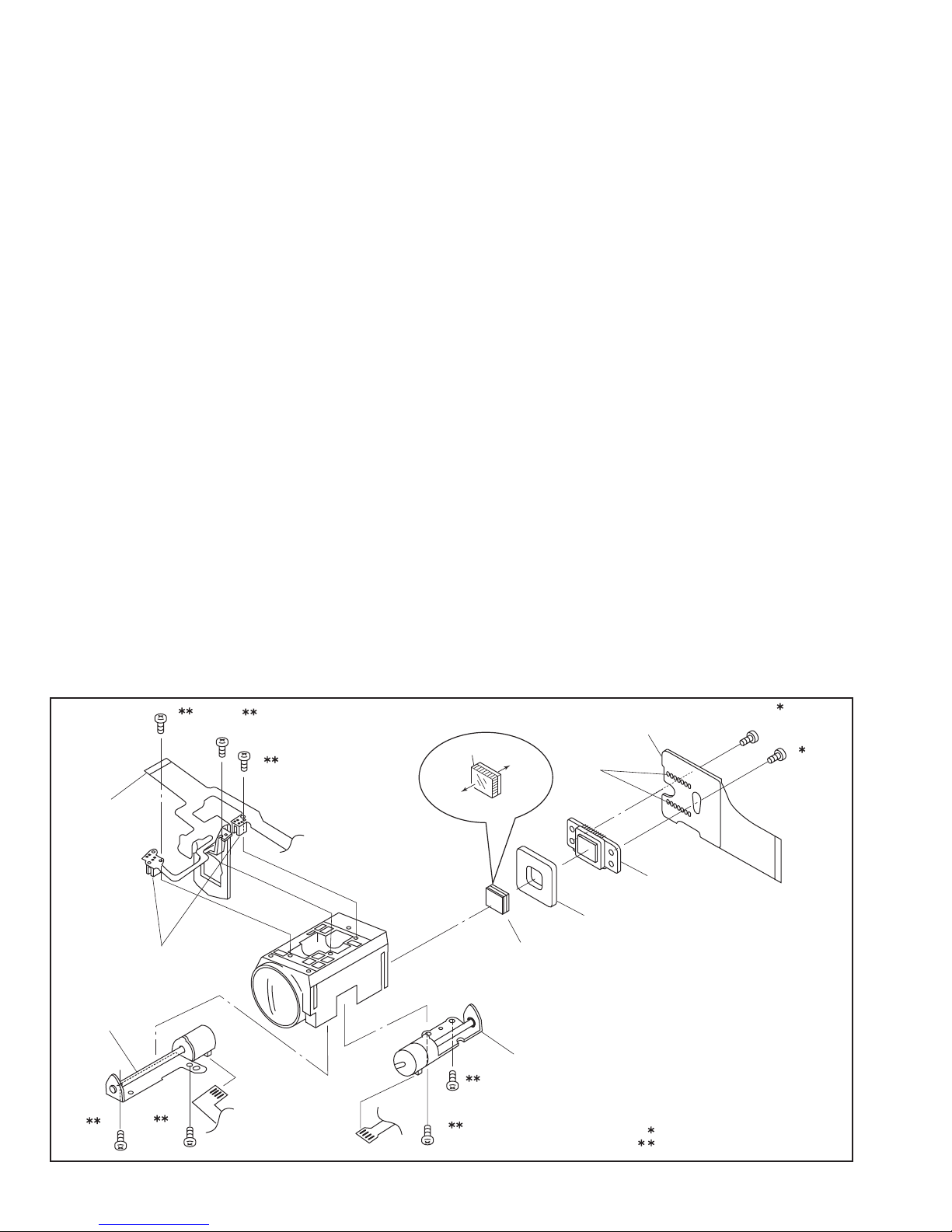
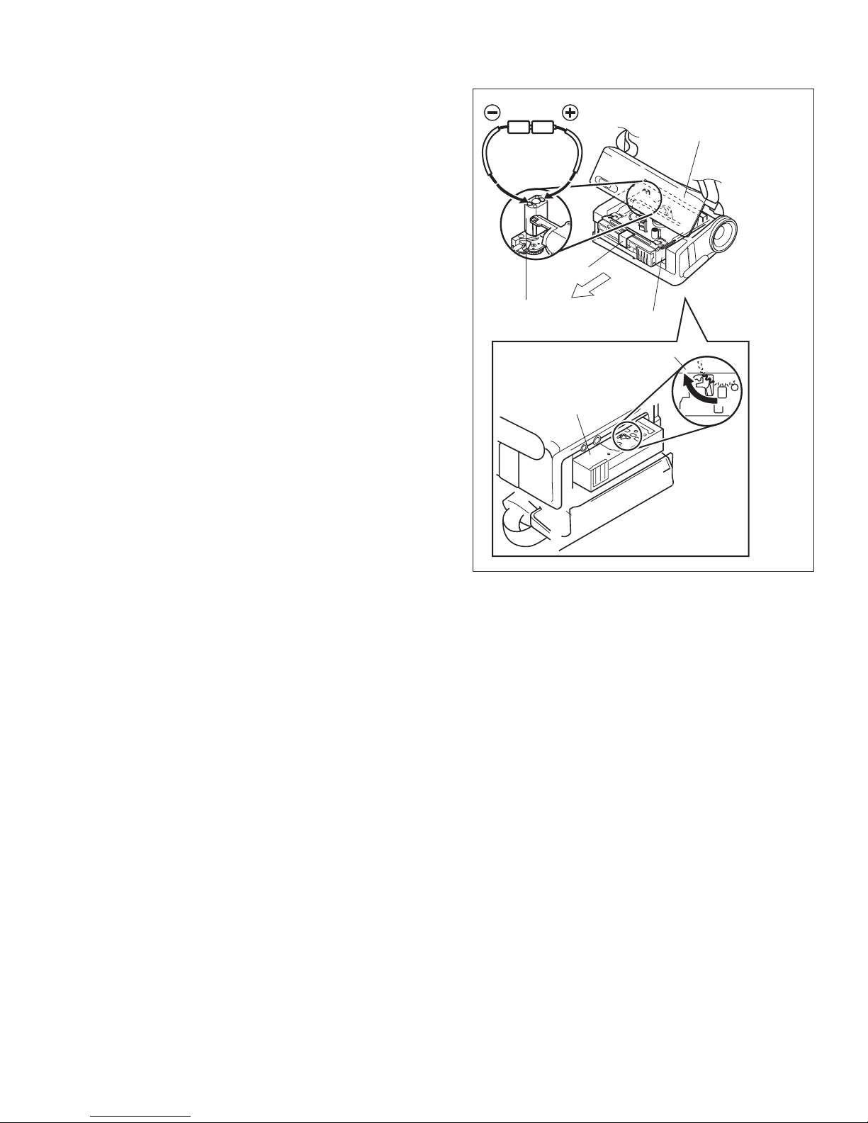
3.2.5 DISASSEMBLY of [13] OP BLOCK ASSMBLY/CCD BOARD ASSEMBLY
zCAUTIONS
(1) During the procedure, remove the OP BLOCK ASSEMBLY
if necessary. When removing the OP BLOCK ASSEMBLY,
be careful not to damage the lens.
(2) During the procedure, be careful in handling CCD
IMAGE SENSOR, OP LPF, lens, and so on. Be careful
not to damage or soil the surface of them.
If they are soiled with fingerprints, etc., gently clean them
with chamois or the cleaning cloth.
(3) When products are shipped from the factory, protection
seals are applied onto transparent glass of some CCD
image sensors. Leave the protection seal as it is, and
take it off just before assembling the CCD image sensor
to the OP BLOCK ASSEMBLY.
(4) When removing OP LPF, be careful of the atta chment
direction of OP LPF. (Marking is attached to some OP
LPFs.) When reassembling OP LPF, reattach OP LPF to
the original position.
zDisassembly procedure of OP BLOCK ASSEMBLY/CCD
BOARD ASSEMBLY
(1) Unsolder the fourteen soldered parts (SD13) on the CCD
BOARD ASSEMBLY, and remove the CCD BOARD
ASSEMBLY.
(2) Remove the two screws (1 and 2), and remove the CCD
BASE ASSEMBLY.
NOTE13a:
When removing the CCD BASE ASSEMBLY, be
careful in handling a sheet and OP LPF since a sheet
or OP LPF may be removed together with the CCD
zAssembly procedure of OP BLOCK ASSEMBLY/CCD
BOARD ASSEMBLY
(1) Attach the OP LPF to the OP BLOCK ASSEMBLY, and
then the sheet to the OP BLOCK ASSEMBLY.
NOTE13c:
When attaching OP LPF to the OP BLOCK ASSEMBLY,
be careful about the attachment direction.
(2) Attach the CCD ASSEMBLY so that the sheet is not
shifted, and attach the CCD ASSEMBLY and the sheet
to the OP BLOCK ASSEMBLY by tightening them with
the two screws (1 and 2).
(3) Insert the CCD BOARD ASSEMBLY to the CCD BASE
ASSEMBLY, and solder the fourteen points (SD13).
zReplacement of service repair parts
Service repair parts of the OP BLOCK ASSEMBLY are as
follows. When replacing the parts, be careful not to cut or
damage the FPC, and not to damage the parts due to
soldering (overheat).
(1) FOCUS MOTOR
(2) ZOOM MOTOR
(3) IRIS MOTOR
NOTE13d:
When replacing the FOCUS MOTOR or the ZOOM
MOTOR, lift the FPC approx.0.5mm away from the
jack to solder the FPC.
NOTE13e:
Iris motor unit contains the FPC ASSEMBLY and the
SENSOR × 2.
BASE ASSEMBLY.
NOTE13b:
When replacing the CCD image sensor, don't remove the
CCD image sensor from the CCD BASE ASSEMBLY.
Instead, replace the entire CCD BASE ASSEMBLY.
IRIS MOTOR
NOTE13e
ZOOM MOTOR
NOTE13d
6
(S13b)
9
(S13c)
SENSOR
5
(S13b)
7
(S13b)
8
(S13c)
SD13c
SD13b
1-14 (No.YF046)
OP LPF
Blue
OP
side
OP BLOCK ASSEMBLY
4
(S13b)
3
(S13b)
Fig.3-2-5
CCD BOARD ASSEMBLY
CCD
FOCUS MOTOR
NOTE13d
side
OP LPF
NOTE13c
SD13a
SHEET
CCD BASE ASSEMBLY
NOTE13a,b
.
0.15N
m (1.5kgf.cm)
.
m (0.7kgf.cm)
0.069N
1
(S13a)
2
(S13a)
Page 15
SECTION 4
ADJUSTMENT
4.1 PREPARATION
4.1.1 Precaution
Camera system and deck system of this model are specially
adjusted by using PC.
However, if parts such as the following are replaced, an
adjustment is required. The adjus tment must be performed in a
Service Center equipped with the concerned facilities.
• OP BLOCK ASSEMBLY
• EEP ROM (IC1005 of MAIN board)
In the event of malfunction with electrical circuits, first find a
defective portion with the aid of proper test instruments as shown
in the following electrical adjustment procedure, and then
commence necessary repair/ replacement/adjustment.
• In observing chip TP, use IC clips, etc. to avoid any stress.
Prior to replacement of chip parts (especially IC), remove the
solder completely to prevent peeling of the pattern.
• Use a patch cord if necessary. As for a patch cord, see the
BOARD INTERCONNECTIONS.
• Since connectors are fragile, carefully handle them in
disconnecting and connecting the FPC.
4.1.2 REQUIRED TEST EQUIPMENT
• Personal computer (for Windows)
• Color TV monitor
• Oscilloscope (dual-trace type, observable 100MHz or higher
frequency). The one observable 300 MHz or higher frequency
is recommended.
• Digital voltmeter
• DC power supply or AC adapter
• Frequency counter (with threshold level adjuster)
4.1.3 TOOLS REQUIRED FOR ADJUSTMENT
Torque Driver
YTU94088
Chip IC Replacement Jig
PTS40844-2
INF Adjustment Lens
YTU92001B
Light box Assembly
YTU93096A
Alignment Tape
MC-2
INF Adjustment Lens Holder
Bit
YTU94088-003
Cleaning Cloth
KSMM-01
YTU94087
Gray Scale Chart
YTU94133A
PC Cable
QAM0099-005
Guide Driver (Hexagonal)
Camera Stand
YTU93079
Color Bar Chart
YTU94133C
Communication Cable
YTU93107A
Tweezers
P-895
D-770-1.27
Service Support System
YTU94057-80
Jig Connector Cable
YTU93106C
Extension Connector
YTU94145D-40
• Torque driver
Be sure to use to fastening the mechanism and exterior parts
because those parts must strictly be controlled for tightening
torque.
• Bit
This bit is slightly longer than those set in conventional torque
drivers.
• Tweezers
To be used for removing and installing parts and wires.
• Chip IC replacement jig
To be used for adjustment of the camera system.
• Cleaning cloth
Recommended the Cleaning cloth to wipe down the video
heads, mechanism (tape transport system), optical lens surface.
(No.YF046)1-15
Page 16
• Guide driver (Hexagonal)
To be used to turn the guide roller to adjustment of the linarity
of playback envelope.
• INF adjustment lens
To be used for adjustment of the camera system. For the
usage of the INF adjustment lens, refer to the Service Bulletin
No. YA-SB-10035.
• INF lens holder
To be used together with the Camera stand for operating the
Videocamera in the stripped-down condition such as the status without the exterior parts or f or usin g commod ities th at are
not yet conformable to the interchangeable ring. For the usage
of the INF lens holder, refer to the Service Bulletin No. YA-SB-
10035.
• Camera stand
To be used together with the INF adjustment lens holder. For
the usage of the Camera stand, refer to the Service Bulletin
No. YA-SB-10035.
• Light box assembly
To be used for adjustment of the camera system. For the
usage of the Light box assembly, refer to the Service Bulletin
No. YA-SB-10035.
• Gray scale chart
To be used for adjustment of the camera system. For the
usage of the INF adjustment lens, refer to the Service Bulletin
No. YA-SB-10035.
• Color bar chart
To be used for adjustment of the camera system. For the
usage of the INF adjustment lens, refer to the Service Bulletin
No. YA-SB-10035.
• Alignment tape
To be used for check and adjustment of interchangeability of
the mechanism.
• PC cable
To be used to connect the Videocamera and a personal computer
with each other when a personal computer issued for adjustment.
• Communication cable
Connect the Communication cable between the PC cable and
Jig connector cable when performing a PC adjustment.
• Service support system
To be used for adjustment with a personal computer. Software
can be downloaded also from JS-net.
• Jig connector cable
Connected to JIG CONNECTOR of the main board and used
for electrical adjustment, etc.
• Extension connector
Connect this extension connector to the connector of the Jig
connector cable for extending the cable connector.
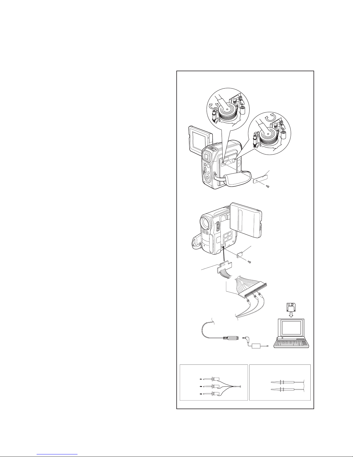
4.2 JIG CONNECTOR CABLE CONNECTION
• Remove one screw (1), and remove the COVER (JIG CON).
• As the figure shows, insert JIG CONNECTOR CABLE in JIG
CONNECTOR by using the EXTENSION CONNECTOR so
that the wire side faces downward.
Connection procedure
GUIDE ROLLER (SUP)
GUIDE ROLLER (TU)
COVER(ADJ)
SCREW(2)
COVER(JIG CON)
SCREW(1)
EXTENSION CONNECTOR
JIG CONNECTOR CABLE
SERVICE SUPPORT SYSTEM
MENU
PERSONAL COMPUTER
COMMUNICATION CABLE
PC CABLE
FOR
COMMUNICATION CABLE
RS232C
COM PORT
1-16 (No.YF046)
TO JLIP_RX
TO JLIP_TX
TO GND
COMMUNICATION CABLEJIG CONNECTOR OSCILLOSCOPEJIG CONNECTOR
RED
WHITE
BLACK
TO ENV_OUT
TO HID1
Page 17
Jig connector diagrams 4.3 MECHANISM COMPATIBILITY ADJUSTMENT
4.3.1 Tape pattern adjustment
JIG CONNECTOR CABLE (YTU93106C)
MAIN CN105
DDI
DD0
DMS
DCK
DRST
FL_MDO
RESET
AL_3VSYS
IF_TX
JLIP_TX
JLIP_RX
TMS_DSC
TCK_DSC
TDI_DSC
TRST_DSC
TDO_DSC
PB_CLK
ENV_OUT
MAIN_VCO
ATFI
HID1
DISCRI
FS_PLL
TXD2
SPA
SBE
RXD2
GND
GND
V_OUT
VCOM_M
CVF_B
CVF_R
CVF_G
HD_M
VCOM_E
NC
EMU1
KENTO
MVD
1
2
3
4
5
6
7
8
9
10
11
12
13
14
15
16
17
18
19
20
NOTE :
The JIG CONNECTOR BOARD uses
21
30 of the 40 pins of the MAIN BOARD.
10 Pins (1 to 5, 21 to 24 and 34) on
22
the JIG CONNECTOR BOARD on the
Main board are NC.
23
24
25
26
27
28
29
30
31
32
33
34
35
36
37
38
39
40
JIG CONN. BOARD
(PIN NO.)
6
7
TRST_DSC
8
9
MAIN_VCO
10
11
12
13
14
15
16
17
18
19
20
25
26
27
28
29
30
31
32
33
35
36
37
38
39
40
JLIP_RX
TCK_DSC
PB_CLK
HID1
FS_PLL
SPA
RXD2
GND
VCOM_M
CVF_R
HD_M
NC
KENTO
JLIP_TX
TMS_DSC
TDI_DSC
TDO_DSC
ENV_OUT
ATFI
DISCRI
TXD2
SBE
V_OUT
CVF_B
CVF_G
VCOM_E
EMU1
MVD
NOTE:
Prior to the adjustment, remove the COVER (ADJ).
(1) Play back the compatibility adjustment tape.
(2) While triggering the HID1, observe the waveform of
ENV_OUT.
(3) Set the manual tracking mode (ATF OFF).
(4) Confirm that the waveform is entirely pa rallel and straight,
and free from remarkable level-down, through the tracking
operation.
Make the confirmation as follows if necessary.
(5) If level-down is observed on the left hand side of the
waveform, straighten the level by turning the GUIDE
ROLLER (SUP).
If level-down is observed on the right hand side of the
waveform, straighten the
level by turning the GUIDE ROLLER (TU).
(6) After the adjustment, try th e unloading motion once, and
confirm that the waveform is flat when the tape has been
played back again.
(7) Play back the self-recording.
(8) Confirm that the waveform is flat.
ENV_OUT
HID1
Fig.4-3-1
Flatten the waveform.
Misalignment of guide
roller height on the
supply side
Misalignment of guide roller
height on the take-up side
Fig.4-3-2
4.4 ELECTRICAL ADJUSTMENT
Electrical adjustment is performed by using a personal computer
and software for SERVICE SUPPORT SYSTEM. Read
README.TXT file to use the software properly.
As for the connection of cables, see "4.2 JIG CONNECTOR
CABLE CONNECTION".
(No.YF046)1-17
Page 18
5.1 SERVICE NOTE
C3 C4
[10]
C8
SECTION 5
TROUBLE SHOOTING
cm)
cm)
cm)
.
.
.
m (0.7kgf
m (2.5kgf
3-2-5
[13] OP BLOCK ASSEMBLY / CCD BOARD ASSEMBLY
.
m (0.5kgf
.
.
[3] [4] [5]
[14] [15] [16]
[1] [2]
CABINET PARTS AND ELECTRICAL PARTS
C1 C2
1 2 3 4 5 6 7 8 9 10 11 12 13 14 15 16 17 18 19 20 21 22 23 24
CABINET PARTS AND ELECTRICAL PARTS
C5 C6 C7
[6] [7] [8] [9] [11]
[12] [13]
25 26 27 28 29 30 31 32 33 34 35 36 37 38 39 40 41 42 43 44 45
CABINET PARTS AND ELECTRICAL PARTS
46 47 48 49 50 51 52 53 54 55 56 57 58
C10 C11
C9
Φ
3-2-3
[9] MONITOR ASSEMBLY
1234567891011
[12] VF ASSEMBLY
1234567891011121314 123456789
3-2-4
cm) : 0.069N
cm) : 0.246N
cm) : 0.049N
.
.
.
m (0.8kgf
m (2.0kgf
m (0.6kgf
.
.
.
cm) : 0.078N
cm) : 0.196N
cm) : 0.059N
.
.
.
cm)
.
m (0.9kgf
m (1.0kgf
m (0.2kgf
.
.
.
m (1.5kgf
.
: 0.098N
: 0.019N
: 0.088N
1) * : Don't reuse the screw, because screw lock bond was applied to them.
2) Pay careful attention to tightening torque for each screw.
NOTE:
: 0.15N
Symbol No.
Place to stick screw
Removing order of screw
1-18 (No.YF046)
Screw tightening torque
Reference drawing (Fig.No.)
Symbol No.
Place to stick screw
Removing order of screw
Screw tightening torque
Reference drawing (Fig.No.)
Symbol No.
Place to stick screw
Removing order of screw
Screw tightening torque
Reference drawing (Fig.No.)
Place to stick screw
Screw tightening torque
Removing order of screw
Reference drawing (Fig.No.)
Removing order of screw
Place to stick screw
Screw tightening torque
Reference drawing (Fig.No.)
Page 19
5.2 TAKE OUT CASSETTE TAPE
The following procedure is a method for taking out the cassette
tape in case the cassette tape cannot be ejected due to an electrical failure. The following procedure is a simplified method;
therefore, for more reliable operation, it is recommended that you
should remove exterior parts so that you can take out the tape
without excessive force.
(1) Remove the Power Unit (battery or DC cord) from the set.
(2) Open the CASSETTE COVER till it is completely opened
and fixed.
(3) Attach a PVC tape as shown in the figure.
NOTE:
Be careful of cassette tape damage caused because the
Cassette Housing Assembly is moved upward at the unloading end (Eject mode).
(4) To set the Slide Deck Assembly to the un loading end , ap-
ply DC 3V to the electrode (terminal) on the top surface of
the LOADING MOTOR that is seen through a space of VF
side.
NOTE:
Be careful not to attach grease or a similar substance to
the surface of the cassette tape on the tape transport
system.
(5) Wind the cassette tape by directly turning the Reel Disk As-
sembly (SUP) from the backside of the SLIDE DECK ASSEMBLY by using a sharp tool (Chip IC replacement tool).
(6) Confirm that the cassette tape is completely woun d, and
then peel off the PVC tape from the CASSETTE HOUSING
ASSEMBLY and take out the cassette tape.
NOTE:
To confirm that the cassette tape is completely wound,
confirm that one REEL DISK ASSEMBLY (TU) rotates
as you rotate the other REEL DISK ASSEMBLY (SUP).
(7) Make sure that grease or a similar substance is not at-
tached to the surface of the tape taken out in the procedure
(6). Similarly, also make sure that grease or a similar substance is not attached on the MECHANISM ASSEMBLY,
especially the tape transport system.
(DC3V)
LOADING MOTOR
ASSEMBLY
SLIDE DECK
ASSEMBLY
CASSETTE COVER
TAPE
CASSETTE HOUSING
ASSEMBLY
REEL DISK
ASSEMBLY (SUP)
Fig.5-2-1
(No.YF046)1-19
Page 20

5.3 EMERGENCY DISPLAY
Example (in case of the error number E01):
Whenever some abnormal signal is input to the syscon CPU, an
error number (E01, as an example) is displayed on the LCD
monitor or (in the electronic view finder).In every error status,
such the message as shown below alter nately appear over and
E01
UNIT IN
SAFEGUARD MODE
E01
REMOVE AND
REATTACH BATTERY
over.
• In an emergency mode, all operations except turning on/off the
POWER switch are ineffectual.
LCD display Emergencymode Details Possible cause
E01 LOADING In the case the encoder position is
not shifted to the next point though
the loading motor has rotated in the
loading direction for 4 seconds or
more. This error is defined as [E01].
E02 UNLOADING In the case the encoder position is
not shifted to the next point though
the loading motor has rotated in the
unloading direction for 4 seconds or
1. The mechanism is locked during mode shift.
2. The mechanism is locked at the mechanism loading end,
because the encoder position is skipped during
mechanism mode shift.
3. No power is supplied to the loading MDA.
1. The mechanism is locked during mode shift.
2. The mechanism is locked at the mechanism loading end,
because the encoder position is skipped during
mechanism mode shift.
more. This error is defined as [E02].
E03 TU & SUP REEL FG In the case no REEL FG is
produced for seconds shown in the
table below or more in the capstan
rotation mode after loading was
complete, the mechanism mode is
shifted to STOP with the pinch roller
set off. This error is defined as
[E03].However, no REEL EMG is
detected in the SLW/STILL mode.
REEL(SUP) REEL(TU)
PB/REC
S-FWD
S-REW
FF
REW
3 SEC
3 SEC
0.3 SEC
3 SEC
0.1 SEC
3 SEC
0.3 SEC
3 SEC
0.1 SEC
3 SEC
E04 DRUM FG In the case there is no DRUM FG
input in the drum rotation mode for
4 seconds or more. This error is
defined as [E04], and the
mechanism mode is shifted to
STOP with the pinch roller set off.
1. The idler gear does not engage with the reel disk well.
2. Though the idler gear and reel disk are engaged with
each other, the tape is not wound because of overload
to the mechanism.
3. No FG pulse is output from the reel sensor.
4. No power is supplied to the reel sensor.
5. Tape transport operation takes place with a cassette
having no tape inside.
6. The tape slackens and no pulse is produced until the
slack is taken up and the tape comes into the normal
status.
1. The drum cannot be started or drum rotation is stopped
because tape transport load is too high.
1) Tape tension is extremely high.
2) The tape is damaged or soiled with grease, etc.
2. The DRUM FG signal is not received by the syscon CPU.
1) Disconnection in the middle of the signal line.
2) Failure of the DRUM FG pulse generator (hall
element).
3. No drum control voltage is supplied to the MDA.
4. No power is supplied to the DRUM MDA.
E05 - - E06 CAPSTAN FG In the case no CAPSTAN FG is
produced in the capstan rotation
mode for 2 seconds or more. This
error is defined as [E06], and the
mechanism mode is shifted to
STOP with the pinch roller set
off.However, no CAPSTAN EMG is
detected in the STILL/FF/REW
mode.
1. The CAPSTAN FG signal is not received by the syscon
CPU.
1) Disconnection in the middle of the signal line.
2) Failure of the CAPSTAN FG pulse generator (MR
element).
2. No capstan control voltage is supplied to the MDA.
3. The capstan cannot be started or capstan rotation is
stopped because tape transport load is too high.
1) Tape tension is extremely high. (Mechanical locking)
2) The tape is damaged or soiled with grease, etc. (Tape
tangling occurs, etc.)
1-20 (No.YF046)
Fig.5-3-1
Page 21

VICTOR COMPANY OF JAPAN, LIMITED
AV & MULTIMEDIA COMPANY CAMCORDER CATEGORY 12, 3-chome, Moriya-cho, kanagawa-ku, Yokohama, kanagawa-prefecture, 221-8528, Japan
(No.YF046)
Printed in Japan
WPC
Page 22

SCHEMATIC DIAGRAMS
DIGITAL VIDEO CAMERA
YF04620044
GR-DX107EK, GR-DX107EX, GR-DX107EY,
GR-DX107EZ, GR-DX307EK, GR-DX307EX,
GR-DX307EY, GR-DX307EZ, GR-DX317EX
CD-ROM No.SML200405
GR-DX107EK, GR-DX107EX, GR-DX107EY, GR-DX107EZ[M4D3S9]
GR-DX307EK, GR-DX307EX, GR-DX307EY, GR-DX307EZ, GR-DX317EX[M4D3M9]
For disassembling and assembling of MECHANISM ASSEMBLY, refer to the SERVICE MANUAL No.86700(MECHANISM ASSEMBLY).
COPYRIGHT © 2004 VICTOR COMPANY OF JAPAN, LIMITED
No.YF046SCH
2004/4
Page 23
CHARTS AND DIAGRAMS
NOTES OF SCHEMATIC DIAGRAM
Safety precautions
The Components identified by the symbol are
critical for safety. For continued safety, replace safety
critical components only with manufacturer's recommended parts.
1. Units of components on the schematic diagram
Unless otherwise specified.
1) All resistance values are in ohm. 1/6 W, 1/8 W (refer to
parts list).
Chip resistors are 1/16 W.
K: KΩ (1000Ω), M: MΩ (1000KΩ)
2) All capacitance values are in µF, (P: PF).
3) All inductance values are in µH, (m: mH).
4) All diodes are 1SS133, MA165 or 1N4148M (refer to parts
list).
2. Indications of control voltage
AUX : Active at high.
AUX or AUX(L) : Active at low.
3. Interpreting Connector indications
Note: If the voltages are not indicated on the schematic
diagram, refer to the voltage charts.
123
2.5
(5.0)
1.8
PB and REC modes
(Voltage of PB and REC modes
are the same)
PB mode
REC mode
4. Voltage measurement
1) Regulator (DC/DC CONV) circuits
REC : Colour bar signal.
PB : Alignment tape (Colour bar).
— : Unmeasurable or unnecessary to measure.
2) Indication on schematic diagram
Voltage Indications for REC and PB mode on the schematic diagram are as shown below.
5. Signal path Symbols
The arrows indicate the signal path as follows.
NOTE : The arrow is DVC unique object.
Playback signal path
Playback and recording signal path
Recording signal path
(including E-E signal path)
Capstan servo path
Drum servo path
(Example)
R-Y
Y
Playback R-Y signal path
Recording Y signal path
6. Indication of the parts for adjustments
The parts for the adjustments are surrounded with the circle as
shown below.
7. Indication of the parts not mounted on the circuit board
“OPEN” is indicated by the parts not mounted on the circuit
board.
R216
OPEN
1
2
3
1
2
3
1
2
3
1
4
2
3
Removable connector
Wire soldered directly on board
Non-removable Board connector
Board to Board
Connected pattern on board
The arrows indicate signal path
Note: The Parts Number, value and rated voltage etc. in
the Schematic Diagram are for references only.
When replacing the par ts, refer to the Parts List.
Note: For the destination of each signal and further line
connections that are cut off from the diagram,
refer to "BOARD INTERCONNECTIONS"
CIRCUIT BOARD NOTES
1. Foil and Component sides
1) Foil side (B side) :
Parts on the foil side seen from foil face (pattern face)
are indicated.
2) Component side (A side) :
Parts on the component side seen from component face
(parts face) indicated.
2. Parts location guides
Parts location are indicated by guide scale on the circuit board.
Note: For general information in service manual, please
refer to the Service Manual of GENERAL INFORMATION Edition 4 No. 82054D (January 1994).
LOCATION
REF No.
IC101 B C 6 A
IC
Category : IC
Horizontal “A” zone
Vertical “6” zone
B : Foil side
(A : Component side)
C : Chip component
D : Discrete component)
2-1 2-2
Page 24

A
1
2
3
4
5
BCDEFG
J105
CN109
CN102
CN304
CN105
CN302CN301
REG_3.1V
CN106
REG_3.6V
EXTM_H
CN103
CN7602
J104
CN7601
EXTM_H
S401
V_OUT
Y_OUT
C_OUT
CN111
SHP
CDS_3V
OSD_VD
ADP_L
OUTV
OSD_VD
SHD
CN104
CN114
CN110
REG_1.8V
EM_DET_L
HID1
AGC_OUT
VRB_AGC
ATFI
VRB_ATF
REC_DATA
REC_CTL
P_DET
REF_CLK
VREF_1.1
VF_CTL
CN101
HID1
CN701
DISCRI
MVD
SELCT_SW
REG_1.8V
ANA_IN_H
DDI
SBE
CDWE
TDA
TAPE_LED
FS_PLL
MAIN_VCO
DD0
PB_CLK
E_SENS
REEL_VCC
GND
DCO[0-3]
PRST
CDDSTB
REG_2.5V
S_SENS
MIC_1
CDWE
MIC_2
MIC_3
REC_SAFE
CDALE
RESET
DCK
SPA
XINT
DV_CS
CPOB
DYO[0-3]
S2_DET
DCI[0-3]
BLKC
CDDSTB
SHUT_ATT
FSPLLCTL
SHUT_ATT
DSC_RST
VC1
DSC_RST
REC_CLK
NAVI_SW
ADDT[00-15]
MD_DEM1
REG_3.1V
AU_DATA
DV_WAIT
DRWSEL
M_VCOCTL
PBVCOCTL
PBPLLCTL
INV
INH
OUTV
OUTH
VC2
J101
CN305
S701
CN115
CN702
TRIG_SW
DYI[0-3]
TSR
FRP
CLK27A
DV_RST
SPA
TPA+
TPA-
TPB+
TPB-
ZOOM_SW
IF_TX
AL_3VSYS
JLIP_TX
T_BATT
CN113
CLK27SEL
SRV_TRK
ASPECT2
ASPECT1
CN7002
CN7001
CN112CN401
CN7603
CN107
MD_AU/L
MD_AU/R
EM_AU/L
EM_AU/R
PWDA2
PWAD2
MD_DEM1
DMS
JLIP_RX
AU_CLK
V_OUT
USBSENS
USB_DN
USB_DP
S_IN_L
D_GAIN
AU_SIG/L
VIFD_OUT
C_OUT
VIFD_IN
AU_SIG/R
IR_OUT
ADCLK
SYSVDSEL
CPOB
CN108
ADP_DC
J103
Y_OUT
EDIT
VIFD_CLK
VENC_CS
TG_RST
DUMP_CTL
ATF_GAIN
NOSIG_LV
RECCADJ
INV
INH
REG_3.1V
REG_4.8V
GND
INT_GND
SPK-
SPK+
P_MEDIA
PWAD2
PD_L
PWDA2
AUDIO_CS
A_MUTE
BUZZER
INT/L
PD_L
AU_CLK
AUDIO_CS
AU_DATA
A_MUTE
BUZZER
EM_DET_L
( E_MIC_GND)
GND
VC0
CN303
EM_DET_L
( E_MIC_L)
( E_MIC_R)
24M_DSC24M_DSC
TMS
TCMK
DYO[0-3]
DCO[0-3]
TRST
PSCTL
CDDSTB
TDI
CAM_CS
SYSVDSEL
USBDOWN
LIT_3V
PHOTO_H
PHOTO_F
TELE_SW
WIDE_SW
MENU_SW
TDI
SET_SW
FF_SW
PLAY_SW
REW_SW
STOP_SW
AL_3.1V
GND
INT/R
MD_AU/L
EM_AU/R
MD_AU/R
EM_AU/L
CDALE
DSP_RST
ADCLK
REG_3.1V
OMT
CDS_3V
SHP
SHD
TCMK
TMS
BLKA
TRST
ADDT[00-15]
PBLKPBLK
OSD_HD
OSD_VD
DOT_CLK
VC3
MVD
MFLD
ADP_L
LITHIUM
BATT_+
REG_CS
AREG_CLK
MMC_DOUT
MMC_CLK
MMC_DIN
MMC_CD
SD_WP
VF_SW
USB_DP
USB_DN
USBSENS
BLKB
USBDOWN
J102
AREG_SO
RESET
V_BATT
I_MTR
CAS_SW
CHRG_EVR
MMC_CS
GND
INFO_SW
INDEX_SW
RECH
DOBCK2
HGVss-ND
HG_U[+]
HG_W[-]
HG_BS[-]
HG_W[+]
HG_BS[+]
HG_U[-]
HG_V[+]
HG_V[-]
C_COIL_U
C_COIL_W
C_FG[+]
C_FG[-]
C_COIL_V
MDA_PS
CCD_CTL
DOMCK2
PBH
DOLRCK2
DODAT2
PSCTL
Z_VCC
CCD-7.5V
CCD+15V
TG_36M
REG_1.8V
REG_4.8V
HID3
P_DET
M_REG4.8
P_DET
CAM_CLK
CAM_OUT
CAM_SW_C
ANA_IN_H
HDIN
REG_4.8V
DRUM_ERR
CAM_SW_B
V_OUT
S_RL[+]
M_REG4.8
CAM_SW_A
GND
S_REEL
OUTV
IR_RMC
T_REEL
TDO
CAPT_REQ
DRUM_PWR
VDIN
REG_3.1V
T_RL[+]
ZOOM01
ZOOM04F_PTR_AD
F_VCC
F_LED
ZOOM03
ZOOM02
L_FRB
HGout+IS
BLKC
HGout-IS
Z_LED
OP_THRMO
DRIVE+IS
DRIVE-IS
HGVss-IS
HGout+ND
S_REEL
REG_3.1V
DEW_SENS
Z_PTR_AD
IRIS_PWM
MDA_PS
DRUM_ERR
CAP_REF
CAP_FG
DRUM_REF
DRUM_PG
REG+CCD
DRUM_FG
LD_ON
REG-CCD
S_IN_L
VENC_CS
S2_DET
TG_RST
XAVD
HID1
SPA
HID1
FRP
TSR
SRV_TRK
CLK27SEL
DV_RST
T_REEL
C_FRB
NOSIG_LV
ADDT[00-15]
DV_CS
DV_WAIT
CPOB
MONI_CHG
REG_3.6V
PBPLLCTL
CLK27A
ATF_GAIN
TG_CS
VIFD_IN
DIAL_PB
DIAL_OFF
TBCCTL
OSD_HD
OSD_VD
DOT_CLK
RECCADJ
DIAL_AUTO
M_VCOCTL
DIAL_MANU
OUT_Y[0-3]
AIDAT
AODAT
AILRCK
AIBCK
AIMCK
PBVCOCTL
POW_LED
AIDAT2
V_BATT
VF_CTL
I_MTR
AREG_SO
AREG_CLK
FSPLLCTL
REG_CS
VC0
REM_OUT
LV_CLK
LV_OUT
LD_ON
DSCIO[0-7]
DSYIO[0-7]
HGout-ND
FOCUS04
FOCUS03
FOCUS02
DRIVE-ND
DRIVE+ND
VIFD_IN
HDCVF
REM_OUT
DOBCK2
DOMCK2
DOLRCK2
FOCUS01
REG_3.1V
HALL_AD
IRIS_O/C
DODAT2
F/Z_CS
AIDAT2
IR_OUT
VIFD_CLK
VIFD_OUT
OUT_C[0-3]
OUT_VS
AU_SIG/R
OUT_HS
AU_SIG/L
USBSENS
USB_DN
USB_DP
L_MUTE
L_MUTE
M_CS
F/Z_CS
VC1
TG_RST
IRIS_O/C
M_REG4.8
OP_THRMO
CAP_PWR
IRIS_CS
IRIS_CS
CAM_VD
CAM_CLK
VIFD_CLK
CLK4M5
CAM_OUT
IRIS_PS
LCD_R
LCD_G
LCD_B
CAM_CLK
ASPECT1
VDCVF
REG_4.8V
REG_3.1V
REG_1.8V
CLK9A
IRIS_MCK
GND
XAVD
XAHD
ASPECT2
DUMP_CTL
TG_RST
LENS_LED
HDIN
TG_36M
CLK9A
EMU1
TMS_DSC
TCK_DSC
TDI_DSC
CHRG_EVR
TRST_DSC
TG_RST
H2
H1
RG
SUB
HID3
HID1
PBH
GND
RECH
INV
INH
DYO[0-3]
CAP_PWR
DRUM_REF
DRUM_PG
DCO[0-3]
MONI_CHG
LOAD_FWD
LOAD_REV
MDA_2.9V
COIL_COM
D_PFG[+]
D_COIL_W
D_COIL_V
D_COIL_U
D_PG[-]
D_FG[-]
CAP_ERR
GND
DRUM_PWR
ENV_OUT
CAP_REF
CAP_FG
DRUM_FG
BLKB
DSCO[0-7]
ATFI
REC_CTL
VREF_1.1
GND
AGC_OUT
V1V2V3
V4
VRB_AGC
VRB_ATF
ATFI
REF_CLK
DSYO[0-7]
HGVcc+ND
REC_DATA
Z_PTR_AD
F_PTR_AD
M_UNREG
M_REG4.8
REC_CLK
AILRCK
AIMCK
AIBCK
AODAT
AIDAT
TMS
RESET
MXDT_OUT
ADP_L
REG_4.8V
REG_3.1V
REG_2.5V
S_SHUT
M_RVS
GND
AU_SIG/R
AU_SIG/L
2S
TALLY
MONI_SW
D_GAIN
2F1S1F
FLDDSC
REG_2.5V
S_RL[-]
T_RL[-]
TCMK
TRST
IRIS_CLK
TBCCTL
HGVcc+IS
OUT_Y[0-3]
OUT_C[0-3]
OUT_VS
OUT_HS
HALL_AD
HDDSC
VDDSC
FLDDSC
OP_THRMO
F_PTR_AD
REG_3.1V
TMS
TCMK
TRST
Z_PTR_AD
HDDSC
TDO
MMC_CD
TDO_DSC
IRIS_PS
VIFD_IN
LENS_LED
V_OUT
CAP_ERR
DSC_STS
FLSH_RST
DSC_RST
DSC_CS
DSC_DT_IN
DSC_DT_OUT
DSC_CLK
DSC_WKUP VDDSC
CAM_OUT
CLKDSC
CLK27B
VIFD_OUT
CLK27B
FLSH_RST
DSC_RST
DSC_CLK
REG_8.5V
DSC_DT_OUT
DSC_DT_IN
DSC_CS
MXDT_OUT
DSC_STS
CAPT_REQ
DSC_WKUP
REG_3.6V
D[0-15]
A10
EM_CS2
FLSH_OE
FLSH_WE
USBDOWN
C_OUT
GIO3
C_FRB
Y_OUT
GIO6
GIO15
CDDSTB
REG_3.1V
L_FRB
DSCIO[0-7]
CAM_CLK
CAM_OUT
LAMP_ON
CLKDSC
GIO15
CDALE
CDWE
DSP_RST
GIO6
GIO3
CPOB
CLK27A
XAHD
ADIN[0-9]
PBLK
CLK27A
VDIN
CDS_CS
MMC_CD
DSYO[0-7]
DSCO[0-7]
GND
CLK27B
USBDOWN
DSYIO[0-7]
TDA
CCD_CTL
VC2
CCD_OUT
CDS_CS
CAM_OUT
CAM_CLK
ADIN[0-9]
REG_3.6V
GND
PBLK
IRIS_PWM
ADDT[00-15]
CAM_VD
CLK4M5
CAM_CS
OMT
MFLD
OUTH
OUTV
DYI[0-3]
MVD
DCI[0-3]
INV
DCO[0-3]
INH
DYO[0-3]
S_SHUT
REG_3.1V
GND
CLK27B
BLKA
REG+CCD
REG-CCD
LIT_3V
AL_3.1V
GND
VFREG4.8
REG_2.5V
REG_3.1V
FLSH_WE
FLSH_OE
EM_CS2
A10
D[0-15]
REG_1.8V
REG_3.1V
GND
RXD2
TXD2
LCD_CTL
GND
REG_4.8V
VIFD_OUT
VIFD_CLK
VC3
M_UNREG
CCD_CTL
EJT_SW
CAM_OUT
CAM_CLK
TG_RST
CDWE
DRWSEL
XINT
CDALE
TG_CS
(Page 2-25)
(Page 2-23)
(Page 2-31)
(Page 2-15)
(Page 2-39)
(Page 2-5)
(Page 2-33)
(Page 2-11)
(Page 2-13)
(Page 2-17)
(Page 2-7)
(Page 2-9)
(Page 2-19)
(Page 2-35)
(Page 2-37)
(Page 2-29)
(Page 2-41)
(Page 2-21)
(Page 2-44)
(Page 2-45)
(Page 2-27)
(Page 2-43)
YTU94074-12
YTU94077-12
YTU94129A-39
YTU94109-39
YTU94074-16
YTU94077-16
YTU94074-8
YTU94077-8
YTU94074-6
YTU94077-6
YTU94074-6
YTU94077-6
YTU94074-11
YTU94077-11
YTU94074-18
YTU94077-18
YTU94074-30
YTU94077-30
YTU94074-6
YTU94077-6
YTU94074-12
YTU94077-12
YTU94074-13
YTU94077-13
YTU94074-22
YTU94077-22
YTU94074-7
YTU94077-7
YTU94074-20
YTU94077-20
YTU94074-28
YTU94077-28
y10459001a_rev0.1
BOARD INTERCONNECTION
NOTE : :The number of patch cords are indicated by interconnected.
2-3 2-4
Page 25

A
1
2
3
4
5
BCD EFG
NOTE : The par ts with marked () is not used.
REG_3.1V
CN101
KEY_C
CN112
CN113
R2001
CN108
CN109
R2002
MMC_CS
CN103
CN114
MMC_DIN
MMC_CLK
MMC_CD
MMC_DOUT
SD_WP
REG_3.1V
P_MEDIA
GND
CN115
D2803
C2803
R2004
R2003
KEY_A
KEY_B
R2007R2006R2005
CN105
TRIG_SW
WIDE_SW
TELE_SW
SET_SW
MENU_SW
GND
GND
NC
CN104
J103
LITHIUM
REG_4.8V
IR_OUT
IR_RMC
TALLY
LAMP_ON
EJT_SW
REG_4.8V
GND
GND
DIAL_PB
DIAL_OFF
DIAL_AUTO
DIAL_MANU
PWR_LED
Q2801
R2803R2804
R2801
R2802
R2805
AU_SIG/R
AU_SIG/L
L_MUTE
CN106
GND
D2802
C_OUT
Y_OUT
REM_OUT
L2801
USBSENS
USB_DP
USB_DN
V_OUT
P_DET
L2802
C2802 C2801
D2801
GND
J102
VCOM_E
TL2003
TDI
R2813
TDO
TRST
TCMK
TMS
TL2002
TL2001
R2812
R2811
R2810
EMU1
TMS_DSC
TCK_DSC
TDI_DSC
TRST_DSC
BATT_+
T_BATT
GND
SPK+
SPK-
TDO_DSC
GND
CVF_G
CVF_R
ZOOM_SW
VCOM_M
GND
GND
RXD2
GND
CVF_B
FS_PLL
ATFI
MAIN_VCO
ENV_OUT
SBE
HID1
HD_M
KENTO
MVD
DISCRI
CAP_REF
TXD2
SPA
DRUM_REF
LD_ON
L_FRB
C_FRB
MDA_PS
CAP_FG
DRUM_PG
DRUM_FG
REG_3.6V
HDCVF
LCD_CTL
GND
MONI_SW
M_RVS
M_UNREG
DEW_SENS
CAM_SW_A
CAM_SW_B
REG_4.8V
VDCVF
CAM_SW_C
M_CS
LV_CLK
LCD_B
LCD_R
LCD_G
DRUM_ERR
DRUM_PWR
GND
CAP_ERR
LV_OUT
CAP_PWR
PB_CLK
REG_3.1V
M_REG4.8
JLIP_RX
JLIP_TX
IF_TX
AL_3VSYS
RESET
FL_MD0
DRST
DCK
DMS
DDO
DDI
V_OUT
REG_8.5V
HST_E
HCK2
HCK1
REG_3.1V
LCD_REF
STB_E
VST_E
VCK
LCD_EN
PCG
CVF_B
CVF_R
CVF_G
PSIG
VCOM_E
VFREG48.
VF_SW
HST_E
HCK2
HCK1
LCD_REF
STB_E
VST_E
VCK
LCD_EN
PCG
CVF_B
CVF_R
CVF_G
PSIG
VCOM_E
REG_8.5V
GND
HD_M
VCOM_M
S_RL[+]
T_RL[-]
S_RL[-]
T_RL[+]
E_SENS
MIC2
MIC3
MIC1
S_SENS
REEL_VCC
TAPE_LED
CAS_SW
REC_SAFE
GND
REG_3.1V
GND
MA8068-X
AU_SIG/L
AU_SIG/R
P_DET
GND
GND
GND
C_OUT
V_OUT
Y_OUT
EDIT
QNZ0670-001
UMX1N-W
NQR0251-004X
NQR0251-004X
QNZ0497-001
3.3k 6.8k
3.3k
22k
22k6.8k3.3k
560k560k
820
820
3.3k
0.01 0.01
0Ω
㧖
㧖
㧖
㧖
y20323001a_rev0.1
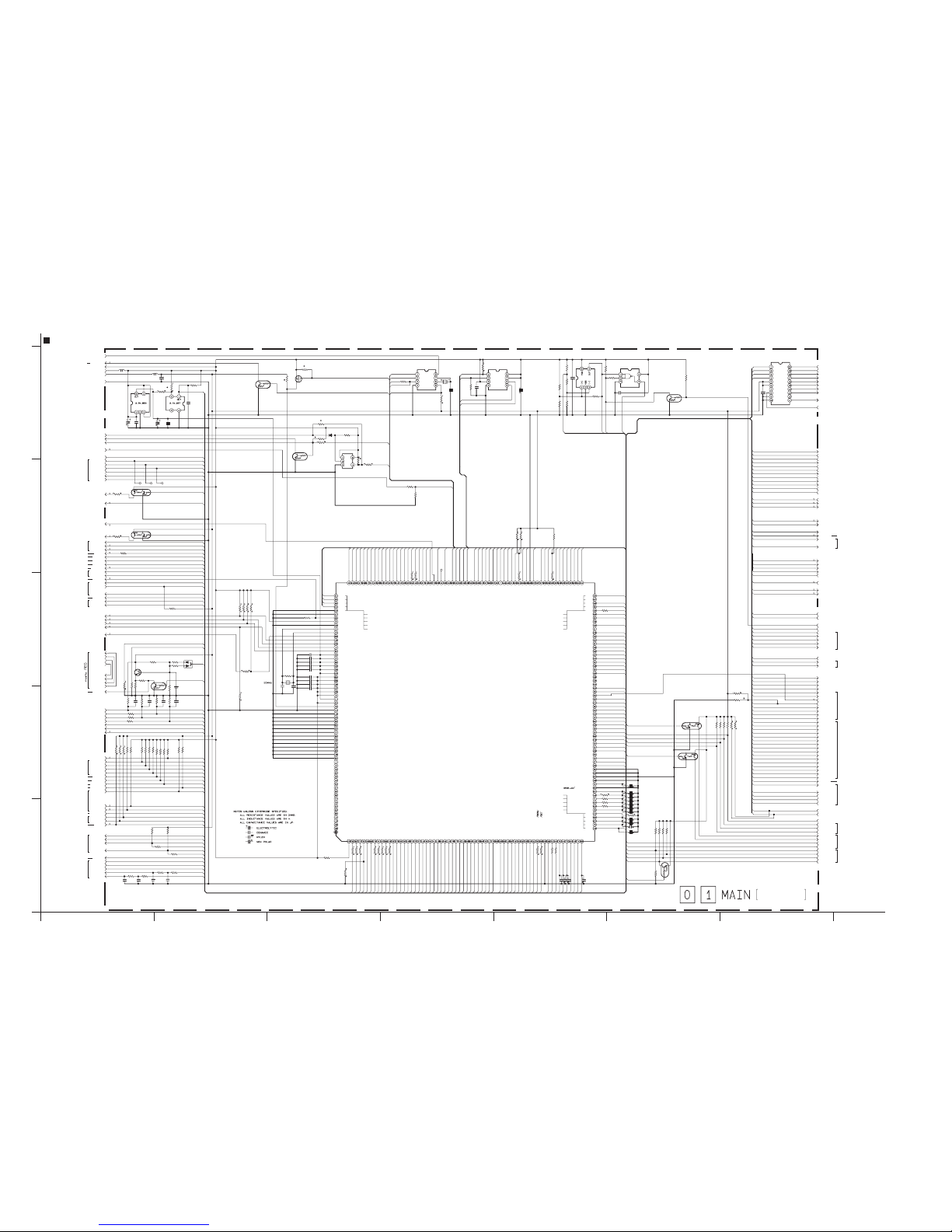
MAIN
(MAIN_IF)
SCHEMATIC DIAGRAM
2-5 2-6
Page 26
A
1
2
3
4
5
BCDEFG
R1138 22K
C1017 C1018
MENU_SW
C1027 0.1
1K R1129
SET_SW
R1139
C1028 0.1
C1021
R1133
C1034 0.1
IR_RMC
ASPECT1
1K R1128
C1029 0.1
Q1012
Q1010
DCK
R1151 100K
FL_MD0
C1031 0.1
C1032 0.1
C1033 0.1
C1035 0.1
C1041 0.1
RESET
1K R1127
R1055
IRIS_CS
ASPECT2
C1026 0.1
R1081
DMS
R1026
KENTO
REM_OUT
Q1011
R1140
XINT
DRST
DDO
DDI
PSCTL
ANA_IN_H
HALL_AD
IRIS_MCK
IRIS_O/C
LENS_LED
IC1006
X1002
R1062
LAMP_ON
EM_DET_L
EXTM_H
SHUT_ATT
PWDA2
WIDE_SW
TELE_SW
KEY_C
TALLY
C1056 0.1
R1056
1K R1027
IF_TX
JLIP_RX
Q1005
JLIP_TX
IC1009
D1002
TG_RST
L_MUTE
R1039
R1037
IC1001
R1094
R1114
C1002
R1001
X1001
C1001
R1008
P_MEDIA
CCD_CTL
MONI_SW
PWR_LED
OP_THRMO
AL_3VSYS
DSC_WKUP
R1060
R1054
R1092
S_IN_L
S2_DET
F_PTR_AD
CAS_SW
LCD_CTL
F/Z_CS
IRIS_PS
Z_PTR_AD
TG_CS
CDS_CS
R1002
KEY_A
R1082
R1080
M_CS
M_RVS
BUZZER
Q1007
Q1008
R1073
R1074
R1070
R1071
R1072
C1046
D1001
R1006
R1089
VF_CTL
L_FRB
DIAL_PB
DIAL_OFF
DIAL_AUTO
DIAL_MANU
ZOOM_SW
TRIG_SW
R1084
R1088
EJT_SW
R1087 R1086
C1054
D_GAIN
Q1004
C1053C1052C1051
REC_SAFEKEY_B
LV_CLK
MIC1
OUTV
MIC2
MIC3
E_SENS
S_SENS
S_REEL
MONI_CHG
CAM_SW_B
CAM_SW_A
CAM_SW_C
T_REEL
DEW_SENS
Q1003
Q1002
TAPE_LED
REEL_VCC
GND
R1028
GND
ADDT06
ADDT07
ADDT08
ADDT09
ADDT10
ADDT11
ADDT12
ADDT13
ADDT14
ADDT15
ADDT00
ADDT01
ADDT02
ADDT03
ADDT04
ADDT05
CDRE
REG_3V
TSR
M_REG4.8
M_UNREG
HID1
SPA
SRV_TRK
REG_3V
M_REG4.8
M_UNREG
CAP_FG
DRUM_PG
DRUM_FG
DRWSEL
CDALE
CDWE
DRUM_REF
CAP_REF
C_FRB
MDA_PS
LD_ON
Q1001
FRP
CLK27SEL
DV_RST
HID3
RECH
PBH
DV_WAIT
L1002
C1042
GND
V_BATT
VF_SW
R1085
DSC_CLK
REG_3.1V
BLKC
CAM_CLK
CAM_OUT
R1053
DV_CS
CAM_CS
DSP_RST
MFLD
IC1003
DSC_DT_OUT
DSC_STS
A_MUTE
OSD_VD
T_BATT
DSC_DT_IN
LV_OUT
AL_3.1V
OMT
OSD_HD
MVD
I_MTR
IC1005
IC1002
L1001
DSC_CS
C1040
P_DET
AREG_SO
AREG_CLK
LIT_3V
VENC_CS
AUDIO_CS
VIFD_CLK
VIFD_OUT
PWAD2
VIFD_IN
R1069
BLKA
VC3
BLKB
VC2
VC1
VC0
DOT_CLK
USBDOWN
DSC_RST
MMC_CD
PD_L
REG_CS
FLSH_RST
CAPT_REQ
MXDT_OUT
C1037
R1045
ADP_L
R1043
CHRG_EVR
R1004
C1003 0.1
C1004 0.1
C1005 0.1
C1006 0.1
C1007 0.1
C1009 0.1
C1010 0.1
C1011 0.1
C1012 0.1
TL1023TL1022TL1021
Q1009
IC1010
C1023
C1024
R1035
R1036
R1041
R1042
C1019
R1021 100K
R1022 100K
R1018 100K
R1017 100K
R1016 100K
R1015 100K
R1013 10K
R1012 10K
R1152 47K
R1083 22K
R1090 22K
C1020
C1025
R1126
R1125
R1117 1K
R1118 1K
R1119 1K
R1120 1K
R1121 1K
R1122 1K
R1123 1K
R1124 1K
R1116
R1137
R1014 10K
R1019 10K
R1136
R1020 10K
R1077
C1048
R1096
R1067
R1134
R1095
R1057
R1058
R1025
C1022
R1024
R1109 22K
R1110 22K
R1111 22K
R1112 22K
R1113
R1052
R1010 47K
R1011 100K
R1038 100K
R1040 100K
R1099 100K
R1093
R1091
R1003
R1079
R1078
C1049
C1050
C1043
R1076
C1047
R1075
R1031
R1030
R1097
R1032
R1033
R1034
IC1004
R1051
R1048R1047
R1061
R1046
TL1014
C1036
C1039
R1050
R1049
C1038
R1044
IC1007
6.3V
DTC143XE-X
DTC144EE-X
UMC3N-W
VSS
VDD
SIO
CLKCSXin
Xout
INTR
RS5C314-X
NAX0564-001X
DTC143XE-X
SN74AHC1G08K-X
1SS376-X
HALL_LV
Z_PTR_LV
F_PTR_LV
OP_THRMO
IR_DET
ZOOM_SW
KEY_A
KEY_B
KEY_C
T_BATT
I_MTR
STRB_AD
S2_DET
SHOE_DET
PHOTO_SW
FOCUS_SW
MENU_SET
F/Z_CS
REG_CS
EEP_CS
DAC_CS
ROM_CS
OSD_CS
AUDIO_CS
TBC_CS
LD_ON
CAP_RVS
CAP_BRK
MDA_PS
LD_FWD
LD_REV
REEL_ON
MVD
OMT
OUTV
XINT
TALLY
D_GAIN
SHOE_VON
GATEPULS
DSC_RST
DSC_WKUP
FLSH_RST
CAPT_REQ
DSC_STS
UDBDOWN
MMC_L
BZ_FREQ
BZ_ENV
CCD_CTL
TGFZ_RST
IR_WB
TAPE_LED
SHOEGATE
HID1
PD_L
VF_CTL
LCD_CTL
M_BL_ON
M_CSADDT13
ADDT14
ADDT15
RESET
CKSEL1
MODE0
FL_MD0
MODEJ
PLLSEL
X1
X2
TD0
TCK
TRST
TMS
TDI
Vdd
Vdd
Vdd
Vdd
Vdd
Vdd
UREG_SEL
AVREF
CVDD
M_RVS
MIC_CTL
PVDD
UPD703166-M40
UPD70F3166M40
UPD70F3166M40A
NAX0645-001X
2SC4617/QR/-X
DTC124EE-X
PDTC124EE-X
DA221-X
UMC3N-W
UMC3N-W
UMC3N-W
DTA114EE-X
RN2102-X
PDTA114EE-X
74HC1G00GW-X
SN74AHC1G00K-X
MC74HC1G00DF-X
VCC
HOLD
SCK
SI
CS
SO
WP
VSS
M95320-WDW6-X
SCLK
CS
DATA
RST
VDD
SDR
XD
EXD
TEST
VSS BLKC
TST0
BLKB
VC3
VD
HD
VC0
VC1
VC2
BLKA
MB90097PFV153-X
D
G
S
2SJ347-X
R1160N251B-X
V_BATT
EJT_SW
MONI_SW
DSC_CS
CHG_WKUP
JLIP_INT
VF_SW
DIAL_PB
DIAL_OFF
DIAL_AUTO
DIAL_MANU
OSD_TBC_OUT
OSD_TBC_IN
OSD_TBC_CLK
ALV_OUT
ALV_IN
ALV_CLK
MIC_SDA
MIC_SCL
IF_TX
IF_RX
EEP_OUT
EEP_IN
EEP_CLK
REG_RTC_OUT
RTC_IN
REG_RTC_CLK
CAM_OUT
RTC_CS
CAM_CLK
DSC_DT_OUT
DSC_DT_IN
DSC_CLK
TG_CS
CDS_CS
DRUM_FG
CAP_FG
T_REEL
S_REEL
RTC_INTR
FLD
DRUM_PG
SPA
SRV_TRK
TSR
FRP
MXDT_OUT
REMOTE
MENU_P_A
MENU_P_B
STO_OFF
ZOOM_T
ZOOM_W
S_SENS
E_SENS
DEW_SENS
MIC3
MIC2
MIC1
CAS_SW
SHOE_PWM
HP_DET
CHRG_LED
TRG_OUT
IRIS_PS
DSP_RST
AVREFOFF
DRUM_REF
CAP_REF
CHRG_EVR
BATT_H
ADP_H
P_DET
S_DET
DV_WAIT
S_IN_L
PSCTL
CLK27SEL
MONI_CHG
CAM_CS
HID3
RECH
PBH
DV_RST
ZMIC_ATT
SHUT_ATT
DV_CS
CDWE
DRWSEL
DSTB
KENTO2
ASTB
KENTO1
CAM_SW_A
CAM_SW_B
CAM_SW_C
REC_SAFE
P_MEDIA
TRIG_SW
A_MUTE
L_MUTE
PWAD2
PWDA2
ADDT00
ADDT01
ADDT02
ADDT03
ADDT04
ADDT05
ADDT06
ADDT07
ADDT08
ADDT09
ADDT10
ADDT11
ADDT12
IRIS_O/CASPECT1
ASPECT2
STRB_SEL
IRIS_CS
EM_DET
EXTM_H
LAMP_ON
LENS_LED
STRB_CHG
ANA_IN_H
S-89220ACNC-W
IC-PST3423U-X
22/
0.1
22/6.3V
0.1
1K
0.1
1.5K
10K
4.7K
0R0
220K
560
510
10K
100
10p1M8p
0R0
100K
10K
12k
8.2k
10K
4.7K
150K 2.7K
18K
1
47K
3.3K1K3.3K
3.3K 3.3K
0.0220.0220.0220.022
10
µ
0.1
1K
2.2K
10
µ
7p
100K
0.01
1M
1k
0.0068
0.01
47K
47K
47K
47K
0.1
1K
1K
100K
1K
1K
100K
0.01
47K
330K
1K
1K
10K
10K
1K
0.0068
1K
22K
100K
10K
10K
22k
39k
0.01
0.01
0.1
47K
0.01
47K
330k
75k
100k
3.3k
3.3k
3.3k
47K
10k100k
100K
100k
0.1
0.01
82k62k
0.01
100k
T_BATT
ALV_IN
HALL_LV
LAMP_ONH
ASPECT1
ASPECT2
HALL_LV
OUTV
I_MTR
IF/TX
KEY_B
PSCTL
IRIS_O/C
IF_RX
AVREFOFF
Z_PTR_LV
F_PTR_LV
MMC_CD
ROM_CS
OP_THRMO
ANA_IN_H
TRG_OUT
ZOOM_SW
KEY_A
MRESET
EEP_CS
S2_DET
EM_DET
EXTM_H
SHUT_ATT
F/Z_CS
PWDA2
REG_CS
ZOOM_T
EEP_CS
ZOOM_W
KEY_C
ROM_CS
OSD_CS
MIC_CTL
AUDIO_CS
TBC_CS
LD_ON
C_FRB1
C_FRB2
MDA_PS
L_FRB1
L_FRB2
REEL_ON
MVD
OMT
OUTV
REMOTE
TALY_LED
TALY_LED
IRIS_CS
D_GAIN
LENS_LED
CCD_CTL
DSC_STS
KEY_C
IR_WB
DSC_RST
DSC_WKUP
FLSH_RST
BZ_FREQ
CAPT_REQ
USBDOWN
BZ_FREQ
BZ_ENV
VF_CTL
TGFZ_RST
M_CS
RTC_INTR
PD_L
IR_WB
ZOOM_SW
BZ_ENV
KEY_A
MENU
DSC_WKUP
SET
EJT_SW
REC_SAFE
P_MEDIA
E_SENS
MONI_SW
DSC_RST
DSC_CS
DSC_DIN
DSC_DOUT
DSC_CLK
DSC_STS
USBDOWN
FLSH_RST
CAPT_REQ
MXDT_OUT
MMC_CD
T_REEL
S_REEL
P_DET
DSP_RST
MVD
FLD
OMT
T_BATT
I_MTR
CHRG_EVR
REG_CS
S_IN_L
PWAD2
A_MUTE
L_MUTE
PD_L
AUDIO_CS
KEY_B
CAM_SW_C
F/Z_CS
IRIS_PS
ALV_OUT
D_REF
DRUM_FG
C_REF
DRUM_PG
L_FRB2
CAP_FG
D_GAIN
MDA_PS
C_FRB1
LD_ON
MIC2
ALV_CLK
CAM_SW_B
MIC3
S_SENS
C_FRB2
VF_CTL
M_BL_ON
M_RVS
CAM_CLK
CAM_OUT
M_CS
VDO_CLK
CDS_CS
TG_CS
TGFZ_RST
OSD_CS
TLED_ON
HID1
M_RVS
M_BL_ON
CAM_SW_A
CHRG_LED
TBC_CS
HID1
SRV_TRK
SPA
FRP
TSR
V_BATT
CAM_CS
DV_CS
ADDT15
ADDT14
ADDT13
RECH
PBH
MONI_CHG
HID3
DV_RST
CLK27SEL
DV_WAIT
CDWE
TRIG_SW
CDALE
DRWSEL
CDRE
ADDT00
ADDT01
ADDT02
ADDT03
ADDT04
ADDT05
ADDT06
ADDT07
ADDT08
VDO_OUT
ADDT09
MRESET
ADDT10
MIC1
ADDT11
ADDT12
MIC_CTL
L_FRB1
CCD_CTL
VF_SW
ADDT13
ADDT14
ADDT15
MRESET
S2_DET
AREG_CLK
AREG_SO
DIAL_MANU
DIAL_AUTO
DIAL_OFF
DIAL_PB
CAS_SW
Z_PTR_LV
F_PTR_LV
OP_THRMO
TGFZ_RST
DEW_SENS
REEL_ON
TLED_ON
VDO_CLK
VDO_OUT
VDO_IN
RTC_IN
AREG_SO
AREG_CLK
RTC_CS
EEP_IN
EEP_OUT
EEP_CLK
VF_SW
ZOOM_W
ZOOM_T
IRIS_O/C
PSCTL
ASPECT1
ASPECT2
LAMP_ONH
EM_DET
LENS_LED
CAM_CS
SPA
SRV_TRK
TSR
DSP_RST
ANA_IN_H
IRIS_PS
CHRG_LED
TRG_OUT
RTC_INTR
FLD
IRIS_CSS
EXTM_H
CAS_SW
EJT_SW
MONI_SW
DSC_CS
CHG_WKUP
IF_RX
SHUT_ATT
PWDA2
DIAL_PB
DIAL_OFF
DIAL_AUTO
DIAL_MANU
VDO_OUT
VDO_IN
AREG_CLK
VDO_CLK
T_BATT
ALV_OUT
ALV_IN
ALV_CLK
MIC2
MIC3
IF/TX
IF_RX
EEP_OUT
EEP_IN
EEP_CLK
AREG_SO
RTC_IN
CAM_OUT
RTC_CS
CAM_CLK
DSC_DOUT
DSC_DIN
DSC_CLK
TG_CS
CDS_CS
DRUM_FG
CAP_FG
S_REEL
T_REEL
DRUM_PG
FRP
MXDT_OUT
REMOTE
MENU
AVREFOFF
D_REF
C_REF
CHRG_EVR
BATT_H
ADP_H
P_DET
DV_WAIT
S_IN_L
CLK27SEL
MONI_CHG
DV_CS
HID3
RECH
PBH
DV_RST
CDWE
DRWSEL
CDRE
CDALE
CAM_SW_A
CAM_SW_B
CAM_SW_C
REC_SAFE
P_MEDIA
TRIG_SW
A_MUTE
L_MUTE
PWAD2
ADDT00
SET
S_SENS
E_SENS
DEW_SENS
MIC3
MIC2
MIC1
V_BATT
ADDT01
ADDT02
ADDT03
ADDT04
ADDT05
ADDT06
ADDT07
ADDT08
ADDT09
ADDT10
ADDT11
ADDT12
BATT_H
ADP_H
CHG_WKUP
SYSCON
TO JIG CONN
TO DVMAIN
TO REG
TO OP_DRV
TO OP_DRV
TO MONITOR
TO POWER OPE
TO MDA
TO MDA
TO CAMERA OPE
TO CAMERA OPE
TO CDS, TG/VDR,
OP DRV
TO MONITOR,
AUDIO
TO OP_DRV
TO CN113
TO FRONT
TO FRONT
TO FRONT
TO JIG CONN
TO JIG CONN
TO JIG CONN
TO CN108
TO MAIN_IF
TO JIG CONN
TO REG
TO AUDIO
TO OP_DRV
TO SENSOR
TO MONITOR
TO SD
TO VF
TO REG
TO SUB OPE
TO TG/VDR
TO CDS
TO CCD
TO VIDEO I/O
TO DSC
TO AUDIO
TO AUDIO
TO VIDEO I/O
TO REEL
TO MAIN_IF
TO PRE/REC
TO REG
TO REG
TO BATT. TERMINAL
TO AUDIO
TO MAIN IF
TO AUDIO AD/DA
TO DVMAIN
TO DVMAIN
TO DVMAIN,
CAMERA_DSP
TO CAMERA_DSP
TO MDA
TO SENSOR
TO MDA
TO CAMERA OPE
TO SENSOR
TO VIDEO I/O
y10460001a_rev0.1
MAIN(SYSCON) SCHEMATIC DIAGRAM
NOTE : The par ts with marked () is not used.
2-7 2-8
Page 27
A
1
2
3
4
5
BCD EFG
R1713
M_REG4.8
REG_3.1V
GND
IC1702 IC1701
R1708
R1707
R1706
R1705
R1704
R1703
R1702
R1701
R1709
R1711
R1710
R1712
S_RL[+]
T_RL[-]
S_RL[-]
T_RL[+]
T_REEL
S_REEL
TO SYSCON
TO SYSCON
C1703
C1701
C1702
NJM2407R-W BA10358FVM-W
T
0
120K
10K
82K
2.2K
2.2K
2.2K
2.2K
82K
10K
1K
120K
1K
10/6.3
0.1
0.1
REEL
y30266001a_rev0.1
MAIN(
REEL) SCHEMATIC DIAGRAM
2-9 2-10
Page 28
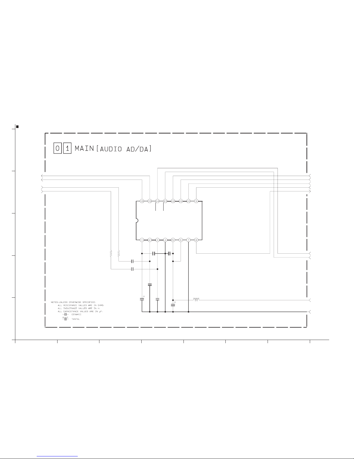
A
1
2
3
4
5
BCDEFG
EM_AU/R
EM_AU/L AIDAT2
REG_3.1V
GND
DOBCK2
L2101
C2105
C2108
PWDA2
TO SYSCON
TO DSC
TO REG
IC2101
DOLRCK2
C2106
R2102R2101
DODAT2
DOMCK2
PWAD2
C2107
MD_AU/R
MD_AU/L
TO AUDIO
C2102
C2101
C2104
C2103
T
T
AK4550VT-X
VCOM
AINR
AINL
VSS
VDD
DEM0
DEM1
SDTO SDTI
LRCK
MCLK
SCLK
PWAD
PWDA
AOUTL
AOUTR
10µ
10/6.3
4.7/6.3
0.1
470
470
0.1
1.0
1.0
0.0022
0.0022
y30281001a_rev0.1
MAIN(AUDIO AD/DA) SCHEMATIC DIAGRAM
2-11 2-12
Page 29
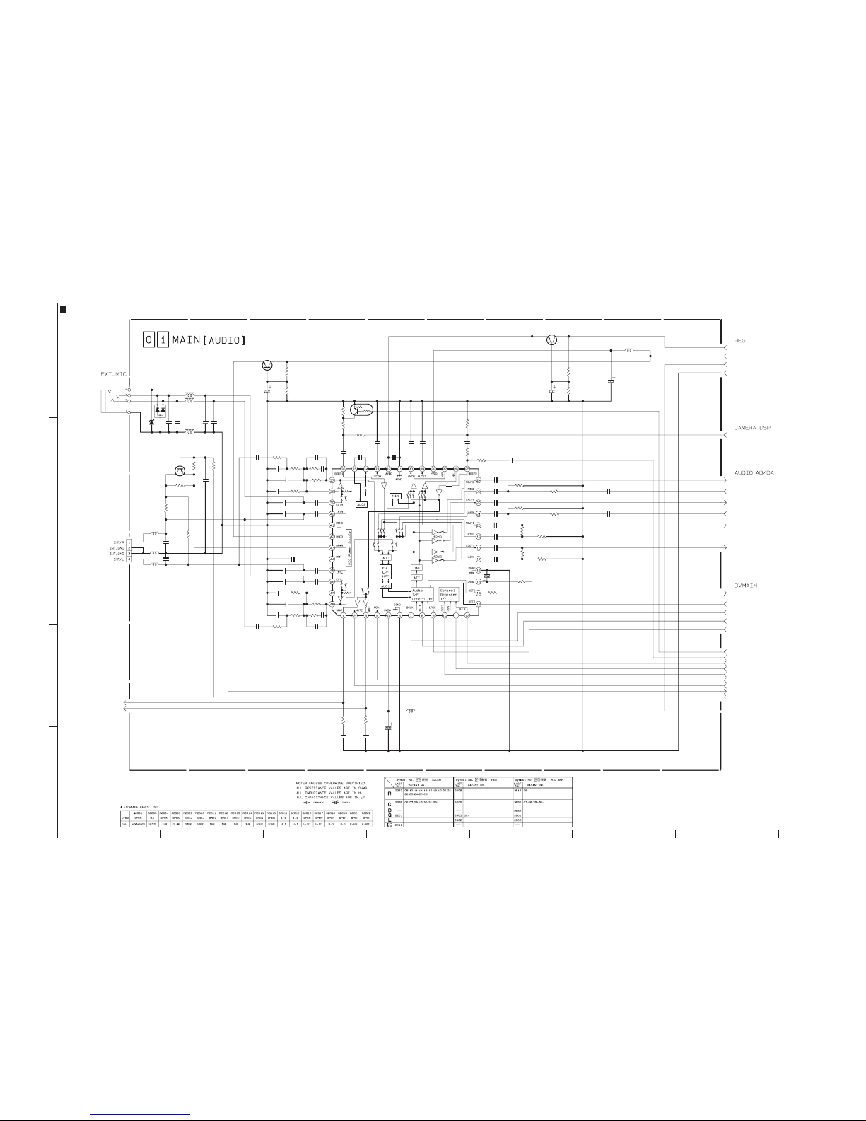
A
1
2
3
4
5
BCD EFG
TO
TO
TO
TO
TO
TO SYSCON
TO BATT.TERMINAL
R2408
PD_L
S_SHUT
R2230
REG_3.1V
AODAT
LV_OUT
AIMCK
REG_4.8V
BUZZER
AIBCK
LV_CLK
AUDIO_CS
AU_SIG/L
AILRCK
R2229
L2602
L2603
L2601
R2602
R2601
C2602
C2601
CN111
C2604
C2603
C2606
C2605
C2613
R2610
R2609
R2607
R2608
C2611
C2612
R2201
R2203C2201
C2223
C2224
R2204
R2202
C2615
L2651
EM_DET_L
C2226
C2225
L2401
L2652
C2402
C2401
Q2401
R2401
R2604
R2407
L2402
C2403
AIDAT
C2405
J101
C2203
R2217
R2605
R2603
Q2601
A_MUTE
SPK+
SPK-
C2210
C2214
C2209
C2213
R2207
R2206
R2209
R2208
C2212
C2216
C2211
C2215
EM_AU/R
EM_AU/L
MD_AU/R
MD_AU/L
SHUT_ATT
EXTM_H
GND
R2228
R2227
IC2201
REG_3.6V
C2406
C2614
Q2403
R2402
R2403C2404
R2232
AU_SIG/R
C2618 R2611
R2613C2616
C2617 R2614
R2612
C2619
R2231
Q2201
C2651
C2655
C2656
L2653
R2615
R2616
C2622
C2621
C2610
C2623
C2624
C2609
D2652
C2652
D2651
C2202
C2204
C2620
R2213
R2212
C2218
C2217
C2205
C2653
C2654
NQR0269-013X
NQR0269-013X
NQR0269-013X
QGA1001F1-04X
#
##
#
CH
NQR0269-013X
NQR0269-013X
T
T
2SC5658-X
#
T
QNS0233-001
#
#
#
AK4564VQ
/6.3
T
CH
2SC5658-X
T
##
#
#
##
#
#
DTC144EE-X
NQR0269-013X
#
#
#
#
EMZ6.8N-X
UDZS6.8B-X
OPEN
33k
33k
2.2k
2.2k
OPEN
OPEN
0.022
0.022
0.0047
0.0047
1.0
22k
22k
220k
39k0.1
0.1
0.1
150k
560k
100p
0.1
0.1
10µ
10/6.3
10/6.3
4.7k
10
10µ
10/6.3
0.11.0
10
1.0
0.1
1.0
0.1
33k
33k
22k
22k
0.1
0.1
0.1
0.1
8.2k
8.2k
10
100p
4.7k
18k10/6.3
OPEN
1k
0.001
0.047
0.047
0.001
OPEN
OPEN
0.001
0.001
1.0
1.0
OPEN
2.7
2.7
0.1
0.1
1.0
OPEN
OPEN
y20324001a_rev0.1
MAIN(
AUDI O) SCHEMATIC DIAGRAM
2-13 2-14
Page 30
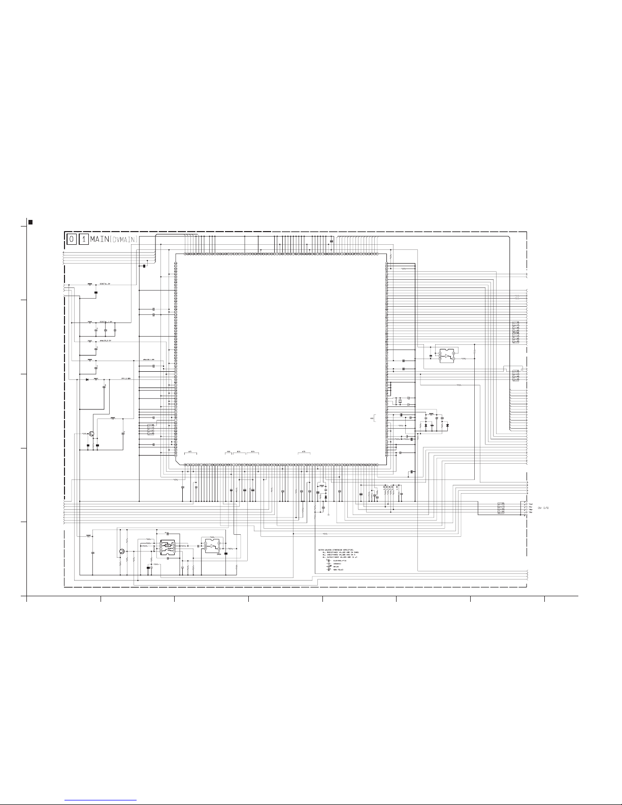
A
1
2
3
4
5
BCDEFG
NOTE : The parts with marked () is not used.
IC3001
GND
REG_2.5V
CLK27SEL
REG_3.1V
ADDT15
TO SYSCON
TO JIG CONN
TO OP DRV
TO AUDIO AD/DA
ADDT07
L3002
L3004
C3040
ADDT06
RA3001
C3005
ADDT05
ADDT04
ADDT03
ADDT02
ADDT01
ADDT00
ADDT08
ADDT09
ADDT10
ADDT11
ADDT12
ADDT13
ADDT14
C3037
PBPLLCTL
DV_WAIT
R3026
RA3002
DRWSEL
CDRE
CDWE
CDALE
INV
INH
OUTV
OUTH
DCO3
DCO2
DCO1
DCO0
DYO3
DYO2
DYO1
DYO0
DCI3
DCI2
DCI1
DCI0
DYI3
DYI2
DYI1
DYI0
AIDAT
AODAT
AILRCK
AIBCK
AIMCK
C3034
C3030
J105
PB_CLK
C3031
R3010
FS_PLL
MAIN_VCO
TSR
DV_CS
R3036
SPA
TL3001
HID1
CLK27A
DV_RST
C3049
R3009
X3002
AGC_OUT
FRP
TDO
TO MAIN_IF
TO REG
TO PRE/REC
VRB_AGC
ATFI
VRB_ATF
REC_DATA
REC_CTL
RA3003
L3005
TMS
TCMK
C3008
C3007
C3011
C3043
C3029
C3048
C3038
C3045
C3003
C3056
C3036
Q3001
RA3004
REF_CLK
IC3004
RA3005
TDA
L3001
C3001
VREF_1.1
R3021
R3022
XINT
R3077
R3078
TRST
PBVCOCTL
M_VCOCTL
FSPLLCTL
C3075
C3071
R3052
L3003
C3002
R3025
C3079
C3006
C3050
DISCRI
R3034
R3029
R3071
C3047
D3002
C3004
REG_1.8V
R3040
C3042
R3053
Q3003
IC3006
R3039
R3038
R3037
L3012
R3044
C3044
R3075
D3004
R3045
IC3007
C3078
R3046
L3015
R3047
C3009
C3077
R3042
R3043 C3081
R3048
R3027
R3005
R3006
SRV_TRK
R3051
C3033
C3082
SBE
C3046
REC_CLK
L3007
L3008
C3032
R3020
C3028
R3015
C3027
R3013
R3014
R3018
R3019
R3016
R3017
C3026
C3017
R3032
C3024
C3023
C3025
C3015
C3013
C3016
C3020
R3057
R3002
R3007
R3008
R3030
C3080
R3041
C3039
C3076
R3049
R3050
D3001
R3011
C3021
C3012
R3004
C3064
C3055
C3022
D3003
R3031
LPFIN
LPFOUT
PHYVDA
PHYVDR
PHYVSA
PHYVSR
PHYAVS3
VDDE
N.C
VDDE
VSS
PWMAUDIO
VDDE
VSSP
VCIAUD
VDDP
VCXO11I
VCXO11O
VCXO12I
VCXO12O
OSC24I
OSC24O
OSC11I
OSC11O
DILRCK
DIBCK
DIMCK
DIDAT
AILRCK
AIBCK
AIMCK
AIDAT1
AIDAT0
DOLRCK
DOBCK
VDDI
DODAT
AOLRCK
AOBCK
VSS
AODAT1
AODAT0
YSO0
YSO1
YSO2
YSO3
BRSO0
BRSO1
BRSO2
BRSO3
YSI0
YSI1
YSI2
YSI3
BRSI0
BRSI1
BRSI2
BRSI3
OUTH
OUTV
INH
INV
CPUALE
XCPUDSTB0
XCPUDSTB1
XCPURW
XCPUCS
XINT
CPUWAIT
CPUWAITLOGIC
CPUDSLOGIC
CPUBUSTYPE
VDDI
MON2
MON5
N.C
VDDE
MON3
N.C
MON0
MON1
MON4
VSS
MON6
MON9
MON11
VDDE
MON14
MON16
MON7
MON8
MON12
VDDI
MON13
MON17
MON10
MON15
MON27
N.C
MON18
MON19
MON21
VDDE
VSS
MON20
MON22
MON23
VDDE
MON24
MON25
MON26
VDDE
VSS
N.C
VSS
VDDE
VDDP
VSSP
VDDA
N.C
VDDE
VSS
VSS
VDDI
VDDE
VDDI
VSS
VSS
MTEST
PHYAVD2
BUSRST
PMODE
VDDI
PHYAVD3
PWR3
PHYAVS2
PWR1
PWR2
PHYAVS1
PHYAVD1
VSS
VSS
VDDE
VDDI
JCY0152
NQR0129-002X
NQR0006-001X
T
CH
CH
[NAX0480-001X]
NQR0006-001X
T
T
2SC5658/QRS/-X
OPEN
NRZ0040-0R0X
NQR0129-002X
T
EC2C01C-TR-X
T
OPEN
2SC5658/QRS/-X
JCY0177-W
OPEN
NQR0129-002X
RB551V-30-X
SN74AHC1G04K-X
NQR0006-001X
CH
ADVIN0
ADAVD0
ADAVS0
ADVRH0
ADVRL0
EXDATAI7
EXDATAI6
EXDATAI5
EXDATAI4
EXDATAI3
EXDATAI2
EXDATAI1
EXDATAI0
PBCLKO
PBCLKI
VSSP
VCI4185
VDDP
DAAOUT0
DAVRO0
DAVREF0
DAAVS0
DAAVD0
DAAOUT1
DAVRO1
DAVREF1
DAAVS1
DAAVD1
SBE
HID
HSP
RECDATA
RECCLK
RECCTL
SPA
VSS
VDDE
VSS
OSC4185I
OSC4185O
DISCRI
REFCLK
ADVIN1
ADAVD1
ADAVS1
ADVRH1
ADVRL1
VSS
PWM27O
VDDE
OSC27I
OSC27O
CLK27I
CLK27O
CLK27SEL
VSS
CLK135O
VDDI
FRRES
FRREF
TRKREF
SERVOFRREF
SERVOTRKREF
PHYTPA
PHYTPB
PHYTPBIAS
PHYXTPA
PHYXTPB
PHYRO
PHYRF
PHYFIL
XRESET AD0
AD1
AD2
AD3
AD4
AD5
AD6
AD7
AD8
AD9
AD10
AD11
AD12
AD13
AD14
AD15
VSS
VDDE
VDDI
VSS
ADRS0
ADRS1
ADRS2
ADRS3
ADRS4
VDDE
VDDI
BUSCLK
VSS
ADRS5
ADRS6
ADRS7
ADRS10
ADRS8
ADRS9
VSS
VDDI
VSS
EXTFRP
EXTREQ
EXTACCESS
EXTDATA0
EXTDATA2
VDDE
EXTDATA5
VSS
EXTDATA6
N.C
N.C
EXTDATA1
VSS
EXTDATA3
EXTDATA4
EXTDATA7
N.C
N.C
TTST
VPD
N.C
N.C
N.C
PBI
TBST
NC.
DCTEST0
VSS
TDI
DCTEST1
TRST
TCK
TMS
TDO
CHCH
T
EC2C01C-TR-X0.001
EC2C01C-TR-X
OPEN
47
10/6.3
8P
OPEN
47
3p
0.1
0.1
10k
10K
2200P
10k
10
10/6.3
47/4
0.1
0.01
0.01
0.047
0.1
0.1
1
OPEN
8P
10k
0Ω
10/6.3
OPEN
0
0Ω
OPEN
OPEN
OPEN
OPEN
OPEN
OPEN
1K
10/6.3
1
0.01
2.2k
8.2k
0
0.1
OPEN
0.01
0W
10k
680
0Ω
0.1
OPEN
OPEN
1
180
4.7k
1
0.1
OPEN
OPEN
OPEN
OPEN
10k
10
10
OPEN
3p
0.01
0.01
2.2
µ
12
µ
0.001
5.1k
270p
3.9k
0.0047
2.4k
3.9k
565656
56
1
0.1
1M
33p
0.1
0.01
0.01
0.1
0.1
150
10k
5.6k
2.2k
220k
0.001
0.1
OPEN
560
560
220k
0.1
0.1
10k
1000P
0.01
0.1
220k
TDA
ADDT00
ADDT01
ADDT02
ADDT03
ADDT15
ADDT14
ADDT13
ADDT12
ADDT11
ADDT10
ADDT09
TDO
TRST
ADDT08
ADDT07
TMS
TCMK
ADDT06
ADDT05
ADDT04
TRST
TDA
TCMK
TMS
TDO
ADDT00
ADDT01
ADDT02
ADDT03
ADDT04
ADDT05
ADDT06
ADDT07
ADDT08
ADDT09
ADDT10
ADDT11
ADDT12
ADDT13
ADDT14
ADDT15
㧖
TO CAMERA DSP
TO SYSCON
y10461001a_rev0.1
MAIN(
DVMA IN) SCHEMATIC DIAGRAM
2-15 2-16
Page 31

A
1
2
3
4
5
BCD EFG
NOTE : The parts with marked () is not used.
㧖
Q3701
IC3701
Q3701
R3712
Q3705
C3713
R3704
R3701
C3712
ASPECT2
C3740
D3701
C3707R3706
R3703
C3741
R3726
R3742
R3743
R3210 R3211
R3728R3725
C3706
Q3702
R3710
L3701
C3701
R3709
R3708
R3707
Q3731
R3732
R3713
R3714
R3715
C3709
R3731
R3730C3731
C_OUT
R3212
C3715
C3711
C3710
C3708
R3339
R3338
C3201
R3716
R3209
R3717
R3718
BLKC
L3702
C3716
PSCTL
ASPECT1
R3741
R3739
R3740
R3738
R3736
R3737
R3735
R3734
R3733
R3744
R3745
R3746
R3747
R3748
R3711
C3240
Q3707
R3213
R3214
Q3706C3705
ANA_IN_H
C3241
RA3201
RA3202
IC3201
L3203
L3204
C3204 C3205
L3201
L3202
C3202
R3727
C3203
R3206
R3207
CLK27A
REG_3.1V
GND
REG_1.8V
TBCCTL
DYO3
DYO2
DYO1
DYO0
DCO3
DCO2
R3722
R3724
DCO1
DCO0
IC3731
LCD_R
LCD_B
LCD_G
INV
Y_OUT
MAIN_IF
V_OUT
VDCVF
HDCVF
INH
OUT_HS
OUT_VS
OUT_C0
OUT_C1
OUT_C2
OUT_C3
OUT_Y0
OUT_Y1
OUT_Y2
OUT_Y3
VIFD_IN
VIFD_OUT
VIFD_CLK
VENC_CS
CLK27B
S_IN_L
TL3211
TG_RST
VC3
VC2
VC1
VC0
BLKB
OSD_HD
L3732
C3746
C3742
Q3735
C3744
C3747
C3743C3745
C3732L3731
C3738
C3733C3735
Q3733
C3736
C3734
C3739
OSD_VD
DOT_CLK
BLKA
S2_DET
R3201
C3225
C3224
C3223
IC3202
C3238
R3208
C3226
C3222
C3221
C3220
C3217
C3218
C3216
C3219
R3202 R3203
R3205
R3204
C3230C3231
C3207
REG_2.5V
C3215
C3206
C3236 C3232 C3229C3233 C3228
C3227
REG_4.8V
IC3201
Q3704
Q3734
C3234
C3211
C3212
C3214
C3213
C3210
C3208
C3209
C3237
C3235
EMT1-W
BH7612FV
EMT1-W
EMT1-W
T
2SC5658/QRS/-X
T
T
DTC114EE-XDTC114EE-X
CSO0
CSO1
CSO2
CSO3
YSO0
YSO1
YSO2
YSO3
VDD( I/O)
OUTH
OUTV
OUTH2
OUTV2
ZCNT
VDD( CORE)
VSS
VC0
VC1
VC2
VC3
BLK1
BLK2
BLK3
HDOUT
VDOUT
CLKOSD
HDCVF
VDCVF
VSS
VDD( CORE)
SCANI3
SDOUT
CLK
SDIN
SCLK
CS
VSS
RST
VSS( 8DA)
VDD( 8DA)
COUT
VREF2
CBOUT
COMP2
ABAR2
CROUT
IREF2
VDD(8DA)
VSS(8DA)
NC
NC
NC
NC
VDD(10DA)
VSS(10DA)
VREF1
YSOUT
COMP1
ABAR1
YCOUT
IREF1
CLPY
VYIN
VSS(8AD)
VDD(8AD)
VRM
VRL
VRH
CIN
VDD(8AD)
VSS(8AD)
VSS
JCP8075
NQR0006-001X
T
T
NQR0129-002X
NQR0129-002X
MM1504XN-X
IN2[H]
IN1[L]
GND
VCC
OUT
SW
EMZ1-X
CHCH
CHCH
EMZ1-W
JCP8075
TT
VDD( I/O)
CSYNC
SCANMODE
SCANEN
ADDATEST
VCC
IPTEST
VDD( I/O)
HRP1
HRP2
VDD( CORE)
WYSI0
WYSI1
WYSI2
WYSI3
MONI1
MONI2
VDD( CORE)
VSS
WCLK
WCSI0
WCSI1
WCSI2
WCSI3
WINV
WINH
SDR_ONH
VDD( I/O)
VSS
VDD( CORE)
RESVD
RESHD
AMUTE
SCANI1
SCANI2
VSS VCCQ
CSI0
CSI1
VSSQ
CSI2
CSI3
VCCQ
VDD( I/O)
CSI4
VSS
VDD( CORE)
CSI5
VSSQ
CSI6
CSI7
INH
INV
VDD( CORE)
VSS
VDD( I/O)
VCC
VSS
YSI0
VDD( CORE)
YSI1
VSSQ
YSI2
YSI3
VCCQ
YSI4
YSI5
VSSQ
YSI6
YSI7
VDD( I/O)
VCCQ
2SA2029/QRS/-X
CH
2SC5658/QRS/-X
CH
1M
100/4
300
270
100/4
1
0.013.3k
3.3k
1
4.7k
100k
100k
OPEN OPEN
130130
1
10k
10
µ
10/6.3
68
68
68
100
100k
82k
10k
0.01
4.7k
4.7k0.01
150
0.01
22/4
22/4
0.1
0Ω
10/6.3
0
OPEN
0
OPEN
OPEN
1k
820
820
680
18k
18k
1.8k
8.2k
560
560
1.5k
2.2k
1k
470k
10k
100p
100
100
OPEN
OPEN
100
100
10
µ
10/6.3 47/4
1
4.7k
1
0Ω
130
4.7k
6.8
µ
4.7
0.1
5p
0.01
3p33p
0.001
6.8
µ
0.01
3p33p
0.001
5p
0.01
100
0.1
0.1
0.1
0.1
0.1
1.0
0.1
1.0
0.1
0.1
0.1
18k 12k
820
820
0.01
0.01
0.01
0.01
0.01
0.01
0.01
0.01
0.01
0.01
0.01
0.01
0.01
0.01
0.01
0.01
0.01
0.01
0.01
0.01
VIDEO I/O
㧖
㧖
㧖
㧖
㧖
y10462001a_rev0
MAIN(
VIDEO I/O) SCHEMATIC DIAGRAM
2-17 2-18
Page 32

A
1
2
3
4
5
BCDEFG
TO HEAD
IC3501
R3507
R3506
R3505
R3504
C3527
MONI_CHG
C3503C3502
TL3501
GND
L3505
L3504
L3503
REG_2.5V
REG_3.1V
REG_4.8V
ATFI
REF_CLK
REC_DATA
R3527
R3526IC3502
ENV_OUT
Q3501
R3511
REC_CTL
RECH
PBH
HID1
HID3
TO JIG CONN.
DUMP_CTL
ATFI
L3501
REC_CLK
C3517
C3518
C3519
C3501
C3520
L3502
C3521
C3523
C3524
C3522
C3525
NOSIG_LV
C3528
ATF_GAIN
RECCADJ
VRB_AGC
VRB_ATF
VREF_1.1
AGC_OUT
R3525
R3524
R3523
R3522
CN110
R3521
C3531
C3530
C3529
R3515
R3513
C3516
C3515
C3514
R3501 C3504
C3526
R3503
C3508
C3505
C3510
C3509
C3506
R3508
C3511
C3512
C3507
C3513
R3502
C3532
R3514
JCY0132
TT
NQR0006-001X
NQR0006-001X
NQR0006-001X
SN74AHC1G04K-X
OPEN
NQR0129-002X
T
GND[P/R_GND]
GND[P/R_GND]
GND[P/R_GND]
GND[P/R_GND]
2S
2F
1S
1F
CH
240
240
240
240
220p
10/6.310/6.3
100
0.01
0.01
0.001
10/6.3
0.01
10µ
0.1
0.01
0.01
4.7
4.7
0.01
OPEN
OPEN
OPEN
OPEN
OPEN
0.047
0.047
0.047
470 0.047
0.01
1k
0.01
0.022
0.1
0.01
1
22k
0.01
0.1
0.01
0.1
100k
OPEN
OPEN
TO OP DRV
TO DVMAIN
TO REG
y20310001a_rev0.1
MAIN(PRE/REC) SCHEMATIC DIAGRAM
2-19 2-20
Page 33

A
1
2
3
4
5
BCD EFG
TO SYSCON
R4204
TL4202
TL4201
R4203
ADCLK
TO TG/V_DRIVER
TO CCD
IC4202
C4218
C4221
C4222
CPOB
PBLK
C4201
CN102
IC4201
R4205
RA4201
RA4202
SHD
R4202
C4217
C4216
CDS_3V
GND
L4202
L4201
SHP
CDS_CS
CAM_OUT
CAM_CLK
REG_3.6V
C4205
C4210
C4211
C4214
C4204
C4215
C4209
C4208
C4213
C4206
ADIN9
ADIN8
ADIN7
ADIN6
ADIN5
ADIN4
ADIN3
ADIN2
ADIN1
ADIN0
C4219
C4207
C4220
GND
CCD_OUT
GND
STBY
VINNCVOUT
BH31FB1WHFV-W
T
CCD_OUT
GND
V1
V2
V3
V4
CCD_CTL
GND
GND
GND
GND
CCD+15V
GND
RG
H1
H2
CCD-7.5V
CCD-7.5V
SUB
CCD+15V
QGF0532F2-20X
D1
D2
D3
D4
D5
D6
D7
D8
D9
BLKFB
CDSIN
BLKC
BIAS
ADCI N
AVSS
AVDD
BLKSH
AVDD
HD49340HNP-X
NRZ0034-101W
NRZ0034-101W
T
D0 DRVVDD
DVSS
ADCLK
DVDD
PBLK
OBP
SPBLK
SPSIG
AVSS
SCK
SDATA
CS
DVSS
DVDD
VRB
VRT
VRM
100
33k
47/4
1
1
0.1
100
100
100
51
0.1
1
10µ
10µ
0.1
1
1
0.1
47/4
0.1
0.1
0.012
0.1
0.1
0.1
0.1
1
TO CAMERA_DSP
TO REG
y30282001a_rev0.1
MAIN(CDS) SCHEMATIC DIAGRAM
2-21 2-22
Page 34

A
1
2
3
4
5
BCDEFG
IC4301
TL4320
TL4318
TL4321
IRIS_PWM
XAVD
XAHD
RA4307
RA4308
L4301
L4302
L4303
CAM_CS TL4313
TL4317
L4304
L4305
R4306
ADIN9
ADIN8
ADIN7
ADIN6
ADIN5
ADIN4
ADIN3
ADIN2
ADIN1
ADIN0
ADDT15
ADDT14
ADDT13
ADDT12
ADDT11
ADDT10
ADDT09
ADDT08
ADDT07
ADDT06
ADDT05
ADDT04
ADDT03
ADDT02
ADDT01
ADDT00
CDWE
CDRE
CDALE
MVD
MFLD
OMT
DSP_RST
CAM_VD
CLK4M5
C4304
R4304
TL4311
R4313
R4312
INH
INV
CLK9A
CLK27A
S_SHUT
OUTV
OUTH
DCI3
DCI2
DCI1
DCI0
DYI3
DYI2
DYI1
DYI0
OUT_VS
OUT_HS
OUT_C3
OUT_C2
OUT_C1
OUT_C0
OUT_Y3
OUT_Y2
OUT_Y1
OUT_Y0
TBCCTL
TCMK
TMS
TRST
TDI
TDA
IC4302
REG_3.1V
C4310
C4302 C4301
REG_1.8V
GND
C4309
C4311
C4308
DSYIO7
DSYIO6
C4303
C4307
DSYIO5
DSYIO4
DSYIO3
DSYIO2
DSYIO1
DSYIO0
DSCIO7
DSCIO6
DSCIO5
DSCIO4
DSCIO3
DSCIO2
DSCIO1
DSCIO0
CLKDSC
HDDSC
VDDSC
FLDDSC
DSYO7
DSYO6
DSYO5
DSYO4
DSYO3
DSYO2
DSYO1
DSYO0
DSCO7
DSCO6
DSCO5
DSCO4
DSCO3
DSCO2
DSCO1
DSCO0
TG_36M
TO TG/V_DRIVER
TO SYSCON
TO CDS
TO OP DRV
HDIN
VDIN
PBLK
CPOB
C4305
X4301
R4303
C4306
R4314
CLK27B
C4312
TL4315
TL4319
RA4301
RA4302
RA4303
RA4304
TL4314
R4319
R4318
R4317
R4316
R4315
R4301
R4307
TL4310
TL4309
TL4308
TL4307
TL4301
R4302
CLK45
PWM
VDMDA
MDRV
SDRV
FRP
FLDCPU
VDCPU
HDCPU
CS
AS
RE
WE
BUS0
BUS1
BUS2
BUS3
BUS4
BUS5
BUS6
BUS7
BUS8
BUS9
BUS10
BUS11
BUS12
BUS13
BUS14
BUS15
ADIN0
ADIN1
ADIN2
ADIN4
ADIN3
ADIN5
ADIN6
ADIN7
ADIN8
ADIN9
CLK36I
HDTG
VDTG
PBLK
OBCP
OUTVA
OUTHA
ACI1
ACI2
AYI3
AYI2
AYI1
AYI0
INVA
INHA
ACO3
ACO2
ACO1
ACO0
AYO3
AYO2
AYO1
AYO0
KO
CLK27AO*
CLK27CO
CLK27I*
OUTV*
OUTH*
DCI3*
DCI2*
DCI1*
DCI0*
DYI3*
DYI2*
DYI1*
DYI0*
INV*
INH*
DCO3*
DCO2*
DCO1*
DCO0*
DYO3*
DYO2*
DYO1*
DYO0*
CLK9AO
CLK9BO
CLK27BO
ANACTL
ACI0
ACI3
VDANA
VCC*
GND
VDDcore
VDDcore
VDDcore
VDDcore
VDDcore
VSScore
VSScore
VSScore
VSScore
VSScore
VSScore
OMT
CLR
VCC
VCC
VCC
VCC
VCC
VCC
VCC
VCC
GND
GND
GND
GND
GND
GND
GND
GND
JCY0183
NQR0129-002X
NQR0129-002X
NQR0129-002X
NQR0129-002X
NQR0129-002X
VDD
GND
EC CE
Vout
R1160N121B-X
TT
T
T
T
NC
GND OUT
VDD
NAX0587-001X
T
FLDDSC
VDDSC
HDDSC
CLKDSC
DSCIO7
DSCIO6
DSCIO5
DSCIO4
DSCIO3
DSCIO2
DSCIO1
DSCIO0
DSYIO7
DSYIO6
DSYIO5
DSYIO4
DSYIO3
DSYIO2
DSYIO1
DSYIO0
DSCO7
DSCO6
DSCO5
DSCO4
DSCO3
DSCO2
DSCO1
DSCO0
DSYO7
DSYO6
DSYO5
DSYO4
DSYO3
DSYO2
DSYO1
DSYO0
TDO
TDI
TRST
TMS
TCK
VBGP
VBGEN
VBB_ENA
SERSTB
SECNT1
SECNT0
ROM_TEST
PLL_TEST
SCAN_ENA
SCAN_TEST
BIST_TEST
JTEST7
JTEST6
JTEST5
JTEST4
JTEST3
JTEST2
JTEST1
JTEST0
CKSEL
AVSSP2
AVSSP1
AVDDP2
AVDDP1
CLK72O
CLK54I
VCC*
VCC*
GND
GND
VDDcore
VDDcore
VDDcore
VDDcore
VDDcore
VDDcore
VDDcore
VSScore
VSScore
VSScore
VSScore
VSScore
VSScore
VSScore
VSScore
VCC
VCC
VCC
VCC
VCC
VCC
VCC
VCC
VCC
GND
GND
GND
GND
GND
GND
GND
GND
VCC
VCC
VCC
VCC
GND
GND
GND
GND
USEL
GND
GND
TVSEL
CCDSEL
#
#
10
10
22
0.01
22
22
22
0.1
10/6.3 10/6.3
0.1
0.1
10/6.3
10/6.3
10/6.3
1
22
10/6.3
1k
0.1
100
100
100
100
100
100
100
100
100
22
ADIN9
ADIN8
ADIN7
ADIN6
ADIN5
ADIN4
ADIN3
ADIN2
ADIN1
ADIN0ADIN0
ADIN1
ADIN2
ADIN3
ADIN4
ADIN5
ADIN6
ADIN7
ADIN8
ADIN9
BUS15
BUS14
BUS13
BUS12
BUS11
BUS10
BUS9
BUS8
BUS7
BUS6
BUS5
BUS4
BUS3
BUS2
BUS1
BUS0
CDSTB
CRWSEL
CALE
MFLD
OMT
DSP_RST
CAM_CS
CAM_VD
TG_36M
HDIN
VDIN
PBLK
CPOB
INV
INH
OUTV
OUTH
DCI3
DCI2
DCI1
DCI0
DYI3
DYI2
DSP_RST
OMT
MFLD
IRIS_PWM
CALE
CRWSEL
CDSTB
BUS0
BUS1
BUS2
BUS3
BUS4
BUS5
BUS6
BUS7
BUS8
BUS9
BUS10
BUS11
BUS12
BUS13
BUS14
BUS15
DYI1
DYI0
CAM_VD
CLK4M5
CLK4M5
INH
INV
IRIS_PWM
CLK9A
CLK9A
OUT_VS
OUT_HS
OUT_C3
OUT_C2
OUT_C1
OUT_C0
OUT_Y3
OUT_Y2
OUT_Y1
OUT_Y0
TBCCTL
OUTV
OUTH
DCI3
DCI2
DCI1
DCI0
DYI3
DYI2
DYI1
DYI0
TBCCTL
OUT_Y0
OUT_Y1
OUT_Y2
OUT_Y3
OUT_C0
OUT_C1
OUT_C2
OUT_C3
OUT_HS
OUT_VS
TCMK
TMS
TRST
TDI
TDA
DSYIO7
DSYIO6
DSYIO5
DSYIO4
DSYIO3
DSYIO2
DSYIO1
DSYIO0
DSCIO7
DSCIO6
DSCIO5
DSCIO4
DSCIO3
DSCIO2
DSCIO1
DSCIO0
CLKDSC
HDDSC
VDDSC
FLDDSC
DSYO7
DSYO6
DSYO5
DSYO4
DSYO3
DSYO2
DSYO1
DSYO0
DSCO7
DSCO6
DSCO5
DSCO4
DSCO3
DSCO2
DSCO1
DSCO0
CAM_CS
CPOB
PBLK
VDIN
HDIN
TG_36M
HDDSC
DSYO0
DSYO1
DSYO2
DSYO3
DSYO4
DSYO5
DSYO6
DSYO7
DSCO0
DSCO1
DSCO2
DSCO3
DSCO4
TCMK
TMS
TRST
TDI
TDA
DSCO5
DSCO6
DSCO7
CLKDSC
DSYIO0
DSYIO1
DSYIO2
DSYIO7
DSYIO6
DSYIO5
DSYIO4
DSYIO3
DSCIO0
DSCIO1
DSCIO2
DSCIO3
DSCIO4
DSCIO5
DSCIO6
DSCIO7
VDDSC
FLDDSC
TO MAIN_IF
TO VIDEO I/O
TO AUDIO
TO VIDEO I/O, DVMAIN
TO DVMAIN
TO REG
TO DSC
y10463001a_rev0.1
MAIN(CAMERA_DSP) SCHEMATIC DIAGRAM
2-23 2-24
Page 35

A
1
2
3
4
5
BCD EFG
!
!
NOTE : The parts with marked () is not used.
OP DRV
L4953
R4961
C4956
F4952
C4955
IC4951
C4951
F4951
M_REG4.8
CAM_VD
L4954
C4953
C4954
C4952
L4955
CLK4M5
C4958
REG_3.1V
VIFD_IN
VIFD_OUT
R4951
R4952
R4953
R4954
R4955
R4949
GND
D4901
C4957
IRIS_PS
R4736
Q4951
LENS_LED
IC4901
CN107
C4905
L4701
TG_RST
TG_RST
IRIS_MCK
F/Z_CS
CAM_OUT
CAM_CLK
R4718
L4901
C4902
R4723
R4704
GND
R4707
R4717
VIFD_CLK
XAVD
XAHD
C4901
TL4903
R4905
IR_OUT
L4902
C4904
R4936
R4935
Z_PTR_AD
RECCADJ
C4903
ATF_GAIN
IRIS_CS
REG_3.1V
NOSIG_LV
DUMP_CTL
FSPLLCTL
M_VCOCTL
PBVCOCTL
R4705
PBPLLCTL
REG_4.8V
F_PTR_AD
OP_THRMO
C4914
R4912
IRIS_PWM
C4913
C4912
R4945
R4948
HALL_AD
TO SYSCON
TO SYSCON
TO SYSCON
TO CAMERA_DSP
R4701
R4724
C4704
IRIS_O/C
C4711
R4722
R4721
C4712
R4959
R4960 R4957
R4956
R4911
C4916
R4910
R4901
R4716
IC4704
C4908
C4911
C4906
C4907
R4708
IC4701
R4904
R4903
R4902
IC4702
R4711
R4706
R4908
R4907
R4906
C4910
C4710
C4909
R4909
C4702
R4924
C4706
R4923
C4915
R4922
R4914
R4720
IC4902
R4947
C4917
C4709
IC4703
R4709
R4712
C4707
C4703
R4702
R4703
C4705
R4715
C4708
C4701
R4713R4714
R4710
Q4701
R4719
NQR0129-002X
/6.3
T
NMFZ007-R20X-K
TEST0
TEST1
TEST2
TEST3
NC
VCC3
VD
SDATA
SCLK
OSCIN
RESET
NC
NC
NC
NCMCSELECT
B2( N4)
VMB
VSEN_HB
VSEN_LB
VSEN_LC
VSEN_HC
VMC
C2( W3)
AN41902A
NMFZ007-R25X-K
NQL38DK-100X
/10
T
/10
T
NQL38DK-100X
RB751V-40-X
DTC114EM-X
JCY0207
NQL38DK-100X
NQR0129-002X
/6.3
T
NQL38DK-100X
/10
T
/10
T
VCC5D
GND5D
VSEN_LA
VSEN_HA
A1( N1)
VMDNCNC
NC
NC
ORSA
A2( N3)
B1( N2)
ORSB ORSC
C1( W1)
D2( W4)
ORSD
VMD
D1( W2)
VSEN_HD
VSEN_LD
GND5A
VCC5A
VCC
GND
NJM3414AV-X
VCC
GND
TA75W01FU-X
VCC
GND
TA75W01FU-X
TA75W01FU-X
NJM3414AV-X
VCC
GND
NJM2143R-X
2SC4655/BC/-X
270
10
0.1
0.1
10
µ
0.1 1010
10
µ
22p
1K
1K
1K
1K
100
68K
22p
0.1
10
µ
100k
10
10k
330
15k
24k
10k
0.1
0.1
15K
10
µ
0.1
10
100K
0.1
560k
68p
100
100k
0.1
10K
10K
10k
10k 10k
0.1
68k
0.1
0.01
10
1k
33K
4.7
4.7
4.7
4.7
100
0.1
100
24K
100k
0.1
0.1
0.1
10K
8.2K
10K
1M
4.7K
1M
680K
0.01
1M
12K 12K
120p
10K
100K
8.2K
0.1
0.1
4.7k
0.1
0.1
68k
1
µ
4.7k 68K
1M
F_PTR_AD
ZOOM01
ZOOM04
FOCUS02
FOCUS04
ZOOM02
ZOOM03
FOCUS03
FOCUS01
HGOUT_1-
HGVCC_1+
HGVSS_1-
OP_THRMO
HGOUT_1+
Z_PTR_AD
Z_PTR_AD
F_PTR_AD
OP_THRMO
HGOUT_1+
HGVCC_1+
HGVSS_1-
HGOUT_1-
TO
CAMERA_DSP
TO CAMERA_DSP
TO
SYSCON
TO CAMERA_DSP
TO
SYSCON
TO
PRE/REC
TO
DVMAIN
TO OP BLOCK
y10464001a_rev0.1
MAIN(OP DRV) SCHEMATIC DIAGRAM
2-25 2-26
Page 36

A
1
2
3
4
5
BCDEFG
GND
IC5001
ADCLK
CDS_3V
C5010
REG_3.1V
C5030
CCD_CTL
CLK9A
R5003
R5002
TG_36M
CN102
R5020
L5001
L5002 L5003
TG_CS
C5014
C5023
C5012
L5006
R5019
L5007
R5009
L5004 L5005
R5006
C5026
C5024
C5016
C5020
C5029
C5018
C5019
C5027
C5028
CAM_OUT
CAM_CLK
C5025
IC5002
L5008
C5011
C5013
REG_3.6V
TG_RST
R5010
REG-CCD
C5007 C5008
C5009
REG+CCD
D5001
CPOB
IC5003
C5001
C5003
C5022
C5021
C5015
C5017
SHP
SHD
PBLK
VDIN
HDIN
CAMERA_DSP
SYSCOM
R5005
C5005
R5004
R5017
C5006
C5004
H2
AVD( H)
XCLPOB
AVD( CDS)
XSHP
XSHD
GND( CDS)
XCLPDM
XPBLK
TEST2
NC
VDD2VDD3
SGMOD
VM
V2
V4
V1
VH
V3
SUB
VL
DSGAT
VDD4
CXD3602AR
T
CCD_OUT
GND
V1
V2
V3
V4
CCD_CTL
GND
GND
GND
GND
RG
H1
H2
CCD-7.5V
CCD-7.5V
SUB
CCD+15V
CCD+15V
GND
QGF0532F2-20X
NQR0129-002X
NQR0129-002X
NQR0129-002X
T
T
FBI
IN
GND
FS0 FS1
OUT2
VDD
OUT1
CY2302SC-1-X
TT
1SS355-X
GND
STBY
VIN VOUT
NC
BH33FB1WHFV-W
T
T
T
TEST1
RST
VDD1
GND
GND
CLDCLRG
GND( RG)
GND( H)
H1
AVD( RG)
CLKI
GND
GND
TEST3
VDI
HDI
VGAT
WEN
SEN
SSI
SSCK
SGEN
T
4.7/20
22p
10
10
10
10µ 10µ
0.1
0.1
0.1
10µ
100k
10
10µ
10
0.1
0.1
10/10
10/6.3
1
0.1
0.1
0.1
0.1
1/35
10µ
0.1
0.1
10
0.1 47/4
10/6.3
0.1
22/6.3
0.1
4.7/20
0.1
47/10
10
0.1
10
100
0.1
1
D
y20325001a_rev0.1
MAIN(TG/V_DRIVER) SCHEMATIC DIAGRAM
2-27 2-28
Page 37

A
1
2
3
4
5
BCD EFG
NOTE : The parts with marked () is not used.
!
!
!
!
!
!
!
C6005
IC6101
L6208
D6203
R6221
Q6204
L6207
C6702
R6230
L6701
M_UNREG
R6228
Q6202
R6231
CAP_ERR
REG_3.1V
R6205
C6225
Q6205
R6002
J104
C6221
REG_3.6V
Q6208
C6701
R6003
R6214
V_BATT
L6101
L6102
C6105
C6107
R6223
REG_4.8V
CAP_PWR
REG_1.8V
C6210
C6216
C6202
C6207
C6211
C6217
C6203
C6201
F6101
C6110
C6228
F6001
C6106
AL_3.1V
R6204
C6208
D6001
IC6002
Q6203
R6202
C6209
C6220
C6009
R6704
R6705
C6006
C6215
C6206
R6215
R6226
R6211
R6213
Q6207
R6225
R6210
C6224
R6227
CHRG_EVR
R6113
R6703
L6206
Q6701
Q6201
Q6209
L6205
L6001
L6203
L6201
REG_8.5V
AREG_CLK
GND
C6223
C6002
C6219
L6202
D6201
R6107
ADP_L
J104
R6702
C6213
C6122
AREG_SO
REG_CS
Q6206
R6216
C6222
C6212
R6219
RESET
R6220
Q6212
C6117
Q6211R6235
C6121
C6119
C6123
C6120
R6234
C6116
REG-CCD
C6118
R6222
I_MTR
TO SYSCON
TO SYSCON
TO SYSCON
TO SYSCON
TO SYSCON
TO MDA
TO MDA
TO TG/V_DRIVER
TO TG/V_DRIVER
TO FRONT
TO MDA
REG+CCD
D6702
R6217
C6214
C6113
C6111
VFREG4.8
R6232
F6201
R6701
R6240
R6237
R6236
BATT_+
R6105
J104J104
C6115
C6227
J104
LITHIUM
R6233
Q6210
R6241
VF_CTL
C6004
Q6001
C6001
C6133
R6005
R6103
R6102
R6101
R6104
R6206
R6006
C6007
R6007
C6109
C6218
C6103
IC6001
C6101
C6108
R6207C6114
R6109
C6134
R6001
R6229
D6002
DRUM_PWR
DRUM_ERR
LIT_3V
R6208
C6205
C6204
REG_2.5V
R6106
R6108
M_REG4.8
L6204
D6701
D_GAIN
C6130
C6131
C6132
C6128
C6129
C6125
R6110
C6126
C6003
C6124
C6112
R6004
C6127
IN7+
IN7-
FB7
IN8+
IN8-
FB8
IN1-
FB1
IN2-
FB2
IN3-
FB3
IN6-
FB6
IN4+
IN4-
FB10
IN10-
OUT10
PGND1
OUT7P
OUT7N
OUT1
OUT2
OUT3
OUT6
OUT4
OUT5
PGND2
VCC2
OUT11
FB11
FA3698F
RB480Y-W
A
SGDNC
CA
QS6U24-W
2SA1577/RS/-X
2SA1577/RS/-X
QNA0037-002
A
SGDNC
CA
QS6U24-W
2.0A
NMFZ007-2R0X-K
NMFZ007-1R0X-K
T
RB706D-40-X
EXT
Vin
Vo
GND
CE
R1224N102G
A
SGDNC
CA
QS6U24-W
T
A
SGDNC
CA
QS6U24-W
SSM3J14T-X
A
SGDNC
CA
QS6U24-W
SSM3J14T-X
RB480Y-W
QNA0037-002
DTC124TM-X
EMT1-W
2SC5658/QRS/-X
DG1M3-X
NMFZ007-1R25X-K
0.25W
NRV142F-R20X
QNA0037-002QNA0037-002QNA0037-002
2SC5658/QRS/-X
E
B
ACa
C
FML9-W
XC6202P33M-X
RB715F-X
DG1M3-X
FB4
IN5+
IN5-
FB5CTGNDRTCP
VDRV
CSS4
CSS5
CSS1
CSS2
CSS3
SHUTDOWN
IN11-
GND
FB9
IN9+
IN9-
IBW
VREG1
CREF
VREF1
VCC1
VREF2
DGND
RST
SDATA
SCLK
CS
VREG2
SGD
SGD
Vin
Vss
Vout
10
10
µ
100k
220m
1
47k
10m
47k
3.3k
47k
1
470
0.001
1
1k
10
µ
10m
1
1
10k
10
1
10
10
0.001
1
0.001
1
0.1
10/20
13k
0.0047
27k
1
1
82k
33k
10/6.3
1
1
4.7k
5.6k
15k
18k
47k
12k
1
27k
1k
12k
47
µ
47
µ
39m
39
µ
39
µ
1
1
39
µ
4.7k
100k
1
10k
0.1
1
24k
3k
0.033
82k
0.022
0.0027
0.1
560p
82k
0.1
560p
12k
1.5k
0.068
1
1
12k
0.2
1k
33k
10k
5.6k
0.1
1
20k
0Ω
1
0.1
0.001
51k
6.2k
750
10k
33k
1k
24k
0.1
1
0.1
0.1
1
18k1
82k
1
220k
2.7k
12k
1
560p
22k
82k
22
µ
0.01
0.01
0.01
0.047
0.01
100p
15k
0.047
150p
0.1
1
680
0.1
TO SYSCON
TO SYSCON
TO
BATT. TERMINAL
y10465001a_rev0.1
MAIN(REG) SCHEMATIC DIAGRAM
2-29 2-30
Page 38

A
1
2
3
4
5
BCDEFG
NOTE : The par ts with marked () is not used.
EMU1
DOLRCK2
AIDAT2
R8009
L8005
R8032
TL8014
IC8004
TL8015
USBDOWN
DOMCK2
DOBCK2
MMC_DOUT
MMC_CD
R8033
R8018
TL8013
SD_WP
L8002
TL8005
L8003
TL8004
TL8003
TL8006
TL8007
C8019
CLK27B
DSCO4
C8020
DSCO3
DSCO2
DSCO1
R8031
DSCO0
DSYO7
DSYO6
DSYO3
DSYO5
DSYO4
DODAT2
DSYO2
IC8001
DSYO1
FLDDSC
HDDSC
TCK_DSC
L8004
VDDSC
DSYIO4
IC8003
DSYIO3
TL8016
TDI_DSC
TRST_DSC
DSYIO2
TXD2
DSYIO1
DSCIO6
DSYIO0
TDO_DSC
R8016
TMS_DSC
DSCIO7
RA8004
C8011
C8015
C8016
C8017
C8014
RA8003
RA8002
C8018
R8008
R8011
R8005
DSCIO3
DSCIO5
Q8001
R8017
R8007
C8021
DSCIO4
RA8001
L8006
DSCIO2
DSCIO1
RXD2
DSYIO5
DSYIO6
DSYIO7
DSYO0
DSCO5
DSCO6
DSCO7
R8037
DSCIO0
CLKDSC
CAPT_REQ
R8022
IC8002
C8025
C8027
C8026
MXDT_OUT
L8001
C8001
DSC_WKUP
C8022
C8023 C8024
R8012
MMC_CD
C8002
DSC_RST
FLSH_RST
TO SYSCON
TO CAMERA_DSP
TO SD
R8025 R8023
DSC_STS
DSC_DT_OUT
DSC_CS
DSC_CLK
DSC_DT_IN
MMC_CLK
MMC_DIN
MMC_CS
REG_3.1V
GND
REG_1.8V
TO REG
TO JIG CONN.
TO USB
A10
D0
D1
D2
D3
D4
D5
D6
D7
D8
D9
D10
D11
D12
D13
D14
D15
EM_CS2
FLSH_OE
FLSH_WE
GIO3
GIO15
GIO6
C8013
R8028
R8019
R8029
R8036
R8030
C8012
R8021
R8042
R8041
C8006
C8007
C8010
C8003
C8005
C8008
C8004
C8009
R8002
R8027
NQR0129-002X
VDD2
VSS2
27M1
27M2
AVDD
AVSS
XOXI512FS2
512FS1
DVSS
DVDD
33M2
FSEL
33M1
OE
BU2360FV-X
NQR0129-002X
NQR0129-002X
SDR_CLK
SDR_RAS
SDR_CAS
SDR_CS
SDR_CKE
SDR_WE
SDR_DQMLL
SDR_DQMLH
SDR_DQMHL
SDR_DQMHH
SDR_DQ0
SDR_DQ1
SDR_DQ3
SDR_DQ2
SDR_DQ4
SDR_DQ5
SDR_DQ7
SDR_DQ6
SDR_DQ8
SDR_DQ9
SDR_DQ10
SDR_DQ12
SDR_DQ11
SDR_DQ13
SDR_DQ14
SDR_DQ15
SDR_DQ16
SDR_DQ17
SDR_DQ18
SDR_DQ19
SDR_DQ20
SDR_DQ21
SDR_DQ22
SDR_DQ23
SDR_DQ24
SDR_DQ25
SDR_DQ26
SDR_DQ27
SDR_DQ28
SDR_DQ29
SDR_DQ30
SDR_DQ31
SDR_A0
SDR_A1
SDR_A2
SDR_A3
SDR_A4
SDR_A5
SDR_A6
SDR_A7
SDR_A8
SDR_A9
SDR_A10
SDR_A11
SDR_A12
SDR_A13
SDR_A14
EMU1
EMU0
TRST
TDO
TDI
TCK
TMS
MXO
CLKIN2
CLKIN1
GIO20
GIO19
GIO18
GIO17
GIO16
GIO15
GIO14
GIO13
GIO12
GIO11
GIO10
GIO9
GIO8
GIO7
GIO6
GIO5
GIO4
GIO3
GIO2
GIO1
GIO0
RXD2
TXD2
RXD1
TXD1
RESERVE
VDIN
HDIN
FID
YIN7
YIN6
YIN5
YIN4
YIN3
YIN2
YIN1
YIN0
CIN7
CIN6
CIN5
CIN4
CIN3
CIN2
CIN1
CIN0
YIO7
YIO6
YIO5
YIO4
YIO3
YIO2
YIO1
YIO0
CIO7
CIO6
CIO5
CIO4
CIO3
CIO2
CIO1
CIO0
TMS320DSC24GHKL
NQR0006-001X
MR27T1602F1GULA
T
2SA1774/RS/-X
NQR0006-001X
VDD
VDD
VDDQ
VDDQ
VDDQ
VDDQ
VSSQ
VSSQ
VSSQ
VSSQ
DQ0
DQ1
DQ2
DQ3
DQ4
DQ5
DQ6
DQ7
VSSQ
DQM0
WE
CAS
RAS
CS
VSSQ
NC
NC
A11
BA0
BA1
VSS
VSS
A7
A8
A9
CKE
CLK
DQM1
DQ8
DQ9
DQ10
DQ11
DQ12
DQ13
DQ14
DQ15
K4S643233F-SE75
VDD
VDD
VDDQ
VDDQ
VDDQ
VDDQVSSQ
VSSQ
VSSQ
VSSQ
VDDQ
A10
A0
A1
A2
DQM2
VDDQ
DQ16
DQ17
DQ18
DQ19
DQ20
DQ21
DQ22
DQ23
VSS
VSV
DQ24
DQ25
DQ26
DQ27
DQ28
DQ29
DQ30
DQ31
DQM3
A3
A4
A5
A6
T
NQR0129-002X
/6.3
T
T
/6.3
T
RESERVE
NC
EM_WIDTH
EM_CS0
EM_CS1
EM_CS2
EM_CS3
EM_CS4
EM_BEL
EM_BEH
EM_WE
EM_OE
EM_RNW
ARM_A0
ARM_A1
ARM_A2
ARM_A3
ARM_A4
ARM_A5
ARM_A6
ARM_A7
ARM_A8
ARM_A9
ARM_A10
ARM_A11
ARM_A12
ARM_A13
ARM_A14
ARM_A15
ARM_A16
ARM_A17
ARM_A18
ARM_A19
ARM_A20
ARM_A21
ARM_A22
ARM_D0
ARM_D1
ARM_D2
ARM_D3
ARM_D4
ARM_D5
ARM_D6
ARM_D7
ARM_D8
ARM_D9
ARM_D10
ARM_D11
ARM_D12
ARM_D13
ARM_D14
ARM_D15
SDEN3
SCLK3
SDI3
SDO3
SCLK2
SDI2
SDO2
SCLK1
SDI1
SDO1
RESET
PWDN
TEST0
TEST1
TEST2
TEST4
TEST3
USB_DP
USB_DN
M48XI
M48XO
MXI
USB_VDD
PLL_VDD1
PLL_GND1
PLL_VDD2
PLL_GND2
DSP_CLKS
DSP_BFSR
DSP_BFSX
DSP_BCLKR
DSP_BCLKX
DSP_BDR
DSP_BDX
DGND9
DGND8
DGND7
DGND6
DGND5
DGND4
DGND3
DGND2
DGND1
DVDD10
DVDD9
DVDD8
DVDD7
DVDD6
DVDD5
DVDD4
DVDD3
DVDD2
DVDD1
CGND9
CGND8
CGND7
CGND6
CGND5
CGND4
CGND3
CGND2
CGND1
CVDD11
CVDD10
CVDD9
CVDD8
CVDD7
CVDD6
CVDD5
CVDD4
CVDD3
CVDD2
CVDD1
DVDD11
DVDD12
SCAN
A1A2A3A4A5A6A7
A17
A18
RY/BYNCNC
RESET
FLSH_WENCA19A8A9
A10
A11
A12
A13
A14
A15
A0
FLSH_CE
Vss
FLSH_OE
DQ0
DQ8
DQ1
DQ9
DQ2
DQ10
DQ3
DQ11
Vcc
DQ4
DQ12
DQ5
DQ13
DQ6
DQ14
DQ7
DQ15/A-1
Vss
BYTE
A16
1M
0Ω
0‘
10
10K
100
10/6.3
0.1
1
0.01
0.1
100
100
0.1
560
0Ω
22
10k
1K
0.01
100
220
0‘
10/6.3
0.1
0.1
10
10/6.3
0.1 0.1
0Ω
10
4.7K 4.7K
0.1
10k0Ω10k2210k
0.1
0Ω
22
22
0.1
0.1
0.1
0.1
0.1
0.1
0.1
0.1
10k
10k
SDR_CLK
DQ16
DQ17
DQ18
VDDSC
HDDSC
FLDDSC
DSYO7
DQ19
DQ20
DQ21
DSYO6
DSYO5
DSYO4
SDR_RAS
SDR_CAS
SDR_CS0
DSYO3
SDR_CKE
SDR_DQMLH
DSYO2
SDR_DQMHH
DQ1
D0
DQ22
DQ23
SDR_A11
DQ2
DQ24
DQ7
DQ3
DQ4
DQ5
DQ8
DQ10
DQ11
DQ12
DQ25
DQ26
DQ27
DQ28
DQ29
DQ30
DQ31
SDR_A0
DSYO1
SDR_A1
SDR_A2
DSYO0
SDR_A3
SDR_A4
DSCO7
SDR_A11
DQ6
DSCO6
SDR_A5
DSCO5
SDR_A6
DSCO4
SDR_A7
DSCO3
SDR_A8
D1
SDR_A9
DSCO2
SDR_A10
DSCO1
DSCO0
DSCIO0
DSCIO1
DSCIO2
SDR_A13
SDR_A14
DSCIO3
DSYIO7
DSCIO4
DSCIO5
DSCIO7
DSYIO6
DSYIO5
DSYIO4
DSYIO3
DSYIO2
DSYIO1
DSYIO0
DSCIO7
DQ9
DSCIO6
DSCIO5
DSCIO4
DSCIO6
DSCIO3
DSCIO2
DSYIO0
DSCIO1
DSYIO1
DSYIO2
CLKDSC
A10
DSCIO0
DSYIO3
DSYIO4
DSYIO5
DSYIO6
DSYIO7
SDR_WE
DSCO0
SDR_DQMLL
SDR_DQMHL
DSCO1
DQ0
D2
DSCO2
DSCO3
DSCO4
DSCO5
DSCO6
DQ13
DQ14
DSCO7
DQ15
DSYO0
DSYO1
SDR_CLK
DSYO2
DSYO3
DSYO4
DSYO5
DSYO6
DSYO7
FLDDSC
HDDSC
VDDSC
SDR_DQMHH
CLKDSC
DQ31
DQ30
SDR_RAS
SDR_CS0
SDR_CKE
DQ5
DQ6
DQ7
DQ8
DQ9
DQ10
DQ11
DQ12
DQ29
SDR_A3
SDR_A10
SDR_A0
DQ28
SDR_A1
SDR_A2
DQ27
SDR_A4
SDR_A5
SDR_A6
SDR_A7
SDR_A8
SDR_A9
D3
SDR_A14
SDR_A13
D4
DQ0
DQ1
DQ2
DQ3
DQ4
DQ13
DQ14
DQ15
SDR_DQMLH
SDR_DQMLL
SDR_CAS
SDR_WE
DQ26
DQ25
DQ24
SDR_DQMHL
D5
DQ16
D6
DQ17
D7
D8
D9
D10
D11
D12
D13
D14
D15
DQ18
DQ19
EM_CS2
FLSH_OE
FLSH_WE
DQ20
DQ21
DQ22
DQ23
A0
FLSH_CE
FLSH_CE
EM_CS2
FLSH_WE
FLSH_OE
A0A1A2A3A4A5A6
A18
A7A8A9
A10
A14
A13
A12
A11
A10A9A8
A7
A11
A12
A13
A14
A15
A16
A17
A18
A19
D0D1D2D3D4D5D6
D7
A17
D8
D9
D10
D11
D12
D13
D14
D15
A15
A6A5A4A3A2
A1
D15D7D14D6D13D5D12D4D11
D10
D2D9D1D8D0
A16
D3
FLSH_OE
FLSH_WE
A19
TO AUDIO AD/DA
y10439001a_rev0.1
MAIN(DSC) SCHEMATIC DIAGRAM
2-31 2-32
Page 39

A
1
2
3
4
5
BCD EFG
NOTE : The par ts with marked () is not used.
X8301
GND
TO MAIN_IF
TO REG
R8314
REG_4.8V
R8315
R8316
L8301
C8301
C8311
D8
R8317
USB_DP
IC8301
C8309
C8308
C8305
R8310
TL8305
R8313
R8303
R8302
USB_DN
USBDOWN
TO SYSCON/DSC
USBSENS
D0
D1
D2
D3
D4
D5
D6
D7
D9
D10
D11
D12
D13
D14
D15
A10
EM_CS2
FLSH_OE
FLSH_WE
GIO3
GIO15
GIO6
DSC_RST
R8306
R8307
R8308
R8309
C8306
C8310
C8307
NAX0612-001X
NQR0129-002X
T
GL
WAKEUP
SUSPEND
EOT
DREQ
DACK
SDWR
SDRD
INT
READY
BCNF0
DATA6
DATA5
DATA3
DATA2
DATA1
GND
VCC( 3.3)
AD
RD
WRVBUS
DATA4
A0
ISP1181ABS
DATA14
DATA13
DATA12
DATA11
DATA10
GND
VREF( 5.0)
DATA8
DATA7
ALE
CS
RESET
CLKOUT
GND
XTAL2
XTAL1
VCC
REGGND
VREG( 3.3)
D-
D+
BCNF1
DATA15
DATA9
1M1M
10/6.3
0.1
0.1
15k 150k
100k
0Ω
22
22
10k
10k
10k
10k
0.1
0.1
0.1
GIO3
DSC_RST
GIO3
GIO15
GIO6
EM_CS2
FLSH_WE
FLSH_OE
D0
A10
D1
D2
D3
D4
D6
D5
GIO6
GIO15
EM_CS2
FLSH_OE
A10
FLSH_WE
D0
D1
D2
D3
D4
D5
D6
D7
D8
D9
D10
D11
D12
D13
D14
D15
D15
D14
D13
D12
D11
D10D9D8
D7
TO DSC
y20312001a_rev0.1
MAIN(USB) SCHEMATIC DIAGRAM
2-33 2-34
Page 40

A
1
2
3
4
5
BCDEFG
TO ROTARY ENCODER
TO LOADING MOTOR
CN301 CN302
CN305
CN304
GND
LOAD_REV
LOAD_FWD
DEW_SENS
CN303
GND
CAP_REF
DRUM_REF
LD_ON
L_FRB
C_FRB
MDA_PS
CAP_FG
DRUM_PG
DRUM_FG
M_UNREG
DEW_SENS
CAM_SW_A
CAM_SW_B
CAM_SW_C
DRUM_ERR
DRUM_PWR
CAP_ERR
CAP_PWR
REG_3.1V
M_REG4.8
GND
GND
CAM_SW_C
CAM_SW_B
CAM_SW_A
D_FG[-]
D_PG[-]
D_PFG[+]
COIL_COM
D_COIL_U
D_COIL_V
D_COIL_W
GND
C_FG[+]
C_FG[-]
C_COIL_W
C_COIL_U
C_COIL_V
HG_U[+]
HG_V[+]
HG_W[+]
HG_BS[+]
HG_W[-]
HG_V[-]
HG_BS[-]
HG_U[-]
GND
MDA_2.9V
y30270001a_rev0.1
MDA(
MDA_IF) SCHEMATIC DIAGRAM
2-35 2-36
Page 41

A
1
2
3
4
5
BCD EFG
!
!
!
NOTE : The par ts with marked () is not used.
C1629
DRUM_ERR
TO REG
TO REG
TO MECHA
Q1601
LOAD_FWD
C1632
MDA_2.9V
TL1608
TL1605
D_FG[-]
R1604
R1641
R1612
TL1620
F1602
D1604
LOAD_REV
C1614
C1601
CAP_ERR
M_REG4.8
DRUM_PWR
CAP_PWR
REG_3.1V
C1607
D_PG[-]
D_PFG[+]
R1631
C1618
GND
R1630
R1611
R1610
COIL_COM
D_COIL_U
D_COIL_V
D_COIL_W
C1619
C1620
C_COIL_V
C_FG[-]
R1639
C1603
DRUM_FG
DRUM_PG
CAP_FG
GND
C_FG[+]
MDA_PS
C_COIL_W
C_COIL_U
HG_V[-]
L_FRB
C_FRB
HG_V[+]
HG_U[-]
HG_BS[+]
R1640
HG_W[+]
CAP_REF
HG_BS[-]
HG_W[-]
TL1618
HG_U[+]
TL1601
LD_ON
M_UNREG
DRUM_REF
TL1613
TL1607
TL1610
C1606
TL1609
TL1606
TL1619
TL1617
TL1612
D1602
R1637
F1601
R1636
R1635
C1633
D1603
TL1602
R1614
TL1626
TL1629
C1631
IC1601
L1601
C1624
C1625
C1627
R1625
C1626
C1628
C1630
C1622
R1616
C1623
R1624
C1621
R1622
R1620
R1603
R1613
R1617
C1615
R1629
R1601
C1616
R1602
C1617
R1632
R1621
R1633
R1634
C1635
C1636
C1634
C1602
C1605
R1642
R1638
UMC3N-W
NMFZ007-R50X-K
DAP222-X
/10
T
DAP222-X
NMFZ007-R20X-K
DAP222-X
T
C.U
C.V
C.RNF
C.W
C.HU+
C.HU-
C.HV+
C.HV-
C.HW+
C.HW-
D.PGSMT
D.PGAMP
D.PGIN-
D.PFGIN+D.PCV
D.COM
D.U
D.V
D.RNF
D.W
L.FRB
L.REF
L.FWD
L.GND
L.REV
L.VM
C.FGIN+
C.FGIN-
C.FGAMP
C.FGSMT
NC
NC
NC
NC
NC
BD6637KV
NQL382M-100X
T
D.FGIN-
D.FGAMP
D.FGSMT
VCC
D.DETECT
D.ISET
D.SL1
D.SL2
UNREG
D.VM
D.VS
D.EC
D.PCI
VG
CP1
CP2
GND
GDXPSC.RCC
C.FRB
C.VM
C.VS
C.EC
C.PCI
C.PCV
NC
NC
NC
0.22
0.47
100k
0
100k
R50
4.7
0.01
0.047
0
0.0022
0
390
390
0.0022
0.0022
0
10µ/6.3
0
0.0015
150K
R20
12k
3.3k
0.47
0.33
10/6.3
1
0.01
100p
0.0047
680
0.0047
0.22
0.22
0.022
3.9k
0.047
18k
1
10k
68k
4.7k
1k
0.33
560k
680120k
10k
10µ/6.3
0.1
0
0
TO SYSCON
TO MECHA
TO MECHA
TO REG
y20313001a_rev0.1
MDA(MDA) SCHEMATIC DIAGRAM
2-37 2-38
Page 42

A
1
2
3
4
5
BCDEFG
D6501 D6503
Q6502
D6502
Q6503
R6505R6503 R6504 R6502
R6501
D401
C402
R402
IC401
BT401S401
Q401
R401
C401
L401
CN401
Q6501
LWE67C/U2V/4/-X LWE67C/U2V/4/-X
EMT1-W
LWE67C/U2V/4/-X
EMT1-W
SML-211UT-X
RPM7138-S
QAB0040-001NSW0122-001X
RPM-22PB
T
NQR0265-001X
DTC114EM-
X
1212 12 120
560
0.1
47
1.5k
10/6.3
y30283001a_rev0.1
FRONT SCHEMATIC DIAGRAM
2-39 2-40
Page 43

A
1
2
3
4
5
BCD EFG
NOTE : The par ts with marked () is not used.
!
!
IC7601
L7502
C7611
R7612
JP7503
C7505
L7501
C7605
R7613
C7609
C7628
C7627
C7626
T7501
C7623
C7622
C7619
Q7504
C7621
C7618
R7507
C7606
C7604
L7602
R7506
C7607
C7624
R7607
C7625
R7606
L7603
R7602
C7620
CN7601
TO MAIN
TO MAIN
CN7602
C7503
C7502
Q7505
Q7503
R7508
R7503
F7501
R7501
JP7501
R7509
R7510
JP7502
Q7506
C7509
C7506
R7502
C7504
R7504
JP7602
JP7601
JP7603
C7501
Q7501
C7602
IC7603
R7511
C7603
IC7602
C7601
CN7603
C7608
C7610
R7615
R7616
JP7604
R7608
C7616
C7615
C7613
L7601
R7601
L7604
C7614
C7617
C7507
R7614
R7611
R7610
R7609
R7618
R7505
C7508
C7510
C7612
Q7502
C7629
C7630
D7601
HST-E
WIDE
HST-M
PCG
XSTB-M
DWN-M
EN
VCK
VST-M
VST-E
XSTB-E
HDOTEST1
VCOM-M
COM-M
PSIG
VCOM-E
COM-E
COMDC-E
COMDC-M
VREG
VCC1( 3V)
R_IN
G_IN
B_IN
CXA3657R
T
T
NQS0060
2SC4617/QR/
T
T
REG_4.8V( BL)
REG_4.8V( BL)
REG_4.8V( BL)
REG_4.8V
M_RVS
REG_8.5V
HST_E
HCK2
HCK1
LCD_REF
STB_E
VST_E
VCK
LCD_EN
PCG
CVF_B
CVF_R
CVF_G
PSIG
VCOM_E
LCD_B
LCD_R
LCD_G
HDCVF
VDCVF
LV_CLK
M_CS
LV_OUT
HD_M
VCOM_M
REG_3.6V
REG_3.6V
LCD_CTL
GND
GND
GND
GND
GND
GND
GND
DTA144EE-X
NMFZ007-R40X-K
2SD1664/QR/
MM1615ANMM1613BN-X
RGT
BLUE
RED
GREEN
PSIG
HCK1
HCK2
TEST
REF
HST
WIDE
VSSG
VSS
VDD
DWN
EN
VCK
VST
COM
CS
NC
XSTB
PCG
TEST
VDHDRESET
RPD
GND1
SEN
SDAT
SCK
VDD( 3V)
RGT-M
HCK1
HCK2
VGS
TEST2
REF
B_OUT
FB_B
VCC2( 5V)
G_OUT
FB_G
R_OUT
FB_R
GND2
T
2SD1664/QR/
UDZS5.6B
22µ
0.1
0
68µ
0.01
0
3.3/10
0.1
0.1
0.1
0.1
4.7
4.7
1
4.7
47k
1
0.01
10µ
47k
10/6.3
0.1
10/6.3
0
10µ
0.47
0.018
15p
1K
1K
0.01
15p
0.01
1
0.01
0.022
6800p
10
10
10k
0.1
0.1
0.1
10µ
10
0.1
10/10
10
000
1M
10
0.01
1
1
TO BACK LIGHT
TO LCD MODULE
y20314001a_rev0.1
MONITOR SCHEMATIC DIAGRAM
2-41 2-42
Page 44

A
1
2
3
4
5
BCDEFG
NOTES : ٨For the destination of each signal and further line connections that are cut off from this diagram,
refer to "BOARD INTERCONNECTIONS".
٨When ordering parts, be sure to order according to the Part Number indicated in the Parts List.
٨IC5501 is incorporated in the CCD base assembly.
When IC5201 needs replacement, replace the CCD base assembly in whole becaouse it cannot
be replaced alone.
NOTE : The par ts with marked () is not used.
C5205
R5203
L5202
R5202
R5205
CN5201
Q5202
L5201
R5206
R5207
C5203
C5202
C5206
C5207
C5204
Q5201
R5204
Q5203
C5201
IC5201
R5201
RG
H2
CCD-7.5V
CCD+15V
CCD-7.5V
SUB
CCD+15V
GND
H1
GND
GND
CCD_OUT
GND
GND
GND
V4
V3
V2
V1
CCD_CTL
2SC4081/RS/-X
T
2SC3931/CD/-X
2SC3931/CD/-X
V4
Vout
V3V2V1
GND
RCsub
Vdd
GND
RG
H1
H2
SUB
VL
ICX475AK-V
T
0.1
10k
10µ
1.5k
10k
10µ
0Ω
0Ω
0.1
10/20
0.1
2200p
10/10
12k
0.1
3.3k
CCD SCHEMATIC DIAGRAM
y40129001a_rev0.1
NOTE : The par ts with marked () is not used.
CN7001
TO VF/FPC
/MAIN
CN7002
R7001
R7002 R7003
D7001
R7005
R7006
Q7001
R7004
C7004
D7002
C7003
C7002
C7001
VFBL4.8V
VCOM_E
PSIG
CVF_G
CVF_R
CVF_B
PCG
LCD_EN
VCK
VST_E
STB_E
LCD_REF
REG_3V
HCK1
HCK2
HST_E
REG_8.5V
GND
GND
GND
VCOM_E
PSIG
CVF_G
CVF_R
CVF_B
PCG
LCD_EN
VCK
VST_E
STB_E
LCD_REF
HCK1
HCK2
HST_E
GND
CS
VSSG
VDD
RGT
WIDE
E1S35AW0C501
2SC4617/QR/
UDZS5.6B
6.8k
2.7k 39
0
10k
1M
1
0.1
TO
LCD
MODULE
VF
SCHEMATIC DIAGRAM
y30272001a_rev0.1
2-43 2-44
Page 45

A
1
2
3
4
5
BCD EFG
NOTE : The par ts with marked () is not used.
MMC_CS
CN701
TO MAIN
MMC_DIN
MMC_CLK
MMC_CD
MMC_DOUT
SD_WP
CN702
REG_3.1V
P_MEDIA
C8503
GND
GND
P_MEDI
REG_3.1V
TL8501
L8501
C8501
D8501
MMC_CS
MMC_CD
MMC_CLK
MMC_DIN
SD_WP
MMC_DOUT
GND
R8507
S701
R8506
R8504
R8505
R8503
C8502
R8502
R8501
SD_DATA2
MMC_CS
Dat2MMC
VSS( GND)
VDD( DSC_3V)
MMC_CLK
VSS2/CD
Dat2Host
SD_DATA1
NQR0006-001X
T
EMZ6.8N-X
NSW0099-001X
10/6.3
0Ω
10k
10k
10k
10k
0.1
10k
10k
y30273001a_rev0.1
SD
SCHEMATIC DIAGRAM
2-45 2-46
Page 46

R4705
R4719
C4712
R1020 R1027
R1036
R1041
R1043
R1046
R1047R1048 R1049
R1053
R1087
C5030
R1129
R2003
R2007
R2602
R2801
R2802
R2803R2804
R2812
R3203
R3206
R3213
R3214
R3501
R3502
R3503
R3508
R3511
R3513
R3707
R3715
R3722
R3724
R3726
R3727 R3728
R3730
R3731
R3732
R3733
R3734
R3738
R3739
R3740
R3744
R3745
R3746
R4202
R4203
R4205
R4301
R4304
R4314
R4701
R4702
R4703
R4706
R4708
R4709
R4710
R4711
R4712
R4713
R4715
R4717
R4718
R4720
R4721
R4722
R4723
R4724
R4736
R4902
R4903
R4904
R4905
R4906
R4907
R4908
R4909
R4910
R4911
R4923
R4924
R4947
R4948
R4951
R4952
R4953
R4954
R4955
R4956
R4960
R5003
R5017
R5019
R6005
R6007
R6103
R6105
R6106
R6107
R6702R6703
R6704R6705
R8308
R8309
R8310
R8314R8315
R8316
R8317
R6003
R8302R8303
R3524 R3527
R4302
R8313
C1021
C1031
C1034
C1036
C2602
C2801C2802
C3207
C3208 C3210
C3215
C3216
C3218
C3219
C3220
C3222
C3225
C3227 C3228
C3233
C3505
C3506
C3507
C3508
C3509
C3510
C3511
C3514
C3515
C3516
C3517
C3527
C3528
C3529
C3530
C3531
C3708
C3709
C3731
C3742
C3743
C3744
C3747
C6003
C4206 C4207
C4208
C4214
C4217
C4304
C4309
C4312
C4704
C4707
C4708
C4709
C4710
C4711
C4901
C4906
C4907
C4908
C4909
C4910
C4911
C4915
C4916
C4951
C4957
C4958
Q6001
C5011
C5012
C5014
C5028
R1096
C6101C6103
C6109
C6111
C6112C6113C6114
C6115
C6116
C6117
C6118
C6119
C6120
C6121
C6123
C6132
C6133
C8306
C8307
C8308C8309
C8310
C8311
C3217
C3221
C4222
C4705
C5004
C3522
C3525
C5024
C6004
C6006
C6105
C6134
L3502
L3731
L3732
L2801
L2802
L4301
L4305
L4953
L5001
L3203
L3505
C3712
C3713
C3201
C3204
C3502
C3710
C3711
C4301
C4307
C4902
C4904
C4952
C4954
C5009
C8301
Q1010
Q6701
Q3733
D5001
D6701
D6002
IC3202
IC3502
IC4202
IC6002
RA4301
RA4302
RA4303 RA4304
RA4307RA4308
CN115
CN101
CN113
CN107
1
116
28
CN103
CN104
IC4701
113
4
5
1
3
4
5
139
238
122
4
5
8
IC4702
1
4
5
8
IC4703
1
4
5
8
IC3701
1
1
301
120
21
21 1
1
3
5
4
40
6
8
9
16
IC4704
1
4
5
8
IC4951
1
12
13
24
25
36
37
48
IC3501
1
13
45
1
8
16
17
32
33
48
49
64
IC3201
IC4201
1
9
1810
19
27
36 28
J101
CN105
X8301
F4951
F6101 F6201
TL2001
TL2003
TL3211
TL3501
TL4201
TL4202
TL4301
TL4307
TL4308
TL4309
TL4310
TL4311
TL4313
TL4314
TL4315
TL4317
TL4318
TL4319
TL4320
TL4321
TL4903
TL8305
CN110
Q3731
Q6211
L3204
L4201
L4202
L4902
L4955
L5008
CN106
D4901
C3241
R1050
R1012 R1013
R1014
R1019
R1021
R1035
R1044R1045
R1051
R1052
R1057
R1058
R1061
R1076
R1077
R1078
R1079
R1080
R1081
R1082
R1086
R1127 R1128
R1137
R2001
R2002 R2004
R2005
R2006
R2601
R2805
R2810
R2811
R3201
R3202
R3204
R3205
R3208
R3209
R3210
R3211
R3212
R3338
R3504
R3505
R3506
R3507
R3514
R3515
R3701
R3703
R3704
R3706
R3708
R3709
R3710
R3711
R3712
R3713
R3714
R3717
R3725
R3735
R3736
R3737
R3741
R3742
R3743
R3747R3748
R4204
R4303
R4306
R4307
R4312
R4313
R4315
R4316
R4317
R4318
R4319
R4704
R4707
R4714
R4716
R4901
R4912
R4935
R4936
R4945
R4957
R4959
R4961
R5002
R5004
R5005
R5006
R5009
R5010
R5020
R6001
R6006
R6101
R6102
R6104
R6108
R6109
R6110
R6113
R6221
R6222
R6223
R6227
R6228
R6234
R6235
R6236
R6237 R6240
R8306
R8307
R6002
R3521
R3522
R3523
R3525
R3526
R4914
R4922
R4949
D2803
R6004
C1026
C1027
C1028
C1029
C1032
C1033
C1037C1038
C1039
C1040
C1047
C1048
C1049
C1050
C1053
C1054
C1056
C2601
C3206
C3209
C3211
C3212
C3213
C3214
C3223
C3224
C3226
C3229
C3230
C3231
C3232
C3234
C3235
C3236
C3237
C3238
C3240
C3504
C3512C3513
C3518
C3519
C3520
C3521
C3523
C3524
C3526
C3532
C3705
C3706 C3707
C3715
C3732
C3733C3734
C3735
C3736
C3738
C3739
C3740
C3741
C3745
C4205
C4209
C4213
C4215
C4219
C4310
C4311
C4702
C4703
C4706
C4903
C4905
C4912
C4913
C4914
C4917
C4953
C4955
C5005
C5006
C5013
C5023
C5026
C5027
C6002
C6007
C6110
C6122
C6124
C6125
C6126
C6127
C6128
C6129
C6130
C6131
C6214 C6217
C8305
C4201
C4210
C4216
C4220
C4221
C4305
C5001
C5029
C6001
C3202
C3203
C3746
C4211
C6108
C6227
C6701
L2601
L2602
L2603
L3201
L3202
L3501
L4302
L4303
L4304
L4901
L8301
L3503
L3504
C6005
C3205
C4204
C4218
C5003
C3501
C3503
C3701
C3716
C4302
C4303
C4306
C4308
C4701
C4956
C5020
C2803
Q3706
Q3707
Q4701
Q2801
Q3701
Q3702
Q3705
Q3735
Q6212
D2801
D6001
D3701
IC1003IC1004
IC4302
IC5003
IC6001
IC3731
RA3201RA3202
RA4201
RA4202
X4301
X1002
CN114
CN109
CN111
IC1002
1
10
11
20
IC1006
1
4
5
8
46
1
3
IC4902
1
4
5
8
IC1005
1
1
1
12
13
4
5
8
IC5002
1
1
4
4
5
8
IC5001
1
13
45
12
13
24
25
36
37
48
IC4901
1
16
17
32
33
48
49
64
IC6101
1
16
17
32
33
48
1
3
2
49
64
IC4301
IC8301
1
12
13
24
25
36
37
J102
J105
J103
J104
CN108
F4952
F6001
Q3501
Q3704
Q3734
Q4951
L3701
L3702
L4701
L4954
CN102
1
17
20
MAIN CIRCUIT BOARD
<01> MAIN
YB10472-01-01
COMPONENT SIDE(A)
!
CAUTION :
FOR CONTINUED PROTECTION AGAINST FIRE HAZARD, REPLACE ONLY WITH SAME TYPE AND RATED FUSE(S).
ATTENTION :
POUR UNE PROTECTION PERMANENTE CONTRE LES RISQUE D'INCENDE,
REMPLACER LES FUSIBLES PAR UN AUTRE DE MEME TYPE ET DE MEME TENSION.
2-47 2-48
Page 47

FOIL SIDE(B)
R1001
R1002
R1003
R1006
R1022 R1024 R1025
R1026
R1028
R1033
R1034
R1042
R1054
R1056
R1060
R1062R1067
R1070
R1071
R1072
R1073
R1074
R1084
R1085
R1092
R1093
R1094
R1097
R1112
R1116
R1125 R1126
R1134
R1136
R1139
R1701
R1709
R2101
R2102
R2201
R2202 R2203
R2204
R2227
R2228
R2403
R2603
R2607
R2611
R2612
R2613
R2614
R3002
R3004
R3005
R3006
R3007
R3020
TL8111
R3029
R3032
R3036
R3039
R3040
R3041
R3042 R3043
R3045
R3046
R3047
R3048
R3049
R3050
R3051
R6202
R6204
R6207 R6208
R6210
R6211
R6213R6214R6216
R6217
R6225R6226
R6229
R6231
R6232
R6233
R8002
R8007
R8008
R8009
R8018
R8023
R8025
R8036
R8037
R8041
R8042
R6701
R1008
R1140
D2652
TL3071
TL8112
R2813
TL8119
TL8121
R8022
R8032
C3034
C1001C1002
C1003C1005
C1006
C1012
C1018
C1020
C1042
C1043
C1051
C1052
C2101
C2102
C2103 C2104 C2106
C2202
C2203
C2204
C2205
C2209
C2210
C2211
C2212
C2213
C2214
C2215
C2216
C2223
C2224
C2225
C2226
C2405
C2603
C2604
C2605
C2606
C2609
C2610
C2611
C2612
C2613
C2614
C2615
C2617
C2618
C2619
C2622
C2623
C2654
C2655
C2656
C3011
C3012
C3015
C3016
C3020
C3021
C3023C3024
C3025
C3026 C3028
C3030
C3031
C3036C3037
C3039
C3044
C3047
C3048
C3071
C3076
C3077
C3080
C3081
C5007
C6203
C6204
C6211
C8003
C8004
C8005
C8009
C8010
C8013
C8015C8017
C8018
C8019 C8020
C8021
C8023
C8024
C1046
C3003
C3009
C6216
C6223
C3002
C3075
C6009
C6201
C6225
L1002
L2401
L2402
L3007
L2653
L3001
L3002
L3012
L5005
L8001
L8002
L3005
L8006
L6204
C6106
C1017
C1019
C1703
C5008
C5016
C5021
C2105
C2108
C2401
C2402
C2403
C2404
C3079
C8001
C8011
C8022
Q1001
Q1007
Q1009
Q1012
Q8001
Q6205
Q1002Q1003
Q1004
Q6209
Q6201
Q6207
D6201 D6203
D3001
D3002
D3003
IC3004
13
45
IC1010
13
45
RA3001
RA3002RA3003
RA3004
RA8001RA8002RA8003RA8004
X1001
X3002
IC1702
1
4
5
8
IC1701
1
4
5
8
IC3006
1
4
5
8
IC1001
IC8001
IC8002
J101
L6201
L6203
D2802
TL1014
TL1021
TL1022
TL1023
TL3001
TL8003
TL8004
TL8005
TL8006
TL8007
TL8013
TL8014
TL8015
TL8016
Q3003
Q6206
L5004
L5006
L6208
IC3001
L6207
R1004
R1010
R1011
R1015
R1016
R1017
R1018
R1030
R1031
R1032
R1037
R1038
R1039
R1040
R1152
R1055
R1069
R1075
R1083
R1088
R1089
R1090
R1091
R1095
R1099
R1109
R1110 R1111
R1113
R1114
R1117
R1118
R1119
R1120
R1121
R1122
R1123
R1124
R1133
R1138
R1151
R1702
R1703
R1704
R1705
R1706
R1707
R1708
R1710
R1711
R1712
R2206R2207
R2208R2209
R2212
R2213
R2217
R2229R2230
R2231
R2232
R2401
R2402
R2407
R2408
R2604
R2605
R2608
R2609
R2610
R2615
R2616
R3008
R3009
R3010
R3011
R3013
R3014
R3015
R3016
R3017
R3018
R3019
R3025
R3026
R3027
R3030
R3031
R3034
R3037
R3038
R3052
R3057
R3075
R3078
R6205 R6206
R6215
R6219
R6220
R6230
R6241
R8005
R8016
R8017
R8027
R8028
R8029
R8030
R8031
R3021
R8033
C1004
C1007
C1009
C1010
C1011
C1022 C1023
C1024
C1025
C1035
C1041
C1701
C1702
C2107
C2201
C2217
C2218
C2616
C2620
C2621
C2624
C2651
C2652
C2653
C3013
C3017
C3022
C3027
C3029
C3032
C3033
C3038
C3040
C3042
C3043
C3045
C3046
C3049
C3050
C3055
C3064
C3082
C5015
C5019
C6205
C6208
C6221
C6222
C8006
C8007
C8008
C8012
C8014
C8026
C8027
C3006
C3056
C3078
C6213
C8016
C5018
C5022
C6107
C6202
C6206
C6209
C6212
C6215
C6218
C6219
C6220
C6224
C6228
C6702
C6207
C6210
L1001
L2101
L3003
L3008
L2651
L2652
L5007
L8003
L8005
L3004
L3015
L8004
C5017
C3007
C5010
C5025
C8025
C2406
C3001
C3004
C3005
C3008
C8002
Q1005
Q1008
Q2201
Q6202
Q1011
Q6203
Q6204
Q6208
D1001
D1002
D3004
D6702
IC1007
IC1009
IC3007
IC8004
1
13
45
8
9
16
IC2101
1
8
9
16
IC2201
1
112
12
13
24
25
36
37
48
IC8003
J102
J105
J103
J104
L6701
L6001
L6101
L6102
L6202
L6205
L6206
D2651
TL2002
Q2401
Q2403
Q2601
Q3001
Q6210
L5002
L5003
CN112
1
13
45
2
34
MAIN CIRCUIT BOARD
<01> MAIN
YB10472-01-01
2-49 2-50
Page 48

<03> MDA
YB10459-01-01
MDA CIRCUIT BOARD
!
CAUTION :
FOR CONTINUED PROTECTION AGAINST FIRE HAZARD, REPLACE ONLY WITH SAME TYPE AND RATED FUSE(S).
ATTENTION :
POUR UNE PROTECTION PERMANENTE CONTRE LES RISQUE D'INCENDE,
REMPLACER LES FUSIBLES PAR UN AUTRE DE MEME TYPE ET DE MEME TENSION.
R1604
R1610 R1611
R1613
R1642
C1606
C1618 C1619
C1620
C1622
C1624
C1625
C1621
C1628
CN302
CN303CN301
IC1601
1
16
17
32
33
48
49
64
F1601
F1602
TL1601
TL1602
TL1605
TL1607
TL1608
TL1609
TL1610
TL1612
TL1613
TL1620
TL1626
TL1629
R1603
R1612
R1624
R1625
R1614
C1605
C1623
C1626
C1627
C1634
C1635
C1636
CN304
1
1
18
1
6
16
11
COMPONENT SIDE(A)
R1601
R1632
R1633
R1634
R1617
R1638
C1615
C1616
C1617
C1630
L1601
C1602
C1603
C1631
D1602
D1603
CN305
TL1606
TL1617
TL1618
TL1619
R1602
R1616
R1620
R1621
R1622
R1629
R1635
R1636
R1637
R1630
R1631
R1641
R1639
R1640
C1601
C1607
C1629
C1632
C1633
C1614
Q1601
D1604
1
1
3
4
5
30
FOIL SIDE(B)
R6502
R6503
R6504
R6505
R6501
Q6501
Q401
IC401
R401 R402 C402
D401
D6501 D6502D6503
Q401
IC401
1
112
3
L401
C401
Q6502Q6503
CN401
BT401
COMPONENT SIDE(A)
FOIL SIDE(B)
<04> FRONT
YB10474
<04> FRONT
YB10474
FRONT CIRCUIT BOARD
2-51 2-52
Page 49

C5201
C5202
C5205
C5207 R5201
R5202
R5204
R5205
C5204
L5201
IC5201
1
7
8
14
C5206
L5202
C5203R5203
R5206
R5207
Q5201
Q5202
Q5203
CN5201
COMPONENT SIDE(A)
IC5201
1
7
8
14
FOIL SIDE(B)
R7005
C7003
CN7002
CN7001
1
1
20
20
R7002R7003
D7002
R7001
R7004
C7001
C7002
C7004
Q7001
D7001
R7006
COMPONENT SIDE(A)
FOIL SIDE(B)
<02> CCD
YB10473-01-01
CCD CIRCUIT BOARD
<06> VF
YB10462
VF CIRCUIT BOARD
R7614
R7618
R7501
R7502
R7503
R7504
R7505
R7506R7507
R7509
ZP2-8
R7602
R7612
R7613
C7605
C7606
C7608
C7611
C7613
C7616
C7623
C7624
C7626
C7627
C7504
C7507
C7509
C7604
C7618
C7619
C7620
C7621
C7622
C7629
C7630
C7510
C7502
C7503
C7609
C7617
C7625
C7505
Q7503 Q7504
Q7506
Q7501
IC7603
T7501
CN7603
L7601
L7603
L7604
ZP1-1
ZP2-1ZP2-2
ZP2-6
ZP2-10
ZP2-11
ZP1-18
ZP1-17
ZP1-16
ZP1-15 ZP1-14
ZP1-13
ZP1-12
ZP1-11
ZP1-10
ZP1-9
ZP1-8
ZP1-7
ZP1-6
ZP2-3
ZP2-4
ZP2-5
ZP2-17
ZP1-4
ZP1-5
ZP1-20
ZP3-2
ZP2-7
ZP2-14
ZP3-9
ZP2-12
ZP3-12
ZP3-14
ZP3-15
ZP1-19
ZP2-13
ZP3-18
ZP3-19
ZP3-22
R7608
R7615
R7616
R7508
R7510
R7601
R7607
R7606
R7609
R7610
R7611
R7511
C7601 C7602
C7603
C7610
C7612
C7614
C7615
C7628
C7506
C7508
C7501
C7607
Q7505
Q7502
D7601
IC7602
L7501L7502
CN7601
IC7601
1
12
13
24
25
36
37
48
F7501
L7602
CN7602
1
20
113
3
4
4
5
5
1
24
1
20
COMPONENT SIDE(A)
FOIL SIDE(B)
<05> MONITOR
YB10461-01-01
MONITOR CIRCUIT BOARD
!
CAUTION :
FOR CONTINUED PROTECTION AGAINST FIRE HAZARD, REPLACE ONLY WITH SAME TYPE AND RATED FUSE(S).
ATTENTION :
POUR UNE PROTECTION PERMANENTE CONTRE LES RISQUE D'INCENDE,
REMPLACER LES FUSIBLES PAR UN AUTRE DE MEME TYPE ET DE MEME TENSION.
2-53 2-54
Page 50

TL8501
CN701
S701
1
12
R8501
R8502
R8504
R8506
C8502
C8503
L8501
C8501
CN702
TL8501
R8503
R8505
R8507
D8501
COMPONENT SIDE(A)
FOIL SIDE(B)
<07> SD
YB10463
SD CIRCUIT BOARD
2-55 2-56
Page 51

USB
PRE/REC
DVMAIN
AUDIO
CAM DSP
SYS CON
VIDEO I/O
AUDIO AD/DA
CDS
TG
OP DRIVER
CCD
20
VF
60
MAIN
10
MONITOR
50
MDA
30
SD
70
REG
3
4
5
6
7
8
2
1
9
20
21
19
18
6
2
3
1
9
8
8
7
6
5
38
39
37
13
12
35
18
24
25
23
29
30
28
18
19
17
2
1
7
6
8
2
1
3
13
12
14
29
30
CN305
CN103
22
17
13
1
CN113
4
8
20
CN7001
1
7
CN7002
21
9
10
CN107
CN102
7
5
4
8
7
5
4
8
CN5201
15
CN301
M
CAPSTAN
MOTOR
M
DRUM
MOTOR
FRONT
40
2
4
12
5
4
12
5
8
7
2
8
7
CN401
CN112
CN701
CN114
CN7603
CN7601
CN7602
CN104
CN101
OP BLOCK
IC6101
Q6201
IC6002
Q6001
D6002
F6101
DRUM_PWR
CAP_PWR
CHRG_EVR
M_REG4.8
REG_8.5V
REG-CCD
REG+CCD
REG_4.8V
REG_3.6V
REG_3.1V
REG_2.5V
REG_1.8V
VFREG4.8
AL_3.1V
IC2101
IC3201
IC3201 IC3731
Q3701 Q3731 Q3733
Q3734 Q3735
IC1006
IC1003 IC1004
IC1005 IC1007
Q1004
IC1002
Q1007
IC1001
Q1011
IC4302
1.2V_REG
IC4301
Q2401
Q2403
IC2201
IC3006
Q3001 Q3003
IC3001
IC3501
IC3502
IC8301
L7604
L7502
L7501
Q7503
T7501
IC7602
REG_3V
IC7601
IC7604
F7501
L8501
IC401
Q401
Q6502
Q6503
D401
LITHIUM
SPEAKER
(+)
(T)
( -)
DSC
IC4202
3V_REG
IC4201
IC8001
IC8002
IC8003
IC8004
Q8001
REEL
IC1701
IC1702
F4951
L4954
L4955
L4953
F4952
IC4951
IC4901 IC4902
IC4701 IC4702
IC4703 IC4704
L4902
L4701
L4901
IC5001
IC5003
Q5201
IC5201
D7001
Q7001
LCD(CVF)
MODULE
LCD(MONITOR)
MODULE
VDD
VDD
IC1601
F1602
F1601
4
CN702
M_UNREG
LITH
IU
M
LIT_3V
V_BATT
T_BATT
ADP_L
BATT_+
BATT_+
BATT_+
BATT_+
BATT_+
BATT_+
BATT_+
BATT_+
T_BATT
SPK+
SPK+
SPKSPK-
REG_3.1V
REG_2.5V
REG_4.8V
REG_3.1V
REG_1.8V
AL_3.1V
REG_3.1V
CHRG_EVR
T_BATT
ADP_L
V_BATT
TALLY
REG_4.8V
REG_3.1V
REG_1.8V
REG_3.6V
SPK+
SPK-
REG_3.1V
REG_2.5V
REG_1.8V
REG_2.5V
REG_3.1V
REG_4.8V
REG_4.8V
REG_3.1V
REG_3.1V
REG_4.8V
REG_4.8V
REG_4.8V
LITHIUM
TALLY
IR_RMC
REG_4.8V
REG_4.8V
REG_4.8V
REG_3.6V
REG_3.6V
REG_8.5V
DC JACK
REG_3.6V
REG+CCD
REG-CCD
REG_3.1V
CDS_3V
CCD-7.5V
CCD+15V
CCD-7.5V
CCD+15V
M_REG4.8
REG_3.1V
REG_4.8V
F_VCC
F_LED
Z_VCC
REG_3.1V
VFREG4.8V
REG_8.5V
REG_3.1V
REG_1.8V
REG_4.8V
REG_3.1V
M_UNREG
CAP_PWR
DRUM_PWR
M_REG4.8
BATT. TERM
SD/MMC
SOCKET
J104
~
Q6212
Q1010
ADP_H
REG_3.1V
3.3V_REG
REG_3.6V
IC5003
POWER SYSTEM BLOCK DIAGRAM
2-57 2-58
Page 52

( CDS/AGC/AD )
IC4201
( TG/VDR )
IC5001
( SYSCON CPU )
IC1001
( RTC )
IC1006
X1002
32kHz
( ON SCREEN )
IC1002
( EEPROM )
IC1005
(CCD Image sensor)
IC5201
( IRIS CONTROL
& IRIS DRIVER )
IC4701 ~ 4704
IC4901
( FOCUS DRIVER
& ZOOM DRIVER )
IC4951
OP BLOCK
MAIN
10
CCD
20
SD
70
VF
60
MONITOR
50
12
12
2
~
3
17
~
20
( CAMERA DSP )
IC4301
( VIDEO I/O )
IC3201
( BUF )
Q3734
( BUF )
Q3735
( BUF )
Q3733
( Y/V SW )
IC3731
( FILTER AMP )
IC3701
( BUF )
Q3701
( DV MAIN )
IC3001
( PRE/REC AMP )
IC3501
( DSC IF )
IC8001
( 64M_SDRAM )
IC8002
( FLASH MEMORY )
IC8003
( USB )
IC8301
SD/MMC
SOCKET
( RGB SIGNAL
PROCESS )
IC7601
2
3
20
17
~
~
12
11
10
8
5
1
2
3
7
1
2
5
7
6
3
2
J105
DV JACK
HEAD
J103
MULTI
CONNECTOR
V_OUT
Y_OUT
C_OUT
C
Y
V
C
Y
YV IN
C IN
24
23
25
17
18
16
5
4
6
16
17
15
16
17
15
19
20
18
2
1
3
4
5
3
LCD_R
LCD_G
LCD_B
CVF_R
CVF_G
CVF_B
LCD (MONITOR) MODULE
LCD (CVF) MODULE
CVF_R
CVF_G
CVF_B
RED
GREEN
BLUE
DQ(0 ~31)
SDR_A(0 ~11,13,14)
A(0 ~19)
D(0 ~15)
MMC_CS
MMC_DIN
MMC_CLK
MMC_DOUT
USB_OP
USB_DN
USB_SENS
J102
USB
H1, H2
V1~V4
CCD_OUT
SHD,SHP
ADIN(0~9)
DYI(0~3)
DCI(0~3)
OUT_Y(0~3)
OUT_C(0~3)
DSYI(0~7)
DSCI(0~7)
DSYO(0~7)
DSCO(0~7)
DYO(0~3)
DCO(0~3)
ADDT(0~15)
REC_DATA
ATFI, AGC_OUT
TPA+/-, TPB+/-
TG_RST
TG_CS
CAM_CLK
CAM_OUT
HALL_AD
CAM_CLK,CAM_OUT
RTC_IN
OSD_CLK
OSD_OUT
OSD_CS
EEP_IN
EEP_OUT
DSC_CLK,DSC_RST
H1
H2
V4
V1
CN5201
CN5201 CN102
CN702
CN701 CN114
3
2
1
CN113
CN7001
CN7002
CN104
CN7602
CN7601
~
CN110
1
~
8
14
~
19
CN107
IRIS_O/C,IRIS_CS, IRIS_PS
CAM_CLK
CAM_OUT
ADDT(0~15)
2S
2F
1S
1F
A(10)
D(0 ~15)
VIDEO SYSTEM BLOCK DIAGRAM
2-59 2-60
Page 53

2-61
<MAIN IF>
MODE
PIN NO.
REC PLAY
<SYSCON>
MODE
PIN NO.
REC PLAY
MODE
PIN NO.
REC PLAY
<REEL>
MODE
PIN NO.
REC PLAY
<AUDIO>
MODE
PIN NO.
REC PLAY
<AUDIO AD/DA>
MODE
PIN NO.
REC PLAY
<DV MAIN>
MODE
PIN NO.
REC PLAY
<PRE/REC>
MODE
PIN NO.
REC PLAY
<VIDEO I/O>
MODE
PIN NO.
REC PLAY
<CDS>
MODE
PIN NO.
REC PLAY
<CAMERA_DSP>
MODE
PIN NO.
REC PLAY
<OP DRV>
MODE
PIN NO.
REC PLAY
MODE
PIN NO.
REC PLAY
Q2801
1 0.0 0.0
2 0.0 0.0
3 0.0 0.0
4 0.0 0.0
5 0.0 0.0
6 0.0 0.0
IC1001 - IC1002
1 2.8 2.8
2 2.5 2.5
3 0.3 0.3
4 3.0 3.1
5 3.0 3.0
6 3.0 3.0
7 1.4 1.4
8 1.4 1.4
9 0.0 0.0
10 0.0 0.0
11 0.0 0.0
12 0.0 0.0
13 0.0 0.0
14 0.0 0.0
15 0.0 0.0
16 0.0 0.0
17 0.0 0.0
18 0.0 0.0
19 2.9 3.0
20 2.8 2.8
IC1003
1 0.0 0.0
2 3.1 3.0
3 0.0 0.0
4 3.1 3.1
5 3.0 3.1
IC1004
1 1.3 1.3
2 0.0 0.0
3 1.5 1.4
4 0.0 0.0
5 3.1 3.1
IC1005
1 3.0 3.1
2 0.0 0.0
3 3.1 3.1
4 0.0 0.0
5 0.0 0.0
6 3.1 3.1
7 3.1 3.1
8 3.1 3.1
IC1006
1 0.0 0.0
2 3.0 3.0
3 0.0 0.0
4 0.0 0.0
5 3.0 3.0
6 0.4 0.4
7 0.2 0.2
8 3.1 3.2
IC1007
1 3.1 3.1
2 2.5 2.5
3 0.0 0.0
4 0.0 0.0
IC1009
1 3.1 3.1
2 3.1 3.1
3 0.0 0.0
4 3.1 3.1
5 3.1 3.0
IC1010
1 3.1 3.1
2 0.0 0.0
3 3.1 3.1
4 2.4 3.0
5 3.1 2.4
Q1001
E 3.0 3.0
C 3.0 3.0
B 3.1 3.1
Q1002
1 0.0 0.0
2 3.0 3.1
3 3.0 3.0
4 2.8 2.8
5 0.0 0.0
Q1003
1 0.0 0.0
2 0.0 0.0
3 3.0 3.1
4 0.0 0.0
5 3.0 3.0
Q1004
1 0.0 0.0
2 3.0 3.1
3 3.0 3.0
4 3.0 3.0
5 0.0 0.0
Q1005
E 0.0 0.0
C 0.0 0.0
B 0.0 0.0
Q1007
E 0.0 0.0
C 0.6 2.9
B 0.5 0.6
Q1008
E 0.0 0.0
C 0.0 0.0
B 3.0 3.1
Q1009
S 0.0 0.0
D 3.0 3.1
G 3.0 3.0
Q1010
E 0.0 0.0
C 3.0 3.0
B 0.0 0.0
Q1011
1 0.0 0.0
2 3.1 0.0
3 3.0 3.0
4 2.9 0.0
5 0.0 3.0
Q1012
E 0.0 0.0
C 0.0 0.0
B 0.0 0.0
IC1701
1 3.6 2 1.4 1.4
3 1.4 1.3
4 0.0 0.0
5 1.5 1.4
6 1.2 1.4
7 - 8 4.8 4.8
IC1702
1 - 2 1.4 1.4
3 - 4 0.0 0.0
5 - 6 1.5 1.4
7 0.0 8 4.8 4.8
IC2201
1 0.0 1.5
2 0.0 0.0
3 0.0 1.5
4 3.0 3.1
5 3.0 3.1
6 0.0 0.0
7 1.5 1.5
8 1.5 1.4
9 1.5 1.5
10 0.0 0.0
11 0.0 3.0
12 3.0 0.0
13 1.6 1.3
14 1.6 1.5
15 3.0 3.0
16 0.0 0.0
17 1.5 1.5
18 0.0 0.5
19 1.5 1.5
20 0.0 0.0
21 1.5 0.0
22 0.0 2.4
23 0.0 0.0
24 0.0 0.0
25 0.1 1.5
26 0.0 0.0
27 0.0 0.0
28 0.1 4.8
29 0.0 0.0
30 2.4 2.3
31 0.0 0.0
32 0.0 3.0
33 1.5 0.0
34 0.0 1.5
35 0.0 1.4
36 1.5 1.5
37 1.6 1.4
38 1.5 1.5
39 1.5 0.0
40 1.5 0.1
41 0.0 0.0
42 4.1 4.5
43 2.6 0.0
44 4.0 4.4
45 1.5 0.0
46 1.5 0.0
47 1.5 1.4
48 1.5 1.4
Q2201
E 0.0 0.0
C 1.5 1.4
B 0.0 0.0
Q2401
E 4.1 4.6
C 4.8 4.8
B 4.7 4.8
Q2403
E 3.1 3.0
C 4.6 4.7
B 3.7 3.6
Q2601
E 2.7 0.0
C 2.7 0.0
B 2.7 0.0
IC2101
1 0.0 0.0
2 0.0 1.2
3 0.0 0.0
4 0.0 0.0
5 3.0 3.0
6 3.1 3.0
7 0.0 0.0
8 0.0 0.0
9 0.0 0.0
10 0.0 0.0
11 0.7 0.7
12 0.1 0.0
13 0.0 0.0
14 0.0 0.0
15 0.0 0.0
16 0.0 0.0
IC3001 - IC3006
1 0.0 0.2
2 0.0 0.4
3 0.0 0.0
4 2.1 2.1
5 0.9 0.9
6 0.0 0.0
7 3.0 3.0
8 1.6 1.6
Q3001
E 1.8 1.7
C 2.8 2.9
B 2.2 2.4
Q3003
E 1.1 1.1
C 3.0 3.0
B 1.7 1.7
IC3501 - IC3502
1 1.5 0.0
2 1.5 0.0
3 0.0 0.0
4 1.1 3.0
5 3.0 3.1
IC3201 - IC3701
1 0.0 0.0
2 0.0 0.0
3 0.0 0.0
4 0.0 0.0
5 0.0 0.0
6 0.0 0.0
7 0.0 0.0
8 0.0 0.0
9 4.8 4.8
10 0.0 0.0
11 0.0 0.0
12 0.0 0.0
13 0.0 0.0
14 1.6 1.5
15 4.8 4.8
16 0.0 0.0
IC3731
1 3.1 3.1
2 1.2 1.2
3 4.8 4.8
4 1.3 1.3
5 0.0 0.0
6 1.5 1.5
Q3701
1 0.6 0.6
2 0.0 0.0
3 0.0 0.0
4 1.3 1.3
5 0.7 0.7
6 0.0 0.0
Q3702
1 0.0 0.0
2 0.0 0.0
3 0.0 0.0
4 4.7 4.8
5 4.3 4.4
6 4.4 4.4
Q3704
E 0.7 0.7
C 0.0 0.0
B 0.1 0.1
Q3705
1 0.7 0.7
2 0.0 0.0
3 0.0 0.0
4 0.5 0.7
5 0.1 0.0
6 0.0 0.0
Q3706
E 0.0 0.0
C 0.0 0.0
B 0.0 0.0
Q3707
E 0.0 0.0
C 0.0 0.0
B 0.0 0.0
Q3731
E 0.0 0.0
C 4.8 4.8
B 0.0 0.0
Q3733
1 1.7 1.8
2 2.4 2.4
3 2.8 2.9
4 4.7 4.8
5 4.2 4.2
6 4.2 4.2
Q3734
E 2.2 2.3
C 4.8 4.8
B 2.8 2.9
Q3735
1 0.0 0.0
2 0.0 0.0
3 0.0 0.0
4 1.4 1.4
5 0.8 0.8
6 4.8 4.8
IC4201
1 1.3 3.1
2 1.2 0.0
3 0.8 0.0
4 0.3 0.0
5 0.0 0.0
6 0.0 0.0
7 0.0 0.0
8 0.0 0.0
9 1.2 0.0
10 3.0 3.1
11 0.0 0.0
12 1.6 0.0
13 3.1 3.1
14 2.6 0.0
15 3.0 0.0
16 2.3 0.0
17 2.3 0.0
18 0.0 0.0
19 3.1 3.1
20 2.0 0.1
21 2.0 0.0
22 1.8 2.2
23 1.9 0.0
24 1.2 0.0
25 3.0 3.0
26 0.0 0.0
27 0.4 0.1
28 1.4 0.0
29 1.9 0.0
30 0.9 0.0
31 3.0 3.1
32 0.0 0.0
33 3.0 3.1
34 0.0 0.0
35 3.1 3.0
36 1.2 3.1
IC4202
1 4.8 4.8
2 0.0 0.0
3 4.8 4.8
4 3.1 3.1
5 0.0 0.0
IC4301 - IC4302
1 1.8 1.8
2 0.0 0.0
3 1.7 1.7
4 0.0 0.0
5 1.2 1.2
IC4701
1 2.4 2.4
2 1.9 1.9
3 1.9 1.9
4 0.0 0.0
5 1.9 1.9
6 1.9 1.9
7 1.9 0.0
8 4.8 4.8
IC4702
1 0.8 0.1
2 0.1 0.1
3 0.1 0.1
4 0.0 0.0
5 1.9 1.9
6 2.0 1.9
7 2.1 0.6
8 4.8 4.8
IC4703
1 0.0 3.5
2 2.0 0.9
3 2.0 0.0
4 2.0 0.0
5 4.8 0.0
6 0.0 0.0
7 0.0 0.0
8 0.0 4.8
IC4704
1 1.9 0.7
2 1.9 2.4
3 1.9 1.8
4 0.0 0.0
5 1.9 1.9
6 1.9 0.2
7 1.9 4.1
8 4.8 4.8
IC4901
1 0.0 0.0
2 0.0 0.0
3 0.0 0.0
4 2.7 2.8
5 0.2 0.2
6 0.0 0.0
7 0.0 0.0
8 0.0 0.1
9 3.1 0.0
10 1.5 1.5
11 0.0 0.0
12 0.3 0.2
13 0.0 0.0
14 0.0 0.0
15 0.0 0.0
16 3.0 3.0
17 1.4 1.4
18 1.2 1.3
19 0.5 0.5
20 0.4 0.4
21 2.0 2.0
22 0.0 0.0
23 2.3 0.1
24 0.0 0.1
25 0.0 0.5
26 0.0 3.0
27 0.0 0.0
28 0.0 3.0
29 0.0 0.0
30 0.0 4.7
31 4.7 4.7
32 4.7 4.7
33 0.0 0.0
34 0.0 0.0
35 0.0 0.0
36 0.0 0.0
37 2.2 0.0
38 2.4 2.4
39 2.4 2.4
40 1.9 4.8
41 2.0 4.2
42 2.6 4.7
43 0.0 0.0
44 2.0 4.8
45 0.0 0.0
46 4.8 4.8
47 0.0 0.0
48 3.2 4.6
49 4.7 4.7
50 2.0 4.2
51 2.0 0.1
52 2.4 2.3
53 0.9 1.0
54 2.4 2.4
55 2.4 0.8
56 2.4 0.0
57 3.1 0.0
58 2.4 0.0
59 4.8 0.0
60 0.0 0.0
61 3.7 3.8
62 1.7 1.7
63 3.8 3.8
64 3.7 3.7
IC4902
1 2.4 2.8
2 2.4 2.4
3 2.4 2.4
4 0.0 0.0
5 2.3 2.4
6 2.4 2.4
7 2.4 2.0
8 4.8 4.8
IC4951
1 0.6 0.6
2 0.0 0.0
3 1.5 1.5
4 1.2 1.5
5 0.0 0.0
6 3.0 3.0
7 0.0 0.0
8 3.0 3.0
9 0.0 0.0
10 3.0 3.0
11 1.4 1.5
12 3.1 3.0
13 4.7 4.8
14 0.0 0.0
15 0.0 0.0
16 0.0 0.0
17 0.0 0.4
18 4.7 4.8
19 0.0 0.0
20 0.0 0.0
21 0.0 0.0
22 4.7 0.1
23 4.4 0.0
24 0.0 0.0
25 3.2 0.0
26 4.7 4.8
27 0.0 0.0
28 0.0 0.0
29 0.0 0.0
30 0.0 0.0
31 0.0 0.0
32 0.0 0.0
33 0.0 0.0
34 0.0 0.0
35 4.7 4.8
36 0.0 0.0
37 0.0 0.0
38 0.0 0.1
39 0.0 0.1
40 0.0 0.0
41 0.0 0.0
42 0.0 0.0
43 4.7 4.8
44 0.1 0.0
45 0.0 0.0
46 0.0 0.0
47 0.0 0.0
48 4.7 4.8
Q4701
E 0.1 0.1
C 1.5 1.5
B 0.8 0.8
Q4951
E 0.0 0.0
C 3.4 3.5
B 0.0 0.0
VOLTAGE CHARTS
Page 54

2-62
<TG/V_DRIVER>
MODE
PIN NO.
REC PLAY
<REG>
MODE
PIN NO.
REC PLAY
MODE
PIN NO.
REC PLAY
<DSC>
MODE
PIN NO.
REC PLAY
<USB>
MODE
PIN NO.
REC PLAY
<MDA>
MODE
REC PLA
PIN NO.
MODE
REC PLAY
PIN NO.
Y
<FRONT>
MODE
REC PLAY
PIN NO.
MODE
EE
<MONITOR> <CCD>
<VF>
PINNO.
MODE
EE
PINNO.
MODE
EE
PINNO.
Q7001
1 0
2 0
3 0
IC5001
1 0.0 0.0
2 0.0 0.0
3 3.0 3.0
4 3.0 3.1
5 0.0 0.0
6 1.5 0.0
7 1.6 1.6
8 3.2 3.3
9 0.6 0.0
10 0.0 0.0
11 0.0 0.0
12 1.7 0.0
13 1.5 0.0
14 3.3 3.3
15 3.0 0.0
16 3.1 3.0
17 2.3 0.0
18 2.3 0.0
19 0.0 0.0
20 3.1 0.0
21 2.6 0.0
22 0.0 0.0
23 0.0 0.0
24 3.0 3.1
25 1.4 1.4
26 0.0 0.0
27 0.0 0.0
28 3.0 0.0
29 2.7 0.0
30 0.0 0.0
31 0.1 0.0
32 3.1 3.1
33 0.0 0.0
34 3.0 3.1
35 0.0 0.0
36 0.0 0.0
37 3.0 3.0
38 0.0 0.0
39 0.0 0.0
40 -0.3 0.0
41 -7.2 0.0
42 -7.2 0.0
43 15.2 15.2
44 -0.2 0.0
45 -7.7 -7.8
46 -7.7 -7.8
47 2.8 3.0
48 3.0 3.1
IC5002
1 1.6 1.6
2 1.5 1.5
3 0.0 0.0
4 3.0 3.0
5 0.0 0.0
6 1.3 1.4
7 3.0 3.0
8 1.4 1.4
IC5003
1 4.8 4.8
2 0.0 0.0
3 4.8 4.8
4 3.3 3.3
5 0.0 0.0
IC6001
1 11.0 11.0
2 3.3 3.0
3 0.0 0.0
IC6002
1 8.1 8.1
2 0.0 0.0
3 0.9 1.0
4 10.4 10.4
5 11.0 11.0
IC6101
1 3.1 3.1
2 3.1 3.0
3 3.0 3.1
4 0.0 0.0
5 3.1 3.1
6 0.0 0.0
7 1.2 1.2
8 11.0 11.0
9 1.0 1.0
10 1.2 1.2
11 2.2 2.1
12 0.0 0.0
13 0.0 0.0
14 0.0 0.0
15 0.0 0.0
16 0.0 0.0
17 0.1 0.1
18 0.0 0.0
19 2.1 2.1
20 0.9 0.9
21 0.0 0.0
22 2.1 0.1
23 1.0 1.0
24 0.6 0.7
25 0.9 1.0
26 0.5 0.6
27 1.0 1.0
28 0.8 0.8
29 0.9 1.0
30 0.6 0.7
31 0.2 0.3
32 0.2 0.2
33 0.6 0.6
34 0.1 0.1
35 0.0 0.0
36 0.5 0.5
37 0.8 0.8
38 0.0 0.0
39 1.0 1.0
40 0.0 0.0
41 2.5 2.4
42 1.1 1.0
43 0.0 0.0
44 2.1 2.1
45 2.2 2.2
46 2.1 2.1
47 8.1 8.2
48 0.9 1.0
49 1.0 0.9
50 2.3 2.1
51 11.0 11.0
52 0.0 0.0
53 0.0 9.7
54 0.1 8.6
55 8.1 8.1
56 5.9 5.9
57 9.0 9.0
58 7.8 7.8
59 0.0 0.0
60 11.0 11.0
61 0.0 0.0
62 0.0 0.0
63 0.0 0.0
64 5.3 5.3
Q6001
1 11.0 11.0
2 10.8 10.9
3 0.0 0.0
4 3.1 3.1
5 3.1 3.1
Q6201
1 0.0 0.0
2 11.0 11.0
3 7.8 7.8
4 3.1 3.1
5 3.1 3.1
6 3.1 3.1
Q6202
E 3.0 3.0
C 2.5 2.5
B 2.3 2.3
Q6203
1 0.0 0.0
2 11.0 11.0
3 9.1 9.0
4 1.7 1.8
5 1.7 1.8
6 1.8 1.8
Q6204
1 0.0 0.0
2 11.0 11.0
3 5.9 6.0
4 4.9 4.9
5 4.8 4.9
6 4.9 4.9
Q6205
E 4.8 4.8
C 0.0 0.0
B 4.8 4.8
Q6206
E 0.0 0.0
C 4.8 4.8
B 0.0 0.0
Q6207
1 0.0 0.0
2 11.0 11.0
3 8.7 8.6
4 3.0 2.9
5 3.0 3.0
6 3.0 2.9
Q6208
1 0.0 0.0
2 11.0 11.0
3 9.7 9.7
4 1.1 1.2
5 1.1 1.1
6 1.1 1.1
Q6209
S 8.1 8.1
D 11.0 11.0
G 0.0 0.0
Q6210
E 8.9 8.9
C 15.2 15.2
B 9.4 9.5
Q6211
E -13.6 -15.3
C -7.7 -7.8
B -13.0 -14.8
Q6212
1 -7.1 -7.2
2 -7.6 -7.7
3 -15.3 -15.4
4 -7.1 -7.2
5 -7.5 -7.8
6 -13.0 -14.9
Q6701
S 11.0 11.0
D 10.9 11.0
G 0.0 0.0
IC8001 - -
IC8002 - -
IC8003 - -
IC8004
1 0.7 0.7
2 0.0 0.0
3 0.7 0.7
4 0.7 0.7
5 0.7 0.7
6 0.0 0.0
7 0.1 0.2
8 0.1 0.1
9 0.0 0.0
10 0.0 0.0
11 0.0 0.0
12 0.0 0.7
13 0.8 0.7
14 0.0 0.0
15 0.7 0.7
16 0.0 0.0
Q8001
E 3.0 3.1
C 0.7 0.7
B 2.5 2.5
IC8301
1 0.0 0.0
2 0.1 0.1
3 0.0 0.0
4 3.2 3.2
5 4.8 4.8
6 0.0 0.0
7 4.8 4.8
8 4.8 4.8
9 4.8 4.8
10 3.2 3.2
11 3.2 3.2
12 0.0 0.0
13 0.0 0.0
14 2.3 2.3
15 2.3 2.3
16 2.3 2.3
17 2.3 2.3
18 2.3 2.3
19 2.3 0.0
20 0.0 0.0
21 3.2 3.2
22 2.3 2.3
23 2.2 2.2
24 0.0 0.0
25 0.0 0.0
26 0.1 0.0
27 0.1 0.0
28 0.1 0.0
29 0.0 0.0
30 0.0 0.0
31 0.0 0.0
32 3.2 3.2
33 0.0 0.0
34 0.0 0.0
35 3.0 3.1
36 3.0 3.0
37 0.0 0.0
38 3.0 3.1
39 4.8 4.8
40 3.2 0.0
41 0.0 0.1
42 - 43 - 44 - 45 - 46 - 47 - 48 - -
IC1601
1 0 0
2 0.5 0.4
3 0.2 0.4
4 0 0
5 0.4 0.5
6 0 0
7 0 0
8 1.5 1.5
9 1.5 1.5
10 1.5 1.5
11 1.5 1.5
12 1.5 1.5
13 1.5 1.5
14 2.7 2.8
15 1.2 1.2
16 1.5 1.5
17 1.5 1.5
18 1.5 1.5
19 1.5 1.5
20 0 1.5
21 0 3.0
22 0 0.7
23 0 0.4
24 1.4 0
25 1.4 1.4
26 0 11.0
27 0 0
28 2.7 2.8
29 0.7 0.6
30 0 0
31 0 0.6
32 1.0 1.0
33 1.2 1.3
34 1.2 1.3
35 1.3 1.3
36 0 0
37 1.2 0
38 0 0
39 1.5 1.5
40 0 0
41 0 0
42 0 0
43 0 0
44 0 0
45 4.8 4.8
46 1.5 1.5
47 1.5 1.6
48 0 1.5
49 1.5 1.5
50 0 0
51 13.9 14.3
52 2.4 2.4
53 12.4 12.5
54 0 0
55 0 0
56 0 0
57 3.1 3.1
58 2.9 2.9
59 0 0
60 1.1 1.0
61 0.3 0.3
62 1.5 1.5
63 0.7 0.7
64 1.0 1.0
Q1601
1 0 0
2 0 0
3 4.9 4.8
4 0 0
5 4.8 4.8
IC401
1 4.3 4.4
2 0 -0.1
3 4.7 4.6
Q401
1 4.6 4.6
2 - 3 -0.1 -0.1
Q6501
E -0.1 -0.1
C 4.3 4.3
B -0.1 -0.1
Q6502
1 4.7 4.7
2 4.3 4.3
3 0 0
4 4.7 4.7
5 4.3 4.3
6 0 0
Q6503
1 4.7 4.7
2 4.3 4.3
3 0 0
4 4.7 4.7
5 4.3 4.3
6 0 0
Q6504
E 4.7 4.7
C 4.3 4.3
B 4.3 4.3
IC7601
1 3.0
2 2.8
3 3.0
4 1.6
5 0
6 3.1
7 3.1
8 3.1
9 3.1
10 3.1
11 1.5
12 1.5
13 0
14 0
15 0
16 0
17 0.2
18 3.1
19 3.1
20 2.8
21 1.5
22 0
23 0
24 0
25 0.3
26 0
27 1.5
28 2.5
29 1.5
30 4.7
31 2.5
32 1.4
33 2.5
34 1.5
35 0
36 0
37 4.0
38 2.0
39 2.1
40 2.5
41 4.1
42 2.0
43 2.5
44 2.0
45 3.1
46 2.1
47 2.0
48 2.1
IC7602
1 3.6
2 0
3 1.3
4 3.1
5 3.6
IC7604
1 3.1
2 3.1
3 0
Q7501
E 0
C 4.4
B -0.4
Q7502
E 0
C 4.4
B -0.4
Q7503
E 4.5
C 4.5
B 0
Q7504
E 0
C 0
B 0.7
IC5501
1 12.1
2 0
3 0
4 -0.4
5 -0.4
6 -7.5
7 -7.5
8 9.6
9 1.3
10 1.6
11 -8.0
12 9.5
13 14.2
14 14.9
Q5501
E 11.3
C 15.0
B 12.1
Page 55

VICTOR COMPANY OF JAPAN, LIMITED
AV & MULTIMEDIA COMPANY CAMCORDER CATEGORY 12, 3-chome, Moriya-cho, kanagawa-ku, Yokohama, kanagawa-prefecture, 221-8528, Japan
(No.YF046)
Printed in Japan
WPC
Page 56

PARTS LIST
SAFETY PRECAUTION
Parts identified by the symbol are critical for safety. Replace only with specified part numbers.
BEWARE OF BOGUS PARTS
Parts that do not meet specifications may cause trouble in regard to safety and performance. We recommend that genuine
JVC parts be used.
1. EXPLODED VIEW
1.1 PACKING AND ACCESSORY ASSEMBLY <M1>
The instruction manual to be provided with this product will differ according to the destination.
FINAL ASSEMBLY
<M2>
MODEL
GR-DX107EK
GR-DX107EX
GR-DX107EY
GR-DX107EZ
GR-DX307EK
GR-DX307EX
GR-DX307EY
GR-DX307EZ
GR-DX317EX
MARK
A
B
C
D
E
F
G
H
J
001
999
014
009
010
006
008
(L-angle TYPE)
012
018
011
015
016
017
004
003
002
LABEL
(SERIAL)
051
052
062
058
057
056
055
054
053
(No.YF046)3-1
Page 57

1.2 FINAL ASSEMBLY <M2>
505
505
505
501
503
512
502
513
510
510
500
504
509
508
504A
511
504C
210
204
203
148
146D
148
146G
146D
148
151
114
112A
b
n
112A
113
146
146A
148
CCD BOARD
ASSEMBLY
<02>
F11
112
112A
112A
113
146C
146E
146B
146F
152
F12
146F
150
116
VF
ASSEMBLY
<M4>
< OP BLOCK ASSEMBLY >
301E
507
FRONT BOARD
ASSEMBLY
<04>
143
143
145
144
124
124
116
v
s
F14
301D
p
u
n
117
116
117
301
301C
J3K-101
123
b
301E
301D
142
u
123
F8
k
122A
h
F13
t
122
v
301D
301A
g
j
209
207
MECHANISM
ASSEMBLY
<M3>
302 303 306
SD BOARD
ASSEMBLY
<07>
120
127
127
m
208
504B
504D
126
125
F17
119
F9
F3
F4
101
c
g
F5
F2
F1
F7
a
h
m
101A
101A
101A
102
102
102
117
103
104
3-2(No.YF046)
301D
301D
305
305
301B
Page 58

a
MDA BOARD
ASSEMBLY
<03>
110
110
109A
109
F3
F2
F1
106
F4
106
F6
W1
108
111
F7
F16
c
F11
F13
F12
F5
F15
F14
F18
MAIN BOARD
ASSEMBLY
<01>
F17
F9
k
s
MONITOR
ASSEMBLY
<M5>
213
205
132
132
212
128A
128
128B
132
128D
128C
128C
149
F8
129
128C
d
f
149
W1
132
132
130
F6
131
130A
131
133B
133A
136
133
121
j
r
F16
d
133B
135
F15
121
133B
133B
135
121
201
121
202
F18
135
135
121
134
p
137
139
139
138
138
r
f
t
141
138
138
206
147
(No.YF046)3-3
Page 59

1.3 MECHANISM ASSEMBLY <M3>
900
900A
901
902
976
930
963
946
906
962
963
906
904
905
932
903
965
963
CC
CC
907
964
933
945
944
959
AA
958
960
910
910
908
913
914
922
925
924
CC
929
AA
928
979
937
937
931
953
AA
953
955
957
937
936
934
954
952
BB
940
940
949
935
AA
CC
AA
909
978
912
913
CC
998
911
919
918
921
939
941
966
920
902
943
956
AA
AA
938
AA
902
915
916
917
921
942
951
951
961
950
948
947
Classification Part No. Symbol in drawing
Grease KYODO-SH-JB AA
Oil YTU94027
Grease (HANARL)
RX-410R CC
3-4(No.YF046)
BB
YMA0029P
YMA0029T
NOTE1: The section marked in AA, BB and CC
indicate lubrication and greasing areas.
NOTE2: Mark is not contained in 900A.
Page 60

1.4 VF ASSEMBLY <M4>
709
708
700
705
702
704
799
707
706
701
702
703
737
720
730
g
714
729
g
f
VF BOARD
ASSEMBLY
<06>
731
713
713
F1F1
715
721
f
721
716
738
714
725
726
726
728
727
726
723
724
e
718
b
d
724
a
734
711
722
717
b
719
735
733
732
a
c
736
e
c
d
719
(No.YF046)3-5
Page 61

1.5 MONITOR ASSEMBLY <M5>
800
809
811
811
818
802
c
818
810C
815
810A
e
815
e
801
b
810
812
812
F3
F2
810B
F3
F2
813
807
806
805
804
MONITOR BOARD
a
F1
For 3.0INCH
F1
a
ASSEMBLY
<05>
804
806
For 2.5INCH
a
818
814G
c
814F
814A
b
814D
803
817
d
814C
d
For 3.0INCH
817
816
For 2.5INCH
814
814B
814E
3-6(No.YF046)
Page 62

2. PARTS LIST
PACKING AND ACCESSORY ASSEMBLY <M1>
Symbol No.
Part No. Part Name Description Local
001 LY30023-003A POLY BAG
002 LY34283-004A PACKING CASE A
002 LY34283-001A PACKING CASE
002 LY34283-002A PACKING CASE J
003 LY21227-001B CUS HION
004 QPA02503505P POLY BAG 25cm x 35cm
006 QAM0542-002 MULTI CABLE MULTI
008 QAM0572-001 AUDIO CABLE MIC
009 QQR0917-002 CORE FILTER MIC 2T
010 QAM0538-001 USB CABLE USB
011 QQR0491-002 FERRITE CORE USB 1T
012 LY21104-012A AC ADAPTER AP-V14E
012 or LY21153-003A AC ADAPTER AP-V15E
014 QMPP210-190-JR POWER CORD(EK)
014 QMPL270-190-JR POWER CORD(EK)
BS PULG 1.9m BLACK
CEE PULG 1.9m BLACK
015 QAM0302-001 ADAPTOR PLUG PERI-RCAS
016 LY21186-002A
017 LY32203-003A
REMOTE CONTROL UNIT
BATTERY PACK ASSY
RM-V720U
BN-V107U
018 LY34285-001A HOO D CAP ASSY
051 YQM30061-3 POLY BAG DOCUMENT A,E
051 QPA02003506 POLY BAG
DOCUMENT 20cm x 35cm
052 LY32210-082C CD ROM ASSY C,D,G,H
052 LY32210-081B C D RO M ASS Y
053 LYT1302-001A INST BOOK(EN) (ENGLISH) A,E
053 LYT1302-007A INST BOOK(DA) (DANISH) C,G
053 LYT1302-008A INST BOOK(FI) (FINNISH) C,G
053 LYT1302-009A INST BOOK(SW) (SWEDISH) C,G
053 LYT1302-010A INST BOOK(NO) (NORWEGIAN) C,G
053 LYT1302-011A INST BOOK(RU) (RUSSIAN) D,H
053 LYT1302-012A INST BOOK(CZ) (CZECH) D,H
053 LYT1302-013A INST BOOK(PO) (POLISH) D,H
053 LYT1302-014A INST BOOK(HU) (HUNGARIAN) D,H
053 LYT1302-002A INST BOOK(GE) (GERMANY)
053 LYT1302-003A INST BOOK(FR) (FRENCH) B, F,J
053 LYT1302-004A INST BOOK(DU) (DUTCH) B,F,J
053 LYT1302-005A INST BOOK(SP) (SPANISH) B,F,J
053 LYT1302-006A INST BOOK(IT) (ITALIAN) B,F,J
053 LYT1302-015A INST BOOK(PT) (PORTUGUESE) B,F,J
054 LYT1247-001A
054 LYT1247-007A
INST BOOK(SOFT.EN) (SOFT .ENGLISH)
INST BOOK(SOFT.DA)
(SOFT.DANISH) C,G
054 LYT1247-008A INST BOOK(SOFT.FI) (SOFT.FINNISH) C,G
054 LYT1247-009A
054 LYT1247-010A
054 LYT1247-011A
054 LYT1247-002A
054 LYT1247-003A
054 LYT1247-004A
054 LYT1247-005A
INST BOOK(SOFT.SW) (SOFT.SWEDI SH )
INST BOOK(SOFT.NO)
(SOFT.NORWEGIAN)
INST BOOK(SOFT.RU) (SOFT.RUSSIAN)
INST BOOK(SOFT.GE)
INST BOOK(SOFT.FR)
INST BOOK(SOFT.DU)
INST BOOK(SOFT.SP)
(SOFT.GERMANY)
(SOFT.FRENCH) B,F,J
(SOFT.DUTCH) B,F,J
(SOFT.SPANISH) B,F,J
054 LYT1247-006A INST BOOK(SOFT.IT) (SOFT.ITALIAN) B,F,J
054 LYT1247-018A
INST BOOK(SOFT.PT)
(SOFT.PORTUGUESE)
055 ------------ WARRANTY CARD
056 LYT0194-001B Q.CARD(JUK) A,E
057 YU30878 REGIST. CARD A,E
058 BT-54008-6 GUARANTY CARD A,E
062 LYT0858-008A SHEET(HEAD.EY) C,G
062 LYT0858-009A SHEET(HEAD.EZER) D,H
062 LYT0858-007A SHEET(HEAD.EKEX)
999 LY44670-001A SHEET
FINAL ASSEMBLY <M2>
Symbol No.
101 LY34147-001A BKT(MECHA)ASSY
101A LY42796-001A BUSH (x3)
102 LY30032-002A S PECIAL SCREW MECHA-BKT(x3)
103 LY34174-001A B KT(PRE-REC)
104 LY30031-015A S PECIAL SCREW BKTP/R-MEC
106 LY30031-015A S PEC IAL SCREW
108 WJT0137-001B E-CARD WIRE FRONT-MAIN
109 LY34377-001A SHIELD ASS Y
109A LY44786-001A SHEET(SHIELD)
Part No. Part Name Description Local
MDAPWB-MEC(x2)
B,C,D,E,F,G,H
A,E
B,C,D,F,G,H,J
B,C,D,F,G,H,J
A,B,E,F,J
B,C,F,G,J
A,E
C,G
C,G
D,H
B,C,F,G,J
B,F,J
B,C,D,F,G,H,J
A,B,E,F,J
MODEL MARK
GR-DX107EK
GR-DX107EX
GR-DX107EY
Symbol No.
A
B
C
Part No. Part Name Description Local
MODEL MARK
GR-DX107EZ
GR-DX307EK
GR-DX307EX
D
E
F
MODEL MARK
GR-DX307EY
GR-DX307EZ
GR-DX317EX
110 LY30031-041A SPECIAL SCREW SH.P/R-M.B(x2)
112 LY34237-001A BKT (OPM)ASSY
112A LY34238-001A BUSH (x4)
113 LY30032-021A SPECIAL SCREW O P-OP BKT(x2)
114 LY30031-016A SPECIAL SCREW
A,B,C,D,E,F,G,H
114 LY30031-0F7A SPECIAL SCREW OP/BKT-ARM J
116 LY30031-016A SPECIAL SCREW VF-ARM(x3)
A,B,C,D,E,F,G,H
116 LY30031-0F7A SPECIAL SCREW VF-ARM(x3) J
117 LY30031-016A SPECIAL SCREW M.BKT-ARM(x3)
A,B,C,D,E,F,G,H
117 LY30031-0F7A SPECIAL SCREW M.BKT-ARM(x3) J
119 WJT0143-001A E-CARD WIRE SD-MAIN
120 LY30031-016A SPECIAL SCREW SD PWB-ARM
A,B,C,D,E,F,G,H
120 LY30031-0F7A SPECIAL SCREW SD PWB-ARM J
121 LY30031-016A SPECIAL SCREW FRMUP-ARM(x5)
A,B,C,D,E,F,G,H
121 LY30031-0F7A SPECIAL SCREW FRMUP-ARM(x5) J
122 LY34282-001A BKT(TOP)ASSY JVM
122A LY44634-001A SPACER JVM
123 LY30031-016A SPECIAL SCREW BKTT1-ARM(x2)
A,B,C,D,E,F,G,H
123 LY30031-0F7A SPECIAL SCREW BKTT1-ARM(x2) J
124 LY30031-016A SPECIAL SCREW BKTT2-ARM(x2)
A,B,C,D,E,F,G,H
124 LY30031-0F7A SPECIAL SCREW BKTT2-ARM(x2) J
125 LY33785-001H
125 LY33785-001L
125 LY33785-003A
REAR COVER ASSY(SD)
REAR COVER ASSY(SD)
REAR COVER ASSY(SD)
126 LY33787-001D CAMERA OPE UNIT
127 LY30031-016A SPECIAL SCREW REAR-ARM(x2)
A,B,C,D,E,F,G,H
127 LY30031-0F7A SPECIAL SCREW REAR-ARM(x2) J
128 LY21255-004A
128 LY21255-001A
FRONT COVER ASSY
FRONT COVER ASSY
JVM A
JVM
A,B,C,D,E,F,G,H
128A LY34257-001A HOOD
128B LY34262-001A LIGHT WINDOW
128C LY30031-068A SPECIAL SCREW (x3)
128D LY30034-077A SPACER(A) JVM C,D,G,H
129 LY34292-001A MIC ASSY C,D,G,H
129 LY33770-001B MIC ASSY
130 LY44682-001A BKT(MIC)ASSY JVM
130A LY30034-072A SPACER(A) JVM
131 LY30031-031A SPECIAL SCREW
132 LY30031-016A SPECIAL SCREW FRONT-ARM(x5)
HOLDER-FRT(x2)
A,B,C,D,E,F,G,H
132 LY30031-0F7A SPECIAL SCREW FRONT-ARM(x5) J
133 LY33901-001G UPPER CASE ASSY
133 LY33901-003A UPP ER CA SE ASSY J
A,B,C,D,E,F,G,H
133A LY44602-001B SHEET(CAUTION)
133B LY42350-001A FOOT (x4)
134 LY33784-001A SUB OPE UNIT
A,B,C,D,E,F,G,H
134 LY33784-003A SUB OPE UNIT J
135 LY30031-016A SPECIAL SCREW
135 LY30031-0F7A SPECIAL SCREW
136 LY33905-001C COVER(DV)ASSY
UPPR-FRMUP(x4)
UPPR-FRMUP(x4)
A,B,C,D,E,F,G,H
A,B,C,D,E,F,G,H
136 LY33905-002A COVER(DV)ASSY J
137 LY33776-003A SIDE COVER (L)ASSY
A,B,C,D,E,F,G,H
137 LY33776-004A SIDE COVER (L)ASSY J
138 LY30031-016A SPECIAL SCREW SCOVL-FRM(x4)
A,B,C,D,E,F,G,H
138 LY30031-0F7A SPECIAL SCREW SCOVL-FRM(x4) J
139 LY30031-016A SPECIAL SCREW
139 LY30031-0F7A SPECIAL SCREW
SCOVL-BKTT(x2)
SCOVL-BKTT(x2)
A,B,C,D,E,F,G,H
141 LY30031-0E7A SPECIAL SCREW SCOVL-FRMU
142 LY34280-003A TOP COVER ASSY A
142 LY34280-001A TOP COVER ASSY
143 LY30031-016A SPECIAL SCREW
143 LY30031-0F7A SPECIAL SCREW
144 LY21249-001A SIDE COVER
TPCOV-BKTT(x2)
TPCOV-BKTT(x2)
A,B,C,D,E,F,G,H
A,B,C,D,E,F,G,H
A,B,C,D,E,F,G,H
144 LY21249-002A SIDE COVER J
145 LY30031-027A SPECIAL SCREW SCOVR-ARM
146 LY33778-001G
146 LY33778-003B
CASSETTE COVER ASSY
CASSETTE COVER ASSY
A,B,C,D,E,F,G,H
146A LY33779-001B KNOB(B.LOCK)
146B LY33780-001B HOLDER(B.LOCK)
146C LY44442-001A SPRIN G SHA FT
146D LY42350-001A FOOT (x2)
146E LY44600-001B TORSION SPRING
146F LY30031-002A SPECIAL SCREW
146G LY34385-001A LABEL(C.COVER)
HOLDER-RCA(x2)
147 LY33782-001A HOOK(F)
148 LY30031-016A SPECIAL SCREW C.COV-ARM(x4)
A,B,C,D,E,F,G,H
148 LY30031-0F7A SPECIAL SCREW C.COV-ARM(x4) J
149 LY30031-016A SPECIAL SCREW HOOK-ARM(x2)
A,B,C,D,E,F,G,H
G
H
J
A,B,E,F
C,D,G,H
J
A,B,E,F,J
J
J
J
J
(No.YF046)3-7
Page 63

Symbol No.
Part No. Part Name Description Local
MODEL MARK
GR-DX107EK
GR-DX107EX
GR-DX107EY
Symbol No.
A
B
C
MODEL MARK
GR-DX107EZ
GR-DX307EK
GR-DX307EX
D
E
F
MODEL MARK
GR-DX307EY
GR-DX307EZ
GR-DX317EX
G
H
J
Part No. Part Name Description Local
149 LY30031-0F7A SPECIAL SCREW HOOK-ARM(x2) J
150 LY30031-016A SPECIAL SCREW SCOVR-ARMF
150 LY30031-0F7A SPECIAL SCREW SCOVR-ARMF J
151 LY30034-044A SPACER(A) OP FPC
152 LY44710-001A SHIELD (CCD PWB) CCD PWB
201 LY44560-001A COVER (JIG CO N)
201 LY44560-002A COVER (JIG CO N) J
202 LY30031-016A SPECIAL SCREW COVJIG-FRM
202 LY30031-0F7A SPECIAL SCREW COVJIG-FRM J
203 LY34157-001B COVER(ADJ)
203 LY34157-002A COVER(ADJ) J
204 LY30031-016A SPECIAL SCREW COVADJ-ARM
204 LY30031-0F7A SPECIAL SCREW C OVADJ-ARM J
205 LY33907-001C JACK COVER ASSY
205 LY33907-003A JACK COVER ASSY J
206 LY21225-001C GRIP BELT ASSY
207 LY40699-002A LABEL(PUSH)
208 LY32001-004A LABEL(HOU SING)
209 QAM0366-002 MEMORY CARD SD 8MB*
210 LY34386-001A D.BATT.ASSY
210 LY34386-003A D.BATT.ASSY J
212 LY30031-023A SPECIAL SCREW SCOV-FRONT
212 LY30031-031A SPECIAL SCREW SCOV-FRONT J
213 LY30034-060A SPACER(A) F-WINDOW
301 J3K-101A OP BLOCK ASSY JVM
301A LY34247-001A FOCUS MOTOR
301B LY34246-001A ZOOM MOTOR
301C LY34248-001A IRIS MOTOR UNIT
301D QYSPSGU1440ZA TAP SCREW M1.4 x 4mm(x5)
301E QYSPSGU1430MA TAP SCREW M1.4 x 3mm(x2)
302 LY44120-001A OPTICAL LPF JVM
303 LY44653-001A SHEET JVM
305 QYSPSGU1750ZA TAP SCREW JVM(x2)
306 LYH30576-001A CCD BASE ASSY
500 LU04D303A LOWER UNIT ASSY JAPAN
500 LU04D304A LOWER UNIT ASSY J
501 LY33962-001D COVER(SPK)
501 LY33962-002A COVER(SPK) J
502 QAS0196-001 SPEAKER
503 LY33967-001B BKT(SPEAKER)
504 LY21190-002A ARM ASSY
504A LY42796-003A BUSH
504B LY34175-001A KNOB(LOCK)
504C QYSPSGT1730ZA TAP SCREW KNOB
504D LY30001-023A TENSION SPRING
505 LY30031-016A SPECIAL SCREW
COV(SPK-AR)(x3)
507 LY30031-016A SPECIAL SCREW FRONTP-ARM
508 LY32575-002A BATTERY TERNIMAL
509 QAL0549-001 FPC BATT FPC
510 LY30031-016A SPECIAL SCREW BATT.TE-AR(x2)
511 LY30034-031A SPACER(A)
512 LY30034-056A SPACER(A)
513 LY30034-043A SPACER(A) ARM ASSY
*NOTE:
DATA FILE is not contained in MEMORY CARD of the service part.
MECHANISM ASSEMBLY <M3>
Symbol No.
900 YMA0029T MECHA(A)ASSY Y/E Y07442
900A YMA0029P MECHA(A)ASSY JVM/BJVC
901 LY32870-001Q
902 YQ43893-8 MINI SCREW (x3)
903 LYH30420-001A UPPER BASE ASSY
904 QYSPSPU1425M SCREW M1.4 x 2.5mm
905 YDV2102B DRUM ASSY M/B SET022
906 LY44533-001A
907 LY44533-002A
908 LY31538-001G REEL DISK ASSY
909 LY31538-002J REEL DISK ASSY
910 YQ44246 SLIT WASHER (x2)
911 LY10372-001J REEL COVER ASSY
912 LY42120-002A MINI SCREW
913 LY41945-003A MINI SCREW (x2)
914 YQ44246 SLIT WASHER
Part No. Part Name Description Local
CASSETTEHOUSING ASSY
DAMPER SCREW ASSY
DAMPER SCREW ASSY
JVM/BJVC(x2)
JVM/BJVC
A,B,C,D,E,F,G,H
A,B,C,D,E,F,G,H
A,B,C,D,E,F,G,H
A,B,C,D,E,F,G,H
A,B,C,D,E,F,G,H
A,B,C,D,E,F,G,H
A,B,C,D,E,F,G,H
A,B,C,D,E,F,G,H
A,B,C,D,E,F,G,H
A,B,C,D,E,F,G,H
915 LY43725-001F TENSION ARM ASSY
916 LYH40269-001A
SLANT POLE ARM ASSY
917 LY43731-001F TAKE UP ARM ASSY
918 LY31531-001E SWING ARM ASSY
919 YQ43893-9 MINI SCREW
920 LYH30424-001A
SLIDE DECK FINAL ASSY
921 YQ43893 MINI SCREW (x2)
922 LY43023-001A MINI SCREW
924 LYH30419-001A PAD ARM ASSY
925 YQ44246 SLIT WASHER
928 LYH40270-001A
TA KE UP BRAKE ASSY
929 YQ44246 SLIT WASHER
930 LY43684-001C
TENSION CONTROL LEVER ASSY
931 LY32861-001B CENTER GEAR
932 LY31516-001J
PINCH ROLLER ARM FINAL ASSY
933 YQ44246 SLIT WASHER
934 LY43681-001B
935 LY43687-001A
936 LYH30421-001A
TENSION CONTROL PLATE ASSY
BRAKE CONTROL LEVER ASSY
MOTOR BRACKET ASSY
937 YQ43893 MINI SCREW (x3)
938 LYH30422-001A GUIDE RAIL ASSY
939 YQ43893 MINI SCREW
940 YQ44246 SLIT WASHER (x2)
941 LY32843-001F SLIDE LEVER2 ASSY
942 LY43690-001A
LOADING PLATE ASSY
943 YQ44246 SLIT WASHER
944 LY32858-001B EJECT LEVE R
945 YQ44246 SLIT WASHER
946 LYH40271-001A BASE R ASSY
947 YQ43893 MINI SCREW
948 LY41945-001B MINI SCREW
949 LY43665-001A MODE GEAR
950 QSW0876-005 ROT ARY ENCODER
951 YQ43893 MINI SCREW (x2)
952 LY32860-001E GEAR COVER ASSY
953 YQ43893 MINI SCREW (x2)
954 YQ43893-4 MINI SCREW
955 LY43676-001A MAIN CAM ASSY
956 LY41941-001B SLIDE ARM ASSY
957 LY43678-001A CONNECT GEAR 2
958 LY43679-001C SUB CAM ASSY
959 LY42120-001A MINI SCREW
960 LY43692-001A
CONTROL ARM ASSY
961 LY32859-001A REEL GE AR 1
962 LY31508-004D DRUM BASE ASSY
963 LY43675-006B MINI SCREW (x3)
964 QAR0142-001 CAPSTAN MOTOR
965 YQ43893 MINI SCREW
966 LY10367-001M MAIN DECK ASSY
976 YQ44246 SLIT WASHER
978 LY44609-001A WASHER
979 LY44502-001A SPACER JVM/BJVC
998 QYWFM163013 WASHER
6.3mm/21.1mm x 0.01mm
VF ASSEMBLY <M4>
Symbol No.
700 VU04D301E VF UNIT ASSY JAPAN
701 LY21135-001E FRAME(VF)
702 LY44417-001A SHEET(POLA) (x2)
703 LY33735-001A STOPPER(POLA)
704 LY33738-001A HOLDER(SHEET)
705 LY44419-001A SHEET(DIFF)
706 LY33736-001B GUIDE(LCD)
707 QLD0313-001 LCD MODULE
708 LY33746-001A SPRING (LCD)
709 LY33739-001A CASE(B.LIG HT)
711 LY33799-001C LENS HOLDER ASSY
713 LY30031-031A SPECIAL SCR EW
714 LY30031-031A SPECIAL SCR EW CASE-FRM-L(x2)
715 QAL0550-002 FPC VF FPC
716 NSW0200-001X LEVER SWITCH
717 LY21137-001C GUIDE(OUTER)
718 LY33804-001B PLATE(CLICK)
719 LY30031-005A SPECIAL SCR EW OUTER-PLT(x2)
Part No. Part Name Description Local
VF PWB-FRM(x2)
3-8(No.YF046)
Page 64

Symbol No.
Part No. Part Name Description Local
720 LY33805-001B BRACKET
721 LY30031-0E1A SPECIAL SCREW
BKT-FPCPWB(x2)
722 LY33803-001C ZOOM UNIT
723 LY21172-001D VF COVER
724 LY30031-002A S PEC IAL SCREW
COV.-OUTER(x2)
725 LY21171-001C HOLDER(EYE)
726 LY30031-0F6A SPECIAL SCREW
HOLDR-CASE(x3)
727 LY44548-001A SHEET(LENS)
728 LY21136-001D EYE CUP
729 LY33988-001A B RACKET(TOP2)
730 LY30031-0E1A SPECIAL SCREW COVVF-BKT2
731 LY30034-035B S PACER(A) VF PWB
732 LY21134-001E CASE(VF)
733 LY33801-001C LEVER(1)
734 LY33802-001B LE VER(2)
735 LY30031-026A S PEC IAL SCREW
736 LY30031-002A S PEC IAL SC REW SW-OUTER
737 LY30034-051A SPACER(A) SW PWB
738 LY30034-096A SPACER(A) ON CN
799 LY34201-001D FRAME ASSY
MONITOR ASSEMBLY <M5>
Symbol No.
800 MU04D32505A
800 MU04D33004A
800 MU04D33005A
801 LY33795-001D HINGE UNIT ASSY
801 LY33795-002A HINGE UNIT ASSY J
802 NSW0217-001X DETECT SWITCH
803 LY21191-001D MONITOR CASE(25) A,B,C,D
803 LY21130-001D MONITOR CASE(3) E,F,G,H
803 LY21130-002A MONITOR CASE(3) J
804 LY33902-001A LCD BKT 2.5(1) A,B,C,D
804 LY33793-001A LC D BKT 3 (1)
805 QLD0314-001 LCD MODULE A,B,C,D
805 QLD0315-001 LCD MODULE
806 LY33903-001A LCD BKT 2.5(2) A,B,C,D
806 LY33794-001A LC D BKT 3 (2)
807 QLL0157-001 BACK LIGHT A,B,C,D
807 QLL0158-001 BACK LIGHT
809 LY30031-041A S PEC IAL SCREW MONPWB-BKT
810 LY21131-005B
810 LY21131-006B
810A LY34281-001A MARK
810A LY34281-002A MARK J
810B LY30034-069A SPACER(A)
810C LY44689-001B S TICKER
811 LY30031-013A S PECIAL SCREW
811 LY30031-036A S PECIAL SCREW
812 LY30031-0E6A SPECIAL SCREW MCOV2-BKT(x2)
813 LY30031-0E 5A SPECIAL SCREW MCOV1-FRM
813 LY30031-084A S PECIAL SCREW MCOV1-FRM J
814 LY33977-001D FRAME(UP)ASSY
814A LY30032-006A SPECIAL SCREW
814B LY33975-001A KNOB(MONI.LOCK)
814C LY44517-001B TORSION SPRING
814D LY30034-049A S PACER(A)
814E LY30034-057A SPACER(A)
814F LY30034-065A SPACER(A)
814G LY30034-070A SPACER(A)
815 LY30031-009A S PEC IAL SCREW
816 LY21128-001D POWER(OPE)UNIT
816 LY21128-002A POWER(OPE)UNIT J
817 LY30031-016A S PEC IAL SCREW
818 LY30031-005A S PEC IAL SCREW FPC-FRMUP(x3)
Part No. Part Name Description Local
MONITOR UNIT ASSY
MONITOR UNIT ASSY
MONITOR UNIT ASSY
JAPAN A,B,C,D
JAPAN E,F,G,H
JAPAN J
A,B,C,D,E,F,G,H
MONITOR COVER ASSY
A,B,C,D,E,F,G,H
MONITOR COVER ASSY
A,B,C,D,E,F,G,H
MCOV-HINGE(x2)
A,B,C,D,E,F,G,H
MCOV-HINGE(x2)
A,B,C,D,E,F,G,H
HING-FRMUP(x2)
A,B,C,D,E,F,G,H
FRMUP-POWE(x2)
E,F,G,H,J
E,F,G,H,J
E,F,G,H,J
E,F,G,H,J
A,B,C,D,J
MODEL MARK
GR-DX107EK
GR-DX107EX
GR-DX107EY
A
B
C
MODEL MARK
GR-DX107EZ
GR-DX307EK
GR-DX307EX
D
E
F
MODEL MARK
GR-DX307EY
GR-DX307EZ
GR-DX317EX
G
H
J
MAIN BOARD ASSEMBLY <01>
Symbol No.
PW1 YB10472A-01 MAIN BOARD ASSY
IC1001 UPD703166-M40 IC(MICRO C ROM) MASK
IC1001 or UPD70F3166M40 IC( MICRO C ROM) FLASH
IC1002 MB90097PFV153-X IC(MICRO C ROM) OSD
IC1003 SN74AHC1G00K-X IC
IC1003 or SN74AHC1G00DC-X IC
IC1004 S-89220ACNC-W IC
IC1005 M95320-WDW6-X IC
IC1006 RS5C314-X IC
IC1007 IC-PST3423U-X IC
IC1007 or S-80823CNNB-X IC
IC1009 SN74AHC1G08K-X IC
IC1009 or SN74AHC1G08DC-X IC(DIGITAL)
IC1010 R1160N251B-X IC
IC1701 BA10358FVM-W IC REELAMP5V
IC1702 NJM2407R-W IC REELSMT
IC2101 AK4550VT-X IC
IC2201 AK4564VQ IC 48P0.5
IC3001 JCY0152 IC JCY0152
IC3006 JCY0177-W IC
IC3201 JCP8075 IC
IC3501 JCY0132 IC
IC3502 SN74AHC1G04K-X IC
IC3502 or SN74AHC1G04DC-X IC(DIGITAL)
IC3701 BH7612FV-X IC
IC3731 MM1504XN-X IC
IC4201 HD49340HNP-X IC CDS/AD
IC4202 BH31FB1WHFV-W IC REG 3.1V
IC4301 JCY0183 IC CAMERA DSP
IC4302 R1160N121B-X IC REG1.2V
IC4701 TA75W01FU-X IC
IC4702 TA75W01FU-X IC
IC4703 TA75W01FU-X IC
IC4704 NJM3414AV-X IC
IC4901 JCY0207 IC
IC4902 NJM3414AV-X IC
IC4951 AN41902A IC
IC5001 CXD3602AR IC TG/V DRV
IC5002 CY2302SC-1-X IC PLL 72MHZ
IC5003 BH33FB1WHFV-W IC REG 3.3V
IC6001 XC6202P33M-X IC
IC6002 R1224N102G-X IC
IC6101 FA3698F IC SW_REG IC
J
IC8001 TMS320DSC24GHKL IC DSC24
IC8002 K4S643233F-SE75 IC 64MSDRAM
IC8002 or K4S643233F-DE75 IC 64MSDRAM
IC8003 MR27T1602F1GULA IC(MICRO C ROM) OTP
IC8004 BU2360FV-X IC FS PLL
IC8301 ISP1181ABS IC USBQNF
J
Q1001 DTA114EE-X DIGI TRANSISTOR
Q1001 or PDTA114EE-X DIGI TRANSISTOR
Q1001 or RN2102-X DIGI TRANSISTOR
Q1001 or BCR183T-X DIGI TRANSISTOR
Q1002 UMC3N-W DIGI TRANSISTOR
Q1003 UMC3N-W DIGI TRANSISTOR
Q1004 UMC3N-W DIGI TRANSISTOR
Q1005 DTC143XE-X DIGI TRANSISTOR
Q1005 or UN921FJ-X DIGI TRANSISTOR
Q1007 2SC4617/QR/-X TRANSISTOR
Q1007 or BC847BT-X TRANSISTOR
Q1007 or 2SD2216J/QR/-X TRANSISTOR
Q1008 DTC124EE-X DIGI TRANSISTOR
Q1008 or PDTC124EE-X DIGI TRANSISTOR
Q1008 or BCR141T-X DIGI TRANSISTOR
Q1009 2SJ347-X MOS FET
Q1010 DTC144EE-X DIGI TRANSISTOR
Q1011 UMC3N-W DIGI TRANSISTOR
Q1012 DTC143XE-X DIGI TRANSISTOR
Q2201 DTC144EE-X DIGI TRANSISTOR
Q2401 2SC5658/QRS/-X TRANSISTOR
Q2403 2SC5658/QRS/-X TRANSISTOR
Q2601 2SA2029/QRS/-X TRANSISTOR
Q2801 EMX1-W TRANSISTOR
Q3001 2SC5658/QRS/-X TRANSISTOR
Part No. Part Name Description Local
Ω
2.6
(No.YF046)3-9
Page 65

Symbol No.
Part No. Part Name Description Local
MODEL MARK
GR-DX107EK
GR-DX107EX
GR-DX107EY
Symbol No.
A
B
C
MODEL MARK
GR-DX107EZ
GR-DX307EK
GR-DX307EX
D
E
F
MODEL MARK
GR-DX307EY
GR-DX307EZ
GR-DX317EX
G
H
J
Part No. Part Name Description Local
Q3003 2SC5658/QRS/-X TRANSISTOR
Q3701 EMT1-W PAIR TRANSISTOR
Q3702 EMZ1-W PAIR TRANSISTOR
Q3704 2SA2029/QRS/-X TRANSISTOR
Q3705 EMT1-W PAIR TRANSISTOR
Q3706 DTC114EE-X DIGI TRANSISTOR
Q3707 DTC114EE-X DIGI TRANSISTOR
Q3731 2SC5658/QRS/-X TRANSISTOR
Q3733 EMZ1-W PAIR TRANSISTOR
Q3734 2SC5658/QRS/-X TRANSISTOR
Q3735 EMZ1-W PAIR TRANSISTOR
Q4701 2SC4655J/BC/-X TRANSISTOR
Q4951 DTC114EM-X DIGI TRANSISTOR
Q6001 FML9-W TRANSISTOR
Q6201 QS6U24-W MOS FET
Q6202 2SA1577/RS/-X TRANSISTOR
Q6203 QS6U24-W MOS FET
Q6204 QS6U24-W MOS FET
Q6205 2SA1577/RS/-X TRANSISTOR
Q6206 DTC124TM-X DIGI TRANSISTOR
Q6207 QS6U24-W MOS FET
Q6208 QS6U24-W MOS FET
Q6209 SSM3J14T-X MOS FET
Q6210 2SC5658/QRS/-X TRANSISTOR
Q6211 2SC5658/QRS/-X TRANSISTOR
Q6212 EMT1-W PAIR TRANSISTOR
Q6701 SSM3J14T-X MOS FET
Q8001 2SA1774/RS/-X TRANSISTOR 2SA1774
Q8001 or 2SB1462J/RS/-X TRANSISTOR
D1001 DA221-X DIODE ARRAY
D1002 1SS376-X SI DIODE
D2652 EMZ6.8N-X Z DIODE
D2803 UDZS6.8B-X Z DIODE
D2803 or MA8068-X Z DIODE
D3001 EC2C01C-TR-X V AR I CAP DIODE
D3002 EC2C01C-TR-X V AR I CAP DIODE
D3003 EC2C01C-TR-X V AR I CAP DIODE
D3004 RB551V-30-X SB DIODE
D4901 RB751V-40-X SB DIODE
D5001 1SS355-X SI DIODE
D5001 or MA111-X SI DIODE
D6001 RB706D-40-X SB DIODE
D6002 RB715F-X SB DIODE
D6201 RB480Y-W SB DIODE
D6203 RB480Y-W SB DIODE
D6701 DG1M3-X SB DIODE
D6702 DG1M3-X SB DIODE
C1001 NDCA1HJ-8R0W C CAPACITOR 8pF 50V J
C1002 NDCA1HJ-100W C CAPACITOR 10pF 50V J
C1003 NCFA1AZ-104W C CAPACITOR 0.1uF 10V Z
C1004 NCFA1AZ-104W C CAPACITOR 0.1uF 10V Z
C1005 NCFA1AZ-104W C CAPACITOR 0.1uF 10V Z
C1006 NCFA1AZ-104W C CAPACITOR 0.1uF 10V Z
C1007 NCFA1AZ-104W C CAPACITOR 0.1uF 10V Z
C1009 NCFA1AZ-104W C CAPACITOR 0.1uF 10V Z
C1010 NCFA1AZ-104W C CAPACITOR 0.1uF 10V Z
C1011 NCFA1AZ-104W C CAPACITOR 0.1uF 10V Z
C1012 NCFA1AZ-104W C CAPACITOR 0.1uF 10V Z
C1017 NBE20JM-226X TA E CAPACITOR 22uF 6.3V M
C1018 NCFA1AZ-104W C CAPACITOR 0.1uF 10V Z
C1019 NBE20JM-226X TA E CAPACITOR 22uF 6.3V M
C1020 NCFA1AZ-104W C CAPACITOR 0.1uF 10V Z
C1021 NCFA1AZ-104W C CAPACITOR 0.1uF 10V Z
C1022 NCBA1EK-682W C CAPACITOR 6800pF 25V K
C1023 NCBA1EK-682W C CAPACITOR 6800pF 25V K
C1024 NCFA1HZ-103W C CAPACITOR 0.01uF 50V Z
C1025 NCFA1AZ-104W C CAPACITOR 0.1uF 10V Z
C1026 NCFA1AZ-104W C CAPACITOR 0.1uF 10V Z
C1027 NCFA1AZ-104W C CAPACITOR 0.1uF 10V Z
C1028 NCFA1AZ-104W C CAPACITOR 0.1uF 10V Z
C1029 NCFA1AZ-104W C CAPACITOR 0.1uF 10V Z
C1031 NCFA1AZ-104W C CAPACITOR 0.1uF 10V Z
C1032 NCFA1AZ-104W C CAPACITOR 0.1uF 10V Z
C1033 NCFA1AZ-104W C CAPACITOR 0.1uF 10V Z
C1034 NCFA1AZ-104W C CAPACITOR 0.1uF 10V Z
C1035 NCFA1AZ-104W C CAPACITOR 0.1uF 10V Z
C1036 NCFA1AZ-104W C CAPACITOR 0.1uF 10V Z
C1037 NCFA1HZ-103W C CAPACITOR 0.01uF 50V Z
C1038 NCFA1HZ-103W C CAPACITOR 0.01uF 50V Z
C1039 NCFA1HZ-103W C CAPACITOR 0.01uF 50V Z
C1040 NDCA1HJ-7R0W C CAPACITOR 7pF 50V J
C1041 NCFA1AZ-104W C CAPACITOR 0.1uF 10V Z
C1042 NCFA1AZ-104W C CAPACITOR 0.1uF 10V Z
C1043 NCFA1AZ-104W C CAPACITOR 0.1uF 10V Z
C1046 NCF31AZ-105X C CAPACITOR 1uF 10V Z
C1047 NCFA1HZ-103W C CAPACITOR 0.01uF 50V Z
C1048 NCFA1HZ-103W C CAPACITOR 0.01uF 50V Z
C1049 NCFA1HZ-103W C CAPACITOR 0.01uF 50V Z
C1050 NCFA1HZ-103W C CAPACITOR 0.01uF 50V Z
C1051 NCBA1CK-223W C CAPACITOR 0.022uF 16V K
C1052 NCBA1CK-223W C CAPACITOR 0.022uF 16V K
C1053 NCBA1CK-223W C CAPACITOR 0.022uF 16V K
C1054 NCBA1CK-223W C CAPACITOR 0.022uF 16V K
C1056 NCFA1AZ-104W C CAPACITOR 0.1uF 10V Z
C1701 NCBA1AK-104W C CAPACITOR 0.1uF 10V K
C1702 NCBA1AK-104W C CAPACITOR 0.1uF 10V K
C1703 NBE20JM-106X TA E CAPACITOR 10uF 6.3V M
C2101 NCJA0JK-105W-A C CAPACITOR 1uF 6.3V K
C2102 NCJA0JK-105W-A C CAPACITOR 1uF 6.3V K
C2103 NCBA1HK-222W C CAPACITOR 2200pF 50V K
C2104 NCBA1HK-222W C CAPACITOR 2200pF 50V K
C2105 NBZ0015-106X TA E CAPACIT OR 10uF 6.3V M
C2106 NCBA1AK-104W C CAPACITOR 0.1uF 10V K
C2107 NCBA1AK-104W C CAPACITOR 0.1uF 10V K
C2108 NBE90JM-475X TA E CAPACITOR 4.7uF 6.3V M
C2201 NCBA1AK-104W C CAPACITOR 0.1uF 10V K
C2202 NCJA0JK-105W-A C CAPACITOR 1uF 6.3V K
C2203 NCJA0JK-105W-A C CAPACITOR 1uF 6.3V K
C2204 NCJA0JK-105W-A C CAPACITOR 1uF 6.3V K
C2205 NCJA0JK-105W-A C CAPACITOR 1uF 6.3V K
C2209 NCJA0JK-105W-A C CAPACITOR 1uF 6.3V K
C2210 NCJA0JK-105W-A C CAPACITOR 1uF 6.3V K
C2211 NCBA1AK-104W C CAPACITOR 0.1uF 10V K
C2212 NCBA1AK-104W C CAPACITOR 0.1uF 10V K
C2213 NCBA1AK-104W C CAPACITOR 0.1uF 10V K
C2214 NCBA1AK-104W C CAPACITOR 0.1uF 10V K
C2215 NCBA1AK-104W C CAPACITOR 0.1uF 10V K
C2216 NCBA1AK-104W C CAPACITOR 0.1uF 10V K
C2217 NCBA1AK-104W C CAPACITOR 0.1uF 10V K
C2218 NCBA1AK-104W C CAPACITOR 0.1uF 10V K
C2223 NCBA1AK-104W C CAPACITOR 0.1uF 10V K
C2224 NCBA1AK-104W C CAPACITOR 0.1uF 10V K
C2225 NCBA1AK-104W C CAPACITOR 0.1uF 10V K
C2226 NCBA1AK-104W C CAPACITOR 0.1uF 10V K
C2401 NBZ0015-106X TA E CAPACIT OR 10uF 6.3V M
C2402 NBZ0015-106X TA E CAPACIT OR 10uF 6.3V M
C2403 NBZ0015-106X TA E CAPACIT OR 10uF 6.3V M
C2404 NBZ0015-106X TA E CAPACIT OR 10uF 6.3V M
C2405 NCBA1AK-104W C CAPACITOR 0.1uF 10V K
C2406 NBXJ0JM-106X TA E CAPACITOR 10uF 6.3V M
C2603 NCBA1CK-223W C CAPACITOR 0.022uF 16V K
C2604 NCBA1CK-223W C CAPACITOR 0.022uF 16V K
C2605 NCBA1EK-472W C CAPACITOR 4700pF 25V K
C2606 NCBA1EK-472W C CAPACITOR 4700pF 25V K
C2609 NCBA1HK-102W C CAPACITOR 1000pF 50V K
C2610 NCBA1HK-102W C CAPACITOR 1000pF 50V K
C2611 NCBA1AK-104W C CAPACITOR 0.1uF 10V K
C2612 NCBA1AK-104W C CAPACITOR 0.1uF 10V K
C2613 NCJA0JK-105W-A C CAPACITOR 1uF 6.3V K
C2614 NDCA1HJ-101W C CAPACITOR 100pF 50V J
C2615 NDCA1HJ-101W C CAPACITOR 100pF 50V J
C2616 NCBA1CK-103W C CAPACITOR 0.01uF 16V K
C2617 NCBA1CK-103W C CAPACITOR 0.01uF 16V K
C2618 NCBA1AK-104W C CAPACITOR 0.1uF 10V K
C2619 NCBA1AK-104W C CAPACITOR 0.1uF 10V K
C2621 NCBA1HK-102W C CAPACITOR 1000pF 50V K
C2622 NCBA1HK-102W C CAPACITOR 1000pF 50V K
C2651 NCBA1HK-102W C CAPACITOR 1000pF 50V K
C2652 NCBA1HK-102W C CAPACITOR 1000pF 50V K
C2655 NCBA1CK-473W C CAPACITOR 0.047uF 16V K
C2656 NCBA1CK-473W C CAPACITOR 0.047uF 16V K
C2801 NCBA1CK-103W C CAPACITOR 0.01uF 16V K
C2802 NCBA1CK-103W C CAPACITOR 0.01uF 16V K
C2803 NCBA1AK-104W C CAPACITOR 0.1uF 10V K
3-10(No.YF046)
Page 66

Symbol No.
Part No. Part Name Description Local
MODEL MARK
GR-DX107EK
GR-DX107EX
GR-DX107EY
Symbol No.
A
B
C
MODEL MARK
GR-DX107EZ
GR-DX307EK
GR-DX307EX
D
E
F
MODEL MARK
GR-DX307EY
GR-DX307EZ
GR-DX317EX
G
H
J
Part No. Part Name Description Local
C3001 NBZ0015-106X TA E CAPACIT O R 10uF 6.3V M
C3003 NCB30JK-105X C CAPACITOR 1uF 6.3V K
C3005 NBZ0015-106X TA E CAPACIT O R 10uF 6.3V M
C3006 NCB30JK-105X C CAPACITOR 1uF 6.3V K
C3007 NBE20GM-476X TA E CAPACITOR 47uF 4V M
C3008 NBZ0015-106X TA E CAPACIT O R 10uF 6.3V M
C3009 NCB30JK-105X C CAPACITOR 1uF 6.3V K
C3011 NCBA1AK-104W C CAPACITOR 0.1uF 10V K
C3012 NCBA1AK-104W C CAPACITOR 0.1uF 10V K
C3013 NCBA1CK-103W C CAPACITOR 0.01uF 16V K
C3015 NCBA1CK-103W C CAPACITOR 0.01uF 16V K
C3016 NCBA1AK-104W C CAPACITOR 0.1uF 10V K
C3017 NCBA1AK-104W C CAPACITOR 0.1uF 10V K
C3020 NCBA1AK-104W C CAPACITOR 0.1uF 10V K
C3021 NCBA1AK-104W C CAPACITOR 0.1uF 10V K
C3022 NCBA1AK-104W C CAPACITOR 0.1uF 10V K
C3023 NDCA1HJ-330W C CAPACITOR 33pF 50V J
C3024 NCBA1HK-102W C CAPACITOR 1000pF 50V K
C3025 NCBA1AK-104W C CAPACITOR 0.1uF 10V K
C3026 NCJA0JK-105W-A C CAPACITOR 1uF 6.3V K
C3027 NCBA1EK-472W C CAPACITOR 4700pF 25V K
C3028 NDCA1EJ-271W C CAPACITOR 270pF 25V J
C3029 NCBA1CK-103W C CAPACITOR 0.01uF 16V K
C3030 NCBA1AK-104W C CAPACITOR 0.1uF 10V K
C3031 NCBA1AK-104W C CAPACITOR 0.1uF 10V K
C3032 NCBA1HK-102W C CAPACITOR 1000pF 50V K
C3033 NDCA1HJ-3R0W C CAPACITOR 3pF 50V J
C3034 NDCA1HJ-3R0W C CAPACITOR 3pF 50V J
C3036 NDCA1HJ-8R0W C CAPACITOR 8pF 50V J
C3037 NDCA1HJ-8R0W C CAPACITOR 8pF 50V J
C3038 NCBA1AK-104W C CAPACITOR 0.1uF 10V K
C3039 NCBA1AK-104W C CAPACITOR 0.1uF 10V K
C3042 NCBA1CK-103W C CAPACITOR 0.01uF 16V K
C3043 NCBA1CK-103W C CAPACITOR 0.01uF 16V K
C3044 NCBA1AK-104W C CAPACITOR 0.1uF 10V K
C3045 NCBA1AK-104W C CAPACITOR 0.1uF 10V K
C3046 NCBA1CK-103W C CAPACITOR 0.01uF 16V K
C3047 NCBA1AK-104W C CAPACITOR 0.1uF 10V K
C3048 NCBA1CK-473W C CAPACITOR 0.047uF 16V K
C3049 NCBA1HK-222W C CAPACITOR 2200pF 50V K
C3050 NCBA1CK-103W C CAPACITOR 0.01uF 16V K
C3055 NCBA1CK-103W C CAPACITOR 0.01uF 16V K
C3064 NCBA1HK-102W C CAPACITOR 1000pF 50V K
C3077 NCBA1AK-104W C CAPACITOR 0.1uF 10V K
C3078 NCB30JK-105X C CAPACITOR 1uF 6.3V K
C3079 NBZ0015-106X TA E CAPACIT O R 10uF 6.3V M
C3080 NCBA1HK-102W C CAPACITOR 1000pF 50V K
C3201 NBZ0015-106X TA E CAPACIT O R 10uF 6.3V M
C3202 NCB21AK-105X C CAPACITOR 1uF 10V K
C3203 NCB21AK-105X C CAPACITOR 1uF 10V K
C3204 NBZ0015-106X TA E CAPACIT O R 10uF 6.3V M
C3205 NBE20GM-476X TA E CAPACITOR 47uF 4V M
C3206 NCBA1CK-103W C CAPACITOR 0.01uF 16V K
C3207 NCBA1CK-103W C CAPACITOR 0.01uF 16V K
C3208 NCBA1CK-103W C CAPACITOR 0.01uF 16V K
C3209 NCBA1CK-103W C CAPACITOR 0.01uF 16V K
C3210 NCBA1CK-103W C CAPACITOR 0.01uF 16V K
C3211 NCBA1CK-103W C CAPACITOR 0.01uF 16V K
C3212 NCBA1CK-103W C CAPACITOR 0.01uF 16V K
C3213 NCBA1CK-103W C CAPACITOR 0.01uF 16V K
C3214 NCBA1CK-103W C CAPACITOR 0.01uF 16V K
C3215 NCBA1CK-103W C CAPACITOR 0.01uF 16V K
C3216 NCBA1AK-104W C CAPACITOR 0.1uF 10V K
C3217 NCB30JK-105X C CAPACITOR 1uF 6.3V K
C3218 NCBA1AK-104W C CAPACITOR 0.1uF 10V K
C3219 NCBA1AK-104W C CAPACITOR 0.1uF 10V K
C3220 NCBA1AK-104W C CAPACITOR 0.1uF 10V K
C3221 NCB30JK-105X C CAPACITOR 1uF 6.3V K
C3222 NCBA1AK-104W C CAPACITOR 0.1uF 10V K
C3223 NCBA1AK-104W C CAPACITOR 0.1uF 10V K
C3224 NCBA1AK-104W C CAPACITOR 0.1uF 10V K
C3225 NCBA1AK-104W C CAPACITOR 0.1uF 10V K
C3226 NCBA1AK-104W C CAPACITOR 0.1uF 10V K
C3227 NCBA1CK-103W C CAPACITOR 0.01uF 16V K
C3228 NCBA1CK-103W C CAPACITOR 0.01uF 16V K
C3229 NCBA1CK-103W C CAPACITOR 0.01uF 16V K
C3230 NCBA1CK-103W C CAPACITOR 0.01uF 16V K
C3231 NCBA1CK-103W C CAPACITOR 0.01uF 16V K
C3232 NCBA1CK-103W C CAPACITOR 0.01uF 16V K
C3233 NCBA1CK-103W C CAPACITOR 0.01uF 16V K
C3234 NCBA1CK-103W C CAPACITOR 0.01uF 16V K
C3235 NCBA1CK-103W C CAPACITOR 0.01uF 16V K
C3236 NCBA1CK-103W C CAPACITOR 0.01uF 16V K
C3237 NCBA1CK-103W C CAPACITOR 0.01uF 16V K
C3240 NDCA1HJ-101W C CAPACITOR 100pF 50V J
C3501 NBZ0015-106X TA E CAPACITOR 10uF 6.3V M
C3502 NBZ0015-106X TA E CAPACITOR 10uF 6.3V M
C3503 NBZ0015-106X TA E CAPACITOR 10uF 6.3V M
C3504 NCBA1AK-473W C CAPACITOR 0.047uF 10V K
C3505 NCBA1CK-223W C CAPACITOR 0.022uF 16V K
C3506 NCJA0JK-105W-A C CAPACITOR 1uF 6.3V K
C3507 NCBA1CK-103W C CAPACITOR 0.01uF 16V K
C3508 NCBA1CK-103W C CAPACITOR 0.01uF 16V K
C3509 NCBA1CK-103W C CAPACITOR 0.01uF 16V K
C3510 NCBA1AK-104W C CAPACITOR 0.1uF 10V K
C3511 NCBA1CK-103W C CAPACITOR 0.01uF 16V K
C3512 NCBA1AK-104W C CAPACITOR 0.1uF 10V K
C3513 NCBA1AK-104W C CAPACITOR 0.1uF 10V K
C3514 NCBA1AK-473W C CAPACITOR 0.047uF 10V K
C3515 NCBA1AK-473W C CAPACITOR 0.047uF 10V K
C3516 NCBA1AK-473W C CAPACITOR 0.047uF 10V K
C3517 NCBA1CK-103W C CAPACITOR 0.01uF 16V K
C3518 NCBA1CK-103W C CAPACITOR 0.01uF 16V K
C3519 NCBA1HK-102W C CAPACITOR 1000pF 50V K
C3520 NCBA1CK-103W C CAPACITOR 0.01uF 16V K
C3521 NCBA1AK-104W C CAPACITOR 0.1uF 10V K
C3522 NCB20JM-475X C CAPACITOR 4.7uF 6.3V M
C3523 NCBA1CK-103W C CAPACITOR 0.01uF 16V K
C3524 NCBA1CK-103W C CAPACITOR 0.01uF 16V K
C3525 NCB20JM-475X C CAPACITOR 4.7uF 6.3V M
C3526 NCBA1CK-103W C CAPACITOR 0.01uF 16V K
C3527 NDCA1EJ-221W C CAPACITOR 220pF 25V J
C3528 NCBA1CK-103W C CAPACITOR 0.01uF 16V K
C3701 NBE20JM-106X TA E CAPACITOR 10uF 6.3V M
C3706 NCJA0JK-105W-A C CAPACITOR 1uF 6.3V K
C3707 NCBA1CK-103W C CAPACITOR 0.01uF 16V K
C3708 NCBA1AK-104W C CAPACITOR 0.1uF 10V K
C3709 NCBA1CK-103W C CAPACITOR 0.01uF 16V K
C3710 NBE90GM-226X TA E CAPACITOR 22uF 4V M
C3711 NBE90GM-226X TA E CAPACITOR 22uF 4V M
C3712 NBE20GM-107X TA E CAPACITOR 100uF 4V M
C3713 NBE20GM-107X TA E CAPACITOR 100uF 4V M
C3715 NCBA1CK-103W C CAPACITOR 0.01uF 16V K
C3731 NCBA1CK-103W C CAPACITOR 0.01uF 16V K
C3732 NCBA1HK-102W C CAPACITOR 1000pF 50V K
C3733 NDCA1HJ-3R0W C CAPACITOR 3pF 50V J
C3734 NDCA1HJ-5R0W C CAPACITOR 5pF 50V J
C3735 NDCA1HJ-330W C CAPACITOR 33pF 50V J
C3736 NCBA1HK-102W C CAPACITOR 1000pF 50V K
C3738 NCBA1CK-103W C CAPACITOR 0.01uF 16V K
C3739 NCBA1CK-103W C CAPACITOR 0.01uF 16V K
C3740 NCJA0JK-105W-A C CAPACITOR 1uF 6.3V K
C3741 NCJA0JK-105W-A C CAPACITOR 1uF 6.3V K
C3742 NCBA1AK-104W C CAPACITOR 0.1uF 10V K
C3743 NDCA1HJ-3R0W C CAPACITOR 3pF 50V J
C3744 NDCA1HJ-5R0W C CAPACITOR 5pF 50V J
C3745 NDCA1HJ-330W C CAPACITOR 33pF 50V J
C3746 NCB20JM-475X C CAPACITOR 4.7uF 6.3V M
C3747 NCBA1CK-103W C CAPACITOR 0.01uF 16V K
C4201 NCBA1AK-104W C CAPACITOR 0.1uF 10V K
C4204 NBE20GM-476X TA E CAPACITOR 47uF 4V M
C4205 NCBA1AK-104W C CAPACITOR 0.1uF 10V K
C4206 NCBA1AK-104W C CAPACITOR 0.1uF 10V K
C4207 NCBA1AK-104W C CAPACITOR 0.1uF 10V K
C4208 NCBA1CK-123W C CAPACITOR 0.012uF 16V K
C4209 NCBA1AK-104W C CAPACITOR 0.1uF 10V K
C4210 NCB30JK-105X C CAPACITOR 1uF 6.3V K
C4211 NCB21CK-105X C CAPACITOR 1uF 16V K
C4213 NCBA1AK-104W C CAPACITOR 0.1uF 10V K
C4214 NCBA1AK-104W C CAPACITOR 0.1uF 10V K
C4215 NCBA1AK-104W C CAPACITOR 0.1uF 10V K
C4216 NCB30JK-105X C CAPACITOR 1uF 6.3V K
C4217 NCBA1AK-104W C CAPACITOR 0.1uF 10V K
C4218 NBE20GM-476X TA E CAPACITOR 47uF 4V M
C4219 NCBA1AK-104W C CAPACITOR 0.1uF 10V K
C4220 NCB30JK-105X C CAPACITOR 1uF 6.3V K
(No.YF046)3-11
Page 67

Symbol No.
Part No. Part Name Description Local
MODEL MARK
GR-DX107EK
GR-DX107EX
GR-DX107EY
Symbol No.
A
B
C
MODEL MARK
GR-DX107EZ
GR-DX307EK
GR-DX307EX
D
E
F
MODEL MARK
GR-DX307EY
GR-DX307EZ
GR-DX317EX
G
H
J
Part No. Part Name Description Local
C4221 NCB30JK-105X C CAPACITOR 1uF 6.3V K
C4222 NCB30JK-105X C CAPACITOR 1uF 6.3V K
C4301 NBZ0015-106X TA E CAPACITOR 10uF 6.3V M
C4302 NBZ0015-106X TA E CAPACITOR 10uF 6.3V M
C4303 NBZ0015-106X TA E CAPACITOR 10uF 6.3V M
C4304 NCBA1CK-103W C CAPACITOR 0.01uF 16V K
C4305 NCB30JK-105X C CAPACITOR 1uF 6.3V K
C4306 NBZ0015-106X TA E CAPACITOR 10uF 6.3V M
C4307 NBZ0015-106X TA E CAPACITOR 10uF 6.3V M
C4308 NBZ0015-106X TA E CAPACITOR 10uF 6.3V M
C4309 NCBA1AK-104W C CAPACITOR 0.1uF 10V K
C4310 NCBA1AK-104W C CAPACITOR 0.1uF 10V K
C4311 NCBA1AK-104W C CAPACITOR 0.1uF 10V K
C4312 NCBA1AK-104W C CAPACITOR 0.1uF 10V K
C4701 NBZ0015-106X TA E CAPACITOR 10uF 6.3V M
C4702 NCFA1AZ-104W C CAPACITOR 0.1uF 10V Z
C4703 NCFA1AZ-104W C CAPACITOR 0.1uF 10V Z
C4704 NCFA1AZ-104W C CAPACITOR 0.1uF 10V Z
C4705 NCB30JK-105X C CAPACITOR 1uF 6.3V K
C4707 NCFA1AZ-104W C CAPACITOR 0.1uF 10V Z
C4708 NCBA1CK-103W C CAPACITOR 0.01uF 16V K
C4709 NCFA1AZ-104W C CAPACITOR 0.1uF 10V Z
C4710 NCFA1AZ-104W C CAPACITOR 0.1uF 10V Z
C4711 NCFA1AZ-104W C CAPACITOR 0.1uF 10V Z
C4712 NCBA0JK-224W C CAPACITOR 0.22uF 6.3V K
C4901 NCFA1AZ-104W C CAPACITOR 0.1uF 10V Z
C4902 NBZ0015-106X TA E CAPACITOR 10uF 6.3V M
C4903 NCFA1AZ-104W C CAPACITOR 0.1uF 10V Z
C4904 NBZ0015-106X TA E CAPACITOR 10uF 6.3V M
C4905 NCFA1AZ-104W C CAPACITOR 0.1uF 10V Z
C4906 NCFA1AZ-104W C CAPACITOR 0.1uF 10V Z
C4907 NCFA1AZ-104W C CAPACITOR 0.1uF 10V Z
C4908 NCFA1AZ-104W C CAPACITOR 0.1uF 10V Z
C4909 NCBA1CK-103W C CAPACITOR 0.01uF 16V K
C4912 NCFA1AZ-104W C CAPACITOR 0.1uF 10V Z
C4914 NDCA1HJ-680W C CAPACITOR 68pF 50V J
C4915 NDCA1HJ-121W C CAPACITOR 120pF 50V J
C4916 NCFA1AZ-104W C CAPACITOR 0.1uF 10V Z
C4917 NCFA1AZ-104W C CAPACITOR 0.1uF 10V Z
C4951 NCFA1AZ-104W C CAPACITOR 0.1uF 10V Z
C4952 NBZ0015-106X TA E CAPACITOR 10uF 6.3V M
C4953 NCFA1AZ-104W C CAPACITOR 0.1uF 10V Z
C4954 NBZ0015-106X TA E CAPACITOR 10uF 6.3V M
C4955 NCFA1AZ-104W C CAPACITOR 0.1uF 10V Z
C4956 NBZ0015-106X TA E CAPACITOR 10uF 6.3V M
C4957 NDCA1HJ-220W C CAPACITOR 22pF 50V J
C4958 NDCA1HJ-220W C CAPACITOR 22pF 50V J
C5001 NCBA1AK-104W C CAPACITOR 0.1uF 10V K
C5003 NBE80JM-226X TA E CAPACITOR 22uF 6.3V M
C5004 NCB30JK-105X C CAPACITOR 1uF 6.3V K
C5005 NCBA1AK-104W C CAPACITOR 0.1uF 10V K
C5006 NCBA1AK-104W C CAPACITOR 0.1uF 10V K
C5007 NCBA1AK-104W C CAPACITOR 0.1uF 10V K
C5008 NBE20GM-476X TA E CAPACIT OR 47uF 4V M
C5009 NBZ0015-106X TA E CAPACITOR 10uF 6.3V M
C5010 NBZ0003-475X TA E CAPACITOR 4.7uF 20V M
C5011 NCBA1AK-104W C CAPACITOR 0.1uF 10V K
C5012 NCBA1AK-104W C CAPACITOR 0.1uF 10V K
C5013 NCBA1AK-104W C CAPACITOR 0.1uF 10V K
C5014 NCBA1AK-104W C CAPACITOR 0.1uF 10V K
C5015 NCBA1AK-104W C CAPACITOR 0.1uF 10V K
C5016 NBE21AM-106X TA E CAPACIT OR 10uF 10V M
C5017 NBE41AM-476X TA E CAPACIT OR 47uF 10V M
C5018 NCB21EK-104X C CAPACITOR 0.1uF 25V K
C5019 NCBA1AK-104W C CAPACITOR 0.1uF 10V K
C5020 NBZ0015-106X TA E CAPACITOR 10uF 6.3V M
C5021 NBZ0003-475X TA E CAPACITOR 4.7uF 20V M
C5022 NCB21EK-104X C CAPACITOR 0.1uF 25V K
C5023 NCBA1AK-104W C CAPACITOR 0.1uF 10V K
C5024 NCB21EK-104X C CAPACITOR 0.1uF 25V K
C5025 NBP21VM-105X TA E CAPACIT OR 1uF 35V M
C5026 NCBA1AK-104W C CAPACITOR 0.1uF 10V K
C5027 NCBA1AK-104W C CAPACITOR 0.1uF 10V K
C5028 NCBA1AK-104W C CAPACITOR 0.1uF 10V K
C5029 NCB30JK-105X C CAPACITOR 1uF 6.3V K
C5030 NDCA1HJ-220W C CAPACITOR 22pF 50V J
C6001 NCB31CK-104X C CAPACITOR 0.1uF 16V K
C6002 NCJA0JK-105W-A C CAPACITOR 1uF 6.3V K
C6003 NDCA1HJ-151W C CAPACITOR 150pF 50V J
C6004 NCB21CK-105X C CAPACITOR 1uF 16V K
C6005 NBE80JM-226X TA E CAPACITOR 22uF 6.3V M
C6006 NCB21CK-105X C CAPACITOR 1uF 16V K
C6101 NCBA1AK-104W C CAPACITOR 0.1uF 10V K
C6103 NCBA1AK-104W C CAPACITOR 0.1uF 10V K
C6105 NCB21CK-105X C CAPACITOR 1uF 16V K
C6106 NBP41DM-106X TA E CAPACITOR 10uF 20V M
C6107 NCB21CK-105X C CAPACITOR 1uF 16V K
C6108 NCB21CK-105X C CAPACITOR 1uF 16V K
C6109 NCBA1AK-104W C CAPACITOR 0.1uF 10V K
C6110 NCBA1AK-104W C CAPACITOR 0.1uF 10V K
C6111 NCJA0JK-105W-A C CAPACITOR 1uF 6.3V K
C6112 NCJA0JK-105W-A C CAPACITOR 1uF 6.3V K
C6113 NCJA0JK-105W-A C CAPACITOR 1uF 6.3V K
C6114 NCJA0JK-105W-A C CAPACITOR 1uF 6.3V K
C6115 NCBA1AK-104W C CAPACITOR 0.1uF 10V K
C6116 NCBA1AK-104W C CAPACITOR 0.1uF 10V K
C6117 NCBA1AK-333W C CAPACITOR 0.033uF 10V K
C6118 NCBA1HK-561W C CAPACITOR 560pF 50V K
C6119 NCBA1HK-272W C CAPACITOR 2700pF 50V K
C6120 NCBA1HK-561W C CAPACITOR 560pF 50V K
C6121 NCBA1CK-223W C CAPACITOR 0.022uF 16V K
C6122 NCBA1HK-471W C CAPACITOR 470pF 50V K
C6123 NCBA1AK-104W C CAPACITOR 0.1uF 10V K
C6124 NCBA1AK-104W C CAPACITOR 0.1uF 10V K
C6125 NDCA1HJ-101W C CAPACITOR 100pF 50V J
C6126 NCBA1AK-473W C CAPACITOR 0.047uF 10V K
C6127 NCBA1AK-104W C CAPACITOR 0.1uF 10V K
C6128 NCBA1AK-473W C CAPACITOR 0.047uF 10V K
C6129 NCBA1CK-103W C CAPACITOR 0.01uF 16V K
C6130 NCBA1CK-103W C CAPACITOR 0.01uF 16V K
C6131 NCBA1CK-103W C CAPACITOR 0.01uF 16V K
C6132 NCBA1CK-103W C CAPACITOR 0.01uF 16V K
C6133 NCBA1HK-102W C CAPACITOR 1000pF 50V K
C6134 NCB21CK-105X C CAPACITOR 1uF 16V K
C6201 NCB21CK-105X C CAPACITOR 1uF 16V K
C6202 NCB10JK-106X C CAPACITOR 10uF 6.3V K
C6203 NCBA1HK-102W C CAPACITOR 1000pF 50V K
C6204 NCBA1HK-561W C CAPACITOR 560pF 50V K
C6205 NCB30JK-105X C CAPACITOR 1uF 6.3V K
C6206 NCB21CK-105X C CAPACITOR 1uF 16V K
C6207 NCB10JK-106X C CAPACITOR 10uF 6.3V K
C6208 NCBA1EK-472W C CAPACITOR 4700pF 25V K
C6209 NCB21CK-105X C CAPACITOR 1uF 16V K
C6210 NCB10JK-106X C CAPACITOR 10uF 6.3V K
C6211 NCBA1HK-102W C CAPACITOR 1000pF 50V K
C6212 NCB21CK-105X C CAPACITOR 1uF 16V K
C6213 NCB30JK-105X C CAPACITOR 1uF 6.3V K
C6214 NCBA1AK-683W C CAPACITOR 0.068uF 10V K
C6215 NCB21CK-105X C CAPACITOR 1uF 16V K
C6216 NCB30JK-105X C CAPACITOR 1uF 6.3V K
C6217 NCJA0JK-105W-A C CAPACITOR 1uF 6.3V K
C6218 NCB21CK-105X C CAPACITOR 1uF 16V K
C6219 NCB21CK-105X C CAPACITOR 1uF 16V K
C6220 NCB21CK-105X C CAPACITOR 1uF 16V K
C6221 NCBA1HK-102W C CAPACITOR 1000pF 50V K
C6222 NCBA1AK-104W C CAPACITOR 0.1uF 10V K
C6224 NCB21CK-105X C CAPACITOR 1uF 16V K
C6225 NCB21CK-105X C CAPACITOR 1uF 16V K
C6227 NCB21CK-105X C CAPACITOR 1uF 16V K
C6701 NCB21CK-105X C CAPACITOR 1uF 16V K
C6702 NCB21CK-105X C CAPACITOR 1uF 16V K
C8001 NBZ0015-106X TA E CAPACIT OR 10uF 6.3V M
C8002 NBZ0015-106X TA E CAPACIT OR 10uF 6.3V M
C8003 NCBA1AK-104W C CAPACITOR 0.1uF 10V K
C8004 NCBA1AK-104W C CAPACITOR 0.1uF 10V K
C8005 NCBA1AK-104W C CAPACITOR 0.1uF 10V K
C8006 NCBA1AK-104W C CAPACITOR 0.1uF 10V K
C8007 NCBA1AK-104W C CAPACITOR 0.1uF 10V K
C8008 NCBA1AK-104W C CAPACITOR 0.1uF 10V K
C8009 NCBA1AK-104W C CAPACITOR 0.1uF 10V K
C8010 NCBA1AK-104W C CAPACITOR 0.1uF 10V K
C8011 NBZ0015-106X TA E CAPACIT OR 10uF 6.3V M
C8012 NCBA1AK-104W C CAPACITOR 0.1uF 10V K
C8013 NCBA1AK-104W C CAPACITOR 0.1uF 10V K
C8014 NCBA1AK-104W C CAPACITOR 0.1uF 10V K
C8015 NCBA1AK-104W C CAPACITOR 0.1uF 10V K
3-12(No.YF046)
Page 68

Symbol No.
Part No. Part Name Description Local
MODEL MARK
GR-DX107EK
GR-DX107EX
GR-DX107EY
Symbol No.
A
B
C
MODEL MARK
GR-DX107EZ
GR-DX307EK
GR-DX307EX
D
E
F
MODEL MARK
GR-DX307EY
GR-DX307EZ
GR-DX317EX
G
H
J
Part No. Part Name Description Local
C8016 NCB30JK-105X C CAPACITOR 1uF 6.3V K
C8017 NCBA1CK-103W C CAPACITOR 0.01uF 16V K
C8018 NCBA1AK-104W C CAPACITOR 0.1uF 10V K
C8021 NCBA1CK-103W C CAPACITOR 0.01uF 16V K
C8022 NBZ0015-106X TA E CAPACIT O R 10uF 6.3V M
C8023 NCBA1AK-104W C CAPACITOR 0.1uF 10V K
C8024 NCBA1AK-104W C CAPACITOR 0.1uF 10V K
C8025 NBE20JM-106X TA E CAPACITOR 10uF 6.3V M
C8026 NCBA1AK-104W C CAPACITOR 0.1uF 10V K
C8027 NCBA1AK-104W C CAPACITOR 0.1uF 10V K
C8301 NBZ0015-106X TA E CAPACIT O R 10uF 6.3V M
C8305 NCBA1AK-104W C CAPACITOR 0.1uF 10V K
C8306 NCBA1AK-104W C CAPACITOR 0.1uF 10V K
C8307 NCBA1AK-104W C CAPACITOR 0.1uF 10V K
C8310 NCBA1AK-104W C CAPACITOR 0.1uF 10V K
C8311 NCBA1AK-104W C CAPACITOR 0.1uF 10V K
R1001 NRSA6AJ-105W MG RESISTOR 1MΩ 1/16W J
R1006 NRSA6AJ-473W MG RESISTOR 47kΩ 1/16W J
R1008 NRSA6AJ-0R0W MG RESISTOR 0Ω 1/16W J
Ω
R1010 NRSA6AJ-473W MG RESISTOR 47k
R1011 NRSA6AJ-104W MG RESISTOR 100k
1/16W J
Ω
1/16W J
R1012 NRSA6AJ-103W MG RESISTOR 10kΩ 1/16W J
R1013 NRSA6AJ-103W MG RESISTOR 10kΩ 1/16W J
R1014 NRSA6AJ-103W MG RESISTOR 10kΩ 1/16W J
R1015 NRSA6AJ-104W MG RESISTOR 100kΩ 1/16W J
R1016 NRSA6AJ-104W MG RESISTOR 100kΩ 1/16W J
R1017 NRSA6AJ-104W MG RESISTOR 100kΩ 1/16W J
R1018 NRSA6AJ-104W MG RESISTOR 100kΩ 1/16W J
R1019 NRSA6AJ-103W MG RESISTOR 10kΩ 1/16W J
R1020 NRSA6AJ-103W MG RESISTOR 10kΩ 1/16W J
R1021 NRSA6AJ-104W MG RESISTOR 100kΩ 1/16W J
R1022 NRSA6AJ-104W MG RESISTOR 100kΩ 1/16W J
R1024 NRSA6AJ-102W MG RESISTOR 1kΩ 1/16W J
R1025 NRSA6AJ-102W MG RESISTOR 1kΩ 1/16W J
R1026 NRSA6AJ-472W MG RESISTOR 4.7kΩ 1/16W J
R1027 NRSA6AJ-102W MG RESISTOR 1kΩ 1/16W J
R1030 NRSA6AJ-753W MG RESISTOR 75kΩ 1/16W J
R1031 NRSA6AJ-334W MG RESISTOR 330kΩ 1/16W J
R1032 NRSA6AJ-332W MG RESISTOR 3.3kΩ 1/16W J
R1033 NRSA6AJ-332W MG RESISTOR 3.3kΩ 1/16W J
R1034 NRSA6AJ-332W MG RESISTOR 3.3kΩ 1/16W J
R1035 NRSA6AJ-473W MG RESISTOR 47kΩ 1/16W J
R1036 NRSA6AJ-473W MG RESISTOR 47kΩ 1/16W J
R1037 NRSA6AJ-561W MG RESISTOR 560Ω 1/16W J
R1038 NRSA6AJ-104W MG RESISTOR 100kΩ 1/16W J
R1040 NRSA6AJ-104W MG RESISTOR 100kΩ 1/16W J
R1041 NRSA6AJ-473W MG RESISTOR 47kΩ 1/16W J
R1042 NRSA6AJ-473W MG RESISTOR 47kΩ 1/16W J
Ω
R1043 NRSA6AJ-102W MG RESISTOR 1k
1/16W J
R1044 NRSA6AJ-104W MG RESISTOR 100kΩ 1/16W J
R1045 NRSA6AJ-105W MG RESISTOR 1M
R1046 NRSA6AJ-104W MG RESISTOR 100k
Ω
1/16W J
Ω
1/16W J
R1047 NRSA6AJ-104W MG RESISTOR 100kΩ 1/16W J
R1048 NRSA6AJ-103W MG RESISTOR 10k
R1049 NRSA6AJ-623W MG RESISTOR 62k
Ω
1/16W J
Ω
1/16W J
R1050 NRSA6AJ-823W MG RESISTOR 82kΩ 1/16W J
R1051 NRSA6AJ-473W MG RESISTOR 47k
Ω
1/16W J
R1052 NRSA6AJ-104W MG RESISTOR 100kΩ 1/16W J
Ω
R1053 NRSA6AJ-222W MG RESISTOR 2.2k
R1054 NRSA6AJ-104W MG RESISTOR 100k
1/16W J
Ω
1/16W J
R1055 NRSA6AJ-152W MG RESISTOR 1.5kΩ 1/16W J
Ω
R1056 NRSA6AJ-561W MG RESISTOR 560
R1057 NRSA6AJ-103W MG RESISTOR 10k
1/16W J
Ω
1/16W J
R1058 NRSA6AJ-103W MG RESISTOR 10kΩ 1/16W J
Ω
R1061 NRSA6AJ-104W MG RESISTOR 100k
R1062 NRSA6AJ-224W MG RESISTOR 220k
R1067 NRSA6AJ-334W MG RESISTOR 330k
R1069 NRSA6AJ-104W MG RESISTOR 100k
1/16W J
Ω
1/16W J
Ω
1/16W J
Ω
1/16W J
R1070 NRSA6AJ-154W MG RESISTOR 150kΩ 1/16W J
Ω
R1071 NRSA6AJ-272W MG RESISTOR 2.7k
R1072 NRSA6AJ-183W MG RESISTOR 18k
1/16W J
Ω
1/16W J
R1073 NRSA6AJ-103W MG RESISTOR 10kΩ 1/16W J
Ω
R1074 NRSA6AJ-472W MG RESISTOR 4.7k
R1075 NRSA6AJ-473W MG RESISTOR 47k
1/16W J
Ω
1/16W J
R1076 NRSA6AJ-473W MG RESISTOR 47kΩ 1/16W J
Ω
R1077 NRSA6AJ-104W MG RESISTOR 100k
R1078 NRSA6AJ-393W MG RESISTOR 39k
1/16W J
Ω
1/16W J
R1079 NRSA6AJ-223W MG RESISTOR 22kΩ 1/16W J
R1080 NRSA6AJ-822W MG RESISTOR 8.2kΩ 1/16W J
R1081 NRSA6AJ-103W MG RESISTOR 10kΩ 1/16W J
R1082 NRSA6AJ-123W MG RESISTOR 12kΩ 1/16W J
R1083 NRSA6AJ-223W MG RESISTOR 22kΩ 1/16W J
Ω
R1084 NRSA6AJ-102W MG RESISTOR 1k
R1085 NRSA6AJ-102W MG RESISTOR 1k
1/16W J
Ω
1/16W J
R1086 NRSA6AJ-332W MG RESISTOR 3.3kΩ 1/16W J
R1087 NRSA6AJ-332W MG RESISTOR 3.3kΩ 1/16W J
R1088 NRSA6AJ-332W MG RESISTOR 3.3kΩ 1/16W J
R1089 NRSA6AJ-332W MG RESISTOR 3.3kΩ 1/16W J
R1090 NRSA6AJ-223W MG RESISTOR 22kΩ 1/16W J
R1091 NRSA6AJ-103W MG RESISTOR 10kΩ 1/16W J
R1092 NRSA6AJ-103W MG RESISTOR 10kΩ 1/16W J
R1093 NRSA6AJ-103W MG RESISTOR 10kΩ 1/16W J
R1094 NRSA6AJ-103W MG RESISTOR 10kΩ 1/16W J
R1095 NRSA6AJ-102W MG RESISTOR 1kΩ 1/16W J
R1096 NRSA6AJ-473W MG RESISTOR 47kΩ 1/16W J
R1097 NRSA6AJ-104W MG RESISTOR 100kΩ 1/16W J
R1099 NRSA6AJ-104W MG RESISTOR 100kΩ 1/16W J
Ω
R1109 NRSA6AJ-223W MG RESISTOR 22k
R1110 NRSA6AJ-223W MG RESISTOR 22k
1/16W J
Ω
1/16W J
R1111 NRSA6AJ-223W MG RESISTOR 22kΩ 1/16W J
R1112 NRSA6AJ-223W MG RESISTOR 22kΩ 1/16W J
R1113 NRSA6AJ-223W MG RESISTOR 22kΩ 1/16W J
R1114 NRSA6AJ-101W MG RESISTOR 100Ω 1/16W J
R1116 NRSA6AJ-104W MG RESISTOR 100kΩ 1/16W J
R1117 NRSA6AJ-102W MG RESISTOR 1kΩ 1/16W J
R1118 NRSA6AJ-102W MG RESISTOR 1kΩ 1/16W J
R1119 NRSA6AJ-102W MG RESISTOR 1kΩ 1/16W J
R1120 NRSA6AJ-102W MG RESISTOR 1kΩ 1/16W J
R1121 NRSA6AJ-102W MG RESISTOR 1kΩ 1/16W J
R1122 NRSA6AJ-102W MG RESISTOR 1kΩ 1/16W J
R1123 NRSA6AJ-102W MG RESISTOR 1kΩ 1/16W J
R1124 NRSA6AJ-102W MG RESISTOR 1kΩ 1/16W J
R1125 NRSA6AJ-102W MG RESISTOR 1kΩ 1/16W J
R1126 NRSA6AJ-102W MG RESISTOR 1kΩ 1/16W J
R1127 NRSA6AJ-102W MG RESISTOR 1kΩ 1/16W J
R1128 NRSA6AJ-102W MG RESISTOR 1kΩ 1/16W J
R1129 NRSA6AJ-102W MG RESISTOR 1kΩ 1/16W J
R1133 NRSA6AJ-102W MG RESISTOR 1kΩ 1/16W J
R1134 NRSA6AJ-102W MG RESISTOR 1kΩ 1/16W J
R1136 NRSA6AJ-102W MG RESISTOR 1kΩ 1/16W J
R1137 NRSA6AJ-102W MG RESISTOR 1kΩ 1/16W J
R1138 NRSA6AJ-223W MG RESISTOR 22kΩ 1/16W J
R1140 NRSA6AJ-0R0W MG RESISTOR 0Ω 1/16W J
R1151 NRSA6AJ-104W MG RESISTOR 100kΩ 1/16W J
R1152 NRSA6AJ-473W MG RESISTOR 47kΩ 1/16W J
R1701 NRSA6AJ-823W MG RESISTOR 82kΩ 1/16W J
Ω
R1702 NRSA6AJ-222W MG RESISTOR 2.2k
1/16W J
R1703 NRSA6AJ-222W MG RESISTOR 2.2kΩ 1/16W J
R1704 NRSA6AJ-222W MG RESISTOR 2.2k
R1705 NRSA6AJ-222W MG RESISTOR 2.2k
Ω
1/16W J
Ω
1/16W J
R1706 NRSA6AJ-823W MG RESISTOR 82kΩ 1/16W J
R1707 NRSA6AJ-103W MG RESISTOR 10k
R1708 NRSA6AJ-124W MG RESISTOR 120k
Ω
1/16W J
Ω
1/16W J
R1709 NRSA6AJ-103W MG RESISTOR 10kΩ 1/16W J
R1710 NRSA6AJ-124W MG RESISTOR 120k
Ω
1/16W J
R1711 NRSA6AJ-102W MG RESISTOR 1kΩ 1/16W J
Ω
R1712 NRSA6AJ-102W MG RESISTOR 1k
R2001 NRSA6AJ-332W MG RESISTOR 3.3k
1/16W J
Ω
1/16W J
R2002 NRSA6AJ-682W MG RESISTOR 6.8kΩ 1/16W J
Ω
R2003 NRSA6AJ-223W MG RESISTOR 22k
R2004 NRSA6AJ-332W MG RESISTOR 3.3k
1/16W J
Ω
1/16W J
R2005 NRSA6AJ-332W MG RESISTOR 3.3kΩ 1/16W J
Ω
R2006 NRSA6AJ-682W MG RESISTOR 6.8k
R2007 NRSA6AJ-223W MG RESISTOR 22k
R2101 NRSA6AJ-471W MG RESISTOR 470
R2102 NRSA6AJ-471W MG RESISTOR 470
1/16W J
Ω
1/16W J
Ω
1/16W J
Ω
1/16W J
R2201 NRSA6AJ-224W MG RESISTOR 220kΩ 1/16W J
Ω
R2202 NRSA6AJ-564W MG RESISTOR 560k
R2203 NRSA6AJ-393W MG RESISTOR 39k
1/16W J
Ω
1/16W J
R2204 NRSA6AJ-154W MG RESISTOR 150kΩ 1/16W J
Ω
R2206 NRSA6AJ-333W MG RESISTOR 33k
R2207 NRSA6AJ-333W MG RESISTOR 33k
1/16W J
Ω
1/16W J
R2208 NRSA6AJ-223W MG RESISTOR 22kΩ 1/16W J
Ω
R2209 NRSA6AJ-223W MG RESISTOR 22k
R2212 NRSA6AJ-2R7W MG RESISTOR 2.7
1/16W J
Ω
1/16W J
(No.YF046)3-13
Page 69

Symbol No.
Part No. Part Name Description Local
MODEL MARK
GR-DX107EK
GR-DX107EX
GR-DX107EY
Symbol No.
A
B
C
MODEL MARK
GR-DX107EZ
GR-DX307EK
GR-DX307EX
D
E
F
MODEL MARK
GR-DX307EY
GR-DX307EZ
GR-DX317EX
G
H
J
Part No. Part Name Description Local
R2213 NRSA6AJ-2R7W MG RESISTOR 2.7Ω 1/16W J
R2217 NRSA6AJ-100W MG RESISTOR 10Ω 1/16W J
R2227 NRSA6AJ-822W MG RESISTOR 8.2kΩ 1/16W J
R2228 NRSA6AJ-822W MG RESISTOR 8.2kΩ 1/16W J
R2229 NRSA6AJ-333W MG RESISTOR 33kΩ 1/16W J
Ω
R2230 NRSA6AJ-333W MG RESISTOR 33k
R2231 NRSA6AJ-102W MG RESISTOR 1k
1/16W J
Ω
1/16W J
R2401 NRSA6AJ-472W MG RESISTOR 4.7kΩ 1/16W J
R2402 NRSA6AJ-472W MG RESISTOR 4.7kΩ 1/16W J
R2403 NRSA6AJ-183W MG RESISTOR 18kΩ 1/16W J
R2407 NRSA6AJ-100W MG RESISTOR 10Ω 1/16W J
R2601 NRSA6AJ-222W MG RESISTOR 2.2kΩ 1/16W J
R2602 NRSA6AJ-222W MG RESISTOR 2.2kΩ 1/16W J
R2604 NRSA6AJ-103W MG RESISTOR 10kΩ 1/16W J
R2605 NRSA6AJ-332W MG RESISTOR 3.3kΩ 1/16W J
R2607 NRSA6AJ-223W MG RESISTOR 22kΩ 1/16W J
R2608 NRSA6AJ-223W MG RESISTOR 22kΩ 1/16W J
R2609 NRSA6AJ-334W MG RESISTOR 330kΩ 1/16W J
R2610 NRSA6AJ-334W MG RESISTOR 330kΩ 1/16W J
R2611 NRSA6AJ-103W MG RESISTOR 10kΩ 1/16W J
Ω
R2612 NRSA6AJ-103W MG RESISTOR 10k
R2613 NRSA6AJ-103W MG RESISTOR 10k
1/16W J
Ω
1/16W J
R2614 NRSA6AJ-103W MG RESISTOR 10kΩ 1/16W J
R2615 NRSA6AJ-334W MG RESISTOR 330kΩ 1/16W J
R2616 NRSA6AJ-334W MG RESISTOR 330kΩ 1/16W J
R2801 NRSA6AJ-821W MG RESISTOR 820Ω 1/16W J
R2802 NRSA6AJ-821W MG RESISTOR 820Ω 1/16W J
R2803 NRSA6AJ-564W MG RESISTOR 560kΩ 1/16W J
R2804 NRSA6AJ-564W MG RESISTOR 560kΩ 1/16W J
R2805 NRSA6AJ-332W MG RESISTOR 3.3kΩ 1/16W J
R2813 NRSA6AJ-0R0W MG RESISTOR 0Ω 1/16W J
R3002 NRSA6AJ-103W MG RESISTOR 10kΩ 1/16W J
R3004 NRSA6AJ-103W MG RESISTOR 10kΩ 1/16W J
R3005 NRSA6AJ-100W MG RESISTOR 10Ω 1/16W J
R3006 NRSA6AJ-100W MG RESISTOR 10Ω 1/16W J
R3007 NRSA6AJ-562W MG RESISTOR 5.6kΩ 1/16W J
R3008 NRSA6AJ-222W MG RESISTOR 2.2kΩ 1/16W J
R3009 NRSA6AJ-103W MG RESISTOR 10kΩ 1/16W J
R3010 NRSA6AJ-103W MG RESISTOR 10kΩ 1/16W J
R3011 NRSA6AJ-224W MG RESISTOR 220kΩ 1/16W J
R3013 NRSA6AJ-242W MG RESISTOR 2.4kΩ 1/16W J
R3014 NRSA6AJ-392W MG RESISTOR 3.9kΩ 1/16W J
R3015 NRSA6AJ-392W MG RESISTOR 3.9kΩ 1/16W J
R3016 NRVA6AD-560W CMF RESISTOR 56Ω 1/16W D
R3017 NRVA6AD-560W CMF RESISTOR 56Ω 1/16W D
R3018 NRVA6AD-560W CMF RESISTOR 56Ω 1/16W D
R3019 NRVA6AD-560W CMF RESISTOR 56Ω 1/16W D
R3020 NRVA6AD-512W CMF RESISTOR 5.1kΩ 1/16W D
R3025 NRSA6AJ-102W MG RESISTOR 1kΩ 1/16W J
Ω
R3027 NRSA6AJ-103W MG RESISTOR 10k
1/16W J
R3029 NRSA6AJ-822W MG RESISTOR 8.2kΩ 1/16W J
R3030 NRSA6AJ-224W MG RESISTOR 220k
R3031 NRSA6AJ-224W MG RESISTOR 220k
Ω
1/16W J
Ω
1/16W J
R3032 NRSA6AJ-105W MG RESISTOR 1MΩ 1/16W J
R3034 NRSA6AJ-222W MG RESISTOR 2.2k
R3036 NRSA6AJ-103W MG RESISTOR 10k
Ω
1/16W J
Ω
1/16W J
R3037 NRSA6AJ-681W MG RESISTOR 680Ω 1/16W J
R3038 NRSA6AJ-103W MG RESISTOR 10k
Ω
1/16W J
R3042 NRSA6AJ-823W MG RESISTOR 82kΩ 1/16W J
Ω
R3043 NRSA6AJ-123W MG RESISTOR 12k
R3046 NRSA6AJ-181W MG RESISTOR 180
1/16W J
Ω
1/16W J
R3047 NRSA6AJ-472W MG RESISTOR 4.7kΩ 1/16W J
Ω
R3049 NRSA6AJ-561W MG RESISTOR 560
R3050 NRSA6AJ-561W MG RESISTOR 560
1/16W J
Ω
1/16W J
R3057 NRSA6AJ-151W MG RESISTOR 150Ω 1/16W J
Ω
R3201 NRSA6AJ-101W MG RESISTOR 100
R3202 NRSA6AD-183W MG RESISTOR 18k
R3203 NRSA6AD-123W MG RESISTOR 12k
R3204 NRSA6AD-821W MG RESISTOR 820
1/16W J
Ω
1/16W D
Ω
1/16W D
Ω
1/16W D
R3205 NRSA6AD-821W MG RESISTOR 820Ω 1/16W D
Ω
R3212 NRSA6AJ-151W MG RESISTOR 150
R3213 NRSA6AJ-101W MG RESISTOR 100
1/16W J
Ω
1/16W J
R3214 NRSA6AJ-101W MG RESISTOR 100Ω 1/16W J
Ω
R3501 NRSA6AJ-471W MG RESISTOR 470
R3502 NRSA6AJ-104W MG RESISTOR 100k
1/16W J
Ω
1/16W J
R3503 NRSA6AJ-102W MG RESISTOR 1kΩ 1/16W J
Ω
R3504 NRSA6AD-241W MG RESISTOR 240
R3505 NRSA6AD-241W MG RESISTOR 240
1/16W D
Ω
1/16W D
R3506 NRSA6AD-241W MG RESISTOR 240Ω 1/16W D
R3507 NRSA6AD-241W MG RESISTOR 240Ω 1/16W D
R3508 NRSA6AJ-223W MG RESISTOR 22kΩ 1/16W J
R3511 NRSA6AJ-101W MG RESISTOR 100Ω 1/16W J
R3521 NRSA6AJ-0R0W MG RESISTOR 0Ω 1/16W J
Ω
R3522 NRSA6AJ-0R0W MG RESISTOR 0
R3523 NRSA6AJ-0R0W MG RESISTOR 0
1/16W J
Ω
1/16W J
R3524 NRSA6AJ-0R0W MG RESISTOR 0Ω 1/16W J
R3525 NRSA6AJ-0R0W MG RESISTOR 0Ω 1/16W J
R3526 NRSA6AJ-0R0W MG RESISTOR 0Ω 1/16W J
R3527 NRSA6AJ-0R0W MG RESISTOR 0Ω 1/16W J
R3701 NRSA6AD-271W MG RESISTOR 270Ω 1/16W D
R3703 NRSA6AJ-332W MG RESISTOR 3.3kΩ 1/16W J
R3704 NRSA6AD-301W MG RESISTOR 300Ω 1/16W D
R3706 NRSA6AJ-332W MG RESISTOR 3.3kΩ 1/16W J
R3707 NRSA6AD-680W MG RESISTOR 68Ω 1/16W D
R3708 NRSA6AD-680W MG RESISTOR 68Ω 1/16W D
R3709 NRSA6AD-680W MG RESISTOR 68Ω 1/16W D
R3710 NRSA6AJ-103W MG RESISTOR 10kΩ 1/16W J
R3711 NRSA6AJ-103W MG RESISTOR 10kΩ 1/16W J
Ω
R3712 NRSA6AJ-105W MG RESISTOR 1M
R3713 NRSA6AJ-104W MG RESISTOR 100k
1/16W J
Ω
1/16W J
R3714 NRSA6AJ-823W MG RESISTOR 82kΩ 1/16W J
R3715 NRSA6AJ-103W MG RESISTOR 10kΩ 1/16W J
R3722 NRSA6AD-750W MG RESISTOR 75Ω 1/16W D
R3724 NRSA6AJ-472W MG RESISTOR 4.7kΩ 1/16W J
R3725 NRSA6AD-750W MG RESISTOR 75Ω 1/16W D
R3726 NRSA6AJ-472W MG RESISTOR 4.7kΩ 1/16W J
R3727 NRSA6AJ-472W MG RESISTOR 4.7kΩ 1/16W J
R3728 NRSA6AD-750W MG RESISTOR 75Ω 1/16W D
R3730 NRSA6AJ-472W MG RESISTOR 4.7kΩ 1/16W J
R3731 NRSA6AJ-472W MG RESISTOR 4.7kΩ 1/16W J
R3732 NRSA6AJ-101W MG RESISTOR 100Ω 1/16W J
R3733 NRSA6AD-561W MG RESISTOR 560Ω 1/16W D
R3734 NRSA6AJ-822W MG RESISTOR 8.2kΩ 1/16W J
R3735 NRSA6AD-182W MG RESISTOR 1.8kΩ 1/16W D
R3736 NRSA6AJ-183W MG RESISTOR 18kΩ 1/16W J
R3737 NRSA6AJ-183W MG RESISTOR 18kΩ 1/16W J
R3738 NRSA6AJ-681W MG RESISTOR 680Ω 1/16W J
R3739 NRSA6AJ-821W MG RESISTOR 820Ω 1/16W J
R3740 NRSA6AJ-821W MG RESISTOR 820Ω 1/16W J
R3741 NRSA6AJ-102W MG RESISTOR 1kΩ 1/16W J
R3742 NRSA6AJ-104W MG RESISTOR 100kΩ 1/16W J
R3743 NRSA6AJ-104W MG RESISTOR 100kΩ 1/16W J
R3744 NRSA6AD-561W MG RESISTOR 560Ω 1/16W D
R3745 NRSA6AD-152W MG RESISTOR 1.5kΩ 1/16W D
R3746 NRSA6AJ-222W MG RESISTOR 2.2kΩ 1/16W J
R3747 NRSA6AJ-102W MG RESISTOR 1kΩ 1/16W J
R3748 NRSA6AJ-474W MG RESISTOR 470kΩ 1/16W J
Ω
R4202 NRSA6AJ-510W MG RESISTOR 51
1/16W J
R4203 NRSA6AJ-333W MG RESISTOR 33kΩ 1/16W J
R4204 NRSA6AJ-101W MG RESISTOR 100
R4205 NRSA6AJ-101W MG RESISTOR 100
Ω
1/16W J
Ω
1/16W J
R4302 NRSA6AJ-0R0W MG RESISTOR 0Ω 1/16W J
R4303 NRSA6AJ-220W MG RESISTOR 22
R4304 NRSA6AJ-220W MG RESISTOR 22
Ω
1/16W J
Ω
1/16W J
R4306 NRSA6AJ-220W MG RESISTOR 22Ω 1/16W J
R4307 NRSA6AJ-220W MG RESISTOR 22
Ω
1/16W J
R4312 NRSA6AJ-220W MG RESISTOR 22Ω 1/16W J
Ω
R4313 NRSA6AJ-220W MG RESISTOR 22
R4314 NRSA6AJ-102W MG RESISTOR 1k
1/16W J
Ω
1/16W J
R4315 NRSA6AJ-101W MG RESISTOR 100Ω 1/16W J
Ω
R4316 NRSA6AJ-101W MG RESISTOR 100
R4317 NRSA6AJ-101W MG RESISTOR 100
1/16W J
Ω
1/16W J
R4318 NRSA6AJ-101W MG RESISTOR 100Ω 1/16W J
Ω
R4319 NRSA6AJ-101W MG RESISTOR 100
R4701 NRSA6AJ-103W MG RESISTOR 10k
R4702 NRSA6AJ-104W MG RESISTOR 100k
R4703 NRSA6AJ-683W MG RESISTOR 68k
1/16W J
Ω
1/16W J
Ω
1/16W J
Ω
1/16W J
R4704 NRSA6AJ-153W MG RESISTOR 15kΩ 1/16W J
Ω
R4705 NRSA6AJ-564W MG RESISTOR 560k
R4706 NRSA6AJ-105W MG RESISTOR 1M
1/16W J
Ω
1/16W J
R4707 NRSA6AJ-243W MG RESISTOR 24kΩ 1/16W J
Ω
R4708 NRSA6AJ-331W MG RESISTOR 330
R4709 NRSA6AJ-103W MG RESISTOR 10k
1/16W J
Ω
1/16W J
R4710 NRSA6AJ-105W MG RESISTOR 1MΩ 1/16W J
Ω
R4712 NRSA6AJ-472W MG RESISTOR 4.7k
R4713 NRSA6AJ-102W MG RESISTOR 1k
1/16W J
Ω
1/16W J
3-14(No.YF046)
Page 70

Symbol No.
Part No. Part Name Description Local
MODEL MARK
GR-DX107EK
GR-DX107EX
GR-DX107EY
Symbol No.
A
B
C
MODEL MARK
GR-DX107EZ
GR-DX307EK
GR-DX307EX
D
E
F
MODEL MARK
GR-DX307EY
GR-DX307EZ
GR-DX317EX
G
H
J
Part No. Part Name Description Local
R4714 NRSA6AJ-683W MG RESISTOR 68kΩ 1/16W J
R4715 NRSA6AJ-472W MG RESISTOR 4.7kΩ 1/16W J
R4716 NRSA6AJ-104W MG RESISTOR 100kΩ 1/16W J
R4717 NRSA6AJ-103W MG RESISTOR 10kΩ 1/16W J
R4718 NRSA6AJ-104W MG RESISTOR 100kΩ 1/16W J
Ω
R4721 NRSA6AJ-104W MG RESISTOR 100k
R4722 NRSA6AJ-123W MG RESISTOR 12k
1/16W J
Ω
1/16W J
R4723 NRSA6AJ-103W MG RESISTOR 10kΩ 1/16W J
R4724 NRSA6AJ-103W MG RESISTOR 10kΩ 1/16W J
R4901 NRSA6AJ-243W MG RESISTOR 24kΩ 1/16W J
R4902 NRSA6AJ-103W MG RESISTOR 10kΩ 1/16W J
R4903 NRSA6AJ-822W MG RESISTOR 8.2kΩ 1/16W J
R4904 NRSA6AJ-103W MG RESISTOR 10kΩ 1/16W J
R4905 NRSA6AJ-153W MG RESISTOR 15kΩ 1/16W J
R4906 NRSA6AJ-684W MG RESISTOR 680kΩ 1/16W J
R4907 NRSA6AJ-105W MG RESISTOR 1MΩ 1/16W J
R4908 NRSA6AJ-472W MG RESISTOR 4.7kΩ 1/16W J
R4909 NRSA6AJ-105W MG RESISTOR 1MΩ 1/16W J
R4910 NRSA6AJ-101W MG RESISTOR 100Ω 1/16W J
R4911 NRSA6AJ-101W MG RESISTOR 100Ω 1/16W J
Ω
R4912 NRSA6AJ-101W MG RESISTOR 100
R4914 NRSA6AJ-104W MG RESISTOR 100k
1/16W J
Ω
1/16W J
R4922 NRSA6AJ-103W MG RESISTOR 10kΩ 1/16W J
R4923 NRSA6AJ-123W MG RESISTOR 12kΩ 1/16W J
R4924 NRSA6AJ-123W MG RESISTOR 12kΩ 1/16W J
R4935 NRSA6AJ-104W MG RESISTOR 100kΩ 1/16W J
R4945 NRSA6AJ-103W MG RESISTOR 10kΩ 1/16W J
R4947 NRSA6AJ-123W MG RESISTOR 12kΩ 1/16W J
R4948 NRSA6AJ-103W MG RESISTOR 10kΩ 1/16W J
R4949 NRSA6AJ-683W MG RESISTOR 68kΩ 1/16W J
R4951 NRSA6AJ-102W MG RESISTOR 1kΩ 1/16W J
R4952 NRSA6AJ-102W MG RESISTOR 1kΩ 1/16W J
R4953 NRSA6AJ-102W MG RESISTOR 1kΩ 1/16W J
R4954 NRSA6AJ-102W MG RESISTOR 1kΩ 1/16W J
R4955 NRSA6AJ-101W MG RESISTOR 100Ω 1/16W J
R4956 NRSA6AJ-4R7W MG RESISTOR 4.7Ω 1/16W J
R4957 NRSA6AJ-4R7W MG RESISTOR 4.7Ω 1/16W J
R4959 NRSA6AJ-4R7W MG RESISTOR 4.7Ω 1/16W J
R4960 NRSA6AJ-4R7W MG RESISTOR 4.7Ω 1/16W J
R4961 NRSA6AJ-271W MG RESISTOR 270Ω 1/16W J
R5002 NRSA6AJ-100W MG RESISTOR 10Ω 1/16W J
R5003 NRSA6AJ-100W MG RESISTOR 10Ω 1/16W J
R5004 NRSA6AJ-100W MG RESISTOR 10Ω 1/16W J
R5005 NRSA6AJ-100W MG RESISTOR 10Ω 1/16W J
R5006 NRSA6AJ-100W MG RESISTOR 10Ω 1/16W J
R5009 NRSA6AJ-100W MG RESISTOR 10Ω 1/16W J
R5010 NRSA6AJ-100W MG RESISTOR 10Ω 1/16W J
R5017 NRSA6AJ-101W MG RESISTOR 100Ω 1/16W J
R5019 NRSA6AJ-104W MG RESISTOR 100kΩ 1/16W J
Ω
R5020 NRSA6AJ-100W MG RESISTOR 10
1/16W J
R6001 NRSA6AJ-224W MG RESISTOR 220kΩ 1/16W J
R6002 NRSA63J-471X MG RESISTOR 470Ω 1/16W J
R6003 NRSA63J-102X MG RESISTOR 1kΩ 1/16W J
R6004 NRSA6AJ-681W MG RESISTOR 680Ω 1/16W J
R6005 NRSA6AD-513W MG RESISTOR 51k
R6006 NRSA6AD-243W MG RESISTOR 24k
Ω
1/16W D
Ω
1/16W D
R6101 NRSA6AD-103W MG RESISTOR 10kΩ 1/16W D
R6102 NRSA6AJ-751W MG RESISTOR 750
Ω
1/16W J
R6103 NRSA6AD-622W MG RESISTOR 6.2kΩ 1/16W D
Ω
R6104 NRSA6AJ-333W MG RESISTOR 33k
R6105 NRSA6AJ-562W MG RESISTOR 5.6k
1/16W J
Ω
1/16W J
R6106 NRSA6AJ-223W MG RESISTOR 22kΩ 1/16W J
Ω
R6107 NRSA6AJ-102W MG RESISTOR 1k
R6108 NRSA6AJ-823W MG RESISTOR 82k
1/16W J
Ω
1/16W J
R6109 NRSA6AJ-823W MG RESISTOR 82kΩ 1/16W J
Ω
R6110 NRSA6AD-153W MG RESISTOR 15k
R6113 NRSA6AJ-102W MG RESISTOR 1k
R6202 NRSA6AD-273W MG RESISTOR 27k
R6204 NRSA6AD-133W MG RESISTOR 13k
1/16W D
Ω
1/16W J
Ω
1/16W D
Ω
1/16W D
R6205 NRSA6AJ-473W MG RESISTOR 47kΩ 1/16W J
Ω
R6206 NRSA6AJ-102W MG RESISTOR 1k
R6207 NRSA6AD-183W MG RESISTOR 18k
1/16W J
Ω
1/16W D
R6208 NRSA6AD-123W MG RESISTOR 12kΩ 1/16W D
Ω
R6210 NRSA6AD-123W MG RESISTOR 12k
R6211 NRSA6AD-153W MG RESISTOR 15k
1/16W D
Ω
1/16W D
R6213 NRSA6AD-183W MG RESISTOR 18kΩ 1/16W D
Ω
R6215 NRSA6AD-472W MG RESISTOR 4.7k
R6216 NRSA6AJ-103W MG RESISTOR 10k
1/16W D
Ω
1/16W J
R6217 NRSA6AJ-152W MG RESISTOR 1.5kΩ 1/16W J
R6219 NRSA6AD-243W MG RESISTOR 24kΩ 1/16W D
R6220 NRSA6AD-302W MG RESISTOR 3kΩ 1/16W D
R6221 NRSA6AD-104W MG RESISTOR 100kΩ 1/16W D
R6222 NRSA6AD-123W MG RESISTOR 12kΩ 1/16W D
Ω
R6223 NRSA6AD-103W MG RESISTOR 10k
R6225 NRSA6AD-473W MG RESISTOR 47k
1/16W D
Ω
1/16W D
R6226 NRSA6AD-562W MG RESISTOR 5.6kΩ 1/16W D
R6227 NRSA6AD-273W MG RESISTOR 27kΩ 1/16W D
R6228 NRSA6AD-473W MG RESISTOR 47kΩ 1/16W D
R6229 NRSA6AJ-272W MG RESISTOR 2.7kΩ 1/16W J
R6230 NRSA6AD-473W MG RESISTOR 47kΩ 1/16W D
R6231 NRSA6AD-332W MG RESISTOR 3.3kΩ 1/16W D
R6232 NRSA6AD-123W MG RESISTOR 12kΩ 1/16W D
R6233 NRSA6AD-203W MG RESISTOR 20kΩ 1/16W D
R6234 NRSA6AD-823W MG RESISTOR 82kΩ 1/16W D
R6235 NRSA6AD-823W MG RESISTOR 82kΩ 1/16W D
R6236 NRSA6AJ-103W MG RESISTOR 10kΩ 1/16W J
R6237 NRSA6AJ-333W MG RESISTOR 33kΩ 1/16W J
R6240 NRSA6AJ-102W MG RESISTOR 1kΩ 1/16W J
Ω
R6241 NRSA63J-0R0X MG RESISTOR 0
R6701 NRV142F-R20X CMF RESISTOR 0.2
1/16W J
Ω
1/4W F
R6702 NRSA6AD-104W MG RESISTOR 100kΩ 1/16W D
R6703 NRSA6AD-123W MG RESISTOR 12kΩ 1/16W D
R6704 NRSA6AD-823W MG RESISTOR 82kΩ 1/16W D
R6705 NRSA6AD-333W MG RESISTOR 33kΩ 1/16W D
R8002 NRSA6AJ-103W MG RESISTOR 10kΩ 1/16W J
R8005 NRSA6AJ-220W MG RESISTOR 22Ω 1/16W J
R8007 NRSA6AJ-102W MG RESISTOR 1kΩ 1/16W J
R8008 NRSA6AJ-561W MG RESISTOR 560Ω 1/16W J
R8009 NRSA6AJ-105W MG RESISTOR 1MΩ 1/16W J
R8016 NRSA6AJ-103W MG RESISTOR 10kΩ 1/16W J
R8017 NRSA6AJ-103W MG RESISTOR 10kΩ 1/16W J
R8022 NRSA6AJ-0R0W MG RESISTOR 0Ω 1/16W J
R8023 NRSA6AJ-472W MG RESISTOR 4.7kΩ 1/16W J
R8025 NRSA6AJ-472W MG RESISTOR 4.7kΩ 1/16W J
R8027 NRSA6AJ-103W MG RESISTOR 10kΩ 1/16W J
R8028 NRSA6AJ-103W MG RESISTOR 10kΩ 1/16W J
R8029 NRSA6AJ-103W MG RESISTOR 10kΩ 1/16W J
R8030 NRSA6AJ-103W MG RESISTOR 10kΩ 1/16W J
R8031 NRSA6AJ-100W MG RESISTOR 10Ω 1/16W J
R8032 NRSA6AJ-0R0W MG RESISTOR 0Ω 1/16W J
R8033 NRSA63J-0R0X MG RESISTOR 0Ω 1/16W J
R8036 NRSA6AJ-220W MG RESISTOR 22Ω 1/16W J
R8037 NRSA6AJ-221W MG RESISTOR 220Ω 1/16W J
R8041 NRSA6AJ-220W MG RESISTOR 22Ω 1/16W J
R8042 NRSA6AJ-220W MG RESISTOR 22Ω 1/16W J
R8302 NRS181J-220X MG RESISTOR 22Ω 1/8W J
R8303 NRS181J-220X MG RESISTOR 22Ω 1/8W J
Ω
R8306 NRSA6AJ-103W MG RESISTOR 10k
1/16W J
R8307 NRSA6AJ-103W MG RESISTOR 10kΩ 1/16W J
R8308 NRSA6AJ-103W MG RESISTOR 10k
R8309 NRSA6AJ-103W MG RESISTOR 10k
Ω
1/16W J
Ω
1/16W J
R8310 NRSA6AJ-153W MG RESISTOR 15kΩ 1/16W J
R8313 NRSA6AJ-0R0W MG RESISTOR 0
R8314 NRSA6AJ-105W MG RESISTOR 1M
Ω
1/16W J
Ω
1/16W J
R8315 NRSA6AJ-105W MG RESISTOR 1MΩ 1/16W J
R8316 NRSA6AJ-104W MG RESISTOR 100k
Ω
1/16W J
R8317 NRSA6AJ-154W MG RESISTOR 150kΩ 1/16W J
Ω
RA3001 NRZ0034-560W NET RESISTOR 56
RA3002 NRZ0034-560W NET RESISTOR 56
1/32W J
Ω
1/32W J
RA3003 NRZ0034-100W NET RESISTOR 10Ω 1/32W J
Ω
RA3004 NRZ0034-103W NET RESISTOR 10k
RA3201 NRZ0034-101W NET RESISTOR 100
1/32W J
Ω
1/32W J
RA3202 NRZ0034-101W NET RESISTOR 100Ω 1/32W J
Ω
RA4201 NRZ0034-101W NET RESISTOR 100
RA4202 NRZ0034-101W NET RESISTOR 100
RA4301 NRZ0034-101W NET RESISTOR 100
RA4302 NRZ0034-101W NET RESISTOR 100
1/32W J
Ω
1/32W J
Ω
1/32W J
Ω
1/32W J
RA4303 NRZ0034-101W NET RESISTOR 100Ω 1/32W J
Ω
RA4304 NRZ0034-101W NET RESISTOR 100
RA4307 NRZ0034-100W NET RESISTOR 10
1/32W J
Ω
1/32W J
RA4308 NRZ0034-100W NET RESISTOR 10Ω 1/32W J
Ω
RA8001 NRZ0034-101W NET RESISTOR 100
RA8002 NRZ0034-101W NET RESISTOR 100
1/32W J
Ω
1/32W J
RA8003 NRZ0034-101W NET RESISTOR 100Ω 1/32W J
Ω
RA8004 NRZ0034-101W NET RESISTOR 100
1/32W J
(No.YF046)3-15
Page 71

Symbol No.
Part No. Part Name Description Local
MODEL MARK
GR-DX107EK
GR-DX107EX
GR-DX107EY
Symbol No.
A
B
C
MODEL MARK
GR-DX107EZ
GR-DX307EK
GR-DX307EX
D
E
F
MODEL MARK
GR-DX307EY
GR-DX307EZ
GR-DX317EX
G
H
J
Part No. Part Name Description Local
L1001 NQL402M-100X COIL 10uH M
L1002 NQL402M-100X COIL 10uH M
L2101 NQL402M-100X COIL 10uH M
L2401 NQL402M-100X COIL 10uH M
L2402 NQL402M-100X COIL 10uH M
L2601 NQR0269-013X FERRITE BEADS
L2602 NQR0269-013X FERRITE BEADS
L2603 NQR0269-013X FERRITE BEADS
L2651 NQR0269-013X FERRITE BEADS
L2652 NQR0269-013X FERRITE BEADS
L2653 NQR0269-013X FERRITE BEADS
L2801 NQR0251-004X FERRITE BEADS
L2802 NQR0251-004X FERRITE BEADS
L3001 NQR0129-002X FERRITE BEADS
L3002 NQR0129-002X FERRITE BEADS
L3004 NQR0006-001X FERRITE BEADS
L3005 NQR0006-001X FERRITE BEADS
L3007 NQL085J-2R2X COIL 2. 2uH J
L3008 NQL085J-120X COIL 12uH J
L3012 NQR0129-002X FERRITE BEADS
L3015 NQR0006-001X FERRITE BEADS
L3201 NQR0129-002X FERRITE BEADS
L3202 NQR0129-002X FERRITE BEADS
L3203 NQR0006-001X FERRITE BEADS
L3204 NQL38DK-100X P COIL 10uH K
L3501 NQR0129-002X FERRITE BEADS
L3502 NQL402M-100X COIL 10uH M
L3503 NQR0006-001X FERRITE BEADS
L3504 NQR0006-001X FERRITE BEADS
L3505 NQR0006-001X FERRITE BEADS
L3701 NQL38DK-100X P COIL 10uH K
L3731 NQL085J-6R8X COIL 6. 8uH J
L3732 NQL085J-6R8X COIL 6. 8uH J
L4201 NQL38DK-100X P COIL 10uH K
L4202 NQL38DK-100X P COIL 10uH K
L4301 NQR0129-002X FERRITE BEADS
L4302 NQR0129-002X FERRITE BEADS
L4303 NQR0129-002X FERRITE BEADS
L4304 NQR0129-002X FERRITE BEADS
L4305 NQR0129-002X FERRITE BEADS
L4701 NQL38DK-100X P COIL 10uH K
L4901 NQR0129-002X FERRITE BEADS
L4902 NQL38DK-100X P COIL 10uH K
L4953 NQR0129-002X FERRITE BEADS
L4954 NQL38DK-100X P COIL 10uH K
L4955 NQL38DK-100X P COIL 10uH K
L5001 NQR0129-002X FERRITE BEADS
L5002 NQL38DK-100X P COIL 10uH K
L5003 NQL38DK-100X P COIL 10uH K
L5004 NQL38DK-100X P COIL 10uH K
L5005 NQR0129-002X FERRITE BEADS
L5006 NQL38DK-100X P COIL 10uH K
L5007 NQR0129-002X FERRITE BEADS
L5008 NQL38DK-100X P COIL 10uH K
L6001 NQL62EM-390X INDUCTOR 39uH M
L6101 NQL62EM-100X COIL 10uH M
L6102 NQL62EM-100X COIL 10uH M
L6201 NQL62EM-390X COIL 39uH M
L6202 NQL62EM-390X COIL 39uH M
L6203 NQL52EM-390X INDUCTOR 39uH M
L6204 NQL144K-220X P COIL 22uH K
L6205 NQL62EM-470X COIL 47uH M
L6206 NQL62EM-470X COIL 47uH M
L6207 NQLZ011-221X COIL 220uH M
L6208 NQL38DK-100X P COIL 10uH K
L6701 NQL52EM-100X COIL 10uH M
L8001 NQR0129-002X FERRITE BEADS
L8002 NQR0129-002X FERRITE BEADS
L8003 NQR0129-002X FERRITE BEADS
L8004 NQR0006-001X FERRITE BEADS
L8005 NQR0129-002X FERRITE BEADS
L8006 NQR0006-001X FERRITE BEADS
L8301 NQR0129-002X FERRITE BEADS
CN101 QGF0532F2-21X CONNECTOR
CN102 QGF0517F2-20X CONNECTOR
CN103 QGF0537F2-30X CONNECTOR
CN104 QGF0307F2-39W CONNECTOR
BATT.TERM. FFC/FPC (1-21)
CCD FFC/FPC (1-20)
MDA PWB FFC/FPC (1-30)
MONI PWB FFC/FPC (1-39)
CN105 QGB0512L4-40X CONNECTOR
CN106 QGF0517F2-16X CONNECTOR
CN107 QGF0530F3-28W CONNECTOR
CN108 QGF0517F2-07X CONNECTOR
CN109 QGF0532F2-13X CONNECTOR
CN110 QGF0517F1-08X CONNECTOR
CN111 QGA1001F1-04X CONNECTOR
CN112 QGF0517F2-12X CONNECTOR
CN113 QGF0532F2-22X CONNECTOR
CN114 QGF0532F2-12X CONNECTOR
CN115 QGF0532F2-06X CONNECTOR
F4951 NMFZ007-R25X-K FUSE 0.25A 50V
F4952 NMFZ007-R20X-K FUSE 0.2A 50V
F6001 NMFZ007-1R0X-K FUSE 1A 32V
F6101 NMFZ007-2R0X-K FUSE 2A 32V
F6201 NMFZ007-1R25X-K FUSE 1.25A 32V
JIG CN B-B (1-40)
SENSOR FFC/FPC (1-16)
OP FFC/FPC (1-28)
POWER SW FFC/FPC (1-7)
OPERATION FFC/FPC (1-13)
HEAD FFC/FPC (1-8)
INT MIC W-B (1-4)
FRONT PWB FFC/FPC (1-12)
VF PWB FFC/FPC (1-22)
SD PWB FFC/FPC (1-12)
SUB OPE FFC/FPC (1-6 )
J101 QNS0233-001 3.5 JACK EXT MIC
J102 QNZ0497-001 USB(B) CONNECTOR USB
J103 QNZ0669-002 M CONNECTOR MULTI
J104 QNA0037-002 DC JACK DC JACK
J105 QNZ0518-002 D CONNECTOR DV
X1001 NAX0645-001X CRYSTAL
X1002 NAX0564-001X CRYSTAL
X3002 NAX0480-001X CRYSTAL
X4301 NAX0587-001X CXO 54MHZ 5*3
X8301 NAX0612-001X C RESONATOR
OT1 LY30034-024A SPACE R(A) IC8003
OT2 LY44158-001A SHEET(SHIELD)
OT3 LY44621-001A SPACER YSK ONLY
OT4 LY44622-001A SPACER YSK ONLY
OT5 LY30034-063A SPACE R(A) BATT FPC
SD1 LY34062-001A SHIELD CASE PRE/REC
CCD BOARD ASSEMBLY <02>
Symbol No.
Part No. Part Name Description Local
PW1 YB10473A-01 CCD BOARD ASSY
Q5201 2SC3931/CD/-X TRANSISTOR CCD OUT
Q5202 2SC4081/RS/-X TRANSISTOR VSUB CTL
Q5203 2SC3931/CD/-X TRANSISTOR CCD BUFFER
C5201 NCB31CK-104X C CAPACITOR 0.1uF 16V K
C5202 NBZ0018-106X TA E CAPACIT OR 10uF 20VM
C5203 NCB31EK-104X C CAPACITOR 0.1uF 25V K
C5204 NBE21AM-106X TA E CAPACITOR 10uF 10V M
C5205 NCB31CK-104X C CAPACITOR 0.1uF 16V K
C5206 NCB31EK-104X C CAPACITOR 0.1uF 25V K
C5207 NCB31HK-222X C CAPACITOR 2200pF 50V K
Ω
R5201 NRSA63J-332X MG RESISTOR 3.3k
1/16W J
R5202 NRSA63J-152X MG RESISTOR 1.5kΩ 1/16W J
R5203 NRSA63J-103X MG RESISTOR 10k
R5204 NRSA63J-123X MG RESISTOR 12k
Ω
1/16W J
Ω
1/16W J
R5205 NRSA63J-103X MG RESISTOR 10kΩ 1/16W J
R5206 NRSA02J-0R0X MG RESISTOR 0
R5207 NRSA63J-0R0X MG RESISTOR 0
Ω
1/10W J
Ω
1/16W J
L5201 NQL38DK-100X P COIL 10uH K
L5202 NQL38DK-100X P COIL 10uH K
MDA BOARD ASSEMBLY <03>
Symbol No.
PW1 YB10459A-01 MDA BOARD ASSY
IC1601 BD6637KV IC MDA 64PIN
Q1601 UMC3N-W DIGI TRANSISTOR LD ON
D1602 DAP222-X DIODE ARRAY LD OUT
Part No. Part Name Description Local
3-16(No.YF046)
Page 72

Symbol No.
Part No. Part Name Description Local
D1602 or MA132WA-X SI DIODE
D1603 DAP222-X DIODE ARRAY LD ON
D1603 or MA132WA-X SI DIODE
D1604 DAP222-X DIODE ARRAY C.ERR-3V
D1604 or MA132WA-X SI DIODE
C1601 NCBA1CK-103W C CAPACITOR 0.01uF 16V K
C1602 NBZ0015-106X TA E CAPACIT O R 10uF 6.3V M
C1603 NBZ0015-106X TA E CAPACIT O R 10uF 6.3V M
C1605 NCBA1AK-104W C CAPACITOR 0.1uF 10V K
C1606 NCBA1HK-152W C CAPACITOR 1500pF 50V K
C1607 NCBA1CK-473W C CAPACITOR 0.047uF 16V K
C1614 NBE91AM-475X TA E CAPACITOR 4.7uF 10V M
C1618 NCBA1HK-222W C CAPACITOR 2200pF 50V K
C1619 NCBA1HK-222W C CAPACITOR 2200pF 50V K
C1620 NCBA1HK-222W C CAPACITOR 2200pF 50V K
C1621 NCB30JK-105X C CAPACITOR 1uF 6.3V K
C1622 NCBA1CK-223W C CAPACITOR 0.022uF 16V K
C1623 NCBA1AK-473W C CAPACITOR 0.047uF 10V K
C1624 NCBA1CK-103W C CAPACITOR 0.01uF 16V K
C1625 NDCA1HJ-101W C CAPACITOR 100pF 50V J
C1626 NCBA1EK-472W C CAPACITOR 4700pF 25V K
C1627 NCBA1EK-472W C CAPACITOR 4700pF 25V K
C1628 NCB31CK-224X C CAPACITOR 0.22uF 16V K
C1629 NCJ31EK-224X-A C CAPACITOR 0.22uF 25V K
C1630 NCJ31EK-224X-A C CAPACITOR 0.22uF 25V K
C1631 NBZ0015-106X TA E CAPACIT O R 10uF 6.3V M
C1632 NCB21CK-474X C CAPACITOR 0.47uF 16V K
C1633 NCB30JK-474X C CAPACITOR 0.47uF 6.3V K
R1601 NRSA6AJ-681W MG RESISTOR 680Ω 1/16W J
R1602 NRSA6AJ-124W MG RESISTOR 120kΩ 1/16W J
R1603 NRSA6AJ-472W MG RESISTOR 4.7kΩ 1/16W J
R1604 NRSA6AJ-104W MG RESISTOR 100kΩ 1/16W J
R1610 NRSA6AJ-391W MG RESISTOR 390Ω 1/16W J
R1611 NRSA6AJ-391W MG RESISTOR 390Ω 1/16W J
R1612 NRSA6AJ-104W MG RESISTOR 100kΩ 1/16W J
R1613 NRSA6AJ-102W MG RESISTOR 1kΩ 1/16W J
R1614 NRZ0072-R330X MG RESISTOR 0.33Ω 1/4W F
R1616 NRSA6AD-392W MG RESISTOR 3.9kΩ 1/16W D
R1617 NRZ0072-R330X MG RESISTOR 0.33Ω 1/4W F
R1620 NRSA6AJ-683W MG RESISTOR 68kΩ 1/16W J
R1621 NRSA6AJ-103W MG RESISTOR 10kΩ 1/16W J
R1622 NRSA6AJ-103W MG RESISTOR 10kΩ 1/16W J
R1624 NRSA6AD-183W MG RESISTOR 18kΩ 1/16W D
R1625 NRSA6AD-681W MG RESISTOR 680Ω 1/16W D
R1629 NRSA6AJ-564W MG RESISTOR 560kΩ 1/16W J
R1630 NRSA6AJ-0R0W MG RESISTOR 0Ω 1/16W J
R1631 NRSA6AJ-0R0W MG RESISTOR 0Ω 1/16W J
Ω
R1635 NRSA6AJ-332W MG RESISTOR 3.3k
1/16W J
R1636 NRSA6AJ-123W MG RESISTOR 12kΩ 1/16W J
R1637 NRSA6AJ-154W MG RESISTOR 150k
R1638 NRSA6AJ-0R0W MG RESISTOR 0
Ω
1/16W J
Ω
1/16W J
R1639 NRSA02J-0R0X MG RESISTOR 0Ω 1/10W J
R1640 NRSA02J-0R0X MG RESISTOR 0
R1641 NRSA6AJ-0R0W MG RESISTOR 0
Ω
1/10W J
Ω
1/16W J
R1642 NRSA6AJ-0R0W MG RESISTOR 0Ω 1/16W J
L1601 NQL382M-100X COIL 10uH M
CN301 QGF0532F2-18X CONNECTOR
CN302 QGF0532F2-11X CONNECTOR
CN303 QGF0532F2-06X CONNECTOR
CN304 QGF0517F2-06X CONNECTOR
CN305 QGF0537F1-30X CONNECTOR
F1601 NMFZ007-R20X-K FUSE 0.2A 50V
F1602 NMFZ007-R50X-K FUSE 0.5A 50V
CAPSTAN FFC/FPC (1-18)
DRUM MOTOR FFC/FPC (1-11)
R.ENCODER FFC/FPC (1-6)
LOAD.MOTOR FFC/FPC (1-6)
MAIN PWB FFC/FPC (1-30)
OT1 LY44587-001B SHEET(MDA) MECHA
OT2 LY30034-080A SPACER(A) IC1601
OT3 LY30034-036A SPACE R(A) FOR IC1001
OT4 LY30034-037A SPACE R(A) FOR IC2201
WR1 WJT0142-001B E-CARD WIRE MAIN PWB
MODEL MARK
GR-DX107EK
GR-DX107EX
GR-DX107EY
A
B
C
MODEL MARK
GR-DX107EZ
GR-DX307EK
GR-DX307EX
D
E
F
MODEL MARK
GR-DX307EY
GR-DX307EZ
GR-DX317EX
FRONT BOARD ASSEMBLY <04>
Symbol No.
PW1 YB10474A
Part No. Part Name Description Local
FRONT BOARD ASSY
IC401 RPM7138-S IR DETECT UNIT IR
Q401 RPM-22PB
PHOTO TRANSISTOR
Q6501 DTC114EM-X DIGI TRANSISTOR
Q6502 EMT1-W PAIR TRANSISTOR
Q6503 EMT1-W PAIR TRANSISTOR
D401 SML-211UT-X LED TALLY
D6501 LWE67C/U2V45C/X LED WHITE
D6501 or LWE67C/U2V/4/-X LED WHITE
D6502 LWE67C/U2V45C/X LED WHITE
D6502 or LWE67C/U2V/4/-X LED WHITE
D6503 LWE67C/U2V45C/X LED WHITE
D6503 or LWE67C/U2V/4/-X LED WHITE
C401 NBXJ0JM-106X TA E CAPACITOR 10uF 6.3V M
C402 NCBA1AK-104W C CAPACITOR 0.1uF 10V K
R401 NRSA6AJ-152W MG RESISTOR 1.5kΩ 1/16W J
R402 NRSA6AJ-470W MG RESISTOR 47Ω 1/16W J
R6501 NRSA6AJ-561W MG RESISTOR 560Ω 1/16W J
R6502 NRSA6AJ-121W MG RESISTOR 120Ω 1/16W J
R6503 NRSA6AJ-120W MG RESISTOR 12Ω 1/16W J
R6504 NRSA6AJ-120W MG RESISTOR 12Ω 1/16W J
R6505 NRSA6AJ-120W MG RESISTOR 12Ω 1/16W J
L401 NQR0265-001X FERRITE BEADS
BT401 QAB0040-001 LITHIUM BATTERY
CN401 QGF0532F2-12X CONNECTOR
MAIN PWB FFC/FPC (1-12)
S401 NSW0122-001X DETECT SWITCH EJECT SW
OT1 LY30034-038A SPACER(A) BT401
OT2 LY30034-028A SPACER(A) Q401
OT3 LY30034-042A SPACER(A) FOR FFC
MONITOR BOARD ASSEMBLY <05>
Symbol No.
PW1 YB10461A-02
IC7601 CXA3657R IC SONY MT+VF
IC7602 MM1613BN-X IC 3.1V
IC7604 DN8797MS-X IC
Q7501 2SD1664/QR/-W TRANSISTOR
Q7502 2SD1664/QR/-W TRANSISTOR
Q7503 DTA144EE-X DIGI TRANSISTOR
Q7503 or RN2104-X DIGI TRANSISTOR
Q7503 or UN9113J-X DIGI TRANSISTOR
Q7504 2SC4617/QR/-X TRANSISTOR
Q7504 or 2SC4738/YG/-X TRANSISTOR
D7601 UDZS5.6B-X Z DIODE
C7501 NCZ1016-150X C CAPACITOR 15pF 2kV J
C7502 NCZ1016-150X C CAPACITOR 15pF 2kV J
C7503 NFV41HJ-183X MPPS CAPACITOR 0.018uF 50V J
C7504 NCB31EK-103X C CAPACITOR 0.01uF 25V K
C7510 NCB10JK-106X C CAPACITOR 10uF 6.3V K
C7602 NCB31EK-103X C CAPACITOR 0.01uF 25V K
C7603 NCB30JK-105X C CAPACITOR 1uF 6.3V K
C7607 NBE20JM-106X TA E CAPACITOR 10uF 6.3V M
C7608 NCB31CK-223X C CAPACITOR 0.022uF 16V K
C7609 NBE21AM-335X TA E CAPACITOR 3.3uF 10V M
C7610 NCB31HK-682X C CAPACITOR 6800pF 50V K
C7611 NCB31CK-104X C CAPACITOR 0.1uF 16V K
C7612 NCB31EK-103X C CAPACITOR 0.01uF 25V K
C7613 NCB31CK-104X C CAPACITOR 0.1uF 16V K
C7614 NCB31CK-104X C CAPACITOR 0.1uF 16V K
C7615 NCB31CK-104X C CAPACITOR 0.1uF 16V K
Part No. Part Name Description Local
MONITOR BOARD ASSY
G
H
J
W/B
(No.YF046)3-17
Page 73

Symbol No.
Part No. Part Name Description Local
C7616 NCB31CK-104X C CAPACITOR 0.1uF 16V K
C7617 NBE21AM-106X TA E CAPACIT OR 10uF 10V M
C7618 NCB20JM-475X C CAPACITOR 4.7uF 6.3V M
C7619 NCB20JM-475X C CAPACITOR 4.7uF 6.3V M
C7620 NCB21CK-474X C CAPACITOR 0.47uF 16V K
C7621 NCB21CK-105X C CAPACITOR 1uF 16V K
C7622 NCB20JM-475X C CAPACITOR 4.7uF 6.3V M
C7623 NCB31CK-104X C CAPACITOR 0.1uF 16V K
C7624 NCB31CK-104X C CAPACITOR 0.1uF 16V K
C7625 NBE20JM-106X TA E CAPACITOR 10uF 6.3V M
C7626 NCB31CK-104X C CAPACITOR 0.1uF 16V K
C7627 NCB31CK-104X C CAPACITOR 0.1uF 16V K
C7628 NCB31CK-104X C CAPACITOR 0.1uF 16V K
C7629 NCB21CK-105X C CAPACITOR 1uF 16V K
C7630 NCB21CK-105X C CAPACITOR 1uF 16V K
R7501 NRSA63J-102X MG RESISTOR 1kΩ 1/16W J
R7502 NRSA63J-102X MG RESISTOR 1kΩ 1/16W J
R7506 NRSA63J-473X MG RESISTOR 47kΩ 1/16W J
R7507 NRSA63J-473X MG RESISTOR 47kΩ 1/16W J
Ω
R7606 NRSA63J-0R0X MG RESISTOR 0
R7608 NRSA63J-103X MG RESISTOR 10k
1/16W J
Ω
1/16W J
R7609 NRSA63J-0R0X MG RESISTOR 0Ω 1/16W J
R7610 NRSA63J-0R0X MG RESISTOR 0Ω 1/16W J
R7611 NRSA63J-0R0X MG RESISTOR 0Ω 1/16W J
R7612 NRSA63J-0R0X MG RESISTOR 0Ω 1/16W J
R7613 NRSA63J-0R0X MG RESISTOR 0Ω 1/16W J
R7614 NRSA63J-100X MG RESISTOR 10Ω 1/16W J
R7615 NRSA63J-100X MG RESISTOR 10Ω 1/16W J
R7616 NRSA63J-100X MG RESISTOR 10Ω 1/16W J
R7618 NRSA63J-105X MG RESISTOR 1MΩ 1/16W J
L7501 NQL76EM-680X COIL 68uH M
L7502 NQL76EM-220X COIL 22uH M
L7601 NRSA02J-0R0X MG RESISTOR 0Ω 1/10W J E,F,G,H
L7601 NQL04DK-100X COIL 10uH K
L7602 NQL04DK-100X COIL 10uH K E,F,G,H
L7602 NRSA02J-0R0X MG RESISTOR 0Ω 1/10W J
L7603 NQL38DK-101X P COIL 100uH K
L7604 NQL04DK-100X COIL 10uH K
T7501 NQS0060-001X SW TARNSF
CN7601 QGF0530F3-20W CONNECTOR
CN7602 QGF0530F3-20W CONNECTOR
CN7603 QGF0530F3-24W CONNECTOR
F7501 NMFZ007-R40X-K FUSE 0.4A 50V
MAIN FFC/FPC (1-20)
MAIN FFC/FPC (1-20)
LCD FFC/FPC (1-24)
OT1 LY44581-001A SHEET(CUSHION)
WR1 QAL0548-001 FPC
A,B,C,D,J
A,B,C,D,J
MODEL MARK
GR-DX107EK
GR-DX107EX
GR-DX107EY
A
B
C
MODEL MARK
GR-DX107EZ
GR-DX307EK
GR-DX307EX
D
E
F
MODEL MARK
GR-DX307EY
GR-DX307EZ
GR-DX317EX
SD BOARD ASSEMBLY <07>
Symbol No.
PW1 YB10463A-01 SD BOARD ASSY
D8501 EMZ6.8N-X Z DIODE
C8501 NBZ0015-106X TA E CAPACIT OR 10uF 6.3V M
C8502 NCBA1AK-104W C CAPACITOR 0.1uF 10V K
R8501 NRSA6AJ-103W MG RESISTOR 10kΩ 1/16W J
R8502 NRSA6AJ-103W MG RESISTOR 10kΩ 1/16W J
R8503 NRSA6AJ-103W MG RESISTOR 10kΩ 1/16W J
R8504 NRSA6AJ-103W MG RESISTOR 10kΩ 1/16W J
R8505 NRSA6AJ-103W MG RESISTOR 10kΩ 1/16W J
R8506 NRSA6AJ-103W MG RESISTOR 10kΩ 1/16W J
R8507 NRSA6AJ-0R0W MG RESISTOR 0Ω 1/16W J
L8501 NQR0006-001X FERRITE BEADS
CN701 QGF0532F2-12X CONNECTOR
CN702 NNZ0104-001X SD CARD CONNE SD CN
S701 NSW0099-001X SLIDE SWITCH DSC/VIDEO
OT1 LY30034-026B SPACE R(A) SD CN
OT2 LY30034-068A SPACER(A) DSC/VIDEO
Part No. Part Name Description Local
MAIN PWB FFC/FPC (1-12)
G
H
J
VF BOARD ASSEMBLY <06>
Symbol No.
PW1 YB10462A VF BOARD ASSY
Q7001 2SC4617/QR/-X TRANSISTOR
Q7001 or 2SC4738/YG/-X TRANSISTOR
D7001 E1S35AW0C501-X LED
D7002 UDZS5.6B-X Z DIODE
C7003 NCB31CK-104X C CAPACITOR 0.1uF 16V K
C7004 NCB21CK-105X C CAPACITOR 1uF 16V K
R7001 NRVA63D-682X CMF RESISTOR 6.8kΩ 1/16W D
R7002 NRVA63D-272X CMF RESISTOR 2.7kΩ 1/16W D
R7003 NRVA63D-390X CMF RESISTOR 39
R7004 NRSA63J-105X MG RESISTOR 1M
R7005 NRSA63J-0R0X MG RESISTOR 0Ω 1/16W J
R7006 NRSA63J-103X MG RESISTOR 10k
CN7001 QGF0532F2-20X CONNECTOR
CN7002 QGF0532F2-20X CONNECTOR
3-18(No.YF046)
Part No. Part Name Description Local
MAIN FFC/FPC (1-20)
Ω
1/16W D
Ω
1/16W J
Ω
1/16W J
LCD FFC/FPC (1-20)
Page 74

86700200304
SERVICE MANUAL
MECHANISM ASSEMBLY
DVC MECHANISM
VHS-C MECHANISM
VHS MECHANISM
<DVC MECHANISM> <VHS MECHANISM><VHS-C MECHANISM>
1 JIGS AND TOOLS . . . . . . . . . . . . . . . . . . . . . . . . . . . . . . . . . . . . . . . . . . . . . . . . . . . . . . . . . . . . . . . . . . . . . 1-1
2 SPECIFIC SERVICE INSTRUCTIONS . . . . . . . . . . . . . . . . . . . . . . . . . . . . . . . . . . . . . . . . . . . . . . . . . . . . . . 2-1
3 PARTS LIST . . . . . . . . . . . . . . . . . . . . . . . . . . . . . . . . . . . . . . . . . . . . . . . . . . . . . . . . . . . . . . . . . . . . . . . . . . 3-1
COPYRIGHT © 2003 VICTOR COMPANY OF JAPAN, LTD.
TABLE OF CONTENTS
No.86700
2003/04
Page 75

1.1 TOOLS REQUIRED FOR ADJUSTMENTS
1.
3.
5. 6.
Torque driver
YTU94088
Tweezers
P-895
Slit washer installation jig
YTU94121A
2.
Chip IC replacement jig
4.
Bit
YTU94088-003
PTS40844-2
Cleaning cloth
KSMM-01
SECTION 1
JIGS AND TOOLS
1. Torque driver
Be sure to use to fastening the mechanism and exterior parts
because those parts must strictly be controlled for tightening
torque.
Torque setting value of torque driver is limited. At the values
over the maximum torque setting value, fasten a screw
manually not to damage the screw thread.
2. Bit
This bit is slightly longer than those set in conventional torque
drivers.
3. Tweezers
To be used for removing and installing parts and wires.
4. Chip IC replacement jig
To be used for replacement of part.
5. Slit washer installation jig
To be used to install slit washers.
6. Cleaning cloth
Recommended cleaning cloth to wipe down the video heads,
mechanism (tape transport system), optical lens surface.
Fig.1-1-1
1-1 (No.86700)
Page 76

SECTION 2
SPECIFIC SERVICE INSTRUCTIONS
2.1 DVC MECHANISM
2.1.1 Precautions
(1) When fastening parts, pay careful attention to the tighten-
ing torque of each screw. Unless otherwise specified, tighten a screw with the torque of 0.055 N•m (0.56 kgf•cm).
(2) Be sure to disconnect the set from the power supply before
fastening and soldering parts.
(3) When disconnecting/connecting wires, be careful not to get
them and their connectors damaged.
(4) When replacing parts, be very carefu l neither to damage
other parts nor to fit wrong parts by mistake.
2.1.2 Notes on procedure for disassembly/assembly
The disassembling procedure table (Fig. 2-1-10 on page 2-4,a
part of the table is shown below for reference)shows the procedure to disassemble/reassemble mechanism parts.
Carefully read the following explanation before starting actual
disassembling/reassembling work. The item numbers(circled
numbers)in the following explanation correspond to those appearing under respective columns of the table.
Example
NO. PART NAME FIG. POINT NOTE REMARKS
[1]
[2]
[3]
[4]
[5]
[6]
*1 *2 *3 *4 *5 *6 *7
*1 Numbers appearing in this column indicate the order to re-
move parts. When reassembling, follow these numbers in
the reverse order. Circled numbers in this column correspond to those appearing in drawings of this section.
*2 This column shows part names corresponding to numbers
in the left column.
*3 The symbol (T or B)appe aring in this column shows the
side which the objective part is mounted on.
T =the upper side, B =the lower side
*4 Symbols appearing in this column indicate drawing num-
bers.
*5 This column indicates parts and points such as screws,
washers,springs,and others to be removed/fitted for disassembling/reassembling the mechanism. Besides such the
parts, this column occasionally indicates working points.
P= Spring
W= Washer
S= Screw
* = Lock (L),soldering (SD),shield,connector (CN),etc.
Example
CASSETTE HOUSING ASSY T Fig.2-4-3 3(S1),(L1a)-(L1e)
UPPER BASE ASSY T Fig.2-4-4 (S2),(L2a),(L2b)
DRUM ASSY T (S3a),2(S3b)
REEL DISK ASSY(SUP) T Fig.2-4-5 (W4)
REEL DISK ASSY(TU) T
REEL COVER ASSY T
• Remove (W1)=Washer W1.
• Remove the solder at (SD1)=Point SD1.
• Disconnect A = Connector A.
(W5a),(W5b),(W5c)
(W6),(S6a),2(S6b)
*6 Numbers in this column represent the numbers of notes in
the text.
(For parts that need phase adjustment after reassembling,
refer to “MECHANISM ADJUSTMENTS”.)
*7 This column indicates required after-disassembling/-reas-
sembling work such as phase adjustment or mechanism
adjustment.
NOTE 1 a,b,c,d
NOTE 2
NOTE 3 a,b
NOTE 4 a
NOTE 5 a,b
NOTE 6
ADJUSTMENT
ADJUSTMENT
(No.86700)2-1
Page 77

2.1.3 DISASSEMBLY AND ASSEMBLY OF MECHANISM ASSEMBLY
2.1.3.1 General statement
The mechanism should generally be disassembled/assembled in
the C.IN mode (ASSEMBLY mode). (Refer to Fig. 2-1-1,2-1-2.)
However, when the mechanism is removed from the main body,
it is set in the STOP mode. Therefore, after the mechanism is removed from the main body, supply 3 V DC to the electrode on the
top of the loading motor to enter the mechanism mode into the C
IN mode compulsory.
<Mechanism assembly/Cassette housing assembly>
2.1.3.2 Explanation of mechanism mode
The mechanism mode of this model is classified into five modes
as shown in Fig. 2-1-9. Each mechanism mode can be distinguished from others by the relative position of “ ”, “ ”, “ ”, “ ”
marks on the sub cam gear to the inner or outer protrusion on the
main deck.
Refer to Fig. 2-1-3 to 2-1-8 below.
DC3V
LOADING MOTOR
<SUB CAM GEAR>
TOP VIEW BOTTOM VIEW
Fig.2-1-3
<C IN mode>
Fig.2-1-4
Fig.2-1-1
<Back side of the mechanism assembly>
C IN mode
<SHORT FWD mode>
Fig.2-1-5
<STOP mode>
Fig.2-1-6
<REV mode>
Fig.2-1-7
Back side of deck
Fig.2-1-2
2-2 (No.86700)
<PLAY mode>
Fig.2-1-8
Page 78

2.1.3.3 Mechanism timing chart
PARTS
MAIN CAM
SUB CAM
ROTARY
ENCODER
EJECT LEVER
TENSION ARM
PAD ARM
TU ARM
SLIDE DECK
SUP. L. ARM
TU. L. ARM
P. ROLLER
BRAKE (S)
BRAKE (T)
MODE
a
b
c
ON
OFF
L. END
LOCK
UL
L. END
OFF
UL
ON
OFF
LOAD
UL
L. END
LOAD
UL
L. END
LOAD
UL
PRESS
LOAD
UL
ON
OFF
ON
OFF
R
SHORT
o
68
o
0
o
0
o
0
o
RELEASE
(30.71o) (95.14o) (110.06o) (206.06o) (210.05o)80.34
(27.14o) (84.08o) (97.35o) (182.10o) (185.63o)71
EJECT
C IN
-12.40o (22.44o) (69.53o) (80.5o) (150.58o) (153.5o)58.71
o
-16.97
o
-15
-13o-3o3
o
o
o
74
TU. P. B
START
o
SLIDE
START
TU. P. B
END
SLIDE
END
STOP PLAYREVFWD
177.79
243.29
o
215
212o218
o
o
o
o
212.77
o
291.16
o
257.3
254.3o260.3
o
243.94
333.82
o
295
292o310
o
o
o
CTL PLATE
C
L
RELEASE
LEVER
ON
OFF
Fig.2-1-9
(No.86700)2-3
Page 79

2.1.4 DISASSEMBLY PROCEDURE TABLE
MARK: # After assembly, perform adjustments.
NO. PART NAME
[1]
[2]
[3]
[4]
[5]
[6]
[7]
[8]
[9]
[10]
[11]
[12]
[13]
[14]
[15]
[16]
[17]
[18]
[19]
[20]
[21]
[22]
[23]
[24]
[25]
[26]
[27]
[28]
[29]
[30]
[31]
[32]
[33]
[34]
[35] / [36]
[36]
[37]
CASSETTE HOUSING ASSY
UPPER BASE ASSY
DRUM ASSY
REEL DISK ASSY(SUP)
REEL DISK ASSY(TU)
REEL COVER ASSY
TENSION ARM ASSY
SLANT POLE ARM ASSY
TU ARM ASSY
SWING ARM ASSY
SLIDE DECK ASSY
PAD ARM ASSY
TU BRAKE ASSY
TENSION CTL LEVER ASSY
CENTER GEAR
PINCH ROLLER ARM F. ASSY
TENSION CTL PLATE ASSY
BRAKE CTL LEVER ASSY
MOTOR BRACKET ASSY
GUIDE RAIL ASSY
SLIDE LEVER 2 ASSY
LOADING PLATE ASSY
MODE GEAR
EJECT LEVER
BASE R ASSY
ROTARY ENCODER
GEAR COVER ASSY
MAIN CAM ASSY
SLIDE ARM ASSY
CONNECT GEAR 2
SUB CAM ASSY
CONTROL ARM ASSY
REEL GEAR 1
DRUM BASE ASSY/
CAPSTAN MOTOR
CAPSTAN MOTOR
MAIN DECK ASSY
FIG. POINT NOTE REMARKS
T Fig.2-1-14
T Fig.2-1-15
T
T Fig.2-1-16
T
T
T Fig.2-1-17
T
T
T
T Fig.2-1-18
3(S1),(L1a)-(L1e)
(S2),(L2a),(L2b)
(S3a),2(S3b)
(W4)
(W5a),(W5b)
(W6),2(S6a),(S6b)
(L7)
(P8)
(L9)
(S10)
2(S11a),(S11b),2(L11a),
NOTE 1 a,b,c,d
NOTE 2
NOTE 3 a,b
NOTE 4
NOTE 5 a,b
NOTE 6
NOTE 7
NOTE 8
NOTE 9
NOTE 10
NOTE 11a,b
2(L11b),(L11c)
T Fig.2-1-19
T
T Fig.2-1-20
T
T
T
T
T Fig.2-1-21
T
T
T
T
T
T Fig.2-1-22
T
T
T
T Fig.2-1-23
T
T
T
T
T Fig.2-1-24
T
T
(P12),(L12),(W12)
(P14),(L14),(W14)
(W15)
(W17)
-
3(S20),(L20a),2(L20b)
2(W21),(S21),2(L21a),(L21b)
(W23)
(W25)
(S26a),(S26b),2(L26)
2(S27)
NOTE 12
-
NOTE 14
NOTE 15
NOTE 16
NOTE 17
NOTE 18
NOTE 19
NOTE 20
NOTE 21
NOTE 22
NOTE 23
NOTE 24
NOTE 25
NOTE 26
NOTE 27
(S28a),2(S28b)
-
-
(S32)
-
3(S35)
(S36)
NOTE 29
NOTE 30
NOTE 31
NOTE 32
NOTE 33
NOTE 34
NOTE 35a,b
NOTE 36
-
-
-
Fig.2-1-10
ADJUSTMENT
ADJUSTMENT
ADJUSTMENT / #
ADJUSTMENT
ADJUSTMENT
ADJUSTMENT
ADJUSTMENT / #
ADJUSTMENT / #
ADJUSTMENT
ADJUSTMENT
ADJUSTMENT
ADJUSTMENT
ADJUSTMENT
ADJUSTMENT
ADJUSTMENT
ADJUSTMENT / #
ADJUSTMENT
ADJUSTMENT
ADJUSTMENT
PHASE ADJUSTMENT
PHASE ADJUSTMENT
ADJUSTMENT
PHASE ADJUSTMENT
ADJUSTMENT
ADJUSTMENT
ADJUSTMENT
2-4 (No.86700)
Page 80

2
(S1)
[1]
17
(S20)
(W12)
[14]
(S20)
[20]
16
[12]
(W14)
(S11b)
[8]
(P8)
(P14)
14
(P12)
(S20)
15
(W4)
[4]
(S6a)
[6]
[7]
(W23)
21
(S27)
[18]
27
[35]
7
5
28
(S35)
[17]
4
(S2)
[36]
[2]
(S36)
(W17)
[3]
30
29
(S35)
1
(S1)
(W5a)
8
(W6)
[27]
[30]
[23]
(S27)
(W5b)
11
(S10)
22
[5]
10
(S6b)
13
(S11a)
3
(S1)
[34]
9
(S6a)
[10]
(S11a)
[11]
(W21)
12
[22]
(W21)
(S21)
[21]
[9]
(S35)
(S3b)
(S3a)
6
(S3b)
18
(W15)
24
(S28b)
[15]
[29]
[16]
[31]
25
(S28b)
[28]
23
(S28a)
[19]
[24]
[37]
Fig.2-1-11
20
(S26b)
(W25)
[25]
19
(S26a)
26
(S32)
[26]
[32]
[33]
(No.86700)2-5
Page 81

< TOP VIEW >
[24] [27] [ 2 ] [ 3 ] [36] [35][21]
[17]
< BOTTOM VIEW >
[20]
[23]
[18]
[8]
[7]
[22]
[12]
[4]
[29]
[19]
[34]
[14][31][28][16][15][30]
[5]
Fig.2-1-12
[36] [3] [22]
[26]
[34]
[9]
[10]
[33]
[26]
[6]
[37]
[25]
[32]
[11]
[26]
[32]
[25]
[31] [16] [6]
Fig.2-1-13
[37]
[11]
[27]
[20]
[30]
[18]
[19]
[29]
[30]
2-6 (No.86700)
Page 82

2.1.5 DISASSEMBLY/ASSEMBLY
2.1.5.1 [ 1 ] CASSETTE HOUSING ASSY
NOTE 1a:
Be careful not to damage any of the parts during work.
NOTE 1b:
Special care is required in mounting.
NOTE 1c:
When mounting, the CASSETTE HOUSING ASSY should be
attached in the Eject status. Pay heed to the positions of the
LOCK LEVER and EJECT LEVER during mounting.
NOTE 1d:
When mounting, be sure to locate the FPC in the gap.
NOTE 1b
NOTE 1c
EJECT
LEVER
LOCK
LEVER
NOTE 1d
*
2
(S1)
NOTE 1b
(L1d)
(L1c)
(L1b)
NOTE 1a
[1]
LOCK
LEVER
NOTE 1c
NOTE1d
*
1
(S1)
NOTE 1d
2.1.5.2 [ 2 ] UPPER BASE ASSY
[ 3 ] DRUM ASSY
NOTE 2:
When mounting, be sure to insert the FPC reinforcing sheet.
NOTE 3a:
Be mindful of scratches or damage during work.
NOTE 3b:
Be careful not to attach screws incorrectly.
NOTE 2
NOTE 3b
5
7
6
(L1e)
* 0.069 N.m (0.7 kgf.cm)
Fig.2-1-14
NOTE 3a
[3]
4
(S2)
3
(S1)
(L1a)
*
[2]
NOTE 2
(L2b)
6
(S3b)
7
(S3b)
Fig.2-1-15
(L2a)
NOTE 2
5
(S3a)
NOTE 3b
(No.86700)2-7
Page 83

2.1.5.3 [ 4 ] REEL DISK ASSY(SUP)
[ 5 ] REEL DISK ASSY(TU)
[ 6 ] REEL COVER ASSY
NOTE 4:
Be careful not to attach the REEL DISK wrongly. The Supply
side can be identified by the white color at the center.
NOTE 5a:
Be careful not to attach the REEL DISK wrongly. The Take-up
side can be identified by the black color at the center.
NOTE 5b
The washer is inserted under the REEL DISK.
Be carefull not to lose the washer.
Two washers are inserted under the REEL DISK in some products manufactured earlier, but one washer is inserted in the
products manufactured recently and in the future.
See the parts list, and use the parts written in the parts list.
NOTE 6:
Perform the following steps for mounting.
(1) Align the hole with the pin.
(2) Attach the [17] PINCH ROLLER ARM FINAL ASSY by
aligning the positions.
(3) Attach the SLIDE DECK ASSY (POINT[A]) by aligning
the positions.
(4) Check that the parts below them are located in the cor-
rect positions.
(5) Tighten the 2 screws.
(6) Tighten the screw.
(7) Attach the 1 SLIT WASHER parts.
NOTE 4
[4]
[6]
NOTE 6
8
(S6a)
(W4)
(W6)
(W5a)
(W5b)
NOTE 5a
[5]
NOTE 5b
10
(S6b)
9
(S6a)
[17]
NOTE 4, 5
REEL DISK ASSY
WHITE
SUP
TU
BLACK
NOTE 6
(3)
[A]
(4)
(5)
Fig.2-1-16
(2),(6)
(1), (7)
2-8 (No.86700)
Page 84

2.1.5.4 [ 7 ] TENSION ARM ASSY
[ 8 ] SLANT POLE ARM ASSY
[ 9 ] TU ARM ASSY
[10] SWING ARM ASSY
NOTE 7:
When detaching, remove the spring of the [12] PAD ARM
ASSY in advance.
Pay attention to the attachment position.
NOTE 8:
When mounting the SLANT POLE ARM ASSY, hook the
spring onto the lug as in diagram A, and fit the combination
onto the SLIDE DECK ASSY. After fitting, hook the spring onto
the lug of the SLIDE DECK ASSY as in diagram B.
Be careful not to lose the spring.
NOTE 9:
Pay attention to the attachment position.
NOTE 10:
When detaching, remove the screw then remove the SWING
ARM ASSY by pulling it up and turning it.
NOTE 7
[7]
(L7)
(P8)
NOTE 8
NOTE 10
[10]
[8]
NOTE 9
[9]
11
(S10)
(L9)
NOTE 7
NOTE 9
SPRING
NOTE 8
AB
SPRING
NOTE 10
NOTE 7
Fig.2-1-17
(No.86700)2-9
Page 85

2.1.5.5 [11] SLIDE DECK ASSY
NOTE 11a:
Each of the parts on the SLIDE DECK ASSY can be replaced
separately.
When detaching the assembly, if there is no need to replace
any of its parts, remove the SLIDE DECK ASSY as it is.
NOTE 11b:
When mounting, pay attention to the positions of the [22]
SLIDE LEVER 2 ASSY studs and the [19] BRAKE CTL LEVER ASSY.
When mounting, position the CONTROL PLATE on the left
side.
Pay attention to the position of the SLIDE GUIDE PLATE during mounting.
NOTE 11b
SLIDE GUIDE
PLATE
(L11b)
14
(S11b)
NOTE 11b
(L11c)
13
(S11a)
12
(S11a)
NOTE 11a
[11]
(L11a)
2.1.5.6 [12] PAD ARM ASSY
[13] [14] TU BRAKE ASSY
NOTE 12:
The spring may have already been disengaged when the [ 8 ]
SLANT POLE ARM ASSY was removed.
NOTES 14:
When mounting, pay attention to the correct positioning.
Mount the CONTROL PLATE by moving it fully toward the left
side.
NOTE 12,14
[12]
CONTROL
PLATE
SPRING
[14]
(W12)
Fig.2-1-18
[12]
NOTE 12
(P12)
(W14)
(L12)
Fig.2-1-19
(P14)
[14]
NOTE 14
(L14)
2-10 (No.86700)
Page 86

2.1.5.7 [15] TENSION CTL LEVER ASSY
[16] CENTER GEAR
[17] PINCH ROLLER ARM FINAL ASSY
[18] TENSION CTL PLATE ASSY
[19] BRAKE CTL LEVER ASSY
NOTES 15/16:
When mounting, pay attention to the correct positioning.
NOTE 17:
Take care against grease attachment during work.
NOTES 18/19:
When mounting, pay attention to the correct positioning.
NOTE 15
NOTE 16
(TOP)
(BOTTOM)
(W15)
NOTE 18
NOTE 19
[19]
[18]
NOTE 17
[17]
[16]
NOTE 16
(W17)
NOTE 17
2.1.5.8 [20] MOTOR BRACKET ASSY
[21] GUIDE RAIL ASSY
[22] SLIDE LEVER 2 ASSY
[23] LOADING PLATE ASSY
[24] MODE GEAR
[25] EJECT LEVER
NOTE 20:
When mounting, pay attention to the positi oning of the slidi ng
parts.
NOTE 21:
When mounting, take care that no part is allowed to float or rattle.
NOTES 22/23/24/25:
When mounting, pay attention to the correct positioning.
NOTE 20 NOTE 21
NOTE 18
NOTE 19
NOTE 22
[15]
NOTE 15
NOTE 20
17
(S20)
(S20)
[20]
(L20a)
(L20b)
16
Fig.2-1-20
NOTE 21
[21]
15
(S20)
NOTE 23
(W23)
[23]
(W21)
(W21)
[22]
NOTE 24
18
(S21)
(L21a)
(L21b)
NOTE 22
[24]
NOTE 23
NOTE 24
(W25)
NOTE 25
[25]
NOTE 25
Fig.2-1-21
(No.86700)2-11
Page 87

2.1.5.9 [26] BASE R ASSY
[27] ROTARY ENCODER
[28] GEAR COVER ASSY
[29] MAIN CAM ASSY
NOTE 26:
When mounting, fold the sliding part to the inner side.
NOTE 27:
When mounting, pay attention to the correct positioning and
the FPC layout.
NOTE 29:
When mounting, pay attention to the correct positioning.
NOTE 26 NOTE 27 NOTE 29
(S28b)
[28]
NOTE 27
[27]
24
25
(S28b)
21
(S27)
23
(S28a)
22
(S27)
(S26a)
19
*
20
(S26b)
2.1.5.10 [30] SLIDE ARM ASSY
[31] CONNECT GEAR 2
[32] SUB CAM ASSY
[33] CONTROL ARM ASSY
[34] REEL GEAR 1
NOTE 30:
When mounting, pay attention to the correct positioning.
NOTE 31:
When mounting, pay attention to the position of the front and
back.
NOTES 32/33/34:
When mounting, pay attention to the correct positioning.
NOTE 30 NOTE 31
(TOP)
(BOTTOM)
[29]
NOTE 29
* 0.0198N
NOTE 30
[30]
.
m (0.2kgf.cm)
NOTE 31
[31]
Fig.2-1-22
26
(S32)
NOTE 32
[26]
NOTE 26
[32]
[33]
NOTE 33
(L26)
NOTE 34
[34]
NOTE 32/33
2-12 (No.86700)
NOTE 34
[33]
[32]
Fig.2-1-23
Page 88

2.1.5.11 [35] DRUM BASE ASSY
[36] CAPSTAN MOTOR
[37] MAIN DECK ASSY
NOTES 35a/36:
Since [36]CAPSTAN MOTOR is attached to [35]DRUM BASE
ASSY, remove [36]CAPSTAN MOTOR together with
[35]DRUM BASE ASSY when removing [36]CAPSTAN MOTOR.
[36]CAPSTAN MOTOR should not be separated from
[35]DRUM BASE ASSY except when replacing them.
NOTE 35b:
It is very important to attach [35]DRUM BASE ASSY to the
proper position.
Especially, improper engagement of [36]CAPSTAN MOTOR
with [34]REEL GEAR 1 causes operational defection or abnormal sound. Therefore, confirm the attachment position before
disassembly procedure.
See the following figure as for the proper attachment position.
NOTE 35b
NG
OK
When [35]DRUM BASE ASSY
is properly attached, the screw
hole tends to be located at the
center of the oval.
NG
When the screw hole is
located far from the center of
the oval, operational defection
or abnormal sound may occur.
*
28
(S35)
*
27
(S35)
[35]
NOTE 35a
[36]
NOTE 36
* 0.078 N.m (0.8 kgf.cm)
** 0.039 N.m (0.4 kgf.cm)
30
(S36)
[37]
**
29
(S35)
*
NOTE 35b
Fig.2-1-24
(A)
Before removing [35]DRUM
BASE ASSY, confirm the
position of [35]DRUM BASE
ASSY by seeing the length
(A), as shown in the left figure.
When reattaching [35]DRUM
BASE ASSY, confirm the
position to reattach [35]DRUM
BASE ASSY by seeing the
length (A). Be sure to reattach
[35]DRUM BASE ASSY to the
same position as it has been
before the removing procedure.
(No.86700)2-13
Page 89

2.1.6 CHECKUP AND ADJUSTMENT OF MECHANISM PHASE
MODE GEAR
[24]
Align the MODE GEAR with the Main Deck
Assembly hole.
Note:
The MODE GEAR may
be displaced during the
mechanism operation,
however it can be
checked from the rear
and realigned during
manual assembly.
[27]
ROTARY ENCODER
Mount the ROTARY ENCODER by aligning its mark ( )
and the mark ( ) of the Main Deck Assembly.
Note:
Be careful when handling the FPC during mounting.
[34]
REEL GEAR 1
Align the REEL GEAR 1 with
the Main Deck Assembly hole.
Note:
The REEL GEAR 1 may be
displaced during mechanism
operation, however this can
be checked from the rear and
realigned during manual
assembly.
[29]
MAIN CAM ASSY/[30]SLIDE ARM ASSY
When mounting the SLIDE ARM ASSY align it with the
Main Deck Assembly and MAIN CAM ASSY holes.
Note:
During the mounting procedure, make sure that the[32]
SUB CAM ASSY is in the correct mounting position.
[32]
Fig.2-1-25
SUB CAM ASSY/[33] CONTROL ARM ASSY
Mount the SUB CAM ASSY hole to align with the CONTROL
ARM ASSY and Main Deck Assembly holes and then tighten
them all together with a screw.
Note:
When mounting it, make sure that the[29]MAIN CAM ASSY is
in the correct mounting position.
2-14 (No.86700)
Page 90

2.1.7 MECHANISM ADJUSTMENTS
2.1.7.1 Adjustment of the slide guide plate
Use Fig. 2-1-26 as the reference unless otherwise specified.
(1) Set the PLAY mode. See Fig. 2-1-8.
(2) Loosen the screws (A, B).
(3) With the Main Deck and Slide Deck Assemblies pushed into th e unit, tighten the screws (A, B) while applying pressure to the
stud (shaft) on the Slide Guide plate.
The pressure applied should be enough to enable utilization of the rebounding force of the springs.
The tightening torque should be 0.069 N•m (0.7 kgf•cm).
(4) Check the operation.
Repeat unloading and loading several times and make sure that these operations can be performed smoothly without producing
rattles.
(3)
(
2)(3
)
SCREW A
(3)
STUD
(SHAFT)
(3)
2)(3
)
(
SCREW B
(3)
(3)
Fig.2-1-26
(No.86700)2-15
Page 91

2.1.7.2 Adjustment of the Tension Arm and Pad Arm Assemblies
Use Fig. 2-1-27 as the reference unless otherwise specified.
(1) Set the PLAY mode.
See Fig. 2-1-8.
(2) Loosen the screw A.
(3) With the take-up side at the bottom, align the extreme end
of the Tension Arm Assembly with the crossed grooves on
the screw B that retains the Loading Motor Assembly and
then tighten the screw A.
The tightening torque should be 0.069 N•m (0.7 kgf•cm).
(4) Check the operation.
Repeat unloading and loading several times and make
sure that the Tension Arm Assembly is located within the
normal range.
TENSION
ARM ASSY
SCREW B
(
2)(3
)
SCREW A
Fig.2-1-28
(
(3)
3)
(
2)(3
)
SCREW A
Fig.2-1-27
2.1.7.3 Adjustment of the Slide Lever 2
Use Fig. 2-1-28 as the reference unless otherwise specified.
(1) Set the C IN mode.
See Fig. 2-1-4.
(2) Loosen the screw A.
(3) Set the Main Deck and Slide Deck Assemblies apart so that
they do not rattle, then tighten the screw A by screwing it
fully toward the Drum Assembly.
The tightening torque should be 0.069 N•m (0.7 kgf•cm).
(4) Check the operation.
Repeat unloading and loading several times and make
sure that these operations can be performed smoothly
without producing rattles.
2-16 (No.86700)
Page 92

2.1.8 SERVICE NOTE
Use the following chart to manage mechanism parts that are removed for disassembling the mechanism.
[1]
CASSETTE HOUSING ASSY UPPER BASE ASSY
[2]
Fig.2-1-14
[3]
Fig.2-1-15
[7]
DRUM ASSY
TENSION ARM ASSY
Fig.2-1-15
REEL DISK ASSY(SUP)
[4]
Fig.2-1-16
SLANT POLE ARM ASSY SWING ARM ASSYTU ARM ASSY
[ 8 ] [ 9 ] [10]
REEL DISK ASSY(TU)
[5]
REEL COVER ASSY
[6]
Fig.2-1-17
SLIDE DECK ASSY
[11]
Fig.2-1-18
Fig.2-1-29
Fig.2-1-19
PAD ARM
ASSY
[13][12]
TU BRAKE
[14]
ASSY
(No.86700)2-17
Page 93

[15]
Fig.2-1-20
TENSION CTL
LEVER ASSY
CENTER GEAR
[16]
PINCH ROLLER
[17]
ARM F ASSY
TENSION
.
[18]
CTL PLATE
ASSY
[19]
BRAKE CTL
LEVER
ASSY
[20]
Fig.2-1-21Fig.2-1-22Fig.2-1-23Fig.2-1-24
[26]
[30]
MOTOR
BRACKET
ASSY
BASE R ASSY
SLIDE ARM
ASSY
[31]
[21]
ROTARY
[27]
ENCODER
CONNECT
GEAR 2
GUIDE
RAIL ASSY
[32]
[28]
SUB CAM
ASSY
[22]
[24]
GEAR COVER
ASSY
[33]
SLIDE LEVER 2
ASSY
MODE GEAR EJECT LEVER
MAIN CAM ASSY
[29]
CONTROL
ARM ASSY
[23]
[25]
[34]
LOADING
PLATE ASSY
REEL GEAR 1
DRUM BASE ASSY
[35]
2-18 (No.86700)
CAPSTAN MOTOR MAIN DECK ASSY
[36]
Fig.2-1-30
[37]
Page 94

2.1.9 SERVICE NOTE
Use the following chart to manage screws.
[22]
21 2215
Symbol No. [1] [2] [3] [6] [10] [ 11] [20] [21]
Removing order of screw 1 2 3 4 5 6 7 8 9 10 11 12 13 14 15 16 17 18 19 20
Place to stick screw
24
Pay careful attention to tightening t or que for each screw.
[27]
<NOTE>
Symbol No. [28] [32] [35] [36]
Place to stick screw
Screw tightening torque
Removing order of screw 21 22 23 24 25 26 27 28 29 30
Screw tightening torque
Reference drawing (Fig. No.2-1-**) 14 16 17 18
Reference drawing (Fig. No.2-1-**) 22 23
Fig.2-1-31
(No.86700)2-19
Page 95

2.1.10 REMARKS
2.1.10.1 Cleaning
(1) For cleaning of th e upper drum (particularly video heads),
use fine-woven cotton cloth with alcohol soaks through. Do
not move the cloth but turn the upper drum counterclock-
wise.
NOTE:
Make sure not to move the cloth in the vertical directi o n
to the video head, since it may cause damage of the video
heads.
(2) For cleaning of parts of the tape tran sport system except
the upper drum, use fine-woven cotton cloth or cotton swab
soaked alcohol.
(3) After cleaning, confirm that the cleaned parts are complete-
ly dry before loading the deck with cassette tape.
2.1.10.2 Applying oil and grease
(1) Periodical oiling a nd greasing are not required but sh ould
be done to new parts when replacing. If oil and grease on
the other parts of the other party are old and dirty, wipe
them clean and apply new oil or grease.
(2) For parts and points to apply oil and grease, refer to the ex-
ploded view of the 3.1 DVC MECHANISM ASSEMBLY.
Fig.2-1-32 specifies oil and grease to be used.
(3) When oiling, clean the objective parts with alcohol first and
apply one or two drop(s) of oil. Too much oiling causes ro-
tary parts to slip because of oil leakage.
Classification Part No. Symbol in drawing
Grease KYODO-SH-JB AA
Oil YTU94027 BB
Grease (HANARL)
RX-410R CC
specifies oil and grease to be used
Fig.2-1-32
2-20 (No.86700)
Page 96

2.2 VHS-C MECHANISM
2.2.1 Precautions
(1) When fastening parts, pay careful attention to the tighten-
ing torque of each screw. Unless otherwise specified, tighten a screw with the torque of 0.216 N•m (2.2 kgf•cm).
Torque setting value of torque driver is limited. At the values over the maximum torque setting value, fasten a screw
manually not to damage the screw thread.
(2) Be sure to disconnect the set from the power supply before
fastening and soldering parts.
(3) When disconnecting/connecting wires, be careful not to get
them and their connectors damaged.
(4) When replacing parts, be very carefu l neither to damage
other parts nor to fit wrong parts by mistake.
Example
STEP/LOC.
No.
[1]
[2]
[3]
ROLLER BASE ASSEMBLY T M1 (S1) –
TENSION ARM ASSEMBLY T M1 (P1), (W1a) –
REEL DISC (SUP) T M1 (W1a), (W1b) _
PART NAME
*1 *2 *3 *4 *5 *6
FIG.
REMOVAL INSTALLATION
ADJUSTMENT
POINT CONDITION
NOTE
2.2.2 How to read the disassembly and assembly
*1 Order of steps in Procedure
When reassembling, perform the step(s) in the reverse order. These numbers are also used as the identification (lo-
cation) No. of parts Figures.
*2 Part to Name be removed or installed.
*3 Location of part.
T = The Upper side
B = The Lower side
*4 Fig. No. showing Procedure or Part Location.
M = Mechanism
*5 Identification of part to be removed, unhooked, unlocked,
released, unplugged, unclamped or unsoldered.
P= Spring
W= Washer
S= Screw
* = Unhook, unlock, release, unplug or unsolder.
Example
• Remove (W1)=Washer W1.
• Remove the solder at (SD1)=Point SD1.
• Disconnect A = Connector A.
*6 Adjustment information for installation.
(+) = Refer to Exploded Views for Lubrication information.
(No.86700)2-21
Page 97

2.2.3 DISASSEMBLY/ASSEMBLY PROCEDRURE TABLE
This procedure starts with the condition that the cabinet parts and deck parts. Also, all the fo llowing procedures for adjustment and
parts replacement should be performed in STOP mode. When reassembling, perform the step(s) in the reverse order.
REMOVAL INSTALLATION
STEP/LOC.
No.
[1]
[2]
[3]
[4]
[5]
[6]
[7]
[8]
[9]
[10]
[11]
[12]
[13]
[14]
[15]
[16]
[17]
[18]
[19]
[20]
[21]
[22]
[23]
[24]
[25]
[26]
[27]
[28]
[29]
[30]
[31]
[32]
[33]
[34]
[35]
[36]
[37]
PART NAME
ROLLER BASE ASSY T M1 (1) –
TENSION ARM ASSY M1 (P1), (W1a) –
REEL DISC T M1 (W1a), (W1b) –
SLANT ARM ASSY M1 (W1a) –
CANCEL LEVER ASSY M2 (W2) –
EJECT LEVER ASSY M2 (W2) –
CASSETTE GUIDE (LEFT) M2 (2) –
SUPPLY CLUTCH ASSY M2 (W2) –
WHEEL GEAR T M2 (W2) See, Adjustment procedure for
ROTARY ENCODER
TIMING BELT B M3 – –
CENTER PULLEY UNIT T/B M3 2(S3a) –
CASSETTE GUIDE (R) ASSY T M3 (S3b), (P3) (Only use SVHS model)
TAKE UP GEAR T M3 (W3a) –
BRAKE SUB GEAR T M3 (W3a) –
PINCH ROLLER ARM ASSY
TAKE UP GUIDE ARM ASSY T M3 (W3a) –
LINK ARM ASSY T M4 (W4) –
LED GUIDE T M4 (S4a) –
A/C HEAD UNIT
SLANT POLE BASE ASSY T M5 (S5a) –
CAPSTAN MOTOR
MOTOR BASE M5 2(S5b), (S5c) –
BRUSH M6 (S6a) –
DRUM FINAL ASSY T/B M6
GUIDE RAIL M6 7(S6d)
POLE BASE (S)ASSY
POLE BASE (T)ASSY T M6
COVER PLATE T M7
DRIVE LEVER ASSY
MOTOR BRACKET ASSY
CONTROL CAM T M8 (W8a) See, Adjustment procedure for
LINK LEVER M8
MIDDLE GEAR M8 –
LOADING GEAR(T) ASSY T
LOADING GEAR(S) ASSY T M8 (W8b) –
LOADING RING ASSY T M8 4(S8) See, Adjustment procedure for
FIG.
T
T
T
T
T
T
B
M3 4(S3a)
M3 (W3b) –
T
M4 2(S4b) –
T
T
M5 3(S5a) –
T
B
T
M6 –
T
T
M7 –
T
M7 3(S7) –
T
T
M8 (W8b) See, Adjustment procedure for
POINT CONDITION
Section 2.2.5
The function of this part varies according
to the ASSY (VHS/SVHS) which this
part is rporated in.
2(S6b), 2(S6c) *
, 8(S6d)
–
–
–
–
CATCHER
(Refer to part list.)
Section 2.2.5
See, Adjustment procedure for
Section 2.2.5
Section 2.2.5
Section 2.2.5
ADJUSTMENT
NOTE
(Refer to fig. 2-2-6)
–
–
–
–
–
Fig.2-2-1
2-22 (No.86700)
Page 98

35
(S7)
[20]
11
21
(S5a)
34
(S7)
j
g
(W1a)
[2]
[31]
33
(S7)
h
x
[25]
y
(S6b)
22
(S6b)
14
(S5a)
15
(S5a)
13
(S5a)
[21]
16
(S5a)
12
(S5a)
[8]
(W2)
[9]
(P1)
(W2)
2
(S2a)
b
j
3
(S3a)
AA
b
(W2)
[6]
(W2)
[5]
[34]
(W1a)
[7]
[30]
[4]
(W8b)
4
(S3a)
(W1a)
[36]
g
(W1b)
[3]
[10]
5
(S3a)
[29]
(W8b)
[35]
(W8a)
27
(S6d)
[1]
30
(S6d)
37
(S8)
[32]
6
(S3a)
Fig.2-2-2
32
(S6d)
(S6d)
(S1)
29
n
1
23
(S6c)
x
(S6a)
(S8)
h
20
26
(S6d)
38
[24]
m
y
24
(S6c)
31
(S6d)
28
(S6d)
[37]
9
(S3b)
[27]
[26]
36
(S8)
[22]
17
(S5b)
18
(S5b)
19
(S5c)
[28]
n
39
(S8)
25
m
(S6d)
[33]
[18]
[23]
(W4)
a
(S4a)
c
d
10
[19]
(W3a)
[16]
(P3)
(W3a)
(W3a)
[15]
[14]
c
(W3b)
7
(S3a)
[12]
d
8
(S3a)
[11]
[17]
a
[13]
(No.86700)2-23
Page 99

<TOP VIEW>
[31]
[37]
[25]
[26]
<BOTTOM VIEW>
[1]
[29]
[28]
[27]
[4]
[36]
[2]
[5]
[9]
[3]
[34]
Fig.2-2-3
[20]
[21]
[19]
[22]
[23]
[17]
[16]
[14]
[15]
[18]
[12]
[13]
[33][32][6][8][30][35][7]
BRACKET (MECHA)
NOTE:
In removing the ROTARY ENCODER,
please remove the BRACKET(MECHA).
2-24 (No.86700)
[11]
NOTE:
When reinstalling the cassette housing to
pay careful attention to the switch
Fig.2-2-4
not to damage it.
[24]
[10]
the set,
Page 100

1
(S1)
[1]
(W1a)
[2]
(P1)
[4]
(W1a)
(W1a)
[3]
(W1b)
9
(S3b)
(P3)
[13]
[12]
7,8
(S3a)
[16]
(W3b)
[17]
(W3a)
(W3a)
[14]
(W3a)
[15]
[11]
(S2)
(W2)
[9]
2
[5]
(W2)
Fig.M1
[6]
(W2)
[7]
[8]
[18]
3
(S3a)
(S4a)
(W4)
10
4
(S3a)
5
(S3a)
Fig.M3
6
(S3a)
[19]
*
11
(S4b)
[10]
[20]
*
12
(S4b)
Fig.M2
* 0.118 N.m (1.2 kgf.cm)
Fig.M4
(No.86700)2-25
 Loading...