

Page 1

SERVICE MANUAL
DIGITAL VIDEO CAMERA
JVC SERVICE & ENGINEERING COMPANY OF AMERICA
DIVISION OF JVC AMERICAS CORP.
Head office
East Coast
Midwest
West Coast
Atlanta
Hawaii
1700 Valley Road Wayne, New Jersey 07470-9976
:
10 New Maple Avenue Pine Brook, New Jersey 07058-9641
:
705 Enterprise Street Aurora, Illinois 60504-8149
:
5665 Corporate Avenue Cypress, California 90630-0024
:
1500 Lakes Parkway Lawrenceville, Georgia 30043-5857
:
2969 Mapunapuna Place Honolulu, Hawaii 96819-2040
:
(973)315-5000
(973)396-1000
(630)851-7855
(714)229-8011
(770)339-2582
(808)833-5828
JVC CANADA INC.
Head office
Montreal
Vancouver
:
21 Finchdene Square Scarborough, Ontario M1X 1A7
:
16800 Rte Trans-Canadienne, Kirkland, Quebec H9H 5G7
:
13040 Worster Court Richmond, B.C. V6V 2B3
(416)293-1311
(514)871-1311
(604)270-1311
S40895-03
GR-DVP3U
No. 86628
GR-DVP3U
SPECIFICATIONS
Camcorder
For General
Power supply : DC 6.3 V } (Using AC Power Adapter/Charger)
Power consumption
LCD monitor off, viewfinder on : Approx. 4.1 W
LCD monitor on, viewfinder off : Approx. 5.0 W
Dimensions (W x H x D) : 43 mm x 115 mm x 80 mm (1-3/4" x 4-9/16" x 3-3/16")
Weight : Approx. 340 g (0.75 lbs)
Operating temperature : 0°C to 40°C (32°F to 104°F)
Operating humidity : 35% to 80%
Storage temperature : –20°C to 50°C (–4°F to 122°F)
Pickup : 1/4" CCD
Lens : F 1.8, f = 3.7 mm to 37 mm, 10:1 power zoom lens
LCD monitor : 2" diagonally measured, LCD panel/TFT active matrix system
Viewfinder : Electronic viewfinder with 0.44" color LCD
Speaker : Monaural
For Digital Video Camera
Format : DV format (SD mode)
Signal format : NTSC standard
Recording/Playback format : Video: Digital component recording
Cassette : Mini DV cassette
Tape speed : SP: 18.8 mm/s
Maximum recording time : SP: 80 min.
(using 80 min. cassette) LP: 120 min.
For Digital Still Camera
Storage media : SD Memroy Card/MultiMediaCard
Compression system : Still image : JPEG (compatible)
File size : 2 modes (XGA: 1024 x 768 pixels/VGA: 640 x 480 pixels)
Picture quality : 2 modes (FINE/STANDARD)
Approximate number of storable images
(with the provided memory card [8 MB], with Sound Effects pre-stored)
FINE : 37 (VGA), 16 (XGA)
STANDARD : 105 (VGA), 51 (XGA)
For other memory cards, see pg. 17.
DC 7.2 V } (Using battery pack)
(with the LCD monitor closed and the viewfinder pushed back in)
(without grip belt, battery and cassette)
Approx. 410 g (0.91 lbs)
(incl. grip belt, battery and cassette)
(It is not possible to attach any lens filter or conversion lens.)
: Audio: PCM digital recording, 32 kHz 4-channel (12-bit),
48 kHz 2-channel (16-bit)
LP: 12.5 mm/s
Moving image : MPEG4 (compatible)
For Connectors
AV
Video output : 1 V (p-p), 75 Ω, analog
Audio output : 300 mV (rms), 1 kΩ, analog, stereo
DV
Input/output : 4-pin, IEEE 1394 compliant
Power requirement
U.S.A. and Canada : AC 120 V `, 60 Hz
Other countries : AC 110 V to 240 V `, 50 Hz/60 Hz
Power consumption : 23 W
Output
Charge : DC 7.2 V }, 1.2 A
VTR : DC 6.3 V }, 1.8 A
Dimensions (W x H x D) : 68 mm x 44 mm x 110 mm (2-11/16" x 1-3/4" x 4-3/8")
Weight : Approx. 255 g (0.57 lbs)
For General
Dimensions (W x H x D) : 48.4 mm x 36 mm x 79 mm (1-15/16" x 1-7/16" x 3-1/8")
Weight : Approx. 53 g (0.12 lbs)
For Connectors
PHONE
Headphone output : ø3.5 mm, stereo
USB : TYPE B
S-VIDEO OUT : Y: 1 V (p-p), 75 W, analog output
EDIT : ø3.5 mm, 2-pole
Specifications shown are for SP mode unless otherwise indicated. E & O.E. Design and specifications subject
to change without notice.
AC power adapter/charger AA-V100U
Docking Station CU-V507U
C: 0.29 V (p-p), 75 W, analog output
Printed in Japan
This service manual is printed on 100% recycled paper.
COPYRIGHT © 2001 VICTOR COMPANY OF JAPAN, LTD.
No. 86628
May 2001
Page 2

TABLE OF CONTENTS
Section Title Page Section Title Page
Important Safety Precautions
INSTRUCTIONS
1. DISASSEMBLY
1.1 BEFORE ASSEMBLY AND DISASSEMBLY ................... 1-1
1.1.1 Precautions ............................................................... 1-1
1.1.2 Assembly and disassembly ....................................... 1-1
1.1.3 Destination of connectors .......................................... 1-1
1.1.4 Disconnection of Connectors (Wires) ........................ 1-1
1.2 JIGS AND TOOLS REQUIRED FOR DISASSEMBLY,
ASSEMBLY AND ADJUSTMENT .................................... 1-2
1.2.1 Tools required for adjustments .................................. 1-2
1.3 DISASSEMBLY/ASSEMBLY OF CABINET PARTS AND
BOARD ASSEMBLY ........................................................ 1-2
1.3.1 Disassembly flow chart .............................................. 1-2
1.3.2 Disassembly method ................................................. 1-3
1.4 DISASSEMBLY OF 5 MONITOR ASSEMBLY ................ 1-8
1.4.1 5 Monitor assembly/Hinge assembly ........................ 1-8
1.4.2 Hinge assembly ......................................................... 1-8
1.5 DISASSEMBLY OF ! E. VF ASSEMBLY ........................ 1-9
1.5.1 !E. VF assembly ....................................................... 1-9
1.6 DISASSEMBLY OF # OP BLOCK ASSEMBLY/CCD
BOARD ASSEMBLY ...................................................... 1-10
1.6.1 Precautions ............................................................. 1-10
How to remove OP block assembly and CCD board assembly
1.6.2
How to install #
1.6.3
1.6.4 Replacement of service parts .................................. 1-10
1.7 EMERGENCY DISPLAY ............................................... 1-11
1.8 SERVICE KNOW-HOW ................................................. 1-12
1.9 SERVICE NOTE ............................................................ 1-14
2. MECHANISM ADJUSTMENT
PRELIMINARY REMARKS ON ADJUSTMENT AND REPAIR
2.1
2.1.1 Precautions ............................................................... 2-1
2.1.2 Notes on procedure for disassemby/assembly.......... 2-1
2.2 JIGS AND TOOLS REQUIRED FOR DISASSEMBLY,
ASSEMBLY AND ADJUSTMENT .................................... 2-2
2.2.1 Tools required for adjustments .................................. 2-2
DISASSEMBLY/ASSEMBLY OF MECHANISM ASSEMBLY .
2.3
2.3.1 General statement ..................................................... 2-3
2.3.2 Explanation of mechanism mode .............................. 2-3
2.3.3 Mechanism timing chart ............................................ 2-4
2.4 DISASSEMBLING PROCEDURE TABLE ....................... 2-5
2.4.1 Disassembly/assembly .............................................. 2-7
2.4.2 List of procedures for disassembly .......................... 2-13
CHECKUP AND ADJUSTMENT OF MECHANISM PHASE .
2.5
2.6 MECHANISM ADJUSTMENTS ..................................... 2-15
2.6.1 Adjustment of the slide guide plate ......................... 2-15
Adjustment of the Tension Arm and Pad Arm Assemblies .
2.6.2
2.6.3 Adjustment of the Slide Lever 2............................... 2-16
2.7 JIG CONNECTOR CABLE CONNECTION ................... 2-17
2.8 SERVICE NOTE ............................................................ 2-18
3. ELECTRICAL ADJUSTMENT
3.1 PRECAUTION ................................................................. 3-1
3.2 SETUP ............................................................................ 3-2
OP block assembly and CCD board assembly
1-10
1-10
2-1
2-3
2-14
2-16
4. CHARTS AND DIAGRAMS
NOTES OF SCHEMATIC DIAGRAM .................................... 4-1
CIRCUIT BOARD NOTES ..................................................... 4-2
4.1 BOARD INTERCONNECTIONS ..................................... 4-3
4.2 SYSCON-CPU SCHEMATIC DIAGRAM ........................ 4-5
4.3 MSD-CPU SCHEMATIC DIAGRAM ............................... 4-7
4.4 MDA SCHEMATIC DIAGRAM ........................................ 4-9
4.5 DV MAIN SCHEMATIC DIAGRAM ............................... 4-11
4.6 PRE/REC SCHEMATIC DIAGRAM .............................. 4-13
4.7 VIDEO OUT SCHEMATIC DIAGRAM .......................... 4-15
4.8 CAM. DSP SCHEMATIC DIAGRAM ............................. 4-17
4.9 TG/VDR SCHEMATIC DIAGRAM ................................. 4-19
4.10 VF MAIN SCHEMATIC DIAGRAM ............................. 4-21
4.11 REG CON SCHEMATIC DIAGRAM ........................... 4-23
4.12 REG SCHEMATIC DIAGRAM .................................... 4-25
4.13 MONITOR MAIN SCHEMATIC DIAGRAM ................. 4-27
4.14 DSC SCHEMATIC DIAGRAM .................................... 4-29
4.15 AUDIO MP3 SCHEMATIC DIAGRAM ........................ 4-31
4.16 USBDRV SCHEMATIC DIAGRAM ............................. 4-33
4.17 W/B SCHEMATIC DIAGRAM ..................................... 4-35
4.18 CCD SCHEMATIC DIAGRAM .................................... 4-36
4.19 WBSE/SW SCHEMATIC DIAGRAM .......................... 4-37
4.20 AUDIO AD/DA SCHEMATIC DIAGRAM .................... 4-39
4.21 MAIN AUDIO SCHEMATIC DIAGRAM ...................... 4-41
4.22 OP DRIVE SCHEMATIC DIAGRAM........................... 4-43
4.23 BOTTOM SCHEMATIC DIAGRAM............................. 4-45
4.24 MONITOR SCHEMATIC DIAGRAM ........................... 4-47
4.25 OPE.COVER UNIT AND SUB OPE. UNIT
SCHEMATIC DIAGRAMS ........................................... 4-49
4.26 MAIN CIRCUIT BOARD ............................................. 4-51
4.27 AUDIO CIRCUIT BOARD ........................................... 4-57
4.28 BOTTOM CIRCUIT BOARD ....................................... 4-59
4.29 MONITOR CIRCUIT BOARD ..................................... 4-61
4.30 CCD AND EJECT CIRCUIT BOARDS ....................... 4-62
4.31 VOLTAGE CHARTS ................................................... 4-63
4.32 POWER SYSTEM BLOCK DIAGRAM ....................... 4-65
4.33 VIDEO SYSTEM BLOCK DIAGRAM .......................... 4-67
5. PARTS LIST
5.1 PACKING AND ACCESSORY ASSEMBLY <M1> .......... 5-1
5.2 FINAL ASSEMBLY <M2> ............................................... 5-3
5.3 MECHANISM ASSEMBLY <M3> ................................... 5-6
5.4 ELECTRONIC VIEWFINDER ASSEMBLY <M4> ........... 5-8
5.5 MONITOR ASSEMBLY <M5> ......................................... 5-9
5.6 ELECTRICAL PARTS LIST ........................................... 5-10
MAIN BOARD ASSEMBLY <01>. ...................................... 5-10
AUDIO BOARD ASSEMBLY <02> ..................................... 5-18
BOTTOM BOARD ASSEMBLY <03> ................................. 5-21
MONITOR BOARD ASSEMBLY <04> ............................... 5-21
CCD BOARD ASSEMBLY <05> ........................................ 5-21
EJECT BOARD ASSEMBLY <06> .................................... 5-21
6. AC POWER ADAPTER (AA-V100U)
6.1 CABINET ASSEMBLY <MA> .......................................... 6-1
6.2 SCHEMATIC DIAGRAM .................................................. 6-2
6.3 CIRCUIT BOARD ............................................................ 6-4
6.4 ELECTRICAL PARTS LIST ............................................. 6-5
Page 3

Important Safety Precautions
Prior to shipment from the factory, JVC products are strictly inspected to conform with the recognized product safety and electrical codes of the
countries in which they are to be sold. However, in order to maintain such compliance, it is equally important to implement the following precautions
when a set is being serviced.
Precautions during Servicing
•
1. Locations requiring special caution are denoted by labels and inscriptions on the cabinet, chassis and certain parts of the product.
When performing service, be sure to read and comply with these
and other cautionary notices appearing in the operation and service manuals.
2. Parts identified by the ! symbol and shaded ( ) parts are
critical for safety.
Replace only with specified part numbers.
Note: Parts in this category also include those specified to com-
ply with X-ray emission standards for products using
cathode ray tubes and those specified for compliance
with various regulations regarding spurious radiation
emission.
3. Fuse replacement caution notice.
Caution for continued protection against fire hazard.
Replace only with same type and rated fuse(s) as specified.
4. Use specified internal wiring. Note especially:
1) Wires covered with PVC tubing
2) Double insulated wires
3) High voltage leads
5. Use specified insulating materials for hazardous live parts. Note
especially:
1) Insulation Tape 3) Spacers 5) Barrier
2) PVC tubing 4) Insulation sheets for transistors
6. When replacing AC primary side components (transformers, power
cords, noise blocking capacitors, etc.) wrap ends of wires securely
about the terminals before soldering.
12. Crimp type wire connector
In such cases as when replacing the power transformer in sets
where the connections between the power cord and power transformer primary lead wires are performed using crimp type connectors, if replacing the connectors is unavoidable, in order to prevent
safety hazards, perform carefully and precisely according to the
following steps.
1) Connector part number : E03830-001
2) Required tool : Connector crimping tool of the proper type which
will not damage insulated parts.
3) Replacement procedure
(1) Remove the old connector by cutting the wires at a point
close to the connector.
Important : Do not reuse a connector (discard it).
cut close to connector
Fig.3
(2) Strip about 15 mm of the insulation from the ends of the
wires. If the wires are stranded, twist the strands to avoid
frayed conductors.
15 mm
Fig.1
7. Observe that wires do not contact heat producing parts (heatsinks,
oxide metal film resistors, fusible resistors, etc.)
8. Check that replaced wires do not contact sharp edged or pointed
parts.
9. When a power cord has been replaced, check that 10-15 kg of
force in any direction will not loosen it.
Power cord
Fig.2
10. Also check areas surrounding repaired locations.
11. Products using cathode ray tubes (CRTs)
In regard to such products, the cathode ray tubes themselves, the
high voltage circuits, and related circuits are specified for compliance with recognized codes pertaining to X-ray emission.
Consequently, when servicing these products, replace the cathode ray tubes and other parts with only the specified parts. Under
no circumstances attempt to modify these circuits.
Unauthorized modification can increase the high voltage value and
cause X-ray emission from the cathode ray tube.
Fig.4
(3) Align the lengths of the wires to be connected. Insert the
wires fully into the connector.
Metal sleeve
Connector
Fig.5
(4) As shown in Fig.6, use the crimping tool to crimp the metal
sleeve at the center position. Be sure to crimp fully to the
complete closure of the tool.
1
.2
5
2
.0
5
.5
Fig.6
(5) Check the four points noted in Fig.7.
Not easily pulled free
Wire insulation recessed
more than 4 mm
Fig.7
Crimping tool
Crimped at approx. center
of metal sleeve
Conductors extended
I
S40888-01
Page 4

Safety Check after Servicing
•
Examine the area surrounding the repaired location for damage or deterioration. Observe that screws, parts and wires have been returned
to original positions, Afterwards, perform the following tests and confirm the specified values in order to verify compliance with safety
standards.
1. Insulation resistance test
Confirm the specified insulation resistance or greater between power cord plug prongs and externally exposed parts of the set (RF terminals, antenna terminals, video and audio input and output
terminals, microphone jacks, earphone jacks, etc.). See table 1 below.
2. Dielectric strength test
Confirm specified dielectric strength or greater between power cord plug prongs and exposed accessible parts of the set (RF terminals, antenna terminals, video and audio input and output terminals,
microphone jacks, earphone jacks, etc.). See table 1 below.
3. Clearance distance
When replacing primary circuit components, confirm specified clearance distance (d), (d’) between soldered terminals, and between terminals and surrounding metallic parts. See table 1
below.
Fig. 8
4. Leakage current test
Confirm specified or lower leakage current between earth ground/power cord plug prongs and
externally exposed accessible parts (RF terminals, antenna terminals, video and audio input and
output terminals, microphone jacks, earphone jacks, etc.).
Measuring Method : (Power ON)
Insert load Z between earth ground/power cord plug prongs and externally exposed accessible
parts. Use an AC voltmeter to measure across both terminals of load Z. See figure 9 and following
table 2.
Externally
exposed
accessible part
Fig. 9
Z
V
ab
A
c
5. Grounding (Class 1 model only)
Confirm specified or lower grounding impedance between earth pin in AC inlet and externally exposed accessible parts (Video in, Video out,
Audio in, Audio out or Fixing screw etc.).
Measuring Method:
Connect milli ohm meter between earth pin in AC inlet and exposed accessible parts. See figure 10 and grounding specifications.
Fig. 10
Table 1 Specifications for each region
Table 2 Leakage current specifications for each region
Note: These tables are unofficial and for reference only. Be sure to confirm the precise values for your particular country and locality.
II
S40888-01
Page 5

SECTION 1
DISASSEMBLY
1.1 BEFORE ASSEMBLY AND DISASSEMBLY
1.1.1 Precautions
1. Be sure to remove the power supply unit prior to mounting and soldering of parts.
2. When removing a component part that needs to disconnect the connector and to remove the screw for removing itself, first disconnect the connecting wire from the
connector and then remove the screw beforehand.
3. When connecting and disconnecting the connectors, be
careful not to damage the wire.
4. Carefully remove and handle the part to which some
spacer or shield is attached for reinforcement or insulation.
5. When replacing chip parts (especially IC parts), desolder
completely first (to prevent peeling of the pattern).
6. Tighten screws properly during the procedures.
Unless specified otherwise, tighten screws at a torque
of 0.078N
•
m(0.8kgf•cm).
1.1.2 Assembly and disassembly
STEP
No.
1
2
3
PART
COVER(UNDER) Fig.1-3-1 (S1)—
COVER(SHOE) Fig.1-3-2 2(S2),(L2a),(L2b) —
MIC COVER ASSY
Fig.No.
POINT NOTE
(S3a),2(S3b) —
1.1.4 Disconnection of Connectors (Wires)
Connector
Pull both ends of the connector in the arrow direction, remove the lock and disconnect the flat wire.
Flat wire
Connector
Fig. 1-1-1 Connector 1
Extend the locks in the direction of the arrow for unlocking
and then pull out the wire. After removing the wire, immediately restore the locks to their original positions because
the locks are apt to come off the connector.
Flat wire
(1) (2) (3) (4) (5)
(1) Indicate the disassembly steps. When assembling, per-
form in the reverse order of these steps. This number
corresponds to the number in the disassembly diagram.
(2) Indicates the name of disassembly/assembly parts.
(3) Indicates the number in the disassembly diagram.
(4) Indicates parts and points such as screws, washers,
springs which must be removed during disassembly/
assembly.
Symbol Name, Point
S Screw
L Lock, Pawl, Hook
SD Soldering
CN Connector
(Example)
• 2 (S1) : Remove the two screws (S1) for removing the
part 1.
• CN 1a: Disconnect the connector 1a.
• SD1 : Unsolder at the point SD1.
(5) Precautions on disassembly/assembly.
1.1.3 Destination of connectors
Note:
Three kinds of double-arrows in connection tables respectively show kinds of connector/wires.
↔ : Wire
⇔ : Flat wire (FPC, FFC)
: Board to Board connector
[Example]
NOTE:
Remove the parts marked in
CONN.
No.
a MAIN CN111 BOTTOM CN301 50
4
b MAIN CN112 ⇔ SUB OPE UNIT CN112 7
4
CONNECTOR
.
Pin No.
Connector
Fig. 1-1-2 Connector 2
B-B connector
Pull the board by both the sides in the direction of the arrow for disconnecting the B-B connector.
Connector
Connector
Fig. 1-1-3 Connector 3
Connector
Fig. 1-1-4 Connector 4
1-1
Page 6
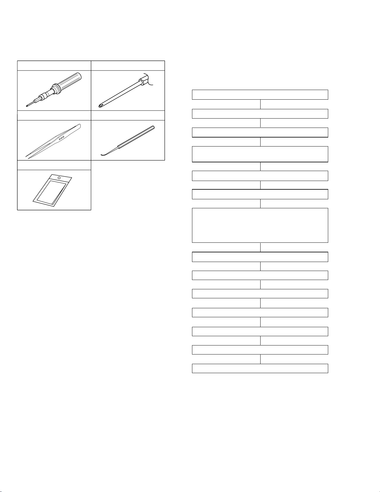
1.2 JIGS AND TOOLS REQUIRED FOR DISASSEMBLY, ASSEMBLY AND ADJUSTMENT
1.2.1 Tools required for adjustments
1
Torque Driver
YTU94088
2
Bit
YTU94088-003
1.3 DISASSEMBLY/ASSEMBLY OF CABINET PARTS AND BOARD ASSEMBLY
1.3.1 Disassembly flow chart
This flowchart indicates the disassembly step for the cabinet parts and board assembly in order to gain access to
item(s) to be serviced. When reassembling, perform the
step(s) in reverse order.
3
5
Tweezers
P-895
Cleaning Cloth
KSMM-01
Chip IC Replacement Jig
4
PTS40844-2
Table 1-2-1
1. Torque driver
Be sure to use to fastening the mechanism and exterior
parts because those parts must strictly be controlled for
tightening torque.
2. Bit
This bit is slightly longer than those set in conventional
torque drivers.
3. Tweezers
To be used for removing and installing parts and wires.
4. Chip IC replacement jig
To be used for adjustment of the camera system.
5. Cleaning cloth
Recommended cleaning cloth to wipe down the video
heads, mechanism (tape transport system), optical lens
surface.
1
2
3
4
5
6
7
8
9
0
!
@
COVER (UNDER)
COVER (SHOE)
MIC COVER ASSY
UPPER CASE ASSY
(Inc.MONITOR ASSY)
MONITOR ASSY
SHUTTER ASSY
LOWER CASE ASSY
(Inc.MICROPHONE
/E.VF UNIT
/AUDIO BOARD ASSY
/OP BLOCK ASSY)
MAIN BOARD ASSY
MECHANISM ASSY
MICROPHONE
E VF UNIT
AUDIO BOARD ASSY
1-2
#
$
OP BLOCK ASSY
SHOE ASSY
Table 1-3-1
Page 7

1.3.2 Disassembly method
STEP
No.
1
2
3
4
5
6
7
8
9
0
!
@
#
$
PART
COVER (UNDER) Fig.1-3-1 (S1) —
COVER (SHOE) Fig.1-3-2 2(S2), (L2a), (L2b) —
MIC COVER ASSY
UPPER CASE ASSY
MONITOR ASSY Fig.1-3-4 2(S5a), GUIDE(MONI), 2(S5b) NOTE5
SHUTTER ASSY FIig.1-3-5(S6
LOWER CASE ASSY
(
Inc.MICROPHONE,
E VF UNIT,
AUDIO BOARD ASSY,
OP BLOCK ASSY)
MAIN BOARD ASSY
MECHANISM ASSY
MICROPHONE Fig.1-3-8a HOOD, SPACER, (S#), (S@) NOTE0a
E VF UNIT (S!), SPACER, CN!a NOTE!a
AUDIO BOARD ASSY
OP BLOCK ASSY
SHOE ASSY CN $a NOTE$
Fig.No.
(S3a), 2(S3b) —
Fig.1-3-3a (SD CARD) NOTE4a
Fig.1-3-3b 2(S4b), (S4c), 2(S4b), (S4d) NOTE4c
Fig.1-3-6
Fig.1-3-7 SHEET(SHUTTER), 2(S8) —
Fig.1-3-8b 2(S@b), SPACER, 3(S$) NOET@
(S4a), COVER (JIG) NOTE4b
CN 4a
2(S4b), (S4e)
CN 4b, CN4c
CN 7a,CN 7b,SHEET(SHUTTER)
CN 7c, CN7d, 4(S7)
(L8a), SHIELD ASSY, CN 8a,
CN 8b, CN 8c, CN 8d
2(L8b), (L8c)
CN 8e, CN 8f
3(S9),BRACKET(MECHA) ASSY
CN0a NOTE0b
CN #a NOTE#a
POINT NOTE
)
Table 1-3-2
NOTE
6
NOTE7
NOTE!b
NOTE#b
NOTE 4a:
NOTE 4b:
NOTE 4c:
NOTE 5:
NOTE 6:
NOTE 7:
NOTE 0a:
NOTE 0b:
NOTE !a:
NOTE !b:
NOTE @, #a, $ :
NOTE #b:
If a card is installed, remove it in advance.
Be careful not to damage the battery removal switch.
When disassembling, ensure that the lock lever is in the
low position and set the battery removal switch only to
the up position.
Take care of the removed screws.
Refer to Fig. 1-4-1 for the disassembly method.
Be careful not to damage or lose the parts.
For the disassembly/assembly of the EVF unit, AUDIO
board assembly, and OP block assembly, see section
1.8, “SERVICE KNOW-HOW”.
Take care not to damage the switch.
Leave the OP block assembly connected to the audio
board and locate it in a vacant space.
Be careful not to cut the FPC wire or damage any of
the switches during work.
Refer to Fig. 1-5-1 for the disassembly method.
When assembling, attach the OP block assembly and
the shoe assembly on the AUDIO board assembly and
install them together in the lower case assembly.
Refer to Fig. 1-6-1 for the disassembly method.
Note:
Remove the parts marked in .
CONN.
No.
CN4a MAIN CN111 BOTTOM CN301 50
CN4b MAIN CN112 ⇔ SUB OPE UNIT - 7
CN4c MAIN CN113 ⇔ MONITOR CN401 39
CN7a MAIN CN110 AUDIIO CN201 120
CN7b MAIN CN111 ⇔ CCD - 20
CN7c MAIN CN107 ⇔ ZOOM OPE UNIT - 13
CN7d MAIN CN108 ←→ EJECT SW - 2
CN8a MAIN CN102 ⇔ LOADING MOTOR - 6
CN8b MAIN CN103 ⇔ ROTARY ENCODER - 6
CN8c MAIN CN101 ⇔ HEAD - 8
CN8d MAIN CN106 ⇔ SENSOR - 16
CN8e MAIN CN105 ⇔ CAPSTAN MOTOR - 18
CN8f MAIN CN104 ⇔ DRUM MOTOR - 11
CN0a AUDIO CN203 ←→ MICROPHONE - 4
CN!a AUDIO CN204 ⇔ VF BL CN7551 20
CN#a AUDIO CN205 ⇔ OP BLOCK ASSY - 24
CN$a AUDIO CN202 ⇔ SHOE ASSY - 16
CONNECTOR
Table 1-3-3
Pin No.
1-3
Page 8

3
5
3
(S b)
6
3
(S b)
2
(L a)
2
1
1
1
(S )
Fig. 1-3-1
4
3
(S a)
Fig. 1-3-2
2
(L b)
2
2
(S )
3
2
(S )
NOTE a
4
COVER
(SD)
4
CN a
NOTE b
4
4
(S a)
COVER
(JIG)
BATT. RELEASE
SWITCH
LOCK LEVER
7
4
1-4
Fig. 1-3-3a
Page 9

Fig. 1-3-3b
4
(S d)
13
4
(S b)
8
4
(S b)
15
4
(S d)
14
4
(S e)
17
4
NOTE c
4
CN b
4
CN c
4
(S e)
17
4
(S c)
10
4
(S b)
16
4
(S b)
12
4
(S b)
11
4
(S b)
9
4
GUIDE
(MONI)
18
5
(S a)
19
5
(S a)
4
20
(S b)
21
5
(S b)
5
NOTE
5
5
22
6
(S )
6
NOTE
6
: 0.98N·m (1.0kgf·cm)
Fig. 1-3-4
Fig. 1-3-5
1-5
Page 10

CASS.
COVER
SPACER
NOTE
7
7
(S )
SHEET
(SHUTTER)
23
7
24
7
(S )
7
CN a
(S )
26
7
CN b
CN c
25
(S )
7
CN d
7
7
7
SHEET
(SHUTTER)
27
8
(S )
28
8
(S )
9
(L a)
SHIELD
ASSY
Fig. 1-3-6
29
(S )
8
(L b)
9
BRACKET
8
CN a
8
30
9
(S )
8
8
CN c
(L c)
31
9
(S )
8
8
CN e
CN f
CN d
8
8
CN b
8
1-6
Fig. 1-3-7
Page 11

Fig. 1-3-8a
10
7
13
14
11
CN a
13
NOTE b
10
NOTE
AUDIO
PWB
SW
a
10
NOTE a
10
CN a
11
CN a
10
(S )
32
13
(S )
34
SPACER
11
(S )
33
HOOD
SPACER
12
12
37
14
(S )
SPACER
KNOB
(VIDEO
/DSC)
12
Fig. 1-3-8b
(S )
CN a
CN a
(S b)
SPACER
14
35
12
14
39
13
14
38
14
(S )
(S b)
13
36
12
1-7
Page 12

1.4 DISASSEMBLY OF 5 MONITOR ASSEMBLY
1.4.1 5 Monitor assembly/Hinge assembly
1. Remove the three screws (1 to 3) and then remove the
monitor cover by disengaging the two hooks (L5a, L5b)
at the top and bottom.
Note
a:
Be careful not to lose part (Lib).
5
2. Pull out the part (sensor) from the monitor case assembly.
3. Disconnect FPC from the connector CN5a and then remove the MONITOR board assembly and backlight.
Note
b:
When removing the parts out of the monitor case
5
assembly, be very careful not to damage the FPC
and parts.
Note5c:
Remove the MONITOR board assembly and
backlight together unless it is needed to separate
them from each other for part replacement, etc.,
because the two are soldered to each other.
4. Take out the LCD module, back light and monitor board
assembly from the monitor case assembly. Be careful
with the hooks (L5e, L5f) on the two sides.
Disconnect the FPC assembly from the connector
(CN5b) and remove the LCD module. Be careful with the
hooks (L5g ,L5h) on the two sides.
1.4.2 Hinge assembly
1. Remove the two screws (4,5) to take out the FPC assembly while removing the hinge cover.
Note
d:
Be careful not to lose any part during the above-
5
mentioned process.
2. Remove the hinge cover (U) from hinge assembly.
e:
Note
Be careful not to lose any part during the abobe
5
mentioned process.
Note5f:
When reassembling, wind the FPC assembly
around the hinge assembly by three turns and a
half.
Be careful not to break the FPC wire during the
work.
MONITOR
CASE ASSY
5
(L f)
HINGE
COVER(L)
5
NOTE e
HINGE
ASSY
FPC ASSY
5
NOTE b,d,e,f
a
5
(L b)
b
b
(L e)
LCD
MODULE
SENSOR
5
(L c)
NOTE d
5
MAGNET
5
(L g)
c
(S c)
(S c)
5
4
5
5
5
NOTE c
BACK LIGHT
HINGE
COVER(U)
5
CN b
5
(L h)
CN a
c
NOTE a
5
1
5
(S a)
2
5
(S a)
NOTE c
MONITOR
5
5
RIB
5
<04>
5
(L b)
a
5
(L b)
NOTE
<WIRING>
MONITOR
COVER
3
5
(S b)
5
c
BROWN
5
CN
b
5
CN
5
NOTE f
FPC ASSY
HINGE
ASSY
ORANGE
a
BLACK
RED
1-8
5
NOTE d
MARKING
Fig. 1-4-1
Page 13

1.5 DISASSEMBLY OF
1.5.1
Note
Note!b:
1. Draw the frame (VF) out of the case assembly.
2. Remove the eyecup and pull out the guide (VF).
<Case assembly>
3. While holding the guide (VF), pull out the case assem-
4. Remove the three screws (3-5) and draw out the eye-
5. Draw out the guide (VF).
Note
E. VF assembly
!
a:
When disassembling the E VF assembly, remove
!
the frame (VF) from the case/cap assembly depending on the situation.
Be very careful not to get the inside of the VF
soiled or dusty during and after disassembling the
E. VF assembly.
bly, remove the two screws (1, 2) and remove the cap
(VF).
piece sub assembly.
c:
A lens assembly and a lever are mounted on the
!
eye-piece sub assembly. When removing this assembly, be careful not to damage them.
E. VF ASSEMBLY
!
<Frame (VF)>
6. Remove the screw (6) first and then LCD module/holder
(LCD).
7. Get the two hooks (L!a, L!b) disengaged and then remove the holder (LCD)
Note
d:
Carefully proceed with the above-mentioned work
!
not to damage any part.
8. Disconnect the connector (CN!a) and remove the LCD
module.
Note!e:
Pay heed the parts not to damage any thing.
: 0.069N·m (0.7kgf·cm)
FPC ASSY
B/L PWB
11
(L
a)
11
CN a
11
CN b
(L b)
LCD MODULE
(S a)
2
11
(S a)
3
11
(S b)
NOTE d
11
HOLDER
(LCD)
11
NOTE b,e
11
1
CAP(VF)
11
6
11
(S c)
FRAME(VF)
NOTE a,b
11
LENS ASSY
(S b)
4
11
(S b)
CASE ASSY
NOTE a,c
11
GUIDE(VF)
5
11
EYE PIECE
SUB ASSY
NOTE c
NOTE c
LENS ASSY
LEVER
CASE ASSY
EYE CUP
11
11
Fig. 1-5-1
1-9
Page 14

1.6 DISASSEMBLY OF # OP BLOCK ASSEMBLY/CCD
BOARD ASSEMBLY
1.6.1 Precautions
1. Carefully handle the CCD image sensor, optical LPF,
lens, etc. during the disassembly work. Pay the most
careful attention to the surface of those parts not to get
it soiled, scratched or dusty. If some of those surfaces
gets soiled with fingerprints, etc., wipe it out with silicone
paper, clean chamois, cleaning cloth or the like.
2. The new CCD image sensor is occasionally shipped from
the factory as a protection seal is applied onto its transparent glass. If so, leave the protection seal as it is and
remove it just before installing the CCD image sensor in
the OP block assembly.
1.6.2 How to remove OP block assembly and CCD
board assembly
1. Remove the spacer.
2. Unsolder at the fourteen points (SD1) and remove the
CCD board assembly.
3. Remove the two screws (1, 2) and then remove the CCD
base assembly.
Note
a:
Carefully remove the CCD base assembly, be-
#
cause the space rubber and optical LPF may be
removed together with the CCD image sensor.
Note#b:
When replacing the CCD image sensor, don’t replace it individually but replace the CCD base assembly in whole with a new one.
1.6.3 How to install # OP block assembly and CCD
board assembly
1. Install the optical LPF with the # OP block assembly.
2. With the spacer rubber left attached to the CCD base
assembly, install the assembly in the OP block assembly and clamp it using the two screws (1, 2).
3. Set the CCD board assembly in the CCD base assembly, and fasten it by soldering at the fourteen points
(SD1).
1.6.4 Replacement of service parts
Service parts to be supplied for the OP block assembly are
as follows.
When replacing a part, be very careful not to get the FPC
wire broken or damaged by soldering (overheating).
1. Focus motor
2. Zoom motor
3. Iris motor unit
Note
c:
When soldering the FPC wire of the focus motor
#
or zoom motor during the replacement work, be
sure to keep the tip of a soldering iron approximately 1 mm above the terminal.
Note#d:
The iris motor unit includes one FPC assembly
and two sensors.
(S b)
ZOOM MOTOR
NOTE c
13
8
13
(S c)
4
13
(S b)
3
13
9
13
(S c)
5
13
(S c)
6
13
(S c)
NOTE d
13
IRIS MOTOR
UNIT
CCD
OP
SIDE
SIDE
BLUE
OPTICAL
LPF
NOTE c
13
OP BLOCK
FOCUS MOTOR
NOTE c
13
7
13
(S c)
1
13
(S a)
(SD1)
(S a)
CCD BASE
ASSY
NOTE a,b
13
SPACER
RUBBER
: 0.118N·m (1.2kgf·cm)
SPACER
2
13
CCD
<05>
1-10
Fig. 1-6-1
Page 15

1.7 EMERGENCY DISPLAY
Whenever some abnormal signal is input to the syscon CPU,
an error number (E01, as an example) is displayed on the
LCD monitor or (in the electronic view finder).
In every error status, such the message as shown below
alternately appear over and over.
• In an emergency mode, all operations except turning on/
off the POWER switch are ineffectual.
LCD
display
E01 LOADING
E02 UNLOADING
E03 TU & SUP REEL
Emergency
mode
FG
Details
In the case the encoder position is not shifted
to the next point though the loading motor has
rotated in the loading direction for 4 seconds
or more. This error is defined as [E01].
In the case the encoder position is not shifted
to the next point though the loading motor has
rotated in the unloading direction for 4 seconds
or more. This error is defined as [E02].
In the case no REEL FG is produced for 4 seconds or more in the capstan rotation mode after loading was complete, the mechanism mode
is shifted to STOP with the pinch roller set off.
This error is defined as [E03].
However, no REEL EMG is detected in the
SLOW/STILL mode.
Example (in case of the error number E01):
E01
UNIT IN
SAFEGUARD MODE
E01
REMOVE AND
REATTACH BATTERY
Possible cause
1. The mechanism is locked during mode shift.
2. The mechanism is locked at the mechanism loading
end, because the encoder position is skipped during
mechanism mode shift.
3. No power is supplied to the loading MDA.
1. The mechanism is locked during mode shift.
2. The mechanism is locked at the mechanism loading
end, because the encoder position is skipped during
mechanism mode shift.
1. The idler gear does not engage with the reel disk well.
2. Though the idler gear and reel disk are engaged with
each other, the tape is not wound because of overload to the mechanism.
3. No FG pulse is output from the reel sensor.
4. No power is supplied to the reel sensor.
5. Tape transport operation takes place with a cassette
having no tape inside.
6. The tape slackens and no pulse is produced until the
slack is taken up and the tape comes into the normal
status.
E04 DRUM FG
E05 –
E06 CAPSTAN FG
In the case there is no DRUM FG input in the
drum rotation mode for 4 seconds or more. This
error is defined as [E04], and the mechanism
mode is shifted to STOP with the pinch roller
set off.
–
In the case no CAPSTAN FG is produced in
the capstan rotation mode for 2 seconds or
more. This error is defined as [E06], and the
mechanism mode is shifted to STOP with the
pinch roller set off.
However, no CAPSTAN EMG is detected in the
STILL/FF/REW mode.
Table 1-7-1
1. The drum cannot be started or drum rotation is stopped
because tape transport load is too high.
1) Tape tension is extremely high.
2) The tape is damaged or soiled with grease, etc.
2. The DRUM FG signal is not received by the syscon
CPU.
1) Disconnection in the middle of the signal line.
2) Failure of the DRUM FG pulse generator (hall ele-
ment).
3. No drum control voltage is supplied to the MDA.
4. No power is supplied to the DRUM MDA.
–
1. The CAPSTAN FG signal is not received by the syscon
CPU.
1) Disconnection in the middle of the signal line.
2) Failure of the CAPSTAN FG pulse generator (MR
element).
2. No capstan control voltage is supplied to the MDA.
3. No power is supplied to the CAPSTAN MDA.
4. The capstan cannot be started or capstan rotation is
stopped because tape transport load is too high.
1) Tape tension is extremely high. (Mechanical lock-
ing)
2) The tape is damaged or soiled with grease, etc.
(Tape tangling occurs, etc.)
(DVC_03)
1-11
Page 16

1.8 SERVICE KNOW-HOW
When performing disassembly/assembly work to this model,
the parts that are most complicated and require special attention are the EVF unit and the AUDIO board, OP block and
shoe assemblies, all of which are mounted inside the lower
case assembly.
Care should be taken in handling these parts as they are
mounted inside the lower case assembly (except the E.VF
unit) and there is a lack of adequate space to work conveniently. This section gives further details regarding the disassembly procedures, although they have been described in
previous sections.
1. See Fig. 1-8-1.
(1) Remove the hood by moving the 0 microphone out of
way.
(2) Peel off the spacer, remove the screw (32) and take out
the # OP block assembly by moving the 0 microphone
out of the way.
(3) Remove the screw (33) and, while opening the @ AU-
DIO board assembly, disconnect the wire from the connector (CN203) and remove the 0 microphone.
(4) Remove the screw (34), peel off the spacer, take out
the ! E.VF assembly by moving the $ shoe assembly
out of way, disconnect the FPC from the connector
(CN204).
Note:
Be careful not to damage the FPC or the switches
when carrying out this work.
NOTE a
10
AUDIO
PWB
CN a
32
(S )
SW
10
13
CN a
13
CN a
(S )
11
33
12
NOTE
10
a
14
11
SPACER
34
11
(S )
10
1-12
SPACER
7
12
Fig. 1-8-1
13
NOTE b
10
HOOD
Page 17

2. See Fig. 1-8-2.
(1) Remove the two screws (35,36) in order to free the @
AUDIO board assembly.
(2) Remove the three screws (37 to 39), peel off the spacer
and take out the @ AUDIO board assembly together with
the # OP block assembly and the $ shoe assembly.
Note:
Be careful not to lose the VIDEO and DSC knobs,
which may slip out during the disassembly.
(3) Disconnect the FPCs from the connectors on the # OP
block assembly and the $ shoe assembly.
37
14
(S )
SPACER
KNOB
(VIDEO
/DSC)
12
(S )
14
CN a
CN a
(S b)
SPACER
14
39
35
12
14
13
38
14
(S )
(S b)
13
36
12
Fig. 1-8-2
1-13
Page 18

1.9 SERVICE NOTE
1 2 3 4 5 6 7 8 9 11 12 13 14 16 17 18
19 20 21
12 3
67 8 90!
!5
#
@# $
45
Fig.1-3-1
Fig.1-3-2
Fig.1-3-3a Fig.1-3-3b Fig.1-3-4
I
I
II
22 23 24 25 26 27 28 29 30 31 32 33 34 35 36 37 38 39
MONITOR ASSY
Fig.1-3-5
Fig.1-3-6 Fig.1-3-7 Fig.1-3-8a Fig.1-3-8b
–
Fig. 1-4-1
I
Symbol No.
Removing order of screw
Place to stick screw
Reference drawing
Screw tightening torque
Symbol No.
Removing order of screw
Place to stick screw
Reference drawing
Screw tightening torque
Removing order of screw
Place to stick screw
Reference drawing
Screw tightening torque
Removing order of screw
Place to stick screw
Reference drawing
Screw tightening torque
Removing order of screw
Place to stick screw
Reference drawing
Screw tightening torque
1 2 3 4 5 1 2 3 4 5 6
E VF UNIT
OP BLOCK ASSY
Fig.1-6-1
III
IV
1234 56789
< NOTE >
1) : : Don’t reuse the screw, because screw lock bond was applied to them.
2) Pay careful attention to tightening torque for each screw.
I : 0.078N·m (0.8kgf·cm)
II : 0.098N·m (1.0kgf·cm)
III : 0.118N·m (1.2kgf·cm)
IV : 0.069N·m (0.7kgf·cm)
Fig.1-5-1
Table 1-9-1
1-14
Page 19

SECTION 2
MECHANISM ADJUSTMENT
2.1 PRELIMINARY REMARKS ON ADJUSTMENT AND REPAIR
2.1.1 Precautions
1. When fastening parts, pay careful attention to the tight-
ening torque of each screw. Unless otherwise specified,
tighten a screw with the torque of 0.039 N
2. Be sure to disconnect the set from the power supply be-
fore fastening and soldering parts.
3. When disconnecting/connecting wires, be careful not to
get them and their connectors damaged. (Refer to the
Section 1.)
4. When replacing parts, be very careful neither to dam-
age other parts nor to fit wrong parts by mistake.
2.1.2 Notes on procedure for disassemby/assembly
The disassembling procedure table (Table 2-4-1 on page
2-5,a part of the table is shown below for reference)shows
the procedure to disassemble/reassemble mechanism
parts.
Carefully read the following explanation before starting actual disassembling/reassembling work. The item numbers
(circled numbers)in the following explanation correspond
to those appearing under respective columns of the table.
(1) Circled numbers appearing in this column indicate the
order to remove parts. When reassembling, follow these
numbers in the reverse order. Circled numbers in this
column correspond to those appearing in drawings of
this section.
(2) This column shows part names corresponding to circled
numbers in the left column.
(3) The symbol (T or B)appearing in this column shows the
side which the objective part is mounted on.
T =the upper side, B =the lower side
(4) Symbols appearing in this column indicate drawing
numbers.
Step Part Name Fig. Point Note Remarks
•
m (0.4 kgf•cm).
(5) This column indicates parts and points such as screws,
washers,springs,and others to be removed/fitted for disassembling/reassembling the mechanism. Besides such
the parts, this column occasionally indicates working
points.
P = Spring
W = Washer
S = Screw
* = Lock (L),soldering (SD),shield,connector (CN),
etc.
Example • Remove ((W1)=Washer W1.
• **Remove the solder at (SD1)=Point SD1.
• **Disconnect
(6) Numbers in this column represent the numbers of notes
in the text.
(For parts that need phase adjustment after reassembling, refer to “2.6 MECHANISM ADJUSTMENTS”.)
(7) This column indicates required after-disassembling/-re-
assembling work such as phase adjustment or mechanism adjustment.
=Connector Å .
Å
NO. PART NAME FIG. POINT NOTE REMARKS
1 CASSETTE HOUSING ASSY T Fig.2-4-3 3(S1),(L1a)-(L1e)
2 UPPER BASE ASSY T Fig.2-4-4 (S2),(L2a),(L2b)
3 DRUM ASSY T (S3a),2(S3b)
4 REEL DISK ASSY(SUP) T Fig.2-4-5 (W4)
5 REEL DISK ASSY(TU) T (W5)
6 REEL COVER ASSY T 2(W6),(S6a),2(S6b)
(1) (2) (3) (4) (5) (6) (7)
NOTE1a,b,c,d
NOTE
2
NOTE3a,b
NOTE4a
NOTE
5
NOTE
6
ADJUSTMENT
ADJUSTMENT
2-1
Page 20

2.2 JIGS AND TOOLS REQUIRED FOR DISASSEMBLY, ASSEMBLY AND ADJUSTMENT
2.2.1 Tools required for adjustments
1
3
5
7
9
11
13
15
Torque Driver
YTU94088
Tweezers
P-895
Guide Driver (Hexagonal)
D-770-1.27
Slit Washer Installation Jig
YTU94121A
Jig Connector cable
YTU93106C
PC cable
QAM0099-002
Service Support System
YTU94057-54
Cleaning Cloth
KSMM-01
2
Chip IC Replacement Jig
4
6
Slit Washer Installation Jig
8
10
12
Cassette Torque Meter
14
Bit
YTU94088-003
PTS40844-2
Adjustment Driver
YTU94028
YTU94121B
Communication cable
YTU93107A
Alignment Tape
MC-1
YTU94151A
1. Torque Driver
Be sure to use to fastening the mechanism and exterior
parts because those parts must strictly be controlled for
tightening torque.
2. Bit
This bit is slightly longer than those set in conventional
torque drivers.
3. Tweezers
To be used for removing and installing parts and wires.
4. Chip IC Replacement Jig
To be used for adjustment of the camera system.
5. Guide Driver (Hexagonal)
To be used to turn the guide roller to adjustment of the
linarity of playback envelope.
6. Adjustment Driver
To be used for adjustment.
7. Slit Washer Installation Jig
To be used to install slit washers.
8. Slit Washer Installation Jig (NEW TYPE)
To be used to install slit washers.
9. Jig Connector Cable
Connected to CN114 of the main board and used for
electrical adjustment, etc.
10. Communication Cable
Connect the Communication cable between the PC cable and Jig connector cable when performing a PC adjustment.
11. PC Cable
To be used to connect the VideoMovie and a personal
computer with each other when a personal computer is
used for adjustment.
12. Alignment Tape
To be used for check and adjustment of interchangeability of the mechanism.
13. Service Support System
To be used for adjustment with a personal computer.
14. Cassette Torque Meter
This is used to cheek the back tension and play torque
during mechanism adjustment.
When using the cassette torque meter, install the
Note:
service support system software in advance.
•
LED : Forced to ON
•
EJECT SW : OFF (Cancel)
The above setting is required to prevent any tape
damage that may occur because the cassette
torque meter cannot detect the leading/trailing sections of the tape.
15. Cleaning Cloth
Recommended cleaning cloth to wipe down the video
heads, mechanism (tape transport system), optical lens
surface.
2-2
Table 2-2-1
Page 21

2.3 DISASSEMBLY/ASSEMBLY OF MECHANISM AS-
<SUB CAM GEAR>
TOP VIEW BOTTOM VIEW
<C IN mode>
<SHORT FWD mode>
<STOP mode>
<REV mode>
<PLAY mode>
SEMBLY
2.3.1 General statement
The mechanism should generally be disassembled/assembled in the C.IN mode (ASSEMBLY mode). (Refer to Fig.
2-3-1,2.)
However, when the mechanism is removed from the main
body, it is set in the STOP mode. Therefore, after the
mechanism is removed from the main body, supply 3 V DC
to the electrode on the top of the loading motor to enter
the mechanism mode into the C,IN mode compulsory.
<Mechanism assembly/Cassette housing assembly>
DC3V
2.3.2 Explanation of mechanism mode
The mechanism mode of this model is classified into five
modes as shown in Table 2-3-1. Each mechanism mode
can be distinguished from others by the relative position
”, “Q”, “Q” “ ” marks on the sub cam gear to the in-
of “
ner or outer protrusion on the main deck.
Refer to Fig. 2-3-3 to 2-3-8 below.
Fig. 2-3-3
<Back side of the mechanism assembly>
C IN mode
LOADING MOTOR
Fig. 2-3-4
Fig. 2-3-5
Fig. 2-3-1
Fig. 2-3-6
Back side of deck
Fig. 2-3-2
Fig. 2-3-7
Fig. 2-3-8
2-3
Page 22

2.3.3 Mechanism timing chart
PARTS
MAIN CAM
SUB CAM
ROTARY
ENCODER
EJECT LEVER
TENSION ARM
TU ARM
SLIDE DECK
BRAKE (S)
BRAKE (T)
MODE
OFF
L. END
LOCK
L. END
OFFPAD ARM
OFF
LOAD
L. END
LOADSUP. L. ARM
L. END
LOADTU. L. ARM
PRESS
LOADP. ROLLER
OFF
OFF
SHORT
EJECT
CAS. IN
-12.40° (22.44°) (69.53°) (80.5°) (150.58°) (153.5°)58.71°0° 177.79° 212.77° 243.94°
-16.97° (30.71°) (95.14°) (110.06°) (206.06°) (210.05°)80.34°0° 243.29° 291.16° 333.82°
-15° (27.14°) (84.08°) (97.35°) (182.10°) (185.63°)71°0°
-13°-3° 3° 68°
a
b
c
ON
UL
UL
ON
UL
UL
UL
UL
ON
ON
R
RELEASE
TU. P. B
START
SLIDE SLIDE
START
TU. P. B
END END
STOP PLAYREVFWD
215°
212° 218°
257.3°
254.3° 260.3°
295°
292° 310°74°
CTL PLATE
RELEASE
LEVER
2-4
C
L
ON
OFF
Table 2-3-1
Page 23

2.4 DISASSEMBLING PROCEDURE TABLE
MARK: 夝 After assembly, perform adjustments.
NO. PART NAME FIG. POINT NOTE REMARKS
1 CASSETTE HOUSING ASSY T Fig.2-4-3 3(S1),(L1a)-(L1e)
2 UPPER BASE ASSY T Fig.2-4-4 (S2),(L2a),(L2b)
3 DRUM ASSY T (S3a),2(S3b)
4 REEL DISK ASSY(SUP) T Fig.2-4-5 (W4)
5 REEL DISK ASSY(TU) T (W5)
6 REEL COVER ASSY T 2(W6),2(S6a),(S6b)
7 TENSION ARM ASSY T Fig.2-4-6 —
8 SLANT POLE ARM ASSY T —
9 TU ARM ASSY T —
10 SWING ARM ASSY T (S0)
11 SLIDE DECK ASSY T Fig.2-4-7a 2(S!a),(S!b),2(L!a),
2(L!b),(L!c)
12 PAD ARM ASSY T Fig.2-4-7b (P@),(L@),(W@)
13 SUP BRAKE ASSY T (P#),(L#),(S#)
14 TU BRAKE ASSY T (P$),(L$),(W$)
15 TENSION CTL LEVER ASSY T Fig.2-4-8 —
16 CENTER GEAR T —
17 PINCH ROLLER ARM F. ASSY T (W&)
18 TENSION CTL PLATE ASSY T —
19 BRAKE CTL LEVER ASSY T —
20 MOTOR BRACKET ASSY T Fig.2-4-9 3(S)),(L)a),2(L)b)
21 GUIDE RAIL ASSY T
22 SLIDE LEVER 2 ASSY T —
23 LOADING PLATE ASSY T (W‹)
24 MODE GEAR T —
25 EJECT LEVER T (Wfi)
26 BASE R ASSY T Fig.2-4-10 (Sfla),(Sflb),2(Lfl)
27 ROTARY ENCODER T 2(S‡)
28 GEAR COVER ASSY T (S°a),2(S°b)
29 MAIN CAM ASSY T —
30 SLIDE ARM ASSY T Fig.2-4-11 —
31 CONNECT GEAR 2 T —
32 SUB CAM ASSY T (S™)
33 CONTROL ARM ASSY T —
34 REEL GEAR 1 T —
35 / 36
DRUM BASE ASSY/ T Fig.2-4-12 3(S∞)
CAPSTAN MOTOR
36 CAPSTAN MOTOR T (S§)
37 MAIN DECK ASSY T —
2(W⁄),(S⁄),2(L⁄a),(L⁄b)
NOTE1a,b,c,d
NOTE
2
NOTE3a,b
NOTE
4
NOTE
5
NOTE
6
NOTE
7
NOTE
8
NOTE
9
NOTE
0
NOTE!a,b
NOTE
@
NOTE
#
NOTE
$
NOTE
%
NOTE
^
NOTE
&
NOTE
*
NOTE
(
NOTE
)
NOTE
⁄
NOTE
¤
NOTE
‹
NOTE
›
NOTE
fi
NOTE
fl
NOTE
‡
—
NOTE
·
NOTE
‚
NOTE
¡
NOTE
™
NOTE
£
NOTE
¢
NOTE∞a,b
NOTE
§
—
ADJUSTMENT
ADJUSTMENT
ADJUSTMENT / 夝
ADJUSTMENT
ADJUSTMENT
ADJUSTMENT
ADJUSTMENT / 夝
ADJUSTMENT / 夝
ADJUSTMENT
ADJUSTMENT
ADJUSTMENT
ADJUSTMENT
ADJUSTMENT
ADJUSTMENT
ADJUSTMENT
ADJUSTMENT / 夝
ADJUSTMENT
ADJUSTMENT
ADJUSTMENT
PHASE ADJUSTMENT
PHASE ADJUSTMENT
ADJUSTMENT
PHASE ADJUSTMENT
ADJUSTMENT
ADJUSTMENT
ADJUSTMENT
Table 2-4-1
2-5
Page 24

< TOP VIEW >
24 27 2 3 36 3521
17
< BOTTOM VIEW >
20
23
18
8
7
22
12
4
29
19
34
143128161530
13
Fig. 2-4-1
5
36 3 22
26
34
9
10
33
26
6
37
25
32
11
26
32
25
31 16 6
Fig. 2-4-2
37
11
27
20
30
18
19
29
30
2-6
Page 25

2.4.1 Disassembly/assembly
1
(S )
1
2
(S )
1
1
NOTE d
1
NOTE c
1
NOTE b
1
NOTE a
1
(S )
1
3
(L d)
LOCK
LEVER
1
(L a)
1
(L e)
1
(L c)
1
(L b)
1
NOTE d
1
2
3
(S )
2
4
(S b)
7
3
(S b)
6
3
(S a)
5
3
(L b)
2
(L a)
2
NOTE
2
NOTE
3
NOTE b
3
NOTE
2
a
CASSETTE HOUSING ASSY
1.
1
NOTE1a:
Be careful not to damage any of the
parts during work.
NOTE1b:
Special care is required in mounting.
1
NOTE b
NOTE1c:
NOTE c
When mounting, the CASSETTE
HOUSING ASSY should be attached in the Eject status. Pay
heed to the positions of the LOCK
LEVER and EJECT LEVER during
mounting.
NOTE1d:
When mounting, be sure to locate the
FPC in the gap.
2.
UPPER BASE ASSY
2
DRUM ASSY
3
NOTE
NOTE2:
When mounting, be sure to insert
the FPC reinforcing sheet.
1
EJECT
LEVER
NOTE d
LOCK
LEVER
1
Fig. 2-4-3
2
NOTE3a:
Be mindful of scratches or damage
during work.
NOTE3b:
Be careful not to attach screws incorrectly.
3
NOTE
b
5
7
6
Fig. 2-4-4
2-7
Page 26

REEL DISK ASSY(SUP)
3.
4
REEL DISK ASSY(TU)
5
REEL COVER ASSY
6
NOTE4:
Be careful not to attach the REEL DISK wrongly. The Supply side can be identified by the white color at the center.
4 5
NOTE5:
Be careful not to attach the
REEL DISK wrongly. The
NOTE ,
REEL DISK ASSY
WHITE
BLACK
Take-up side can be identified by the black color at
the center.
NOTE
6
SUP
:
TU
Perform the following steps for mounting.
1. Align the 2 holes with the pins.
2. Attach the PINCH ROLLER ARM ASSY by aligning the
positions.
3. Attach the SUB DECK
ASSY by aligning the
positions.
4. Check that the parts
NOTE
6
53
2,6
below them are located in the correct
positions.
5. Tighten the 2 screws.
4
6. Tighten the screw.
7. Attach the 2 SLIT
WASHER parts.
1, 7
NOTE
4
NOTE
(W )
4
8
6
(S a)
6
(W )
6
6
4
(W )
5
(W )
6
Fig. 2-4-5
NOTE
5
10
6
(S b)
5
9
6
(S a)
4.
TENSION ARM ASSY
7
SLANT POLE ARM ASSY
8
TU ARM ASSY
9
SWING ARM ASSY
0
NOTE7:
When detaching, remove the spring
of the @ PAD ARM ASSY in advance.
Pay attention to the attachment position.
NOTE8:
Be careful not to lose any parts
(such as a spring).
NOTE9:
Pay attention to the
mounting position.
9
NOTE
7
NOTE
SPRING
8
NOTE
SPRING
10
NOTE
TOP SIDE
NOTE
7
NOTE
7
(P )
NOTE
NOTE
7
10
8
NOTE
8
8
10
11
10
(S )
9
9
NOTE0:
When detaching, remove the
screw then remove the SWING
ARM ASSY by pulling it up and
turning it.
2-8
Fig. 2-4-6
Page 27

5.
11
(S b)
14
11
(S a)
12
11
(S a)
13
11
(L b)
11
(L a)
11
(L c)
11
NOTE a
11
NOTE b
11
SLIDE DECK ASSY
!
NOTE!a:
Each of the parts on the SLIDE DECK ASSY can be replaced separately.
When detaching the assembly, if there is no need to replace
any of its parts, remove the SLIDE DECK ASSY as it is.
NOTE!b:
When mounting, pay attention to the positions of the
¤
SLIDE LEVER (2) studs and the BRAKE CONTROL LEVER
ASSY.
When mounting, position the CONTROL PLATE on the left
side.
Pay attention to the position of the SLIDE GUIDE PLATE
during mounting.
11
NOTE
b
6.
PAD ARM ASSY
@
SUP BRAKE ASSY
#
TU BRAKE ASSY
$
NOTE@:
The spring may have already been disengaged when the
8
SLANT POLE ARM ASSY was removed.
NOTES#/$:
When mounting, pay attention to the correct positioning.
Mount the CONTROL PLATE by moving it fully toward the
left side.
12 13 14
NOTE
12
SPRING
CONTROL
PLATE
13 14
12
(W )
NOTE
(L )
13
13
12
15
(S )
13
NOTE
12
(P )
13
Fig. 2-4-7a
12
13
(P )
(W )
12
(L )
14
14
NOTE
(L )
14
(P )
14
14
Fig. 2-4-7b
2-9
Page 28

TENSION CTL LEVER ASSY
7.
%
CENTER GEAR
^
PINCH ROLLER ARM F. ASSY
&
TENSION CTL PLATE ASSY
*
BRAKE CTL LEVER ASSY
(
NOTES%/^:
When mounting, pay attention to the correct positioning.
15
NOTE
NOTE
16
(TOP)
(BOTTOM)
NOTES*/(:
When mounting, pay at-
NOTE&:
Take care against grease
attachment during work.
17
NOTE
tention to the correct positioning.
19
NOTE
18
NOTE
NOTE
15
NOTE
19
15
19
NOTE
18
18
NOTE
17
16
17
NOTE
17
(W )
16
MOTOR BRACKET ASSY
8.
)
GUIDE RAIL ASSY
⁄
SLIDE LEVER 2 ASSY
¤
LOADING PLATE ASSY
‹
MODE GEAR
›
EJECT LEVER
fi
NOTE):
When mounting, pay attention to the positioning of the sliding parts.
21
NOTE
NOTE⁄:
When mounting, take care
that no part is allowed to
float or rattle.
NOTES¤/‹/›/fi:
NOTE
When mounting, pay attention to the
correct positioning.
23
NOTE
22
NOTE
NOTE
24
Fig. 2-4-8
20
21
(W )
(W )
23
22
21
NOTE
19
21
(S )
22
(L a)
21
(L b)
21
NOTE
18
20
(S )
20
20
17
20
(S )
NOTE
16
20
(S )
21
21
NOTE
23
23
(L b)
25
(W )
(L a)
20
(W )
20
NOTE
24
24
25
25
NOTE
2-10
NOTE
25
Fig. 2-4-9
Page 29

BASE R ASSY
9.
fl
ROTARY ENCODER
‡
GEAR COVER ASSY
°
MAIN CAM ASSY
·
NOTEfl:
When mounting, fold the sliding
part to the inner side.
NOTE
22
27
(S )
27
NOTE
26
27
23
27
(S )
25
26
28
24
28
(S a)
21
26
(S b)
28
(S b)
(S b)
NOTE‡:
When mounting, pay attention to
the correct positioning and the
FPC layout.
NOTE
·
:
When mounting, pay attention to
the correct positioning.
SLIDE ARM ASSY
10.
‚
CONNECT GEAR 2
¡
SUB CAM ASSY
™
CONTROL ARM ASSY
£
REEL GEAR 1
¢
NOTE
‚
:
When mounting, pay attention to the
correct positioning and the FPC layout.
NOTE
NOTE
NOTE
20
26
27
(S a)
28
29
29
NOTE
29
26
NOTE
26
26
(L )
Fig. 2-4-10
30
30
NOTE
30
27
32
(S )
NOTE
32
32
NOTE
34
34
NOTE¡:
When mounting, pay attention to the position of the front and back.
NOTE
(BOTTOM)
31
(TOP)
NOTES™/£/¢:
When mounting, pay attention to the correct positioning and
the FPC layout.
34
32 33
NOTE /
33
32
NOTE
NOTE
31
31
Fig. 2-4-11
33
NOTE
33
2-11
Page 30

11.
DRUM BASE ASSY
∞
CAPSTAN MOTOR
§
MAIN DECK ASSY
¶
NOTES
∞
a /§:
When detaching, remove them together and then separate
from ∞a.
§
∞
b:
NOTE
When mounting, attach the DRUM BASE ASSY so that the
screw hole is located at the center of the ellipse.
35
NOTE b
NOTE
35
35
28
35
(S )
a
29
35
(S )
31
36
(S )
30
35
(S )
NG
OK
NG
NOTE
36
36
Fig. 2-4-12
37
NOTE
35
b
2-12
(Z27 Ver.2)
Page 31

2.4.2 List of procedures for disassembly
(S15 )
13
13
(P )
18
20
(S )
(W )
13
12
14
17
20
(S )
20
12
(S b)
8
(P )
14
(W )
14
(P )
8
(S )
14
11
(P )
(S )
2
1
12
16
20
4
(W )
4
8
6
(S a)
6
(W )
6
7
23
(W )
22
27
(S )
18
27
(W )
6
(W )
30
23
5
(S b)
11
(S )
23
27
(S )
5
10
6
10
13
11
(S a)
3
1
(S )
34
1
9
6
(S a)
10
12
11
(S a)
11
21
(W )
1
(S )
22
21
(W )
19
(S )
21
1
9
(S b)
21
(S )
28
35
(S )
35
7
3
(S b)
5
3
(S a)
6
3
(S )
29
35
17
36
4
2
2
3
31
36
(S )
30
35
(S )
17
(W )
25
28
(S b)
15
29
16
31
26
28
(S b)
28
24
28
(S a)
19
24
37
Fig. 2-4-13
21
26
(S b)
20
26
(S a)
26
25
(W )
(S )
25
27
32
32
33
2-13
Page 32

2.5 CHECKUP AND ADJUSTMENT OF MECHANISM PHASE
MODE GEAR
24
Align the MODE GEAR with the Main Deck
Assembly hole.
Note:
The MODE GEAR may
be displaced during the
mechanism operation,
however it can be
checked from the rear
and realigned during
manual assembly.
27
ROTARY ENCODER
Mount the ROTARY ENCODER by aligning its mark ( )
and the mark ( ) of the Main Deck Assembly.
Note:
Be careful when handling the FPC during mounting.
34
REEL GEAR 1
Align the REEL GEAR 1 with
the Main Deck Assembly hole.
Note:
The REEL GEAR 1 may be
displaced during mechanism
operation, however this can
be checked from the rear and
realigned during manual
assembly.
MAIN CAM ASSY/ 30 SLIDE ARM ASSY
29 32
When mounting the SLIDE ARM ASSY align it with the
Main Deck Assembly and MAIN CAM ASSY holes.
Note:
During the mounting procedure, make sure that the 32 .
SUB CAM ASSY is in the correct mounting position.
Fig. 2-5-1
SUB CAM ASSY/ 33 CONTROL ARM ASSY
Mount the SUB CAM ASSY hole to align with the CONTROL
ARM ASSY and Main Deck Assembly holes and then tighten
them all together with a screw.
The screw tightening torque should be 0.039 N•m (0.4 kgf•cm)
Note:
When mounting it, make sure that the 29 MAIN CAM ASSY is
in the correct mounting position.
2-14
Page 33

2.6 MECHANISM ADJUSTMENTS
2.6.1 Adjustment of the slide guide plate
Use Fig. 2-6-1 as the reference unless otherwise specified.
1. Set the PLAY mode.
See Fig. 2-3-8.
2. Loosen the screws ( A , B ).
3. With the Main Deck and Slide Deck Assemblies pushed
into the unit, tighten the screws ( A , B ) while applying
pressure to the stud (shaft) on the Slide Guide plate.
The pressure applied should be enough to enable utilization of the rebounding force of the springs.
The tightening torque should be 0.069 N
•
m (0.7 kgf•cm).
4. Check the operation.
Repeat unloading and loading several times and make
sure that these operations can be performed smoothly
without producing rattles.
3
2, 3
SCREW
3
STUD
(SHAFT)
3
3
A
2,3
SCREW
B
3
Fig. 2-6-1
2-15
Page 34

2.6.2 Adjustment of the Tension Arm and Pad Arm Assemblies
Use Fig. 2-6-2 as the reference unless otherwise specified.
1. Set the PLAY mode.
Se Fig. 2-3-8.
2. Loosen the screw A .
3. With the take-up side at the bottom, align the extreme
end of the Tension Arm Assembly with the crossed
grooves on the screw B that retains the Loading Motor
Assembly and then tighten the screw A .
The tightening torque should be 0.069 N
•
m (0.7 kgf•cm).
4. Check the operation.
Repeat unloading and loading several times and make
sure that the Tension Arm Assembly is located within the
normal range.
Note :
With the above checking method, a Torque Meter is not used.
When a Torque meter is used, the following are
the reference values:
2, 3
SCREW
SCREW
A
TENSIOM
ARM ASSY
B
Back Tension : 2.0 to 6.0 g•cm
Play Torque : 8.3 to 12.5 g
•
cm
2.6.3 Adjustment of the Slide Lever 2
Use Fig. 2-6-3 as the reference unless otherwise specified.
1. Set the C IN mode.
See Fig. 2-3-4.
2. Loosen the screw A .
3. Set the Main Deck and Slide Deck Assemblies apart so
that they do not rattle, then tighten the screw A by
screwing it fully toward the Drum Assembly.
The tightening torque should be 0.069 N
•
m (0.7 kgf•cm).
4. Check the operation.
Repeat unloading and loading several times and make
sure that these operations can be performed smoothly
without producing rattles.
2, 3
SCREW
Fig. 2-6-2
3
A
2-16
3
Fig. 2-6-3
Page 35

2.7 JIG CONNECTOR CABLE CONNECTION
Remove one screw (1) first and the cover (JIG) next.
GUIDE ROLLER
(SUP) ASSY
COVER
(M.ADJ)
MAIN
CN114
VF_RPD 40
CVF_G 20
CVF_R 39
CVF_B 19
VF_COM 38
MT_RPD 18
MT_G 37
MT_R 17
MT_B 36
MT_COMCS 16
MT_PSIG 35
GND 15
GND 34
MONI_CHG 14
SBE 33
SPA 13
FRP 32
FS_PLL 12
DISCRI 31
HID1 11
ATFI 30
MAIN_VCO 10
ENV_OUT 29
PB_CLK 9
TRST 28
TCMK 8
TMS 27
TDO 7
TDI 26
JLIP_RX 6
JLIP_TX 25
IF_TX 5
AL_3VSYS 24
RST 4
VPPC 23
SRV_RX 3
SRV_TX 22
REG_3V 2
DRST 21
VPPD 1
JIG CONNECTOR CABLE
Fig. 2-7-1
JIG CONN. BOARD
(PIN NO.)
40 VF_RPD
39 CVF_R
38 VF_COM
37 MT_G
36 MT_B
35 MT_PSIG
33 SBE
32 FRP
31 DISCRI
30 ATFI
29 ENV_OUT
28 TRST
27 TMS
26 TDI
25 JLIP_TX
20 CVF_G
19 CVF_B
18 MT_RPD
17 MT_R
16 MT_COMCS
15 GND
14 MONI_CHG
13 SPA
12 FS_PLL
11 HID1
10 MAIN_VCO
9 PB_CLK
8 TCMK
7 TDO
6 JLIP_RX
NOTE)
The JIG connector board uses 30 of the 40 pins of CN114 on
the Main board.
Pins 1 to 5, 21 to 24 and 34 of CN114 on the Main board are
not used.
1
COVER
(JIG)
GUIDE ROLLER
(TU) ASSY
Fig. 2-7-2
2-17
Page 36

2.8 SERVICE NOTE
Use the following chart to manage mechanism parts that are removed for disassembling the mechanism.
Fig.
1
CASSETTE HOUSING ASSY UPPER BASE ASSY
Fig.
2
2
I
4
I
3
Fig. Fig.
3
DRUM ASSY
2
I
4
I
4
2
I
4
I
5
REEL DISK ASSY(SUP)
4
REEL DISK ASSY(TU)
5
2
I
4
I
4
REEL COVER ASSY
6
Fig.
TENSION ARM ASSY
7
SLANT POLE ARM ASSY SWING ARM ASSYTU ARM ASSY
8 9
2
I
4
I
6
Fig. Fig.
2
I
4
I
7
a
SLIDE DECK ASSY
11
2
I
4
I
7
b
PAD ARM
ASSY
1312
10
SUP
BRAKE
ASSY
14
TU BRAKE
ASSY
2-18
Table 2-8-1a
Page 37

Fig.
2
I
4
I
8
TENSION CTL
15
LEVER ASSY
CENTER GEAR
16
PINCH ROLLER
17
ARM F. ASSY
TENSION
18
CTL PLATE
ASSY
BRAKE CTL
19
LEVER
ASSY
Fig.
2
I
4
I
9
Fig.
2
I
4
I
10
Fig.
MOTOR
20
BRACKET
ASSY
BASE R ASSY ROTARY
26
SLIDE ARM
30
ASSY
31
27
CONNECT
GEAR 2
GUIDE
21
RAIL ASSY
ENCODER
32
28
SUB CAM
ASSY
22
24
GEAR COVER
ASSY
33
SLIDE LEVER 2
ASSY
MODE GEAR EJECT LEVER
MAIN CAM ASSY
29
CONTROL
ARM ASSY
LOADING
23
PLATE ASSY
25
REEL GEAR 1
34
2
I
4
I
11
Fig.
2
I
4
I
12
DRUM BASE ASSY
35
CAPSTAN MOTOR MAIN DECK ASSY
36
Table 2-8-1b
37
2-19
Page 38

SECTION 3
ELECTRICAL ADJUSTMENT
3.1 PRECAUTION
1. Precaution
Both the camera and deck sections of this model needs a
personal computer for adjustment except simple adjustment
with potentiometers. If some of the following parts is replaced
for repair or other reason, the repaired set must be adjusted
with a personal computer.
• OP block
2
• E
PROM (IC1003 of MAIN board)
In the event of malfunction with electrical circuits, troubleshooting with the aid of proper test instruments most be done
first, and then commence necessary repair, replacement and
adjustment, etc.
1. In case of wiring to chip test points for measurement,
use IC clips, etc. to avoid any stress.
2. Since connectors are fragile, carefully handle them in disconnecting and connecting.
3. Shortcircuit between operation un it and DECK chassis.
2. Required test equipment
1. Color TV monitor.
2. AC power adapter/charger
3. Oscilloscope (dual-trace type, observable 100 MHz or
higher frequency)
Jig Connector Cable
5
7
9
11
YTU93106C
PC Cable
QAM0099-002
Service Support System
YTU94057-54
INF Adjustment Lens Holder
YTU94087
Communication Cable
6
8
10
12
YTU93107A
Alignment Tape
INF Adjustment Lens
YTU92001B
Camera Stand
MC-1
YTU93079
Note :
It is recommended to use one observable 300 MHz
or higher frequency.
4. Digital voltmeter
5. Frequency counter (with threshold level adjuster)
6. Personal computer
3. Tools required for adjustments
1
3
Torque Driver
YTU94088
Tweezers
P-895
2
Chip IC Replacement Jig
4
Bit
YTU94088-003
PTS40844-2
Light box Assembly
13
15
YTU93096A
Color Bar Chart
YTU94133C
14
16
Table 3-1-1b
Gray Scale Chart
YTU94133A
Cleaning Cloth
KSMM-01
3-1
Table 3-1-1a
Page 39

1. Torque driver
Be sure to use to fastening the mechanism and exterior parts because those parts must strictly be controlled for tightening torque.
2. Bit
This bit is slightly longer than those set in conventional
torque drivers.
3. Tweezers
To be used for removing and installing parts and wires.
4. Chip IC replacement jig
To be used for adjustment of the camera system.
5. Jig connector cable
Connected to CN114 of the main board and used for
electrical adjustment, etc.
6. Communication Cable
Connect the Communication cable between the PC
cable and Jig connector cable when performing a PC
adjustment.
7. PC cable
To be used to connect the VideoMovie and a personal
computer with each other when a personal computer
is used for adjustment.
8. Alignment tape
To be used for check and adjustment of interchangeability of the mechanism.
9. Service support system
To be used for adjustment with a personal computer.
10. INF adjustment lens
To be used for adjustment of the camera system.
11. INF adjustment lens holder
To be used together with the camera stand for operating the VideoMovie in the stripped-down
condition such as the status without the exterior parts
or for using commodities that are not yet conformable
to the interchangeable ring.
12. Camera stand
To be used together with the INF adjustment lens
holder.
13. Light box assembly
To be used for adjustment of the camera system.
14. Gray scale chart (for Light box assembly)
To be used for adjustment of the camera system.
15. Color bar chart (for Light box assembly)
To be used for adjustment of the camera system.
16. Cleaning Cloth
Recommended cleaning cloth to wipe down the video
heads, mechanism (tape transport system), optical lens
surface.
3.2 SETUP
1. Setup for electrical adjustment with personal computer.
NOTE:
Remove one screw (1) first and the cover (JIG)
next.
20 1
40
21
1
COVER
(JIG)
COMMUNICATION CABLE
JIG CONNECTOR
CABLE
CN114
(JIG CONN.)
JIG CONNECTOR COMMUNICATION CABLE
to 6 pin
( GND )
RED
WHITE
BLACK
( JLIP_RX )
to 25 pin
( JLIP_TX )
to 15 pin
Service Support System
RS232C
COM Port
MENU
PC CABLE
Fig. 3-2-1 Connection for Service support system
Personal Computer
3-2
 Loading...