

Page 1
SECTION 4
CHARTS AND DIAGRAMS
NOTES OF SCHEMATIC DIAGRAM
Safety precautions
The Components identified by the symbol are
critical for safety. For continued safety, replace saf ety
critical components only with manufacturer's recommended parts.
1. Units of components on the schematic diagram
Unless otherwise specified.
1) All resistance values are in ohm. 1/6 W, 1/8 W (refer to
parts list).
Chip resistors are 1/16 W.
K: KΩ (1000Ω), M: MΩ (1000KΩ)
2) All capacitance values are in µF, (P: PF).
3) All inductance values are in µH, (m: mH).
4) All diodes are 1SS133, MA165 or 1N4148M (refer to parts
list).
4. Voltage measurement
1) Regulator (DC/DC CONV) circuits
REC : Colour bar signal.
PB : Alignment tape (Colour bar).
— : Unmeasurable or unnecessary to measure.
4) Indication on schematic diagram
Voltage Indications for REC and PB mode on the schematic diagram are as shown below.
REC mode
123
2.5
(5.0)
PB mode
1.8
PB and REC modes
(Voltage of PB and REC modes
are the same)
Note: If the voltages are not indicated on the schematic
diagram, refer to the voltage charts.
CIRCUIT BOARD NOTES
1. Foil and Component sides
1) Foil side (B side) :
Parts on the foil side seen from foil face (pattern face)
are indicated.
2) Component side (A side) :
Parts on the component side seen from component face
(parts face) indicated.
2. Parts location guides
Parts location are indicated by guide scale on the circuit board.
LOCATION
IC
Category : IC
Horizontal “A” zone
Vertical “6” zone
(A : Component side)
D : Discrete component)
B : Foil side
C : Chip component
REF No.
IC101 B C 6 A
2. Indications of control voltage
AUX : Active at high.
AUX or AUX(L) : Active at low.
3. Interpreting Connector indications
1
2
Removable connector
3
1
2
Wire soldered directly on board
3
1
Non-removable Board connector
2
3
1
2
4
Board to Board
3
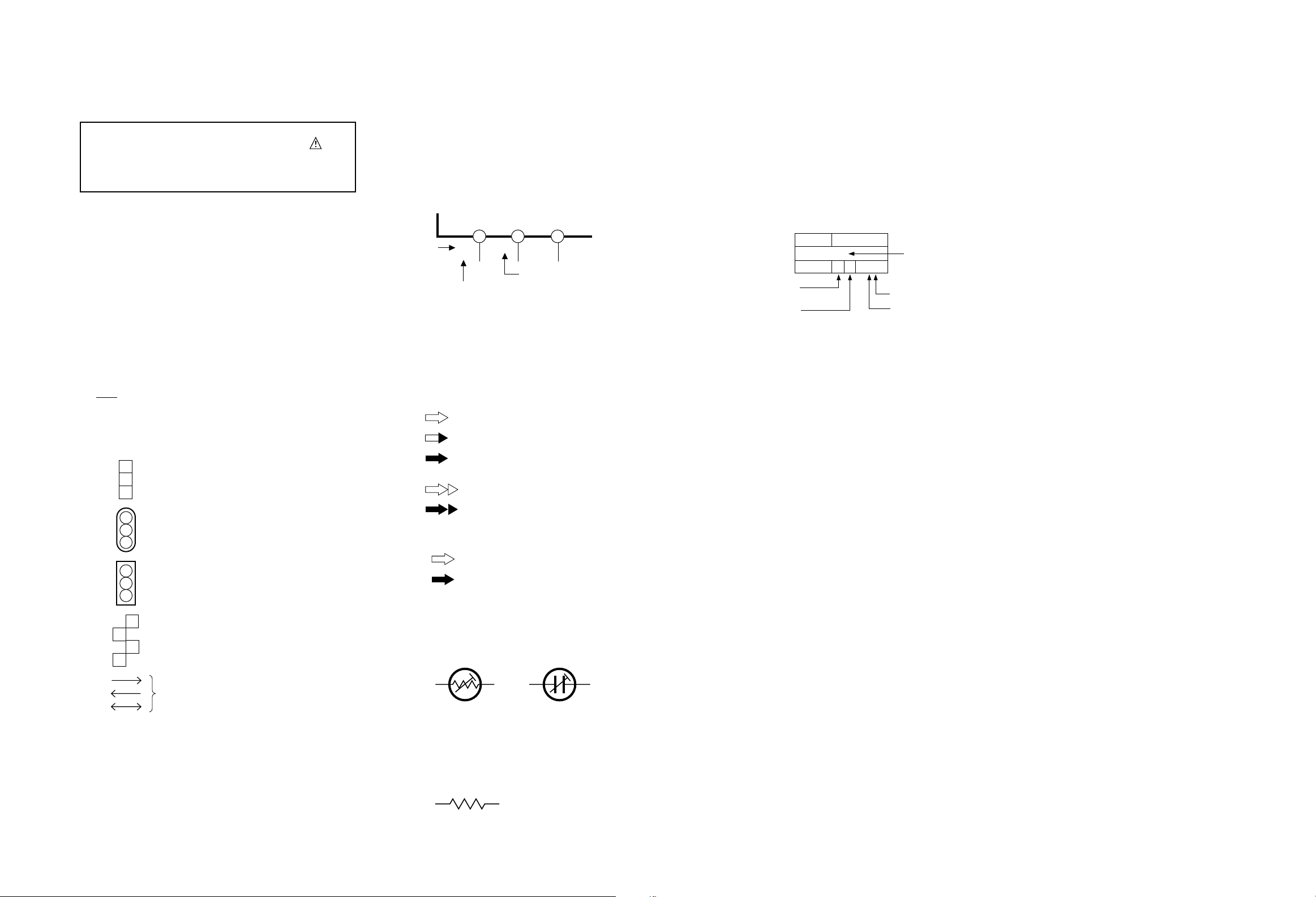
5. Signal path Symbols
The arrows indicate the signal path as follows.
NOTE : The arrow is DVC unique object.
Playback signal path
Playback and recording signal path
Recording signal path
(including E-E signal path)
Capstan servo path
Drum servo path
(Example)
R-Y
Playback R-Y signal path
Y
Recording Y signal path
6. Indication of the parts for adjustments
The parts for the adjustments are surrounded with the circle as
shown below.
Note: For g eneral information in service manual, please
refer to the Service Manual of GENERAL INFORMATION Edition 4 No. 82054D (January 1994).
S40889-01
Connected pattern on board
The arrows indicate signal path
7. Indication of the parts not mounted on the circuit board
“OPEN” is indicated by the parts not mounted on the circuit
board.
R216
OPEN
4-1
4-2
4-1 4-2
S40889-01
Page 2
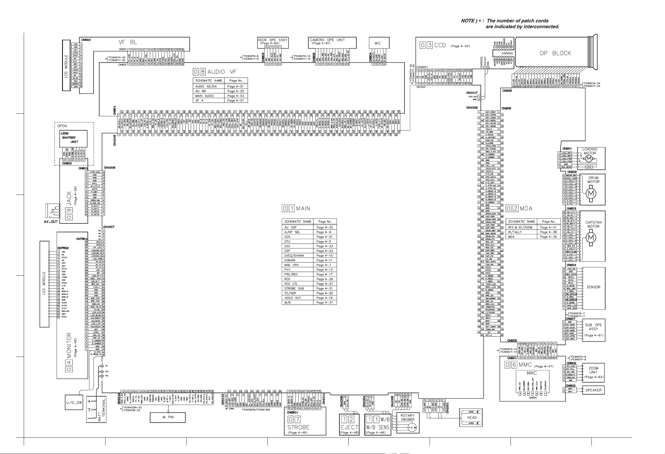
4.1 BOARD INTERCONNECTIONS
5
4
3
2
1
A
B
C
DEF
4-3
4-4
G
H
Page 3
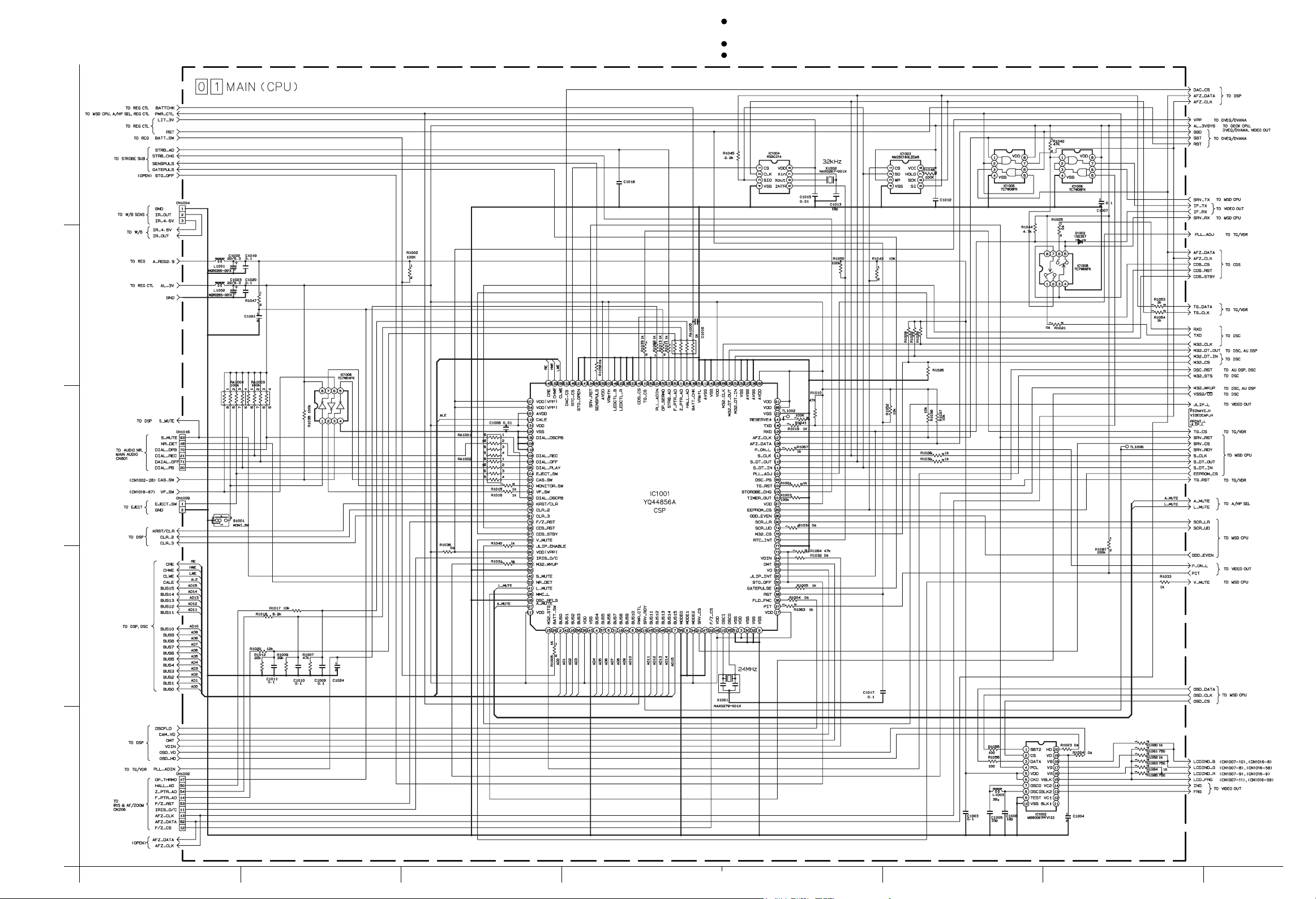
4.2 CPU SCHEMATIC DIAGRAM
5
4
NOTES: For the destination of each signal and further line connections that are cut off from
this diagram, refer to “4.1 BOARD INTERCONNECTIONS”.
When ordering parts, be sure to order according to the Part Number indicated in the Parts List.
According to the parts which have no values are not used.
3
2
1
A
B
C
DEF
4-5 4-6
G
H
Page 4
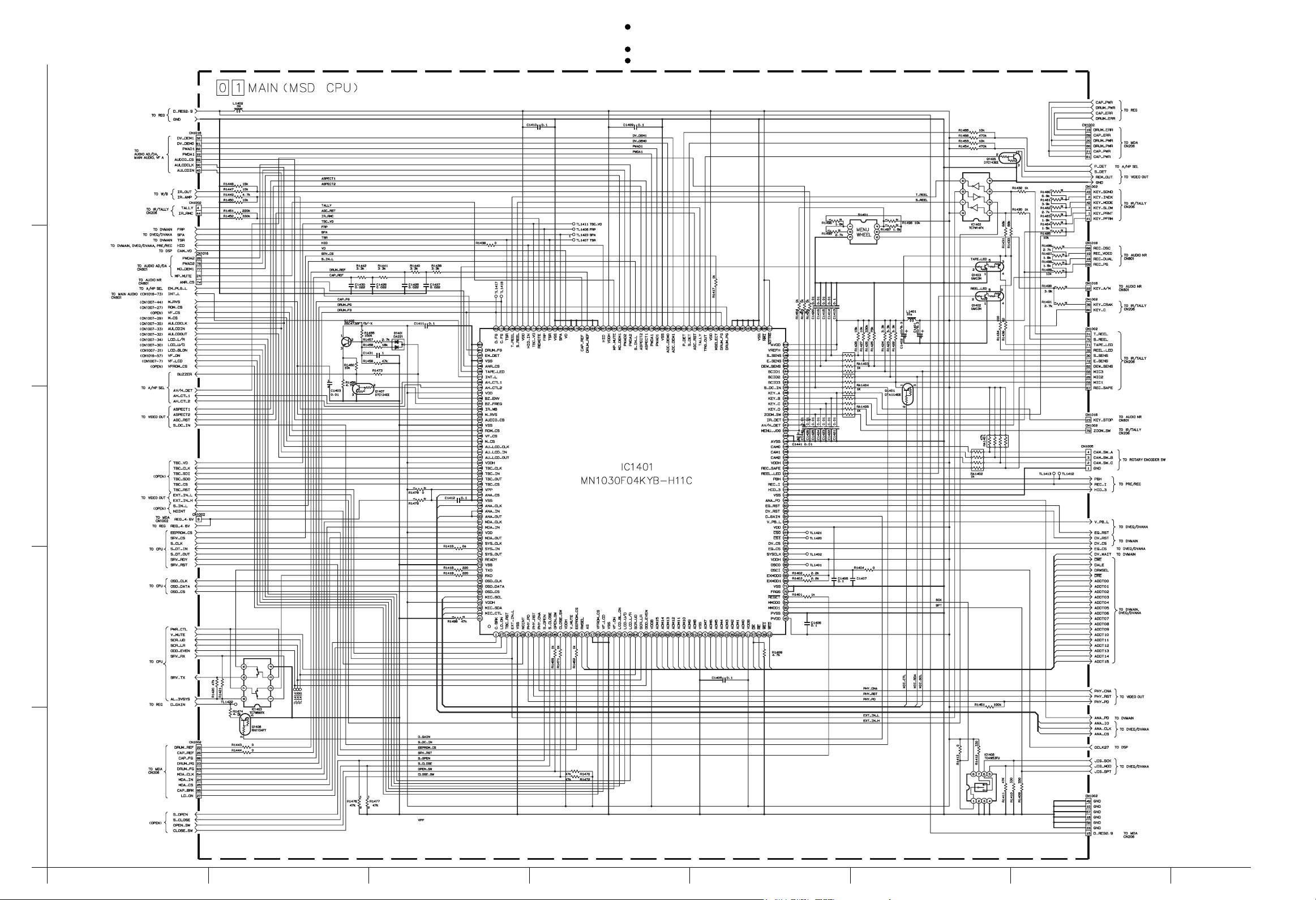
4.3 MSD CPU SCHEMATIC DIAGRAM
5
4
NOTES: For the destination of each signal and further line connections that are cut off from
this diagram, refer to “4.1 BOARD INTERCONNECTIONS”.
When ordering parts, be sure to order according to the Part Number indicated in the Parts List.
According to the parts which have no values are not used.
3
2
1
A
B
C
DEF
4-7
4-8
G
H
Page 5
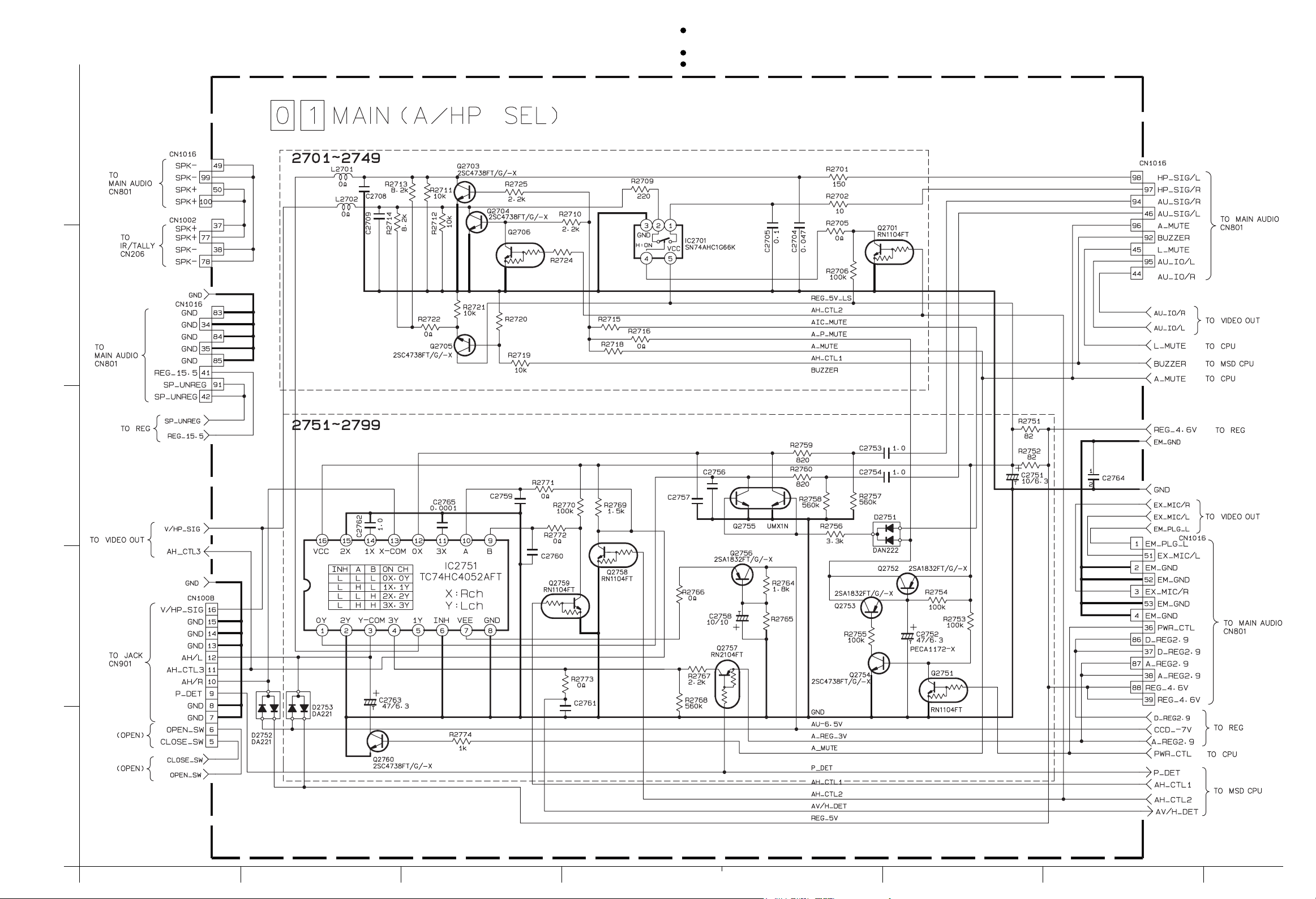
4.4 A/HP SEL SCHEMATIC DIAGRAM
5
4
NOTES: For the destination of each signal and further line connections that are cut off from
this diagram, refer to “4.1 BOARD INTERCONNECTIONS”.
When ordering parts, be sure to order according to the Part Number indicated in the Parts List.
According to the parts which have no values are not used.
3
2
1
A
B
C
DEF
4-9
4-10
G
H
Page 6
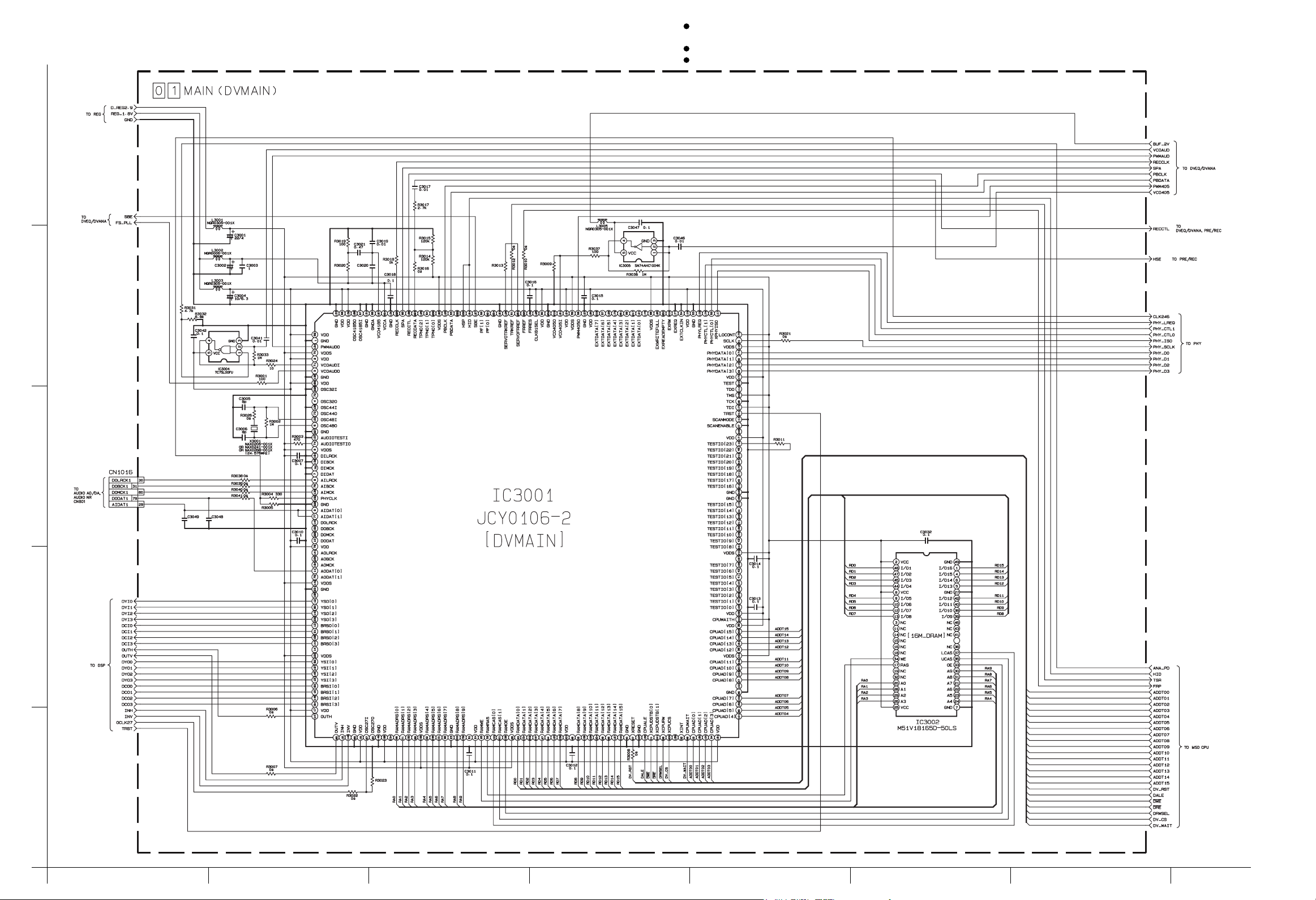
4.5 DVMAIN SCHEMATIC DIAGRAM
5
4
NOTES: For the destination of each signal and further line connections that are cut off from
this diagram, refer to “4.1 BOARD INTERCONNECTIONS”.
When ordering parts, be sure to order according to the Part Number indicated in the Parts List.
According to the parts which have no values are not used.
3
2
1
A
B
C
DEF
4-11 4-12
G
H
Page 7
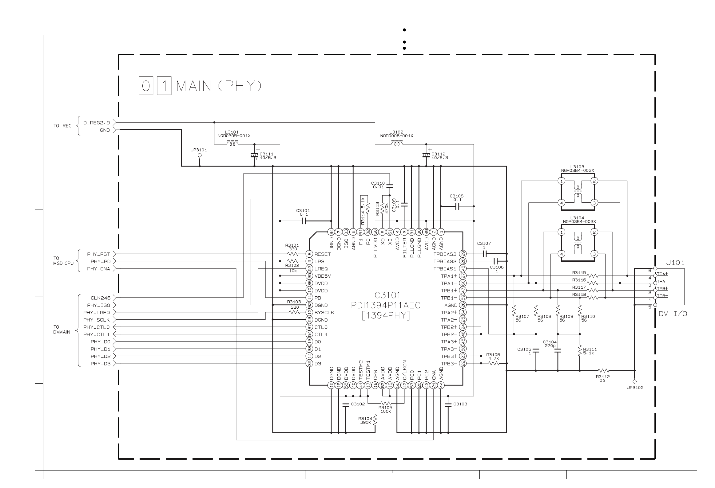
4.6 PHY SCHEMATIC DIAGRAM
5
4
NOTES: For the destination of each signal and further line connections that are cut off from
this diagram, refer to “4.1 BOARD INTERCONNECTIONS”.
When ordering parts, be sure to order according to the Part Number indicated in the Parts List.
According to the parts which have no values are not used.
3
2
1
A
B
C
DEF
4-13
4-14
G
H
Page 8
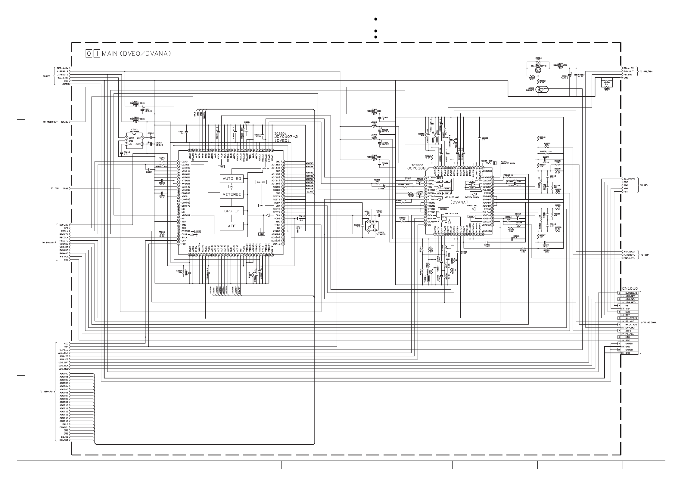
4.7 DVEQ/DVANA SCHEMATIC DIAGRAM
5
4
NOTES: For the destination of each signal and further line connections that are cut off from
this diagram, refer to “4.1 BOARD INTERCONNECTIONS”.
When ordering parts, be sure to order according to the Part Number indicated in the Parts List.
According to the parts which have no values are not used.
3
2
1
A
B
C
DEF
4-15
4-16
G
H
Page 9
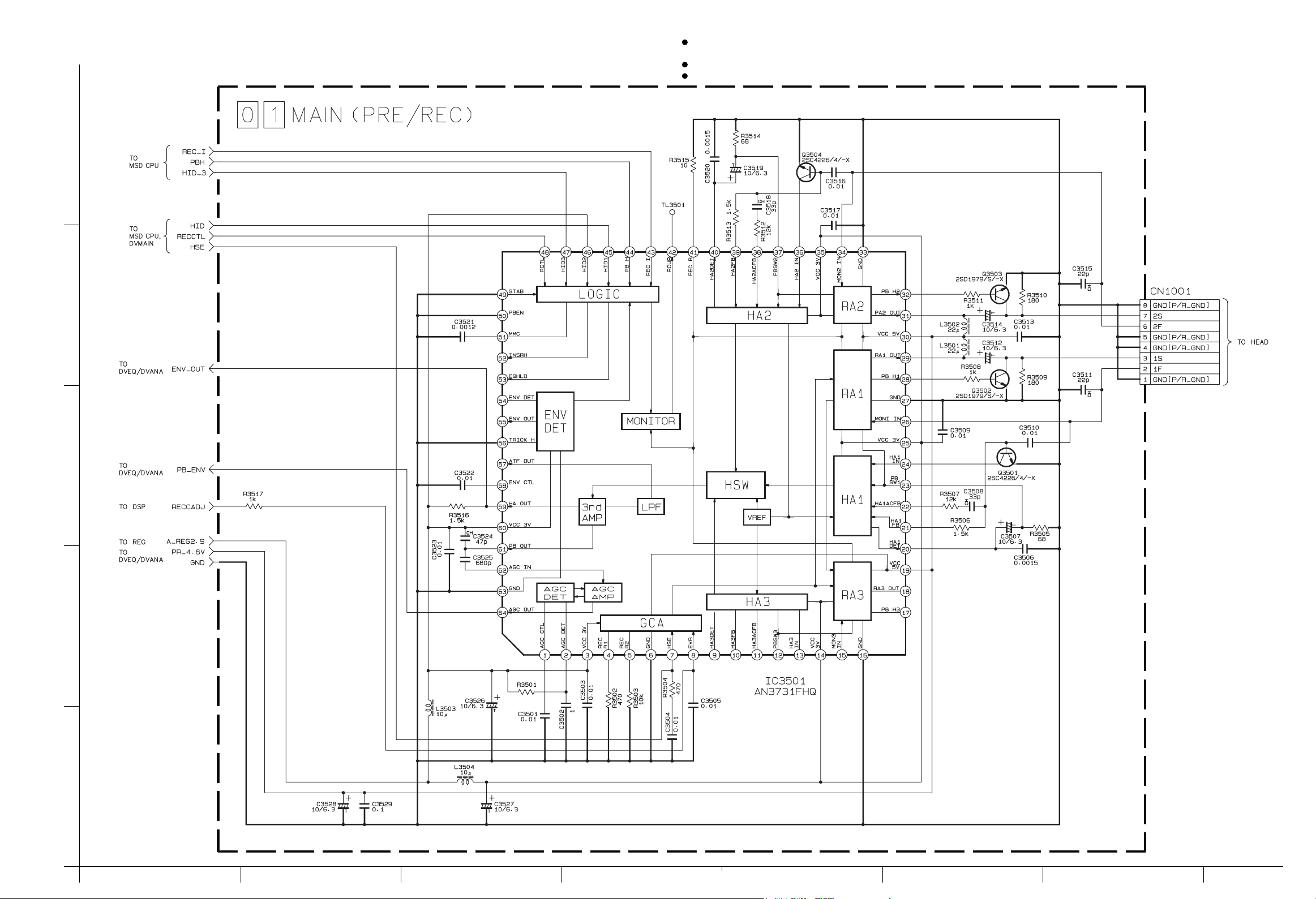
4.8 PRE/REC SCHEMATIC DIAGRAM
5
4
NOTES: For the destination of each signal and further line connections that are cut off from
this diagram, refer to “4.1 BOARD INTERCONNECTIONS”.
When ordering parts, be sure to order according to the Part Number indicated in the Parts List.
According to the parts which have no values are not used.
3
2
1
A
B
C
DEF
4-17
4-18
G
H
Page 10
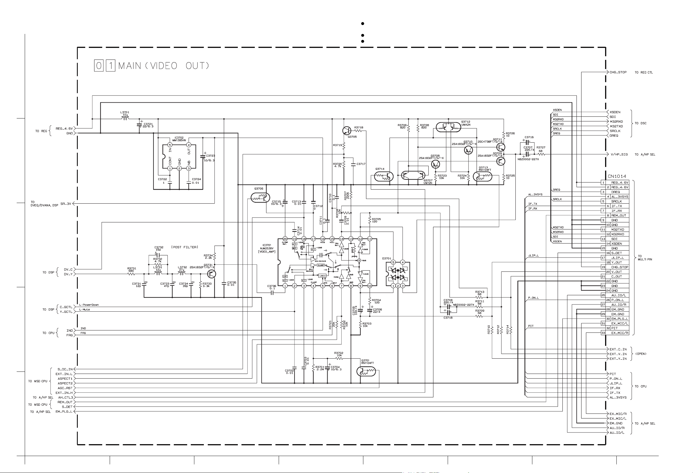
4.9 VIDEO OUT SCHEMATIC DIAGRAM
5
4
NOTES: For the destination of each signal and further line connections that are cut off from
this diagram, refer to “4.1 BOARD INTERCONNECTIONS”.
When ordering parts, be sure to order according to the Part Number indicated in the Parts List.
According to the parts which have no values are not used.
3
2
1
A
B
C
DEF
4-204-19
G
H
Page 11
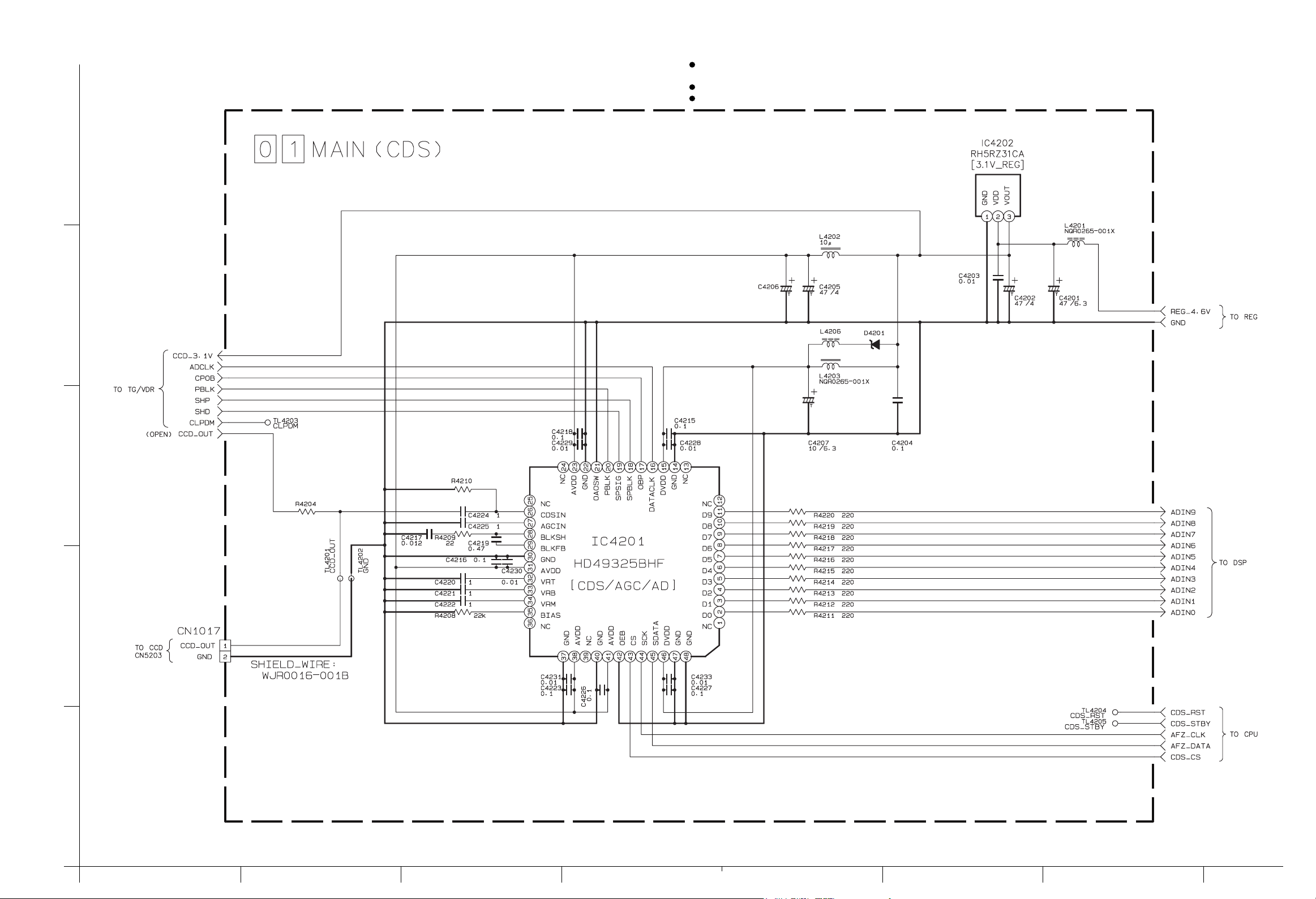
4.10 CDS SCHEMATIC DIAGRAM
NOTES: For the destination of each signal and further line connections that are cut off from
this diagram, refer to “4.1 BOARD INTERCONNECTIONS”.
When ordering parts, be sure to order according to the Part Number indicated in the Parts List.
According to the parts which have no values are not used.
5
4
3
2
1
A
B
C
DEF
4-21 4-22
G
H
Page 12
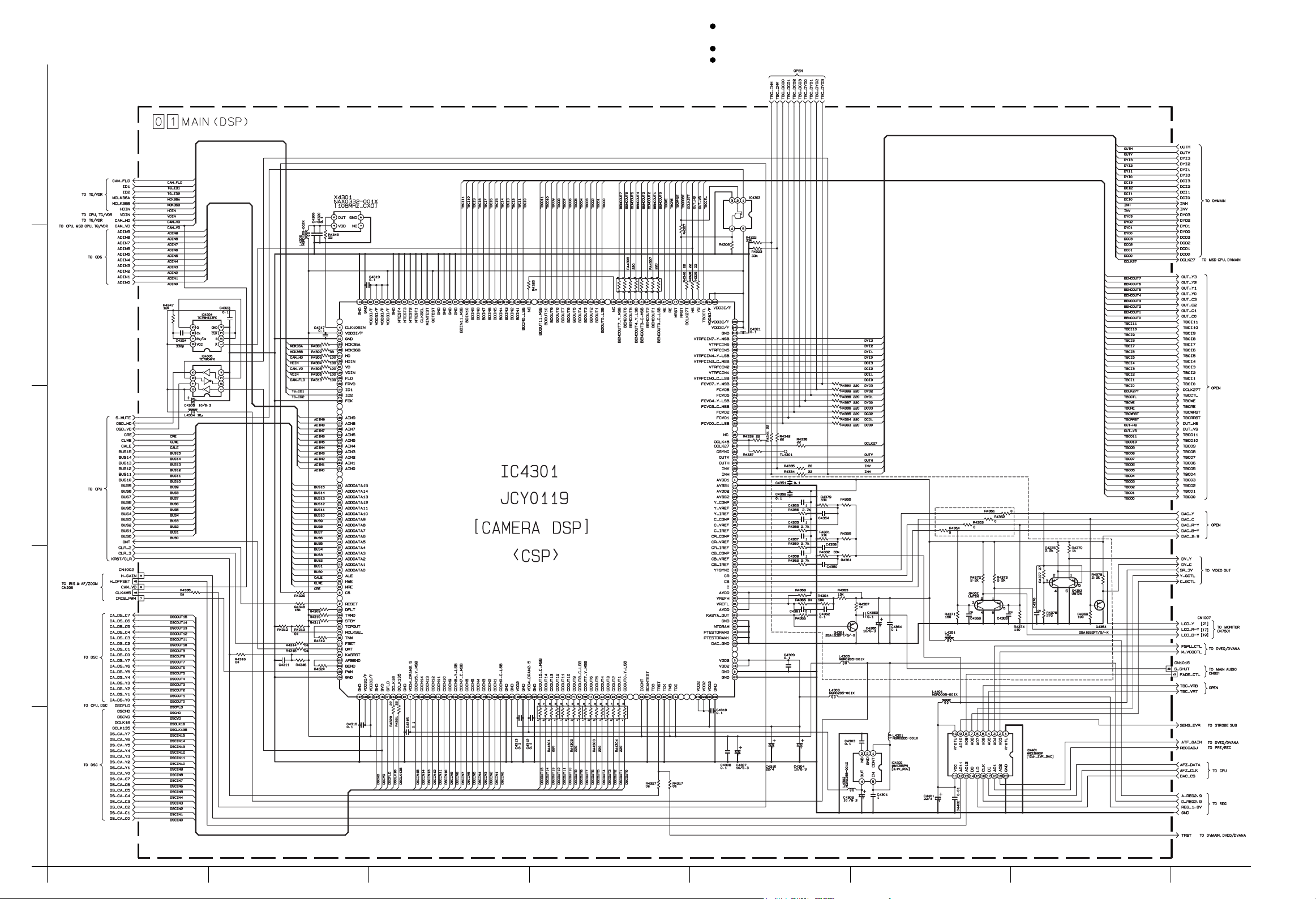
4.11 DSP SCHEMATIC DIAGRAM
5
4
NOTES: For the destination of each signal and further line connections that are cut off from
this diagram, refer to “4.1 BOARD INTERCONNECTIONS”.
When ordering parts, be sure to order according to the Part Number indicated in the Parts List.
According to the parts which have no values are not used.
3
2
1
A
B
C
DEF
4-23
4-24
G
H
Page 13
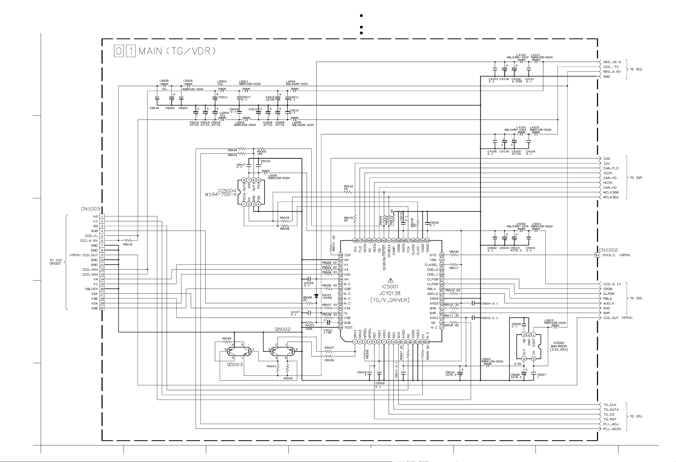
4.12 TG/VDR SCHEMATIC DIAGRAM
5
4
NOTES: For the destination of each signal and further line connections that are cut off from
this diagram, refer to “4.1 BOARD INTERCONNECTIONS”.
When ordering parts, be sure to order according to the Part Number indicated in the Parts List.
According to the parts which have no values are not used.
3
2
1
A
B
C
DEF
4-25 4-26
G
H
Page 14
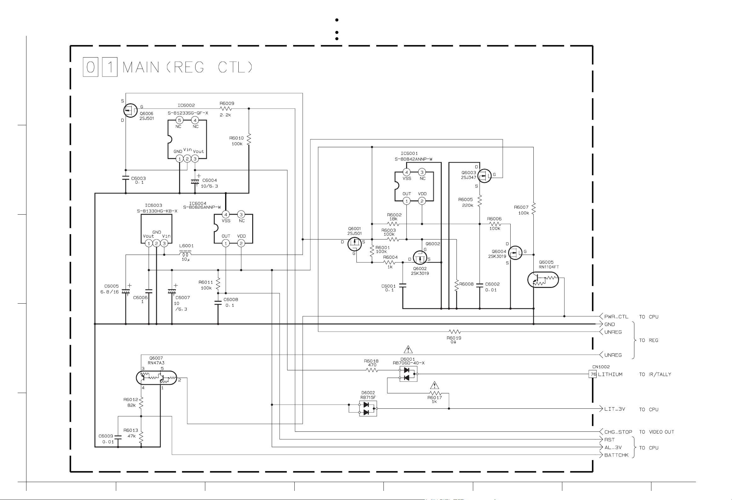
4.13 REG CTL SCHEMATIC DIAGRAM
5
4
NOTES: For the destination of each signal and further line connections that are cut off from
this diagram, refer to “4.1 BOARD INTERCONNECTIONS”.
When ordering parts, be sure to order according to the Part Number indicated in the Parts List.
According to the parts which have no values are not used.
3
2
1
A
B
C
DEF
4-27
4-28
G
H
Page 15
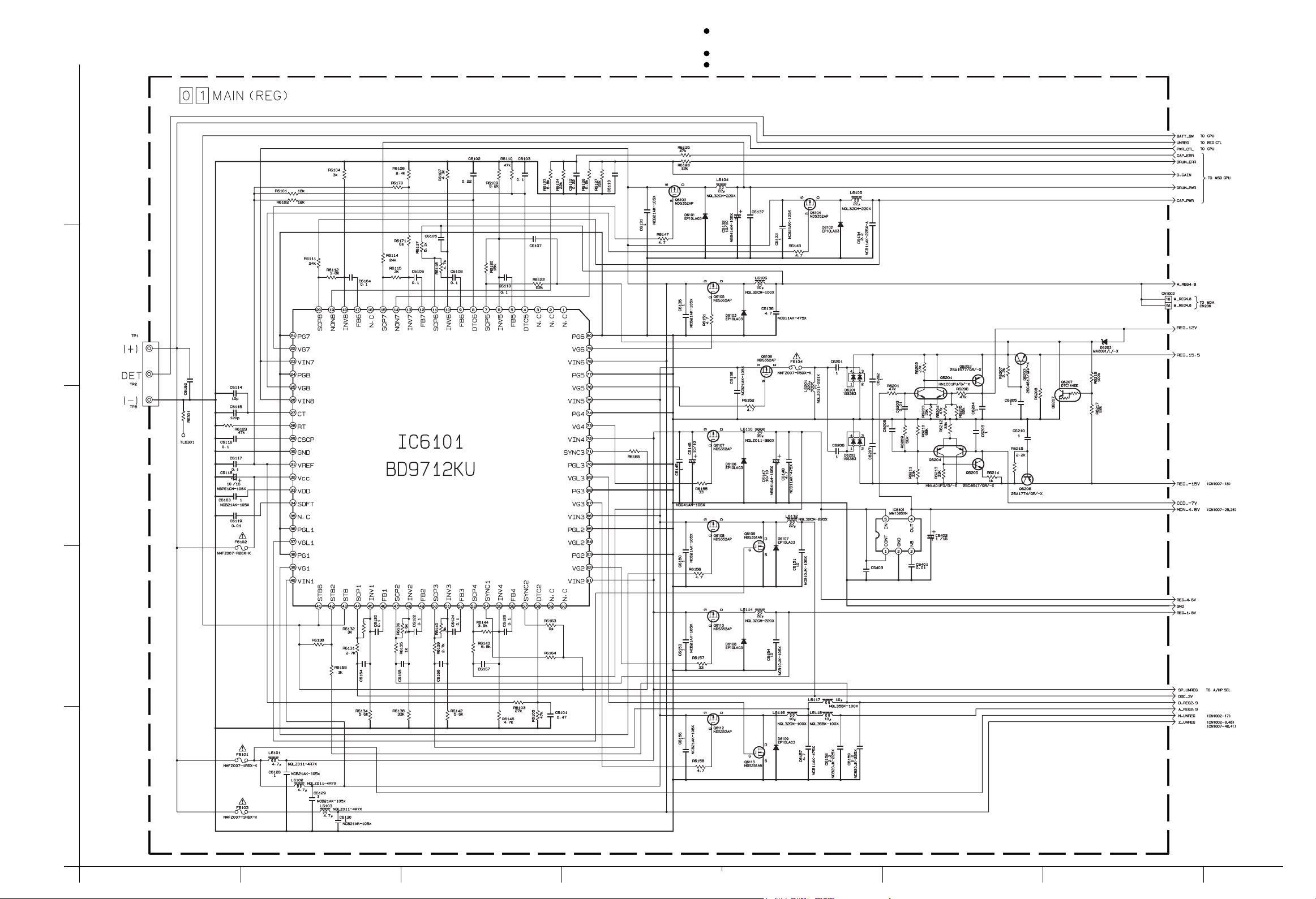
4.14 REGULATOR SCHEMATIC DIAGRAM
5
4
NOTES: For the destination of each signal and further line connections that are cut off from
this diagram, refer to “4.1 BOARD INTERCONNECTIONS”.
When ordering parts, be sure to order according to the Part Number indicated in the Parts List.
According to the parts which have no values are not used.
3
2
1
A
B
C
DEF
4-29 4-30
G
H
Page 16

4.15 STROBE SUB SCHEMATIC DIAGRAM
5
4
NOTES: For the destination of each signal and further line connections that are cut off from
this diagram, refer to “4.1 BOARD INTERCONNECTIONS”.
When ordering parts, be sure to order according to the Part Number indicated in the Parts List.
According to the parts which have no values are not used.
3
2
1
A
B
C
DEF
4-31 4-32
G
H
Page 17

4.16 DSC SCHEMATIC DIAGRAM
5
4
NOTES: For the destination of each signal and further line connections that are cut off from
this diagram, refer to “4.1 BOARD INTERCONNECTIONS”.
When ordering parts, be sure to order according to the Part Number indicated in the Parts List.
According to the parts which have no values are not used.
3
2
1
A
B
C
DEF
4-33 4-34
G
H
Page 18

4.17 AU DSP SCHEMATIC DIAGRAM
5
4
NOTES: For the destination of each signal and further line connections that are cut off from
this diagram, refer to “4.1 BOARD INTERCONNECTIONS”.
When ordering parts, be sure to order according to the Part Number indicated in the Parts List.
According to the parts which have no values are not used.
3
2
1
A
B
C
DEF
4-35
4-36
G
H
Page 19
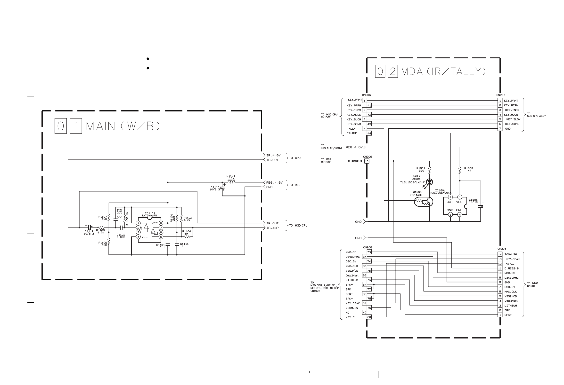
4.18 W/B AND IR/TALLY SCHEMATIC DIAGRAMS
5
NOTES: For the destination of each signal and further line connections that are cut off from
this diagram, refer to “4.1 BOARD INTERCONNECTIONS”.
When ordering parts, be sure to order according to the Part Number indicated in the Parts List.
4
3
2
1
A
B
C
DEF
4-37
4-38
G
H
Page 20

4.19 MDA SCHEMATIC DIAGRAM
5
4
NOTES: For the destination of each signal and further line connections that are cut off from
this diagram, refer to “4.1 BOARD INTERCONNECTIONS”.
When ordering parts, be sure to order according to the Part Number indicated in the Parts List.
According to the parts which have no values are not used.
3
2
1
A
B
C
DEF
4-39
4-40
G
H
Page 21

4.20 IRIS & AF/ZOOM SCHEMATIC DIAGRAM
5
4
NOTES: For the destination of each signal and further line connections that are cut off from
this diagram, refer to “4.1 BOARD INTERCONNECTIONS”.
When ordering parts, be sure to order according to the Part Number indicated in the Parts List.
According to the parts which have no values are not used.
3
2
1
A
B
C
DEF
4-41 4-42
G
H
Page 22

4.21 CCD SCHEMATIC DIAGRAM
NOTES: For the destination of each signal and further line connections that are cut off from
this diagram, refer to “4.1 BOARD INTERCONNECTIONS”.
When ordering parts, be sure to order according to the Part Number indicated in the Parts List.
According to the parts which have no values are not used.
5
4
3
2
1
A
B
C
DEF
4-43 4-44
G
H
Page 23
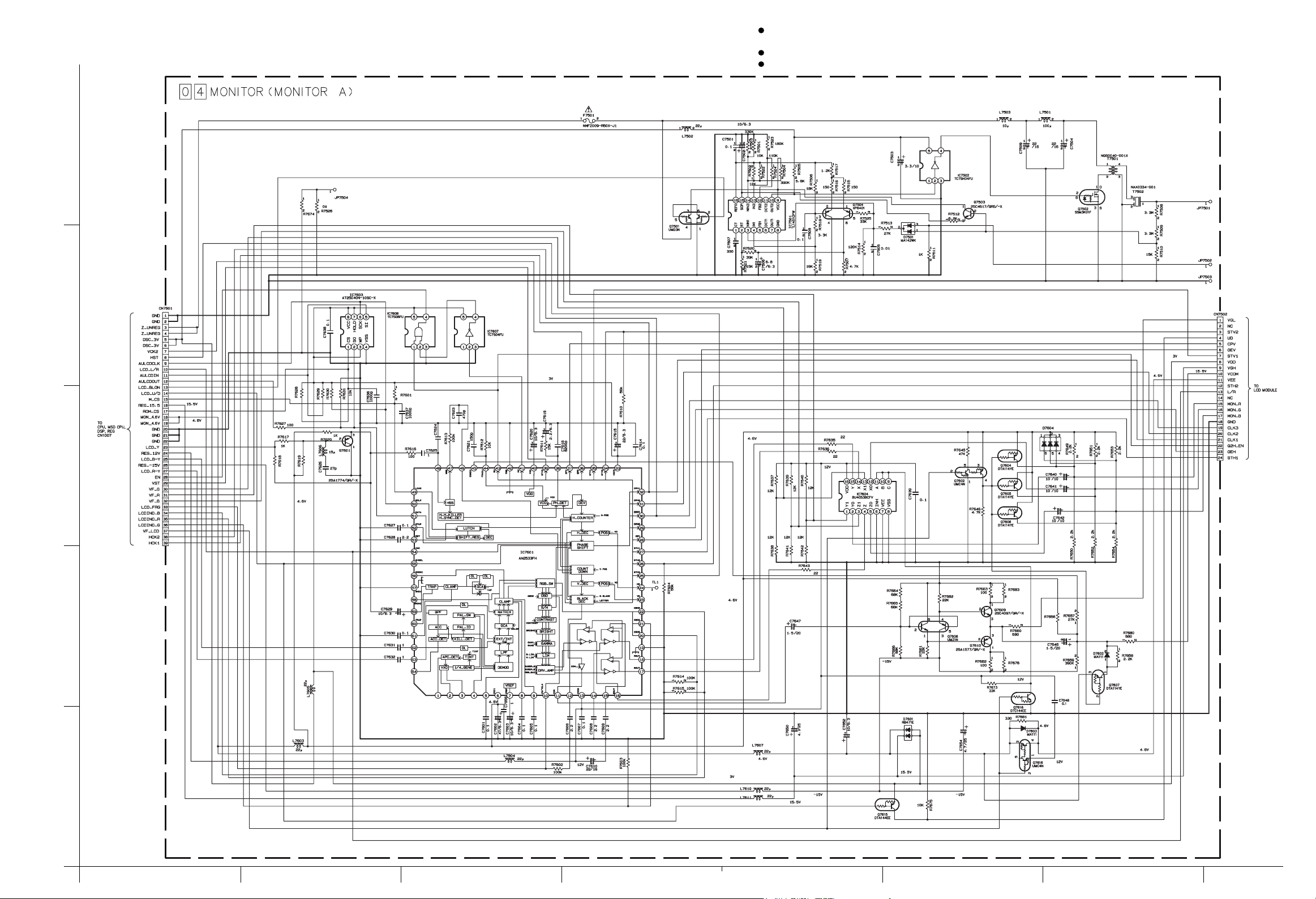
4.22 MONITOR A SCHEMATIC DIAGRAM
5
4
NOTES: For the destination of each signal and further line connections that are cut off from
this diagram, refer to “4.1 BOARD INTERCONNECTIONS”.
When ordering parts, be sure to order according to the Part Number indicated in the Parts List.
According to the parts which have no values are not used.
3
2
1
A
B
C
DEF
4-45
4-46
G
H
Page 24

4.23 MMC,W/B SENS AND EJECT SCHEMATIC DIAGRAMS
NOTES: For the destination of each signal and further line connections that are cut off from
this diagram, refer to “4.1 BOARD INTERCONNECTIONS”.
When ordering parts, be sure to order according to the Part Number indicated in the Parts List.
According to the parts which have no values are not used.
5
4
3
2
1
A
B
C
DEF
4-47 4-48
G
H
Page 25

4.24 STROBE SCHEMATIC DIAGRAM
5
NOTES: For the destination of each signal and further line connections that are cut off from
this diagram, refer to “4.1 BOARD INTERCONNECTIONS”.
When ordering parts, be sure to order according to the Part Number indicated in the Parts List.
4
3
2
1
A
B
C
DEF
4-49
4-50
G
H
Page 26

4.25 AUDIO AD/DA SCHEMATIC DIAGRAM
5
4
NOTES: For the destination of each signal and further line connections that are cut off from
this diagram, refer to “4.1 BOARD INTERCONNECTIONS”.
When ordering parts, be sure to order according to the Part Number indicated in the Parts List.
According to the parts which have no values are not used.
3
2
1
A
B
C
DEF
4-51
4-52
G
H
Page 27

4.26 MAIN AUDIO SCHEMATIC DIAGRAM
5
4
NOTES: For the destination of each signal and further line connections that are cut off from
this diagram, refer to “4.1 BOARD INTERCONNECTIONS”.
When ordering parts, be sure to order according to the Part Number indicated in the Parts List.
According to the parts which have no values are not used.
3
2
1
A
B
C
DEF
4-53 4-54
G
H
Page 28

4.27 AU NR SCHEMATIC DIAGRAM
5
4
NOTES: For the destination of each signal and further line connections that are cut off from
this diagram, refer to “4.1 BOARD INTERCONNECTIONS”.
When ordering parts, be sure to order according to the Part Number indicated in the Parts List.
According to the parts which have no values are not used.
3
2
1
A
B
C
DEF
4-55 4-56
G
H
Page 29

4.28 VF A SCHEMATIC DIAGRAM
NOTES: For the destination of each signal and further line connections that are cut off from
this diagram, refer to “4.1 BOARD INTERCONNECTIONS”.
When ordering parts, be sure to order according to the Part Number indicated in the Parts List.
According to the parts which have no values are not used.
5
4
3
2
1
A
B
C
DEF
4-57 4-58
G
H
Page 30

4.29 JACK SCHEMATIC DIAGRAM
5
NOTES: For the destination of each signal and further line connections that are cut off from
this diagram, refer to “4.1 BOARD INTERCONNECTIONS”.
When ordering parts, be sure to order according to the Part Number indicated in the Parts List.
According to the parts which have no values are not used.
4
3
2
1
A
B
C
DEF
4-59 4-60
G
H
Page 31

4.30 CAMERA OPE UNIT, SUB OPE ASSY, ZOOM UNIT AND DECK OPE UNIT SCHEMATIC DIAGRAMS
5
4
NOTES: For the destination of each signal and further line connections that are cut off from
this diagram, refer to “4.1 BOARD INTERCONNECTIONS”.
The schematic diagram is only for reference. Avoid replacing individual parts.
Replace the entire unit only.
3
2
1
A
B
C
DEF
4-61 4-62
G
H
Page 32

4.31 MAIN CURCUIT BOARD
5
4
FOIL SIDE (B)
3
2
1
A
B
C
DEF
4-63 4-64
4-63 4-64
G
H
Page 33

COMPONENT PARTS LOCATION GUIDE (MAIN)
REF.No. LOCATION
CAPACITOR
C1003 B C 4D
C1004 B C 4D
C1005 B C 4D
C1006 B C 4D
C1007 B C 2A
C1008 B C 2A
C1009 B C 2A
C1010 B C 2A
C1011 B C 2A
C1012 B C 2B
C1013 A C 2B
C1015 A C 2B
C1016 B C 2A
C1017 B C 3A
C1018 B C 2B
C1019 B C 3A
C1020 B C 3A
C1021 B C 2A
C1022 B C 3A
C1023 B C 3A
C1024 B C 2B
C1101 B C 1C
C1102 B C 2D
C1103 B C 1C
C1111 B C 1C
C1112 B C 1C
C1113 B C 1C
C1201 A C 4C
C1202 A C 4C
C1203 A C 4C
C1204 A C 4C
C1401 B C 5C
C1402 B C 5C
C1403 B C 4C
C1405 B C 5D
C1406 B C 5D
C1407 B C 5D
C1408 B C 5D
C1409 B C 5C
C1410 B C 5C
C1411 B C 4C
C1412 B C 4D
C1413 B C 5C
C1414 B C 5C
C1415 B C 5C
C1416 B C 5C
C1420 B C 5C
C1421 B C 5C
C1422 B C 5C
C1423 B C 5C
C1424 B C 5C
C1425 B C 5C
C1426 B C 5C
C1427 B C 5C
C1428 B C 5C
C1429 B C 4C
C1430 B C 4C
C1431 A C 4D
C1440 B C 5C
C1441 B C 5C
C2704 A C 5C
C2705 A C 5C
C2708 A C 5C
C2709 A C 5C
C2751 A C 5C
C2752 A C 4C
C2753 A C 5D
C2754 A C 5C
C2756 A C 5D
C2757 A C 5D
C2758 A C 5D
C2759 A C 5D
C2760 A C 5D
C2761 A C 5D
C2762 A C 5D
C2763 A C 5C
C2764 A C 5C
C2765 A C 5D
C3001 B C 3D
C3002 B C 2D
C3003 B C 2D
C3004 B C 3D
C3005 B C 2D
C3006 B C 2D
C3007 B C 2D
C3010 B C 2D
C3011 B C 3C
C3012 B C 3C
C3013 B C 3C
C3014 B C 3C
C3015 B C 3D
C3016 B C 3D
C3017 B C 2D
C3018 B C 3D
C3019 B C 2D
C3020 B C 2D
C3021 B C 2D
C3032 B C 3C
C3041 B C 2D
C3042 B C 2D
C3046 B C 3D
C3047 B C 3D
C3048 A C 3B
C3049 A C 2B
C3101 A C 2D
C3102 A C 2C
C3103 A C 2C
C3104 A C 3D
REF.No. LOCATION
C3105 A C 3D
C3106 A C 2D
C3107 A C 2C
C3108 A C 2D
C3109 A C 2D
C3110 A C 2D
C3111 A C 2C
C3112 A C 2C
C3201 B C 4C
C3202 B C 4D
C3203 B C 4D
C3204 B C 4D
C3205 B C 4C
C3206 B C 4C
C3207 B C 4C
C3208 B C 4D
C3209 B C 4C
C3210 B C 4C
C3211 B C 4C
C3212 B C 4C
C3213 B C 4C
C3214 B C 4C
C3215 B C 4C
C3216 B C 4D
C3217 B C 4D
C3218 B C 3D
C3221 B C 4C
C3222 B C 4C
C3301 B C 3C
C3302 B C 3B
C3303 B C 4B
C3304 B C 4C
C3305 B C 3B
C3306 B C 4B
C3307 B C 4C
C3308 B C 4C
C3309 B C 4C
C3310 B C 4C
C3311 B C 4C
C3312 B C 4C
C3313 B C 4C
C3314 B C 4C
C3315 B C 4C
C3316 B C 4C
C3317 B C 4C
C3318 B C 4C
C3319 B C 4C
C3320 B C 4C
C3321 B C 3C
C3322 B C 3C
C3323 B C 3B
C3324 B C 3C
C3325 B C 3C
C3326 B C 3C
C3327 B C 3C
C3328 B C 3C
C3329 B C 3B
C3330 B C 3C
C3331 B C 3C
C3332 B C 3B
C3501 A C 3C
C3502 A C 3C
C3503 A C 3C
C3504 A C 3C
C3505 A C 3C
C3506 A C 3D
C3507 A C 3D
C3508 A C 3D
C3509 A C 3D
C3510 A C 3D
C3511 A C 3D
C3512 A C 3D
C3513 A C 3D
C3514 A C 4D
C3515 A C 4D
C3516 A C 4D
C3517 A C 4C
C3518 A C 4D
C3519 A C 4D
C3520 A C 4C
C3521 A C 4C
C3522 A C 4C
C3523 A C 3C
C3524 A C 3C
C3525 A C 3C
C3526 A C 3C
C3527 A C 4C
C3528 A C 3D
C3529 A C 3D
C3551 B C 3D
C3552 B C 3D
C3702 B C 5C
C3703 B C 5C
C3704 B C 5C
C3705 B C 5C
C3706 B C 5C
C3707 B C 5C
C3708 B C 5C
C3709 B C 5D
C3710 B C 5C
C3711 B C 5D
C3712 B C 5D
C3713 B C 5D
C3714 B C 5C
C3715 B C 5D
C3716 B C 5C
C3717 B C 5D
C3718 B C 5C
C3721 A C 5B
C3722 A C 5B
REF.No. LOCATION REF.No. LOCATION REF.No. LOCATION
C3723 A C 5C
C3724 A C 5C
C3731 B C 5C
C3732 B C 5C
C3733 B C 5C
C3734 B C 5C
C3735 B C 5C
C3736 B C 5C
C3801 A C 2C
C3802 A C 2C
C3803 A C 3C
C3804 A C 3C
C3805 A C 3C
C3806 A C 3C
C3807 A C 3C
C3808 A C 3C
C3809 A C 3C
C3810 A C 3B
C3811 A C 3C
C3812 A C 3B
C3813 A C 3B
C3815 A C 3C
C3816 A C 3C
C3817 A C 3B
C3818 A C 3B
C3819 A C 3C
C3820 A C 2C
C3821 A C 2C
C3822 A C 3C
C3823 A C 3C
C3824 A C 3C
C3825 B C 3B
C3851 B C 4B
C3852 B C 3B
C3853 B C 3B
C3854 B C 3B
C3855 B C 3B
C3856 B C 4B
C3857 B C 4B
C3858 B C 4B
C3861 B C 3B
C3862 B C 3B
C4101 A C 1C
C4102 A C 1C
C4103 A C 1C
C4104 A C 1C
C4105 A C 1C
C4106 A C 1C
C4107 B C 1C
C4109 B C 1C
C4111 B C 1C
C4118 A C 1C
C4119 A C 1C
C4201 A C 1B
C4202 B C 1B
C4203 B C 1C
C4204 B C 1C
C4205 B C 1B
C4206 B C 1B
C4207 B C 2C
C4208 A C 2C
C4209 A C 2C
C4210 A C 2C
C4211 A C 1C
C4212 A C 1C
C4213 A C 2B
C4215 B C 2C
C4216 B C 1C
C4217 B C 1C
C4218 B C 1C
C4219 B C 1C
C4220 B C 1B
C6112 A C 5B
C6113 A C 5B
C6114 A C 5B
C6115 A C 5A
C6116 A C 5A
C6117 A C 5A
C6118 A C 5A
C6119 A C 5A
C6120 A C 5A
C6122 A C 5A
C6124 A C 5A
C6126 A C 5A
C6128 B C 5A
C6129 B C 5A
C6130 B C 5B
C6131 B C 5B
C6132 B C 5B
C6133 B C 5B
C6134 B C 5B
C6135 B C 5A
C6136 B C 5A
C6137 B C 5B
C6138 B C 4A
C6145 B C 5B
C6146 B C 5B
C6147 B C 5B
C6148 B C 5B
C6150 B C 5A
C6151 B C 4A
C6153 B C 5B
C6154 B C 4B
C6156 B C 5B
C6157 B C 4B
C6158 B C 4B
C6159 B C 4B
C6162 B C 5B
C6163 A C 5A
C6164 A C 5A
C6165 A C 5A
C6166 A C 5A
C6167 A C 5A
C6201 B C 3A
C6202 B C 3A
C6203 B C 3B
C6204 B C 3A
C6205 B C 3B
C6206 B C 4B
C6207 B C 4B
C6208 B C 4B
C6209 B C 4B
C6210 B C 3B
C6401 B C 4C
C6402 B C 4C
C6403 B C 4B
C6601 A C 1C
C6602 A C 1C
C6603 A C 1C
C6604 A C 1C
C6605 A C 1C
C6611 A C 1C
C6612 A C 1C
C6613 A C 1C
C7502 A C 2A
C7503 A C 2B
C8001 A C 3A
C8002 A C 3A
C8003 A C 4B
C8004 A C 3A
C8006 A C 4B
C8007 A C 5B
C8008 A C 4B
C8009 A C 5A
C8010 A C 5B
C8011 A C 5A
C8012 A C 5A
C8013 A C 5A
C8017 A C 4C
C8020 A C 4B
C8021 A C 5C
C8022 A C 5C
C8023 A C 5C
C8024 A C 5C
C8025 A C 5C
C8026 A C 5C
C8027 A C 4B
C8028 A C 4C
C8029 A C 4B
C8030 A C 4B
C8031 A C 4B
C8032 A C 5B
C8033 A C 5B
C8034 A C 5B
C8035 A C 5B
C8036 A C 5B
C8037 A C 5B
C8038 A C 5B
C8039 A C 5B
C8040 A C 5B
C8041 A C 5B
C8042 A C 5C
C8043 A C 5C
C8044 A C 5B
C8045 A C 4B
C8046 A C 5B
C8048 A C 5A
C8049 A C 5A
C8050 A C 4B
C8051 A C 4B
C8052 A C 4B
C8053 A C 4B
C8054 A C 4B
C8055 A C 3B
C8056 A C 4B
C8057 A C 4B
C8058 A C 4C
C8059 A C 4B
C8060 A C 4B
C8062 A C 5C
C8101 A C 4A
C8102 A C 3A
C8103 A C 4A
C8104 A C 4A
C8105 A C 4B
C8106 A C 4A
C8107 A C 4B
C8108 A C 4B
C8109 A C 4B
C8110 A C 4B
C8111 A C 4A
C8112 A C 4A
C8113 A C 4B
C8114 A C 4A
C8115 A C 4A
C8116 A C 4A
C8117 A C 4A
C8118 A C 4A
C8119 A C 4A
C8120 A C 4A
C8121 A C 4B
C8122 A C 4B
C8123 A C 4B
C8124 A C 4B
C8125 A C 4A
C8126 A C 4A
CONNECTOR
CN1001 A C 3D
CN1002 A C 4D
CN1003 A C 1C
CN1004 A C 1C
CN1005 B C 2B
CN1007 A C 3B
CN1008 A C 5C
CN1009 A C 2C
CN1010 A C 3A
CN1011 A C 1C
CN1014 A C 5C
CN1016 A C 2A
DIODE
D1002 B C 3A
D1201 A C 4C
D1401 A C 4D
D2751 A C 5C
D2752 A C 5C
D2753 A C 5C
D2754 A C 5C
D2755 A C 5C
D3701 B C 5D
D4101 B C 1C
D4201 B C 1C
D6001 B C 5A
D6002 B C 4A
D6101 B C 5B
D6102 B C 5B
D6103 B C 5A
D6106 B C 5C
D6107 B C 5A
D6108 B C 4B
D6109 B C 5B
D6201 B C 3A
D6202 B C 3B
D6203 B C 3A
IC
IC1001 B C 3A
IC1002 B C 4D
IC1003 B C 2B
IC1004 A C 2B
IC1005 B C 3A
IC1006 B C 3B
IC1008 B C 3A
IC1009 B C 2A
IC1101 B C 1C
IC1201 A C 4C
IC1401 B C 5D
IC1402 B C 5D
IC1403 B C 4C
IC1405 A C 3A
IC2701 A C 5C
IC2751 A C 5D
IC3001 B C 3D
IC3002 B C 3C
IC3004 B C 2D
IC3005 B C 3D
IC3101 A C 2D
IC3201 B C 4C
IC3202 B C 4C
IC3203 B C 4D
IC3301 B C 4C
IC3501 A C 3C
IC3701 B C 5C
IC3702 A C 5B
IC3801 A C 3C
IC3851 B C 4B
IC4201 B C 2C
IC4202 B C 1B
IC4301 B C 2C
IC4302 B C 2C
IC4303 A C 2C
IC4304 A C 3C
IC4305 A C 3C
IC4401 A C 3C
IC5001 B C 1C
IC5002 B C 1C
IC5004 A C 2C
IC6001 B C 5A
IC6002 B C 5A
IC6003 B C 4A
IC6004 B C 4A
IC6101 A C 5A
IC6401 B C 4B
IC6601 A C 1C
IC8001 A C 4B
IC8002 A C 3B
IC8003 A C 5B
IC8004 A C 4C
IC8005 A C 5A
IC8006 A C 5B
IC8007 A C 5A
IC8008 A C 4A
IC8009 A C 4C
IC8101 A C 4A
IC8102 A C 4A
IC8103 A C 4A
COIL
L1001 B C 3A
L1002 B C 3A
L1003 B C 4D
L1101 B C 1C
L1201 A C 4C
L1401 B C 5C
L1402 B C 5C
L2701 A C 5C
L2702 A C 5C
L3001 B C 3C
L3002 B C 2D
REF.No. LOCATION
L3003 B C 3C
L3005 B C 3D
L3101 A C 2C
L3102 A C 2C
L3103 A C 3D
L3104 A C 3D
L3201 B C 4C
L3202 B C 4D
L3301 B C 3C
L3302 B C 3B
L3303 B C 4B
L3304 B C 4C
L3501 A C 4D
L3502 A C 4D
L3503 A C 3C
L3504 A C 4C
L3551 B C 3D
L3701 A C 5B
L3731 B C 5C
L3732 B C 5C
L3801 A C 2C
L3802 A C 3C
L3851 B C 4B
L4101 A C 1C
L4102 A C 1C
L4103 A C 1C
L4104 A C 1C
L4201 A C 1C
L4202 B C 1B
L4203 B C 2C
L4204 A C 1C
L4205 A C 2B
L4206 B C 2C
L4301 B C 2C
L4302 B C 2C
L4303 A C 2C
L4304 A C 2C
L4305 B C 2D
L4306 B C 2D
L4351 A C 3B
L4401 A C 3D
L5001 A C 2C
L5002 A C 2C
L5003 B C 1C
L5004 B C 1C
L5005 A C 2C
L5201 A C 1C
L5202 A C 2C
L5203 A C 1C
L5204 A C 1C
L5205 A C 1C
L5206 A C 1C
L6001 B C 4A
L6101 B C 5B
L6102 B C 5A
L6103 B C 5B
L6104 B C 5B
L6105 B C 5B
L6106 B C 5A
L6110 B C 5B
L6112 B C 4A
L6114 B C 4B
L6116 B C 4B
L6117 B C 4B
L6118 B C 4B
L6201 B C 4A
L6601 A C 1C
L8001 A C 5A
L8002 A C 4B
L8003 A C 5A
L8005 A C 4B
L8006 A C 5B
L8007 A C 5B
L8008 A C 5B
L8010 A C 4B
L8011 A C 3A
L8101 A C 3A
L8102 A C 3A
TRANSISTOR
Q1401 B C 5C
Q1402 B C 5D
Q1403 B C 5D
Q1405 B C 5C
Q1406 A C 4D
Q1407 A C 4D
Q1408 A C 4D
Q2701 A C 5C
Q2703 A C 5C
Q2704 A C 5C
Q2705 A C 5C
Q2706 A C 5C
Q2751 A C 5C
Q2752 A C 5C
Q2753 A C 5C
Q2754 A C 5C
Q2755 A C 5C
Q2756 A C 5D
Q2757 A C 5D
Q2758 A C 5D
Q2759 A C 5D
Q2760 A C 5C
Q3501 A C 3D
Q3502 A C 3D
Q3503 A C 4D
Q3504 A C 4D
Q3551 B C 3D
Q3552 B C 3D
Q3701 B C 5C
Q3705 B C 5D
REF.No. LOCATION
Q3706 B C 5D
Q3707 B C 5D
Q3708 B C 5D
Q3709 B C 5D
Q3710 B C 5D
Q3711 B C 5D
Q3712 B C 5D
Q3713 B C 5D
Q3714 B C 5D
Q3731 B C 5C
Q3801 A C 3C
Q3802 A C 3C
Q3851 B C 4B
Q3852 B C 3B
Q3853 B C 3B
Q3855 B C 3B
Q3856 B C 3B
Q3857 B C 3B
Q3858 B C 3B
Q4351 A C 2B
Q4352 A C 3B
Q4353 A C 3B
Q4354 A C 3B
Q5002 B C 1C
Q5003 B C 1C
Q6001 B C 4A
Q6002 B C 4A
Q6003 B C 5A
Q6004 B C 5A
Q6005 B C 5A
Q6006 B C 5A
Q6007 B C 5A
Q6103 B C 5B
Q6104 B C 5B
Q6105 B C 5A
Q6106 B C 4A
Q6107 B C 5C
Q6108 B C 4A
Q6109 B C 4A
Q6110 B C 4B
Q6112 B C 4B
Q6113 B C 4B
Q6201 B C 3B
Q6202 B C 3A
Q6203 B C 3B
Q6204 B C 3B
Q6205 B C 3B
Q6206 B C 3B
Q6207 B C 3A
Q6601 A C 1C
Q6602 A C 1C
Q6611 A C 1C
Q6612 A C 1C
Q6613 A C 1C
Q6614 A C 1C
Q6615 A C 1C
Q7501 A C 2A
RESISTOR
R1001 B C 2A
R1002 B C 3B
R1003 B C 3A
R1004 B C 3A
R1005 B C 2A
R1006 B C 3B
R1007 B C 2A
R1008 B C 3A
R1009 B C 2A
R1010 B C 2A
R1011 B C 2B
R1012 B C 2A
R1013 B C 2A
R1015 B C 3B
R1016 B C 3B
R1017 B C 2A
R1018 B C 2A
R1019 B C 2A
R1020 B C 2A
R1021 B C 3A
R1022 B C 2A
R1023 B C 4D
R1024 B C 4D
R1025 B C 3A
R1026 B C 3A
R1028 B C 2B
R1029 B C 2A
R1030 B C 2B
R1031 B C 3B
R1032 B C 3A
R1033 B C 3B
R1034 B C 3A
R1035 B C 3B
R1036 A C 3A
R1037 B C 3A
R1038 B C 3A
R1039 B C 2B
R1040 B C 3B
R1041 B C 2A
R1042 B C 3A
R1043 B C 3A
R1044 B C 3A
R1045 A C 2B
R1047 B C 2A
R1048 B C 2B
R1050 B C 3A
R1052 B C 3A
R1053 B C 2B
R1054 B C 2B
R1055 B C 4D
4-65
Page 34

REF.No. LOCATION REF.No. LOCATION
R1056 B C 4D
R1058 B C 2B
R1063 B C 3A
R1064 B C 3A
R1067 B C 2A
R1068 B C 2B
R1080 B C 4D
R1081 B C 4D
R1082 B C 4D
R1083 B C 4D
R1084 B C 4D
R1085 B C 4D
R1087 B C 3A
R1101 B C 1C
R1102 B C 1C
R1104 B C 1C
R1106 B C 1D
R1107 B C 1C
R1108 B C 1C
R1109 B C 1D
R1201 A C 4C
R1202 A C 4C
R1401 B C 5D
R1402 B C 5D
R1403 B C 5D
R1404 B C 5D
R1408 B C 4D
R1409 A C 3A
R1410 A C 3A
R1411 A C 3A
R1412 A C 3A
R1413 A C 3A
R1415 B C 4C
R1417 B C 5C
R1418 B C 4C
R1419 B C 4C
R1420 B C 4C
R1421 B C 4C
R1422 B C 5C
R1423 B C 5C
R1424 B C 5C
R1425 B C 5C
R1426 B C 5C
R1427 B C 5C
R1428 B C 5C
R1429 B C 5C
R1430 B C 5D
R1431 B C 5D
R1432 B C 5D
R1433 B C 5D
R1434 B C 5D
R1436 B C 5D
R1438 B C 4C
R1439 B C 5C
R1440 B C 5C
R1441 B C 5C
R1442 B C 4C
R1443 B C 5C
R1444 B C 4C
R1447 A C 2D
R1448 A C 2D
R1449 A C 2D
R1450 A C 2D
R1451 A C 4D
R1452 A C 4D
R1453 A C 5D
R1454 A C 4D
R1455 A C 4D
R1456 A C 4D
R1457 A C 4D
R1458 A C 4D
R1459 A C 4D
R1460 A C 4D
R1461 B C 4D
R1462 B C 4C
R1463 B C 5C
R1464 B C 5C
R1465 A C 5D
R1466 A C 4D
R1469 B C 5D
R1470 B C 5D
R1471 B C 5D
R1472 B C 4D
R1473 A C 4D
R1474 A C 4D
R1476 A C 4D
R1477 A C 4D
R1478 A C 3A
R1479 A C 3A
R1480 A C 4D
R1481 A C 4D
R1482 A C 4D
R1483 A C 4D
R1484 A C 4D
R1485 A C 4D
R1486 A C 3A
R1487 A C 3A
R1488 A C 3A
R1489 A C 3A
R1490 A C 3A
R1491 A C 3A
R1495 A C 3A
R1496 A C 3A
R1497 A C 3A
R1498 A C 3A
R1499 B C 4D
R2701 A C 5C
R2702 A C 5C
R2705 A C 5C
R2706 A C 5C
R2709 A C 5C
R2710 A C 5C
R2711 A C 5C
R2712 A C 5C
R2713 A C 5C
R2714 A C 5C
R2715 A C 5C
R2716 A C 5C
R2718 A C 5C
R2719 A C 5C
R2720 A C 5C
R2721 A C 5C
R2722 A C 5C
R2724 A C 5C
R2725 A C 5C
R2751 A C 5C
R2752 A C 5C
R2753 A C 5C
R2754 A C 5C
R2755 A C 5C
R2756 A C 5D
R2757 A C 5D
R2758 A C 5C
R2759 A C 5D
R2760 A C 5C
R2764 A C 5D
R2765 A C 5D
R2766 A C 5D
R2767 A C 5D
R2768 A C 5D
R2769 A C 5D
R2770 A C 5D
R2771 A C 5D
R2772 A C 5D
R2773 A C 5D
R2774 A C 5C
R3001 B C 2D
R3002 B C 2D
R3003 B C 2D
R3004 B C 2D
R3005 B C 2D
R3006 B C 2C
R3007 B C 2C
R3008 B C 3C
R3009 B C 3D
R3010 B C 3D
R3011 B C 3D
R3012 B C 3D
R3013 B C 3D
R3014 B C 2D
R3015 B C 2D
R3016 B C 2D
R3017 B C 2D
R3018 B C 3D
R3019 B C 2D
R3020 B C 2D
R3021 B C 3D
R3022 B C 3C
R3023 B C 3C
R3024 B C 2D
R3026 B C 2D
R3031 B C 2D
R3032 B C 2D
R3033 B C 2D
R3036 B C 3D
R3037 B C 3D
R3038 B C 2C
R3039 B C 2C
R3040 B C 2C
R3041 B C 2C
R3101 A C 2D
R3102 A C 2D
R3103 A C 2D
R3104 A C 2C
R3105 A C 2C
R3106 A C 2C
R3107 A C 3D
R3108 A C 3D
R3109 A C 3D
R3110 A C 3D
R3111 A C 3D
R3112 B C 3D
R3113 A C 2D
R3114 A C 2D
R3115 A C 3D
R3116 A C 3D
R3117 A C 3D
R3118 A C 3D
R3201 B C 4D
R3202 B C 4D
R3203 B C 4C
R3204 B C 4D
R3208 B C 4C
R3209 B C 4C
R3211 B C 4C
R3301 B C 4B
R3302 B C 4B
R3303 B C 4C
R3305 B C 4B
R3306 B C 4B
R3308 B C 4B
R3310 B C 4B
R3312 B C 4B
R3313 B C 3B
R3314 B C 4C
R3315 B C 4C
R3316 B C 4B
R3317 B C 4B
R3318 B C 4C
REF.No. LOCATION REF.No. LOCATION REF.No. LOCATION
R3319 B C 4C
R3320 B C 4C
R3322 B C 4C
R3323 B C 4C
R3324 B C 4C
R3325 B C 4C
R3326 B C 4C
R3327 B C 4C
R3328 B C 4C
R3329 B C 4C
R3330 B C 4C
R3331 B C 4C
R3332 B C 4C
R3333 B C 4C
R3334 B C 4C
R3335 B C 4C
R3336 B C 4C
R3337 B C 4C
R3338 B C 4C
R3339 B C 4C
R3340 B C 3C
R3341 B C 3C
R3342 B C 3C
R3344 B C 3C
R3349 B C 3C
R3350 B C 3C
R3351 B C 3C
R3352 B C 3B
R3353 B C 3B
R3501 A C 3C
R3502 A C 3C
R3503 A C 3C
R3504 A C 3C
R3505 A C 3D
R3506 A C 3D
R3507 A C 3D
R3508 A C 4D
R3509 A C 3D
R3510 A C 4D
R3511 A C 4D
R3512 A C 4D
R3513 A C 4D
R3514 A C 4C
R3515 A C 4C
R3516 A C 4C
R3517 A C 3D
R3551 B C 4D
R3552 B C 4D
R3554 B C 3D
R3555 A C 4C
R3556 A C 3D
R3701 B C 5C
R3702 B C 5C
R3703 B C 5C
R3704 B C 5C
R3705 B C 5C
R3706 B C 5D
R3707 B C 5D
R3708 B C 5D
R3709 B C 5C
R3710 B C 5C
R3711 B C 5C
R3712 B C 5C
R3713 B C 5D
R3714 B C 5D
R3718 B C 5D
R3719 B C 5D
R3720 B C 5D
R3721 B C 5C
R3722 B C 5C
R3723 B C 5D
R3724 B C 5D
R3725 B C 5D
R3726 B C 5D
R3727 B C 5C
R3728 B C 5D
R3731 B C 5C
R3732 B C 5C
R3733 B C 5C
R3734 B C 5C
R3801 A C 3C
R3802 A C 3C
R3803 A C 3C
R3804 A C 3C
R3805 A C 3C
R3806 A C 3C
R3807 A C 3B
R3808 A C 3B
R3809 A C 3C
R3810 A C 3C
R3811 A C 3C
R3812 A C 3C
R3813 A C 3C
R3814 B C 3B
R3851 B C 3B
R3852 B C 3B
R3853 B C 3B
R3854 B C 3B
R3855 B C 3B
R3856 B C 3B
R3857 B C 3B
R3858 B C 3B
R3859 B C 3B
R3861 B C 3B
R3862 B C 3B
R3863 B C 3B
R3869 B C 3B
R3870 B C 3B
R3871 B C 3B
R3872 B C 3B
R3873 B C 3B
R3874 B C 3B
R3875 B C 4B
R3876 B C 4B
R4101 B C 1C
R4204 B C 1C
R4208 B C 1B
R4209 B C 1C
R4210 B C 1C
R4211 B C 2B
R4212 B C 2B
R4213 B C 2B
R4214 B C 2B
R4215 B C 2B
R4216 B C 2C
R4217 B C 2C
R4218 B C 2C
R4219 B C 2C
R4220 B C 2C
R4301 B C 2C
R4302 B C 2C
R4303 B C 1C
R4304 B C 1C
R4305 B C 1C
R4306 B C 1C
R4307 A C 2C
R4308 A C 2C
R4309 B C 1C
R4310 B C 1C
R4311 B C 1C
R4312 B C 2C
R4313 B C 2C
R4314 B C 2B
R4315 B C 2B
R4316 B C 2C
R4317 B C 2C
R4318 B C 1C
R4319 B C 2C
R4320 B C 2B
R4321 B C 2B
R4322 A C 3D
R4323 A C 3D
R4324 B C 2B
R4325 B C 3C
R4326 B C 2C
R4327 B C 2C
R4328 A C 2C
R4329 A C 2C
R4334 A C 3D
R4335 A C 3D
R4336 A C 4D
R4337 B C 2B
R4338 B C 3B
R4339 B C 2B
R4340 B C 3B
R4341 A C 3D
R4342 A C 3D
R4345 B C 2C
R4346 B C 2C
R4347 A C 2C
R4348 B C 2B
R4351 A C 2C
R4352 A C 2C
R4353 A C 3B
R4354 A C 3B
R4355 B C 2C
R4356 B C 2C
R4358 B C 2C
R4359 B C 2C
R4360 B C 2C
R4361 B C 2C
R4362 B C 2C
R4363 B C 2C
R4364 B C 2C
R4365 B C 2C
R4366 A C 2C
R4367 A C 2B
R4368 B C 2C
R4369 A C 3B
R4370 A C 3B
R4371 A C 3B
R4372 A C 3B
R4373 A C 3B
R4374 A C 3B
R4375 A C 3B
R4376 A C 3B
R4377 A C 3B
R4378 A C 3B
R4379 B C 2C
R4381 B C 2C
R4382 B C 2C
R4383 B C 2C
R4384 B C 2C
R4385 B C 2C
R4386 B C 2C
R4387 B C 2C
R4388 B C 2C
R4389 B C 2C
R4390 B C 2C
R5003 B C 1C
R5004 B C 1D
R5005 B C 1C
R5006 B C 1C
R5007 B C 1C
R5008 B C 1D
R5009 B C 1C
R5010 B C 1C
R5011 B C 1C
R5012 B C 1C
R5013 B C 1C
R5014 B C 1C
R5015 B C 1D
R5016 A C 2C
R5017 B C 1D
R5018 B C 1D
R5019 A C 1C
R5020 A C 1C
R5021 A C 1C
R5022 A C 2C
R5023 A C 2C
R5024 A C 1C
R5025 A C 1C
R5026 A C 1C
R5027 B C 1C
R5028 B C 1C
R5036 B C 1C
R5037 B C 1C
R5039 B C 1C
R5040 B C 1C
R5041 B C 1C
R5042 B C 1C
R5043 A C 2C
R5044 A C 2C
R6001 B C 4A
R6002 B C 5A
R6003 B C 5A
R6004 B C 4A
R6005 B C 4A
R6006 B C 5A
R6007 B C 5A
R6008 B C 5A
R6009 B C 5A
R6010 B C 5A
R6011 B C 4A
R6012 B C 5A
R6013 B C 5A
R6017 B C 5A
R6018 B C 5A
R6019 B C 5A
R6101 A C 5B
R6102 A C 5B
R6103 A C 5A
R6104 A C 5B
R6105 A C 5A
R6106 A C 5B
R6107 A C 5B
R6109 A C 5B
R6110 A C 5B
R6111 A C 5B
R6112 A C 5B
R6114 A C 5B
R6115 A C 5B
R6117 A C 5B
R6118 A C 5B
R6120 A C 5B
R6122 A C 5B
R6123 A C 5B
R6124 A C 5B
R6125 A C 5B
R6126 A C 5B
R6127 A C 5B
R6128 A C 5B
R6129 A C 5A
R6130 A C 5A
R6131 A C 5A
R6132 A C 5A
R6134 A C 5A
R6135 A C 5A
R6136 A C 5A
R6138 A C 5A
R6139 A C 5A
R6140 A C 5A
R6142 A C 5A
R6143 A C 5A
R6144 A C 5A
R6146 A C 5A
R6147 B C 5B
R6148 B C 5A
R6151 B C 5B
R6152 B C 4A
R6155 B C 5B
R6156 B C 4A
R6157 B C 4B
R6158 B C 4B
R6159 A C 5A
R6163 A C 5A
R6164 A C 5A
R6165 A C 5A
R6170 A C 5B
R6171 A C 5B
R6201 B C 3B
R6202 B C 3A
R6203 B C 3A
R6204 B C 3B
R6205 B C 3B
R6206 B C 3B
R6207 B C 3B
R6208 B C 3B
R6209 B C 4B
R6210 B C 4B
R6211 B C 4B
R6212 B C 4B
R6213 B C 3B
R6214 B C 3B
R6215 B C 3B
R6216 B C 3B
R6217 B C 3A
R6301 A C 3A
R6601 A C 1C
R6602 A C 1C
REF.No. LOCATION
R6603 A C 1C
R6604 A C 1C
R6605 A C 1C
R6606 A C 1C
R6611 A C 1C
R6612 A C 1C
R6613 A C 1C
R6614 A C 1C
R6615 A C 1C
R6616 A C 1C
R7501 A C 2A
R7502 A C 2A
R7503 A C 2A
R7504 A C 2A
R8001 A C 4B
R8002 A C 4B
R8003 A C 4B
R8004 A C 5C
R8011 A C 4C
R8012 A C 4C
R8015 A C 4B
R8016 A C 4B
R8017 A C 4B
R8018 A C 4B
R8021 A C 4B
R8022 A C 4B
R8023 A C 4B
R8049 A C 5A
R8050 A C 4B
R8051 A C 4B
R8064 A C 4B
R8065 A C 4B
R8069 A C 4C
R8070 A C 5B
R8071 A C 5B
R8072 A C 5C
R8073 A C 5B
R8074 A C 5B
R8075 A C 5B
R8076 A C 5C
R8077 A C 5C
R8101 A C 4B
R8102 A C 4A
R8104 A C 4B
R8105 A C 4B
R8106 A C 4B
R8107 A C 4A
R8108 A C 4A
R8109 A C 4A
R8110 A C 4A
R8111 A C 4A
R8112 A C 4A
R8113 A C 4B
R8114 A C 4B
R8115 A C 4B
R8116 A C 4A
R8117 A C 4A
R8118 A C 4B
R8119 A C 4A
R8120 A C 4A
R8121 A C 4B
R8122 A C 4A
R8123 A C 4A
R8124 A C 4A
R8125 A C 4A
R8126 A C 4B
R8127 A C 4B
R8128 A C 4A
R8129 A C 4A
R8130 A C 4A
R8131 A C 4B
R8132 A C 4B
R8133 A C 4B
R8134 A C 4B
R8135 A C 4A
RA1001 B C 3B
RA1002 B C 2B
RA1003 B C 3B
RA1004 B C 2B
RA1005 B C 2A
RA1401 B C 5C
RA1402 B C 5C
RA1403 B C 5C
RA1404 B C 5C
RA1405 B C 5C
RA4301 B C 3C
RA4302 B C 3C
RA4303 B C 3C
RA4304 B C 3C
RA4307 B C 3C
RA4308 B C 3B
RA8001 A C 3B
RA8002 A C 3B
RA8003 A C 3C
RA8004 A C 3C
FUSE
F6101 B C 5B
F6102 A C 5B
F6103 B C 5B
F6104 B C 4A
TEST POINT
TP1 A D 5B
TP2 A D 5B
TP3 A D 5C
REF.No. LOCATION
OTHER
FL3851 B C 3B
FL3852 B C 3B
J101 A C 3D
JP3101 B C 3D
JP3102 B C 3D
S1001 A C 3D
S1401 A C 3A
TH3301 B C 4C
TL1002 A C 2A
TL1006 A C 2A
TL1401 A C 4D
TL1402 A C 4D
TL1406 A C 4D
TL1407 A C 4D
TL1411 A C 3C
TL1412 A C 4C
TL1413 A C 4D
TL1414 A C 3A
TL1415 A C 3A
TL1416 A C 2A
TL1417 A C 4D
TL1418 A C 4D
TL1420 A C 4D
TL1421 A C 4D
TL1422 A C 4D
TL1423 A C 4C
TL3501 A C 3B
TL4201 B C 1C
TL4202 B C 1C
TL4301 B C 2B
TL6301 A D 3A
TL8001 A C 3A
TL8002 A C 5B
TL8003 A C 4B
TL8004 A C 5B
TL8005 A C 5B
TL8006 A C 4C
TL8007 A C 3A
TL8008 A C 3A
TL8010 A C 4B
TL8011 A C 4B
TL8018 A C 5C
TL8019 A C 5B
TL8020 A C 5B
TL8021 A C 5B
TL8022 A C 5B
TL8023 A C 5B
TL8024 A C 5C
TL8025 A C 4C
TL8026 A C 4C
TL8027 A C 4C
TL8028 A C 4C
TL8101 A C 4A
TL8102 A C 4A
TL8104 A C 4A
TL8105 A C 4A
TL8106 A C 4A
TL8107 A C 4A
X1001 B C 3A
X1002 A C 2B
X3001 B C 2D
X3301 B C 3C
X4301 B C 2C
X8002 A C 5A
X8101 A C 4A
ZP5-2 B C 3B
ZP5-3 B C 3B
ZP5-4 B C 3B
ZP7-7 A C 3B
ZP8-9 A C 5C
ZP10-6 A C 3B
ZP14-6 B C 3A
ZP14-7 B C 3A
ZP14-9 B C 5B
ZP7-18 A C 3B
ZP8-10 A C 5C
ZP8-12 A C 5C
ZP8-13 A C 5C
ZP8-16 A C 5C
ZP14-16 B C 5C
ZP14-18 B C 5C
ZP14-21 B C 5D
ZPDV-1 A C 2D
ZPDV-2 A C 2D
ZPDV-3 A C 2D
ZPDV-4 A C 2D
ZPDV-5 A C 2D
ZPTP1 A C 3B
ZPTP3 A C 3B
4-66
4-66
Page 35

COMPONENT SIDE (A)
CAUTION:
5
F
FOR CONTINUED PROTECTION AGAINST
FIRE HAZARD, REPLACE ONLY WITH SAME
TYPE AND RATED FUSE.
ATTENTION:
POUR UNE PROTECTION PERMANENTE
CONTRE LES RISQUE DÕINCENDE,
REMPLACER LE FUSIBLE PAR UN AUTRE
DE MEME TYPE ET DE MEME TENSION.
4
3
2
1
A
B
C
DEF
4-67 4-684-67 4-68
G
H
Page 36

4.32 MDA AND CCD CIRCUIT BOARDS
(
)
FOIL SIDE (B)
5
COMPONENT PARTS LOCATION GUIDE (MDA)
REF.No. LOCATION
CAPACITOR
C1601 A C 2 A
C1602 B C 2 A
C1603 B C 2 A
C1605 B C 2 A
C1606 B C 2 A
C1607 A C 2 A
C1610 B C 2 A
C1611 B C 2 A
C1612 B C 2 A
C1613 B C 2 A
C1614 B C 2 A
C1615 B C 2 A
C1616 B C 2 A
C1617 B C 2 A
C1618 A C 1 A
C1619 A C 1 A
C1620 A C 1 A
C1621 B C 1 A
C1622 B C 2 A
C1623 B C 2 A
C1624 A C 2 B
C1625 A C 2 B
C1626 A C 2 B
C1627 A C 2 A
C1628 A C 2 B
C1632 B C 2 A
REF.No. LOCATION REF.No. LOCATION
C1633 B C 2A
C1635 A C 2B
C1638 B C 2A
C1639 B C 2A
C1640 B C 2A
C1641 B C 2A
C1642 B C 2A
C1801 A C 3A
C4803 B C 2A
C4804 B C 2A
C4805 B C 3B
C4806 B C 3A
C4807 B C 3A
C4808 B C 3A
C4809 B C 3A
C4810 A C 3A
C4811 A C 3A
C4812 A C 3A
C4813 B C 3A
C4814 B C 2A
C4815 B C 3A
C4819 B C 2A
C4820 B C 3A
C4822 B C 3A
C4823 B C 2A
C4851 A C 3A
C4852 A C 3A
C4853 B C 3B
C4854 A C 3A
C4855 A C 3B
C4858 B C 3A
C4859 B C 3A
C4860 B C 3A
C4861 B C 3A
C4862 B C 3A
C4863 B C 3A
C4864 A C 3B
C4865 B C 3B
C4866 B C 3B
CONNECTOR
CN201 A C 3A
CN202 A C 3A
CN203 A C 1A
CN204 B C 1A
CN205 A C 3B
CN206 B C 2B
CN207 A C 2B
CN208 A C 1A
DIODE
D1602 B C 2A
D1603 B C 2A
D1604 B C 1A
REF.No. LOCATION
D1801 A C 3A
IC
IC1601 A C 2A
IC1801 A C 3A
IC4802 B C 3A
IC4803 A C 3A
IC4804 B C 2A
IC4806 B C 3B
IC4807 A C 3A
IC4851 B C 3A
COIL
L1601 A C 1A
L1602 B C 1A
L4802 B C 2A
L4851 A C 3A
L4852 A C 3B
L4853 B C 3B
TRANSISTOR
Q1601 A C 1A
Q1801 A C 3A
Q4801 A C 3A
Q4802 B C 3A
Q4803 B C 2A
Q4804 B C 2A
REF.No. LOCATION
Q4805 A C 3A
Q4851 B C 3A
RESISTOR
R1601 B C 2 A
R1602 A C 2 A
R1603 B C 2 A
R1604 B C 2 A
R1605 B C 2 A
R1606 B C 2 A
R1609 B C 2 A
R1610 A C 1 A
R1611 A C 1 A
R1612 A C 1 A
R1613 A C 1 A
R1614 B C 2 A
R1615 B C 2 A
R1616 B C 2 A
R1617 B C 2 A
R1618 A C 2 B
R1619 A C 2 B
R1620 B C 2 A
R1621 A C 2 A
R1622 B C 2 A
R1624 A C 2 A
R1625 B C 2 A
R1626 B C 2 A
REF.No. LOCATION
R1627 B C 2A
R1628 B C 2A
R1629 B C 2A
R1630 A C 2A
R1631 A C 2B
R1632 A C 2A
R1633 B C 2A
R1634 A C 1A
R1635 B C 2A
R1636 B C 2A
R1637 A C 1A
R1638 B C 2A
R1639 B C 2A
R1640 A C 2B
R1641 B C 2A
R1642 B C 2A
R1643 B C 2A
R1644 A C 2A
R1645 B C 2A
R1646 B C 2A
R1801 A C 3A
R1802 A C 3A
R4804 B C 2A
R4805 B C 3A
R4806 B C 3A
R4807 B C 3A
R4808 A C 3A
REF.No. LOCATION
R4809 A C 3 A
R4810 A C 3 A
R4811 A C 3 A
R4812 A C 3 A
R4813 A C 3 A
R4814 A C 3 A
R4815 A C 3 A
R4816 A C 3 A
R4817 B C 2 A
R4818 B C 2 A
R4819 B C 3 A
R4820 B C 3 A
R4821 B C 3 A
R4822 B C 3 A
R4823 B C 3 A
R4824 B C 3 A
R4825 B C 3 A
R4826 B C 3 A
R4827 B C 3 A
R4828 B C 3 A
R4829 B C 3 A
R4830 B C 2 A
R4831 B C 3 A
R4833 B C 2 A
R4836 B C 2 A
R4837 B C 2 A
R4839 A C 3 A
REF.No. LOCATION
R4840 A C 3A
R4845 B C 2A
R4846 A C 3A
R4848 B C 3B
R4849 A C 3A
R4850 B C 3A
R4852 B C 3B
R4854 B C 3A
R4855 A C 3A
R4856 B C 3A
R4857 B C 3A
R4858 B C 3A
R4859 B C 3A
R4860 B C 3A
R4862 B C 3B
R4863 B C 3B
R4864 B C 3B
R4865 B C 3B
R4866 B C 3B
R4867 B C 3B
R4868 B C 3B
R4870 B C 3A
R4871 A C 3A
R4872 B C 3A
R4874 B C 3A
REF.No. LOCATION
OTHER
TL1601 A C 2B
TL1602 A C 1A
TL1603 A C 1A
TL1604 A C 2A
TL1605 A C 1A
TL1606 A C 2A
TL1607 A C 2A
TL1608 A C 1A
TL1609 A C 2A
TL1610 A C 2A
TL1611 A C 1A
TL1612 A C 2A
TL1613 A C 2A
TL1614 A C 2A
TL1615 A C 2A
TL1616 A C 2B
TL1617 A C 2B
TL1618 A C 2B
TL1619 A C 1B
TL4801 A C 3A
4
FOIL SIDE (B)
3
COMPONENT SIDE (A)
(
)
COMPONENT SIDE (A)
2
1
A
B
C
DEF
4-69 4-70
G
H
Page 37
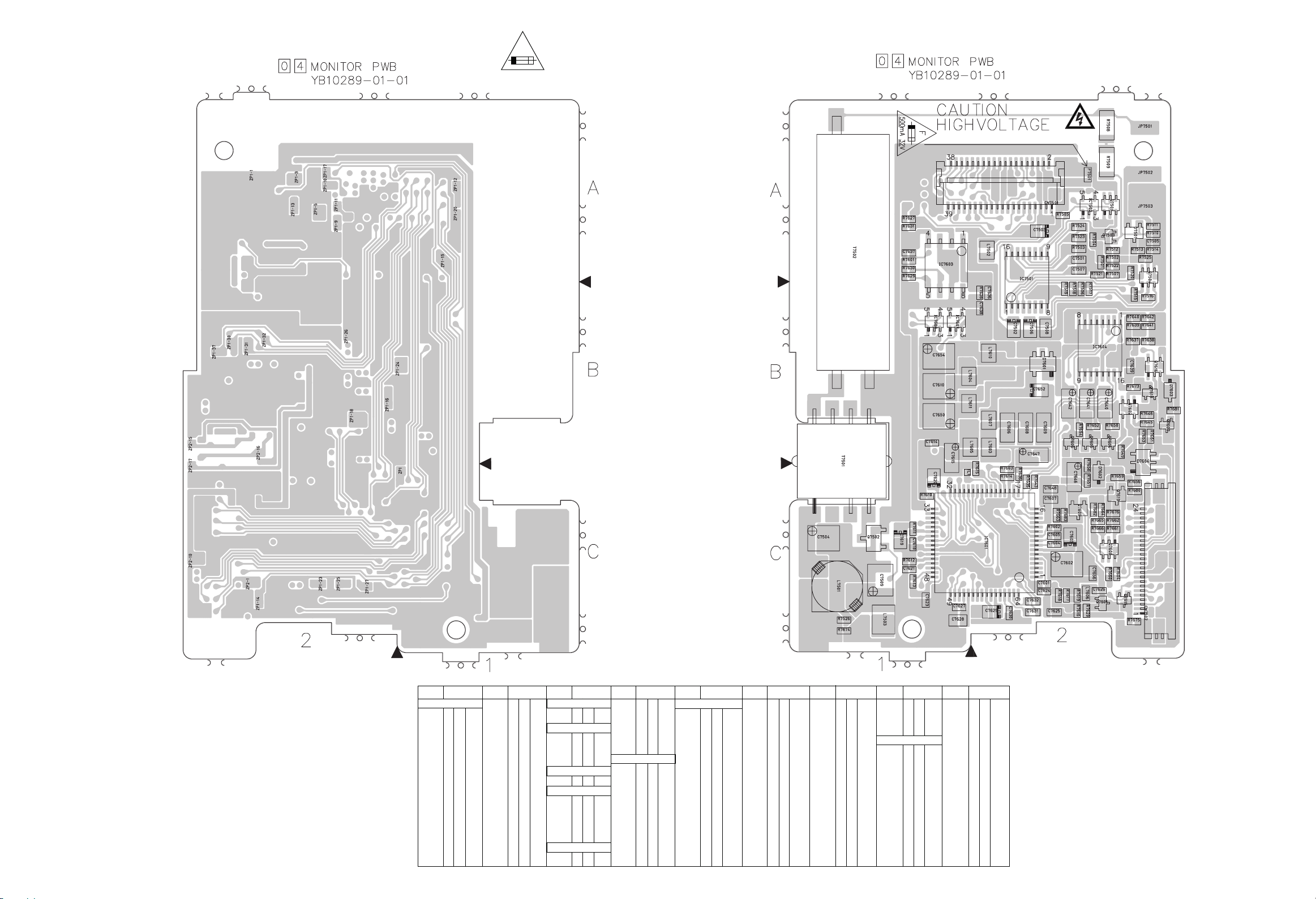
4.33 MONITOR CIRCUIT BOARD
5
4
FOIL SIDE (B)
CAUTION:
F
FOR CONTINUED PROTECTION AGAINST
FIRE HAZARD, REPLACE ONLY WITH SAME
TYPE AND RATED FUSE.
ATTENTION:
POUR UNE PROTECTION PERMANENTE
CONTRE LES RISQUE DÕINCENDE,
REMPLACER LE FUSIBLE PAR UN AUTRE
COMPONENT SIDE (A)
DE MEME TYPE ET DE MEME TENSION.
3
2
COMPONENT PARTS LOCATION GUIDE (MONITOR)
REF.No. LOCATION
CAPACITOR
C7501 A C 2A
C7502 A C 2B
C7503 A C 2A
C7504 A C 1C
C7505 A C 3A
C7506 A C 2B
C7507 A C 2A
C7508 A C 2B
C7509 A C 1C
C7601 A C 2C
C7602 A C 2C
C7603 A C 2C
1
A
B
C7604 A C 2C
C7605 A C 2C
C7606 A C 2B
C7607 A C 2C
C7608 A C 2B
C7609 A C 2B
C7610 A C 1B
C7614 A C 1B
C7615 A C 1C
C7618 A C 1C
C7619 A C 1C
C7620 A C 1C
C7621 A C 1C
REF.No. LOCATION REF.No. LOCATION
C7623 A C 1C
C7624 A C 2C
C7625 A C 2C
C7626 A C 2C
C7627 A C 1C
C7628 A C 1C
C7629 A C 2C
C7630 A C 2C
C7631 A C 2C
C7632 A C 2C
C7636 A C 2B
C7637 A C 1A
C7638 A C 2B
C7639 A C 2B
C7640 A C 2B
C7641 A C 2B
C7642 A C 2B
C7646 A C 2C
C7647 A C 2B
C7648 A C 2C
C7650 A C 1B
C7652 A C 2B
C7654 A C 1B
C7656 A C 2C
CONNECTOR
CN7501 A C 2A
CN7502 A C 2C
DIODE
D7501 A C 2A
D7601 A C 2B
D7602 A C 2C
D7603 A C 3B
D7604 A C 2C
FUSE
F7501 A C 2A
IC
IC7501 A C 2B
IC7502 A C 2A
IC7601 A C 2C
IC7603 A C 1A
IC7604 A C 2B
IC7607 A C 1B
IC7608 A C 1B
COIL
L7501 A C 1C
L7502 A C 2A
C
REF.No. LOCATION
L7503 A C 1C
L7603 A C 2B
L7604 A C 1B
L7605 A C 1B
L7606 A C 2C
L7607 A C 2B
L7610 A C 2B
L7611 A C 1B
TRANSISTOR
Q7501 A C 2A
Q7502 A C 1C
Q7503 A C 2A
Q7504 A C 2B
Q7601 A C 2C
Q7602 A C 2B
Q7604 A C 2B
Q7605 A C 2B
Q7606 A C 2B
Q7607 A C 3B
Q7608 A C 2C
Q7609 A C 2C
Q7610 A C 2C
Q7615 A C 2C
Q7616 A C 3B
Q7618 A C 2B
DEF
REF.No. LOCATION
RESISTOR
R7501 A C 2A
R7502 A C 2A
R7503 A C 2A
R7504 A C 2A
R7505 A C 2A
R7506 A C 2B
R7507 A C 2A
R7508 A C 2A
R7509 A C 2A
R7510 A C 3A
R7511 A C 3A
R7512 A C 2A
R7513 A C 2A
R7514 A C 3A
R7515 A C 2B
R7516 A C 2B
R7517 A C 2B
R7518 A C 2B
R7519 A C 2B
R7520 A C 2A
R7521 A C 2A
R7522 A C 2A
R7523 A C 2A
R7524 A C 2A
R7525 A C 2A
4-71 4-72
REF.No. LOCATION
R7526 A C 1C
R7601 A C 1A
R7602 A C 2C
R7603 A C 2C
R7604 A C 2C
R7610 A C 1C
R7611 A C 1C
R7612 A C 1C
R7613 A C 1C
R7614 A C 2C
R7615 A C 2C
R7616 A C 2C
R7617 A C 2C
R7618 A C 2C
R7619 A C 2C
R7620 A C 2C
R7627 A C 1A
R7628 A C 2B
R7629 A C 1B
R7630 A C 1A
R7631 A C 1A
R7635 A C 2C
R7636 A C 2C
R7637 A C 2B
R7638 A C 2B
R7639 A C 2B
REF.No. LOCATION
R7640 A C 2B
R7641 A C 2B
R7642 A C 2B
R7643 A C 2C
R7645 A C 2B
R7646 A C 2B
R7649 A C 2B
R7650 A C 2B
R7651 A C 2B
R7652 A C 2B
R7653 A C 2B
R7654 A C 2B
R7656 A C 2C
R7657 A C 2C
R7658 A C 2C
R7659 A C 2C
R7660 A C 2C
R7661 A C 2C
R7662 A C 2C
R7663 A C 2C
R7664 A C 2C
R7665 A C 2C
R7666 A C 2C
R7673 A C 2B
R7674 A C 1C
R7675 A C 2C
REF.No. LOCATION
R7676 A C 2C
R7680 A C 2C
R7681 A C 3B
R7682 A C 2C
R7683 A C 2C
OTHER
JP7501 A C 2A
JP7502 A C 2A
JP7503 A C 2A
T7501 A C 1C
T7502 A C 1A
TL1 A C 1C
ZP1 B C 1C
ZP1-1 B C 2A
ZP1-3 B C 2A
ZP1-5 B C 2A
ZP1-9 B C 2A
ZP2-1 B C 2C
ZP1-10 B C 2A
ZP1-11 B C 2A
ZP1-12 B C 1A
ZP1-13 B C 2A
ZP1-14 B C 2C
ZP1-15 B C 1A
ZP1-16 B C 2B
REF.No. LOCATION
ZP1-17 B C 2A
ZP1-18 B C 2B
ZP1-20 B C 1A
ZP1-23 B C 2C
ZP1-24 B C 1B
ZP1-25 B C 2C
ZP1-26 B C 2B
ZP1-27 B C 2C
ZP1-30 B C 2B
ZP1-31 B C 2B
ZP1-32 B C 2B
ZP1-37 B C 2B
ZP2-10 B C 3C
ZP2-15 B C 3B
ZP2-16 B C 2B
ZP2-17 B C 3C
G
H
Page 38
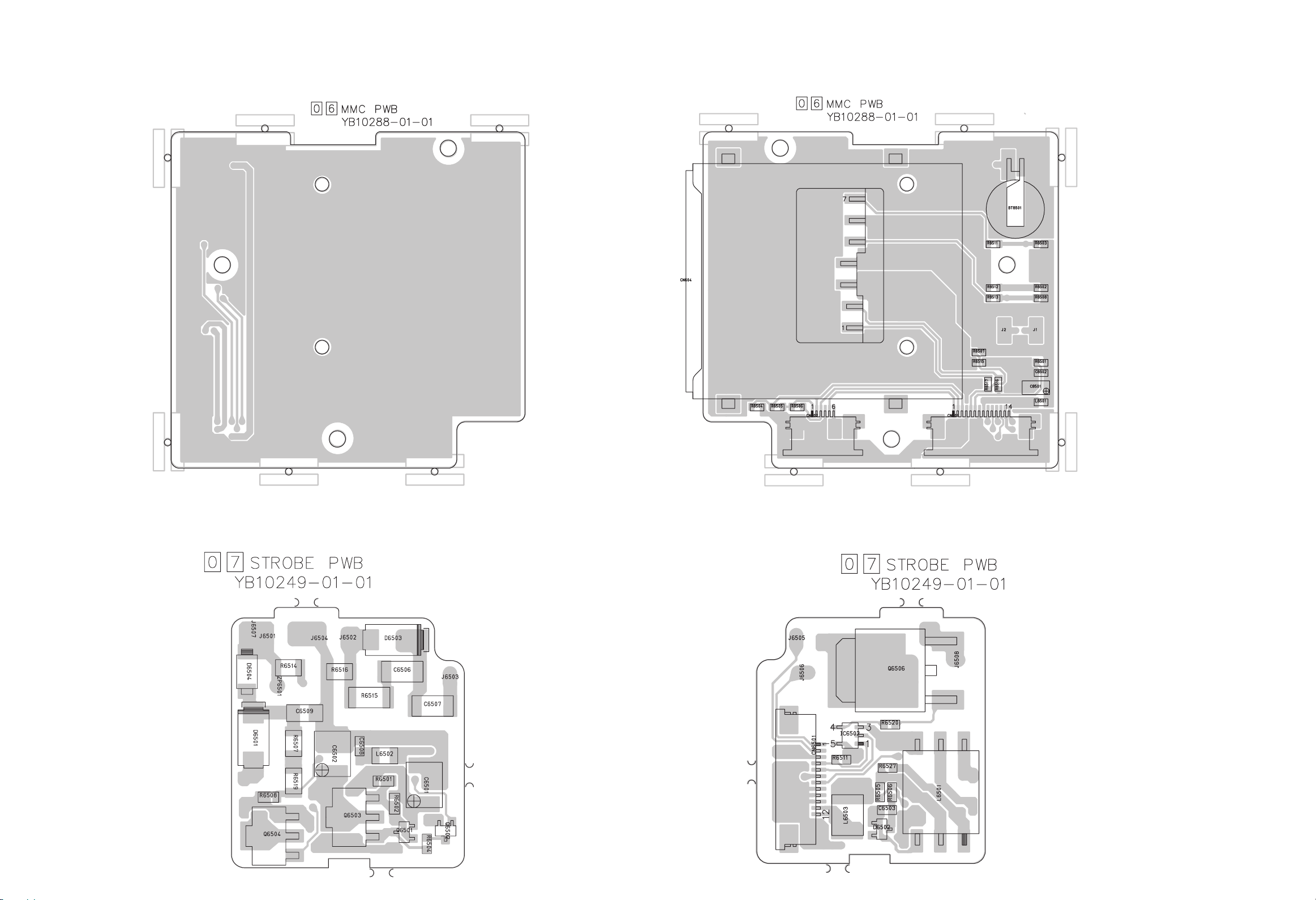
4.34 MMC AND STROBE CURCUIT BOARDS
FOIL SIDE (B)
5
4
COMPONENT SIDI (A)
3
FOIL SIDE (B)
2
1
COMPONENT SIDE (B)
A
B
C
DEF
4-73 4-74
G
H
Page 39

4.35 AUDIO VF CIRCUIT BOARD
FOIL SIDE (B)
COMPONENT SIDE (A)
5
4
3
2
COMPONENT PARTS LOCATION GUIDE (AUDIO/VF)
REF.No. LOCATION
CAPACITOR
C2101 B C 2A
C2102 B C 2A
C2103 B C 2A
C2104 B C 2A
C2105 B C 2A
C2106 B C 2A
C2107 B C 2A
C2108 B C 2A
C2109 B C 2A
C2111 B C 2A
C2112 B C 2A
C2113 B C 2A
C2114 B C 2A
C2115 B C 2B
C2116 B C 2B
C2117 B C 2B
C2118 B C 2B
C2119 B C 3B
C2120 B C 3B
C2121 B C 2A
1
A
B
C2122 B C 2A
C2123 B C 3A
C2124 B C 3A
C2131 A C 3A
C2132 A C 3A
C2133 A C 2A
C2134 A C 2A
C2135 A C 2A
C2136 A C 2A
C2137 A C 3A
C2138 A C 3A
C2202 A C 1B
C2203 A C 1B
C2204 A C 1B
C2207 A C 2B
C2208 A C 2B
REF.No. LOCATION REF.No. LOCATION
C2210 A C 2A
C2211 A C 2A
C2212 A C 2A
C2214 A C 2A
C2215 A C 2A
C2216 B C 2A
C2217 A C 2A
C2218 A C 2A
C2220 A C 2A
C2221 A C 2A
C2224 A C 2A
C2225 A C 1A
C2227 A C 2A
C2228 A C 2A
C2229 A C 2A
C2230 B C 3A
C2231 A C 1B
C2301 B C 1A
C2303 B C 1B
C2304 B C 1A
C2305 B C 1B
C2306 B C 1A
C2307 B C 1B
C2308 B C 1A
C2309 B C 1A
C2310 B C 1A
C2311 B C 2A
C2312 B C 2A
C2313 A C 1B
C2314 A C 1A
C2315 B C 1B
C2316 B C 1A
C2401 B C 1A
C2402 B C 1A
C2406 A C 2B
C2407 B C 1A
C2411 A C 2B
C2412 A C 2A
C2413 A C 2A
C2501 B C 2A
C2502 B C 1B
C2503 B C 1B
C2504 B C 1B
C2505 B C 1B
C2506 B C 1A
C2508 B C 1A
C2601 A C 1A
C2602 A C 1B
C2603 A C 1A
C2604 A C 1B
C2605 A C 1A
C2606 A C 1B
C2611 A C 1A
C2612 A C 1B
C2613 A C 1A
C2614 A C 1B
C2615 A C 1A
C2616 A C 1B
C2617 A C 1A
C2618 A C 1A
C2619 A C 1A
C2620 A C 1A
C2621 A C 1A
C2622 A C 1A
C2625 A C 1A
C2626 A C 1A
C2627 A C 1A
C2628 A C 1A
C2629 B C 1A
C2631 A C 1A
C2632 A C 1B
C2635 A C 1A
C2636 A C 1B
C2639 A C 1A
C
REF.No. LOCATION
C2640 A C 1B
C2702 A C 2B
C2703 A C 2B
C2753 A C 2A
C2754 A C 2B
C2756 B C 2A
C2757 B C 2A
C2764 B C 2A
C2765 B C 2A
C2766 A C 2A
C2767 A C 2B
C2768 A C 1B
C2769 A C 2A
C7401 A C 3C
C7402 A C 3B
C7403 A C 3C
C7404 A C 3C
C7405 A C 3B
C7406 A C 3B
C7407 A C 3B
C7408 A C 3B
C7409 A C 3B
C7411 A C 3B
C7413 A C 3C
C7414 A C 3B
C7415 A C 2C
C7416 A C 2C
C7417 A C 2C
C7418 A C 2C
C7419 A C 2C
C7420 A C 2C
C7421 A C 3C
C7422 A C 3C
C7423 A C 3C
C7424 A C 3C
C7425 A C 3C
C7426 A C 3C
REF.No. LOCATION
C7427 A C 2B
C7428 A C 3B
C7429 A C 3B
C7430 A C 3B
C7431 A C 3B
C7432 A C 3B
C7433 A C 3B
C7434 A C 3B
CONNECTOR
CN801 B C 3C
CN802 B C 3A
CN803 A C 3A
CN804 B C 1B
CN805 A C 2B
DIODE
D2001 B C 1A
D2501 B C 1B
D2502 B C 2A
D2751 B C 2A
D7401 A C 3C
IC2101 B C 2A
IC2102 B C 2B
IC2103 A C 2A
IC2201 A C 2A
IC2301 B C 1B
IC2302 B C 1A
IC2501 B C 2B
IC7401 A C 3C
IC7402 A C 3C
COIL
L2101 B C 2A
L2102 B C 2B
IC
REF.No. LOCATION
L2131 A C 3A
L2401 B C 2A
L2601 A C 1A
L2602 A C 1B
L2603 A C 1B
L2604 A C 1A
L7401 A C 3C
L7402 A C 2C
L7403 A C 2B
L7404 A C 3C
TRANSISTOR
Q2101 B C 2B
Q2102 B C 2A
Q2201 A C 2A
Q2202 A C 1B
Q2301 B C 2A
Q2302 B C 1A
Q2401 B C 1A
Q2403 A C 2B
Q2501 B C 1A
Q2602 B C 2A
Q2603 A C 1A
Q2604 A C 1B
Q2755 B C 2A
Q7401 A C 3B
Q7402 A C 2C
RESISTOR
R2001 B C 1A
R2002 A C 3B
R2003 A C 3B
R2004 A C 3B
R2005 A C 3B
R2101 B C 2A
R2102 B C 2A
R2103 B C 2A
DEF
REF.No. LOCATION
R2104 B C 2A
R2105 B C 2A
R2106 B C 2A
R2107 B C 2A
R2111 B C 2A
R2112 B C 2A
R2113 B C 2A
R2114 B C 2A
R2116 B C 2B
R2117 B C 2B
R2118 B C 3B
R2119 B C 3B
R2120 B C 2B
R2121 B C 3B
R2122 B C 3B
R2131 A C 2A
R2132 A C 2A
R2133 A C 2A
R2134 A C 2A
R2135 A C 2A
R2136 A C 2A
R2137 A C 2A
R2138 A C 3A
R2139 A C 3A
R2140 A C 2A
R2141 A C 2A
R2201 A C 1B
R2202 A C 1B
R2203 A C 2A
R2204 A C 2A
R2205 B C 2A
R2206 B C 2A
R2208 A C 2A
R2210 A C 2A
R2220 A C 2A
R2221 A C 2A
R2224 B C 2A
R2228 A C 2A
4-75 4-76
REF.No. LOCATION
R2229 B C 1A
R2230 B C 1A
R2231 A C 2A
R2232 A C 2A
R2233 B C 2A
R2234 B C 2A
R2301 B C 1A
R2302 B C 1A
R2303 B C 1A
R2305 B C 1B
R2306 B C 1A
R2307 B C 1B
R2308 B C 2A
R2309 B C 1B
R2310 B C 1A
R2311 B C 1B
R2312 B C 1A
R2313 B C 1B
R2314 B C 1A
R2315 B C 1B
R2316 B C 1A
R2317 B C 1B
R2318 B C 1A
R2319 B C 1A
R2320 B C 1A
R2321 B C 1A
R2322 B C 1A
R2323 B C 1A
R2324 B C 1A
R2325 B C 2A
R2326 B C 2A
R2327 B C 2A
R2328 B C 2A
R2329 B C 1B
R2330 B C 2A
R2331 B C 1B
R2332 B C 1A
R2333 B C 1B
REF.No. LOCATION
R2334 B C 1A
R2335 B C 1B
R2336 B C 1A
R2401 B C 1A
R2402 B C 1A
R2403 B C 1A
R2412 A C 2B
R2413 A C 2B
R2415 A C 2A
R2429 A C 2B
R2501 B C 2A
R2502 B C 2A
R2504 B C 1B
R2505 B C 2B
R2506 B C 1B
R2507 B C 1B
R2508 B C 1B
R2509 B C 1B
R2510 B C 2A
R2512 B C 2A
R2513 B C 1A
R2514 B C 1A
R2515 B C 1A
R2601 A C 1A
R2602 A C 1B
R2603 A C 1A
R2604 A C 1B
R2605 B C 1A
R2606 B C 1A
R2609 A C 1A
R2610 A C 1B
R2613 A C 1A
R2614 A C 1B
R2615 A C 1A
R2616 A C 1B
R2617 A C 1A
REF.No. LOCATION
R2618 A C 1B
R2619 A C 1A
R2620 A C 1B
R2621 A C 1A
R2622 A C 1B
R2623 A C 1A
R2624 A C 1A
R2627 A C 1A
R2628 A C 1B
R2629 A C 1A
R2630 A C 1B
R2631 A C 1A
R2632 A C 1B
R2633 A C 1A
R2634 A C 1B
R2635 A C 1A
R2636 A C 1B
R2640 A C 1A
R2641 A C 1A
R2642 B C 2A
R2643 B C 2A
R2715 B C 2A
R2756 B C 2A
R2757 B C 2A
R2758 B C 2A
R2759 B C 2A
R2760 B C 2A
R2775 A C 1B
R2776 A C 1A
R2777 A C 1B
R2778 A C 1A
R7401 A C 3C
R7402 A C 3C
R7403 A C 3C
R7404 A C 3C
R7405 A C 3C
R7406 A C 3C
REF.No. LOCATION
R7407 A C 3C
R7408 A C 3C
R7409 A C 3C
R7410 A C 3C
R7411 A C 3C
R7412 A C 2C
R7413 A C 2C
R7414 A C 2C
R7415 A C 2C
R7416 A C 2C
R7417 A C 2B
R7418 A C 2B
R7419 A C 2B
R7420 A C 3C
R7421 A C 3C
R7422 A C 3C
R7423 A C 3C
R7424 A C 3C
R7426 A C 3C
R7427 A C 3C
R7428 A C 3C
R7429 A C 3C
R7430 A C 3C
R7433 A C 2C
R7434 A C 3C
R7435 A C 3C
R7439 A C 2C
R7440 A C 2C
R7441 A C 2C
R7442 A C 3B
R7443 A C 3B
R7444 A C 3B
R7445 A C 3B
VR7401 A C 3C
OTHER
JP51 B C 3A
REF.No. LOCATION
JP52 B C 3A
JP53 B C 3A
S7001 A C 3B
TL7401 B C 2C
ZP7401 B C 3C
ZP7402 B C 3C
ZP7403 B C 3C
ZP7404 B C 3C
ZP7405 B C 3C
ZP7406 B C 3C
ZP7407 B C 2C
ZP7408 B C 2C
ZP7409 B C 2C
ZP7410 B C 3B
ZP7411 B C 3C
ZP7412 B C 3C
ZP7413 B C 3C
ZP7414 B C 3C
ZP7415 B C 3C
ZP7416 B C 3C
ZP7417 B C 2B
ZP7418 B C 2C
ZP7419 B C 2C
ZP7420 B C 2C
ZP7421 B C 2C
ZP7422 B C 2C
ZP7423 B C 2C
ZP7424 B C 2C
ZP7425 B C 2C
ZP7426 B C 3C
ZP7427 B C 3C
ZP7428 B C 2B
ZP7429 B C 3B
ZP7430 B C 3B
ZP7431 B C 3B
ZP7432 B C 3B
G
H
Page 40

4.36 JACK,W/B AND EJECT CIRCUIT BOARDS
FOIL SIDE (B)
5
4
FOIL SIDE (B) COMPONENT SIDE (A)
3
CONPONET SIDE (A)
FOIL SIDE (B)
2
1
COMPONENT SIDE (A)
A
B
C
DEF
4-77 4-78
G
H
Page 41

4.37 POWER SYSTEM BLOCK DIAGRAM
5
4
3
2
1
A
B
C
DEF
4-79 4-80
G
H
Page 42

4.38 VIDEO SYSTEM BLOCK DIAGRAM
5
4
3
2
1
A
B
C
DEF
4-81 4-82
G
H
Page 43

4.39 REGULATOR SYSTEM BLOCK DIAGRAM
5
4
3
2
1
A
B
C
DEF
4-83 4-84
G
H
Page 44

4.40 VOLTAGE CHARTS
<CPU>
MODE
PIN NO.
IC1002
10 0 0
11 0 0
12 0 0
13 0 0
14 0 0
15 0 0
16 0 0
17 0 0
18 0 0
19 2.9 2.9
20 2.8 2.8
IC1003
IC1004
IC1005
IC1006
IC1008
IC1009
REC PLAY
1 2.7 2.7
20 0
3 2.7 2.7
43 3
53 3
63 3
7 1.5 1.5
8 1.5 1.5
90 0
13 3
2 2.3 2.3
33 3
40 0
53 3
63 3
73 3
83 3
1- 2- 3- 4- 5- 6- 7- 8- -
13 3
23 3
33 3
40 0
53 3
63 3
73 3
83 3
13 3
23 3
33 3
40 0
50 0
60 0
70 0
83 3
13 3
23 3
33 3
40 0
53 3
63 3
73 3
83 3
13 3
23 3
33 3
40 0
5 2.9 3
63 3
73 3
83 3
MODE
PIN NO.
Note: Parts whose data cannot be obtained by physical measurement (for example, CSP IC, etc.) are
<MSD CPU>
REC PLAY
IC1402
1 2.8 2.8
20 0
3 2.8 40 0
53 63 3
73 83 3
IC1403
13 3
23 3
33 3
40 0
53 3
63 3
73 3
83 3
IC1405
13 3
20 0
30 0
40 0
50 0
60 0
73 3
83 3
Q1401
E3 3
C3 3
B3 3
Q1402
10 0
23 3
3 3 2.9
4 2.8 2.8
50 0
Q1403
10 0
20 0
3 3 2.9
40 0
5 2.9 2.9
Q1405
E0 0
C 0.5 0.7
B0 0
Q1406
E- C- B- -
Q1407
E- C- B- -
Q1408
E- C- B- -
omitted from the following chart in some cases.
<A/HP SEL>
MODE
PIN NO.
IC2701
IC2751
10 0 0
11 0 0
12 0 0
13 0 0
14 0 0
15 0 0
16 4.7 4.8
Q2701
Q2703
Q2704
Q2705
Q2751
Q2752
Q2753
Q2754
Q2755
Q2756
Q2757
Q2758
Q2759
REC PLAY
1 0.8 0.5
20 0
30 0
40 0
5 4.7 4.7
10 0
20 0
30 0
40 0
50 0
60 0
7 -7.2 -7.2
80 0
9 4.7 4.7
E0 0
C0 0
B3 3
E0 0
C0 0
B -0.4 0
E0 0
C0 0
B0 0
E0 0
C 4.7 4.7
B0 0
E0 0
C0 0
B3 3
E 4.7 4.7
C0 0
B 4.7 4.7
E 4.7 4.7
C0 0
B 3.5 3.5
E0 0
C 3.5 3.5
B0 0
1- 2- 3- 4- 5- 6- -
E- C- B- -
E- C- B- -
E0 0
C0 0
B3 3
E0 0
C 4.7 4.7
B0 0
MODE
PIN NO.
Q2760
<DVMAIN>
MODE
PIN NO.
IC3004
IC3005
<DVEQ/DVANA>
MODE
PIN NO.
IC3202
IC3203
IC3301
REC PLAY
E0 0
C0 0
B0 0
REC PLAY
10 0
2 1.6 0.8
30 0
4 1.8 0.9
5 1.8 1.8
11 1
21 1
30 0
4 0 0.9
52 2
REC PLAY
1 2.7 1.3
20 3
30 0
4 3 1.1
53 3
1 1.8 1.8
20 0
3 1.3 1.2
42 2
53 3
10 0
2 2.2 1.3
3 0 1.4
4 0 0.7
5 0 1.7
6 1.1 1.1
7 0 1.8
80 1
90 0
10 0 0
11 0 0
12 0 0
13 3 3
14 3 3
15 2.2 1.9
16 3 3
17 0 1.2
18 0 1.5
19 0 0
20 0 1.4
21 0.7 1.7
22 0.7 1.6
23 3 3
24 3 3
25 2.9 0
26 3 3
27 0.8 0
28 0 0
29 0 0
30 2.2 2.2
31 0.5 0.5
32 2.2 2.2
33 0.6 0.5
34 1.9 1.9
35 1.8 1.5
36 1.7 1.5
37 2.2 1.6
38 0 1.5
MODE
PIN NO.
Q3551
Q3552
REC PLAY
39 0 0
40 0 0
41 0 0
42 0 0
43 1.6 1.6
44 1.4 1.5
45 1.2 1.2
46 0.7 0.7
47 1.2 1.3
48 1.8 1.8
49 1.3 1.3
50 0.6 0
51 0 0
52 0 0
53 0.5 0.5
54 1.5 1.5
55 3 3
56 3 3
57 3 2.9
58 3 3
59 2.7 2.7
60 2.5 2.4
61 0 1.5
62 2.6 2.5
63 1.9 2
64 0.4 0.8
E 4.8 4.8
C 4.8 4.8
B 4.1 4.8
E0 0
C 0 4.8
B0 0
<PRE/REC>
MODE
PIN NO.
IC3501
Q3501
Q3502
Q3503
REC PLAY
1 3 2.3
2 2.6 1.9
33 3
40 0
50 0
60 0
7 2.7 3
8 0 0.7
9 0.5 0
10 0 0
11 2.7 2.6
12 0.6 0.6
13 2.6 2.6
14 3 3
15 0.6 0.6
16 0 0
17 0 0
18 0.8 0.5
19 4.8 4.8
20 1.2 1.3
21 0.6 0.7
22 2.7 2.2
23 0 0
24 2.2 1.1
25 3 3
26 0 0
27 0 0
28 -0.9 1.8
29 4.8 4.8
30 4.8 4.8
31 4.7 4.8
32 -1 1.8
33 0 0
34 0 0
35 3 3
36 1.6 1.1
37 0 0
38 2.7 2.2
39 0.7 0.7
40 1.3 1.3
41 0 0
42 0 0
43 3 0
44 0 0
45 1.5 3
46 3 1.5
47 0 3
48 2.9 3
49 0 0
50 0 0
51 0 0
52 0 0
53 0 0
54 0.7 0
55 0.6 2.3
56 0 0
57 2.7 1.1
58 3 2.2
59 3 2
60 3 3
61 2.6 1.8
62 3 2.5
63 0 0
64 1.6 1
E0 0
C 2.4 1.1
B 0.6 0.7
E0 0
C0 0
B -0.8 0.7
E0 0
C0 0
B -0.7 0.7
MODE
PIN NO.
Q3504
REC PLAY
E0 0
C 1.9 1.1
B 0.7 0.7
<VIDEO OUT>
MODE
PIN NO.
IC3701
IC3702
Q3701
Q3707
Q3708
Q3709
Q3710
Q3711
Q3712
Q3713
Q3731
REC PLAY
1 1.8 0
2 1.5 1.5
3 1.3 0
4 1.2 2.3
50 0
60 0
70 0
80 0
9 2.8 0
10 0 0
11 1.9 0
12 0 0
13 0 0
14 2 0
15 4.8 4.8
16 3 3
17 30 0
18 1.4 0
19 1.8 0
20 1.9 0
1- -
2- -
3- -
4- -
5- -
E0 0
C0 0
B3 3
1 1.2 1.2
2 0.7 0.6
30 0
40 0
5 0.6 0.6
60 0
E0 0
C0 0
B0 0
E 0.8 0.7
C0 0
B0 0
E 1.2 1.2
C 1.2 1.2
B 0.7 0.7
E 0.8 0.8
C 4.8 4.8
B 1.2 1.2
1 4.8 4.8
2 4.8 4.8
3 4.8 4.8
4 0.7 0.7
50 0
E0 0
C 4.8 4.8
B0 0
E 1.7 1.6
C0 0
B 1.1 1
<CDS>
MODE
PIN NO.
IC4201
IC4202
REC PLAY
100
2 1.2 0
3 1.2 0
4 1.3 0
5 1.3 0
6 1.2 0
7 1.7 3.1
8 1.2 0
9 1.4 0
10 0.9 0
11 0 0
12 0 0
13 0 0
14 0 0
15 3.1 3.1
16 1.3 1.3
17 3 3
18 2.4 2.4
19 2.4 2.5
20 2.6 2.6
21 0 0
22 0 0
23 3 3.1
24 0 0
25 0 0
26 2 0.5
27 1.5 1.4
28 2 0
29 2 0
30 0 0
31 3 3.1
32 0 1.3
33 1 1.2
34 1.5 1.1
35 1.2 0
36 0 0
37 0 0
38 3 3.1
39 0 0
40 0 0
41 3 3.1
42 0 0
43 3 3
44 3 3
45 3 3
46 3.1 3
47 0 0
48 0 0
100
2 4.8 4.8
3 3.1 3.1
<DSP>
MODE
PIN NO.
IC4302
IC4304
IC4305
IC4401
Q4351
Q4352
Q4353
Q4354
REC PLAY
133
200
3 1.3 1.2
4 2.4 2.4
533
1 2.9 2.9
233
333
400
500
600
7 2.8 2.8
833
100
200
300
400
5 2.8 2.8
6 2.9 2.8
7 2.9 2.9
833
100
222
3 1.6 1.6
400
500
6 1.5 1.5
700
833
9 0.7 0.7
10 3 3
11 3 3
12 1.9 1.9
13 1.2 1.2
14 2.7 2.5
15 0 0
16 3 3
17 3 3
18 0.8 0.8
19 2.7 2.7
20 0 0
E 1.2 1.2
C00
B 0.6 0.6
1 0.7 0.7
2 0.7 0.7
300
400
500
600
1 1.2 1.2
2 1.1 1.1
3 0.6 0.6
400
5 0.6 0.6
600
E 1.1 1.1
C00
B 0.5 0.5
<TG/VDR>
MODE
PIN NO.
IC5001
IC5002
IC5004
REC PLAY
10 0
23 3
33 3
40 0
53 3
6 3.1 3
70 0
83 3
93 3
10 3 3
11 3.5 3.5
12 0.5 0.5
13 0 0
14 0 0
15 1.6 1.7
16 0 0
17 0 0
18 1.3 1.2
19 3.5 3.5
20 2.4 2.3
21 2.4 2.4
22 3 3.1
23 0 0
24 1.2 1.1
25 2.6 2.6
26 3 3
27 3 3
28 0 0
29 0 0
30 0 0
31 0.4 0
32 0 0.5
33 3 3
34 0 0
35 1.1 1.1
36 1.2 1.3
37 1.1 1.1
38 3 3
39 0 0
40 0 0
41 0 0
42 1.4 1.4
43 0 0
44 0.6 0.6
45 0 0
46 0 0
47 1.5 1.5
48 1.5 1.5
49 1.5 1.5
50 0 0
51 0 0
52 -7.3 -7.3
53 0 0
54 14.8 14.8
55 0 0
56 0 0
57 0 0
58 0 0
59 0 0
60 -7.2 -7.2
61 -7.6 -7.6
62 -7.2 -7.2
63 -7.6 -7.6
64 0 0
1 4.8 4.8
20 0
3- -
4 3.5 3.5
5 4.8 4.8
1- -
2- -
3- -
4- -
5- -
6- -
7- -
8- -
4-85 4-86
Page 45

<REG CTL>
MODE
PIN NO.
IC6001
IC6002
IC6003
IC6004
Q6001
Q6002
Q6003
Q6004
Q6005
Q6006
Q6007
REC PLAY
1 6.7 6.7
2 6.5 6.5
30 0
40 0
10 0
2 6.7 6.8
3 3.3 3.3
40 0
50 0
13 3
20 0
3 6.7 6.7
1 3 2.6
23 3
30 0
40 0
G0 0
D 6.7 6.8
S 6.8 6.7
G 6.7 6.7
D0 0
S0 0
G3 3
D0 0
S 3.9 3.9
G0 0
D 6.5 6.5
S0 0
G3 3
D0 0
S0 0
G0 0
D 6.6 6.7
S 6.7 6.7
10 0
23 3
3 6.8 6.8
4 6.8 6.8
50 0
<REG>
MODE
PIN NO.
IC6101
REC PLAY
1 0.4 0.4
2 0.4 0.4
3 0.4 0.4
4 1.1 1.1
51 1
6 1.5 1.5
7 4.3 4.3
8 1.5 1.5
9 0.6 0.7
10 1.5 1.5
11 3.1 3.1
12 0.8 0.8
13 0 0
14 0 0
15 0 0
16 0 0
17 0.7 0.7
18 0 0
19 0 0
20 0 0
21 0 0
22 5 5
23 6.8 6.7
24 0 0
25 5.6 5.6
26 6.8 6.8
27 1.3 1.3
28 0.5 0.5
29 0 0
30 0 0
31 1.5 1.5
32 6.7 6.7
33 4 4
34 2.1 2.1
35 0.5 0
36 0 0
37 1.9 1.9
38 0 0
39 4 4
40 6.7 6.7
41 3 3
42 3 2.9
43 3 3
44 2.3 2.3
45 1.5 1.5
46 0.9 0.9
47 1.8 1.8
48 1.5 1.5
49 0.8 0.8
50 2.3 2.3
51 1.5 1.5
52 0.9 0.9
53 0 0
54 0 0
55 1.5 1.5
56 1.1 1.1
57 3 3
58 1 1
59 0.4 0.4
60 0.4 0.4
61 6.7 6.7
62 4.8 4.8
63 0 0
64 0 0
65 0 0
66 6.7 6.7
67 3.6 3.5
68 0 0
69 1.6 1.6
70 0 0
71 0 0
72 6.7 6.7
73 1 1.8
74 0 0
75 6.7 6.7
76 2.7 2.7
77 0 0
78 6.8 6.7
MODE
PIN NO.
IC6401
Q6103
Q6104
Q6105
Q6106
Q6107
Q6108
Q6109
Q6110
Q6112
Q6113
Q6201
Q6202
Q6203
Q6204
Q6205
Q6206
REC PLAY
79 0 0
80 0 0
1 4.8 4.8
20 0
3 1.2 1.2
4 4.5 4.5
5 4.8 4.8
G 4.9 4.9
D 1.8 1.7
S 6.7 6.8
G 5.7 5.6
D 0.9 1
S 6.7 6.7
G 5.5 5.5
D 4.9 4.9
S 6.8 6.8
G 2.7 2.7
D0 0
S 6.7 6.7
G 1.8 1.8
D 4.9 4.9
S 6.7 6.7
G4 4
D 3.1 3
S 6.7 6.7
G 1.9 1.9
D3 3
S0 0
G 4.8 4.8
D 1.8 1.8
S 6.7 6.7
G 3.6 3.5
D 3 3.1
S 6.7 6.7
G 0 1.6
D 3.1 3
S0 0
14 4
2 4.6 4.6
3 0 15.1
44 4
5 4.5 4.5
6 15.6 0
E 15.6 15.6
C 11.8 11.8
B 15 15.1
E 14.8 14.8
C 15.6 15.7
B 15.5 15.5
1 -7.1 -7.1
2 -7.6 -7.6
3 -11.5 -11.5
4 -7.1 -7.1
5 -7.6 -7.1
6 -15.9 -7.6
E -12.1 -12.1
C -7.6 -7.6
B -11.5 -11.5
E -15.3 -15.3
C -15.9 -15.9
B -15.8 -15.8
MODE
PIN NO.
Q6207
REC PLAY
E0 0
C 15.6 15.6
B -0.8 -0.9
<STROBE SUB>
MODE
PIN NO.
IC6601
Q6601
Q6602
Q6611
Q6612
Q6613
Q6614
Q6615
REC PLAY
1- 2- 3- 4- 5- 6- 7- 8- -
E- C- B- -
1- 2- 3- 4- 5- -
E- C- B- -
1- 2- 3- 4- 5- -
E- C- B- -
1- 2- 3- 4- 5- -
1- 2- 3- 4- 5- -
<DSC>
MODE
PIN NO.
IC8005
IC8006
IC8007
IC8008
IC8009
REC PLAY
13 3
23 3
30 0
40 0
53 3
13 3
20 0
3 1.3 1.2
4 2.5 2.5
53 3
1 4.8 4.8
20 0
3 1.3 1.3
4 3.3 3.3
5 4.8 4.8
1 1.4 1.4
2 1.4 1.4
33 3
40 0
50 0
6 1.5 1.5
7 1.3 1.1
83 3
1- 2- 3- 4- 5- 6- 7- 8- -
<AU DSP>
MODE
PIN NO.
IC8102
10 0 0
11 3 3
12 0 0
13 1.1 0.5
14 3 3
15 0 0
16 3 3
17 0 0
18 3 3
19 3 3
20 3 3
IC8103
REC PLAY
10 0
23 3
3 1.2 0.5
4 3 3.1
53 3
63 3
7 3 3.1
80 0
93 3
10 0
2 1.5 1.5
30 0
4 1.5 1.5
53 3
4-87
Page 46

<W/B>
MODE
PIN NO.
IC1101
REC PLAY
1 2.4 2.3
2 2.4 2.4
30 0
4 4.8 4.8
5 2.4 2.4
6 2.4 2.4
7 2.4 0
8 0 4.8
<IR/TALLY>
MODE
PIN NO.
IC1801
Q1801
REC PLAY
1 4.8 4.8
2 4.4 4.4
30 0
40 0
5
E0 0
C 0 1.8
B3 0
<MDA>
MODE
PIN NO.
IC1601
REC PLAY
10 0
2 0.9 0.9
3 0.8 0.8
40 0
5 0.8 0.8
60 0
70 0
80 0
90 0
10 0 0
11 0 0
12 0 0
13 0 0
14 4.9 4.9
15 0 0
16 0.5 0.5
17 0 0
18 0.5 0.5
19 0 0
20 0.4 0.4
21 0 0
22 0 0
23 0.9 0.9
24 6.7 6.7
25 1.5 1.5
26 1.5 1.5
27 1.5 1.5
28 1.5 1.5
29 1.5 1.5
30 1.5 1.5
31 1.5 1.5
32 1.5 1.5
33 1.5 1.5
34 1.5 1.5
35 3 3
36 3 3
37 0 0
38 0.7 0.7
39 0.7 0.7
40 1.2 1.2
41 1.5 1.5
42 0.5 0.5
43 3 3
44 0 0
45 0 0
MODE
PIN NO.
Q1601
REC PLAY
46 0 0
47 3 3
48 0 0
49 3 3
50 2 2
51 0 0
52 1.5 1.5
53 1.2 1.1
54 0.5 0.5
55 0.7 0.7
56 0.7 0.7
57 1.1 1
58 0.7 0.7
59 0 0
60 1.1 1.1
61 2.7 2.7
62 1.2 1.2
63 1.5 1.5
64 1.5 1.5
65 1.5 1.5
66 1.5 1.5
67 1.5 1.5
68 0.5 0.5
69 0 0
70 0.8 0.8
71 0.8 0.8
72 0.8 0.8
73 0.9 0.8
74 1.2 1.2
75 0.4 0.4
76 0 0
77 6.7 6.7
78 1.7 1.7
79 0 0
80 0 0
10 0
20 0
3 4.9 4.9
40 0
5 4.9 4.9
<IRIS & AF/ZOOM>
MODE
PIN NO.
IC4802
IC4803
IC4804
IC4806
REC PLAY
1 2.8 2.8
2 2.2 2.2
3 2.2 2.2
40 0
50 0
6 2.2 2.2
7 2.2 2.2
8 4.8 4.8
1 1.2 1.2
2 0.5 0.5
3 0.5 0.5
40 0
5 2.1 2.1
6 2.2 2.2
7 0.6 0.6
8 4.8 4.8
1 1.2 0
2 1.3 0
3 1.3 0
40 0
5 1.9 1.6
6 1.9 1.6
7 0.9 2.8
8 4.8 4.8
1 1.3 0
2 1.3 0
3 1.2 0
4 1.3 0
MODE
PIN NO.
IC4807
IC4851
Q4801
Q4802
Q4803
Q4804
Q4805
Q4851
REC PLAY
53 3
6 1.7 3
7 1.7 3
83 3
1 1.6 1.6
2 1.6 1.6
3 4.8 4.8
40 0
5 1.6 1.6
6 1.6 1.6
7 4.8 4.8
8 4.8 4.8
10 0
2 0.4 0.4
30 0
40 0
50 0
60 0
70 0
83 3
9 6.8 6.7
10 0 0
11 0 0
12 0 0
13 6.7 6.7
14 0 0
15 0 0
16 0 0
17 0 0.7
18 0 0
19 0 0
20 0 0
21 0.8 0
22 0 0
23 6.7 6.7
24 0 0
25 0 0
26 0 0
27 6.7 6.8
28 0 0
29 0 0
30 0 0
31 3 3
32 0 0
33 0 0
34 3 3
35 3 3
36 1.5 1.5
37 1.5 1.5
38 0 3
E 0.5 0.5
C 1.6 1.6
B 1.2 1.2
E0 0
C 1.9 1.6
B0 0
E0 0
C 4.8 4.8
B0 0
E 4.8 4.8
C 1.9 1.6
B 4.8 4.8
E 4.8 4.8
C 1.6 1.6
B 4.8 4.8
E0 0
C 3.6 0
B 0 0.7
<AUDIO AD/DA>
MODE
PIN NO.
IC2101
IC2102
Q2101
Q2102
REC PLAY
1 0 1.3
200
3 1.3 0
400
533
633
700
8 1.5 0
9 1.3 1.3
10 1.5 1.5
11 1.5 1.5
12 1.5 1.5
13 3 0
14 0 1.3
15 1.4 1.3
16 1.1 1.3
100
2 0.8 0.8
3 0 0.8
400
533
633
700
800
900
10 1.5 1.5
11 1.5 1.5
12 1.5 1.5
13 0 0
14 0 0
15 0 0
16 0 0
E00
C00
B00
E00
C00
B00
<MAIN AUDIO>
MODE
PIN NO.
IC2201
IC2301
IC2302
REC PLAY
1 1.5 0.5
2 1.5 0.5
3 1.5 0.5
4 1.5 1.5
5 1.5 1.5
6 1.5 1.6
700
8 2.2 2.3
9 2.2 2.3
10 1.6 0
11 1.5 1.6
12 1.5 1.5
13 1.5 1.6
14 1.5 0.5
15 1.5 0.5
16 1.6 0.5
17 1.5 1.6
18 1.6 1.6
19 15 1.2
20 1.5 0.8
21 1.5 1.6
22 2.8 3
23 1.5 1.7
24 1.5 1.5
25 2.3 2.1
26 0 0.5
27 2.4 2.1
28 2.8 1.7
29 2.3 2.3
30 2.4 2.1
31 2.4 2.4
32 2.4 2.1
33 5.2 4.6
34 4.6 4.6
35 0 0
36 2.4 2.3
37 4.6 4.6
38 2.4 2.1
39 3 3
40 0 0
41 3 3
42 0 2.3
43 2.4 2.1
44 3 3
45 1.5 1.6
46 0 0
47 2.3 2.3
48 2.8 1.7
49 1.6 1.6
50 1.5 1.6
51 1.5 1.6
52 1.6 0
53 1.6 0
54 3 3
55 0 0
56 2.3 2.1
57 1.5 1.6
58 1.5 1.6
59 2.8 3
60 1.5 1.6
61 1.5 1.3
62 1.5 1
63 1.5 1.7
64 1.5 1.6
1 2.3 2.3
2 2.3 2.3
3 2.3 2.3
400
5 2.3 2.3
6 2.3 2.3
7 2.3 2.3
8 4.6 4.6
1 2.3 2.3
2 2.3 2.3
3 2.3 2.3
400
4-88
Page 47

MODE
PIN NO.
Q2201
Q2301
Q2401
Q2403
Q2603
Q2604
Q2755
REC PLAY
5 2.3 2.3
6 2.3 2.3
7 2.3 2.3
8 4.6 4.6
E00
C00
B 0.7 0.6
E 1.4 1.4
C 4.6 4.6
B22
E 2.8 3
C 4.8 4.8
B 3.5 3.6
E 5.2 4.6
C 6.7 6.7
B 5.9 5.8
E 0.9 1.1
C 2.8 3
B 1.5 1.6
E 0.9 1.1
C 2.8 3
B 1.5 1.6
100
200
300
400
500
600
<AU NR>
MODE
PIN NO.
IC2103
REC PLAY
1 1.4 0
2 1.5 0
300
433
500
600
700
800
900
10 0 0
11 0 0
12 0 0
13 3 3
14 3 3
15 3 3
16 0 0
17 0 0
18 0 0
19 3 0
20 3 0
21 1.5 1.5
22 1.5 1.5
23 1.5 1.5
24 0 0
<VF A>
MODE
PIN NO.
Q7401
1 5.3
2 5.8
30
4 5.8
5 5.3
6 11.8
<CCD>
MODE
PIN NO.
CN5202
10
20
3 -7.2
4 -7.2
50
60
70
8 11.2
9 -7.6
10 13.4
11 0
12 14.8
13 0
14 1.8
15 1.4
16 8.5
Q5201
E 10.4
C 14.8
B 11.2
<MONITOR>
EE
EE
MODE
PIN NO.
IC7501
121
3 1.4
4 1.1
5 2.5
6 0.7
7 0.9
80
9 6.7
10 2.2
11 0.7
12 1.9
13 1.2
14 1.2
15 0
16 2.5
IC7502
10
2 2.2
30
4 0.8
53
IC7601
1 2.3
2 0.8
3 2.6
4 2.6
5 3.2
6 4.5
719
8 3.2
9 3.2
10 0.4
11 6
12 6
13 11.8
14 6
15 6
16 0
17 6.1
18 6.1
19 0
20 0
21 0
22 0
23 3
24 2.8
25 0
26 0
27 0
28 1.2
29 2.8
30 0.9
31 1
32 0.7
33 3
34 0
35 0
36 2.7
37 0.4
38 2.3
39 0
40 3.3
41 0
42 0
43 1.5
44 1.6
45 2.1
46 0
47 0
48 2.4
49 0
50 3
51 0
52 3.3
53 3.3
54 0
55 0
EE
MODE
PIN NO.
56 2.5
57 0
58 2.6
59 3
60 2.3
61 2.6
62 2.6
63 2.6
64 3.3
IC7603
13
20
33
40
53
63
73
83
IC7604
1 5.8
2 6.1
3 5.8
4 5.9
5 6.1
60
70
80
90
10 0
11 0
12 6.1
13 5.7
14 6
15 6.1
16 11.8
IC7607
10
20
30
43
53
IC7608
1 1.5
23
30
4 1.5
5 3.1
Q7501
10
23
3 6.7
40
50
6 6.6
Q7502
G 0.8
D 6.6
S0
Q7503
E0
C 6.7
B0
Q7504
1 1.9
2 1.9
3 1.3
40
5 1.4
6 0.8
Q7601
E-
C-
B-
Q7602
10
23
3 4.5
4 4.5
50
EE
MODE
PIN NO.
Q7604
E 4.5
C 2.2
B 2.4
Q7605
E 4.5
C 2.3
B 4.5
Q7606
E 4.5
C 2.3
B 4.5
Q7607
E 4.5
C1
B 4.5
Q7608
1 -10.7
2 -10.1
3 -15.3
40
50
60
Q7609
E -10.1
C0
B -9.6
Q7610
E -10.1
C -15.2
B -10.6
Q7615
E3
C3
B0
Q7616
10
23
3 4.5
4 4.5
50
Q7618
E0
C0
B3
<STROBE>
MODE
PIN NO.
IC6502
1 2.3
20
30
40
5 4.8
Q6501
E0
C 4.5
B49
Q6502
E0
C 4.5
B0
Q6503
E 4.9
C0
B 4.5
Q6504
E0
C0
B0
Q6506
E0
CB0
EE
EE
4-89
(Ozaki)-M14D6S
4-89
 Loading...