

Page 1
SERVICE MANUAL
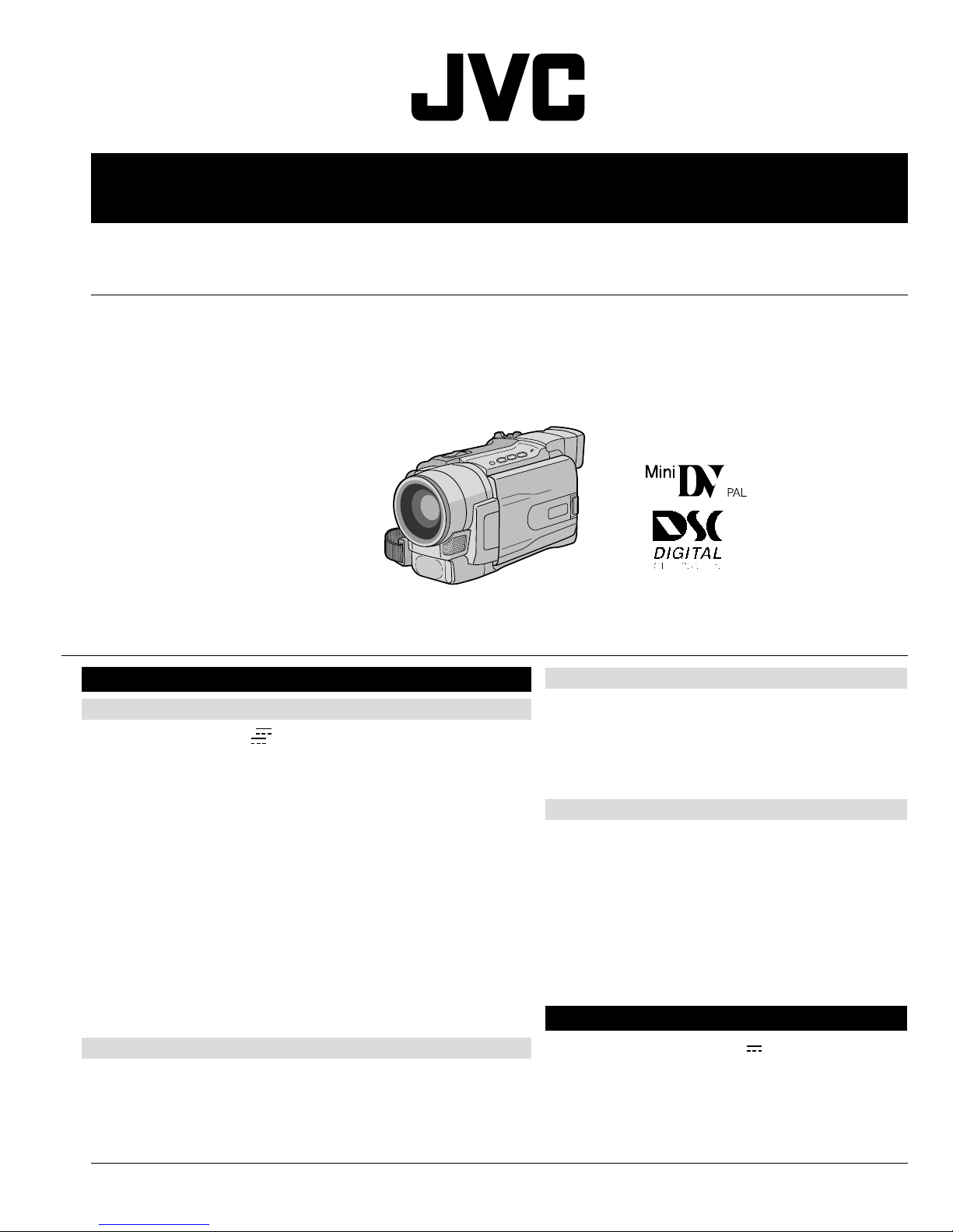
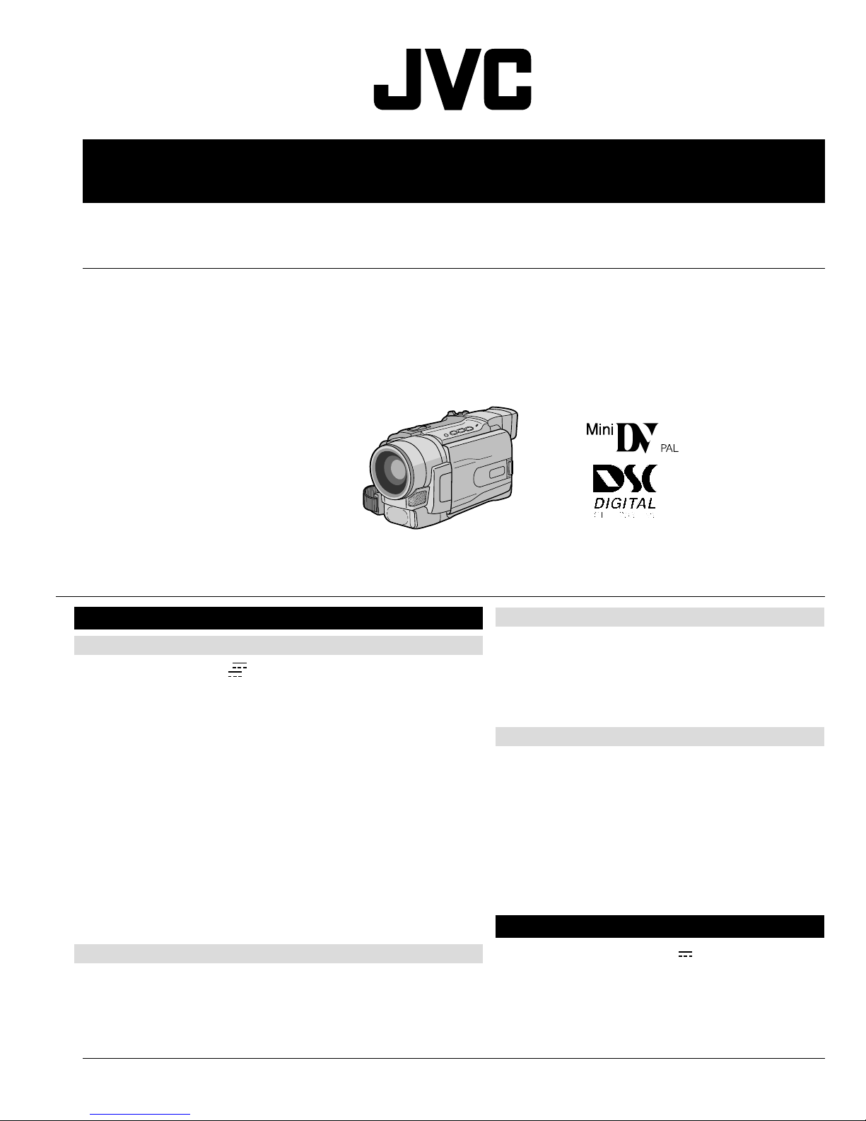
DIGITAL VIDEO CAMERA
GR-DVL820A/EA/SH,
DVL1020A/EA/SH
Regarding service information other than these sections, refer to the GR-DVL765EG service manual (No. 86670).
Also, be sure to note important safety precautions provided in the service manual.
SPECIFICATIONS
(The specifications shown pertain specifically to the model GR-DVL320, DVL520, DVL820, DVL1020)
Camcorder
General
Power supply : DC 11.0 V (Using AC Adapter)
Power consumption
LCD monitor off, viewfinder on
LCD monitor on, viewfinder off
Video light : Approx. 2.8 W (GR-DVL1020/DVL820)
Dimensions (W x H x D) : 79 mm x 89 mm x 184 mm (GR-DVL1020/DVL820)
Weight : Approx. 580 g (GR-DVL1020)
Operating temperature : 0°C to 40°C
Operating humidity : 35% to 80%
Storage temperature : –20°C to 50°C
Pickup : 1/3.8" CCD (GR-DVL1020/DVL820)
Lens : F 1.8, f = 3.8 mm to 38 mm, 10:1 power zoom lens (GR-DVL1020/DVL820)
Filter diameter : ø37 mm
LCD monitor : 3.5" diagonally measured, LCD panel/TFT active matrix system
Viewfinder :
Speaker : Monaural
Format : DV format (SD mode)
Signal format : PAL standard
Recording/Playback format
Cassette : Mini DV cassette
Tape speed : SP: 18.8 mm/s
Maximum recording time : SP: 80 min.
(using 80 min. cassette) LP: 120 min.
DC 7.2 V (Using battery pack)
: Approx. 4.5 W (GR-DVL1020/DVL820)
Approx. 4.3 W (GR-DVL520/DVL320)
: Approx. 5.7 W (GR-DVL1020/DVL820)
Approx. 5.3 W (GR-DVL520/DVL320)
Approx. 3.5 W (GR-DVL520/DVL320)
79 mm x 89 mm x 167 mm (GR-DVL520/DVL320)
(with the LCD monitor closed and the viewfinder pushed down)
Approx. 570 g (GR-DVL820)
Approx. 560 g (GR-DVL520)
Approx. 550 g (GR-DVL320)
1/4" CCD (GR-DVL520/DVL320)
F 1.8, f = 3.6 mm to 36 mm, 10:1 power zoom lens(GR-DVL520/DVL320)
(GR-DVL1020)
2.5" diagonally measured, LCD panel/TFT active matrix system
(GR-DVL820/DVL520/DVL320)
Electronic viewfinder with 0.44" colour LCD (GR-DVL1020)
Electronic viewfinder with 0.24" black/white LCD (GR-DVL820/DVL520/DVL320)
Digital Video Camera
: Video: Digital component recording
:
Audio: PCM digital recording, 32 kHz 4-channel (12-bit), 48 kHz 2-channel (16-bit)
LP: 12.5 mm/s
Digital Still Camera Function (GR-DVL1020/DVL820/DVL520 only)
Storage media : SD Memory Card/MultiMediaCard
Compression system : Still image : JPEG (compatible)
File size : 3 modes (1280 X 960 pixels*, 1024 x 768 pixels,
Picture quality : 2 modes (FINE/STANDARD)
Approximate number of
storable images : 墌 pg. 27.
* GR-DVL1020/DVL820 only.
Moving image* : MPEG4 (compatible)
640 x 480 pixels)
Connectors
S-Video
Output : Y:1 V (p-p), 75 Ω, analogue
Input (GR-DVL1020/DVL820 only)
AV
Video output : 1 V (p-p), 75 Ω, analogue
Video input (GR-DVL1020/DVL820 only)
Audio output : 300 mV (rms), 1 kΩ, analogue, stereo
Audio input (GR-DVL1020/DVL820 only)
DV
Output : 4-pin, IEEE 1394 compliant
Input : 4-pin, IEEE 1394 compliant
USB (GR-DVL1020/DVL820/DVL520 only)
PC (GR-DVL320 only) : ø2.5 mm, 3-pole
EDIT (GR-DVL1020/DVL820/DVL520 only)
JLIP (GR-DVL320 only) : ø3.5 mm, 4-pole
C:0.29 V (p-p), 75 Ω, analogue
: Y:0.8 V (p-p) – 1.2 V (p-p), 75 Ω, analogue
C:0.2 V (p-p) – 0.4 V (p-p), 75 Ω, analogue
: 0.8 V (p-p) – 1.2 V (p-p), 75 Ω, analogue
: 300 mV (rms), 50 kΩ, analogue, stereo
: 5-pin
: ø3.5 mm, 2-pole
AC Adapter
Power requirement : AC 110 V to 240 V`, 50 Hz/60 Hz
Output : DC 11 V , 1 A
Specifications shown are for SP mode unless otherwise indicated. E & O.E.
Design and specifications subject to change without notice.
This service manual is printed on 100% recycled paper.
COPYRIGHT © 2002 VICTOR COMPANY OF JAPAN, LTD.
No. 86683
March 2002
Page 2
TABLE OF CONTENTS
DIFFERENT TABLE................................................................................................................................................................................................... 1 to 2
4. CHARTS AND DIAGRAMS (4-1 to 4-6)
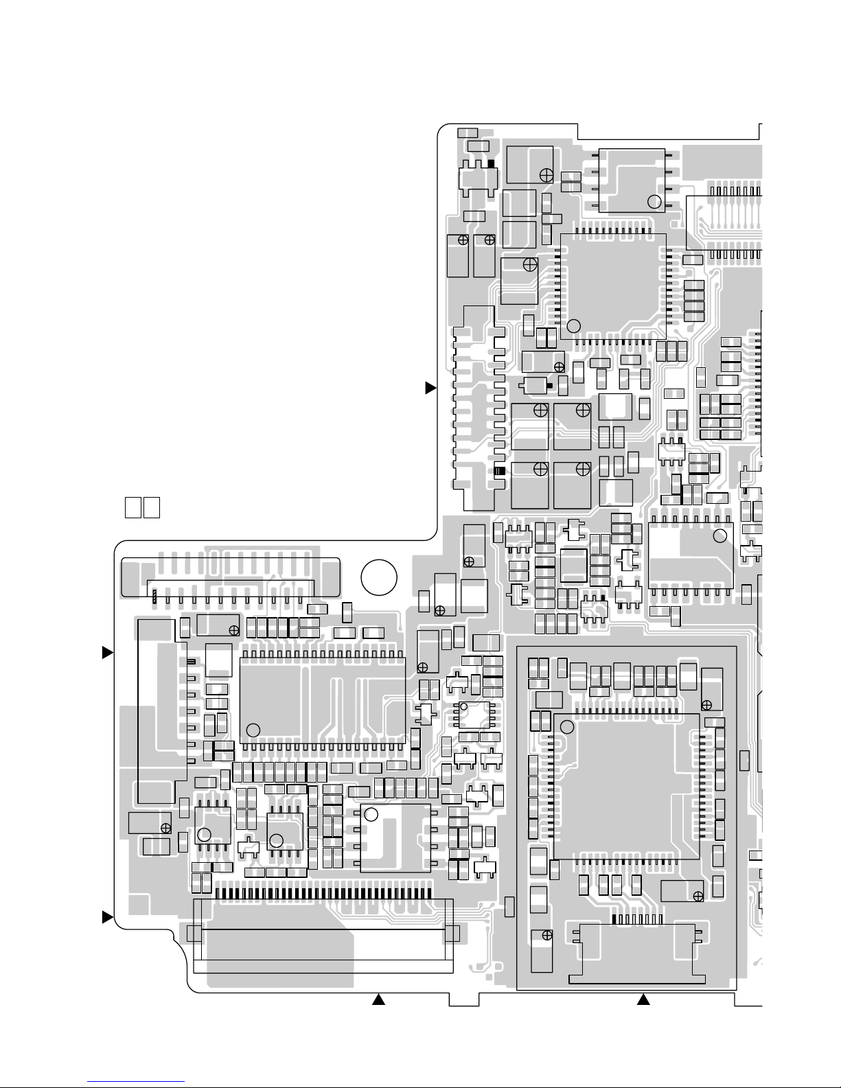
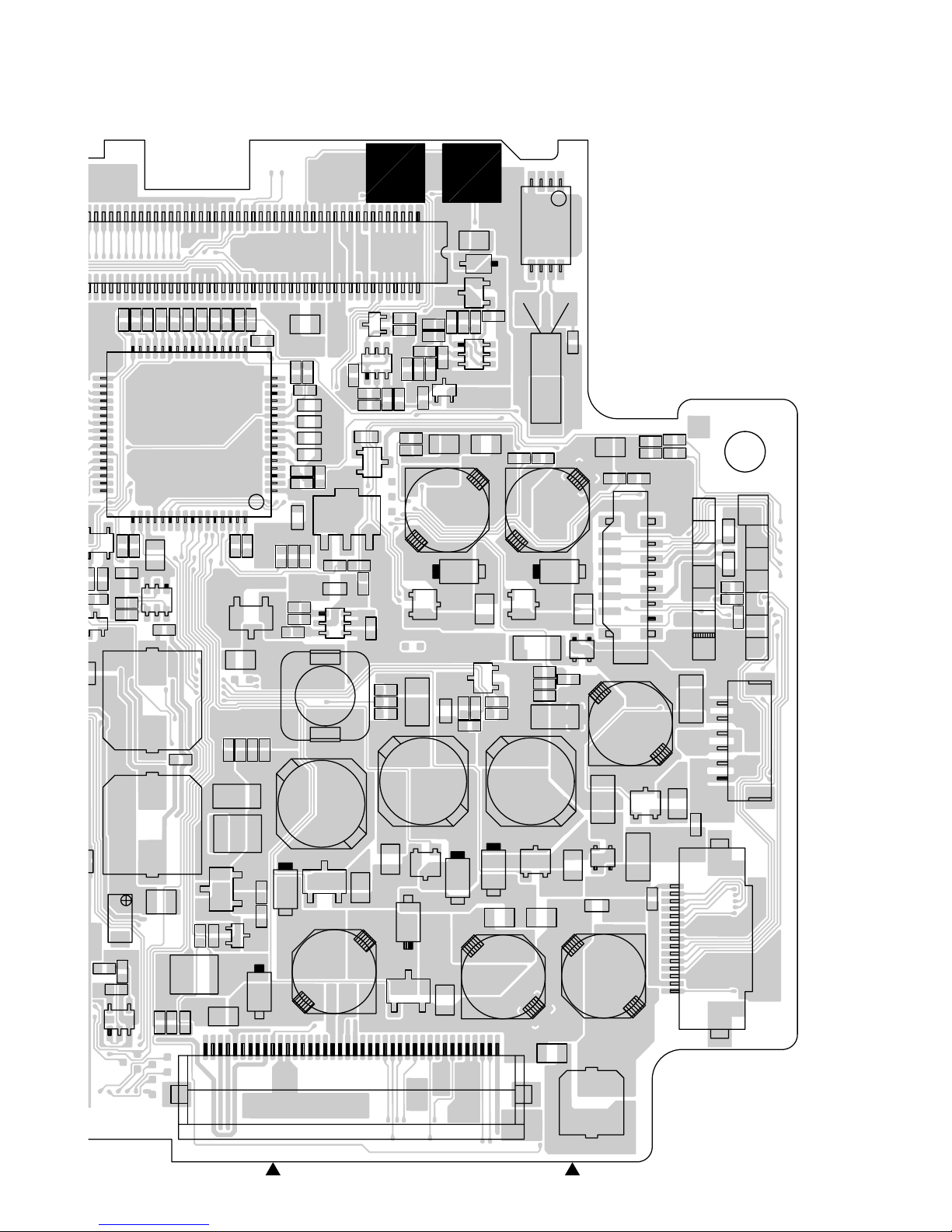
4.1 MAIN CIRCUIT BOARD [GR-DVL1020EA/SH] ....................................................................................................................................................... 4-1
5. PARTS LIST (5-1 to 5-17)
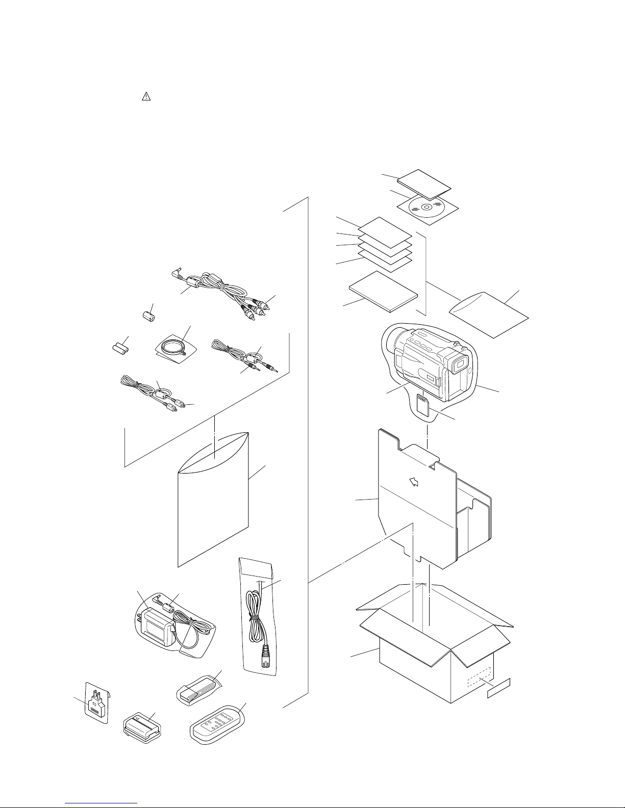
5.1 PACKING AND ACCESSORY ASSEMBLY <M1> ................................................................................................................................................... 5-1
5.2 FINAL ASSEMBLY <M2> ........................................................................................................................................................................................ 5-3
5.3 ELECTRONIC VIEWFINDER ASSEMBLY <M4> [GR-DVL1020A/EA/SH]............................................................................................................. 5-6
5.4 MONITOR ASSEMBLY <M5> [GR-DVL820A/A-S/EA/SH] ..................................................................................................................................... 5-7
5.4 MONITOR ASSEMBLY <M5> [GR-DVL1020A/EA/SH] .......................................................................................................................................... 5-8
5.5 ELECTRICAL PARTS LIST ..................................................................................................................................................................................... 5-9
MAIN BOARD ASSEMBLY <01> ............................................................................................................................................................................ 5-9
The following table indicate main different points between models GR-DVL765EG-X, GR-DVL820A, GR-DVL820A-S,
GR-DVL820EA, GR-DVL820SH, GR-DVL1020A, GR-DVL1020EA and GR-DVL1020SH.
ITEM
LCD MONITOR 2.5” 3.5”
VIEW FINDER B/W COLOR
DV TERMINAL OUTPUT ONLY IN/OUT
TOTAL ZOOM RATIO 500X 700X 700X 700X
MODEL
The following table indicate different parts number between models GR-DVL765EG-X, GR-DVL820A, GR-DVL820A-S,
GR-DV820EA, GR-DVL820SH, GR-DVL1020A, GR-DVL1020EA and GR-DVL1020SH.
PACKING AND ACCESSORY ASSEMBLY <M1> Note: As for IB (INSTRUCTIONS), refer to sec.5.
REF.
!
!
!
ITEM
NO.
1 PACKING CASE LY32567-021A LY32567-017A LY32567-008A LY32567-019A
3 POLY BAG LY30023-008A*LY30023-022A
7 SHEET(AGREMENT) LYT0934-001A ———
8 SHEET(E.UE) LYT0889-010A —————BT-56001-2 —
13 SHEET(CON.PLUG) — LYT0609-001A — — LYT0609-001A — —
14 SER.NET CARD — — — BT-56002-2 — — BT-56002-2 —
26 POWER CORD
29 CONVERSION PLUG — PEMC1012-02 PEMC1012 — QAM0001-001 PEMC1012-02 — QAM0001-001
34 CD ROM ASSY LY32210-023A LY32210-038A
36
CAP(HOOD)ASSY/CAP(M)ASSY
38 WARRANTY CARD BT-54013-2 — — BT-56001-2 — — BT-56001-2 —
39 ADAPTOR PLUG QAM0302-001 ———————
40 CORE FILTER QQR0919-002
MODEL
FINAL ASSEMBLY <M2>
REF.
!
ITEM
NO.
101 UPPER CASE ASSY LY20774-005B
101A TOP COVER LY20775-001A LY20776-001A
101E COVER(SD) LY32375-001A*LY32375-001B
101J
EARTH SHEET/BRAKET(EARTH)
101M SPECIAL SCREW,X2 LY30018-084A LY30018-038A
120 STICKER(SIDE) LY43566-005A LY43566-003A
122 SPACER(A) —
140 LOWER CASE ASSY LY20769-004D LY20769-003E
140B COVER(DC) LY32364-001A*LY32364-001B
144 PLATE(ADJUST) LY43256-001A*LY43256-001B
252 SPACER(A) — — LY30029-0Z7A
MODEL
ELECTRONIC VIEWFINDER ASSEMBLY <M4>
REF.
!
1
ITEM
NO.
300 C.VF ASSY —————LY20838-003A
301
EYE CUP/EYE PIECE ASSY
302
CASE A(VF)/TOP CASE SUB ASSY
303 BOTTOM CASE —————PTY20712-021
304 CAP(VF) LY32351-001A PTY20712-022
305
VF HINGE ASSY/HINGE ASSY
306 LCD MODULE/LCD ASSY QLD0193-001 PTY20712-041
307 FPC QAL0380-002 QAL0287-001
308 SPECIAL SCREW,X4 —————LY30018-063A
309 SPECIAL SCREW,X3 LY30018-0F1A LY30018-055A
310 SPECIAL SCREW,X2 —————LY30018-035A
311 SCREW —————PTY20712-051
321 CASE B(VF) LY20767-001A ———
322 SPECIAL SCREW LY30019-037A ———
323 LEVER(VF) LY43231-001A ———
324 LENS ASSY LY32472-001A ———
324A LENS(A) LY43356-001A ———
324B LENS(B) LY43357-001A ———
325 SPRING(VF) LY43404-001A ———
331 SHEET LY43236-001A ———
332 SHEET2(POLA) LY43246-001A ———
333 HOLDER LCD(VF) LY32347-001A ———
334 SHEET(CUSION) LY43245-001A ———
335 SHEET1(POLA) LY43234-001A ———
336 SHEET(VF) LY43232-001A ———
337 SHEET(DIFF) LY43235-001A ———
338 HOLDER(LED) LY43238-001A ———
339 GUIDE(VF),X2 LY43239-001A ———
340 SPECIAL SCREW,X4 LY30018-060A ———
341 SPACER(A) LY30029-0U6A ———
343 BRACKET(VF) —————LY43827-001A
Notes : Mark is same as left. Mark — is not used. Mark * reference model was also changed.
MODEL
GR-DVL765EG-X GR-DVL820A GR-DVL820A-S GR-DVL820EA GR-DVL820SH GR-DVL1020A GR-DVL1020EA GR-DVL1020SH
GR-DVL765EG-X GR-DVL820A GR-DVL820A-S GR-DVL820EA GR-DVL820SH GR-DVL1020A GR-DVL1020EA GR-DVL1020SH
* * * * * *
QMPL120-190-JR QMPS110-190-JR QMPH020-190-JR QMPL120-190-JR QMPH020-190-JR QMPL120-190-JR
LY43294-002A*LY43322-002A
—
*
GR-DVL765EG-X GR-DVL820A GR-DVL820A-S GR-DVL820EA GR-DVL820SH GR-DVL1020A GR-DVL1020EA GR-DVL1020SH
LY43540-001A*LY32886-001A
LY30029-0Y5A
*
GR-DVL765EG-X GR-DVL820A GR-DVL820A-S GR-DVL820EA GR-DVL820SH GR-DVL1020A GR-DVL1020EA GR-DVL1020SH
LY32349-001A PTY20712-001
LY20766-001A PTY20712-011
LY20824-001B PTY20838-031
* * * * * *
—
*
LY20774-005C
*
* * * * * *
* * *
* * *
* * * * * *
* * * * * *
—
*
* *
—
*
—
*
LY20797-004C
LY32887-001A
—
LY30029-0Y5A
*
—
*
—
*
*
Page 3
MONITOR ASSEMBLY <M5>
REF.
!
ITEM
NO.
500 MONITOR ASSY LYH20246-043B LYH20246-042B
501 MONITOR COVER ASSY LY20863-001B LY20864-001C
501F EARTH MON LY43784-001A LY43785-001A
501G WINDOW(M.MEGA) LY32704-001A LY32704-002A
501H PLATE LY32706-001B LY32707-001B
502 MONITOR CASE ASSY LY20874-001A LY20598-002A
504 HOLDER LY20674-001A LY20568-001A
506 BACK LIGHT QLL0121-001 QLL0123-001
507 LCD MODULE QLD0154-001 QLD0203-001
511 SPACER(A) —
512 SPACER(A) —————LY30029-0Y6A
MODEL
GR-DVL765EG-X GR-DVL820A GR-DVL820A-S GR-DVL820EA GR-DVL820SH GR-DVL1020A GR-DVL1020EA GR-DVL1020SH
LY30029-0Y4A
*
* * *
———
MAIN BOARD ASSEMBLY <01>
REF.
!
ITEM
NO.
PW MAIN BOARD ASSY YB10391QC YB10391PD-01 YB10391QD-03
MODEL
GR-DVL765EG-X GR-DVL820A GR-DVL820A-S GR-DVL820EA GR-DVL820SH GR-DVL1020A GR-DVL1020EA GR-DVL1020SH
MONITOR BOARD ASSEMBLY <02>
REF.
!
ITEM
NO.
PW MONITOR BOARD ASSY YB10360PG-02 YB10360PJ
IC7101 IC(DIGITAL) TC7SH32FU ——
Q7101 TRANSISTOR 2SA1774/QR/-X ——
Q7102 TRANSISTOR 2SC4617/QR/-X ——
R7110 MG RESISTOR NRSA63J-562X ——
R7111 MG RESISTOR NRSA63J-0R0X ——
R7113 MG RESISTOR NRSA63J-0R0X ——
R7114 MG RESISTOR NRSA63J-271X ——
R7116 MG RESISTOR NRSA63J-102X ——
R7604 MG RESISTOR —————NRSA63J-0R0X
R7612 CMF RESISTOR NRVA63D-223X NRSA63D-682X
R7624 CMF RESISTOR —————NRVA63D-223X
R7625 CMF RESISTOR —————NRVA63D-223X
R7626 CMF RESISTOR —————NRVA63D-183X
R7627 CMF RESISTOR —————NRVA63D-334X
R7634 MG RESISTOR —————NRSA63J-0R0X
R7635 MG RESISTOR —————NRSA63J-0R0X
R7636 MG RESISTOR NRSA63J-101X NRSA63J-221X NRSA63J-101X
R7637 MG RESISTOR NRSA63J-101X NRSA63J-221X NRSA63J-101X
R7638 MG RESISTOR NRSA63J-101X NRSA63J-221X NRSA63J-101X
R7640 MG RESISTOR —————NRSA63J-0R0X
R7643 MG RESISTOR —————NRSA63J-0R0X
R7644 MG RESISTOR —————NRSA63J-0R0X
R7645 MG RESISTOR —————NRSA63J-0R0X
R7646 MG RESISTOR —————NRSA63J-0R0X
C7101 CAPACITOR NDC31HJ-221X ———
C7102 CAPACITOR NCF31CZ-104X ———
C7636 CAPACITOR —————NCF31CZ-104X
C7638 CAPACITOR —————NCB21AK-225X
C7639 T CAPACITOR —————NBE21AM-106X
L7605 COIL NQL365K-100X ——
L7606 COIL —————NQL365K-100X
OT2 SPACER — LY43869-001A
MODEL
GR-DVL765EG-X GR-DVL820A GR-DVL820A-S GR-DVL820EA GR-DVL820SH GR-DVL1020A GR-DVL1020EA GR-DVL1020SH
DSC BOARD ASSEMBLY <10>
REF.
!
ITEM
NO.
PW DSC BOARD ASSY YB20931F-01 YB20931D-01
IC8003 IC(MICRO C ROM)
IC8007 IC MM1385EN ———
IC8301 IC —————ISP1181ADGG
Q8001 DIGI TRANSISTOR DTA114EE ———
R8020 MG RESISTOR
R8027 MG RESISTOR NRSA6AJ-152W ———
R8028 MG RESISTOR NRS181J-270X ———
R8029 MG RESISTOR NRS181J-270X ———
R8030 MG RESISTOR NRSA6AJ-105W NRSA6AJ-0R0W
R8031 MG RESISTOR NRSA6AJ-105W NRSA6AJ-0R0W
R8036 MG RESISTOR NRSA6AJ-105W ———
R8056 MG RESISTOR —————NRSA6AJ-0R0W
R8074 MG RESISTOR —————NRSA6AJ-473W
R8302 MG RESISTOR —————NRS181J-220X
R8303 MG RESISTOR —————NRS181J-220X
R8305 MG RESISTOR —————NRSA6AJ-105W
R8306 MG RESISTOR —————NRSA6AJ-103W
R8307 MG RESISTOR —————NRSA6AJ-103W
R8308 MG RESISTOR —————NRSA6AJ-103W
R8309 MG RESISTOR —————NRSA6AJ-103W
R8311 MG RESISTOR —————NRSA6AJ-0R0W
C8027 CAPACITOR NCB30JK-105X ———
C8028 CAPACITOR
C8029 T CAPACITOR NBE20JM-106X ———
C8301 T CAPACITOR —————NBE20JM-106X
C8305 CAPACITOR —————NCBA1AK-104W
C8306 CAPACITOR —————NCBA1AK-104W
C8307 CAPACITOR —————NCBA1AK-104W
C8310 CAPACITOR —————NCBA1AK-104W
C8311 CAPACITOR —————NCBA1AK-104W
L8301 FERRITE BEAD —————NQR0129-002X
X8002 C OSCILLATOR NAX0398-001X ———
X8301 RESONATOR —————NAX0522-001X
MODEL
GR-DVL765EG-X GR-DVL820A GR-DVL820A-S GR-DVL820EA GR-DVL820SH GR-DVL1020A GR-DVL1020EA GR-DVL1020SH
MBV160TE90PTA29 MBV160TE90PTA41
NRSA6AJ-0R0W
NCBA1AK-104W
Notes : Mark is same as left. Mark — is not used. Mark * reference model was also changed.
———
———
2
Page 4

VICTOR COMPANY OF JAPAN, LIMITED
VIDEO DIVISION
S40894
Printed in Japan
Page 5
SCHEMATIC DIAGRAMS
DIGITAL VIDEO CAMERA
GR-DVL820A/EA/SH,
DVL1020A/EA/SH
CD-ROM No.SML200204
Regarding service information other than these sections, refer to the GR-DVL765EG service manual (No. 86670).
Also, be sure to note important safety precautions provided in the service manual.
SPECIFICATIONS
(The specifications shown pertain specifically to the model GR-DVL320, DVL520, DVL820, DVL1020)
Camcorder
General
Power supply : DC 11.0 V (Using AC Adapter)
Power consumption
LCD monitor off, viewfinder on
LCD monitor on, viewfinder off
Video light : Approx. 2.8 W (GR-DVL1020/DVL820)
Dimensions (W x H x D) : 79 mm x 89 mm x 184 mm (GR-DVL1020/DVL820)
Weight : Approx. 580 g (GR-DVL1020)
Operating temperature : 0°C to 40°C
Operating humidity : 35% to 80%
Storage temperature : –20°C to 50°C
Pickup : 1/3.8" CCD (GR-DVL1020/DVL820)
Lens : F 1.8, f = 3.8 mm to 38 mm, 10:1 power zoom lens (GR-DVL1020/DVL820)
Filter diameter : ø37 mm
LCD monitor : 3.5" diagonally measured, LCD panel/TFT active matrix system
Viewfinder :
Speaker : Monaural
Format : DV format (SD mode)
Signal format : PAL standard
Recording/Playback format
Cassette : Mini DV cassette
Tape speed : SP: 18.8 mm/s
Maximum recording time : SP: 80 min.
(using 80 min. cassette) LP: 120 min.
DC 7.2 V (Using battery pack)
: Approx. 4.5 W (GR-DVL1020/DVL820)
Approx. 4.3 W (GR-DVL520/DVL320)
: Approx. 5.7 W (GR-DVL1020/DVL820)
Approx. 5.3 W (GR-DVL520/DVL320)
Approx. 3.5 W (GR-DVL520/DVL320)
79 mm x 89 mm x 167 mm (GR-DVL520/DVL320)
(with the LCD monitor closed and the viewfinder pushed down)
Approx. 570 g (GR-DVL820)
Approx. 560 g (GR-DVL520)
Approx. 550 g (GR-DVL320)
1/4" CCD (GR-DVL520/DVL320)
F 1.8, f = 3.6 mm to 36 mm, 10:1 power zoom lens(GR-DVL520/DVL320)
(GR-DVL1020)
2.5" diagonally measured, LCD panel/TFT active matrix system
(GR-DVL820/DVL520/DVL320)
Electronic viewfinder with 0.44" colour LCD (GR-DVL1020)
Electronic viewfinder with 0.24" black/white LCD (GR-DVL820/DVL520/DVL320)
Digital Video Camera
: Video: Digital component recording
:
Audio: PCM digital recording, 32 kHz 4-channel (12-bit), 48 kHz 2-channel (16-bit)
LP: 12.5 mm/s
Digital Still Camera Function (GR-DVL1020/DVL820/DVL520 only)
Storage media : SD Memory Card/MultiMediaCard
Compression system : Still image : JPEG (compatible)
File size : 3 modes (1280 X 960 pixels*, 1024 x 768 pixels,
Picture quality : 2 modes (FINE/STANDARD)
Approximate number of
storable images : 墌 pg. 27.
* GR-DVL1020/DVL820 only.
Moving image* : MPEG4 (compatible)
640 x 480 pixels)
Connectors
S-Video
Output : Y:1 V (p-p), 75 Ω, analogue
Input (GR-DVL1020/DVL820 only)
AV
Video output : 1 V (p-p), 75 Ω, analogue
Video input (GR-DVL1020/DVL820 only)
Audio output : 300 mV (rms), 1 kΩ, analogue, stereo
Audio input (GR-DVL1020/DVL820 only)
DV
Output : 4-pin, IEEE 1394 compliant
Input : 4-pin, IEEE 1394 compliant
USB (GR-DVL1020/DVL820/DVL520 only)
PC (GR-DVL320 only) : ø2.5 mm, 3-pole
EDIT (GR-DVL1020/DVL820/DVL520 only)
JLIP (GR-DVL320 only) : ø3.5 mm, 4-pole
C:0.29 V (p-p), 75 Ω, analogue
: Y:0.8 V (p-p) – 1.2 V (p-p), 75 Ω, analogue
C:0.2 V (p-p) – 0.4 V (p-p), 75 Ω, analogue
: 0.8 V (p-p) – 1.2 V (p-p), 75 Ω, analogue
: 300 mV (rms), 50 kΩ, analogue, stereo
: 5-pin
: ø3.5 mm, 2-pole
AC Adapter
Power requirement : AC 110 V to 240 V`, 50 Hz/60 Hz
Output : DC 11 V , 1 A
Specifications shown are for SP mode unless otherwise indicated. E & O.E.
Design and specifications subject to change without notice.
This schematic diagrams is printed on 100% recycled paper.
COPYRIGHT © 2002 VICTOR COMPANY OF JAPAN, LTD.
No. 86683SCH
March 2002
Page 6
1
C
C
C
0
R
3
7
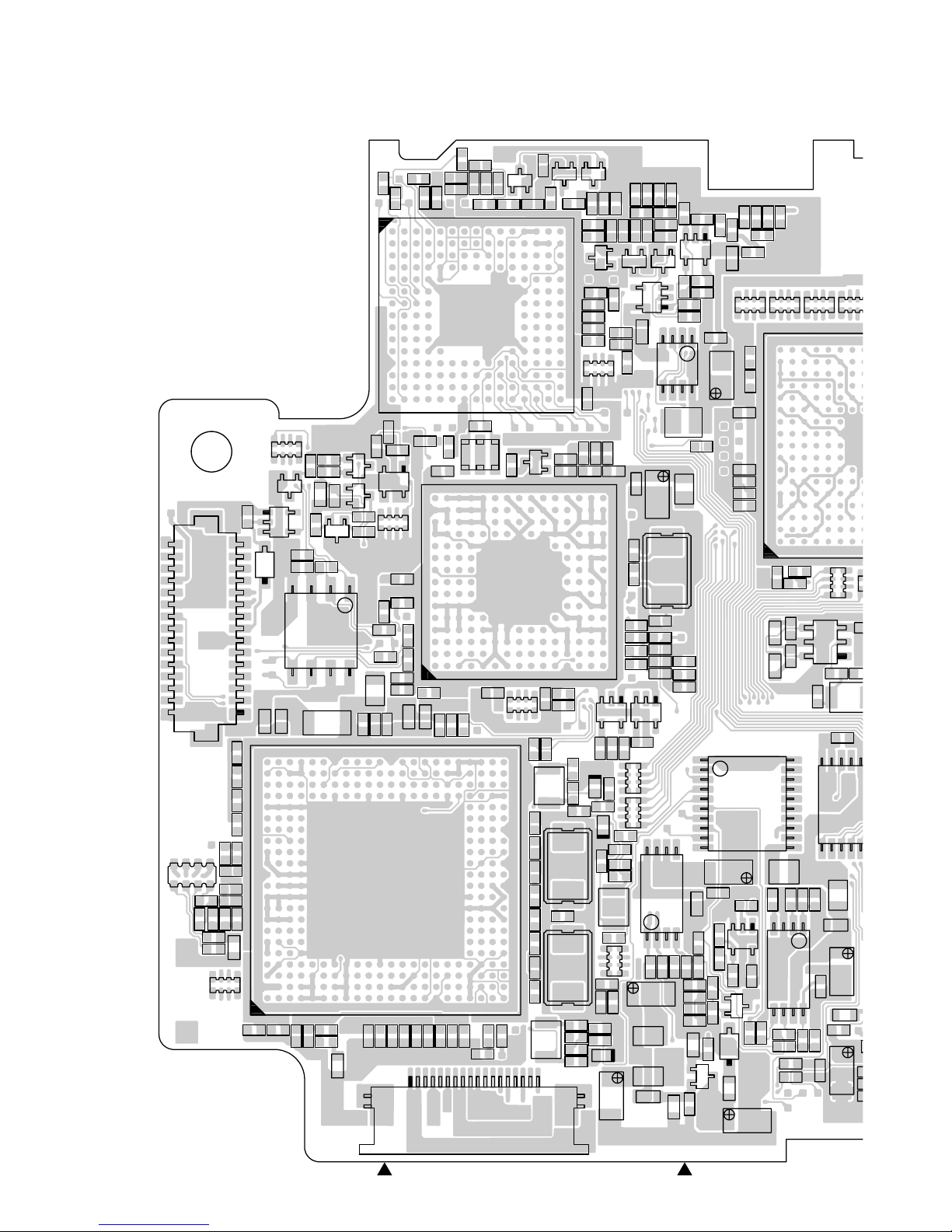
4.1 MAIN CIRCUIT BOARD
[GR-DVL1020EA/SH]
RA1010
R1016
R1052
R1051
Q1004
C1031
R1026
1
5
TL1420
30
3
15
D1002
IC1007
4
R1066
C1007
R1056
R1018
4
CN105
IC1003
TL1410
TL1408
5
16
TL3006
RA3005
R3018
R3019
TG3
R3016
R3017
R3013
RA3004
C3027
C3029
R3020
C3028
R3014
1
C3047
C3050
C3042C3043
R3015
C3055
C3026
C3045 C3046
L3002
C3003
C3044
C3049
C3007
R3036
R3037
5
4-1
SECTION 4
CHARTS AND DIAGRAM
FOIL SIDE(B)
R1006
TL1038
TL1001 TL1002TL1003
C1036
R1001
C1026
23
D1001
IC1008
R1054
Q1001
R1055
Q1002
R1053
RA1008
1
R1407
R1417
TL1409
TL1411
R1022
L3005
8
C3038
C3040
C3041
IC3001
C3011
C3012
C3021
C3048
R1003
R1083
R1015
R1060
R1011
R1058
C1034
C1039
R1057
TL1036
C1407
R1404
TL1405
R1415
R1416
R1012
R1080
IC1001
R1037
TL1009TL1027 TL1029TL1030 TL1031TL1032TL1033 TL1034
R1039
R1072
14
R1020R1021
R1406
C3004
L3003
C3020
R3002
C3015
C1406
C3025
C3016
C3039
R3004
R3059
TL1414
C3031
X1001
R3008
C1404
R3007
TL3005
118
CN112
R1071
R1036
R3057
R1405
RA1401
TL3001
Q1009
C1038
IC1401
Q1401
R3005
C3017
C3013
C3036
R3032 R3034
C3058
R3047R3048
4
R1014
C1405
R3006
L3008
L3007
R1009
R1426
R1425
C3037
Q1005
C1409
C1013
TL1401TL1402
C3032 C3033
C3064
X3001X3002
C3023
R3009
R3011
C3024
C1017
C1015
TL1004
R1079
R1082
R1030
R1081
R1078
RA1009
C1037
R1408
R1409
Q1008
C1014
Q1003
TL1007
C1411
D3002
R3030
C3022
R3010
D3001
C1009
TL1005
C1410
R1421R1422
R1423
D3003
C3035
R3027
R3071
C3057
C1011
C1016
R1077
R1007
R1002
Q1403
R1626
C3030
R3033
R3031
C3034
L3009
RA3003
R3051
C3005
R1005
R1076
TL1035
TL1407
TL1404
TL1403
TL3501
R1625
R3029
4
5
R1403
R1411
R1412
R1413
RA3001 RA3002
R1049
R1050
C1030
R1044 R1045
C1019
C1027
R1047
R1029
Q1006
Q1007
IC1005
C1021
451
C1403
C1408
C1402
R1401
C1401
R1402
C1412
C1413
C1414
Q1402
R1410
TL3002
IC3005
R3066
R3067
C3008
L3006
L3004
L3012
C1029
R1019
R1038
R1008
R1027
14
23
IC1004
C1020
R1028
R1024
3
R1032
R1031
1
R1010
C1004
IC1009
C1003
8
L1401
R1061
TL4313
TL4311
TL4315
TL4309
X1401
TL1406
L1002
C1416
R1414
C1415
110
TL3004
58
C3059
C3066
C3060
34
R3003
R3072
41
R3050
C3067
R3068
C3068
R3049
R3073 R3074
C3069
C3070
Q3002
R3075
R3069
C3006
D3004
R3025
L3001
Q3001
R3026
C3009
R1004
R1048
C1010
C1028
R1046
R1023
RA4304
R4305
R4321
TL4312
C4310
TL4310
TL4314
C4311
R4311
C4317
C4312
C4318
R4308
C4313
R3742 R3743
C3740 C3741
4
6
20 11
IC3002
L3014
R3040
R3041
R3042 R3043
C3014
15
IC3004
C3061
R3046
C3001
R3045
IC3007
R3070
R3044
R1610
R1611
TL1601
14
85
TL1612TL1613TL1617
IC3731
C3743
10
11
C3051 C3052
C3053
C1642
R3744
C1023
C3054
R1622
RA430RA4302RA4303
RA4305
L3732
L3015
C3056
C1621
C1632
3
3
1
TL16
C
C3
IC
Page 7
2
A4301
IC4301
3
4
C4303
R4320
1
IC4302
5
L4301 L4302L4305
C4302
C4314
R4302
C4301
C4315
C4304
3
4
C4306
IC4303
C4309
1
5
C4307
TL4304
R4316
R4205
R4204
RA4201RA4202
TL4317
TL4308
TL4318
R4317
C4305
L4303
TL4306
121
TL4305
TL4319
3
C4308
1348
C4206
IC4202
1
L4201
C4205
C4207 C4208
C4219
C4218
IC4201
C4204
2437
C4203
C4201
C4202
TL4202
C4215
2536
C4209
TG4
C4217
C4216
C4210
C4214
R4203
C4213
C4212
TL4201
C4220
A
C4211
R4201
RA4307RA4308
R4306
R4307
R4310
3
1
C3744
32
3
RA4306
C3742
R3746
C3747
R3745
C3746
Q3735
C3745
R3748
R3747
TL3802
TL3801
R4313
TL4316
3
R4303
R3807
R3808
IC3802
R4314
R4315
1
R4304
R4312
R4309
R4301
C3819
C3805
1
5
4
IC1006
IC1602
20
TL1611
TL1603
R3809
C1614
16
C3820
Q3704
R3724
R1609
D1602
C1601
Q3703
R4301
C3807
R3723
R1614
R1605
C3806
R1617
TL1614
17
C1620
C1619
C1618
R1613
R1612
1
L1602
D1604
C1622
C1623
C1607
R1616
R1630
32
R1631
33
C1624
IC1601
C3817
IC3801
R3801
R1618
1
48
L3802
R3721
R3722
R1615
C3814
R1602
C3808
C1641
TL1604
X4301
R3806
C3802
64
49
R1601
R1629
R1621
R3802
C3809
R1624
C1627
R1628
R1620
C1606
R1604
C1633
D1603
C3801
R3705
C3704
R3704
R1635R1637
C1628
C3818
C3816
C3815
C3812
C3810
C3811
R3701
R3805
C3813
R3702
C3702
C1605
R1603
C1602
C1603
Q3701
C1625
C1626
R1619
R1643
L3801
C3705
Q1601
C4316
L4304
C3703
R1636
L3803
L3804
R3803
R3804
R2012
C2501
C2502
C2503
C2515
C2514
R2513
R2010
Q2501
R2006
R2014
R2015
R2016
R2013
R2011
C2001
C2011
C3803
C3804
169
R2510 R2511
C2516
C2006
C2007
R2009
R2018
C2026
C2010
R2509
R2512
C2008
Q2001
B
C2517
R2007R2008
C2016
17
32
C2009
IC2501
C2021
R2025
C2017
R2023
C2020
R2024
16
33
C2027
R2028
C2028
C2003
18
C2019
R2001
C2015
C2504 C2505
C2018
R2020
C2014
IC2001
R2019
C2013
R2506
C2511
R2004R2005
0 1 MAIN PWB
YB10391-01-01
L2501
C2508
R2501
R2502
R2503
R2504
R2505
C2510
C2004
C2005
C2127
L2002
C2512
C2513
R2507
C2506
R2119
C2125
R2508
C2126
R2120 R2121
Q2102
1
48
C2121
R2125
C2507
C2128
R2122
R2105
C2123
R2029
R2128
C2124
C2122
R2123
C2509
C2120
C2119
R2111
C2115
Q2101
R2126
R2124
R2114
R2112
64
49
R2103
R2107
C2118
R2116R2118
C2110
C2112
C2111
C2109
C2105
R2109
R2113
R2117
R2127
L2001
C2002
C2116
R2203
R2108
R2106
R2104
C2106
C2113
R2115
C2117
C2104
R2110
Q2002
124
C2114
R2129
R2017
C2103
C2108
C2107
CN102
C
C2024
Q2103
C2025
C2012
D
12
4-2
Page 8
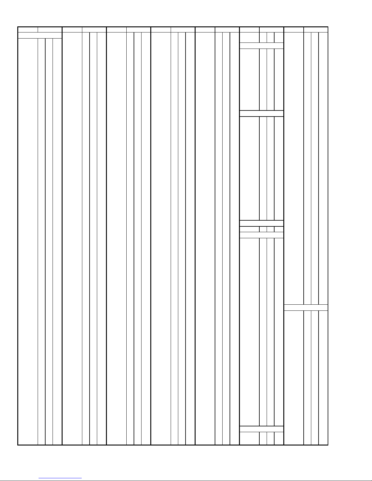
COMPONENT PARTS LOCATION GUIDE <MAIN/YB10391-01-01> (1/2)
REF.NO. LOCATION REF.NO. LOCATION REF.NO. LOCATION REF.NO. LOCATION REF.NO. LOCATION REF.NO. LOCATION REF.NO. LOCATION
CAPACITOR
C1003 B C 3A
C1004 B C 3A
C1006 A C 5A
C1007 B C 5B
C1009 B C 4A
C1010 B C 3A
C1011 B C 4A
C1013 B C 4A
C1014 B C 4A
C1015 B C 4A
C1016 B C 4A
C1017 B C 4A
C1019 B C 4A
C1020 B C 3A
C1021 B C 4A
C1023 B C 3B
C1026 B C 4B
C1027 B C 4A
C1028 B C 3A
C1029 B C 4A
C1030 B C 4A
C1031 B C 5B
C1034 B C 4A
C1036 B C 4A
C1037 B C 4A
C1038 B C 4A
C1039 B C 4A
C1401 B C 4B
C1402 B C 4B
C1403 B C 4B
C1404 B C 4B
C1405 B C 4B
C1406 B C 4B
C1407 B C 4B
C1408 B C 4B
C1409 B C 4B
C1410 B C 4B
C1411 B C 4B
C1412 B C 4B
C1413 B C 4B
C1414 B C 4B
C1415 B C 4B
C1416 B C 4B
C1601 B C 2C
C1602 B C 2D
C1603 B C 2D
C1605 B C 2C
C1606 B C 2C
C1607 B C 3D
C1614 B C 3C
C1618 B C 3C
C1619 B C 3C
C1620 B C 3C
C1621 B C 3C
C1622 B C 3D
C1623 B C 3D
C1624 B C 3D
C1625 B C 2C
C1626 B C 2C
C1627 B C 2C
C1628 B C 2D
C1632 B C 3D
C1633 B C 2C
C1641 B C 2C
C1642 B C 3D
C2001 B C 2C
C2002 B C 1B
C2003 B C 1D
C2004 B C 1C
C2005 B C 1C
C2006 B C 2C
C2007 B C 2C
C2008 B C 2C
C2009 B C 2C
C2010 B C 2C
C2011 B C 2C
C2012 B C 1C
C2013 B C 1D
C2014 B C 1D
C2015 B C 1D
C2016 B C 2C
C2017 B C 2C
C2018 B C 1C
C2019 B C 1C
C2020 B C 2C
C2021 B C 2C
C2024 B C 1C
C2025 B C 1C
C2026 B C 2C
C2027 B C 2D
C2028 B C 1D
C2103 B C 1D
C2104 B C 1C
C2105 B C 1C
C2106 B C 1C
C2107 B C 1C
C2108 B C 1C
C2109 B C 1C
C2110 B C 1C
C2111 B C 1C
C2112 B C 1C
C2113 B C 1C
C2114 B C 1C
C2115 B C 1D
C2116 B C 1C
C2117 B C 1D
C2118 B C 1C
C2119 B C 1D
C2120 B C 1C
C2121 B C 1D
C2122 B C 1C
C2123 B C 1D
C2124 B C 1C
C2125 B C 1D
C2126 B C 1C
C2127 B C 1D
C2128 B C 1C
C2201 A C 1C
C2202 A C 1C
C2501 B C 2B
C2502 B C 2B
C2503 B C 2C
C2504 B C 1C
C2505 B C 1C
C2506 B C 1C
C2507 B C 1C
C2508 B C 1B
C2509 B C 1B
C2510 B C 1C
C2511 B C 1C
C2512 B C 1B
C2513 B C 1B
C2514 B C 2C
C2515 B C 2C
C2516 B C 2C
C2517 B C 2C
C3001 B C 3D
C3003 B C 5B
C3004 B C 4B
C3005 B C 4D
C3006 B C 3D
C3007 B C 5B
C3008 B C 4C
C3009 B C 4D
C3011 B C 5C
C3012 B C 4C
C3013 B C 4C
C3014 B C 3C
C3015 B C 4C
C3016 B C 4C
C3017 B C 4C
C3020 B C 4C
C3021 B C 5C
C3022 B C 4C
C3023 B C 4C
C3024 B C 4D
C3025 B C 4B
C3026 B C 5C
C3027 B C 5C
C3028 B C 5C
C3029 B C 5C
C3030 B C 4C
C3031 B C 4C
C3032 B C 4C
C3033 B C 4C
C3034 B C 4C
C3035 B C 4C
C3036 B C 4C
C3037 B C 4C
C3038 B C 5B
C3039 B C 4B
C3040 B C 4B
C3041 B C 5B
C3042 B C 5C
C3043 B C 5C
C3044 B C 5C
C3045 B C 5C
C3046 B C 5C
C3047 B C 5C
C3048 B C 5D
C3049 B C 5C
C3050 B C 5C
C3051 B C 3C
C3052 B C 3D
C3053 B C 3C
C3054 B C 3C
C3055 B C 5C
C3056 B C 3C
C3057 B C 4C
C3058 B C 4C
C3059 B C 3C
C3060 B C 3C
C3061 B C 3C
C3064 B C 4C
C3066 B C 3C
C3067 B C 4C
C3068 B C 3C
C3069 B C 3C
C3070 B C 3C
C3501 A C 3C
C3502 A C 3C
C3503 A C 2D
C3504 A C 2C
C3505 A C 2C
C3506 A C 2C
C3507 A C 2C
C3508 A C 2C
C3509 A C 2C
C3510 A C 2C
C3511 A C 3C
C3512 A C 3C
C3513 A C 3C
C3514 A C 3C
C3515 A C 3C
C3516 A C 3C
C3517 A C 3C
C3518 A C 3C
C3519 A C 3C
C3520 A C 3C
C3521 A C 2C
C3522 A C 2C
C3523 A C 2C
C3524 A C 2C
C3525 A C 2C
C3526 A C 2C
C3527 A C 3C
C3528 A C 3C
C3701 A C 3C
C3702 B C 2C
C3703 B C 2C
C3704 B C 2C
C3705 B C 2C
C3706 A C 3B
C3707 A C 3B
C3708 A C 3B
C3709 A C 3B
C3712 A C 3C
C3713 A C 3B
C3714 A C 3B
C3715 A C 2B
C3731 A C 2B
C3732 A C 2B
C3733 A C 2B
C3734 A C 2B
C3735 A C 2B
C3736 A C 2B
C3737 A C 2B
C3738 A C 2B
C3739 A C 2B
C3740 B C 3B
C3741 B C 3B
C3742 B C 3B
C3743 B C 3B
C3744 B C 3B
C3745 B C 3B
C3746 B C 3B
C3747 B C 3B
C3801 B C 2B
C3802 B C 2B
C3803 B C 2B
C3804 B C 2B
C3805 B C 2B
C3806 B C 2C
C3807 B C 2C
C3808 B C 2C
C3809 B C 2C
C3810 B C 2B
C3811 B C 2B
C3812 B C 2B
C3813 B C 2C
C3814 B C 2B
C3815 B C 2B
C3816 B C 2B
C3817 B C 2B
C3818 B C 2B
C3819 B C 2B
C3820 B C 3C
C4201 B C 2A
C4202 B C 2A
C4203 B C 2A
C4204 B C 2A
C4205 B C 2A
C4206 B C 2B
C4207 B C 2B
C4208 B C 2B
C4209 B C 2B
C4210 B C 2B
C4211 B C 2A
C4212 B C 2A
C4213 B C 2A
C4214 B C 2A
C4215 B C 2A
C4216 B C 2A
C4217 B C 2A
C4218 B C 2A
C4219 B C 2A
C4220 B C 2A
C4301 B C 3A
C4302 B C 3A
C4303 B C 3A
C4304 B C 3A
C4305 B C 2A
C4306 B C 3A
C4307 B C 2A
C4308 B C 2A
C4309 B C 2A
C4310 B C 3A
C4311 B C 3B
C4312 B C 3B
C4313 B C 3B
C4314 B C 3A
C4315 B C 3A
C4316 B C 2B
C4317 B C 3B
C4318 B C 3B
C4803 A C 1C
C4804 A C 1C
C4806 A C 1C
C4807 A C 1C
C4808 A C 1C
C4809 A C 1C
C4810 A C 1C
C4811 A C 1C
C4812 A C 1C
C4813 A C 1C
C4814 A C 2C
C4815 A C 1C
C4819 A C 2C
C4820 A C 1C
C4822 A C 1C
C4823 A C 2C
C4851 A C 2B
C4852 A C 2B
C4853 A C 2B
C4854 A C 2B
C4855 A C 2B
C4858 A C 1C
C4859 A C 1C
C4860 A C 1C
C4861 A C 1C
C4862 A C 1C
C4863 A C 1C
C4864 A C 1B
C4865 A C 1B
C4866 A C 1B
C5001 A C 2A
C5002 A C 2A
C5003 A C 2A
C5004 A C 2A
C5005 A C 2A
C5006 A C 2A
C5007 A C 2A
C5008 A C 2A
C5009 A C 2A
C5010 A C 2A
C5011 A C 2A
C5012 A C 3A
C5013 A C 3A
C5014 A C 3A
C5015 A C 2B
C5016 A C 2B
C5017 A C 2B
C5018 A C 2B
C5019 A C 2B
C5020 A C 2B
C5021 A C 2B
C5022 A C 2B
C5023 A C 2A
C5024 A C 2A
C5025 A C 2A
C5026 A C 2A
C5027 A C 2A
C5028 A C 2A
C6001 A C 3B
C6004 A C 4B
C6005 A C 4B
C6101 A C 4C
C6102 A C 5D
C6103 A C 4C
C6105 A C 4D
C6106 A C 4B
C6107 A C 4A
C6108 A C 4A
C6109 A C 4A
C6110 A C 3A
C6111 A C 3A
C6112 A C 3A
C6113 A C 3A
C6114 A C 3A
C6115 A C 3A
C6116 A C 3A
C6117 A C 3A
C6118 A C 3A
C6119 A C 3A
C6120 A C 3A
C6121 A C 3B
C6122 A C 3B
C6123 A C 3B
C6124 A C 3B
C6125 A C 3B
C6126 A C 3B
C6127 A C 3B
C6128 A C 3B
C6129 A C 3B
C6130 A C 4B
C6131 A C 5B
C6132 A C 5C
C6134 A C 4B
C6201 A C 5C
C6202 A C 4B
C6203 A C 4B
C6204 A C 4B
C6205 A C 4B
C6206 A C 4C
C6207 A C 4B
C6208 A C 4B
C6209 A C 4C
C6210 A C 3C
C6211 A C 3C
C6212 A C 3B
C6213 A C 4B
C6214 A C 5B
C6215 A C 5B
C6216 A C 5B
C6217 A C 4B
C6218 A C 4B
C6219 A C 4B
C6220 A C 5C
C6221 A C 5C
C6222 A C 5C
C6224 A C 4A
C6225 A C 4A
C6226 A C 4A
C6227 A C 5B
C6228 A C 4B
C6230 A C 4A
C6231 A C 1C
C6701 A C 4C
C6703 A C 3C
C6704 A C 3C
CONNECTOR
CN101 A C 3D
CN102 B C 1C
CN103 A C 5B
CN104 A C 5C
CN105 B C 5B
CN106 A C 1C
CN107 A C 2B
CN108 A C 1B
CN109 A C 5C
CN110 A C 2D
CN111 A C 4A
CN112 B C 4D
CN113 A C 1C
DIODE
D1001 B C 5B
D1002 B C 5B
D1602 B C 2C
D1603 B C 2C
D1604 B C 3D
D3001 B C 4D
D3002 B C 4C
D3003 B C 4C
D3004 B C 3D
D3701 A C 2B
D5001 A C 2A
D6002 A C 4B
D6201 A C 4C
D6202 A C 4C
D6203 A C 4C
D6204 A C 4B
D6205 A C 4B
D6206 A C 5C
D6207 A C 4A
D6208 A C 5B
D6701 A C 3C
D6702 A C 4C
FUSE
F6101 A C 5C
IC
IC1001 B C 4A
IC1002 A C 4A
IC1003 B C 5B
IC1004 B C 3A
IC1005 B C 4A
IC1006 B C 3C
IC1007 B C 5B
IC1008 B C 4B
IC1009 B C 4A
IC1401 B C 4B
IC1601 B C 2C
IC1602 B C 3C
IC2001 B C 1C
IC2501 B C 2C
IC3001 B C 4C
IC3002 B C 3C
IC3004 B C 3C
IC3005 B C 4C
IC3007 B C 3C
IC3501 A C 2C
IC3502 A C 3C
IC3701 A C 3B
IC3731 B C 3B
IC3801 B C 2B
IC3802 B C 3C
IC4201 B C 2A
IC4202 B C 2A
IC4301 B C 3B
IC4302 B C 3A
IC4303 B C 2A
IC4802 A C 1C
IC4803 A C 1C
IC4804 A C 2C
IC4807 A C 2C
IC4851 A C 1C
IC5001 A C 2A
IC5002 A C 2A
IC5003 A C 2A
IC6001 A C 3B
IC6101 A C 3A
COIL
L1002 B C 4A
L1401 B C 4B
L2001 B C 1B
L2002 B C 1D
L2101 A C 1C
L2102 A C 1C
L2103 A C 1C
L2501 B C 1B
L3001 B C 3D
L3002 B C 5B
L3003 B C 4B
L3004 B C 4D
L3005 B C 5B
L3006 B C 4C
L3007 B C 4D
L3008 B C 4C
L3009 B C 4C
L3012 B C 4D
L3014 B C 3C
L3015 B C 3C
L3501 A C 3C
L3502 A C 3C
L3503 A C 2B
L3504 A C 2C
L3505 A C 2C
L3701 A C 3C
L3731 A C 2B
L3732 B C 3B
L3801 B C 2B
L3802 B C 2B
L3803 B C 2B
L3804 B C 2B
L4201 B C 2A
L4301 B C 3A
L4302 B C 2A
L4303 B C 2A
L4304 B C 2B
L4305 B C 3A
L4802 A C 1C
L4851 A C 2B
L4852 A C 2B
L4853 A C 1C
L5001 A C 2A
L5002 A C 2A
L5003 A C 2A
L5004 A C 2B
L5005 A C 2B
L5006 A C 2B
L5007 A C 3B
L6101 A C 5C
L6102 A C 4C
L6201 A C 4C
L6202 A C 4C
L6203 A C 4C
L6204 A C 3C
L6205 A C 4B
L6206 A C 4B
L6207 A C 4B
L6208 A C 5B
L6701 A C 4C
TRANSISTOR
Q1001 B C 5B
Q1002 B C 5B
Q1003 B C 4A
Q1004 B C 5B
Q1005 B C 4A
Q1006 B C 4A
Q1007 B C 4A
Q1008 B C 4A
Q1009 B C 4A
Q1401 B C 4B
Q1402 B C 4B
Q1403 B C 4B
Q1601 B C 2C
Q2001 B C 2D
Q2002 B C 1C
Q2101 B C 1D
Q2102 B C 1C
Q2103 B C 1C
Q2501 B C 2C
Q3001 B C 3D
Q3002 B C 3C
Q3701 B C 2C
Q3702 A C 3B
Q3703 B C 2C
Q3704 B C 3C
Q3705 A C 2B
Q3731 A C 2B
Q3732 A C 2B
4-3
Page 9
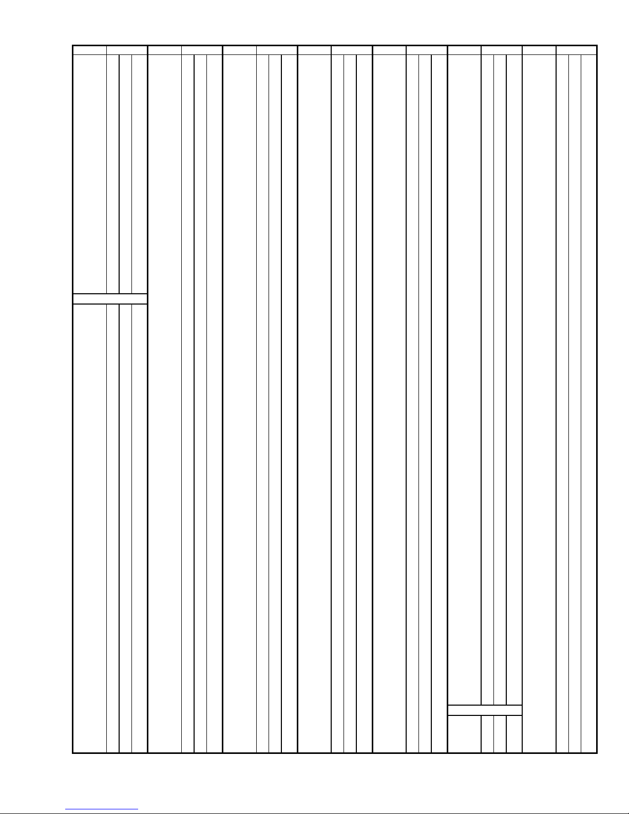
COMPONENT PARTS LOCATION GUIDE <MAIN/YB10391-01-01> (2/2)
REF.NO. LOCATION REF.NO. LOCATION REF.NO. LOCATION REF.NO. LOCATION REF.NO. LOCATION REF.NO. LOCATION REF.NO. LOCATION
Q3733 A C 2B
Q3734 A C 2B
Q3735 B C 3B
Q4801 A C 1C
Q4802 A C 2C
Q4803 A C 2C
Q4804 A C 2C
Q4805 A C 2C
Q4806 A C 2C
Q4851 A C 2C
Q6001 A C 3B
Q6002 A C 3B
Q6004 A C 4B
Q6201 A C 4C
Q6202 A C 4B
Q6203 A C 4C
Q6204 A C 4C
Q6205 A C 3C
Q6206 A C 3C
Q6207 A C 3B
Q6208 A C 4B
Q6210 A C 4B
Q6211 A C 5C
Q6212 A C 4A
Q6213 A C 4A
Q6214 A C 4A
Q6215 A C 4A
Q6216 A C 4A
Q6217 A C 4B
Q6701 A C 4C
RESISTOR
R101 A C 5B
R102 A C 5B
R1001 B C 5B
R1002 B C 4A
R1003 B C 4A
R1004 B C 3A
R1005 B C 4A
R1006 B C 5A
R1007 B C 4A
R1008 B C 3A
R1009 B C 4A
R1010 B C 3A
R1011 B C 4A
R1012 B C 4A
R1014 B C 4A
R1015 B C 4A
R1016 B C 5B
R1017 A C 5C
R1018 B C 5B
R1019 B C 4A
R1020 B C 4B
R1021 B C 4B
R1022 B C 4B
R1023 B C 3A
R1024 B C 3A
R1026 B C 5B
R1027 B C 3A
R1028 B C 4A
R1029 B C 4A
R1030 B C 4A
R1031 B C 3A
R1032 B C 3A
R1036 B C 4A
R1037 B C 4A
R1038 B C 3A
R1039 B C 4B
R1044 B C 4A
R1045 B C 4A
R1046 B C 3A
R1047 B C 4A
R1048 B C 3A
R1049 B C 4A
R1050 B C 4A
R1051 B C 5B
R1052 B C 5B
R1053 B C 5B
R1054 B C 5B
R1055 B C 5B
R1056 B C 5B
R1057 B C 4A
R1058 B C 4A
R1060 B C 4A
R1061 B C 3B
R1066 B C 5B
R1071 B C 4A
R1072 B C 4B
R1076 B C 4A
R1077 B C 4A
R1078 B C 4A
R1079 B C 4A
R1080 B C 4A
R1081 B C 4A
R1082 B C 4A
R1083 B C 4A
R1401 B C 4B
R1402 B C 4B
R1403 B C 4B
R1404 B C 4B
R1405 B C 4B
R1406 B C 4B
R1407 B C 5B
R1408 B C 4B
R1409 B C 4B
R1410 B C 4C
R1411 B C 4B
R1412 B C 4B
R1413 B C 4B
R1414 B C 4B
R1415 B C 4B
R1416 B C 4B
R1417 B C 5B
R1421 B C 4B
R1422 B C 4B
R1423 B C 4C
R1425 B C 4B
R1426 B C 4B
R1601 B C 2D
R1602 B C 2D
R1603 B C 2C
R1604 B C 2D
R1605 B C 2C
R1609 B C 3C
R1610 B C 3D
R1611 B C 3D
R1612 B C 3C
R1613 B C 3C
R1614 B C 2C
R1615 B C 2C
R1616 B C 3D
R1617 B C 2C
R1618 B C 2C
R1619 B C 2C
R1620 B C 2C
R1621 B C 2D
R1622 B C 3C
R1624 B C 2C
R1625 B C 4C
R1626 B C 4C
R1628 B C 2C
R1629 B C 2D
R1630 B C 3D
R1631 B C 3D
R1635 B C 2C
R1636 B C 2C
R1637 B C 2C
R1643 B C 2C
R2001 B C 1D
R2004 B C 1D
R2005 B C 1D
R2006 B C 2C
R2007 B C 2D
R2008 B C 2D
R2009 B C 2C
R2010 B C 2C
R2011 B C 2C
R2012 B C 2C
R2013 B C 2C
R2014 B C 2D
R2015 B C 2D
R2016 B C 2D
R2017 B C 1C
R2018 B C 2C
R2019 B C 1D
R2020 B C 1D
R2023 B C 2C
R2024 B C 2C
R2025 B C 2C
R2028 B C 1C
R2029 B C 1D
R2103 B C 1C
R2104 B C 1C
R2105 B C 1C
R2106 B C 1C
R2107 B C 1C
R2108 B C 1C
R2109 B C 1C
R2110 B C 1C
R2111 B C 1D
R2112 B C 1C
R2113 B C 1D
R2114 B C 1C
R2115 B C 1D
R2116 B C 1C
R2117 B C 1D
R2118 B C 1C
R2119 B C 1D
R2120 B C 1C
R2121 B C 1D
R2122 B C 1C
R2123 B C 1D
R2124 B C 1C
R2125 B C 1D
R2126 B C 1C
R2127 B C 1D
R2128 B C 1C
R2129 B C 1C
R2201 A C 1C
R2202 A C 1C
R2203 B C 1C
R2501 B C 1B
R2502 B C 1B
R2503 B C 1B
R2504 B C 1B
R2505 B C 1B
R2506 B C 1B
R2507 B C 1B
R2508 B C 1B
R2509 B C 2C
R2510 B C 2C
R2511 B C 2C
R2512 B C 2C
R2513 B C 2C
R3002 B C 4C
R3003 B C 3C
R3004 B C 4C
R3005 B C 4C
R3006 B C 4C
R3007 B C 4C
R3008 B C 4D
R3009 B C 4C
R3010 B C 4D
R3011 B C 4D
R3013 B C 5C
R3014 B C 5C
R3015 B C 5C
R3016 B C 5C
R3017 B C 5C
R3018 B C 5C
R3019 B C 5C
R3020 B C 5C
R3025 B C 3D
R3026 B C 3D
R3027 B C 4C
R3029 B C 4C
R3030 B C 4C
R3031 B C 4C
R3032 B C 4C
R3033 B C 4C
R3034 B C 4C
R3036 B C 5C
R3037 B C 5D
R3040 B C 3C
R3041 B C 3C
R3042 B C 3C
R3043 B C 3D
R3044 B C 3D
R3045 B C 3C
R3046 B C 3C
R3047 B C 4C
R3048 B C 4C
R3049 B C 3C
R3050 B C 3C
R3051 B C 4C
R3057 B C 4C
R3059 B C 4B
R3066 B C 4C
R3067 B C 4C
R3068 B C 3C
R3069 B C 3C
R3070 B C 3C
R3071 B C 4C
R3072 B C 3C
R3073 B C 3C
R3074 B C 3C
R3075 B C 3C
R3501 A C 2C
R3502 A C 2C
R3503 A C 2C
R3504 A C 2C
R3505 A C 2C
R3506 A C 2C
R3507 A C 2C
R3508 A C 3C
R3509 A C 2C
R3510 A C 2C
R3511 A C 3C
R3512 A C 3C
R3521 A C 3C
R3522 A C 2C
R3701 B C 2B
R3702 B C 2C
R3703 A C 3B
R3704 B C 2C
R3705 B C 2C
R3706 A C 3B
R3707 A C 3B
R3708 A C 3C
R3709 A C 3B
R3710 A C 3B
R3711 A C 3B
R3712 A C 3B
R3713 A C 3B
R3714 A C 3B
R3715 A C 3B
R3721 B C 2C
R3722 B C 2C
R3723 B C 2C
R3724 B C 3C
R3725 A C 2B
R3726 A C 2B
R3727 A C 2B
R3728 A C 2B
R3730 A C 2B
R3731 A C 2B
R3732 A C 2B
R3733 A C 2B
R3734 A C 2B
R3735 A C 2B
R3736 A C 2B
R3737 A C 2B
R3738 A C 2B
R3739 A C 2B
R3740 A C 2B
R3741 A C 2B
R3742 B C 3B
R3743 B C 3B
R3744 B C 3B
R3745 B C 3B
R3746 B C 3B
R3747 B C 3B
R3748 B C 3B
R3801 B C 2C
R3802 B C 2C
R3803 B C 2B
R3804 B C 2B
R3805 B C 2B
R3806 B C 2B
R3807 B C 3B
R3808 B C 3B
R3809 B C 3C
R4201 B C 2B
R4203 B C 2A
R4204 B C 2A
R4205 B C 2A
R4301 B C 2B
R4302 B C 3A
R4303 B C 3B
R4304 B C 3B
R4305 B C 3A
R4306 B C 3B
R4307 B C 3B
R4308 B C 3B
R4309 B C 3B
R4310 B C 3B
R4311 B C 3B
R4312 B C 3B
R4313 B C 3B
R4314 B C 3B
R4315 B C 3B
R4316 B C 2B
R4317 B C 2B
R4320 B C 3A
R4321 B C 3A
R4322 A C 3A
R4323 A C 3B
R4804 A C 2C
R4805 A C 1C
R4806 A C 1C
R4807 A C 1C
R4808 A C 1C
R4809 A C 1C
R4810 A C 1C
R4811 A C 1C
R4812 A C 1C
R4813 A C 1C
R4814 A C 1C
R4815 A C 1C
R4816 A C 1C
R4817 A C 2C
R4818 A C 2C
R4819 A C 1C
R4820 A C 1C
R4821 A C 1C
R4822 A C 2C
R4823 A C 2C
R4824 A C 1C
R4825 A C 2C
R4826 A C 2C
R4827 A C 1C
R4828 A C 2C
R4829 A C 1C
R4830 A C 2C
R4831 A C 2C
R4833 A C 2C
R4836 A C 2C
R4837 A C 2C
R4839 A C 2C
R4840 A C 2C
R4841 A C 2C
R4842 A C 2C
R4843 A C 2C
R4844 A C 2C
R4845 A C 2C
R4846 A C 2C
R4847 A C 2C
R4849 A C 2C
R4850 A C 2C
R4852 A C 1B
R4854 A C 1C
R4855 A C 1C
R4856 A C 1C
R4857 A C 1C
R4858 A C 2C
R4859 A C 2C
R4860 A C 2C
R4862 A C 1B
R4863 A C 1B
R4864 A C 1B
R4865 A C 1B
R4866 A C 1B
R4867 A C 1B
R4868 A C 1B
R4870 A C 2C
R4871 A C 1B
R4872 A C 2C
R4874 A C 1B
R5001 A C 2A
R5002 A C 3A
R5003 A C 3A
R5004 A C 3A
R5005 A C 3A
R5006 A C 2A
R5009 A C 2A
R5010 A C 3A
R5017 A C 2A
R5020 A C 3A
R6001 A C 3B
R6002 A C 3B
R6003 A C 3B
R6004 A C 3B
R6005 A C 3B
R6009 A C 4A
R6010 A C 4B
R6011 A C 4B
R6012 A C 4B
R6013 A C 4B
R6101 A C 4A
R6102 A C 4A
R6103 A C 4A
R6106 A C 3A
R6107 A C 3A
R6108 A C 3A
R6113 A C 3A
R6114 A C 3B
R6115 A C 3B
R6116 A C 3A
R6117 A C 3B
R6118 A C 3B
R6124 A C 4B
R6201 A C 4B
R6202 A C 4B
R6203 A C 4B
R6204 A C 4B
R6205 A C 4B
R6206 A C 4B
R6207 A C 4B
R6208 A C 4B
R6209 A C 4B
R6210 A C 3C
R6211 A C 3C
R6212 A C 3C
R6213 A C 3C
R6214 A C 3C
R6215 A C 3C
R6216 A C 3C
R6217 A C 4B
R6218 A C 4B
R6219 A C 5B
R6220 A C 5B
R6221 A C 5B
R6222 A C 5B
R6223 A C 5B
R6224 A C 4B
R6225 A C 4B
R6226 A C 4B
R6227 A C 4A
R6228 A C 4A
R6229 A C 4A
R6230 A C 4A
R6231 A C 4A
R6232 A C 4A
R6233 A C 4A
R6234 A C 4A
R6235 A C 4A
R6236 A C 4A
R6237 A C 4A
R6238 A C 4A
R6239 A C 4A
R6240 A C 4A
R6241 A C 4A
R6242 A C 4A
R6243 A C 4A
R6244 A C 4B
R6245 A C 4B
R6246 A C 4B
R6247 A C 4A
R6701 A C 3C
R6702 A C 3C
R6703 A C 3C
R6704 A C 5B
R6705 A C 5B
RA1008 B C 4B
RA1009 B C 4A
RA1010 B C 5B
RA1401 B C 4B
RA3001 B C 4C
RA3002 B C 4C
RA3003 B C 4C
RA3004 B C 5C
RA3005 B C 5C
RA4201 B C 2A
RA4202 B C 2A
RA4301 B C 3A
RA4302 B C 3A
RA4303 B C 3A
RA4304 B C 3A
RA4305 B C 3B
RA4306 B C 3B
RA4307 B C 2B
RA4308 B C 2B
OTHER
TL1001 B C 5A
TL1002 B C 4A
TL1003 B C 4A
TL1004 B C 4A
TL1005 B C 4A
TL1007 B C 4A
TL1009 B C 4A
TL1027 B C 4A
TL1029 B C 4A
TL1030 B C 4A
TL1031 B C 4A
TL1032 B C 4A
TL1033 B C 4A
TL1034 B C 4A
TL1035 B C 4A
TL1036 B C 4A
TL1038 B C 4A
TL1401 B C 4B
TL1402 B C 4B
TL1403 B C 4B
TL1404 B C 4B
TL1405 B C 4B
TL1406 B C 4B
TL1407 B C 4B
TL1408 B C 5B
TL1409 B C 4B
TL1410 B C 5B
TL1411 B C 5B
TL1412 A C 3B
TL1413 A C 3B
TL1414 B C 4B
TL1415 A C 4B
TL1416 A C 4B
TL1417 A C 4B
TL1418 A C 4B
TL1419 A C 4B
TL1420 B C 5B
TL1601 B C 3D
TL1602 B C 3C
TL1603 B C 3C
TL1604 B C 2C
TL1605 A C 3D
TL1606 A C 2D
TL1607 A C 3D
TL1608 A C 3D
TL1609 A C 2D
TL1610 A C 2D
TL1611 B C 3C
TL1612 B C 3D
TL1613 B C 3D
TL1614 B C 2C
TL1617 B C 3D
TL1618 A C 3D
TL1619 A C 3D
TL1620 A C 3D
TL1621 A C 3D
TL1622 A C 3D
TL3001 B C 4C
TL3002 B C 4C
TL3004 B C 4C
TL3005 B C 4D
TL3006 B C 5C
TL3501 B C 4B
TL3801 B C 3B
TL3802 B C 3B
TL4201 B C 2B
TL4202 B C 2A
TL4304 B C 2B
TL4305 B C 2B
TL4306 B C 2B
TL4308 B C 2B
TL4309 B C 3B
TL4310 B C 3B
TL4311 B C 3B
TL4312 B C 3A
TL4313 B C 3A
TL4314 B C 3B
TL4315 B C 3B
TL4316 B C 3B
TL4317 B C 2B
TL4318 B C 2B
TL4319 B C 2B
TL4801 A C 1C
TL5001 A C 3A
TL5002 A C 3A
TL5004 A C 3A
X1001 B C 4B
X1002 A C 4A
X1401 B C 4B
X3001 B C 4C
X3002 B C 4C
X4301 B C 2B
4-4
Page 10
1
C
2
3
15
0 1 MAIN PWB
YB10391-01-01
123
CN106
C
TL4801
C4803
L4802
TG2
CN108
C4865
C4864
R4868
R4867
R4866
R4865
R4852
R4871
R4864
R4874
C4866
38
17
L4853
L2103
L2101
C2202
L2102
C2201
1
R2202
C6231
R2201
C4858
4
R4807
R4806
R4812
R4811
R4813
Q4801
C4859
C4812
815
C4808
815
C4809
IC4802
C4804
C4806
C4820
1 33
R4805
C4807
C4860
IC4803
C4861
R4814
R4808R4809 R4810
C4862
4
C4863
IC4851
R4854
R4815R4816
C4810 C4811
CN113
R4855
R4827
R4829
C4822
R4819
R4856 R4857
C4815
14
R4821
R4824
R4820
C4813
COMPONENT SIDE(A)
C5002
C5001
3
1
C5009
IC5003
4
5
L5003
L5002
191
C5008
D5001
C5024
C5025
C5021
C5016
C5010
C5007
C5023
37
48
C5026
A
L5001
C5028
C5003
CN107
B
C3737
R3739
Q3734
S-CASE-L1
R3522
Q3733
C3504
R3735
C3735
R3737
C3738
R3741
R3740
C3505C3507C3508C3509C3510
C3506
R3502
L3504L3505
R3736
C3739
R3501
C3526
116
R3738
C4853
C4854
R4870
C4814
R4843
85
C4852
14
R4804
R4830
R4844
R4836
R4837
L4851
R4825
Q4802
R4841
R4833
R4817
Q4803
C4823
R4818
L4852
L3503
R4846
R4850
R4840
R4826
R4839
IC4807
R4849
Q4806
C4819
85
Q4805
R4847
R4845
Q4804
C4855
R4862R4863
20
C4851
R4858
Q4851
R4872
19
R4859
R4860
R4828
R4822
R4823
R4831
R4842
IC4804
C5027
C3736
C3715
R3503
R5017
C5011
R5001
Q3732
R3728
R3726
R3509
5
IC5002
8
36
IC5001
1
C5006
C5005
C5004
C5017 C5020
L3731
R3725
R3727
C3525
R3733
R3734
C3733
R5009
C3734
Q3705
R3510
L5006
C5019
C5022
C5015
C5018
L5004
C3731
R3730
R3732
C3732
Q3731
S-CASE-L3
C3523
R5006
C3522
L5005
R3731
D3701
C3521
6417
IC3501
R3504
R3505
R3506
R3507
18
25
12
R5010
L5007
8
9
C3709
C3519
C3517C3520C3524
TL5004
R5005
R4323
C3707
C3527
24
13
R5004
R3711
Q3702
C3518
C3502
4
1
C5014
TL5002
R5003
R5002
C5013
C5012
TL5001
R5020
R3710
R3712
IC3701
R3707
4932
R4322
C6123 C6124
C3714
R3714
R3715
R3703
R3706
L3502
C3516
50
51
R6115
C3706
4833
C6120
R6114
R3713
C3501
C6118
C6119
R6116
C6121
C6122
C6125C6126
1
16
C3511 C3513 C3514 C3515
R3508
C3512
L3501
48 33
4
IC6001
1
R6004
R6005
R6001
Q6001
C3708
R3521
S-CASE-L2
R35
D
12
4-5
TL1606
TL1609
TL1610
C3503
CN110
S-CASE
Page 11
R3521
-C E-L2
451
1
4
1
IC1002
CN111
C6226
D6207
8
C6225
R6232
C6224
R6242
C6207
L6202
R6228
R6231
Q6214
C6205
R6233
R6207
Q6213
R6236
Q6212
C6204
R6235
C6218C6219
Q6202
R6206
R6234
C6217
R6205
R6204
R6224 R6225
L6206L6207
Q6208Q6210
C6228
R6202
R6201
C6203
L6201
X1002
D6204D6205
C6202
R6203
C1006
C6214
D6208
C6215
R6219 R6220
C6221
TG1
R6223
R6221
C6216
R6222
CN103
111
C6227
L6208
16
Q6211
C6220
C6132
R6705
R6704
R101 R102
C6131
CN104
100
Q6004
R6010R6011
R6239
R6237
R6247
R6009
D6002
Q6216
R6218
Q6215
TL1417
TL1415
TL1416
R6244
R6209
R6208
C6208
R6241
R6240
R6229
R6230
R6238
R6243
R6227
R6226
TL1418TL1419
C6117
3249
R6113
C6116
C6115
C6114
C6113
IC6101
C6112
C6111
R6108
1764
R6107
48 33
3
IC6001
R6117
C6127
R6005
6001
C3708
2
R6004
Q6001
C6001
R6002
R6003
C6128
Q6002
R3709
R3708
C3712 C3713
R6118
C6212
TL1412TL1413
R6211
R6212
C6210
L6204
C6230
C6110
R6106
R6101
R6102
R6103
C6109
C6108
C6107
C6106
C6130
C6134
R6124
116
C6004
C6129
Q6207
R6210
C6211
R6013
R6246
R6245
R6217
C6005
R6012
C6213
Q6217
L6205
L6203
R3511
C3528
5
1
TL1608
C3701
R3512
IC3502
TL1605
TL1618
4
3
TL1620
TL1619
TL1621
L3701
TL1607
TL1622
Q6205
Q6206
R6215
R6216
R6701
C6703
R6702
R6703
C6704
1 40
R6213R6214
D6701
D6203
3
Q6204
C6209
L6701
CN101
E. & O. E. No. 86683
C6206
D6702
Q6701
4
Q6203
C6701
D6202
D6201
C6201
F6101
D6206
R1017
L6101
C6102
Q6201
C6101C6103
L6102
C6105
C6222
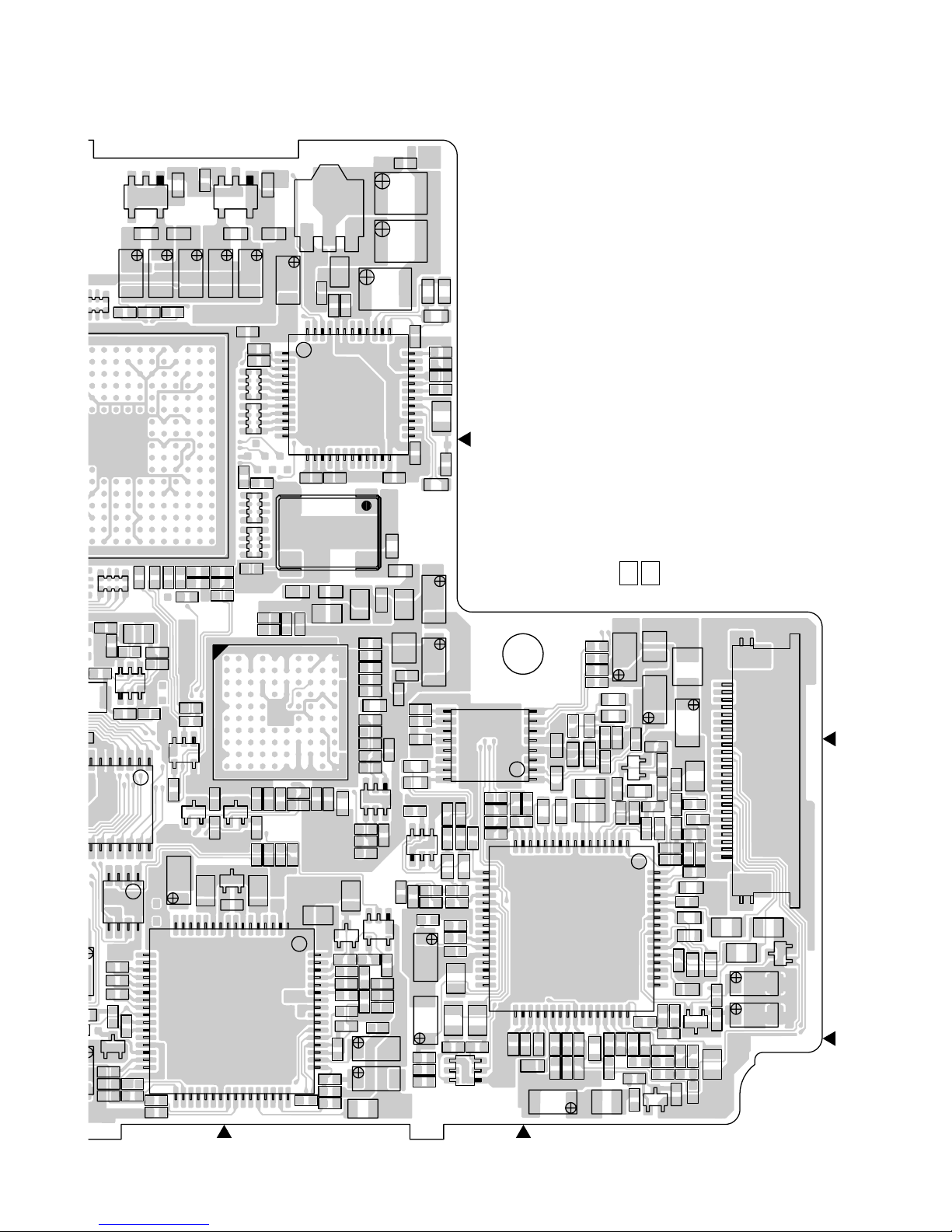
(Sanwa)-M2D229/249
GR-DVL820A/A-S/EA/SH, DVL1020A/EA/SH
CN109
115
5
4-6
Page 12

VICTOR COMPANY OF JAPAN, LIMITED
VIDEO DIVISION
S40894
Printed in Japan
Page 13
SECTION 5
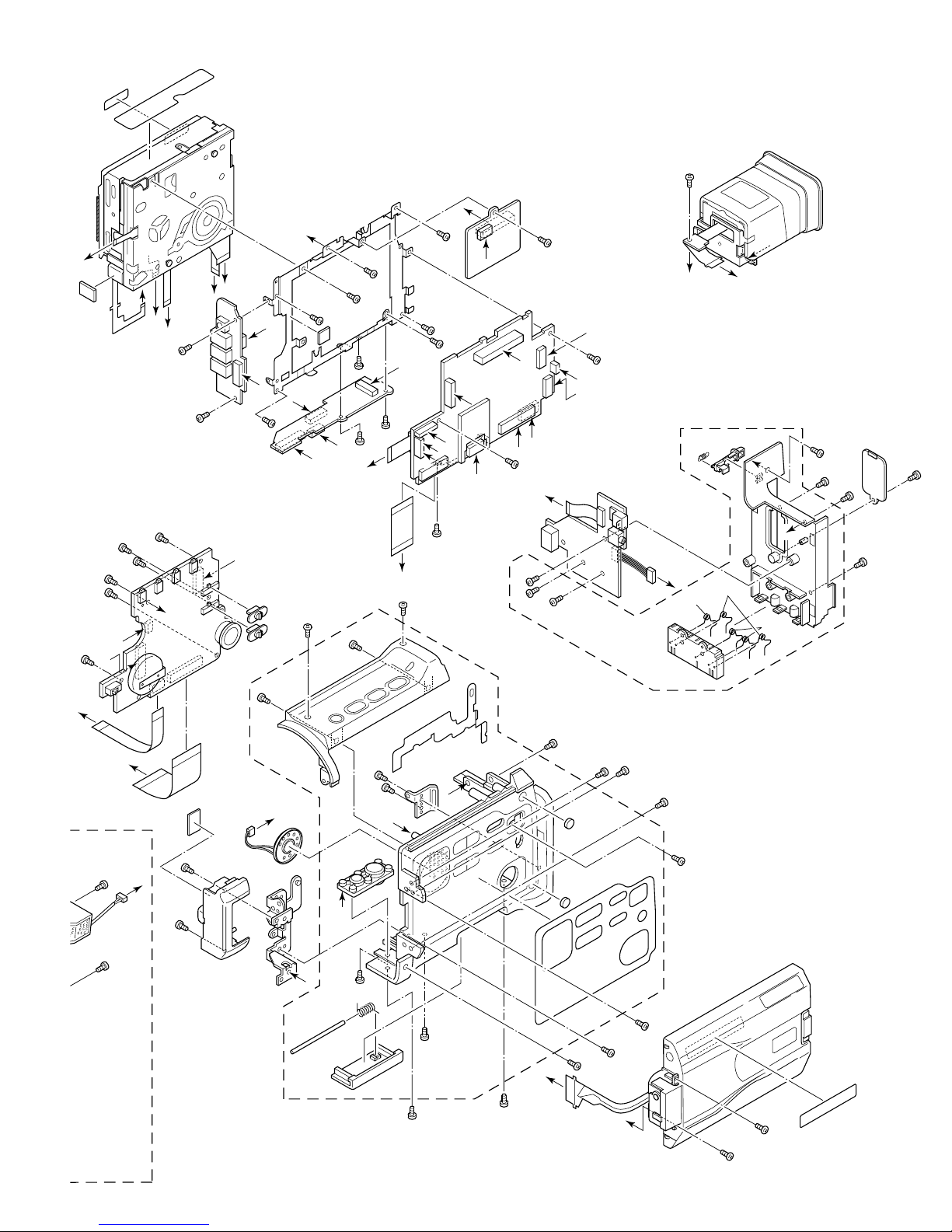
PARTS LIST
SAFETY PRECAUTION
Parts identified by the symbol are critical for safety. Replace only with specified part numbers.
5.1 PACKING AND ACCESSORY ASSEMBLY <M1>
The instruction manual to be provided with this product will differ according to the destination.
38
34
14
13
7
6
33
24
41
21
17
25
36
20
18
19
15
16
4
5
3
FINAL ASSY
<M2>
37
2
26
29
30
5-1
31
32
1
LABEL
(SERIAL)
Page 14

# REF No. PART No. PART NAME, DESCRIPTION
---------------- ----------------------- -----------------------------------------------------
******************************
PACKING AND ACCESSORY ASSEMBLY <M1>
1 LY32567-021A PACKING CASE,A,B,C
LY32567-008A PACKING CASE,E,F
LY32567-017A PACKING CASE,D
LY32567-019A PACKING CASE,G
2 LY32568-001A CUSHION
3 LY30023-022A POLY BAG
4 QPA02003506 POLY BAG
!
5 LYT0963-001A INST.BOOK(EN),A,B,C,E,F
!
!
!
!
!
!
!
!
6 LYT0912-001A INST.BOOK(SOFT.EN),A,B,C,D
7 LYT0934-001A SHEET(AGREMENT),A,B,C,D
13 LYT0609-001A SHEET(CON.PLUG),A,B,E
14 BT-56002-2 SER.NET CARD,C,F
15 QPA01703005 POLY BAG
16 QAM0212-001 CABLE ASSY,AUDIO/VIDEO CABLE
17 QQR0918-002 CORE FILTER
18 PEAC0428-150 CABLE ASSY,EDITING CABLE
19 QQR0491-002 CORE FILTER
20 QAM0324-001 USB CABLE
21 QQR0491-002 CORE FILTER
!
24 LY20847-001C AC ADAPTER,AP-V12EG
25 QQR0917-002 CORE FILTER
!
26 QMPL120-190-JR POWER CORD,A,D,E,G
!
!
!
29 PEMC1012 CONVERSION PLUG,B
!
!
!
30 LY32566-001A BATTERY PACK ASSY,BN-V408U
31 LY20186-001A SHOULDER STRAP
32 LY20750-001A REMOTE CONTROL UNIT,RM-V717U
33 – BATTERY,AAA(R03),X2
34 LY32210-023A CD ROM ASSY,A,B,C,D
36 LY43322-002A CAP(M)ASSY
37 QAM0342-002 MEMORY CARD,8MB(SD)
38 BT-56001-2 WARRANTY CARD,C,F
41 QQR0491-002 CORE FILTER
LYT0963-002A INST.BOOK(CH),A,B,E
LYT0963-003A INST.BOOK(RU),A,B,E
LYT0963-004A INST.BOOK(AR),A,B,E
LYT0963-005A INST.BOOK(GE),A,B,E
LYT0963-006A INST.BOOK(FR),A,B,E
LYT0964-001A INST.BOOK(EN),D,G
LYT0964-002A INST.BOOK(CH),D,G
LYT0964-003A INST.BOOK(RU),D,G
LYT0912-002A INST.BOOK(SOFT.GE),A,B
LYT0912-003A INST.BOOK(SOFT.FR),A,B
LYT0912-011A INST.BOOK(SOFT.CH),A,B,D
LYT0912-012A INST.BOOK(SOFT.RU),A,B,D
LYT0931-001A INST.BOOK(SOFT.EN),E,F,G
LYT0931-002A INST.BOOK(SOFT.GE),E
LYT0931-003A INST.BOOK(SOFT.FR),E
LYT0931-011A INST.BOOK(SOFT.CH),E,G
LYT0931-012A INST.BOOK(SOFT.RU),E,G
QMPH020-190-JR POWER CORD,C,F
QMPS110-190-JR POWER CORD,B
PEMC1012-02 CONVERSION PLUG,A,E
QAM0001-001 CONVERSION PLUG,D,G
LY32210-038A CD ROM ASSY,E,F,G
MODEL MARK
GR-DVL820A A
GR-DVL820A-S B
GR-DVL820EA C
GR-DVL820SH D
GR-DVL1020A E
GR-DVL1020EA F
GR-DVL1020SH G
• INSTRUCTIONS
EN ....... ENGLISH
CH ...... CHINESE
RU....... RUSSIAN
AR ....... ARABIC
GE ...... GERMANY
FR ....... FRENCH
5-2
Page 15
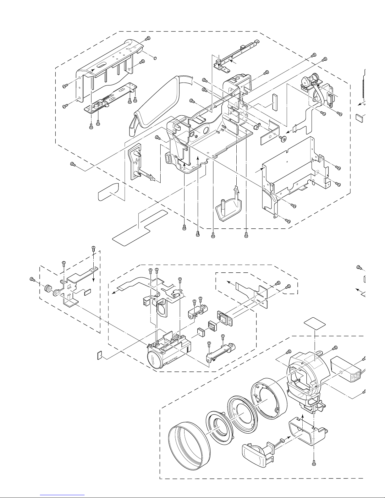
5.2 FINAL ASSEMBLY <M2>
5
5
140J
a
140T
140T
140T
140U
140G
140
140N
140F
c
g
140R
143
131
140H
173
170A
140T
171
141
170
140S
170B
172
c
140K
140S
144
140S
RATING
LABEL
s
140S
251D
251J
140M
140A
251C
140N
d
141
251D
251C
140N
b
142
251C
142
251
251B
140B
r
131
140C
a
140E
140D
251H
CCD
<04>
m
140P
140L
251H
140L
140R
140R
140L
140L
k
bb
166
1
1
111
p
252
5-3
OPTICAL BLOCK
SECTION
125K
251E
251C
251F
125C
251C
251A
251G
125B
125H
125A
125E
t
126
125
125E
125F
d
125G
125D
12
12
Page 16
166
111
p
bb
155
110
110
110
h
aa
110
ff
113
154
z
110
y
cc
153
JACK
<06>
153
MONITOR
<02>
gg
MECHANISM
<M3>
x
bb
v
156
JUNCTION
<05>
dd
108
107
101K
z
116
g
156
w
101A
165
aa
150
152
v
101K
158
151
159
163
y
153
w
101J
152
116
157
u
158
t
s
162
ELECTRONIC
VIEWFINDER
<M4>
ee
130E
130C
118
f
130B
130A
130D
dd
130
j
k
130E
131
132
j
134
135
132
133
DSC
<10>
o
164
p
MAIN
<01>
n
160
o
r
q
160
cc
130F
130F
101
x
n
118
ee
m
REAR
<07>
130F
q
125E
125E
u
106
122
106
112
105
103
ff
109
e
101F
101D
b
101L
101G
101M
101M
gg
101E
101H
114
101L
119
121
f
101C
101C
h
115
101B
104
114
119
117
MONITOR
104
e
<M5>
120
102
102
5-4
Page 17

# REF No. PART No. PART NAME, DESCRIPTION # REF No. PART No. PART NAME, DESCRIPTION
---------------- ----------------------- ----------------------------------------------------- ----------------- ----------------------- -----------------------------------------------------
133 LY30018-0C9A SPECIAL SCREW
******************************
FINAL ASSEMBLY <M2>
101 LY20774-005B UPPER CASE(2.5)ASSY,A
LY20774-005C UPPER CASE(2.5)ASSY,B,C,D
LY20797-004C UPPER CASE(3.5)ASSY,E,F,G
101A LY20775-001A TOP COVER(2.5),A,B,C,D
LY20776-001A TOP COVER(3.5),E,F,G
101B LY32371-003A PLATE(UPPER)
101C LY40664-001A SPACER,X2
101D LY31019-001A BASE
101E LY32375-001B COVER(SD)
101F LY43292-001A SHAFT
101G LY43293-001A SPRING
101H LY43261-001A HOOK(UPPER)
101J LY32886-001A BRAKET(EARTH)2.5,A,B,C,D
LY32887-001A BRAKET(EARTH)3.5,E,F,G
101K LY30018-023A SPECIAL SCREW,X2
101L LY30018-084A SPECIAL SCREW,X2
101M LY30018-084A SPECIAL SCREW,X2,A,B,C,D
LY30018-038A SPECIAL SCREW,X2,E,F,G
102 LY30018-0D6A SPECIAL SCREW,X2
103 LY32373-001A BRACKET(MONITOR)
104 LY30018-066A SPECIAL SCREW,X2
105 LY20777-001A COVER(HINGE)
106 LY30018-047A SPECIAL SCREW,X2
107 LY43263-001A KNOB(SLIDE)
108 LY43263-002A KNOB(SLIDE)
109 QAS0048-001 SPEAKER
110 LY30018-023A SPECIAL SCREW,X5
111 LY30018-047A SPECIAL SCREW
112 QUQ105-4007AA FFC WIRE,MONI CN761-MAIN CN101
113 QUQ105-1011AA FFC WIRE,MONI CN762-DSC CN8002
114 LY30018-084A SPECIAL SCREW,X2
115 LY30018-084A SPECIAL SCREW
116 LY30018-047A SPECIAL SCREW,X2
117 LY30018-047A SPECIAL SCREW
118 LY30018-064A SPECIAL SCREW,X2
119 LY30018-099A SPECIAL SCREW,X2
120 LY43566-003A STICKER(SIDE)
121 LY30018-084A SPECIAL SCREW
122 LY30029-0Y5A SPACER(A),A,B,C,D,F,G
125 LY32382-007A FRONT COVER ASSY
125A LY32383-001A HOOD
125B LY32687-001B RING(MEGA)
125C LY32705-001A HOOD(SCREW)
125D LY30018-084A SPECIAL SCREW
125E LY30018-0A7A SPECIAL SCREW,X4
125F LY32343-001A MICROPHONE
125G LY32388-001A BASE(LIGHT)
125H LY32338-001A DC LIGHT ASSY
125K LY32387-001A HOOD(MEGA)
126 LY43567-002A STICKER(TOP)
130 LY10317-001A REAR UNIT
130A LY32408-001A KNOB(BATT.RELE)
130B LY30001-018A TENSION SPRING
130C LY32409-001A TERMINAL BASE
130D LY43291-001A TERMINAL(R),X2
130E LY43290-001A TERMINAL(L),X3
130F LY30018-084A SPECIAL SCREW,X3
131 LY30018-084A SPECIAL SCREW,X3
132 LY30018-0C9A SPECIAL SCREW,X2
134 LY41691-001A COVER(JIG)
135 LY30018-037A SPECIAL SCREW
140 LY20769-003E LOWER CASE ASSY
140A LY32363-001A COVER(JACK)
140B LY32364-001B COVER(DC)
140C LY40592-001A CAP(GRIP BELT)
140D LY20770-001A ARM ASSY
140E LY30029-0T9A SPACER(A)
140F LY32365-001A PLATE
140G LY20780-001A GRIP BELT
140H LY10304-001A ZOOM UNIT
140J LY10309-001A CASSETTE COVER
140K LY43254-001B LOCK ASSY
140L LY30018-084A SPECIAL SCREW,X4
140M LY30018-038A SPECIAL SCREW
140N LY30018-038A SPECIAL SCREW,X3
140P LY30018-0D1A SPECIAL SCREW
140R LY30018-084A SPECIAL SCREW,X3
140S LY30018-023A SPECIAL SCREW,X4
140T LY30018-038A SPECIAL SCREW,X4
140U LY43609-001A SPACER(B)
141 LY30018-084A SPECIAL SCREW,X2
142 LY30018-084A SPECIAL SCREW,X2
143 LY30018-0C9A SPECIAL SCREW
144 LY43256-001B PLATE(ADJUST)
150 LY20778-001A BRACKET(MECHA)
151 YQ43893-4 MINI SCREW
152 LY30019-026A SPECIAL SCREW,X2
153 QYSPSPT1730R SCREW,X3
154 LY40698-002A LABEL(HOUSING)
155 LY40699-002A LABEL(PUSH)
156 LY30018-084A SPECIAL SCREW,X2
157 LY30018-066A SPECIAL SCREW
158 LY30018-066A SPECIAL SCREW,X2
159 LY30018-038A SPECIAL SCREW
160 LY30019-038A SPECIAL SCREW,X2
162 YQ43893-4 MINI SCREW
163 WJT0066-001A
164 LY30019-038A SPECIAL SCREW
165 LY30029-0V6A SPACER(A)
166 LY30029-0X1A SPACER(A)
170 LY43258-001A BRACKET(OP)ASSY
170A LY42796-001A BUSH
170B LY30016-0N9A SPACER-A
171 LY30018-084A SPECIAL SCREW
172 LY30018-066A SPECIAL SCREW
173 LY30019-029B SPECIAL SCREW
252 LY30029-0Z7A SPACER(A),B,C,D,E,F,G
E-CARD WIRE,MAIN CN113-JUNC.CN571
– OPTICAL BLOCK SECTION –
251 J7C-112A OPTICAL BLOCK ASSY
251A LY31572-001A ZOOM MOTOR
251B LY31571-001A FOCUS MOTOR
251C LY30727-002A SCREW,X5
251D LY30727-001A SCREW,X2
251E LY43384-001A OPTICAL LPF
251F LY43494-001A SHEET
251G LYH30375-003A CCD BASE ASSY
251H QYSPSGU1750Z SCREW,X2
251J LY32721-001A IRIS MOTOR UNIT
5-5
Page 18

5.3 ELECTRONIC VIEWFINDER ASSEMBLY <M4> [GR-DVL1020A/EA/SH]
300
312
342
305
343
303
302
314
307
306
311
301
308
308
304
308
309
309
308
309
# REF No. PART No. PART NAME, DESCRIPTION # REF No. PART No. PART NAME, DESCRIPTION
--------------- ----------------------- ----------------------------------------------------- ---------------- ----------------------- ------------------------------------------------------
******************************
ELECTRONIC VIEWFINDER ASSEMBLY <M4>
300 LY20838-003A C.VF ASSY
301 PTY20712-001 EYE PIECE ASSY
302 PTY20712-011 TOP CASE SUB ASSY
303 PTY20712-021 BOTTOM CASE
304 PTY20712-022 CAP(VF)
305 PTY20838-031 HINGE ASSY
310
310
306 PTY20712-041 LCD ASSY
307 QAL0287-001 FPC
308 LY30018-063A SPECIAL SCREW,X4
309 LY30018-055A SPECIAL SCREW,X3
310 LY30018-035A SPECIAL SCREW,X2
311 PTY20712-051 SCREW
312 LY41701-002A SHEET(CAUTION)1
314 LY43041-002A LABEL(VF)
342 LY43489-001B PLATE(VF)
343 LY43827-001A BRACKET(VF)
5-6
Page 19

5.4 MONITOR ASSEMBLY <M5> [GR-DVL820A/A-S/EA/SH]
501E
500
501H
501
501G
501J
d
501A
501C
508A
508F
508E
508D
c
508G
a
508
508C
508E
c
508B
b
510
504
LCD BL
<03>
506
507
501F
501D
d
501B
501D
509
511
505
b
502
a
# REF No. PART No. PART NAME, DESCRIPTION # REF No. PART No. PART NAME, DESCRIPTION
--------------- ----------------------- ----------------------------------------------------- ---------------- ----------------------- ------------------------------------------------------
******************************
MONITOR ASSEMBLY <M5>
500 LYH20246-043B MONITOR ASSY
501 LY20863-001B
501A LY31620-001A KNOB(LOCK 1)
501B LY42180-001A KNOB(LOCK 2)
501C LY30002-044A COMPRESSION SPRING
501D LY30018-084A SPECIAL SCREW,X2
501E LY42883-001A MARK
501F LY43784-001A EARTH MON(2.5)
501G LY32704-001A WINDOW(M.MEGA)
501H LY32706-001B PLATE(M2.5MEGA)
501J QLE0017-001 EL PANEL
502 LY20874-001A MONITOR CASE ASSY
MONITOR COVER(2.5MEGA)ASSY
502A LY42388-001A EARTH MON(2)
504 LY20674-001A HOLDER(2.5)
505 LY31622-001A BRACKET(EARTH)
506 QLL0121-001 BACK LIGHT
507 QLD0154-001 LCD MODULE
508 LY32695-001A MONITOR FPC ASSY
508A LY32574-001A MONITOR FPC ASSY
508B LY32079-001A HINGE ASSY
508C LY32380-001A HINGE COVER(U)
508D LY32381-001A HINGE COVER(L)
508E LY30018-058A SPECIAL SCREW,X2
508F LY30018-023A SPECIAL SCREW
508G LY30029-0Q5A SPACER(A)
509 QYSPSPT1730R SCREW,X2
510 LY30018-0F2A SPECIAL SCREW,X2
511 LY30029-0Y4A SPACER(A)
502A
5-7
Page 20
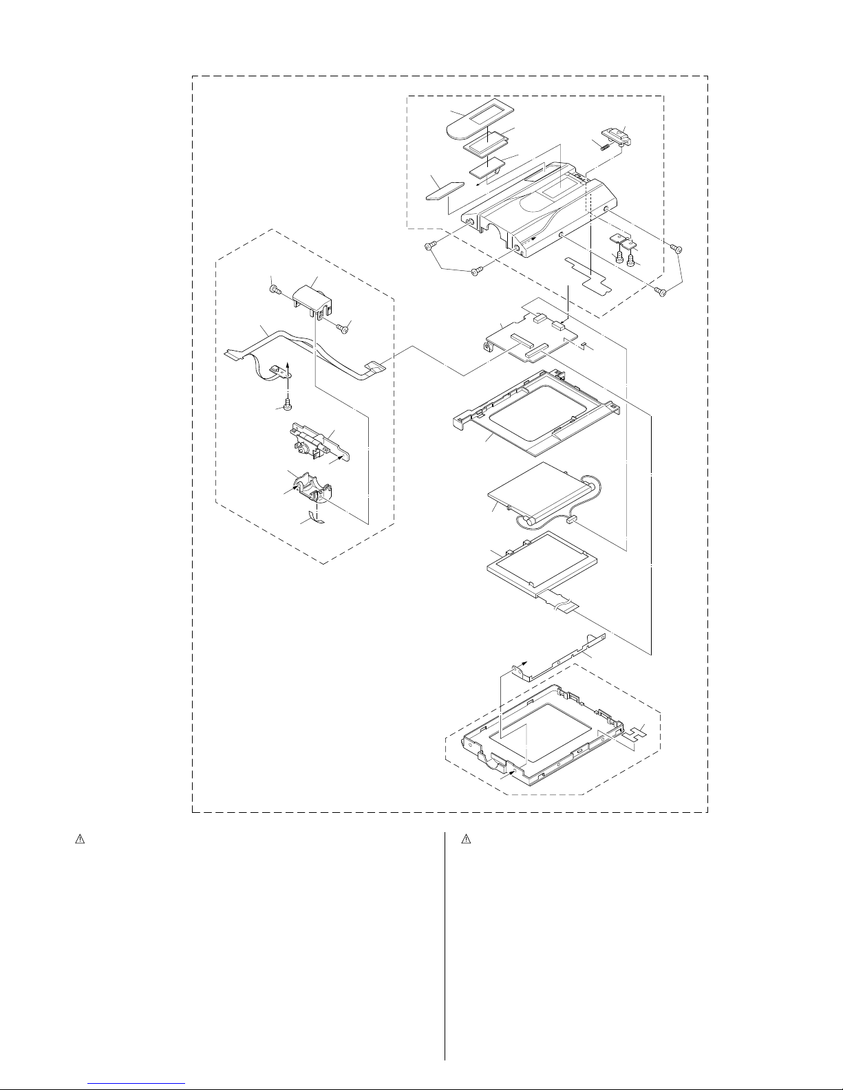
5.4 MONITOR ASSEMBLY <M5> [GR-DVL1020A/EA/SH]
501E
500
501H
501
501G
501J
d
501A
501C
508A
508F
508E
508D
c
508G
a
508
508C
508E
c
508B
b
510
504
LCD BL
<03>
506
507
d
501F
501D
512
501B
501D
509
# REF No. PART No. PART NAME, DESCRIPTION # REF No. PART No. PART NAME, DESCRIPTION
--------------- ----------------------- ----------------------------------------------------- ---------------- ----------------------- ------------------------------------------------------
******************************
MONITOR ASSEMBLY <M5>
500 LYH20246-042B MONITOR ASSY
501 LY20864-001C MONITOR COVER(3.5MEGA)ASSY
501A LY31620-001A KNOB(LOCK 1)
501B LY42180-001A KNOB(LOCK 2)
501C LY30002-044A COMPRESSION SPRING
501D LY30018-084A SPECIAL SCREW,X2
501E LY42883-001A MARK
501F LY43785-001A EARTH MON(3.5)
501G LY32704-002A WINDOW(M.MEGA)
501H LY32707-001B PLATE(M3.5MEGA)
501J QLE0017-001 EL PANEL
502 LY20598-002A MONITOR CASE ASSY
b
502
a
505
502A
502A LY42388-001A EARTH MON(2)
504 LY20568-001A HOLDER(3.5PWB)
505 LY31622-001A BRACKET(EARTH)
506 QLL0123-001 BACK LIGHT
507 QLD0203-001 LCD MODULE
508 LY32695-001A MONITOR FPC ASSY
508A LY32574-001A MONITOR FPC ASSY
508B LY32079-001A HINGE ASSY
508C LY32380-001A HINGE COVER(U)
508D LY32381-001A HINGE COVER(L)
508E LY30018-058A SPECIAL SCREW,X2
508F LY30018-023A SPECIAL SCREW
508G LY30029-0Q5A SPACER(A)
509 QYSPSPT1730R SCREW,X2
510 LY30018-0F2A SPECIAL SCREW,X2
512 LY30029-0Y6A SPACER(A)
5-8
Page 21

5.5 ELECTRICAL PARTS LIST
# REF No. PART No. PART NAME, DESCRIPTION # REF No. PART No. PART NAME, DESCRIPTION
---------------- ----------------------- ----------------------------------------------------- ----------------- ----------------------- -----------------------------------------------------
******************************
MAIN BOARD ASSEMBLY <01>
PW YB10391PD-01 MAIN BOARD ASSY,A,B,C,D,E
YB10391QD-03 MAIN BOARD ASSY,F,G
IC1001 UPD703039F1-A27 IC(MICRO C ROM)
or UPD70F3040F1A27 IC(MICRO C ROM)
IC1002 RS5C314 IC
IC1003 X25330S8I-2.5-X IC
or 25LC640-I/SN-X IC
or AT25320N-10SI-X IC
or CAT25C32SI IC
IC1004 TC75S56FU IC
IC1005 TC7S00FU IC
or SN74AHC1G00K IC
IC1006 MB90097PFV145 IC(MICRO C ROM)
IC1007 SN74AHC1G08K IC
IC1008 IC-PST3423U-X IC
IC1009 TC7W08FU IC(DIGITAL)
or SN74AHC2G08T IC
IC1401 UPD703040YF-M06 IC(MICRO C ROM)
or UPD70F3040YFM06 IC(MICRO C ROM)
!
IC1601 BD6631KV IC
IC1602 TC7W14FU IC(DIGITAL)
or SN74AHC2G14T IC
IC2001 AK4560AVQ IC
IC2501 AK4550VT IC
IC3001 JCY0152 IC
IC3002 BU2501FV IC
IC3004 MC74VHC1G04DF-X IC,E,G
IC3005 JCY0136 IC,A,B,C,D,E
IC3007 JCY0174 IC,F,G
IC3501 JCY0132 IC
IC3502 SN74AHC1G04K IC
IC3701 BA7665FS IC
IC3731 MM1504XN IC
IC3801 JCP8045 IC(DIGITAL)
IC4201 HD49334HF IC
or HD49334AHF IC
IC4202 RH5RZ31CA IC
IC4301 JCY0160-2 IC
IC4302 R1160N151B IC
IC4303 MM1385NN IC
IC4802 TA75W01FU IC
IC4803 TA75W01FU IC
IC4804 LM358DR2 IC
IC4851 UPD16879GS IC
IC5001 CXD3602R IC
IC5002 W194-70G-X IC
IC5003 MM1385DN IC
IC6001 S-80842ANNP-W IC
or S-80842CNNB-W IC
IC6101 FA3698F IC
Q1001 DTC124EE DIGI TRANSISTOR
or UN9212J DIGI TRANSISTOR
Q1002 2SC4617/QR/-X TRANSISTOR
or 2SD2216J/QR/-X TRANSISTOR
Q1003 DTC143EE DIGI TRANSISTOR
or UN921LJ DIGI TRANSISTOR
Q1004 DTC143XE DIGI TRANSISTOR
Q1005 2SJ347 MOS FET
Q1006 DTA114EE DIGI TRANSISTOR
or PDTA114EE DIGI TRANSISTOR
or UN9111J DIGI TRANSISTOR
Q1007 DTC144EE DIGI TRANSISTOR
or PDTC144EE DIGI TRANSISTOR
or UN9213J DIGI TRANSISTOR
Q1008 DTA114EE DIGI TRANSISTOR
or PDTA114EE DIGI TRANSISTOR
or UN9111J DIGI TRANSISTOR
Q1009 DTC144EE DIGI TRANSISTOR
or PDTC144EE DIGI TRANSISTOR
or UN9213J DIGI TRANSISTOR
Q1401 DTA114EE DIGI TRANSISTOR
or PDTA114EE DIGI TRANSISTOR
or RN2102 DIGI TRANSISTOR
or UN9111J DIGI TRANSISTOR
Q1402 UMC3N DIGI TRANSISTOR
Q1403 UMC3N DIGI TRANSISTOR
Q1601 UMC3N DIGI TRANSISTOR
Q2001 UMX1N PAIR TRANSISTOR
Q2002 2SC4617/RS/-X TRANSISTOR
or 2SD2216J/RS/-X TRANSISTOR
Q2501 UMX18N PAIR TRANSISTOR
Q3001 2SC4617/RS/-X TRANSISTOR,A,B,C,D,E
Q3002 2SC4617/RS/-X TRANSISTOR,A,B,C,D,E
Q3701 UMT1N PAIR TRANSISTOR
or XP4401 TRANSISTOR
Q3702 UMZ1N PAIR TRANSISTOR
or XP4601 TRANSISTOR
Q3703 2SA1774/RS/-X TRANSISTOR
Q3704 2SA1774/RS/-X TRANSISTOR
Q3705 UMT1N PAIR TRANSISTOR
or XP4401 TRANSISTOR
Q3731 2SC4617/RS/-X TRANSISTOR
or 2SD2216J/RS/-X TRANSISTOR
Q3732 DTC144EE DIGI TRANSISTOR
or UN9213J DIGI TRANSISTOR
Q3733 UMZ1N PAIR TRANSISTOR
or XP4601 TRANSISTOR
Q3734 2SC4617/RS/-X TRANSISTOR
or 2SD2216J/RS/-X TRANSISTOR
Q3735 UMZ1N PAIR TRANSISTOR
or XP4601 TRANSISTOR
Q4801 2SC4655/BC/-X TRANSISTOR
Q4802 2SC4617/RS/-X TRANSISTOR
Q4803 DTC144EE DIGI TRANSISTOR
or PDTC144EE DIGI TRANSISTOR
or RN1104 DIGI TRANSISTOR
or UN9213J DIGI TRANSISTOR
Q4804 DTA144EE DIGI TRANSISTOR
or PDTA144EE DIGI TRANSISTOR
or RN2104 DIGI TRANSISTOR
or UN9113J DIGI TRANSISTOR
Q4805 DTA143EE DIGI TRANSISTOR
or RN2101 DIGI TRANSISTOR
or UN911LJ DIGI TRANSISTOR
Q4806 2SC4617/RS/-X TRANSISTOR
Q4851 2SC4617/RS/-X TRANSISTOR
Q6001 DTC144EE DIGI TRANSISTOR
or PDTC144EE DIGI TRANSISTOR
or RN1104 DIGI TRANSISTOR
or UN9213J DIGI TRANSISTOR
Q6002 MCH6613 MOS FET
Q6004 2SB1188/QR/-W TRANSISTOR
5-9
Page 22

# REF No. PART No. PART NAME, DESCRIPTION # REF No. PART No. PART NAME, DESCRIPTION
---------------- ----------------------- ----------------------------------------------------- ----------------- ----------------------- -----------------------------------------------------
Q6201 MCH3308 MOS FET
Q6202 2SA1577/RS/-X TRANSISTOR
Q6203 MCH3308 MOS FET
Q6204 CPH3314 MOS FET
Q6205 CPH3101 TRANSISTOR
Q6206 2SC4617/RS/-X TRANSISTOR
Q6207 2SD2444K TRANSISTOR
Q6208 MCH3308 MOS FET
Q6210 MCH3308 MOS FET
Q6211 MCH3308 MOS FET
Q6212 HN1C01FU/G/-X PAIR TRANSISTOR
or PUMX1 PAIR TRANSISTOR
or UMX1N PAIR TRANSISTOR
Q6213 2SA1577/RS/-X TRANSISTOR
Q6214 DTC144EE DIGI TRANSISTOR
or PDTC144EE DIGI TRANSISTOR
or RN1104 DIGI TRANSISTOR
or UN9213J DIGI TRANSISTOR
Q6215 HN1A01FU/G/-X PAIR TRANSISTOR
or PUMT1 PAIR TRANSISTOR
or UMT1N PAIR TRANSISTOR
Q6216 2SC4617/RS/-X TRANSISTOR
Q6217 UMZ1N PAIR TRANSISTOR
Q6701 CPH3314 MOS FET
D1001 DA221 DIODE
D1002 1SS376 DIODE
D1602 DAP222 DIODE
D1603 DAP222 DIODE
D1604 DAP222 DIODE
D3001 EC2C01C VARI CAP DIODE
D3002 EC2C01C VARI CAP DIODE
D3003 EC2C01C VARI CAP DIODE
D3004 MA2Z720 SB DIODE
D5001 1SS355 DIODE
!
D6002 RB715F SB DIODE
D6201 CRS01 SB DIODE
D6202 CRS01 SB DIODE
D6203 CRS01 SB DIODE
D6204 CRS01 SB DIODE
D6205 CRS01 SB DIODE
D6206 RB480Y SB DIODE
D6207 UDZS9.1B ZENER DIODE
D6208 RB480Y SB DIODE
D6701 EP10HY03 SB DIODE
D6702 EP10HY03 SB DIODE
R101 NRSA63J-0R0X MG RESISTOR 0Ø,1/16W
R102 NRSA63J-0R0X MG RESISTOR 0Ø,1/16W
R1001 NRSA6AJ-104W MG RESISTOR 100kØ,1/16W
R1002 NRSA6AJ-224W MG RESISTOR 220kØ,1/16W
R1003 NRSA6AJ-472W MG RESISTOR 4.7kØ,1/16W
R1004 NRSA6AJ-103W MG RESISTOR 10kØ,1/16W
R1005 NRSA6AJ-153W MG RESISTOR 15kØ,1/16W
R1006 NRSA6AJ-103W MG RESISTOR 10kØ,1/16W
R1007 NRSA6AJ-334W MG RESISTOR 330kØ,1/16W
R1008 NRSA6AJ-102W MG RESISTOR 1kØ,1/16W
R1009 NRSA6AJ-561W MG RESISTOR 560Ø,1/16W
R1010 NRSA6AJ-561W MG RESISTOR 560Ø,1/16W
R1015 NRSA6AJ-474W MG RESISTOR 470kØ,1/16W
R1017 NRSA6AJ-561W MG RESISTOR 560Ø,1/16W
R1018 NRSA6AJ-103W MG RESISTOR 10kØ,1/16W
R1019 NRSA6AJ-623W MG RESISTOR 62kØ,1/16W
R1020 NRSA6AJ-331W MG RESISTOR 330Ø,1/16W
R1021 NRSA6AJ-331W MG RESISTOR 330Ø,1/16W
R1022 NRSA6AJ-331W MG RESISTOR 330Ø,1/16W
R1023 NRSA6AJ-103W MG RESISTOR 10kØ,1/16W
R1024 NRSA6AJ-823W MG RESISTOR 82kØ,1/16W
R1026 NRSA6AJ-472W MG RESISTOR 4.7kØ,1/16W
R1027 NRSA6AJ-104W MG RESISTOR 100kØ,1/16W
R1028 NRSA6AJ-185W MG RESISTOR 1.8MØ,1/16W
R1029 NRSA6AJ-473W MG RESISTOR 47kØ,1/16W
R1030 NRSA6AJ-104W MG RESISTOR 100kØ,1/16W
R1031 NRSA6AJ-102W MG RESISTOR 1kØ,1/16W
R1032 NRSA6AJ-104W MG RESISTOR 100kØ,1/16W
R1036 NRSA6AJ-102W MG RESISTOR 1kØ,1/16W
R1037 NRSA6AJ-103W MG RESISTOR 10kØ,1/16W
R1038 NRSA6AJ-104W MG RESISTOR 100kØ,1/16W
R1039 NRSA6AJ-103W MG RESISTOR 10kØ,1/16W
R1044 NRSA6AJ-123W MG RESISTOR 12kØ,1/16W
R1045 NRSA6AJ-822W MG RESISTOR 8.2kØ,1/16W
R1046 NRSA6AJ-103W MG RESISTOR 10kØ,1/16W
R1047 NRSA6AJ-473W MG RESISTOR 47kØ,1/16W
R1048 NRSA6AJ-104W MG RESISTOR 100kØ,1/16W
R1049 NRSA6AJ-393W MG RESISTOR 39kØ,1/16W
R1050 NRSA6AJ-223W MG RESISTOR 22kØ,1/16W
R1051 NRSA6AJ-272W MG RESISTOR 2.7kØ,1/16W
R1052 NRSA6AJ-183W MG RESISTOR 18kØ,1/16W
R1053 NRSA6AJ-154W MG RESISTOR 150kØ,1/16W
R1054 NRSA6AJ-473W MG RESISTOR 47kØ,1/16W
R1055 NRSA6AJ-103W MG RESISTOR 10kØ,1/16W
R1056 NRSA6AJ-472W MG RESISTOR 4.7kØ,1/16W
R1057 NRSA6AJ-473W MG RESISTOR 47kØ,1/16W
R1058 NRSA6AJ-222W MG RESISTOR 2.2kØ,1/16W
R1060 NRSA6AJ-473W MG RESISTOR 47kØ,1/16W
R1061 NRSA6AJ-473W MG RESISTOR 47kØ,1/16W
R1066 NRSA6AJ-473W MG RESISTOR 47kØ,1/16W
R1071 NRSA6AJ-474W MG RESISTOR 470kØ,1/16W
R1072 NRSA6AJ-104W MG RESISTOR 100kØ,1/16W
R1076 NRSA6AJ-0R0W MG RESISTOR 0Ø,1/16W
R1077 NRSA6AJ-0R0W MG RESISTOR 0Ø,1/16W
R1078 NRSA6AJ-102W MG RESISTOR 1kØ,1/16W
R1079 NRSA6AJ-102W MG RESISTOR 1kØ,1/16W
R1080 NRSA6AJ-102W MG RESISTOR 1kØ,1/16W
R1081 NRSA6AJ-103W MG RESISTOR 10kØ,1/16W
R1082 NRSA6AJ-103W MG RESISTOR 10kØ,1/16W
R1083 NRSA6AJ-103W MG RESISTOR 10kØ,1/16W
R1401 NRSA6AJ-105W MG RESISTOR 1MØ,1/16W
R1402 NRSA6AJ-102W MG RESISTOR 1kØ,1/16W
R1403 NRSA6AJ-103W MG RESISTOR 10kØ,1/16W
R1404 NRSA6AJ-472W MG RESISTOR 4.7kØ,1/16W
R1405 NRSA6AJ-332W MG RESISTOR 3.3kØ,1/16W
R1406 NRSA6AJ-332W MG RESISTOR 3.3kØ,1/16W
R1407 NRSA6AJ-332W MG RESISTOR 3.3kØ,1/16W
R1408 NRSA6AD-753W MG RESISTOR 75kØ,1/16W
R1409 NRSA6AJ-334W MG RESISTOR 330kØ,1/16W
R1411 NRSA6AJ-332W MG RESISTOR 3.3kØ,1/16W
R1412 NRSA6AJ-332W MG RESISTOR 3.3kØ,1/16W
R1413 NRSA6AJ-332W MG RESISTOR 3.3kØ,1/16W
R1414 NRSA6AJ-332W MG RESISTOR 3.3kØ,1/16W
R1415 NRSA6AJ-472W MG RESISTOR 4.7kØ,1/16W
R1416 NRSA6AJ-472W MG RESISTOR 4.7kØ,1/16W
R1417 NRSA6AJ-101W MG RESISTOR 100Ø,1/16W
R1421 NRSA6AJ-103W MG RESISTOR 10kØ,1/16W
R1422 NRSA6AJ-153W MG RESISTOR 15kØ,1/16W
R1423 NRSA6AJ-820W MG RESISTOR 82Ø,1/16W
R1425 NRSA6AJ-473W MG RESISTOR 47kØ,1/16W
R1601 NRSA6AJ-681W MG RESISTOR 680Ø,1/16W
5-10
Page 23

# REF No. PART No. PART NAME, DESCRIPTION # REF No. PART No. PART NAME, DESCRIPTION
---------------- ----------------------- ----------------------------------------------------- ----------------- ----------------------- -----------------------------------------------------
R1602 NRSA6AJ-124W MG RESISTOR 120kØ,1/16W
R1603 NRSA6AJ-472W MG RESISTOR 4.7kØ,1/16W
R1604 NRSA6AJ-104W MG RESISTOR 100kØ,1/16W
R1605 NRV142F-R22X CMF RESISTOR 0.22Ø,1/4W
R1609 NRV142F-R33X CMF RESISTOR 0.33Ø,1/4W
R1610 NRSA6AJ-471W MG RESISTOR 470Ø,1/16W
R1611 NRSA6AJ-471W MG RESISTOR 470Ø,1/16W
R1612 NRSA6AJ-104W MG RESISTOR 100kØ,1/16W
R1613 NRSA6AJ-102W MG RESISTOR 1kØ,1/16W
R1614 NRSA6AJ-102W MG RESISTOR 1kØ,1/16W
R1615 NRSA6AJ-102W MG RESISTOR 1kØ,1/16W
R1616 NRSA6AJ-391W MG RESISTOR 390Ø,1/16W
R1617 NRSA6AJ-683W MG RESISTOR 68kØ,1/16W
R1618 NRSA6AJ-683W MG RESISTOR 68kØ,1/16W
R1619 NRSA6AJ-393W MG RESISTOR 39kØ,1/16W
R1620 NRSA6AJ-103W MG RESISTOR 10kØ,1/16W
R1621 NRSA6AJ-103W MG RESISTOR 10kØ,1/16W
R1622 NRSA6AJ-103W MG RESISTOR 10kØ,1/16W
R1624 NRVA6AD-123W CMF RESISTOR 12kØ,1/16W
R1625 NRSA6AJ-181W MG RESISTOR 180Ø,1/16W
R1626 NRSA6AJ-181W MG RESISTOR 180Ø,1/16W
R1628 NRVA6AD-271W CMF RESISTOR 270Ø,1/16W
R1629 NRSA6AJ-564W MG RESISTOR 560kØ,1/16W
R1630 NRSA6AJ-0R0W MG RESISTOR 0Ø,1/16W
R1631 NRSA6AJ-0R0W MG RESISTOR 0Ø,1/16W
R1635 NRSA6AJ-472W MG RESISTOR 4.7kØ,1/16W
R1636 NRSA6AJ-103W MG RESISTOR 10kØ,1/16W
R1637 NRSA6AJ-154W MG RESISTOR 150kØ,1/16W
R2001 NRSA6AJ-0R0W MG RESISTOR 0Ø,1/16W
R2004 NRSA6AJ-0R0W MG RESISTOR 0Ø,1/16W
R2006 NRSA6AJ-100W MG RESISTOR 10Ø,1/16W
R2007 NRSA6AJ-102W MG RESISTOR 1kØ,1/16W
R2008 NRSA6AJ-102W MG RESISTOR 1kØ,1/16W
R2009 NRSA6AJ-332W MG RESISTOR 3.3kØ,1/16W
R2010 NRSA6AJ-273W MG RESISTOR 27kØ,1/16W
R2011 NRSA6AJ-223W MG RESISTOR 22kØ,1/16W
R2012 NRSA6AJ-273W MG RESISTOR 27kØ,1/16W
R2013 NRSA6AJ-223W MG RESISTOR 22kØ,1/16W
R2014 NRSA6AJ-820W MG RESISTOR 82Ø,1/16W
R2015 NRSA6AJ-820W MG RESISTOR 82Ø,1/16W
R2016 NRSA6AJ-820W MG RESISTOR 82Ø,1/16W
R2017 NRSA6AJ-102W MG RESISTOR 1kØ,1/16W
R2018 NRSA6AJ-103W MG RESISTOR 10kØ,1/16W
R2019 NRSA6AJ-2R7W MG RESISTOR 2.7Ø,1/16W
R2020 NRSA6AJ-2R7W MG RESISTOR 2.7Ø,1/16W
R2023 NRSA6AJ-102W MG RESISTOR 1kØ,1/16W
R2024 NRSA6AJ-183W MG RESISTOR 18kØ,1/16W
R2025 NRSA6AJ-102W MG RESISTOR 1kØ,1/16W
R2028 NRSA6AJ-224W MG RESISTOR 220kØ,1/16W
R2029 NRSA6AJ-0R0W MG RESISTOR 0Ø,1/16W
R2103 NRSA6AJ-153W MG RESISTOR 15kØ,1/16W
R2104 NRSA6AJ-153W MG RESISTOR 15kØ,1/16W
R2105 NRSA6AJ-472W MG RESISTOR 4.7kØ,1/16W
R2106 NRSA6AJ-472W MG RESISTOR 4.7kØ,1/16W
R2107 NRSA6AJ-153W MG RESISTOR 15kØ,1/16W
R2108 NRSA6AJ-153W MG RESISTOR 15kØ,1/16W
R2109 NRSA6AJ-182W MG RESISTOR 1.8kØ,1/16W
R2110 NRSA6AJ-182W MG RESISTOR 1.8kØ,1/16W
R2111 NRSA6AJ-153W MG RESISTOR 15kØ,1/16W
R2112 NRSA6AJ-153W MG RESISTOR 15kØ,1/16W
R2113 NRSA6AJ-222W MG RESISTOR 2.2kØ,1/16W
R2114 NRSA6AJ-222W MG RESISTOR 2.2kØ,1/16W
R2116 NRSA6AJ-472W MG RESISTOR 4.7kØ,1/16W
R2117 NRSA6AJ-472W MG RESISTOR 4.7kØ,1/16W
R2118 NRSA6AJ-472W MG RESISTOR 4.7kØ,1/16W
R2119 NRSA6AJ-332W MG RESISTOR 3.3kØ,1/16W
R2120 NRSA6AJ-332W MG RESISTOR 3.3kØ,1/16W
R2121 NRSA6AJ-473W MG RESISTOR 47kØ,1/16W
R2122 NRSA6AJ-473W MG RESISTOR 47kØ,1/16W
R2123 NRSA6AJ-104W MG RESISTOR 100kØ,1/16W
R2124 NRSA6AJ-104W MG RESISTOR 100kØ,1/16W
R2127 NRSA6AJ-0R0W MG RESISTOR 0Ø,1/16W
R2128 NRSA6AJ-0R0W MG RESISTOR 0Ø,1/16W
R2201 NRSA6AJ-122W MG RESISTOR 1.2kØ,1/16W
R2202 NRSA6AJ-122W MG RESISTOR 1.2kØ,1/16W
R2203 NRSA6AJ-0R0W MG RESISTOR 0Ø,1/16W
R2501 NRSA6AJ-0R0W MG RESISTOR 0Ø,1/16W
R2502 NRSA6AJ-0R0W MG RESISTOR 0Ø,1/16W
R2504 NRSA6AJ-0R0W MG RESISTOR 0Ø,1/16W
R2505 NRSA6AJ-273W MG RESISTOR 27kØ,1/16W
R2506 NRSA6AJ-273W MG RESISTOR 27kØ,1/16W
R2507 NRSA6AJ-223W MG RESISTOR 22kØ,1/16W
R2508 NRSA6AJ-223W MG RESISTOR 22kØ,1/16W
R2509 NRSA6AJ-564W MG RESISTOR 560kØ,1/16W
R2510 NRSA6AJ-564W MG RESISTOR 560kØ,1/16W
R2511 NRSA6AJ-103W MG RESISTOR 10kØ,1/16W
R2512 NRSA6AJ-103W MG RESISTOR 10kØ,1/16W
R2513 NRSA6AJ-332W MG RESISTOR 3.3kØ,1/16W
R3002 NRSA6AJ-103W MG RESISTOR 10kØ,1/16W
R3003 NRSA6AJ-105W MG RESISTOR,F,G 1MØ,1/16W
R3004 NRSA6AJ-103W MG RESISTOR 10kØ,1/16W
R3005 NRSA6AJ-100W MG RESISTOR 10Ø,1/16W
R3006 NRSA6AJ-100W MG RESISTOR 10Ø,1/16W
R3007 NRSA6AJ-562W MG RESISTOR 5.6kØ,1/16W
R3008 NRSA6AJ-222W MG RESISTOR 2.2kØ,1/16W
R3009 NRSA6AJ-103W MG RESISTOR 10kØ,1/16W
R3010 NRSA6AJ-103W MG RESISTOR 10kØ,1/16W
R3011 NRSA6AJ-224W MG RESISTOR 220kØ,1/16W
R3013 NRSA6AJ-242W MG RESISTOR 2.4kØ,1/16W
R3014 NRSA6AJ-392W MG RESISTOR 3.9kØ,1/16W
R3015 NRSA6AJ-392W MG RESISTOR 3.9kØ,1/16W
R3016 NRVA6AD-560W CMF RESISTOR 56Ø,1/16W
R3017 NRVA6AD-560W CMF RESISTOR 56Ø,1/16W
R3018 NRVA6AD-560W CMF RESISTOR 56Ø,1/16W
R3019 NRVA6AD-560W CMF RESISTOR 56Ø,1/16W
R3020 NRVA6AD-512W CMF RESISTOR 5.1kØ,1/16W
R3025 NRSA6AJ-102W MG RESISTOR,A,B,C,D,E 1kØ,1/16W
R3027 NRSA6AJ-103W MG RESISTOR 10kØ,1/16W
R3029 NRSA6AJ-153W MG RESISTOR 15kØ,1/16W
R3030 NRSA6AJ-224W MG RESISTOR 220kØ,1/16W
R3031 NRSA6AJ-224W MG RESISTOR 220kØ,1/16W
R3032 NRSA6AJ-105W MG RESISTOR 1MØ,1/16W
R3033 NRSA6AJ-103W MG RESISTOR 10kØ,1/16W
R3034 NRSA6AJ-222W MG RESISTOR 2.2kØ,1/16W
R3036 NRSA6AJ-103W MG RESISTOR 10kØ,1/16W
R3037 NRSA6AJ-681W MG RESISTOR 680Ø,1/16W
R3040 NRSA6AJ-222W MG RESISTOR,F,G 2.2kØ,1/16W
R3041 NRSA6AJ-561W MG RESISTOR,F,G 560Ø,1/16W
R3042 NRSA6AJ-561W MG RESISTOR,F,G 560Ø,1/16W
R3043 NRSA6AJ-122W MG RESISTOR,F,G 1.2kØ,1/16W
R3044 NRSA6AJ-152W MG RESISTOR,F,G 1.5kØ,1/16W
R3045 NRSA6AJ-123W MG RESISTOR,F,G 12kØ,1/16W
R3046 NRSA6AJ-823W MG RESISTOR,F,G 82kØ,1/16W
R3049 NRSA6AJ-100W MG RESISTOR,F,G 10Ø,1/16W
R2115 NRSA6AJ-472W MG RESISTOR 4.7kØ,1/16W
5-11
Page 24

# REF No. PART No. PART NAME, DESCRIPTION # REF No. PART No. PART NAME, DESCRIPTION
---------------- ----------------------- ----------------------------------------------------- ----------------- ----------------------- -----------------------------------------------------
R3050 NRSA6AJ-0R0W MG RESISTOR,A,B,C,D,E 0Ø,1/16W
R3051 NRSA6AJ-0R0W MG RESISTOR 0Ø,1/16W
R3057 NRSA6AJ-100W MG RESISTOR 10Ø,1/16W
R3059 NRSA6AJ-101W MG RESISTOR 100Ø,1/16W
R3066 NRSA6AJ-561W MG RESISTOR,A,B,C,D,E 560Ø,1/16W
R3067 NRSA6AJ-561W MG RESISTOR,A,B,C,D,E 560Ø,1/16W
R3068 NRSA6AJ-271W MG RESISTOR,A,B,C,D,E 270Ø,1/16W
R3069 NRSA6AJ-472W MG RESISTOR,A,B,C,D,E 4.7kØ,1/16W
R3071 NRSA6AJ-0R0W MG RESISTOR 0Ø,1/16W
R3074 NRSA6AJ-103W MG RESISTOR,A,B,C,D,E 10kØ,1/16W
NRSA6AJ-0R0W MG RESISTOR,F,G 0Ø,1/16W
R3501 NRSA6AJ-471W MG RESISTOR 470Ø,1/16W
R3502 NRSA6AJ-104W MG RESISTOR 100kØ,1/16W
R3503 NRSA6AJ-102W MG RESISTOR 1kØ,1/16W
R3504 NRSA6AD-241W MG RESISTOR 240Ø,1/16W
R3505 NRSA6AD-241W MG RESISTOR 240Ø,1/16W
R3506 NRSA6AD-241W MG RESISTOR 240Ø,1/16W
R3507 NRSA6AD-241W MG RESISTOR 240Ø,1/16W
R3508 NRSA6AJ-223W MG RESISTOR 22kØ,1/16W
R3511 NRSA6AJ-101W MG RESISTOR 100Ø,1/16W
R3521 NRSA6AJ-0R0W MG RESISTOR 0Ø,1/16W
R3522 NRSA6AJ-0R0W MG RESISTOR 0Ø,1/16W
R3701 NRSA6AD-271W MG RESISTOR 270Ø,1/16W
R3702 NRSA6AD-271W MG RESISTOR 270Ø,1/16W
R3703 NRSA6AJ-332W MG RESISTOR 3.3kØ,1/16W
R3704 NRSA6AD-301W MG RESISTOR 300Ø,1/16W
R3705 NRSA6AD-301W MG RESISTOR 300Ø,1/16W
R3706 NRSA6AJ-332W MG RESISTOR 3.3kØ,1/16W
R3707 NRSA6AD-680W MG RESISTOR 68Ø,1/16W
R3708 NRSA6AD-680W MG RESISTOR 68Ø,1/16W
R3709 NRSA6AD-680W MG RESISTOR 68Ø,1/16W
R3710 NRSA6AJ-103W MG RESISTOR 10kØ,1/16W
R3711 NRSA6AJ-103W MG RESISTOR 10kØ,1/16W
R3712 NRSA6AJ-105W MG RESISTOR 1MØ,1/16W
R3713 NRSA6AJ-104W MG RESISTOR 100kØ,1/16W
R3714 NRSA6AJ-823W MG RESISTOR 82kØ,1/16W
R3715 NRSA6AJ-103W MG RESISTOR 10kØ,1/16W
R3721 NRSA6AD-151W MG RESISTOR 150Ø,1/16W
R3722 NRSA6AD-131W MG RESISTOR 130Ø,1/16W
R3723 NRSA6AJ-332W MG RESISTOR 3.3kØ,1/16W
R3724 NRSA6AJ-472W MG RESISTOR 4.7kØ,1/16W
R3725 NRSA6AD-131W MG RESISTOR 130Ø,1/16W
R3726 NRSA6AJ-472W MG RESISTOR 4.7kØ,1/16W
R3727 NRSA6AJ-472W MG RESISTOR 4.7kØ,1/16W
R3728 NRSA6AD-131W MG RESISTOR 130Ø,1/16W
R3730 NRSA6AJ-472W MG RESISTOR 4.7kØ,1/16W
R3731 NRSA6AJ-472W MG RESISTOR 4.7kØ,1/16W
R3732 NRSA6AJ-101W MG RESISTOR 100Ø,1/16W
R3733 NRSA6AD-561W MG RESISTOR 560Ø,1/16W
R3734 NRSA6AJ-822W MG RESISTOR 8.2kØ,1/16W
R3735 NRSA6AD-182W MG RESISTOR 1.8kØ,1/16W
R3736 NRSA6AJ-183W MG RESISTOR 18kØ,1/16W
R3737 NRSA6AJ-183W MG RESISTOR 18kØ,1/16W
R3738 NRSA6AJ-681W MG RESISTOR 680Ø,1/16W
R3739 NRSA6AJ-821W MG RESISTOR 820Ø,1/16W
R3740 NRSA6AJ-821W MG RESISTOR 820Ø,1/16W
R3741 NRSA6AJ-102W MG RESISTOR 1kØ,1/16W
R3742 NRSA6AJ-104W MG RESISTOR 100kØ,1/16W
R3743 NRSA6AJ-104W MG RESISTOR 100kØ,1/16W
R3744 NRSA6AD-561W MG RESISTOR 560Ø,1/16W
R3745 NRSA6AD-152W MG RESISTOR 1.5kØ,1/16W
R3746 NRSA6AJ-222W MG RESISTOR 2.2kØ,1/16W
R3747 NRSA6AJ-102W MG RESISTOR 1kØ,1/16W
R3748 NRSA6AJ-474W MG RESISTOR 470kØ,1/16W
R3801 NRSA6AJ-101W MG RESISTOR 100Ø,1/16W
R3802 NRSA6AD-821W MG RESISTOR 820Ø,1/16W
R3803 NRSA6AD-273W MG RESISTOR 27kØ,1/16W
R3804 NRSA6AD-153W MG RESISTOR 15kØ,1/16W
R3805 NRSA6AD-821W MG RESISTOR 820Ø,1/16W
R3808 NRSA6AJ-0R0W MG RESISTOR 0Ø,1/16W
R4201 NRSA6AJ-0R0W MG RESISTOR 0Ø,1/16W
R4203 NRSA6AJ-153W MG RESISTOR 15kØ,1/16W
R4204 NRSA6AJ-100W MG RESISTOR 10Ø,1/16W
R4205 NRSA6AJ-100W MG RESISTOR 10Ø,1/16W
R4301 NRSA6AJ-220W MG RESISTOR 22Ø,1/16W
R4303 NRSA6AJ-220W MG RESISTOR 22Ø,1/16W
R4304 NRSA6AJ-220W MG RESISTOR 22Ø,1/16W
R4305 NRSA6AJ-101W MG RESISTOR 100Ø,1/16W
R4306 NRSA6AJ-0R0W MG RESISTOR 0Ø,1/16W
R4307 NRSA6AJ-0R0W MG RESISTOR 0Ø,1/16W
R4308 NRSA6AJ-222W MG RESISTOR 2.2kØ,1/16W
R4309 NRSA6AJ-101W MG RESISTOR 100Ø,1/16W
R4310 NRSA6AJ-101W MG RESISTOR 100Ø,1/16W
R4311 NRSA6AJ-101W MG RESISTOR 100Ø,1/16W
R4312 NRSA6AJ-101W MG RESISTOR 100Ø,1/16W
R4313 NRSA6AJ-101W MG RESISTOR 100Ø,1/16W
R4315 NRSA6AJ-0R0W MG RESISTOR 0Ø,1/16W
R4316 NRSA6AJ-0R0W MG RESISTOR 0Ø,1/16W
R4320 NRSA6AJ-0R0W MG RESISTOR 0Ø,1/16W
R4321 NRSA6AJ-0R0W MG RESISTOR 0Ø,1/16W
R4322 NRSA6AJ-0R0W MG RESISTOR 0Ø,1/16W
R4323 NRSA6AJ-0R0W MG RESISTOR 0Ø,1/16W
R4804 NRSA6AJ-681W MG RESISTOR 680Ø,1/16W
R4805 NRSA6AJ-103W MG RESISTOR 10kØ,1/16W
R4806 NRSA6AJ-683W MG RESISTOR 68kØ,1/16W
R4807 NRSA6AJ-563W MG RESISTOR 56kØ,1/16W
R4808 NRSA6AJ-243W MG RESISTOR 24kØ,1/16W
R4809 NRSA6AJ-561W MG RESISTOR 560Ø,1/16W
R4810 NRSA6AJ-103W MG RESISTOR 10kØ,1/16W
R4811 NRSA6AJ-684W MG RESISTOR 680kØ,1/16W
R4812 NRSA6AJ-153W MG RESISTOR 15kØ,1/16W
R4814 NRSA6AJ-105W MG RESISTOR 1MØ,1/16W
R4815 NRSA6AJ-472W MG RESISTOR 4.7kØ,1/16W
R4816 NRSA6AJ-105W MG RESISTOR 1MØ,1/16W
R4817 NRSA6AJ-334W MG RESISTOR 330kØ,1/16W
R4818 NRSA6AJ-154W MG RESISTOR 150kØ,1/16W
R4819 NRSA6AJ-103W MG RESISTOR 10kØ,1/16W
R4820 NRSA6AJ-104W MG RESISTOR 100kØ,1/16W
R4821 NRSA6AJ-104W MG RESISTOR 100kØ,1/16W
R4822 NRSA6AJ-333W MG RESISTOR 33kØ,1/16W
R4823 NRSA6AJ-102W MG RESISTOR 1kØ,1/16W
R4824 NRSA6AJ-472W MG RESISTOR 4.7kØ,1/16W
R4825 NRSA6AJ-222W MG RESISTOR 2.2kØ,1/16W
R4826 NRSA6AJ-473W MG RESISTOR 47kØ,1/16W
R4827 NRSA6AJ-0R0W MG RESISTOR 0Ø,1/16W
R4828 NRSA6AJ-0R0W MG RESISTOR 0Ø,1/16W
R4833 NRSA6AJ-104W MG RESISTOR 100kØ,1/16W
R4836 NRSA6AJ-0R0W MG RESISTOR 0Ø,1/16W
R4837 NRSA6AJ-0R0W MG RESISTOR 0Ø,1/16W
R4841 NRSA6AJ-0R0W MG RESISTOR 0Ø,1/16W
R4842 NRSA6AJ-0R0W MG RESISTOR 0Ø,1/16W
R4843 NRSA6AJ-0R0W MG RESISTOR 0Ø,1/16W
R4844 NRSA6AJ-151W MG RESISTOR 150Ø,1/16W
R4846 NRSA6AJ-0R0W MG RESISTOR 0Ø,1/16W
R4854 NRSA6AJ-0R0W MG RESISTOR 0Ø,1/16W
R4856 NRSA63J-6R8X MG RESISTOR 6.8Ø,1/16W
5-12
Page 25

# REF No. PART No. PART NAME, DESCRIPTION # REF No. PART No. PART NAME, DESCRIPTION
---------------- ----------------------- ----------------------------------------------------- ----------------- ----------------------- -----------------------------------------------------
R4857 NRSA63J-6R8X MG RESISTOR 6.8Ø,1/16W
R4858 NRSA6AJ-333W MG RESISTOR 33kØ,1/16W
R4859 NRSA6AJ-0R0W MG RESISTOR 0Ø,1/16W
R4860 NRSA6AJ-0R0W MG RESISTOR 0Ø,1/16W
R4862 NRSA63J-6R8X MG RESISTOR 6.8Ø,1/16W
R4863 NRSA63J-6R8X MG RESISTOR 6.8Ø,1/16W
R4864 NRSA6AJ-102W MG RESISTOR 1kØ,1/16W
R4865 NRSA6AJ-102W MG RESISTOR 1kØ,1/16W
R4866 NRSA6AJ-102W MG RESISTOR 1kØ,1/16W
R4867 NRSA6AJ-102W MG RESISTOR 1kØ,1/16W
R4868 NRSA6AJ-0R0W MG RESISTOR 0Ø,1/16W
R4870 NRSA6AJ-271W MG RESISTOR 270Ø,1/16W
R4871 NRSA6AJ-0R0W MG RESISTOR 0Ø,1/16W
R4874 NRSA6AJ-0R0W MG RESISTOR 0Ø,1/16W
R5001 NRSA6AJ-104W MG RESISTOR 100kØ,1/16W
R5002 NRSA6AJ-100W MG RESISTOR 10Ø,1/16W
R5003 NRSA6AJ-100W MG RESISTOR 10Ø,1/16W
R5004 NRSA6AJ-100W MG RESISTOR 10Ø,1/16W
R5005 NRSA6AJ-100W MG RESISTOR 10Ø,1/16W
R5006 NRSA6AJ-100W MG RESISTOR 10Ø,1/16W
R5009 NRSA6AJ-0R0W MG RESISTOR 0Ø,1/16W
R5010 NRSA6AJ-100W MG RESISTOR 10Ø,1/16W
R5017 NRSA6AJ-220W MG RESISTOR 22Ø,1/16W
R5020 NRSA6AJ-100W MG RESISTOR 10Ø,1/16W
R6001 NRSA6AJ-104W MG RESISTOR 100kØ,1/16W
R6002 NRSA6AJ-104W MG RESISTOR 100kØ,1/16W
R6003 NRSA6AJ-224W MG RESISTOR 220kØ,1/16W
R6004 NRSA6AJ-183W MG RESISTOR 18kØ,1/16W
R6005 NRSA6AJ-104W MG RESISTOR 100kØ,1/16W
!
R6009 NRSA63J-102X MG RESISTOR 1kØ,1/16W
R6010 NRSA6AJ-473W MG RESISTOR 47kØ,1/16W
R6011 NRSA6AJ-102W MG RESISTOR 1kØ,1/16W
R6012 NRVA6AD-104W CMF RESISTOR 100kØ,1/16W
R6013 NRVA6AD-683W CMF RESISTOR 68kØ,1/16W
R6101 NRVA6AD-103W CMF RESISTOR 10kØ,1/16W
R6102 NRVA6AD-751W CMF RESISTOR 750Ø,1/16W
R6103 NRVA6AD-103W CMF RESISTOR 10kØ,1/16W
R6106 NRSA6AJ-333W MG RESISTOR 33kØ,1/16W
R6107 NRVA6AD-562W CMF RESISTOR 5.6kØ,1/16W
R6108 NRSA6AJ-223W MG RESISTOR 22kØ,1/16W
R6113 NRSA6AJ-472W MG RESISTOR 4.7kØ,1/16W
R6114 NRSA6AJ-823W MG RESISTOR 82kØ,1/16W
R6115 NRSA6AJ-823W MG RESISTOR 82kØ,1/16W
R6116 NRVA6AD-153W CMF RESISTOR 15kØ,1/16W
R6117 NRSA6AJ-0R0W MG RESISTOR 0Ø,1/16W
R6118 NRSA6AJ-102W MG RESISTOR 1kØ,1/16W
R6124 NRSA6AJ-102W MG RESISTOR 1kØ,1/16W
R6201 NRVA6AD-223W CMF RESISTOR 22kØ,1/16W
R6202 NRSA6AJ-474W MG RESISTOR 470kØ,1/16W
R6203 NRVA6AD-103W CMF RESISTOR 10kØ,1/16W
R6204 NRSA6AJ-473W MG RESISTOR 47kØ,1/16W
R6205 NRSA6AJ-102W MG RESISTOR 1kØ,1/16W
R6206 NRVA6AD-183W CMF RESISTOR 18kØ,1/16W
R6207 NRVA6AD-123W CMF RESISTOR 12kØ,1/16W
R6208 NRVA6AD-123W CMF RESISTOR 12kØ,1/16W
R6209 NRVA6AD-153W CMF RESISTOR 15kØ,1/16W
R6210 NRVA6AD-183W CMF RESISTOR 18kØ,1/16W
R6212 NRVA6AD-472W CMF RESISTOR 4.7kØ,1/16W
R6213 NRSA6AJ-103W MG RESISTOR 10kØ,1/16W
R6214 NRSA6AJ-152W MG RESISTOR 1.5kØ,1/16W
R6215 NRSA6AJ-473W MG RESISTOR 47kØ,1/16W
R6217 NRSA6AJ-151W MG RESISTOR 150Ø,1/16W
R6218 NRSA6AJ-104W MG RESISTOR 100kØ,1/16W
R6219 NRVA6AD-243W CMF RESISTOR 24kØ,1/16W
R6220 NRVA6AD-302W CMF RESISTOR 3kØ,1/16W
R6221 NRVA6AD-104W CMF RESISTOR 100kØ,1/16W
R6222 NRVA6AD-103W CMF RESISTOR 10kØ,1/16W
R6223 NRVA6AD-123W CMF RESISTOR 12kØ,1/16W
R6224 NRVA6AD-473W CMF RESISTOR 47kØ,1/16W
R6225 NRVA6AD-562W CMF RESISTOR 5.6kØ,1/16W
R6226 NRVA6AD-223W CMF RESISTOR 22kØ,1/16W
R6227 NRVA6AD-473W CMF RESISTOR 47kØ,1/16W
R6228 NRVA6AD-473W CMF RESISTOR 47kØ,1/16W
R6229 NRVA6AD-332W CMF RESISTOR 3.3kØ,1/16W
R6230 NRSA6AJ-272W MG RESISTOR 2.7kØ,1/16W
R6231 NRVA6AD-104W CMF RESISTOR 100kØ,1/16W
R6232 NRVA6AD-473W CMF RESISTOR 47kØ,1/16W
R6233 NRSA6AJ-822W MG RESISTOR 8.2kØ,1/16W
R6234 NRSA6AJ-273W MG RESISTOR 27kØ,1/16W
R6235 NRVA6AD-683W CMF RESISTOR 68kØ,1/16W
R6236 NRVA6AD-473W CMF RESISTOR 47kØ,1/16W
R6237 NRVA6AD-823W CMF RESISTOR 82kØ,1/16W
R6238 NRVA6AD-104W CMF RESISTOR 100kØ,1/16W
R6239 NRSA6AJ-103W MG RESISTOR 10kØ,1/16W
R6240 NRSA6AJ-333W MG RESISTOR 33kØ,1/16W
R6241 NRSA6AJ-102W MG RESISTOR 1kØ,1/16W
R6242 NRSA6AJ-104W MG RESISTOR 100kØ,1/16W
R6243 NRSA6AJ-823W MG RESISTOR 82kØ,1/16W
R6244 NRSA6AJ-152W MG RESISTOR 1.5kØ,1/16W
R6245 NRSA6AJ-562W MG RESISTOR 5.6kØ,1/16W
R6246 NRSA6AJ-222W MG RESISTOR 2.2kØ,1/16W
R6701 NRZ0058-R20X MG RESISTOR 0.2Ø,1/2W
R6702 NRVA6AD-104W CMF RESISTOR 100kØ,1/16W
R6703 NRVA6AD-123W CMF RESISTOR 12kØ,1/16W
R6704 NRVA6AD-823W CMF RESISTOR 82kØ,1/16W
R6705 NRVA6AD-333W CMF RESISTOR 33kØ,1/16W
RA1008 NRZ0034-104W NETWORK RESISTOR 100kØ
RA1009 NRZ0034-104W NETWORK RESISTOR 100kØ
RA1010 NRZ0034-104W NETWORK RESISTOR 100kØ
RA1401 NRZ0034-473W NETWORK RESISTOR 47kØ
RA3001 NRZ0034-100W NETWORK RESISTOR 10Ø
RA3002 NRZ0034-100W NETWORK RESISTOR 10Ø
RA3003 NRZ0034-100W NETWORK RESISTOR 10Ø
RA3004 NRZ0034-103W NETWORK RESISTOR 10kØ
RA3005 NRZ0040-0R0X NETWORK RESISTOR 0Ø
RA4201 NRZ0034-100W NETWORK RESISTOR 10Ø
RA4202 NRZ0034-100W NETWORK RESISTOR 10Ø
RA4301 NRZ0034-181W NETWORK RESISTOR 180Ø
RA4302 NRZ0034-181W NETWORK RESISTOR 180Ø
RA4303 NRZ0034-181W NETWORK RESISTOR 180Ø
RA4304 NRZ0034-181W NETWORK RESISTOR 180Ø
RA4305 NRZ0034-100W NETWORK RESISTOR 10Ø
RA4306 NRZ0034-100W NETWORK RESISTOR 10Ø
RA4307 NRZ0034-100W NETWORK RESISTOR 10Ø
RA4308 NRZ0034-100W NETWORK RESISTOR 10Ø
C1003 NBE20JM-106X T CAPACITOR 10µF,6.3V
C1004 NCFA1AZ-104W CAPACITOR 0.1µF,10V
C1006 NDCA1HJ-130W CAPACITOR 13pF,50V
C1007 NCFA1HZ-103W CAPACITOR 0.01µF,50V
C1009 NCFA1HZ-103W CAPACITOR 0.01µF,50V
C1010 NCFA1HZ-103W CAPACITOR 0.01µF,50V
C1011 NCFA1HZ-103W CAPACITOR 0.01µF,50V
C1013 NCFA1HZ-103W CAPACITOR 0.01µF,50V
C1014 NCFA1HZ-103W CAPACITOR 0.01µF,50V
C1015 NCFA1HZ-103W CAPACITOR 0.01µF,50V
C1016 NCFA1HZ-103W CAPACITOR 0.01µF,50V
5-13
Page 26

# REF No. PART No. PART NAME, DESCRIPTION # REF No. PART No. PART NAME, DESCRIPTION
---------------- ----------------------- ----------------------------------------------------- ----------------- ----------------------- -----------------------------------------------------
C1017 NCFA1HZ-103W CAPACITOR 0.01µF,50V
C1019 NCFA1HZ-103W CAPACITOR 0.01µF,50V
C1023 NCFA1AZ-104W CAPACITOR 0.1µF,10V
C1026 NCFA1AZ-104W CAPACITOR 0.1µF,10V
C1027 NCFA1HZ-103W CAPACITOR 0.01µF,50V
C1028 NCFA1HZ-103W CAPACITOR 0.01µF,50V
C1029 NCFA1HZ-103W CAPACITOR 0.01µF,50V
C1030 NCFA1HZ-103W CAPACITOR 0.01µF,50V
C1031 NCF31AZ-105X CAPACITOR 1µF,10V
C1034 NCFA1HZ-103W CAPACITOR 0.01µF,50V
C1036 NCFA1HZ-103W CAPACITOR 0.01µF,50V
C1037 NCFA1HZ-103W CAPACITOR 0.01µF,50V
C1038 NCFA1HZ-103W CAPACITOR 0.01µF,50V
C1039 NCFA1HZ-103W CAPACITOR 0.01µF,50V
C1401 NDCA1HJ-150W CAPACITOR 15pF,50V
C1402 NDCA1HJ-150W CAPACITOR 15pF,50V
C1403 NCBA1AK-104W CAPACITOR 0.1µF,10V
C1404 NCBA1AK-104W CAPACITOR 0.1µF,10V
C1405 NCBA1AK-104W CAPACITOR 0.1µF,10V
C1406 NCBA1AK-104W CAPACITOR 0.1µF,10V
C1407 NCBA1AK-104W CAPACITOR 0.1µF,10V
C1409 NCBA1CK-103W CAPACITOR 0.01µF,16V
C1410 NCBA1CK-103W CAPACITOR 0.01µF,16V
C1411 NCBA1CK-103W CAPACITOR 0.01µF,16V
C1412 NCBA1CK-223W CAPACITOR 0.022µF,16V
C1413 NCBA1CK-223W CAPACITOR 0.022µF,16V
C1414 NCBA1CK-223W CAPACITOR 0.022µF,16V
C1415 NCBA1CK-223W CAPACITOR 0.022µF,16V
C1416 NCBA1AK-104W CAPACITOR 0.1µF,10V
C1601 NCBA1CK-103W CAPACITOR 0.01µF,16V
C1602 NBE20JM-106X T CAPACITOR 10µF,6.3V
C1603 NBE20JM-106X T CAPACITOR 10µF,6.3V
C1605 NCBA1AK-104W CAPACITOR 0.1µF,10V
C1606 NCBA1HK-152W CAPACITOR 0.0015µF,50V
C1607 NCBA1AK-473W CAPACITOR 0.047µF,10V
C1614 NBE20JM-106X T CAPACITOR 10µF,6.3V
C1618 NCBA1HK-222W CAPACITOR 0.0022µF,50V
C1619 NCBA1HK-222W CAPACITOR 0.0022µF,50V
C1620 NCBA1HK-222W CAPACITOR 0.0022µF,50V
C1621 NCB30JK-105X CAPACITOR 1µF,6.3V
C1622 NCBA1CK-223W CAPACITOR 0.022µF,16V
C1623 NCBA1AK-473W CAPACITOR 0.047µF,10V
C1624 NCBA1CK-103W CAPACITOR 0.01µF,16V
C1625 NCBA1AK-473W CAPACITOR 0.047µF,10V
C1626 NCBA1HK-331W CAPACITOR 330pF,50V
C1627 NCBA1CK-822W CAPACITOR 0.0082µF,16V
C1628 NCB21CK-224X CAPACITOR 0.22µF,16V
C1632 NBE20JM-106X T CAPACITOR 10µF,6.3V
C1633 NCB21CK-474X CAPACITOR 0.47µF,16V
C1641 NCB21CK-474X CAPACITOR 0.47µF,16V
C2001 NBE20JM-106X T CAPACITOR 10µF,6.3V
C2002 NBE20JM-106X T CAPACITOR 10µF,6.3V
C2004 NCB21CK-105X CAPACITOR 1µF,16V
C2005 NCB21CK-105X CAPACITOR 1µF,16V
C2006 NCBA1AK-104W CAPACITOR 0.1µF,10V
C2007 NCBA1AK-104W CAPACITOR 0.1µF,10V
C2008 NCB21CK-105X CAPACITOR 1µF,16V
C2009 NCB21CK-105X CAPACITOR 1µF,16V
C2010 NCB21CK-105X CAPACITOR 1µF,16V
C2011 NBE20JM-106X T CAPACITOR 10µF,6.3V
C2012 NBE20JM-106X T CAPACITOR 10µF,6.3V
C2013 NCBA1AK-104W CAPACITOR 0.1µF,10V
C2014 NCBA1AK-104W CAPACITOR 0.1µF,10V
C2015 NBE20JM-106X T CAPACITOR 10µF,6.3V
C2016 NCBA1CK-223W CAPACITOR 0.022µF,16V
C2017 NCBA1AK-333W CAPACITOR 0.033µF,10V
C2018 NCB31CK-104X CAPACITOR 0.1µF,16V
C2019 NCB31CK-104X CAPACITOR 0.1µF,16V
C2020 NCBA1AK-104W CAPACITOR 0.1µF,10V
C2021 NCBA1AK-104W CAPACITOR 0.1µF,10V
C2024 NCB21CK-105X CAPACITOR 1µF,16V
C2025 NBE20JM-106X T CAPACITOR 10µF,6.3V
C2103 NCB21CK-105X CAPACITOR 1µF,16V
C2104 NCB21CK-105X CAPACITOR 1µF,16V
C2109 NCBA1HK-102W CAPACITOR 0.001µF,50V
C2110 NCBA1HK-102W CAPACITOR 0.001µF,50V
C2111 NCB31CK-104X CAPACITOR 0.1µF,16V
C2112 NCB31CK-104X CAPACITOR 0.1µF,16V
C2115 NCBA1CK-223W CAPACITOR 0.022µF,16V
C2116 NCBA1CK-223W CAPACITOR 0.022µF,16V
C2117 NCBA1CK-223W CAPACITOR 0.022µF,16V
C2118 NCBA1CK-223W CAPACITOR 0.022µF,16V
C2119 NCBA1CK-223W CAPACITOR 0.022µF,16V
C2120 NCBA1CK-223W CAPACITOR 0.022µF,16V
C2121 NCBA1EK-472W CAPACITOR 0.0047µF,25V
C2122 NCBA1EK-472W CAPACITOR 0.0047µF,25V
C2123 NCBA1EK-472W CAPACITOR 0.0047µF,25V
C2124 NCBA1EK-472W CAPACITOR 0.0047µF,25V
C2125 NCBA1CK-223W CAPACITOR 0.022µF,16V
C2126 NCBA1CK-223W CAPACITOR 0.022µF,16V
C2127 NCB31CK-104X CAPACITOR 0.1µF,16V
C2128 NCB31CK-104X CAPACITOR 0.1µF,16V
C2201 NCBA1CK-103W CAPACITOR 0.01µF,16V
C2202 NCBA1CK-103W CAPACITOR 0.01µF,16V
C2504 NCB31CK-104X CAPACITOR 0.1µF,16V
C2505 NCB31CK-104X CAPACITOR 0.1µF,16V
C2506 NCBA1HK-222W CAPACITOR 0.0022µF,50V
C2507 NCBA1HK-222W CAPACITOR 0.0022µF,50V
C2508 NBE20JM-106X T CAPACITOR 10µF,6.3V
C2509 NBE20JM-475X T CAPACITOR 4.7µF,6.3V
C2510 NCB30JK-105X CAPACITOR 1µF,6.3V
C2511 NCB30JK-105X CAPACITOR 1µF,6.3V
C2512 NCB30JK-105X CAPACITOR 1µF,6.3V
C2513 NCB30JK-105X CAPACITOR 1µF,6.3V
C2514 NCB30JK-105X CAPACITOR 1µF,6.3V
C2515 NCB30JK-105X CAPACITOR 1µF,6.3V
C2516 NCB31CK-104X CAPACITOR 0.1µF,16V
C2517 NCB31CK-104X CAPACITOR 0.1µF,16V
C3001 NBE20JM-106X T CAPACITOR 10µF,6.3V
C3003 NCB30JK-105X CAPACITOR 1µF,6.3V
C3005 NBE20JM-106X T CAPACITOR 10µF,6.3V
C3006 NCB30JK-105X CAPACITOR,A,B,C,D,E 1µF,6.3V
C3007 NCB10JK-106X CAPACITOR 10µF,6.3V
C3008 NBE20JM-106X T CAPACITOR 10µF,6.3V
C3009 NCB30JK-105X CAPACITOR,A,B,C,D,E 1µF,6.3V
C3011 NCBA1AK-104W CAPACITOR 0.1µF,10V
C3012 NCBA1AK-104W CAPACITOR 0.1µF,10V
C3013 NCBA1CK-103W CAPACITOR 0.01µF,16V
C3014 NCBA1CK-103W CAPACITOR,F,G 0.01µF,16V
C3015 NCBA1CK-103W CAPACITOR 0.01µF,16V
C3016 NCBA1AK-104W CAPACITOR 0.1µF,10V
C3017 NCBA1AK-104W CAPACITOR 0.1µF,10V
C3020 NCBA1AK-104W CAPACITOR 0.1µF,10V
C3021 NCBA1AK-104W CAPACITOR 0.1µF,10V
C3022 NCBA1AK-104W CAPACITOR 0.1µF,10V
C3023 NDCA1HJ-330W CAPACITOR 33pF,50V
5-14
Page 27

# REF No. PART No. PART NAME, DESCRIPTION # REF No. PART No. PART NAME, DESCRIPTION
---------------- ----------------------- ----------------------------------------------------- ----------------- ----------------------- -----------------------------------------------------
C3024 NCBA1HK-102W CAPACITOR 0.001µF,50V
C3025 NCBA1AK-104W CAPACITOR 0.1µF,10V
C3026 NCB30JK-105X CAPACITOR 1µF,6.3V
C3027 NCBA1EK-472W CAPACITOR 0.0047µF,25V
C3028 NDCA1EJ-271W CAPACITOR 270pF,25V
C3029 NCBA1CK-103W CAPACITOR 0.01µF,16V
C3030 NCBA1AK-104W CAPACITOR 0.1µF,10V
C3031 NCBA1AK-104W CAPACITOR 0.1µF,10V
C3032 NCBA1HK-102W CAPACITOR 0.001µF,50V
C3033 NDCA1HJ-120W CAPACITOR 12pF,50V
C3036 NDCA1HJ-8R0W CAPACITOR 8pF,50V
C3037 NDCA1HJ-8R0W CAPACITOR 8pF,50V
C3038 NCBA1AK-104W CAPACITOR 0.1µF,10V
C3039 NCBA1AK-104W CAPACITOR 0.1µF,10V
C3042 NCBA1CK-103W CAPACITOR 0.01µF,16V
C3043 NCBA1CK-103W CAPACITOR 0.01µF,16V
C3044 NCBA1AK-104W CAPACITOR 0.1µF,10V
C3045 NCBA1AK-104W CAPACITOR 0.1µF,10V
C3046 NCBA1CK-103W CAPACITOR 0.01µF,16V
C3048 NCB31CK-473X CAPACITOR 0.047µF,16V
C3049 NCBA1HK-222W CAPACITOR 0.0022µF,50V
C3050 NCBA1CK-103W CAPACITOR 0.01µF,16V
C3051 NCBA1HK-102W CAPACITOR,F,G 0.001µF,50V
C3052 NCBA1AK-473W CAPACITOR,F,G 0.047µF,10V
C3054 NCB30JK-105X CAPACITOR,F,G 1µF,6.3V
C3055 NCBA1CK-103W CAPACITOR 0.01µF,16V
C3059 NBE20GM-226X T CAPACITOR 22µF,4.0V
C3060 NCBA1CK-103W CAPACITOR 0.01µF,16V
C3061 NCBA1CK-103W CAPACITOR,F,G 0.01µF,16V
C3064 NCBA1HK-102W CAPACITOR 0.001µF,50V
C3066 NCB30JK-105X CAPACITOR,A,B,C,D,E 1µF,6.3V
C3067 NCBA1HK-102W CAPACITOR,A,B,C,D,E 0.001µF,50V
C3069 NCBA1AK-104W CAPACITOR,A,B,C,D,E 0.1µF,10V
C3501 NBE20JM-106X T CAPACITOR 10µF,6.3V
C3502 NBE20JM-106X T CAPACITOR 10µF,6.3V
C3503 NBE20JM-106X T CAPACITOR 10µF,6.3V
C3504 NCBA1AK-473W CAPACITOR 0.047µF,10V
C3505 NCBA1CK-223W CAPACITOR 0.022µF,16V
C3506 NCB21AK-105X CAPACITOR 1µF,10V
C3507 NCBA1CK-103W CAPACITOR 0.01µF,16V
C3508 NCBA1CK-103W CAPACITOR 0.01µF,16V
C3509 NCBA1CK-103W CAPACITOR 0.01µF,16V
C3510 NCBA1AK-104W CAPACITOR 0.1µF,10V
C3511 NCBA1CK-103W CAPACITOR 0.01µF,16V
C3512 NCB31CK-104X CAPACITOR 0.1µF,16V
C3513 NCBA1AK-104W CAPACITOR 0.1µF,10V
C3514 NCBA1AK-473W CAPACITOR 0.047µF,10V
C3515 NCBA1AK-473W CAPACITOR 0.047µF,10V
C3516 NCBA1AK-473W CAPACITOR 0.047µF,10V
C3517 NCBA1CK-103W CAPACITOR 0.01µF,16V
C3518 NCBA1CK-103W CAPACITOR 0.01µF,16V
C3519 NCBA1HK-102W CAPACITOR 0.001µF,50V
C3520 NCBA1CK-103W CAPACITOR 0.01µF,16V
C3521 NCBA1AK-104W CAPACITOR 0.1µF,10V
C3522 NCB20JM-475X CAPACITOR 4.7µF,6.3V
C3523 NCBA1CK-103W CAPACITOR 0.01µF,16V
C3524 NCBA1CK-103W CAPACITOR 0.01µF,16V
C3525 NCB20JM-475X CAPACITOR 4.7µF,6.3V
C3526 NCBA1CK-103W CAPACITOR 0.01µF,16V
C3527 NDCA1EJ-221W CAPACITOR 220pF,25V
C3528 NCBA1CK-103W CAPACITOR 0.01µF,16V
C3701 NBE20JM-106X T CAPACITOR 10µF,6.3V
C3702 NDCA1HJ-560W CAPACITOR 56pF,50V
C3703 NDCA1HJ-270W CAPACITOR 27pF,50V
C3704 NDCA1HJ-680W CAPACITOR 68pF,50V
C3705 NDCA1HJ-270W CAPACITOR 27pF,50V
C3706 NCB30JK-105X CAPACITOR 1µF,6.3V
C3707 NCBA1CK-103W CAPACITOR 0.01µF,16V
C3708 NCBA1AK-104W CAPACITOR 0.1µF,10V
C3709 NCBA1CK-103W CAPACITOR 0.01µF,16V
C3712 NEA70GM-337X E CAPACITOR 330µF,4.0V
C3713 NEA70GM-337X E CAPACITOR 330µF,4.0V
C3715 NCBA1CK-103W CAPACITOR 0.01µF,16V
C3731 NCBA1CK-103W CAPACITOR 0.01µF,16V
C3732 NCBA1HK-102W CAPACITOR 0.001µF,50V
C3733 NDCA1HJ-3R0W CAPACITOR 3pF,50V
C3734 NDCA1HJ-5R0W CAPACITOR 5pF,50V
C3735 NDCA1HJ-330W CAPACITOR 33pF,50V
C3736 NCBA1HK-102W CAPACITOR 0.001µF,50V
C3738 NCBA1CK-103W CAPACITOR 0.01µF,16V
C3739 NCBA1CK-103W CAPACITOR 0.01µF,16V
C3740 NCB30JK-105X CAPACITOR 1µF,6.3V
C3741 NCB30JK-105X CAPACITOR 1µF,6.3V
C3742 NCBA1AK-104W CAPACITOR 0.1µF,10V
C3743 NDCA1HJ-3R0W CAPACITOR 3pF,50V
C3744 NDCA1HJ-5R0W CAPACITOR 5pF,50V
C3745 NDCA1HJ-330W CAPACITOR 33pF,50V
C3746 NCB20JM-475X CAPACITOR 4.7µF,6.3V
C3747 NCBA1CK-103W CAPACITOR 0.01µF,16V
C3801 NCB21AK-105X CAPACITOR 1µF,10V
C3802 NCB21AK-105X CAPACITOR 1µF,10V
C3803 NBE20JM-106X T CAPACITOR 10µF,6.3V
C3804 NBE20GM-476X T CAPACITOR 47µF,4.0V
C3805 NCBA1CK-103W CAPACITOR 0.01µF,16V
C3806 NCBA1CK-103W CAPACITOR 0.01µF,16V
C3807 NCBA1CK-103W CAPACITOR 0.01µF,16V
C3808 NCBA1CK-103W CAPACITOR 0.01µF,16V
C3809 NCB31CK-104X CAPACITOR 0.1µF,16V
C3810 NCBA1CK-103W CAPACITOR 0.01µF,16V
C3811 NCB31CK-104X CAPACITOR 0.1µF,16V
C3812 NCBA1AK-104W CAPACITOR 0.1µF,10V
C3813 NCBA1AK-104W CAPACITOR 0.1µF,10V
C3814 NCBA1CK-103W CAPACITOR 0.01µF,16V
C3815 NCBA1AK-104W CAPACITOR 0.1µF,10V
C3816 NCBA1AK-104W CAPACITOR 0.1µF,10V
C3817 NCBA1AK-104W CAPACITOR 0.1µF,10V
C3818 NCBA1AK-104W CAPACITOR 0.1µF,10V
C3819 NCBA1CK-103W CAPACITOR 0.01µF,16V
C4201 NBE40JM-476X T CAPACITOR 47µF,6.3V
C4202 NBE40JM-476X T CAPACITOR 47µF,6.3V
C4203 NCBA1CK-103W CAPACITOR 0.01µF,16V
C4204 NBE40GM-107X T CAPACITOR 100µF,4.0V
C4205 NCBA1AK-104W CAPACITOR 0.1µF,10V
C4206 NCBA1AK-104W CAPACITOR 0.1µF,10V
C4207 NCBA1AK-104W CAPACITOR 0.1µF,10V
C4208 NCBA1AK-104W CAPACITOR 0.1µF,10V
C4209 NCBA1AK-104W CAPACITOR 0.1µF,10V
C4210 NCB30JK-105X CAPACITOR 1µF,6.3V
C4211 NCB21CK-105X CAPACITOR 1µF,16V
C4212 NCBA1CK-123W CAPACITOR 0.012µF,16V
C4213 NCBA1AK-104W CAPACITOR 0.1µF,10V
C4214 NCBA1AK-104W CAPACITOR 0.1µF,10V
C4215 NCBA1AK-104W CAPACITOR 0.1µF,10V
C4216 NCB30JK-105X CAPACITOR 1µF,6.3V
C4217 NCB30JK-105X CAPACITOR 1µF,6.3V
C4218 NCBA1AK-104W CAPACITOR 0.1µF,10V
5-15
Page 28

# REF No. PART No. PART NAME, DESCRIPTION # REF No. PART No. PART NAME, DESCRIPTION
---------------- ----------------------- ----------------------------------------------------- ----------------- ----------------------- -----------------------------------------------------
C4219 NCBA1AK-104W CAPACITOR 0.1µF,10V
C4220 NCB30JK-105X CAPACITOR 1µF,6.3V
C4301 NCB30JK-105X CAPACITOR 1µF,6.3V
C4302 NBE20JM-106X T CAPACITOR 10µF,6.3V
C4303 NBE20JM-106X T CAPACITOR 10µF,6.3V
C4304 NCBA1AK-104W CAPACITOR 0.1µF,10V
C4305 NCB30JK-105X CAPACITOR 1µF,6.3V
C4306 NBE20JM-106X T CAPACITOR 10µF,6.3V
C4307 NBE20JM-106X T CAPACITOR 10µF,6.3V
C4308 NBE20JM-106X T CAPACITOR 10µF,6.3V
C4309 NCBA1AK-104W CAPACITOR 0.1µF,10V
C4310 NCBA1AK-104W CAPACITOR 0.1µF,10V
C4311 NCBA1AK-104W CAPACITOR 0.1µF,10V
C4312 NCBA1AK-104W CAPACITOR 0.1µF,10V
C4313 NCBA1CK-103W CAPACITOR 0.01µF,16V
C4315 NBE20JM-106X T CAPACITOR 10µF,6.3V
C4316 NCB30JK-105X CAPACITOR 1µF,6.3V
C4317 NCBA1AK-104W CAPACITOR 0.1µF,10V
C4318 NCBA1AK-104W CAPACITOR 0.1µF,10V
C4803 NBE80JM-106X T CAPACITOR 10µF,6.3V
C4804 NCFA1AZ-104W CAPACITOR 0.1µF,10V
C4806 NCFA1AZ-104W CAPACITOR 0.1µF,10V
C4808 NCB30JK-105X CAPACITOR 1µF,6.3V
C4809 NCFA1AZ-104W CAPACITOR 0.1µF,10V
C4810 NCBA1CK-103W CAPACITOR 0.01µF,16V
C4811 NCBA1CK-103W CAPACITOR 0.01µF,16V
C4812 NCFA1AZ-104W CAPACITOR 0.1µF,10V
C4813 NCFA1AZ-104W CAPACITOR 0.1µF,10V
C4814 NCFA1AZ-104W CAPACITOR 0.1µF,10V
C4815 NCB31HK-152X CAPACITOR 0.0015µF,50V
C4819 NCF31CZ-104X CAPACITOR 0.1µF,16V
C4851 NBE80JM-106X T CAPACITOR 10µF,6.3V
C4852 NCFA1AZ-104W CAPACITOR 0.1µF,10V
C4853 NBE21AM-335X T CAPACITOR 3.3µF,10V
C4854 NBE21AM-106X T CAPACITOR 10µF,10V
C4855 NCB31CK-104X CAPACITOR 0.1µF,16V
C4858 NDCA1HJ-680W CAPACITOR 68pF,50V
C4859 NCBA1CK-223W CAPACITOR 0.022µF,16V
C4860 NCBA1CK-223W CAPACITOR 0.022µF,16V
C4861 NCBA1HK-102W CAPACITOR 0.001µF,50V
C4862 NCBA1HK-102W CAPACITOR 0.001µF,50V
C4864 NBE80JM-106X T CAPACITOR 10µF,6.3V
C4865 NCFA1AZ-104W CAPACITOR 0.1µF,10V
C5001 NCB30JK-105X CAPACITOR 1µF,6.3V
C5002 NCBA1AK-104W CAPACITOR 0.1µF,10V
C5003 NBE20JM-106X T CAPACITOR 10µF,6.3V
C5004 NCB30JK-105X CAPACITOR 1µF,6.3V
C5005 NCBA1AK-104W CAPACITOR 0.1µF,10V
C5006 NCBA1AK-104W CAPACITOR 0.1µF,10V
C5008 NBE40JM-476X T CAPACITOR 47µF,6.3V
C5009 NBE40JM-476X T CAPACITOR 47µF,6.3V
C5011 NCBA1AK-104W CAPACITOR 0.1µF,10V
C5012 NCBA1AK-104W CAPACITOR 0.1µF,10V
C5013 NCBA1AK-104W CAPACITOR 0.1µF,10V
C5014 NCBA1AK-104W CAPACITOR 0.1µF,10V
C5017 NBE41AM-476X T CAPACITOR 47µF,10V
C5021 NBP41EM-475X T CAPACITOR 4.7µF,25V
C5023 NCBA1AK-104W CAPACITOR 0.1µF,10V
C5024 NCF31EZ-104X CAPACITOR 0.1µF,25V
C5025 NBP21VM-105X T CAPACITOR 1µF,35V
C5026 NCBA1AK-104W CAPACITOR 0.1µF,10V
C5027 NCBA1AK-104W CAPACITOR 0.1µF,10V
C5028 NBE20JM-106X T CAPACITOR 10µF,6.3V
C6001 NCBA1CK-103W CAPACITOR 0.01µF,16V
C6004 NCB30JK-105X CAPACITOR 1µF,6.3V
C6005 NDCA1HJ-101W CAPACITOR 100pF,50V
C6101 NCB21CK-105X CAPACITOR 1µF,16V
C6102 NEA71CM-106X E CAPACITOR 10µF,16V
C6103 NCB21CK-105X CAPACITOR 1µF,16V
C6105 NCB21CK-105X CAPACITOR 1µF,16V
C6106 NCB30JK-105X CAPACITOR 1µF,6.3V
C6107 NCB30JK-105X CAPACITOR 1µF,6.3V
C6108 NCB30JK-105X CAPACITOR 1µF,6.3V
C6109 NCB30JK-105X CAPACITOR 1µF,6.3V
C6110 NCBA1AK-104W CAPACITOR 0.1µF,10V
C6111 NCBA1AK-104W CAPACITOR 0.1µF,10V
C6112 NCBA1AK-333W CAPACITOR 0.033µF,10V
C6113 NCBA1HK-561W CAPACITOR 560pF,50V
C6114 NCBA1HK-272W CAPACITOR 0.0027µF,50V
C6115 NCBA1HK-561W CAPACITOR 560pF,50V
C6116 NCBA1CK-103W CAPACITOR 0.01µF,16V
C6117 NCBA1AK-104W CAPACITOR 0.1µF,10V
C6118 NCBA1AK-104W CAPACITOR 0.1µF,10V
C6119 NDCA1HJ-101W CAPACITOR 100pF,50V
C6120 NCB30JK-105X CAPACITOR 1µF,6.3V
C6121 NCBA1AK-104W CAPACITOR 0.1µF,10V
C6122 NCBA1CK-223W CAPACITOR 0.022µF,16V
C6123 NCBA1CK-103W CAPACITOR 0.01µF,16V
C6124 NCBA1CK-103W CAPACITOR 0.01µF,16V
C6125 NCBA1CK-103W CAPACITOR 0.01µF,16V
C6126 NCBA1CK-103W CAPACITOR 0.01µF,16V
C6127 NCBA1HK-102W CAPACITOR 0.001µF,50V
C6128 NCB21CK-105X CAPACITOR 1µF,16V
C6129 NCBA1HK-561W CAPACITOR 560pF,50V
C6130 NCBA1AK-104W CAPACITOR 0.1µF,10V
C6131 NCBA1AK-104W CAPACITOR 0.1µF,10V
C6132 NCBA1AK-104W CAPACITOR 0.1µF,10V
C6134 NCBA1AK-104W CAPACITOR 0.1µF,10V
C6201 NCB21CK-105X CAPACITOR 1µF,16V
C6202 NCB10JK-106X CAPACITOR 10µF,6.3V
C6203 NCBA1HK-102W CAPACITOR 0.001µF,50V
C6204 NCBA1HK-561W CAPACITOR 560pF,50V
C6205 NCB30JK-105X CAPACITOR 1µF,6.3V
C6206 NCB21CK-105X CAPACITOR 1µF,16V
C6207 NCB10JK-106X CAPACITOR 10µF,6.3V
C6208 NCBA1EK-472W CAPACITOR 0.0047µF,25V
C6209 NCB21CK-105X CAPACITOR 1µF,16V
C6210 NCB10JK-106X CAPACITOR 10µF,6.3V
C6211 NCBA1HK-102W CAPACITOR 0.001µF,50V
C6212 NCB21CK-105X CAPACITOR 1µF,16V
C6213 NCB30JK-105X CAPACITOR 1µF,6.3V
C6214 NCB21CK-105X CAPACITOR 1µF,16V
C6215 NCB21CK-105X CAPACITOR 1µF,16V
C6216 NCBA1AK-683W CAPACITOR 0.068µF,10V
C6217 NCB21CK-105X CAPACITOR 1µF,16V
C6218 NCB21CK-105X CAPACITOR 1µF,16V
C6219 NCB21CK-224X CAPACITOR 0.22µF,16V
C6220 NCB21CK-105X CAPACITOR 1µF,16V
C6221 NCB11EK-105X CAPACITOR 1µF,25V
C6222 NCB11EK-105X CAPACITOR 1µF,25V
C6224 NCBA1HK-152W CAPACITOR,A,B,C,D,E 0.0015µF,50V
NCBA1EK-472W CAPACITOR,F,G 0.0047µF,25V
C6225 NCBA1CK-103W CAPACITOR 0.01µF,16V
C6226 NCB21CK-105X CAPACITOR 1µF,16V
C6227 NCB11EK-105X CAPACITOR 1µF,25V
C6228 NCB11EK-105X CAPACITOR 1µF,25V
5-16
Page 29

# REF No. PART No. PART NAME, DESCRIPTION # REF No. PART No. PART NAME, DESCRIPTION
---------------- ----------------------- ----------------------------------------------------- ----------------- ----------------------- -----------------------------------------------------
C6230 NCB21CK-105X CAPACITOR 1µF,16V
C6231 NCBA1CK-103W CAPACITOR 0.01µF,16V
C6701 NCB21CK-105X CAPACITOR 1µF,16V
C6703 NCB21CK-105X CAPACITOR 1µF,16V
L1002 NQL315K-100X COIL 10µH
L1401 NQR0006-001X FERRITE BEAD
L2001 NQL315K-100X COIL 10µH
L2002 NQL38DK-220X COIL 22µH
L2101 NQR0269-013X FERRITE BEAD
L2102 NQR0269-013X FERRITE BEAD
L2103 NQR0269-013X FERRITE BEAD
L2501 NQL38DK-220X COIL 22µH
L3001 NQR0129-002X FERRITE BEAD
L3002 NQR0129-002X FERRITE BEAD
L3004 NQR0006-001X FERRITE BEAD
L3005 NQR0006-001X FERRITE BEAD
L3006 NQR0006-001X FERRITE BEAD,F,G
L3007 NQL085J-2R2X COIL 2.2µH
L3008 NQL085J-120X COIL 12µH
L3012 NQR0129-002X FERRITE BEAD,A,B,C,D,E
L3014 NQL38DK-100X COIL 10µH
L3015 NQR0006-001X FERRITE BEAD
L3501 NQR0129-002X FERRITE BEAD
L3502 NQL402M-100X COIL 10µH
L3503 NQR0006-001X FERRITE BEAD
L3504 NQR0006-001X FERRITE BEAD
X1002 NAX0325-001X CRYSTAL RESONATOR
X1401 NAX0204-001X CRYSTAL RESONATOR
X3002 NAX0480-001X CRYSTAL RESONATOR
X4301 NAX0356-001X CXO
WR1 WJT0065-001A E-CARD WIRE,CN102-JACK CN502
WR2 WJJ0268-001A E-SI C WIRE C-C,CN104-REAR CN552
CN101 QGF0508F1-40X FPC CONNECTOR
CN102 QGF0505F2-24X FPC CONNECTOR
CN103 QGF0503C1-12V FFC/FPC CONNECTOR
CN104 QGA1002C1-06X CONNECTOR
CN105 QGB0801K2-30X CONNECTOR
CN106 QGA1201C2-07X CONNECTOR
CN107 QGF0503C1-20X FFC/FPC CONNECTOR
CN108 QGF0512C1-24X FPC CONNECTOR
CN109 QGF0507F4-15X FFC/FPC CONNECTOR
CN110 QGF0505F1-08X FPC CONNECTOR
CN111 QGB0501L1-A0X CONNECTOR
CN112 QGF0505F2-18X FPC CONNECTOR
CN113 QGF0508F1-33X FPC CONNECTOR
!
F6101 NMFZ007-2R0X-K FUSE T2.0A,50V
OT1 LY43491-001A SHEET(MAIN)
OT2 LY43549-001A SHEET(MECHA)
OT3 LY43770-001A SPACER(CAPSTAN)
OT4 LY43770-002A SPACER(CAPSTAN)
OT5 LY30030-012A SPACER(A),F,G
SD1 LY32080-001A SHIELD CASE
L3505 NQR0006-001X FERRITE BEAD
L3701 NQL38DK-100X COIL 10µH
L3731 NQL085J-6R8X COIL 6.8µH
L3732 NQL085J-6R8X COIL 6.8µH
L3801 NQR0129-002X FERRITE BEAD
L3802 NQR0129-002X FERRITE BEAD
L3803 NQR0006-001X FERRITE BEAD
L3804 NQL38DK-100X COIL 10µH
L4201 NQL402M-100X COIL 10µH
L4301 NQR0129-002X FERRITE BEAD
L4302 NQR0129-002X FERRITE BEAD
L4303 NQR0129-002X FERRITE BEAD
L4304 NQR0129-002X FERRITE BEAD
L4305 NQR0129-002X FERRITE BEAD
L4802 NQL302N-100X COIL 10µH
L4851 NQR0129-002X FERRITE BEAD
L4852 NQL315K-100X COIL 10µH
L4853 NQL315K-100X COIL 10µH
L5001 NQR0129-002X FERRITE BEAD
L5002 NQL045K-100X COIL 10µH
L5003 NQL045K-100X COIL 10µH
L5004 NQL045K-100X COIL 10µH
L5005 NQR0129-002X FERRITE BEAD
L5006 NQL045K-100X COIL 10µH
L5007 NQR0129-002X FERRITE BEAD
L6101 NQLZ011-4R7X COIL 4.7µH
L6102 NQLZ011-4R7X COIL 4.7µH
L6201 NQL52EM-390X COIL 39µH
L6202 NQL52EM-390X COIL 39µH
L6203 NQL52EM-390X COIL 39µH
L6204 NQL144K-220X COIL 22µH
L6205 NQL64EM-220X COIL 22µH
L6206 NQLZ011-470X COIL 47µH
L6207 NQLZ011-470X COIL 47µH
L6208 NQLZ011-221X COIL 220µH
L6701 NQLZ010-100X COIL 10µH
X1001 NAX0474-001X C OSCILLATOR
5-17
E. & O. E. No. 86683
GR-DVL820A/A-S/EA/SH, DVL1020A/EA/SH
(Sanwa)-M2D229/249
Page 30
SERVICE MANUAL
No. 86670
February 2002
SPECIFICATIONS
DIGITAL VIDEO CAMERA
Printed in Japan
This service manual is printed on 100% recycled paper.
COPYRIGHT © 2002 VICTOR COMPANY OF JAPAN, LTD.
GR-DVL765EG
No. 86670
GR-DVL765EG
S40894
(The specifications shown pertain specifically to the model GR-DVL160,DVL167,DVL365,
DVL367,DVL567,DVL765,DVL767,DVL865,DVL867)
Digital Still Camera Function
(GR-DVL867/DVL865/DVL767/DVL765/DVL567/DVL367/DVL365 only)
Storage media : SD Memory Card/MultiMediaCard
Compression system : Still image : JPEG (compatible)
Moving image : MPEG4 (compatible)
File size : 3 modes (1280 X 960 pixels*, 1024 x 768 pixels,
640 x 480 pixels)
Picture quality : 2 modes (FINE/STANDARD)
Approximate number of
storable images : 墌 pg. 27.
* GR-DVL867/DVL865/DVL767/DVL765 only.
Connectors
S-Video
Output : Y:1 V (p-p), 75 Ω, analogue
C:0.29 V (p-p), 75 Ω, analogue
AV
Video output : 1 V (p-p), 75 Ω, analogue
Audio output : 300 mV (rms), 1 kΩ, analogue, stereo
DV
Output : 4-pin, IEEE 1394 compliant
Input (GR-DVL867/DVL767/ : 4-pin, IEEE 1394 compliant
DVL567/DVL367/DVL167 only)
USB (GR-DVL867/DVL865/
DVL767/DVL765/DVL567/
DVL367/DVL365 only) : 5-pin
PC (GR-DVL167/DVL160 only) : ø2.5 mm, 3-pole
EDIT (GR-DVL867/DVL865/
DVL767/DVL765/DVL567/
DVL367/DVL365 only) : ø3.5 mm, 2-pole
JLIP (GR-DVL167/DVL160 only) : ø3.5 mm, 4-pole
AC Adapter
Power requirement : AC 110 V to 240 V`, 50 Hz/60 Hz
Output : DC 11 V , 1 A
Specifications shown are for SP mode unless otherwise indicated.
E & O.E. Design and specifications subject to change without notice.
Camcorder
General
Power supply : DC 11.0 V (Using AC Adapter)
DC 7.2 V
(Using battery pack)
Power consumption
LCD monitor off, viewfinder on
: Approx. 4.5 W (GR-DVL867/DVL865/DVL767/DVL765)
Approx. 4.3 W (GR-DVL567/DVL367/DVL365/DVL167/DVL160)
LCD monitor on, viewfinder off
: Approx. 5.7 W (GR-DVL867/DVL865/DVL767/DVL765)
Approx. 5.3 W (GR-DVL567/DVL367/DVL365/DVL167/DVL160)
Video light : Approx. 2.8 W (GR-DVL867/DVL865/DVL767/DVL765)
Approx. 3.5 W (GR-DVL567/DVL367/DVL365/DVL167/DVL160)
Dimensions (W x H x D) : 79 mm x 89 mm x 184 mm (GR-DVL867/DVL865/DVL767/DVL765)
79 mm x 89 mm x 167 mm
(GR-DVL567/DVL367/DVL365/DVL167/DVL160)
(with the LCD monitor closed and the viewfinder pushed down)
Weight : Approx. 580 g (GR-DVL867/DVL865)
Approx. 570 g (GR-DVL767/DVL765/DVL567)
Approx. 560 g (GR-DVL367/DVL365)
Approx. 550 g (GR-DVL167/DVL160)
Operating temperature : 0°C to 40°C
Operating humidity : 35% to 80%
Storage temperature : –20°C to 50°C
Pickup : 1/3.8" CCD (GR-DVL867/DVL865/DVL767/DVL765)
1/4" CCD (GR-DVL567/DVL367/DVL365/DVL167/DVL160)
Lens : F 1.8, f = 3.8 mm to 38 mm, 10:1 power zoom lens
(GR-DVL867/DVL865/DVL767/DVL765)
F 1.8, f = 3.6 mm to 36 mm, 10:1 power zoom lens
(GR-DVL567/DVL367/DVL365/DVL167/DVL160)
Filter diameter : ø37 mm
LCD monitor : 3.5" diagonally measured, LCD panel/TFT active matrix system
(GR-DVL867/DVL865/DVL567)
2.5" diagonally measured, LCD panel/TFT active matrix system
(GR-DVL767/DVL765/DVL367/DVL365/DVL167/DVL160)
Viewfinder : Electronic viewfinder with 0.24" black/white LCD
Speaker : Monaural
Digital Video Camera
Format : DV format (SD mode)
Signal format : PAL standard
Recording/Playback format : Video: Digital component recording
:
Audio: PCM digital recording, 32 kHz 4-channel (12-bit), 48 kHz 2-channel (16-bit)
Cassette : Mini DV cassette
Tape speed : SP: 18.8 mm/s
LP: 12.5 mm/s
Maximum recording time : SP: 80 min.
(using 80 min. cassette) LP: 120 min.
Page 31

TABLE OF CONTENTS
Section Title Page Section Title Page
Important Safety Precautions
INSTRUCTIONS
1. DISASSEMBLY
1.1 BEFORE ASSEMBLY AND DISASSEMBLY ......................... 1-1
1.1.1 Precautions ..................................................................... 1-1
1.1.2 Assembly and disassembly ............................................ 1-1
1.1.3 Destination of connectors ............................................... 1-1
1.1.4 Disconnection of connectors (Wires) .............................. 1-1
1.2 JIGS AND TOOLS REQUIRED FOR DISASSEMBLY,
ASSEMBLY AND ADJUSTMENT ......................................... 1-2
1.2.1 Tools required for adjustments ........................................ 1-2
1.3 DISASSEMBLY/ASSEMBLY OF CABINET PARTS AND
BOARD ASSEMBLY ............................................................. 1-2
1.3.1 Disassembly flow chart ................................................... 1-2
1.3.2 Disassembly method ...................................................... 1-3
1.4 4 MONITOR ASSEMBLY ..................................................... 1-7
1.4.1 Disassembly/assembly of monitor assembly
(for 2.5”-type LCD) .......................................................... 1-7
1.4.2 Disassembly/assembly of hinge assembly
(for 2.5”-type LCD) .......................................................... 1-7
1.5 5 E. VF ASSEMBLY .............................................................. 1-8
1.5.1 Disassembly/assembly of E.VF assembly
(for the B/W VF) .............................................................. 1-8
1.6 DISASSEMBLY/ASSEMBLY OF 0 OP BLOCK
ASSEMBLY/CCD BOARD ASSEMBLY ................................. 1-9
1.6.1 Precautions ..................................................................... 1-9
1.6.2 How to remove CCD board assembly and CCD
base assembly ................................................................ 1-9
1.6.3 How to assemble CCD base assembly and CCD
board assembly .............................................................. 1-9
1.6.4 Replacement of service repair parts............................... 1-9
1.7 EMERGENCY DISPLAY ..................................................... 1-10
1.8 SERVICE NOTE.................................................................. 1-11
2. MECHANISM ADJUSTMENT
2.1
PRELIMINARY REMARKS ON ADJUSTMENT AND REPAIR ..
2.1.1 Precautions ..................................................................... 2-1
2.1.2 Notes on procedure for disassemby/assembly ............... 2-1
2.2 JIGS AND TOOLS REQUIRED FOR DISASSEMBLY,
ASSEMBLY AND ADJUSTMENT ......................................... 2-2
2.2.1 Tools required for adjustments ........................................ 2-2
2.3 DISASSEMBLY/ASSEMBLY OF MECHANISM ASSEMBLY 2-3
2.3.1 General statement .......................................................... 2-3
2.3.2 Explanation of mechanism mode ................................... 2-3
2.3.3 Mechanism timing chart .................................................. 2-4
2.4 DISASSEMBLY/ASSEMBLY OF MECHANISM ASSEMBLY 2-5
2.4.1 Follow chart .................................................................... 2-5
2.4.2 Disassembly/assembly ................................................... 2-8
2.4.3 List of procedures for disassembly ............................... 2-14
2.5
CHECKUP AND ADJUSTMENT OF MECHANISM PHASE .
2.6 MECHANISM ADJUSTMENTS .......................................... 2-16
2.6.1
Assembling slide deck assembly and main deck assembly .
2.6.2 Locating tension pole .................................................... 2-17
2.7 SERVICE NOTE .................................................................. 2-18
2.8 COMPATIBILITY ADJUSTMENT ........................................ 2-20
2.8.1 Jig connector cable connection .................................... 2-20
2.8.2 Tape pattern check ....................................................... 2-21
2-1
2-15
2-16
3. ELECTRICAL ADJUSTMENT
3.1 PRECAUTION ....................................................................... 3-1
3.2 SETUP .................................................................................. 3-2
4. CHARTS AND DIAGRAMS
NOTES OF SCHEMATIC DIAGRAM .......................................... 4-1
CIRCUIT BOARD NOTES ........................................................... 4-2
4.1 BOARD INTERCONNECTIONS ........................................... 4-3
4.2
MAIN IF SCHEMATIC DIAGRAM ............................................... 4-5
4.3 SYSCON SCHEMATIC DIAGRAM ............................................. 4-7
4.4 D.CPU SCHEMATIC DIAGRAM ................................................. 4-9
4.5 MDA SCHEMATIC DIAGRAM .................................................. 4-11
4.6 AUDIO SCHEMATIC DIAGRAM ............................................... 4-13
4.7 DVMAIN SCHEMATIC DIAGRAM ............................................ 4-15
4.8 PRE/REC SCHEMATIC DIAGRAM .......................................... 4-17
4.9 VIDEO I/O SCHEMATIC DIAGRAM ......................................... 4-19
4.10 CDS SCHEMATIC DIAGRAM ................................................ 4-21
4.11 CAMERA DSP SCHEMATIC DIAGRAM ................................ 4-23
4.12 OP DRIVER SCHEMATIC DIAGRAM .................................... 4-25
4.13 TG SCHEMATIC DIAGRAM ................................................... 4-27
4.14 REG SCHEMATIC DIAGRAM ................................................ 4-29
4.15 MONITOR SCHEMATIC DIAGRAM ....................................... 4-31
4.16 LCD BL SCHEMATIC DIAGRAM ........................................... 4-33
4.17 CCD SCHEMATIC DIAGRAM ................................................ 4-35
4.18 JUNCTION SCHEMATIC DIAGRAM ..................................... 4-36
4.19 JACK SCHEMATIC DIAGRAM .............................................. 4-37
4.20 REAR SCHEMATIC DIAGRAM .............................................. 4-38
4.21 B/W VF SCHEMATIC DIAGRAM ........................................... 4-39
4.22 DSC SCHEMATIC DIAGRAM ................................................ 4-41
4.23 USB SCHEMATIC DIAGRAM
[THIS SCHEMATIC DIAGRAM IS NOT USED] ..................... 4-43
4.24 MAIN CIRCUIT BOARD ......................................................... 4-45
4.25 MONITOR CIRCUIT BOARD ................................................. 4-51
4.26 LCD BL CIRCUIT BOARD ...................................................... 4-53
4.27 CCD AND JUNCTION CIRCUIT BOARDS ............................ 4-55
4.28 JACK AND VF CIRCUIT BOARDS ........................................ 4-57
4.29 REAR CIRCUIT BOARD ........................................................ 4-59
4.30 DSC CIRCUIT BOARD ........................................................... 4-61
4.31 VOLTAGE CHARTS ............................................................... 4-63
4.32 POWER SYSTEM BLOCK DIAGRAM ................................... 4-67
4.33 VIDEO SYSTEM BLOCK DIAGRAM ...................................... 4-69
4.34 REGULATOR SYSTEM BLOCK DIAGRAM .......................... 4-73
5. PARTS LIST
5.1 PACKING AND ACCESSORY ASSEMBLY <M1> ............... 5-1
5.2 FINAL ASSEMBLY <M2> ..................................................... 5-3
5.3 MECHANISM ASSEMBLY <M3> ......................................... 5-6
5.4 ELECTRONIC VIEWFINDER ASSEMBLY <M4> ................ 5-8
5.5 MONITOR ASSEMBLY <M5> .............................................. 5-9
5.6 ELECTRICAL PARTS LIST ................................................. 5-10
MAIN BOARD ASSEMBLY <01> ............................................. 5-10
MONITOR BOARD ASSEMBLY <02> ..................................... 5-18
LCD BL BOARD ASSEMBLY <03> ......................................... 5-19
CCD BOARD ASSEMBLY <04> .............................................. 5-19
JUNCTION BOARD ASSEMBLY <05> ................................... 5-20
JACK BOARD ASSEMBLY <06> ............................................. 5-20
REAR BOARD ASSEMBLY <07> ............................................ 5-20
B/W VF BOARD ASSEMBLY <08> ......................................... 5-20
DSC BOARD ASSEMBLY <10> .............................................. 5-21
Page 32

Important Safety Precautions
Prior to shipment from the factory, JVC products are strictly inspected to conform with the recognized product safety and electrical codes of the
countries in which they are to be sold. However, in order to maintain such compliance, it is equally important to implement the following precautions
when a set is being serviced.
Precautions during Servicing
•
1. Locations requiring special caution are denoted by labels and inscriptions on the cabinet, chassis and certain parts of the product.
When performing service, be sure to read and comply with these
and other cautionary notices appearing in the operation and service manuals.
2. Parts identified by the ! symbol and shaded ( ) parts are
critical for safety.
Replace only with specified part numbers.
Note: Parts in this category also include those specified to com-
ply with X-ray emission standards for products using
cathode ray tubes and those specified for compliance
with various regulations regarding spurious radiation
emission.
3. Fuse replacement caution notice.
Caution for continued protection against fire hazard.
Replace only with same type and rated fuse(s) as specified.
4. Use specified internal wiring. Note especially:
1) Wires covered with PVC tubing
2) Double insulated wires
3) High voltage leads
5. Use specified insulating materials for hazardous live parts. Note
especially:
1) Insulation Tape 3) Spacers 5) Barrier
2) PVC tubing 4) Insulation sheets for transistors
6. When replacing AC primary side components (transformers, power
cords, noise blocking capacitors, etc.) wrap ends of wires securely
about the terminals before soldering.
12. Crimp type wire connector
In such cases as when replacing the power transformer in sets
where the connections between the power cord and power transformer primary lead wires are performed using crimp type connectors, if replacing the connectors is unavoidable, in order to prevent
safety hazards, perform carefully and precisely according to the
following steps.
1) Connector part number : E03830-001
2) Required tool : Connector crimping tool of the proper type which
will not damage insulated parts.
3) Replacement procedure
(1) Remove the old connector by cutting the wires at a point
close to the connector.
Important : Do not reuse a connector (discard it).
cut close to connector
Fig.3
(2) Strip about 15 mm of the insulation from the ends of the
wires. If the wires are stranded, twist the strands to avoid
frayed conductors.
15 mm
Fig.1
7. Observe that wires do not contact heat producing parts (heatsinks,
oxide metal film resistors, fusible resistors, etc.)
8. Check that replaced wires do not contact sharp edged or pointed
parts.
9. When a power cord has been replaced, check that 10-15 kg of
force in any direction will not loosen it.
Power cord
Fig.2
10. Also check areas surrounding repaired locations.
11. Products using cathode ray tubes (CRTs)
In regard to such products, the cathode ray tubes themselves, the
high voltage circuits, and related circuits are specified for compliance with recognized codes pertaining to X-ray emission.
Consequently, when servicing these products, replace the cathode ray tubes and other parts with only the specified parts. Under
no circumstances attempt to modify these circuits.
Unauthorized modification can increase the high voltage value and
cause X-ray emission from the cathode ray tube.
Fig.4
(3) Align the lengths of the wires to be connected. Insert the
wires fully into the connector.
Metal sleeve
Connector
Fig.5
(4) As shown in Fig.6, use the crimping tool to crimp the metal
sleeve at the center position. Be sure to crimp fully to the
complete closure of the tool.
1
.2
5
2
.0
5
.5
Fig.6
(5) Check the four points noted in Fig.7.
Not easily pulled free
Wire insulation recessed
more than 4 mm
Fig.7
Crimping tool
Crimped at approx. center
of metal sleeve
Conductors extended
I
S40888-01
Page 33

Safety Check after Servicing
•
Examine the area surrounding the repaired location for damage or deterioration. Observe that screws, parts and wires have been returned
to original positions, Afterwards, perform the following tests and confirm the specified values in order to verify compliance with safety
standards.
1. Insulation resistance test
Confirm the specified insulation resistance or greater between power cord plug prongs and externally exposed parts of the set (RF terminals, antenna terminals, video and audio input and output
terminals, microphone jacks, earphone jacks, etc.). See table 1 below.
2. Dielectric strength test
Confirm specified dielectric strength or greater between power cord plug prongs and exposed accessible parts of the set (RF terminals, antenna terminals, video and audio input and output terminals,
microphone jacks, earphone jacks, etc.). See table 1 below.
3. Clearance distance
When replacing primary circuit components, confirm specified clearance distance (d), (d’) between soldered terminals, and between terminals and surrounding metallic parts. See table 1
below.
Fig. 8
4. Leakage current test
Confirm specified or lower leakage current between earth ground/power cord plug prongs and
externally exposed accessible parts (RF terminals, antenna terminals, video and audio input and
output terminals, microphone jacks, earphone jacks, etc.).
Measuring Method : (Power ON)
Insert load Z between earth ground/power cord plug prongs and externally exposed accessible
parts. Use an AC voltmeter to measure across both terminals of load Z. See figure 9 and following
table 2.
Externally
exposed
accessible part
Z
V
Fig. 9
A
ab
c
5. Grounding (Class 1 model only)
Confirm specified or lower grounding impedance between earth pin in AC inlet and externally exposed accessible parts (Video in, Video out,
Audio in, Audio out or Fixing screw etc.).
Measuring Method:
Connect milli ohm meter between earth pin in AC inlet and exposed accessible parts. See figure 10 and grounding specifications.
Fig. 10
Table 1 Specifications for each region
Note: These tables are unofficial and for reference only. Be sure to confirm the precise values for your particular country and locality.
Table 2 Leakage current specifications for each region
II
S40888-01
Page 34

SECTION 1
DISASSEMBLY
1.1 BEFORE ASSEMBLY AND DISASSEMBLY
1.1.1 Precautions
1. Be sure to remove the power supply unit prior to mounting and soldering of parts.
2. When removing a component part that needs to disconnect the connector and to remove the screw for removing itself, first disconnect the connecting wire from the
connector and then remove the screw beforehand.
3. When connecting and disconnecting the connectors, be
careful not to damage the wire.
4. Carefully remove and handle the part to which some
spacer or shield is attached for reinforcement or insulation.
5. When replacing chip parts (especially IC parts), desolder
completely first (to prevent peeling of the pattern).
6. Tighten screws properly during the procedures.
Unless specified otherwise, tighten screws at a torque
of 0.088N
•
m(0.9kgf•cm).
1.1.2 Assembly and disassembly
STEP
No.
1
/
2
3
PART
UPPER CASE
ASSY
(Inc. MONITOR
ASSY / E.VF
ASSY)
----------------- --------------------------------------
DSC BOARD
ASSY
COVER (HINGE)
Fig.No.
Fig. 1-3-1
Fig. 1-3-2
POINT NOTE
5(S1a), 4(S1b), 3(S1c),
CN1
(S2), CN2a, CN2b
2(S3)
–
–
–
1.1.4 Disconnection of connectors (Wires)
Connector
Pull both ends of the connector in the arrow direction, remove the lock and disconnect the flat wire.
Flat wire
Connector
Fig. 1-1-1 Connector 1
Extend the locks in the direction of the arrow for unlocking
and then pull out the wire. After removing the wire, immediately restore the locks to their original positions because
the locks are apt to come off the connector.
Flat wire
Connector
(1) (2) (3) (4) (5)
(1) Indicate the disassembly steps. When assembling, per-
form in the reverse order of these steps. This number
corresponds to the number in the disassembly diagram.
(2) Indicates the name of disassembly/assembly parts.
(3) Indicates the number in the disassembly diagram.
(4) Indicates parts and points such as screws, washers,
springs which must be removed during disassembly/
assembly.
Symbol Name, Point
S Screw
L Lock, Pawl, Hook
SD Soldering
(Example)
•2 (S
) : Remove the two screws (S1) for removing the
1
part 1.
•CN
: Disconnect the connector1.
1
•SD1: Unsolder at the point SD1.
(5) Precautions on disassembly/assembly.
1.1.3 Destination of connectors
Note:
Three kinds of double-arrows in connection tables respectively show kinds of connector/wires.
↔ : Wire
⇔ : Flat wire
: Board to Board connector
[Example]
CONN.
No.
CN1MAIN CN101 ⇔ MONITOR CN761 40
CONNECTOR
Fig. 1-1-2 Connector 2
B-B connector
Pull the board by both the sides in the direction of the arrow for disconnecting the B-B connector.
Connector
Connector
Fig. 1-1-3 Connector 3
Connector
Pin No.
Fig. 1-1-4 Connector 4
1-1
Page 35

1.2 JIGS AND TOOLS REQUIRED FOR DISASSEMBLY,
ASSEMBLY AND ADJUSTMENT
1.2.1 Tools required for adjustments
1
3
5
1. Torque driver
Torque driver
YTU94088
Tweezers
P-895
Cleaning cloth
KSMM-01
Be sure to use to fastening the mechanism and exterior
parts because those parts must strictly be controlled for
tightening torque.
2
4
Table 1-2-1
Chip IC replacement jig
Bit
YTU94088-003
PTS40844-2
1.3 DISASSEMBLY/ASSEMBLY OF CABINET PARTS
AND BOARD ASSEMBLY
1.3.1 Disassembly flow chart
This flowchart indicates the disassembly step for the cabinet parts and board assembly in order to gain access to
item(s) to be serviced. When reassembling, perform the
step(s) in reverse order.
UPPER CASE ASSY
1
(Inc. MONITOR ASSY / E.VF ASSY)
/
DSC BOARD ASSY
2
COVER (HINGE)
3
MONITOR ASSY
4
E.VF ASSY
5
MONITOR BOARD ASSY
6
FRONT ASSY
7
(Inc. DC LIGHT, MIC )
/
DC LIGHT
8
/
MIC
9
2. Bit
This bit is slightly longer than those set in conventional
torque drivers.
3. Tweezers
To be used for removing and installing parts and wires.
4. Chip IC replacement jig
To be used for adjustment of the camera system.
5. Cleaning cloth
Recommended cleaning cloth to wipe down the video
heads, mechanism (tape transport system), optical lens
surface.
OP BLOCK ASSY
0
REAR UNIT ASSY
!
LOWER CASE ASSY
@
JUNCTION BOARD ASSY
#
MAIN BOARD ASSY
$
JACK BOARD ASSY
%
/
MECHANISM ASSY
^
Table 1-3-1
1-2
Page 36

1.3.2 Disassembly method
STEP
No.
1
/
2
3
4
5
6
7
/
8
/
9
0
!
@
#
$
%
/
^
PART
UPPER CASE
ASSY
(Inc. MONITOR
ASSY / E.VF
ASSY)
----------------- --------------------------------------
DSC BOARD
ASSY
COVER (HINGE)
MONITOR ASSY
E.VF ASSY
MONITOR
BOARD ASSY
FRONT ASSY
(Inc. DC
LIGHT,MIC )
----------------- ----------------------------
DC LIGHT
----------------- ----------------------------
MIC
OP BLOCK ASSY
REAR UNIT
ASSY
LOWER CASE
ASSY
JUNCTION
BOARD ASSY
MAIN BOARD
ASSY
JACK BOARD
ASSY
----------------- ----------------------------
MECHANISM
ASSY
Fig.No.
Fig. 1-3-1
Fig. 1-3-2
Fig. 1-3-3
Fig. 1-3-4
Fig. 1-3-5
Fig. 1-3-6
Fig. 1-3-7
Fig. 1-3-8
Fig. 1-3-9
Fig. 1-3-10
Fig. 1-3-11
Fig. 1-3-12
POINT NOTE
6(S1a), 4(S1b), 3(S1c),
CN1
(S2), CN2a, CN2b
2(S3)
CN4, 2(S4)
CN5, 2(S5)
CN6, 5(S6a), (S6b), 4(S6c),
BRACKET (MONITOR), SPEAKER
COVER (JACK), CN7,
2(S7), (L7a), (L7b)
2(L8c)
(S9)
CN0a, CN0b, (S0a), (S0b)
CN!a, CN!b,
COVER(DC), 3(S!)
CN@, 2(S@a), 3(S@b)
(S#a), (S#b),
CN#a, CN#b, CN#c, CN#d
(S$a), (L$), SHIELD PLATE,
CN$a, CN$b, CN$c, 2(S$b)
2(S%), CN%
2(S^a), (S^b)
Table 1-3-2
NOTE6:
NOTE7:
Be careful not to lose any parts.
As screw No.31 is hidden behind the COVER
(JACK), open the COVER (JACK) to enable removal of the screw.
NOTE0:
Remove the connector.
–
–
–
–
–
NOTE6
NOTE7
NOTE0
NOTE!
–
NOTE#a
NOTE#b
–
–
Note:
Remove the parts marked in .
CONN.
No.
CN1 MAIN CN101 ⇔ MONITOR CN761 40
CN2a DSC CN8002 ⇔ MONITOR CN762 10
CN2b DSC CN8001 MAIN CN111 100
CN4 MONITOR CN764 ⇔ LCD BL CN751 33/32
CN5 MONITOR CN763 ⇔
CN6 MONITOR CN765 ←→ SPEAKER — 2
CN7 MAIN CN106
CN0a MAIN CN108 ⇔ OP BLOCK ASSY — 24
CN0b MAIN CN107 ⇔ CCD — 20
CN!a MAIN CN103 ⇔ REAR UNIT CN551 12
CN!b MAIN CN104 ←→ REAR UNIT CN552 6
CN@ MAIN CN109 ⇔ ZOOM UNIT — 15
CN#a JUNCTION CN571 ⇔ MAIN CN113 33
CN#b JUNCTION CN574 ⇔
CN#c JUNCTION CN573 ⇔ DRUM MOTOR — 11
CN#d JUNCTION CN572 ⇔ SENSOR — 15
CN$a MAIN CN110 ⇔ HEAD — 8
CN$b MAIN CN112 ⇔ CAPSTAN MOTOR — 18
CN$c MAIN CN102 ←→ JACK CN502 24
CN% JACK CN501 ⇔ ROTARY ENCODER — 6
CONNECTOR
E.VF ASSY
←→ MIC 3
←→ DC LIGHT 2
LOADING MOTOR
CN7001 20/6
— 6
Table 1-3-3
NOTE!:
NOTE#a:
Open the COVER (DC).
As the CN572 is located at the back of the as-
sembly, unplug the three connectors and remove
the screws bofore disconnecting the CN572.
NOTE#b:
Be coreful not to damage any of the switches.
Pin No.
< BOTTOM VIEW >
4
5
12
1
1
(S a)
CN
2
1
(S a)
1
CN b
Fig. 1-3-1
(S b)
2
6
1
8
1
(S b)
CN a
(S b)
2
14
(S )
2
1
4
1
(S a)
7
1
2
(S c)
10
1
(S c)
12
1
(S b)
9
1
13
1
(S a)
11
1
(S c)
5
1
(S a)
3
1
(S a)
1-3
Page 37

16
3
(S )
15
3
(S )
5
19
5
(S )
CN
5
20
5
(S )
3
4
CN
: 0.147N·m (1.5kgf·cm)
∗
Fig. 1-3-2
4
∗
18
4
(S )
∗
17
4
(S )
21
(S a)
26
(S b)
SPEAKER
BRACKET
(MONITOR)
(S a)
6
(S a)
6
24
6
25
6
23
6
(S a)
Fig. 1-3-4
22
6
(S a)
CN
(S c)
6
6
NOTE
30
6
6
KNOB
(VIDEO-DSC)
KNOB
(DC LIGHT)
27
(S c)
(S c)
29
6
(S c)
6
28
6
Fig. 1-3-3
1-4
Fig. 1-3-5
Page 38

33
11
(S )
36
11
(S )
38
11
CN
COVER
(DC)
b
11
NOTE
11
CN a
11
(S )
37
11
9
(S )
9
NOTE
7
COVER
(JACK)
7
(L a)
7
8
(L c)
8
31
7
(S )
7
(L b)
Fig. 1-3-6
32
7
(S )
CN
7
CN
DC LIGHT
7
MIC
7
6
5
4
3
2
1
DC LIGHT
NC
MIC
10
CN b
10
CN a
10
NOTE
TO MAIN
TO CCD
Fig. 1-3-7 Fig. 1-3-8
(S b)
34
10
(S a)
NOTE
35
10
10
10
1-5
Page 39

12
14
13
CN a
40
12
(S a)
39
12
(S a)
43
12
(S b)
(S b)
12
CN
41
12
(S b)
42
12
14
CN c
46
14
(S a)
Fig. 1-3-9 Fig. 1-3-11
16
CN a
14
(L )
14
SHIELD
PLATE
48
14
(S b)
14
CN b
47
14
(S b)
13
CN c
13
44
13
(S a)
13
CN d
13
NOTE
a
45
EJECT SW
13
NOTE b
1-6
13
(S b)
13
CN b
Fig. 1-3-10
49
15
(S )
15
50
15
(S )
CN
15
Fig. 1-3-12
51
16
(S a)
53
16
(S b)
BRACKET
(MECHA)
52
16
(S a)
Page 40

1.4
MONITOR ASSEMBLY
4
1.4.1 Disassembly/assembly of monitor assembly
(for 2.5”-type LCD)
Be careful not to soil or scratch the monitor screen
Note:
through the disassembly/assembly work.
1. Remove the four screws (1 to 4) in numerical order. While
disengaging the six hooks (L
a to L4f) in alphabetical
4
order, remove the monitor cover assembly.
a:
Note
When removing the monitor cover assembly, be
4
careful not to damage the FPC and connector.
2. Unlock the connector b and then disconnect the FPC
while lifting the hinge assembly upwards to remove it together with the FPC.
Note
b:
For disconnecting the FPC, unlock the connector
4
first and then lift the hinge assembly upwards.
Accordingly, the FPC is disconnected together
with the hinge assembly.
Note4c:
Treat the wires carefully.
: 0.069N·m (0.7kgf·cm)
∗
: 0.098N·m (1.0kgf·cm)
∗∗
: 0.147N·m (1.5kgf·cm)
∗∗∗
3. Unplug the wires and FPCs from the two connectors ( c ,
d ) and then remove the LCD BL board assembly, holder
(PWB) and backlight in that order.
4. Remove the LCD module.
1.4.2 Disassembly/assembly of hinge assembly
(for 2.5”-type LCD)
1. Remove the three screws (5 to 7), and then remove the
hinge covers (1) and (2) by disengaging a total of four
hooks (L
g, L4h) at the two sides.
4
2. Separate the SW board assembly and the FPC from the
hinge assembly.
Note
d:
When connecting the FPC, arrange the FPC wire
4
by winding it around the shaft (hinge pin) of the
hinge assembly by two and a half turns while paying heed to the orientation of the hinge assembly
and FPC.
Note4e:
When disassembling/assembling the hinge assembly, pay careful attention to every part not to damage anything.
4
(L f)
4
(L e)
Monitor cover
assy
4
(L b)
4
(L c)
MONI. FPC ASSY
4 4
Note d / e
4 4
Note d / e
FPC
Hinge
6
∗
4
(S d)
5
∗
4
(S c)
(L g)
c
Hinge cover(2)
4
Note c
Hinge cover(1)
c
4 4
Note d / e
Hinge assy
4
b
7
∗
4
(S d)
4
(L h)
3
∗∗∗
4
(S b)
LCD BL PWB
(S b)
Holder
(PWB)
4
∗∗∗
4
c
a
b
4
Note b
Backlight
LCD module
d
a
4
(L a)
(L d)
1
∗∗
4
(S a)
a
4
Note a
2
∗∗
4
4
(S a)
Fig. 1-4-1
Bracket(Earth)
a
Monitor case assy
1-7
Page 41

1.55 E. VF ASSEMBLY
1.5.1 Disassembly/assembly of E.VF assembly
(for the B/W VF)
1. Remove the EYE CUP.
2. Remove the three screws (1 to 3) and then remove the
CASE B (VF).
3. Remove the screw (4) to remove the LEVER (VF) and pull
out the LENS ASSY.
Note
a:
Be careful not to lose the SPRING (VF).
5
4. Remove the three screws (5 to 7) and then remove the
VF HINGE ASSY.
b:
Note
Be careful not to damage the FPC and not to
5
break any wires during the operation.
5. Remove the screw (8) and the remove the CAP (VF).
6. Remove the FPC from the CASE A (VF) so that the CASE
A (VF) may be unlocked.
7. Remove the HOLDER LCD (VF) while unlocking it by the
both side.
EYE CUP
1
∗
CASE B (VF)
5
(S a)
VF HINGE ASSY
5
∗
5
(S c)
6
∗
5
(S c)
7
∗
5
(S c)
CASE A (VF)
2
∗
5
(S a)
(S d)
HOLDER LCD (VF)
5
(L c)
3
∗
5
(S a)
CAP (VF)
8
∗
5
LENS ASSY
(L b)
FPC
5
Note b
SPRING (VF)
Note a
5
: 0.078 N•m (0.8 kgf•cm)
∗
5
(L a)
LEVER (VF)
4
∗
5
(S b)
5
1-8
Fig. 1-5-1
Page 42

1.6 DISASSEMBLY/ASSEMBLY OF 0 OP BLOCK
CCD BOARD ASSY
(SD )
CCD BASE ASSY
OPTICAL LPF
ZOOM MOTOR
SPACER RUBBER
∗
9
(S c)
10
∗
8
(S c)
10
∗
7
(S b)
10
∗
1
(S a)
10
∗
6
(S b)
10
∗
3
(S b)
10
∗
4
(S b)
10
∗
5
(S b)
10
∗
2
(S a)
10
BKT(OP) ASSY
SENSOR
SENSOR
Note d
10
Note a
10
OPTICAL LPF
IRIS
MOTOR
UNIT
Note c
10
Note b
10
Note e
10
FOCUS
MOTOR
Note d
10
OP
side
CCD
side
Blue
10
∗
: 0.078 N•m (0.8 kgf•cm)
ASSEMBLY/CCD BOARD ASSEMBLY
1.6.1 Precautions
1. Take care in handling the CCD image sensor, optical LPF
and lens components when performing maintenance
etc., especially with regard to surface contamination, attached dust or scratching. If fingerprints are present on
the surface they should be wiped away using either a
silicon paper, clean chamois or the cleaning cloth.
2. The CCD image sensor may have been shipped with a
protective sheet attached to the transmitting glass. When
replacing the CCD image sensor, do not peel off this
sheet from the new part until immediately before it is
mounted in the OP Block Assembly.
3. The orientation of the optical LPF is an important factor
for installation. If there is some marking on the LPF, be
sure to note it down before removing and to reassemble it very carefully as it was referring to the marking.
1.6.2 How to remove CCD board assembly and CCD
base assembly
1. Unsolder the CCD board assembly by the 14 points
(SD 0) and then remove it.
2. Remove the two screws (1, 2) and remove the CCD base
assembly.
Note
a:
When removing the CCD base assembly, pay
0
heed to the CCD image sensor because the
spacer rubber and optical LPF are occasionally
removed together with the CCD image sensor.
Note 0b:
When replacing the CCD image sensor, don’t replace it individually but replace the CCD base assembly in whole with a new one.
1.6.3 How to assemble CCD base assembly and CCD
board assembly
1. Install the optical LPF with the spacer rubber attached
to its CCD side in the OP block assembly.
Note
c:
Pay careful attention to the orientation of the LPF.
0
2. Set the CCD base assembly with careful attention to the
spacer rubber not to come off the right position, and fasten them together with the two screws (1, 2).
3. Set the CCD board assembly in the CCD base assem-
bly, and then solder it by the 14 points (SD 0).
1.6.4 Replacement of service repair parts
The service repair parts for the OP Block Assembly are as
listed below.
Before replacement of these parts, remove the bracket (OP
assembly) as required.
Take special care not to disconnect any of the FPC wires or
cause any damage due to soldering (excessive heating).
1. Focusing motor
2. Zoom motor
3. Iris motor unit
Note
d:
When replacing the focusing motor or the zoom
0
motor, solder the FPC at a space of about 1 mm
above the terminal pin.
Note0e:
The iris motor unit includes the FPC Assembly and
two sensors.
Fig. 1-6-1
1-9
Page 43

1.7 EMERGENCY DISPLAY
Whenever some abnormal signal is input to the syscon CPU,
an error number (E01, as an example) is displayed on the
LCD monitor or (in the electronic view finder).
In every error status, such the message as shown below
alternately appear over and over.
• In an emergency mode, all operations except turning on/
off the POWER switch are ineffectual.
LCD
display
E01 LOADING
E02 UNLOADING
E03 TU & SUP REEL
Emergency
mode
FG
Details
In the case the encoder position is not shifted
to the next point though the loading motor has
rotated in the loading direction for 4 seconds
or more. This error is defined as [E01].
In the case the encoder position is not shifted
to the next point though the loading motor has
rotated in the unloading direction for 4 seconds
or more. This error is defined as [E02].
In the case no REEL FG is produced for 4 seconds or more in the capstan rotation mode after loading was complete, the mechanism mode
is shifted to STOP with the pinch roller set off.
This error is defined as [E03].
However, no REEL EMG is detected in the
SLOW/STILL mode.
Example (in case of the error number E01):
E01
UNIT IN
SAFEGUARD MODE
E01
REMOVE AND
REATTACH BATTERY
Possible cause
1. The mechanism is locked during mode shift.
2. The mechanism is locked at the mechanism loading
end, because the encoder position is skipped during
mechanism mode shift.
3. No power is supplied to the loading MDA.
1. The mechanism is locked during mode shift.
2. The mechanism is locked at the mechanism loading
end, because the encoder position is skipped during
mechanism mode shift.
1. The idler gear does not engage with the reel disk well.
2. Though the idler gear and reel disk are engaged with
each other, the tape is not wound because of overload to the mechanism.
3. No FG pulse is output from the reel sensor.
4. No power is supplied to the reel sensor.
5. Tape transport operation takes place with a cassette
having no tape inside.
6. The tape slackens and no pulse is produced until the
slack is taken up and the tape comes into the normal
status.
E04 DRUM FG
E05 –
E06 CAPSTAN FG
In the case there is no DRUM FG input in the
drum rotation mode for 4 seconds or more. This
error is defined as [E04], and the mechanism
mode is shifted to STOP with the pinch roller
set off.
–
In the case no CAPSTAN FG is produced in
the capstan rotation mode for 2 seconds or
more. This error is defined as [E06], and the
mechanism mode is shifted to STOP with the
pinch roller set off.
However, no CAPSTAN EMG is detected in the
STILL/FF/REW mode.
Table 1-7-1
1. The drum cannot be started or drum rotation is stopped
because tape transport load is too high.
1) Tape tension is extremely high.
2) The tape is damaged or soiled with grease, etc.
2. The DRUM FG signal is not received by the syscon
CPU.
1) Disconnection in the middle of the signal line.
2) Failure of the DRUM FG pulse generator (hall ele-
ment).
3. No drum control voltage is supplied to the MDA.
4. No power is supplied to the DRUM MDA.
–
1. The CAPSTAN FG signal is not received by the syscon
CPU.
1) Disconnection in the middle of the signal line.
2) Failure of the CAPSTAN FG pulse generator (MR
element).
2. No capstan control voltage is supplied to the MDA.
3. No power is supplied to the CAPSTAN MDA.
4. The capstan cannot be started or capstan rotation is
stopped because tape transport load is too high.
1) Tape tension is extremely high. (Mechanical lock-
ing)
2) The tape is damaged or soiled with grease, etc.
(Tape tangling occurs, etc.)
(DVC_03)
1-10
Page 44

1.8 SERVICE NOTE
1 2 3 4 5 6 7 8 9 10 11 12 13 14 15 16 17 18 19 20
13
425
Fig. 1-3-2 Fig. 1-3-3 Fig. 1-3-4
Fig. 1-3-1
21 22 23 24 25 26 27 28 29 30 31 32 33 34 35 36 37 38 39 40 41 42 43
6
#$ %
0! @7 / 8 / 9
Fig. 1-3-5 Fig. 1-3-6 Fig. 1-3-7 Fig. 1-3-8 Fig. 1-3-9
Fig. 1-3-10 Fig. 1-3-11 Fig. 1-3-12
Symbol No.
Removing order of screw
Place to stick screw
Reference drawing
Screw tightening torque
→
→
→
→
→
Symbol No.
Removing order of screw
Place to stick screw
Reference drawing
Screw tightening torque
→
→
→
→
→
Symbol No.
Removing order of screw
Place to stick screw
Reference drawing
Screw tightening torque
→
→
→
→
→
Removing order of screw
Place to stick screw
Reference drawing
Screw tightening torque
→
→
→
→
44 45 46 47 48 49 50 51 52 53
MONITOR ASSY
Fig. 1-4-1
Removing order of screw
Place to stick screw
Reference drawing
Screw tightening torque
→
→
→
→
1234 567
E.VF ASSY (B/W)
Fig. 1-5-1
1234 567 8
< NOTE >
1)
∗
: Don’t reuse the screw, because screw lock bond was applied to them.
2) Pay careful attention to tightening torque for each screw.
: 0.088N·m (0.9kgf·cm)
: 0.147N·m (1.5kgf·cm)
: 0.098N·m (1.0kgf·cm)
: 0.069N·m (0.7kgf·cm)
: 0.078N·m (0.8kgf·cm)
: 0.118N·m (1.2kgf·cm)
OP BLOCK ASSY
Fig. 1-6-1
1234 56789
∗∗ ∗∗
∗∗∗∗ ∗ ∗∗∗
∗∗∗
Table 1-8-1
1-11
Page 45

SECTION 2
MECHANISM ADJUSTMENT
2.1 PRELIMINARY REMARKS ON ADJUSTMENT AND
REPAIR
2.1.1 Precautions
1. When fastening parts, pay careful attention to the tight-
ening torque of each screw. Unless otherwise specified,
tighten a screw with the torque of 0.039 N
2. Be sure to disconnect the set from the power supply be-
fore fastening and soldering parts.
3. When disconnecting/connecting wires, be careful not to
get them and their connectors damaged. (Refer to the
Section 1.)
4. When replacing parts, be very careful neither to dam-
age other parts nor to fit wrong parts by mistake.
2.1.2 Notes on procedure for disassemby/assembly
The disassembling procedure table (Table 2-4-1 on page
2-6, a part of the table is shown below for reference)shows
the procedure to disassemble/reassemble mechanism
parts.
Carefully read the following explanation before starting actual disassembling/reassembling work. The item numbers
(circled numbers)in the following explanation correspond
to those appearing under respective columns of the table.
(1) Circled numbers appearing in this column indicate the
order to remove parts. When reassembling, follow these
numbers in the reverse order. Circled numbers in this
column correspond to those appearing in drawings of
this section.
(2) This column shows part names corresponding to circled
numbers in the left column.
•
m (0.4 kgf•cm).
(3) The symbol (T or B)appearing in this column shows the
side which the objective part is mounted on.
T =the upper side, B =the lower side
(4) Symbols appearing in this column indicate drawing
numbers.
Step Part Name Fig. Point Note Remarks
(5) This column indicates parts and points such as screws,
washers, springs, and others to be removed/fitted for
disassembling/reassembling the mechanism. Besides
such the parts, this column occasionally indicates working points.
P = Spring
W = Washer
S = Screw
∗ = Lock (L),soldering (SD),shield,connector (CN),
etc.
Example • Remove (W1)=Washer W1.
• ∗Remove the solder at (SD1)=Point SD1.
• ∗Disconnect
(6) Numbers in this column represent the numbers of notes
in the text. For example, “1” means “Note 1”.
(For parts that need phase adjustment after reassembling, refer to “2.6 MECHANISM ADJUSTMENTS”.)
(7) This column indicates required after disassembling/re-
assembling work such as phase adjustment or mechanism adjustment.
=Connector Å .
Å
NO. PART NAME FIG. POINT NOTE REMARKS
A Cassette housing assembly T Fig. 2-4-5 3(S1),(L1a)-(L1d)
2a Reel disk (SUP) assembly T Fig. 2-4-6 (W2) 2a, 2b
2b Reel disk (TU) assembly T Fig. 2-4-6 (W2) 2a, 2b
2c Reel cover assembly T Fig. 2-4-6 (S2b),2(S2a),(W2) 2d
3a Tension arm assembly T Fig. 2-4-7 (W3a) 3b
3b Release guide assembly T Fig. 2-4-7 - 3a
3c Idler arm assembly T Fig. 2-4-7 (W3b) -
3d Guide arm assembly T Fig. 2-4-7 - 3a
3e Pinch roller arm assembly T Fig. 2-4-7 (W3a) -
4a Cleaner arm assembly T Fig. 2-4-8 (L4a) 4a
4b Slant pole arm assembly T Fig. 2-4-8 (W4),(L4b),(P4a),(P4b) 4b
4c Drum assembly T Fig. 2-4-8 3(S4) -
5a Guide roller (S) assembly T Fig. 2-4-9 (P5) 5a
5b Rail assembly T Fig. 2-4-9 3(W5a), (W5b) 5b, 5c
(1) (2) (3) (4) (5) (6) (7)
1a, 1b, 1c, 1d
Adjustment
2-1
Page 46

2.2 JIGS AND TOOLS REQUIRED FOR DISASSEMBLY,
ASSEMBLY AND ADJUSTMENT
2.2.1 Tools required for adjustments
1
3
5
7 8
9 10
11
Torque driver
YTU94088
Tweezers
P-895
Guide driver
YTU94148A
Slit washer installation jig
YTU94121A
Communication cable
YTU93107A
Service support system
YTU94057-57
2
4
6
12
Chip IC replacement jig
Bit
YTU94088-003
PTS40844-2
Adjustment driver
YTU94028
Jig connector cable
YTU93082C
PC cable
QAM0099-002
Alignment tape
MC-2
1. Torque driver
Be sure to use to fastening the mechanism and exterior
parts because those parts must strictly be controlled for
tightening torque.
2. Bit
This bit is slightly longer than those set in conventional
torque drivers.
3. Tweezers
To be used for removing and installing parts and wires.
4. Chip IC replacement jig
To be used for adjustment of the camera system.
5. Guide driver
To be used to turn the guide roller to adjustment of the
linarity of playback envelope.
6. Adjustment driver
To be used for adjustment.
7. Slit washer installation jig
To be used to install slit washers.
8. Jig connector cable
Connected to CN105 of the main board and used for
electrical adjustment, etc.
9. Communication cable
Connect the Communication cable between the PC cable and Jig connector cable when performing a PC adjustment.
10. PC cable
To be used to connect the VideoMovie and a personal
computer with each other when a personal computer is
used for adjustment.
11. Service support system
To be used for adjustment with a personal computer.
12. Alignment tape
To be used for check and adjustment of interchangeability of the mechanism.
13. Cleaning cloth
Recommended cleaning cloth to wipe down the video
heads, mechanism (tape transport system), optical lens
surface.
13
Cleaning cloth
KSMM-01
Table 2-2-1
2-2
Page 47

2.3 DISASSEMBLY/ASSEMBLY OF MECHANISM
ASSEMBLY
2.3.1 General statement
The mechanism should generally be disassembled/assembled in the EJECT mode (ASSEMBLY mode). (Refer to Fig.
2-3-1.)
However, when the mechanism is removed from the main
body, it is set in the STOP mode. Therefore, after the
mechanism is removed from the main body, supply 3 V DC
to the electrode on the top of the loading motor to enter
the mechanism mode into the EJECT mode compulsory.
<Mechanism assembly/Cassette housing assembly>
DC3V
<SUB CAM GEAR>
TOP VIEW BOTTOM VIEW
Fig. 2-3-2
<EJECT mode>
Fig. 2-3-3
Motor
<Back side of the mechanism assembly>
EJECT mode
Back side of deck
<C IN mode>
Fig. 2-3-4
<SHORT FF mode>
Fig. 2-3-5
<STOP mode>
Fig. 2-3-6
<REV mode>
Fig. 2-3-1
2.3.2 Explanation of mechanism mode
The mechanism mode of this model is classified into six
modes as shown in Table 2-3-1. Each mechanism mode
can be distinguished from others by the relative position
of “
” mark on the sub cam gear to the inner or outer protrusion on the main deck.
Refer to Fig. 2-3-2 to 2-3-8 below.
The EJECT mode, C IN mode and SHORT FF mode should
be recognized by the relative position of the “
the inner protrusion, while the STOP mode, REV mode and
PLAY mode should be recognized by that to the outer protrusion.
2-3
Fig. 2-3-7
<PLAY mode>
” mark to
Fig. 2-3-8
Page 48

2.3.3 Mechanism timing chart
PARTS
MAIN CAM (ø10.4)
SUB CAM (ø11)
ENCODER (ø10)
ROTARY
ENCODER
CAM SW
<SLIDE DECK>
MODE
1
2
3
C
B
A
EJECT
0
0
0
C IN
31.7
30
33
45.6
43.1
47.4
SHORT FF
49.5
46.8
51.5
74.04
70
77
129.5
122.5
134.7
SLIDE STARTSLIDE END
156.6
148.1
162.9
STOP
169.2
160
176
REV
211.5
200
220
PLAY
280.3
265
291.5
SLIDE
POLE BASE
EJECT LEVER
SUP LOADING
BRAKE
RELEASE GUIDE
SUB BRAKE (T)
PINCH ROLLER
TENSION
PAD ARM
MAIN CAM (ø10.4)
SUB CAM (ø11)
ENCODER (ø10)
47.2
44.6
49.1
52.0
49.2
54.1
Table 2-3-1
155.5
147.0
161.7
265.0
250.5
275.6
2-4
Page 49

2.4 DISASSEMBLY/ASSEMBLY OF MECHANISM ASSEMBLY
2.4.1 Follow chart
1. Configuration
Mechanism assembly
A
Cassette housing assembly
2. Procedures for disassembly
A
B
Fig. 2-4-1
Mechanism assembly
Cassette housing assembly
2a 5b
C
Main deck assemblySlide deck assembly
B
2-5
Slide deck assembly
7a 8a
7h
Fig. 2-4-2
C
Main deck assembly
11e
Page 50

3. Disassembling procedure table
NO. PART NAME FIG. POINT NOTE REMARKS
A Cassette housing assembly T Fig. 2-4-5 3(S1),(L1a)-(L1d)
1a, 1b, 1c, 1d
Adjustment
2a Reel disk (SUP) assembly T Fig. 2-4-6 (W2) 2a, 2b
2b Reel disk (TU) assembly T Fig. 2-4-6 (W2) 2a, 2b
2c Reel cover assembly T Fig. 2-4-6 (S2b),2(S2a),(W2) 2d
3a Tension arm assembly T Fig. 2-4-7 (W3a) 3b
3b Release guide assembly T Fig. 2-4-7 - 3a
3c Idler arm assembly T Fig. 2-4-7 (W3b) -
3d Guide arm assembly T Fig. 2-4-7 - 3a
3e Pinch roller arm assembly T Fig. 2-4-7 (W3a) -
4a Cleaner arm assembly T Fig. 2-4-8 (L4a) 4a
4b Slant pole arm assembly T Fig. 2-4-8 (W4),(L4b),(P4a),(P4b) 4b
4c Drum assembly T Fig. 2-4-8 3(S4) -
5a Guide roller (S) assembly T Fig. 2-4-9 (P5) 5a
5b Rail assembly T Fig. 2-4-9 3(W5a), (W5b) 5b, 5c
B
Slide deck assembly / C Main deck assembly
T Fig. 2-4-10 (W6),(L6a)-(L6d) 6a, 6b (Adjustment)
B Slide deck assembly
7a Loading brake assembly T Fig. 2-4-11 (W7),(L7a),(P7a) 7e Adjustment
7b Guide pin (S) T Fig. 2-4-11 (S7a) -
7c Pad arm assembly T Fig. 2-4-11 (W7),(L7b),(P7b) 7d
7d Slide guide plate assembly T Fig. 2-4-11 (S7b) 7c Adjustment
7e Collar T Fig. 2-4-11 - 7a
7f Collar T Fig. 2-4-11 - 7a
7g Sub brake assembly T Fig. 2-4-11 (W7),(L7c),(P7c) 7b
7h Control plate assembly T Fig. 2-4-11 2(W7),(L7d),(P7d) 7b
C Main deck assembly
8a Tension lever assembly T Fig. 2-4-12 - 8c
8b Slide lever assembly T Fig. 2-4-12 - 8b
8c Brake control lever assembly T Fig. 2-4-12 - 8a
9a Loading guide T Fig. 2-4-13 (S9) -
9b Timing belt T Fig. 2-4-13 - 9b
9c Center gear assembly T Fig. 2-4-13 - -
9d Motor bracket assembly T Fig. 2-4-13 2(S9) 9a
9e Worm wheel T Fig. 2-4-13 (W9) - (Phase adjustment)
9f Gear holder T Fig. 2-4-13 (S9) -
10a Main cam gear T Fig. 2-4-14 (S10) 10b Phase adjustment
10b Brake control plate T Fig. 2-4-14 (L10) 10b Phase adjustment
10c Rotary encoder T Fig. 2-4-14 (S10),(W10a) 10a Phase adjustment
10d Connect gear T Fig. 2-4-14 (W10a) - (Phase adjustment)
10e Reel drive pulley assembly T Fig. 2-4-14 (W10b) -
11a Catcher (T) assembly T Fig. 2-4-15 2(S11) -
11b Capstan motor T Fig. 2-4-15 2(S11) -
11c Charge arm assembly T Fig. 2-4-15 (W11) 11
11d Sub cam gear T Fig. 2-4-15 (S11) - Phase adjustment
11e PWB holder B Fig. 2-4-15 2(S11) -
Table 2-4-1
2-6
Page 51

< TOP VIEW >
5b
9e
10c
8a
9f
10d
3a
7c
2a
B
Slide deck
assembly
9d 5a 4c 4a 4b
11b 11a
7b 7a 7d 7e 9c 3c 3b 7h 2b
C
Main deck
assembly
10e
3d
9a
2c
3e
9b
8c
7f
7g
< BOTTOM VIEW >
11e
11d
11c
B
Slide deck
assembly
Fig. 2-4-3
C
Main deck
assembly
10a
10b
8b
2-7
Fig. 2-4-4
Page 52

2.4.2 Disassembly/assembly
1. A Cassette housing assembly
(L1b)
1
(S1)
A
Cassette
housing
assembly
<STOP mode>
Note 1a:
Shift the mechanism mode
from the STOP mode to the
EJECT mode.
Note 1b:
Reassemble the cassette
housing assembly to the
mechanism as the cancel
lever is moved in the direction of the arrow.
2
(S1)
Note 1b
(L1b)
(L1d)
(L1c)
Note 1c
Fig. 2-4-5
2. 2a Reel disk (SUP) assembly
2b Reel disk (TU) assembly
2c Reel cover assembly
(W2)
Note 2b
(W2)
2a
4
(S2a)
6
(S2b)
5
(S2a)
(L1a)
3
(S1)
(L1a)
Slide deck assembly
/Main deck assembly
2b
Note 2b
(W2)
<EJECT mode>
Note 1c:
When reassembling the
cassette housing to the
mechanism, make sure that
there is no deformation in
the frame or no damage to
the switches, etc.
Note 1d:
After reassembling the com-
<PLAY mode>
ponent parts, check the
mechanism operation in the
PLAY mode.
For details of checking
method, refer to “2.6.1 assembling slide deck assembly and main deck assembly”.
Note 2a:
When removing the reel disk assembly, be careful not to
break the brake pad which applies lateral pressure to the
reel disk.
Note 2b:
Be careful not to make a mistake in installing the reel disk.
The SUP reel disk and TU reel disk can be distinguished
from each other by the appearance as shown below.
2c
Note 2a
Note 2c
Note 2a
Fig. 2-4-6
Note 2c
Slide deck assembly
/Main deck assembly
(SUP) (TU)
Note 2c:
When reassembling the cassette housing to the mechanism,
make sure that there is no deformation in the frame or no
damage to the switches, etc.
Note 2d:
When fitting the reel cover assembly to the set, carefully
tighten the screw with the specified tightening torque of
0.069N
•
m (0.7kgf•cm).
2-8
Page 53

3. 3a
Tension arm assembly/
3c Idler arm assembly/ 3d Guide arm assembly
3e Pinch roller arm assembly
3b
Release guide assembly
(W3a)
3d
3a
3b
Note 3a
Note 3a
3c
(W3b)
(W3a)
3e
Note 3b
Note 3a:
When removing the reel cover assembly, pay heed to release guide assembly and guide arm assembly. For the
guide arm assembly is just inserted into the slide deck assembly from the upside and it is apt to come off after the
reel cover assembly is removed.
Note 3b:
Reassemble the tension arm assembly to the mechanism
as the pad arm assembly is moved to the extent in the direction of the arrow.
4. 4a
Cleaner arm assembly/
4c Drum assembly
4c
9
(S4)
Fig. 2-4-7
4b
7
(S4)
Slant pole arm assembly
8
(S4)
4a
(L4a)
Note 4a
Note 4b
(W4)
4b
(P4b)
(P4a)
(L4b)
Note 4a:
When removing the cleaner arm assembly, it is recommended to remove the slant pole arm assembly together
with it except the case of a single unit replacement, because
the hook (L4a) is hard to disengage.
Note 4b:
How to set the coil spring (P4b).
(P4b)
4a
4b
(P4b)
Fig. 2-4-8
2-9
Page 54

5. 5aGuide roller (S) assembly/
1mm
5a
Note 5a
(W5a)
(W5b)
(W5a)
5b
5b
(P5)
Note 5b
Note 5c
(W5a)
Rail assembly
Note 5d
Note 5a:
When reassembling, insert the tip
of the guide roller with the coil
spring put on it into the hole on
the main deck. Tighten the guide
roller by about 6 turns so that the
height of the guide roller assembly is 19 mm or so as shown in
the figure.
Note 5b:
Pay careful attention to the spring not to lose it.
Note 5c:
Pay careful attention to the engagement of the rail assembly’s arm ends because they easily come off the engagement. Moreover, make sure that there is neither deformation nor damage observed in them.
Note 5d:
When removing the rail assembly, check to see if the collar
is securely set in the arm groove.
Guide roller
(s) assembly
19mm
6. B
Slide deck assembly/
(L6a)
(L6b)
(W6)
Note 6a
Fig. 2-4-9
C
Main deck assembly
BSlide deck assembly
CMain deck
assembly
(L6c)
(L6d)
Note 6b
Note 6a:
When removing the slide deck assembly, pay heed to the
three components of the following because they are apt to
come off after the slide deck assembly is removed.
8a
Tension lever assembly/
8c
Brake control lever assembly
For reassembling those components, refer to Fig. 2-4-12.
Note 6b:
When reassembling the slide deck assembly to the main
deck assembly, combine them with each other by the side
grooves and then slide the slide deck assembly by 1 mm
or so.
8b
Slide lever assembly
Fig. 2-4-10
2-10
Page 55

7. 7a Loading brake assembly/ 7b Guide pin (S)
7c
Pad arm assembly/
7e Collar/ 7f Collar/ 7g Sub brake assembly
7h Control plate assembly
(P7b)
10
(S7a)
7b
(W7)
7d
Slide guide plate assembly
Note 7d
7c
11
Note 7c
(S7b)
7d
(W7)
7g
Note 7a:
Don’t remove these parts unreasonably. If they are removed
for some reason, be very careful not to lose them.
Note 7b:
When reinstalling the sub brake assembly, set the control
plate assembly so that its hook is set in the
sub brake assembly.
Note 7b
part of the
(P7a)
7a
Note 7e
(P7d)
(L7b)
(W7)
(W7)
7e
7f
Note
7a
(W7)
(P7c)
Note 7b
7h
(L7a)
(L7d)
Fig. 2-4-11
8. 8a Tension lever assembly/ 8b Slide lever assembly
8c Brake control lever assembly
Note 8c
8a
(L7c)
8c
8b
Note 8a
Note
8b
Note 7c:
Since the slide guide plate assembly controls the slide deck
assembly so that it exactly slides the main deck assembly, it
must exactly be assembled in the PLAY mode. Therefore,
temporarily fix the slide guide plate assembly in this stage.
For details of reassembling procedure, refer to “2.6.1
Assembling slide deck assembly and main deck assembly” .
Note 7d:
The pad arm assembly controls the tension level of the
tension arm assembly. For adjustment of the tension arm
assembly, refer to “2.6.2 Locating tension pole”.
Note 7e:
When reinstalling the load brake assembly, slightly lift the
slide deck assembly upwards because the lower part of the
load brake assembly sticks out of the slide deck assembly.
Note 8a, 8b, 8c:
For refitting the respective parts, refer to the following figures
8a
Tension lever assembly
8b
Slide lever assembly
Fig. 2-4-12
2-11
8c Brake control lever
assembly
Page 56

9. 9a Loading guide/ 9b Timing belt
9c Center gear assembly/ 9d Motor bracket assembly
9e Worm wheel/ 9f Gear holder
9b
Note 9b
Note 9a
9d
9c
14
(S9)
13
(S9)
15
(S9)
(W9)
9e
9f
12
(S9)
9a
Note 9a:
Carefully handle the DEW sensor. (Don’t touch the sensor
surface in particular.)
Note 9b:
When engaging the timing belt, make sure that it securely
engages with the gears of both the center gear assembly and
reel drive pulley assembly.
Fig. 2-4-13
10. 10a Main cam gear/ 10b Brake control plate
10c Rotary encoder/ 10d Connect gear
10e Reel drive pulley assembly
17
(S10)
(W10a)
10c
16
(W10a)
10d
(S10)
10a
(W10b)
10e
10b
Note
10b
(L10)
Note 10a
Note 10a:
When removing/refitting parts, pay careful attention to the
flexible board and so on not to damage them.
Note 10b:
When reinstalling the main cam gear and the brake control plate,
first fit them together so that the protrusion on the brake control
plate is set in the slot on the main cam gear as shown below,
next install the two together to the main deck assembly.
10a
10b
Fig. 2-4-14
Note 10b
2-12
Page 57

11. 11a Catcher (T) assembly/ 11b Capstan motor
11c Charge arm assembly/ 11d Sub cam gear
11e PWB holder
18
(S11)
19
(S11)
21
(S11)
11c
(W11)
Note 11
20
(S11)
22
(S11)
11d
11b
11a
Note 11:
The following figure shows how to put the charge arm assembly and sub cam gear assembly together.
11d
11c
11e
24
(S11)
Fig. 2-4-15
23
(S11)
2-13
Page 58

2.4.3 List of procedures for disassembly
Cassette housing assembly
A
(L1b)
1
(S1)
(W3b)
3c
(W10b)
5b
(W5a)
(W5a)
5a
(P5)
(W5b)
(W5a)
14
(S9)
13
(S9)
9d
(L1d)
(W6)
7d
11
(S7b)
4
(S2a)
2
(S1)
(P7a)
7b
7a
2a
8b
AA
10b
(S7a)
(W2)
(S2b)
(L1c)
10a
10
(W7)
6
(S10)
(P7b)
7c
(P7d)
5
(S2a)
16
(W7)
AA
(S9)
(W7)
15
(W3a)
AA
7h
(W2)
9f
3a
(W7)
2b
3
(S1)
(W10a)
10c
8a
BB
(L1a)
(S10)
AA
(W9)
AA
BB
7e
7f
BSlide deck
assembly
9c
7
9e
(W10a)
AA
3b
BB
9b
(S11)
10d
20
(S11)
CMain deck
assembly
(W7)
7g
10e
(S11)
21
3d
(P7c)
19
BB
18
(S11)
11a
11b
AA
AA
11d
(P4b)
12
(S9)
8c
(S11)
9
(S4)
9a
22
7
(S4)
4a
(P4a)
3e
(W11)
8
(S4)
4c
(W4)
4b
(W3a)
11c
AA
2c
Note)
Classification Part No. Symbol in drawing
Grease
KYODO-SH-JB
Oil YTU94027 BB
(W2)
AA
Fig. 2-4-16
24
(S11)
11e
23
(S11)
2-14
Page 59

2.5 CHECKUP AND ADJUSTMENT OF MECHANISM PHASE
<Connect gear> (Note 2)
<Rotary encoder>
Set the “■” of the rotary
part at the tapped hole
as shown in the figure.
Set the connect gear so
that its locating hole meets
the hole on the main deck
assembly.
<Worm wheel> (Note 2)
Set the worm wheel so
that its locating hole
meets the hole on the
main deck assembly.
<Main cam gear
/Brake control plate>
After fitting the main cam
gear and brake control plate
together,set them together
so that their locating holes
meet the hole on the main
deck assembly.
<Connect gear 2> (Note 2)
Set the connect gear 2 so
that its locating hole meets
the hole on the main deck
assembly.
Note 1
<Sub cam gear>
Set the sub cam gear
so that its locating hole
meets the hole on the
main deck assembly.
This state represents
that the mechanism is
in the EJECT mode,
which is the “mechanism
assembly mode”.
Note 1:
Since the connect gear 2 is tightly fixed to the main deck
by caulking, adjust its phase with the connect gear and
sub cam gear.
2-15
Note 2:
The part that needs phase adjustment by the hole on the main
deck assembly must exactly be set as the specified phase.
There is a fear that some part is installed in a wrong phase
because assembling of the mechanism is automated. If so,
set every part in the correct phase whenever the mechanism
is reassembled.
Fig. 2-5-1
Page 60

2.6 MECHANISM ADJUSTMENTS
2.6.1 Assembling slide deck assembly and main deck assembly
CC
2
3
œ
Œ
D
A
3
3
3
3
BB
1
Assembling procedure
1. Loosen the screw A.
2. Set the mechanism in the PLAY mode.
(Refer to “2.3.2 Explanation of mechanism mode”.)
3. Press the end face B of the slide deck assembly (reel
disk side) and the end face C of the main deck assembly (drum assembly side) with uniform force so that the
two assemblies are tightly pressed to each other. Furthermore, press the part D and tighten the screw A.
Note :
Tightening torque for screw A: 0.069 N·m (0.7 kgf·cm)
Fig. 2-6-1
2-16
Page 61

2.6.2 Locating tension pole
b
a
c
<PLAY mode>
Locating procedure
1. Enter the mechanism assembly into the PLAY mode.
(Refer to “2.3.2 Explanation of mechanism mode”.)
2. When the “ ” part is positioned down, make sure
that the part “a” of the tension arm assembly is located
within the range of “b”.
3. If the part “a” is out of the range, turn the pin “c” to
adjust the position.
Fig. 2-6-2
2-17
Page 62

1
2
3
4
5
A Cassette housing assembly
S1×3
W2×1
Reel disk (SUP) assembly
W2×1
W3a×1
P5×1
Reel cover assembly
S2a×2
S2b×1
W2×1
Reel disk (TU) assembly
Tension arm
assembly
Release guide
assembly
W3b×1
Idler arm
assembly
W3a×1
Pinch roller arm
assembly
Guide arm
assembly
Cleaner arm assembly
W4×1 P4a×1 P4b×1
Slant pole arm assembly
S4×3
Drum assembly
Guide roller (S) assembly
W5a×3 W5b×1
Rail assembly
2a
2b
3a 3b 3c 3d 3e
2c
4b
5b
4a
5a
4c
2.7 SERVICE NOTE
Use the following chart to manage mechanism parts that are removed for disassembling the mechanism.
Table 2-7-1a
2-18
Page 63

6
BCSlide deck assembly
7
Loading
7a 7b
brake
assembly
Guide pin
(S)
7c
Pad arm
assembly
7d
Slide guide
plate
assembly
W7×1 P7a×1
7e
Collar
S7a×1
7f
Collar
W7×1 P7b×1
7g
Sub brake
assembly
W6×1
8
9
Main deck assembly
Loading
9b9a
guide
Timing belt
8a
Tension lever
assembly
Center gear
9c 9d 9e 9f
assembly
Motor bracket
assembly
Slide lever
8b
assembly
W7×1 P7c×1
8c
Worm wheel
S7b×1
Control
7h
plate
assembly
W7×2 P7d×1
Brake control
lever assembly
Gear
holder
S9×1
10
Main cam
gear
Brake control
10b10a
plate
S10×1
11
Catcher (T)
Capstan motor
11b11a
assembly
S11×2
2-19
S11×2
S9×2
Rotary encoder
S10×1 W10a×1
Charge arm
11c
assembly
W11×1
Table 2-7-1b
W9×1
Connect gear
10d10c
W10a×1
Sub cam gear
11d 11e
S11×1
S11×2
Reel drive
10e
pulley
assembly
W10b×1
PWB holder
S9×1
Page 64

2.8 COMPATIBILITY ADJUSTMENT
2.8.1 Jig connector cable connection
Remove one screw (1) first and the cover (JIG) next.
CN105
Jig connector cable
(YTU93082C)
Jig board
1
MAIN CN105
VPPC
REG_3V
SRV_TX
CJIG_RST
IF_TX
I_MTR
FS_PLL
ATFI
MAIN VCO
ENV_OUT
PB_CLK
HID1
GND
JLIP_TX
JLIP_RX
MON_G
CVF_G
SRV_RX
VPPD
Al_3VSYS
DRST
DISCRI
NC
SRV_GND
NC
TRST
TCMK
TMS
TDO
TDA
Cover(JIG)
Fig. 2-8-1 Jig connector cable connection
1
16
2
17
3
18
4
19
5
20
6
21
7
22
8
23
9
24
10
25
11
26
12
27
13
28
14
29
15
30
JIG BOARD
CN1
NC
1
SRV_TX
2
CJIG_RST
3
IF_TX
4
I_MTR
5
FS_PLL
6
AT FI
7
MAIN VCO
8
9
ENV_OUT
PB_CLK
10
11
HID1
GND
12
13
JLIP_TX
VPPD
14
CN2
JLIP_RX
1
MON_G
2
CVF_G
3
SRV_RX
4
Al_3VSYS
5
DRST
6
DISCRI
7
NC
8
SRV_GND
9
NC
10
TRST
11
TCMK
12
TMS
13
TDO
14
15
TDA
Fig. 2-8-2 Jig connector cable schematic diagram
2-20
Page 65

2.8.2 Tape pattern check
(1) Play back the compatibility adjustment tape.
(2) While triggering the MAIN CN105-21PIN (HID1), ob-
serve the waveform of CN105-20PIN (ENV_OUT).
(3) Confirm that the waveform is free from remarkable
level-down, and entirely parallel and straight.
Moreover, perform the following adjustment as required.
(4) In case any level-down is observed on the left hand
side, straighten the level by turning the guide roller of
the pole base assembly (supply).
In case any level-down is observed on the right hand
side, however, straighten the level by turning the guide
roller of the pole base assembly (Take-up).
(5) After adjustment, try the unloading motion once, and
confirm that the waveform is flat (straight) when the
tape has been played back again.
Moreover, perform readjustment as required.
(6) When the recording has been played back again, play
back the self-recording to confirm that the waveform
is flat.
Note:
When an adjustment is performed with the lower case cover
attached, first slide the plate open and then perform the
compatibility adjustment.
Be sure not to damage the cover plate when sliding it open
to make an adjustment because it must be re-positioned after completing the adjustment.
CN105
(ENV_OUT)
CN105
(HID1)
Misalignment of guide
roller height on the
supply side
Fig. 2-8-3
Flatten the waveform.
Misalignment of guide roller
height on the take-up side
Fig. 2-8-4
GUIDE ROLLER (SUP) ASSY GUIDE ROLLER (TU) ASSY
NOTE:
The plate serves as a cover
for the service adjustment
access hole.
PLATE (Adjust)
JIG CONNECTOR CABLE
Refer to page 2-20.
MAIN CN105
20PIN (ENV_OUT)
21PIN (HID1)
JIG BOARD
CN1-9PIN (ENV_OUT)
CN1-11PIN (HID1)
2-21
Fig. 2-8-5
Page 66

SECTION 3
Torque driver
YTU94088
1
Bit
YTU94088-003
2
Service support system
YTU94057-57
10
INF adjustment lens
YTU92001B
11
INF adjustment lens holder
YTU94087
12
Camera stand
YTU93079
13
Light box assembly
YTU93096A
14
Gray scale chart
YTU94133A
15
Color bar chart
YTU94133C
Communication cable
YTU93107A
7
PC cable
QAM0099-002
8
Alignment tape
MC-2
9
3
Chip IC replacement jig
PTS40844-2
4
Tweezers
P-895
Jig connector cable
YTU93082C
5
6
ELECTRICAL ADJUSTMENT
3.1 PRECAUTION
1. Precaution
Both the camera and deck sections of this model needs a
personal computer for adjustment except simple adjustment
with potentiometers. If some of the following parts is replaced
for repair or other reason, the repaired set must be adjusted
with a personal computer.
• OP block
2
• E
PROM (IC1003 of MAIN board)
• MONITOR
2
• E
PROM (IC7603 of MONITOR board)
In the event of malfunction with electrical circuits, troubleshooting with the aid of proper test instruments most be done
first, and then commence necessary repair, replacement and
adjustment, etc.
1. In case of wiring to chip test points for measurement,
use IC clips, etc. to avoid any stress.
2. Since connectors are fragile, carefully handle them in disconnecting and connecting.
3. Shortcircuit between operation and DECK chassis.
2. Required test equipment
1. Color TV monitor.
2. AC adapter
3. Oscilloscope (dual-trace type, observable 100 MHz or
higher frequency)
3. Tools required for adjustments
Note :
It is recommended to use one observable 300 MHz
or higher frequency.
4. Digital voltmeter
5. Frequency counter (with threshold level adjuster)
6. Personal computer
Table 3-1-1
3-1
Page 67

1. Torque driver
Be sure to use to fastening the mechanism and exterior parts because those parts must strictly be controlled for tightening torque.
2. Bit
This bit is slightly longer than those set in conventional
torque drivers.
3. Tweezers
To be used for removing and installing parts and wires.
4. Chip IC replacement jig
To be used for adjustment of the camera system.
5. Jig connector cable
Connected to CN105 of the main board and used for
electrical adjustment, etc.
6. Communication cable
Connect the Communication cable between the PC
cable and Jig connector cable when performing a PC
adjustment.
7. PC cable
To be used to connect the VideoMovie and a personal
computer with each other when a personal computer
is used for adjustment.
8. Service support system
To be used for adjustment with a personal computer.
9. Alignment tape
To be used for check and adjustment of interchangeability of the mechanism.
10. INF adjustment lens
To be used for adjustment of the camera system.
11. INF adjustment lens holder
To be used together with the camera stand for operating the VideoMovie in the stripped-down
condition such as the status without the exterior parts
or for using commodities that are not yet conformable
to the interchangeable ring.
12. Camera stand
To be used together with the INF adjustment lens
holder.
13. Light box assembly
To be used for adjustment of the camera system.
14. Gray scale chart (for Light box assembly)
To be used for adjustment of the camera system.
15. Color bar chart (for Light box assembly)
To be used for adjustment of the camera system.
3.2 SETUP
1. Setup for electrical adjustment with personal computer.
NOTE:
Remove one screw (1) first and the cover (JIG)
next.
COMMUNICATION CABLE JIG CONNECTOR
to CN105-8 pin (CN2-1 pin)
RED
( JLIP_RX )
to CN105-22 pin (CN1-13 pin)
( JLIP_TX )
WHITE
to CN105-7 pin (CN1-12 pin)
BLACK
( GND )
Jig connector cable
CN105
1
Cover(JIG)
COMMUNICATION CABLE
Service Support System
RS232C
COM Port
MENU
PC CABLE
Personal Computer
Fig. 3-2-1 Connection for Service support system
3-2
Page 68

4-1
SECTION 4
CHARTS AND DIAGRAMS
NOTES OF SCHEMATIC DIAGRAM
Safety precautions
The Components identified by the symbol are
critical for safety. For continued safety, replace safety
critical components only with manufacturer's recommended parts.
1. Units of components on the schematic diagram
Unless otherwise specified.
1) All resistance values are in ohm. 1/6 W, 1/8 W (refer to
parts list).
Chip resistors are 1/16 W.
K: KØ (1000Ø), M: MØ (1000KØ)
2) All capacitance values are in µF, (P: PF).
3) All inductance values are in µH, (m: mH).
4) All diodes are 1SS133, MA165 or 1N4148M (refer to parts
list).
2. Indications of control voltage
AUX : Active at high.
AUX or AUX(L) : Active at low.
3. Interpreting Connector indications
Note: If the voltages are not indicated on the schematic
diagram, refer to the voltage charts.
123
2.5
(5.0)
1.8
PB and REC modes
(Voltage of PB and REC modes
are the same)
PB mode
REC mode
4. Voltage measurement
1) Regulator (DC/DC CONV) circuits
REC : Colour bar signal.
PB : Alignment tape (Colour bar).
— : Unmeasurable or unnecessary to measure.
4) Indication on schematic diagram
Voltage Indications for REC and PB mode on the schematic diagram are as shown below.
5. Signal path Symbols
The arrows indicate the signal path as follows.
NOTE : The arrow is DVC unique object.
Playback signal path
Playback and recording signal path
Recording signal path
(including E-E signal path)
Capstan servo path
Drum servo path
(Example)
R-Y
Y
Playback R-Y signal path
Recording Y signal path
6. Indication of the parts for adjustments
The parts for the adjustments are surrounded with the circle as
shown below.
7. Indication of the parts not mounted on the circuit board
“OPEN” is indicated by the parts not mounted on the circuit
board.
R216
OPEN
1
2
3
1
2
3
1
2
3
1
4
2
3
Removable connector
Wire soldered directly on board
Non-removable Board connector
Board to Board
Connected pattern on board
The arrows indicate signal path
S40889-01
4-2
S40889-01
CIRCUIT BOARD NOTES
1. Foil and Component sides
1) Foil side (B side) :
Parts on the foil side seen from foil face (pattern face)
are indicated.
2) Component side (A side) :
Parts on the component side seen from component face
(parts face) indicated.
2. Parts location guides
Parts location are indicated by guide scale on the circuit board.
Note: For general information in service manual, please
refer to the Service Manual of GENERAL INFORMATION Edition 4 No. 82054D (January 1994).
LOCATION
REF No.
IC101 B C 6 A
IC
Category : IC
Horizontal “A” zone
Vertical “6” zone
B : Foil side
(A : Component side)
C : Chip component
D : Discrete component)
Page 69

1
2
3
5
4
ABCD EFGH
BOARD INTERCONNECTIONS4.1
4-44-3
RECH
CN501
CN574
CN571
CN573CN112
REG_3V
CN108
CN572
CN109
RECH
PBH
HID3
DUMP_CTL
HG_U[+]
HG_W[-]
HG_BS[-]
HG_W[+]
HG_BS[+]
HG_U[-]
HG_V[+]
HG_V[-]
C_COIL_U
C_COIL_W
C_FG[+]
C_FG[-]
C_COIL_V
CAP_RVS
MDA_PS
CN113
J7601
PBH
CN761
NOSIG_LV
ATF_GAIN
RECCADJ
Z_VCC
ATFI
LCD_Y
ADCLK
REF_CLK
PBLK
SHP
CN105
REC_DATA
REC_CTL
MONI_CHG
HID3
ROM_CS
MONI_CHG
HID1
REC_CLK
VRB_AGC
VRB_ATF
AGC_OUT
CJIG_RST
EEPROM_CS
EEP_DT_CLK
CLK_OUT
GND
DATA_OUT
CAM_SW_C
CN551
CN103
HDIN
CPOB
REG_4.8V
CN765
DRUM_ERR
CAM_SW_B
CN751
SHD
REG_3V
REG_2.5V
V_OUT
REG_4.8V
VREF_1.1
S_REEL
ENV_OUT
2S
2F
CN110
1S
M_REG4.8
1F
LITHIUM
GND
REG_1.8V
CAM_SW_A
M_REG4.8
DRUM_BRK
HID1
AGC_OUT
VRB_AGC
ATFI
VRB_ATF
REC_DATA
REC_CTL
I_MTR
REF_CLK
VREF_1.1
KEY_C
MON_G
CVF_G
HID1
S_CLK
CN106
DISCRI
EEP_DT_OUT
EEP_IN
REG_1.8V
SRV_CS
S_CLK
SRV_GND
CAP_RVS
IR_RMC
CALE
VF_LCD
TDO
TDB
CAPT_REQ
CCD_CTL
VDIN
TAPE_LED
CN763
FS_PLL
REEL_VCC
MAIN_VCO
S_DT_IN
ZOOM01
PB_CLK
E_SENS
ZOOM04
F_PTR_AD
F_VCC
F_LED
REEL_VCC
ZOOM03
ZOOM02
SREEL_IN
GND
DAMP+
DCO[0-3]
EXT_IN_L
S_DT_OUT
HGout+
DAMP-
OP_THRMO
HGout-
HGVss-
HGVcc+
DRIVE+
REG_2.5V
TREEL_IN
GND
S_SENS
CN764
REC_SAFE
MIC1
MIC2
MIC3
DEW_SENS
Z_PTR_AD
IRIS_PWM
SRV_RDY
MDA_PS
CAM_VD
CCD_3.1V
CAP_BRK
CAP_REF
CAP_FG
DRUM_REF
DRUM_PG
MONI_SW
CN766
DRUM_FG
TREELLED
M_UNREG
CLK9A
LD_ON
DRST
S_IN_L
TBC_RST
DYO[0-3]
TBC_CS
TBC_CLK
TBC_DTO
DCI[0-3]
TBC_DTI
CAM_VD
INV
HID1
SPA
SRV_RST
DSP_72M
HID1
FRP
TSR
OUTV
SRV_TRK
CLK27SEL
DV_RST
LD_FWD
LD_REV
PHOTO_SW
KEY_C
DUMP_CTL
VC[0-3]
SRV_RX
NOSIG_LV
SRV_TX
D_GAIN
ADDT[00-15]
OUTV
REC_CLK
DV_WAIT
EEPROM_CS
TG_36M
EEP_DT_CLK
EEP_DT_OUT
EEP_IN
CN754
REG_4.8V
S_DT_IN
VPPD
ADDT[00-15]
MD_DEM1
CN104
CLK27A
REG_3V
ATFI
GND
CJIG_RST
CLK_OUT
DV_WAIT
ATF_GAIN
DRWSEL
TG_CS
DRE
DWE
DALE
INV
INH
OUTV
OUTH
BLK[A-C]
MENU_P_A
MENU_P_B
A_CSYNCMENU_SET
DIAL_PB
DIAL_OFF
TBCCTL
CN552
OSD_HD
OSD_VD
DOT_CLK
RECCADJ
DIAL_AUTO
DATA_OUT
J551
CN751
DIAL_MANU
CHRG_LED
OUT_Y[0-3]
TRIG_SW
CN752
DYI[0-3]
AIDAT
AODAT
AILRCK
AIBCK
AIMCK
TSR
FRP
CLK_OUT
CLK27A
DV_RST
SPA
TPA+
TPA-
TPB+
TPB-
FOCUS_SW
POW_LED
ZOOM_SW
IF_TX
VPPC
AL_3VSYS
J554
DCO[0-3]
CN101
CN763
CN7001
JLIP_TX
JLIP_RX
T_BATT
ADP_H
JLIP_TX
V_BATT
LAMP_ON
VF_CTL
I_MTR
EM_DET
CLK27SEL
AREG_SO
AREG_CLK
SRV_TRK
DAC_CS
REG_CS
S_DC_IN
ASPECT2
ASPECT1
CN7002
LD_ON
DYO[0-3]
CN111
CLK27B
FOCUS04
FOCUS03
FOCUS02
BATT_+
BATT_CHK
INV
ADP_DC
GND
HDCVF
LAMP_4.5V
P_DET
LAMP_ON
DRUM_PWR
DRUM_ERR
D_GAIN
FOCUS01
REG_3V
HALL_AD
IRIS_O/C
CAP_PWR
F/Z_CS
CAP_ERR
IR_AMP
REG_15V
IR_OUT
DATA_OUT
V_BATT
I_MTR
M_UNREG
INH
OUT_C[0-3]
OUT_VS
AREG_SO
AREG_CLK
OUT_HS
REG_CS
REG_3V
REG_2.5V
GND
REG_1.8V
M_REG4.8
REG_4.8V
VFREG4.8
VF_CTL
REG_12V
REG-CCD
REG_-15V
LIT_3V
AL_3V
CHRG_EVR
F/Z_CS
EXT_IN_L
S_IN_L
TBC_RST
TBC_CS
CLK_OUT
TG_RST
M_REG4.8
OP_THRMO
TBC_CLK
STV1
H_GAIN
CAM_VD
TBC_DTO
TBC_DTI
CLK4M5
H_GAIN
LCD_Y
LCD_G
LCD_B
LCD_R
H_OFFSET
H_OFFSET
ASPECT1
VDCVF
REG_4.8V
REG_3V
REG_1.8V
SD_DATA2
MMC_CS
GND
Dat2MMC
VSS(GND)
ASPECT2
INV
REG-CCD
VDD(DSC_3V)
MMC_CLK
VSS2/CD
Dat2Host
SD_DATA1
STV2
Q2H
CLK1
CPV
CARD_DET
VSS(GND)
SD_WP
CHRG_EVR
M32_MMC_CS
MMC_CMD
DSC_GND
CLK2
REG_15V
DSC_3V
TG_RST
SREELLED
H2
H1
RG
CCD-7V
SUB
CLK3
MMC_CLK
VFREG4.8
LCD_RVS
MMC_CD
MMC_DATA
OEH
CAP_PWR
DRUM_REF
DRUM_PG
CCD_15V
BL_4.8V
LOAD_FWD
LOAD_REV
CAP_BRK
COIL_COM
D_PFG[+]
D_COIL_W
D_COIL_V
D_COIL_U
D_PG[-]
D_FG[-]
CAP_ERR
GND
DRUM_PWR
EM_DET
CAP_REF
CAP_FG
DRUM_FG
CN102
P_MEDIA
LITHIUM
KEY_B
OEV
KEY_A
STH1
GND
STH2
V1V2V3
V4
MON_R
MON_G
MON_B
CHRG_LED
CN107
GND
Z_PTR_AD
F_PTR_AD
TREEL_IN
REG_3V
REG_4.8V
CN8001
GND
MP_MUTE
MP_MUTE
AILRCK
AIMCK
AIBCK
AODAT
AIDAT
TMS
M_CS
S_DT_OUT
SPK-
MXDT_OUT
SPK+
LCD_CTL
EL_CTL
IN_MIC/L
IN_MIC/R
S_SHUT
M_RVS
P_MEDIA
PWAD2
PD_L
PWDA2
AUDIO_CS
DATA_OUT
A_MUTE
BUZZER
AU_SIG/R
AU_SIG/L
PWDA2
PD_L
CLK_OUT
AUDIO_CS
DATA_OUT
A_MUTE
BUZZER
KEY_B
KEY_A
TALLY
MONI_SW
REM_OUT
S_DT_IN
J553
CN502
HRP
SREEL_IN
T_REEL
TCMK
TRST
DATA_OUT
CLK_OUT
DAC_CS
TBCCTL
Z_LED
OUT_Y[0-3]
OUT_C[0-3]
OUT_VS
OUT_HS
HALL_AD
IRIS_O/C
INT_GND
HD_SEL
HDDSC
VDDSC
FLDDSC
HD_SEL
OP_THRMO
F_PTR_AD
VF_COM
CVF_G
CVF_R
CVF_B
VFREG4.8
HCK1
HCK2
HST
VDD
Z_PTR_AD
TG_RST
VCK
VST
EN
VFREG4.8
BW_Y
REG_12V
VDD
VF_CTL
REG_12V
DATA_OUT
REG_3V
CLK_OUT
DSC_STS
FLSH_RST
DSC_RST
DSC_CS
DSC_DT_IN
DSC_DT_OUT
DSC_CLK
DSC_WKUP
USBDOWN
CN752
VGL
MMC_CD
AL_3V
LCD_COM
GND
CN753
VB
LCD_VEE
VGH
VDD
VSS
UD
CN762
C_OUT
CN8002
LD_REV
Y_OUT
LD_FWD
DRUM_BRK
DSP_72M
EX_MIC/R
LIT_3V
GND
REG_3V
EX_MIC/L
EM_GND
PWAD2
MD_DEM1
DOBCK2
DOMCK2
DOLRCK2
DODAT2
DSCIO[0-7]
CLK_OUT
DATA_OUT
CRWSEL
CDSTB
CLKDSC
REG_4.8V
REG_15V
REG_-15V
AIDAT2
CRWSEL
CDSTB
DSP_RST
DSP_RST
ADCLK
CLK9A
HDIN
TG_36M
VDIN
REG_2.5V
CLK27A
IRIS_C
IRIS_C
ADIN[0-9]
CPOB
CLK27A
PBLK
CDS_CS
S_DT_OUT
S_CLK
BUS[0-15]
OMT
DSYO[0-7]
DSCO[0-7]
CCD_3.1V
CPOB
SHP
SHD
CLK27B
TCMK
TMS
BLK[A-C]
INV
TRST
TDA
DSYIO[0-7]
TDB
CCD_CTL
INV
A_CSYNC
VF_LCD
PBLK
ROM_CS
S_DT_IN
M_CS
LCD_B
VDCVF
HDCVF
REG_12V
LCD_R
REG_3V
LCD_G
CCD_OUT
CDS_CS
CLK_OUT
DATA_OUT
ADIN[0-9]REG_4.8V
GND
CPOB
PBLK
HRP
IRIS_PWM
OSD_HD
BUS[0-15]
OSD_VD
DOT_CLK
VC[0-3]
CAM_VD
CLK4M5
MVD
CALE
OMT
MFLD
MFLD
OUTH
OUTV
DYI[0-3]
MVD
DCI[0-3]
INV
DCO[0-3]
INH
DYO[0-3]
S_SHUT
REG_3V
GND
CLK27B
S_DET
S_DC_IN
CCD_CTL
EJT_SW
CAS_SW
CLK_OUT
DATA_OUT
TG_RST
DRWSEL
DRE
DWE
DALE
TG_CS
SRV_RDY
SRV_CS
S_CLK
S_DT_OUT
SRV_RST
CCD
C_FG[+]
Vdd
HG_BS[-]
C_FG[-]
HG_U[-]
HG_W[+]
HG_W[-]
JACK (Page 4-37)
HG_U[+]
HG_V[-]
HG_V[+]
LOAD_REV
GND
C_COIL_U
C_COIL_U
C_COIL_W
C_COIL_W
C_COIL_V
C_COIL_V
DR_GND
D_PFG[+]
COIL_COM
D_COIL_W
D_COIL_W
D_COIL_V
D_COIL_V
D_COIL_U
D_COIL_U
D_PG[-]
D_FG[-]
MAIN
SPEAKER
REG_3V
MENU_SET
2S2F1S1FGND
GND/TAPE_GND
GND
GND
GND
MONITOR
01
TAPE_GND
CN113
GND
D.CPU
CAM_SW_A
0
CAM_SW_B
CAM_SW_C
PDR
GND
TAPE_LED
NC
NC
6
VCKN
AV
0
4
VSUB
BL
C-VF
0
DSC, USB
CN105
CONN.
IN_MIC/R
INT_GND
DC LIGHT
OP BLOCK
DIAL_PB
Z_LED
Z_PTR_AD
Z_VCC
HGout+
GND
ZOOM01
ZOOM04
ZOOM03
VF_COM
ZOOM02
F_VCC
VIDHI
VPLN
F_LED
FOCUS01
FOCUS04
FOCUS03
FOCUS02
GND
OP_THRMO
PB_CLK
MAIN_VCO
F_PTR_AD
EL_CTL
A_REG_3V
GND
BL_GND
1
DAMP-
SYSCON
HGVcc+
HGout-
HGVss-
DRIVE+
DAMP+
GND
CN101
5
GND
D.CPU
DVMAIN
REG
V1
GND
DEW_SENS
LCD BL (Page 4-33)
0
HG_BS[+]
LOAD_REV3LOAD_FWD
LOAD_FWD
SENSOR
CN110
MultiMediaCard
CN113
IN_MIC/L
MM
GND
MIC
M
HODL
HLTOR
R.E.SW
GND
BW_COM
BW_VEE
CVF_G
CAPSTAN MOTOR DRUM MOTOR HEAD
GND
CVF_R
MIC
CVF_B
LOADING MOTOR
BW_VDD
V2
LAMP_4.5V
REG_12V
GND
0
ROTARY
ENCODER
SW
B/W VF (Page 4-39)
08
OP DRIVER
LCD(B/W VF) MODULE
0
HCK1
V4
9
TALLY
LCD(C-VF) MODULE
REAR
0
7
DV
TRIG_SW
CN105
HCK2
POW_LED
PRE/REC
SPK+
SPK-
DVMAIN
MDA
CN105
REG
HID1
DVMAIN
JIG
CAMERA DSP
INV
INH
DYO[0-3]
DCO[0-3]
VIDEO I/O
AUDIO
HST
OP DRIVER
AUDIO
D.CPU
CN103
CN105
FS_PLL
GND
CAMERA DSP
GND
EXT
IN/OUT
IN/OUT
IN/OUT
INDEX
CN102
CAS_SW
REC_SAFE
VFREG4.8
PRE/REC
DVMAIN
S_SENS
V3
REG
CN111
DVMAIN
REEL_GND
GND
DVMAIN
JLIP_TX
CN105
DVMAIN
1
JLIP_RX
MONITOR
0
2
USB
T_REEL
CDS
HI
REM_OUT
EM_GND
RG
MMC
SD/
H2
CDS
EX_MIC/L
EX_MIC/R
ZOOM UNIT
EM_DET
GND/AV_GND
S_REEL
CCD-7V
E_SENS
CAMERA DSP
GND
BATT_+
GND
GND/AV_GND
V_OUT
P_DET
AU_SIG/L
AU_SIG/R
EN
VDD
GND
JLIP_TX
IR_RMC
IR_OUT
REG_4.8V
IR_AMP
VDD
VCK
GND
GND
GND
GND
SUB
Vout
VDD
SREELLED
VST
VFREG4.8
VFREG4.8
NCRGNC
GND
GND
VFREG4.8
GND
NC
GND
NC
GND
NC
GND
SRV_TX
GND
NC
NC
TAPE_LED
NC
CAS_SWNCREC_SAFE
REV_SW
BL_GND
VREF
NC
LCD_Y/BW_Y
GND
VDD
VDD
CAM_SW_A
VDD
SLEEP/VF_CTL
REG_12V
HPLN
CDS
HCLKN
RENEN
S_SENS
RENON
VIDLO
TCL
CAM_SW_B
CCD_15V
CCD_OUT
CAM_SW_C
VF_COM
GND
CVF_G
CVF_R
CVF_B
VPPD
SRV_RX
GND
HCK1
HCK2
HST
VDD
V1
VCK2
V2
V3
VST
VDD
EN
STB
GND
REG_12V
SREELLED
TREELLED
V4
NC
NC
GND/REEL_GND
NC
H1
BL_GND
LCD_CTL
GND/DR_GND
DRST
DISCRI
BL_4.8V
NC
BL_4.8V
STH1
OEH
Q2H
CLK1
CLK2
CLK3
GND
D.CPU
MON_B
MON_G
MON_R
VB
LCD_RVS
STH2
LCD_VEE
LCD_COM
VGH
LCD_VDD/VDD
STV1
OEV
CPV
UD
STV2
VSS
VGL
SYSCON
REG
JLIP_RX
STH1
OEH
Q2H
REG
CLK1
SYSCON
SYSCON
CLK2
CLK3
SIG_GND
MON_G
OP DRIVER
TG
B
AUDIO (Page 4-13)
G
R
MDA
VB
PRE/REC
RL
STH2
VEE
VCOM
VGH
VDD
STV1
OEV
CPV
UD
MDA
STV2
VSS
VGL
SRV_GND
BL_GND
NC
TRST
TCMK
HV
LCD(MONITOR) MODULE
ENV_OUT
H2
TMS
TDO
SUB
TDA
USBSENSE
VL
CAMERA DSP
DC JACK
ADP_DC
ADP_DC
DIAL_AUTO
USB_DN_RX
ZOOM_SW
BATT_CHK
MENU_P_B
MENU_P_A
ADP_H
DIAL_OFF
BATT_+
USB_DP_TX
T_BATT
GND
TPB-
PHOTO_SW
FOCUS_SW
DIAL_MANU
GND
TG
+
TPB+
T_REEL
S_REEL
E_SENS
TREELLED
TPA-
MIC3
MIC2
MIC1
TPA+
D_PFG[+]
COIL_COM
D_COIL_W
D_COIL_W
D_COIL_V
D_COIL_V
D_COIL_U
D_COIL_U
D_PG[-]
D_FG[-]
LOAD_REV
GND
DEW_SENS
LOAD_REV
LOAD_FWD
LOAD_FWD
EJT_SW
-
JUNCTION (Page 4-36)
T
BATT_TERM.
MIC3
MIC2
MIC1
2
REG_3V
GND
CJIG_RST
IF_TX
VPPC
AL_3VSYS
CN103
CN104
CN107
CDS
CAMERA DSP
D.CPU
VIDEO I/O
DECK OPE
MONI_SW
CHRG_LED
CHRG_LED
SPK+
CCD_15V
ATFI
CCD_CTL
REG_3V
SPK-
REG_3V
KEY_A
KEY_B
LITHIUM
Y_OUT
M_RVS
CVF_G
BL_GND/GND
BL_GND/GND
LCD_CTL
REG_4.8V
SYSCON
REG_4.8V
KEY_C
REG_-15V
MECHA
REG_15V
S_DT_OUT
TG
S_CLK
M_CS
S_DT_IN
34
56
LITHIUM
ROM_CS
BW_Y/LCD_Y
CN102
HRP
LCD_B
REG
D.CPU
SYSCON
REG
CN105
VF_LCD
LCD_R
CN103
CN109
AUDIO
REG
REG_4.8V
MON_G
CN102
SYSCON
CN106
CN101
CN102
REG_12V
REG
CAMERA DSP
SYSCON
CN108
CN101
CN101
VFREG4.8
LCD_G
S_DET
GND
VIDEO I/O (Page 4-19)
JLIP
CAMERA DSP
DVMAIN
GND
S
HDCVF
VIDEO I/O
VDCVF
SYSCON
REG
CAMERA DSP
CN107
REG
C_OUT
TG
CN111
OP DRIVER
EL_CTL
P_MEDIA
M32_MMC_CS
/SD/MMC_CS
MMC_CMD
/Data2MMC
CN111
DSC_GND
MMC_CLK
DSC_3V
SYSCON
CAMERA DSP
MMC_CD
I_MTR
CVF_G
REG
D.CPU
CN112
CN113
BATT.
MMC_DATA
/Data2Host
SD_WP
GND
GND
GND
CLK27/CLK27B
GND
EL_CTL
GND
GND
GND
GND
REG_4.8V
REG_4.8V
GND
REG_3V
REG_3V
REG_3V
REG_1.8V
REG_1.8V
REG_1.8V
MMC_CD
USBSENSE
USB_DN
USB_DP
GND
GND
GND
GND
GND
P_MEDIA
USBDOWN
FLSH_RST
DSC_RST
DSC_CS
DSC_CLK
DSC_DT_IN
DSC_DT_OUT
MXDT_OUT
CAPT_REQ
DSC_WKUP
DSC_STS
DOLRCK2
DOMCK2
DOBCK2
DODAT2
AIDAT2
DSCIO1
DSCIO2
DSCIO0
DSCIO3
DSCIO4
DSCIO5
DSCIO6
DSCIO7
DSYIO0
DSYIO1
DSYIO2
DSYIO3
DSYIO4
DSYIO5
DSYIO6
DSYIO7
CLKDSC
VDDSC
HDDSC
FLDDSC
DSYO0
DSYO1
DSYO3
DSYO4
DSYO5
DSYO6
DSYO7
DSCO0
DSCO1
DSCO2
DSCO3
DSCO4
DSCO5
DSCO6
DSCO7
DSYO2
SELECT
E-MAIL
INFO
GND
NAVI
EL
EL1
EL1
NC
NC
EL2
EL2
GND
GND
GND
GND
GND
GND
GND
GND
GND
GND
GND
GND
GND
GND
GND
GND
GND
GND
y10258001a_rev0
(Page 4-35)
(Page 4-27)
(Page 4-21)
(Page 4-25)
(Page 4-23)
(Page 4-41, 4-43)
(Page 4-31)
2019181716151413121110
987654321
(Page 4-11)
(Page 4-17)
J501 J502 J503
(Page 4-15)
(Page 4-9)
(Page 4-7)
(Page 4-29)
(Page 4-38)
YTU94074-24
YTU94077-24
∗
YTU94074-20
YTU94077-20
∗
YTU94074-24
YTU94077-24
∗
YTU94074-15
YTU94077-15
∗
YTU94074-12
YTU94077-12
∗
YTU94105-40
YTU94077-40
∗
YTU94074-10
YTU94077-10
∗
YTU94074-20
YTU94077-20
∗
YTU94074-20
YTU94077-20
∗
OPEN
YTU94074-6
YTU94077-6
∗
NOTE )∗ : The number of patch cords
are indicated by interconnected.
Page 70

HGF
EDCBA
4
5
3
2
1
4-64-5
MAIN IF SCHEMATIC DIAGRAM4.2
CN105
USBSENSE
REM_OUT
0 1 MAIN (MAIN IF)
JLIP_RX
DRST
GND
LAMP_4.5V
REG_3V
INT_GND
CAM_SW_C
CJIG_RST
MONI_SW
M_RVS
CVF_G
GND
LCD_CTL
CLK27B
GND
KEY_C
REG_-15V
REG_15V
S_DT_OUT
S_CLK
M_CS
S_DT_IN
ROM_CS
VDCVF
LCD_G
HDCVF
LCD_R
EL_CTL
MON_G
REG_12V
VFREG4.8
VF_LCD
S_DET
GND
REG_3V
KEY_B
KEY_A
SPK-
SPK+
REG_4.8V
LCD_Y
HRP
LCD_B
CHRG_LED
IR_RMC
IR_OUT
IR_AMP
REG_4.8V
LITHIUM
CVF_G
C_OUT
P_DET
AU_SIG/R
AU_SIG/L
V_OUT
Y_OUT
TRIG_SW
JLIP_TX
EM_DET
EX_MIC/R
DIAL_MANU
DIAL_AUTO
DIAL_OFF
DIAL_PB
MENU_SET
MENU_P_B
IN_MIC/R
MENU_P_A
PHOTO_SW
FOCUS_SW
POW_LED
ADP_DC
BATT_CHK
BATT_+
ADP_H
T_BATT
ZOOM_SW
C_COIL_V
GND
IN_MIC/L
TPA+
TPA-
TPB+
TPB-
R101
USB_DN_RX
C_FG[-]
GND
C_FG[+]
REG_3V
C_COIL_W
C_COIL_U
HG_V[-]
HG_V[+]
HG_U[-]
HG_BS[+]
HG_W[+]
HG_BS[-]
HG_W[-]
HG_U[+]
USB_DP_TX
EJT_SW
GND
TAPE_LED
E_SENS
SREELLED
S_REEL
TREELLED
T_REEL
S_SENS
MIC1
MIC2
MIC3
REC_SAFE
CAS_SW
COIL_COM
D_PFG[+]
D_COIL_W
D_COIL_V
D_COIL_U
D_PG[-]
D_FG[-]
DEW_SENS
LOAD_FWD
LOAD_REV
EX_MIC/L
GND
EM_GND
TALLY
CAM_SW_B
CAM_SW_A
DISCRI
SRV_GND
TRST
TCMK
TMS
TDO
TDA
REG_3V
REG_1.8V
USBSENSE
USB_DN_RX
USB_DP_TX
FLSH_RST
DSC_RST
DSC_DT_OUT
CAPT_REQ
DSC_WKUP
AIDAT2
CLKDSC
VDDSC
HDDSC
FLDDSC
DSYO0
DSYO1
DSYO2
DSYO3
DSYO4
DSYO5
DSYO6
DSYO7
DSCO0
DSCO1
DSCO2
REG_3V
VPPC
SRV_TX
DSCO3
IF_TX
I_MTR
FS_PLL
ATFI
ENV_OUT
GND
JLIP_TX
JLIP_RX
PB_CLK
MON_G
HID1
MAIN_VCO
DSCO4
SRV_RX
VPPD
AL_3VSYS
DSCO5
DSCO6
DSCO7
DSYIO7
DSYIO6
DSYIO5
DSYIO4
DSYIO3
DSYIO2
DSYIO1
DSYIO0
DSCIO7
DSCIO6
DSCIO5
DSCIO4
DSCIO3
DSCIO2
DSCIO1
DSCIO0
VDDSC
HDDSC
FLDDSC
DSYO0
DSYO1
DSYO2
DSYO3
DSYO4
DSYO5
DSYO6
DSYO7
DSCO0
DSCO1
DSCO2
DSCO3
DSCO4
DSCO5
DSCO6
DSCO7
DSYIO7
DSYIO6
DSYIO5
DSYIO4
DSYIO3
DSYIO2
DSYIO1
DSYIO0
DSCIO7
DSCIO6
DSCIO5
DSCIO4
DSCIO3
DSCIO2
DSCIO1
DSCIO0
DODAT2
DOBCK2
DOMCK2
DOLRCK2
DSC_STS
MXDT_OUT
DSC_DT_IN
DSC_CLK
DSC_CS
USBDOWN
GND
R102
REG_4.8V
P_MEDIA
MMC_CD
0Ω
0Ω
GND
AIDAT2
GND
GND
GND
GND
GND
GND
GND
MXDT_OUT
CAPT_REQ
DSC_WKUP
DSC_STS
DOLRCK2
DOMCK2
DOBCK2
DODAT2
GND
GND
GND
GND
GND
GND
GND
GND
GND
GND
GND
GND
GND
GND
GND
GND
GND
GND
GND
GND
GND
GND
GND
GND
USBDOWN
FLSH_RST
P_MEDIA
MMC_CD
REG_3V
REG_3V
REG_3V
REG_1.8V
REG_1.8V
REG_4.8V
REG_4.8V
CLK27B
EL_CTL
DSC_RST
DSC_CS
DSC_CLK
DSC_DT_IN
DSC_DT_OUT
CLKDSC
CN111
TO REG
TO SYSCON
TO SYSCON
TO
CAMERA DSP
TO REG
TO
MAIN IF
CN103
TO SYSCON
TO AUDIO
REG_1.8V
USBSENSE
USB_DN
USB_DP
GND
TO DSC CN8001
TO CAMERA DSP
CN102
TO D.CPU
TO JACK
CN502
TO SYSCON
TO REG
TO SYSCON
TO SYSCON
TO AUDIO
TO VIDEO I/O
TO AUDIO
TO SYSCON, AUDIO
TO SYSCON
TO MAIN IF CN105,
SYSCON
TO SYSCON
TO REG
TO SYSCON
TO MIC
/DC LIGHT
CN106
TO REG
TO AUDIO
TO JUNCTION CN571
TO REG
TO D.CPU
TO MDA
TO D.CPU
TO SYSCON
TO D.CPU
TO MDA
CN113
CN101
TO MONITOR CN761
TO VIDEO I/O
TO SYSCON
TO VIDEO I/O
TO VIDEO I/O
TO VIDEO I/O
TO VIDEO I/O
TO REG
TO MAIN IF
CN105
TO SYSCON
TO SYSCON
TO SYSCON
TO D.CPU
TO SYSCON
TO SYSCON
TO SYSCON
TO SYSCON
TO SYSCON
TO REG
TO REG
TO REG
TO REG
TO REG
TO AUDIO
TO MAIN IF
CN105
TO CAPSTAN MOTOR
CN112
TO MDA
TO REG
TO REG
TO MDA
TO MDA
y20179001a_rev0
TO REG
CN104
TO REAR
CN552
TO
ZOOM UNIT
CN109
TO SYSCON
TO REG
TO SYSCON
TO SYSCON
TO REG
TO MAIN IF
CN111
TO DVMAIN
CN103
TO REAR
CN551
JIG CONN.
TO SYSCON
TO REG
TO D.CPU
TO SYSCON, REG
TO DVMAIN
TO PRE/REC
TO SYSCON
TO REG
TO DVMAIN
TO PRE/REC
TO DVMAIN
TO D.CPU
TO REG
TO SYSCON
TO MAIN IF CN102
TO MAIN IF
CN101
TO D.CPU
TO SYSCON
TO D.CPU
TO DVMAIN
TO DVMAIN,
CAMERA DSP
TO D.CPU
TO DVMAIN
TO CAMERA DSP
NC
NC
When ordering parts,be sure to order according to the Part Number indicated in the Parts List.
For the destination of each signal and fur ther line connections that are cut off from
this diagram,refer to "4.1 BOARD INTERCONNECTIONS".
NOTES :
Page 71

1
2
3
5
4
ABCD EFGH
SYSCON SCHEMATIC DIAGRAM4.3
4-84-7
TG_RST
S_DT_IN
S_DT_OUT
R1077
IC1004
CHRG_LED
SRV_RST
CALE
CCD_CTL
TL1001
R1058
R1060
IC1007
R1076
GND
P_MEDIA
CRWSEL
GND
V_BATT
R1080
R1079
R1066
MONI_SW
TL1003
TBC_CS
X1001
HD_SEL
TL1004
TL1005
EL_CTL
R1078
IC1001
OP_THRMO
DSC_CLK
REG_3V
TL1036
BLKC
R1023
R1036
R1008
TL1007
CLK_OUT
DATA_O U T
R1001
R1029
TL1002
BUS1
BUS2
BUS3
BUS4
BUS5
BUS6
BUS7
BUS9
C1019
Q1003
BUS11
BUS8
BUS12
BUS10
BUS13
BUS14
BUS15
VF_LCD
F_PTR_AD
CDSTB
DSP_RST
MFLD
CAS_SW
LCD_CTL
IC1005
R1038
Q1007
DSC_DT_OUT
R1022
DSC_STS
R1057
R1020
EEPROM_CS
R1018
SRV_RDY
A_MUTE
RA1009
RA1008
OSD_VD
R1027
EEP_DT_CLK
SRV_CS
Q1006
R1046
R1050
T_BATT
R1049
R1048
DSC_DT_IN
C1028
RA1010
R1010
C1029
C1030
C1039
AL_3V
F/Z_CS
R1071
AL_3VSYS
IRIS_O/C
TG_RST
Z_PTR_AD
HALL_AD
OMT
BUS0
OSD_HD
MVD
TL1009
I_MTR
DAC_CS
R1037
IC1003
IC1006
CJIG_RST
IC1001
L1002
VPPC
DSC_CS
R1030
TG_CS
C1006
TBC_RST
CDS_CS
IF_TX
IC1002
P_DET
S_DC_IN
C1004
R1072
EXT_IN_L
X1002
S_CLK
JLIP_TX
R1016
C1003
C1026
R1026
AREG_SO
AREG_CLK
R1047
IC1009
REM_OUT
TBC_DTO
C1034
C1037
KEY_A
C1023
LIT_3V
C1027
R1044
R1045
IR_OUT
C1017
C1036
C1038
C1007
R1014
R1004
R1005
C1015
TL1029
C1013
POW_LED
C1011
R1017
C1016
ASPECT1
ASPECT2
AUDIO_CS
TL1030
M_CS
M_RVS
IR_RMC
IR_AMP
TALLY
TL1031
TL1032
MP_MUTE
MD_DEM1
TL1033
PWAD2
TL1034
R1021
TL1035
BUZZER
PWDA2
Q1002
Q1001
R1055R1056
R1053 R1051
R1052
C1031
D1001
R1054
S_DET
R1015
R1006
R1007
R1003
R1002
EEP_IN
R1039
INV
BLKA
VC3
BLKB
VC2
VC1
VC0
DOT_CLK
EEP_DT_OUT
USBDOWN
DSC_RST
MMC_CD
DSC_WKUP
S_IN_L
A_CSYNC
TBC_DTI
Q1004
JLIP_RX
TL1027
TBC_CLK
R1061
D1002
TL1038
R1083
R1082
PD_L
VF_CTL
ROM_CS
REG_CS
R1081
R1011
EM_DET
R1012
LAMP_ON
R1024
FLSH_RST
CAPT_REQ
MXDT_OUT
DIAL_PB
DIAL_OFF
DIAL_AUTO
DIAL_MANU
ZOOM_SW
TRIG_SW
PHOTO_SW
KEY_C
MENU_SET
MENU_P_A
MENU_P_B
Q1005
Q1009
Q1008
R1009
EJT_SW
R1019
C1020
C1014
C1009
C1010
C1021
R1028
ADP_H
R1032
R1031
KEY_B
IC1008
CHRG_EVR
FOCUS_SW
0R0
2.2k
47K
0R0
1k
1k
47K
1k
10k
1k
1k
100K
47K
0.01
100k
330
47k
330
10K
100k
100k
100k
10k
22k
39k
100k
0.01
100K
560
0.01
0.01
0.01
470K
10K
10µ
100k
13p
0.1
100K
0.1
4.7k
47K
0.01
0.01
0.1
0.01
12k
8.2k
0.01
0.01
0.01
0.01
10K
15K
0.01
0.01
0.01
560
0.01
330
10K
4.7K
150K 2.7K
18K
1
47K
470K
10K
330K
4.7K
220K
10k
47k
10k
10k
10k
82k
560
62k
0.01
0.01
0.01
100k
1k
TC75S56FU-X
SN74AHC1G08K-X
NAX0474-001X
DSC_CLK
RXD
EEPROM_CS
S_DT_IN
TXD
S_DT_OUT
S_CLK
DATA_IN
DATA_OUT
CLK_OUT
SRV_CS
SRV_RDY
VDD
VSS
SRV_RST
RTC_CS
JLIP_L
PWR_CTL
TIMER_OUT
HD_SEL
IR_WB
OSD_CS
OSD_TBC_IN
OSD_TBC_OUT
OSD_TBC_CLK
TBC_CS
BZ_FREQ
BZ_ENV
A_CSYNC
TBC_RST
EXT_IN_L
S_IN_L
TGFZ_RST
TG_CS
CDS_CS
CCD_CTL
ROM_CS
M_CS
VDD
VSS
M_RVS
VF_LCD
LCD_CTL
VF_CTL
FLSH_RST
REG_CS
LAMP_ON
DAC_CS
CHRG_WKUP
AVREF_OFFNCNC
DIAL_PB
DIAL_OFF
DIAL_AUTO
DIAL_MANU
A_FADE
CHRG_EVR
PHOTO_SW
FOCUS_SW
P_MEDIANCF/Z_CS
IRIS_O/C
VPP
XT1
RESET
XT2
VDD
OSCO
OSCI
VSS
AUDIO_CS
A_MUTE
EM_DET
PWDA1
PWDA2
PWAD1
PWAD2
MD_DEM1
VDD
VSS
DV_DEM0
DV_DEM1
L_MUTE
INT_L
MP_MUTE
NC
JLIP_INT
PD_L
MXDT_OUT
MONI_SW
CAS_SW
EJCT_SW
VD
OMT
DSC_CS
VDD
VSS
REMOTE
EL_CTL
TBC_INV
FLD
DSP_RST
ASPECT1
ASPECT2
CAPT_REQ
MENU_P_A
MENU_P_B
RTC_INT
MMC_L
NC
NC
TALLY
TRG_OUT
V_BATT
HALL_AD
Z_PTR_AD
F_PTR_AD
NC
OP_THRMO
ZOOM_SW
IR_DET
KEY_A
KEY_B
KEY_C
NC
S_DC_IN
T_BATT
I_MTR
NC
AVREF
AVSS
AVDD
VDD
VSS
WRL
NC
R/W
DSTB
ASTB
BATT_H
ADP_H
BUS0
BUS1
BUS2
BUS3
BUS4
BUS5
BUS6
BUS7
BVDD
BVSS
BUS8
BUS9
BUS10
BUS11
BUS12
BUS13
BUS14
BUS15
CHRG_LED
P_DET
S_DET
MENU_SET
TRIG_SW
KENTO
SYSCLK
WAIT
DSC_STS
DSC_RST
DSC_PCTL
USBDOWN
DSC_DT_IN
DSC_DT_OUT
A_P_CTL
UPD70F3040F1A27
UPD703039F1-A27
DTC143EE-X
TC7S00FU-X
DTC144EE-X
DTA114EE-X
VCC
HOLD
SCK
SI
CS
SO
WP
VSS
X25330S8I-2.5-X
SCLK
CS
DATA
RST
VDD
SDR
XD
EXD
TEST
VSS BLKC
TST0
BLKB
VC3
VD
HD
VC0
VC1
VC2
BLKA
MB90097PFV145-X
VSS
VDD
SIO
CLKCSXin
Xout
INTR
RS5C314-X
NAX0325-001X
TC7W08FU-X
2SC4617/QR/-X
DTC124EE-X
DA221-X
DTC143XE-X
1SS376-X
2SJ347-X
DTC144EE-X
DTA114EE-X
IC-PST3423U-X
D
G
S
VDD
OUT
16MHZ
SHOE_PWM
SHOE_VON
32kHz
VSS
[-]
[+]
MENU_KEY
FOCUS_PA/
FOCUS_PB/
GATEPULS
SHOE_DET
VF_CS
PWR_CTL
MP_CTL
SENSPULS
STRB_CHG
SHOE_AD/STRB_AD
STO_OFF
VF_SW
IRIS_C
JLIP_L
HP_DET
EM_DET
10/6.3
RESET_DET
FADE_CTL
INT_L
DV_DEM1
DV_DEM0
PWDA1
PWAD1
A_P_CTL
L_MUTE
NOTE : The parts with marked ( ) is not used.
∗
0 1 MAIN (SYSCON)
TO REG
TO MAIN IF
CN105
TO REG
TO MAIN IF
CN102
TO MAIN IF
CN101
TO MAIN IF
CN102
TO REG
TO MAIN IF
CN109
TO MAIN IF
CN105
TO MAIN IF CN102
TO MAIN IF CN102, CN105
TO MAIN IF CN105
∗
Vcc
N.C
OUT
GND
∗
TO AUDIO, DVMAIN,
CDS, OP DRIVER,
TG
TO VIDEO I/O,
CAMERA DSP
TO VIDEO I/O
TO TG
TO CDS
TO AUDIO
TO TG
TO MAIN IF
CN101
TO REG
TO OP DRIVER
TO MAIN IF
CN109
TO MAIN IF
CN113
TO D.CPU
TO MAIN IF
CN101
TO MAIN IF
CN111
TO MAIN IF
CN109
TO MAIN IF
CN101
∗
∗
∗
∗
y10259001a_rev0
TO VIDEO I/O
TO MAIN IF
CN102
TO AUDIO
TO REG
TO MAIN IF
CN111
TO AUDIO
TO AUDIO
TO AUDIO
TO AUDIO
TO CAMERA DSP
TO VIDEO I/O
TO MAIN IF
CN101
TO MAIN IF CN102
TO DVMAIN
TO CAMERA DSP
TO MAIN IF
CN111
TO D.CPU
TO D.CPU
TO D.CPU
TO MAIN IF
CN101, D.CPU
TO MAIN IF
CN103
TO REG
IC1007
∗
When ordering parts,be sure to o rder according to the Part Number indicated in the Parts List.
For the destination of each signal and fur ther line connections that are cut off from
this diagram,refer to "4.1 BOARD INTERCONNECTIONS".
NOTES :
Page 72

HGF
EDCBA
4
5
3
2
1
4-104-9
D.CPU SCHEMATIC DIAGRAM4.4
IC1401
GND
REG_3V
IC1401
TL1418
EEPROM_CS
TL1419
LD_FWD
GND
LD_REV
TL1401
S_DT_IN
S_DT_OUT
S_CLK
R1426R1425
TL1415
D_GAIN
CAS_SW
SRV_CS
SRV_RST
SRV_RDY
TL1405
R1402
SRV_GND
REC_SAFE
MIC1
OUTV
MIC2
MIC3
R1403
R1414 R1413 R1412 R1411
C1414C1415 C1413 C1412
E_SENS
S_SENS
TL1420
C1416
R1409
SREEL_IN
R1408
MONI_CHG
CAM_SW_B
CAM_SW_A
CAM_SW_C
DRUM_PWR
CAP_PWR
R1423
TREEL_IN
DEW_SENS
R1422
Q1403
Q1402
R1421
TAPE_LED
REEL_VCC
R1410
R1415
GND
R1416
REG_3V
M_REG4.8
M_UNREG
C1402
R1401
X1401
C1401
DRUM_ERR
TL1410
TL1409
TL1408
ADDT06
ADDT07
ADDT08
ADDT09
ADDT10
ADDT11
ADDT12
ADDT13
ADDT14
ADDT15
ADDT00
ADDT01
ADDT02
ADDT03
ADDT04
ADDT05
DRE
TL1407
REG_3V
TSR
M_REG4.8
VPPD
DRST
TL1403 TL1404
TL1411
M_UNREG
TL1406
HID1
SPA
SRV_TRK
L1401
C1403C1408
RA1401
CAS_SW
CAP_ERR
C1404
C1405
DRUM_ERR
CAP_FG
DRUM_PG
DRUM_FG
C1406
DRWSEL
DALE
DWE
CAP_ERR
CAP_PWR
DRUM_PWR
DRUM_REF
CAP_REF
CAP_RVS
DRUM_BRK
MDA_PS
CAP_BRK
LD_ON
R1407
R1406
R1405
Q1401
C1407
EEP_DT_CLK
EEP_DT_OUT
EEP_IN
R1404
FRP
CAM_VD
C1411
C1410
C1409
TL1402
TL1416
CLK27SEL
DV_RST
HID3
RECH
PBH
DV_WAIT
SRV_RX
SRV_TX
TL1417
TL1412
TL1413
R1417
TL1414
#
#
1k
10K
3.3k 3.3k 3.3k 3.3k
0.0220.022 0.022 0.022
0.1
330k
75k8215k
10k
4.7K
4.7K
15p1M15p
0.1
47k
0.1
0.1
0.1
3.3k
3.3k
3.3k
0.1
4.7k
0.01
0.01
0.01
100
MDA_PS
DRUM_BRK
CAP_RVS
CAP_BRK
LD_ON
D_GAIN
LD_FWD
LD_REV
CAM0
CAM1
CAM2
REC_SAFE
HID
DIN_L
NC
XI164SEL
VDD
VSS
REEL_ON
MONI_CHG
CLK27SEL
FFREWH
DV_RSTNCNCNCNCNCNCNCNC
CAP_REF
DRUM_REF
KENTO1_REF
KENTO2_REFNCNCNCNC
VPP
XT1
RESET
XT2
VDD
OSCO
OSCI
VSSNCHID
PBH
RECHNCNCNCNC
VDD
VSSNCNCNCNCNCNC
MSELECT
NC
NC
NC
DRUM_FG
DRUM_PG
NC
OUTV
NC
NC
VDD
VSS
T_REEL
S_REEL
TSR
FRP
NC
NC
NC
NC
SPA
SRVTRK
DRUM_FG
CAP_FG
NC
NC
NC
NC
S_SENS
E_SENS
DEW_SENS
BCID1
BCID2
BCID3
NC
NC
NC
NC
NC
NC
NC
NC
NC
NC
AVREF
AVSS
AVDD
VDD
VSS
DEW
NC
DRWSEL
DRE
DALE
NC
NC
ADDT00
ADDT01
ADDT02
ADDT03
ADDT04
ADDT05
ADDT06
ADDT07
BVDD
BVSS
ADDT08
ADDT09
ADDT10
ADDT11
ADDT12
ADDT13
ADDT14
ADDT15
NCNCNC
NC
SYS_OUT
KENTO1
KENTO2
NC
NC
CLK_OUT
NCNCNC
SYS_IN
READY
MIC_SDA
MIC_CTL
MIC_SCL
EEP_READ
EEP_WRITE
EEP_CLK
EEP_CS
EEP_SEL
Vdd
Vss
CAM_VD
NC
NC
NC
TAPE_LED
NC
NC
NC
HID3
DV_WAIT
SYS_CLK
RXD
TXD
NC
UMC3N-W
UMC3N-W
NAX0204-001X
DTA114EE-X
RN2102-X
PDTA114EE-X
T
UPD703040YF-M09
DRST
SPA
*
FFREWH
UPD70F3040YFM09
XI164SEL
SRV_TRK
VPPD
DRUM_REF
CAP_REF
SRV_TRK
01
TREEL_IN
SREEL_IN
MIC_CTL
SRV_CS
TAPE_LED
REEL_VCC
FRP
SPA
TSR
HID
FRP
TSR
TESTDA0 TESTDA1
NOTE : The parts with marked ( ) is not used.
∗
MAIN (D.CPU)
NQR0006-001X
∗
TO REG
TO
CAMERA DSP
TO MAIN IF
CN101, SYSCON
TO SYSCON
TO
DVMAIN
TO MAIN IF
CN105, DVMAIN,
PRE/REC
TO DVMAIN
TO SYSCON
TO SYSCON
TO MAIN IF
CN105
TO MAIN IF
CN105
TO REG
TO MDA
# : EXCHANGE PARTS LIST
DV INPUT MODEL
NON DV INPUT MODEL
R1425 R1426
47k
∗
∗
47k
y10260001a_rev0
TO REG
TO SYSCON
TO MAIN IF
CN113
TO MDA
TO MAIN IF
CN113
TO MDA
TO MAIN IF
CN113
TO MAIN IF
CN102
TO PRE/REC
TO DVMAIN
When ordering parts,be sure to order according to the Part Number indicated in the Parts List.
For the destination of each signal and fur ther line connections that are cut off from
this diagram,refer to "4.1 BOARD INTERCONNECTIONS".
NOTES :
Page 73

1
2
3
5
4
ABCD EFGH
MDA SCHEMATIC DIAGRAM4.5
4-124-11
IC1601
DRUM_ERR
Q1601
C1627
R1624
LOAD_FWD
C1642
TREELLED
C1626
IC1602
C1624
C1625
R1619
C1628
TL1621
R1605
C1623
C1622
R1612
R1613
C1621
R1602
R1601
D_FG[-]
C1641
TL1622
C1602
R1604
R1603
C1605
LD_FWD
LD_REV
TL1612
D1604
R1643
TL1613
R1616
LOAD_REV
R1609
C1601
CAP_ERR
M_REG4.8
DRUM_PWR
REEL_VCC
CAP_PWR
REG_3V
C1620
C1619
C1618
D_PG[-]
D_PFG[+] SREELLED
TL1608
TL1609
TL1610
GND
C1614
R1611
R1610
COIL_COM
D_COIL_U
TREEL_IN
D_COIL_V
D_COIL_W
R1622
R1621
C_COIL_V
R1620
C_FG[-]
C1603
SREEL_IN
C1606
DRUM_FG
DRUM_PG
CAP_FG
GND
C_FG[+]
DRUM_BRK
MDA_PS
C_COIL_W
C_COIL_U
HG_V[-]
CAP_RVS
CAP_BRK
R1625
HG_V[+]
HG_U[-]
HG_BS[+]
R1626
HG_W[+]
CAP_REF
HG_BS[-]
HG_W[-]
TL1601
HG_U[+]
T_REEL
R1614
R1615
R1618
R1617
LD_ON
M_UNREG
DRUM_REF
S_REEL
R1628
R1629
C1632
R1630
R1631
TL1605
TL1604
TL1603
TL1606
TL1607
TL1614
D1602
R1637
TL1611
R1636
R1635
C1633
D1603
TL1602
C1607
TL1620
TL1617
TL1618
TL1619
0.0082
12K
330P
0.01
0.047
39K
0.22
0.22
0.047
0.022
100K
1K
1
120k
680
0.47
10
100k
4.7K
0.1
390
0.33
0.01
0.0022
0.0022
0.0022
10
470
470
10K
10K
10K
10
0.0015
180
180
1K
1K
68K
68K
270
560K
10
0
0
150K
10K
4.7K
0.47
0.047
FGND1
D.U
D.V
D.W
D.GND
N.C
L.FWD
FGND2
L.GND
L.REV
C.GND
L.UNREG
C.U
C.V
C.W
N.C
C.VM
C.UNREG
C.HW-
C.HW+
C.HV-
C.HV+
C.HU-
C.HU+
C.FGSOUT
C.FGOUT
C.FG-
C.FG+
VCC
C.VS
C.PCV
C.PCI
C.EC
C.RCC
C.BRK
C.FR
P.S
D.BRK
GND2
D.EC
D.PCI
D.PCV
D.OSC
D.DETECT
L.FIN
L.RIN
D.PGSOUT
D.PGOUT
D.PG-
D.FGPG+
D.FG-
D.FGOUT
D.FGSOUT
D.VS
GND1
D.UIN
D.VIN
D.WIN
D.COM
D.SL
D.ISET
L.REF
D.UNREG
D.VM
BD6631KV
UMC3N-W
TC7W14FU-X
/6.3
DAP222-X
/6.3
/6.3
/6.3
DAP222-X
DAP222-X
T
T
T
T
∗
∗
TO D.CPU
NOTE : The parts with marked ( ) is not used.
∗
0 1 MAIN (MDA)
TO MAIN IF
CN113
TO MAIN IF
CN113
TO D.CPU
TO D.CPU
TO
MAIN IF
CN112
TO D.CPU
TO D.CPU
TO MAIN IF CN113
TO
MAIN IF
CN113
y20171001a_rev0
When ordering par ts,be sure to order according to the Part Number indicated in the Parts List.
For the destination of each signal and further line connections that are cut off from
this diagram,refer to "4.1 BOARD INTERCONNECTIONS".
NOTES :
Page 74

HGF
EDCBA
4
5
3
2
1
4-144-13
AUDIO SCHEMATIC DIAGRAM4.6
IC2001
M_REG4.8
L2002
REG_4.8V
C2517
REG_3V
GND
R2017
C2507
R2123
R2120
C2126
R2110
R2109
R2103
R2104
C2005
C2012
C2124
C2128
C2123
C2003
C2115
R2119
C2116
R2018
C2125
C2025
IN_MIC/R
AU_SIG/R
R2122
Q2002
R2024
R2121
R2006
C2516
C2121
C2122
R2508
R2009
C2112
R2023
R2025
C2513
C2113
C2020
C2018
C2512
C2114
C2007
C2006
INT_GND
IN_MIC/L
C2028 C2027 C2026
R2001
C2015
L2001
C2002
C2004
C2008
R2014
R2015
R2016
C2019
C2016
C2001
C2011
C2017
C2010
C2009
C2107
Q2001
R2507
R2007
R2008
C2117
C2118
R2201 R2202
C2109
C2110
AIDAT
C2106
DATA_O U T
AODAT
A_MUTE
C2104
R2124
C2127
C2105
C2103
R2118
R2028
C2021
BUZZER
S_SHUT
R2019
R2020
C2013
C2014
AUDIO_CS
CLK_OUT
AIBCK
AILRCK
AIMCK
PD_L
R2029
R2117 R2115
R2116
R2106R2108
R2105R2107
R2112
R2114
C2120
R2111
R2113
C2119
C2202
C2201
C2111
C2024
IC2501
C2503
C2502
C2501
C2506
C2108
C2505
C2504
R2501
R2502
R2504
R2503
R2506
R2505
C2510
C2511
C2515
C2514
C2509
DOLRCK2
DODAT2
PWDA2
PWAD2
MP_MUTE
MD_DEM1
DOMCK2
DOBCK2
AIDAT2
L2501
C2508
Q2501
R2511 R2512
R2513
R2509
R2510
R2005
R2004
AU_SIG/L
Q2101
Q2102
EM_DET
EX_MIC/R
EX_MIC/L
EM_GND
SPK+
SPK-
R2203
R2126
R2125
Q2103
R2129
L2101
L2102
L2103
R2127
R2128
22µ
1k
100k
1.5k
0.022
1.8k
1.8k
15k
15k
1
10
0.0047
0.1
0.0047
0.022
1.5k
0.022
10k
0.022
10
47k
18k
47k
10
0.0047
0.0047
3.3k
0.1
1k
100k
0.1
0.1
0.001
0.001
0
Ω
10
10µ
10
1
1
82
82
82
0.1
0.022
10
10
0.033
1
1
1k
1k
0.022
0.022
1.2k 1.2k
0.001
0.001
1
100k
0.1
1
4.7k
220k
0.1
2.7
2.7
0.1
0.1
0Ω
4.7k 4.7k
4.7k
4.7k15k
4.7k15k
15k
2.2k
0.022
15k
2.2k
0.022
0.01
0.01
0.1
1
AK4560AVQ
NQL38DK-220X
/6.3
/6.3
2SC4617/RS/-X
/6.3
/6.3
/6.3
/6.3
UMX1N-W
#
#
T
T
#
#
##
T
T
T
T
#
#
#
#
#
#
#
#
#
#
#
#
#
#
##
T
#
#
T
#
#
##
#
#
#
#
#
#
###
#
#
#
#
#
∗
Lch
Rch
ALC AMP
ALC AMP
Lch
Rch
+
-
MIX
MIX
+
-
MIX
++--
INT
EXT
EXT
INT
+
+
+
+
-
-
-
-
+
-
Control
Register
I/F
Audio I/F
Controller
Clock
Divider
++--
OFF
OFF
HPFA/D Converter
D/A Converter
+
-
++-
-
+-
+-
HPF
HPFONON
VCOM
VREF
MIC
MIC
LINE
LINE
++-
-
VA
VOLVOL
BEEP
BEEP
SIG
SIG
AVR OUT
LINE IN
Lch
LINE OUT
Lch
SP IN
LINE IN
Rch
Rch
LINE OUT
HP OUT
HP OUT
Lch
Rch
A_MUTE
MIC SEL
GND
GND
GND
GND
SPK+
SPK-
EXT MIC
EXT MIC
INT MIC
INT MIC
Lch
Lch
Rch
Rch
HVDD
4.8V
HVCM
2.4V
VD
3V
1.5V
1.5V
(VA)
3V
(VD)
SVDD
4.0V
(SVDD)
MPWR
3.3V
MRF
MVCM
2V
MVDD
4V
(MVDD)
MA
BIAS
2V
CS
DATA
CCLK
BCLK
LRCK
MCLK
PD
ND
LINEOUT2
Rch
LINEOUT2
Lch
SDTI
SDTO
MCLK
LRCK
BCLK
PD
CCLK
AU_SIG/R
AU_SIG/L
∗
SPK+
SPK-
∗
CS
DATA
SDTI
SDTO
∗
∗
∗
∗
∗
∗
∗∗∗
NOTE : The parts with marked ( ) is not used.
∗
0 1 MAIN (AUDIO)
TO
MAIN IF
CN102
TO
MAIN IF
CN106
TO
MAIN IF
CN101
TO
DVMAIN
TO SYSCON
TO REG
TO
MAIN IF
CN102
TO SYSCON
TO SYSCON
TO CAMERA DSP
TO MAIN IF
CN111
y10252001a_rev0
AOUTR
AOUTL
PWDA
PWAD
SCLK
MCLK
LRCK
SDTI
VCOM
AINR
AINL
VSS
VDD
DEMO
DEM1
SDTO
# EXCHANGE PARTS LIST
∗
0
∗
Ω
Q2101
Q2102
Q2103
R2125
R2126
R2127
∗
∗
∗
∗
∗
C2107
∗
2SC4617/RS/-X
2SC4617/RS/-X
C2108
EXT_MIC IN
YES NO
∗
100k
0
Ω
R2128
R2129
R2004
R2005
R2203
100k
∗
1
1
IC2501
∗
∗
0
∗
DTC144EE-X
∗
0Ω
0Ω
0Ω
Ω
∗
∗
∗
∗
∗
L2501
Q2501
E-Mail/WEB_Camwith
YES NO
∗
R2501
R2502
AK4550VT-X
R2504
R2505
R2506
R2507
R2508
R2509
∗
R2510
∗
∗
R2511
R2512
NQL38DK-220X
R2513
C2504
C2505
C2506
C2507
C2508
C2509
∗
C2510
∗
C2511
C2512
C2513
C2514
C2515
C2516
C2517
∗
∗
∗
∗
UMX18N-W
0
0
0
YES NO
∗
27k
27k
22k
22k
560k
560k
10k
10k
3.3k
∗
0.1
∗
∗
0.0022
0.0022
∗
10
4.7
1
1
1
1
1
∗
1
0.1
0.1
0.1
∗
∗
∗
∗
∗
Ω
Ω
Ω
∗
∗
When ordering par ts,be sure to order according to the Part Number indicated in the Parts List.
For the destination of each signal and further line connections that are cut off from
this diagram,refer to "4.1 BOARD INTERCONNECTIONS".
NOTES :
Page 75

1
2
3
5
4
ABCD EFGH
DVMAIN SCHEMATIC DIAGRAM4.7
4-164-15
PHYFIL
IC3001
GND
REG_2.5V
CLK27SEL
REG_3V
ADDT15
ADDT07
L3002
L3004
L3006
ADDT06
R3003
RA3001
TL3005
C3005
ADDT05
ADDT04
ADDT03
ADDT02
ADDT01
ADDT00
ADDT08
ADDT09
ADDT10
ADDT11
ADDT12
ADDT13
ADDT14
C3037
R3020
IC3002
DV_WAIT
R3026
RA3002
DRWSEL
DRE
DWE
DALE
INV
INH
OUTV
OUTH
DCO3
DCO2
DCO1
DCO0
DYO3
DYO2
DYO1
DYO0
DCI3
DCI2
DCI1
DCI0
DYI3
DYI2
DYI1
DYI0
AIDAT
AODAT
AILRCK
AIBCK
AIMCK
C3059
C3030
C3060
R3040 L3014
PB_CLK
C3031
C3028
RECCADJ
R3010
FS_PLL
MAIN_VCO
ATF_GAIN
TSR
FRP
R3015
C3027
R3013
R3014
R3018
NOSIG_LV
R3019
R3016
R3017
C3026
R3036
C3014
C3017
DUMP_CTL
TPA+
R3032
TL3001
HID1
CLK27A
DV_RST
C3035
C3049
C3024
C3023
IC3004
R3009
X3002
C3025
AGC_OUT
SPA
VRB_AGC
ATFI
VRB_ATF
REC_DATA
C3015
REC_CTL
RA3003
L3005
L3003
C3004
C3008
C3007
C3011
H_GAIN
C3013
H_OFFSET
C3043
C3016
C3029
C3048
C3020
C3038
C3045
C3003
TL3004
C3036
Q3001
RA3004
REF_CLK
TL3002
L3009
RA3005
C3061
R3057
L3001
C3001
R3002
VREF_1.1 TPA-
TPB+
TPB-
R3033
R3049
TL3006
DAC_CS
CLK_OUT
DATA_OUT
X3001
R3070
R3072
R3047
C3057
C3058
R3025
Q3002
R3007
R3008
C3006
C3050
DISCRI
R3034
R3029
R3071
C3047
R3030
D3002
R3048
TDB
REG_1.8V
C3040C3041
C3042
C3039
TRST
TCMK
C3034
R3059
TMS
TDO
R3037
L3012
R3074
R3073
C3044
R3075
C3070
D3004
IC3007
R3042
R3041
R3043
R3044
C3053
C3052
C3051
L3015
C3054
C3009
D3001
R3011
R3051
R3027
C3021
C3012
R3004
C3064
R3005
R3006
SRV_TRK
R3050
C3033
C3055
R3045
R3046
C3046
REC_CLK
C3056
C3022
L3007
L3008
D3003
C3032
R3031
C3067
C3066
R3067
R3066
IC3005
R3068
C3068
C3069
R3069
∗
1M
10
10
8P
5.1k
∗
10
22/4
0.1
0.01
2.2k
10µ
0.1
270p
10k
3.9k
0.0047
2.4k
3.9k
565656
56
1
10K
∗
0.1
1M
∗
2200P
0.001
33p
10k
0.1
0.01
10
∗
∗
10
1
0.1
0.01
0.01
0.1
0.01
0.047
0.1
0.1
0.1
1
8P
10k
∗
0Ω
0.01
10
10
10k
∗
10
∗
∗
∗
∗
∗
∗
∗
5.6k
2.2k
∗
0.01
2.2k
15K
0
∗
220k
∗
∗∗
0.01
0.1
∗
100
680
10K
∗
0.1
∗
∗
560
560
1.2k
1.5k
∗
0.047
0.001
1
∗
220k
0
10k
0.1
0.1
10k
1000P
10
10
∗
12P
0.01
12k
82k
0.01
∗
0.1
2.2µ
12µ
0.001
220k
∗
∗
∗
∗
∗
∗
∗
∗
LPFIN
LPFOUT
ADVIN0
ADAVD0
ADAVS0
ADVRH0
ADVRL0
EXDATAI7
EXDATAI6
EXDATAI5
EXDATAI4
EXDATAI3
EXDATAI2
EXDATAI1
EXDATAI0
PBCLKO
PBCLKI
VSSP
VCI4185
VDDP
DAAOUT0
DAVRO0
DAVREF0
DAAVS0
DAAVD0
DAAOUT1
DAVRO1
DAVREF1
DAAVS1
DAAVD1
SBE
HID
HSP
RECDATA
RECCLK
RECCTL
SPA
VSS
VDDE
VSS
OSC4185I
OSC4185O
DISCRI
REFCLK
ADVIN1
ADAVD1
ADAVS1
ADVRH1
ADVRL1
VSS
PWM27O
VDDE
OSC27I
OSC27O
CLK27I
CLK27O
CLK27SEL
VSS
CLK135O
VDDI
FRRES
FRREF
TRKREF
SERVOFRREF
SERVOTRKREF
PHYTPA
PHYTPB
PHYTPBIAS
PHYXTPA
PHYXTPB
PHYRO
PHYRF
PHYFIL
XRESET
PHYVDA
PHYVDR
PHYVSA
PHYVSR
PHYAVS3
VDDE
N.C
VDDE
VSS
PWMAUDIO
VDDE
VSSP
VCIAUD
VDDP
VCXO11I
VCXO11O
VCXO12I
VCXO12O
OSC24I
OSC24O
OSC11I
OSC11O
DILRCK
DIBCK
DIMCK
DIDAT
AILRCK
AIBCK
AIMCK
AIDAT1
AIDAT0
DOLRCK
DOBCK
VDDI
DODAT
AOLRCK
AOBCK
VSS
AODAT1
AODAT0
YSO0
YSO1
YSO2
YSO3
BRSO0
BRSO1
BRSO2
BRSO3
YSI0
YSI1
YSI2
YSI3
BRSI0
BRSI1
BRSI2
BRSI3
OUTH
OUTV
INH
INV
CPUALE
XCPUDSTB0
XCPUDSTB1
XCPURW
XCPUCS
XINT
CPUWAIT
CPUWAITLOGIC
CPUDSLOGIC
CPUBUSTYPE
AD0
AD1
AD2
AD3
AD4
AD5
AD6
AD7
AD8
AD9
AD10
AD11
AD12
AD13
AD14
AD15
VSS
VDDE
VDDI
VSS
ADRS0
ADRS1
ADRS2
ADRS3
ADRS4
VDDE
VDDI
BUSCLK
VSS
ADRS5
ADRS6
ADRS7
ADRS10
ADRS8
ADRS9
VSS
VDDI
VSS
EXTFRP
EXTREQ
EXTACCESS
EXTDATA0
EXTDATA2
VDDE
EXTDATA5
VSS
EXTDATA6
N.C
N.C
EXTDATA1
VSS
EXTDATA3
EXTDATA4
EXTDATA7
N.C
N.C
TTST
VPD
N.C
N.C
N.C
PBI
TBST
N.C
DCTEST0
VSS
TDI
DCTEST1
TRST
TCK
TMS
TDO
VDDI
MON2
MON5
N.C
VDDE
MON3
N.C
MON0
MON1
MON4
VSS
MON6
MON9
MON11
VDDE
MON14
MON16
MON7
MON8
MON12
VDDI
MON13
MON17
MON10
MON15
MON27
N.C
MON18
MON19
MON21
VDDE
VSS
MON20
MON22
MON23
VDDE
MON24
MON25
MON26
VDDE
VSS
N.C
VSS
VDDE
VDDP
VSSP
VDDA
N.C
VDDE
VSS
VSS
VDDI
VDDE
VDDI
VSS
VSS
MTEST
PHYAVD2
BUSRST
PMODE
VDDI
PHYAVD3
PWR3
PHYAVS2
PWR1
PWR2
PHYAVS1
PHYAVD1
VSS
VSS
VDDE
VDDI
JCY0152
NQR0129-002X
NQR0006-001X
/6.3
CH
AO1
AO2
GNDDICLKLDDO
AO12
AO11
VCC VREFU
AO10
AO9
AO8
AO7
AO6
AO5
AO4
AO3
VREFL
BU2501FV-X
CH
CH
CH
[NAX0480-001X]
NQR0006-001X
/6.3
NCB10JK-106X
CH
∗
NRZ0040-0R0X
NQR0129-002X
/6.3
NAX0169-001X
CH CH
EC2C01C-X
NQR0129-002X
MA2Z720-X
JCY0174
NQR0006-001X
EC2C01C-X
CH
EC2C01C-X
∗
T
T
T
T
T
SBE
[12ch_EVR_DAC]
[41.85M]
MC74VHC1G04DF-X
MAIN (DVMAIN)
[DVMAIN]
0.5
0.5
0
ANALOG_2.5V
DIGITAL_2.5V
ANALOG_1.8V
DIGITAL_1.8V
DIGITAL_3V
1
VCO
PHY_2.85V
VCO D/AA/D A/DD/A
VCO
AMP+
AMP-
AMPO
GND
VCC
NORI1
NORI2
TRICSW
0.5
0.5
0.5
y10261001a_rev0
TO MAIN IF
CN105
TO CAMERA DSP,
REG
TO CAMERA DSP
TO REG
TO REG
TO REG
TO PRE/REC
TO VIDEO I/O,
CAMERA DSP
TO D.CPU, CAMERA DSP
TO CAMERA DSP
TO VIDEO I/O,
CAMERA DSP
TO CAMERA DSP
TO AUDIO
TO D.CPU
TO MAIN IF
CN105
TO MAIN IF
CN103
TO PRE/REC
TO SYSCON
TO OP DRIVER
NOTE : The parts with marked ( ) is not used.
∗
∗
When ordering parts,be sure to order according to the Part Number indicated in the Parts List.
For the destination of each signal and fur ther line connections that are cut off from
this diagram,refer to "4.1 BOARD INTERCONNECTIONS".
NOTES :
Page 76

HGF
EDCBA
4
5
3
2
1
4-184-17
PRE/REC SCHEMATIC DIAGRAM4.8
IC3501
C3516
C3515
C3514
R3501 C3504
R3509
R3507
R3506
R3505
R3504
C3526
R3503
C3508
C3527
C3505
MONI_CHG
C3503
C3510
C3502
C3509
TL3501
C3506
GND
L3505
L3504
L3503
REG_2.5V
REG_3V
REG_4.8V
ATFI
R3510
REF_CLK
REC_DATA
R3522 R3521
IC3502
IC3502
ENV_OUT
R3512 R3511
REC_CTL
RECH
PBH
HID1
HID3
R3508
DUMP_CTL
ATFI
C3511
C3512
L3501
REC_CLK
C3507
C3517
C3518
C3519
C3501
C3513
C3520
L3502
C3521
C3523
C3524
C3522
C3525
NOSIG_LV
C3528
ATF_GAIN
RECCADJ
VRB_AGC
VRB_ATF
VREF_1.1
AGC_OUT
R3502
TO HEAD
CN110
0.047
0.047
0.047
470 0.047
240
240
240
240
0.01
1k
0.01
220p
0.022
10
0.1
10
0.01
1
0Ω 0Ω
100
22k
0.01
0.1
0.01
0.01
0.01
0.001
10
0.1
0.01
10µ
0.1
0.01
0.01
4.7
4.7
0.01
100k
JCY0132
CH
/6.3/6.3
NQR0006-001X
NQR0006-001X
NQR0006-001X
SN74AHC1G04K-X
NQR0129-002X
/6.3
GND[P/R_GND]
GND[P/R_GND]
GND[P/R_GND]
GND[P/R_GND]
2S
2F
1S
1F
TTT
PB_MONI
DCS_C3
DCS_C2
DCS_C1
R_CTL
VCC5
REC_H
PB_H
HID1
HID2
HID3
VDD2.8
DUMP
PBIN_R
HEAD_GND
HEAD_GND
HEAD_GND
DX3
X3
Y3
DY3
HEAD_GND
DX2
X2
Y2
DY2
HEAD_GND
DX1
X1
Y1
DY1
HEAD_GND
PB_OUT
AGC_IN
AGC_CTL
AGC_DET
PB_GND
AGC_OUT
AGC_BUFF_IN
REG_1.1V
AGC_BUFF_OUT
VRB_AGC
MAIN_GND
ATF_GAIN
VCA_OUT
ATF_IN
VRB_ATF
ATF_OUT
ATF_GNDTCPB_GND
REF_CLK
ADREF
REC_DATA
REC_GND
REC_CLK
REC_GAIN
VCC3
MONI_CHG
REC_R
HEAD_VCC
F0_EVR
HEAD_GND
HEAD_GND
∗
F0 Auto
∗
10dB
MAIN0 1 (PRE/REC)
30dB
30dB
30dB
10dB
∗
DC Servo
LOGIC
Dumping
6dB
AGCLPF
VCA
REC
10dB
F.F.
REC_MONI
BIASREG
10.3dB
Typ:-1.3dB
Typ:7.8dB
Typ:24dB
BPF
BIAS
REG
12dB
REG
NOTE : The parts with marked ( ) is not used.
∗
y20172001a_rev0
TO D.CPU
TO
MAIN IF
CN105
TO
DVMAIN
TO
DVMAIN
TO REG
TO REG
TO CAMERA DSP,
REG
When ordering par ts,be sure to order according to the Part Number indicated in the Parts List.
For the destination of each signal and further line connections that are cut off from
this diagram,refer to "4.1 BOARD INTERCONNECTIONS".
NOTES :
Page 77

1
2
3
5
4
ABCD EFGH
VIDEO I/O SCHEMATIC DIAGRAM4.9
4-204-19
Q3701
IC3701
Q3701
R3712
Q3705
C3713
R3704
R3701
C3712
C3714
C3740
D3701
R3702
R3705
C3702
C3704
C3703
C3705
C3707
R3706
R3703
C3741
R3726
R3742
R3743
R3809
R3728R3725
C3706
R3711
Q3702
R3710
L3701
C3701
R3709
R3708
R3707
Q3731
R3732
R3713
R3714
R3715
C3709
R3731
R3730C3731
C_OUT
BLKC
HRP
C3715
C3708
IC3801
L3803
L3804
C3803 C3804
L3801
L3802
C3801 C3802
R3806
R3807
CLK27A
R3741
R3739
R3740
R3738
R3736
R3737
R3735
R3734
R3733
R3744
R3745
R3746
R3747
R3748
REG_3V
GND
REG_4.8V
REG_1.8V
TBCCTL
DYO3
DYO2
DYO1
DYO0
DCO3
DCO2
DCO1
DCO0
INV
INH
OUT_HS
OUT_VS
OUT_C0
OUT_C1
OUT_C2
OUT_C3
OUT_Y0
OUT_Y1
OUT_Y2
OUT_Y3
TBC_DTI
TBC_DTO
TBC_CLK
TBC_CS
CLK27B
R3727
ASPECT1
S_IN_L
EXT_IN_L
TBC_RST
VC3
VC2
VC1
VC0
BLKB
OSD_HD
OSD_VD
DOT_CLK
BLKA
ASPECT2
S_DC_IN
Q3703
R3721
R3722
R3724R3723
Q3704
A_CSYNC
IC3731
LCD_R
LCD_B
LCD_G
LCD_Y
Y_OUT
V_OUT
VDCVF
HDCVF
TL3801
TL3802
R3801
IC3802
C3820
R3808
R3802
C3807
C3819
C3805
C3806
R3805
C3808
C3809
C3812
C3810
C3811
C3813
C3814
C3815
C3816
C3817
C3818
R3803 R3804
L3732
C3746
C3742
Q3735
C3744
C3747
C3743C3745
C3732L3731
C3738
Q3732
C3733C3735
Q3734
Q3733
C3736
C3737
C3734
C3739
1M
330
300
270
330
1
270
300
56p
68p
27p
27p
0.01
3.3k
3.3k
1
4.7k
100k
100k
120120
1
10k10k
10µ
10
68
68
68
100
100k
82k
10k
0.01
4.7k
4.7k0.01
0.01
0.1
10µ
10 47
11
1k
820
820
680
18k
18k
1.8k
8.2k
560
560
1.5k
2.2k
1k
470k
4.7k
150
120
4.7k3.3k
100
0Ω
820
0.01
0.01
0.01
0.01
820
0.01
0.1
0.1
0.01
0.1
0.1
0.01
0.1
0.1
0.1
0.1
27k 15k
6.8µ
4.7
0.1
5p
0.01
3p33p
0.001
6.8µ
0.01
3p33p
0.001
5p
0.01
UMT1N-W
BA7665FS-X
UMT1N-W
/4
/4
CH
UMZ1N-W
/6.3
2SC4617/RS/-X
CSO0
CSO1
CSO2
CSO3
YSO0
YSO1
YSO2
YSO3
OUTH
VDD(C)
VSS
OUTV
ZCNT
RESVD
RESHD
MONI1
MONI2
SDOUT
SDIN
SCLK
CS
VDD(I)
VSS
RST
CLK
VC0
VC1
VC2
VC3
BLK1
BLK2
BLK3
HDCVF
VDCVF
CSYNC
HDOUT
VDOUT
VSS
VDD(I)
CLKOSD
SCANMODE
SCANEN
ADDATEST
RAMTEST
AVSS
AVDD[DA]
IREF2
CROUT
ABAR2
COMP2
CBOUT
VREF2
COUT
AVDD[DA]
AVSS
IREF1
YCOUT
ABAR1
COMP1
YSOUT
VREF1
AVSS
AVDD[DA]
CLPY
VYIN
AVSS
AVDD[AD]
VRM
VRL
VRH
CIN
AVDD[AD]
AVSS
AMUTE
HRP1
HRP2
CSI0
CSI1
CSI2
CSI3
CSI4
CSI5
CSI6
CSI7
VDD(C)
VSS
YSI0
YSI1
YSI2
YSI3
YSI4
YSI5
YSI6
YSI7
INH
INV
JCP8045
NQR0006-001X
/6.3 /4
NQR0129-002X
NQR0129-002X
2SA1774/RS/-X
2SA1774/RS/-X
MM1504XN-X
IN2[H]
IN1[L]
GND
VCC
OUT
SW
UMZ1N-W
CH
CHCH
DTC144EE-X
CHCH
2SC4617/RS/-X
UMZ1N-W
CH
CH
#
#
#
#
T
#
#
#
#
TT
#
#
#
#
#
#
#
#
#
#
#
#
#
#
#
#
#
#
#
#
#
##
#
#
#
#
##
#
#
#
#
#
*
∗
∗
USED
USED
USED
USED
∗
∗
C3731-C3747
NOT USED
WITH ANALOG INPUT
∗
Q3731-Q3735
L3731,L3732
WITHOUT ANALOG INPUT
NOT USED
NOT USED
NOT USED
NOT USED
#: EXCHANGE PARTS LIST
IC3731
R3731-R3748
Ω
Ω
6dB
Ω
6dB
MAIN (VIDEO I/O)01
20k
Mute
Chroma Mute
6dB
TO REG
TO
SYSCON
TO
DVMAIN
∗
∗
NOTE : The parts with marked ( ) is not used.
∗
TO
CAMERA DSP
TO SYSCON,
DVMAIN
TO MAIN IF
CN101
TO MAIN IF
CN102
TO MAIN IF
CN101
TO MAIN IF
CN101
y20176001a_rev0
USED
When ordering parts,be sure to order according to the Part Number indicated in the Parts List.
For the destination of each signal and fur ther line connections that are cut off from
this diagram,refer to "4.1 BOARD INTERCONNECTIONS".
NOTES :
Page 78

HGF
EDCBA
4
5
3
2
1
4-224-21
CDS SCHEMATIC DIAGRAM4.10
CN107
CCD_3.1V
TL4201 TL4202
CCD_OUT
R4203
C4219
C4207
ADCLK
C4220
RA4201
RA4202
R4204
R4205
CPOB
PBLK
SHD
IC4201
GND
SHP
C4203
CDS_CS
DATA_OUT
CLK_OUT
IC4202
REG_4.8V
C4201C4202
C4217
L4201
C4205
C4210
C4216
C4211
C4214
C4218
C4204
R4201
C4215
C4209
C4208
C4212
C4213
C4206
ADIN9
ADIN8
ADIN7
ADIN6
ADIN5
ADIN4
ADIN3
ADIN2
ADIN1
ADIN0
15k
0.1
0.1
1
10
10
10
10
0.01
4747
1
10µ
0.1
1
1
1
0.1
0.1
100
0Ω
0.1
0.1
0.1
0.012
0.1
0.1
CCD_OUT GND
NC
D0
D1
D2
D3
NC
D4
D5
D6
D7
D8
D9
SCK
SD ATA
VRM
DVDD
DVSS
SPSIG
CDSIN
CS DVSS
DVDD
DRDVDD
VRB
ADCIN
AVSS
BLKC
VRT
DVSS
NC
AVSS
AVDD
BLKSH
BLKFB
BIAS
AVDD
NC
AVSS
OEB
DVDD
DVDD
DVSS
OBP
PBLK
DVDD
DVDD
ADCLK
SPBLK
HD49334HF
VDD
VOUT
GND
RH5RZ31CA-X
/6.3/6.3
/4
TT
T
0 1 MAIN (CDS)
TO
CAMERA DSP
TO TG
TO CCD
CN5201
TO SYSCON
TO REG
TO TG
[CDS/AGC/AD]
[3.1V_REG]
y30164001a_rev0.1
When ordering parts,be sure to order according to the Part Number indicated in the Parts List.
For the destination of each signal and fur ther line connections that are cut off from
this diagram,refer to "4.1 BOARD INTERCONNECTIONS".
NOTES :
Page 79

1
2
3
5
4
ABCD EFGH
CAMERA DSP SCHEMATIC DIAGRAM4.11
4-244-23
IC4301
TL4319
R4321
R4320
HD_SEL
R4323
R4322
TL4317
TL4318
R4304
ADIN9
ADIN8
ADIN7
ADIN6
ADIN5
ADIN4
ADIN3
ADIN2
ADIN1
ADIN0
BUS15
BUS14
BUS13
BUS12
BUS11
BUS10
BUS9
BUS8
BUS7
BUS6
BUS5
BUS4
BUS3
BUS2
BUS1
BUS0
CDSTB
CRWSEL
CALE
MFLD
MVD
OMT
DSP_RST
CAM_VD
IRIS_PWM
CLK4M5
IRIS_C
C4313
R4303
TL4316
R4307
R4306
RA4307
RA4308
RA4301 RA4302 RA4303 RA4304
RA4305
RA4306
DYO0
DYO1
DYO2
DYO3
DCO0
DCO1
DCO2
DCO3
INH
INV
CLK9A
CLK27A
S_SHUT
OUTV
OUTH
DCI3
DCI2
DCI1
DCI0
DYI3
DYI2
DYI1
DYI0
OUT_VS
OUT_HS
OUT_C3
OUT_C2
OUT_C1
OUT_C0
OUT_Y3
OUT_Y2
OUT_Y1
OUT_Y0
TBCCTL
R4313
R4312
R4311
R4310
R4309
TCMK
TMS
TRST
TDA
TDB
IC4302
REG_3V
C4310
C4302 C4301
REG_1.8V
IC4303
GND
C4306
C4309
C4304
C4305
C4318
C4311
C4312
L4301
L4302
L4303C4308
DSYIO7
DSYIO6
C4303
C4307
DSYIO5
DSYIO4
DSYIO3
DSYIO2
DSYIO1
DSYIO0
DSCIO7
DSCIO6
DSCIO5
DSCIO4
DSCIO3
DSCIO2
DSCIO1
DSCIO0
CLKDSC
HDDSC
VDDSC
FLDDSC
DSYO7
DSYO6
DSYO5
DSYO4
DSYO3
DSYO2
DSYO1
DSYO0
DSCO7
DSCO6
DSCO5
DSCO4
DSCO3
DSCO2
DSCO1
DSCO0
R4305
TL4315
TL4314
TL4313
TL4312
TL4311
TL4310
TL4309
TL4308
TL4306
TL4305
TL4304
R4314
R4315
R4317
R4316
C4314
TG_36M
HDIN
VDIN
PBLK
CPOB
L4304
C4316
X4301
R4301
DSP_72M
R4302
L4305
C4315
R4308
CLK27B
REG_2.5V
C4317
0Ω
0Ω
0Ω
0Ω
22
0.01
22
0Ω
0Ω
10
10
180 180 180 180
10
10
100
100
100
100
100
0.1
10 1
10
0.1
0.1
1
0.1
0.1
0.1
10
10
10
100
0Ω
0Ω
1
22
10
2.2k
0.1
VSS
VSS
VDDS
CLK45
PWM
VDMDA
MDRV
SDRV
VSS
VSS
VDDS
CLR
OMT
FRP
FLDCPU
VDCPU
HDCPU
CS
AS
RE
WE
BUS0
BUS1
BUS2
BUS3
BUS4
BUS5
BUS6
BUS7
BUS8
BUS9
BUS10
BUS11
BUS12
BUS13
BUS14
BUS15
VSS
VSS
VDDS
ADIN0
ADIN1
ADIN2
ADIN4
ADIN3
ADIN5
ADIN6
ADIN7
ADIN8
ADIN9
CLK36I
HDTG
VDTG
PBLK
OBCP
VGND[0]
VEXT1[0]
VGND[6]
VEXT2[0]
VSS
VDDC
FLDDSC
VDDSC
HDDSC
CLKDSC
DSCIO7
DSCIO6
DSCIO5
DSCIO4
DSCIO3
DSCIO2
DSCIO1
DSCIO0
DSYIO7
DSYIO6
DSYIO5
DSYIO4
DSYIO3
DSYIO2
DSYIO1
DSYIO0
VGND[1]
VEXT1[1]
VGND[7]
VEXT2[1]
VSS
VDDC
DSCO7
DSCO6
DSCO5
DSCO4
DSCO3
DSCO2
DSCO1
DSCO0
DSYO7
DSYO6
DSYO5
DSYO4
DSYO3
DSYO2
DSYO1
DSYO0
VGND[2]
VEXT1[2]
VSS
VDDC
VSS
VDDC
VEXT1[3]
VGND[3]
NC
NC
CLK27AO
CLK27BO
INVA
INHA
ACO3
ACO2
ACO1
ACO0
AYO3
AYO2
AYO1
AYO0
VSS
VDDC
VGND[8]
VEXT2[2]
VGND[4]
VEXT1[4]
NC
OUTV
OUTH
DCI3
DCI2
DCI1
DCI0
DYI3
DYI2
DYI1
DYI0
INV
INH
DCO3
DCO2
DCO1
DCO0
DYO3
DYO2
DYO1
DYO0
VSS
VDDC
VGND[9]
VEXT2[3]
VGND[5]
VEXT1[5]
KO
VSS
VSS
VSS
VDDC
VDDS
TDO
TDI
TRST
TMS
TCK
VSS
VSS
VSS
VDDC
VDDS
DSVPL
DSVBB
DSVBL
DSVPP
DVBGR
DVBB
DVBL
DVPL
DVPP
DMEB
DVM
SMODE
TCLK
TSEL2
TSEL1
TSEL0
JTEST7
JTEST6
JTETS5
JTEST4
JTEST3
JTEST2
JTEST1
JTEST0
VSS
VSS
VSS
VDDC
VDDS
CKSEL
USEL
TVSEL
VSS
VSS
VSS
VDDS
LP
AGS
AVSSP
AVDDP
BP
NDRST
CLK72O
CLK54I
NC
NC
NC
NC
NC
NC
NC
NCNCNC
NC
NCNCNC
NC
NC
NC
NCNCNCNCNC
CLK9AO
CLK9BO
NC
NC
NC
NC
NC
NC
NC
NC
NC NC
NC
NC
NC
NC
NC
NC
NC
NC
ANACTL
NC
NC
NC
NC
JCY0160-2
VDD
GND
EC CE
Vout
R1160N151B-X
/6.3
NOISE
GND
CONTVin
Vout
MM1385NN-X
/6.3
NQR0129-002X
NQR0129-002X
NQR0129-002X
/6.3
/6.3
/6.3
NQR0129-002X
NC
GND OUT
VDD
NAX0319-001X
NQR0129-002X
/6.3
T
T
T
T
T
T
∗
[CAMERA DSP]
∗
∗
[1.5V]
[2.5V]
[108MHz_CXO]
[54MHz_CXO]
∗
TO
OP DRIVER
TO SYSCON
TO CDS
TO TG
[L:NT,H:PAL]
[L:NEC,H:Pana]
[L:54,H:108]
[1.5V_REG]
[2.5V_REG]
NOTE : The parts with marked ( ) is not used.
∗
TO D.CPU
CAM_VD
TBC_CTL
TO
MAIN IF CN105
TO DVMAIN
TO AUDIO
TO DVMAIN, VIDEO I/O
TO MAIN IF CN111,
VIDEO I/O
TO VIDEO I/O
TO DVMAIN
TO DVMAIN
TO SYSCON, DVMAIN
TO REG
TO PRE/REC,
DVMAIN
TO MAIN IF
CN111
y10262001a_rev0.1
0 1 MAIN (CAMERA DSP)
When ordering parts,be sure to order according to the Part Number indicated in the Parts List.
For the destination of each signal and fur ther line connections that are cut off from
this diagram,refer to "4.1 BOARD INTERCONNECTIONS".
NOTES :
Page 80

HGF
EDCBA
4
5
3
2
1
4-264-25
OP DRIVER SCHEMATIC DIAGRAM4.12
FILa
FILb
FILc
FILd
R4804
H_GAIN
L4802
H_OFFSET
GND
M_REG4.8
R4821
IC4804
R4817
R4820
IRIS_C
R4818
C4855
R4827
R4809
C4807
IC4802
C4854
R4812
OP_THRMO
IC4803
R4813
R4808
R4814
R4831
R4819
C4813
C4804
C4811
R4811
C4815
IRIS_PWM
GND
FOCUS02
M_REG4.8
C4866
R4828
HALL_AD
R4805
R4829
R4841
R4810
R4815
Q4805
C4806
C4822
R4842
REG_4.8V
Q4806
R4843
C4812
C4809
R4806
R4807
C4808
Q4802
IRIS_O/C
IC4851
C4853
R4824
R4862
R4864
R4863
R4865
R4866
C4814
R4874
R4826
R4825
R4867
R4868
C4858
C4859
C4860
C4861
C4862
R4855
R4854
C4863
R4857
R4856
R4858
R4859
C4810
R4860
TG_RST
R4844
R4847
CAM_VD
F/Z_CS
L4852
L4851
DATA_OUT
CLK_OUT
CLK4M5
R4846
FOCUS03
FOCUS04
FOCUS01
C4851C4852
C4803
F_LED
F_VCC
R4823
REG_3V
R4833
F_PTR_AD
R4822
ZOOM02
ZOOM03
ZOOM04
R4836
C4819
ZOOM01
C4820
R4816
L4853
C4865
TL4801
C4864
Q4801
DAMP+
DRIVE+
HGVss-
HGout-
HGVcc+
GND
C4823
R4845
Q4851
DAMP-
R4870
HGout+
Z_VCC
Z_PTR_AD
Z_LED
DAMP+
IC4807
DRIVE+
Q4803
HGVss-
HGout-
Z_PTR_AD
HGVcc+
Q4804
GND
DAMP-
HGout+
Z_VCC
R4837 Z_PTR_AD
Z_LED
GND
R4839
R4840
R4830
OP_THRMO
FOCUS02
FOCUS03
FOCUS04
FOCUS01
F_LED
F_VCC
F_PTR_AD
R4850
R4849
ZOOM02
ZOOM03
R4871
R4852
ZOOM04
R4872
F_PTR_AD
OP_THRMO
ZOOM01
CN108
680
10µ
100k
330k
100k
150k
0.1
0Ω
560
10
15k
24k
1M
10k
0.1
0.1
0.01
680K
1500P
0Ω
10k
0Ω
10k
4.7k
0.1
0Ω
0Ω
0.1
0.1
68k
56K
1
3.3
4.7k
6.8
1k
6.8
1k
1k
0.1
0Ω
47k
2.2k
1k
0Ω
68p
0.022
0.022
1000p
1000p
0Ω
6.8
6.8
33k
0Ω
0.01
0Ω
150
10µ
0Ω
100.1
10
1k
100k
33k
0Ω
0.1
1M
10µ
0.1 10
270
0Ω
0Ω
LM358DR2-X
TA75W01FU-X
/10
TA75W01FU-X
DTA143EE-X
2SC4617/RS/-X
2SC4617/RS/-X
LGND
Cosc
FILa
FILb
FILc
FILd
Vref
Vdd
Vm3
D2
FBd
D1
Vm4
C2
FBc
C1
EXP0
EXP1
VREFSEL
PGND
EXTa
Vm1
A1
FBa
A2
Vm2
B1
FBb
B2
LATCH
SDATA
SCLK
OSCin
OSCout
RESET
EXTb
VD
UPD16879GS-X
/10
NQR0129-002X
/6.3
/6.3
/6.3
2SC4655/BC/-X
2SC4617/RS/-X
VSS
VDD
DTC144EE-X
DTA144EE-X
DAMP+
HGVcc+
HGout+
HGVss-
HGout-
DAMP-
GND
DRIVE+
Z_VCC
Z_PTR_AD
Z_LED
FOCUS04
FOCUS03
FOCUS02
FOCUS01
F_PTR_AD
GND
OP_THRMO
F_VCC
F_LED
ZOOM04
ZOOM03
ZOOM02
ZOOM01
QGF0508-F1-24X
TT
#
T
T
T
130mA
*
∗
[Zoom/Focus_MDA]
∗
∗
0∗1∗MAIN (OP DRIVER)
∗
∗
∗
∗
∗
*
∗
∗
∗
∗
∗
∗
∗
OP_DRIVER
NOTE : The parts with marked ( ) is not used.
∗
TO DVMAIN
TO
CAMERA DSP
TO REG
TO
SYSCON
TO REG
TO
SYSCON
TO CAMERA DSP
TO
OP BLOCK
TO
SYSCON
TO
OP DRIVER
CN108
[17]
[18]
[14]
[13]
[12]
[15]
[20]
[19]
[16]
[23]
[22]
[21]
[24]
[1]
[8]
[4]
[5]
[2]
[7]
[6]
[3]
[9]
[10]
[11]
y20177001a_rev0.1
When ordering parts,be sure to order according to the Part Number indicated in the Parts List.
For the destination of each signal and fur ther line connections that are cut off from
this diagram,refer to "4.1 BOARD INTERCONNECTIONS".
NOTES :
Page 81

1
2
3
5
4
ABCD EFGH
TG SCHEMATIC DIAGRAM4.13
4-284-27
GND
IC5001
ADCLK
R5005
C5028
TL5001
TL5002
CLK9A
R5003
R5002
TG_36M
R5020
DSP_72M
TG_CS
C5014
C5005
C5023
C5012
R5004
R5009
R5006
C5026
C5024
V2
V3
C5027
DATA_OUT
CLK_OUT
C5025
IC5002
R5017
C5011
C5020
C5013
L5001
REG_4.8V
C5006
TG_RST
C5004
V4
CCD_CTL
R5010
C5016
L5007
L5005
CCD_VHH
SUB
REG-CCD
C5007
C5010
C5008
C5009
L5002 L5003
TL5004
H1
CCD_3.1V
REG_15V
CCD_VL
CCD_VHH
H2
CCD_VL
SUB
R5001
D5001
RG
V1
V2
V4
V1
V3
RG
H1
H2
CPOB
IC5003
C5001
C5003
C5002
C5022
L5006
C5019
C5021
C5018
L5004
C5015
C5017
SHP
SHD
PBLK
VDIN
HDIN
CN107
CN107
10
10
10
10
10
0.1
0.1
0.1
0.1
10
0Ω
10
0.1
0.1
0.1
1
220
0.1
0.1
0.1
1
10
47/6.3
47
10µ 10µ
100k
1
10
0.1
10µ
4.7
10µ
47
TEST1
RST
VDD1
GND
GND
CLDCLRG
GND(RG)
GND(H)
H1
H2
AVD(H)
AVD(RG)
XCLPOB
AVD(CDS)
XSHP
XSHD
GND(CDS)
XCLPDM
XPBLK
TEST2
CLM(18M)
VDD2
CLKI
GND
GND
TEST3
VDI
HDI
VGAT
WEN
SEN
SSI
SSCK
SGEN
VDD3
SGMOD
VM
V2
V4
V1
VH
V3
SUB
VL
DSGAT
VDD4
CXD3602R
/6.3
/35
FBI
IN
GND
FS0 FS1
OUT2
VDD
OUT1
W194-70G-X
NQR0129-002X
NQR0129-002X
NQR0129-002X
/6.3
1SS355-X
NOISE
GND
CONT
Vin
Vout
MM1385DN-X
/6.3
/25
/10
SUB
CCD-7V
H2
H1
RG
GND
GND
GND
GND
GND
GND
GND
CCD_15V
CCD_15V
CCD_CTL
V4
V3
V2
V1
T
T
T
T
T
T
T
T
T
∗
01
MAIN (TG)
∗
TO CDS
[3.5V_REG]
[TG/V_DRIVER]
∗
∗
∗
∗
∗
∗
TO CAMERA DSP
TO CDS
TO CDS
TO CAMERA DSP, CDS
TO CAMERA DSP,
CDS
TO REG
TO CAMERA DSP
TO SYSCON
NOTE : The parts with marked ( ) is not used.
∗
TO CCD
CN5201
TO TG
TO TG
TO REG
TO TG
TO SYSCON
CN107
CN107
[19]
[17]
[20]
[18]
[1]
[5]
[4]
[3]
[2]
[14, 15]
y30165001a_rev0.1
When ordering parts,be sure to order according to the Part Number indicated in the Parts List.
For the destination of each signal and fur ther line connections that are cut off from
this diagram,refer to "4.1 BOARD INTERCONNECTIONS".
NOTES :
Page 82

HGF
EDCBA
4
5
3
2
1
4-304-29
REG SCHEMATIC DIAGRAM4.14
D6206
IC6101
REG_-15V
D6208
R6221
LAMP_ON
D6207
C6703
R6228
L6701
M_UNREG
R6227
Q6202
R6229
CAP_ERR
REG_3V
R6204
C6227
Q6205
C6124
R6222
C6704
C6224
C6125
BATT_+
C6231
C6701
Q6002
R6211
C6126
C6122
C6123
C6119
R6116
V_BATT
L6101
L6102
C6101 C6103C6102
REG_4.8V
CAP_PWR
REG_1.8V
C6210
C6218
C6202
C6207
C6211
C6219
C6203
C6201
F6101
C6130
R6202
C6213
Q6217
R6246
AL_3V
R6203
C6208
R6247
C6212
L6205
R6201
C6120
C6209
C6222
Q6203
R6704
R6705
Q6004
C6217
C6206
R6212
R6225
R6209
R6210
D6201
R6224
R6208
R6012
R6226
R6118
CHRG_EVR
R6124
R6703
L6207
D6203
D6205
D6202
L6206
Q6701
L6203
L6201
R6013
AREG_CLK
GND
C6228
Q6208
R6237
L6202
C6005
C6004
Q6206
R6117
R6702
C6215
Q6201
AREG_SO
REG_CS
D6204
R6213
BATT_CHK
C6214
R6219
CJIG_RST
R6220
ADP_DC
C6112
R6113
Q6216
C6116
C6114
C6118
C6117
C6115
LAMP_4.5V
C6111
REG-CCD
C6113
R6223
I_MTR
REG_15V
D6701
R6214
C6216
C6107
C6109
VFREG4.8
Q6210
R6701
C6221
C6108
R6107
R6244
Q6215
C6110
Q6207
LITHIUM
R6011
R6216
R6215
R6010
VF_CTL
C6129
R6239
R6240 R6241
C6127
R6238
R6103
R6102
R6101
R6106
R6205
R6217
C6134
C6220
C6132
R6218
L6208
R6245
Q6204
C6131
Q6211
C6105
R6206
C6106
C6121
R6115
C6128
R6005
R6230
R6242
R6243
Q6214
C6230
D6002
DRUM_PWR
DRUM_ERR
R6009
LIT_3V
R6207
C6205
C6204
REG_2.5V
IC6001
R6108
R6114
M_REG4.8
L6204
D6702
D_GAIN
Q6212
R6236
R6231
R6233
R6235
C6226
C6225
Q6213
REG_12V
R6234
R6232
R6004
R6001
Q6001
C6001
R6002
R6003
100k
1
47k
10
µ
47k
3.3k
47k
1
0.01
10k
0.001
0.0110.01
0.022
0.01
100p
15k
4.7µ
4.7µ
1110
10
1
10
10
0.001
0.22
0.001
1
0.1
470k
10k
0.0047
22k
1
1
1
82k
33k
1
1
4.7k
5.6k
15k
18k
47k
12k
100k
22k
1k
1k
12k
47
µ
47µ
39µ
39µ
68k
1
39
µ
100p
1
0Ω
100k
1
10k
1
24k
3k
0.033
4.7k
0.01
0.0027
0.1
0.1
560p
0.1
560p
12k
1.5k
0.068
1
1
0.2
1
1
5.6k
0.1
1k
47k
47k
560p
10k
33k 1k
0.001
100k
10k
750
10k
33k
1k
0.1
1
0.1
220
µ
0.1
1
18k
1
0.1
82k
1
100k
2.7k
100k
82k
1
1k
12k
1
560p
22k
82k
22
µ
47k
100k
8.2k
68k
1
0.01
27k
47k
18k
100k
0.01
100k
220k
RB480Y-W
IN7+
IN7-
FB7
IN8+
IN8-
FB8
IN1-
FB1
IN2-
FB2
IN3-
FB3
IN6-
FB6
IN4+
IN4-
FB4
IN5+
IN5-
FB5CTGNDRTCP
VDRV
CSS4
CSS5
CSS1
CSS2
CSS3
SHUTDOWN
IN11-
FB10
IN10-
OUT10
PGND1
OUT7P
OUT7N
OUT1
OUT2
OUT3
OUT6
OUT4
OUT5
PGND2
VCC2
OUT11
FB11
GND
FB9
IN9+
IN9-
IBW
VREG1
CREF
VREF1
VCC1
VREF2
DGND
RST
SDATA
SCLK
CS
VREG2
FA3698F
RB480Y-W
UDZS9.1B-X
2SA1577/RS/-X
CPH3101-X
S1
G1
D2 S2
G2
D1
MCH6613-W
/16
2.0A
NMFZ007-2R0X-K
MCH3308-X
2SB1188/QR/-W
CRS01-X
CRS01-X
CRS01-X
CRS01-X
CPH3314-X
MCH3308-X
2SC4617/RS/-X
MCH3308-X
CRS01-X
2SC4617/RS/-X
EP10HY03-X
MCH3308-X
0.5W
NRZ0058-R20X
HN1A01FU/G/-X
CPH3314-X
MCH3308-X
DTC144EE-X
RB715F-X
OUTVDD
NC VSS
S-80842ANNP-W
EP10HY03-X
HN1C01FU/G/-X
2SA1577/RS/-X
DTC144EE-X
#
#
#
#
#
#
DGS
DGS
DGS
#
DGS
DGS
#
#
#
#
#
DGS
DGS
∗
Nch
∗
Pch
∗
3V
1.8V
4.8V
∗
15V
DRUM
CAPS
for
Verr
for
for
2.5V
AL_3V
I_detect
Ierr
for
for
NOTE : The parts with marked ( ) is not used.
∗
y10255001a_rev0
0 1 MAIN (REG)
TO SYSCON
TO SYSCON
TO SYSCON
TO SYSCON
TO SYSCON
TO SYSCON
TO
MAIN IF CN105
SYSCON
TO MAIN IF CN105
TO MAIN IF
CN101
TO MAIN IF
CN106
TO
MAIN IF CN101, TG
TO MAIN IF CN101
TO MAIN IF CN101
TO MAIN IF CN101
TO TG
TO D.CPU
TO D.CPU, AUDIO, OP DRIVER
TO MAIN IF CN101, CN102, CN111,
AUDIO, PRE/REC, VIDEO I/O, CDS,
OP DRIVER, TG
TO MAIN IF CN111,
DVMAIN, VIDEO I/O, CAMERA DSP
TO DVMAIN,
PRE/REC
TO MAIN IF CN101, CN105,
CN109, CN111, CN112,
SYSCON, D.CPU, AUDIO, DVMAIN, PRE/REC,
VIDEO I/O, CAMERA DSP, OP DRIVER, TG
TO D.CPU
TO MAIN IF CN104
TO MAIN IF CN103
TO MAIN IF CN104
TO MAIN IF CN101~CN106,
CN109, CN111~CN113,
SYSCON, D.CPU, AUDIO, DVMAIN,
PRE/REC, VIDEO I/O, CDS,
CAMERA DSP, OP DRIVER, TG
TO SYSCON
# EXCHANGE PARTS LIST
With DC LIGHT
Without DC LIGHT
L6205 Q6207 Q6217 R6217 R6218 R6244 R6245 R6246 C6212 C6213 C6231
22µ2SD2444K-X UMZ1N-W 150 100k 1.5k 5.6k 2.2k 1 1 0.01
open open open open open open open open open open open
68CK CCD
Mega CCD
R6237
75k
82k
When ordering par ts,be sure to order according to the Part Number indicated in the Parts List.
For the destination of each signal and further line connections that are cut off from
this diagram,refer to "4.1 BOARD INTERCONNECTIONS".
NOTES :
Page 83

1
2
3
5
4
ABCD EFGH
MONITOR SCHEMATIC DIAGRAM4.15
4-324-31
IC7601
C7603
CN766
C7601
C7604
C7608
C7605
C7606
C7622
CN766
CN764
C7621
R7601
C7614
C7613
R7602
Q7603
Q7604
R7618
R7111
R7619
R7617
IC7604
IC7604
C7642
IC7602
R7604
C7625
R7113
Q7608
L7601
R7630
C7624
R7609
R7610
R7611
C7627
R7608
D7601
C7607
R7612
R7613
R7614
C7628
C7629
Q7101
C7640
R7603
R7632
R7631
Q7610
Q7609
C7618
C7620
C7619
C7617
SW2
R4
L7603
L7602
C7609
C7602
SW3
R7635
C7626
R5
R7625R7624
C7636
C7635
C7634
L7607
L7606
C7632
C7633
R7634
Q7605
R7622
SW4
R6
SW5
D1
SW6
R3
C1
SW1
R2
R1
SW7601
C7641
R7633
C7615
J7601
C7637
C7610
L7604
C7630
C7631
C7611
C7612
IC7603
CN761
D11
R7640
R7110
#CN762
D7602
R7605
R7606
SW7
SW8
R7646
CN766
R7645
R7643
R7644
sw9
R7112
SW10
R7
R8 R9 R10
R7636
R7637
Q7607
R7626
R7627
R7629
R7638
R7628
C7638
C7623
Q7601
Q7602
L7605
R7623
R7615
C7616
R7616
Q7606
R7621
C7639
CN763
BT1
CN765
R18R19R20R21R22L10
C10
C11
Q10
R26
R25
D10
R28
R23
C7645
2.212.2
0.01
2.2
0.1
1
1
6.2K
1500p
2.2
15K
560
560
0.1
10µ
22K
0.01
22K
43K
820
0.1
15k
10
22k
22k
4.7
3.3
103
68k
3.3M
10
0.01
10
0.01
1.5K
10
47µ
0.1
0.01
0.1
1.8K
0.01
2.2
10µ
4.7
0.01
2.7K
10K
0.01
10K
10K
0.01
0.01
2.2
10µ
4.7
0.01
2.2
2.2
0
0
0
10
22K
1000p
22K
Bout1
Gout1
Rout1
D-Vref1
OEV
QH/EN
Bin
Vcc2(7.5)
Vcc3(12V)
GND2
D-Vref2
Bout2
Gout2
Rout2
VCOM
VCOMDC
CPH3
CPH2
CPH1
OEH
STH2
STH1
VCO
PH_DET
Vcc4(3V)
STV1
STV2
CPV/VCK
VMC
HMC
Vss
LOAD
SCLK
SDATA
FRP
Vdd(3V)
GND1
Vcc1(3V)
Vsync
Hsync
Rin
Gin
AN2540FHQ
SD_DATA2
MMC_CS
Dat2MMC
VSS(GND)
VDD(DSC_3V)
MMC_CLK
VSS2/CD
Dat2Host
SD_DATA1
CARD_DET
SD_WP
VSS(GND)
REV_SW
BL_GND
BL_GND
LCD_CTL
BL_4.8V
BL_4.8V
A_REG_3V
VGL
VSS
STV2
UD
CPV
OEV
STV1
VDD
VGH
LCD_COM
LCD_VEE
STH2
LCD_RVS
VB
MON_R
MON_G
MON_B
GND
GND
CLK3
EL_CTL
QGF0508F1-33X
2SC4617/QR/-X
2SA1774/QR/-X
CLK2
CLK1
Q2H
OEH
STH1
1A1B1Y2A2B2YGND 3Y
3A3B4Y4A4B
Vcc
SN74LV08APW-X
BA4558F-X
DTC144EE-X
FC806-W
/25
/16
DTA144EE-X
DTC144EE-X
/25
SML-110MT-X
QSW0451-001X
QND0087-001
/25
CSSOWP
GND
VCC
HOLD
SCK
SI
AT25040N-10SC-X
MONI_SW
SPK+
SPK-
REG_3V
KEY_A
KEY_B
LITHIUM
M_RVS
BL_GND
BL_GND
CVF_G
LCD_CTL
REG_4.8V
REG_4.8V
REG_-15V
REG_15V
S_DT_OUT
CHRG_LED
Y_OUT
KEY_C
QGF0508F1-40X
S_CLK
M_CS
S_DT_IN
ROM_CS
BW_Y
HRP
LCD_B
VF_LCD
LCD_R
REG_4.8V
MON_G
REG_12V
VFREG4.8
LCD_G
GND
GND
HDCVF
VDCVF
C_OUT
S_DET
SD_WP
MMC_DATA
MMC_CD
DSC_3V
MMC_CLK
DSC_GND
MMC_CMD
P_MEDIA
M32_MMC_CS
EL_CTL
QGF0508F1-10X
UDZS6.8B-X
GND
GND
/10
2SC4617/QR/-X
2SA1774/QR/-X
GND
GND
VFREG4.8
VFREG4.8
GND/N.C
CVF_B/N.C
CVF_R/N.C
CVF_G/N.C
VF_COM/N.C
HCK2/N.C
HCK1/BW_Y
EN/N.C
GND/N.C
QGF0507F3-20X
VST/N.C
VCK/N.C
VDD/(REG_4.8V)
VDD/(REG_4.8V)
VDD/(REG_4.8V)
REG_12V/REG_12V
HST/VF_CTL
QAB0025-001
SPK+
SPK-
QGA1201F2-02X
#
#
#
#
#
T
T
#
#
##
#
#
T
#
#
#
#
#
#
T
#
#
#
#
#
#
#
#
#∗#
#
###
#
#
#
T
#
#
#
#
T
#
#####
T
##
CHARGE_LED
∗
#
∗
STOP
∗
VF_LCD
REW
FF
PLAY/PAUSE
DSC
LIGHT_SW
∗
∗
∗
LITHIUM
∗
∗
∗
∗
∗
∗
∗
∗
∗
∗
NOTE : The parts with marked ( ) is not used.
∗
0 2 MONITOR
y10256001a_rev0
+
+
TO
SPEAKER
TO MAIN IF
CN101
TO DSC
CN8002
TO LCD BL
CN751
# EXCHANGE PARTS LIST
54
321
IC7101
#
IC7102
#
C7644
C7643
∗
∗
R7114
#
C7101
#
R7115
Q7102
#
R7115
#
TO B/W VF
CN7001
2.5inch MODEL
3.5inch MODEL
Q7605 Q7606
∗
∗
∗
∗
∗∗∗∗
∗∗∗
∗∗
∗∗
∗∗∗
∗∗∗
∗
∗∗
∗∗∗∗
0
∗∗∗∗∗∗∗∗
∗
∗∗∗
L7605 L7606
10µ
10µ
R7612 R7621 R7622 R7623 R7624 R7625
22K
6.8K
0
3inch MODEL 10µ 22K
DTA144EE-XDTC144EE-X
∗∗
22K22K22K
∗∗
0.1
∗
6.8K ∗
22K 22K
C7636
0.1
BWVF MODEL
COLOR VF MODEL
R7604 R7626 R76270R7634 R7635 R7640 R7643 R7644 R7646
18K 330K 0 0 0 0 0 0
C7638 C7639
2.2 10/10
Q7101
2SA1774/QR/-X
R7110
5.6K
R7111
0
∗
R7113
0
0
R7645
∗
∗
IC7101
TC7SH32F0-X
∗
C7102
0.1
∗
R7114
270
∗
C7101
220p
∗
Q7102
2SC4617/QR/-X
∗
R7116
1k
DSC MODEL [WITH E-MAIL/WEB CAM]
DSC MODEL [WITHOUT E-MAIL/WEB CAM]
Without DSC MODEL
CN762
QGF0508F1-10X
QGF0508F1-10X
CN766
NNZ0058-001X
NNZ0058-001X
SW6
NSW0099-001X
NSW0099-001X
SW7
NSW0160-001X
NSW0160-001X
SW8
NSW0160-001XNSW0160-001XNSW0160-001X
NSW0160-001X
SW9 SW10 R7
10K
10K
R8
1.5K
1.5K
R9
1.8K
R10
2.7K
47K
∗∗∗
10K
∗
R18
47K
47K
R19
10K
10K
R21
10K
R22
47K
100K
∗
R23
100K
With LIGHT MODEL
Without LIGHT MODEL
SW1
NSW0092-001X
R2
10K
C11
10/6.3
10/6.3
∗
L10
NQR0129-002X
NQR0129-001X
∗
When ordering par ts,be sure to order according to the Part Number indicated in the Parts List.
For the destination of each signal and further line connections that are cut off from
this diagram,refer to "4.1 BOARD INTERCONNECTIONS".
NOTES :
Page 84

HGF
EDCBA
4
5
3
2
1
4-344-33
LCD BL SCHEMATIC DIAGRAM4.16
CN752
CN753
CN754
#
CN751
C754
F751
F7501
Q7504
L752
IC751
D751 C753
C751
C752
R751
L751
C7506R7504
R7506
C7507
R7505
Q7505
R7507
R7508
C7508
R7509
R7510
Q7506
C7509
TL7501
TL7502
C7503
R7511
T7501
C7504
C7501
R7502
L7502 L7501
C7505
R7503
R7501
Q7501
Q7502
Q7503
47K
47K
0.027
0
0.01
18p
1k
68µ
10
1k
1k
VGL
VSS
STV1
UD
CPV
OEV
STV2
VDD
VGH
VCOM
VEE
STH2
RL
VB
SIG_GND
CLK3
CLK2
CLK1
Q2H
OEH
STH1
BL_GND
HV
EL1
EL1
NC
NC
EL2
EL2
BL_GND
BL_GND
LCD_CTL
BL_4.8V
BL_4.8V
EL_CTL
A_REG_3V
VGL
VSS
STV2
UD
CPV
OEV
STV1
LCD_VDD
VGH
LCD_COM
LCD_VEE
STH2
LCD_RVS
VB
MON_R
MON_G
MON_B
GND
GND
CLK3
CLK2
CLK1
Q2H
OEH
STH1
NMFZ007-R40X-K
2SC4617/QR/-X
NCELEL
VCC
ENB
GND
RT2
RT1
CIL
DC
NQS0048-001X
/6
2SD1664/QR/-W
2SD1664/QR/-W
DTA144EE-X
R
G
B
#
#
NMFZ007-R20X-K
#
#
##
T
#
T
#
#
#
T
TO LCD MODULE
TO BACK LIGHT
TO_EL
TO MONITOR
CN764
∗∗
∗
∗
∗
∗
∗
∗
∗
∗
∗
∗
y30162001a_rev0
NOTE : The parts with marked ( ) is not used.
∗
0 3 LCD BL
# EXCHANGE PARTS LIST
With EL MODEL
Without EL MODEL
IC751
MIP805-X
D751
1SS376-X
L751
680
L75210R751
100K
C751
10/6
C752
10/6
C753
2200p
C754
2200p
∗ ∗ ∗∗∗∗∗∗∗
CN754
QGF0505F2-06X
∗
F751
NMFZ007-R20X-K
∗
When ordering par ts,be sure to order according to the Part Number indicated in the Parts List.
For the destination of each signal and further line connections that are cut off from
this diagram,refer to "4.1 BOARD INTERCONNECTIONS".
NOTES :
Page 85

DCBA
4
5
3
2
1
Q5202
2SC4081/RS/-X
R5202
4.7K
5
4
3
2
1
DCBA
CCD SCHEMATIC DIAGRAM4.17 JUNCTON SCHEMATIC DIAGRAM4.18
4-364-35
C5205
C5210
R5204
Tl5202
Q5202
Q5203
C5211
R5205
R5206
CN5201
R5207
R5208
R5209
TL5203
C5203
C5208
R5202
IC5201
R5203
C5202
C5201
C5206
C5207
R5201
C5204
Q5201
L5201
0.1
0Ω
1
#
10K
12K
1K
0.1
0Ω
100k
10
0.1
0.1
2200p
4.7k
10
10µ
#
2SC3931/CD/-X
V1
V2
V3
V4
CCD_CTL
CCD_15V
CCD_15V
GND
GND
GND
CCD_OUT
GND
H2
CCD-7V
SUB
GND
H1
RG
GND
GND
V4
Vout
V3V2V1
GND
VSUB
Vdd
GND
RG
H1
H2
SUB
VL
/20
/10
2SC3931/CD/-X
∗
∗
T
T
∗
0 4 CCD
y30163001a_rev0
TO TG
CN107
TO CDS
CN107
TO TG
CN107
NOTE : The parts with marked ( ) is not used.
∗
# EXCHANGE PARTS LIST
With DSC MODEL
Without DSC MODEL
CN574
CN573
CN572
SW571
CN571
QGF0505F2-06X
QGF0505F2-11X
QGF0507F3-15X
NSW0120-002X
QGF0508F1-33X
LOAD_REV
TO SENSOR
JUNCTION
TO LOADING
LOAD_REV
LOAD_REV
LOAD_REV
LOAD_FWD
TO MAIN IF
CN113
LOAD_FWD
LOAD_FWD
LOAD_FWD
GND
GND
DEW_SENS
DEW_SENS
D_FG(-)
D_FG(-)D_PG(-)
D_PG(-)D_COIL_U
D_COIL_UD_COIL_U
D_COIL_UD_COIL_V
D_COIL_V D_COIL_V
D_COIL_VD_COIL_W
D_COIL_WD_COIL_W
D_COIL_WD_PFG(+)
D_PFG(+)COIL_COM
COIL_COMDR_GND
DR_GND
CAS_SW
GND
GND
CAS_SW
REC_SAFE
REC_SAFE
MIC3
MIC3
MIC2
MIC2
MIC1
MIC1
S_SENS
S_SENS
REEL_GND
REEL_GND
T_REEL
T_REEL
TREELLED
SREELLED
TREELLED
SREELLED
S_REEL
S_REEL
E_SENS
E_SENS
TAPE_LED
TAPE_LED
TAPE_GND
TAPE_GND
EJT_SW
05
EJECT SW
MOTOR
TO DRUM MOTOR
y40093001a_rev0
∗∗
When ordering par ts,be sure to order according to the Part Number indicated in the Parts List.
For the destination of each signal and further line connections that are cut off from
this diagram,refer to "4.1 BOARD INTERCONNECTIONS".
NOTES :
When ordering par ts,be sure to order according to the Part Number indicated in the Parts List.
IC5201 is incorporated in the CCD base assembly. When IC5201 needs replacement, replace
the CCD base assembly in whole because it cannot be replaced alone.
For the destination of each signal and further line connections that are cut off from
this diagram,refer to "4.1 BOARD INTERCONNECTIONS".
NOTES :
Page 86

JACK SCHEMATIC DIAGRAM
4.19
NOTES :
For the destination of each signal and further line connections that are cut off from
this diagram,refer to "4.1 BOARD INTERCONNECTIONS".
When ordering parts,be sure to order according to the Part Number indicated in the Parts List.
R501
10k
T
C502
0.1
BA10358F-XE
R508
68k
OUT
C511C510
TL501
D505
MA8068-X
JACK
C501
3.3
/10
IC501
IC502
VccGND
D502
MA8068-X
L504
L505
L506
RPM7138-V4
IR SENSOR
C508
∗
NQR0251-004X
D503
∗
#
#
#
C516
R515
0Ω
Vcc
VEE
C507
∗
T
NQR0251-004X
L502
∗∗
∗
D506
R506
820k
R507
C503
0.015
R509
8.2k
C506
/10
10
R512
47
W/B SENSOR
L503
NQR0251-004X
C514C512
0.01 0.01
C517
∗
EMZ6.8N-X
R502 R503
680k 1.8k
R504
2.2k
R505
10k
100k
C504
0.015
C505
∗
T
Q501
RPM-22PB
R513
100
R516
220
R517
330
C515C513
R514
100
MA8068-X
R511
D504
R510
0Ω
22
C509
/6.3
TO
ROTARY ENCODER
CN501
NC
NC
CAM_SW_A
CAM_SW_B
CAM_SW_C
GND
TO MAIN IF
CN102
3k
T
R519
0Ω
∗
R520
CN502
CAM_SW_C
CAM_SW_B
CAM_SW_A
GND
IR_AMP
REG_4.8V
IR_OUT
IR_RMC
GND
AU_SIG/R
AU_SIG/L
P_DET
V_OUT
AV_GND
AV_GND
EM_DET
EX_MIC/R
EX_MIC/L
EM_GND
REM_OUT
JLIP_RX
JLIP_TX
GND
TALLY
06
5
4
AV
J501 L501
QNS0078-001
3
∗∗
MIC
J502
#
L
R
2
JLIP
PEMC1203
J503
1
NOTE : The parts with marked ( ) is not used.
# EXCHANGE PARTS LIST
Without MIC JACK
With MIC JACK
J502
∗
QNS0005-001
D501
SML-010LT-X
TALLY LAMP
∗
L504 ~ L506
∗
NQR0251-004X
R518
0Ω
y40092001a_rev0
DCBA
4-37
Page 87

4.20 REAR SCHEMATIC DIAGRAM
NOTES :
For the destination of each signal and further line connections that are cut off from
this diagram,refer to "4.1 BOARD INTERCONNECTIONS".
When ordering parts,be sure to order according to the Part Number indicated in the Parts List.
D551
#
#
REAR
R551
0Ω
R552
0Ω
D552
#
#
L551
∗
R555
#
#
R556
#
#
R553
R554
0Ω
0Ω
R562
∗
L552
∗
TO MAIN IF
CN103
CN551
QGF0507F3-12X
07
5
4
DV
QNZ0557-001
PC
#
#
J551
J552
TL554
TPA+
USB
#
#
3
J553
L553
R557
#
#
TPA-
TPB+
∗
R558
#
#
R559
R560
#
#
R561
0Ω
0Ω
TPB-
GND
USB_DP_TX
USB_DN_RX
USBSENSE
GND
BATT_CHK
T_BATT
BATT_TERM.
TL551
+
ADP_H
TL552
2
DC JACK
J554
QNA0027-001
TL553
-
T
1
NOTE : The parts with marked ( ) is not used.
# EXCHANGE PARTS LIST
Without DSC MODEL
With DSC MODEL
4-38
J552
QNS0152-001
∗
QNZ0497-001
D553
MA8068-X
J553
∗
C551
0.1
∗
R555, R556
330
∗
∗
R557~R559
∗
0
D551, D552
EMZ6.8N-X
∗
R564R563
∗
y40094001a_rev0
TO MAIN IF
CN104
CN552
QGA1002F1-06X
BATT_+
BATT_+
ADP_DC
ADP_DC
GND
GND
DCBA
Page 88

HGF
EDCBA
4
5
3
2
1
4-404-39
B/W VF SCHEMATIC DIAGRAM4.21
PLL_FILTER
IC7001
C7013
R7009
C7003
R7001
R7007
CN7002
R7005
R7010
D7001
Q7001
R7011
R7013R7012
CN7001
L7002
L7001
C7005
D7002
C7011
C7006
C7015
C7004
R7008
R7002
C7002
C7001
C7014
R7004
R7003
R7006
C7017
C7016
C7010
C7009
C7008
C7007
C7012
0.1
6.8k
1
10k
15k
1k
3.3k
47560
10µ
10µ
0.01
0.001
1
0.01
0.022
47k
1.8k
0.1
0.1
0.1
18k
33k
10
4.7
0.1
0.1
0.1
0.1
0.01
CLAMP
OSD_IN
SLEEP
HOLD_SEL
A_GND
VIDEO_IN
PLL_FILTER
GAIN
SYFLTR
525/625
D_GND
A_GND
PDR
VIDH
VCK
VPL
HODL
V_COM
VEE
VDD
VSS
V_REF
HPL
HCK
RENE
RENO
VIDL
VIDLC
VIDCH
BLACK_LEVEL
NC
VDD_CAP
NC
OK
GAMMA
HOLD_INV_F
NC
NC
VDDH
TEST
SEL_PDR
VBAT
A_VBAT
H_SYNC
V_SYNC
VHIO_SEL
REF_GND
VBG
MCVVQ111FB
GND
VIDLO
RENON
RENEN
HCLKN
HPLN
VREF
BW_VDD
BW_VEE
BW_COM
HLTOR
HODL
VPLN
VIDHI
VCKN
PDR
TCL
THL
TV
THH
QGF0517F2-20X
NSCW100A0/ST/-X
PUMX1-W
VFREG4.8V
REG_12V
REG_4.8V
LCD_Y
SLEEP
GND
QGF0517F1-06X
MA111-X
/6.3
/16
0Ω
GAIN
VF
∗
y30149001a_rev0
NOTE : The parts with marked ( ) is not used.
∗
TO MONITOR
CN763
TO LCD MODULE
0 8 B/W VF
VR7001
22k
GAIN
When ordering par ts,be sure to order according to the Part Number indicated in the Parts List.
For the destination of each signal and further line connections that are cut off from
this diagram,refer to "4.1 BOARD INTERCONNECTIONS".
NOTES :
Page 89

1
2
3
5
4
ABCD EFGH
DSC SCHEMATIC DIAGRAM4.22
4-424-41
IC8003
REG_3V
GND
R8022
IC8002
TL8013
TL8016
R8025
R8051
R8050
USB_DP
IC8006
IC8006
# BU2288FV
USB_DN
CAPT_REQ
MXDT_OUT
DSC_WKUP
CLK27
DSCO4
R8026
L8006
TL8001
R8067
R8048
TL8017
TL8021
R8073
R8076
X8002
R8036
R8001
IC8007
R8053
R8054
R8055
R8058
R8060
DOLRCK2
R8062
R8061
MMC_CD
R8002
R8064
R8063
R8057
R8056
IC8004
USBSENS
C8027
R8005
R8006
REG_1.8V
TL8019
R8003
A10
C8028
D8001
R8020
TL8020
R8059
USBDOWN
Q8001
R8027
TL8014
RA8001
CN8002
R8072
P_MEDIA
RA8002
C8029
REG_4.8V
TL8007
RA8003
R8066
RA8004
TL8018
L8005
C8021
C8020
R8065
C8022 C8023 C8024
C8025
DSC_RST
FLSH_RST
C8026
R8068
R8069
R8070
R8071
EL_CTL
Q8002
R8037
R8074
R8075
C8030
R8077
DSC_STS
DSC_DT_OUT
DSCO3
L8002
R8030
DSCO2
TL8012
R8031
TL8002
TL8011
TL8008
TL8009
TL8010
TL8003
AIDAT2
DSCO1
DSCO0
R8029
R8028
L8004
C8006
DOMCK2
R8046
R8043
R8038
D0
D1
D2
D3
D4
D5
D6
D7
D8
R8008
D9
D10
D11
D12
D13
D14
D15
A0
L8001
DSYO7
DSYO6
DSYO3
DSYO5
DSYO4
DSYO2
DSYO1
FLDDSC
HDDSC
VDDSC
DSYIO4
DSYIO3
DSYIO2
DSYIO1
DSCIO6
DSYIO0
DSCIO7
DSCIO3
DSCIO5
DSCIO4
DSCIO2
DSCIO1
DSYIO5
DSYIO6
DSYIO7
DSYO0
DSCO5
DSCO6
DSCO7
DSCIO0
IC8001
C8001
L8003
C8003
C8014 C8015
C8016
C8017
C8018C8019
C8010
C8011
C8007
C8008
C8004 C8005
DOBCK2
R8034
TL8004
EM_CS2
FLSH_OE
FLSH_WE
CLKDSC
C8002
R8042
R8016
R8017
TL8006
TL8005
DSC_CS
DSC_CLK
DSC_DT_IN
GIO3
GIO15
GIO6
R8009R8007
R8010
DODAT2
R8032
P_MEDIA
GND
REG_4.8V
REG_3V
REG_1.8V
USBSENSE
USB_DN
USB_DP
TO MAIN IF
CN111
CN8001
FLSH_RST
DSC_RST
DSC_DT_OUT
CAPT_REQ
DSC_WKUP
AIDAT2
CLKDSC
VDDSC
HDDSC
FLDDSC
DSYO0
DSYO1
DSYO2
DSYO3
DSYO4
DSYO5
DSYO6
DSYO7
DSCO0
DSCO1
DSCO2
DSCO3
DSCO4
DSCO5
DSCO6
DSCO7
DSYIO7
DSYIO6
DSYIO5
DSYIO4
DSYIO3
DSYIO2
DSYIO1
DSYIO0
DSCIO7
DSCIO6
DSCIO5
DSCIO4
DSCIO3
DSCIO2
DSCIO1
DSCIO0
DODAT2
DOBCK2
DOMCK2
DOLRCK2
DSC_STS
MXDT_OUT
DSC_DT_IN
DSC_CLK
DSC_CS
MMC_CD
USBDOWN
CLK27
EL_CTL
1M
0
0
000
10k
0
0
0
0
0
0
10k
22
0R0
15K
10k
100
100
100
47K
100
10
0.1
0
0.1
560
10k
0.01
10
0
22
22
10
10
0.1 0.1
0.1
0.1
0.10.1
0.1
0.1
0.1
0.1
0.1
0.1
0
10
10k
10k
4.7K4.7K
0
A1A2A3A4A5A6A7
A17
A18
RY/BYNCNC
RESET
FLSH_WENCA19A8A9
A10
A11
A12
A13
A14
A15
A0
FLSH_CE
Vss
FLSH_OE
DQ0
DQ8
DQ1
DQ9
DQ2
DQ10
DQ3
DQ11
Vcc
DQ4
DQ12
DQ5
DQ13
DQ6
DQ14
DQ7
DQ15/A-1
Vss
BYTE
A16
MBV160TE90PTAXX
VDD
VDD
VDDQ
VDDQ
VDDQ
VDDQ
VSSQ
VSSQ
VSSQ
VSSQ
DQ0
DQ1
DQ2
DQ3
DQ4
DQ5
DQ6
DQ7
NC
DQM0
WE
CAS
RAS
CS
NC
NC
NC
NC
BA0
BA1
VSS
VSS
A7
A8
A9
CKE
CLK
DQM1
DQ8
DQ9
DQ10
DQ11
DQ12
DQ13
DQ14
DQ15
K4S643232E-TC60
CONT
GND
NOISE
VoutVin
S-80842ANNP-W
RB751V-40-X
VDD
VDD
VDDQ
VDDQ
VDDQ
VDDQVSSQ
VSSQ
VSSQ
VSSQ
NC
A10
A0
A1
A2
DQM2
NC
DQ16
DQ17
DQ18
DQ19
DQ20
DQ21
DQ22
DQ23
VSS
VSS
DQ24
DQ25
DQ26
DQ27
DQ28
DQ29
DQ30
DQ31
DQM3
A3
A4
A5
A6
EL_CTL
SD/MMC_CS
SD_WP
P_MEDIA
Data2MMC
DSC_GND
MMC_CLK
DSC_3V
MMC_CD
Data2Host
NQR0129-002X
/6.3
NQR0129-002X
NQR0129-002X
/6.3
NQR0129-002X
DVDD2
RXD1
DSP_CLKS
GIO12
CGND1
GIO3
GIO2
CIN7
YIN1
YIN5
SDEN3
FID
CIO1
USB_DP
TXD2
CLKIN2
CIN5
GIO17
GIO13
GIO8
GIO4
GIO1
CLKIN1
YIN3
YIN6
CGND2
SDR_DQMLH
CVDD9_1.8V
DGND2
TXD1
CGND3
GIO18
GIO14
CIN0
CIN4
GIO5
GIO0
YIN0
YIN4
SDO3
DVDD7
SDR_DQMLL
SDR_A14
CVDD10_1.8V
M48XO
PLLGND
SDR_A13
SDR_A12
ARM_A0
HDIN
EM_CS1
YIN2
CGND7
SDR_A10
SDR_A5
SDR_A4
ARM_A7
ARM_A2
SDR_A6
SDR_A2
SDR_A0
SDR_A1
ARM_A11
ARM_A9
ARM_A8
ARM_A5
SDR_DQ31
DGND7
SDR_DQ30
SDR_DQ29
SDR_DQ28
ARM_A13
CVDD11_1.8V
SDR_DQ26
SDR_DQ25
CVDD8_1.8V
ARM_A18
ARM_A20
CGND9
ARM_D1
ARM_D0
SDR_DQ18
SDR_DQ17
SDR_DQ16
DGND6
SDR_DQ15
ARM_D2
ARM_D3
ARM_D4
ARM_D5
DVDD10
SDR_DQ11
SDR_DQ12
SDR_DQ13
SDR_DQ14
ARM_D7
DVDD1
ARM_D8
ARM_D12
SDR_DQ1
SDR_DQ6
SDR_DQ8
SDR_DQ9
SDR_DQ10
ARM_D10
ARM_D11
CGND8
ARM_D15
DSP_BFSX
TEST0
EM_CS3
CGND5
CGND6
TMS
EM_BEL
SDR_DQ0
SDR_DQ4
SDR_DQ5
SDR_DQ7
ARM_D14
DSP_BCLKX
TEST2
YIO4
YIO1
CVDD7_1.8V
DVDD8
TDI
RESET
DGND4
SDR_DQ2
SDR_DQ3
DGND8
EM_WE
EM_OE
SDR_CS
SDR_WE
SDR_CAS
EM_CS0
EM_CS4
EM_WIDTH
EMU0
TEST1
TEST3
YIO5
DVDD6(3.3or1.8)
CIO7
CIO4
DVDD9
TDO
CVDD6_1.8V
SDO2
PLLVDD2(1.8V)
PWDN
SDR_CKE
SCLK2
PLLVDD(1.8V)
SDI1
DSP_BDX
DSP_BCLKR
SCAN
YIO7
DVDD5(3.3or1.8)
CGND4
YIO0
CIO5
CIO2
TRST
DGND9
MXO
VDIN
CVDD1_1.8V
SCLK1
CST1
DVDD3
DGND1
DVDD11
YIO6
DGND3
YIO2
CVDD5_1.8V
CIO6
CIO3
TCK
SDI2
MXI
PLLGND2
SDR_CLK
CIN1
SDO1
CIN3
CIN6
USB_DN
RXD2
CIN2
SCLK3
M48XI
GIO9
SDR_DQMHL
EM_RnW
GVDD3_1.8V
RESERVE
GIO11
SDR_A7
DVDD12
ARM_A6
ARM_A3
ARM_A10
ARM_A12
SDR_DQ24
SDR_DQ23
SDR_DQ22
SDR_DQ21
SDR_DQ20
SDR_DQ19
ARM_A21
ARM_A22
ARM_D6
ARM_D9
ARM_D13
YIO3
DVDD4
EM_BEH
DSP_BFSR
DSP_BDR
EMU1
SDR_RAS
CVDD2_1.8V
GIO16
DGND5
nc
SDR_A11
SDR_A9
SDR_A3
SDR_DQ27
TEST4
SDR_DQMHH
CIO0
ARM_A19
ARM_A17
ARM_A16
ARM_A15
ARM_A14
YIN7
GIO7
GIO15
GIO19
CVDD4_1.8V
ARM_A1
EM_CS2
ARM_A4
SDR_A8
USB_VDD
SDI3
GIO6
GIO10
GIO20
TMS320DSC24GHK
TMX320DSC24GHK
/6.3
NQR0129-002X
/6.3
/6.3
GND
GND
GND
GND
GND
GND
GND
GND
GND
GND
GND
GND
GND
EL_CTL
CLK27
REG_4.8V
REG_4.8V
GND
REG_3V
REG_3V
REG_3V
REG_1.8V
REG_1.8V
REG_1.8V
GND
GND
GND
GND
MMC_CD
USBSENSE
USB_DN
USB_DP
GND
GND
GND
GND
GND
P_MEDIA
USBDOWN
FLSH_RST
DSC_RST
DSC_CS
DSC_CLK
DSC_DT_IN
DSC_DT_OUT
MXDT_OUT
CAPT_REQ
DSC_WKUP
DSC_STS
DOLRCK2
DOMCK2
DOBCK2
DODAT2
AIDAT2
GND
GND
GND
GND
GND
GND
GND
GND
GND
GND
DSYO0
DSYO1
DSYO2
DSYO3
DSYO4
DSYO5
DSYO6
DSYO7
DSCO0
DSCO1
DSCO2
DSCO3
DSCO4
DSCO5
DSCO6
DSCO7
CLKDSC
VDDSC
HDDSC
FLDDSC
DSCIO0
DSCIO1
DSCIO2
DSCIO3
DSCIO4
DSCIO5
DSCIO6
DSCIO7
DSYIO0
DSYIO1
DSYIO2
DSYIO3
DSYIO4
DSYIO5
DSYIO6
DSYIO7
#
#
#
#
#
#
#
##
#
#
#
T
#
T
## #
#
#
#
#
#
#
#
#
#
T
T
T
T
CN8001
CN8001
∗
∗
CN8001
TO USB,
CN8001-65
TO USB
CN8001
[64M_32bit_SDRAM]
∗
[FLASH_MEMORY]
∗
∗
∗
∗
∗
∗
∗∗
48MHz
∗
44.1KHZ
11.2896MHZ
∗
32*44.1KHZ
TO MONITOR
CN762
[SD/MMC_D_OUT]
[SD/MMC_D_IN]
y10263001a_rev0
1 0 DSC (DSC)
[9, 58]
[12, 61, 62]
[10, 11, 60]
[1~7, 51~56,
13, 14, 63, 64,
17, 18, 19, 67, 68,
28~32, 78~82]
[16]
[66]
[90]
[40]
[89]
[39]
[88]
[38]
[87]
[37]
[86]
[36]
[85]
[35]
[84]
[34]
[83]
[33]
[92]
[42]
[91]
[41]
[8]
[100]
[50]
[99]
[49]
[98]
[48]
[97]
[47]
[96]
[46]
[95]
[45]
[94]
[44]
[93]
[43]
VccOUT
VssNC
OE
CLK33M
FSEL1
CLK16M
DVDD
DVSS
CLK512FS
CLKA
VDD2
VSS2
CLK27M
TEST
AVDD
AVSS
XTALOUT
XTALIN
[75]
[26]
[76]
[27]
[77]
[70]
[21]
[71]
[22]
[72]
[23]
[73]
[24]
[74]
[25]
[20]
[69]
[15]
[57]
TO
DSC, USB
TO DSC
TO
DSC, USB
TO
DSC, USB
TO DSC
TO DSC
TO DSC
TO DSC
TO DSC
TO DSC, USB
NOTE : The parts with marked ( ) is not used.
∗
#
CN8001
# EXCHANGE PARTS LIST
FUNCTION
SIMBOL No.
ONLY DSC
DSC & E-MAIL
DSC & E-MAIL
& WEB CAMERA
IC8006
MM1385EN-X
DTA114EE-X∗
IC8007
DTA114EE-X
NQR0129-002X
X8002
NAX0398-001X
NAX0398-001X
MM1385EN-X
BU2288FV-X
BU2288FV-X
NQR0129-002X
Q8001 L8006 R8020 R8027 R8028 R8029 R8030 R8031 R8036 R8056 R8060 R8070 R8071 C8022 C8023 C8024 C8025
C8027 C8028
C8029
0Ω
0Ω
0Ω 0Ω 0Ω
0Ω 0Ω1.5K
1.5K2727 27
27 1M1M1M1M1M
1M 22
22
∗∗∗∗∗∗∗∗ ∗
∗
∗∗
∗
∗
∗
∗
∗∗∗∗
∗∗∗
0.1
0.1 0.1
0.1 0.1
0.1 0.1
0.1 0.1
0.11110/6.3
10/6.3
13
12
29
R8075
∗
1k
1k
R8074
∗
∗
47k
Q8002
∗
2SA177/QR/-X
2SA1774/QR/-X
IC8003 MEMORY No.
When ordering parts,be sure to order according to the Part Number indicated in the Parts List.
For the destination of each signal and fur ther line connections that are cut off from
this diagram,refer to "4.1 BOARD INTERCONNECTIONS".
NOTES :
Page 90

HGF
EDCBA
4
5
3
2
1
4-444-43
USB SCHEMATIC DIAGRAM [THIS SCHEMATIC DIAGRAM IS NOT USED]4.23
TL8303
GND
REG_3V
REG_4.8V
TL8302
X8301
L8301
C8301
C8306
C8311
D8
L8302
C8302
USB_DP
A10
C8309
R8310
C8308
TL8301
C8310
IC8301
R8311
C8305R8305
C8307
R8303
R8302
USB_DN
TL8304
C8303
C8304
R8301
USBSENSE
D0
D1
D2
D3
D4
D5
D6
D7
D9
D10
D11
D12
D13
D14
D15
A0
EM_CS2
FLSH_OE
FLSH_WE
GIO3
GIO15
GIO6
DSC_RST (CN8001-21)
R8306
R8307
R8308
R8309
10
0.1
0.1
0.1
0R0
0.11M
0.1
22
22
10k
10k
10k
10k
NAX0522-001X
NQR0129-002X
/6.3
EOT
DREQ
DACK
SDWR
SDRD
INT
READY
VCC(5V)
REGGND
Vreg(3.3V)
D-
D+
VBUS
GL
WAKEUP
SUSPEND
BUS_CONF0
BUS_CONF1
DATA15
DATA14
DATA13
DATA12
DATA11
DATA10 GND
Vref(5.0)
DATA 9
DATA 8
DATA 7
DATA 6
DATA 5
DATA 4
DATA 3
DATA 2
DATA 1
GND
VCC(3.3V)
AD
A0
RD
WR
ALE
CS
RESET
CLKOUT
GND
XTAL2
XTAL1
ISP1181ADGG-X
TT
∗
∗
∗
∗
∗
∗
∗
∗
NOTE : The parts with marked ( ) is not used.
∗
y20174001a_rev0
1 0 DSC (USB)
TO DSC
CN8001
TO DSC
[9, 58]
[10, 11, 60]
[1~7, 51~56,
13, 14, 63, 64,
17, 18, 19, 67, 68,
28~32, 78~82]
[66]
[16]
TO DSC
OPEN
When ordering parts,be sure to order according to the Part Number indicated in the Parts List.
For the destination of each signal and fur ther line connections that are cut off from
this diagram,refer to "4.1 BOARD INTERCONNECTIONS".
NOTES :
Page 91

MAIN CIRCUIT BOARD4.24
4-464-45
R1081
R1082
R1083
C1606
C1621
TG3
TG4
R1002
R1007
C4216
R1010
R1011
R1012
R1018
R1022
R1023
R1024
R1027
R1029
R1030
R1031
R1032
R1036
R1037
R1044 R1045
R1046
R1047
R1051
R1052
R1053
R1055
R1058
R1066
R1072
R1078
R1079
R1080
C1004
C1007
C1013
C1015
C1017
C1023
C1026
C1038
R3075
L1002
Q1001
Q1003
Q2102
D1001
Q2103
IC1005
RA1008
RA1009
RA1010
IC1006
IC1007
IC1003
X1001
IC1001
R1402
R1403
R1404
R1406
R1409
R1410
R1411
R1412
R1413
R1414
R1415
R1416
R1417
R1421R1422
C1401
C1404
C1406
C1407
C1409
C1412
C1413
C1414
C1415
Q1401
RA1401
R1601
R1602
R1610
R1611
R1616
R1619
R1620
R1621
R1622
R1624
R1628
R1629
R1635R1637
R1643
R1630
R1631
C1601
C1607
C1618
C1619
C1620
C1622
C1623
C1624
C1625
C1626
C1627
C1628
C1641
C1602
C1603
IC1602
IC1601
R2006
R2007R2008
R2009
R2014
R2015
R2016
R2018
R2023
R2024
R2025
R4308
R2104
R2105
R2107
R2108
R2111
R2112
R2114
R2117
R2503
R2513
R2203
R2501
R2502
R2504
C2006
C2007
C2017
C2021
C2026
C2110
C2115
C2116
C2119
C2121
C2124
C2501
C2502
C2503
C2003
C2105
C2106
C2111
C2112
C2128
C2512
C2513
C2514
C2515
C2004
C2005
C2024
C2107
C2108
C2012
C2015
C2025
Q2001
IC2001
L2002
R3008
R3009
R3010
R3011
R3016
R3017
R3018
R3020
R3027
R3029
R3030
R3031
R3036
R3037
R3044
R1425
R2128
R1426
R2125
R3701
R3702
R3033
R4204
R4205
R4320
C3014
C3022
C3023
C3024
C3028
C3029
C3034
C3037
C3045 C3046
C3064
C3702
C3704
C3054
C3007
L3004
L3006
C3001
C3008
RA3004
RA3005
IC3007
D3001
IC3001
TL1420
TL3006
R3071
R3070
R4301
R4304
R2011
R4311
R4312
R4314
R2013
Q3002
Q3001
C1416
C3070
R1061
R4315
R4317
C4207 C4208
C4313
C4212
C4213
C4214
C3060
C4309
C4312
C4314
C4317
R4203
R4303
R4309
L4301 L4302L4305
C4202
C4210
C4204
C3059
RA4301RA4302RA4303
TL1001 TL1002TL1003
TL1004
TL1005
TL1007
TL1009TL1027 TL1029TL1030 TL1031TL1032TL1033 TL1034
TL1035
TL1401TL1402
TL1403
TL1404
TL1405
TL1406
TL1407
TL1408
TL1409
TL1410
TL1411
TL1414
TL1601
TL1602
TL1603
TL1604
TL1611
TL1612TL1613
TL1614
TL1617
TL3001
TL3005
TL4201
TL4202
R4302
C4203
C4311
C4206
L4303
R3704
L4304
C4201
CN112
C4310
IC4301
RA4304
RA4306
X4301
R3069
R3705
R3721
R3722
R3744
R3745
R3747
R3748
R3803
R3805
R3807
R3806
R3808
C3069
C3742
C3744
C3745
C3747
C3805
C3810
C3812
C3813
C3815
C3816
C3818
C3819
C3811
C3746
C3802
L3012
L3802
L3732
IC3731
IC3005
L3014
IC1009
TL1036
TL1038
TL3002
TL3004
TL3501
TL3801
TL3802
TL4318
TL4319
R3057
R1001
R1003
R1004
R1005
R1006
R1009
R1014
R1015
R1016
R1019
R1020R1021
C4217
R1026
R1028
C4220
R1038
R1039
R1048
R1049
R1050
R1054
R1056
R1057
R1060
R1071
R1076
R1077
R4201
C1009
C1010
C1011
R4306
C1014
C1016
R4307
C1019
C1027
C1028
C1029
C1030
C1034
C1036
C1037
Q2101
C1020
C1021
C1031
Q1002
Q1005
Q1006
Q1007
Q1008
Q1009
IC1008
IC1004
R1401
R1405
R1407
R1408
R1423
C1402
C1403
C1405
C1410
C1411
L1401
C1408
Q1402
Q1403
X1401
IC1401
R1603
R1604
R1612
R1613
R1614
R1615
R1617
R1618
R1625
R1626
R1636
R1605
R1609
C1605
C1642
C1633
C1614
C1632
Q1601
D1602
D1603
D1604
R2004R2005
R2017
R2019
R2020
R2028
R2103
R2106
R2109
R2110
R2113
R2115
R2116R2118
R2119
R2120 R2121
R2122
R2123
R2124
R2505
R2506
R2507
R2508
R2509
R2510 R2511
R2512
R2029
C2013
C2014
C2016
C2020
C2027
C2028
C2109
C2117
C2118
C2120
C2122
C2123
C2125
C2126
C2506
C2507
C2018
C2019
C2113
C2114
C2127
C2504 C2505
C2510
C2511
C2516
C2517
C2008
C2009
C2010
C2103
C2104
L2001
C2001
C2002
C2011
C2509
Q2002
Q2501
IC2501
R3002
R3003
R3004
R3005
R3006
R3007
R3013
R3014
R3015
R3019
R3032 R3034
R3040
R3041
R3042 R3043
R3045
R3046
R3047R3048
R3051
R3059
R2126
R2129
R3049
R3723
R3724
R4321
R3050
C3011
C3012
C3013
C3015
C3016
C3017
C3020
C3021
C3025
C3027
C3030
C3031
C3032 C3033
C3035
C3036
C3038
C3039
C3040
C3041
C3042C3043
C3044
C3047
C3049
C3050
C3051 C3052
C3053
C3055
C3057
C3058
C3061
C1003
C3703
C3705
C3006
C3026
C3003
C3004
C3048
L3001
L3002
L3003
L3005
L3015
L3007
L3008
L3009
C3005
C3056
Q3701
D3004
IC3004
RA3001 RA3002
RA3003
X3001X3002
D3002
D3003
RA4201RA4202
R3072
R4310
R4313
R4316
R3073 R3074
R3025
R3026
C1039
R1008
C3009
C4218
C4205
C4215
C4304
C3067
C4318
C3066
R4305
C4307
C3803
C4315
C3804
C4302
C4303
C4211
C4301
C4306
IC4201
C4308
TL4304
TL4305
TL4306
TL4308
TL4309
TL4310
TL4311
TL4312
TL4313
TL4314
TL4315
TL4316
TL4317
C2508
R2001
L2501
C4316
C4209
L4201
R3066
R3067
RA4307RA4308
CN102
CN105
C4305
IC4202
IC4302
R2010
R2012
R2127
C4219
IC4303
RA4305
R3068
R3742 R3743
R3746
R3801
R3802
R3804
R3809
C3068
C3743
C3806
C3807
C3808
C3814
C3817
C3820
C3740 C3741
C3809
C3801
L3801
L3803
Q3703
Q3704
Q3735
IC3802
IC3002
IC3801
L3804
Q1004
D1002
15
30
1
16
451
8
135
4
1
2
4
3
1
3
5
4
314
5
451
8
463
1
10
11
1
20
20
11
1
10
815
4
1
3
5
4
451
8
118
1
3
5
4
451
8
16
33
1
48
17
32
64
49
16
33
1
48
17
32
64
49
1
16
8
9
24 1
1
3
5
4
1
3
5
4
3
1
37
48
24
13
36
1
25
12
A
B
C
D
12
3
4
5
0 1 MAIN PWB
YB10391
FOIL SIDE (B)
Page 92

COMPONENT PARTS LOCATION GUIDE <MAIN/YB10391>
REF.NO. LOCATION REF.NO. LOCATION REF.NO. LOCATION REF.NO. LOCATION REF.NO. LOCATION REF.NO. LOCATION REF.NO. LOCATION
CAPACITOR
C1003 B C 3A
C1004 B C 3A
C1006 A C 5A
C1007 B C 5B
C1009 B C 4A
C1010 B C 3A
C1011 B C 4A
C1013 B C 4A
C1014 B C 4A
C1015 B C 4A
C1016 B C 4A
C1017 B C 4A
C1019 B C 4A
C1020 B C 3A
C1021 B C 4A
C1023 B C 3B
C1026 B C 4B
C1027 B C 4A
C1028 B C 3A
C1029 B C 4A
C1030 B C 4A
C1031 B C 5B
C1034 B C 4A
C1036 B C 4A
C1037 B C 4A
C1038 B C 4A
C1039 B C 4A
C1401 B C 4B
C1402 B C 4B
C1403 B C 4B
C1404 B C 4B
C1405 B C 4B
C1406 B C 4B
C1407 B C 4B
C1408 B C 4B
C1409 B C 4B
C1410 B C 4B
C1411 B C 4B
C1412 B C 4B
C1413 B C 4B
C1414 B C 4B
C1415 B C 4B
C1416 B C 4B
C1601 B C 2C
C1602 B C 2D
C1603 B C 2D
C1605 B C 2C
C1606 B C 2C
C1607 B C 3D
C1614 B C 3C
C1618 B C 3C
C1619 B C 3C
C1620 B C 3C
C1621 B C 3C
C1622 B C 3D
C1623 B C 3D
C1624 B C 3D
C1625 B C 2C
C1626 B C 2C
C1627 B C 2C
C1628 B C 2D
C1632 B C 3D
C1633 B C 2C
C1641 B C 2C
C1642 B C 3D
C2001 B C 2C
C2002 B C 1B
C2003 B C 1D
C2004 B C 1C
C2005 B C 1C
C2006 B C 2C
C2007 B C 2C
C2008 B C 2C
C2009 B C 2C
C2010 B C 2C
C2011 B C 2C
C2012 B C 1C
C2013 B C 1D
C2014 B C 1D
C2015 B C 1D
C2016 B C 2C
C2017 B C 2C
C2018 B C 1C
C2019 B C 1C
C2020 B C 2C
C2021 B C 2C
C2024 B C 1C
C2025 B C 1C
C2026 B C 2C
C2027 B C 2D
C2028 B C 1D
C2103 B C 1D
C2104 B C 1C
C2105 B C 1C
C2106 B C 1C
C2107 B C 1C
C2108 B C 1C
C2109 B C 1C
C2110 B C 1C
C2111 B C 1C
C2112 B C 1C
C2113 B C 1C
C2114 B C 1C
C2115 B C 1D
C2116 B C 1C
C2117 B C 1D
C2118 B C 1C
C2119 B C 1D
C2120 B C 1C
C2121 B C 1D
C2122 B C 1C
C2123 B C 1D
C2124 B C 1C
C2125 B C 1D
C2126 B C 1C
C2127 B C 1D
C2128 B C 1C
C2201 A C 1C
C2202 A C 1C
C2501 B C 2B
C2502 B C 2B
C2503 B C 2C
C2504 B C 1C
C2505 B C 1C
C2506 B C 1C
C2507 B C 1C
C2508 B C 1B
C2509 B C 1B
C2510 B C 1C
C2511 B C 1C
C2512 B C 1B
C2513 B C 1B
C2514 B C 2C
C2515 B C 2C
C2516 B C 2C
C2517 B C 2C
C3001 B C 3D
C3003 B C 5B
C3004 B C 4B
C3005 B C 4D
C3006 B C 3D
C3007 B C 5B
C3008 B C 4C
C3009 B C 4D
C3011 B C 5C
C3012 B C 4C
C3013 B C 4C
C3014 B C 3C
C3015 B C 4C
C3016 B C 4C
C3017 B C 4C
C3020 B C 4C
C3021 B C 5C
C3022 B C 4C
C3023 B C 4C
C3024 B C 4D
C3025 B C 4B
C3026 B C 5C
C3027 B C 5C
C3028 B C 5C
C3029 B C 5C
C3030 B C 4C
C3031 B C 4C
C3032 B C 4C
C3033 B C 4C
C3034 B C 4C
C3035 B C 4C
C3036 B C 4C
C3037 B C 4C
C3038 B C 5B
C3039 B C 4B
C3040 B C 4B
C3041 B C 5B
C3042 B C 5C
C3043 B C 5C
C3044 B C 5C
C3045 B C 5C
C3046 B C 5C
C3047 B C 5C
C3048 B C 5D
C3049 B C 5C
C3050 B C 5C
C3051 B C 3C
C3052 B C 3D
C3053 B C 3C
C3054 B C 3C
C3055 B C 5C
C3056 B C 3C
C3057 B C 4C
C3058 B C 4C
C3059 B C 3C
C3060 B C 3C
C3061 B C 3C
C3064 B C 4C
C3066 B C 3C
C3067 B C 4C
C3068 B C 3C
C3069 B C 3C
C3070 B C 3C
C3501 A C 3C
C3502 A C 3C
C3503 A C 2D
C3504 A C 2C
C3505 A C 2C
C3506 A C 2C
C3507 A C 2C
C3508 A C 2C
C3509 A C 2C
C3510 A C 2C
C3511 A C 3C
C3512 A C 3C
C3513 A C 3C
C3514 A C 3C
C3515 A C 3C
C3516 A C 3C
C3517 A C 3C
C3518 A C 3C
C3519 A C 3C
C3520 A C 3C
C3521 A C 2C
C3522 A C 2C
C3523 A C 2C
C3524 A C 2C
C3525 A C 2C
C3526 A C 2C
C3527 A C 3C
C3528 A C 3C
C3701 A C 3C
C3702 B C 2C
C3703 B C 2C
C3704 B C 2C
C3705 B C 2C
C3706 A C 3B
C3707 A C 3B
C3708 A C 3B
C3709 A C 3B
C3712 A C 3C
C3713 A C 3B
C3714 A C 3B
C3715 A C 2B
C3731 A C 2B
C3732 A C 2B
C3733 A C 2B
C3734 A C 2B
C3735 A C 2B
C3736 A C 2B
C3737 A C 2B
C3738 A C 2B
C3739 A C 2B
C3740 B C 3B
C3741 B C 3B
C3742 B C 3B
C3743 B C 3B
C3744 B C 3B
C3745 B C 3B
C3746 B C 3B
C3747 B C 3B
C3801 B C 2B
C3802 B C 2B
C3803 B C 2B
C3804 B C 2B
C3805 B C 2B
C3806 B C 2C
C3807 B C 2C
C3808 B C 2C
C3809 B C 2C
C3810 B C 2B
C3811 B C 2B
C3812 B C 2B
C3813 B C 2C
C3814 B C 2B
C3815 B C 2B
C3816 B C 2B
C3817 B C 2B
C3818 B C 2B
C3819 B C 2B
C3820 B C 3C
C4201 B C 2A
C4202 B C 2A
C4203 B C 2A
C4204 B C 2A
C4205 B C 2A
C4206 B C 2B
C4207 B C 2B
C4208 B C 2B
C4209 B C 2B
C4210 B C 2B
C4211 B C 2A
C4212 B C 2A
C4213 B C 2A
C4214 B C 2A
C4215 B C 2A
C4216 B C 2A
C4217 B C 2A
C4218 B C 2A
C4219 B C 2A
C4220 B C 2A
C4301 B C 3A
C4302 B C 3A
C4303 B C 3A
C4304 B C 3A
C4305 B C 2A
C4306 B C 3A
C4307 B C 2A
C4308 B C 2A
C4309 B C 2A
C4310 B C 3A
C4311 B C 3B
C4312 B C 3B
C4313 B C 3B
C4314 B C 3A
C4315 B C 3A
C4316 B C 2B
C4317 B C 3B
C4318 B C 3B
C4803 A C 1C
C4804 A C 1C
C4806 A C 1C
C4807 A C 1C
C4808 A C 1C
C4809 A C 1C
C4810 A C 1C
C4811 A C 1C
C4812 A C 1C
C4813 A C 1C
C4814 A C 2C
C4815 A C 1C
C4819 A C 2C
C4820 A C 1C
C4822 A C 1C
C4823 A C 2C
C4851 A C 2B
C4852 A C 2B
C4853 A C 2B
C4854 A C 2B
C4855 A C 2B
C4858 A C 1C
C4859 A C 1C
C4860 A C 1C
C4861 A C 1C
C4862 A C 1C
C4863 A C 1C
C4864 A C 1B
C4865 A C 1B
C4866 A C 1B
C5001 A C 2A
C5002 A C 2A
C5003 A C 2A
C5004 A C 2A
C5005 A C 2A
C5006 A C 2A
C5007 A C 2A
C5008 A C 2A
C5009 A C 2A
C5010 A C 2A
C5011 A C 2A
C5012 A C 3A
C5013 A C 3A
C5014 A C 3A
C5015 A C 2B
C5016 A C 2B
C5017 A C 2B
C5018 A C 2B
C5019 A C 2B
C5020 A C 2B
C5021 A C 2B
C5022 A C 2B
C5023 A C 2A
C5024 A C 2A
C5025 A C 2A
C5026 A C 2A
C5027 A C 2A
C5028 A C 2A
C6001 A C 3B
C6004 A C 4B
C6005 A C 4B
C6101 A C 4C
C6102 A C 5D
C6103 A C 4C
C6105 A C 4D
C6106 A C 4B
C6107 A C 4A
C6108 A C 4A
C6109 A C 4A
C6110 A C 3A
C6111 A C 3A
C6112 A C 3A
C6113 A C 3A
C6114 A C 3A
C6115 A C 3A
C6116 A C 3A
C6117 A C 3A
C6118 A C 3A
C6119 A C 3A
C6120 A C 3A
C6121 A C 3B
C6122 A C 3B
C6123 A C 3B
C6124 A C 3B
C6125 A C 3B
C6126 A C 3B
C6127 A C 3B
C6128 A C 3B
C6129 A C 3B
C6130 A C 4B
C6131 A C 5B
C6132 A C 5C
C6134 A C 4B
C6201 A C 5C
C6202 A C 4B
C6203 A C 4B
C6204 A C 4B
C6205 A C 4B
C6206 A C 4C
C6207 A C 4B
C6208 A C 4B
C6209 A C 4C
C6210 A C 3C
C6211 A C 3C
C6212 A C 3B
C6213 A C 4B
C6214 A C 5B
C6215 A C 5B
C6216 A C 5B
C6217 A C 4B
C6218 A C 4B
C6219 A C 4B
C6220 A C 5C
C6221 A C 5C
C6222 A C 5C
C6224 A C 4A
C6225 A C 4A
C6226 A C 4A
C6227 A C 5B
C6228 A C 4B
C6230 A C 4A
C6231 A C 1C
C6701 A C 4C
C6703 A C 3C
C6704 A C 3C
CONNECTOR
CN101 A C 3D
CN102 B C 1C
CN103 A C 5B
CN104 A C 5C
CN105 B C 5B
CN106 A C 1C
CN107 A C 2B
CN108 A C 1B
CN109 A C 5C
CN110 A C 2D
CN111 A C 4A
CN112 B C 4D
CN113 A C 1C
DIODE
D1001 B C 5B
D1002 B C 5B
D1602 B C 2C
D1603 B C 2C
D1604 B C 3D
D3001 B C 4D
D3002 B C 4C
D3003 B C 4C
D3004 B C 3D
D3701 A C 2B
D5001 A C 2A
D6002 A C 4B
D6201 A C 4C
D6202 A C 4C
D6203 A C 4C
D6204 A C 4B
D6205 A C 4B
D6206 A C 5C
D6207 A C 4A
D6208 A C 5B
D6701 A C 3C
D6702 A C 4C
FUSE
F6101 A C 5C
IC
IC1001 B C 4A
IC1002 A C 4A
IC1003 B C 5B
IC1004 B C 3A
IC1005 B C 4A
IC1006 B C 3C
IC1007 B C 5B
IC1008 B C 4B
IC1009 B C 4A
IC1401 B C 4B
IC1601 B C 2C
IC1602 B C 3C
IC2001 B C 1C
IC2501 B C 2C
IC3001 B C 4C
IC3002 B C 3C
IC3004 B C 3C
IC3005 B C 4C
IC3007 B C 3C
IC3501 A C 2C
IC3502 A C 3C
IC3701 A C 3B
IC3731 B C 3B
IC3801 B C 2B
IC3802 B C 3C
IC4201 B C 2A
IC4202 B C 2A
IC4301 B C 3B
IC4302 B C 3A
IC4303 B C 2A
IC4802 A C 1C
IC4803 A C 1C
IC4804 A C 2C
IC4807 A C 2C
IC4851 A C 1C
IC5001 A C 2A
IC5002 A C 2A
IC5003 A C 2A
IC6001 A C 3B
IC6101 A C 3A
COIL
L1002 B C 4A
L1401 B C 4B
L2001 B C 1B
L2002 B C 1D
L2101 A C 1C
L2102 A C 1C
L2103 A C 1C
L2501 B C 1B
L3001 B C 3D
L3002 B C 5B
L3003 B C 4B
L3004 B C 4D
L3005 B C 5B
L3006 B C 4C
L3007 B C 4D
L3008 B C 4C
L3009 B C 4C
L3012 B C 4D
L3014 B C 3C
L3015 B C 3C
L3501 A C 3C
L3502 A C 3C
L3503 A C 2B
L3504 A C 2C
L3505 A C 2C
L3701 A C 3C
L3731 A C 2B
L3732 B C 3B
L3801 B C 2B
L3802 B C 2B
L3803 B C 2B
L3804 B C 2B
L4201 B C 2A
L4301 B C 3A
L4302 B C 2A
L4303 B C 2A
L4304 B C 2B
L4305 B C 3A
L4802 A C 1C
L4851 A C 2B
L4852 A C 2B
L4853 A C 1C
L5001 A C 2A
L5002 A C 2A
L5003 A C 2A
L5004 A C 2B
L5005 A C 2B
L5006 A C 2B
L5007 A C 3B
L6101 A C 5C
L6102 A C 4C
L6201 A C 4C
L6202 A C 4C
L6203 A C 4C
L6204 A C 3C
L6205 A C 4B
L6206 A C 4B
L6207 A C 4B
L6208 A C 5B
L6701 A C 4C
TRANSISTOR
Q1001 B C 5B
Q1002 B C 5B
Q1003 B C 4A
Q1004 B C 5B
Q1005 B C 4A
Q1006 B C 4A
Q1007 B C 4A
Q1008 B C 4A
Q1009 B C 4A
Q1401 B C 4B
Q1402 B C 4B
Q1403 B C 4B
Q1601 B C 2C
Q2001 B C 2D
Q2002 B C 1C
Q2101 B C 1D
Q2102 B C 1C
Q2103 B C 1C
Q2501 B C 2C
Q3001 B C 3D
Q3002 B C 3C
Q3701 B C 2C
Q3702 A C 3B
Q3703 B C 2C
Q3704 B C 3C
Q3705 A C 2B
Q3731 A C 2B
Q3732 A C 2B
(1/2)
4-47
Page 93

COMPONENT PARTS LOCATION GUIDE <MAIN/YB10391>
REF.NO. LOCATION REF.NO. LOCATION REF.NO. LOCATION REF.NO. LOCATION REF.NO. LOCATION REF.NO. LOCATION REF.NO. LOCATION
Q3733 A C 2B
Q3734 A C 2B
Q3735 B C 3B
Q4801 A C 1C
Q4802 A C 2C
Q4803 A C 2C
Q4804 A C 2C
Q4805 A C 2C
Q4806 A C 2C
Q4851 A C 2C
Q6001 A C 3B
Q6002 A C 3B
Q6004 A C 4B
Q6201 A C 4C
Q6202 A C 4B
Q6203 A C 4C
Q6204 A C 4C
Q6205 A C 3C
Q6206 A C 3C
Q6207 A C 3B
Q6208 A C 4B
Q6210 A C 4B
Q6211 A C 5C
Q6212 A C 4A
Q6213 A C 4A
Q6214 A C 4A
Q6215 A C 4A
Q6216 A C 4A
Q6217 A C 4B
Q6701 A C 4C
RESISTOR
R101 A C 5B
R102 A C 5B
R1001 B C 5B
R1002 B C 4A
R1003 B C 4A
R1004 B C 3A
R1005 B C 4A
R1006 B C 5A
R1007 B C 4A
R1008 B C 3A
R1009 B C 4A
R1010 B C 3A
R1011 B C 4A
R1012 B C 4A
R1014 B C 4A
R1015 B C 4A
R1016 B C 5B
R1017 A C 5C
R1018 B C 5B
R1019 B C 4A
R1020 B C 4B
R1021 B C 4B
R1022 B C 4B
R1023 B C 3A
R1024 B C 3A
R1026 B C 5B
R1027 B C 3A
R1028 B C 4A
R1029 B C 4A
R1030 B C 4A
R1031 B C 3A
R1032 B C 3A
R1036 B C 4A
R1037 B C 4A
R1038 B C 3A
R1039 B C 4B
R1044 B C 4A
R1045 B C 4A
R1046 B C 3A
R1047 B C 4A
R1048 B C 3A
R1049 B C 4A
R1050 B C 4A
R1051 B C 5B
R1052 B C 5B
R1053 B C 5B
R1054 B C 5B
R1055 B C 5B
R1056 B C 5B
R1057 B C 4A
R1058 B C 4A
R1060 B C 4A
R1061 B C 3B
R1066 B C 5B
R1071 B C 4A
R1072 B C 4B
R1076 B C 4A
R1077 B C 4A
R1078 B C 4A
R1079 B C 4A
R1080 B C 4A
R1081 B C 4A
R1082 B C 4A
R1083 B C 4A
R1401 B C 4B
R1402 B C 4B
R1403 B C 4B
R1404 B C 4B
R1405 B C 4B
R1406 B C 4B
R1407 B C 5B
R1408 B C 4B
R1409 B C 4B
R1410 B C 4C
R1411 B C 4B
R1412 B C 4B
R1413 B C 4B
R1414 B C 4B
R1415 B C 4B
R1416 B C 4B
R1417 B C 5B
R1421 B C 4B
R1422 B C 4B
R1423 B C 4C
R1425 B C 4B
R1426 B C 4B
R1601 B C 2D
R1602 B C 2D
R1603 B C 2C
R1604 B C 2D
R1605 B C 2C
R1609 B C 3C
R1610 B C 3D
R1611 B C 3D
R1612 B C 3C
R1613 B C 3C
R1614 B C 2C
R1615 B C 2C
R1616 B C 3D
R1617 B C 2C
R1618 B C 2C
R1619 B C 2C
R1620 B C 2C
R1621 B C 2D
R1622 B C 3C
R1624 B C 2C
R1625 B C 4C
R1626 B C 4C
R1628 B C 2C
R1629 B C 2D
R1630 B C 3D
R1631 B C 3D
R1635 B C 2C
R1636 B C 2C
R1637 B C 2C
R1643 B C 2C
R2001 B C 1D
R2004 B C 1D
R2005 B C 1D
R2006 B C 2C
R2007 B C 2D
R2008 B C 2D
R2009 B C 2C
R2010 B C 2C
R2011 B C 2C
R2012 B C 2C
R2013 B C 2C
R2014 B C 2D
R2015 B C 2D
R2016 B C 2D
R2017 B C 1C
R2018 B C 2C
R2019 B C 1D
R2020 B C 1D
R2023 B C 2C
R2024 B C 2C
R2025 B C 2C
R2028 B C 1C
R2029 B C 1D
R2103 B C 1C
R2104 B C 1C
R2105 B C 1C
R2106 B C 1C
R2107 B C 1C
R2108 B C 1C
R2109 B C 1C
R2110 B C 1C
R2111 B C 1D
R2112 B C 1C
R2113 B C 1D
R2114 B C 1C
R2115 B C 1D
R2116 B C 1C
R2117 B C 1D
R2118 B C 1C
R2119 B C 1D
R2120 B C 1C
R2121 B C 1D
R2122 B C 1C
R2123 B C 1D
R2124 B C 1C
R2125 B C 1D
R2126 B C 1C
R2127 B C 1D
R2128 B C 1C
R2129 B C 1C
R2201 A C 1C
R2202 A C 1C
R2203 B C 1C
R2501 B C 1B
R2502 B C 1B
R2503 B C 1B
R2504 B C 1B
R2505 B C 1B
R2506 B C 1B
R2507 B C 1B
R2508 B C 1B
R2509 B C 2C
R2510 B C 2C
R2511 B C 2C
R2512 B C 2C
R2513 B C 2C
R3002 B C 4C
R3003 B C 3C
R3004 B C 4C
R3005 B C 4C
R3006 B C 4C
R3007 B C 4C
R3008 B C 4D
R3009 B C 4C
R3010 B C 4D
R3011 B C 4D
R3013 B C 5C
R3014 B C 5C
R3015 B C 5C
R3016 B C 5C
R3017 B C 5C
R3018 B C 5C
R3019 B C 5C
R3020 B C 5C
R3025 B C 3D
R3026 B C 3D
R3027 B C 4C
R3029 B C 4C
R3030 B C 4C
R3031 B C 4C
R3032 B C 4C
R3033 B C 4C
R3034 B C 4C
R3036 B C 5C
R3037 B C 5D
R3040 B C 3C
R3041 B C 3C
R3042 B C 3C
R3043 B C 3D
R3044 B C 3D
R3045 B C 3C
R3046 B C 3C
R3047 B C 4C
R3048 B C 4C
R3049 B C 3C
R3050 B C 3C
R3051 B C 4C
R3057 B C 4C
R3059 B C 4B
R3066 B C 4C
R3067 B C 4C
R3068 B C 3C
R3069 B C 3C
R3070 B C 3C
R3071 B C 4C
R3072 B C 3C
R3073 B C 3C
R3074 B C 3C
R3075 B C 3C
R3501 A C 2C
R3502 A C 2C
R3503 A C 2C
R3504 A C 2C
R3505 A C 2C
R3506 A C 2C
R3507 A C 2C
R3508 A C 3C
R3509 A C 2C
R3510 A C 2C
R3511 A C 3C
R3512 A C 3C
R3521 A C 3C
R3522 A C 2C
R3701 B C 2B
R3702 B C 2C
R3703 A C 3B
R3704 B C 2C
R3705 B C 2C
R3706 A C 3B
R3707 A C 3B
R3708 A C 3C
R3709 A C 3B
R3710 A C 3B
R3711 A C 3B
R3712 A C 3B
R3713 A C 3B
R3714 A C 3B
R3715 A C 3B
R3721 B C 2C
R3722 B C 2C
R3723 B C 2C
R3724 B C 3C
R3725 A C 2B
R3726 A C 2B
R3727 A C 2B
R3728 A C 2B
R3730 A C 2B
R3731 A C 2B
R3732 A C 2B
R3733 A C 2B
R3734 A C 2B
R3735 A C 2B
R3736 A C 2B
R3737 A C 2B
R3738 A C 2B
R3739 A C 2B
R3740 A C 2B
R3741 A C 2B
R3742 B C 3B
R3743 B C 3B
R3744 B C 3B
R3745 B C 3B
R3746 B C 3B
R3747 B C 3B
R3748 B C 3B
R3801 B C 2C
R3802 B C 2C
R3803 B C 2B
R3804 B C 2B
R3805 B C 2B
R3806 B C 2B
R3807 B C 3B
R3808 B C 3B
R3809 B C 3C
R4201 B C 2B
R4203 B C 2A
R4204 B C 2A
R4205 B C 2A
R4301 B C 2B
R4302 B C 3A
R4303 B C 3B
R4304 B C 3B
R4305 B C 3A
R4306 B C 3B
R4307 B C 3B
R4308 B C 3B
R4309 B C 3B
R4310 B C 3B
R4311 B C 3B
R4312 B C 3B
R4313 B C 3B
R4314 B C 3B
R4315 B C 3B
R4316 B C 2B
R4317 B C 2B
R4320 B C 3A
R4321 B C 3A
R4322 A C 3A
R4323 A C 3B
R4804 A C 2C
R4805 A C 1C
R4806 A C 1C
R4807 A C 1C
R4808 A C 1C
R4809 A C 1C
R4810 A C 1C
R4811 A C 1C
R4812 A C 1C
R4813 A C 1C
R4814 A C 1C
R4815 A C 1C
R4816 A C 1C
R4817 A C 2C
R4818 A C 2C
R4819 A C 1C
R4820 A C 1C
R4821 A C 1C
R4822 A C 2C
R4823 A C 2C
R4824 A C 1C
R4825 A C 2C
R4826 A C 2C
R4827 A C 1C
R4828 A C 2C
R4829 A C 1C
R4830 A C 2C
R4831 A C 2C
R4833 A C 2C
R4836 A C 2C
R4837 A C 2C
R4839 A C 2C
R4840 A C 2C
R4841 A C 2C
R4842 A C 2C
R4843 A C 2C
R4844 A C 2C
R4845 A C 2C
R4846 A C 2C
R4847 A C 2C
R4849 A C 2C
R4850 A C 2C
R4852 A C 1B
R4854 A C 1C
R4855 A C 1C
R4856 A C 1C
R4857 A C 1C
R4858 A C 2C
R4859 A C 2C
R4860 A C 2C
R4862 A C 1B
R4863 A C 1B
R4864 A C 1B
R4865 A C 1B
R4866 A C 1B
R4867 A C 1B
R4868 A C 1B
R4870 A C 2C
R4871 A C 1B
R4872 A C 2C
R4874 A C 1B
R5001 A C 2A
R5002 A C 3A
R5003 A C 3A
R5004 A C 3A
R5005 A C 3A
R5006 A C 2A
R5009 A C 2A
R5010 A C 3A
R5017 A C 2A
R5020 A C 3A
R6001 A C 3B
R6002 A C 3B
R6003 A C 3B
R6004 A C 3B
R6005 A C 3B
R6009 A C 4A
R6010 A C 4B
R6011 A C 4B
R6012 A C 4B
R6013 A C 4B
R6101 A C 4A
R6102 A C 4A
R6103 A C 4A
R6106 A C 3A
R6107 A C 3A
R6108 A C 3A
R6113 A C 3A
R6114 A C 3B
R6115 A C 3B
R6116 A C 3A
R6117 A C 3B
R6118 A C 3B
R6124 A C 4B
R6201 A C 4B
R6202 A C 4B
R6203 A C 4B
R6204 A C 4B
R6205 A C 4B
R6206 A C 4B
R6207 A C 4B
R6208 A C 4B
R6209 A C 4B
R6210 A C 3C
R6211 A C 3C
R6212 A C 3C
R6213 A C 3C
R6214 A C 3C
R6215 A C 3C
R6216 A C 3C
R6217 A C 4B
R6218 A C 4B
R6219 A C 5B
R6220 A C 5B
R6221 A C 5B
R6222 A C 5B
R6223 A C 5B
R6224 A C 4B
R6225 A C 4B
R6226 A C 4B
R6227 A C 4A
R6228 A C 4A
R6229 A C 4A
R6230 A C 4A
R6231 A C 4A
R6232 A C 4A
R6233 A C 4A
R6234 A C 4A
R6235 A C 4A
R6236 A C 4A
R6237 A C 4A
R6238 A C 4A
R6239 A C 4A
R6240 A C 4A
R6241 A C 4A
R6242 A C 4A
R6243 A C 4A
R6244 A C 4B
R6245 A C 4B
R6246 A C 4B
R6247 A C 4A
R6701 A C 3C
R6702 A C 3C
R6703 A C 3C
R6704 A C 5B
R6705 A C 5B
RA1008 B C 4B
RA1009 B C 4A
RA1010 B C 5B
RA1401 B C 4B
RA3001 B C 4C
RA3002 B C 4C
RA3003 B C 4C
RA3004 B C 5C
RA3005 B C 5C
RA4201 B C 2A
RA4202 B C 2A
RA4301 B C 3A
RA4302 B C 3A
RA4303 B C 3A
RA4304 B C 3A
RA4305 B C 3B
RA4306 B C 3B
RA4307 B C 2B
RA4308 B C 2B
OTHER
TL1001 B C 5A
TL1002 B C 4A
TL1003 B C 4A
TL1004 B C 4A
TL1005 B C 4A
TL1007 B C 4A
TL1009 B C 4A
TL1027 B C 4A
TL1029 B C 4A
TL1030 B C 4A
TL1031 B C 4A
TL1032 B C 4A
TL1033 B C 4A
TL1034 B C 4A
TL1035 B C 4A
TL1036 B C 4A
TL1038 B C 4A
TL1401 B C 4B
TL1402 B C 4B
TL1403 B C 4B
TL1404 B C 4B
TL1405 B C 4B
TL1406 B C 4B
TL1407 B C 4B
TL1408 B C 5B
TL1409 B C 4B
TL1410 B C 5B
TL1411 B C 5B
TL1412 A C 3B
TL1413 A C 3B
TL1414 B C 4B
TL1415 A C 4B
TL1416 A C 4B
TL1417 A C 4B
TL1418 A C 4B
TL1419 A C 4B
TL1420 B C 5B
TL1601 B C 3D
TL1602 B C 3C
TL1603 B C 3C
TL1604 B C 2C
TL1605 A C 3D
TL1606 A C 2D
TL1607 A C 3D
TL1608 A C 3D
TL1609 A C 2D
TL1610 A C 2D
TL1611 B C 3C
TL1612 B C 3D
TL1613 B C 3D
TL1614 B C 2C
TL1617 B C 3D
TL1618 A C 3D
TL1619 A C 3D
TL1620 A C 3D
TL1621 A C 3D
TL1622 A C 3D
TL3001 B C 4C
TL3002 B C 4C
TL3004 B C 4C
TL3005 B C 4D
TL3006 B C 5C
TL3501 B C 4B
TL3801 B C 3B
TL3802 B C 3B
TL4201 B C 2B
TL4202 B C 2A
TL4304 B C 2B
TL4305 B C 2B
TL4306 B C 2B
TL4308 B C 2B
TL4309 B C 3B
TL4310 B C 3B
TL4311 B C 3B
TL4312 B C 3A
TL4313 B C 3A
TL4314 B C 3B
TL4315 B C 3B
TL4316 B C 3B
TL4317 B C 2B
TL4318 B C 2B
TL4319 B C 2B
TL4801 A C 1C
TL5001 A C 3A
TL5002 A C 3A
TL5004 A C 3A
X1001 B C 4B
X1002 A C 4A
X1401 B C 4B
X3001 B C 4C
X3002 B C 4C
X4301 B C 2B
(2/2)
4-48
Page 94

4-504-49
CN110
TG1
TG2
C3504
C3516
C3517C3520C3524
C3506
C3502
S-CASE-L3
C6106
C6107
C6108
C6109
C6120
C6213
L2101
L2103
L6701
IC1002
Q6208Q6210
R2202
C2201
R3511
R3708
R3714
R3715
R4323
R6222
C3528
C3707
C3709
R6247
C3706
L3503
IC3701
L3701
R4827
R4836
CN111
R4808R4809 R4810
R4814
R4819
R4829
R4837
R4841
R4850
R4852
R4856 R4857
R4862R4863
R4859
R4874
R4843
R4846
R4871
C4806
C4812
C4820
C4822
C4808
C4815
L4802
Q4851
IC4802
IC4803
IC4851
R6001
R6002
R6003
R6010R6011
R6103
R6106
R6116
R6201
R6202
R6203
R6204
R6205
R6207
R6208
R6209
R6217
R6219 R6220
R6221
R6223
R6224 R6225
R6226
R6227
R6229
R6232
R6234
R6237
R6240
R6241
R6245
R6246
R6704
R6705
R6009
C6001
C6118
C6119
C6121
C6122
C6123 C6124
C6125C6126
C6130
C6134
C6203
C6208
C6216
C6225
C6101C6103
C6105
C6212
C6215
C6218C6219
C6226
C6230
C6703
C6202
C6210
C6228
L6204
Q6206
Q6216
Q6202
Q6213
Q6212
Q6217
Q6205
D6207
D6002
F6101
D6204D6205
L6206L6207
R6701
TL1412TL1413
TL1415
TL1416
TL1417
TL1418TL1419
TL1605
TL1606
TL1607
TL1608
TL1609
TL1610
TL1618
TL1619
TL1620
TL1621
TL1622
TL4801
R4825
R4839
R4840
R4844
R4849
CN113
CN101
CN108
C4803
C4864
R5002
R5003
R5017
C5002
C5005
C5006
C5007
C5011
C5012
C5013
C5014
C5001
L5001
L5002
L5003
L5004
L5006
C5009
C5025
D5001
IC5001
R3709
R3730
R3732
R3733
R3734
R3735
R3737
R3739
R3740
R3741
C3714
C3731
C3733
C3735
C3737
C3738
Q3731
Q3732
Q3734
TL5001
TL5002
TL5004
C3526
R3501
R3502
R3503
R3504
R3505
R3506
R3507
R3508
R3509
C3505C3507C3508C3509C3510
C3511 C3513 C3514 C3515
C3518
C3519
C3521
C3523
C3512
C3522
C3525
L3501
L3502
L3504L3505
C3501
C3503
IC3501
R3521
R3522
S-CASE
S-CASE-L1
S-CASE-L2
C3527
C6004
C6205
C1006
L2102
L6205
Q6002
Q6201
Q6203
Q6207
X1002
Q6211
R101
R2201
C2202
R102
R3510
R3512
R3703
R3706
R3707
R3711
R3712
R3713
R4322
C3715
C3701
C3712 C3713
Q3702
D3701
IC3502
R4828
R4804
R4805
R4806
R4807
R4811
R4812
R4813
R4815R4816
R4817
R4818
R4820
R4821
R4822
R4823
R4824
R4831
R4833
R4845
R4855
R4858
R4864
R4865
R4866
R4867
R4870
R4872
R4842
R4854
R4868
C5023
C5026
C5027
R4847
R4860
C4804
C4807
C4809
C4810 C4811
C4813
C4814
C4823
C4852
C4858
C4859
C4860
C4861
C4862
C4865
C4866
C5024
C4819
C4855
L4851
L4852
L4853
C4853
C4854
Q4801
IC4804
R6004
R6005
R6012
R6013
R6101
R6102
R6107
R6108
R6113
R6114
R6115
R6118
R6124
R6206
R6210
R6211
R6212
R6213R6214
R6215
R6216
R6218
R6228
R6230
R6231
R6233
R6235
R6236
R6238
R6239
R6242
R6243
R6244
R6702
R6703
R6117
C6005
C6110
C6111
C6112
C6113
C6114
C6115
C6116
C6117
C6127
C6129
C6131
C6132
C6204
C6211
C6224
C6231
C6704
C6128
C6201
C6206
C6209
C6214
C6217
C6220
C6701
C6207
C6221
C6222
C6227
C6102
Q6001
Q6214
Q6215
Q6204
Q6701
Q6004
IC6001
IC6101
L6201
L6202
L6203
D6201
D6202
D6203
D6701
D6702
L6101
L6102
L6208
D6206
D6208
R1017
R4826
C3708
R4830
C4863
Q4802
Q4803
Q4804
Q4805
Q4806
IC4807
CN103
CN107
CN109
CN106
CN104
C4851
R5001
R5004
R5005
R5006
R5010
R5020
R5009
C5010
C5015
C5018
C5004
C5019
C5022
L5005
L5007
C5008
C5016
C5017 C5020
C5021
C5003
C5028
IC5003
IC5002
R3710
R3725
R3726
R3727
R3728
R3731
R3736
R3738
C3732
C3734
C3736
C3739
L3731
Q3705
Q3733
4
5
3
1
5
4
8
1
36
1
25
12
37
48
24
13
50
51
1
100
3348
3249
161
1764
1
2
4
3
8
9
1
16
184
5
111
16
115
1 40
15
34
116
4833
18
4932
6417
14
85
14
85
1 33
184
5
184
5
1
38
19
20
17
123
119
A
B
C
D
12
3
4
5
0 1 MAIN PWB
YB10391
COMPONENT SIDE (A)
Page 95

MONITOR CIRCUIT BOARD4.25
4-524-51
R7614
R7619
R7624R7631
R1
R2
R3
R6
R7R8R9
R7618
R7646
C7617
C7636
C7642
C1
C7629
Q7601
Q7602
Q7604
CN766
BT1
SW7
SW8SW9
SW10
C7102
A
B
C
C
B
A
1
1
2
2
3
3
4
5
4
5
0 2 MONITOR PWB
YB10360-01-03
0 2 MONITOR PWB
YB10360-01-03
FOIL SIDE (B) COMPONENT SIDE (A)
R7602
R7603
R7608
R7621
R7627
R7629
R7632
R7110
R7113
R18
R19
R23
R7604
R7605
R7606
R7634
R7635
C7606
C7614
C7615
C7616
C7620
C7624
C7625
C7633 C7635
C7637
C7640
C7641
C7638
C7603
C7604
C7605
C7634
L7605
L7606
L7607
C7632
C7639
Q7606
Q7609
Q7610
Q10
Q7607
D10
D7602
D7601
IC7603
CN761
CN762
ZP2-10
ZP1-7
ZP1-14
ZP1-13
ZP1-20
ZP1-15
ZP1-18
ZP1-22
ZP1-17
ZP1-36
ZP1-12
ZP1-21
ZP1-19
ZP1-2
ZP1-3
ZP1-4
ZP1-5
ZP1-23
ZP1-9
ZP4-25
ZP1-11
ZP4-18
ZP4-9
ZP4-17
ZP4-22
ZP4-23
ZP4-33
ZP4-24
ZP1-39
ZP3-17
ZP3-18
ZP3-19
ZP3-20
ZP3-13
ZP3-9
D11
Q7101
R7636
R7638
R7652
R7651
Q7102
R7116
C7101
R7114
R7601
R7612
R7613
R7615
R7616
R7630
R7633
C7643
R4
R5
R10
R7617
R7640
R7643
R7645
C7602
C7645
C7618
L7603
C7628
Q7603
SW2 SW3 SW4SW5
IC7604
SW6
SW1
D1
R7637
R7650
IC7101
C7644
J7601
SW7601
1 40
1
10
33
1
14
85
20
1
4
1
5
8
25 36
12
13
24
48
37
1
21
7
1
8
14
8
1
9
R7609
R7610
R7611
R7622
R7623
R7625
R7626
R7628
R7111
R20
R21
R22
R25
R26
R28
R7644
C7608
C7609
C7626
C7627
C7631
C10
C7601
C7621
C7622
C7610
C7611
C7612
C7613
C7619
L10
L7601
L7602
L7604
C7607
C7630
C7623
C11
Q7605
Q7608
CN763
CN765
IC7602
IC7601
CN764
R7115
REF.NO. LOCATION REF.NO. LOCATION REF.NO. LOCATION REF.NO. LOCATION REF.NO. LOCATION REF.NO. LOCATION REF.NO. LOCATION REF.NO. LOCATION REF.NO. LOCATION REF.NO. LOCATION REF.NO. LOCATION REF.NO. LOCATION REF.NO. LOCATION REF.NO. LOCATION
CAPACITOR
C1 A C 2A
C10 B C 3C
C11 B C 3C
C7101 B C 4B
C7102 A C 4A
C7601 B C 3B
C7602 A C 3A
C7603 B C 2A
C7604 B C 2A
C7605 B C 2A
C7606 B C 2A
C7607 B C 2A
C7608 B C 2A
C7609 B C 2A
C7610 B C 2A
C7611 B C 3A
C7612 B C 3A
C7613 B C 3A
C7614 B C 3A
C7615 B C 3A
C7616 B C 3B
C7617 A C 3A
C7618 A C 3A
C7619 B C 3B
C7620 B C 3A
C7621 B C 3B
C7622 B C 3B
C7623 B C 3B
C7624 B C 4B
C7625 B C 4B
C7626 B C 4B
C7627 B C 3B
C7628 A C 3B
C7629 A C 2B
C7630 B C 2C
C7631 B C 2C
C7632 B C 3C
C7633 B C 3C
C7634 B C 2B
C7635 B C 2C
C7636 A C 2B
C7637 B C 2C
C7638 B C 3B
C7639 B C 4B
C7640 B C 3B
C7641 B C 1C
C7642 A C 4A
C7643 A C 3B
C7644 A C 3B
C7645 A C 2B
CONNECTOR
CN761 B C 4C
CN762 B C 3C
CN763 B C 4A
CN764 B C 2C
CN765 B C 2B
CN766 A C 4D
DIODE
D1 A C 4A
D10 B C 3C
D11 B C 3C
D7601 B C 2C
D7602 B C 5C
IC
IC7101 A C 4A
IC7601 B C 3A
IC7602 B C 4B
IC7603 B C 3B
IC7604 A C 3A
COIL
L10 B C 3C
L7601 B C 2A
L7602 B C 3B
L7603 A C 3A
L7604 B C 2C
L7605 B C 3C
L7606 B C 3C
L7607 B C 2B
TRANSISTOR
Q10 B C 4C
Q7101 B C 4B
Q7102 B C 4B
Q7601 A C 3B
Q7602 A C 3B
Q7603 A C 2B
Q7604 A C 2B
Q7605 B C 2C
Q7606 B C 2C
Q7607 B C 4A
Q7608 B C 4A
Q7609 B C 3B
Q7610 B C 3B
RESISTOR
R1 A C 3B
R2 A C 4B
R3 A C 2A
R4 A C 2A
R5 A C 3A
R6 A C 3A
R7 A C 3B
R8 A C 3B
R9 A C 3B
R10 A C 3B
R18 B C 4C
R19 B C 4C
R20 B C 3C
R21 B C 3C
R22 B C 3C
R23 B C 3C
R25 B C 3C
R26 B C 4C
R28 B C 3C
R7110 B C 4B
R7111 B C 4B
R7113 B C 4B
R7114 B C 4B
R7115 B C 4B
R7116 B C 4B
R7601 A C 3A
R7602 B C 3A
R7603 B C 3A
R7604 B C 4B
R7605 B C 4C
R7606 B C 5C
R7608 B C 4B
R7609 B C 4B
R7610 B C 3B
R7611 B C 3B
R7612 A C 3B
R7613 A C 3B
R7614 A C 3B
R7615 A C 3B
R7616 A C 3B
R7617 A C 2B
R7618 A C 3B
R7619 A C 2B
R7621 B C 2C
R7622 B C 2C
R7623 B C 2C
R7624 A C 2B
R7625 B C 2B
R7626 B C 3A
R7627 B C 3B
R7628 B C 4A
R7629 B C 4A
R7630 A C 4A
R7631 A C 2B
R7632 B C 3B
R7633 A C 1C
R7634 B C 4B
R7635 B C 4B
R7636 B C 3A
R7637 A C 3A
R7638 B C 3A
R7640 A C 3A
R7643 A C 4A
R7644 B C 4A
R7645 A C 4A
R7646 A C 3A
R7650 A C 3C
R7651 B C 4C
R7652 B C 4C
OTHER
BT1 A C 2C
J7601 A D 5C
SW1 A C 4B
SW2 A C 2A
SW3 A C 2A
SW4 A C 4A
SW5 A C 3A
SW6 A C 4B
SW7 A C 3A
SW8 A C 3A
SW9 A C 3B
SW10 A C 3B
SW7601 A D 1C
TM04 A C 5D
TM4 A C 5D
ZP1-2 B C 4C
ZP1-3 B C 4C
ZP1-4 B C 4C
ZP1-5 B C 4A
ZP1-7 B C 3B
ZP1-9 B C 4B
ZP3-9 B C 4A
ZP4-9 B C 1A
ZP4-9 B C 2C
ZP1-11 B C 3B
ZP1-12 B C 3B
ZP1-13 B C 3A
ZP1-14 B C 3B
ZP1-15 B C 3B
ZP1-17 B C 3B
ZP1-18 B C 3B
ZP1-19 B C 3B
ZP1-20 B C 3B
ZP1-21 B C 3B
ZP1-22 B C 3C
ZP1-23 B C 2C
ZP1-36 B C 2C
ZP1-39 B C 4A
ZP2-10 B C 2C
ZP3-13 B C 4A
ZP3-17 B C 4A
ZP3-18 B C 4A
ZP3-19 B C 4A
ZP3-20 B C 4B
ZP4-17 B C 2C
ZP4-18 B C 3A
ZP4-22 B C 2B
ZP4-23 B C 3B
ZP4-24 B C 2B
ZP4-25 B C 2B
ZP4-33 B C 3A
COMPONENT PARTS LOCATION GUIDE <MONITOR/YB10360-01-03>
Page 96

4-544-53
LCD BL CIRCUIT BOARD4.26
0 3 LCD BL PWB
YB10325-01-03
CAUTION HIGH VOLTAGE
0 3 LCD BL PWB
YB10325-01-03
FOIL SIDE (B) COMPONENT SIDE (A)
R7501
R7502
R7506
R7507
R7509
R7510
R751
C7504
C7509
C753
C7501
C7508
Q7503
Q7504
Q7506
D751
CN753
CN752
L7501L7502
L751
T7501
BANKIN
C754
TG3
TG4
ZP1-1
ZP1-3
ZP1-4
ZP1-6
ZP1-7
ZP3-1
ZP3-2
ZP4-1
ZP4-5
TL7501
TL7502
TG1
TG2
R7503
R7504
R7505
R7508
C7506
C7507
F7501
F7501
C7503
L752
C7505
C751
C752
Q7505
Q7501
Q7502
CN754
CN751
IC751
F751
F751
C751P
C752P
C7505P
R7511
12
6
1
51
610
1
32
24
1
Page 97

CCD AND JUNCTION CIRCUIT BOARDS4.27
4-564-55
0 4 CCD PWB
YB20914-01-01
0 4 CCD PWB
YB20914-01-01
0 5 JUNCTION PWB
YB10358-01-01
0 5 JUNCTION PWB
YB10358-01-01
FOIL SIDE (B)
COMPONENT SIDE (A)
COMPONENT SIDE (A)FOIL SIDE (B)
- CCD - - JUNCTION -
IC5201
C5201
C5203
C5211
C5205
L5201
C5202
Q5202
TL5202
TL5203
R5204
R5209
CN574
CN573
CN571
SW571
R5201
R5202
R5203
R5205
C5206
C5207
C5210
C5204
Q5201
CN5201
R5206
R5207
R5208
Q5203
C5208
CN572
11
1
1
6
1
33
151
Page 98

4-584-57
JACK AND VF CIRCUIT BOARDS4.28
- JACK - - VF -
0 6 JACK PWB
YB10357-01-01
0 6 JACK PWB
YB10357-01-01
0 8 VF PWB
YB20910
0 8 VF PWB
YB20910
FOIL SIDE (B)
COMPONENT SIDE (A)
COMPONENT SIDE (A)
FOIL SIDE (B)
R502
R506
R509
R511
R510
C503
C504
C505
C508
C511
C513
C514
C515
C510
L503
L504
L506
D502
D503
D505
CN501
R512
R520
R519
C502
L502
C501
C506
C507
C509
CN502
J501
J503
J502
Q501
IC502
L7002
C7005
CN7002
15
4
1
5
8
1
3
1
24
1
6
25
36
37
48
112
13
24
20 1
TL501
R501
R503
R504
R505
R513
R514
R516
R517
R515
R518
C516
C517
C512
L501
L505
D506
D504
TL502 R521
R507R508
D501
IC501
R7002
R7004
R7005
R7009
R7010
R7011
R7012
R7013
C7004
C7007
C7008
C7009
C7010
C7012
C7014
C7015
C7017
D7001
R7001
ZP1-6
ZP1-5
ZP1-4
ZP1-3
ZP1-2
ZP1-1
ZP2-17
C7006
IC7001
CN7001
VR7001
L7001
D7002
R7003
R7006R7007
R7008
C7001
C7002
C7011
C7013
C7003
C7016
Q7001
Page 99

REAR CIRCUIT BOARD4.29
4-604-59
0 7 REAR PWB
YB10362-01-01
0 7 REAR PWB
YB10362-01-01
FOIL SIDE (B) COMPONENT SIDE (A)
D553
R557
R558
R559
R560
R562
C551
J554
TL552
R552
R554
R555
R556
D551
D552
L551
L552
TL551
TL554
TL553
CN551
J552
J553
J551
R551
R553
R563
R564
CN552
L553
112
16
Page 100

4-624-61
DSC CIRCUIT BOARD4.30
R8006
R8010
R8074
R8016
R8017
TL8020
R8076
R8030
C8027
C8028
R8028
R8029
R8005
C8029
TL8021
R8025
R8026
R8034
R8057
R8061
R8062
C8014
C8017
C8019
C8001
C8002
Q8001
R8072
IC8001
R8077
TL8001
TL8002
TL8003
TL8004
TL8005TL8006
TL8007
TL8008TL8009 TL8010
TL8011TL8012
TL8014TL8016
TL8017
TG3
TG4
R8064
R8066
TL8018
TL8019
IC8006
L8006
R8070
R8071
C8022C8023
C8024
C8025
CN8001
R8301
R8302
C8007
C8008
C8303
C8306
C8308 C8309
C8310C8311
L8003
L8301
L8302
C8006
C8301
C8302
CN8002
IC8301
X8301
TL8013
TL8301
TL8302
TL8303
TL8304
TG1
TG2
IC8002
R8001
R8002
R8003
R8073
R8007 R8008
R8009
R8020
R8022
R8027
R8031
R8032
R8036
R8037
R8075
IC8007
R8042
R8056
R8060
Q8002
R8038
R8043
R8046
R8048
R8050
R8051
R8053
R8054
R8055
R8058
R8059
C8010
C8011
C8015
C8016
C8018
L8001 L8002
D8001
IC8004
RA8001
RA8002
RA8003
RA8004
X8002
R8063
L8005
C8020
C8021
R8068
R8069
C8026
C8030
R8305
R8306
R8307
R8308
R8309
R8303
C8004 C8005
C8304
C8305
C8307
L8004
C8003
IC8003
R8065
R8067
R8310
R8311
1
100
50
51
8
9
1
16
34
15
23
14
110
43
44
1
86
2550
241
48
1
25
24
21
12
C
A
B
C
A
B
1 0 DSC PWB
YB20931
1 0 DSC PWB
YB20931
FOIL SIDE (B) COMPONENT SIDE (A)
REF.NO. LOCATION REF.NO. LOCATION REF.NO. LOCATION REF.NO. LOCATION REF.NO. LOCATION REF.NO. LOCATION REF.NO. LOCATION REF.NO. LOCATION REF.NO. LOCATION REF.NO. LOCATION REF.NO. LOCATION REF.NO. LOCATION REF.NO. LOCATION
CAPACITOR
C8001 B C 2C
C8002 B C 2C
C8003 A C 1B
C8004 A C 1B
C8005 A C 1B
C8006 A C 2B
C8007 A C 1B
C8008 A C 2B
C8010 B C 1B
C8011 B C 1A
C8014 B C 2B
C8015 B C 1B
C8016 B C 1B
C8017 B C 1A
C8018 B C 1B
C8019 B C 2B
C8020 B C 1C
C8021 B C 1C
C8022 B C 2A
C8023 B C 2A
C8024 B C 2A
C8025 B C 1A
C8026 B C 2A
C8027 B C 1A
C8028 B C 1A
C8029 B C 1A
C8030 B C 1B
C8301 A C 1A
C8302 A C 1A
C8303 A C 1A
C8304 A C 1A
C8305 A C 1A
C8306 A C 1A
C8307 A C 1A
C8308 A C 1A
C8309 A C 1A
C8310 A C 1A
C8311 A C 1A
CONNECTOR
CN8001 B C 2B
CN8002 A C 2A
DIODE
D8001 B C 1A
IC
IC8001 B C 1B
IC8002 A C 2B
IC8003 A C 1B
IC8004 B C 1A
IC8006 B C 1A
IC8007 B C 1A
IC8301 A C 1A
COIL
L8001 B C 2B
L8002 B C 2B
L8003 A C 1B
L8004 A C 2B
L8005 B C 2C
L8006 B C 2A
L8301 A C 1A
L8302 A C 1A
TRANSISTOR
Q8001 B C 1A
Q8002 B C 2A
RESISTOR
R8001 B C 1B
R8002 B C 1B
R8003 B C 1B
R8005 B C 1A
R8006 B C 1A
R8007 B C 1A
R8008 B C 1A
R8009 B C 1A
R8010 B C 1A
R8016 B C 1A
R8017 B C 2B
R8020 B C 1A
R8022 B C 1A
R8025 B C 1A
R8026 B C 1B
R8027 B C 1A
R8028 B C 1A
R8029 B C 1A
R8030 B C 1A
R8031 B C 1A
R8032 B C 1A
R8034 B C 1A
R8036 B C 1B
R8037 B C 1A
R8038 B C 1B
R8042 B C 1B
R8043 B C 1B
R8046 B C 1A
R8048 B C 1B
R8050 B C 1B
R8051 B C 1B
R8053 B C 1B
R8054 B C 1B
R8055 B C 1B
R8056 B C 1A
R8057 B C 1A
R8058 B C 1B
R8059 B C 1A
R8060 B C 1B
R8061 B C 1A
R8062 B C 1B
R8063 B C 1B
R8064 B C 1A
R8065 A C 1B
R8066 B C 1A
R8067 A C 1B
R8068 B C 2A
R8069 B C 2A
R8070 B C 1A
R8071 B C 1A
R8072 B C 2B
R8073 B C 2A
R8074 B C 1A
R8075 B C 1A
R8076 B C 2A
R8077 B C 2B
R8301 A C 1A
R8302 A C 1A
R8303 A C 1A
R8305 A C 1A
R8306 A C 1A
R8307 A C 1A
R8308 A C 1A
R8309 A C 1A
R8310 A C 1A
R8311 A C 1A
RA8001 B C 1A
RA8002 B C 1A
RA8003 B C 1A
RA8004 B C 1A
OTHER
TL8001 B C 1B
TL8002 B C 1C
TL8003 B C 1A
TL8004 B C 1A
TL8005 B C 2B
TL8006 B C 2B
TL8007 B C 1C
TL8008 B C 1C
TL8009 B C 1C
TL8010 B C 1B
TL8011 B C 1B
TL8012 B C 1C
TL8013 A C 1C
TL8014 B C 1B
TL8016 B C 1B
TL8017 B C 1A
TL8018 B C 2B
TL8019 B C 1B
TL8020 B C 2B
TL8021 B C 2A
TL8301 A C 1A
TL8302 A C 1A
TL8303 A C 1A
TL8304 A C 1A
X8002 B C 1B
X8301 A C 1A
COMPONENT PARTS LOCATION GUIDE <DSC/YB20931>
 Loading...