

Page 1
SECTION 4
CHARTS AND DIAGRAMS
NOTES OF SCHEMATIC DIAGRAM
Safety precautions
The Components identified by the symbol are
critical for safety. For continued safety, replace safety
critical components only with manufacturer's recommended parts.
1. Units of components on the schematic diagram
Unless otherwise specified.
1) All resistance values are in ohm. 1/6 W, 1/8 W (refer to
parts list).
Chip resistors are 1/16 W.
K: KØ (1000Ø), M: MØ (1000KØ)
2) All capacitance values are in µF, (P: PF).
3) All inductance values are in µH, (m: mH).
4) All diodes are 1SS133, MA165 or 1N4148M (refer to parts
list).
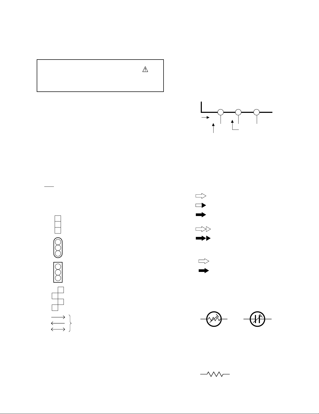
2. Indications of control voltage
AUX : Active at high.
AUX or AUX(L) : Active at low.
4. Voltage measurement
1) Regulator (DC/DC CONV) circuits
REC : Colour bar signal.
PB : Alignment tape (Colour bar).
— : Unmeasurable or unnecessary to measure.
4) Indication on schematic diagram
Voltage Indications for REC and PB mode on the schematic diagram are as shown below.
REC mode
12 3
2.5
(5.0)
PB mode
1.8
PB and REC modes
(Voltage of PB and REC modes
are the same)
Note: If the voltages are not indicated on the schematic
diagram, refer to the voltage charts.
5. Signal path Symbols
The arrows indicate the signal path as follows.
NOTE : The arrow is DVC unique object.
Playback signal path
3. Interpreting Connector indications
1
2
Removable connector
3
1
2
Wire soldered directly on board
3
1
Non-removable Board connector
2
3
1
2
4
Board to Board
3
Connected pattern on board
The arrows indicate signal path
Playback and recording signal path
Recording signal path
(including E-E signal path)
Capstan servo path
Drum servo path
(Example)
R-Y
Playback R-Y signal path
Y
Recording Y signal path
6. Indication of the parts for adjustments
The parts for the adjustments are surrounded with the circle as
shown below.
7. Indication of the parts not mounted on the circuit board
“OPEN” is indicated by the parts not mounted on the circuit
board.
S40889-01
R216
OPEN
4-1
Page 2
CIRCUIT BOARD NOTES
1. Foil and Component sides
1) Foil side (B side) :
Parts on the foil side seen from foil face (pattern face)
are indicated.
2) Component side (A side) :
Parts on the component side seen from component face
(parts face) indicated.
2. Parts location guides
Parts location are indicated by guide scale on the circuit board.
LOCATION
IC
Category : IC
Horizontal “A” zone
Vertical “6” zone
(A : Component side)
D : Discrete component)
B : Foil side
C : Chip component
REF No.
IC101 B C 6 A
Note: For general information in service manual, please
refer to the Service Manual of GENERAL INFORMATION Edition 4 No. 82054D (January 1994).
4-2
S40889-01
Page 3
4.1 BOARD INTERCONNECTIONS
NOTE
)
: The number of patch cords
are indicated by interconnected.
JUNCTION
ZOOM UNIT
(
)
Page 4-41
VTR CPU
(
)
Page 4-9
YTU94074-15
YTU94077-15
VPPC
RESET
YTU94074-20
YTU94077-20
CN5001
MDA 3.0V
5
YTU94074-24
YTU94077-24
OP DRIVE
(
)
4
Page 4-25
(
Page 4-37
OP DRIVE
VDCVF DS
)
TG/VDRV
(
)
Page 4-27
MDA 3.0V
(
)
REG 2.5V
(
)
Page 4-23
VC0
INV
VTR CPU
VC2
VC3
VC1
BLKA
BLKB
BLKC
Page 4-11
VTR CPU
(
Page 4-13
)
PD L
(
Page 4-38
)
(
)
Page 4-17
CAM
DSP
(
)
Page 4-15
INV
INH
VTR CPU
VTR CPU
XI164SEL
YTU94074-6
YTU94077-6
INV
VC0
VC1
VC2
1413
3
(
Page 4-33
)
Page 4-35
(
MONITOR
(
Page 4-33
B/W VF
(
Page 4-40
GND
SD WP
)
GND
(
VSS
VDCVF-DS
DSC/USB
(
)
Page 4-31
MMC CD
)
MON G
VDCVF DS
MMC CD
)
)
2
YTU94109-33
YTU94129A-33
VFREG4.8
BW Y
CVF G
VD
HD
NSLEED
BW VDD
ANA IN
(
Page 4-21
OP DRIVE
MMC CD
INV
A CSYNC
)
EXT V IN
VC3
BLKB
BLKA
BLKC
(
)
Page 4-5
INV
SDTIN
A CSYNC
(
)(
Page 4-7
ZOOM
CHRG LED
S DET
EXT V IN
Page 4-19
POW LED
XI164SEL
JIG
RESET
VTR CPU
D GAIN
S DET
VDC
BSEL
)
VTR CPU
B SEL
D GAIN
VD
HD
NC
NC
BW Y
NSLEEP
NCNCNC
1
YTU94074-20
NC
YTU94077-20
(
)
Page 4-39
VDC
(
Page 4-29
)
y10185001a rev0
ABCD EFGH
4-3 4-4
Page 4
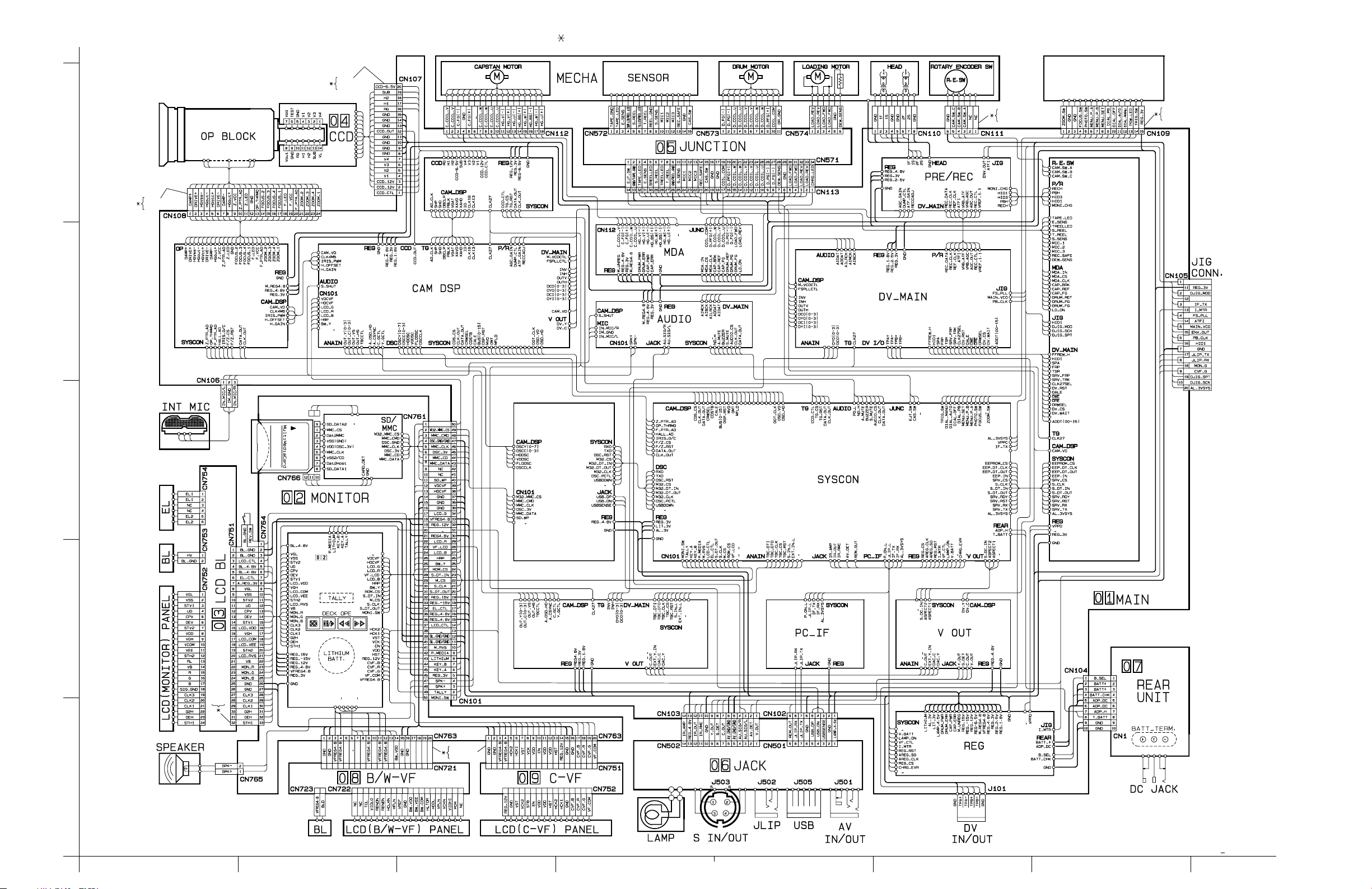
4.2 SYSCON SCHEMATIC DIAGRAM
NOTES :
For the destination of each signal and further line connections that are cut off from
this diagram,refer to "4.1 BOARD INTERCONNECTIONS".
The Parts Number,value and rated voltage etc. in the Schematic Diagram are for references only.
When replacing the parts,refer to the Parts List.
TO VTR CPU
TO VTR CPU
PC IF
TO REG
,
MAIN(SYSCON
)
5
JIG CONN.
TO REG
TO JACK
CN501
TO JACK
CN502
(
)
RESET DET
VCC
VOUT
NC
GND
TO
DSC/USB
TO MONITOR
CN761
4
TO PC IF
C
,
TO CAM DSP
,
AUDIO,TG/VDRV
OP DRIVE
,
TO CAM DSP
ANA IN
TO
3
ANA IN
UPD703039F1-A02
TO
CAM DSP
TO
REG
TO REAR UNIT
CN1
C
TO TG/VDRV
TO CAM DSP
TO TG/VDRV
TO REG
TO AUDIO
TO
MONITOR
CN761
2
TO
OP DRIVE
TO JUNCTION
CN571
TO
ZOOM UNIT
TO CAM DSP
TO AUDIO
TO CAM DSP
TO
VOUT
1
NO WEAR
4-5 4-6
y10186001a rev0
HGFEDCBA
Page 5
4.3 PC IF SCHEMATIC DIAGRAM
NOTES :
5
MAIN(PC IF
)
For the destination of each signal and further line connections that are cut off from
this diagram,refer to "4.1 BOARD INTERCONNECTIONS".
The Parts Number,value and rated voltage etc. in the Schematic Diagram are for references only.
When replacing the parts,refer to the Parts List.
4
3
2
1
TO SYSCON
TO REG
2SC4617/RS/-X
RB501V-40-X
TO JACK
CN501
JIG CONN.
NO WEAR
ABCD EFGH
4-7 4-8
y30121001a rev0
Page 6
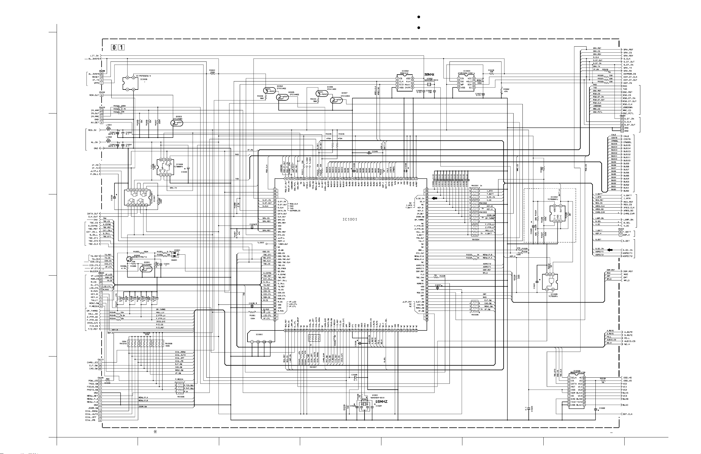
4.4 VTR CPU SCHEMATIC DIAGRAM
NOTES :
For the destination of each signal and further line connections that are cut off from
this diagram,refer to "4.1 BOARD INTERCONNECTIONS".
The Parts Number,value and rated voltage etc. in the Schematic Diagram are for references only.
When replacing the parts,refer to the Parts List.
TO REG
MAIN(VTR CPU
)
TO REG
5
TO CAM DSP
TO DV MAIN
,
TO DV MAIN
PRE/REC
JIG CONN.
TO JUNCTION
CN571
4
YQ44881A
MN10316KJH
MN1030F04KYBJH
TO
ROTARY ENCODER SW
TO MDA
TO JUNCTION
CN571
TO PRE/REC
3
2
1
TO SYSCON
TO SYSCON
TO SYSCON
TO SYSCON
TO REG
TO MDA
TO DV MAIN
1k
1k
TO DV MAIN
TO TG/VDRV
SN74AHC2G53T
MN103016KJH
JIG CONN.
TO
ROTARY ENCODER SW
NO WEAR
4-9 4-10
TO REG
y10188001a rev0
HGFEDCBA
Page 7
4.5 MDA SCHEMATIC DIAGRAM
NOTES :
For the destination of each signal and further line connections that are cut off from
this diagram,refer to "4.1 BOARD INTERCONNECTIONS".
The Parts Number,value and rated voltage etc. in the Schematic Diagram are for references only.
When replacing the parts,refer to the Parts List.
5
4
TO VTR CPU
TO REG
TO VTR CPU
TO JUNCTION
CN571
MAIN(MDA
)
TO REG
TO VTR CPU
TO REG
TO VTR CPU
TO
CAPSTAN MOTOR
3
270
TO JUNCTION
CN571
TO VTR CPU
TO JUNCTION
CN571
2
TO JUNCTION
CN571
1
NO WEAR
ABCD EFGH
4-11 4-12
y20123001a rev1
Page 8
4.6 AUDIO SCHEMATIC DIAGRAM
NOTES :
For the destination of each signal and further line connections that are cut off from
this diagram,refer to "4.1 BOARD INTERCONNECTIONS".
The Parts Number,value and rated voltage etc. in the Schematic Diagram are for references only.
When replacing the parts,refer to the Parts List.
AUDIO
TO MONITOR
CN761
5
TO DV MAIN
R
4
R
TO
INT MIC
R
L
L
R
R
R
R
L
R
L
TO SYSCON
TO REG
3
L
R
R
R
L
L
L
L
R
L
R
L
R
L
L
TO JACK
CN502
2
L
1
NO WEAR
3.3k
TO SYSCON
TO CAM DSP
TO SYSCON
y20124001a rev0
4-13 4-14
HGFEDCBA
Page 9
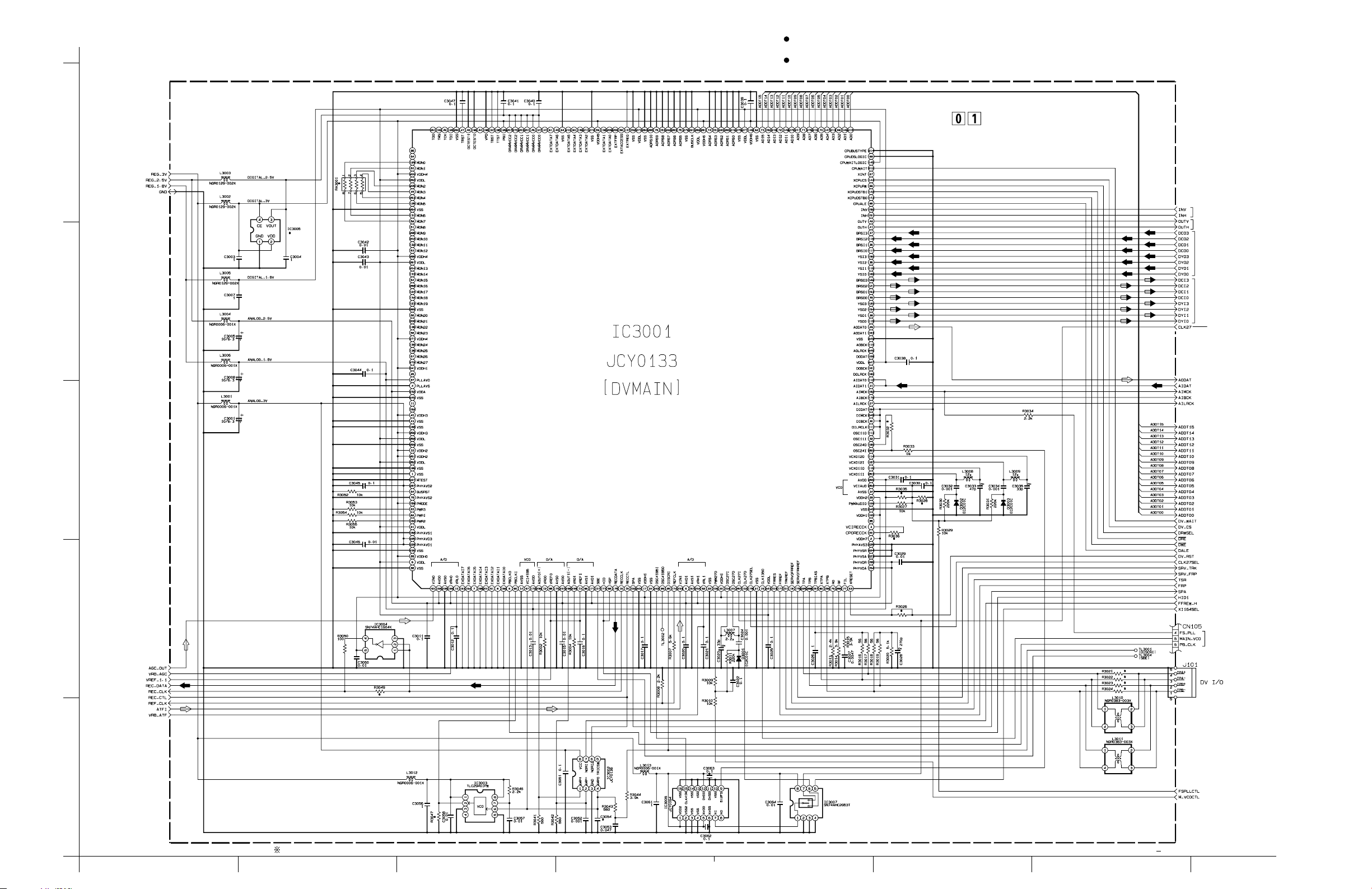
4.7 DV MAIN SCHEMATIC DIAGRAM
NOTES :
For the destination of each signal and further line connections that are cut off from
this diagram,refer to "4.1 BOARD INTERCONNECTIONS".
The Parts Number,value and rated voltage etc. in the Schematic Diagram are for references only.
When replacing the parts,refer to the Parts List.
MAIN(DV MAIN
)
5
TO REG
TO CAM DSP
ANA IN
C
C
C
C
Y
Y
Y
Y
C
C
C
C
4
Y
Y
Y
Y
C
C
C
C
Y
Y
Y
Y
C
C
C
C
Y
Y
Y
Y
TO CAM DSP
TO CAM DSP
ANA IN
TO CAM DSP
TO AUDIO
TO VTR CPU
TO TG/VDRV
3
2
JIG CONN.
TO
PRE/REC
1
TO CAM DSP
NO WEAR
ABCD EFGH
4-15 4-16
y10196001a rev0
Page 10
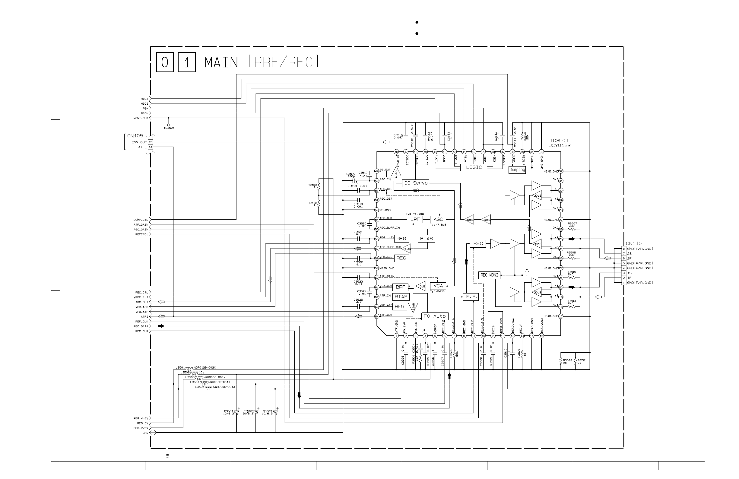
4.8 PRE/REC SCHEMATIC DIAGRAM
NOTES :
For the destination of each signal and further line connections that are cut off from
this diagram,refer to "4.1 BOARD INTERCONNECTIONS".
The Parts Number,value and rated voltage etc. in the Schematic Diagram are for references only.
When replacing the parts,refer to the Parts List.
5
TO
VTR CPU
JIG CONN.
4
TO CAM DSP
TO HEAD
3
TO DV MAIN
2
TO REG
1
NO WEAR
4-17 4-18
y20126001a rev0
HGFEDCBA
Page 11
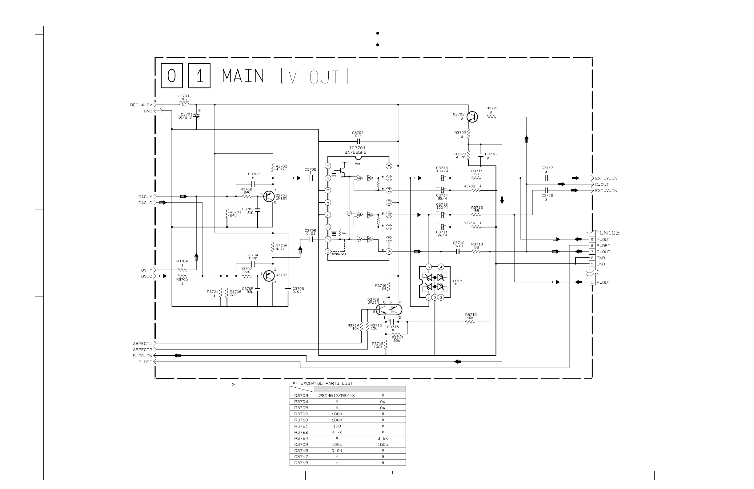
4.9 V OUT SCHEMATIC DIAGRAM
NOTES :
For the destination of each signal and further line connections that are cut off from
this diagram,refer to "4.1 BOARD INTERCONNECTIONS".
The Parts Number,value and rated voltage etc. in the Schematic Diagram are for references only.
When replacing the parts,refer to the Parts List.
5
TO REG
C
4
TO ANA IN
Y
Y
C
Y
C
Y
C
TO ANA IN
TO JACK
CN502
Y
Y
C
3
Y
C
CC
TO CAM DSP
C
2
TO SYSCON
C
NO WEAR
UMT2N
With ANALOG INPUT
C
y30123001a rev0
Without ANALOG INPUT
1
ABCD EFGH
4-19 4-20
Page 12
4.10
ANA IN SCHEMATIC DIAGRAM [GR-DVL915U]
NOTES :
For the destination of each signal and further line connections that are cut off from
this diagram,refer to "4.1 BOARD INTERCONNECTIONS".
The Parts Number,value and rated voltage etc. in the Schematic Diagram are for references only.
When replacing the parts,refer to the Parts List.
5
TO
CAM DSP
MAIN(ANA IN
)
C
Y
C
4
TO SYSCON
TO V OUT
C
Y
Y
C
Y
3
Y
C
Y
C
C
2
TO REG
C
C
C
Y
Y
C
Y
C
C
Y
Y
C
1
Y
Y
Y
C
C
TO TG/VDRV
TO SYSCON
DV MAIN
TO DV MAIN
TO CAM DSP
TO SYSCON
CAM DSP
TO
CAM DSP
TO
DV MAIN
,
,
Y
Y
Y
Y
Y
C
C
C
C
Y
Y
C
C
NO WEAR
4-21 4-22
y20127001a rev0
HGFEDCBA
Page 13
4.11 CAM DSP SCHEMATIC DIAGRAM
NOTES :
For the destination of each signal and further line connections that are cut off from
this diagram,refer to "4.1 BOARD INTERCONNECTIONS".
The Parts Number,value and rated voltage etc. in the Schematic Diagram are for references only.
When replacing the parts,refer to the Parts List.
TO TG/VDRV
MAIN(CAM DSP
)
CY
YC
CY
YC
YC
CY
CN101
TO MONITOR
CN761
5
TO
DV MAIIN
YC
TO CCD
CN5001
CY
4
Y
B-Y
R-Y
TO SYSCON,DV MAIN
TO DV MAIN
TO OP DRIVE
TO
ANA IN
TO PRE/REC
TO PRE/REC
TO DV MAIN
TO PRE/REC
TO SYSCON
Y
3
VC0
VC1
VC2
TO ANA IN
BLKA
BLKC
BLKB
VC3
100
YC
YC
2
TO
OP DRIVE,VTR CPU
TO OP DRIVE
C
TO AUDIO
Y
Y
Y
R-Y
B-Y
YC
B-Y
R-Y
C
Y
Y
Y
B-Y
YC
TO V OUT
C
TO REG
Y
R-Y
Y
YC
TO
DSC/USB
TO MONITOR
CN761
JIG CONN.
1
R4303 R4304
TO REG
y10190001a rev0
ABCD EFGH
4-23 4-24
Page 14

4.12 OP DRIVE SCHEMATIC DIAGRAM
NOTES :
For the destination of each signal and further line connections that are cut off from
this diagram,refer to "4.1 BOARD INTERCONNECTIONS".
The Parts Number,value and rated voltage etc. in the Schematic Diagram are for references only.
When replacing the parts,refer to the Parts List.
MAIN(OP DRIVE
)
5
1M
4
82k
680
TO OP BLOCK
3
TO CAM DSP
TO REG
TO SYSCON
2
1
NO WEAR
4-25 4-26
y30125001a rev0
HGFEDCBA
Page 15

4.13 TG/VDRV SCHEMATIC DIAGRAM
NOTES :
For the destination of each signal and further line connections that are cut off from
this diagram,refer to "4.1 BOARD INTERCONNECTIONS".
The Parts Number,value and rated voltage etc. in the Schematic Diagram are for references only.
When replacing the parts,refer to the Parts List.
MAIN(TG/VDRV
)
5
TO CCD
CN5001
4
TO
CAM DSP
3
TO SYSCON
TO CAM DSP
2
TO CAM DSP,DV MAIN
ANA IN,VTR CPU
TO REG
1
NO WEAR
ABCD EFGH
4-27 4-28
y30126001a rev0
Page 16

4.14 REG SCHEMATIC DIAGRAM
NOTES :
For the destination of each signal and further line connections that are cut off from
this diagram,refer to "4.1 BOARD INTERCONNECTIONS".
The Parts Number,value and rated voltage etc. in the Schematic Diagram are for references only.
When replacing the parts,refer to the Parts List.
MAIN(REG
TO
REAR UNIT
CN1
TO SYSCON
TO SYSCON
TO SYSCON
5
4
)
TO SYSCON
TO SYSCON
REG RST
JIG CONN.
TO MDA
TO SYSCON
TO ANA IN,SYSCON
DSC/USB,VTR CPU
PRE/REC,DV MAIN
MDA,CAM DSP,TG/VDRV
AUDIO,OP DRIVE
TO ZOOM UNIT
TO DV MAIN,PRE/REC,CAM DSP
TO JACK
CN501
TO ANA IN
DV MAIN
CAM DSP
TO ANA IN,DSC/USB
PRE/REC,MDA
TO MDA
CAM DSP,AUDIO
AUDIO
VOUT,OP DRIVE
OP DRIVE
TO SYSCON
TO JACK
CN502
TO MONITOR
CN761
3
0.022
2
CPU ROM
(
)
NORM : R6014 SIDE
TO TG/VDRV
TO TG/VDRV
TO VTR CPU
TO SYSCON
TO
VTR CPU
TO SYSCON
1
Q6207
NO WEAR
4-29 4-30
y10192001a rev0
HGFEDCBA
Page 17

4.15 DSC/USB SCHEMATIC DIAGRAM
NOTES :
For the destination of each signal and further line connections that are cut off from
this diagram,refer to "4.1 BOARD INTERCONNECTIONS".
The Parts Number,value and rated voltage etc. in the Schematic Diagram are for references only.
When replacing the parts,refer to the Parts List.
MAIN(DSC/USB
)
5
TO MONITOR
CN761
100k
TO SYSCON
TO JACK
CN501
TO REG
TO
CAM DSP
TO
SYSCON
TO REG
SN74AHC2G53T
4
0
0.001
NRZ0034-221W
220
220
NRZ0034-221W
YC
3
15
10/6.3
CY
2
Y
C
MBV400TC90PTA06
820
15p
1
OUT
VSS
VDD
NC
CY
YC
CY
TO SYSCON
NO WEAR
ABCD EFGH
4-31 4-32
y10193001a rev0
Page 18

4.16 MONITOR SCHEMATIC DIAGRAM
NOTES :
For the destination of each signal and further line connections that are cut off from
this diagram,refer to "4.1 BOARD INTERCONNECTIONS".
The Parts Number,value and rated voltage etc. in the Schematic Diagram are for references only.
When replacing the parts,refer to the Parts List.
B/W VF
TO
B/W VF
TO
TO
C VF/B/W VF UNIT
MONITOR
5
Y
B-Y
R-Y
Y
Y
Y
TO AUDIO CN101
TO REG CN101
TO SYSCON CN101
TO REG CN101
TO REG CN101
TO REG CN101
TO CAM DSP CN101
TO REG CN101
TO REG CN101
TO SPEAKER
Y
Y
Y
Y
R-Y
R-Y
B-Y
Y
B-Y
Y
4
TO SYSCON CN101
TO SYSCON CN101
TO CAM DSP CN101
3
2
TO SYSCON CN101
TO SYSCON CN101
TO SYSCON CN101
TO SYSCON CN101
TO CAM DSP CN101
TO CAM DSP CN101
TO CAM DSP CN101
TO DSC/USB CN101
Y
R-Y
Y
B-Y
Y
-
VCC
+
+
-
GND
B-Y
Y
R-Y
B-Y
R-Y
B-Y
Y
Y
B-Y
R-Y
Y
/NC
/NC
/NC
/NC
/NC
/NC
TO LCD BL
CN751
TO CAM DSP CN101
TO
MULTI MEDIA CARD
TALLY
OPEN SW
1
y10194001a rev0
HGFEDCBA
With DSC
Without DSC
R7110
R7111 R7112 R7113 R7114 R7115
0
00000
With LIGHT
Without LIGHT
NO WEAR
4-33 4-34
Page 19

4.17 LCD BL SCHEMATIC DIAGRAM
NOTES :
For the destination of each signal and further line connections that are cut off from
this diagram,refer to "4.1 BOARD INTERCONNECTIONS".
The Parts Number,value and rated voltage etc. in the Schematic Diagram are for references only.
When replacing the parts,refer to the Parts List.
LCD BL
TO EL
5
4
TO
BACKLIGHT
2SC3647/ST/-X2SC3647/ST/-X
TO MONITOR
CN764
3
: EXCHANGE PARTS LIST
2
With EL Without EL
1
R-Y
Y
B-Y B-Y
TO LCD
R-Y
Y
NO WEAR
ABCD EFGH
4-35 4-36
y30127001a rev0
Page 20

4.18 CCD SCHEMATIC DIAGRAM 4.19 JUNCTION SCHEMATIC DIAGRAM
NOTES :
5
For the destination of each signal and further line connections that are cut off from
this diagram,refer to "4.1 BOARD INTERCONNECTIONS".
The Parts Number,value and rated voltage etc. in the Schematic Diagram are for references only.
When replacing the parts,refer to the Parts List.
5
NOTES :
For the destination of each signal and further line connections that are cut off from
this diagram,refer to "4.1 BOARD INTERCONNECTIONS".
The Parts Number,value and rated voltage etc. in the Schematic Diagram are for references only.
When replacing the parts,refer to the Parts List.
CCD
TO
TO TG/VDRV
CN107
4
TO CAM DSP
CN107
LOADING MOTOR
4
TO
DRUM MOTOR
TO SYSCON CN113
TO MDA
CN113
TO VTR CPU CN113
TO MDA
CN113
3
2
1 1
3
TO SYSCON CN113
TO VTR CPU
CN113
TO MDA CN113
TO VTR CPU CN113
TO MDA CN113
2
TO
SENSOR
TO VTR CPU CN113
TO MDA CN113
TO VTR CPU
CN113
TO SYSCON CN113
NO WEAR
y40071001a rev0
DCBA
4-37 4-38
y40069001a rev0
A DCB
Page 21

4.20 JACK SCHEMATIC DIAGRAM
NOTES :
For the destination of each signal and further line connections that are cut off from
this diagram,refer to "4.1 BOARD INTERCONNECTIONS".
The Parts Number,value and rated voltage etc. in the Schematic Diagram are for references only.
When replacing the parts,refer to the Parts List.
5
BA10358F-XE
4
TO SYSCON CN103
WB SENS
Y
Y Y
Y
C
C
TO REG CN103
TO SYSCON
CN103
TO V OUT
CN103
L
R
C
3
C
R
L
R
L
L
R
2
TO AUDIO CN103
TO SYSCON CN103
TO V OUT CN103
TO SYSCON CN102
TO PC IF CN102
TO DSC/USB
CN102
TO REG CN102
NO WEAR
1
Without DSC
With DSC
ABCD
y40068001a rev0
4-39
Page 22

4.21 B/W VF SCHEMATIC DIAGRAM
NOTES :
For the destination of each signal and further line connections that are cut off from
this diagram,refer to "4.1 BOARD INTERCONNECTIONS".
The Parts Number,value and rated voltage etc. in the Schematic Diagram are for references only.
When replacing the parts,refer to the Parts List.
5
TO
MONITOR
TO
MONITOR
Y
Y
4
TO
MONITOR
Vin
Vout
Cont
GND
3
TO
MONITOR
NOISE
TO
MONITOR
2
: EXCHANGE PARTS LIST
y40070001a rev0
NO WEAR
1
4-40
ABCD
Page 23

4.22 ZOOM UNUT SCHEMATIC DIAGRAM
5
4
TO SYSCON
CN109
3
ZOOM SW
GND
GND
FOCUS SW
PHOTO SW
MENU P A
MENU P B
MENU SET
DIAL PB
DIAL OFF
DIAL AUTO
DIAL MANU
1
2
3
4
5
6
7
8
9
10
11
12
NOTES :
For the destination of each signal and further line connections that are cut off from
this diagram,refer to "4.1 BOARD INTERCONNECTIONS".
The schematic diagram is only for reference. Avoid replacing individual parts.
Replace the entire unit only.
POWER LED
FOCUS
SNAP SHOT
PUSH
PLAY
OFF
AUTO
MANU
POWER SW
13
14
15
START/STOP
ZOOM SW(T/W)/VOL.
)
(
/
TO REG
CN109
POW LED
TRIG SW
REG 3V
2
1
ABCD
4-41 4-42
Page 24

4.23 MAIN CIRCUIT BOARD
FOIL SIDE(B
)
MAIN
YB10137-01-02
72
73
451
108
20
10
8
24
109
1
80
37
4
5
36
3
1
5
8
4
5
14
1
144
1
5
3
4
4
1
3
1
8
5
51
20
21
40
41
4
5
1
60
3
1
1
80
61
19
38
20
18 1
1
3
4
5
5
4
3
1
36
37
48
1
25
12
D
24
13
C
11
3
4
1
5
1
25
2
1
5
8
58
81
100
48
4
1
41
1 30
4
3
5
1
50
31
8
1
14
4
1
5
8
5
9
4
16
8
5
815
20
1
8
1
14
11
5
15
10
5
4
8
1
1
23
4
4
3
4
3
14 1
B
A
4
1
3
8
1
4
1
3
1
5
5
8
5
4
7
4
1
14
8
5
12
4-43 4-44
45
3
Page 25

COMPONENT PARTS LOCATION GUIDE
REF.NO. LOCATION REF.NO. LOCATION REF.NO. LOCATION REF.NO. LOCATION REF.NO. LOCATION REF.NO. LOCATION REF.NO. LOCATION REF.NO. LOCATION
CAPACITOR
C1001 B C 5A
C1002 B C 5A
C1003 B C 4A
C1004 B C 4A
C1005 B C 5A
C1006 B C 5A
C1007 B C 3B
C1008 B C 5A
C1009 B C 5A
C1010 B C 5A
C1011 B C 5A
C1012 B C 5A
C1013 B C 5A
C1014 B C 5A
C1015 B C 5A
C1016 B C 5A
C1017 B C 5A
C1018 B C 5A
C1019 B C 5A
C1020 B C 4B
C1021 B C 4B
C1022 B C 3B
C1023 B C 3B
C1024 B C 4A
C1025 B C 4A
C1026 B C 4A
C1027 B C 5A
C1028 B C 5A
C1029 B C 5A
C1030 B C 5A
C1031 B C 4A
C1032 B C 3A
C1033 B C 3A
C1034 B C 4A
C1035 B C 4A
C1036 B C 4A
C1037 B C 4A
C1038 B C 4A
C1039 B C 5A
C1040 A C 1B
C1041 A C 1B
C1307 B C 3A
C1401 B C 3B
C1402 B C 3B
C1405 B C 3A
C1406 B C 3B
C1408 B C 3B
C1409 B C 3B
C1410 B C 3A
C1411 B C 3A
C1412 B C 3A
C1413 B C 3B
C1414 B C 3B
C1415 B C 3B
C1416 B C 3B
C1417 B C 3A
C1418 B C 3A
C1419 B C 3A
C1420 B C 3A
C1601 B C 3D
C1602 B C 3C
C1603
BC3C
C1605 B C 3C
C1606 B C 3C
C1607 A C 3A
C1610 B C 3D
C1611 B C 3D
C1612 B C 3D
C1613 B C 3C
C1614 B C 3D
C1615 B C 3D
C1616 B C 3D
C1617 B C 3D
C1618 B C 3C
C1619 B C 3C
C1620 B C 3C
C1621 B C 3C
C1622 B C 3C
C1623 B C 3C
C1624 B C 3C
C1625 B C 3C
C1626 B C 3C
C1627 B C 3C
C1628 B C 3C
C1632 B C 3C
C1633 B C 3D
C1635 B C 3C
C1638 B C 3D
C1639 B C 3D
C1640 B C 3D
C1641 B C 3D
C1642 B C 3C
C2001 A C 4A
C2002 A C 4A
C2003 A C 4A
C2004 A C 5A
C2005 A C 5A
C2006 A C 4A
C2007 A C 4A
C2008 A C 4A
C2009 A C 4A
C2010 A C 4A
C2011 A C 4A
C2012 A C 5A
C2013 A C 4A
C2014 A C 4A
C2015 A C 4B
C2016 A C 4A
C2017 A C 4A
C2018 A C 4A
C2019 A C 4A
C2020 A C 4A
C2021 A C 4A
C2101 A C 5A
C2102 A C 5A
C2103 A C 5A
C2104 A C 5A
C2107 A C 5A
C2108 A C 5A
C2109 A C 5A
C2110 A C 5A
C2111 A C 4A
C2112 A C 5A
C2113 A C 5A
C2114 A C 5A
C2115 A C 4A
C2116 A C 5A
C2121 A C 5A
C2122 A C 5A
C2123 A C 5B
C2124 A C 5A
C2125 A C 5B
C2126 A C 5A
C2129 A C 5A
C2130 A C 5A
C2131 A C 5A
C2132 A C 5A
C2133 A C 5B
C2134 A C 5A
C2201 A C 5A
C2202 A C 5A
C3001 B C 1A
C3003 B C 1A
C3004 B C 1A
C3005 B C 1A
C3007 B C 1A
C3008 B C 3A
C3011 B C 2A
C3012 B C 2A
C3013 B C 2A
C3015 B C 2A
C3016 B C 2A
C3017 B C 2A
C3020 B C 2A
C3021 B C 2A
C3022 B C 3A
C3023 B C 3A
C3024 B C 3A
C3025 B C 1A
C3026 B C 1A
C3027 B C 2A
C3028 B C 1A
C3029 B C 1A
C3030
3BCB
3ACBC3031
3BCBC3032
3ACBC3033
3ACBC3034
3ACBC3035
2BCBC3038
1ACBC3039
1ACBC3040
1ACBC3041
2ACBC3042
2ACBC3043
2ACBC3044
2ACBC3045
2ACBC3046
2BCBC3047
1ACBC3051
1ACBC3052
1ACBC3053
1ACBC3054
1ACBC3056
1ACBC3057
1ACBC3058
1ACBC3060
MAIN
3ACBC3061
3ACBC3062
3ACBC3063
3ACBC3064
3CCAC3501
3CCAC3502
2DCAC3503
2CCAC3504
2CCAC3505
2CCAC3506
2CCAC3507
2CCAC3508
2CCAC3509
2CCAC3510
3CCAC3511
3CCAC3512
3CCAC3513
3CCAC3514
3CCAC3515
3CCAC3516
3CCAC3517
3CCAC3518
3CCAC3519
2CCAC3520
2CCAC3521
2CCAC3522
2CCAC3523
2CCAC3524
2CCAC3525
2CCAC3526
3CCAC3527
1ACAC3701
3ACAC3702
3ACAC3703
3ACAC3704
3ACAC3705
3ACAC3706
1ACAC3707
2ACAC3708
2ACAC3709
1ACAC3710
1ACAC3711
1ACAC3712
1ACAC3713
1ACAC3714
1ACAC3715
1ACAC3716
1ACAC3717
1ACAC3718
3ACAC3901
3ACAC3902
3ACAC3903
3ACAC3904
3BCAC3905
3BCAC3906
3BCAC3907
3BCAC3908
3BCAC3909
4BCAC3910
4ACAC3911
4ACAC3912
4ACAC3913
3ACAC3914
3ACAC3915
3ACAC3916
3BCAC3917
4BCAC3919
4BCAC3920
3ACAC3923
4ACAC3924
4BCAC3925
3BCAC3951
3BCAC3954
3ACAC3955
3ACAC3956
3ACAC3957
3ACAC3958
3ACAC3959
3BCAC3961
3BCAC3962
3BCAC3963
3BCAC3964
3BCAC3965
3BCAC3966
3BCAC3967
3BCAC3968
4DCBC4201
4CCBC4202
4CCBC4203
5CCBC4204
5CCBC4205
5DCBC4206
5DCBC4207
5DCBC4208
COIL
3ACBIC1402
3BCBIC1403
3ACBIC1404
3CCBIC1601
4ACAIC2001
2ACBIC3001
1ACBIC3002
1ACBIC3003
2ACBIC3004
1ACBIC3005
3ACBIC3006
3ACBIC3007
2CCAIC3501
1ACAIC3701
4ACAIC3901
3BCAIC3902
4ACAIC3903
3BCAIC3951
4CCBIC4201
4CCBIC4202
4BCBIC4301
4CCBIC4302
4CCBIC4304
4CCAIC4802
4CCAIC4803
3BCAIC4804
4BCAIC4806
4BCAIC4851
4CCAIC5501
2ACAIC6001
2ACAIC6101
2CCBIC8001
2BCBIC8002
1BCBIC8003
3CCBIC8004
2CCBIC8005
2CCBIC8006
1CCBIC8007
2DCBIC8051
2CCBIC8052
2CCBIC8053
3CCAIC8401
5BCAIC8402
5BCAIC8403
5ACBL1001
4ACBL1002
3BCBL1401
3BCBL1402
4ACAL2001
4BCAL2002
1ACBL3001
1ACBL3002
1ACBL3003
1ACBL3004
1ACBL3005
3ACBL3006
3ACBL3007
3ACBL3008
3ACBL3009
1ACBL3010
1ACBL3011
1ACBL3012
3ACBL3013
3CCAL3501
3CCAL3502
2BCAL3503
2CCAL3504
2CCAL3505
1ACAL3701
3BCAL3901
3BCAL3902
4BCAL3903
3ACAL3904
3BCAL3951
3ACAL3952
3BCAL3953
4CCBL4201
4CCBL4301
4CCBL4302
5BCBL4303
4BCBL4304
4CCBL4305
4BCBL4306
3BCBL4307
4CCAL4802
4BCAL4851
4BCAL4852
4BCAL4853
3CCAL5501
3CCAL5502
3DCAL5503
3DCAL5504
3DCAL5505
TRANSISTOR
RESISTOR
5DCBC4209
4DCBC4210
4DCBC4211
4DCBC4212
4DCBC4213
4CCBC4214
4CCBC4215
4CCBC4216
4CCBC4301
3CCBC4302
4CCBC4303
5BCBC4304
4CCBC4305
4CCBC4306
4BCBC4307
4BCBC4308
4CCBC4309
4CCBC4310
4CCBC4311
5BCBC4312
4BCBC4313
5BCBC4314
5BCBC4315
5CCBC4317
4BCBC4318
5BCBC4319
5CCBC4320
5CCBC4321
4BCBC4322
4CCBC4323
3BCBC4324
4BCBC4325
4BCBC4326
4BCBC4327
4BCBC4328
4BCBC4329
4CCBC4330
3CCBC4331
3CCBC4332
4CCBC4333
3CCBC4334
4BCBC4335
4CCBC4336
4BCBC4337
4BCBC4338
5CCBC4339
4CCBC4340
4CCBC4341
5CCBC4342
4BCBC4343
5CCBC4344
4BCBC4345
4BCBC4346
4BCBC4347
4BCBC4348
5CCBC4349
5BCBC4350
4CCAC4803
4CCAC4804
4BCAC4805
3CCAC4806
3CCAC4807
4CCAC4808
4CCAC4809
4CCAC4810
4CCAC4811
4CCAC4812
3BCAC4813
4CCAC4814
3BCAC4815
3BCAC4819
4CCAC4820
3CCAC4822
4BCAC4823
4BCAC4851
4BCAC4852
4BCAC4853
4BCAC4854
4BCAC4855
4BCAC4858
4BCAC4859
4BCAC4860
4BCAC4861
4BCAC4862
4BCAC4864
4BCAC4865
4CCAC4866
4CCAC5501
4CCAC5503
4CCAC5504
4CCAC5505
3CCAC5506
4CCAC5507
4CCAC5508
4CCAC5509
3CCAC5510
4CCAC5511
3DCAC5512
3CCAC5513
3DCAC5514
4CCAC5515
3CCAC5516
3DCAC5517
4CCAC5518
3DCAC5519
2ACAC6001
2ACAC6004
2ACAC6005
1BCAC6101
1BCAC6102
1BCAC6103
1BCAC6105
2BCAC6106
2BCAC6107
2BCAC6108
2BCAC6109
3BCAC6110
3ACAC6111
3ACAC6112
3ACAC6113
3ACAC6114
3ACAC6115
3ACAC6116
2ACAC6117
2ACAC6118
2ACAC6119
2ACAC6120
2ACAC6121
2ACAC6122
2ACAC6123
2ACAC6124
2ACAC6125
2ACAC6126
2ACAC6127
2ACAC6128
2BCAC6129
2BCAC6130
1ACAC6131
1ACAC6132
1ACAC6133
2BCAC6134
2CCAC6201
2BCAC6202
3ACAC6203
2ACAC6204
2ACAC6205
1CCAC6206
2CCAC6207
3ACAC6208
1CCAC6209
2CCAC6210
3ACAC6211
1CCAC6212
2BCAC6213
1CCAC6214
1BCAC6215
3ACAC6216
1BCAC6217
1BCAC6218
2ACAC6219
1BCAC6220
2BCAC6221
2BCAC6222
1BCAC6223
3ACAC6224
3BCAC6225
2BCAC6226
2BCAC6227
3BCAC6228
1BCAC6229
3BCAC6230
5BCAC6231
2DCAC6701
2CCAC6702
2CCAC6703
2CCAC6704
3BCAC6705
2CCBC8001
2CCBC8002
2CCBC8003
2CCBC8004
2DCBC8005
2DCBC8006
2CCBC8007
2CCBC8008
1CCBC8009
1CCBC8010
1DCBC8011
CONNECTOR
DIODE
2CCBC8012
1ACBC8013
1BCBC8014
2BCBC8015
2BCBC8016
2BCBC8017
3BCBC8018
3BCBC8019
3BCBC8020
2CCBC8021
2BCBC8022
1BCBC8023
1BCBC8024
1BCBC8025
2BCBC8026
1CCBC8027
1CCBC8028
2CCBC8029
2CCBC8030
2CCBC8031
3CCBC8039
1CCBC8040
3CCBC8045
3BCBC8046
3CCBC8047
2CCBC8051
2CCBC8052
2DCBC8053
2CCBC8054
2CCBC8055
3CCAC8401
3CCAC8402
3CCAC8403
3CCAC8404
5BCAC8405
5BCAC8406
5BCAC8407
4BCAC8408
4BCAC8409
3ACACN101
5BCACN102
5BCBCN103
1BCACN104
1BCBCN105
5ACACN106
4DCACN107
4CCACN108
1DCACN109
2DCACN110
1BCBCN111
4DCBCN112
3DCACN113
4ACBD1001
1BCAD1002
3ACBD1301
3ACBD1302
3DCBD1602
4DCBD1603
3CCBD1604
4ACAD2001
4ACAD2002
3ACBD3001
3BCBD3002
3ACBD3003
1ACAD3701
3CCAD5501
2ACAD6002
2BCAD6201
2CCAD6202
1CCAD6203
1BCAD6204
1BCAD6205
2BCAD6206
2BCAD6207
2CCAD6701
2CCAD6702
2CCBD8051
5BCAD8401
IC
4ACBIC1001
5ACBIC1002
4ACBIC1003
4BCBIC1004
4BCBIC1005
4BCBIC1006
4ACBIC1007
4ACBIC1008
4ACBIC1009
3ACBIC1303
3ACBIC1304
3BCBIC1401
3DCAL5506
1BCAL6101
1BCAL6102
2BCAL6201
2CCAL6202
1CCAL6203
4BCAL6204
1CCAL6205
1CCAL6206
1BCAL6207
2BCAL6208
2BCAL6209
2BCAL6210
2CCAL6701
2CCBL8001
1ACBL8002
1BCBL8003
3BCAL8401
4BCAL8402
4ACBQ1001
4ACBQ1002
4ACBQ1003
4ACBQ1004
4ACBQ1005
5ACBQ1006
5ACBQ1007
3ACBQ1301
3BCBQ1401
3BCBQ1402
3ACBQ1403
3ACBQ1404
3DCBQ1601
4ACAQ2001
5ACAQ2002
4ACAQ2004
3ACAQ3701
1ACAQ3702
1ACAQ3703
3ACAQ3951
3BCAQ3952
3BCAQ3953
3BCAQ3954
4BCBQ4301
4BCBQ4302
4BCBQ4303
4CCAQ4801
4BCAQ4851
2ACAQ6001
2ACAQ6002
2ACAQ6003
2ACAQ6004
3BCAQ6101
3BCAQ6102
1BCAQ6201
2ACAQ6202
1CCAQ6203
1CCAQ6204
3BCAQ6205
3BCAQ6206
2BCAQ6207
1CCAQ6208
1BCAQ6210
1BCAQ6211
3BCAQ6212
2BCAQ6213
2BCAQ6214
3BCAQ6215
3BCAQ6216
2BCAQ6217
2DCAQ6701
3CCBQ8001
3BCAQ8401
4ACBR1001
5BCBR1002
5BCBR1003
5BCBR1004
5BCBR1005
5BCBR1006
5BCBR1007
3ACBR1008
4ACBR1009
5ACBR1010
4ACBR1011
4ACBR1012
4ACBR1013
4ACBR1014
4ACBR1015
4ACBR1016
3ACBR1017
3ACBR1018
3ACBR1019
4-45
Page 26

REF.NO. LOCATION REF.NO. LOCATION REF.NO. LOCATION REF.NO. LOCATION REF.NO. LOCATION REF.NO. LOCATION REF.NO. LOCATION
R1020 B C 3A
R1021 B C 3A
R1022 B C 3A
R1023 B C 4B
R1024 B C 4B
R1025 B C 4B
R1026 B C 4B
R1027 B C 4B
R1028 B C 4B
R1029 B C 5A
R1030 B C 5A
R1031 B C 4B
R1032 B C 4B
R1033 B C 5A
R1034 B C 5A
R1035 B C 5A
R1036 B C 3B
R1037 B C 4A
R1038 B C 4A
R1039 B C 4A
R1040 B C 4A
R1041 B C 4A
R1042 B C 4A
R1043 B C 4A
R1044 B C 5A
R1045 B C 5A
R1046 B C 5A
R1047 B C 5A
R1048 B C 5A
R1049 B C 5A
R1050 B C 5A
R1051 B C 4A
R1052 B C 4A
R1053 B C 4A
R1054 B C 4A
R1055 B C 4A
R1056 B C 4A
R1057 B C 4A
R1058 B C 4A
R1059 B C 4A
R1060 B C 4A
R1061 B C 3A
R1062 B C 3A
R1080 B C 3A
R1302 B C 3A
R1305 B C 3A
R1306 B C 3A
R1401 B C 3B
R1402 B C 3B
R1403 B C 3B
R1407 B C 3B
R1408 B C 3B
3CCBR1601
3CCBR1602
3CCBR1603
3CCBR1604
3DCBR1605
2CCBR1606
3CCBR1607
3CCBR1608
3DCBR1609
3CCBR1610
4DCBR1611
3CCBR1612
3CCBR1613
3CCBR1614
3CCBR1615
3CCBR1616
3CCBR1617
3CCBR1618
3CCBR1619
3CCBR1620
3CCBR1621
2CCBR1622
3DCBR1624
3BCBR1625
3BCBR1626
3CCBR1628
3CCBR1629
3ACAR1630
3ACAR1631
4DCBR1635
4DCBR1636
4DCBR1637
3CCBR1638
3CCBR1639
3CCBR1640
3CCBR1641
3CCBR1643
3CCBR1646
4ACAR2006
4ACAR2007
4ACAR2008
4ACAR2009
4ACAR2010
4ACAR2011
4ACAR2012
4ACAR2013
4ACAR2014
4ACAR2015
4ACAR2016
5ACAR2017
4ACAR2018
4ACAR2019
4ACAR2020
4ACAR2023
4ACAR2024
4ACAR2025
4ACAR2026
4ACAR2027
4ACAR2028
4BCAR2029
3BCBR1409
3BCBR1410
3BCBR1411
3BCBR1412
3BCBR1413
3ACBR1414
3ACBR1415
3ACBR1416
3BCBR1417
3ACBR1418
3ACBR1419
3ACBR1420
3BCBR1422
3BCBR1423
3BCBR1424
3BCBR1425
3BCBR1426
3BCBR1427
3BCBR1428
3BCBR1429
3BCBR1430
3ACBR1432
3ACBR1433
3ACBR1434
3ACBR1435
3ACBR1436
3ACBR1437
3ACBR1439
3ACBR1440
3ACBR1441
3ACBR1442
3ACBR1443
3ACBR1444
3ACBR1445
5ACAR2101
5ACAR2102
5ACAR2103
5ACAR2104
5ACAR2105
5ACAR2106
4ACAR2107
5ACAR2108
5ACAR2109
5ACAR2110
5ACAR2111
5ACAR2112
5ACAR2113
5ACAR2114
5ACAR2117
5ACAR2118
5ACAR2119
5ACAR2120
5ACAR2127
5ACAR2128
5BCAR2129
5ACAR2130
5ACAR2201
5ACAR2202
2ACBR3002
2ACBR3004
2ACBR3007
2ACBR3008
3ACBR3009
3ACBR3010
3ACBR3011
2ACBR3013
2ACBR3014
2ACBR3015
1ACBR3016
1ACBR3017
1ACBR3018
1ACBR3019
1ACBR3020
1ACBR3021
1ACBR3022
1ACBR3023
1ACBR3024
2BCBR3026
3ACBR3027
2BCBR3028
2BCBR3029
3BCBR3030
3ACBR3031
3ACBR3032
3ACBR3033
3ACBR3034
2BCBR3035
2ACBR3036
1ACBR3041
1ACBR3042
1ACBR3043
1ACBR3044
1ACBR3046
1ACBR3047
1ACBR3049
1ACBR3050
2ACBR3052
2ACBR3053
1ACBR3054
1ACBR3055
2CCAR3501
2CCAR3502
2CCAR3503
2CCAR3504
2CCAR3505
2CCAR3506
3CCAR3507
3CCAR3508
2CCAR3509
3CCAR3510
3CCAR3521
2CCAR3522
3ACAR3701
3ACAR3702
3ACAR3703
5BCBR3704
5BCBR3705
3ACAR3706
3ACAR3707
3ACAR3708
1ACAR3709
1ACAR3710
1ACAR3711
1ACAR3712
1ACAR3713
1ACAR3714
1ACAR3715
1ACAR3716
1ACAR3717
1ACAR3718
1ACAR3719
1ACAR3721
1ACAR3722
1ACAR3723
3ACAR3724
3ACAR3901
4ACAR3904
4BCAR3911
4BCAR3912
3ACAR3951
3ACAR3952
3ACAR3953
3ACAR3954
3ACAR3955
3ACAR3956
3BCAR3961
3BCAR3962
3BCAR3963
3BCAR3964
3BCAR3965
3BCAR3966
3BCAR3967
3BCAR3968
3BCAR3969
5CCBR4201
5CCBR4202
5CCBR4203
5DCBR4204
4CCBR4205
4CCBR4206
4CCBR4207
4CCBR4208
4BCBR4301
3CCBR4302
5CCBR4303
5CCBR4304
5CCBR4307
5CCBR4308
5BCBR4311
5BCBR4312
5BCBR4313
5BCBR4314
5BCBR4315
4BCBR4316
4BCBR4317
4BCBR4318
4BCBR4319
4BCBR4320
4BCBR4321
4BCBR4322
4BCBR4323
4BCBR4324
4BCBR4325
4BCBR4326
4BCBR4327
4BCBR4330
4BCBR4331
4BCBR4332
4BCBR4333
4BCBR4334
4BCBR4335
4BCBR4336
4CCBR4338
4BCBR4340
5BCBR4342
5BCBR4343
5CCBR4344
4CCBR4345
2BCAR4346
5BCBR4347
4BCBR4348
5BCBR4349
4BCBR4350
5BCBR4351
3CCAR4804
3CCAR4805
4CCAR4806
4CCAR4807
4CCAR4808
3CCAR4809
4CCAR4810
4CCAR4811
4CCAR4812
4CCAR4813
4CCAR4814
4CCAR4815
4CCAR4816
3CCAR4817
3CCAR4818
4BCAR4819
3BCAR4820
4BCAR4821
4BCAR4822
4BCAR4823
4BCAR4824
3BCAR4829
4BCAR4831
4BCAR4833
4CCAR4836
4CCAR4845
3BCAR4848
3BCAR4850
4CCAR4852
4BCAR4856
4BCAR4857
4BCAR4858
4CCAR4862
4CCAR4863
4CCAR4864
4CCAR4865
4CCAR4866
4CCAR4867
4CCAR4868
4BCAR4870
4BCAR4874
4CCAR5501
4CCAR5503
4CCAR5504
4CCAR5505
4CCAR5506
4CCAR5507
4CCAR5509
4CCAR5510
4CCAR5511
4CCAR5512
4CCAR5513
4CCAR5514
4CCAR5515
4CCAR5516
2ACAR6001
2ACAR6002
2ACAR6003
2ACAR6004
2ACAR6005
1ACAR6009
2ACAR6010
2ACAR6011
2ACAR6012
2ACAR6013
1BCAR6014
1BCAR6015
1BCAR6016
2BCAR6101
2BCAR6102
3BCAR6103
3BCAR6104
2BCAR6105
3BCAR6106
3BCAR6107
3BCAR6108
3BCAR6109
3ACAR6110
3ACAR6113
2ACAR6114
2ACAR6115
2ACAR6116
2ACAR6117
2BCAR6118
3BCAR6122
2BCAR6123
2BCAR6124
3ACAR6201
3ACAR6202
3ACAR6203
2ACAR6204
2ACAR6205
2ACAR6206
2ACAR6207
3ACAR6208
3ACAR6209
3ACAR6210
3ACAR6211
3ACAR6212
3BCAR6213
3BCAR6214
3BCAR6215
3BCAR6216
2BCAR6217
2BCAR6218
3ACAR6219
3ACAR6220
3ACAR6221
3ACAR6223
2ACAR6224
2ACAR6225
3ACAR6226
3ACAR6227
3ACAR6228
3ACAR6229
3ACAR6230
3BCAR6231
3BCAR6232
3BCAR6233
3BCAR6234
3BCAR6235
3BCAR6236
3BCAR6237
3BCAR6238
3BCAR6239
3BCAR6240
3BCAR6241
2BCAR6242
2BCAR6243
2BCAR6244
2BCAR6245
2BCAR6246
2CCAR6701
2CCAR6702
2CCAR6703
1ACAR6712
1ACAR6713
3CCBR8001
2CCBR8002
2CCBR8003
1CCBR8004
2BCBR8006
2CCBR8013
2CCBR8014
1CCBR8015
1CCBR8016
1CCBR8017
1CCBR8018
1CCBR8019
1CCBR8020
1CCBR8021
2CCBR8022
2CCBR8023
2CCBR8024
OTHER
2CCBR8025
2CCBR8026
2DCBR8027
2CCBR8028
3CCBR8030
3CCBR8031
3BCBR8035
3CCBR8036
1CCBR8037
1CCBR8038
2CCBR8053
2CCBR8056
2CCBR8057
2CCBR8059
2CCBR8060
3CCAR8401
3CCAR8402
3CCAR8403
3BCAR8404
5BCAR8406
5BCAR8407
5BCAR8408
5BCAR8409
5ACBRA1001
5ACBRA1002
5ACBRA1003
5ACBRA1004
5ACBRA1005
4ACBRA1006
5ACBRA1007
4ACBRA1008
5ACBRA1009
5ACBRA1010
3BCBRA1401
3BCBRA1402
3BCBRA1403
3ACBRA3001
4DCBRA4301
4DCBRA4302
4DCBRA4303
3CCBRA4304
3CCBRA4305
3BCBRA4306
3CCARA8401
3CCARA8402
3CCARA8403
3CCARA8404
1BCAF6101
1ADAJ101
1CCAS6001
4ACBTL1001
4ACBTL1002
4ACBTL1003
4BCBTL1301
3BCBTL1401
3BCBTL1402
3BCBTL1403
3BCBTL1404
3ACBTL1406
3ACBTL1407
3ACBTL1408
3ACBTL1409
3ACBTL1410
3ACBTL1411
3BCBTL1412
3BCBTL1413
3ACBTL1414
3ACBTL1415
3ACBTL1416
3CCBTL1601
3CCBTL1602
3CCBTL1603
3DCBTL1604
3ACATL1605
3ACATL1606
3BCATL1607
3BCATL1608
3BCATL1609
3BCATL1610
2CCBTL1611
3DCBTL1612
3BCBTL1613
3DCBTL1614
3DCBTL1615
3CCBTL1616
3CCBTL1617
3CCBTL1618
3CCBTL1619
1CCBTL3001
2ACBTL3002
1CCBTL3004
1CCBTL3501
4CCBTL4201
5CCBTL4202
5DCBTL4203
3CCBTL4301
4BCBTL4302
4BCBTL4303
4CCBTL4304
4BCBTL4305
4BCBTL4306
4BCBTL4307
4BCBTL4308
4BCBTL4309
4BCBTL4310
4BCBTL4311
4BCBTL4312
4BCBTL4313
4BCBTL4314
4BCBTL4405
3BCATL4801
4CCATL5501
4CCATL5502
4CCATL5503
4CCATL5504
4ACBX1001
5ACBX1002
4CCAX5501
2DCBX8001
3CCAX8401
4-46
Page 27

COMPONENT SIDE(A
MAIN
YB10317-01-02
)
D
C
1
34
12
13
20
24
124
38
1
25
1
48
37
36
20
19
58
8
1
33
4
1
48
5
8
41
5
8
32
49
1
17
16
1
64
15 1
A
B
1
1
1
3
9
1
3
5
4
4
1
23
48
49
64
1
41
3
4
51
33
60
32
17
16
5
8
40
61
4
1
4
1
4
2
3
21
20
6
4
1
3
1
6
80
1 50
4
1
3
16
17
32
33
1
64
110
49
48
1
4
2
3
1
16
54
4-47 4-48
8
9
21
3
Page 28
4.24
MONITOR CIRCUIT BOARD
14 8
17
24
25
36
37
13
112
48
453
)
E
MONITOR
YB10324-01-02
D
1
9
1
C
8
D
C
MONITOR
YB10324-01-02
E
COMPONENT SIDE(A
41
FOIL SIDE(B
58
41
)
20
58
1
21
501
B
2
A
3
4
B
232
2
A
3
4
1
COMPONENT PARTS LOCATION GUIDE
REF.NO. LOCATION REF.NO. LOCATION REF.NO. LOCATION REF.NO. LOCATION REF.NO. LOCATION REF.NO. LOCATION REF.NO. LOCATION REF.NO. LOCATION REF.NO. LOCATION REF.NO. LOCATION REF.NO. LOCATION REF.NO. LOCATION REF.NO. LOCATION REF.NO. LOCATION REF.NO. LOCATION
CAPACITOR
C1 A C 1C
C10 A C 3D
C11 A C 4D
C7101 B C 3D
C7102 B C 3D
C7103 B C 2D
C7601 B C 2C
C7602 A C 1C
C7603 B C 2C
C7604 B C 2D
C7605 B C 2D
C7606 B C 1D
C7607 A C 1D
C7608 A C 1D
C7609 B C 1D
C7610 A C 1D
C7611 A C 1D
C7612 A C 1D
C7613 B C 1C
C7614 B C 1D
C7615 A C 1D
C7616 B C 1C
C7617 B C 1C
C7618 B C 1C
C7619 B C 1C
C7620 B C 1C
C7621 B C 2C
C7622 B C 1C
C7623 A C 2D
C7624 A C 2D
C7625 A C 2D
C7626 A C 2D
C7627 A C 2C
C7628 B C 3B
C7629 B C 3B
C7630 A C 3B
C7631 A C 3B
C7632 A C 3B
C7633 A C 3B
C7634 A C 3B
C7635 A C 3B
C7636 A C 2B
C7637 A C 3B
C7638 B C 1D
C7639 B C 1D
C7640 A C 1B
C7641 A C 1A
C7642 B C 1E
C7643 B C 2C
C7644 B C 2C
MONITOR
C7645 B C 3B
CONNECTOR
CN761 A C 4D
CN763 A C 1E
CN764 A C 3B
CN765 A C 1C
CN766 B C 4C
DIODE
D1 A C 1A
D10 A C 3D
D7601 A C 3B
IC
IC7101 B C 2D
IC7601 B C 1D
IC7602 A C 2C
IC7603 A C 1B
IC7604 B C 1D
IC7605 B C 2C
COIL
L10 A C 4D
L7601 A C 2D
L7602 B C 1C
L7603 B C 1C
L7604 A C 3B
L7605 A C 3B
L7606 A C 3B
L7607 A C 3B
TRANSISTOR
Q10 A C 3D
Q7101 B C 2D
Q7601 B C 3B
Q7602 B C 3B
Q7603 B C 3B
Q7604 B C 3B
Q7605 B C 3B
Q7606 B C 3B
Q7607 B C 1D
Q7608 B C 1D
Q7609 A C 2B
Q7610 A C 2B
RESISTOR
R1 A C 3E
R2 A C 3E
R3 B C 1C
R4 B C 1D
R5 B C 1D
R6 B C 1D
R10 A C 4D
R11 A C 4D
R12 A C 4D
R13 A C 3D
R14 A C 4D
R15 A C 3D
R16 A C 3D
R17 A C 3D
R18 A C 4D
R19 A C 3D
R20 A C 3D
R21 A C 3D
R22 A C 3D
R23 A C 4D
R24 A C 3D
R25 A C 3D
R26 A C 3D
R27 A C 3D
R28 A C 3D
R7101 B C 2D
R7102 B C 2D
R7103 B C 2D
R7104 B C 2D
R7110 B C 2E
R7111 B C 1E
R7112 A C 1D
R7113 B C 1E
R7114 B C 2E
R7115 B C 1E
R7601 B C 1D
R7602 B C 1D
R7603 A C 2C
R7604 A C 2C
R7605 A C 2C
R7606 A C 2C
R7607 A C 2C
R7608 A C 2C
R7609 A C 2C
R7610 A C 2C
R7611 A C 2C
R7612 B C 3B
R7613 B C 3B
R7614 B C 3B
R7615 B C 3B
R7616 B C 3B
R7617 B C 3B
R7618 B C 3B
R7619 A C 3B
R7621 B C 3B
R7622 B C 3B
R7623 B C 3B
R7624 A C 2B
R7625 A C 2B
R7626 B C 1D
R7627 B C 1D
R7628 B C 2D
R7629 B C 1D
R7630 B C 1E
R7631 B C 3B
R7632 A C 1B
R7633 A C 1A
R7634 B C 2C
R7635 B C 2C
R7640 B C 1D
R7641 B C 1E
R7642 B C 1E
R7643 A C 1D
R7644 B C 1E
4-49 4-50
R7645 B C 1D
R7646 B C 1D
OTHER
BT1 A C 3C
C11P A C 4D
C7103P B C 3D
C7623P A C 2D
C7629P B C 3B
C7639P B C 1D
SW1 B C 3E
SW2 A C 1C
SW3 A C 1D
SW4 A C 1E
SW5 A C 1D
SW6 B C 2E
SW7601 B C 2A
TM1 A C 4A
ZP1-2 B C 4D
ZP1-3 B C 4D
ZP1-4 B C 3C
ZP1-5 B C 4D
ZP1-6 B C 4D
ZP1-7 B C 4C
ZP1-8 B C 4D
ZP3-3 B C 2E
ZP4-9 B C 3B
ZP6-1 B C 4D
ZP6-2 B C 4D
ZP6-3 B C 4C
ZP6-4 B C 4C
ZP6-5 B C 4C
ZP6-6 B C 4C
ZP6-7 B C 4C
ZP6-8 B C 4C
ZP6-9 B C 4D
ZP1-11 B C 4C
ZP1-12 B C 2C
ZP1-13 B C 2D
ZP1-14 B C 4A
ZP1-17 B C 1C
ZP1-18 B C 3D
ZP1-19 B C 3D
ZP1-20 B C 3C
ZP1-21 B C 3B
ZP1-22 B C 2D
ZP1-23 B C 2D
ZP1-24 B C 2D
ZP1-25 B C 2C
ZP1-26 B C 2D
ZP1-27 B C 4A
ZP1-28 B C 4A
ZP1-29 B C 2C
ZP1-30 B C 4A
ZP1-31 B C 4A
ZP1-32 B C 3B
ZP1-33 B C 3B
ZP1-38 B C 4A
ZP1-46 B C 3B
ZP1-49 B C 1A
ZP3-17 B C 1E
ZP3-18 B C 2D
ZP3-19 B C 2E
ZP3-20 B C 2D
ZP4-18 B C 3B
ZP4-23 B C 2B
ZP4-24 B C 2B
ZP4-25 B C 2C
ZP6-10 B C 3D
ZP7601 B C 1D
ZP7602 B C 2B
ZPG1 A D 2A
ZPG2 A D 3A
ZPG3 A D 2E
ZPG4 A D 1D
ZPG5 A D 3B
ZPG6 A D 1B
ZPG7 A D 1A
ZPG8 A D 1A
ZPG9 A D 1A
85
14
1
Page 29

LCD BL CIRCUIT BOARD4.25
LCD BL
YB10324-01-02
CAUTION HIGH VOLTAGE
CAUTION:
FOR CONTINUED PROTECTION AGAINST
F
FIRE HAZARD,REPLACE ONLY WITH SAME
TYPE AND RATED FUSE(S).
FOIL SIDE(B
F
ATTENTION:
POUR UNE PROTECTION PERMANENTE
CONTRE LES RISQUE D’INCENDE
REMPLACER LES FUSIBLES PAR UN AUTRE
DE MEME TYPE ET DE MEME TENSION.
)
,
COMPONENT SIDE(A
)
LCD BL
YB10324-01-02
12
F
0.375A
F7501
F751
16
0.2A
321
5
106
241
1
4-51 4-52
Page 30

CCD AND JUNCTION CIRCUIT BOARDS4.26
CCD
YB10316-01-01
FOIL SIDE(B
)
JUNCTION
FOIL SIDE(B
)
YB10314-01-01
15 1
COMPONENT SIDE(A
COMPONENT SIDE(A
)
)
JUNCTION
YB10314-01-01
111
CCD
YB10316-01-01
1 34
16
4-53 4-54
Page 31

JACK CIRCUIT BOARD4.27
FOIL SIDE(B
)
COMPONENT SIDE(A
)
8
1
5
4
JACK
YB10314-01-01
9
14
1
1
JACK
YB10314-01-01
4-55 4-56
Page 32

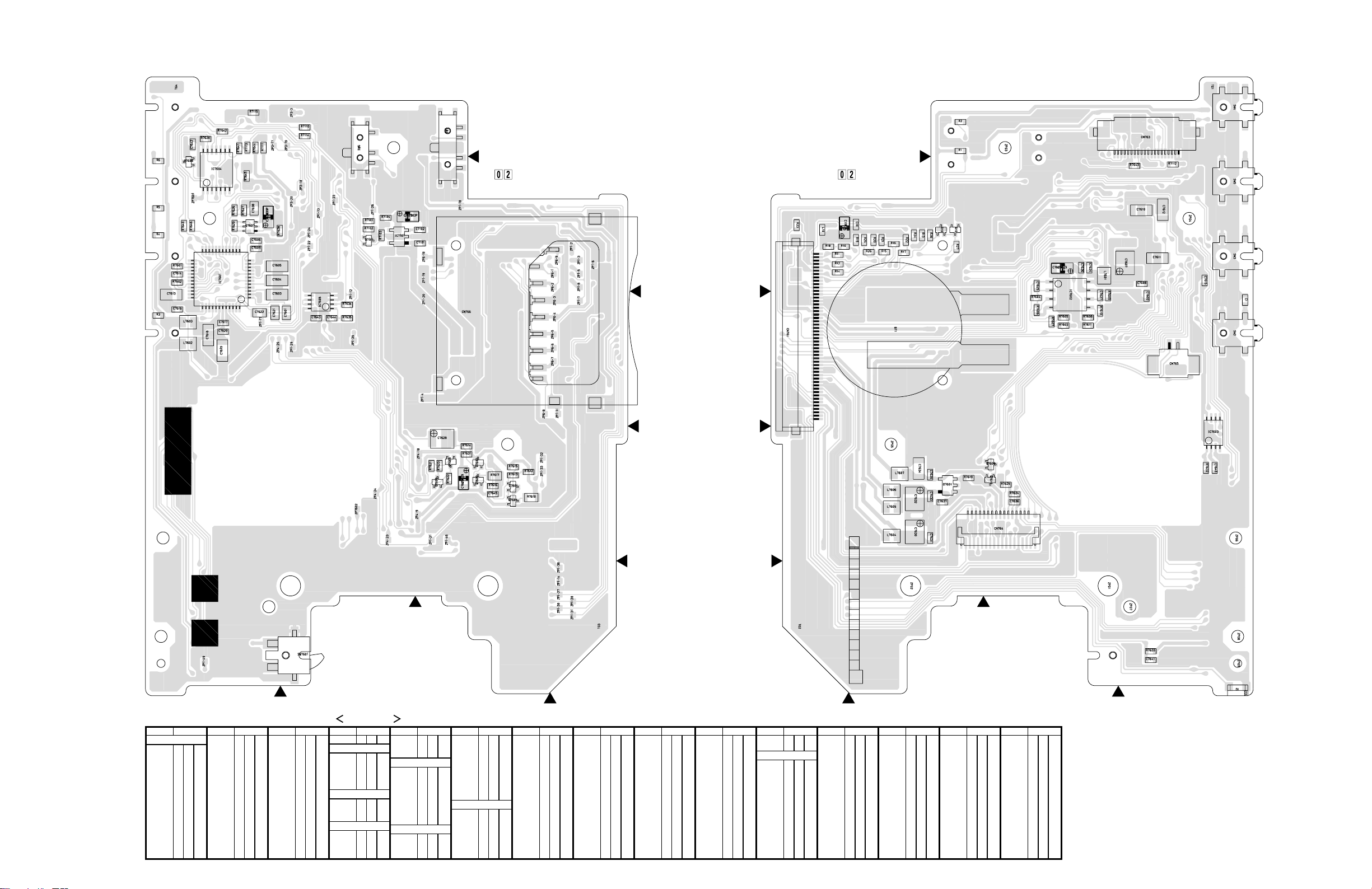
POWER SYSTEM BLOCK DIAGRAM
4.28
REAR70
BATT.
TERM
5
4
3
ADP DC IN
(
FOR C VF MODEL
LCD MODULE
REG 12V
CN751
VDD
REG 12V
CN763
14 12 11 4 3 14 12 9 4 311
BW VDD
1
)
FOR DSC MODEL
(
SD/MMC CARD
CN766
VGH
A REG3V
BL 4.8V
REG 15V
DSC 3V
4
)(
VDD
CN752
09
CVF
VFREG4.8
VDD
VDD
VFREG4.8
VFREG4.8
9
1
R7645
1
R7644
Q7607
L7605
2
FOR B/W VF MODEL
LCD MODULE
BW VDD
BW VDD
1
IC7001
3.3V
REG
IC7601
REG 12V
3
L7606
Q7601,Q7602
3
B/W VF
CN722
08
VFREG4.8
IC7602
Q7603
Q7605
Q7606
B/W VF
VFREG4.8
VFREG4.8
VFREG4.8
4
R7115
Q7001
CN1
2
3
9
10
7
6
5
)
BL
VFREG4.8
VFREG4.8
Q7610
CN723
CN721
VFREG4.8
CN763
BATT
BATT
GND
GND
ADP H
ADP DC
ADP DC
1 B/W VF MODEL
2 2.5" MONITOR MODEL
3 3"/3.5" MONITOR MODEL
4 WITH SIDE LED
INDICATAR MODEL
CN761
VFREG4.8
18
REG 12V
19
REG 15V
32
REG 3V
46
REG 4.8V
21
REG 4.8V
35
REG 4.8V
36
REG 15V
33
DSC 3V
6
SPK-
47
SPK+
48
CN765
1
2
SPEAKER
CN104
CN101
2
3
9
10
7
6
5
33
32
19
5
30
16
15
18
6
4
3
0 1 MAIN
REG
Q6701
BATT
POWER CTL
F6101
IC6101
VCC1
VCC2
L6102
L6101
Q6207,Q6217
LAMP
UNREG
Q6208
DRUM
PWR
Q6210
CAPSTAN
PWR
Q6201
3V
REG
Q6203
1.8V
REG
Q6204
4.8V
REG
L6204
Q6211 Q6213
SW REG
REG 12V
D6206
L6210
Q6104
AL 3V
REG
Q6101
2.5V
REG
Q6216
REG
-6.5V
Q6205
VF
REG4.8
LAMP 4.5V
DRUM PWR
CAP PWR
M UNREG
REG 3V
REG 2.5V
REG 1.8V
REG 4.8V
VFREG4.8
M REG4.8V
REG 12V
REG 15V
REG-6.5V
AL 3V
REG 1.8V
REG 3V
REG 4.8V
REG 4.8V
M REG4.8V
REG 3V
LIT 3V
AL 3VSYS
AL 3V
ADP H
REG 3V
REG 4.8V
M REG4.8
REG 3V
SYSCON
L1001
CAM DSP
5
1
OP DRIVE
L4852
L4851
L1002
ADP H
AUDIO
IC4302
IC4202
3V REG
IC1001
IC1007
IC1003
IC1006
Q1006
REG 1.8V
4
L4853
AL 3V
Q2002
REG4.8V
RST
AL 3V
RST
DET
IC1009
IC4301
Q4301
Q4302
IC4201
IC4802
IC4804
IC4851
IC4806
Q4851
43
AL 3V
IC1002
IC1004
IC1005
IC1008
IC1009
Q1004
IC2001
REG 2.5V
FZ VCC
REG 3V
REG 2.5V
REG4.8V
VREF 1.1
REG 4.8V
CAP PWR
REG 3V
M REG4.8V
M UNREG
DRUM PWR
SPK-
SPK+
REG 12V
REG-6.5V
REG 3V
TG/VDRV
PRE/REC
MDA
IC5501
Q1601
SW
IC1601
IC3501
X5501
MDA 3V
0 4 CCD
CN107 CN5001
CCD 12V
22
CCD 12V
33
CCD-6.5V
20 20
CN108
FOCUS VCC
19
ZOOM VCC
9
CN112
6
CN113
CN103 CN502
CN102
11
22
CN571 CN573
REG 4.8V
CN501
LAMP 4.5V
GND
Q5001
IC5001
1313
OP BLOCK
CAPSTAN
MOTOR
M
JUNCTION50
DRUM LOADING
MOTOR
MOTOR
MM
CN574
JACK60
REG 4.8V
IC501
IC502
Q501
DC LIGHT
2
02
VGH
BL 4.8V
LCD VEE
19 17 5 6
18 16 4 5
1
79 28
VEE VGH VDDVSS
BL 4.8V
F751
F7501
4
A REG3V
8
7
03
4
IC751
4
L751
L7501
Q7503
MONITOR
LCD BL
Q7501
T7501
Q7502SW
VSS
10
LCD VDD
16
CN764
CN752
9
15
EL1
EL2
CN752
CN754
CN753
4
1
2
EL
5
6
1
BL
V OUT
IC3701
Q3701
Q3703
REG 4.8V
VTR CPU
IC1401
IC1403
IC1404
Q1401
IC1402
REG 3V
REG 3V
Q1403
AL 3VSYS
REG 1.8V
VREF 1.1
REG 2.2V
REG 3V
REG 1.8V
REG 3V
REG 4.8V
DV MAIN
IC3001
WITH ANALOG INPUT MODEL
ANA IN
REG 4.8V
IC3002,IC3003
IC3006,IC3007
IC3901
IC3951,Q3951
Q3953,Q3954
LCD MODULE
PC IF
IC1303
IC1304
WITH DSC MODEL
DSC/USB
REG 3V
REG 4.8V
IC8053
REG 3.1V
IC8403
REG 3.3V
IC8004
AL 3VSYS
IC8003
IC8001
IC8007
IC8005
IC8051,IC8052
IC8401
IC8402
CN109
15
REG 3V
ZOOM UNIT
REG 3V
4-57 4-58
HGFEDCBA
Page 33

REGULATOR SYSTEM BLOCK DIAGRAM
4.29
T_BATT
ADP_DC
T_BATT
56
45
175
128
10 MAIN (REG)
Voltage DET
<5.2V: Pin1=L
(POWER OFF)
<4.2V: Pin1=L
(POWER ON)
R6712
R6713
IC1002
8
VDD
IC1009
34
RESET
at Pin2
R6005
R6004
IC6001
BATT DC DET
at POWER OFF
LITHIUM
Q6207
H :ON
L :ON
Q6217
DRUM
POWER
54
DC-DC
CONV
CAPSTAN
POWER
53
DC-DC
CONV
3V
SW REG
58
DC-DC
CONV
1.8V
SW REG
57
DC-DC
CONV
IC6101, Q6204
L6203, C6210
4.8V
SW REG
56
DC-DC
CONV
31
32
35
34
23
25
27
IC6101, Q6208
L6206, C6215
IC6101, Q6210
L6207, C6218
IC6101, Q6201
L6201, C6202
IC6101, Q6203
L6202, C6207
IC6101, Q6202
R62006, C6204
2.5V
SW REG
50
DC-DC
CONV
VF_CTL
D_GAIN
48
Q6205
VF
REG4.8
Q6206
ES
R6001
R6002
2
1
DET:L
R6003
L :ON
Q6003
Q6002
POWER OFF:ON
Q6001
POWER ON:H
REG_3V
D1001
F6101
IC6101, Q6701
L6701, C6703
BATT
POWER CTL
60
DC-DC
CONV
IC6101
Q6101, Q6102
BATT
SEL CTL
12, 17
DC-DC
CONV
LAMP ON
L6102
IC6101
47
SHUTDOWN
DC-DC CONV
CTL
H :START
L :STOP
13
21
14
R6701
VCC1
VCC2
L6101
8
51
L6204
CN102
CN105
CN109
CN101
CN101
15 16
CN103
1
LAMP_4.5V
M_UNREG
DRUM_PWR
DRUM_ERR
CAP_PWR
CAP_ERR
REG_2.5V
REG_3V
11
REG_3V
15
REG_3V
REG_1.8V
33
VFREG4.8
M_REG4.8V
REG_4.8V
30
REG_4.8V
REG_4.8V
13
REG_4.8V
0 7 REAR
CN104CN1
B_SEL
BATT+
BATT+
GND
GND
1
2
3
8
9
10
7
6
5
4
BATT.TERM
5
T
ADP_DC IN
B_SEL_SW
1
2
3
8
9
10
7
6
5
4
T_BATT
ADP_H
ADP_DC
ADP_DC
BATT_CHK
4
MONITOR2
0
BT1
(SYSCON)
3
CN761
LTHIUM
43 8
IC1001 (CPU)
CN101
ADP_H
T_BATT
BATT_SEL
RESET
2
AL_3V
V_BATT
LAMP ON
78
135
L1002
AL_3V
SW REG
55
DC-DC
CONV
IC6101, Q6211
L6208
AL 3V
SW REG
62
DC-DC
CONV
IC6101, Q6004
C6004
29
64
C6221
L6210
L6209
D6206
Q6212 Q6213
DIF
AMP
Q6215 Q6216
DIF
AMP
REG
12V
REG
-6.5V
CN101
32
CN101
19
18
REG_12V
REG_12V
REG_15V
REG_-15V
REG-6.5V
1
151
VF_CTL
VF_CTL
4-59 4-60
HGFEDCBA
Page 34

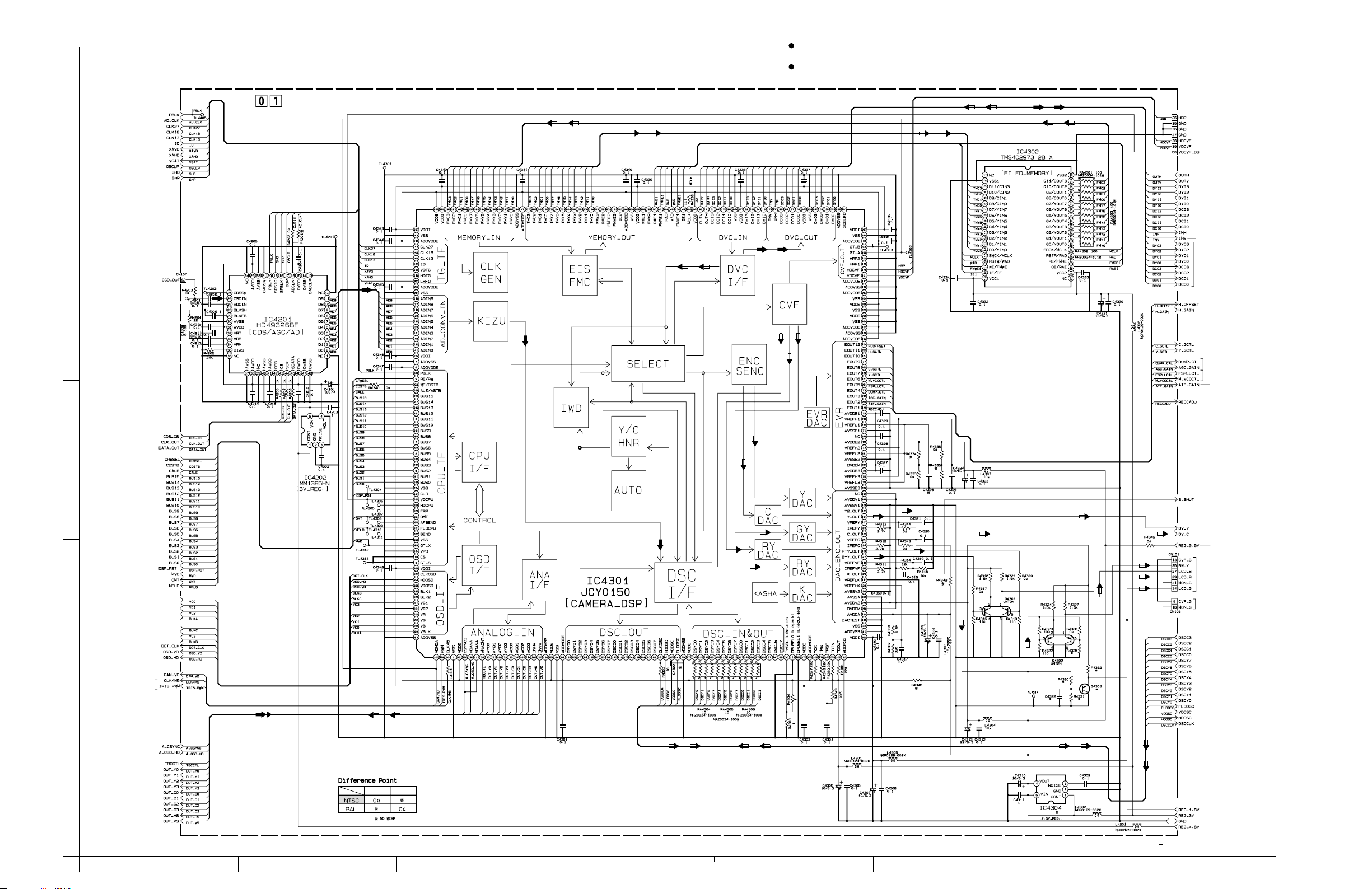
4.30
VIDEO SYSTEM BLOCK DIAGRAM
)
CLK
GEN
CONTROL
)
2 MONITOR0
Y/C
DAC
RY/GY/BY
DAC
CPU
I/F
OSD
TMC0
135
6
D8/CIN0
)
KIZU
I/F
C
B/W VF
Q7101
48
1
47
39
5
6
TMC357
3
D11/CIN3
AMP
Gin
Bin
Rin
SCLK
SCK
SI
IC7601
IC7603
ENC
SENC
CVF
Y
TMY0134
14
DO/YIN0
ROUT1
GOUT1
BOUT1
ROUT2
GOUT2
BOUT2
MEMO
OUT
TMY7132
7
D7/YIN7
8
6
4
18
16
14
MCLK
203
15
SWCK/MCLK
6
SELECT
48
16
V REF
WAD
RSTW/WAD
AUTO
IE1
FMWE1
49
130
17
18
IE
WE/FMWE
(
FILED MEMORY
CN721CN763
08
C-VF MODEL
IC4302
C-VF
IWD
Y/C
HNR
C
FMC0
199
34
Q8/COUT0
B/W VF
EIS
FMC
MEMO
IN
FMC3
198
37
Q11/COUT3
)
CN766
1
2
5
7
CN764
23
24
25
CN763
18
19
17
DSC
DYI0
13
DYI3
DVC
IN
DVC
I/F
DVC
OUT
DSC
IN
/OUT
I/F
DSC
OUT
ANA
I/F
EVR
DAC
MEMO
OUT
Y
FMY0
FMY7
RAD
MCLK
200
203
257
261
33
26
Q0/YOUT0
CN722
Q7/YOUT7
24
25
RSTR/RAD
SRCK/MCLK
LCD MODULE
V REF
DCI01195
DCI3
DYO098174
DYO3
DCO0
DCO3
OUTH
OUTV
DYI7
DSCI0 217
VDDSC
CLKDSC
FLDDSC
HDDSC
AYO0
AYO3
ACO0
ACO3
EOUT5
EOUT6
EOUT2
EOUT1
RAE1
FMRE1
50
201
22
23
0E/RAE
RE/FMRE
12
TO
DV MAIN
a
240
16
173
INH
172
INV
171
96
146DY I0
213
278DSCI3
212
211
143
141
33
32
35
114
281
FSPLLCTL
151
M VCOCTL
280
ATF GAIN
149
RECCADJ
TO DV MAIN
ANA IN
TO DSC/USB
TO
ANA IN
TO
DV MAIN
PRE/REC
TO
VTR CPU
ANA IN
DSC/USB
b
c
d
e
f
B/W VF MODEL
WITH DSC MODEL
SD/MMC
CARD
CN751
CN752
MON R
22
MON G
23
MON B
24
LCD MODULE
15
16
17
R
G
B
30
LCD BL
CVF R
CVF G
CVF B
CN751
CN752
VF BL
R OUT
GOUT
BOUT
LCD MODULE
R
G
B
TO
DSC/USB
g
ADIN9
ADIN0
124
CLR
44
CLK27
42
CLK18
45
CLK13
123
ID
189
VDTG
116
HDTG
253
LMFO
COUT
109
183 Y2 OUT
181 Y OUT
R-YOUT182
B-YOUT27
HDCVF175
VDCVF101
20
CLK45
158
PWM
100
VDMDA
242
PBLK
99
GT X
227
OMT
161
FLDCPU(MFLD
BUS15
BUS0
157
CLKOSD(DOT CLK
84
HDOSD
226
VDOSD
285
VB
82
VG
155
VR
80
VBLK
81
VC1
225
BLK1
BW Y
M32MMC CD
MMC CMD
MMC CLK
MM C D ATA
LCD G
LCD B
LCD R
CLK OUT
DATA OUT
IC4301(CAMERA DSP
AD
CONV
CN761
2625
2
3
5
8
17
24
22
31
30
MAIN01CCD40
26
SHP
SHD
CAM/VTR
TG RST
IC4851
1
2
+
VGAT
XAVD
XAHD
CLK18
CLK13
CLK27
TG CS
PBLK
CDSIN
CK
IF RX
IF TX
JLIP L
ID
17
OBP
)
)
2
7
OBP18SPBLK
IC4201 (CDS/AGC/AD)
SPSIG43CDS CS44CLK45DATA16ADCLK
19SHD
CS
SHP
CLK18
CLK OUT
DATA OU T
5
32
31
34
35
30
28
27
26
25
22
REG 3V
38
2
1
OSCIN
VD
SCLK
SDATA3334
LATCH
RESET
3
36
32
35
38
OP DRIVE
VF B
TO CAM DSP
TO DSC/USB
Q3701
1
AMP
Q3701
AMP
X5501
54MHz
CXO
5
32
17
16
15
14
13
D9
D0
REG 3V
4
VCO
(
ON SCREEN
VC1(VF G
VC2(VF R
BLKA(VBLK
VC3(VC1
BLKB(BLK1
DV Y
(
Y OUT
DV C
(
C OUT
11
2
CLK45
CAM VD
CLK OUT
DATA OUT
F/Z CS
F/Z RST
IRIS O/C
HALL AD
IRIS PWM
IC1006
)
)
)
)
)
)
)
SCLK
)
DATA
CS
EXD
HD
VD
TO IC4301-158PIN
RX
IC1007
TX18
6
3
OSD DATA
2
OSD CS
1
OSD CLK
TO
VTR CPU
8
DOT CLK
20
OSD HD
OSD VD
19
TO
CAM DSP
5
4
AL 3V
TO
IC1008 1PIN
TO
VTR CPU
IC1007
IC1007
CAM AD
8
11
IC1007
3
SRV TX
IF RX
0 CAM AD9
X1002
32KHz
MVD
X1001
16MHz
2
1
TO CAM DSP
Y2 OUT
B-Y OUT
R-Y OUT
133
105
106
112
158
144
142
171
9
10
REG 3V
13
12
127
149
TO
IC1007-5PIN
62
49
85
73
16
33
71
63
61
7
6
3
5
XIN
XOUT
VD
TG RST
TG CS
CDS CS
OSCO
OSCI
F/Z CS
F/Z RST
CLK OUT
DATA OUT
IRIS O/C
HALL AD
JLIP L
JLIP INT
RXD
TXD
SRV RST
SRV CS
SRV RDY
Q4302
BUF
BUF
Q4301
IC1003
2
(
EPROM
IC1002
(
RTC
IC1001
(
SYSCON CPU
3
6
1
7
2
1
)
)
Q4302
BUF
BUF
Q4301
)
OMT
BUS15
BUS0
DATA IN
S DT OUT
SCLK
SDTIN
A MUTE
S MUTE
ND H
PD L
DSC RST
5
2
IC1008
10
5
EEP DT OUT
SI
2
EEP DT IN
SO
6
EEP DT CLK
SCK
3
AREG SO
SIO
DATA I N
CLK OUT
2
CLK
135
108
FLD
16
7
41
46
47
48
32
174
145
160
130
34
RXD
TXD
15
23
DSP RST
XAVD
XAHD
VGAT
CAM VD
PBLK
MVD
CN101
34
27
29
20
21
118
41
230
166
49
48
46
43
IC5001
(
)
V1V2V3
CN107 CN5001
42
VOUT
YIN
YIN
YIN
V14V23V4
V3
2
4
4
44
V1
V240V4
V3
26
24
28
30
10
12
14
16
D1302
CCD
1
765
V4
SUB
765
41
45
BRIDGE
DRIVER
BRIDGE
DRIVER
BRIDGE
DRIVER
BRIDGE
DRIVER
MOTOR
AL 3VSYS
TO ANA
TO ANA
TO ANA
19
RG
SUB
HALL
AMP
DRIVE
AMP
Q1301
111013
H1
RG
IC4804IC4802
OP
BLOCK
5
IRIS CTL
4
3
JACK
0
6
JLIP
J502
WITHOUT
DSC MODEL
PC
J504
2
WITH
DSC MODEL
J505
USB
J501
AV
1
IN/OUT
S IN/OUT
J503
12
34
R520
R521
R519
R522
CN501
7
4
5
7
8
1
HG VCC
HG OUT
HG VSS
HG OUT
GND/DRIVE
DUMP
DRIVE
DUMP
JLIP RX
JLIP TX
PC TX/USB DN
PC RX/USB DR
Y OUT
V OUT
C OUT
CN108
C3FOCUS
15
C1FOCUS
17
C4FOCUS
16
C2FOCUS
14
21
c2ZOOM
C4ZOOM
23
C3ZOOM
22
C1ZOOM
24
5
4
3
8
6
7
2
1
CN102
8
7
USB DN
4
USB DR
5
CN103CN502
99
1
7
H1RGSUB
171619
H1
C3713
C3714
C3711
C3712
Q5001
8
VOUT
BUF
H2
12
181716
H2
18
14118
H2
IC5501
(TG/VDRV)
PULSE
GENERATOR
3
PC IF
1
2
IC1304
4
IC3701
15
75
14
12
75
11
9
75
IC1303
CN5001
12
4
1
2
CCD
OUT
PARARELLE
DECODER
7
6
5
6dB
DRV
6dB
DRV
6dB
DRV
CN107
12
371817
OBCLP
CLK(CLK OUT
DATA(DATA O U T
SERIAL-
IC4806
REG 3V
ABCD EFGH
4-624-61
Page 35

41
42
191
192
257
97
65
143
142
66
144
212
YSO0
YSO3
BRSO0
BRSO3
OUTH
OUTV
YSI0
YSI3
BRSI0
BRSI3
INH
INV
OSC27I
AD0
AD15
XRST
CPUALE
XCPUDSTB0
XCPUDSTB1
XCPURW
XCPUCS
CPUWAIT
IC3001 (DV MAIN)
VIDEO I/F
(VBID DET
RAM) VLD WORK
RAM
CONV)
COMPRESS
(DCT,VLC
(CLOCK(CLOCK
CONV)
RAM)
RAM
(ENC/DET)
RAM
(CLOCK
CONV)
RAMOUTER ECC
(SUB/AUX)
INNER ECC
(ENC/DEC)
RAM
(CLOCK
CONV)
FORMATTER
(Formatting
Sync Detect
ID Protect
De-formatting)
PWMAUDIO
RECCTL
RECDATA
RECCLK
TRKREF
FRREF
TO
109
15
175
16
100
SPA
98
HSP
173
HID
101
177
TO
VTR CPU
TR
FR
FSPLLCTL
RECCTL
HSE
RECCLK
SPAIN
VTR CPU
TO JIG
(CN105)
HID3
PBH
RECH
HID1
REC DTA
REC CTL
REC CTL 12
ENV OUT
38
41
42
40
44
48
D-RAM I/F
PB ENV
RECCADT
(TO CAM DSP)
)
IC3901(ANA IN
42
YSI0
HOST CPU I/F
IEE1394
LINK
(ISO/
ASYNC
FIFO)
AUDIO
(WORK
RAM
PROGRAM
RISC
CORE)
TO
CAM DSP
(
IC4301
)
(DECK DSP)
TPA
TPB
XTPA
XTPB
80
156
229
288
AILRCK
27
179
AIBCK
182
AIMCK
29
AODAT0
AIDAT1
AIDAT0
31
112
TBCCTL
ASYNC
A OSD HD59
YSI3
45
38
CSI0
CSI3
41
32
YS00
YS03
35
26
CS00
CS03
29
24
OUTH
25
OUTV
36
INH
37
INV
56
ZCNT
58
CSYNC
59
HDOUT
(
A/D,D/A CONV
YSOUT
COUT
CIN
VYIN
)
TO
V OUT
7
80
Q3954
18
Q3951
12
BUF
Q3953
AMPBUF
IC3951
2
CIN
EXT V IN
4
EXT Y IN
6
TO
V OUT
57
10
MAIN01
119
120
39
122
5
TO
CAM DSP
a
TO
CAM DSP
b
TO
CAM DSP
c
TO
TG/VDRV
CLK27
189
190
117
37
4
TO
TO
CAM DSP
d
TO
CAM DSP
e
VTR CPU
ADDTO0
ADDT15
DV RST
DALE
DWE
DRE
DRWSEL
DV CS
DV WATT
215
73
3
7
HID3
PBH
RECH
HID1
REC DATA
R CTL
MONI..CHG
PB MONI
AGCOUT
REG GAIN
IC3501
(PRE/REC)
2F
24
Y2
25
X2
20
X1
19
Y1
2S
1S
1F
HEAD
CN110
6
2F
7
2S
3
1S
2
1F
DOLRCK
DOBCK
DOMCK
DODAT
WITH DSC MODEL
8
8
IC8006
6
USB CE
CS
OE
WE
REST
AIDAT
TO CAM DSP
AD7
A0 A7
AD0
TO SYSCON (IC1003)
TO SYSCON
IC8401
(
)
USB
2
D+
12
D-
TO
SYSCON
RESET
WR
RD
7
8
16
(IC1001)
(IC1014)
TO
SYSCON
f
V OUT
2
1
TO
JACK
g
IC8051
7
4
IC8052
1
2
1
118
MY7
MY0
125
132
MC3
MC0
135
IC8001
11
P CE/MMC CS
117
CE1
116
SCK
114
SI
115
SO
YIN
CPU
IF
B-Y
IN
R-Y
138
AVD
90
)
AVD(INT
97
2TXD
98
2RXD
136
FLD
92 128
PORT3
XOUT
SCLK
HREQ
HACK
P VS2
RY/BY
(
)
DSC/USB
22
XIN
21
R8003
20
100
SID
9
99
R/W
101
BCL
102
BCH
8
DC
43
29
CS
42
INT
85
CE
129
OE
130
WE
131
80
RST
X8001
17
2
IC8007
24
16
A8 A30
18
CLKIN
71
SID
13
BSBS
69
R/W
72
DSC
BCL
73
CPU
BCH
12
DC
IC8002
4044
HREQ
39
HACK
22
CS
37
INT
60
RST
6
ADDRESS BUS
DATA BUS
D15
D0
REG 3.1V
A19
DQ14
D0
DQ0
2M
RAM
IC8003
47
BYTE
CEOEWE
RY/BY
RESET
WP
26
122815
11
14
FLASH CE
A9
53
IC8007
3
5
6
IC8007
1
7
2
TO
TG/VDRV
SRV TX
IF RX
TO TG/VDRV
CLK27
VD
SRV CS
CLK 27
54
CLK
AIMK
AILRCK
AIBCK
AIDAT
AODAT
ND H
PD L
CLK OUT
DATA OUT
AUDIO CS
S MUTE
S SHUT
TO
AUDIO
TO
AUDIO
TO CAM DSP
120
159
108
109
93
89
78
74
180
76
55
77
59
72
IC1401 (VTR CPU)
MONI CHG
VD
EEP WRITE
EEP CLK
EEP READ
SYS CLK
SYS IN
SYS OUT
MSELECT
SRV RDY
SRV RST
TXD
RXD
OSCI
DV RST
DV C S
ADM0
ADM15
RWSEL
WE0
CLK27SEL
HIDIN
HID1
PBH
RECH
HID 3
FRP
TSR
99
104
37 DV WAIT
DK
2333ADDT00
47 DALE
AS
5DRWSEL
24
RE
12
83
219
207
117
116
119
220
SPA
190
231
ADDT15
DRE
DWE
TO IC3001
TO IC3001
TO IC3001
L3010
TO IC3201
TO IC3501
4
1
43
1
L3011
3
2
2
TPA+
TPA-
TPB+
TPB-
DV
J101
DV IN/OUT
TO IC3501
TO IC3001
FR
TR
ABCD EFGH
4-63 4-64
Page 36

AUDIO SYSTEM BLOCK DIAGRAM
4.31
MAIN(AUDIO
)
5
TAAID
TO
DV MAIN
4
MIC UNIT
3
2
AIBCK
AILRCK
AIMCK
IN MIC/R
IM GND
IN MIC/L
TAODA
CN106
3
2
1
C2123
R2103
USED
USED
R2104
C2124
NOT
NOT
R2127 R2109
C2125
50
51
EXT MIC
53
Rch
INT MIC
54
Rch
INT MIC
59
Lch
EXT MIC
60
Lch
62
63
R2128 R2110
C2126
48 49
PRE AMP
PRE AMP
R2113
EQ AMP
EQ AMP
641
R2114
R2111
C2113
47
46
HPF
ON
OFF
HPF
OFF
ON
32
C2112
INT
EXT
EXT
INT
R2107
HPF AMP
HPF AMP
R2108
R2129
45
R2130
C2115
44
LINE
MIC
LINE
54
C2116
MIC
C2007
LINE IN Rch
LINE IN Lch
20 41
18
C2006
MIC SEL
IC2001
(
AUDIO PROCESSOR
Rch
ALC AMP
MIX
Lch
ALC AMP
MIX
LINE OUT2
)
A/D
SIG
BEEP
Lch
Rch
C2018 C2109
LINE OUT2
1110
HPF
12
SIG
TAAID
29
OSDT
BEEP
TAODA
30 34
SDTI
UDIOA
I/F CTL
1413
R2024
AILRCK
AIBCLK
BCLK
LRCK
AIMCK
35
D/A
BEEPS
VRA
OUT
15
MIX
R2023
MCLK
CLOCK
DIVIDER
ALCS
C2016
36
EE/REC
PB
PB
EE/REC
39
37
PD
ND
Rch
Lch
CS
ATAD
SPK+
SPK-
33
32
31
26
21
19
24
NOT
USED
25
NOT
USED
40
38
SW
Q2001
SW
Q2001
A MUTE
LINE OUT
LINE OUT
CCLK
Rch
Lch
HP OUT
HP OUT
OLCONTR
RESISTER
I/F
Rch
LINE AMP
Lch LINE AMP
Rch
HP AMP
Lch
HP AMP
1716
ND H
PD L
DATA CLK
AUDI O CS
DATA OUT
A MUTE
U SIG/RA
U SIG/LA
SPK+
SPK-
CN502
4
3
48
47
CN103
4
3
CN101 CN761
3
4
TO SYSCON
70
7
4
5
3
2
1
02
JACK
J501
A/V OUT
MONITOR
CN765
1
2
SPEAKER
C2114
SW
Q2004
TO
SYSCON
TO
CAM DSP
UZZERB
S MUTE
S SHUT
1
4-65 4-66
HGFEDCBA
Page 37
4.32 VOLTAGE CHARTS
<SYSCON>
MODE
PIN NO.
IC1001 - IC1002
IC1003
IC1004
IC1005
IC1006
IC1007
REC PLAY
100
2 3.0 3.0
3 1.5 1.5
400
5 2.9 2.9
6 0.5 0.5
7 0.5 0.5
8 3.1 3.1
1 3.0 3.0
2 0.7 0.7
3 2.9 3.0
400
5 0.6 0.7
6 3.0 3.0
7 2.9 2.9
8 2.9 2.9
1 1.4 1.4
200
3 1.3 1.3
400
5 3.0 3.0
100
2 3.0 3.0
300
4 3.0 3.0
5 3.0 3.0
1 2.7 2.7
2 0.5 0.5
300
4 3.0 3.0
5 3.0 3.0
6 3.0 3.0
7 1.3 1.3
8 1.4 1.4
900
10 0 0
11 0 0
12 0 0
13 0 0
14 0 0
15 0 0
16 0 0
17 0 0
18 0 0
19 2.9 2.9
20 2.7 2.7
1 3.0 3.0
2 3.0 3.0
3 3.0 3.0
4 3.0 3.0
5 3.0 3.0
6 3.0 3.0
700
8 3.0 3.0
9 3.0 3.0
10 3.0 3.0
MODE
PIN NO.
IC1008
IC1009
Q1001
Q1002
Q1003
Q1004
Q1005
Q1006
Q1007
<PC IF>
MODE
PIN NO.
IC1303
IC1304
REC PLAY
11 1.3 1.3
12 1.5 1.5
13 3.0 3.0
14 3.0 3.0
1 3.0 3.0
2 1.0 1.0
300
400
5 0 0.5
6 3.0 3.0
700
8 3.0 0
100
200
3 3.0 3.0
4 3.0 3.0
E00
C00
B00
E00
C 3.0 3.0
B 0.6 0.6
E00
C 0.5 0.5
B00
E 3.1 3.1
C00
B 3.1 3.1
E00
C 3.1 3.1
B00
E 2.9 0
C 2.9 0
B 0 3.0
E00
C 0 3.0
B 3.1 0
REC PLAY
1 3.0 3.0
200
300
400
5 3.0 3.0
1 3.0 3.0
200
300
400
5 3.0 3.0
MODE
PIN NO.
Q1301
<VTR CPU>
MODE
PIN NO.
IC1401 - IC1403
IC1404
Q1401
Q1402
Q1403
Q1404
<MDA>
MODE
PIN NO.
IC1601
REC PLAY
E00
C00
B00
REC PLAY
1 3.0 3.0
200
300
400
500
600
7 3.0 3.0
8 3.0 3.0
1-2 2.9 2.9
3-400
5-600
7-8 2.9 2.9
1 3.0 3.0
2 3.0 3.0
3 3.0 3.0
1(E) 0 0
2(B) 3.0 3.0
3(E) 3.0 3.0
4(C) 2.7 2.7
5(C) 0 0
1(E) 0 0
2(B) 0 0
3(E) 3.0 3.0
4(C) 0 0
5(C) 3.0 3.0
100
200
3 3.0 3.0
REC PLAY
100
2 0.8 0.8
3 0.8 0
400
5 0.8 0
600
700
MODE
PIN NO.
800
900
10 0 0
11 0 0
12 0 0
13 0 0
14 4.7 4.7
15 0 0
16 0 0
17 0 0
18 0 0
19 0 0
20 0.4 0.4
21 0 0
22 0 0
23 0.9 0.9
24 11.0 11.0
25 1.5 1.5
26 0 0
27 1.5 1.5
28 1.5 1.5
29 1.5 1.5
30 1.5 1.5
31 1.5 1.5
32 1.5 1.5
33 1.4 0
34 1.4 0
35 0 0
36 2.9 2.9
37 0 0
38 0.6 0.6
39 0 0.6
40 0 1.2
41 1.5 0
42 0.5 0.7
43 2.9 2.9
44 0 0
45 0 0
46 0 0
47 0.9 2.9
48 0 0
49 2.9 2.9
50 1.9 1.9
51 0 0
52 1.6 1.6
53 0 1.1
54 0.4 0.7
55 0.6 0.6
56 0.7 0.7
57 1.0 1.0
58 0.6 0.6
59 0 0
60 1.0 1.0
61 2.6 0
62 0 1.2
63 0 1.5
64 0 1.5
65 0 1.4
66 0 0
67 0 1.5
68 0.4 0
69 0 0
70 0 0.8
REC PLAY
MODE
PIN NO.
Q1601
<AUDIO>
MODE
PIN NO.
IC2001
REC PLAY
71 0 0.8
72 0 0.8
73 0.8 0
74 1.1 0
75 0 0
76 0 0
77 0 0
78 0 1.7
79 0 0
80 0 0
1(E) 0 0
2(B) 0 0
3(E) 4.8 4.8
4(C) 0 0
5(C) 4.8 4.8
REC PLAY
1 2.0 2.0
2 2.0 2.0
3 2.0 2.0
4 2.0 2.0
5 1.5 1.5
6 1.5 1.5
7 1.5 1.5
800
9 3.0 3.0
10 1.5 1.5
11 1.5 1.5
12 1.5 1.5
13 1.5 1.5
14 1.5 1.5
15 1.5 1.5
16 1.5 1.5
17 1.5 1.5
18 1.5 0
19 1.5 2.3
20 2.3 2.3
21 1.5 1.4
22 2.3 2.3
23 2.3 2.3
24 4.7 4.7
25 2.3 2.3
26 0 0
27 2.9 2.9
28 0 0
29 1.5 1.5
30 1.5 1.5
31 1.5 1.7
32 2.9 1.7
33 3.0 3.0
34 1.5 1.5
35 1.5 1.5
36 1.5 1.5
37 3.0 3.1
38 2.4 3.1
39 0 0
40 2.4 2.4
4-67
Page 38

MODE
PIN NO.
Q2001
Q2002
Q2004
<DV MAIN>
MODE
PIN NO.
IC3001 - IC3002
IC3003
REC PLAY
41 0 0
42 0 0
43 4.8 4.8
44 1.5 1.5
45 2.0 2.0
46 2.0 2.0
47 2.0 2.0
48 2.0 2.0
49 2.0 2.0
50 2.0 2.0
51 2.0 2.0
52 2.6 2.6
53 2.0 2.0
54 2.0 2.0
55 4.0 4.0
56 2.0 2.0
57 0 0
58 4.0 4.0
59 2.0 2.0
60 2.0 2.0
61 2.0 2.0
62 2.0 2.0
63 2.0 2.0
64 2.0 2.0
1(E) 0 0
2(B) 0 0
3(C) 0 0
4(E) 0 0
5(B) 0 0
6(C) 0 0
E 4.1 4.1
C 4.8 4.8
B 4.7 4.7
E00
C00
B 0.7 0.7
REC PLAY
1 0 0.4
200
300
4 0.5 1.5
5 0.7 0
6 2.9 0
700
8 3.0 2.9
1 3.0 2.9
2 1.0 0.9
300
400
500
6 0.5 1.5
7 2.3 2.3
MODE
PIN NO.
IC3004
IC3006
<PRE/REC>
MODE
PIN NO.
IC3501
REC PLAY
8 3.0 2.9
1 0.5 0
2 0.5 0
300
4 0.8 2.9
5 2.9 2.9
1 2.9 2.9
200
300
400
5 2.9 2.9
600
7 1.0 1.5
8 1.3 0.7
9 1.3 1.3
10 0 0
11 0 0
12 2.9 2.9
13 0 0
14 0 0
15 0.5 0.5
16 0 0
REC PLAY
100
2 1.1 1.1
300
400
5 0 2.5
6 3.3 0
7 1.4 0
800
9 1.6 3.0
10 0 1.6
11 3.0 0
12 0 0
13 4.8 4.8
14 0 0
15 0 0
16 0 0
17 0 0
18 3.7 1.7
19 3.4 1.7
20 3.5 0
21 3.7 1.7
22 0 0
23 3.7 1.7
24 3.5 1.7
25 3.5 1.7
26 3.7 1.7
27 0 0
28 2.3 2.5
29 3.4 1.7
30 3.4 1.7
31 2.4 2.5
32 0 0
MODE
PIN NO.
<V OUT>
MODE
PIN NO.
IC3701
Q3701
REC PLAY
33 0 0
34 0 0
35 1.8 1.8
36 0.4 0
37 3.0 3.0
38 0 3.0
39 3.0 3.0
40 1.5 1.5
41 0 3.0
42 3.0 0
43 4.8 4.8
44 2.9 0
45 0 0
46 0 1.9
47 0 2.0
48 4.7 3.0
49 4.4 2.8
50 0.4 1.6
51 1.2 1.2
52 0.8 1.5
53 0 0
54 3.2 2.6
55 2.5 1.9
56 1.1 1.1
57 2.5 1.9
58 2.5 1.3
59 0 0
60 1.2 1.2
61 3.4 1.9
62 2.5 1.9
63 2.5 1.3
64 2.5 1.9
REC PLAY
100
2 2.3 2.3
300
400
500
600
7 1.9 1.9
800
9 2.3 2.3
10 0 0
11 2.0 2.0
12 2.2 2.2
13 4.8 4.8
14 1.8 1.8
15 1.9 1.9
16 4.8 4.8
1(E) 1.1 1.1
2(E) 1.2 0
3(B) 0.6 0.6
4(C) 0 0
5(B) 0 0.5
MODE
PIN NO.
Q3702
Q3703
<ANA IN>
MODE
PIN NO.
IC3901
REC PLAY
6(C) 0 0
1(E) 0 0
2(B) 0 0
3(C) 0 0
4(E) 4.7 0
5(B) 4.7 4.8
6(C) 0 0
E00
C 4.8 4.8
B00
REC PLAY
100
2 2.9 2.9
3 1.0 1.0
400
500
6 1.6 1.6
7 0.6 0.6
8 1.0 1.0
900
10 2.9 2.9
11 0.4 0.4
12 0 0
13 0 0
14 3.0 3.0
15 0 0
16 0 0
17 0 0
18 0 0
19 0 0
20 0 0
21 0 0
22 0 0
23 1.8 1.8
24 2.8 2.8
25 1.5 1.5
26 1.0 0.9
27 0.9 0.9
28 0.9 0.9
29 1.4 1.4
30 0 0
31 3.0 3.0
32 1.5 1.5
33 1.2 1.2
34 1.1 1.1
35 0.8 0.8
36 2.8 2.8
37 1.5 1.5
38 0.9 0.9
39 0.9 0.9
40 0.9 0.9
41 1.4 1.4
42 1.1 1.1
MODE
PIN NO.
IC3951
Q3951
Q3952
Q3953
REC PLAY
43 1.1 1.1
44 1.1 1.1
45 0.8 0.8
46 0 0
47 0 0
48 0 0
49 0.4 0.4
50 2.7 2.7
51 2.8 2.8
52 0 0
53 1.8 1.8
54 1.2 1.7
55 3.1 3.1
56 0 0
57 0 0
58 3.0 3.0
59 0 0
60 0 0
61 1.4 1.4
62 0 0
63 3.0 0
64 0 0
65 0 0
66 0 0
67 0 0
68 0 0
69 0 0
70 0 0
71 0 0
72 0 0
73 3.0 3.0
74 1.1 1.1
75 0 0
76 0 0
77 1.7 1.7
78 0 0
79 1.1 1.1
80 0.5 0.5
1 3.0 3.0
2 1.9 1.9
3 4.7 4.8
4 1.7 1.7
500
6 2.2 2.2
1(E) 0 0
2(B) 0.4 0
3(C) 0 0
4(E) 0 2.0
5(B) 1.4 0
6(C) 4.8 4.8
E00
C00
B 3.0 3.0
1(E) 0 0
2(B) 0.4 0.4
3(C) 0 0
4(E) 4.8 0
5(B) 4.8 4.8
6(C) 4.8 4.8
4-68
Page 39

MODE
PIN NO.
Q3954
<CAM DSP>
MODE
PIN NO.
IC4201
IC4202
REC PLAY
E00
C 4.8 4.8
B00
REC PLAY
100
2 1.1 0
3 1.1 0
4 1.0 0
5 0.7 0
6 0.7 0
7 2.2 3.0
8 0.5 0
9 0.7 0
10 0.4 0
11 0 0
12 0 0
13 0 0
14 0 0
15 2.9 3.0
16 1.2 0
17 2.8 0
18 2.1 0
19 0 0
20 2.4 0
21 0 0
22 0 0
23 3.0 0
24 0 0
25 0 0
26 1.9 0
27 1.4 0
28 1.9 0
29 2.1 0
30 0 0
31 3.0 3.0
32 1.9 0
33 0.9 0
34 1.4 0
35 1.2 0
36 0 0
37 0 0
38 3.0 3.0
39 0 0
40 0 0
41 3.0 3.0
42 0 0
43 3.0 3.0
44 3.0 0
45 0 1.5
46 3.0 3.0
47 0 0
48 0 0
1 4.8 4.8
200
3 1.2 1.2
MODE
PIN NO.
IC4301 - IC4302
Q4301
Q4302
REC PLAY
4 3.0 3.0
5 4.8 4.8
100
2 0 1.4
3 1.4 0.9
4 0.9 0.9
5 0.9 0.9
6 0.9 0.9
7 0.8 0.8
8 1.2 1.2
9 1.2 1.3
10 1.8 1.9
11 1.0 1.1
12 1.2 1.0
13 1.2 1.1
14 1.3 1.1
15 1.3 1.4
16 0 0
17 2.7 2.6
18 2.9 2.9
19 0 3.0
20 0 0
21 3.0 3.0
22 2.7 2.7
23 2.7 2.7
24 0 0
25 1.3 1.5
26 1.5 1.4
27 1.4 1.3
28 1.3 1.3
29 1.2 1.2
30 1.8 1.8
31 1.5 1.5
32 1.4 1.3
33 1.1 1.1
34 1.2 1.3
35 1.1 0
36 1.1 1.2
37 1.6 1.6
38 0 0
1(E) 0.9 0.9
2(E) 0.9 0.9
3(B) 0 0
4(C) 0 0
5(B) 0 0
6(C) 0 0
1(E) 1.2 1.2
2(E) 0 0.9
3(B) 0 0
4(C) 0 0
5(B) 0.6 0.6
6(C) 0 0
<OP DRIVE>
MODE
PIN NO.
IC4802
IC4803
IC4804
IC4806
IC4851
REC PLAY
1 2.9 2.9
2 2.6 2.6
3 2.6 2.6
400
5 2.6 2.6
6 2.6 2.6
7 2.6 2.6
8 4.7 4.7
1 1.0 1.0
200
300
400
5 2.6 2.6
6 2.6 2.6
7 2.4 3.3
8 4.7 4.8
1 2.2 0
2 2.4 3.0
3 2.4 2.9
400
5 1.8 3.0
6 1.8 3.0
7 1.2 0
8 4.7 4.8
1 2.4 3.0
2 2.4 3.0
3 2.4 3.0
400
5 3.0 3.0
6 0.6 0
7 0.6 0
8 3.0 3.0
100
2 0.6 0.6
3 0 0.4
4 0.4 0
5 0 0.4
6-7-8-9-10 - 11 - 12 - 13 - 14 - 15 - 16 - 17 - 18 - 19 - 20 0 0
21 0.7 0
22 0 0
23 4.8 4.8
24 0 0
25 0 0
26 0 0
MODE
PIN NO.
Q4801
Q4851
<TG/VDRV>
MODE
PIN NO.
IC5501
REC PLAY
27 4.8 4.8
28 0 0
29 0 0
30 0 0
31 3.0 3.0
32 0 0
33 0 0
34 1.3 1.5
35 3.0 3.0
36 1.4 1.4
37 1.4 1.4
38 3.1 3.1
E00
C 2.3 2.3
B 1.0 1.0
E00
C 3.8 3.8
B00
REC PLAY
1 -0.5 -0.7
2 2.4 0
3 2.9 0
4 2.9 2.9
500
6 2.9 2.9
700
8 0.5 0
900
10 2.9 2.9
11 1.4 0
12 2.9 2.9
13 0 0
14 1.2 0
15 0 0
16 2.9 2.9
17 2.2 0
18 2.2 0
19 2.2 0
20 0 0
21 0 0
22 0 0
23 0 0
24 2.9 2.9
25 1.3 0
26 3.0 3.0
27 0 0
28 1.2 1.8
29 0 0
30 1.3 1.5
31 0 0
32 0 0
33 2.9 2.9
34 1.5 0
35 1.2 0
36 2.9 0
MODE
PIN NO.
<REG>
MODE
PIN NO.
IC6001
IC6101
REC PLAY
37 2.9 0
38 3.0 3.0
39 0 0
40 0 0
41 -6.3 0
42 0 11.9
43 11.9 11.9
44 -6.2 11.9
45 -6.6 -6.7
46 -6.6 0
47 0 0
48 2.9 0
REC PLAY
1 8.0 8.0
2 10.4 10.4
300
400
1 3.1 3.1
2 3.1 3.1
3 3.1 3.1
4 1.5 1.5
5 3.1 3.1
600
7 1.3 1.3
8 11.0 11.0
9 1.0 1.0
10 1.2 1.2
11 2.1 2.1
12 0 0
13 0 0
14 0 0
15 0 0
16 0 0
17 0 0
18 0 0
19 2.2 2.2
20 0.9 0.9
21 0 0
22 2.2 2.2
23 1.0 1.0
24 0.6 0.6
25 1.0 1.0
26 0.5 0.5
27 1.0 1.0
28 0.8 0.8
29 1.0 1.0
30 0.9 0.9
31 0 0
32 0 0
33 0.5 0.5
34 0 0
35 0 0
36 0.5 0.5
37 0.8 0.8
38 0 0
39 1.0 1.0
4-69
Page 40

MODE
PIN NO.
Q6001
Q6002
Q6003
Q6004
Q6101
Q6102
Q6201
Q6202
Q6203
REC PLAY
40 0 0
41 2.4 2.4
42 1.1 1.1
43 0 0
44 2.1 2.1
45 2.1 2.1
46 2.1 2.1
47 8 8
48 1.0 1.0
49 1.1 1.1
50 2.1 2.1
51 11.0 11.0
52 0 0
53 10.2 10.2
54 9.4 9.4
55 4.7 4.7
56 6.1 6.1
57 9.3 9.3
58 7.9 7.9
59 0 0
60 11.0 11.0
61 0 0
62 10.3 10.3
63 1.3 1.3
64 1.0 1.0
E00
C00
B 3.0 3.0
D 10.4 10.4
S00
G00
D00
S 4.1 4.1
G 0 3.1
E 11.0 11.0
C 3.0 3.0
B 10.4 10.4
D00
S00
G00
D00
S00
G 3.0 3.0
D 3.0 3.0
S 11.0 11.0
G 7.9 7.9
E 0 3.0
C 2.5 2.5
B 2.3 2.3
1(D) 1.8 1.8
2(D) 1.8 1.8
3(G) 9.3 9.3
4(S) 11.0 11.0
5(D) 1.8 1.8
MODE
PIN NO.
Q6204
Q6205
Q6206
Q6207
Q6208
Q6210
Q6211
Q6212
Q6213
Q6214
Q6215
Q6216
Q6217
REC PLAY
6(D) 1.8 1.8
D 4.8 4.8
S 11.0 11.0
G 6.2 6.2
E 4.8 4.8
C00
B 4.8 4.8
E00
C 4.8 4.8
B00
E00
C 4.8 4.8
B00
1(D) 1.7 1.7
2(D) 1.7 1.7
3(G) 9.4 9.4
4(S) 11.0 11.0
5(D) 1.7 1.7
6(D) 1.7 1.7
1(D) 0.9 0.9
2(D) 0.9 0.9
3(G) 10.2 0
4(S) 11.0 11.0
5(D) 0.9 0.9
6(D) 0.9 0
D00
S 11.0 11.0
G 4.7 4.7
1(E) 4.3 4.3
2(B) 4.8 4.8
3(C) 15.0 15.0
4(E) 0 4.3
5(B) 5.0 4.9
6(C) 14.4 14.4
E 15.0 15.0
C 11.9 11.9
B 14.4 14.4
E00
C 15.0 15.0
B 0 -1.1
1(E) -6.0 -6.1
2(B) -6.5 -6.6
3(C) -15.3 -15.3
4(E) -6.1 -6.1
5(B) -6.6 -6.7
6(C) -13.3 -15.2
E -13.9 -15.3
C -6.6 -6.7
B -13.9 -15.2
1(E) 0 0
MODE
PIN NO.
Q6701
<DSC/USB>
MODE
PIN NO.
IC8001
REC PLAY
2(B) 0 0
3(C) 0 0
4(E) 0 11.0
5(B) 11.0 11.0
6(C) 11.0 11.0
1(D) 0 0
2(D) 0 0
3(G) 11.0 11.0
4(S) 11.0 11.0
5(D) 0 0
6(D) 0 0
REC PLAY
1 1.0 1.0
2 1.0 1.0
3 1.0 1.0
4 1.0 1.0
5 1.0 1.0
6 1.0 1.0
7 1.0 1.0
8 1.0 1.0
9 1.0 1.0
10 0 0
11 0.7 0.7
12 0.6 0.6
13 1.5 1.6
14 0.4 0.4
15 0.4 0.4
16 0.4 0.4
17 0.4 0
18 0 0
19 1.0 1.0
20 0 0
21 0 0
22 0.5 0.5
23 0.4 0.4
24 0.4 0.4
25 0.4 0.4
26 0.4 0.4
27 0.4 0.4
28 0 0
29 0 0
30 1.0 0
31 1.0 1.0
32 0 1.0
33 1.0 1.0
34 0 1.0
35 1.0 1.0
36 1.0 1.0
37 0 0
38 0.7 0.7
39 0.7 0.7
40 0.7 0.7
41 0.7 1.0
42 1.0 1.0
MODE
PIN NO.
REC PLAY
43 1.0 1.0
44 1.0 1.0
45 0 0
46 0.4 0.4
47 0.4 0.4
48 0.4 0.4
49 0.4 0.4
50 0.4 0.4
51 0.4 0.4
52 0.4 0.4
53 0.4 0.4
54 0 0
55 1.0 1.0
56 0.4 0.4
57 0.4 0.4
58 0.4 0.4
59 0.4 0.4
60 0.4 0.4
61 0 0.4
62 0.4 0.4
63 0.4 0.4
64 0.6 0.6
65 0.6 0.6
66 0.6 0
67 0.6 0.6
68 0.7 0.7
69 0.7 0.7
70 0.7 0.7
71 0.7 0.7
72 0 0
73 1.0 1.0
74 1.0 1.0
75 1.0 1.0
76 1.0 1.0
77 1.0 1.0
78 1.0 1.0
79 1.0 1.0
80 0 0
81 0 0
82 0.8 0.8
83 0.8 0.8
84 0.6 0.6
85 0 0
86 0.6 0.6
87 1.0 1.0
88 1.0 1.0
89 0 0
90 0 0
91 0 0
92 0 0
93 1.0 1.0
94 0 0
95 1.0 1.0
96 0.5 0.5
97 1.0 1.0
98 0 0
99 1.0 1.0
100 1.0 1.0
101 1.0 1.0
102 1.0 1.0
103 1.0 1.0
104 1.0 1.0
105 1.0 1.0
MODE
PIN NO.
IC8002
REC PLAY
106 1.0 1.0
107 1.0 1.0
108 1.0 1.0
109 0 0
110 0 0
111 1.0 1.0
112 1.0 1.0
113 1.0 1.0
114 0 0
115 1.0 1.0
116 1.0 1.0
117 0.8 0.8
118 0 0
119 0 0
120 0 0
121 0 0
122 0 0
123 0 0
124 0 0
125 0 0
126 0 0
127 1.0 1.0
128 1.0 1.0
129 1.0 1.0
130 1.0 1.0
131 0.7 0.7
132 0 0
133 0 0
134 0 0
135 0 0
136 0 0
137 0 0
138 0 0
139 0 0
140 0 0
141 0 0
142 0 0
143 0 0
144 0 0
1 1.0 1.0
2 0 1.0
3 1.0 1.0
4 1.0 1.0
5 1.0 1.0
600
7 1.0 1.0
8 0 1.0
9 0 1.0
10 1.0 1.0
11 1.0 1.0
12 1.0 1.0
13 0 1.0
14 1.0 1.0
15 0 0
16 0 0
17 0 0
18 0 0
19 0 0
20 0.5 0.5
21 0.5 0.5
22 1.0 1.0
23 1.0 1.0
4-70
Page 41

MODE
PIN NO.
REC PLAY
24 1.0 1.0
25 0 0
26 1.0 1.0
27 1.0 1.0
28 1.0 1.0
29 1.0 1.0
30 1.0 1.0
31 0 0
32 0.8 0.6
33 0.8 0.6
34 0.8 0.6
35 0.8 0.6
36 1.0 1.0
37 0 1.0
38 1.0 1.0
39 1.0 1.0
40 1.0 1.0
41 1.0 1.0
42 0 0
43 0 0
44 1.0 1.0
45 1.0 1.0
46 0.9 0.6
47 0.9 0.6
48 0.9 0.6
49 0.9 0.6
50 0 0
51 1.0 1.0
52 1.0 1.0
53 1.0 1.0
54 1.0 1.0
55 1.0 1.0
56 0 0
57 1.3 1.0
58 1.0 1.0
59 0 0
60 0 0
61 1.0 1.0
62 1.0 1.0
63 1.0 1.0
64 1.0 1.0
65 0 0
66 0 0
67 1.0 1.0
68 1.0 1.0
69 1.0 1.0
70 1.0 1.0
71 1.0 1.0
72 1.0 1.0
73 0 1.0
74 0 1.0
75 1.0 0
76 0 1.0
77 0 1.0
78 0 1.0
79 0 1.0
80 1.0 1.0
81 1.0 0
82 0 0
83 1.0 1.0
84 0 0
85 1.0 1.0
86 1.0 1.0
MODE
PIN NO.
IC8003
REC PLAY
87 1.0 1.0
88 1.0 1.0
89 1.0 1.0
90 0 0
91 1.0 1.0
92 0 0
93 1.0 1.0
94 0 1.0
95 1.0 1.0
96 0 0
97 0 0
98 0 0
99 0 0
100 0 0
1 1.0 1.0
2 1.0 1.0
3 1.0 1.0
4 1.0 1.0
5 1.0 1.0
6 1.0 1.0
7 1.0 1.0
8 1.0 1.0
9 1.0 1.0
10 0 0
11 1.0 1.0
12 0 0
13 0 0
14 0 0
15 0.7 0.7
16 1.0 1.6
17 1.0 1.0
18 1.0 1.0
19 1.0 1.0
20 1.0 1.0
21 1.0 0
22 1.0 1.0
23 1.0 1.0
24 1.0 1.0
25 1.0 1.0
26 1.0 1.0
27 0 0
28 1.0 1.0
29 0 0
30 0 0
31 1.0 1.0
32 0.9 0.7
33 1.0 1.0
34 0.9 0.7
35 1.0 1.0
36 0.8 0.8
37 1.0 1.0
38 0 0
39 0.9 0.7
40 0 0
41 0.9 0.7
42 0 0
43 0.9 0.7
44 0 0
45 0.9 0.7
46 0 0
47 1.0 1.0
48 1.0 1.0
MODE
PIN NO.
IC8004
IC8006
IC8007
IC8051
IC8052
IC8401 - IC8402
Q8001
Q8401
REC PLAY
1 4.8 0
200
300
400
5 1.0 1.0
1 0.5 0.5
2 0.5 0.5
3 1.0 1.0
400
500
6 0.6 0.6
7 0.6 0.6
8 1.0 1.0
1 1.0 1.0
2 1.0 1.0
3 1.0 1.0
400
500
6 1.0 1.0
7 1.0 1.0
8 1.0 1.0
1 0.7 0.7
2 1.0 1.0
300
4 1.0 1.0
5 1.0 1.0
1 0.5 0.5
200
300
400
5 0.7 0.7
600
700
8 1.0 1.0
100
200
300
400
E 4.8 4.8
C 1.0 1.0
B 4.8 4.8
E 3.3 3.3
C 0 3.3
B 1.5 1.5
<JACK>
MODE
PIN NO.
IC501
IC502
Q501
<B/W VF>
MODE
PIN NO.
IC7101 - 1Q7101 - -
REC PLAY
1 1.9 1.9
2 1.9 1.9
3 1.9 1.9
400
5 1.9 1.9
6 1.9 1.9
7 1.4 1.4
8 4.8 4.8
100
200
3 4.8 4.8
4 4.8 4.8
E00
C 4.2 4.2
B--
REC PLAY
<MONITOR>
MODE
MODE
PIN NO.
PIN NO.
IC7601
10
2 7.1
3 2.4
4 2.4
5 2.4
6 2.4
7 2.4
8 2.4
9 2.4
10 0
11 0
12 5.9
13 0
14 6.0
15 6.0
16 6.0
17 6.0
18 6.0
19 6.0
20 1.7
21 1.4
22 0
23 1.2
24 0.4
25 0
26 1.1
27 0.9
28 1.3
29 2.9
30 1.1
31 0
32 0.5
33 0
34 0
35 0
36 3.0
37 0
38 0
39 3.0
40 0.9
41 1.5
42 2.9
43 2.9
44 0
45 2.9
46 2.7
47 2.4
48 0
IC7602
1 11.8
2 0.5
3 0.5
40
5 4.8
6 4.8
7 7.1
8 11.9
IC7603
1 0.7
2 3.1
30
4 3.0
EE
REC PLAY
4-71
Page 42

MODE
PIN NO.
5 3.0
6 0.7
70
80
IC7604
1 1.0
2 3.0
3 2.3
4 1.0
5 3.1
60
70
80
9 1.0
10 0
11 0
12 1.0
13 0
14 3.0
Q7601
E -9.1
C0
B -8.6
Q7602
E0
C0
B -8.5
Q7603
E -8.6
C0
B -8.2
Q7604
E -8.6
C -14.7
B -9.1
Q7605
E 2.9
C 2.9
B0
Q7606
E0
C0
B 2.9
Q7607
1(E) 0
2(B) 6.3
3(C) 0
4(E) 0
5(B) 5.7
6(C) 11.9
Q7608
E0
C0
B 3.1
Q7609
E0
C 4.7
B0
Q7610
E 4.8
C 1.4
B 4.7
EE
<LCD BL>
MODE
PIN NO.
IC751
10
2 4.5
30
40
5 3.1
60
70
80
90
10 0
Q7501
E0
C 4.5
B 0.4
Q7502
E0
C 4.5
B 0.4
Q7503
E 4.6
C0
B0
Q7504
E0
C0
B 0.7
<CCD>
MODE
PIN NO.
Q5001
E0
C 8.1
B0
EE
EE
MODE
PIN NO.
EE
MODE
PIN NO.
EE
MODE
PIN NO.
EE
4-72
(Sanwa)-M1D227/D2M7/D247/D2L8
 Loading...