

Page 1
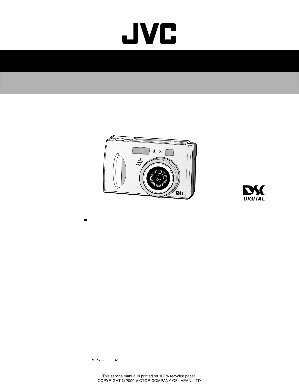
SERVICE MANUAL
DIGITAL STILL CAMERA
GC-X1E-S/E-BK/E-BL/E-RD/EK-S/EA
STILL CAMERA
SPECIFICATIONS
Power source
Power consumption
Dimensions
Weight
Operating temperature
Relative humidity
Storage temperature
LCD screen
Storage media
CCD
Focal distance
Lens
Video
Recording format
Sensitivity
Iris value (F value)
Exposure control
Exposure compensation
Minimum subject distance
Light measurement system
Flash
Recommended distance for flash
Shutter speed
White balance
Focus
: DC 5 V
: 4.0 W (when the LCD screen is off)
5.6 W (when the LCD screen is on)
: 101 (W) mm x 67 (H) mm x 59 (D) mm
(except protruding parts)
: Approx. 290 g
(without a Memory card and battery)
:0°C to 40°C
: 35% to 80%
: –20°C to 50°C
: 2.0 inch, polysilicon TFT (200,000 pixels)
: SmartMedia
: 3.34 million pixels (3.24 million valid pixels),
1/1.8" square pixels, primary color filter,
interlace scan CCD
: 7.5 mm to 17.5 mm
(equivalent to 37mm to 86 mm on a 35 mm still camera)
: 2.3X optical zoom lens
: 160 pixels x 120 pixels, 20 seconds, JVC original format
: Exif Ver. 2.1 (DCF compliant), TIFF (Uncompressed),
DPOF-compatible
: 80/160/320 (ISO compliant)
: F2.8/3.8, 5.6, 8, 11
: Program AE, iris priority AE
: +/–2EV (0.5EV steps)
: Approx. 2 cm to 50 cm (in Macro mode)
: Multi, spot
: Built-in,
Auto/red-eye prevention/forced/disabled
: Approx. 2.5 m
: Auto (Program AE: 1/8 seconds – 1/750 seconds,
Iris priority AE: 1/4 seconds – 1/750 seconds )
: Auto/Manual (
: Auto/Manual
TM
3.3V (up to 64MB)
, , , MWB, )
Self timer
Photo quality
Number of storable photos
(with an 8MB Memory card,
STANDARD/FINE/NO COMP.)
Battery
Printer connector
VIDEO output connector
Digital output connector
: 1 second, 8 seconds
: 3 modes (STANDARD/FINE/NO COMP.)
: 2032 x 1536: approx. 10/8/0
1024 x 768: approx. 43/32/3
640 x 480: approx. 87/65/8
: Lithium ion battery
: Output for optional printer
: Two-pole plug, 3.5 mm diameter (PAL)
: Mini-USB connector
AC Power Adapter/Charger AA-V37
Power requirement
U.S.A. and Canada
Other countries
Power consumption
Output
Charge
Camera
Operating temperature
Dimensions
Weight
E. & O. E. Design and specifications subject to change without notice.
: AC 120 V`, 60 Hz
: AC 110 V – 240 V`, 50 Hz/60 Hz
: 23 W
: DC 3.6 V
: DC 5.0 V
:0°C to 40°C [when charging: 10°C to 35°C]
: 68 (W) mm x 38 (H) mm x 110 (D) mm
: Approx. 230 g (without a DC cord)
, 0.77 A
, 1.5 A
No.86572
June 2000
Page 2

TABLE OF CONTENTS
Operating Environment
The host computer that runs the Macintosh
®
operating environment must satisfy the following
conditions.
USB Driver
1. USB-compatible computer (iMac™, iBook™,
Power Mac™ G3/G4, Power Book™ G3, etc.)
2. Mac OS 8.5.1/Mac OS 8.6/Mac OS 9.0
JVC Video Decoder
1. Power PC 603e/120MHz or faster
2. Mac OS 7.6.1 or later
3. QuickTime 3.0 or later
4. Minimum RAM requirement: 32MB
5. Minimum hard disk space requirement: 1MB
* Macintosh
®
is a registered trademark of Apple
Computer.
* Other trademarks are property of their
owners.
* If you use Macintosh
®
which does not have a
port, use an optional flash path, conversion
adapter, etc. For details on the operating en
ment of these devices, contact the dealers or
manufacturers.
Operating Environment
The host computer that runs the Windows
®
operating environment must satisfy the following
conditions.
USB Driver
1. Microsoft
®
Windows® 98/Windows® 98 Second
Edition, pre-installed
2. Available USB port
3. CD-ROM drive
Video Player
1. CPU: Intel
®
Pentium® 200MHz class or higher
2. Microsoft
®
Windows® 95/Windows® 98
3. Display capability of 65,536 colors or more
4. CD-ROM drive
5. Minimum RAM requirement: 32MB
6. Minimum hard disk space requirement: 1MB
* The system requirements information is not a
guarantee that provided software applications will
work on all personal computers meeting those
requirements.
* Microsoft
®
, Windows® are either registered
trademarks or trademarks of Microsoft corporation
in United States and/or other countries.
* Intel
®
, Pentium® are registered trademarks of Intel
corporation.
* Other trademarks are property of their respective
owners.
* If you use Windows
®
95 or a personal computer
which does not have a USB port, use an optional
flash path, conversion card adapter, etc. For
details on the operating environment of these
devices, contact the dealers or manufacturers.
SOFTWARE SECTION FOR Macintosh
®
SOFTWARE SECTION FOR Windows
®
Section Title Page Section Title Page
Important Safety Precautions
1. DISASSEMBLY
1.1 BEFORE ASSEMBLY AND DISASSEMBLY .................... 1-1
1.1.1 Precautions ................................................................. 1-1
1.1.2 Assembly and disassembly ......................................... 1-1
1.1.3 Disconnection of Connectors (Wires) ......................... 1-2
TOOLS AND EQUIPMENTS REQUIRED FOR ADJUSTMENTS ............
1.2
1.2.1 Tools required for adjustments ................................... 1-2
1.3 DISASSEMBLY /ASSEMBLY OF CABINET PARTS ......... 1-2
1.3.1 Disassembly flow chart ............................................... 1-2
1.3.2 Disassembly method ( I ) ............................................ 1-3
1.3.3 Disassembly method ( II ) <OP UNIT> ....................... 1-6
1.3.4 OP BLOCK Lens composition ..................................... 1-7
1.4 IC BLOCK DIAGRAM ...................................................... 1-8
1.4.1 IC 1002 (CXD2497R) ................................................... 1-8
1.4.2 IC 2001 (CDS/AGL) ..................................................... 1-9
1.4.3 IC 7302 (CXA3268AR) ............................................... 1-10
1.4.4 LCD (ACX301AK) ...................................................... 1-11
1.4.5 CCD (ICX262AQ) ....................................................... 1-12
2. ELECTRICAL ADJUSTMENT
2.1 ELECTRICAL ADJUSTMENT .......................................... 2-1
2.1.1 Precautions ................................................................. 2-1
2.1.2
2.1.3 Required test equipment ............................................ 2-1
2.1.4 Setup (LCD ADJUSTMENT) ........................................ 2-1
2.1.5 Setup (CCD ADJUSTMENT) ....................................... 2-2
2.2 Setup with patch cords and jig connector cables............ 2-3
3. CHARTS AND DIAGRAMS
NOTES OF SCHEMATIC DIAGRAM ........................................ 3-1
CIRCUIT BOARD NOTES ......................................................... 3-2
3.1 BOARD INTERCONNECTION ......................................... 3-3
3.2 MAIN (SYSCON) SCHEMATIC DIAGRAM ...................... 3-5
3.3 MAIN (DSP96) SCHEMATIC DIAGRAM.......................... 3-7
3.4 MAIN (DSP97) SCHEMATIC DIAGRAM.......................... 3-9
3.5 MAIN (G/A JCY0148) AND
MAIN (SD SUB) SCHEMATIC DIAGRAM........... 3-11
3.6 MAIN (F/Z MDA) AND
MAIN (IRIS) SCHEMATIC DIAGRAMS............... 3-12
3.7 MAIN (CDS AGC A/D AND ARM ROM)
SCHEMATIC DIAGRAM ..................................... 3-13
3.8 MAIN (STROBE CONTROL AND STROBE FLASH)
SCHEMATIC DIAGRAM ..................................... 3-14
3.9 CCD SCHEMATIC DIAGRAM........................................ 3-15
3.10 MONI REG (MONITOR) SCHEMATIC DIAGRAM ......... 3-16
3.11 MONITOR REG (DC/DC) SCHEMATIC DIAGRAM........ 3-17
JACK (VIDEO OUT/USB/PRINTER/DC JACK) AND
3.12
3.13 VOLTAGE CHARTS........................................................ 3-20
3.14 MAIN CIRCUIT BOARD (YB10282-01-06) ..................... 3-23
3.15 MONITOR REG CIRCUIT BOARD (YB10283-01-02) ..... 3-29
3.16 MONITOR REG CIRCUIT BOARD (YB10283-01-04) ..... 3-31
3.17 JACK CIRCUIT BOARD (YB10283-01-02) ..................... 3-33
3.18 JACK CIRCUIT BOARD (YB10283-01-04) ..................... 3-35
3.19 CCD CIRCUIT BOARD (YB10283-01-02) ....................... 3-37
The following table lists the differing points between Models GC-X1E-S, GC-X1E-BK, GC-X1E-BL, GC-XE-RD, GC-X1EK-S/GC-X1EA in this
series.
AC POWER ADAPTER AA-V37E ++ + AA-V37EK AA-V37EA
Test instruments required for electrical adjustment .............
MONITOR BACK LIGHT SCHEMATIC DIAGRAM .....
E-S E-BK E-BL E-RD EK-S EA
1-2
2-1
3-19
3.20 CCD CIRCUIT BOARD (YB10283-01-04) ....................... 3-38
STOROBE FLASH CIRCUIT BOARD (YB10283-01-02) ......
3.21
STOROBE FLASH CIRCUIT BOARD (YB10283-01-04) ......
3.22
3-39
3-40
3.23 OVER ALL BLOCK DIAGRAM....................................... 3-41
3.24 POWER SUPPLY BLOCK DIAGRAM ............................ 3-43
3.25 OP BLOCK SCHEMATIC DIAGRAM <REFERENCE> .. 3-45
3.26 OPERATION UINT
SCHEMATIC DIAGRAM <REFERENCE>.......... 3-46
4. PARTS LIST
4.1 PACKING AND ACCESSORY ASSEMBLY <M1> ........... 4-1
4.2 OP BLOCK ASSEMBLY <M3> ........................................ 4-2
4.3 FINAL ASSEMBLY <M2> .............................................. 4-3
4.4 ELECTRICAL PARTS LIST ............................................... 4-6
MAlN BOARD ASSEMBLY <01> .................................... 4-6
CCD BOARD ASSEMBLY <02> .................................... 4-11
MONI REG BOARD ASSEMBLY <03> ......................... 4-12
JACK BOARD ASSEMBLY <04> .................................. 4-14
STROBE FLASH BOARD ASSEMBLY <05> ................. 4-15
5. AC POWER ADAPTER (AA-V37E/EK/EA)
5.1 CABINET ASSEMBLY <MA> .......................................... 5-1
5.2 SCHEMATIC DIAGRAM .................................................. 5-2
5.3 CIRCUIT BOARD ............................................................. 5-4
5.4 ELECTRICAL PARTS LIST ............................................... 5-5
MAIN AND TERMINAL BOARD ASSEMBLY <91> ........ 5-5
Page 3
Important Safety Precautions
cut close to connector
Prior to shipment from the factory, JVC products are strictly inspected to conform with the recognized product safety and electrical codes
of the countries in which they are to be sold. However, in order to maintain such compliance, it is equally important to implement the
following precautions when a set is being serviced.
v
Precautions during Servicing
1. Locations requiring special caution are denoted by labels and
inscriptions on the cabinet, chassis and certain parts of the
product. When performing service, be sure to read and comply with these and other cautionary notices appearing in the
operation and service manuals.
2. Parts identified by the
critical for safety.
Replace only with specified part numbers.
Note: Parts in this category also include those specified to com-
ply with X-ray emission standards for products using
cathode ray tubes and those specified for compliance
with various regulations regarding spurious radiation
emission.
3. Fuse replacement caution notice.
Caution for continued protection against fire hazard.
Replace only with same type and rated fuse(s) as specified.
4. Use specified internal wiring. Note especially:
1) Wires covered with PVC tubing
2) Double insulated wires
3) High voltage leads
5. Use specified insulating materials for hazardous live parts.
Note especially:
1) Insulation Tape 3) Spacers 5) Barrier
2) PVC tubing 4) Insulation sheets for transistors
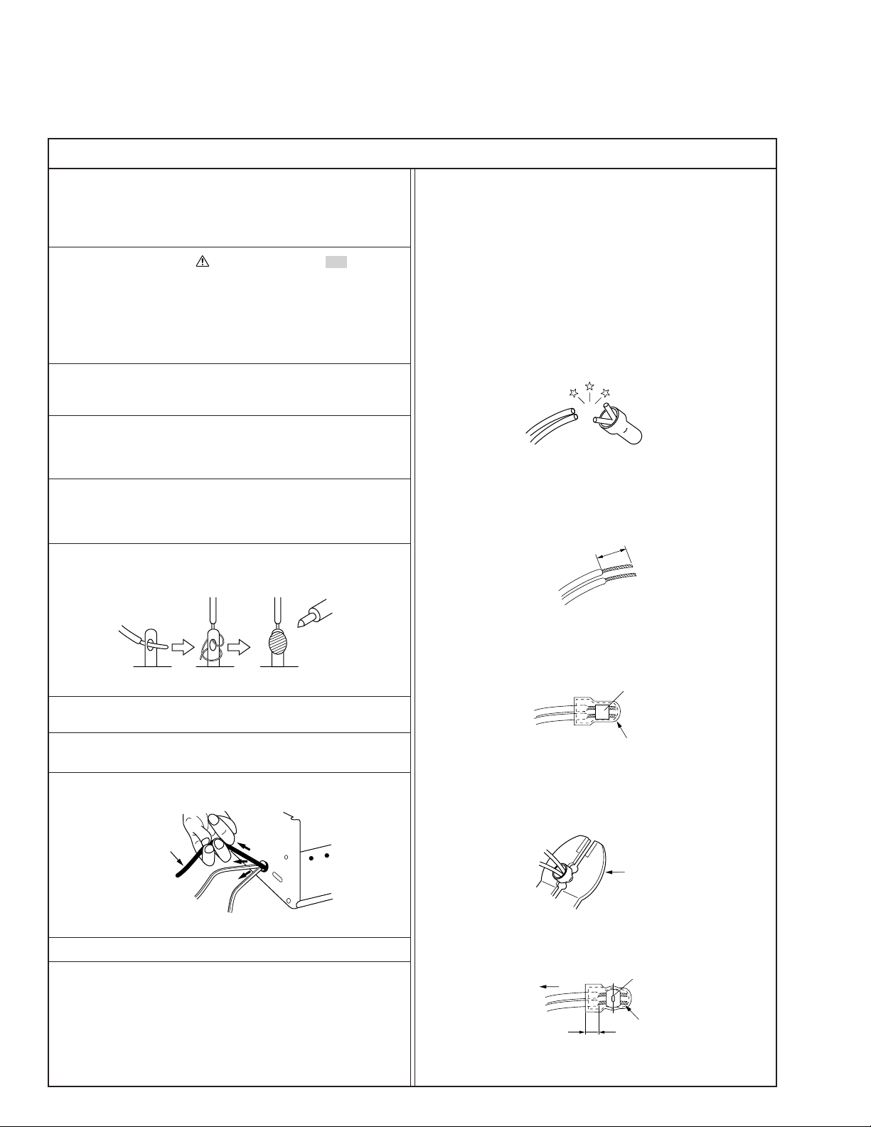
6. When replacing AC primary side components (transformers,
power cords, noise blocking capacitors, etc.) wrap ends of
wires securely about the terminals before soldering.
symbol and shaded ( ) parts are
12. Crimp type wire connector
In such cases as when replacing the power transformer in sets
where the connections between the power cord and power
transformer primary lead wires are performed using crimp type
connectors, if replacing the connectors is unavoidable, in order to prevent safety hazards, perform carefully and precisely
according to the following steps.
1) Connector part number : E03830-001
2) Required tool : Connector crimping tool of the proper type
which will not damage insulated parts.
3) Replacement procedure
(1) Remove the old connector by cutting the wires at a point
close to the connector.
Important : Do not reuse a connector (discard it).
Fig.3
(2) Strip about 15 mm of the insulation from the ends of
the wires. If the wires are stranded, twist the strands to
avoid frayed conductors.
15 mm
Fig.1
7. Observe that wires do not contact heat producing parts
(heatsinks, oxide metal film resistors, fusible resistors, etc.)
8. Check that replaced wires do not contact sharp edged or
pointed parts.
9. When a power cord has been replaced, check that 10-15 kg of
force in any direction will not loosen it.
Power cord
Fig.2
10. Also check areas surrounding repaired locations.
11. Products using cathode ray tubes (CRTs)
In regard to such products, the cathode ray tubes themselves,
the high voltage circuits, and related circuits are specified for
compliance with recognized codes pertaining to X-ray emission.
Consequently, when servicing these products, replace the cathode ray tubes and other parts with only the specified parts.
Under no circumstances attempt to modify these circuits.
Unauthorized modification can increase the high voltage value
and cause X-ray emission from the cathode ray tube.
Fig.4
(3) Align the lengths of the wires to be connected. Insert
the wires fully into the connector.
Metal sleeve
Connector
Fig.5
(4) As shown in Fig.6, use the crimping tool to crimp the
metal sleeve at the center position. Be sure to crimp fully
to the complete closure of the tool.
1.25
2.0
5.5
Fig.6
(5) Check the four points noted in Fig.7.
Not easily pulled free
Wire insulation recessed
more than 4 mm
Fig.7
Crimping tool
Crimped at approx. center
of metal sleeve
Conductors extended
1
S40888-01
Page 4
v
d'
d
Chassis
Power cord,
primary wire
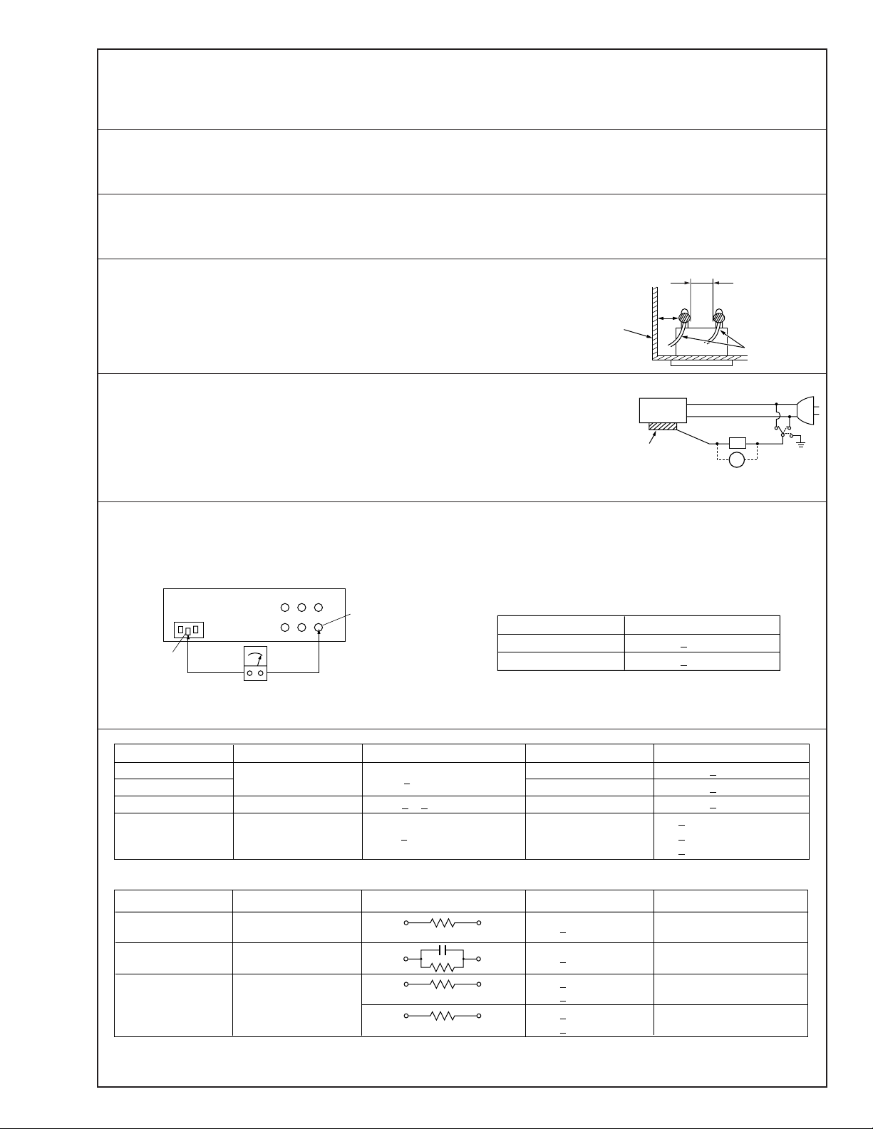
Safety Check after Servicing
Examine the area surrounding the repaired location for damage or deterioration. Observe that screws, parts and wires have been
returned to original positions, Afterwards, perform the following tests and confirm the specified values in order to verify compliance with safety standards.
1. Insulation resistance test
Confirm the specified insulation resistance or greater between power cord plug prongs and
externally exposed parts of the set (RF terminals, antenna terminals, video and audio input
and output terminals, microphone jacks, earphone jacks, etc.). See table 1 below.
2. Dielectric strength test
Confirm specified dielectric strength or greater between power cord plug prongs and exposed
accessible parts of the set (RF terminals, antenna terminals, video and audio input and output
terminals, microphone jacks, earphone jacks, etc.). See table 1 below.
3. Clearance distance
When replacing primary circuit components, confirm specified clearance distance (d), (d’) between soldered terminals, and between terminals and surrounding metallic parts. See table 1
below.
Fig. 8
4. Leakage current test
Confirm specified or lower leakage current between earth ground/power cord plug prongs
and externally exposed accessible parts (RF terminals, antenna terminals, video and audio
input and output terminals, microphone jacks, earphone jacks, etc.).
Measuring Method : (Power ON)
Insert load Z between earth ground/power cord plug prongs and externally exposed accessible parts. Use an AC voltmeter to measure across both terminals of load Z. See figure 9 and
following table 2.
Externally
exposed
accessible part
Z
V
Fig. 9
ab
c
5. Grounding (Class 1 model only)
Confirm specified or lower grounding impedance between earth pin in AC inlet and externally exposed accessible parts (Video in,
Video out, Audio in, Audio out or Fixing screw etc.).
Measuring Method:
Connect milli ohm meter between earth pin in AC inlet and exposed accessible parts. See figure 10 and grounding specifications.
AC inlet
Earth pin
AC Line Voltage
100 V
100 to 240 V
110 to 130 V
110 to 130 V
200 to 240 V
Exposed accessible part
Milli ohm meter
Fig. 10
Region
Japan
USA & Canada
Europe & Australia R 10 MΩ/500 V DC
Region Load Z
Insulation Resistance (R)
≤
R 1 MΩ/500 V DC
≥≥
1 MΩ R 12 MΩ/500 V DC
≤
Table 1 Specifications for each region
Grounding Specifications
Region
USA & Canada
Europe & Australia
Dielectric Strength
AC 1 kV 1 minute
AC 1.5 kV 1 miute
AC 1 kV 1 minute
AC 3 kV 1 minute
AC 1.5 kV 1 minute
(Class 2)
(Class 1)
Grounding Impedance (Z)
≤
Z 0.1 ohm
≤
Z 0.5 ohm
Clearance Distance (d), (d')
≤
d, d' 3 mm
≤
d, d' 4 mm
≤
d, d' 3.2 mm
≤
d 4 mm
≤
d' 8 mm (Power cord)
≤
d' 6 mm (Primary wire)
a, b, cLeakage Current (i)AC Line Voltage
100 V
110 to 130 V
110 to 130 V
220 to 240 V
Note: These tables are unofficial and for reference only. Be sure to confirm the precise values for your particular country and locality.
Japan
USA & Canada
Europe & Australia
Table 2 Leakage current specifications for each region
1 kΩ
0.15 µF
1.5 kΩ
2 kΩ
50 kΩ
2
≤
i 1 mA rms Exposed accessible parts
≤
i 0.5 mA rms
≤
i 0.7 mA peak
≤
i 2 mA dc
≤
i 0.7 mA peak
≤
i 2 mA dc
Exposed accessible parts
Antenna earth terminals
Other terminals
S40888-01
Page 5

Page 6
SECTION 1
DISASSEMBLY
1.1 BEFORE ASSEMBLY AND DISASSEMBLY
1.1.1 Precautions
1. Be sure to remove the power supply unit prior to mounting and soldering of parts.
2. When connecting and disconnecting the connectors, be
careful not to damage the wire.
3. When replacing chip parts (especially IC parts), desolder
completely first (to prevent peeling of the pattern).
4. Tighten screws properly during the procedures.
Unless specified otherwise, tighten screws at a torque
of 0.1N•m (1.0 kgf•cm).
CAUTION!!
RISK OF ELECTRIC SHOCK
When disassembling the unit, electric hazards may
occur in some cases if the capacitor for strobe
emission (STROBE board C6512) has been charged.
Therefore be also very careful when performing repairs
and inspections.
It is recommended that operations be carried out after
waiting for more than ten minutes with the power
supply removed or after discharging the capacitor
forcibly.
Discharge the capacitor according to <NOTE 2> on
Page 1-3.
C6512 is located behind the STROBE board.
PRECAUTIONS ON HANDLING
THE LITHIUM SECONDARY BATTERY
This unit is equipped with a coin type lithium secondary
battery.
Improper handling of this battery may cause heat to
be generated, damage, fires, or leakage. Always follow
the precautions below.
1 Do not short-circuit, disassemble, distort, nor heat
the battery.
2 Load the battery with its + and - poles connected
correctly.
3 Do not solder the battery itself.
4 When replacing parts, also refer to the numbers
listed in the Parts List of the manual.
5 Do not store the battery in direct sunlight and hot
and humid places.
6 When replacing the battery, handle it with care and
do not attempt to hold it with tweezers as it may
short-circuit.
7 When disposing the battery, wind tape around the
terminal to insulate the battery, and dispose the
battery according to the method prescribed.
1.1.2 Assembly and disassembly
STEP
PART NAME
1 FRONT CASE Remove screws
REAR CASE
2 OPERATION UNIT Remove the Connector Remove screws NOTE 1
FIG.
NO.
Fig
1-2-1
r MAIN CN4001 OPERATION UNIT
Remove the TOP COVER 2 (115)
POINT
2(115), 3(156), 4(114), 1(116)
3 (116)
(1) (2) (3) (4) (5)
(1) : Indicate the disassembly steps. When assembling,
perform in the reverse order of these steps. This
number corresponds to the number in the disassem-
bly diagram.
(2) : Indicates the name of disassembly/assembly parts.
(3) : Indicates the number in the disassembly diagram.
(4) : Indicates parts and points such as screws, washers,
springs which must be removed during disassembly/
assembly.
Lock (L), soldering (SD), shield, connector, etc.
The encircled numbers indicate the order for disas-
Note:
sembling the cabinet parts.
The screw numbers indicate the disassembling order.
:Wire
:Flat wire
:Board to Bord Connector
[Example]
• (115) = Remove the parts No 115 screw.
• (SD1) = Desoldering at the point SD1.
• a = Disconnect the connector/ML a .
(5) : Precautions on disassembly/assembly.
NOTE
1-1
Page 7
1.1.3 Disconnection of Connectors (Wires)
Connector
Pull both ends of the connector in the arrow direction, remove the lock and disconnect the flat wire.
Flat wire
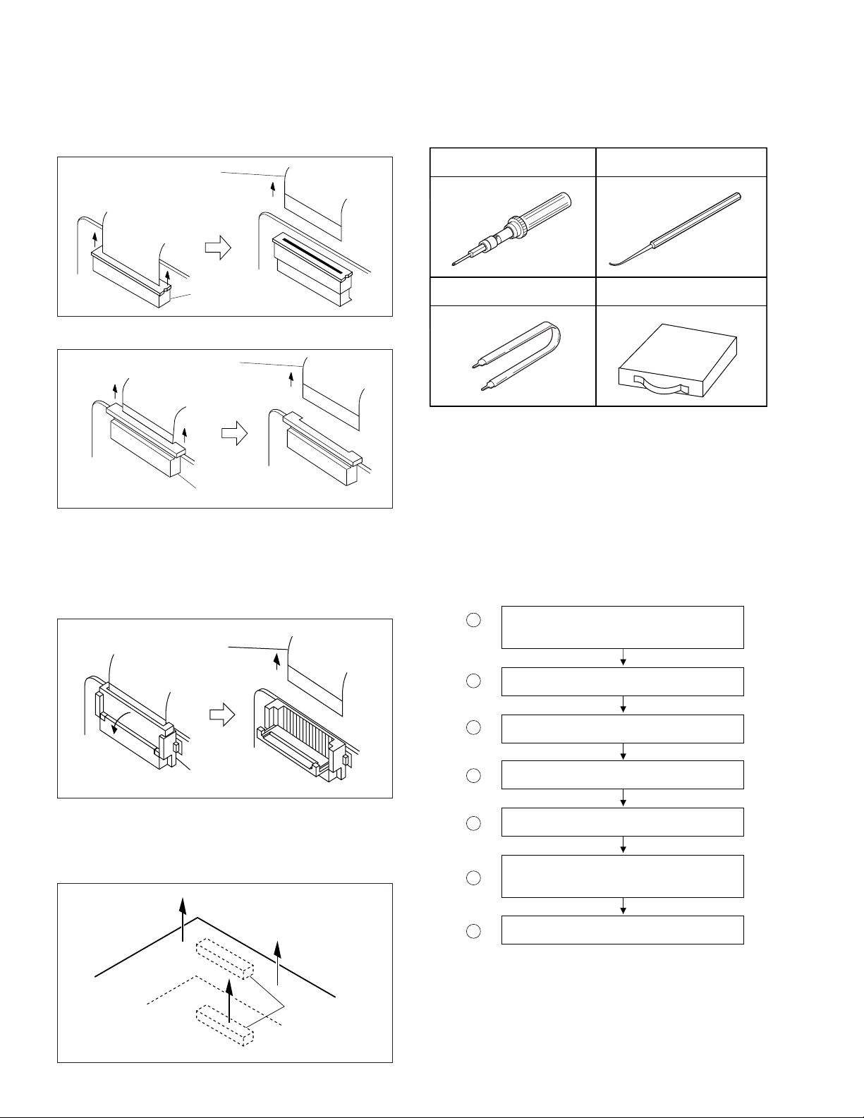
1.2 TOOLS AND EQUIPMENTS REQUIRED FOR ADJUSTMENTS
1.2.1 Tools required for adjustments
12
Torque driver
YTU94088
Clip IC replacement jig
PTS40844-2
Connector 1
Fig. 1-1-1 Connector 1
Flat wire
Connector 2
Fig. 1-1-2 Connector 2
Extend the locks in the direction of the arrow for unlocking
and then pull out the wire. After removing the wire,
immediately restore the locks to their original positions
because the locks are apt to come off the connector.
Flat wire
Connector catcher
34
YTU94036A
Soldering kit
YTU96016B
1.3 DISASSEMBLY/ASSEMBLY OF CABINET PARTS
1.3.1 Disassembly flow chart
The following flow chart shows the steps for disassembling
the cabinet parts. To assemble, perform the steps of the flow
chart in the reverse order.
The encircled numbers indicate the order for disas-
Note:
sembling the cabinet parts.
The screw numbers indicate the disassembling order.
1
FRONT CASE
REAR CASE
2
OPERATION UNIT
Connector 3
Fig. 1-1-3 Connector 3
B-B connector
Pull the board by both the sides in the direction of the arrow
for disconnecting the B-B connector.
Connector 4
Fig. 1-1-4 Connector 4
1-2
3
4
5
6
7
STROBE BOARD ASSEMBLY
JACK BOARD ASSEMBLY
LCD MODULE
MAIN BOARD ASSEMBLY
MONI/REG BOARD ASSEMBLY
OP UNIT
Page 8

1.3.2 Disassembly method ( I )
STEP
1 FRONT CASE Remove screws
REAR CASE 2 (115), 3 (156), 4 (157), 1 (154)
2 OPERATION UNIT Remove the Connector Remove screws Note 1
3 STROBE BOARD ASSEMBLY Remove the Connector Remove screw Note 1
JACK BOARD ASSEMBLY Remove the Connector Remove screws
4 LCD MODULE Remove the Connector Remove screws Note 1
5 MAIN BOARD ASSEMBLY Remove the Connector Note 1
MONI/REG BOARD ASSEMBLY Remove the PWB HOLDER Remove screws 2 (114) Note 1
6 OP UNIT Remove from the Frame Assy Remove screws 3 (117)
PART NAME
Fig
1-3-1
Fig
1-3-1
Fig
1-3-2
Fig
1-3-3
r MAIN CN4001
Remove the TOP COVER 2 (115)
n MAIN CN6601
p MAIN CN5501
m LCD MODULE (BL)
k MAIN CN3002
Remove from the Frame Assy
Remove from the LCD Holder Note 4
h MAIN CN501
c MAIN CN3001
d MON/REG TL9001
OPERATION UNIT 3 (116)
STROBE CN6501 1 (114) Note 2
JACK CN101 2 (114)
LCD MODULE (LCD) 2 (114)
OP UNIT
MON/REG CN9001
Frame Assy d (SD1)
POINTFIG. NO.
JACK CN701 e (SD3), f (SD4), g (SD5)
NOTE
Note 3
CONNEC- NO.OF
TOR/HL PINS
c
80 MAIN Board CN3001
d
e
g
h
k
m 2 JACK Board CN701
n
p 38 MAIN Board CN5501
q
s
u
v
w
1 MONI/REG Board TL9001
1 JACK Board TP3
f 1 JACK Board TP2
1 JACK Board TP1
22 MAIN Board CN501
j
2 MAIN Board CN502
24 MAIN Board CN3002
14 MAIN Board CN6601
28 MAIN Board CN2001
r 12 MAIN Board CN4001
STROBE UNIT WIRE (ORANGE)
1
t
STROBE UNIT WIRE (BROWN)
1
1 STROBE UNIT WIRE (RED)
STROBE UNIT WIRE (BLACK)
1
1
STROBE UNIT WIRE (Red, Thin wire) STROBE Board J6505 (Through hole)
CONNECTION
MONI/REG Board CN9001
MAIN FRAME (RED)
MAIN FRAME (BROWN)
MONI/REG Board J9001 (BLACK)
MONI/REG Board J9002 (RED)
OP UNIT
OP UNIT
LCD MODULE (LCD)
LCD MODULE (BL)
STROBE Board CN6501
JACK Board CN101
CCD Board CN1001
OPERATION UNIT
STROBE Board J6501 (Through hole)
STROBE Board J6502 (Through hole)
STROBE Board J6503 (Through hole)
STROBE Board J6504 (Through hole)
Note 1
Destination of connectors.
Note:
Three kinds of double-arrows in connection tables
respectively show kinds of connector/wires.
: Board to Board connector
: Flat wire
: Wire
Note 2
Be careful from electric shock hazard because the capacitor
(C6512) for the strobe is exposed. Be sure to positively discharge the capacitor if it is energized by short-circuiting a
resistor (10 - 22 k ) connected at both capacitor terminals.
Please be very careful when doing this job.
Note 3
Make sure that there is no slippage between the LCD panel
and the backlight, the four spots are locked with hooks
securely, and the sheet is placed in the correct direction.
no
4 sprts locked
slippege
Note 4
Both the stripe pattern and the non-slippage (notch) on the
sheet surface are to be in the direction as illustrated.
x
STROBE UNIT WIRE (BLACK, Thin wire)
1
STROBE Board J6506 (Through hole)
1-3
Page 9

116
110
C6512
2
s
116
2
u
v
157
116
2
L6501
x
w
t
153
111
D
1
155
r
2
STROBE
BOARD ASSY
< 05 >
G
114
115
2
3
115
H
E
r
G
F
n
n
1
E
114
1
JACK BOARD ASSY
< 04 >
F
E
MONI/REG BOARD ASSY
< 02 >
MAIN BOARD ASSY
< 01 >
H
152
D
G
H
154
1
156
1
1-4
LCDMODULE + BRAKLIGHT
WHITE WIRE
RED WIRE
LEFT LOW FOOT
HOLDER (LCD)
MAIN PWB
F
Fig.1-3-1
Remove screw marks
STEP 1
STEP 2
STEP 3
STEP 4
STEP 5
STEP 6
1
2
3
4
5
6
157
1
Page 10

Pass this through the inside of the boss.
d
101
117
6
MONI/REG BOARD ASSY
< 02 >
(SD1)
d
B
103
MAIN BOARD ASSY
< 01 >
c
114
6
117
A
p
3
F
m
e
(SD3)
f
(SD4)
g
(SD5)
JACK BOARD ASSY
< 04 >
C
e
OP BLOCK ASSY
<M3>
(SD2)
107B
107C
f
g
CCD BOARD ASSY
< 03 >
q
p
j
h
113
C
107A
106
114
5
A
108
105
109
h
q
j
B
114
4
k
104
114
5
107
m
k
Fig.1-3-2
1-5
Page 11

1.3.3 Disassembly method ( II ) <OP Unit>
STEP POINT
PART NAME
NOTE
1 OP Block ASSEMBLY Remove screws 3 (208)
2 COVER
Remove screws 3 (206),2 (207),
CCD BASE ASSEMBLY 1 (236)
SPACER Remove screws 3(206),2(207).
SET PLATE Remove the CCD Board Assy
20(SD1)
3 TILT FRAME Remove the SET RING Note 1
RATCH GEAR 2 (231) Note 2
MAIN PIN Note 3
4 RATCH MAGNET Remove Screws Note 4
NUT ASSEMBLY 3 (237),1 (236)
RATCH PIECE
Note 1
Turn and fix the set ring and make sure that the convex marks
are identical.
Note 2
Make sure that the torsion spring is in the groove of the
latch gear.
Note 3
Turn the latch gear clockwise ( ) and position it so that
the toothless portion comes to the level that is as high as
the main frame.
NOTE2
NOTE3
Note 4
Never move the setscrew in the
center of the nut assembly!
1
208
208
Remove screw marks
STEP 1
STEP 2
STEP 4
1
2
4
203
206
206
2
2
232
229
228
237
4
227
202
225
226
224
223
231
Fig. 1-3-3
221
234
234
236
222
230
4
233
204
237
231
4
SET SCREW
205
CCD Board Assembly
S2
207
SD1
1-6
Page 12

1.3.4 OP BLOCK Lens Composition
Fig. 1-3-4 Composition of GC-X1E Lens (8-group 9-element lens composition)
2GROUP
1GROUP
3GROUP 4GROUP 5GROUP 6GROUP 7GROUP 8GROUP
123 4 5 6 87 9
1.2.3...Condensing and focal length
Subject Image
5.6.7...Focal adjustment
7.8.9...Correction or compensation
Fig. 1-3-5 8-group-9-piece lens composition
1-7
Page 13

1.4 IC BLOCK DIAGRAM
1.4.1 IC 1002 (CXD2497R)
3
DD
V
OSCI
28
OSCO
27
CKI
26
25
CKO
MCKO
SNCSL
SSI
SCK
SEN
SSGSL
RST
TEST1
TEST2
30
3
31
32
33
6
2
37
48
Selctor
1/2
Register
1
5
DD
DD
V
V
Pin Descriptions
Pin No. Pin Name I/O Description
1VSS1 - GND
2 RST I System reset input terminal H: Reset released L: Reset
activated
(Should be activated at power ON, normally.)
(Schmitt trigger input/without protection diode on power
supply side)
3 SNCSL I Sync system switching control input terminal
(with pull-down resistor)
H: CKI sync L: MCKO sync
4 ID O Line identification pulse output terminal in the vertical
direction
5 WEN O Memory write timing pulse output terminal
6 SSGSL I Built-in SSG enable input terminal (with pull-down
resistor)
H: Built-in SSG is effective. L: External sync is effective.
7VDD1 - 3.3V power (for common logic section)
8VDD2 - 3.3V power (for RG terminal)
9 RG O Reset gate pulse output terminal for CCD
10 VSS2 - GND
11 VSS3 - GND
12 H1 O Clock output terminal for CCD horizontal register
13 H2 O Clock output terminal for CCD horizontal register
14 VDD3 - 3.3V to 5.0V power (for H1 and H2 terminals)
15 VDD4 - 3.3V power (for CDS system terminals)
16 XSHP O CCD pre-charge level sample/hold pulse output terminal
17 XSHD O CCD data level sample/hold pulse output terminal
18 XRS O Sample/hold pulse output terminal for phase matching in
analog-to-digital conversion
19 PBLK O Pulse output terminal for pulse cleaning during
horizontal and vertical blanking period
20 CLPDM O Pulse output terminal for CCD dummy signal clamping
21 VSS4 - GND
22 OBCLP O Pulse output terminal for CCD optical black signal
23 ADCLK O Clock output terminal for analog-to-digital conversion IC
Logical phase is adjustable with the serial interface data
H1H2V
SSG
1
5
SS
SS
V
V
2
3
DD
SS
V
11
Pulse Generator
35361297
RG
Latch
HD
2
SS
V
Selector
34
VD
4
DD
V
XSHP
V Driver
XSHD
181716151098 21131214
XRS
4
SS
V
19
PBLK
CLPDM
20
22
OBCLP
23
ADCLK
24
V
SS
5
4
ID
5
WEN
41
V1A
43
V1B
39
V2
44
V3A
46
V3B
40
V4
47
SUB
VH
42
VM
38
VL
45
24 VSS5 - GND
25 CKO O Inverter output terminal
26 CKI I Inverter input terminal
27 OSCO O Inverter output terminal for oscillation (If not used,
should be opened or connected to GND through a
capacitor.)
28 OSCI I Inverter input terminal for oscillation (If not used, should
be fixed to "Low".)
29 VDD5 - 3.3V power (for common logic section)
30 MCKO O System clock output terminal for signal processing IC
31 SSI I Serial interface data input terminal for setting each IC
mode (Schmitt trigger input/without protection diode on
power supply side)
32 SCK I Serial interface clock input terminal for setting each IC
mode (Schmitt trigger input/without protection diode on
power supply side)
33 SEN I Serial interface strobe input terminal for setting each IC
mode (Schmitt trigger input/without protection diode on
power supply side)
34 VD I/O Vertical sync signal input/output terminal
35 HD I/O Horizontal sync signal input/output terminal
36 VSS6 - GND
37 TEST1 I IC test terminal 1 with pull-down resistor (Should be
fixed to GND normally.)
38 VM - GND (for vertical drivers)
39 V2 O Clock output terminal for CCD vertical register
40 V4 O Clock output terminal for CCD vertical register
41 V1A O Clock output terminal for CCD vertical register
42 VH - 15.0V power (for vertical drivers)
43 V1B O Clock output terminal for CCD vertical register
44 V3A O Clock output terminal for CCD vertical register
45 VL - -7.5V power (for vertical drivers)
46 V3B O Clock output terminal for CCD vertical register
47 SUB O Pulse output terminal for CCD electronic shutter
48 TEST2 I IC test terminal 2 with pull-down resistor (Should be
fixed to GND normally.)
1-8
Page 14

1.4.2 IC 2001 (CDS/AGL)
OADSW
OADCLK
13 16 18 19
21
ADCLK
SPBLK
SPSIG
41
AVDDDVDD
46
AVSS
DVSS
40
48
27
ADCIN
25
CDSSW
26
CDSIN
BLKSH
BLKFB
28
29
CDS PGA
DC offset
compensatory
17
20
OBP
PBLK
Pin Descriptions
Pin No. Pin Name Description I/O
1 NC No internal connection - 2 D0 Digital output terminal (LSB) O D
3-10 D1-D8 Digital output terminals O D
11 D9 Digital output terminal (MSB) O D
12 NC No internal connection - 13 OADCLK Latch clock output terminal for D0 to D9 O D
14 DVSS Digital GND (0V) - D
15 DV
DD Power for digital 3.0V system - D
(Should be connected to AVDD outside the IC.)
16 ADCLK Analog-to-digital conversion clock input terminal I D
17 OBP Optical black pulse input terminal I D
18 SPBLK Black level sampling clock input terminal I D
19 SPSIG Signal level sampling clock input terminal I D
20 PBLK Pre-blanking signal input terminal I D
21 OADSW OADCLK enable input terminal I D
22 AVSS Analog GND (0V) - A
23 AVDD Power for analog 3.0V system - A
24 NC No internal connection - 25 CDSSW Signal level sampling output terminal O A
26 CDSIN CDS input terminal I A
27 ADCIN ADC input terminal I A
28 BLKSH Black level sample/hold terminal - A
29 BLKFB Black level feedback terminal - A
30 AVSS Analog GND (0V) - A
31 AV
DD Power for analog 3.0V system - A
(Should be connected to DVDD outside the IC.)
32 VRT Reference voltage terminal 3 - A
(Ceramic capacitor of 0.1µF or more should be
connected between this terminal and AVss.)
33 VRB Reference voltage terminal 2 - A
(Ceramic capacitor of 0.1µF or more should be
connected between this terminal and AVss.)
Serial
Interface
44
SCK
Analog (A) or
Digital (D)
TIMING
gen
43CS45
SDATA
Bias
Occurrence
35
BIAS
10bit
ADC
33
Output
32
34
VRT
VRB
VRM
Latch
circuit
42 OEB
11 D9
10 D8
9D7
8D6
7D5
6D4
5D3
4D2
3D1
D0
2
34 VRM Reference voltage terminal 1 - A
(Ceramic capacitor of 0.1µF or more should
be connected between this terminal and AVss.)
35 BIAS Internal bias terminal - A
(A 24-Kohm resistor should be connected
between this terminal and AVss.)
36 NC No internal connection - 37 AVSS Analog GND (0V) - A
38 AV
DD Power for analog 3.0V system - A
(Should be connected to DVDD outside the IC.)
39 NC No internal connection - 40 AVSS Analog GND (0V) - A
41 AVDD Power for analog 3.0V system - A
(Should be connected to DVDD outside the IC.)
42 OEB Digital output enable control input terminal I D
43 CS Serial interface control input terminal I D
44 SCK Serial clock input terminal I D
45 SDATA Serial data input terminal I D
46 DV
DD Power for digital 3.0V system - D
(Should be connected to AVDD outside the IC.)
47,48 DV
SS Digital GND - D
1-9
Page 15

1.4.3 IC 7302 (CXA3268AR)
VSSVSSTST10
TST9
51 38 37
V
SSVSS
+3.0V
55
V
DD
56
TST11
OSD B
OSD R
OSD G
HCK1
HCK2
VCC1
FIL IN
B/B-Y
R/R-Y
GEN
57
58
59
60
NC
61
HCK
GEN
62
+3.0V
63
64
HST
HCOUNTER
HPULSE
65
EN
GEN
66
VCK
67
VST
67
RGT
69
70
71
G/Y
72
H.FILTER SYNC SEP
SS
V
CONTRAST
S/H
CONT
GR
MODE
PIC-G
PIC-F
MODE
SS
V
FIL OUT
SYNC IN
SYNC OUT
Pin Descriptions
Pin No. Pin Name I/O Description
1 Vss - GND terminal for digital 3.0V system
2 FIL OUT O H filter output terminal (for internal sync separator use)
3 SYNC IN I Sync input terminal for sync separator circuit
(for internal sync separator use)
4
SYNC OUT
O Sync output terminal for sync separator circuit
(for internal sync separator use)
5
CSYNC/HD
I CSYNC/horizontal sync signal input terminal
6 DA OUT O DAC output terminal
7 REF O Level shifter circuit reference voltage output terminal for
LCD panel
8 F ADJ O f0 adjust resistor connecting terminal for TRAP
9 GND1 - GND terminal for analog 3.0V system
10 VD I Vertical sync signal input terminal
11 DWN O Up/Down switching signal output terminal
12 WIDE O 16:9 wide display switching pulse output terminal
13 TST1 - Test terminal (Should be opened.)
14 SCK I Serial clock input terminal
15 SEN I Serial load input terminal
16 SDAT I Serial data input terminal
17 R INJECT O Resistor connecting terminal for serial block current control
18 VSS - GND terminal for digital 3.0V system
19 VDD - Power for digital 3.0V system
20 VDD - Power for digital 3.0V system
21 CKO O Oscillation cell output terminal
22 CKI I Oscillation cell input terminal
23 Vss - GND terminal for digital 3.0V system
24 RPD O Phase comparison output terminal
25 XCLR I Capacitor connecting terminal for power-on reset (for
timing generating system)
26 VDO O VDO pulse output terminal
27 HDO O HDO pulse output terminal
28 TST2 - Test terminal (Should be connected to GND.)
29 GND2 - GND terminal for analog 12.0V system
30 SIG.C I DC voltage adjust terminal for R, G, B and PSIG outputs
31 B DC DET O Capacitor connecting terminal for B signal's DC voltage
feedback circuit
32 B OUT O B signal output terminal
33 R DC DET O Capacitor connecting terminal for R signal's DC voltage
feedback circuit
34 R OUT O R signal output terminal
35 G DC DET O Capacitor connecting terminal for G signal's DC voltage
feedback circuit
1-10
TST8
OSD RGB
TRAP
LPF
CLAMP
MATRIX
DL1PICTURE
HUE
CLAM[P
SYNC/HD
TST7
DL1
COLOR
DA
Buf Buf
DA OUT
B
BGR
HUE
CLP
REF
TST6
LPF
FILTER
FILTER
BIAS
REF
Input
Res.
L
H
TST5NCPOF
S/H
USER-BRIGHT
GAMMAM
CLAMP
BLK-LIM
SUB-BRIGHT
POL SW
PULSE
ELM
V COUNTER
GND1
F ADJ
GND1
U-GRT
γ1γ2
WHITLIM
SUB-CONT R
SUB-CONT B
BLKLIM
SUB-BRT R
SUB-BRT B
VD
TST4
GND3
COUNTER
V CONTROL
V POSITION
DWN
GND3
Buf
PLL
V SEP
WIDE
3
CC
COM
V
+12.0V +12.0V
PSIGBRT
PSIGBRIGHT
POL SW
S/P CONV
REGISTER DAC
SCK
TST1
TST3
COM-DC
HDO GEN
VDO GEN
COMPARATOR
HSYNC DET
H SKEW DET
CLK
1615141312111098765321 4 17 18
SEN
PSIG OUT
394041424344454647484950525354
Buf
Buf
Buf
Buf
PHASE
CK
CONTROL
SDAT
2
CC
PSIG DC DET
V
SIG.C
MCK
V
SS
SS
V
R INJECT
+3.0V
+3.0V
GND2
36
G OUT
35
G DC OUT
34
R OUT
33
R DC DET
32
B OUT
31
B DC DET
30
SIG. C
29
GND2
28
TST2
27
HDO
26
VFO
25
XCLR
24
RPD
23
SS
V
SS
V
22
CKI
21
CKO
20
DD
V
19
V
DD
36 G OUT O G signal output terminal
37 VCC2 - Power for analog 12.0V system
38 PSIG DC O Capacitor connecting terminal for G signal's DC voltage
DET feedback circuit
39 PSIG OUT O PSIG output terminal
40 TST3 - Test terminal (Should be opened.)
41 VCC3 - Power for analog 12.0V system COM (CS)
42 COM O
Common electrode voltage output terminal (CS) for LCD panel
43 GND3 - GND terminal for analog 12.0V system COM (CS)
44 TST4 - Test terminal (Should be opened.)
45 POF O LCD panel power ON/OFF terminal
(Open, if this function is not used.)
46 NC - No internal connection
47 TST5 - Test terminal (Should be connected to GND.)
48 TST6 - Test terminal (Should be connected to GND.)
49 TST7 - Test terminal (Should be opened.)
50 TST8 - Test terminal (Should be opened.)
51 TST9 - Test terminal (Should be opened.)
52 TST10 - Test terminal (Should be opened.)
53 VSS - GND terminal for digital 3.0V system
54 VSS - GND terminal for digital 3.0V system
55 VDD - Power for digital 3.0V system
56 TST11 - Test terminal (Should be connected to GND.)
57 OSD B I OSD B input terminal
58 OSD R I OSD R input terminal
59 OSD G I OSD G input terminal
60 NC - No internal connection
61 HCK1 O H clock pulse 1 output terminal
62 HCK2 O H clock pulse 2 output terminal
63 VCC1 - Power for analog 3.0V system
64 HST O H start pulse output terminal
65 EN O EN pulse output terminal
66 VCK O V clock pulse output terminal
67 VST O V start pulse output terminal
68 RGT O Right/Left switching signal output terminal
69 FIL IN I H FILTER input terminal (for internal sync separator use)
70 B/B-Y I B/B-Y signal input terminal
71 G/Y I G/Y signal input terminal
72 R/R-Y I R/R-Y signal input terminal
DOWN SCAN and UP SCAN RGT: RIGHT SCAN and LEFT SCAN
* DWN:
H: Pull-up resistor incorporated L: Pull-down resistor incorporated
Page 16

1.4.4 LCD (ACX301AK)
V shift register
COM
V Level shifter
Electrode
1 2 3 4 5 6 7 8 9 10 11 12 13 14 15 16 17 18 19 20 21 22 23 24
TESTL
Pin Descriptions
Pin No. Pin Name Description
1 TESTL Panel testing terminal (Should be opened.)
2 COM Common electrode voltage input terminal for panel
3 VST Start pulse input terminal for V shift register drive
4 VCK Clock input terminal for V shift register drive
5 EN Enable signal input terminal for gate select pulse
6 DWN Drive direction signal input terminal for V shift register
7VVDD Power for V driver
8VSS GND for H and V drivers
9HVDD Power for H driver
10 VSSG Negative voltage setting terminal for V driver
11 TEST2 Connected to GND through a 1-Mohm resistor in the panel
12 WIDE Pulse input terminal for 16:9 mode
13 HST Start pulse input terminal for H shift register drive
14 REF Level shifter circuit reference voltage input terminal
15 TEST Panel testing terminal (Should be opened.)
16 Cext/Rext Power input terminal for setting H shift register drive time
constant
17 HCK2 Clock input terminal for H shift register drive
18 HCK1 Clock input terminal for H shift register drive
19 PSIG Uniformity improving signal input terminal
20 GREEN Video signal (G) input terminal for the panel
21 RED Video signal (R) input terminal for the panel
22 BLUE Video signal (B) input terminal for the panel
23 RGT Drive direction signal input terminal for H shift register
24 TESTR Panel testing terminal (Should be opened.)
COM
EN
VST
VCK
H Level shifter & Shift register
Negative
Voltage
Occurence
Circuit
VSS
DWN
VVDD
HVDD
COM
LCCs
HST
VSSQ
TEST2
WIDE
REF
TEST
HCK2
Cext/Rext
HCK1
PSIG
GREEN
RED
BLUE
RTG
TESTR
Features
• Device Structure
- Active matrix panel with internal driver using lowtemperature polysilicon transistors
- Pixels
Total dots: 896 (H) x 230 (V) =206,080
Display dots: 880 (H) x 228 (V) =200,640 (2.0 in.)
• Total dots: 200,000 dots 5.1cm diagonal (2.0 in.)
• Horizontal resolution: 440 TV scanning lines
• Light permeability: 5.6% (standard)
• Smooth screen image with RGB delta array
• NTSC/PAL compatible
• High image quality internal circuitry
• 16:9 screen display function
• Low-reflection screen display processing assures easy
viewing even outdoors
• Anti-grime display
RBGRGB
BGRBRG
RBGRGB
BGRBRG
RBGRGB
Delta array
1-11
Page 17

1.4.5 CCD (ICX262AQ)
OUT
V
GND
TEST
10
9
8
Gb
Gb
Gb
Vertical register
11
12
13
ØRG
Ø2
H
DD
V
Pin Descriptions
Pin No. Pin Name Description
1Vø4 Vertical register transfer clock
2Vø3A Vertical register transfer clock
3Vø3B Vertical register transfer clock
4Vø2 Vertical register transfer clock
5Vø1A Vertical register transfer clock
6Vø3B Vertical register transfer clock
7 TEST Test terminal*
8 TEST Test terminal*
1
1
9 GND GND
10 VOUT Signal output
11 VDD Circuit power
12 øRG Reset gate clock
13 Hø2 Horizontal register transfer clock
14 Hø1 Horizontal register transfer clock
15 GND GND
16 øSUB PCB clock
17 CSUB PCB bias*
2
18 VL Protection transistor bias
19 Hø1 Horizontal register transfer clock
20 V
ø2 Horizontal register transfer clock
*1: Terminal should be opened.
*2: A 0.1µF capacitor should be connected between the pin and GND, since the
DC bias is generated inside the CCD.
Ø1B
TEST
V
7
6
B
R
R
R
14
Gr
B
Gr
B
Gr
Horizontal register
15
Ø1
H
GND
Ø1A
Ø2
Ø3B
Ø3A
Ø4
V
V
2
1
(NOTE)
(NOTE)
19
20
Ø1
Ø2
H
H
: Photo Sensor
5
16
V
ØSUB
V
V
4
3
Gb
R
Gb
R
Gb
Gb
17
SUB
C
B
Gr
B
Gr
B
Gr
18
L
V
Features
• Field period readout system
• Interline CCD image sensor
• Total number of pixels: 2140 (H) x 1560 (V) approx. 3340k
pixels
• Number of effective pixels: 2088 (H) x 1550 (V) approx.
3240k pixels
• Effective number of pixels: 2080 (H) x 1542 (V) approx.
3210k pixels (1.18in)
• Chip size: 8.10mm (H) x 6.64mm (V)
• Unit cell size: 3.45m␣ m (H) x 3.45m␣ m (V)
• Optical black:
Horizontal (H) direction : front 4 pixels, rear 48 pixels
Vertical (V) direction : front 8 pixels, rear 2 pixels
• Number of dummy bits: Horizontal 28 Vertical 1 (even fields
only)
• Square pixels
• Horizontal drive frequency: 18kHz
• RGB basic color mosaic on-chip color filter
• High sensitivity
• Cyclic, variable speed shutter
• Excellent anti-blooming characteristics
1pin
2
1-12
V
4
11pin
H
48
Optical black wiring diagram
(Top View)
8
Page 18

SECTION 2
910
Light box assembly
YTU93096A
Gray scale chart
YTU94133A
Cleaning cloth
KSMM-01
11
Color bar chart
YTU94133C
12
Smart media card
16MB
13
USB
QAM0252-001
14
ELECTRICAL ADJUSTMENT
2.1 ELECTRICAL ADJUSTMENT
2.1.1 Precautions
Both the camera section and deck section of this model
are designed and manufactured to be adjustment-free.
However, if both or either of the following parts is replaced,
it needs special adjustment with a personal computer at a
JVC service equipment after the part replacement
• OP block assembly
• EEPROM (on the MAIN board)
When there is some trouble in the electric circuit, it is required
to detect the faulty part with specified test instruments first
and then to proceed to repair, replacement and adjustment.
1. When cheking a signal at a chip test point, be sure to use
an IC clip or the like not to apply any stress to the test point.
When replacing a chip part (IC in particular), completely
remove solder chips from it and its periphery before
proceeding to part replacement (in order to avoid exfoliation
of the pattern).
2. Carefully disconnect/connect connectors because they
are apt to get damaged.
2.1.2 Test instruments required for electrical
adjustment
12
34
5
Patch cord
YTU93099A
Service support system
YTU94057-47
Jig connector cable
YTU93091B
Jig connector cable
YTU93102A
PC cable
QAM0099-002
Extension connector
6
YTU94145A
2.1.3 Required test equipment
1. Color TV monitor.
2. AC power adapter (AA-V37 or equivalent)
3. Oscilloscope (dual-trace type, for more than 20 MHz).
4. Digital voltmeter
5. Frequency counter (with threshold level adjuster)
6. Personal computer
2.1.4 Setup (LCD ADJUSTMENT)
Setup for electrical adjustment with personal computer
Note 1:
As a general rule for adjustment with a personal
computer, connect a personal computer to its
PRINTER terminal.
Note 2:
Use DC cord to supply the power.
PRINTER
Service support system
YTU94057-47
INF adjustment lens
78
YTU92001B
Camera stand
YTU93079
RS-232C
PC cable
QAM0099-002
port
MENU
Personal computer
Fig. 2-1-1 Setup for electrical adjustment with
personal computer (I)
2-1
Page 19

Extension connector
Note) It is needs to connect
the extension
double for use the DC
cord(coupler)
Jig connector cable
(YTU93091B)
Fig. 2-1-2 Setup for electrical adjustment with
personal computer (II)
connector
2.1.5 Setup (CCD ADJUSTMENT)
Setup for electrical adjustment with personal computer
Note 1:
As a general rule for adjustment with a personal
computer, connect a personal computer to its
DIGITAL terminal.
Note 2:
Use DC cord to supply the power.
USB
USB
port
16MB
Smart media
Card
Service support system
YTU94057-47
MENU
Pin No. FUNCTION
1 135TMS
2 135TDI
3 nTRST
4 AL_3.3V
5 32DBI
6 GND
7 M_COM
8 M_SIG_C
9 M_RED
10 M_SIG_GND
11 JTAGMODE
12 135TDO
13 135TCK
14 AL_3.3V
15 32RST
16 M_BLUE
17 RPD
18 M_PSIG
19 M_GREEN
20 NC
Personal computer
Fig. 2-1-3 Setup for electrical adjustment with
personal computer (I)
2-2
Table 2-1-1 Jig Connector Function
Page 20

2.2 Setup with patch cords and jig connector cables Note:
Fig. 2-2-1 shows an example of expansion setup that facilitates inspection of major boards because main components are
connected by means of patch cords and jir cables.For proceeding to electrical adjustment in such the setup, disassemble the
set at certain level required for the current adjustment objectives referring to the section 1 "DISASSEMBLY" and properly set
up the expanded set and test instruments.
OP/CCD
MON/REGMON/REG
PRINTER
DIGITAL
VIDEO
CN9001
DC
5V
5
YTU94077-22
YTU94071-22
4YTU94077-38
JACK
CN101
CN7101
MENU
3YTU94077-28
CN502
CN5501
CN501
STROBE
CN6501
CN6601
MAIN
CN2001
CN3002
MONITOR
CN4001
CN2002
YTU94077-12
1
YTU94074-12
OPERATION UNIT
2YTU94126B-80
6YTU63091B
Personal computer
Fig. 2-2-1
Connection
Pin No. Parts Number
1 MAIN CN4001 OPRATION UNIT 12 YTU94077-12 FPC wire
YTU94074-12 FPC CN.ASSY
2 MAIN MON/REG CN9001 80 YTU94126B-80 B TO B CN.ASSY
3 MAIN CN2001 CCD CN1001 28 YTU94077-28 FPC wire
4 MAIN CN5501 JACK CN101 38 YTU94077-38 FPC wire
5 MAIN CN501 OPUNIT 22 YTU94077-22 FPC wire
YTU94074-22 FPC CN.ASSY
6 MAIN CN2202 20 YTU93091B JIG CN.cable
2-3
Page 21

Page 22

VICTOR COMPANY OF JAPAN, LIMITED
VIDEO DIVISION
S40894
Printed in Japan
 Loading...