

Page 1
YA315200510
SERVICE MANUAL
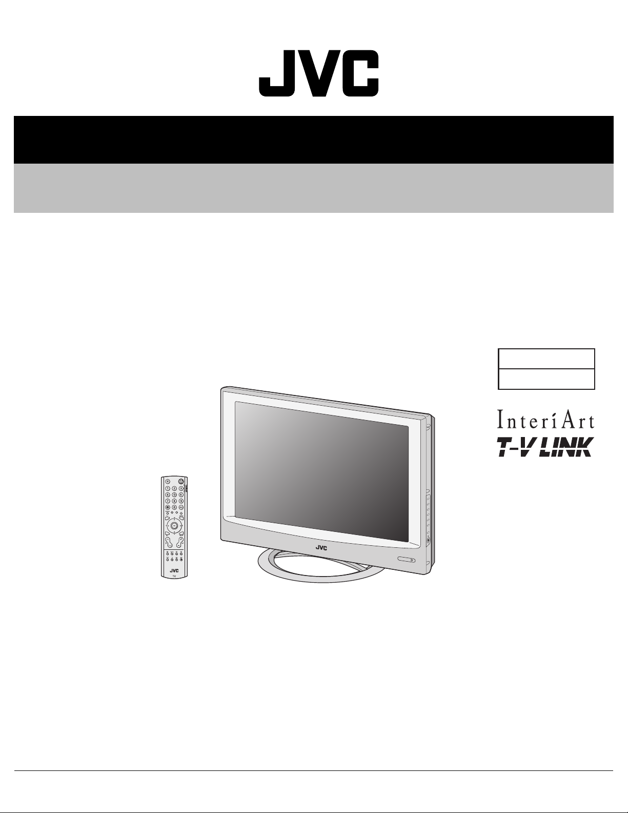
WIDE LCD PANEL TELEVISION
LT-32A60BU,
LT-32A60SJ,
LT-32A60SU
BASIC CHASSIS
FT
TABLE OF CONTENTS
1 PRECAUTION. . . . . . . . . . . . . . . . . . . . . . . . . . . . . . . . . . . . . . . . . . . . . . . . . . . . . . . . . . . . . . . . . . . . . . . . . 1-3
2 SPECIFIC SERVICE INSTRUCTIONS . . . . . . . . . . . . . . . . . . . . . . . . . . . . . . . . . . . . . . . . . . . . . . . . . . . . . . 1-7
3 DISASSEMBLY . . . . . . . . . . . . . . . . . . . . . . . . . . . . . . . . . . . . . . . . . . . . . . . . . . . . . . . . . . . . . . . . . . . . . . 1-10
4 ADJUSTMENT . . . . . . . . . . . . . . . . . . . . . . . . . . . . . . . . . . . . . . . . . . . . . . . . . . . . . . . . . . . . . . . . . . . . . . . 1-15
5 TROUBLESHOOTING . . . . . . . . . . . . . . . . . . . . . . . . . . . . . . . . . . . . . . . . . . . . . . . . . . . . . . . . . . . . . . . . . 1-19
COPYRIGHT © 2005 Victor Company of Japan, Limited
No.YA315
2005/10
Page 2
SPECIFICATION
Items Contents
Dimensions ( W × H × D ) 82.0 cm × 60.2 cm × 22.5 cm [Included stand]
82.0 cm × 55.1 cm × 12.7 cm [TV only]
Mass 18.8 kg [Included stand]
15.4 kg [TV only]
Power Input AC110V - AC240 V, 50 Hz / 60 Hz
Power Consumption 158 W (Standby: 2.1 W)
TV RF System CCIR (B/G, I, D/K, L)
Colour System PAL, SECAM, NTSC 3.58/4.43 [EXT only]
Stereo System NICAM (B/G, I, D/K, L), A2 (B/G, D/K)
Teletext System FLOF (Fastext level 2.5), TOP, WST(World Standard system)
Receiving Frequency VHF: 47MHz - 470MHz
UHF: 470MHz - 862MHz
Intermediate
Frequency
Colour Sub
Carrier Frequency
LCD panel 32V-inch wide aspect (16 : 9)
Screen Size Diagonal : 80 cm (H: 69.7 cm × V: 39.2 cm)
Display Pixels Horizontal : 1366 dots × Vertical : 768 dots (W-XGA)
Audio Power Output 5 W + 5 W
Speaker 6.6 cm, round type × 2 (Oblique corn)
Aerial terminal (VHF/UHF) 75 Ω unbalanced, coaxial
EXT-1 / EXT-2 (Input / Output) 21-pin Euro connector (SCART socket ) × 2
EXT-3 (Input) S-Video
EXT-4 (Input) Component Video
625p / 525p / 625i / 525i
PC (RGB) Input D-sub 15 pin × 1
Headphone 3.5 mm stereo mini jack × 1
Remote Control Unit RM-C1816S (AA/R6 dry cell battery × 2)
Design & specifications are subject to change without notice.
VIF 38.9MHz (B/G, I, D/K, L)
SIF 33.4MHz (5.5MHz :B/G)
32.9MHz (6.0MHz :I)
32.4MHz (6.5MHz :D/K)
PAL 4.43MHz
SECAM 4.40625MHz / 4.25MHz
NTSC 3.58MHz / 4.43MHz
Mini-DIN 4 pin × 1
Y: 1 V (p-p), Positive (Negative sync provided), 75 Ω
C: 0.286 V (p-p) (Burst signal), 75 Ω
Video
1 V (p-p), Positive (Negative sync provided), 75 Ω, RCA pin jack × 1
Audio
500 mV (rms), High impedance, RCA pin jack × 2
RCA pin jack × 3
Y : 1 V (p-p) (Sync signal: ±0.35V(p-p), 3-value sync.), 75Ω
750p
Pb/Pr : ±0.35V(p-p), 75 Ω
Y : 1 V (p-p), Positive (Negative sync provided), 75 Ω
Cb/Cr : 0.7V(p-p), 75 Ω
R/G/B : 0.7 V (p-p), 75Ω
HD / VD : 1 V (p-p) to 5 V (p-p), high impedance
< Available signal >
VGA : 640 pixels × 480 pixels (Horizontal : 31.5 kHz / Vertical : 60 Hz)
XGA : 1024 pixels × 768 pixels (Horizontal : 48.4 kHz / Vertical : 60 Hz)
1-2 (No.YA315)
Page 3

SECTION 1
PRECAUTION
1.1 SAFETY PRECAUTIONS [EXCEPT FOR UK]
(1) The design of this product contains special hardware,
many circuits and components specially for safety
purposes. For continued protection, no changes should be
made to the original design unless authorized in writing by
the manufacturer. Replacement parts must be identical to
those used in the original circuits. Service should be
performed by qualified personnel only.
(2) Alterations of the design or circuitry of the products should
not be made. Any design alterations or additions will void
the manufacturer's warranty and will further relieve the
manufacturer of responsibility for personal injury or
property damage resulting therefrom.
(3) Many electrical and mechanical parts in the products have
special safety-related characteristics. These
characteristics are often not evident from visual inspection
nor can the protection afforded by them necessarily be
obtained by using replacement components rated for
higher voltage, wattage, etc. Replacement parts which
have these special safety characteristics are identified in
the parts list of Service manual. Electrical components
having such features are identified by shading on the
schematics and by ( ) on the parts list in Service
manual. The use of a substitute replacement which does
not have the same safety characteristics as the
recommended replacement part shown in the parts list of
Service manual may cause shock, fire, or other hazards.
(4) Don't short between the LIVE side ground and
ISOLATED (NEUTRAL) side ground or EARTH side
ground when repairing.
Some model's power circuit is partly different in the GND.
The difference of the GND is shown by the LIVE : ( ) side
GND, the ISOLATED (NEUTRAL) : ( ) side GND and
EARTH : ( ) side GND.
Don't short between the LIVE side GND and ISOLATED
(NEUTRAL) side GND or EARTH side GND and never
measure the LIVE side GND and ISOLATED (NEUTRAL)
side GND or EARTH side GND at the same time with a
measuring apparatus (oscilloscope etc.). If above note will
not be kept, a fuse or any parts will be broken.
(5) When service is required, observe the original lead dress.
Extra precaution should be given to assure correct lead
dress in the high voltage circuit area. Where a short circuit
has occurred, those components that indicate evidence of
overheating should be replaced. Always use the
manufacturer's replacement components.
(6) Isolation Check (Safety for Electrical Shock Hazard)
After re-assembling the product, always perform an
isolation check on the exposed metal parts of the cabinet
(antenna terminals, video/audio input and output terminals,
Control knobs, metal cabinet, screw heads, earphone jack,
control shafts, etc.) to be sure the product is safe to operate
without danger of electrical shock.
a) Dielectric Strength Test
The isolation between the AC primary circuit and all metal
parts exposed to the user, particularly any exposed metal
part having a return path to the chassis should withstand a
voltage of 3000V AC (r.m.s.) for a period of one second. (.
. . . Withstand a voltage of 1100V AC (r.m.s.) to an
appliance rated up to 120V, and 3000V AC (r.m.s.) to an
appliance rated 200V or more, for a period of one second.)
This method of test requires a test equipment not generally
found in the service trade.
b) Leakage Current Check
Plug the AC line cord directly into the AC outlet (do not use
a line isolation transformer during this check.). Using a
"Leakage Current Tester", measure the leakage current
from each exposed metal part of the cabinet, particularly
any exposed metal part having a return path to the chassis,
to a known good earth ground (water pipe, etc.). Any
leakage current must not exceed 0.5mA AC (r.m.s.).
However, in tropical area, this must not exceed 0.2mA AC
(r.m.s.).
Alternate Check Method
Plug the AC line cord directly into the AC outlet (do not
use a line isolation transformer during this check.). Use
an AC voltmeter having 1000Ω per volt or more
sensitivity in the following manner. Connect a 1500Ω
10W resistor paralleled by a 0.15µF AC-type capacitor
between an exposed metal part and a known good earth
ground (water pipe, etc.). Measure the AC voltage
across the resistor with the AC voltmeter. Move the
resistor connection to each exposed metal part,
particularly any exposed metal part having a return path
to the chassis, and measure the AC voltage across the
resistor. Now, reverse the plug in the AC outlet and
repeat each measurement. Any voltage measured must
not exceed 0.75V AC (r.m.s.). This corresponds to
0.5mA AC (r.m.s.).
However, in tropical area, this must not exceed 0.3V AC
(r.m.s.). This corresponds to 0.2mA AC (r.m.s.).
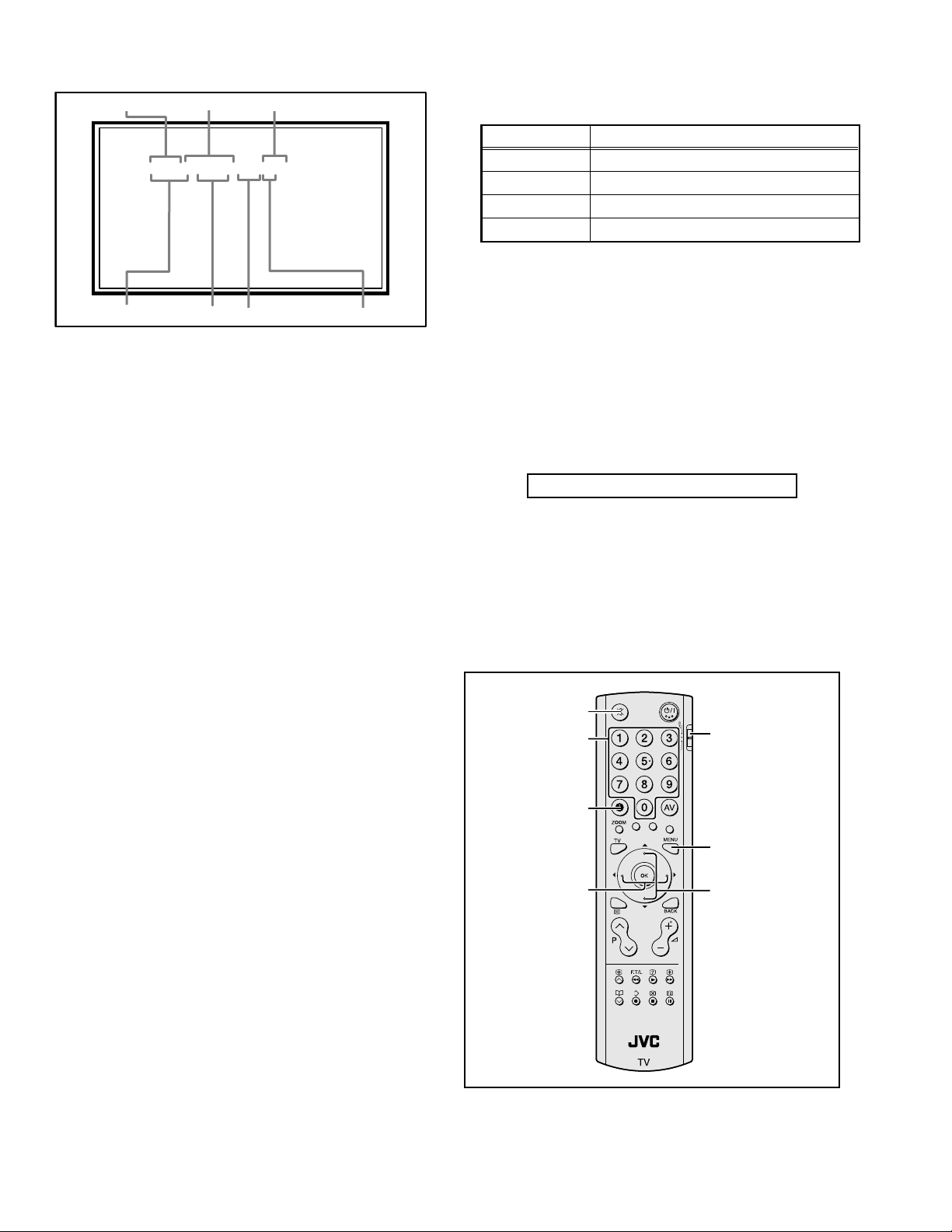
AC VOLTMETER
(HAVING 1000 /V,
OR MORE SENSITIVITY)
0.15 F AC-TYPE
GOOD EARTH GROUND
1500 10W
PLACE THIS PROBE
ON EACH EXPOSED
ME TAL PAR T
(No.YA315)1-3
Page 4

1.2 SAFETY PRECAUTIONS [FOR UK]
(1) The design of this product contains special hardware and many circuits and components specially for safety purposes. For
continued protection, no changes should be made to the original design unless authorized in writing by the manufacturer.
Replacement parts must be identical to those used in the original circuits. Service should be performed by qualified personnel
only.
(2) Alterations of the design or circuitry of the product should not be made. Any design alterations or additions will void the
manufacturer's warranty and will further relieve the manufacturer of responsibility for personal injury or property damage
resulting therefrom.
(3) Many electrical and mechanical parts in the product have special safety-related characteristics. These characteristics are often
not evident from visual inspection nor can the protection afforded by them necessary be obtained by using replacement
components rated for higher voltage, wattage, etc. Replacement parts which have these special safety characteristics are
identified in the Parts List of Service Manual. Electrical components having such features are identified by shading on the
schematics and by ( ) on the Parts List in the Service Manual. The use of a substitute replacement which does not have the
same safety characteristics as the recommended replacement part shown in the Parts List of Service Manual may cause shock,
fire, or other hazards.
(4) The leads in the products are routed and dressed with ties, clamps, tubing’s, barriers and the like to be separated from live parts,
high temperature parts, moving parts and / or sharp edges for the prevention of electric shock and fire hazard. When service is
required, the original lead routing and dress should be observed, and it should be confirmed that they have been returned to
normal, after re-assembling.
WARNING
(1) The equipment has been designed and manufactured to meet international safety standards.
(2) It is the legal responsibility of the repairer to ensure that these safety standards are maintained.
(3) Repairs must be made in accordance with the relevant safety standards.
(4) It is essential that safety critical components are replaced by approved parts.
(5) If mains voltage selector is provided, check setting for local voltage.
1-4 (No.YA315)
Page 5
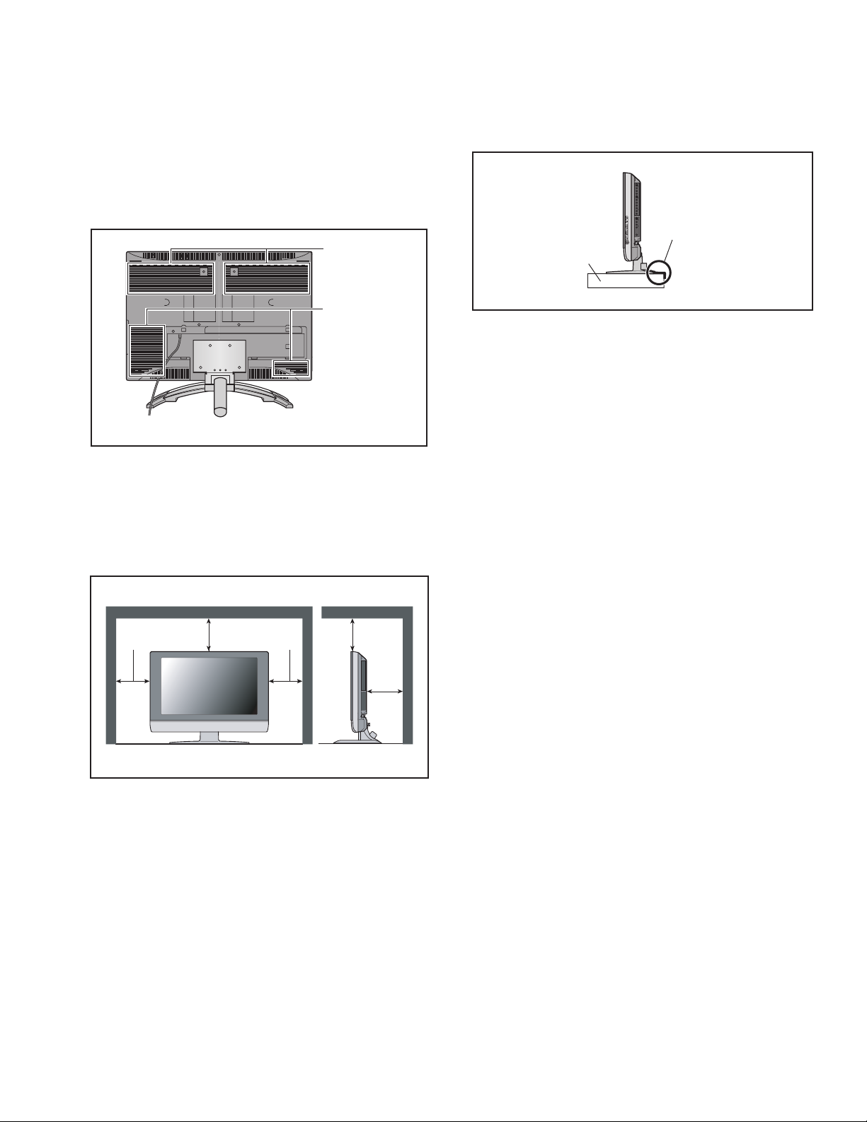
1.3 INSTALLATION
1.3.1 HEAT DISSIPATION
If the heat dissipation vent behind this unit is blocked, cooling
efficiency may deteriorate and temperature inside the unit will
rise. The temperature sensor that protects the unit will be
activated when internal temperature exceeds the pre-determined
level and power will be turned off automatically.Therefore,
please make sure pay attention not to block the heat dissipation
vent as well as the ventilation outlet behind the unit and ensure
that there is room for ventilation around it.
Ventilation hole
1.3.3 INSTALLATION REQUIREMENTS
To ensure safety in an emergency such as an earthquake, and
to prevent accidents, ensure that measures are taken to prevent
the TV dropping or falling over.
It fixes in a band.
TV Stand
Ventilation hole
*Diagram differs from actual appearance.
1.3.2 INSTALLATION REQUIREMENTS
Ensure that the minimal distance is maintained, as specified
below, between the unit with and the surrounding walls, as well
as the floor etc.Install the unit on stable flooring or stands.Take
precautionary measures to prevent the unit from tipping in order
to protect against accidents and earthquakes.
150 mm 150 mm
200 mm 200 mm
50 mm
*Diagram differs from actual appearance.
1.3.4 NOTES ON HANDLING
(1) WHEN TAKING UNIT OUT OF A PACKING CASE
When taking the unit out of a packing case, do not grasp
the upper part of the unit. If you take the unit out while
grasping the upper part, the LCD PANEL may be damaged
because of a pressure. Instead of grasping the upper part,
put your hands on the lower backside or sides of the unit.
(2) AS FOR PRESSING OR TOUCHING A SPEAKER
Be careful not to press the opening of the speaker in the
lower part of the unit and around them since the decorative
sheet on the surface of the openings may be deformed.
*Diagram differs from actual appearance.
(No.YA315)1-5
Page 6

1.4 HANDLING LCD PANEL
1.4.1 PRECAUTIONS FOR TRANSPORTATION
When transporting the unit, pressure exerted on the internal LCD
panel due to improper handling (such as tossing and dropping)
may cause damages even when the unit is carefully packed. To
prevent accidents from occurring during transportation, pay
careful attention before delivery, such as through explaining the
handling instructions to transporters.
Ensure that the following requirements are met during
transportation, as the LCD panel of this unit is made of glass and
therefore fragile:
(1) USE A SPECIAL PACKING CASE FOR THE LCD PANEL
When transporting the LCD panel of the unit, use a special
packing case (packing materials). A special packing case
is used when a LCD panel is supplied as a service spare
part.
(2) ATTACH PROTECTION SHEET TO THE FRONT
Since the front (display part) of the panel is vulnerable,
attach the protection sheet to the front of the LCD panel
before transportation. Protection sheet is used when a LCD
panel is supplied as a service spare part.
(3) AVOID VIBRATIONS AND IMPACTS
The unit may be broken if it is toppled sideways even when
properly packed. Continuous vibration may shift the gap of
the panel, and the unit may not be able to display images
properly. Ensure that the unit is carried by at least 2
persons and pay careful attention not to exert any vibration
or impact on it.
(4) DO NOT PLACE EQUIPMENT HORIZONTALLY
Ensure that it is placed upright and not horizontally during
transportation and storage as the LCD panel is very
vulnerable to lateral impacts and may break. During
transportation, ensure that the unit is loaded along the
traveling direction of the vehicle, and avoid stacking them
on one another. For storage, ensure that they are stacked
in 2 layers or less even when placed upright.
1.4.2 OPTICAL FILTER (ON THE FRONT OF THE LCD PANEL)
(1) Avoid placing the unit under direct sunlight over a
prolonged period of time. This may cause the optical filter
to deteriorate in quality and COLOUR.
(2) Clean the filter surface by wiping it softly and lightly with a
soft and lightly fuzz cloth (such as outing flannel).
(3) Do not use solvents such as benzene or thinner to wipe the
filter surface. This may cause the filter to deteriorate in
quality or the coating on the surface to come off. When
cleaning the filter, usually use the neutral detergent diluted
with water. When cleaning the dirty filter, use water-diluted
ethanol.
(4) Since the filter surface is fragile, do not scratch or hit it with
hard materials. Be careful enough not to touch the front
surface, especially when taking the unit out of the packing
case or during transportation.
1.4.3 PRECAUTIONS FOR REPLACEMENT OF EXTERIOR
PARTS
Take note of the following when replacing exterior parts (REAR
COVER, FRONT PANEL, etc.):
(1) Do not exert pressure on the front of the LCD panel (filter
surface). It may cause irregular COLOUR.
(2) Pay careful attention not to scratch or stain the front of the
LCD panel (filter surface) with hands.
(3) When replacing exterior parts, the front (LCD panel) should
be placed facing downward. Place a mat, etc. underneath
to avoid causing scratches to the front (filter surface).
1-6 (No.YA315)
Page 7
SECTION 2
SPECIFIC SERVICE INSTRUCTIONS
2.1 FEATURES
T-V LINK
When you have a T-V LINK compatible VCR connected to the
EXT-2 Terminal on the TV,it is easier to set up the VCR and to
view videos.
PICTURE MODE
This function can adjust the picture settings automatically.
2.2 MAIN DIFFERENCE LIST
Item LT-32A60BU LT-32A60SU LT-32A60SJ
FRONT PANEL COLOUR BLACK SILVER SILVER
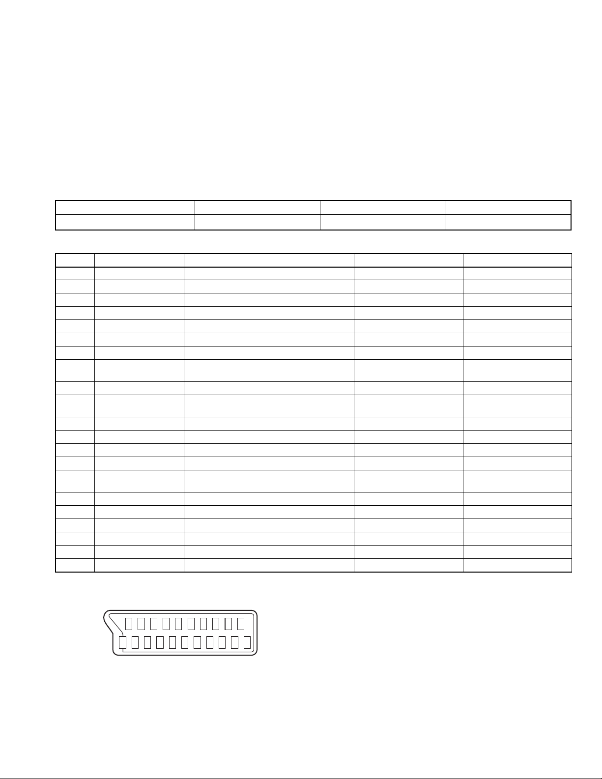
2.3 21-PIN EURO CONNECTOR (SCART) : EXT-1 / EXT-2
Pin No. Signal designation Matching value EXT-1 EXT-2
1 AUDIO R output 500mV(rms) (Nominal), Low impedance Used (TV OUT) Used (LINE OUT)
2 AUDIO R input 500mV(rms) (Nominal), High impedance Used (R1) Used (R2)
3 AUDIO L output 500mV(rms) (Nominal), Low impedance Used (TV OUT) Used (LINE OUT)
4 AUDIO GND Used Used
5 GND (B) Used Used
6 AUDIO L input 500mV(rms) (Nominal), High impedance Used (L1) Used (L2)
7 B input 700mV
8 FUNCTION SW
(SLOW SW)
Low : 0V-3V
High : 8V-12V, High impedance
, 75Ω Used Used
(B-W)
9 GND (G) Used Used
10 SCL / T-V LINK Not used Used
11 G input 700mV
, 75Ω Used Used
(B-W)
12 SDA Not used Used (SDA2)
13 GND (R) Used Used
14 GND (YS) Used Not used
15 R / C input R : 700mV
C : 300mV
(B-W)
(P-P)
, 75Ω
, 75Ω
16 Ys input (FAST SW) Low : 0V-0.4V, High : 1V-3V, 75Ω Used Used
17 GND (VIDEO output) Used Used
18 GND (VIDEO input) Used Used
19 VIDEO output 1V
20 VIDEO / Y input 1V
(Negative sync), 75Ω Used (TV OUT) Used (LINE OUT)
(P-P)
(Negative sync), 75Ω Used Used
(P-P)
21 COMMON GND Used Used
(P-P= Peak to Peak, B-W= Blanking to white peak)
[Pin assignment]
20 18 16 14 12 10 8 6 4 2
ZOOM
This function can change the screen size according to the
picture aspect ratio.
DIGITAL VNR
This function cuts down the amount of noise in the original
picture.
Used Used
(SCL2 / TV-LINK)
Used (R) Used (C2/R)
21 19 17 15 13 11 9 7 5 3 1
(No.YA315)1-7
Page 8

2.4 TECHNICAL INFORMATION
2.4.1 LCD PANEL
This unit uses the flat type panel LCD (Liquid Crystal Display) panel that occupies as little space as possible, instead of the
conventional CRT (Cathode Ray Tube), as a display unit.
Since the unit has the two polarizing filter that are at right angles to each other, the unit adopts "normally black" mode, where light
does not pass through the polarizing filter and the screen is black when no voltage is applied to the liquid crystals.
2.4.1.1 SPECIFICATIONS
The following table shows the specifications of this unit.
Item Specifications
Maximum dimensions ( W × H × D ) 760.0 mm × 450.0 mm × 50.0 mm
Weight 7.5 kg
Effective screen size Diagonal: 800 mm (H: 576 mm × V: 324 mm)
Aspect ratio 16 : 9
Drive device / system a-Si-TFT active matrix system
Resolution Horizontally 1366 × Vertically 768 × RGB < W-XGA > 3147264 dots in total
Pixel pitch (pixel size) Horizontally: 0.51075 mm Vertically: 0.51075mm
Displayed colour 16777216 colours 256 colours for R G and B
Brightness 500cd/m2
Contrast ratio 1000 : 1
Response time 8ms
View angle Horizontally: 170° Vertically: 170°
Surface polarizer Anti-Glare type Low reflective coat
Colour filter Vertical stripe
Backlight Direct-type Cold cathode fluorescent lamp × 16
Power supply voltage in LCD 6.5 V
Power supply voltage in inverter 25.2 V
Panel interface system LVDS (Low Voltage Differential Signaling)
2.4.1.2 PIXEL FAULT
There are three pixel faults - bright fault , dark fault and flicker fault - that are respectively defined as follows.
BRIGHT FAULT
In this pixel fault, a cell that should not light originally is lighting on and off.
For checking this pixel fault, input ALL BLACK SCREEN and find out the cell that is lighting on and off.
DARK FAULT
In this pixel fault, a cell that should light originally is not lighting or lighting with the brightness twice as brighter as originally lighting.
For checking this pixel fault, input 100% of each R/G/B colour and find out the cell that is not lighting.
FLICKER FAULT
In the pixel fault, a cell that should light originally or not light originally is flashing on and off.
For checking this pixel fault, input ALL BLACK SCREEN signal or 100% of each RGB colour and find out the cell that is flashing on
and off.
1-8 (No.YA315)
Page 9

2.4.2 MAIN CPU PIN FUNCTION [U302 : MAIN PWB]
Pin Pin name I/O Function Pin Pin name I/O Function
1 D1 I/O Program ROM data for CPU 51 NC2 - Not used
2 D4 I/O Program ROM data for CPU 52 XTAL2 O 6MHz for system clock
3 D2 I/O Program ROM data for CPU 53 XTAL1 I 6MHz for system clock
4 D3 I/O Program ROM data for CPU 54 NC3 - Not used
5XROM O
6 VDD 2.5 I 2.5V 56 VDDA 2.5 I 2.5V
7 VSS - GND 57 R O R for teletext
8 VDD 3.5 I 3.5V 58 G O G for teletext
9 P0.0 I/O Address/Data for scaler IC 59 B O B for teletext
10 P0.1 I/O Address/Data for scaler IC 60
11 P0.2 I/O Address/Data for scaler IC 61 NC4 - Not used
12 P0.3 I/O Address/Data for scaler IC 62 P1.7 O Reset for Scaler IC [H=Reset]
13 P0.4 - Not used 63 NC5 - Not used
14 P0.5 O Address latch Enable 64 WR O Write for memory
15 P0.6 - Not used 65 RD O Read for memory
16 P0.7 - Not used 66 NC6 Not used
17 ENE - Not used 67 A19 O Program ROM address for CPU
18 STOP - Not used 68 A18 O Program ROM address for CPU
19 OCF - Not used 69 A16 O Program ROM address for CPU
20 EXTIF - Not used 70 A17 O Program ROM address for CPU
21 CVBS I Video for teletext 71 A15 O Program ROM address for CPU
22 VDDA 2.5 I 2.5V 72 FL_PGM - Test purpose
23 VSSA - GND 73 VDD 2.5 I 2.5V
24 P2.0 I Scart2 ID [H=Detect] 74 VSS - GND
25 P2.1 I key scan data 1 75 VDD 3.3 I 3.3V
26 P2.2 I key scan data 2 76 A14 O Program ROM address for CPU
27 P2.3 I Scaet1 ID [H=Detect] 77 A12 O Program ROM address for CPU
28 NC1 - Not used 78 A13 O Program ROM address for CPU
29 HS/SSC I Horizontal sync 79 A7 O Program ROM address for CPU
30 VS I Vertical sync 80 FL_RST - Test purpose
31 P3.0 O Data Read for Scaler IC 81 A8 O Program ROM address for CPU
32 P3.1 O Comunication for adjustment [H=TXD] 82 A6 O Program ROM address for CPU
33 P3.2 I TV-Link in 83 A9 O Program ROM address for CPU
34 P3.3 I Remote control 84 A5 O Program ROM address for CPU
35 P3.4 I/O I2C bus Data(for EEPROM) 85 A11 O Program ROM address for CPU
36 P3.5 O I2C bus Clock(for EEPROM) 86 A4 O Program ROM address for CPU
37 P3.6 O Data Write for Scaler IC 87 ALE O Address Latch Enable
38 P3.7 I Comunication for adjustment [H=RXD] 88 PSEN O Program Store Enable
39 VSS - GND 89 A3 O Program ROM address for CPU
40 VDD 3.3 I 3.3V 90 A10 O Program ROM address for CPU
41 P1.0 O RGB Select [L=SCART1, H=SCART2] 91 VSS - GND
42 P1.1 I Headphone Ident [L=Detect] 92 VDD 3.3 I 3.3V
43 P1.2 I/O I2C bus Data(for inter IC) 93 A2 O Program ROM address for CPU
44 P1.3 O I2C bus Clock(for inter IC) 94 A1 O Program ROM address for CPU
45 P1.4 O Reset for inter IC [L=Reset] 95 FL_CE - Test purpose
46 P1.5 I PC Detect [L=Detect] 96 D7 I/O Program ROM data for CPU
47 P1.6 O Memory Pack I2C S/W [L=Detect] 97 A0 O Program ROM address for CPU
48 P4.2 O Main power control [L=ON, H=OFF] 98 D6 I/O Program ROM data for CPU
49 P4.3 O TV-Link out 99 D0 I/O Program ROM data for CPU
50 RST O Reset [L=Reset] 100 D5 I/O Program ROM data for CPU
This pin must be pulled low to access external ROM.
55 VSSA - GND
BLANK/COR
O Ys for Teletext
(No.YA315)1-9
Page 10

SECTION 3
DISASSEMBLY
3.1 DISASSEMBLY PROCEDURE
CAUTION AT DISASSEMBLY:
• Make sure that the power cord is disconnected from the outlet.
• Pay special attention not to break or damage the parts.
• When removing each board, remove the connectors as required. Taking notes of the connecting points (connector numbers)
makes service procedure manageable.
• Make sure that there is no bent or stain on the connectors before inserting, and firmly insert the connectors.
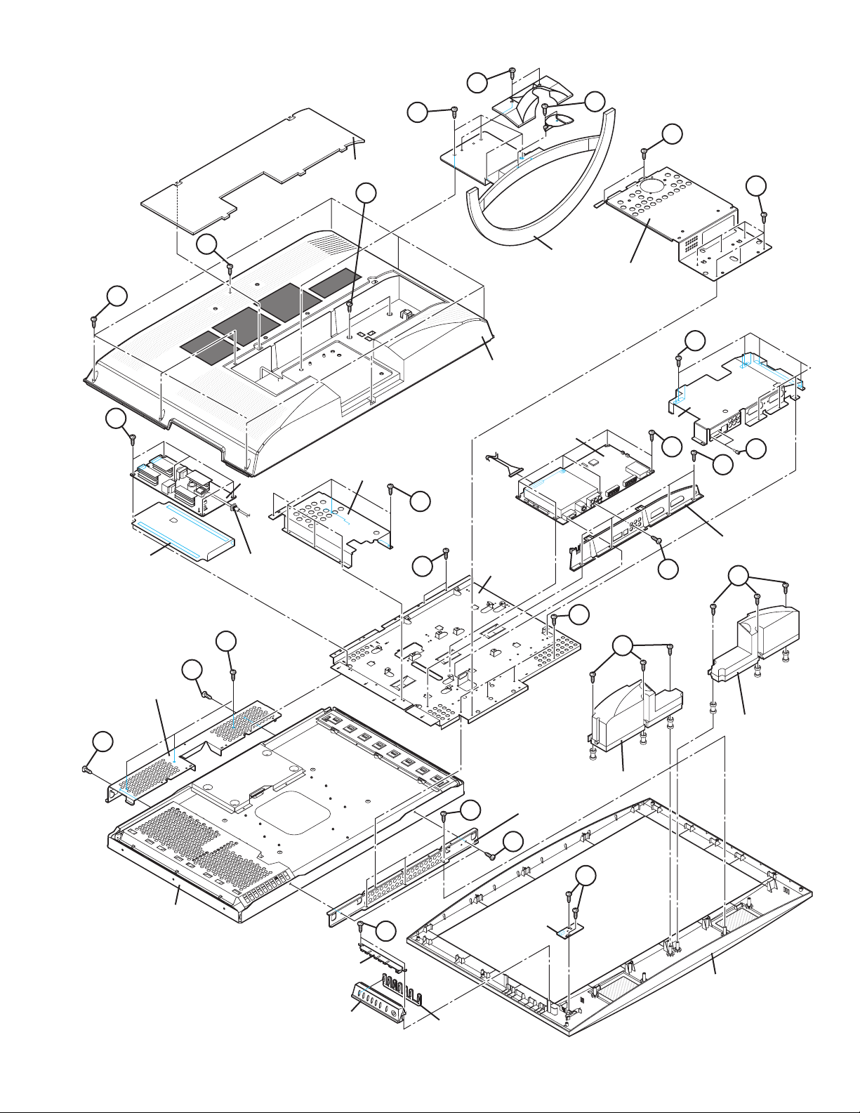
3.1.1 REMOVING THE STAND
(1) Remove the JACK COVER.
(2) Remove the 2 screws [A], then remove the STAND
COVER.
(3) Remove the 2 screws [W], then remove the CABLE
COVER.
(4) Remove the 4 screws [B], then remove the STAND.
3.1.2 REMOVING THE REAR COVER
• Remove the STAND.
(1) Remove the 8 screws [C], 1 screw [D] and 2 screws [E],
then remove the REAR COVER.
3.1.3 REMOVING THE POWER PWB
• Remove the STAND.
• Remove the REAR COVER.
(1) Remove the 4 screws [G] and 1 screw [H], then remove the
TERMINAL BASE.
(2) Remove the 8 screws [F], then remove the BACK
BRACKET.
(3) Remove the 6 screws [J], then remove the POWER PWB
SHIELD.
(4) Remove the 5 screws [K], then remove the POWER PWB.
3.1.4 REMOVING THE MAIN PWB
• Remove the STAND.
• Remove the REAR COVER.
• Remove the TERMINAL BASE.
• Remove the BACK BRACKET.
• Remove the POWER PWB SHIELD.
(1) Remove the 7 screws [L] and 2 screws [N], then remove
the MAIN PWB SHIELD.
(2) Remove the 6 screws [M], then remove the MAIN PWB.
3.1.5 REMOVING THE KEY PWB
• Remove the STAND.
• Remove the REAR COVER.
(1) Remove the 2 screws [P], then remove the KEY PWB.
3.1.6 REMOVING THE LED PWB
• Remove the STAND.
• Remove the REAR COVER.
(1) Remove the 2 screws [Q], then remove the LED PWB.
3.1.7 REMOVING THE SPEAKER
• Remove the STAND.
• Remove the REAR COVER.
(1) Remove the 6 screws [R], then remove the SPEAKER (L/
R).
CAUTION:
Please do not disassembly the SPEAKER.
When the speaker is decomposed, the performance cannot be
kept.
3.1.8 REMOVING THE LCD PANEL UNIT
• Remove the STAND.
• Remove the REAR COVER.
• Remove the TERMINAL BASE.
• Remove the BACK BRACKET.
(1) Remove the 6 screws [S], then remove the MAIN BASE.
(2) Remove the 6 screws [T], then remove the FRONT
PANEL.
(3) Remove the 2 screws [U], then remove the TOP FRAME.
(4) Remove the 2 screws [V], then remove the BOTTOM
FRAME.
NOTE:
• Pay special attention not to break or damage on the FRONT
PANEL.
• The LCD PANEL UNIT is fixed to the FRONT PAMEL (at the
back side)by using double-side adhesive tapes. To remove
the LCD PANEL UNIT, remove the adhesive tape on the
FRONT PANEL slowly.
1-10 (No.YA315)
Page 11
JACK COVER
E
A
B
W
F
F
C
K
INSULATOR
D
POWER PWB
POWER CORD
T
POWER PWB SHIELD
J
S
REAR COVER
MAIN PWB
MAIN BASE
STAND
BACK BRACKET
MAIN PWB SHIELD
S
R
L
M
TERMINAL BASE
H
N
G
R
TOP FRAME
U
LCD PANEL UNIT
U
SPEAKER
SPEAKER
BOTTOM FRAME
T
V
Q
P
LED PWB
KEY PWB
FRONT PANEL
KNOB BASE
CONTROL KNOB
Fig.1
(No.YA315)1-11
Page 12
3.2 MEMORY IC REPLACEMENT
SERVICE MENU
1.ADJUST
2.SELF_CHECK
3.I2C STOP
S001 5I R OF 126
PAL50 FULL STD H
• This model uses the memory IC.
• This memory IC stores data for proper operation of the video and drive circuits.
• When replacing, be sure to use an IC containing this (initial value) data.
3.2.1 MEMORY IC REPLACEMENT PROCEDURE
1. Power off
Switch off the power and disconnect the power plug from the AC outlet.
2. Replace the memory IC
Be sure to use the memory IC written with the initial setting values.
3. Power on
Connect the power plug to the AC outlet and switch on the power.
4. Receiving channel setting
Refer to the OPERATING INSTRUCTIONS and set the receive channels (Channels Preset) as described.
5. User setting
Check the user setting items according to the given in page later. Where these do not agree, refer to the OPERATING
INSTRUCTIONS and set the items as described.
6. SERVICE MODE setting
Verify what to set in the SERVICE MODE, and set whatever is necessary (Fig.1). Refer to the SERVICE ADJUSTMENT for setting.
3.2.2 SERVICE MODE SETTING
SERVICE MODE SCREEN
Not used
(Display only)
SERVICE MODE SCREEN
SETTING ITEM
Setting items Settings Item No.
Video system setting -1 Adjust S001 - S043
Video system setting -2 Fixed M001 - M009
Audio System Setting Fixed A001 - A003
Video system setting -3 Fixed D001 - D051
SERVICE MENU
1.ADJUST
2.SELF_CHECK
3.I2C STOP
ADJUSTMENT MODE SCREEN
S001 5I R OF 126
PAL50 FULL STD H
Fig.1
NOTE:
As self check feature is not used in this TV,
“2.SELF_CHECK” cannot be selected (screen display
only).
1-12 (No.YA315)
Page 13
3.2.3 SETTINGS OF FACTORY SHIPMENT
3.2.3.1 BUTTON OPERATION 3.2.3.2 REMOTE CONTROL DIRECT OPERATION
Setting item Setting position
POWER Off
CHANNEL PR1
VOLUME 10
TV/AV TV
3.2.3.3 REMOTE CONTROL MENU OPERATION
(1) PICTURE
Setting item Setting position
PICTURE MODE BRIGHT
COLOUR TEMP. COOL
FEATURES
DIGITAL VNR AUTO (LOW)
COLOUR SYSTEM TV Depends on PR/CH
EXT AUTO
4:3 AUTO ASPECT PANORAMIC
(2) SOUND
Setting item Setting position
STEREO / I•II Stereo sound
BASS Centre
TREBLE Centre
BALANCE Centre
3D SOUND OFF
CHANNEL PR1
VOLUME 10
ZOOM PANORAMIC
3D SOUND OFF
(4) FEATURES
SLEEP TIMER OFF
CHILD LOCK ID NO.0000, All CH off
APPEARANCE TYPE D
BLUE BACK ON
FAVOURITE SETTING Reset
(5) SET UP
AUTO PROGRAM TV channel automatically set
EDIT/MANUAL PRESET CH only
LANGUAGE ENGLISH
DECODER (EXT-2) OFF
EXT SETTING
S-IN BLANK
ID BLANK
DUBBING EXT-1 → EXT-2
Setting item Setting position
Setting item Setting position
Setting item Setting position
(No.YA315)1-13
Page 14
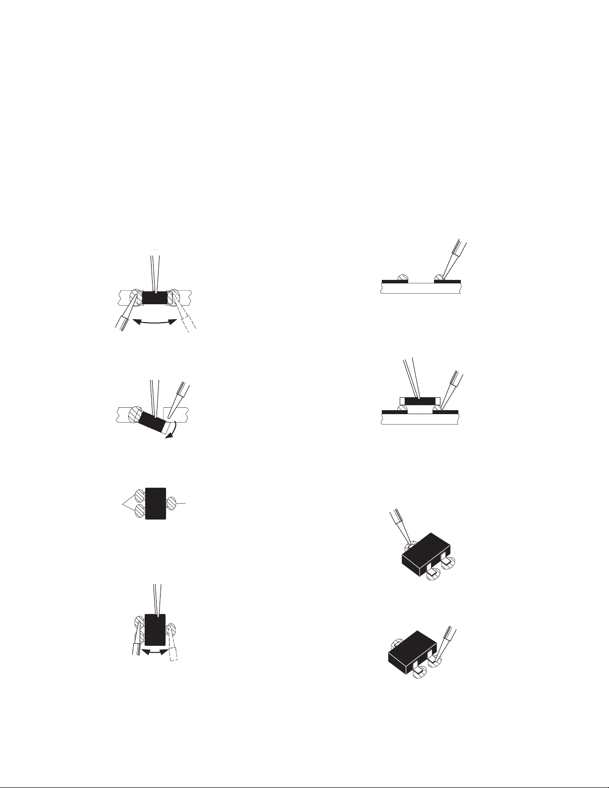
3.3 REPLACEMENT OF CHIP COMPONENT
3.3.1 CAUTIONS
(1) Avoid heating for more than 3 seconds.
(2) Do not rub the electrodes and the resist parts of the pattern.
(3) When removing a chip part, melt the solder adequately.
(4) Do not reuse a chip part after removing it.
3.3.2 SOLDERING IRON
(1) Use a high insulation soldering iron with a thin pointed end of it.
(2) A 30w soldering iron is recommended for easily removing parts.
3.3.3 REPLACEMENT STEPS
1. How to remove Chip parts
2. How to install Chip parts
[Resistors, capacitors, etc.]
(1) As shown in the figure, push the part with tweezers and
alternately melt the solder at each end.
(2) Shift with the tweezers and remove the chip part.
[Transistors, diodes, variable resistors, etc.]
(1) Apply extra solder to each lead.
SOLDER
SOLDER
[Resistors, capacitors, etc.]
(1) Apply solder to the pattern as indicated in the figure.
(2) Grasp the chip part with tweezers and place it on the
solder. Then heat and melt the solder at both ends of the
chip part.
[Transistors, diodes, variable resistors, etc.]
(1) Apply solder to the pattern as indicated in the figure.
(2) Grasp the chip part with tweezers and place it on the
solder.
(3) First solder lead A as indicated in the figure.
(2) As shown in the figure, push the part with tweezers and
alternately melt the solder at each lead. Shift and remove
the chip part.
NOTE :
After removing the part, remove remaining solder from the
pattern.
1-14 (No.YA315)
A
B
C
(4) Then solder leads B and C.
A
B
C
Page 15

SECTION 4
SERVICE MENU
1.ADJUST
2.SELF_CHECK
3.I2C STOP
S001 5I R OF 126
PAL50 FULL STD H
ADJUSTMENT
4.1 ADJUSTMENT PREPARATION
(1) The adjustment using the REMOTE CONTROL UNIT is
made on the basis of the initial setting values. The
setting values which adjust the screen to the optimum
condition can be different from the initial setting
values.
(2) Make sure that connection is correctly made AC to AC
power source.
(3) Turn on the power of the TV and measuring instruments for
warming up for at least 30 minutes before starting
adjustments.
(4) If the receive or input signal is not specified, use the most
appropriate signal for adjustment.
(5) Never touch the parts (such as variable resistors,
transformers and condensers) not shown in the adjustment
items of this service adjustment.
4.2 PRESET SETTING BEFORE ADJUSTMENTS
Unless otherwise specified in the adjustment items, preset the
following functions with the REMOTE CONTROL UNIT.
Setting item Settings position
PICTURE MODE STANDARD
PICTURE adjustments Centre
COLOUR TEMP. NORMAL
4.3 MEASURING INSTRUMENT AND FIXTURES
• Signal generator (Pattern generator)[PAL]
• Remote control unit
4.4 ADJUSTMENT ITEMS
VIDEO CIRCUIT
• WHITE BALANCE (HIGH LIGHT) adjustment
4.5 BASIC OPERATION OF SERVICE MODE
4.5.1 HOW TO ENTER THE SERVICE MODE
(1) Press [INFORMATION] key and [MUTING] key on the
remote control unit simultaneously to enter the SERVICE
MODE SCREEN.
(2) In the SERVICE MENU, press the [1] key to display
ADJUSTMENT MODE SCREEN.
NOTE:
• As self check feature is not used in this TV,
“2.SELF_CHECK” cannot be selected (screen display
only).
• Before entering the SERVICE MODE, confirm that the setting of VCR/TV/DVD switch is at the "TV" side. If the switches have not been properly set, you cannot enter the
SERVICE MODE.
• When a number key other than the [1] key is pressed in the
SERVICE MODE SCREEN, the other relevant screen may
be displayed.
This is not used in the adjustment procedure. Press the
[MENU] key to return to the SERVICE MODE SCREEN.
Not used
(Display only)
SERVICE MODE SCREEN
SERVICE MENU
1.ADJUST
2.SELF_CHECK
3.I2C STOP
ADJUSTMENT MODE SCREEN
S001 5I R OF 126
PAL50 FULL STD H
4.5.2 HOW TO EXIT THE SERVICE MODE
Press the [MENU] key to exit the Service mode.
(No.YA315)1-15
Page 16
4.5.3 DESCRIPTION OF STATUS DISPLAY
S001 5I R OF 126
PAL50 FULL STD H
SETTING VALUE (DATA)SETTINGITEM No. SETTING ITEM
S001 5I R OF 126
PAL50 FULL STD H
SIGNAL SYSTEM
ZOOM MODE
PICTURE MODE
COLOUR TEMP.
(5) SETTING ITEM NAME
Setting item name are displayed. The setting item numbers to
be displayed are listed below.
Item No. Setting item
S001 - S043 Video system setting -1
M001 - M009 Video system setting -2
A001 - A003 Audio System Setting
D001 - D051 Video system setting -3
(6) SETTING ITEM NO.
Setting item numbers are displayed. For the setting item
names to be displayed, refer to "INITIAL SETTING VALUES
IN THE SERVICE MODE".
(1) SIGNAL SYSTEM
The signal displayed on the screen is displayed.
PAL50 : PAL50Hz (Composite / S-video)
PAL60 : PAL60Hz (Composite / S-video)
SECAM : SECAM
NTSC3 : NTSC3.58
NTSC4 : NTSC4.43
525I : 525i (Component)
525P : 525p
625I : 625i (Component)
625P : 625p
750P6 : 750p 60Hz
RGB5 : RGB 525i
RGB6 : RGB 625i
PCVGA : PC (VGA)
PCXGA : PC (XGA)
(2) ZOOM MODE
State of the screen mode is displayed.
NOTE:
In ADJUSTMENT MODE, the screen mode can be set only
to "FULL". When it is entered to ADJUSTMENT MODE, it is
automatically changed to "FULL", even if the setting is in
other screen mode.
(7) SETTING VALUE (DATA)
The SETTING VALUE is displayed.
4.5.4 CHANGE AND MEMORY OF SETTING VALUE
SELECTION OF SETTING ITEM
• [FUNCTION /] key.
For scrolling up / down the setting items.
S001... ↔ M001... ↔ A001... ↔ D001...
CHANGE OF SETTING VALUE (DATA)
• [FUNCTION /] key.
For scrolling up / down the setting values.
MEMORY OF SETTING VALUE (DATA)
Changed setting value is memorized by pressing [MUTING]
key.
4.5.5 SERVICE MODE SELECT KEY LOCATION
MUTING
NUMBER
VCR/TV/DVD
switch
(3) PICTURE MODE
State of the picture mode is displayed.
NOTE:
In ADJUSTMENT MODE, the picture mode can be set only
to "STANDARD". When it is entered to ADJUSTMENT
MODE, it is automatically changed to "STANDARD", even
if the setting is in other picture mode.
(4) COLOUR TEMP.
State of the colour temperature is displayed.
NOTE:
In ADJUSTMENT MODE, the colour temperature can be set
only to "NORMAL". When it is entered to ADJUSTMENT
MODE, it is automatically changed to "NORMAL", even if
the setting is in other colour temperature.
1-16 (No.YA315)
INFORMATION
FUNCTION /
MENU
FUNCTION /
Page 17
4.6 INITIAL SETTING VALUES IN THE SERVICE MODE
• Perform fine-tuning based on the "initial values" using the remote control when in the Service mode.
• The "initial values" serve only as an indication rough standard and therefore the values with which optimal display can be achieved
may be different from the default values. But, don't change the values that are not written in "ADJUSTMENT PROCEDURE". They
are fixed values.
4.6.1 VIDEO SYSTEM SETTING -1 4.6.2 VIDEO SYSTEM SETTING -2 (*Fixed values)
Item No. Item name Variable range Setting value
S001 5I R OF 000 - 255 122
S002 5I G OF 000 - 255 120
S003 5I B OF 000 - 255 122
S004 5P R OF 000 - 255 122
S005 5P G OF 000 - 255 120
S006 5P B OF 000 - 255 122
S007 HD75 R OF 000 - 255 127
S008 HD75 R OF 000 - 255 127
S009 HD75 R OF 000 - 255 127
S010 HD25 R OF 000 - 255 127
S011 HD25 R OF 000 - 255 127
S012 HD25 R OF 000 - 255 127
S013 R DRIVE 000 - 255 150
S014 G DRIVE 000 - 255 150
S015 B DRIVE 000 - 255 150
S016 HD R DR -32 - 31 -02
S017 HD G DR -32 - 31 07
S018 HD B DR -32 - 31 00
S019 CL R DR -32 - 31 00
S020 CL G DR -32 - 31 00
S021 CL B DR -32 - 31 11
S022 WM R DR -32 - 31 11
S023 WM G DR -32 - 31 00
S024 WM B DR -32 - 31 00
S025 HD CL R DR -32 - 31 00
S026 HD CL G DR -32 - 31 00
S027 HD CL B DR -32 - 31 00
S028 HD WM R DR -32 - 31 00
S029 HD WM G DR -32 - 31 00
S030 HD WM B DR -32 - 31 00
S031 PC R OF 000 - 255 133
S032 PC G OF 000 - 255 121
S033 PC B OF 000 - 255 115
S034 PC R DR -32 - 31 -15
S035 PC G DR -32 - 31 14
S036 PC B DR -32 - 31 10
S037 PC CL R DR -32 - 31 00
S038 PC CL G DR -32 - 31 00
S039 PC CL B DR -32 - 31 00
S040 PC WM R DR -32 - 31 00
S041 PC WM G DR -32 - 31 00
S042 PC WM B DR -32 - 31 00
S043 PC AUTO WB 000 - 001 000
Item No. Item name Variable range Setting value
M001 MV CON 000 - 255 104
M002 MV SHA 000 - 255 128
M003 MV COL 000 - 255 154
M004 MV TIN 000 - 255 048
M005 (Not display) 000 - 255 120
M006 CH MUTE 000 - 001 000
M007 PC R GAIN 000 - 001 097
M008 PC G GAIN 000 - 001 101
M009 PC B GAIN 000 - 001 101
4.6.3 AUDIO SYSTEM SETTING (*Fixed values)
Item No. Item name Variable range Setting value
A001 S BASS 000 - 016 008
A002 S TREBLE 000 - 016 008
A003 3D LEVEL 000 - 063 031
4.6.4 VIDEO SYSTEM SETTING -3 (*Fixed values)
Item No. Item name Variable range Setting value
D001 S CON 000 - 063 029
D002 S BRI 000 - 063 038
D003 S SHA 000 - 008 004
D004 S COL 000 - 063 032
D005 S TIN 000 - 063 032
D006 RGB S COL 000 - 127 032
D007 5I S CON 000 - 063 032
D008 5I S BRI 000 - 063 032
D009 5I S SHA 000 - 063 032
D010 5I S COL 000 - 063 032
D011 5I S TIN 000 - 063 032
D012 5P S CON 000 - 063 032
D013 5P S BRI 000 - 063 032
D014 5P S SHA 000 - 063 032
D015 5P S COL 000 - 063 032
D016 5P S TIN 000 - 063 032
D017 HD S CON 000 - 063 032
D018 HD S BRI 000 - 063 032
D019 HD S SHA 000 - 063 032
D020 HD S COL 000 - 063 032
D021 HD S TIN 000 - 063 032
D022 HD25 S CON 000 - 063 032
D023 HD25 S BRI 000 - 063 032
D024 HD25 S SHA 000 - 063 032
D025 HD25 S COL 000 - 063 032
D026 HD25 S TIN 000 - 063 032
D027 PC S CON 000 - 063 021
(No.YA315)1-17
Page 18
Item No. Item name Variable range Setting value
D028 PC S BRI 000 - 063 030
D029 TXT S CON 000 - 127 024
D030 TXT S BRI 000 - 127 016
D031 RGB S CON 000 - 127 048
D032 RGB S BRI 000 - 127 048
D033 STD BRI1 000 - 031 025
D034 STD CON 000 - 031 016
D035 STD BRI2 000 - 031 016
D036 STD SHA 000 - 031 016
D037 STD COL 000 - 031 016
D038 STD TIN 000 - 031 016
D039 SFT BRI1 000 - 031 014
D040 SFT CON 000 - 031 014
D041 SFT BRI2 000 - 031 014
D042 SFT SHA 000 - 031 014
D043 SFT COL 000 - 031 014
D044 SFT TIN 000 - 031 016
D045 BRI BRI1 000 - 031 031
D046 BRI CON 000 - 031 018
D047 BRI BRI2 000 - 031 016
D048 BRI SHA 000 - 031 018
D049 BRI COL 000 - 031 016
D050 BRI TIN 000 - 031 016
D051 PWM 000 - 031 008
4.7 ADJUSTMENT PROCEDURE
4.7.1 VIDEO CIRCUIT
Item
WHITE
BALANCE
(HIGHLIGHT)
Measuring
instrument
Remote
control unit
Signal
generator
Test point Adjustment part Description
[1.ADJUST]
S013: R DRIVE (Red drive)
S015: G DRIVE (Green drive)
S017: B DRIVE (Blue drive)
(1) Receive a PAL 75% all white signal.
(2) Set PICTURE MODE to "STANDARD".
(3) Set ZOOM to "FULL".
(4) Set COLOUR TEMP. to "NORMAL".
(5) Select "1.ADJUST" from the SERVICE MODE.
(6) Set < S013 > (R DRIVE), < S015 > (G DRIVE)
and < S017 > (B DRIVE) to "145".
(7) Adjust to Keep one of < S030 > (Red drive),
< S031 > (Green drive) or < S032 > (Blue drive)
unchanged, then lower the other two so that the
all-white screen is equally white throughout.
NOTE:
Set one or more of < S013 >, < S015 >, and
< S017 > to "145".
(8) Check that white balance is properly tracked
from low light to high light. If the white balance
tracking is deviated, adjust to correct it.
(9) Press the [MUTING] key to memoirze the set
value.
1-18 (No.YA315)
Page 19

SECTION 5
TROUBLESHOOTING
This service manual does not describe TROUBLESHOOTING.
(No.YA315)1-19
Page 20

Victor Company of Japan, Limited
AV & MULTIMEDIA COMPANY DISPLAY CATEGORY 12, 3-chome, Moriya-cho, Kanagawa-ku, Yokohama-city, Kanagawa-prefecture, 221-8528, Japan
(No.YA315)
Printed in Japan
VPT
Page 21
PARTS LIST
CAUTION
J The parts identified by the symbol are important for the safety . Whenever replacing these parts, be sure to use specified ones to secure the
safety.
J The parts not indicated in this Parts List and those which are filled with lines --- in the Parts No. columns will not be supplied.
J P.W. BOARD Ass'y will not be supplied, but those which are filled with the Parts No. in the Parts No. columns will be supplied.
ABBREVIATIONS OF RESISTORS, CAPACITORS AND TOLERANCES
RESISTORS CAPACITORS
CR Carbon Resistor C CAP. Ceramic Capacitor
FR Fusible Resistor E CAP. Electrolytic Capacitor
PR Plate Resistor M CAP. Mylar Capacitor
VR Variable Resistor CH CAP. Chip Capacitor
HV R High Voltage Resistor HV CAP. High Voltage Capacitor
MF R Metal Film Resistor MF CAP. Metalized Film Capacitor
MG R Metal Glazed Resistor MM CAP. Metalized Mylar Capacitor
MP R Metal Plate Resistor MP CAP. Metalized Polystyrol Capacitor
OM R Metal Oxide Film Resistor PP CAP. Polypropylene Capacitor
CMF R Coating Metal Film Resistor PS CAP. Polystyrol Capacitor
UNF R Non-Flammable Resistor TF CAP. Thin Film Capacitor
CH V R Chip Variable Resistor MPP CAP. Metalized Polypropylene Capacitor
CH MG R Chip Metal Glazed Resistor TAN. CAP. Tantalum Capacitor
COMP. R Composition Resistor CH C CAP. Chip Ceramic Capacitor
LPTC R Linear Positive Temperature Coefficient Resistor BP E CAP. Bi-Polar Electrolytic Capacitor
CH AL E CAP. Chip Aluminum Electrolytic Capacitor
CH AL BP CAP. Chip Aluminum Bi-Polar Capacitor
CH TAN. E CAP. Chip Tantalum Electrolytic Capacitor
CH AL BP E CAP. Chip Tantalum Bi-Polar Electrolytic Capacitor
RESISTORS
FGJ KMNRHZ P
±1% ±2% ±5% ±10% ±20% ±30%
+30%
-10%
+50%
-10%
+80%
-20%
+100%
-0%
(No.YA315)3-1
Page 22

CONTENTS
USING P.W. BOARD & REMOTE CONTROL UNIT ................................................................................................... 3-2
EXPLODED VIEW PARTS LIST ................................................................................................................................. 3-3
EXPLODED VIEW ....................................................................................................................................................... 3-4
PRINTED WIRING BOARD PARTS LIST ................................................................................................................... 3-5
MAIN P.W. BOARD ASS'Y (QAL0747-001) ...................................................................................................... 3-5
POWER P.W. BOARD ASS'Y (QAL0748-001) .................................................................................................. 3-9
KEY P.W. BOARD ASS'Y (QAL0730-001) ...................................................................................................... 3-11
LED P.W. BOARD ASS'Y (QAL0731-001) ...................................................................................................... 3-11
REMOTE CONTROL UNIT PARTS LIST (RM-C1816S-1C) ..................................................................................... 3-11
PACKING ................................................................................................................................................................... 3-12
PACKING PARTS LIST ............................................................................................................................................. 3-12
USING P.W. BOARD & REMOTE CONTROL UNIT
P.W.B ASS'Y LT-32A60BU LT-32A60SJ LT-32A60SU
MAIN P.W.B QAL0747-001 ←←
POWER P.W.B QAL0748-001 ←←
KEY P.W.B QAL0730-001 ←←
LED P.W.B QAL0731-001 ←←
REMOTE CONTROL UNIT RM-C1816S-1C ←←
3-2(No.YA315)
Page 23

EXPLODED VIEW PARTS LIST
Please note that the TUNER is not included in the MAIN PWB (QAL0728-001).
Ref.No. Part No. Part Name Description Local
101 LC12342-001A-U JACK COVER LT-32A60SJ
101 LC12342-002A-U JACK COVER LT-32A60BU,LT-32A60SU
102 LC30789-002B-U WARNING LABEL LT-32A60BU,LT-32A60SU
105 LC41999-004A-U CAUTION LABEL
106 LC12396-001A-U REAR COVER LT-32A60BU
106 LC12396-002A-U REAR COVER LT-32A60SJ,LT-32A60SU
107 QYSBSF4012ZA TAP SCREW M4 x 12mm(x8)
108 LC42063-001A SCREW
109 LC42063-001A SCREW (x2)
110 GA10045-002A-U STAND ASSY LT-32A60BU
110 GA10045-001A-U STAND ASSY LT-32A60SJ,LT-32A60SU
110A GA30080-002A-U STAND COVER LT-32A60BU
110A GA30080-001A-U STAND COVER LT-32A60SJ,LT-32A60SU
110B GA30081-002A-U CABLE COVER LT-32A60BU
110B GA30081-001A-U CABLE COVER LT-32A60SJ,LT-32A60SU
111 QYSPSPD5016MA SCREW M5 x 16mm(x4)
112 QMPN260-170-JC POWER CORD(EK) 1.7m BLACK LT-32A60SJ
112 QMPK300-170-JC POWER CORD(EU) 1.7m BLACK LT-32A60BU,LT-32A60SU
113 LC21908-001A-U KNOB BASE LT-32A60BU
113 LC21908-002A-U KNOB BASE LT-32A60SJ,LT-32A60SU
114 LC33186-001A-U CONTROL KNOB LT-32A60SJ,LT-32A60SU
115 LC12387-001A-U TERMINAL BASE LT-32A60BU
115 LC12387-002A-U TERMINAL BASE LT-32A60SJ,LT-32A60SU
116 QLD0371-001-JUK LCD PANEL UNIT LT-32A60BU,LT-32A60SJ
116 QLD0371-001 LCD PANEL UNIT LT-32A60SU
117 LC42239-003A-C SPEAKER ASSY(L)
118 LC42239-004A-C SPEAKER ASSY(R)
119 LC40226-003A-H SPACER (x6)
120 QNB0036-001 HEX SCREW (x2)
121 WJW0027-002A-E DIGITAL(LVDS)CABLE
122 QYSBSF3010ZA TAP SCREW M3 x 10mm
123 LC42301-001A SCREW (x4)
124 QQR0491-002 FERRITE CORE
125 QQR0491-001 FERRITE CORE (x2)
126 QAU0439-001 TUNER
130 LC12415-001A-U FRONT PANEL ASSY LT-32A60BU
130 LC12415-002A-U FRONT PANEL ASSY LT-32A60SJ,LT-32A60SU
201 QAL0748-001 POWER PWB
202 QAL0747-001 MAIN PWB Not included TUNER
203 QAL0730-001 KEY PWB
204 QAL0731-001 LED PWB
(No.YA315)3-3
Page 24

EXPLODED VIEW
107
102
201
101
108
112
111
105
109
POWER PWB SHIELD
110A
106
121
202
110B
BACK BRACKET
110
126
MAIN PWB SHIELD
125
120
123
INSULATOR
TOP FRAME
116
124
113
203
MAIN BASE
114
BOTTOM FRAME
125
118
119
204
122
115
117
119
130
3-4(No.YA315)
Page 25

PRINTED WIRING BOARD PARTS LIST
MAIN P.W. BOARD ASS'Y (QAL0747-001)
Ref No. Part No. Part Name Description Local
U101 T1001-00081A IC
U301 T1001-00073A IC
U302 T1001-00064A IC
U303 ATF32-32A60SU IC (SERVICE)
U401 T1001-00084A IC
U402 T1001-00085A IC
U405 T1001-00075A IC
U501 T1001-00086A IC
U502 T1001-00063A IC
U601 T1001-00087A IC
U602 T1001-00088A IC
U603 T1001-00070A IC
U801 T0507-00002A TRANSISTOR
U802 T0507-00002A TRANSISTOR
Q101 T1001-00052A IC
Q102 T0507-00001A TRANSISTOR
Q103 T0507-00001A TRANSISTOR
Q104 T0507-00001A TRANSISTOR
Q105 T0507-00001A TRANSISTOR
Q106 T0507-00001A TRANSISTOR
Q108 T0507-00001A TRANSISTOR
Q202 T0507-00001A TRANSISTOR
Q203 T0507-00001A TRANSISTOR
Q301 T1001-00049A IC
Q303 T1001-00078A IC
Q304 T0507-00003A TRANSISTOR
Q305 T0507-00003A TRANSISTOR
Q306 T0507-00007A TRANSISTOR
Q307 T0507-00008A TRANSISTOR
Q308 T0507-00001A TRANSISTOR
Q309 T0507-00001A TRANSISTOR
Q311 T0507-00001A TRANSISTOR
Q315 T0507-00006A TRANSISTOR
Q316 T0507-00001A TRANSISTOR
Q317 T0507-00008A TRANSISTOR
Q403 T0507-00006A TRANSISTOR
Q501 T1001-00079A IC
Q502 T1001-00048A IC
Q503 T0507-00007A TRANSISTOR
Q601 T0507-00006A TRANSISTOR
Q602 T0507-00001A TRANSISTOR
Q603 T0507-00001A TRANSISTOR
Q604 T0507-00005A TRANSISTOR
Q701 T0507-00001A TRANSISTOR
Q702 T0507-00001A TRANSISTOR
Q703 T0507-00001A TRANSISTOR
Q801 T1001-00089A IC
Q802 T0507-00001A TRANSISTOR
Q804 T1001-00051A IC
Q805 T0507-00001A TRANSISTOR
Q806 T0507-00001A TRANSISTOR
D101 T0407-00004A DIODE
D205 T0408-00002A Z DIODE
D206 T0408-00002A Z DIODE
D207 T0408-00002A Z DIODE
D208 T0408-00002A Z DIODE
D209 T0408-00002A Z DIODE
D210 T0408-00002A Z DIODE
D301 T0407-00002A DIODE
D601 T0407-00002A DIODE
D602 T0407-00002A DIODE
D702 T0407-00002A DIODE
D704 T0407-00002A DIODE
D801 T0407-00003A DIODE
ZD101 T0408-00002A Z DIODE
ZD202 T0408-00002A Z DIODE
ZD203 T0408-00002A Z DIODE
ZD204 T0408-00002A Z DIODE
ZD206 T0408-00002A Z DIODE
ZD207 T0408-00002A Z DIODE
ZD208 T0408-00002A Z DIODE
ZD209 T0408-00002A Z DIODE
ZD210 T0408-00002A Z DIODE
ZD211 T0408-00002A Z DIODE
ZD212 T0408-00002A Z DIODE
ZD213 T0408-00002A Z DIODE
ZD214 T0408-00002A Z DIODE
ZD215 T0408-00002A Z DIODE
ZD216 T0408-00002A Z DIODE
ZD217 T0408-00002A Z DIODE
ZD218 T0408-00002A Z DIODE
Ref No. Part No. Part Name Description Local
ZD219 T0408-00002A Z DIODE
ZD221 T0408-00002A Z DIODE
ZD222 T0408-00002A Z DIODE
ZD225 T0408-00002A Z DIODE
ZD227 T0408-00002A Z DIODE
ZD230 T0408-00002A Z DIODE
ZD231 T0408-00002A Z DIODE
ZD232 T0408-00002A Z DIODE
ZD250 T0408-00002A Z DIODE
ZD251 T0408-00002A Z DIODE
ZD252 T0408-00002A Z DIODE
ZD253 T0408-00002A Z DIODE
ZD254 T0408-00002A Z DIODE
ZD255 T0408-00002A Z DIODE
ZD256 T0408-00002A Z DIODE
ZD257 T0408-00002A Z DIODE
ZD258 T0408-00002A Z DIODE
ZD259 T0408-00002A Z DIODE
ZD260 T0408-00002A Z DIODE
ZD261 T0408-00002A Z DIODE
ZD262 T0408-00002A Z DIODE
ZD263 T0408-00002A Z DIODE
ZD264 T0408-00002A Z DIODE
ZD265 T0408-00002A Z DIODE
ZD266 T0408-00002A Z DIODE
ZD267 T0408-00002A Z DIODE
ZD270 T0408-00002A Z DIODE
ZD271 T0408-00002A Z DIODE
ZD702 T0407-00005A Z DIODE
C101 T2203-DC104E C CAPACITOR 0.1uF 25V K
C102 T2203-FC104E C CAPACITOR 0.1uF 50V Z
C103 T2203-BC106E C CAPACITOR 10uF 10V Z
C105 T2203-FC104E C CAPACITOR 0.1uF 50V Z
C106 T2203-BC106E C CAPACITOR 10uF 10V Z
C107 T2203-BC106E C CAPACITOR 10uF 10V Z
C109 T2203-BC106E C CAPACITOR 10uF 10V Z
C110 T2203-BC106E C CAPACITOR 10uF 10V Z
C112 T2203-BC106E C CAPACITOR 10uF 10V Z
C113 T2203-BC106E C CAPACITOR 10uF 10V Z
C201 T2203-FC102D C CAPACITOR 1000pF 50V K
C202 T2203-FC473D C CAPACITOR 0.047uF 50V K
C203 T2203-FC473D C CAPACITOR 0.047uF 50V K
C204 T2203-FC473D C CAPACITOR 0.047uF 50V K
C205 T2203-FC473D C CAPACITOR 0.047uF 50V K
C206 T2203-FC473D C CAPACITOR 0.047uF 50V K
C207 T2203-FC473D C CAPACITOR 0.047uF 50V K
C208 T2203-FC473D C CAPACITOR 0.047uF 50V K
C209 T2203-FC473D C CAPACITOR 0.047uF 50V K
C210 T2203-FC102D C CAPACITOR 1000pF 50V K
C211 T2203-FC473D C CAPACITOR 0.047uF 50V K
C213 T2203-FC100D C CAPACITOR 10pF 50V K
C214 T2203-FC100D C CAPACITOR 10pF 50V K
C215 T2203-FC100D C CAPACITOR 10pF 50V K
C216 T2203-FC471D C CAPACITOR 470pF 50V K
C217 T2203-FC103D C CAPACITOR 0.01uF 50V K
C218 T2203-FC471D C CAPACITOR 470pF 50V K
C219 T2203-FC103D C CAPACITOR 0.01uF 50V K
C220 T2203-FC471D C CAPACITOR 470pF 50V K
C221 T2203-FC103D C CAPACITOR 0.01uF 50V K
C222 T2203-FC471D C CAPACITOR 470pF 50V K
C223 T2203-FC103D C CAPACITOR 0.01uF 50V K
C226 T2203-FC471D C CAPACITOR 470pF 50V K
C227 T2203-FC473D C CAPACITOR 0.047uF 50V K
C228 T2203-FC473D C CAPACITOR 0.047uF 50V K
C229 T2203-FC473D C CAPACITOR 0.047uF 50V K
C230 T2203-FC471D C CAPACITOR 470pF 50V K
C231 T2203-FC471D C CAPACITOR 470pF 50V K
C232 T2203-FC471D C CAPACITOR 470pF 50V K
C233 T2203-FC471D C CAPACITOR 470pF 50V K
C234 T2203-FC471D C CAPACITOR 470pF 50V K
C235 T2203-FC471D C CAPACITOR 470pF 50V K
C236 T2203-FC100D C CAPACITOR 10pF 50V K
C238 T2203-FC100D C CAPACITOR 10pF 50V K
C242 T2203-FC331D C CAPACITOR 330pF 50V K
C243 T2203-FC331D C CAPACITOR 330pF 50V K
C244 T2203-FC331D C CAPACITOR 330pF 50V K
C248 T2203-FC334D C CAPACITOR 0.33uF 16V Z
C249 T2203-FC334D C CAPACITOR 0.33uF 16V Z
C301 T2203-DC104E C CAPACITOR 0.1uF 25V K
C302 T2203-DC104E C CAPACITOR 0.1uF 25V K
C303 T2203-DC104E C CAPACITOR 0.1uF 25V K
C304 T2203-DC104E C CAPACITOR 0.1uF 25V K
C305 T2203-DC104E C CAPACITOR 0.1uF 25V K
C307 T2203-FC103D C CAPACITOR 0.01uF 50V K
(No.YA315)3-5
Page 26

Ref No. Part No. Part Name Description Local
Ref No. Part No. Part Name Description Local
C308 T2203-FC224D C CAPACITOR 0.22uF 50V K
C309 T2203-DC104E C CAPACITOR 0.1uF 25V K
C310 T2203-DC104E C CAPACITOR 0.1uF 25V K
C311 T2203-FC330D C CAPACITOR 33pF 50V K
C312 T2203-FC101D C CAPACITOR 0.01uF 50V K
C313 T2203-FC101D C CAPACITOR 0.01uF 50V K
C314 T2203-FC101D C CAPACITOR 0.01uF 50V K
C316 T2203-FC330D C CAPACITOR 33pF 50V K
C317 T2203-DC104E C CAPACITOR 0.1uF 25V K
C318 T2203-DC104E C CAPACITOR 0.1uF 25V K
C319 T2203-DC104E C CAPACITOR 0.1uF 25V K
C321 T2203-DC104E C CAPACITOR 0.1uF 25V K
C402 T2203-DC104E C CAPACITOR 0.1uF 25V K
C403 T2203-DC104E C CAPACITOR 0.1uF 25V K
C404 T2203-DC104E C CAPACITOR 0.1uF 25V K
C405 T2203-DC104E C CAPACITOR 0.1uF 25V K
C406 T2203-DC104E C CAPACITOR 0.1uF 25V K
C407 T2203-DC104E C CAPACITOR 0.1uF 25V K
C409 T2203-DC104E C CAPACITOR 0.1uF 25V K
C411 T2203-DC104E C CAPACITOR 0.1uF 25V K
C412 T2203-DC104E C CAPACITOR 0.1uF 25V K
C413 T2203-DC104E C CAPACITOR 0.1uF 25V K
C414 T2203-DC104E C CAPACITOR 0.1uF 25V K
C415 T2203-DC104E C CAPACITOR 0.1uF 25V K
C416 T2203-DC104E C CAPACITOR 0.1uF 25V K
C417 T2203-DC104E C CAPACITOR 0.1uF 25V K
C419 T2203-DC104E C CAPACITOR 0.1uF 25V K
C420 T2203-DC104E C CAPACITOR 0.1uF 25V K
C421 T2203-FC152D C CAPACITOR 1500pF 50V K
C422 T2203-FC152D C CAPACITOR 1500pF 50V K
C423 T2203-FC152D C CAPACITOR 1500pF 50V K
C424 T2203-FC100D C CAPACITOR 10pF 50V K
C425 T2203-FC220D C CAPACITOR 22pF 50V K
C426 T2203-FC220D C CAPACITOR 22pF 50V K
C427 T2203-DC104E C CAPACITOR 0.1uF 25V K
C428 T2203-DC104E C CAPACITOR 0.1uF 25V K
C429 T2203-DC104E C CAPACITOR 0.1uF 25V K
C430 T2203-DC104E C CAPACITOR 0.1uF 25V K
C431 T2203-DC104E C CAPACITOR 0.1uF 25V K
C432 T2203-DC104E C CAPACITOR 0.1uF 25V K
C433 T2203-DC104E C CAPACITOR 0.1uF 25V K
C434 T2203-DC104E C CAPACITOR 0.1uF 25V K
C435 T2203-DC104E C CAPACITOR 0.1uF 25V K
C436 T2203-FC100D C CAPACITOR 10pF 50V K
C438 T2203-DC104E C CAPACITOR 0.1uF 25V K
C439 T2203-DC104E C CAPACITOR 0.1uF 25V K
C440 T2203-DC104E C CAPACITOR 0.1uF 25V K
C441 T2203-DC104E C CAPACITOR 0.1uF 25V K
C442 T2203-DC104E C CAPACITOR 0.1uF 25V K
C443 T2203-DC104E C CAPACITOR 0.1uF 25V K
C444 T2203-DC104E C CAPACITOR 0.1uF 25V K
C445 T2203-DC104E C CAPACITOR 0.1uF 25V K
C446 T2203-DC104E C CAPACITOR 0.1uF 25V K
C447 T2203-DC104E C CAPACITOR 0.1uF 25V K
C451 T2203-FC103D C CAPACITOR 0.01uF 50V K
C452 T2203-DC104E C CAPACITOR 0.1uF 25V K
C453 T2203-DC104E C CAPACITOR 0.1uF 25V K
C454 T2203-DC104E C CAPACITOR 0.1uF 25V K
C455 T2203-FC471D C CAPACITOR 470pF 50V K
C456 T2203-DC104E C CAPACITOR 0.1uF 25V K
C457 T2203-DC104E C CAPACITOR 0.1uF 25V K
C458 T2203-DC104E C CAPACITOR 0.1uF 25V K
C459 T2203-FC150D C CAPACITOR 15pF 50V K
C460 T2203-FC150D C CAPACITOR 15pF 50V K
C461 T2203-FC152D C CAPACITOR 1500pF 50V K
C501 T2203-DC104E C CAPACITOR 0.1uF 25V K
C502 T2203-DC104E C CAPACITOR 0.1uF 25V K
C503 T2203-DC104E C CAPACITOR 0.1uF 25V K
C504 T2203-DC104E C CAPACITOR 0.1uF 25V K
C505 T2203-DC104E C CAPACITOR 0.1uF 25V K
C506 T2203-DC104E C CAPACITOR 0.1uF 25V K
C507 T2203-DC104E C CAPACITOR 0.1uF 25V K
C508 T2203-DC104E C CAPACITOR 0.1uF 25V K
C509 T2203-DC104E C CAPACITOR 0.1uF 25V K
C510 T2203-DC104E C CAPACITOR 0.1uF 25V K
C511 T2203-DC104E C CAPACITOR 0.1uF 25V K
C512 T2203-DC104E C CAPACITOR 0.1uF 25V K
C513 T2203-DC104E C CAPACITOR 0.1uF 25V K
C514 T2203-DC104E C CAPACITOR 0.1uF 25V K
C515 T2203-DC104E C CAPACITOR 0.1uF 25V K
C516 T2203-DC104E C CAPACITOR 0.1uF 25V K
C517 T2203-DC104E C CAPACITOR 0.1uF 25V K
C518 T2203-DC104E C CAPACITOR 0.1uF 25V K
C519 T2203-DC104E C CAPACITOR 0.1uF 25V K
C520 T2203-DC104E C CAPACITOR 0.1uF 25V K
C524 T2203-DC104E C CAPACITOR 0.1uF 25V K
C525 T2203-DC104E C CAPACITOR 0.1uF 25V K
C526 T2203-DC104E C CAPACITOR 0.1uF 25V K
C527 T2203-DC104E C CAPACITOR 0.1uF 25V K
C528 T2203-DC104E C CAPACITOR 0.1uF 25V K
C529 T2203-DC104E C CAPACITOR 0.1uF 25V K
C530 T2203-DC104E C CAPACITOR 0.1uF 25V K
C531 T2203-DC104E C CAPACITOR 0.1uF 25V K
C532 T2203-DC104E C CAPACITOR 0.1uF 25V K
C533 T2203-DC104E C CAPACITOR 0.1uF 25V K
C534 T2203-DC104E C CAPACITOR 0.1uF 25V K
C535 T2203-DC104E C CAPACITOR 0.1uF 25V K
C536 T2203-DC104E C CAPACITOR 0.1uF 25V K
C537 T2203-DC104E C CAPACITOR 0.1uF 25V K
C538 T2203-DC104E C CAPACITOR 0.1uF 25V K
C539 T2203-DC104E C CAPACITOR 0.1uF 25V K
C540 T2203-DC104E C CAPACITOR 0.1uF 25V K
C541 T2203-DC104E C CAPACITOR 0.1uF 25V K
C543 T2203-DC104E C CAPACITOR 0.1uF 25V K
C544 T2203-DC104E C CAPACITOR 0.1uF 25V K
C545 T2203-DC104E C CAPACITOR 0.1uF 25V K
C546 T2203-DC104E C CAPACITOR 0.1uF 25V K
C548 T2203-DC104E C CAPACITOR 0.1uF 25V K
C549 T2203-DC104E C CAPACITOR 0.1uF 25V K
C550 T2203-FC100D C CAPACITOR 10pF 50V K
C552 T2203-DC104E C CAPACITOR 0.1uF 25V K
C553 T2203-FC330D C CAPACITOR 33pF 50V K
C554 T2203-FC330D C CAPACITOR 33pF 50V K
C555 T2203-DC104E C CAPACITOR 0.1uF 25V K
C556 T2203-FC102D C CAPACITOR 1000pF 50V K
C557 T2203-FC100D C CAPACITOR 10pF 50V K
C559 T2203-CC105D C CAPACITOR 1uF 16V Z
C601 T2203-DC104E C CAPACITOR 0.1uF 25V K
C604 T2203-FC332D C CAPACITOR 3300pF 50V K
C605 T2203-FC332D C CAPACITOR 3300pF 50V K
C606 T2203-FC060D C CAPACITOR 6pF 50V K
C607 T2203-FC060D C CAPACITOR 6pF 50V K
C608 T2203-FC470D C CAPACITOR 47pF 50V K
C610 T2203-DC104E C CAPACITOR 0.1uF 25V K
C611 T2203-FC470D C CAPACITOR 47pF 50V K
C612 2007-000070 C RESISTOR 0Ω 1/16W J
C614 T2203-FC472D C CAPACITOR 4700pF 50V K
C615 T2203-FC331D C CAPACITOR 330pF 50V K
C616 T2203-FC331D C CAPACITOR 330pF 50V K
C617 T2203-DC104E C CAPACITOR 0.1uF 25V K
C618 T2203-FC103D C CAPACITOR 0.01uF 50V K
C619 T2203-FC103D C CAPACITOR 0.01uF 50V K
C620 T2203-FC103D C CAPACITOR 0.01uF 50V K
C621 T2203-DC104E C CAPACITOR 0.1uF 25V K
C623 T2203-FC392D C CAPACITOR 3900pF 50V K
C624 T2203-FC392D C CAPACITOR 3900pF 50V K
C625 T2203-FC102D C CAPACITOR 1000pF 50V K
C626 T2203-FC331D C CAPACITOR 330pF 50V K
C627 T2203-FC331D C CAPACITOR 330pF 50V K
C632 T2203-FC331D C CAPACITOR 330pF 50V K
C633 T2203-FC331D C CAPACITOR 330pF 50V K
C634 T2203-CC105D C CAPACITOR 1uF 16V Z
C635 T2203-CC105D C CAPACITOR 1uF 16V Z
C636 T2203-FC470D C CAPACITOR 47pF 50V K
C638 T2203-DC104E C CAPACITOR 0.1uF 25V K
C639 T2203-FC682D C CAPACITOR 6800pF 50V K
C640 T2203-FC682D C CAPACITOR 6800pF 50V K
C701 T2203-DC104E C CAPACITOR 0.1uF 25V K
C702 T2203-DC104E C CAPACITOR 0.1uF 25V K
C703 T2203-FC103D C CAPACITOR 0.01uF 50V K
C707 T2203-FC104D C CAPACITOR 0.1uF 50V K
C710 T2203-FC104D C CAPACITOR 0.1uF 50V K
C712 T2203-FC471D C CAPACITOR 470pF 50V K
C714 T2203-FC103D C CAPACITOR 0.01uF 50V K
C715 T2203-FC103D C CAPACITOR 0.01uF 50V K
C801 T2203-DC104E C CAPACITOR 0.1uF 25V K
C802 T2203-DC104E C CAPACITOR 0.1uF 25V K
C805 T2203-DC104E C CAPACITOR 0.1uF 25V K
C806 T2203-DC104E C CAPACITOR 0.1uF 25V K
C807 T2203-DC104E C CAPACITOR 0.1uF 25V K
C820 T2203-DC104E C CAPACITOR 0.1uF 25V K
C821 T2203-DC104E C CAPACITOR 0.1uF 25V K
R101 2007-000076 C RESISTOR 330Ω 1/16W J
R102 2007-000076 C RESISTOR 330
R104 2007-000076 C RESISTOR 330
R107 2007-000075 C RESISTOR 220
R108 2007-000070 C RESISTOR 0
R109 2007-000102 C RESISTOR 100KΩ 1/16W J
R110 2007-000102 C RESISTOR 100KΩ 1/16W J
R114 2007-000102 C RESISTOR 100K
R115 2007-000076 C RESISTOR 330
R118 2007-001167 C RESISTOR 75Ω 1/16W J
R119 2007-000076 C RESISTOR 330
R121 2007-000102 C RESISTOR 100KΩ 1/16W J
R123 2007-000076 C RESISTOR 330
R124 2007-000075 C RESISTOR 220Ω 1/16W J
R126 2007-000078 C RESISTOR 1K
Ω
1/16W J
Ω
1/16W J
Ω
1/16W J
Ω
1/16W J
Ω
1/16W J
Ω
1/16W J
Ω
1/16W J
Ω
1/16W J
Ω
1/16W J
3-6(No.YA315)
Page 27

Ref No. Part No. Part Name Description Local
Ref No. Part No. Part Name Description Local
R127 2007-000090 C RESISTOR 10KΩ 1/16W J
R128 2007-000090 C RESISTOR 10KΩ 1/16W J
R129 2007-000090 C RESISTOR 10KΩ 1/16W J
R130 2007-000078 C RESISTOR 1KΩ 1/16W J
R131 2007-000090 C RESISTOR 10KΩ 1/16W J
R132 2007-000097 C RESISTOR 47KΩ 1/16W J
R133 2007-000075 C RESISTOR 220Ω 1/16W J
R134 2007-000090 C RESISTOR 10KΩ 1/16W J
R135 2007-000078 C RESISTOR 1K
R136 2007-000129 C RESISTOR 27K
R137 2007-000123 C RESISTOR 1.5KΩ 1/16W J
R138 2007-000090 C RESISTOR 10KΩ 1/16W J
R142 2007-000090 C RESISTOR 10KΩ 1/16W J
R143 2007-000129 C RESISTOR 27K
R210 2007-000643 C RESISTOR 270
R211 2007-000074 C RESISTOR 100Ω 1/16W J
R214 2007-000078 C RESISTOR 1KΩ 1/16W J
R215 2007-000078 C RESISTOR 1KΩ 1/16W J
R216 2007-000078 C RESISTOR 1KΩ 1/16W J
R217 2007-000078 C RESISTOR 1KΩ 1/16W J
R218 2007-000078 C RESISTOR 1KΩ 1/16W J
R219 2007-000078 C RESISTOR 1K
R220 2007-000078 C RESISTOR 1K
R223 2007-000077 C RESISTOR 470
R224 2007-000113 C RESISTOR 33
R225 2007-001167 C RESISTOR 75Ω 1/16W J
R226 2007-000113 C RESISTOR 33Ω 1/16W J
R227 2007-001167 C RESISTOR 75Ω 1/16W J
R228 2007-000113 C RESISTOR 33Ω 1/16W J
R229 2007-001167 C RESISTOR 75Ω 1/16W J
R230 2007-000113 C RESISTOR 33Ω 1/16W J
R231 2007-000113 C RESISTOR 33Ω 1/16W J
R232 2007-000077 C RESISTOR 470Ω 1/16W J
R233 2007-000113 C RESISTOR 33Ω 1/16W J
R235 2007-001167 C RESISTOR 75Ω 1/16W J
R236 2007-001167 C RESISTOR 75Ω 1/16W J
R237 2007-000115 C RESISTOR 82Ω 1/16W J
R238 2007-000115 C RESISTOR 82Ω 1/16W J
R239 2007-000115 C RESISTOR 82Ω 1/16W J
R240 2007-001167 C RESISTOR 75Ω 1/16W J
R241 2007-001167 C RESISTOR 75Ω 1/16W J
R242 2007-001167 C RESISTOR 75Ω 1/16W J
R243 2007-000078 C RESISTOR 1KΩ 1/16W J
R244 2007-000078 C RESISTOR 1KΩ 1/16W J
R245 2007-001167 C RESISTOR 75Ω 1/16W J
R246 2007-001167 C RESISTOR 75Ω 1/16W J
R247 2007-001167 C RESISTOR 75Ω 1/16W J
R248 2007-000090 C RESISTOR 10KΩ 1/16W J
R249 2007-000090 C RESISTOR 10KΩ 1/16W J
R255 2007-000074 C RESISTOR 100Ω 1/16W J
R256 2007-001167 C RESISTOR 75Ω 1/16W J
R260 2007-001167 C RESISTOR 75Ω 1/16W J
R261 2007-000129 C RESISTOR 27KΩ 1/16W J
R262 2007-001167 C RESISTOR 75Ω 1/16W J
R263 2007-001167 C RESISTOR 75Ω 1/16W J
R264 2007-001167 C RESISTOR 75
R267 2007-001167 C RESISTOR 75
R271 2007-000074 C RESISTOR 100Ω 1/16W J
R272 2007-000074 C RESISTOR 100
R273 2007-000643 C RESISTOR 270Ω 1/16W J
R274 2007-000074 C RESISTOR 100Ω 1/16W J
R275 2007-000070 C RESISTOR 0
R277 2007-000070 C RESISTOR 0
R278 2007-000078 C RESISTOR 1K
R279 2007-000078 C RESISTOR 1K
R280 2007-000078 C RESISTOR 1K
R281 2007-000115 C RESISTOR 82
R282 2007-000115 C RESISTOR 82Ω 1/16W J
R283 2007-000115 C RESISTOR 82Ω 1/16W J
R285 2007-001167 C RESISTOR 75Ω 1/16W J
R286 2007-000129 C RESISTOR 27K
R287 2007-000882 C RESISTOR 4.7
R288 2007-001167 C RESISTOR 75
R289 2007-001167 C RESISTOR 75
R290 2007-000074 C RESISTOR 100
R291 2007-000074 C RESISTOR 100
R292 2007-000078 C RESISTOR 1K
R294 2007-000882 C RESISTOR 4.7
R295 2007-001167 C RESISTOR 75
R296 2007-000078 C RESISTOR 1KΩ 1/16W J
R299 2007-000113 C RESISTOR 33Ω 1/16W J
R304 2007-000074 C RESISTOR 100
R305 2007-000074 C RESISTOR 100
R307 2007-000074 C RESISTOR 100Ω 1/16W J
R308 2007-000074 C RESISTOR 100
R309 2007-000074 C RESISTOR 100Ω 1/16W J
R310 2007-000090 C RESISTOR 10K
R311 2007-000074 C RESISTOR 100Ω 1/16W J
R313 2007-000074 C RESISTOR 100
Ω
1/16W J
Ω
1/16W J
Ω
1/16W J
Ω
1/16W J
Ω
1/16W J
Ω
1/16W J
Ω
1/16W J
Ω
1/16W J
Ω
1/16W J
Ω
1/16W J
Ω
1/16W J
Ω
1/16W J
Ω
1/16W J
Ω
1/16W J
Ω
1/16W J
Ω
1/16W J
Ω
1/16W J
Ω
1/16W J
Ω
1/16W J
Ω
1/16W J
Ω
1/16W J
Ω
1/16W J
Ω
1/16W J
Ω
1/16W J
Ω
1/16W J
Ω
1/16W J
Ω
1/16W J
Ω
1/16W J
Ω
1/16W J
Ω
1/16W J
Ω
1/16W J
R314 2007-000084 C RESISTOR 4.7KΩ 1/16W J
R315 2007-000309 C RESISTOR 10Ω 1/16W J
R316 2007-000309 C RESISTOR 10Ω 1/16W J
R317 2007-000309 C RESISTOR 10Ω 1/16W J
R318 2007-000081 C RESISTOR 2.7KΩ 1/16W J
R319 2007-000309 C RESISTOR 10Ω 1/16W J
R320 2007-000074 C RESISTOR 100Ω 1/16W J
R321 2007-000081 C RESISTOR 2.7KΩ 1/16W J
R322 2007-000074 C RESISTOR 100
R327 2007-000074 C RESISTOR 100
R328 2007-000074 C RESISTOR 100Ω 1/16W J
R329 2007-001167 C RESISTOR 75Ω 1/16W J
R330 2007-000084 C RESISTOR 4.7KΩ 1/16W J
R331 2007-000074 C RESISTOR 100
R332 2007-000071 C RESISTOR 22
R333 2007-000071 C RESISTOR 22Ω 1/16W J
R335 2007-000094 C RESISTOR 22KΩ 1/16W J
R336 2007-000097 C RESISTOR 47KΩ 1/16W J
R337 2007-000082 C RESISTOR 3.3KΩ 1/16W J
R338 2007-000082 C RESISTOR 3.3KΩ 1/16W J
R339 2007-000082 C RESISTOR 3.3KΩ 1/16W J
R340 2007-000071 C RESISTOR 22
R341 2007-000074 C RESISTOR 100
R342 2007-000309 C RESISTOR 10
R343 2007-000078 C RESISTOR 1K
R344 2007-000074 C RESISTOR 100Ω 1/16W J
R345 2007-000074 C RESISTOR 100Ω 1/16W J
R346 2007-000074 C RESISTOR 100Ω 1/16W J
R347 2007-000074 C RESISTOR 100Ω 1/16W J
R348 2007-000074 C RESISTOR 100Ω 1/16W J
R349 2007-000084 C RESISTOR 4.7KΩ 1/16W J
R350 2007-000084 C RESISTOR 4.7KΩ 1/16W J
R351 2007-000113 C RESISTOR 33Ω 1/16W J
R352 2007-000113 C RESISTOR 33Ω 1/16W J
R353 2007-000113 C RESISTOR 33Ω 1/16W J
R354 2007-000113 C RESISTOR 33Ω 1/16W J
R355 2007-000074 C RESISTOR 100Ω 1/16W J
R356 2007-000074 C RESISTOR 100Ω 1/16W J
R357 2007-000082 C RESISTOR 3.3KΩ 1/16W J
R358 2007-000074 C RESISTOR 100Ω 1/16W J
R359 2007-000074 C RESISTOR 100Ω 1/16W J
R360 2007-000082 C RESISTOR 3.3KΩ 1/16W J
R361 2007-000084 C RESISTOR 4.7KΩ 1/16W J
R363 2007-000120 C RESISTOR 680Ω 1/16W J
R364 2007-000070 C RESISTOR 0Ω 1/16W J
R365 2007-000084 C RESISTOR 4.7KΩ 1/16W J
R367 2007-000074 C RESISTOR 100Ω 1/16W J
R368 2007-000097 C RESISTOR 47KΩ 1/16W J
R370 2007-000090 C RESISTOR 10KΩ 1/16W J
R371 2007-000076 C RESISTOR 330Ω 1/16W J
R373 2007-000074 C RESISTOR 100Ω 1/16W J
R374 2007-000094 C RESISTOR 22KΩ 1/16W J
R375 2007-000090 C RESISTOR 10KΩ 1/16W J
R376 2007-000074 C RESISTOR 100Ω 1/16W J
R377 2007-000070 C RESISTOR 0Ω 1/16W J
R378 2007-000078 C RESISTOR 1K
R380 2007-000090 C RESISTOR 10K
R382 2007-000074 C RESISTOR 100Ω 1/16W J
R383 2007-000119 C RESISTOR 560
R385 2007-000074 C RESISTOR 100Ω 1/16W J
R388 2007-000070 C RESISTOR 0Ω 1/16W J
R390 2007-000084 C RESISTOR 4.7K
R391 2007-000070 C RESISTOR 0
R392 2007-000084 C RESISTOR 4.7K
R393 2007-000074 C RESISTOR 100
R394 2007-000078 C RESISTOR 1K
R395 2007-000070 C RESISTOR 0
R396 2007-000076 C RESISTOR 330Ω 1/16W J
R397 2007-000076 C RESISTOR 330Ω 1/16W J
R411 2007-000077 C RESISTOR 470Ω 1/16W J
R412 2007-001134 C RESISTOR 68
R413 2007-000074 C RESISTOR 100
R414 2007-000113 C RESISTOR 33
R415 2007-000120 C RESISTOR 680
R416 2007-000071 C RESISTOR 22
R417 2007-000071 C RESISTOR 22
R418 2007-000084 C RESISTOR 4.7K
R419 2007-000070 C RESISTOR 0
R427 2007-000109 C RESISTOR 1M
R429 2007-000113 C RESISTOR 33Ω 1/16W J
R432 2007-000113 C RESISTOR 33Ω 1/16W J
R434 2007-000113 C RESISTOR 33
R436 2007-000113 C RESISTOR 33
R438 2007-000113 C RESISTOR 33Ω 1/16W J
R440 2007-000113 C RESISTOR 33
R442 2007-000113 C RESISTOR 33Ω 1/16W J
R443 2007-000113 C RESISTOR 33
R444 2007-000113 C RESISTOR 33Ω 1/16W J
R445 2007-000113 C RESISTOR 33
Ω
1/16W J
Ω
1/16W J
Ω
1/16W J
Ω
1/16W J
Ω
1/16W J
Ω
1/16W J
Ω
1/16W J
Ω
1/16W J
Ω
1/16W J
Ω
1/16W J
Ω
1/16W J
Ω
1/16W J
Ω
1/16W J
Ω
1/16W J
Ω
1/16W J
Ω
1/16W J
Ω
1/16W J
Ω
1/16W J
Ω
1/16W J
Ω
1/16W J
Ω
1/16W J
Ω
1/16W J
Ω
1/16W J
Ω
1/16W J
Ω
1/16W J
Ω
1/16W J
Ω
1/16W J
Ω
1/16W J
Ω
1/16W J
Ω
1/16W J
Ω
1/16W J
(No.YA315)3-7
Page 28

Ref No. Part No. Part Name Description Local
Ref No. Part No. Part Name Description Local
R446 2007-000113 C RESISTOR 33Ω 1/16W J
R447 2007-000113 C RESISTOR 33Ω 1/16W J
R448 2007-000113 C RESISTOR 33Ω 1/16W J
R449 2007-000113 C RESISTOR 33Ω 1/16W J
R456 2007-000084 C RESISTOR 4.7KΩ 1/16W J
R457 2007-001167 C RESISTOR 75Ω 1/16W J
R458 2007-001167 C RESISTOR 75Ω 1/16W J
R459 2007-001167 C RESISTOR 75Ω 1/16W J
R460 2007-000084 C RESISTOR 4.7K
R461 2007-000107 C RESISTOR 470K
R462 2007-000084 C RESISTOR 4.7KΩ 1/16W J
R501 2007-000090 C RESISTOR 10KΩ 1/16W J
R504 2007-000084 C RESISTOR 4.7KΩ 1/16W J
R505 2007-000102 C RESISTOR 100K
R509 T2901-HC011A CHIP BEAD 30
R510 T2901-HC011A CHIP BEAD 30
R511 T2901-HC011A CHIP BEAD 30
R515 T2901-HC011A CHIP BEAD 30
R516 T2901-HC011A CHIP BEAD 30
R517 T2901-HC011A CHIP BEAD 30
R518 T2901-HC011A CHIP BEAD 30
R519 T2901-HC011A CHIP BEAD 30
R529 2007-000070 C RESISTOR 0Ω 1/16W J
R541 T2901-HC011A CHIP BEAD 30
R542 T2901-HC011A CHIP BEAD 30
R543 T2901-HC011A CHIP BEAD 30
R544 2007-000071 C RESISTOR 22Ω 1/16W J
R546 T2901-HC011A CHIP BEAD 30
R548 T2901-HC011A CHIP BEAD 30
R550 T2901-HC011A CHIP BEAD 30
R560 T2901-HC011A CHIP BEAD 30
R561 T2901-HC011A CHIP BEAD 30
R562 T2901-HC011A CHIP BEAD 30
R563 T2901-HC011A CHIP BEAD 30
R565 T2901-HC011A CHIP BEAD 30
R566 2007-000309 C RESISTOR 10Ω 1/16W J
R567 T2901-HC011A CHIP BEAD 30
R568 2007-000309 C RESISTOR 10Ω 1/16W J
R571 T2901-HC011A CHIP BEAD 30
R572 T2901-HC011A CHIP BEAD 30
R573 T2901-HC011A CHIP BEAD 30
R574 2007-000074 C RESISTOR 100Ω 1/16W J
R576 2007-000113 C RESISTOR 33Ω 1/16W J
R577 T2901-HC011A CHIP BEAD 30
R579 T2901-HC011A CHIP BEAD 30
R580 2007-000113 C RESISTOR 33Ω 1/16W J
R581 2007-000113 C RESISTOR 33Ω 1/16W J
R582 T2901-HC011A CHIP BEAD 30
R583 T2901-HC011A CHIP BEAD 30
R584 T2901-HC011A CHIP BEAD 30
R585 T2901-HC011A CHIP BEAD 30
R586 T2901-HC011A CHIP BEAD 30
R587 T2901-HC011A CHIP BEAD 30
R588 T2901-HC011A CHIP BEAD 30
R589 2007-000070 C RESISTOR 0Ω 1/16W J
R591 T2901-HC011A CHIP BEAD 30
R592 T2901-HC011A CHIP BEAD 30
R593 2007-000078 C RESISTOR 1KΩ 1/16W J
R594 2007-000078 C RESISTOR 1K
R595 2007-000084 C RESISTOR 4.7KΩ 1/16W J
R596 2007-000084 C RESISTOR 4.7KΩ 1/16W J
R597 2007-000118 C RESISTOR 390
R601 2007-000078 C RESISTOR 1K
R602 2007-000100 C RESISTOR 68K
R603 2007-000402 C RESISTOR 150
R604 2007-000084 C RESISTOR 4.7K
R605 2007-000078 C RESISTOR 1K
R606 2007-000097 C RESISTOR 47KΩ 1/16W J
R607 2007-000084 C RESISTOR 4.7KΩ 1/16W J
R608 2007-000096 C RESISTOR 30KΩ 1/16W J
R609 2007-000078 C RESISTOR 1K
R610 2007-000096 C RESISTOR 30K
R611 2007-000078 C RESISTOR 1K
R612 2007-000097 C RESISTOR 47K
R613 2007-000074 C RESISTOR 100
R614 2007-000074 C RESISTOR 100
R615 2007-000074 C RESISTOR 100
R616 2007-000074 C RESISTOR 100
R617 2007-000074 C RESISTOR 100
R618 2007-000074 C RESISTOR 100Ω 1/16W J
R619 2007-000070 C RESISTOR 0Ω 1/16W J
R620 2007-000070 C RESISTOR 0
R621 2007-000070 C RESISTOR 0
R622 2007-000070 C RESISTOR 0Ω 1/16W J
R623 2007-000090 C RESISTOR 10K
R624 2007-000093 C RESISTOR 20KΩ 1/16W J
R625 2007-000078 C RESISTOR 1K
R629 2007-000074 C RESISTOR 100Ω 1/16W J
R630 2007-000093 C RESISTOR 20K
Ω
1/16W J
Ω
1/16W J
Ω
1/16W J
Ω
1/16W J
Ω
1/16W J
Ω
1/16W J
Ω
1/16W J
Ω
1/16W J
Ω
1/16W J
Ω
1/16W J
Ω
1/16W J
Ω
1/16W J
Ω
1/16W J
Ω
1/16W J
Ω
1/16W J
Ω
1/16W J
Ω
1/16W J
Ω
1/16W J
Ω
1/16W J
Ω
1/16W J
Ω
1/16W J
Ω
1/16W J
Ω
1/16W J
Ω
1/16W J
Ω
Ω
Ω
Ω
Ω
Ω
Ω
Ω
Ω
Ω
Ω
Ω
Ω
Ω
Ω
Ω
Ω
Ω
Ω
Ω
Ω
Ω
Ω
Ω
Ω
Ω
Ω
Ω
Ω
Ω
Ω
Ω
Ω
Ω
R631 2007-000090 C RESISTOR 10KΩ 1/16W J
R632 2007-000309 C RESISTOR 10Ω 1/16W J
R633 2007-000084 C RESISTOR 4.7KΩ 1/16W J
R701 2007-000074 C RESISTOR 100Ω 1/16W J
R702 2007-000074 C RESISTOR 100Ω 1/16W J
R703 2007-000074 C RESISTOR 100Ω 1/16W J
R704 2007-000119 C RESISTOR 560Ω 1/16W J
R705 2007-000121 C RESISTOR 820Ω 1/16W J
R707 2007-000309 C RESISTOR 10
R708 2007-000074 C RESISTOR 100
R709 2007-000309 C RESISTOR 10Ω 1/16W J
R710 2007-000078 C RESISTOR 1KΩ 1/16W J
R711 2007-000102 C RESISTOR 100KΩ 1/16W J
R712 2007-000102 C RESISTOR 100K
R713 2007-000094 C RESISTOR 22K
R801 2007-000090 C RESISTOR 10KΩ 1/16W J
R802 2007-000084 C RESISTOR 4.7KΩ 1/16W J
R803 2007-000643 C RESISTOR 270Ω 1/16W J
R804 2007-000084 C RESISTOR 4.7KΩ 1/16W J
R805 2007-000084 C RESISTOR 4.7KΩ 1/16W J
R806 2007-000084 C RESISTOR 4.7KΩ 1/16W J
R810 2007-000070 C RESISTOR 0
L201 T2901-HC002A CHIP BEAD 80
L202 T2901-HC002A CHIP BEAD 80
L203 T2901-HC002A CHIP BEAD 80
L204 T2901-HC002A CHIP BEAD 80
L205 T2901-HC002A CHIP BEAD 80
L206 T2901-HC002A CHIP BEAD 80
L207 T2901-HC002A CHIP BEAD 80
L208 T2901-HC002A CHIP BEAD 80
L209 T2901-HC002A CHIP BEAD 80
L210 T2901-HC002A CHIP BEAD 80
L211 T2901-HC002A CHIP BEAD 80
L212 T2901-HC002A CHIP BEAD 80
L213 T2901-HC002A CHIP BEAD 80
L214 T2901-HC002A CHIP BEAD 80
L215 T2901-HC002A CHIP BEAD 80
L216 T2901-HC002A CHIP BEAD 80
L217 T2901-HC002A CHIP BEAD 80
L218 T2901-HC002A CHIP BEAD 80
L219 T2901-HC002A CHIP BEAD 80
L220 T2901-HC002A CHIP BEAD 80
L221 T2901-HC002A CHIP BEAD 80
L301 2007-000084 C RESISTOR 4.7KΩ 1/16W J
L302 T2901-HC002A CHIP BEAD 80
L303 T2901-HC002A CHIP BEAD 80
L304 T2901-HC002A CHIP BEAD 80
L305 T2901-HC002A CHIP BEAD 80
L306 T2901-JC004A CHIP BEAD 500
L317 T2703-IC002A COIL-CHIP 10uH
L401 T2901-JC004A CHIP BEAD 500
L402 T2901-JC004A CHIP BEAD 500
L404 T2901-JC004A CHIP BEAD 500
L405 T2901-JC004A CHIP BEAD 500
L406 T2901-JC004A CHIP BEAD 500
L408 T2901-JC004A CHIP BEAD 500
L501 T2901-JC004A CHIP BEAD 500
L502 T2901-JC004A CHIP BEAD 500
L504 T2901-JC004A CHIP BEAD 500
L505 T2901-JC004A CHIP BEAD 500
L506 T2901-JC004A CHIP BEAD 500
L507 T2901-JC004A CHIP BEAD 500
L509 T2901-JC004A CHIP BEAD 500
L510 T2901-JC004A CHIP BEAD 500
L511 T2901-JC004A CHIP BEAD 500
L512 T2901-JC004A CHIP BEAD 500
L513 T2901-JC004A CHIP BEAD 500
L514 T2901-JC004A CHIP BEAD 500
L515 T2901-JC004A CHIP BEAD 500
L516 T2901-JC004A CHIP BEAD 500
L517 T2901-JC004A CHIP BEAD 500
L5VA T2901-JC005A CHIP BEAD 80
L5VB T2901-JC005A CHIP BEAD 80
L5VC T2901-JC005A CHIP BEAD 80
L601 T2703-JC011A COIL-CHIP 10uH
L602 T2703-JC011A COIL-CHIP 10uH
L603 T2901-JC004A CHIP BEAD 500
L606 T2901-JC004A CHIP BEAD 500
L608 T2901-JC004A CHIP BEAD 500
L701 T2703-IC002A COIL-CHIP 10uH
L703 T2703-KC008A COIL-SMD 680uH
L705 T2703-KC007A COIL-SMD 470uH
L801 T2901-JC005A CHIP BEAD 80
L802 T2901-JC005A CHIP BEAD 80
L803 T2901-JC005A CHIP BEAD 80
L804 T2901-JC005A CHIP BEAD 80
L805 T2901-JC005A CHIP BEAD 80
L806 T2901-JC005A CHIP BEAD 80
Ω
1/16W J
Ω
1/16W J
Ω
1/16W J
Ω
1/16W J
Ω
1/16W J
Ω
Ω
Ω
Ω
Ω
Ω
Ω
Ω
Ω
Ω
Ω
Ω
Ω
Ω
Ω
Ω
Ω
Ω
Ω
Ω
Ω
Ω
Ω
Ω
Ω
Ω
Ω
Ω
Ω
Ω
Ω
Ω
Ω
Ω
Ω
Ω
Ω
Ω
Ω
Ω
Ω
Ω
Ω
Ω
Ω
Ω
Ω
Ω
Ω
Ω
Ω
Ω
Ω
Ω
Ω
Ω
Ω
Ω
Ω
3-8(No.YA315)
Page 29

Ref No. Part No. Part Name Description Local
Ref No. Part No. Part Name Description Local
L807 T2901-JC005A CHIP BEAD 80
L808 T2901-JC005A CHIP BEAD 80
L809 T2901-JC005A CHIP BEAD 80
L810 T2901-JC005A CHIP BEAD 80
L812 T2901-JC005A CHIP BEAD 80
L813 T2901-JC005A CHIP BEAD 80
L814 T2703-LC010A COIL-SMD 100uH
L815 T2901-JC005A CHIP BEAD 80
L816 T2901-JC005A CHIP BEAD 80
L820 T2901-JC005A CHIP BEAD 80
L821 T2901-JC005A CHIP BEAD 80
L822 T2901-JC005A CHIP BEAD 80
L823 T2901-JC005A CHIP BEAD 80
L830 2007-000078 C RESISTOR 1KΩ 1/16W J
RN301 T2901-JC010B BEAD ARRAY 120
RN302 T2901-JC010B BEAD ARRAY 120
RN303 T2901-JC010B BEAD ARRAY 120
RN304 T2901-JC010B BEAD ARRAY 120
RN305 T2901-JC010B BEAD ARRAY 120
RN306 T2901-JC010B BEAD ARRAY 120
RN307 T2901-JC010B BEAD ARRAY 120
RN308 T2007-HC472J RC ARRAY 4.7KΩ 1/16W J
RN309 T2901-JC010B BEAD ARRAY 120
RN310 T2007-HC472J RC ARRAY 4.7KΩ 1/16W J
RN408 T2901-JC012B BEAD ARRAY 30
RN409 T2901-JC012B BEAD ARRAY 30
RN410 T2901-JC012B BEAD ARRAY 30
RN411 T2901-JC012B BEAD ARRAY 30
RN503 T2901-JC012B BEAD ARRAY 30
RN505 T2901-JC012B BEAD ARRAY 30
RN508 T2901-JC012B BEAD ARRAY 30
RN509 T2901-JC012B BEAD ARRAY 30
RN510 T2901-JC012B BEAD ARRAY 30
RN511 T2901-JC012B BEAD ARRAY 30
RN512 T2901-JC012B BEAD ARRAY 30
RN513 T2901-JC012B BEAD ARRAY 30
RN514 T2901-JC012B BEAD ARRAY 30
RN515 T2901-JC012B BEAD ARRAY 30
RN516 T2901-JC012B BEAD ARRAY 30
RN517 T2901-JC012B BEAD ARRAY 30
RN518 T2901-JC012B BEAD ARRAY 30
RN519 T2901-JC012B BEAD ARRAY 30
RN520 T2901-JC012B BEAD ARRAY 30
CE101 2401-000269 E CAPACITOR 100uF 16V M
CE102 T2401-CT470O E CAPACITOR 47uF 16V M
CE103 2401-000914 E CAPACITOR 22uF 16V M
CE105 2401-002235 E CAPACITOR 10uF 16V M
CE106 2401-000603 E CAPACITOR 1uF 50V M
CE107 2401-000603 E CAPACITOR 1uF 50V M
CE108 T2401-FT0R1A E CAPACITOR 0.1uF 50V M
CE202 2401-002235 E CAPACITOR 10uF 16V M
CE203 2401-002235 E CAPACITOR 10uF 16V M
CE204 2401-002235 E CAPACITOR 10uF 16V M
CE205 2401-002235 E CAPACITOR 10uF 16V M
CE206 2401-002594 E CAPACITOR 220uF 16V M
CE207 2401-002594 E CAPACITOR 220uF 16V M
CE220 2401-000269 E CAPACITOR 100uF 16V M
CE221 2401-000269 E CAPACITOR 100uF 16V M
CE301 T2401-BT101O E CAPACITOR 100uF10V M
CE302 2401-000242 E CAPACITOR 100uF10V M
CE305 2401-002235 E CAPACITOR 10uF 16V M
CE402 2401-000914 E CAPACITOR 22uF 16V M
CE404 2401-002235 E CAPACITOR 10uF 16V M
CE405 2401-002235 E CAPACITOR 10uF 16V M
CE407 2401-002235 E CAPACITOR 10uF 16V M
CE408 2401-002235 E CAPACITOR 10uF 16V M
CE410 2401-000603 E CAPACITOR 1uF 50V M
CE411 2401-002075 E CAPACITOR 4.7uF 50V M
CE412 2401-002235 E CAPACITOR 10uF 16V M
CE413 2401-002235 E CAPACITOR 10uF 16V M
CE414 2401-002075 E CAPACITOR 4.7uF 50V M
CE415 2401-002235 E CAPACITOR 10uF 16V M
CE416 2401-002075 E CAPACITOR 4.7uF 50V M
CE502 T2401-CT221O E CAPACITOR 220uF 16V M
CE503 2401-000269 E CAPACITOR 100uF 16V M
CE504 T2401-CT470O E CAPACITOR 47uF 16V M
CE505 2401-001495 E CAPACITOR 47uF 16V M
CE506 2401-000914 E CAPACITOR 22uF 16V M
CE507 2401-000914 E CAPACITOR 22uF 16V M
CE508 2401-001495 E CAPACITOR 47uF 16V M
CE509 2401-000914 E CAPACITOR 22uF 16V M
CE510 2401-000914 E CAPACITOR 22uF 16V M
CE511 2401-000914 E CAPACITOR 22uF 16V M
CE512 2401-000914 E CAPACITOR 22uF 16V M
CE513 2401-000914 E CAPACITOR 22uF 16V M
CE514 2401-000914 E CAPACITOR 22uF 16V M
CE515 2401-000914 E CAPACITOR 22uF 16V M
CE516 2401-000914 E CAPACITOR 22uF 16V M
Ω
Ω
Ω
Ω
Ω
Ω
Ω
Ω
Ω
Ω
Ω
Ω
Ω
Ω
Ω
Ω
Ω
Ω
Ω
Ω
Ω
Ω
Ω
Ω
Ω
Ω
Ω
Ω
Ω
Ω
Ω
Ω
Ω
Ω
Ω
Ω
Ω
Ω
Ω
CE517 2401-002235 E CAPACITOR 10uF 16V M
CE518 2401-000269 E CAPACITOR 100uF 16V M
CE601 2401-002594 E CAPACITOR 220uF 16V M
CE602 2401-002594 E CAPACITOR 220uF 16V M
CE603 2401-001495 E CAPACITOR 47uF 16V M
CE604 2401-001495 E CAPACITOR 47uF 16V M
CE605 2401-000603 E CAPACITOR 1uF 50V M
CE606 2401-000242 E CAPACITOR 100uF10V M
CE607 2401-002235 E CAPACITOR 10uF 16V M
CE608 2401-002235 E CAPACITOR 10uF 16V M
CE609 2401-002235 E CAPACITOR 10uF 16V M
CE610 2401-002235 E CAPACITOR 10uF 16V M
CE611 2401-002235 E CAPACITOR 10uF 16V M
CE612 2401-001495 E CAPACITOR 47uF 16V M
CE613 2401-002235 E CAPACITOR 10uF 16V M
CE614 2401-002235 E CAPACITOR 10uF 16V M
CE617 2401-002235 E CAPACITOR 10uF 16V M
CE620 2401-002235 E CAPACITOR 10uF 16V M
CE621 2401-002235 E CAPACITOR 10uF 16V M
CE622 2401-000603 E CAPACITOR 1uF 50V M
CE623 2401-000603 E CAPACITOR 1uF 50V M
CE624 2401-002235 E CAPACITOR 10uF 16V M
CE625 2401-000603 E CAPACITOR 1uF 50V M
CE626 2401-000603 E CAPACITOR 1uF 50V M
CE627 2401-001495 E CAPACITOR 47uF 16V M
CE630 2401-000914 E CAPACITOR 22uF 16V M
CE701 2401-000269 E CAPACITOR 100uF 16V M
CE703 2401-000269 E CAPACITOR 100uF 16V M
CE704 2401-000269 E CAPACITOR 100uF 16V M
CE705 2401-000603 E CAPACITOR 1uF 50V M
CE801 2401-002594 E CAPACITOR 220uF 16V M
CE802 2401-001363 E CAPACITOR 470uF 16V M
CE803 T2401-CT470O E CAPACITOR 47uF 16V M
CE804 2401-000269 E CAPACITOR 100uF 16V M
CE805 2401-002594 E CAPACITOR 220uF 16V M
CE808 T2401-CT221O E CAPACITOR 220uF 16V M
CE809 2401-000302 E CAPACITOR 100uF 25V M
CE810 T2401-CT471O E CAPACITOR 470uF 16V M
CE811 2401-002594 E CAPACITOR 220uF 16V M
J101 T3711-00037 CONNECTOR
J102 AA60-40014A CONNECTOR
J201 T3722-00039A JACK PC IN
J202 T3722-00040A JACK EXT-2
J203 T3722-00040A JACK EXT-1
J204 T3722-00042A JACK EXT-3
J205 T3722-00041A JACK EXT-3/EXT-4
J209 T3711-00034 CONNECTOR
J210 T3711-00035 CONNECTOR
J303 T3711-00033 CONNECTOR
J304 T3711-00036 CONNECTOR
J501 T3711-00019 CONNECTOR
J601 T3711-00029 CONNECTOR
J602 T3711-00037 CONNECTOR
J801 T3711-00038 CONNECTOR
X301 T2801-00011A CRYSTAL 6MHz
X401 T2801-00012A CRYSTAL 27MHz
X501 T2801-00013A CRYSTAL 14.318MHz
X601 T2801-00014A CRYSTAL 18.432MHz
POWER P.W. BOARD ASS'Y (QAL0748-001)
Ref No. Part No. Part Name Description Local
FB2 T2901-JC008A FERRITE BEAD
FB3 T2901-JC008A FERRITE BEAD
FB4 T2901-JC008A FERRITE BEAD
FB5 T2901-JC008A FERRITE BEAD
FB6 T2901-JC008A FERRITE BEAD
FB7 T2901-JC008A FERRITE BEAD
FB8 T2901-JC008A FERRITE BEAD
FB9 T2901-IC009A FERRITE BEAD
Q1 T0507-00009A TRANSISTOR
Q2 T0507-00009A TRANSISTOR
Q3 T0507-00010A TRANSISTOR
Q4 T0501-00006A POWER MOS FET
Q5 T0501-00007A POWER MOS FET
Q6 T0507-00010A TRANSISTOR
Q7 T0501-00010A TRANSISTOR
Q8 T0501-00009A POWER MOS FET
Q9 T0507-00009A TRANSISTOR
Q10 T0507-00009A TRANSISTOR
Q11 T0507-00010A TRANSISTOR
Q12 T0501-00008A POWER MOS FET
Q13 T0507-00010A TRANSISTOR
Q14 T0507-00009A TRANSISTOR
(No.YA315)3-9
Page 30

Ref No. Part No. Part Name Description Local
Ref No. Part No. Part Name Description Local
U1 T1001-00091A IC
U2 T1001-00092A IC
U3 T1001-00096A IC
U4 T1001-00031A IC
U5 T1001-00092A IC
U6 T1001-00031A IC
U7 T1001-00093A IC
D1 T0402-00012A DIODE
D2 T0402-00014A DIODE
D4 T0407-00001A DIODE
D5 T0407-00001A DIODE
D6 T0402-00013A DIODE
D7 T0402-00013A DIODE
D8 T0402-00015A DIODE
D9 T0402-00016A DIODE
D10 T0407-00001A DIODE
D11 T0407-00001A DIODE
D12 T0402-00013A DIODE
D14 T0402-00017A DIODE
D15 T0402-00017A DIODE
D16 T0407-00001A DIODE
D17 T0407-00001A DIODE
D18 T0407-00001A DIODE
C2 T2306-TB105A F CAPACITOR 1uF 630V J
C3 T2203-FC103E C CAPACITOR 0.01uF 50V K
C4 T2203-FC101E C CAPACITOR 0.01uF 50V J
C5 T2203-DC105E C CAPACITOR 1uF 16V K
C6 T2203-DC105E C CAPACITOR 1uF 16V K
C7 T2401-ET100O E CAPACITOR 10uF 35V
C8 T2203-FC104E C CAPACITOR 0.1uF 50V K
C9 T2203-FC104E C CAPACITOR 0.1uF 50V K
C10 T2201-PB103A C CAPACITOR 0.01uF 1KV Z
C11 T2401-NB150O E CAPACITOR 150uF 450V
C12 T2401-FT220O E CAPACITOR 22uF 50V
C13 T2203-FC104E C CAPACITOR 0.1uF 50V K
C14 T2203-FC102E C CAPACITOR 1000pF 50V K
C15 T2203-FC102E C CAPACITOR 1000pF 50V K
C16 T2306-TB472A F CAPACITOR 4700pF 630V K
C17 T2203-DC474E C CAPACITOR 0.47uF 25V K
C18 T2401-ET101O E CAPACITOR 100uF 35V
C19 T2201-PB222A C CAPACITOR 2200pF 1KV K
C20 T2401-DT471O E CAPACITOR 470uF 25V
C22 T2401-DT102O E CAPACITOR 1000uF 25V
C23 T2203-FC104E C CAPACITOR 0.1uF 50V K
C24 T2201-PB102A C CAPACITOR 1000pF 1KV K
C25 T2401-BT332O E CAPACITOR 3300uF 10V
C26 T2401-BT332O E CAPACITOR 3300uF 10V
C27 T2401-BT102O E CAPACITOR 1000uF 10V
C28 T2203-FC104E C CAPACITOR 0.1uF 50V K
C29 T2401-ET101O E CAPACITOR 100uF 35V
C30 T2203-FC104E C CAPACITOR 0.1uF 50V K
C31 T2203-DC474E C CAPACITOR 0.47uF 25V K
C32 T2401-FT220O E CAPACITOR 22uF 50V
C33 T2203-FC104E C CAPACITOR 0.1uF 50V K
C34 T2203-FC102E C CAPACITOR 1000pF 50V K
C35 T2203-FC102E C CAPACITOR 1000pF 50V K
C36 T2203-FC102E C CAPACITOR 1000pF 50V K
C37 T2203-FC104E C CAPACITOR 0.1uF 50V K
C38 T2203-FC104E C CAPACITOR 0.1uF 50V K
C39 T2306-TB472A F CAPACITOR 4700pF 630V K
C40 T2203-FC104E C CAPACITOR 0.1uF 50V K
C41 T2201-PB102A C CAPACITOR 1000pF 1KV K
C42 T2401-ET222O E CAPACITOR 2200uF 35V
C43 T2401-ET222O E CAPACITOR 2200uF 35V
C44 T2401-ET122O E CAPACITOR 1200uF 35V
C45 T2203-FC104E C CAPACITOR 0.1uF 50V K
C46 T2203-FC104E C CAPACITOR 0.1uF 50V K
C47 T2203-DC474E C CAPACITOR 0.47uF 25V K
C48 T2203-DC474E C CAPACITOR 0.47uF 25V K
C49 T2203-FC104E C CAPACITOR 0.1uF 50V K
C50 T2401-ET100O E CAPACITOR 10uF 35V
C52 T2301-HT104A F CAPACITOR 0.1uF 100V K
C21A T2401-DT471O E CAPACITOR 470uF 25V
C21B T2401-DT471O E CAPACITOR 470uF 25V
C27B T2401-BT102O E CAPACITOR 1000uF 10V
CX1 T2306-U105A F CAPACITOR 1uF 275V
CX3 T2306-U474A F CAPACITOR 0.47uF 275V
CX5 T2201-MB102A C CAPACITOR 1000pF
CX6 T2201-MB102A C CAPACITOR 1000pF
CY1 T2201-MB102A C CAPACITOR 1000pF
CY2 2201-000987 C CAPACITOR 2200pF
R1 T2007-IC364J C RESISTOR 360KΩ J
R2 T2007-IC474J C RESISTOR 470KΩ J
R3 T2007-IC434J C RESISTOR 430K
R4 T2007-IC564J C RESISTOR 560KΩ J
R5 T2007-IC123F C RESISTOR 12K
R6 T2007-IC102J C RESISTOR 1KΩ J
R6 T2007-IC273J C RESISTOR 27KΩ J
R7 T2007-IC221J C RESISTOR 220Ω J
R8 T2007-IC273J C RESISTOR 27KΩ J
R9 T2007-IC222J C RESISTOR 2.2KΩ J
R10 T2007-IC100J C RESISTOR 10Ω J
R11 T2007-JC470J C RESISTOR 47Ω J
R12 T2007-IC102J C RESISTOR 1KΩ J
R13 T2007-IC304J C RESISTOR 300K
R14 T2007-IC304J C RESISTOR 300K
R15 T2007-IC304J C RESISTOR 300KΩ J
R16 T2007-IC304J C RESISTOR 300KΩ J
R17 T2007-IC752F C RESISTOR 7.5KΩ F
R18 T2007-IC391J C RESISTOR 390
R19 T2007-IC471J C RESISTOR 470
R20 T2007-IC682J C RESISTOR 6.8KΩ J
R21 T2007-IC682J C RESISTOR 6.8KΩ J
R22 T2007-IC682J C RESISTOR 6.8KΩ J
R23 T2007-IC222J C RESISTOR 2.2KΩ J
R24 T2007-JC470J C RESISTOR 47Ω J
R25 T2007-IC103J C RESISTOR 10KΩ J
R26 T2007-IC102J C RESISTOR 1K
R27 T2003-ET823A MF RESISTOR 82K
R28 T2007-IC153J C RESISTOR 15K
R29 T2007-IC222J C RESISTOR 2.2K
R30 T2007-IC153J C RESISTOR 15KΩ J
R31 T2007-IC102J C RESISTOR 1KΩ J
R32 T2007-IC153J C RESISTOR 15KΩ J
R33 T2003-CT4R7R MF RESISTOR 4.7Ω 1W J
R34 T2003-ET470A MF RESISTOR 47Ω 3W J
R35 T2007-IC103J C RESISTOR 10KΩ J
R36 T2007-IC103J C RESISTOR 10KΩ J
R37 T2007-IC273J C RESISTOR 27KΩ J
R38 T2003-ET220A MF RESISTOR 22Ω 3W J
R39 T2007-JC122J C RESISTOR 1.2KΩ J
R40 T2007-IC392J C RESISTOR 3.9KΩ J
R41 T2007-IC222J C RESISTOR 2.2KΩ J
R42 T2007-IC471J C RESISTOR 470Ω J
R43 T2007-IC222J C RESISTOR 2.2KΩ J
R44 T2007-IC101J C RESISTOR 100Ω J
R45 T2007-IC101F C RESISTOR 100Ω F
R46 T2007-IC202F C RESISTOR 2KΩ F
R47 T2007-IC202F C RESISTOR 2KΩ F
R48 T2003-CT1R5R MF RESISTOR 1.5Ω 1W J
R49 T2007-IC153J C RESISTOR 15KΩ J
R50 T2007-IC103J C RESISTOR 10KΩ J
R51 T2007-IC153J C RESISTOR 15KΩ J
R52 T2007-IC100J C RESISTOR 10Ω J
R53 T2007-JC470J C RESISTOR 47Ω J
R54 T2007-IC103J C RESISTOR 10KΩ J
R55 T2003-ET224A MF RESISTOR 220KΩ 3W J
R56 T2003-ET224A MF RESISTOR 220KΩ 3W J
R57 T2007-IC123F C RESISTOR 12KΩ F
R58 T2007-IC153J C RESISTOR 15KΩ J
R59 T2007-IC103J C RESISTOR 10KΩ J
R60 T2003-ET220A MF RESISTOR 22
R61 T2007-IC153J C RESISTOR 15K
R62 T2007-JC122J C RESISTOR 1.2KΩ J
R63 T2007-JC122J C RESISTOR 1.2K
R64 T2007-IC222J C RESISTOR 2.2KΩ J
R65 T2007-IC101J C RESISTOR 100Ω J
R66 T2007-IC153F C RESISTOR 15K
R67 T2007-IC242F C RESISTOR 2.4K
R68 T2007-IC202F C RESISTOR 2K
R69 T2007-IC123F C RESISTOR 12K
R70 T2007-IC152J C RESISTOR 1.5K
R71 T2007-IC181J C RESISTOR 180
R72 T2007-IC181J C RESISTOR 180Ω J
R73 T2007-IC123F C RESISTOR 12KΩ F
R74 T2007-IC153J C RESISTOR 15KΩ J
R75 T2007-IC683J C RESISTOR 68K
R76 T2007-IC222J C RESISTOR 2.2K
R77 T2007-IC562J C RESISTOR 5.6K
R78 T2007-JC331J C RESISTOR 330
R79 T2007-IC562J C RESISTOR 5.6K
R80 T2007-IC562J C RESISTOR 5.6K
R81 T2007-IC153J C RESISTOR 15K
R82 T2007-IC102J C RESISTOR 1K
R83 T2007-IC153J C RESISTOR 15K
R84 T2007-IC562J C RESISTOR 5.6KΩ J
R85 T2007-IC102J C RESISTOR 1KΩ J
R87 T2007-IC103J C RESISTOR 10K
R88 T2007-IC222J C RESISTOR 2.2K
R89 T2007-IC102J C RESISTOR 1KΩ J
R34B T2003-ET470A MF RESISTOR 47
RX T2007-JC564J C RESISTOR 560KΩ J
Ω
J
Ω
F
RX1 T2007-JC564J C RESISTOR 560K
RX2 T2007-JC564J C RESISTOR 560KΩ J
L1 TV49-00005A CHOKE BAR 5.5uH
Ω
Ω
Ω
Ω
Ω
Ω
Ω
Ω
3W J
Ω
Ω
3W J
Ω
Ω
Ω
Ω
Ω
Ω
Ω
Ω
Ω
Ω
Ω
Ω
Ω
Ω
Ω
Ω
Ω
Ω
Ω
3W J
Ω
J
J
J
J
J
J
J
J
J
F
F
F
F
J
J
J
J
J
J
J
J
J
J
J
J
J
J
3-10(No.YA315)
Page 31

Ref No. Part No. Part Name Description Local
Ref No. Part No. Part Name Description Local
L3 TV09-00004A CHOKE BAR 5.0uH
L4 TA49-00004A INDUCTOR FILTER 100uH 7A
T1 TV26-3L01A TRANSFOMER
T2 TV26-26L02A TRANSFOMER
T3 TV26-26L03A TRANSFOMER
BD1 T0402-00018A BRIDGE-DIODE
CN1 T3711-00039 CONNECTOR
CN2 T3711-00040 CONNECTOR
CN3 T3711-00041 CONNECTOR
FU1 3601-000297 FUSE 250V 5A
LF1 AB63-00012A LINE FILTER 15mH 4A
LF2 AB63-00012A LINE FILTER 15mH 4A
NT1 T1404-00001A THERMISTOR
PC1 T1001-00094A PHOTO COUPLER
PC2 T1001-00094A PHOTO COUPLER
PC3 T1001-00094A PHOTO COUPLER
RC1 T2007-JC224J C RESISTOR 220KΩ J
RC2 T2007-JC224J C RESISTOR 220KΩ J
RC3 T2007-JC224J C RESISTOR 220KΩ J
RS1 T2003-ETR15A R-WIRE 0.2Ω 3W J
RS2 T2003-ETR62A R-WIRE 0.62
RS3 T2003-ET0R2A R-WIRE 0.2
SC1 T0501-00011A SCR 0.8A 30V
VX1 T1405-0011A VARISTOR
VX4 T1405-0011A VARISTOR
ZD1 T0408-00007A Z DIODE
ZD2 T0408-00006A Z DIODE
ZD3 T0408-00008A Z DIODE
ZD4 T0408-00007A Z DIODE
ZD5 T0408-00005A Z DIODE
ZD6 T0408-00005A Z DIODE
ZD7 T0408-00005A Z DIODE
ZD8 T0408-00008A Z DIODE
ZD9 T0408-00007A Z DIODE
ZD10 T0408-00006A Z DIODE
Ω
Ω
3W J
3W J
KEY P.W. BOARD ASS'Y (QAL0730-001)
Ref No. Part No. Part Name Description Local
D201 T0407-00004A DIODE
C246 T2203-FC332D C CAPACITOR 3300pF 50V K
C247 T2203-FC332D C CAPACITOR 3300pF 50V K
R205 2007-000122 C RESISTOR 1.2KΩ 1/16W J
R206 2007-000120 C RESISTOR 680Ω 1/16W J
R207 2007-000124 C RESISTOR 2.2KΩ 1/16W J
R208 2007-000122 C RESISTOR 1.2KΩ 1/16W J
R209 2007-000120 C RESISTOR 680Ω 1/16W J
R293 2007-000113 C RESISTOR 33Ω 1/16W J
L226 T2901-AC002A CHIP BEAD 80
L227 T2901-AC002A CHIP BEAD 80
L240 T2901-CC004A CHIP BEAD 500
J1 3812-000219 JUMPER
J207 T3722-0043A JACK
J209 T3711-00035 CONNECTOR
S201 T3404-00004A TACT SWITCH POWER
S202 T3404-00004A TACT SWITCH TV/AV
S203 T3404-00004A TACT SWITCH MENU/OK
S204 T3404-00004A TACT SWITCH CH+
S205 T3404-00004A TACT SWITCH CHS206 T3404-00004A TACT SWITCH VOL+
S207 T3404-00004A TACT SWITCH VOLZD228 T0408-00002A Z DIODE
ZD229 T0408-00002A Z DIODE
Ω
Ω
Ω
LED P.W. BOARD ASS'Y (QAL0731-001)
Ref No. Part No. Part Name Description Local
IR201 TA59-00037A IR RECEIVER
Q201 T0507-00001A TRANSISTOR
Q204 T0507-00001A TRANSISTOR
C237 T2203-FC102D C CAPACITOR 1000pF 50V K
R201 2007-000084 C RESISTOR 4.7KΩ 1/16W J
R202 2007-000078 C RESISTOR 1KΩ 1/16W J
R203 2007-000309 C RESISTOR 10Ω 1/16W J
R204 2007-000081 C RESISTOR 2.7KΩ 1/16W J
R297 2007-000090 C RESISTOR 10KΩ 1/16W J
R298 2007-000090 C RESISTOR 10KΩ 1/16W J
CE201 2401-001495 E CAPACITOR 47uF 16V M
J210 T3711-00034 CONNECTOR
J211 T3711-00034 CONNECTOR
LD201 T0601-00002A LED POWER
REMOTE CONTROL UNIT PARTS LIST (RM-C1816S-1C)
Ref.No. Part No. Part Name Description Local
2AA070311 BATTERY COVER
(No.YA315)3-11
Page 32
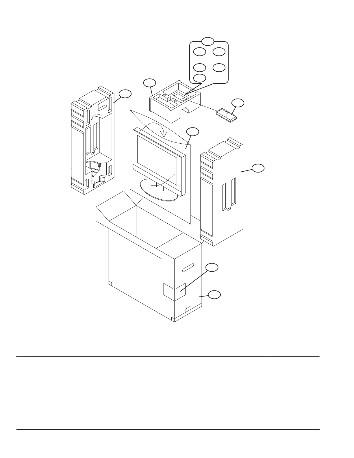
PACKING
106
107 108
109 110
103
103
111
105
104
103
102
101
PACKING PARTS LIST
Ref.No. Part No. Part Name Description Local
101 GA10002-057A-U PACKING CASE
102 GA10001-060A-U EURO LABEL LT-32 A60BU
102 GA10001-061A-U EURO LABEL LT-32 A60SJ
102 GA10001-059A-U EURO LABEL LT-32 A60SU
103 GA10049-001A-U CUSHION ASSY 3pcs in 1set
104 GA10026-002A-U POLY BAG
105 RM-C1816S-1C REMOCON UNIT
106 GA30007-001A-U DOCUMENT BAGS (x2) LT-32A60BU,LT-32A60SJ
106 AEM3021-003B-E DOCUMENT BAGS (x2) LT-32A60SU
107 ------------ WARRANTY CARD BT-54026-1E
108 LCT1863-001B-U INST BOOK English LT-32A60SJ
108 LCT1860-001B-U INST BOOK English/German/French/Dutch/Spanish/Italian/Portuguese LT-32A60BU,LT-32A60SU
109 LCT1861-001B-U INST BOOK Norwegian/Finn/Danish/Swedish LT-32A60BU,LT-32A60SU
110 LCT1862-001B-U INST BOOK Russian/Romanian/Czech/Polish/Hungarian/Bulgarian LT-32A60BU,LT-32A60SU
111 ------------ BATTERY R6P/AA(x2)
3-12(No.YA315)
Page 33
SCHEMATIC DIAGRAMS
WIDE LCD PANEL TELEVISION
YA31520055
LT-32A60BU,
LT-32A60SJ,
LT-32A60SU
CD-ROM No.SML200510
BASIC CHASSIS
FT
COPYRIGHT © 2005 Victor Company of Japan, Limited
No.YA315
2005/10
Page 34
LT-32A60BU, LT-32A60SJ, LT-32A60SU
STANDARD CIRCUIT DIAGRAM
NOTE ON USING CIRCUIT DIAGRAMS
1.SAFETY
The components identified by the symbol and shading are
critical for safety. For continued safety replace safety ciritical
components only with manufactures recommended parts.
2.SPECIFIED VOLTAGE AND WAVEFORM VALUES
The voltage and waveform values have been measured under the
following conditions.
(1)Input signal : Colour bar signal
(2)Setting positions of
each knob/button and
variable resistor
(3)Internal resistance of tester
(4)Oscilloscope sweeping time
(5)Voltage values
Since the voltage values of signal circuit vary to some extent
according to adjustments, use them as reference values.
: Original setting position
when shipped
: DC 20kΩ/V
: H
: V
: Othters
: All DC voltage values
20µs / div
5ms / div
Sweeping time is
specified
3.INDICATION OF PARTS SYMBOL [EXAMPLE]
In the PW board
: R209
R209
Type
No indication
MM
PP
MPP
MF
TF
BP
TAN
(3)Coils
No unit
Others
(4)Power Supply
Respective voltage values are indicated
(5)Test point
: Test point
(6)Connecting method
: Ceramic capacitor
: Metalized mylar capacitor
: Polypropylene capacitor
: Metalized polypropylene capacitor
: Metalized film capacitor
: Thin film capacitor
: Bipolar electrolytic capacitor
: Tantalum capacitor
: [µH]
: As specified
: B1
: 9V
: Connector
: Receptacle
: Only test point display
: Wrapping or soldering
: B2 (12V
: 5V
)
4.INDICATIONS ON THE CIRCUIT DIAGRAM
(1)Resistors
Resistance value
No unit : [Ω]
K
M
Rated allowable power
No indication : 1/16 [W]
Others : As specified
Type
No indication
OMR
MFR
MPR
UNFR
FR
Composition resistor 1/2 [W] is specified as 1/2S or Comp.
(2)Capacitors
Capacitance value
1 or higher : [pF]
less than 1
Withstand voltage
No indication : DC50[V]
Others : DC withstand voltage [V]
AC indicated
Electrolytic Capacitors
47/50[Example]: Capacitance value [µF]/withstand voltage[V]
: [kΩ]
: [MΩ]
: Carbon resistor
: Oxide metal film resistor
: Metal film resistor
: Metal plate resistor
: Uninflammable resistor
: Fusible resistor
: [µF]
: AC withstand voltage [V]
(7)Ground symbol
: LIVE side ground
: ISOLATED(NEUTRAL) side ground
: EARTH ground
: DIGITAL ground
5.NOTE FOR REPAIRING SERVICE
This model's power circuit is partly different in the GND. The
difference of the GND is shown by the LIVE : ( ) side GND and the
ISOLATED(NEUTRAL) : ( ) side GND. Therefore, care must be
taken for the following points.
(1)Do not touch the LIVE side GND or the LIVE side GND and the
ISOLATED(NEUTRAL) side GND simultaneously. if the above
caution is not respected, an electric shock may be caused.
Therefore, make sure that the power cord is surely removed from
the receptacle when, for example, the chassis is pulled out.
(2)Do not short between the LIVE side GND and ISOLATED(NEUTRAL
side GND or never measure with a measuring apparatus measure
with a measuring apparatus ( oscilloscope, etc.) the LIVE side GND
and ISOLATED(NEUTRAL) side GND at the same time.
If the above precaution is not respected, a fuse or any parts will be broken.
Since the circuit diagram is a standard one, the circuit and
circuit constants may be subject to change for improvement
without any notice.
NOTE
Due improvement in performance, some part numbers show
in the circuit diagram may not agree with those indicated in
the part list.
When ordering parts, please use the numbers that appear
in the Parts List.
)
(No.YA315)2-1
Page 35

CONTENTS
SEMICONDUCTOR SHAPES ...................................................................... 2-2
WIRING DIAGRAM ........................................................................................2-3
BLOCK DIAGRAM ........................................................................................2-5
CIRCUIT DIAGRAMS
MAIN PWB CIRCUIT DIAGRAM ................................................................................................................ 2-7
KEY PWB CIRCUIT DIAGRAM ................................................................................................................. 2-17
LED PWB CIRCUIT DIAGRAM ................................................................................................................. 2-18
POWER PWB CIRCUIT DIAGRAM .......................................................................................................... 2-19
PATTERN DIAGRAMS
MAIN PWB PATTERN .............................................................................................................................. 2-25
POWER PWB PATTERN .......................................................................................................................... 2-29
KEY PWB PATTERN ................................................................................................................................ 2-31
LED PWB PATTERN ................................................................................................................................ 2-31
VOLTAGE CHATRS ................................................................................... 2-33
WAVEFORMS ............................................................................................ 2-34
USING P.W. BOARD
P.W.B ASS’Y name
MAIN P.W BOARD
POWER P.W BOARD
KEY P.W BOARD
LED P.W BOARD
LT-32A60BU
QAL0747-001
QAL0748-001
QAL0730-001
QAL0731-001
LT-32A60SJ
LT-32A60SU
SEMICONDUCTOR SHAPES
TRANSISTOR
BOTTOM VIEW FRONT VIEW TOP VIEW
CHIP TR
E
C
B
ECB
IC
BOTTOM VIEW FRONT VIEW TOP VIEW
OUT
E
IN
IN OUTE
B
(G)E(S)C(D)
1 N
ECB
ECB
1
1 N
C
BE
N
CHIP IC
N
2-2(No.YA315)
TOP VIEW
1
1
N
Page 36

WIRING DIAGRAM
LCD PANEL UNIT
TOP
LCD PANEL UNIT
LCD PANEL UNIT
TOP
TOP
10115
CN3
1
CN2
30 1
1
J304
4
1
J210
7
1
J209
4
1
J801
15
J501
J602
J601
2
1
3
1
H701
U/V TUNER
7
1
J209-1
CONTROL PWB
41
J210-1
LED PWB
CN1
POWER CORD
TOP
MAIN PWB
SPEAKER (R) SPEAKER (L)
FU1
250V/5A
POWER PWB
2-4(No.YA315)(No.YA315)2-3
Page 37

BLOCK DIAGRAM
J203
EXT-1
J202
EXT-2
J204/J205
EXT-3
S VIDEO,VIDEO
AUDIO L/R
H701
U/V TUNER
VIDEO_OUT
SIF
AUDIO_OUT
SCART2 R1/G1/B1
SCART1 R/G/B
TV_CVBS
SCART2 CVBS
SCART1 CVBS
AV CVBS
V
Y
C
SCART1_R
Pb/Pr
U405
RGB SELECT
U101
VIDEO INPUT SELECT
SCART R/G/B
V
Y
C
OSD R/G/B/FB
U402
3D YC SEP.
/RGB PROCESS
/COLOR DEMOD
/VIDEO SELECT
/OSD SW
AD
DQ
U401
MEMORY
(16Mbit)
Y(0-7), C(0-7)
Y8
HS/VS
U501
A-D CONVERT
/3D NR
/LVDS FORMAT
CONVERSION
ADRS
DQ
U502
MEMORY
(64Mbit)
LCD PANEL
J205
EXT-4
Y,Pb,Pr
J201
PC IN
(D-SUB)
110-240V AC,
50/60Hz
TV ROUT/LOUT (SCART1 L/R OUT)
MAIN PWB
LF1
FU1
LF2
POWER PWB
ANA_IN
MONO_IN
SCART1 AL/AR
SCART2 AL/AR
SCART2 L/R OUT
BD1
AV L/R
T1
T2
T3
AGC DEMOD.
VOLTAGE
FEED BACK
PC1, PC2, PC3
A-D
SCART2_OUT
SCART1_OUT
R/G/B, HS/VS
U602
MULTI SOUND PROCESS
SPEAKER
SOUND
PROCESS
HEADPHONE
SOUND
PROCESS
D-A
5V OUT
12V OUT
24V OUT
A-D
U1, U2
U3, U5
POWER
SW
POWER
ON/OFF
SOUND
SELECT
D-A
D-A
SCART
OUTPUT
SELECT
DACM_R/L
DACA_L/R
U301
PROGRAM
DATA
(4Mbit)
U303
MAIN MEMORY
/SETTING DATA
U601
AUDIO OUT
U603
HEADPHONE AMP
U301
MAIN
CPU
/TELETEXT
DECODER
HEAD PHONE
L/R
KEY 0.1
IRSCL/SDA
Y/Pb/Pr
PC R/G/B, HS/VS
OUT2
OUT1
SPEAKER(L)
SPEAKER(R)
KEY PWB
J207
HEADPHONE
S201~S207
IR201
IR RECEIVER
LED PWB
(No.YA315)2-5 2-6(No.YA315)
Page 38

CIRCUIT DIAGRAMS
MAIN PWB CIRCUIT DIAGRAM [WHOLE CHART]
MAD0
Q0
MAD1
14
SHEET1
ZD254
KDZ5.6V
ZD253
KDZ5.6V
ZD252
KDZ5.6V
ZD251
KDZ5.6V
ZD250
J210
KDZ5.6V
CON7P(A2004WV0-7P)
HP_IDEN
1
HP_AL
2
HP_AR
3
4
5
6
7
C314
100P
C313
100P
L302 B-800
C312
L303 B-800
100P
L301 4.7K
4
L304 B-800
3
C315
2
L305 B-800
OPEN
1
ZD255
KDZ5.6V
ON/OFF
IR
ST5V
ZD256
KDZ5.6V
ZD257
KDZ5.6V
J209
CON4P(A2004WV0-4P)
LTA260W2-L02,L07
R363 --> 10K OHM
PANEL
OPTION
LTA320W2-L07
R363 --> 680 OHM
LTA260W2-L02
R395,L308,C559:OPEN
PANEL
OPTION
LTA260W2-L07
R366,L313,L318,L308:OPEN
TO INVERTER
R366
1
2
3
4
J304
CON4P(A2008WV0-4P)
1
2
3
4
5
6
7
8
9
10
11
12
13
14
15
0
R388
L308
0
OPEN
L313
0(1608)
L318
B-501(3216)
R395
0
R136
27K
R133
220
ZD101
KDZ5.6V
1
2
3
L801 B-800(3216)
4
L802 B-800(3216)
5
L803 B-800(3216)
6
L5VC B-800(3216)
7
L5VA B-800(3216)
8
L5VB B-800(3216)
9
L822 B-800(3216)
10
L823 B-800(3216)
11
L820 B-800(3216)
12
13
L821 B-800(3216)
14
L830
15
1K
J801
CON15(A2008WV0-4P)
.
REGULATOR
OPTION
Digital GND Analog GND
31
P12V
R364
0
Q106
KTC3875S-Y
D101
KDS114
Q103
KTC3875S-Y
R129
10K
GAMMA
R809:OPEN
SANKEN
R810:OPEN
VCC3_3
SCL2
Q105
KTC3875S-Y
31
2
R138
10K
2
R128
10K
CE809
100uF 25V
L809
B-800(3216)
L810
B-800(3216)
ST5V
CE805
220uF 16V
ST5V
TP328
TP327
AD0
AD1
AD2
AD3
ALE
KEY0
KEY1
SCART1_ID
DEC_HS
VDVS
SCART2_ID
HP_IDEN
SDA1
SCL1
SDA2
SCL2
2
31
Q102
31
KTC3875S-Y
2
R127
10K
Q104
31
KTC3875S-Y
R132
2
47K
C802
104
Q804
GM7130-3.3TA5
12
IN OUT
C821
104
345
R809 0
CE802
470uF 16V
MAD2
MAD1
MAD4
MAD3
Q301
GM1117-3(SOT-223)
C301
CE301
104
OUT
G
1
R386 OPEN
2
R387
OPEN
R390 4.7K
100uF 10V
C1608
D301
KDS181
3
CE302
100uF 10V
RN308 4.7KA
TP303
1
2
C303 104
RN309 B-121A
R304 100
R307 100
R308 100
R310 10K
R312 (1608)
C308 224
C309 104
R318 2.7K
R320 100
R321 2.7K
R322 100
R327 100
R328 100
R330 4.7K
R343 1K
RN301 B-121A
1
D1
2
D4
3
D2
4
C304 104
D3
5
XROM_
6
VDD2.5
7
VSS
8
VDD3.3
9
P0.0
10
P0.1
11
P0.2
12
P0.3
13
P0.4
14
P0.5
15
P0.6
16
P0.7
17
ENE
18
STOP_
19
OCF
20
EXTIF_
21
CVBS
22
VDDA2.5
23
VSSA
24
P2.0
25
P2.1
26
P2.2
27
P2.3
28
NC1
29
HS/SSC
30
VS
47K
R336
3
IN
ST5V
R350
R349
4.7K
4.7K
31
Q305
2N7002
31
Q304
2
2N7002
ST5V
R382
R373
100
100
Q309
KTC3875S-Y
31
2
31
Q316
KTC3875S-Y
5V
R363
10K
31
..
.
Q306
2N3904
R376
100
ST5V
2
R375
10K
.
R365
2
4.7K
5V
R383
R368
560
47K
2
.
..
R374
Q315
22K
31
KTA1504S-Y
R380
10K
31
..
2
.
Q307
KRC111S
C321
104
R397
R396
330
330
R370
10K
L317
10uH(2012)
ST5V
R134
10K
R131
10K
R130
1K
GND
S/W
R143
27K
1uF 50V
CE108
CE107
0.1uF 50V
R135
2
1K
R142
R137
10K
1.5K R275
L812
B-800(3216)
L814
100uH/3A
CE810
470uF 16V
C806
F_B
D801
MBRS340T3
104
R810 0
P12V
C801
104
ST12V
L806
B-800(3216)
L805
B-800(3216)
L804
B-800(3216)
C820
104
CE801
220uF 16V
R337 3.3K
R355
100
R356
100
2
L306
B-501(3216)
U303
C319
24C32
104
1
8
+5
.
2
7
VCLK
.
ESCL
3
6
SCL
.
ESDA
4
5
SDA
.
ST5V
1
2
3
4
5
6
J303
CON6P(S06B-PH-2)
R377
0
.
CE305
10uF 16V
CVBS
TV_LINKIN
TV_LINKOUT
330
R102
R101
330
53495655585144414757504236333432485254
31
Q108
VOUT1
KTC3875S-Y
TVV1V2V3V4Y1Y2Y3C1C2C3
U101
631815223101751219613207142162291623644111825
C106 106(2012)
C110 106(2012)
TV_CVBS
AV_CVBS
VCC3_3
L813
B-800(3216)
C805
104
CE808
220uF 16V
ST5V
R805
4.7K
Q806
31
KTC3875S-Y
R806
2
4.7K
Q1
MAD2
15
Q2
16
GND
MAD3
17
Q3
MAD4
18
Q4
MAD5
19
Q5
MAD6
20
Q6
MAD7
MAD5
MAD6
MAD0
MCA0
MCA1
MCA2
MAD7
MCA10
PSEN
MCA3
RN303 B-121A
RN302 B-121A
C302 104
100
A3
A2
A1
D7A0D6D0D5
A10
ALE
ASS
FL_CE
PSEN_
VDD3.3
U302
SDA5550M
P3.0
P3.1
P3.2
P3.3
P3.4
P3.5
P3.6
P3.7
VSS
VDD3.3
P1.0
P1.1
P1.2
P1.3
31323334353637383940414243444546474849
R342 10
R347 100
R345 100
R348 100
C317 104
R340 22
R338 3.3K
R344 100
R339 3.3K
R346 100
R341 100
R358 100
R357 3.3K
LINK_IN
R385
100
SCL
WR
TV_LINKIN
RD
SDA
C
Y
SCART2_OUT
SCART1_OUT
330
330
R104
R123
R119
R115
330
330
463937
YIN1
CIN1
TRAP1
TRAP2
VOUT3
YOUT1
COUT1
COUT2
V/YOUT2
S2-1
S2-2
V5V6Y4C4S2-4
3060242627
C102 104(2012)
C105 104(2012)
C113 106(2012)
C112 106(2012)
C103 106(2012)
C109 106(2012)
75
C107 106(2012)
R118
R103
'05-02/24
'05-02/12
SVHS_Y
Y_WSS
SVHS_C
SCART1_R
SCART2_CVBS
SCART1_CVBS
ST5V
R803
270
Q805
31
KTC3875S-Y
R804
2
4.7K
L815
U802
B-800(3216)
8
1
D1
S1
7
2
D1
G1
6
3
D2
S2
5
4
D2
G2
L816
B-800(3216)
Si4925BDY
R801
10K
R802
31
4.7K
Q802
2
KTC3875S-Y
Q7CEA10OEA11A9A8
212223242526272829
MCA11
MCA4
TP302
A4
A11
P1.4
P1.5
R360 3.3K
R359 100
R331
100
7657_CTL
PC_DET
YOUT3
S2-3
OPEN
CE106
MCA3
MCA4
MCA1
MCA5
MCA2
MCA6
MCA7
MCA0
5678910111213
A7A6A5A4A3A2A1
A0
VCC
WE/
A13
A14
MCA8
MCA9
MCA14
MCA11
PSEN
MCA10
MCA13
MCA5
MCA9
RN304 B-121A
81828384858687888990919293949596979899
A8A6A9
A5
80
FL_RST
79
A7
78
A13
77
A12
76
A14
75
VDD3.3
74
VSS
73
VDD2.5
72
FL_PGA
71
A15
70
A17
69
A16
68
A18
67
A19
66
NC6
65
RD_
64
WR_
63
NC5
62
P1.7
61
NC4
60
BLANK/COR
59
B
58
G
57
R
56
VDDA2.5
55
VSSA
54
NC3
53
XTAL1
52
XTAL2
51
NC2
P1.6
P4.2
P4.3
RST
50
R332 22
R333 22
R354 33
R351 33
R353 33
R352 33
LINK_OUT
ON/OFF
TV_LINKOUT
5V5V9V
CE103
22uF 16V
R113
CE105 10uF 16V
35
VCC
ADR
BIAS
VGND
AGND
COUT3
DC OUT
S-1
S-2
S-3
S-4
2829593161
R110 100K
R109 100K
R121 100K
R114 100K
OPEN
1uF 50V
CE104
5V
CE811
220uF 16V
U801
Si4925BDY
1
8
D1
S1
2
7
D1
G1
3
6
D2
S2
4
5
D2
G2
4
A12
3
A15
2
A16
1
A18
32
31
30
A17
U301
A29040AL
MCA8
MCA7
MCA6
MCA13
RN305 B-121A
C305
104
R305 100
R309 100
R311 100
R313 100
R314 4.7K
R329 75
1
Q303
KIA7027AF
RN310 4.7KA
R361 4.7K
R378
1K
SCART2_FB
SDA1
SCL1
OPEN
R108 0
R107 220
R126 1K
R124 220
SCL
SDA
MUTE
LTV
LV1
LV2
LV3
C807
104
L807
B-800(3216)
L808
B-800(3216)
ST5V
MCA12
MCA15
MCA16
MCA18
TP301
MCA17
R301 OPEN
R391
0
MCA16
MCA14
MCA15
MCA12
MCA17
MCA18
RN306 B-121A
C307 103
C310 104
C311 33P
X301
6MHZ
C316 33P
R335
22K
3
.
.
.
2
ST5V
J302
YFM254-05 5PIN
KTC3875S-Y
2
Q317
KRC111S
31
45
43
LOUT1
LOUT2
ROUT2
ROUT1
LV4
RTV
RV1
RV2
LV5
LV6
31
CE101
100uF 16V
12V
31
CE804
100uF 16V
ST5V
RN307 B-121A
R392
4.7K
TP325
TP326
C318
104
Q311
2
'05-02/18 .
7657_CTL
38
40
LOUT3
RV3
RV4
RV5
Q101
KA7809R(D-PAK)
IN OUT
2
Q801
GM66102-2
IN OUT
2
ROUT3
RV6
G
G
R323 OPEN
TXD
RXD
31
31
R367 100
R371
330
R315 10
R316 10
R317 10
R319 10
R324 OPEN
Q308
KTC3875S-Y
CXA2069Q
J501
VCC3_3 VCC2_5
L501
Q502
B-501(3216)
GM1117-1
3
1
IN
OUT
G
C501
CE518
100uF 16V
VCC3_3
L401
VCC2_5A
B-501(3216)
C406
C404
C403
C402
C405
C407
104
104
104
104
104
104
CE402
22uF 16V
C507
C508
C506
104
104
104
C502
104
104
2
CE502
220uF 16V
VCC2_5
L504
VCC1_8AVCC3_3A
B-501(3216)
CE506
C512
C511
C509
C510
22uF 16V
104
104
104
104
Q501
VCC3_3 VCC1_8
AIC1117A-18CY
L502
B-501(3216)
3
2
VIN
VOUT
ADJ
C503
CE503
104
100uF 16V
C513
104
1
CE504
47uF 16V
VCC1_8
L505
B-501(3216)
C517
C514
C516
C515
C518
C519
104
104
104
104
104
104
C504
104
CE507
22uF 16V
CONN FLEX-30PIN
1234567891011121314151617181920212223242526272829
26INCH-LO2
OPTION
R508 OPEN
R506 OPEN
R507 OPEN
R529
0
32INCH-LO1
OPTION
VCC3_3
VCC3_3
RXO3-
RXO0-
RXOC+
RXO2-
RXO1+
RXO0+
RXO1-
RXO2+
RXO3+
197
196
193
192
191
190
189
188
NC2
NC3
NC4
NC5
NC6
NC7
NC8
NC9
LVBCKM
LVBCKP
LVACKM
LVACKP
MDATA[0]
MDATA[1]
MDATA[2]
MDATA[3]
MDATA[4]
MDATA[5]
MDATA[6]
MDATA[7]
MDATA[8]
MDATA[9]
MDATA[10]
MDATA[11]
MDATA[12]
MDATA[13]
MDATA[14]
MDATA[15]
MDATA[16]
MDATA[17]
MDATA[18]
MDATA[19]
MDATA[20]
MDATA[21]
MDATA[22]
MDATA[23]
MDATA[24]
MDATA[25]
MDATA[26]
MDATA[27]
MDATA[28]
MDATA[29]
MDATA[30]
MDATA[31]
MADR[11]
MADR[10]
MADR[9]
MADR[8]
MADR[7]
MADR[6]
MADR[5]
MADR[4]
MADR[3]
MADR[2]
MADR[1]
MADR[0]
BADR[0]
BADR[1]
SVHS_C
L212
B-800
ZD207
KDZ5.6V
71110123456
7
6
11
10
CY
S-VHS
J204 SV JACK (SW4-1)
RXOC-
187
LVB0M
186
LVB0P
181
LVB1M
180
LVB1P
179
LVB2M
178
LVB2P
177
176
175
LVB3M
174
LVB3P
R517 B-300
171
LVA0M
R516 B-300
170
LVA0P
R511 B-300
169
LVA1M
R518 B-300
168
LVA1P
R509 B-300
167
LVA2M
R510 B-300
166
LVA2P
R543 B-300
165
R519 B-300
164
R515 B-300
161
LVA3M
R542 B-300
160
LVA3P
153
DQS[0]
152
151
150
149
148
147
146
145
144
143
142
141
138
137
136
135
134
DQS[1]
R566 10
133
DQM[0]
R568 10
101
DQM[1]
100
DQS[2]
99
98
97
96
95
94
93
92
91
90
89
88
85
84
83
82
81
DQS[3]
RN518 B-300A
130
129
128
127
RN519 B-300A
124
123
122
121
RN520 B-300A
120
119
118
117
R582 B-300
116
WEZ
R583 B-300
115
CASZ
R585 B-300
112
RASZ
R587 B-300
111
R588 B-300
110
C558 OPEN
R589 0
107
MCLK
106
MCLKZ
R591 B-300
105
MCLKE
R592 B-300
104
MVREF
TV_CVBS
SVHS_Y
R240
R241
75
75
C232
C231
471
471
L213
B-800
ZD208
KDZ5.6V
9
8
9
8
12345
J201
105-15202N3301-F
D-SUB-JACK
L515
B-501(3216)
L516
L511
B-501(3216)
L513
B-501(3216)
L512
B-501(3216)
L510
B-501(3216)
C535 104
C533 104
C532 104
C536 104
C534 104
CE510
VCC4
VCC5
VCC6
DQML
DQMU
TUDM
TLDM
C418
OPEN
ALE
RD
WR
AD0
AD1
AD2
AD3
TP501
TP502
L205
B-800
D208
KDS114
123456789101112131415161718192021
2641384447
GND3
GND4
GND5
GND1
NC1
NC2
4
33
37
RN513 B-300A
RN515 B-300A
R571 B-300
R572
B-300
RN516 B-300A
RN517 B-300A
R573 B-300
TP503
C553 33P
C554 33P
SCART2_R_OUT
CE205 10uF 16V
C223
471
L221
B-800
22uF 16V
50
U401
KM4S161622H
TSOP-50
GND6
207
GND2
208
VCC3_3
10
R597 390
PC_HS
PC_VS
BLUE+
BLUESOG
GREEN+
GREENRED+
RED-
PBPB+
YY+
SOY
PRPR+
C548 104
C549 104
C550 10P
R576 33
R577 B-300
R579 B-300
200
R580 33
201
R581 33
C552 104
158
R584 B-300
R586 B-300
202
X501
14.318MHZ
203
PR+
C206 473
R228 33
C215
10P
C238
10P
L208
B-800
R264
75
KDZ5.6V
ZD217
C244
331
123456789
123456789
J205 YUV JACK (AV-601)
TDQ0
TDQ15
TDQ14
TDQ13
TDQ12
TDQ11
TDQ10
TDQ9
TDQ8
TDQ7
TDQ6
TDQ5
TDQ4
TDQ3
TDQ2
TDQ1
TDQ0
TLDM
TUDM
/TWE
/TCAS
/TRAS
/TCS
TCLK
SCART2_FB
R277
0
R284
OPENC217
.
ZD260
KDZ5.6V
ZD233
OPEN
TDQ1
235689111239404243454648491713
D0D1D2D3D4D5D6D7D8
A0A1A2A3A4A5A6A7A8A9A10
21222324272829303132201935
TAD1
TAD0
TAD10
TAD9
TAD8
TAD7
TAD6
TAD5
TAD4
TAD3
TAD2
TAD1
TAD0
TBA
C424 10P
VD_Y7
VD_Y6
VD_Y5
VD_Y4
VD_Y3
VD_Y2
VD_Y1
VD_Y0
VD_C7
VD_C6
VD_C5
VD_C4
VD_C3
VD_C2
VD_C1
VD_C0
R429 33
VDCLK
C436 10P
VDHS
R434 33
VDVS
R436 33
TP404
TP405
TP407
TP408
TP409
TP410
TP411
TP412
TP413
VDVS
SCART2_R1
R215
R214
1K
1K
R238
R237
82
82
ZD222
ZD221
KDZ5.6V
KDZ5.6V
U402
C460 151P
Vcc
Blue 1 input
CE414
CE206
220uF 16V
R260
75
C409 104
C411 104
C459 151P
C412 104
C413 104
C414 104
R411 470
VCC3_3
R412 68
Q403
2
.
KTA1504S-Y
..
31
C417 104
C419 104
C420 104
C421
C422
C423
152
152
152
VCC3_3
R414 33
X401
27MHz
R427 1M
L402
C425
VCC3_3
B-501(3216)
22P
C427
CE404
C428
104
10uF 16V
104
L404
VCC3_3
B-501(3216)
12
C433
CE405
C432
104
10uF 16V
104
L405
VCC3_3
B-501(3216)
12
CE407
C440
10uF 16V
104
L406
VCC3_3
R457 75
R393 100
Green output
composite video input
composite sync output
GND
Red 2 input
GND
4.7uF 50V
C454 104
C453 104
CE415 10uF 16V
SCART2_R1
SCART2_G1
SCART1_FB
0
R254
OPEN
ZD258
KDZ5.6V
ZD220
OPEN
B-501(3216)
R459 75
CE408
10uF 16V
1415161718192021222324
CTL
VD output
Blue output
Green 2 input
GND
Blue 2 input
VD 1 input VD 2 input
12 13
R460 4.7K
C458 104
CE413 10uF 16V
CE412 10uF 16V
SCART2_B1
SCL2
SDA2
SCART1_ID
SCART1_G
SCART1_R
R279
R278
1K
1K
R281
R282
82
82
R239
R248
10K
27K
R261
'05-02/12
'05-02/12
100
100
R290
R291
ZD270
KDZ5.6V
ZD271
KDZ5.6V
ZD230
ZD223
ZD231
KDZ5.6V
KDZ5.6V
OPEN
CVBS
Y
C
SCART_R
SCART_G
SCART_B
TP306
SCART_FB
RESET
TEXT_R
TEXT_G
TEXT_FB
TEXT_B
TEXT_B
TEXT_G
TEXT_R
SCL
SDA
#RESET
R326 OPEN
R325 OPEN
1
2
3
4
5
CE102
47uF 16V
2
9V
8V
12
#RESET
SCART_FB
R394
1K
SCART1_FB
9V
J101
1
2
CON2P(S02B-PH-2)
C101
104
CE803
47uF 16V
DEC_HS
TEXT_FB
SCART_B
SCART_G
SCART_R
5V
7657_CTL
R274
100
'.
L408
B-501(3216)
103
C451
CE410
4.7K
R456
HD output
HD 2 input
HD 1 input
Red 1 input
HD Sync signal detector
Green 1 input
U405 B A7657F
1234567891011
CE416
C457 104
C456 104
R461 470K
C455 471
CE411 4.7uF 50V
SCART1_R
SCART1_G
SCART1_OUT
9V
31
2
Q203
KTC3875S-Y
R210
270
R236
75
C230
471
L217
B-800
ZD206
KDZ5.6V
J202 SCART1 (GCH01-0061)-EX2
C461
152PF
1uF 50V
4.7uF 50V
SCART1_CVBS
R413 100
R458 75
Red output
GND
C452 104
SCART1_B
TW9918
61
DRAM_DQ15
MUX0
60
DRAM_DQ14
MUX1
64
DRAM_DQ13
MUX2
65
DRAM_DQ12
MUX3
66
DRAM_DQ11
MUX4
67
DRAM_DQ10
MUX5
DRAM_DQ9
62
DRAM_DQ8
MXOUT
63
DRAM_DQ7
YIN
57
DRAM_DQ6
YBFOUT
C415 104
C416 104
R462 4.7K
R415
680
R416 22
R417 22
R418 4.7K
R419 0
C426
22P
C431
C430
C429
104
104
104
C435
C434
104
104
C441
C442
104
104
12
C447
104
DRAM_DQ5
56
DRAM_DQ4
CIN0
55
DRAM_DQ3
CIN1
DRAM_DQ2
75
DRAM_DQ1
RIN0
76
DRAM_DQ0
GIN0
80
BIN0
68
DRAM_AD10
FB0
DRAM_AD9
74
DRAM_AD8
RIN1
77
DRAM_AD7
GIN1
81
DRAM_AD6
BIN1
69
DRAM_AD5
FB1
DRAM_AD4
83
DRAM_AD3
HS
85
DRAM_AD2
RSET
DRAM_AD1
9
DRAM_AD0
SCLK
10
DRAM_BA
SDAT
11
SIAD
DRAM_LDM
13
DRAM_UDM
RST
7
DRAM_WE
PDN
8
DRAM_CAS
OE
12
DRAM_RAS
TMODE
DRAM_CS
15
XI
16
XO
14
VDDE0
38
VDDE1
102
VDDE2
119
VDDE3
128
VDDE4
17
VSSE0
39
VSSE1
96
VSSE2
103
VSSE3
120
VSSE4
1
VSSE5
26
VDD0
46
VDD1
89
VDD2
113
VDD3
27
VSS0
47
VSS1
90
VSS2
114
VSS3
70
AVD0
73
AVD1
86
AVD2
71
AVS0
72
AVS1
84
AVS2
88
AVDP
87
AVSP
VCC3_3
R501
10K
R504
4.7K
C559 105
SCART1_B
SCART1_AL
TV_L_OUT
CE202
10uF 16V
R217 1K
R216 1K
C216
471
471
82
L201
B-800
L218
B-800
ZD210
KDZ5.6V
D209
KDS114
ZD259
ZD232
KDZ5.6V
Q503
31
2N3904
..
R505 100K
2
.
SCART2_OUT
R211
100
TV_R_OUT
SCART1_AR
2
Q202
KTC3875S-Y
CE203
R218
10uF 16V
1K
C219
C218
471
471
L202
L203
B-800
B-800
KDZ5.6V
ZD211
KDZ5.6V
D210
KDS114
123456789101112131415161718192021
CbCr CbY YCr
SHEET3 SHEET4
125
126
127
2
3
4
5
6
115
116
117
118
121
122
123
124
106
93
94
95
97
98
99
100
101
104
105
107
112
91
111
110
109
108
92
CLK
RN408 B-300A
28
VD15
29
VD14
30
VD13
31
VD12
RN409 B-300A
32
VD11
33
VD10
34
VD9
35
VD8
RN410 B-300A
36
VD7
37
VD6
40
VD5
41
VD4
RN411 B-300A
42
VD3
43
VD2
44
VD1
45
VD0
25
VCLK
R432 33
18
FIELD
19
HSYNC
20
VSYNC
R438 33
21
HACTIVE
R440 33
22
VACTIVE
R442 33
23
DVALID
R443 33
24
MPOUT
C438 104
58
VREFP
C439 104
59
VERFN
C443 104
54
VCOM0
C444 104
79
VREFP1
C445 104
78
VREFN1
C446 104
82
VCOM1
R444 33
48
T0
R445 33
49
T1
R446 33
50
T2
R447 33
51
T3
R448 33
52
T4
R449 33
53
T5
ADJ_PWM
9V
31
SCART2_CVBS
.
R273
270
CE207
220uF 16V
R267
R235
75
75
C226
471
L219
B-800
ZD212
KDZ5.6V
J203 SCART2 (GCH01-0061)-EX1
VCC3_3A
TDQ6
TDQ15
TDQ2
TDQ3
TDQ9
TDQ14
TDQ4
TDQ12
TDQ10
TDQ7
TDQ5
TDQ8
TDQ11
TDQ13
25
D9
D10
D11
D12
D13
D14
D15
VCC1
VCC2
VCC3
A11/BA
CLK
RAS
CASWECS
CKE
17161518341436
TAD2
TAD5
TAD4
TAD3
TBA
TAD9
TAD6
TAD10
TAD8
TAD7
/TRAS
/TCAS
/TWE
/TCS
TCLK
VCC3_3A
VD_C0
VD_C1
VD_C2
VD_C3
VD_C4
VD_C5
VD_C6
VD_C7
VDHS
VDCLK
VD_Y0
VD_Y1
VD_Y2
VD_Y3
VD_Y4
VD_Y5
VD_Y6
VD_Y7
VDVS
R574 100
RESET
ADJ_PWM
SCART2_B1
SCART2_ID
SCART2_G1
SCART2_AR
SCART2_AL
SCART2_L_OUT
CE204
10uF 16V
R280 1K
R220 1K
R219 1K
R283
82
R249
R286
27K
OPEN
ZD224
C222
C221
C220
471
471
471
L204
B-800
10K
L220
ZD214
B-800
KDZ5.6V
ZD213
KDZ5.6V
D207
KDS114
ZD261
KDZ5.6V
ZD219
KDZ5.6V
11
14
15
18
19
20
21
22
23
24
25
26
27
28
29
30
31
32
33
36
37
38
39
40
41
42
43
44
45
46
47
48
51
52
53
54
55
56
57
58
59
60
61
77
67
68
69
70
71
72
73
74
75
62
76
78
2
3
5
6
8
9
PR-
C207 473
R229 75
C236
10P
KDZ5.6V
ZD216
CE511
22uF 16V
DVI_R+
DVI_RDVI_G+
DVI_GDVI_B+
DVI_BDVI_CK+
DVI_CKREXT
DDCD_DA
DDCD_CK
HSYNC1
VSYNC1
BIN1
BIN1M
SOGIN1
GIN1
GIN1M
RIN1
RIN1M
BIN0M
BIN0
GIN0M
GIN0
SOGIN0
RIN0M
RIN0
HSYNC0
VSYNC0
RMID
REFP
REFM
VI_DATA[8]
VI_DATA[9]
VI_DATA[10]
VI_DATA[11]
VI_DATA[12]
VI_DATA[13]
VI_DATA[14]
VI_DATA[15]
GPIO[5]/VHS
GPIO[4]/VCLK2
VI_CK
VI_DATA[0]
VI_DATA[1]
VI_DATA[2]
VI_DATA[3]
VI_DATA[4]
VI_DATA[5]
VI_DATA[6]
VI_DATA[7]
GPIO[2]/VVS
HWRESET
INT
ALE
RDZ
WRZ
DBUS[0]
DBUS[1]
DBUS[2]
DBUS[3]
PWM0
PWM1
VCTRL
BYPASS
GPIO[3]/VDE
GPIO[1]/FIELD
XOUT
XIN
PB+
C204 473
R226 33
CE512
22uF 16V
173441020466162
AVDD0_ADC
AVDD1_ADC
PB-
Y_WSS
C205 473
R299 33
R227 75
C214
10P
L207
B-800
R263
75
KDZ5.6V
ZD215
C243
331
C537 104
AVDD0_DVI
AVDD1_DVI
.
C202 473
C201 102
R223 470
L206
B-800
CE513
22uF 16V
CE514
22uF 16V
VCC2_5A
18286102
VDDP0
VDDP1
VDDP2
AVDD_MPLL
GND0
GND1
GND2
GND3
GND4
171316355064806587103
Y-Y+SOY
AV_CVBS
C203 473
R224 33
R225 75
C213
10P
R262
75
C242
331
L514
B-501(3216)
C539 104
C540 104
C538 104
113
125
139
VDDM0
VDDM1
VDDM2
VDDM3
VDDM4
U501
MST6151A
GND5
GND6
GND8
GND7
GND9
GND10
R242
75
C233
471
L214
B-800
ZD209
KDZ5.6V
ZD262
KDZ5.6V
CE515
22uF 16V
CE516
22uF 16V
15412109496379131
VDDC0
VDDM5
AVDD_PLL1
AVDD_PLL2
GND11
GND12
GND13
GND14
GND15
GND16
GND17
108
114
126
132
140
155
157
159
AV_R
AV_L
R244
R243
1K
1K
C234
471
L215
L216
B-800
B-800
ZD263
KDZ5.6V
D205
D206
KDS114
KDS114
B-501(3216)
C541 104
VCC1_8A
156
173
185
195
199
198
NC0
NC1
VDDC1
VDDC2
VDDC3
VDDC4
VDDC5
VDDC6
VDDC7
GND18
GND19
GND20
GND21
GND22
GND23
GND24
GND25
163
172
183
184
194
205
206
C235
471
MDATA0
MDATA1
MDATA2
MDATA3
MDATA4
MDATA5
MDATA6
MDATA7
MDATA8
MDATA9
MDATA10
MDATA11
MDATA12
MDATA13
MDATA14
MDATA15
MDQM0
MDQM1
C520
RXO0RXO0+
RXO1RXO1+
RXO2RXO2+
RXOCRXOC+
RXO3RXO3+
MDATA16
MDATA17
MDATA18
MDATA19
MDATA20
MDATA21
MDATA22
MDATA23
MDATA24
MDATA25
MDATA26
MDATA27
MDATA28
MDATA29
MDATA30
MDATA31
MADR10
MADR9
MADR8
MADR7
MADR6
MADR5
MADR4
MADR3
MADR2
MADR1
MADR0
/MWE
/MCAS
/MRAS
MBA0
MBA1
MCLK
MCKE
R593 1K
R594
1K
BLUE-
C227 473
R256 75
104
30
C505
104
C555
104
GREEN-
C228 473
R285 75
RED-
C229 473
R288 75
CE505
47uF 16V
47uF 16V
VCC2_5A
R245
75
12V
L503
OPEN
L506
B-501(3216)
B-501(3216)
CE508
MDQM0
MDQM1
C556
102
RED+
C208 473
R230 33
ZD202
L209
B-800
162738495
.........
.....
1112131415
32inch
SS
AU
LG
5V5V12V
L507
L508
OPEN
VCC3_3
L509
B-501(3216)
CE509
22uF 16V
L517
B-501(3216)
CE517
10uF 16V
VCC3_3
R596 4.7K
R595 4.7K
R562 B-300
R563 B-300
R565 B-300
R567 B-300
MDATA0
RN503 B-300A
MDATA1
MDATA2
MDATA3
RN505 B-300A
MDATA5
MDATA6
MDATA7
MDATA8
RN508 B-300A
MDATA9
MDATA10
MDATA11
MDATA12
RN509 B-300A
MDATA13
MDATA14
MDATA15
MDATA16
RN510 B-300A
MDATA17
MDATA18
MDATA19
MDATA20
RN511 B-300A
MDATA21
MDATA22
MDATA23
RN512 B-300A
MDATA24
MDATA25
MDATA26
MDATA27
MDATA28
RN514 B-300A
MDATA29
MDATA30 MD30
MDATA31
GREEN+
SOG
BLUE+
PC_DET
C209 473
C210 102
C211 473
R233 33
R231 33
R232 470
R246
R247
75
75
ZD203
ZD204
KDZ5.6V
KDZ5.6V
KDZ5.6V
R255
L211
L210
100
B-800
B-800
ZD264
10
.
VS
HS
C604
332
CE704
100uF 16V
R707
10
J601
CON3P(S03B-PH-2)
J602
CON2P(S02B-PH-2)
SIF_OUT
AM
AV_R
AV_L
SCART1_AR
SCART1_AL
SCART2_AR
SCART2_AL
AM
SIF_OUTA
5V
3
2
1
2
1
L506,L507
L503,L508
L503,L508
C525
C524
104
104
12
C543
C544
104
104
C557 10P
DQM0
16
DQM0
DQM1
71
DQM1
DQM2
28
DQM2
DQM3
59
DQM3
MD0
2
DQ0
MD1
4
DQ1
MD2
5
DQ2
MD3
7
DQ3
MD4MDATA4
8
DQ4
MD5
10
DQ5
MD6
11
DQ6
MD7
13
DQ7
MD8
74
DQ8
MD9
76
DQ9
MD10
77
DQ10
MD11
79
DQ11
MD12
80
DQ12
MD13
82
DQ13
MD14
83
DQ14
MD15
85
DQ15
MD16
31
DQ16
MD17
33
DQ17
MD18
34
DQ18
MD19
36
DQ19
MD20
37
DQ20
MD21
39
DQ21
21
MD22
40
DQ22
MD23
42
DQ23
MD24
45
DQ24
MD25
47
DQ25
MD26
48
DQ26
MD27
50
DQ27
MD28
51
DQ28
MD29
53
DQ29
54
DQ30
MD31
56
DQ31
PC_VS
PC_HS
SDA1
SCL1
KDZ5.6V
ZD218
KDZ5.6V
ZD225
KDZ5.6V
43
R271
100
R272
ZD227
KDZ5.6V
100
SHEET2
+3_3V_DMQ
C526
104
+3_3V_DMC
C545
104
R704 560
VIDEO OUT
AUDIO OUT
C530
C527
C528
C531
C529
104
104
104
104
104
C546
104
MCKE
MCLK
/MCAS
/MWE
MBA0
/MRAS
MBA1
R560 B-300
R548 B-300
R544 22
R546 B-300
R561 B-300
R550 B-300
R541 B-300
U502
67681918172223
K45643232F
WE
BA0
BA1
CLK
CKE
RAS
CAS
MADR0
25
A0
MADR1
26
A1
MADR2
27
A2
MADR3
60
A3
MADR4
61
A4
MADR5
62
A5
MADR6
63
A6
MADR7
64
A7
MADR8
65
A8
MADR9
66
A9
MADR10
24
A10/AP
1
VDD
15
VDD
29
VDD
43
+3_3V_DMQ
VDD
3
VDDQ
9
VDDQ
35
VDDQ
41
VDDQ
49
+3_3V_DMC
VDDQ
55
VDDQ
75
VDDQ
81
VDDQ
6
VSSQ
12
VSSQ
32
VSSQ
38
VSSQ
46
VSSQ
52
VSSQ
78
VSSQ
84
VSSQ
44
VSS
58
VSS
72
VSS
86
VSS
CS
20
HP_AL
HP_AR
5V
31
C702
R703 100
104
2
'.
Q702
KTC3875S-Y
R705
820
VIDEO_OUT
17
16
AFT OUT
15
14
VT
SIF_OUTA
13
SIF
5V_IN
12
B+
SDA_I/O
11
SDA
SCL_IN
10
SCL
9
SAS
8
AGC OUT
7
N.C
6
N.C
R702
100
5
IF OUT
4
N.C
3
NC
2
NC
1
NC
H701 SAMSUNG-TCMW3001PD29A(H)
SCL1
SDA1
R295
75
R289
75
R287
R292
R296
4.7
1K
1K
R706
C248
OPEN
334
ZD265
KDZ5.6V
R711
ZD702
100K
UDZ33B
C703
103
C701 104
CE701 100uF 16V
L701
10uH(2012)
R701
100
PARTSNIC-PA2MF72DA
ON/OFF
5V
C615
331
PAL, SCART
R708 100
R615 100
SCL1
R294
4.7
C249
334
Q701
KTC3875S-Y
R710 1K
ZD266
KDZ5.6V
U601
TDA7266D
2519
VCC
TDA 7266D AUDIO AMP
VCC
7
R604
4.7K
R612
47K
C636
47P
ANA_IN1-
ANA_IN2+
SC1_OUT_R
SC1_OUT_L
CE620
10uF 16V
0
0
R622
R621
C633
331
TV_L_OUT
TV_R_OUT
EARTH
3
231
16
1
PW-GND
OUT 1-
OUT 2-
OUT 1+
OUT 2+
10
PW-GND
11
PW-GND
20
PW-GND
S-GND
IN 1
ST-BY
IN 2
MUTE
91314
8
TP602
CE626
1uF 50V
R611
R610
1K
30K
.
A_OUT_L
5V
L603
B-501(3216)
C610
104
ZD267
KDZ5.6V
CE606
100uF 10V
TP603
65
AVSUP
AVSUP
ANA_IN1+
64
NC
63
NC
62
AVSS
61
AVSS
60
MONO_IN
59
NC
58
VREFTOP
57
SC1_IN_R
56
SC1_IN_L
55
ASG1
54
SC2_IN_R
53
SC2_IN_L
52
ASG2
51
SC3_IN_R
50
SC3_IN_L
49
ASG4
48
SC4_IN_R
47
SC4_IN_L
46
NC
45
AGND
44
AHVSS
43
AHVSS
42
NC
41
NC
CAPL_A
AHVSUP
CAPL_M
40
L608
CE621
B-501(3216)
10uF 16V
CE624
C625
10uF 16V
102
L703
680uH
C710
Q703
104
KTC3875S-Y
2
C712
D704
471
KDS181
8V
C605
332
TP604
C620 103
31
R608
30K
C613
OPEN
L605
OPEN(2012)
C611
47P
C614
472
C617
104
C618
103
CE607
10uF 16V
CE608
10uF 16V
CE609
10uF 16V
CE610
10uF 16V
CE611
10uF 16V
CE613
10uF 16V
CE614
10uF 16V
CE617
10uF 16V
R712
100K
C714
103
TP601
CE625
1uF 50V
.
R609
1K
A_OUT_R
.
C612
R613
0
100
L604
OPEN(2012)
R614
100
L705
470uH
C715
103
ST12V
ST12V
R601
1K
231
R602
68K
2
B
31
3
Q603
KTC3875S-Y
R607
2
4.7K
31
1
NC
2
12C_CL
3
12C_DA
4
12S_CL
5
12S_WS
331
6
C616
12S_DA_OUT
7
R616 100
L606
C619
103
#RESET
SDA1
ZD234
OPEN
2
5V
B-501(3216)
R709 10
CE612
47uF 16V
104
C621
R629
100
C634
105
5V
R632
10
Q604
KSC1623-Y
31
R618
100
HP_SW
CE221 100uF 16V
CE220 100uF 16V
ZD235
OPEN
31
2
CE630
5V
CE703
100uF 16V
12S_DA_IN
8
ADR_DA
9
ADR_WS
10
ADR_CL
11
DVSUP
12
DVSUP
13
DVSUP
14
DVSS
15
DVSS
16
DVSS
17
12S_DA_IN2
18
NC
19
NC
20
NC
21
RESET_Q
22
NC
23
NC
24
DACA_R
472
C640
R617
100
C635
105
R630
20K
R631
10K
123
CE627
47uF 16V
104
C638
22uF 16V
H_R
H_L
L602
L601
10uH(3216)
10uH(3216)
C601
D601
104
KDS181
R603
150
Q601
KTA1504S-Y
CE
D602
KDS181
807978777675747372717069686766
STBY_Q
DACA_L
252627282930313233343536373839
472
C639
R624
20K
45
A
B
C
DGND
EFVCC
678
33V
CE601
CE603
47uF 16V
Q602
31
KTC3875S-Y
2
2
1
R605
1K
CE605
MUTE
1uF 50V
TP605
C606
6P
R633
R625
4.7K
1K
TP606
X601
NC
NC
NC
ADR_SEL
D_CTR_OUT0
D_DTR_OUT1
AUD_CL_OUT
U602
MSP3410G
MSP3410G(NT/PAL/SECAM)
MSP3420G(NT/PAL MN)
VREF2
DACM_R
DACM_LNCDACM_SUPNCASG3
C624
392
392
C626
C623
331
CE623
CE622
1uF 50V
1uF 50V
A_OUT_L
A_OUT_R
R623
10K
U603
TDA7050T
R713
22K
CE705
1uF 50V
220uF 16V
CE604
47uF 16V
18.432MHz
XTAL_OUT
SC2_OUT_R
0
R619
SCART2_R_OUT
D702 KDS181
C707
104
CE602
C607
6P
XTAL_IN
SC2_OUT_L
0
R620
C627
331
C632
331
SCART2_L_OUT
1
2
15
6
220uF 16V
ST5V
R606
47K
C608
47P
TEST_IN
VREF1
J102
Note: Please refer to SHEET1-4 for details of this circuit diagram.
2-8(No.YA315)(No.YA315)2-7
Page 39
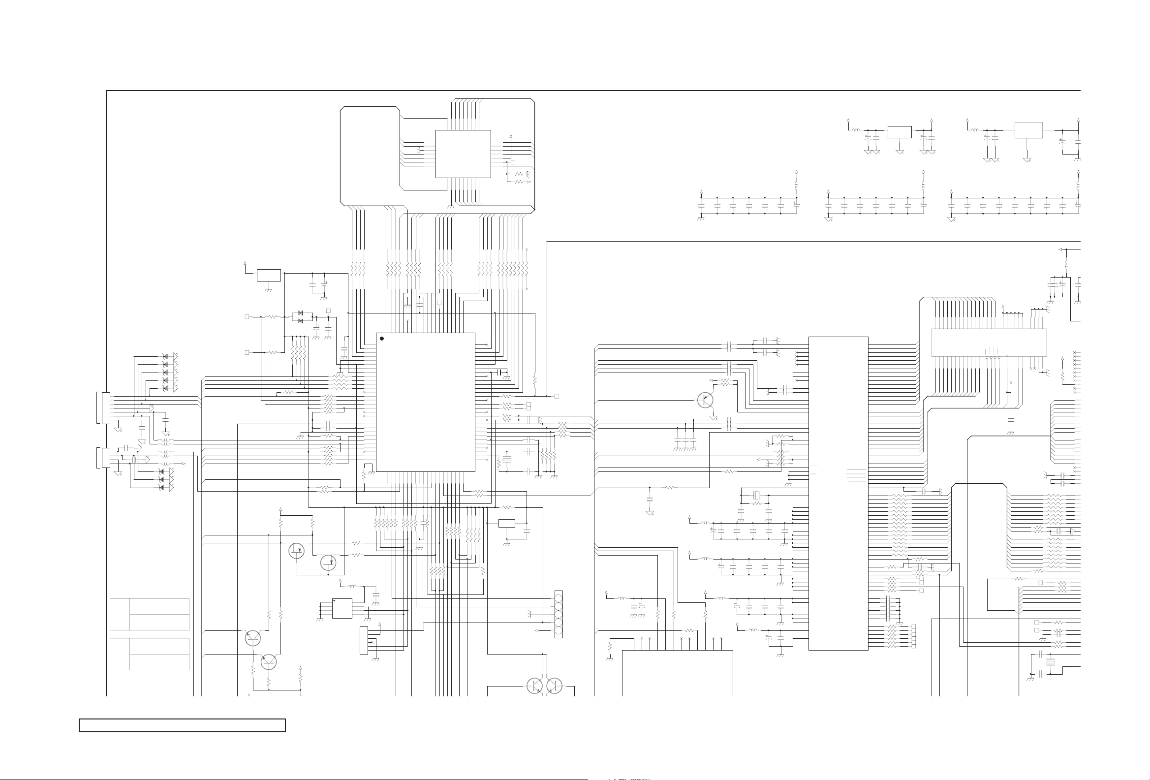
1
1
0
0
1
1
1
1
1
2
2
2
2
2
2
2
2
2
2
3
3
3
3
3
3
3
3
4
5
4
4
4
4
4
4
4
4
5
5
5
5
5
5
5
5
6
6
6
6
6
7
7
7
7
7
7
7
0
0
6
5
7
7
0
0
C535 104
MAIN PWB CIRCUIT DIAGRAM (1/4) SHEET1
MAIN PWB ASS'Y (1/4)
QAL0747-001
ZD254
KDZ5.6V
ZD253
KDZ5.6V
ZD252
KDZ5.6V
KEY PWB ASS'Y
J209-1
(SHEET5)
LED PWB ASS'Y
J210-1
(SHEET6)
NOTE : Refer to the part list for the part number of U303.
CON7P(A2004WV0-7P)
C315
OPEN
C314
KDZ5.6V
KDZ5.6V
100P
ZD255
KDZ5.6V
ZD256
KDZ5.6V
ZD257
KDZ5.6V
J210
1
2
3
4
5
6
7
C312
100P
4
3
2
1
J209
CON4P(A2004WV0-4P)
LTA260W2-L02,L07
R363 --> 10K OHM
PANEL
OPTION
LTA320W2-L07
R363 --> 680 OHM
LTA260W2-L02
R395,L308,C559:OPEN
PANEL
OPTION
LTA260W2-L07
R366,L313,L318,L308:OPEN
ZD251
ZD250
HP_IDEN
HP_AL
HP_AR
L302 B-800
L303 B-800
L301 4.7K
L304 B-800
L305 B-800
C313
ST5V
100P
AD0
AD1
AD2
AD3
ALE
KEY0
KEY1
SCART1_ID
DEC_HS
VDVS
SCART2_ID
ON/OFF
IR
HP_IDEN
SDA1
SCL1
SDA2
SCL2
ST5V
TP328
TP327
GM1117-3(SOT-223)
3
Q309
KTC3875S-Y
2
R370
10K
5V
Q301
IN
G
1
R386 OPEN
R382
100
31
2
2
OUT
D301
KDS181
3
CE302
100uF 10V
R387
OPEN
RN308 4.7KA
R390 4.7K
ST5V
R349
4.7K
31
Q304
2
2N7002
R373
100
31
Q316
KTC3875S-Y
ST5V
R375
10K
C301
CE301
104
100uF 10V
C1608
TP303
1
2
C303 104
RN309 B-121A
R304 100
R307 100
R308 100
R310 10K
R312 (1608)
C308 224
C309 104
R318 2.7K
R320 100
R321 2.7K
R322 100
R327 100
R328 100
R330 4.7K
R343 1K
R350
4.7K
Q305
2N7002
31
R380
10K
3
2
ST5V
1
2
3
4
U303
.
.
.
.
C304 104
VCLK
SDA
L306
B-501(3216)
+5
SCL
MAD3
MAD2
8
7
6
5
J303
CON6P(S06B-PH-2)
MAD4
R355
100
R356
100
MAD0
MAD6
MAD5
MAD1
RN301 B-121A
10
11
12
13
14
15
16
17
18
19
20
21
22
23
24
25
26
27
28
29
30
47K
R336
ST5V
1
2
3
4
5
6
MCA0
100
1
D1
2
D4
3
D2
4
D3
5
XROM_
6
VDD2.5
7
VSS
8
VDD3.3
9
P0.0
P0.1
P0.2
P0.3
P0.4
P0.5
P0.6
P0.7
ENE
STOP_
OCF
EXTIF_
CVBS
VDDA2.5
VSSA
P2.0
P2.1
P2.2
P2.3
NC1
HS/SSC
VS
P3.0
P3.1
P3.2
31323334353637383940414243444546474849
R337 3.3K
R342 10
R340 22
R338 3.3K
R339 3.3K
R341 100
C319
104
ESCL
ESDA
MAD0
MAD1
MAD2
MAD3
MAD4
MAD5
MAD6
MAD7
MCA1
MCA2
MAD7
MCA10
RN302 B-121A
RN303 B-121A
A2
A1
D7A0D6D0D5
ASS
FL_CE
VDD3.3
U302
SDA5550M
P3.3
P3.4
P3.5
P3.6
P3.7
VSS
VDD3.3
C317 104
R347 100
R344 100
R346 100
R345 100
14
15
16
17
18
19
20
PSEN
C302 104
A3
A10
P1.0
P1.1
R348 100
R357 3.3K
MCA4
MCA3
MCA1
MCA5
MCA2
MCA6
MCA7
MCA0
5678910111213
ST5V
A7A6A5A4A3A2A1
A0
Q0
Q1
Q2
GND
Q3
Q4
Q5
Q6
Q7CEA10OEA11A9A8
212223242526272829
MCA10
MCA5
MCA3
MCA11
MCA4
RN304 B-121A
TP302
A5
A4
A11
ALE
PSEN_
BLANK/COR
P1.2
P1.3
P1.4
P1.5
P1.6
R352 33
R351 33
R359 100
R360 3.3K
R358 100
MCA9
MCA11
PSEN
81828384858687888990919293949596979899
A8A6A9
FL_RST
A13
A12
A14
VDD3.3
VSS
VDD2.5
FL_PGA
A15
A17
A16
A18
A19
NC6
RD_
WR_
NC5
P1.7
NC4
VDDA2.5
VSSA
NC3
XTAL1
XTAL2
NC2
P4.2
P4.3
RST
50
R332 22
R333 22
R354 33
R353 33
A13
MCA8
MCA13
A7
B
G
R
A12
A15
A16
A18
VCC
WE/
A17
A14
U301
A29040AL
MCA14
MCA8
MCA9
MCA6
80
79
78
77
76
75
74
73
72
71
70
69
68
67
66
65
64
63
62
61
60
59
58
57
56
55
54
53
52
51
KIA7027AF
RN310 4.7KA
R361 4.7K
4
3
2
1
32
31
30
MCA7
MCA13
RN305 B-121A
C305
104
R305 100
R309 100
R311 100
R313 100
R314 4.7K
R329 75
1
.
Q303
R301 OPEN
R391
0
MCA14
MCA15
MCA12
R335
22K
.
.
2
MCA12
MCA15
MCA16
MCA18
TP301
MCA17
MCA16
MCA17
RN306 B-121A
C307 103
C310 104
C311 33P
X301
6MHZ
C316 33P
3
MCA18
ST5V
J302
RN307 B-121A
TP325
TP326
C318
104
R392
4.7K
ST5V
R315 10
R316 10
R317 10
R319 10
R324 OPEN
R323 OPEN
TXD
RXD
TP306
RESET
TEXT_FB
TEXT_B
TEXT_G
TEXT_R
R326 OPEN
R325 OPEN
#RESET
1
2
3
4
5
YFM254-05 5PIN
Q311
KTC3875S-Y
Q308
3
3
KTC3875S-Y
2
2
(No.YA315)2-9 2-10(No.YA315)
CVBS
Y
C
SCART_R
SCART_G
SCART_B
SCART_FB
TEXT_R
TEXT_G
TEXT_B
SCL
SDA
#RESET
DEC_HS
TEXT_FB
SCART_B
SCART_G
SCART_R
5V
7657_CTL
L408
B-501(3216)
C451
4.7K
R456
C503
104
C515
C514
104
104
VCC3_3A
TDQ15
TDQ14
TDQ13
D13
D14
D15
VCC1
VCC2
CLK
RAS
CASWECS
35
17161518341436
/TRAS
/TCAS
/TWE
/TCS
TCLK
R574 100
RESET
Q501
GM1117-1
3
VIN
25
VCC3
VCC4
CKE
VCC3_3A
VD_C0
VD_C1
VD_C2
VD_C3
VD_C4
VD_C5
VD_C6
VD_C7
VDHS
VDCLK
VD_Y0
VD_Y1
VD_Y2
VD_Y3
VD_Y4
VD_Y5
VD_Y6
VD_Y7
VDVS
VOUT
ADJ
1
C517
C516
104
104
2641384447
VCC5
VCC6
GND3
NC1
DQML
DQMU
33
37
TUDM
TLDM
C418
OPEN
RN513 B-300A
RN515 B-300A
R571 B-300
R572
B-300
RN516 B-300A
RN517 B-300A
R573 B-300
TP503
ALE
RD
WR
AD0
AD1
AD2
AD3
TP501
TP502
C553 33P
C554 33P
GND4
NC2
4
VCC3_3
50
GND5
GND1
10
2
CE504
47uF 16V
L505
B-501(3216)
C518
104
C533 104
C532 104
U401
KM4S161622H
TSOP-50
GND6
GND2
VCC3_3
PC_HS
PC_VS
BLUE+
BLUESOG
GREEN+
GREENRED+
RED-
PBPB+
YY+
SOY
PRPR+
C548 104
C549 104
C550 10P
R576 33
R577 B-300
R579 B-300
R580 33
R581 33
C552 104
R584 B-300
R586 B-300
X501
14.318MHZ
VCC
C519
104
L510
B-501(3216)
C534 104
CE510
22uF 16V
2
2
R597 390
2
2
1
2
2
C402
104
C403
104
C404
104
C405
104
L401
B-501(3216)
C406
104
VCC3_3
C407
104
CE402
22uF 16V
VCC3_3 VCC2_5
L501
B-501(3216)
CE518
100uF 16V
VCC2_5A
C507
C506
104
104
GM66102-2.5TC3(TO-252)
C501
104
C508
C509
104
104
Q502
1
3
OUT
IN
G
2
CE502
220uF 16V
VCC2_5
L504
B-501(3216)
C510
C511
104
CE506
104
22uF 16V
U402
104
C442
104
C447
104
C431
104
TW9918
61
MUX0
60
MUX1
64
MUX2
65
MUX3
66
MUX4
67
MUX5
62
MXOUT
63
YIN
57
YBFOUT
56
CIN0
55
CIN1
75
RIN0
76
GIN0
80
BIN0
68
FB0
74
RIN1
77
GIN1
81
BIN1
69
FB1
83
HS
85
RSET
9
SCLK
10
SDAT
11
SIAD
13
RST
7
PDN
8
OE
12
TMODE
15
XI
16
XO
14
VDDE0
38
VDDE1
102
VDDE2
119
VDDE3
128
VDDE4
17
VSSE0
39
VSSE1
96
VSSE2
103
VSSE3
120
VSSE4
1
VSSE5
26
VDD0
46
VDD1
89
VDD2
113
VDD3
27
VSS0
47
VSS1
90
VSS2
114
VSS3
70
AVD0
73
AVD1
86
AVD2
71
AVS0
72
AVS1
84
AVS2
88
AVDP
87
AVSP
DRAM_DQ15
DRAM_DQ14
DRAM_DQ13
DRAM_DQ12
DRAM_DQ11
DRAM_DQ10
DRAM_DQ9
DRAM_DQ8
DRAM_DQ7
DRAM_DQ6
DRAM_DQ5
DRAM_DQ4
DRAM_DQ3
DRAM_DQ2
DRAM_DQ1
DRAM_DQ0
DRAM_AD10
DRAM_AD9
DRAM_AD8
DRAM_AD7
DRAM_AD6
DRAM_AD5
DRAM_AD4
DRAM_AD3
DRAM_AD2
DRAM_AD1
DRAM_AD0
DRAM_BA
DRAM_LDM
DRAM_UDM
DRAM_WE
DRAM_CAS
DRAM_RAS
DRAM_CS
VD15
VD14
VD13
VD12
VD11
VD10
VCLK
FIELD
HSYNC
VSYNC
HACTIVE
VACTIVE
DVALID
MPOUT
VREFP
VERFN
VCOM0
VREFP1
VREFN1
VCOM1
CLK
VD9
VD8
VD7
VD6
VD5
VD4
VD3
VD2
VD1
VD0
T0
T1
T2
T3
T4
T5
125
126
127
2
3
4
5
6
115
116
117
118
121
122
123
124
106
93
94
95
97
98
99
100
101
104
105
107
112
91
111
110
109
108
92
RN408 B-300A
28
29
30
31
RN409 B-300A
32
33
34
35
RN410 B-300A
36
37
40
41
RN411 B-300A
42
43
44
45
25
R432 33
18
19
20
R438 33
21
R440 33
22
R442 33
23
R443 33
24
C438 104
58
C439 104
59
C443 104
54
C444 104
79
C445 104
78
C446 104
82
R444 33
48
R445 33
49
R446 33
50
R447 33
51
R448 33
52
R449 33
53
TDQ15
TDQ14
TDQ13
TDQ12
TDQ11
TDQ10
TDQ9
TDQ8
TDQ7
TDQ6
TDQ5
TDQ4
TDQ3
TDQ2
TDQ1
TDQ0
TAD10
TAD9
TAD8
TAD7
TAD6
TAD5
TAD4
TAD3
TAD2
TAD1
TAD0
TBA
TLDM
TUDM
/TWE
/TCAS
/TRAS
/TCS
TCLK
C424 10P
R429 33
C436 10PC435
R434 33
R436 33
TP408
TP409
TP410
TP411
TP412
TP413
TP404
TP405
TP407
VD_Y7
VD_Y6
VD_Y5
VD_Y4
VD_Y3
VD_Y2
VD_Y1
VD_Y0
VD_C7
VD_C6
VD_C5
VD_C4
VD_C3
VD_C2
VD_C1
VD_C0
VDCLK
C427
104
C425
22P
C432
104
12
VCC3_3
VCC3_3
X401
27MHz
R427 1M
C428
104
L406
B-501(3216)
10uF 16V
C460 151P
C459 151P
R462 4.7K
R415
680
R416 22
R417 22
R418 4.7K
R419 0
C429
104
C434
C433
104
104
C441
C440
104
104
12
CE408
C415 104
C416 104
C426
22P
C430
104
C409 104
C411 104
C412 104
C413 104
C414 104
R411 470
VCC3_3
R412 68
Q403
2
.
KTA1504S-Y
..
31
C417 104
C419 104
152
17
C423
152
10uF 16V
16
composite sync output
L402
B-501(3216)
CE404
L404
B-501(3216)
CE405
10uF 16V
VCC3_3
R459 75
15
CTL
14
Blue output
C420 104
R414 33
12
L405
B-501(3216)
CE407
10uF 16V
13
VD output
VD 2 input
C421
C422
152
R413 100
C461
152PF
VCC3_3
VCC3_3
103
1uF 50V
CE410
R458 75
R457 75
R393 100
18
19
20
212223
24
Vcc
HD output
HD 2 input
HD 1 input
Red output
Green output
ctor
composite video input
VCC3_3 VCC
L502
B-501(3216)
C502
104
CE503
100uF 16V
VCC1_8AVCC3_3A
C513
C512
104
104
TDQ0
TDQ6
TDQ2
TDQ3
TDQ9
TDQ4
TDQ1
235689111239404243454648491713
D0D1D2D3D4D5D6D7D8
A0A1A2A3A4A5A6A7A8A9A10
2122232427282930313220
TAD2
TAD1
TAD4
TAD3
TAD0
VDHS
VDVS
TDQ12
TDQ10
TDQ7
TDQ5
TDQ8
TDQ11
D9
D10
D11
D12
A11/BA
19
TAD5
TBA
TAD9
TAD6
TAD10
TAD8
TAD7
ADJ_PWM
Page 40

-
MAIN PWB CIRCUIT DIAGRAM (2/4) SHEET2
LED PANEL UNIT
J501
CONN FLEX-30PIN
1234567891011121314151617181920212223242526272829
26INCH-LO2
OPTION
R508 OPEN
R506 OPEN
R507 OPEN
R529
0
32INCH-LO1
OPTION
VCC3_3
C520
30
104
2
CE504
47uF 16V
C518
104
L505
B-501(3216)
C519
104
VCC1_8
VCC1_8
C504
104
CE507
22uF 16V
CC3_3
RXO0-
RXO1+
RXO0+
L515
L513
L510
B-501(3216)
L511
B-501(3216)
L512
C533 104
C532 104
CE510
22uF 16V
C536 104
C534 104
C535 104
CE511
CE512
22uF 16V
22uF 16V
B-501(3216)
B-501(3216)
L514
B-501(3216)
C537 104
C538 104
CE513
22uF 16V
CE514
22uF 16V
B-501(3216)
L516
B-501(3216)
C539 104
C540 104
C541 104
CE515
22uF 16V
CE516
22uF 16V
VCC1_8A
RXO1-
RXO3-
RXOC+
RXO2-
RXOC-
RXO2+
RXO3+
VCC2_5A
U401
KM4S161622H
TSOP-50
207
208
VCC3_3
C548 104
C549 104
300
C550 10P
300
R576 33
R577 B-300
R579 B-300
R580 33
R581 33
C552 104
R584 B-300
R586 B-300
P
P
PC_HS
PC_VS
BLUE+
BLUESOG
GREEN+
GREENRED+
RED-
PBPB+
YY+
SOY
PRPR+
X501
14.318MHZ
R597 390
B-300A
B-300A
B-300A
B-300A
2
3
5
6
8
9
11
14
15
18
19
20
21
22
23
24
25
26
27
28
29
30
31
32
33
36
37
38
39
40
41
42
43
44
45
46
47
48
51
52
53
54
55
56
57
58
59
60
61
77
67
68
69
70
71
72
73
74
75
200
201
62
158
76
78
202
203
DVI_R+
DVI_RDVI_G+
DVI_GDVI_B+
DVI_BDVI_CK+
DVI_CKREXT
DDCD_DA
DDCD_CK
HSYNC1
VSYNC1
BIN1
BIN1M
SOGIN1
GIN1
GIN1M
RIN1
RIN1M
BIN0M
BIN0
GIN0M
GIN0
SOGIN0
RIN0M
RIN0
HSYNC0
VSYNC0
RMID
REFP
REFM
VI_DATA[8]
VI_DATA[9]
VI_DATA[10]
VI_DATA[11]
VI_DATA[12]
VI_DATA[13]
VI_DATA[14]
VI_DATA[15]
GPIO[5]/VHS
GPIO[4]/VCLK2
VI_CK
VI_DATA[0]
VI_DATA[1]
VI_DATA[2]
VI_DATA[3]
VI_DATA[4]
VI_DATA[5]
VI_DATA[6]
VI_DATA[7]
GPIO[2]/VVS
HWRESET
INT
ALE
RDZ
WRZ
DBUS[0]
DBUS[1]
DBUS[2]
DBUS[3]
PWM0
PWM1
VCTRL
BYPASS
GPIO[3]/VDE
GPIO[1]/FIELD
XOUT
XIN
173441020466162
VDDP0
AVDD0_DVI
AVDD1_DVI
AVDD_MPLL
AVDD0_ADC
AVDD1_ADC
GND0
GND1
171316355064806587103
18286102
VDDP1
VDDP2
VDDM0
VDDM1
U501
MST6151A
GND2
GND3
GND4
GND5
GND6
GND7
113
125
139
15412109496379131
VDDM2
VDDM3
VDDM4
VDDM5
GND8
GND9
GND10
GND11
GND12
GND13
108
114
126
156
173
185
195
199
198
197
196
193
192
191
190
189
188
NC0
NC1
NC2
NC3
NC4
NC5
NC6
NC7
NC8
NC9
187
VDDC0
VDDC1
VDDC2
VDDC3
VDDC4
VDDC5
VDDC6
AVDD_PLL1
AVDD_PLL2
GND14
GND15
GND16
132
140
155
157
VDDC7
GND17
GND18
GND19
GND20
GND21
GND22
GND23
GND24
159
GND25
163
172
183
184
194
205
206
LVB0M
LVB0P
LVB1M
LVB1P
LVB2M
LVB2P
LVBCKM
LVBCKP
LVB3M
LVB3P
LVA0M
LVA0P
LVA1M
LVA1P
LVA2M
LVA2P
LVACKM
LVACKP
LVA3M
LVA3P
DQS[0]
MDATA[0]
MDATA[1]
MDATA[2]
MDATA[3]
MDATA[4]
MDATA[5]
MDATA[6]
MDATA[7]
MDATA[8]
MDATA[9]
MDATA[10]
MDATA[11]
MDATA[12]
MDATA[13]
MDATA[14]
MDATA[15]
DQS[1]
DQM[0]
DQM[1]
DQS[2]
MDATA[16]
MDATA[17]
MDATA[18]
MDATA[19]
MDATA[20]
MDATA[21]
MDATA[22]
MDATA[23]
MDATA[24]
MDATA[25]
MDATA[26]
MDATA[27]
MDATA[28]
MDATA[29]
MDATA[30]
MDATA[31]
DQS[3]
MADR[11]
MADR[10]
MADR[9]
MADR[8]
MADR[7]
MADR[6]
MADR[5]
MADR[4]
MADR[3]
MADR[2]
MADR[1]
MADR[0]
WEZ
CASZ
RASZ
BADR[0]
BADR[1]
MCLK
MCLKZ
MCLKE
MVREF
186
181
180
179
178
177
176
175
174
R517 B-300
171
R516 B-300
170
R511 B-300
169
R518 B-300
168
R509 B-300
167
R510 B-300
166
R543 B-300
165
R519 B-300
164
R515 B-300
161
R542 B-300
160
153
152
151
150
149
148
147
146
145
144
143
142
141
138
137
136
135
134
R566 10
133
R568 10
101
100
99
98
97
96
95
94
93
92
91
90
89
88
85
84
83
82
81
RN518 B-300A
130
129
128
127
RN519 B-300A
124
123
122
121
RN520 B-300A
120
119
118
117
R582 B-300
116
R583 B-300
115
R585 B-300
112
R587 B-300
111
R588 B-300
110
R589 0
107
106
R591 B-300
105
R592 B-300
104
RXO0RXO0+
RXO1RXO1+
RXO2RXO2+
RXOCRXOC+
RXO3RXO3+
MDATA0
MDATA1
MDATA2
MDATA3
MDATA4
MDATA5
MDATA6
MDATA7
MDATA8
MDATA9
MDATA10
MDATA11
MDATA12
MDATA13
MDATA14
MDATA15
MDQM0
MDQM1
MDATA16
MDATA17
MDATA18
MDATA19
MDATA20
MDATA21
MDATA22
MDATA23
MDATA24
MDATA25
MDATA26
MDATA27
MDATA28
MDATA29
MDATA30
MDATA31
MADR10
MADR9
MADR8
MADR7
MADR6
MADR5
MADR4
MADR3
MADR2
MADR1
MADR0
/MWE
/MCAS
/MRAS
MBA0
MBA1
C558 OPEN
MCLK
MCKE
R593 1K
R594
1K
C505
104
C555
104
12V
L503
OPEN
L506
B-501(3216)
CE505
47uF 16V
L507
B-501(3216)
CE508
47uF 16V
L508
OPEN
MDQM0
MDQM1
MDATA0
MDATA1
MDATA2
MDATA3
MDATA5
MDATA6
MDATA7
MDATA8
MDATA9
MDATA10
MDATA11
MDATA12
MDATA13
MDATA14
MDATA15
MDATA16
MDATA17
MDATA18
MDATA19
MDATA20
MDATA21
MDATA22
MDATA23
MDATA24
MDATA25
MDATA26
MDATA27
MDATA28
MDATA29
MDATA30 MD30
MDATA31
VCC2_5A
C556
102
MAIN PWB ASS'Y (2/4)
QAL0747-001
5V5V12V
ST12V
R601
1K
231
R602
2
47uF 16V
104
C621
R629
100
C634
105
68K
2
B
CE
31
3
Q603
KTC3875S-Y
31
1
NC
2
12C_CL
3
12C_DA
4
12S_CL
5
12S_WS
6
12S_DA_OUT
7
12S_DA_IN
8
ADR_DA
9
ADR_WS
10
ADR_CL
11
DVSUP
12
DVSUP
13
DVSUP
14
DVSS
15
DVSS
16
DVSS
17
12S_DA_IN2
18
NC
19
NC
20
NC
21
RESET_Q
22
NC
23
NC
24
DACA_R
472
C640
R617
100
VCC3_3
L509
B-501(3216)
CE509
22uF 16V CE604
L517
B-501(3216)
CE517
10uF 16V
C525
C524
104
104
12
C543
104
VCC3_3
C557 10P
R596 4.7K
R595 4.7K
R562 B-300
R563 B-300
R565 B-300
R567 B-300
RN503 B-300A
RN505 B-300A
RN508 B-300A
RN509 B-300A
RN510 B-300A
RN511 B-300A
RN512 B-300A
RN514 B-300A
MD0
MD1
MD2
MD3
MD4MDATA4
MD5
MD6
MD7
MD8
MD9
MD10
MD11
MD12
MD13
MD14
MD15
MD16
MD17
MD18
MD19
MD20
MD21
MD22
MD23
MD24
MD25
MD26
MD27
MD28
MD29
MD31
DQM0
DQM1
DQM2
DQM3
C544
104
16
71
28
59
2
4
5
7
8
10
11
13
74
76
77
79
80
82
83
85
31
33
34
36
37
39
40
42
45
47
48
50
51
53
54
56
C526
104
+3_3V_DMC
C545
104
MCKE
R541 B-300
67681918172223
DQM0
DQM1
DQM2
DQM3
DQ0
DQ1
DQ2
DQ3
DQ4
DQ5
DQ6
DQ7
DQ8
DQ9
DQ10
DQ11
DQ12
DQ13
DQ14
DQ15
DQ16
DQ17
DQ18
DQ19
DQ20
DQ21
DQ22
DQ23
DQ24
DQ25
DQ26
DQ27
DQ28
DQ29
DQ30
DQ31
C527
104
C546
104
MCLK
/MCAS
/MWE
/MRAS
R548 B-300
R544 22
R546 B-300
R550 B-300
WE
CLK
CKE
RAS
CAS
CS
20
+3_3V_DM Q
MBA1
R561 B-300
A10/AP
BA1
VDDQ
VDDQ
VDDQ
VDDQ
VDDQ
VDDQ
VDDQ
VDDQ
VSSQ
VSSQ
VSSQ
VSSQ
VSSQ
VSSQ
VSSQ
VSSQ
C529
104
A0
A1
A2
A3
A4
A5
A6
A7
A8
A9
VDD
VDD
VDD
VDD
VSS
VSS
VSS
VSS
C530
104
U502
K45643232F
25
26
27
60
61
62
63
64
65
66
24
1
15
29
43
+3_3V_DM Q
3
9
35
41
49
+3_3V_DMC
55
75
81
6
12
32
38
46
52
78
84
44
58
72
86
C531
104
MADR0
MADR1
MADR2
MADR3
MADR4
MADR5
MADR6
MADR7
MADR8
MADR9
MADR10
C615
331
R607
4.7K
331
C616
R615 100
R616 100
5V
CE612
L606
B-501(3216)
C619
103
C528
104
MBA0
R560 B-300
BA0
ST12V
L601
10uH(3216)
C601
104
D601
KDS181
CE603
R603
47uF 16V
150
Q601
KTA1504S-Y
KTC3875S-Y
2
2
1
D602
KDS181
R605
1K
MUTE
TP605
R625
1K
TP606
807978777675747372717069686766
STBY_Q
ADR_SEL
D_CTR_OUT0
D_DTR_OUT1
MSP3410G(NT/PAL/SECAM)
MSP3420G(NT/PAL MN)
DACA_L
VREF2
DACM_R
DACM_LNCDACM_SUPNCASG3
252627282930313233343536373839
3
2
L602
10uH(3216)
Q602
31
R633
4.7K
NC
NC
AUD_CL_OUT
MSP3410G
C624
392
CE601
CE605
1uF 50V
C606
6P
X601
NC
U602
220uF 16V
18.432MHz
XTAL_OUT
SC2_OUT_R
R619
15
VCC
6
VCC
220uF 16V
CE602
47uF 16V
R604
4.7K
ST5V
R606
47K
R612
47K
C607
C608
C636
6P
47P
47P ZD267
XTAL_IN
TEST_IN
ANA_IN2+
SC2_OUT_L
VREF1
SC1_OUT_R
0
0
R620
2
5
19
OUT 1-
OUT 1+
OUT 2+
TDA 7266D AUDI O AMP
IN 1
ST-BY
IN 2
7
91314
TP602
R610
30K
.
5V
L603
B-501(3216)
C610
104
CE606
100uF 10V
65
AVSUP
AVSUP
ANA_IN1-
ANA_IN1+
NC
NC
AVSS
AVSS
MONO_IN
NC
VREFTOP
SC1_IN_R
SC1_IN_L
ASG1
SC2_IN_R
SC2_IN_L
ASG2
SC3_IN_R
SC3_IN_L
ASG4
SC4_IN_R
SC4_IN_L
NC
AGND
AHVSS
AHVSS
NC
NC
SC1_OUT_L
CAPL_A
AHVSUP
CAPL_M
40
CE621
10uF 16V
16
OUT 2-
MUTE
8
CE626
1uF 50V
R611
1K
TP603
64
63
62
61
60
59
58
57
56
55
54
53
52
51
50
49
48
47
46
45
44
43
42
41
B-501(3216)
U601
TDA7266D
PW-GND
PW-GND
PW-GND
PW-GND
S-GND
A_OUT_L
KDZ5.6V
L608
1
10
11
20
C605
332
TP604
C620 103
8V
.
R608
30K
C611
47P
C613
OPEN
L605
OPEN(2012)
C614
472
C617
104
C618
103
CE607
10uF 16V
CE608
10uF 16V
CE609
10uF 16V
CE610
10uF 16V
CE611
10uF 16V
CE613
10uF 16V
CE614
10uF 16V
CE617
10uF 16V
CE625
1uF 50V
R609
1K
A_OUT_R
.
R613
100
L604
OPEN(2012)
TP601
R614
100
C612
0
J601
CON3P(S03B-PH-2)
J602
CON2P(S02B-PH-2)
C604
332
SIF_OUT
AM
AV_R
AV_L
SCART1_AR
SCART1_AL
SCART2_AR
SCART2_AL
3
2
SPEAKER (L)
1
2
SPEAKER (R)
1
2-12(No.YA315)(No.YA315)2-11
Page 41

R366,L313,L318,L308:OPEN
PR
ST5V
R229 75
20
D
u
n
d
e
e
DHD
C
3
C207 473
A
R
5
MAIN PWB CIRCUIT DIAGRAM (3/4) SHEET3
LCD PANEL UNIT
POWER PWB
ASS'Y(3/3)
CN2
(SHEET10)
TO INVERTER
R366
1
0
2
R388
3
0
4
L313
J304
0(1608)
CON4P(A2008WV0-4P)
R136
27K
R133
220
ZD101
KDZ5.6V
1
1
2
2
3
3
L801 B-800(3216)
4
4
L802 B-800(3216)
5
5
L803 B-800(3216)
6
6
L5VC B-800(3216)
7
7
L5VA B-800(3216)
8
8
L5VB B-800(3216)
9
9
L822 B-800(3216)
10
10
L823 B-800(3216)
11
11
L820 B-800(3216)
12
12
13
13
L821 B-800(3216)
14
14
L830
15
15
1K
J801
CON15(A2008WV0-4P)
REGULATOR
OPTION
Digital GND Analog GND
L308
OPEN
L318
B-501(3216)
R395
0
.
D101
KDS114
Q103
31
KTC3875S-Y
P12V
GAMMA
R809:OPEN
SANKEN
R810:OPEN
R364
0
VCC3_3
SCL2
Q106
KTC3875S-Y
2
2
R129
10K
L809
CE805
220uF 16V
R128
10K
B-800(3216)
L810
Q105
KTC3875S-Y
31
R138
10K
CE809
100uF 25V
B-800(3216)
ST5V
R370
10K
5V
L317
10uH(2012)
R376
100
R134
2
Q102
31
KTC3875S-Y
Q104
31
KTC3875S-Y
C802
104
R809 0
C821
104
10K
31
2
R127
R131
10K
10K
R132
2
47K
Q804
GM7130-3.3TA5
12
IN OUT
GND
345
P12V
CE802
470uF 16V
2
R375
10K
R363
10K
31
..
2
.
Q306
2N3904
R383
560
..
Q315
31
KTA1504S-Y
CE108
0.1uF 50V
R130
1K
L814
100uH/3A
F_B
S/W
D801
MBRS340T3
C801
104
L804
B-800(3216)
H
Q311
2
Q317
KRC111S
45
ROUT2
RV2
RV3
Q308
31
31
KTC3875S-Y
2
SCART_FB
R367 100
R371
330
2
R394
'05-02/18 .
7657_CTL
38
40
LOUT3
ROUT3
RV4
RV5
RV6
25
31
61
1K
SCART1_FB
CXA2069Q
C457 104
SCART1_R
SCART1_OUT
R274
100
Q203
KTC3875S-Y
'.
R378
1K
R108 0
R126 1K
MUTE
LOUT1
LV2
LV3
LV4
KTC3875S-Y
31
LOUT2
ROUT1
RTV
RV1
LV5
LV6
29
59
R380
10K
31
..
.
R365
4.7K
5V
C321
R368
104
47K
2
.
R374
22K
ST5V
1uF 50V
CE107
R135
1K
R137
1.5K R275
2
R142
10K
.
R396
330
2
Q307
KRC111S
R397
330
R143
27K
R377
0
TV_LINKIN
31
Q108
KTC3875S-Y
.
CE305
10uF 16V
CVBS
TV_LINKOUT
330
R102
R101
330
534956555851444147
VOUT1
TVV1V2V3V4Y1Y2Y3C1C2C3
U101
631815223101751219613
C110 106(2012)
C106 106(2012)
R104
C103 106(2012)
RD
C
330
R119
330
YIN1
YOUT1
C107 106(2012)
LINK_IN
R385
100
WR
TV_LINKIN
Y
330
R123
R115
330
CIN1
TRAP1
COUT1
V5V6Y4
306024
C112 106(2012)
C109 106(2012)
SCART1_OUT
C113 106(2012)
LINK_OUT
R331
100
SCL
7657_CTL
TV_LINKOUT
ON/OFF
PC_DET
SDA
CE103
22uF 16V
SCART2_OUT
46
39
37
TRAP2
VOUT3
YOUT3
COUT2
V/YOUT2
S2-1
S2-2
S2-3
C4
2071421622916236441118
26
27
C102 104(2012)
C105 104(2012)
75
R118
R103
1uF 50V
OPEN
CE106
CE104
SCART2_FB
SDA1
SCL1
5V5V9V
R113
OPEN
R107 220
R124 220
CE105 10uF 16V
5750423633343248525443
35
SCL
SDA
VCC
ADR
BIAS
VGND
AGND
COUT3
DC OUT
S-1
S-2
S-3
LTV
R114 100K
R121 100K
R109 100K
R110 100K
LV1
S-4
28
S2-4
OPEN
H
Red 1 input
HD Sync signal detector
U405 BA7657F
CE411 4.7uF 50V
Green 1 input
1234567891011
CE416
4.7uF 50V
C456 104
C455 471
R461 470K
C452 104
SCART1_B
SCART1_G
9V
SCART1_CVBS
31
2
R210
270
R236
75
C230
471
'05-02/24
L217
B-800
ZD206
KDZ5.6V
20
21
J202 SCART1 (G CH01-0061)-EX2
L805
B-800(3216)
L806
470uF 16V
R810 0
ST12V
B-800(3216)
CE801
220uF 16V
CE810
L812
C820
104
TV_CVBS
AV_CVBS
SVHS_Y
SCART1_CVBS
SCART2_CVBS
Y_WSS
'05-02/12
SVHS_C
SCART1_R
ST5V
VCC3_3
B-800(3216)
L813
C806
104
B-800(3216)
CE808
220uF 16V
C805
104
R803
270
Q805
31
KTC3875S-Y
R804
2
4.7K
9V
J101
1
2
CON2P(S02B-PH-2)
ST5V
R805
4.7K
Q806
31
KTC3875S-Y
U802
1
S1
2
G1
3
S2
4
R802
4.7K
G2
Si4925BDY
R806
2
4.7K
L815
B-800(3216)
8
D1
7
D1
6
D2
5
D2
L816
B-800(3216)
R801
10K
31
Q802
2
KTC3875S-Y
U801
Si4925BDY
1
2
3
4
CE811
220uF 16V
S1
G1
S2
G2
5V
C807
104
L807
B-800(3216)
8
D1
7
D1
6
D2
5
D2
L808
B-800(3216)
Q101
KA7809R(D-PAK)
31
IN OUT
2
CE101
100uF 16V
Q801
12V
GM66102-2
31
IN OUT
2
CE804
100uF 16V
9V
G
CE102
47uF 16V
C101
104
8V
12
G
CE803
47uF 16V
R
GND
19
Blue 1 input
CE414
4.7uF 50V
C453 104
SCART2_R1
CE206
220uF 16V
R260
75
R254
OPEN
ZD258
KDZ5.6V
ZD220
OPEN
V
Gre
GND
0
Bl
composite vi
composite sy
Red 2 input
GND
Green 2 input
GND
Blue 2 input
VD 1 input V
12
R460 4.7K
C454 104
C458 104
CE412 10uF 16V
CE413 10uF 16V
CE415 10uF 16V
SCART2_G1
SCART2_B1
SCART1_B
SCL2
SDA2
SCART1_FB
SCART1_R
R278
R279
1K
1K
R282
R281
82
82
'05-02/12
100
R290
ZD270
KDZ5.6V
ZD230
ZD231
KDZ5.6V
161718
SCART1_ID
SCART1_G
R216 1K
82
R239
R248
10K
27K
R261
'05-02/12
100
R291
ZD271
KDZ5.6V
ZD223
KDZ5.6V
OPEN
R504
4.7K
C559 105
SCART1_AL
TV_L_OUT
CE202
10uF 16V
R217 1K
C216
471
471
L201
B-800
L218
B-800
ZD210
KDZ5.6V
D209
KDS114
ZD259
ZD232
KDZ5.6V
VCC3_3
R501
10K
Q503
31
2N3904
..
R505 100K
2
.
SCART2_OUT
R211
100
SCART1_AR
TV_R_OUT
2
Q202
KTC3875S-Y
CE203
R218
10uF 16V
1K
C218
C219
471
471
L202
L203
B-800
B-800
KDZ5.6V
ZD211
KDZ5.6V
D210
KDS114
123456789101112131415
R273
270
R235
C226
471
9V
31
.
75
L219
B-800
ZD212
KDZ5.6V
ADJ_PWM
VDVS
R214
1K
R237
82
R215
1K
R238
ZD222
KDZ5.6V
SCART2_G1
R283
82
82
10K
R249
R286
27K
OPEN
ZD224
121314
SCART2_FB
SCART2_R1
SCART2_CVBS
R277
0
CE207
220uF 16V
R284
OPENC217
R267
75
.
ZD260
KDZ5.6V
ZD221
ZD233
KDZ5.6V
OPEN
151617
18
19
20
21
SCART2_B1
SCART2_ID
SCART2_AL
CE204
10uF 16V
R219 1K
R280 1K
C221
C220
471
471
L204
B-800
L220
B-800
ZD213
KDZ5.6V
D207
ZD261
KDZ5.6V
ZD219
KDZ5.6V
C554 33P
PR+
SCART2_AR
SCART2_R_OUT
SCART2_L_OUT
R220 1K
CE205 10uF 16V
C223
C222
471
471
L205
B-800
ZD214
KDZ5.6V
KDS114
L221
B-800
D208
KDS114
1234567891011
C238
10P
KDZ5.6V
ZD217
C206 473
R228 33
123
123
C215
10P
L208
B-800
7
3
CbCr CbY YCr
J203 SCART2 (GCH01-0061)-EX1
J205 YUV J
MAIN PWB ASS'Y (3/4)
QAL0747-001
(No.YA315)2-13 2-14(No.YA315)
Page 42

5262728293031323334353637383940
203
105
XIN
MCLKE
C
4
MAIN PWB CIRCUIT DIAGRAM (4/4) SHEET4
R631
10K
2
R617
100
C635
472
C639
105
R624
R630
20K
20K
123
45
A
B
C
DGND
EFVCC
678
CE627
47uF 16V
104
C638
H_R
H_L
392
C623
CE622
A_OUT_R
R623
10K
U603
TDA7050T
C624
392
CE623
1uF 50V
1uF 50V
A_OUT_L
C626
0
0
R619
R620
CE620
C627
10uF 16V
331
331
0
0
R621
R622
C632
C633
331
331
SCART2_L_OUT
SCART2_R_OUT
TV_R_OUT
TV_L_OUT
J102
CE621
10uF 16V
C625
102
L608
B-501(3216)
CE624
10uF 16V
8V
EARTH
AM
SIF_OUTA
L703
C712
471
680uH
Q703
KTC3875S-Y
2
L705
R707
470uH
C715
103
10
CE704
100uF 16V
5V
31
R712
100K
C714
103
R713
D702 KDS181
22K
33V
CE705
1uF 50V
C707
104
1
2
C710
104
3
231
D704
KDS181
R592 B-300
104
ZD207
KDZ5.6V
10
SVHS_C
L212
B-800
71110
6
7
6
CY
MVREF
S-VHS
R240
75
C231
471
TV_CVBS
SVHS_Y
L213
B-800
8
12345
12345
R241
75
C232
471
ZD208
KDZ5.6V
8
9
9
P
PR+
PR-
PB+
PB-
GND0
171316355064806587103
Y+
SOY
GND1
GND2
GND3
GND4
GND5
GND6
GND8
GND7
GND9
GND10
GND11
GND12
GND13
GND14
GND15
GND16
GND17
GND18
GND19
GND20
GND21
GND22
GND23
GND24
108
114
126
132
140
155
157
Y-
GND25
159
163
172
183
184
194
205
206
.
L206
B-800
AV_CVBS
AV_L
R242
C202 473
R224 33
C213
10P
R262
75
C242
331
75
C203 473
C233
R225 75
471
L214
B-800
ZD209
KDZ5.6V
ZD262
AV_R
R244
R243
1K
1K
C235
C234
471
471
L215
L216
B-800
B-800
ZD263
KDZ5.6V
KDZ5.6V
D205
D206
KDS114
KDS114
11
J204 SV JACK (SW4-1)
C207 473
C215
10P
L208
B-800
R229 75
C236
10P
R264
75
KDZ5.6V
C244
331
ZD216
456
456
C204 473
R226 33
C238
10P
KDZ5.6V
ZD217
C206 473
R228 33
123
123
J205 YUV JACK (AV-601)
C214
10P
L207
B-800
R263
75
C243
331
Y_WSS
C205 473
R227 75
KDZ5.6V
ZD215
C201 102
R299 33
R223 470
789
789
R593 1K
R594
C555
1K
104
GREEN-
BLUE-
RED-
C229 473
C228 473
C227 473
R288 75
R285 75
R256 75
J201
105-15202N3301-F
D-SUB-JACK
VCC2_5A
C556
102
RED+
C208 473
R230 33
R245
75
ZD202
L209
B-800
162738495
.........
.....
1112131415
C634
105
5V
SDA1
ZD234
OPEN
2
#RESET
R632
10
Q604
KSC1623-Y
31
R618
100
HP_SW
CE221 100uF 16V
CE220 100uF 16V
ZD235
OPEN
R709 10
31
2
CE630
22uF 16V
5V
CE703
100uF 16V
GREEN+
SOG
BLUE+
C209 473
C210 102
C211 473
R233 33
R231 33
R232 470
R247
R246
75
75
ZD204
ZD203
KDZ5.6V
KDZ5.6V
L211
L210
B-800
B-800
10
.
VS
HS
PC_VS
PC_HS
SCL1
ON/OFF
SDA1
ZD218
KDZ5.6V
R271
100
R272
100
SCL1
31
C702
104
'.
R704 560
R705
820
VIDEO OUT
AFT OUT
AUDIO OUT
VT
SIF
B+
SDA
SCL
SAS
AGC OUT
N.C
N.C
IF OUT
N.C
NC
NC
NC
H701 SAMSUNG-TCMW3001PD29A(H)
5V
Q702
KTC3875S-Y
17
16
15
14
13
12
11
10
9
8
7
6
5
4
3
2
1
HP_AR
R703 100
2
VIDEO_OUT
SIF_OUTA
5V_IN
SDA_I/O
SCL_IN
R702
100
R292
1K
R706
OPEN
ZD265
KDZ5.6V
ZD702
UDZ33B
C701 104
CE701 100uF 16V
R701
100
PARTSNIC-PA2MF72DA
SCL1
SDA1
HP_AL
R296
1K
C703
103
L701
10uH(2012)
R711
100K
R295
75
R289
75
R287
4.7
C248
334
PAL, SCART
R708 100
5V
R294
4.7
C249
334
Q701
KTC3875S-Y
R710 1K
ZD266
KDZ5.6V
PC_DET
KDZ5.6V
R255
100
ZD264
KDZ5.6V
ZD225
KDZ5.6V
ZD227
KDZ5.6V
MAIN PWB ASS'Y (4/4)
QAL0747-001
2-16(No.YA315)(No.YA315)2-15
Page 43
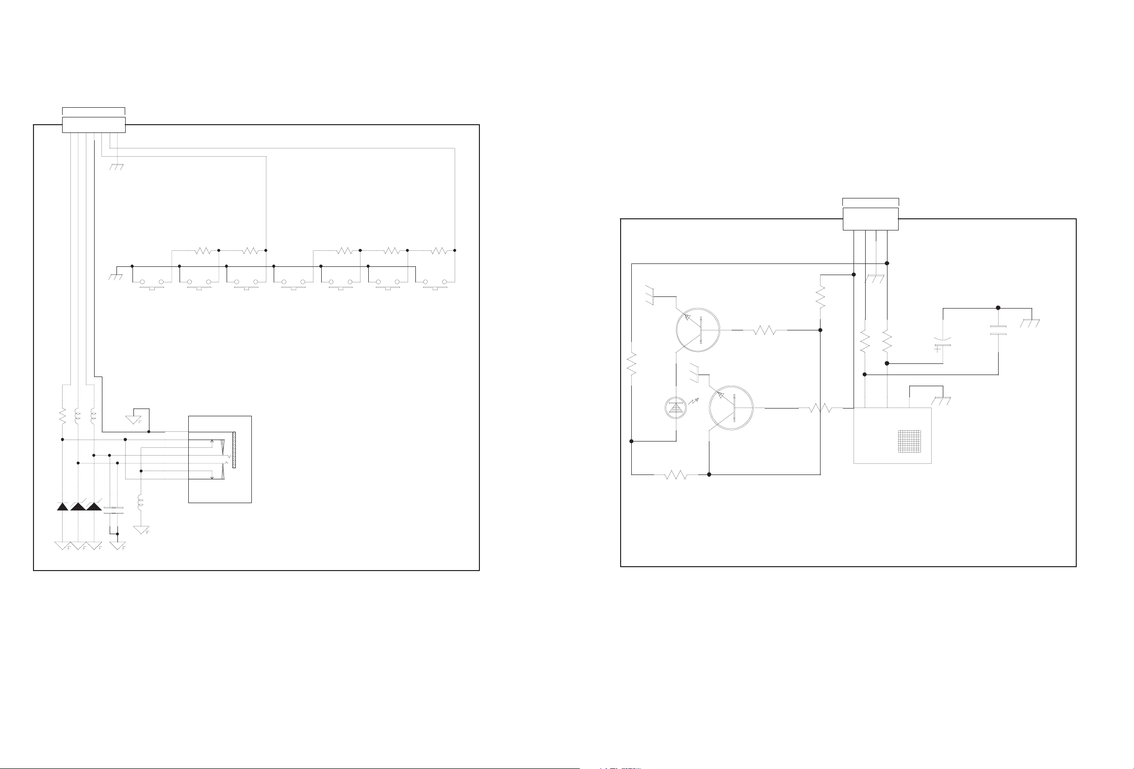
KEY PWB CIRCUIT DIAGRAM SHEET 5 LED PWB CIRCUIT DIAGRAM SHEET 6
MAIN PWB ASS'Y(1/4)
J210 (SHEET1)
1234567
J209-1
CON7P(A2004WV0-7P)
MAIN PWB ASS'Y(1/4)
J209 (SHEET1)
1
2
3
4
R293
D201 KDS114
33
L226
B-800
ZD229 KDZ5.6V
L227
B-800
ZD228 KDZ5.6V
C246 332
S201
R-K097110R
C247 332
R205
1.2K
R-K097110R
4
7
8
5
6
10
9
L240
B-501(3216)
R206
680
S202
S203
R-K097110R
MENUVIDEO
J207
PPJ- 35G-01
4
7
8
5
6
10
9
R
L
KEY PWB ASS'Y
QAL0730-001
J210-1
CON4P(A2004WR0-4P)
R203
10
CE201
47uF 16V
C237
102
S204
R-K097110R
R207
2.2K
S205
R-K097110R
R208
1.2K
S206
R-K097110R
R209
680
S207
R-K097110R
VOL PROPOWER
-+
-+
R204
2.7K
.
Q204
KTC3875S-Y
2
31
Q201
R250
0
R298
10K
R202
1K
KTC3875S-Y
R201
2
LD201
4.7K
IR
VC
G
LED
31
R297
EAR PHONE
10K
IR201
KSM-913TC5N
LED PWB ASS'Y
QAL0731-001
(No.YA315)2-17 2-18(No.YA315)
c00000001x_0000_1/1_0.0
Page 44

POWER PWB CIRCUIT DIAGRAM (1/3) SHEET 8
!
!
!
!
!
!
!
!
POWER PWB ASS'Y (1/3)
QAL0748-001
POWER CORD
2-20(No.YA315)(No.YA315)2-19
Page 45

POWER PWB CIRCUIT DIAGRAM (2/3) SHEET 9
POWER PWB ASS'Y (2/3)
!
QAL0748-001
(No.YA315)2-21 2-22(No.YA315)
Page 46

POWER PWB CIRCUIT DIAGRAM (3/3) SHEET 10
MAIN PWB ASS'Y (3/4)
J801 (SHEET3)
LCD PANEL UNIT
POWER PWB ASS'Y (3/3)
QAL0748-001
2-24(No.YA315)(No.YA315)2-23
Page 47

PATTERN DIAGRAMS
MAIN PWB PATTERN [SOLDER SIDE]
TOP
(No.YA315)2-25 2-26(No.YA315)
Page 48

MAIN PWB PATTERN [PARTS SIDE]
TOP
2-28(No.YA315)(No.YA315)2-27
Page 49

POWER PWB PATTERN [SOLDER SIDE]
TOP
POWER PWB PATTERN [PARTS SIDE]
TOP
(No.YA315)2-29 2-30(No.YA315)
Page 50

KEY PWB PATTERN [SOLDER SIDE]
TOP
KEY PWB PATTERN [PARTS SIDE]
LED PWB PATTERN [SOLDER SIDE]
TOP
LED PWB PATTERN [PARTS SIDE]
TOP
TOP
2-32(No.YA315)(No.YA315)2-31
Page 51

VOLTAGE CHARTS
<MAIN PWB>
MODE
PIN NO.
U101
1 3.9
2 4.4
3 3.9
4 4.4
5 4.4
6 0
7 4.8
8 3.9
9 4.4
10 3.9
11 4. 4
12 4.4
13 0
14 4.8
15 3.8
16 4.4
17 3.9
18 4.4
19 4.4
20 0
21 4.8
22 3.9
23 4.4
24 3.9
25 4.4
26 4.4
27 0
28 4.8
29 4.2
30 3.9
31 4.4
32 0
33 2.9
34 2.1
35 0
36 0
37 4.4
38 4.4
39 3.7
40 4.5
41 4.6
42 8.9
43 4.5
44 3.5
45 4.5
46 3.6
47 4.4
48 0
49 3.9
50 4.4
51 4.4
52 4.4
53 4.4
54 4.5
55 3.7
56 2.9
57 0
58 3.9
59 4.4
60 3.9
61 4.4
62 4.4
63 4.3
64 4.4
U301
1 1
2 2.6
3 2.3
4 12.3
5 1.6
6 1.6
7 1.6
8 1.7
9 0.8
10 1.7
11 0. 8
12 0
13 0.7
14 1.4
15 1.2
16 1.3
17 1.4
18 0
19 2.5
20 1.6
21 3.1
22 3.2
23 0.3
24 2.4
25 2.5
26 0
27 4.8
28 4.8
29 0
30 0
31 0.2
DC (V
)
MODE
DC (V
PIN NO.
32 0.2
U302
1 1.7
2 1.4
3 0.8
4 0.7
5 0
6 2.5
7 0
8 3.3
9 0
10 0
11 0
12 3.3
13 0
14 0
15 0
16 0
17 3.3
18 3.3
19 0
20 0
21 0.7
22 2.5
23 0
24 0
25 3.0
26 3.0
27 0
28 0
29 2.9
30 3.1
31 3.3
32 3.3
33 0
34 3.1
35 3.3
36 3.3
37 3.3
38 0
39 0
40 3.3
41 2.5
42 3.3
43 1.2
44 2.1
45 3.3
46 3.3
47 2.5
48 0
49 0
50 3.3
51 0
52 0.3
53 0.6
54 0
55 0
56 2.5
57 0.2
58 0.2
59 0.3
60 0
61 0
62 0
63 0
64 3.3
65 3.3
66 0
67 0
68 0
69 0.1
70 0
71 0.2
72 3.2
73 2.5
74 0
75 3.2
76 2.5
77 0.2
78 2.4
79 1
80 3.3
81 0.2
82 2.6
83 3.1
84 2.3
85 3.1
86 2.3
87 0
88 1.5
89 1.7
90 2.5
91 0
92 3.2
93 1.6
94 1.6
95 0
)
MODE
DC (V
PIN NO.
96 1.4
97 1.7
98 1.3
99 0.8
100 1.3
U303
1 0
2 0
3 0
4 0
5 3.2
6 3.3
7 0
8 4.8
U401
1 3.2
2 1.2
3 1.1
4 0
5 1.1
6 1.0
7 3.2
8 1.1
9 0
10 0
11 0. 8
12 0.7
13 3.1
14 0
15 2.9
16 2.9
17 2.9
18 2.6
19 1.6
20 0.5
21 0.1
22 0.1
23 0.4
24 1.1
25 3.2
26 0
27 1.1
28 1.1
29 1.1
30 1.1
31 0.5
32 0.5
33 0
34 3.2
35 1.4
36 0
37 0
38 3.2
39 0.6
40 0.9
41 0
42 0.8
43 0.9
44 3.2
45 0.8
46 0.9
47 0
48 0.8
49 0.8
50 0
U402
1 0
2 0.7
3 0.9
4 0.8
5 0.9
6 0
7 0
8 0
9 2.1
10 0
11 0
12 0
13 3.2
14 3.2
15 1.4
16 1.4
17 0
18 1.6
19 2.8
20 3.1
21 2.5
22 2.9
23 2.2
24 0
25 1.6
26 3.2
27 0
28 0.6
29 1.0
30 1.0
31 1.7
)
MODE
DC (V
PIN NO.
32 1.0
33 1.0
34 1.0
35 1.3
36 1.8
37 0.6
38 3.2
39 0
40 0.6
41 0.5
42 0.6
43 0.6
44 0.5
45 0.5
46 3.2
47 0
48 2.4
49 2.4
50 2.3
51 2.4
52 2.4
53 2.4
54 1.6
55 0
56 2.9
57 1.3
58 2.0
59 1.1
60 0
61 1.4
62 1.5
63 1.4
64 0.2
65 0.3
66 0.3
67 0.2
68 0.9
69 0
70 3.2
71 0
72 0
73 3.2
74 1.2
75 0.1
76 0.2
77 1.2
78 1.1
79 1.9
80 0.1
81 1.2
82 1.5
83 2.9
84 0
85 1.0
86 3.2
87 0
88 3.2
89 3.2
90 0
91 0
92 1.4
93 0.4
94 0.5
95 1.1
96 0
97 1.1
98 1.1
99 1.1
100 1.1
101 0.4
102 3.2
103 0
104 0.1
105 0.1
106 0.5
107 1.6
108 2.7
109 2.9
110 2.9
111 3. 0
112 0
113 3.2
114 0
115 0.5
116 0.9
117 1.1
118 1.2
119 3.2
120 0
121 1.0
122 1.3
123 1.0
124 1.2
125 0.9
126 0.8
127 0.9
128 3.2
)
MODE
DC (V
PIN NO.
U405
1 3.4
2 0
3 3.4
4 0
5 3.4
6 0
7 0
8 0
9 0
10 0
11 0
12 0
13 0
14 0
15 1.9
16 2.5
17 0
18 2.3
19 1.9
20 4.7
21 1.9
22 0
23 0
24 0
U501
1 0
2 0
3 3.2
4 3.2
5 3.2
6 3.2
7 0
8 3.2
9 0
10 3.2
11 0
12 3.2
13 0
14 2.1
15 0
16 0
17 3.2
18 0.2
19 2.1
20 0
21 0.3
22 0
23 0.6
24 0.5
25 0.2
26 0
27 0.1
28 0.1
29 0
30 0
31 0
32 0
33 0.3
34 3.2
35 0
36 2.1
37 2.2
38 0.2
39 0
40 0
41 0.4
42 0.4
43 0.4
44 0.4
45 0.7
46 0.5
47 0.8
48 2.4
49 1.7
50 0
51 2.8
52 2.2
53 1.6
54 1.3
55 1.0
56 1.0
57 1.0
58 1.7
59 0.9
60 0.9
61 0.4
62 0
63 1.7
64 0
65 0
66 3.2
67 0
68 2.2
69 0
70 3.3
71 3.3
)
MODE
DC (V
PIN NO.
72 0
73 0
74 0
75 3.3
76 2.3
77 3.1
78 1.6
79 1.7
80 0
81 0
82 0.2
83 0.3
84 0.2
85 0.4
86 2.5
87 0
88 0.3
89 0.4
90 0.3
91 0.3
92 0.6
93 0.4
94 0.4
95 0.3
96 0.4
97 0.3
98 0.4
99 0.3
100 0
101 0
102 2.5
103 0
104 1.8
105 2.5
106 1.4
107 1.3
108 0
109 3.2
110 1.2
111 1.4
112 0
113 2.5
114 0
115 2.0
116 2.4
117 0.2
118 1.0
119 0.2
120 1.0
121 1.1
122 1.0
123 1.0
124 1.4
125 2.5
126 0
127 0
128 0
129 0
130 0
131 1.7
132 0
133 0
134 0
135 0.2
136 0.2
137 0.3
138 0.7
139 2.4
140 0
141 0.4
142 0.2
143 0.3
144 0.2
145 0.3
146 0.3
147 0.3
148 0.2
149 0.3
150 0.3
151 0.2
152 0.3
153 0
154 2.4
155 0
156 1.7
157 0
158 3.1
159 0
160 1.0
161 1.3
162 3.2
163 0
164 1.2
165 1.2
166 1.1
167 1.3
168 1.1
MODE
)
PIN NO.
169 1.3
170 1.1
171 1.3
172 0
173 1.7
174 0
175 0
176 0
177 0
178 0
179 0
180 0
181 0
182 3.2
183 0
184 0
185 1.7
186 0
187 0
188 0
189 0
190 0
191 0
192 0
193 0
194 0
195 1.7
196 0
197 0
198 0
199 0
200 0.3
201 1.6
202 1.6
203 1.3
204 3.2
205 0
206 0
207 3.2
208 3.2
U502
1 3.2
2 0.4
3 3.2
4 0.3
5 0.3
6 0
7 0.4
8 0.4
9 3.2
10 0.3
11 0.4
12 0
13 0.3
14 0
15 3.2
16 0
17 2.3
18 1.9
19 2.5
20 0
21 0
22 1.4
23 1.3
24 0
25 0.3
26 0
27 0.3
28 0
29 3.2
30 0
31 0.4
32 0
33 0.4
34 0.3
35 3.2
36 0.4
37 0.3
38 0
39 0.4
40 0.3
41 3.2
42 0.6
43 3.1
44 0
45 0.3
46 0
47 0.2
48 0.3
49 3.2
50 0.2
51 0.4
52 0
53 0.3
54 0.3
55 3.2
56 0.3
DC (V
MODE
)
PIN NO.
57 0
58 0
59 0
60 1.0
61 1.0
62 1.0
63 0.9
64 1.2
65 0
66 0
67 2.5
68 1.3
69 0
70 0
71 0
72 0
73 0
74 0.3
75 3.2
76 0.3
77 0.4
78 0
79 0.4
80 0.7
81 3.2
82 0.2
83 0.4
84 0
85 0.3
86 0
U601
1 0
2 6.1
3 0
4 0
5 6.0
6 12.0
7 1.5
8 4.8
9 2.4
10 0
11 0
12 0
13 0
14 1.5
15 12.0
16 6.0
17 0
18 0
19 6.0
20 0
U602
1 0
2 2.8
3 2.0
4 2.2
5 2.3
6 4.6
7 0.2
8 0.2
9 0.2
10 0.2
11 4. 7
12 4.6
13 4.7
14 0
15 0
16 0
17 0.2
18 0
19 0
20 0
21 3.2
22 0
23 0
24 0
25 0
26 0
27 0
28 0
29 0
30 0.1
31 0
32 0
33 3.7
34 3.7
35 0
36 3.7
37 3.7
38 7.0
39 8.0
40 7.0
41 0
42 0
43 0
44 0
45 3.7
DC (V
MODE
)
PIN NO.
46 0
47 3.7
48 3.7
49 0
50 3.7
51 3.7
52 0
53 3.7
54 3.7
55 0
56 3.7
57 3.7
58 2.6
59 0
60 3.8
61 0
62 0
63 0
64 0
65 4.7
66 4.7
67 1.5
68 1.5
69 0
70 0
71 2.2
72 2.2
73 0
74 2.4
75 0
76 0
77 0
78 0
79 0
80 3.3
U603
1 0
2 0
3 0
4 0
5 0
6 0
7 0
8 0.3
U801
1 12.0
2 0
3 12.0
4 0
5 12.0
6 12.1
7 12.1
8 12.0
U802
1 4.8
2 0
3 4.8
4 0
5 4.7
6 4.7
7 4.7
8 4.7
Q101
1 12.0
2 0
3 8.9
Q102
E 4.1
C 1.8
B 2.3
Q103
E 0
C 4.4
B 0
Q104
E 0
C 0
B 0
Q105
E 4.8
C 1.2
B 1.8
Q106
E 4.1
C 4.8
B 4.7
Q108
E 0
C 0
B 0.6
Q202
E 3.6
C 8.9
B 4.6
DC (V
)
MODE
DC (V
PIN NO.
Q203
E 2.7
C 8.9
B 3.4
Q301
1 0
2 3.3
3 4.8
Q303
1 3.3
2 0
3 3.3
Q304
S 3.2
D 2.1
G 2.8
Q305
S 3.3
D 1.5
G 2.0
Q306
E 0
C 4.0
B 0
Q307
E 0
C 0
B 2.6
Q308
E 0
C 3.3
B -0.2
Q309
E 0.1
C 2.0
B 0
Q311
E 0
C 3.3
B 0
Q315
E 0.7
C 0
B 0
Q316
E 4.4
C 2.8
B 0
Q317
E 0
C 0
B 2.5
Q403
E 0.7
C 0
B 0
Q501
1 0
2 1.8
3 3.2
Q502
1 3.2
2 0
3 2.3
Q503
E 0
C 2.3
B 0.2
Q601
E 11.8
C -0.2
B 11.9
Q602
E 0
C 4.8
B 0
Q603
E 0
C 2.3
B 0
Q604
E 0.3
C 4.7
B 0
Q701
E 1.8
C 4.6
B 2.4
Q702
E 0.9
C 4.7
B 1.4
Q703
E 0
C 4.6
B 0.3
MODE
)
PIN NO.
Q801
1 8.0
2 0
3 12.0
Q802
E 0
C 0
B 0.7
Q804
1 4.8
2 3.4
3 0
4 3.2
5 0
Q805
E 0
C 4.1
B 0
Q806
E 0
C 0
B 0.5
H701
1 NC
2 NC
3 NC
4 NC
5 0
6 0
7 0
8 3.6
9 0
10 2.8
11 2. 1
12 4.6
13 0
14 5.7
15 2.4
16 2.0
17 1.5
<
LED BOARD SW PWB
MODE
PIN NO.
IR201
IR 3.1
VC 4.8
G 0
Q201
E 0
C 1.8
B 0
Q204
E 0
C 0
B 0.7+
<POWER PWB>
MODE
PIN NO.
U1
1 2.5
2 6.0
3 1.4
4 0
5 3.1
6 -0.1
7 5.0
8 14.1
U2
1 0
2 1.0
3 0.1
4 0
5 1.7
6 14.2
7 0
8 200.7
U3
1 13.6
2 12.0
3 0
4 13.6
U4
1 2.4
2 0
3 3.7
U5
1 0.5
2 1.5
3 0
4 0
5 2.1
6 14.1
7 0
8 1.2
DC (V
DC (V
DC (V
)
>
)
)
MODE
DC (V
PIN NO.
U6
1 2.5
2 0
3 21.3
U7
1 0
2 0
3 13.6
4 0.6
5 0.5
6 5.0
7 45.0
8 0
9 0
10 2.1
11 0. 6
12 0
13 0
14 0
Q1
E 0
C 0
B 0.6
Q2
E 5.2
C 14.1
B 5.0
Q3
E 5.2
C 0
B 5.0
Q4
S 0
D 202.6
G 4.5
Q5
S 0
D 386.1
G 1.2
Q6
E 14.2
C 14.1
B 13.5
Q7
E 14.2
C 15.4
B 14.9
Q8
S 13.6
D 5.0
G 4.8
Q9
E 0
C 13.6
B 0
Q10
E 1.9
C 14.1
B 2.0
Q11
E 1.9
C 0
B 2.1
Q12
S 0
D 386.3
G 1.6
Q13
E 5.0
C 5.0
B 4.1
Q14
E 0
C 14.9
B -1.5
WAVEFORMS
U402-19
MAIN PWB (3/4)
(SHEET3)
MAIN PWB (4/4)
(SHEET4)
2-34(No.YA315)(No.YA315)2-33
MAIN PWB (1/4)
(SHEET1)
U302-21
1.1 Vp-p
3.2 Vp-p
MAIN PWB (2/4)
(SHEET2)
U501-51
3.2 Vp-p
U101-41
3.1 Vp-p
H701-17
2.4 Vp-p
(H)
(H)
(H)
(H)
(H)
U302-29
U402-20
U501-53
U101-44
3.2 Vp-p
3.2 Vp-p
4.2 Vp-p
3.1 Vp-p
(H)
(V)
(0.5µs)
(H)
U302-30
U402-61
U501-77
U101-53
3.2 Vp-p
1.0 Vp-p
3.2 Vp-p
2.2 Vp-p
(H)
(V)
(H)
(V)
U302-52
1.4 Vp-p
U501-202
U101-63
4.9 Vp-p
1.4 Vp-p
(1µs)
(0.5µs)
(H)
U302-53
1.4 Vp-p
U501-203
4.0 Vp-p
(1µs)
(0.5µs)
U402-15
U602-71
3.0 Vp-p
2.6 Vp-p
(0.2µs)
(0.5µs)
U402-16
U602-72
(0.2µs)
4.1 Vp-p
(0.5µs)
3.4 Vp-p
)
Page 52

Victor Company of Japan, Limited
AV & MULTIMEDIA COMPANY DISPLAY CATEGORY 12, 3-chome, Moriya-cho, Kanagawa-ku, Yokohama-city, Kanagawa-prefecture, 221-8528, Japan
(No.YA315)
Printed in Japan
VPT
Page 53

LT-32A60BU
LT-32A60SU
LT-26A60BU
LT-26A60SU
ENGLISH
DEUTSCH
FRANÇAIS
NEDERLANDS
CASTELLANO
ITALIANO
PORTUGUÊS
WIDE LCD PANEL TV
16:9 LCD TV
TELEVISEUR A ECRAN LCD PANORAMIQUE
BREEDBEELD LCD TV
TELEVISOR CON PANEL LCD PANORÁMICO
TV LCD WIDESCREEN
TELEVISOR COM ECRÃ PANORÂMICO DE
CRISTAL LÍQUIDO
INSTRUCTIONS
BEDIENUNGSANLEITUNG
MANUEL D’INSTRUCTIONS
GEBRUIKSAANWIJZING
MANUAL DE INSTRUCCIONES
ISTRUZIONI
INSTRUÇÕES
Page 54

Thank you for buying this JVC LCD flat television.
To make sure you understand how to use your new TV, please read this manual thoroughly before you
begin. (“LCD” stands for Liquid Crystal Display.)
WARNING: TO PREVENT FIRE OR SHOCK HAZARD, DO NOT EXPOSE THIS
APPLIANCE TO RAIN OR MOISTURE.
WARNING
• The TV may fall causing injuries. Hold the bottom of the
stand with your hand and tilt the TV up and down.
• Do not allow children to hang from the TV, place their
elbows on the TV or lean against the TV. Doing so may
cause the TV to fall over and lead to injuries.
CAUTION
• The TV screen may be damaged if the TV is carried as
shown in the diagram below.
The TV should always be carried by two people.
ENGLISH
Pixel defects
LCDs use collections of fine points (“pixels”) to display images. While there is no problem with
more than 99.99% of these pixels, please understand that a very small number of pixels may not
light, or may light all the time.
Distance recommendations
Avoid improper installation and never position the unit
where good ventilation is impossible.
When installing this TV, distance recommendations
must be maintained between the set and the wall, as well
as inside a tightly enclosed area or piece of furniture.
Keep to the minimum distance guidelines shown for
safe operation.
150 mm 150 mm
200 mm 200 mm
50 mm
1
Page 55

Failure to take the following precautions may cause damage to the television
or remote control.
DO NOT block the TV’s ventilation openings or holes.
(If the ventilation openings or holes are blocked by a newspaper or cloth, etc., the heat may not be
able to get out.)
DO NOT place anything on top of the TV.
(such as cosmetics or medicines, flower vases, potted plants, cups, etc.)
DO NOT allow objects or liquid into the cabinet openings.
(If water or liquid is allowed to enter this equipment, fire or electric shock may be caused.)
DO NOT place any naked flame sources, such as lighted candles, on the TV.
DO NOT subject the TV to direct sunlight.
The surface of the TV screen is easily damaged. Be very careful with it when handling the TV.
Should the TV screen become soiled, wipe it with a soft dry cloth. Never rub it forcefully.
Never use any cleaner or detergent on it.
If there is a fault, unplug the unit and call a service technician. Do not attempt to repair it yourself
or remove the rear cover.
Cleaning the screen
The screen is coated with a special thin film to reduce reflection. If this film is damaged, uneven
colors, discoloration, scratches, and other problems that cannot be repaired may occur. Pay
attention to the following when handling the screen.
• Do not use glue or adhesive tape on the screen.
• Do not write on the screen.
• Do not allow the screen to come in contact with any hard objects.
• Do not allow condensation to form on the screen.
• Do not use alcohol, thinner, benzene or other solvents on the screen.
• Do not rub the screen hard.
CAUTION:
• Operate only from the power source specified (AC 110 – 240 V, 50/60 Hz) on the unit.
• Avoid damaging the AC plug and power cord.
• When you are not using this unit for a long period of time, it is recommended that you disconnect
the power cord from the main outlet.
2
Page 56

CONTENTS
Setting up your TV ...................................4
Installation.................................................. 4
Using the stand .......................................... 4
Removing the terminal cover ..................... 5
Connecting the aerial and video cassette
recorder (VCR) ....................................... 6
Connecting the power cord to the AC
outlet....................................................... 7
Putting the batteries into the remote
control..................................................... 7
Initial settings ............................................. 7
T-V LINK functions................................... 10
TV buttons and functions......................12
Turn the TV on from standby mode ......... 12
Choose a TV channel .............................. 12
Watch images from external devices....... 12
Adjust the volume .................................... 13
Using the Menu........................................ 13
Remote control buttons and
functions..............................................14
Turn the TV on or off from standby mode
Choose a TV channel and watch images
from external devices ........................... 15
Adjust the volume .................................... 16
Information function ................................. 16
ZOOM function......................................... 17
3D SOUND function ................................. 18
Return to TV channel instantly................. 18
Favourite channel function....................... 19
Operating a JVC brand VCR or DVD
player.................................................... 20
... 14
Teletext function ....................................21
Basic operation ........................................ 21
Using the List Mode ................................. 21
Hold.......................................................... 22
Sub-page ................................................. 22
Reveal...................................................... 22
Size .......................................................... 22
Index ........................................................ 23
Cancel...................................................... 23
Using the TV’s menu..............................24
Basic operation ........................................ 24
PICTURE menu ......................................25
PICTURE MODE...................................... 25
BRIGHT-1 ................................................ 25
CONTRAST ............................................. 25
BRIGHT-2 ................................................ 25
SHARP..................................................... 25
COLOUR.................................................. 25
HUE.......................................................... 25
COLOUR TEMP....................................... 25
FEATURES .............................................. 26
SOUND menu ......................................... 28
STEREO / I • II ......................................... 28
BASS........................................................ 28
TREBLE ................................................... 28
BALANCE ................................................ 28
3D SOUND............................................... 28
FEATURES menu................................... 29
SLEEP TIMER ......................................... 29
CHILD LOCK............................................ 29
APPEARANCE......................................... 30
BLUE BACK ............................................. 30
FAVOURITE SETTING ............................ 31
SET UP menu ......................................... 32
AUTO PROGRAM.................................... 32
EDIT/MANUAL ......................................... 32
LANGUAGE ............................................. 36
DECODER (EXT-2).................................. 36
EXT SETTING.......................................... 37
Displaying a computer screen.............. 40
Connecting to the computer ..................... 40
Watching images from a computer .......... 40
Table of signals for each type of
computer............................................... 40
Additional preparation .......................... 41
Connecting external equipment ...............41
CH/CC numbers ..................................... 44
Troubleshooting ....................................46
Specifications ........................................49
ENGLISH
3
Page 57

Setting up your TV
• When you install the TV on the wall, only use a JVC wall mounting unit (optional) which is
designed for this TV.
• Make sure that the TV is installed on the wall by a skilled installer.
Installation
Cautions for installation
• Install the TV in a corner on a wall or on the floor so as to keep cords out of the way.
• The TV will generate a slight amount of heat during operation. Ensure that sufficient space is
available around the TV to allow satisfactory cooling. See “Distance recommendations” on
page 1.
Using the stand
This TV comes with a table top stand already attached.
This stand can be used to adjust the direction of the TV screen to the left or right.
Rotate the TV to the left and right:
While holding the bottom of the stand with one
hand, use your other hand to hold the edge of
the panel and slowly adjust the direction of the
TV screen.
4
Page 58
Setting up your TV
Removing the terminal cover
There are connection terminals behind the cover on the rear of the TV. Remove the cover before
connecting an antenna or VCR.
Remove the cover by removing the hooks.
When replacing the cover, place the side of the
cover against the TV and insert the hooks.
• Leave the cover off if they do not fit properly. Do not force to replace the cover. Doing so may
cause damage to the connection cables and the cover.
ENGLISH
5
Page 59
Setting up your TV
Connecting the aerial and video cassette recorder (VCR)
• The connecting cables are not provided.
• For further details, refer to the manuals provided with the devices to be connected.
Caution
• Turn off all the equipment including the TV before connecting anything.
If you are connecting a VCR,
follow A → B → C in the diagram
opposite.
If you are not connecting a VCR,
follow 1.
without terminal covers
Aerial
To use the T-V LINK functions, you must
have a T-V LINK compatible VCR
connected by a SCART cable C to the EXT2 terminal on the TV. For details about T-V
LINK functions, see “T-V LINK functions”
on page 10.
• You can watch a video using the VCR
without doing C. For details, see your
VCR instruction manual.
• To connect more equipment, please see
“Connecting external equipment” on
page 41.
• If you connect a decoder to a T-V LINK
compatible VCR, set the DECODER
(EXT-2) function to ON. For details, see
“DECODER (EXT-2)” on page 36.
Otherwise, you will not be able to watch
scrambled channels.
21-pin
SCART
Cable
VCR
AV IN/OUT
Terminal
75-ohm
Coaxial
Cable
To Aerial
Input
To Aerial
Output
75-ohm
Coaxial
Cable
6
Page 60

Setting up your TV
s
Connecting the power cord to
the AC outlet
Insert the AC plug on the power cord from
the TV into an AC outlet.
Caution
• Operate only from the power source
specified (AC 110 – 240 V, 50/60 Hz)
on the unit.
• Remove the AC plug from the outlet to
completely disconnect the TV from the
power supply.
Putting the batteries into the
remote control
Use two AA/R6 dry cell batteries.
Insert the batteries from the - end, making
sure the + and - polarities are correct.
• Follow the warnings printed on the
batteries.
• Battery life is about six months to one
year, depending on how much you use the
remote control.
• The batteries we supply are only for
setting up and testing your TV, please
replace them as soon as you need to.
• If the remote control does not work
properly, replace the batteries.
Initial settings
When the TV is first turned on, it goes into
the initial settings mode, and you will see the
JVC logo. Follow the instructions on the
screen display to make the initial settings.
# button
VCR/TV/DVD
switch
Yellow button
Blue button
7 button
1 Make sure to set the VCR/TV/DVD
switch on the remote control to the
TV position
• You cannot turn the TV on when the
VCR/TV/DVD switch is set to the
VCR or DVD position.
2 Press the # button on the remote
control
The TV turns on from standby mode and
the JVC logo is displayed.
• Check that the AC plug on the power
cord from the TV is connected to AC
outlet.
ENGLISH
Remote control
sensor
Power lamp
7
Page 61

Setting up your TV
• If the JVC logo does not appear this is
because your TV has already been
turned on for the first time:
use the “LANGUAGE” and “AUTO
PROGRAM” functions to make the
initial settings. For details, see “SET
UP menu” on page 32.
3 Press the a button
The LANGUAGE menu appears.
> LANGUAGE
OK
D0002(E)-EN
4 Press the 6 buttons to choose
ENGLISH. Then press the a
button
The on-screen display will then be in
English.
The COUNTRY menu appears as a submenu of the AUTO PROGRAM function.
There are two COUNTRY menus.
Pressing the yellow button changes the
COUNTRY menu as follows:
> COUNTRY
OK
> COUNTRY
START
MORE
5 Press the 5 and 6 buttons to
choose the country where you are
6 Press the blue button to start the
AUTO PROGRAM function
The AUTO PROGRAM menu appears
and received TV channels are
automatically stored in the programme
numbers (PR).
>> AUTO PROGRAM
CH 28
14%
OK
D0004-EN
• To cancel the AUTO PROGRAM
function:
Press the b button.
After the TV channels have been
registered in the programme
numbers (PR), the EDIT menu
appears
> EDIT
D0038-EN
PR ID
AV
01
02
03
04
05
06
07
08
09
OK
MOVE
BBC1
CH/CC
CH
CH
CH
CH
CH
CH
CC
CC
CC
ID
INSERT
21
22
23
24
25
26
01
02
03
MANUAL
DELETE
• If you want to, you can now edit the
programme numbers (PR) using the
EDIT/MANUAL function. For details,
see “EDIT/MANUAL” on page 32.
• If you do not want to edit programme
numbers (PR), go to the next step.
OK
D0003-EN
START
MORE
8
Page 62

7 Press the a button to display the
T-V LINK menu
T-V LINK
DOWNLOAD TV RECORDING DEVICE
Setting up your TV
EXIT
OK
D0005
-EN
If you do not have a T-V LINK
compatible VCR connected:
Press the b button to exit the T-V LINK
menu.
The T-V LINK menu disappears.
If you have a T-V LINK compatible
VCR connected to the EXT-2
terminal:
Follow the operating procedure
“Downloading the data to VCR” on
page 10 to transmit the Programme
number (PR) data.
Now, the initial settings are complete,
and you can watch the TV
• If your TV can detect the TV channel
name from the TV channel broadcast
signal, the TV channel name is assigned
to the programme number (PR) to which
the TV channel has been set. However,
which TV channels are set to which
programme numbers (PR) will depend on
the area in which you live.
• If a TV channel you want to view is not
set to a programme number (PR), you can
set it using the MANUAL function. For
details, see “EDIT/MANUAL” on
page 32.
• The AUTO PROGRAM function does not
set the programme number PR 0 (AV) for
your video cassette recorder. You will
need to set this using the MANUAL
function.
ENGLISH
9
Page 63

Setting up your TV
Downloading the data to VCR
You can transmit to the latest Programme
numbers (PR) data to a VCR with the T-V
LINK function.
Caution
• This only works when a T-V LINK
compatible VCR is connected to the
EXT-2 terminal.
• This only works when the T-V LINK
menu is being displayed.
T-V LINK
DOWNLOAD TV RECORDING DEVICE
EXIT
OK
D0005
-EN
1 Turn on the VCR
2 Press the a button
The data transmission begins.
TV RECORDING DEVICE
TRANSFER. . . . .
D0037
-EN
The T-V LINK menu disappears once the
data transmission ends.
When the T-V LINK menu is
changed over to another menu:
The TV has finished its menu. This new
menu is operated from the VCR. See the
VCR instruction manual for what to do
next.
If “FEATURE NOT AVAILABLE”
appears at the T-V LINK menu:
Check the following three items. Then
press the 2 button to retry data
transmission.
• Has a T-V LINK compatible VCR
been connected to the EXT-2
terminal?
• Has the VCR power been turned on?
• Does the SCART cable that is
connected to the EXT-2 terminal to TV LINK compatible VCR have all its
proper connections?
T-V LINK functions
When you have a T-V LINK compatible
VCR connected to the EXT-2 Terminal on
the TV, it is easier to set up the VCR and to
view videos. T-V LINK uses the following
features:
To use T-V LINK functions:
A “T-V LINK compatible VCR” means a
JVC video cassette recorder with the T-V
LINK logo, or with one of the following
logos. However, these VCRs may support
some or all of the features described earlier.
For details, see your VCR instruction
manual.
“Q-LINK” (a trademark of Panasonic
Corporation)
“Data Logic” (a trademark of Metz
Corporation)
“Easy Link” (a trademark of Phillips
Corporation)
“Megalogic” (a trademark of Grundig
Corporation)
“SMARTLINK” (a trademark of Sony
Corporation).
10
Page 64

Setting up your TV
Pre-set download
The VCR will automatically download the
registered data on the TV channels from the
TV. This means you do not need to set up the
program channels on your VCR manually.
The preset download function automatically
begins when the initial setting is complete or
whenever you carry out the AUTO
PROGRAM or EDIT/MANUAL functions.
You can also carry out this function using
your VCR controls.
When “FEATURE NOT AVAILABLE” is
displayed:
If “FEATURE NOT AVAILABLE” is
displayed, the download was not performed
correctly. Before trying to download again,
check that:
• the VCR power is turned on
• the VCR is T-V LINK compatible
• the VCR is connected to the EXT-2
terminal
• the SCART cable is fully wired.
Direct Rec
“What You See Is What You Record”
You can easily record to VCR the images
that you are watching on the TV.
For details, read the manual for your VCR.
Use your VCR controls. “DEVICE IS
RECORDING” is displayed.
In the following situations, the VCR
will stop recording if the TV is turned
off, if the TV channel or input is
changed, or if the menu is displayed
on the TV:
• when recording images from an external
device connected to the TV (for example
a camcorder)
• when recording a TV channel after it has
been unscrambled on a decoder
• when recording a TV channel by using the
TV’s output because the VCR’s own
tuner cannot properly receive that
channel.
You cannot carry out Direct Rec using your
TV’s control.
Generally, the VCR cannot record a TV
channel that it cannot receive properly on its
own tuner, even if you can view that TV
channel on the TV. However, some VCRs
can record a TV channel by using the TV’s
output if that channel can be viewed on the
TV. For details, see your VCR instruction
manual.
When the VCR is not ready, the following
messages are displayed.
ERROR
MESSAGE
NO
RECORDING
NO
RECORDING
POSSIBLE
NO
RECORDING,
MEDIA
PROBLEM
NO
RECORDING,
DEVICE BUSY
Cause and
countermeasure
The VCR is not able to
record.
Check the VCR.
The TV input is set to EXT-4
or PC. Since the EXT-4
picture or PC picture cannot
be output to EXT-2, DIRECT
REC is not possible.
The recording device is not
ready to record. Check the
VCR tape.
The recording device cannot
record as it is recording or
playing. Check the VCR.
Refer to the VCR instruction manual.
ENGLISH
11
Page 65

TV buttons and functions
Turn the TV on from standby
mode
Press the A button or the P p
buttons to turn the TV on from
standby mode.
When the TV is turned on, the power lamp
lights blue.
To turn the TV off:
Press the A button again.
The power lamp goes off.
Caution
•The A button on the TV does not fully
isolate the TV from the AC supply. If
you are not going to use the TV for a
long period, be sure to disconnect the
AC plug from the AC socket.
Choose a TV channel
Press the P p buttons to choose a
programme number (PR) or an EXT
terminal
Refer to the pages in parentheses for details.
1 Remote control sensor
2 Power lamp (page 7)
3 TV/AV button (page 12)
4 MENU/OK button (pages 13, 24)
5 P p buttons (page 12)
6 r (Volume) q buttons (page 13)
7 A (Stand by) button (page 12)
8 Headphone jack (mini jack) (page 41)
12
Watch images from external
devices
Press the TV/AV button to choose an
EXT terminal
TV mode EXT modes
Last
Programme
number
or
or
Page 66

Adjust the volume
Press the r (Volume) q buttons
The volume level indicator appears.
TV buttons and functions
Using the Menu
Use the MENU/OK button
Refer to “Using the TV’s menu” (see
page 24) for details of using the menu.
ENGLISH
13
Page 67

Remote control buttons and functions
1 Muting button
2 Number buttons
3 Information button
1
2
3
4
5
6
7
8
~
!
@
#
$
%
^
4 c button
5 i button
6 b button
7 7 buttons
8 g (Text) button
9 p p buttons
0 VCR/DVD/Teletext control buttons
- p buttons
= d (Favourite) button
~ # (Standby) button
! VCR/TV/DVD switch
@ G button
# Colour buttons
$ H button
% a button
^ b button
& r (Volume) q buttons
Turn the TV on or off from
standby mode
14
9
0
=
&
Press the # (standby) button to turn
the TV on or off
When the TV is turned on, the power lamp
lights blue.
• The power can be turned on by pressing
the b button, p p buttons or Number
buttons.
To turn the TV on or off, set the VCR/TV/
DVD switch on the remote control to the
TV position and press the # button.
If the VCR/TV/DVD switch on the remote
control is set to a position other than TV,
the TV will not be turned on or off even if
the # button is pressed.
Page 68

Remote control buttons and functions
Choose a TV channel and
watch images from external
devices
Use the number buttons:
Enter the programme number (PR)
of the channel using the number
buttons.
Example:
•PR 6 → press 6
• PR 12 → press 1 and 2
Use the p p buttons:
Press the p p buttons to
choose the programme number
(PR) you want or an EXT terminal.
Use the AV button:
Press the AV button to choose an
EXT terminal.
TV mode EXT modes
Programme
numbers
PR 1 – PR 99
or
or
• Since this TV is designed to make full use
of the resolution of the original video
source, the motion may appear unnatural
when the video source is input with
progressive-scanning component signals.
If this happens, change the output setting
of the connected device to interlacescanning component signal output. See
the instructions that came with the device
for more information.
• The PC sound is the same as the EXT-3
sound.
To return to a TV channel:
Press the b button, the 6 buttons or the
number buttons.
To use the programme number PR 0
(AV):
When the TV and VCR are connected only
by the aerial cable, choosing the programme
number PR 0 (AV) allows you to view
images from the VCR. Set the VCR RF
channel to the programme number PR 0
(AV) manually. For details, see “EDIT/
MANUAL” on page 32.
Pressing the G button changes the choice as
follows:
TV mode EXT modes
Programme
numbers
PR 1 – PR 99
PR 0
EXT-1
EXT-2
or
ENGLISH
• You can choose a video input signal from
the S-VIDEO signal (Y/C signal) and
regular video signal (composite signal).
For details, see “S-IN (S-VIDEO input)”
on page 37.
• If you do not have a clear picture or no
colour appears, change the colour system
manually. See “COLOUR SYSTEM” on
page 26.
• If you choose an EXT terminal with no
input signal, the EXT terminal number
becomes fixed on the screen.
EXT-3
or
EXT-4
• The VCR sends its playback image along
the aerial cable as an RF (radio frequency)
signal.
• Also see your VCR instruction manual.
15
Page 69

Remote control buttons and functions
Adjust the volume
Press the r q buttons to adjust
the volume.
The volume level indicator appears and the
volume changes as you press the r q
buttons.
Muting the sound
Press the l (muting) button to
turn off the sound.
Pressing the l (muting) button again
restores the previous volume level.
Information function
You can see the channel number of the
programme you are watching, the current
time or the PR LIST.
From the PR LIST, you can choose a channel
or EXT terminal.
Press the h (Information) button to
display the information you want to
see.
Pressing the h (Information) button changes
the display as follows:
PR LIST
PR ID
AV
BBC1
01
02
03
04
05
06
07
OK
+8-8
D0011-EN
Channel number display:
The channel number and channel name
(when the channel name is registered) of the
programme you are watching or the EXT
terminal number is displayed.
Channel number display
12 : 00
No indication
Time display:
The current time of the teletext data is
displayed.
If the TV has not received a TV channel that
has teletext programmes since it was turned
on, the time display is blank. To view the
current time, choose a TV channel that has
teletext programmes.
• An incorrect current time is sometimes
displayed when watching videos.
PR LIST:
The programme number (PR) and EXT
terminal list is displayed.
Pressing the a button after choosing the
programme number (PR) or EXT terminal
with the 7 buttons will display the
chosen programme or EXT terminal.
• For programme numbers (PR) for which
the CHILD LOCK function is set, the n
(CHILD LOCK) mark is displayed. For
details see “CHILD LOCK” on page 29.
• For programme numbers (PR) which is
registered as a favourite channel, the d
(favourite) mark is displayed. For details
see “Favourite channel function” on
page 19.
16
Page 70

Remote control buttons and functions
ZOOM function
You can change the screen size according to
the picture aspect ratio. Choose the optimum
one from the following ZOOM modes.
• The ZOOM mode is fixed at FULL when
you are using the TV as a PC screen.
AUTO:
When a WSS (Wide Screen Signalling)
signal, which shows the aspect ratio of the
picture, is included in the broadcast signal or
the signal from an external device, the TV
automatically changes the ZOOM mode to
16:9 ZOOM mode or FULL mode according
to the WSS signal.
If a WSS signal is not included, the picture is
displayed according to the ZOOM mode set
with the 4:3 AUTO ASPECT function.
• For details of the 4:3 AUTO ASPECT
function, see “4:3 AUTO ASPECT” on
page 27.
• When the AUTO (WSS) mode does not
function correctly due to poor WSS signal
quality or when you want to change the
ZOOM mode, press the c button
and change to another ZOOM mode.
REGULAR:
Use to view a normal picture (4:3 aspect
ratio) as this is its original shape.
PANORAMIC:
This stretches the left and right sides of a
normal picture (4:3 aspect ratio) to fill the
screen, without making the picture appear
unnatural.
• The top and bottom of the picture are
slightly cut off.
14:9 ZOOM:
This zooms up the wide picture (14:9 aspect
ratio) to the upper and lower limits of the
screen.
16:9 ZOOM:
This zooms up the wide picture (16:9 aspect
ratio) to the full screen.
16:9 ZOOM SUBTITLE:
This zooms up the wide picture (16:9 aspect
ratio) with subtitles to the full screen.
FULL:
This uniformly stretches the left and right
sides of a normal picture (4:3 aspect ratio) to
fill the wide TV screen.
• For 16:9 aspect ratio pictures that have
been squeezed into a normal picture (4:3
aspect ratio), use the FULL mode to
restore the picture to its original shape.
Choose the ZOOM mode
1 Press the c button to display
the ZOOM menu
ZOOM
AUTO
REGULAR
PANORAMIC
14:9 ZOOM
16:9 ZOOM
16:9 ZOOM SUBTITLE
FULL
OK
D0009-EN
2 Press the 6 buttons to choose a
ZOOM mode. Then press the a
button
The picture expands and the chosen
ZOOM mode is displayed in about 5
seconds.
• The ZOOM mode may be
automatically changed by the control
signal from an external device. When
you want to return to the previous
ZOOM mode, choose the ZOOM
mode again.
ENGLISH
17
Page 71

Remote control buttons and functions
Adjusting the visible area of the
picture
If subtitles or the top (or bottom) of the
picture are cut off, you can adjust the visible
area of the picture manually.
1 Press the c button
The ZOOM menu appears.
2 Press the a button to display the
ZOOM mode indicator
The indicator appears.
16 : 9 ZOOM
D0010-EN
3 While it is displayed, press the 6
buttons to change the position of
the picture
• You cannot adjust the visible area in
REGULAR or FULL mode.
The visible area adjustment is saved even
after the TV channel is changed.
However, it is cancelled if the following
operations are performed.
• The power is turned off/on
• The ZOOM mode is changed
• g (Text) button is pressed
• The TV is switched between TV mode
and EXT mode
MONO:
Select the MONO mode, when you listen to
the mono sound.
You can enjoy the sound for a wider
audience similar to stereo sound.
OFF:
The 3D SOUND function switches off.
• You can choose the 3D SOUND mode
with the “SOUND menu” (see page 28).
Return to TV channel instantly
You can return to a TV channel instantly.
Press the b button
The TV returns to the TV mode and a TV
channel appears.
3D SOUND function
You can enjoy sounds with a wider
ambience.
• This function does not work for the sound
from headphones.
Press the i button to select one of
3D SOUND modes
ON:
When you listen to stereo sound, please
select ON mode.
You can enjoy sound similar to the
experience at the theatre.
18
Page 72

Remote control buttons and functions
Favourite channel function
You can register your favourite TV channels
(PR 1 – PR 99) in the number buttons 1 to 4.
After registering, the channel can be called
by pressing the d (favourite) button and a
number button 1 to 4.
Favourite channel registration
1 In the normal screen, choose a TV
channel (PR 1 – PR 99) that you
want to register
For details, refer to “Choose a TV channel
and watch images from external devices”
on page 15.
2 Press and hold the d (favourite)
button for three seconds or more
Then “SET 1-4?” appears on the screen.
3 Press one of the number buttons 1
to 4
The current channel is registered in the
pressed number button.
After “PROGRAMMED!” appears on the
screen, the favourite channel icon appears
at the top-right of the screen.
• If the channel you are trying to register
is already registered in one of the other
number buttons 1 to 4, “NOT
AVAILABLE” appears on the screen.
• Channels locked with the CHILD
LOCK function cannot be registered.
• If AUTO PROGRAM is performed,
the registered favourite channels are
reset.
Calling the favourite channel
1 In the normal screen, press the d
(favourite) button
Then “FAVORITE1-4?” appears.
2 Press one of the number buttons 1
to 4
The called favourite channel appears on
the screen.
• If a number button in which no
channel is registered is pressed, “NO
MEMORY” appears on the screen.
Setting the picture effect
When a favourite channel has been chosen
with the d (favourite) button and number
buttons 1 to 4, picture effect settings can be
memorised for each favourite channel by
setting the picture effects in the PICTURE
menu (see page 25).
The following items in the PICTURE menu
(see page 25) are memorised.
PICTURE MODE
BRIGHT-1
CONTRAST
BRIGHT-2
SHARP
COLOUR
HUE
COLOUR TEMP.
DIGITAL VNR
COLOUR SYSTEM
The last setting made for each item is
memorised.
ENGLISH
• When you want to delete a favourite
channel, delete the set channel and set
contents with FAVOURITE SETTING
(see page 31) in the FEATURES menu.
19
Page 73

Remote control buttons and functions
Operating a JVC brand VCR or
DVD player
These buttons will operate a JVC brand VCR
or DVD player. Pressing a button that looks
the same as the device’s original remote
control button has the same effect as the
original remote control.
1 Set the VCR/TV/DVD Switch to the
VCR or DVD position
VCR:
When you are operating the VCR, set the
switch to the VCR position.
• You can turn the VCR on or off with
the # (standby) button.
DVD:
When you are operating the DVD player,
set the switch to the DVD position.
• You can turn the DVD player on or off
with the # (standby) button.
• You can also press the H or
T button and display the
DVD disc menu screen, and then
operate by pressing the 7
buttons.
2 Press the VCR/DVD Control Button
to control your VCR or DVD player
• If your device is not made by JVC,
these buttons will not work.
• Even if your device is made by JVC,
some of these buttons may not work,
depending on the device you are using.
• You can use the p buttons to choose
a TV channel the VCR will receive, or
choose the chapter the DVD player
plays back.
• Some models of DVD player use the
p buttons for both operating the fast
forward/backward functions and for
choosing the chapter. In this case, the
253 buttons do not work.
You cannot turn the TV on or off when the
VCR/TV/DVD switch is set to the VCR or
DVD position.
When you turn the TV on or off, set the
VCR/TV/DVD switch to the TV position.
20
Page 74

Teletext function
VCR/TV/
DVD
4 Choose a teletext page by pressing
the p p buttons, number buttons
or colour buttons
To return to the TV mode:
Press the b button or g (Text) button.
Basic operation
1 Choose a TV channel with a teletext
broadcast
2 Set the VCR/TV/DVD switch to the
TV position
3 Press g (Text) button to display
the teletext
Pressing g (Text) button changes the
mode as follows:
TEXT
---
TEXT
---
TV mode Text mode
• If you have trouble receiving teletext
broadcasts, consult your local dealer or
the teletext station.
• The ZOOM function will not work in
the TV and text mode or Text mode.
• You cannot operate menus when
viewing a teletext programme.
• Language display depends on the
country which was set on the
COUNTRY menu. If characters on a
Teletext programme do not appear
properly, change the COUNTRY
setting to other country’s. To change
the COUNTRY setting, perform steps
1 and 2 of the “AUTO PROGRAM”
procedure on page 32 and then press
the a button.
Using the List Mode
You can store the numbers of your favourite
teletext pages in memory and call them up
quickly using the colour buttons.
To store the page numbers:
1 Press B button to go into the
List mode
The page numbers you have stored are
displayed at the bottom of the screen.
ENGLISH
21
Page 75
Teletext function
2 Press a colour button to choose a
position. Then press the number
buttons to enter the page number
3 Press and hold down the A (Store)
button
The four page numbers blink white to
show that they are stored in memory.
To call up a stored page:
1 Press the B button to enter the
List mode
2 Press a colour button having a
stored page
To exit the List mode:
Press the B button again.
Hold
You can hold a teletext page on the screen for
as long as you want, even while several other
teletext pages are being received.
Press the C (Hold) button
Hold indication
Sub-page
Some teletext pages include sub-pages that
are automatically displayed.
You can hold any sub-page, or view it at any
time.
1 Press the d (Favourite) button to
operate the Sub-page function
2 Press the Number buttons to enter
a sub-page number
Example:
• 3rd sub-page → press 0, 0, 0 and 3.
To cancel the Sub-page function:
Press the d (Favourite) button again.
Reveal
Some teletext pages include hidden text
(such as answers to a quiz).
You can display the hidden text.
Each time you press the E (Reveal)
button, text is hidden or revealed
Size
You can double the height of the teletext
display.
Press the F (Size) button
To cancel the Hold function:
Press C (Hold) button again.
22
Page 76

Index
You can return to the index page instantly.
Press the G (Index) button
Returns to page 100 or a previously specified
page.
Cancel
You can search for a teletext page while
watching TV.
1 Press the number button to enter a
page number, or press a colour
button
The TV searches for a teletext page.
2 Press H (Cancel) button
The TV programme appears. When the
TV finds the teletext page, its page
number appears in the upper left of the
screen.
3 Press H (Cancel) button to return
to a teletext page when the page
number is on the screen
• The TV mode cannot be resumed by
pressing the H (Cancel) button. To
return to the TV mode press b.
Teletext function
ENGLISH
23
Page 77

Using the TV’s menu
PICTURE
PICTURE
This TV has a number of functions you can
operate using menus. To use all your TV’s
functions, you need to understand the basic
menu operating techniques fully.
Buttons used to operate the menus
Basic operation
1 Press the H button to display
the menu bar
D0105-EN
2 Press the 5 buttons to choose
the menu you want to use and then
press the a button
Types of menu
PICTURE menu
D0106
Choose to set the screen
settings.
SOUND menu
D0107
Choose to set the sound settings.
FEATURES menu
D0108
Choose to set the sleep timer
and child lock settings.
SET UP menu
Choose to edit the channels or
D0109
set the display language
settings.
• The menu will disappear after about
one minute if no operation is
performed.
Operation with the buttons on the TV
You can also operate the menus using the
buttons on the front panel of the TV.
D1105-EN
Chosen
menu
3 Press the 6 buttons to choose
the item to be set, press the 5
buttons to set the item, and then
press the a button
If there are sub-menus, use the 7
buttons to operate them.
• Press the b button to return to
the previous menu.
• Press the b or H button to exit
from the menu.
• Some menu items may not be operated
or set depending on the TV status or
other menu item settings.
Menu items that cannot be operated or
set are displayed in grey in the menu
and cannot be chosen.
24
Chosen
menu name
TV/AV button
MENU/OK button
6 buttons
5 buttons
Page 78

PICTURE menu
PICTURE
PICTURE
STANDARD
PICTURE MODE
BRIGHT-1
CONTRAST
BRIGHT-2
SHARP
COLOUR
HUE
COLOUR TEMP.
FEATURES
OK
D0014
-EN
• While the PICTURE menu is displayed,
pressing the blue button will set the
BRIGHT-1, CONTRAST, BRIGHT-2,
SHARP, COLOUR, HUE settings to their
default settings.
• When watching the picture from EXT-1
to EXT-4 or the PC, picture effect settings
can be memorised for each external input
by setting the picture effects in the
PICTURE menu.
The following items in the PICTURE
menu are memorised.
PICTURE MODE
BRIGHT-1
CONTRAST
BRIGHT-2
SHARP
COLOUR
HUE
COLOUR TEMP.
DIGITAL VNR
COLOUR SYSTEM
The last setting made for each item is
memorised.
PICTURE MODE
You can choose one of three PICTURE
MODEs to adjust the picture settings
automatically.
BRIGHT:
Heightens contrast and sharpness.
STANDARD:
Standardizes picture adjustment.
SOFT:
Softens contrast and sharpness.
STANDARD
COOL
COOL
RESET
BRIGHT-1
You can adjust the back light.
2 : darker
3 : brighter
CONTRAST
You can adjust the picture contrast.
2 :lower
3 : higher
BRIGHT-2
You can adjust the picture brightness.
2 : darker
3 : brighter
SHARP
You can adjust the picture sharpness.
2 : softer
3 :sharper
COLOUR
You can adjust the picture colour.
2 : lighter
3 :deeper
HUE
You can adjust the picture tint.
2 : reddish
3 :greenish
• You can change the HUE setting (picture
hue) when the colour system is NTSC
3.58, or NTSC 4.43.
COLOUR TEMP.
You can select one of three COLOUR
TEMP. modes (three tones of white) to adjust
the white balance of the picture. Since white
is the colour which is used as a reference for
all the other colours, changing the COLOUR
TEMP. mode affects the appearance of all
the other colours on the screen.
ENGLISH
25
Page 79

PICTURE menu
COOL:
A bluish white. Using this mode when
watching bright pictures allows you to enjoy
a more vivid and bright picture.
NORMAL:
The normal white colour.
WARM:
A reddish white. Using this mode when
watching films allows you to enjoy colours
that are characteristic of films.
FEATURES
Choose FEATURES and press the a or 3
button to display the sub-menu.
> FEATURES
DIGITAL VNR
COLOUR SYSTEM
4:3 AUTO ASPECT
OK
D1015-EN
DIGITAL VNR
The DIGITAL VNR function cuts down the
amount of ‘noise’ (‘snow’ or interference) in
the original picture.
ON:
This function is turned on.
OFF:
This function is turned off.
AUTO(LOW)
COLOUR SYSTEM
The colour system is chosen automatically.
However, if the picture is not clear or no
colour appears, choose the colour system
manually.
1 Choose COLOUR SYSTEM. Then
press the a or 3 button
The sub-menu of the COLOUR SYSTEM
function appears.
>> COLOUR SYSTEM
AUTO
OK
D0016-EN
2 Press the 6 buttons to choose
the appropriate colour system.
Then press the a button
PAL:
PAL system
SECAM:
SECAM system
NTSC 3.58:
NTSC 3.58 MHz system
NTSC 4.43:
NTSC 4.43 MHz system
AUTO:
This function detects a colour system
from the input signal. You can only use
this when you are viewing a picture from
programme number PR 0 (AV), or an
EXT terminal.
• The AUTO function may not function
properly if you have poor signal quality.
If the picture is abnormal in the AUTO
function, choose another colour system
manually.
• When in the Programme numbers PR 0
(AV) to PR 99, you cannot choose NTSC
3.58 or NTSC 4.43.
• COLOUR SYSTEM cannot be chosen
when you are watching the PC picture.
26
Page 80

4:3 AUTO ASPECT
You can choose one of three ZOOM modes,
REGULAR, PANORAMIC or 14:9 ZOOM,
as the ZOOM mode for the normal picture
(4:3 aspect ratio).
1 Choose 4:3 AUTO ASPECT then
press the a button
>> 4:3 AUTO ASPECT
PANORAMIC
REGULAR
14:9 ZOOM
OK
D0017-EN
2 Press the 6 buttons to choose a
ZOOM mode
PICTURE menu
ENGLISH
27
Page 81

SOUND menu
SOUND
STEREO/
BASS
TREBLE
BALANCE
D0019
3D SOUND
OK
-EN
OFF
• When the headphones are connected, only
“STEREO / I • II” can be used.
STEREO / I • II
When you are viewing a bilingual broadcast
programme, you can choose the sound from
Bilingual I (Sub I) or Bilingual II (Sub II). If
you have poor reception on a stereo
broadcast, you can change from stereo to
mono sound so that you can hear the
broadcast more clearly and easily.
s: Stereo sound
v : mono sound
t : Bilingual I (sub I)
u : Bilingual II (sub II)
• The sound mode you can choose differs
depending on the TV programme.
• This function does not work in the EXT
modes.
BALANCE
You can adjust the volume balance between
the left and right speaker.
2 : turn the left speaker’s volume level up.
3 : turn the right speaker’s volume level up.
3D SOUND
You can enjoy Surround sound with a “live”
effect by using the 3D SOUND function.
• You can choose a 3D SOUND mode from
ON, MONO and OFF modes. For details,
see “3D SOUND function” on page 18.
• You can also operate the 3D SOUND
function with the i button. For details,
see “3D SOUND function” on page 18.
BASS
You can adjust the low tone of the sound.
2 : weaker
3 :strong
TREBLE
You can adjust the high tone of the sound.
2 : weaker
3 :strong
28
Page 82

FEATURES menu
FEATURES
SLEEP TIMER
CHILD LOCK
APPEARANCE
BLUE BACK
FAVOURITE SETTING
OK
D0023-EN
TYPE A
ON
SLEEP TIMER
You can set the TV to automatically turn off
after a set period of time.
1 Choose SLEEP TIMER. Then press
the a or 3 button
A Sub-menu of the SLEEP TIMER
function appears.
> SLEEP TIMER
0120
OFF
OK
D0024-EN
2 Press the 5 buttons to set the
period of time.
Then press the a button
You can set the period of time for up to
120 minutes (2 hours) in 10 minute steps.
• One minute before the SLEEP TIMER
function turns off the TV,
“GOODNIGHT!” appears.
• The SLEEP TIMER function cannot
be used to turn off the TV’s main
power.
• When the SLEEP TIMER function is
on, you can display the sub-menu of
the SLEEP TIMER function again to
confirm or change the remaining
period of time of the SLEEP TIMER
function. Press the a button to leave
the menu after confirming or changing
the remaining time.
To cancel the SLEEP TIMER
function:
Press the 2 button to set the period of
time to “OFF”.
CHILD LOCK
When there is a TV channel you do not want
your children to watch, you can use the
CHILD LOCK function to lock out the TV
channel. Even when a child chooses a
programme number (PR) for a locked TV
channel the screen will change to blue and
display n (CHILD LOCK) so the TV channel
cannot be viewed. Unless you enter a pre-set
ID number by a special operation, the lock
cannot be released and the child cannot view
the TV channel.
To set the CHILD LOCK function
1 Choose CHILD LOCK, then press
the 0 button
“SET ID NO.” (ID number setting screen)
appears.
>> SET ID NO.
040
0
OK
D0025-EN
2 Set the ID number to your liking
1 Press the 6 buttons to choose
a number.
2 Press the 5 buttons to move
the cursor.
3 Press the a button
The Sub-menu of CHILD LOCK appears.
>> CHILD LOCK
D0026-EN
PR ID
AV
01
02
03
04
05
06
07
08
09
OK
BBC1
CH/CC
CH
CH
CH
CH
CH
CH
CC
CC
CC
21
22
23
24
25
26
01
02
03
LOCK
ENGLISH
29
Page 83

FEATURES menu
4 Press the 6 buttons to choose a
TV channel
Every time you press the 6 buttons, the
Programme number (PR) changes, and the
picture of the TV channel registered in the
Programme number (PR) is displayed on
the screen.
5 Press the blue button and set the
CHILD LOCK function.
Then press the a button
n (CHILD LOCK) appears and the TV
channel is locked.
To reset the CHILD LOCK function:
Press the blue button again.
n (CHILD LOCK) disappears.
To disable easy resetting of the CHILD
LOCK function, the menu disappears if
you choose the CHILD LOCK function
and press the a button.
To view a locked TV channel
1 Choose a programme number (PR)
of a locked TV channel with the
number buttons or PR LIST
The screen changes to blue and the n
(CHILD LOCK) appears. You cannot
view the TV channel.
5
D0027-EN
2 Press the h (Information) button to
display “ID NO.” (ID No. input
screen)
5
ID NO. :
D0028-EN
3 Press the number buttons to enter
the ID number
The lock is temporarily released so you
can view the TV channel.
If you have forgotten the ID
number:
Perform step 1 of “To set the CHILD
LOCK function”. After confirming the ID
number, press the b button to exit the
menu.
• Even if you reset the lock temporarily,
it does not mean that the CHILD
LOCK function set for the TV channel
is cancelled. The next time anyone
tries to view the TV channel, it will be
locked again.
• When you want to cancel the CHILD
LOCK function, you must perform the
operation “To set the CHILD LOCK
function” again.
• To stop it being easy to choose the
programme number (PR) of a locked
TV channel, the programme number
(PR) has been set so that it cannot be
chosen with the 6 buttons or the
buttons of the TV.
• To stop it being easy to reset the lock,
“ID NO.” (ID No. input screen) is set
so that it cannot appear unless you
press the h (Information) button.
APPEARANCE
Press the 5 button and choose the format
in which the channel number is displayed
from two types: TYPE A and TYPE B.
BLUE BACK
You can set the TV to automatically change
to a blue screen and mute the sound if the
signal is weak or absent, or when there is no
input from an external device.
ON:
This function is turned on.
OFF:
This function is turned off.
30
Page 84

FAVOURITE SETTING
Chose when deleting the favourite channels
registered in the buttons 1 to 4.
1 Choose FAVOURITE SETTING,
then press the a or 3 button
The FAVOURITE SETTING menu
appears.
FAVOURITE SETTING
FEATURES menu
ENGLISH
1
2
3
4
OK
D0112-EN
PR
PR 01
PR
PR
07
01
01
RESET
2 Press the 6 buttons and chose
the favourite channel that you want
to delete
3 Press the blue button
The chosen favourite channel and set
contents are deleted.
• For details of the favourite channels, see
“Favourite channel function” on page 19.
31
Page 85

SET UP menu
SET UP
AUTO PROGRAM
EDIT/MANUAL
LANGUAGE
DECODER(EXT-2)
EXT SETTING
D0029
-EN
OK
OFF
AUTO PROGRAM
You can again perform the AUTO
PROGRAM function TV channel automatic
registration which was performed in the
“Initial settings” (page 7).
1 Choose AUTO PROGRAM, then
press the a or 3 button
The COUNTRY menu appears as a submenu of the AUTO PROGRAM function.
There are two COUNTRY menus.
Pressing the yellow button changes the
COUNTRY menu as follows:
> COUNTRY
OK
> COUNTRY
OK
D0003-EN
2 Press the 5 and 6 buttons to
choose the country where you are
START
MORE
START
MORE
EDIT/MANUAL
The EDIT/MANUAL functions are divided
into two types:
• editing the current programme numbers
(PR) (EDIT functions); and
• manually storing a TV channel you want
to view on a particular programme
number (PR) (MANUAL function).
Here are the details about these functions:
MOVE:
This function changes the programme
number (PR) of a TV channel.
ID:
This function registers a channel name (ID)
to a TV channel.
INSERT:
This function adds a new TV channel in the
current programme numbers (PR) list by
using the CH/CC number.
• You cannot use the INSERT function if
you do not know the channel number of a
TV channel. Use the MANUAL function
to register a TV channel in the programme
number (PR).
DELETE:
This function deletes a TV channel you do
not want to list.
MANUAL:
This function manually stores a new TV
channel in a programme number (PR).
Caution
• Using the MOVE, DELETE or INSERT
functions rewrites the current
programme numbers (PR) list.
Therefore, the programme numbers
(PR) of some of the TV channels will
change.
• Using the MANUAL function for a TV
channel for which the CHILD LOCK
function has been set cancels the
CHILD LOCK function for that channel.
3 Perform steps 5 and 6 of the “Initial
settings” (page 8)
32
Page 86

SET UP menu
• Using the MANUAL function for a TV
channel for which the DECODER
(EXT-2) function has been set to ON
returns the setting of the DECODER
(EXT-2) function for that channel to
OFF.
• When a TV channel has already been
registered in PR 99, using the INSERT
function deletes that TV channel.
Basic operation
1 Choose EDIT/MANUAL, then press
the a or 3 button
The EDIT menu appears.
> EDIT
PR ID
AV
01
02
03
04
05
06
07
08
09
OK
MOVE
D0038-EN
2 Follow the description for the
function you want to use
3 Press the a button to complete
the settings
The T-V LINK menu appears.
T-V LINK
DOWNLOAD TV RECORDING DEVICE
EXIT
OK
D0005
-EN
If you do not have a T-V LINK
compatible VCR connected:
Press the b button to exit the T-V LINK
menu.
The T-V LINK menu disappears.
If you have a T-V LINK compatible
VCR connected to the EXT-2 terminal:
Follow “Downloading the data to VCR” on
page 10 to transmit the programme number
(PR) data.
BBC1
CH/CC
CH
CH
CH
CH
CH
CH
CC
CC
CC
ID
INSERT
21
22
23
24
25
26
01
02
03
MANUAL
DELETE
• For programme number PR 0, “AV”
appears in the programme numbers (PR)
list.
• An EXT terminal number does not appear
in the programme numbers (PR) list.
MOVE
1 Press the 6 buttons to choose a
TV channel
2 Press the 3 button to start the
MOVE function
> EDIT
PR ID
AV
01
02
03
04
05
06
07
08
09
D0030-EN
CH/CC
21
CH
BBC1
OK
STORE
CH
CH
CH
CH
CH
CCCC02
22
23
24
25
26
03
CC
3 Press the 6 buttons to choose a
new programme number (PR)
To cancel the MOVE function:
Press the b button.
4 Press the 2 button to change the
programme number (PR) of a TV
channel to a new programme
number (PR)
DELETE
1 Press the 6 buttons to choose a
TV channel
2 Press the yellow button to delete
the TV channel
The TV channel is deleted from the
programme numbers (PR) list.
ENGLISH
01
33
Page 87

SET UP menu
ID
1 Press the 6 buttons to choose a
TV channel
2 Press the red button to start the ID
function
> EDIT
BBC1
BBC1
M
CH/CC
CH
CH
CH
CH
CH
CH
CC
CC
CC
CH/CC
CH
CH
CH
CH
CH
CH
CC
CC
CC
21
22
23
24
25
26
01
02
03
21
22
23
24
25
26
01
02
03
PR ID
AV
01
02
03
04
05
06
07
08
09
OK
D0031-EN
3 Press the 6 buttons to choose a
character
> EDIT
PR ID
AV
01
02
03
04
05
06
07
08
09
OK
D0032-EN
Before performing INSERT or
MANUAL operation
• If you register the TV channel (SECAML system) from a French station, be sure
to set the COUNTRY setting to
FRANCE. If the COUNTRY setting is
not set to FRANCE, perform steps 1 and 2
of the “AUTO PROGRAM” (page 32)
procedure and set the COUNTRY setting
to FRANCE before pressing the a
button.
• A CH/CC number unique to this TV and
corresponding to the Channel number of a
TV channel is required. Find the
corresponding CH/CC number from a
table “CH/CC numbers” on page 44 based
on the Channel number of the TV
channel.
• When the COUNTRY setting is not
FRANCE, use a two-digit CH/CC
number. When the COUNTRY setting is
FRANCE, use a three-digit CH/CC
number.
4 Press the 5 buttons to move the
cursor
5 Repeat steps 3 and 4 to complete
the channel name
6 Press the a button to give a
channel name (ID) to a TV channel
34
Page 88

SET UP menu
INSERT
1 Press the 6 buttons to choose a
programme number (PR) for which
you will register a new TV channel
2 Press the green button and start
the INSERT function
> EDIT
PR ID
AV
01
02
03
04
05
06
07
08
09
OK
D0034-EN
CH/CC
To cancel the INSERT function:
Press the b button.
3 Press the 6 buttons to choose
“CH” or “CC”, then enter the
remaining CH or CC number
When the COUNTRY setting is
FRANCE:
Choose “CH1”, “CH2”, “CC1” or “CC2”.
The TV shifts to registration mode.
When the registration is completed, the
picture of the TV channel appears on the
screen.
• The CH/CC number is a number given
to each broadcast frequency that
carries a TV channel. If the TV cannot
detect the TV channel corresponding
to the broadcast frequency indicated
by the CH/CC number, a “no-signal”
picture appears.
BBC1
CH/CC
CH
CH
CH
CH
CH
CH
CC
CCCC02
0 9
21
22
23
24
25
26
03
MANUAL
1 Press the 6 buttons to choose a
programme number (PR) for a new
TV channel
2 Press the blue button to activate
the MANUAL function
At the right side following the CH/CC
number, the SYSTEM (broadcasting
system) of the TV channel appears.
> MANUAL
BBC1
CH/CC
CH
CH
CH
CH
CH
CH
CC
CC
CC
SEARCH+
SEARCH-
21
22
23
24
25
26
(
)
01
B / G
02
03
FINE-
FINE+
PR ID
AV
01
02
03
04
05
06
07
08
09
OK
SYSTEM
D0035-EN
To cancel the MANUAL function:
Press the b button.
3 Press the 3 button to choose the
SYSTEM (broadcasting system) for
a TV channel you want to register
TV channel (SECAM-L system)
from a French station:
Set the SYSTEM to “L”. If it is set to one
other than “L”, you cannot receive the TV
channel of the SECAM-L system.
Other TV channels:
If you do not know the correct
broadcasting system, set the SYSTEM to
“B/G”. If “B/G” is not correct, you will
not hear the sound normally when the TV
detects a TV channel. In this case, retry to
set the SYSTEM correctly so that no
problem arises.
ENGLISH
35
Page 89

SET UP menu
4 Press the green or red button to
search for a TV channel
Scanning stops when the TV finds a TV
channel. Then the TV channel is
displayed.
5 Press the green or red button
repeatedly until the TV channel you
want appears
If the TV channel reception is poor:
Press the blue or yellow button to finetune the TV channel.
6 Press the a button and register
the TV channel to a Programme
number (PR)
The normal EDIT menu is resumed.
LANGUAGE
The LANGUAGE setting which was
performed in the “Initial settings” (page 7)
can be changed.
1 Choose LANGUAGE, then press
the a or 3 button
A sub-menu of the LANGUAGE function
appears.
> LANGUAGE
DECODER (EXT-2)
If you have a decoder connected to a T-V
LINK compatible VCR, which in turn is
connected to the EXT-2 terminal, use the
DECODER (EXT-2) function to unscramble
the scrambled TV channels.
1 Turn on the decoder power
2 Display the scrambled TV channel
on the TV
Even if the decoder is working, a
scrambled picture appears.
3 Display the SET UP menu and
choose DECODER (EXT-2)
SET UP
AUTO PROGRAM
EDIT/MANUAL
LANGUAGE
DECODER(EXT-2)
EXT SETTING
OK
D0029
-EN
4 Press the 5 buttons to choose
ON
An unscrambled picture appears.
To cancel the DECODER (EXT-2)
function:
Press the 5 buttons to choose OFF.
OFF
OK
D0002-EN
2 Press the 5 and 6 buttons to
choose a language. Then press the
a button
36
5 Press the a button to complete
the setting
The T-V LINK menu appears.
T-V LINK
DOWNLOAD TV RECORDING DEVICE
EXIT
OK
D0005
-EN
You can send the programme numbers
data to a VCR with the T-V LINK
function.
Page 90
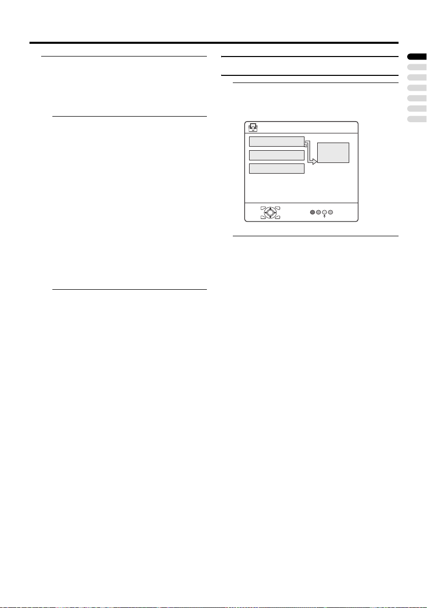
SET UP menu
6 Turn on the VCR, and then press
the a button to transmit the data
to VCR
The T-V LINK menu disappears once the
data transmission ends.
If the DECODER (EXT-2) function has
been set to “ON” but the TV channel
cannot be unscrambled, check the
following:
• Has the decoder been connected to the
VCR properly according to the VCR
and decoder instruction manuals?
• Has the decoder power been turned
on?
• Can the TV channel be unscrambled
with a decoder?
• Do you need to change the VCR
settings in order to connect the
decoder? Confirm that the VCR is set
properly by rechecking the VCR
instruction manual.
EXT SETTING
1 Choose EXT SETTING, then press
the a or 3 button
The EXT SETTING menu appears.
EXT SETTING
>
EXT-1
EXT-3
TV
OK
D0020-EN
2 Follow the instructions for the
function you want to use and
operate the function
S-IN:
You can enjoy the high-quality picture of
the S-VIDEO signal (Y/C signal).
ID LIST:
You can have a name for each of the
devices connected for each EXT terminal.
DUBBING:
You can choose a signal source to be
output from an EXT-2 terminal.
S-IN (S-VIDEO input)
You can connect a device (such as an S-VHS
VCR) to enjoy the high-quality picture of the
S-VIDEO signal (Y/C signal).
Preparation:
• First read the device’s instruction manual
and “Additional preparation” on page 41
to connect the device to the TV properly.
Second, follow the device’s instruction
manual to set the device so that it sends an
S-VIDEO signal (Y/C signal) to the TV.
• Do not set S-IN (S-VIDEO input) to an
EXT terminal connected to a device
which cannot output an S-VIDEO (Y/C
signal).
DUBBING
EXT-2
S-IN
ENGLISH
37
Page 91
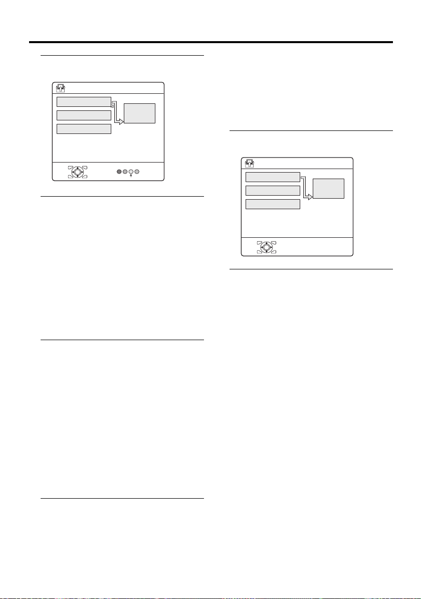
SET UP menu
1 Press the 5 or 6 buttons to
choose an EXT terminal
EXT SETTING
>
EXT-1
EXT-3
TV
OK
D0020-EN
DUBBING
EXT-2
S-IN
2 Press the yellow button and set the
S-IN (S-VIDEO input).
Then press the a button
An S-IN (S-VIDEO input) mark is
displayed. You can view an S-VIDEO
signal (Y/C signal) instead of the regular
video signal (composite signal).
To cancel the S-IN (S-VIDEO input)
setting:
Press the yellow button and turn off S-IN (SVIDEO input) mark. The regular video
signal (composite signal) pictures are
resumed.
• Setting S-IN (S-VIDEO input) changes
the head character from “E” to “S”. When
an EXT terminal receives a normal video
signal, “E1”, “E2” or “E3” appears on the
display. This changes to “S1”, “S2” or
“S3” when it receives an S-VIDEO
signal.
• Even a device which can output an S-VIDEO
signal (Y/C signal) may output a regular
video signal (composite signal) depending on
the device setting. If a picture cannot appear
because the S-IN (S-VIDEO input) setting
has been made, read the device instruction
manual carefully again to check for the
device settings.
DUBBING
You can choose a signal source to be output
from the EXT-2 terminal.
You can do this with the output signals of the
devices connected to other EXT terminals, or
with the picture and sound from a TV
channel you are currently viewing.
1 Press the 5 buttons to choose
the arrow from the menu
> EXT SETTING
EXT-1
EXT-3
TV
OK
D0022
-EN
2 Press the 6 buttons to choose an
EXT terminal or TV.
Then press the a button
The arrow in the menu represents a signal
flow. The left side of the arrow shows a
signal source output from the EXT-2
terminal.
EXT-1/EXT-3:
The output signal of the device connected
to an EXT terminal passes through the TV
and is output from the EXT-2 terminal.
TV:
The picture and sound of the TV channel
you are currently viewing are output from
the EXT-2 terminal.
DUBBING
EXT-2
38
Page 92

• During dubbing, you cannot turn off
the TV. Turning off the TV also turns
off the output from the EXT-2
terminal.
• When you choose an EXT terminal as
an output, you can view a TV
programme or a picture from the other
EXT terminal while dubbing the
picture from a device connected to the
EXT terminal onto a VCR connected
to the EXT-2 terminal.
• The RGB signals from TV games
cannot be output. Teletext programmes
cannot be output.
SET UP menu
ENGLISH
39
Page 93

Displaying a computer screen
This TV can be used as a computer screen.
Connecting to the computer
Use a D-SUB cable to connect the TV’s PC
IN terminal to the computer’s analogue RGB
output terminal.
If you want to listen to the sound from the
computer, use an audio cable to connect the
EXT-3 L/R terminal to the computer’s sound
output terminal.
When the sound from the computer is mono,
connect to the EXT-3 L terminal.
• Refer to the computer manual for a
detailed explanation of the connections at
the computer side.
• Ensure that the connectors are facing the
correct way when connecting.
• After connecting the D-SUB cable,
tighten the two screws to fix the connector
in place.
Watching images from a
computer
After starting the computer, press the
G or p p buttons to choose “PC”
“PC” is after EXT-4.
You can listen to the sound when the
sound from the computer is connected to
the EXT-3 L/R terminal.
• When the sound from the computer is
connected to EXT-3, by choosing
external input EXT-3 the sound from
the computer can be listened to, but the
images from the computer cannot be
seen.
Table of signals for each type
of computer
Resolution Vertical
640 × 480
(VGA)
1024 × 768
(XGA)
* Only the above formats are supported.
* Even with the above formats and at
60 Hz, some problems may be
experienced depending on the quality of
the synchronous signal. (Depending on
the quality, some pictures may not be
displayed properly.)
* Apple Macintosh
supported.
When a picture is not displayed
Check the computer’s refresh rate and set it
to 60 Hz. Refer to the computer’s instruction
manual.
Computers which cannot have their refresh
rate set to 60 Hz cannot be used with this
unit.
frequency
(Hz)
60.0 31.5
60.0 42.0
*
computers are not
Horizontal
frequency
(kHz)
40
* Apple Macintosh is a registered
trademark of Apple Computer, Inc.
Page 94

Additional preparation
Connecting external equipment
Connect the equipment to the TV, making
the correct rear panel and front panel
connections.
Before connecting anything:
• Read the manuals that came with the
equipment.
Depending on the equipment, the
connection method may be different from
the diagram. Also, the equipment settings
may need to change depending on the
connection method.
• Turn off all the equipment including the
TV.
• The “Specifications” on page 49 give the
details of the EXT terminals. If you are
connecting equipment not listed in the
following connection diagram, see the
table to choose the best EXT terminal.
• Connecting cables are not supplied.
Connecting the PC
For details, see “Connecting to the computer”
on page 40.
1 VCR (composite signal)
2 VCR (composite signal/S-VIDEO signal)
3 T-V LINK compatible VCR (composite
signal/S-VIDEO signal)
4 Decoder
5 DVD player (composite signal/S-VIDEO
signal)
6 DVD player (composite signal/RGB
signal)
7 DVD player (component video signals;
Y/Pb/Pr)
8 TV game (composite signal/RGB signal)
9 TV game (composite signal/S-VIDEO
signal)
0 Headphones
- Camcorder (composite signal/S-VIDEO
signal)
= SCART cable
~ Audio cable
! Video cable
@ S-VIDEO cable
# Component cable
ENGLISH
41
Page 95

Additional preparation
without terminal covers
42
Page 96

Additional preparation
Equipment which can output the
S-VIDEO signal (Y/C signal) such
as an S-VHS VCR
Connect the equipment to an EXT terminal
other than EXT-1/EXT-4.
You can choose between an S-VIDEO signal
(Y/C signal) and a regular video signal
(composite signal). For details of how to
operate the equipment, see “S-IN (S-VIDEO
input)” on page 37.
T-V LINK compatible VCR
Be sure to connect the T-V LINK compatible
VCR to the EXT-2 terminal. If not, the T-V
LINK function will not work properly.
• When connecting a T-V LINK compatible
VCR to the EXT-2 terminal, be sure to
connect the decoder to the VCR. If not,
the T-V LINK function may not work
properly.
• When you connect the decoder to the
VCR, after you have stored TV channels
in the programme numbers (PR) list, set
the DECODER (EXT-2) function for the
programme number (PR) to ON to
unscramble a scrambled TV channel. For
details, see “DECODER (EXT-2)” on
page 36.
Connecting headphones
Connect the headphones with a stereo minijack (3.5 mm diameter) to the headphone
socket at the TV rear panel.
• No sound comes from the TV speakers
when the headphones are connected.
Video or sound signal output from
the EXT-2 terminal
You can change over the output of the video/
sound signal from the EXT-2 terminal. This
is useful when you want to dub the video/
sound from another device onto the VCR
connected to the EXT-2 terminal. For details
on how to do this, see “DUBBING” on
page 38.
• The signals from EXT-4 and PC IN
terminal cannot be output from EXT-2.
TV output from the EXT-1 terminal
The video/sound signal of a TV channel you
are viewing is always output from the EXT-1
terminal.
• Changing over a programme number (PR)
also changes over the TV output from the
EXT-1 terminal.
• The video/sound signal from an EXT
terminal cannot be output.
• Teletext programmes cannot be output.
ENGLISH
43
Page 97

CH/CC numbers
When you want to use the INSERT function on page 35, find the CH/CC number corresponding to
the Channel number of the TV channel from this table.
CH Channe l
CH 02 / CH 202 E2, R1
CH 03 / CH 203 E3, ITALY A
CH 04 / CH 204 E4, ITALY B, R2
CH 05 / CH 205 E5, ITALY D, R6
CH 06 / CH 206 E6, ITALY E, R7
CH 07 / CH 207 E7, ITALY F, R8
CH 08 / CH 208 E8, R9
CH 09 / CH 209 E9, ITALY G
CH 10 / CH 210 E10, ITALY H, R10
CH 11 / CH 211
CH 12 / CH 212
CH 21 / CH 221 E21, R21
CH 22 / CH 222 E22, R22
CH 23 / CH 223 E23, R23
CH 24 / CH 224 E24, R24
CH 25 / CH 225 E25, R25
CH 26 / CH 226 E26, R26
CH 27 / CH 227 E27, R27
CH 28 / CH 228 E28, R28
CH 29 / CH 229 E29, R29
CH 30 / CH 230 E30, R30
CH 31 / CH 231 E31, R31
CH 32 / CH 232 E32, R32
CH 33 / CH 233 E33, R33
CH 34 / CH 234 E34, R34
CH 35 / CH 235 E35, R35
CH 36 / CH 236 E36, R36
CH 37 / CH 237 E37, R37
CH 38 / CH 238 E38, R38
CH 39 / CH 239 E39, R39
E11, ITALY H+1, R11
E12, ITALY H+2, R12
CH Channel
CH 40 / CH 240 E40, R40
CH 41 / CH 241 E41, R41
CH 42 / CH 242 E42, R42
CH 43 / CH 243 E43, R43
CH 44 / CH 244 E44, R44
CH 45 / CH 245 E45, R45
CH 46 / CH 246 E46, R46
CH 47 / CH 247 E47, R47
CH 48 / CH 248 E48, R48
CH 49 / CH 249 E49, R49
CH 50 / CH 250 E50, R50
CH 51 / CH 251 E51, R51
CH 52 / CH 252 E52, R52
CH 53 / CH 253 E53, R53
CH 54 / CH 254 E54, R54
CH 55 / CH 255 E55, R55
CH 56 / CH 256 E56, R56
CH 57 / CH 257 E57, R57
CH 58 / CH 258 E58, R58
CH 59 / CH 259 E59, R59
CH 60 / CH 260 E60, R60
CH 61 / CH 261 E61, R61
CH 62 / CH 262 E62, R62
CH 63 / CH 263 E63, R63
CH 64 / CH 264 E64, R64
CH 65 / CH 265 E65, R65
CH 66 / CH 266 E66, R66
CH 67 / CH 267 E67, R67
CH 68 / CH 268 E68, R68
CH 69 / CH 269 E69, R69
CC Channel
CC 01 / CC 201 S1
CC 02 / CC 202 S2
CC 03 / CC 203 S3
CC 04 / CC 204 S4
CC 05 / CC 205 S5
CC 06 / CC 206 S6
CC 07 / CC 207 S7
CC 08 / CC 208 S8
CC 09 / CC 209 S9
CC 10 / CC 210 S10
CC 11 / CC 211 S11
CC 12 / CC 212 S12
CC 13 / CC 213 S13
CC 14 / CC 214 S14
CC 15 / CC 215 S15
CC 16 / CC 216 S16
CC 17 / CC 217 S17
CC 18 / CC 218 S18
CC 19 / CC 219 S19
CC 20 / CC 220 S20
CC 21 / CC 221 S21
CC 22 / CC 222 S22
CC 23 / CC 223 S23
CC 24 / CC 224 S24
CC 25 / CC 225 S25
CC 26 / CC 226 S26
CC 27 / CC 227 S27
CC 28 / CC 228 S28
CC 29 / CC 229 S29
CC 30 / CC 230 S30
CC Channel
CC 31 / CC 231 S31
CC 32 / CC 232 S32
CC 33 / CC 233 S33
CC 34 / CC 234 S34
CC 35 / CC 235 S35
CC 36 / CC 236 S36
CC 37 / CC 237 S37
CC 38 / CC 238 S38
CC 39 / CC 239 S39
CC 40 / CC 240 S40
CC 41 / CC 241 S41
CC 75 / CC 275 X
CC 76 / CC 276 Y, R3
CC 77 / CC 277 Z, ITALY C, R4
CC 78 / CC 278 Z+1, R5
CC 79 / CC 279 Z+2
CH Channe l
CH 102 F2
CH 103 F3
CH 104 F4
CH 105 F5
CH 106 F6
CH 107 F7
CH 108 F8
CH 109 F9
CH 110 F10
CH 121 F21
CH 122 F22
CH 123 F23
CH 124 F24
CH 125 F25
CH 126 F26
CH 127 F27
CH 128 F28
CH 129 F29
CH 130 F30
CH 131 F31
CH 132 F32
CH 133 F33
CH 134 F34
CH 135 F35
CH 136 F36
CH 137 F37
CH 138 F38
CH 139 F39
CH 140 F40
44
CH Channel
CH 141 F41
CH 142 F42
CH 143 F43
CH 144 F44
CH 145 F45
CH 146 F46
CH 147 F47
CH 148 F48
CH 149 F49
CH 150 F50
CH 151 F51
CH 152 F52
CH 153 F53
CH 154 F54
CH 155 F55
CH 156 F56
CH 157 F57
CH 158 F58
CH 159 F59
CH 160 F60
CH 161 F61
CH 162 F62
CH 163 F63
CH 164 F64
CH 165 F65
CH 166 F66
CH 167 F67
CH 168 F68
CH 169 F69
CC Frequency (MHz)
CC 110 116 - 124
CC 111 124 - 132
CC 112 132 - 140
CC 113 140 - 148
CC 114 148 - 156
CC 115 156 - 164
CC 116 164 - 172
CC 123 220 - 228
CC 124 228 - 236
CC 125 236 - 244
CC 126 244 - 252
CC 127 252 - 260
CC 128 260 - 268
CC 129 268 - 276
CC 130 276 - 284
CC 131 284 - 292
CC 132 292 - 300
CC 133 300 - 306
CC 141 306 - 311
CC 142 311 - 319
CC 143 319 - 327
CC 144 327 - 335
CC 145 335 - 343
CC 146 343 - 351
CC 147 351 - 359
CC 148 359 - 367
CC 149 367 - 375
CC 150 375 - 383
CC 151 383 - 391
CC Frequency ( MHz)
CC 152 391 - 399
CC 153 399 - 407
CC 154 407 - 415
CC 155 415 - 423
CC 156 423 - 431
CC 157 431 - 439
CC 158 439 - 447
CC 159 447 - 455
CC 160 455 - 463
CC 161 463 - 469
Page 98

CH/CC numbers
• When two CH/CC numbers correspond to one Channel number, choose either one according to
the current COUNTRY setting. When the COUNTRY setting is other than FRANCE, choose a
two-digit CH/CC number. When the COUNTRY setting is FRANCE, choose a three-digit CH/
CC number.
• Find the CH/CC number (CC110 to CC161) corresponding to the TV channel (SECAM-L
system) from a French cable TV station, based on the broadcast frequency of the TV channel.
When you do not know the broadcast frequency, please contact the cable TV station.
• The CH/CC numbers of CH102-CH169 and CC110-CC161 correspond to the TV channels
being broadcast by a SECAM-L system. The other CH/CC numbers correspond to the TV
channels being broadcast by a method other than a SECAM-L system.
ENGLISH
45
Page 99

Troubleshooting
If a problem arises while you are using the TV, please read this troubleshooting guide carefully
before you ask to have the TV repaired. You may be able to fix it easily by yourself. For example,
if the mains plug is disconnected from the mains outlet, or the TV aerial has problems, you may
think there is a problem with the TV itself.
Important:
• This troubleshooting guide only covers problems whose causes are not easy to decide. If you
have a question when you are operating a function, read the page(s) for that function carefully,
not this troubleshooting guide.
• If you follow the advice in this troubleshooting guide without any success, unplug the mains
plug and ask for your TV to be repaired. Do not attempt to repair the TV by yourself or to
remove the rear cover of the TV.
If you cannot turn on the TV
• Is the mains plug connected to the mains
outlet?
• Is the power lamp lit? If not, press the A
button on the TV.
• Make sure you set the VCR/TV/DVD
switch to the TV position. You cannot
turn the TV on when the VCR/TV/DVD
switch is set to the VCR or DVD position.
If you cannot turn off the TV
• Make sure you set the VCR/TV/DVD
switch to the TV position. You cannot
turn the TV off when the VCR/TV/DVD
switch is set to the VCR or DVD position.
No picture or no sound
• Have you chosen a TV channel with very
poor reception? If so, the BLUE BACK
function will be activated: the entire
screen becomes blue, and the sound is
muted. If you still want to view the TV
channel, follow the description “BLUE
BACK” on page 30 to change the BLUE
BACK function setting to OFF.
• If the SYSTEM setting for a TV channel
is incorrect, it may prevent the sound
from being issued. Follow the description
“EDIT/MANUAL” on page 32 to use the
MANUAL function to try to change the
SYSTEM setting.
Poor picture
• If noise (snow) totally blocks out the
picture, there may be a problem with the
aerial or aerial cable. Check the following
to try to solve the problem:
– Have the TV and aerial been connected
properly?
– Has the aerial cable been damaged?
– Is the aerial pointing in the right
direction?
– Is the aerial itself faulty?
• If the TV or aerial suffers interference
from other equipment, stripes or noise
may appear in the picture. Move any
equipment such as an amplifier, personal
computer, or a hair drier, that can cause
interference away from your TV. Or try
moving the TV. If the aerial suffers
interference from a radio tower or highvoltage wire, please contact your local
dealer.
• If the TV suffers interference from signals
reflecting from mountains or buildings,
double-pictures (ghosting) will occur. Try
to change the aerial’s direction or replace
it with one with better directionality.
• Are your COLOUR SYSTEM settings
correct? Follow the description
“COLOUR SYSTEM” on page 26 to try
to solve the trouble.
• Have the COLOUR and BRIGHT settings
been adjusted properly? Follow the
description “BRIGHT-2” and
“COLOUR” on page 25 to try to adjust
them properly.
46
Page 100

Troubleshooting
• Videotaping teletext is not recommended
because it may not record correctly.
• When viewing images from commercially
available video software products, or
videos from videotapes which have been
recorded improperly, the top of the image
may be distorted. This is due to the
condition of the video signal. There is
nothing wrong with the TV.
• Since this TV is designed to make full use
of the resolution of the original video
source, the motion may appear unnatural
when the video source is input with
progressive-scanning component signals.
If this occurs, change the output setting of
the connected device to interlacescanning component signal output. See
the instructions that came with the device
for more information.
Poor sound
• Have you adjusted BASS or TREBLE
properly? If not, follow the description
“BASS” or “TREBLE” on page 28.
• When TV channel reception is poor, it can
be hard to hear stereo or bilingual sound.
In this case, follow the description
“STEREO / I • II” on page 28 to hear the
sound more easily by changing it to a
mono sound.
If the TV does not respond to the
remote control
• Have the batteries of the remote control
worn out? Follow the description “Putting
the batteries into the remote control” on
page 7 and replace them with new batteries.
• Have you attempted to use the remote
control from the sides or rear of the TV or
from more than seven metres away from the
TV? Use the remote control in front of your
TV or from less than seven metres away.
• When you are viewing a teletext
programme, you cannot operate the
menus. Press the b button to return to
the ordinary TV programme, and then try
operating the menus.
• If the TV suddenly stops responding,
disconnect the power cord of the TV from
the AC outlet. Connect them to the AC
outlet again to turn on the TV. If the TV
returns to a normal state, it is not a failure.
Other issues
• When the SLEEP TIMER function
operates, the TV is automatically turned
off. If the TV suddenly turns off, try to
press the # (standby) button to turn on
the TV once again. If the TV goes back to
normal, there is no problem.
• When the TV is receiving a wide-screen
signal (WSS) or a signal from an external
device affecting the screen size, the
ZOOM mode automatically changes.
When you want to resume the previous
ZOOM mode, press the c button
again.
• It takes a short period of time from the
time an operation such as changing
channels is performed until an image is
displayed. This is not a fault. This is the
time needed for the image to stabilize
before it can be displayed.
• The TV may make a crackling sound due
to a sudden change in temperature. The
picture or sound may be normal. If you
hear crackling sounds frequently while
you are viewing the TV, there may be
other causes. As a precaution, ask your
service technician to inspect it.
ENGLISH
47
 Loading...