

Page 1
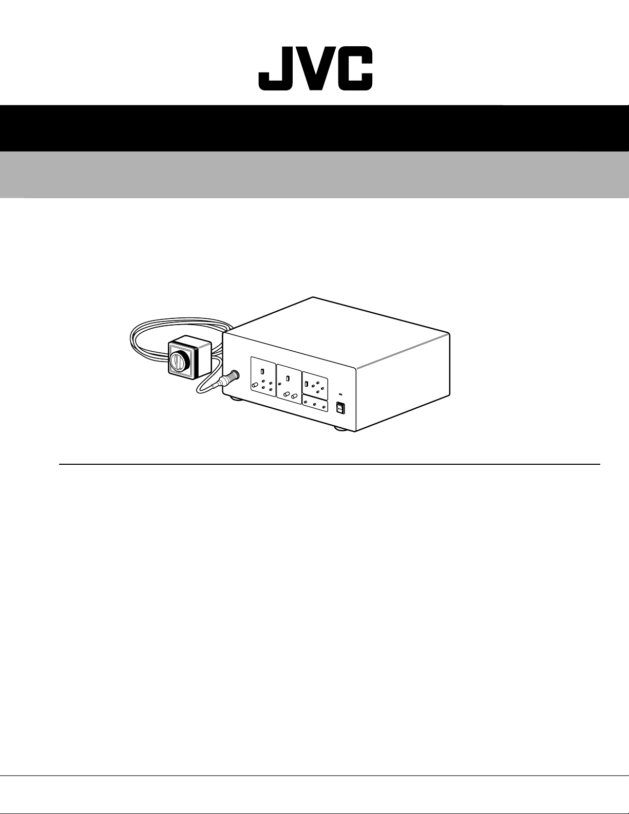
SERVICE MANUAL
MICRO HD CAMERA
DZ-VCA3U
SPECIFICATIONS
Camera head section
L Image sensing device : 1/3-inch PS-CCD (350,000 pixels)
L Shooting system : 3-CCD system
L Color separation optical system : 1/3-inch F1.4 3-color separation prism
L Number of effective pixels : 659 (horizontal) x 494 (vertical), 330,000 pixels approximately
L Camera output : 19 pins
L Lens mount : Standard C mount ( flange back: 17.526 mm in air)
L Dimensions : Camera head; 44 (W) x 51.4 (H) x 57.7 (D) mm (1-6/8” x 2-1/16” x 2-2/8”) (not including
L Weight : Camera head; 100 g (0.22 lbs.)
L Classification : Type CF applied part
Camera control unit section
L Number of scanning lines : 1125 (980 effective)
L Scanning system : 2:1 interlace (HD output, NTSC output)
L Scanning frequency : HD OUT 33.71625kHz (horizontal), 59.94 Hz (vertical)
L Aspect ratio : 4:3
L Horizontal resolution (center) : 750 TV lines TYP. (HD Y output, SXGA output)
L Vertical resolution (center) : 700 TV lines TYP. (HD Y output, SXGA output)
L S/N : 52dB
L Sensitivity : F6.8, 2000 lx
L Minimum subject illuminance : 5 lx
L Sync system : Internal sync/external sync
L External sync signal input : Composite sync signal of ±0.3 Vp-p, 75 ohms, BNC x 1 (ITU-R Rec.BT .709-3 HDTV standard
L Color bar : Full color bar
L Contour correction : Horizontal dual-edged (7-step variable)
L Electronic shutter speed : 1/60 s (normal), 1/100 s, 1/175 s, 1/250 s, 1/375 s, 1/500 s, 1/1000 s, 1/2000 s,1/4000s,
protrusion and camera cable etc)
Progressive (SXGA output)
SXGA OUT 67.4325kHz(horizontal), 59.94 Hz (vertical)
NTSC OUT 15.73425kHz(horizontal), 59.94 Hz (vertical)
compliant)
Vertical dual-edged (7-step variable)
1/10000s
L Video output
• SXGA signal : R/G/B 0.7 Vp-p, 75 ohms HD/VD TTL D-Sub mini 15 pin
• HD signal : Y 1 Vp-p Pb/Pr 0.7 Vp-p 75 ohms BNC x 3
• NTSC signal : VBS 1 Vp-p 75 ohms BNC Y/C 1 Vp-p 75 ohms S terminal
• DV signal : IEEE1394 6 pins
L Camera input : 19 pins
L Date indication : Menu system 1) Year, month, day 2) Day , month, year 3) Month, day, year
L Time indication : Menu system, hour : minute: second
L Rating : 120V AC 60Hz, 0.7A
L Classification of insulation : Class I
L Operating environment :+5°C to +35°C (41°F to 95°F), 35 – 75%
L Storage environment : -20°C to +50°C (-4°F to 102°F), 35 – 80%
L Dimensions : 280 (W) x 140 (H) x 300 (D) mm
L Weight : 5.5 kg (12.1 lbs.)
L Accessories : Power cord x 1
(11-3/16” x 5-9/16” x 11-13/16”) (excluding the protrusion and switches etc)
Instruction manual x 1
Warranty card x 1
This service manual is printed on 100% recycled paper.
COPYRIGHT © 2002 VICTOR COMPANY OF JAPAN, LTD
DZ-VCA3U S14H42
No.86711
2002/12
Page 2

TABLE OF CONTENTS
Section Title Page Section Title Page
Important Safety Precautions
INSTRUCTIONS
1. PRECAUTIONS OF SERVICING
1.1
BEFORE DISASSEMBLING AND REASSEMBLING
1.1.1 Precautions ........................................................... 1-1
1.1.2 Disassembly of optical block assembly..................1-1
1.2 PREPARATION AND PRELIMINARY CHECK
REQUIRED FOR ADJUSTMENT ............................. 1-1
1.2.1 Before adjustment ................................................. 1-1
1.2.2
Tools and jigs required for repair and adjustment
1.3 Standard setup............................................................ 1-2
1.4 How to set the “ADJUSTNENT MODE” ...................... 1-2
1.5 How to set the “DEBUG MODE” ................................. 1-2
1.6 How to do “ALL RESET” ............................................. 1-2
Warnings for accident prevention in handking battery .......1-3
1.7 SERVICE CAUTIONS................................................. 1-4
1.7.1 Precautions ........................................................... 1-4
1.7.2 How to read the disassembly and assembly......... 1-4
1.7.3 Connection of the wires ........................................ 1-4
1.7.4 Disassembly procedure .........................................1-5
1.8 WIRING AND BOARD LAYOUT ..................................1-8
2. ELECTRICAL ADJUSTMENT
2.1 INITIAL SETTING ....................................................... 2-1
2.1.1 Functions and initial settings of
internal switches of boards ................................. 2-1
2.1.2 Adjustment procedure ........................................... 2-2
2.2 MTP BOARD ADJUSTMENT...................................... 2-3
2.2.1 Adjustment part(s) location guide...........................2-3
2.2.2 Input voltage check ............................................... 2-3
2.2.3 output voltage level ................................................2-3
2.2.4 output voltage check(1)..........................................2-3
2.2.5 output voltage check(2)..........................................2-3
2.2.6 output voltage check(3)..........................................2-3
2.3 MICOM BOARD ADJUSTMENT..................................2-4
2.3.1 Adjustment part(s) location guide...........................2-4
2.3.2 Main clock level......................................................2-4
2.3.3 GENLOCK output level ..........................................2-4
2.4 DSP BOARD ADJUSTMENT.......................................2-5
2.4.1 Adjustment part(s) location guide...........................2-5
2.4.2 HD OUT .................................................................2-5
2.4.2.1 Y signal ratio level ............................................. 2-5
2.4.2.2 Y signal level ..................................................... 2-5
2.4.2.3 Pr signal raio level.............................................2-6
2.4.2.4 Pr signal level....................................................2-6
2.4.2.5 Pb signal ratio level ........................................... 2-6
2.4.2.6 Pb signal level ................................................... 2-6
2.4.3 SXGA OUT.............................................................2-7
2.4.3.1 G gain level .......................................................2-7
2.4.3.2 B gain level .......................................................2-7
2.4.3.3 R gain level .......................................................2-7
2.5 NTSC BOARD ADJUSTMENT ....................................2-8
2.5.1 Adjustment part(s) locatio guide.............................2-8
2.5.2 INPUT SIGNAL ......................................................2-8
2.5.2.1 G gain level .......................................................2-8
2.5.2.2 B gain level .......................................................2-8
2.5.2.3 R gain level .......................................................2-9
2.5.3 OUTPUT SIGNAL ..................................................2-9
2.5.3.1 Video level (1) ...................................................2-9
2.5.3.2 Video level (2) ...................................................2-9
2.5.3.3 Y level ...............................................................2-9
2.5.3.4 Color level .......................................................2-10
2.5.3.5 DV signal check .............................................. 2-10
2.6 AD BOARD ASJUSTMENT ........................................ 2-11
2.6.1 Adjustment part(s) location guide.........................2-11
2.6.2 A/D AND AUTO GAIN .......................................... 2-11
2.6.2.1 A/D gain level .................................................. 2-11
2.6.2.2 AUTO gain level .............................................. 2-11
2.6.2.3 Color gain........................................................2-12
2.6.2.4 Color gain for tint adjustment ..........................2-12
2.6.2.5 White defect ....................................................2-12
... 1-1
... 1-1
3. INSTALLATION MANUAL
1. Precautions ....................................................................3-1
2. Connection of system components ................................ 3-1
3. Connection of each unit to the power supply unit .......... 3-1
4. Check of grounding (AA-V31U) .....................................3-2
5. Check of operation ......................................................... 3-2
6. Liaison slip of customer data .........................................3-2
7. Sterilization ....................................................................3-2
8. Report of complaints dealt with ...................................... 3-2
4. CHARTS AND DIAGRAMS
4.1 BOARD INTERCONNECTIONS ................................. 4-3
4.2 MTP SCHEMATIC DIAGRAM...................................... 4-5
4.3 AD IO SCHEMATIC DIAGRAM ....................................4-7
4.4 ANALOG SCHEMATIC DIAGRAM............................... 4-9
4.5 ADC SCHEMATIC DIAGRAM .................................... 4-11
4.6 SSG1 SCHEMATIC DIAGRAM..................................4-13
4.7 F MEN SCHEMATIC DIAGRAM ................................ 4-15
4.8 FLASH SCHEMATIC DIAGRAM................................4-17
4.9 AMDP IO SCHEMATIC DIAGRAM ............................4-19
4.10 AMDP G SCHEMATIC DIAGRAM ...........................4-21
4.11 AMDP B SCHEMATIC DIAGRAM ............................4-23
4.12 AMDP R SCHEMATIC DIAGRAM............................ 4-25
4.13 AMDP FM SCHEMATIC DIAGRAM ......................... 4-27
4.14 AMDP 01 SCHEMATIC DIAGRAM ..........................4-29
4.15 DSP-1 SCHEMATIC DIAGRAM...............................4-31
4.16 DSP-2 SCHEMATIC DIAGRAM...............................4-33
4.17 DSP-3 SCHEMATIC DIAGRAM...............................4-35
4.18 MICOM SCHEMATIC DIAGRAM.............................4-37
4.19 MICOM2 SCHEMATIC DIAGRAM...........................4-39
4.20 MICOM3 SCHEMATIC DIAGRAM...........................4-41
4.21 MICOM4 SCHEMATIC DIAGRAM...........................4-43
4.22 NTSC-2 SCHEMATIC DIAGRAM ............................4-45
4.23 NTSC-1 SCHEMATIC DIAGRAM ............................4-47
4.24 NTSC-5 SCHEMATIC DIAGRAM ............................4-48
4.25 NTSC-3 SCHEMATIC DIAGRAM ............................4-49
4.26 NTSC-4 SCHEMATIC DIAGRAM ............................4-51
4.27 NTSC-6 SCHEMATIC DIAGRAM ............................4-53
4.28 DV-1 SCHEMATIC DIAGRAM .................................4-55
4.29 DV-2 SCHEMATIC DIAGRAM .................................4-57
4.30 DV-3 SCHEMATIC DIAGRAM .................................4-59
4.31 FRT/LED SCHEMATIC DIAGRAM ..........................4-61
4.32 MTP CIRCUIT BOARD ............................................ 4-63
4.33 AD CIRCUIT BOARD...............................................4-67
4.34 AMDP CIRCUIT BOARD..........................................4-71
4.35 DSP CIRCUIT BOARD ............................................4-75
4.36 MICOM CIRCUIT BOARD .......................................4-79
4.37 NTSC CIRCUIT BOARD ..........................................4-83
4.38 DV CIRCUIT BOARD...............................................4-87
4.39 FRT & LED CIRCUIT BOARDS ............................... 4-89
4.40 CAMERA SYSTEM BLOCK DIAGRAM ...................4-91
5. PARTS LIST
5.1 PACKING AND ACCESSORY ASSEMBLY<M1> ....... 5-1
5.2 CAMERA CONTROL UNIT ASSEMBLY<M3> ............ 5-2
5.3 ELECTRICAL PARTS LIST......................................... 5-5
MTP BOARD ASSEMBLY<01>........................................ 5-5
AD BOARD ASSEMBLY<02> ..........................................5-6
AMDP BOARD ASSEMBLY<03> ................................... 5-11
DSP BOARD ASSEMBLY<04> ......................................5-15
MICOM BOARD ASSEMBLY<05> .................................5-18
NTSC BOARD ASSEMBLY<06> ...................................5-21
DV BOARD ASSEMBLY<07> ........................................5-25
FRT BOARD ASSEMBLY<08> ......................................5-26
LED BOARD ASSEMBLY<09> ......................................5-27
1
Page 3
Important Safety Precautions
Connector
Metal sleeve
Prior to shipment from the factory, JVC products are strictly inspected to conform with the recognized product safety and electrical codes
of the countries in which they are to be sold. However, in order to maintain such compliance, it is equally important to implement the
following precautions when a set is being serviced.
v
Precautions during Servicing
1. Locations requiring special caution are denoted by labels and
inscriptions on the cabinet, chassis and certain parts of the
product. When performing service, be sure to read and comply with these and other cautionary notices appearing in the
operation and service manuals.
2. Parts identified by the
such as fuses and circuit protectors are critical for safety.
Replace only with specified part numbers.
3. Fuse replacement caution notice.
Caution for continued protection against fire hazard.
Replace only with same type and rated fuse(s) as specified.
4. Use specified internal wiring. Note especially:
1) Wires covered with PVC tubing
2) Double insulated wires
3) High voltage leads
5. Use specified insulating materials for hazardous live parts.
Note especially:
1) Insulation Tape 3) Spacers 5) Barrier
2) PVC tubing 4) Insulation sheets for transistors
6. When replacing AC primary side components (transformers,
power cords, noise blocking capacitors, etc.) wrap ends of
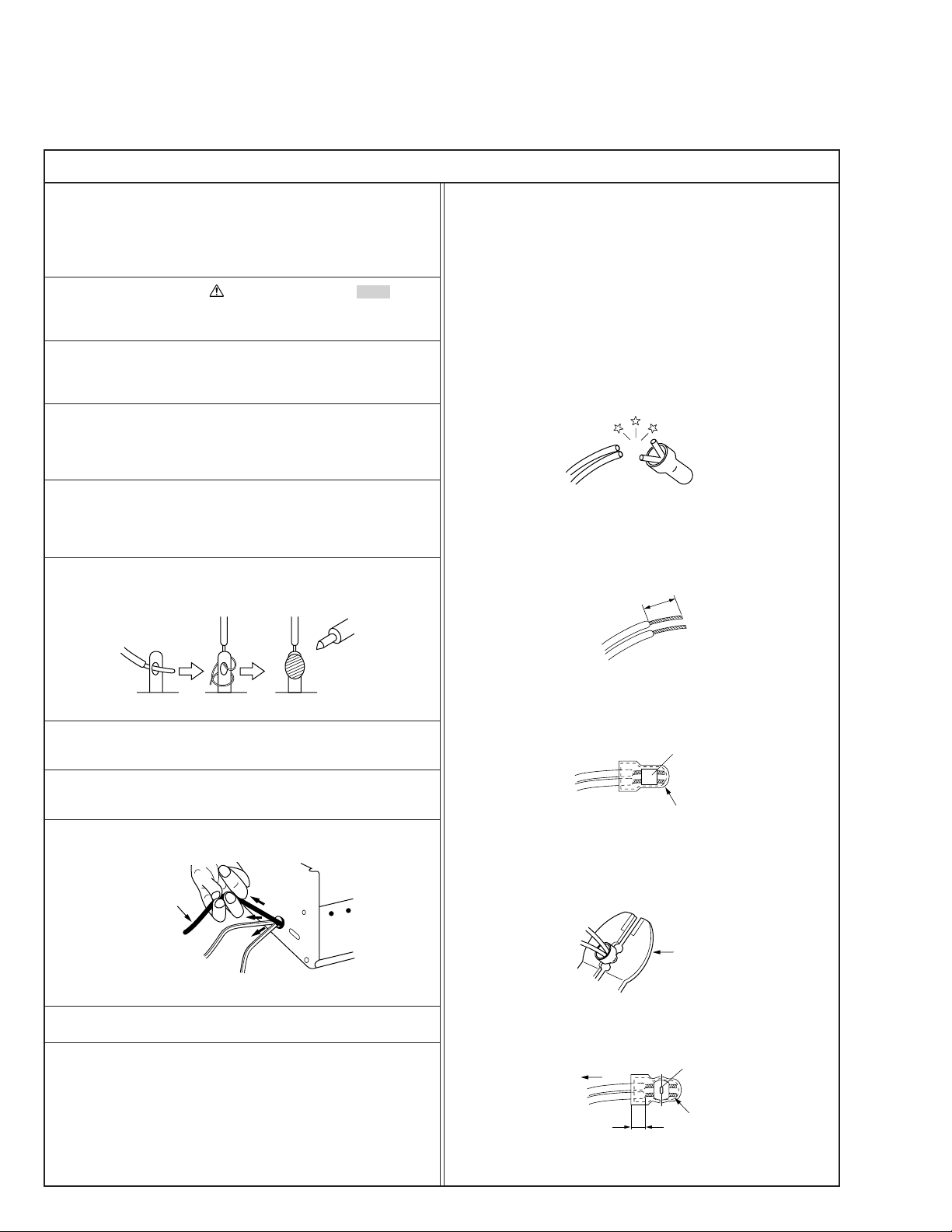
wires securely about the terminals before soldering.
symbol and shaded ( ) parts
12. Crimp type wire connector
In such cases as when replacing the power transformer in sets
where the connections between the power cord and power
transformer primary lead wires are performed using crimp type
connectors, if replacing the connectors is unavoidable, in order to prevent safety hazards, perform carefully and precisely
according to the following steps.
1) Connector part number : E03830-001
2) Required tool : Connector crimping tool of the proper type
which will not damage insulated parts.
3) Replacement procedure
(1) Remove the old connector by cutting the wires at a point
close to the connector.
Important : Do not reuse a connector (discard it).
cut close to connector
Fig.3
(2) Strip about 15 mm of the insulation from the ends of
the wires. If the wires are stranded, twist the strands to
avoid frayed conductors.
15 mm
Fig.1
7. Observe that wires do not contact heat producing parts
(heatsinks, oxide metal film resistors, fusible resistors, etc.)
8. Check that replaced wires do not contact sharp edged or
pointed parts.
9. When a power cord has been replaced, check that 10-15 kg of
force in any direction will not loosen it.
Power cord
Fig.2
10. Also check areas surrounding repaired locations.
11. Products using cathode ray tubes (CRTs)
In regard to such products, the cathode ray tubes themselves,
the high voltage circuits, and related circuits are specified for
compliance with recognized codes pertaining to X-ray emission.
Consequently, when servicing these products, replace the cathode ray tubes and other parts with only the specified parts.
Under no circumstances attempt to modify these circuits.
Unauthorized modification can increase the high voltage value
and cause X-ray emission from the cathode ray tube.
Fig.4
(3) Align the lengths of the wires to be connected. Insert
the wires fully into the connector.
Fig.5
(4) As shown in Fig.6, use the crimping tool to crimp the
metal sleeve at the center position. Be sure to crimp fully
to the complete closure of the tool.
1.25
2.0
5.5
Fig.6
(5) Check the four points noted in Fig.7.
Not easily pulled free
Wire insulation recessed
more than 4 mm
Fig.7
Crimping tool
Crimped at approx. center
of metal sleeve
Conductors extended
1
Page 4
v
a, b, cLeakage Current ( i )AC Line Voltage
110 to 130 V
220 to 240 V
Japan
USA & Canada
i 1 mA rms Exposed accessible parts
Exposed accessible parts
Antenna earth terminals
Other terminals
i 0.5 mA rms
i 0.7 mA peak
i 2 mA dc
i 0.7 mA peak
i 2 mA dc
Europe & Australia
Region
Load Z
≤
≤
≤
≤
≤
≤
1 kØ
2 kØ
1.5 kØ
0.15 µF
50 kØ
100 V
110 to 130 V
a, b, cLeakage Current ( i )
AC Line Voltage
110 to 130 V
220 to 240 V
Japan
USA & Canada
Exposed accessible parts
Exposed accessible parts
Antenna earth terminals
Other terminals
Europe & Australia
Region Load Z
1 kØ
2 kØ
1.5 kØ
0.15 µF
50 kØ
100 V
110 to 130 V
i 0.1 mA
i 0.1 mA
i 0.1 mA
i 0.1 mA
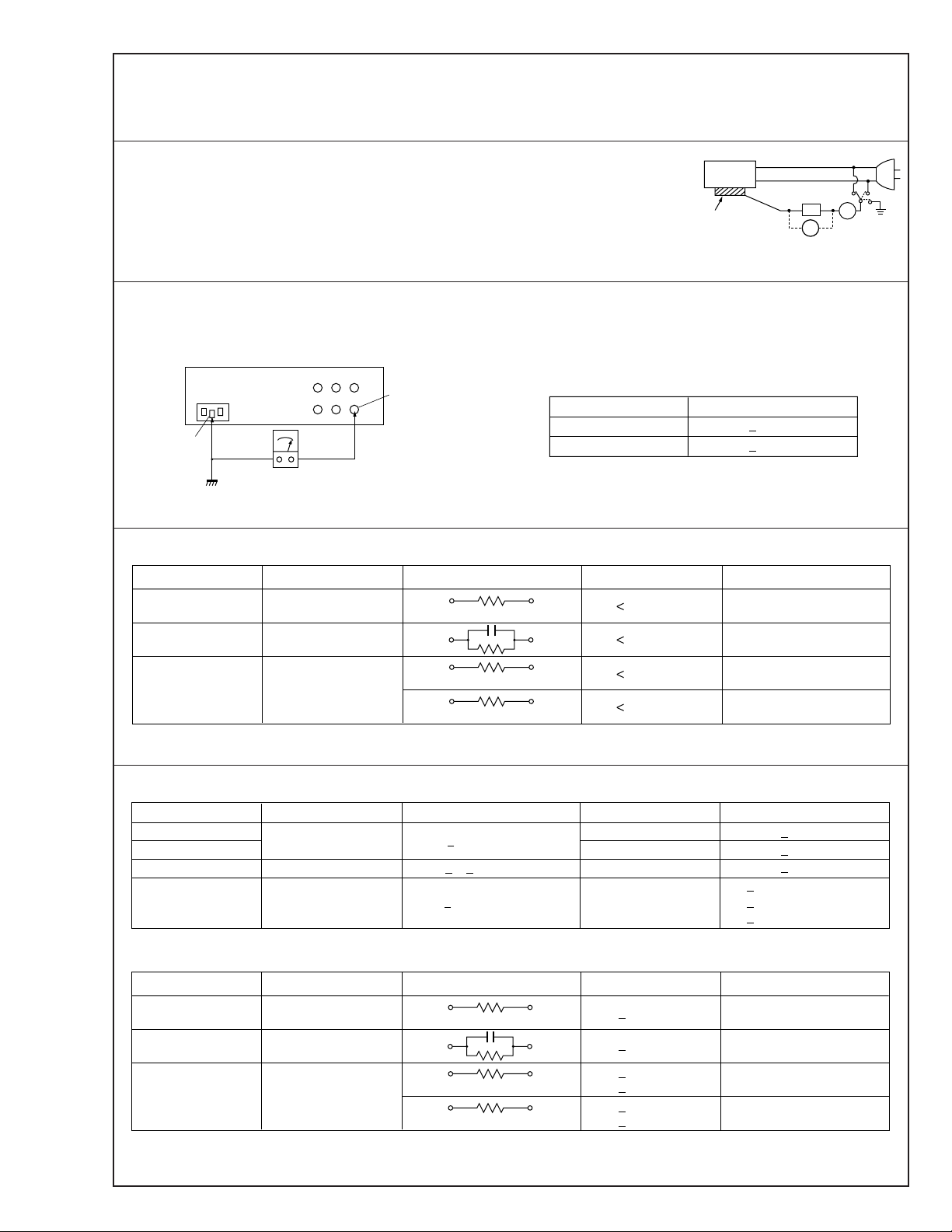
Safety Check after Servicing
Examine the area surrounding the repaired location for damage or deterioration. Observe that screws, parts and wires have been
returned to original positions, Afterwards, perform the following tests and confirm the specified values in order to verify compliance with safety standards.
1. Leakage current test
Confirm specified or lower leakage current between earth ground/power cord plug prongs
and externally exposed accessible parts (RF terminals, antenna terminals, video and audio
input and output terminals, microphone jacks, earphone jacks, etc.).
Measuring Method : (Power ON)
Insert load Z between earth ground/power cord plug prongs and externally exposed accessible parts. Use an AC voltmeter to measure across both terminals of load Z. See figure 9 and
following table 2.
2. Grounding (Class 1 model only)
Confirm specified or lower grounding impedance between earth pin and externally exposed accessible parts (Video in, Video out,
Audio in, Audio out or Fixing screw etc.).
Measuring Method:
Connect milli ohm meter between earth pin and exposed accessible parts. See figure 10 and grounding specifications.
Externally
exposed
accessible part
Z
V
Fig. 8
ab
c
A
Earth pin
Milli ohm meter
Earth
< MEDICAL USE >
< GENERAL USE >
AC Line Voltage
100 V
100 to 240 V
110 to 130 V
110 to 130 V
200 to 240 V
Exposed accessible part
Fig. 9
Table 1 Leakage current specifications for each region
Region
Japan
USA & Canada
Europe & Australia R 10 MØ/500 V DC
Insulation Resistance (R)
≤
R 1 MØ/500 V DC
≥≥
1 MØ R 12 MØ/500 V DC
≤
Table 2 Specifications for each region
Grounding Specifications
Region
USA & Canada
Europe & Australia
Dielectric Strength
AC 1 kV 1 minute
AC 1.5 kV 1 miute
AC 1 kV 1 minute
AC 3 kV 1 minute
AC 1.5 kV 1 minute
(Class 2)
(Class 1)
Grounding Impedance (Z)
≤
Z 0.2 ohm
≤
Z 0.2 ohm
Clearance Distance (d), (d')
≤
d, d' 3 mm
≤
d, d' 4 mm
≤
d, d' 3.2 mm
≤
d 4 mm
≤
d' 8 mm (Power cord)
≤
d' 6 mm (Primary wire)
Note: These tables are unofficial and for reference only. Be sure to confirm the precise values for your particular country and locality.
Table 3 Leakage current specifications for each region
2
Page 5
SECTION 1
PRECAUTIONS FOR SERVICING
1.1 BEFORE DISASSEMBLING AND REASSEMBLING
1.1.1 Precautions
1. When disconnecting and reconnecting connectors, pay careful attention to their wirings not to damage them, particularly
to the wiring of the CCU’s camera connector that requires
the most meticulous care for disconnection and connection.
2. When unsoldering chip parts (IC in particular) for replacement, completely remove solder particles from them and their
surroundings beforehand. Moreover, pay heed to the circuit
pattern not to exfoliate it from the substrate during replacement of a chip part.
3. Don’t use any chip part that was once removed.
4. Handle the optical block assembly with meticulous care.
Don’t apply it a strong shock.
5. There is a lithium battery for backing up the timer on the
POWER board assembly. Pay careful attention to the lithium
battery for accident prevention.
1.1.2 Disassembly of optical block assembly
Since the CCD is precisely glued to the prism in the optical
block assembly, the CCD cannot be replaced individually if
it comes into failure. Therefore, the optical block assembly
is subject to repair by the JVC Home AV Network Business
Unit. If there is something wrong in the optical block assembly, send the camera head assembly whole with a written
request filled out with necessary matters to the Service Engineering Section, Home AV Network Business Unit, JVC.
1.2.2 Tools and jigs required for repair and adjustment
Use the following tools, jigs and test instruments to perform
check and adjustment properly.
1) Multiscan monitor and color monitor
For SXGA(G, B,R) signal : Flex Scan T962 (or equal)
For HD(Y,PB,PR) signal : DT-V1900CG(U) (or equal)
For NTSC siganl : DT-V1900CG(U) (or equal)
2) 1/2” professional zoom lens (Model No. YH13x7.5B12 or
YH13x7.5K12 is recommended by the Professional Video
Division)
3) C mount adapter (Model No. ACM-11)
4) Tripod
5) RCA cable
6) SXGA cable
7) Extension board
8) Resolution chart for HDTV
9) Gray scale chart (for NTSC, Part No. GS-2A)
10) Oscilloscope (for 300 MHz or more)
11) Wrench for removing connector ring
12) Illuminometer
13) Color temperature meter
14) Digital voltmeter
15) Lighting apparatus (3200 K halogen lamp)
C mount adapter (ACM-11)
1.2 PREP ARATION AND PRELIMINARY CHECK REQUIRED FOR ADJUSTMENT
1.2.1 Before adjustment
1. Use two or more lighting apparatuses whose color tempera-
ture is 3200K for illuminating the test pattern, and uniformly
light up the test pattern surface with illuminance of 4000 lx
approximately while checking it with an illuminometer. If the
pattern surface is unevenly illuminated, adjustment may result in failure. Carefully set up lighting apparatuses so that
the test pattern is illuminated uniformly. (It is desired to use
two or more light sources.)
2. Be sure to use a clean test pattern as far as circumstances
permit.
RCA - S Adapter (PTU93001A)
Extension board
1-1
Page 6
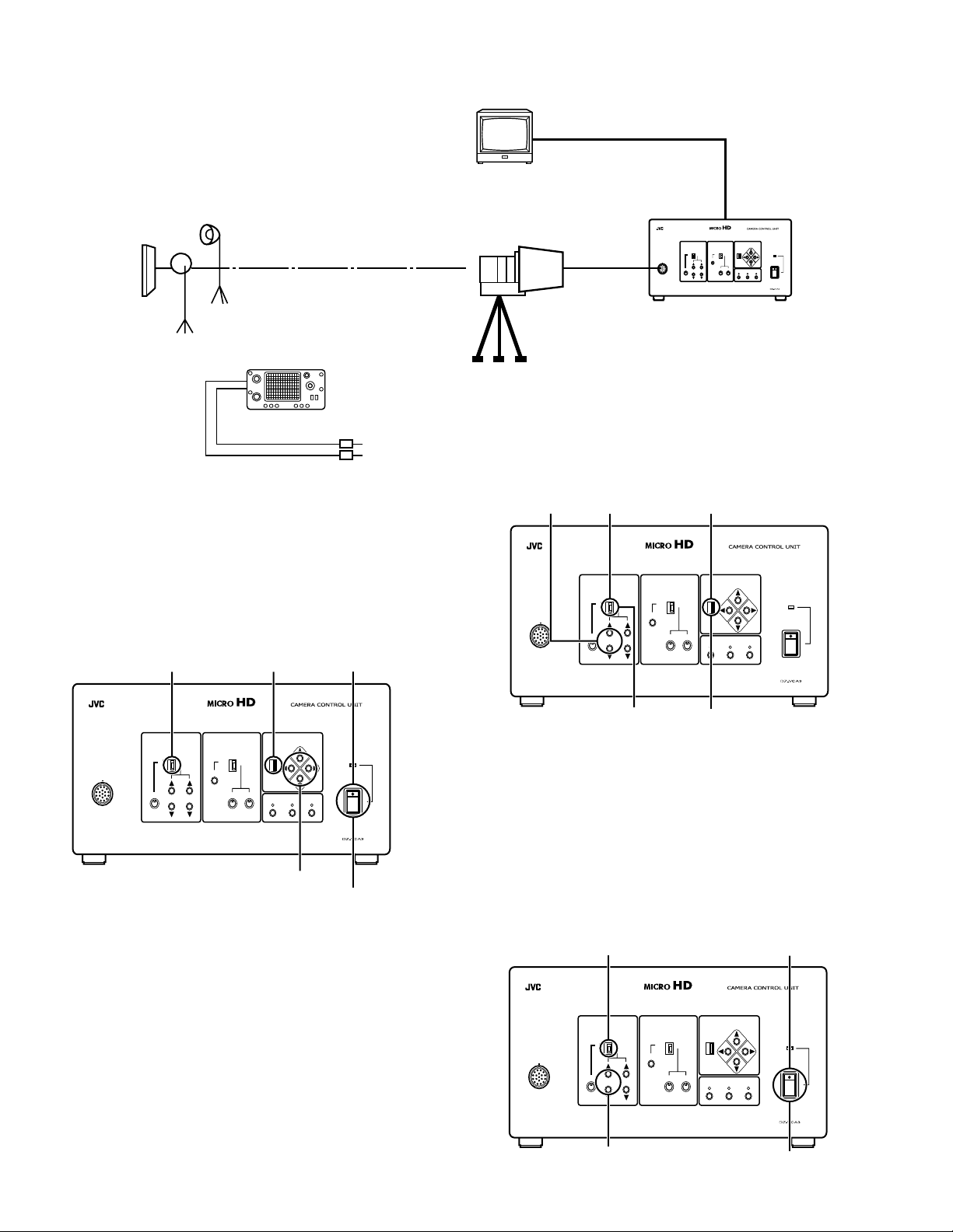
1.3 Standard setup
Monitor
Test pattern
Lighting of 3200 K
Oscilloscope
1.4 How to set the "ADJUSTMENT MODE"
1. Turn off the power of the CCU (Camera Control Unit).
2. Set the "MENU SETTING" switch to "OFF"
3. Set the "OUTPUT LEVEL" switch to "MANUAL"
4. Press and hold the "UP" and "DOWN" buttons of the
menu control button.
(The "UP" and "DOWN" buttons of the menu control button is pressing until picture comes to the monitor.)
5. Turn on the power of the CCU.
3. MANUAL 2. OFF 1. OFF
3-1.GAIN UP and
GAIN DOWN
CAMERA
ADJUST
2. AUTO
OUTPUT LEVEL
AUTO MANUAL
GAIN SHUTTER
CAMERA
ADJUST
CAMERA
WHITE BALANCE
AUTO MANU ON OFF
SETTING
RED BLUE
OUTPUT LEVEL
AUTO MANUAL
SETTING
GAIN SHUTTER
1. OFF
ENHANCE FREEZE BAR
WHITE BALANCE
AUTO MANU ON OFF
RED BLUE
MENU SETTING
MENU SETTING
ENHANCE FREEZE BAR
POWER
ON I
OFF
ON I
OFF
O
POWER
O
OUTPUT LEVEL
AUTO MANUAL
CAMERA
ADJUST
GAIN SHUTTER
WHITE BALANCE
AUTO MANU ON OFF
SETTING
RED BLUE
MENU SETTING
ENHANCE FREEZE BAR
POWER
ON I
OFF
O
4. UP and DOWN
5. ON
To release the "ADJUSTMENT MODE" as follows.
1. Turn off the power of the CCU.
2. Turn on the power of the CCU in the usual steps.
1.5 How to set the "DEBUG MODE"
1. Set the "MENU SETTING" switch to "OFF".
2. Set the "OUTPUT LEVEL" switch to "AUTO".
3. Press and hold the "GAIN UP" and "GAIN DOWN" buttons, and set the "MENU SETTING" switch to "ON".
4. Set the "OUTPUT LEVEL" switch to "MANUAL".
4. MANUAL 3-2. ON
To release the "DEBUG MODE" as follows.
1. Run the "RETURN"
1.6 How to do "ALL RESET"
1. Turn off the power of the CCU.
2. Set the "OUTPUT LEVEL" switch to "AUTO".
3. Press and hold the "GAIN UP" and "GAIN DOWN" buttons.
(The "GAIN UP" and "GAIN DOWN" buttons is pressing
until picture comes to the monitor.)
4. Turn on the power of the CCU.
2. AUTO
CAMERA
ADJUST
3.GAIN UP and
GAIN DOWN
OUTPUT LEVEL
AUTO MANUAL
GAIN SHUTTER
WHITE BALANCE
AUTO MANU ON OFF
SETTING
RED BLUE
MENU SETTING
ENHANCE FREEZE BAR
1. OFF
POWER
ON I
OFF
4. ON
O
1-2
Page 7

Warnings for accident prevention in handling battery
WARNING: Fire, Explosion, Leakage and Burn Hazard. Do not recharge, Disassemble, Heat Above
212°F , Incinerate, Or Expose Contents T o Water. Be Sure The Battery Is Inserted In The Right Direction.
The lithium battery incorporates inflammable substances such as lithium and organic solvent, etc.
inside.
If the lithium battery is handled in a wrong way, it may cause injury, fire and other dangerous
accident caused by heating, bursting, firing, etc. Be sure to follow the instructions mentioned below
to prevent you from an unexpected accident before unpacking, in and after using the battery.
1. Be careful of short-circuit.
If the positive (+) and negative (-) terminals come into contact with each other or with other metallic
material, the battery is shortcircuited. If many batteries are left disorderly and their terminals are in contact
with others, some of the batteries may generate heat, burst or fire and resultingly cause accident.
2. Neither immerse battery in water nor throw it into fire.
If the lithium battery is immersed in water or thrown into fire, it may fire or burst violently.
3. Avoid heating the battery.
If the lithium battery is heated at a temperature of 100°C or more, the electrolyte may leak from the battery
because the plastic materials such as gasket and separator are damaged or the battery may burst or fire
because the battery is heated by internal shortcircuit.
4. Avoid directly soldering the battery.
If the lithium battery is directly soldered, the electrolyte may leak from it because the plastic materials such
as the gasket and separator are damaged or the battery may burst or fire because it is heated by internal
shortcircuit.
5. Avoid charging the battery.
If the primary battery is charged, the battery may generate gas inside and it may resultingly cause
expansion, burst or fire of the battery.
6. Avoid dismantling the battery.
If the lithium battery is dismantled, some kind of gas is generated and it stimulates the throat or the
dismantled battery may fire because the negative lithium reacts on water and generates heat.
7. Avoid deformation with pressure.
If the lithium battery is deformed with pressure, the electrolyte may leak from it because of warp or
damage in the sealing, or the battery may burst or fire because it is heated by internal shortcircuit.
8. Don’t use batteries of different types or old ones mixedly.
If batteries of different brands/types are mixedly used or new and old batteries are mixedly used, it may
cause expansion, burst or fire of the batteries because they are over-discharged by difference in their
characteristics of voltage, capacitance, etc.
9. Avoid setting of the battery in wrong polarities.
If the battery is set in wrong polarities (+ and - poles are set reversely), the battery may be shortcircuited
and it may resultingly cause heating, bursting or firing in the battery.
1-3
Page 8
1.7 SERVICE CAUTIONS
1.7.1 Precautions
1. Before disassembling/re-assembling the set as well as soldering parts, make sure to disconnect the power cable.
2. When disconnecting/connecting connectors, pay enough attention to wiring not to damage it.
3. In general, chip parts such as resistor, shorting jumpers (0ohm resistor), ceramic capacitors, diodes, etc. can not be
reused after they were once removed.
4. When installing parts, be careful not to do with other parts
as well as not to damage others.
5. When removing ICs, be careful not to damage circuit patterns.
6. Tighten screws properly during the procedures. Unless specified otherwise, tighten screws at torque of 0.196 N·m (2.0
kgf·cm).
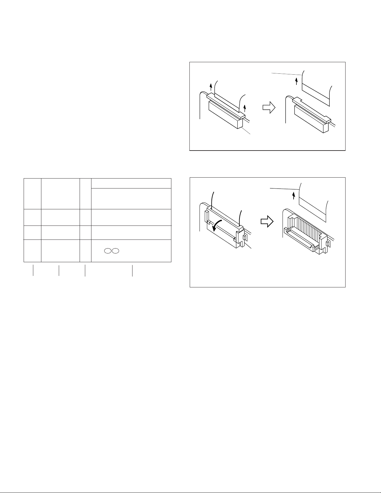
1.7.3 Connection of the wires
1. Pull the connector structure upward to release the clamp
when removing or inserting the flat wire cable.
Wire
Connector
1.7.2 How to read the disassembly and assembly
(For Cabinet Parts)
STEP
/LOC PART
NO.
Fig.
No.
REMOVAL
*UNLOCK/RELEASE/
UNPLUG/UNCLAMP/
UNSOLDER
1 CASSETTE C1 (S1),3(L1a),(L1b),(L1c)
COVER ASSEMBLY Push button, spring
2
UPPER CASE C2 2(S2), (L2)
LOWER CASE C3 9(S3), (L3a), (L3b)
3 ASSEMBLY(INCL. *CN 3a 3b
E. VF. ASSEMBLY) CAP (RCA jack)
▲
▲
(1) (2) (3) (4)
(1) Order of steps in Procedure
When reassembling, preform the step(s) in the reverse order. These numbers are also used as the identification (lo-
cation) No. of parts Figures.
(2) Part to be removed or installed.
(3) Fig. No. showing Procedure or Part Location.
C = Cabinet
CA = Camera
D = Deck
(4) Identification of part to be removed, unhooked, unlocked, re-
leased, unplugged, unclamped or unsoldered.
P = Spring
W = Washer
S = Screw
* = Unhook, unlock, release, unplug or unsolder.
2(S3) = 2 Screws (S3)
CN = Connector
(5) Adjustment information for installation.
▲
▲
NOTE:
Fig. 1-7-1
Wire
Connector
After removing the wire, return the stopper to
its original position, because it is apt to come
off if it is left open.
Fig. 1-7-2
1-4
Page 9
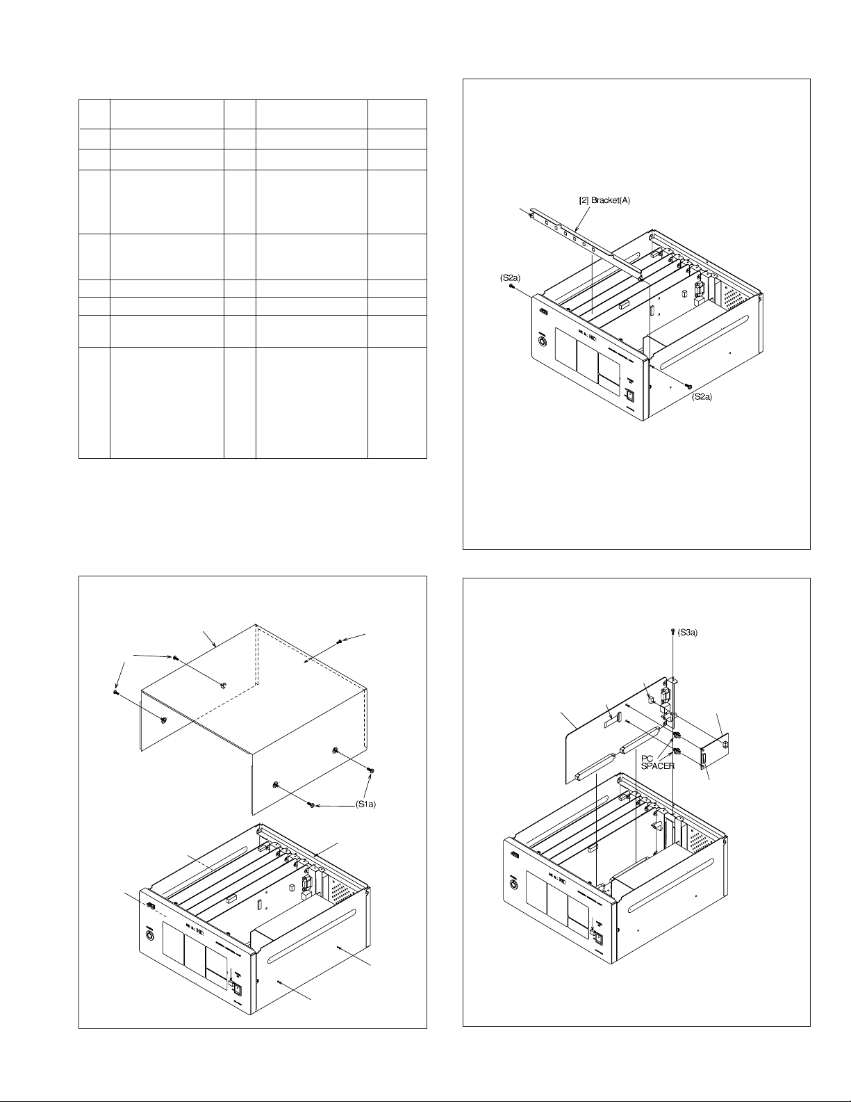
1.7.4
Disassembly procedure
Step/
Loc No.
Part Name
[1] TOP COVER
[2] BRACET(A)
[3]
NTSC board assembly
--------------------------------------------------------------------------
DV board assembly
Fig.
No.
1-7-4a
1-7-4b
1-7-4c
1-7-4c
Point Note
4(S1a), (S1b)
2(S2a)
(S3a),(L3a)
CN5501(WR3a), <Note 3a>
(CN3a),
PC SPACER,x2
MICOM board assembly1-7-4d
[4]
(S4a),(L4a) <Note 3a>
CN4004(D CONNECTOR ASSEMBLY),
CN4005(WR4b)
[5] DSP board assembly
[6]
AMDP board assembly
[7] AD board assembly
1-7-4e
(S5a),(L5a)
1-7-4f
(S6a),(L6a)
1-7-4g
(S7a),(L7a) <Note 3a>
CN1003(D CONNECTOR ASSEMBLY)
[8] FRONT PANEL
1-7-4h
6(S8a),(S7b), <Note 3a>
assembly CN615(WR8a),
CN616(D CONNECTOR ASSEMBLY),
CN617(D CONNECTOR ASSEMBLY)
--------------------------------------------------------------------------
FRT board assembly
--------------------------------------------------------------------------
LED board assembly
1-7-4i
1-7-4i
(WR8b),(WR8c)
7(S8c),3(S8d)
2(S8e)
<Note 3a>
• Be careful not to damage the connector and wire etc. during
connection and disconnection.
• When connecting the flat wire to the connector, be careful with
the flat wire direction.
• When removing or attaching the WIRE/FPC, refer to “1.8 WIRING AND BOARD LAYOUT” at same time.
Fig. 1-7-4b
(S1a)
[1] TOP COVER
(S1b)
[3] NTSC BOARD ASSY
(WR3a)
<Note 3a>
(CN3a)
[3] DV BOARD ASSY
CN5501
Fig. 1-7-4a
Fig. 1-7-4c
1-5
Page 10

To CN4004
(3pin)
D CONNECTOR
ASSEMBLY
(WR4a)
[4] MICOM BOARD ASSY
CN4004
CN4003
(S4a)
(S6a)
[6] AMDP BOARD ASSY
Fig. 1-7-4d
[5] DSP BOARD ASSY
(S5a)
CN1003
D CONNECTOR
ASSEMBLY
Fig. 1-7-4f
[7] AD BOARD ASSY
To CN1003
(8pin)
(S7a)
1-6
Fig. 1-7-4e
Fig. 1-7-4g
Page 11

D CONNECTOR
ASSEMBLY
(S8a)
(S8a)
[8] FRONT PANEL
ASSEMBLY
(S8a)
DETAIL "A"
The wire connection of the power switch.
Note : Confirm the following items when reattaching.
To CN617
(2pin)
To CN616
(4pin)
CN617
(S8a)
CN616
"A"
(WR8a)
(S8a)
FRONT PANEL
ASSEMBLY
POWER
SWITCH
1. The direction of the power switch.
2. The color of the wire(s).
3. The connected location (SW.REG or AC
INLET) of the wire(s).
(brown)
(blue)
(WR8c)
(To SW.REG)
(S8a)
(brown)
(blue)
(WR8b)
(To AC INLET)
CN615
FRONT PANEL
ASSEMBLY
Fig. 1-7-4h
[8] FRT board assembly
Fig. 1-7-4i
(S8c)
(S8d)
(S8c)
(S8e)
[8] LED board
assembly
(S8c)
1-7
Page 12

1.8 WIRING AND BOARD LAYOUT
AMDP board
assembly
AD board
assembly
DSP board
assembly
MICOM board
assembly
NTSC board
assembly
DV board
assembly
MTP board
assembly
NUT
WASHER
SCREW
WIRE CLAMP
Attach the WIRE CLAMP to the
center between CORE FILTER
of the wire which has connected
D CONNECTOR with AD board
assembly.
D CONNECTOR
assembly
A part of number of the CORE FILTER
in the figure is omitted.
CN617
CN1003
CN4004
Process the sag of the wire which
has connected CN4004 of the
MICOM board assembly with D
CONNECTOR, between the
MICOM board assembly and the
DSP board assembly.
(see the figure)
CN613
Fix the wire which has connected
the MTP board assembly with
SW.REG assembly, through the
hole (the 4th hole from the left) of
SW.REG assembly.
(see the figure)
Fix the wire which has
connected to CN615 and
CN616 of the MTP board
assembly at this position.
CN616
CN615
Process the wire which has connected
CN616 of the MTP board assembly with
D CONNECTOR, under each B to B
board assembly, being cautious of
interference of CORE FILTER.
(see the figure)
Attach the CORE FILTER to come to
each edge of the SW.REG assembly.
(see the figure)
Soldering of D. CONNECTOR ASSEMBLY
11
10
9
8
D.CONNECTOR
Parts Number
Connector Pin No.
WIRE color
Pin No. of
D. CONNECTOR
WJM0254
-001A
12123 1234 123456789101112
brown red green blue brown red orange brown red orange yellowred white brown red black
GND 13 14 11 3 4 512 8 9 7 1015161718126–
WJM0255
-001A
STEP. 1 STEP. 2 STEP. 3
Coil the UL TAPE(about 19mm
width) around the wire 1 round
and a half.
(For insulation of GND terminal)
SHIELD
TAPE
Cut the SHIELD TAPE
into 30mm and coil
the SHIELD TAPE around the wire.
The edge of the
SHIELD TAPE
of the wire.
Detail of coiling the shield tape to the D.CONNECTOR.
1
12
2
13
3
14
18
19
4
15
17
16
5
67
GND
WJM0256
-001A
Cut SHIELD TAPE into 80mm, and coil
SHIELD
the SHIELD TAPE around the wire so
TAPE
that each SHIELD section certainly
overlaps. (refer to the figure)
WJM0257
-001A
The edge of the
STEP 2.
Fig. 1-8-1
Fig. 1-8-2
Detail of installation of the CORE FILTER(s).
Attach the CORE FILTER(s) after attaching the D.CONNECTOR
ASSEMBLY to the FRONT PANEL ASSEMBLY.
CORE FILTER "A"
To
MTP
To
MICOM
To
MTP
To
AD
CORE FILTER "B"
20±5mm
On the basis of this position, put
six CORE FILTERs side by side.
30±5mm
On the basis of this position, put
five CORE FILTERs side by side.
30±5mm
On the basis of this position, put
two CORE FILTERs side by side.
CORE FILTER "A"
• The dimension is a straight
line dimension (no sag).
• Certainly lock a claw.
CORE FILTER "A" : QQR0490-002
CORE FILTER "B" : QQR0917-002
CORE FILTER "C" : QQR0942-001
CORE FILTER "C"
20±5mm
50±5mm
CORE FILTER "B"
1-8
Page 13

SECTION 2
ELECTRICAL ADJUSTMENT
2.1 INITIAL SETTING
2.1.1 Functions and initial settings of internal switches of boards
Board assembly Switch Function Initial setting
AMDP SW2101 1 : Don’t care 1 : ON
MICOM SW4304 1 : DIN(SG2_DATA) 1 : ON
SW4305 1 : Don’t care 1 : ON
AD SW1501 1 : DIAG (ON : VD2 lock) 1 : ON
SW1502 1 : T. GEN (ON : TEST GAN) 1 : OFF
DSP SW3002 1 : I/O 1 : OFF
SW3003 1 : I/O 1 : OFF
NTSC SW5001 1 : I/O 1 : OFF
2 : XRST 2 : ON
3 : DSCLK 3 : ON
4 : DSDT0 4 : ON
2 : DONE(SG2_DONE) 2 : ON
3 : INIT(SG2_INI) 3 : ON
4 : PROGRAM(SG2_PRG) 4 : ON
2 : Don’t care 2 : ON
3 : Don’t care 3 : ON
4 : DCLK(SG2_CLK) 4 : ON
2 : GAMMA (ON : GAMMA ON) 2 : ON
3 : Don’t care 3 : OFF
4 : Program write 4 : ON
2 : T. SEL0 (GENERATOR MODE 1) 2 : OFF
3 : T. SEL1 (GENERATOR MODE 2) 3 : OFF
4 : Don’t care 4 : OFF
2 : I/O 2 : OFF
3 : I/O 3 : ON
4 : I/O 4 : ON
2 : I/O 2 : ON
3 : I/O 3 : ON
4 : I/O 4 : OFF
2 : I/O 2 : OFF
3 : I/O 3 : OFF
4 : I/O 4 ; OFF
OFFON1234
OFFON1234
OFFON1234
OFFON1234
OFFON1234
OFFON1234
OFFON1234
OFFON1234
SXGA OUT
GENLOCK
NTSC OUT SXGA OUT
HD OUT
IN/OUT
DV Y
GBR
Y/C
(S)
VBS
PB
PR
D-SUB 15pin ⇔ BNC CABLE.
Y/C(S) OUT
S CABLE
GENLOCK
NTSC OUT SXGA OUT
IN/OUT
DV Y
Y/C
(S)
VBS
HD OUT
GBR
PB
PR
RCA ⇔ BNC CABLE
Oscilloscope
PTU93001A
Connection of SXGA terminal to Oscilloscope
Connection of Y/C(S) terminal to oscilloscope
Fig. 2.1.1 Connection (SXGA) Fig. 2.1.2 Connection (Y/C(S))
DV OUT
GENLOCK
NTSC OUT SXGA OUT
HD OUT
IN/OUT
DV Y
GBR
PB
Y/C
(S)
PR
VBS
DV CABLE
AV CABLE
Oscilloscope
Extension board
VTR MONITOR
Connection of DV terminal to Monitor
Fig. 2.1.3 Connection (DV) Fig. 2.1.4 Extension Board
2-1
Page 14

2.1.2 Adjustment procedure
1. Standard adjustment procedure
2.1
Initial setting
2.2
MTP board adjustment
2.3
MICOM board adjustment
2.4
DSP board asjustment
2.5
NTSC board adjustment
2.6
AD board adjustment
2. Adjustment procedure at camera head replacement
2.6
AD board asjustment
2-2
Page 15

2.2 MTP BOARD ADJUSTMENT
2.2.1 Adjustment part(s) location guide
CN602
CN601
CN617
12
CN604
CN603
CN606
CN605
CN608
CN607
CN610
CN609
TP601
CN612
CN611
TP610
3
CN614
TP604
TP605
TP603
TP602
TP607
TP606
CN616
1
VR601
CP611
TP609
TP608
41
10
1
CN613
CN615
12
Fig. 2.2.1 Adjustment part(s) location of MTP board assembly
2.2.2 Input voltage check
Signal • (None)
Mode • Power ON
Equipment • Digital voltmeter
Test points • CN613 (1)pin • CN613 (10)pin
External trigger • Use TP601(or TP610) as the ground
Specified value • +6.20±0.30V • –6.20±0.30V
(1) Each test point to check is measured using Digital voltmeter.
2.2.3 output voltage level
Signal • (None)
Mode • Power ON
Equipment • Digital voltmeter
Test points • TP603
External trigger • Use TP601(or TP610) as the ground
Adjustment part • VR601
Specified value • +2.5±0.05V
(1) Adjust part is adjusted and output voltage level is set as
Specified value.
2.2.4 output voltage check (1)
Signal • (None)
Mode • Power ON
Equipment • Digital voltmeter
Test points •
External trigger • Use TP601(or TP610) as the ground
Specified value • +5.00±0.20V • –5.00±0.20V
TP604,TP605,TP606
• TP607
(1) Each test point to check is measured using Digital voltmeter.
2.2.5 output voltage check (2)
Signal • (None)
Mode • Power ON
Equipment • Digital voltmeter
Test points • TP602 • TP609
External trigger • Use TP601(or TP610) as the ground
Specified value • +3.30±0.15V • +15.00±0.50V
(1) Each test point to check is measured using Digital voltmeter.
2.2.6 output voltage check (3)
Signal • (None)
Mode • Power ON
Equipment • Digital voltmeter
Test points • TP608 • CP611
External trigger • Use TP601(or TP610) as the ground
Specified value • –7.50±0.50V • More than 3V
(1) Each test point to check is measured using Digital voltmeter.
2-3
Page 16

2.3 MICOM BOARD ADJUSTMENT
2.3.1 Adjustment part(s) location guide
When adjusting or checking the MICOM board assembly, use the extension board. (Be careful of board direction)
SW4302
SW4303
Fig. 2.3.1a Adjustment part(s) location of MICOM board assembly
2.3.2 Main clock level
Signal • (None)
Mode • Power ON
Equipment • Frequency couter
Test points • TP4413
External trigger • Use TP601(or TP610) as the ground
Adjustment part • VR4401
Specified value • 101.1480MHz
(1) The test point to check is measured using frequency counter.
(2) Adjustment part is adjusted and main clock level is set as
Specified value.
TP4413
VR4401
GENLOCK
IN/OUT
2.3.3 GENLOCK output level
Note :
• Connect with Oscilloscope directly through a 75
Ω
terminus using a coaxial cable.
• Measure the range of an oscilloscope by 0.1V.
Signal • (None)
Mode • SYNC OUT(MENU)
Equipment • Oscilloscope
Test points • GENLOCK terminal (75Ω terminated)
Specified value • 600mV±60mVp-p
(1) The test point to check is measured using Oscilloscope.
(2) It checks that measured value is Specified value.
2-4
Page 17

2.4 DSP BOARD ADJUSTMENT
TP3005
TP3007
VR3002
VR3001
VR3003
VR3006
VR3007
VR3005
VR3009
VR3008
VR3010
SW3002SW3003
SXGA
OUT
2.4.1 Adjustment part(s) location guide
When adjusting or checking the DSP board assembly, use the extension board. (Be careful of board direction)
Fig. 2.4.1 Adjustment part(s) location of DSP board assembly
2.4.2 HD OUT
Note :
• Connect with Oscilloscope directly through a 75
Ω
terminated using a coaxial cable.
• Measure the range of an oscilloscope by 0.2V or 0.1V.
2.4.2.1 Y signal ratio level
Signal • Built-in color bar signal
Mode • BAR(LED lighting)
Equipment • Oscilloscope
Test points • Y OUT terminal (75Ω teminated)
AMDP board assembly
External trigger • TP3005
Adjustment part • VR3002
Specified value • A:B = 7:6 (Signal ratio)
2.4.2.2 Y signal level
Signal • Built-in color bar signal
Mode • BAR(LED lighting)
Equipment • Oscilloscope
Test points • Y OUT terminal (75Ω teminated)
AMDP board assembly
External trigger • TP3005
Adjustment part • VR3009
Specified value • 1.0V
(1) The test point to check is measured using Oscilloscope.
(2) Adjustment part is adjusted and Y signal is set as Specified
value.
(1) The test point to check is measured using Oscilloscope.
(2) Adjustment part is adjusted so that the ratio of a luminosity
signal and a synchronized signal may become Specified
value.
A
B
Fig. 2.4.2.1
1.0V
Fig. 2.4.2.2
2-5
Page 18

2.4.2.3Pr signal ratio level
Signal • Built-in color bar signal
Mode • BAR(LED lighting)
Equipment • Oscilloscope
Test points • Pr OUT terminal (75Ω teminated)
AMDP board assembly
External trigger • TP3005
Adjustment part • VR3003
Specified value • A:B = 7:6 (Signal ratio)
2.4.2.5 Pb signal ratio level
Signal • Built-in color bar signal
Mode • BAR(LED lighting)
Equipment • Oscilloscope
Test points • Pb OUT terminal (75Ω teminated)
AMDP board assembly
External trigger • TP3005
Adjustment part • VR3001
Specified value • A:B = 7:6 (Signal ratio)
(1) The test point to check is measured using Oscilloscope.
(2) Adjustment part is adjusted so that the ratio of a Pr signal
and a synchronized signal may become Specified value.
B
A
Fig. 2.4.2.3
2.4.2.4 Pr signal level
Signal • Built-in color bar signal
Mode • BAR(LED lighting)
Equipment • Oscilloscope
Test points • Pr OUT terminal (75Ω teminated)
AMDP board assembly
External trigger • TP3005
Adjustment part • VR3010
Specified value • 700mV
(1) The test point to check is measured using Oscilloscope.
(2) Adjustment part is adjusted and Pr signal is set as Specified
value.
(1) The test point to check is measured using Oscilloscope.
(2) Adjustment part is adjusted so that the ratio of a Pb signal
and a synchronized signal may become Specified value.
B
A
Fig. 2.4.2.5
2.4.2.6 Pb signal level
Signal • Built-in color bar signal
Mode • BAR(LED lighting)
Equipment • Oscilloscope
Test points • Pb OUT terminal (75Ω teminated)
AMDP board assembly
External trigger • TP3005
Adjustment part • VR3008
Specified value • 700mV
(1) The test point to check is measured using Oscilloscope.
(2) Adjustment part is adjusted and Pb signal is set as Specified
value.
2-6
700mV
Fig. 2.4.2.4
700mV
Fig. 2.4.2.6
Page 19

2.4.3 SXGA OUT
Note :
• Since a signal is outputted from SXGA OUT, a D-SUB 15
⇔
BNC cable is used.
• Connect with Oscilloscope directly through a 75
Ω
terminated using a coaxial cable.
• Measure the range of an oscilloscope by 0.2V or 0.1V.
2.4.3.1G gain level
Signal • Built-in color bar signal
Mode • BAR(LED lighting)
Equipment • Oscilloscope
Test points • G OUT terminal (75Ω teminated)
External trigger • TP3007
Adjustment part • VR3006
Specified value • 700mV
• D-SUB15 ⇔ BNC cable
(1) Since a G OUT signal is outputted from SXGA OUT, a D-
SUB15 ⇔ BNC cable is used. The test point to check is
measured using Oscilloscope.
(2) Adjustment part is adjusted and G gain is set as Specified
value.
TP3007
2.4.3.3 R gain level
Signal • Built-in color bar signal
Mode • BAR(LED lighting)
Equipment • Oscilloscope
• D-SUB15 ⇔ BNC cable
Test points • R OUT terminal (75Ω teminated)
External trigger • TP3007
Adjustment part • VR3005
Specified value • 700mV
(1) Since a R OUT signal is outputted from SXGA OUT, a D-
SUB15 ⇔ BNC cable is used. The test point to check is
measured using Oscilloscope.
(2) Adjustment part is adjusted and R gain is set as Specified
value.
TP3007
700mV
Fig. 2.4.3.3
700mV
Fig. 2.4.3.1
2.4.3.2B gain level
Signal • Built-in color bar signal
Mode • BAR(LED lighting)
Equipment • Oscilloscope
Test points • B OUT terminal (75Ω teminated)
External trigger • TP3007
Adjustment part • VR3007
Specified value • 700mV
(1) Since a B OUT signal is outputted from SXGA OUT, a D-
SUB15 ⇔ BNC cable is used. The test point to check is
measured using Oscilloscope.
(2) Adjustment part is adjusted and B gain is set as Specified
value.
• D-SUB15 ⇔ BNC cable
TP3007
Fig. 2.4.3.2
700mV
2-7
Page 20

2.5 NTSC BOARD ADJUSTMENT
2.5.1 Adjustment part(s) location guide
When adjusting or checking the NTSC board assembly, use the extension board. (Be careful of board direction)
VR5101
VR5201 VR5301
VR5003 VR5002 VR5001
TP5102
SW5001
TP5202
TP5302
Fig. 2.5.1 Adjustment part(s) location of NTSC board assembly
2.5.2 INPUT SIGNAL
2.5.2.1G gain level
Signal • Built-in color bar signal
Mode • BAR(LED lighting)
Equipment • Oscilloscope
Test points • TP5102
External trigger • TP5013
Adjustment part • VR5101
Specified value • 1.49V
(1) The test point to check is measured using Oscilloscope.
(2) Adjustment part is adjusted and G gain is set as Specified
value.
DV OUT
TP5001
TP5013
S OUT
VBS OUT
2.5.2.2 B gain level
Signal • Built-in color bar signal
Mode • BAR(LED lighting)
Equipment • Oscilloscope
Test points • TP5202
External trigger • TP5013
Adjustment part • VR5201
Specified value • 1.49V
(1) The test point to check is measured using Oscilloscope.
(2) Adjustment part is adjusted and B gain is set as Specified
value.
2-8
Fig. 2.5.2.1
1.49V
TP5013
TP5013
1.49V
Fig. 2.5.2.2
Page 21

2.5.2.3R gain level
Signal • Built-in color bar signal
Mode • BAR(LED lighting)
Equipment • Oscilloscope
Test points • TP5302
External trigger • TP5013
Adjustment part • VR5301
Specified value • 1.49V
(1) The test point to check is measured using Oscilloscope.
(2) Adjustment part is adjusted and R gain is set as Specified
value.
TP5013
1.49V
2.5.3.2Video level (2)
Signal • Built-in color bar signal
Mode • BAR(LED lighting)
Equipment • Oscilloscope
Test points • VBS terminal (75Ω terminated)
External trigger • TP5001
Adjustment part • VR5002
Specified value • 0.714V
(1) The test point to check is measured using Oscilloscope.
(2) Adjustment part is adjusted and Y signal is set as Specified
value.
0.714V
Fig. 2.5.2.3
2.5.3 OUTPUT SIGNAL
Note :
• Connect with Oscilloscope directly through a 75
Ω
terminated using a coaxial cable.
• Measure the range of an oscilloscope by 0.2V or 0.1V.
2.5.3.1Video level (1)
Signal • Built-in color bar signal
Mode • BAR(LED lighting)
Equipment • Oscilloscope
Test points • VBS terminal (75Ω terminated)
External trigger • TP5001
Adjustment part • VR5201, VR5301
Specified value • Minimum signal level
(1) The test point to check is measured using Oscilloscope.
(2) Adjustment part is fine-adjusted and the signal waveform
level of the white portion of a color bar is made into the
minimum.
minimum
Fig. 2.5.3.2
2.5.3.3Y level
Signal • Built-in color bar signal
Mode • BAR(LED lighting)
Equipment • Oscilloscope
• PTU93001A(RCA-S ADAPTER)
Test points • S OUT terminal (75Ω terminated)
External trigger • TP5001
Adjustment part • VR5001
Specified value • 0.714V
(1) The test point to check is measured using Oscilloscope.
PTU93001A is used for changing S terminal into a RCA
terminal.
(2) Adjustment part is adjusted and Y level is set as Specified
value.
0.714V
white portion
Fig. 2.5.3.1
Fig. 2.5.3.3
2-9
Page 22

2.5.3.4Color level
Signal • Built-in color bar signal
Mode • BAR(LED lighting)
Equipment • Oscilloscope
Test points • C OUT terminal (75Ω terminated)
External trigger • TP5001
Adjustment part • VR5003
Specified value • 286mV
• PTU93001A(RCA-S ADAPTER)
(1) The test point to check is measured using Oscilloscope.
PTU93001A is used for changing S terminal into a RCA
terminal.
(2) Adjustment part is adjusted and burst level is set as Specified
value.
286mV
Fig. 2.5.3.4
2.5.3.5DV signal check
Signal • Built-in color bar signal
Mode • BAR(LED lighting)
Equipment • apparatus with DV input Monitor
Test points • DV terminal
(1) It checks that connect apparatus with DV INPUT and a color
bar signal is reflected in a monitor.
2-10
Page 23

2.6 AD BOARD ADJUSTMENT
1.8V
TP1002
1.8V
signal line
Note :
• A camera head is attached.
• Shoot the gray scale chart under the standard shooting condition, an iris is set as F8.
• Standard shooting conditions
1) Ambient temperature : +20° to +25°C
2) Standard lighting : 3200 K, 4000 lx
3) Lens : YH13x7.5B12 or YH13x7.5K12
2.6.1 Adjustment part(s) location guide
When adjusting or checking the AD board assembly, use the extension board. (Be careful of board direction)
TP1102
VR1101
VR1103
TP1202
VR1201
SW1501 SW1502
VR1203
VR1303
TP1002
TP1001
VR1301
TP1010
VR1001
TP1302
Fig. 2.6.1 Adjustment part(s) location of AD board assembly
2.6.2 A/D AND AUTO GAIN
Note :
• A/D adjustment and AUTO adjustment are performed
continuously.
2.6.2.1A/D gain level
Perform this adjustment at ADJUSTMENT MODE.
After adjustment, turn off and turn on the power again.
Signal • Shot the gray scale chart
Mode • Adjustment mode
Equipment • Oscilloscope
Test points • TP1102, TP1202, TP1302
External trigger • TP1001
Adjustment part • VR1101, VR1201, VR1301
Specified value • 1.61V
(1) The test point to check is measured using Oscilloscope.
(2) Adjustment part is adjusted and A/D gain is set as Speci-
fied value. It measures in the bottom position of a signal line.
2.6.2.2AUTO gain level
Signal • Shot the gray scale chart
Mode • Adjustment mode
Equipment • Oscilloscope
Test points • TP1010
External trigger • TP1002
Adjustment part • VR1001
Specified value • 1.8V
(1) Adjustment parts is adjusted and AUTO gain is set as Speci-
fied value. It is measured in the center position of a signal
line.
(2) Adjustment mode will be canceled if a power supply is
switched on again.
TP1001
1.61V
Fig. 2.6.2.1
signal line
1.61V
Fig. 2.6.2.2
2-11
Page 24

2.6.2.3Color gain
Signal •
Mode • CAMERA
Equipment • Oscilloscope
Test points • TP1102, TP1202, TP1302
External trigger • TP1001
Adjustment part • VR1103, VR1203, VR1303
Specified value • Minimum siganl level
An iris is closed and GAIN is set as +24dB.
(1) The test point to check is measured using Oscilloscope.
(2) Adjustment part is adjusted to minimize deflection of the sig-
nal level in the “A” and “B” sides of the waveform.
It is changing into the state where volume had been turned,
when it cannot adjust to minimum.
(3) GAIN is returned to +0dB and an iris is set as F8.
TP1001
A
B
A
B
Fig. 2.6.2.3
2.6.2.5White defect
Note :
• Connect to the monitor by SXGA or HD(Y, Pb, Pr), when
checking WHITE DEFECT.
• Perform this adjustment at DEBUG MODE.
• After adjustment, turn off and turn on the power again.
Signal •
Mode • DEBUG
Equipment • Monitor
Setup • GAIN : 18dB, SHUT : 1/60
Specified value • Minimum signal level
(1) An iris is closed.
(2) It is made DEBUG MODE. And WHITE DEFECT is chosen
using UP and DOWN of MENU operation.
(3) It changes into STANDBY state using → of MENU opera-
tion. And a setup is checked.
DEBUG PAGE RETURN
S/N MODE NO
M.BLACK
ALC
AUTO DEBUG
WHITE DEF. STANDBY
2.6.2.4Color gain for tint adjustment
Signal • Shot the gray scale chart
Mode • CAMERA
Equipment • Oscilloscope
Test points • Pb OUT, Pr OUT
External trigger • TP1002
Adjustment part • VR1201, VR1301
Specified value • Minimum signal level
(1) The test point to check is measured using Oscilloscope di-
rectly uses with a coaxial cable.
(2) Adjustment part is adjusted to minimize deflection of the sig-
nal level of the waveform.
(4) Detection of WHITE DEFECT carries out START by “DOWN”
of MENU operation. After detection of WHITE DEFECT is
completed, it is automatic to STANDBY and returns to it.
DEBUG PAGE RETURN
S/N MODE
M.BLACK
ALC
AUTO DEBUG
WHITE DEF.
(5) MENU is operated and DEBUG mode is ended.
2-12
Page 25

SECTION 3
INSTALLATION MANUAL
For installing and operating the system which this camera is incorporated in, be sure to follow the instructions
mentioned below.
1. Use the AA-V31U isolation transformer to supply the power to every unit of the system.
2. Ground the AA-V31U. (Please refer to “4. Check of grounding (AA-V31U)”)
3. Cover disused power outlets of the AA-V31U with protection brackets respectively.
1. Safety precautions
• Before starting installation, carefully read “Safety precautions” appearing on pages 4 to 8 of the instructions.
2. Connection of system components
• Connect each unit referring to “Connection” appearing on page 9 of the instructions.
• Please install isolation transformer near the equipotential terminal of video cart.
• When installing the system, power supply cords should be routed so that they are not pinched by items placed upon
or against them. Besides that, when moving the system, please pay special attention to power cords as the cart will
not be fallen down.
Please do not connect other equipment to the signal in - or outputs during use of the system at the patient - unless
you are using facility for galvanic separation, e.g. electro-optical transimitter.
The system may not be changed without additional checking of the safety provisions of EN 60601-1-1. Please note
that the party (person or company) which is assembling, installing or modifying a medical sytstem is responsible that
it complies with all relevant requirements of that standard.
3. Connection of each unit to the power supply unit
• Connect the power cable of each unit to the isolation transformer (AA-V31U) referring to the following figure.
The plug of each power cable must be fastened by a band and a holder, which needs to be fastened with a screwdriver.
Washer
Use exclusive screws to fasten
the plug and tighten the screws
with the special screwdriver.
(Pay need to the orientation of
each screw.)
Cover disused power outlets of the
AA-V31U with exclusive protection
brackets,
and fasten each protection bracket
with exclusive screws that need the
special screwdriver for tightening.
When fastening the band to the AA-V31U with an exclusive screw, be sure to put two washers (two different
types) on the screw so that they are inserted between the band and the AA-V31U.
• When fitting the cover to the DZ-VCA3U for medical use, be sure to disconnect the power cord from the AC outlet in
the hospital/clinic to avoid getting an electric shock.
• Be careful not to insert a screwdriver or the like into the AC outlet.
3-1
Page 26

4. Check of grounding (AA-V31U)
• If the AA-V31U is connected to an AC outlet that is not grounded or is poorly grounded, the indicator lamp of the AAV31U goes on. In such a case, reconnect the AA-V31U to another AC outlet that is perfectly grounded.
5. Check of operation
• Check main operations of the system referring to the instructions.
6. Liaison slip of customer data
• When all the above-mentioned work is complete, fill out the liaison slip of customer data and send it to the sales office
concerned.
7. Sterilization
When returnings to repair this camera, the camera head must be sterilized by following the instructions of the sterilizing app aratus referring to the following example of sterilization.
Example of sterilization
• Sterilization by ethylene oxide gas
Gas composition : Ethylene oxide gas 20%
Carbon dioxide 80%
Temperature : 104 to 140 F
Humidity : 40 to 60% RH
EO density : 500 to 600 mg/liter
Action time : 4 hours
Degassing method : Aeration
Shelf condition : By aerator, 122 F
Shelf time : 18 hours or more
(48 hours or more at the room temperature and a general atmospheric pressure)
This equipment is not waterproof.
Don't sterilize the equipment and accessories in a way other than the above-mentioned condition, otherwise
it may cause a failure in the equipment.
8. Report of complaints dealt with
When a complaint about the system is settled on the spot (except rapair of system failure), write details of dealing
with the complaint in the part of “Details of complaint and progress to settlement ” of the “Complaint reception slip
about medical instrument GMP (Good Manufacturing Practice) ”, and send the slip to the following addresses.
JVC Professional Product Company
1700 Vallay Road,Wayne NJ 07470
TEL:(973)317-5000
FAX:(973)317-5030
3-2
Page 27

JVC SERVICE & ENGINEERING COMPANY OF AMERICA
DIVISION OF JVC AMERICAS CORP.
www.jvcservice.com(US Only)
JVC CANADA INC.
Head office
:
21 Finchdene Square Scarborough, Ontario M1X 1A7
(416)293-1311
Printed in Japan
0212 VP
 Loading...