

Page 1
VICTOR COMPANY OF JAPAN, LIMITED
VIDEO DIVISION
S40894
SCHEMATIC DIAGRAMS
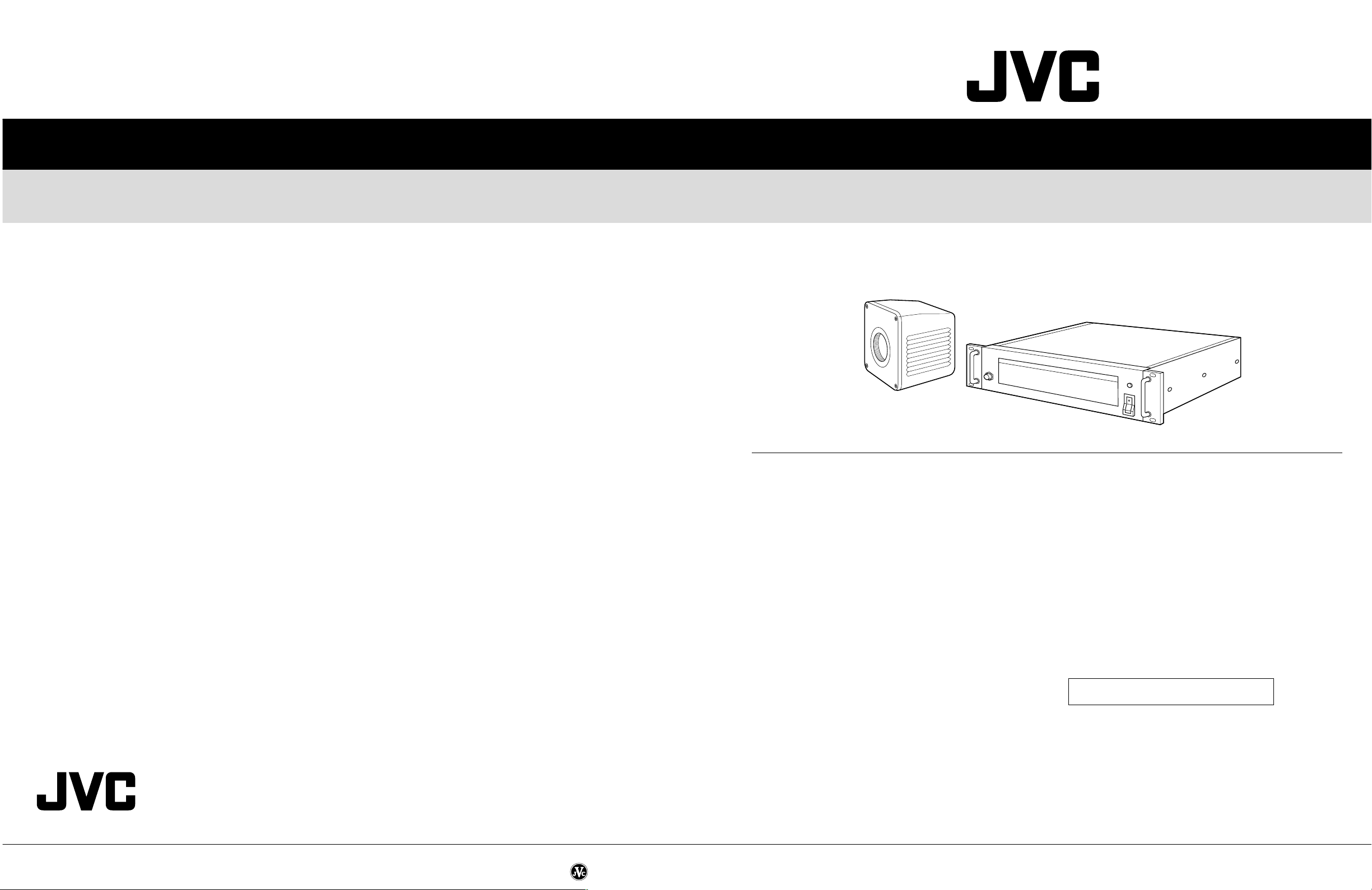
MICRO HD CAMERA
DZ-VCA1SE
CD-ROM No. SML200106
SPECIFICATIONS
* Design and specifications subject to change without notice.
Camera head section
■ Image sensing device : 1/3-inch IT-CCD (410,000 pixels)
■ Shooting system : 4-CCD new dual green system
■ Colour separation optical
system : 1/3 type F1.4 3-colour separation prism
■ Number of effective pixels : 768 (horizontal) x 494 (vertical), 380,000 pixels
■ Camera output : 19 pins
■ Lens mount : Special mount (C mount form, flange back: 28.0 mm)
■ Dimensions : Camera head; 59 (W) x 70 (H) x 79 (D) mm
■ Weight : Camera head; 230 g (0.51 lbs.) (not including
■ Classification : Type BF
Camera control unit section
■ Number of scanning lines : 1125 (980 effective)
■ Scanning system : 2:1 interlace
■ Scanning frequency : 33.75 kHz (horizontal), 60 Hz (vertical)
■Aspect ratio : 4:3
■ Horizontal resolution (center) : More than 800 TV lines (Y signal)
■ Vertical resolution (center) : More than 650 TV lines (Y signal)
■ S/N : 52 dB
■ Sensitivity : F5.6, 2000 lx
■ Minimum subject illuminance : 10 lx (F1.6 + 12 dB, 1/30 shutter, 50% level)
■ Sync system : Internal sync/external sync
■ External sync signal input : Composite video signal of 1 Vp-p or composite sync
■ Colour bar : Full colour bar
■ Contour correction : Horizontal dual-edged (9-step variable)
■ Electronic shutter speed : 1/30 s, 1/60 s (normal), 1/100 s (flicker-free),
■ Video output
• R/G/B signal : 0.7 Vp-p, 75 ohms for each (no sync), BNC
• Y/PB/PR Y : 1 Vp-p, 75 ohms (including sync)
• Sync signal : HD; BNC x 1 (TTL)
PB : 0.7 Vp-p, 75 ohms (including sync)
PR : 0.7 Vp-p, 75 ohms (including sync)
(2-3/8” x 2-13/16” x 3-1/8”)
(not including insulating rubber covers)
insulating rubber covers)
signal of ±0.3 Vp-p, 75 ohms, BNC x 1
Vertical dual-edged (9-step variable)
1/175 s, 1/250 s, 1/375 s, 1/500 s, 1/1000 s,
1/2000 s
connector x 3 (one for each)
VD, BNC x 1 (TTL)
C. SYNC; BNC x 1
(±0.3 Vp-p, 75 ohms, compliant with HDTV
standard ITU-R Rec. 709)
■ SCSI Interface : 50 pin mini x 2
■ Camera input : 20 pins
■ Date indication : Menu system
■ Time indication : Menu system,
■ Power supply : DC 12 V, 1.3 A XLR 4 pins, AA-V112E AC
■ Power consumption : 18 W
■ Operating environment :+5°C to +35°C (41°F to 95°F), 35 – 75%
■ Allowable storage environment : –20°C to +50°C (–4°F to 122°F), 35 – 80%
■ Dimensions : 430 (W) x 93 (H) x 322 (D) mm
■ Weight : 4.9 kg (10.8 lbs.)
■ Accessories : Handle set x 1
■ Supplied documentation : Instruction manual x 1
TECHNICAL AND SERVICE
ASSISTANCE
JVC offers technical and customer service assistance.
Please contact us at the following address.
JVC PROFESSIONAL PRODUCTS (UK) LIMITED
ULLswater House, Kendel Avenue, London W3 OXA,
United Kingdom
TEL: (0181) 896-6000
FAX: (0181) 896-6060
JVC PROFESSIONAL PRODUCTS GmbH
Grüner Weg 10, 61169 Fiedberg/Hessen, Germany
TEL: (06031) 6050
FAX: (06031) 605180
1) Year, month, day
2) Day, month, year
3) Month, day, year
hour: minute: second
power adaptor (optional)
When using this unit for medical purposes, be
absolutely sure to use the separately sold
AA-V31E isolation transformer.
(16-15/16" x 3-11/16" x 12-11/16")
(excluding the handle for rack mounting)
Warrantee card x 1
Service center information x 1
Printed in Japan
This schematic diagrams is printed on 100% recycled paper.
COPYRIGHT © 2001 VICTOR COMPANY OF JAPAN, LTD.
No. 86536SCH
May 2001
Page 2
CHARTS AND DIAGRAMS
NOTES OF SCHEMATIC DIAGRAM
Safety precautions
5
4
3
2
The Components identified by the symbol are
critical for safety. For contin ued saf ety, replace safety
critical components only with manufacturer's recommended parts.
1. Units of components on the schematic diagram
Unless otherwise specified.
1) All resistance values are in ohm, 1/6 W, 1/8 W (refer to
parts list).
Chip resistors are 1/16 W.
K: KΩ (1000Ω), M: MΩ (1000KΩ)
2) All capacitance values are in µF, (P: PF).
3) All inductance values are in µH, (m: mH).
4) All diodes are 1SS133, MA165 or 1N4148M (refer to parts
list).
2. Indications of control voltage
AUX : Active at high
AUX or AUX(L) : Active at low
3. Interpreting Connector indications
1
2
Removable connector
3
1
2
Wire soldered directly on board
3
1
Non-removable Board connector
2
3
1
2
4
Board to Board
3
SECTION 4
4) Indication on schematic diagram
Voltage Indications for REC and PB mode on the schematic diagram are as shown below.
REC mode
Note: If the voltages are not indicated on the schematic
5. Waveform measurement
1) Video circuits
REC : Colour bar signal in SP mode, normal VHS mode
PB : Alignment tape, colour bar SP mode, normal VHS
2) Audio circuits
REC : 1KHz, –8 dBs sine wave signal in SP mode, normal
PB : REC then playback it
3) Movie Camera circuits
Measured using a correctly illuminated gray scale or colour
bar test chatrs in the E-E mode
4) Indication on schematic diagram
Waveform indications on the schematic diagram are as
shown below.
123
2.5
(5.0)
PB mode
1.8
PB and REC modes
(Voltage of PB and REC modes
are the same)
diagram, refer to the voltage charts.
mode
VHS mode
Measurement point
24
22201816
C329
0.1/50
R344
47K
R343
18K
C330
0.1/50
C331
11/10
R345
10K
WF25
R346
15K
Waveform number
6. Signal path Symbols
The arrows indicate the signal path as follows.
Playback signal path
Playback and recording signal path
Recording signal path
(including E-E signal path)
Capstan servo path
Drum servo path
(Example)
R-Y
Playback R-Y signal path
Y
Recording Y signal path
7. Indication of the parts for adjustments
The parts for the adjustments are surrounded with the circle as
shown below.
8. Indication of the parts not mounted on the circuit board
“OPEN” is indicated by the parts not mounted on the circuit
board.
R216
OPEN
CIRCUIT BOARD NOTES
1. Foil and Component sides
1) Foil side (B side) :
Parts on the foil side seen from foil face (pattern face)
are indicated.
2) Component side (A side) :
Parts on the component side seen from component face
(parts face) indicated.
2. Parts location guides
Parts location are indicated by guide scale on the circuit board.
REF No.
IC101 B C 6 A
(A : Component side)
(D : Discrete component)
B : Foil side
C : Chip component
Note:
For general information in service manual, please ref er
to the Service Manual of GENERAL INFORMA TION Edition 4 No. 82054D (January 1994).
LOCATION
IC
Category : IC
Horizontal “A” zone
Vertical “6” zone
4. Voltage measurement
1) Video circuits
REC : Colour bar signal in SP mode, normal VHS mode
PB : Alignment tape, colour bar SP mode, normal VHS
mode
— : Unmeasurable or unnecessary to measure
2) Audio circuits
1
REC : 1KHz, –8 dBs sine wave signal in SP mode, Nor-
mal VHS mode
PB : REC then playback it
3) Movie Camera circuits
Measured using a correctly illuminated gray scale or colour
bar test charts in the E-E mode
S40884-03
Connected pattern on board
The arrows indicate signal path
A
5) W aveform indications
Waveform number
WF25
REC/PB 1.2 Vp-p
50 mV/2 msec/DIV
Oscilloscope Volts and Time/Division, Probe 10 : 1
Mode : REC or PB modes
B
C
ALC OUT
Waveform name or
measurement point
Level : 1.2 Vp-p
DEF
4-1
4-1 4-2
4-2
G
H
S40884-03
Page 3
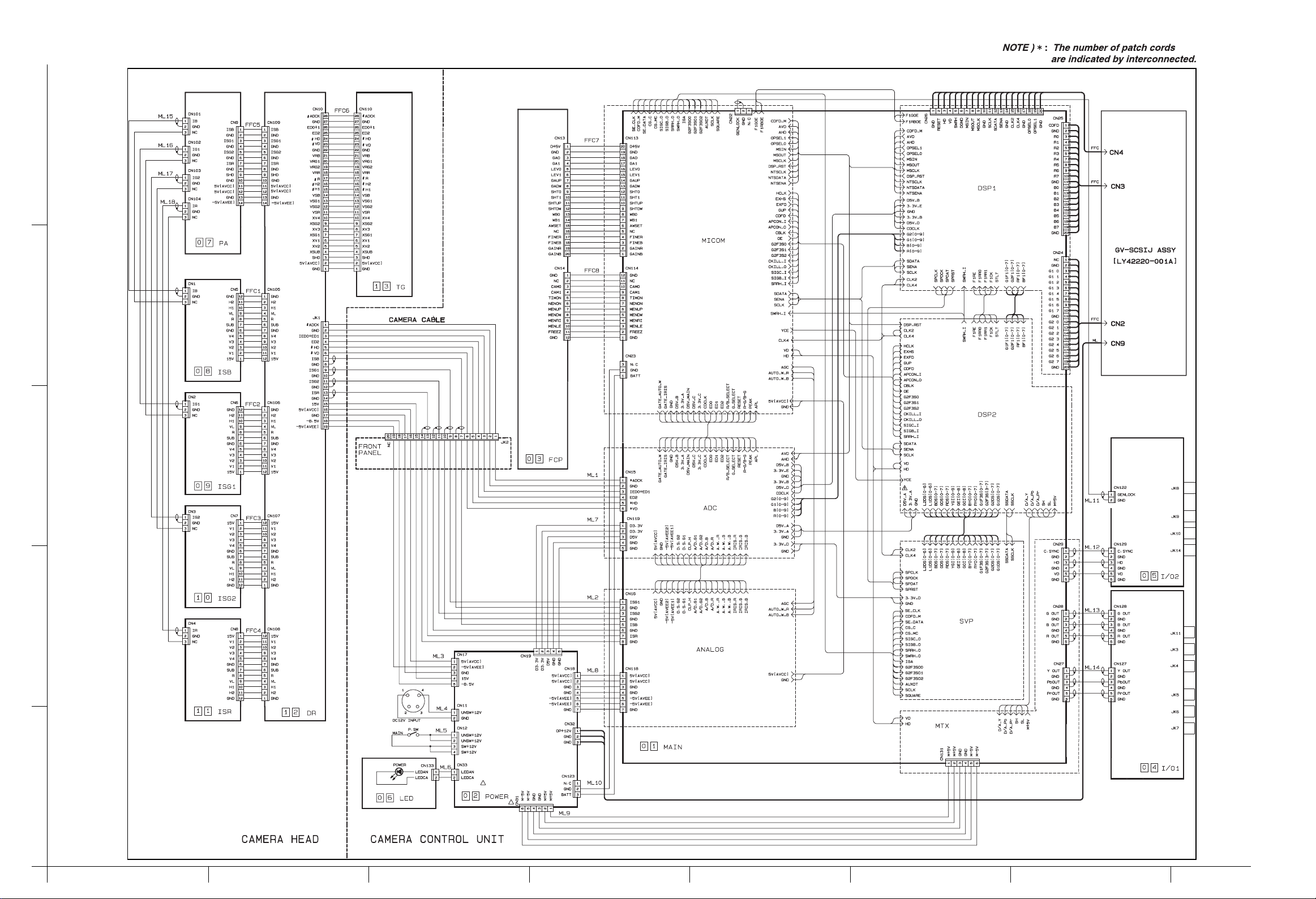
4.1 BOARD INTERCONNECTIONS
5
4
3
2
1
A
B
C
DEF
4-3
4-4
G
H
Page 4
4.2 CAMERA UNIT SCHEMATIC DIAGRAM
5
4
3
2
1
A
B
C
DEF
4-5 4-6
G
H
Page 5
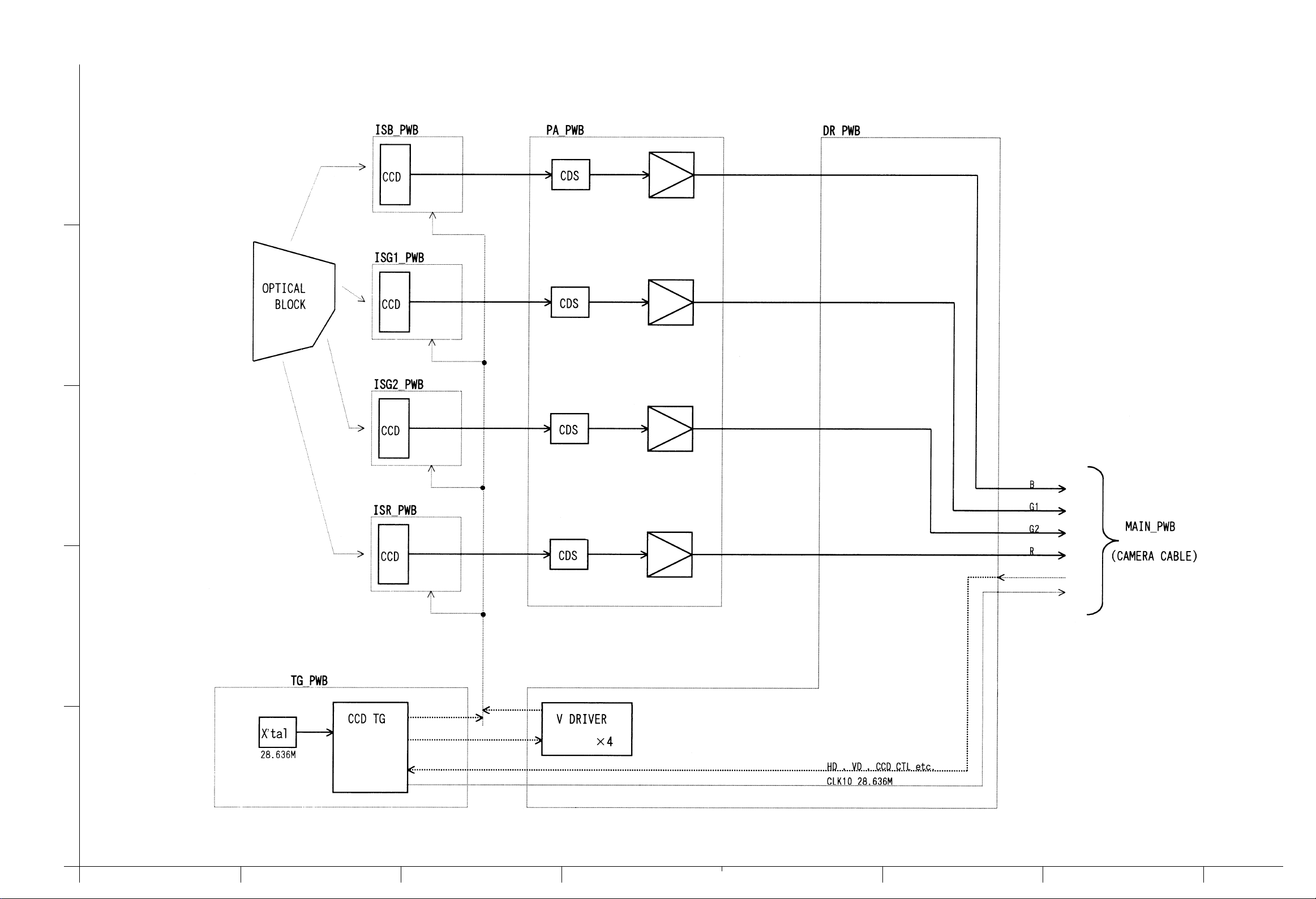
4.3 CCD SCHEMATIC DIAGRAM
5
4
3
2
1
A
B
C
DEF
4-7
4-8
G
H
Page 6
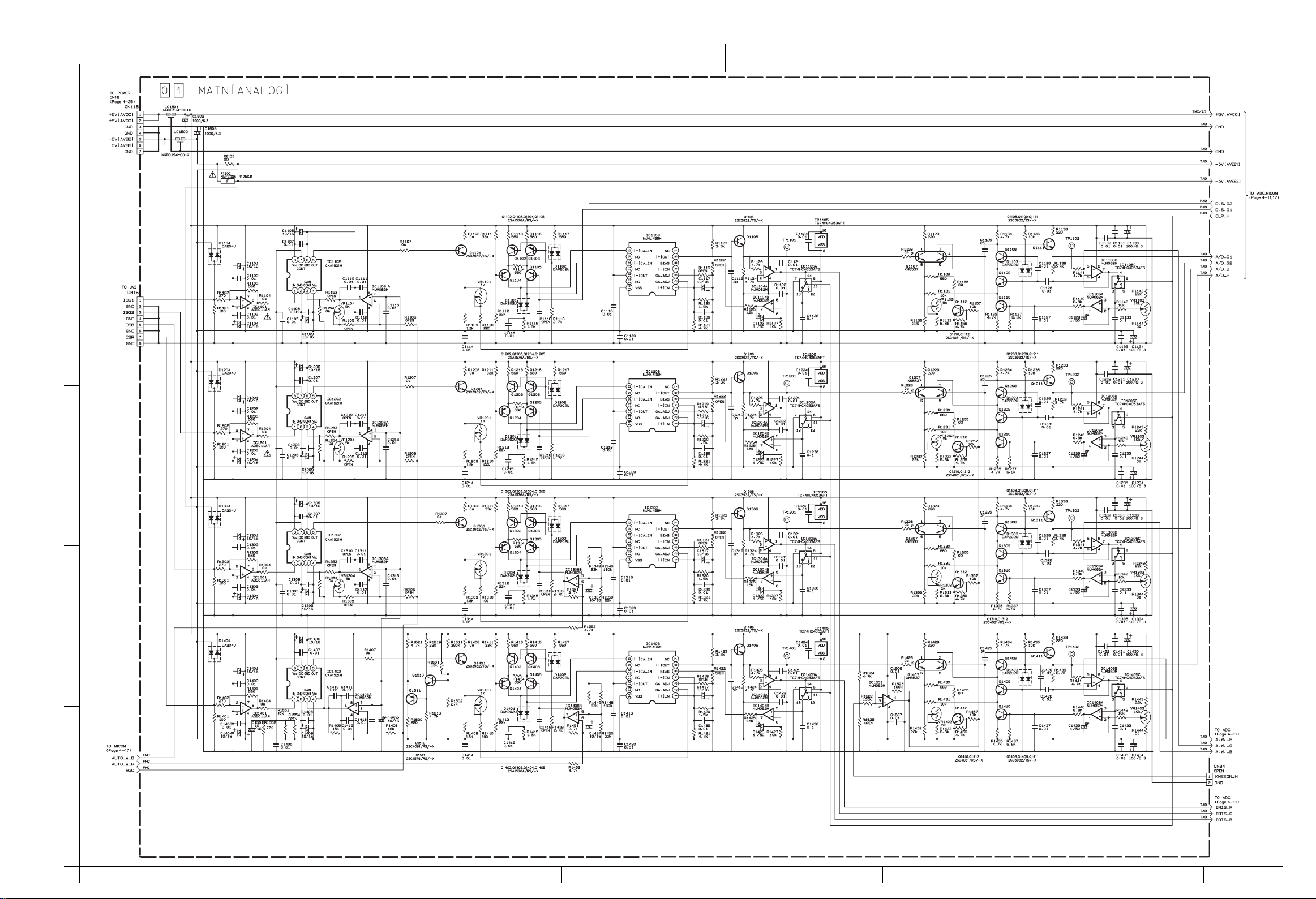
4.4 ANALOG SCHEMATIC DIAGRAM
5
4
Note : The Parts Number, value and rated voltage etc. in the Schematic Diagram are for references only.
When replacing the parts, refer to the Parts List.
3
2
1
A
B
C
DEF
4-9
4-10
G
H
Page 7
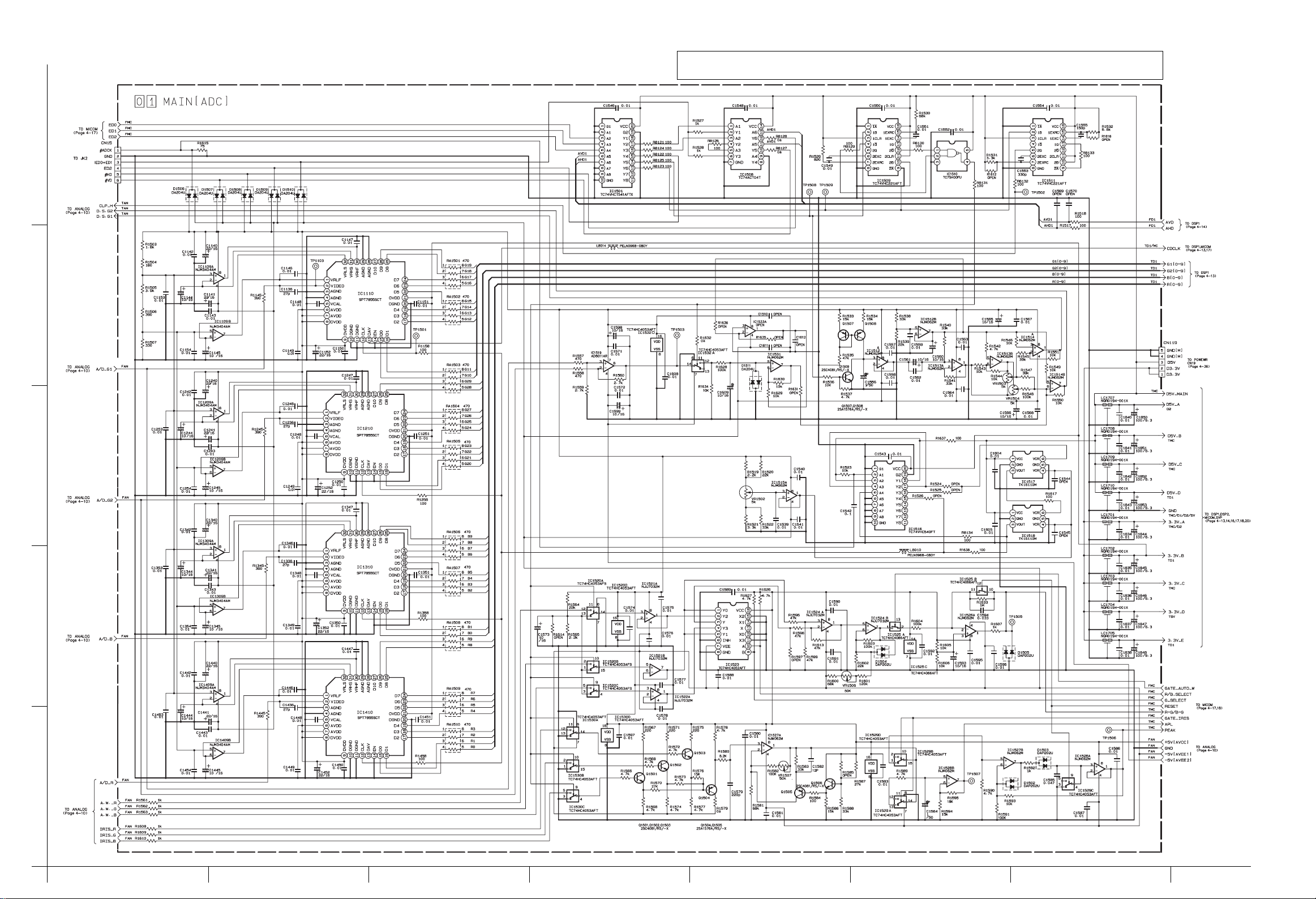
4.5 ADC SCHEMATIC DIAGRAM
5
4
Note : The Parts Number, value and rated voltage etc. in the Schematic Diagram are for references only.
When replacing the parts, refer to the Parts List.
3
2
1
A
B
C
DEF
4-11 4-12
G
H
Page 8

4.6 DSP1 SCHEMATIC DIAGRAM
5
4
Note : The Parts Number, value and rated voltage etc. in the Schematic Diagram are for references only.
When replacing the parts, refer to the Parts List.
3
2
1
A
B
C
DEF
4-13
4-14
G
H
Page 9
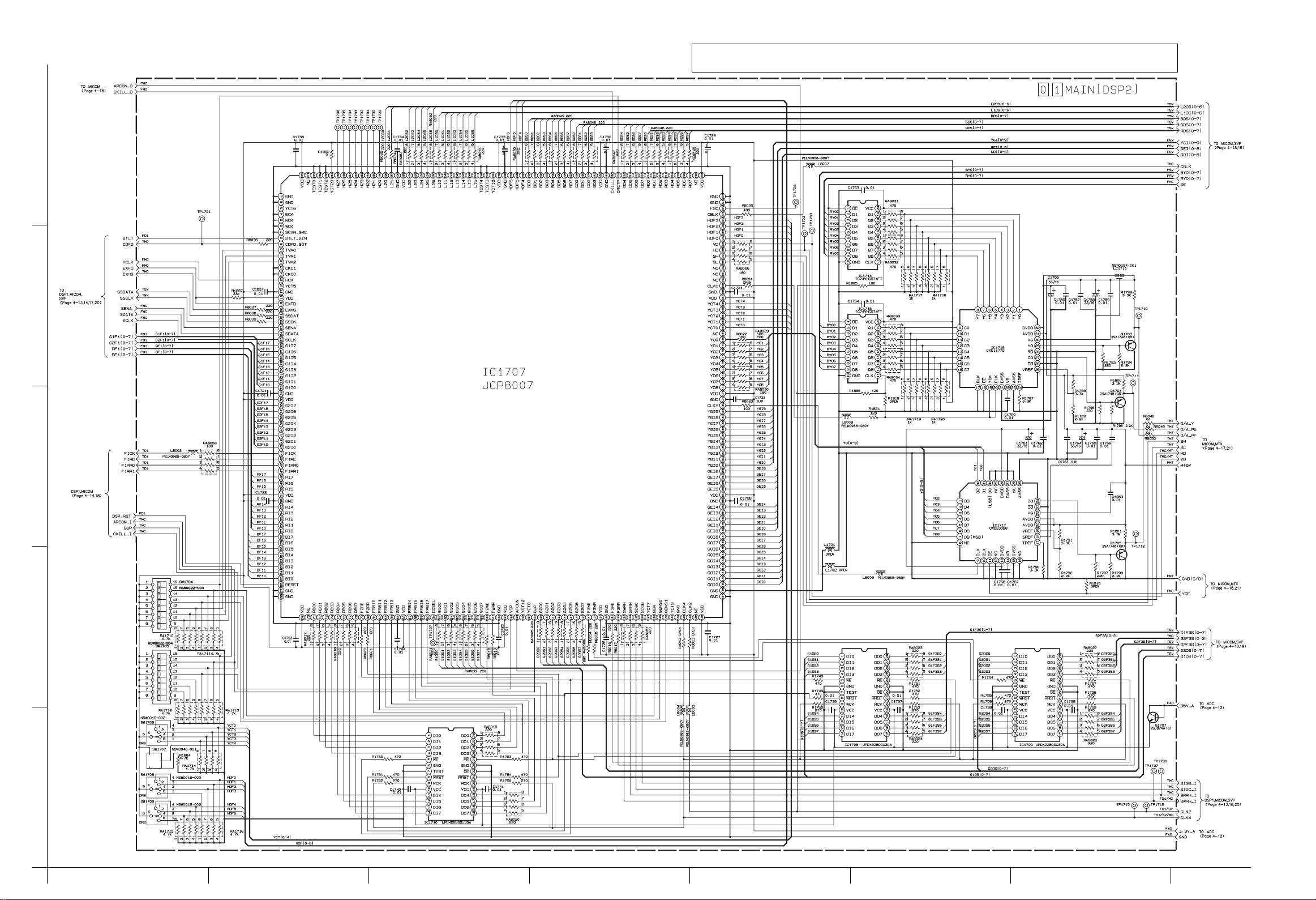
4.7 DSP2 SCHEMATIC DIAGRAM
5
4
Note : The Parts Number, value and rated voltage etc. in the Schematic Diagram are for references only.
When replacing the parts, refer to the Parts List.
3
2
1
A
B
C
DEF
4-15
4-16
G
H
Page 10
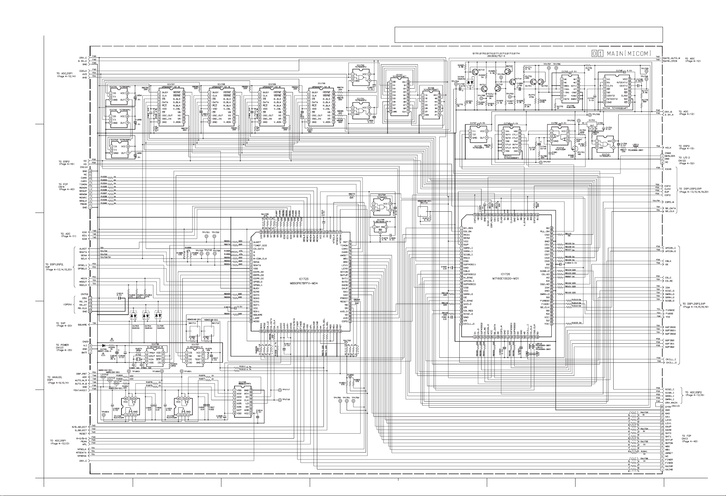
4.8 MICOM SCHEMATIC DIAGRAM
5
4
Note : The Parts Number, value and rated voltage etc. in the Schematic Diagram are for references only.
When replacing the parts, refer to the Parts List.
3
2
1
A
B
C
DEF
4-17
4-18
G
H
Page 11
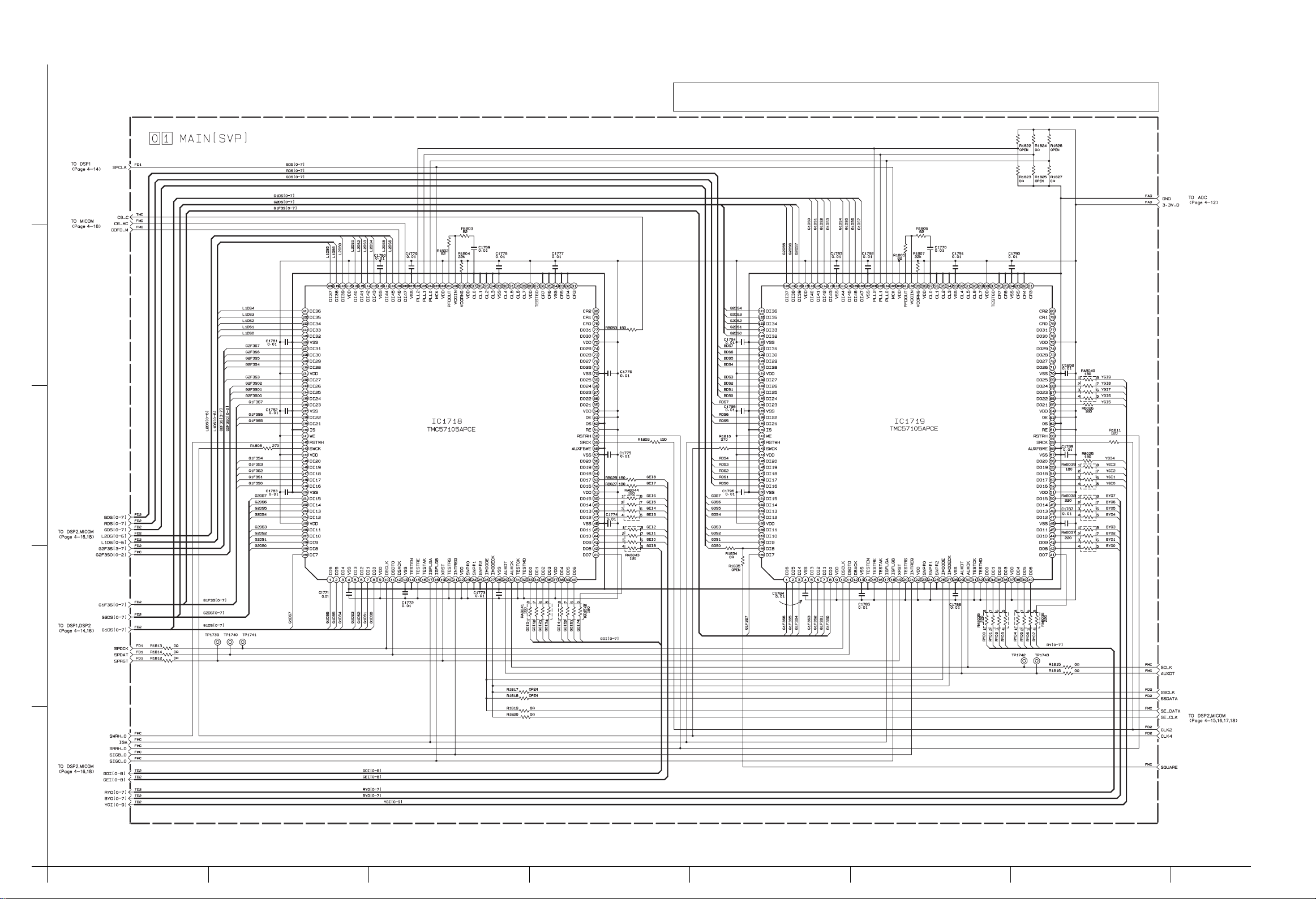
4.9 SVP SCHEMATIC DIAGRAM
5
4
Note : The Parts Number, value and rated voltage etc. in the Schematic Diagram are for references only.
When replacing the parts, refer to the Parts List.
3
2
1
A
B
C
DEF
4-204-19
G
H
Page 12

4.10 MTX SCHEMATIC DIAGRAM
5
4
Note : The Parts Number, value and rated voltage etc. in the Schematic Diagram are for references only.
When replacing the parts, refer to the Parts List.
3
2
1
A
B
C
DEF
4-21 4-22
G
H
Page 13

4.11 MAIN CIRCUIT BO ARD
R
R
R
C
C
C
C
FOIL SIDE(B)(1/2)
NOTE: This board diagram is divided into two for
printing and they appear on two pages.
I
TP1754
TP1753 TP1755TP1757
5
CN131
LC2402
LC2401
7
R1775
C2450 C2449
4
16 16
CN27CN28CN29
IC1744
8
8
VR1701
TP1711
R1946
R1947
9
110
IC1715
20 11
9
16
17
IC1716
24
R1789
25
32
RA8057
TP1715
L8004
L8003
TP1716
110
IC1714
20 11
RA8031 RA8032 RA8033 RA8034
18
TP1710
C1756
C1755 C1758
LC1711
C1727
R1506
TP1501
TP1103
25
32
1
R1507
C1145
C1140
136
137
C1761
9
C1762
16
1724
C1766
L8009
R8023
18
IC1717
C1763
C1764
L8008
R1821
RA8029 RA8030
R8022
32
25
TP1712
F2101 F2201F2301
204
R8029
RA8056
TP1702TP1703
C1729
L8007
205
TP1728
R1606
C1593
TP1505
R1600
R1605
R1604
VR1506
D1504
R1601
R1503R1504
R1505
C1141
C1144
C1827
R1876
C1831
R1829
RA1502 RA1501RA1503RA1504RA1505RA1507 RA1506RA1508RA1509RA1510
17 24
IC1110IC1210IC1310IC1410
8
C1152
C1241
C1244
R1831
R1878
C1829
C1832
TP1801
TP1802
LC1712
LC1713
LC1714
TP1803
TP1804
17 24
C1245
C1252
16
25
9
32
8
C1341
C1344
16
25
9
32
1
C1240
17 24
16
9
8
1
C1352
C1345
C1340
C1444
25
32
C1441
41
TP1713
17 24
16
9
8
1
C1452
C1445
C1440
R1548
R1547
R1631
R1535
R1533
R1534
C1560
C1565
TP1726
Q1507
R1726
Q1508
VR1503 VR1504
80
R1727
SW1702SW1703
R1519
R1520
R1521
R1522
L8010
C1556
Q1509
R1537
R1536
18
C1562
C1561
18
C1566
TP1502
R8131
R8129R8130
R8132
IC1509IC1511
IC1510
R1617
IC1518
IC1517
R8133
VR1502
169
169
TP1508
R1637
R8126
R1638
R8134
R1525
R1524
RA1736
1
CN113
1112131415161718192021
SW1701
R1615
C1720
TP1509
CN15
C1539
R1526
110
110
17
R8121
R8124
IC1516IC1508
IC1501
C1543
F1102
F1302
2011
R1523
C1542
2011
R8122
R8123
148
R8128
C1588
R1626
R1586
C1576
C1578
Q1505
R1582
R1566 R1567
TP1506
C1582
R1583
Q1501
R1570
R1568
Q1506
R1614
R1565
C1584
R1571
R1569
Q1502
C1573
R1589
R1585
R1588
R1573R1574
R1627
R1564
R1587
VR1507
R1575
R1572
C1589
C1575
C1577
C1574
TP1507
Q1503
R1576R1577
D1503
R1592
D1502
C1585
R1561
R1563
R1562
VR2107
R2188
C2141
IC2407
R2121
R2189
R2157
VR2105
R2181
R2191
C2127
C2131
R2180
C2103
R2190
C2410
R2158
VR2104
R2197
R2162
C2452
C2448
17
LC2403
14 8
C2442
TP2104
R1584
TP2101
VR2106
R2184
R2476
R2477
VR2108
C2101
C2138 C2238C2338
C2137C2139 C2237C2239C2337C2339
C2409
C2124C2128
TP2103 TP2203TP2303
C2447
C2451
R2288
C2241
R2415 R2416
R2221
R2289
R2256
R2259
C2227
C2231
R2281
R2291
R2254
R2257
C2405
VR2207
R2290
C2203
TP2204
VR2204
VR2205
R2280
C2408
TP2301
R2384
C2301
C2324C2328
VR2402
VR2401
VR2308
R2388
C2341
R2321
R2389
R2356
C2327
R2359
C2331
R2466
R2410
R2411
R2381
R2391
R2354
R2357
VR2307
R2390
C2303
TP2304
VR2304
VR2305
R2380
R2160R2161
VR2208
TP2402
3
TP2404
R2163
16
R2260
R2360
R2284
C2201
TP2201
C2224C2228
2
TP2403
16
TP2401
C2403
1
TP2406
C1134
TP1102
C1129
R1139
R1140
C1127
R1137
R1135
Q1110
TP1101TP1201TP1301TP1401
C1139
R1121
C1117
R1109
C1114
R1153
R1154
C1109
C1104
C1130
C1135
C1131
VR1103
R1143
R1144
C1126
D1103
Q1111
R1138
R1136
R1134
C1125
Q1108
Q1109
VR1102
C1123
R1132
R1131
R1129
Q1107Q1207Q1307Q1407
R1130
R1128
R1119
R1122
R1111
R1112
D1102
R1117
R1113
Q1102
C1106
C1101
Q1103
C1116
Q1101
R1107
1
R1116
R1118
R1108
CN16
R1114
R1103
R1120
R1142
R1133
Q1104
Q1105
VR1101
VR1104
D1104
TP1202
R1259
C1214
R1240
R1253
R1254
C1234
C1229
R1239
C1227
R1237
R1235
Q1210
R1221
C1239
C1217
R1209
C1209
C1204
8
R1220
R1242
Q1204
Q1205
Q1211
R1233
VR1201
VR1204
Q1209
R1219
R1203
D1204
C1235
VR1202
R1232
R1211
R1212
R1214
R1230
R1222
VR1203
R1238
Q1208
R1231
C1206
C1201
D1202
Q1202
Q1203
C1216
R1228
C1230
Q1201
R1207
D1203
C1223
C1231
R1243
R1244
C1226
R1236
R1234
C1225
R1229
R1217
R1213
R1216
R1218
R1208
R1320
Q1304
Q1305
R1342
Q1311
R1333
VR1301
VR1304
Q1309
R1319
R1303
D1304
C1335
VR1302
R1332
R1311
R1312
R1330
R1322
R1314
C1316
VR1303
R1338
Q1308
R1331
C1306
C1301
R1308
D1302
Q1302
Q1303
C1330
R1328
D1303
C1323
C1331
R1343
R1344
C1326
R1336
R1334
C1325
R1317
R1313
R1316
R1318
R1329
C1337
Q1301
R1307
C1608
TP1302
C1314
R1340
R1354
R1353
C1327
R1337
R1335
R1321
C1334
C1329
R1339
Q1310
C1339
C1317
R1309
C1309
C1304
C1599
C1598
TP1503
R1628
R1634
C1609
C1606
C1607
R1625
R1624
CN34
TP1402
C1414
R1440
R1409
C1427
R1437
R1435
R1421
C1429
C1417
R1439
C1439
C1404
C1434
Q1410
C1409
Q1401
R1420
R1442
Q1404
Q1405
VR1401
R1433
Q1411
D1404
Q1409
VR1402
R1419
R1414
R1403
R1411
R1412
C1416
C1435
R1432
R1430
R1422
R1408
R1407
VR1403
R1438
Q1408
R1431
C1406
C1401
D1402
Q1402
Q1403
R1428
C1430
C1603
LC1502
17 16
CN118
LC1501
C1602
C1502
C1437
D1403
C1423
C1431
R1443
R1444
C1426
R1436
R1434
C1425
R1429
R1417
R1413
R1416
R1418
C1501
4-23
I
H
G
4-24
F
E
D
C
B
G
A
H
A
O
N
M
B
L
K
C
J
DEF
Page 14

FOIL SIDE(B)(2/2)
TP1753 TP1755TP1757
NOTE: This board diagram is divided into two for
printing and they appear on two pages.
O
N
C1850
5
R1884
SW1707
4
R1750R1753 R1756R1759R1762R1765
3
SW1704 SW1705 SW1706 SW1708 SW1709
C1813
M
TP1739TP1740TP1741TP1742TP1743
CN119
15
114
IC1709
28 15
RA8027 RA8028
114
IC1708
28 15
RA8023 RA8024
114
IC1710
28 15
RA8019 RA8020
R1813
R1814
R1812
R1819
R1818
R1820
R1817
R1816
R1815
RA8035RA8036
L
160
140
RA8041RA8042
41
RA8043RA8044
R1835
160
140
41
RA8037RA8038RA8039RA8040
R8027
R8028
K
R8025
R1810
R1808
R1809
R1811
IC1718IC1719
R8026
J
R8053
I
121
C1847
R1822R1823
R1824R1825
R1826R1827
R1802
R1803
C1769
R1804
81 120
80
121
R1805
R1806
C1770
R1807
81 120
80
C1837
LC1704
H
120
R8119 R8120
R8118
R8089
31
R8090
R8091
R8093
R8095
R8096
L8012
L8013
50
5180
R1910
R1915
R8083R8085
IC1729
20 11
R8079R8081
IC1727
20 11
IC1726
R8104R8108
R8100
R8101
R8102
R1951
R8082
110
R1949 R1950
R1948
R8078
110
R8086
G
SW1710
20 11
20 11
R1873
F
TP1737 TP1738
C1846
130
120
81
R8110
IC1730
IC1728
R8114
R8113
R8112
R1871
110
110
C1836
IC1748IC1747
17
20 11 14 8
110
C1852
C1842
LC1709
120
LC1703
CN25 CN26
R1883
E
RA8013 RA8014RA8015 RA8016
LC1710
C1843
120
RA8009 RA8010RA8011 RA8012
Q1706
CN24
C
28 13
28 13
C1848
C1838
R1914R1917
C1853
B
LC1705
R1703 R1706
IC1703IC1704
114
R1709 R1712
114
D
R1901
R1715 R1718
IC1705IC1706
28 13
R1913
R1918
28 13
114
R1721 R1724
114
A
12345678910
1
D1706
TP1704
C1860
R1770
R1944
C1815
5
1
3
X1701
TP1708
1
5
R1781
3
8
1
7
R1775
2
CN23 CN702
CN22
1
TP1754 TP1756
A
R1780
C1864
IC1712
IC1746
X1702
C1749
C1861
1414
14
8
C1865
8
1
8
TP1709
TP1705
C1851
IC1744 IC1711
R1779
TP1707
TP1706
R1946
14
TP1721
TP1722
TP1723
IC1737
85
R1875
R8058
R8059
R8060
C1811
R1877
R1876
IC1725
C1828
C1827
C1832
76
51 75
50
R1879
C1830
R1831
R1878
100
R8061
R8072
125
R8062
R8063
R8064
R1904
R8065
R8066
R8067
26
RA8055
R8068
TP1717 TP1718
C1831
R1830
R1829
C1829
TP1752
TP1751
TP1750
1
2
TP1714TP1724TP1725
RA8001RA8002RA8003RA8004
160
140
R8055
R8056
41
TP1713
IC1701
TP1726
RA8005RA8006
R1726
121
RA8007RA8008
R8004
R8005
R8006
R8007
81 120
80
R1727
L8002
RA8058
C1723
RA8017RA8018
69
R8020
R8021
TP1727
TP1715
RA8021RA8022
RA8025RA8026
RA8057
L8004
L8003
136205
C
7
1
16
9
B
R8039
IC1707
R8038
R8036
1 68
C1735
272
DEF
C1844
TP1736
TP1734TP1735
TP1732TP1733
TP1730TP1731
TP1729
TP1719TP1720
RA8049 RA8050
4-25 4-26
TP1701
SW1711SW1712
LC1702
C1835
112
C1845
C1718
116
IC1702
32 17
G
CN114
RA1733RA1734RA1735RA1736
R1941
120
CN113
H
1
Page 15

COMPONENT PARTS LOCATION GUIDE (MAIN PWB)
REF.No. LOCATION REF.No. LOCATION
CAPACITOR
C1101 A C 20G
C1102 B C 20G
C1103 B C 20H
C1104 A C 20H
C1105 B C 20G
C1106 A C 20G
5
C1107 B C 20G
C1108 B C 20H
C1109 A C 20H
C1110 B C 19H
C1111 B C 19G
C1112 B C 19H
C1113 B C 19H
C1114 A C 19H
C1115 B C 19G
C1116 A C 19G
C1117 A C 18H
C1118 B C 18H
C1119 B C 18G
C1120 B C 18H
C1121 B C 17G
C1122 B C 17H
C1123 A C 17G
4
C1124 B C 15G
C1125 A C 17G
C1126 A C 16G
C1127 A C 17H
C1128 B C 16H
C1129 A C 16H
C1130 A C 15G
C1131 A C 16G
C1132 B C 16G
C1133 B C 16H
C1134 A C 15H
C1135 A C 16G
C1136 B C 13G
C1138 B C 17G
C1139 A C 18H
C1140 A C 15H
3
C1141 A C 14H
C1142 B C 15H
C1143 B C 14H
C1144 A C 15H
C1145 A C 14H
C1146 B C 14G
C1147 B C 13H
C1148 B C 14G
C1149 B C 14G
C1150 B C 14G
C1151 B C 13G
C1152 A C 14G
C1153 B C 14H
C1154 B C 14H
C1201 A C 20F
C1202 B C 20E
C1203 B C 20F
2
C1204 A C 20F
C1205 B C 20E
C1206 A C 20F
C1207 B C 20E
C1208 B C 20F
C1209 A C 20F
C1210 B C 19F
C1211 B C 19E
C1212 B C 19F
C1213 B C 19F
C1214 A C 19F
C1215 B C 19F
C1216 A C 19E
C1217 A C 18F
C1218 B C 18F
C1219 B C 18E
C1220 B C 18F
1
C1221 B C 17E
C1222 B C 17F
C1223 A C 17E
C1224 B C 15E
C1225 A C 17E
C1226 A C 16E
C1227 A C 17F
C1228 B C 16F
C1229 A C 16F
C1230 A C 15E
C1231 A C 16E
C1232 B C 16E
C1233 B C 16F
C1234 A C 15F
C1235 A C 16F
C1236 B C 13F
C1238 B C 17E
C1239 A C 18F
C1240 A C 15G
C1241 A C 14G
C1242 B C 15G
C1243 B C 14G
C1244 A C 15G
C1245 A C 14G
C1246 B C 14G
C1247 B C 13G
C1248 B C 14F
C1249 B C 14F
C1250 B C 14F
C1251 B C 13F
C1252 A C 14F
C1253 B C 14G
C1254 B C 14G
C1301 A C 20D
C1302 B C 20D
C1303 B C 20D
C1304 A C 20D
C1305 B C 20D
C1306 A C 20D
C1307 B C 20D
C1308 B C 20D
C1309 A C 20D
C1310 B C 19E
C1311 B C 19D
C1312 B C 19D
C1313 B C 19D
C1314 A C 19E
C1315 B C 19D
C1316 A C 19D
C1317 A C 18D
C1318 B C 18D
C1319 B C 18D
C1320 B C 18D
C1321 B C 17D
C1322 B C 17D
C1323 A C 17D
C1324 B C 15D
C1325 A C 17D
C1326 A C 16D
C1327 A C 17D
C1328 B C 16D
C1329 A C 16D
C1330 A C 15D
C1331 A C 16D
C1332 B C 16D
C1333 B C 16D
C1334 A C 15D
C1335 A C 16D
C1336 B C 13F
C1337 A C 19D
C1338 B C 17D
C1339 A C 18D
C1340 A C 15F
C1341 A C 14F
C1342 B C 15F
C1343 B C 14F
C1344 A C 15F
C1345 A C 14F
C1346 B C 14F
C1347 B C 13F
C1348 B C 14F
C1349 B C 14F
C1350 B C 14E
C1351 B C 13F
C1352 A C 14F
C1353 B C 14F
C1354 B C 14F
C1401 A C 20B
C1402 B C 20B
C1403 B C 20C
C1404 A C 20C
C1405 B C 20B
C1406 A C 20B
C1407 B C 20B
C1408 B C 20C
C1409 A C 20C
C1410 B C 19C
C1411 B C 19B
C1412 B C 19C
C1413 B C 19C
C1414 A C 19C
C1415 B C 19B
C1416 A C 19B
C1417 A C 18C
C1418 B C 18C
C1419 B C 18B
C1420 B C 18C
C1421 B C 17B
C1422 B C 17C
C1423 A C 17B
C1424 B C 15B
C1425 A C 17B
C1426 A C 16B
C1427 A C 17C
C1428 B C 16C
C1429 A C 16C
C1430 A C 15B
C1431 A C 16B
C1432 B C 16B
C1433 B C 16C
C1434 A C 15C
C1435 A C 16B
C1436 B C 13E
C1437 A C 19B
C1438 B C 17B
C1439 A C 18C
C1440 A C 15E
C1441 A C 14E
C1442 B C 15E
C1443 B C 14E
C1444 A C 15E
C1445 A C 14E
C1446 B C 14E
C1447 B C 13E
C1448 B C 14E
C1449 B C 14E
C1450 B C 14E
C1451 B C 13E
C1452 A C 14E
C1453 B C 14E
C1454 B C 14E
C1501 A C 20B
C1502 A C 19B
C1539 A C 12B
C1540 B C 12C
C1541 B C 12B
C1542 A C 13B
C1543 A C 13B
C1544 B C 13C
C1545 B C 13C
C1546 B C 14B
C1548 B C 14B
C1549 B C 14C
C1550 B C 14C
C1551 B C 14C
C1552 B C 14C
C1553 B C 15C
C1554 B C 14C
C1555 B C 14C
C1556 A C 13C
C1557 B C 13D
C1558 B C 13C
C1559 B C 13D
REF.No. LOCATION
C1560 A C 13D
C1561 A C 14C
C1562 A C 14C
C1563 B C 14D
C1564 B C 14C
C1565 A C 14D
C1566 A C 14C
C1567 B C 14D
C1568 B C 15C
C1569 B C 14B
C1570 B C 14B
C1571 B C 16E
C1572 B C 15E
C1573 A C 17I
C1574 A C 17I
C1575 A C 16I
C1576 A C 16I
C1577 A C 16I
C1578 A C 16I
C1579 B C 19I
C1580 B C 19I
C1581 B C 19I
C1582 A C 18I
C1583 B C 18I
C1584 A C 17I
C1585 A C 18I
C1586 B C 18I
C1587 B C 17I
C1588 A C 15I
C1589 A C 16I
C1590 B C 15I
C1591 B C 15I
C1592 B C 14I
C1593 A C 14I
C1594 B C 14I
C1595 B C 14I
C1596 B C 13I
C1597 B C 20I
C1598 A C 16E
C1599 A C 15E
C1602 A C 18A
C1603 A C 16A
C1604 B C 13C
C1605 B C 13C
C1606 A C 17E
C1607 A C 18E
C1608 A C 17E
C1609 A C 17E
C1610 B C 15C
C1611 B C 15D
C1612 B C 15D
C1701 B C 3B
C1702 B C 3C
C1703 B C 5B
C1704 B C 5C
C1705 B C 3D
C1706 B C 3E
C1707 B C 5D
C1708 B C 5E
C1709 B C 9E
C1710 B C 10E
C1711 B C 10E
C1712 B C 11D
C1713 B C 10C
C1714 B C 10C
C1715 B C 9C
C1716 B C 9C
C1717 B C 9D
C1718 A C 9B
C1719 B C 11A
C1720 A C 12A
C1721 B C 9K
C1722 B C 9K
C1723 A C 9L
C1724 B C 9L
C1725 B C 10L
C1726 B C 10L
C1727 A C 11L
C1728 B C 11K
REF.No. LOCATION
C1729 A C 11I
C1730 B C 10J
C1731 B C 11J
C1732 B C 11K
C1733 B C 10J
C1734 B C 9J
C1735 A C 9I
C1736 B C 4N
C1737 B C 4N
C1738 B C 2N
C1739 B C 3N
C1740 B C 5N
C1741 B C 6N
C1742 B C 10O
C1743 B C 11N
C1744 B C 10N
C1745 B C 10N
C1746 B C 11N
C1747 B C 10N
C1748 B C 10N
C1749 A C 10N
C1750 B C 10O
C1751 B C 8O
C1752 B C 9N
C1753 B C 12L
C1754 B C 12M
C1755 A C 14M
C1756 A C 13M
C1757 B C 13M
C1758 A C 14M
C1759 B C 13M
C1760 B C 13M
C1761 A C 13K
C1762 A C 13K
C1763 A C 13K
C1764 A C 13K
C1765 B C 13K
C1766 A C 13K
C1767 B C 13K
C1768 B C 13K
C1769 A C 3I
C1770 A C 6I
C1771 B C 2L
C1772 B C 3L
C1773 B C 3L
C1774 B C 4K
C1775 B C 4K
C1776 B C 4J
C1777 B C 3J
C1778 B C 3J
C1779 B C 2J
C1780 B C 2J
C1781 B C 2J
C1782 B C 2K
C1783 B C 2K
C1784 B C 5L
C1785 B C 6L
C1786 B C 6L
C1787 B C 7K
C1789 B C 7K
C1790 B C 6J
C1791 B C 6J
C1792 B C 6J
C1793 B C 5J
C1794 B C 5J
C1795 B C 5K
C1796 B C 5K
C1797 B C 1C
C1798 B C 1D
C1799 B C 1E
C1800 B C 1F
C1801 B C 2G
C1802 B C 6G
C1803 B C 6F
C1804 B C 5G
C1805 B C 5F
C1806 B C 5G
C1807 B C 5G
C1808 B C 8F
REF.No. LOCATION REF.No. LOCATIONREF.No. LOCATION
C1809 B C 8G
C1810 B C 9G
C1811 A C 10G
C1812 B C 10H
C1813 A C 7O
C1814 B C 11H
C1815 A C 8O
C1816 B C 8O
C1817 B C 8H
C1820 B C 3G
C1821 B C 3G
C1822 B C 3H
C1823 B C 4H
C1824 B C 3G
C1825 B C 3G
C1826 B C 11H
C1827 A C 11G
C1828 A C 11G
C1829 A C 11F
C1830 A C 11F
C1831 A C 11G
C1832 A C 11G
C1834 B C 8I
C1835 A C 8B
C1836 A C 3F
C1837 A C 2I
C1838 A C 2C
C1840 B C 1O
C1841 B C 8N
C1842 A C 6F
C1843 A C 7C
C1844 A C 8I
C1845 A C 8B
C1846 A C 3F
C1847 A C 2I
C1848 A C 1C
C1850 A C 1N
C1851 A C 8N
C1852 A C 6F
C1853 A C 7C
C1854 B C 7G
C1855 B C 7G
C1856 B C 6G
C1857 B C 9J
C1858 B C 7J
C1859 B C 13K
C1860 A C 11O
C1861 A C 10N
C1862 B C 4H
C1863 B C 4H
C1864 A C 7N
C1865 A C 7N
C2101 A C 16K
C2102 B C 16K
C2103 A C 16J
C2104 B C 16J
C2107 B C 16K
C2108 B C 16J
C2124 A C 17K
C2125 B C 17K
C2126 B C 18J
C2127 A C 18J
C2128 A C 18K
C2129 B C 18K
C2130 B C 18J
C2131 A C 18J
C2132 B C 19K
C2133 B C 19J
C2137 A C 16K
C2138 A C 16K
C2139 A C 16J
C2140 B C 17J
C2141 A C 17J
C2201 A C 16N
C2202 B C 16N
C2203 A C 16M
C2204 B C 16N
C2207 B C 16N
C2208 B C 16N
C2224 A C 17N
C2225 B C 17N
C2226 B C 18M
C2227 A C 18N
C2228 A C 18N
C2229 B C 18N
C2230 B C 18M
C2231 A C 18N
C2232 B C 19L
C2233 B C 19N
C2237 A C 16N
C2238 A C 16N
C2239 A C 16N
C2240 B C 17N
C2241 A C 17N
C2301 A C 16M
C2302 B C 16L
C2303 A C 16L
C2304 B C 16L
C2307 B C 16L
C2308 B C 16L
C2324 A C 17M
C2325 B C 17L
C2326 B C 18L
C2327 A C 18L
C2328 A C 18M
C2329 B C 18L
C2330 B C 18L
C2331 A C 18L
C2332 B C 19N
C2333 B C 19L
C2337 A C 16L
C2338 A C 16L
C2339 A C 16L
C2340 B C 17L
C2341 A C 17L
C2401 B C 20L
C2402 B C 20K
C2403 A C 20N
C2404 B C 20N
C2405 A C 20N
C2406 B C 20N
C2407 B C 20M
C2408 A C 20M
C2409 A C 17K
C2410 A C 17J
C2442 A C 21J
C2447 A C 19K
C2448 A C 19J
C2450 A D 13O
C2451 A C 19K
C2452 A C 19J
CONNECTOR
CN15 A C 15A
CN16 A C 21G
CN22 A C 10O
CN23 A C 9O
CN24 A C 1C
CN25 A C 1E
CN26 A C 1H
CN27 A C 15O
CN28 A C 16O
CN29 A C 20O
CN34 A D 21E
CN113 A C 11A
CN114 A C 8A
CN118 A C 17A
CN119 A C 1M
CN131 A C 12O
CN702 A C 7O
DIODE
D1101 B C 19G
D1102 A C 18G
D1103 A C 16G
D1104 A C 21G
D1201 B C 19F
D1202 A C 18F
REF.No. LOCATION
D1203 A C 16E
D1204 A C 21F
D1301 B C 19D
D1302 A C 18D
D1303 A C 16D
D1304 A C 21D
D1401 B C 19B
D1402 A C 18B
D1403 A C 16B
D1404 A C 21B
D1502 A C 19I
D1503 A C 18I
D1504 A C 15I
D1505 B C 13I
D1506 B C 15A
D1507 B C 14A
D1508 B C 14A
D1509 B C 15A
D1510 B C 15A
D1511 B C 17E
D1701 B C 12A
D1702 B C 10O
D1703 B C 8O
D1704 B C 8O
D1705 B C 7O
D1706 A C 8O
D2104 B C 16K
D2105 B C 18J
D2204 B C 16N
D2205 B C 18N
D2304 B C 16L
D2305 B C 18L
D2401 B C 20O
D2402 B C 20O
D2403 B C 20O
IC
IC1101 B C 20G
IC1102 B C 20G
IC1103 B C 18G
IC1104 B C 17G
IC1105 B C 16G
IC1106 B C 16G
IC1108 B C 19G
IC1109 B C 14H
IC1110 A C 13G
IC1201 B C 20F
IC1202 B C 20F
IC1203 B C 18F
IC1204 B C 17F
IC1205 B C 16F
IC1206 B C 16F
IC1208 B C 19F
IC1209 B C 14G
IC1210 A C 13F
IC1301 B C 20D
IC1302 B C 20D
IC1303 B C 18D
IC1304 B C 17D
IC1305 B C 16D
IC1306 B C 16D
IC1308 B C 19D
IC1309 B C 14F
IC1310 A C 13F
IC1401 B C 20B
IC1402 B C 20B
IC1403 B C 18B
IC1404 B C 17B
IC1405 B C 16B
IC1406 B C 16B
IC1408 B C 19B
IC1409 B C 14E
IC1410 A C 13E
IC1501 A C 14B
IC1508 A C 15B
IC1509 A C 14C
IC1510 A C 13C
IC1511 A C 14C
IC1512 B C 13D
REF.No. LOCATION REF.No. LOCATION
IC1513 B C 14D
IC1514 B C 14D
IC1515 B C 12C
IC1516 A C 13B
IC1517 A C 13C
IC1518 A C 13C
IC1519 B C 16E
IC1520 B C 17I
IC1521 B C 16I
IC1522 B C 16I
IC1523 B C 15I
IC1524 B C 15I
IC1525 B C 14I
IC1526 B C 14I
IC1527 B C 19I
IC1528 B C 18I
IC1529 B C 18I
IC1530 B C 20I
IC1531 B C 17E
IC1532 B C 17E
IC1533 B C 15D
IC1701 A C 10D
IC1702 A C 10B
IC1703 A C 3C
IC1704 A C 5C
IC1705 A C 3D
IC1706 A C 5D
IC1707 A C 10K
IC1708 A C 4M
IC1709 A C 2M
IC1710 A C 6M
IC1711 A C 10N
IC1712 A C 10O
IC1713 B C 9N
IC1714 A C 12M
IC1715 A C 12M
IC1716 A C 13M
IC1717 A C 13K
IC1718 A C 3K
IC1719 A C 6K
IC1720 B C 2C
IC1721 B C 2D
IC1722 B C 2F
IC1723 B C 2F
IC1724 B C 2H
IC1725 A C 9G
IC1726 A C 4G
IC1727 A C 6H
IC1728 A C 6G
IC1729 A C 5H
IC1730 A C 5G
IC1731 B C 5G
IC1732 B C 5G
IC1734 B C 8G
IC1735 B C 8F
IC1736 B C 8N
IC1737 A C 8H
IC1738 B C 11H
IC1739 B C 11G
IC1740 B C 11G
IC1741 B C 7G
IC1742 B C 6G
IC1743 B C 7G
IC1744 A C 11N
IC1745 B C 10N
IC1746 A C 11O
IC1747 A C 5F
IC1748 A C 5F
IC2101 B C 16J
IC2104 B C 17J
IC2105 B C 18J
IC2201 B C 16N
IC2204 B C 17N
IC2205 B C 18N
IC2301 B C 16L
IC2304 B C 17L
IC2305 B C 18L
IC2401 B C 20N
IC2407 A C 20K
NOISE FILTER
L8001 B C 8D
L8002 A C 8K
L8003 A C 11L
L8004 A C 11L
L8005 B C 1H
L8006 B C 1H
L8007 A C 11J
L8008 A C 11J
L8009 A C 11K
L8010 A C 13C
L8011 B C 9N
L8012 A C 4H
L8013 A C 4H
L8014 B C 13G
EMI FILTER
LC1501
A C 18A
LC1502
A C 16A
LC1701
BC8I
LC1702
AC8B
LC1703
AC3E
LC1704
AC2I
LC1705
AC2C
LC1707
BC1N
LC1708
BC8N
LC1709
AC7F
LC1710
AC7C
LC1711
A C 14L
LC1712
A C 11G
LC1713
A C 11G
LC1714
A C 11G
LC2401
A C 12O
LC2402
A C 13O
LC2403
A C 21J
TRANSISTOR
Q1101 A C 19G
Q1102 A C 19G
Q1103 A C 19G
Q1104 A C 19H
Q1105 A C 19H
Q1106 B C 18G
Q1107 A C 18G
Q1108 A C 17G
Q1109 A C 17G
Q1110 A C 17H
Q1111 A C 17H
Q1112 B C 17H
Q1201 A C 19E
Q1202 A C 18F
Q1203 A C 19F
Q1204 A C 19F
Q1205 A C 19F
Q1206 B C 18F
Q1207 A C 18F
Q1208 A C 17F
Q1209 A C 17F
Q1210 A C 17F
Q1211 A C 17F
Q1212 B C 17F
Q1301 A C 19D
Q1302 A C 18D
Q1303 A C 19D
Q1304 A C 18D
Q1305 A C 19D
Q1306 B C 18D
Q1307 A C 18D
Q1308 A C 17D
Q1309 A C 17D
Q1310 A C 17D
Q1311 A C 17D
Q1312 B C 17D
Q1401 A C 19C
Q1402 A C 19B
Q1403 A C 19B
Q1404 A C 19C
Q1405 A C 19C
Q1406 B C 18B
REF.No. LOCATION REF.No. LOCATION
Q1407 A C 18B
Q1408 A C 17B
Q1409 A C 17B
Q1410 A C 17C
Q1411 A C 17C
Q1412 B C 17C
Q1501 A C 20I
Q1502 A C 20I
Q1503 A C 20I
Q1504 B C 19I
Q1505 A C 19I
Q1506 A C 18I
Q1507 A C 14D
Q1508 A C 14D
Q1509 A C 14C
Q1510 B C 18B
Q1511 B C 19B
Q1701 B C 10O
Q1702 B C 10O
Q1703 B C 14M
Q1704 B C 14M
Q1705 B C 13J
Q1706 A C 6C
Q1707 B C 1N
Q1710 B C 10O
Q1711 B C 10O
Q1712 B C 10O
Q1713 B C 10O
Q1714 B C 10O
Q2101 B C 14K
Q2115 B C 17J
Q2120 B C 16J
Q2121 B C 16K
Q2122 B C 17J
Q2201 B C 14N
Q2213 B C 17M
Q2220 B C 16N
Q2221 B C 16N
Q2222 B C 17M
Q2301 B C 14M
Q2313 B C 17L
Q2320 B C 16L
Q2321 B C 16M
Q2322 B C 17L
Q2401 B C 20L
Q2402 B C 20L
Q2404 B C 20M
Q2405 B C 20M
Q2406 B C 20L
Q2407 B C 20L
Q2408 B C 20M
Q2409 B C 20M
RESISTOR
R1101 B C 21H
R1102 B C 21G
R1103 A C 20G
R1104 B C 20G
R1105 B C 19H
R1106 B C 19H
R1107 A C 19G
R1108 A C 19G
R1109 A C 19H
R1110 B C 19H
R1111 A C 18G
R1112 A C 18G
R1113 A C 18G
R1114 A C 19G
R1115 B C 19G
R1116 A C 19G
R1117 A C 18G
R1118 A C 19G
R1119 A C 18G
R1120 A C 18H
R1121 A C 18H
R1122 A C 18G
R1123 B C 18G
R1124 B C 18H
R1125 B C 18G
R1126 B C 17H
R1127 B C 17G
R1128 A C 18G
R1129 A C 18G
R1130 A C 18G
R1131 A C 17G
R1132 A C 17G
R1133 A C 18G
R1134 A C 17G
R1135 A C 17H
R1136 A C 17G
R1137 A C 17H
R1138 A C 17G
R1139 A C 16H
R1140 A C 16H
R1141 B C 16G
R1142 A C 16H
R1143 A C 16G
R1144 A C 16G
R1145 B C 13G
R1153 A C 19H
R1154 A C 20H
R1155 B C 17H
R1156 B C 17H
R1157 B C 17H
R1158 B C 13G
R1201 B C 21F
R1202 B C 21F
R1203 A C 20F
R1204 B C 20F
R1205 B C 19F
R1206 B C 19F
R1207 A C 19E
R1208 A C 19E
R1209 A C 19F
R1210 B C 19F
R1211 A C 18F
R1212 A C 18F
R1213 A C 18E
R1214 A C 19F
R1215 B C 19F
R1216 A C 19E
R1217 A C 18E
R1218 A C 19E
R1219 A C 18F
R1220 A C 18F
R1221 A C 18F
R1222 A C 18F
R1223 B C 18E
R1224 B C 18F
R1225 B C 18F
R1226 B C 17F
R1227 B C 17E
R1228 A C 18F
R1229 A C 18E
R1230 A C 18F
R1231 A C 17F
R1232 A C 17F
R1233 A C 18F
R1234 A C 17E
R1235 A C 17F
R1236 A C 17E
R1237 A C 17F
R1238 A C 17F
R1239 A C 16F
R1240 A C 16F
R1241 B C 16F
R1242 A C 16F
R1243 A C 16E
R1244 A C 16E
R1245 B C 13F
R1253 A C 19F
R1254 A C 20F
R1255 B C 17F
R1256 B C 17F
R1257 B C 17F
R1258 B C 13F
R1259 A C 16F
R1301 B C 21D
REF.No. LOCATION REF.No. LOCATION
R1302 B C 21D
R1303 A C 20D
R1304 B C 20D
R1305 B C 19E
R1306 B C 19E
R1307 A C 19D
R1308 A C 19D
R1309 A C 19D
R1310 B C 19D
R1311 A C 18D
R1312 A C 18D
R1313 A C 18D
R1314 A C 18D
R1315 B C 19D
R1316 A C 19D
R1317 A C 18D
R1318 A C 19D
R1319 A C 18D
R1320 A C 18D
R1321 A C 18D
R1322 A C 18D
R1323 B C 18D
R1324 B C 18D
R1325 B C 18D
R1326 B C 17D
R1327 B C 17D
R1328 A C 18D
R1329 A C 18D
R1330 A C 18D
R1331 A C 17D
R1332 A C 17D
R1333 A C 18D
R1334 A C 17D
R1335 A C 17D
R1336 A C 17D
R1337 A C 17D
R1338 A C 17D
R1339 A C 16D
R1340 A C 16E
R1341 B C 16D
R1342 A C 16D
R1343 A C 16D
R1344 A C 16D
R1345 B C 13F
R1346 B C 19D
R1349 B C 19D
R1350 B C 19D
R1351 B C 19D
R1352 B C 19D
R1353 A C 19E
R1354 A C 20E
R1355 B C 17D
R1356 B C 17D
R1357 B C 17E
R1358 B C 13E
R1401 B C 21C
R1402 B C 21B
R1403 A C 20B
R1404 B C 20B
R1405 B C 19C
R1406 B C 19C
R1407 A C 19B
R1408 A C 19B
R1409 A C 19C
R1410 B C 19C
R1411 A C 18B
R1412 A C 18B
R1413 A C 18B
R1414 A C 19B
R1415 B C 19B
R1416 A C 19B
R1417 A C 18B
R1418 A C 19B
R1419 A C 18B
R1420 A C 18C
R1421 A C 18C
R1422 A C 18B
R1423 B C 18B
R1424 B C 18C
R1425 B C 18B
R1426 B C 17C
R1427 B C 17B
R1428 A C 18B
R1429 A C 18B
R1430 A C 18B
R1431 A C 17B
R1432 A C 17B
R1433 A C 18B
R1434 A C 17B
R1435 A C 17C
R1436 A C 17B
R1437 A C 17C
R1438 A C 17B
R1439 A C 16C
R1440 A C 16C
R1441 B C 16B
R1442 A C 16C
R1443 A C 16B
R1444 A C 16B
R1445 B C 13E
R1446 B C 19B
R1449 B C 19B
R1450 B C 19B
R1451 B C 19B
R1452 B C 19B
R1455 B C 17C
R1456 B C 17C
R1457 B C 17C
R1458 B C 13E
R1501 B C 18B
R1502 B C 18B
R1503 A C 14H
R1504 A C 14H
R1505 A C 14H
R1506 A C 14H
R1507 A C 14H
R1517 B C 14B
R1518 B C 14B
R1519 A C 12C
R1520 A C 12C
R1521 A C 12C
R1522 A C 13C
R1523 A C 13B
R1524 A C 13C
R1525 A C 13C
R1526 A C 13B
R1527 B C 15B
R1528 B C 15B
R1529 B C 14C
R1530 B C 14C
R1531 B C 14C
R1532 B C 15C
R1533 A C 14D
R1534 A C 14D
R1535 A C 13D
R1536 A C 14C
R1537 A C 14C
R1538 B C 13D
R1539 B C 13D
R1540 B C 14D
R1541 B C 14C
R1542 B C 14D
R1543 B C 14D
R1544 B C 14D
R1545 B C 14C
R1546 B C 15D
R1547 A C 14D
R1548 A C 14D
R1549 B C 15D
R1550 B C 14D
R1551 B C 14C
R1552 B C 20B
R1553 B C 20C
R1554 B C 20C
R1557 B C 15E
R1558 B C 15E
R1559 B C 15E
R1560 B C 16E
A
B
C
DEF
4-27
4-28
G
H
Page 16

REF.No. LOCATION
R1561 A C 17H
R1562 A C 17H
R1563 A C 17H
R1564 A C 17I
R1565 A C 17I
R1566 A C 20I
R1567 A C 19I
5
R1568 A C 20I
R1569 A C 20I
R1570 A C 19I
R1571 A C 19I
R1572 A C 20I
R1573 A C 19I
R1574 A C 20I
R1575 A C 19I
R1576 A C 19I
R1577 A C 20I
R1578 B C 19I
R1579 B C 19I
R1580 B C 19I
R1581 B C 19I
R1582 A C 19I
R1583 A C 18I
R1584 A C 18I
4
R1585 A C 18I
R1586 A C 18I
R1587 A C 18I
R1588 A C 18I
R1589 A C 18I
R1590 B C 18I
R1591 B C 19H
R1592 A C 19I
R1593 B C 19I
R1594 B C 17H
R1595 B C 18H
R1596 B C 15I
R1597 B C 15I
R1598 B C 15I
R1599 B C 15I
R1600 A C 15I
3
R1601 A C 15I
R1602 B C 15I
R1603 B C 15I
R1604 A C 14I
R1605 A C 14I
R1606 A C 13I
R1607 B C 14I
R1608 B C 20H
R1609 B C 20H
R1610 B C 20H
R1611 B C 18B
R1612 B C 14C
R1613 B C 15I
R1614 A C 17I
R1615 A C 15B
R1616 B C 15C
R1617 A C 13C
2
R1618 B C 19B
R1619 B C 18B
R1620 B C 19B
R1621 B C 19B
R1622 B C 18E
R1623 B C 18E
R1624 A C 18E
R1625 A C 18E
R1626 A C 15I
R1627 A C 15I
R1628 A C 17E
R1629 B C 17E
R1630 B C 17E
R1631 A C 14D
R1632 B C 16E
R1633 B C 14I
R1634 A C 17E
1
R1635 B C 15D
R1636 B C 15D
R1637 A C 13B
R1638 A C 13C
R1701 B C 3B
REF.No. LOCATION REF.No. LOCATION
R1702 B C 3B
R1703 A C 3B
R1704 B C 3C
R1705 B C 3C
R1706 A C 3C
R1707 B C 5B
R1708 B C 5B
R1709 A C 5B
R1710 B C 5C
R1711 B C 5C
R1712 A C 5C
R1713 B C 3D
R1714 B C 3D
R1715 A C 3D
R1716 B C 3E
R1717 B C 3E
R1718 A C 3E
R1719 B C 5D
R1720 B C 5D
R1721 A C 5D
R1722 B C 5E
R1723 B C 5E
R1724 A C 5E
R1725 B C 12A
R1726 A C 11D
R1727 A C 11C
R1728 B C 9D
R1729 B C 9D
R1730 B C 9D
R1731 B C 9D
R1732 B C 9D
R1733 B C 9D
R1734 B C 9D
R1735 B C 9D
R1736 B C 9D
R1737 B C 9D
R1738 B C 9D
R1739 B C 9D
R1748 B C 4M
R1749 B C 4M
R1750 A C 4M
R1751 B C 4M
R1752 B C 4M
R1753 A C 5M
R1754 B C 2M
R1755 B C 2M
R1756 A C 2M
R1757 B C 3M
R1758 B C 3M
R1759 A C 3M
R1760 B C 5M
R1761 B C 5M
R1762 A C 5M
R1763 B C 6M
R1764 B C 6M
R1765 A C 6M
R1770 A C 10O
R1771 B C 11N
R1772 B C 11N
R1773 B C 11O
R1774 B C 11O
R1775 A C 11O
R1776 B C 10N
R1777 B C 11N
R1778 B C 11N
R1779 A C 9N
R1780 A C 10O
R1781 A C 10O
R1782 B C 10O
R1787 B C 13M
R1788 B C 13M
R1789 A C 13M
R1790 B C 13K
R1791 B C 13K
R1792 B C 13K
R1793 B C 14M
R1794 B C 14M
R1795 B C 14M
R1796 B C 14M
R1797 B C 13J
R1798 B C 13J
R1799 B C 14M
R1800 B C 14M
R1801 B C 13K
R1802 A C 3J
R1803 A C 3J
R1804 A C 3J
R1805 A C 6J
R1806 A C 6J
R1807 A C 6J
R1808 A C 1K
R1809 A C 4K
R1810 A C 4K
R1811 A C 7K
R1812 A C 6L
R1813 A C 5L
R1814 A C 5L
R1815 A C 6L
R1816 A C 6L
R1817 A C 6L
R1818 A C 6L
R1819 A C 6L
R1820 A C 6L
R1821 A C 12J
R1822 A C 2I
R1823 A C 2I
R1824 A C 2I
R1825 A C 2I
R1826 A C 2I
R1827 A C 2I
R1828 B C 10G
R1829 A C 11G
R1830 A C 11G
R1831 A C 11G
R1832 B C 9G
R1833 B C 8N
R1834 B C 6K
R1835 A C 4L
R1858 B C 1H
R1859 B C 1H
R1860 B C 1H
R1861 B C 1H
R1862 B C 1H
R1863 B C 1I
R1864 B C 1H
R1865 B C 1H
R1866 B C 1I
R1867 B C 1I
R1871 A C 5F
R1872 B C 9F
R1873 A C 2G
R1874 B C 8O
R1875 A C 8H
R1876 A C 11G
R1877 A C 11G
R1878 A C 11F
R1879 A C 11G
R1880 B C 10H
R1881 B C 10H
R1882 B C 9J
R1883 A C 1E
R1884 A C 2O
R1885 B C 12M
R1886 B C 12M
R1887 B C 9J
R1888 B C 9H
R1889 B C 9H
R1890 B C 9H
R1891 B C 9G
R1892 B C 9G
R1893 B C 9G
R1895 B C 9H
R1896 B C 9H
R1897 B C 9G
R1898 B C 9G
R1899 B C 9G
R1900 B C 9G
R1901 A C 1D
REF.No. LOCATION
R1902 B C 10H
R1903 B C 10H
R1904 A C 9H
R1910 A C 4H
R1911 B C 10G
R1912 B C 10G
R1913 A C 4E
R1914 A C 4C
R1915 A C 4H
R1916 B C 13K
R1917 A C 4C
R1918 A C 4D
R1919 B C 13M
R1920 B C 10O
R1921 B C 10O
R1922 B C 10O
R1923 B C 10O
R1924 B C 10O
R1925 B C 10O
R1926 B C 10O
R1927 B C 10O
R1928 B C 10O
R1929 B C 11O
R1932 B C 8A
R1933 B C 8A
R1934 B C 8A
R1935 B C 8A
R1936 B C 8A
R1937 B C 8A
R1938 B C 8A
R1939 B C 8A
R1940 B C 8A
R1941 A C 11B
R1942 B C 1I
R1943 B C 1I
R1944 A C 8O
R1945 B C 10O
R1946 A C 11N
R1947 A C 11N
R1948 A C 6G
R1949 A C 6G
R1950 A C 5G
R1951 A C 5G
R2101 B C 14K
R2102 B C 15K
R2103 B C 14K
R2104 B C 14K
R2120 B C 16J
R2121 A C 16K
R2122 B C 16K
R2155 B C 17J
R2156 B C 17J
R2157 A C 17K
R2158 A C 17J
R2159 B C 17J
R2160 A C 18K
R2161 A C 18K
R2162 A C 18J
R2163 A C 16O
R2180 A C 16J
R2181 A C 16J
R2182 B C 16K
R2183 B C 16J
R2184 A C 16K
R2185 B C 16K
R2186 B C 16K
R2187 B C 16K
R2188 A C 16K
R2189 A C 16K
R2190 A C 16J
R2191 A C 16J
R2192 B C 17J
R2193 B C 17J
R2194 B C 17J
R2195 B C 17J
R2196 B C 17J
R2197 A C 18J
R2201 B C 14N
R2202 B C 15N
REF.No. LOCATION
R2203 B C 14N
R2204 B C 14N
R2220 B C 16M
R2221 A C 16N
R2222 B C 16N
R2251 B C 17N
R2252 B C 17M
R2253 B C 18M
R2254 A C 17N
R2255 B C 18N
R2256 A C 17N
R2257 A C 18N
R2258 B C 18M
R2259 A C 18N
R2260 A C 17O
R2280 A C 16M
R2281 A C 16N
R2282 B C 16N
R2283 B C 16N
R2284 A C 16N
R2285 B C 16N
R2286 B C 16N
R2287 B C 16N
R2288 A C 16N
R2289 A C 16N
R2290 A C 16N
R2291 A C 16N
R2292 B C 17N
R2293 B C 17M
R2294 B C 17N
R2295 B C 17N
R2296 B C 17M
R2301 B C 14M
R2302 B C 15M
R2303 B C 14L
R2304 B C 14M
R2320 B C 16L
R2321 A C 16L
R2322 B C 16L
R2351 B C 17L
R2352 B C 17L
R2353 B C 18L
R2354 A C 17L
R2355 B C 18L
R2356 A C 17L
R2357 A C 18L
R2358 B C 18L
R2359 A C 18L
R2360 A C 17O
R2380 A C 16L
R2381 A C 16L
R2382 B C 16L
R2383 B C 16L
R2384 A C 16M
R2385 B C 16M
R2386 B C 16L
R2387 B C 16M
R2388 A C 16L
R2389 A C 16L
R2390 A C 16L
R2391 A C 16L
R2392 B C 17L
R2393 B C 17L
R2394 B C 17L
R2395 B C 17L
R2396 B C 17L
R2404 B C 19L
R2405 B C 20L
R2406 B C 20L
R2407 B C 20L
R2408 B C 20L
R2409 B C 20L
R2410 A C 20L
R2411 A C 20L
R2414 B C 20M
R2415 A C 20N
R2416 A C 20N
R2417 B C 20N
R2455 B C 19L
REF.No. LOCATION REF.No. LOCATION
R2460 B C 20M
R2461 B C 20M
R2462 B C 20M
R2463 B C 20M
R2464 B C 20N
R2465 B C 19L
R2466 A C 20L
R2467 B C 20L
R2468 B C 19L
R2469 B C 20M
R2470 B C 20L
R2471 B C 20M
R2472 B C 20M
R2473 B C 20M
R2474 B C 20M
R2475 B C 20M
R2476 A C 21K
R2477 A C 21K
R2478 B C 20L
R2479 B C 20K
R8001 B C 9D
R8002 B C 9D
R8003 B C 9D
R8004 A C 9C
R8005 A C 9C
R8006 A C 10C
R8007 A C 10C
R8014 B C 10L
R8015 B C 10L
R8016 B C 10L
R8017 B C 10L
R8018 B C 10L
R8019 B C 10L
R8020 A C 9L
R8021 A C 9L
R8022 A C 12J
R8023 A C 11K
R8025 A C 7K
R8026 A C 7K
R8027 A C 4K
R8028 A C 4K
R8029 A C 11J
R8034 B C 9J
R8035 B C 9J
R8036 A C 8J
R8037 B C 9J
R8038 A C 8J
R8039 A C 8J
R8048 B C 13K
R8049 B C 14N
R8050 B C 14M
R8053 A C 4J
R8054 B C 9O
R8055 A C 9E
R8056 A C 9E
R8058 A C 9G
R8059 A C 9G
R8060 A C 9G
R8061 A C 9H
R8062 A C 9H
R8063 A C 9H
R8064 A C 9H
R8065 A C 10H
R8066 A C 10H
R8067 A C 10H
R8068 A C 10G
R8069 B C 10G
R8070 B C 10G
R8071 B C 10G
R8072 A C 9H
R8073 B C 9G
R8074 B C 5G
R8075 B C 5G
R8076 B C 10N
R8077 B C 9N
R8078 A C 7G
R8079 A C 6H
R8080 B C 7F
R8081 A C 6G
R8082 A C 5G
R8083 A C 5H
R8084 B C 6F
R8085 A C 5G
R8086 A C 5G
R8089 A C 3H
R8090 A C 3H
R8091 A C 3H
R8093 A C 3H
R8095 A C 4H
R8096 A C 4H
R8097 B C 4G
R8100 A C 4H
R8101 A C 4H
R8102 A C 4G
R8103 B C 4G
R8104 A C 4G
R8105 B C 4G
R8106 B C 4G
R8107 B C 4G
R8108 A C 4G
R8109 B C 4G
R8110 A C 4G
R8112 A C 4F
R8113 A C 3F
R8114 A C 3F
R8118 A C 3H
R8119 A C 3H
R8120 A C 3H
R8121 A C 14B
R8122 A C 14B
R8123 A C 14B
R8124 A C 14B
R8125 B C 14B
R8126 A C 15C
R8127 B C 14B
R8128 A C 14B
R8129 A C 14C
R8130 A C 14C
R8131 A C 13C
R8132 A C 15C
R8133 A C 15C
R8134 A C 13C
RA1501 A C 13G
RA1502 A C 13G
RA1503 A C 13G
RA1504 A C 13G
RA1505 A C 13F
RA1506 A C 13F
RA1507 A C 13F
RA1508 A C 13E
RA1509 A C 13E
RA1510 A C 13E
RA1701 B C 1C
RA1702 B C 1D
RA1703 B C 1D
RA1704 B C 1D
RA1705 B C 1F
RA1706 B C 1F
RA1707 B C 1F
RA1708 B C 1G
RA1709 B C 1H
RA1710 B C 6O
RA1711 B C 6O
RA1712 B C 5O
RA1713 B C 5O
RA1714 B C 4O
RA1715 B C 3O
RA1716 B C 4O
RA1717 B C 13L
RA1718 B C 13M
RA1719 B C 13M
RA1720 B C 13M
RA1722 B C 10F
RA1726 B C 9G
RA1733 A C 10B
RA1734 A C 10B
RA1735 A C 10B
RA1736 A C 11B
REF.No. LOCATION
RA8001 A C 9E
RA8002 A C 9E
RA8003 A C 9D
RA8004 A C 9D
RA8005 A C 9D
RA8006 A C 9C
RA8007 A C 9C
RA8008 A C 9C
RA8009 A C 4C
RA8010 A C 3C
RA8011 A C 6C
RA8012 A C 5C
RA8013 A C 4E
RA8014 A C 3E
RA8015 A C 6E
RA8016 A C 5E
RA8017 A C 9L
RA8018 A C 9L
RA8019 A C 6M
RA8020 A C 6N
RA8021 A C 10L
RA8022 A C 10L
RA8023 A C 5M
RA8024 A C 5N
RA8025 A C 10L
RA8026 A C 10L
RA8027 A C 3M
RA8028 A C 3N
RA8029 A C 12K
RA8030 A C 12K
RA8031 A C 13L
RA8032 A C 13M
RA8033 A C 13M
RA8034 A C 13M
RA8035 A C 6L
RA8036 A C 7L
RA8037 A C 7L
RA8038 A C 7K
RA8039 A C 7K
RA8040 A C 7J
RA8041 A C 3L
RA8042 A C 3L
RA8043 A C 4L
RA8044 A C 4K
RA8045 B C 11J
RA8046 B C 11J
RA8047 B C 11J
RA8048 B C 10J
RA8049 A C 10I
RA8050 A C 10I
RA8051 B C 10J
RA8052 B C 10J
RA8053 B C 9J
RA8055 A C 10G
RA8056 A C 11J
RA8057 A C 11L
RA8058 A C 8K
SWITCH
SW1701
A C 12A
SW1702
A C 11C
SW1703
A C 11C
SW1704
AC6O
SW1705
AC5O
SW1706
AC4O
SW1707
AC3O
SW1708
AC4O
SW1709
AC3O
SW1710
AC2G
SW1711
A C 10H
SW1712
A C 10H
TEST POINT
TP1101 A C 17H
TP1102 A C 16H
TP1103 A C 14H
TP1201 A C 17F
TP1202 A C 16F
TP1301 A C 17E
REF.No. LOCATION
TP1302 A C 16E
TP1401 A C 17C
TP1402 A C 16C
TP1501 A C 13H
TP1502 A C 15C
TP1503 A C 16E
TP1505 A C 14I
TP1506 A C 18I
TP1507 A C 18I
TP1508 A C 14C
TP1509 A C 14B
TP1701 A C 9I
TP1702 A C 12J
TP1703 A C 12J
TP1704 A C 9O
TP1705 A C 10N
TP1706 A C 10N
TP1707 A C 10N
TP1708 A C 10O
TP1709 A C 10N
TP1710 A C 13L
TP1711 A C 13N
TP1712 A C 13J
TP1713 A C 11E
TP1714 A C 9E
TP1715 A C 11M
TP1716 A C 11L
TP1717 A C 10H
TP1718 A C 10H
TP1719 A C 10I
TP1720 A C 10I
TP1721 A C 9H
TP1722 A C 9H
TP1723 A C 9H
TP1724 A C 9E
TP1725 A C 9E
TP1726 A C 11D
TP1727 A C 10M
TP1728 A C 12I
TP1729 A C 10I
TP1730 A C 9I
TP1731 A C 9I
TP1732 A C 9I
TP1733 A C 9I
TP1734 A C 9I
TP1735 A C 9I
TP1736 A C 9I
TP1737 A C 2G
TP1738 A C 2G
TP1739 A C 1M
TP1740 A C 1L
TP1741 A C 1L
TP1742 A C 1L
TP1743 A C 1K
TP1750 A C 9F
TP1751 A C 9F
TP1752 A C 8F
TP1753 A C 11O
TP1754 A C 11O
TP1755 A C 11O
TP1756 A C 10O
TP1757 A C 11O
TP1801 A C 11F
TP1802 A C 11F
TP1803 A C 11F
TP1804 A C 11F
TP2101 A C 16K
TP2103 A C 18K
TP2104 A C 17J
TP2201 A C 16O
TP2203 A C 18N
TP2204 A C 17M
TP2301 A C 16M
TP2303 A C 18M
TP2304 A C 17L
TP2401 A C 19N
TP2402 A C 16O
TP2403 A C 19O
TP2404 A C 17O
REF.No. LOCATION
TP2406 A C 21O
OTHER
F1102 A C 15B
F1302 A C 15B
F2101 A C 15K
F2201 A C 15N
F2301 A C 15L
VR1101 A C 19G
VR1102 A C 17H
VR1103 A C 16G
VR1104 A C 19G
VR1201 A C 19F
VR1202 A C 17F
VR1203 A C 16F
VR1204 A C 19F
VR1301 A C 19D
VR1302 A C 17D
VR1303 A C 16D
VR1304 A C 19D
VR1401 A C 19C
VR1402 A C 17C
VR1403 A C 16B
VR1502 A C 12C
VR1503 A C 14D
VR1504 A C 14D
VR1506 A C 15I
VR1507 A C 19I
VR1701 A C 11N
VR2104 A C 18J
VR2105 A C 18J
VR2106 A C 18K
VR2107 A C 15J
VR2108 A C 15K
VR2204 A C 17M
VR2205 A C 18M
VR2207 A C 15M
VR2208 A C 15N
VR2304 A C 17L
VR2305 A C 18L
VR2307 A C 15L
VR2308 A C 15L
VR2401 A C 20M
VR2402 A C 20M
X1701 A D 9O
X1702 A C 8N
A
B
C
DEF
4-29 4-30
G
H
Page 17

COMPONENT SIDE (A)(1/2)
2
8
18
NOTE: This board diagram is divided into two for
printing and they appear on two pages.
C1809
C1810
1
R1911
R8070
5
C1855
C1854
C1856
R8074R8075
C1806
C1807
R1893
IC1734
5
5
5
5
1
R1912
R8071R8073
IC1743
IC1741
IC1742
IC1732
IC1731
5
56
4
R8069
R1891
R1892
R1872
IC1735
34
C1808
34
1
34
R8080R8084
1
34
1
34
1
34
1
C1803
C1805
RA1722
C1711
C1710
C1709
R1722
R1723
C1712
R1736 R1737
R8001
L8001
C1717
R1719
R1720
C1707C1708
R1734 R1735
R8002
R1732 R1733
R8003
R1730 R1731
R1728 R1729
R1738 R1739
C1713
C1714
C1715
C1716
R1710
R1711
R1707
R1708
C1703C1704
R1940
R1939
R1938
R1937
R1936
R1935
R1934
R1933
R1932
110987654321
IC1739 IC1740
1
R1828
C1812
R1897
R1898
RA1726
C1802
C1804
R1899
56
4
R1832
R1900
RA
R1778
R1771
R1772
R1773
R1774
R1929
Q1701
C1743
C1744
Q1702
R1776
C1750
R1782
C1752
1
5
IC1713
R8054
3
4
C1751
R1874
14
IC1736
R1928
Q1714
R1925
R1926
Q1712
R1927
R1924
Q1713
R1923
Q1711
R1945
5
4
Q1710
R1920
R1921
D1703
D1704
D1705
R1922
D1702
C1742
C1816
RA1710RA1711RA1712RA1713RA1714RA1715 RA1716
3
R1777
C1746
C1745
C1748
34
R8076
IC1745
5
1
C1747
R8077L8011
85
C1841
R1833
LC1708
R1763
R1764
R1760
R1761
C1726 C1730
R8016
R8017
R8019
R8014
R8015
R8018
C1725
C1724
C1722
C1787
C1786
C1785
C1784
C1721
R8037
R1887
C1789
R1834
C1857
C1858
C1790
C1791
C1792
C1793
R8034
R8035
RA8046RA8047RA8048
RA8051RA8052RA8053
C1733
C1734
R1882
C1834
LC1701
C18
IC1738
9
16
C1814
R1880 R1881
R1902
R1903
R1890
R1889
R1896
R1888
R1895
C1817
C1775
C1794
C1781
R8097
R8103
R8105
R8106
R8107
R8109
C1863
C1862
R1863
R1862
R1861
R1860
R1859
C1823
C1822
10
11 20
R1858
H
IC1724
L8006
R1865
C1821
1
C1801
L8005
R1864
C1776
C1777
C1778
C1779
C1780
R1942
R1943
R1866
R1867
J
DEF
4-33 4-34
4-31 4-32
I
G
C1820
C1824
C1825
10
11 20
1
10
11 20
C1800
F
R1704
R1705
1
C1797
RA1701RA1702RA1703RA1704RA1705RA1706RA1707RA1708RA1709
C
10
IC1721IC1722IC1723
11 20
D
R1713
R1714
C1705C1706
1
10
11 20
C1798
IC1720
R1716
R1717
1
C1799
E
R1701
R1702
C1701C1702
A
B
G
H
C1795
C1796
R1751
R1752
R1748
R1749
C1736 C1737C1738 C1739 C1740 C1741
C1774
2
R1757
R1758
R1754
R1755
1
O
Q1707
C1840
LC1707
M
N
A
B
C1773
C1772
C1771
C1782
C1783
L
K
C
Page 18

COMPONENT SIDE (A)(2/2)
NOTE: This board diagram is divided into two for
printing and they appear on two pages.
O
N
M
L
K
J
I
H
G
F
E
D
C
B
A
2120191817161514131211
5
R1609
IC1530
R1578
R1580
C1579 C1580
IC1527
C1583
IC1529
C1586
IC1528
IC1520IC1523
IC1521 IC1522IC1524IC1526
C1590
17
148
C1595
R1610
C1597
16
R1608
9
8
R1591
5
R1593
16
9
58
R1594 R1595
916
58
58
916
58
R1602 R1603
C1592
85
41
C1153
D2401 D2402D2403
4
3
R2204
2
58
R2417
IC2401
58
58
D2204
58
IC2201 IC2204 IC2205
R2282
14
D2205
R2258
14
R2255
R2253
14
R2251
R2294
R2295
R2292
C2240
C2204
14
Q2220
R8049 R8050
C2404
C2332 C2333
C2229
C2225
C2207 C2208
R2222
R2285
C2202
R2287
Q2221
R2286
R2202
Q2201
R2203
R2201
R2283
C2406
R2464
C2226
C2230
R2220
Q2213
R1796
R1795
R1787
C1760
R1919
R1788
R2463
Q2405
R2252
R2296
R1886
R2462
C2407
R2461
R2473
R2475
R2470
Q2404
Q2408
Q2409
R2385
R2302
R2472
Q2321
R1885
R2387
Q2301
R2301
Q2407
R2467
R2474
R2468
C2232C2233
58
C2329
58
C2325
C2307 C2308
D2304
58
R2322
C2302
R2382
R2386
R2303
RA1717RA1718RA1719RA1720
C1753
IC2301 IC2304 IC2305
R2469
R2414
R2460
R2471
R2304
R1799R1800
Q1703Q1704
R1794
R1793
C1757
C1759
C1754
D2305
R2351
R2394
Q2406
R2465
R2409
C2304
C2340
R2407
R2355
R2392
Q2320
R2478
R2405
R2406
C2401
R2408
Q2402
R2455
C2330
R2358
14
C2326
R2353
R2352
14
Q2313
R2396
R2395
14
R2320
R2383
Q2401
R2404
C2402
R2479
R2104
C1767
R1916
R2185
R2102
R1790
Q2121
R2101
R1792
C2132 C2133
D2105
58
C2126
58
C2125 C2129
R2156
R2194
C2107 C2108
D2104
58
R2122
IC2101 IC2104 IC2105
C2102
R2187
R2182
R2186
Q2101
R2103
R8048
Q1705
R1801
R1798
R1797
C1765
R1791
C1859
C1768
C2130
14
R2159
14
R2195
R2192
C2140
C2104
14
R2120
Q2120
R2183
Q2115
Q2122Q2222 Q2322
81
Q1504
R1579
R1581
41
C1581
R1590
81
R2155
R2196
R2193R2293 R2393
41
C1587
81
41
41
81
R1597R1598
R1613
R1596R1599
41
C1591
IC1525
R1607
14
R1633
C1594C1596
D1505
R1101
R1102
C1102
IC1101
58
41
C1103
R1104 R1204 R1304 R1404
C1105
C1107
IC1102
41
C1108
C1110
R1105
R1106
C1113
41
C1112
R1110
C1120
14
17
R1124
R1126 R1127
41
C1122
Q1112
R1157
R1156
C1133
41
C1128
IC1109
C1143
58
C1111
58
C1115
R1115
D1101
C1118
8
IC1103 IC1203 IC1303 IC1403
R1155
IC1105 IC1205 IC1305
C1142
58
C1154
C1147
Q1106
IC1104IC1106 IC1108
R1141
169
C1149
C1146 C1148
R1145
C1136
C1151
R1123
C1119
R1125
C1121
58
C1138
C1132
58
18
C1124
41
C1253
L8014
C1243
C1150
R1158
IC1209
C1242
58
C1254
C1249
C1246 C1248
R1245
C1236
C1247
C1251
R1201
R1202
IC1201
C1203
41
C1208
C1210
R1205
R1206
C1213
41
C1212
R1210
C1220
14
17
R1224
R1226 R1227
41
C1222
Q1212
R1257
R1256
C1233
C1228
41
41
C1353
C1343
C1250
R1258
41
IC1202
C1215
R1215
D1201
C1218
Q1206
IC1204IC1206 IC1208
R1255
R1241
18
169
C1342
IC1309
58
C1354
C1349
C1346 C1348
R1345
C1336
C1347
C1351
58
58
C1211
58
8
R1225
58
C1232
58
C1224
C1202
C1221
C1238
C1207
R1223
C1219
C1205
C1453
C1350
R1358
R1623
R1622
14
IC1531
58
R1629 R1630
D1511
18
IC1532
916
R1632
C1571
58
IC1519
14
R1557
R1558
R1559
C1572
C1442
IC1409
C1443
C1446 C1448
C1447
R1445
C1436
C1451
C1454
C1449
58
41
R1560
R1301
R1302
IC1301
C1303
41
IC1302
41
C1308
C1310
R1305
R1306
C1313
41
C1312
R1315
C1315
R1310
14
R1326 R1327
C1322
R1357
R1356
C1333
C1328
C1450
R1458
D1301
C1318
C1320
17
R1324
R1325
Q1306
IC1304IC1306 IC1308
41
R1355
Q1312
41
R1341
18
169
C1612
R1635
R1636
C1611
R1549
R1550
C1567
R1542
R1544
C1563
C1559
R1539
R1538
C1557
C1302
58
C1305
C1307
58
C1311
R1351
R1352
R1350
58
R1346
R1349
8
R1323
C1319
C1321
C1338
58
C1332
58
C1324
IC1533
41
R1546
85
R1540
85
R1543
IC1512 IC1513 IC1514
85
C1610
58
C1553
C1568
R1612
R1531
R1545
14
R1551
C1564
C1549
R1529
14
R1541
C1558
14
R1401
R1402
IC1401
41
C1403
R1554
R1553
IC1402
41
C1408
C1410
R1405
R1406
C1413
41
C1412
R1415
C1415
R1410
D1401
C1418
C1420
14
17
R1424
R1425
Q1406
R1426 R1427
IC1404IC1406 IC1408
41
C1422
R1455
Q1412
R1457
R1456
C1433
C1428
41
R1441
18
IC1405
169
R1616
R1532
C1555
C1554
R1530
R1517
R1518
C1551
C1550
C1552
C1604C1605
C1544C1545
C1541
IC1515
85
C1540
14
C1402
58
C1405
C1407
R1552
58
C1411
R1451
R1452
R1450
58
R1446
R1449
R1620
Q1511
R1618
R1502
Q1510
8
R1619
R1423
C1419
C1421
58
C1438
C1432
85
C1424
R1528
R1527
C1548
C1569
C1570
R8125
C1546
R1501
R1611
R8127
R1621
D1506
D1510
D1509
D1508
D1507
D1701
1
C1732
C1728
R1778
R1771
R1772
R1773
R1774
R1929
A
R1777
B
C
C1731
RA8045RA8046
DEF
4-33 4-34
C1826
IC1738
18
5656
IC1739 IC1740
G
R1725
C1719
H
Page 19

4.12 POWER SCHEMATIC DIAGRAM
5
4
Note : The Parts Number, value and rated voltage etc. in the Schematic Diagram are for references only.
When replacing the parts, refer to the Parts List.
3
2
1
A
B
C
DEF
4-35
4-36
G
H
Page 20

4.13 PO WER CIRCUIT BOARD
YB10204-01-01
5
COMPONENT SIDE(A)
15
B
4
S1.0
S1.0
12
A
1
4
3
S1.0
S1.0
S1.0
S1.0
7
F
125mA
64
S1.0
S1.0
1
15
S1.0
13
64
13 13
S1.0
S1.0
13
B
A
64
T
2A 125V
13
64
13
23457 68
12
1
COMPONENT PARTS LOCATION GUIDE (POWER PWB)
REF.No. LOCATION
CAPACITOR
2
C901 A C 6B
C902 A D 6B
C903 A C 7B
C904 A C 8B
C905 A C 7B
C906 A C 7B
C907 A C 8B
C908 A C 8B
C909 A C 8B
C910 A C 7B
C911 A C 5A
C912 A D 5A
REF.No. LOCATION
C913 A D 5B
C914 A C 6B
C915 A D 5B
C916 A C 5B
C917 A C 3B
C918 A C 4B
C919 A D 4B
C920 A D 4A
C921 A C 4A
C922 A C 3A
C923 A C 4A
C924 A D 4A
C925 A D 4B
REF.No. LOCATION
C926 A C 4B
C927 A C 2B
C928 A C 2B
C929 A D 2B
C930 A C 3B
C931 A C 3A
C932 A C 2A
C933 A C 2A
C934 A D 2A
C935 A C 3A
C936 A C 3B
C937 A D 8A
REF.No. LOCATION REF.No. LOCATION
CONNECTOR
CN11 A D 2A
CN12 A D 8A
CN17 A D 8B
CN18 A D 6B
CN19 A D 4B
CN31 A D 5B
CN32 A D 3B
CN33 A D 8B
CN123 A D 2B
CIRCUIT PROTECTOR
CP901 A C 6B
CP902 A C 7B
CP903 A C 4B
CP904 A C 4B
CP905 A C 6B
CP907 A C 6B
CP908 A C 7B
CP909 A C 8B
CP910 A C 8B
CP911 A C 2B
CP912 A C 2B
REF.No. LOCATION
DD CONVERT
DD901 A D 7B
DD902 A D 5A
DD903 A C 4B
DD904 A C 4A
DD905 A C 3B
DD906 A C 3A
FUSE
F1 A D 4A
F906 A C 5B
REF.No. LOCATION REF.No. LOCATION
NOISE FILTER
LC901 A C 6B
LC902 A C 7B
LC903 A C 8B
LC904 A C 8B
LC905 A C 6B
LC906 A C 5A
LC907 A C 6B
LC908 A C 5B
LC909 A C 4B
LC910 A C 3B
LC911 A C 4B
LC912 A C 4A
LC913 A C 2B
LC914 A C 2A
LC915 A C 3A
LC916 A C 3A
LC917 A C 2A
TRANSISTOR
Q901 A C 8B
Q902 A C 7B
RESISTOR
R901 A C 8B
R902 A C 8B
REF.No. LOCATION
R903 A C 7B
R904 A C 7B
R905 A C 8B
R906 A C 7B
R907 A C 8A
R908 A C 8A
R909 A C 8A
R910 A C 8A
OTHER
BAT1 A D 2B
1
A
B
C
DEF
4-37
4-38
G
H
Page 21

4.14 FCP SCHEMATIC DIAGRAM
5
4
Note : The Parts Number, value and rated voltage etc. in the Schematic Diagram are for references only.
When replacing the parts, refer to the Parts List.
3
2
1
A
B
C
DEF
4-39
4-40
G
H
Page 22

4.15 FCP CIRCUIT BOARD
5
4
FOIL SIDE(B)
COMPONENT SIDE(A)
3
2
COMPONENT PARTS LOCATION GUIDE (FPC PWB)
REF.No. LOCATION
CAPACITOR
C801 B C 9B
C802 B C 9A
C803 B C 8A
C804 B C 8A
C805 B C 7B
C806 B C 7A
C807 B C 7A
C808 B C 4B
C809 B C 5B
1
C810 B C 3A
C811 B C 8A
C813 B C 4A
C814 B C 3A
C815 B C 5A
C816 B C 5A
C817 B C 3B
REF.No. LOCATION
C818 B C 2B
C819 B C 2B
C820 B C 2B
C821 B C 2A
C822 B C 1B
C823 B C 1A
C824 B C 1A
C825 B C 1A
CONNECTOR
CN13 A D 6A
CN14 A D 5A
DIODE
D801 B C 2B
D802 A D 3A
REF.No. LOCATION
IC
IC801 B C 9B
IC802 B C 9A
IC803 B C 7B
IC804 B C 4B
IC805 B C 3B
IC806 B C 8A
IC807 B C 3B
IC808 B C 2B
IC809 B C 2B
TRANSISTOR
Q801 B C 2B
RESISTOR
R801 B C 9B
R802 B C 8B
REF.No. LOCATION REF.No. LOCATION
R803 B C 9B
R804 B C 9B
R805 B C 9B
R806 B C 9B
R807 B C 9A
R808 B C 9A
R809 B C 9A
R810 B C 9A
R811 B C 9A
R812 B C 9A
R813 B C 9A
R814 B C 8A
R815 B C 8A
R816 B C 7B
R817 B C 7B
R818 B C 7B
R819 B C 7B
R820 B C 7A
R821 B C 7B
R822 B C 7A
R823 B C 6A
R824 B C 4B
R825 B C 4B
R826 B C 4B
R827 B C 4B
R828 B C 4B
R829 B C 4B
R830 B C 4A
R831 B C 5B
R832 B C 2A
R833 B C 2B
R834 B C 2B
R835 B C 3B
R836 B C 3B
REF.No. LOCATION
R837 B C 3B
R838 B C 3B
R839 B C 2B
R840 B C 2B
R841 B C 3A
R842 B C 2A
R843 B C 1B
R844 B C 1A
R845 B C 1A
R846 B C 1A
R847 B C 1A
R848 B C 9B
R849 B C 9B
R850 B C 9A
R851 B C 8A
R852 B C 8A
R853 B C 7B
REF.No. LOCATION
R854 B C 7A
R855 B C 7A
R856 B C 4B
R857 B C 4B
R858 B C 5B
R859 B C 2B
R860 B C 3A
R861 B C 2A
R862 B C 1B
R863 B C 1A
R864 B C 1A
R865 B C 1A
R866 B C 1A
R867 B C 2B
SWITCH
SW801
AD8B
REF.No. LOCATION
SW802
AD9B
SW803
AD9A
SW804
AD8A
SW805
AD8A
SW806
AD7B
SW807
AD7A
SW808
AD7A
SW809
AD4B
SW810
AD4A
SW812
AD2B
SW813
AD2A
SW814
AD2A
SW815
AD1B
SW816
AD1A
SW817
AD1A
SW818
AD1A
SW819
AD1A
REF.No. LOCATION
SW820
AD2B
TESTPOINT
TP801 B C 7A
OTHER
VR801 A D 4A
VR802 A D 3A
VR803 A D 6A
VR804 A D 5A
A
B
C
DEF
4-41
4-42
G
H
Page 23

4.16 DR SCHEMATIC DIAGRAM
5
4
Note : The Parts Number, value and rated voltage etc. in the Schematic Diagram are for references only.
When replacing the parts, refer to the Parts List.
3
2
1
A
B
C
DEF
4-43 4-44
G
H
Page 24

4.17 PA SCHEMATIC DIAGRAM
5
4
Note : The Parts Number, value and rated voltage etc. in the Schematic Diagram are for references only.
When replacing the parts, refer to the Parts List.
3
2
1
A
B
C
DEF
4-45
4-46
G
H
Page 25

4.18 TG SCHEMATIC DIAGRAM
5
4
Note : The Parts Number, value and rated voltage etc. in the Schematic Diagram are for references only.
When replacing the parts, refer to the Parts List.
3
2
1
A
B
C
DEF
4-47 4-48
G
H
Page 26

4.19 DR CIRCUIT BOARD
FOIL SIDE(B) COMPONENT SIDE(A)
COMPONENT PARTS LOCATION GUIDE (DR PWB)
REF.No. LOCATION
CAPACITOR
C101 B C 2B
C102 B C 2A
C103 B C 2A
C104 A C 2A
C105 B C 2A
C106 B C 2A
C107 B C 2A
C108 B C 2A
C109 B C 1B
C110 B C 1B
C111 B C 1A
C112 A C 1A
C113 B C 1A
C114 B C 1A
C115 B C 1A
C116 B C 1A
C117 B C 1B
C118 B C 1B
C119 B C 1B
C120 A C 1B
REF.No. LOCATION
C121 B C 1B
C122 B C 1B
C123 B C 1C
C124 B C 1B
C125 B C 2B
C126 B C 2B
C127 B C 2B
C128 A C 2B
C129 B C 2B
C130 B C 2B
C131 B C 2B
C132 B C 2B
C133 A C 2B
C134 A C 2A
C135 A C 1B
C136 B C 2A
C137 B C 2A
C138 B C 1A
C139 B C 1A
C140 B C 1C
C141 B C 1C
REF.No. LOCATION
C142 B C 2C
C143 B C 2C
C144 A C 2A
C145 A C 1A
CONNECTOR
CN105 A C 2A
CN106 A C 2A
CN107 A C 1C
CN108 A C 2C
CN109 A C 1B
DIODE
D101 B C 2A
D102 B C 2A
D103 B C 2A
D104 B C 1A
D105 B C 1A
D106 B C 1A
D107 B C 1B
D108 B C 1B
REF.No. LOCATION
D109 B C 1B
D110 B C 2B
D111 B C 2B
D112 B C 2B
D113 B C 2A
D114 B C 1A
D115 B C 1C
D116 B C 2C
IC
IC101 A C 2A
IC102 A C 1A
IC103 A C 1B
IC104 A C 2B
IC105 B C 2A
IC106 B C 2B
RESISTOR
R101 B C 2A
R102 B C 2A
R103 B C 1A
REF.No. LOCATION
R104 B C 1A
R105 B C 1B
R106 B C 1C
R107 B C 2B
R108 B C 2C
R109 B C 2A
R110 B C 1A
R111 B C 1C
R112 B C 2C
R113 B C 2B
R114 B C 2A
R115 B C 2A
R116 B C 2A
R117 B C 1A
R118 B C 1A
R119 B C 1A
R120 B C 1A
R121 B C 1A
R122 B C 1A
R123 B C 2B
R124 B C 2B
REF.No. LOCATION
R125 B C 2B
TESTPOINT
TP101 A C 2A
OTHER
JK1 A D 2B
LC101 B C 1B
4-49
Page 27

4.20 PA CIRCUIT BOARD
FOIL SIDE(B) COMPONENT SIDE(A)
IC201 IC202 IC203 IC204
C241
C216
C205
C223
C234
R203
R220
R237
R254
R211 R212
4
C202
IP49
Q202
R275 R276 R277 R278
C203
1
R206
Q201
IP20
R228 R229
4
C213
IP43
Q204
C214
1
R223
Q203
IP47
R245 R246
4
C220
IP36
Q206
1
C221
R240
Q205
IP44
R262 R263
4
C231
IP35
Q208
1
C232
R257
Q207
IP39
R210
R227
R244
R261
R207
R224
R241
R258 R259
R202
IP33
R204
IP16
R205
C206
R209
R208
IP18
R219
IP41
IP25
IP38
C217
R226
R225
IP7
R236
IP45
IP28
IP40
C224
R243
R242
IP17
R253
IP30
R255
R256
C235
R260
R201
R218
R235
R252
C201 C212 C219
C230
R221
R238
IP3
IP5
IP2
IP1
IP6
IP4
R222
R239
CN101CN102CN103CN104
TP201TP202TP203TP204
VR202VR203
TP205
13131313
DL201
DL202
C222
DL203
C233
DL204
TP209
TP206
C204
TP208
C211
114
CN9
C227
TP210
C240
C209
C239
C
TP207
B
A
IP50
R213
C225
R267
5
IP57
8
14
85
C210
R250
R251
R268
C237
17
148
R274
C215
R230
5
8
IP62
14
R247
5
8
85
C226
IP65
IP55
R264
5
8
IP58
IP60
R214
R215
C207
R216
R231
C242
C208
R232
C228
R265
C229
C218
IC205
R271
R272
R248
R266
IC207
R233
R217
R234
R249
IC206
C236
R269
C238
IP64
C
R270
D201
D202
D203
B
D204
R273
LC201
IP82
A
LC202
1
2
COMPONENT PARTS LOCATION GUIDE (PA PWB)
REF.No. LOCATION
CAPACITOR
C201 B C 2C
C202 B C 2C
C203 B C 2C
C204 A C 1C
C205 B C 2C
C206 B C 2C
C207 B C 1C
C208 B C 1C
C209 A C 1C
C210 B C 1B
C211 A C 1B
C212 B C 2B
C213 B C 2B
C214 B C 2B
C215 B C 1C
C216 B C 1C
C217 B C 2B
C218 B C 1B
C219 B C 2B
C220 B C 2B
C221 B C 2B
C222 A C 1B
C223 B C 2B
C224 B C 2A
C225 B C 1B
C226 B C 1A
REF.No. LOCATION
C227 A C 1B
C228 B C 1B
C229 B C 1B
C230 B C 2A
C231 B C 2A
C232 B C 2A
C233 A C 1A
C234 B C 2A
C235 B C 2A
C236 B C 1A
C237 B C 1A
C238 B C 1A
C239 A C 1A
C240 A C 1A
C241 B C 1C
C242 B C 1A
CONNECTOR
CN9 A C 1B
CN101 A C 2C
CN102 A C 2B
CN103 A C 2B
CN104 A C 2A
DIODE
D201 B C 1B
D202 B C 1B
REF.No. LOCATION
D203 B C 1B
D204 B C 1B
IC
IC201 B C 1C
IC202 B C 1B
IC203 B C 1B
IC204 B C 1A
IC205 B C 1C
IC206 B C 1B
IC207 B C 1A
TRANSISTOR
Q201 B C 2C
Q202 B C 2C
Q203 B C 2B
Q204 B C 2B
Q205 B C 2A
Q206 B C 2B
Q207 B C 2A
Q208 B C 2A
RESISTOR
R201 B C 2C
R202 B C 2C
R203 B C 2C
R204 B C 2C
21
REF.No. LOCATION REF.No. LOCATION
R205 B C 2C
R206 B C 2C
R207 B C 2C
R208 B C 2C
R209 B C 2C
R210 B C 2C
R211 B C 2C
R212 B C 2C
R213 B C 1C
R214 B C 1C
R215 B C 1C
R216 B C 1C
R217 B C 1C
R218 B C 2B
R219 B C 2B
R220 B C 2B
R221 B C 2B
R222 A C 2C
R223 B C 2B
R224 B C 2B
R225 B C 2B
R226 B C 2B
R227 B C 2B
R228 B C 2B
R229 B C 2B
R230 B C 1C
R231 B C 1B
R232 B C 1B
R233 B C 1B
R234 B C 1B
R235 B C 2B
R236 B C 2B
R237 B C 2A
R238 B C 2B
R239 A C 2B
R240 B C 2B
R241 B C 2A
R242 B C 2A
R243 B C 2A
R244 B C 2B
R245 B C 2B
R246 B C 2B
R247 B C 1B
R248 B C 1B
R249 B C 1B
R250 B C 1B
R251 B C 1B
R252 B C 2A
R253 B C 2A
R254 B C 2A
R255 B C 2A
R256 B C 2A
R257 B C 2A
R258 B C 2A
REF.No. LOCATION
R259 B C 2A
R260 B C 2A
R261 B C 2A
R262 B C 2A
R263 B C 2A
R264 B C 1A
R265 B C 1A
R266 B C 1A
R267 B C 1A
R268 B C 1A
R269 B C 1A
R270 B C 1B
R271 B C 1B
R272 B C 1B
R273 B C 1B
R274 B C 1A
R275 B C 2C
R276 B C 2B
R277 B C 2B
R278 B C 2A
TESTPOINT
TP201 A C 2C
TP202 A C 2B
TP203 A C 2B
TP204 A C 2A
TP205 A C 2A
REF.No. LOCATION
TP206 A C 1A
TP207 A C 1C
TP208 A C 1C
TP209 A C 1B
TP210 A C 1A
OTHER
VR202 A C 2C
VR203 A C 2B
DL201 A C 2C
DL202 A C 2B
DL203 A C 2B
DL204 A C 2A
LC201 B C 1A
LC202 B C 1A
4-50
Page 28

4.21 TG CIRCUIT BOARD
FOIL SIDE(B) COMPONENT SIDE(A)
COMPONENT PARTS LOCATION GUIDE (TG PWB)
REF.No. LOCATION
CAPACITOR
C301 B C 1C
C302 B C 1C
C303 A C 1B
C304 B C 2C
C305 B C 2C
C306 A C 2B
C307 A C 1A
C308 A C 1A
C309 A C 1A
C310 B C 1A
C311 B C 1A
C312 A C 1A
C313 A C 1A
C314 A C 2A
C315 B C 2A
C316 B C 1A
C317 B C 1C
C318 A C 1C
CONNECTOR
CN110 A C 1B
REF.No. LOCATION
DIODE
D301 B C 1A
D302 B C 1A
D303 B C 1A
IC
IC301 B C 1C
IC302 B C 1B
IC303 B C 1B
IC304 B C 2C
IC305 B C 2C
IC306 B C 1C
IC307 B C 1C
IC308 B C 1C
IC309 B C 1B
IC310 B C 1B
IC311 B C 1A
IC312 B C 1A
IC313 B C 1A
IC314 A C 1A
IC315 B C 1C
REF.No. LOCATION
RESISTOR
R301 B C 1C
R302 B C 2C
R303 B C 2C
R304 B C 2C
R305 B C 2C
R306 B C 2C
R307 B C 2C
R308 B C 1A
R309 A C 1A
R310 A C 1A
R311 A C 1A
R312 B C 1B
R313 B C 1A
R314 B C 1A
R315 B C 1A
R316 B C 1A
R317 B C 1A
R318 B C 1A
R319 B C 1A
R320 B C 1A
R321 B C 1A
REF.No. LOCATION
R322 B C 2C
R323 B C 2C
R324 B C 2C
R325 B C 2C
R326 B C 2A
R327 B C 1C
R328 B C 1C
R329 B C 1C
R330 B C 1C
TESTPOINT
TP301 A C 1B
TP302 A C 1B
TP303 A C 2C
TP304 A C 1C
OTHER
LC301 B C 1C
SW301A C 2B
VR301 A C 1C
VR302 A C 2C
VR303 A C 1C
VR304 A C 2C
4-51
Page 29

4.22 I/O1,I/O2 AND LED SCHEMATIC DIAGRAMS
5
4
3
Note : The Parts Number, value and rated voltage etc. in the Schematic Diagram are for references only.
When replacing the parts, refer to the Parts List.
2
1
4-52
A
B
C
D
Page 30

4.23 I/O1,I/O2 AND LED CIRCUIT BOARDS
–I/01–
FOIL SIDE(B)
–I/02–
FOIL SIDE(B)
–LED–
COMPONENT SIDE(A)
EF
G
H
4-53
Page 31

4.24 ISB AND ISG1 SCHEMATIC DIAGRAMS
Note : The Parts Number, value and rated voltage etc. in the Schematic Diagram are for references only.
When replacing the parts, refer to the Parts List.
5
4
3
2
1
4-54
A
B
C
D
Page 32

4.25 ISB AND ISG1 CIRCUIT BO ARDS
FOIL SIDE(B)
–ISB–
COMPONENT SIDE(A)
FOIL SIDE(B)
–ISG1–
COMPONENT SIDE(A)
EF
G
H
4-55
Page 33

4.26 ISG2 AND ISR SCHEMATIC DIAGRAMS
Note : The Parts Number, value and rated voltage etc. in the Schematic Diagram are for references only.
When replacing the parts, refer to the Parts List.
5
4
3
2
1
4-56
A
B
C
D
Page 34

4.27 ISG2 AND ISR CIRCUIT BOARDS
FOIL SIDE(B)
–ISG2–
COMPONENT SIDE(A)
FOIL SIDE(B)
–ISR–
COMPONENT SIDE(A)
EF
G
H
(Ozaki)-S11H42 E. & O . E. No .86536
4-57
4-57
Page 35

4-58
 Loading...