

Page 1

Page 2
SERVICE MANUAL
COLOR TELEVISION
YA07320043
AV-27D305 /R,
AV-27D305
/S
BASIC CHASSIS
FE3
TABLE OF CONTENTS
1 PRECAUTION. . . . . . . . . . . . . . . . . . . . . . . . . . . . . . . . . . . . . . . . . . . . . . . . . . . . . . . . . . . . . . . . . . . . . . . . . 1-3
2 SPECIFIC SERVICE INSTRUCTIONS . . . . . . . . . . . . . . . . . . . . . . . . . . . . . . . . . . . . . . . . . . . . . . . . . . . . . . 1-4
3 DISASSEMBLY . . . . . . . . . . . . . . . . . . . . . . . . . . . . . . . . . . . . . . . . . . . . . . . . . . . . . . . . . . . . . . . . . . . . . . . 1-6
4 ADJUSTMENT . . . . . . . . . . . . . . . . . . . . . . . . . . . . . . . . . . . . . . . . . . . . . . . . . . . . . . . . . . . . . . . . . . . . . . . 1-11
5 TROUBLESHOOTING . . . . . . . . . . . . . . . . . . . . . . . . . . . . . . . . . . . . . . . . . . . . . . . . . . . . . . . . . . . . . . . . . 1-25
COPYRIGHT © 2004 VICTOR COMPANY OF JAPAN, LIMITED
No.YA073
2004/3
Page 3

SPECIFICATION
Items Contents
Dimensions (W × H × D) 75.2cm × 59.0cm × 53.1cm (29-5/8" × 23-1/4" × 23")
Mass 32.2kg (70.8lbs)
TV RF System CCIR (M)
Color System NTSC
Sound System BTSC (Multi Channel Sound)
TV Receiving Channels
and Frequency
TV / CATV Total Channel 180 Channels
Intermediate Frequency Video IF
Color Sub Carrier 3.58 MHz
Power Input AC 120V, 60Hz
Power Consumption 105W
Picture Tube 68cm (27") Measured diagonally (H: 55.4cm × V: 41.8cm)
High Voltage 28kV±1.3kV (at zero beam current)
Speaker 5 × 9cm (2" × 3-1/2") Oval type × 2
Audio Power Output 1.2W + 1.2W
Antenna terminal (VHF / UHF) F-type connector, 75Ω unbalanced, coaxial
Video / Audio input
Input-1/2/3
Audio Output (Fix) 500mV(rms)(-4dBs), low Impedance, (400kHz when modulated 100%),
Remote Control Unit RM-C1259G (AA/R6/UM-3 battery × 2)
Component Video
VHF Low
VHF High
UHF
CATV
Sound IF
[Input-2]
S-video
[Input-1]
Video
Audio
02ch~06ch : 54MHz~88MHz
07ch~13ch : 174MHz~216MHz
14ch~69ch : 470MHz~806MHz
54MHz~804MHz
Low Band : 02~06, A-8 by 02~06&01
High Band : 07~13 by 07~13
Mid Band : A~I by 14~22
Super Band : J~W by 23~36
Hyper Band : W+1~W+28 by 37~64
Ultra Band : W+29~W+84 by 65~125
Sub Mid Band : A8, A4~A1 by 01, 96~99
45.75 MHz
41.25 MHz (4.5MHz)
RCA pin jack × 3
Y : 1V(p-p), negative sync, 75 Ω
Pb/Pr : 0.7V(p-p), 75 Ω
Mini DIN 4-pin × 1
Y : 1V(p-p), negative sync, 75 Ω
C : 0.286V(p-p)(burst signal), 75 Ω
1V(p-p), negative sync, 75 Ω, RCA pin jack × 3
500mV(rms)(-4dBs), high impedance, RCA pin jack × 6
RCA pin jack × 2
Design & specifications are subject to change without notice.
1-2 (No.YA073)
Page 4
SECTION 1
PRECAUTION
1.1 SAFETY PRECAUTIONS
(1) The design of this product contains special hardware, many
circuits and components specially for safety purposes. For
continued protection, no changes should be made to the original
design unless authorized in writing by the manufacturer.
Replacement parts must be identical to those used in the original
circuits. Service should be performed by qualified personnel only.
(2) Alterations of the design or circuitry of the products should not be
made. Any design alterations or additions will void the
manufacturer's warranty and will further relieve the manufacturer
of responsibility for personal injury or property damage resulting
therefrom.
(3) Many electrical and mechanical parts in the products have special
safety-related characteristics. These characteristics are often not
evident from visual inspection nor can the protection afforded by them
necessarily be obtained by using replacement components rated for
higher voltage, wattage, etc. Replacement parts which have these
special safety characteristics are identified in the parts list of Service
manual. Electrical components having such features are
identified by shading on the schematics and by ( ) on the
parts list in Service manual. The use of a substitute replacement
which does not have the same safety characteristics as the
recommended replacement part shown in the parts list of Service
manual may cause shock, fire, or other hazards.
(4) Use isolation transformer when hot chassis.
The chassis and any sub-chassis contained in some products are
connected to one side of the AC power line. An isolation
transformer of adequate capacity should be inserted between the
product and the AC power supply point while performing any
service on some products when the HOT chassis is exposed.
(5) Don't short between the LIVE side ground and ISOLATED (NEU-
TRAL) side ground or EARTH side ground when repairing.
Some model's power circuit is partly different in the GND. The difference of the GND is shown by the LIVE : ( ) side GND, the ISOLATED (NEUTRAL) : ( ) side GND and EARTH : ( ) side GND.
Don't short between the LIVE side GND and ISOLATED (NEUTRAL)
side GND or EARTH side GND and never measure the LIVE side
GND and ISOLATED (NEUTRAL) side GND or EARTH side GND at
the same time with a measuring apparatus (oscilloscope etc.). If
above note will not be kept, a fuse or any parts will be broken.
(6) If any repair has been made to the chassis, it is recommended that
the B1 setting should be checked or adjusted (See B1 POWER
SUPPLY check).
(7) The high voltage applied to the picture tube must conform with that
specified in Service manual. Excessive high voltage can cause an
increase in X-Ray emission, arcing and possible component
damage, therefore operation under excessive high voltage
conditions should be kept to a minimum, or should be prevented.
If severe arcing occurs, remove the AC power immediately and
determine the cause by visual inspection (incorrect installation,
cracked or melted high voltage harness, poor soldering, etc.). To
maintain the proper minimum level of soft X-Ray emission,
components in the high voltage circuitry including the picture tube
must be the exact replacements or alternatives approved by the
manufacturer of the complete product.
(8) Do not check high voltage by drawing an arc. Use a high voltage
meter or a high voltage probe with a VTVM. Discharge the picture
tube before attempting meter connection, by connecting a clip lead
to the ground frame and connecting the other end of the lead
through a 10kΩ 2W resistor to the anode button.
(9) When service is required, observe the original lead dress. Extra
precaution should be given to assure correct lead dress in the high
voltage circuit area. Where a short circuit has occurred, those
components that indicate evidence of overheating should be
replaced. Always use the manufacturer's replacement
components.
(10) Isolation Check (Safety for Electrical Shock Hazard)
After re-assembling the product, always perform an isolation
check on the exposed metal parts of the cabinet (antenna
terminals, video/audio input and output terminals, Control knobs,
metal cabinet, screw heads, earphone jack, control shafts, etc.) to
be sure the product is safe to operate without danger of electrical
shock.
a) Dielectric Strength Test
The isolation between the AC primary circuit and all metal parts
exposed to the user, particularly any exposed metal part having a
return path to the chassis should withstand a voltage of 1100V AC
(r.m.s.) for a period of one second.
(. . . . Withstand a voltage of 1100V AC (r.m.s.) to an appliance rat-
ed up to 120V, and 3000V AC (r.m.s.) to an appliance rated 200V
or more, for a period of one second.) This method of test requires
a test equipment not generally found in the service trade.
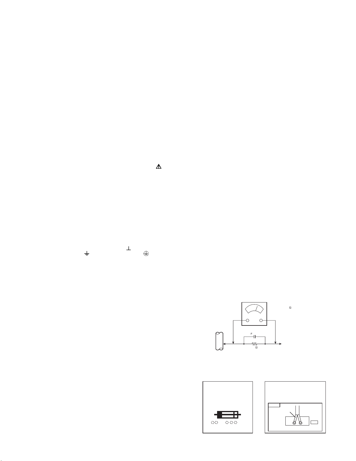
b) Leakage Current Check
Plug the AC line cord directly into the AC outlet (do not use a line
isolation transformer during this check.). Using a "Leakage
Current Tester", measure the leakage current from each exposed
metal part of the cabinet, particularly any exposed metal part
having a return path to the chassis, to a known good earth ground
(water pipe, etc.). Any leakage current must not exceed 0.5mA AC
(r.m.s.).
However, in tropical area, this must not exceed 0.2mA AC (r.m.s.).
Alternate Check Method
Plug the AC line cord directly into the AC outlet (do not use a
line isolation transformer during this check.). Use an AC
voltmeter having 1000Ω per volt or more sensitivity in the
following manner. Connect a 1500Ω 10W resistor paralleled by
a 0.15µF AC-type capacitor between an exposed metal part and
a known good earth ground (water pipe, etc.). Measure the AC
voltage across the resistor with the AC voltmeter. Move the
resistor connection to each exposed metal part, particularly any
exposed metal part having a return path to the chassis, and
measure the AC voltage across the resistor. Now, reverse the
plug in the AC outlet and repeat each measurement. Any
voltage measured must not exceed 0.75V AC (r.m.s.). This
corresponds to 0.5mA AC (r.m.s.).
However, in tropical area, this must not exceed 0.3V AC
(r.m.s.). This corresponds to 0.2mA AC (r.m.s.).
AC VOLTMETER
(HAVING 1000 /V,
OR MORE SENSITIVITY)
0.15 F AC-TYPE
PLACE THIS PROBE
1500 10W
(11) High voltage hold down circuit check.
GOOD EARTH GROUND
ON EACH EXPOSED
ME TAL PAR T
After repair of the high voltage hold down circuit, this circuit shall
be checked to operate correctly.See item "How to check the high
voltage hold down circuit".
This mark shows a fast
operating fuse, the
letters indicated below
show the rating.
A V
POWER CORD
REPLACEMENT WARNING.
Connecting the white line side of power
cord to "WHT" character side.
PWB
White line side
WHT
PW
(No.YA073)1-3
Page 5
SECTION 2
SPECIFIC SERVICE INSTRUCTIONS
2.1 FEATURES
SMART SOUND
Decreases high sound levels, giving a regulated sound level.
SMART CAPTION
SMART CAPTION will appear when you press the MUTING
button, only on channels where the broadcast contains closed
captioning.
DIGITAL COMB FILTER
By the 3 line digital comb filter, the refreshed image can be
seen.
VIDEO STATUS
Expression of a favorite screen can be chosen by the VIDEO
STATUS function.
[STANDARD ↔ DYNAMIC ↔ THEATER ↔ GAME]
COMPONENT INPUT
Since the component signal input terminal is equipped, it
reappears direct without deteriorating the signal from DVD.
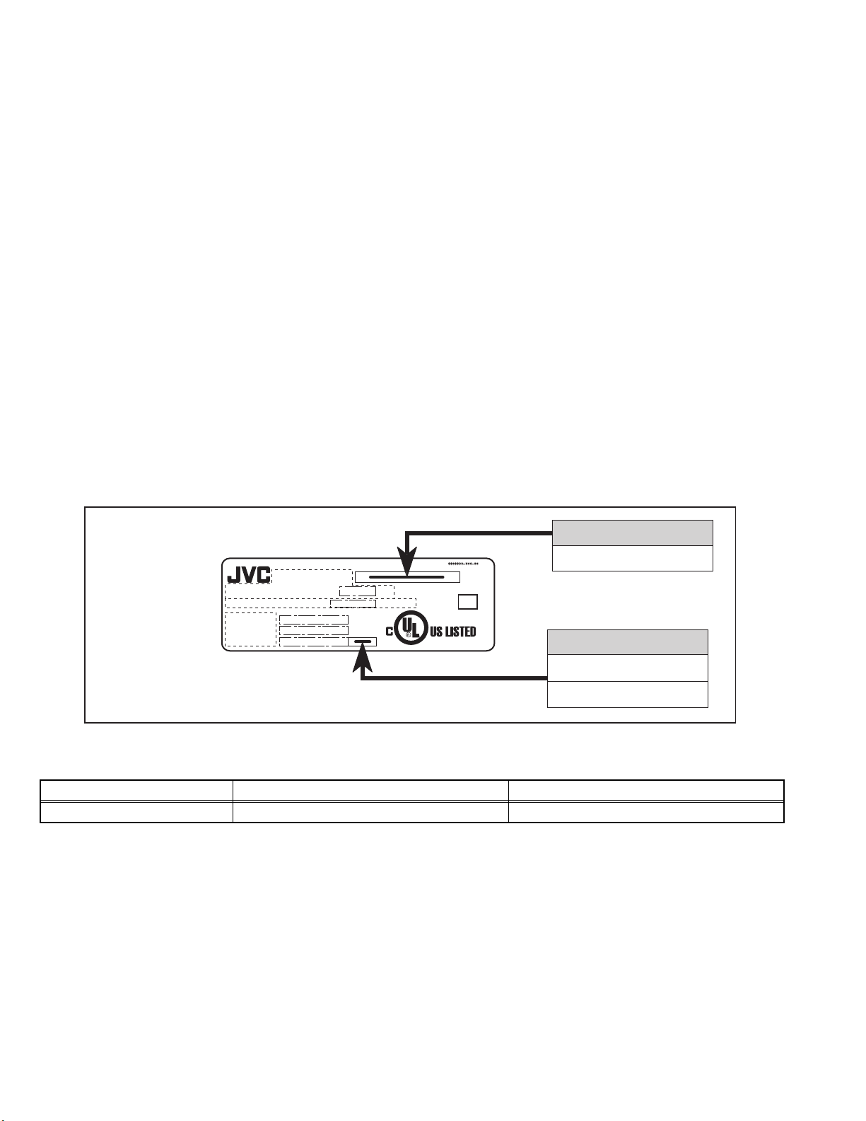
2.2 HOW TO IDENTIFY MODELS
How to recognize from the appearance of the model concerned is written below. Please distinguish from several contents currently
printed on the rating label
V-CHIP
Since the V-CHIP is built in, it can choose, view and listen to a
healthy program.
MTS STEREO
The voice multiplex function of the MTS system is built in.
(MTS = Multi channel Television Sound system)
RETURN PLUS
You program a specific channel to return to while scanning
through the channels using the CH+ and CH - keys.
BBE
High definition audio adds natural, clear and extraordinary
sound quality to any program.
HYPER SURROUND
Creates a deep, three-dimensional sound effect by channeling
the audio through the TV's front-firing speakers.
MODEL NAME
AV-27D305
MODEL NO.
AC 120V 60Hz
TV SCREEN SIZE : DIAGONAL
CHASSIS NO.
MANUFACTURED
SERIAL NO.
W
INCHES
ME
VIDEO EQUIPMENT
4C43
DISTINGUISH NAME
S
R
2.3 MAIN DIFFERENCE LIST
The difference between R models and S models are in the PICTURE TUBE.
Item AV-27D305/R AV-27D305/S
PICTURE TUBE (ITC) A68ADT25X01 A68QDN891X001
1-4 (No.YA073)
Page 6
2.4 TECHNINAL INFORMATION
2.4.1 MAIN MI-COM (CPU) PIN FUNCTION
Pin
Pin name I/O Function
No.
1 MTS_ADJ I Not used 29 YC_GND - GND
2 AFT1 I AFT voltage for tuner (Tuning frequency control) 30 V1_IN I Not used
3 KEY I Key scan for front control [No signal : H] 31 ABCL I Current for automatic beam (brightness)/contrast limit
4 uP_DVss - GND 32
5 Reset I CPU reset 33 BLACK_DET - Black level detection filter
6 8MHz_OUT O CPU system clock : 8MHz oscillation 34 SVM_OUT O Y signal for velocity scan modulation
7 8MHz_IN I CPU system clock : 8MHz oscillation 35 APL_FIL - Average picture level filter
8 TEST - GND 36 APC_FIL - Automatic phase control filter
9 uP_DVD D - 5V 37 fsc_OUT O Color sub carrier (3.58MHz) for 3-line digital comb filter [IC5201]
10 AGC_MUTE O AGC muting for tuner (when channel select) [Muting : H] 38 YC_Vcc - 5V (for video process circuit)
11 uP_VVSS - GND 39 R_OUT O R signal
12 TV_HGND - GND 40 G_OUT O G signal
13 FBP_SCP I Flyback pulse (H. pulse) 41 B_OUT O B signal
14 HOUT O H. drive (oscillation) 42 RGB_Vcc - 9V (for RGB process circuit)
15 H_Vcc - 9V (for H. oscillation start) 43 IK_IN I Not used
16 HAFC_1 - H. AFC filter 44 TV_DGND - GND
17 Vsaw - V. saw filter 45 uP_AGND - GND
18 VOUT O V. drive 46 uP_AVdd - 5V
19 EW_OUT O Parabola waveform (for sidepin correection) 47 MAIN_POWER O Power on/off switching control [Powen on : L]
20 X-RAY I X-ray detection (for protection) [Detection : H] 48 HAZARD I Not used
21 Ys I Not used 49 SDAO I/O Data for Inter IC control bus (for various devices)
22 Cb_IN I Cb (external) signal 50 SCLO O Clock for Inter IC control bus (for various devices)
23 Y_IN I Y (external) signal 51 SDA1 I/O Data for Inter IC control bus (for main memory)
24 Cr_IN I Cr (external) signal 52 A_MUTING O Audio muting [Muting : H]
25 TV_DVcc - 3.3V 53 SCL1 O Clock for Inter IC control bus (for main memory)
26 V3IN/CIN I Chroma signal (for YC separation output) 54 LED O POWER / ON TIMER LED lndication [lighting : L]
27 EHT_IN I Not used 55 REMOCON I Remote control sensor input [No input : H]
28 V2_IN/Y_IN I Y signal (for YC separation output) 56 ASP_ABL I Not used
Pin
Pin name I/O Function
No.
MONITOR_OUT
O Not used
(No.YA073)1-5
Page 7

SECTION 3
DISASSEMBLY
3.1 DISASSEMBLY PROCEDURE
3.1.1 REMOVING THE REAR COVER
(1) Unplug the power plug.
(2) Remove the 11 screws [A] (Fig.1).
(3) Remove the 4 screws [B] (Fig.1).
(4) Then remove the REAR COVER toward you.
3.1.2 REMOVING THE MAIN PWB
• Remove the REAR COVER.
(1) Raise this side of the MAIN PWB, and remove the PWB
STOPPER [C] from the cabinet.
(2) Withdraw the MAIN PWB backward. (If necessary, remove
the wire clamp, connectors etc.)
3.1.3 REMOVING THE SPEAKER
• Remove the REAR COVER.
(1) Remove the 4 screws [D], then remove the speaker
(Fig.1).
(2) Follow the same steps when remove the other hand
speaker.
3.1.4 CHECKING THE PW BOARD
(1) Pull out the MAIN PWB (refer to REMOVING THE MAIN
PWB).
(2) Erect the MAIN PWB vertically with the HVT side facing
down so that you can easily check the backside of the PW
Board.
CAUTION:
• When erecting the chassis, be careful so that there will be no
contacting with other PW Board.
• Before turning on power, make sure that the wire connector
is properly connected.
• When conducting a check with power supplied, be sure to
confirm that the CRT EARTH WIRE (BRAIDED ASS'Y) is
connected to the CRT SOCKET PW board.
3.1.5 WIRE CLAMPING AND CABLE TYING
(1) Be sure to clamp the wire.
(2) Never remove the cable tie used for tying the wires
together.
Should it be inadvertently removed, be sure to tie the wires
with a new cable tie.
1-6 (No.YA073)
Page 8
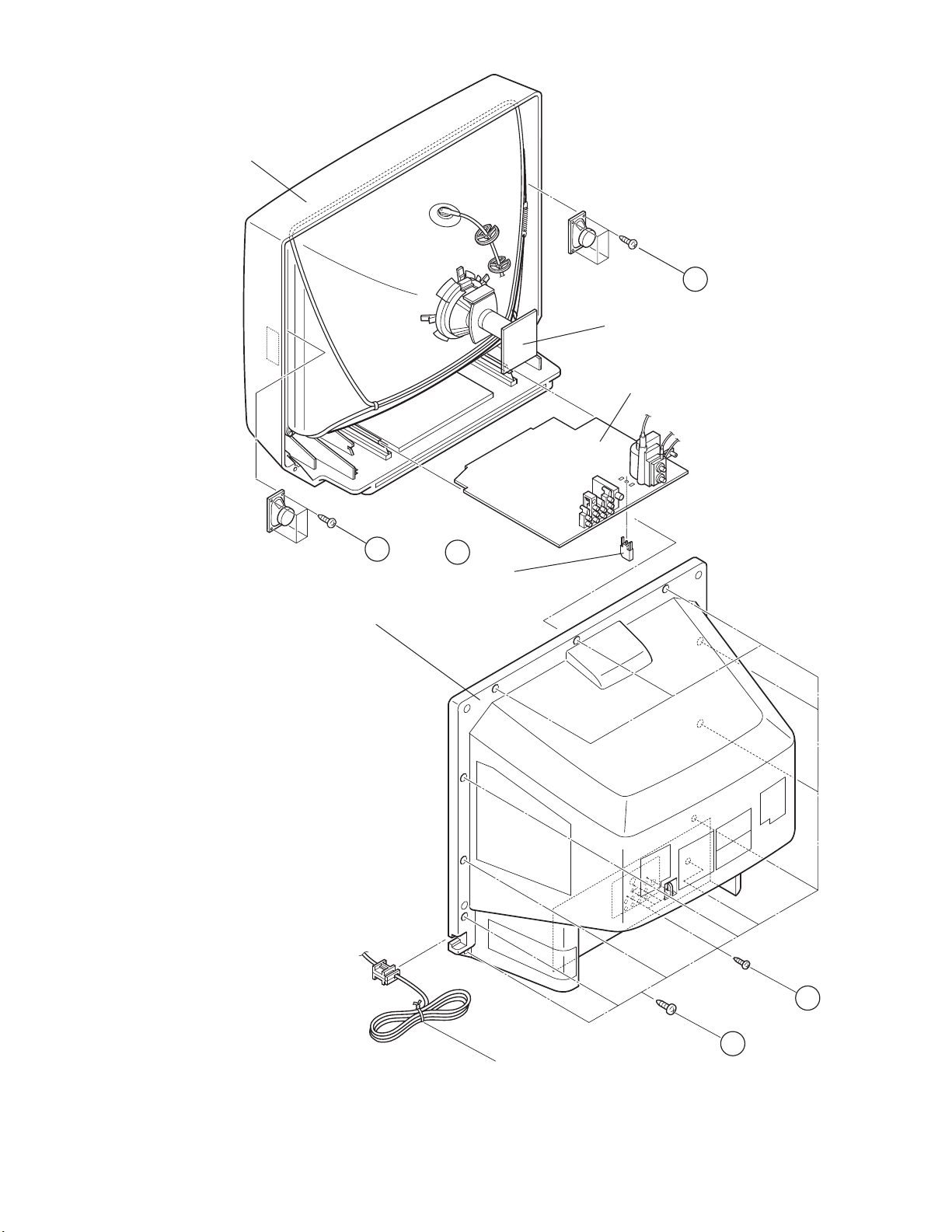
FRONT CABINET
D
CRT SOCKET PWB
MAIN PWB
D
REAR COVER
C
PWB STOPPER
B
POWER CORD
Fig.1
A
(No.YA073)1-7
Page 9

3.2 MEMORY IC REPLACEMENT
• This model uses the memory IC.
• This memory IC stores data for proper operation of the video and drive circuits.
• When replacing, be sure to use an IC containing this (initial value) data.
3.2.1 MEMORY IC REPLACEMENT PROCEDURE
1. Power off
Switch off the power and disconnect the power plug.
2. Replace the memory IC
Be sure to use a memory IC written with the initial setting data.
3. Power on
Connect the power cord to the wall outlet and switch on the
power.
4. Receiving channel setting
Refer to the OPERATING INSTRUCTIONS (USER'S GUIDE)
and set the receive channels (Channels Preset) as described.
5. User settings
Check the user setting items according to the "FACTORY
SETTING ITEM" table.
Where these do not agree, refer to the OPERATING
INSTRUCTIONS (USER'S GUIDE) and set the items as
described.
6. SERVICE MODE setting
Verify what to set in the SERVICE MODE, and set whatever is
necessary(Fig.1) .
Refer to the SERVICE ADJUSTMENT for setting.
3.2.2 SERVICE MODE SETTING ITEMS
SERVICE MENU
SERV ICE MENU
1.
V/C(S)
3.
SOUND(A)
5.
3L Y/C(LYC)
7.
LOW LIGHT
9.
VCO
11.
I2C BUS
SELECT BY
OPERATE BY
2.
DEF(D)
4.
OTHERS(F)
8.
HIGH LIGHT
12.
SYSTEM(SYS)
EXIT BY
Fig.1
Setting items Settings Item No.
1. V/C
(Video setting)
2. DEF
(Deflection setting)
3. SOUND(A)
(Audio setting)
4. OTHERS [Do not adjust]
(Factory setting)
5. 3L Y/C [Do not adjust]
(Y/C Separate setting)
7. LOW LIGHT
(White balance setting)
8. HIGH LIGHT
(White balance setting)
9. VCO
(VCO setting)
11. I2C BUS [Do not adjust]
2
C BUS setting)
(I
12.SYSTEM (SYS)
(System constant setting)
Adjust S01~S48
Adjust D01~D33
Adjust A01~A08
Fixed F01~F18
Fixed LYC01~LYC12
Adjust ---
Adjust ---
Adjust ---
Fixed ---
Fixed SYS01~SYS25
EXIT
1-8 (No.YA073)
Page 10
3.2.3 SETTINGS OF FACTORY SHIPMENT
3.2.3.1 BUTTON OPERATION 3.2.3.2 REMOTE CONTROL DIRECT OPERATION
Setting item Setting position
POWER Off
CHANNEL CH-02
VOLUME 10
3.2.3.3 REMOTE CONTROL MENU OPERATION
(1) PICTURE ADJUST
INPUT TV
CHANNEL CH-02
VOLUME 10
MUTING OFF
DISPLAY OFF
OFF TIMER OFF
VIDEO STATUS DYNAMIC
GAME OFF
SOUND HYPER SURROND OFF
(3) CLOCK / TIMERS
Setting item Setting position
BBE ON
Setting item Setting position
TINT 0
COLOR 0
PICTURE +8
BRIGHT 0
DETAIL +8
COLOR TEMPERATURE HIGH
NOISE MUTING ON
(2) SOUND ADJUST
Setting item Setting position
BASS Center
TREBLE Center
BALANCE Center
MTS STEREO
SMART SOUND OFF
Setting item Setting position
SET CLOCK OFF
ON / OFF TIMER OFF
(4) INITIAL SETUP
Setting item Setting position
LANGUAGE ENG
CLOSED CAPTION OFF
FRONT PANEL LOCK OFF
AUTO SHUT OFF OFF
XDS ID ON
V-CHIP OFF
(No.YA073)1-9
Page 11
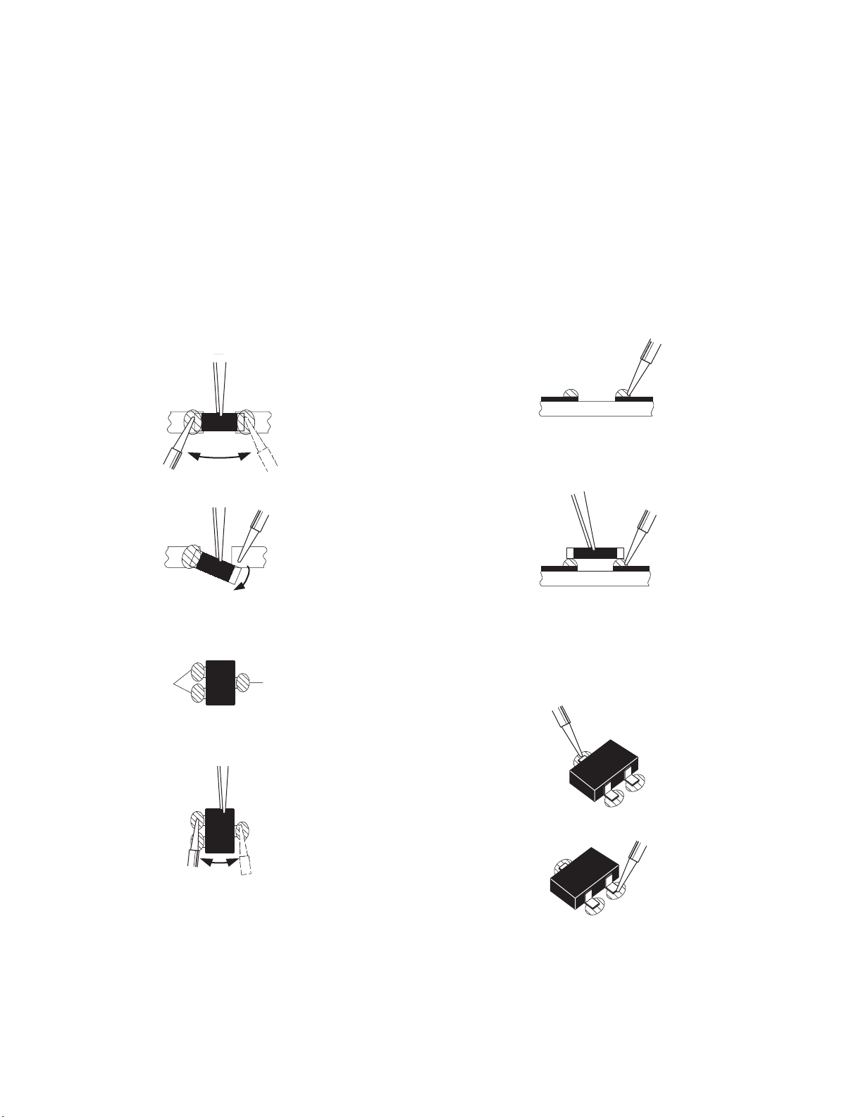
3.3 REPLACEMENT OF CHIP COMPONENT
3.3.1 CAUTIONS
(1) Avoid heating for more than 3 seconds.
(2) Do not rub the electrodes and the resist parts of the pattern.
(3) When removing a chip part, melt the solder adequately.
(4) Do not reuse a chip part after removing it.
3.3.2 SOLDERING IRON
(1) Use a high insulation soldering iron with a thin pointed end of it.
(2) A 30w soldering iron is recommended for easily removing parts.
3.3.3 REPLACEMENT STEPS
1. How to remove Chip parts
2. How to install Chip parts
[Resistors, capacitors, etc.]
(1) As shown in the figure, push the part with tweezers and
alternately melt the solder at each end.
(2) Shift with the tweezers and remove the chip part.
[Transistors, diodes, variable resistors, etc.]
(1) Apply extra solder to each lead.
SOLDER
SOLDER
[Resistors, capacitors, etc.]
(1) Apply solder to the pattern as indicated in the figure.
(2) Grasp the chip part with tweezers and place it on the
solder. Then heat and melt the solder at both ends of the
chip part.
[Transistors, diodes, variable resistors, etc.]
(1) Apply solder to the pattern as indicated in the figure.
(2) Grasp the chip part with tweezers and place it on the
solder.
(3) First solder lead A as indicated in the figure.
(2) As shown in the figure, push the part with tweezers and
alternately melt the solder at each lead. Shift and remove
the chip part.
NOTE :
After removing the part, remove remaining solder from the
pattern.
1-10 (No.YA073)
A
B
C
(4) Then solder leads B and C.
A
B
C
Page 12
SECTION 4
ADJUSTMENT
4.1 ADJUSTMENT PREPARATION
(1) There are 2 ways of adjusting this TV : One is with the
REMOTE CONTROL UNIT and the other is the
conventional method using adjustment parts and
components.
(2) The adjustment using the REMOTE CONTROL UNIT is
made on the basis of the initial setting values. The
setting values which adjust the screen to the optimum
condition can be different from the initial setting
values.
(3) Make sure that connection is correctly made AC to AC
power source.
(4) Turn on the power of the TV and measuring instruments for
warning up for at least 30 minutes before starting
adjustments.
(5) If the receive or input signal is not specified, use the most
appropriate signal for adjustment.
(6) Never touch the parts (such as variable resistors,
transformers and condensers) not shown in the adjustment
items of this service adjustment.
4.2 PRESET SETTING BEFORE ADJUSTMENTS
Unless otherwise specified in the adjustment items, preset the
following functions with the REMOTE CONTROL UNIT.
Item Preset value
VIDEO STATUS STANDARD
TINT / COLOR / PICTURE / BRIGHT / DETAIL 0
COLOR TEMPERTURE LOW
BASS / TREBLE / BALANCE Center
MTS STEREO
BBE OFF
HYPER SORROUND OFF
4.3 MEASURING INSTRUMENT AND FIXTURES
• DC voltmeter (or digital voltmeter)
• Oscilloscope
• Signal generator (Pattern generator) [NTSC]
• TV audio multiplex signal generator
• Remote control unit
4.4 ADJUSTMENT ITEMS
CHECK ITEM
• B1 POWER SUPPLY adjustment
• HIGH VOLTAGE HOLD DOWN check
TUNER / IF CIRCUIT
• IF VCO adjustment
ADJUSTMENT OF FOCUS
•FOCUS
DEFLECTION CIRCUIT
• V. SIZE / V. CENTER adjustment
• H. CENTER adjustment
VIDEO CIRCUIT
• WHITE BALANCE (LOW LIGHT) adjustment
• WHITE BALANCE (HIGH LIGHT) adjustment
• SUB BRIGHT adjustment
• SUB CONTRAST adjustment
MTS CIRCUIT
• MTS INPUT LEVEL adjustment
• MTS SEPARATION adjustment
(No.YA073)1-11
Page 13
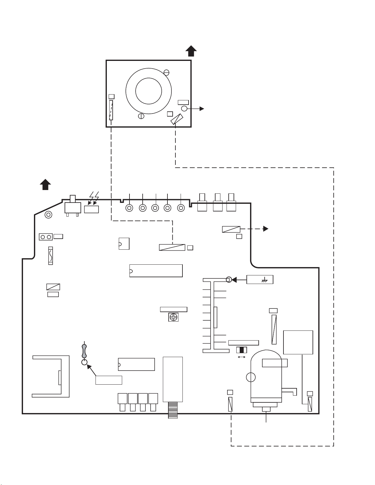
4.5 ADJUSTMENT LOCATIONS
FRONT
MAIN PWB
POWER
CRT SOCKET PWB
(Within MAIN PWB ASS'Y)
T
U
TP-E
(SOLDER SIDE)
VOL+ VOL- CH+ CH- MENU
TP-B
E1
TOP
CRT EARTH
(BRAIDED ASS'Y)
POWER
F901
DEG
IC901
PW
R926
TP-91(B1)
IC702
MEMORY
IC851
IC201
T111
CW TRANSF.
T
TUNER
S
IC421
S401
V. CENTER SW
DOWN UP
U
SPEAKER
TP-E( )
HV
1:X-RAY
2:GND
3:X-RAY
HVT
X
1-12 (No.YA073)
UPPER : FOCUS
LOWER : SCREEN
Page 14

4.6 BASIC OPERATION OF SERVICE MODE
MAIN MENU
SERVICE MENU
1.V/C(S) 2.DEF(D)
3.SOUND(A) 4.OTHERS(F)
5.3L Y/C(LYC)
7.LOW LIGHT 8.HIGH LIGHT
9.VCO
11.I2C BUS 12.SYSTEM(SYS)
SELECT BY
OPERATE BY EXIT BY
RF 4 : 3 STD LOW
S01 BRIGHT
RF 4 : 3 STD LOW
D01 V FREQ
EXIT
1.V/C(S)
2.DEF(D)
SUB MENU
7.LOW LIGHT
BRIGHT
8.HIGH LIGHT
9.VCO
TOO HIGH GOOD TOO LOW
SYNC: YES
AFC ON
FINE 0
3.SOUND(A)
A01 IN LEVEL
4.OTHERS(F) [Fixed value]
F01
5.3L Y/C(LYC) [Fixed value]
LYC01
11.I2C BUS [Fixed value]
I2C BUS ON
12.SYSTEM(SYS) [Fixed value]
SYS01 VIDEO IN
(No.YA073)1-13
Page 15
4.6.1 TOOL OF SERVICE MODE OPERATION
Operate the SERVICE MODE with the REMOTE CONTROL UNIT.
4.6.2 SERVICE MODE ITEMS
In general, basic setting (adjustments) items or verifications are performed in the SERVICE MODE.
1. V/C (S) This sets the setting values of the VIDEO circuit.
2. DEF (D) This sets the setting values of the DEFLECTION circuit.
3. SOUND (A) This sets the setting values of the AUDIO circuit.
4. OTHERS (F) This sets the setting values of the factory settings. [Do not adjust]
5. 3L Y/C(LYC) This sets the setting values of the 3 line YC separation control circuit. [Do not adjust]
7. LOW LIGHT This sets the setting values of the WHITE BALANCE (LOW LIGHT) control circuit.
8. HIGH LIGHT This sets the setting values of the WHITE BALANCE (HIGH LIGHT) control circuit.
9. VCO This sets the setting values of the VCO control circuit.
2
11. I2C BUS This sets the setting values of the I
C BUS control circuit. [Do not adjust]
12. SYSTEM(SYS) This sets the setting values of the system control circuit. [Do not adjust]
4.6.3 HOW TO ENTER THE SERVICE MODE
(1) Set to 0 minutes using the [SLEEP TIMER] key.
(2) Press the [VIDEO STATUS] key and [DISPLAY] key
SERVICE MODE SELECT KEY
simultaneously, then enter the SERVICE MODE.
NOTE:
Before entering the SERVICE MODE, confirm that the setting
of TV / CATV switch of the REMOTE CONTROL UNIT is at the
TV/CATV
switch
"TV" side and the setting of VCR / DVD switch is at the "VCR"
side. If the switches have not been properly set, you cannot
enter the SERVICE MODE.
4.6.4 HOW TO STORE OF SETTING VALUE
The setting value will be stored automatically when release the
REMOTE CONTROL UNIT keys
4.6.5 HOW TO EXIT THE SERVICE MODE
Press the [EXIT] key to exit the SERVICE MODE.
DISPLAY
SLEEP
TIMER
VIDEO
STATUS
VOL -
MENU
SOUND
GAME
VCR/DVD
switch
POWER
NUMBER
CH +
VOL +
EXIT
CH -
1-14 (No.YA073)
RM-C1259G
Page 16
4.6.6 SERVICE MODE SETTING
A
1. V/C, 2. DEF
• Press [CH+] / [CH-] key
For scrolling up/down the adjustment item.
• Press [VOL+] / [VOL-] key
For scrolling up/down the data values.
NOTE:
The setting value will be stored automatically when release
the REMOTE CONTROL UNIT keys.
INPUT
SIGNAL
RF 4 : 3 STD LOW
SPECT
COLOR
TEMPERATURE
VIDEO
STATUS
7. LOW LIGHT
The settings for LOW LIGHT is described in the WHITE
BALANCE page of ADJUSTMENT PROCEDURE.
NOTE:
The setting value will be stored automatically when release
the REMOTE CONTROL UNIT keys.
SETTING ITEM
BRIGHT
R CUTOFF G CUTOFF B CUTOFF
BRIGHT
SETTING ITEM
SETTING NO.
SETTING VALUE
(1) INPUT SIGNAL
RF : Antenna input
COMP : External (component) input
EXT : External (S / Composite) input
(2) ASPECT
4:3 : 4:3 screen mode
(3) VIDEO STATUS
STD : STANDARD
THEA : THEATER
(4) COLOR TEMPERATURE
HIGH : White balance high mode
LOW : White balance low mode
3. SOUND (A)
• Press [CH+] / [CH-] key
For scrolling up/down the adjustment item.
• Press [VOL+] / [VOL-] key
For scrolling up/down the data values.
NOTE:
The setting value will be stored automatically when release
the REMOTE CONTROL UNIT keys.
8. HIGH LIGHT
The settings for HIGH LIGHT is described in the WHITE
BALANCE page of ADJUSTMENT PROCEDURE.
NOTE:
The setting value will be stored automatically when release
the REMOTE CONTROL UNIT keys.
R DRIVE B DRIVE
9. VCO
The setting for VCO is described in the IF VCO page of
ADJUSTMENT PROCEDURE.
NOTE:
The setting value will be stored automatically when release
the REMOTE CONTROL UNIT keys.
VCO adjustment status (AFC level)
TOO HIGH GOOD TOO LOW
SYNC INPUT
AFC SW
A01 IN LEVEL
SETTING NO.
SETTING ITEM
SETTING VALUE
SYNC: YES
AFC OFF
FINE 0
Setting value
(No.YA073)1-15
Page 17
4.7 INITIAL SETTING VALUE OF SERVICE MODE
(1) Adjustment of the service menu is made on the basis of the initial setting values. however, the new setting values which displays
on the screen in its optimum condition may differ from the initial setting value.
(2) Do not change the initial setting values of the items not listed in "ADJUSTMENT PROCEDURE".
(3) "---" is impossible to adjust.
4.7.1 [1. V/C(S)]
No. Setting item
S01 BRIGHT 0~127 64 --- --- --- --- ---
S02 PICTURE 0~127 65 --- --- --- --- ---
S03 COLOR 0~127 44 --- --- --- 53 ---
S04 TINT 0~127 65 --- --- --- 68 ---
S05 DETAIL 0~63 35 --- 40 --- 40 ---
S06 BRIGHT +- -32~+32 --- ±0 -2 --- -2 ---
S07 PICT+- -32~+32 --- -15 ±0 --- ±0 ---
S08 COLOR +- -32~+32 --- -3 +1 --- --- ---
S09 TINT+- -32~+32 --- -6 -11 --- --- ---
S10 DETAIL+- -32~+32 --- +3 --- --- --- ---
No. Setting item
S11 R CUT OFF 0 ~ 255 30 --- --- --- --- --- --- ---
S12 G CUT OFF 0 ~ 255 30 --- --- --- --- --- --- ---
S13 B CUT OFF 0 ~ 255 30 --- --- --- --- --- --- ---
S14 R DRIVE 0 ~ 127 64 --- --- --- --- --- --- ---
S15 B DRIVE 0 ~ 127 64 --- --- --- --- --- --- ---
S16 R CUT +- -128 ~ +127 --- ±0 ±0 ±0 -12 --- --- ---
S17 G CUT +- -128 ~ +127 --- ±0 ±0 ±0 8 --- --- ---
S18 B CUT +- -128 ~ +127 --- ±0 ±0 ±0 -10 --- --- ---
S19 R DRV +- -128 ~ +127 --- 5 13 7 ±0 --- --- ---
S20 B DRV +- -128 ~ +127 --- 6 -25 -9 ±0 --- --- ---
S21NTSC MAT 0 ~ 333112211
S22 BLACK ST 0 ~ 3 2 --- 1 --- --- --- --- ---
S23 DC REST 0 ~ 1 1 --- 1 --- --- --- --- ---
S24 DCRSW 0 ~ 1 1 --- 1 --- --- --- --- ---
Variable
range
Variable
range
RF
STANDARD THEATER STANDARD THEATER STANDARD THEATER
RF / EXTERNAL (S / COMPOSITE) EXTERNAL (COMPONENT)
STANDARD THEATER STANDARD THEATER
LOW HIGH LOW HIGH LOW HIGH LOW HIGH
Initial setting value
EXTERNAL (S / COMPOSITE)
Initial setting value
AV-27D305/S
EXTERNAL (COMPONENT)
1-16 (No.YA073)
Page 18

Initial setting value
No. Setting item
S11 R CUT OFF 0 ~ 255 30 --- --- --- --- --- --- ---
S12 G CUT OFF 0 ~ 255 30 --- --- --- --- --- --- ---
S13 B CUT OFF 0 ~ 255 30 --- --- --- --- --- --- ---
S14 R DRIVE 0 ~ 127 64 --- --- --- --- --- --- ---
S15 B DRIVE 0 ~ 127 64 --- --- --- --- --- --- ---
S16 R CUT +- -128 ~ +127 --- ±0 ±0 ±0 ±0 --- --- ---
S17 G CUT +- -128 ~ +127 --- ±0 ±0 ±0 ±0 --- --- ---
S18 B CUT +- -128 ~ +127 --- ±0 ±0 ±0 ±0 --- --- ---
S19 R DRV +- -128 ~ +127 --- ±0 7 7 ±0 --- --- ---
S20 B DRV +- -128 ~ +127 --- ±0 -9 -9 ±0 --- --- ---
S21NTSC MAT 0 ~ 333112211
S22 BLACK ST 0 ~ 3 2 --- 1 --- --- --- --- ---
S23 DC REST 0 ~ 1 1 --- 1 --- --- --- --- ---
S24 DCRSW 0 ~ 1 1 --- 1 --- --- --- --- ---
Variable
range
RF / EXTERNAL (S / COMPOSITE) EXTERNAL (COMPONENT)
STANDARD THEATER STANDARD THEATER
LOW HIGH LOW HIGH LOW HIGH LOW HIGH
AV-27D305/R
No. Setting item
S25 ASY SHRP 0 ~ 7 4 4 4
S26 BPF FO 0 ~ 1 0 0 ---
S27 KILR OFF 0 ~ 1 0 0 ---
S28 KILR SEN 0 ~ 1 1 1 ---
No. Setting item
S29 RGB MUTE 0 ~ 1 0
S30 BLUE B 0 ~ 1 1
S31 VIDEO SW 0 ~ 3 3
S32 CMP ABCL 0 ~ 1 0
S33 OSD ABL 0 ~ 1 0
S34 OSD CONT 0 ~ 63 9
S35 SUB CONT 0 ~ 15 8
S36 ABL GAIN 0 ~ 3 0
S37 ABL PNT 0 ~ 3 3
S38 Y GAMMA 0 ~ 3 1
S39 Y MUTE 0 ~ 1 0
S40 SVM GAIN 0 ~ 3 3
S41 SVM PH 0 ~ 3 0
S42 WPL 0 ~ 1 0
S43 COL GMM 0 ~ 1 0
S44 V1 GAIN 0 ~ 7 4
S46 VMOFF DE -128 ~ +127 0
S47 APC CLK 0 ~ 1 1
S48 PIP ADJ 0 ~ 15 0
Variable
range
Variable
range
RF
Initial setting value
Initial setting value
EXTERNAL (S / COMPOSITE)
EXTERNAL (COMPONENT)
(No.YA073)1-17
Page 19

4.7.2 [2. DEF(D)]
Initial setting value
No. Setting item
D01V FREQ0 ~ 30303
D02AFC GAIN0 ~ 30202
D03 H POSI 0 ~ 31 11 11 11 11
D04 H POSI+- -128 ~ +127 --- --- --- ---
D05V PHASE0 ~ 70000
D06 V PH+- -128 ~ +127 --- --- --- ---
D07 V SIZE 0 ~ 127 50 50 50 50
D08 V SIZE+- -128 ~ +127 --- --- --- ---
D09 V CENTER 0 ~ 63 32 32 32 32
D10 V CENT+- -128 ~ +127 --- --- --- ---
D11V S CORR 0 ~ 154444
D12 V S CO+- -128 ~ +127 --- --- --- ---
D13 V LIN 0 ~ 15 11 11 11 11
D14 V LIN+- -128 ~ +127 --- --- --- ---
D15 H SIZE 0 ~ 63 32 32 32 32
D16 H SIZE+- -128 ~ +127 --- --- --- ---
D17WVMT TOP0 ~ 31100
D18WVMT BTM0 ~ 30000
D19 EWCR TOP 0 ~ 31 16 16 16 16
D20 EWCR T+- -128 ~ +127 --- --- --- ---
D21 EWCR BTM 0 ~ 31 16 16 16 16
D22 EWCR B+- -128 ~ +127 --- --- --- ---
D23 EW PARA 0 ~ 63 26 26 26 26
D24 EW PAR+- -128 ~ +127 --- --- --- ---
D25V EHT0 ~ 70000
D26 V EHT+- -128 ~ +127 --- --- --- ---
D27H EHT0 ~ 70000
D28 H EHT+- -128 ~ +127 --- --- --- ---
D29 TRAPEZ 0 ~ 63 34 34 34 34
D30 TRAPEZ+- -128 ~ +127 --- --- --- ---
D31V AGC0 ~ 10000
D32BLANK SW0 ~ 10000
D33VRMP BI0 ~ 10000
Variable
range
AV-27D305/R AV-27D305/S
RF
EXTERNAL
(S / COMPOSITE)
RF
EXTERNAL
(S / COMPOSITE)
1-18 (No.YA073)
Page 20

4.7.3 [3. SOUND(A)]
No. Setting item
A01 IN LEVEL 0 ~ 15 12
A02 LOW SEP 0 ~ 63 39
A03 HI SEP 0 ~ 63 16
A04 SAPC 0 ~ 1 0
A05 BBE BASS -128 ~ +127 -6
A06 BBE TRE -128 ~ +127 -6
A07 AHS MVE -128 ~ +127 0
A08 AHS MSC -128 ~ +127 0
4.7.4 [4. OTHERS(F)] [Do not adjust : All fixed]
No. Setting item
F01 OSD POSI 0 ~ 255 24
F02 OSD FREQ 0 ~ 255 83
F03 CCD POSI 0 ~ 255 44
F04 CCD FREQ 0 ~ 255 93
F05 CCD CONT 0 ~ 63 11
F06 PUR WBCK 0 ~ 1 0
F07 PUR CONT 0 ~ 63 62
F08 CCD PCHK 0 ~ 1 1
F09 VMOFF 0 ~ 1 0
F10 VNR CHK 0 ~ 255 3
F11 VCSN TM 0 ~ 255 5
F12 VM DAT A -128 ~ +127 8
F13 VM DAT B -128 ~ +127 -4
F14 VM DAT C -128 ~ +127 -10
F15 VM DAT D -128 ~ +127 -16
F16 VM DAT E 0 ~ 1 0
F17 XDSID TM 0 ~ 255 15
F18 FM TRAP 0 ~ 1 0
Variable
range
Variable
range
Initial setting value
Initial setting value
4.7.5 [5. 3L Y/C(LYC)] [Do not adjust : All fixed]
No. Setting item
LYC01 MODE 0 ~ 7 4
LYC02 VENH 0 ~ 7 1
LYC03 PDSOFF 0 ~ 1 0
LYC04 CB 0 ~ 1 0
LYC05 VNLR 0 ~ 15 2
LYC06 GSEL0 0 ~ 1 0
LYC07 GSEL1 0 ~ 1 1
LYC08 COR 0 ~ 3 0
LYC09 TRAP 0 ~ 1 1
LYC10 CHTRAP 0 ~ 1 0
LYC11 CBPF 0 ~ 1 0
LYC12 ENHOFF 0 ~ 1 0
4.7.6 [12. SYSTEM(SYS)] [Do not adjust : All fixed]
No. Setting item
SYS01 VIDEO IN 0 ~ 4 3
SYS02 VSM 0 ~ 1 0
SYS03 CLR TEMP 0 ~ 1 1
SYS04 THEATER 0 ~ 1 1
SYS05 THEA PRO 0 ~ 1 1
SYS06 GAME MD 0 ~ 1 1
SYS07 AHS 0 ~ 1 0
SYS08 HYPER SR 0 ~ 1 1
SYS09 BBE 0 ~ 1 1
SYS10 S SOUND 0 ~ 1 1
SYS11 16:9 MD 0 ~ 3 0
SYS12 S CCD 0 ~ 1 1
SYS13 ID DISP 0 ~ 1 1
SYS14 CH LAB 0 ~ 1 0
SYS15 V LAB 0 ~ 1 0
SYS16 W CLOCK 0 ~ 1 0
SYS17 PIM 0 ~ 1 1
SYS18 PURITY 0 ~ 1 0
SYS19 VOL MUTE 0 ~ 1 0
SYS20 VCHIP 0 ~ 1 1
SYS21 VCHIP CA 0 ~ 1 1
SYS22 CCD 0 ~ 1 1
SYS23 HYPSCAN 0 ~ 1 1
SYS24 JVC LOGO 0 ~ 1 1
SYS25 PANORAMA 0 ~ 1 0
Variable
range
Variable
range
Initial setting value
Initial setting value
(No.YA073)1-19
Page 21

4.8 ADJUSTMENT PROCEDURE
4.8.1 CHECK ITEM
Item
B1 POWER
SUPPLY
Measuring
instrument
Signal
generator
R927 : TP-91
HEAT SINK
(IC421) : TP-E
HIGH VOLTAGE
HOLD DOWN
check
DC voltmeter
Resistor
(18.0kΩ,1/4W)
[MAIN PWB]
X connector
1-pin
3-pin
[MAIN PWB]
RESISTOR
18.0 k 1%
X CONNECTOR3 2 1
Test point Adjustment part Description
(1) Receive the black and white signal. (color off)
(2) Connect the DC voltmeter to the TP-E and TP-91
(R927).
(3) Confirm that the voltage is DC134V±2V.
• After reparing the high voltage hold down circuit. This
circuit shall be checked to operate correctly.
(1) Turn the power switch to on.
(2) Refer to the figure, connect the resistor between X
connector 1-pin and 3-pin.
(3) Make sure that the screen picture disappeares.
(4) Disconnect the power plug.
HEATER
(5) Remove the resistor.
(6) Again connect the power plug.
(7) Turn the power switch to on.
T521
(8) Make sure that the normal picture is displayed on the
screen.
4.8.2 TUNER / IF CIRCUIT
Item
Measuring
instrument
IF VCO Remote
control unit
TOO HIGH GOOD TOO LOW
SYNC: YES
AFC ON
FINE 0
4.8.3 FOCUS
Item
Measuring
instrument
FOCUS Signal
generator
Test point Adjustment part Description
[9.VCO]
• It must not adjust without inputting the RF signal.
(1) Receive the any broadcast.
CW transf. (T111)
[MAIN PWB]
(2) Select 9.VCO from the SERVICE MODE.
(3) Change the "AFC" to "OFF" and "FINE" to "0".
(4) Confirm that the color change from "TOO HIGH" to
"TOO LOW" by CW transf. on MAIN PWB, and
AFC STATUS
(Turn to green)
check the "SYNC" is "YES".
(5) Adjust CW transf. until "GOOD" letters turns green.
And then confirm that the "SYNC" is "YES" again.
Adjustment can be done in this statement.
(6) It return the "AFC" to "ON".
(7) Push the [EXIT] key to exit the 9.VCO.
Test point Adjustment part Description
FOCUS VR
[In HVT]
(1) Receive the crosshatch signal.
(2) While looking at the screen, adjust the FOCUS VR
to the vertical and horizontal lines will be clear and in
fine detail.
(3) Make sure that the picture is in focus even when the
screen gets darkened.
1-20 (No.YA073)
Page 22

4.8.4 DEFLECTION CIRCUIT
Item
V. SIZE /
V. POSITION
Measuring
instrument
Signal
generator
Remote
control unit
Test point Adjustment part Description
[2.DEF(D)]
D07 : V SIZE
(1) Receive the cross-hatch signal.
(2) Select 2.DEF(D) from the SERVICE MODE.
(3) Select the < D07 >(V SIZE).
V. CENTER SW(S401)
[MAIN PWB]
(4) Adjust < D07 > so that the vertical screen size
become setting value in the table.
(5) Adjust the V. CENTER SW to agree the vertical
center with display center.
Screen
size
Model name Vertical screen size
AV-27D305/R
AV-27D305/S
Setting item
D07: V SIZE
H. POSITION Signal
generator
Remote
control unit
90.0%
89.0%
Initial setting value
50
[2.DEF(D)]
D03 : H POSI
Picture
size
(100%)
(1) Receive the cross-hatch signal.
(2) Select 2.DEF(D) from the SERVICE MODE.
(3) Select the < D03 >(H POSI).
(4) Adjust the < D03 > so that left width and right width
of the crosshatch screen becomes equal.
Setting item
D03: H POSI
Initial setting value
11
(No.YA073)1-21
Page 23

4.8.5 VIDEO CIRCUIT
Item
WHITE
BALANCE
Measuring
instrument
Signal
generator
(LOW LIGHT)
Remote
control unit
SETTING ITEM
Test point Adjustment part Description
LOW LIGHT adjustment mode
BRIGHT
R CUTOFF G CUTOFF B CUTOFF
SINGLE HORIZONTAL LINE
[1.V/C (S)]
S01: BRIGHT
S11: R CUTOFF
S12: G CUTOFF
S13: B CUTOFF
[7.LOW LIGHT]
SCREEN VR
[in HVT]
BRIGHT
(1) Receive the black and white signal ( color off ).
(2) Select the 1.V/C (S) from the SERVICE MODE.
(3) Confirm the initial setting value of < S11 > (R
CUTOFF), < S12 > (G CUTOFF), < S13 > (B
CUTOFF) and < S01 > (BRIGHT).
(4) Return to the main menu in SERVICE MODE.
(5) Select the 7.LOW LIGHT from the SERVICE MODE.
(6) Display a single horizontal line by pressing the [1]
key.
(7) Turn the SCREEN VR all the way to the left.
(8) Turn the SCREEN VR gradually to the right from the
left until either one of the red, blue or green colors
appears faintly.
(9) Adjust the two colors which did not appear until the
single horizontal line that is displayed becomes
white using the [4]~[9] keys.
(10) Turn the SCREEN VR until the single horizontal line
is displayed faintly.
(11) Press the [2] key to cancel the single horizontal line
mode.
(12) Return to the main menu in SERVICE MODE.
(13) Select the 1.V/C (S) from the SERVICE MODE.
(14) Adjust the BRIGHT level to become the black
component shines white slightly by < S01 >.
(15) Confirm that whether the color ingredient of R, G, or
B is visible to the black component, which shines
white slightly.
(16) When the color ingredient can be seen, two colors
other than a visible color are adjusted, and it is made
to look white.
(17) Return the value of < S01 > to initial setting value.
Setting item
S11: R CUT OFF
S12: G CUT OFF 30
S13: B CUT OFF 30
S01: BRIGHT 64
Initial setting value
30
• The [3] (EXIT) key is the cancel key for the WHITE
BALANCE.
REMOTE CONTROL UNIT
H.LINE ON
R CUTOFF G CUTOFF B CUTOFF
R CUTOFF G CUTOFF B CUTOFF
H.LINE OFF EXIT
1-22 (No.YA073)
Page 24

Item
WHITE
BALANCE
(HIGH LIGHT)
Measuring
instrument
Test point Adjustment part Description
Signal
generator
Remote
control unit
HIGH LIGHT adjustment mode
[1.V/C (S)]
S14: R DRIVE
S15: B DRIVE
[8.HIGH LIHGT]
(1) Receive the black-and-white signal (color off).
(2) Select the 1.V/C (S) from the SERVICE MODE.
(3) Set the initial setting value of < S14 > (R DRIVE) and
< S15 > (B DRIVE).
(4) Return to the main menu in SERVICE MODE.
(5) Select the 8.HIGH LIGHT from the SERVICE
MODE.
(6) Adjust the screen until it becomes white using the
[4], [6], [7] and [9] keys.
• The [3] (EXIT) key is the cancel key for the WHITE
BALANCE.
REMOTE CONTROL UNIT
R DRIVE B DRIVE
Setting item
S14: R DRIVE
S15: B DRIVE 64
SUB BRIGHT Remote
control unit
Setting item Initial setting value
S01:
BRIGHT
SUB
CONTRAST
Remote
control unit
Setting item Initial setting value
S02:
PICTURE
Initial setting value
64
[1.V/C (S)]
S01: BRIGHT
64
[1.V/C (S)]
S02: PICTURE
65
EXIT
R DRIVE
R DRIVE
B DRIVE
B DRIVE
(1) Receive the any broadcast.
(2) Select the 1.V/C (S) from the SERVICE MODE.
(3) Select < S01 > (BRIGHT).
(4) Set the initial setting value of the < S01 >.
(5) If the brightness is not the best with the initial setting
value, make fine adjustment of the < S01 > until you
get the optimum brightness.
(1) Receive the any broadcast.
(2) Select the 1.V/C (S) from the SERVICE MODE.
(3) Select < S02 > (PICTURE).
(4) Set the initial setting value of the < S02 >.
(5) If the contrast is not the best with the initial setting
value, make fine adjustment of the < S02 > until you
get the optimum contrast.
(No.YA073)1-23
Page 25

4.8.6 MTS CIRCUIT
Item
MTS INPUT
LEVEL
Remote
control unit
Measuring
instrument
Test point Adjustment part Description
[3.SOUND (A)]
A01: IN LEVEL
(1) Receive the any broadcast.
(2) Select the 3.SOUND (A) from the SERVICE MODE.
(3) Select the < A01 > (IN LEVEL).
(4) Set the intal setting value of the < A01 >.
S
etting
item
Initial setting value
MTS
SEPARATION
1 cycle
TV audio
multiplex
signal
generator
Oscilloscope
L-Channel
signal waveform
R OUT
L OUT
[AUDIO OUT]
R-Channel
crosstalk portion
Minimum
[3.SOUND (A)]
A02: LOW SEP.
A03: HI SEP.
A01: IN LEVEL
12
(1) Input the stereo L signal (300Hz) from the TV audio
multiplex signal generator to the antenna terminal.
(2) Connect an oscilloscope to R OUT pin of the AUDIO
OUT, and display one cycle portion of the 300Hz
signal.
(3) Select the 3.SOUND (A) from the SERVICE MODE.
(4) Select the < A02 > (LOW SEP.).
(5) Set the initial setting value of the < A02 >.
(6) Adjust the < A02 > so that the stroke element of the
300Hz signal will become minimum.
(7) Change the connection of the oscilloscope to L OUT
pin of the AUDIO OUT, and enlarge the voltage axis.
(8) Change the signal to 3kHz, and similarly adjust
the < A03 > (HI SEP.).
etting
item Initial setting value
S
A02: LOW SEP
A03: HI SEP
39
16
1-24 (No.YA073)
Page 26

SECTION 5
TROUBLESHOOTING
This service manual does not describe TROUBLESHOOTING.
(No.YA073)1-25
Page 27

JVC SERVICE & ENGINEERING COMPANY OF AMERICA
DIVISION OF JVC AMERICAS CORP.
www.jvcservice.com(US Only)
JVC CANADA INC.
Head office : 21 Finchdene Square Scarborough, Ontario M1X 1A7 (416)293-1311
(No.YA073)
Printed in Japan
WPC
Page 28

PARTS LIST
CAUTION
J The parts identified by the symbol are important for the safety . Whenever replacing these parts, be sure to use specified ones to secure the
safety.
J The parts not indicated in this Parts List and those which are filled with lines --- in the Parts No. columns will not be supplied.
J P.W. BOARD Ass'y will not be supplied, but those which are filled with the Parts No. in the Parts No. columns will be supplied.
ABBREVIATIONS OF RESISTORS, CAPACITORS AND TOLERANCES
RESISTORS CAPACITORS
CR Carbon Resistor C CAP. Ceramic Capacitor
FR Fusible Resistor E CAP. Electrolytic Capacitor
PR Plate Resistor M CAP. Mylar Capacitor
VR Variable Resistor CH CAP. Chip Capacitor
HV R High Voltage Resistor HV CAP. High Voltage Capacitor
MF R Metal Film Resistor MF CAP. Metalized Film Capacitor
MG R Metal Glazed Resistor MM CAP. Metalized Mylar Capacitor
MP R Metal Plate Resistor MP CAP. Metalized Polystyrol Capacitor
OM R Metal Oxide Film Resistor PP CAP. Polypropylene Capacitor
CMF R Coating Metal Film Resistor PS CAP. Polystyrol Capacitor
UNF R Non-Flammable Resistor TF CAP. Thin Film Capacitor
CH V R Chip Variable Resistor MPP CAP. Metalized Polypropylene Capacitor
CH MG R Chip Metal Glazed Resistor TAN. CAP. Tantalum Capacitor
COMP. R Composition Resistor CH C CAP. Chip Ceramic Capacitor
LPTC R Linear Positive Temperature Coefficient Resistor BP E CAP. Bi-Polar Electrolytic Capacitor
CH AL E CAP. Chip Aluminum Electrolytic Capacitor
CH AL BP CAP. Chip Aluminum Bi-Polar Capacitor
CH TAN. E CAP. Chip Tantalum Electrolytic Capacitor
CH AL BP E CAP. Chip Tantalum Bi-Polar Electrolytic Capacitor
RESISTORS
FGJ KMNRHZ P
±1% ±2% ±5% ±10% ±20% ±30%
+30%
-10%
+50%
-10%
+80%
-20%
+100%
-0%
(No.YA073)3-1
Page 29

CONTENTS
USING P.W. BOARD & REMOTE CONTROL UNIT ................................................................................................... 3-2
EXPLODED VIEW PARTS LIST -1 ............................................................................................................................. 3-2
EXPLODED VIEW -1 ................................................................................................................................................... 3-2
EXPLODED VIEW PARTS LIST -2 ............................................................................................................................. 3-3
EXPLODED VIEW -2 ................................................................................................................................................... 3-4
PRINTED WIRING BOARD PARTS LIST [AV-27D305/R]
MAIN P.W. BOARD ASS'Y (SFE-1044A-M2) .................................................................................................... 3-5
PRINTED WIRING BOARD PARTS LIST [AV-27D305/S]
MAIN P.W. BOARD ASS'Y (SFE-1041A-M2) .................................................................................................... 3-9
REMOTE CONTROL UNIT PARTS LIST (RM-C1259G-1H) .................................................................................... 3-13
PACKING ................................................................................................................................................................... 3-13
PACKING PARTS LIST ............................................................................................................................................. 3-13
USING P.W. BOARD & REMOTE CONTROL UNIT
P.W.B ASS'Y AV-27D305/R AV-27D305/S
MAIN P.W.B SFE-1044A-M2 SFE-1041A-M2
REMOTE CONTROL UNIT RM-C1259G-1H
←
EXPLODED VIEW PARTS LIST -1
Ref.No. Part No. Part Name Description Local
1 GQ30025-002A-A CONTROL KNOB
2 LC30191-004A-A REMOCON LENS
3 GQ30026-002A-A POWER KNOB
4 CM48006-007-C JVC MARK
100 GQ10018-004A-A FRONT CABINET ASSY Inc.No.101
101 GQ30024-002A-A DOOR
EXPLODED VIEW -1
1
2
3
3-2(No.YA073)
101
4
100
Page 30

EXPLODED VIEW PARTS LIST -2
Ref.No. Part No. Part Name Description Local
V01 A68ADT25X01 ITC Inc.DEF YOKE/PC MAGNET AV-27D305/R
V01 A68QDN891X001 ITC Inc.DEF YOKE/PC MAGNET AV-27D305/S
L01 CE41329-00DJB DEG COIL
T1521 QQH0129-001 FB TRANSF
5 CHGB0016-0C BRAIDED ASSY
6 CHGB0015-0B BRAIDED ASSY
7 QAS0054-001 SPEAKER SP01/SP02(x2)
8 CM48144-001-A PB STOPPER
9 GQ10017-001B-A REAR COVER
10 LC20106-001D-A POWER CORD CLAMP
11 QMPD390-200-JS POWER CORD(US/CA) 2m BLACK
12 QYSBSFG4016Z TAP SCREW 4.0mm x 16mm(x11)
13 QYSBSB3010Z TAP SCREW 3.0mm x 10mm(x4)
14 GQ30032-001A-A RATING LABEL
15 GQ30034-001B-A WARNING LABEL
16 QYSBSB4012Z TAP SCREW 4mm x 12mm(x8)
20 SFE-1044A-M2 MAIN PWB Inc.CRT SOCKET PWB AV-27D305/R
20 SFE-1041A-M2 MAIN PWB Inc.CRT SOCKET PWB AV-27D305/S
(No.YA073)3-3
Page 31

EXPLODED VIEW -2
V01
15
L01
5
7
16
6
CRT SOCKET PWB (Within MAIN PWB)
20
T1521
9
7
16
8
3-4(No.YA073)
11
10
12
(x11)
13
14
(x4)
Page 32

PRINTED WIRING BOARD PARTS LIST [AV-27D305/R]
MAIN P.W. BOARD ASS'Y (SFE-1044A-M2)
Ref No. Part No. Part Name Description Local
IC1101 M52342FP-X IC
IC1201 TM8812CSDNG5DB9 IC(MCU)
IC1251 TC90A49AP IC
IC1421 AN5522 IC
IC1601 NJM2150AD IC
IC1602 TFA9842J/N1 IC
IC1641 CXA2205Q-X IC
IC1702 AT24C08-27D305 IC (SERVICE)
IC1703 S-80840CNY-T IC
IC1704 AN78L05-T IC
IC1751 GP1UM281QK IR DETECT UNIT 38kHz
IC1851 TA1218AN IC
IC1901 STR-G5624A/F8 IC
IC1921 L7809CP IC
IC1922 L7805CP IC
Q1001 UN2212-X TRANSISTOR
Q1101 2SC5083/L-P/-T TRANSISTOR
Q1131 2SA1530A/QR/-X SI TRANSISTOR
Q1161 2SC3928A/QR/-X TRANSISTOR
Q1211 2SC3928A/QR/-X TRANSISTOR
Q1232 2SC3928A/QR/-X TRANSISTOR
Q1233 2SC3928A/QR/-X TRANSISTOR
Q1251 2SC3928A/QR/-X TRANSISTOR
Q1252 2SC3928A/QR/-X TRANSISTOR
Q1281 2SA1530A/QR/-X SI TRANSISTOR
Q1282 2SC3928A/QR/-X TRANSISTOR
Q1283 2SA1530A/QR/-X SI TRANSISTOR
Q1291 2SA1530A/QR/-X SI TRANSISTOR
Q1292 2SC3928A/QR/-X TRANSISTOR
Q1293 2SA1530A/QR/-X SI TRANSISTOR
Q1301 2SC4075/DE/YA11 POW TRANSISTOR
Q1311 2SC4075/DE/YA11 POW TRANSISTOR
Q1321 2SC4075/DE/YA11 POW TRANSISTOR
Q1331 2SA1530A/QR/-X SI TRANSISTOR
Q1352 2SD601A/QR/-X TRANSISTOR
Q1501 2SC4212/Z1/ TRANSISTOR
Q1521 2SD2634-YD TRANSISTOR H.OUT
Q1623 2SA1530A/QR/-X SI TRANSISTOR
Q1625 2SC3928A/QR/-X TRANSISTOR
Q1681 2SC3928A/QR/-X TRANSISTOR
Q1682 2SC3928A/QR/-X TRANSISTOR
Q1683 2SC3928A/QR/-X TRANSISTOR
Q1684 2SC3928A/QR/-X TRANSISTOR
Q1701 2SA1530A/QR/-X SI TRANSISTOR
Q1751 UN2112-X TRANSISTOR
Q1851 2SA1530A/QR/-X SI TRANSISTOR
Q1921 2SD1383K/AB/-X SI TRANSISTOR
Q1922 2SC2785/JH/-T SI TRANSISTOR
Q1923 2SA1530A/QR/-X SI TRANSISTOR
Q1924 2SA1208/ST/Z1-T TRANSISTOR
D1331 1SS133-T2 DIODE
D1332 1SS133-T2 DIODE
D1333 1SS133-T2 DIODE
D1334 1SS133-T2 DIODE
D1352 MTZJ9.1C-T2 Z DIODE
D1353 1SS133-T2 DIODE
D1365 1SS133-T2 DIODE
D1366 1SS133-T2 DIODE
D1367 1SS133-T2 DIODE
D1368 MTZJ5.1B-T2 Z DIODE
D1369 MTZJ5.1B-T2 Z DIODE
D1370 MTZJ5.1B-T2 Z DIODE
D1401 1SR35-400A-T2 SI DIODE
D1402 MTZJ75-T2 Z DIODE
D1501 MTZJ3.3A-T2 Z DIODE
D1521 1SR35-400A-T2 SI DIODE
D1522 RH1S-T3 SI DIODE
D1523 1SR35-400A-T2 SI DIODE
D1524 RGP10J-04TS-T3 SI DIODE
D1525 MTZJ5.6A-T2 Z DIODE
D1526 MA4068N/Z1/-T2 Z DIODE
D1621 1SS133-T2 DIODE
D1622 1SS133-T2 DIODE
D1623 1SS133-T2 DIODE
D1681 MTZJ9.1C-T2 Z DIODE
D1682 MTZJ9.1C-T2 Z DIODE
D1683 MTZJ9.1C-T2 Z DIODE
D1684 MTZJ9.1C-T2 Z DIODE
D1685 MTZJ9.1C-T2 Z DIODE
D1686 MTZJ9.1C-T2 Z DIODE
Ref No. Part No. Part Name Description Local
D1687 MTZJ9.1C-T2 Z DIODE
D1688 MTZJ9.1C-T2 Z DIODE
D1705 1SS133-T2 DIODE
D1751 LG22440 LED POWER/ON TIMER
D1801 MTZJ9.1C-T2 Z DIODE
D1802 MTZJ9.1C-T2 Z DIODE
D1803 MTZJ9.1C-T2 Z DIODE
D1804 MTZJ9.1C-T2 Z DIODE
D1807 MTZJ9.1C-T2 Z DIODE
D1831 MTZJ9.1C-T2 Z DIODE
D1832 MTZJ9.1C-T2 Z DIODE
D1833 MTZJ9.1C-T2 Z DIODE
D1834 MTZJ9.1C-T2 Z DIODE
D1901 GSIB460-S1 DIODE BRI
D1902 RGP10J-04TS-T3 SI DIODE
D1903 RGP10J-04TS-T3 SI DIODE
D1904 RGP10J-04TS-T3 SI DIODE
D1905 SARS01-T2 SI DIODE
D1907 MA700A-T2 SB DIODE
D1908 MTZJ15C-T2 Z DIODE
D1921 RGP10J-04TS-T3 SI DIODE
D1922 RGP10J-04TS-T3 SI DIODE
D1923 RGP10J-04TS-T3 SI DIODE
D1924 RGP10J-04TS-T3 SI DIODE
D1925 1SS133-T2 DIODE
D1926 RU3AM-LFC4 SI DIODE
D1927 RU3YX-LFC4 SI DIODE
D1928 RU3YX-LFC4 SI DIODE
D1929 MTZJ7.5A-T2 Z DIODE
D1930 1SS133-T2 DIODE
D1931 1SS133-T2 DIODE
D1932 MTZJ33B-T2 Z DIODE
D1933 1N4002G-T2 FR DIODE
C1001 QETN1HM-475Z E CAPACITOR 4.7uF 50V M
C1002 NCB31HK-103X C CAPACITOR 0.01uF 50V K
C1003 QETN1VM-476Z E CAPACITOR 47uF 35V M
C1004 QETN0JM-477Z E CAPACITOR 470uF 6.3V M
C1005 NCB31HK-103X C CAPACITOR 0.01uF 50V K
C1101 NCB31HK-103X C CAPACITOR 0.01uF 50V K
C1102 NCB31HK-103X C CAPACITOR 0.01uF 50V K
C1104 NCB31HK-103X C CAPACITOR 0.01uF 50V K
C1105 NCB31HK-103X C CAPACITOR 0.01uF 50V K
C1106 QETN1EM-476Z E CAPACITOR 47uF 25V M
C1107 NCB31HK-103X C CAPACITOR 0.01uF 50V K
C1113 NCB31HK-103X C CAPACITOR 0.01uF 50V K
C1114 NCB31HK-103X C CAPACITOR 0.01uF 50V K
C1116 NCB31CK-224X C CAPACITOR 0.22uF 16V K
C1119 NDC31HJ-681X C CAPACITOR 680pF 50V J
C1120 QETN1HM-474Z E CAPACITOR 0.47uF 50V M
C1124 NCB31HK-103X C CAPACITOR 0.01uF 50V K
C1131 NCB31HK-103X C CAPACITOR 0.01uF 50V K
C1161 QETN1HM-106Z E CAPACITOR 10uF 50V M
C1162 QETN1HM-106Z E CAPACITOR 10uF 50V M
C1163 NDC31HJ-470X C CAPACITOR 47pF 50V J
C1164 NDC31HJ-470X C CAPACITOR 47pF 50V J
C1165 NCB31HK-103X C CAPACITOR 0.01uF 50V K
C1166 NCB31HK-103X C CAPACITOR 0.01uF 50V K
C1167 NCB31HK-103X C CAPACITOR 0.01uF 50V K
C1202 QETN1HM-105Z E CAPACITOR 1uF 50V M
C1203 NCB31HK-152X C CAPACITOR 1500pF 50V K
C1211 QETN1HM-476Z E CAPACITOR 47uF 50V M
C1221 QETN1HM-106Z E CAPACITOR 10uF 50V M
C1222 NCF31AZ-105X C CAPACITOR 1uF 10V Z
C1223 NCB31HK-103X C CAPACITOR 0.01uF 50V K
C1233 NDC31HJ-680X C CAPACITOR 68pF 50V J
C1237 NCB31HK-103X C CAPACITOR 0.01uF 50V K
C1241 NCB31HK-103X C CAPACITOR 0.01uF 50V K
C1243 QETN1EM-476Z E CAPACITOR 47uF 25V M
C1244 NCB31HK-103X C CAPACITOR 0.01uF 50V K
C1247 QETN1HM-225Z E CAPACITOR 2.2uF 50V M
C1252 NDC31HJ-101X C CAPACITOR 100pF 50V J
C1253 NDC31HJ-470X C CAPACITOR 47pF 50V J
C1254 NDC31HJ-181X C CAPACITOR 180pF 50V J
C1261 NCB31HK-103X C CAPACITOR 0.01uF 50V K
C1262 QETN1EM-476Z E CAPACITOR 47uF 25V M
C1263 NCB31HK-103X C CAPACITOR 0.01uF 50V K
C1264 NCB31HK-103X C CAPACITOR 0.01uF 50V K
C1265 QETN1HM-474Z E CAPACITOR 0.47uF 50V M
C1266 NCB31HK-103X C CAPACITOR 0.01uF 50V K
C1267 NCB31HK-103X C CAPACITOR 0.01uF 50V K
C1268 QETN1EM-476Z E CAPACITOR 47uF 25V M
C1269 NCB31HK-103X C CAPACITOR 0.01uF 50V K
C1270 QETN1EM-476Z E CAPACITOR 47uF 25V M
(No.YA073)3-5
Page 33

Ref No. Part No. Part Name Description Local
Ref No. Part No. Part Name Description Local
C1272 NCB31HK-103X C CAPACITOR 0.01uF 50V K
C1273 NCB31HK-103X C CAPACITOR 0.01uF 50V K
C1274 NDC31HJ-181X C CAPACITOR 180pF 50V J
C1275 QETN1EM-476Z E CAPACITOR 47uF 25V M
C1276 NCB31HK-103X C CAPACITOR 0.01uF 50V K
C1277 NCB31HK-103X C CAPACITOR 0.01uF 50V K
C1278 NCB31HK-103X C CAPACITOR 0.01uF 50V K
C1283 NDC31HJ-330X C CAPACITOR 33pF 50V J
C1293 NDC31HJ-470X C CAPACITOR 47pF 50V J
C1302 NDC31HJ-331X C CAPACITOR 330pF 50V J
C1312 NDC31HJ-271X C CAPACITOR 270pF 50V J
C1322 NDC31HJ-271X C CAPACITOR 270pF 50V J
C1331 QETN1AM-107Z E CAPACITOR 100uF 10V M
C1341 QETN1CM-107Z E CAPACITOR 100uF 16V M
C1343 QCZ0121-102 C CAPACITOR 1000pF 3KV
C1352 QETN1EM-476Z E CAPACITOR 47uF 25V M
C1354 NCB31HK-103X C CAPACITOR 0.01uF 50V K
C1361 QETN1EM-476Z E CAPACITOR 47uF 25V M
C1362 NCB31HK-103X C CAPACITOR 0.01uF 50V K
C1401 QFVF1HJ-474Z MF CAPACITOR 0.47uF 50V J
C1402 NCB31HK-102X C CAPACITOR 1000pF 50V K
C1403 QENC1CM-106Z BP E CAPACITOR 10uF 16V M
C1404 NCB31HK-222X C CAPACITOR 2200pF 50V K
C1405 QETN1HM-106Z E CAPACITOR 10uF 50V M
C1406 NCB31HK-102X C CAPACITOR 1000pF 50V K
C1407 QETN1VM-107Z E CAPACITOR 100uF 35V M
C1408 QCS32HJ-100Z C CAPACITOR 10pF 500V J
C1409 QFLC2AK-104Z M CAPACITOR 0.1uF 100V K
C1410 QFLC2AK-104Z M CAPACITOR 0.1uF 100V K
C1411 QETM1VM-228 E CAPACITOR 2200uF 35V M
C1412 QETN1HM-225Z E CAPACITOR 2.2uF 50V M
C1501 QETN1EM-476Z E CAPACITOR 47uF 25V M
C1502 NCB31HK-103X C CAPACITOR 0.01uF 50V K
C1503 NCB31HK-103X C CAPACITOR 0.01uF 50V K
C1504 QETN1HM-225Z E CAPACITOR 2.2uF 50V M
C1505 NCB31AK-474X C CAPACITOR 0.47uF 10V K
C1506 QETN1EM-476Z E CAPACITOR 47uF 25V M
C1507 NCB31HK-103X C CAPACITOR 0.01uF 50V K
C1508 QCB32HK-151Z C CAPACITOR 150pF 500V K
C1509 QCB32HK-331Z C CAPACITOR 330pF 500V K
C1510 QETN2EM-225Z E CAPACITOR 2.2uF 250V M
C1522 QFZ0198-123 MPP CAPACITOR 0.012uF 1.5kV H
C1523 QFZ0199-564 MPP CAPACITOR 0.56uF 250V J
C1524 QCB32HK-561Z C CAPACITOR 560pF 500V K
C1525 QEZ0203-107 E CAPACITOR 100uF 160V M
C1526 QFLC1HJ-823Z M CAPACITOR 0.082uF 50V J
C1527 QETN2EM-106Z E CAPACITOR 10uF 250V M
C1528 QETN1VM-108Z E CAPACITOR 1000uF 35V M
C1529 QETN1VM-476Z E CAPACITOR 47uF 35V M
C1530 QFLC2AK-104Z M CAPACITOR 0.1uF 100V K
C1601 NCF31AZ-105X C CAPACITOR 1uF 10V Z
C1602 NCF31AZ-105X C CAPACITOR 1uF 10V Z
C1603 NCB31HK-332X C CAPACITOR 3300pF 50V K
C1604 NCB31HK-332X C CAPACITOR 3300pF 50V K
C1605 NCB31HK-333X C CAPACITOR 0.033uF 50V K
C1606 NCB31HK-333X C CAPACITOR 0.033uF 50V K
C1607 QETN1HM-106Z E CAPACITOR 10uF 50V M
C1608 QETN1HM-106Z E CAPACITOR 10uF 50V M
C1609 QETN1EM-476Z E CAPACITOR 47uF 25V M
C1610 NCB31HK-103X C CAPACITOR 0.01uF 50V K
C1616 QETN1HM-106Z E CAPACITOR 10uF 50V M
C1619 QETN1HM-106Z E CAPACITOR 10uF 50V M
C1622 NCF21CZ-105X C CAPACITOR 1uF 16V Z
C1623 QETN1HM-226Z E CAPACITOR 22uF 50V M
C1624 NCF21CZ-105X C CAPACITOR 1uF 16V Z
C1625 QETN1EM-227Z E CAPACITOR 220uF 25V M
C1627 QETN1EM-108Z E CAPACITOR 1000uF 25V M
C1628 QETN1EM-227Z E CAPACITOR 220uF 25V M
C1629 QETN1HM-106Z E CAPACITOR 10uF 50V M
C1630 QETN1HM-225Z E CAPACITOR 2.2uF 50V M
C1632 QETN1EM-108Z E CAPACITOR 1000uF 25V M
C1633 QETN1EM-108Z E CAPACITOR 1000uF 25V M
C1641 QENC1HM-475Z BP E CAPACITOR 4.7uF 50V M
C1642 NCB31EK-104X C CAPACITOR 0.1uF 25V K
C1643 QENC1HM-475Z BP E CAPACITOR 4.7uF 50V M
C1644 NCB31HK-562X C CAPACITOR 5600pF 50V K
C1645 NCB31HK-123X C CAPACITOR 0.012uF 50V K
C1646 QETN1HM-105Z E CAPACITOR 1uF 50V M
C1647 QETN1HM-475Z E CAPACITOR 4.7uF 50V M
C1648 QETN1HM-106Z E CAPACITOR 10uF 50V M
C1649 QETN1HM-475Z E CAPACITOR 4.7uF 50V M
C1650 NCB31HK-103X C CAPACITOR 0.01uF 50V K
C1651 QETN1CM-107Z E CAPACITOR 100uF 16V M
C1652 QENC1HM-475Z BP E CAPACITOR 4.7uF 50V M
C1653 QETN1HM-475Z E CAPACITOR 4.7uF 50V M
C1654 QENC1HM-475Z BP E CAPACITOR 4.7uF 50V M
C1655 NCB31HK-272X C CAPACITOR 2700pF 50V K
C1656 NCB31HK-473X C CAPACITOR 0.047uF 50V K
C1657 QETN1HM-335Z E CAPACITOR 3.3uF 50V M
C1658 QENC1HM-475Z BP E CAPACITOR 4.7uF 50V M
C1659 QETN1HM-106Z E CAPACITOR 10uF 50V M
C1660 QETN1HM-105Z E CAPACITOR 1uF 50V M
C1661 NCB31HK-103X C CAPACITOR 0.01uF 50V K
C1662 NCB31HK-103X C CAPACITOR 0.01uF 50V K
C1663 QENC1HM-475Z BP E CAPACITOR 4.7uF 50V M
C1664 QENC1HM-475Z BP E CAPACITOR 4.7uF 50V M
C1665 QETN1CM-227Z E CAPACITOR 220uF 16V M
C1666 NCB31HK-223X C CAPACITOR 0.022uF 50V K
C1667 NCB31HK-472X C CAPACITOR 4700pF 50V K
C1668 QENC1HM-475Z BP E CAPACITOR 4.7uF 50V M
C1669 NCB31EK-104X C CAPACITOR 0.1uF 25V K
C1670 NCB31HK-472X C CAPACITOR 4700pF 50V K
C1681 QETN1HM-106Z E CAPACITOR 10uF 50V M
C1682 QETN1HM-106Z E CAPACITOR 10uF 50V M
C1683 QETN1HM-106Z E CAPACITOR 10uF 50V M
C1684 QETN1HM-106Z E CAPACITOR 10uF 50V M
C1685 QETN1HM-106Z E CAPACITOR 10uF 50V M
C1686 QETN1HM-106Z E CAPACITOR 10uF 50V M
C1687 QETN1HM-106Z E CAPACITOR 10uF 50V M
C1688 QETN1HM-106Z E CAPACITOR 10uF 50V M
C1689 QETN1CM-106Z E CAPACITOR 10uF 16V M
C1701 NCB31HK-102X C CAPACITOR 1000pF 50V K
C1702 QETN1HM-106Z E CAPACITOR 10uF 50V M
C1703 QETN1HM-106Z E CAPACITOR 10uF 50V M
C1704 QETN1EM-476Z E CAPACITOR 47uF 25V M
C1705 NCB31HK-103X C CAPACITOR 0.01uF 50V K
C1708 NDC31HJ-220X C CAPACITOR 22pF 50V J
C1709 NDC31HJ-220X C CAPACITOR 22pF 50V J
C1711 QETN1EM-476Z E CAPACITOR 47uF 25V M
C1712 NCB31HK-103X C CAPACITOR 0.01uF 50V K
C1751 QETN1EM-476Z E CAPACITOR 47uF 25V M
C1801 QETN1HM-106Z E CAPACITOR 10uF 50V M
C1802 QETN1HM-106Z E CAPACITOR 10uF 50V M
C1803 QETN1HM-105Z E CAPACITOR 1uF 50V M
C1804 QETN1HM-106Z E CAPACITOR 10uF 50V M
C1807 NCB31HK-103X C CAPACITOR 0.01uF 50V K
C1815 NCB31HK-103X C CAPACITOR 0.01uF 50V K
C1831 NCB31CK-224X C CAPACITOR 0.22uF 16V K
C1832 NCB31HK-104X C CAPACITOR 0.1uF 50V K
C1833 NCB31HK-104X C CAPACITOR 0.1uF 50V K
C1834 QETN1HM-106Z E CAPACITOR 10uF 50V M
C1851 NCB31HK-103X C CAPACITOR 0.01uF 50V K
C1852 NCB31HK-103X C CAPACITOR 0.01uF 50V K
C1853 QETN1HM-106Z E CAPACITOR 10uF 50V M
C1854 NCB31HK-103X C CAPACITOR 0.01uF 50V K
C1855 NCB31HK-103X C CAPACITOR 0.01uF 50V K
C1856 NCB31HK-103X C CAPACITOR 0.01uF 50V K
C1857 QETN1HM-106Z E CAPACITOR 10uF 50V M
C1858 NCB31HK-103X C CAPACITOR 0.01uF 50V K
C1859 NCB31HK-103X C CAPACITOR 0.01uF 50V K
C1860 NCB31HK-103X C CAPACITOR 0.01uF 50V K
C1861 QETN1EM-476Z E CAPACITOR 47uF 25V M
C1862 QETN1HM-106Z E CAPACITOR 10uF 50V M
C1901 QFZ9072-104 MM CAPACITOR 0.1uF AC250V K
C1902 QFZ9072-104 MM CAPACITOR 0.1uF AC250V K
C1903 QEZ0169-477 E CAPACITOR 470uF 200V M
C1904 QCZ9054-102 C CAPACITOR 1000pF AC250V Z
C1905 QCZ9054-102 C CAPACITOR 1000pF AC250V Z
C1907 QETN1HM-476Z E CAPACITOR 47uF 50V M
C1908 QCZ0340-332 C CAPACITOR 3300pF 2kV K
C1909 NCB31HK-182X C CAPACITOR 1800pF 50V K
C1910 NDC31HJ-471X C CAPACITOR 470pF 50V J
C1911 QFP32GJ-103Z PP CAPACITOR 0.01uF 400V J
C1921 QETN1EM-477Z E CAPACITOR 470uF 25V M
C1923 QEZ0203-107 E CAPACITOR 100uF 160V M
C1924 QETN2CM-476Z E CAPACITOR 47uF 160V M
C1925 QETN1CM-108Z E CAPACITOR 1000uF 16V M
C1926 QETN1CM-107Z E CAPACITOR 100uF 16V M
C1927 QETN1EM-477Z E CAPACITOR 470uF 25V M
C1929 QCZ0340-102 C CAPACITOR 1000pF 2kV K
C1930 QCB32HK-102Z C CAPACITOR 1000pF 500V K
C1931 QCB32HK-102Z C CAPACITOR 1000pF 500V K
C1932 QETN0JM-107Z E CAPACITOR 100uF 6.3V M
C1933 QETN1VM-476Z E CAPACITOR 47uF 35V M
C1935 QETN1CM-476Z E CAPACITOR 47uF 16V M
C1940 NCB31HK-103X C CAPACITOR 0.01uF 50V K
C1941 QETN1CM-107Z E CAPACITOR 100uF 16V M
C1942 QETN1CM-107Z E CAPACITOR 100uF 16V M
C1943 NCB31HK-103X C CAPACITOR 0.01uF 50V K
C1944 QETN1CM-107Z E CAPACITOR 100uF 16V M
C1945 NCB31HK-103X C CAPACITOR 0.01uF 50V K
C1991 QCZ9074-103 C CAPACITOR 0.01uF AC250V M
C1992 QCZ9074-103 C CAPACITOR 0.01uF AC250V M
3-6(No.YA073)
Page 34

Ref No. Part No. Part Name Description Local
Ref No. Part No. Part Name Description Local
R1003 NRSA63J-221X MG RESISTOR 220Ω 1/16W J
R1004 NRSA63J-221X MG RESISTOR 220Ω 1/16W J
R1005 NRSA63J-0R0X MG RESISTOR 0Ω 1/16W J
R1006 NRSA63J-223X MG RESISTOR 22kΩ 1/16W J
R1008 NRSA63J-820X MG RESISTOR 82Ω 1/16W J
R1101 NRSA63J-562X MG RESISTOR 5.6kΩ 1/16W J
R1102 NRSA63J-182X MG RESISTOR 1.8kΩ 1/16W J
R1103 QRE121J-101Y C RESISTOR 100Ω 1/2W J
R1104 NRSA63J-180X MG RESISTOR 18Ω 1/16W J
R1105 NRSA63J-270X MG RESISTOR 27Ω 1/16W J
R1111 NRSA 63J- 394X MG RESISTOR 390kΩ 1/16W J
R1112 NRSA63J-334X MG RESISTOR 330kΩ 1/16W J
R1113 NRSA63J-101X MG RESISTOR 100Ω 1/16W J
R1115 NRSA63J-101X MG RESISTOR 100Ω 1/16W J
R1116 NRSA63J-680X MG RESISTOR 68Ω 1/16W J
R1117 NRSA63J-273X MG RESISTOR 27kΩ 1/16W J
R1121 NRSA63J-823X MG RESISTOR 82kΩ 1/16W J
R1122 NRSA63J-274X MG RESISTOR 270kΩ 1/16W J
R1131 NRSA63J-102X MG RESISTOR 1kΩ 1/16W J
R1132 NRSA63J-331X MG RESISTOR 330Ω 1/16W J
R1133 NRSA63J-821X MG RESISTOR 820Ω 1/16W J
R1134 NRSA63J-471X MG RESISTOR 470Ω 1/16W J
R1135 NRSA63J-102X MG RESISTOR 1kΩ 1/16W J
R1161 NRSA63J-332X MG RESISTOR 3.3kΩ 1/16W J
R1163 NRSA63J-223X MG RESISTOR 22kΩ 1/16W J
R1164 NRSA63J-102X MG RESISTOR 1k
R1165 NRSA63J-223X MG RESISTOR 22k
R1166 NRSA63J-103X MG RESISTOR 10kΩ 1/16W J
R1167 NRSA63J-102X MG RESISTOR 1kΩ 1/16W J
R1168 NRSA63J-101X MG RESISTOR 100Ω 1/16W J
R1169 NRSA63J-561X MG RESISTOR 560Ω 1/16W J
R1171 NRSA63J-333X MG RESISTOR 33kΩ 1/16W J
R1201 NRSA63J-223X MG RESISTOR 22kΩ 1/16W J
R1212 NRSA63J-272X MG RESISTOR 2.7kΩ 1/16W J
R1215 NRSA63J-562X MG RESISTOR 5.6kΩ 1/16W J
R1216 NRSA63J-562X MG RESISTOR 5.6kΩ 1/16W J
R1217 NRSA63J-102X MG RESISTOR 1kΩ 1/16W J
R1227 NRSA63J-104X MG RESISTOR 100kΩ 1/16W J
R1231 NRSA63J-182X MG RESISTOR 1.8kΩ 1/16W J
R1232 NRSA63J-392X MG RESISTOR 3.9kΩ 1/16W J
R1233 NRSA63J-332X MG RESISTOR 3.3kΩ 1/16W J
R1234 NRSA63J-152X MG RESISTOR 1.5kΩ 1/16W J
R1235 NRSA63J-102X MG RESISTOR 1kΩ 1/16W J
R1251 NRSA63J-332X MG RESISTOR 3.3kΩ 1/16W J
R1252 NRSA63J-103X MG RESISTOR 10kΩ 1/16W J
R1253 NRSA63J-102X MG RESISTOR 1kΩ 1/16W J
R1254 NRSA63J-181X MG RESISTOR 180Ω 1/16W J
R1255 NRSA63J-152X MG RESISTOR 1.5kΩ 1/16W J
R1256 NRSA63J-152X MG RESISTOR 1.5kΩ 1/16W J
R1257 NRSA63J-222X MG RESISTOR 2.2kΩ 1/16W J
R1261 NRSA63J-101X MG RESISTOR 100Ω 1/16W J
R1262 NRSA63J-101X MG RESISTOR 100Ω 1/16W J
R1263 NRSA63J-101X MG RESISTOR 100Ω 1/16W J
R1264 NRSA63J-821X MG RESISTOR 820Ω 1/16W J
R1282 NRSA63J-222X MG RESISTOR 2.2kΩ 1/16W J
R1283 NRSA63J-821X MG RESISTOR 820
R1285 NRSA63J-331X MG RESISTOR 330Ω 1/16W J
R1286 NRSA63J-102X MG RESISTOR 1k
R1287 NRSA63J-102X MG RESISTOR 1k
R1288 NRSA63J-0R0X MG RESISTOR 0Ω 1/16W J
R1292 NRSA63J-222X MG RESISTOR 2.2kΩ 1/16W J
R1293 NRSA63J-471X MG RESISTOR 470Ω 1/16W J
R1295 NRSA63J-331X MG RESISTOR 330Ω 1/16W J
R1296 NRSA63J-102X MG RESISTOR 1k
R1297 NRSA63J-102X MG RESISTOR 1k
R1298 NRSA63J-0R0X MG RESISTOR 0
R1301 NRSA63J-151X MG RESISTOR 150
R1302 QRL029J-123 OMF RESISTOR 12k
R1303 QRZ0107-152Z C RESISTOR 1.5k
R1304 NRSA63J-332X MG RESISTOR 3.3k
R1305 NRSA63J-271X MG RESISTOR 270
R1306 NRSA63J-101X MG RESISTOR 100Ω 1/16W J
R1311 NRSA63J-151X MG RESISTOR 150
R1312 QRL029J-123 OMF RESISTOR 12k
R1313 QRZ0107-152Z C RESISTOR 1.5kΩ 1/2W K
R1314 NRSA63J-332X MG RESISTOR 3.3k
R1315 NRSA63J-271X MG RESISTOR 270Ω 1/16W J
R1316 NRSA63J-101X MG RESISTOR 100
R1321 NRSA63J-151X MG RESISTOR 150Ω 1/16W J
R1322 QRL029J-123 OMF RESISTOR 12k
R1323 QRZ0107-152Z C RESISTOR 1.5kΩ 1/2W K
R1324 NRSA63J-332X MG RESISTOR 3.3k
R1325 NRSA63J-271X MG RESISTOR 270
R1326 NRSA63J-101X MG RESISTOR 100Ω 1/16W J
R1331 NRSA63J-151X MG RESISTOR 150Ω 1/16W J
R1335 NRSA63J-152X MG RESISTOR 1.5k
R1354 NRSA63J-331X MG RESISTOR 330
Ω
1/16W J
Ω
1/16W J
Ω
1/16W J
Ω
1/16W J
Ω
1/16W J
Ω
1/16W J
Ω
1/16W J
Ω
1/16W J
Ω
1/16W J
Ω
2W J
Ω
1/2W K
Ω
1/16W J
Ω
1/16W J
Ω
1/16W J
Ω
2W J
Ω
1/16W J
Ω
1/16W J
Ω
2W J
Ω
1/16W J
Ω
1/16W J
Ω
1/16W J
Ω
1/16W J
R1356 NRSA63J-123X MG RESISTOR 12kΩ 1/16W J
R1359 NRSA63J-103X MG RESISTOR 10kΩ 1/16W J
R1360 NRSA63J-0R0X MG RESISTOR 0Ω 1/16W J
R1364 NRSA63J-101X MG RESISTOR 100Ω 1/16W J
R1365 NRSA63J-101X MG RESISTOR 100Ω 1/16W J
R1366 NRSA63J-101X MG RESISTOR 100Ω 1/16W J
R1401 NRSA63J-102X MG RESISTOR 1kΩ 1/16W J
R1402 NRSA63J-472X MG RESISTOR 4.7kΩ 1/16W J
R1403 NRSA63J-103X MG RESISTOR 10kΩ 1/16W J
R1405 NRSA63J-103X MG RESISTOR 10kΩ 1/16W J
R1407 QRE121J-681Y C RESISTOR 680Ω 1/2W J
R1408 QRE121J-681Y C RESISTOR 680Ω 1/2W J
R1409 QRX01GJ-1R0 MF RESISTOR 1Ω 1W J
R1411 NRSA63J-123X MG RESISTOR 12kΩ 1/16W J
R1412 NRSA63J-153X MG RESISTOR 15kΩ 1/16W J
R1414 NRSA63J-103X MG RESISTOR 10kΩ 1/16W J
R1416 QRE121J-102Y C RESISTOR 1kΩ 1/2W J
R1501 NRSA63J-472X MG RESISTOR 4.7kΩ 1/16W J
R1502 NRSA63J-681X MG RESISTOR 680Ω 1/16W J
R1504 NRSA63J-392X MG RESISTOR 3.9kΩ 1/16W J
R1505 NRSA63J-154X MG RESISTOR 150kΩ 1/16W J
R1506 NRSA63J-471X MG RESISTOR 470Ω 1/16W J
R1507 NRSA63J-561X MG RESISTOR 560Ω 1/16W J
R1508 NRSA63J-101X MG RESISTOR 100Ω 1/16W J
R1509 NRSA63J-271X MG RESISTOR 270Ω 1/16W J
R1510 QRE121J-103Y C RESISTOR 10k
R1511 QRG029J-182 OMF RESISTOR 1.8k
R1512 QRG029J-182 OMF RESISTOR 1.8kΩ 2W J
R1521 QRE121J-220Y C RESISTOR 22Ω 1/2W J
R1522 QRE121J-681Y C RESISTOR 680Ω 1/2W J
R1523 QRL039J-152 OMF RESISTOR 1.5kΩ 3W J
R1524 QRE121J-224Y C RESISTOR 220kΩ 1/2W J
R1525 QRE121J-184Y C RESISTOR 180kΩ 1/2W J
R1526 QRK129J-150 UNF C RESISTOR 15Ω 1/2W J
R1527 QRX01GJ-1R0 MF RESISTOR 1Ω 1W J
R1528 QRE121J-103Y C RESISTOR 10kΩ 1/2W J
R1529 QRK126J-4R7X UNF C RESISTOR 4.7Ω 1/2W J
R1530 QRX029J-1R5 MF RESISTOR 1.5Ω 2W J
R1531 NRZ0032-7151X CHIP MF RESISTOR 7.15k
R1533 NRZ0032-2941X CHIP MF RESISTOR 2.94k
R1541 QRE121J-683Y C RESISTOR 68kΩ 1/2W J
R1601 NRSA63J-223X MG RESISTOR 22kΩ 1/16W J
R1602 NRSA63J-223X MG RESISTOR 22kΩ 1/16W J
R1603 NRSA63J-223X MG RESISTOR 22kΩ 1/16W J
R1604 NRSA63J-223X MG RESISTOR 22kΩ 1/16W J
R1605 NRSA63J-0R0X MG RESISTOR 0Ω 1/16W J
R1607 NRSA63J-0R0X MG RESISTOR 0Ω 1/16W J
R1609 NRSA63J-103X MG RESISTOR 10kΩ 1/16W J
R1615 NRSA63J-153X MG RESISTOR 15kΩ 1/16W J
R1616 NRSA63J-103X MG RESISTOR 10kΩ 1/16W J
R1618 NRSA63J-153X MG RESISTOR 15kΩ 1/16W J
R1619 NRSA63J-103X MG RESISTOR 10kΩ 1/16W J
R1621 NRSA63J-103X MG RESISTOR 10kΩ 1/16W J
R1622 NRSA63J-332X MG RESISTOR 3.3kΩ 1/16W J
R1624 NRSA63J-103X MG RESISTOR 10kΩ 1/16W J
R1625 NRSA63J-103X MG RESISTOR 10k
R1626 NRSA63J-104X MG RESISTOR 100kΩ 1/16W J
R1638 QRT039J-3R3 MF RESISTOR 3.3
R1641 NRSA63J-101X MG RESISTOR 100
R1642 NRSA63J-101X MG RESISTOR 100Ω 1/16W J
R1643 NRSA63J-101X MG RESISTOR 100Ω 1/16W J
R1644 NRSA63J-101X MG RESISTOR 100Ω 1/16W J
R1645 NRSA63J-105X MG RESISTOR 1MΩ 1/16W J
R1646 NRSA63J-104X MG RESISTOR 100k
R1647 NRSA63J-103X MG RESISTOR 10k
R1648 NRSA63J-123X MG RESISTOR 12k
R1649 NRSA63J-683X MG RESISTOR 68k
R1650 NRSA63J-332X MG RESISTOR 3.3k
R1651 NRSA63J-333X MG RESISTOR 33k
R1652 NRSA63J-332X MG RESISTOR 3.3k
R1653 NRSA63J-392X MG RESISTOR 3.9k
R1654 NRSA63J-101X MG RESISTOR 100Ω 1/16W J
R1655 NRSA63J-101X MG RESISTOR 100
R1656 NRSA63J-101X MG RESISTOR 100
R1657 NRSA63J-101X MG RESISTOR 100Ω 1/16W J
R1658 NRSA63J-101X MG RESISTOR 100
R1659 NRSA63J-101X MG RESISTOR 100Ω 1/16W J
R1660 NRSA63J-105X MG RESISTOR 1M
R1681 NRSA63J-681X MG RESISTOR 680Ω 1/16W J
R1682 NRSA63J-681X MG RESISTOR 680
R1683 NRSA63J-223X MG RESISTOR 22kΩ 1/16W J
R1684 NRSA63J-223X MG RESISTOR 22k
R1685 NRSA63J-223X MG RESISTOR 22k
R1686 NRSA63J-223X MG RESISTOR 22kΩ 1/16W J
R1687 NRSA63J-221X MG RESISTOR 220Ω 1/16W J
R1688 NRSA63J-221X MG RESISTOR 220
R1691 NRSA63J-823X MG RESISTOR 82k
Ω
1/2W J
Ω
2W J
Ω
1/16W J
Ω
3W J
Ω
1/16W J
Ω
1/16W J
Ω
1/16W J
Ω
1/16W J
Ω
1/16W J
Ω
1/16W J
Ω
1/16W J
Ω
1/16W J
Ω
1/16W J
Ω
1/16W J
Ω
1/16W J
Ω
1/16W J
Ω
1/16W J
Ω
1/16W J
Ω
1/16W J
Ω
1/16W J
Ω
1/16W J
Ω
1/16W J
Ω
Ω
(No.YA073)3-7
Page 35

Ref No. Part No. Part Name Description Local
Ref No. Part No. Part Name Description Local
R1692 NRSA63J-823X MG RESISTOR 82kΩ 1/16W J
R1701 NRSA63J-102X MG RESISTOR 1kΩ 1/16W J
R1702 NRSA63J-102X MG RESISTOR 1kΩ 1/16W J
R1703 NRSA63J-103X MG RESISTOR 10kΩ 1/16W J
R1704 NRSA63J-472X MG RESISTOR 4.7kΩ 1/16W J
R1705 NRSA63J-472X MG RESISTOR 4.7kΩ 1/16W J
R1706 NRSA63J-472X MG RESISTOR 4.7kΩ 1/16W J
R1707 NRSA63J-103X MG RESISTOR 10kΩ 1/16W J
R1708 NRSA63J-101X MG RESISTOR 100Ω 1/16W J
R1709 NRSA63J-101X MG RESISTOR 100Ω 1/16W J
R1714 NRSA63J-823X MG RESISTOR 82kΩ 1/16W J
R1715 NRSA63J-101X MG RESISTOR 100Ω 1/16W J
R1718 NRSA63J-101X MG RESISTOR 100Ω 1/16W J
R1720 QRJ149J-1R0 UNF C RESISTOR 1Ω 1/4W J
R1721 NRSA63J-102X MG RESISTOR 1kΩ 1/16W J
R1729 NRSA63J-223X MG RESISTOR 22kΩ 1/16W J
R1731 NRSA63J-101X MG RESISTOR 100Ω 1/16W J
R1732 NRSA63J-101X MG RESISTOR 100Ω 1/16W J
R1733 NRSA63J-472X MG RESISTOR 4.7kΩ 1/16W J
R1734 NRSA63J-472X MG RESISTOR 4.7kΩ 1/16W J
R1739 NRSA63J-272X MG RESISTOR 2.7kΩ 1/16W J
R1740 NRSA63J-101X MG RESISTOR 100Ω 1/16W J
R1751 NRSA63J-102X MG RESISTOR 1kΩ 1/16W J
R1752 NRSA63J-102X MG RESISTOR 1kΩ 1/16W J
R1753 NRSA63J-152X MG RESISTOR 1.5kΩ 1/16W J
R1754 NRSA63J-272X MG RESISTOR 2.7k
R1755 NRSA63J-562X MG RESISTOR 5.6k
R1756 NRSA63J-122X MG RESISTOR 1.2kΩ 1/16W J
R1757 NRSA63J-101X MG RESISTOR 100Ω 1/16W J
R1758 NRSA63J-101X MG RESISTOR 100Ω 1/16W J
R1764 NRSA63J-471X MG RESISTOR 470Ω 1/16W J
R1765 NRSA63J-471X MG RESISTOR 470Ω 1/16W J
R1766 NRSA63J-471X MG RESISTOR 470Ω 1/16W J
R1767 NRSA63J-471X MG RESISTOR 470Ω 1/16W J
R1768 NRSA63J-682X MG RESISTOR 6.8kΩ 1/16W J
R1769 NRSA63J-102X MG RESISTOR 1kΩ 1/16W J
R1770 NRSA63J-103X MG RESISTOR 10kΩ 1/16W J
R1771 NRSA63J-153X MG RESISTOR 15kΩ 1/16W J
R1772 NRSA63J-103X MG RESISTOR 10kΩ 1/16W J
R1773 NRSA63J-103X MG RESISTOR 10kΩ 1/16W J
R1774 NRSA63J-103X MG RESISTOR 10kΩ 1/16W J
R1775 NRSA63J-103X MG RESISTOR 10kΩ 1/16W J
R1776 NRSA63J-101X MG RESISTOR 100Ω 1/16W J
R1777 NRSA63J-101X MG RESISTOR 100Ω 1/16W J
R1778 NRSA63J-103X MG RESISTOR 10kΩ 1/16W J
R1801 NRSA63J-680X MG RESISTOR 68Ω 1/16W J
R1802 NRSA63J-750X MG RESISTOR 75Ω 1/16W J
R1803 NRSA63J-750X MG RESISTOR 75Ω 1/16W J
R1804 NRSA63J-750X MG RESISTOR 75Ω 1/16W J
R1805 NRSA63J-101X MG RESISTOR 100Ω 1/16W J
R1821 NRSA63J-124X MG RESISTOR 120kΩ 1/16W J
R1831 NRSA63J-750X MG RESISTOR 75Ω 1/16W J
R1832 NRSA63J-750X MG RESISTOR 75Ω 1/16W J
R1833 NRSA63J-750X MG RESISTOR 75Ω 1/16W J
R1834 NRSA63J-101X MG RESISTOR 100Ω 1/16W J
R1835 NRSA63J-101X MG RESISTOR 100
R1836 NRSA63J-101X MG RESISTOR 100Ω 1/16W J
R1839 NRSA63J-225X MG RESISTOR 2.2M
R1851 NRSA63J-101X MG RESISTOR 100
R1852 NRSA63J-101X MG RESISTOR 100Ω 1/16W J
R1853 NRSA63J-101X MG RESISTOR 100Ω 1/16W J
R1854 NRSA63J-101X MG RESISTOR 100Ω 1/16W J
R1855 NRSA63J-153X MG RESISTOR 15kΩ 1/16W J
R1856 NRSA63J-101X MG RESISTOR 100
R1857 NRSA63J-103X MG RESISTOR 10k
R1858 NRSA63J-101X MG RESISTOR 100
R1859 NRSA63J-101X MG RESISTOR 100
R1860 NRSA63J-101X MG RESISTOR 100
R1861 NRSA63J-101X MG RESISTOR 100
R1862 NRSA63J-104X MG RESISTOR 100k
R1863 NRSA63J-473X MG RESISTOR 47k
R1901 QRF074K-R47 UNF WW RESISTOR 0.47Ω 7W K
R1902 QRE121J-473Y C RESISTOR 47k
R1903 QRE121J-473Y C RESISTOR 47k
R1904 QRT029J-R22 MF RESISTOR 0.22Ω 2W J
R1905 QRT029J-R22 MF RESISTOR 0.22
R1906 QRE121J-2R2Y C RESISTOR 2.2Ω 1/2W J
R1907 QRE121J-472Y C RESISTOR 4.7k
R1908 QRK126J-681X UNF C RESISTOR 680Ω 1/2W J
R1910 QRE121J-684Y C RESISTOR 680k
R1911 QRG01GJ-470 OMF RESISTOR 47Ω 1W J
R1922 NRSA63J-102X MG RESISTOR 1k
R1923 NRSA63J-473X MG RESISTOR 47k
R1924 QRX01GJ-1R0 MF RESISTOR 1Ω 1W J
R1925 QRX01GJ-1R0 MF RESISTOR 1Ω 1W J
R1926 QRT029J-1R2 MF RESISTOR 1.2
R1927 QRT029J-1R2 MF RESISTOR 1.2
Ω
1/16W J
Ω
1/16W J
Ω
1/16W J
Ω
1/16W J
Ω
1/16W J
Ω
1/16W J
Ω
1/16W J
Ω
1/16W J
Ω
1/16W J
Ω
1/16W J
Ω
1/16W J
Ω
1/16W J
Ω
1/16W J
Ω
1/2W J
Ω
1/2W J
Ω
Ω
1/2W J
Ω
1/2W J
Ω
1/16W J
Ω
1/16W J
Ω
Ω
2W J
2W J
2W J
R1928 QRE121J-272Y C RESISTOR 2.7kΩ 1/2W J
R1929 QRE121J-223Y C RESISTOR 22kΩ 1/2W J
R1930 QRE121J-473Y C RESISTOR 47kΩ 1/2W J
R1932 NRSA63J-123X MG RESISTOR 12kΩ 1/16W J
R1933 NRSA63J-123X MG RESISTOR 12kΩ 1/16W J
R1934 NRSA63J-273X MG RESISTOR 27kΩ 1/16W J
R1935 NRSA63J-333X MG RESISTOR 33kΩ 1/16W J
R1936 QRE121J-103Y C RESISTOR 10kΩ 1/2W J
R1938 QRE121J-103Y C RESISTOR 10kΩ 1/2W J
R1939 QRE121J-103Y C RESISTOR 10kΩ 1/2W J
R1941 QRG029J-180 OMF RESISTOR 18Ω 2W J
R1942 QRE121J-5R6Y C RESISTOR 5.6Ω 1/2W J
R1943 QRE121J-820Y C RESISTOR 82Ω 1/2W J
R1991 QRZ9041-275 C RESISTOR 2.7MΩ 1/2W K
L1101 QQLZ014-R39 COIL 0.39uH 100mA L
L1131 QQL29BJ-220Z P COIL 0.65Ω 22uH J
L1161 QQL29BJ-220Z P COIL 0.65Ω 22uH J
L1232 QQL29BJ-560Z PEAKING COIL 56uH J
L1251 QQL29BJ-4R7Z PEAKING COIL 4.7uH J
L1281 QQL29BJ-150Z PEAKING COIL 15uH J
L1291 QQL29BJ-150Z PEAKING COIL 15uH J
L1341 QQL29BJ-390Z PEAKING COIL 39uH J
L1521 QQR1027-004 LINIARITY COIL
L1921 QQL26AK-470Z CHOKE COIL 47uH K
L1922 QQL26AK-470Z CHOKE COIL 47uH K
T1111 QQR0 907-001 I F T
T1501 QQR1414-001 DRIVE TRANSF
T1901 QQT0355-001 POWER TRANSF
T1921 QQS0204-001 SW TRANSF
CF1001 QAX0349-001 C TRAP 47.25MHz
CF1131 QAX0639-001Z C TRAP 4.500MHz
CF1161 QAX0642-001Z C FILTER 4.500MHz
CN100C QGA2501F1-06 CONNECTOR W-B (1-6)
CN100S QGA2501C5-04Z CONNECTOR W-B (1-4)
CN100T CHGC05-480 CONNECTOR ASSY
CN100U CHGC04-400 CONNECTOR ASSY
CN10E1 CHGT0015-0B CONNECTOR ASSY
CN10HV QGZ5004C1-06 CONNECTOR (1-6)
CN1DEG QGA7901C1-02 CONNECTOR W-B (1-2)
CN1X CH41169-R03Y EH POST HEADER
F1901 QMF51N1-5R0-J5 FUSE 5A AC125V
H1002 LC30381-001A HEAT SINK
H1602 LC32599-001A HEAT SINK
HS1004 LC31696-001A HEAT SINK
HS1009 LC31678-001A HEAT SINK/AL-F/
J1001 QNZ0454-001 AV JACK S/V/L/R IN
J1002 QNN0348-001 PIN JACK L/R OUT
J1003 QNN0349-002 PIN JACK V/L/R IN
J1004 QNN0348-001 PIN JACK L/R IN
J1005 CEMN065-001 PIN JACK V IN
J1006 CEMN065-002 PIN JACK L IN
J1007 CEMN072-003 PIN JACK R IN
K1001 QQR0582-001Z FERRITE BEADS
K1101 QQR0582-001Z FERRITE BEADS
K1251 QQR0582-001Z FERRITE BEADS
K1252 QQR0582-001Z FERRITE BEADS
K1253 QQR0582-001Z FERRITE BEADS
K1254 QQR0582-001Z FERRITE BEADS
K1255 QQR0621-002Z FERRITE BEADS
K1401 QQR0582-001Z FERRITE BEADS
K1701 QQR0582-001Z FERRITE BEADS
K1702 QQR0582-001Z FERRITE BEADS
K1901 QQR0582-001Z FERRITE BEADS
K1902 QQR0582-001Z FERRITE BEADS
K1903 QQR0582-001Z FERRITE BEADS
K1904 QQR0582-001Z FERRITE BEADS
K1921 QQR0582-001Z FERRITE BEADS
K1922 QQR0582-001Z FERRITE BEADS
K1923 QQR0582-001Z FERRITE BEADS
LC1687 QQR1459-001 EMI F. COIL
LC1688 QQR1459-001 EMI F. COIL
LC1801 QQR1459-001 EMI F. COIL
LF1901 QQR0527-003 LINE FILTER
RY1901 QSK0085-001 RELAY
S1401 QSL4A13-C02 LEVER SWITCH V.CENTER
S1751 QSW0619-003Z TACT SWITCH POWER
S1752 QSW0619-003Z TACT SWITCH VOL+
S1753 QSW0619-003Z TACT SWITCH VOLS1754 QSW0619-003Z TACT SWITCH CH+
S1755 QSW0619-003Z TACT SWITCH CHS1756 QSW0619-003Z TACT SWITCH MENU
SF1101 QAX0723-001 SAW FILTER
SK1351 QNZ0536-001 CRT SOCKET
TH1901 QAD0129-3R0 POSISTOR 3
TU1001 QAU0353-001 TUNER
VA1901 ERZV10V621CS ZNR
X1701 QAX0717-001Z CRYSTAL 8.000MHz
Ω
3-8(No.YA073)
Page 36

PRINTED WIRING BOARD PARTS LIST [AV-27D305/S]
MAIN P.W. BOARD ASS'Y (SFE-1041A-M2)
Ref No. Part No. Part Name Description Local
IC1101 M52342FP-X IC
IC1201 TM8812CSDNG5DB9 IC(MCU)
IC1251 TC90A49AP IC
IC1421 AN5522 IC
IC1601 NJM2150AD IC
IC1602 TFA9842J/N1 IC
IC1641 CXA2205Q-X IC
IC1702 AT24C08-27D305 IC (SERVICE)
IC1703 S-80840CNY-T IC
IC1704 AN78L05-T IC
IC1751 GP1UM281QK IR DETECT UNIT 38kHz
IC1851 TA1218AN IC
IC1901 STR-G5624A/F8 IC
IC1921 L7809CP IC
IC1922 L7805CP IC
Q1001 UN2212-X TRANSISTOR
Q1101 2SC5083/L-P/-T TRANSISTOR
Q1131 2SA1530A/QR/-X SI TRANSISTOR
Q1161 2SC3928A/QR/-X TRANSISTOR
Q1211 2SC3928A/QR/-X TRANSISTOR
Q1232 2SC3928A/QR/-X TRANSISTOR
Q1233 2SC3928A/QR/-X TRANSISTOR
Q1251 2SC3928A/QR/-X TRANSISTOR
Q1252 2SC3928A/QR/-X TRANSISTOR
Q1281 2SA1530A/QR/-X SI TRANSISTOR
Q1282 2SC3928A/QR/-X TRANSISTOR
Q1283 2SA1530A/QR/-X SI TRANSISTOR
Q1291 2SA1530A/QR/-X SI TRANSISTOR
Q1292 2SC3928A/QR/-X TRANSISTOR
Q1293 2SA1530A/QR/-X SI TRANSISTOR
Q1301 2SC4075/DE/YA11 POW TRANSISTOR
Q1311 2SC4075/DE/YA11 POW TRANSISTOR
Q1321 2SC4075/DE/YA11 POW TRANSISTOR
Q1331 2SA1530A/QR/-X SI TRANSISTOR
Q1352 2SD601A/QR/-X TRANSISTOR
Q1501 2SC4212/Z1/ TRANSISTOR
Q1521 2SD2634-YD TRANSISTOR H.OUT
Q1623 2SA1530A/QR/-X SI TRANSISTOR
Q1625 2SC3928A/QR/-X TRANSISTOR
Q1681 2SC3928A/QR/-X TRANSISTOR
Q1682 2SC3928A/QR/-X TRANSISTOR
Q1683 2SC3928A/QR/-X TRANSISTOR
Q1684 2SC3928A/QR/-X TRANSISTOR
Q1701 2SA1530A/QR/-X SI TRANSISTOR
Q1751 UN2112-X TRANSISTOR
Q1851 2SA1530A/QR/-X SI TRANSISTOR
Q1921 2SD1383K/AB/-X SI TRANSISTOR
Q1922 2SC2785/JH/-T SI TRANSISTOR
Q1923 2SA1530A/QR/-X SI TRANSISTOR
Q1924 2SA1208/ST/Z1-T TRANSISTOR
D1331 1SS133-T2 DIODE
D1332 1SS133-T2 DIODE
D1333 1SS133-T2 DIODE
D1334 1SS133-T2 DIODE
D1352 MTZJ9.1C-T2 Z DIODE
D1353 1SS133-T2 DIODE
D1365 1SS133-T2 DIODE
D1366 1SS133-T2 DIODE
D1367 1SS133-T2 DIODE
D1368 MTZJ5.1B-T2 Z DIODE
D1369 MTZJ5.1B-T2 Z DIODE
D1370 MTZJ5.1B-T2 Z DIODE
D1401 1SR35-400A-T2 SI DIODE
D1402 MTZJ75-T2 Z DIODE
D1501 MTZJ3.3A-T2 Z DIODE
D1521 1SR35-400A-T2 SI DIODE
D1522 RH1S-T3 SI DIODE
D1523 1SR35-400A-T2 SI DIODE
D1524 RGP10J-04TS-T3 SI DIODE
D1525 MTZJ5.6A-T2 Z DIODE
D1526 MA4068N/Z1/-T2 Z DIODE
D1621 1SS133-T2 DIODE
D1622 1SS133-T2 DIODE
D1623 1SS133-T2 DIODE
D1681 MTZJ9.1C-T2 Z DIODE
D1682 MTZJ9.1C-T2 Z DIODE
D1683 MTZJ9.1C-T2 Z DIODE
D1684 MTZJ9.1C-T2 Z DIODE
D1685 MTZJ9.1C-T2 Z DIODE
D1686 MTZJ9.1C-T2 Z DIODE
Ref No. Part No. Part Name Description Local
D1687 MTZJ9.1C-T2 Z DIODE
D1688 MTZJ9.1C-T2 Z DIODE
D1705 1SS133-T2 DIODE
D1751 LG22440 LED POWER/ON TIMER
D1801 MTZJ9.1C-T2 Z DIODE
D1802 MTZJ9.1C-T2 Z DIODE
D1803 MTZJ9.1C-T2 Z DIODE
D1804 MTZJ9.1C-T2 Z DIODE
D1807 MTZJ9.1C-T2 Z DIODE
D1831 MTZJ9.1C-T2 Z DIODE
D1832 MTZJ9.1C-T2 Z DIODE
D1833 MTZJ9.1C-T2 Z DIODE
D1834 MTZJ9.1C-T2 Z DIODE
D1901 GSIB460-S1 DIODE BRI
D1902 RGP10J-04TS-T3 SI DIODE
D1903 RGP10J-04TS-T3 SI DIODE
D1904 RGP10J-04TS-T3 SI DIODE
D1905 SARS01-T2 SI DIODE
D1907 MA700A-T2 SB DIODE
D1908 MTZJ15C-T2 Z DIODE
D1921 RGP10J-04TS-T3 SI DIODE
D1922 RGP10J-04TS-T3 SI DIODE
D1923 RGP10J-04TS-T3 SI DIODE
D1924 RGP10J-04TS-T3 SI DIODE
D1925 1SS133-T2 DIODE
D1926 RU3AM-LFC4 SI DIODE
D1927 RU3YX-LFC4 SI DIODE
D1928 RU3YX-LFC4 SI DIODE
D1929 MTZJ7.5A-T2 Z DIODE
D1930 1SS133-T2 DIODE
D1931 1SS133-T2 DIODE
D1932 MTZJ33B-T2 Z DIODE
D1933 1N4002G-T2 FR DIODE
C1001 QETN1HM-475Z E CAPACITOR 4.7uF 50V M
C1002 NCB31HK-103X C CAPACITOR 0.01uF 50V K
C1003 QETN1VM-476Z E CAPACITOR 47uF 35V M
C1004 QETN0JM-477Z E CAPACITOR 470uF 6.3V M
C1005 NCB31HK-103X C CAPACITOR 0.01uF 50V K
C1101 NCB31HK-103X C CAPACITOR 0.01uF 50V K
C1102 NCB31HK-103X C CAPACITOR 0.01uF 50V K
C1104 NCB31HK-103X C CAPACITOR 0.01uF 50V K
C1105 NCB31HK-103X C CAPACITOR 0.01uF 50V K
C1106 QETN1EM-476Z E CAPACITOR 47uF 25V M
C1107 NCB31HK-103X C CAPACITOR 0.01uF 50V K
C1113 NCB31HK-103X C CAPACITOR 0.01uF 50V K
C1114 NCB31HK-103X C CAPACITOR 0.01uF 50V K
C1116 NCB31CK-224X C CAPACITOR 0.22uF 16V K
C1119 NDC31HJ-681X C CAPACITOR 680pF 50V J
C1120 QETN1HM-474Z E CAPACITOR 0.47uF 50V M
C1124 NCB31HK-103X C CAPACITOR 0.01uF 50V K
C1131 NCB31HK-103X C CAPACITOR 0.01uF 50V K
C1161 QETN1HM-106Z E CAPACITOR 10uF 50V M
C1162 QETN1HM-106Z E CAPACITOR 10uF 50V M
C1163 NDC31HJ-470X C CAPACITOR 47pF 50V J
C1164 NDC31HJ-470X C CAPACITOR 47pF 50V J
C1165 NCB31HK-103X C CAPACITOR 0.01uF 50V K
C1166 NCB31HK-103X C CAPACITOR 0.01uF 50V K
C1167 NCB31HK-103X C CAPACITOR 0.01uF 50V K
C1202 QETN1HM-105Z E CAPACITOR 1uF 50V M
C1203 NCB31HK-152X C CAPACITOR 1500pF 50V K
C1211 QETN1HM-476Z E CAPACITOR 47uF 50V M
C1221 QETN1HM-106Z E CAPACITOR 10uF 50V M
C1222 NCF31AZ-105X C CAPACITOR 1uF 10V Z
C1223 NCB31HK-103X C CAPACITOR 0.01uF 50V K
C1233 NDC31HJ-680X C CAPACITOR 68pF 50V J
C1237 NCB31HK-103X C CAPACITOR 0.01uF 50V K
C1241 NCB31HK-103X C CAPACITOR 0.01uF 50V K
C1243 QETN1EM-476Z E CAPACITOR 47uF 25V M
C1244 NCB31HK-103X C CAPACITOR 0.01uF 50V K
C1247 QETN1HM-225Z E CAPACITOR 2.2uF 50V M
C1252 NDC31HJ-101X C CAPACITOR 100pF 50V J
C1253 NDC31HJ-470X C CAPACITOR 47pF 50V J
C1254 NDC31HJ-181X C CAPACITOR 180pF 50V J
C1261 NCB31HK-103X C CAPACITOR 0.01uF 50V K
C1262 QETN1EM-476Z E CAPACITOR 47uF 25V M
C1263 NCB31HK-103X C CAPACITOR 0.01uF 50V K
C1264 NCB31HK-103X C CAPACITOR 0.01uF 50V K
C1265 QETN1HM-474Z E CAPACITOR 0.47uF 50V M
C1266 NCB31HK-103X C CAPACITOR 0.01uF 50V K
C1267 NCB31HK-103X C CAPACITOR 0.01uF 50V K
C1268 QETN1EM-476Z E CAPACITOR 47uF 25V M
C1269 NCB31HK-103X C CAPACITOR 0.01uF 50V K
C1270 QETN1EM-476Z E CAPACITOR 47uF 25V M
(No.YA073)3-9
Page 37

Ref No. Part No. Part Name Description Local
Ref No. Part No. Part Name Description Local
C1272 NCB31HK-103X C CAPACITOR 0.01uF 50V K
C1273 NCB31HK-103X C CAPACITOR 0.01uF 50V K
C1274 NDC31HJ-181X C CAPACITOR 180pF 50V J
C1275 QETN1EM-476Z E CAPACITOR 47uF 25V M
C1276 NCB31HK-103X C CAPACITOR 0.01uF 50V K
C1277 NCB31HK-103X C CAPACITOR 0.01uF 50V K
C1278 NCB31HK-103X C CAPACITOR 0.01uF 50V K
C1283 NDC31HJ-330X C CAPACITOR 33pF 50V J
C1293 NDC31HJ-470X C CAPACITOR 47pF 50V J
C1302 NDC31HJ-331X C CAPACITOR 330pF 50V J
C1312 NDC31HJ-271X C CAPACITOR 270pF 50V J
C1322 NDC31HJ-271X C CAPACITOR 270pF 50V J
C1331 QETN1AM-107Z E CAPACITOR 100uF 10V M
C1341 QETN1CM-107Z E CAPACITOR 100uF 16V M
C1343 QCZ0121-102 C CAPACITOR 1000pF 3KV
C1352 QETN1EM-476Z E CAPACITOR 47uF 25V M
C1354 NCB31HK-103X C CAPACITOR 0.01uF 50V K
C1361 QETN1EM-476Z E CAPACITOR 47uF 25V M
C1362 NCB31HK-103X C CAPACITOR 0.01uF 50V K
C1401 QFVF1HJ-474Z MF CAPACITOR 0.47uF 50V J
C1402 NCB31HK-102X C CAPACITOR 1000pF 50V K
C1403 QENC1CM-106Z BP E CAPACITOR 10uF 16V M
C1404 NCB31HK-222X C CAPACITOR 2200pF 50V K
C1405 QETN1HM-106Z E CAPACITOR 10uF 50V M
C1406 NCB31HK-102X C CAPACITOR 1000pF 50V K
C1407 QETN1VM-107Z E CAPACITOR 100uF 35V M
C1408 QCS32HJ-100Z C CAPACITOR 10pF 500V J
C1409 QFLC2AK-104Z M CAPACITOR 0.1uF 100V K
C1410 QFLC2AK-104Z M CAPACITOR 0.1uF 100V K
C1411 QETM1VM-228 E CAPACITOR 2200uF 35V M
C1412 QETN1HM-225Z E CAPACITOR 2.2uF 50V M
C1501 QETN1EM-476Z E CAPACITOR 47uF 25V M
C1502 NCB31HK-103X C CAPACITOR 0.01uF 50V K
C1503 NCB31HK-103X C CAPACITOR 0.01uF 50V K
C1504 QETN1HM-225Z E CAPACITOR 2.2uF 50V M
C1505 NCB31AK-474X C CAPACITOR 0.47uF 10V K
C1506 QETN1EM-476Z E CAPACITOR 47uF 25V M
C1507 NCB31HK-103X C CAPACITOR 0.01uF 50V K
C1508 QCB32HK-151Z C CAPACITOR 150pF 500V K
C1509 QCB32HK-331Z C CAPACITOR 330pF 500V K
C1510 QETN2EM-225Z E CAPACITOR 2.2uF 250V M
C1522 QFZ0198-133 MPP CAPACITOR 0.013uF 1.5kV H
C1523 QFZ0199-564 MPP CAPACITOR 0.56uF 250V J
C1524 QCB32HK-561Z C CAPACITOR 560pF 500V K
C1525 QEZ0203-107 E CAPACITOR 100uF 160V M
C1526 QFLC1HJ-823Z M CAPACITOR 0.082uF 50V J
C1527 QETN2EM-106Z E CAPACITOR 10uF 250V M
C1528 QETN1VM-108Z E CAPACITOR 1000uF 35V M
C1529 QETN1VM-476Z E CAPACITOR 47uF 35V M
C1530 QFLC2AK-104Z M CAPACITOR 0.1uF 100V K
C1601 NCF31AZ-105X C CAPACITOR 1uF 10V Z
C1602 NCF31AZ-105X C CAPACITOR 1uF 10V Z
C1603 NCB31HK-332X C CAPACITOR 3300pF 50V K
C1604 NCB31HK-332X C CAPACITOR 3300pF 50V K
C1605 NCB31HK-333X C CAPACITOR 0.033uF 50V K
C1606 NCB31HK-333X C CAPACITOR 0.033uF 50V K
C1607 QETN1HM-106Z E CAPACITOR 10uF 50V M
C1608 QETN1HM-106Z E CAPACITOR 10uF 50V M
C1609 QETN1EM-476Z E CAPACITOR 47uF 25V M
C1610 NCB31HK-103X C CAPACITOR 0.01uF 50V K
C1616 QETN1HM-106Z E CAPACITOR 10uF 50V M
C1619 QETN1HM-106Z E CAPACITOR 10uF 50V M
C1622 NCF21CZ-105X C CAPACITOR 1uF 16V Z
C1623 QETN1HM-226Z E CAPACITOR 22uF 50V M
C1624 NCF21CZ-105X C CAPACITOR 1uF 16V Z
C1625 QETN1EM-227Z E CAPACITOR 220uF 25V M
C1627 QETN1EM-108Z E CAPACITOR 1000uF 25V M
C1628 QETN1EM-227Z E CAPACITOR 220uF 25V M
C1629 QETN1HM-106Z E CAPACITOR 10uF 50V M
C1630 QETN1HM-225Z E CAPACITOR 2.2uF 50V M
C1632 QETN1EM-108Z E CAPACITOR 1000uF 25V M
C1633 QETN1EM-108Z E CAPACITOR 1000uF 25V M
C1641 QENC1HM-475Z BP E CAPACITOR 4.7uF 50V M
C1642 NCB31EK-104X C CAPACITOR 0.1uF 25V K
C1643 QENC1HM-475Z BP E CAPACITOR 4.7uF 50V M
C1644 NCB31HK-562X C CAPACITOR 5600pF 50V K
C1645 NCB31HK-123X C CAPACITOR 0.012uF 50V K
C1646 QETN1HM-105Z E CAPACITOR 1uF 50V M
C1647 QETN1HM-475Z E CAPACITOR 4.7uF 50V M
C1648 QETN1HM-106Z E CAPACITOR 10uF 50V M
C1649 QETN1HM-475Z E CAPACITOR 4.7uF 50V M
C1650 NCB31HK-103X C CAPACITOR 0.01uF 50V K
C1651 QETN1CM-107Z E CAPACITOR 100uF 16V M
C1652 QENC1HM-475Z BP E CAPACITOR 4.7uF 50V M
C1653 QETN1HM-475Z E CAPACITOR 4.7uF 50V M
C1654 QENC1HM-475Z BP E CAPACITOR 4.7uF 50V M
C1655 NCB31HK-272X C CAPACITOR 2700pF 50V K
C1656 NCB31HK-473X C CAPACITOR 0.047uF 50V K
C1657 QETN1HM-335Z E CAPACITOR 3.3uF 50V M
C1658 QENC1HM-475Z BP E CAPACITOR 4.7uF 50V M
C1659 QETN1HM-106Z E CAPACITOR 10uF 50V M
C1660 QETN1HM-105Z E CAPACITOR 1uF 50V M
C1661 NCB31HK-103X C CAPACITOR 0.01uF 50V K
C1662 NCB31HK-103X C CAPACITOR 0.01uF 50V K
C1663 QENC1HM-475Z BP E CAPACITOR 4.7uF 50V M
C1664 QENC1HM-475Z BP E CAPACITOR 4.7uF 50V M
C1665 QETN1CM-227Z E CAPACITOR 220uF 16V M
C1666 NCB31HK-223X C CAPACITOR 0.022uF 50V K
C1667 NCB31HK-472X C CAPACITOR 4700pF 50V K
C1668 QENC1HM-475Z BP E CAPACITOR 4.7uF 50V M
C1669 NCB31EK-104X C CAPACITOR 0.1uF 25V K
C1670 NCB31HK-472X C CAPACITOR 4700pF 50V K
C1681 QETN1HM-106Z E CAPACITOR 10uF 50V M
C1682 QETN1HM-106Z E CAPACITOR 10uF 50V M
C1683 QETN1HM-106Z E CAPACITOR 10uF 50V M
C1684 QETN1HM-106Z E CAPACITOR 10uF 50V M
C1685 QETN1HM-106Z E CAPACITOR 10uF 50V M
C1686 QETN1HM-106Z E CAPACITOR 10uF 50V M
C1687 QETN1HM-106Z E CAPACITOR 10uF 50V M
C1688 QETN1HM-106Z E CAPACITOR 10uF 50V M
C1689 QETN1CM-106Z E CAPACITOR 10uF 16V M
C1701 NCB31HK-102X C CAPACITOR 1000pF 50V K
C1702 QETN1HM-106Z E CAPACITOR 10uF 50V M
C1703 QETN1HM-106Z E CAPACITOR 10uF 50V M
C1704 QETN1EM-476Z E CAPACITOR 47uF 25V M
C1705 NCB31HK-103X C CAPACITOR 0.01uF 50V K
C1708 NDC31HJ-220X C CAPACITOR 22pF 50V J
C1709 NDC31HJ-220X C CAPACITOR 22pF 50V J
C1711 QETN1EM-476Z E CAPACITOR 47uF 25V M
C1712 NCB31HK-103X C CAPACITOR 0.01uF 50V K
C1751 QETN1EM-476Z E CAPACITOR 47uF 25V M
C1801 QETN1HM-106Z E CAPACITOR 10uF 50V M
C1802 QETN1HM-106Z E CAPACITOR 10uF 50V M
C1803 QETN1HM-105Z E CAPACITOR 1uF 50V M
C1804 QETN1HM-106Z E CAPACITOR 10uF 50V M
C1807 NCB31HK-103X C CAPACITOR 0.01uF 50V K
C1815 NCB31HK-103X C CAPACITOR 0.01uF 50V K
C1831 NCB31CK-224X C CAPACITOR 0.22uF 16V K
C1832 NCB31HK-104X C CAPACITOR 0.1uF 50V K
C1833 NCB31HK-104X C CAPACITOR 0.1uF 50V K
C1834 QETN1HM-106Z E CAPACITOR 10uF 50V M
C1851 NCB31HK-103X C CAPACITOR 0.01uF 50V K
C1852 NCB31HK-103X C CAPACITOR 0.01uF 50V K
C1853 QETN1HM-106Z E CAPACITOR 10uF 50V M
C1854 NCB31HK-103X C CAPACITOR 0.01uF 50V K
C1855 NCB31HK-103X C CAPACITOR 0.01uF 50V K
C1856 NCB31HK-103X C CAPACITOR 0.01uF 50V K
C1857 QETN1HM-106Z E CAPACITOR 10uF 50V M
C1858 NCB31HK-103X C CAPACITOR 0.01uF 50V K
C1859 NCB31HK-103X C CAPACITOR 0.01uF 50V K
C1860 NCB31HK-103X C CAPACITOR 0.01uF 50V K
C1861 QETN1EM-476Z E CAPACITOR 47uF 25V M
C1862 QETN1HM-106Z E CAPACITOR 10uF 50V M
C1901 QFZ9072-104 MM CAPACITOR 0.1uF AC250V K
C1902 QFZ9072-104 MM CAPACITOR 0.1uF AC250V K
C1903 QEZ0169-477 E CAPACITOR 470uF 200V M
C1904 QCZ9054-102 C CAPACITOR 1000pF AC250V Z
C1905 QCZ9054-102 C CAPACITOR 1000pF AC250V Z
C1907 QETN1HM-476Z E CAPACITOR 47uF 50V M
C1908 QCZ0340-332 C CAPACITOR 3300pF 2kV K
C1909 NCB31HK-182X C CAPACITOR 1800pF 50V K
C1910 NDC31HJ-471X C CAPACITOR 470pF 50V J
C1911 QFP32GJ-103Z PP CAPACITOR 0.01uF 400V J
C1921 QETN1EM-477Z E CAPACITOR 470uF 25V M
C1923 QEZ0203-107 E CAPACITOR 100uF 160V M
C1924 QETN2CM-476Z E CAPACITOR 47uF 160V M
C1925 QETN1CM-108Z E CAPACITOR 1000uF 16V M
C1926 QETN1CM-107Z E CAPACITOR 100uF 16V M
C1927 QETN1EM-477Z E CAPACITOR 470uF 25V M
C1929 QCZ0340-102 C CAPACITOR 1000pF 2kV K
C1930 QCB32HK-102Z C CAPACITOR 1000pF 500V K
C1931 QCB32HK-102Z C CAPACITOR 1000pF 500V K
C1932 QETN0JM-107Z E CAPACITOR 100uF 6.3V M
C1933 QETN1VM-476Z E CAPACITOR 47uF 35V M
C1935 QETN1CM-476Z E CAPACITOR 47uF 16V M
C1940 NCB31HK-103X C CAPACITOR 0.01uF 50V K
C1941 QETN1CM-107Z E CAPACITOR 100uF 16V M
C1942 QETN1CM-107Z E CAPACITOR 100uF 16V M
C1943 NCB31HK-103X C CAPACITOR 0.01uF 50V K
C1944 QETN1CM-107Z E CAPACITOR 100uF 16V M
C1945 NCB31HK-103X C CAPACITOR 0.01uF 50V K
C1991 QCZ9074-103 C CAPACITOR 0.01uF AC250V M
C1992 QCZ9074-103 C CAPACITOR 0.01uF AC250V M
3-10(No.YA073)
Page 38

Ref No. Part No. Part Name Description Local
Ref No. Part No. Part Name Description Local
R1003 NRSA63J-221X MG RESISTOR 220Ω 1/16W J
R1004 NRSA63J-221X MG RESISTOR 220Ω 1/16W J
R1005 NRSA63J-0R0X MG RESISTOR 0Ω 1/16W J
R1006 NRSA63J-223X MG RESISTOR 22kΩ 1/16W J
R1008 NRSA63J-820X MG RESISTOR 82Ω 1/16W J
R1101 NRSA63J-562X MG RESISTOR 5.6kΩ 1/16W J
R1102 NRSA63J-182X MG RESISTOR 1.8kΩ 1/16W J
R1103 QRE121J-101Y C RESISTOR 100Ω 1/2W J
R1104 NRSA63J-180X MG RESISTOR 18Ω 1/16W J
R1105 NRSA63J-270X MG RESISTOR 27Ω 1/16W J
R1111 NRSA 63J- 394X MG RESISTOR 390kΩ 1/16W J
R1112 NRSA63J-334X MG RESISTOR 330kΩ 1/16W J
R1113 NRSA63J-101X MG RESISTOR 100Ω 1/16W J
R1115 NRSA63J-101X MG RESISTOR 100Ω 1/16W J
R1116 NRSA63J-680X MG RESISTOR 68Ω 1/16W J
R1117 NRSA63J-273X MG RESISTOR 27kΩ 1/16W J
R1121 NRSA63J-823X MG RESISTOR 82kΩ 1/16W J
R1122 NRSA63J-274X MG RESISTOR 270kΩ 1/16W J
R1131 NRSA63J-102X MG RESISTOR 1kΩ 1/16W J
R1132 NRSA63J-331X MG RESISTOR 330Ω 1/16W J
R1133 NRSA63J-821X MG RESISTOR 820Ω 1/16W J
R1134 NRSA63J-471X MG RESISTOR 470Ω 1/16W J
R1135 NRSA63J-102X MG RESISTOR 1kΩ 1/16W J
R1161 NRSA63J-332X MG RESISTOR 3.3kΩ 1/16W J
R1163 NRSA63J-223X MG RESISTOR 22kΩ 1/16W J
R1164 NRSA63J-102X MG RESISTOR 1k
R1165 NRSA63J-223X MG RESISTOR 22k
R1166 NRSA63J-103X MG RESISTOR 10kΩ 1/16W J
R1167 NRSA63J-102X MG RESISTOR 1kΩ 1/16W J
R1168 NRSA63J-101X MG RESISTOR 100Ω 1/16W J
R1169 NRSA63J-561X MG RESISTOR 560Ω 1/16W J
R1171 NRSA63J-333X MG RESISTOR 33kΩ 1/16W J
R1201 NRSA63J-223X MG RESISTOR 22kΩ 1/16W J
R1212 NRSA63J-272X MG RESISTOR 2.7kΩ 1/16W J
R1215 NRSA63J-562X MG RESISTOR 5.6kΩ 1/16W J
R1216 NRSA63J-562X MG RESISTOR 5.6kΩ 1/16W J
R1217 NRSA63J-102X MG RESISTOR 1kΩ 1/16W J
R1227 NRSA63J-104X MG RESISTOR 100kΩ 1/16W J
R1231 NRSA63J-182X MG RESISTOR 1.8kΩ 1/16W J
R1232 NRSA63J-392X MG RESISTOR 3.9kΩ 1/16W J
R1233 NRSA63J-332X MG RESISTOR 3.3kΩ 1/16W J
R1234 NRSA63J-152X MG RESISTOR 1.5kΩ 1/16W J
R1235 NRSA63J-102X MG RESISTOR 1kΩ 1/16W J
R1251 NRSA63J-332X MG RESISTOR 3.3kΩ 1/16W J
R1252 NRSA63J-103X MG RESISTOR 10kΩ 1/16W J
R1253 NRSA63J-102X MG RESISTOR 1kΩ 1/16W J
R1254 NRSA63J-181X MG RESISTOR 180Ω 1/16W J
R1255 NRSA63J-152X MG RESISTOR 1.5kΩ 1/16W J
R1256 NRSA63J-152X MG RESISTOR 1.5kΩ 1/16W J
R1257 NRSA63J-222X MG RESISTOR 2.2kΩ 1/16W J
R1261 NRSA63J-101X MG RESISTOR 100Ω 1/16W J
R1262 NRSA63J-101X MG RESISTOR 100Ω 1/16W J
R1263 NRSA63J-101X MG RESISTOR 100Ω 1/16W J
R1264 NRSA63J-821X MG RESISTOR 820Ω 1/16W J
R1282 NRSA63J-222X MG RESISTOR 2.2kΩ 1/16W J
R1283 NRSA63J-821X MG RESISTOR 820
R1285 NRSA63J-331X MG RESISTOR 330Ω 1/16W J
R1286 NRSA63J-102X MG RESISTOR 1k
R1287 NRSA63J-102X MG RESISTOR 1k
R1288 NRSA63J-0R0X MG RESISTOR 0Ω 1/16W J
R1292 NRSA63J-222X MG RESISTOR 2.2kΩ 1/16W J
R1293 NRSA63J-471X MG RESISTOR 470Ω 1/16W J
R1295 NRSA63J-331X MG RESISTOR 330Ω 1/16W J
R1296 NRSA63J-102X MG RESISTOR 1k
R1297 NRSA63J-102X MG RESISTOR 1k
R1298 NRSA63J-0R0X MG RESISTOR 0
R1301 NRSA63J-151X MG RESISTOR 150
R1302 QRL029J-123 OMF RESISTOR 12k
R1303 QRZ0107-152Z C RESISTOR 1.5k
R1304 NRSA63J-332X MG RESISTOR 3.3k
R1305 NRSA63J-271X MG RESISTOR 270
R1306 NRSA63J-101X MG RESISTOR 100Ω 1/16W J
R1311 NRSA63J-151X MG RESISTOR 150
R1312 QRL029J-123 OMF RESISTOR 12k
R1313 QRZ0107-152Z C RESISTOR 1.5kΩ 1/2W K
R1314 NRSA63J-332X MG RESISTOR 3.3k
R1315 NRSA63J-271X MG RESISTOR 270Ω 1/16W J
R1316 NRSA63J-101X MG RESISTOR 100
R1321 NRSA63J-151X MG RESISTOR 150Ω 1/16W J
R1322 QRL029J-123 OMF RESISTOR 12k
R1323 QRZ0107-152Z C RESISTOR 1.5kΩ 1/2W K
R1324 NRSA63J-332X MG RESISTOR 3.3k
R1325 NRSA63J-271X MG RESISTOR 270
R1326 NRSA63J-101X MG RESISTOR 100Ω 1/16W J
R1331 NRSA63J-151X MG RESISTOR 150Ω 1/16W J
R1335 NRSA63J-152X MG RESISTOR 1.5k
R1354 NRSA63J-331X MG RESISTOR 330
Ω
1/16W J
Ω
1/16W J
Ω
1/16W J
Ω
1/16W J
Ω
1/16W J
Ω
1/16W J
Ω
1/16W J
Ω
1/16W J
Ω
1/16W J
Ω
2W J
Ω
1/2W K
Ω
1/16W J
Ω
1/16W J
Ω
1/16W J
Ω
2W J
Ω
1/16W J
Ω
1/16W J
Ω
2W J
Ω
1/16W J
Ω
1/16W J
Ω
1/16W J
Ω
1/16W J
R1356 NRSA63J-123X MG RESISTOR 12kΩ 1/16W J
R1359 NRSA63J-103X MG RESISTOR 10kΩ 1/16W J
R1360 NRSA63J-0R0X MG RESISTOR 0Ω 1/16W J
R1364 NRSA63J-101X MG RESISTOR 100Ω 1/16W J
R1365 NRSA63J-101X MG RESISTOR 100Ω 1/16W J
R1366 NRSA63J-101X MG RESISTOR 100Ω 1/16W J
R1401 NRSA63J-102X MG RESISTOR 1kΩ 1/16W J
R1402 NRSA63J-472X MG RESISTOR 4.7kΩ 1/16W J
R1403 NRSA63J-103X MG RESISTOR 10kΩ 1/16W J
R1405 NRSA63J-103X MG RESISTOR 10kΩ 1/16W J
R1407 QRE121J-681Y C RESISTOR 680Ω 1/2W J
R1408 QRE121J-681Y C RESISTOR 680Ω 1/2W J
R1409 QRX01GJ-1R0 MF RESISTOR 1Ω 1W J
R1411 NRSA63J-123X MG RESISTOR 12kΩ 1/16W J
R1412 NRSA63J-153X MG RESISTOR 15kΩ 1/16W J
R1414 NRSA63J-103X MG RESISTOR 10kΩ 1/16W J
R1416 QRE121J-102Y C RESISTOR 1kΩ 1/2W J
R1501 NRSA63J-472X MG RESISTOR 4.7kΩ 1/16W J
R1502 NRSA63J-681X MG RESISTOR 680Ω 1/16W J
R1504 NRSA63J-392X MG RESISTOR 3.9kΩ 1/16W J
R1505 NRSA63J-154X MG RESISTOR 150kΩ 1/16W J
R1506 NRSA63J-471X MG RESISTOR 470Ω 1/16W J
R1507 NRSA63J-561X MG RESISTOR 560Ω 1/16W J
R1508 NRSA63J-101X MG RESISTOR 100Ω 1/16W J
R1509 NRSA63J-271X MG RESISTOR 270Ω 1/16W J
R1510 QRE121J-103Y C RESISTOR 10k
R1511 QRG029J-182 OMF RESISTOR 1.8k
R1512 QRG029J-182 OMF RESISTOR 1.8kΩ 2W J
R1521 QRE121J-220Y C RESISTOR 22Ω 1/2W J
R1522 QRE121J-681Y C RESISTOR 680Ω 1/2W J
R1523 QRL039J-152 OMF RESISTOR 1.5kΩ 3W J
R1524 QRE121J-224Y C RESISTOR 220kΩ 1/2W J
R1525 QRE121J-184Y C RESISTOR 180kΩ 1/2W J
R1526 QRK129J-150 UNF C RESISTOR 15Ω 1/2W J
R1527 QRX01GJ-1R0 MF RESISTOR 1Ω 1W J
R1528 QRE121J-103Y C RESISTOR 10kΩ 1/2W J
R1529 QRK126J-4R7X UNF C RESISTOR 4.7Ω 1/2W J
R1530 QRX029J-1R5 MF RESISTOR 1.5Ω 2W J
R1531 NRZ0032-7151X CHIP MF RESISTOR 7.15k
R1533 NRZ0032-2941X CHIP MF RESISTOR 2.94k
R1541 QRE121J-683Y C RESISTOR 68kΩ 1/2W J
R1601 NRSA63J-223X MG RESISTOR 22kΩ 1/16W J
R1602 NRSA63J-223X MG RESISTOR 22kΩ 1/16W J
R1603 NRSA63J-223X MG RESISTOR 22kΩ 1/16W J
R1604 NRSA63J-223X MG RESISTOR 22kΩ 1/16W J
R1605 NRSA63J-0R0X MG RESISTOR 0Ω 1/16W J
R1607 NRSA63J-0R0X MG RESISTOR 0Ω 1/16W J
R1609 NRSA63J-103X MG RESISTOR 10kΩ 1/16W J
R1615 NRSA63J-153X MG RESISTOR 15kΩ 1/16W J
R1616 NRSA63J-103X MG RESISTOR 10kΩ 1/16W J
R1618 NRSA63J-153X MG RESISTOR 15kΩ 1/16W J
R1619 NRSA63J-103X MG RESISTOR 10kΩ 1/16W J
R1621 NRSA63J-103X MG RESISTOR 10kΩ 1/16W J
R1622 NRSA63J-332X MG RESISTOR 3.3kΩ 1/16W J
R1624 NRSA63J-103X MG RESISTOR 10kΩ 1/16W J
R1625 NRSA63J-103X MG RESISTOR 10k
R1626 NRSA63J-104X MG RESISTOR 100kΩ 1/16W J
R1638 QRT039J-3R3 MF RESISTOR 3.3
R1641 NRSA63J-101X MG RESISTOR 100
R1642 NRSA63J-101X MG RESISTOR 100Ω 1/16W J
R1643 NRSA63J-101X MG RESISTOR 100Ω 1/16W J
R1644 NRSA63J-101X MG RESISTOR 100Ω 1/16W J
R1645 NRSA63J-105X MG RESISTOR 1MΩ 1/16W J
R1646 NRSA63J-104X MG RESISTOR 100k
R1647 NRSA63J-103X MG RESISTOR 10k
R1648 NRSA63J-123X MG RESISTOR 12k
R1649 NRSA63J-683X MG RESISTOR 68k
R1650 NRSA63J-332X MG RESISTOR 3.3k
R1651 NRSA63J-333X MG RESISTOR 33k
R1652 NRSA63J-332X MG RESISTOR 3.3k
R1653 NRSA63J-392X MG RESISTOR 3.9k
R1654 NRSA63J-101X MG RESISTOR 100Ω 1/16W J
R1655 NRSA63J-101X MG RESISTOR 100
R1656 NRSA63J-101X MG RESISTOR 100
R1657 NRSA63J-101X MG RESISTOR 100Ω 1/16W J
R1658 NRSA63J-101X MG RESISTOR 100
R1659 NRSA63J-101X MG RESISTOR 100Ω 1/16W J
R1660 NRSA63J-105X MG RESISTOR 1M
R1681 NRSA63J-681X MG RESISTOR 680Ω 1/16W J
R1682 NRSA63J-681X MG RESISTOR 680
R1683 NRSA63J-223X MG RESISTOR 22kΩ 1/16W J
R1684 NRSA63J-223X MG RESISTOR 22k
R1685 NRSA63J-223X MG RESISTOR 22k
R1686 NRSA63J-223X MG RESISTOR 22kΩ 1/16W J
R1687 NRSA63J-221X MG RESISTOR 220Ω 1/16W J
R1688 NRSA63J-221X MG RESISTOR 220
R1691 NRSA63J-823X MG RESISTOR 82k
Ω
1/2W J
Ω
2W J
Ω
1/16W J
Ω
3W J
Ω
1/16W J
Ω
1/16W J
Ω
1/16W J
Ω
1/16W J
Ω
1/16W J
Ω
1/16W J
Ω
1/16W J
Ω
1/16W J
Ω
1/16W J
Ω
1/16W J
Ω
1/16W J
Ω
1/16W J
Ω
1/16W J
Ω
1/16W J
Ω
1/16W J
Ω
1/16W J
Ω
1/16W J
Ω
1/16W J
Ω
Ω
(No.YA073)3-11
Page 39

Ref No. Part No. Part Name Description Local
Ref No. Part No. Part Name Description Local
R1692 NRSA63J-823X MG RESISTOR 82kΩ 1/16W J
R1701 NRSA63J-102X MG RESISTOR 1kΩ 1/16W J
R1702 NRSA63J-102X MG RESISTOR 1kΩ 1/16W J
R1703 NRSA63J-103X MG RESISTOR 10kΩ 1/16W J
R1704 NRSA63J-472X MG RESISTOR 4.7kΩ 1/16W J
R1705 NRSA63J-472X MG RESISTOR 4.7kΩ 1/16W J
R1706 NRSA63J-472X MG RESISTOR 4.7kΩ 1/16W J
R1707 NRSA63J-103X MG RESISTOR 10kΩ 1/16W J
R1708 NRSA63J-101X MG RESISTOR 100Ω 1/16W J
R1709 NRSA63J-101X MG RESISTOR 100Ω 1/16W J
R1714 NRSA63J-823X MG RESISTOR 82kΩ 1/16W J
R1715 NRSA63J-101X MG RESISTOR 100Ω 1/16W J
R1718 NRSA63J-101X MG RESISTOR 100Ω 1/16W J
R1720 QRJ149J-1R0 UNF C RESISTOR 1Ω 1/4W J
R1721 NRSA63J-102X MG RESISTOR 1kΩ 1/16W J
R1729 NRSA63J-223X MG RESISTOR 22kΩ 1/16W J
R1731 NRSA63J-101X MG RESISTOR 100Ω 1/16W J
R1732 NRSA63J-101X MG RESISTOR 100Ω 1/16W J
R1733 NRSA63J-472X MG RESISTOR 4.7kΩ 1/16W J
R1734 NRSA63J-472X MG RESISTOR 4.7kΩ 1/16W J
R1739 NRSA63J-272X MG RESISTOR 2.7kΩ 1/16W J
R1740 NRSA63J-101X MG RESISTOR 100Ω 1/16W J
R1751 NRSA63J-102X MG RESISTOR 1kΩ 1/16W J
R1752 NRSA63J-102X MG RESISTOR 1kΩ 1/16W J
R1753 NRSA63J-152X MG RESISTOR 1.5kΩ 1/16W J
R1754 NRSA63J-272X MG RESISTOR 2.7k
R1755 NRSA63J-562X MG RESISTOR 5.6k
R1756 NRSA63J-122X MG RESISTOR 1.2kΩ 1/16W J
R1757 NRSA63J-101X MG RESISTOR 100Ω 1/16W J
R1758 NRSA63J-101X MG RESISTOR 100Ω 1/16W J
R1764 NRSA63J-471X MG RESISTOR 470Ω 1/16W J
R1765 NRSA63J-471X MG RESISTOR 470Ω 1/16W J
R1766 NRSA63J-471X MG RESISTOR 470Ω 1/16W J
R1767 NRSA63J-471X MG RESISTOR 470Ω 1/16W J
R1768 NRSA63J-682X MG RESISTOR 6.8kΩ 1/16W J
R1769 NRSA63J-102X MG RESISTOR 1kΩ 1/16W J
R1770 NRSA63J-103X MG RESISTOR 10kΩ 1/16W J
R1771 NRSA63J-153X MG RESISTOR 15kΩ 1/16W J
R1772 NRSA63J-103X MG RESISTOR 10kΩ 1/16W J
R1773 NRSA63J-103X MG RESISTOR 10kΩ 1/16W J
R1774 NRSA63J-103X MG RESISTOR 10kΩ 1/16W J
R1775 NRSA63J-103X MG RESISTOR 10kΩ 1/16W J
R1776 NRSA63J-101X MG RESISTOR 100Ω 1/16W J
R1777 NRSA63J-101X MG RESISTOR 100Ω 1/16W J
R1778 NRSA63J-103X MG RESISTOR 10kΩ 1/16W J
R1801 NRSA63J-680X MG RESISTOR 68Ω 1/16W J
R1802 NRSA63J-750X MG RESISTOR 75Ω 1/16W J
R1803 NRSA63J-750X MG RESISTOR 75Ω 1/16W J
R1804 NRSA63J-750X MG RESISTOR 75Ω 1/16W J
R1805 NRSA63J-101X MG RESISTOR 100Ω 1/16W J
R1821 NRSA63J-124X MG RESISTOR 120kΩ 1/16W J
R1831 NRSA63J-750X MG RESISTOR 75Ω 1/16W J
R1832 NRSA63J-750X MG RESISTOR 75Ω 1/16W J
R1833 NRSA63J-750X MG RESISTOR 75Ω 1/16W J
R1834 NRSA63J-101X MG RESISTOR 100Ω 1/16W J
R1835 NRSA63J-101X MG RESISTOR 100
R1836 NRSA63J-101X MG RESISTOR 100Ω 1/16W J
R1839 NRSA63J-225X MG RESISTOR 2.2M
R1851 NRSA63J-101X MG RESISTOR 100
R1852 NRSA63J-101X MG RESISTOR 100Ω 1/16W J
R1853 NRSA63J-101X MG RESISTOR 100Ω 1/16W J
R1854 NRSA63J-101X MG RESISTOR 100Ω 1/16W J
R1855 NRSA63J-153X MG RESISTOR 15kΩ 1/16W J
R1856 NRSA63J-101X MG RESISTOR 100
R1857 NRSA63J-103X MG RESISTOR 10k
R1858 NRSA63J-101X MG RESISTOR 100
R1859 NRSA63J-101X MG RESISTOR 100
R1860 NRSA63J-101X MG RESISTOR 100
R1861 NRSA63J-101X MG RESISTOR 100
R1862 NRSA63J-104X MG RESISTOR 100k
R1863 NRSA63J-473X MG RESISTOR 47k
R1901 QRF074K-R47 UNF WW RESISTOR 0.47Ω 7W K
R1902 QRE121J-473Y C RESISTOR 47k
R1903 QRE121J-473Y C RESISTOR 47k
R1904 QRT029J-R22 MF RESISTOR 0.22Ω 2W J
R1905 QRT029J-R22 MF RESISTOR 0.22
R1906 QRE121J-2R2Y C RESISTOR 2.2Ω 1/2W J
R1907 QRE121J-472Y C RESISTOR 4.7k
R1908 QRK126J-681X UNF C RESISTOR 680Ω 1/2W J
R1910 QRE121J-684Y C RESISTOR 680k
R1911 QRG01GJ-470 OMF RESISTOR 47Ω 1W J
R1922 NRSA63J-102X MG RESISTOR 1k
R1923 NRSA63J-473X MG RESISTOR 47k
R1924 QRX01GJ-1R0 MF RESISTOR 1Ω 1W J
R1925 QRX01GJ-1R0 MF RESISTOR 1Ω 1W J
R1926 QRT029J-1R2 MF RESISTOR 1.2
R1927 QRT029J-1R2 MF RESISTOR 1.2
Ω
1/16W J
Ω
1/16W J
Ω
1/16W J
Ω
1/16W J
Ω
1/16W J
Ω
1/16W J
Ω
1/16W J
Ω
1/16W J
Ω
1/16W J
Ω
1/16W J
Ω
1/16W J
Ω
1/16W J
Ω
1/16W J
Ω
1/2W J
Ω
1/2W J
Ω
Ω
1/2W J
Ω
1/2W J
Ω
1/16W J
Ω
1/16W J
Ω
Ω
2W J
2W J
2W J
R1928 QRE121J-272Y C RESISTOR 2.7kΩ 1/2W J
R1929 QRE121J-223Y C RESISTOR 22kΩ 1/2W J
R1930 QRE121J-473Y C RESISTOR 47kΩ 1/2W J
R1932 NRSA63J-123X MG RESISTOR 12kΩ 1/16W J
R1933 NRSA63J-123X MG RESISTOR 12kΩ 1/16W J
R1934 NRSA63J-273X MG RESISTOR 27kΩ 1/16W J
R1935 NRSA63J-333X MG RESISTOR 33kΩ 1/16W J
R1936 QRE121J-103Y C RESISTOR 10kΩ 1/2W J
R1938 QRE121J-103Y C RESISTOR 10kΩ 1/2W J
R1939 QRE121J-103Y C RESISTOR 10kΩ 1/2W J
R1941 QRG029J-180 OMF RESISTOR 18Ω 2W J
R1942 QRE121J-5R6Y C RESISTOR 5.6Ω 1/2W J
R1943 QRE121J-820Y C RESISTOR 82Ω 1/2W J
R1991 QRZ9041-275 C RESISTOR 2.7MΩ 1/2W K
L1101 QQLZ014-R39 COIL 0.39uH 100mA L
L1131 QQL29BJ-220Z P COIL 0.65Ω 22uH J
L1161 QQL29BJ-220Z P COIL 0.65Ω 22uH J
L1232 QQL29BJ-560Z PEAKING COIL 56uH J
L1251 QQL29BJ-4R7Z PEAKING COIL 4.7uH J
L1281 QQL29BJ-150Z PEAKING COIL 15uH J
L1291 QQL29BJ-150Z PEAKING COIL 15uH J
L1341 QQL29BJ-390Z PEAKING COIL 39uH J
L1521 QQR1027-004 LINIARITY COIL
L1921 QQL26AK-470Z CHOKE COIL 47uH K
L1922 QQL26AK-470Z CHOKE COIL 47uH K
T1111 QQR0 907-001 I F T
T1501 QQR1414-001 DRIVE TRANSF
T1901 QQT0355-001 POWER TRANSF
T1921 QQS0204-001 SW TRANSF
CF1001 QAX0349-001 C TRAP 47.25MHz
CF1131 QAX0639-001Z C TRAP 4.500MHz
CF1161 QAX0642-001Z C FILTER 4.500MHz
CN100C QGA2501F1-06 CONNECTOR W-B (1-6)
CN100S QGA2501C5-04Z CONNECTOR W-B (1-4)
CN100T CHGC05-480 CONNECTOR ASSY
CN100U CHGC04-400 CONNECTOR ASSY
CN10E1 CHGT0015-0B CONNECTOR ASSY
CN10HV QGZ5004C1-06 CONNECTOR (1-6)
CN1DEG QGA7901C1-02 CONNECTOR W-B (1-2)
CN1X CH41169-R03Y EH POST HEADER
F1901 QMF51N1-5R0-J5 FUSE 5A AC125V
H1002 LC30381-001A HEAT SINK
H1602 LC32599-001A HEAT SINK
HS1004 LC31696-001A HEAT SINK
HS1009 LC31678-001A HEAT SINK/AL-F/
J1001 QNZ0454-001 AV JACK S/V/L/R IN
J1002 QNN0348-001 PIN JACK L/R OUT
J1003 QNN0349-002 PIN JACK V/L/R IN
J1004 QNN0348-001 PIN JACK L/R IN
J1005 CEMN065-001 PIN JACK V IN
J1006 CEMN065-002 PIN JACK L IN
J1007 CEMN072-003 PIN JACK R IN
K1001 QQR0582-001Z FERRITE BEADS
K1101 QQR0582-001Z FERRITE BEADS
K1251 QQR0582-001Z FERRITE BEADS
K1252 QQR0582-001Z FERRITE BEADS
K1253 QQR0582-001Z FERRITE BEADS
K1254 QQR0582-001Z FERRITE BEADS
K1255 QQR0621-002Z FERRITE BEADS
K1401 QQR0582-001Z FERRITE BEADS
K1701 QQR0582-001Z FERRITE BEADS
K1702 QQR0582-001Z FERRITE BEADS
K1901 QQR0582-001Z FERRITE BEADS
K1902 QQR0582-001Z FERRITE BEADS
K1903 QQR0582-001Z FERRITE BEADS
K1904 QQR0582-001Z FERRITE BEADS
K1921 QQR0582-001Z FERRITE BEADS
K1922 QQR0582-001Z FERRITE BEADS
K1923 QQR0582-001Z FERRITE BEADS
LC1687 QQR1459-001 EMI F. COIL
LC1688 QQR1459-001 EMI F. COIL
LC1801 QQR1459-001 EMI F. COIL
LF1901 QQR0527-003 LINE FILTER
RY1901 QSK0085-001 RELAY
S1401 QSL4A13-C02 LEVER SWITCH V.CENTER
S1751 QSW0619-003Z TACT SWITCH POWER
S1752 QSW0619-003Z TACT SWITCH VOL+
S1753 QSW0619-003Z TACT SWITCH VOLS1754 QSW0619-003Z TACT SWITCH CH+
S1755 QSW0619-003Z TACT SWITCH CHS1756 QSW0619-003Z TACT SWITCH MENU
SF1101 QAX0723-001 SAW FILTER
SK1351 QNZ0536-001 CRT SOCKET
TH1901 QAD0129-3R0 POSISTOR 3
TU1001 QAU0353-001 TUNER
VA1901 ERZV10V621CS ZNR
X1701 QAX0717-001Z CRYSTAL 8.000MHz
Ω
3-12(No.YA073)
Page 40

REMOTE CONTROL UNIT PARTS LIST (RM-C1259G-1H)
Ref.No. Part No. Part Name Description Local
UR77EC0603B BATTERY COVER
PACKING
2
3
657 8 9 10
4
1
2
PACKING PARTS LIST
Ref.No. Part No. Part Name Description Local
1 GQ10009-007C-A PACKING CASE
2 GQ10019-001B-A CUSHION ASSY 4pcs in 1set
3 CP30055-001-A TOP COVER
4 CP30056-008-A POLY BAG
5 QPA02503505 POLY BAG 25cm x 35cm
6 RM-C1259G-1H REMOCON
7 LCT1555-001A-A INST BOOK English/French
8 BT-52006-2Q WARRANTY CARD
9 BT-51034-1Q REGIST. CARD
10 ------------ DRY BATTERY R6P/AA(x2)
11 CM36616-001-A CORNER LABEL 2pcs in 1set
11
11
(No.YA073)3-13
Page 41

SCHEMATIC DIAGRAMS
COLOR TELEVISION
YA07320043
AV-27D305 /R,
AV-27D305
CD-ROM No.SML200403
/S
BASIC CHASSIS
FE3
COPYRIGHT © 2004 VICTOR COMPANY OF JAPAN, LIMITED
No.YA073
2004/3
Page 42

AV-27D305
/R
, AV-27D305
/S
STANDARD CIRCUIT DIAGRAM
NOTE ON USING CIRCUIT DIAGRAMS
1.SAFETY
The components identified by the symbol and shading are
critical for safety. For continued safety replace safety ciritical
components only with manufactures recommended parts.
2.SPECIFIED VOLTAGE AND WAVEFORM VALUES
The voltage and waveform values have been measured under the
following conditions.
(1)Input signal : Colour bar signal
(2)Setting positions of
each knob/button and
variable resistor
(3)Internal resistance of tester
(4)Oscilloscope sweeping time
(5)Voltage values
Since the voltage values of signal circuit vary to some extent
according to adjustments, use them as reference values.
: Original setting position
when shipped
: DC 20k
: H
: V
: Othters
: All DC voltage values
/V
20µs / div
5ms / div
Sweeping time is
specified
3.INDICATION OF PARTS SYMBOL [EXAMPLE]
In the PW board
: R1209
R209
Type
No indication
MM
PP
MPP
MF
TF
BP
TAN
(3)Coils
No unit
Others
(4)Power Supply
Respective voltage values are indicated
(5)Test point
: Test point
(6)Connecting method
: Ceramic capacitor
: Metalized mylar capacitor
: Polypropylene capacitor
: Metalized polypropylene capacitor
: Metalized film capacitor
: Thin film capacitor
: Bipolar electrolytic capacitor
: Tantalum capacitor
: [µH]
: As specified
: B1
: 9V
: Connector
: Receptacle
: Only test point display
: Wrapping or soldering
: B2 (12V
: 5V
)
4.INDICATIONS ON THE CIRCUIT DIAGRAM
(1)Resistors
Resistance value
No un i t : [
K
M
Rated allowable power
No indication : 1/16 [W]
Others : As specified
Type
No indication
OMR
MFR
MPR
UNFR
FR
Composition resistor 1/2 [W] is specified as 1/2S or Comp.
(2)Capacitors
Capacitance value
1 or higher : [pF]
less than 1
Withstand voltage
No indication : DC50[V]
Others : DC withstand voltage [V]
AC indicated
Electrolytic Capacitors
47/50[Example]: Capacitance value [µF]/withstand voltage[V]
]
: [k
]
: [M
]
: Carbon resistor
: Oxide metal film resistor
: Metal film resistor
: Metal plate resistor
: Uninflammable resistor
: Fusible resistor
: [µF]
: AC withstand voltage [V]
(7)Ground symbol
: LIVE side ground
: ISOLATED(NEUTRAL) side ground
: EARTH ground
: DIGITAL ground
5.NOTE FOR REPAIRING SERVICE
This model's power circuit is partly different in the GND. The
difference of the GND is shown by the LIVE : ( ) side GND and the
ISOLATED(NEUTRAL) : ( ) side GND. Therefore, care must be
taken for the following points.
(1)Do not touch the LIVE side GND or the LIVE side GND and the
ISOLATED(NEUTRAL) side GND simultaneously. if the above
caution is not respected, an electric shock may be caused.
Therefore, make sure that the power cord is surely removed from
the receptacle when, for example, the chassis is pulled out.
(2)Do not short between the LIVE side GND and ISOLATED(NEUTRAL
side GND or never measure with a measuring apparatus measure
with a measuring apparatus ( oscilloscope, etc.) the LIVE side GND
and ISOLATED(NEUTRAL) side GND at the same time.
If the above precaution is not respected, a fuse or any parts will be broken.
Since the circuit diagram is a standard one, the circuit and
circuit constants may be subject to change for improvement
without any notice.
NOTE
Due improvement in performance, some part numbers show
in the circuit diagram may not agree with those indicated in
the part list.
When ordering parts, please use the numbers that appear
in the Parts List.
)
2-1
No.YA073
Page 43

CONTENTS
SEMICONDUCTOR SHAPES ......................................................................2-2
BLOCK DIAGRAM........................................................................................2-3
CIRCUIT DIAGRAMS....................................................................................2-5
MAIN PWB CIRCUIT DIAGRAM ................................................................................................................ 2-5
PATTERN DIAGRAMS ................................................................................ 2-9
MAIN PWB PATTERN ................................................................................................................................ 2-9
CHANNEL CHART (US) ..............................................................................2-11
CHANNEL CHART (CA)............................................................................. 2-12
SEMICONDUCTOR SHAPES
TRANSISTOR
BOTTOM VIEW FRONT VIEW TOP VIEW
CHIP TR
E
C
B
ECB
IC
BOTTOM VIEW FRONT VIEW TOP VIEW
OUT
E
IN
IN OUTE
CHIP IC
N
N
B
(G)E(S)C(D)
TOP VIEW
1 N
1
ECB
ECB
1
1 N
C
BE
N
N
1
N
N
No.YA073
2-2
Page 44

BLOCK DIAGRAM
A
S
S
F
N
R
E
T
U
IC851
AV SW
INPUT 1
INPUT 2
COMPONENT
VIDEO
INPUT 3
AUDIO
OUT
V1
L1
R1
Y/V2
Pb
Pr
L2
R2
V3
L3
R
TU001
TUNER
Y/C
Y, R-Y, B-Y
R3
L
IF
IC101
V. OUT
IF / DET
A. OUT
V3
L3/R3
V1
L1/R1
VTV
V1
V2
V3
Y/C
V2V2
L2/R2
Y/C
YC
Y IN
C IN
CHROMA
PROCESS
Y/C
AUDIO OUT L/R
Y PROCESS
BASE BAND
PROCESS
L/R
L3/R3
R/G/B
CUTOFF/
DRIVE
V
Y/C
COMP_IN
RGB
SW
IC251
Y/C SEP
MTS DECODE
IC201
IC641
MAIN CPU/CLO
VIDEO PROCE
SYNC. SEP/DE
OSD
GENERAT
CLOSED
CAPTIO
DECODE
M
S
2-3
LF901
D901
IC901
POWER REG
No.YA073
Y, R-Y, B-Y
T921
SW
TRANSF.
SYNC.
SEP
Y
Pb, Pr
B1
VERTICAL
PROCESS
H_OUT
H
HORIZONTAL
PROCESS
V_OUT
V
M
Page 45

MTS DECODE/AUDIO CONTROL
1
SURROUND
/CLOSED CAPTION DECODE/
OCESS/RGB PROCESS/
P/DEF PROCESS
SD
ERATE
CONTROL
TONE
VOLUME
CONTROL
CRT SOCKET PWB
Q301
R/G/B
L/R
Q321
RGB OUT
CRT
SED
TION
ODER
AL
S
OUT
MICOM
SDI1
MAIN PWB
L/R
SCL1
IC702
MEMORY
IC601
BBE
IC602
AUDIO OUT
SPEAKER L
SPEAKER R
DEF
YOKE
V
H
IC421
VERT OUT
Q521
H OUT
V
H
B1
FOCUS
T521
HVT
SCREEN
No.YA073
2-4
Page 46

8
2
C
Z
A
3
CIRCUIT DIAGRAMS
MAIN PWB CIRCUIT DIAGRAM (1/2) SHEET1
IC101-22
IC201-6
IC201-7
0.2ǴU 0.2ǴU
IC201-13
IC201-14
IC201-1
A_MUTING
R718
100
R708
SDA1
100
X701
QAX0717-001Z
Y253
BW
Y293
OPEN
SCL0
100
R731
C708C709
22p22p
QQR0582-001Z
Q252
*2
R256
1.5k
SDA0
SDA0
R734R733R704
4.7k4.7k4.7k
K701
QQR0582-001Z
SCL0
SCL0
100
R732
K251
4.3 Vp-p
22k
R729
R740
100
C705
.01
C704
47/25
AGC-M
K252
QQR0582-001Z
Y251
0
K253
QQR0582-001Z
R768
6.8k
.01
C712
R739
2.7k
K702
QQR0582-001Z
C267
.01
C711
C269
R769
1k
Q701
*1
R770
10k
47/25
R360
0
R501
4.7k
680
R502
HD
FBP
COMB FILTER
C261
.01
C262
47/25
C263
.01
C264
.01
C265
.47/50
C266
.01
C268
47/25
C270
47/25
R261
100
.01
R262
100
15 Vp-p
C701
R701
.001
TM8812CSDNG5DB9
R715
100
R706
4.7k
R821
120k
C815
0.01
Q251
*2
R254
180
R253
10k
1k
1K
REMOCON
R721
R714
AFT
LED
1k
82k
KEY1
SCL1
R716
X
R709
100
R702
1K
C713
C253
47p
R255
1.5k
L251
QQL29BJ-4R7Z
C254
C252
100p
180p
R705
4.7k
OPT
FL3
FR3
C661
100
R655
100
R654
0.01
C662
0.01
C663
R656
4.7/50
N
100
R
R657
N
L
100
C664
R658
4.7/50
100
EXTR
R659
EXTL
100
C665
220/16
R660
1M
C666
0.022
C667
4700p
N
C668
4.7/50
C669
0.1
C670
4700p
N
C641
4.7/50
C642
0.1
ROT
LOT
SDA0
SCL0
3.9K
R653
1/50
C660
CXA2205Q-X
MTS DECODE /
AUDIO CONTROL
R643
R641
R642
100
100
100
33K
R651
C658
3.3k
4.7/50
C659
10/50
IC641
R644
100
3.3k
R652
R650
N
C657
2700p
C655
3.3/50
R645
1M
C644
5600p
N
C643
4.7/50
R646
N
C654
C656
4.7/50
0.047
C653
4.7/50
N
C652
4.7/50
C651
100/16
C650
0.01
C649
4.7/50
R649
68K
C648
10/50
R648
12k
COM_IN
R647
10k
C647
4.7/50
1/50
C646
C645
0.012
100k
IC704
AN78L05-T
C703
C702
10/50
10/50
IC702
CAT24WC08PI
C807
.01
C710
OPEN
MTS_ADJ
D705
*5
R703 R707
10k 10k
IC703
S-80840CNY-T
R257
2.2k
L
IC201
R251
3.3k
R252
R
MAIN PWB(2/2)
D367
*5
D366
*5
D365
*5
47/25
.01
R363
C361
C362
C504
2.2/50
R504
X
3.9K
R503
C502C501
.01 47/25
100X100
R366
X
X
R361
R362
C401
.47
.01
C503
IC251
TC90A49AP
100
R365
R364
R401
1k
C505
.47
C402
1000p
V-OUT
3.9 Vp-p
CN00T
CHGC05-480
47/25
C243
S751
QSW0619-003Z
R751
1k
KEY1 LED
D370
MTZJ5.1B-T2
D369
MTZJ5.1B-T2
D368
MTZJ5.1B-T2
R201
22k
.01
R241
X
.0015
2.2/50
1/50
C203
C244
C247
C202
R505
150k
C836 C837
C835
XXX
R838 R837
X
R834 R835 R836
100 100 100
R506 R507
470 560
CMP_PR
CMP_Y
CMP_PB
C278
.01
C277
.01
C276
K254
QQR0582-001Z
.01
C275
47/25
C274
180p
R264
C273
.01
820
R263
C272
100
.01
D353
*5
R359R227
10k100k
C221
10/50
X
C507
.01
Y292 Y281
OPEN OPEN
5 Vp-p
Q751
R756
1.2k
.01
C354
C241
.01
C222
C237
1
.01
2.2M
R839
D501
MTZJ3.3A-T2
C506
47/25
R282
2.2k
R283
820
Q281
*1
R292
2.2k
Q291
R293
*1
470
*3
D751
LG22440
C282
X
L281
QQL29BJ-150Z
Y295
X
C292
R294
L291
QQL29BJ-150Z
5 Vp-p
S752
QSW0619-003Z
ROT
C602
NCF31AZ-105X
C601
NCF31AZ-105X
LOT
Q283
R285
*1
330
R288
0
Q282
*2
C283
33p
R287
R286
1K
1k
R295
330
R296
1k
K255
QQR0621-002Z
R298
0
Q293
*1
Q292
*2
R297
1K
X
Y294
0
X
C293
47p
S753
QSW0619-003Z
R753R752
1.5k1k
C615
Q352
*2
R356
12k
2
S754
QSW0619-003
R754
2.7k
Y602
OPEN
C604
R602
R604
X
22K
.0033
22K
N
IC601 NJM2150
N
R601
C613
C603
R603
.0033
22K
X
22K
Y601
OPEN
R354
330
D352C352
*647/25
R234
1.5K
Y808
OPEN
2-5
AV SELECT
IC851
TA1218AN
BBE_SW
OPEN
*2
D681
*6
D682
*6
*2
Q683
1.1 Vp-p
MTS_ADJ
C1
R698D690
OPENOPEN
D691
OPEN
C690
OPEN
D803
*6
R684
22K
Q682
QNN0348-001
*2
R681
680
C681
R691
10/50
82K
R682
C682
R692
680
10/50
82K
Q684
R686
*2
22K
D807
*6
J001
QNZ0454-001
C803
1/50
R803
75
J002
Y855
OPEN
IC851-30
1.7 Vp-p
EL1
ER1
V1
Y1
D801
*6
C801
10/50
C683
10/50
C684
10/50
J003
QNZ0
D802
R801
68
*6
C802
10/50
R802
75
*
C696
D683
X
*6
C697
D684
X
*6
IC851-3
1
COUT
YOUT
C861
47/25
10/50
C862
10k
R778
.01
.01
100
100
100
C851
C852
R851
R852
R853
C853
10/50
V1
EL1
ER1
VTV
IC251-4
F_V
.01
.01
C859
C860
.01
.01
100
10/50
C856
C858
R861
C857
.01
15K
100
.01
100
100
C854
R854
100
C855
R856
R859
R858
R860
R855
OPEN
OPEN
C863
C864
C1
EL2
Y1
CMP_Y2
1 Vp-p
100
ER2
100
R777
R771
OPEN
C865
100
R776
10k
R772
15k
IC251-17
10k
R775
10k
10k
R774
R773
Q851
*1
R857
10k
R720
1/4W
1.0
R863
47k
IC251-20
0.3 Vp-p
0.9 Vp-p
R697
R695
OPEN
OPEN
R690 Q690
OPEN OPEN
C691
OPEN
R693
R696
R694
OPEN
OPEN
C689
R683
22K
10/50
Q681
EXTL
C694
R862
X
100k
C695
X
R685
EXTR
22K
IC851-10
No.YA073
Page 47

201-18
IC201-26
IC201-28
IC201-37
2ǴU
IC201-39
IC201-40
IC-201-41
2 Vp-p
S755
S754
SW0619-003Z
QSW0619-003Z
R754 R755
2.7k 5.6k
2
OPEN
C606
C604 C610
R604 C609
22K 47/25
.033
.0033 .01
C608
10/50
R603
22K
R234
1.5K
J003
QNZ0349-002
*
BBE
C605
R607
R605
R606
X
Q211
*2
R217
1K
Q233
*2
C233
68p
L232
QQL29BJ-560Z
Q232
*2
Y133
Y132
CMP_Y2
D834
*6
601 NJM2150AD
C603
.00330.033
Y601
OPEN
R354
330
52
808
PEN
D684
*6
851-32
0
R608
OPEN
BW
C834
10/50
.22
R831 D831
C832
.1
R832
75
C833
R833
75
QSW0619-003Z
X
R233
3.3K
75 *6
.1
S756
R609
10K
R215
5.6K
R216
5.6K
R232
3.9K
R231
1.8K
R235
1K
C607
10/50
R212
2.7K
C211
47/25
C223
0.01
Y852
OPEN
D832
*6
D833
*6
IC851-34
CMP_Y
CMP_PB
CMP_PR
0.4 Vp-p
R758
100
R757
100
A_MUTING
Y686
OPEN
Y685
OPEN
REMOCON
C698
Y856
OPEN
Y854
0
R688
220
R805
100
C617
OPEN
C618
X
D622
*5
L131
CF131
QAX0639-001Z
IC101
M52342FP-X
R111
390K
R112
330K
R103
QRE121J-101Y
R104
18
2782.01
QQR0582-001Z
SDA0
SCL0
R765
R766
470
J005
CEMN065-001
C693
X
R804
75
C804
10/50
D804
*6
C622
1uF
Q622
X
Q623
C628
220/25
C629
10/50
R621
10K
R132
.47/50
C121
X
L114
X
R119 R116
X68
R115
100
R113
100
C113 C114 C124
.01 .01 .01
R121R123R122R124
82KX270KX
R101
5.6k
C101
.01
R008
R102
1.8k
K001
C004
470/6.3
R764
470
470
IC851-38
0.47 Vp-p
IC602 TFA9842J/N1
C623
22/50
*1
R622
3.3k
R131
C119
C120
680p
CF001
QAX0349-001
C003
47/35
Y101
0
X
Y102
R005
0
R006
22k
3.5 Vp-p
J008
OPEN
R637
R636
OPEN
OPEN
Y603
BW
Y604
BW
!
H602LC32599-001A
C624
1uF
C625
220/25
R624
10K
D623
*5
R625
T111
QQR0907-001
C005
.01
C002
C006
.01
OPEN
R004
220
R003
220
C007
OPEN
C001
4.7/50
1000/25
X
C626
10K
R626
100K
SF101
QAX0723-001
TU001
QAU0353-001
AUDIO
OUT
C632
C627
C630
2.2/50
Q625
1000/25
R631
D625
X
X
D624
R630
X
X
C633
1000/25
R638
3.3
Y638
X
R627
OPEN
Q626
OPEN
*2
R628
OPEN
C631
X
R167
R165
22K
C163
CF161
CH
QAX0642-001Z
47p
R164
1k
QQL29BJ-220Z
.01
47/25
C107
C106
C116
.22
L161
22K
R163
C164
47p
CH
R171
33k
R161
3.3k
C161
10/50
QQR0582-001Z
Q161
*2
BUFFER
R166 R168
100
10K
R169
560
C166
.01
C162
10/50
K101
!
3 Vp-p
!
!
CN00S
QGA2501C5-04Z
A_VCC
GND
V-OUT
HD
FBP
GNDGNDGND
A_VCC
C167
.01
1K
C165
.01
9V
BT
5V
A_VCC
GND
V-OUT
HD
FBP
ABCL
MAIN_PW
STBVCC
SHEET 2
3.5 Vp-p
MODE
PIN NO.
IC 101
1 2
2 4.1
3 1.8
4 1.4
5 1.4
6 0
7 0
8 0
9 0
10 2.7
11 2.2
12 4.7
13 2.1
14 3.5
15 2.1
16 8.8
17 8.8
18 4
19 4
20 4.8
21 4.8
22 1.5
23 3.3
24 1.3
IC 201
1 0
2 0.4
3 5.1
4 0
5 5.1
6 2.2
7 2
8 0
9 5.1
10 0
11 0
12 0
13 0.9
14 1.9
15 8.8
16 6.4
17 3.6
18 4.5
19 4.3
20 0
21 0
22 2.2
23 2.2
24 2.2
25 3.5
26 2.2
27 1
28 2.4
29 0
30 2.2
31 6.1
32 0
33 2.4
34 3.7
35 1.7
36 2.5
37 2.9
38 4.9
39 2.2
40 2.2
41 2.2
42 8.8
43 0
44 0
45 0
46 5.1
47 0.3
48 0
49 4.8
50 4.5
51 5.1
52 0
53 5.1
54 0
55 5
56 0
DC (V
MODE
)
PIN NO.
IC 601
1 4.4
2 4.4
3 4.4
4 4.4
5 4.4
6 4.4
7 4.4
8 8.8
9 8.8
10 0.1
11 0
12 8.8
13 4.4
14 4.4
15 4.4
16 4.4
17 4.4
18 4.4
19 4.4
20 4.4
IC 602
1 3.1
2 8.8
3 3.1
4 3.1
5 0
6 10.1
7 16.9
8 8.8
9 17.4
IC 641
1 4
2 4.1
3 4
4 4
5 4.8
6 4.7
7 0
8 4
9 3.9
10 4
11 3.9
12 3.4
13 0
14 1.2
15 1.2
16 0
17 0
18 3
19 8.8
20 0
21 4
22 4
23 4.2
24 3.8
25 4
26 4
27 4
28 0
29 0
30 4
31 2
32 4
33 4
34 4
35 4
36 4
37 4
38 4
39 0
40 4
41 1.2
42 4
43 4.1
44 4
45 4
46 0
47 4.1
48 4
DC (V
)
MODE
DC (V
PIN NO.
IC 702
1 0
2 0
3 0
4 0
5 5.1
6 5.1
7 0
8 5.1
IC 703
1 0
2 5.1
3 0
IC 704
1 8.7
2 0
3 5.1
IC 751
1 5
2 5
3 0
IC 851
1 3.9
2 3.9
3 6.5
4 3.6
5 5.1
6 5.1
7 5.1
8 5.1
9 5.1
10 5.1
11 5.1
12 5.1
13 5.1
14 1.7
15 5.1
16 5.1
17 5.1
18 1.7
19 0
20 0.1
21 0
22 1
23 0
24 4.4
25 4.8
26 1.3
27 0
28 5.1
29 5.1
30 5.1
31 5.1
32 5.1
33 8.8
34 3.7
35 3.9
36 3.7
37 3.9
38 4.4
39 3.9
40 3.9
41 0.1
42 4.4
Q 001
E 0
C 2
B 0
Q 101
E 1.1
C 8.8
B 1.8
Q 131
E 1.7
C 0
B 1
Q 161
E 2
C 5.7
B 2.7
)
MODE
DC (V
PIN NO.
Q 211
E 3.7
C 8.8
B 4.4
Q 232
E 0
C 0
B 0.6
Q 233
E 3.3
C 8.8
B 4
Q 251
E 3
C 4.9
B 3.7
Q 252
E 2.4
C 4.9
B 3
Q 281
E 3
C 0
B 2.4
Q 282
E 2.3
C 4.3
B 3
Q 283
E 4.9
C 2.9
B 4.3
Q 291
E 3.1
C 0
B 2.5
Q 292
E 2.5
C 4.3
B 3.1
Q 293
E 4.9
C 3.1
B 4.3
Q 623
E 9
C -1.4
B 8.8
Q 625
E 0
C 17
B 0
Q 681
E 2.1
C 0
B -0.1
Q 682
E 0
C 2
B -0.1
Q 683
E 0
C 0
B -0.1
Q 684
E 0
C 2.1
B -0.1
Q 690
E 8.8
C 0
B 8.3
Q 851
E 8.8
C 1.7
B 8.7
)
0.7 Vp-p
J006
J007
CEMN065-002
CEMN072-003
IC751
GP1UM281QK
C751
47/25
C752
X
Y630
0
R633
X
C634
X
Q624
X
R634
X
R632
X
BBE_SW
VTV
YOUT
COUT
COM_IN
ER2
EL2
D685
C699
X
D686
X
C685
C686C831
J004
QNN0348-001
R687
220
C688
C692
C687
10/50
X
10/50
D687
D688
*6
*6
QQR1459-001
QQR1459-001
LC687
LC688
FL3
FR3
LC801
QQR1459-001
C635
OPEN
C616
10/50
R615
15K
R616
10K
R617
C636
X
OPEN
R618
15K
C619
10/50
C620
R619
10K
OPEN
R620
X
Q621
X
C621
X
D621
*5
Y605
0
R135
1k
QQL29BJ-220Z
R134
4701k330
C131
.01
Q131
*1
R133
820
R117
27k
AFT
Q001
*4
AGC-M
L101
QQLZ014-R39
C104
.01
Q101
2SC5083/L-P/-T
C105
.01
C102
R105
SCL0
SDA0
SCL1
SDA1
R767
470
CN00C
QGA2501F1-06
IC851-36
1 Vp-p
1 Vp-p
1.7 Vp-p
2 Vp-p
No.YA073
MAIN PWB ASS'Y (1/2)
SFE-1041A-M2 [AV-27D305/S]
SFE-1044A-M2 [AV-27D305/R]
2-6
Page 48

-
H
0
2
2
MAIN PWB CIRCUIT DIAGRAM (2/2) SHEET 2
CN0PW
QMPD200-200-JC
L01
CE41329-00DJB
CNDEG
QGA7901C1-02
IC421-1
1.3 Vp-p
Q301-C
120Vp-p
Q501-C
200 Vp-p
IC421-3
Q311-C
Q501-B
4.2 Vp-p
120 Vp-p
0.8 Vp-p
IC421-5
Q321-C
Q521-B
50 Vp-p
110 Vp-p
3 Vp-p
IC421-6
Q521-C
34 Vp-p
1200 Vp-p
T521-2
8 Vp-p
T521-3
100 Vp-p
T521-4
45 Vp-p
T521-5
29 Vp-p
T521-7
250 Vp
SHEET 1
FC901
!
CEMG002-001Z
!
!
QRT029J-R22
QQR0582-001Z
HS009
LC31678-001A
IC901
STR-G5624/F8
F901
QMF51N1-5R0-J5
5.0A
VA901
ERZV10V621CS
!
!
TH901
QAD0129-3R0
CEKP007-002
R904
K903
R908
QRK126J-681X
D907
MA700A-T2
C910
D908
470p
MTZJ15C-T2
CH
!
C901
QFZ9075-104
QCZ9054-102
QRF074K-R47
R905
QRT029J-R22
K904
QQR0582-001Z
K901
QQR0582-001Z
K902
QQR0582-001Z
D904
*8
C909
1800p
C904
R907
4.7K
!
!
R901
QFZ9075-104
!
GSIB460-S1
C903
QEZ0376-477
QEZ0561-477
C908
QCZ0340-332
R902
47K
R903
47K
1/2W
C907
47/50
C902
!
LF901
QQR0527-003
D901
C911
QFP32GJ-103Z
1/2W
SARS01-T2
1/2W
D902
*8
D903
*8
D906
X
!
D905
C905
QCZ9054-102
T921
QQS0158-001
R910
680K
1/2W
R911
47
R906
2.2
T901
QQT0355-001
!
R991
QRZ9041-275
!
!
RELAY
RY901
QSK0085-001
! !
C991 C992
**
!
1W
1/2W
D922
*8
C922
OPT
QQR0582-001Z
QQR0582-001Z
D921
*8
D923
*8
D925
*5
Q921
2SD1383K/AB/-X
QQR0582-001Z
K922
QRX01GJ-1R0
K923
D924
*8
R921
BW
K921
K924
X
C930
QCB32HK-102Z
D927
21DQ10N-T3
R925
RU3YX-LFC4
R922
1k
R923
47K
C929
QCZ0340-102
R924
QRX01GJ-1R0
C931
QCB32HK-102Z
D928
C921
470/25
R934
27K
D931
*5
Q922
2SC2785/JH/-T
D926
RU3AM-LFC4
QQL26AK-470Z
C923
QEZ0203-107
QQL26AK-470Z
C925
1000/16
C927
470/25
STBVCC
A_VCCA_VCC
GND
5V
BT
MAIN_PW
9V
Y910
OPEN
Q923
*1
R933
12K
R932
12K
C935
R938
47/16
10K
R929
1/2W
R930
1/2W
22K
47K
C940
0.01
R939
10K
1/2W
R937
X
Q924
2SA1208/ST/Z1-T
IC921
L7809CP
1/2W
R936
10K
MTZJ7.5A-T2
C933
47/35
R941 2WOMR
R935
33K
L921
C924
47/160
L922
C926
100/16
C946
OPT
D933
1N4002G-T2
D932
MTZJ33B-T2
1/2W
R926
2W
1.2
B1
R927
C932
1.2
2W
100/16
R928
2.7K
1/2W
D930
D929
R931
X
CN0B1
OPEN
18
C943
0.01
9V
C941
100/16
82
R943 1/2W
IC922L7805CP
R942
5.6
1/2W
C942
100/16 100/16
C944
5V
C945
0.01
HD
GND
ABCL
GND
2SC4212/Z1/
R508
100
R509
270
V-OUT
VP
FBP
M
R535
X
R511
QRG029J-18
R512
QRG029J-18
R510
QRE121J-1
Q501
C508
QCB32HK-151Z
C509
Y501
QCB32
0
2-7
No.YA073
Page 49

50 Vp-p
35
R403
10k
R404
X
R405
10k
D526
MA4068N/Z1/-T2
R534
X
T521-8
R406
OPT
R533
NRZ0032-2941X
150 Vp-p
C405
10/50
C403
10/16
R402
4.7K
CNX
CH41169-R03Y
R532
X
R531
NRZ0032-7151X
QCS32HJ-100Z
2200p
D525
*7
C529
47/35
MAIN PWB(1/2)
IC421 AN5522
!
C408
C404
R529
QRK126J-4R7X
C530
QFLC2AJ-104Z
R530
QRX029J-1R5
C528
1000/35
CN10T
CHGC05-480
C413
X
C407
100/35
D401
*9
D523
1SR35-400A-T2
R528
QRE121J-103Y
D524
*8
CRT SOCKET PWB ASS'Y
SFE-1041A-M2 [AV-27D305/S]
SFE-1044A-M2 [AV-27D305/R]
C341
100/16
D332
D333D331
*5
*5
D334
C331
*5
100/16
R334
OPEN
1.5K
R335
HS004
VERT OUT
LC31696-001A
C406
1000p
K401
D402
MTZJ75-T2
R414
C531
X
10K
QQR0582-001Z
R413
X
R412
15K
R415
X
C409
QFLC2AK-104Z
C410
QFLC2AK-104Z
R411
12k
C412
2.2/50
R410
X
D522
RH1S-T3
R527
QRX01GJ-1R0
L522
X
T521
QQH0129-001
QRE121J-681Y
C532
R331
150
Q331
*1
R407
C411
2200/35
R409
QRX01GJ-1R0
X
R526
QRK129J-150
!
QGZ5003C1-06
R408
QRE121J-681Y
R416
QRE121J-102Y
S401
QSL4A13-C02
C527
10/250
R301
150
C301
R311
150
C311
R321
150
C321
X
Y341
CN0HV
V
MODE
PIN NO.
IC 421
1 4.3
V01
QQL29BJ-390Z
CN10U
CHGC04-400-G
Y342
TP-E
!
A68ADT25X01 [AV-27D305/R]
A68QDN891X001 [AV-27D305/S]
Y343
X
X
!
C343
.001
3KV
QCZ0121-102
!
SK351
R303
1.5k1/2W
C302
330p5%
R306
100
R313
1.5k
1/2W
Q311
2SC4075/DE/YA11
270p5%
C312
R316R315
100270
R323
1.5k
1/2W
Q321
2SC4075/DE/YA11
C322
270p5%
R326
100
QNZ0537-001
L341
C342
X
R302
12K
2WOMR
Q301
2SC4075/DE/YA11
X
X
X
R304
3.3k
R312
12K
2WOMR
R314
3.3k
R322
12K
2WOMR
R324
3.3k
DEF YOKE
CN00U
HB
HEATER
R305
270
R325
270
!
2 27.6
3 2.1
4 0
5 15.8
6 28.6
7 4.4
IC 901
1 127
2 0.1
3 0
4 32.2
5 1.6
IC 921
1 11.9
2 0
3 8.8
IC 922
1 7.3
2 0
3 5
Q 301
E 1.9
C 168.9
B 2.5
Q 311
E 1.7
C 165.8
B 2.2
Q 321
E 1.7
C 166.4
B 2.3
Q 352
E 8.3
C 8.8
B 8.9
Q 501
E 0
C 64.1
B 0.3
Q 521
E -0.1
C 134
B 0
Q 921
E 0
C 0.7
B 1.3
Q 922
E 0
C 8.9
B 0
Q 923
E 9
C 0
B 8.9
Q 924
E 134
C 0
B 134
DC (V
)
R511
029J-182
R512
029J-182
R510
E121J-103Y
-151Z
C509
QCB32HK-331Z
C510
2.2/250
T501
QQR1414-001
QRE121J-220Y
H002
LC30381-001A
Q521
2SD2634-YD
R521
!
C521
OPT
C524
QCB32HK-561Z
L521
QQR1027-004
OPT
OPT
680
R522
QRE121J-681Y
Y521
C522
Y522
*
QFZ0197-564
C523
R523
QRL039J-152
QRE121J-184Y
R525
C525
QEZ0203-107
QRE121J-683Y
R524
QRE121J-224Y
R541
C526
.082
MY
D521
1SR35-400A-T2
MAIN PWB ASS'Y (2/2)
SFE-1041A-M2 [AV-27D305/S]
SFE-1044A-M2 [AV-27D305/R]
CN0HV
QGZ5003C1-06
No.YA073
DY01
!
DEF YOKE
*
2-8
Page 50

2
Q161
2
PATTERN DIAGRAMS
MAIN PWB PATTERN
K902
C903
R901
D904
D908
C904
LF901
R908
W901
IC901
C909
K901
VA901
CL003
C901
R907
C910
CL002
D901
C905
W903
HS009
C991
W905
C902
F901
R991
CL004
S751
D903
D902
W902
D907
K904
R905
R904
C911
C992
W904
Q923
R932 R933
Q922
R935
C935
D930
D929
W918
C691
D682
C907
K903
C682
D681
R906
R910
C664
C681
C694 C695
D906
C908
R937
R934
R657
D905
R911
W912
R931
R696
C663
R659
C932
W911
R690
R653
R660
RY901
TH901
R921
R695
R697
C660
C661
R658
C922
R694
Q690
C666
R929
T901
D931
C662
R656
C665
C668
Q924
C659
C667
D751
R928
C690
R693
C657
Q921
T921
W909
R922
R652
C658
C669
R756
C656
R903
R902
R926
D922
D923
D924
R923
R651
C670
D921
D925
W908
R650
D690
C655
C641
IC751
W920
K921
R927
C924
D933
C654
R698
R941
D691
K924
C923
W928
W927
W926
W923
W922
W925
W924
C653
C652
R641
C752
K923
R930
W917
C929
C751
B
K922
L921
IC921
W907
C941
C943
C651
IC641
C642
C650
C647
R642
R924
C643
R757
R925
D927
C921
W803
W964
R758
C933
Y910
R645
C925
D926
C926
C940
W202
C649
C644
Q751
L922
R297
R298
Q293
R293
W201
R649
C648
C645
R646
D928
W919
C930
C859
W816
R654
R655
C927
Q292
C292
C946
Y295
R294 R295
R231
W804
W814
C703
W713
C702
C646
B
R254
R296
R216
R720
Q682
R232
R647
R648
C931
Q681
Q683
Q684
R252
Y294
C233
R217
R644
R643
R682
R692
R685
C293
Q291
Y281
Q233
R233
R212
IC704
R684
Q251
W718
R621
S752
R257
R251
C274
Y251
W813
W613
R706
W717
W607
R691
C689
R292
C252
R255
C254
W251
Y253
W811
Q211
R702
C701
W967
W609
W608
W610
J002
W806
R256
C266
Q232
W711
W716
Y855
R681
R683
C697
D807
W681
Q851
R863
R862
R852
R686
C253
Y293
D705
W715
W719
W942
W941
W601
W602
W605
W604
W916
W915
D684
C684
D803
W810
R253
K254
R215
IC703
R701
R721
C807
W732
W710
W709
W603
W815
R261
L232
W714
R751
R752
C211
L251
Q252
R262
R235
R715
C711
IC201
R803
IC702
J001
W812
R778
R263
C270
S753
C803
R861
C862
C272
R234
W257
C704
R703
C710
W614
R802
W805
R851
IC851
W253
R705
R707
R709
R708
R718
W612
C601
C602
R801
C860
C273
W204
C705
C858
C223
Y808
W258
C276
W203
R714
C815
R821
X701
R716
R731
R732
C613
C615
D802
R853
C851
R264
W205
C713
R704
R740
W913
C275
C268
C269
D621
R768
W914
R753
D683
C696
R854
K701
C709
R733
R769
R609
IC601
C683
W802
W801
C802
R857
C854
C852
C861
L291
C267
K253
W270
R739
C708
R734
W729 R729
W728
R770
Y601
R601
R602
Y602
S754
K702
Y854
J004
D686
D801
C699
C685
C801
Y852
W836
R855
C863
C855
C864 C865
C856
W807
C857
W809
C264
Y292
IC251
K252
C265
W252
C501
W707
W501
R504
C503
C502
R503
C712
R360
C362
Q701
C361
D365
D367
W361
W720
Y638
R638
W615
R754 R755
C263
R363
R833
Y685
C686
R366
D366
W362
S755
J003
C833
R771
C278
C277
K255
W706
W616
Y856
C698
R772
R362
D685
R773
C261
C262
K251
C504
R365
R831
D834
C283
L281
W271
C282
Q281
W290
C402
R401
R361
R606
C831
R774
R777
Y132
R286
W113
C608
C834
W131
W123
R776
R287
W112
R364
R608
C610
R856
Y133
R285
Q282
R288
C166
R283
R282
C401
C243
D831
R858
R775
Q283
R834
R502
R832
Y686
D833
C832
R859
C853
W161
C163
R171
L161
C164
CF161
R835
W832
R634
R622
C607
C603
C604
S756
R860
R836
R501
C247
D369
D368
D370
Y630
Q624
C609
R006
R005
D832
C162
R164
W831
R839
D622
R603
R604
C007
C006
C002
C005
R008
R165
W254
W833
D501
W001
C161
R161
R166
W272
C507
R359
C20
Q6
W617
2-9
No.YA073
Page 51

R006
R005
C007
C006
D832
C002
R008
R164
R165
6
1
R839
9
8
0
0
R603
R604
9
C005
W001
R166
W254
W833
D501
C161
R359
C202
TU001
R003
Y101
C101
CF001
Y102
SF101
R161
C116
IC101
R163
T111
C167
R167
C165
Q161
R169
R168
W835
W255
W272
W281
W291
R354
C507
C506
W206
D353
R201
C221
R632
D623
R633
Q623
R605
C605
C606
W617
C692 C693
R004
R936
L131
C244
W687
C628
R607
R102
R101
C104
W002
W834
C203
C687
C001
C004
C003
W954
W207
D352
C352
R356
R241
C634
W686
R104
W953
Q352
R227
C354
D932
R103
W963
R505
C241
C636
R620
LC687
Q101
L101
W105
R838
R837
C505
C619
D687
C102
R105
CF131
Q001
W962
W952
C835
R625
C629
R687
C105
C121
W705
C237
C222
W951
C836
W688
R618
R113
C119
C120
W704
W961
C837
C631
C627
C688
J006 J007
K001
W102
R123
R121
C113
C114
C107
L114
W106
K101
W703
R506
Q626
R624
R619
C621
LC688
C106
R131 R132
W682
R507
R626
C620
R767
R122
R115
R112
R111
R117
R119
Q131
R135
W103
D688
R688
R766
R124
C124
R116
R134
W702
C632
R765
R133
C630
R764
R938
R939
R530
C528
C131
W701
W683
R628
R627
C624
Q621
J005
S401
Q625
IC602
D625
C804
W684
LC801
R805
D524
R528
W403
W401
D401
W404
C618
Y604
C531
C530
D525
W353
W685
C622
C625
C626
D804
R804
W506
W505
R
4
0
9
R404 R405
R403
R406
HS004
W409
R942
Y605
R617
Q622
C616
C635
R631
W622
R630
R637
J008
R402
C404
IC421
C405
R410
R413
C406
C403
W507
W405
C623
D624
R615
R636
C412
W406
C942
C633
Y603
C617
R616
H602
R415
W408
IC922
R943
W621
R416
R414
R412
R411
C413
C407
C408
W402
W407
K401
C945
T521
C411
D402
C944
R407
R408
C409
C532
C
522
L521
Y521
Y522
Q501
C410
R508 R509
R526
H002
C524
TOP
D522
C521
R522
Y501
C527
C523
C509
C508
R523
T501
D523
R525
Q521
R521
L522
W503
R510
R529
R314
R316
C321
R324
R325
C322
R527
W509
R524
W502
D333
C341
C529
D331
R326
C525
C510
R311
D332
R335
R534
R531
D526
D521
W504
D334
R321
R535
W508
R541
C526
W510
SCREEN
W351
R533
R532
R511
R512
C312
R331
W352
C311
R315
Q331
C331
R334
C343
R323
Q311
Y342
Q321
FRONT
R313
Y341
TP-E
R322
R312
R301
C301
R306
Q301
R305
C302
R304
R303
Y343
351
K
S
R302
L341
C342
No.YA073
2-10
Page 52

CHANNEL CHART (US)
MODE
TV REAL DISP.
CATV
BAND
VL
VH
MID
SUPER
HYPER
ULTRA
CHANNEL
02
03
04
05
06
07
08
09
10
11
12
13
A
B
C
D
E
F
G
H
I
J
K
L
M
N
O
P
Q
R
S
T
U
V
W
W+1
W+2
W+3
W+4
W+5
W+6
W+7
W+8
W+9
W+10
W+11
W+12
W+13
W+14
W+15
W+16
W+17
W+18
W+19
W+20
W+21
W+22
W+23
W+24
W+25
W+26
W+27
W+28
W+29
W+30
W+31
W+32
W+33
W+34
14
15
16
17
18
19
20
21
22
23
24
25
26
27
28
29
30
31
32
33
34
35
36
37
38
39
40
41
42
43
44
45
46
47
48
49
50
51
52
53
54
55
56
57
58
59
60
61
62
63
64
65
66
67
68
69
70
TUNER
BAND
I
II
I
II
IV
MODE
TV REAL DISP.
CATV
NOTE:
TO RECEIVE THE SUBSCRIPTION OR PREMIUM
PROGRAMMING FROM CERTAIN
CABLE COMPANIES.
SPECIAL ADAPTERS MAY BE REQUIRED.
BAND
ULTRA
SUB
MID
UHF
TOTAL 180CH
VHF
UHF
CHANNEL
W+35
W+36
W+37
W+38
W+39
W+40
W+41
W+42
W+43
W+44
W+45
W+46
W+47
W+48
W+49
W+50
W+51
W+52
W+53
W+54
W+55
W+56
W+57
W+58
W+59
W+60
W+61
W+62
W+63
W+64
W+65
W+66
W+67
W+68
W+69
W+70
W+71
W+72
W+73
W+74
W+75
W+76
W+77
W+78
W+79
W+80
W+81
W+82
W+83
W+84
A-8
A-4
A-3
A-2
A-1
124CH
56CH
71
72
73
74
75
76
77
78
79
80
81
82
83
84
85
86
87
88
89
90
91
92
93
94
100
101
102
103
104
105
106
107
108
109
110
111
112
113
114
115
116
117
118
119
120
121
122
123
124
125
01
96
97
98
99
14
69
TUNER
BAND
IV
I
IV
2-11
No.YA073
Page 53

CHANNEL CHART (CA)
MODE
TV REAL DISP.
CATV
BAND
VL
VH
MID
SUPER
HYPER
ULTRA
CHANNEL
02
03
04
05
06
07
08
09
10
11
12
13
A
B
C
D
E
F
G
H
I
J
K
L
M
N
O
P
Q
R
S
T
U
V
W
W+1
W+2
W+3
W+4
W+5
W+6
W+7
W+8
W+9
W+10
W+11
W+12
W+13
W+14
W+15
W+16
W+17
W+18
W+19
W+20
W+21
W+22
W+23
W+24
W+25
W+26
W+27
W+28
W+29
W+30
W+31
W+32
W+33
W+34
14
15
16
17
18
19
20
21
22
23
24
25
26
27
28
29
30
31
32
33
34
35
36
37
38
39
40
41
42
43
44
45
46
47
48
49
50
51
52
53
54
55
56
57
58
59
60
61
62
63
64
65
66
67
68
69
70
TUNER
BAND
I
II
III
IV
MODE
TV REAL DISP.
CATV
NOTE:
TO RECEIVE THE SUBSCRIPTION OR PREMIUM
PROGRAMMING FROM CERTAIN
CABLE COMPANIES.
SPECIAL ADAPTERS MAY BE REQUIRED.
BAND
ULTRA
SUB
MID
UHF
TOTAL 180CH
VHF
UHF
CHANNEL
W+35
W+36
W+37
W+38
W+39
W+40
W+41
W+42
W+43
W+44
W+45
W+46
W+47
W+48
W+49
W+50
W+51
W+52
W+53
W+54
W+55
W+56
W+57
W+58
W+59
W+60
W+61
W+62
W+63
W+64
W+65
W+66
W+67
W+68
W+69
W+70
W+71
W+72
W+73
W+74
W+75
W+76
W+77
W+78
W+79
W+80
W+81
W+82
W+83
W+84
A-8
A-4
A-3
A-2
A-1
124CH
56CH
71
72
73
74
75
76
77
78
79
80
81
82
83
84
85
86
87
88
89
90
91
92
93
94
100
101
102
103
104
105
106
107
108
109
110
111
112
113
114
115
116
117
118
119
120
121
122
123
124
125
01
96
97
98
99
14
69
TUNER
BAND
IV
I
II
IV
No.YA073
2-12
Page 54

JVC SERVICE & ENGINEERING COMPANY OF AMERICA
DIVISION OF JVC AMERICAS CORP.
www.jvcservice.com(US Only)
JVC CANADA INC.
Head office : 21 Finchdene Square Scarborough, Ontario M1X 1A7 (416)293-1311
(No.YA073)
Printed in Japan
WPC
 Loading...