

Page 1
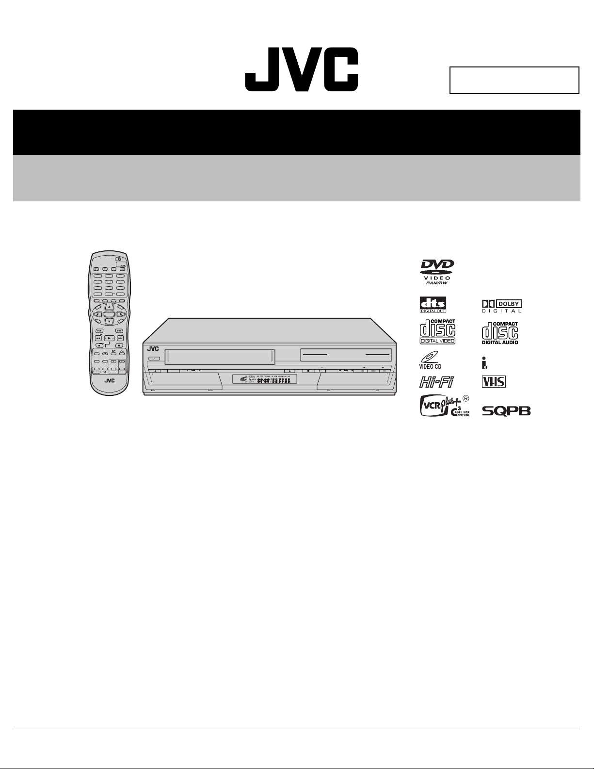
Preliminary
SERVICE MANUAL
DVD VIDEO RECORDER & VIDEO CASSETTE RECORDER
YD00620044
DR-MV1SUC, DR-MV1SUS
DVDTV
CABLE/DBS
TV/CBL/DBS
DVD
VCR
VCR
/DVD
TIMER
/DVD
TIMER
NUMBER/ TV CH / DVD CHNUMBER/ TV CH / DVD CH
3
1
2
ABC DEF
5
6
4
JKL MNO
GHI
8
9
7
TUV
PQRS WXYZ
0
MEMO/MARK
AUX
CANCEL
PROG/CHECK
DISPLAYON SCREEN
PROGRESSIVE
VCR PLUS+
SCAN
TION
VIGA
U
M
N
NA
EN
E
U
P M
O
T
ENTER
S
E
T
RN
U
TU
P
E
R
PREVIOUS NEXT
SLOW
SLOW
PLAY/SELECT
CLEAR
PAUSESTOP/
REMAIN REC
REC MODE
ANGLE
LIVE CHECK
TV/VCR
TV/DVD
SUBTITLE
AUDIO
TV/CBL/DVD
TV
CH
VOL.
TV
POWER
VCR/DVD TIMER VCR REC OPEN/CLOSE STOP PLAY
VCR EJECT
PULL-OPEN
DVD
S-VIDEO
VIDEO (MONO) L - AUDIO - R
F-1
TIMER DVD DVDREC VCR DUBBING
REC PAUSE REW FF
REMAIN
REC MODE SLOW
<< >>
PULL-OPEN
REC LINK
DV IN
CH
DVD
DR-MV1SUC, DR-MV1SUS [D3RV21]
For disassembling and assembling of MECHANISM ASSEMBLY, refer to the SERVICE MANUAL No.86700(MECHANISM ASSEMBLY).
TABLE OF CONTENTS
1 PRECAUTION. . . . . . . . . . . . . . . . . . . . . . . . . . . . . . . . . . . . . . . . . . . . . . . . . . . . . . . . . . . . . . . . . . . . . . . . . 1-3
2 SPECIFIC SERVICE INSTRUCTIONS . . . . . . . . . . . . . . . . . . . . . . . . . . . . . . . . . . . . . . . . . . . . . . . . . . . . . . 1-5
3 DISASSEMBLY . . . . . . . . . . . . . . . . . . . . . . . . . . . . . . . . . . . . . . . . . . . . . . . . . . . . . . . . . . . . . . . . . . . . . . . 1-7
4 ADJUSTMENT . . . . . . . . . . . . . . . . . . . . . . . . . . . . . . . . . . . . . . . . . . . . . . . . . . . . . . . . . . . . . . . . . . . . . . . 1-10
5 TROUBLESHOOTING . . . . . . . . . . . . . . . . . . . . . . . . . . . . . . . . . . . . . . . . . . . . . . . . . . . . . . . . . . . . . . . . . 1-15
COPYRIGHT © 2004 VICTOR COMPANY OF JAPAN, LIMITED
No.YD006
2004/4
Page 2

SPECIFICATION
DR-MV1SUC DR-MV1SUS
GENERAL
Power requirement AC 120 V, 60 Hz
Power consumption
Power on 43 W
Power off 16.5 W
Temperature
Operating 5°C to 35°C (41°F to 95°F)
Storage -20°C to 60°C (-4°F to 140°F)
Operating position Horizontal only
Dimensions (W × H × D) 435 mm × 96 mm × 347 mm (17-3/16" × 3-13/16" × 13-11/16")
Weight 6.1 kg (13.5 lbs)
VIDEO/AUDIO (DVD Deck)
Recording format DVD-RAM: DVD Video Recording format
DVD-RW: DVD-Video format, DVD Video Recording format
Recording time Maximum 8 hours (with 4.7 GB disc)
Audio recording system Dolby Digital (2 ch), Linear PCM (XP mode only)
Video recording compression system MPEG2 (CBR/VBR)
Input/Output
S-video input Y: 0.8 - 1.2 Vp-p, 75 Ω, C: 0.2 - 0.4 Vp-p, 75 Ω
S-video output Y: 1.0 Vp-p, 75 Ω, C: 0.3 Vp-p, 75 Ω
Video input 0.5 - 2.0 Vp-p, 75 Ω (pin jack)
Video output 1.0 Vp-p, 75 Ω (pin jack)
Audio input -8 dB, 50 kΩ (pin jack), Corresponding to mono (left)
Audio output -8 dB, 1 kΩ (pin jack)
i.Link 4-pin for DV input
Component video output Y: 1.0 Vp-p, 75 Ω, CB/CR, PB/PR: 0.7 Vp-p, 75 Ω
Digital audio output Optical: -18 dBm, 660 nm, Coaxial: 0.7 Vp-p, 75 Ω,
VIDEO/AUDIO (VCR Deck)
Signal system NTSC color signal and EIA monochrome signal, 525 lines/60 fields
Recording system DA4 (Double Azimuth) head helical scan system
Format VHS NTSC standard
Maximum recording time
(SP) 210 min. with ST-210 video cassette
(EP) 630 min. with ST-210 video cassette
Signal-to-noise ratio 45 dB
Horizontal resolution 230 lines
Frequency range 70 Hz to 10,000 Hz (Normal audio), 20 Hz to 20,000 Hz (Hi-Fi audio)
Input/Output RCA connectors: IN
TUNER/TIMER
Tuning system Frequency synthesized tuner
Channel coverage VHF: Channels 2 - 13, UHF: Channels 14 - 69, CATV: 113 Channels
RF output Channel 3 or 4 (switchable; preset to Channel 3 when shipped) 75 Ω, unbalanced
Memory backup time Approx. 5 seconds
ACCESSORIES
Provided accessories RF cable × 1, Infrared remote control unit, "AA" battery
(XP): Approx. 1 hour, (SP): Approx. 2 hours, (LP): Approx. 4 hours
(EP): Approx. 6 hours, (FR): Approx. 1 hour - 8 hours
Corresponding to Dolby Digital and DTS Digital Surround
Bit stream Selectable in digital audio output setting menu
× 2
• Specifications shown are for SP mode unless otherwise specified.
• E.& O.E. Design and specifications subject to change without notice.
• VCR Plus+, C
• The VCR Plus+ system is manufactured under license from Gemstar Development Corporation.
TM
•DSS
Corporation.
• Manufactured under license from Dolby Laboratories. "Dolby" and the double-D symbol are trademarks of Dolby Laboratories.
• "DTS" and "DTS Digital Out" are trademarks of Digital Theater Systems, Inc.
• (i.Link) refers to the IEEE1394-1995 industry specification and extensions thereof. The logo is used for products compliant with the i.Link standard.
3
and PlusCode are registered trademarks of Gemstar Development Corporation.
is an official trademark of DIRECTV, Inc., a unit of GM Hughes Electronics. DISH NetworkTM is a trademark of Echostar Communications
DVD-R: DVD-Video format
Corresponding to copy protection
× 2, OUT × 1
RF cable × 3, Antenna splitter, Infrared remote control
unit, "AA" battery × 2
1-2 (No.YD006)
Page 3

SECTION 1
r
e
PRECAUTION
1.1 SAFTY PRECAUTIONS
Prior to shipment from the factory, JVC products are strictly inspected to conform with the recognized product safety and electrical codes of the countries in which they are to be
sold.However,in order to maintain such compliance, it is equally
important to implement the following precautions when a set is
being serviced.
1.1.1 Precautions during Servicing
(1) Locations requiring special caution are denoted by labels
and inscriptions on the cabinet, chassis and certain parts of
the product.When performing service, be sure to read and
comply with these and other cautionary notices appearing
in the operation and service manuals.
(2) Parts identified by the symbol and shaded ( ) parts
are critical for safety.
Replace only with specified part numbers.
NOTE :
Parts in this category also include those specified to
comply with X-ray emission standards for products
using cathode ray tubes and those specified for
compliance with various regulations regarding spurious radiation emission.
(3) Fuse replacement caution notice.
Caution for continued protection against fire hazard.
Replace only with same type and rated fuse(s) as specified.
(4) Use specified internal wiring. Note especially:
• Wires covered with PVC tubing
• Double insulated wires
• High voltage leads
(5) Use specified insulating materials for hazardous live parts.
Note especially:
• Insulation Tape
• PVC tubing
•Spacers
• Insulation sheets for transistors
•Barrier
(6) When replacing AC primary side components (transformers,
power cords, noise blocking capacitors, etc.) wrap ends of
wires securely about the terminals before soldering.
Consequently, when servicing these products, replace the
cathode ray tubes and other parts with only the specified
parts. Under no circumstances attempt to modify these circuits.Unauthorized modification can increase the high voltage value and cause X-ray emission from the cathode ray
tube.
(12) Crimp type wire connectorIn such cases as when replacing
the power transformer in sets where the connections between the power cord and power trans former primary lead
wires are performed using crimp type connectors, if replacing the connectors is unavoidable, in order to prevent safety hazards, perform carefully and precisely according to the
following steps.
• Connector part number :E03830-001
• Required tool : Connector crimping tool of the proper
type which will not damage insulated parts.
• Replacement procedure
a) Remove the old connector by cutting the wires at a
point close to the connector.Important : Do not reuse a connector (discard it).
cut close to connector
Fig.1-1-3
b) Strip about 15 mm of the insulation from the ends
of the wires. If the wires are stranded, twist the
strands to avoid frayed conductors.
15 mm
Fig.1-1-4
c) Align the lengths of the wires to be connected. In-
sert the wires fully into the connector.
Metal sleeve
Fig.1-1-1
(7) Observe that wires do not contact heat producing parts
(heatsinks, oxide metal film resistors, fusible resistors, etc.)
(8) Check that replaced wires do not contact sharp edged or
pointed parts.
(9) When a power cord has been replaced, check that 10-15
kg of force in any direction will not loosen it.
Power cord
Fig.1-1-2
(10) Also check areas surrounding repaired locations.
(11) Products using cathode ray tubes (CRTs)In regard to such
products, the cathode ray tubes themselves, the high voltage circuits, and related circuits are specified for compliance with recognized codes pertaining to X-ray emission.
Connector
Fig.1-1-5
d) As shown in Fig.1-1-6, use the crimping tool to crimp
the metal sleeve at the center position. Be sure to
crimp fully to the complete closure of the tool.
1.2
5
2
.0
5.5
Crimping tool
Fig.1-1-6
e) Check the four points noted in Fig.1-1-7.
Not easily pulled free
Wire insulation recessed
more than 4 mm
Crimped at approx. cente
of metal sleev
Conductors extended
Fig.1-1-7
(No.YD006)1-3
Page 4
1.1.2 Safety Check after Servicing
Examine the area surrounding the repaired location for damage
or deterioration. Observe that screws, parts and wires have been
returned to original positions, Afterwards, perform the following
tests and confirm the specified values in order to verify compliance with safety standards.
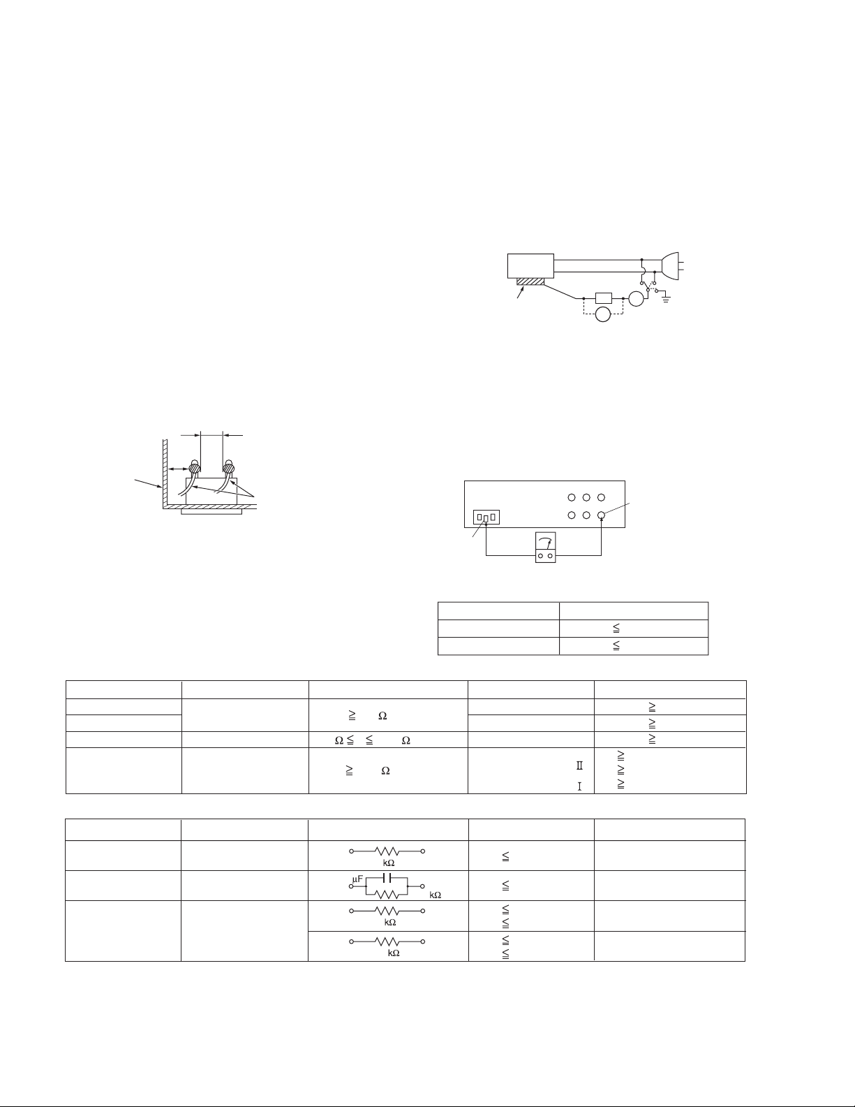
(1) Insulation resistance test
Confirm the specified insulation resistance or greater between power cord plug prongs and externally exposed
parts of the set (RF terminals, antenna terminals, video and
audio input and output terminals, microphone jacks, earphone jacks, etc.).See table 1 below.
(2) Dielectric strength test
Confirm specified dielectric strength or greater between
power cord plug prongs and exposed accessible parts of
the set (RF terminals, antenna terminals, video and audio
input and output terminals, microphone jacks, earphone
jacks, etc.). See Fig.1-1-11 below.
(3) Clearance distance
When replacing primary circuit components, confirm specified clearance distance (d), (d') between soldered terminals, and between terminals and surrounding metallic
parts. See Fig.1-1-11 below.
d
Chassis
d'
Power cord
primary wire
Fig.1-1-8
(4) Leakage current test
Confirm specified or lower leakage current between earth
ground/power cord plug prongs and externally exposed accessible parts (RF terminals, antenna terminals, video and
audio input and output terminals, microphone jacks, earphone jacks, etc.).
Measuring Method : (Power ON)Insert load Z between
earth ground/power cord plug prongs and externally exposed accessible parts. Use an AC voltmeter to measure
across both terminals of load Z. See Fig.1-1-9 and following Fig.1-1-12.
ab
Externally
exposed
accessible part
Z
V
c
A
Fig.1-1-9
(5) Grounding (Class 1 model only)
Confirm specified or lower grounding impedance between
earth pin in AC inlet and externally exposed accessible
parts (Video in, Video out, Audio in, Audio out or Fixing
screw etc.).Measuring Method:
Connect milli ohm meter between earth pin in AC inlet and
exposed accessible parts. See Fig.1-1-10 and grounding
specifications.
AC inlet
Earth pin
Exposed accessible part
MIlli ohm meter
Grounding Specifications
Region
USA & Canada
Europe & Australia
Grounding Impedance (Z
Z 0.1 ohm
Z 0.5 ohm
)
Fig.1-1-10
AC Line Voltage
100 V
100 to 240 V
110 to 130 V
110 to 130 V
200 to 240 V
Region
Japan
USA & Canada
Europe & Australia
Insulation Resistance (R
R 1 M /500 V DC
1 M R 12 M /500 V DC
R 10 M /500 V DC
)
Dielectric Strength
AC 1 kV 1 minute
AC 1.5 kV 1 minute
AC 1 kV 1 minute
AC 3 kV 1 minute
AC 1.5 kV 1 minute
(
Class
(
Class
Clearance Distance (d), (d'
d, d' 3 mm
d, d' 4 mm
d, d' 3.2 mm
d 4 m m
)
d' 8 m m (Power cord
d' 6 m m (Primary wire
)
Fig.1-1-11
AC Line Voltage
100 V
110 to 130 V
110 to 130 V
220 to 240 V
Region
Japan
USA & Canada
Europe & Australia
Load Z
1
0.15
1.5
2
50
Leakage Current (i)
i 1 mA rms
i 0.5 mA rms
i 0.7 mA peak
i 2 mA dc
i 0.7 mA peak
i 2 mA dc
a, b, c
Exposed accessible parts
Exposed accessible parts
Antenna earth terminals
Other terminals
Fig.1-1-12
NOTE :
These tables are unofficial and for reference only. Be sure to confirm the precise values for your particular country and locality.
)
)
)
1-4 (No.YD006)
Page 5
SECTION 2
SPECIFIC SERVICE INSTRUCTIONS
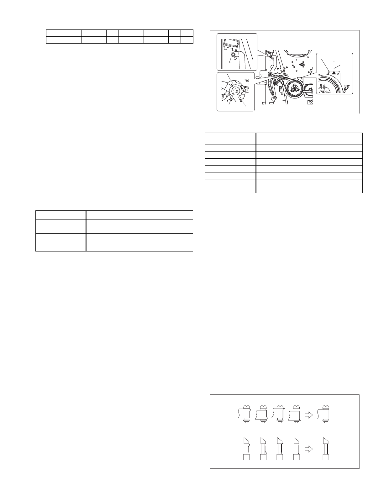
2.1 Service position
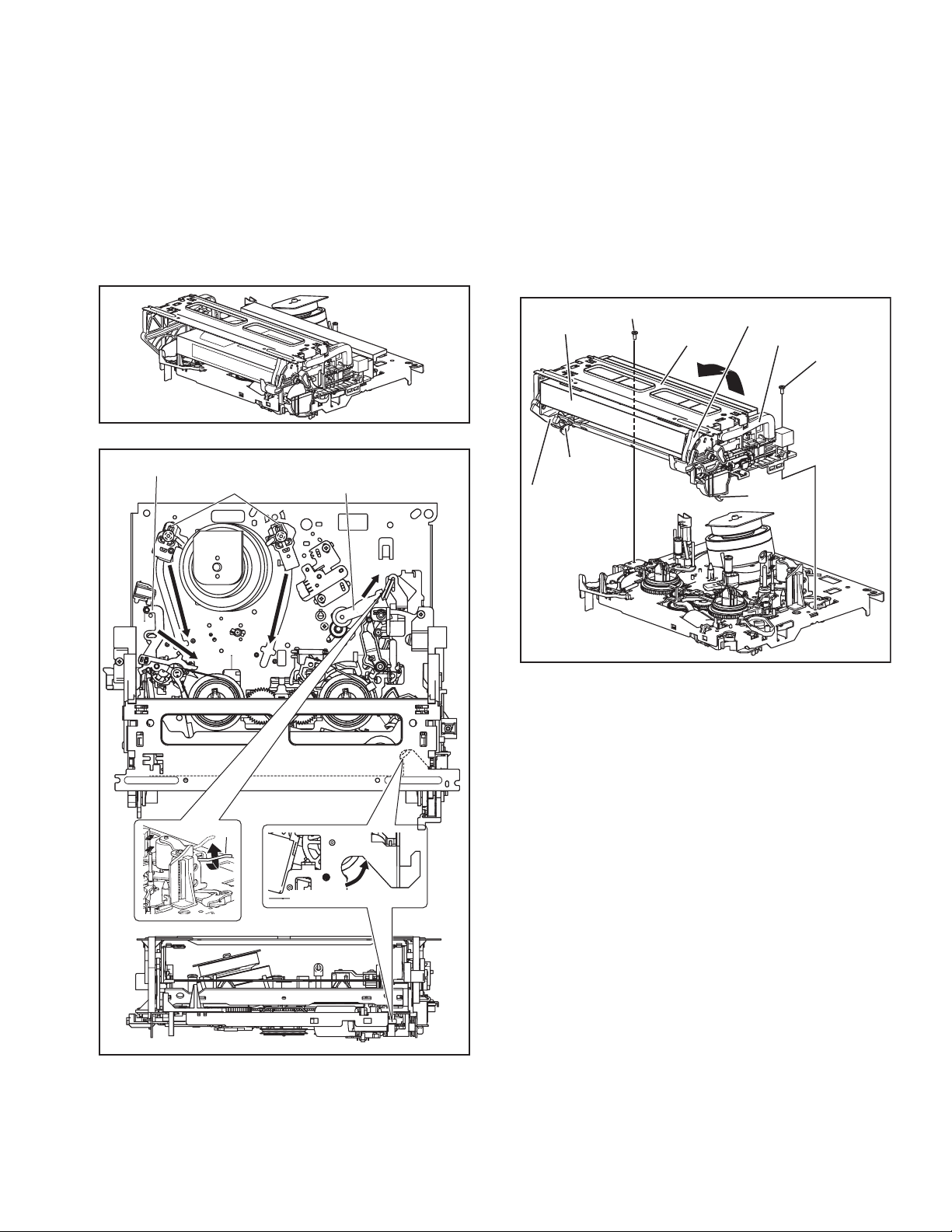
This unit has been designed so that the Mechanism and Main
board assemblies can be removed together from the bottom
chassis. Before diagnosing or servicing the circuit boards, take
out the major parts from the bottom chassis.
2.1.1 How to set the "Service position"
(1) Refer to the disassembly procedure and perform the disas-
sembly of the major parts before removing the Mechanism
assembly.
(2) Remove the screws that fix the Mechanism, Main board as-
sembly to the bottom chassis. If any other screws are used
to fix the boards, remove them also.
(3) Remove the combined Mechanism, DVD unit, regulator,
digital, junction and Main board assemblies.
(4) If any other major parts are used, remove them also.
(5) Connect the wires and connectors of the major parts that
have been removed in steps (1) to (4). (Refer to Fig. 2-1a.)
(6) Place the combined Mechanism, Main board and other
board assemblies upside down.
(7) Insert the power cord plug into the power outlet and then
proceed with the diagnostics and servicing of the board as-
sembly.
Notes:
• Before inserting the power cord plug into the power out-
let, make sure that none of the electrical parts are able
to short-circuit between the workbench and the board
assembly.
• For the disassembly procedure of the major parts and
details of the precautions to be taken, see "Removing
the major parts".
• If there are wire connections from the Main board and
Mechanism assemblies to the other major parts, be sure
to remove them (including wires connected to the major
parts) first before performing step (2).
• When carrying out diagnosis and repair of the Main
board assembly in the "Service position", be sure to
ground both the Main board and Mechanism assemblies. If they are improperly grounded, there may be
noise on the playback picture or FDP counter display
may move even when the mechanism is kept in an inoperative status.
• In order to diagnose the playback or recording of the
cassette tape, set the Mechanism assembly to the required mode before placing it upside down. If the mechanism mode is changed (including ejection) while it is in
an upside down position the tape inside may be damaged.
• For some models, the mechanism and board assem-
blies are attached by connectors only. When carrying
out a diagnosis or repair of the boards in the "Service
position", make sure that the connectors are not disconnected.
Regulator board assy
Junction
board
assy
Digital
board
assy
Jack
board
assy
Switch display board assy Operation jack board assy
Main board assy
TP111 D.FF
TP106 PB FM
TP2253 A.PB FM
TP4001 CTL.P
Fig.2-1a
2.2 Jig RCU mode
This unit uses the following two modes for receiving remote control codes.
(1) User RCU mode:Ordinary mode for use by the user.
(2) Jig RCU mode: Mode for use in production and servicing.
When using the Jig RCU, it is required to set the VCR to the Jig
RCU mode (the mode in which codes from the Jig RCU can be
received). As both of the above two modes are stored in the EEPROM, it is required to set the VCR back to the User RCU mode
each time that an adjustment is made or to check that the necessary operations have been completed.These modes can be set
by the operations described below.
Note:
• When the unit is set to JIG mode and when the unit is
under JIG mode, the remote control unit attached to
product operates only in "Remote Control Code 1".
Since the unit is in "Remote Control Code 3" when it is
shipped and just after its batteries are changed, "Remote Control Code 3" needs to be changed to "Remote
Control Code 1."
• Confirm the RCU mode when exchanged parts. Since
some SERVICE PARTS sets the VCR to the Jig RCU
mode as initial setting. Therefore please set the VCR to
the user RCU mode after replacing the EEPROM.
User RCU mode
Jig RCU mode
Fig.2-2a User/Jig RCU mode
( blinked)
(No.YD006)1-5
Page 6
2.2.1 Changing Remote Control Code
(1) Slide the TV/CABLE/DBS/DVD switch to DVD.
(2) Press the numeric button "1" of the remote control unit
while pressing the "SET UP" button of the remote control
unit. Then,press the "ENTER" button, and then release the
"SET UP" button.
(3) Press the "POWER" button on the unit to turn off the unit.
(4) Press the "PLAY" button on the unit for over 5 seconds
while the unit is turned off. The code currently set appears
on the front display panel.
(5) Press the "STOP" button on the remote control to change
the unit’s code. When FDP indicator displays "DVD1," it
means that the Remote Control Code has been changed to
"1."
2.2.2 Setting the Jig RCU mode
(1) Turn on the power.
(2) Press the “VCR/DVD“ button repeatedly on the unit so that
the VCR lamp lights up on the unit.
(3) Press the following remocon keys continuously within 2
seconds " SET UP " → " 2 " → " 8 " → " ENTER ".
When the VCR is set to the Jig RCU mode, the symbols
( " : " ) in the time display of the FDP are blinked.
(Refer to Fig.2-2a User/Jig RCU mode)
2.2.3 Setting the User RCU mode
(1) Turn off the power.
(2) Press the "REC" and "PAUSE" buttons of the VCR simul-
taneously. Alternatively, transmit the code "9D" from the
Jig RCU.
2.3 Mechanism service mode
This model has a unique function to enter the mechanism into every operation mode without loading of any cassette tape. This
function is called the "Mechanism service mode".
2.3.1 How to set the "Mechanism service mode"
(1) Set the VCR to the Jig RCU mode (the mode in which
codes from the Jig RCU can be received)
(2) Transmit the code "E5" from the Jig RCU.
(3) Release the lug of the Cassette holder and then slide the
Cassette holder toward the direction where the Cassette
holder is loaded by manually.
(4) The cassette holder lowers and, when the loading has
completed, the mechanism enters the desired mode.
When the VCR is set to the Mechanism service mode, the
symbols ("HDD") in the FDP (LED) are turned on.
2.3.2 How to exit from the "Mechanism service mode"
(1) Unplug the power cord plug from the power outlet.
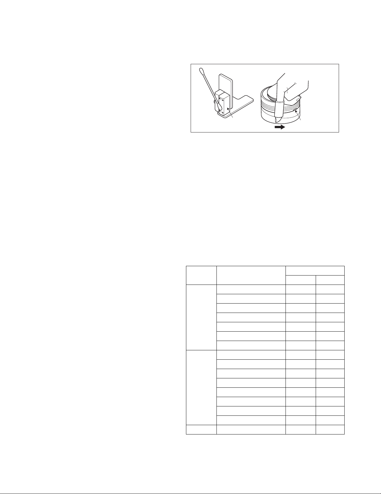
2.4 Maintenance and inspection
2.4.1 Cleaning
Regular cleaning of the transport system parts is desirable but
practically impossible. So make it a rule to carry out cleaning of
the tape transport system whenever the machine is serviced.
When the video head, tape guide and/or brush get soiled, the
playback picture may appear inferior or at worst disappear, resulting in possible tape damage.
Note:
• Absolutely avoid sweeping the upper drum vertically as
this will cause damage to the video head.
(1) When cleaning the upper drum (especially the video head),
soak a piece of closely woven cloth with alcohol and while
holding the cloth onto the upper drum by the fingers, turn
the upper drum counterclockwise.
(2) To clean the parts of the tape transport system other than
the upper drum, use a piece of closely woven cloth or a cotton swab soaked with alcohol.
(3) After cleaning, make sure that the cleaned parts are com-
pletely dry before using the cassette tape.
A/C head
Video heads
Fig.2-4a
2.4.2 Lubrication
With no need for periodical lubrication, you have only to lubricate
new parts after replacement. If any oil or grease on contact parts
is soiled, wipe it off and newly lubricate the parts.
Note:
• See the "mechanism assembly" diagram of the "parts
list" for the lubricating or greasing spots, and for the
types of oil or grease to be used.
2.4.3 Suggested servicing schedule for main components
The following table indicates the suggested period for such service measures as cleaning, lubrication and replacement. In practice, the indicated periods will vary widely according to
environmental and usage conditions. However, the indicated
components should be inspected when a set is brought for service and the maintenance work performed if necessary. Also
note that rubber parts may deform in time, even if the set is not
used.
System Parts name
Operation hours
1000H 2000H
Drum assembly C,X X
A/C head C,X C,X
Pinch roller arm assembly C C
Tape
transport
Full erase head C C
Tension arm assembly C C
Capstan motor (Shaft) C C
Guide arm assembly C C
Capstan motor X
Capstan brake assembly X
Main brake assembly X
Drive
Belt (Capstan) X X
Loading motor X
Clutch unit X
Worm gear X
Control plate X
Other Rotary encoder X
C : Cleaning
X : Inspection or Replacement if necessary
1-6 (No.YD006)
Page 7
SECTION 3
DISASSEMBLY
3.1 Removing the major parts
3.1.1 Destination of connectors
Two kinds of double-arrows in connection tables respectively
show kinds of connector/wires.
: The connector of the side to remove
CONN. No. PIN No.CONNECTOR
WR2a
WR2b
Main CN101
Main CN103
Destination of connectors
CONN. No. PIN No.CONNECTOR
WR2a
WR2b
WR2c
WR3a
WR3b
WR4a
WR4b
WR5a
CN7108
(CN1001)
CN7109
(CN1002)
CN4104
(CN1801)
WR7a
WR7b
WR7c
WR7d
WR7e
WR8a
WR8b
Main
Main
Junction
Main
Drum
assembly
DVD unit
DVD unit
Junction
Junction
Junction
Jack
Junction
Main
Main
Junction
Regulator
Regulator
Regulator
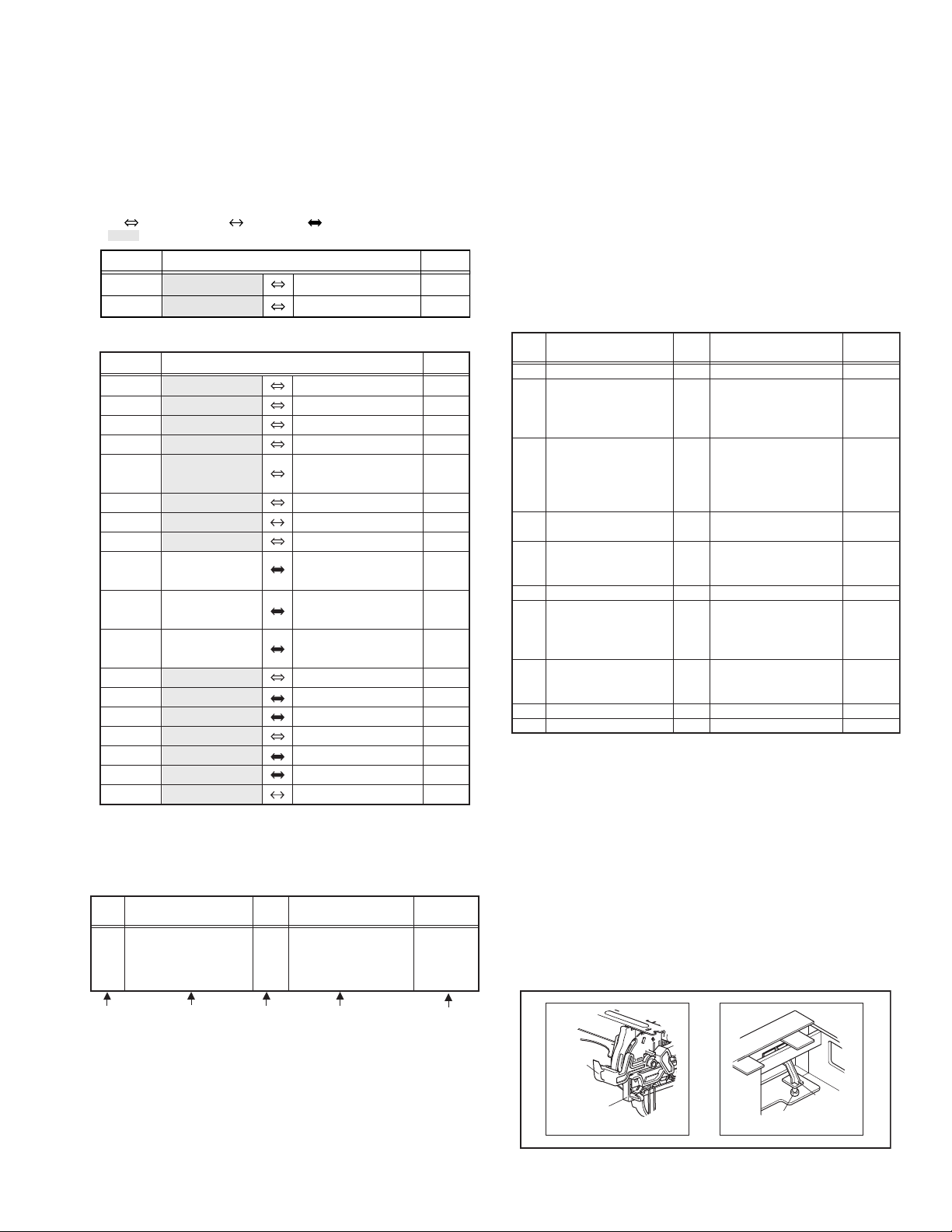
3.1.2 How to read the procedure table
This table shows the steps for disassembly of the externally furnished parts and board assemblies. Reverse these steps when
re-assembling them.
Step/
Loc No.
[1] Top cover 3-1a
Part Name
Bracket 2(S1c)
: Wire: Flat wire : Board to board (B-B)
Digital CN761
Digital CN762
CN3104
CN3102
CN7103
CN2001
CN7106
CN7108
CN7109
CN4104
CN7104
CN3103
CN2601
CN7107
CN5304
CN5301
CN5302
Operation jack
Switch display
Switch display
A/C head
Main
Digital
Regulator
Digital
Digital
Digital
Digital
Main
Junction
Junction
Main
Junction
Main
Fun motor
Fig.
No.
4(S1a),(S1b),3(L1a), <Note 1a>
2(SD1a),(P1a),(W1a),
CN1(WR1a),
----------------------------------------
CN7201
CN7001
CN7002
CN2201
CN5303
CN1404
CN1001
CN1002
CN1801
CN501
CN7102
CN8001
CN7111
CN5501
CN5311
Point Note
CN1
40
10
13
11
4
6
9
40
4
4
28
28
10
4
15
11
13
15
15
2
P= Spring, W= Washer, S= Screw, L= Locking tab, SD=
Solder, CN**(WR**)= Remove the wire (WR**) from the
connector (CN**).
Note:
• The bracketed ( ) WR of the connector symbol are
assigned nos. in priority order and do not correspond to those on the spare parts list.
(5) Adjustment information for installation
3.1.3 Disassembly procedure
Step/
Loc No.
[1]
[2]
[3]
[4]
[5]
[6]
[7]
[8]
[9]
[10]
Part Name
Top cover
Front panel assembly
(Operation jack board assembly)
(Switch display board assembly)
Mechanism assembly
(Drum assembly)
(Cleaner assembly)
DVD unit
(Bracket)
Digital board assembly
Jack board assembly
Junction board assembly
Regulator board assembly
Rear cover
Main board assembly
Fig.
No.
3-1d
3-1a,
3-1d
3-1b,
3-1c,
3-1d
3-1d
3-1d
3-1d
3-1d
3-1d
3-1d
3-1d
Point Note
6(S1a)
3(L2a),5(L2b)
CN3104(WR2a)
CN3102(WR2b)
CN7103(WR2c)
CN2001(WR3a)
3(S3a),(S3b)
CN(WR3b)
(S3c),(S3d),(S3e)
2(L3a)
4(S4a),4(S4b)
(WR4a),(WR4b)
4(S5a)
CN7106(WR5a),CN7101
(CN1001),CN7109(CN1002)
(S6a),CN4104(CN1801)
(S7a),CN7104(WR7a),
CN3103(WR7b),CN2601
(WR7c),CN7107(WR7d),
CN5304(WR7e)
4(S8a)
CN5301(WR8a),
CN5302(WR8b)
2(S9a),5(S9b),2(S9c),3(L9a)
3(S10a)
<Note2a>
<Note2b>
<Note2a>
<Note3a>
<Note3b>
<Note3c>
<Note2a>
<Note2a>
<Note2a>
<Note2a>
<Note 2a>
• Be careful not to damage the connector and wire etc. during
connection and disconnection.
• When connecting the flat wire to the connector, be careful with
the flat wire direction.
<Note 2b>
• When reattaching the Front panel assembly, make sure that
the door opener of the Side frame (R) is lowered in position prior to the reinstallation.
• When reattaching the Front panel assembly, pay careful attention
to the switch lever of the Front panel assembly not to make it
touch the switch knob of the Main board assembly from the side.
• When reattaching the Front panel assembly, lift the Cassette
door slightly.
(1) (2) (3) (4) (5)
(1) Order of steps in Procedure
When reassembling, perform the step(s) in the reverse order.
These numbers are also used as the identification (loca-
tion) No. of parts Figures.
(2) Part name to be removed or installed.
(3) Fig. No. showing procedure or part location.
(4) Identification of part to be removed, unhooked, unlocked,
released, unplugged, unclamped or unsoldered.
Door
opener
Side
frame(R)
Fig.3-1a
Switch
lever
Switch
knob
(No.YD006)1-7
Page 8
<Note 3a>
• When reattaching the Mechanism assembly, secure the
screws (S3a to S3b) in the order of 1,2,3.
<Note 3b>
• When reattaching the Mechanism assembly, be sure to align
the phase of the Rotary encoder on the Main board assembly.
• When reattaching the Mechanism assembly, set the “Mechanism assembling mode”. [See “MECHANISM ASSEMBLY
SERVICE MANUAL (No. 86700)”.]
• When reattaching the Mechanism assembly to the Main board
assembly, take care not to damage the sensors and switch on
the Main board assembly.
<Note 3c>
• When reattaching the Drum assembly, secure the screws (S3c
to S3e) in the order of c, d, e.
(S3d)
Mechanism
assembly
(S3c)
(S3e)
(S3d)
(S3e)
Drum
assembly
<Note 3c>
<NOTE>
Attach the Drum assembly appropriately,
since the installation state of the Drum assembly
influences the FM WAVEFORM LINEARITY
greatly.
(S3c)
HOOK
Fig.3-1b
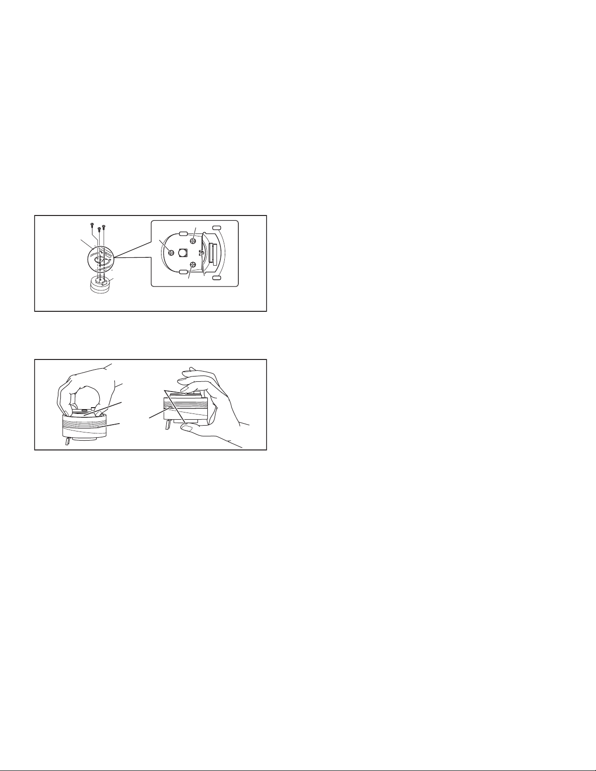
• When handling the drum assembly alone, hold it by the motor
or shaft. Be careful not to touch other parts, especially the video heads. Also take care not to damage the connectors.
Shaft
Motor
Video heads
Fig.3-1c
1-8 (No.YD006)
Page 9
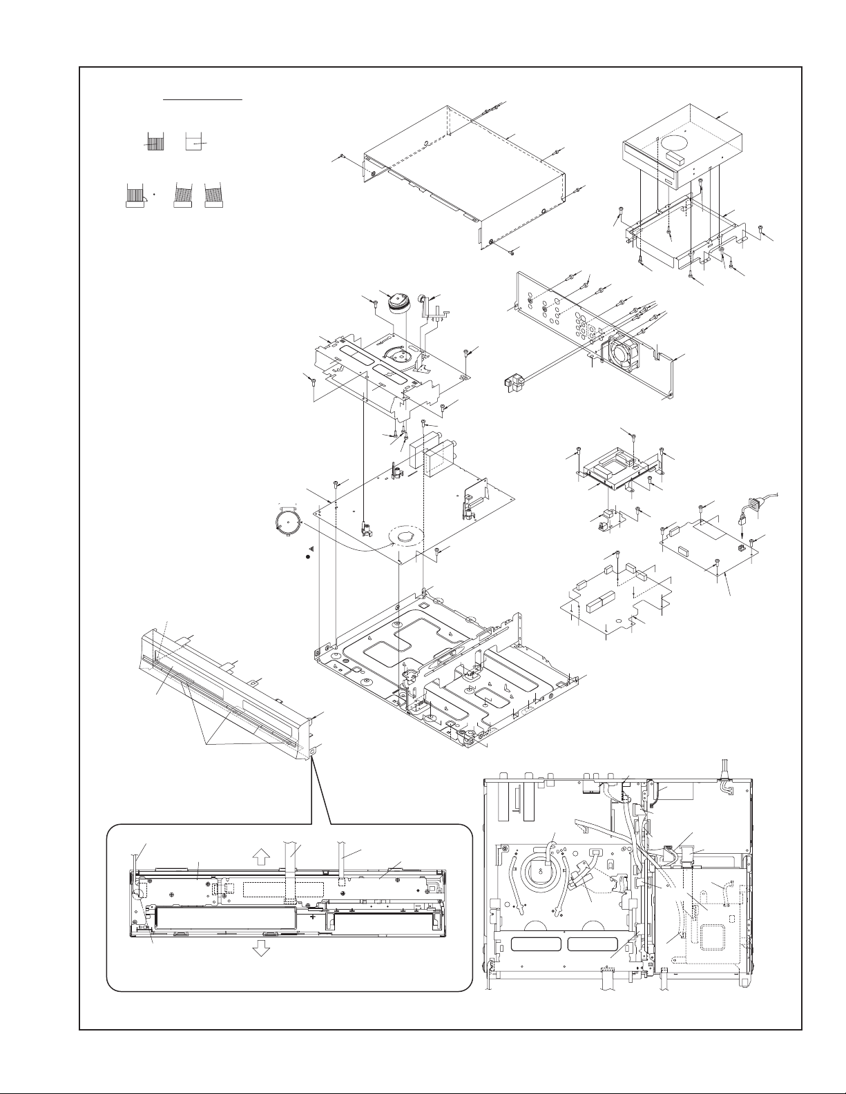
1.Insert direction of FCC WIRE as follows.
NOTE
right side back side
electrode side
supporting side
2.FFC WIRE and DRUM FPC WIRE should be insert as follows.
OK
90
CN CN CN
3.Insert the wire to even the root of connector completely
at the same time as inserting each wire.
4.Check to see that outside parts.TOP COVER,BOTTOM COVER,
FRONT PANEL, etc are fixed certainly to the BOTTOM CHASSIS
with SCRWES.
NG
5.Pay attention NOT to make any scratches on FRONT PANEL.
6.Pay close attention not to cut any Sheath of WIRE by sharp edge
of CHASSIS while Wireing Process.
[3]Mechanism
assembly
(S3a)
[10]Main board
assembly
JS3001JS3001
<Phase alignment>
.
Accord the position of V gap on R.ENCORDER and PWB silk
.
Accord the position of Boss on R.ENCORDER and PWB silk
(L2b)
(L2a)
(L2a)
(L2a)
Cassette door
<Note2b>
(L2b)
(S1a)
(S3a)
j
(S10a)
[2]Front panel
assembly
(L2b)
[3]Drum
assembly
j
(S3c)
(S3e)
(S3d)
(S1a)
[4]DVD unit
[1]Top cover
(S1a)
(S1a)
[4]Bracket
(S4a)
b
(S4a)
(S1a)
(S9c)
[3]Cleaner
assembly
q
(L9a)
(S9b)
(S3a)
b
(S9b)
(S4b)
(S9b)
f
(S4b)
(S9a)
b
(S4a)
(S4b)
[9]Rear cover
b
(S4b)
(S4a)
(L9a)
g
h
(S10a)
r
(S5a)
(S3b)
[5]Digital board
JS3001
e'
assembly
[6]Jack board
assembly
(S10a)
a
i
i
c
c
g
h
b
a
b
e
e
e
d
b
e
d
k
m
c
b
e
(S7a)
e'
d
e
c
i
d
m
(S5a)
k
(L9a)
e'
e'
(S5a)
e'
(S6a)
c
e
e'
e'
e'
e
[7]Junction board
assembly
e
(S5a)
(S8a)
e
(S8a)
c
(S8a)
c
[8]Regulator board
assembly
CN5001
f
(S8a)
c
(WR2a)
<Note2a>
CN7201
OPERATION JACK
BOARD ASSY
CN7002
NOTE)Push the slack of the wire
BOTTOM SIDE
CN7001
into the FW7001 side.
(WR2b)
<Note2a>
CN7001
CN7002
(WR2c)
<Note2a>
NOTE)Pass slit PCB through wire.
TOP SIDE
NOTE) INSERT FFC WIRE TO THE CONNECTOR BEFORE ATTACHING TO FRONT PANEL.
SWITCH DISPLAY
BOARD ASSY
Fig.3-1d
MAIN BOARD ASSY
CN3104
Operation jack assembly
CN7201
(WR3b)
<Note2a>
FW7504
CN501
CN2001
A/C HEAD
(WR3a)
<Note2a>
(WR7b)
<Note2a>
Switch display assembly
CN7001
JACK BOARD ASSY
CN8501
CN3102
CN7111
CN5302
(WR7d)
CN5301
<Note2a>
CN5311
(WR8a)
<Note2a>
CN3106
CN7107
CN8001
CN2601
(WR7c)
<Note2a>
CN3103
CN7102
DVD
(WR7a)
<Note2a>
Switch display assembly
CN7002
CN7103
(WR8b)
FAN
UNIT
REGULATOR BOARD ASSY
(WR4b)
<Note2a>
CN5304
(WR7e)
JUNCTION
CN5501
BOARD ASSY
(WR5a)
<Note2a>
(WR4a)
CN2201
<Note2a>
CN7104
DIGITAL
BOARD ASSY
(No.YD006)1-9
CN5001
CN7106
CN1404
Page 10
SECTION 4
ADJUSTMENT
4.1 Before adjustment
4.1.1 Precaution
• The adjustments of this unit include the mechanism compatibility and electrical adjustments. During the performance of this work, be sure to observe the precautions for
each type of adjustment.
• If there is a reference to a signal input method in the signal
column of the adjustment chart, “Ext. S-input” means the
Y/C separated video signal and “Ext. input” means the
composite video signal input.
• Unless otherwise specified, all measuring points and
adjustment parts are located on the Main board.
4.1.2 Required test equipments
• Color (colour) television or monitor
• Oscilloscope: wide-band, dual-trace, triggered delayed sweep
• Signal generator: RF / IF sweep / marker
• Signal generator: stairstep, color (colour) bar [NTSC]
• Recording tape
• Digit-key remote controller(provided)
4.1.3 Required adjustment tools
--- : Not used
z
: Used
Roller driver
Mechanism
compatibility
adjustment
z ---
Electrical
adjustment
Jig RCU --- z
Back tension cassette gauge z ---
Alignment tape(MHP) z ---
Alignment tape(MHP-L) zz
Roller driver
PTU94002
Alignment tape
(SP, stairstep, NTSC)
MHP
Jig RCU
PTU94023B
Alignment tape
(EP, stairstep, NTSC)
MHP-L
Back tension cassette gauge
PUJ48076-2
4.1.4 Color (colour) bar signal,Color (colour) bar pattern
Color(colour) bar signal [NTSC]
White(100%)
White(75%)
100 IRE
1V
40 IRE
Horizontal sync
Yellow
Cyan
Green
Magenta
Red
QI
Blue
Color(colour) bar pattern [NTSC]
(75%)
Burst
40 IRE
White
Yellow
White
Q I Black
100%
Cyan
Green
Magenta
Red
Blue
4.1.5 Switch settings
When adjusting this unit, set the VCR mode and switches
as described below.
• When using the Jig RCU, it is required to set the VCR to the
Jig RCU mode (the mode in which codes from the Jig RCU can
be received). (See "section 2 SPECIFIC SERVICE INSTRUCTIONS".)
Jig RCU
[Data transmitting method]
Depress the " "( 3 ) button
after the data code is set.
CUSTOM CODE
43: A CODE
DATA CODE
INITIAL MODE
Fig.4-1 Jig RCU [PTU94023B]
• Set the switches as shown below unless otherwise specified
on the relevant adjustment chart. The switches that are not listed below can be set as desired.
If the VCR is not equipped with the functions detailed below,
setup is not required.
AUTO PICTURE/VIDEO CALIBRATION/
B.E.S.T./D.S.P.C.
PICTURE CONTROL/SMART PICTURE NORMAL/NATURAL
VIDEO STABILIZER OFF
TBC ON
Digital 3R ON
VIDEO NAVIGATION/TAPE MANAGER OFF
BLUE BACK OFF
OFF
4.1.6 Manual tracking mode (Auto tracking ON/OFF) set-
ting
(1) In order to set to the manual tracking mode during tape
playback, press the “SP/EP(LP)”button on the remote control unit.
• Each press of the button switches the auto tracking ON
or OFF.
• When the manual tracking mode is set, the tracking is
placed at the center position.
(2) Press “channel +/-” to adjust the tracking manually.
4.1.7 EVR Adjustment
Some of the electrical adjustments require the adjustment performed by the EVR system. The main unit have EEPROMs for
storing the EVR adjustment data and user setups.
Notes:
• In the EVR adjustment mode, the value is varied with the
channel buttons (+, -). The adjusted data is stored when
the setting mode changes (from PB to STOP, when the
tape speed is changed, etc.). Take care to identify the
current mode of each adjustment item when making an
adjustment.
• When changing the address setting in the EVR adjust-
ment mode, use the Jig RCU or the remote controller
having numeric keypad with which a numeric code can
be directly input.
The remote control code of the Jig RCU corresponds to
each of the digit keys on the remote controller as follows.
1-10 (No.YD006)
Page 11
Digit-key0123456789
Code 20 21 22 23 24 25 26 27 28 29
• As the counter indication and remaining tape indication
are not displayed FDP during the EVR adjustment
mode, check them on the TV monitor screen.
• When performing the EVR adjustment, confirm that the
FDP indication is changed to the EVR mode.
4.2 Mechanism compatibility adjustment (VHS SECTION)
Notes:
• Although compatibility adjustment is very important, it
is not necessary to perform this as part of the normal
servicing work. It will be required when you have replaced the A/C head, drum assembly or any part of the
tape transport system.
• To prevent damaging the alignment tape in the compat-
ibility adjustment, prepare a cassette tape (for self-recording/playback), perform a test on it by transporting it
and making sure that the tape is not bent by the tape
transport mechanisms such as in the guide rollers.(See
Fig.4-2b.)
4.2.1 Tension pole position
Notes:
• This adjustment must be performed every time the ten-
sion band is replaced.
Signal (A) • Back tension cassette gauge [PUJ48076-2]
Mode (B1)
Adjustment part (F) • Adjust pin [Mechansim assembly]
Specified value (G)
•PB
(B2)
• Eject end
• 25 - 51 gf•cm (2.45 - 5 x 10
-3
Nm)
(1) Play back the back tension cassette gauge (A).
(2) Check that the indicated value on the left side gauge is
within the specified value (G).
(3) If the indicated value is not within the specified value (G),
perform the adjustment in a following procedure.(See
Fig.4-2a.)
a) Remove the top frame, cassette holder and side
frames (L/R) all together. (Refer to the SERVICE
MANUAL No.86700 [MECHANISM ASSEMBLY].)
b) Rotate the loading motor gear to move the control
plate so that the triangular stamping to the left of the
“P”stamping is aligned with the stamping (a) on the
main deck. This positioning is mode (B1).
c) Adjust by turning the adjustment pin so that the tip of
the tension arm is aligned with the stamping (b) on
the main deck.
d) Rotate the reel disk (S) by about one turn clockwise
and make sure that the round hole of the adjustment
pin is located in the “OK” range. If it is outside this
range, restart the adjustment from the beginning.
After completion of the adjustment, rotate the loading gear
motor to return it to the mode (B2) position.
TENSION ARM
CONTROL PLATE
Stamping(b)
OK
ADJUST PIN
NG
Stamping(a)
Fig.4-2a
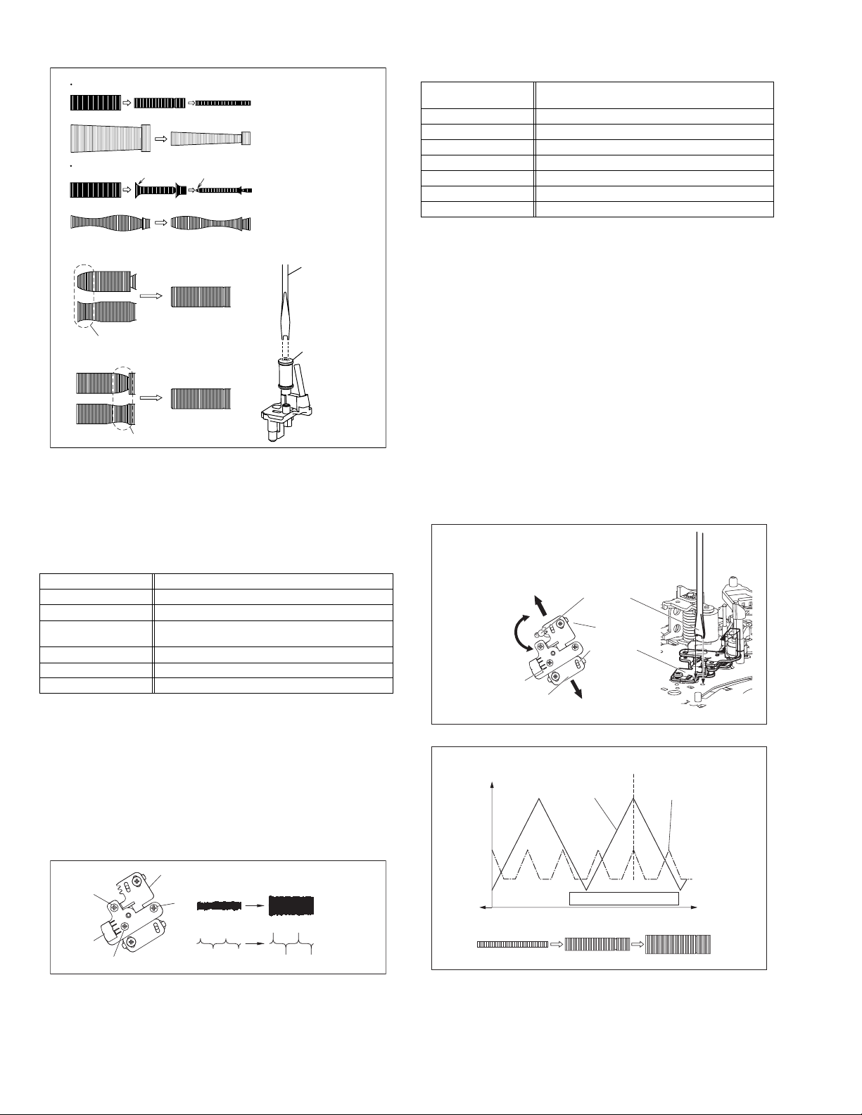
4.2.2 FM waveform linearity
Signal (A1)
Mode (B) • PB
Equipment (C) • Oscilloscope
Measuring point (D) • TP106 (PB. FM)
External trigger (E) • TP111 (D.FF)
Adjustment part (F) • Guide roller [Mechanism assembly]
Specified value (G) • Flat V.PB FM waveform
Adjustment tool (H) • Roller driver [PTU94002]
• Alignment tape(SP, stairstep, NTSC) [MHP]
(A2)
• Alignment tape(EP,stairstep,NTSC) [MHP-L]
(1) Play back the alignment tape (A1).
(2) Apply the external trigger signal to D.FF (E), to observe
the V.PB FM waveform at the measuring point (D).
(3) Set the VCR to the manual tracking mode.
(4) Make sure that there is no significant level drop of the V.PB
FM waveform caused by the tracking operation, with its
generally parallel and linear variation ensured. Perform the
following adjustments when required. (See Fig. 4-2c.)
(5) Reduce the V.PB FM waveform by the tracking operation.
If a drop in level is found on the left side, turn the guide roll-
er of the pole base assembly (supply side) with the roller
driver to make the V.PB FM waveform linear.
If a drop in level is on the right side, likewise turn the guide
roller of the pole base assembly (take-up side) with the
roller driver to make it linear. (See Fig. 4-2c.)
(6) Make sure that the V.PB FM waveform varies in parallel
and linearly with the tracking operation again. When re-
quired, perform fine-adjustment of the guide roller of the
pole base assembly (supply or take-up side).
(7) Unload the cassette tape once, play back the alignment
tape (A1) again and confirm the V.PB FM waveform.
(8) After adjustment, confirm that the tape wrinkling does not
occur at the roller upper or lower limits. (See Fig. 4-2b.)
[Perform adjustment step (9) only for the models equipped
with SP mode and EP (or LP) mode.]
[Perform adjustment step (9) only for the models
equipped with SP mode and EP (or LP) mode.]
(9) Repeat steps (1) to (8) by using the alignment tape (A2).
Improper
Proper
(a)
GUIDE ROLLER
(b)
GUIDE POLE
Fig.4-2b
(No.YD006)1-11
Page 12
Proper waveform variation
Improper waveform variation
A
C
Up Down
B
D
Roller driver
Guide roller
(supply side)
Fig.4-2c
4.2.3 Height and tilt of the A/C head
Note:
• Set a temporary level of the height of the A/C head in ad-
vance to make the adjustment easier after the A/C head
has been replaced. (Refer to the SERVICE MANUAL
No.86700 [MECHANISM ASSEMBLY].)
Signal (A) • Alignment tape(SP, stairstep, NTSC) [MHP]
Mode (B) • PB
Equipment (C) • Oscilloscope
Measuring point (D1)
External trigger (E) • TP111 (D.FF)
Adjustment part (F) • A/C head [Mechanism assembly]
Specified value (G) • Maximum waveform
• TP106 (PB. FM)
(D2)
• TP4001 (CTL. P)
(1) Play back the alignment tape (A).
(2) Apply the external trigger signal to D.FF (E), to observe the
AUDIO OUT waveform and Control pulse waveform at the
measuring points (D1) and (D2) in the ALT mode.
(3) Set the VCR to the manual tracking mode.
(4) Adjust the AUDIO OUT waveform and Control pulse wave-
form by turning the screws (1), (2) and (3) little by little until
both waveforms reach maximum. The screw (1)
and (3) are for adjustment of tilt and the screw (2) for azi-
muth.
Head base
(2)
(1)
AUDIO OUT
4.2.4 A/C head phase (X-value)
Signal (A1)
Mode (B) • PB
Equipment (C) • Oscilloscope
Measuring point (D) • TP106 (PB. FM)
External trigger (E) • TP111 (D.FF)
Adjustment part (F) • A/C head base [Mechanism assembly]
Specified value (G) • Flat V.PB FM waveform
Adjustment tool (H) • Roller driver [PTU94002]
• Alignment tape(SP, stairstep, NTSC) [MHP]
(A2)
• Alignment tape(EP,stairstep,NTSC) [MHP-L]
(1) Play back the alignment tape (A1).
(2) Apply the external trigger signal to D.FF (E), to observe the
V.PB FM waveform at the measuring point (D).
(3) Set the VCR to the manual tracking mode.
(4) Loosen the screws (4) and (5), then set the Roller driver to
the innermost projected part of the A/C head. (See Fig. 4-
2e.)
(5) Rotate the roller driver so that the A/C head comes closest
to the capstan. From there, move the A/C head back grad-
ually toward the drum until the point where the FM wave-
form is maximized for the second time, and then
tighten the screws (4) and (5) temporarily.
(6) Play an alignment tape (A2) and set to the manual-tracking
mode.
(7) Fine-adjust A/C head base position to maximize the FM
waveform, and then tighten the screws (4) and (5) firmly.
(8) Play alignment tapes (A1) and (A2) and confirm that the FM
waveforms are maximized when the tracking is at the cen-
ter position.
To the drum
Toward the capstan
Toward the drum
A/C head
Screw (5)
Roller driver
Screw (4)
Head base
To the capstan
Fig.4-2e
Alignment tape
[SP, stairstep]
played with the
SP head
Waveform output
X-value adjustment point
Drum side Control head position Capstan side
Alignment tape
[EP(LP), stairstep]
played with the
EP(LP) head
A/C head
(3)
1-12 (No.YD006)
Fig.4-2d
CTL. P
Maximum
Fig.4-2f
Page 13
4.3 Electrical adjustment
Note:
The following adjustment procedures are not only necessary
after replacement of consumable mechanical parts or board
assemblies, but are also provided as references to be referred
to when servicing the electrical circuitry.
In case of trouble with the electrical circuitry, always begin a
service by identifying the defective points by using the measuring instruments as described in the following electrical adjustment procedures. After this, proceed to the repair,
replacement and/or adjustment. If the required measuring instruments are not available in the field, do not change the adjustment parts (variable resistor, etc.) carelessly.
4.3.1 Servo circuit
4.3.1.1 Switching point
Signal (A1)
Mode (B) • PB
Equipment (C) • Oscilloscope
Measuring point (D) • VIDEO OUT terminal (75 ohm terminated)
External trigger (E) • TP111 (D.FF)
Adjustment part (F) • Jig RCU: Code “5A”
Specified value (G) • 6.5 ± 0.5H
Adjustment tool (H) • Jig RCU [PTU94023B]
• Stairstep signal
(A2)
• Alignment tape(EP,stairstep,NTSC) [MHP-L]
• TP106 (PB. FM)
(1) Play back the signal (A1) of the alignment tape (A2).
(2) Apply the external trigger signal to D.FF (E) to observe the
VIDEO OUT waveform and V.PB FM waveform at the
measuring points (D1) and (D2).
(3) Set the VCR to the manual tracking mode.
(4) Adjust tracking so that the V.PB FM waveform becomes
maximum.
(5) Set the VCR to the Auto adjust mode by transmitting the
code (F) from the Jig RCU. When the VCR enters the stop
mode, the adjustment is completed.
(6) If the VCR enters the eject mode, repeat steps (1) to (5)
again.
(7) Play back the alignment tape (A2) again, confirm that the
switching point is the specified value (G).
Trigger point
Switching point
V.sync
V. rate
Fig.4-3a Switching point
4.3.1.2 Slow tracking preset
Signal (A1)
Mode (B1)
Measuring point (D) • TV-Monitor
Adjustment part (F) • Jig RCU: Code “71”or “72”
Specified value (G) • minimum noise
Adjustment tool (H) • Jig RCU [PTU94023B]
• Ext. input
(A2)
• Color (colour) bar signal [NTSC]
• VHS SP
(B2)
•VHS EP
(1) Record the signal (A2) in the mode (B1), and play back
the recorded signal.
(2) Set the VCR to the manual tracking mode.
(3) Set the VCR to the FWD slow (+1/6x) mode.
(4) Transmit the code (F) from the Jig RCU to adjust so that the
noise bar becomes the specified value (G) on the TV
monitor in the slow mode.
(5) Set the VCR to the Stop mode.
(6) Confirm that the noise bar is (G) on the TV monitor in the
slow mode.
(7) Repeat steps (3) to (6) in the REV slow (+1/6x) mode.
(8) Repeat steps (1) to (7) in the mode (B2).
Note:
• For FWD slow (+1/6x) playback, transmit the code “08”
from the Jig RCU to enter the slow playback mode, and
transmit the code “D0”for REV slow (-1/6x) mode.
4.3.2 DVD Video circuit
Note
• when perform these adjustments, set the unit to DVD
mode.(DVD lamp lights up)
4.3.2.1 EE COMPONENT Y level
Signal (A) • Internal color bar
Mode (B) • EE
Equipment (C) • Oscilloscope
Measuring point (D) • COMPONENT Y terminal
EVR mode
EVR address
Specified value (G) • 1.00 ± 0.02 Vp-p (terminated)
Adjustment tool (H) • Jig RCU [PTU94023B]
(F1)
• Jig code “95”
(F2)
• "ADJUST01 : **"
(F3)
• Jig code “21”
(F4)
• Jig code “18” or “19” (Channel +/-)
(F5)
• Jig code “3C”
(1) Observe the Y OUT waveform at the measuring point (D).
(2) Set the VCR to the EVR mode by transmitting the code (F1)
from the Jig RCU.
(3) Set the EVR address to (F2) by transmitting the code (F3)
from the Jig RCU.
(4) Transmit the code (F4) from the Jig RCU to adjust so that
the Y level of the Y OUT waveform becomes the specified
value (G).
(5) Release the EVR mode of the VCR by transmitting the
code (F5) from the Jig RCU again. (When the EVR mode
is released, the adjusted data is memorized.)
Y level
Fig.4-3b EE componet Y level
(No.YD006)1-13
Page 14
4.3.2.2 EE Y level
Signal (A1)
Mode (B) • EE
Equipment (C) • Oscilloscope
Measuring point (D) • Y OUT (S terminal)
EVR mode
EVR address
Specified value (G) • 1.00 ± 0.02 Vp-p (terminated)
Adjustment tool (H) • Jig RCU [PTU94023B]
• Ext. input
(A2)
• Color (colour) bar signal
• Jig code “95”
(F1)
• "ADJUST02 : **"
(F2)
• Jig code “22”
(F3)
• Jig code “18” or “19” (Channel +/-)
(F4)
• Jig code “3C”
(F5)
(1) Observe the Y OUT waveform at the measuring point (D).
(2) Set the VCR to the EVR mode by transmitting the code (F1)
from the Jig RCU.
(3) Set the EVR address to (F2) by transmitting the code (F3)
from the Jig RCU.
(4) Transmit the code (F4) from the Jig RCU to adjust so that
the Y level of the Y OUT waveform becomes the specified
value (G).
(5) Release the EVR mode of the VCR by transmitting the
code (F5) from the Jig RCU again. (When the EVR mode
is released, the adjusted data is memorized.)
Y level
H. rate
Fig.4-3c EE Y level
4.3.2.3 EE COMPONENT PB/CB level
Signal (A) • Internal color bar
Mode (B) • EE
Equipment (C) • Oscilloscope
Measuring point (D) • COMPONENT PB/CB terminal
EVR mode
EVR address
Specified value (G) • 0.70 ± 20 Vp-p (terminated)
Adjustment tool (H) • Jig RCU [PTU94023B]
• Jig code “95”
(F1)
• "ADJUST06 : **"
(F2)
• Jig code “26”
(F3)
• Jig code “18” or “19” (Channel +/-)
(F4)
• Jig code “3C”
(F5)
PB/CB level
Fig.4-3d EE component PB/CB level
4.3.3 Syscon circuit
Notes:
• When perform this adjustment, remove the Mechanism
assembly.
4.3.3.1 Timer clock
Signal (A) • No signal
Mode (B) • EE
Equipment (C) • Frequency counter
Measuring point (D1)
Adjustment part (F) • C3025 (TIMER CLOCK)
Specified value (G) • 1024.008 ± 0.001 Hz
• IC3001 pin 61
• IC3001 pin 24
(D2)
• C3026 + and -
(D3)
(976.5549 ± 0.0010 usec)
(1) Connect the frequency counter to the measuring point
(D1).
(2) Connect the short wire between the short point (D2) and
Vcc (5V).
(3) Short the leads of capacitor (D3) once in order to reset
the microprocessor of the Syscon.
(4) Disconnect the short wire between the short point (D2)
and Vcc then connect it again.
(5) Adjust the Adjustment part (F) so that the output frequency
becomes the specified value (G).
(1) Observe the CB OUT waveform at the measuring point (D).
(2) Set the VCR to the EVR mode by transmitting the code (F1)
from the Jig RCU.
(3) Set the EVR address to (F2) by transmitting the code (F3)
from the Jig RCU.
(4) Transmit the code (F4) from the Jig RCU to adjust so that
the CB level of the CB OUT waveform becomes the specified value (G).
(5) Release the EVR mode of the VCR by transmitting the
code (F5) from the Jig RCU again. (When the EVR mode
is released, the adjusted data is memorized.)
1-14 (No.YD006)
Page 15
SECTION 5
TROUBLESHOOTING
5.1 Manually removing the cassette tape
If you cannot remove the cassette tape which is loaded because
of any electrical or mechanical failures, manually remove it by
taking the following steps.
(1) Unplug the power cord plug from the power outlet.
(2) Refer to the disassembly procedure of the VCR and per-
form the disassembly of the major parts before removing
the mechanism assembly. (See Fig. 5-1a)
Fig.5-1a
Tension arm assembly
Pole base assembly
Pinch roller arm assembly
sion arm assembly free from tension, pull out the tape
on the pole base assembly. Take the spring(a) of the
pinch roller arm assembly off the hook, and detach it
from the tape.
(4) Remove the screw (a) of the side frame (L/R).
(5) Hold the slack tape and cassette cover together, lift the
cassette tape, top frame, cassette holder and side frames
(L, R) together from the rear and remove them by dis-en-
gaging the hooks (a) and (b).
Screw(a)
Cassette tape
Hook(a)
Side frame(L)
Cassette holder
Top frame
Side frame(R)
Screw(a)
Hook(b)
Spring(a)
Direction of unloading
Fig.5-1b
(3) Unload the pole base assembly by manually turning the
gear of the loading motor until the pole base assembly is
hidden behind the cassette lid. In doing so, hold the tape by
the hand to keep the slack away from any grease. (See
Fig.5-1b )
In case of mechanical failures, while keeping the ten-
Fig.5-1c
(6) Take up the slack of the tape into the cassette. This com-
pletes removal of the cassette tape.
5.2 Manually removing the disk(DVD/CD)
If you cannot remove the disk which is loaded because of any
electrical or mechanical failures, manually remove it by taking the
following steps.
5.2.1 Method 1
(1) AC Plug is pulled out at once and inserted again.
(2) It is displayed on FDP as "LOADING", and while it blinks,
pushing the OPEN/CLOSE button is continued.
(3) After a while, a tray opens (About 20 seconds).
(4) After removed a disk, press the OPEN/CLOSE button
again to close the tray.
(5) The "LOADING" blink display of FDP disappears and it will
be in a standby mode.
(6) If the POWER button is pushed, it will usually be operating.
5.2.2 Method 2
(1) Unplug the ACpower cord from the AC outlet.
(2) Remove the top cover and front panel assembly.
(Refer to the disassembly procedure and perform the dis-
assembly of the major parts before removing)
(3) Pass a thin wire through a hole in the DVD unit.
(4) The disc tray comes out slightly. Take out the disc tray
manually.(See Fig.5-2a)
(No.YD006)1-15
Page 16
EMG display of FDP display mode
(1) Transmit the code “59” from the Jig RCU.
The FDP shows the EMG content in the form of “E:**:**”.
<Example 1> E : 01
Latest EMG
disk tray hole
Fig.5-2a
5.3 Emergency display function (VHS SECTION)
This unit saves details of the last two emergencies as the EMG
history and allows the status of the VCR and the mechanism of
each emergency to be shown both on the display and as OSD information.
When using the emergency function, it is required to set the VCR
to the Jig RCU mode.
Jig RCU
[Data transmitting method]
Depress the " " ( 3 ) button
after the data code is set.
CUSTOM CODE
43: A CODE
DATA CODE
INITIAL MODE
Fig.5-3a Jig RCU [PTU94023B]
5.3.1 Displaying the EMG information
The EMG detail of information can be displayed by transmitting
the code "59" from the Jig RCU.
Note:
• The EMG detail information <1><2> show the informa-
tion on the latest EMG.
It becomes “ - - : - - : - - ” when there is no latest EMG
record.
0: 00
E: **
1E: **
1: *1
2: *2
3: 34
4: *5
5: *6
6: *7
7: *8
8: *9
9: *1 0
Normal display
EMG content display (Latest) See 5.3.4
EMG content display (Previous) See 5.3.4
EMG detail information <1> See 5.3.5
[Deck operation mode]
EMG detail information <1> See 5.3.5
[Mechanism operation mode]
EMG detail information <1> See 5.3.5
[Mechanism sensor information and Mechanism mode position]
EMG detail information <2> See 5.3.6
[Type of the cassette tape in use <1>]
EMG detail information <2> See 5.3.6
[Winding position of the cassette tape in use]
EMG detail information <2> See 5.3.6
[Type of the cassette tape in use <2> (Winding area)]
EMG detail information <3> See 5.3.7
[Previous deck operation mode]
EMG detail information <3> See 5.3.7
[The deck operation mode of the one before the last]
EMG detail information <3> See 5.3.7
[The deck operation mode of the one prior to one above]
EMG display of 7 FDP display model
Fig.5-3b
<Example 2> E : - -
No EMG record
(2) Transmit the code “59” from the Jig RCU again.
The FDP shows the EMG detail information <1> in the form
of “ *1: *2 : 34 ”.
*1 : Deck operation mode at the moment of EMG
*2 : Mechanism operation mode at the moment of EMG
3- : Mechanism sensor information at the moment of EMG
-4 : Mechanism mode position at the moment of EMG
(3) Transmit the code “59” from the Jig RCU once again.
The FDP shows the EMG detail information <2> in the form
of “ *5 : *6 : *7 ”.
*5 : Type of the cassette tape in use <1> .
*6 : Winding position of the cassette tape in use
*7 : Type of the cassette tape in use <2> (Winding area)
(4) Transmit the code “59” from the Jig RCU once again.
The FDP shows the EMG detail information <3> in the form
of “*8 : *9 : *10”.
*8 : Previous deck operation mode at the moment of EMG
*9 : The deck operation mode of the one before the last at
the moment of EMG
*10: The deck operation mode of the one prior to one
above at the moment of EMG
(5) Transmit the code “59” from the Jig RCU once again to re-
set the display.
5.3.2 Clearing the EMG history
(1) Display the EMG history.
(2) Transmit the code “36” from the Jig RCU.
(3) Reset the EMG display.
5.3.3 Details of the OSD display in the EMG display mode
During the EMG display, the OSD shows the data on the deck
mode, etc. The details of the display contents are as follows.
Notes:
• The display is variable depending on the part No. of the
System Control microcomputer (IC3001) built into the
VCR. In the following, refer to the figure carrying the
same two characters as the top two characters of the
part number of your IC.
• The sensor information in the OSD display contents is
partially different from the mechanism sensor information in EMG detail information <1>.
[For MN* only]
AA BB CC DD EE
FF GG HH I I J J
KK L L MM NN OO
PP QQ RR SS TT
UU VV WW XX YY
1-16 (No.YD006)
Page 17
AA : Deck operation mode (See EMG detail information <1>.)
BB : Mechanism operation mode
(See EMG detail of information <1>.)
CC : Mechanism transition flag
DD : Capstan motor control status
EE : Loading motor control status
FF : Sensor information (See sensor information details.)
GG : Capstan motor speed
HH : Key code (JVC code)
I I : Supply reel winding diameter data higher 8 bits.
JJ : Supply reel winding diameter data lower 8 bits.
KK : Mechanism sensor information & mechanism mode posi-
tion(See EMG detail of information <1>.)
LL : Tape speed data higher 8 bits.
MM : Tape speed data lower 8 bits.
NN : Cassette tape type <2> higher 8 bits.
(See EMG detail of information <2>.)
OO : Cassette tape type <2> lower 8 bits.
(See EMG detail of information <2>.)
PP : General data display area
YY : General data display area
*FF:Sensor information details
<Display>
** h
********
Encoder data
(See Mechanism mode sequence.)
Cassette tab present = 1
Cassette tab broken = 0
Cassette absent = 1
Cassette present = 0
Start sensor
End sensor
[For *HD only]
<Display>
** h
********
Encoder data
(See Mechanism mode sequence.)
Remote pause
End sensor
Start sensor
Cassette tab present = 1
Cassette tab broken = 0
[For both MN*/HD*]
Mechanism mode sequence
Mechanism mode - Encoder data
LSA
LSB
LSC
LSD
No. Position Encoder data
21
Encoder output = Low
or
Trerminal - GND = SHORT
1
EJECT 0 h = 0000
2
EJECT1 1 h = 0001
3
EJECT2 2 h = 0010
4
ULSTOP 3 h = 0011
5
UPPER 4 h = 0100
6
ONSTOP(PLAY) 5 h = 0101
7
FWD/SS 6 h = 0110
8
REV/SS 7 h = 0111
9
OFFSTOP 8 h = 1000
10
FFREW-BRAKE 9 h = 1001
FFREW A h = 1010
11
MIDDLE F h = 1111
12
543
Encoder output = High
Trerminal - GND = OPEN
LSA
12345
1110
GND
9876
or
LSB
LSD
LSC
AA BB CC
DD EE FF
GGGG HHHH
I I JJJJ
KKKK LLLL MMMM
ROM No.
AA : Key code (JVC code)
BB : Deck operation mode(See EMG detail information
<1>.)
CC : Mechanism operation mode (See EMG detail informa-
tion <1>.)
DD : Sensor information (See sensor information details.)
EE : Capstan motor speed (Search, double speed)
FF : Tracking value
GGGG : Cassette tape type <2>, 16 bits.
(See EMG detail information <2>.)
HHHH : Supply reel winding diameter data
I I : Capstan motor speed (FF/REW, double speed)
JJJJ : Tape speed data, lower 8 bits.
KKKK : General data display area
LLLL : General data display area
MMMM : General data display area
*DD:Sensor information details
(No.YD006)1-17
Page 18

5.3.4 EMG content description
Note:
EMG contents “E09” are for the model with Dynamic Drum (DD).
FDP CONTENT CAUSE
E01: Loading EMG
E02:
Unloading EMG
E03: Take Up Reel
Pulse EMG
E04: Drum FG EMG
E05: Cassette Eject
EMG
E06: Capstan FG
EMG
E07: SW Power
Short-Circuit
EMG
E08:
DVD EMG
E09: DD FG EMG
E0A: Supply Reel
Pulse EMG
EU1:
Head clog warning
history
If the mechanism mode does not change to the next mode within 4 seconds after the loading motor starts rotating in the loading direction, while
the mechanism is in the after-loading position (with the tape up against
the pole base), [E:01] is identified and the power is switched OFF.
However, if the tape loading is not completed within 4 seconds after
the loading motor starts rotating in the loading direction, the tape is
simply unloaded and ejected. No EMG data is recorded in this case.
When the mechanism mode cannot be changed to another mode
even when the loading motor has rotated for more than 4 seconds in the unloading direction, [E:02] is identified and the power
is turned off.
When the falling edje of the take-up reel pulse has not been generated for more than 4 seconds in the capstan rotating mode,
[E:03] is identified, the pinch rollers are turned off and stopped,
and the power is turned off. In this case, however, the mechanism should be in position after tape loading. Note that the reel
EMG is not detected during Slow/Frame advance operations.
When the drum FG pulse has not been input for more than 3 seconds in the drum rotating mode, [E:04] is identified, the pinch rollers are turned off and stopped, and the power is turned off.
If the cassette does not reach the eject position within about 0.7
seconds after the cassette housing has started the cassette ejection operation, [E:05] is identified, the drive direction is reversed
to load the tape, the mode is switched to STOP mode with the
pinch roller OFF, and the power is switched OFF.
During the cassette insertion process, the drive direction is reversed
and the cassette is ejected if the tape is not up against the pole
base within about 3 seconds after the start of the cassette pullingin operation. If the cassette does not reach the eject position within
about 0.7 seconds after the drive mode reversal operation, [E:05]
is identified and the power is switched OFF immediately.
When the capstan FG pulse has not been generated for more
than 1 second in the capstan rotating mode, [E:06] is identified,
the pinch rollers are turned off and stopped, and the power is
turned off.However, the capstan EMG is not detected in SLOW/
STILL modes.
Note that, if the part number of the System Control IC begins with
"MN" or "M3", the capstan EMG is not detected even during the
FF/REW operation.
When short-circuiting of the SW power supply with GND has lasted
for 0.5 second or more, [E:07] is identified, all the motors are
stopped and the power is turned off.
When communication with a system computer of VHS side is not
carried out because of the defective DVD unit, or when the DVD
unit must be reset
When the DD FG pulse is not generated within 2.5 seconds, [E:09]
is identified, the tilt motor is stopped and the power is turned off.
When the falling edge of the supply reel pulse has not been generated for more than 10 seconds in the capstan rotating mode,
[E:0A] is identified and the cassette is ejected (but the power is
not turned off). In this case, however, the mechanism should be
in the position after tape loading (with the tape up against the pole
base). Also note that the reel EMG is not detected during Slow/
Frame advance operations.
Presupposing the presence of the control pulse output in the PLAY mode, when the value obtained by mixing the two V.FM output channels (without regard
to the A.FM output) has remained below a certain threshold level for more than 10 seconds, [E:U1] is identified and recorded in the emergency history.
During the period in which the head clog is detected, the FDP shows "U:01" and the OSD repeats the "3 seconds of warning display" and the "7 seconds of
noise picture display" alternately.
EMG code : "E:C1" or "E:U1" / FDP : "U:01" / OSD : "Try cleaning tape." or "Use cleaning cassette."
The head clog warning is reset when the above-mentioned threshold has been exceeded for more than 2 seconds or the mode is changed to another mode
than PLAY.
1. The mechanism is locked in the middle of the mode transition during a tape loading operation.
2.
The mechanism overruns during the tape loading operation because the SYSCON cannot recognize
the mechanism mode normally. This problem is due to a cause such as a rotary encoder failure.
3.
Power is not supplied to the loading MDA. (M12V/Vcc/Vref/ICP are disconnected in the middle.)
1.
The mechanism is locked in the middle of mode transition.
2.
Without an eject signal being sent from the SYSCON, unloading is attempted (i.e. Ejection is attempted
while the tape is still inside the mechanism.) because the SYSCON cannot recognize the mechanism
mode normally. This is due to a cause such as a rotary encoder failure. (Mechanism position:
UPPER)
3.
Power is not supplied to the loading MDA. (M12V/Vcc/Vref/ICP are disconnected in the middle.)
1.
The take-up reel pulse is not generated in the FWD transport modes (PLAY/FWD SEARCH/FF,
etc.) because;
1) The idler gear is not meshed with the take-up reel gear because the mechanism mal-functions for
2)
3) The reel is rotating normally but an FG pulse is not generated due to the take-up reel sensor failure.
2.
The supply reel pulse is not generated in the REV transport modes (REV SEARCH/REW, etc.)
because;
1) The idler gear is not meshed with the supply reel gear because the mechanism mal-functions for
2) The idler gear is meshed with the supply reel gear, but incapable of winding due to too large a
3) The reel rotates normally but the FG pulse is not generated due to a supply reel sensor failure.
3.
Power(SW5V) is not supplied to the reel sensor on the tape winding side.
1.
The drum could not start or the drum rotation has stopped due to too large a load on the tape,
because;
1) The tape tension is abnormally high;
2) The tape is damaged or a foreign object (grease, etc.) adheres to the tape.
2.
The drum FG pulse did not reach the System controller CPU because;
1) The signal circuit is disconnected in the middle;
2) The FG pulse generator (hall device) of the drum is faulty.
3.
The drum control voltage (DRUM CTL V) is not supplied to the MDA.
4.
Power (M12V) is not supplied to the drum MDA.
1.
The cassette cannot be ejected due to a failure in the drive mechanism of the housing.
2.
When the housing load increases during ejection, the loading motor is stopped because of lack of
headroom in its drive torque.
3.
The sensor/switch for detecting the end of ejection are not functioning normally.
4.
The loading motor drive voltage is lower than specified or power (M12V) is not supplied to the
motor (MDA).
5.
When the user attempted to eject a cassette, a foreign object (or perhaps the user's hand) was
caught in the opening of the housing.
1.
The capstan could not start or the capstan rotation has stopped due to too large a load on the tape,
because;
1) The tape tension is abnormally high (mechanical lock);
2) The tape is damaged or a foreign object (grease, etc.) is adhered to the tape (occurrence of tape
2.
The capstan FG pulse did not reach the System controller CPU because;
1) The signal circuit is disconnected in the middle;
2) The FG pulse generator (MR device) of the capstans is faulty.
3.
The capstan control voltage (CAPSTAN CTL V) is not supplied to the MDA.
4.
Power (M12V, SW5V) are not supplied to the capstan MDA.
1.
The SW 5 V power supply circuit is shorted with GND.
2.
The SW 12 V power supply circuit is shorted with GND.
1. The DVD unit is defective.
2. Contact failure of the wires in the DVD unit or VHS side.
1. The FG sensor is defective. (The soldered parts have separated.)
2. The pull-up resistor at the FG sensor output is defective. (The soldered parts have separated.)
3. Contact failure or soldering failure of the pins of the connector (board-to-board) to the FG sensor.
4. The power (5V) to the sensor is not supplied. (Connection failure/soldering failure)
5. The FG pulse is not sent to the System Controller CPU.
6.
The tilt motor is defective. (The soldered parts have separated.)
7. The drive power to the tilt motor is not supplied. (Connection failure/soldering failure)
8. The tilt motor drive MDA - IC is defective.
9. Auto-recovery of the DD tilting cannot take place due to overrun.
1.
The supply reel pulse is not generated in the FWD transport mode (PLAY/FWD SEARCH/FF,
etc.) because;
1) PLAY/FWD or SEARCH/FF is started while the tape in the inserted cassette is cut in the middle;
2) A mechanical factor caused tape slack inside and outside the supply reel side of the cassette shell.
3) The reel is rotating normally but the FG pulse is not generated due to a supply reel sensor failure.
2.
The take-up reel pulse is not generated in the REV transport mode (REV SEARCH/REW, etc.).
1) REV SEARCH/REW is started when the tape in the inserted cassette has been cut in the middle;
2) A mechanical factor caused tape slack inside and outside the take-up reel side of the cassette
3) The reel is rotating normally but the FG pulse is not generated due to a take-up reel sensor failure.
3.
The power (SW 5V) to a reel sensor is not supplied.
some reason.
The idler gear is meshed with the take-up reel gear, but incapable of winding due to too large
mechanical load (abnormal tension);
some reason.
mechanical load (abnormal tension);
Housing load increasing factors: Temperature environment (low temperature, etc.), mechanism
wear or failure.
entangling, etc.).
In this case, the supply reel will not rotate until the tape slack is removed by the FWD transport,
so the pulse is not generated until then;
shell. In this case, the take up will not rotate until the tape slack is removed by the REV transport,
so the pulse will not be generated until that time;
1-18 (No.YD006)
Page 19
5.3.5 EMG detail information <1>
The status (electrical operation mode) of the VCR and the status
(mechanism operation mode/sensor information) of the mechanism in the latest EMG can be confirmed based on the figure in
EMG detail information <1> .
[FDP/OSD display] *1 : *2 : 34
*1 : Deck operation mode at the moment of EMG
*2 : Mechanism operation mode at the moment of EMG
3- : Mechanism sensor information at the moment of EMG
-4 : Mechanism mode position at the moment of EMG
Note:
• For EMG detailed information <1>, the content of the
code that is shown on the display (or OSD) differs depending on the parts number of the system control microprocessor (IC3001) of the VCR. The system control
microprocessor parts number starts with two letters, refer these to the corresponding table.
*1 : Deck operation mode
[Common table of MN* and HD]
Display
MN* HD*
00 - Mechanism being initialized
01 00 STOP with pinch roller pressure off (or tape present with P.OFF)
02 01 STOP with pinch roller pressure on
03 - POWER OFF as a result of EMG
04 04 PLAY (Normal playback)
0C 0E REC
10 11 Cassette ejected
20 22 FF
21 - Tape fully loaded, START sensor ON, short FF
22 -
24 26 FWD SEARCH (variable speed) including x2-speed
2C 2E INSERT REC
40 43 REW
42 - Cassette identification REV SEARCH before transition to REW
44 47 REV SEARCH (variable speed)
4C 4C AUDIO DUB
6C 6E INSERT REC (VIDEO + AUDIO)
84 84 FWD STILL / SLOW
85 85 REV STILL / SLOW
8C 8F REC PAUSE
8D - Back spacing
8E - Forward spacing (FWD transport mode with BEST function)
AC AF INSERT REC PAUSE
AD - INSERT REC back spacing
CC CD AUDIO DUB PAUSE
CD - AUDIO DUB back spacing
EC EF INSERT REC (VIDEO + AUDIO) PAUSE
ED - INSERT REC (VIDEO + AUDIO) back spacing
Cassette identification FWD SEARCH before transition to FF
(SPx7-speed)
(SPx7-speed)
Deck operation mode
*2 : Mechanism operation mode
[Table of MN*]
Display
00 Command standby (No command to be executed)
01 Immediate Power OFF after EMG occurrence
02 Loading from an intermediate position during mechanism initialization
03 Unloading due to EMG occurrence during mechanism initialization
04 Ejecting cassette (ULSTOP to EJECT)
05 Inserting cassette (EJECT to ULSTOP)
06 Loading tape (ULSTOP to PLAY)
07 Unloading tape (PLAY to ULSTOP)
08 Transition from pinch roller ON to STOP
09 Transition from pinch roller OFF to STOP (PLAY to OFFSTOP)
0A Transition from pinch roller OFF to STOP at power OFF
0B Transition from pinch roller ON to STOP at power ON
0C Transition to PLAY
0D Transition to Search FF
0E Transition to REC
0F Transition to FWD STILL/SLOW
10 Transition to REV STILL/SLOW
11 Transition to Search REV
12 Transition from FF/REW to STOP
13 Transition to FF
14 Transition to REW
15 Tape end detection processing during loading
16 Short FWD/REV at tape sensor ON during unloading
17 Transition to FF/REW brake mode
Mechanism operation mode
[Table of HD*]
Display
00 STOP with pinch roller pressure off
01 STOP with pinch roller pressure on
02 U/L STOP (or tape being loaded)
04 PLAY (Normal playback)
05 PLAY (x1-speed playback using JOG)
0E REC
11 Cassette ejected
22 FF
26 FWD SEARCH (variable speed) including x2-speed
2E INSERT REC
43 REW
47 REV SEARCH
4C AUDIO DUB
6E INSERT REC (VIDEO + AUDIO)
84 FWD STILL/SLOW
85 REV STILL/SLOW
8F REC PAUSE
AF INSERT REC PAUSE
C7 REV SEARCH (x1-speed reverse playback using JOG)
CD AUDIO DUB PAUSE
EF INSERT REC (VIDEO + AUDIO) PAUSE
F0 Mechanism being initialized
F1 POWER OFF as a result of EMG
F2 Cassette being inserted
F3 Cassette being ejected
F4 Transition from STOP with pinch roller pressure on to STOP with pinch
roller pressure off
F5 Transition from STOP with pinch roller pressure on to PLAY
F6 Transition from STOP with pinch roller pressure on to REC
F7 Cassette type detection SEARCH before FF/REW is being executed
F8 Tape being unloaded
F9 Transition from STOP with pinch roller pressure off to STOP with pinch
roller pressure on
FA Transition from STOP with pinch roller pressure off to FF/REW
FB Transition from STOP with pinch roller pressure off to REC.P (T.REC,etc.)
FC Transition from STOP with pinch roller pressure off to cassette type
detection SEARCH
FD Short REV being executed after END sensor on during unloading
FE Tension loosening being executed after tape loading (STOP with pinch
roller pressure on)
FF Tape being unloaded
Mechanism operation mode
(No.YD006)1-19
Page 20
3- : Mechanism sensor information
[Common table of MN* and HD*]
Display
REC safety SW
0- Tab broken ON ON ON
1- Tab broken ON
2- Tab broken ON
3- Tab broken ON OFF
4- Tab present ON
5- Tab present
6- Tab present OFF
7- Tab present OFF
8- Tab broken ON ON
9- Tab broken ON
A- Tab broken
B- Tab broken OFF
C- Tab present ON
D- Tab present
E- Tab present OFF
F- Tab present OFF
Tab broken = 0 Sensor ON = 0 Sensor ON = 0
Tab present = 1 sensor OFF = 1 Sensor OFF = 1
Mechanism sensor informatio n
Start sensor End sensor
ON
OFF
OFF
OFF
ON
ON
OFF
OFF
ON
OFF
OFF
ON
OFF
ON
OFF
OFF OFF
Mechansim
position sensor
OFF
ON
OFF
ON
OFF
ON
OFF
ON
OFF
ON
OFF
ON
OFF
ON
-4 : Mechanism mode position
[Common table of MN* and HD*]
Mechanism
sensor
information
Display
Deck operation mode
-0 Not established
-1 EJECT EJECT position
-2 EJECT-EJECT1 Intermodal position
-3 EJECT1 EJECT1 position
-4 EJECT1-EJECT2 Intermodal position
-5 EJECT2 EJECT2 position
-6 EJECT2-ULSTOP Intermodal position
Even number
(0, 2, 4, 6, 8,
A, C, E)
-7 ULSTOP ULSTOP position
-8 ULSTOP-UPPER Intermodal position
-9 UPPER Loading (unloading) tape
-A UPPER-ONSTOP Intermodal position
-B ONSTOP PLAY position
-C PLAY-FWD/SS Intermodal position
-D FWD/SS
FWD (FWD Still/Slow) position
-E FWD/SS-REV Intermodal position
-F REV
REV (REV Still/Slow) position
-0 REV-OFFSTOP Intermodal position
-1 OFFSTOP Pinch roller OFF position
Odd number
(1, 3, 5, 7, 9,
B, D, F)
-2
OFFSTOP-FFREWB
Intermodal position
-3 FFREWB FF/REW Brake position
-4 FFREWB-FFREW Intermodal position
-5 FFREW FF/REW position
5.3.6 EMG detail information <2>
The type of the cassette tape and the cassette tape winding position can be confirmed based on the figure in EMG detail information <2> .
Note:
• EMG detail information <2> is the reference information
stored using the remaining tape detection function of
the cassette tape. As a result, it may not identify cassette correctly when a special cassette tape is used or
when the tape has variable thickness.
*5 : Cassette tape type <1>
Display Cassette tape type <1>
00 Cassette type not identified
16
Large reel/small reel (T-0 to T-15/T-130 to T-210) not classified
82 Small reel, thick tape (T-120) identified/thin tape (T-140) identified
84 Large reel (T-0 to T-60) identified
92
Small reel, thick tape (T-130) identified/thin tape (T-160 to T-210) identified
93
Small reel, thick tape/C cassette (T-0 to T-100/C cassette) not classified
C3
Small reel, thick tape/C cassette (T-0 to T-100/C cassette) being classified
D3
Small reel, thick tape/C cassette (T-0 to T-100/C cassette) being classified
E1 C cassette, thick tape (TC-10 to TC-20) identified
E2 Small reel, thick tape (T-0 to T-100) identified
E9 C cassette, thin tape (TC-30 to TC-40) identified
F1
C cassette, thick tape/thin tape (TC-10 to TC-40) not classified
Notes:
• Cassette tape type <1> is identified a few times during
mode transition and the identification count is variable
depending on the cassette tape type. If an EMG occurs
in the middle of identification, the cassette tape type
may not be able to be identified.
• If other value than those listed in the above table is dis-
played, the cassette tape type is not identified.
*6 : Cassette tape winding position
The cassette tape winding position at the moment of EMG is displayed by dividing the entire tape (from the beginning to the end)
in 21 sections using a hex number from “00” to “14”.
00 : End of winding
14 : Beginning of winding
FF : Tape position not identified
*7 : Cassette tape type <2> (Winding area)
Display
00
04 - 08
05 - 06
05 - 0C
06 - 0C
06 - 0C
07 - 08
09 - 0B
0C - 0D
0D - 0F
0E - 10
10 - 12
10 - 13
11 - 14
12 - 14
13 - 14
13 - 14
13 - 14
13 - 14
15 - 16
16 - 17
17 - 18
19 - 1B
Cassette tape type <2>
Cassette type not identified
C cassette, thick tape TC-10
Small reel, thick tape T-20
C cassette, thick tape TC-20P
C cassette, thin tape TC-40
C cassette, thin tape TC-30
Small reel, thick tape T-40
Small reel, thick tape T-60
Small reel, thick tape T-80(DF-160)
Small reel, thick tape T-90(DF-180)
Small reel, thick tape T-100
Small reel, thin tape T-140
Small reel, thick tape T-120(DF-240)
Small reel, thick tape T-130
Small reel, thin tape T-160
Small reel, thin tape T-210(DF-420)
Small reel, thin tape T-180(DF-360)
Small reel, thin tape T-168
Small reel, thick tape DF-300
Large reel T-20
Large reel T-30
Large reel T-40
Large reel T-60
(Reference) Word data
(Beginning) (End)
(0497 - 0506) (0732 - 0858)
(05A9 - 0661)
(0599 - 05FF) (0AA1 - 0C07)
(0623 - 063D) (0C41 - 0CC3)
(0611 - 0638) (0C0C - 0CB2)
(07CC - 08E5)
(09FD - 0B78)
(0C20 - 0DFC)
(0D31 - 0F3E)
(0E43 - 107F)
(10E1 - 120C)
(1073 - 1313)
(1185 - 1429)
(12D3 - 141F)
(1373 - 14C3)
(1357 - 14C0)
(1395 - 14EE)
(13A8 - 14CE)
(1536 - 1618)
(1647 - 175A)
(1759 - 189C)
(1989 - 1B2F)
Note:
• The values of cassette tape type <2> in the above table
are typical values with representative cassette tapes.
5.3.7 EMG detail information <3>
Three deck operation modes preceding the deck operation mode
in which the EMG occurs may be confirmed based on the figures
in the EMG information detail <3>. For the contents of the displayed information, see the table "Deck operation mode" in section "5.3.5 EMG detail information <1>".
1-20 (No.YD006)
Page 21
5.4 Display function of DVD section
5.4.1 Displaying SYSTEM INFO
SYSTEM INFO contains information on firmware version of the unit and the mechanism drive, and an initialize execution menu.
(1) Set the unit to the Jig RCU mode.
(2) Transmit "8b" from the JIG RCU.
(3) SYSTEM INFORMATION menu is displayed in the screen.
(4) To move cursor in SYSTEM INFO, use the " ", " ", " ", and " " buttons of a remote control unit attached to product.
(5) To quit the SYSTEM INFO menu, transmit "8b" from the JIG RCU..
(6) Cancel JIG RCU mode.
SYSTEM INFO
VERSION INITIALIZE INFORMATION
CPRM Key Download
C-Ware / A-Ware
JVRI / Host
1394 / OSD
Analog / BE-R / FE-R
SET UP
SYSTEM INFO
VERSION INITIALIZE INFORMATION
SET UP
ENTER
SELECT WITH [CURSORS]
THEN PRESS [ENTER]
SELECT
Silicon version of E5
BSP
Drive firmware version
Drive last error
ENTER
SELECT WITH [CURSORS]
THEN PRESS [ENTER]
SELECT
Done
PROD101 / JVC03_44-2
0081-2 / V0128-2J
0053 / MTEN03
004 / 2 / 2
1B0
1.2/010
P201
00 00 00
Version of firmware
this part is updated sfter the firmware
of the unit is upgraded.
System controller version/
Region code (back end)/
Region code (front end)
Drive firmware version
NOTE:
Items other than the ones described above are not used in service work.
5.4.2 Upgrading firmware of the unit
• Firmware upgrade disk supports only DVD-RAM media
• When firmware needs to be upgraded, Digital Video Storage CSG will distribute a firmware upgrade disk.
(1) Set the unit to the Jig RCU mode.
(2) Set the unit to DVD mode.(DVD lamp lights up)
(3) Transmit "70" from the JIG RCU.
(4) "UPDATE" appears in FDP, load the upgrade disk on the disk tray then close the disk tray.
(5) Wait for approx.30 seconds while FDP is displayed as "UPDATE."
(6) Then, "FW UPDATE" appears in FDP. It takes approx. 3 minutes at maximum to upgrade firmware.
(7) The tray is ejected. Then, take out the disk and close the tray.
(8) The tray is ejected. Then, take out the disk and close the tray.Turn off the unit, and unplug the AC power cord from the AC outlet.
Then plug the AC power cord into the AC outlet.
(9) "LOADING" of FDP disappears. then, turn on the unit.
(10) Display the SYSTEM INFO menu, and check the version of the firmware.
(11) Cancel the JIG RCU mode
ATTENTION :
Firmware may sometimes not be upgraded successfully.
If firmware is not upgraded successfully, the tray opens, and "ERROR" appears in FDP.
If firmware is upgraded successfully, the tray opens, and "OPEN" appears in FDP.
If unplug the AC power cord from the AC outlet while "ERROR" appears, data in the flash memory is destroyed and the unit cannot
start: the flash memory needs to be replaced.
After upgrading procedure, pay enough attention to FDP when the tray opens.
When "ERROR" appears, upgrade firmware again in the following way to restore the firmware
(1) Transmit "70" from theJIG RCU while the tray opens.
(2) When "UPDATE" appears in FDP, close the tray and make the unit read the disk. Upgrading starts.
(3) After (2), perform upgrading procedure (4) - (10) of 5.4.2 Upgrading firmware of the unit above.
(No.YD006)1-21
Page 22

5.4.3 The exchange method of a tray fitting
When DVD unit is exchanged, please transplant a tray fitting from an old drive, or change for a new tray fitting.
5.4.4 Initialization method
Since the information on internal is as follows if it initializes, before enforcement, it is required to surely obtain the approval of a customer.
All initial setting of DVD returns to an initial state.
(1) Set the unit to theJIG RCU mode.
(2) Set the unit to DVD mode.(DVD lamp lights up)
(3) Press the "POWER" button on the unit to turn off the unit.
(4) Transmit "6F" from the JIG RCU.
(5) Confirm the FDP changes from "FACTORY" to "CHECK OK".
(6) Press the "VCR/DVD" buttojn on the unit so that the VCR lamp lights up on the unit.
(7) To cancel JIG RCU mode transmit "9D" from the JIG RCU.
5.4.5 The setting method of a region code
A region code should be set after a DVD unit is replaced.
While a DVD unit is in a warehouse as a stock, a region code of the DVD unit is not determined.
Only replacement of a DVD unit may cause abnormal playback of Disc.
Set a region code of a DVD unit in the following procedure.
(1) Replace a DVD unit.
(2) Set the unit to JIG RCU mode.
(3) nsert a DVD-RAM disc in the unit to make the unit read the DVD-RAM disc.(The DVD-RAM disk used in this procedure is not a
disk for upgrade. If it is a DVD-RAM disk, it is good anything.)
(4) Transmit "F2" from the JIG RCU.
(5) "REGION 1" is displayed on FDP.
(6) Set the unit to STANDBY mode.
(7) Turn the POWER switch ON.
(8) To cancel JIG RCU mode transmit "9D" from the JIG RCU.
(9) Colon is displayed on a clock on FL display.
(10) Setting is completed in the procedure above.
1-22 (No.YD006)
Page 23

(No.YD006)1-23
Page 24

JVC SERVICE & ENGINEERING COMPANY OF AMERICA
DIVISION OF JVC AMERICAS CORP.
www.jvcservice.com(US Only)
JVC CANADA INC.
Head office : 21 Finchdene Square Scarborough, Ontario M1X 1A7 (416)293-1311
(No.YD006)
Printed in Japan
WPC
Page 25
Preliminary
CHARTS AND DIAGRAMS
NOTES OF SCHEMATIC DIAGRAM
Safety precautions
The Components indentified by the symbol are
critical for safety. For continued safety, replace safety
critical components only with manufacturer's recommended parts.
1. Units of components on the schematic diagram
Unless otherwise specified.
1) All resistance values are in ohm. 1/6 W, 1/8 W (refer to
parts list).
Chip resistors are 1/16 W.
K: KΩ(1000Ω), M: MΩ (1000KΩ)
2) All capacitance values are in µF, (P: PF).
3) All inductance values are in µH, (m: mH).
4) All diodes are 1SS133, MA165 or 1N4148M (refer to parts
list).
Note: The Parts Number, value and rated voltage etc. in
the Schematic Diagram are for references only.
When replacing the parts, refer to the Parts List.
2. Indications of control voltage
AUX : Active at high.
AUX or AUX(L) : Active at low.
!
4. Voltage measurement
1) Regulator (DC/DC CONV) circuits
REC : Colour bar signal.
PB : Alignment tape (Colour bar).
— : Unmeasurable or unnecessary to measure.
2) Indication on schematic diagram
Voltage indications for REC and PB mode on the schematic diagram are as shown below.
REC mode
12 3
2.5
(5.0)
PB mode
1.8
PB and REC modes
(Voltage of PB and REC modes
are the same)
Note: If the voltages are not indicated on the schematic
diagram, refer to the voltage charts.
5. Signal path Symbols
The arrows indicate the signal path as follows.
NOTE : The arrow is DVC unique object.
Playback signal path
Playback and recording signal path
CIRCUIT BOARD NOTES
1. Foil and Component sides
1) Foil side (B side) :
Parts on the foil side seen from foil face (pattern face)
are indicated.
2) Component side (A side) :
Parts on the component side seen from component face
(parts face) indicated.
rts location are indicated by guide scale on the circuit board.
2. Parts location guides
Parts location are indicated by guide scale on the circuit board.
REF No.
IC101 B C 6 A
(A : Component side)
D : Discrete component)
B : Foil side
C : Chip component
Note: For general information in service manual, please
refer to the Service Manual of GENERAL INFORMATION Edition 4 No. 82054D (January 1994).
LOCATION
IC
Category : IC
Horizontal “A” zone
Vertical “6” zone
3. Interpreting Connector indications
1
2
Removable connector
3
1
2
Wire soldered directly on board
3
1
Non-removable Board connector
2
3
1
2
4
Board to Board
3
Connected pattern on board
The arrows indicate signal path
Note: For the destination of each signal and further line
connections that are cut off from the diagram,
refer to "BOARD INTERCONNECTIONS"
Recording signal path
(including E-E signal path)
Capstan servo path
Drum servo path
(Example)
R-Y
Playback R-Y signal path
Y
Recording Y signal path
6. Indication of the parts for adjustments
The parts for the adjustments are surrounded with the circle
as shown below.
7. Indication of the parts not mounted on the circuit board
“OPEN” is indicated by the parts not mounted on the circuit
board.
R216
OPEN
2-1 2-2
Page 26
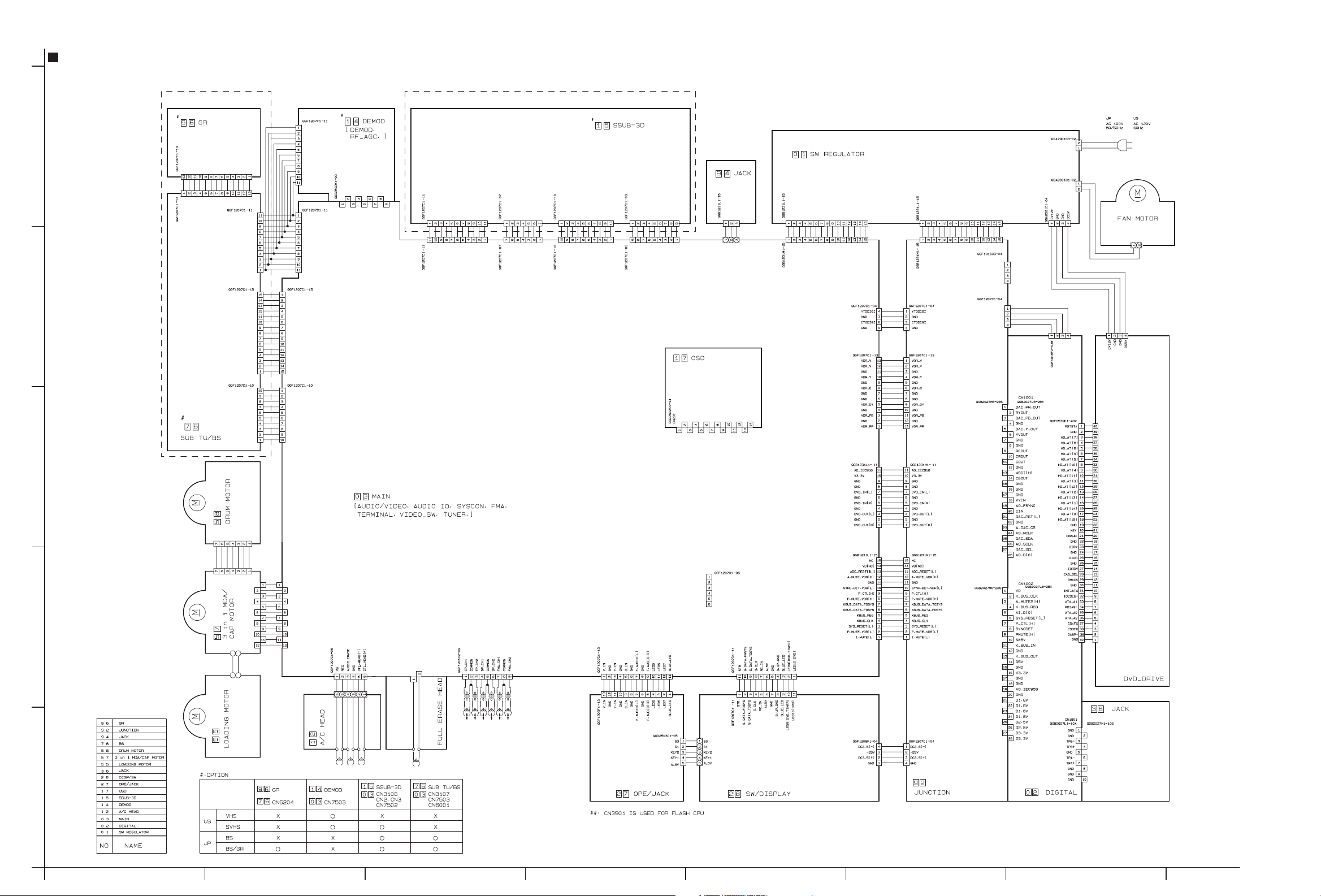
BOARD INTERCONNECTIONS
5
NCNCAL5.8V
CN1901
CN6204
4
3
SW12V
GND
BS_I2C_DATA
BS_I2C_CLKNCNCNCTU_VIDEO2
GR_ON[H]
GR_TU_VIDEO2
CN6202 CN7503
REAR_V_IN
GND
A.IN[R]
A.IN[L]
GND
SELD_AUDIO[R]
SELD_AUDIO[L]
GND
SELD_V_IN
SW-7V
NC
CN6201
AL5.8V
M26V
SW12V
BS_I2C_CLK
BS_I2C_DATA
GND
GND
BS_ANT/AFC
ANT_CTL[H]
BIT_IN[H]
BS_P.CTL[H]
INPUT_SEL3
GR_ON[H]
GND
AL5.8V
SW12V
SW5V
BT2
I2C_CLK2
I2C_DATA2
GND
DEMOD2[L]
DEMOD2[R]
GND
TU_VIDEO2
DEMOD Page 2-33
RF AUDIO AGC Page 2-34
CN2301
SW12V
NC
LINE_OUT[R]
GND
RF_AUDIO
NC
GND
NC
NC
GND
LINE_OUT[L]
CN3107
CN6001CN6203
CN6701
CN6501
JUST_CLK
I2C_DATA
I2C_CLKNCR_OUT
L_OUT
SW5V
OPENOPEN
CN5001
LIVE
CN5303
CN1404
NEUTRAL
CN5302
FAN12V
GND
CN2201
Page 2-5
Page 2-32
GND
SIF
CN8501
AD_IEC956
V3.3V
CN501
CN7502
CHARA_DATA
SW5V
V_FROM_OSD
GND
GND
GND
GND
C_OUT
Y_OUT
SELD_YV/F_IN
SELD_C_IN
CN502
CN2
PB_COLOR
GND
Fsc
KILLER
GND
TO_SUB_EMPH
FROM_SUB_EMPH
CN504
CN3
V_FROM_AV
GND
Y_TO_SUB
VHS[H]
SYNC_OUT
GND
REC_COLOR
GND
Y_TO_AV
V_TO_OSD_SSUB
CN503
CN3106
P.MUTE_VHS[L]
I2C_CLK_A/V
I2C_DATA_A/V
GND
V.P_CTL
V.REF
D.FF
TRICK[H]
SLOW_PULSE
GND
FW7504
Page 2-35
GND
S.DATA_TOSYS
P.MUTE_VHS[L]
OSD_CS
SYNC_DET[H]
S.CLK
S.DATA_FRSYS
EDS_CS[L]
JUST/EDS[H]
VIDEO/N.AUDIO Page 2-19
VIDEO SW Page 2-21
FMA/DEMOD Page 2-23
AUDIO I/O Page 2-25
SYSCON Page 2-27
TUNER Page 2-29
TERMINAL Page 2-31
2Fsc
CN7505
CHARA_DATA
V_TO_OSD
V_FROM_OSD
SW5V
CN5301
CN5311
SW5V
SW12V
BT2
45V
FAN_CTL[H]
SW-7V
GND
GND
P.SAVE[L]
AL5.8V
P.CTL[H]
M12V
GND[M]
GND[M]
M26V
CN501
CN7501
CN2601 CN8001
CN7104
CN7107
CN5304CN5501
P.CTL[H]
D1.8V
D1.8V
AL3V
AL5.8V
AL5.8V
GND
GND
GND
GND
SW12V
SW-7V
-29V
DC3.5[-]
DC3.5[+]
CN7106
D3.3V
JLIP_TX
GND
JLIP_RX
CN7105
JLIP_RX
GND
JLIP_TX
D3.3V
CN7108
CN3103
D_PG+
D_PG-
M_GND
D_COM
D_W_OUT
D_V_OUT
D_U_OUT
2
L1
L2
BLK
RED
1
CN3001
QGB2032M4-12
CAP.M_FG
CAP.M_Vcc
Vcc5V
CAP.M_F/R
LM_VCTL
M_GND
S_GND
Vcc12V
CAP.M_VCTL
LM_F/R/S
DRUM_PG/FG
DRUM_VCTL
CN2001
R/P A.E CTL
FULL_ERASE
QGB2532J1-02
CN2002
F.E
GND
CN1
EP
CH1EPCH2SPCH1SPCH2
CN3104
CN7201
FMA
FMA
CH2
CH1
Page 2-39
##
CN3901
CN7001 CN3102
FW7001CN7202
Page 2-37
CN7102
CN7103CN7002
REG Page 2-7
VIDEO Page 2-39
AUDIO AD/DA Page 2-41
CN7109
VIDEO IF Page 2-7
FLASH Page 2-9
MEDIA PROCESSOR
DDR SDRAM Page 2-13
1394PHY Page 2-15
ATAPI IF Page 2-17
CN4104
Page 2-11
Page 2-38
p10611001a_rev0
A
BCDEFG
2-3 2-4
Page 27
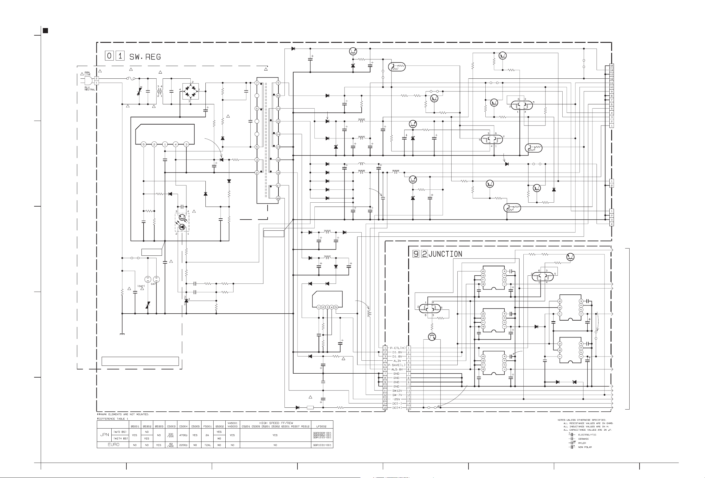
SW.REG AND
5
4
3
2
!
JUNCTION
!
CN5001
SCHEMATIC DIAGRAMS
!
F5001
/250
!
#
VA5001
QAF0039-431
QAF0024-431
QAF0023-431
QAF0055-431
OCP/
FB S D Vcc GND
#
B5001
SG5001
##
#
C5005
R5001
4.7M
100p
1/2W
/250
#
QAF0039-431
QAF0024-431
QAF0023-431
QAF0055-431
#
LF5002
!
C5001
0.068
/250
STR-G6653-F9
R5106
R5107
680
C5105
470p
/50
GROUND POINT FOR
PRIMARY VOLTAGE
!!
VA5003
3.9k
R5108
0.33
1W
!
IC5101
DANGEROUS VOLTAGE
##
C5002
0.022
/250
C5104
470p
/1k
D5104
1SS133
1SS270A
#
C5004
/250
#
D5202
L5207
33
L5206
33
C5207
1500
/6.3
D5307
RK34
IC5302
PQ5EV3
C5209
18
C5210
220
/6.3
2SC5739/QP/
2SD2394/EF/
D5204
D1FS4A
D5207
D1FS4A
D5212
D1FS4A
µ
µ
R5319
4.7k
FR
/50
C5202
/100
C5205
1500
/10
R5326
47
1/4W
R5325
4.7
C5307
100
/10
D5306
RK34
8.2
Q5301
#
D5201
1SR156-400
!
T5001
QQS0245-001
R5103
C5102
4700p
/1k
2W
D5001
D3SBA60
GBJ4J
#
C5003
R5101
68k
2W
D5103
1F4G
10ERB20
ERA18-02
AU01Z
1SR153-400
D5106
1F4G
10ERB20
ERA18-02
AU01Z
/50
!
PC5101
PC123Y22
LTV-817M/BC/
C5301
0.15
MY MY
C5302
0.033
R5303
/50
/50
1.5k
1SR153-400
C5106
0.01
R5301
220
!
R5302
4.7k
IC5301
L5431
MM1431AT
UTCTL431
C5107
220p
/50
C5103
27
R5306
3.9k
FR
/35
R5304
6.8k
R5305
24k
!
R5109
47
1/4W
D5101
SARS01
R5105
68
D5105
1F4G
10ERB20
ERA18-02
AU01Z
1SR153-400
R5102
1.2k
R5104
1k
C5101
100p
/1k
GROUND POINT FOR
SECONDARY VOLTAGE
D5211
1F4G
10ERB20
ERA18-02
#
C5201
120
/35
D5209
RK34
D5208
RK34
D5308
RK34
R5318
47k
C5313
470p
/50
D5210
1F4G
10ERB20
ERA18-02
PG104RS
1SR153-400
!
CP5301
1.5A
/125
CP
1SR156-400
D5213
1F4G
10ERB20
ERA18-02
AU01Z
1SR153-400
D5203
RL2Z
D5301
MTZJ15A
RD15ES/B1/
D5205
RK34
##
D5206
RK34
C5208
1000
/10
I O G ref SW
C5315
0.01
/50
D5309
AW04
1S4
C5314
100
/6.3
!
#
D5302
MTZJ27D
RD27ES/B4/
R5324
C5204
680
/16
C5308
100
/10
L5302
SHORT
47k
C5203
1200
/16
C5206
1200
/10
#
R5307
4.7k
L5201
33
L5202
33
L5204
33
L5205
33
µ
µ
µ
µ
C5316
OPEN
C5306
100
/10
#
C5309
47
#
B5302
C5303
100
/16
100
/35
C5304
100
/16
C5305
TO MAIN(SYSCON)
CN5311
CN5301
GND[M]
M26V
GND[M]
M12V
P.CTL[H]
AL5.8V
P.SAVE[L]
GND
GND
SW-7V
45V
BT2
SW12V
SW5V
TO FAN
CN5302
FAN
GND
TO DVD UNIT
CN5303
DV12V
GND
GND
DV5V
D1.8V
D2.5V
D5V
D3.3V
TO JUNCTION
(VIDEO)
V3.3V
SW5V[2]
GND
SW12V
SW-7V
-29V
DC[-]
DC[+]
B5303
##
Q5313
Q5304
UMD12N
XP4313
Q5307
2SA1585S/QR/
R5317
1k
Vout
Vout
Vout
IC5503
##
R5328
1k
NC
C5502
100
NC
100
NC
##
Q5309
2SA1585S/QR/
##
R5322
D5313
1A3G
10EDB20
ERA15-02
Q5308
DTC114EUA
UN5211
RN1302
PDTC114EU
C5503
470p
/6.3
C5506
470p
/50
C5505
/10
C5508
100
/10
#
B5305
1k
##
Q5310
UMD12N
XP4313
##
R5323
##
Q5315
B5304
##
R5329
10k
R5501 R5503R5502
1/2W 1/2W
820 1k680
/50
D5501
1A3G
10EDB20
C5509
470p
/50
##
Q5314
##
R5330
1k
C5513
/10
1
##
D5312
1SS133
1SS270A
Q5502
UN5111
DTA114EUA
IC5504
MM1563EF
Sub
Vout
Vin
C5510
/10
1
IC5505
MM1563DF
Cont Cn
Sub
VoutVin
D5502 D5503
1SS133
MTZJ27C
1SS270A
RD27ES/B3/
Q5501
2SD1819A/QRS/
2SC4081/QRS/
2PC4081/R/
C5512
470p
CnCont
GND
NC
C5511
100
/6.3
C5515
470p
/50
GND
NC
C5514
/6.3
100
/50
##
B5501
##
R5321
##
R5327
R5316
10k
IC5501
MM1662GH
10k
C5501
1
C5504
1
C5507
1
5.6k
Cont Cn
GND GND
GND
Vin
/10
IC5502
MM1565AF
Cont Cn
GND GND
GND
Vin
/10
Cont Cn
GND GND
GND
Vin
MM1565AF
/10
##
R5315
39
1/2W
R5320
##
B5502
#
Q5302
DTA144WUA
UN511E
RN2309
PDTA144WU
B5301
R5309
R5308
1k68k
1.2k
R5313
10k
R5505
2.2k
C5311
100
/10
##
Q5303
2SA1576A/QR/
##
C5312
100
/10
R5504
1k
Q5503
2SD2144S/UV/
2SC3576
R5311
27k
##
R5310
27k
Q5305
2SD2144S/UV/
2SC3576-JVC
#
R5312
10k
C5310
2.2
/50
D5303
MTZJ11C
RD11ES/B3/
/10
L5301
SHORT
Q5306
R5314
470
Q5504
UN5211
DTC114FUA
CN5304
2SC5739/QP/
D5304
MTZJ5.6C
RD5.6ES/B3/
CN5501
1
p20371001a_rev0
A
BCD EFG
2-5 2-6
Page 28

DIGITAL(VIDEO IF) SCHEMATIC DIAGRAM
TO MEDIA PROCESSOR
5
4
TO MEDIA PROCESSOR
3
2
TO MEDIA PROCESSOR
VDDI1.8
DIGI3.3V
K_BUS_OUT
K_BUS_IN
P_CTL[H]
SYS_RESET[L]
AI_D[0]
K_BUS_REQ
A_MUTE2[H]
K_BUS_CLK
TO JUNCTION(VIDEO)
CN7109
CN1002
AO_IEC958
TO JUNCTION(VIDEO)
CN7108
CN1001
AO_D[0]
SPI_CLK
AO_SCLK
SPI_MOSI
AO_MCLKO
A_DAC_CS
DAC_RST[L]
AO_FSYNC
DAC_CVBS_OUT
DAC_SY_OUT
DAC_SC_OUT
DAC_Y_OUT
DAC_PB_OUT
DAC_PR_OUT
DIGITAL(VIDEO IF)
A5A4A3
PLL_RST
C1011
OPEN OPEN
A0A1A2
0VDDI
0VDDI
OPEN
02
R1010
OPEN
WE
RAS
CAS
WEA2A1
A0
CAS
RAS
OUTH
VDOUT
CLKOSD
HDOUT
HDCVF
0VDDI
CSYNC
VDCVF
0VDDI
RESVD
MONI1
RESHD
MONI2
0VDDE
0VDDE
INV
INH
0VSS
YSI1
YSI4
YSI7
YSI0 OUTV
VO_D[1]
VO_D[4]
VO_D[7]
VO_D[0]
TL1031
TL1032
TL1033
TL1034
YSO3
YSO3
YSO2
YSO2
VSS
TL1035
C1021
OPEN
YSO1
YSO1
YSO0
YSO0
VDDE
0VSS
CSO3
CSO2
VSS
CSO1
CSO0
VSS
VO_D[14]
CSI6
VO_D[15]
CSI7
ZCNT
VDDI
VO_D[11]
CSI3
VO_D[12]
CSI4
VO_D[13]
CSI5
VDDI
VSS
VO_D[8]
CSI0
VO_D[9]
CSI1
VO_D[10]
CSI2
VO_D[5]
YSI5
VO_D[2]
YSI2
VO_D[6]
YSI6
VO_D[3]
C1020
0.1
CSO3
CSO2
CSO1
C1016
OPEN
CSO0
R1006
R1007
0
R1004
10k
0
R1005
10k
R1003
C1014
0.1
0
C1013
OPEN
C1012
0.1
27M_VIDEO
RA1001
0
YSO3
YSO2
YSO1
YSO0
CSO3
CSO2
CSO1
CSO0
C1015
0.1
VI_D[9]
VI_D[8]
VI_D[7]
VI_D[6]
VI_D[5]
VI_D[4]
VI_D[3]
VI_D[2]
RA1002
0
TO MEDIA PROCESSOR
VI_D[2-9]
VO_D[0-15]
0
R1019
0
R1017
]
VI_D[2-9
VO_D[0-15]
VIDEO_27M
VIDEO_MUTE[H]
VIDEO_RXD
VIDEO_RST[L]
SPI_MOSI
VIDEO_CS
SPI_CLK
480I[H]
IC1002
DQ14
DQ14
SCLKCSSDIN
R1013
UDQM
DQ13
DQ13
000
R1015
DQ0
DQ1
DQ2
DQ3
DQ4
DQ5
DQ6
DQ7
WE
CAS
RAS
AP
A0
A1
A2
A3
DQ12
DQ11
DQ12
0
R1029
R1014
DQ11
TRST
DQ10
DQ10
TMS
HY57V161610DTC8
K4S161622D-TC80
DQ9
DQ9
0VDDI
TCK
0VDDE
VDD
DQ0
DQ1
VSSQ
DQ2
DQ3
VDDQ
DQ4
DQ5
VSSQ VSSQ
DQ6
DQ7
VDDQ VDDQ
LDQM
N.C/RFU
WE( L)
CAS( L)
RAS( L)
CS( L)
BA
A10/AP
A0
A1
A2
A3
VDD
C1041
10
T
/6.3
DQ8
DQ7
DQ6
DQ5
DQ4
DQ5
DQ6
DQ7
DQ8
0VSS
0VDDE
TDO
SDOUT
0VSS
ADY_RL
ADYI
TDI
0
R1012
C1005
0.1
VSS
DQ15
DQ15
DQ14
DQ14
VSSQ
DQ13
DQ13
DQ12
DQ12
VDDQ
DQ11
DQ11
DQ10
DQ10
DQ9
DQ9
DQ8
DQ8
27M_SDRAM
A9
A8
A7
A6
A5
A4
DQ2
DQ1
DQ0
DQ0
DQ1
DQ2
VSS
0VDDE
0VDDI
IC1001
JCP8059
ADY_AVDD2
ADY_AVSS2
ADC_RL
ADCI
ADC_RH
ADC_AVDD1
0.1
0.1
0
TL1091
C1017
C1018
22k
R1060 R1002
0.1 0.1 0.1
TL1092
C1019
0.01
R1033
A9
A9
ADC_AVSS1
UDQM
CLK
CKE
N.C
A9
A8
A7
A6
A5
A4
VSS
DQ3
DQ3
DQ4
VDDE
ADY_RH
ADY_AVDD1
ADY_AVSS1
C1006 C1007 C1008 C1009
OPEN
C1047
0.1
C1088
OPEN
C1046
0.1
470
R1032
10k
AP
UDQM
A10
LUDQM
ADC_AVDD2
ADC_AVSS2
R1001
R1061
RA1005RA1003
10k10k
RA1006
10k
C1025 C1024C1026C1027C1028C1029C1030C1031
OPEN OPENOPENOPENOPENOPEN
0.10.1
A3
A4
RST
1SS355
AMUTE
A5
A8A7A6
0VSS
0VDDE
ANATST
0VDDI
PLL_VSS
CLK
VPD
0
R1072
OPEN
C1010
R1009
10k
27M_8059
1SS355
D1002
R1020 C1023
0
R1018
D1001
A6A7A8
VSS
VDDI
VSS
VDDE
_0.5%
TL1093
220
22k
OPEN
C1022
D2.5V
D1.8V
GND
R1036
CR
1k
R1035
Q1002
0
R1037
100
K1002
SHORT
NQR0129-002X
K1003
SHORT
K1004
NQR0129-002X
K1005
SHORT
K1006
SHORT
K1007
SHORT
K1008
SHORT
K1009
NQR0129-002X
K1010
D5.0V
V3.3V
GND
TL1001
TL1002
TL1003
TL1005
TL1006
TL1009
TL1010
TL1011
TL1014
SHORT
SHORT
SHORT
SHORT
SHORT
SHORT
LC1004
D3.3V
TL1018
K1011
TL1020
K1012
K1013
K1014
K1015
K1016
K1017
SHORT
K1018
SHORT
OPEN
OPEN
C1048
B1008
LC1001
OPEN
C1067
C1066
OPEN
OPEN
D5.0V
K1001
SHORT
C1078
C1079
C1054 C1055 C1056
OPEN OPEN
0.1 0.1 0.1
C1061
C1059C1057
0.1
0.10.1
B1004
B1007
LC1002
OPEN
OPEN
OPEN
OPEN
C1053
C1049
C1050
OPEN
L1004
C1069
10µ
OPEN
T
C1052
C1051
10
##
R1034
10k
##
Q1001
UN221E-X
DTC144WKA-X
RT1N44HC-X
/6.3
C1063
OPEN
0.1
CB
R1038
0
Y
R1041
0
C
R1044
0
RY
R1048
##
0
RC
##
R1052
0
C1065
4.7
R1056
2.2k
R1057
33
C1076
OPEN
C1077
0.1
R1068
2.2k
_0.5%
R1069
Q1010
2.2k
_0.5%
Q1011
R1070
1.2k
_0.5%
C1098C1097
0.10.1
_0.5%
C1070
OPEN
R1039
1k
Q1003
R1040
100
_0.5%
OPEN
C1071
R1042
1k
Q1004
R1043
150
_0.5%
OPEN
C1072
R1045
1k
Q1005
##
R1047
C1073
OPEN
##
R1049
1k
##
Q1006
##
R1051
270
_0.5%
C1074
OPEN
##
R1053
1k
##
Q1007
##
R1055
180
_0.5%
C1075
OPEN
Q1009
Q1008
UMZ1N
BC847PN
BC846PN
TL1097
R1059
470
R1066
R1062
OPEN
100
TL1098
D3.3V
K1020
TL1099
NQR0129-002X
R1065
R1067
120
120
K1019
SHORT
C1095
10
/6.3
C1096
0.1
C1036
0.1
C1032
0.1
R1021
R1022
1.5k
_0.5%
R1050
1.5k
_0.5%
C1092
0.1
3.3k
_0.5%
OPEN
C1037
0.1
C1038
0.1
C1039
OPEN
C1040
C1034
C1035
OPEN
C1087
0.1
C1060
0.1
C1089
0.1
C1090
0.1
C1093
R1046
3.3k
_0.5%
0.1
C1091
0.1
C1094
R1054
R1071
3.3k
1.5k
_0.5%
_0.5%
B1001
LC1003
OPEN
C1001
22
T
/6.3
C1042
0.1
C1043
0.1
C1044
RA1004
R1024
##
C1058
2.7k
0.1
10k
R1030
10k
R1031
10k
C1045
0.1
DQ15
DQ15
VC2
VC3
VC0
OPEN
VC1
0VDDI
0VSS
0.1
DAY_COMP
DAY_VREF
C1033
DAY_AVSS1
DAY_VRO
_0.5%
DAY_AVDD1
DAYO
DAY_AVDD2
DAY_AVSS2
DACB_AVSS2
DACB_AVDD2
DACBO
DACB_AVDD1
0.1
DACB_COMP
DACB_AVSS1
DACR_AVSS1
0.1
DACR_COMP
DACR_AVDD1
DACRO
DACR_AVDD2
DACR_AVSS2
DARC_AVSS1
DARC_AVDD1
DARCO
DARYO
DARY_AVDD1
0.01
C1062
DARY_AVSS1
DARY_VREF
DARY_VRO
R1028
DACO
_0.5%
2.7k
DAC_AVDD1
DAC_AVSS1
DAC_VREF
DAC_VRO
R1027
0VDDI
2.7k
0VSS
BLK1
BLK2
BLK3 YSI3
SIMTST
C1002
C1003
C1004
0.1
0.1
T
10
/6.3
1
p10593001a_rev0
A
BCDEFG
2-7 2-8
Page 29

DIGITAL(FLASH) SCHEMATIC DIAGRAM
5
C1207
IC1203
0.1
SN74LVC373APW-X
LH_AR[22]
LH_AR[14]
IC1201
LH_AR[16]
LH_AR[15]
LH_AR[14]
LH_AR[13]
LH_AR[12]
R1217
R1218
R1219
R1220
R1221
R1222
R1223
R1224
LH_AR[11]
LH_AR[10]
LH_AR[9]
LH_AR[19]
LH_AR[18]
LH_AR[8]
LH_AR[7]
LH_AR[6]
LH_AR[5]
LH_AR[4]
LH_AR[3]
LH_AR[2]
LH_AR[1]
LH_AR[22]
R1216
B1202
100
OPEN
B1204
R1225
10k
MADD[1]
MADD[2]
MADD[3]
MADD[4]
MADD[5]
LH_AR[21]
4
LH_AR[20]
3
TO MEDIA PROCESSOR
D3.3V
GND
UART2_RX
UART2_TX
CS[0]
CS[1]
E5_RESET[L]
MADD[1-5]
MADD[6-21]
MADD[22]
ALE
MADD[1-5]
MADD[6-21]
2
TO MEDIA PROCESSOR
DTACK[L]
WAIT[L]
ELINK_INT[L]
OE[L]/LDS[L]
UWE[L]/UDS[L]
RD/WR[L]
MBPL65LM90TN
A15
A14
A13
A12
A11
A10
A9
A8
A21
A20
64MBIT
WE
0‘
4.7k
4.7k
LH_AR[1]
100
LH_AR[2]
100
LH_AR[3]
100
LH_AR[4]
100
LH_AR[5]
100
FLASH
RESET
MEMORY
ACC
WP
A19
A18
A17
A7
A6
A5
A4
A3
A2
A1 A0
MADD[21]
MADD[20]
MADD[19]
MADD[18]
MADD[17]
MADD[16]
MADD[15]
MADD[14]
MADD[13]
MADD[12]
MADD[11]
MADD[10]
MADD[9]
MADD[8]
MADD[7]
MADD[6]
VCCQ
DQ15
DQ14
DQ13
DQ12
DQ11
DQ10
LH_AR[17]
A16
VSS
MADD[21]
MADD[13]
DQ7
MADD[20]
MADD[12]
DQ6
MADD[19]
MADD[11]
DQ5
MADD[18]
MADD[10]
DQ4
VCC
MADD[17]
MADD[9]
DQ3
MADD[16]
MADD[8]
DQ2
MADD[15]
DQ9
MADD[7]
DQ1
MADD[14]
DQ8
MADD[6]
DQ0
OE
VSS
CE
R1226
4.7k
RA1201
10k
RA1202
10k
RA1203
10k
RA1204
10k
K1201
SHORT
47
C1203
0.1
C1204
/6.3
MADD[14]
MADD[15]
LH_AR[15]
LH_AR[16]
MADD[16]
MADD[17]
LH_AR[17]
LH_AR[6]
MADD[6]
MADD[7]
LH_AR[7]
LH_AR[8]
MADD[8]
MADD[9] MADD[10]
LH_AR[9]
C1206
0.1
OE
Q0
D0
D1
Q1
Q2
D2
D3
Q3
GND
IC1202
SN74LVC373APW-X
OE
Q0
D0
D1
Q1
Q2
D2
D3
Q3
GND
VCC
VCC
LH_AR[21]
Q7
MADD[21]
D7
MADD[20]
D6
LH_AR[20]
Q6
LH_AR[19]
Q5
MADD[19]
D5
MADD[18]
D4
LH_AR[18]
Q4
LE
LH_AR[13]
Q7
MADD[13]
D7
MADD[12]
D6
LH_AR[12]
Q6
LH_AR[11]
Q5
MADD[11]
D5
D4
LH_AR[10]
Q4
LE
D3.3V
4.7k
4.7k
R1229
R1230
DIGITAL(FLASH)
02
OPEN
B1205
R1227
100
R1228
100
OPEN
B1206
4.7k
R1231
C1208
OPEN
TL1217
B1207
OPEN
B1208
TL1215
MADD[5]
MADD[4]
MADD[3]
MADD[2]
MADD[1]
MADD[21]
MADD[20]
MADD[19]
MADD[18]
MADD[17]
MADD[16]
MADD[15]
MADD[14]
MADD[13]
MADD[12]
MADD[11]
MADD[10]
MADD[9]
MADD[8]
MADD[7]
MADD[6]
TL1216
GND
TO ELINK BOARD
CN1202
GND
UART2_CTS
UART2_RX
UART2_TX
UART2_RTS
CS_L[1]
ALE
RST[L]
MADD[5]
MADD[4]
MADD[3]
MADD[2]
MADD[1]
MADD[21]/MDT[15]
MADD[20]/MDT[14]
MADD[19]/MDT[13]
MADD[18]/MDT[12]
MADD[17]/MDT[11]
MADD[16]/MDT[10]
MADD[15]/MDT[9]
MADD[14]/MDT[8]
GND
MADD[13]/MDT[7]
MADD[12]/MDT[6]
MADD[11]/MDT[5]
MADD[10]/MDT[4]
MADD[9]/MDT[3]
MADD[8]/MDT[2]
MADD[7]/MDT[1]
MADD[6]/MDT[0]
DTACK[L]/WAIT[L]
MEDUSA_INT[L]
OE[L]/LDS[L]
UWE[L]/UDS[L]
RD/WR[L]
GND
1
p20402001a_rev0
A
BCD EFG
2-9 2-10
Page 30

DIGITAL(MEDIA PROCESSOR) SCHEMATIC DIAGRAM
TO VIDEO IF
AO_D[0]
AO_SCLK
AO_FSYNC
AO_IEC958
AO_MCLKO
AI_D[0]
VIDEO_MUTE[H]
480I[H]
TO 1394PHY
5
4
3
2
PHY_CNA
TO VIDEO IF
VIDEO_27M
VI_D[2-9]
VO_D[0-15]
TO VIDEO IF
DAC_CVBS_OUT
DAC_SY_OUT
DAC_SC_OUT
DAC_Y_OUT
DAC_PB_OUT
DAC_PR_OUT
TO 1394PHY
PHY_DATA[0-7]
PHY_CTL[1]
PHY_CTL[0]
PHY_LREQ
PHY_LPS
PHY_LINK_ON
PHY_CLK
TO VIDEO IF
TO VIDEO IF
TO DDR SDRAM
SSTL2_VDD
DIGI3.3V
VDDI1.8
V3.3V
D2.5V
D1.8V
GND
D5.0V
D1.8V
D2.5V
GND
D3.3V
GND
TL1402
TL1437
R1408
1k
D3.3V
TL1403
TL1404
R1409
10k
R1410
10k
TL1407
R1411
100
R1412
10k
R1413
10k
VI_D[2]
VI_D[3]
VI_D[4]
VI_D[5]
VI_D[6]
VI_D[7]
VI_D[8]
VI_D[9]
R1414
1k
R1415
V3.3V
K1407
VI_D[2-9]
VO_D[0-15]
PHY_DATA[0-7]
02
SHORT
C1450
0.1
C1433
0.1
R1402
0Ω
X1401
NAX0580-001X
R1421
OPEN
R1422
OPEN
R1423
OPEN
R1424
OPEN
R1425
OPEN
R1426
OPEN
VDDI1.8
0.1
C1452
R1493
C1453
0Ω
0.1
K1408
SHORT
OPEN
C1454
C1455
0.1
C1456
OPEN
PHY_DATA[7]
PHY_DATA[6]
PHY_DATA[5]
PHY_DATA[4]
PHY_DATA[3]
PHY_DATA[2]
PHY_DATA[1]
PHY_DATA[0]
B1401
LC1401
OPEN NQR0415-002X
C1440
0.1
C1426C1431
0.10.1
C1441
0.1
LC1403
NQR0415-002X
C1413 C1414
100 0.1
/6.3
/6.3
C1405
0.1
LC1402
NQR0415-002X
C1449
0.1
C1411
100
/6.3
C1406
0.1
C1412
0.1
C1415 C1416
OPEN
C1443
0.1
C1401
C1402
0.1
0.1
B1402
OPEN
C1408
C1409
0.1
0.1
B1403
OPEN
C1432
0.1
DIGITAL(MEDIA PROCESSOR)
1k
R1416
1k
R1417
1k
TL1489
VO_D[0]
VO_D[1]
RA1401
VO_D[2]
VO_D[3]
100
VO_D[4]
VO_D[5]
VO_D[6]
RA1402
VO_D[7]
100
VO_D[8]
VO_D[9]
VO_D[10]
RA1403
VO_D[11]
100
VO_D[12]
VO_D[13]
VO_D[14]
RA1404
VO_D[15]
100
100
R1419
TL1412
TL1490
TL1491
R1420
100
R1485
OPEN
R1486
OPEN
R1487
OPEN
R1488
OPEN
R1489
OPEN
R1490
OPEN
D1402D1401
TL1413
TL1414
TL1415
R1491
1k
TL1417
TL1418
TL1419
R1427
100
TL1420
RA1405
100
RA1406
100
R1428
100
R1429
100
R1430
100
R1431
100
C1403
0.1
C1417
0.1
C1418
0.1
0.1
C1410
C1407
0.10.1
SSTL2_VDD
CLKI
CLKX
CLKO_DAC/GPIOExt[35]
BYPASS_PLL
EPD[L]
RSTO[L]
TCK
TDI
TDO
TMS
TRST[L]
VI_D[0]
VI_D[1]
VI_D[2]
VI_D[3]
VI_D[4]
VI_D[5]
VI_D[6]
VI_D[7]
VI_D[8]
VI_D[9]
VI_E[0]
VI_VSYNC[0]
VI_CLK[0]
VI_CLK[1]
VI_VSYNC[1]/IvGPIOExt[45]
VI_E[1]/IvGPIOExt[29]
VO2_D[0]
VO2_D[1]
VO2_D[2]
VO2_D[3]
VO2_D[4]
VO2_D[5]
VO2_D[6]
VO2_D[7]
VO2_D[8]
VO2_D[9]
VO_D[0]/IvGPIOExt[0]
VO_D[1]/IvGPIOExt[1]
VO_D[2]/IvGPIOExt[2]
VO_D[3]/IvGPIOExt[3]
VO_D[4]/IvGPIOExt[4]
VO_D[5]/IvGPIOExt[5]
VO_D[6]/IvGPIOExt[6]
VO_D[7]/IvGPIOExt[7]
VO_D[8]/IvGPIOExt[8]
VO_D[9]/IvGPIOExt[9]
VO_D[10]/IvGPIOExt[10]
VO_D[11]/IvGPIOExt[11]
VO_D[12]/IvGPIOExt[12]
VO_D[13]/IvGPIOExt[13]
VO_D[14]/IvGPIOExt[14]
VO_D[15]/IvGPIOExt[15]
VO_E/IvGPIOExt[30]
VO_ACTIVE
VO_HSYNC
VO_VSYNC
VO_CLK
DAC1_OUT
DAC2_OUT
DAC3_OUT
DAC4_OUT
DAC5_OUT
DAC6_OUT
DAC_DVSS_1
DAC_DVDD
DAC_VDD_0
DAC_VDD_3
DAC4_OUTB
DAC2_OUTB
USB_AVDD_0
USB_AVDD_1
USB_AGND_0
USB_AGND_1
DPLUS_0
DMINUS_0
HOST_PO_0
HOST_OC_0
DPLUS_1
DMINUS_1
HOST_PO_1/GPIOExt[43]
HOST_OC_1/GPIOExt[44]
USB_48MHz/GPIOExt[36]
1394_PHY_DATA[7]
1394_PHY_DATA[6]
1394_PHY_DATA[5]
1394_PHY_DATA[4]
1394_PHY_DATA[3]
1394_PHY_DATA[2]
1394_PHY_DATA[1]
1394_PHY_DATA[0]
1394_PHY_CTL[1]
1394_PHY_CTL[0]
1394_LREQ
1394_LPS
1394_LINK_ON
1394_PHY_CLK
T
C1419
OPEN
T
/6.3
K1401
SHORT
T
OPEN
VDD_15
VDD_00
VDD_01
VDDP_01
VDDP_02
VDDP_03
VDDP_04
VDDP_21
VDDP_20
VDDP_19
VDDP_19A
T
C1421
C1420C1404
/6.3
T
/6.3
VDDP_10
VDDP_09
VDDP_08A
C1425C1424C1423
C1422
0.10.10.1
0.10.110100
C1430C1429C1428C1427
0.10.10.110
C1438C1437C1436C1434 C1435
C1439
0.1
0.10.10.110
VDD_02
VDD_14
VDD_30
VDD_23
0‘
0‘
100
0‘
100
100
OPEN
R1482
R1483
AI_MCLKO
AI_MCLKI/GPIOExt[32]
VDD25_00
VDD_03
VDD_09
VDD_08
VDD25_01
100
TL1435
TL1434
R1477
R1478
R1479
R1476
R1480
R1481
AI_D[0]
AI_SCLK
AO_MCLKO
AI_FSYNC
AO_IEC958
AI2_D/GPIO[7]
AI_D[1]/GPIO[6]
AO_MCLKI/GPIOExt[33]
BIAS_5V01
BIAS_5V00
VDD25_02
VDD25_08
VDD25_03
VDD25_04
VDD25_05
VDD25_06
K1402
SHORT
C1442
0.1
K1403
SHORT
K1404
#
K1405
OPEN
C1445
0.1
100
100
TL1433
TL1432
R1474
R1475
AO2_D[0]
AO_FSYNC
A2_SCLK/GPIOExt[31]
A2_FSYNC/GPIOExt[34]
AVDD_1
AVDD_0
AVDD_2
C1444
0.1
#
C1446
0.1
AO_SCLK
AVDD_3
K1406
TL1431
AO_D[3]
XTALVDD
TL1429
TL1430
100
R1473
SDRAM_CLK_L[0]
SDRAM_CLK[1]
SDRAM_CLK_L[1]
AO_D[2]
AO_D[1]
AO_D[0]
SDRAM_VREF
SDRAM_CLK[1]
SDRAM_CLK_L[1]
AGND_2
AGND_1
AGND_3
AGND_0
XTALVSS
D5.0V
1
SDRAM_WE_L
SDRAM_CLK[0]
SDRAM_WE[L]
SDRAM_CLK[0]
SDRAM_CLK_L[0]
GROUND
GROUND
GROUND
SDRAM_RAS_L
SDRAM_CKE
SDRAM_CKE
IC1401
GROUND
SDRAM_A[17]
SDRAM_CAS_L
SDRAM_CAS[L]
SDRAM_RAS[L]
GROUND
GROUND
TL1488
SDRAM_A[16]
SDRAM_A[17]
GROUND
GROUND
SDRAM_A[15]
SDRAM_A[14]
SDRAM_A[15]
GROUND
TL1487
SDRAM_A[14]
SDRAM_A[13]
GROUND
GROUND
SDRAM_A[11]
SDRAM_A[12]
SDRAM_A[12]
GROUND
SDRAM_A[10]
SDRAM_A[10]
SDRAM_A[11]
GROUND
GROUND
SDRAM_A[8]
SDRAM_A[9]
SDRAM_A[9]
GROUND
SDRAM_A[7]
SDRAM_A[8]
SDRAM_A[7]
GROUND
GROUND
SDRAM_A[5]
SDRAM_A[6]
SDRAM_A[6]
GROUND
SDRAM_A[4]
SDRAM_A[5]
GROUND
SDRAM_A[3]
SDRAM_A[4]
SDRAM_A[3]
GROUND
GROUND
SDRAM_A[2]
SDRAM_A[2]
GROUND
SDRAM_A[0]
SDRAM_A[1]
SDRAM_A[1]
GROUND
SDRAM_DQS[3]
SDRAM_DQM[3]
SDRAM_A[0]
SDRAM_DQM[3]
GROUND
GROUND
SDRAM_DQ[31]
SDRAM_DQ[30]
SDRAM_DQS[3]
SDRAM_DQ[31]
GROUND
GROUND
SDRAM_DQ[28]
SDRAM_DQ[29]
SDRAM_DQ[29]
SDRAM_DQ[30]
GROUND
GROUND
SDRAM_DQ[26]
SDRAM_DQ[27]
SDRAM_DQ[27]
SDRAM_DQ[28]
GROUND
GROUND
SDRAM_DQ[24]
SDRAM_DQ[25]
SDRAM_DQ[25]
SDRAM_DQ[26]
GROUND
GROUND
SDRAM_DQS[2]
SDRAM_DQM[2]
SDRAM_DQM[2]
SDRAM_DQ[24]
GROUND
GROUND
TL1495
TX
CN1403
OPEN
SDRAM_DQ[22]
SDRAM_DQ[23]
SDRAM_DQ[22]
SDRAM_DQ[23]
SDRAM_DQS[2]
GROUND
GROUND
GROUND
TL1493
TL1494
RX
GND
SDRAM_DQ[20]
SDRAM_DQ[21]
SDRAM_DQ[21]
SDRAM_DQ[20]
REFVSS
TL1492
D5.0V
SDRAM_DQ[17]
SDRAM_DQ[18]
SDRAM_DQ[19]
SDRAM_DQ[18]
SDRAM_DQ[19]
SDRAM_DQ[17]
REFVDD
VREF
_1%
1.18k
0.1
0.01
C1447
C1448
R1401
A_MUTE2[H]
VIDEO_RST[L]
TO VIDEO IF
SDRAM_DQS[1]
SDRAM_DQM[1]
SDRAM_DQ[16]
SDRAM_DQM[1]
SDRAM_DQS[1]
SDRAM_DQ[16]
SIO_IRTX1/GPIOExt[40]
SIO_IRTX2
SIO_IRRX/GPIOExt[39]
TL1436
CN1404
SPI_CLK
SPI_MOSI
##
SDRAM_DQ[14]
SDRAM_DQ[15]
SDRAM_DQ[14]
SDRAM_DQ[15]
SIO_SDA
SIO_SCL
OPEN
OPEN
R1433
R1432
D3.3V
JLIP_TX
CN7105
(VIDEO)
SDRAM_DQ[13]
GND
SDRAM_DQ[8]
SDRAM_DQ[9]
SDRAM_DQ[10]
SDRAM_DQ[11]
SDRAM_DQ[12]
SDRAM_DQ[9]
SDRAM_DQ[12]
SDRAM_DQ[11]
SDRAM_DQ[10]
SDRAM_DQ[13]
SIO_UART2_CTS
SIO_UART1_RX
SIO_UART2_RX/GPIOExt[37]
SIO_UART2_TX/GPIOExt[38]
SIO_UART2_RTS
100
100
R1434
R1435
TL1422
OPEN
R1492
D3.3V
CN1402
JLIP_TX
JRIP_RX
##
OPEN
SDRAM_DQ[6]
SDRAM_DQ[7]
SDRAM_DQM[0]
SDRAM_DQS[0]
SDRAM_DQ[7]
SDRAM_DQ[6]
SDRAM_DQ[8]
SDRAM_DQS[0]
SDRAM_DQM[0]
SIO_SPI_MISO
SIO_UART1_TX
SIO_UART1_RTS/GPIOExt[41]
SIO_UART1_CTS/GPIOExt[42]
SIO_SPI_MOSI
100
0‘
R1437
TL1423
TL1424
R1436
GND
JRIP_RX
TO VIDEO IF
SDRAM_DQ[1]
SDRAM_DQ[2]
SDRAM_DQ[3]
SDRAM_DQ[4]
SDRAM_DQ[5]
SDRAM_DQ[5]
SDRAM_DQ[3]
SDRAM_DQ[2]
SDRAM_DQ[4]
SIO_SPI_CS[2]
SIO_SPI_CS[3]
SIO_SPI_CS[0]/GPIOExt[24]
SIO_SPI_CS[1]/GPIOExt[25]
100
100
100
R1440
R1439
TL1425
TL1448
R1438
SPI_MOSI
VIDEO_CS
A_DAC_CS
VIDEO_RXD
SDRAM_DQ[0]
SDRAM_DQ[0]
SDRAM_DQ[1]
SIO_SPI_CLK
SPI_CLK
SN74HCT08APW
IC1404
LDS[L]/OE[L]
UDS[L]/UWE[L]
GPIO[4] /PCMCIA_IOW[L]
GPIO[5] /PCMCIA_IOR[L]
WR[L]/LWE[L]
MADDR[21]/MDATA[15]
MADDR[20]/MDATA[14]
MADDR[19]/MDATA[13]
MADDR[18]/MDATA[12]
MADDR[17]/MDATA[11]
MADDR[16]/MDATA[10]
MADDR[15]/MDATA[9]
MADDR[14]/MDATA[8]
MADDR[13]/MDATA[7]
MADDR[12]/MDATA[6]
MADDR[11]/MDATA[5]
MADDR[10]/MDATA[4]
MADDR[9]/MDATA[3]
MADDR[8]/MDATA[2]
MADDR[7]/MDATA[1]
MADDR[6]/MDATA[0]
ATAPI_ADDR[0]
ATAPI_ADDR[1]
ATAPI_ADDR[2]
ATAPI_ADDR[3]
ATAPI_ADDR[4]
ATAPI_DATA[15]
ATAPI_DATA[14]
ATAPI_DATA[13]
ATAPI_DATA[12]
ATAPI_DATA[11]
ATAPI_DATA[10]
ATAPI_DATA[9]
ATAPI_DATA[8]
ATAPI_DATA[7]
ATAPI_DATA[6]
ATAPI_DATA[5]
ATAPI_DATA[4]
ATAPI_DATA[3]
ATAPI_DATA[2]
ATAPI_DATA[1]
ATAPI_DATA[0]
ATAPI_RESET
ATAPI_DMAACK[L]
ATAPI_DMARQ
ATAPI_IORDY
ATAPI_INTRQ
ATAPI_DIOR[L]
ATAPI_DIOW[L]
ATAPI2_RESET
ATAPI2_DMAACK[L]
ATAPI2_DMARQ
ATAPI2_IORDY
ATAPI2_INTRQ
ATAPI2_DIOR[L]
ATAPI2_DIOW[L]
ATAPI2_ADDR[0]
ATAPI2_ADDR[1]
ATAPI2_ADDR[2]
ATAPI2_ADDR[3]
ATAPI2_ADDR[4]
ATAPI2_DATA[15]
ATAPI2_DATA[14]
ATAPI2_DATA[13]
ATAPI2_DATA[12]
ATAPI2_DATA[11]
ATAPI2_DATA[10]
ATAPI2_DATA[9]
ATAPI2_DATA[8]
ATAPI2_DATA[7]
ATAPI2_DATA[6]
ATAPI2_DATA[5]
ATAPI2_DATA[4]
ATAPI2_DATA[3]
ATAPI2_DATA[2]
ATAPI2_DATA[1]
ATAPI2_DATA[0]
CS0_8BIT
DTACK[L]
MADDR[26]
MADDR[25]
MADDR[24]
MADDR[23]
MADDR[22]
MADDR[5]
MADDR[4]
MADDR[3]
MADDR[2]
MADDR[1]
RST[L]
MCONFIG
GPIO[0]
GPIO[1]
GPIO[2]
GPIO[3]
WAIT[L]
R1471
100
ALE
R1469
R1468
R1467
R1466
R1465
R1462
R1461
R1460
R1459
R1458
CS[5]
CS[4]
CS[3]
CS[2]
R1453
CS[1]
R1452
CS[0]
R1451
R1450
RA1411
100
RA1410
100
RA1409
100
RA1408
100
RA1407
100
R1498
R1497
R1496
R1472R1470
0‘1k
C1459
1k
100
100
100
100
TL1486
TL1485
100
100
100
100
100
100
100
100
100
10k
10k
10k
TL1464
TL1463
TL1462
TL1461
TL1460
TL1459
TL1458
TL1457
TL1456
TL1455
TL1454
TL1453
TL1452
TL1451
TL1450
TL1449
R1441
10k
CS[1]
CS[0]
MADD[22]
MADD[5]
MADD[4]
MADD[3]
MADD[2]
MADD[1]
MADD[21]
MADD[20]
MADD[19]
MADD[18]
MADD[17]
MADD[16]
MADD[15]
MADD[14]
MADD[13]
MADD[12]
MADD[11]
MADD[10]
MADD[9]
MADD[8]
MADD[7]
MADD[6]
ATA_ADD[0]
ATA_ADD[1]
ATA_ADD[2]
ATA_ADD[3]
ATA_ADD[4]
ATA_DAT[15]
ATA_DAT[14]
ATA_DAT[13]
ATA_DAT[12]
ATA_DAT[11]
ATA_DAT[10]
ATA_DAT[9]
ATA_DAT[8]
ATA_DAT[7]
ATA_DAT[6]
ATA_DAT[5]
ATA_DAT[4]
ATA_DAT[3]
ATA_DAT[2]
ATA_DAT[1]
OPEN
S1401
C1458C1457
0.10.1
SN74LV08APW
IC1405
OPEN
SDRAM_A[14-17]
SDRAM_VREF
SDRAM_CLK_L[1]
SDRAM_CLK[1]
SDRAM_CLK_L[0]
SDRAM_CLK[0]
SDRAM_WE_L
SDRAM_CKE
SDRAM_RAS_L
SDRAM_CAS_L
SDRAM_DQM[0-3]
SDRAM_DQS[0-3]
SDRAM_A[0-12]
SDRAM_DQ[16-31]
SDRAM_DQ[0-15]
MADD[1-5]
MADD[6-21]
ATA_ADD[0-4]
ATA_DAT[0-15]ATA_DAT[0]
D1403
1SS355
4.7k
4.7k
R1443
R1444
TO DDR SDRAM
SDRAM_A[14-17]
SDRAM_VREF
SDRAM_CLK_L[1]
SDRAM_CLK[1]
SDRAM_CLK_L[0]
SDRAM_CLK[0]
SDRAM_WE_L
SDRAM_CKE
SDRAM_RAS_L
SDRAM_CAS_L
SDRAM_DQM[0-3]
SDRAM_DQS[0-3]
SDRAM_A[0-12]
SDRAM_DQ[16-31]
SDRAM_DQ[0-15]
TO FLASH
ALE
OE[L]/LDS[L]
UWE[L]/UDS[L]
ELINK_INT[L]
RD/WR[L]
WAIT[L]
DTACK[L]
CS[1]
CS[0]
MADD[22]
MADD[1-5]
MADD[6-21]
/MDT[0-15]
TO 1394PHY
PHY_RESET[L]
TO VIDEO IF
DAC_RST[L]
TO ATAPI IF
ATA_ADD[0-4]
ATA_DAT[0-15]
ATA_RESET
ATA_DMAACK[L]
ATA_DMARQ
ATA_IORDY
ATA_INTRQ
ATA_DIOR[L]
ATA_DIOW[L]
TO VIDEO IF
R1445
100
K_BUS_CLK
R1446
100
K_BUS_REQ
R1447
100
SYS_RESET[L]
R1448
100
K_BUS_OUT
R1449
100
K_BUS_IN
TO FLASH
E5_RESET[L]
UART2_TX
UART2_RX
TO JUNCTION
p10594001a_rev1
A
BCDEFG
2-11 2-12
Page 31

DIGITAL(DDR SDRAM) SCHEMATIC DIAGRAM
5
C1637
OPEN
C1638
0.1
C1639
OPEN
C1640
4
K1702
SHORT
3
2
TO MEDIA PROCESSOR
SSTL2_VDD
SDRAM_DQ[0-15]
SDRAM_DQ[16-31]
SDRAM_A[14-17]
SDRAM_A[0-12]
SDRAM_CKE
SDRAM_RAS_L
SDRAM_CAS_L
SDRAM_WE_L
SDRAM_DQM[0]
SDRAM_DQM[1]
SDRAM_DQM[2]
SDRAM_DQM[3]
SDRAM_DQS[0]
SDRAM_DQS[1]
SDRAM_DQS[2]
SDRAM_DQS[3]
SDRAM_CLK[0]
SDRAM_CLK[1]
SDRAM_CLK_L[0]
SDRAM_CLK_L[1]
SDRAM_VREF
D3.3V
GND
GND
K1701
SHORT
D3.3V
C1701
SDRAM_DQ[0-15]
SDRAM_DQ[16-31]
SDRAM_A[14-17]
SDRAM_A[0-12]
SDRAM_CKE
SDRAM_RAS_L
SDRAM_CAS_L
SDRAM_WE_L
SDRAM_DQM[0]
SDRAM_DQM[1]
SDRAM_DQM[2]
SDRAM_DQM[3]
SDRAM_DQS[0]
SDRAM_DQS[1]
SDRAM_DQS[2]
SDRAM_DQS[3]
SDRAM_CLK[0]
SDRAM_CLK_L[0]
SDRAM_CLK_L[1]
C1703
0.1
C1702
/6.3
100
0.1
C1653
OPEN
C1654
0.1
0.1
IC1701
PQ015YZ01Z
C1704
100
/6.3
C1647
OPEN
C1648
0.1
RA1601
100
RA1602
100
RA1603
100
RA1604
100
RA1605
100
RA1606
100
RA1607
100
RA1608
100
R1702
1k
R1701
270
R1707
OPEN
T
C1707
0.1
R1703
2.2k
_0.5%
R1704
2.2k
_0.5%
OPEN
R1645
OPEN
R1646
OPEN
R1647
R1648
OPEN
R1649
100
R1650
100
R1651
100
R1652
100
R1609
OPEN
R1610
OPEN
R1611
OPEN
R1612
OPEN
SDRAM_DQ[0]
SDRAM_DQ[1]
SDRAM_DQ[2]
SDRAM_DQ[3]
SDRAM_DQ[4]
SDRAM_DQ[5]
SDRAM_DQ[6]
SDRAM_DQ[7]
SDRAM_DQ[8]
SDRAM_DQ[9]
SDRAM_DQ[10]
SDRAM_DQ[11]
SDRAM_DQ[12]
SDRAM_DQ[13]
SDRAM_DQ[14]
SDRAM_DQ[15]
SDRAM_DQ[16]
SDRAM_DQ[17]
SDRAM_DQ[18]
SDRAM_DQ[19]
SDRAM_DQ[20]
SDRAM_DQ[21]
SDRAM_DQ[22]
SDRAM_DQ[23]
SDRAM_DQ[24]
SDRAM_DQ[25]
SDRAM_DQ[26]
SDRAM_DQ[27]
SDRAM_DQ[28]
SDRAM_DQ[29]
SDRAM_DQ[30]
SDRAM_DQ[31]
OS
C1709
C1710C1708
/6.3T/6.3
OPEN
4747
C1705
OPEN
C1706
0.1
SDRAM_DQM[0]
SDRAM_DQM[1]
SDRAM_DQM[2]
SDRAM_DQM[3]
SDRAM_DQS[0]
SDRAM_DQS[1]
SDRAM_DQS[2]
SDRAM_DQS[3]
SDRAM_CLK[0] SDRAM_CLK[0]
SDRAM_CLK[1]
SDRAM_CLK_L[0]
SDRAM_CLK_L[1]
SDRAM_DQM[0]
SDRAM_DQM[1]
SDRAM_DQM[2]
SDRAM_DQM[3]
SDRAM_DQS[0]
SDRAM_DQS[1]
SDRAM_DQS[2]
SDRAM_DQS[3]
SDRAM_CLK[1]
SDRAM_CLK_L[0]
SDRAM_CLK_L[1]
SDRAM_DQ[0]
SDRAM_DQ[1]
SDRAM_DQ[2]
SDRAM_DQ[3]
SDRAM_DQ[4]
SDRAM_DQ[5]
SDRAM_DQ[6]
SDRAM_DQ[7]
SDRAM_DQ[8]
SDRAM_DQ[9]
SDRAM_DQ[10]
SDRAM_DQ[11]
SDRAM_DQ[12]
SDRAM_DQ[13]
SDRAM_DQ[14]
SDRAM_DQ[15]
SDRAM_DQ[16]
SDRAM_DQ[17]
SDRAM_DQ[18]
SDRAM_DQ[19]
SDRAM_DQ[20]
SDRAM_DQ[21]
SDRAM_DQ[22]
SDRAM_DQ[23]
SDRAM_DQ[24]
SDRAM_DQ[25]
SDRAM_DQ[26]
SDRAM_DQ[27]
SDRAM_DQ[28]
SDRAM_DQ[29]
SDRAM_DQ[30]
SDRAM_DQ[31]
SDRAM_A[0]
SDRAM_A[1]
SDRAM_A[2]
SDRAM_A[3]
SDRAM_A[4]
SDRAM_A[5]
SDRAM_A[6]
SDRAM_A[7]
SDRAM_A[8]
SDRAM_A[9]
SDRAM_A[10]
SDRAM_A[11]
SDRAM_A[12]
SDRAM_A[14]
SDRAM_A[15]
SDRAM_CKE
SDRAM_RAS_L
SDRAM_CAS_L
SDRAM_WE_L
DIGITAL(DDR SDRAM)
02
RA1609
22
RA1610
22
RA1611
22
RA1612
22
RA1613
RA1614
22
RA1615
22
RA1616
22
RA1625
10
RA1626
10
RA1627
10
RA1628
10
R1642
R1601
R1602
R1603
R1604
RA1629
C1645
OPEN
RA1630
C1646
0.1
RA1631
RA1632
R1653
R1654
R1655
R1656
R1657
R1658
R1659
R1660
R1613
R1614
R1615
R1616
DDR_DQ[0]
DDR_DQ[1]
DDR_DQ[2]
DDR_DQ[3]
DDR_DQ[4]
DDR_DQ[5]
DDR_DQ[6]
DDR_DQ[7]
DDR_DQ[8]
DDR_DQ[9]
DDR_DQ[10]
DDR_DQ[11]
DDR_DQ[12]
DDR_DQ[13]
DDR_DQ[14]
DDR_DQ[15]
DDR_DQ[0]
DDR_DQ[16]
DDR_DQ[17]
DDR_DQ[18]
DDR_DQ[19]
DDR_DQ[20]
DDR_DQ[21]
DDR_DQ[22]
DDR_DQ[23]
DDR_DQ[24]
DDR_DQ[25]
DDR_DQ[26]
DDR_DQ[27]
DDR_DQ[28]
DDR_DQ[29]
DDR_DQ[30]
DDR_DQ[31]
DDR_A[0]
DDR_A[1]
DDR_A[2]
DDR_A[3]
DDR_A[4]
DDR_A[5]
DDR_A[6]
DDR_A[7]
DDR_A[8]
DDR_A[9]
DDR_A[10]
DDR_A[11]
DDR_A[12]
DDR_BA[0]
DDR_BA[1]
DDR_CS[0]SDRAM_A[17]
DDR_CKE
10
DDR_RAS_L
10
DDR_CAS_L
10
DDR_WE_L
10
DDR_A[0]
DDR_A[1]
47
DDR_A[2]
DDR_A[3]
DDR_A[4]
DDR_A[5]
47
DDR_A[6]
DDR_A[7]
DDR_A[8]
DDR_A[9]
47
DDR_A[11]
DDR_A[12]
DDR_BA[0]
47
DDR_BA[1]
DDR_A[10]
R1644
47
R1605
47
DDR_CKE
R1606
47
DDR_RAS_L
R1607
47
DDR_CAS_L
R1608
47
DDR_WE_L
0‘
DDR_DQM[0]
0‘
DDR_DQM[1]
0‘
DDR_DQM[2]
0‘
DDR_DQM[3]
DDR_DQS[0]
22
DDR_DQS[1]
22
DDR_DQS[2]
22
DDR_DQS[3]
DDR_CLK[0]
0‘
DDR_CLK[1]
0‘
DDR_CLK_L[0]
0‘
DDR_CLK_L[1]SDRAM_CLK[1]
0‘
VTT
R1617
DDR_DQM[0]
27
R1618
DDR_DQM[1] DDR_DQM[3]
27
R1619
100
R1620
100
DDR_DQS[1] DDR_DQS[3]
R1621
DDR_CLK[0]
27
R1622
DDR_CLK_L[0]
27
C1649 C1651
OPEN OPEN
C1650
0.1
DDR_A[0]
DDR_A[1]
DDR_A[2]
DDR_A[3]
DDR_A[4]
DDR_A[5]
DDR_A[6]
DDR_A[7]
DDR_A[8]
DDR_A[9]
DDR_A[10]
DDR_A[11]
DDR_A[12]
DDR_BA[0] DDR_BA[0]
DDR_BA[1]
DDR_CKE
DDR_RAS_L
DDR_CAS_L
DDR_WE_L
DDR_DQM[0]
DDR_DQM[1]
DDR_DQS[0]
DDR_DQS[1]
C1655
C1656
39
C1605 C1606
0.1 0.1 0.1 0.1 0.1 0.1 0.1 0.1 0.1 0.1220.1 0.1 0.1 0.1 0.1 0.1
#1
IC1601
IC1601IC1601
IC1601
IC1601 IC1602
IC1601
DDR_DQ[7]
D0
A0
A1
A2
A3
A4
A5
A6
A7
A8
A9
A10/AP
A11
A12
BA0
BA1
CS
CKE
RAS
CAS
WE
LDM
UDM
LDQS
UDQS
CLK
CLK
VREF
VDD
VDD
VDD
VDDQ
VDDQ
VDDQ
VDDQ
VDDQ
15 55 61 1 18 33
C1607 C1608 C1609 C1610 C1611 C1612
DDR_DQ[6]
D1
DDR_DQ[5]
D2
DDR_DQ[4]
D3
DDR_DQ[3]
D4
DDR_DQ[2]
D5
DDR_DQ[1]
D6
DDR_DQ[0]
D7
DDR_DQ[15]
D8
DDR_DQ[14]
D9
DDR_DQ[13]
D10
DDR_DQ[12]
D11
DDR_DQ[11]
D12
DDR_DQ[10]
D13
DDR_DQ[9]
D14
DDR_DQ[8]
D15
NC
NC
NC
NC
NC
NC
NC
GND
GND
GND
GNDQ
GNDQ
GNDQ
GNDQ
GNDQ
OS
C1601 C1602
/4V /4V
220 220
DDR_DQ[1]
DDR_DQ[2]
DDR_DQ[3]
DDR_DQ[4]
DDR_DQ[5]
DDR_DQ[6]
DDR_DQ[7]
DDR_DQ[8]
DDR_DQ[9]
DDR_DQ[10]
DDR_DQ[11]
DDR_DQ[12]
DDR_DQ[13]
DDR_DQ[14]
DDR_DQ[15]
RA1617
100
RA1618
100
RA1619
100
RA1620
100
SSTL2_VDD
C1624
C1621
0.1 0.1
R1623
27
DDR_DQM[2]
R1624
27
R1625
100
DDR_DQS[2]DDR_DQS[0]
R1626
100
R1627
DDR_CLK[1]
27
R1628
DDR_CLK_L[1]
27
C1652
0.1
DDR_A[0]
DDR_A[1]
DDR_A[2]
DDR_A[3]
DDR_A[4]
DDR_A[5]
DDR_A[6]
DDR_A[7]
DDR_A[8]
DDR_A[9]
DDR_A[10]
DDR_A[11]
DDR_A[12]
DDR_BA[1]
DDR_CKE
DDR_RAS_L
DDR_CAS_L
DDR_WE_L
DDR_DQM[2]
DDR_DQM[3]
DDR_DQS[2]
DDR_DQS[3]
C1657
OPENOPEN
C1658
0.10.1
0.1100.1220.1
C1623
C1622
C1625
IC1602IC1602
IC1602
#2
IC1602
IC1602
A0
A1
A2
A3
A4
A5
A6
A7
A8
A9
A10/AP
A11
A12
BA0
BA1
CS
CKE
RAS
CAS
WE
LDM
UDM
LDQS
UDQS
CLK
CLK
VREF
VDD
VDD
VDD
VDDQ
VDDQ
VDDQ
VDDQ
VDDQ
3 9 15 55 61 1 18 33
C1613 C1614
C1615 C1616 C1617 C1618 C1619 C1620
DDR_DQ[16]
D0
DDR_DQ[17]
D1
DDR_DQ[18]
D2
DDR_DQ[19]
D3
DDR_DQ[20]
D4
DDR_DQ[21]
D5
DDR_DQ[22]
D6
DDR_DQ[23]
D7
DDR_DQ[24]
D8
DDR_DQ[25]
D9
DDR_DQ[26]
D10
DDR_DQ[27]
D11
DDR_DQ[28]
D12
DDR_DQ[29]
D13
DDR_DQ[30]
D14
DDR_DQ[31]
D15
NC
NC
NC
NC
NC
NC
NC
GND
GND
GND
GNDQ
GNDQ
GNDQ
GNDQ
GNDQ
OS
DDR_DQ[16]
DDR_DQ[17]
DDR_DQ[18]
DDR_DQ[19]
DDR_DQ[20]
DDR_DQ[21]
DDR_DQ[22]
DDR_DQ[23]
DDR_DQ[24]
DDR_DQ[25]
DDR_DQ[26]
DDR_DQ[27]
DDR_DQ[28]
DDR_DQ[29]
DDR_DQ[30]
DDR_DQ[31]
RA1621
RA1622
RA1623
RA1624
100
100
100
100
C1643C1641
OPENOPEN
C1644C1642
0.10.1
1
p10595001a_rev0
A
BCD EFG
2-13 2-14
Page 32

DIGITAL(1394PHY) SCHEMATIC DIAGRAM
5
/6.3
D3.3V
C1814
OPEN
#
R1819
750
_0.5%
TPA0-
TPB0+
TPB0-
#
R1818
5.6k
_0.5%
TPA0+
565656
565.1k
DIGITAL(1394PHY)
02
T1801T1801T1801T1801T1801T1801T1801T1801
#
NQR0444-001X
NQR0444-001XNQR0444-001XNQR0444-001XNQR0444-001XNQR0444-001XNQR0444-001XNQR0444-001X
TPA+
TPA-
TPB+
TPB-
TO JACK
CN4104
#
CN1801
QGB2027L1-10X
#
#
/6.3
C1813
OPEN
12p
12p
#
X1801
4
TO MEDIA PROCESSOR
3
D3.3V
PHY_RESET[L]
PHY_LREQ
PHY_CLK
PHY_CNA
PHY_CTL[0]
PHY_CTL[1]
PHY_DATA[0-7]
PHY_LPS
PHY_LINK_ON
GND
PHY_DATA[0-7]
#
R1801
R1802
#
PHY_DATA[0]
PHY_DATA[1]
PHY_DATA[2]
PHY_DATA[3]
PHY_DATA[4]
PHY_DATA[5]
PHY_DATA[6]
PHY_DATA[7]
0Ω
0Ω
NAX0551-001X
NAX0666-001X
#
IC1801
TSB41AB2PAP
LREQ
SYSCLK
CNA
CTL0
CTL1
D0
D1
D2
D3
D4
D5
D6
D7
PD
LPS
NC AGND
DGND
DGND
DGND
DGND
C1809
DVDD
DVDD
C/LKON
PC0
###
1801_X0
XO
PC1
C1808
XI
PC2
1801_XI
PLLGND
ISO
#
C1805
0.1
C1810
#
PLLGND
PLLVDD
CPS
DVDD
OPEN
OPEN
K1801
SHORT
C1807
#
NC
DVDD
0.1
NC
TESTM
B1801B1802
#
L1801L1802 C1804
#
R1820
10k
0Ω
R1822
AVDD
RESET
BRIDGE
TEST0
OPEN
10
AVDD
AVDD
µ
AGND
TPBIAS0
AVDD
AGND
AGND
AVDD
AGND
TPA0+
TPA0-
TPB0+
TPB0-
AGND
#
#
C1803C1806
0.1
1010
NC
NC
NC
NC
NC
R1
R0
R1805
#
0Ω
390k
10k
OPEN
##
#
R1808 R1807
10k 10k
2
##
R1823
0Ω
RA1801
10k
RA1802
10k
10k
R1803
10k
R1806
R1804
R1809
#
R1810
#
0.1
C1811
#
OPEN
R1811
R1812
#
1k
R1821
#
0Ω
0.1
C1812
#
TPBIAS0
#
R1813
1
C1801
#
R1814
#
R1815
#
270p
C1802
#
R1816R1817
#
#
GND
1
p30122001a_rev1
A
BCDEFG
2-15 2-16
Page 33

DIGITAL(ATAPI IF) SCHEMATIC DIAGRAM
DIGITAL(ATAPI IF)
02
5
ATA_DAT[7]
ATA_DAT[8]
ATA_DAT[6]
ATA_DAT[9]
ATA_DAT[5]
ATA_DAT[10]
ATA_DAT[4]
ATA_DAT[11]
ATA_DAT[3]
ATA_DAT[12]
ATA_DAT[2]
ATA_DAT[13]
ATA_DAT[1]
ATA_DAT[14]
ATA_DAT[0]
ATA_DAT[15]
RA2201
0Ω
RA2202
0Ω
RA2203
0Ω
RA2204
0Ω
RA2205
0Ω
FE_DAT[7]
FE_DAT[8]
FE_DAT[6]
FE_DAT[9]
FE_DAT[5]
FE_DAT[10]
FE_DAT[4]
FE_DAT[11]
FE_DAT[3]
FE_DAT[12]
FE_DAT[2]
FE_DAT[13]
FE_DAT[1]
FE_DAT[14]
FE_DAT[0]
FE_DAT[15]
4
SN74CBTD16210##
IC2201
NC
ATA_DAT[7]
ATA_DAT[8]
ATA_DAT[6]
ATA_DAT[9]
ATA_DAT[5]
ATA_DAT[10]
ATA_DAT[4]
ATA_DAT[11]
ATA_DAT[3]
ATA_DAT[12]
ATA_DAT[2]
3
TO MEDIA PROCESSOR
D5.0V
D3.3V
P_CTL[H]
ATA_RESET
ATA_DAT[0-15]
GND
ATA_DAT[0-15]
GND
ATA_DAT[13]
ATA_DAT[1]
ATA_DAT[14]
ATA_DAT[0]
ATA_DAT[15]
ATA_ADD[0]
ATA_ADD[1]
ATA_ADD[2]
R2203
4.7k
C2201
0.1
1A1
1A2
1A3
1A4
1A5
1A6
GND
1A7
1A8
1A9
1A10
2A1
2A2
VCC
2A3
GND GND
2A4
2A5
2A6
2A7
2A8
2A9
2A10
2
C2202
IC2202
TO MEDIA PROCESSOR
ATA_DIOW[L]
ATA_DIOR[L]
ATA_DMAACK[L]
ATA_DMARQ
ATA_IORDY
ATA_INTRQ
ATA_ADD[0-4]
ATA_ADD[0-4]
R2201
ATA_ADD[3]
ATA_ADD[4]
R2202
10k
5.6k
NC
A1
A2
A3
A4
A5
A6
A7
A8
GND
1OE
2OE
1B1
1B2
1B3
1B4
1B5
GND
1B6
1B7
1B8
1B9
1B10
2B1
2B2
2B3
2B4
2B5
2B6
2B7
2B8
2B9
2B10
0.1
SN74CBT3245A##
VCC
OE
B1
B2
B3
B4
B5
B6
B7
B8
DIOR
FE_DAT[7]
FE_DAT[8]
FE_DAT[6]
FE_DAT[9]
FE_DAT[5]
FE_DAT[10]
FE_DAT[4]
FE_DAT[11]
FE_DAT[3]
FE_DAT[12]
FE_DAT[2]
FE_DAT[13]
FE_DAT[1]
FE_DAT[14]
FE_DAT[0]
FE_DAT[15]
##
Q2201
UN221E-X
DTC144WKA-X
RT1N44HC-X
D5.0V
##
R2217
22k
ATA_ADD[3]
ATA_ADD[4]
RA2206
RA2207
TO DVD UNIT
R2204
FE_DAT[7]
FE_DAT[8]
FE_DAT[6]
FE_DAT[9]
FE_DAT[5]
FE_DAT[10]
FE_DAT[4]
FE_DAT[11]
FE_DAT[3]
FE_DAT[12]
FE_DAT[2]
FE_DAT[13]
FE_DAT[1]
FE_DAT[14]
FE_DAT[0]
FE_DAT[15]
R2205
R2206
0Ω
0Ω
R2207
R2208
R2209
R2210
R2211
R2212
R2213
R2214
R2215
33
#
K2201
#
K2202
RA2208
#
33
K2203
#
K2204
#
K2205
#
RA2209
K2206
#
33
K2207
#
K2208
#
K2209
#
RA2210
K2210
#
33
K2211
#
K2212
#
K2213
#
K2214
RA2211
#
33
K2215
#
K2216
82
22
22
82
22
82
33
33
33
33
33
D3.3V
#
#
#
#
#
K2217
K2218
K2219
K2220
K2221
R2216
OPEN
D2201
OPEN
CN2201
RSTAT
GND
HD_AT[7]
HD_AT[8]
HD_AT[6]
HD_AT[9]
HD_AT[5]
HD_AT[10]
HD_AT[4]
HD_AT[11]
HD_AT[3]
HD_AT[12]
HD_AT[2]
HD_AT[13]
HD_AT[1]
HD_AT[14]
HD_AT[0]
HD_AT[15]
GND
DMARQ
GND
DIOW
GND
DIOR
GND
IORDY
CAB_SEL
DMACK
GND
INT_ATA
ATA_A1
ATA_A0
ATA_A2
CS1FX
CS3FX
GND
A
1
p20403001a_rev1
A
BCD EFG
2-17 2-18
Page 34

MAIN(VIDEO/N.AUDIO) SCHEMATIC DIAGRAM
5
TO FMA/DEMOD
NA_REC
NA_PB
Fsc
GND
0.01
#
R21
2.2k
L2001
SHORT
#
1.2k
/6.3
#
C63
4
TO SYSCON
SW12V
SW5V
TO FMA/DEMOD
FMA_CH1
FMA_COM
FMA_CH2
TO DRUM
GND
CN1
B10
SHORT
OPEN
D1
!
10µ
L10
#
Q7
2SC4081/QRS/
2PC4081/R/
#
Q8
2SC4081/QRS/
2PC4081/R/
#
C61
100
/6.3
#
0.1
C60
3
TO SYSCON
CTL[+]
CTL[-]
R2051
CN2001
P/R
A.E
CTL
CN2002
FE
C2051
OPEN
330p
6.8k
R2053
MY
#
C2052
R2052
OPEN
#
C2053
#
T2051
C2055
10
/25
2
TO SYSCON
N.REC[H]
N.REC_ST[H]
R2054
#
C2054
#
R2057
Q2051
47k
R2058
18k
Q2053
R2060
DTC144WUA
PDTC144WU
UN521E
RN1309
18k
Q2055
DTC144WUA
PDTC144WU
UN521E
RN1309
Q2003
UN511E
DTA144WKA
Q2002
2SC4081/QRS/
2SD1819A/QRS/
2PC4081/R/
Q2001
2SC4081/QRS/
2SD1819A/QRS/
2PC4081/R/
R2018
4.7k
R2019
4.7k
R2056
#
R2055
2SA1576A/QR/
2SB1218A/QR/
2PA1576/R/
R2059
47k
Q2054
2SA1576A/QR/
2SB1218A/QR/
2PA1576/R/
#
12k
Q2052
R24
OPEN
R27
B6
#
L9
10
µ
#
C52
12p
C57
C58
C59
Q6
OPEN
C2004C2003
0.0147
C62
0.01
0.1
33k
R2021
C2005
4.7
R2015
/50
330
390k
R2014
C2006
0.0068
C2007
22
/16
C2008
C2010
R2017
C2011
22k
C2012
C2009 R2016
820p 33k
C55C56
OPEN
0.1
TP111
D.FF
R2023
10k
10k
R2022
D2001
1SS133
1SS270A
R2013
12k
4.7
/50
820p
4.7
/50
4.7
/50
#
IC1
R2024
R2007
#
Q1
DTC144WUA
PDTC144WU
UN521E
RN1309
0.01
R37
15k
10k
12k
12k
R2010
#
R4
6.8k
/50
C49
4.7
TP106
PB.FM
#
C50
/50
C2001
4.7
R1
6.2k
/50
1
SHORT#
C4
10
L2
/25
#
C2002
C3
#
R5
33k
150p
1.5k
R25
OPEN
C1
R2
R26
OPEN
C6
0.110.1
C5
0.1
/50
C47
0.47
R11
4.7k
#
R3
/50
/50
C44
C46
C48
0.022
#
L1
#
C2
0.1
#
X2
QAX0739
C7
C43
C45
2.2
3.3
0.0047
R12
1k
C8
147p
C11
C9
1
2.2
/50
/6.3
/50
C36
C39
C41
C38
1
100
0.1
0.01
R14
1.8k
#
D4
D3
OPEN
OPEN
D5
OPEN
C13
#
C12
1
R18
OPEN
L7
12µ
C40
0.01
C35
0.01
#
C16
0.01
#
C17
0.1
C15
0.1
C10
C14
1
100
/6.3
Q15
OPEN
B7
C37
4p
#
C18
R31
OPEN
C34
0.01
C33
/25
10
#
Q2
2SD601A/QRS/
2SC2412K/QRS/
C19
0.1
B1
OPEN
OPEN
Q4
OPEN
C42
R17
OPEN
B4
R38
4.7M
B3
OPEN
C29
#
R19
0.01µ
C26
/25
10
C24
0.1
#
0.1
C23
#
#
C21
0.01
C22
0.1
#
R7
4700.1
L4
OPEN
SHORT
OPEN
L5
L6
!
10µ
R20
Q3
OPEN
OPEN
C28
10µ
C31
100
/6.3
330p
C30
0.1
C32
0.01
C27
C25
/50
3.3
0.1
C20
B8
#
L3
10µ
1
TO SYSCON
2Fsc
SP_SHORT[H]
VIDEO_ENV
D.FF
A.MUTE_VHS[H]
I2C_DATA_A/V
I2C_CLK_A/V
TO SYSCON
C.SYNC/V.REF
V.PULSE
S_DET[H]
SB_GAIN
V_TO_OSD
TO TERMINAL
GND
SELD_YV/F_IN
REAR_V_IN
TU_VIDEO1
DVD_V_IN
Fsc
OPEN
#
CN2
FROM_SUB_EMPH
GND
TO_SUB_EMPH
KILLER
Fsc
GND
PB_COLOR
OPEN
#
CN3
V_TO_OSD_SSUB
GND
Y_TO_AV
GND
REC_COLOR
SYNC_OUT
VHS[H]
Y_TO_SUB
GND
V_FROM_AV
p10604001a_rev0
A
BCDEFG
2-19 2-20
Page 35

MAIN(VIDEO SW) SCHEMATIC DIAGRAM
5
4
3
TO SYSCON
SW5V
I2C_DATA2
I2C_CLK2
TO JUNCTION(VIDEO)
CN7104
CN501
0Ω
R511
0Ω
R513
OPEN
R512
R535
1.5k
C577
0.01
/50
OPEN
C534
C531
C532
C533
C530
OPEN
4.7
0.01
C535
C536
0.01
0.01
OPEN
C538
OPEN
C539
0.01
C540
0.01
C541
0.01
C543
0.1
C545
2.2
/50
C546
0.01
/16
/6.3
C528
C529
10
0.01
47
R510
3.3k
C527
1
L501
10
C526
0.01
C525
0.01
C524
0.01
C523
0.01
C522
0.01
C521
0.01
µ
GND
C547
0.01
R542
C548
OPEN
Q505
R518
2.7k
C555
0.01
L503
OPEN
R519
OPEN
C549
10p
L504 R521
33
µ
Q503
R543
OPEN
270
C550
OPEN
R527
5.6k
R529
2.2k 0.01
R528R526
5.6k1k
C556
L502
10µ
Q504
R533
4.7k
R534
2.2k
C565
47
/6.3
C537
0.01
R514
R515
1.2M
C544
OPEN
R516
OPEN
IC501
JCP8038
2
GR_TU_VIDEO2
TO TUNER
TO SYSCON
FRONT_Y_IN
FRONT_C_IN
FRONT_V_IN
WIDE_DET2
D501
D502
R503
R501
0Ω
0Ω
C504
C507
OPEN OPEN
C506
0.01
C503
1
R502
10K 10K
C505
0.01
#
R506
R504
0Ω
0Ω
C512
OPEN
#
C511
C508
0.01
1
#
R505
10k
#
C510
0.01
R509
0Ω
R507
0Ω
C517C509
OPENOPEN
C514
OPEN
C516
0.01
C518 C519
R508
C513
1
11
C515
0.01
C520
OPEN
C501
47
/6.3
C502
0.1
C578
0.1
#
R548
470
#
R553 R551
0Ω 0Ω
#
R549
470
R554
OPEN OPEN
#
R550
#
Q507
0Ω
R545
470
R546
470
R552
R547
Q506
0Ω
TO TERMINAL
Fsc
VHS_Y_OUT
VHS_C_OUT
GND
BIAS_FOR_C_OUT
REAR_C_IN
REAR_Y_IN
SELD_V_IN
FRONT_Y_IN
FRONT_C_IN
FRONT_V_IN
1
p10607001a_rev0
A
BCD EFG
2-21 2-22
Page 36

MAIN(FMA/DEMOD) SCHEMATIC DIAGRAM
TP2253
A.PB_FM
R2253
100
L2251
10
K2251
SHORT
K2252
SHORT
K2253
OPEN
#
R2254
10k
#
Q2251
DTC144WUA
PDTC144WU
UN521E
RN1309
RT1N44HM
SHORT
A.FF
TO SYSCON
S.CASS[H]
ET_REC[H]
JUST/EDS[H]
I2C_DATA_A/V
I2C_CLK_A/V
A.MUTE_VHS[H]
H.REC_ST[H]
LED
A.ENV/ND[L]
A.FF
TO VIDEO/N.AUDIO
FMA_CH2
FMA_CH1
FMA_COM
B6601
µ
0.01
0.01
TP2254
#
A.REC_FM
H.REC_ST[H]
A.ENV/ND[L]
#
R2258
220
C2253
C2252
D2251
1SS133
1SS270A
#
Q2253
C2259
R2252
3.3k
C2208
R2257
DTC144WUA
PDTC144WU
UN521E
RN1309
RT1N44HM
C2257
C2256
C2261
OPEN
C2262
OPEN
C2251
C2207
C2206
C2205
#
#
VR2251
10k
33
R2225
OPEN
R2256
2.2k
#
Q2254
DTC114EUA
PDTC114EU
UN5211
RN1302
RT1N141M
/6.3
C2209C2210
/25/25
1010
5
C2222
0.01
TO SYSCON
AL5.8V
SW5V
GND
SW12V
Q2201
DTA144WUA
PDTA144WU
UN511E
RN2309
RT1P44HM
4
TO TUNER
SIF
RF_AUDIO
R2209
TO AUDIO I/O
FMA_OUT[R]
FMA_OUT[L]
GND
F.AUDIO[R]
3
F.AUDIO[L]
A.IN1[R]
A.IN1[L]
DVD_OUT[R]
DVD_OUT[L]
TO VIDEO/N.AUDIO
NA_REC
NA_PB
GND
Fsc
2SC4081/QRS/
2SD1819A/QRS/
2PC4081/R/
2SC4154/EF/
2SC4154/EF/
R2211
3.3k
R2212
3.3k
100
Q2203
R2210
4.7k
R2213
4.7k
Q2204
R2214
100
R2215
SHORT /25
C2216 C2217
/16 OPEN
47
L6501
SHORT
D2201
OPEN
R2218
Q2202
DTC144WUA
PDTC144WU
UN521E
RN1309
RT1N44HM
R2220
1k
C6510 C6511
OPEN OPEN
3.9k
R2219
1k
#
R2216
1.2k
#
R2217
4.7k
C6604
OPEN
C6605
1
C2212
47
/6.3
OPEN
OPEN
OPEN
C6516
C6601C6505
/50/25
C6504
OPEN
R6502C6517
OPENOPEN
C6602
/50
1
C6508
OPEN
C6509
OPEN
C6512
OPEN
C2214
/25
10
C6513
OPEN
/25
C2215
10
#
C2218
10
/16#
C2219
22
/25
C2220
10
C2221
0.022
/50
OPEN
C6514
/50
C6515
1
110
470
/25
10
R2231
C2231
470
R2230
C2230
C2213
L2201
SHORT
27k
R2259
#
27k
R2255
#
C2211
R2224 C2224
OPEN OPEN
#
Q2252
DTC144WUA
PDTC144WU
UN521E
RN1309
RT1N44HM
0.015
680k
/50
0.33
R2251
4.7k
0.01
0.01
C2254C2255
470.01
/6.3
0.01
0.015
/25
10
/25
10
2
R2226
R2228
39k
39k
!
IC2201
AN3663FBP
R2227 R2229
6.8k 6.8k
µ
1
C2234
µ
1
C2235
R2201
R2203
C2204
33
R2223
OPEN
C2223
OPEN
/6.3
/50
/25
OPEN
4.7
10
0.1
C6502
C2202
C2201
C6501
47k
47k
R2205
R2207
/50
4.7
C2203
47k
47k
OPEN
C6503
R2208R2206R2204R2202
6.8k6.8k6.8k6.8k
R2222
OPEN
1
p20413001a_rev0
A
BCDEFG
2-23 2-24
Page 37

MAIN(AUDIO I/O) SCHEMATIC DIAGRAM
5
R2610
VCC
100
IC2603
BA15218F
TO TUNER
DEMOD2[R]
DEMOD2[L]
R2609
1k
BA X2X1XX0X3 VDD
Y0Y2YY3Y1INHVEEVSS
IC2602
BU4052BCF
VEE
TO JUNCTION(AUDIO AD/DA)
CN8001
CN2601
DVD_OUT[R]
GND
DVD_OUT[L]
GND
DVD_IN[R]
GND
DVD_IN[L]
GND
GND
V3.3V
AD_IEC958
4
R2611
100
R2658 R2659
10k 10k
TO FMA/DEMOD
FMA_OUT[R]
FMA_OUT[L]
GND
F.AUDIO[R]
F.AUDIO[L]
A.IN1[R]
A.IN1[L]
DVD_OUT[R]
3
2
DVD_OUT[L]
TO SYSCON
SW5V
SW12V
SW-7V
AL5.8V
GND
TO SYSCON
A_INPUT_SEL1
A_INPUT_SEL2
A.MUTE[L]
VDR[H]
R2651
R2652
220
0Ω
C2651
47
22k
R2662
22k
R2663
22k
R2667
/16
C2652
OPEN
C2653
47
B2603
#
B2604
#
C2603
10
R2632
/25
470
R2631
1k
R2634
C2604
10
10k
R2635
10k
/25
VCC
IC2605
BA15218F
R2633
470
IC2604
BU4052BCF
Y0Y2YY3Y1INHVEEVSS
C2654
/16
OPEN
R2653
10k
R2654
15k
OPEN
R2664
OPEN
R2665
BA X2X1XX0X3 VDD
R2660 R2661
10k 10k
VEE
R2636
4.7k
Q2601
2SC4081/QRS/
2SD1819A/QRS/
2PC4081/R/
2SC4154/EF/
R2637
4.7k
Q2602
2SC4081/QRS/
2SD1819A/QRS/
2PC4081/R/
2SC4154/EF/
A.IN1[R]
A.IN1[L]
F.AUDIO[R]
F.AUDIO[L]
AD_IEC958
V3.3V
GND
DVD_OUT[R]
DVD_OUT[L]
LINE_OUT[R]
LINE_OUT[L]
SELD_AUDIO[R]
SELD_AUDIO[L]
A.GND
TO TERMINAL
TO SYSCON
TO TERMINAL
D2601
1SS133
R2666
22k
R2638
1k
Q2603
DTA144WUA
PDTA144WU
UN511E
RN2309
RT1P44HM
1
p20414001a_rev0
A
BCD EFG
2-25 2-26
Page 38

MAIN(SYSCON) SCHEMATIC DIAGRAM
SLOW_PULSE
TRICK[H]
D.FF
V.REF
V.P_CTL
GND
I2C_DATA_A/V
OPEN
3106
#
I2C_CLK_A/V
P.MUTE_VHS[L]
TO FMA/DEMOD
]
SW12V
A.FF
AL5.8V
H.REC_ST[H]
SW5V
A.ENV/ND[L]
JUST/EDS[H
LED
GND
I2C_DATA_A/V
I2C_CLK_A/V
A.MUTE_VHS[H]
ET_REC[H]
S.CASS[H]
TO AUDIO I/O
F.AUDIO[R]
F.AUDIO[L]
TO VIDEO SW
WIDE_DET2
WIDE_DET
I2C_DATA2
I2C_CLK2
GND
SW5V
5
4
FRONT_V_IN
FRONT_Y_IN
FRONT_C_IN
TO VIDEO/N.AUDIO
A.MUTE_VHS[H]
I2C_CLK_A/V
N.REC[H]
N.REC_ST[H]
SP_SHORT[H]
S_DET[H]
C.SYNC/V.REF
V.PULSE
VIDEO_ENV
SB_GAIN
TO CAPSTAN MDA
CAP.M_FG
CAP.M_Vcc
CAP.M_F/
LM_VCTL
M_GND
S_GND
CAP.M_VCTL
LM_F/R/S
DRUM_PG/FG
DRUM_VCTL
D.FF
CTL[+]
CTL[-]
SW5V
SW12V
GND
CN3001
Vcc5V
Vcc12
QMFZ050-1R25X-E
CP
!
CP3002
C3004
0.047
C3071
33
R3252
OPEN
3
TO ROTARY ENCODER
JS3001
GND[C]
TO SW.REG
CN5301
CN5311
GND[M]
M12V/M17V/M25V
GND[M]
P.CTL[H]
P.SAVE[L]
FAN_CTL[H]
SW12V
LSA
LSB
LSC
LSD
M12V
AL5.8V
GND
GND
SW-7V
48V
BT2
SW5V
2
TO DISPLAY/SW
CN7001
CN3102
STB
S.DATA_FRSYS
S.DATA_TOSYS
S.CLK
RC_IN
AL5V
GND
B.UP_GND
BLUE_LED
[DVD_TIMER]LED9
[DVD]LED10
/50
C4032
OPEN
C4031
33
L4001
C3072
OPEN
R3253
10k
/16
1µ
!
CP4002
QMFZ050-1R25X-E
#
B3025
TO TERMINAL
AL5.8V
SW12V
V_INPUT_SEL1
V_INPUT_SEL2
C_BIAS1
C_BIAS2/CONV_CTL[H]
BS_REC_LINKI2C_DATA_A/V
LINE2INFO
VDR[H]
GND
CHARA_DATA
V_FROM_OSD
TO OPE/JACEK
CN7201
CN3104
#
B3023
100p
0.1
0.22
0.1
C3033
C4012
C4014
C4011
1k
C3066
OPEN
OPEN
R3254
OPEN
R3255
CP
R3206 R3207
R3205
12k 18k
180 470k120 120
1/4W
Q3002 Q3003
PTZ-NV16A PTZ-NV16A
D3001
LNB2301L01VI
10k
R3214
R3215
10k
R3216
10k
R3217
10k
L3001
0.22
C3042
/6.3
470
[for_EDL]
10K
C3007 C3008
OPEN OPEN
#
S3002
QSW0602-004
QSW0955-001
D3004
R3218
4.7k
R3208 R3210
S3001
QSW0602-004
QSW0955-001
100k
R3242
#
11ES2
D3005
1A3G
11ES2
1A3G
Q3004
2SD1819A/QRS/
D3003
2SC4081/QRS/
RD39ES/B3/
2PC4081/R/
MTZJ39C
R3219
4.7k
OPEN
C3011R3237
EDL
QEZ0244-229#
C3010
PC3001 PC3002
RPI-304 RPI-304
100k
R3241
R3212
R3211R3209
18k18k
D3002
1SS133
330k
R3213
Q3005
2SD1819A/QRS/
R3222
2SC4081/QRS/
10k
2PC4081/R/
R3220
C3012
100k
47
/6.3
1SS270A
R3012
0
R3019
1K
DTC114EUA
UN5211
RN1302
TP4001
CTL.P
C4017
0.0022 820p
Q4001
DTC114EUA
UN5211
RN1302
0.022
C4010
R3247
OPEN
R4007
C3014
C3015
R3256
OPEN
R3259
OPEN
Q4003
OPEN
C4001
0.01
C4002
OPEN
C4003
C4004
/16
22
T
C4005
R4005
OPEN
5.6k
1k
OPEN
0.1
R4017
4.7k
R4001
1k
C4016
TP3910
R4013
C4015
220p
Q4002
DTC114EUA
UN5211
R4022
RN1302
OPEN
560
R4004
R4003
/6.3
47
C4006
T
OPEN
C4007
1
C4008
SHORT
C4009
0
R3011
4.7K
R3013
0
R3014
0
R3015
4.7K
R3016
4.7K
R3017
R3018
0
OPEN
R3020
R3021
0
0
R3022 C3024
R3025
1K
R3026
1K
R3027
1k
R4008
1k
C3049
R3257
R3258
R3260
560
CTL[+]
SVss
CTL[-]
CTLBIAS
CTLFB
CTLAMPOUT
CTLSMTIN
CFG
SVcc
AVcc
NORM/MESEC/S_DET
WIDE_DET2/AFC2
LSA
START_SENSOR
END_SENSOR
LSB
LSC
LED/RF_AGC
WIDE_DET
BS_ANT/AFC
VIDEO_ENV
A.ENV/ND[L]
AVss
CTL_GAIN/TEST
A.MUTE_VDR[H]
P.MUTE_VDR[H]
C.BIAS2/CONV_CTL
CAP.M_F/R
TP3911
OPEN
10K
10K
47k
Vcc
Vss
CTLREF
V.PULSE
RC_IN
0
100
0
4.7k
R3031
R3029
R3032
R3030
#
#
1k
OPEN
R3106
R3107
DFG
DFG
GR_ON[L]
INPUT_SEL1
INPUT_SEL2
0
0
0
R3035
R3033
R3034
#
22K
R4015
100
1k
2.2k
0
NRSA63J
-0R0X
R3105
R4012
D4002
R3103
R3104
#
BIT_IN[H]
ET_REC[H]
DRUMPWM
P.MUTE_VHS[L]
P.MUTE_VDR[L]
IC3001
HD6432194SAD72F
HD64F2194CFD72
BS_REC_LINK/COMPU_IN
INPUT_SEL5/COMPU_OUT
LM_F/R/S[LMC1]
LSD[LMC2]
SB_GAIN[PWM]
STB
BS_P.CTL[H]/EDS_CS[L]
4.7K
1.8k0000
0
R3037
R3036
R3038
R3039
R3040
OPEN
C3040
2.7k
R36
CAPPWM
POWER_DET
R3041
2.2k1k01K1K1K1k001K2.2k
R4010
A.FF
V.FF
PROTECT
REC_SAFTY
0
R3042
R4009
R3097
C.SYNC
Vss
R3044
OPEN
R3096
R3095
P.CTL[H]
P.SAVE[L]
Vcc
C_BIAS1/RMO
TP3901
000
R3046
0.1
C3016
OPEN
R3094
R3092
R3093
ADC_RST[L]
EXP1_DATA
HI_S.FFREW
TU_I2C_DATA
JUST_CLOCK/EDS[H]
KBUS_DATA_IN
KBUS_DATA_OUT
KBUS_CLK
00470
TP3902
R3049
R3047
R3048
0.001
C4018
R3091
OSD_CS
E5_RESET
N.REC_ST[H]
BS_I2C_CLK
I2C_DATA_A/V
I2C_CLK_A/V
R3050
0
R3089
R3090
LINE2INFO
ANT_CTL/CH_SW
S.DATA_TOSYS
S.DATA_FRSYS
470
R3051
R3052
R3088
R3087
#
VP_CTL
H.REC_ST[H]
SYNC_DET_VDR[L]
A.MUTE_VHS[H]
S.CLK
SP_FG
4701k1k
R3053
R3054
2.2k
R3086
R3085
#
SLOW_PULSE
BS_I2C_DATA
I2C_DATA2
SYNC_DET[H]
OSC2[OUT]
TU_I2C_CLK
TU_FG
0
R3055
R3056
SP_SHORT[H]
A.MUTE[L]
TRICK[H]
I.MUTE[L]
EXP_CLK
I2C_CLK2
S.CASS[H]
MODE
OSC1[IN]
RES
NMI
FWE
KBUS_REQ( IN)
C3017
C3018
C3019
C3020
C3021
R3235
R3236
R3264
Vss
Vcc
Vcc
Vss
X1
X2
TP3906
#
B3022
OPEN
OPEN
OPEN
OPEN
OPEN
3.3k
3.3k
10K
#
TP3904
R3071
B3001
C3050
TP3905
R3063
4.7k
TP3903
R3062 R3061
TP3908
TP3907
0.1
C3022
Q7201
#
2SC1317/RS/
R7204
1/2W
10
#
R7203
4.7k
R3083
1k
#
R3081
1K
1k
R3080
R3079
470
R3078
1k
#
100
R3077
R3076
470
470
R3075
R3074
0
#
0
R3073
0
R3072
10k
QAX0527
QAX0528
OPEN
QAX0533
R3069
QAX0532
100
0.1
R3229
1M
X3001
QAX0444
10k 470
R3060
R3059
R3058
R3057
C3025
QAT3725-300Z
R3223
4.7k
R3224
4.7k
SCLWPVCCA0
A1A2VSS
#
IC3003
#
D3007
X3002
C3036
C3041
SDA
#
Q3007
DTC144WUA
#
L7201
#
B3024
100µ
#
R7202
220
#
C3056
C7201
OPEN
/6.3
470
C3034
OPEN
C3037
12p
18p
R3066
OPEN
C3026
22P
470
1k
0
100
C3032
0.1
C3035
OPEN
C3031
RST
VSS
IC-PST3427U
0.1
T
C3030
/16
47
R3231R3230
1k4.7k
/16
10
C3027
VCC
#OPEN
R3608R3246
IC3601
BU2090FS
R3604
R3603
R3602
R3601
R3612
2.2K
VCC
LED8
LED9
LED10
LED11
LED6[L]
C3602
0.1
OPEN
OPEN
OPEN
2.2k
10K
LED7[L]
VSS
DATA1
CLK
A.IN_SEL1
A.IN_SEL2
VDR[H]
N.REC[H]
FAN_CTL[H] LED5[L]
Q3011
DTC143EUA
C3603C3604
UN521L
OPENOPEN
PDTC143EU
RN1301
C3029
OPEN
R3261
10k
R3262
10k
10k
R3263
3.3k
R3265
#
CN3901
GND
RESET
FWE
AL5V
SIO
SII
3.3k
R3266
#
C3054
0.1
4.7k
OPEN
IC3002
C3028
OPEN
C3057
OPEN
Q3901
#
DTC144WUA
UN521E
PDTC144WU
RN1309
V_IN
GND
Y_IN
GND
C_IN
GND
F.AUDIO[L]
GND
F.AUDIO[R]
LED5[VHS_TIMER]
LED6[VHS]
LED[VHS_REC]
BLUE_LED
TO OSD
CN201
CN750
5
EDS_CS[L]
2Fsc
P.MUTE_VHS[L]
JUST/EDS[H]
OSD_CS
S.DATA_TOSYS
S.DATA_FRSYS
S.CLK
CHARA_DATA
SYNC_DET[H]
V_TO_OSD
GND
V_FROM_OSD
SW5V
TO VIDEO /N.AUDIO
2Fsc
V_TO_OSD
TO TUNER
AFC2
I2C_DATA2
I2C_CLK2
SW5V
BT2
SW12V
TU_I2C_CLK
TU_I2C_DATA
CH_SW
C_BIAS2/CONV_CTL[H]
AFC
AL5.8V
GND
TO AUDIO I/O
A.MUTE[L]
A_INPUT_SEL2
A_INPUT_SEL1
VDR[H]
AL5.8V
SW12V
SW-7V
GND
OPEN
#
CN3107
AL5.8V
M26V
SW12V
BS_I2C_CLK
BS_I2C_DATA
GND
GND
BS_ANT/AFC
ANT_CTL[H]
BIT_IN[H]
BS_P.CTL[H]
INPUT_SEL3
GR_ON[H]
GND
AL5.8V
TO JUNCTION(VIDEO)
CN7102
3
CN310
I.MUTE[H]
P.MUTE_VDR[L]
SYS_RESET[L]
KBUS_CLK
KBUS_REQ
KBUS_DATA_FRSYS
KBUS_DATA_TOSYS
P.MUTE_VDR[H]
P.CTL[H]
SYSNC_DET_VDR[L]
GND
A.MUTE_VDR[H]
ADC_RESET[L]
VD[NC]
NC
1
p10610001a_rev0
A
BCDEFG
2-27 2-28
Page 39

MAIN(TUNER) SCHEMATIC DIAGRAM
5
4
3
#
TU6001
#
TU6001
C6003
0.01
#
#
L6002
1µ
#
C6004
100
/6.3
100
C6001
OPEN
330p
0.01
/6.3#
C6002
#
0.01
0
0
OPEN
OPEN
C6113
0.01
1000
/6.3#
100P
0
100
1k
1k
/6.3#
0.01
#
C6112
1000
/6.3#
L6103
#
1µ
R6120
1k
#
C6120
OPEN
R6121
1k
#
C6121
OPEN
C6106
0.01
#
C6105
10
/50#
D6102
OPEN
L6105
SHORT
#
#
TU6002
Q6001
#
2SD2144S/UV
R6001
#
47
R6054
#
R6051
#
C6054
C6053
C6013
#
C6012
C6052
#
#
L6003
K6050
#
1µ
R6050
#
C6055
#
R6020
C6020
R6021
C6021
B6021
#
B6024
#
B6025
#
#
L6001
#
1µ
C6007
1000
C6008
#
C6006
#
0.01
C6005
#
10
/50
D6002
HZ30-2L
L6005
SHORT
#
R6130
SW5V
3.3k
R6131
#
#
Q6130
2SB1218A/QR
2SA1576A/QR
2PA1576/R
NC
I2C_CLK
I2C_DATA
JUST_CLK
100
RF_AUDIO
DEMOD2[L]
DEMOD2[R]
TO TUNER
TO AUDIO I/O
GR_TU_VIDEO2
TO VIDEO SW
OPEN
CN6001
SW12V
SW5V
BT2
I2C_CLK2
I2C_DATA2
GND
DEMOD2[L]
DEMOD2[R]
GND
GR_TU_VIDEO2
p10609001a_rev0
R6030
2
R6031
100
C6532
0.1
1
A
BCD EFG
SIF
TO FMA/DEMOD
3.3k
L6032
SHORT
CF6031 Q6030
OPEN
2SB1218A/QR
2SA1576A/QR
2PA1576/R
B6020
#
AFC
CH_SW
TU_I2C_CLK
TU_I2C_DATA
C_BIAS2/CONV_CTL[H]
TO SYSCON
GND
RF_VIDEO
TU_VIDEO1
TO TERMINAL
SW5V
AL5.8V
SW12V
TO SYSCON
2-29 2-30
C6802
#
0.01
C6801
#
330
/6.3
L6801
SHORT
BT2
GND
AFC2
I2C_CLK2
I2C_DATA2
SIF
CN6501
TO DEMOD
GND
Page 40

MAIN(TERMINAL) AND JACK SCHEMATIC DIAGRAMS
TO VIDEO SW
REAR_Y_IN
REAR_C_IN
SELD_V_IN
BIAS_FOR_C_OUT
FRONT_Y_IN
5
4
3
2
FRONT_C_IN
FRONT_V_IN
VHS_Y_OUT
VHS_C_OUT
#
CN7502
SELD_C_IN
SELD_YV/F_IN
V_FROM_OSD
CHARA_DATA
TO VIDEO/N.AUDIO
SELD_YV/F_IN
REAR_V_IN
DVD_V_IN
TU_VIDEO1
TO SYSCON
V_FROM_OSD
CHARA_DATA
TO TUNER
TU_VIDEO1
RF_VIDEO
TO JUNCTION(VIDEO)
CN7107
CN7501
VDR_DY
VDR_PB
VDR_PR
TO SYSCON
WIDE_DET
V_INPUT_SEL1
V_INPUT_SEL2
LINE2INFO
C_BIAS1
C_BIAS2/CONV_CTL[H]
BS_REC_LINK
CN7503#
TO DEMOD
REAR_V_IN
CN2301
A.IN1[R]
A.IN1[L]
SELD_AUDIO[R]
SELD_AUDIO[L]
SELD_V_IN
TO AUDIO I/O
SELD_AUDIO[L]
SELD_AUDIO[R]
A.IN1[L]
A.IN1[R]
DVD_OUT[L]
DVD_OUT[R]
LINE_OUT[L]
LINE_OUT[R]
AD_IEC958
OPEN
Y_OUT
C_OUT
SW5V
VDR_V
VDR_V
VDR_Y
VDR_C
SW-7V
AL5.8V
SW5V
VDR[H]
SW12V
SW-7V
A.GND
V3.3V
Fsc
GND
B7503
#
GND
GND
GND
GND
B7501
#
GND
Fsc
GND
GND
GND
GND
GND
GND
GND
GND
GND
GND
NC
GND
B7504
#
L7503
10
µ
C7501
47
L7501
/6.3
L7504
##
10
##
L7502
10
µ
C7505
##
0.1
C7503 C7504
##
0.1 100
µ
C7575 C7576
0.1 100
R7510
##
100
B7511
B7512
B7513
2SA1576A
##
#
R7516
270
1/2
##
R7514
100
Q7571
##
Q7504
##
2SA1576A
Q7508
2SA1576A
270
1/2
Q7505
2SA1576A
R7508
#
#
100
R7571
#
270
1/2
#
2SA1576A
R7574
#
100
R7517
##
270
1/2
Q7509
##
2SA1576A
R7515
##
100
##
/16
R7507
##
/16
R7572
#
100
C7506
##
100
Q7507
##
/16
2SA1576A
R7513
##
100
B7514
B7515
B7516
Vcc
X2 X1 X0 X3 A B
#
C7577
0.01
#
R7580
1k
##
C7573 R7581
0.1 39k
µ
10
C7502
0.01
Q7501
R7501
220
R7502
220
#
R7503
220
R7505
R7504
#
#
220
220
R7506
#
Q7502
#
220
Q7503
#
Y0 Y2 Y3 Y1 INH Vee
R7554
#
10K
R7553
#
10K
VSS VEE INH Z0 Z Z1 Y0 Y1
IC7502
74HC4053D
X0 X1 X Y VDDCBA
B7502
OPEN
GND
IC7501
#
74HC4052
C7571
#
0.01
C7553
0.01
Q7572
R7512
R7511
##
##
270
270
1/2
1/2
470
C7518
Q7506
##
R7518
270
1/2
##
2SA1576A
R7509
100
R7573
#
270
1/2
C7519
470
C7520
470
C7521
470
R7576
Q7573
2SA1576A
100
/6.3
/6.3
/6.3
R7575
270
1/2
#
C7591
0.0027
0.01
C7517
10k
R7588
C7539
470
/6.3
C7516
#
470
/6.3
0.01
C7515
#
470
C7538
75
R7532
#
#
10k
R7534
75
R7535
#
_0.5%
75
R7537
#
_0.5%
#
B7591
#
R7592
100
#
DTC114EUA
VDD
#
R8501
FW7504
CN8501
4.7
#
C8501
100 0.1
/6.3
C8502
#
GND
#
IC8501
74VHCT08ASJ
#
R8502
300
R8503
#
300
C8503
#
4.7
C8401 C8402K8401
##
#
100 0.1
OPEN
/6.3
#/50
µ
#
C8504R8504
150p82
R8505
#
10
/6.3
/6.3
#
Q7591
DTA114EUA
Q7592
NQR0227-004#
R7541
R7543
#
75
75
#
R7519
10k
R7536
#
R8506L8501
R7538
#
R7539
#
R7540
101
K8501
R7542
75
C7529
0.01
R7561
100
C7581
R7562
220
100
C7582
220
75
R7522
_0.5%
75
R7523
R7528
75
100
R7565
R7566
R7520
#
#
R7521
R7544
R7563
R7564
#
R7591
1k
75
_0.5%
75
_0.5%
75
_0.5%
R7529
OPEN
C7587
220
100
C7588
220
B7505
75
_0.5%
75
75
100
C7585
220
100
C7586
220
10k
R7533
#
10k
#
B7592
C8505
OPEN
C8506
S_IN
CY
V
L
R
S_OUT
CY
V
L
R
S_OUT
CY
V
L
R
J7504J7504J7504J7504J7504J7504J7504J7504J7504J7504J7504J7504
#
D-OUT
R7593
100
Y
PB
PR
0.1
#
J8401
J7506
/SAT_CTL
###
J8501
J7501
QNZ0609-001
#
J7502
J7502J7502J7502
J7503
#
QNN0587-002
1
p10606001a_rev0
A
BCDEFG
2-31 2-32
Page 41

DEMOD SCHEMATIC DIAGRAM
5
4
L6501
SHORT
100
DEMOD(RF AUDIO AGC) SCHEMATIC DIAGRAM
/5 0
C6510
0.33
C6511
0. 1
3.3k
/25
/50
/25
/25
/50
10k
R6507
#
#
R6503
C6520R6508
2.2
180k
/5 0
C6509
2. 2
C6508C6507
0.0330. 1
10k
R6501
IC6601
AN5833SA
#
C6506
0.022
/5 0
/50
IC6501
AN5832SA
#
C6504
C6501 C6502 C6503 C6505
0. 1
/5 0 / 50
/2 5
10 0.33 3. 3 1
C6512
0.22
0.001
4.7
100
R6504
0
0
C6519
47
/6.3
R6505
R6510
#
R6509
R6511
R6512
#
C6516 C6515 C6514
C6523 C6522 C6521
2.2
C6518 C6517
##
10
10
2.2
5
IC2301
BA3308
R2301
12k
4
R2303
12k
R2302 R2304
180 180
R2305 R2311
100 100
R2306 R2310
10k 10k
R2307
2.2k
R2308
220k
C2302
10
/25
R2309
2.2k
C2303C2301
1010
/25/25
3
R6654
#
#
#
#
22k
R6655
10k
R6657
2
470k
IC6650
BA10358F
#
#
470k
R6650
270p
C6652
OUT1
VCC
-IN 1
OUT2
R6653
470k
#
+IN1
-IN 2
#
#
#
R6652
Q6650
0.01
C6619
39k
GND+IN2
DTC114E
UN5211
#
#
470k
R6651
R6656
39k
#
270p
C6650
#
0.01
C6651
1
CN6701
CN6501
I2C_CLK
I2C_DATA
JUST_CLK
NC
SW5V
GND
SIF
3
C2306 C2305
OPEN /16
C2304R2312
108.2k
/25
47
2
GND
LINE_OUT[R]
NC
SW12V
CN2301
CN7503
NC
GND
LINE_OUT[L]
NC
GND
NC
RF_AUDIO
1
TO MAIN(TERMINAL)
TO MAIN(TUNER)
A
BCD
p20412001a_rev1
2-33 2-34
A
BCD
p40053001a_rev0
Page 42

ON SCREEN SCHEMATIC DIAGRAM
5
4
3
TO MAIN(SYSCON)
CN7505
#
CN201
SW5V
V_FROM_OSD
V_TO_OSD
SYNC_DET[H]
CHARA_DATA
S.CLK
S.DATA_FRSYS
S.DATA_TOSYS
OSD_CS
JUST/EDS[H]
P.MUTE_VHS[L]
EDS_CS[L]
GND
2Fsc
L201
1µ
10k
10k
10k
10k
C220
OPEN
R201
470
B201
OPEN
2SA1576A/QR/
R204
100
Q201
2SC4081/QRS/
#
R202
10k
#
R203
1k
C209
330
/6.3
Q202
C210
OPEN
R205
100
C201
C202
#
#
C203
0.01
R207 L202
330 4.7
#
R206
1
10K
R208
10k
µ
#
R209
0Ω
#
B202
R211R210
0Ω10k
C204
/5 0
1
#
B203
#
B204
C205
OPEN
#
B205
#
C207
0.47
C208
68p0.01
#
IC201
C219
0.22
R212
#
D201
2
D202
D203
D204
R213
#
R214
#
R215
#
R216
0Ω
SHORT
C211L205
0.01
R217
1k
L206
22
33p33p
R218
µ
2.2k
C216C215C214C213C212
OPENOPENOPEN
1
p30123001a_rev0
A
BCDEFG
2-35 2-36
Page 43

OPERATION JACK, SWITCH DISPLAY AND JACK SCHEMATIC DIAGRAM
OPE/JACK
5
S7033S7035 S7034
REWPLAY REC
S7014 S7013
PAUSE FF
4
3
D7012
D7013
D7014
D7015
S10
S11
S12
S13
S14
S15
S16
VEE
S17
S18
G10
G9
IC7001
UPD16315GB-3BS
G8G5G6G7G4G3G2
C7001
0.1 220
S1S2S3S4S5S6S7S8S9
VSS
VDD
KEY2
KEY1
STB
CLK
DIN
DOUT
OSC
LED4
LED3
LED2
LED1
G1
VDD
VSS
C7002
C7007
OPEN
S7032
OPEN/CLOSE
S7012
DVD-VHS
C7008
/1 0
10k
R7002
10k 33k
R7001 R7014
0.1
D7005
L7001
S7005 S7004S7015
MARUGOTOSTOP
D7031
D7004
IC7002
GP1UM281XK
PNA4652M00XB
OPEN
SHORT
REC-LINK
V.OUT
VCC
GND
R7009
R7015
R7005
R7007
R7006
R7013
D7034
D7033
D7032
D7035
R7003
C7005
C7004
S7024
R7021
SHORT
S7023 S7022
REC_MODE CH-
D7003
10k
1k
4.7k
1k
4.7k
33k
OPEN
OPEN
OPEN
OPEN
82k
OPEN
OPEN
FR
R7016
SHORT
C7006
220
D7002
/6.3
S7002
CH+
D7001
FW7001
TO MAIN(SYSCON)
CN3102
CN7001
CN7202
S7216
VHS_EJECT
S7217
VIDEO/DVD
S7218
OPE
R7224 D7224
330
R7223
330
R7222
330
C7221
0.01
R7225
D7221
LIGHTING
D7223
D7222
10K
R7221
C7201
OPEN
D7203D7202
OPENOPEN
C7207
OPEN
L7204
SHORT
100
CN7201
CN3104
TO MAIN(SYSCON)
L7202
C7203
OPEN
L7203
C7205
OPEN
SHORT
D7204
OPEN
R7202 J7201
75
C7202
OPEN
SHORT
C7204
OPEN
L7201
C7206
0.01
SHORT
R7206R7207
7575
J7204
V_IN
A.IN[L]
A.IN[R]
J7201
J7201
100
R7045
10k
2
D7021
F+
1
DISPLAY/SW
P9P8P7P6P5P4P3P2P1
P11
P10
QLF0121-001
P12
DI7001
P16
P15
P14
P13
12G
11G
10G
F-
1G2G3G4G5G6G7G8G9G
RD9.1ES/B2/
0.047
C7010
0.047
C7011
/50
10
C7003
R7010
330
R7041
330
R7042
330
R7043
330
R7044
0.01
C7013
10K
R7053
D7046
D7045
LIGHTING
330
R7046
D7047D7043D7041 D7044D7042
330
R7047
TO DIGITAL(1394PHY)
TO JUNCTION(VIDEO)
CN7103
CN7002
CN1801
CN4104
GND
GND
TPB-
TPB+
GND
TPA-
TPA+
GND
GND
GND
K4105
K4106
SHORT
SHORT
OPEN
B4123
KA4102
OPEN
B4124K4107
B4121
B4122
KA4101
OPEN
K4104
K4103
K4102
K4101
J4112
SHORTNQR0339-001X
SHORTNQR0339-001X
SHORTNQR0339-001X
SHORTNQR0339-001X
p10565001a_rev0
A
BCD EFG
2-37 2-38
Page 44

VIDEO(JUNCTION) SCHEMATIC DIAGRAM
GND
TO AUDIO AD/DA
A_MUTE2[H]
AO_IEC958
DAC_SDA
AI_D[0]
DAC_SCL
A_DAC_CS
AO_MCLKO
AO_SCLK
DAC_RST[L]
AO_D[0]
AO_FSYNC
CN7108
TO DIGITAL(VIDEO IF)
CN1001
TO MAIN(VIDEO SW)
CN501
CN7104
OPEN
CN7123
#
CN7109
TO DIGITAL(VIDEO IF)
CN1002
GND
A.MUTE_VDR[H]
SW-7V
ADC_RST[L]
5
OPEN
C7137
4
3
###
B7121
###
B7122
###
B7123
###
B7124
###
B7125
##
C7107
1
##
C7106
1
##
C7105
1
##
C7104
/16
22
##
C7103
1
### # ##
R7161
0Ω 0Ω
R7162
C7142
C7141
33p 33p
OPEN
B7107
B7108
B7115
B7113
C7143
OPEN
#
K7101
#
#
NQR0129-002X
OPEN
OPEN
C7133
#
R7109
100
#
R7108
#
Q7103
1k
C7132
OPEN
C7131
B7112
OPEN
C7134
R7101
1.2k
OPEN
C7135
TO MAIN(SYSCON)
CN3103
CN7102
TO REG
D1.8V
GND
D2.5V
D3.3V
GND
V3.3V
D5V
GND
SW5V[2]
GND
SW-7V
DC[+]
DC[-]
-29V
HDD_P.SAVE[L]
TO DISPLAY/SW
CN7002
CN7103
#
#
#
Q7104
UMZ1N-W
C7113
0.1
C7114
0.1
#
R7110
1k
#
R7113
330
#
R7114
100
CN7125
#
CN1402
TO DIGITAL
(MEDIA PROCESSOR)
C7123
C7124
L7102
12p
µ
6.8
6p
Q7101
B7101
CN7124
OPEN
###
R7102
B7111
OPEN
L7101
µ
10
1k
K4111
K4112
K4113
K4114
CN7122
OPEN
#
CN7105
###
CN1404
OPEN
#
TO JIG
CN7106
CN7121
TO DIGITAL
(MEDIA PROCESSOR)
#
R7111
##
C7102
##
C7101
0.01
0.01
Q7107
##
C7112
220
OPEN
/6.3
B7114
OPEN
B7117
OPEN
B7118
R7117
OPEN
B7116
OPEN
##
C7109
2
R7146
R7147
R7148
R7149
R7150
###
###
###
##
###
0.01
##
C7108
OPEN
20
20
75
R7145
R7151
##
##
##
B7126
OPEN
##
IC7101
MM1623XF
820
#
R7112
1k
#
R7115
150
#
Q7106
#
R7116
0Ω
1
CN7107
CN7501
TO MAIN(TERMINAL)
p20420001a_rev0
A
BCDEFG
2-39 2-40
Page 45

JUNCTION(AUDIO AD/DA) SCHEMATIC DIAGRAM
TO VIDEO
5
4
3
ADC_RST[L]
A.MUTE_VDR[H]
TO JUNCTION
(AUDIO AD/DA)
CN2601
CN8001
DVD_OUT[R]
GND
DVD_OUT[L]
GND
DVD_IN[R]
GND
DVD_IN[L]
GND
GND
V3.3V
AD_IEC958
K8201
SHORT
Q8005
DTA144WUA
C8232 C8231
0.1 100
/6.3
C8053C8052
/16
0.1100
Q8003
DTC144WUA
Q8002
2SC4081/QRS/
R8232
2.2k
Q8001
2SC4081/QRS/
R8231
2.2k
R8233
1k
R8212
470
R8201
470
R8202
27k
Q8004
DTC144WUA
/16
47
C8208
R8211
27k
Vcc
IC8201
BA15218F
C8201
47
R8002
10k
R8004
10k
/16
C8202
470p
C8004 C8003
OPEN
VEE
C8207
470p
R8003
10k
OPEN
C8001C8002
100p
100p
VEE
R8001
10k
IC8001
BA15218F
R8210
R8209
C8205
470p
R8204
R8203
5.1k
120
R8208
120
C8203
470p
R8205
120
120
5.1k
C8206
0.0047
R8207
5.1k
R8206
5.1k
C8204
0.0047
C8055 C8057
0.1 100
C8056
100
/16
C8211
0.1
R8221R8222
R8220 R8219
4.3k4.3k
AOUTL+
PDN
R8016
SCLK
4.3k 4.3k
AOUTR+
AOUTL-
CSN
CCLK
R8015 R8014
47 4747
MCLK
LRCK
CDTI AOUTR-
R8013
47
SDTO
R8218
OPEN
R8217
TO VIDEO
A_MUTE2[H
]
DAC_SDA
DAC_SCL
10k
A_DAC_CS
DAC_RST[L]
AO_D[0]
AO_SCLK
AO_MCLKO
AO_FSYNC
AI_D[0]
AO_IEC958
C8210 C8209
330 0.1
/6.3
VSS
VDD
DZFR
K8202
4.7‘
IC8202
AK4381VT
/16
DZFLAINR
MCLK
BICK
SDTI
R8213 R8214 R8215 R8216
47 47 47 47
R8018
12k
R8019
22k
R8017
10k
DIF
CKS0
CKS2
LRCK
PDN
Vcc
R8005
10k
C8006 C8007
OPEN
100p
2
TO VIDEO
D3.3V
V3.3V
SW12V
SW-7V
GND
D5V
L8001
L8002
R8051
R8052
22
µ
µ
22
C8051
330
220
/6.3
0Ω
C8054
330
/6.3
R8007
10k
B8001B8002
OPENOPEN
R8006
10k
R8008
10k
C8005 C8008
100p
OPEN
R8009
R8011
IC8002
AK5381VTP
1.5k
1.5k
AINL
C8010
C8009
/25
10
10
R8010 R8012
1.5k 1.5k
CSK1
VCOM
AGNDVAVD
/50
/25
4.7
0.1
K8001
SHORT
C8012
C8011
K8002
SHORT
DGND
C8013
100
/6.3
0.1
C8015
100
/6.3
C8014
0.1
C8016
1
p20421001a_rev0
A
BCD EFG
2-41 2-42
Page 46

REGULATOR CIRCUIT BOARD
CAUTION :
FOR CONTINUED PROTECTION AGAINST FIRE HAZARD, REPLACE ONLY WITH SAME TYPE AND RATED FUSE(S).
T
ATTENTION :
REPLACER PAR DES FUSIBLE DE MEME TYPE.
JUNCTION CIRCUIT BOARD
<01> REGULATOR
DANGEROUS VOLTAGE
LPB10248-001B
R5106
W5501
D5210
R5326
C5316
Q5306
C5105
D5304
Q5315
T5001
C5209
L5205
C5305
D5103
L5204
R5107
D5206
C5206
C5205
C5307
D5106
C5104
D5309
D5205
D5207
R5314
B5305
CN5301
IC5101
D5209
D5301
C5207
D5212
D5204
C5208
L5207
C5303
C5308
D5208
D5213
R5315
C5204
L5202
R5108
L5206
D5306
D5203
C5304
C5103
L5201
D5202
C5314
C5101
D5101
D5201
C5203
C5311
R5318 R5319
C5004
R5101
R5109
C5102
C5201
C5310
D5303
Q5305
C5313
IC5302
R5329
B5304
C5106
R5304 R5305
R5306
CN5304
CN5303
B5303
R5104
R5102
D5104
PC5101
C5301
IC5301
Q5313
R5303
C5302
CP5301
C5210
L5302
D5313
D5312
D5105
R5325
C5315
Q5314
L5301
R5330
R5328
R5327
C5107
R5105
R5302
D5211
C5312
R5301
C5306
COMPONENT PARTS LOCATION GUIDE <REGULATOR> LPB10248-001B
REF.NO. LOCATION REF.NO. LOCATION REF.NO. LOCATION REF.NO. LOCATION REF.NO. LOCATION REF.NO. LOCATION REF.NO. LOCATION
CAPACITOR
C5001 A D 5G
C5002 A D 4F
C5003 A D 3F
C5004 A D 1E
C5005 A D 1F
C5101 A D 3E
C5102 A D 5E
C5103 A D 1D
C5104 A D 2C
C5105 A D 2B
C5106 B C 3A
C5107 B C 1B
C5201 A D 7E
C5202 A D 7E
C5203 A D 7E
C5204 A D 6D
C5205 A D 7C
C5206 A D 6B
C5207 A D 6D
C5208 A D 7C
C5209 A D 6B
C5210 A D 6A
C5301 A D 4A
C5302 A D 5A
C5303 A D 9C
C5304 A D 8D
C5305 A D 8B
C5306 A D 7B
C5307 A D 8C
C5308 A D 8D
C5309 A D 8F
C5310 A D 9E
C5311 A D 9D
C5312 A D 9B
C5313 B C 10E
C5314 A D 10D
C5315 B C 7A
C5316 B C 8B
CONNECTOR
CN5001 A D 3G
CN5301 A D 11D
CN5302 A D 11F
CN5303 A D 10A
CN5304 A D 8A
CP5301 A D 6B
DIODE
D5001 A D 4E
D5101 A D 3D
D5103 A D 3B
D5104 A D 3A
D5105 A D 3A
D5106 A D 1B
D5201 B C 6E
D5202 B C 5D
D5203 A D 5D
D5204 B C 5B
D5205 A D 5C
D5206 A D 5B
D5207 B C 5B
D5208 A D 5D
D5209 A D 5C
D5210 A D 6B
D5211 A D 5B
D5212 B C 5C
D5213 A D 5D
D5301 A D 6C
D5302 A D 9F
D5303 A D 9E
D5304 A D 9B
D5306 A D 9D
D5307 A D 8F
D5308 A D 9F
D5309 A D 8C
D5312 A D 9A
D5313 A D 8B
IC
IC5101 A D 2C
IC5301 A D 5A
IC5302 A D 10E
COIL
L5201 A D 8D
L5202 A D 8D
L5204 A D 8B
L5205 A D 7B
L5206 A D 7D
L5207 A D 8C
L5301 A D 8B
L5302 A D 7A
TRANSISTOR
Q5301 A D 8F
Q5302 B C 7F
Q5303 B C 8F
Q5304 B C 7G
Q5305 A D 10E
Q5306 A D 9B
Q5307 A D 11F
Q5308 B C 11F
Q5309 A D 11F
Q5310 B C 10G
Q5313 A D 10A
Q5314 A D 9A
Q5315 B C 10B
RESISTOR
R5001 A D 1G
R5101 A D 3E
R5102 B C 2B
R5103 A D 5E
R5104 B C 2B
R5103
B5302
C5202
D5308
C5003
R5316
Q5307
D5001
R5307
R5324
C5309
D5307
Q5308
Q5302
D5302
R5323
C5002
LF5002
Q5301
C5005
R5309
CN5302
R5001
B5001
R5313
R5312
B5301
Q5309
R5317
R5105 A D 3B
R5106 A D 1B
R5107 B C 1C
R5108 A D 1D
R5109 A D 5E
R5301 B C 4B
R5302 B C 4B
R5303 B C 4A
R5304 B C 4A
R5305 B C 5A
R5306 B C 5A
R5307 B C 7F
R5308 B C 8G
R5309 B C 8G
R5310 B C 8G
R5311 B C 8G
R5312 B C 8F
R5313 B C 7G
R5314 B C 9B
R5315 A D 10D
R5316 B C 11F
R5317 B C 11F
R5318 B C 10E
CN5001
Q5304
R5308
Q5310
R5320
R5321
C5001
R5322
F5001
VA5001
Q5303
R5310
VA5003
R5311
FC5001
FC5002
R5319 B C 11E
R5320 A D 10G
R5321 B C 10G
R5322 B C 10G
R5323 A D 10F
R5324 A D 8F
R5325 A D 6A
R5326 A D 7B
R5327 B C 10A
R5328 B C 10A
R5329 B C 9A
R5330 B C 9A
OTHER
F5001 A D 4G
FC5001 A D 3G
FC5002 A D 4G
LF5002 A D 5F
PC5101 A D 4A
SG5001 B C 2H
T5001 A D 3B
VA5001 A D 5H
VA5003 A D 1H
R8207
C8205
C8203
R8206
R8001
R8009
R8010
R8011
C7137
C8055
C8057
C8008
R8012
C7107
IC8202
C8056
B8001
B7111
B7101
W12
R8019
R8018
C8009
C8010
C8011
C7106
W14
W13
R8222
IC8002
C8012
R8221
C8013
C7105
R8220
R8017
C8014
IC7101
C7104
R8218
C8015
C7103
CN7102
R8219
C8209
C8211
C8232
K8001
C8051
C7102
C8231
K8202
C8210
C8016
K8201
CN7108
R8233
K8002
L8002
B7117
C7109
Q8003
Q8005
C8054
L8001
K7101
B7108
C7101
C7112
C7108
W7
Q8004
CN7104
W8
R7117
B7107
Q7107
R7101
L7101
B7118
R8213
R7116
B7113
B7115
R8214
R8016
R7115
R8215
W9
R8015
R7109
B7112
C7123
R8216
R8217
R8013
R8014
Q7106
W6
L7102
Q7103
<92> JUNCTION
LPB10248-001B
C7133
C7134
C7135
CN7109
W5
R7112
R7108
R7111
B7116
C7113
C7114
R7110
R7114
Q7104
C7124
R7113
B7114
Q7101
R7102
CN7121
C7131
K4113
C7132
K4114
K4112
K4111
CN7103
ET2
CN7122
W2
CN7107
CN5501
B5505
B5506
B5503
CN7105
B5504
W901
W10
C5506
Q5504
Q5502
C5521
B5510
B5511
R5511
C5509
IC5501
IC5502
C5515
R5503
B7126
R5512
Q5508
R5509
C5503
IC5504
Q5501
C5512
IC5505
C5522
R5513
Q5509
R5510
IC5503
C5513
CN7123
C5507
Q5510
C5501
C5504
C5510
D5504
C5519
C5508
C5514
R5514
C5502
C5505
C5511
B5507
W11
D5508
IC5506
R5508
D5512
C5516
Q5507
R5506
W1
CN7124
CN8001
R5507
C5518
D5511
D5501
CN7106
R8211
R8231 R8232
D5507
D5505
B5509
R5504
CN7125
Q8001
R8201
C5520
Q5506
R8202
R8052
C5517
D5506
C8202
B5508
R8203
R8204
R5502
R8205
C8204
CN5502
CN5503
W3
Q5503
Q5505
ET3
W4
CN5504
R5505
D5503
R5501
Q8002
ET1
B5502
D5502
R8212
C8052
C8053
C8208
C8201
R8004
R8003
C8003
C8004
R8051
C8207
IC8201
R8007
C8005
R8006
R7150
C8006
R8008
B5501
IC8001
C8007
R7149
R7151
R7145
R8210
R8209
R8005
R7148
R8002
R7146
B7121
B7122
B7123
B7124
B7125
C8002
C8206
R8208
C8001
B8002
R7147
COMPONENT PARTS LOCATION GUIDE <JUNCTION> LPB10248-001B
REF.NO. LOCATION REF.NO. LOCATION REF.NO. LOCATION REF.NO. LOCATION REF.NO. LOCATION REF.NO. LOCATION REF.NO. LOCATION REF.NO. LOCATION REF.NO. LOCATION REF.NO. LOCATION
CAPACITOR
C5501 B C 2F
C5502 A D 3G
C5503 B C 2F
C5504 B C 2F
C5505 A D 3F
C5506 B C 2F
C5507 B C 2G
C5508 A D 2G
C5509 B C 2G
C5510 B C 2E
C5511 A D 3E
C5512 B C 2E
C5513 B C 2D
C5514 A D 2E
C5515 B C 2D
C5516 A D 3D
C5517 B C 3H
C5518 A D 3G
C5519 A D 3G
C5520 B C 3H
C5521 A D 2G
C5522 B C 2H
C7101 B C 8E
C7102 B C 8F
C7103 B C 8E
C7104 A D 7E
C7105 B C 7E
C7106 B C 7E
C7107 B C 7E
C7108 A D 8D
C7109 B C 8D
C7112 A D 8E
C7113 B C 11E
C7114 B C 11E
C7123 B C 10E
C7124 B C 10E
C7131 B C 12F
C7132 B C 12F
C7133 B C 11G
C7134 B C 11G
C7135 B C 10G
C7137 B C 6E
C8001 B C 6I
C8002 B C 6I
C8003 B C 6I
C8004 B C 6I
C8005 B C 6H
C8006 B C 6H
C8007 B C 6H
C8008 B C 6H
C8009 A D 7H
C8010 A D 7H
C8011 A D 7H
C8012 B C 7H
C8013 A D 7H
C8014 B C 7H
C8015 A D 8H
C8016 B C 8H
C8051 A D 8H
C8052 A D 5I
C8053 B C 5I
C8054 A D 8H
C8055 B C 7J
C8056 A D 7J
C8057 A D 7J
C8201 A D 5J
C8202 B C 6J
C8203 B C 6J
C8204 B C 6J
C8205 B C 6K
C8206 B C 6K
C8207 B C 6K
C8208 A D 5J
C8209 B C 8J
C8210 A D 8J
C8211 B C 8J
C8231 A D 8I
C8232 B C 8I
CONNECTOR
CN4104 A D 6C
CN5501 A D 1G
CN5502 A D 4G
CN5503 A D 4G
CN5504 A D 5F
CN7102 A D 9K
CN7103 A D 12J
CN7104 A D 9H
CN7105 A D 1C
CN7106 A D 3B
CN7107 A D 1J
CN7108 A D 7G
CN7109 A D 10G
CN7121 A D 11C
CN7122 A D 12C
CN7123 A D 3J
CN7124 A D 3A
CN7125 A D 4B
CN8001 A D 4K
DIODE
D5501 A D 3E
D5502 A D 4B
D5503 A D 4C
D5504 A D 2D
D5505 A D 3F
D5506 A D 3F
D5507 A D 3G
D5508 A D 3I
D5511 A D 3F
D5512 A D 3G
DIODE
IC5501 B C 2F
IC5502 B C 2F
IC5503 B C 2G
IC5504 B C 2E
IC5505 B C 2D
IC5506 A D 4H
IC7101 B C 7E
IC8001 B C 6I
IC8002 B C 7I
IC8201 B C 6J
IC8202 B C 7J
COIL
L7101 A D 9D
L7102 A D 10E
L8001 A D 8H
L8002 A D 8G
TRANSISTOR
Q5501 B C 2C
Q5502 B C 1C
Q5503 A D 4C
Q5504 B C 1C
Q5505 B C 4C
Q5506 B C 4C
Q5507 A D 3D
Q5508 A D 2I
Q5509 A D 2I
Q5510 B C 2H
Q7101 B C 10E
Q7103 B C 10F
Q7104 B C 10E
Q7106 B C 10E
Q7107 B C 9E
Q8001 B C 5J
Q8002 B C 5J
Q8003 B C 8I
Q8004 B C 8I
Q8005 B C 8I
RESISTOR
R5501 A D 4B
R5502 A D 4B
R5503 B C 2C
R5504 B C 3C
R5505 B C 4C
R5506 A D 3D
R5507 B C 3H
R5508 B C 3H
R5509 B C 2H
R5510 B C 2H
R5511 B C 2I
R5512 B C 2I
R5513 B C 2I
R5514 B C 2I
R7101 B C 10E
R7102 B C 10D
R7108 B C 10E
R7109 B C 10E
R7110 B C 11E
R7111 B C 10F
R7112 B C 10F
R7113 B C 11E
R7114 B C 10E
R7115 B C 10E
R7116 B C 10E
R7117 A D 9E
R7145 B C 6D
R7146 B C 6F
R7147 B C 6F
R7148 B C 6F
R7149 B C 6F
R7150 B C 5F
R7151 B C 6E
R8001 B C 6I
R8002 B C 6I
R8003 B C 6I
R8004 B C 6I
R8005 B C 6H
R8006 B C 6H
R8007 B C 6H
R8008 B C 6H
R8009 B C 6I
R8010 B C 6I
R8011 B C 6H
R8012 B C 6H
R8013 B C 8I
R8014 B C 8I
R8015 B C 7I
R8016 B C 7I
R8017 B C 7I
R8018 B C 7I
R8019 B C 7I
R8051 B C 5I
R8052 B C 6J
R8201 B C 5J
R8202 B C 5J
R8203 B C 5J
R8204 B C 6J
R8205 B C 6J
R8206 B C 6J
R8207 B C 6K
R8208 B C 6K
R8209 B C 6K
R8210 B C 6K
R8211 B C 5J
R8212 B C 5J
R8213 B C 7J
R8214 B C 7J
R8215 B C 7J
R8216 B C 7J
R8217 B C 8J
R8218 B C 8J
R8219 B C 8K
R8220 B C 7K
R8221 B C 7K
R8222 B C 7K
R8231 B C 5J
R8232 B C 5J
R8233 B C 8I
OTHER
K4111 B C 12C
K4112 B C 12C
K4113 B C 12C
K4114 B C 12C
K7101 B C 9F
K8001 B C 8H
K8002 B C 8H
K8201 B C 8H
K8202 B C 8J
2-43 2-44
Page 47

JACK, DEMOD, OSD, OPERATION JACK, SWITCH DISPLAY AND JACK CIRCUIT BOARDS
K4105
CN4104
W33
KA4101
B4122
K4107
KA4102
B4124
B4123
K4106
B4121
W32
W34
W31
<27> OPERATION JACK
LPB10248-001B
CN7202
D7222
C7207
L7203
D7223
R7222 R7223
C7204
C7202
L7201
<36> JACK
LPB10248-001B
J7201
K4103
K4102
D7224
K4104
R7224
J4112
K4101
D7203
D7202
L7202
S7217
C7203
C7201
R7202
C7205
R7206
R7207
J7204
L7204
S7216
C7206
D7204
W71
CN7201
W72
S7218
R7221
R7225
C7221
D7221
<14> DEMOD
LPB10243-001C
CN2301
C
R2312
R2305
C2304
R2307
IC2301
R2309
B
R2303 R2304
R2310
A
1
R2306
R2308
C2306
R2311
R2301
R2302
C2302
C2305
C2303
C2301
C6508
C6507
C6519
C6510
C6511
C6509
C6512
W2
R6503
L6501
R6501
W4
IC6601
C6516
C6514
C6505
W1
C6517
C6515
C6506
R6507
R6504
C6504
IC6501
C6518
C6521
C6503
R6508
R6505
R6657
C6502
C6501
C6520
IC6650
C6650
R6654
C6523
C6651
R6509
CN6701
W3
C6652
R6653
R6652
C6522
R6510
Q6650
C6619
R6512
W5
R6655
R6656
R6651
R6650
R6511
W6
2 3 45
<17> OSD
LPB10243-001C
COMPONENT PARTS LOCATION GUIDE <DEMOD> LPB10243-001C
REF.NO. LOCATION REF.NO. LOCATION REF.NO. LOCATION REF.NO. LOCATION REF.NO. LOCATION REF.NO. LOCATION
CAPACITOR
C2301 A D 2C
C2302 A D 2B
C2303 A D 2A
C2304 A D 1C
C2305 A D 2A
C2306 B C 2B
C6501 A D 4C
C6502 A D 4C
C6503 A D 4C
C6504 B C 4C
C6505 A D 3C
C6506 B C 3C
C6507 B C 3C
C6508 B C 3C
C6509 A D 3C
C6510 A D 3B
C6511 B C 3B
C6512 B C 3A
C6514 B C 3B
C6515 A D 3A
C6516 A D 3B
C6517 B C 3B
C6518 B C 4B
C6519 A D 3B
C6520 A D 4B
C6521 A D 4B
C6522 A D 4B
C6523 A D 4B
C6619 B C 5B
C6650 B C 4C
C6651 B C 4B
C6652 B C 5B
CONNECTOR
CN2301 A D 1C
CN6701 A D 4A
IC
IC2301 A D 2C
IC6501 B C 3C
IC6601 B C 3C
IC6650 B C 5C
RESISTOR
R2301 B C 2C
R2302 B C 2B
R2303 B C 1B
R2304 B C 1A
R2305 B C 2C
R2306 B C 2B
R2307 B C 1B
R2308 B C 2B
R2309 B C 1B
R2310 B C 1A
R2311 B C 2A
R2312 B C 1C
R6501 B C 3C
R6503 B C 3B
R6504 B C 4B
R6505 B C 4B
R6507 B C 4B
R6508 B C 4B
R6509 B C 4A
R6510 B C 5A
R6511 B C 5A
R6512 B C 5A
R6650 B C 5B
R6651 B C 5B
R6652 B C 5B
R6653 B C 5B
R6654 B C 4C
R6655 B C 5C
R6656 B C 5C
R6657 B C 5C
COIL
L6501 A D 3A
TRANSISTOR
Q6650 B C 5C
OTHER
PC044 B C 12P
B201
R207
Q201
R201
L202
R204
C220
Q202
R214
R213
R205
W101
R212
C208
C219
C205
R215
D203
C207
C216
C215
C214
R211
C204
B203
B205
W102
B202
B204
R218
L206
C213
C203
R209
C212
D204
R210
D202
L201
R208
R206
R202
C202
C201
C211
W103
CN201
R217
C210
C209
IC201
R203
D201
R216
L205
<94> JACK
LPB10243-001C
C8504
C8503
L8501
C8501
R8502
C8502
IC8501
R8501
CN8501
C8402
K8401
C8401
R8504
R8503
R8506
K8501
C8505
C8506
R8505
<28> SWITCH DISPLAY
LPB10248-001B
D7045
D7044
S7012
D7043
R7044
S7005
R7053
S7002
D7042
C7013
R7043
S7004
D7041
R7042
S7022 S7023 S7024
R7041
S7013 S7014
D7047
R7047
R7045
S7033 S7034
D7046
R7046
W41
D7021
S7035
C7003
COMPONENT PARTS LOCATION GUIDE <OPERATION JACK> LPB10248-001B
REF.NO. LOCATION REF.NO. LOCATION REF.NO. LOCATION REF.NO. LOCATION REF.NO. LOCATION
CAPACITOR
C7201 A D 5A
C7202 B C 3A
C7203 A D 5B
C7204 B C 2B
C7205 A D 5B
C7206 B C 7B
C7207 B C 2B
C7221 A D 8C
CONNECTOR
CN7201 A D 7B
CN7202 A D 1A
DIODE
D7202 A D 5A
D7203 A D 5A
D7204 A D 7A
D7221 A D 8B
D7222 A D 2C
D7223 A D 3C
D7224 A D 4C
COIL
L7201 A D 3A
L7202 A D 5A
L7203 A D 1B
L7204 A D 7B
REGISTOR
R7202 A D 5A
R7206 B C 6A
R7207 B C 6B
R7221 A D 7B
R7222 B C 2B
R7223 B C 3B
R7224 B C 4C
R7225 A D 8C
OTHER
J7201 A D 3B
J7204 A D 6B
S7216 A D 7C
S7217 A D 5C
S7218 A D 7D
R7010
C7010
C7011
CN7002
S7032
S7015
C7006
W43
W44
IC7002
R7016
D7034
D7002
W414
W407
D7003
D7004
D7005
W411
C7005
R7005
D7033
R7006
C7004
R7007
D7032
W616
R7015
D7035
R7009
W413
R7015
W603
W602
CN7001
W615
W601
W600
W611
C7007
W612
W604
COMPONENT PARTS LOCATION GUIDE <SWITCH DISPLAY> LPB10248-001B
REF.NO. LOCATION REF.NO. LOCATION REF.NO. LOCATION REF.NO. LOCATION REF.NO. LOCATION REF.NO. LOCATION REF.NO. LOCATION
CAPACITOR
C7001 B C 16B
C7002 A D 18A
C7003 A D 9B
C7004 B C 13B
C7005 A D 13B
C7006 A D 11A
C7007 A D 15A
C7008 A D 16B
C7010 B C 9A
C7011 B C 10A
C7013 A D 4A
CONNECTOR
CN7001 A D 14C
CN7002 A D 10A
DIODE
D7001 A D 20B
D7002 A D 13A
D7003 A D 13A
D7004 A D 13A
D7005 A D 13A
D7012 A D 16A
D7013 A D 16A
D7014 A D 16A
D7015 A D 16A
D7021 A D 8B
D7031 A D 20B
D7032 A D 13A
D7033 A D 13B
D7034 A D 12B
D7035 A D 14A
D7041 A D 5B
D7042 A D 4B
D7043 A D 3B
D7044 A D 1B
D7045 A D 1B
D7046 A D 7B
D7047 A D 6B
IC
IC7001 B C 17B
IC7002 A D 11B
COIL
L7001 A D 19A
REGISTOR
R7001 A D 19B
R7002 A D 19B
R7003 A D 19B
C7008
C7001
D7012
D7013
D7014
D7015
R7005 A D 13B
R7006 A D 13B
R7007 A D 13B
R7009 A D 14B
R7010 B C 9A
R7013 A D 20B
R7014 A D 20B
R7015 B C 14B
R7016 A D 11B
R7021 A D 20B
R7041 A D 6B
R7042 A D 4B
R7043 A D 4B
IC7001
R7044 A D 2B
R7045 A D 6A
R7046 A D 6B
R7047 A D 6B
R7053 A D 3A
OTHER
DI7001 A D 15B
FW7001 A D 21A
S7002 A D 3A
S7004 A D 5B
S7005 A D 3B
S7012 A D 2B
W614
W613
C7002
DI7001
S7013 A D 5A
S7014 A D 7A
S7015 A D 10B
S7022 A D 4A
S7023 A D 9A
S7024 A D 2A
S7032 A D 13C
S7033 A D 6A
S7034 A D 8A
S7035 A D 9B
R7003
R7001
L7001
R7002
R7021
R7013
D7031
R7014
D7001
FW7001
2-45 2-46
Page 48

MAIN CIRCUIT BOARD
<03> MAIN
LPB10238-001B
R3601
R3604
R3262
IC3003
R3603
R3612
R3602
Q3011
C3028
C3029
IC3002
R3261
R3224
R3223
C3022
C3042
CN3901 CN3102
R3237
W22
R3059
C3025
W13
C3603
R3608
R3055
R3066
R3230
C3604
R3060
R3061
C3054
Q3901
R3207
C3011
IC3601
R3054
R3058
C3026
R3231
CN3104
C3010
C3602
R3056
W15
C3037
C2053
R3242
R3063
C3036
C3027
C3031
R3263
S3001
C3057
R3057
R3062
B3001
C3030
R2054
Q2051
C2054
R3213
C3017
C3018
C3019
R3051
C3020
R3052
C3021
R3053
C3041
R3072
R3241
R2055
R3044
R3042
C3024
R3229
R3071
R3073
R2058
Q2054
R2053
R3220
R3040
R3047
R3048
X3001
X3002
R3075
R3074
Q2053
R2051
R2052
R3039
R3046
R3050
C3035
R2056
T2051
C3040
R3037
R3038
R3049
C3050
R3069
R3076
C3034
D2001
R2060
R2059
C3016
R3077
C3056
R3079
Q2052
R3036
R3041
R3078
R3035
R3033
R3034
R3080
Q2055
R3031
R3032
C3032
R3083
R3081
R2057
C2055
C3049
S3002
R3029
R3030
R3085
R3086
D3002
R3027
R4008
R3088
R3087
ZZ7
R3264
R3026
R3089
R3091
Q4001
R3025
R3022
IC3001
R3092
R3090
ZZ1
R3210
R3019
R3246
R3021
R3020
W24
D4002
R3093
R3208
PC3002
R3247
R3259
C3015
R3094
R2023
IC2605
R3255
R3211
C4010
R3018
C4009
PC3001
R3016 R3017
C4002
C3033
R4015
R3095
R3254
R3014 R3015
C4008
R4001
R4010
R3209
R3258
D3007
R3012
R3013
R3256
R4005
C4007
R4003
R4004
R4012
R36
W12
CN3103
W37
R3011
C4015
R4022
R3106
R4009
R3097
R2633
R3214
R3215
R3217
Q3007
C4006
R3096
W7
IC2604
R2632
C2603
C2604
R3216
R4007
C4003
C4005
C4004
R3105
C4011
C4018
R3260
R3107
R3104
R3103
C4012
R2631
R2636
R2637
Q2601
R2635
C3014
C4017
C4016
R2660
R2661
R2634
Q2602
JS3001
Q4003
Q4002
C4014
R2666
R4013
ZZ4
R2664
R2638
R4017
R2665
D2601
Q2603
R3212
C4001
B6601
Q2202
Q2201
R2211
R2210
R2213
D3004
R3205
L2201
R2220
Q2203
R2209
Q2204
R3222
C2212
L6501
D2201
R2215
Q3005
D3001
C6516
R2212
D3005
B3022
C6510
C3007
R3206
R3266
R3265
R3257
C6517
C6602
C2214
R2214
C3008
C3012
R7202
B3024
C6601
R6502
C6504
C2215
Q3003
Q3002
R7203
R7204
C6505
C6508
C6509
C6604
C6513
R2216
R2231
C2222
R2217
W43
W42
Q2252
Q2251
Q7201
W23
R2230
C6512
C2216
C2218
C2219
B8
C52
B6
C2231
IC2201
C6511
W44
Q6
D2251
R2253
R2254
W8
L7201
R26
Q2253
R2259
C2230
C2213
C2217
C2220
C7201
Q15
Q2254
C2221
R2218
R25
C49
R2251
R2256
W2
C34
C44
R12
B7
L9
R2255
R2219
R31
R2252
C6605
VR2251
R17
R27
R24
C2211
C2224
R2225
L3001
W38
C3071
C28
C43
Q4
C42
R2224
C6514
L4
R3252
C4031
C4032
ZZ5
C38
B4
C2259
R14
C6515
CN2601
L4001
Q3
B3
R19
C29
L5
L6
C35
C39
R18
C36
L7
C41
R2257
C2257
C2209
C2210
L2251
C2208
C2254
C2255
C2234 C2235
R2226
R2228
R2227
CN2002
R20
C30
C31
C32
C37
C45
C2256
C2261
C6501
R3253
C40
C48
K2251
K2252
C2262
R2229
CN3001
C3066
R38
C27
C24
X2
C47
C2251
R2202
C2201
ZZ2
C26
C20
C46
C2253
C2252
K2253
R2201
C23
C22
C21
C50
C55
R2223
ZZ8
C2223
R2222
R2204
C2202
C2052
C33
R11
R2203
W45
R2205
R37
W3
W4
C25
Q2
B1
L10
CN1
C2206
R2206
C6502
CN3106
R7
R2022
C2207
R2208
W5
R3235
C56
R2258
R2207
C18
W46
L3
C16
C17
R3236
C19
C2205
C2204
C15
C14
D3
Q7
IC1
W1
D4
C10
C62
C6503
C2004
C61
Q8
C9
D5
C8
C7
W11
C63
R21
C2203
C13
C59
C11
C5
C6
C57
C60
R2024
C2012
C2008
C58
IC2603
IC2602
C3
C2
R2013
R2609
C4
R2
C2006
R2014
L2001
W9
R2654
R5
R2010
R2019
C2003
L1
R3
C1
R1
Q2002
C2010
C2007
R2610
R2663
CP3002
Q1
R4
C2011
R2653
R2659
R2007
Q2003
C2005
C2653
R2658
C2051
C2001
C2002
R2018
R2017
C2009
R2016
R2015
R2021
R2611
C2654
R2662
D1
C2652
CN2001
Q2001
B10
W36
C2651
W26
W32
R2652
C71
R41
W18
CP4002
CN3
R2651
TP4001
C534
W20
B2604
L504
R512
C533
C535
W19
R529
B2603
TP2254
R515
C3004
W41
R543
R513
R527
B7518
TP2253
CN501
R542
C565
R521
R514
C537
C555
Q503
R528
B7507
CN7503
B7508
C547
C549
C550
R511
C532
CN5311
C3072
CN2
C528
C538
C539
C540
R526
B7506
TP106
R533
C531
C536
C556
C545
C548
R535
C527
R510
C541
B7517
W48
B7509
R3219
Q3004
L503
R519
C543
C503
Q6030
TP111
C6532
R518
W25
Q504
R516
C530
C544
C504
D502
Q6130
B6025
C12
W39
Q505
C577
R534
C526
C546
R501
R6130
R6030
R3218
D3003
W47
CN7505
B7501
W35
C529
L502
R503
C505
R502
W14
L6032
B6020
IC7501
R6031
C6005
C506
D501
L6105
CF6031
IC501
C507
R504
C509
R6131
CN3107
CN7502
R7554
C7571
R7553
B7503
C522
R506
C510
L6005
C6007
B6024
C6006
W33
W31
C523
R507
C508
C512
L7501
C524
C514
R505
CN7501
C7502
R7580
C7573
C517
C511
C6105
C6106
C7501
R7503
R7581
C518
R509
C515
C578
R545
B6021
C6008
R6020
R7505
R7501
C525
C521
R548
R553
C6121
R7515
R7502
R7506
R7504
W27
C7577
ZZ6
C502
C520
R549
R554
B3023
D6102
CN6001
R6021
W29
C519
C516
R508
C513
R546
C6120
L6001
B7514
ZZ3
L7503
Q7501
Q7503
Q7502
L501
C501
R551
R6120
C6802
C6801
C6021
D6002
Q507
R552
C6020
B7516
R7514
B7515
R7513
L7504
R550
R6121
W40
W28
C7576
Q506
Q7509
Q7507
C7506
L7502
B7504
W6
Q7508
R7511
R547
L6103
TU6002
W10
CN6501
TU6001
R7518
R7516
C7505
R7510
C7503
B3025
L6801
R7517
C7575
R6050
R7532
B7502
B7512
C7517
C7504
C7519
R7508
Q7505
R7588
R7541
R2667
L6003
ZZ9
R7535
R7536
C7529
R7542
R7575
C7538
W21
C6112
C6012
C7521
R7507
B7511
C7518
R7523
B7592
R7593
Q7592
C6113
K6050
C6055
B7513
Q7504
R7576
Q7573
Q7572
C7515
R7592
C6002
C6052
C7520
R7540
R7509
R7522
R7561
R7573
C7591
R6051
C6013
R7537
Q7506
R7512
R7565
C7587
R7562
C7581
C7516
R7521
R7519
B7591
C6004
C6053
R6054
R7539
R7528
R7566
C7588
C7582
W34
IC7502
R7574
R7563 R7564
R7520
R7529
R7544
C6001
C6003
R7534
B7505
R7543
R7571
W16
R7591
Q7591
R6001
L6002
C6054
R7538
C7539
C7553
C7585
W17
R7533
R7572
Q7571
C7586
J7504
J7503
FW7504
J7501
J7502
J7506
Q6001
2-47 2-48
Page 49

COMPONENT PARTS LOCATION GUIDE <MAIN> LPB10238-001B
VPS/PDC
V
CD
VR
GRPBSTITLE TRK LPCM 3D
RND
A-
CHAP CH
PRGM
1B
LP
EP
DV
XP
SP
HDD
DVD
-R
FR
W
+R
W
-RAM
BS
-
RAM
XP SP LP EP FR
VR DV
-
RW+RW
DISC
GRP TITLE TRK CHAP 3D
LPCM RND PRGM 1
A-B
HDD
VPS / PDC V CD
DVDIIIIII
DISC
REF.NO. LOCATION REF.NO. LOCATION REF.NO. LOCATION REF.NO. LOCATION REF.NO. LOCATION REF.NO. LOCATION REF.NO. LOCATION REF.NO. LOCATION
CAPACITOR
C1 B C 13H
C2 B C 13H
C3 B C 13I
C4 A D 13J
C5 B C 13H
C6 B C 13H
C7 B C 13H
C8 B C 13H
C9 A D 13J
C10 A D 12I
C11 B C 13I
C12 B C 17L
C13 B C 13J
C14 B C 12J
C15 B C 12H
C16 B C 12I
C17 B C 12I
C18 B C 12J
C19 B C 12I
C20 B C 11I
C21 B C 11I
C22 B C 11I
C23 B C 11J
C24 B C 11J
C25 A D 12J
C26 A D 11J
C27 B C 11J
C28 B C 10J
C29 B C 11J
C30 A D 11I
C31 A D 11H
C32 B C 11H
C33 A D 11J
C34 B C 10I
C35 A D 10H
C36 A D 10H
C37 B C 11G
C38 B C 10G
C39 A D 10H
C40 B C 11G
C41 B C 10G
C42 B C 10G
C43 A D 10H
C44 A D 10H
C45 B C 11G
C46 B C 11G
C47 A D 11F
C48 B C 11F
C49 A D 9H
C50 B C 12F
C52 B C 9G
C55 B C 11F
C56 B C 12F
C57 B C 13F
C58 B C 13F
C59 B C 13F
C60 B C 13F
C61 A D 12F
C62 A D 12F
C63 B C 13D
C71 B C 15K
C501 A D 19H
C502 B C 19H
C503 B C 17G
C504 B C 17G
C505 B C 17G
C506 B C 18G
C507 B C 18G
C508 B C 18G
C509 B C 18G
C510 B C 18G
C511 B C 18G
C512 B C 18G
C513 B C 19G
C514 B C 18H
C515 B C 19G
C516 B C 19H
C517 B C 18H
C518 B C 18H
C519 B C 19H
C520 B C 19H
C521 B C 18H
C522 B C 18I
C523 B C 18H
C524 B C 18H
C525 B C 18I
C526 B C 17I
C527 B C 17I
C528 A D 17J
C529 A D 17J
C530 B C 17J
C531 B C 16H
C532 B C 16H
C533 B C 16H
C534 A D 16H
C535 B C 16H
C536 B C 16H
C537 B C 16G
C538 B C 16G
C539 B C 16G
C540 B C 16G
C541 B C 17G
C543 B C 17G
C544 B C 17G
C545 A D 17G
C546 B C 17G
C547 B C 16K
C548 B C 17K
C549 B C 16J
C550 B C 16J
C555 B C 16G
C556 B C 16G
C565 A D 16J
C577 B C 17J
C578 B C 18G
C2001 A D 14H
C2002 A D 14H
C2003 A D 13F
C2004 B C 13G
C2005 A D 14F
C2006 B C 13G
C2007 A D 14F
C2008 A D 14F
C2009 B C 14F
C2010 B C 14F
C2011 A D 14G
C2012 A D 13G
C2051 B C 14L
C2052 A D 11A
C2053 B C 2B
C2054 B C 3B
C2055 A D 4B
C2201 A D 11C
C2202 A D 12C
C2203 A D 13D
C2204 A D 12D
C2205 A D 12D
C2206 A D 12D
C2207 B C 12D
C2208 B C 10E
C2209 A D 10E
C2210 A D 10F
C2211 A D 10F
C2212 A D 8E
C2213 B C 9E
C2214 A D 8C
C2215 A D 8C
C2216 A D 9C
C2217 A D 9C
C2218 A D 9C
C2219 A D 9C
C2220 A D 9C
C2221 B C 10C
C2222 B C 9E
C2223 B C 12D
C2224 B C 10F
C2230 B C 9E
C2231 B C 9E
C2234 B C 10C
C2235 B C 11C
C2251 B C 11E
C2252 B C 11E
C2253 B C 11E
C2254 A D 11E
C2255 B C 11E
C2256 B C 11E
C2257 A D 11F
C2259 A D 10F
C2261 B C 11E
C2262 B C 11E
C2603 A D 6C
C2604 A D 6B
C2651 A D 14D
C2652 B C 14C
C2653 A D 14E
C2654 B C 14E
C3004 B C 16P
C3007 B C 8P
C3008 B C 8A
C3010 A D 2O
C3011 A D 2O
C3012 A D 8O
C3014 B C 6J
C3015 B C 5H
C3016 B C 3H
C3017 B C 3I
C3018 B C 3I
C3019 B C 3H
C3020 B C 3H
C3021 B C 3H
C3022 B C 2C
C3024 B C 3G
C3025 A D 2G
C3026 B C 2F
C3027 A D 2F
C3028 B C 2G
C3029 B C 2G
C3030 A D 2E
C3031 B C 3F
C3032 B C 4F
C3033 B C 5G
C3034 B C 3F
C3035 B C 3F
C3036 B C 3F
C3037 B C 2F
C3040 B C 3J
C3041 B C 3G
C3042 A D 2O
C3049 B C 4J
C3050 B C 3G
C3054 B C 2F
C3056 B C 3F
C3057 B C 3G
C3066 B C 11M
C3071 A D 10N
C3072 B C 17P
C3602 B C 2L
C3603 B C 2M
C3604 B C 2M
C4001 B C 7K
C4002 B C 5H
C4003 B C 6I
C4004 B C 6H
C4005 B C 6I
C4006 B C 6I
C4007 B C 5H
C4008 B C 5I
C4009 B C 5I
C4010 B C 5J
C4011 B C 6F
C4012 B C 6G
C4014 B C 6H
C4015 B C 6H
C4016 B C 6H
C4017 B C 6I
C4018 B C 6F
C4031 A D 11O
C4032 B C 11N
C6001 A D 21D
C6002 B C 21C
C6003 B C 21B
C6004 A D 21C
C6005 A D 18C
C6006 B C 18B
C6007 A D 18C
C6008 B C 18C
C6012 A D 20C
C6013 B C 21B
C6020 B C 19B
C6021 B C 19B
C6052 B C 20B
C6053 B C 21C
C6054 B C 21B
C6055 B C 20B
C6105 A D 18F
C6106 B C 18E
C6112 A D 20F
C6113 B C 20E
C6120 B C 19E
C6121 B C 19E
C6501 B C 11C
C6502 A D 12C
C6503 A D 12D
C6504 B C 8D
C6505 A D 9D
C6508 B C 9D
C6509 B C 9D
C6510 A D 8D
C6511 A D 9D
C6512 B C 9D
C6513 A D 9C
C6514 B C 10C
C6515 A D 10C
C6516 A D 8E
C6517 B C 8D
C6532 A D 17B
C6601 A D 8E
C6602 A D 8C
C6604 B C 9C
C6605 A D 10C
C6801 A D 19C
C6802 B C 19D
C7201 A D 9O
C7501 A D 18K
C7502 B C 18K
C7503 B C 20L
C7504 A D 20L
C7505 B C 20P
C7506 A D 19P
C7515 B C 21G
C7516 A D 21I
C7517 B C 20L
C7518 A D 20M
C7519 A D 20P
C7520 A D 20P
C7521 A D 20P
C7529 B C 20L
C7538 A D 20I
C7539 A D 21M
C7553 B C 21J
C7571 B C 18J
C7573 B C 18J
C7575 B C 20I
C7576 A D 20I
C7577 B C 19J
C7581 B C 21K
C7582 B C 21L
C7585 B C 21H
C7586 B C 21H
C7587 B C 21L
C7588 B C 21L
C7591 B C 21E
CF6031 A D 18D
CONNECTOR
CN1 A D 12E
CN2 A D 16M
CN3 A D 15L
CN501 A D 16K
CN2001 A D 14L
CN2002 A D 11B
CN2601 A D 10P
CN3001 A D 11N
CN3102 A D 1M
CN3103 A D 5P
CN3104 A D 3A
CN3106 A D 12P
CN3107 A D 19O
CN3901 A D 1O
CN5311 A D 17P
CN6001 A D 18D
CN6501 A D 20D
CN7501 A D 19P
CN7502 A D 18M
CN7503 A D 16D
CN7505 A D 16N
DIODE
D1 B C 14D
D3 A D 13J
D4 A D 13J
D5 B C 13I
D501 B C 17G
D502 B C 17G
D2001 A D 4C
D2201 A D 8C
D2251 A D 9F
D2601 A D 7C
D3001 A D 8I
D3002 A D 4L
D3003 A D 17P
D3004 A D 8O
D3005 A D 8O
D3007 A D 6K
D4002 B C 5G
D6002 A D 19B
D6102 A D 19E
IC
IC1 B C 12H
IC501 B C 17H
IC2201 B C 10D
IC2602 B C 14D
IC2603 B C 13E
IC2604 B C 7D
IC2605 B C 5C
IC3001 B C 4G
IC3002 B C 2F
IC3003 B C 2C
IC3601 B C 2L
IC7501 B C 18J
IC7502 B C 20J
COIL
L1 A D 14I
L3 A D 12J
L4 A D 10J
L5 A D 11J
L6 A D 10I
L7 A D 11G
L9 A D 9G
L10 A D 12F
L501 A D 19H
L502 A D 17J
L503 A D 17J
L504 A D 16J
L2001 A D 14F
L2201 A D 7E
L2251 A D 11E
L3001 A D 10O
L4001 A D 11O
L6001 A D 19C
L6002 A D 21C
L6003 A D 20C
L6005 A D 18D
L6032 A D 17D
L6103 A D 19F
L6105 A D 17F
L6501 A D 8D
L6801 A D 20C
L7201 A D 9O
L7501 A D 18K
L7502 A D 20I
L7503 A D 19M
L7504 A D 19P
TRANSISTOR
Q1 B C 14J
Q2 B C 12I
Q3 B C 11J
Q4 B C 10G
Q6 B C 9G
Q7 B C 12E
Q8 B C 13E
Q15 B C 10H
Q503 B C 16G
Q504 B C 17I
Q505 B C 17K
Q506 B C 19G
Q507 B C 19G
Q2001 B C 14G
Q2002 B C 14G
Q2003 B C 14G
Q2051 B C 3B
Q2052 B C 3C
Q2053 B C 3C
Q2054 B C 3C
Q2055 B C 4C
Q2201 B C 7D
Q2202 B C 7D
Q2203 B C 7C
Q2204 B C 7C
Q2251 B C 9E
Q2252 B C 9E
Q2253 B C 9E
Q2254 B C 9E
Q2601 B C 6C
Q2602 B C 6B
Q2603 B C 7C
Q3002 A D 8P
Q3003 A D 8B
Q3004 B C 17P
Q3005 B C 8O
Q3007 B C 6L
Q3011 B C 1L
Q3901 B C 2E
Q4001 B C 5J
Q4002 B C 7H
Q4003 B C 7I
Q6001 A D 21C
Q6030 B C 17D
Q6130 B C 17E
Q7201 A D 9O
Q7501 B C 19K
Q7502 B C 19K
Q7503 B C 19K
Q7504 B C 20M
Q7505 B C 20M
Q7506 B C 21M
Q7507 B C 19P
Q7508 B C 19P
Q7509 B C 19P
Q7571 B C 21I
Q7572 B C 21H
Q7573 B C 21I
Q7591 B C 21F
Q7592 B C 21F
RESISTOR
R1 B C 13H
R2 B C 14H
R3 B C 14I
R4 B C 14I
R5 B C 13I
R7 B C 12J
R11 B C 11F
R12 B C 10H
R14 B C 10G
R17 B C 10G
R18 B C 10H
R19 B C 11J
R20 B C 11J
R21 B C 13D
R24 A D 10F
R25 B C 9I
R26 B C 9H
R27 B C 10G
R31 B C 10H
R36 B C 6F
R37 B C 12F
R38 B C 11J
R41 B C 15K
R501 B C 17G
R502 B C 17G
R503 B C 18G
R504 B C 18G
R505 B C 18G
R506 B C 18G
R507 B C 18G
R508 B C 19H
R509 B C 18H
R510 B C 17H
R511 B C 16H
R512 B C 16H
R513 B C 16G
R514 B C 16H
R515 B C 16G
R516 B C 17G
R518 B C 17J
R519 B C 17J
R521 B C 16J
R526 B C 16F
R527 B C 16G
R528 B C 16F
R529 B C 16G
R533 B C 17J
R534 B C 17I
R535 B C 17J
R542 B C 16J
R543 B C 16J
R545 B C 18G
R546 B C 19G
R547 B C 19G
R548 B C 18G
R549 B C 19G
R550 B C 19G
R551 B C 19G
R552 B C 19G
R553 B C 19G
R554 B C 19G
R2007 B C 14H
R2010 B C 13G
R2013 B C 13G
R2014 B C 13G
R2015 B C 14F
R2016 B C 14F
R2017 B C 14G
R2018 B C 14G
R2019 B C 14G
R2021 B C 14F
R2022 B C 12F
R2023 B C 5E
R2024 B C 13H
R2051 B C 3B
R2052 B C 3B
R2053 B C 3B
R2054 B C 3B
R2055 B C 3B
R2056 A D 3C
R2057 B C 4C
R2058 B C 3C
R2059 B C 3C
R2060 B C 3C
R2201 B C 11C
R2202 B C 11C
R2203 B C 11C
R2204 B C 11C
R2205 B C 12C
R2206 B C 12D
R2207 B C 12C
R2208 B C 12D
R2209 B C 8C
R2210 B C 7C
R2211 B C 7C
R2212 B C 8C
R2213 B C 7C
R2214 B C 8C
R2215 B C 8C
R2216 B C 8C
R2217 B C 9C
R2218 B C 9C
R2219 B C 10C
R2220 B C 7D
R2222 B C 12D
R2223 B C 11D
R2224 B C 10E
R2225 B C 10E
R2226 B C 11C
R2227 B C 10C
R2228 B C 11C
R2229 B C 11C
R2230 A D 9E
R2231 A D 9E
R2251 B C 10F
R2252 B C 10F
R2253 B C 9F
R2254 B C 9E
R2255 B C 10E
R2256 B C 9E
R2257 B C 10F
R2258 B C 12E
R2259 B C 9E
R2609 B C 14C
R2610 B C 14E
R2611 B C 14E
R2631 B C 6D
R2632 A D 6C
R2633 B C 6B
R2634 B C 6C
R2635 B C 6B
R2636 B C 6C
R2637 B C 6C
R2638 B C 7C
R2651 A D 16D
R2652 B C 15C
R2653 B C 14D
R2654 B C 13D
R2658 B C 14D
R2659 B C 14D
R2660 B C 6D
R2661 B C 6C
R2662 B C 14D
R2663 B C 14D
R2664 B C 7C
R2665 B C 7C
R2666 B C 6C
R2667 B C 20D
R3011 B C 6I
R3012 B C 6J
R3013 B C 5J
R3014 B C 5I
R3015 B C 5J
R3016 B C 5I
R3017 B C 5J
R3018 B C 5I
R3019 B C 5J
R3020 B C 5I
R3021 B C 5I
R3022 B C 5I
R3025 B C 4J
R3026 B C 4I
R3027 B C 4J
R3029 B C 4J
R3030 B C 4I
R3031 B C 4J
R3032 B C 4I
R3033 B C 4J
R3034 B C 4I
R3035 B C 4J
R3036 B C 3J
R3037 B C 3J
R3038 B C 3J
R3039 B C 3J
R3040 B C 3J
R3041 B C 3I
R3042 B C 3J
R3044 B C 3J
R3046 B C 3J
R3047 B C 3I
R3048 B C 3I
R3049 B C 3H
R3050 B C 3H
R3051 B C 3H
R3052 B C 3H
R3053 B C 3H
R3054 B C 2H
R3055 B C 2H
R3056 B C 2H
R3057 B C 3G
R3058 B C 2G
R3059 B C 2G
R3060 B C 2G
R3061 B C 2G
R3062 B C 3G
R3063 B C 3G
R3066 B C 2F
R3069 B C 3F
R3071 B C 3F
R3072 B C 3F
R3073 B C 3F
R3074 B C 3F
R3075 B C 3F
R3076 B C 3F
R3077 B C 3F
R3078 B C 3F
R3079 A D 4E
R3080 B C 4F
R3081 B C 4F
R3083 B C 4F
R3085 B C 4F
R3086 B C 4F
R3087 B C 4F
R3088 B C 4F
R3089 B C 4F
R3090 B C 5F
R3091 A D 4E
R3092 B C 5F
R3093 B C 5F
R3094 B C 5F
R3095 A D 5F
R3096 B C 6F
R3097 B C 5F
R3103 B C 6G
R3104 B C 6G
R3105 B C 6G
R3106 B C 6H
R3107 B C 6H
R3205 A D 8J
R3206 B C 8P
R3207 B C 2D
R3208 B C 5E
R3209 B C 5E
R3210 B C 5K
R3211 B C 5K
R3212 A D 7O
R3213 B C 3J
R3214 B C 6M
R3215 B C 6M
R3216 B C 6M
R3217 B C 6M
R3218 B C 17P
R3219 B C 17P
R3220 B C 3J
R3222 B C 8O
R3223 B C 2C
R3224 B C 2C
R3229 B C 3F
R3230 B C 2F
R3231 B C 2F
R3235 B C 12P
R3236 B C 12P
R3237 B C 1N
R3241 B C 3C
R3242 A D 2P
R3246 B C 5J
R3247 B C 5J
R3252 B C 10O
R3253 B C 11N
R3254 B C 5L
R3255 B C 5L
R3256 B C 5I
R3257 B C 8N
R3258 B C 6L
R3259 B C 5J
R3260 B C 6K
R3261 B C 2D
R3262 B C 2C
R3263 B C 2D
R3264 B C 5P
R3265 B C 8N
R3266 B C 8N
R3601 B C 1M
R3602 B C 2M
R3603 B C 2M
R3604 B C 1M
R3608 B C 2L
R3612 B C 2M
R4001 B C 5G
R4003 B C 6H
R4004 B C 6H
R4005 B C 6I
R4007 B C 6J
R4008 B C 4I
R4009 B C 5F
R4010 B C 5F
R4012 B C 6G
R4013 B C 6H
R4015 B C 5G
R4017 B C 6H
R4022 B C 6H
R6001 B C 21D
R6020 B C 19B
R6021 B C 19B
R6030 B C 17D
R6031 B C 17D
R6050 A D 20C
R6051 B C 21C
R6054 B C 21B
R6120 B C 19E
R6121 B C 19E
R6130 B C 17E
R6131 B C 18E
R6502 B C 8D
R7202 A D 8O
R7203 B C 8O
R7204 A D 8N
R7501 B C 19K
R7502 B C 19K
R7503 B C 18K
R7504 B C 19K
R7505 B C 19K
R7506 B C 19K
R7507 B C 20M
R7508 B C 20M
R7509 B C 21M
R7510 A D 20M
R7511 A D 20L
R7512 A D 21M
R7513 B C 19P
R7514 B C 19P
R7515 B C 19Q
R7516 A D 20P
R7517 A D 20P
R7518 A D 20P
R7519 B C 21G
R7520 B C 21G
R7521 B C 21G
R7522 B C 21L
R7523 B C 20L
R7528 B C 21M
R7529 B C 21G
R7532 A D 20O
R7533 B C 21O
R7534 B C 21O
R7535 B C 20O
R7536 A D 20O
R7537 B C 21P
R7538 B C 21N
R7539 B C 21N
R7540 B C 21N
R7541 B C 20K
R7542 B C 20K
R7543 B C 21L
R7544 B C 21G
R7553 B C 18J
R7554 B C 18K
R7561 B C 21K
R7562 B C 21K
R7563 B C 21H
R7564 B C 21H
R7565 B C 21L
R7566 B C 21L
R7571 A D 21I
R7572 A D 21I
R7573 A D 21I
R7574 A D 21I
R7575 A D 20I
R7576 A D 20I
R7580 B C 18K
R7581 B C 18J
R7588 B C 20L
R7591 B C 21F
R7592 B C 21F
R7593 B C 21F
OTHER
CP3002 A D 14P
CP4002 A D 15P
FW7504 A D 21M
J7501 A D 22L
J7502 A D 22G
J7503 A D 22N
J7504 A D 22O
J7506 A D 22F
JS3001 A D 6M
K2251 B C 11E
K2252 B C 11E
K2253 B C 11E
K6050 B C 20C
PC3001 A D 5E
PC3002 A D 5K
S3001 A D 3C
S3002 A D 4P
T2051 A D 3B
TP106 A D 17C
TP111 A D 17C
TP2253 A D 16C
TP2254 A D 16C
TP3901 B C 3I
TP3902 B C 3H
TP3903 B C 3G
TP3904 B C 3G
TP3905 B C 2F
TP3906 B C 2H
TP3907 B C 3G
TP3908 B C 3G
TP3910 B C 6G
TP3911 B C 4I
TP4001 A D 16C
TU6001 A D 21B
TU6002 A D 21E
VR2251 A D 10A
X2 A D 11G
X3001 A D 3G
X3002 A D 3F
FDP GRID ASSIGNMENT AND ANODE CONNECTION
8G9G10G11G
7G 5G 3G
B3
a
h
j
k
b
f
m
g
c
e
r
p
n
d
a
h
j
k
b
f
m
g
c
e
r
p
n
d
P1
P2
P3
P4
P5
P6
P7
P8
P9
P10
P11
P12
P13
P14
P15
P16
12G
S9
S6
S5
S4
S3
12G
11G 10G 9G 8G 7G 6G 5G 4G 3G 2G 1G
(CD)
(V)
S1
S2
S3
S4
S5
S6
S7
S8
(-R)
B1
(+R)
B2
B3
-
S8
S1
S7
S2
B2B1
S9 Dp Dp
a
h
j
k
b
f
m
g
c
e
r
p
n
d
m
a
h
j
k
b
f
a
h
j
k
b
f
m
g
c
e
r
p
n
d
g
c
e
r
p
n
d
g
col
a
h
b
m
g
e
p
n
d
1G2G4G7G6G
a
bmkjhf
Col
cnpre
d
Dp
col
a
h
j
k
j
k
b
f
f
m
g
c
c
e
r
r
p
n
d
a
h
j
k
b
f
m
g
c
e
r
p
n
d
a
h
j
k
b
f
m
g
c
e
r
p
n
d
a
h
j
k
b
f
m
g
c
e
r
p
n
d
2-49 2-50
Page 50

VOLTAGE CHARTS
<SW.REG>
MODE
REC PLAY
PIN NO.
IC5101
1 85.2 85.6
2 6.3 6.7
3 6.5 6.6
4 16.2 16.6
5 7.5 7.8
IC5301
1 2.4 2.4
2 0.0 0.0
3 4.8 4.7
IC5302
1 2.5 2.5
2 2.0 2.0
3 0.0 0.0
4 1.2 1.2
5 4.9 4.9
Q5304
1(E) 0.0 0.0
2(B) 4.9 4.9
3(C) 29.3 29.2
4(E) 29.3 29.2
5(B) 0.0 0.0
6(C) 0.0 0.0
Q5305
E 10.7 10.8
C 12.0 12.0
B 11.3 11.3
Q5306
E 5.0 5.1
C 5.8 5.8
B 5.7 5.7
Q5307
E 11.6 11.6
C 11.6 11.6
B 10.9 10.9
Q5308
E 0.0 0.0
C 0.0 0.0
B 2.6 2.6
Q5313
E 13.2 13.1
C 13.1 13.1
B 12.4 12.4
Q5314
E 5.2 5.2
C 5.2 5.2
B 4.5 4.4
Q5315
E 0.0 0.0
C 0.0 0.0
B 4.9 4.9
CN5301
1 5.0 5.0
2 10.7 10.7
3 32.6 32.4
4 54.1 53.9
5 2.6 2.6
6 -3.8 -4.1
7 0.0 0.0
8 0.0 0.0
9 4.9 4.9
10 5.8 5.8
11 4.9 4.9
12 12.0 12.0
13 0.0 0.0
14 12.0 12.0
15 0.0 0.0
CN5302
1 11.6 11.6
2 0.0 0.0
CN5303
1 13.1 13.1
2 0.0 0.0
3 0.0 0.0
4 5.2 5.2
CN5304
1 4.9 4.9
2 2.0 2.0
3 2.0 2.0
4 3.5 3.5
5 4.9 4.9
6 5.8 5.8
7 0.0 0.0
8 0.0 0.0
9 0.0 0.0
10 0.0 0.0
11 10.8 10.8
12 -3.8 -3.9
13 -30.2 -30.2
14 -21.3 -21.2
15 -16.8 -16.8
<MAIN>
MODE
PIN NO.
IC1
1 0.0 0.0
2 0.0 0.0
3 0.0 0.0
4 4.3 4.3
5 2.0 2.1
6 2.5 2.5
7 2.8 2.8
8 1.8 1.4
9 1.8 1.3
10 2.4 2.0
11 2.6 3.0
12 1.5 0.6
13 0.0 0.0
14 2.7 2.4
15 2.8 2.8
16 0.0 0.0
17 2.7 2.8
18 1.9 1.9
19 1.2 2.8
20 0.2 0.0
21 2.8 2.7
22 4.9 5.0
23 0.0 0.0
24 0.0 0.0
25 0.0 0.0
26 3.0 2.8
27 0.0 0.0
28 0.0 0.0
29 2.4 2.3
30 2.8 2.8
31 0.3 0.2
32 2.7 2.4
33 2.0 2.0
34 1.7 1.8
35 3.0 3.0
36 2.3 2.3
37 3.0 3.0
38 2.1 39 1.2 1.4
40 2.1 0.0
41 1.1 2.8
42 2.0 0.0
43 0.0 2.0
44 0.0 0.0
45 3.2 3.2
46 3.2 3.2
47 5.0 4.9
48 0.0 0.0
49 - 0.0
50 5.0 5.0
51 2.0 1.9
52 5.0 4.9
53 2.6 2.5
54 0.0 0.0
55 2.0 2.0
56 0.0 0.0
57 2.1 2.1
58 2.3 2.2
59 4.9 4.9
60 4.9 4.9
61 0.0 0.0
62 2.3 0.0
63 2.2 2.2
64 2.7 2.7
65 2.2 2.2
66 2.7 2.5
67 0.0 0.2
68 1.2 1.2
69 1.9 1.9
70 2.7 1.1
71 0.0 0.0
72 4.9 4.9
73 4.8 4.8
74 4.8 4.8
75 2.7 2.7
76 2.2 2.1
77 2.8 2.8
78 0.0 0.0
79 0.5 2.5
80 0.0 2.5
81 0.0 0.0
82 0.0 0.0
83 0.0 2.0
84 4.7 5.0
85 2.3 2.3
86 2.4 2.3
87 2.3 2.2
88 0.0 0.0
89 0.0 0.0
90 0.0 0.0
91 0.0 0.0
92 5.0 5.0
93 0.0 0.0
94 0.0 2.5
95 2.5 2.5
96 2.5 2.5
REC PLAY
MODE
REC PLAY
PIN NO.
97 0.0 0.0
98 2.2 2.5
99 0.0 0.0
100 2.5 2.5
IC501
1 2.8 2.7
2 0.1 0.2
3 2.1 2.1
4 5.0 5.0
5 2.8 2.8
6 0.2 0.2
7 2.1 2.1
8 0.0 0.0
9 0.0 0.0
10 0.1 0.0
11 2.1 2.0
12 2.8 2.8
13 0.0 0.0
14 2.7 2.7
15 1.5 1.4
16 2.7 2.7
17 2.4 2.4
18 0.0 0.0
19 1.5 1.5
20 0.0 0.0
21 2.6 2.6
22 2.7 2.6
23 0.0 2.9
24 0.0 2.7
25 2.8 2.8
26 4.9 5.0
27 0.1 2.8
28 2.1 2.2
29 0.0 2.3
30 0.0 0.1
31 3.0 3.0
32 0.0 0.0
33 2.8 2.8
34 0.4 0.4
35 2.8 2.8
36 3.1 3.0
37 0.0 0.0
38 3.8 3.7
39 4.2 4.2
40 2.8 2.7
41 2.6 2.6
42 2.8 2.8
43 3.0 3.0
44 1.6 1.6
45 2.5 2.6
46 0.0 5.0
47 0.0 0.6
48 2.8 2.2
49 0.0 0.0
50 0.0 0.0
51 2.9 0.0
52 0.0 0.0
53 3.2 3.2
54 0.0 2.8
55 1.9 1.8
56 0.0 2.5
IC2201
1 2.4 2.4
2 0.0 0.0
3 2.4 2.4
4 0.0 0.0
5 2.3 2.4
6 2.5 2.4
7 2.0 2.0
8 0.1 0.4
9 0.0 0.0
10 0.0 0.0
11 0.0 0.0
12 2.0 2.0
13 2.5 2.5
14 0.0 0.0
15 0.0 0.0
16 2.6 2.5.
17 0.6 0.8
18 2.5 2.4
19 2.4 0.4
20 2.0 0.0
21 1.9 0.0
22 2.0 0.6
23 0.0 0.0
24 2.0 0.6
25 4.9 5.0
26 2.0 0.0
27 0.0 2.5
28 4.2 2.8
29 4.3 1.7
30 2.3 0.9
31 1.0 1.8
32 2.4 2.3
33 2.5 2.4
34 0.6 0.8
35 2.5 2.5
MODE
REC PLAY
PIN NO.
36 0.0 0.0
37 1.6 1.6
38 0.0 0.0
39 0.0 0.0
40 5.0 5.0
41 0.0 0.0
42 4.8 4.8
43 4.8 4.8
44 2.3 2.3
45 0.1 0.0
46 3.4 3.4
47 2.8 2.4
48 2.2 2.2
49 3.5 3.4
50 3.2 3.4
51 5.0 5.0
52 3.3 3.4
53 4.3 4.3
54 2.3 2.3
55 0.0 0.0
56 0.0 0.0
57 4.3 4.3
58 10.7 10.8
59 4.3 4.3
60 0.0 1.2
61 2.5 2.5
62 2.4 2.3
63 2.6 2.5
64 0.5 0.3
IC2602
1 0.0 0.0
2 0.0 0.0
3 0.0 0.0
4 0.0 0.0
5 0.0 0.0
6 0.0 0.0
7 -6.7 -6.5
8 0.0 0.0
9 0.0 0.0
10 0.0 0.0
11 0.0 0.0
12 0.0 0.0
13 0.0 0.0
14 0.0 0.0
15 0.0 0.0
16 5.5 5.4
IC2603
1 0.0 0.0
2 0.0 0.0
3 0.0 0.0
4 -6.7 -6.5
5 0.0 0.0
6 0.0 0.0
7 0.0 0.0
8 9.2 9.2
IC2604
1 0.0 0.0
2 0.0 0.0
3 0.0 0.0
4 0.0 0.0
5 0.0 0.0
6 0.0 0.0
7 -6.7 -6.4
8 0.0 0.0
9 5.0 5.0
10 0.0 0.0
11 0.0 0.0
12 0.0 0.0
13 0.0 0.0
14 0.0 0.0
15 0.0 0.0
16 5.5 5.5
IC2605
1 0.0 0.0
2 0.0 0.0
3 0.0 0.0
4 -6.8 -6.4
5 0.0 0.0
6 0.0 0.0
7 0.0 0.0
8 9.1 9.1
IC3001
1 2.8 2.4
2 0.0 0.0
3 1.8 2.5
4 2.5 2.4
5 0.0 0.0
6 2.6 2.6
7 2.5 2.4
8 2.3 2.4
9 5.0 5.0
10 0.0 5.0
11 0.0 0.0
12 1.7 1.7
13 0.0 0.0
14 4.6 4.6
15 4.3 0.0
MODE
REC PLAY
PIN NO.
16 5.0 5.0
17 0.0 0.0
18 0.0 0.0
19 0.0 0.0
20 2.3 2.3
21 0.0 2.0
22 4.2 2.7
23 0.0 0.0
24 4.9 4.9
25 4.9 0.0
26 0.0 0.0
27 5.0 0.0
28 0.0 0.0
29 4.9 4.9
30 0.0 0.0
31 0.0 0.0
32 5.0 14.9
33 0.0 0.0
34 0.0 0.0
35 2.4 0.0
36 5.0 5.0
37 4.7 4.7
38 0.0 0.0
39 2.8 0.0
40 0.0 0.0
41 4.9 4.9
42 4.3 4.3
43 0.0 0.0
44 0.0 0.0
45 5.0 0.0
46 0.1 47 0.5 48 4.1 4.0
49 4.8 4.8
50 4.8 4.8
51 4.8 4.8
52 1.5 53 4.3 4.1
54 - 4.9
55 - 56 - 57 0.2 0.1
58 5.0 0.0
59 0.0 0.0
60 4.3 5.0
61 4.3 0.0
62 0.0 0.0
63 0.0 0.0
64 0.0 1.2
65 0.6 0.6
66 5.1 5.0
67 2.4 2.4
68 0.0 0.0
69 2.4 2.4
70 5.0 0.0
71 5.0 5.0
72 0.0 0.0
73 0.0 0.0
74 0.0 0.0
75 0.0 76 3.7 3.6
77 0.0 0.0
78 5.0 0.0
79 0.4 0.1
80 0.0 0.0
81 0.0 0.0
82 5.0 5.0
83 5.0 0.0
84 0.0 0.0
85 0.0 0.0
86 0.0 0.0
87 0.0 0.0
88 4.9 0.0
89 0.0 5.0
90 0.0 5.0
91 3.0 2.8
92 5.0 5.0
93 0.0 0.0
94 5.0 4.9
95 0.1 0.0
96 4.9 4.9
97 4.9 4.9
98 0.2 0.3
99 0.0 2.5
100 2.5 2.4
101 2.5 2.5
102 2.4 2.4
103 0.0 0.0
104 5.0 4.9
105 0.0 0.0
106 5.0 5.0
107 0.0 0.0
108 1.3 1.2
109 5.0 5.0
110 0.0 0.0
111 0.0 0.0
112 2.5 2.5
MODE
REC PLAY
PIN NO.
IC3002
1 5.0 5.0
2 5.0 5.0
3 0.0 0.0
4 0.0 0.0
IC3003
1 0.0 0.0
2 0.0 0.0
3 0.0 0.0
4 0.0 0.0
5 4.0 3.6
6 4.1 4.2
7 0.0 0.0
8 5.0 5.0
IC3601
1 0.0 0.0
2 0.1 0.1
3 0.1 0.1
4 0.0 0.0
5 4.8 0.0
6 0.0 0.0
7 0.0 0.0
8 2.6 2.6
9 3.8 3.7
10 0.2 11 0.3 3.7
12 3.5 3.5
13 3.7 3.7
14 3.3 3.4
15 0.0 0.0
16 5.0 5.0
IC7502
1 2.4 2.3
2 0.0 0.2
3 2.2 2.2
4 2.4 2.3
5 2.4 2.3
6 0.0 0.0
7 0.0 0.0
8 0.0 0.0
9 0.0 0.0
10 0.0 0.0
11 0.0 0.0
12 2.4 2.3
13 2.2 2.2
14 2.3 2.3
15 0.0 0.2
16 5.8 5.8
Q503
E 1.8 1.8
C 4.9 5.0
B 2.4 2.4
Q504
E 1.5 1.5
C 0.0 0.0
B 0.8 0.8
Q505
E 2.9 3.0
C 0.0 0.0
B 2.2 2.3
Q506
E 3.1 3.0
C 0.0 0.0
B 2.4 2.3
Q2001
E -9.9 0.0
C 0.0 0.0
B -18.4 0.7
Q2002
E -9.9 0.0
C 0.0 0.0
B -18.1 0.7
Q2003
E 5.0 5.0
C -18.2 4.9
B 4.8 0.0
Q2051
E 0.0 0.0
C 7.5 0.0
B 0.3 0.0
Q2052
E 10.6 10.7
C 10.5 0.0
B 10.0 10.7
Q2053
E 0.0 0.0
C 0.0 10.6
B 5.0 0.0
Q2054
E 10.4 0.0
C 10.3 0.0
B 9.8 0.0
Q2055
E 0.0 0.0
C 0.0 0.0
B 4.8 0.0
Q2201
MODE
REC PLAY
PIN NO.
E 5.8 5.8
C 0.0 -0.7
B 5.7 5.7
Q2202
E 0.0 0.0
C 5.7 5.7
B 0.0 0.0
Q2203
E 0.0 0.0
C 0.0 0.0
B 0.0 -0.7
Q2204
E 0.0 0.0
C 0.0 0.0
B 0.0 -0.9
Q2601
E 0.0 0.0
C 0.0 0.0
B 0.0 -0.8
Q2602
E 0.0 0.0
C 0.0 0.0
B 0.0 -0.8
Q2603
E 5.2 5.2
C 0.0 -1.0
B 5.0 5.0
Q3002
E 0.0 0.0
C 4.6 4.6
B - Q3003
E 0.0 0.0
C 4.6 4.7
B - Q3004
E 0.0 0.0
C 0.0 0.0
B 0.7 0.7
Q3005
E 5.0 5.0
C 5.8 5.8
B 5.6 5.6
Q3011
E 0.0 0.0
C 0.0 0.0
B 3.5 3.5
Q3901
E 0.0 0.0
C 5.0 5.0
B 0.0 0.0
Q4001
E 0.0 0.0
C 0.0 0.0
B 4.9 4.9
Q6030
E 2.1 2.2
C 0.0 0.0
B 1.6 1.6
Q6130
E 2.8 2.8
C 0.0 0.0
B 2.2 2.1
Q7201
E 0.0 0.0
C 5.7 5.7
B 0.0 0.0
Q7501
E 2.8 2.8
C 0.0 0.0
B 2.2 2.2
Q7573
E 3.1 3.0
C 0.0 0.0
B 2.5 2.4
Q7591
E 0.0 0.0
C 0.0 0.0
B 0.0 0.0
Q7592
E 0.0 0.0
C 0.0 0.0
B 0.0 0.0
TU6001
27 0.0 0.0
28 0.0 5.0
29 4.9 4.9
30 0.0 4.9
31 0.0 0.0
32 - 33 1.9 2.0
34 0.0 0.0
35 0.0 0.0
36 4.3 5.0
37 4.3 5.0
38 2.4 2.3
39 2.4 2.5
MODE
REC PLAY
PIN NO.
40 2.3 2.3
41 32.5 32.5
42 0.0 0.0
43 1.6 1.6
TU6002
1 0.0 0.0
2 4.3 4.3
3 4.9 4.9
4 0.0 0.0
5 0.0 0.0
6 - 7 3.8 3.8
8 0.0 0.0
9 0.0 0.0
10 4.2 4.2
11 3.9 3.8
12 1.7 1.7
13 2.2 2.3
14 2.3 2.3
15 32.5 32.5
16 0.0 0.0
17 2.2 2.2
CN1
1 0.0 0.0
2 0.0 0.0
3 0.0 0.0
4 2.4 2.2
5 2.4 2.2
6 2.4 2.3
7 1.9 0.0
8 1.9 0.0
9 1.9 0.0
CN501
1 0.0 0.0
2 1.8 1.8
3 0.0 0.0
4 3.0 3.0
CN2001
1 0.0 0.0
2 0.0 0.0
3 0.0 0.0
4 0.0 0.0
5 2.1 2.5
6 2.4 2.5
CN2002
1 0.0 0.0
2 0.0 0.0
CN2601
1 0.0 0.0
2 0.0 0.0
3 0.0 0.0
4 0.0 0.0
5 0.0 0.0
6 0.0 0.0
7 0.0 0.0
8 0.0 0.0
9 0.0 0.0
10 3.3 3.3
11 1.7 1.7
CN3001
1 2.4 2.4
2 12.0 12.0
3 5.0 5.0
4 0.0 0.0
5 10.1 10.1
6 0.0 0.0
7 0.0 0.0
8 12.0 12.0
9 2.5 2.5
10 2.4 2.4
11 1.2 1.2
12 2.4 2.4
CN3102
1 3.3 3.4
2 3.7 3.7
3 0.0 0.0
4 0.0 0.0
5 0.0 0.0
6 5.0 5.0
7 4.3 4.9
8 4.3 4.1
9 4.8 4.8
10 1.4 1.8
11 - 3.0
CN3103
1 4.8 4.8
2 4.8 4.8
3 5.0 5.0
4 3.9 4.0
5 2.4 6 0.4 0.5
7 0.2 8 0.0 0.0
9 4.7 4.9
10 5.0 5.0
11 0.0 0.0
12 5.0 5.0
MODE
REC PLAY
PIN NO.
13 4.8 4.8
14 0.0 0.0
15 0.0 0.0
CN3104
1 0.0 0.0
2 0.0 0.0
3 0.0 0.0
4 0.0 0.0
5 0.1 0.1
6 0.1 0.0
7 0.0 0.0
8 0.0 0.0
9 0.0 0.0
10 3.7 3.7
11 0.2 0.3
12 0.2 3.7
13 0.0 0.0
CN5311
1 5.0 5.0
2 10.7 10.8
3 32.5 32.5
4 54.0 53.9
5 2.6 2.5
6 -6.7 -6.6
7 0.0 0.0
8 0.0 0.0
9 3.3 4.9
10 5.8 5.8
11 4.9 4.9
12 12.0 12.0
13 0.0 0.0
14 12.0 12.0
15 0.0 0.0
CN6501
1 0.0 0.0
2 4.0 3.6
3 4.2 4.1
4 0.0 0.0
5 0.0 0.0
6 0.0 0.0
7 5.0 4.9
8 0.0 0.0
9 2.3 2.3
CN7501
1 2.4 2.4
2 0.0 0.0
3 2.4 2.4
4 0.0 0.0
5 2.2 2.2
6 0.0 0.0
7 0.0 0.0
8 2.4 2.3
9 0.0 0.0
10 2.2 2.2
11 0.0 0.0
12 2.1 2.2
13 2.2 2.1
CN7505
1 4.8 4.7
2 2.2 2.2
3 5.0 5.0
4 0.0 0.0
5 2.2 2.9
6 4.7 4.8
7 1.4 2.0
8 4.2 4.1
9 0.0 0.0
10 5.0 4.9
11 2.4 2.3
12 0.0 0.0
13 2.4 2.3
14 5.0 5.0
FW7504
1 1.7 1.7
2 3.2 3.3
3 0.0 0.0
JS3001
1 0.0 0.0
2 0.0 0.0
3 5.0 5.0
4 0.0 0.0
5 5.0 5.0
<DEMOD>
MODE
REC PLAY
PIN NO.
IC6501 - IC6701 - -
<ONSCREEN>
MODE
REC PLAY
PIN NO.
IC201
1 0.0 0.0
2 2.6 2.6
3 5.0 5.0
4 0.0 0.0
5 0.0 0.0
6 2.4 2.5
7 2.5 2.4
8 5.0 5.0
9 2.7 3.2
10 4.1 4.0
11 1.8 1.8
12 5.0 5.0
13 2.4 2.5
14 0.0 0.0
15 2.4 2.4
16 5.0 5.0
17 3.0 3.0
18 3.6 3.6
19 5.0 5.0
20 5.0 5.0
21 5.0 5.0
22 4.9 4.9
23 5.0 5.0
24 5.0 5.0
CN201
1 4.8 4.9
2 2.2 2.3
3 5.0 5.0
4 0.0 0.0
5 1.6 3.0
6 4.8 4.9
7 1.2 1.5
8 1.3 4.2
9 0.0 0.0
10 5.0 5.0
11 2.4 2.4
12 0.0 0.0
13 2.4 2.4
14 5.0 5.0
<OPERATION JACK>
MODE
REC PLAY
PIN NO.
CN7201
1 0.0 0.0
2 0.4 3.8
3 0.3 0.1
4 3.8 3.8
5 0.0 0.1
6 0.0 0.0
7 0.0 0.0
8 0.0 0.0
9 0.2 0.0
10 0.0 0.0
11 0.0 0.0
12 0.0 0.0
13 0.0 0.0
CN7202
1 0.2 0.2
2 1.1 1.1
3 0.0 0.0
4 0.0 0.0
5 5.0 5.0
<SWITCH DISPLAY>
MODE
REC PLAY
PIN NO.
IC7001
1 5.0 5.0
2 5.0 5.0
3 5.0 5.0
4 5.0 5.0
5 2.8 2.7
6 4.7 4.7
7 1.2 1.5
8 0.0 4.2
9 2.9 2.7
10 0.0 0.0
11 0.0 0.0
12 0.0 0.0
13 5.0 5.1
14 -27.2 -27.2
15 -29.5 -29.6
16 -29.6 -29.6
17 -29.6 -29.6
18 -28.4 -29.5
19 -26.0 -27.1
20 -25.9 -29.6
21 -27.1 -28.6
22 -17.5 -18.7
23 -17.3 -19.8
24 -24.6 -29.5
25 -27.1 -29.5
26 -29.6 -29.5
27 0.0 -29.5
28 0.0 -27.1
29 -27.2 -29.6
30 -30.3 -30.2
31 -27.5 -27.4
32 -27.5 -27.4
33 -27.5 -27.4
34 -27.5 -27.5
35 -27.4 -27.4
36 -27.5 -27.4
37 -27.5 -27.4
38 -27.5 -27.4
39 -27.5 -27.5
40 -27.5 -27.4
41 -27.5 -27.4
42 0.0 -27.4
43 5.0 5.0
44 0.0 0.0
IC7002
1 5.0 5.0
2 5.0 5.0
3 0.0 0.0
CN7001
1 2.9 2.7
2 1.0 1.8
3 4.8 4.9
4 4.2 4.1
5 5.0 5.0
6 5.0 5.0
7 0.0 0.0
8 0.0 0.0
9 0.0 0.0
10 3.7 3.7
11 3.5 3.5
CN7002
1 0.0 0.0
2 -16.9 -17.0
3 -30.3 -30.2
4 -21.2 -21.2
FW7001
1 0.3 0.2
2 1.0 1.1
3 0.0 0.0
4 0.0 0.0
5 5.0 5.0
<JUNCTION>
MODE
REC PLAY
PIN NO.
IC5501
1 2.6 2.6
2 0.0 0.0
3 0.0 0.0
4 1.2 1.1
5 4.9 4.9
6 0.0 0.0
7 0.0 0.0
8 3.4 3.3
IC5502
1 5.0 5.0
2 0.0 0.0
3 0.0 0.0
4 3.3 3.3
5 4.9 4.9
6 0.0 0.0
7 0.0 0.0
8 5.7 5.7
IC5503
1 5.0 5.0
2 0.0 0.1
3 0.0 0.0
4 3.3 3.3
5 4.9 4.9
6 0.0 0.0
7 0.0 0.0
8 5.7 5.7
IC5504
1 2.4 3.4
2 0.0 0.0
3 0.0 0.0
4 2.0 2.0
5 4.9 4.9
6 0.0 0.0
7 4.2 4.2
IC5505
1 3.3 3.3
2 0.0 0.0
3 0.0 0.0
4 1.9 1.9
5 4.9 4.9
6 0.0 0.0
7 4.2 4.2
IC7101
1 5.0 4.9
2 2.3 2.3
3 4.8 4.8
4 1.0 1.2
5 0.0 0.0
6 1.6 1.6
7 0.0 0.1
8 2.3 2.4
9 3.4 3.4
10 1.7 1.7
11 0.0 0.0
12 2.3 2.3
13 4.8 4.7
14 2.3 2.3
15 0.0 0.0
16 2.4 2.4
17 0.0 0.0
18 2.4 2.4
19 0.0 0.0
20 2.2 2.3
21 2.2 2.2
22 0.0 0.0
23 2.2 2.2
24 0.0 0.0
25 0.0 0.0
26 2.4 2.3
27 0.0 0.0
28 4.9 4.9
IC8001
1 0.0 0.0
2 0.0 0.0
3 0.0 0.0
4 -3.8 -3.6
5 0.0 0.0
6 0.0 0.0
7 0.0 0.0
8 8.5 8.5
IC8002
1 2.4 2.5
2 2.4 2.5
3 0.0 0.0
4 2.4 2.5
5 0.0 0.0
6 5.0 4.9
7 3.4 3.4
8 0.0 0.0
9 1.3 0.9
10 1.7 1.7
11 1.7 1.7
12 1.7 1.7
13 3.1 3.1
14 3.4 3.4
15 0.0 0.0
MODE
REC PLAY
PIN NO.
16 0.0 0.0
IC8201
1 - 0.7
2 1.4 1.4
3 0.0 1.1
4 -4.1 -3.8
5 0.9 1.0
6 1.5 1.6
7 1.5 1.0
8 8.5 8.6
IC8202
1 1.7 1.8
2 1.4 1.7
3 1.8 1.8
4 1.7 1.6
5 3.4 3.4
6 3.4 3.4
7 2.9 2.8
8 0.1 0.0
9 2.0 2.5
10 3.1 2.0
11 2.1 2.9
12 2.1 2.6
13 0.0 0.0
14 4.9 4.9
15 0.0 0.0
16 0.0 0.0
Q5501
E -4.3 -3.6
C -4.3 -3.7
B -3.3 -3.2
Q5502
1(E) 0.0 0.0
2(B) 5.0 5.0
3(C) 5.8 5.8
4(E) 5.8 5.8
5(B) 0.0 0.0
6(C) - 0.0
Q5503
E -16.9 -16.8
C -16.8 -16.7
B -16.2 -16.1
Q5504
1(E) 0.0 0.0
2(B) 5.0 5.7
3(C) 5.7 5.7
4(E) 5.8 5.8
5(B) 0.0 0.0
6(C) 0.0 0.0
Q7101
E 1.9 1.9
C 0.0 0.0
B 1.1 1.2
Q8001
E 0.0 0.0
C 0.0 0.0
B 0.7 0.7
Q8002
E 0.0 0.0
C 0.0 0.0
B 0.7 0.7
Q8003
E 0.0 0.0
C 0.0 0.0
B 5.0 5.0
Q8004
E 0.0 0.0
C 0.0 0.0
B 0.0 0.0
Q8005
E 5.0 5.0
C 4.8 4.8
B 0.0 0.0
CN5501
1 4.9 4.8
2 2.0 1.9
3 1.9 1.8
4 3.4 3.4
5 4.9 4.9
6 5.8 5.8
7 0.0 0.0
8 0.0 0.0
9 0.0 0.0
10 0.0 0.0
11 10.8 10.8
12 -4.1 -3.9
13 -30.2 -30.1
14 -21.3 -21.1
15 -16.8 -16.7
CN7102
1 4.8 4.8
2 4.8 4.7
3 5.0 5.0
4 4.0 4.0
5 - 2.0
6 0.4 0.5
7 0.1 0.1
MODE
REC PLAY
PIN NO.
8 0.0 0.0
9 4.9 4.9
10 5.0 5.0
11 0.0 0.0
12 5.9 5.0
13 4.8 4.8
14 0.0 0.0
15 0.0 0.0
CN7103
1 -21.1 -21.2
2 -16.9 -16.9
3 -30.2 -30.2
4 0.0 0.0
CN7104
1 3.0 3.0
2 0.0 0.0
3 1.7 1.8
4 0.0 0.0
CN7105
1 2.7 2.7
2 0.0 0.0
3 3.4 3.4
4 3.5 3.4
CN7106
1 3.4 3.4
2 3.4 3.4
3 0.0 0.0
4 2.7 2.7
CN7107
1 2.2 2.2
2 2.2 2.2
3 0.0 0.0
4 2.2 2.2
5 0.0 0.0
6 2.3 2.3
7 0.0 0.0
8 0.0 0.0
9 2.2 2.2
10 0.0 0.0
11 2.4 2.4
12 0.0 0.0
13 2.4 2.4
CN7108
1 0.0 0.0
2 0.0 0.0
3 0.0 0.0
4 0.0 0.0
5 0.0 0.0
6 1.2 1.2
7 0.0 0.0
8 0.0 0.0
9 0.0 0.0
10 1.1 1.1
11 1.1 1.1
12 0.0 0.0
13 3.4 3.4
14 1.1 1.1
15 0.0 0.0
16 0.0 0.0
17 0.0 0.0
18 3.0 3.0
19 1.7 1.7
20 1.7 1.7
21 3.4 3.4
22 0.0 0.0
23 3.5 3.5
24 1.7 1.7
25 0.0 0.1
26 1.7 1.7
27 2.7 2.7
28 1.8 1.6
CN7109
1 0.0 0.0
2 4.0 4.2
3 0 0.0
4 2.1 1.7
5 1.4 1.3
6 5.0 5.0
7 4.9 4.9
8 5.0 5.0
9 0.0 0.0
10 5.0 5.0
11 0.1 0.1
12 0.0 0.0
13 0.6 5.0
14 5.0 5.0
15 0.0 0.0
16 3.3 3.2
17 0.0 0.0
18 0.0 0.0
19 1.7 1.6
20 0.0 0.0
21 1.8 1.7
22 1.8 1.8
23 1.8 1.7
24 1.8 1.8
25 2.5 2.6
MODE
REC PLAY
PIN NO.
26 2.5 2.5
27 3.4 3.4
28 3.4 3.5
CN7125
1 3.4 3.4
2 3.4 3.4
3 0.0 0.0
4 0.0 2.7
CN8001
1 0.0 0.0
2 0.0 0.0
3 0.0 0.0
4 0.0 0.0
5 0.0 0.0
6 0.0 0.0
7 0.0 0.0
8 0.0 0.0
9 0.0 0.0
10 3.3 3.3
11 1.7 1.7
<JACK>
MODE
REC PLAY
PIN NO.
IC8501
1 0.0 0.0
2 0.0 0.0
3 0.0 0.0
4 0.0 0.0
5 0.0 0.0
6 0.0 0.0
7 0.0 0.0
8 0.0 1.7
9 1.7 1.8
10 3.3 3.2
11 1.6 1.6
12 1.7 1.7
13 3.3 3.3
14 3.3 3.3
CN4104 - CN8501
1 1.7 1.7
2 3.3 3.3
3 0.0
2-51 2-52
Page 51

DIGITAL CIRCUIT BOARD
REF.NO. LOCATION REF.NO. LOCATION REF.NO. LOCATION REF.NO. LOCATION REF.NO. LOCATION REF.NO. LOCATION
COMPONENT PARTS LOCATION GUIDE <DIGITAL> LPB10236-001D
CAPACITOR
C1001 A C 1D
C1002 A C 2D
C1003 A C 2D
C1004 A C 1D
C1005 A C 1E
C1006 A C 1E
C1007 A C 1E
C1008 A C 1E
C1009 A C 1E
C1010 A C 1E
C1011 A C 1E
C1012 A C 1E
C1013 A C 1E
C1014 A C 1D
C1015 A C 1E
C1016 A C 1D
C1017 B C 1E
C1018 B C 1E
C1019 B C 1E
C1020 A C 1D
C1021 A C 1D
C1022 B C 1E
C1023 B C 1E
C1024 A C 1D
C1025 A C 1D
C1026 A C 1D
C1027 A C 1D
C1028 A C 1D
C1029 A C 1D
C1030 A C 1D
C1031 A C 2D
C1032 A C 1D
C1033 A C 2D
C1034 A C 1D
C1035 A C 2D
C1036 A C 2D
C1037 A C 2D
C1038 A C 1D
C1039 A C 2D
C1040 A C 1D
C1041 A C 1D
C1042 B C 1D
C1043 B C 1C
C1044 B C 1C
C1045 B C 1B
C1046 B C 2C
C1047 B C 2C
C1048 B C 3F
C1049 B C 1F
C1050 B C 1E
C1051 B C 3F
C1052 A C 4E
C1053 A C 4E
C1054 A C 4D
C1055 A C 5B
C1056 A C 3E
C1057 B C 5E
C1058 A C 2D
C1059 A C 4B
C1060 A C 2D
C1061 A C 3C
C1062 A C 2E
C1063 A C 3E
C1065 A C 4E
C1066 A C 2E
C1067 B C 2F
C1069 B C 3F
C1070 B C 4F
C1071 B C 4E
C1072 B C 4E
C1073 B C 3F
C1074 B C 4F
C1075 B C 4F
C1076 A C 4E
C1077 A C 4E
C1078 A C 2E
C1079 B C 2F
C1087 A C 2D
C1088 B C 2C
C1089 A C 2D
C1090 A C 1E
C1091 A C 1E
C1092 A C 2E
C1093 A C 2E
C1094 A C 2E
C1095 A C 1E
C1096 A C 1E
C1097 A C 4E
C1098 A CA 4E
C1203 A C 4A
C1204 A C 4C
C1206 A C 5A
C1207 A C 5B
C1208 B C 4B
C1401 B C 2F
C1402 B C 2F
C1403 A C 3E
C1404 A C 2E
C1405 A C 2D
C1406 A C 4C
C1407 A C 6F
C1408 A C 4E
C1409 A C 4E
C1410 A C 7C
C1411 A C 5E
C1412 A C 5E
C1413 A C 1E
C1414 A C 3D
C1415 A C 2D
C1416 A C 3C
C1417 B C 5C
C1418 B C 5B
C1419 A C 3D
C1420 A C 3D
C1421 A C 2C
C1422 A C 4C
C1423 A C 3E
C1424 A C 4D
C1425 A C 3D
C1426 A C 5A
C1427 A C 4C
C1428 A C 4E
C1429 A C 4C
C1430 A C 4D
C1431 B C 3B
C1432 A C 3A
C1433 A C 1F
C1434 A C 3D
C1435 A C 3D
C1436 A C 3D
C1437 A C 3D
C1438 A C 3D
C1439 A C 3C
C1440 B C 3F
C1441 B C 1F
C1442 A C 2D
C1443 B C 1F
C1444 A C 2E
C1445 A C 3C
C1446 A C 4D
C1447 B C 2E
C1448 B C 2E
C1449 B C 3F
C1450 A C 2E
C1452 A C 3D
C1453 A C 3D
C1454 A C 3D
C1455 A C 2D
C1456 A C 3D
C1457 A C 3C
C1458 A C 2C
C1459 B C 4B
C1601 A C 6C
C1602 B C 6C
C1605 A C 5D
C1606 A C 5D
C1607 A C 6D
C1608 A C 6C
C1609 A C 5C
C1610 A C 5D
C1611 A C 6D
C1612 A C 7D
C1613 B C 5C
C1614 B C 5C
C1615 B C 6C
C1616 B C 6D
C1617 B C 5D
C1618 B C 5C
C1619 B C 6C
C1620 B C 6C
C1621 B C 7C
C1622 B C 6C
C1623 B C 5C
C1624 B C 5D
C1625 B C 5D
C1637 B C 5C
C1638 B C 5C
C1639 B C 5E
C1640 B C 5E
C1641 A C 5D
C1642 A C 5D
C1643 B C 5C
C1644 B C 5C
C1645 B C 7D
C1646 B C 7D
C1647 A C 5D
C1648 A C 5D
C1649 A C 6D
C1650 A C 6D
C1651 B C 6C
C1652 B C 6C
C1653 B C 5E
C1654 A C 4E
C1655 A C 6C
C1656 A C 6C
C1657 B C 6D
C1658 B C 6D
C1701 B C 6A
C1702 A C 6B
C1703 B C 6A
C1704 A C 6B
C1705 B C 5E
C1706 B C 6D
C1707 B C 6A
C1708 A C 6B
C1709 A C 5C
C1710 A C 6B
C1801 A C 2B
C1802 A C 2B
C1803 A C 2B
C1804 B C 3A
C1805 A C 2B
C1806 A C 2B
C1807 B C 3B
C1808 B C 3B
C1809 B C 3B
C1810 B C 3B
C1811 B C 1B
C1812 B C 1B
C1813 B C 3B
C1814 A C 2A
C2201 A C 6D
C2202 A C 6E
CONNECTOR
CN1001 A C 4F
CN1002 A C 2F
CN1202 B C 4B
CN1402 B C 6A
CN1403 B C 5B
CN1404 B C 7B
CN1801 A C 1B
CN2201 B C 6F
DIODE
D1001 B C 1F
D1002 B C 1F
D1401 A C 3E
D1402 A C 3E
D1403 A C 2C
D2201 B C 5F
IC
IC1001 B C 1D
IC1002 B C 1C
IC1201 A C 3B
IC1202 A C 5B
IC1203 A C 5B
IC1401 B C 3D
IC1404 A C 3C
IC1405 A C 2C
IC1601 A C 6D
IC1602 B C 6D
IC1701 B C 6B
IC1801 B C 2B
IC2201 A C 6E
IC2202 A C 5E
COIL
L1004 B C 3F
L1801 A C 2B
L1802 A C 2B
TRANSISTOR
Q1001 B C 3F
Q1002 B C 4F
Q1003 B C 4E
Q1004 B C 4E
Q1005 B C 4F
Q1006 B C 4F
Q1007 B C 4F
Q1008 A C 4E
Q1009 A C 4E
Q1010 A C 3E
Q1011 A C 3D
Q2201 B C 4E
RESISTOR
R1001 B C 1E
R1002 B C 1E
R1003 B C 1E
R1004 B C 1E
R1005 B C 1E
R1006 B C 1E
R1007 B C 1E
R1009 B C 1E
R1010 A C 1D
R1012 B C 1E
R1013 B C 2E
R1014 B C 2E
R1015 B C 2E
R1017 B C 2E
R1018 B C 1E
R1019 B C 1E
R1020 B C 1E
R1021 A C 1D
R1022 A C 1D
R1024 A C 2D
R1027 A C 2E
R1028 A C 2E
R1029 B C 2E
R1030 B C 1C
R1031 B C 1C
R1032 B C 2C
R1033 B C 2C
R1034 B C 3F
R1035 B C 5F
R1036 B C 5F
R1037 B C 4F
R1038 B C 4E
R1039 B C 4E
R1040 B C 4E
R1041 B C 4E
R1042 B C 4E
R1043 B C 4E
R1044 B C 4F
R1045 B C 4F
R1046 A C 2E
R1047 B C 4F
R1048 B C 4F
R1049 B C 4F
R1050 A C 2E
R1051 B C 4F
R1052 B C 4F
R1053 B C 4F
R1054 A C 2E
R1055 B C 4F
R1056 A C 4E
R1057 A C 4E
R1059 A C 4E
R1060 B C 1E
R1061 B C 1E
R1062 A C 3E
R1065 A C 3D
R1066 A C 3E
R1067 A C 3D
R1068 A C 3E
R1069 A C 4E
R1070 A C 3E
R1071 A C 2E
R1072 B C 1E
R1216 A C 3A
R1217 A C 5B
R1218 B C 4B
R1219 B C 4B
R1220 B C 4B
R1221 B C 4B
R1222 A C 3A
R1223 A C 3A
R1224 A C 3A
R1225 A C 3A
R1226 A C 5B
R1227 B C 3B
R1228 B C 3B
R1229 B C 4B
R1230 B C 5B
R1231 B C 5B
R1401 B C 2E
R1402 A C 3E
R1408 A C 2D
R1409 A C 3E
R1410 A C 3E
R1411 A C 3E
R1412 A C 3E
R1413 A C 2D
R1414 A C 4E
R1415 B C 4E
R1416 A C 4E
R1417 A C 4D
R1419 A C 3E
R1420 A C 3E
R1421 B C 2E
R1422 B C 2E
R1423 B C 2E
R1424 B C 3E
R1425 B C 3E
R1426 B C 3E
R1427 A C 2D
R1428 B C 2D
R1429 B C 2D
R1430 B C 2D
R1431 B C 2D
R1432 B C 4B
R1433 B C 4B
R1434 B C 4B
R1435 B C 5B
R1436 B C 4B
R1437 B C 4B
R1438 B C 4B
R1439 B C 4B
R1440 B C 4B
R1441 A C 2C
R1443 A C 2C
R1444 A C 2C
R1445 A C 3C
R1446 A C 2C
R1447 A C 2C
R1448 A C 2C
R1449 A C 2B
R1450 B C 3B
R1451 B C 2B
R1452 B C 3B
R1453 B C 3B
R1458 B C 3B
R1459 B C 3B
R1460 B C 3B
R1461 B C 3B
R1462 B C 3B
R1465 B C 3B
R1466 B C 3B
R1467 B C 3B
R1468 B C 3B
R1469 B C 3E
R1470 B C 4B
R1471 B C 3B
R1472 B C 4B
R1473 A C 4D
R1474 A C 4E
R1475 A C 4E
R1476 A C 4E
R1477 A C 4E
R1478 A C 4E
R1479 A C 4D
R1480 A C 4E
R1481 A C 4D
R1482 A C 4E
R1483 A C 4E
R1485 B C 2E
R1486 B C 2E
R1487 B C 2E
R1488 B C 3E
R1489 B C 3E
R1490 B C 3E
R1491 A C 2D
R1492 B C 4B
R1493 A C 3D
R1496 A C 1C
R1497 A C 2C
R1498 A C 1C
R1601 A C 5C
R1602 A C 5C
R1603 A C 5C
R1604 A C 5C
R1605 A C 6C
R1606 B C 6C
R1607 B C 6C
R1608 B C 6C
R1609 A C 5D
R1610 A C 5D
R1611 A C 5D
R1612 A C 5D
R1613 A C 5D
R1614 A C 5D
R1615 A C 5D
R1616 A C 5D
R1617 A C 6D
R1618 A C 6C
R1619 A C 6D
R1620 A C 6C
R1621 A C 6C
R1622 A C 6C
R1623 B C 6C
R1624 B C 6D
R1625 B C 6C
R1626 B C 6D
R1627 B C 6D
R1628 B C 6D
R1642 A C 5C
R1644 B C 6C
R1645 A C 5D
R1646 A C 5D
R1647 A C 5D
R1648 A C 5D
R1649 A C 5D
R1650 A C 5D
R1651 A C 5D
R1652 A C 5D
R1653 A C 5D
R1654 A C 5D
R1655 A C 5D
R1656 A C 5D
R1657 A C 5D
R1658 A C 5D
R1659 A C 5D
R1660 A C 5D
R1701 B C 6A
R1702 B C 6A
R1703 B C 5E
R1704 B C 6D
R1707 A C 6B
R1801 B C 3B
R1802 B C 3B
R1803 B C 2B
R1804 B C 2B
R1805 B C 2B
R1806 B C 1B
R1807 B C 1B
R1808 B C 1B
R1809 B C 1B
R1810 B C 1B
R1811 B C 1B
R1812 B C 1B
R1813 A C 2B
R1814 A C 2B
R1815 A C 2B
R1816 A C 2B
R1817 A C 2B
R1818 B C 2A
R1819 B C 2A
R1820 B C 3A
R1821 B C 1B
R1822 B C 3B
R1823 B C 3B
R2201 B C 5E
R2202 B C 5E
R2203 B C 5E
R2204 A C 6E
R2205 A C 5E
R2206 A C 6E
R2207 A C 6E
R2208 A C 6E
R2209 A C 5E
R2210 A C 5E
R2211 A C 6F
R2212 A C 5F
R2213 A C 5E
R2214 A C 5F
R2215 A C 5E
R2216 B C 5F
R2217 B C 5E
RA1001 B C 1D
RA1002 B C 1D
RA1003 B C 1D
RA1004 B C 1C
RA1005 B C 2D
RA1006 B C 2C
RA1201 A C 5B
RA1202 A C 5B
RA1203 A C 5B
RA1204 A C 5B
RA1401 A C 3E
RA1402 A C 3E
RA1403 B C 3E
RA1404 B C 4E
RA1405 B C 2B
RA1406 B C 2B
RA1407 A C 4B
RA1408 A C 4B
RA1409 A C 3B
RA1410 A C 3B
RA1411 A C 3B
RA1601 B C 5C
RA1602 B C 5C
RA1603 B C 5C
RA1604 B C 5D
RA1605 B C 5D
RA1606 B C 5D
RA1607 B C 5E
RA1608 B C 5D
RA1609 B C 5C
RA1610 B C 5C
RA1611 B C 5C
RA1612 B C 5D
RA1613 B C 5D
RA1614 B C 5D
RA1615 B C 5E
RA1616 B C 5D
RA1617 A C 5D
RA1618 A C 5D
RA1619 A C 5C
RA1620 A C 5C
RA1621 B C 5C
RA1622 B C 6C
RA1623 B C 5D
RA1624 B C 5D
RA1625 A C 5C
RA1626 A C 4C
RA1627 A C 4C
RA1628 A C 5C
RA1629 A C 6D
RA1630 B C 6D
RA1631 B C 6D
RA1632 A C 6D
RA1801 B C 2B
RA1802 B C 2B
RA2201 B C 7E
RA2202 B C 6E
RA2203 B C 6E
RA2204 B C 6E
RA2205 B C 6E
RA2206 B C 5E
RA2207 B C 5E
RA2208 A C 6E
RA2209 A C 6E
RA2210 A C 6E
RA2211 A C 6E
OTHER
K1001 B C 2F
K1002 B C 3F
K1003 B C 3F
K1004 B C 3F
K1005 B C 3F
K1006 B C 2F
K1007 B C 3F
K1008 B C 2F
K1009 B C 2F
K1010 B C 2F
K1011 A C 4E
K1012 A C 4E
K1013 A C 4E
K1014 A C 4E
K1015 A C 3E
K1016 A C 4E
K1017 A C 3E
K1018 A C 3E
K1019 A C 1E
K1020 A C 2D
K1201 A C 5C
K1401 A C 3D
K1402 A C 2D
K1403 A C 2E
K1404 B C 2E
K1405 A C 3C
K1406 A C 3C
K1407 A C 2E
K1408 A C 3D
K1701 A C 6B
K1702 A C 6B
K1801 B C 3A
K2201 A C 6F
K2202 A C 6F
K2203 A C 6F
K2204 A C 6F
K2205 A C 6F
K2206 A C 6F
K2207 A C 6F
K2208 A C 6F
K2209 A C 6F
K2210 A C 6F
K2211 A C 6F
K2212 A C 6F
K2213 A C 6F
K2214 A C 6F
K2215 A C 6F
K2216 A C 6F
K2217 A C 6F
K2218 A C 5F
K2219 A C 5F
K2220 A C 5F
K2221 A C 5F
LC1001 B C 2F
LC1002 B C 3F
LC1003 A C 2D
LC1004 A C 4E
LC1401 B C 2F
LC1402 A C 5E
LC1403 B C 1F
S1401 B C 3A
T1801 A C 2B
TM1 A C 1F
TM2 A C 1F
TM3 A C 6A
TM4 A C 6A
TM5 A C 7F
TM6 A C 7F
TM7 A C 1A
TM8 A C 1A
X1401 A C 2E
X1801 B C 3B
F
E
D
C
B
A
<02> DIGITAL
LPB10236-001D -FOIL SIDE-
ZP154
TL1091TL1092TL1093
LC1403
R1072
R1060R1061
C1050
C1019
R1019
C1023
R1020
R1018
R1007
R1006
R1005
R1004
R1003
RA1001 RA1002
TL1035
TL1031
TL1032
TL1033
TL1034
C1042
RA1003RA1004
C1043
C1044 C1046
R1030R1031
C1045
ZP142
ZP144
ZP146
ZP148
ZP150
1
<02> DIGITAL
LPB10236-001D -COMPONENT SIDE-
TM5
TM6
K2201
C1407
RA2208
RA2209
R2204
IC2201112
C1649 C1650
RA1629 RA1632
C1612
C1410
K1701 K1702
C1702
ZP96
C1443
C1441
ZP95
C1049
D1001
D1002
B1403
C1017C1018
R1002
R1001
R1009
IC1001
144458889
IC1002
1
13.52526
12.5
37.5
ZP141
ZP143
ZP145
ZP147
ZP149
K2202 K2203
K2204 K2205
K2206 K2207
RA2210
37
48
25
36
13
24
C2201
R1605
R1621
C1708
TM3
ZP158
ZP161ZP162
ZP159ZP160
ZP70
ZP72
ZP78
ZP82
ZP86
ZP90
ZP94
ZP152
ZP151
ZP74
ZP76
ZP80
ZP84
ZP88
ZP92
ZP153
ZP77
ZP81
ZP85
ZP89
ZP93
ZP79
ZP83
ZP87
ZP91
ZP155
ZP156
K1010
K1008
K1009
C1401
C1402
B1401
LC1401
C1067
TL1097TL1099
TL1098
R1013
C1022
R1017
R1014
R1012
R1029
R1015
133
132
176
R1428
R1429
R1430
R1431
RA1005RA1006
C1088
C1047
38.5
50
R1033
R1032
RA1405 RA1406
R1808
R1807
RA1801 RA1802
R1805
R1806
R1809
R1810
C1811
R1821
R1811
R1812
C1812
R1818 R1819
2 3 4 5 6
K2208 K2209
K2210 K2211
K2212 K2213
K2214 K2215
K2216 K2217
K2218 K2219
K2220 K2221
R2211
R2212
R2214
R2206
R2207
R2208
R2209
R2213
RA2211
C2202
IC22021101120
RA1617 RA1618
C1606
C1607
C1611
R1617
R1619
50.5
66
34
49.5
17.5
33
IC1601116.5
R1618
R1620
R1622
C1655
C1656
C1608
C1601
C1710
R1707
RA1201
C1207
C1055
C1704
RA1203
C1206
TL1492TL1493TL1494
TL1495
TM4
R1034
K1002
K1004
K1006
ZP69
ZP73
ZP157
ZP75
ZP71
K1005
K1007
B1008
LC1001
K1001
C1079
K1404
R1485
R1486
R1487
R1488
R1489
C1448
C1447
R1401
R1421
R1422
R1423
R1424
R1425
R1450
R1451
R1461
R1462
R1803
R1804
R1801
R1802
R1823
C1813
C1809
49
64
C1808
33
48
C1810
17
32
C1807
IC1801116
R1822
R1820
C1804
K1801
R2205
B1402
LC1402
R2210
R2215
C1412
C1647
R1610
R1614
R1612
R1616
C1648
C1641
C1642
R1648
R1656
R1645
R1653
C1605
C1610
R1652
R1660
R1649
R1657
R1609
R1613
R1611
R1615
R1647
R1655
R1646
R1654
R1651
R1659
R1650
R1658
R1603R1604
R1601 R1602
R1642
RA1628
RA1619RA1620
C1609
RA1625
C1709
K1201
R1217
R1226
IC1203
1
RA1202
10
11
20
IC1202
1
10
11
20
C1426
C1449
ZP62
ZP64
ZP66
ZP68
C1048
Q1001
Q1005 Q1006 Q1007
B1007
LC1002
C1069
C1440
K1003
R1490
R1426
R1458
R1459
S1401
C1409
C1411
RA1626 RA1627
C1204
RA1204
R1045
R1047
C1073
C1051
L1004
B1004
RA1403 RA1404
R1469
IC1401
19798
195
292
194
291
388
R1452
R1453
R1460
R1465
R1466
R1467
R1468
R1470
R1471
C1431
B1205
B1206
R1227
R1228
X1801
ZP140
TL1215
ZP135
ZP137
ZP139
ZP128
ZP133
ZP136
ZP138
TL1216
CN1001 CN1002
K1011
K1012
C1053
K1013
K1014
C1408
C1052
R1056
R1057
Q1008
C1076 C1077
R1478
R1483
R1476
R1059
R1416
R1482
R1477
R1414
C1428
C1097C1098
C1654
R1475
R1417
R1474
R1480
R1481
C1446
R1473
R1479
C1424
C1054
C1430
C1429
C1427
TL1488
C1406
C1422
TL1436
TL1448
TL1487
C1059
RA1407 RA1408 RA1409
C1203
ZP60
C1459
ZP134
ZP127
LC1004
C1065
R1069 R1070
ZP58
C1074
R1044
Q1003 Q1004
C1071
R1415
TL1489
R1440
R1472
R1221
ZP126
ZP125
K1015
K1016
C1063
Q1009
R1068
Q1010Q1011
IC1201
1121324253637
ZP48
ZP50
ZP52
ZP54
ZP56
TL1010
TL1006
Q1002
R1048
R1052
R1035
R1036
R1037
R1049
R1051
R1053
R1055
C1070
C1075
D2201
R1038
R1041
Q2201
R1434
R1219
ZP123
R1066
R1419
C1423
R1065
C1439
48
R1438
R1218
CN1202
ZP122
K1017
R1224
R1043
C1072
R1432
R1439
TL1217
ZP129ZP130ZP131ZP132
ZP120
ZP121
R1410
R1409
R1412
C1061
RA1410 RA1411
R1223
R1225
R2217
R1042
TL1430
TL1434
TL1429TL1431
TL1432
TL1433TL1435
C1057
C1653
R1703
C1705
RA1609 RA1610 RA1611 RA1612 RA1613 RA1614 RA1615RA1616
TL1422
TL1424
TL1423
TL1425
R1435
R1436
R1492
R1437
C1208
R1229
B1207
B1208
R1230 R1231
ZP114
ZP116
ZP118
ZP113
ZP115
ZP117
ZP119
C1056
RA1401RA1402
TL1412
TL1491
D1401D1402
TL1404
TL1490
TL1403
C1452
C1454
R1493
C1453
C1420
K1408
C1425
C1435
C1456
C1414
K1401
C1419
C1434
C1416
C1457
K1405
K1406
C1445
TL1485TL1486
R1216
R1222
R1039
R1040
R1433
R1220
ZP124
K1018
C1403
R1062
R1420
R1402
C1438
C1436
R1067
B1202
B1204
TL1009TL1011
TL1014TL1018
TL1020
ZP47
ZP49
ZP51
ZP53
ZP55
ZP57
ZP59
ZP61
ZP63
ZP65
ZP67
ZP45
ZP44
R2216
ZP3
ZP1
C1418
ZP112
TL1407
R1411
C1442
R1445
C1432
C1640
C1639
C1437
IC140417814
ZP111
K1402
R1449
ZP46
ZP5
RA1601 RA1602 RA1603 RA1604 RA1605 RA1606 RA1607RA1608
ZP106 ZP107
C1078
C1455
C1421
TL1002TL1003TL1005
ZP41
C1638
C1637
ZP105
ZP110
ZP109
C1450
X1401
R1408
K1020
C1415
C1405
R1446
ZP42ZP43
TL1001
ZP7
C1618
K1407
R1413
R1427
ZP4
ZP2
ZP11
C1613
C1623
CN1403
ZP108
TL1402
TL1413
TL1418
R1491
C1002
R1441
C1458
C1805
C1806
L1802
B1802
C1803
L1801
B1801
C1814
ZP8
ZP6
ZP9
R2201
C1625
C1617
RA1621 RA1622
C1643
C1644
ZP101
C1066
C1444
K1403
TL1414TL1417
TL1415
TL1437
C1003
R1447
IC140517814
23456
ZP32
ZP34
ZP16
ZP20
ZP24
ZP28
ZP12
ZP14
ZP18
ZP22
ZP10
ZP26
CN2201
ZP19
ZP23
ZP17
ZP21
ZP15
ZP13
R2202
R2203
C1624
R1704
C1706
RA1623RA1624 RA1630RA1631
C1616
C1657
C1658
R1624
R1626
50.5
66
34
49.5
17.5
33
IC1602116.5
R1625
C1614
C1615
C1619
R1623
C1602
C1417
IC1701
C1701
C1703
C1707
R1701
ZP163
ZP103
ZP102
ZP104
C1404
R1071
R1027
R1054
C1005
C1006
C1092
R1028
R1046
R1050
C1062
C1090
C1091
C1093 C1094
C1031
C1040C1060
C1087
C1035 C1036 C1038
C1089
C1034
C1030
C1032
C1033
C1037
C1039
R1024
R1021
R1022
C1058
TL1419TL1420
B1001
LC1003
C1001
TL1449 TL1450TL1451
D1403
R1444
TL1452
TL1454
TL1460
R1443
R1448
TL1453
TL1455
TL1457
TL1456
TL1458
TL1461
R1498
TL1459
TL1462
TL1463TL1464
R1496
R1497
R1817
C1802
R1816
R1815
T1801
R1814
R1813
C1801
ZP38
ZP40
ZP30
ZP36
ZP27
ZP31
ZP35
ZP39
ZP25
ZP29
ZP33
ZP37
RA2201RA2202RA2203RA2204RA2205RA2206RA2207
R1627
R1628
C1645
C1646
C1620
R1606
R1607
R1608
R1644
C1651
C1652
C1621
C1622
CN1404
R1702
CN1402
TM1
TM2
F
C1433
C1413
E
K1019
C1009
C1010
C1011
C1013
C1096
C1012
C1007
C1008
C1015
C1095
C1016
C1014
C1020
C1021
C1024
C1026
C1028
C1029
C1025
C1027
R1010
C1004
D
C1041
C
CN1801
TM8
TM7
B
A
1
2-53 2-54
Page 52

CPU PIN FUNCTION
<SYSCON IC3001>
PIN NO.
1 CTL[+] IN/OUT CTL(+) SIGNAL
2 SVss - GND
3 CTL[-] IN/OUT CTL(-) SIGNAL
4 CTLBIAS - CTL BIAS VOLTAGE
5 CTLFB IN CTL PULSE FEEDBACK
6 CTLAMPOUT OUT CTL PULSE OUTPUT
7 CTLSMTIN IN CTL PULSE OUTPUT
8 CFG IN CAPSTAN FG PULSE INPUT
9 SVcc - SYSTEM POWER
10 Avcc - SYSTEM POWER
11 NORM/MESEC/S_DET IN SQPB:H/MESECAM:M/NORMAL:L
12 WIDE_DET2/AFC2 IN NOT USED/TUNING CHECK
13 LSA IN MECHANISM MODE DETECT (A)
14 START_SENSOR IN START SENSOR
15 END_SENSOR IN END SENSOR
16 LSB IN MECHANISM MODE DETECT (B)
17 LSC IN MECHANISM MODE DETECT (C)
18 LED/RF_AGC IN DETECT THE MTS MODE
19 WIDE_DET IN S1/S2 DETECT
20 BS_ANT/AFC IN TUNING CHECK
21 VIDEO_ENV IN
22 A.ENV/ND[L] IN AUDIO PB FM ENV.INPUT/NON HiFi MODE:L
23 Avss - GND
24 CTL_GAIN/TEST OUT CONTROL AMP OUT FREQUENCY RESPONSE SWITCHIN
25 A.MUTE_VDR[H] OUT AUDIO MUTE CONTROL FOR VDR(MUTE:H)
26 P.MUTE_VDR[H] OUT PICTURE MUTE CONTROL FOR VDR(MUTE:H)
27 C.BIAS2/CONV_CTL OUT
28 CAP.M_F/R OUT CAPSTAN MOTOR REVERSE CONTROL (FWD:L/REV:H)
29 RC_IN IN REMOTE CONTROL DATA INPUT
30 INPUT_SEL1 OUT VIDEO SIGNAL INPUT SELECT
31 GR_ON[L] - NOT USED
32 BS_REC_LINK/COMPU_IN - NOT USED
33 INPUT_SEL5/COMPU_OUT - NOT USED
34 INPUT_SEL2 OUT VIDEO SIGNAL INPUT SELECT
35 LM_F/R/S[LMC1] OUT LOADING MOTOR DRIVE
36 LSD[LMC2] IN MECHANISM MODE DETECT (D)
37 BS_P.CTL[H]/EDS_CS[L] OUT EDS CHIP SELECT
38 SB_GAIN[PWM] OUT
39 STB OUT CLOCK OUTPUT PERMISSION
40 POWER_DET IN
41 REC_SAFETY IN REC SAFETY SWITCH DETECT (SW ON:L)
42 PROTECT IN DETECTION VOLTAGE FOR SW POWER SUPPLY
43 Vss - GND
44 C_BIAS1/RMO OUT ADD THE DC BIAS TO COLOR OUTPUT
45 Vcc - SYSTEM POWER
46 KBUS_DATA_IN IN SERIAL DATA TRANSFER INPUT FROM DVD CPU
47 KBUS_DATA_OUT OUT SERIAL DATA TRANSFER OUTPUT TO DVD CPU
48 KBUS_CLK OUT SERIAL DATA TRANSFERMER CLOCK FOR DVD CPU
49 12C_DATA_AV OUT SERIAL DATA TRANSFER OUTPUT FOR AV IC
50 12C_CLK_AV IN/OUT SERIAL DATA TRANSFER CLOCK FOR AV IC
51 S.DATA_TO_SYS IN
52 S.DATA_FR_SYS OUT
53 S.CLK OUT SERIAL DATA TRANSFERMER CLOCKFOR ONSCREEN IC
54 SP_FG IN
55 TU_FG IN
56 KBUS_REQ(IN) OUT SERIAL DATA TRANSFER REQUEST TO DVD CPU
LABEL IN/OUT FUNCTION
AUTO TRACKING DTECT/INPUT THE AVERAGE OF PLAYBACK VIDEO SIGNAL
ADD THE DC BIAS TO COLOR OUTPUT/RF CONVERTER CONTROL
VOLTAGE CONTROL SIGNAL FOR VIDEO FREQUENCY RESPONSE
DETECTION SIGNAL FOR POWER DOWN OF AC POWER SUPPLY
SERIAL DATA TRANSFER OUTPUT FROM THE ON-SCREEN TO THE FDP DRIVER
SERIAL DATA TRANSFER OUTPUT FROM THE FDP DRIVER TO THE ON-SCREEN
DETECTION SIGNAL FOR SUPPLY REEL ROTATION/TAPE REMAIN
DETECTION SIGNAL TAKE-UP REEL ROTATION/TAPE REMAIN
PIN NO.
LABEL IN/OUT FUNCTION
57 BS_12C_CLK - NOT USED
58 N.REC_ST[H] OUT NORMAL AUDIO SOUND RECORDING START
59 JUST_CLOCK/EDS[H] IN VIDEO SIGNAL FIELD DETECT
60 TU_12C_DATA OUT DATA OUTPUT TO TUNER
61 TU_12C_CLK OUT CLOCK OUTPUT TO TUNER
62 FWE - FLASH WRITE ENABLE
63 NMI - NOT USED
64 X2 - TIMER CLOCK(32kHz)
65 X1 - TIMER CLOCK(32kHz)
66 RES - RESET TERMINAL(RESET ON:L)
67 OSC1[IN] IN MAIN SYSTEM CLOCK(10MHz)
68 Vss - GND
69 OSC2[OUT] IN MAIN SYSTEM CLOCK(10MHz)
70 Vcc - SYSTEM POWER
71 MODE - NOT USED
72 SYNC_DET[H] IN DETECTION OF VIDEO SYNC SIGNAL (DETECTED : H)
73 S.CASS[H] IN DETECTION SIGNAL FOR SVHS CASSETTE(SVHS:H)
74 A.MUTE_VHS[H] OUT AUDIO MUTE CONTROL FOR VHS(MUTE:H)
75 12C_CLK2 OUT SERIAL DATA TRANSFER CLOCK FOR MEMORY IC
76 12C_DATA2 IN/OUT SERIAL DATA TRANSFER OUTPUT FOR MEMORY IC
77 BS_12C_DATA - NOT USED
78 SYNC_DET_VDR[L] IN
DETECTION OF VIDEO SYNC SIGNAL FOR VDR (DETECTED : L)
79 EXP_CLK OUT EXPANDER IC DATA TRANFER CLOCK
80 I.MUTE[L] OUT INTERFACE VIDEO SIGNAL MUTING CONTROL OUTPUT
81 TRICK[H] OUT SLOW/STILL/SEARCH MODE : H
82 Vcc - SYSTEM POWER
83 A.MUTE[H] OUT AUDIO MUTE CONTROL (MUTE:H)
84 Vss - GND
85 SP_SHORT[H] OUT MODE SELECT
86 SLOW_PULSE - NOT USED
87 VP_CTL - NOT USED
88 H.REC_ST[H] OUT HiFi AUDIO SOUND RECORDING START
89 LINE2INFO - NOT USED
90 ANT_CTL/CH_SW OUT NOT USED/RF CONVERTER CHANNEL SELECT
91 OSD_CS OUT ONSCREEN IC CHIP SELECT
92 E5_RESET OUT RESET OUTPUT TO IC1401
93 HI_S.FFREW OUT HIGH SPEED FF/REW CONTROL
94 ADC_RST[L] OUT STEREO A/D CONVERTER RESET PULSE
95 EXP1_DATA OUT SERIAL DATA TO EXPAND IC
96 P.SAVE[L] OUT POWER SAVE MODE:H
97 P.CTL[H] OUT POWER ON/OFF CONTRPL (POWER ON:H)
98 C.SYNC IN COMPOSITE SYNC INPUT
99 A.FF OUT AUDIO FF OUTPUT
100 V.FF OUT
ROTATION DETECTION SIGNAL FOR DRUM MOTOR
/TIMING CONTROL SIGNAL FOR REC
101 CAPPWM OUT CAPSTAN MOTOR CONTROL
102 DRUMPWM OUT DRUM MOTOR CONTROL
103 BIT_IN[H] - NOT USED
104 P.MUTE_VDR[L] OUT PICTURE MUTE CONTROL FOR DVD (MUTE ON:L)
105 ET_REC[H] OUT S-VHS ET REC MODE:H
106 P.MUTE_VHS[L] OUT PICTURE MUTE CONTROL FOR VHS (MUTE ON:L)
107 DFG IN DRUM FG PULSE INPUT
108 DFG IN DRUM FG PULSE INPUT
109 Vcc - SYSTEM POWER
110 V.PULSE OUT V.PULSE ADDITION TIMING CONTROL
111 Vss - GND
112 CTLREF - CTL REFERENCE VOLTAGE
SYSTEM CONTROL BLOCK DIAGRAM
TO
FMA/DEMOD
TO
I2C_DATA_AV
)
SYSTEM CONTROL MICRO PROCESSOR
(
IC3001
)
SYSCON
(
MAIN
30
M
DRUM MOTOR
58
)_VHS(H)
H
(
A.MUTE
I2C_CLK_AV
88
OSC2(OUT)
69
X3002
MAIN SYSTEM
H.REC_ST(H)
I2C_DATA_AV
49
50
)
H
(
H.REC_ST
I2C_DATA_AV
OSC1(IN)
67
65
CLOCK
(10MHz)
DPGDPG+
12
VIDEO/N. AUDIO
)
H
(
)
H
(
I2C_CLK_AV
A.MUTE_VHS
N.REC
74
)
H
(
I2C_CLK_AV
A.MUTE_VHS
X1
X2
64
)
X3001
32kHz
(
TIMER CLOCK
C3025
TIMER CLOCK
WF1
21
IC3003
CFG
8
CN3001
149
CAP.M_FG
1
57
)
SERIAL MEMORY
(
28
CAP.M_F/R
TO
VIDEO SW
I2C_CLK2
I2C_DATA2
5
CAP.M_F/R
CAPPWM
10135108
LM_F/R/S
CAP.M_VCTL
9
4
3in1MDA
CAP MOTOR
I2C_DATA2
SDA
SCL
6
76
I2C_DATA2
LM_F/R/S(LMC1)
DFG
DRUMPWM
102
TP4001
11
10
12
DRUM_VCTL
DRUM_PG/FG
11
12
10
M
TO
TUNER
I2C_CLK2
TU_I2C_DATA
75
61
60
I2C_CLK2
TU_I2C_DATA
CTL_AMP_OUT
6
CTL. P
WF3
WF2
L2
L1
TU_I2C_CLK
TU_I2C_CLK
CTL_GAIN
24
SW
Q4001
PC3001
SP_FG
54
PHOTO
Q7591
89
COMPU_IN
TU_FG
55
PC3002
PHOTO
SENSOR
LOADING MOTOR
55
123
Q7592
Q3007
30
14
SENSOR
M
J7506
SAT CTL
SW
SW
)
IC3601
SERIAL to PARALLEL
(
COMPU_OUT
START_SENSOR
END_SENSOR
15
END
START
SENSOR
SENSOR
Q3002
Q3003
VDR(H)
4
5
VDR(H)
N.REC(H)
DATA1
CLK
2
3
95
79
EXP_CLK
EXP1_DATA
LSA
13
JS3001
2
LSA
ROTARY
TO
AUDIO I/O
A_INPUT_SEL1
A_INPUT_SEL2
6
7
9
8
LED5(L)
A.IN_SEL1
A.IN_SEL2
FAN_CTL(H)
LSB
LSD(LMC2)
LSC
36
16
17
4
5
3
LSB
LSC
LSD
ENCODER
10
LED6(L)
TO SW. REG.
11
LED7(L)
CN5301
CN5311
12
13
LED8
2
1
FAN_CTL(H)
5
14
LED9
LED10
CTL(-)
3
5
CN2001
( - )HEADCTL
2
CN1
HEADA/C
HEADA/C
TO OPE/JACK
CN7201
LED6(VHS)
LED5(VHS_TIMER)13BLUE_LED
11
10
CN3104
SW
Q3011
CTL(+)
1
WF4
6
( + )HEADCTL
1
CTL
TO DISPLAY
LED(VHS_REC)
12
AL5V
V. PULSEV. PULSE
S_DETS_DET
V.F F
11
21
110
100
D.FF
CN7001
LED9(DVD_TIMER)
BLUE_LED
2
3
CN3102
SWSAFETYRECS3001
41
REC_SAFETY
)
H
(
SP_SHORT(H)SP_SHORT(H)
N.REC_ST
SB_GAIN(PWM)
VIDEO_ENVVIDEO_ENV
58
85
38
98
)
H
(
N.REC_ST
SP_GAIN(PWM)
TO
VIDEO/N. AUDIO
LED10(DVD)
1
C.SYNCC.SYNC
WF5
CTL.P IC3001-1 IC3001-98
TP4001
CN3001-11
DRUM_PG/FG
WF2WF1 WF3 WF4 WF5
CN3001-1
CAP.M_FG
REC 5.0Vp-p
2.0V/0.1msec/DIV
REC 3.7Vp-p
2.0V/10msec/DIV
PB 3.2Vp-p
1.0V/10msec/DIV
REC/PB 4.6Vp-p
0.1V/1.0msec/DIV
REC/PB 4.6Vp-p
0.2V/0.5msec/DIV
2-55 2-56
Page 53
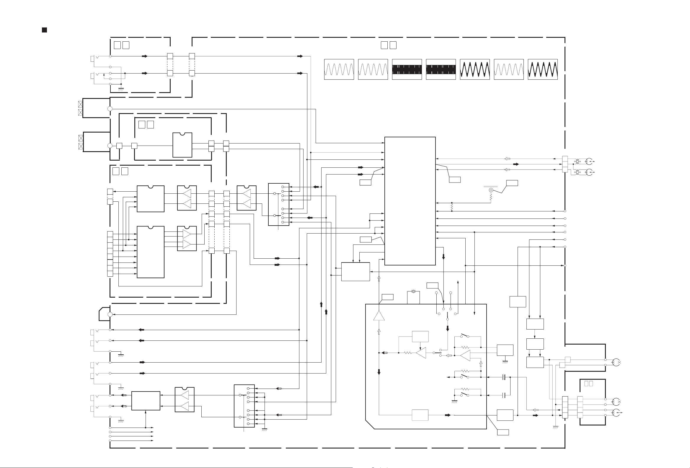
AUDIO BLOCK DIAGRAM
J7201
AUDIO IN
AUDIO IN
VHS TUNER
ANT IN
ANT OUT
VDR TUNER
ANT IN
ANT OUT
J8401
OPTICAL OUT
J7501
VDR OUT
AUDIO(L)
AUDIO(R
L-1 IN
AUDIO
AUDIO
J7502
LINE OUT
AUDIO(L)
AUDIO(R
TO
SYSCON
(L)
(R)
TU6001
SIF OUT
TU6002
SIF OUT
TO DIGITAL
(VIDEO IF)
CN1001
AI_D(0)
AO_IEC958
TO DIGITAL
(VIDEO IF)
CN1002
AO_D(0)
AO_FSYNC
AO_SCLK
AO_MCLK
DAC_SDA
DAC_SCL
A_DAC_CS
DAC_RST(L)
)
(L)
(R)
)
A.MUTE(H)
VDR(H)
A_INPUT_SEL1
A_INPUT_SEL2
47
14
CN7108
5
19
CN7109
28
19
26
24
25
27
23
21
1
4
3
6
7
5
CN65001
9
3
2
1
7
6
5
3
L
2
R
1
72
OPE/JACK
L
R
41
DEMOD
CN7201
CN6701
9
29
JUNCTION(AUDIO AD/DA, VIDEO
IC8002
A/D
9
SDTO
11
MCLK
12
SCLK
10
LRCK
IC8202
D/A
3
SDTI
4
LRCK
2
BICK
1
MCLK
8
CDTI
7
CCLK
6
CSN
5
PDN
L
R
L
R
AINL
AINR
AOUTL+
AOUTL-
AOUTR+
AOUTR-
2
1
12
11
10
9
21
7
5
IC8001
INPUT
IC8001
7
1
IC8201
3
2
5
6
CN3104
L out
R out
AMP
AMP
AMP
AMP
7
9
30
29
IC2605
7
MUTE
CONTROL
(Q2601 - Q2603)
A.MUTE(H)
VDR(H)
A_INPUT_SEL1
A_INPUT_SEL2
AMP
1
AMP
5
3
5
3
1
7
CN6701
6
5
)
CN8001
7
5
3
1
11
CN6501
6
5
CN2601
7
5
3
1
11
DEMOD2(L)
DEMOD2(R)
7
1
IC2604
13
3
A.MUTE(H)
IC2603
AMP
AMP
9,10
VDR(H)
IC2602
13
5
3
3
A_INPUT_SEL1
A_INPUT_SEL2
11
12
14
15
1
2
4
5
30
MAIN(VIDEO/N. AUDIO,FMA/DEMOD, TERMINAL, TUNER
L
R
IC2201-15
WF1 IC2201-57WF2 IC2201-21
REC/PB 60mVp-p
20mV/20µsec/DIV
REC/PB 0.2Vp-p
50mV/20msec/DIV
WF3
REC 1.0Vp-p
20mV/0.5µsec/DIV
WF4 IC1-6
A.PB_FM
PB 0.7Vp-p
20mV/5µsec/DIV
TP2253
WF5 IC1-2
REC/PB 0.3Vp-p
50mV/20ms/DIV
WF6 IC1-98
REC/PB 25mVp-p
5mV/20ms/DIV
WF7
REC 0.4Vp-p
0.1V/20ms/DIV
)
IC2201
48
SIF_IN
14
EXT1_IN(L)
9,10
L
R
9
EXT1_IN(R)
15
L
R
11
12
14
15
1
2
4
5
L
R
WF1
WF2
MUTE
CONTROL
EXT2_IN(L)
10
EXT2_IN(R)
4
EXT3_IN(L)
3
BS_IN(L)
2
EXT3_IN(R)
1
BS_IN(R)
57
LINE_OUT(L)
53
LINE_OUT(R)
62
NORMAL_IN
PB_FM_IN
PRE_OUT
MUTE_CTL
NORMAL_OUT
(Q2201 - Q2204)
X2
L
R
WF5
621347963
69 67
CH1
COM
CH2
CLK
DATA
fsc_IN
WF6
NOT
USED
22
21
24
WF3
TP2253
A.PB_FM
WF4
30
29
42
43
36
45
61
SW5V
NOT
USED
Q2001
POWER
-Q2003
A.MUTE
SP ON
SW
POWER
SW
Q2052-Q2055
DET
94
FILTER
95
VCA
R
-
P
+
PRE AMP
96
L
REC ON
+
OSC
TRANS
T2051
97
EP(LP)ON
R
IC1
(
VIDEO/N.AUDIO SIGNAL PROCESSOR)
REC
EQ
98
FILTER
WF7
Q2051
5
6
CN1
7
8
9
TO
SYSCON
H.REC_ST(H)
I2C_CLK_AV
I2C_DATA_AV
A.MUTE_VHS(H)
N.REC_ST(H)
N.REC(H)
TO
VIDEO SW
Fsc
FULL ERASE HEAD
CN2002
1
2
CN2001
3
4
2
1
CN1
4
3
5
6
AUDIO HEAD
FMA_CH1
FMA_CH2
F. ERASE
21
A/C HEAD
A. ERASE
REC/PB
2-57 2-58
Page 54
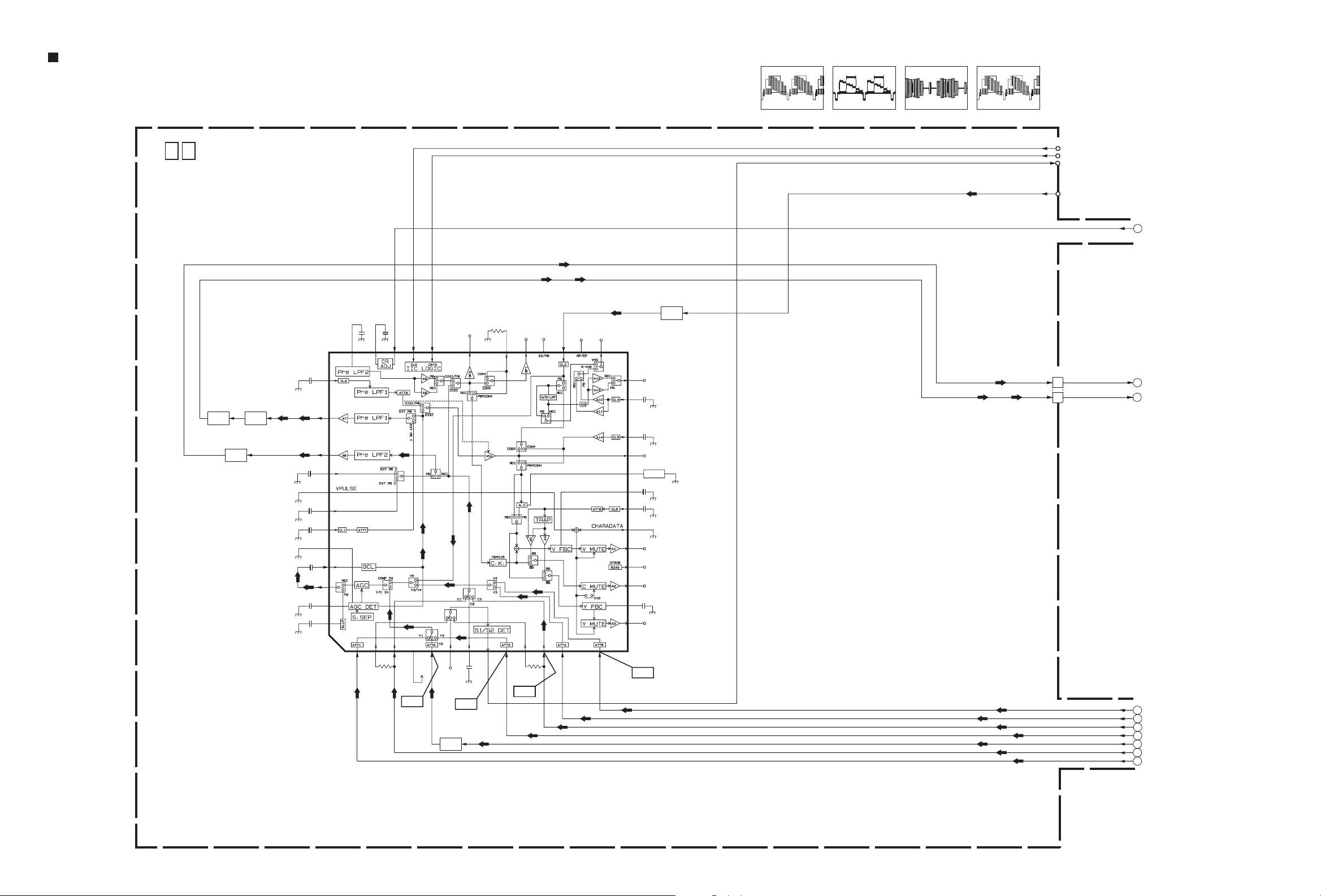
VIDEO BLOCK DIAGRAM(1)
WF1 WF4WF2
IC501-5 IC501-14
IC501-9
WF3
IC501-11
0 3 MAIN (VIDEO SW)
Q505
BUF
FILTER
Q503
BUF
43
45
Y
47
C
48
49
50
51
52
53
54
Y
55
56
IC501
( Y/C SWITCH )
REC 1.0Vp-p
0.5V/20µsec/DIV
C
Y
REC 1.0Vp-p
0.5V/20µsec/DIV
REC 0.7Vp-p
0.2V/20µsec/DIV
REC 1.0Vp-p
0.5V/20µsec/DIV
I2C_CLK2
I2C_DATA2
WIDE_DET2
GR_TU_VIDEO2
Fsc
TO
SYSCON
TO
TUNER
1
Q504
BUF
NOT
USED
NOT
USED
36
C
Y
6
85
WF2
+
42
Y
41
Y
21
C
40 39 38
C
Y
4
3
SW5V
WF1
Q506
BUF
NOT
NOT
USED
USED
34 33 32 30 2931
C
97
1110
WF3
C
Y
NOT
NOT
USED
USED
28
NOT
USED
27
25
24
NOT
USED
23
FILTERFILTER
22
21
20
19
NOT
USED
18
NOT
USED
17
NOT
USED
16
15
NOT
USED
12
14
C
CN501
CTODIGI
2
Y
YTODIGI
4
2
3
WF4
SELD_V_IN
FRONT_V_IN
C
Y
C
Y
REAR_C_IN
REAR_Y_IN
V_FROM_OSD
FRONT_C_IN
FRONT_Y_IN
4
5
6
7
8
9
10
2-59 2-60
Page 55

VIDEO BLOCK DIAGRAM(2)
WF1 WF2 WF3 WF4
IC1-19 IC1-26 IC1-29
TP106
PB.FM
WF5 IC1-86
TP 111
D.FF
WF6
TO
SYSCON
I2C_DATA_AV
I2C_CLK_AV
SB_GAIN(PWM)
TO
TUNER
Fsc
1
TO DIGITAL
(VIDEO IF)
CN1001
COUT
YVOUT
CBOUT
CROUT
VYIN
CIN
CTODIGI
2
YTODIGI
3
J7503
COMPONENT
VIDEO OUT
J7502
LINE OUT
J7501
VDR OUT
J7501
LINE IN
SLED_V_IN
4
FRONT_V_IN
5
REAR_C_IN
6
REAR_Y_IN
7
V_FROM_OSD
8
FRONT_C_IN
9
FRONT_Y_IN
10
J7204
FRONT_S_IN
J7201
V_IN
V.PULSE
C.SYNC
TU_VIDEO1
CN7108
6
10
20
CN7104
Pr
Pb
Y
REC 1.0Vp-p
0.5V/20µsec/DIV
REC 0.7Vp-p
0.2V/20µsec/DIV
REC/PB 2.1Vp-p
1.0V/20µsec/DIV
PB 0.4Vp-p
20mV/20µsec/DIV
REC/PB 0.4Vp-p
0.2V/10msec/DIV
REC 1.3Vp-p
0.5V/20µsec/DIV
MAIN (VIDEO/N. AUDIO, TERMINAL, ON SCREEN)03
TO
FMA/DEMOD
Fsc
WF4
L7
C
NOT
USED
ET LPF
SW52
35PinGCL
GCL
FILTER
5859
2fsc
CHROMA
ACC DET
P
R
21
CLPF2
MAIN
CONV2
SW31
PR
ATT
-10dB
ACC
SW
4PHASE
C
VIDEO AGC
C
H
4
ATT
-10dB
DOWN
CONV
ACC
DET
+
CONV1
SW32
R
P
4.43PAL
MPAL CONV.
DELAY
C
C
H
H
2
3
-10dB
CLPF1
SW33
RP
MAIN
SW16
C
H
1
ATT
REC
DISCRI
AFC
C
DO DET
ATT
-4dB
ATT
-6dB
15161719
LCVCO
SW30
P
VCA
R
RP
SW29
L-DET
P
SW28
R
SW15
Y-LP F
GCL
SW14
PC
SW18
P
R
R
ATP
26
23
WF1
IC7101
53 55 57
75 DRV
75 DRV
75 DRV
75 DRV
26
23
21
20
18
1614
PR
13 11 9 4 6 2
CN7107
1 3 5 10 8 12
CN7501
C
Y
CY
PB
NOT
USED
1
13
37
35
NOT
USED
28
WF3
CLOCK DRIVER
DATA
CLK
SW27
R*L-SECAM
CCD-
CONT
MODE
CONTROL
CCD BLOCK
KINSEKI
MSM7470 Series
Y-CC D
C-CCD
CCD
LPF
RP
SW51
P
EXT
INT
SW26
LPF
SW24
DO
GCL
GCL
DO/REC
R*SDECK
GCL
R*SVHS
NP
C.K
CONV
6dBAMP
SQPB EQ
SQPB
SQPB
SW19
C-SQUELCH
SW23
YNR
V-AMP
SQUE
LCH
SW21
R*SDECK
SYNC
SEP
R*SDECK
PG
27
NOT
USED
B.D
CLEAR
PILOT
PILOT
ERASE
ADD
BPF
SW17
SVHS+L-SECAM
SECAM
DELAY
N.L.
DE-EMPH
SW20
P
SYNC
+SSEQ
SVHS+L-SECAM
R
N.L.
DEH
EMPH
HP-NC
TRAP-NC
VIDEO ALC
/ FBC
R*SDECK
SW22
PG
AGC DET
0.5Vp-p
R*SDECK
24
48
51
49
46
45
74
73
43
42
40
38
34
33
36
25
31
29
Q7101
NOT
USED
2
6dB
+
-6dB
4
6dB
5
6
6dB
10
6dB
12
6dB
6dB
75 DRV
LPF
6dB
LPF
LPF
75 DRV
LPF
LPF
LPF
C
11
Y
FILTER
Cb
14
Cr
18
BUF
Y
C
3
1
JUNCTION (VIDEO)92
4
PR
1
4
1
4
1
4
1
10
Y
C
9
11
12
PB
Y
Q7573
BUF
Y
C
X2
NOT
USED
70
72
CCD
CONT
APC
C
SQPB
SQPB
SUB LPF
71
ACC
SW34
P
ACC
KILLER
:C-ACC:ON
P-EQ
FM AGC
DET
P
R
MAIN
CR DET
REC
APC
SW35
SW36
L-SECAM
MIX LEVEL
ADJUST
L-SECAM
B.E
REC
TRAP
LPF
:ON
SW37
REC
R
TRAP
:OFF
2MLPF
SW38
P
R
SD
SW25
HPF
SD
LPF
S-DET
SW11
R
SW13
P
14
10
X-TAL
VCO/OSC
PB
APC
SW
CHROMA
+
C.K
C-ACC:THROUGH
FH HPF
CTL TRAP
REC TRAP
C
DELAY
HiFi TRAP
DL
SQPB
SW12
G-EQ
DLIM
DEMO
REC FBC+ALC
PB AGC+APL
DE EMPHASIS
12
L-SECAM
L-SECAM
TP106
PB. FM
MESECAM
SW39
+
57 PIN
3.3k ADD
629
TRAP
4
1
13
Y
C
14
16
15
Y
C
14
13
12
IC7502
Q7501
BUF
WF2
8
5
C
Y
C
Y
CN7505 CN201
7
2
1
Y
C
3
4
2
2
1
OPE/JACK
CN7201
Y
C
CN3104
3
11
5
9
1
13
11
13
2
3
5
1
17
ON SCREEN
15
13
2
NOT
USED
77 78
7665 67 6963
B-Y INVERT
C
O
M
P
DET
DET DET
REC
VC
MUTE
SW40
SW41
EXT
SP
INT
SP
EXT
INT
EXT
SW8
P
SW9
R
IC201
(ON SCREEN)
CVin
SYNC_DET
CVout
XTALin
CS1
SCLK
SIN
MUTE
HPF
SP2
SP2
SW42
CH2
CH1
SP1
SP1
SP2
SP2
SW43
CH2
CH1
SP1
SP1
REC
FILTER
FM MOD
FO/DEV ADJ
MAIN EMPHASIS
CARRIER OFFSET
W.C/D.C
SW10
IC1
(
VIDEO & AUDIO
SIGNAL PROCESSOR
10 5 8 7 3
CN7505
10 5 8 7 3
CN201
8
9
10
11
3
ENVDET
WF5
TP111
D. FF
80
D.FF
81
TANK
NOT
82
USED
83
85
SW44
86
SW45
87
SW46
WF6
89
SW47
90
SW48
91
SW49
20
CN1
6
5
4
3
2
1
D. FF
S_DET(H)
TO
SYSCON
TO
SYSCON
VIDEO_ENV
TO
SYSCON
VIDEO
HEAD
SP CH2
SP CH1
LP/EP_CH2
LP/EP_CH1
8
9
)
TO
SYSCON
SYNC_DET(H)
OSC_CS
S.CLK
S.DATA_FRSYS
P.MUTE_VHS(L)
2-61 2-62
Page 56

DIGITAL BLOCK DIAGRAM
DIGITAL20
1394
3 6
JACK
J4112
TO
JUNCTION
(VIDEO)
CN7108
TO
JUNCTION
(VIDEO)
CN7109
TO
JUNCTION
(VIDEO)
CN7105
OPEN
FOR JIG
VIDEO IF
CN1002
AO_IEC958, AI_D[0], A_MUTE2[H], K_BUS_CLK
K_BUS_REQ, SYS_RESET[L], K_BUS_IN/OUT
AO_SCLK, AO_MCLKO, AO_FSYNC, DAC_RST[L]
DAC_SCL, DAC_SDA, AO_D[0], A_DAC_CS
CIN
CN1001
VYIN
YV_OUT
C_OUT
CB_OUT
CR_OUT
MEDIA PROCESSOR
CN1404
JLIP_TX
JLIP_RX
CN1403
UART2_TX
UART2_RX
1394PFY
TPA+
CN1801
CN4104
TPATPB+
TPB-
FLASH
IC1201
Flash
memory
LH_AR[6] to LH_AR[21]
IC1203
IC1204
Transparent
CN1404
C
Y
IC1801
IEEE1394
Controller
MADD[1-5]
MADD[6-22]
E5_RESET[L]
MADD[6-21]
ALE
MADD[1-5]
MADD[6-22]
E5_RESET[L]
UART2_TX, UART2_RX
DDR RAM
SW5V, SW12V, D5V, D3.3V
D2.5V, D1.8V, V3.3V
RA1609
to
DDR_DQ[0-15]SDRAM_DQ[0-15]
RA1612
SDRAM_DQ[16-31]
RA1613
to
DDR_DQ[16-31]
RA1616
DDR_A[0-12]
C
Q1008
Y
Y
SW
CrCb
Q1002 to Q1005
BUF
IC1001
Video
Controller
IC1002
SDRAM
VI_D[2-9], VIDEO_RST[L]
VO_D[0-15], SPI_MOSI
VIDEO_27M, VIDEO_CS
VIDEO_MUTE[H], SPI_CLK
VIDEO_RXD
AP, A0 to A9,DQ0 to DQ15
UDQM, WE,CAS, RAS
VI_D[2-9]
VO_D[0-15]
VIDEO_27M
SDRAM_A[0-12]
SDRAM_A[14-17]
SDRAM_CKE
SDRAM_RAS_L
SDRAM_CAS_L
SDRAM_WE_L
SDRAM_CLK[0]
SDRAM_CLK[1]
SDRAM_CLK_L[0]
SDRAM_CLK_L[1]
RA1625
to
RA1628
R1601
to
R1604
R1613
to
DDR_BA[0]
DDR_BA[1]
DDR_CS[0]
R1616
VI_D[2-9], VO_D[0-15]
SDRAM_DQ[0- 31]
SDRAM_A[0-12]
SDRAM_A[14-17]
SDRAM_DQS[0] to [3]
SDRAM_DQM[0] to [3]
SDRAM_CLK[0], SDRAM_CLK[1]
SDRAM_CLK_L[0], SDRAM_CLK_L[1]
SDRAM_CKE, SDRAM_RAS_L
SDRAM_CAS_L, SDRAM_WE_L
SDRAM_DQM[0] to [3]
SDRAM_DQS[0] to [3]
RA1653
to
R1660
IC1401
PHY_RESET[L]
PHY_LREQ
PHY_CLK
PHY_CNA
PHY_CTL[0]
PHY_CTL[1]
PHY_DATA[0-7]
PHY_LPS
PHY_LINK_ON
Media
Processor
VIDEO_RXD, VIDEO_CS
VIDEO_27M, AO_SCLK, AO_FSYNC
AO_MCLKO, AO_IEC958, AO_D[0]
AI_D[0], SPI_MOSI, SPI_CLK
DAC_SCL, DAC_SDA, A_DAC_CS
DAC_RST[L], VIDEO_RST[L], VIDEO_MUTE[H]
IC1404
A_MUTE2[H]
K_BUS_CLK
K_BUS_REQ
ATAPI IF
3.3V --> 5.0V
RD/WR[L]
OE[L]/LDS[L]
CS[0]
MADD[1-5]
RD/WR[L]
OE[L]/LDS[L]
CS[0]
MADD[1-5]
ALE
IC1405
5.0V --> 3.3V
ATA_RESET, ATA_DAT[0-15], ATA_DMARQ
ATA_IORDY, ATA_INTRQ, ATA_DIOW[L]
ATA_DIOR[L], ATA_DMAACK[L], ATA_ADD[0] to [4]
SYS_RESET[L]
K_BUS_IN/OUT
ATA_RESET
ATA_DAT[0-15]
ATA_DIOW[L]
ATA_DIOR[L]
ATA_DMAACK[L]
ATA_ADD[0] to [4]
ATA_DMARQ
ATA_IORDY
ATA_INTRQ
RA2201
to
RA2205
RA2206
RA2207
IC1601
IC1603
DDR SDRAM
IC1602
IC1604
DDR SDRAM
DDR_CKE
DDR_RAS_L
DDR_CAS_L
DDR_WE_L
DDR_CLK[0]
DDR_CLK[1]
DDR_CLK_L[0]
DDR_CLK_L[1]
HD_AT[0] to [15]
RSTATA
DMARQ, DIOW, DIOR
IORDY, DMACK, INT_ATA
ATA_A0, ATA_1,ATA_A2
CS1FX, CS3FX
DDR_DQM[2],[3]
DDR_DQS[2],[3]
DDR_DQM[0],[1]
DDR_DQS[0],[1]
CN2201
TO
DVD
Recorder
Unit
2-63 2-64
Page 57
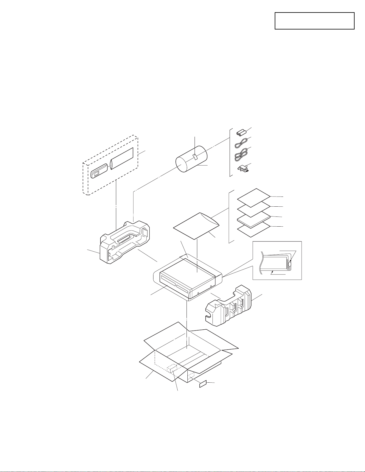
Preliminary
PARTS LIST
SAFETY PRECAUTION
Parts identified by the symbol are critical for safety. Replace only with specified part numbers.
BEWARE OF BOGUS PARTS
Parts that do not meet specifications may cause trouble in regard to safety and performance. We recommend that genuine
JVC parts be used.
1. EXPLODED VIEW
1.1 PACKING AND ACCESSORY ASSEMBLY <M1>
The instruction manual to be provided with this product will differ according to the destination.
307
ADHESIVE TAPE
306
312
314
302
FINAL ASSY <M2>
303
308
315
317
316
310
320
311
POWER CORD
SET
POLY BAG
302
301
SPEC OF BARCODE
304
(No.YD006)3-1
Page 58

1.2 FINAL ASSEMBLY <M2>
504
504
503
501D
501F
501H
501C
501J
MACHAMISM ASSY<M4>
MAIN BOARD
ASSY<03>
501
511
501A
j
j
520
501B
j
501E
j
535
501F
524
520
502
533
503
533
505
j
535
519
509
504
545
508
504
546
D
515
b
514
515
518
b
b
527
f
i
526
525
517
525
515
518
523
525
c
c
REGULATOR BOARD
ASSY<01>
541
527
522
e'
k
e'
e'
e
518
527
e'
e'
526
532
c
e
e
e'
e
JUNCTION BOARD
ASSY<92>
534
516
541
534A
q
g
h
JS3001
a
521
524
r
524
g
h
j
i
b
a
b
e
d
533
i
520
547
548
JACK BOARD
DEMOD BOARD
ASSY<14>
535
513
C
a
a
e
e
b
e
d
k
m
ASSY<94>
OSD BOARD
ASSY<17>
513
c
a
i
c
c
b
e
533
526
DIGITAL BOARD
ASSY<02>
JACK BOARD
ASSY<36>
531
e'
543
i
512
c
i
526
544
m
526
e'
d
e
d
b
CN5001
529
518
515
f
525
c
3-2(No.YD006)
Page 59

CN7201
CN3104
to MAIN BOARD ASSY
(CN3104)
CN3104
from FRONT PANEL
(OPERATION JACK BOARD ASSY CN7201)
OPERATION JACK
BOARD ASSY<27>
WR3
507
MAIN BOARD ASSY
507
C
WR2
A/C HEAD
BOTTOM SIDE
WR4
FW7504
CN501
CN2001
JACK BOARD ASSY
CN8501
CN7111
CN3106
CN3102
CN5311
CN2601
CN3103
CN5301
CN8001
CN7102
CN5302
CN7107
DVD
CN7103
FAN
WR1
WR7
B
UNIT
CN7104
WR5
CN5001
REGULATOR BOARD ASSY
CN5304
JUNCTION
CN5501
BOARD ASSY
WR8
WR6
CN2201
DIGITAL
BOARD ASSY
CN7106
CN1404
SWITCH DISPLAY BOARD ASSY<28>
506
CN7001
CN7002
NOTE)Push the slack of the wire
into the FW7001 side.
CN7001
506
507
CN7201
507 506
NOTE)Pass slit PCB through wire.
TOP SIDE
NOTE) INSERT FFC WIRE TO THE CONNECTOR BEFORE ATTACHING TO FRONT PANEL.
5. Insert direction of FCC WIRE as follows.
BRACKET(CENTER)
right side
electrode side
back side
supporting side
Make a crease.
6. FFC WIRE and DRUM FPC WIRE should be insert as follows.
OK
90
CN
7. Insert direction of POWER CORD.
U/U(C)/JPN
WHITE LINE
NEUTRAL
CN5001
8. Insert the wire to even the root of connector completely
at the same time as inserting each wire.
NG
CN
CN
except U/U(C)/JPN
BLUE
NEUTRAL
CN5001
CN7111 CN501
DRAWING FROM DIRECTION
NOTE) Push both ends of connector
when it is inserted to the DRIVE UNIT.
536
DRAWING FROM DIRECTION
CN7002
506
Make a crease.
MAIN BOARD ASSY
C
B
NOTE) FJ CONN should be insert as follows.
OK
CN
NG
CN
CN7102 CN3103
CN8001 CN2601
CN5501 CN5304
CN5311 CN5301
NOTE) Replace the attached FITING.
<HOW TO REMOVE>
FITTING(DVD) ASSY
Take it out up
by doing the slide.
It pulls out toward
front side.
506
TRAY
542
Pasted to conceal the edge
of the BRACKET .
DRAWING FROM DIRECTION
D
(No.YD006)3-3
Page 60

1.3 MECHANISM ASSEMBLY <M4>
112
AA
124
127
128
126
AA
110
AA
118
77
76
134
AA
122
130
121
74
105
88
BB
90
89
21
4
AA
BB
BB
BB
BB
90
72
71
AA
73
75
37
17
AA
78
89
38
AA
36
107
AA
Not used
79
137
151
123
125
126
119
107
111
115
80
105
117
26
86
AA
83
81
AA
56
52
58
3
AA
55
53
91
1
39
120
82
113
112
116
114
A/C HEAD
BOARD ASSY <12>
WR2
57
58
42
50
44
49
WR1
51
85
PMD0044A-C
Classification Part No. Symbol in drawing
Grease KYODO-SH-JB AA
3-4(No.YD006)
102
AA
69
70
AA
96
94
Oil COSMO-HV56 BB
AA
23B
AA
64
65
23
23A
WR3
67
62
59
AA
68
AA
84
61
60
63
66
AA
95
93
15
AA
18B
18A
22
AA
24
18
19
20
LOADING MOTOR
BOARD ASSY <55>
16
87
AA
AA
46
47
NOTE:The section marked in AA and BB
indicate lubrication and greasing areas.
Page 61

2. PARTS LIST
PACKING AND ACCESSORY ASSEMBLY <M1>
Symbol No.
301 LP31338-010A PACKING CASE
302 LP31340-001A CUSHION ASSY
303 PQM30021-105 POLY BAG
304 LP31258-001A MINI CUSHION
306 RM-SDR013J REMOCON
307 ------------ BATTERY R6 TYPE(x2)
308 QPC02202230P POLY BAG 22cm x 22cm
310 LPT0952-001A INST.BOOK (ENGLISH) A
310 LPT0952-002A INST.BOOK (FRENCH) A
310 LPT0918-001A INST.BOOK (ENGLISH) B
311 QPC02503530P POLY BAG 25cm x 35cm
312 QAM0501-003 RF CABLE
314 QAM0523-003 RF CABLE
315 QAU0361-001 ANT. SPLITTER B
316 BT-52006-2 WARRANTY CARD A
317 BT-51034-2 REGIST CARD B
320 LP30666-005C SHEET(COUPON)
Part No. Part Name Description Local
ANT. SPLITTER(x2)
FINAL ASSEMBLY <M2>
Symbol No.
501 LP10526-005A FRONT PANEL ASSY
501A LP21232-002A CASSETTE DOOR
501B PQ46448 TORSION SPRING
501C LP31358-003A DISPLAY WINDOW
501D LP31353-001A DOOR(L)
501E LP31354-001A DOOR(R)
501F PU60109 CATCHER (x2)
501H LP31356-005A WINDOW(L)
501J LP31357-004A WINDOW(R)
502 LP10460-004B TOP COVER
503 QYSBSG3006NA TAP SCREW
504 QYSBSG3006NA TAP SCREW
505 PDV2531C DRUM FINAL ASSY
506 QYTDSF2608ZA TAP SCREW
507 QYTDSF2608ZA TAP SCREW
508 LP31372-002A FITTING(DVD) ASSY
509 QAL0551-001 DRIVE UNIT
511 LP10525-001D BOTTOM CHASSIS
512 LP21222-001B BRACKET(CENTER)
513 LP31391-001A SPECIAL SCREW
514 LP21223-001A BRACKET(DVD UNIT)
515 LP31391-001A SPECIAL SCREW
516 LP21134-012A REAR COVER
517 QYSBSG3006NA TAP SCREW
518 QYTDST3006ZA TAP SCREW
519 QYSPSPD3008ZA SCREW
520 LP31391-002A SPECIAL SCREW MECHANISM(x3)
521 LP31391-001A SPECIAL SCREW HOUSING
522 QAR0310-001 FAN MOTOR
523 QYTDSF3008MA TAP SCREW M3 x 8mm FAN ( x 2)
524 LP31391-001A SPECIAL SCREW MAIN(x3)
525 LP31391-001A SPECIAL SCREW REGULATOR(x4)
526 LP31391-001A SPECIAL SCREW JUNCTION(x5)
527 QYTDSF3008MA TAP SCREW
529 QMPD190-170-K POWER CORD(JP) 1.7m BLACK
531 LP31390-001A BARCODE LABEL
532 LP31391-001A SPECIAL SCREW JACK
533 LP31348-001A FOOT (x4)
534 LP40910-002G HEA D CLEAN E R A S S Y
534A PQ46419-2 CLEANER
535 LP41140-001A INSULATOR (x3)
536 QGZ0018A1-40 CONNECTOR (1-40)
541 QYTDST3005MA TAP SCREW
542 LP30002-0F6A SPACER
543 LP41171-001A SHIELD TIGHT
544 LP41171-001A SHIELD TIGHT
545 LP41171-001A SHIELD TIGHT
546 LP31417-001A SHIELD PLATE
Part No. Part Name Description Local
M3 x 6mm TOP SIDE(x2)
M3 x 6mm TOP REAR(x4)
M2.6 x 8mm SWITCH DISPLA Y(x5)
M2.6 x 8mm OPERA TION JACK(x4)
BRACKET(CENTER)(x2)
BRACKET(DVD)(x4)
M3 x 6mm REAR COVER(x2)
M3 x 6mm DVD UNIT(x 4)
M3 x 8mm DRUM(x3)
M3 x 8mm JACK(x5)
M3 x 5mm TUNER(x2)
MODEL MARK
MODEL MARK
DR-MV1SUC
DR-MV1SUSAB
JUNCTION CN7107-MAIN CN7501
JUNCTION CN7104-MAIN CN501
OPERA TION JACK CN7201-MAIN CN 3104
SWITCH DISPLAY CN7001-MAIN CN3102
JUNCTION C N7103-SWI CH DISPLA Y CN7002
DVD UNIT-DIGIT AL CN2201
REGULA TOR CN5303-DVD UNIT
DIGIT AL CN1404 -JUNCTION CN7105
Symbol No.
547 LP31345-001A EARTH PLATE
548 LP31345-001A EARTH PLATE
WR1 QUQ112-1318CG FFC WIRE
WR2 QUQ212-0430CG FFC WIRE
WR3 QUQ112-1308CG FFC WIRE
WR4 WJT0151-001A E-CARD WIRE
WR5 QUQ212-0410CG FFC WIRE
WR6 QUQ105-4020AF FFC WIRE
WR7 QJJ032-040804 SIN CR C-C WIRE
WR8 QUQ210-0406CC FFC WIRE
Part No. Part Name Description Local
DR-MV1SUC
DR-MV1SUSAB
MECHANISM ASSEMBLY <M4>
B
Symbol No.
1 LP21039-003A MAIN DECK ASSY
3 LP40097-002E GUIDE POLE CAP
4 NAH0004-001 FULL ERASE HEAD
15 LP30958-001B LO A D I N G G E A R B A S E
16 QYTPST2620ZA TAP SCREW M2.6 x 20mm(x2)
17 QYTDST2606ZA TAP SC REW M2.6 x 6mm
18 LP40798-002A
18A LP21040-001A
18B LP40799-002A
19 LP40837-001A
20 LP40903-004A FIXING PLATE
21 LP40806-001D
22 LP30959-001B LOADING GEAR
23 LP40802-002A
23A LP21041-001D
23B LP40803-002A
24 LP40838-001A
26 LP40808-001E
36 LP21055-001G TAKE UP LEVER
37 LP40943-001A TENSION SPRING
38 LP40859-001D T-UP HEAD
39 LP30961-001C LID GUIDE
42 LP40810-003A
44 LP40840-001D TORSION SPRING
46 LP30963-002A PRESS LEVER
47 PQM30017-24 SLIT WASHER
49 LP40813-001D GUIDE ARM ASSY
50 LP40841-001A TORSION SPRING
51 LP30002-090A SPACER
52 NAH0003-001 AC HEAD
53 LP30965-003A HEAD BASE
55 LP40842-001D
56 QYTDST2006MA TAP SCREW M2 x 6mm
57 LP41036-002A A/C ADJ.SCREW (x2)
58 QYTDST2606ZA TAP SCREW M2.6 x 6mm(x2)
59 QAR0289-001 LOADING MOTOR
60 QYTPSP3003ZA SCREW M3 x 3mm(x2)
61 LP21056-002J MOTOR BRACKET
62 QYTPST2620ZA TAP SCREW M2.6 x 20mm
63 LP40814-001B WORM BEARING
64 LP21044-001E CONTROL CAM
65 PQM30017-24 SLIT WASHER
66 LP40815-001A WORM GEAR
67 LP40816-001B HELICAL GEAR
68 LP40817-001A CONNECT GEAR
69 LP10400-001N CONTROL PLATE
70 LP40843-001A TORSION SPRING
71 LP40818-002A TENSION ARM ASSY
72 LP40844-001F TENSION SPRING
73 LP21045-001E TENSION ARM BASE
74 LP40821-001A
75 LP30967-001B BAND HOLDER-1
76 LP30968-001C BAND HOLDER-2
77 LP40822-002B ADJUST PIN
78 LP31000-005E TE N S I O N A R M L E V E R
79 LP21046-001C MAIN BRAKE(TAKE UP)
80 LP40824-001A BAND BRAKE ASSY
81 LP30969-002B BRAKE LEVER
82 LP30003-033B TENSION SPRING
Part No. Part Name Description Local
LOADING GEAR(SUPPL Y) ASSY
LOADING GEAR(SUPPLY)
LOADING ARM(SUPPLY) ASSY
TORSION SPRING(SUPPL Y)
POLE BASE ASSY(SUPPLY)
LOADING GEAR(T AKE UP) ASSY
LOADING GEAR(TAKE UP)
LOADING ARM(TAKE UP) ASSY
TORSION SPRING(T AKE UP)
POLE BASE ASSY(TAKE UP)
PINCH ROLLER ARM ASSY
COMPRESSION SPRING
TENSION BAND ASSY
(No.YD006)3-5
Page 62

Symbol No.
Part No. Part Name Description Local
Symbol No.
MODEL MARK
DR-MV1SUC
DR-MV1SUSAB
Part No. Part Name Description Local
MODEL MARK
DR-MV1SUC
DR-MV1SUSAB
83 LP30003-035B TENSION SPRING
84 LP40825-001B
85 QAR0267-002 CAPSTAN MOTOR
86 QYTPSG2606ZA TAP SCREW M2.6 x 6mm(x3)
87 LP30005-010A BELT CAPSTAN MOTOR
88 LP30970-001A IDLER ARM
89 LP40828-004A IDLER GEAR 1 (x2)
90 LP40829-002A IDLER GEAR 2 (x2)
91 LP31014-002A WIRE HOLDER
93 LP40934-001B CLUTCH UNIT
94 PQM30017-47 SLIT WASHER
95 LP30973-001A DIRECT GEAR
96 LP40939-001A
102 LP30974-001C CHANGE LEVER
105 LP21049-001A REEL DISK (x2)
107 LP30017-004A SPACER REEL DISK(x2)
110 LP10401-001L SIDE FRAME(L)
111 LP10402-001M SIDE FRAME(R)
112 QYTDST2606ZA TAP SCREW M2.6 x 6mm(x2)
113 LP40917-001D TORSION SPRING
114 LP30976-002A SIDE PLA TE
115 LP30977-002D LIMIT PLATE
116 LP40846-001C LIMIT SPRING
117 LP31100-002A DRIVE LEVER
118 LP30978-001B DRIVE ARM(L)
119 LP30979-001S DRIVE ARM(R)
120 LP40847-001B TORSION SPRING
121 LP30980-002A CONNECT PLATE
122 LP10403-001C SIDE HOLDER(L)
123 LP10404-001E SIDE HOLDER(R)
124 LP30983-002A LOCK LEVER(L)
125 LP30984-002A LOCK LEVER(R)
126 LP40924-001D TENSION SPRING (x2)
127 LP40972-001A EARTH SPRING(1)
128 LP40857-001B EARTH SPRING(2)
130 LP30981-003A
134 LP21051-002C REC SAFETY LEVER
137 LP21052-002A TOP FRAME
151 LP30985-002M DOOR OPENER
WR1 WJT0117-001A E-CARD WIRE DRUM
WR2 WJT0067-001B E-CARD WIRE A/ C H E A D C N 2 0 0 1
WR3 WJS0022-001A E-FL/RB WIRE LOADING MOTOR
CAPSTAN BRAKE ASSY
COMPRESSION SPRING
CASSETTE HOLDER ASSY
REGULATOR BOARD ASSEMBLY <01>
Symbol No.
PW1 LPA10248-02C1 R EGULATOR BOARD ASSY
IC5101 STR-G6653-F9 IC
IC5301 UTCTL431-T IC
IC5301 or MM1431AT-T IC
IC5301 or L5431-T IC
IC5301 or TL431/A/-T IC
IC5302 PQ5EV3 IC
Q5304 UMD12N-W DIGI TRANSISTOR
Q5304 or XP4313-W DIGI TRANSISTOR
Q5305 2SD2144S/UV/-T TRANSISTOR
Q5305 or 2SC3576-JVC-T TRANSISTOR
Q5306 2SC5739/QP/ TRANSISTOR
Q5307 2SA1585S/QR/-T TRANSISTOR
Q5308 PDTC114EU-X DIGI TRANSISTOR
Q5308 or DTC114EUA-X DIGI TRANSISTOR
Q5308 or UN5211-X DIGI TRANSISTOR
Q5308 or RN1302-X DIGI TRANSISTOR
Q5313 2SA1585S/QR/-T TRANSISTOR
Q5314 2SA1585S/QR/-T TRANSISTOR
Q5315 PDTC114EU-X DIGI TRANSISTOR
Q5315 or DTC114EUA-X DIGI TRANSISTOR
Q5315 or UN5211-X DIGI TRANSISTOR
Q5315 or RN1302-X DIGI TRANSISTOR
D5001 GBJ4J BRIDGE DIODE
Part No. Part Name Description Local
D5001 or D3SBA60 DIODE
D5101 SARS01-T2 SI DIODE
D5103 1F4G-T2 FR DIODE
D5103 or 10ERB20-T2 FR DIODE
D5103 or ERA18-02-T2 FR DIODE
D5103 or AU01Z-T2 FR DIODE
D5103 or 1SR153-400-T2 FR DIODE
D5104 1SS133-T2 DIODE
D5104 or 1SS270A-T2 SI DIODE
D5105 10ERB20-T2 FR DIODE
D5105 or ERA18-02-T2 FR DIODE
D5105 or AU01Z-T2 FR DIODE
D5105 or 1SR153-400-T2 FR DIODE
D5105 or 1F4G-T2 FR DIODE
D5106 10ERB20-T2 FR DIODE
D5106 or ERA18-02-T2 FR DIODE
D5106 or AU01Z-T2 FR DIODE
D5106 or 1SR153-400-T2 FR DIODE
D5106 or 1F4G-T2 FR DIODE
D5202 1SR156-400-X SI DIODE
D5203 RL2Z-LFB2 FRD
D5204 D1FS4A-X SB DIODE
D5205 RK34-LFB2 SB DIODE
D5207 D1FS4A-X SB DIODE
D5208 RK34-LFB2 SB DIODE
D5209 RK34-LFB2 SB DIODE
D5210 1F4G-T2 FR DIODE
D5210 or PG104RS-T2 FR DIODE
D5210 or 10ERB20-T2 FR DIODE
D5210 or 1SR153-400-T2 FR DIODE
D5210 or ERA18-02-T2 FR DIODE
D5211 ERA18-02-T2 FR DIODE
D5211 or 1SR153-400-T2 FR DIODE
D5211 or 10ERB20-T2 FR DIODE
D5211 or 1F4G-T2 FR DIODE
D5212 D1FS4A-X SB DIODE
D5213 1F4G-T2 FR DIODE
D5213 or 10ERB20-T2 FR DIODE
D5213 or ERA18-02-T2 FR DIODE
D5213 or AU01Z-T2 FR DIODE
D5213 or 1SR153-400-T2 FR DIODE
D5301 MTZJ15A-T2 Z DIODE
D5301 or RD15ES/B1/-T2 Z DIODE
D5303 MTZJ11C-T2 Z DIODE
D5303 or RD11ES/B3/-T2 Z DIODE
D5304 MTZJ5.6C-T2 Z DIODE
D5304 or RD5.6ES/B3/-T2 Z DIODE
D5306 RK34-LFB2 SB DIODE
D5307 RK34-LFB2 SB DIODE
D5308 RK34-LFB2 SB DIODE
D5309 1S4-T2 SB DIODE
D5309 or SBO40-T2 SB DIODE
D5309 or AW04-T2 SB DIODE
D5312 1SS133-T2 DIODE
D5312 or 1SS270A-T2 SI DIODE
D5313 1A3G-T2 SI DIODE
D5313 or ERA15-02-T2 SI DIODE
D5313 or 10EDB20-T2 SI DIODE
PC5101 PC123Y22FZ PHOTO COUPLER
C5001 QFZ9073-683 MM CAPACITOR 0.068uF AC250 V M
C5002 QFZ9051-223 MM CAPACITOR 0.022uF 250V M
C5003 QEZ0639-337 E CAPACITOR 330uF 200V M
C5004 QCZ9079-472 C CAPACITOR 4700pF AC250 V M
C5005 QCZ9071-101 C CAPACITOR 100pF AC400V K
C5101 QCZ0339-101Z C CAPAC ITOR 100pF 1kV K
C5102 QCZ0349-472Z C CAPAC ITOR 4700pF 1kV K
C5103 QEMU1VM-276Z E CAPA CITOR 27uF 35V M
C5104 QCZ0136-471Z C CAPAC ITOR 470pF 1kV K
C5105 QFLC1HJ-471Z M CAPACITOR 470pF 50V J
C5106 NCB21HK-103X C CAPACITOR 0.01uF 50V K
C5107 NCB21HK-221X C CAPACITOR 220pF 50V K
C5202 QETN2AM-475Z E CAPACITOR 4.7uF 100V M
C5203 QEMT1CM-687 E CAPACITOR 680uF 16V M
C5204 QEMT1CM-687 E CAPACITOR 680uF 16V M
C5205 QEMT1AM-128 E CAPACITOR 1200uF 10V M
C5206 QECS1AM-128 E CAPACITOR 1200uF 10V M
3-6(No.YD006)
Page 63

Symbol No.
C5207 QECS0JM-158 E CAPACITOR 1500uF 6.3V M
C5208 QEMT1AM-108 E CAPACITOR 1000uF 10V M
C5209 QEMU1HM-186Z E CAPACITOR 18uF 50V M
C5210 QEMX0JM-227Z E CAPACITOR 220uF 6.3V M
C5301 QFVF1HJ-154Z MF CAPACITOR 0.15uF 50V J
C5302 QFLC1HJ-333Z M CAPACITOR 0.033uF 50V J
C5303 QETN1CM-107Z E CAPACITOR 100uF 16V M
C5304 QETN1CM-107Z E CAPACITOR 100uF 16V M
C5305 QETN1AM-107Z E CAPACITOR 100uF 10V M
C5306 QETN1AM-107Z E CAPACITOR 100uF 10V M
C5307 QETN1CM-107Z E CAPACITOR 100uF 16V M
C5308 QETN1CM-107Z E CAPACITOR 100uF 16V M
C5310 QETN1HM-225Z E CAPACITOR 2.2uF 50V M
C5311 QETN1AM-107Z E CAPACITOR 100uF 10V M
C5312 QETN1AM-107Z E CAPACITOR 100uF 10V M
C5313 NCB21HK-471X C CAPACITOR 470pF 50V K
C5314 QETN1AM-107Z E CAPACITOR 100uF 10V M
C5315 NCB21HK-103X C CAPACITOR 0.01uF 50V K
R5001 QRZ9046-475Z C RESISTOR 4.7MΩ 1/2W K
R5101 QRG02GJ-683 OMF RESISTOR 68k
R5102 NRSA02J-122X MG RESISTOR 1.2k
R5103 QRE141J-684Y C RESISTOR 680kΩ 1/4W J
R5104 NRSA02J-102X MG RESISTOR 1kΩ 1/10W J
R5105 QRE141J-680Y C RESISTOR 68Ω 1/4W J
R5106 QRE141J-392Y C RESISTOR 3.9kΩ 1/4W J
R5107 NRSA02J-681X MG RESISTOR 680Ω 1/10W J
R5108 QRT01DJ-R33X MF RESISTOR 0.33Ω 1W J
R5109 QRZ9005-470X FUSI RESISTOR 47Ω 1/4W G
R5301 NRSA02J-221X MG RESISTOR 220Ω 1/10W J
R5302 NRSA02J-472X MG RESISTOR 4.7kΩ 1/10W J
R5303 NRVA02D-152X CMF RESISTOR 1.5kΩ 1/10W D
R5304 NRVA02D-682X CMF RESISTOR 6.8kΩ 1/10W D
R5305 NRVA02D-243X CMF RESISTOR 24kΩ 1/10W D
R5306 NRVA02D-392X CMF RESISTOR 3.9kΩ 1/10W D
R5308 NRSA02J-122X MG RESISTOR 1.2kΩ 1/10W J
R5309 NRSA02J-102X MG RESISTOR 1kΩ 1/10W J
R5312 NRSA02J-103X MG RESISTOR 10kΩ 1/10W J
R5313 NRSA02J-103X MG RESISTOR 10kΩ 1/10W J
R5314 NRSA02J-471X MG RESISTOR 470Ω 1/10W J
R5315 QRE121J-820Y C RESISTOR 82Ω 1/2W J
R5316 NRSA02J-103X MG RESISTOR 10kΩ 1/10W J
R5317 NRSA02J-102X MG RESISTOR 1kΩ 1/10W J
R5318 NRVA02D-302X CMF RESISTOR 3kΩ 1/10W D
R5319 NRVA02D-472X CMF RESISTOR 4.7kΩ 1/10W D
R5325 QRE141J-8R2Y C RESISTOR 8.2Ω 1/4W J
R5326 QRZ9005-470X FUSI RESISTOR 47Ω 1/4W G
R5327 NRSA02J-103X MG RESISTOR 10kΩ 1/10W J
R5328 NRSA02J-471X MG RESISTOR 470Ω 1/10W J
R5329 NRSA02J-103X MG RESISTOR 10k
R5330 NRSA02J-471X MG RESISTOR 470Ω 1/10W J
L5201 PELN1184 CHOKE COIL
L5202 PELN1184 CHOKE COIL
L5204 PELN1184 CHOKE COIL
L5205 PELN1184 CHOKE COIL
L5206 PELN1184 CHOKE COIL
L5207 PELN1184 CHOKE COIL
L5301 QQR0678-001Z FERRITE BEADS
L5302 QQR0678-001Z FERRITE BEADS
T5001 QQS0263-001 SW TRANSF
B5301 NRSA02J-0R0X MG RESISTOR 0
B5305 NRSA02J-0R0X MG RESISTOR 0
CN5001 QGA7901C3-02 CONNECTOR W-B (1-2)
CN5301 QGB1231L1-15 CONNECTOR B-B (1-15)
CN5302 QGA2001C1-02 CONNECTOR W-B (1-2)
CN5303 QGA2501C1-04 CONNECTOR W-B (1-4)
CN5304 QGB1231L1-15 CONNECTOR B-B (1-15)
CP5301 QMFZ049-1R5Z-E FUSE 1.5A 125V
F5001 QMF51N2-1R6-J1 FUSE 1.6A AC250V
FC5001 QNG0020-001Z FUSE CLIP
FC5002 QNG0020-001Z FUSE CLIP
LF5002 QQR0908-001 LINE FILTER
VA5001 QAF0039-431Z VARISTOR 430V
W5501 NRSA02J-0R0X MG RESISTOR 0Ω 1/10W J
Part No. Part Name Description Local
Ω
Ω
1/10W J
Ω
1/10W J
Ω
1/10W J
Ω
1/10W J
2W J
MODEL MARK
DR-MV1SUC
DR-MV1SUC
DR-MV1SUSAB
DR-MV1SUSAB
DIGITAL BOARD ASSEMBLY <02>
Symbol No.
PW1 LPA10236-05C DIGITAL BOARD ASSY
IC1001 JCP8059 IC
IC1002 HY57V161610DTC7 IC
IC1002 or K4S161622H-TC80 IC
IC1002 or MT48LC1M16A1TG8 IC
IC1002 or HY57V161610DTC8 IC
IC1002 or MT48LC1M16TG-7S IC
IC1201 MBPL65LM90TN IC
IC1202 SN74LVC373APW-X IC(DIGITAL)
IC1203 SN74LVC373APW-X IC(DIGITAL)
IC1401 DMN8652-B0 IC(DIGITAL)
IC1404 SN74HCT08APW-X IC
IC1405 SN74LV08APW-X IC
IC1601 HY5DU561622CT-J IC
IC1602 HY5DU561622CT-J IC
IC1701 PQ015YZ01Z-X IC
IC1801 TSB41AB2PAP IC
Q1001 UN221E-X TRANSTSTOR
Q1001 or DTC144WKA-X DIGI TRANSISTOR
Q1001 or RT1N44HC-X DIGI TRANSISTOR
Q1002 2SA1037AK/QR/-X TRANSISTOR
Q1002 or 2SA1530A/QR/-X TRANSISTOR
Q1002 or 2SB709A/QR/-X TRANSISTOR
Q1003 2SA1037AK/QR/-X TRANSISTOR
Q1003 or 2SA1530A/QR/-X TRANSISTOR
Q1003 or 2SB709A/QR/-X TRANSISTOR
Q1004 2SA1037AK/QR/-X TRANSISTOR
Q1004 or 2SA1530A/QR/-X TRANSISTOR
Q1004 or 2SB709A/QR/-X TRANSISTOR
Q1005 2SA1037AK/QR/-X TRANSISTOR
Q1005 or 2SA1530A/QR/-X TRANSISTOR
Q1005 or 2SB709A/QR/-X TRANSISTOR
Q1008 UMZ1N-W PAIR TRANSISTOR
Q1008 or BC847PN-X PAIR TRANSISTOR
Q1008 or BC846PN-X PAIR TRANSISTOR
Q1009 2SC2412K/QRS/-X TRANSISTOR
Q1009 or 2SC3928A/QRS/-X TRANSISTOR
Q1009 or 2SD601A/QRS/-X TRANSISTOR
Q1010 2SC2412K/QRS/-X TRANSISTOR
Q1010 or 2SC3928A/QRS/-X TRANSISTOR
Q1010 or 2SD601A/QRS/-X TRANSISTOR
Q1011 2SC2412K/QRS/-X TRANSISTOR
Q1011 or 2SC3928A/QRS/-X TRANSISTOR
Q1011 or 2SD601A/QRS/-X TRANSISTOR
D1001 1SS355-X SI DIODE
D1001 or MA111-X SI DIODE
D1002 1SS355-X SI DIODE
D1002 or MA111-X SI DIODE
D1401 1SS355-X SI DIODE
D1401 or MA111-X SI DIODE
D1402 1SS355-X SI DIODE
D1402 or MA111-X SI DIODE
D1403 1SS355-X SI DIODE
D1403 or MA111-X SI DIODE
C1001 NBE20JM-226X TA E CAP AC ITOR 22uF 6.3V M
C1002 NBE20JM-106X TA E CAP AC ITOR 10uF 6.3V M
C1003 NCB31CK-104X C CAPACITOR 0.1uF 16V K
C1004 NCB31CK-104X C CAPACITOR 0.1uF 16V K
C1005 NCB31CK-104X C CAPACITOR 0.1uF 16V K
C1007 NCB31CK-104X C CAPACITOR 0.1uF 16V K
C1008 NCB31CK-104X C CAPACITOR 0.1uF 16V K
C1009 NCB31CK-104X C CAPACITOR 0.1uF 16V K
C1012 NCB31CK-104X C CAPACITOR 0.1uF 16V K
C1014 NCB31CK-104X C CAPACITOR 0.1uF 16V K
C1015 NCB31CK-104X C CAPACITOR 0.1uF 16V K
C1017 NCB31CK-104X C CAPACITOR 0.1uF 16V K
C1018 NCB31CK-104X C CAPACITOR 0.1uF 16V K
C1019 NCB31EK-103X C CAP ACITOR 0.01uF 25V K
C1020 NCB31CK-104X C CAPACITOR 0.1uF 16V K
C1026 NCB31CK-104X C CAPACITOR 0.1uF 16V K
C1030 NCB31CK-104X C CAPACITOR 0.1uF 16V K
C1032 NCB31CK-104X C CAPACITOR 0.1uF 16V K
Part No. Part Name Description Local
MODEL MARK
(No.YD006)3-7
Page 64

Symbol No.
Part No. Part Name Description Local
Symbol No.
MODEL MARK
DR-MV1SUC
DR-MV1SUSAB
MODEL MARK
DR-MV1SUC
DR-MV1SUSAB
Part No. Part Name Description Local
C1033 NCB31CK-104X C CAPACITOR 0.1uF 16V K
C1034 NCB31CK-104X C CAPACITOR 0.1uF 16V K
C1035 NCB31CK-104X C CAPACITOR 0.1uF 16V K
C1036 NCB31CK-104X C CAPACITOR 0.1uF 16V K
C1038 NCB31CK-104X C CAPACITOR 0.1uF 16V K
C1039 NCB31CK-104X C CAPACITOR 0.1uF 16V K
C1041 NBE20JM-106X TA E CAPACITOR 10uF 6.3V M
C1042 NCB31CK-104X C CAPACITOR 0.1uF 16V K
C1043 NCB31CK-104X C CAPACITOR 0.1uF 16V K
C1044 NCB31CK-104X C CAPACITOR 0.1uF 16V K
C1045 NCB31CK-104X C CAPACITOR 0.1uF 16V K
C1046 NCB31CK-104X C CAPACITOR 0.1uF 16V K
C1047 NCB31CK-104X C CAPACITOR 0.1uF 16V K
C1051 NBE20JM-106X TA E CAPACITOR 10uF 6.3V M
C1052 NCB31CK-104X C CAPACITOR 0.1uF 16V K
C1053 NCB31EK-103X C CAPACITOR 0.01uF 25V K
C1054 NCB31CK-104X C CAPACITOR 0.1uF 16V K
C1055 NCB31CK-104X C CAPACITOR 0.1uF 16V K
C1056 NCB31CK-104X C CAPACITOR 0.1uF 16V K
C1057 NCB31CK-104X C CAPACITOR 0.1uF 16V K
C1059 NCB31CK-104X C CAPACITOR 0.1uF 16V K
C1060 NCB31CK-104X C CAPACITOR 0.1uF 16V K
C1061 NCB31CK-104X C CAPACITOR 0.1uF 16V K
C1065 NCB20JM-475X C CAPACITOR 4.7uF 6.3V M
C1077 NCB31CK-104X C CAPACITOR 0.1uF 16V K
C1089 NCB31CK-104X C CAPACITOR 0.1uF 16V K
C1090 NCB31CK-104X C CAPACITOR 0.1uF 16V K
C1091 NCB31CK-104X C CAPACITOR 0.1uF 16V K
C1092 NCB31CK-104X C CAPACITOR 0.1uF 16V K
C1093 NCB31CK-104X C CAPACITOR 0.1uF 16V K
C1094 NCB31CK-104X C CAPACITOR 0.1uF 16V K
C1095 NBE20JM-106X TA E CAPACITOR 10uF 6.3V M
C1096 NCB31CK-104X C CAPACITOR 0.1uF 16V K
C1097 NCB31CK-104X C CAPACITOR 0.1uF 16V K
C1098 NCB31CK-104X C CAPACITOR 0.1uF 16V K
C1203 NCB31CK-104X C CAPACITOR 0.1uF 16V K
C1204 NEH90JM-476X E CAPACITOR 47uF 6.3V M
C1206 NCB31CK-104X C CAPACITOR 0.1uF 16V K
C1207 NCB31CK-104X C CAPACITOR 0.1uF 16V K
C1401 NCB31CK-104X C CAPACITOR 0.1uF 16V K
C1402 NCB31CK-104X C CAPACITOR 0.1uF 16V K
C1403 NCB31CK-104X C CAPACITOR 0.1uF 16V K
C1404 NEHS0JM-107X E CAPACITOR 100uF 6.3V M
C1405 NCB31CK-104X C CAPACITOR 0.1uF 16V K
C1406 NCB31CK-104X C CAPACITOR 0.1uF 16V K
C1407 NCB31CK-104X C CAPACITOR 0.1uF 16V K
C1408 NCB31CK-104X C CAPACITOR 0.1uF 16V K
C1409 NCB31CK-104X C CAPACITOR 0.1uF 16V K
C1410 NCB31CK-104X C CAPACITOR 0.1uF 16V K
C1411 NEHS0JM-107X E CAPACITOR 100uF 6.3V M
C1412 NCB31CK-104X C CAPACITOR 0.1uF 16V K
C1413 NEHS0JM-107X E CAPACITOR 100uF 6.3V M
C1414 NCB31CK-104X C CAPACITOR 0.1uF 16V K
C1416 NCB31CK-104X C CAPACITOR 0.1uF 16V K
C1417 NCB31CK-104X C CAPACITOR 0.1uF 16V K
C1418 NCB31CK-104X C CAPACITOR 0.1uF 16V K
C1420 NBE20JM-106X TA E CAPACITOR 10uF 6.3V M
C1421 NCB31CK-104X C CAPACITOR 0.1uF 16V K
C1422 NCB31CK-104X C CAPACITOR 0.1uF 16V K
C1423 NCB31CK-104X C CAPACITOR 0.1uF 16V K
C1424 NCB31CK-104X C CAPACITOR 0.1uF 16V K
C1425 NCB31CK-104X C CAPACITOR 0.1uF 16V K
C1426 NCB31CK-104X C CAPACITOR 0.1uF 16V K
C1427 NBE20JM-106X TA E CAPACITOR 10uF 6.3V M
C1428 NCB31CK-104X C CAPACITOR 0.1uF 16V K
C1429 NCB31CK-104X C CAPACITOR 0.1uF 16V K
C1430 NCB31CK-104X C CAPACITOR 0.1uF 16V K
C1431 NCB31CK-104X C CAPACITOR 0.1uF 16V K
C1432 NCB31CK-104X C CAPACITOR 0.1uF 16V K
C1433 NCB31CK-104X C CAPACITOR 0.1uF 16V K
C1435 NBE20JM-106X TA E CAPACITOR 10uF 6.3V M
C1436 NCB31CK-104X C CAPACITOR 0.1uF 16V K
C1437 NCB31CK-104X C CAPACITOR 0.1uF 16V K
C1438 NCB31CK-104X C CAPACITOR 0.1uF 16V K
C1439 NCB31CK-104X C CAPACITOR 0.1uF 16V K
C1440 NCB31CK-104X C CAPACITOR 0.1uF 16V K
C1441 NCB31CK-104X C CAPACITOR 0.1uF 16V K
C1442 NCB31CK-104X C CAPACITOR 0.1uF 16V K
C1443 NCB31CK-104X C CAPACITOR 0.1uF 16V K
C1444 NCB31CK-104X C CAPACITOR 0.1uF 16V K
C1445 NCB31CK-104X C CAPACITOR 0.1uF 16V K
C1446 NCB31CK-104X C CAPACITOR 0.1uF 16V K
C1447 NCB31CK-104X C CAPACITOR 0.1uF 16V K
C1448 NCB31EK-103X C CAPACITO R 0.01uF 25V K
C1449 NCB31CK-104X C CAPACITOR 0.1uF 16V K
C1450 NCB31CK-104X C CAPACITOR 0.1uF 16V K
C1452 NCB31CK-104X C CAPACITOR 0.1uF 16V K
C1453 NCB31CK-104X C CAPACITOR 0.1uF 16V K
C1455 NCB31CK-104X C CAPACITOR 0.1uF 16V K
C1457 NCB31CK-104X C CAPACITOR 0.1uF 16V K
C1458 NCB31CK-104X C CAPACITOR 0.1uF 16V K
C1601 NBAD0GM-227X OS E CAPACITOR 220uF 2.5V M
C1602 NBAD0GM-227X OS E CAPACITOR 220uF 2.5V M
C1605 NCB31CK-104X C CAPACITOR 0.1uF 16V K
C1606 NCB31CK-104X C CAPACITOR 0.1uF 16V K
C1607 NCB31CK-104X C CAPACITOR 0.1uF 16V K
C1608 NCB31CK-104X C CAPACITOR 0.1uF 16V K
C1609 NCB31CK-104X C CAPACITOR 0.1uF 16V K
C1610 NCB31CK-104X C CAPACITOR 0.1uF 16V K
C1611 NCB31CK-104X C CAPACITOR 0.1uF 16V K
C1612 NCB31CK-104X C CAPACITOR 0.1uF 16V K
C1613 NCB31CK-104X C CAPACITOR 0.1uF 16V K
C1614 NCB31CK-104X C CAPACITOR 0.1uF 16V K
C1615 NCB31CK-104X C CAPACITOR 0.1uF 16V K
C1616 NCB31CK-104X C CAPACITOR 0.1uF 16V K
C1617 NCB31CK-104X C CAPACITOR 0.1uF 16V K
C1618 NCB31CK-104X C CAPACITOR 0.1uF 16V K
C1619 NCB31CK-104X C CAPACITOR 0.1uF 16V K
C1620 NCB31CK-104X C CAPACITOR 0.1uF 16V K
C1621 NCB31CK-104X C CAPACITOR 0.1uF 16V K
C1622 NCB31CK-104X C CAPACITOR 0.1uF 16V K
C1623 NCB31CK-104X C CAPACITOR 0.1uF 16V K
C1624 NCB31CK-104X C CAPACITOR 0.1uF 16V K
C1625 NCB31CK-104X C CAPACITOR 0.1uF 16V K
C1638 NCB31CK-104X C CAPACITOR 0.1uF 16V K
C1640 NCB31CK-104X C CAPACITOR 0.1uF 16V K
C1642 NCB31CK-104X C CAPACITOR 0.1uF 16V K
C1644 NCB31CK-104X C CAPACITOR 0.1uF 16V K
C1646 NCB31CK-104X C CAPACITOR 0.1uF 16V K
C1648 NCB31CK-104X C CAPACITOR 0.1uF 16V K
C1650 NCB31CK-104X C CAPACITOR 0.1uF 16V K
C1652 NCB31CK-104X C CAPACITOR 0.1uF 16V K
C1654 NCB31CK-104X C CAPACITOR 0.1uF 16V K
C1656 NCB31CK-104X C CAPACITOR 0.1uF 16V K
C1658 NCB31CK-104X C CAPACITOR 0.1uF 16V K
C1701 NCB31CK-104X C CAPACITOR 0.1uF 16V K
C1702 NEHS0JM-107X E CAPACITOR 100uF 6.3V M
C1703 NCB31CK-104X C CAPACITOR 0.1uF 16V K
C1704 NEHS0JM-107X E CAPACITOR 100uF 6.3V M
C1706 NCB31CK-104X C CAPACITOR 0.1uF 16V K
C1707 NCB31CK-104X C CAPACITOR 0.1uF 16V K
C1708 NBE40JM-476X TA E CAPACITOR 47uF 6.3V M
C1710 NBE40JM-476X TA E CAPACITOR 47uF 6.3V M
C1801 NCB30JK-105X C CAPACITOR 1uF 6.3V K
C1802 NDC31HJ-271X C CAPACITOR 270pF 50V J
C1803 NBE20JM-106X TA E CAPACITOR 10uF 6.3V M
C1804 NCB31CK-104X C CAPACITOR 0.1uF 16V K
C1805 NCB31CK-104X C CAPACITOR 0.1uF 16V K
C1806 NBE20JM-106X TA E CAPACITOR 10uF 6.3V M
C1807 NCB31CK-104X C CAPACITOR 0.1uF 16V K
C1808 NDC31HJ-120X C CAPACITOR 12pF 50V J
C1809 NDC31HJ-120X C CAPACITOR 12pF 50V J
C1811 NCB31CK-104X C CAPACITOR 0.1uF 16V K
C1812 NCB31CK-104X C CAPACITOR 0.1uF 16V K
C2201 NCB31CK-104X C CAPACITOR 0.1uF 16V K
C2202 NCB31CK-104X C CAPACITOR 0.1uF 16V K
R1001 NRSA63D-221X MG RESISTOR 220Ω 1/16W D
Ω
R1002 NRSA63J-0R0X MG RESISTOR 0
R1003 NRSA63J-0R0X MG RESISTOR 0
1/16W J
Ω
1/16W J
R1004 NRSA63J-0R0X MG RESISTOR 0Ω 1/16W J
Ω
R1005 NRSA63J-103X MG RESISTOR 10k
R1006 NRSA63J-0R0X MG RESISTOR 0
1/16W J
Ω
1/16W J
R1007 NRSA63J-103X MG RESISTOR 10kΩ 1/16W J
Ω
R1009 NRSA63J-103X MG RESISTOR 10k
R1012 NRSA63J-0R0X MG RESISTOR 0
1/16W J
Ω
1/16W J
3-8(No.YD006)
Page 65

Symbol No.
Part No. Part Name Description Local
Symbol No.
MODEL MARK
DR-MV1SUC
DR-MV1SUSAB
MODEL MARK
DR-MV1SUC
DR-MV1SUSAB
Part No. Part Name Description Local
R1013 NRSA02J-0R0X MG RESISTOR 0Ω 1/10W J
R1014 NRSA02J-0R0X MG RESISTOR 0Ω 1/10W J
R1015 NRSA02J-0R0X MG RESISTOR 0Ω 1/10W J
R1017 NRSA63J-0R0X MG RESISTOR 0Ω 1/16W J
R1018 NRSA63J-0R0X MG RESISTOR 0Ω 1/16W J
Ω
R1019 NRSA63J-0R0X MG RESISTOR 0
R1021 NRSA63D-332X MG RESISTOR 3.3k
1/16W J
Ω
1/16W D
R1022 NRSA63D-152X MG RESISTOR 1.5kΩ 1/16W D
R1024 NRSA63D-272X MG RESISTOR 2.7kΩ 1/16W D
R1027 NRSA63J-272X MG RESISTOR 2.7kΩ 1/16W J
R1028 NRSA63J-272X MG RESISTOR 2.7kΩ 1/16W J
R1029 NRSA63J-0R0X MG RESISTOR 0Ω 1/16W J
R1030 NRSA63J-103X MG RESISTOR 10kΩ 1/16W J
R1031 NRSA63J-103X MG RESISTOR 10kΩ 1/16W J
R1032 NRSA63J-103X MG RESISTOR 10kΩ 1/16W J
R1033 NRSA63J-471X MG RESISTOR 470Ω 1/16W J
R1034 NRSA63J-103X MG RESISTOR 10kΩ 1/16W J
R1035 NQR0129-002X FERRITE BEADS
R1036 NRSA63J-102X MG RESISTOR 1kΩ 1/16W J
R1037 NRSA63D-101X MG RESISTOR 100Ω 1/16W D
R1038 NQR0129-002X FERRITE BEADS
R1039 NRSA63J-102X MG RESISTOR 1kΩ 1/16W J
R1040 NRSA63D-101X MG RESISTOR 100Ω 1/16W D
R1041 NQR0129-002X FERRITE BEADS
R1042 NRSA63J-102X MG RESISTOR 1kΩ 1/16W J
R1043 NRSA63D-151X MG RESISTOR 150Ω 1/16W D
R1044 NQR0129-002X FERRITE BEADS
R1045 NRSA63J-102X MG RESISTOR 1kΩ 1/16W J
R1046 NRSA63J-332X MG RESISTOR 3.3kΩ 1/16W J
R1047 NRSA63D-221X MG RESISTOR 220Ω 1/16W D
R1050 NRSA63J-152X MG RESISTOR 1.5kΩ 1/16W J
R1054 NRSA63D-332X MG RESISTOR 3.3kΩ 1/16W D
R1056 NRSA63J-222X MG RESISTOR 2.2kΩ 1/16W J
R1057 NRSA63J-330X MG RESISTOR 33Ω 1/16W J
R1059 NRSA63J-471X MG RESISTOR 470Ω 1/16W J
R1060 NRSA63J-223X MG RESISTOR 22kΩ 1/16W J
R1061 NRSA63J-223X MG RESISTOR 22kΩ 1/16W J
R1065 NRSA63J-121X MG RESISTOR 120Ω 1/16W J
R1066 NRSA63J-101X MG RESISTOR 100Ω 1/16W J
R1067 NRSA63J-121X MG RESISTOR 120Ω 1/16W J
R1068 NRSA63D-222X MG RESISTOR 2.2kΩ 1/16W D
R1069 NRSA63D-222X MG RESISTOR 2.2kΩ 1/16W D
R1070 NRSA63D-122X MG RESISTOR 1.2kΩ 1/16W D
R1071 NRSA63D-152X MG RESISTOR 1.5kΩ 1/16W D
R1072 NRSA63J-0R0X MG RESISTOR 0Ω 1/16W J
R1216 NRSA63J-101X MG RESISTOR 100Ω 1/16W J
R1217 NRSA63J-101X MG RESISTOR 100Ω 1/16W J
R1218 NRSA63J-101X MG RESISTOR 100Ω 1/16W J
R1219 NRSA63J-101X MG RESISTOR 100Ω 1/16W J
Ω
R1220 NRSA63J-101X MG RESISTOR 100
1/16W J
R1221 NRSA63J-101X MG RESISTOR 100Ω 1/16W J
R1222 NRSA63J-0R0X MG RESISTOR 0
R1223 NRSA63J-472X MG RESISTOR 4.7k
Ω
1/16W J
Ω
1/16W J
R1224 NRSA63J-472X MG RESISTOR 4.7kΩ 1/16W J
R1225 NRSA63J-103X MG RESISTOR 10k
R1226 NRSA63J-472X MG RESISTOR 4.7k
Ω
1/16W J
Ω
1/16W J
R1227 NRSA63J-101X MG RESISTOR 100Ω 1/16W J
R1228 NRSA63J-101X MG RESISTOR 100
Ω
1/16W J
R1229 NRSA63J-472X MG RESISTOR 4.7kΩ 1/16W J
Ω
R1230 NRSA63J-472X MG RESISTOR 4.7k
R1231 NRSA63J-472X MG RESISTOR 4.7k
1/16W J
Ω
1/16W J
R1401 NRSA63F-1181X MG RESISTOR 1.18kΩ 1/16W F
Ω
R1402 NRSA63J-0R0X MG RESISTOR 0
R1408 NRSA63J-102X MG RESISTOR 1k
1/16W J
Ω
1/16W J
R1409 NRSA63J-103X MG RESISTOR 10kΩ 1/16W J
Ω
R1410 NRSA63J-103X MG RESISTOR 10k
R1411 NRSA63J-101X MG RESISTOR 100
R1412 NRSA63J-103X MG RESISTOR 10k
R1413 NRSA63J-103X MG RESISTOR 10k
1/16W J
Ω
1/16W J
Ω
1/16W J
Ω
1/16W J
R1414 NRSA63J-102X MG RESISTOR 1kΩ 1/16W J
Ω
R1415 NRSA63J-102X MG RESISTOR 1k
R1416 NRSA63J-102X MG RESISTOR 1k
1/16W J
Ω
1/16W J
R1417 NRSA63J-102X MG RESISTOR 1kΩ 1/16W J
Ω
R1419 NRSA63J-101X MG RESISTOR 100
R1420 NRSA63J-101X MG RESISTOR 100
1/16W J
Ω
1/16W J
R1427 NRSA63J-101X MG RESISTOR 100Ω 1/16W J
Ω
R1428 NRSA63J-101X MG RESISTOR 100
R1429 NRSA63J-101X MG RESISTOR 100
1/16W J
Ω
1/16W J
R1430 NRSA63J-101X MG RESISTOR 100Ω 1/16W J
R1431 NRSA63J-101X MG RESISTOR 100Ω 1/16W J
R1434 NRSA63J-101X MG RESISTOR 100Ω 1/16W J
R1435 NRSA63J-101X MG RESISTOR 100Ω 1/16W J
R1436 NRSA63J-101X MG RESISTOR 100Ω 1/16W J
Ω
R1437 NRSA63J-0R0X MG RESISTOR 0
R1438 NRSA63J-101X MG RESISTOR 100
1/16W J
Ω
1/16W J
R1439 NRSA63J-101X MG RESISTOR 100Ω 1/16W J
R1440 NRSA63J-101X MG RESISTOR 100Ω 1/16W J
R1441 NRSA63J-103X MG RESISTOR 10kΩ 1/16W J
R1443 NRSA63J-472X MG RESISTOR 4.7kΩ 1/16W J
R1444 NRSA63J-472X MG RESISTOR 4.7kΩ 1/16W J
R1445 NRSA63J-101X MG RESISTOR 100Ω 1/16W J
R1446 NRSA63J-101X MG RESISTOR 100Ω 1/16W J
R1447 NRSA63J-101X MG RESISTOR 100Ω 1/16W J
R1448 NRSA63J-101X MG RESISTOR 100Ω 1/16W J
R1449 NRSA63J-101X MG RESISTOR 100Ω 1/16W J
R1450 NRSA63J-101X MG RESISTOR 100Ω 1/16W J
R1451 NRSA63J-101X MG RESISTOR 100Ω 1/16W J
R1452 NRSA63J-101X MG RESISTOR 100Ω 1/16W J
Ω
R1453 NRSA63J-101X MG RESISTOR 100
R1458 NRSA63J-101X MG RESISTOR 100
1/16W J
Ω
1/16W J
R1459 NRSA63J-101X MG RESISTOR 100Ω 1/16W J
R1460 NRSA63J-101X MG RESISTOR 100Ω 1/16W J
R1461 NRSA63J-101X MG RESISTOR 100Ω 1/16W J
R1462 NRSA63J-101X MG RESISTOR 100Ω 1/16W J
R1465 NRSA63J-101X MG RESISTOR 100Ω 1/16W J
R1466 NRSA63J-101X MG RESISTOR 100Ω 1/16W J
R1467 NRSA63J-101X MG RESISTOR 100Ω 1/16W J
R1468 NRSA63J-101X MG RESISTOR 100Ω 1/16W J
R1469 NRSA63J-102X MG RESISTOR 1kΩ 1/16W J
R1470 NRSA63J-102X MG RESISTOR 1kΩ 1/16W J
R1471 NRSA63J-101X MG RESISTOR 100Ω 1/16W J
R1472 NRSA63J-0R0X MG RESISTOR 0Ω 1/16W J
R1473 NRSA63J-101X MG RESISTOR 100Ω 1/16W J
R1474 NRSA63J-101X MG RESISTOR 100Ω 1/16W J
R1475 NRSA63J-101X MG RESISTOR 100Ω 1/16W J
R1476 NRSA63J-101X MG RESISTOR 100Ω 1/16W J
R1477 NRSA63J-101X MG RESISTOR 100Ω 1/16W J
R1478 NRSA63J-101X MG RESISTOR 100Ω 1/16W J
R1479 NRSA63J-101X MG RESISTOR 100Ω 1/16W J
R1480 NRSA63J-0R0X MG RESISTOR 0Ω 1/16W J
R1481 NRSA63J-0R0X MG RESISTOR 0Ω 1/16W J
R1482 NRSA63J-0R0X MG RESISTOR 0Ω 1/16W J
R1491 NRSA63J-102X MG RESISTOR 1kΩ 1/16W J
R1493 NRSA63J-0R0X MG RESISTOR 0Ω 1/16W J
R1496 NRSA63J-103X MG RESISTOR 10kΩ 1/16W J
R1497 NRSA63J-103X MG RESISTOR 10kΩ 1/16W J
R1498 NRSA63J-103X MG RESISTOR 10kΩ 1/16W J
Ω
R1601 NRSA63J-100X MG RESISTOR 10
1/16W J
R1602 NRSA63J-100X MG RESISTOR 10Ω 1/16W J
R1603 NRSA63J-100X MG RESISTOR 10
R1604 NRSA63J-100X MG RESISTOR 10
Ω
1/16W J
Ω
1/16W J
R1605 NRSA63J-470X MG RESISTOR 47Ω 1/16W J
R1606 NRSA63J-470X MG RESISTOR 47
R1607 NRSA63J-470X MG RESISTOR 47
Ω
1/16W J
Ω
1/16W J
R1608 NRSA63J-470X MG RESISTOR 47Ω 1/16W J
R1613 NRSA63J-0R0X MG RESISTOR 0
Ω
1/16W J
R1614 NRSA63J-0R0X MG RESISTOR 0Ω 1/16W J
Ω
R1615 NRSA63J-0R0X MG RESISTOR 0
R1616 NRSA63J-0R0X MG RESISTOR 0
1/16W J
Ω
1/16W J
R1617 NRSA63J-270X MG RESISTOR 27Ω 1/16W J
Ω
R1618 NRSA63J-270X MG RESISTOR 27
R1619 NRSA63J-101X MG RESISTOR 100
1/16W J
Ω
1/16W J
R1620 NRSA63J-101X MG RESISTOR 100Ω 1/16W J
Ω
R1621 NRSA63J-270X MG RESISTOR 27
R1622 NRSA63J-270X MG RESISTOR 27
R1623 NRSA63J-270X MG RESISTOR 27
R1624 NRSA63J-270X MG RESISTOR 27
1/16W J
Ω
1/16W J
Ω
1/16W J
Ω
1/16W J
R1625 NRSA63J-101X MG RESISTOR 100Ω 1/16W J
Ω
R1626 NRSA63J-101X MG RESISTOR 100
R1627 NRSA63J-270X MG RESISTOR 27
1/16W J
Ω
1/16W J
R1628 NRSA63J-270X MG RESISTOR 27Ω 1/16W J
Ω
R1642 NRSA63J-100X MG RESISTOR 10
R1644 NRSA63J-470X MG RESISTOR 47
1/16W J
Ω
1/16W J
R1649 NRSA63J-101X MG RESISTOR 100Ω 1/16W J
Ω
R1650 NRSA63J-101X MG RESISTOR 100
R1651 NRSA63J-101X MG RESISTOR 100
1/16W J
Ω
1/16W J
(No.YD006)3-9
Page 66

Symbol No.
Part No. Part Name Description Local
Symbol No.
MODEL MARK
DR-MV1SUC
DR-MV1SUSAB
MODEL MARK
DR-MV1SUC
DR-MV1SUSAB
Part No. Part Name Description Local
R1652 NRSA63J-101X MG RESISTOR 100Ω 1/16W J
R1653 NRSA63J-0R0X MG RESISTOR 0Ω 1/16W J
R1654 NRSA63J-0R0X MG RESISTOR 0Ω 1/16W J
R1655 NRSA63J-0R0X MG RESISTOR 0Ω 1/16W J
R1656 NRSA63J-0R0X MG RESISTOR 0Ω 1/16W J
Ω
R1657 NRSA63J-220X MG RESISTOR 22
R1658 NRSA63J-220X MG RESISTOR 22
1/16W J
Ω
1/16W J
R1659 NRSA63J-220X MG RESISTOR 22Ω 1/16W J
R1660 NRSA63J-220X MG RESISTOR 22Ω 1/16W J
R1701 NRSA63J-271X MG RESISTOR 270Ω 1/16W J
R1702 NRSA63J-102X MG RESISTOR 1kΩ 1/16W J
R1703 NRSA63D-222X MG RESISTOR 2.2kΩ 1/16W D
R1704 NRSA63D-222X MG RESISTOR 2.2kΩ 1/16W D
R1801 NRSA63J-0R0X MG RESISTOR 0Ω 1/16W J
R1802 NRSA63J-0R0X MG RESISTOR 0Ω 1/16W J
R1803 NRSA63J-103X MG RESISTOR 10kΩ 1/16W J
R1804 NRSA63J-103X MG RESISTOR 10kΩ 1/16W J
R1805 NRSA63J-0R0X MG RESISTOR 0Ω 1/16W J
R1807 NRSA63J-103X MG RESISTOR 10kΩ 1/16W J
R1809 NRSA63J-103X MG RESISTOR 10kΩ 1/16W J
Ω
R1810 NRSA63J-394X MG RESISTOR 390k
R1812 NRSA63J-0R0X MG RESISTOR 0
Ω
1/16W J
1/16W J
R1813 NRSA63J-560X MG RESISTOR 56Ω 1/16W J
R1814 NRSA63J-560X MG RESISTOR 56Ω 1/16W J
R1815 NRSA63J-560X MG RESISTOR 56Ω 1/16W J
R1816 NRSA63J-560X MG RESISTOR 56Ω 1/16W J
R1817 NRSA63J-512X MG RESISTOR 5.1kΩ 1/16W J
R1818 NRSA63D-562X MG RESISTOR 5.6kΩ 1/16W D
R1819 NRSA63D-751X MG RESISTOR 750Ω 1/16W D
R1820 NRSA63J-103X MG RESISTOR 10kΩ 1/16W J
R1821 NRSA63J-102X MG RESISTOR 1kΩ 1/16W J
R1822 NRSA63J-0R0X MG RESISTOR 0Ω 1/16W J
R2201 NRSA63J-103X MG RESISTOR 10kΩ 1/16W J
R2202 NRSA63J-562X MG RESISTOR 5.6kΩ 1/16W J
R2203 NRSA63J-472X MG RESISTOR 4.7kΩ 1/16W J
R2204 NRSA63J-330X MG RESISTOR 33Ω 1/16W J
R2205 NRSA63J-820X MG RESISTOR 82Ω 1/16W J
R2206 NRSA63J-220X MG RESISTOR 22Ω 1/16W J
R2207 NRSA63J-220X MG RESISTOR 22Ω 1/16W J
R2208 NRSA63J-820X MG RESISTOR 82Ω 1/16W J
R2209 NRSA63J-220X MG RESISTOR 22Ω 1/16W J
R2210 NRSA63J-820X MG RESISTOR 82Ω 1/16W J
R2211 NRSA63J-330X MG RESISTOR 33Ω 1/16W J
R2212 NRSA63J-330X MG RESISTOR 33Ω 1/16W J
R2213 NRSA63J-330X MG RESISTOR 33Ω 1/16W J
R2214 NRSA63J-330X MG RESISTOR 33Ω 1/16W J
R2215 NRSA63J-330X MG RESISTOR 33Ω 1/16W J
RA1001 NRZ0040-0R0X NET RESISTOR 0Ω 1/16W J x4
RA1002 NRZ0040-0R0X NET RESISTOR 0Ω 1/16W J x4
Ω
RA1003 NRZ0034-103W NET RESISTOR 10k
1/32W J
RA1004 NRZ0034-103W NET RESISTOR 10kΩ 1/32W J
RA1005 NRZ0034-103W NET RESISTOR 10k
RA1006 NRZ0034-103W NET RESISTOR 10k
Ω
1/32W J
Ω
1/32W J
RA1201 NRZ0034-103W NET RESISTOR 10kΩ 1/32W J
RA1202 NRZ0034-103W NET RESISTOR 10k
RA1203 NRZ0034-103W NET RESISTOR 10k
Ω
1/32W J
Ω
1/32W J
RA1204 NRZ0034-103W NET RESISTOR 10kΩ 1/32W J
RA1401 NRZ0040-101X NET RESISTOR 100
Ω
1/16W J x4
RA1402 NRZ0040-101X NET RESISTOR 100Ω 1/16W J x4
Ω
RA1403 NRZ0040-101X NET RESISTOR 100
RA1404 NRZ0040-101X NET RESISTOR 100
1/16W J x4
Ω
1/16W J x4
RA1405 NRZ0034-101W NET RESISTOR 100Ω 1/32W J
Ω
RA1406 NRZ0034-101W NET RESISTOR 100
RA1407 NRZ0034-101W NET RESISTOR 100
1/32W J
Ω
1/32W J
RA1408 NRZ0034-101W NET RESISTOR 100Ω 1/32W J
Ω
RA1409 NRZ0034-101W NET RESISTOR 100
RA1410 NRZ0034-101W NET RESISTOR 100
RA1411 NRZ0034-101W NET RESISTOR 100
RA1601 NRZ0040-101X NET RESISTOR 100
1/32W J
Ω
1/32W J
Ω
1/32W J
Ω
1/16W J x4
RA1602 NRZ0040-101X NET RESISTOR 100Ω 1/16W J x4
Ω
RA1603 NRZ0040-101X NET RESISTOR 100
RA1604 NRZ0040-101X NET RESISTOR 100
1/16W J x4
Ω
1/16W J x4
RA1605 NRZ0040-101X NET RESISTOR 100Ω 1/16W J x4
Ω
RA1606 NRZ0040-101X NET RESISTOR 100
RA1607 NRZ0040-101X NET RESISTOR 100
1/16W J x4
Ω
1/16W J x4
RA1608 NRZ0040-101X NET RESISTOR 100Ω 1/16W J x4
Ω
RA1609 NRZ0040-220X NET RESISTOR 22
RA1610 NRZ0040-220X NET RESISTOR 22
1/16W J x4
Ω
1/16W J x4
RA1611 NRZ0040-220X NET RESISTOR 22Ω 1/16W J x4
RA1612 NRZ0040-220X NET RESISTOR 22Ω 1/16W J x4
RA1613 NRZ0040-220X NET RESISTOR 22Ω 1/16W J x4
RA1614 NRZ0040-220X NET RESISTOR 22Ω 1/16W J x4
RA1615 NRZ0040-220X NET RESISTOR 22Ω 1/16W J x4
Ω
RA1616 NRZ0040-220X NET RESISTOR 22
RA1617 NRZ0040-101X NET RESISTOR 100
1/16W J x4
Ω
1/16W J x4
RA1618 NRZ0040-101X NET RESISTOR 100Ω 1/16W J x4
RA1619 NRZ0040-101X NET RESISTOR 100Ω 1/16W J x4
RA1620 NRZ0040-101X NET RESISTOR 100Ω 1/16W J x4
RA1621 NRZ0040-101X NET RESISTOR 100Ω 1/16W J x4
RA1622 NRZ0040-101X NET RESISTOR 100Ω 1/16W J x4
RA1623 NRZ0040-101X NET RESISTOR 100Ω 1/16W J x4
RA1624 NRZ0040-101X NET RESISTOR 100Ω 1/16W J x4
RA1625 NRZ0040-100X NET RESISTOR 10Ω 1/16W J x4
RA1626 NRZ0040-100X NET RESISTOR 10Ω 1/16W J x4
RA1627 NRZ0040-100X NET RESISTOR 10Ω 1/16W J x4
RA1628 NRZ0040-100X NET RESISTOR 10Ω 1/16W J x4
RA1629 NRZ0040-470X NET RESISTOR 47Ω 1/16W J x4
RA1630 NRZ0040-470X NET RESISTOR 47Ω 1/16W J x4
Ω
RA1631 NRZ0040-470X NET RESISTOR 47
RA1632 NRZ0040-470X NET RESISTOR 47
1/16W J x4
Ω
1/16W J x4
RA1801 NRZ0034-103W NET RESISTOR 10kΩ 1/32W J
RA1802 NRZ0034-103W NET RESISTOR 10kΩ 1/32W J
RA2201 NRZ0040-0R0X NET RESISTOR 0Ω 1/16W J x4
RA2202 NRZ0040-0R0X NET RESISTOR 0Ω 1/16W J x4
RA2203 NRZ0040-0R0X NET RESISTOR 0Ω 1/16W J x4
RA2204 NRZ0040-0R0X NET RESISTOR 0Ω 1/16W J x4
RA2205 NRZ0040-0R0X NET RESISTOR 0Ω 1/16W J x4
RA2206 NRZ0040-0R0X NET RESISTOR 0Ω 1/16W J x4
RA2207 NRZ0040-0R0X NET RESISTOR 0Ω 1/16W J x4
RA2208 NRZ0040-330X NET RESISTOR 33Ω 1/16W J x4
RA2209 NRZ0040-330X NET RESISTOR 33Ω 1/16W J x4
RA2210 NRZ0040-330X NET RESISTOR 33Ω 1/16W J x4
RA2211 NRZ0040-330X NET RESISTOR 33Ω 1/16W J x4
L1004 NQL144K-100X P COIL 0.30Ω 10uH K
L1801 NQL144K-100X P COIL 0.30Ω 10uH K
T1801 NQR0444-001X CHOKE COIL
B1001 NRSA02J-0R0X MG RESISTOR 0Ω 1/10W J
B1007 NRSA02J-0R0X MG RESISTOR 0Ω 1/10W J
B1008 NQR0339-001X FERRITE BEADS
B1204 NRSA63J-0R0X MG RESISTOR 0Ω 1/16W J
B1208 NRSA63J-0R0X MG RESISTOR 0Ω 1/16W J
B1802 NRSA02J-0R0X MG RESISTOR 0Ω 1/10W J
CN1001 QGB2027L6-28X CONNECTOR B-B (1-28)
CN1002 QGB2027L6-28X CONNECTOR B-B (1-28)
CN1202 QGF0508F1-36X CONNECTOR FFC/FPC (1-36)
CN1403 QGF1016C2-04W CONNECTOR FFC/FPC (1-4)
CN1404 QGF1016F2-04W CONNECTOR FFC/FPC (1-4)
CN1801 QGB2027L1-10X CONNECTOR B-B (1-10)
CN2201 QGF0539C1-40W CONNECTOR FFC/FPC (1-40)
K1001 NQR0339-001X FERRITE BEADS
K1002 NRSA63J-0R0X MG RESISTOR 0Ω 1/16W J
K1003 NQR0129-002X FERRITE BEADS
Ω
K1004 NRSA63J-0R0X MG RESISTOR 0
1/16W J
K1005 NQR0129-002X FERRITE BEADS
K1006 NRSA63J-0R0X MG RESISTOR 0
K1007 NRSA63J-0R0X MG RESISTOR 0
K1008 NRSA63J-0R0X MG RESISTOR 0
Ω
1/16W J
Ω
1/16W J
Ω
1/16W J
K1009 NRSA63J-0R0X MG RESISTOR 0Ω 1/16W J
K1010 NQR0129-002X FERRITE BEADS
K1011 NQR0129-002X FERRITE BEADS
K1012 NQR0129-002X FERRITE BEADS
K1013 NQR0129-002X FERRITE BEADS
K1014 NQR0129-002X FERRITE BEADS
K1015 NQR0129-002X FERRITE BEADS
K1016 NQR0129-002X FERRITE BEADS
K1017 NQR0129-002X FERRITE BEADS
K1018 NQR0129-002X FERRITE BEADS
K1019 NRSA02J-0R0X MG RESISTOR 0Ω 1/10W J
K1020 NQR0129-002X FERRITE BEADS
Ω
K1201 NRSA63J-0R0X MG RESISTOR 0
K1401 NRSA02J-0R0X MG RESISTOR 0
1/16W J
Ω
1/10W J
K1402 NRSA02J-0R0X MG RESISTOR 0Ω 1/10W J
Ω
K1403 NRSA02J-0R0X MG RESISTOR 0
K1404 NRSA02J-0R0X MG RESISTOR 0
1/10W J
Ω
1/10W J
3-10(No.YD006)
Page 67

Symbol No.
Part No. Part Name Description Local
Symbol No.
MODEL MARK
DR-MV1SUC
DR-MV1SUSAB
Part No. Part Name Description Local
MODEL MARK
DR-MV1SUC
DR-MV1SUSAB
K1406 NRSA02J-0R0X MG RESISTOR 0Ω 1/10W J
K1407 NRSA02J-0R0X MG RESISTOR 0Ω 1/10W J
K1408 NRSA02J-0R0X MG RESISTOR 0Ω 1/10W J
K1701 NRSA02J-0R0X MG RESISTOR 0Ω 1/10W J
K1702 NRSA02J-0R0X MG RESISTOR 0Ω 1/10W J
K1801 NRSA02J-0R0X MG RESISTOR 0
K2201 NQR0129-002X FERRITE BEADS
K2202 NQR0129-002X FERRITE BEADS
K2203 NQR0129-002X FERRITE BEADS
K2204 NQR0129-002X FERRITE BEADS
K2205 NQR0129-002X FERRITE BEADS
K2206 NQR0129-002X FERRITE BEADS
K2207 NQR0129-002X FERRITE BEADS
K2208 NQR0129-002X FERRITE BEADS
K2209 NQR0129-002X FERRITE BEADS
K2210 NQR0129-002X FERRITE BEADS
K2211 NQR0129-002X FERRITE BEADS
K2212 NQR0129-002X FERRITE BEADS
K2213 NQR0129-002X FERRITE BEADS
K2214 NQR0129-002X FERRITE BEADS
K2215 NQR0129-002X FERRITE BEADS
K2216 NQR0129-002X FERRITE BEADS
K2217 NQR0129-002X FERRITE BEADS
K2218 NQR0129-002X FERRITE BEADS
K2219 NQR0129-002X FERRITE BEADS
K2220 NQR0129-002X FERRITE BEADS
K2221 NQR0129-002X FERRITE BEADS
LC1401 NQR0415-002X EMI FILTER 1uF 16V Z
LC1402 NQR0415-002X EMI FILTER 1uF 16V Z
LC1403 NQR0415-002X EMI FILTER 1uF 16V Z
OT1 LC41656-001A COOLING SHEET
SD1 LP21293-001A
X1401 NAX0580-001X CXO 27.0000MHz
X1801 NAX0666-001X CRYSTAL 24.576000MHz
SHIELD FRAME(DIGITA L)
Ω
1/10W J
MAIN BOARD ASSEMBLY <03>
Symbol No.
PW1 LPA10238-03B MAIN BOARD ASSY A
PW1 LPA10238-01B MAIN BOARD ASSY B
IC1 JCP8060-NVA IC
IC501 JCP8038-I IC
IC501 or JCP8038 IC
IC2201 AN3663FBP IC
IC2602 BU4052BCF-X IC
IC2602 or CD4052BM-X IC
IC2603 BA15218F-XE IC
IC2604 BU4052BCF-X IC
IC2604 or CD4052BM-X IC
IC2605 BA15218F-XE IC
IC3001 HD6432194SAD72F IC(MCU)
IC3001 or HD64F2194CFD72 IC(MCU)
IC3002 IC-PST3427U-X IC
IC3003 LPN0878-003A-02 IC(EEPROM)
IC3003 LPN0878-001C-02 IC(EEPROM)
IC3003 or CAT24WC08JI-X IC
IC3003 or BR24C08F-X IC
IC3003 or X24C08S-X IC
IC3601 BU2090FS-X IC
IC7502 74HC4053D-X IC
Q503 2SC4081/QRS/-X TRANSISTOR
Q503 or 2PC4081/R/-X TRANSISTOR
Q503 or 2SD1819A/QRS/-X TRANSISTOR
Q503 or 2SC4154/EF/-X TRANSISTOR
Q504 2SA1576A/QR/-X TRANSISTOR
Q504 or 2PA1576/R/-X TRANSISTOR
Q504 or 2SB1218A/QR/-X TRANSISTOR
Q504 or 2SA1602A/E/-X TRANSISTOR
Q505 2SA1576A/QR/-X TRANSISTOR
Q505 or 2PA1576/R/-X TRANSISTOR
Q505 or 2SB1218A/QR/-X TRANSISTOR
Q505 or 2SA1602A/E/-X TRANSISTOR
Part No. Part Name Description Local
*(REFER TO BELOW)
*(REFER TO BELOW)
Q506 2SA1576A/QR/-X TRANSISTOR
Q506 or 2PA1576/R/-X TRANSISTOR
Q506 or 2SB1218A/QR/-X TRANSISTOR
Q506 or 2SA1602A/E/-X TRANSISTOR
Q2001 2SC4081/QRS/-X TRANSISTOR
Q2001 or 2SD1819A/QRS/-X TRANSISTOR
Q2001 or 2PC4081/R/-X TRANSISTOR
Q2001 or 2SC4154/EF/-X TRANSISTOR
Q2002 2SC4081/QRS/-X TRANSISTOR
Q2002 or 2SD1819A/QRS/-X TRANSISTOR
Q2002 or 2PC4081/R/-X TRANSISTOR
Q2002 or 2SC4154/EF/-X TRANSISTOR
Q2003 DTA144WUA-X DIGI TRANSISTOR
Q2003 or UN511E-X DIGI TRANSISTOR
Q2003 or PDTA144WU-X DIGI TRANSISTOR
Q2003 or RN2309-X DIGI TRANSISTOR
Q2003 or RT1P44HM-X DIGI TRANSISTOR
Q2051 2SC4081/QRS/-X TRANSISTOR
Q2051 or 2SD1819A/QRS/-X TRANSISTOR
Q2051 or 2PC4081/R/-X TRANSISTOR
Q2051 or 2SC4154/EF/-X TRANSISTOR
Q2052 2SA1576A/QR/-X TRANSISTOR
Q2052 or 2SB1218A/QR/-X TRANSISTOR
Q2052 or 2PA1576/R/-X TRANSISTOR
Q2053 DTC144WUA-X DIGI TRANSISTOR
Q2053 or PDTC144WU-X DIGI TRANSISTOR
Q2053 or UN521E-X DIGI TRANSISTOR
Q2053 or RN1309-X DIGI TRANSISTOR
Q2053 or RT1N44HM-X D IGI TRANSISTOR
Q2054 2SA1576A/QR/-X TRANSISTOR
Q2054 or 2SB1218A/QR/-X TRANSISTOR
Q2054 or 2PA1576/R/-X TRANSISTOR
Q2055 DTC144WUA-X DIGI TRANSISTOR
Q2055 or PDTC144WU-X DIGI TRANSISTOR
Q2055 or UN521E-X DIGI TRANSISTOR
Q2055 or RN1309-X DIGI TRANSISTOR
Q2055 or RT1N44HM-X D IGI TRANSISTOR
Q2201 DTA144WUA-X DIGI TRANSISTOR
Q2201 or PDTA144WU-X DIGI TRANSISTOR
Q2201 or UN511E-X DIGI TRANSISTOR
Q2201 or RN2309-X DIGI TRANSISTOR
Q2201 or RT1P44HM-X DIGI TRANSISTOR
Q2202 DTC144WUA-X DIGI TRANSISTOR
Q2202 or PDTC144WU-X DIGI TRANSISTOR
Q2202 or UN521E-X DIGI TRANSISTOR
Q2202 or RN1309-X DIGI TRANSISTOR
Q2202 or RT1N44HM-X D IGI TRANSISTOR
Q2203 2SC4081/QRS/-X TRANSISTOR
Q2203 or 2PC4081/R/-X TRANSISTOR
Q2203 or 2SD1819A/QRS/-X TRANSISTOR
Q2203 or 2SC4154/EF/-X TRANSISTOR
Q2204 2SC4081/QRS/-X TRANSISTOR
Q2204 or 2PC4081/R/-X TRANSISTOR
Q2204 or 2SD1819A/QRS/-X TRANSISTOR
Q2204 or 2SC4154/EF/-X TRANSISTOR
Q2601 2SC4081/QRS/-X TRANSISTOR
Q2601 or 2PC4081/R/-X TRANSISTOR
Q2601 or 2SD1819A/QRS/-X TRANSISTOR
A
B
Q2601 or 2SC4154/EF/-X TRANSISTOR
Q2602 2SC4081/QRS/-X TRANSISTOR
Q2602 or 2PC4081/R/-X TRANSISTOR
Q2602 or 2SD1819A/QRS/-X TRANSISTOR
Q2602 or 2SC4154/EF/-X TRANSISTOR
Q2603 DTA144WUA-X DIGI TRANSISTOR
Q2603 or PDTA144WU-X DIGI TRANSISTOR
Q2603 or UN511E-X DIGI TRANSISTOR
Q2603 or RN2309-X DIGI TRANSISTOR
Q2603 or RT1P44HM-X DIGI TRANSISTOR
Q3002 PTZ-NV16A IC(PHOTO SENSOR
Q3003 PTZ-NV16A IC(PHOTO SENSOR
Q3004 2SD1819A/QRS/-X TRANSISTOR
Q3004 or 2SC4081/QRS/-X TRANSISTOR
Q3004 or 2PC4081/R/-X TRANSISTOR
Q3005 2SD1819A/QRS/-X TRANSISTOR
Q3005 or 2SC4081/QRS/-X TRANSISTOR
Q3005 or 2PC4081/R/-X TRANSISTOR
Q3011 DTC143EUA-X DIGI TRANSISTOR
Q3011 or UN521L-X DIGI TRANSISTOR
*The VCR goes to jig RCU mode after replacing the EEPROM and the VCR does not accept some RCU command.
Therefore please set the VCR to the user RCU mode after replacing the EEPROM.
The method of setting the VCR to the user RCU mode is written on the service manual.
(No.YD006)3-11
Page 68

Symbol No.
Part No. Part Name Description Local
Symbol No.
MODEL MARK
DR-MV1SUC
DR-MV1SUSAB
MODEL MARK
DR-MV1SUC
DR-MV1SUSAB
Part No. Part Name Description Local
Q3011 or PDTC143EU-X DIGI TRANSISTOR
Q3011 or RN1301-X TRANSISTOR
Q4001 UN5211-X DIGI TRANSISTOR
Q4001 or DTC114EUA-X DIGI TRANSISTOR
Q4001 or RN1302-X DIGI TRANSISTOR
Q6030 2SB1218A/QR/-X TRANSISTOR
Q6030 or 2SA1576A/QR/-X TRANSISTOR
Q6030 or 2PA1576/R/-X TRANSISTOR
Q6130 2SB1218A/QR/-X TRANSISTOR
Q6130 or 2SA1576A/QR/-X TRANSISTOR
Q6130 or 2PA1576/R/-X TRANSISTOR
Q7201 2SC1317/RS/-T TRANSISTOR
Q7501 2SB1218A/QR/-X TRANSISTOR
Q7501 or 2SA1576A/QR/-X TRANSISTOR
Q7501 or 2PA1576/R/-X TRANSISTOR
Q7573 2SB1218A/QR/-X TRANSISTOR
Q7573 or 2SA1576A/QR/-X TRANSISTOR
Q7573 or 2PA1576/R/-X TRANSISTOR
D501 DA204U-X SI DIODE
D502 DA204U-X SI DIODE
D2001 1SS133-T2 DIODE
D2001 or 1SS270A-T2 SI DIODE
D2251 1SS133-T2 DIODE
D2251 or 1SS270A-T2 SI DIODE
D2601 1SS133-T2 DIODE
D2601 or 1SS270A-T2 SI DIODE
D3001 LNB2301L01VI LED
D3002 1SS133-T2 DIODE
D3002 or 1SS270A-T2 SI DIODE
D3003 RD39ES/B3/-T2 Z DIODE
D3003 or MTZJ39C-T2 Z DIODE
D3004 1A3G-T2 SI DIODE
D3005 1A3G-T2 SI DIODE
D4002 NRSA63J-0R0X MG RESISTOR 0Ω 1/16W J
D6002 HZ30-2L-T2 Z DIODE
D6002 or HZ30-2LTD Z DIODE
PC3001 RPI-304J IC(PHOTO SENSOR)
PC3002 RPI-304J IC(PHOTO SENSOR)
C1 NDC31HJ-151X C CAPACIT OR 150pF 50V J
C2 NDC31HJ-330X C CAPACIT OR 33pF 50V J
C4 QEKJ1EM-106Z E CAPACITOR 10uF 25V M
C5 NCB31CK-104X C CAPACITO R 0.1uF 16V K
C6 NCB31CK-104X C CAPACITO R 0.1uF 16V K
C7 NCB31CK-104X C CAPACITO R 0.1uF 16V K
C8 NCF31AZ-105X C CAPACITOR 1uF 10V Z
C9 QEKJ1HM-225Z E CAPACITOR 2.2uF 50V M
C10 QEKJ0JM-476Z E CAPACITOR 47uF 6.3V M
C11 NCF31AZ-105X C CAPACITOR 1uF 10V Z
C12 NCF31AZ-105X C CAPACITOR 1uF 10V Z
C13 NCF31AZ-105X C CAPACITOR 1uF 10V Z
C14 NCF31AZ-105X C CAPACITOR 1uF 10V Z
C15 NCB31CK-104X C CAPACITOR 0.1uF 16V K
C17 NCB31CK-104X C CAPACITOR 0.1uF 16V K
C19 NCB31CK-104X C CAPACITOR 0.1uF 16V K
C20 NCB31CK-104X C CAPACITOR 0.1uF 16V K
C22 NCB31CK-104X C CAPACITOR 0.1uF 16V K
C24 NCB31CK-104X C CAPACITOR 0.1uF 16V K
C25 QEKJ1HM-335Z E CAPACITOR 3.3uF 50V M
C26 QEKJ1EM-106Z E CAP ACITOR 10uF 25V M
C27 NCB31EK-103X C CAPACITOR 0.01uF 25V K
C28 NDC31HJ-470X C CAPACITOR 47pF 50V J
C29 NCB31EK-103X C CAPACITOR 0.01uF 25V K
C30 QCBB1HK-331Y C CAPACITOR 330pF 50V K
C31 QEKJ0JM-476Z E CAPACITOR 47uF 6.3V M
C32 NCB31CK-104X C CAPACITOR 0.1uF 16V K
C33 QEKJ1EM-106Z E CAP ACITOR 10uF 25V M
C34 NCB31EK-103X C CAPACITOR 0.01uF 25V K
C35 QCBB1HK-103Y C CAPACITOR 0.01uF 50V K
C36 QEKJ1HM-105Z E CAPACITOR 1uF 50V M
C37 NDC31HJ-4R0X C CAPACITOR 4pF 50V J
C38 NCB31EK-103X C CAPACITOR 0.01uF 25V K
C39 QEKJ0JM-476Z E CAPACITOR 47uF 6.3V M
C40 NCB31EK-103X C CAPACITOR 0.01uF 25V K
C41 NCB31CK-104X C CAPACITOR 0.1uF 16V K
C43 QEKJ1HM-335Z E CAPACITOR 3.3uF 50V M
C44 QEKJ1HM-225Z E CAPACITOR 2.2uF 50V M
C45 NCB31EK-472X C CAPACITOR 4700pF 25V K
C46 NCB31CK-104X C CAPACIT O R 0.1uF 16V K
C47 QEKJ1HM-474Z E CAPACITOR 0.47uF 50V M
C48 NCB31EK-223X C CAPACITOR 0.022uF 25V K
C49 QEKJ1HM-475Z E CAPACITOR 4.7uF 50V M
C56 NCB31CK-104X C CAPACIT O R 0.1uF 16V K
C57 NCF31EZ-104X C CAP ACITOR 0.1uF 25V Z
C58 NCF31EZ-104X C CAP ACITOR 0.1uF 25V Z
C59 NCF31EZ-104X C CAP ACITOR 0.1uF 25V Z
C60 NCF31EZ-104X C CAP ACITOR 0.1uF 25V Z
C61 QEKC0JM-476Z E CAPACITOR 47uF 6.3V M
C62 QCBB1HK-103Y C CAPACITOR 0.01uF 50V K
C501 QEKJ0JM-476Z E CAPACITOR 47uF 6.3V M
C502 NCB31CK-104X C CAPACITOR 0.1uF 16V K
C503 NCF31AZ-105X C CAPACITOR 1uF 10V Z
C505 NCB31EK-103X C CAPACITOR 0.01uF 25V K
C506 NCB31EK-103X C CAPACITOR 0.01uF 25V K
C508 NCF31AZ-105X C CAPACITOR 1uF 10V Z
C510 NCB31EK-103X C CAPACITOR 0.01uF 25V K
C512 NCB31EK-103X C CAPACITOR 0.01uF 25V K
C513 NCF31AZ-105X C CAPACITOR 1uF 10V Z
C515 NCB31EK-103X C CAPACITOR 0.01uF 25V K
C516 NCB31EK-103X C CAPACITOR 0.01uF 25V K
C518 NCF31AZ-105X C CAPACITOR 1uF 10V Z
C519 NCF31AZ-105X C CAPACITOR 1uF 10V Z
C521 NCB31EK-103X C CAPACITOR 0.01uF 25V K
C522 NCB31EK-103X C CAPACITOR 0.01uF 25V K
C523 NCB31EK-103X C CAPACITOR 0.01uF 25V K
C524 NCB31EK-103X C CAPACITOR 0.01uF 25V K
C525 NCB31EK-103X C CAPACITOR 0.01uF 25V K
C526 NCB31EK-103X C CAPACITOR 0.01uF 25V K
C527 NCF31AZ-105X C CAPACITOR 1uF 10V Z
C528 QEKJ1CM-106Z E CAPACITOR 10uF 16V M
C529 QEKJ0JM-476Z E CAPACITOR 47uF 6.3V M
C530 NCB31EK-103X C CAPACITOR 0.01uF 25V K
C533 NCB31EK-103X C CAPACITOR 0.01uF 25V K
C534 QEKJ1HM-475Z E CAPACITOR 4.7uF 50V M
C535 NCB31EK-103X C CAPACITOR 0.01uF 25V K
C536 NCB31EK-103X C CAPACITOR 0.01uF 25V K
C537 NCB31EK-103X C CAPACITOR 0.01uF 25V K
C538 NCB31EK-104X C CAPACITOR 0.1uF 25V K
C539 NCB31EK-103X C CAPACITOR 0.01uF 25V K
C540 NCB31EK-103X C CAPACITOR 0.01uF 25V K
C541 NCB31EK-103X C CAPACITOR 0.01uF 25V K
C543 NCB31EK-104X C CAPACITOR 0.1uF 25V K
C545 QEKJ1HM-225Z E CAPACITOR 2.2uF 50V M
C546 NCB31EK-103X C CAPACITOR 0.01uF 25V K
C547 NCB31EK-103X C CAPACITOR 0.01uF 25V K
C549 NDC31HJ-120X C CAPACITOR 12pF 50V J
C550 NDC31HJ-820X C CAPACITOR 82pF 50V J
C555 NCB31EK-104X C CAPACITOR 0.1uF 25V K
C556 NCB31EK-103X C CAPACITOR 0.01uF 25V K
C565 QEKJ0JM-476Z E CAPACITOR 47uF 6.3V M
C577 NCB31EK-103X C CAPACITOR 0.01uF 25V K
C578 NCB31EK-104X C CAPACITOR 0.1uF 25V K
C2001 QEKJ1HM-475Z E CAPACITOR 4.7uF 50V M
C2002 QEKJ1HM-105Z E CAPACITOR 1uF 50V M
C2003 QEKJ0JM-476Z E CAPACITOR 47uF 6.3V M
C2004 NCB31EK-103X C CAPACITO R 0.01uF 25V K
C2005 QEKJ1HM-475Z E CAPACITOR 4.7uF 50V M
C2006 NCB31EK-682X C CAPACITO R 6800pF 25V K
C2007 QEKJ1CM-226Z E CAPACITOR 22uF 16V M
C2008 QEKJ1HM-475Z E CAPACITOR 4.7uF 50V M
C2009 NCB31HK-821X C CAPACITOR 820pF 50V K
C2010 NCB31HK-821X C CAPACITOR 820pF 50V K
C2011 QEKJ1HM-475Z E CAPACITOR 4.7uF 50V M
C2012 QEKJ1HM-475Z E CAPACITOR 4.7uF 50V M
C2051 NDC31HJ-331X C CAPACITOR 330pF 50V J
C2052 QFV61HJ-823Z MF CAPACITOR 0.082uF 50V J
C2053 NCB31HK-472X C CAPACITOR 4700pF 50V K
C2054 NCB31EK-223X C CAPACITO R 0.022uF 25V K
C2055 QEKJ1EM-106Z E CAPACITOR 10uF 25V M
C2201 QEKJ1EM-106Z E CAPACITOR 10uF 25V M
C2202 QEKJ1HM-475Z E CAPACITOR 4.7uF 50V M
C2203 QEKJ1HM-475Z E CAPACITOR 4.7uF 50V M
C2204 QEKJ0JM-336Z E CAPACITOR 33uF 6.3V M
C2205 QEKJ1EM-106Z E CAPACITOR 10uF 25V M
3-12(No.YD006)
Page 69

Symbol No.
Part No. Part Name Description Local
Symbol No.
MODEL MARK
DR-MV1SUC
DR-MV1SUSAB
MODEL MARK
DR-MV1SUC
DR-MV1SUSAB
Part No. Part Name Description Local
C2206 QEKJ1EM-106Z E CAPACITOR 10uF 25V M
C2207 NCB31EK-153X C CAPACITO R 0.015uF 25V K
C2208 NCB31EK-153X C CAPACITO R 0.015uF 25V K
C2209 QEKJ1EM-106Z E CAPACITOR 10uF 25V M
C2210 QEKJ1EM-106Z E CAPACITOR 10uF 25V M
C2211 QEKJ0JM-336Z E CAPACITOR 33uF 6.3V M
C2212 QEKJ0JM-476Z E CAPACITOR 47uF 6.3V M
C2214 QEKJ1EM-106Z E CAPACITOR 10uF 25V M
C2215 QEKJ1EM-106Z E CAPACITOR 10uF 25V M
C2216 QEKC1CM-476Z E CAPACITOR 47uF 16V M
C2219 QEKJ1CM-226Z E CAPACITOR 22uF 16V M
C2220 QEKJ1EM-106Z E CAPACITOR 10uF 25V M
C2221 NCB31EK-223X C CAPACITO R 0.022uF 25V K
C2222 NCB31EK-103X C CAPACITO R 0.01uF 25V K
C2234 NCB30JK-105X C CAPACITOR 1uF 6.3V K
C2235 NCB30JK-105X C CAPACITOR 1uF 6.3V K
C2251 NCB31EK-103X C CAPACITO R 0.01uF 25V K
C2252 NCB31EK-103X C CAPACITO R 0.01uF 25V K
C2253 NCB31EK-103X C CAPACITO R 0.01uF 25V K
C2254 QEKJ0JM-476Z E CAPACITOR 47uF 6.3V M
C2255 NCB31EK-103X C CAPACITO R 0.01uF 25V K
C2256 NCB31EK-103X C CAPACITO R 0.01uF 25V K
C2257 QCBB1HK-103Y C CAPACITOR 0.01uF 50V K
C2259 QEKJ1HM-334Z E CAPACITOR 0.33uF 50V M
C2603 QEKJ1EM-106Z E CAPACITOR 10uF 25V M
C2604 QEKJ1EM-106Z E CAPACITOR 10uF 25V M
C2651 QEKJ1CM-476Z E CAPACITOR 47uF 16V M
C2653 QEKJ1CM-476Z E CAPACITOR 47uF 16V M
C3004 NCB31EK-473X C CAPACITO R 0.047uF 25V K
C3012 QEKJ0JM-476Z E CAPACITOR 47uF 6.3V M
C3015 NCB31CK-104X C CAPACITOR 0.1uF 16V K
C3016 NCB31CK-104X C CAPACITOR 0.1uF 16V K
C3022 NCB31CK-104X C CAPACITOR 0.1uF 16V K
C3024 NDC31HJ-220X C CAPACITOR 22pF 50V J
C3025 QAT3725-300Z TRIM CAPACITOR
30pF TIMER CLOCK
C3027 QERF1CM-106Z E CAPACITOR 10uF 16V M
C3030 QERF1CM-476Z E CAPACITOR 47uF 16V M
C3031 NCB31CK-104X C CAPACITOR 0.1uF 16V K
C3032 NCB31CK-104X C CAPACITOR 0.1uF 16V K
C3033 NCB31CK-104X C CAPACITOR 0.1uF 16V K
C3036 NDC31HJ-180X C CAPACITOR 18pF 50V J
C3037 NDC31HJ-120X C CAPACITOR 12pF 50V J
C3042 QETJ0JM-477Z E CAPACITOR 470uF 6.3V M
C3050 NCB31CK-104X C CAPACITOR 0.1uF 16V K
C3054 NCB31CK-104X C CAPACITOR 0.1uF 16V K
C3071 QEKJ1HM-336Z E CAPACITOR 33uF 50V M
C3602 NCB31EK-104X C CAPACITO R 0.1uF 25V K
C4002 NCB31HK-103X C CAPACITOR 0.01uF 50V K
C4004 NBE20JM-226X TA E CAPAC ITOR 22uF 6.3V M
C4005 NCB31HK-222X C CAPACITOR 2200pF 50V K
C4006 NBE40JM-476X TA E CAPAC ITOR 47uF 6.3V M
C4008 NCB30JK-105X C CAPACITOR 1uF 6.3V K
Ω
C4009 NRSA63J-0R0X MG RESISTOR 0
1/16W J
C4010 NCB31EK-223X C CAPACITO R 0.022uF 25V K
C4011 NCB31CK-104X C CAPACITOR 0.1uF 16V K
C4012 NCB30JK-105X C CAPACITOR 1uF 6.3V K
C4014 NDC31HJ-101X C CAPACITOR 100pF 50V J
C4015 NCB31HK-102X C CAPACITOR 1000pF 50V K
C4018 NCB31HK-102X C CAPACITOR 1000pF 50V K
C4031 QEKJ1CM-336Z E CAPACITOR 33uF 16V M
C6013 NCB31HK-103X C CAPACITOR 0.01uF 50V K
C6021 NDC31HJ-331X C CAPACITOR 330pF 50V J
C6501 NCB31CK-104X C CAPACITOR 0.1uF 16V K
C6502 QEKJ1EM-106Z E CAPACITOR 10uF 25V M
C6503 QEKJ1HM-105Z E CAPACITOR 1uF 50V M
C6504 NCB31CK-104X C CAPACITOR 0.1uF 16V K
C6505 QEKJ1HM-335Z E CAPACITOR 3.3uF 50V M
C6508 NCB31CK-223X C CAPACITOR 0.022uF 16V K
C6509 NCB31CK-104X C CAPACITOR 0.1uF 16V K
C6512 NCB31EK-223X C CAPACITO R 0.022uF 25V K
C6513 QEKJ1HM-225Z E CAPACITOR 2.2uF 50V M
C6514 NCB31EK-223X C CAPACITO R 0.022uF 25V K
C6515 QEKJ1HM-335Z E CAPACITOR 3.3uF 50V M
C6516 QEKJ1HM-475Z E CAPACITOR 4.7uF 50V M
C6517 NCB31AK-224X C CAPACITO R 0.22uF 10V K
C6532 QCBB1HK-104Y C CAPACITOR 0.1uF 50V K
C7201 QEKJ0JM-227Z E CAPACITOR 220uF 6.3V M
C7501 QEKJ0JM-476Z E CAPACITOR 47uF 6.3V M
C7502 NCB31EK-103X C CAPACITOR 0.01uF 25V K
C7517 NCB31EK-103X C CAPACITOR 0.01uF 25V K
C7518 QETN0JM-477Z E CAPACITOR 470uF 6.3V M
C7519 QETN0JM-477Z E CAPACITOR 470uF 6.3V M
C7520 QETN0JM-477Z E CAPACITOR 470uF 6.3V M
C7521 QETN0JM-477Z E CAPACITOR 470uF 6.3V M
C7529 NCB31EK-103X C CAPACITOR 0.01uF 25V K
C7538 QETJ0JM-477Z E CAPACIT OR 470uF 6.3V M
C7539 QETN0JM-477Z E CAPACITOR 470uF 6.3V M
C7553 NCB31HK-103X C CAPACITOR 0.01uF 50V K
C7575 NCB31HK-103X C CAPACITOR 0.01uF 50V K
C7576 QEKJ1CM-107Z E CAPACITOR 100uF 16V M
C7581 NCB31HK-221X C CAPACITOR 220pF 50V K
C7582 NCB31HK-221X C CAPACITOR 220pF 50V K
C7585 NCB31HK-221X C CAPACITOR 220pF 50V K
C7586 NCB31HK-221X C CAPACITOR 220pF 50V K
C7587 NCB31HK-221X C CAPACITOR 220pF 50V K
C7588 NCB31HK-221X C CAPACITOR 220pF 50V K
R1 NRSA63J-622X MG RESISTOR 6.2kΩ 1/16W J
Ω
R2 NRSA63J-152X MG RESISTOR 1.5k
R3 NRSA63J-822X MG RESISTOR 8.2k
1/16W J
Ω
1/16W J
R11 NRSA63J-472X MG RESISTOR 4.7kΩ 1/16W J
R12 NRSA63J-102X MG RESISTOR 1kΩ 1/16W J
R19 NCB31EK-103X C CAPACITOR 0.01uF 25V K
R36 NRSA63J-272X MG RESISTOR 2.7kΩ 1/16W J
R37 NRSA63J-153X MG RESISTOR 15kΩ 1/16W J
R38 NRSA63J-475X MG RESISTOR 4. 7MΩ 1/16W J
R501 NRSA63J-0R0X MG RESISTOR 0Ω 1/16W J
R502 NRSA63J-103X MG RESISTOR 10kΩ 1/16W J
R503 NRSA63J-0R0X MG RESISTOR 0Ω 1/16W J
R504 NRSA63J-0R0X MG RESISTOR 0Ω 1/16W J
R507 NRSA63J-0R0X MG RESISTOR 0Ω 1/16W J
R508 NRSA63J-103X MG RESISTOR 10kΩ 1/16W J
R509 NRSA63J-0R0X MG RESISTOR 0Ω 1/16W J
R510 NRSA63J-332X MG RESISTOR 3.3kΩ 1/16W J
R511 NRSA63J-0R0X MG RESISTOR 0Ω 1/16W J
R512 NRSA63J-0R0X MG RESISTOR 0Ω 1/16W J
R518 NRSA63J-272X MG RESISTOR 2.7kΩ 1/16W J
R521 NRSA63J-271X MG RESISTOR 270Ω 1/16W J
R526 NRSA63J-102X MG RESISTOR 1kΩ 1/16W J
R527 NRSA63J-562X MG RESISTOR 5.6kΩ 1/16W J
R528 NRSA63J-562X MG RESISTOR 5.6kΩ 1/16W J
R529 NRSA63J-222X MG RESISTOR 2.2kΩ 1/16W J
R533 NRSA63J-472X MG RESISTOR 4.7kΩ 1/16W J
R534 NRSA63J-222X MG RESISTOR 2.2kΩ 1/16W J
R535 NRSA63J-152X MG RESISTOR 1.5kΩ 1/16W J
R542 NRSA63J-102X MG RESISTOR 1kΩ 1/16W J
R545 NRSA63J-471X MG RESISTOR 470Ω 1/16W J
Ω
R546 NRSA63J-471X MG RESISTOR 470
1/16W J
R547 NRSA63J-0R0X MG RESISTOR 0Ω 1/16W J
R551 NRSA63J-0R0X MG RESISTOR 0
R2007 NRSA63J-123X MG RESISTOR 12k
Ω
1/16W J
Ω
1/16W J
R2010 NRSA63J-123X MG RESISTOR 12kΩ 1/16W J
R2013 NRSA63J-123X MG RESISTOR 12k
R2014 NRSA63J-394X MG RESISTOR 390k
Ω
1/16W J
Ω
1/16W J
R2015 NRSA63J-331X MG RESISTOR 330Ω 1/16W J
R2016 NRSA63J-333X MG RESISTOR 33k
Ω
1/16W J
R2017 NRSA63J-223X MG RESISTOR 22kΩ 1/16W J
Ω
R2018 NRSA63J-472X MG RESISTOR 4.7k
R2019 NRSA63J-472X MG RESISTOR 4.7k
1/16W J
Ω
1/16W J
R2021 NRSA63J-333X MG RESISTOR 33kΩ 1/16W J
Ω
R2022 NRSA63J-103X MG RESISTOR 10k
R2023 NRSA63J-103X MG RESISTOR 10k
1/16W J
Ω
1/16W J
R2024 NRSA63J-103X MG RESISTOR 10kΩ 1/16W J
Ω
R2053 NRSA63J-682X MG RESISTOR 6.8k
R2054 NRSA63J-123X MG RESISTOR 12k
R2055 NRSA63J-3R3X MG RESISTOR 3.3
R2056 QRE141J-820Y C RESISTOR 82
1/16W J
Ω
1/16W J
Ω
1/16W J
Ω
1/4W J
R2057 NRSA63J-473X MG RESISTOR 47kΩ 1/16W J
Ω
R2058 NRSA63J-183X MG RESISTOR 18k
R2059 NRSA63J-473X MG RESISTOR 47k
1/16W J
Ω
1/16W J
R2060 NRSA63J-183X MG RESISTOR 18kΩ 1/16W J
Ω
R2201 NRSA63J-473X MG RESISTOR 47k
R2202 NRSA63J-682X MG RESISTOR 6.8k
1/16W J
Ω
1/16W J
R2203 NRSA63J-473X MG RESISTOR 47kΩ 1/16W J
Ω
R2204 NRSA63J-682X MG RESISTOR 6.8k
R2205 NRSA63J-473X MG RESISTOR 47k
1/16W J
Ω
1/16W J
(No.YD006)3-13
Page 70

Symbol No.
Part No. Part Name Description Local
Symbol No.
MODEL MARK
DR-MV1SUC
DR-MV1SUSAB
MODEL MARK
DR-MV1SUC
DR-MV1SUSAB
Part No. Part Name Description Local
R2206 NRSA63J-682X MG RESISTOR 6.8kΩ 1/16W J
R2207 NRSA63J-473X MG RESISTOR 47kΩ 1/16W J
R2208 NRSA63J-682X MG RESISTOR 6.8kΩ 1/16W J
R2209 NRSA63J-101X MG RESISTOR 100Ω 1/16W J
R2210 NRSA63J-472X MG RESISTOR 4.7kΩ 1/16W J
Ω
R2211 NRSA63J-332X MG RESISTOR 3.3k
R2212 NRSA63J-332X MG RESISTOR 3.3k
1/16W J
Ω
1/16W J
R2213 NRSA63J-472X MG RESISTOR 4.7kΩ 1/16W J
R2214 NRSA63J-101X MG RESISTOR 100Ω 1/16W J
R2215 NRSA63J-0R0X MG RESISTOR 0Ω 1/16W J
R2218 NRSA63J-392X MG RESISTOR 3.9kΩ 1/16W J
R2219 NRSA63J-102X MG RESISTOR 1kΩ 1/16W J
R2220 NRSA63J-102X MG RESISTOR 1kΩ 1/16W J
R2226 NRSA63J-393X MG RESISTOR 39kΩ 1/16W J
R2227 NRSA63J-682X MG RESISTOR 6.8kΩ 1/16W J
R2228 NRSA63J-393X MG RESISTOR 39kΩ 1/16W J
R2229 NRSA63J-682X MG RESISTOR 6.8kΩ 1/16W J
R2230 QRE141J-471Y C RESISTOR 470Ω 1/4W J
R2231 QRE141J-471Y C RESISTOR 470Ω 1/4W J
R2251 NRSA63J-472X MG RESISTOR 4.7kΩ 1/16W J
Ω
R2252 NRSA63J-332X MG RESISTOR 3.3k
R2253 NRSA63J-101X MG RESISTOR 100
1/16W J
Ω
1/16W J
R2257 NRSA63J-684X MG RESISTOR 680kΩ 1/16W J
R2259 NRSA63J-273X MG RESISTOR 27kΩ 1/16W J
R2609 NRSA63J-102X MG RESISTOR 1kΩ 1/16W J
R2610 NRSA63J-101X MG RESISTOR 100Ω 1/16W J
R2611 NRSA63J-101X MG RESISTOR 100Ω 1/16W J
R2631 NRSA63J-102X MG RESISTOR 1kΩ 1/16W J
R2632 QRE141J-471Y C RESISTOR 470Ω 1/4W J
R2633 NRSA63J-471X MG RESISTOR 470Ω 1/16W J
R2634 NRSA63J-103X MG RESISTOR 10kΩ 1/16W J
R2635 NRSA63J-103X MG RESISTOR 10kΩ 1/16W J
R2636 NRSA63J-472X MG RESISTOR 4.7kΩ 1/16W J
R2637 NRSA63J-472X MG RESISTOR 4.7kΩ 1/16W J
R2638 NRSA63J-102X MG RESISTOR 1kΩ 1/16W J
R2651 QRE141J-221Y C RESISTOR 220Ω 1/4W J
R2652 NRSA63J-0R0X MG RESISTOR 0Ω 1/16W J
R2653 NRSA63J-103X MG RESISTOR 10kΩ 1/16W J
R2654 NRSA63J-153X MG RESISTOR 15kΩ 1/16W J
R2658 NRSA63J-103X MG RESISTOR 10kΩ 1/16W J
R2659 NRSA63J-103X MG RESISTOR 10kΩ 1/16W J
R2660 NRSA63J-103X MG RESISTOR 10kΩ 1/16W J
R2661 NRSA63J-103X MG RESISTOR 10kΩ 1/16W J
R2662 NRSA63J-223X MG RESISTOR 22kΩ 1/16W J
R2663 NRSA63J-223X MG RESISTOR 22kΩ 1/16W J
R2666 NRSA63J-223X MG RESISTOR 22kΩ 1/16W J
R2667 NRSA63J-223X MG RESISTOR 22kΩ 1/16W J
R3011 NRSA63J-0R0X MG RESISTOR 0Ω 1/16W J
R3012 NRSA63J-0R0X MG RESISTOR 0Ω 1/16W J
Ω
R3013 NRSA63J-472X MG RESISTOR 4.7k
1/16W J
R3014 NRSA63J-0R0X MG RESISTOR 0Ω 1/16W J
R3015 NRSA63J-0R0X MG RESISTOR 0
R3016 NRSA63J-472X MG RESISTOR 4.7k
Ω
1/16W J
Ω
1/16W J
R3017 NRSA63J-472X MG RESISTOR 4.7kΩ 1/16W J
R3018 NRSA63J-0R0X MG RESISTOR 0
R3021 NRSA63J-0R0X MG RESISTOR 0
Ω
1/16W J
Ω
1/16W J
R3022 NRSA63J-0R0X MG RESISTOR 0Ω 1/16W J
R3025 NRSA63J-0R0X MG RESISTOR 0
Ω
1/16W J
R3026 NRSA63J-0R0X MG RESISTOR 0Ω 1/16W J
Ω
R3027 NRSA63J-102X MG RESISTOR 1k
R3029 NRSA63J-472X MG RESISTOR 4.7k
1/16W J
Ω
1/16W J
R3032 NRSA63J-101X MG RESISTOR 100Ω 1/16W J
Ω
R3033 NRSA63J-0R0X MG RESISTOR 0
R3035 NRSA63J-0R0X MG RESISTOR 0
1/16W J
Ω
1/16W J
R3036 NRSA63J-472X MG RESISTOR 4.7kΩ 1/16W J
Ω
R3037 NRSA63J-0R0X MG RESISTOR 0
R3038 NRSA63J-182X MG RESISTOR 1.8k
R3039 NRSA63J-0R0X MG RESISTOR 0
R3040 NRSA63J-0R0X MG RESISTOR 0
1/16W J
Ω
1/16W J
Ω
1/16W J
Ω
1/16W J
R3041 NRSA63J-0R0X MG RESISTOR 0Ω 1/16W J
Ω
R3042 NRSA63J-0R0X MG RESISTOR 0
R3044 NRSA63J-0R0X MG RESISTOR 0
1/16W J
Ω
1/16W J
R3046 NRSA63J-0R0X MG RESISTOR 0Ω 1/16W J
Ω
R3047 NRSA63J-0R0X MG RESISTOR 0
R3048 NRSA63J-0R0X MG RESISTOR 0
1/16W J
Ω
1/16W J
R3049 NRSA63J-0R0X MG RESISTOR 0Ω 1/16W J
Ω
R3050 NRSA63J-0R0X MG RESISTOR 0
R3051 NRSA63J-471X MG RESISTOR 470
1/16W J
Ω
1/16W J
R3052 NRSA63J-471X MG RESISTOR 470Ω 1/16W J
R3053 NRSA63J-471X MG RESISTOR 470Ω 1/16W J
R3054 NRSA63J-102X MG RESISTOR 1kΩ 1/16W J
R3055 NRSA63J-102X MG RESISTOR 1kΩ 1/16W J
R3056 NRSA63J-0R0X MG RESISTOR 0Ω 1/16W J
Ω
R3057 NRSA63J-101X MG RESISTOR 100
R3058 NRSA63J-0R0X MG RESISTOR 0
1/16W J
Ω
1/16W J
R3059 NRSA63J-102X MG RESISTOR 1kΩ 1/16W J
R3060 NRSA63J-471X MG RESISTOR 470Ω 1/16W J
R3061 NRSA63J-471X MG RESISTOR 470Ω 1/16W J
R3062 NRSA63J-103X MG RESISTOR 10kΩ 1/16W J
R3063 NRSA63J-472X MG RESISTOR 4.7kΩ 1/16W J
R3066 NRSA63J-472X MG RESISTOR 4.7kΩ 1/16W J
R3069 NRSA63J-101X MG RESISTOR 100Ω 1/16W J
R3071 NRSA63J-103X MG RESISTOR 10kΩ 1/16W J
R3072 NRSA63J-0R0X MG RESISTOR 0Ω 1/16W J
R3074 NRSA63J-0R0X MG RESISTOR 0Ω 1/16W J
R3075 NRSA63J-471X MG RESISTOR 470Ω 1/16W J
R3076 NRSA63J-471X MG RESISTOR 470Ω 1/16W J
R3078 NRSA63J-102X MG RESISTOR 1kΩ 1/16W J
Ω
R3079 QRE141J-471Y C RESISTOR 470
R3080 NRSA63J-102X MG RESISTOR 1k
1/4W J
Ω
1/16W J
R3083 NRSA63J-102X MG RESISTOR 1kΩ 1/16W J
R3085 NRSA63J-222X MG RESISTOR 2.2kΩ 1/16W J
R3088 NRSA63J-0R0X MG RESISTOR 0Ω 1/16W J
R3089 NRSA63J-0R0X MG RESISTOR 0Ω 1/16W J
R3090 NRSA63J-0R0X MG RESISTOR 0Ω 1/16W J
R3091 QRE141J-102Y C RESISTOR 1kΩ 1/4W J
R3092 NRSA63J-102X MG RESISTOR 1kΩ 1/16W J
R3094 NRSA63J-102X MG RESISTOR 1kΩ 1/16W J
R3095 QRE141J-102Y C RESISTOR 1kΩ 1/4W J
R3097 NRSA63J-0R0X MG RESISTOR 0Ω 1/16W J
R3104 NRSA63J-102X MG RESISTOR 1kΩ 1/16W J
R3106 NRSA63J-102X MG RESISTOR 1kΩ 1/16W J
R3205 QRE141J-181Y C RESISTOR 180Ω 1/4W J
R3206 NRSA63J-123X MG RESISTOR 12kΩ 1/16W J
R3207 NRSA63J-183X MG RESISTOR 18kΩ 1/16W J
R3208 NRSA63J-121X MG RESISTOR 120Ω 1/16W J
R3209 NRSA63J-183X MG RESISTOR 18kΩ 1/16W J
R3210 NRSA63J-121X MG RESISTOR 120Ω 1/16W J
R3211 NRSA63J-183X MG RESISTOR 18kΩ 1/16W J
R3212 QRE141J-474Y C RESISTOR 470kΩ 1/4W J
R3213 NRSA63J-334X MG RESISTOR 330kΩ 1/16W J
R3214 NRSA63J-103X MG RESISTOR 10kΩ 1/16W J
R3215 NRSA63J-103X MG RESISTOR 10kΩ 1/16W J
R3216 NRSA63J-103X MG RESISTOR 10kΩ 1/16W J
R3217 NRSA63J-103X MG RESISTOR 10kΩ 1/16W J
R3218 NRSA63J-472X MG RESISTOR 4.7kΩ 1/16W J
R3219 NRSA63J-472X MG RESISTOR 4.7kΩ 1/16W J
Ω
R3220 NRSA63J-104X MG RESISTOR 100k
1/16W J
R3222 NRSA63J-103X MG RESISTOR 10kΩ 1/16W J
R3223 NRSA63J-472X MG RESISTOR 4.7k
R3224 NRSA63J-472X MG RESISTOR 4.7k
Ω
1/16W J
Ω
1/16W J
R3229 NRSA63J-105X MG RESISTOR 1MΩ 1/16W J
R3230 NRSA63J-472X MG RESISTOR 4.7k
R3231 NRSA63J-102X MG RESISTOR 1k
Ω
1/16W J
Ω
1/16W J
R3235 NRSA63J-332X MG RESISTOR 3.3kΩ 1/16W J
R3236 NRSA63J-332X MG RESISTOR 3.3k
Ω
1/16W J
R3237 NRSA63J-103X MG RESISTOR 10kΩ 1/16W J
Ω
R3241 NRSA63J-104X MG RESISTOR 100k
R3253 NRSA63J-103X MG RESISTOR 10k
1/16W J
Ω
1/16W J
R3257 NRSA63J-103X MG RESISTOR 10kΩ 1/16W J
Ω
R3258 NRSA63J-103X MG RESISTOR 10k
R3259 NRSA63J-0R0X MG RESISTOR 0
1/16W J
Ω
1/16W J
R3260 NRSA63J-473X MG RESISTOR 47kΩ 1/16W J
Ω
R3261 NRSA63J-103X MG RESISTOR 10k
R3262 NRSA63J-103X MG RESISTOR 10k
R3263 NRSA63J-103X MG RESISTOR 10k
R3264 NRSA63J-103X MG RESISTOR 10k
1/16W J
Ω
1/16W J
Ω
1/16W J
Ω
1/16W J
R3265 NRSA63J-332X MG RESISTOR 3.3kΩ 1/16W J
Ω
R3601 NRSA63J-222X MG RESISTOR 2.2k
R3608 NRSA63J-222X MG RESISTOR 2.2k
1/16W J
Ω
1/16W J
R3612 NRSA63J-103X MG RESISTOR 10kΩ 1/16W J
Ω
R4003 NRSA63J-561X MG RESISTOR 560
R4004 NRSA63J-561X MG RESISTOR 560
1/16W J
Ω
1/16W J
R4005 NRSA63J-562X MG RESISTOR 5.6kΩ 1/16W J
Ω
R4007 NRSA63J-102X MG RESISTOR 1k
R4008 NRSA63J-102X MG RESISTOR 1k
1/16W J
Ω
1/16W J
3-14(No.YD006)
Page 71

Symbol No.
Part No. Part Name Description Local
Symbol No.
MODEL MARK
DR-MV1SUC
DR-MV1SUSAB
MODEL MARK
DR-MV1SUC
DR-MV1SUSAB
Part No. Part Name Description Local
R4009 NRSA63J-102X MG RESISTOR 1kΩ 1/16W J
R4010 NRSA63J-222X MG RESISTOR 2.2kΩ 1/16W J
R4012 NRSA63J-222X MG RESISTOR 2.2kΩ 1/16W J
R4013 NRSA63J-102X MG RESISTOR 1kΩ 1/16W J
R4015 NRSA63J-562X MG RESISTOR 5.6kΩ 1/16W J
Ω
R4017 NRSA63J-102X MG RESISTOR 1k
R6020 NRSA63J-102X MG RESISTOR 1k
1/16W J
Ω
1/16W J
R6021 NRSA63J-102X MG RESISTOR 1kΩ 1/16W J
R6030 NRSA63J-332X MG RESISTOR 3.3kΩ 1/16W J
R6031 NRSA63J-101X MG RESISTOR 100Ω 1/16W J
R6050 QRE141J-101Y C RESISTOR 100Ω 1/4W J
R6051 NQR0129-003X FERRITE BEADS
R6054 NQR0129-003X FERRITE BEADS
R6120 NRSA63J-102X MG RESISTOR 1kΩ 1/16W J
R6121 NRSA63J-102X MG RESISTOR 1kΩ 1/16W J
R6130 NRSA63J-332X MG RESISTOR 3.3kΩ 1/16W J
R6131 NRSA63J-101X MG RESISTOR 100Ω 1/16W J
R6502 NRSA63J-332X MG RESISTOR 3.3kΩ 1/16W J
R7202 QRE141J-221Y C RESISTOR 220Ω 1/4W J
R7203 NRSA63J-472X MG RESISTOR 4.7kΩ 1/16W J
Ω
R7204 QRE121J-100Y C RESISTOR 10
R7501 NRSA63J-221X MG RESISTOR 220
1/2W J
Ω
1/16W J
R7502 NRSA63J-221X MG RESISTOR 220Ω 1/16W J
R7522 NRSA63J-750X MG RESISTOR 75Ω 1/16W J
R7523 NRSA63J-750X MG RESISTOR 75Ω 1/16W J
R7528 NRSA63J-560X MG RESISTOR 56Ω 1/16W J
R7529 NRSA63J-182X MG RESISTOR 1.8kΩ 1/16W J
R7538 NRSA63D-560X MG RESISTOR 56Ω 1/16W D
R7539 NRSA63D-560X MG RESISTOR 56Ω 1/16W D
R7540 NRSA63D-560X MG RESISTOR 56Ω 1/16W D
R7541 NRSA63J-750X MG RESISTOR 75Ω 1/16W J
R7542 NRSA63J-750X MG RESISTOR 75Ω 1/16W J
R7543 NRSA63J-750X MG RESISTOR 75Ω 1/16W J
R7544 NRSA63J-750X MG RESISTOR 75Ω 1/16W J
R7561 NRSA63J-101X MG RESISTOR 100Ω 1/16W J
R7562 NRSA63J-101X MG RESISTOR 100Ω 1/16W J
R7563 NRSA63J-101X MG RESISTOR 100Ω 1/16W J
R7564 NRSA63J-101X MG RESISTOR 100Ω 1/16W J
R7565 NRSA63J-101X MG RESISTOR 100Ω 1/16W J
R7566 NRSA63J-101X MG RESISTOR 100Ω 1/16W J
R7575 QRE123J-271X C RESISTOR 270Ω 1/2W J
R7576 QRE141J-101Y C RESISTOR 100Ω 1/4W J
R7593 NRSA63J-101X MG RESISTOR 100Ω 1/16W J
L3 QQL29BJ-100Z P COIL 0.40Ω 10uH J
L5 QQL29BJ-100Z P COIL 0.40Ω 10uH J
L6 QQL29BJ-100Z P COIL 0.40Ω 10uH J
L7 QQL071J-120Y COIL 1.50Ω 12uH J
L10 QQL29BJ-100Z P COIL 0.40Ω 10uH J
L501 QQL29BJ-100Z P COIL 0.40
Ω
10uH J
L502 QQL29BJ-100Z P COIL 0.40Ω 10uH J
L504 QQL231J-330Y COIL 4.70
L2251 QQL29BJ-100Z P COIL 0.40
Ω
33uH J
Ω
10uH J
L3001 QQL231J-R22Y COIL 0.40Ω 0.22uH J
L4001 QQL29BK-1R0Z P COIL 0.14
L6003 QQL29BK-1R0Z P COIL 0.14
Ω
Ω
L6103 QQL29BK-1R0Z P COIL 0.14Ω 1uH K
L7201 QQL29BJ-100Z P COIL 0.40
Ω
10uH J
L7501 QQL29BJ-100Z P COIL 0.40Ω 10uH J
Ω
L7502 QQL29BJ-100Z P COIL 0.40
10uH J
T2051 PELN0832 OSC TRANS
B1 NRSA63J-0R0X MG RESISTOR 0Ω 1/16W J
B4 NRSA63J-0R0X MG RESISTOR 0
Ω
1/16W J
B10 NRSA63J-0R0X MG RESISTOR 0Ω 1/16W J
Ω
B2603 NRSA63J-0R0X MG RESISTOR 0
B2604 NRSA63J-0R0X MG RESISTOR 0
B3001 NRSA63J-0R0X MG RESISTOR 0
B3022 NRSA63J-0R0X MG RESISTOR 0
1/16W J
Ω
1/16W J
Ω
1/16W J
Ω
1/16W J
B6021 NRSA63J-0R0X MG RESISTOR 0Ω 1/16W J
Ω
B6024 NRSA63J-0R0X MG RESISTOR 0
B7503 NRSA63J-0R0X MG RESISTOR 0
1/16W J
Ω
1/16W J
B7504 NRSA63J-0R0X MG RESISTOR 0Ω 1/16W J
Ω
B7505 NRSA63J-0R0X MG RESISTOR 0
B7509 NRSA63J-0R0X MG RESISTOR 0
1/16W J
Ω
1/16W J
B7511 NRSA63J-0R0X MG RESISTOR 0Ω 1/16W J
Ω
B7512 NRSA63J-0R0X MG RESISTOR 0
B7513 NRSA63J-0R0X MG RESISTOR 0
1/16W J
Ω
1/16W J
1uH K
1uH K
B7514 NRSA63J-0R0X MG RESISTOR 0Ω 1/16W J
B7515 NRSA63J-0R0X MG RESISTOR 0Ω 1/16W J
B7516 NRSA63J-0R0X MG RESISTOR 0Ω 1/16W J
B7591 NRSA63J-0R0X MG RESISTOR 0Ω 1/16W J
B7592 NRSA63J-0R0X MG RESISTOR 0Ω 1/16W J
CN1 QGF1201C2-09 CONNECTOR FFC/FPC (1-9)
CN501 QGF1207C1-04 CONNECTOR FFC/FPC (1-4)
CN2001 QGF1207C1-06 CONNECTOR FFC/FPC (1-6)
CN2002 QGB2532J1-02 CONNECTOR B-B (1-2)
CN2601 QGB1231L1-11 CONNECTOR B-B (1-11)
CN3001 QGB2032M4-12 CONNECTOR B-B (1-12)
CN3102 QGF1207C1-11 CONNECTOR FFC/FPC (1-11)
CN3103 QGB1231L1-15 CONNECTOR B-B (1-15)
CN3104 QGF1207C1-13 CONNECTOR FFC/FPC (1-13)
CN5311 QGB1231M1-15 CONNECTOR B-B (1-15)
CN7501 QGF1207C1-13 CONNECTOR FFC/FPC (1-13)
CN7503 QGF1207C1-11 CONNECTOR FFC/FPC (1-11)
CP3002 QMFZ050-1R25X-E FUSE 1.25A 125V
CP4002 QMFZ050-1R25X-E FUSE 1.25A 125V
FW7504 QUM023-12A4A4 PARA RIBON WIRE
J7501 QNZ0609-001 AV JACK DVD/VCR IN/OUT
J7502 QNN0587-001 PIN JACK
J7503 QNN0587-002 PIN JACK
DVD/VCR OUT PUT
COMPONENT VIDEO OUT
J7506 QNS0100-001 3.5 JACK CABLE BOX
JS3001 QSW0954-003 ROTARY ENCODER
K2251 NRSA02J-0R0X MG RESISTOR 0Ω 1/10W J
K2252 NRSA02J-0R0X MG RESISTOR 0Ω 1/10W J
K6050 NQR0129-003X FERRITE BEADS
OT1 LP31378-001A BOSS(MECHA)3
OT2 LP31379-001A BOSS(MECHA)4 (x2)
S3001 QSW0602-004 PUSH SWITCH REC SAFETY
SD1 LP31179-001A
SHILD PLATE(PRE/REC)
TU6001 QAU0336-001 TUNER
TU6002 QAU0336-001 TUNER
W1 NRSA63J-0R0X MG RESISTOR 0Ω 1/16W J
W2 NRSA63J-0R0X MG RESISTOR 0Ω 1/16W J
W3 NRSA63J-0R0X MG RESISTOR 0Ω 1/16W J
W4 NRSA63J-0R0X MG RESISTOR 0Ω 1/16W J
W5 NRSA63J-0R0X MG RESISTOR 0Ω 1/16W J
W6 NRSA63J-0R0X MG RESISTOR 0Ω 1/16W J
W7 NRSA63J-0R0X MG RESISTOR 0Ω 1/16W J
W9 NRSA63J-0R0X MG RESISTOR 0Ω 1/16W J
W10 NRSA63J-0R0X MG RESISTOR 0Ω 1/16W J
W12 NRSA63J-0R0X MG RESISTOR 0Ω 1/16W J
W13 NRSA63J-0R0X MG RESISTOR 0Ω 1/16W J
W14 NRSA63J-0R0X MG RESISTOR 0Ω 1/16W J
W15 NRSA63J-0R0X MG RESISTOR 0Ω 1/16W J
W16 NRSA63J-0R0X MG RESISTOR 0Ω 1/16W J
W17 NRSA63J-0R0X MG RESISTOR 0Ω 1/16W J
Ω
W18 NRSA63J-0R0X MG RESISTOR 0
1/16W J
W21 NRSA63J-0R0X MG RESISTOR 0Ω 1/16W J
W22 NRSA63J-0R0X MG RESISTOR 0
W23 NRSA63J-0R0X MG RESISTOR 0
Ω
1/16W J
Ω
1/16W J
W24 NRSA63J-0R0X MG RESISTOR 0Ω 1/16W J
W25 NRSA63J-0R0X MG RESISTOR 0
W26 NRSA63J-0R0X MG RESISTOR 0
Ω
1/16W J
Ω
1/16W J
W27 NRSA63J-0R0X MG RESISTOR 0Ω 1/16W J
W28 NRSA63J-0R0X MG RESISTOR 0
Ω
1/16W J
W29 NRSA63J-0R0X MG RESISTOR 0Ω 1/16W J
Ω
W31 NRSA63J-0R0X MG RESISTOR 0
W32 NRSA63J-0R0X MG RESISTOR 0
1/16W J
Ω
1/16W J
W33 NRSA63J-0R0X MG RESISTOR 0Ω 1/16W J
Ω
W35 NRSA63J-0R0X MG RESISTOR 0
W37 NRSA63J-0R0X MG RESISTOR 0
1/16W J
Ω
1/16W J
W38 NRSA63J-0R0X MG RESISTOR 0Ω 1/16W J
Ω
W39 NRSA63J-0R0X MG RESISTOR 0
W40 NRSA63J-0R0X MG RESISTOR 0
W41 NRSA63J-0R0X MG RESISTOR 0
W42 NRSA63J-0R0X MG RESISTOR 0
1/16W J
Ω
1/16W J
Ω
1/16W J
Ω
1/16W J
W43 NRSA63J-0R0X MG RESISTOR 0Ω 1/16W J
Ω
W44 NRSA63J-0R0X MG RESISTOR 0
W46 NRSA63J-0R0X MG RESISTOR 0
1/16W J
Ω
1/16W J
W47 NRSA63J-0R0X MG RESISTOR 0Ω 1/16W J
Ω
W48 NRSA63J-0R0X MG RESISTOR 0
1/16W J
WR1 QUQ112-1112CG FFC WIRE
X2 QAX0739-001 CRYSTAL 3.57MHz
X3001 QAX0444-001 CRYSTAL 32.768kHz
X3002 QAX0527-001 CRYSTAL 10.000000MHz
(No.YD006)3-15
Page 72

MODEL MARK
DR-MV1SUC
DR-MV1SUSAB
MODEL MARK
DR-MV1SUC
DR-MV1SUSAB
A/C HEAD BOARD ASSEMBLY <12>
Symbol No.
PW1 LPA10158-01A1 A/C HEAD BOARD ASSY
Part No. Part Name Description Local
DEMOD BOARD ASSEMBLY <14>
Symbol No.
PW1 LPA10243-01C1 DEMOD BOARD ASSY
IC2301 BA3308 IC
IC6501 AN5832SA-W IC
C2301 QEKJ1EM-106Z E CAPACITOR 10uF 25V M
C2302 QEKJ1EM-106Z E CAPACITOR 10uF 25V M
C2303 QEKJ1EM-106Z E CAPACITOR 10uF 25V M
C2304 QEKJ1EM-106Z E CAPACITOR 10uF 25V M
C2305 QEKJ1CM-476Z E CAPACITOR 47uF 16V M
C6501 QEKJ1EM-106Z E CAPACITOR 10uF 25V M
C6502 QEKJ1HM-334Z E CAPACITOR 0.33uF 50V M
C6503 QEKJ1HM-335Z E CAPACITOR 3.3uF 50V M
C6504 NCB31CK-104X C CAPACITOR 0.1uF 16V K
C6506 NCB31HK-223X C CAPACITOR 0.022uF 50V K
C6507 NCB31CK-104X C CAPACITOR 0.1uF 16V K
C6508 NCB31CK-333X C CAPACITOR 0.033uF 16V K
C6509 QEKJ1HM-225Z E CAPACITOR 2.2uF 50V M
C6510 QEKJ1HM-334Z E CAPACITOR 0.33uF 50V M
C6511 NCB31CK-104X C CAPACITOR 0.1uF 16V K
C6512 NCB31CK-224X C CAPACITOR 0.22uF 16V K
C6514 NCB31HK-102X C CAPACITOR 1000pF 50V K
C6515 QEKJ1EM-475Z E CAPACITOR 4.7uF 25V M
C6516 QEKJ1HM-225Z E CAPACITOR 2.2uF 50V M
C6519 QEKJ1CM-476Z E CAPACITOR 47uF 16V M
C6520 QEKJ1HM-225Z E CAPACITOR 2.2uF 50V M
C6521 QEKJ1EM-106Z E CAPACITOR 10uF 25V M
C6522 QEKJ1EM-106Z E CAPACITOR 10uF 25V M
C6523 QEKJ1HM-225Z E CAPACITOR 2.2uF 50V M
R2301 NRSA63J-123X MG RESISTOR 12kΩ 1/16W J
R2302 NRSA63J-181X MG RESISTOR 180Ω 1/16W J
R2303 NRSA63J-123X MG RESISTOR 12kΩ 1/16W J
R2304 NRSA63J-181X MG RESISTOR 180Ω 1/16W J
R2305 NRSA63J-101X MG RESISTOR 100Ω 1/16W J
R2306 NRSA63J-103X MG RESISTOR 10kΩ 1/16W J
R2307 NRSA63J-222X MG RESISTOR 2.2k
R2308 NRSA63J-224X MG RESISTOR 220k
R2309 NRSA63J-222X MG RESISTOR 2.2k
R2310 NRSA63J-103X MG RESISTOR 10kΩ 1/16W J
R2311 NRSA63J-101X MG RESISTOR 100
R2312 NRSA63J-822X MG RESISTOR 8.2k
R6501 NRSA63J-103X MG RESISTOR 10k
R6503 NRSA63J-332X MG RESISTOR 3.3k
R6504 NRSA63J-102X MG RESISTOR 1kΩ 1/16W J
R6505 NRSA63J-102X MG RESISTOR 1k
R6508 NRSA63J-184X MG RESISTOR 180kΩ 1/16W J
R6509 NRSA63J-0R0X MG RESISTOR 0
R6510 NRSA63J-103X MG RESISTOR 10k
R6511 NRSA63J-0R0X MG RESISTOR 0Ω 1/16W J
R6512 NRSA63J-103X MG RESISTOR 10k
BK1 LP40425-001A
CN2301 QGF1207F1-11 CONNECTOR FFC/FPC (1-11)
CN6701 QGG2502K1-09 CONNECTOR (1-9)
W1 NRSA63J-0R0X MG RESISTOR 0
W2 NRSA63J-0R0X MG RESISTOR 0
W3 NRSA63J-0R0X MG RESISTOR 0
W4 NRSA63J-0R0X MG RESISTOR 0Ω 1/16W J
W5 NRSA63J-0R0X MG RESISTOR 0
W6 NRSA63J-0R0X MG RESISTOR 0
Part No. Part Name Description Local
Ω
1/16W J
Ω
1/16W J
Ω
1/16W J
Ω
1/16W J
Ω
1/16W J
Ω
1/16W J
Ω
1/16W J
Ω
1/16W J
Ω
1/16W J
Ω
1/16W J
Ω
1/16W J
BRACKET(BOARD ASSY)
Ω
1/16W J
Ω
1/16W J
Ω
1/16W J
Ω
1/16W J
Ω
1/16W J
OSD BOARD ASSEMBLY <17>
Symbol No.
PW1 LPA10243-01C3 OSD BOARD ASSY
IC201 LC74785N-9762 IC (OSD)
D201 1SS133-T2 DIODE
D202 1SS133-T2 DIODE
D203 1SS133-T2 DIODE
D204 1SS133-T2 DIODE
C201 NCB31EK-103X C CAPACITOR 0.01uF 25V K
C202 NCB21CK-105X C CAPACITOR 1uF 16V K
C203 NCB31EK-103X C CAPACITOR 0.01uF 25V K
C204 QEKJ1HM-105Z E CAPACITOR 1uF 50V M
C208 NDC31HJ-680X C CAPACITOR 68pF 50V J
C209 QEKJ0JM-337Z E CAPACITOR 330uF 6.3V M
C211 NCB31EK-103X C CAPACITOR 0.01uF 25V K
C212 NDC31HJ-330X C CAPACITOR 33pF 50V J
C213 NDC31HJ-330X C CAPACITOR 33pF 50V J
C219 NCB31CK-224X C CAPACITOR 0.22uF 16V K
C220 NCB31CK-224X C CAPACITOR 0.22uF 16V K
R202 NRSA63J-103X MG RESISTOR 10kΩ 1/16W J
R203 QRE141J-102Y C RESISTOR 1kΩ 1/4W J
R207 NRSA63J-0R0X MG RESISTOR 0Ω 1/16W J
R208 NRSA63J-103X MG RESISTOR 10kΩ 1/16W J
R209 NRSA63J-0R0X MG RESISTOR 0Ω 1/16W J
R210 NRSA63J-103X MG RESISTOR 10kΩ 1/16W J
R211 NRSA63J-0R0X MG RESISTOR 0Ω 1/16W J
R212 NRSA63J-103X MG RESISTOR 10kΩ 1/16W J
R216 NRSA63J-0R0X MG RESISTOR 0Ω 1/16W J
R217 NRSA63J-102X MG RESISTOR 1kΩ 1/16W J
R218 NRSA63J-222X MG RESISTOR 2.2kΩ 1/16W J
L201 QQL29BK-1R0Z P COIL 0.14Ω 1uH K
L206 QQL29BJ-220Z P COIL 0.65Ω 22uH J
B201 NRSA63J-0R0X MG RESISTOR 0Ω 1/16W J
B203 NRSA63J-0R0X MG RESISTOR 0Ω 1/16W J
B205 NRSA63J-0R0X MG RESISTOR 0Ω 1/16W J
BK1 LP40425-001A
CN201 QGG2502K1-14 CONNECTOR (1-14)
W101 NRSA63J-0R0X MG RESISTOR 0Ω 1/16W J
W102 NRSA63J-0R0X MG RESISTOR 0Ω 1/16W J
W103 NRSA63J-0R0X MG RESISTOR 0Ω 1/16W J
Part No. Part Name Description Local
BRACKET(BOARD ASSY)
OPERATION JACK BOARD ASSEMBLY <27>
Symbol No.
PW1 LPA10248-02C5 OPERATION JACK BOARD ASSY
D7204 RD6.8ES/B1/-T2 Z DIODE
D7204 or MTZJ6.8A-T2 Z DIODE
D7221 SLA-580BC3T3F LED
D7221 or SLA-580BCT3F LED
D7221 or SDPB50A0/DEGH/ LED
D7222 SLR-325VC-T LED
D7222 or LTL-816EE-T LED
D7223 SLR-325MC-T LED
D7223 or LTL-816GE-T LED
D7223 or SLR-343MC-T LED
D7224 SLR-325VC-T LED
D7224 or LTL-816EE-T LED
C7206 NCB21HK-103X C CAPACITOR 0.01uF 50V K
C7221 QCBB1HK-103Y C CAPACITOR 0.01uF 50V K
R7202 QRE141J-750Y C RESISTOR 75Ω 1/4W J
R7206 NRSA02J-750X MG RESISTOR 75
R7207 NRSA02J-750X MG RESISTOR 75
R7221 QRE141J-101Y C RESISTOR 100Ω 1/4W J
R7222 NRSA02J-331X MG RESISTOR 330
R7223 NRSA02J-331X MG RESISTOR 330
Part No. Part Name Description Local
Ω
1/10W J
Ω
1/10W J
Ω
1/10W J
Ω
1/10W J
3-16(No.YD006)
Page 73

Symbol No.
Part No. Part Name Description Local
Symbol No.
MODEL MARK
DR-MV1SUC
DR-MV1SUSAB
Part No. Part Name Description Local
MODEL MARK
DR-MV1SUC
DR-MV1SUSAB
R7224 NRSA02J-331X MG RESISTOR 330Ω 1/10W J
R7225 QRE141J-103Y C RESISTOR 10kΩ 1/4W J
CN7201 QGF1209F1-13 CONNECTOR FFC/FPC (1-13)
CN7202 QGD2503C1-05 CONNECTOR (1-5)
J7201 QNN0591-001 PIN JACK FRONT AV
J7204 QND0084-001 S JACK FRONT S-VIDEO
S7216 QSW0381-001Z TACT SWITCH VCR_EJECT
S7217 QSW0381-001Z TACT SWITCH VCR/DVD
S7218 QSW0381-001Z TACT SWITCH POWER
W71 NRSA02J-0R0X MG RESISTOR 0Ω 1/10W J
W72 NRSA02J-0R0X MG RESISTOR 0Ω 1/10W J
SWITCH DISPLAY BOARD ASSEMBLY <28>
Symbol No.
PW1 LPA10248-02C4 SWITCH DISPLAY BOARD ASSY
IC7001 UPD16315GB-3BS IC
IC7001 or PT6315 IC
IC7002 GP1UM281XK IR DETECT UNIT 38kHz
IC7002 or PNA4652M00XB IR DETECT UNIT
D7001 1SS133-T2 DIODE
D7001 or 1SS270A-T2 SI DIODE
D7002 1SS133-T2 DIODE
D7002 or 1SS270A-T2 SI DIODE
D7003 1SS133-T2 DIODE
D7003 or 1SS270A-T2 SI DIODE
D7004 1SS133-T2 DIODE
D7004 or 1SS270A-T2 SI DIODE
D7005 1SS133-T2 DIODE
D7005 or 1SS270A-T2 SI DIODE
D7012 1SS133-T2 DIODE
D7012 or 1SS270A-T2 SI DIODE
D7013 1SS133-T2 DIODE
D7013 or 1SS270A-T2 SI DIODE
D7014 1SS133-T2 DIODE
D7014 or 1SS270A-T2 SI DIODE
D7015 1SS133-T2 DIODE
D7015 or 1SS270A-T2 SI DIODE
D7021 RD9.1ES/B2/-T2 Z DIODE
D7021 or MTZJ9.1B-T2 Z DIODE
D7041 SLR-325VC-T LED
D7041 or LTL-816EE-T LED
D7042 SLR-325MC-T LED
D7042 or LTL-816GE-T LED
D7042 or SLR-343MC-T LED
D7043 SLR-325VC-T LED
D7043 or LTL-816EE-T LED
D7044 SLR-325MC-T LED
D7044 or LTL-816GE-T LED
D7044 or SLR-343MC-T LED
D7045 SLA-580BC3T3F LED
D7045 or SLA-580BCT3F LED
D7045 or SDPB50A0/DEGH/ LED
D7046 SLR-325VC-T LED
D7046 or LTL-816EE-T LED
D7047 SLR-325MC-T LED
D7047 or LTL-816GE-T LED
D7047 or SLR-343MC-T LED
C7001 NCB21EK-104X C CAPACITO R 0.1uF 25V K
C7002 QCFB1HZ-104Y C CAPACITO R 0.1uF 50V Z
C7003 QEKJ1HM-106Z E CAPACITOR 10uF 50V M
C7006 QEKC0JM-227Z E CAPACITOR 220uF 6.3V M
C7008 QERF1AM-227Z E CAPACITOR 220uF 10V M
C7010 NCF31HZ-473X C CAPACITOR 0.047uF 50V Z
C7011 NCF31HZ-473X C CAPACITOR 0.047uF 50V Z
C7013 QCBB1HK-103Y C CAPACITOR 0.01uF 50V K
R7001 QRE141J-103Y C RESISTOR 10kΩ 1/4W J
R7002 QRE141J-103Y C RESISTOR 10kΩ 1/4W J
R7003 QRE141J-823Y C RESISTOR 82k
Part No. Part Name Description Local
Ω
1/4W J
R7005 QRE141J-472Y C RESISTOR 4.7kΩ 1/4W J
R7006 QRE141J-472Y C RESISTOR 4.7kΩ 1/4W J
R7007 QRE141J-102Y C RESISTOR 1kΩ 1/4W J
R7009 QRE141J-103Y C RESISTOR 10kΩ 1/4W J
R7010 NRSA02J-103X MG RESISTOR 10kΩ 1/10W J
R7013 QRE141J-333Y C RESISTOR 33k
R7014 QRE141J-333Y C RESISTOR 33k
R7015 NRSA02J-102X MG RESISTOR 1kΩ 1/10W J
R7041 QRE141J-331Y C RESISTOR 330Ω 1/4W J
R7042 QRE141J-331Y C RESISTOR 330Ω 1/4W J
R7043 QRE141J-331Y C RESISTOR 330Ω 1/4W J
R7044 QRE141J-181Y C RESISTOR 180Ω 1/4W J
R7045 QRE141J-101Y C RESISTOR 100Ω 1/4W J
R7046 QRE141J-331Y C RESISTOR 330Ω 1/4W J
R7047 QRE141J-181Y C RESISTOR 180Ω 1/4W J
R7053 QRE141J-103Y C RESISTOR 10kΩ 1/4W J
CN7001 QGF1207C1-11 CONNECTOR FFC/FPC (1-11)
CN7002 QGF1209C1-04 CONNECTOR FFC/FPC (1-4)
DI7001 QLF0121-001 FL TUBE
FW7001 QUM025-07A4BF PARA RIBON WIRE
HD1 PQ34949-1-1 FDP HOLDER(L)
HD2 PQ34950-1-1 FDP HOLDER(R)
OT1 LP30002-0F8A SPACER
S7002 QSW0381-001Z TACT SWITCH CH+
S7004 QSW0381-001Z TACT SWITCH VCR-DVD
S7005 QSW0381-001Z TACT SWITCH DUBBING
S7012 QSW0381-001Z TACT SWITCH DVD-VCR
S7013 QSW0381-001Z TACT SWITCH FF
S7014 QSW0381-001Z TACT SWITCH PAUSE
S7015 QSW0381-001Z TACT SWITCH STOP
S7022 QSW0381-001Z TACT SWITCH CHS7023 QSW0381-001Z TACT SWITCH REC MODE
S7024 QSW0381-001Z TACT SWITCH REC-LINK
S7032 QSW0381-001Z TACT SWITCH OPEN/CLOSE
S7033 QSW0381-001Z TACT SWITCH REW
S7034 QSW0381-001Z TACT SWITCH REC
S7035 QSW0381-001Z TACT SWITCH PLAY
W41 NRSA02J-0R0X MG RESISTOR 0Ω 1/10W J
W43 NRSA02J-0R0X MG RESISTOR 0Ω 1/10W J
W44 NRSA02J-0R0X MG RESISTOR 0Ω 1/10W J
Ω
1/4W J
Ω
1/4W J
JACK BOARD ASSEMBLY <36>
Symbol No.
PW1 LPA10248-01C3 JACK BOARD ASSY
B4121 NRSA02J-0R0X MG RESISTOR 0
B4122 NRSA02J-0R0X MG RESISTOR 0
B4123 NRSA02J-0R0X MG RESISTOR 0
B4124 NRSA02J-0R0X MG RESISTOR 0Ω 1/10W J
CN4104 QGB2027M1-10S CONNECTOR B-B (1-10)
J4112 QNZ0675-001 D CONNECTOR
K4101 NRSA02J-0R0X MG RESISTOR 0Ω 1/10W J
K4102 NRSA02J-0R0X MG RESISTOR 0
K4103 NRSA02J-0R0X MG RESISTOR 0
K4104 NRSA02J-0R0X MG RESISTOR 0Ω 1/10W J
OT1 QZW0021-001 PC SUPPORT
W31 NRSA02J-0R0X MG RESISTOR 0Ω 1/10W J
Part No. Part Name Description Local
Ω
1/10W J
Ω
1/10W J
Ω
1/10W J
Ω
1/10W J
Ω
1/10W J
LOADING MOTOR BOARD ASSEMBLY <55>
Symbol No.
PW1 LPA10158-01A2 LOADING MOTOR BOARD ASSY
Part No. Part Name Description Local
(No.YD006)3-17
Page 74

JUNCTION BOARD ASSEMBLY <92>
Symbol No.
PW1 LPA10248-02C2 JUNCTION BOARD ASSY
IC5501 MM1662GH-X IC
IC5502 MM1565AF-X IC 5.0V
IC5503 MM1565AF-X IC 5.0V
IC5504 MM1563EF-X IC 3.4V
IC5505 MM1563DF-X IC 3.3V
IC7101 MM1623XF-X IC
IC8001 BA15218F-XE IC
IC8001 or RC4558D-X IC
IC8002 AK5381VTP-X IC
IC8201 BA15218F-XE IC
IC8201 or RC4558D-X IC
IC8202 AK4381VT-X IC
IC8202 or AK4385VT-X IC
Q5501 2SD1819A/QRS/-X TRANSISTOR
Q5501 or 2SC4081/QRS/-X TRANSISTOR
Q5501 or 2PC4081/R/-X TRANSISTOR
Q5502 UN5111-X DIGI TRANSISTOR
Q5502 or DTA114EUA-X DIGI TRANSISTOR
Q5502 or PDTA114EU-X DIGI TRANSISTOR
Q5502 or RN2302-X DIGI TRANSISTOR
Q5502 or RT1P141M-X DIGI TRANSISTOR
Q5503 2SD2144S/UV/-T TRANSISTOR
Q5503 or 2SC3576-JVC-T TRANSISTOR
Q5504 UN5211-X DIGI TRANSISTOR
Q5504 or DTC114EUA-X DIGI TRANSISTOR
Q5504 or PDTC114EU-X DIGI TRANSISTOR
Q5504 or RN1302-X DIGI TRANSISTOR
Q5504 or RT1N141M-X DIGI TRANSISTOR
Q5505 UN5111-X DIGI TRANSISTOR
Q5505 or DTA114EUA-X DIGI TRANSISTOR
Q5505 or PDTA114EU-X DIGI TRANSISTOR
Q5505 or RN2302-X DIGI TRANSISTOR
Q5505 or RT1P141M-X DIGI TRANSISTOR
Q5506 UN5211-X DIGI TRANSISTOR
Q5506 or DTC114EUA-X DIGI TRANSISTOR
Q5506 or PDTC114EU-X DIGI TRANSISTOR
Q5506 or RN1302-X DIGI TRANSISTOR
Q5506 or RT1N141M-X DIGI TRANSISTOR
Q7101 2SB1218A/QR/-X TRANSISTOR
Q7101 or 2SA1576A/QR/-X TRANSISTOR
Q7101 or 2PA1576/R/-X TRANSISTOR
Q8001 2SC4081/QRS/-X TRANSISTOR
Q8001 or 2PC4081/R/-X TRANSISTOR
Q8001 or 2SD1819A/QRS/-X TRANSISTOR
Q8002 2SC4081/QRS/-X TRANSISTOR
Q8002 or 2PC4081/R/-X TRANSISTOR
Q8002 or 2SD1819A/QRS/-X TRANSISTOR
Q8003 DTC144WUA-X DIGI TRANSISTOR
Q8003 or PDTC144WU-X DIGI TRANSISTOR
Q8003 or UN521E-X DIGI TRANSISTOR
Q8003 or RN1309-X DIGI TRANSISTOR
Q8004 DTC144WUA-X DIGI TRANSISTOR
Q8004 or PDTC144WU-X DIGI TRANSISTOR
Q8004 or UN521E-X DIGI TRANSISTOR
Q8004 or RN1309-X DIGI TRANSISTOR
Q8005 DTA144WUA-X DIGI TRANSISTOR
Q8005 or PDTA144WU-X DIGI TRANSISTOR
Q8005 or UN511E-X DIGI TRANSISTOR
Q8005 or RN2309-X DIGI TRANSISTOR
D5501 1A3G-T2 SI DIODE
D5501 or 10EDB20-T2 SI DIODE
D5501 or ERA15-02-T2 SI DIODE
D5502 1SS133-T2 DIODE
D5502 or 1SS270A-T2 SI DIODE
D5503 MTZJ27C-T2 Z DIODE
D5503 or RD27ES/B3/-T2 Z DIODE
C5501 NCB21AK-105X C CAPACITOR 1uF 10V K
C5502 QETN0JM-107Z E CAPACITOR 100uF 6.3V M
C5503 NCB21HK-471X C CAPACITOR 470pF 50V K
C5504 NCB21AK-105X C CAPACITOR 1uF 10V K
C5505 QETN1AM-107Z E CAPACITOR 100uF 10V M
Part No. Part Name Description Local
MODEL MARK
DR-MV1SUC
DR-MV1SUSAB
Symbol No.
C5506 NCB21HK-471X C CAPACITOR 470pF 50V K
C5507 NCB21AK-105X C CAPACITO R 1uF 10V K
C5508 QETN1AM-107Z E CAPACITOR 100uF 10V M
C5509 NCB21HK-471X C CAPACITOR 470pF 50V K
C5510 NCB21AK-105X C CAPACITO R 1uF 10V K
C5511 QETN0JM-107Z E CAPACITOR 100uF 6.3V M
C5512 NCB21HK-471X C CAPACITOR 470pF 50V K
C5513 NCB21AK-105X C CAPACITO R 1uF 10V K
C5514 QETN0JM-107Z E CAPACITOR 100uF 6.3V M
C5515 NCB21HK-471X C CAPACITOR 470pF 50V K
C7101 NCB21HK-103X C CAPACITOR 0.01uF 50V K
C7102 NCB21HK-103X C CAPACITOR 0.01uF 50V K
C7103 NCF21CZ-105X C CAPACITOR 1uF 16V Z
C7104 QEKC1CM-226Z E CAPACITOR 22uF 16V M
C7105 NCF21CZ-105X C CAPACITOR 1uF 16V Z
C7106 NCF21CZ-105X C CAPACITOR 1uF 16V Z
C7107 NCF21CZ-105X C CAPACITOR 1uF 16V Z
C7109 NCB21HK-103X C CAPACITOR 0.01uF 50V K
C7112 QEKC0JM-227Z E CAPACITOR 220uF 6.3V M
C7123 NDC21HJ-120X C CAPACITOR 12pF 50V J
C7124 NDC21HJ-6R0X C CAPACITOR 6pF 50V J
C7141 NDC21HJ-330X C CAPACITOR 33pF 50V J
C7142 NDC21HJ-330X C CAPACITOR 33pF 50V J
C8001 NDC21HJ-101X C CAPACITOR 100pF 50V J
C8003 NDC21HJ-101X C CAPACITOR 100pF 50V J
C8005 NDC21HJ-101X C CAPACITOR 100pF 50V J
C8007 NDC21HJ-101X C CAPACITOR 100pF 50V J
C8009 QEKC1EM-106Z E CAPACITOR 10uF 25V M
C8010 QEKC1EM-106Z E CAPACITOR 10uF 25V M
C8011 QEKC1HM-475Z E CAPACITOR 4.7uF 50V M
C8012 NCB21HK-104X C CAPACITOR 0.1uF 50V K
C8013 QEKC0JM-107Z E CAPACITOR 100uF 6.3V M
C8014 NCB21HK-104X C CAPACITOR 0.1uF 50V K
C8015 QEKC0JM-107Z E CAPACITOR 100uF 6.3V M
C8016 NCB21HK-104X C CAPACITOR 0.1uF 50V K
C8051 QEKC0JM-337Z E CAPACITOR 330uF 6.3V M
C8052 QEKC1CM-107Z E CAPACITOR 100uF 16V M
C8053 NCB21HK-104X C CAPACITOR 0.1uF 50V K
C8054 QEKC0JM-337Z E CAPACITOR 330uF 6.3V M
C8055 NCB21HK-104X C CAPACITOR 0.1uF 50V K
C8056 QEKC1CM-107Z E CAPACITOR 100uF 16V M
C8057 QEKC1CM-107Z E CAPACITOR 100uF 16V M
C8201 QEKC1CM-476Z E CAPACITOR 47uF 16V M
C8202 NCB21HK-471X C CAPACITOR 470pF 50V K
C8203 NCB21HK-471X C CAPACITOR 470pF 50V K
C8204 NCB21HK-472X C CAPACITOR 4700pF 50V K
C8205 NCB21HK-471X C CAPACITOR 470pF 50V K
C8206 NCB21HK-472X C CAPACITOR 4700pF 50V K
C8207 NCB21HK-471X C CAPACITOR 470pF 50V K
C8208 QEKC1CM-476Z E CAPACITOR 47uF 16V M
C8209 NCB21HK-104X C CAPACITOR 0.1uF 50V K
C8210 QEKC0JM-337Z E CAPACITOR 330uF 6.3V M
C8211 NCB21HK-104X C CAPACITOR 0.1uF 50V K
C8231 QEKC0JM-107Z E CAPACITOR 100uF 6.3V M
C8232 NCB21HK-104X C CAPACITOR 0.1uF 50V K
R5501 QRE121J-821Y C RESISTOR 820
R5502 QRE121J-681Y C RESISTOR 680
R5503 NRSA02J-562X MG RESISTOR 5.6kΩ 1/10W J
R5504 NRSA02J-102X MG RESISTOR 1k
R5505 NRSA02J-222X MG RESISTOR 2.2k
R7101 NRSA02J-122X MG RESISTOR 1.2kΩ 1/10W J
R7102 NRSA02J-102X MG RESISTOR 1k
R7145 NRSA02J-200X MG RESISTOR 20
R7146 NRSA02J-0R0X MG RESISTOR 0Ω 1/10W J
R7147 NRSA02J-0R0X MG RESISTOR 0
R7148 NRSA02J-200X MG RESISTOR 20
R7149 NRSA02J-200X MG RESISTOR 20
R7150 NRSA02J-200X MG RESISTOR 20
R7151 NRSA02J-200X MG RESISTOR 20Ω 1/10W J
R7161 NRSA02J-0R0X MG RESISTOR 0
R7162 NRSA02J-0R0X MG RESISTOR 0
R8001 NRSA02J-103X MG RESISTOR 10kΩ 1/10W J
R8002 NRSA02J-103X MG RESISTOR 10k
R8003 NRSA02J-103X MG RESISTOR 10k
R8004 NRSA02J-103X MG RESISTOR 10kΩ 1/10W J
R8005 NRSA02J-103X MG RESISTOR 10k
R8006 NRSA02J-103X MG RESISTOR 10k
Part No. Part Name Description Local
MODEL MARK
DR-MV1SUC
DR-MV1SUSAB
Ω
1/2W J
Ω
1/2W J
Ω
1/10W J
Ω
1/10W J
Ω
1/10W J
Ω
1/10W J
Ω
1/10W J
Ω
1/10W J
Ω
1/10W J
Ω
1/10W J
Ω
1/10W J
Ω
1/10W J
Ω
1/10W J
Ω
1/10W J
Ω
1/10W J
Ω
1/10W J
3-18(No.YD006)
Page 75

Symbol No.
R8007 NRSA02J-103X MG RESISTOR 10kΩ 1/10W J
R8008 NRSA02J-103X MG RESISTOR 10kΩ 1/10W J
R8009 NRSA02J-152X MG RESISTOR 1.5kΩ 1/10W J
R8010 NRSA02J-152X MG RESISTOR 1.5kΩ 1/10W J
R8011 NRSA02J-152X MG RESISTOR 1.5kΩ 1/10W J
R8012 NRSA02J-152X MG RESISTOR 1.5k
R8013 NRSA02J-470X MG RESISTOR 47
R8014 NRSA02J-470X MG RESISTOR 47Ω 1/10W J
R8015 NRSA02J-470X MG RESISTOR 47Ω 1/10W J
R8016 NRSA02J-470X MG RESISTOR 47Ω 1/10W J
R8017 NRSA02J-103X MG RESISTOR 10kΩ 1/10W J
R8018 NRSA02J-123X MG RESISTOR 12kΩ 1/10W J
R8019 NRSA02J-223X MG RESISTOR 22kΩ 1/10W J
R8051 NRSA02J-221X MG RESISTOR 220Ω 1/10W J
R8052 NRSA02J-0R0X MG RESISTOR 0Ω 1/10W J
R8201 NRSA02J-471X MG RESISTOR 470Ω 1/10W J
R8202 NRSA02J-273X MG RESISTOR 27kΩ 1/10W J
R8203 NRSA02J-512X MG RESISTOR 5.1kΩ 1/10W J
R8204 NRSA02J-121X MG RESISTOR 120Ω 1/10W J
R8205 NRSA02J-121X MG RESISTOR 120Ω 1/10W J
R8206 NRSA02J-512X MG RESISTOR 5.1k
R8207 NRSA02J-512X MG RESISTOR 5.1k
R8208 NRSA02J-121X MG RESISTOR 120Ω 1/10W J
R8209 NRSA02J-121X MG RESISTOR 120Ω 1/10W J
R8210 NRSA02J-512X MG RESISTOR 5.1kΩ 1/10W J
R8211 NRSA02J-273X MG RESISTOR 27kΩ 1/10W J
R8212 NRSA02J-471X MG RESISTOR 470Ω 1/10W J
R8213 NRSA02J-470X MG RESISTOR 47Ω 1/10W J
R8214 NRSA02J-470X MG RESISTOR 47Ω 1/10W J
R8215 NRSA02J-470X MG RESISTOR 47Ω 1/10W J
R8216 NRSA02J-470X MG RESISTOR 47Ω 1/10W J
R8217 NRSA02J-103X MG RESISTOR 10kΩ 1/10W J
R8219 NRSA02J-432X MG RESISTOR 4.3kΩ 1/10W J
R8220 NRSA02J-432X MG RESISTOR 4.3kΩ 1/10W J
R8221 NRSA02J-432X MG RESISTOR 4.3kΩ 1/10W J
R8222 NRSA02J-432X MG RESISTOR 4.3kΩ 1/10W J
R8231 NRSA02J-222X MG RESISTOR 2.2kΩ 1/10W J
R8232 NRSA02J-222X MG RESISTOR 2.2kΩ 1/10W J
R8233 NRSA02J-102X MG RESISTOR 1kΩ 1/10W J
Part No. Part Name Description Local
Ω
1/10W J
Ω
1/10W J
Ω
1/10W J
Ω
1/10W J
MODEL MARK
DR-MV1SUC
DR-MV1SUSAB
MODEL MARK
DR-MV1SUC
DR-MV1SUSAB
JACK BOARD ASSEMBLY <94>
Symbol No.
PW1 LPA10243-01C2 JACK BOARD ASSY
IC8501 74VHCT08ASJ-X IC
IC8501 or SN74AHCT08NS-X IC
C8401 QEKJ0JM-107Z E CAPACITOR 100uF 6.3V M
C8402 NCB31CK-104X C CAPACITOR 0.1uF 16V K
C8501 QEKJ0JM-107Z E CAPACITOR 100uF 6.3V M
C8502 NCB31CK-104X C CAPACITOR 0.1uF 16V K
C8503 QEKJ1HM-475Z E CAPACITOR 4.7uF 50V M
C8504 NDC31HJ-151X C CAPACITOR 150pF 50V J
C8506 NCB31CK-104X C CAPACITOR 0.1uF 16V K
R8501 NRSA63J-4R7X MG RESISTOR 4.7Ω 1/16W J
R8502 NRSA63J-301X MG RESISTOR 300Ω 1/16W J
R8503 NRSA63J-301X MG RESISTOR 300Ω 1/16W J
R8504 NRSA63J-820X MG RESISTOR 82Ω 1/16W J
R8505 NRSA63J-100X MG RESISTOR 10Ω 1/16W J
R8506 NRSA63J-100X MG RESISTOR 10Ω 1/16W J
L8501 QQL071J-1R0Y COIL 0.46Ω 1uH J
CN8501 QGD2503C1-03 CONNECTOR (1-3)
J8401 GP1FA313TZ OPT TRANSMITTER OPTICAL
J8501 QNN0096-001 PIN JACK COAXIAL
K8401 NQR0227-004X FERRITE BEADS
K8501 NQR0227-004X FERRITE BEADS
Part No. Part Name Description Local
L7101 QQL29BJ-100Z P COIL 0.40Ω 10uH J
L7102 QQL071J-6R8Y COIL 1.20Ω 6.8uH J
L8001 QQL29BJ-220Z P COIL 0.65Ω 22uH J
L8002 QQL29BJ-220Z P COIL 0.65Ω 22uH J
B7101 NRSA02J-0R0X MG RESISTOR 0Ω 1/10W J
B7107 NRSA02J-0R0X MG RESISTOR 0Ω 1/10W J
B7112 NRSA02J-0R0X MG RESISTOR 0Ω 1/10W J
B7113 NRSA02J-0R0X MG RESISTOR 0Ω 1/10W J
B7115 NRSA02J-0R0X MG RESISTOR 0
B7118 NRSA02J-0R0X MG RESISTOR 0Ω 1/10W J
CN5501 QGB1231M1-15 CONNECTOR B-B (1-15)
CN7102 QGB1231M1-15 CONNECTOR B-B (1-15)
CN7103 QGF1207C1-04 CONNECTOR FFC/FPC (1-4)
CN7104 QGF1207C1-04 CONNECTOR FFC/FPC (1-4)
CN7105 QGF1207C1-04 CONNECTOR FFC/FPC (1-4)
CN7106 QGF1016C3-04 CONNECTOR FFC/FPC (1-4)
CN7107 QGF1207C1-13 CONNECTOR FFC/FPC (1-13)
CN7108 QGB2027M6-28S CONNECTOR B-B (1-28)
CN7109 QGB2027M6-28S CONNECTOR B-B (1-28)
CN8001 QGB1231M1-11 CONNECTOR B-B (1-11)
K7101 NQR0129-002X FERRITE BEADS
K8001 NRSA02J-0R0X MG RESISTOR 0Ω 1/10W J
K8002 NRSA02J-0R0X MG RESISTOR 0
K8201 NRSA02J-0R0X MG RESISTOR 0Ω 1/10W J
K8202 NRSA02J-4R7X MG RESISTOR 4.7
W1 NRSA02J-0R0X MG RESISTOR 0
W2 NRSA02J-0R0X MG RESISTOR 0
W5 NRSA02J-0R0X MG RESISTOR 0
W6 NRSA02J-0R0X MG RESISTOR 0Ω 1/10W J
W9 NRSA02J-0R0X MG RESISTOR 0
W10 NRSA02J-0R0X MG RESISTOR 0
W11 NRSA02J-0R0X MG RESISTOR 0Ω 1/10W J
W12 NRSA02J-0R0X MG RESISTOR 0
W13 NRSA02J-0R0X MG RESISTOR 0
W14 NRSA02J-0R0X MG RESISTOR 0Ω 1/10W J
Ω
1/10W J
Ω
1/10W J
Ω
1/10W J
Ω
1/10W J
Ω
1/10W J
Ω
1/10W J
Ω
1/10W J
Ω
1/10W J
Ω
1/10W J
Ω
1/10W J
(No.YD006)3-19
Page 76

REVISED
A
A
A
K
K
K
K
K
K
No.
YB-SB-00005-5 1/9
SUBJECT:
TO IMPROVE PICTURE AND SOUND NOISE
DATE:
MARCH, 2005
Model & Manual No. Performed at factory Priority
Shown below
Reference Information
Revise one of the wire position of page 7/9 due to miss print of “-4”
( ) S. All Products.
( ) A. Items in JVC/Dealer stock/Servic e return goods.
( ) B. JVC stock/Units returned for service.
( ) C. Sold items returned for service.
( ! ) D. Only Units related to this bulletin.
( ) E. Others.
<Models>
DR-M10SUS : No. XA019 DR-M10BE : No. XA020 DR-M10SA
: No. YD025
DR-MV1SUS : No. YD006 DR-MH20SE : No. YD027 DR-M10SAA2 : No. YD025B
DR-MH20SUS : No. YD026 DR-MH30SE : No. YD027 DR-MV1SA
DR-MH30SUS : No. YD026 DR-M10SEU : No. XA020 DR-MH30SA
: No. YD036
: No. YD044
DR-MX1SUS : No. YD041 DR-MV1SEU : No. YD014 DR-M10SAG : No. YD025
SR-MV30US No. YD012 DR-MV1BEU : No. YD014 DR-MH30SAG : No. YD044
SR-MV50US : No. YD045 DR-M10SE
DR-M10SUC : No. XA019 DR-M10BE
DR-MV1SUC : No. YD006 DR-MV1SE
DR-MH20SUC : No. YD026 DR-MV1BE
DR-MH30SUC : No. YD026 DR-MH20SE
DR-M10SUJ : No. XA019 DR-MH30SE
: No. XA020 DR-MV1SAS : No. YD036
: No. XA020 DR-M10SAX : No. YD025
: No. YD014 DR-MH30SAX : No. YD044
: No. YD014 DR-M10STW : No. YD046
: No. YD027 DR-MH30STW: No. YD026
: No. YD027
DR-MV1SUJ : No. YD022 DR-M10SER : No. XA020
DR-MH20SUJ : No. YD026 DR-MH30SER : No. YD027
DR-MH30SUJ : No. YD026 DR-M10SEF : No. XA020
DR-MV1SEF : No. YD014
DR-MH20SEF : No. YD027
DR-MH30SEF : No. YD027
ATTACHM ENT
( ) NONE ( ) EXPLODED VIEW ( ) ADJUSTMENT PROCEDURE
( ) SCHEMATIC DIAGRAM ( ) COMPONENT/PWB LAYOUT ( ! ) SEE NEXT PAGE
VICTOR COMPANY OF JAPAN, LIMITED
AV & MULTIMEDIA COMPANY, GLOBAL QUALITY MANAGEMENT DEPARTMENT,
CUSTOMER SATISFACTION CENTER [1∴3∴0∴0∴0]
12, 3-chome, Moriya-cho, Kanagawa-ku, Yokohama, Kanagawa, 221-8528, Japan TEL:+81-45-450-2552 FAX:+81-45-450-2558
Page 77

No.
YB-SB-00005-5 2/9
<Symptom>
After make the power on mode for a while, the green or white noise and sound noise occurs and then
become the loading sutiation.
<Cause>
The clock of some type of IC1401 (DIGITAL BOARD ASSY) is unstable.
Page 78

No.
A
A
A
A
A
A
A
A
A
A
A
A
A
A
YB-SB-00005-5 3/9
<Service measure>
1. Countermeasure for DR-M10, DR-MV1
Check the the DIGITAL BOARD ASSY No..
Then select the relevant coumtermesure from the below table according to the DIGITAL BOARD
ASSY No..
Then do the relevant cuontermesure as shown below.
MODELS
DR-M10SUS
DR-M10SUC LPA10236-01D B
DR-M10SUJ LPA10236-01E ~
DR-M10BE
DR-M10SEU
DR-M10SEK
DR-M10BEK
DR-M10SEF
DIGITAL BOARD
ASSY No.
LPA10236-01A, B, C
LPA10236-03A, B, C
LPA10236-03D B
LPA10236-03E NEED NOT
COUNTERMESURE
IN SERVICE
NEED NOT
CARRIED OUT COUNTERMESURE
IN FACTRORY
FOR VIDEO CLOCK FOR AUDIO CLOCK
NOT COMPLIED WITH NOT COMPLIED WITH
COMPLIED WITH NOT COMPLIED WITH
COMPLIED WITH COMPLIED WITH
NOT COMPLIED WITH NOT COMPLIED WITH
COMPLIED WITH NOT COMPLIED WITH
COMPLIED WITH COMPLIED WITH
DR-MV1SUS
DR-MV1SUC
DR-MV1SUJ
SR-MV30US
DR-MV1SEU
DR-MV1BEU
DR-MV1SEK
DR-MV1BEK
DR-MV1SEF
DR-M10SA
DR-M10SAA2 LPA10236-11A
DR-M10SER
DR-M10SAG
DR-M10SAX
DR-M10STW
DR-MV1SAA
DR-MV1SAS
SR-MV50US
LPA10236-05A, B, C, D
LPA10236-05E, F B
LPA10236-05G ~
LPA10236-06A, B
LPA10236-06C B
LPA10236-06D~
LPA10236-07A
LPA10236-07B
LPA10236-07C ~
LPA10236-11B
LPA10236-11C ~
LPA10236-08A
LPA10236-08B B
LPA10236-08C ~
LPA10236-10A
LPA10236-10B B
LPA10236-10C ~
LPA10236-12A
LPA10236-12B B
LPA10236-12C ~
LPA10236-13A, B, C
LPA10236-13D B
LPA10236-13E ~
LPA10236-17A
LPA10236-17B, C B
LPA10236-17D ~
LPA10236-20A
LPA10236-20B B
LPA10236-20C ~
LPA10236-21A
LPA10236-21B B
LPA10236-21C ~ NEED NOT
NEED NOT
NEED NOT
B
NEED NOT
B
NEED NOT
NEED NOT
NEED NOT
NEED NOT
NEED NOT
NEED NOT
NEED NOT
NOT COMPLIED WITH NOT COMPLIED WITH
COMPLIED WITH NOT COMPLIED WITH
COMPLIED WITH COMPLIED WITH
NOT COMPLIED WITH NOT COMPLIED WITH
COMPLIED WITH NOT COMPLIED WITH
COMPLIED WITH COMPLIED WITH
NOT COMPLIED WITH NOT COMPLIED WITH
COMPLIED WITH NOT COMPLIED WITH
COMPLIED WITH COMPLIED WITH
NOT COMPLIED WITH NOT COMPLIED WITH
COMPLIED WITH NOT COMPLIED WITH
COMPLIED WITH COMPLIED WITH
NOT COMPLIED WITH NOT COMPLIED WITH
COMPLIED WITH NOT COMPLIED WITH
COMPLIED WITH COMPLIED WITH
NOT COMPLIED WITH NOT COMPLIED WITH
COMPLIED WITH NOT COMPLIED WITH
COMPLIED WITH COMPLIED WITH
NOT COMPLIED WITH NOT COMPLIED WITH
COMPLIED WITH NOT COMPLIED WITH
COMPLIED WITH COMPLIED WITH
NOT COMPLIED WITH NOT COMPLIED WITH
COMPLIED WITH NOT COMPLIED WITH
COMPLIED WITH COMPLIED WITH
NOT COMPLIED WITH NOT COMPLIED WITH
COMPLIED WITH NOT COMPLIED WITH
COMPLIED WITH COMPLIED WITH
NOT COMPLIED WITH NOT COMPLIED WITH
COMPLIED WITH NOT COMPLIED WITH
COMPLIED WITH COMPLIED WITH
NOT COMPLIED WITH NOT COMPLIED WITH
COMPLIED WITH NOT COMPLIED WITH
COMPLIED WITH COMPLIED WITH
Page 79

No.
YB-SB-00005-5 4/9
A) Add a SUB PWB ASSY (YB20820F1) on the DIGITAL BOARD ASSY as shown below.
#500SPACER: PU59915- 105( 100pcs/1sheet)
ASSY
No.
#500
SPACER
R1478
R1414
R1420
YB20820F
#500
SPACER
Page 80

No.
YB-SB-00005-5 5/9
B) Add a SUB PWB ASSY (YB20820F1) on the DIGITAL BOARD ASSY as shown below.
#500SPACER: PU59915- 105( 100pcs/1sheet)
ASSY
No.
#500
SPACER
R1478
R1414
R1420
REMOVE THE WIRE
AT THIS POINT.
YB20820F
#500
SPACER
Page 81

No.
A
A
A
YB-SB-00005-5 6/9
2. Countermeasure for DR-MH20, DR-MH30, DR-MX1
Check the the DIGITAL BOARD ASSY No..
Then select the relevant coumtermesure from the below table according to the the DIGITAL
BOARD ASSY No..
Then do the relevant cuontermesure as shown below.
CARRIED OUT COUNTERMESURE
IN FACTRORY
FOR VIDEO CLOCK FOR AUDIO CLOCK
NOT COMPLIED WITH NOT COMPLIED WITH
NOT COMPLIED WITH NOT COMPLIED WITH
COMPLIED WITH NOT COMPLIED WITH
COMPLIED WITH COMPLIED WITH
MODELS
DR-MH20SUS
DR-MH30SUS
DR-MH20SUC
DR-MH30SUC
DR-MH20SUJ
DR-MH30SUJ
DR-MH30STW
DIGITAL BOARD
ASSY No.
LPA10247-01A, B, C
LPA10247-01D B
LPA10247-01E C
LPA10247-01F ~
COUNTERMESURE
IN SERVICE
NEED NOT
DR-MH20SE
DR-MH30SE
DR-MH20SEK
DR-MH30SEK
DR-MH30SER
DR-MH20SEF
DR-MH30SEF
DR-MH30SA
DR-MH30SAG
DR-MH30SAX
DR-MX1SUS LPA10247-05A, B, C
LPA10247-03A, B, C, D
LPA10247-03E B
LPA10247-03F C
LPA10247-03G ~
LPA10247-05D ~
NEED NOT
C
NEED NOT
NOT COMPLIED WITH NOT COMPLIED WITH
NOT COMPLIED WITH NOT COMPLIED WITH
COMPLIED WITH NOT COMPLIED WITH
COMPLIED WITH COMPLIED WITH
COMPLIED WITH NOT COMPLIED WITH
COMPLIED WITH COMPLIED WITH
Page 82

No.
YB-SB-00005-5 7/9
A) Add a SUB PWB ASSY (LPA20044-001A) on the DIGITAL BOARD ASSY as shown
below.
#500SPACER: PU59915- 105( 100pcs/1sheet)
ASSY
No.
K1014
#500
SPACER
R1414
R1420
LPA20044
-001A
#500
SPACER
Page 83

No.
YB-SB-00005-5 8/9
B) Add a SUB PWB ASSY (LPA20044-001A) on the DIGITAL BOARD ASSY as shown
below.
#500SPACER: PU59915- 105( 100pcs/1sheet)
ASSY
No.
K1014
#500
SPACER
R1483
R1420
R1414
LPA20044
-001A
#500
SPACER
Page 84
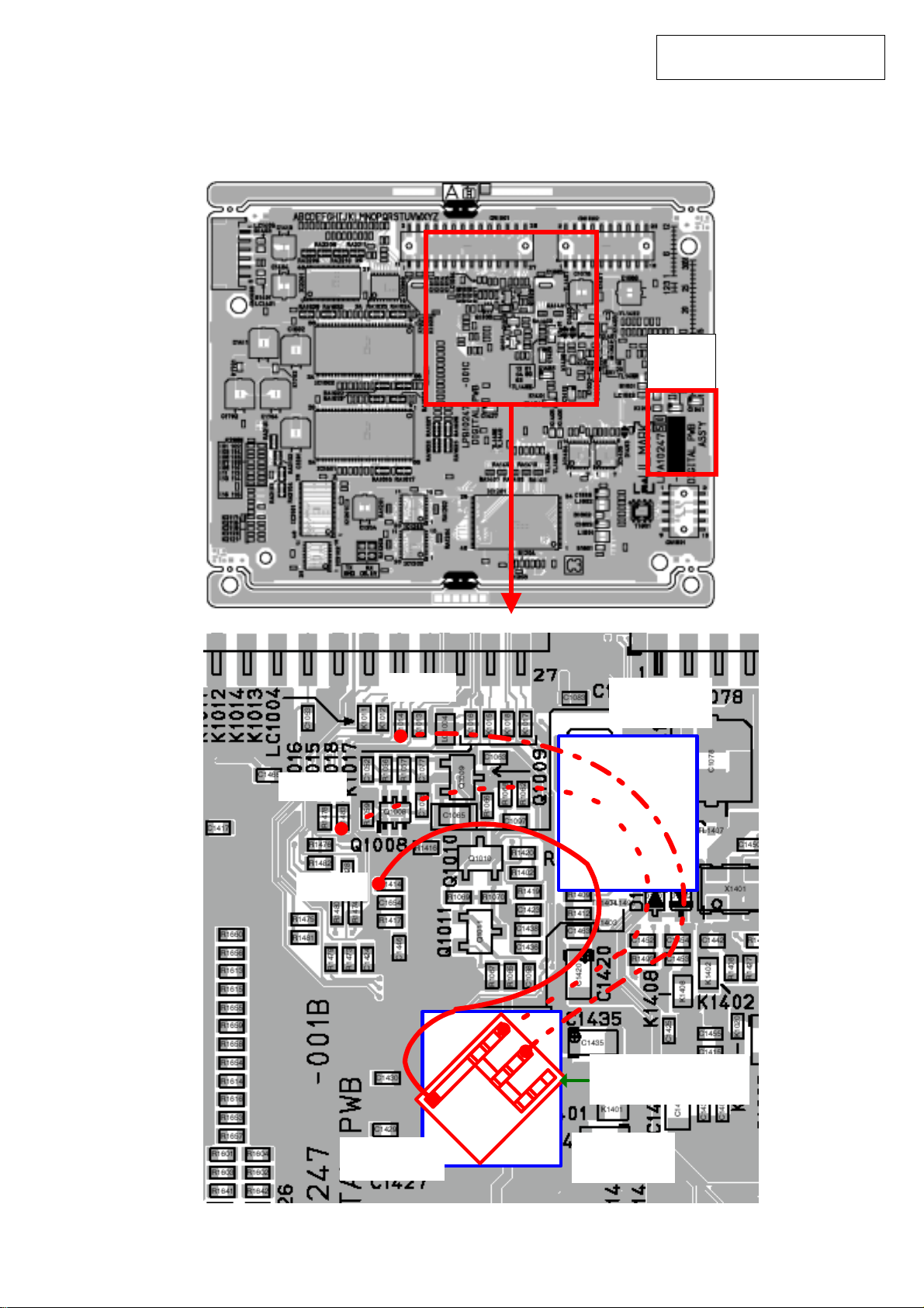
No.
YB-SB-00005-5 9/9
C) Add a SUB PWB ASSY (LPA20044-001A) on the DIGITAL BOARD ASSY as shown
below.
#500SPACER: PU59915- 105( 100pcs/1sheet)
ASSY
No.
K1014
#500
SPACER
R1483
R1414
LPA20044
-001A
REMOVE THE WIRE
AT THIS POINT.
#500
SPACER
Page 85

REVISED
K
K
A
No.
YB-SB-00018-2 1/4
SUBJECT:
COUNTERMEASURE FOR DRY UP OF E CAP
DATE:
MAY, 2005
Model & Manual No. Performed at factory Priority
Shown below
Reference Information
( ) S. All Products.
( ) A. Items in JVC/Dealer stock/Servic e return goods.
( ) B. JVC stock/Units returned for service.
( ! ) C. Sold items returned for service.
( ) D. Only Units related to this bulletin.
( ) E. Others.
<Models>
DR-MV1SUS : No. YD006 DR-MV1SEU : No. YD014
DR-MV1SUC : No. YD006 DR- MV1BEU : No. YD014
DR-MV1SUJ : No. YD022 DR-MV1SE
SR-MV30US : No. YD012 DR-MV1BE
DR-MV1SA
: No. YD036 DR- MV1SEF : No. YD014
DR-MV1SAS : No. YD036
: No. YD014
: No. YD014
<Symptom>
The unit becomes the loading sutiation.
<Cause>
In REGULATOR ASSEMBLY, C5205, C5206 and C5207 is heated by D5205 and D5208, then C5205,
C5206 and C5207 dry up.
ATTACHM ENT
( ) NONE ( ) EXPLODED VIEW ( ) ADJUSTMENT PROCEDURE
( ) SCHEMATIC DIAGRAM ( ) COMPONENT/PWB LAYOUT ( ! ) SEE NEXT PAGE
VICTOR COMPANY OF JAPAN, LIMITED
AV & MULTIMEDIA COMPANY, GLOBAL QUALITY MANAGEMENT DEPARTMENT,
CUSTOMER SATISFACTION CENTER [1∴3∴0∴0∴0]
12, 3-chome, Moriya-cho, Kanagawa-ku, Yokohama, Kanagawa, 221-8528, Japan TEL:+81-45-450-2552 FAX:+81-45-450-2558
Page 86

No.
YB-SB-00018-2 2/4
<Service measure>
1. Displacement of D5205 and D5208
Mobilize D5205 and D5208 from COMPONENT SIDE to FOIL SIDE as shown below.
Page 87

2. Change of C5205, C5206 and C5207
Change C5205, C5206 and C5207 as shown below.
Page Ref. No. Previous Part No. New Part No. Part Name
3-6
3-6
3-7
3-8
3-8
3-8
C5205
C5206
C5207
C5205
C5206
C5207
QEMT1AM-128
QECS1AM-128
QECS0JM-158
DR-MV1SUS :
DR-MV1SUC :
SR-MV30US :
QEMT1AM-128
QECS1AM-128
QECS0JM-158
DR-MV1SUJ :
DR-MV1SAA :
DR-MV1SAS :
QECS1AM-158
or
QECP1AM-158
or
QTM91AM-158
QECS1AM-158
or
QECP1AM-158
or
QTM91AM-158
QECS0JM-478
or
QECP0JM-478
or
QTM90JM-478
No. YD006
No. YD006
No. YD012
QECS1AM-158
or
QECP1AM-158
or
QTM91AM-158
QECS1AM-158
or
QECP1AM-158
or
QTM91AM-158
QECS0JM-478
or
QECP0JM-478
or
QTM90JM-478
No. YD022
No. YD036
No. YD036
E CAPACITOR
E CAPACITOR
E CAPACITOR
E CAPACITOR
E CAPACITOR
E CAPACITOR
No.
YB-SB-00018-2 3/4
FOB
(New Part)
-
-
-
-
-
-
Itg Rsn Note
C
C
C
C
C
C
B
B
B
B
B
B
-
-
-
-
-
-
Page 88
No.
YB-SB-00018-2 4/4
Page Ref. No. Previous Part No. New Part No. Part Name
3-9
3-9
3-9
C5205
C5206
C5207
QEMT1AM-128
QECS1AM-128
QECS0JM-158
DR-MV1SEU :
DR-MV1BEU :
DR-MV1SEK :
DR-MV1BEK :
DR-MV1SEF :
QECS1AM-158
or
QECP1AM-158
or
QTM91AM-158
QECS1AM-158
or
QECP1AM-158
or
QTM91AM-158
QECS0JM-478
or
QECP0JM-478
or
QTM90JM-478
No. YD014
No. YD014
No. YD014
No. YD014
No. YD014
E CAPACITOR
E CAPACITOR
E CAPACITOR
FOB
(New Part)
Itg: INTERCHANGEABILITY Rsn: REASON FOR CHANGE
A. Completely interchangeable.
B. Previous part can be used for new set, but
new part cannot be used for previous set.
C. New part can be used for previous set, but
previous part cannot be used for new set.
D. Not interchangeable.
E. Addition.
F. Deletion.
A. To improve performance
B. To improve reliability
C. To improve safety
D. To improve productivity
Itg Rsn Note
-
-
E. Standardization of part
F. For your demand
G. Correction of misprint
H. Others
C
B
C
B
C
B
-
-
-
<Product>
Above counter measure had been enforced from MAY 2005.
 Loading...