

Page 1
CY2907
Single-PLL General-Purpose
EPROM Programmable Clock Generator
Features Benefits
Single phase-locked loop architecture Generates a custom frequency from an external source
EPROM programmability Easy customization and fast turnaround
Factory-programmable (CY2907, CY2907I) or field-pro-
grammable (CY2907F & CY2907FI) device options
Up to two configurable outputs Provides clocking requirem en ts from a singl e devi ce
Low-skew, low-jitter, high-accuracy outputs Meets critical industry standard timing requirements
Power management (Power-Down, OE) Supports low-power applications
Frequency select option Up to 16 user-selectable frequencies
Configurable 5V or 3.3V operation Supports industry-standard design platforms
8-pin or 14-pin SOIC packages Industry-standard packaging saves on board space
Selector Guide
Part Number Outputs Input Frequency Range Output Frequency Range Specifics
CY2907 2 10 MHz–25 MHz (e xternal crystal)
CY2907I 2 10 MHz–25 MHz (external crystal)
CY2907F8
CY2907F14
CY2907F8I
CY2907F14I
1 MHz–30 MHz (reference clock)
1 MHz–30 MHz (reference clock)
210 MHz–25 MHz (external crystal)
1 MHz–30 MHz (reference clock)
210 MHz–25 MHz (external crystal)
1 MHz–30 MHz (reference clock)
Programming support available for all opportunities
500 kHz–130 MHz (5V)
500 kHz–100 MHz (3.3V)
500 kHz–100 MHz (5V)
500 kHz–80 MHz (3.3V)
500 kHz–100 MHz (5V)
500 kHz–80 MHz (3.3V)
500 kHz–90 MHz (5V)
500 kHz–66.66 MHz (3.3V)
Factory Programmable
Commercial Temperature
Factory Programmable
Industrial Temperature
Field Programmable
Commercial Temperature
Field Programmable
Industrial Temperature
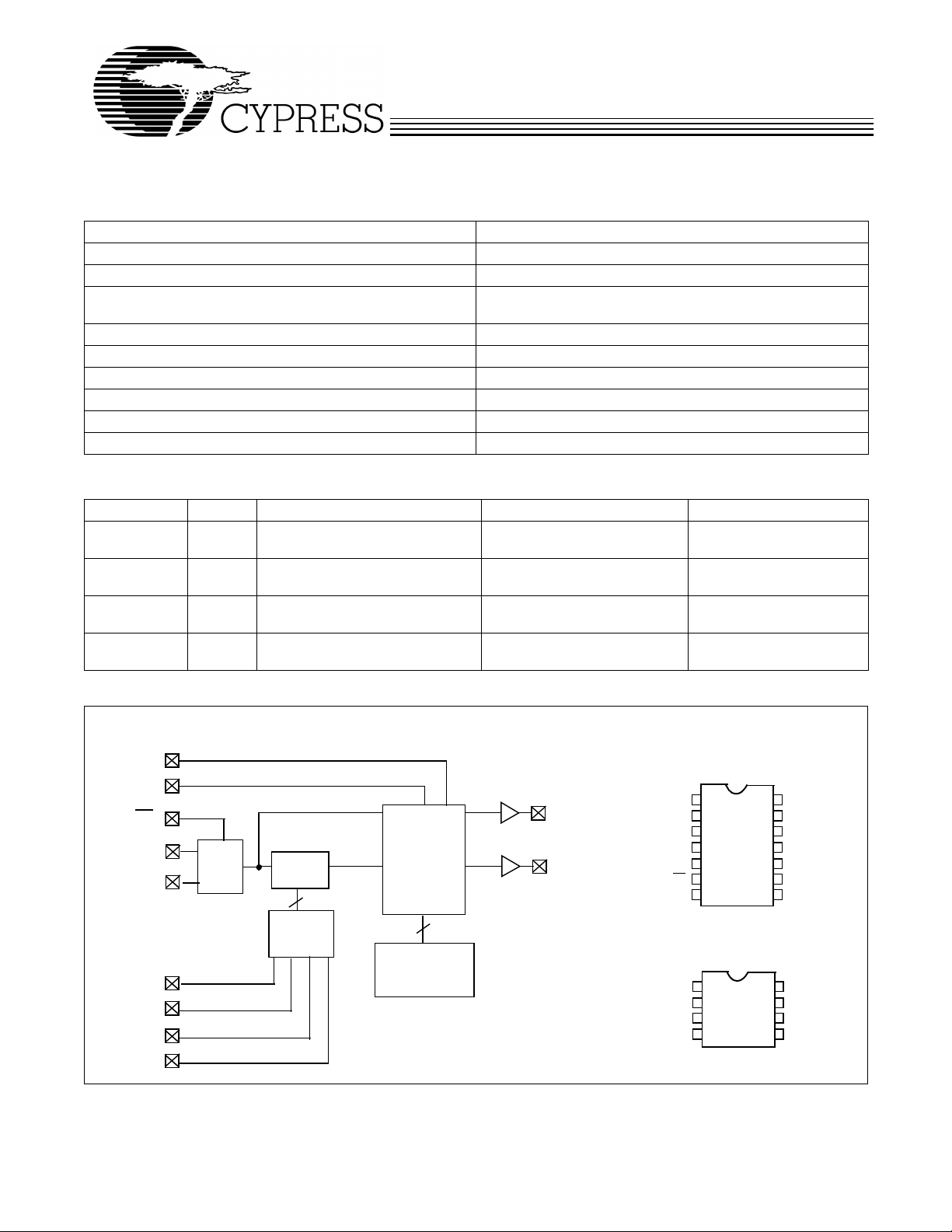
Logic Block Diagram
OEA
OER
PD
XTALIN
OSC.
PLL
XTALOUT
EPROM
Table
S0
S1
S2
S3
CyClocks is a trademark of Cypress Semiconductor Corporation.
Output
Multiplexer
and
Dividers
Configuration
EPROM
Test Logic
and
REFCLK
CLKA
Pin Configurations
Top View
14-Pin SOIC
S1
S2
S3
V
SS
V
SS
PD
XTALIN
S0
V
SS
XTALIN
XTALOUT
1
2
3
4
5
6
7
8-Pin SOIC
1
2
3
4
14
13
12
11
10
9
8
8
7
6
5
S0
REFCLK
V
DD
CLKA
OEA
OER
XTALOUT
REFCLK
V
DD
CLKA
S1
Cypress Semiconductor Corporation • 3901 North First Street • San Jose • CA 95134 • 408-943-2600
Document #: 38-07137 Rev. ** Revised September 26, 2001
Page 2
CY2907
Pin Summary
Pin Number
Name
S1 1 5 Frequency Select (CLKA) (Internal pull-up resistor to VDD)
S2 2 NA Frequency Select (CLKA) (Internal pull-up resistor to VDD)
S3 3 NA Frequency Select (CLKA) (Internal pull-up resistor to VDD)
V
SS
V
SS
4 2 Ground
5 NA Ground
PD 6 NA Power-Down (active LOW) (Internal pull-up resistor to VDD)
XTALIN
XTALOUT
[1]
[1, 2]
7 3 Reference Crystal Input
8 4 Reference Crystal Feedback
OER 9 NA REFCLK Output Enable (active HIGH) (Internal pull-up resistor to VDD)
OEA 10 NA CLKA Output Enable (active HIGH) (Internal pull -up resistor to VDD)
CLKA 11 6 Clock Output
V
DD
12 7 Voltage Supply
REFCLK 13 8 Reference Clock Output (Default, can be driven by PLL if desired)
S0 14 1 Frequency Select (CLKA) (Internal pull-up resistor to VDD)
Notes:
1. For best accuracy, use a parallel-resonant crystal, C
2. Float XTALOUT pin if XTALIN is driven by reference clock (as opposed to crystal).
LOAD
≈ 17 pF.
Description14-Pin SOIC 8-Pin SOIC
Functional Description
The CY2907 is a general-purpose Clock Generator designed
for use in a wide variety of applications—from graphics to PC
peripherals to dis k drives. It genera tes selectable sy stem clock
frequencies from a sing le re ference i nput (c rysta l or referenc e
clock). The CY2907 is co nfigured with an EPROM a rray , much
like the other devices in the Cypress EPROM Programmable
Clock Family, making it easily customizable for any application. Furthermore, the CY2907 is compatible with all industry-standard 9107 and 9108 clock synthesizers.
CyClocks™ Software
CyClocks is an easy-to-use software application that allows
you to configure any one of the EPROM Programmable Clocks
offered by Cypress . You may specify the input frequency, PLL
and output frequencies, and different functional options.
Please note the output frequency ranges in this data sheet
when specifying them in CyClocks to ensure that you stay
within the limits. Y ou can down load a copy of CyCloc ks free on
the Cypress Semiconductor website at www.cypress.com.
Consider using the CY2081, CY2291, or CY2292 for applications that require unrelated and multiple output frequencies.
Consider using the CY2071A for applications that require
more than one output clock.
Cypress FTG Programmer
The Cypress Frequency Timing Generator (FTG) Programmers are portable programmers designed to custom program
our family of EPROM Field Programmable Clock Devices.
The FTG programmers connect to a PC serial port and allow
users of CyClocks so ftware t o quickly and eas ily pro gram an y
of the CY2291F, CY2292F , CY2 071AF , and CY2 907F devices.
The ordering code for the Cypress FTG Programmer is
CY3670.
Maximum Ratings
(Beyond which the useful life may be impaired. For u ser guidelines, not tested.)
Supply Voltage .................................................–0.5 to +7.0V
Input Voltage ...........................................–0.5V to V
Storage Temperature (Non-Condensing)... –65°C to +150°C
Max. Soldering Temperature (10 sec)...................... +260°C
Junction Temperature............................................... +150°C
Static Discharge Voltage ...........................................>2000V
(per MIL-STD-883, Method 3015)
DD
+0.5V
Document #: 38-07137 Rev. ** Page 2 of 10
Page 3
CY2907
Operating Conditions
[3]
Parameter Description Min. Max. Unit
V
DD
Supply Voltage, 5V Operation 4.5 5.5 V
Supply Voltage, 3.3V Operation 3.0 3.6 V
T
A
Commercial Operating Temperature, Ambient 0 70 °C
Industrial Operating Temperature, Ambient –40 85 °C
C
L
f
REF
Electrical Characteristics at 5.0 V Commercial V
Max. Capacitive Load 15 pF
External Reference Crystal 10.0 25.0 MHz
External Reference Clock
[4, 5]
= 4.5V to 5.5V, TA = 0°C to +70°C
DD
1.0 30.0 MHz
Parameter Description Test Conditions Min. Max. Unit
V
V
V
V
I
I
I
I
I
I
I
R
OH
OL
IH
IL
DD
DD
DD
IH
IL
OH
OL
PU
[4]
[4]
[4]
[4]
[5]
[4]
High-level Input Voltage Except Crystal Inputs 2.0 V
Low-level Input Voltage Except Crystal Inputs 0.8 V
High-level Output Voltage VDD = VDD Min. IOH = –30 mA CLKA 2.4 V
Low-level Output Voltage VDD = VDD Min. IOL = 10 mA CLKA 0.4 V
Output High Current VOH = 2.0V –35 mA
Output Low Current V
Input High Current VIH = V
= 0.8V 22 mA
OL
DD
–2 2 µA
Input Low Current VIL = 0V 20 µA
Power Supply Current PD HIGH, CLKA = 50 MHz 42 mA
Power Supply Current PD LOW, Logic Inputs LOW 100 µA
Power Supply Current PD LOW, Logic Inputs HIGH 40 µA
Pull-up Resistor V
IN = VDD
– 1.0 V 700 kΩ
Electrical Characteristics at 3.3 V Commercial V
= 3.0V to 3.6V, TA = 0°C to +70°C
DD
Parameter Description Test Conditions Min. Max. Unit
V
IH
V
IL
[4]
V
OH
[4]
V
OL
[4]
I
OH
[4]
I
OL
I
IH
I
IL
[5]
I
DD
I
DD
I
DD
[4]
R
PU
Notes:
3. Electrical parameters are guaranteed with these operating conditions.
4. Guaranteed by design, not 100% tested in production.
5. Load = max. typical configuration, f
I
(mA) = VDD * (6.25 + (0.055*F
DD
High-level Input Voltage Except Crystal Inputs 0.7*V
DD
Low-level Input Voltage Except Crystal Inputs 0.2*V
High-level Output Voltage CLKA, I
–5 mA 0.85*V
OH =
DD
Low-level Output Voltage CLKA, IOL = 6 mA 0.1*V
Output High Current V
Output Low Current V
Input High Current VIH = V
OH
OL
= 0.7*V
= 0.2*V
DD
DD
DD
–10 mA
15 mA
–2 2 µA
DD
DD
V
V
V
V
Input Low Current VIL = 0V 10 µA
Power Supply Current PD HIGH, CLKA = 50 MHz 40 mA
Power Supply Current PD LOW, Logic Inputs LOW 40 µA
Power Supply Current PD LOW, Logic Inputs HIGH 12 µA
Pull-up Resistor V
= 14.318 MHz. Specific configurations may vary. A close approximation of IDD can be derived by the following formula:
REF
) + (0.0017*C
REF
IN = VDD
LOAD
– 0.5V 900 kΩ
*(F
+ REFCLK))). C
CLKA
is specified in pF and F is specified in MHz.
LOAD
Document #: 38-07137 Rev. ** Page 3 of 10
Page 4
CY2907
Electrical Characteristics at 5.0V Industrial V
= 4.5V to 5.5V, TA = –40°C to +85°C
DD
Parameter Description Test Conditions Min. Max. Unit
V
IH
V
IL
[4]
V
OH
[4]
V
OL
[4]
I
OH
[4]
I
OL
I
IH
I
IL
[5]
I
DD
I
DD
I
DD
[4]
R
PU
Electrical Characteristics at 3.3V Industrial V
High-level Input Voltage Except Crystal Inputs 2.0 V
Low-level Input Voltage Except Crystal Inputs 0.8 V
High-level Output Voltage VDD = VDD Min. IOH = –30 mA CLKA 2.4 V
Low-level Output Voltage VDD = VDD Min. IOL = 10 mA CLKA 0.4 V
Output High Current VOH = 2.0V –45 mA
Output Low Current V
Input High Current VIH = V
= 0.8V 20 mA
OL
DD
–2 2 µA
Input Low Current VIL = 0V 20 µA
Power Supply Current PD HIGH, CLKA = 50 MHz 54 mA
Power Supply Current PD LOW, Logic Inputs LOW 110 µA
Power Supply Current PD LOW, Logic Inputs HIGH 45 µA
Pull-up Resistor V
IN = VDD
– 1.0 V 700 kΩ
= 3.0V to 3.6V, TA = –40°C to +85°C
DD
Parameter Description Test Conditions Min. Max. Unit
V
V
V
V
I
I
I
I
I
I
I
R
OH
OL
IH
IL
DD
DD
DD
IH
IL
OH
OL
PU
[4]
[4]
[4]
[4]
[5]
[4]
High-level Input Voltage Except Crystal Inputs 0.7*V
Low-level Input Voltage Except Crystal Inputs 0.2*V
High-level Output Voltage CLKA, I
–5 mA 0.85*V
OH =
Low-level Output Voltage CLKA, IOL = 6 mA 0.1*V
Output High Current V
Output Low Current V
Input High Current VIH = V
OH
OL
= 0.7*V
= 0.2*V
DD
DD
DD
DD
DD
DD
DD
–12 mA
14 mA
–22µA
Input Low Current VIL = 0V 10 µA
Power Supply Current PD HIGH, CLKA = 50 MHz 50 mA
Power Supply Current PD LOW, Logic Inputs LOW 50 µA
Power Supply Current PD LOW, Logic Inputs HIGH 15 µA
Pull-up resistor V
IN = VDD
– 0.5V 900 kΩ
V
V
V
V
Document #: 38-07137 Rev. ** Page 4 of 10
Page 5

CY2907
Switching Characteristics at 5.0V Commercial
Parameter Output
t
R
t
F
t
R
t
F
t
D
F
F
F
t
JIS
t
JIS
t
JIS
t
JAB
t
JAB
t
JAB
t
PU
t
FT
I
I
O
CLKA Output Rise Time 0.8V to 2.0V 15-pF Load 1.40 ns
CLKA Output Fall Time 2.0V to 0.8V 15-pF Load 1.00 ns
CLKA Output Rise Time 20% to 80% 15-pF Load 3.5 ns
CLKA Output Fall Time 80% to 20% 15-pF Load 2.5 ns
CLKA Duty Cycle 15-pF Load at 1.4V 45.0 55.0 %
XTALIN Input Frequency Crystal Oscillator 10 25 MHz
XTALIN Input Frequency External Input Clock
CLKA Output Frequency CY2907, 15-p F Load 0.5 130.0 MHz
CLKA Jitter (One Sigma) 20 MHz to 130 MHz 150 ps
CLKA Jitter (One Sigma) 14 MHz to 20 MHz 200 ps
CLKA Jitter (One Sigma) Less than 14 MHz 1 %
CLKA Jitter (Absolute) 20 MHz to 130 MHz –250 + 250 ps
CLKA Jitter (Absolute) 14 MHz to 20 MHz –500 + 500 ps
CLKA Jitter (Absolute) Less than 14 MHz 3 %
CLKA Transition Time 8 MHz to 66.6 MHz 13 ms
[6]
Description Test Conditions Min. Max. Unit
Power-up Time 18 ms
[4]
[7]
1 30 MHz
CY2907F, 15-pF Load 0.5 100.0 MHz
Switching Characteristics at 3.3V Commercial
Parameter Output
t
R
t
F
t
D
F
I
F
I
F
O
CLKA Output Rise Time 20% to 80% 15-pF Load 3.5 ns
CLKA Output Fall Time 80% to 20% 15-pF Load 2.5 ns
CLKA Duty Cycle 15-pF Load at 1.4V 40.0 53.0 %
XTALIN Input Frequency Crystal Oscillator 10 25 MHz
XTALIN Input Frequency External Input Clock
CLKA Output Frequency CY2907, 15-pF Load 0.5 100.0 MHz
[6]
Description Test Conditions Min. Max. Unit
[4]
[7]
CY2907F, 15-pF Load 0.5 80.0 MHz
t
JIS
t
JIS
t
JIS
t
JAB
t
JAB
t
JAB
t
PU
t
FT
Notes:
6. REFCLK output can also be configured to be driven by the PLL, in which case the above characteristics are valid.
7. Please refer to the application note “Crystal Oscillator Topics” when using an external reference clock as an input frequency source.
CLKA Jitter (One Sigma) 25 MHz to 100 MHz 150 ps
CLKA Jitter (One Si gma) 14 MHz to 25 MHz 200 ps
CLKA Jitter (One Sigma) Less than 14 MHz 1 %
CLKA Jitter (Absolute) 25 MHz to 120 MHz –250 +250 ps
CLKA Jitter (Absolute) 14 MHz to 25 MHz –500 +500 ps
CLKA Jitter (Absolute) Less than 14 MHz 3 %
Power-up Time 18 ms
CLKA Transition Time 8 MHz to 66.6 MHz 13 ms
130MHz
:
Document #: 38-07137 Rev. ** Page 5 of 10
Page 6

Switching Characteristics at 5.0V Industrial
Parameter Output
t
R
t
F
t
R
t
F
t
D
F
F
F
t
JIS
t
JIS
t
JIS
t
JAB
t
JAB
t
JAB
t
PU
t
FT
I
I
O
CLKA Output Rise Time 0.8V to 2.0V 15-pF Load 1.40 ns
CLKA Output Fall Time 2.0V to 0.8V 15-pF Load 1.00 ns
CLKA Output Rise Time 20% to 80% 15-pF Load 3.5 ns
CLKA Output Fall Time 80% to 20% 15-pF Load 2.5 ns
CLKA Duty Cycle 15-pF Load at 1.4V 45.0 55.0 %
XTALIN Input Frequency Crystal Oscillator 10 25 MHz
XTALIN Input Frequency External Input Clock
CLKA Output Frequency CY2907, 15-pF Load 0.5 100.0 MHz
CLKA Jitter (One Sigma) 20 MHz to 130 MHz 150 ps
CLKA Jitter (One Sigma) 14 MHz to 20 MHz 200 ps
CLKA Jitter (One Sigma) Less than 14 MHz 1 %
CLKA Jitter (Absolute) 20 MHz to 130 MHz –250 + 250 ps
CLKA Jitter (Absolute) 14 MHz to 20 MHz –500 + 500 ps
CLKA Jitter (Absolute) Less than 14 MHz 3 %
CLKA Transition Time 8 MHz to 66.6 MHz 13 ms
[6]
Description Test Conditions Min. Max. Unit
Power-up Time 18 ms
CY2907
[7]
CY2907F, 15-pF Load 0.5 90 MHz
1 30 MHz
Switching Characteristics at 3.3V Industrial
Parameter Output
t
R
t
F
t
D
F
F
F
t
JIS
t
JIS
t
JIS
t
JAB
t
JAB
t
JAB
t
PU
t
FT
I
I
O
CLKA Output Rise Time 20% to 80% 15-pF Load 3.5 ns
CLKA Output Fall Time 80% to 20% 15-pF Load 2.5 ns
CLKA Duty Cycle 15-pF Load at 1.4V 40.0 53.0 %
XTALIN Input Frequency Crystal Oscillator 10 25 MHz
XTALIN Input Frequency External Input Clock
CLKA Output Frequency CY2907I, 15-pF Load 0.5 80.0 MHz
CLKA Jitter (One Sigma) 25 MHz to 100 MHz 150 ps
CLKA Jitter (One Sigma) 14 MHz to 25 MHz 200 ps
CLKA Jitter (One Sigma) Less than 14 MHz 1 %
CLKA Jitter (Absolute) 25 MHz to 120 MHz –250 +250 ps
CLKA Jitter (Absolute) 14 MHz to 25 MHz –500 +500 ps
CLKA Jitter (Absolute) Less than 14 MHz 3 %
CLKA Transition Time 8 MHz to 66.6 MHz 13 ms
[6]
Description Test Conditions Min. Max. Unit
Power-up Time 18 ms
[7]
1 30 MHz
CY2907FI, 15-pF Load 0.5 66.6 MHz
Document #: 38-07137 Rev. ** Page 6 of 10
Page 7

Switching Waveforms
Frequency Select Change (Transition Time)
CY2907
SELECT
CLKA
OLD SELECT NEW SELECT STABLE
F
Duty Cycle Timing
tD=t
÷ t
2
1
CLKA
1.4V
All Outputs Rise/Fall Time
CLKA
old
t
20%
R
80%
t
FT
t
1
t
2
F
new
2907–4
2907–3
2907–5
t
F
2907–6
Test Circuit
V
DD
V
DD
0.1 µF
Note: All capacitorsshould be placed as close to each pin as
Document #: 38-07137 Rev. ** Page 7 of 10
CLKA
REFCLK
C
C
LOAD
OUTPUTS
LOAD
possible.
Page 8

CY2907
Ordering Information
Ordering Code Package Name Package Type Operating Range
CY2907SC-xxx S8, S14 8-pin or 14-pin SOIC 5.0V, Commercial, Fact ory Programmable
CY2907SL-xxx S8, S14 8-pin or 14-pin SOIC 3.3V, Commercia l, Factory Programmable
CY2907SI-xxx S8, S14 8-pin or 14-pin SOIC 5.0V/3.3V, Industrial, Factory Programmable
CY2907F8 S8 8-pin SOIC 5.0V/3.3V, Commercial, Field Programmable
CY2907F8I S8 8-pin SOIC 5.0V/3.3V, Industrial, Field Programmable
CY2907F14 S14 14-pin SOIC 5.0V/3.3V, Commercial, Field Programmable
CY2907F14I S14 14-pin SOIC 5.0V/3.3V, Industrial, Field Programmable
CY3670 Cypress FTG Programmer Custom Programming for Field Programmable
Package Characteristics
Package θ
8-pin SOIC 170 35 5436
14-pin SOIC 140 31 5436
(C/W) θ
JA
Clocks
(C/W) Transistor Count
JC
Package Diagrams
8-Lead (150-Mil) SOIC S8
51-85066-A
Document #: 38-07137 Rev. ** Page 8 of 10
Page 9

ng so indemnifies Cypress Semiconductor against all charges.
Package Diagrams (continued)
CY2907
14-Lead (150-Mil) SOIC S14
51-85067-A
Document #: 38-07137 Rev. ** Page 9 of 10
© Cypress Semiconductor Corporation, 2001. The information contained herein is subject to change without notice. Cypress Semiconductor Corporation assumes no responsibility for the use
of any circuitry other than circuitry embodied in a Cypress Semiconductor product. No r does it convey or imply any license under patent or other rights. Cypress Semiconductor does not autho rize
its products for use as critical components in life-support systems where a malfunction or failure may reasonably be expected to result in significant injury to the user. The inclusion of Cypress
Semiconductor products in life-support systems application implies that the manufacturer assume s all risk of such use and in doi
Page 10

Document Title: CY2907 Single-PLL General-Purpose EPROM Programmable Clock Generator
Document Number: 38-07137
REV. ECN NO.
** 110246 12/18/01 SZV Change from Spec number: 38-00505 to 38-07137
Issue
Date
Orig. of
Change Description of Change
CY2907
Document #: 38-07137 Rev. ** Page 10 of 10
Page 11

This datasheet has been download from:
www.datasheetcatalog.com
Datasheets for electronics components.
 Loading...