

Page 1
SERVICE MANUAL
CD CHANGER
CH-X470RF
CH-X470RF
CH-X470RF is a combination of CH-X470 and KS-RF50.
KS-RF50 is a combination of Remote control and the RF unit.
Contents
Safety precaution
Preventing static electricity
Disassembly method
Forced eject procedures
C
O
MP
A
C
T
D
IS
C
C
H
A
N
G
E
R
1
2
–
D
IS
CH-X470
C
KS-RF50
Area Suffix
J ------ Northern America
1-2
1-3
1-4
1-20
Trouble shooting
Flow of functional
operation until TOC read
Description of major ICs
1-21
1-23
1-27
COPYRIGHT 2001 VICTOR COMPANY OF JAPAN, LTD.
No.49668
Dec. 2001
Page 2
CH-X470RF
Safety precaution
!
!
Burrs formed during molding may be left over on some parts of the chassis. Therefore,
pay attention to such burrs in the case of preforming repair of this system.
Please use enough caution not to see the beam directly or touch it in case of an
adjustment or operation check.
1-2
Page 3
CH-X470RF
Preventing static electricity
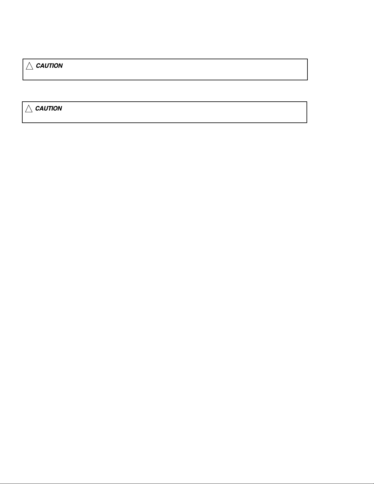
1.Grounding to prevent damage by static electricity
Electrostatic discharge (ESD), which occurs when static electricity stored in the body, fabric, etc. is discharged,
can destroy the laser diode in the traverse unit (optical pickup). Take care to prevent this when performing repairs.
2.About the earth processing for the destruction prevention by static electricity
Static electricity in the work area can destroy the optical pickup (laser diode) in devices such as CD players.
Be careful to use proper grounding in the area where repairs are being performed.
2-1 Ground the workbench
Ground the workbench by laying conductive material (such as a conductive sheet) or an iron plate over
it before placing the traverse unit (optical pickup) on it.
2-2 Ground yourself
Use an anti-static wrist strap to release any static electricity built up in your body.
(caption)
Anti-static wrist strap
Conductive material
(conductive sheet) or iron plate
3. Handling the optical pickup
1. In order to maintain quality during transport and before installation, both sides of the laser diode on the
replacement optical pickup are shorted. After replacement, return the shorted parts to their original condition.
(Refer to the text.)
2. Do not use a tester to check the condition of the laser diode in the optical pickup. The tester's internal power
source can easily destroy the laser diode.
4.Handling the traverse unit (optical pickup)
1. Do not subject the traverse unit (optical pickup) to strong shocks, as it is a sensitive, complex unit.
2. Cut off the shorted part of the flexible cable using nippers, etc. after replacing the optical pickup. For specific
details, refer to the replacement procedure in the text. Remove the anti-static pin when replacing the traverse
unit. Be careful not to take too long a time when attaching it to the connector.
3. Handle the flexible cable carefully as it may break when subjected to strong force.
4. It is not possible to adjust the semi-fixed resistor that adjusts the laser power. Do not turn it
Attention when traverse unit is decomposed
*Please refer to "Disassembly method" in the text for pick-up and how to
detach the substrate.
1.Solder is put up before the card wire is removed from connector on
the CD substrate as shown in Figure.
(When the wire is removed without putting up solder, the CD pick-up
assembly might destroy.)
2.Please remove solder after connecting the card wire with
when you install picking up in the substrate.
Traverse mechanism PCB Ass'y
Pickup unit
Soldering
1-3
Page 4
CH-X470RF
Disassembly method
Perform operations according to the items to be
disassembled.
<Replacement of the pickup>
1.
After removing the exterior (top and bottom).
2.
Proceed to the pickup replacement section.
3.
When applying grease, refer to the exploded view.
Use new grease.
<Mechanism section>
1.
Remove the exterior (required section only).
2.
The mechanism section is designed so that each unit
can be removed separately.
3.
When reassembling, refer to the assembling
precautions. (Use new grease when applying grease.)
B
B
Bottom cover
Knob
A
B
Fig. 1
B
Bottom cover
Remove A and turn in
the direction of the arrow.
BB
A
B
Knob
B
Exterior section
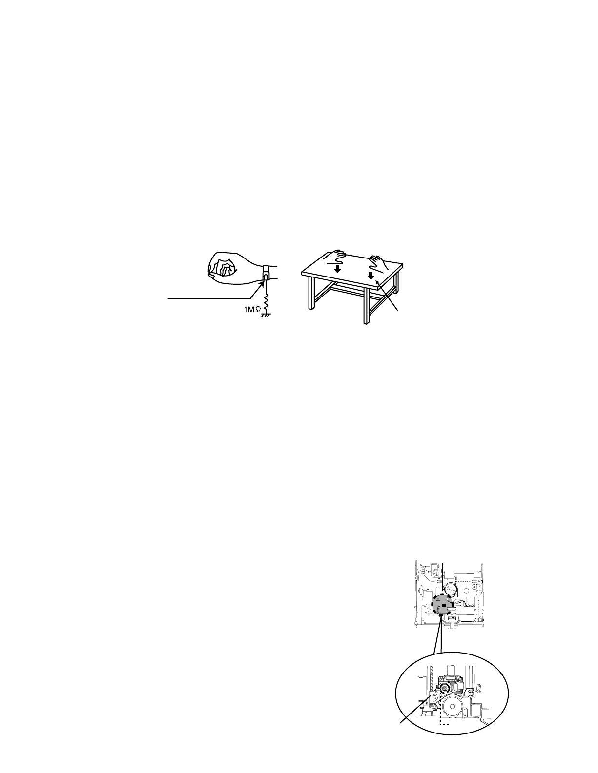
<
>
Removing the bottom cover and front
panel assembly
(See Fig.1 to 4)
Remove the two screw A to unlock the mounting
1.
direction knob located on the side of the main unit.
Turn the mounting direction knob in the direction of
2.
the arrow using a coin, etc. to remove it. (The knob
can be removed only when it is set to this position.)
Remove the four top cover fixing screws B at the
3.
triangle marks on the side of the main unit. (Perform
the same operation on both sides.)
Turn the unit upside down so the bottom surface is
4.
facing upward.
Lift the rear edge of the bottom cover slightly and lift
5.
the side by grasping the DIN jack section on the side
panel, then turn it toward the front (raise upward) to
remove the bottom cover.
Remove A and turn in
the direction of the arrow
The front panel can be
separated by raising the cover.
Unhook catches
Fig. 2
Fig. 3
Bottom cover
Slightly lift the jack
section to remove.
Unhook the four catches located on both sides of the
6.
front panel, and turn the front panel toward the top
cover (lower down) to remove the front panel.
1-4
Front panel
Unhook catches
Fig. 4
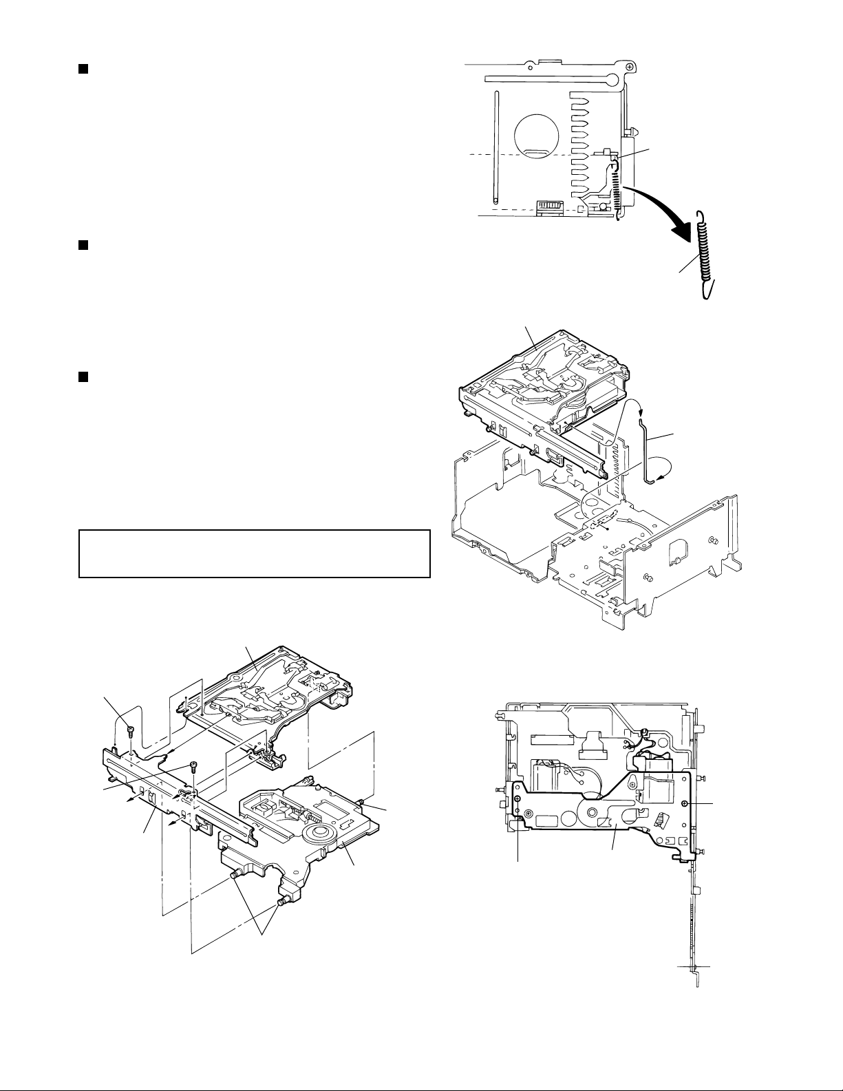
Page 5
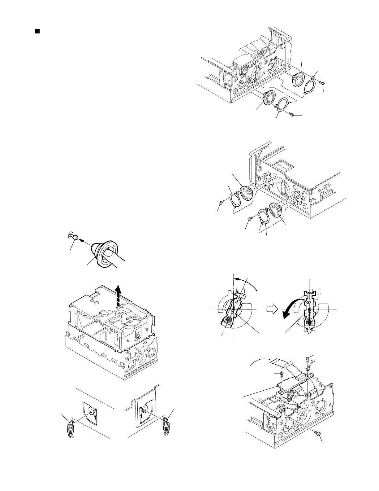
Removing the top cover
(See Fig.5 to 9)
Remove the four damper bracket fixing screws C to
1.
remove the damper brackets.
Pull out the dampers, being careful not to damage
2.
them.
When reattaching a damper, insert your finger to
push out the center of the damper to mount it on the
damper shaft, as shown in Fig. 6-1.
Turn the damper spring bracket toward the top at a
3.
right angle as shown in Fig. 7, then push down the
lower side of the damper spring bracket to lift it off.
Remove the three fixing screws D and E on the DIN
4.
jack board assembly.
Damper
Damper bracket
Fig. 5
CH-X470RF
Damper
Damper bracket
C
C
Lift the changer unit upward.
5.
Remove the damper springs from the mechanism
6.
chassis if required. To reassemble, refer to the
diagram below.
Apply alcohol to the shaft then immediately
attach the damper. (After attaching, check
that the shaft is correctly inserted.)
Damper shaft
Damper
Fig. 6-1
Push out with your finger
before attaching
Lift the changer unit upward
Damper
Damper bracket
C
Damper
C
Damper bracket
Fig. 6
Turn to the top position (at a right angle),
then push down to lift off.
Damper spring bracket
Fig. 7
E
Damper spring
Silver
(mechanism side)
Fig. 8
Mechanism
Chassis
How to attach the damper springs
Fig. 8-1
Damper spring
Black
(magazine side)
Remove the flexible ribbon
wire if required
DIN jack board
E
D
Fig. 9
1-5
Page 6
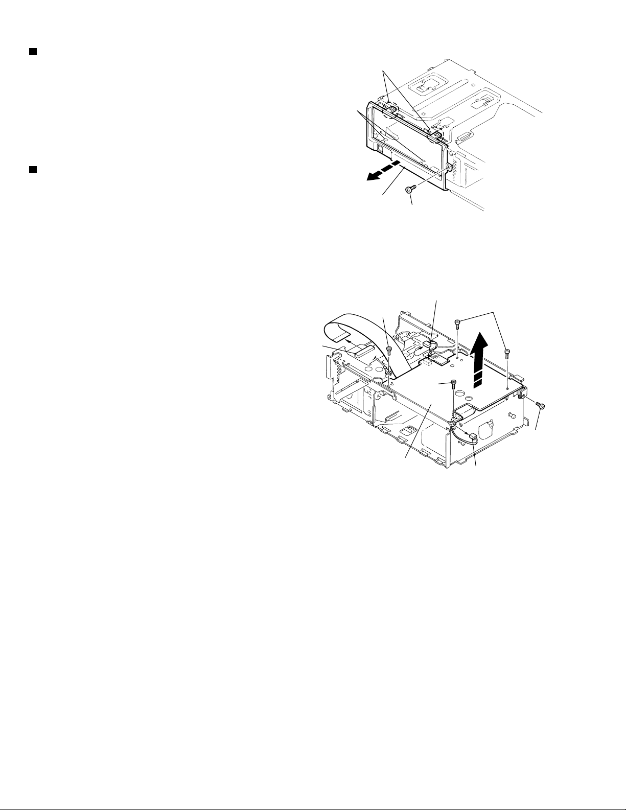
CH-X470RF
Removing the fittings
Remove the fixing screw F.
1.
Unhook the two catches a on the top edge of the
2.
fitting, then unhook the two catches b at the left /
right bottom edges.
(See Fig.10)
Removing the main PCB assembly
(See Fig.11)
Remove the power IC fixing screw G.
1.
Remove the four screws H securing the main board
2.
assembly.
Disconnect position motor wire connector CN504
3.
from the main board assembly.
Disconnect sensor board assembly wire connector
4.
CN601 from the main board assembly.
Remove the flexible ribbon wire from CN502 on the
5.
traverse mechanism board assembly.
When reinstalling the board boards, refer to the
reassembling procedures for protecting switches, etc.
CN502
Catches b
Catches a
Fitting
H
F
Fig. 10
CN601
H
H
Main board
Fig. 11
G
CN504
1-6
Page 7
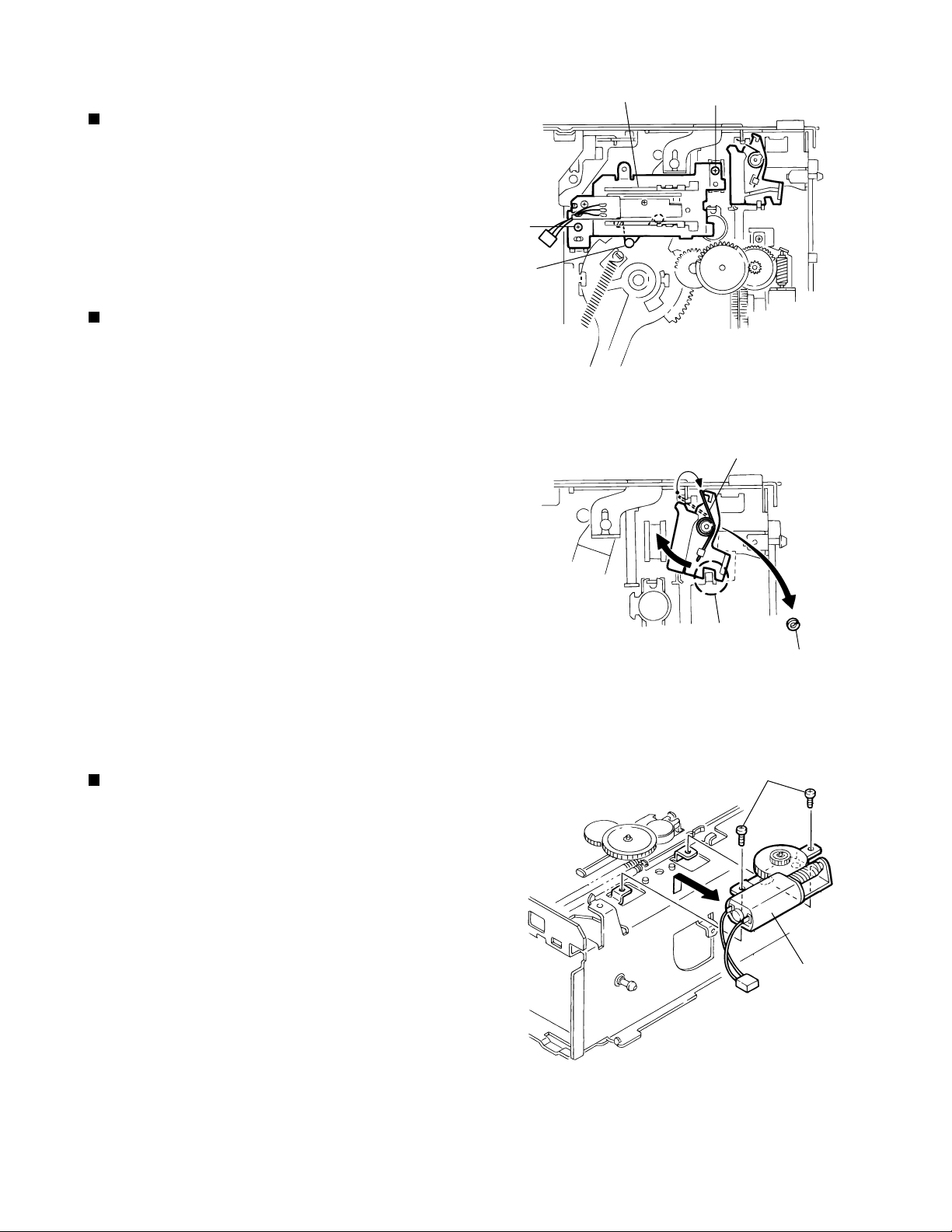
CH-X470RF
<Changer mechanism section>
Sensor assembly unit
Remove the two screws I securing the sensor
1.
assembly unit.
Unhook the spring on the back of the sensor
2.
assembly unit from the holes on the chassis.
Magazine lock arm
Remove the magazine lock spring from the front side
1.
of the chassis.
Remove the poly-washer c securing the magazine
2.
lock arm.
Turn the magazine lock arm in the direction of the
3.
arrow until the notch is at the d position to remove it
from the chassis.
(See Fig.12)
(See Fig.12 and 13)
I
Spring
Sensor assembly
Rear
I
Fig. 12
Magazine lock spring
Positioning motor assembly
(See Fig.14)
Remove the two screws J securing the positioning
1.
motor.
Slightly lift the positioning motor assembly to remove
2.
it from the two burrs on the chassis.
d
Poly-washer c
Fig. 13
J
Positioning
motor assembly
Fig. 14
1-7
Page 8
CH-X470RF
Rear slider
Position the unit with the front section facing down.
1.
Rotate the third gear located on the back of the main
unit in the direction of the arrow (clockwise).
Shift the rear slider in the direction of the arrow and
2.
remove it at the rear slider mounting position (at the
widest hole).
Front slider
Position the unit with the rear section facing down.
1.
Rotate the third gear located on the bottom of the
unit in the direction of the arrow (clockwise) until the
front slider is shifted to the outermost position.
Remove the E-washer securing the front slider to
2.
remove the front slider from the chassis
(See Fig.15)
(See Fig.16)
Can be removed at the stud position
(at the widest hole)
Shift
Third gear
Fig. 15
Fig. 16
Remove
Third gear
Remove the E-washer
Rear slider
Front slider
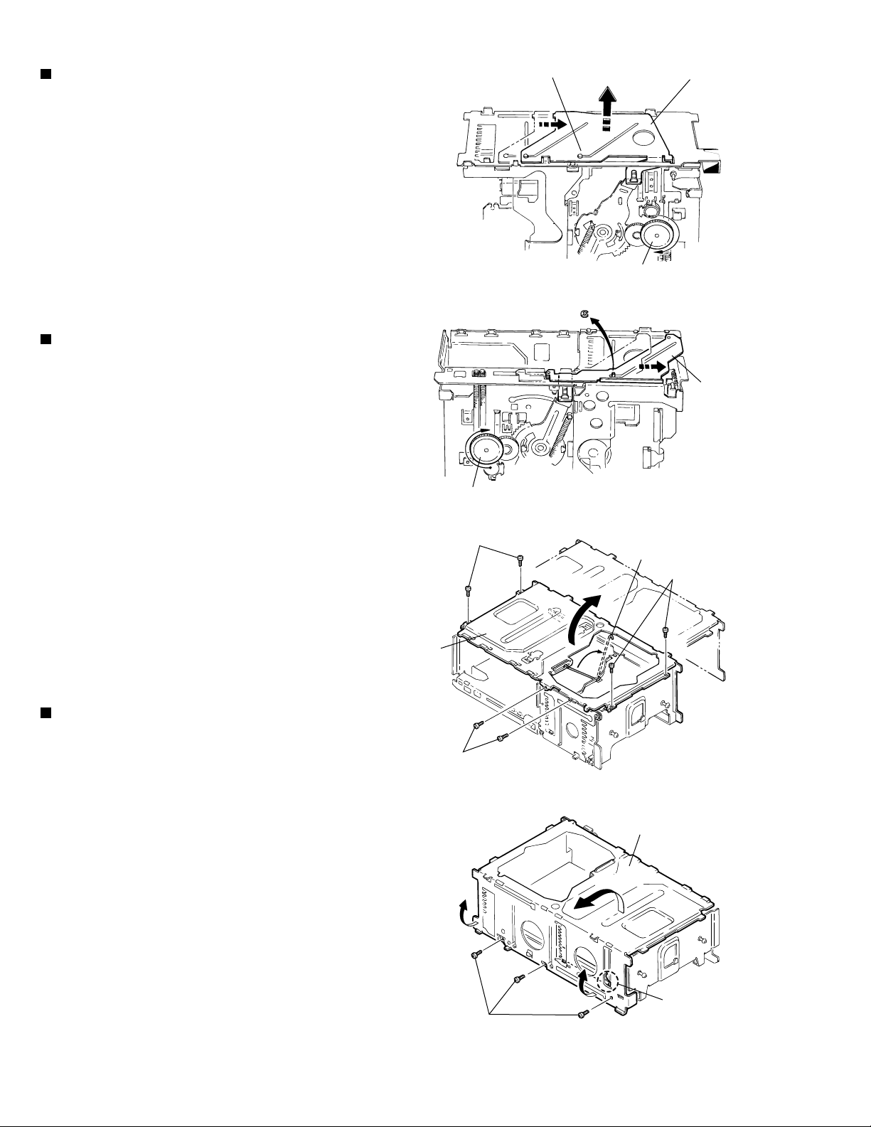
Top plate
Remove the nine screws K securing the top plate.
1.
Disconnect the section e attached to the rear of the
2.
unit, then lift the top plate slightly.
Slide the top plate toward the rear of the unit to
3.
remove the upper rod from the top plate.
(See Fig.17 and 18)
Top plate
K
K
Slide and remove the rod inside
Rod
K
Slide
Fig. 17
Top plate
Remove
1-8
K
After lifting
Fig. 18
e
Page 9
CH-X470RF
Lifter unit
Unhook the elevator spring located on the front side
1.
of the unit. (Be sure to first unhook the spring from
the lifter side as shown in the upper part of the
diagram.)
Lift the lifter unit upward, then remove the lower rod
2.
to remove the lifter unit from the chassis.
Lifter bracket
Remove the two lifter bracket fixing screws L located
1.
on the back of the lifter unit.
Remove the lower rod.
2.
(See Fig.19 and 20)
(See Fig.21)
Side bracket and traverse mechanism
assembly
Remove the two side bracket unit fixing screws M to
1.
disconnect the side bracket unit from the lifter unit.
(See Fig.22)
Unhook this part first
Proper
orientation
Spring
Fig. 19
Lifter unit
Lift up the lifter unit
Lower rod
Remove the three shafts on the traverse mechanism
2.
assembly from the lifter unit.
CAUTION:
For reassembling, refer to the reassembling
procedures.
Lifter unit
M
M
Side bracket
Traverse mechanism
assembly
Remove from the
lifter unit
Fig. 20
L
Lifter bracket
L
Remove from the lifter unit
Fig. 22
Fig. 21
1-9
Page 10
CH-X470RF
Removing the mechanism board / pickup
assembly (See Fig.23 to 26)
Remove the three screws N fixing the mechanism
1.
board on the back of the traverse mechanism.
Disconnect the two feed motor wires (blue and
2.
white), two spindle motor wires (red and black) and
two tray motor wires (brown and black) that are
soldered to the mechanism board.
Short-circuit the grounding point on the mechanism
3.
board. Move the mechanism board without
disconnecting the wire from connector CN501. Solder
the short circuit round on the pickup assembly.
Disconnect the wire from connector CN501 on the
4.
mechanism board.
Remove the screw O to remove the feed motor
5.
assembly.
Remove the screw P to remove the shaft holder
6.
retaining the feed slide shaft assembly and the
middle gear.
Red and black
N
Mechanism board
CN501
Brown and black
N
Blue and white
Fig. 23
Flexible wire
Move the middle gear.
7.
Move the pickup assembly upward from the gear
8.
section and remove it from the traverse chassis
assembly.
Remove the two screws Q to remove the rack arm.
9.
Pull out the feed slide shaft assembly.
10.
Remove the screw R to remove the spring.
11.
CAUTION:
To reattach the mechanism board, connect
the pickup flexible wire to connector CN501
on the mechanism board before unsoldering
the short circuit round. Subsequently, fix the
mechanism board using screws.
R
Spring
Pickup
Short circuit round
(Grounding point)
Fig. 24
Pickup assembly
Grounding point
P
Shaft holder
Feed slide
shaft assembly
Middle gear
Feed motor
1-10
Rack arm
Q
Fig. 26
Pull out
Chassis
Remove gears and
motors only when
required.
O
Fig. 25
Page 11
CH-X470RF
Tray motor
Remove the two screws S securing the tray motor.
1.
Remove the two screws T to remove the tray motor
2.
assembly from the tray motor holder.
(See Fig.27 and 28)
S
S
Tray motor assembly
Fig. 27
Tray motor holder
Tray motor
Separation of the chassis (L) assembly
and chassis (R) assembly
Remove the two screws U retaining the chassis (L)
1.
and (R) assemblies.
Slide the chassis (L) assembly toward the front and
2.
detach it, then remove the chassis (L) upward.
(See Fig.29)
Slide and remove upward
as shown by the arrow
U
Front side
T
Fig. 28
U
Chassis (L) assembly
Fig. 29
Chassis (R) assembly
1-11
Page 12

CH-X470RF
<Precautions on reassembling>
CAUTION:
Mounting the traverse mechanism
When mounting the pickup assembly, attach the feed
1.
slide shaft assembly to the traverse chassis.
Apply E-JC-525 grease to the shaft.
Mount the middle gear and the feed slide shaft to the
2.
traverse chassis and secure them with the screw P
through the shaft holder.
Before mounting the mechanism board, move the
3.
pickup to the outer edge position, then secure the
board assembly using the screw N.
At this time, check that the rest switch is correctly
placed.
To mount the rack arm, first move the pickup to the
4.
middle position and secure it with the screws Q.
When reassembling, also refer to the
disassembling procedures.
(See Fig.30 to 34)
Pickup assembly
Attached to chassis
P
Shaft holder
Feed slide shaft
(half coated with grease)
Middle gear
Motor
Chassis
Mounting the
feed motor assembly
Fig. 30
Feed motor
CAUTION:
To reattach the mechanism board, connect
the pickup flexible wire to connector CN501
on the mechanism board before unsoldering
the short circuit round. Subsequently, fix the
mechanism board using screws.
Q
Rack arm
Move the pickup to
the middle position
Shaft holder
Mechanism board
N
N
Spindle motor
Fig. 31
CN501
N
Fig. 33
Flexible wire
1-12
Fig. 32
Pickup
Short circuit round
(Grounding point)
Fig. 34
Page 13

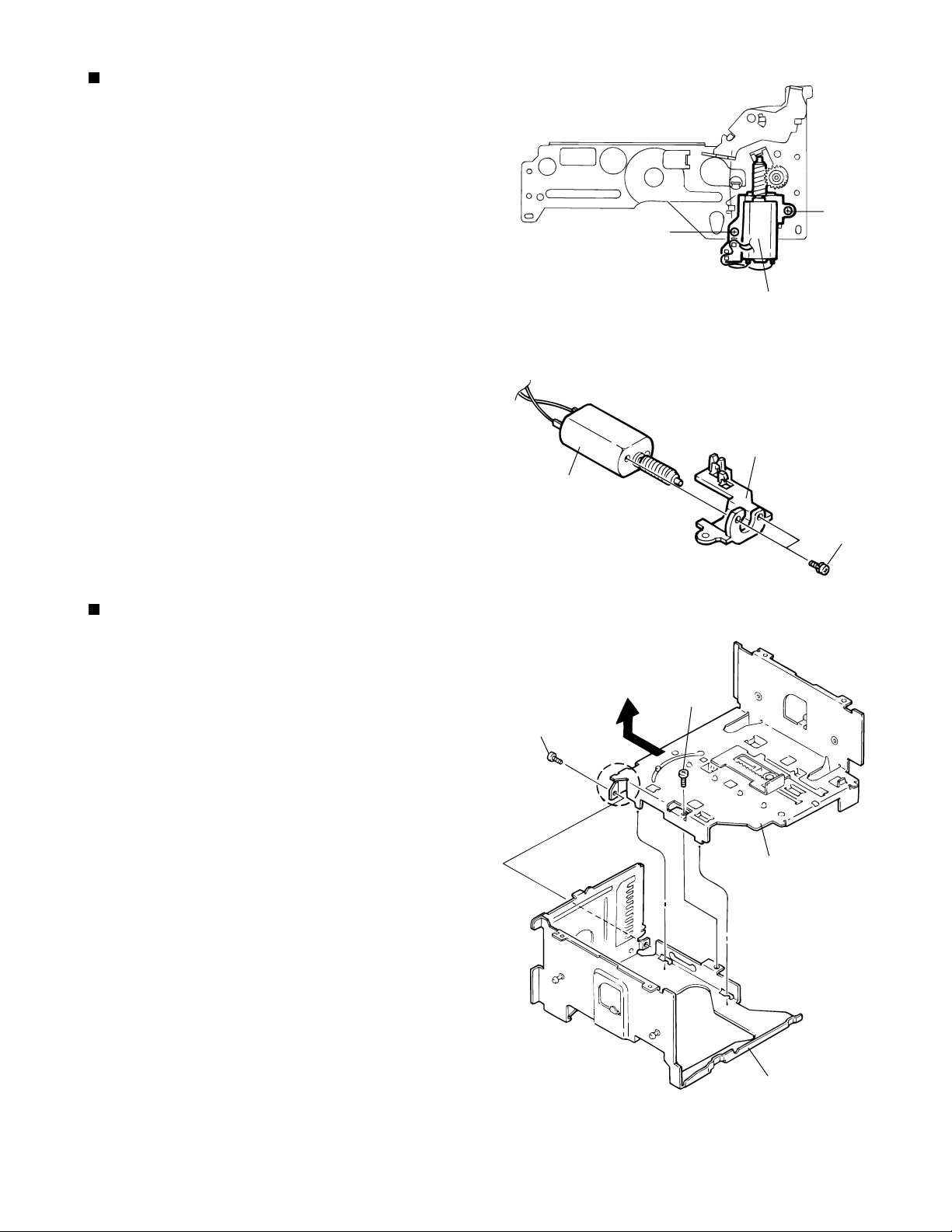
Mounting the lifter unit
(See Fig.35 to 37)
Insert the shafts f of the traverse mechanism
1.
assembly into the slide grooves g on the lifter unit.
Shift the hook of the lifter unit to the edge, and shift
2.
the sliding lever inside the side bracket unit to the
edge as well.
With each hole and lever shifted to the edge, mount
3.
the lifter unit and side bracket unit from the side.
(Check each attached section, and check that the
two shafts h of the lifter unit are correctly inserted
into the holes i of the side bracket unit. After
mounting, check that the levers move together. )
Turn the lifter unit upside down.
4.
As shown in Fig. 35, slide the lever 30 mm away from
the edge, then mount the lifter bracket assembly.
Attach
Fig. 35
Lifter unit
h
CH-X470RF
f
g
f
M
Side bracket
g
g
i
f
Traverse mechanism
assembly
Fig. 36
Lifter bracket
Shift inside by approx. 30 mm
Expanded view
Fig. 37
1-13
Page 14

CH-X470RF
Connection of the chassis (L) assembly
and chassis (R) assembly
(See Fig.38 to 40)
Attach the lower rod to the chassis (R) assembly.
1.
While shifting the rod toward the front side, mount
the rod on the lifter unit.
With the rod mounted, place the lifter unit on the
chassis (R) assembly.
Combine the chassis (L) and (R) assemblies so that
2.
the hook section j of the chassis (L) assembly is
inserted into the notch of the chassis (R) assembly
by sliding it from the front side.
After engaging, secure with the two screws U.
3.
Attach the tension spring between the lifter unit and
4.
the chassis.
Lifter unit
j
Lower Rod
Fig. 38
Notch
Attached
Set first
(chassis side)
Tension spring
Set last (lifter side)
Proper
orientation
Slide to engage
U
Chassis (R) assembly
Fig. 39
Chassis (L) assembly
U
Combine with (R) chassis
1-14
Fig. 40
Page 15

Mounting the top plate
(See Fig.41 to 44)
Mount the upper rod on the lifter side l and set it on
1.
the rear of the top plate, then mount the other end of
the upper rod to m.
Check that the five points (n, o, p, s and r) are
2.
correctly positioned.
When mounting section s, set it so that section t of
the lifter unit is pinched by the bending section of the
top plate.
Secure the top plate with six fixing screws K.
3.
CH-X470RF
m
Upper rod
l
Fig. 41
K
K
Top plate
K
Fig. 42
Expanded view of mounting s
Section t
n
o
p
s
r
Lifter Unit
Point r
Fig. 43Fig. 44
1-15
Page 16

CH-X470RF
Mounting the front slider and rear slider
(See Fig.45 and 46)
Position the unit with the rear side facing down, then
1.
rotate the third gear in the direction of the arrow
(clockwise) until the lift arm comes to the position at
which the holes are exposed, as shown in Fig. 45-1.
Mount the front slider from the top.
2.
Rotate the third gear counterclockwise until the hole
of the slider is lined up with the right hole of the stud,
as shown in Fig. 45-2.
Mount the E-washer on the shaft.
3.
Position the unit with the front side facing down, then
4.
mount the rear slider. Check that the u, v and w
positions are correctly mounted as shown in Fig. 46.
Rotate the third gear in the direction of the arrow
5.
(counterclockwise) until the lifter unit is at the top
position.
Front slider
Check after mounting
Rotate the third gear
to move the slider
Fig. 45-1
E-Washer
Fig. 45
Set so the holes
are exposed
Rotate until the
holes are lined up
Stud
Position so
that the stud
and right hole
are lined up
Fig. 45-2
u
v
w
Rotate the third gear
to move the slider
Fig. 46
1-16
Page 17

CH-X470RF
Mounting the sensor board assembly
(See Fig.47)
Attach the longer spring to the white resin, and
1.
attach the shorter spring temporarily to the sensor
assembly bracket.
Mount the sensor assembly so that the shaft of the
2.
lift arm is inserted into the longer hole on the white
resin located on the back of the sensor board
assembly.
Attach the shorter spring to the hook of the lift arm.
3.
Attach
temporarily
Shorter spring
Longer spring
Sensor assembly fixing screws
I
Fig. 47
I
Shorter
spring
Mounting the main PC board assembly
(See Fig.48)
Rotate the third gear clockwise until section x of the
1.
front slider and the third hole from the right are lined
up.
(Be sure to set properly. If incorrectly set, the
switches on the board assembly may be damaged.)
After they are correctly positioned, mount the main
2.
board assembly.
Position so that the slider hole and
third hole from the right are lined up
x
Fig. 48
1-17
Page 18

CH-X470RF
Pickup replacement procedure
(See Fig.49 to 55)
Remove the bottom cover, front panel and top cover
1.
from the exterior section.
Unplug the flexible ribbon wire from connector
2.
CN502 on the traverse mechanism PC board
assembly.
Turn the rear slider and third gear in the lifter section
3.
counterclockwise until the traverse mechanism
assembly is in the lowermost (bottom) position.
Unsolder the two wires (black and brown) connected
4.
to the tray motor.
Remove the two screws M from the round holes on
5.
the chassis (R) assembly to remove the lifter bracket
(L).
Remove the lower rod.
6.
Disconnect the two feed motor wires (blue and
7.
white), two spindle motor wires (red and black) and
two tray motor wires (brown and black) that are
soldered to the mechanism board.
Main PCB assembly
M
Lifter bracket (L)
N
Unsolder
Grounding point
CN502
Fig. 49
Third gear
M
Feed motor
assembly
Unsolder
N
Short-circuit the grounding point on the mechanism
8.
board. Move the mechanism board without
disconnecting the wire from connector CN501. Solder
the short circuit round on the pickup assembly.
Disconnect the wire from connector CN501 on the
9.
mechanism board.
Remove the three fixing screws N from the round
10.
holes on the chassis (R) assembly to remove the
traverse mechanism board assembly.
Remove the pickup shaft holder fixing screw P to
11.
remove the pickup assembly.
CAUTION:
When replacing the pickup, be sure to apply
countermeasures against static electricity
(grounding the operation table, wrist band
and soldering iron). To remove it, first shortcircuit the grounding point on the
mechanism board, then lift the mechanism
board assembly with CN501 connected.
Next, short-circuit the grounding point on
the pickup main unit, then unplug the pickup
flexible board from connector CN501.
Tray motor
assembly
Traverse mechanism
board assembly
Fig. 50
Spindle motor
Pickup assembly
Fig. 51
N
CN501
Shaft holder
P
Flexible wire
CAUTION:
1-18
When reassembling, perform in the reverse
order.
Pickup
Short circuit round
(Drounding point)
Fig. 52
Page 19

Remove the two rack arm fixing screws Q.
12.
Pull out the feed slide shaft.
Remove the shaft holder fixing screw R.
When mounting the lifter bracket after replacing the
13.
pickup, shift the lifter unit lever approx. 30 mm
towards the inside, then mount the lifter bracket.
Rack arm
CH-X470RF
R
Pickup
Feed slide shaft
Q
Pickup
Middle gear
Fig. 53
P
Shaft Holder
Middle gear
Chassis
Fig. 54
Shift approx. 30 mm
Shift approx. 30 mm
Enlarged diagram
Fig. 55
Lifter unit lever
1-19
Page 20

CH-X470RF
Forced eject procedures
Magazine eject does not function.
RESET (Press EJECT for 3 sec.)
YES
Completed
Check that the trays remain no more
than 10 mm inside the magazine.
Improperly positioned
Remove the dampers and the top
cover to take out the mechanism.
Remove the item(s) causing the
disc-jam through the clearance at
the top of the lifter.
Are trays stored in
the magazine?
Check visually.
Remove the bottom cover
NO
Is the disc set in the playing
position?
Rotate the third gear clockwise and
unchuck the disc.
Disconnect the tray from the hook.
NO
NO
YES
YES
Peel off the sticker on the left side
of the unit. Insert a screwdriver
and press the internal lever to
forcibly eject the magazine.
Completed
Remove the lifter bracket (L) and
return the tray to the magazine.
Place the unit with its left side
facing down and apply a slight
shock, then return the tray to the
magazine.
Rotate the third gear clockwise
until the lifter level is below the 9th
tray position.
Press the magazine lock lever to
eject the magazine.
Completed
1-20
Page 21

Troubleshooting
Servicing procedures for CH-X470RF error displays
CH-X470RF
Error display
E1: Eject error
E2: Position
motor error
E3: Tray motor
error
Servicing procedure
The magazine cannot be ejected until S601 (magazine switch) turns off.
Can the magazine be ejected? YES 1, NO 2
1 The magazine switch (S601) does not turn off even though the magazine is completely ejected.
2 Check that the magazine is not engaged with the mechanism assembly.
The lifter does not move up and down when exchanging or ejecting discs.
After resetting, check whether or not the lifter moves.YES 3, NO 4
3If the lifter exceeds the required disc position, check the lift position input. (IC601 pin 76)
If the lifter does not reach the required disc position, check the mechanism (mainly the lifter
elevation mechanism)
4Check that voltage is present at the motor terminal.
If voltage is present, check the lifter elevation mechanism. If voltage is not present, separate the
motor from the circuit and check again whether or not voltage is present.
If voltage is present, next check that the armature resistance of the position motor (resistance
between motor terminals) is approx. 12 .
If the resistance is excessively low (1 - 2 ), the motor is defective.
Trays cannot be opened or closed when exchanging or ejecting discs.
Does the tray move when changing or ejecting discs? YES 5, NO 6
5Check that TRAY OUT SW (S602) and TRAY IN SW (S603) function correctly.
S602 & IC601 pin (46) S603 & IC601 pin (45)
E4: Pick returning
error
When opening
When closing
6Check that the drive voltage is applied to the motor terminal.
If the voltage is present, check the tray mechanism.
If the voltage is not present, separate the motor from the circuit and check again whether or
not the voltage is present.
Does the feed (pickup unit) return to the inner area of the disc when ejecting?
YES 7, NO 8, 9
7 Check the rest switch.
8If the feed gear is rotated, check the feed transfer mechanism
9If the feed gear is not rotated, check the motor driver and the pattern.
H
L
HL
Other errors occurring in the receiver or controller.
E8: Connection
error
The E1 E8 error displays described above may appear as E-1 E-8, 1E1 1E8, R-1 R-8, or RST1 RST8,
depending on the product.
When selecting the CD Changer mode using function keys, etc., the unit does not enter the CD
changer mode, or the E8 error display appears. This signifies trouble relating to communications.
aCheck the connection cables between the CD changer and the receiver (CD changer controller).
bCheck the CD changer power cord and the fuse (including F901 on the PC board).
cCheck IC651 and its peripheral circuits.
1-21
Page 22

CH-X470RF
CH-X470RF Error code
The following error codes can be displayed and stored in up to 3 memories when the KD-MX3000 is used with
the controller. Refer to the KD-MX3000 service manual regarding error code indication.
The error code indication when using the earlier controller is the same as the CH-X99,KD-MK88 and other
12CD changer models.
CH-1 error code table
Generating condition Description Error code
Tray extension
error
Tray retraction
error
Lifter raise error
Lifter lower error
Chuck error
Unchuck error
Eject error
Initialize error
Tray-in switch time out
(Tray-in switch Low, Tray-out switch High)
Tray-out switch time out (Tray-in switch High,
Tray-out switch High)
Tray-in switch time out (Tray-in switch Low,
Tray-out switch Low)
MAG-in switch Low to High
Tray-in switch time out (Tray-in switch Low,
Tray-out switch Low)
Tray-out switch time out (Tray-in switch High,
Tray-out switch High)
Tray-in switch time out (Tray-in switch Low,
Tray-out switch Low)
MAG-in switch Low to High
Wait position time out
Wait position time out
Play position time out
Wait position time out
Eject position time out
MAG in switch time out
Tray stops part way
Tray stops part way
Tray-in switch faulty or other defect
Magazine removed when tray partly
extende
Tray motor inoperative
Tray retraction stops part way
Tray-in switch faulty or other defect
Magazine removed when tray partly r
etracted
Position motor inoperativeWait position time out
Position not stable in fine adjust mode
Other faultWait position time out
Position motor inoperative
Position not stable in fine adjust modeWait position time out
Other faultWait position time out
Position motor inoperativePlay position time out
Position not stable in fine adjust modePlay position time out
Other fault
Position motor inoperativeWait position time out
Position not stable in fine adjust modeWait position time out
Other fault
Position motor inoperativeEject position time out
Eject position not attained
Magazine not ejected
Both Tray-in and Tray-out LowMechanism switch time out
Not stable at absolute positionAbsolute position time out
E1 03 00 11
E1 03 00 12
E1 03 00 13
E1 03 00 14
E1 03 00 16
E1 03 00 17
E1 03 00 18
E1 03 00 19
E1 02 00 21
E1 02 00 22
E1 02 00 23
E1 02 00 26
E1 02 00 27
E1 02 00 28
E1 02 00 31
E1 02 00 32
E1 02 00 33
E1 02 00 36
E1 02 00 37
E1 02 00 38
E1 02 00 41
E1 02 00 42
E1 02 00 43
E1 03 00 46
E1 03 00 47
Note: The 1st error code is indicated by E1, while the 2nd and 3rd error codes are respectively indicated by
E2 and E3.
1-22
Page 23

Acceler
ation
Flow of functional operation until TOC read
CH-X470RF
• When the pickup correctly moves
to the inner area of the disc
Microprocessor
commands
FMO
TC9462
FEED MOTOR
IC581
RESET SW
53
TERMINAL
20
$ 83
$ 82 $81
5V
Hi-Z
0V
6V
4V
2V
OFF
ON
• When correctly focused
Focus Servo Loop ON
Power ON
Set Function to CD
Disc inserted
Pickup feed to the inner area
YES
Laser emitted
Focus search
YES
Disc rotates
RF signal eye-pattern
remains closed
• When the laser diode correctly
emits
Microprocessor
commands
SEL
TC9462
LD
5
CN502
or
22
CN503
$ 84
57
"No disc"
display
• When the disc correctly rotates
Microprocessor
commands
5V
0V
4V
0V
Tracking loop closed
RF signal eye-pattern
opens
TOC readout
Jump to the first track
Play
Spindle
motor (+)
Acceler
ation
Acceleration
Tracking Servo Loop ON
• RF signal
Rough
Servo
Servo CLV
Rough Servo Mode
CLV Servo Mode
(ProgramArea)
CLV Servo Mode
(Lead-In Area;
Digital: 0)
1-23
Page 24

CH-X470RF
General section
Turn the power on with
no magazine loaded.
Reset
Move the lifter until it
comes to the STOP
position
(shipping position).
YES
Connect the receiver,
etc. and turn the power
on.
Set to the changer
mode.
CD changer indication
appears on the receiver,
etc.
YES
Load the magazine.
Is the disc pulled out to
start play?
YES
Is the disc taken out?
Is the disc rotated?
Is voltage present at
IC521 pin z 2.5 V while
the disc rotates?
Proceed to the Tracking
Is track selection or
search performed
correctly?
NO
NO
NO
section.
The lifter moves up or
down and stops.
The position motor does
not function.
The tray motor goes
forward and back
several times.
Check the connections
to the receiver or the
circuits in the vicinity of
IC651.
NO
YES
NO
YES
NO
YES
NO
NO
NO
Check the MAG SW,
TRAY-IN, and TRAY-
OUT switches.
Proceed to
the Signal
Processing
section.
YES
Check the linear position
sensor (VR601).
YES
Check the wiring of the
CD 9 V power supply
position motor.
Check the TRAY-IN and
TRAY-OUT switches.
Proceed to the Focus
Exchange discs, then
check whether or not the
feed motor moves.
Set from the STOP to
PLAY mode, then check
that the triangle wave
appears at IC581 pins H
Does the laser emit?
Proceed to the Focus
section.
YES
and I .
YES
YES
section.
NO
NO
NO
Check the RESET
switch and feed
section
(Refer to the Feed section).
Check the vicinity of
IC501 6and 7.
1-24
YES
10. Is the playback
sound normal?
YES
Normal
NO
Proceed to the Signal
Processing section.
Page 25

Feed section
CH-X470RF
Is the voltage output at
IC521 pin u 5V or 0V?
YES
Is 4V present at both
sides of the feed motor?
YES
Check the feed motor.
Focus section
When the lens is
moving:
Does the S-search
waveform appear at
IC581 pins H and I?
YES
4V
NO
Is the wiring for IC521
(90) (100) correct?
Is 6V or 2V present at
IC581 Q and R?
Check IC581.
NO
Check the circuits in
the vicinity of IC581
Check the pickup and
NO
pins H K.
YES
its connections.
YES
YES
Is 5V present at IC581
pin 6?
YES
Check the vicinity of
IC521.
Check the feed motor
connection wiring.
NONO
Check CD 9V
and 5V.
Spindle section
Is the disk rotated?
YES
Does the RF signal
appear at TP1?
YES
Is the RF waveform at TP1
distorted?
YES
Proceed to the Tracking
section
Tracking section
When the disc is rotated
at first:
NO
NO
NO
Approx. 1.2 V
Is 4V present between
IC581 pins 1 and 2?
Check the spindle motor
and its wiring.
Check the circuits in the
vicinity of IC501 J O or
the pickup
Check the circuit in the
vicinity of IC501 pins
NO NO
Is 4V present at IC521
2C.
pin x?
YES
Check the vicinity of
IC581.
YESYES
Check the pickup and
Check IC501 and
IC521.
its connections.
Is the tracking error
signal output at TP3?
YES
Check IC521.
1-25
Page 26

CH-X470RF
Signal processing section
Is the sound output from
both channels (L, R)?
YES
Normal
No sound from either
channel.
YES
Is 9V present at IC101 pin
(8)?
YES
Is the audio signal
(including sampling output
components) output to
IC521 pins ^and | during
YES
Is the audio signal output
at IC101 pins 1
and7during playback?
YES
Check the muting circuit.
NONO
NO
NO
NO
Compare the L-ch and
R-ch to locate the
defective point.
Check the vicinity of the
Q981 audio power
supply.
Check IC521 and its
peripheral circuits.
Check IC101 and its
peripheral circuits
1-26
Page 27

Description of major ICs
UPD780058GC-291(IC601):CPU
1.Terminal layout
80 61
1
60
CH-X470RF
2.Pin function
Pin
PORT
No.
Name
LCDDA
1
LCDSCK
2
LCDCE
3
GND
4
VREF
5
POSCON
6
AVREF1
7
NC
8
NC
9
CDCHECK
10
EPROMDI
11
EOROMDO
12
EPROMCK
13
NC
14
BUS I/O
15
BUS SI
16
BUS SO
17
BUS SCK
18
NC
19
NC
20
NC
21
NC
22
NC
23
NC
24
NC
25
CD ON
26
PWR CONT
27
POSMO+
28
POSMO-
29
TRAYMO+
30
TRAYMO-
31
BUCK
32
GND
33
LSI RESET
34
CCE
35
BUS0
36
BUS1
37
BUS2
38
BUS3
39
NC
40
20
21 40
I/O
O
LCD driver data output
O
LCD driver clock output
O
LCD driver chip enable output
-
Connect to ground
-
Reference voltage output
O
Position control output
-
Connect to 5V
-
Unused output port
-
Unused output port
I
CD check mode input. Reset only.
I/O
EEPROM data input
O
EEPROM data output. Hi durring input.
I/O
EEPROM clock input/output
-
Unused output port
O
JVC bus input/output control(Lo:input)
I
JVC bus data input
O
JVC bus data output
I/O
JVC bus clock input/output
-
Unused output port
-
Unused output port
-
Unused output port
-
Unused output port
-
Unused output port
-
Unused output port
-
Unused output port
O
CD power control Hi:on
O
Power supply control output Hi:on
O
Position motor control output
O
Position motor control output
O
Tray motor control output
O
Tray motor control output
-
CD LSI data clock
-
Connect to ground
O
CD LSI reset
I/O
CD LSI chip enable
I/O
CD LSI data 0(open drain)
I/O
CD LSI data 1 (open drain)
I/O
CD LSI data 2 (open drain)
O
CD LSI data 3 (open drain)
-
Unused output port
Function
41
Pin
No.
CD RW
41
NC
42
NC
43
MAG IN
44
TRAY OUT
45
TRAY IN
46
REST
47
DISC SEL
48
EMPH
49
NC
50
OE
51
SHOCK SW
52
SHOCK
53
NC
54
A.MUTE
55
MUTE PWR
56
STAGE
57
STAGE2
58
EPROM CLR
59
RESET
60
REMOCON
61
PWR DET
62
PWR SW
63
BUS INT
64
EJECT
65
NC
66
GND
67
VDD0
68
X2
69
X1
70
GND
71
XT2
72
XT1
73
VDD
74
AVREF0
75
L SENSOR
76
KEY1
77
KEY2
78
KEY3
79
KEY0
80
PORT
Name
I/O
O
CD-RW Detect signal output
-
Unused output port
-
Unused output port
-
Magazine switch Lo:magazine inserted
O
Tray extend switch Lo:extension complete
O
Tray retract switch Lo:retraction complete
I
Resr switch
O
Disc select output
O
Emphasis select output Hi:on
-
Unused output port
-
Unused output port
I
Shock proof switch signal input
O
Shock proof output
-
Unused output port
-
Unused output port
O
Power supply for mute
I
LCD,AD key,remote inhibit selector Low:inhidit
-
Unused output port
I
EEPROM clear input Functional only dunng reset
I
Reset input (includes flash write in function)
I
Remote controller signal input
I
Memory power detect input
I
CRTL+B detect input
I
JVC bus com start interrupt input
I
Eject key input
-
Unused output port
-
Connect to ground
-
Conneto to VDD
O
Oscillater (4.19430 MHz)
I
Oscillater (4.19430 MHz)
-
Connect to ground
O
Open
I
Connect to VDD
-
Connect to 5V
-
Connect to ADCONT
I
Linear sensor input(8 bit A/D input)
I
Key input 1 (8 bit A/D input)
I
Key input 2 (8 bit A/D input)
I
Key input 3 (8 bit A/D input)
I
Key input 0 (8 bit A.D input)
Function
1-27
Page 28

CH-X470RF
TC9490FA (IC521) : DSP
1. Pin layout & Block diagram
DD3
XO
XV
48 47 46 45 44 43 42 41 40 39 38 37 36 35 34 33
SS3
XI
XV
TESIN
DD3VSS3
V
DMO
FMO
DD3
AV
SEL
TEBC
RFGC
REF
V
TRO
FOO
2. Pin function (1/2)
No. Symbol
1
2
3
4
5
6
7
8
9
10
11
12
13
14
15
16
17
18
19
20
21
22
23
24
25
BCK
LRCK
AOUT
DOUT
IPF
VDD3
VSS3
SBOK
CLCK
DATA
SFSY
SBSY
/HSO
/UHSO
PVDD3
PDO
TMAX
LPFN
LPFO
PVREF
VCOF
AVSS3
SLCO
RFI
AVSS3
49DV
SS3
RO
50
51
DV
DVR
DV
ZDET
V
BUS0
BUS1
BUS2
BUS3
BUCK
/CCE
/RST
V
DD3
LO
DD3
SS5
DD5
LPF
52
53
54
55
56
57
58
59
60
61
62
63
64
1 2 3 4 5 6 7 8 9 10 11 12 13 14 15 16
BCK
I/O
O
Bit clock output pin.32fs, 48fs, or 64fs selectable by command.
O
L/R channel clock output pin. "L" for L channel and "H" for R channel.
O
Audio data output pin. MSB-first or LSB-first selected by command.
O
Digital data output pin. Outputs up to double-speed playback.
O
Correction flog output pin.
-
Digital 3.3V power supply voltage pin.
-
Digital GND pin.
O
Subcode Q data CRCC result output pin. "H" level when result is OK.
I/O
Sub-code P-W data read clock I/O pin. I/O polarity selectable by command.
O
Sub-code P-W data output pin.
O
Playback frames sync signal output pin.
O
Sub-code block sync output pin.
O
Playback speed mode flag output pin.
O
Playback speed mode flag output pin.
-
PLL-only 3.3V power supply voltage pin.
O
EFM and PLCK phase difference signal output pin.
O
TMAX detection result output pin.
I
Inverted input pin for PLL RF amp.
O
Output pin for PLL LPF amp.
-
PLL-only VREF pin.
O
VCO filter pin.
-
Analog GND pin.
O
DAC output pin for data slice level generation.
I
RF signal input pin.
-
Analog 3.3V power supply voltage pin.
generator
Micro-
controller
interface
LRCK
Clock
1-bit
DAC
Audio output
AOUT
circuit
DOUT
circuit
Correction
Digital output
IPF
Address
circuit
16 k
RAM
DD3
V
V
SS3
PWM
SBOK
Servo control
ROM
RAM
CLV servo
Sync signal
protection
EFM
Sub code
decoder
DATA
CLCK
Function
Digital equalizer
automatic
adjustment circuit
SFSY
SBSY
/HSO
A/D
VCO
PLL
TMAX
D/A
Data
slicer
/UHSO
PV
DD3
PDO
32
31
30
29
28
27
26
25
24
23
22
21
20
19
18
17
TEZI
TEI
SBAD
FEI
RFRP
RFZI
RFCT
AV
DD3
RFI
SLCO
AV
SS3
VCOF
PV
REF
LPFO
LPFN
TMAX
1-28
Page 29

2. Pin function (2/2)
No. Symbol
26
27
28
29
30
31
32
33
34
35
36
37
38
39
40
41
42
43
44
45
46
47
48
49
50
51
52
53
54
55
56
57
58
59
60
61
62
63
64
RFCT
RFZI
RFRP
FEI
SBADTEI
TEI
TEZI
FOO
TRO
VREF
RFGC
TEBC
SEL
AVDD3
FMO
DMO
VSS3
VDD3
TESIN
XVSS3
XI
XO
XVDD3
DVSS3
RO
DVDD3
DVR
LO
DVSS3
ZDET
VSS5
BUS0
BUS1
BUS2
BUS3
BUCK
/CCE
/RST
VDD5
I/O
I
RFRP signal center level input pin.
I
RFRP signal zero-cross input pin.
I
RF ripple signal input pin.
I
Focus error signal input pin.
I
Sub-beam adder signal input pin.
I
Tracking error input pin. Inputs when tracking servo is on.
I
Tracking error signal zero-cross input pin.
O
Focus equalizer output pin.
O
Tracking equalizer output pin.
-
Analog reference power supply voltage pin.
O
RF amplitude adjustment control signal output pin.
O
Tracking barance control signal output pin.
O
APC circuit ON/OFF signal output pin.
-
Analog 3.3V power supply voltage pin.
O
Feed equalizer output pin.
O
Disc equalizer output pin.
-
Digital GND pin.
-
Digital 3.3V power supply voltage pin.
I
Test input pin.
-
System clock oscillator GND pin.
I
System clock oscillator input pin.
O
System clock oscillator output pin.
-
System clock oscillator 3.3V power supply voltage pin.
-
DA converter GND pin.
O
R-channel data foward output pin.
-
DA converter 3.3V power supply pin.
-
Reference voltage pin.
O
L-channel data forward output pin.
-
DC converter GND pin.
O
1 bit DA converter zero data detection flag output pin.
-
Microcontroller interface GND pin.
I/O
Microcontroller interface data I/O pins.
I/O
Microcontroller interface data I/O pins.
I/O
Microcontroller interface data I/O pins.
I/O
Microcontroller interface data I/O pins.
I
Microcontroller interface clock input pin.
I
Microcontroller interface chip enable signal input pin.
I
Reset signal input pin.
-
Microcontroller interface 5V power supply pin.
Function
CH-X470RF
1-29
Page 30

CH-X470RF
BA15218F-XE (IC101) : Dual operation amplifier
1. Pin layout
OUT1 1
-IN1 2
+IN1 3
VEE 4
2. Block diagram
Vcc
-IN
+IN
1
2
R1
Q5
Q1
Q2
D1
Q3 Q4
8 Vcc
7 OUT2
6 -IN2
5 +IN2
C2
R5
Q6
Q9
Q8
Q10
Q7
R7
Q11
R6
Q12
R8
Q18Q13
OTHER
CH
Q19
Q17Q16
VEE
C1
R3R2
R4
OUTPUT
Q14 Q15Q114
R9
1-30
Page 31

BR24CO1AF-X-W(IC604):EP ROM
2.Block Diagrram1.Terminal Layout
VCC TEST SCL SDA
CH-X470RF
BR24C01AF
A0 A1 A2 GND
3.Pin Function
Symbol
VCC
GND
A1 A2 A3
SCL
SDA
TEST
I/O
I/O
1A 0
7bit
2A 1
Address
Decoder
3A 2
4GND
Function
-
I
I
I
Puwer Supply
Ground(OV)
Slaves Address Set(Pin)
Serial Clock Input
Slaves and Word Address,Serial Data Input,
Serial Data Output(*)
Ground
High Voltage Gen.
1,024bit EEPROM Array
7bit
START STOP
Address Register
Control logic
Vcc level detect
Slave Word
ACK
8bit
Data
Register
8 VCC
7 TEST
6 SCL
5SDA
(*)
An open drain output requires a pull-up resistor.
1-31
Page 32

CH-X470RF
FAN8037 (IC581) : CD driver
1. Pin layout & Block diagram
48 47 46 45 44 43 42 41 40 39 38 37
2. Pin function
Pin
Symbol
No.
1
IN2+
2
IN2-
3
OUT2
4
IN3+
5
IN3-
6
OUT3
7
IN4+
8
IN4-
9
OUT4
10
CTL1
11
FWD1
12
REV1
13
CTL2
14
FWD2
15
REV2
16
SGND
17
FWD3
18
REV3
19
CTL3
20
SB
21
PS
22
MUTE
23
PVCC2
24
DO7-
1
2
3
4
5
6
7
8
9
10
11
12
13 14 15 16 17 18 19 20 21 22 23 24
Function
I/O
I
CH2 op-amp input(+)
I
CH2 op-amp input(-)
O
CH2 op-amp output
I
CH3 op-amp input(+)
I
Ch3 op-amp input(-)
O
CH3 op-amp output
I
CH4 op-amp input(+)
I
CH4 op-amp input(-)
O
CH4 op-amp output(+)
I
CH5 motor speed control
I
CH5 forward input
I
CH5 reverse input
I
CH6 motor speed control
I
CH6 forward input
I
CH6 reverse input
-
Signal ground
I
CH7 forward input
I
CH7 reverse input
I
CH7 motor speed control
I
Stand by
I
Power save
I
All mute
-
Power supply voltage
O
CH7 drive output(-)
M
s
S
w
C
M
s
S
w
C
M
s
S
w
C
T.S . D
D
D
D
D
D
D
STAND BY
ALL MUTE
POWER SAVE
Pin
No.
25
26
27
28
29
30
31
32
33
34
35
36
37
38
39
40
41
42
43
44
45
46
47
48
Symbol
DO7+
DO6-
DO6+
PGND2
DO5-
DO5+
DO4-
DO4+
DO3-
DO3+
PGND1
DO2-
DO2+
DO1-
DO1+
PVCC1
REGOX
REGX
RESX
VREF
SVCC
IN1+
IN1-
OUT1
36
35
34
33
32
31
30
29
28
27
26
25
I/O
Function
O
CH7 drive output(+)
O
CH6 drive output(-)
O
CH6 drive output(+)
-
Power ground2
O
CH5 drive output(-)
O
CH5 drive output(+)
O
CH4 drive output(-)
O
CH4 drive output(+)
O
CH3 drive output(-)
O
CH3 drive output(+)
-
Power ground1
O
CH2 drive output(-)
O
CH2 drive output(+)
O
CH1 drive output(-)
O
CH1 drive output(+)
-
Power supply voltage
I
Regulator feedback input
O
Regulator output
I
Regulator reset input
I
Bias voltage input
-
Signal supply voltage
I
CH1 op-amp input(+)
I
CH1 op-amp input(-)
O
CH1 op-amp output
1-32
Page 33

HD74HC126FP-X (IC651) : Buffer
CH-X470RF
1.Terminal layout
1C
1
1A
2
3
1Y
4
2C
5
2A
6
2Y
GND
2.Block diagram
7
Input
3Y
14
3A
13
12
3C
11
4Y
10
4A
9
4C
8
Vcc
Vcc Vcc
1A
2A
3A
4A
1C
2C
3C
See Function Table
4C
3.Pin function
Output
1Y
Output
2Y
Output
3Y
Output
4Y
Input Output
C
A
L
X
H
L
H
H
Note:
1k
CL
Sample as Load Circuit 1
Sample as Load Circuit 1
Sample as Load Circuit 1
Y
Z
H
L
H : High
L : Low
X : H and L
Z : H.L.X
S1
1k
1-33
Page 34

CH-X470RF
IC-PST9333U-X (IC602) : Reset IC
1. Pin layout
NC
GND
2. Block diagram
1
2
Vcc
NC
NC
GND
4
1
4
Vcc
3
VOUT
3
VOUT
GND
2
3. Pin function
Pin No.
1
2
3
4
Symbol
NC
GND
VOUT
Vcc
Function
Non connect
GND terminal
Reset signal output terminal
Power supply terminal
1-34
Page 35

TA2147F-X (IC501) : RF amp
1. Pin layout & Block diagram
GND
RFN
RFO
AGCIN
RFGC
RFGO
RFRPIN
RFRP
FEN
FEO
CH-X470RF
VRO
GVSW
cc
24
1
V
3 k
3 k
23
40 pF
20 k
2
FNI
180 k
60 k
80 k
22
180 k
40 pF
60 k
20 k
3
FPI
30 k
80 k
2
21
1
4
TPI
0.5
20 k
240 k
15 pF
2
20
k
5
TNI
0.5
15 pF
240 k
1.75 k
19
6
MDI
40 k
14 k
2 k
18
BOTTOM
PEAK
1 k
7
LDO
20 k
1.3 V
60 A
12 k
17
8
SEL
12 k
2 k
50 k
20 k
50 A
16
40 k
9
TEBC
10 pF
15 k
20 k
20 k
15
10 pF
10
TEN
20 k
40 k
14
20 A
11
TEO
13
20 k 20 k
PEAK
50 k 15 k
12
RFDC
2. Pin function
Pin
Symbol I/O Function
No.
1
2
3
4
5
6
7
8
9
10
11
12
13
14
15
16
17
18
19
20
21
22
23
24
Vcc
FNI
FPI
TPI
TNI
MDI
LDO
SEL
TEBC
TEN
TEO
RFDC
GVSW
VRO
FEO
FEN
RFRP
RFRPIN
RFGO
RFGC
AGCIN
RFO
RFN
GND
-
3.3V power supply pin
I
Main-beam amp input pin
I
Main-beam amp input pin
I
Sub-beam amp input pin
I
Sub-beam amp input pin
I
Monitor photo diode amp input pin
O
Laser diode amp output pin
I
APC circuit ON/OFF control signal, laser diode control signal input
or bottom/peak detection frequency change pin
I
Tracking error balance adjustment signal input pin
I
Tracking error signal generation amp negative-phase input pin
O
Tracking error signal generation amp output pin
O
RF signal peak detection output pin
I
AGC/FE/TE amp gain change pin
O
Reference voltage output pin
O
Focus error signal generation amp output pin
I
Focus error signal generation amp negative-phase input pin
O
Signal amp output pin for track count
I
Signal generation amp input pin for track count
O
RF signal amplitude adjustment amp output pin
I
RF amplitude adjustment control signal input pin
I
RF signal amplitude adjustment amp input pin
O
RF signal generation amp output pin
I
RF signal generation amp input pin
-
GND pin
1-35
Page 36

CH-X470RF
VICTOR COMPANY OF JAPAN, LIMITED
MOBILE ELECTRONICS DIVISION
PERSONAL & MOBILE NETWORK BUSINESS UNIT. 10-1,1Chome,Ohwatari-machi,Maebashi-city,371-8543,Japan
(No.49668)
200112
 Loading...