

Page 1
49776200301
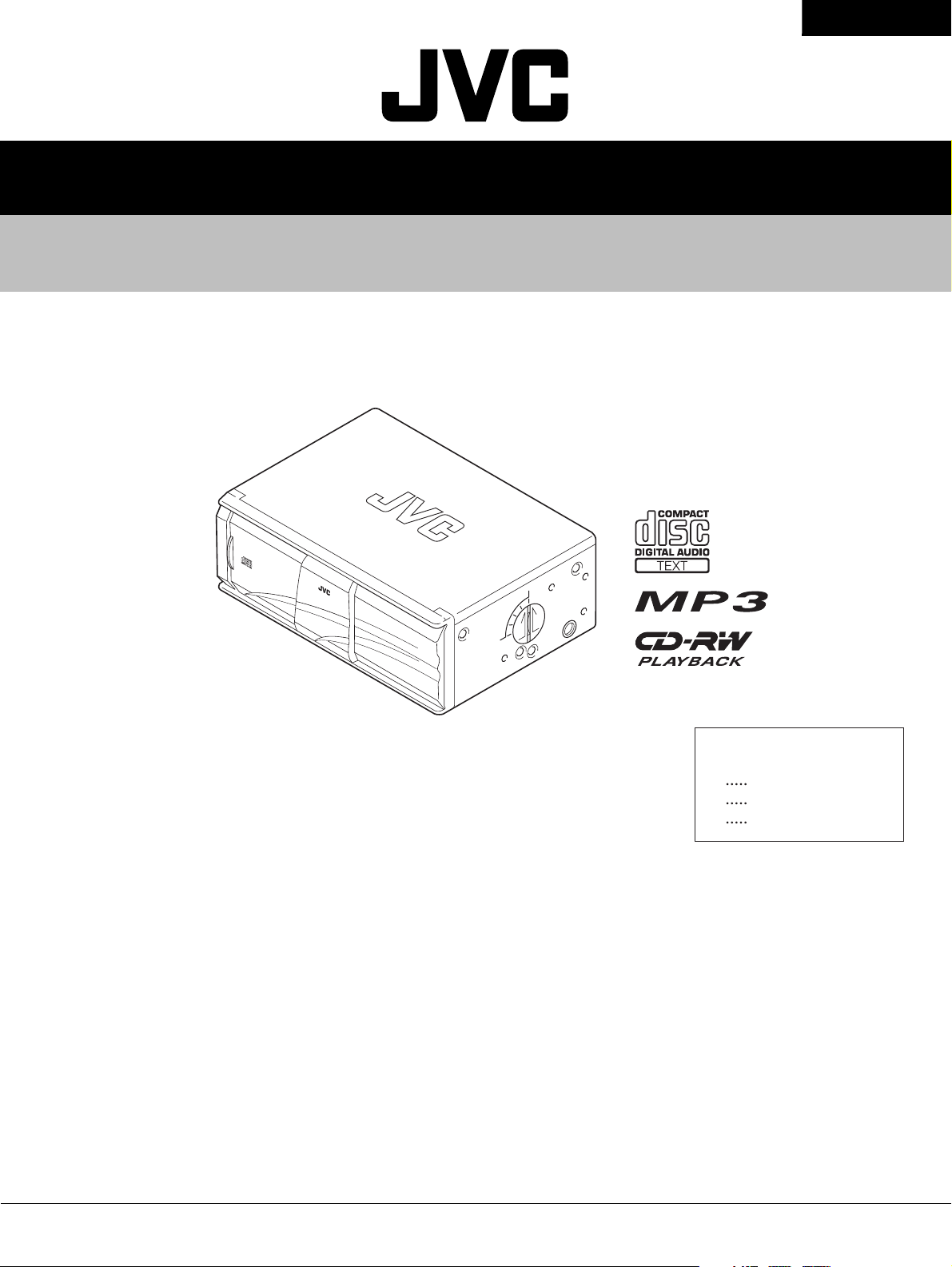
CH-X1500
SERVICE MANUAL
CD CHANGER
CH-X1500
Area Suffix
J Northern America
E
Continental Europe
U
Other Areas
TABLE OF CONTENTS
1 Important Safety Precautions . . . . . . . . . . . . . . . . . . . . . . . . . . . . . . . . . . . . . . . . . . . . . . . . . . . . . . . . . . . . 1-2
2 Disassembly method . . . . . . . . . . . . . . . . . . . . . . . . . . . . . . . . . . . . . . . . . . . . . . . . . . . . . . . . . . . . . . . . . . .1-4
3 Adjustment method . . . . . . . . . . . . . . . . . . . . . . . . . . . . . . . . . . . . . . . . . . . . . . . . . . . . . . . . . . . . . . . . . . .1-22
4 Description of major ICs . . . . . . . . . . . . . . . . . . . . . . . . . . . . . . . . . . . . . . . . . . . . . . . . . . . . . . . . . . . . . . .1-30
COPYRIGHT © 2003 VICTOR COMPANY OF JAPAN, LTD.
No.49776
2003/01
Page 2
CH-X1500
1.1 Safety Precautions
SECTION 1
Important Safety Precautions
!
!
Burrs formed during molding may be left over on some parts of the chassis. Therefore,
pay attention to such burrs in the case of preforming repair of this system.
Please use enough caution not to see the beam directly or touch it in case of an
adjustment or operation check.
!
This unit can only be connected to the JVC car receivers/controllers equipped with
MP3-CD changer control functions. If connected to any other receiver/controller, this
unit cannot work (even CDs may not play back).
1-2
Page 3
1.2 Preventing static electricity
Electrostatic discharge (ESD), which occurs when static electricity stored in the body, fabric, etc. is discharged,
can destroy the laser diode in the traverse unit (optical pickup). Take care to prevent this when performing repairs.
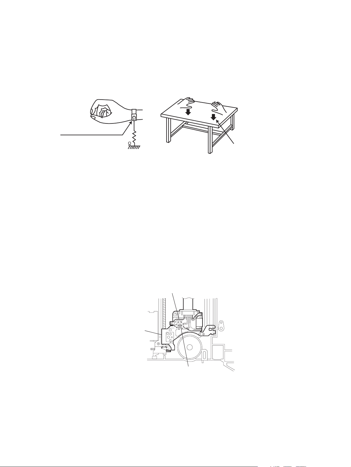
1.2.1 Grounding to prevent damage by static electricity
Static electricity in the work area can destroy the optical pickup (laser diode) in devices such as DVD players.
Be careful to use proper grounding in the area where repairs are being performed.
(1) Ground the workbench
Ground the workbench by laying conductive material (such as a conductive sheet) or an iron plate over it before placing the
traverse unit (optical pickup) on it.
(2) Ground yourself
Use an anti-static wrist strap to release any static electricity built up in your body.
(caption)
Anti-static wrist strap
CH-X1500
1M
Conductive material
(conductive sheet) or iron plate
(3) Handling the optical pickup
• In order to maintain quality during transport and before installation, both sides of the laser diode on the replacement optical
pickup are shorted. After replacement, return the shorte d parts to their original condition.
(Refer to the text.)
• Do not use a tester to check the condition of the laser diode in the optical pickup. The tester's internal power source can
easily destroy the laser diode.
1.3 Handling the traverse unit (optical pickup)
(1) Do not subject the traverse unit (optical pickup) to strong shocks, as it is a sensitive, complex unit.
(2) Cut off the shorted part of the flexible cable using nipper s, e tc. after re pla cing th e optical picku p. For sp ecific details , refer to
the replacement procedure in the text. Remove the anti-static pin when replacing the traverse unit. Be careful not to take too
long a time when attaching it to the connector.
(3) Handle the flexible cable carefully as it may break when subjected to strong force.
(4) I t is not possible to adjust the semi-fixed resistor that adjusts the laser power. Do not turn it.
1.4 Attention when traverse unit is decomposed *Please refer to "Disassembly method" in the text for the CD pickup unit.
• Apply solder to the short land before the flexible wire is disconnected from the connector on the CD pickup unit.
(If the flexible wire is disconnected without applying solder, the CDpickup may be destroyed by static electricity.)
• In the assembly, be sure to remove solder from the short land after connecting the flexible wire.
Flexible wire
Pickup
Sorting round point
1-3
Page 4
CH-X1500
r
r
Disassembly method
Perform operations according to the items to be disassembled.
2.1 Replacement of the Pickup
(1) After removing the exterior (top and bottom).
(2) Proceed to the "2.5.8.Pickup replacement procedure" sec-
tion.
(3) When applying grease, refer to the Exploded View. Use
new grease.
2.2 Mechanism Section
(1) Remove the exterior (required section only).
(2) The mechanism section is designed so that each unit can
be removed separately.
(3) When reassembling, refer to 2-5.Precautions reassem-
bling. (Use new grease when applying grease.)
2.3 Exterior Section
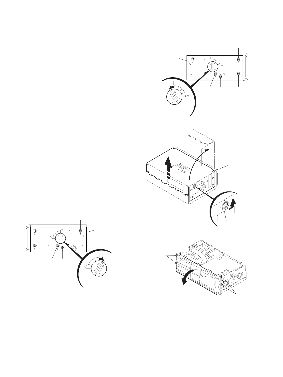
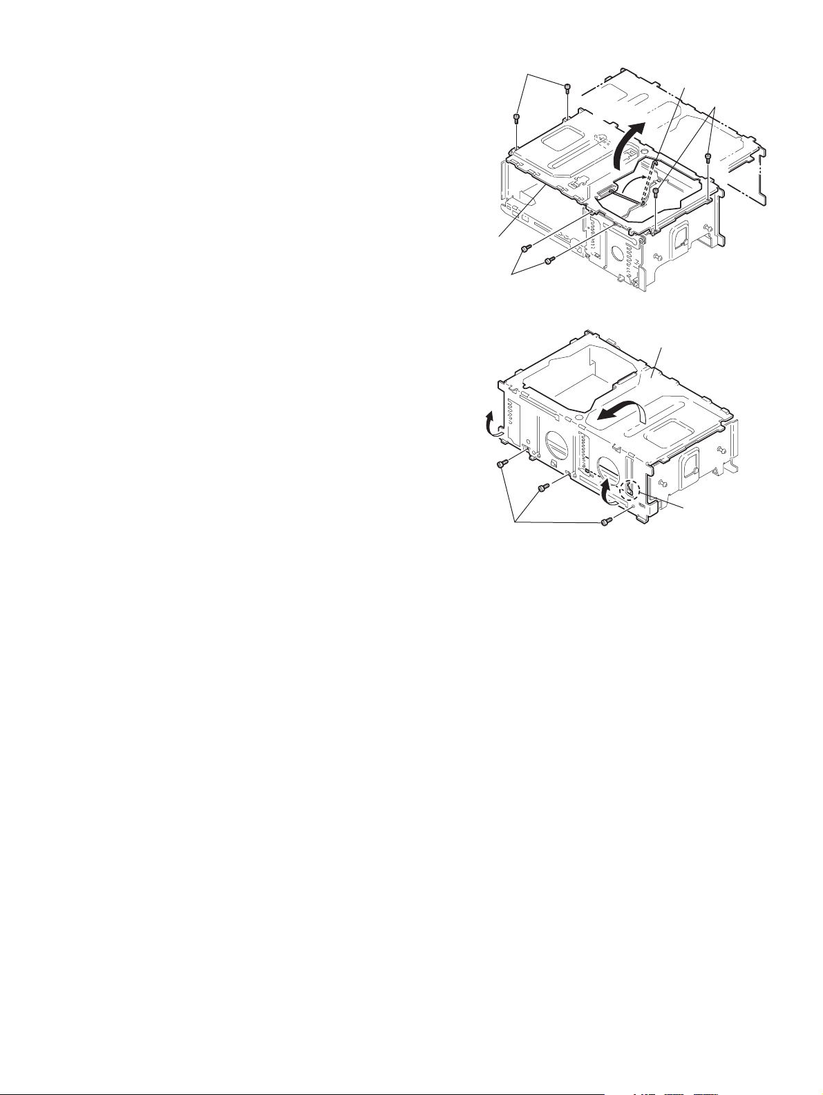
2.3.1 Removing the bottom cover and front panel assembly (See fig.1~4)
(1) Remove the screw A to unlock the mounting direction
knob located on the side of the main unit.
(2) Turn the mounting direction knob in the direction of the ar-
row using a coin, etc. to remove it. (The knob can be removed only when it is set to this position.)
(3) Remove the four screws B attaching the bottom cover on
both sides of the main unit.
(4) Turn the unit upside down so the bottom surface is facing
upward.
(5) Lift the rear edge of the bottom cover slightly and lift the
side by grasping the DIN jack section on the side panel,
then turn it toward the front (raise upward) to remove the
bottom cover.
(6) Release the four joints on both sides of the front panel,
and turn the front panel toward the top cover (lower down)
to remove the front panel.
SECTION 2
BB
Bottom cover
AB B
Fig.2
Bottom cove
B B
BAB
Fig.1
Bottom cove
DIN jack
Fig.3
Joints
Joints
Fig.4
1-4
Page 5
2.3.2 Removing the top cover (See fig.5~9)
r
A
(1) Pull out the dampers, being careful not to damage them.
REFERNCE:
When reattaching a damper, insert your finger to push
out the center of the damper to mount it on the damper
shaft, as shown in Fig. 6-1.
(2) Turn the damper spring bracket toward the top at a right
angle as shown in Fig. 7, then push down the lower side
of the damper spring bracket to lift it off.
(3) Remove the three screws C and D attaching the DIN jack
board assembly, and remove.
(4) Lift the changer unit upward.
(5) Remove the damper springs from the mechanism chassis
if required.
REFERENCE:
To reassemble, refer to the diagram below.
CH-X1500
Turn to the top position (at a right
angle) ,then the push down to lift off.
Damper spring bracket
Fig.7
Remove the card
wire if required
D
D
DIN jack board
Dampe
Fig.5
C
Fig.8
Changer unit
Damper
Fig.6
pply alcohol to the shaft then
immediately attach the damper. (After
attaching, check that the shaft is
correctly inserted.)
Damper shaft
Damper
Fig.9
Mechanisum chassis
Push out with your finger
before attaching
Fig.6-1
Damper spring
Silver
(Mechanisum side)
Damper spring
Black
(Magazine side)
Fig.9-1
1-5
Page 6
CH-X1500
2.3.3 Removing the fitting (See fig.10)
(1) Remove the screw E attaching the fitting.
(2) Release the two joints a on the top edge of the fitting, then
release the joints b at the left / right bottom edges, and
remove.
2.3.4 Removing the main board assembly (See fig.11)
(1) Remove the screw F attaching the power IC.
(2) Remove the four screws G attaching the main board as-
sembly, and remove.
(3) Disconnect the wire from connector CN602 on the main
board assembly.
(4) Disconnect the wire from connector CN501 on the main
board assembly.
(5) Disconnect the card wire from connector CN604 on the
traverse mechanism board assembly.
a
b
b
E
Fig.10
G
CN501
G
G
F
CN604
CN602
Main board assembly
Fig.11
1-6
Page 7
2.4 Changer-mechanism section
r
2.4.1 Remove the sensor assembly unit (See fig.12)
(1) Remove the two screws H attaching the sensor assembly
unit.
(2) Release the springs on the back of the sensor assembly
unit from the holes on the chassis.
2.4.2 Remove the magazine lock arm (See fig.12,13)
(1) Remove the magazine lock spring from the front side of
the chassis.
(2) Remove the poly-washer attaching the magazine lock
arm.
(3) Turn the magazine lock arm in the direction of the arrow
until the notch is at the c position to remove it from the
chassis.
H
Spring
CH-X1500
Sensor assembly Magazine lock arm
H
Fig.12
Magazine lock springMagazine lock arm
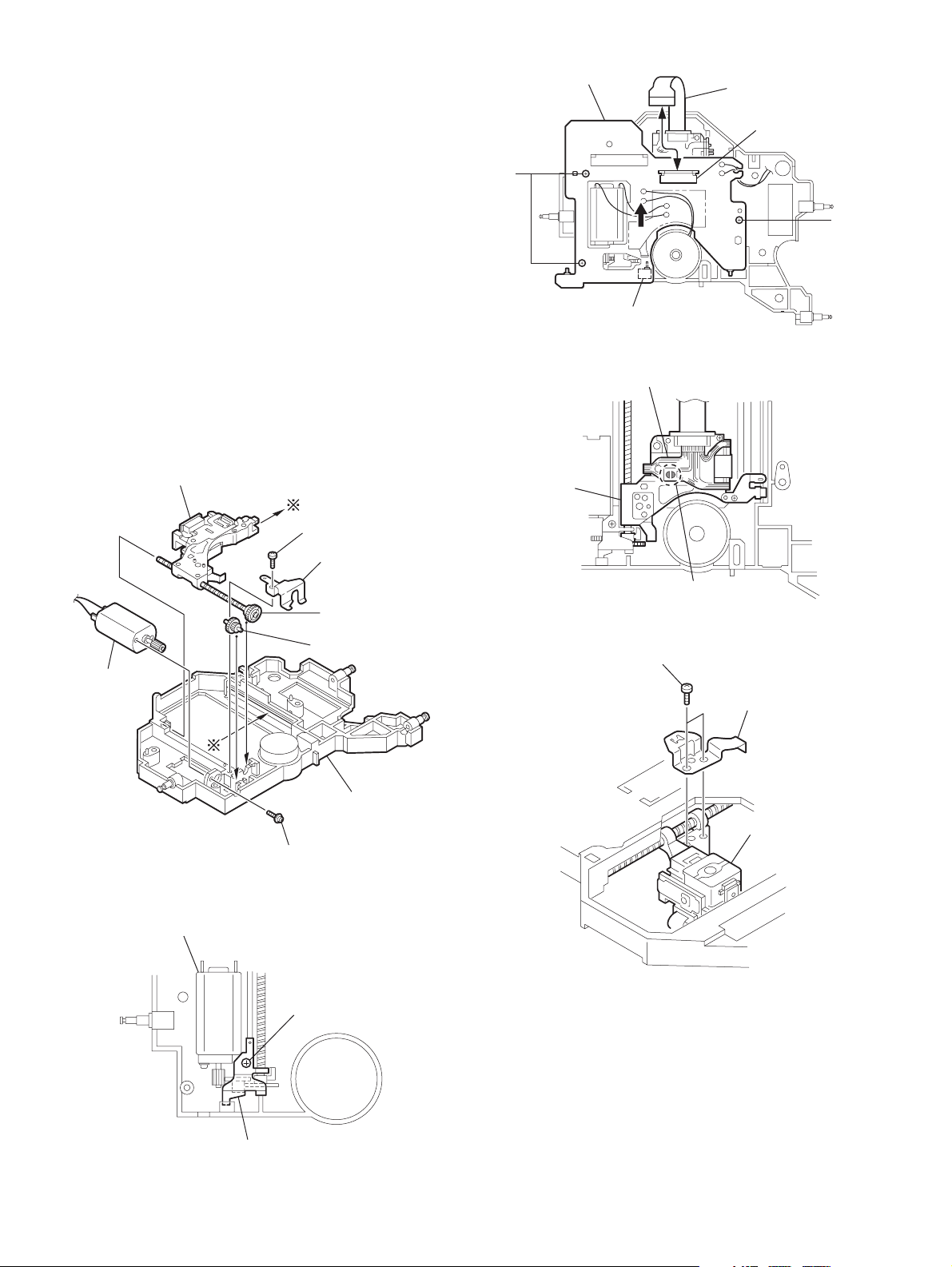
2.4.3 Remove the positioning motor assembly (See fig.14)
(1) Remove the two screws I attaching the positioning motor.
ATTENTION:
When removing the positioning motor assembly from
chassis, remove the spacer attaching the wires.
(2) Slightly lift the positioning motor assembly to remove it
from the two burrs on the chassis.
c
Poly-washer
Fig.13
I
Burrs
Positioning moto
assembly
Spacer
Fig.14
1-7
Page 8
CH-X1500
2.4.4 Remove the rear slider (See fig.15)
(1) Position the unit with the front section facing down. Rotate
the third gear located on the back of the main u nit in the
direction of the arrow (clockwise).
(2) Move the rear slider in the direction of the arrow and re-
move it at the rear slider mounting position (at the widest
hole).
2.4.5 Remove the front slider (See fig.16)
(1) Position the unit with the rear section facing down. Rotate
the third gear located on the bottom of the unit in the direction of the arrow (clockwise) until the front slider is moved
to the outermost position.
(2) Remove the E-washer attaching the front slider, and re-
move from the chassis.
Can be remove at the stud position
(At the wideness position)
Third gear
Fig.15
E-washer
Rear slider
Front slider
Third gear
Fig.16
1-8
Page 9
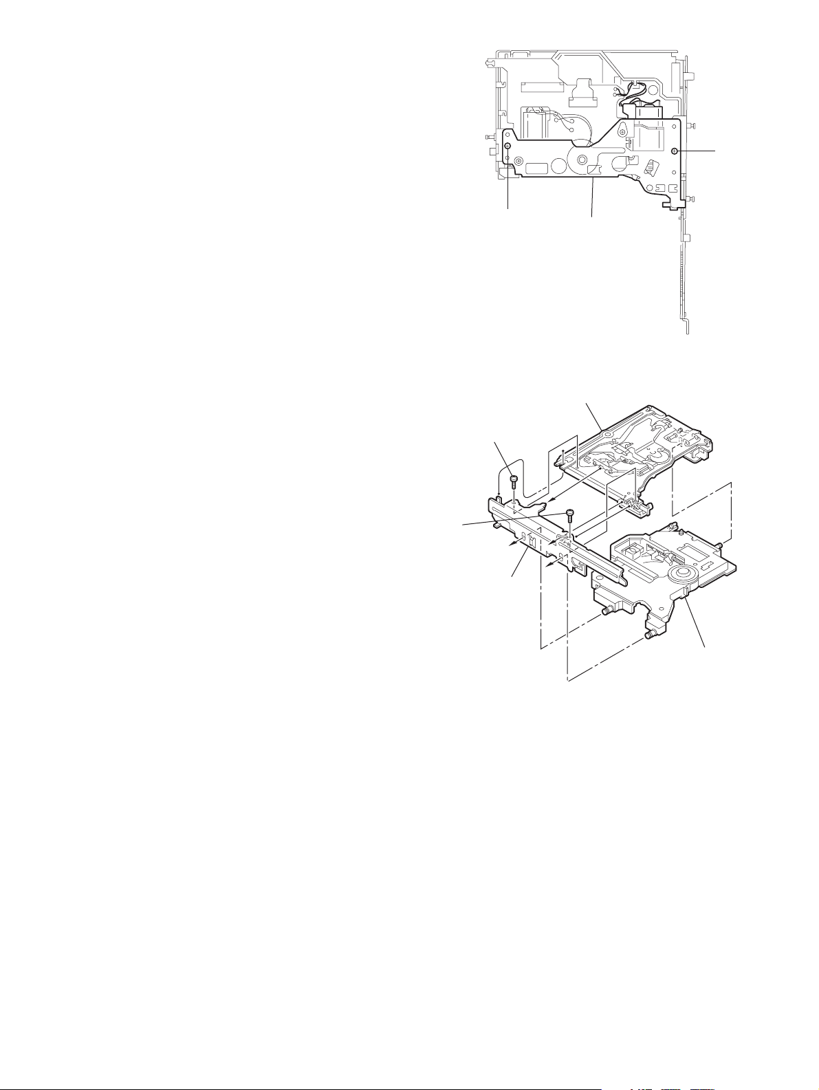
2.4.6 Remove the top plate (See fig.17,18)
(1) Remove the nine screws J attaching the top plate.
(2) Disconnect the section d attached to the rear of the unit,
then lift the top plate slightly.
(3) Move the top plate toward the rear of the unit to remove
the upper rod from the top plate.
CH-X1500
J
Rod
J
Top plate
J
Fig.17
Top plate
d
J
Fig.18
1-9
Page 10
CH-X1500
2.4.7 Remove the lifter unit (See fig.19,20)
(1) Remove the elevator spring located on the front side of the
unit. (Be sure to first remove the spring from the lifter side
as shown in the upper part of the diagram.)
(2) Lift the lifter unit upward, then remove the lower rod to re-
move the lifter unit from the chassis.
Remove this part first
Elevator spring
Proper orientation
Fig.19
Lifter unit
Fig.20
Lower rod
1-10
Page 11
2.4.8 Remove the lifter bracket (See fig.21)
(1) Remove the two screws K attaching the lifter bracket from
the back of the lifter unit.
(2) Remove the lower rod.
CH-X1500
K
K
2.4.9 Remove the side bracket and traverse mechanism assenbly (See fig.22)
(1) Remove the two screws L attaching the side bracket, and
remove the side bracket.
(2) Remove the three shafts on the traverse mech anism as-
sembly from the lifter unit.
L
L
Side bracket
Lifter bracket
Fig.21
Lifter unit
Fig.22
Traverse mechanism
assembly
1-11
Page 12
CH-X1500
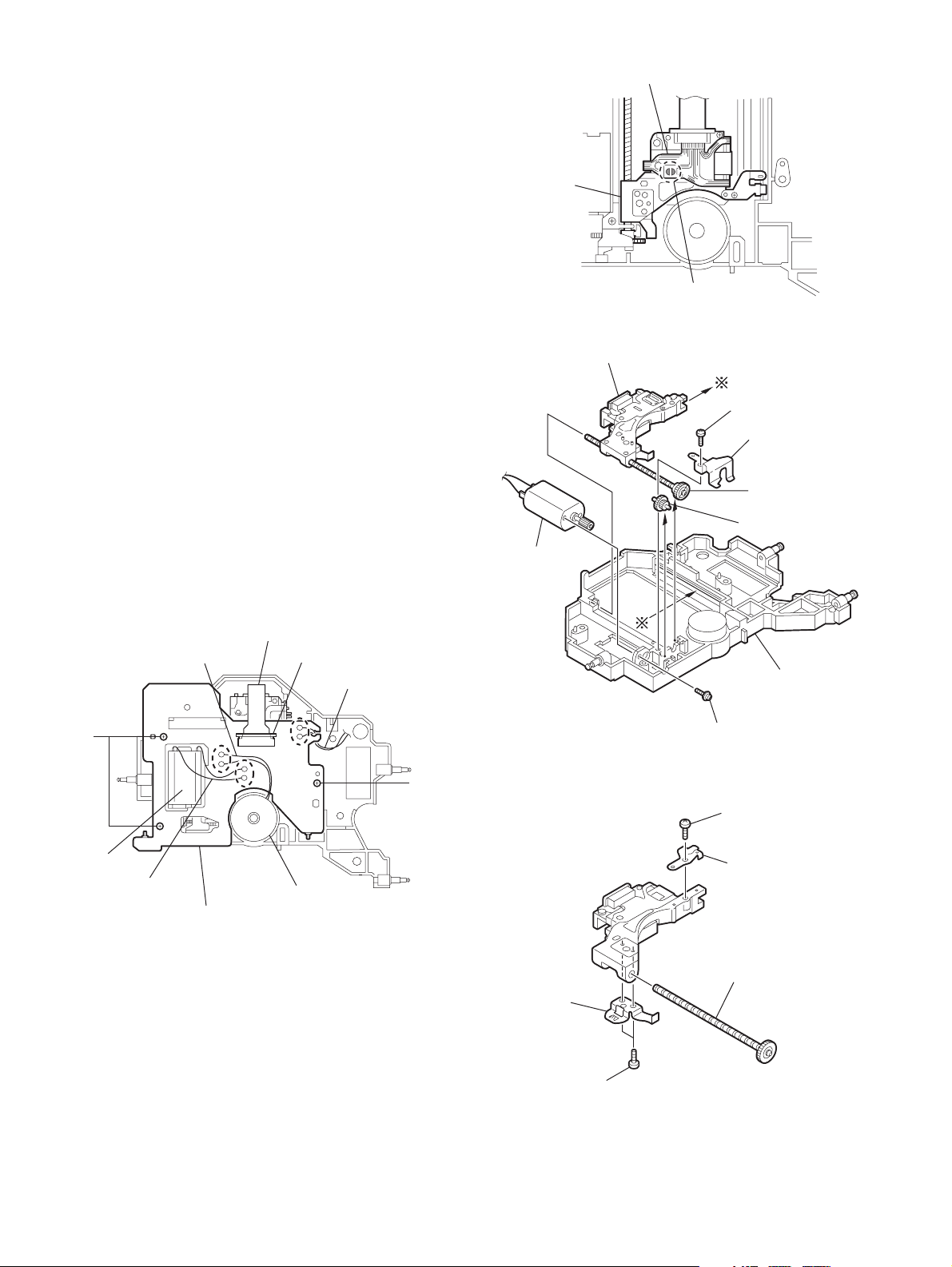
2.4.10 Remove the pickup assembly (See fig.23~26)
CAUTION:
When replacing the flexible wire connected, solder the shorting round point. Otherwise, the pickup may be damaged.
(1) Remove the three screws M attaching the mechanism
board on the back of the traverse mechanism assembly.
(2) Disconnect the two feed motor wires (blue and white), two
spindle motor wires (red and black) and two tray motor
wires (brown and black) that are soldered to the mechanism board assembly.
(3) Move and lift mechanism board assembly with the flexible
wire attached to connector CN603. Next, solder the sorting round point on the pickup assembly and then disconnect CN603.
(4) Remove the screw N attaching the feed motor assembly,
and remove.
(5) Remove the screw O attaching the shaft holder retaining
the feed slide shaft assembly and the middle gear, and remove.
(6) Remove the middle gear.
REFERENCE:
Remove gears and motors only when required.
(7) Move the pickup assembly upward from the gear section
and remove it from the traverse chassis assembly.
(8) Remove the two screws P attaching the rack arm, and re-
move.
(9) Pull out the feed slide shaft assembly, and remove.
(10) Remove the screw Q attaching the spring, and remove.
CAUTION:
When reassembling, connect the flexible wire from the
pickup to the main board and unsolder the shorting
round point.
Flexible wire
Spindle motor wire
CN603
Tray motor wire
Flexible wire
Pickup
Sorting round point
Fig.24
Pickup assembly
O
Shaft holder
Feed slide shaft
assembly
Middle gear
Feed motor
Traverse chassis
M
Feed motor
Feed motor wire
N
Fig.25
M
Q
Spring
Spindle motor
Mechanism board
Fig.23
Feed slide shaft assembly
Lack arm
P
Fig.26
1-12
Page 13
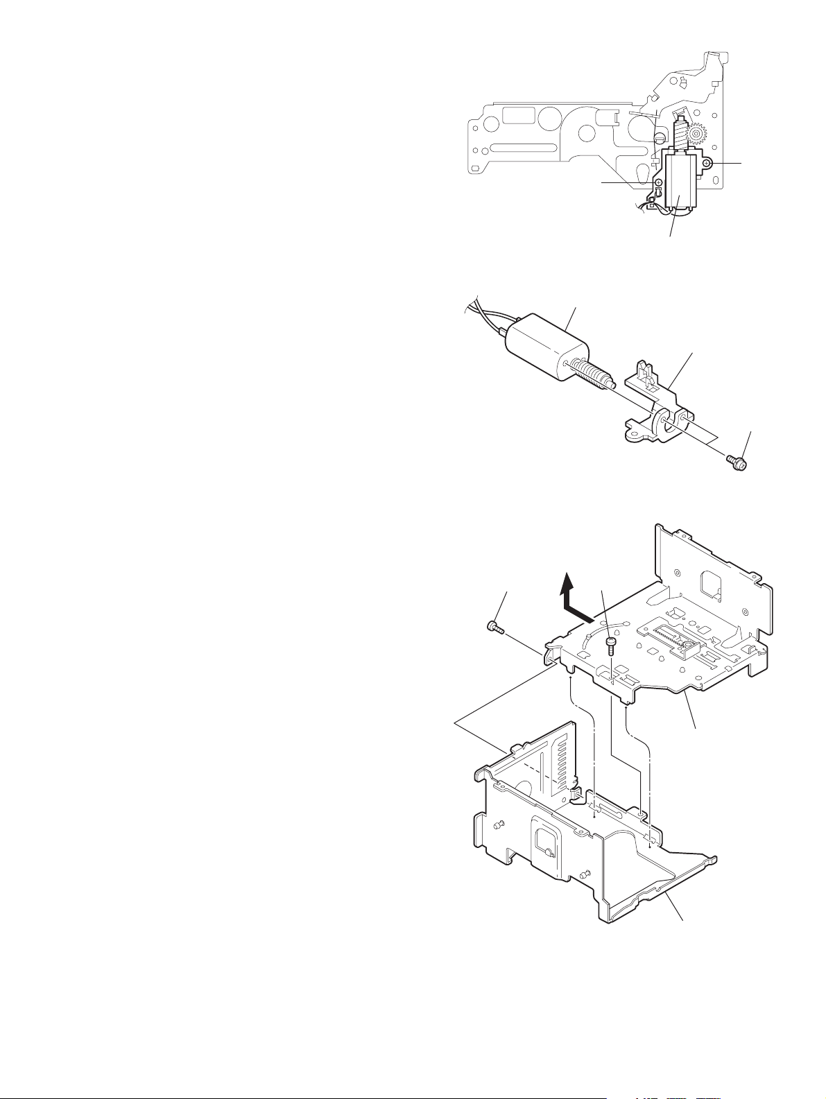
2.4.11 Removing the tray motor assembly (See fig.27, 28)
(1) Remove the two screws R attaching the tray motor as-
sembly, and remove.
(2) Remove the two screws S attaching the tray motor, and
remove the tray motor assembly from the tray motor holder.
CH-X1500
R
R
Tray motor assembly
Fig.27
Tray motor
Tray motor holder
2.4.12 Separation of the chassis (L) assembly and chassis (R) assembly (See fig.29)
(1) Remove the two screws T retaining the chassis (L) and
(R) assemblies.
(2) Slide the chassis (L) assembly toward the front and detach
it, then remove the chassis (L) upward.
T
Front side
S
Fig.28
T
Chassis(L) assembly
Fig.29
Chassis(R) assembly
1-13
Page 14
CH-X1500
2.5 Precautions reassembling REFERENCE:
When reassembling, also refer to the disassembling procedures.
2.5.1 Mounting the traverse mechanism assembly (See
fig.30~34)
(1) When mounting the pickup assembly, attach the feed slide
shaft assembly to the traverse chassis. Apply E-JC-525
grease to the shaft.
(2) Mount the middle gear and the feed slide shaft to the
traverse chassis and secure them with the screw O
through the shaft holder.
(3) Before attaching the mechanism board, move the pickup
to the outer edge position, then attach the mechanism
board using the screw M. At this time, check that the rest
switch is correctly placed.
(4) To mount the rack arm, first move the pickup to the middle
position and fixing it with the screw P.
CAUTION:
When reassembling the mechanism board, reattach the
flexible wire to connector CN603 on the mechanism
board, and then unsolder the sorting round point. Next,
reattach the mechanism board with screw M.
Pickup assembly
Mechanism board
M
Rest switch
Pickup
Flexible wire
CN603
M
Fig.32
Flexible wire
Feed motor
Feed motor assembly
Fig.30
O
Shaft holder
Feed slide shaft
assembly
Middle gear
Traverse chassis
N
Sorting round point
Fig.33
P
Lack arm
Pickup
Fig.34
1-14
O
Spindle
motor
Shaft holder
Fig.31
Page 15

2.5.2 Mounting the lifter unit (See fig.35~37)
(1) Insert the shafts e of the traverse mechanism assembly
into the slide grooves f on the lifter unit.
(2) Move the hook of the lifter unit to the edge, and move the
sliding lever inside the side bracket unit to the edge as
well.
(3) With each hole and lever shifted to the edge, mount the lift-
er unit and side bracket unit from the side. (Check each attached section, and check that the joint g of the lifter unit
is correctly inserted into the holes h of the side bracket
unit. After reassembled, check that levers move together.)
(4) Turn the lifter unit upside down.
As shown in Fig. 37, slide the lever 30 mm away from the
edge, and then mount the lifter bracket (L) assembly.
CH-X1500
e
Fig.35
Lifter unit
f
L
g
L
e
Side bracket
Lifter bracket(L) assembly
f
f
h
e
Traverse mechanism
assembly
Fig.36
Shift inside by approx. 30mm
Fig.37
1-15
Page 16

CH-X1500
2.5.3 Mounting the chassis (L) assembly and chassis (R)
assembly (See fig.38~40)
(1) Attach the lower rod to the chassis (R) assembly. While
shifting the rod toward the front side, mount the rod on the
lifter unit.
With the rod mounted, place the lifter unit on the chassis
(R) assembly.
(2) Combine the chassis (L) and (R) assemblies so that the
hook section i of the chassis (L) assembly is inserted into
the notch of the chassis (R) assembly by sliding it from the
front side, and then the two lib j jointed to the chassis (L)
assembly.
(3) After reassembled, fix with the screw T.
(4) Attach the elevator spring between the lifter unit and the
chassis.
Lifter unit
Lower rod
Chassis(R) assembly
Fig.38
Chassis(L) assembly
i
Attached
Chassis(R) assembly
T
Chassis(R) assembly
Fig.39
Chassis(L) assembly
T
j
j
Fig.40
1-16
Page 17

2.5.4 Mounting top plate (See fig.41~44)
(1) Mount the upper rod on the lifter side and set it on the rear
of the top plate, then mount the other end of the upper rod
to k .
(2) Check that the five points l, m, n, o and p are correctly
positioned.
When mounting section p, set it so that the bending section of the top plate pinches section q of the lifter unit.
(3) Attach the top plate with six screws J.
Remove this part first
Elevator spring
CH-X1500
k
Upper rod
Fig.42
J
Rod
J
Fig.41
Proper orientation
Top plate
J
Fig.43
Lifter unit
q
o section
lm
np
o
Fig.44
1-17
Page 18

CH-X1500
r
2.5.5 Mounting the front slider and rear slider (See fig.45, 46)
(1) Position the unit with the rear side facing down, then rotate
the third gear in the direction of the arrow (clockwise) until
the lift arm comes to the position at which the holes are ex-
posed.
(2) Mount the front slider from the top.
Rotate the third gear counterclockwise until the hole of the
slider is lined up with the right hole of the stud.
(3) Attach the E-washer on the shaft.
(4) Position the unit with the front side facing down, then
mount the rear slider.
Check that the r, s and t positions are correctly mounted
as shown in Fig. 46.
(5) Rotate the third gear in the direction of the arrow (counter-
clockwise) until the lifter unit is at the top position.
Front slider
E-washer
Stud
Psition so that
the stud and
right hole
are lined up.
Rotate until the holes
are lined up.
rst
Set the holes
are exposed.
Lift arm
Fig.45
Lifter unit
Rotate the third gea
to move the slider.
Fig.46
1-18
Page 19

2.5.6 Mounting the sensor board assembly (See fig.47)
r
(1) Attach the longer spring to the white resin, and attach the
shorter spring temporarily to the sensor assembly bracket.
(2) Mount the sensor assembly so that the shaft of the lift arm
is inserted into the longer hole on the white resin located
on the back of the sensor board assembly.
(3) Attach the shorter spring to the hook of the lift arm.
2.5.7 Mounting the main board (See fig.48)
(1) Rotate the third gear clockwise until section u of the front
slider and the third hole from the right are lined up. (Be
sure to set properly. If incorrectly set, the switches on the
assembly may be damaged.)
(2) After they are correctly positioned, mount the main board
assembly.
CH-X1500
Sensor board assembly
Attach temporarity
Shote
spring
Shorter
Longer
spring
Fig.47
u
Front slider
u
Third gear
Fig.48
1-19
Page 20

CH-X1500
2.5.8 Pickup replacement procedure (See fig.49~55)
(1) Remove the bottom cover, front panel and top cover of the
exterior section.
(2) Remove the card wire from the connector CN604 on the
mechanism board.
(3) Rotate the rear slider and third gear in the lifter section
counterclockwise and then the traverse mechanism as-
sembly is move in the lowermost (bottom) position.
(4) Unsolder the two wires (black and brown) connected to the
tray motor.
(5) Remove the two screws K from the round holes on the
chassis (R) assembly to remove the lifter bracket (L).
(6) Remove the lower rod.
(7) Unsolder the two wires (blue and white), two wires of spin-
dle motor (red and black) and wire of tray motor (brown
and black) soldered on the mechanism board.
(8) Solder the sorting round point on the pickup assembly to
move the mechanism board and then unplug the flexible
wire from CN603 on the mechanism board.
(9) Remove the flexible wire from the connector CN603 on the
mechanism board.
(10) Remove the three screws M from the round hole on the
chassis (R) assembly, and remove.
(11) Remove the screw O attaching pickup shaft holder, and
remove the pickup assembly.
CAUTION:
When replacing the pickup, be sure to apply countermeasures against static electricity (grounding the operation table, wrist band and soldering iron). To remove
it, first sorting round point on the mechanism board, then
lift the mechanism board assembly with CN603 connected. Next, sorting round point on the pickup main
unit, then unplug the pickup flexible board from connector CN603.
ATTENTION:
When reassembling, perform in the reverse order.
(12) Remove the two screws P attaching lack arm. Pull out the
feed slide shaft assembly. Remove the screw Q attaching
shaft holder.
(13) When mounting the lifter bracket after replacing the pick-
up, move the lifter unit lever approx. 30mm towards the in-
side and then mount the lifter bracket.
Main board
Third gear
M
Mechanism board
Pickup assembly
Flexible wire
Pickup
Unsolder
M
CN603
Fig.50
Shaft holderSpindle motor
O
Fig.51
Soting round point
Fig.52
K
Tray motor assembly
1-20
Unsolder
CN604
Fig.49
Lifter bracket(L)
K
Feed motor
Lack arm
Pickup
Q
Spring
Feed slide shaft assembly
P
Fig.53
Page 21

Pickup assembly
Middle gear
CH-X1500
O
Shaft holder
Feed slide shaft
assembly
Traverse chassis
Fig.54
Shift approx.30mm
Shift approx.30mm
Lifter unit lever
Fig.55
1-21
Page 22

CH-X1500
3.1 Forced eject procedures
SECTION 3
Adjustment method
Magazine eject does not function.
RESET (Press EJECT for 3 sec.)
YES
Completed
Check that the trays remain no more
than 10 mm inside the magazine.
Improperly positioned
Remove the dampers and the top
cover to take out the mechanism.
Remove the item(s) causing the
disc-jam through the clearance at
the top of the lifter.
Are trays stored in
the magazine?
Check visually.
Remove the bottom cover
NO
Is the disc set in the playing
position?
Rotate the third gear clockwise and
unchuck the disc.
Disconnect the tray from the hook.
NO
NO
YES
YES
Peel off the sticker on the left side
of the unit. Insert a screwdriver
and press the internal lever to
forcibly eject the magazine.
Completed
Remove the lifter bracket (L) and
return the tray to the magazine.
Place the unit with its left side
facing down and apply a slight
shock, then return the tray to the
magazine.
Rotate the third gear clockwise
until the lifter level is below the 9th
tray position.
Press the magazine lock lever to
eject the magazine.
Completed
1-22
Page 23

3.2 Troubleshooting
3.2.1 Servicing procedures for CH-X1500 error displays
CH-X1500
Error display
E1: Eject error
E2: Position
motor error
E3: Tray motor
error
Servicing procedure
The magazine cannot be ejected until S601 (magazine switch) turns off.
Can the magazine be ejected? YES 1, NO 2
1 The magazine switch (S601) does not turn off even though the magazine is completely ejected.
2 Check that the magazine is not engaged with the mechanism assembly.
The lifter does not move up and down when exchanging or ejecting discs.
After resetting, check whether or not the lifter moves.YES 3, NO 4
3 If the lifter exceeds the required disc position, check the lift position input. (IC601 pin 76)
If the lifter does not reach the required disc position, check the mechanism (mainly the lifter
elevation mechanism)
4 Check that voltage is present at the motor terminal.
If voltage is present, check the lifter elevation mechanism. If voltage is not present, separate the
motor from the circuit and check again whether or not voltage is present.
If voltage is present, next check that the armature resistance of the position motor (resistance
between motor terminals) is approx. 12 .
If the resistance is excessively low (1 - 2 ), the motor is defective.
Trays cannot be opened or closed when exchanging or ejecting discs.
Does the tray move when changing or ejecting discs?YES 5, NO 6
5 Check that TRAY OUT SW (S602) and TRAY IN SW (S603) function correctly.
S602 & IC601 pin (46) S603 & IC601 pin (45)
E4: Pick returning
error
When opening
When closing
6 Check that the drive voltage is applied to the motor terminal.
If the voltage is present, check the tray mechanism.
If the voltage is not present, separate the motor from the circuit and check again whether or
not the voltage is present.
Does the feed (pickup unit) return to the inner area of the disc when ejecting?
YES 7, NO 8, 9
7 Check the rest switch.
8 If the feed gear is rotated, check the feed transfer mechanism
9 If the feed gear is not rotated, check the motor driver and the pattern.
H
L
HL
Other errors occurring in the receiver or controller.
E8: Connection
error
The E1 ~ E8 error displays described above may appear as E-1 ~ E-8, 1E1 ~1E8, R-1 ~ R-8, or RST1 ~ RST8,
depending on the product.
When selecting the CD Changer mode using function keys, etc., the unit does not enter the CD
changer mode, or the E8 error display appears. This signifies trouble relating to communications.
a Check the connection cables between the CD changer and the receiver (CD changer controller).
b Check the CD changer power cord and the fuse (including F901 on the PC board).
c Check IC651 and its peripheral circuits.
1-23
Page 24

CH-X1500
3.2.2 CH-X1500 Error code
The following error codes can be displayed and stored in up to 3 memories when the KD-MX3000 is used with the controller. Refer
to the KD-MX3000 service manual regarding error code indication.
The error code indication when using the earlier controller is the same as the CH-X99,KD-MK88 and other 12CD changer models.
CH-1 error code table
Generating condition Description Error code
Tray extension error Tray-in switch time out
(Tray-in switch Low Tray-out switch High)
Tray-out switch time out
(Tray-in switch High Tray-out switch High)
Tray-in switch time out
(Tray-in switch Low Tray-out switch Low)
MAG-in switch Low to High Magazine removed when tray partly extende E1 03 00 14
Tray retraction error Tray-in switch time out
(Tray-in switch Low Tray-out switch Low)
Tray-out switch time out
(Tray-in switch High Tray-out switch High)
Tray-in switch time out
(Tray-in switch Low Tray-out switch Low)
MAG-in switch Low to High Magazine removed when tray partly retracted E1 03 00 19
Lifter raise error Wait position time out Position motor inoperative E1 02 00 21
Wait position time out Position not stable in fine adjust mode E1 02 00 22
Wait position time out Other fault E1 02 00 23
Lifter lower error Wait position time out Position motor inoperative E1 02 00 26
Wait position time out Position not stable in fine adjust mode E1 02 00 27
Wait position time out Other fault E1 02 00 28
Chuck error Play position time out Position motor inoperative E1 02 00 31
Play position time out Position not stable in fine adjust mode E1 02 00 32
Play position time out Other fault E1 02 00 33
Unchuck error Wait position time out Position motor inoperative E1 02 00 36
Wait position time out Position not stable in fine adjust mode E1 02 00 37
Wait position time out Other fault E1 02 00 38
Eject error Eject position time out Position motor inoperative E1 02 00 41
Eject position time out Eject position not attained E1 02 00 42
MAG in switch time out Magazine not ejected E1 02 00 43
Initialize error Mechanism switch time out Both Tray-in and Tray-out Low E1 03 00 46
Absolute position time out Not stable at absolute position E1 03 00 47
Tray stops part way E1 03 00 11
Tray stops part way E1 03 00 12
Tray-in switch faulty or other defect E1 03 00 13
Tray motor inoperative E1 03 00 16
Tray retraction stops part way E1 03 00 17
Tray-in switch faulty or other defect E1 03 00 18
Note:
The 1st error code is indicated by E1, while the 2nd and 3rd error codes are respective ly indicated by E2 and E3.
1-24
Page 25

3.3 Flow of functional operatio n until TOC read
CH-X1500
When the pickup correctly moves
to the inner area of the disc
Microprocessor
commands
FMO
TC9462
FEED MOTOR
IC581
RESET SW
53
TERMINAL
20
$ 83
$ 82 $81
5V
Hi-Z
0V
6V
4V
2V
OFF
ON
• When correctly focused
FSO
14
2.2V
Focus Servo Loop ON
Power ON
Set Function to CD
Disc inserted
Pickup feed to the inner area
YES
Laser emitted
Focus search
YES
Disc rotates
RF signal eye-pattern
remains closed
Tracking loop closed
RF signal eye-pattern
opens
TOC readout
Jump to the first track
When the laser diode correctly
emits
Microprocessor
commands
SEL
TC9462
LD
CN502
or
CN503
57
5
22
$ 84
"No disc"
display
When the disc correctly rotates
Microprocessor
commands
DMO
TC9462
Spindle
motor (+)
1
IC581
$ 8A
55
AccelerationAcceleration
0.2Sec 0.5Sec
$ 86
$ A200
Rough
Servo
Tracking Servo Loop ON
5V
0V
4V
0V
5V
2.2V
0V
6V
3.2V
2V
Servo CLV
Play
RF signal
Rough Servo Mode
CLV Servo Mode
(Program Area)
CLV Servo Mode
(Lead-In Area;
Digital: 0)
1-25
Page 26

CH-X1500
3.3.1 General section
Turn the power on with
no magazine loaded.
Reset
Move the lifter until it
comes to the STOP
position
(shipping position).
YES
Connect the receiver,
etc. and turn the power
on.
Set to the changer
mode.
CD changer indication
appears on the receiv
etc.
YES
Load the magazine.
Is the disc pulled out to
start play?
YES
Is the disc taken out?
Is the disc rotated?
Is voltage present at
IC521 pin z 2.5 V while
Proceed to the Tracking
Is track selection or
search performed
correctly?
NO
NO
er,
NO
YES
YES
the disc rotates?
YES
section.
NO
The lifter moves up or
down and stops.
NO
The position motor does
not function.
NO
The tray motor goes
forward and back
several times.
Check the connections
to the receiver or the
circuits in the vicinity of
IC651.
NO
NO
NO
Check the MAG SW,
TRAY-IN, and TRAY-
OUT switches.
Proceed to
the Signal
Processing
section.
YES
Check the linear position
sensor (VR601).
YES
Check the wiring of the
CD 9 V power supply
position motor.
Check the TRAY-IN and
TRAY-OUT switches.
Proceed to the Focus
Exchange discs, then
check whether or not the
feed motor moves.
Set from the STOP to
PLAY mode, then check
that the triangle wave
appears at IC581 pins H
Does the laser emit?
Proceed to the Focus
section.
YES
and I .
YES
YES
section.
NO
NO
NO
Check the RESET
switch and feed
section
(Refer to the Feed section).
Check the vicinity of
IC501 6and 7.
1-26
YES
10. Is the playback
sound normal?
YES
Normal
NO
Proceed to the Signal
Processing section.
Page 27

3.3.2 Feed section
Is the voltage output at
IC521 pin u 5V or 0V?
YES
Is the wiring for IC521
(90) (100) correct?
YES
Is 5V present at IC581
pin 6?
YES
Check the vicinity of
IC521.
CH-X1500
NONO
Check CD 9V
and 5V.
Is 4V present at both
sides of the feed motor?
YES
Check the feed motor.
3.3.3 Focus section
When the lens is
moving:
Does the S-search
waveform appear at
IC581 pins H and I?
YES
3.3.4 Spindle section
Is the disk rotated?
YES
Does the RF signal
appear at TP1?
YES
4V
NO
NO
Is 6V or 2V present at
IC581 Q and R?
Check IC581.
NO
Check the circuits in
the vicinity of IC581
Check the pickup and
its connections.
Is 4V present between
IC581 pins 1 and 2?
Check the spindle motor
and its wiring.
NO
NO
pins H K.
YES
YES
Check the feed motor
connection wiring.
NO NO
Is 4V present at IC521
pin x?
YES
Check the vicinity of
IC581.
Check IC501 and
IC521.
Is the RF waveform at TP1
distorted?
YES
Proceed to the Tracking
section
3.3.5 Tracking section
When the disc is rotated
at first:
Approx. 1.2 V
Is the tracking error
signal output at TP3?
YES
Check IC521.
Check the circuits in the
vicinity of IC501 J O or
NO
the pickup
Check the circuit in the
vicinity of IC501 pins
2C.
YESYES
Check the pickup and
its connections.
1-27
Page 28

CH-X1500
3.3.6 Signal processing section
Is the sound output from
both channels (L, R)?
YES
Normal
No sound from either
channel.
YES
Is 9V present at IC101 pin
(8)?
YES
NONO
Compare the L-ch and
R-ch to locate the
defective point.
NO
Check the vicinity of the
Q981 audio power
supply.
Is the audio signal
(including sampling output
components) output to
IC521 pins ^and | during
YES
Is the audio signal output
at IC101 pins 1
and7during playback?
YES
Check the muting circuit.
NO
NO
Check IC521 and its
peripheral circuits.
Check IC101 and its
peripheral circuits
1-28
Page 29

3.4 Maintenance of laser pickup
(1) Cleaning the pick up lens
Before you replace the pick up, please try to clean the lens
with a alcohol soaked cotton swab.
(2) Life of the laser diode
When the life of the laser diode has expired,the following
symptoms will appear.
• The level of RF output (EFM output:ampli tude of eye
pattern) will be low.
CH-X1500
3.5 Replacement of laser pickup
Turn off the power switch and,disconnect the
power cord from the ac outlet.
Replace the pickup with a normal one.(Refer
to "Pickup Removal" on the previous page)
Is RF output
1.0 0.35Vp-p?
NO
Replace it.
YES
O.K
(3) Semi-fixed resistor on the APC PC board
The semi-fixed resistor on the APC printed circuit board
which is attached to the pickup is used to adjust the laser
power.Since this adjustment should be performed to
match the characteristics of the whole optical block, do not
touch the semi-fixed resistor. If the laser power is lower
than the specified value,the laser diode is almost worn out,
and the laser pickup should be replaced. If the semi-fixed
resistor is adjusted while the pickup is functioning normally,the laser pickup may be damaged due to excessive current.
Plug the power cord in,and turn the power on.
At this time,check that the laser emits for
about 3seconds and the objective lens moves
up and down.
Note: Do not observe the laser beam directly.
Play a disc.
Check the eye-pattern at TP1.
Finish.
1-29
Page 30

CH-X1500
SECTION 4
Description of major ICs
4.1 AK4381VT-X (IC121) : 2ch DAC
• Pin layout • Pin functions
1
2
3
4
5
6
7
8
16
15
14
13
12
11
10
9
Pin No Symbol Function
1 MCLK Master clock input pin
2 BICK Audio serial data clock pin
3 SDTI Audio serial data input pin
4 LRCK L/R clock pin
5 PDN Power-Down mode pin
6 CSN Chip select pin
7 CCLK Control data input pin
8 CDTI Control data input pin
9 AOUTR- Rch negative analog output pin
10 AOUTR+ Rch positive analog output pin
11 AOUTL- Lch negative analog output pin
12 AOUTL+ Lch positive analog output pin
13 VSS Ground pin
14 VDD Power supply pin
15 DZFR Rch data zero input detect pin
16 DZFL Lch data zero input detect pin
• Block diagram
CSN
CCLK
CDTI
LRCK
BICK
SDTI
uP
Interface
Audio
Data
Interface
PDN
De-emphasis
Control
8X
Interpolator
8X
Interpolator
MCLK
Clock
Divider
Modulator
Modulator
SCF
SCF
VDD
VSS
DZFL
DZFR
AOUTL+
AOUTL-
AOUTR+
AOUTR-
1-30
Page 31

4.2 DB4833FVE-W (IC502) : Voltage detector
• Pin layout • Block diagram
CH-X1500
45
123
• Pin functions
Pin No Symbol Function
1 VOUT Reset output
2 SUB Sub slate (connect to GND)
3 N.C. Non connect
4GNDGND
5 VDD Power supply voltage
VDD
VOUT
Vref
GND
1-31
Page 32

CH-X1500
4.3 BD7961FM-X (IC681) : Power driver
• Pin layout & Block diagram
35 34 33 32 31 30 29 28 27 26 25 24 23 23 21 20 19
36
CH6
BIAS
MUTE
(CH1~CH4)
REG2
REG1
Vcc2
(POW Vcc
CH5/6)
(REG GND)
Vcc3GND3
(POW Vcc
REG Vcc)
Vcc1
(POW Vcc
CH1~4)
CONT1
LD
LD
CONT2
10k
10k
CH4
10k
10k
Level shift
CH3
10k
10k
Level shift
10k
10k
(POW GND
CH5/6)
GND2
Control
logic
CH5
Control
RR
logic
FF
123456789 101112131415161718
• Pin functions
Pin No Symbol Function
1 GND2 Power GND (loading driver unit)
2 OUT5- Loading driver (CH5) output 3 OUT5+ Loading driver (CH5) output +
4 IN5FWD Loading driver (CH5) FWD input
5 IN5REV Loading driver (CH5) REV input
6 IN6REV Loading driver (CH6) REV input
7 IN6FWD Loading driver (CH6) FWD input
8 REG2SW Regulator 2 switch terminal
9 REG1SW Regulator 1 switch terminal
10 IN4 CH4 input
11 IN3 CH3 input
12 IN1 CH1 input
13 IN2 CH2 input
14 GND1 Power GND (BTL driver unit)
15 OUT2- BTL driver (CH2) output 16 OUT2+ BTL driver (CH2) output +
17 OUT1- BTL driver (CH1) output 18 OUT1+ BTL driver (CH1) output +
REG2 SW
REG1 SW
47k
23.5k
23.5k 23.5k
47k
23.5k
47k 47k
Level shift Level shift
10k
10k
10k
CH2
GND1
10k
10k
CH1
10k
10k
Pin No Symbol Function
19 OUT3+ BTL driver (CH3) output +
20 OUT3- BTL driver (CH3) output 21 OUT4+ BTL driver (CH4) output +
22 OUT4- BTL driver (CH4) output 23 LDCONT2 Loading driver (CH6) voltage setting
24 LDCONT1 Loading driver (CH5) voltage setting
25 Vcc1 Supply voltage (BTL driver unnit)
26 Vcc3 Supply voltage (regulator unit)
27 GND3 REG GND (regulator unit)
28 Vcc2 Supply voltage (loading driver unit)
29 REG1OUT Regulator output 1
30 REG1 B Regulator 1 Tr base
31 REG2 B Regulator 2 Tr base
32 REG2OUT Regulator output 2
33 MUTE BTL drivermute terminal
34 OUT6+ Loading driver (CH6) output +
35 OUT6- Loading driver (CH6) output 36 BIAS BIAS terminal
10k
1-32
Page 33

4.4 BR24C01AFV-W-X (IC503) : EEPROM
A
• Pin layout
Vcc WP SCL SDA
A0 A1 A2 GND
• Block diagram
CH-X1500
A0
1
7bit
A1
2
A2
3
GND
• Pin function
Pin name I/O Description
Vcc - Power supply
GND - Ground (0v)
A0A1A2 IN Slave address set
SCL IN Serial clock input
SDA IN / OUT Slave and word addressserial data input serial data output *1
WP IN Write protect input
4
ADDRESS
DECODER
CONTROL LOGIC
HIGH VOLTAGE GEN.
1kbit EEPROM ARRAY
SLAVE/WORD
7bit
ADDRESS REGISTER
START
STOP
Vcc LEVEL DETECT
DATA
REGISTER
ACK
8bit
Vcc
8
WP
7
SCL
6
SD
5
*1 An open drain output requires a pull-up resister.
1-33
Page 34

CH-X1500
4.5 HD74HCT126T-X : (IC541,IC691) Buffer
• Pin arrangement • Pin function
1C
1A
1Y
2C
2A
2Y
GND
• Block diagram
1
2
3
4
5
6
7
14
13
12
11
10
Vcc
4C
4A
4Y
3C
9
3A
8
3Y
1A
Input Output
CA Y
LX Z
HL L
HH H
H : High level
L : Low level
X : Irrelevant
Z : Off (Hhigh-impedance)state of a 3-stage output
1C
2A
2C
3A
3C
4A
1Y
2Y
3Y
4Y
1-34
4C
Page 35

4.6 NJM4565V-X (IC151) : Dual ope amp
T
• Terminal layout & Pin function
1
2
3
4
4.7 NJU7241F25-X (IC653) : Regulator
• Pin layout
CH-X1500
1
8
A
+
-
7
B
+
-
6
AOUTPUT
2
A-INPUT
3
A+INPUT
4
V
5
B+INPUT
6
B-INPUT
7
B OUTPUT
8
V
5
GND 1
VIN 2
VOUT 3
• Block diagram
VIN 2
STB 5
GND 1
4.8 NJU7241F33-X (IC652) : Voltage regulator
5 STB
4 NC
Short protect
3 VOU
Vref
1 GND
1
2
3
5
4
PIN FUNCTION
1. GND
IN
2. V
3. VOUT
4. +NC
5. STB
1-35
Page 36

CH-X1500
4.9 TA2157FN-X (IC601) : RF amp
• Terminal layout
24 ~ 13
1 ~ 12
• Block diagram
13
14
15
16
17
18
19
20
21
10pF
40k30k
20k 20k
20k
20k
15k
50 A
12k
12k
BOTTOM
PEAK
20k
20k
20k
PEAK
1.3V
40k
240k
15pF
240k
15pF
40k
50k
2k
20k
50k
14k
K
1
15k
x0.5
x2
x0.5
x2
1k
2k
1.75k
10pF
12
11
10
9
8
7
6
5
4
180k
40pF
60k
60k
PIN
VCTRLPIN
22
23
24
SEL
(APC SW)
180k
40pF
3k
3k
TEB
(TE BAL)
VCC APC ON -50% +12dB
HiZ APC ON 0% +6dB
GND
APC OFF
(LDO=H)
50% 0dB
94k
22k
94k
22k
RFGC
(AGC Gian)
3
2
1
TEB
(TE BAL)
Normal mode
(0dB)
Normal mode
(0dB)
CD-RW mode
(+12dB)
1-36
Page 37

• Pin function
Pin No. S ymbol I/O Function
1 VCC - 3.3V power supply pin
2 FNI I Main-beam amp input pin
3 FPI I Main-beam amp input pin
4 TPI I Sub-beam amp input pin
5 TNI I Sub-beam amp input pin
6 MDI I Monitor photo diode amp input pin
7 LDO O Laser diode amp output pin
8 SEL I APC circuit ON/OFF control signal, laser diode (LDO) control signal input
or bottom/peak detection frequency change pin.
CH-X1500
SEL
GND
Hiz
VCC
9 TEB I Tracking error balance adjustment signal input pin
Adjusts TE signal balance by eliminating carrier component from PWM signal (3-state output,
PWM carrier = 88.2kHz) output from TC94A14F/FA
TEBC pin using RC-LPF and inputting DC.
TEBC input voltage:GND~VCC
10 TEN I Tracking error signa l generation amp negative-phase input pin
11 TEO O Tracking error signal generation amp output pin.
Combining TEO signal RFRP signal with TC94A14F/FA configures tracking search system.
12 RFDC O RF signal peak detection output pin
13 GVSW I AGC/FE/TE amp gain change pin
APC
circuit
LDO
OFF Connected VCC through 1k resistor
ON
Control signal output
ON Control signal output
GVSW Mode
GND
Hiz
CD-RW
Normal
VCC
14 VRO O Reference voltage (VRO) output pin
*VRO=1/2VCC When VCC=3.3V
15 FEO O Focus error signal generation amp output pin
16 FEN I Focus error signal generation amp negative-phase input pin
17 RFRP O Signal amp output pin for track count
Combining RFRP signal and TEO signal with TC94A14F/FA configures tracking search system.
18
19
20
21 AGCIN I RF signal amplitude adjustment amp input pin
22 RFO O RF signal generation amp output pin
23 RFI I RF signal generation amp input pi n
24 GND - GND pin
REIS
RFGO
RFGC
I
OIRF signal amplitude adjustment amp output pin
RF amplitude adjustment control signal input pin
Adjusts RF signal amplitude by eliminating carrier component from PWM signal (3-state output,
PWM carrier=88.2kHz)output fromTC94A14F/14FA *RFGC pin using RC-LPF and inputting DC.
*RFGC input voltage:GND~VCC
1-37
Page 38

CH-X1500
4.10 TC94A14FA (IC621) : DSP & DAC
• Terminal layout & block daiagram
48 47 46 45 44 43 42 41 40 39
38 37 36 35 34 33
49
50
51
52
53
54
55
56
57
58
59
60
61
62
63
LPF
generator
Micro-
controller
interface
Clock
1-bit
DAC
Correction
Audio out
circuit
circuit
Address
circuit
16 k
RAM
Digital
output
PWM
Servo
control
ROM
RAM
CLV servo
Synchronous
guarantee
EFM
decoder
Sub code
decoder
Digital equalizer
automatic
adjustment circuit
A/D
Data
slicer
VCO
PLL
TMAX
D/A
32
31
30
29
28
27
26
25
24
23
22
21
20
19
18
64
17
161514131211101 2 3 4 5 6 7 8 9
• Pin function
Pin
Symbol I/O Descroption
No
1 BCK O Bit clock output pin.32fs48fsor 64fs selectable by command.
2 LRCK O L/R channel clock output pin."L" for L chann el an d " H" for R channel.
Output polarity can be inverted by command.
3 AOUT O Audio data output pin. MSB-first or LSB-first selectable by command.
4 DOUT O Digital data output pin.Outputs up to double-speed playback.
5 IPF O Correction flag output pin. When set to "H" AOUT output cannot be corrected by C2 correction processing.
6V
DD3
7V
SS3
- Digital 3.3V power supply voltage pin.
- Digital GND pin.
8 SBOK O Subcode Q data CRCC result output pin. "H" level when result is OK.
9 CLCK O Subcode P-W data read I/O pin. I/O polarity selectable by command.
10 DATA O Subcode P-W data output pin.
11 SFSY O Playback frame sync signal output pin.
12 SBSY O Subcode block sync signal output pin. "H" level at S1 when subcode sync is detected.
13 HSO
14 UHSO
15 PV
I/O General-purpose input / output pins.Input port at reset.
- PLL-only 3.3V power supply voltage pin.
DD3
16 PDO O EFM and PLCK phase difference signal output pin.
1-38
Page 39

Pin
Symbol I/O Descroption
No
17 TMAX O TMAX detection result output pin.
CH-X1500
TMAX Detection Result
Longer than fixed period
Within fixed period
Shorter than fixed period
TMAX Output
DD3"
"PV
"HiZ"
"AV
SS3"
18 LPFN I Inverted input pin for PLL LPF amp.
19 LPFO O Outpu t pin for PLL LPF amp.
20 PVREF - PLL-only VREF pin.
21 VCOF O VCO filter pin.
22 AV
- Analog GND pin.
SS3
23 SLCO O DAC output pin for data slice level generation.
24 RFI I RF signal input pin. Zin selectable by command.
25 AV
- Analog 3.3V power supply voltage pin.
DD3
26 RFCT I RFRP signal center level input pin.
27 RFZI I RFRP signal zero-cross input pin.
28 RFRP I RF ripple signal input pin.
29 FEI I Focus error signal input pin.
30 SBAD I Sub-beam adder signal input pin.
31 TEI I Tracking error input pin. Inpu ts when tracking servo is on.
32 TEZI I Tracking error signal zero-cross input pin.
33 FOO O Focus equalizer output pin.
34 TRO O Tracking equalizer output pin.
35 VREF - Analog reference po wer supply voltage pin.
36 RFGC O RF amplitude adjustment control signal output pin.
37 TEBC O Tracking balance control signal output pin.
38 SEL O APC circuit ON/OFF signal output pin. At lase r on, high impedance with UHS="L",
H output with UHS="H".
39 AV
- Analog 3.3V power supply voltage pin.
DD3
40 FMO O Feed equalizer output pin.
41 DMO O Disc equalizer output pin.
42 V
43 V
SS3
DD3
- Digital GND pin.
- Digital 3.3V power supply voltage pin.
44 TESIN I Test input pin. Normally, fixed to "L".
45 XV
- System clock oscillator GND pin.
SS3
46 XI I System clock oscillator input pin.
47 XO O System clock oscillator output pin.
48 XV
49 DV
SS3
- System clock oscillator 3.3V power supply voltage pin.
DD3
R - DA converter GND pin.
50 RO O R-channel data forward output pin.
51 DV
- DA converter 3.3V power supply pin.
DD3
52 DVR - Reference voltage pin.
53 LO O L-channel data forward output pin.
54 DV
L - DA converter GND pin.
SS3
55 ZDET O 1 bit DA converter zero detection flag output pin.
56 V
SS5
- Microcontroller interface GND pin.
57 BUS0
58 BUS1
I/O Microcontroller interface data I/O pins.59 BUS2
60 BUS3
61 BUCK I Microcontroller interface clock input pin.
62 /CCE I Microcontroll er interface chip enable signal input pin.At "L", BUS0 to BUS3 are active.
63 /RST I Reset signal input pin. At reset, "L".
64 V
DD5
- Microcontroller interface 5V power supply pin.
1-39
Page 40

CH-X1500
4.11 TC94A20F-011 (IC651) : DAC/SRAM built in type D-ROM decoder+ MP3 decoder
• Pin layout
48 33
49
32
• Block diagram
33
34
35
36
37
38
39
64
17
116
32 31 30 29 28
DIT
port
General output
2sets
Address calc.
27
Switch
register
C-Pointer
register
Y-Pointer
register
X-Pointer
25
26
DAC DAC
Bus
22 21
23
24
ALU
20 19 18 17
A2A1A0 A3
16
15
14
13
12
11
Audio I/F
10
40
41
Flag
42
43
Timer
44
control
45
46
47
48
Interrupt
DRAM I/F
General
inputbport
ERAM
2k word
*7
CROM
4k word
Y-RAM
4k word
X-RAM
4k word
SRAM I/F
1Mbit
SRAM
I/F
SubCode
register
X0 X1 X2
PRAM
Y0 Y1 Y2
256word
MX AX AYMY MZ
Program
PROM
VCO
MAC
control
4k*3
=12k word
Timing
generator
round & limit round & limit
decoder
Instruction
Microcom. I/F
1
9
8
7
6
5
4
3
2
1-40
51
52
5049
53
5857565554
6059
6261
64
63
Page 41

• Pin functions
Pin No Symbol I/O Functions
1 /RESET I Hard reset input H:normal L:reset
2 MiMD I Micon I/F mode select input
3 /MiCS I Micon I/F chip select input
4 /MiLP I Micon I/F latch palus input
5 MiDio I/O Micon I/F data input/output
6 /MiCK I Micon I/F clock input
7 MiACK O Micon I/F acknowledge output
8 VDDT - Power supply for digital (3.3V)
9 SDo O Data output
10 BCKo O Bit output
11 LRCKo O LR clock output
12 SDiO I Data input 0
13 BCKiA I Bit clock input A
14 LRCKiA I LR clock input A
15 SDiL I Data input terminal 1
16 BCKiB I Bit clock input terminal B
17 LRCKiB I LR clock input terminal B
18 VDD - Power supply for digital (2.5V)
19 STANBY I Standby mode control input H:STBY L:normal
20 VSS - GND for digital
21 VSSL - GND for DAC Lch
22 VRAL - Reference voltage for DAC Lch
23 LO O DAC Lch output
24,25 VDAL,VDAR - Power supply for DAC Lch/Power supply for DAC Rch (2.5V)
26 RO O DAC Rch output
27 VRAR - Reference voltage for DAC Rch
28 VSSR - GND for DAC R ch
29 TESTP I Test terminal H:test mode L:normal
30 TXO O SPDIF output
31~34 Po0~Po3 O General purpose output 0 ~ 3
35 VDDT - Power supply for digital (3.3V)
36~38 Po4~Po6 O General purpose output 4 ~ 6
39 REQ O REC terminal
40 VSS - GND for digital
41 IRO I/O External interrupt input
42 VDDM - Internal 1Mbit SRAM power supply (2.5V)
43,44 Fi0,Fi1 I Flug input 0,1
45 VSSM - GND for internal 1Mbit SRAM
46,47 Pi0,Pi1 I General ourpose input 01
48 VSS - GND for digital
49,50 Pi2,Pi3 I General purpose input 23
51 Pi4/CLCL I General purp ose input 4/SUBQ I/F clock inputoutput
52 VDD - Power supply for digital (2.5V)
53 Pi5/DATA I General pu rpose input 5/SUBQ I/F data input
54 TSTiN/SFSY I Test terminal/SUBQ I/F flame sync input
55 Fi2/SBSY I Flug input 2/SUBQ I/F block sync input
56 VSSP - GND for VCO
57 Pdo O PLL phase error detection signal output
58 Vcoi I VCO control voltage input
59 VDDP - Power supply for VCO (2.5V)
60 CKo/CKi I/O External clock input/Clock output terminal
61 VDDX - Power supply for X'tal oscillator (2.5V)
62,63 Xi,Xo I,O Oscillator connection terminal for input/output
64 VSSX - GND for oscillator
CH-X1500
1-41
Page 42

CH-X1500
4.12 UPD784217AGC209 (IC501) : System micon
• Pin layout
75 ~ 51
76 ~ 100
50 ~ 26
1 ~ 25
• Pin functions
Pin No Symbol I/O Function
1 NC O Non connect
2 DAC SEL I DAC presence mode
3,4 NC - Non connect
5 MP3 SEL I MP3 presence mode
6 SHOCK SEL I H:shock detection 1 L:shock detection 2
7 STAGE1 I LCD/AD key/Rimocon invalid select L:invalid
8 STAGE2 I Initial setting port
9 VDD1 - Connect to 5V
10 X2 O Oscillator output(12.5MHz)
11 X1 I Oscillator input(12.5MHz)
12 GND - GND
13 XT2 O Open
14 XT1 I Connect to GND
15 RESET I Reset input
16 REMOCON I Remocon signal input
17 B.DET I Buck up power supply detection
18 P.DET I Main power off detection
19 BUS INT I JVC BUS communication start interrupu input
20 MP3 REQ I CD MP3 request input
21 NC - Non connect
22 EJECT I Eject key input
23 VDD0 - Connect to 5V
24 AVDD - Connect to AD CONT(power supply for A/D converter)
25 IOP I Pickup IOP measurement input
26~29 KEY0~3 I Key input 0 ~ 3 (8bit A/D input)
30 TEMP IN I Temp. detection input
31 L SENSOR I Linear senser input (8bit A/D input)
32 NC I Non connect (connect to GND)
33 GND - GND for A/D converter
34 ADCONT O Out put H at power ON stop mode:L
35 V CONT O Position motor voltage control analog output
36 VREF - Reference voltage for A/D converter
37 EPROMDI I EEPROM data input
38 EPROMDO O EEPROM data output
39 EPROMCK I/O EEPROM clock inpt/output
40 LCD CE O CE output for LCD driv er
41 LCD DA O Data output for LCD driver
42 LCD CK O Clock output for LCD driver
43 NC O Non connect
44 BUS I/O O JVC BUS input/output control
45 BUS SI I JVC BUS data input
46 BUS SO O JVC BUS data output
1-42
Page 43

Pin No Symbol I/O Function
47 BUS SCK I/O JVC BUS colck input/ooutput
48 POSMO+ O Position motor control output
49 POSMO- O Position motor control output
50 TRAYMO+ O Tray motor control output
51 TRAYMO- O Tray motor control output
52,53 NC - Non connect
54 EMPH O Emphasis select output H:ON
55 PWR CONT O Output for power control H:ON
56 BUSOUT O JVC BUS output
57 CD ON O CD power supply control (5V) H:ON
58 NC - Non connect
59 CD MUTE O CD mute output H:mute ON
60 SHOCK I Shock detection input Shock:L
61 NC - Non connect
68 2X PLAY O 2x speed playback corespond RF frequency response select output (2x:L)
69 RW SEL O CD-RW select output (RW:L)
70,71 NC - Non connect
72 GND - GND
73 MP3 DI I CD MP3 data input
74 MP3 DO O CD MP3 data output
75 MP3 CK O Clock for CD MP3 data
76 MP3 RESET O CD MP3 reset
77 MP3 STB O CD MP3 standby output (H:standby)
78 CD CHECK I CD CHECK mode input (only reset mode)
79 LED O Lifter LED output
80 EPROM CLR I EPROM clear input
81 VDD - Connect to 5V
82 MAG IN I Magazin switch L:magazin in
83 TRAY IN I Tray return switch L: complete return
84 TRAY OUT I Tray loading switch L:complete loading
85 REST I Rest switch
86 DAC PDN O DAC power down mode
87 DAC CSN O DAC chip select output
88 DAC CCLK O DAC clock data output
89 DAC CDTI O DAC data output
90 NC O Non connect
91 DSP RESET O CD DSP reset
92 CCE O CD DSP chip enable
93 BUCK O Clock for CD DSP data
94 VPP - Connect to GND
95~98 BUS0~3 I/O CD DSP data 0 ~ 3
99100 NC I Non connect
CH-X1500
1-43
Page 44

CH-X1500
VICTOR COMPANY OF JAPAN, LIMITED
AV & MULTIMEDIA COMPANY 10-1,1chome,Ohwatari-machi,Maebashi-city,371-8543,Japan
(No.49776)
Printed in Japan
2003/01
 Loading...