

Page 1
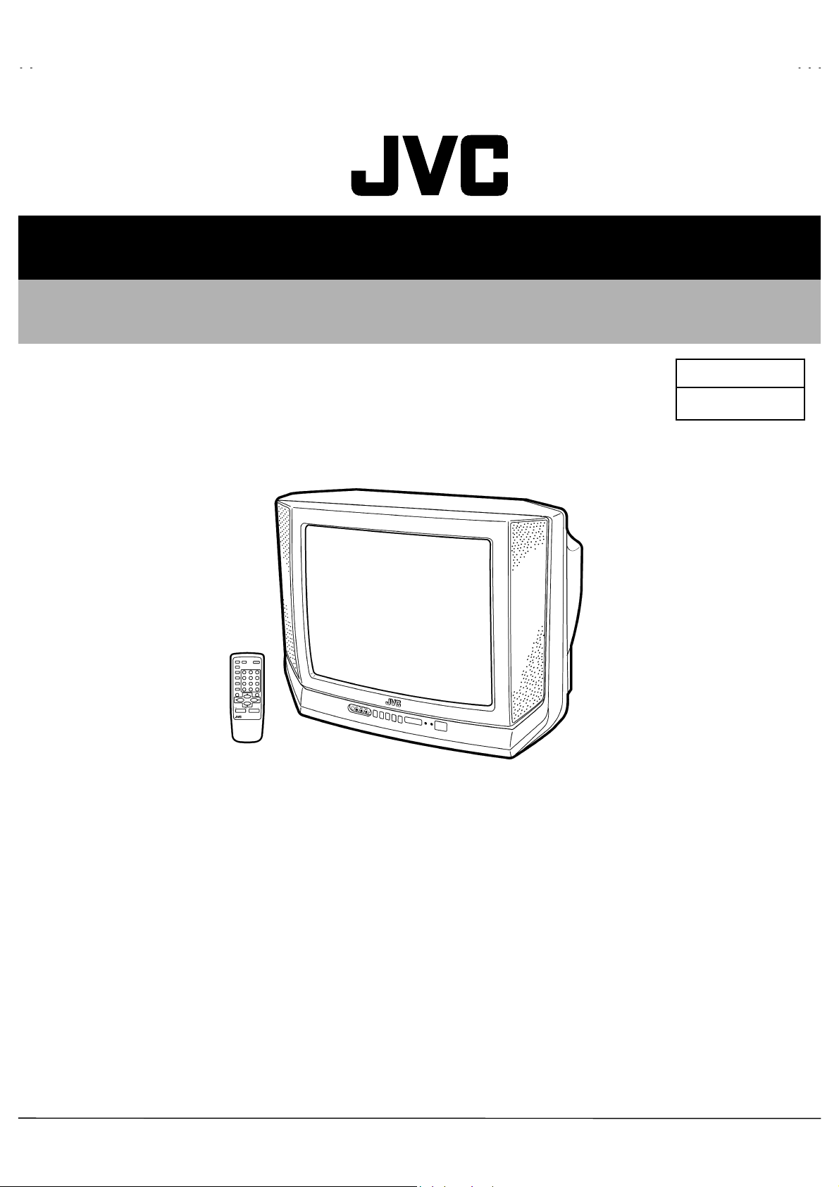
A
SER VICE MANUAL
COLOR TELEVISION
V-T2122
BASIC CHASSIS
GA2
AV-T2122
!!
/AR
CONTENTS
SPECIFICATIONS
!
SAFETY PRECAUTIONS
!
FEATURES
!
FUNCTIONS
!
SPECIFIC SERVICE INSTRUCTIONS
!
SERVICE ADJUSTMENTS
!
PARTS LIST
!
★
OPERATING INSTRUCTIONS
★
STANDARD CIRCUIT DIAGRAM (APPENDIX)
1
・・・・・・・・・・・・・・・・・・・・・・・・・・・・・・・・
・・・・・・・・・・・・・・・・・・・・・・・・・・・・・・・・ ・・・・・・・・・・・・・・・・・・・・・・・・・・・・・・・・
・・・・・・・・・・・・・・・・・・・・・・・・・・・・・・・・・・・・・・・・・・・・・・・・・・・・・・・・・・・・・・・・
・・・・・・・・・・・・・・・・・・・・・・・・・・・・・・・・
・・・・・・・・・・・・・・・・・・・・・・・・・・・・・・・・ ・・・・・・・・・・・・・・・・・・・・・・・・・・・・・
・・・・・・・・・・・・・・・・・・・・・・・・・・・・・・・・・・・・・・・・・・・・・・・・・・・・・・・・・・・・・・・・
・・・・・・・・・・・・・・・・・・・・・・・・・・・・・・・・
・・・・・・・・・・・・・・・・・・・・・・・・・・・・・・・・ ・・・・・・・・・・・・・・・・・・・・・・・
・・・・・・・・・・・・・・・・・・・・・・・・・・・・・・・・・・・・・・・・・・・・・・・・・・・・・・・・・・・・・・・・
・・・・・・・・・・・・・・・・・・・・・・・・・・・・・・・・ ・・・
・・・・・・・・・・・・・・・・・・・・・・・・・・・・・・・・・・・・・・・・・・・・・・・・・・・・・・・・・・・・・・・・
・・・・・・・・・・・・・・・・・・・・・・・・・・・・・・・・
・・・・・・・・・・・・・・・・・・・・・・・・・・・・・・・・ ・・・・・・・・・・・・・・・・・・・・・・・・・・・・・・・・
・・・・・・・・・・・・・・・・・・・・・・・・・・・・・・・・・・・・・・・・・・・・・・・・・・・・・・・・・・・・・・・・
・・・・・・・・・・・・・・・・・・・・・・・・・・・・・・・・
・・・・・・・・・・・・・・・・・・・・・・・・・・・・・・・・ ・・・・・・・・・・・・・
・・・・・・・・・・・・・・・・・・・・・・・・・・・・・・・・・・・・・・・・・・・・・・・・・・・・・・・・・・・・・・・・
・・・・・・・・・・・・・・・・・・・・・・・・・・・・・・・・
・・・・・・・・・・・・・・・・・・・・・・・・・・・・・・・・ ・・・・・・・・・・・・・・・・・・・・・
・・・・・・・・・・・・・・・・・・・・・・・・・・・・・・・・・・・・・・・・・・・・・・・・・・・・・・・・・・・・・・・・
・・・・・・・・・・・・・・・・・・・・・・・・・・・・・・・・
・・・・・・・・・・・・・・・・・・・・・・・・・・・・・・・・ ・・・・・・・・・・・・・・・・・・・・・・・・・・・・・・・・
・・・・・・・・・・・・・・・・・・・・・・・・・・・・・・・・・・・・・・・・・・・・・・・・・・・・・・・・・・・・・・・・
・・・・・・・・・・・・・・・・・・・・・・・・・・・・・・・・
・・・・・・・・・・・・・・・・・・・・・・・・・・・・・・・・ ・・・・・
・・・・・・・・・・・・・・・・・・・・・・・・・・・・・・・・・・・・・・・・・・・・・・・・・・・・・・・・・・・・・・・・
COPYRIGHT © 2001 VICTOR COMPANY OF JAPAN, LTD.
・・・・・・・・・・・・・・・・・・・・・・・・・・・・・
・・・・・・・・・・・・・・・・・・・・・・・・・・・・・・・・・・・・・・・・・・・・・・・・・・・・・・・・・・
・・・・・・・・・・・・・・・・・・・・・・・
・・・・・・・・・・・・・・・・・・・・・・・・・・・・・・・・・・・・・・・・・・・・・・
・・・・・・・・・・・・・・・・・・・・・・・・・・・・・・・・ ・・
・・・・・・・・・・・・・・・・・・・・・・・・・・・・・・・・・・・・・・・・・・・・・・・・・・・・・・・・・・・・・・・・
・・・・・・・・・・・・・
・・・・・・・・・・・・・・・・・・・・・・・・・・
・・・・・・・・・・・・・・・・・・・・・
・・・・・・・・・・・・・・・・・・・・・・・・・・・・・・・・・・・・・・・・・・
・・・・・・・・・・・・・・・・・・・・・・・・・・・・・・・・ ・・・・
・・・・・・・・・・・・・・・・・・・・・・・・・・・・・・・・・・・・・・・・・・・・・・・・・・・・・・・・・・・・・・・・
・・・・・
・・・・・・・・・・
・・・
・・・・・・
・・
・・・・
10
29
2-1
2
3
4
4
6
No.51866
Aug.2001
Sept. 2001
Page 2
A
V-T2122
SPECIFICATIONS
Items Contents
Dimensions (W
Mass
TV RF System
Color/ Sound System
TV Receiving Channels and Frequency
VL Band
VH Band
UHF Band
CATV Receiving Channels and Frequency
Low Band
High Band
Mid Band
Super Band
Hyper Band
Ultra Band
Sub Mid Band
TV/CATV Total Cha nne l
Intermediate Frequency
Video IF Carrier
Sound IF Carrier
Color Sub Carrier
××××H××××
D)
61.9cm×45.8cm×48.7cm
22.0kg
CCIR (M)&(N)
NTSC-M / PAL-M / PAL-N
MTS (Multi Channel Sound)
(02~06) 55.25MHz~83.25MHz
(07~13) 175.25MHz~211.25MHz
(14~69) 471.25MHz~801.25MHz
(02~06)
(07~13)
(14~22)
(23~36)
(37~64)
(65~94, 100~125)
(01, 96~99)
181 Channels
45.75MHz
41.25MHz (4.5MHz)
NTSC-M : 3.579545MHz
PAL-M : 3.57561149MHz
PAL-N : 3.58205625MHz
(55.25MHz~799.25MHz)
Antenna te rminal
Power Input
Power Consumption 87W(max.) / 63W(Avg.)
Picture Tube
High Voltage (at zero been current) 26.5kV±1.0kV
Speaker
Audio Power Output
Input
Video input
Audio input
Variable Audio Output
Headphone Jack / Earphone Jack
Remote Control Unit
75Ω(VHF/UHF) Terminal, F-Type Connector
Rated Volta ge : 120V~240V AC, 50Hz/60Hz
Operating Voltage : 90V~260V AC, 50Hz/60Hz
Visible size: 51 cm measured diagonally
6×12cm oval type×2
1.5W+1.5W (Stereo)
(Front / Rear)
1Vp-p 75Ω (RCA pin jack)
500mVrms (-4dBs),High Impedance (RCA pin jack)
More then 0~1550mVrms (+6dBs)
Low Impedance (400Hz when modula ted 100%) (RCA pin jack)
3.5mm stereo
mini jack (Headphone Jack)
RM-C373 (AA/R6/UM-3 battery×2)
Design & specification are subject to change without notic e.
2
No.51866
Page 3
A
SAFETY PRECAUTIONS
V-T2122
1. The design of this product contains special hardware, many
circuits and components specially for safety purposes. For
continued protection, no changes should be made to the original
design unless authorized in writing by the manufacturer.
Replacement parts must be identical to those used in the original
circuits. Service should be performed by qualified personnel
only.
2. Alterations of the design or circuitry of the products should not be
made. Any design alterations or additions will void the
manuf act urer's warr an t y and wil l fur t h er reli ev e t h e manufacturer
of responsi bility f or person al injury or pr operty dam age res ulting
therefrom.
3. Many electrical and mechanical parts in the products have
special safety-related characteristics. These characteristics are
often not evident f rom visual i nspection nor can t he protect ion
afford ed by them n ecess arily be obt ained by using rep lacem ent
compon ents rated f or higher voltag e, watt ag e, etc. R epl acem ent
parts which have these special safety characteristics are
identified in the parts list of Service manual.
compon ents hav in g su ch feat ures are id entif ied by s hadin g
on the sche matics and by (
manual.
have the same safety characteristics as the recommended
replac ement part shown i n the p arts list of S ervic e manu al may
cause shock, fire, or other hazards.
The us e of a subst itute replacement which does n ot
) on the parts list in Service
!!!!
Electrical
4.
Don't short b etween the LIV E side groun d and ISOLATED
(NEUTRAL) side ground or EARTH side ground when
repairing.
Some model's power circuit is partly different in the GND. The
difference of the GN D is sh ow n by the LIV E : (") side GND, the
ISOLATED(NEUTRAL ) : (#) side GND and EARTH : ($) side
GND. Don't short between the LIVE side GND and
ISOLATED(NEUTRAL) side GND or EARTH side GND and
never meas ure with a measuri ng apparatus (osc illoscope etc .)
the LIVE side GND and ISOLATED(NEUTRAL) side GND or
EARTH side GND at the same time.
If above not e wi ll n ot be kept, a fuse or any parts w ill be broken.
5. If any repair has been made to the chassis, it is recommended
that the B1 setting should be checked or adjusted (See
ADJUSTMENT OF B1 POWER SUPPLY).
6. The hig h voltage app lied t o the picture t ube must c onform wit h
that specified in Service manual. Excessive high voltage can
cause an increase in X-Ray emission, arcing and possible
component damage, therefore operation under excessive high
voltag e conditions s hould b e kept to a mi nimum, or sh ould be
prevented. If severe arcing occurs, remove the AC power
immediately and determine the cause by visual inspection
(incorrect install ation, crack ed or melted high volt age harness ,
poor solderi ng, etc.). To maintain the pr oper minimum le vel of
soft X-Ray emission, components in the high voltage circuitry
including the picture tube must be the exact replacements or
alternatives approved by the manufacturer of the complete
product.
7. Do not check high voltage by drawing an arc. Use a high voltage
meter or a high voltage probe with a VTVM. Discharge the
picture tube before attempting meter connection, by connecting
a clip l ead to th e g roun d fr am e and c on necti ng t h e oth er end of
the lead through a 10k" 2W resistor t o the an ode button .
8. W hen servic e is requir ed, obser ve the origin al lead dress . Extr a
precaut ion shou ld be gi ven to assure c orrect l ead dr ess in t he
high voltage circuit area. Where a short circuit has occurred,
those comp onents that in dicat e evidenc e of over heating should
be replaced. Always use the manufacturer's replacement
components.
9.
Isolation Check
(Saf ety for Electrical Shock Hazard)
After re-assembling the product, always perform an isolation
check on the exposed metal parts of the cabinet (antenna
termin als , vid eo/ au dio input and output term inals, Con trol knobs,
metal c abinet, s crewhead s, earph one j ack, contr ol shafts, etc.)
to be sure the product is safe to operate without danger of
electrical shock.
(1)
Dielectric Stren gt h Test
The isol ation b etween th e AC pr imar y circuit and all metal parts
expos ed t o th e user, p ar tic u larly any exp osed metal part h avi ng a
return p ath to the chassis should withst and a voltage of 3000V
AC (r.m.s .) for a period of on e s ec on d.
(. . . . W ithstand a voltag e of 1100 V AC ( r.m.s.) to an applianc e
rated up t o 120V, and 3000V AC (r. m.s.) t o an appl iance rat ed
200V or mor e, f or a peri od of on e s ec on d.)
This method of test requires a test equipment not generally found
in the service trade.
(2)
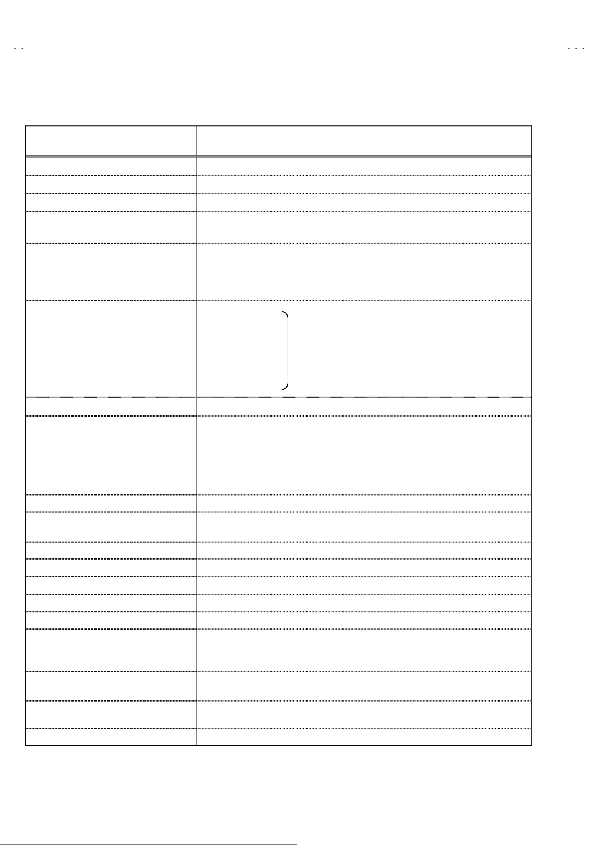
Leak age Current Check
Plug the AC lin e c or d dir ec t l y int o t he AC outlet ( d o not use a line
isolation transformer during this check.). Using a "Leakage
Current Tester", measure the leakage current from each exposed
metal part of the cabinet, particularly any exposed metal part
having a return path to the chassis, to a known good earth
ground ( water pipe, etc. ). An y leak age c urr ent mus t not exceed
0.5mA AC (r.m.s.).
However, in tropical area, this must not exceed 0.2mA AC
(r.m.s.).
Alternate Check Method
""""
Plug the AC lin e c or d dir ec t l y int o t he AC outlet ( d o not use a line
isolati on transform er during t his check. ). Use an AC voltmet er
having 1000 ohms per volt or more sensitivity in the following
manner. Connect a 1 500" 10W resistor paralleled by a 0.15#F
AC-typ e capacitor betw een an expos ed metal part and a know n
good earth ground (water pipe, etc.). Measure the AC voltage
across the resistor with the AC voltmeter. Move the resistor
connect ion t o each exp os ed met al p art, part icul arl y any exp osed
metal part h avin g a return p ath to th e chassis , and meas ure th e
AC voltag e across the res istor. N ow, re vers e the plug in the AC
outlet and repeat each measurement. Any voltage measured
must not exceed 0.75V AC (r.m.s.). This corresponds to 0.5mA
AC (r.m.s.).
However , i n t ropical area, this m us t not exc eed 0.3V AC (r.m.s .).
This corresponds to 0.2mA AC (r.m.s.).
0.15μF AC-TYPE
1500
GOOD EARTH GROUND
"
AC VOLTMETER
(HAVING 1000
OR MORE SENSITIVITY)
10W
"
/V,
PLACE THIS PROBE
ON EACH EXPOSED
METAL PART
No.51866
3
Page 4
A
V-T2122
FEATURES
New chassis desi gn enabl es us e of a main b oard with simp lif ied
"
circuitry.
Provided with mi niatur e tun er (TV /C ATV).
"
PLL synthesizer system TV/CATV tota ling 181 channels.
"
Multifunctional remote control permits picture adjustment.
"
With AUDIO. VIDEO INPUT terminal.
"
FUNCTIONS
Front control
■■■■
Adopti on of the VIDEO STATUS func ti on.
"
Adoption of the ON/OFF TIMER function.
"
With 75ΩV/U in common (F-Type) ANT Terminal.
"
SLEEP TIMER for sett ing in real ti me.
"
Wide range voltage (90V~260V) AC power input.
"
Variable audio ou t p ut terminal.
"
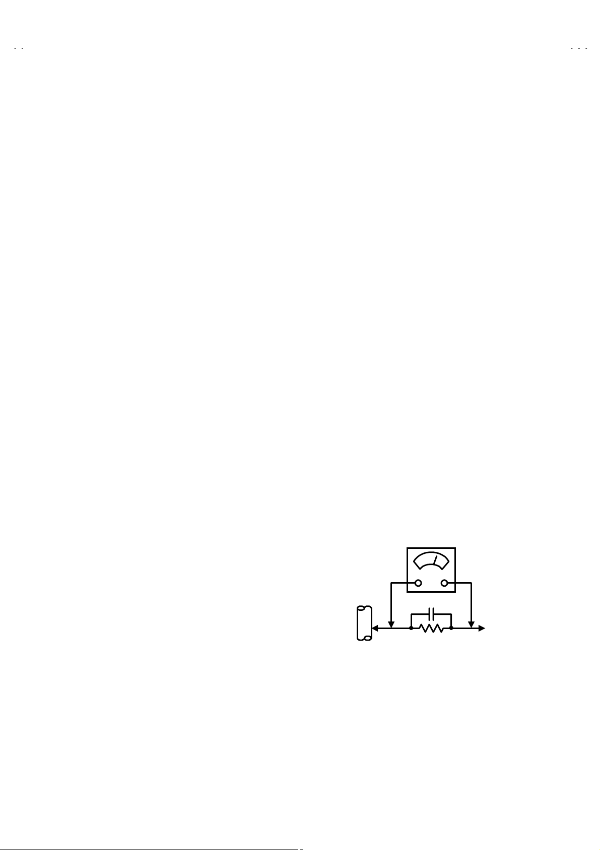
1 2 3 4 5 6 7 8 9 10 11 12 13 14
HEADPHONE JACK Teminal
①
VIDEO INPUT Teminal
②
AUDIO L INPUT Tem inal
③
AUDIO R INPUT Teminal
④
MENU Button
⑤
CHANNEL ∨Button
⑥
CHANNEL ∧Button
⑦
4
No. 51866
VOLUME - Buttom
⑧
VOLUME + Buttom
⑨
ECO sensor
⑩
Remote control sensor
⑪
ON TIMER lamp
⑫
POWER lamp
⑬
MAIN POWER SW Button
⑭
Page 5
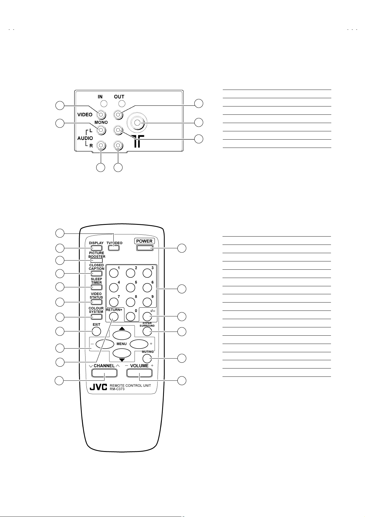
A
■
■Rear terminal
■■
2
3
4 7
■
■Remote control unit ( RM-C373)
■■
V-T2122
ANT Terminal
①
VIDEO INPUT Terminal
5
1
6
②
AUDIO L INPUT Terminal
③
AUDIO R INPUT Terminal
④
VIDEO OUTPUT Terminal
⑤
AUDIO L OUTPUT Terminal
⑥
AUDIO R OUTPUT Terminal
⑦
11
10
1
TV / VIDEO key
①
DISPLAY key
2
3
4
5
6
7
8
9
12
13
14
15
16
17
②
PICTURE BOOSTER key
③
CLOSED CAPTION key
④
SLEEP TIMER key
⑤
VIDEO STATUS key
⑥
COLOUR SYSTEM key
⑦
EXIT key
⑧
MENU (▲/▼& +/-)key
⑨
RETURN+ key
⑩
CHANNEL key
⑪
POWER key
⑫
Number (CH.) key
⑬
- /- - key
⑭
HYPER SURROUND key
⑮
MUTING key
⑯
VOLUME key
⑰
No. 51866
5
Page 6

A
V-T2122
SPECIFIC SERVICE INSTRUCTIONS
DISASSEMBLY PROCEDURE
REMOVING THE REAR COVER
1. Unplug the power supply cord.
2. Remove the 6 screws marked
3. Withdraw the rear cover toward you.
REMOVING THE MAIN PW BOARD
Afte r removing the rear cover.
"
1. Slight l y raise both sid es of the MAIN PW Board by hand and w it hdraw it b ack w ard.
(If necessary, t ak e off the wire clam p and connec tors, etc.)
REMOVING THE SPEAKER
Afte r removing the rear cover.
"
1. Remove the 2 screws marked
2. Follow the same step for removing the other hand speaker.
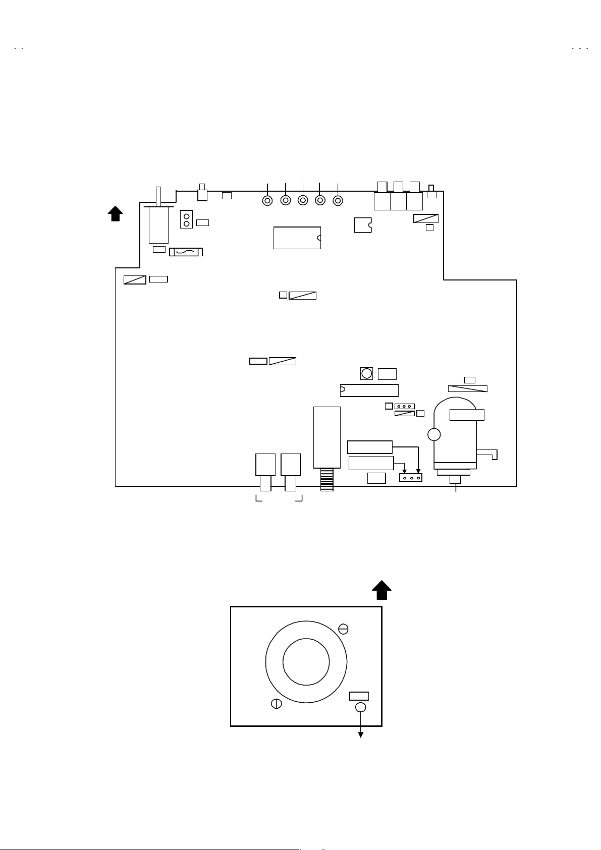
CHECKING THE MAIN PW BOARD
1. To check the backside of the MAIN PW Board.
1) Pull out the MAIN PW Board. (Refer to REMOVING THE MAIN PWB).
2) Erect the chassis vertically so that you can easily check the backside of the MAIN PW Board.
and 2 screws marked
!"
!"
!"!"
.
$$$$
####.""""
[CAUTION]
When erecting the MAIN PW Board, be careful so that there will be no contacting with other PW Board.
"
Bef or e turni ng on power, m ak e sure that all connector s are properl y connected.
"
WIRE CLAMPING AND CABLE TYING
1. Be sure clamp the wire.
2. Never remove the cable tie used for tying the wires together.
Should it be inadvertently removed, be sure to tie the wires with a new cable tie.
6
No. 51866
Page 7
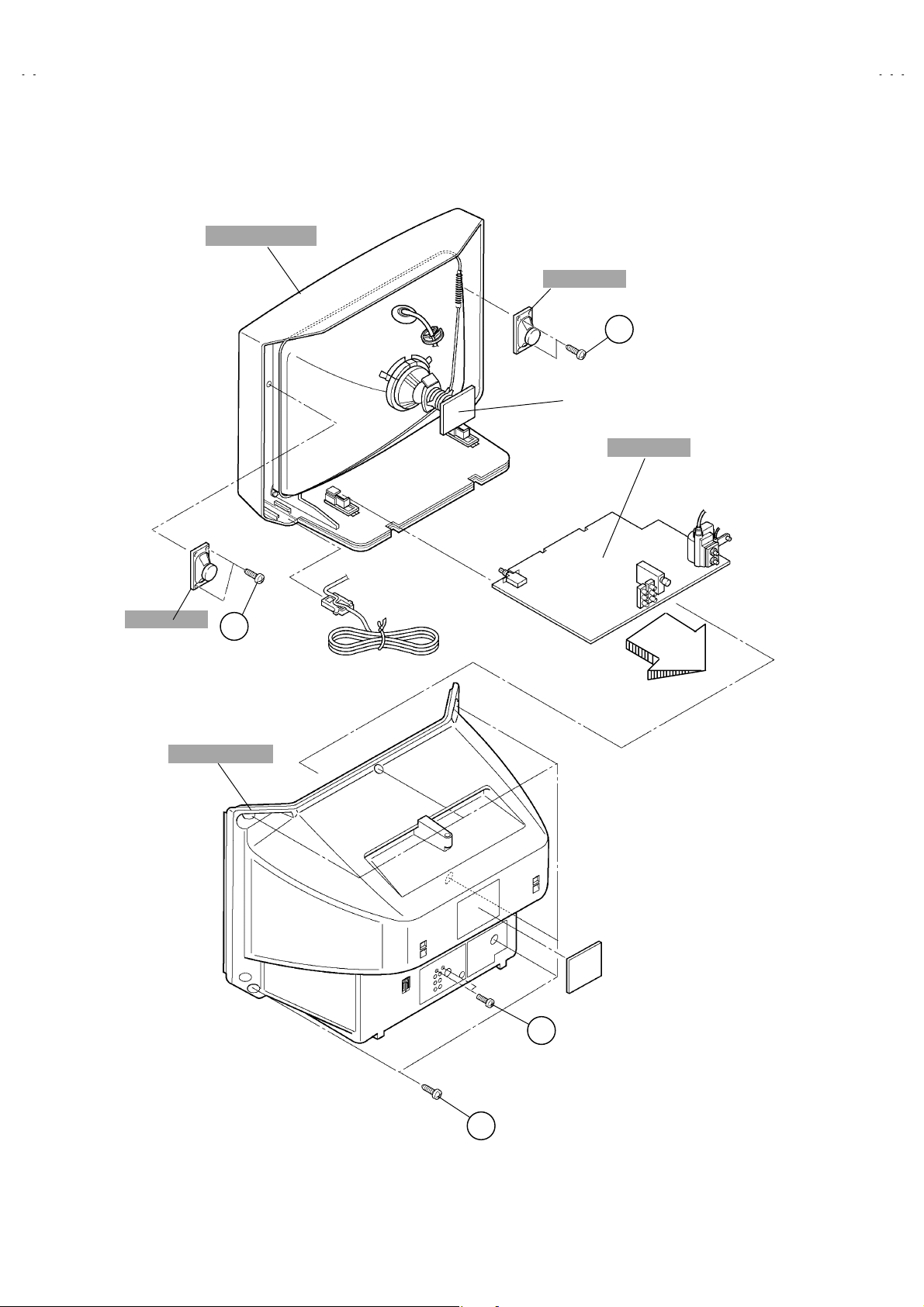
A
FRONT CABINET
SPEAKER
C
CRT SOCKET PWB
(Wit hin MAIN PWB )
MAIN PWB
V-T2122
(×2)
SPEAKER
REAR COVER
C
(×2)
(×2)
B
(×6)
A
No. 51866
7
Page 8
A
V-T2122
MEMORY I C REPLAC EMENT
1. Memory IC
This model uses a memory IC.
The memor y IC st or es dat a for proper op er at ion of video and deflecti on c irc uits.
When replacing, be sure to use an IC containing this (initial value) data.
2. Memory IC replacement pro cedu re
PROCEDURE SCREEN DISPLAY
(1)
Power off
Switch off the power and dis connect th e pow er c or d from the wall
outlet.
(2)
Replace the memory IC
.
Be sure to u se memo ry ICs written with the i nitial data values.
(3)
Power on
Connect the power cord to the wall outlet and switch on the power.
(4)
System constant check and setting
) Simul taneous ly press th e DISPLA Y key and V IDEO STAT US key
1
of the remote control unit.
) The SERVICE MENU screen of Fig.1 is displayed.
2
) While the SERVICE MENU is displayed, again simultaneously
3
press t h e D IS PLAY an d VIDEO S T ATUS k eys to dis play t h e Fig.2
SYSTEM CONSTANT screen.
) Refer to the SYSTEM CONSTANT table and check the setting
4
items. W here these diff er, select th e setting it em with the MENU
UP / DO WN key and adjust t he setting with the MENU LEFT /
RIGHT keys. (The letters of the selected item are displayed in
yellow.)
) A fter adj ustin g, r el ease t h e MENU LE FT / R IG HT key to st or e t he
5
setting value.
) Press the EXIT key twice to return the normal screen.
6
SERVICE MENU
PICTURE SOUND
VIDEO STATUS OTHERS
LOW LIGHT HI GH LIGHT
RF AFC CHK
VCO (CW) I2C BUS CTRL
SELECT BY
OPERATE BY
EXIT BY
EXIT
IT
Fig.1
SYSTEM CONSTANT
VIDEO : 2
AUDIO : MTS
VARI. OUT : NO
GAME : YES
CINEMA : YES
(5)
Receive chann el s et ting
SELECT BY
OPERATE BY
EXIT BY
EXIT
Refer to the OPERATING INSTRUCTIONS (USER’S GUID E) and
set the receive channels (Channels Preset) as de scribed.
SYSTEM CONSTANT
(6)
User setti n gs
Check th e us er s ett in g i t ems according t o Table 2-1 and 2- 2.
CCD : YES
RETURN+ : YES
SURROUND : YES
Where these do not agree, refer to the OPERATING
INSTRUCTIONS (USER’S GUIDE) and set the items as described.
(7)
SERVICE MENU setting
M37272MA-
SELECT BY
OPERATE BY
×××
×××
××××××
SP
EXIT BY
EXIT
Verify what to set in the SERVICE MENU, and set whatever is
necessary. (Fig.1) Refer to the SERVICE ADJUSTMENT for setting.
Fig.2
8
No.51866
Page 9
A
SETTING OF SYSTEM CONSTANT SET
Setting item Setting content Setting value
V-T2122
VIDEO 2
AUDIO MTS
VARI. OUT NO
GAME YES
CINEMA YES
CCD YES
RETURN +
SURROUND YES
MONO PH.MONO MTS
12
YES NO
YES NO
YES NO
YES NO
YES NO
YES NO
Table 1
YES
USER SETTING VALUES
1.Settin g of FUN CTION
Setting item Setting value Setting item Setting value
MAIN POWER OFF DISPLAY OFF
SUB POWER ON SLEEP TIMER 0 MIN
CHANNEL CH 02 VIDEO STATUS ESTANDAR
CAPTION OFF(CC1/T1) PICTURE BOOSTER OFF
VOLUME 10 COLOR SYSTEM AUTO
TV/VIDEO TV HYPER SURROUND OFF
Table 2-1
2.Setting of MENU
Setting item Setting value
TINTE ESTANDAR ALTAVOCES SI
COLOR ESTANDAR CHILD LOCK NO
CONTRASTE ESTANDAR TEMPORIZADOR NO
BRILLO ESTANDAR LISTA DE CANAIS SET OPTIONALLY
DETALLE ESTANDAR AJUSTE CODIGO DE ACCESO Unnecessary to Set
GRAVES CENTER PANTALLA AZUL NO
AGUDOS CENTER FONDO NEGRO SI (SIM)
BALANCE CENTER IDIOMA ESP.
MTS ESTÉREO SUBTITULOS OCULTOS NO(CC1/T1)
Table 2-2
Setting item Setting value
No.51866
9
Page 10
A
V-T2122
SERVICE ADJUSTMENTS
ADJUSTMENT PREPARATION
1. You can make t he n ec essary adju st ments for this un it wit h eit her the r em ote contro l u nit or with th e adj ust ment equ ip ment and
part s as given below.
2. Adjustment with the remot e contro l un it i s m ade on t he b a si s of the initial set t i ng values, h owever, th e new sett i n g values which
set the screen to its optimum condition may differ from the initial settings.
3. Make sure that AC power is turned on correctly..
4. Turn on the power for the set and test equipment before use, and start the adjustment procedures after waiting at least 30 minutes
5. Unless otherwise specified, prepare the most suitable reception or input signal for adjustment.
6. Never touch any adjustment parts, which are not specified in the list for this adjustment-variable resistors, transformers, condensers, etc .
7. Presetti ng b ef or e ad jus t m ent .
Unless otherwise specified in the adjustment instructions, preset the following functions with the remote control unit.
VIDEO STATUS ESTANDAR
GRAVES, AGUDOS, BALANCE CENTER
$$$$
ADJUSTMENT EQUIPMENT
1. DC voltmet er ( or di gi tal voltmeter)
2. Oscilloscope
3. Signal generator ( Pattern generator ) [NTSC%M]![PAL-M] [PAL-N ]
4. Remote control unit
5. TV audio multiplex signal generator
6. Frequency counter
ADJUSTMENT ITEMS
B1 POWER SUPPLY
●
IF VCO adjustment
●
RF AGC adjustment
●
FOCUS ad jus tment
●
DEFLECT IO N ad jus t m ent
●
V. HEIGHT, V. POSITION, V. LIN., V S CR adjustment
H. POSITION adjustment
VIDEO / CHROMA adjustment
●
WHITE BALANCE (Low light) adjustment
WHIT E BALAN C E (H i gh li ght) adjus t m ent
SUB BRIGHT adjustment
SUB CONTRAST adjustment
SUB COLOR adjustment
SUB TINT adjustment
●MTS adjus t m en t
INPUT LEVEL adjustment
STEREO VCO adjustment
SAP VCO adjustment
FILTER check
SEPARATION adjust ment
10
No.51866
Page 11
A
ADJUSTMENT LOCATIONS
(
)
FRONT
VOL+
V-T2122
CH-CH+VOL-
MENU
SW
DEG.
F901
PW
MPX
T
5 1
AV IN OUT
IC701
TUNER
IC704
T111
CW
IC101
B1(TP-91)
GND(TP-E)
B1
S
MAIN P WB
HV
3
1
X
U
T522
3
1
UPPER : FOCUS
LOWER : SCREEN
CRT SOCKET PWB
TOP
(Within MAIN PWB ASS'Y)
TP-47B
E1
TP-E
SOLDER SIDE
No.51866
CRT EARTH
(BRAIDED ASS'Y)
11
Page 12

A
V-T2122
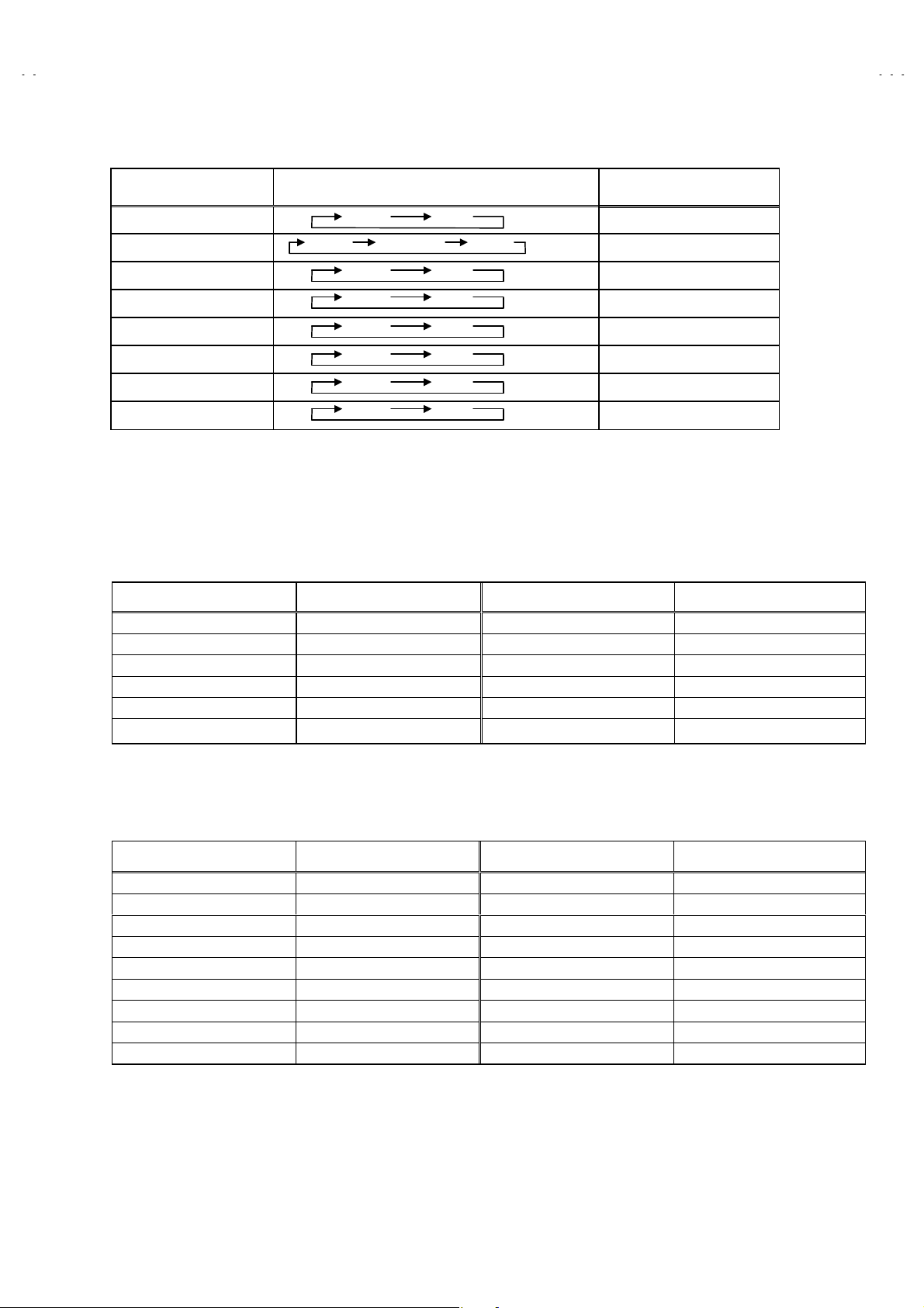
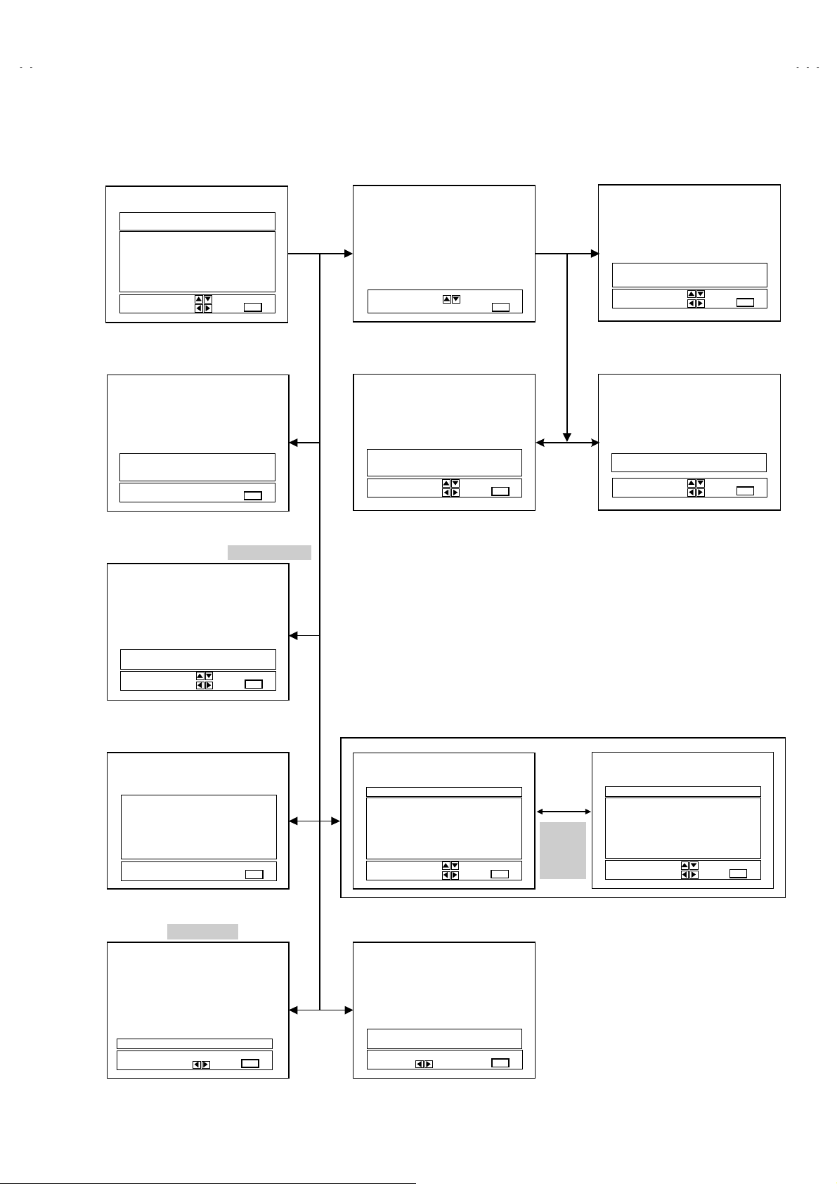
BASIC OPERATION OF SERVICE MENU
1. Operate the SERVICE MENU with the REMOTE CONTROL UNIT.
2. In general
(1) PICTURE
(2) SOUND
(3) VIDEO STATUS
(4) OTHERS
(5) LOW LIGHT
(6) HIGH LIGHT
(7) RF AFC CHK
(8) VCO (CW)
(9) I
3. Basic Opera ti o ns of th e SER VI C E M EN U
(1) How to enter the SERVICE MENU.
(2) SERVICE MENU screen selection
basic sett ing
!!!!
・・・・・・・・・・・・・・・・・・・
・・・・・・・・・・・・・・・・・・・・
・・・・・・・・・・・・・・・・・・・
・・・・・・・・・・・・・・・・・
・・・・・・・・・・・・・・・・・・
2
C BUS CTRL
・・・・・・・・・・・・・・・・
・・・・・・・・・・・・・・・・
(adjustments) items or verifications are performed in the SERVICE MENU.
!!!!
This set the setting values (adjustment values) of the VIDEO/CHROMA and DEFLECTION circuits.
This set the setting values (adjustment values) of the AUDIO circuit.
・・・・・・・・・・・・・
This is used when the THEATER and GAME MODE is adjusted.
This is used when the OTHERS MODE is adjusted.
This sets the setting values (adjustment values) of the WHITE BALANCE circuit.
This sets the setting values (adjustment values) of the WHITE BALANCE circuit.
This is used when the RF AFC CHK MODE is verified.
This is used when the IF VCO is adjusted.
・・・・・・・・・・・・・・・
This is used when ON/OFF of the I2C BUS CTRL is set.
[Do not adjust]
[Fixed ON]
Press the DISPL A Y k ey and V IDEO ST AT US k e y!of the remote control unit at the same time to enter the SERVICE MENU screen
shown in figure page la ter.
Press the UP / DOWN key of the MENU to select any of the following items.
(The lett ers of t h e sel ec t ed it ems are disp l ayed in y ell ow .)
PICTURE
●
VIDEO STATUS
●
LOW LIGHT
●
RF AFC CHK
●
VCO (CW)
●
SOUND
●
OTHERS
●
HIGH LIGHT
●
I2C BUS CTRL
●
①
(3) Enter the any setting ( adjustment ) mode
PICTURE, SOUND and OTHERS mode
"
1) If select any of PICTURE, SOUND or OTHERS items, and the LEFT / RIGHT key is pressed from SERVICE MENU ( MAIN
MENU ), the screen ② will be dis p layed as sh ow n in fi gure page later.
2) T hen the U P / DOWN k ey is pr ess ed, th e PICT UR E m ode sc r een ③ or th e SOUND m ode s cr een ④ or the OTHERS mode
screen ⑤ is displayed, and the PICTURE, SOUND or OTHERS setting can be performed.
VIDEO STATUS, LOW LIGHT, HIGH LIGHT, RF AF C
"
CHK,
VCO (CW) and I
!!!!
!!!!
2
C BUS CTRL mode
1) If select any of VIDEO STATUS / LOW LIGHT / HIGH LIGHT / RF AFC CHK / VCO (CW) / I2C BUS CTRL items, and the LEFT
/ RIGHT k ey is pr essed fr om SER V I CE ME NU ( MAIN MENU ), t h e sc reens ⑥ ⑦ ⑧ ⑨ ⑩ ⑪ w ill b e displ ayed as sh own in
figure page later.
2) Then the s ett in gs or verificat i ons c an b e performed.
12
No.51866
Page 13
A
V-T2122
)
)
y
①①①①
SERVICE MENU (MAIN MENU
SERVICE MENU
PICTURE SOUND
VIDEO STATUS OTHERS
LOW LIGHT HIGH LIGHT
RF AFC CHK
VCO (CW
SELECT BY
OPERATE BY
⑧⑧⑧⑧
HIGH LIGHT MODE
HIGH LIGHT
***
*** ***
******
⑨⑨⑨⑨
RF AFC CHK MODE
I2C BUS CTRL
EXIT BY
EXIT
***
******
EXIT BY
EXIT
[DO NOT ADJUST]
②②②②
SCREEN
SELECT BY EXIT BY
④④④④
SOUND MODE
1. NOISE
STATUS
SELECT BY
OPERATE BY
EXIT
***
***
******
****
****
********
EXIT BY
EXIT
③③③③
PICTURE MODE
1. PICTURE
*****
***** ****
**********
SELECT BY
OPERATE BY
⑤⑤⑤⑤
OTHERS MODE
1. OSD HP
SELECT BY
OPERATE BY
***
***
******
****
********
EXIT BY
EXIT
***
***
******
EXIT BY
EXIT
RF AFC ON
FINE
SELECT BY
OPERATE BY
⑩⑩⑩⑩
VOC (CW) MODE
TOO HIGH
ABOVE REFERENCE
BELOW REFERE NCE
TOO LOW
SYNC : YES
⑪⑪⑪⑪
I2C BUS CTRL MODE
[FIXED ON]
I2C BUS ON
OPERATE BY
EXIT BY
**
**
****
EXIT BY
EXIT
EXIT BY
EXIT
EXIT
CINEMA
TINT G DRIVE
COLOR B DRIVE
PICTURE R CUT.
BRIGHT G CUT.
DETAIL B CUT.
SELECT BY
OPERATE BY
BRIGHT
***
*** ***
******
***
*** ***
******
***
*** ***
******
***
*** ***
******
***
*** ***
******
⑦⑦⑦⑦
LOW LIGHT MODE
BRIGHT
***
*** *** ***
******
***
***
******
*** ***
*** ****** ***
EXIT BY
EXIT
EXIT BY
EXIT
⑥⑥⑥⑥
VIDEO STATUS MODE
***
******
***
******
***
******
***
******
***
******
STATUS
Press
VIDEO
Ke
GAME
TINT G DRIVE
COLOR B DRIVE
PICTURE R CUT.
BRIGHT G CUT.
DETAIL B CUT.
SELECT BY
OPERATE BY
***
*** ***
******
***
*** ***
******
***
*** ***
******
***
*** ***
******
***
*** ***
******
EXIT BY
EXIT
***
******
***
******
***
******
***
******
***
******
No.51866
13
Page 14
A
V-T2122
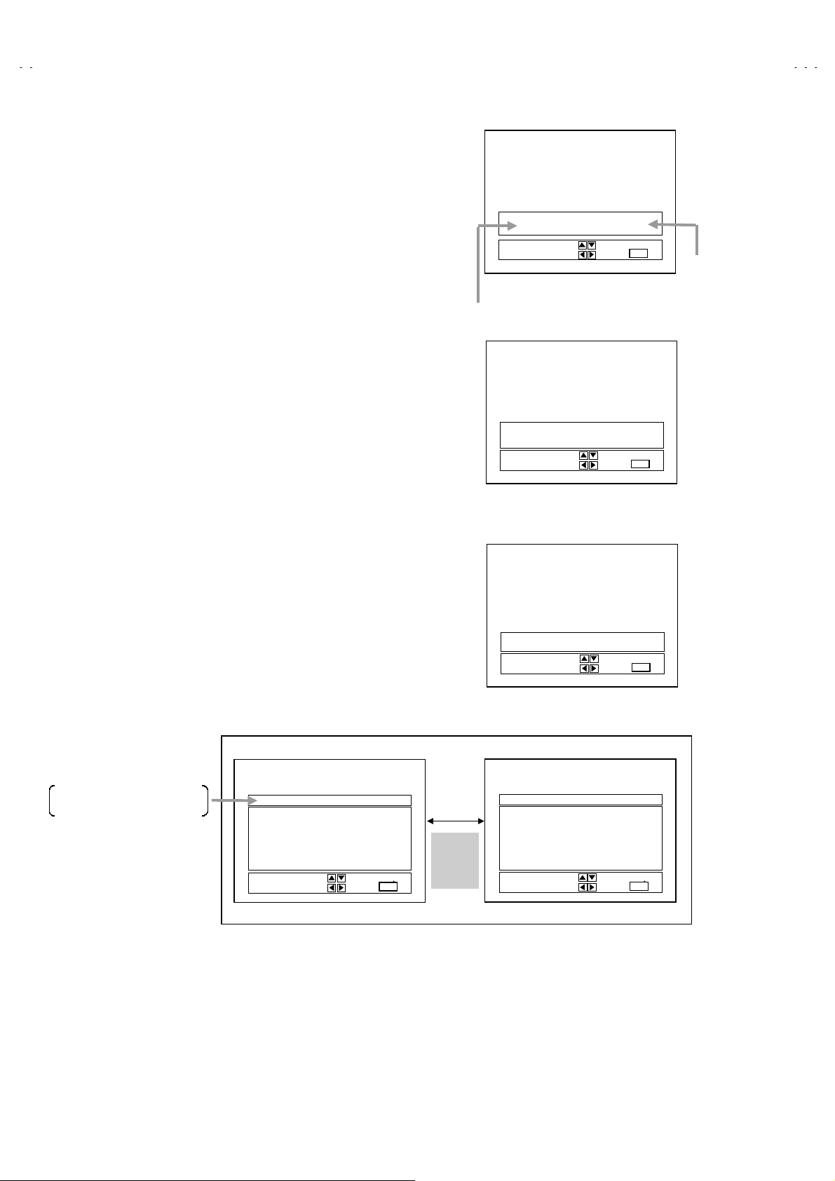
(4) Setting method
1) UP / DOWN key of the MENU
Select the SETTING ITEM.
2) LEFT / RIGHT key of the MENU
Setting (adjust) the SETTING VALUE of the SETTING ITEM.
When the key is released the SETTING VALUE will be stored
(memorized).
3) EXIT key
Returns to the previous screen.
(PICTURE MODE ONLY)
[NOTE]
When the IN ITIAL SET TING VALUE is t urned to yell ow, you can adj ust the
values but you cannot adjust the values when it is turned to red.
(Because the signal conditions, etc. are not met.)
(5) Releasing SERVICE MENU
1) After returni ng to the SERVICE MENU upon c ompletion of t he setting
(adjust m ent ) w or k, pr ess the EXIT key ag ain.
1. PICTURE
*****
***** ****
**********
SELECT BY
OPERATE BY
PICTURE MODE
SETTING
ITEM
1. NOISE
STATUS
SELECT BY
OPERATE BY
***
***
******
****
********
EXIT BY
EXIT
***
***
******
****
****
********
EXIT BY
EXIT
IT
IT
INITIAL
SETTING VALUE
↓ (Adjus t)
SETTING VALUE
The s ettings f or LOW LIGHT and H IGH LIGHT are descr ibed in t he W HITE
★
BALANCE page of ADJUSTMENT.
The setting for VCO (CW) are described in the IF VCO page of ADJUSTMENT.
★
The letter of the
Items are dis played in y ell ow .
selected
CINEMA
TINT G DRIVE
COLOR B DRIVE
PICTURE R CUT.
BRIGHT G CUT.
DETAIL B CUT.
SELECT BY
OPERATE BY
***
*** ***
******
***
*** ***
******
***
*** ***
******
***
*** ***
******
***
*** ***
******
EXIT BY
EXIT
***
******
***
******
***
******
***
******
***
******
I
T
Press
VIDEO
STATUS
Key
SOUND MODE
1. OSD HP
SELECT BY
OPERATE BY
OTHERS MODE
GAME
TINT G DRIVE
COLOR B DRIVE
PICTURE R CUT.
BRIGHT G CUT.
DETAIL B CUT.
SELECT BY
OPERATE BY
***
*** ***
******
***
*** ***
******
***
*** ***
******
***
*** ***
******
***
*** ***
******
***
***
******
EXIT BY
EXIT
EXIT BY
EXIT
***
******
***
******
***
******
***
******
***
******
IT
I
T
VIDEO STATUS MODE
14
No.51866
Page 15

A
V-T2122
INITIAL SETTING VALUE OF SERVICE MENU
1. Adjustment of the SERVICE MENU is ma de on the basis of the initi al sett ing values; however, the new setting values
which set the screen in its optimum condition may differ from the initial setting.
2. Do not change the initial Setting Values of the Setting (Adjustment) items not listed In “ADJUSTMENT”.
PICTURE MODE
""""
The four settin g items i n the vi deo mod e No.8 E XT PIC., No.9 E XT BR I., No. 10 EXT C OL. a n d No.11 E XT T IN T are linked to th e it ems in
#
the TV MO DE No.1 PICT U R E, No.2 BR IG H T , N o.5 CO L . N T S C and No.6 T IN T , r es pectively. When the setting items i n the TV mod e are
adjust ed, th e val u es in the s et t in g items in the vid eo mode are revis ed au tomatic ally to t h e same valu es i n t h e TV mode. (The initial setting
values given in ( ) are off-set values.)
When the f our it ems (No.8, 9, 10 and 11) ar e adj us ted in the vid eo mode, the s etting valu es in eac h it em ar e re vised independently.
#
No. Setting item Variable range
1. PICTURE
2. BRIGHT
3. COL. PALM
4. COL. PALN
5. COL. NTSC
6. TINT
7. TV DTL
8. EXT PIC.
9. EXT BRI.
10. EXT COL.
11. EXT TINT
12. EXT DTL
13. P/N KILL 0 / 1
14. Y S CONT
15. TV Y-DL
16. EXT Y-DL
17. WPL SW 0 / 1
18. Y GAMMA 0 / 1
19. P/N G P 0 / 1
20. COL. L SW 0 / 1
21. CO L. LMT.
22. PN C. ATT
23. OFST. SW 0 / 1
24. OFSET. B-Y
25. OFSET. R-Y
26. C-TOF SW 0 / 1
27. TV T FO
28. TV T Q
29. EXT T FO
30. EXT T Q
0~127
0~127
0~127
0~127
0~127
0~127
0~63
25
±
25
±
25
±
25
±
0~63
0~31
0~7
0~7
0~3
0~3
0~15
0~15
0~3
0~3
0~3
0~3
Initial setting value No. Set ting item Variable r ange Initial setting valu e
65
64
70
70
80
65
38
(0)
(+5)
(0)
+1
35
1
31
1
2
0
0
0
1
1
1
0
8
8
1
1
0
0
0
31. C-TRAP 0 / 1
32. C-TR. FO
33. C-TRAP Q
34. FIX B/W 0 / 1
35. APA P. FO
36. DC TRAN.
37. B. ST. SW
38. B. ST. PO. 0 / 1
39. ABL GAIN
40. ABL PO
41. HALF T.
42. DRV G SW 0 / 1
43. NT. COMB 0 / 1
44. COIN DET
45. NOISE L
46. VCD MODE 0 / 1
47. V AGC SP 0 / 1
48. H POS. 50
49. H BLK. 50
50. V POS. 50
51. V SIZE50
52. V S CR50
53. V LIN. 50
54. H POS. 60
55. H BLK. 60
56. V POS. 60
57. V SIZE60
58. V S CR60
59. V LIN. 60
60. RF AGC
0~3
0~3
0~3
0~7
0~7
0~7
0~7
0~2
0~3
0~3
0~31
0~7
0~7
0~127
0~127
0~31
0~31
0~7
0~7
0~127
0~127
0~31
0~255
0
2
0
0
1
7
0
0
4
0
1
0
1
3
3
0
0
7
0
0
87
28
4
12
0
0
88
48
4
160
No.51866
15
Page 16

A
V-T2122
SOUND MODE
"
No. Setting item Variable range Initial setting value
1. NOISE 0 / 1 1
2. IN LEVEL
3. FH MON. 0 / 1 0
4. ST VCO
5. PILOT 0 / 1 0
6. FILTER
7. LOW SEP.
8. HI SEP.
9. 5FH MON . 0 / 1 0
10. SAP VCO
11. IN GAIN 0 / 1 0
12. FIL. OFF
VIDEO STATUS MODE
"
No.Setting (Adjustment) item Variable range
1. TINT
0~63
0~63
0~63
0~63
0~63
0~63
10
±
20
±
Initial settin g val ue
CINEMA GAME
00
20
25
30
22
23
26
0
2. COLOR
3. PICTURE
4. BRIGHT
5. DETAIL
6. G DRIVE
7. B DRIVE
8. R CUT.
9. G CUT.
10. B CUT
20
±
20
±
20
±
15
±
-99~+50
-99~+50
10
±
10
±
10
±
-3 -3
-10 -10
00
0-5
-22 0
-54 0
00
00
00
16
No.51866
Page 17

A
OTHERS MODE!
"
No. Setting (Adjustment) item Variable range Initial setting value
!
!!
V-T2122
1. OSD HP
2. OSD VP
3. H CK SW 0 / 1 0
LOW LIGHT MODE!
"
Setting (Adjustment) item Variable range Initial setting value
R CUTOFF 0~255 20
G CUTOFF 0~255 20
B CUTOFF 0~255 20
HIGH LIGHT MODE!
"
Setting (Adjustment) item Variable range Initial setting value
G DRIVE
B DRIVE
!
!!
!
!!
0~31
0~15
0~255
0~255
23
12
128
128
RF AFC CHECK MODE!
"
Setting (Adjustment) item Variable range Initial setting value
RF AFC ON / OFF ON
FINE
2
C BUS CTRL MODE!
I
"
Setting (Adjustment) item Variable range Initial setting value
I2C BUS ON / OFF
!
!!
(DO NOT ADJUST)
-77~+77
!
!!
± **
[Fixed ON]
No.51866
17
Page 18

A
V-T2122
■■■■
ADJUSTMENTS
!!!!
B1 POWER SUPPLY
Item
Check of
B1 POWER
SUPPLY
Measuring
instrument
DC Voltmeter B1 (
IF VCO ADJUSTMENT
Item
IF VCO
adjustment
Measuring
instrument
Signal
generator
TOO HIGH
ABOVE REFERENCE
BELOW REFERE NCE
TOO LOW
SYNC : YES
Test point Adjustment ite m Description
B1
Connector
pin)
1
(TP-91)
TP-E(#)
(
B1
Connector
pin)
3
Test point Adjustment ite m Description
CW TRANSF. (T111)
[VCO (CW)] mode
YELLOW
1. Rec eive a bl ac k and whit e sig n al (color off) . (NT S C)
2. Connect the DC voltmeter to B1 connector 1 pin (TP-91)
and TP-E(#) (B1 connector 3 pin).
3. Confirm that the voltage is DC134.5V±2V.
Under normal conditions, no adjustment is required.
"
1. Rec eive a br oadcast. ( use channels w ith out offs et frequenc y).
2. Select the VCO(CW) mode from the SERVICE MENU.
3. Confirm the color change (yellow) from “TOO HIGH” to
TOO LOW”by CW TRAN SF. and “SYNC : YES” being
“
shown on the screen. Then, adjust CW TRANSF. until
BELOW REFERENCE” mark turns yellow and confirm
“
again “ SYNC : YES” being shown on the screen.
RF AGC AD JUS TMENT
RF AGC
adjustment
FOCUS ADJUST MENT
FOCUS
adjustment
Signal
generator
EXIT BY
EXIT
IT
No.60 RF AGC
FOCUS VR
[In HVT]
1. Rec eive a br oadcast.
2. S elect “No.60 RF AGC” of the PICT URE mode in SERVICE
MENU.
3. Press the MUTE key and turn off color.
4. W ith the M ENU L EFT k ey, g et nois e in t he scr een pic ture. ( 0
side of sett in g value)
5. Press the MENU R IGHT k ey and s top wh en n ois e dis app ears
from the screen.
6. Change to other channels and make sure that there is no
irregularity.
7. Press the MUTE key and get color out.
1. Receive a crosshatch signal.
2. While looking at the screen, adjust FOCUS VR s o that the
vertic al and hor i z ont al lines will be cl ear and in fine detail.
3. Make sure t hat the pictur e is in focus even when the sc reen
gets dark en ed.
18
No.51866
Page 19

A
DEFLECTI ON AD JUSTMENT
r
%
(
)
(
)
The setting (adjustment) using the REMOTE CONTROL UNIT is made on the basis of the initial setting values.
The setting values which adjust the screen to the optimum condition can be different from the initial setting values.
V-T2122
Item
V. HEI GHT,
V. POSITION,
V. LIN.
V. S CR
adjustment
Screen
size
92%
Measuring
instrument
Signal
generator
Test point Adjustment ite m Description
[60Hz]
No.56 V POS. 60
No.57 V SIZE 60
No.58 V S CR60
No.59 V. LIN. 60
1. Receive a crosshatch signal.(NTSC or PAL-M)
2. C onfirm that the value of PICTURE MODE “No.56 V PO S.
60” is 0.
3. C onfirm th e initial setting value of t he “No.57 V SIZE 60”,
No.58 V S CR60” and “No.59 V LIN. 60”.
4. Adjust the vertical screen size to 92% with the PICTURE
MODE “No. 57 V SIZE 60”.
5. Adjust the PICTURE MODE “No.59 L LIN. 60” and “No.58
V S CR60” to get the best vertical linearity.
NOTE :
The PICTURE MODE “No.56 V POS. 60” is fixed on value 0.
[50Hz]
No.50 V POS.50
No.51 V SISE 50
No.52 V S CR50
No.53 V LIN.50
1. Receive a crosshatch signal. (PAL-N)
2. Confirm the initial setting value of the “No.50 V POS.50”,
“No.51 V SIZE 50” , “No.52 V S CR 50” and “No.53 V LIN.50”.
3. Adjust the vertical screen size to 92% with the PICTURE
MODE “No.51 V SIZE50”.
4. Adjus t the P ICT URE MO DE “ No. 53 V LIN. 50” and “N o.52 V S
Scree s ize
CR50” to get the best vertical linearity.
5. Adjust the PICTURE MODE “No.50 V POS.50” so that the
vertic al cent er lin e com es clos e to th e CRT vertic al cent er as
much as possible.
Readjust V SIZE, V LIN., V S CR if necessary.
Pictu
size
100
"
100%
No.54 H PO S .60
[60Hz]
1. Rec eive a cr osshatc h sig n al. ( NTSC or PAL-M)
H. POSITION
adjustment
Picture size
Signal
generator
2. Select the “No.54 H POS. 60” of the PICTURE mode in
SERVICE MENU.
3. Confirm the initial setting value of the "No.54 H POS. 60".
4. Adjust the “No.54 H POS. 60” until the screen will be
horizontally centered.
[50Hz]
No.48 H PO S .50
1. Receive a crosshatch signal. (PAL-N)
2. Select the “No.48 H POS. 50” of the PICTURE mode in
SERVICE MENU.
3. Confirm the initial setting value of the "No.48 H POS. 50".
4. Adjust the “No.48 H POS. 50” until the screen will be
horizontally centered.
No.51866
19
Page 20

A
V-T2122
VIDEO / CHROMA !!!!ADJUSTMENT
The setting (adjustment) using the REMOTE CONTROL UNIT is made on the basis of the initial setting values.
The setting values which adjust the screen to the optimum condition can be different from the initial setting values.
Do not change the initial setting values of the setting items not listed in “ADJUSTMENT”.
Item
WHITE
BALANCE
(Low Light)
adjustment
Measuring
instrument
Signal
generator
Remote
control unit
REMOTE CONTROL UNIT
H.LINE OFF EXITH.LINE ON
1111
R CUTOFF G CUTOFF
4444
7777
R CUTOFF
2222 3333
5555 6666
8888
Test point Adjustment ite m Description
BRIGHT
1. Rec eive a bl ac k and whit e sig n al (color off) .
2. Select the LOW LIGHT mode from the SERVICE MENU.
R CUTOFF
G CUTOFF
B CUTOFF
SCREEN VR
3. Confirm th e In itial s ett in g val ue of “ BRIGHT ” , “R C UTOFF” , “ G
CUTOFF” and “B CUTOFF”.
4. Displ ay a single h orizont al line by pr essing t he
remote control unit.
5. Turn the screen VR all the way to th e le ft.
6. T urn the screen VR gradual ly to the right fr om the left until
either one of the red, blue or green colors appears faintly.
7. Adjust the two colors which did not appear until the single
horizontal line tha t is displayed becomes white using the
keys of the remote control unit.
⑨⑨⑨⑨
8. Turn the sc reen VR un til the si ngl e hor iz ontal li ne is dis play ed
B CUTOFF
faintly.
9. Press the
key to return to the regular screen.
②②②②
9999
[LOW LIGHT] MODE
B CUTOFFG CUTOFF
R CUTOFF
G CUTOFF
BRIGHT
B CUTOFF
key of the
①①①①
to
④④④④
WHITE
BALANCE
(High Light)
adjustment
Signal
generator
Remote
control unit
Remote Control Unit
key : H.LINE ON
①
key : H.LINE OFF
②
key : EXIT
③
key : G DRIVE
⑤
key : B DRIVE
⑥
key : G DRIVE
⑧
key : B DRIVE
⑨
***
***
******
*** *** ***
*** *** ***
*** *** ****** *** ***
EXIT BY
EXIT
IT
G DRIVE
B DRIV E
BRIGHT
BRIGHT
1. Rec eive a bl ac k and whit e sig n al (color off) .
2. Select the HIGH LIGHT mode in the SERVICE MENU.
3. Confirm the initial setting value of “G DRIVE” and “B DRIVE”.
4. Adjust the screen color to white with the
⑤⑤⑤⑤, ⑥⑥⑥⑥, ⑧⑧⑧⑧
and
⑨⑨⑨⑨
keys of the remote control unit.
[HIGH LIGHT] MODE
▲
G DRIVE
▲
▼
▼
HIGH LIGHT
***
******
B DRIVE
***
******
******
EXIT BY
EXIT
IT
20
No.51866
Page 21

A
V-T2122
Item
SUB BR I GHT
adjustment
SUB
CONTRAST
adjustment
SUB COLOR
adjustment
Measuring
instrument
Remote
control unit
Remote
control unit
Remote
control unit
Test point Adjustment ite m Description
No.2 BRIGHT
No.1 PICTURE
No.3 COL. PALM
1. Rec eive a br oadcast.
2. Select “No.2 BRIGHT” of the PICTURE mode in SERVICE
MENU.
3. Confirm the initial setting value of the “No.2 BRIGHT” .
4. If the brightness is not the b est with the initial settin g value,
make fin e adjustm ent of th e “No.2 BRIG HT” until you get th e
optimu m bri ghtness.
1. Rec eive a br oadcast.
2. S elect “No.1 PICTURE” of the PICTURE mode in S ERVICE
MENU.
3. Confirm the initial setting value of the “No.1 PICTURE”.
4. If the contrast is not the best with the initial setting value, make
fine adjustment of the “No.1 PICTURE” until you get the
optimum contrast.
[PAL-M]
1. Rec eive a PA L -M c olor b ar sig nal.
2. S elect “No.3 COL. PALM” of t he PICTURE mode in SERVICE
MENU.
3. Confirm the initial setting value of the “No.3 COL. PALM”.
4. If th e color is not th e best wit h the init ial setti ng value, make
fine adjustment until you get the best color.
SUB TINT
adjustment
Remote
control unit
No.4 C O L . P A LN
No.5 C O L . NTSC
No. 6 TINT
[PAL-N]
1. Rec eive a PA L -N c olor b ar sig n al.
2. Select “N o.4 C OL. PA LN” of the P ICT URE mod e in S ER VICE
MENU.
3. Confirm the initial setting value of the “No.4 COL. PALN”.
4. If th e color is not th e best wit h the init ial setti ng value, make
fine adjustment until you get the best color.
[NTSC]
1. Receive a NTSC color bar signal.
2. Select “No.5 COL. NTSC” of the PICTURE mode in SERVICE
MENU.
3. Confirm the initial setting value of the “No.5 COL. NTSC”.
4. If th e color is not th e best wit h the init ial setti ng value, make
fine adjustment until you get the best color.
1. Receive a NTSC color bar signal.
2. Select “No. 6 TINT” of the PICTURE mode in SERVICE
MENU.
3. Confirm the initial setting value of the “No. 6 TINT”.
4. If the tint is not the best with the ini tial setti ng valu e, mak e fine
adjust m ent un t il you get t h e bes t tint.
No.51866
21
Page 22

A
V-T2122
MT S ADJUSTME NT
Item
INPUT LEVEL
adjustment
STEREO VCO
adjustment
Measuring
instrument
Signal
generator
Frequency
counter
Test point Adjustment part Desc ription
1. Select the “No.2 IN LEVEL” of the SOUND mode in SE RVICE
MENU.
2. Verify that the “No.2 IN LEVEL” is set at its initial setting
value.
1. Receive a NTSC RF signal (non modulated sound signal) from
the anten n a t ermi n al.
2. Select the “No.3 FH MON” of SOUND mode in SERVICE
MENU, change the setting value from 0 to 1.
3. Connect the frequency connector to pin 2 of MPX
connector.
4. Select the “No.4 ST VCO”.
5. Confirm the initial setting value of the “No.4 ST VCO”.
6. Adj ust the “No.4 ST VCO” so th at the frequ ency count er wil l
displ ay 15. 73kHz±0.1kHz.
7. Select the “No.3 FH MON” of the SOUND mode, and reset the
setting v al u e fr om 1 to 0.
MPX
Connector
2 pin TVR
[M AI N PWB]
No.2 IN LEVEL
No.3 FH MON
No.4 ST VCO
!
SAP VCO
adjustment
FILTER
check
Signal
generator
Frequency
counter
MPX
Connector
4 pin SDA
3 pin GND
2 pin TVR
[M AI N PWB]
No.9 5FH MON.
No.10 SAP VCO.
No.6 FILTER
1. Rec eive a NTSC RF si gn al ( n on m od ul ated sound si gn al) fr om
the anten n a t ermi n al.
2. Connect between pin 4 of MPX connector and GND (pin
3 of MPX connector) through 1MΩ resistor.
3. Select the “No.9 5FH MON.” of the SOUND mode in SERVICE
MENU, and reset the setting value from 0 to 1.
4. Connect the frequency connector to pin 2 (R.OUT) of
MPX connector.
5. Select the “No.10 SAP VCO”.
6. Confirm the initial setting value of “No.10 SAP VCO”.
7. Adjus t th e “N o.10 SA P VCO ” s o th at th e f r equenc y c onnec tor
will display 78.67kHz±0.5kHz.
8. Select the “No.9 5FH MON.” of the SOUND mode, and reset
the setting value from 1 to 0.
1. Select the “No.6 FILTER” of the SOUND mode in SERVICE
MENU.
2. Verify that the “No.6 FILTER” is set at its initial setting value.
22
No.51866
Page 23

A
V-T2122
Item
SEPARATION
adjustment
L-Channel
signal wave form
Measuring
instrument
TV audio
multiplex
signal
generator
Oscilloscope
Test point Adjustment part Desc ription
MPX
Connector
1 pin TVL
2 pin TVR
[M AI N PWB]
R-Channel
crosstalk port i on
Minimum
No.7 LOW SEP.
No.8 HI SEP.
1. Input a s tereo L sig nal (30 0Hz) fr om the TV Au dio multi plex
signal g en er at or to the antenna terminal.!(NTSC)
2. Connect an oscilloscope to pin 2 (R.OUT) of MPX
connector, and display one cycle portion of the 300Hz signal.
3. Select the “No.7 LOW SEP.” of the SOUND mode in SERVICE
MENU.
4. Confirm the initial setting value of the “No.7 LOW SEP.”.
5. Adjus t the “No.7 LOW SEP.” so that the stroke element of the
300Hz sig n al wi ll b ec om e minimum .
6. Ch ang e t h e c onn ect ion of the osc illosc op e to pin 1 (L.OUT )
of MP X connect or , and en large th e volt ag e axis.
7. Ch ange th e signal t o 3kHz, and si milarly adjust the “N o.8 HI
SEP.”.
!
1 cy cl e
No.51866
23
Page 24

A
V-T2122
(
)
PURITY, CONVERGENCE
PURITY ADJUSTMENT
1. Demagnetize CRT with the dema gnetizer.
2. Loosen the retainer screw of the deflection yoke.
3. R emo ve t h e w ed g es.
4. Input a green r aster signal fr om the sign al generat or, and t urn
the screen to green raster.
5. Move the defl ec ti on yoke back w ar d.
6. Brin g the long l ug of the pur ity magnets on the sh ort lug an d
position them horizontally. (Fig.2)
7. Adj us t the gap b etween t w o l ugs s o th at th e G R EE N R AS T E R
will come into the center of the screen. (Fig.3)
8. Move the defl ection yoke forwar d, and fix the position of the
deflection yoke so that the whole screen will become green.
9. Insert the wedge to the top side of the deflection yoke so that it
will not move.
WEDGE
CRT
P/C M A GNETS
$
P : PURITY MAGNET
4 : 4 POLES
6 : 6 POLES
(con ver g ence magnet s )
(con ver g ence magnet s )
Fig.1
PURITY MAGNETS
DEFLECTION
YOKE
P
46
P / C
MAGNETS
10. Input a crosshatch signa l.
11. Verify that the screen is hori z ont al.
12. Inp ut red and blu e raster si gnals, and make su re that pur ity is
properly adjust ed.
Long lug
Short lug
FRONT VIEW
Bring the long lug over the short lug
and position them horizontally.
Fig.2
GREEN RASTER
CENTER
Fig.3
24
No.51866
Page 25

A
STATIC CONVERGENCE ADJUSTMENT
1. Input a crosshatch signal.
2. Using 4- pole conver gence magn ets, overlap th e red and bl ue
lines in the center of the screen (Fig.1) and turn them to
magenta (red/blue).
3. Using 6-pole convergence magnets, overlap the
magent a(red/bl ue) and green lines in th e center of th e screen
and turn them to white.
4. R epeat 2 and 3 above, an d m ak e best conver gence.
DYNAMIC CONVERGENCE ADJUSTMENT
1. Move t he defl ecti on yok e up an d d own and ov erl ap the lin es i n
the periphery. (Fig. 2)
2. Move the deflection yoke left to right and overlap the lines in the
periphery. (Fig. 3)
3. R epeat 1 and 2 above, an d m ak e best conver gence.
(FRONT VIEW)
(FRONT VIEW)
BLUE
GREEN
RED
RED
Fig.1
GREEN
V-T2122
BLUE
RED
GREEN
BLUE
After ad jus t m ent , fi x the w ed g e at th e ori gi nal positi on.
●
Fasten the retainer screw of the deflection yoke.
Fix the 6 magnets w ith glue.
(FRONT VIEW)
GREEN
RED
BLUE
BLUE
GREEN RED
Fig.2
BLUE
Fig.3
GREEN
RED
RED
GREEN
BLUE
BLUE
GREEN
RED
No.51866
25
Page 26

A
V-T2122
HOW TO CHECK THE HIGH VOLTAGE HOLD DOWN CIRCUIT
1. HIGH VOLTAGE HOLD DOWN CIRCUIT
After rep air i ng the hi gh voltage h old down circ uit sh ow n in Fi g. 1.
This circuit shall be checked to operate correctly.
2. CHECKI NG OF THE HIGH VOLTAGE HOLD DOWN CIRCUIT
(1) Turn the POWER SW ON.
(2) As shown in Fig.2, set the resistor (between X connector 1 & 3 ).
(3) Make sure that the screen picture disappears.
(4) Tempor arily unplug the power c or d.
(5) Remove the resistor (between X connector 1 & 3 ).
(6) Again plug the power cord, make sure that the normal picture is displayed on the screen.
B1
Q941
Q942
IC701
27 28
Q511
H-Vcc
D510
3
D562
IC201
H-OUT
4
R563
3 2 1
R562
Fig. 1
Q521
C561
Q522
T521
Fig. 2
X
FR561
D561
T522
HVT
10
4
HEATER
26
RESISTOR
D562
17.2k
R563
RESISTOR
RESISTORRESISTOR
1% 1/4W
ΩΩΩΩ±±±±
3 2 1 X
R562
Fig. 2
No.51866
CONNECTOR
FR561
C561
D561
Page 27

A
SELF CHECK FUNCTIONS
1. Outline
This model includes protector functions for Over-current, X-ray and CRT NECK which cutoff the sub-power in the event of a malfunction and
inform of the malfunction by flashing POWER/ON TIMER LED.
The malfunction is detected according to the state of the control line input connected to the main CPU.
2. Self check items
Check ite m Det e cte d contents Detection method Abnorma lit y stat e
V-T2122
Over-c urrent prot ector Oper ati on of over-current
protection circuit
X-ray protector Operation of X-ray protection
circuit
CRT NECK protector When the vertical circuit S-
correction capacitor C413 is
shorted, detect the potential
drop of the C413, and prevent
the burn damage to the CRT
NECK.
The main CPU detects at
1second intervals.
If NG is detected f or mor e than
1ms, a malfunction is interpreted
The main CPU detects at
1second intervals.
If NG is detected f or mor e than
1ms, a malfunction is interpreted
The main CPU detects at
1second intervals.
If NG is detected f or mor e than
1ms, a malfunction is interpreted
During an abn ormality the subpower is cutoff. The remote
controll er p ow er k ey op eration is
not recognized and sub-power
off is main tained until the power
cord is unpl ug g ed an d
reinserted.
During an abnormality the subpower is cutoff. The remote
controll er p ow er k ey op eration is
not recognized and sub-power
off is maintained until the power
cord is unplugged and
reinserted.
During an abnormality the subpower is cutoff. The remote
controll er p ow er k ey op eration is
not recognized and sub-power
off is maintained until the power
cord is unplugged and
reinserted.
3. Self check indicating function
The self check function begins detection about 5
seconds after power is sup pl i ed.
In the event a malfunction is detected, the sub-power is
cutoff immediately.
At this time, the POWER/ON TIMER LED flashes to
inform of the malfun ction .
Item LED flashing intervals P riority of detection
OCP/X-ray
NECK
POWER
supplied
Red and gr een LED fl ash al ternat el y at
0.5 second intervals
Red and gr een LED fl ash al ternat el y at
1.0 second intervals
No.51866
About 5 seconds
after
Detection
start
Malfuction is
detected
SUB-POWER OFF
Flashing
POWER /
ON TIMER LED
1
2
27
Page 28

A
V-T2122
REPLACEMENT OF CHIP COMPONENT
CAUTIONS
!
1. Avoid heating for more than 3 seconds.
2. Do not rub the electrodes and the resist parts of the pattern.
3. When removing a chip part, melt the solder adequately.
4. Do not r euse a chip part after removi ng it.
SOLDERING IRON
!
1. Use a high ins ul ation sold er in g iron with a thin p ointed end of it.
2. A 30w soldering iron is recommended for easily removing parts.
REPLACEMEN T STEPS
!
How to remove Chip parts
1.
Resistors, capa citors, etc.
%
(1) As sh own in th e figure, pus h the p art with t weezers and
alternately melt t h e s old er at eac h en d.
2. How to install Chip part s
Resistors, capa citors, etc.
%
(1) Apply solder to the pattern as indicated in the figure.
(2) S hif t wi th tweezers an d rem ove the chip p ar t.
Transistors, diodes, variable resistors, etc.
%
(1) Apply extra solder to each lead.
SOLDER
(2) As sh own in th e figure, pus h the p art with t weezers and
alternat ely melt th e solder at each l ead. Shift and remov e
the chip part.
SOLDER
(2) Grasp the chip part with tweezers and place it on the
solder. Then h eat and m elt the sold er at both en ds of the
chip part.
Transistors, diodes, variable resistors, etc.
%
(1) Apply solder to the pattern as indicated in the figure.
(2) Grasp the chip part with tweezers and place it on the
solder.
(3) First solder lead
(4) Then solder leads
as indicated in the figure.
A
A
C
and C.
B
B
A
B
Note
!
28
: After removing the part, remove remaining solder from
the pa ttern.
No.51866
C
Page 29

V
ICTOR COMPANY OF JAPAN, LIMITED
HOME AV NETWORK BUSINESS UNIT 12, 3-chome, Moriya-cho, Kanagawa-ku, Yokohama, Kanagawa-prefecture, 221-8528, Japan
4
AVT2122AR-CK #3
Printed in Japan
VP 0109
DP7051
Page 30

A
PARTS LIST
CAUTION
V-T2122
The parts identified by the
!
the safety .
The parts not indicated in this P arts Lis t and those which are fill ed w ith lin es
!
P. W. Board Ass'y will not be supplied, but those which are filled with the Parts No. in the Parts No. columns will be supplied.
!
symbol are important for the safety. Whenever replacing these parts, be sure to use specified ones to secure
!
in the Parts No. columns will not be supplied.
ABBREVIATIONS OF RESISTO RS, CAPACITO RS AND TOLE RANCES
RESISTORS CAPACITORS
C R Ca rbon Resistor C CAP. Ceramic Capacitor
F R Fusible Resistor E CAP. Electrolytic Capacitor
P R Plate Resistor M CAP. Mylar Capacitor
V R
HV R High Voltage Resistor MF CAP. Metalized Film Capacitor
MF R Metal Film Resistor MM CAP. Metalized Mylar Capacitor
MG R Metal Glazed Resistor MP CAP. Metalized Polystyrol Capacitor
MP R Metal Plate Resistor PP CAP. Polypropylene Capacitor
OM R Metal Oxide Film Resistor
Variable Resisto
r
HV CAP. High Voltage Capacitor
PS CAP
.
Polystyrol Capacitor
CMF R Coating Metal Film Resistor TF CAP. Thin Fi l m Capacito r
UNF R Non-Flammable Resistor MPP CAP. Metalized Polypropylene Capacitor
CH V R Chip Variable Resistor TAN. CAP. Tantalum Capacitor
CH MG R Chip Metal Glazed Resistor CH C CAP. Chip Ceramic Capacitor
COMP. R Composition Resistor BP E CAP. Bi-Polar Electrolytic Capacitor
LPTC R
Linear Positive Temperature Coefficient
Resistor
CH AL E CAP. Chip Aluminum Electrolytic Capacitor
CH AL BP CAP.
CH TAN. E CAP.
CH AL BP E CAP.
Chip Aluminum Bi-Polar Capacitor
Chip Tantalum Electrolytic Capacitor
Chip Tantalum Bi-Polar Electrolytic Capacitor
TOLERANCES
FGJKMNRHZP
1%
±
2%
±
5%
±
10%
±
20%
±
±
30%
+30%
-10%
+50%
-10%
+80%
-20%
+100%
-0%
No.51866
29
Page 31

A
V-T2122
CONTENTS
EXPLODED VIEW PARTS LIST
!
EXPLODED VIEW
!
PRINTED WIRING BOARD PARTS LIST
!
MAIN PW BOARD ASS'Y (SGA-1019A-R2) (With CRT SOCKET PW BOARD)
"
PACKING / PACKING PARTS LIST
!
REMOTE CONTROL UNIT PARTS LIST
!
・・・・・・・・・・・・・・・・・・・・・・・・・・・・・・・・・・・・・・・・・・・・・・・・・・・・・・・・・・・・・・・・・・・・・・・・・・・・・・・・・・・・・・・・
・・・・・・・・・・・・・・・・・・・・・・・・・・・・・・・・・・・・・・・・・・・・・・・・・・・・・・・・・・・・・・・・・・・・・・・・・・
・・・・・・・・・・・・・・・・・・・・・・・・・・・・・・・・・・・・・・
・・・・・・・・・・・・・・・・・・・・・・・・・・・・・・・・・・・・・・・・・・・・・・・・・・・・・・・・・・・・・・・・・・・・・・
・・・・・・・・・・・・・・・・・・・・・・・・・・・・・・・・・・・・・・・・・・・・・・・・・・・・・・・・・・・・・・・・
EXPLODED VIEW PA RTS LI ST
!"#$%&$ '()*+% &$ '()*+% (," -"./)0 1*0& 2
!
345 67589: 4;7< => '?:@A!9+@A B9C: D ?2/$-EF+': +G6H %9@F +I9- H9
!
845 JJI444 ;K44 5 -9H$:L?8
!
@57MM JJN44> 4K44 M N$3$@! 6%OP $
!
++5 8:54>Q=K4> =6KN R P!L%@+:6B? %9@
!
++M 8:M4MQMK44 =6KN :L%@!L8+R%LB
!
++> 8:>4;5SK44 56KN 8$9$-$89%O
!
++= :G=S44;K44 TK: U3:+G6!R
++7 8:>4;5TK44 5:KN 9$9$+I?%-LI
!
++; 8:>4;5;K44 =6KN 'LI9!+R%LB
!
++T :G>4S;5K4S = O'!?%H
++S 6=S=7TK=KO O'!?%H
++Q :NHB445;K4 BKHO B!6?-9-+I?!9
+54 :G>;;M >KB4 5KN :N6OO?O+!6?8 C×MD
!
+55 J6O44> TK44 5 O'96R9! C×MDO'45K4M
!
+5M :G=T44 7K64 5KN 'LI9!+:L!-+:86 G'
!
+5> JG'!57 4KM4 4KU: 'LI9!+:L!-
!
+5= 8:54== SK44 >6KN R !96!+:L39!
!
+57 8:>4=; MK44 T6K- !6@?%H+86B98
!
+5; JEOBOP >454 V @6''?%H+O: !9I C×MD
+5T JEOBOP H=45 ;V @6''?%H+O: !9I C×;D
+5S 8:>4S5 QK44 56 @9!G?%68+O N99@
!
30
31
32
36
36
30
No.51866
Page 32

A
V-T2122
EXPLODED VIEW
!
L01
!
10
!
V01
8
11
CRT SOCKET PWB
9
(Within MAIN PWB)
!
10
!
4
!
!
5
MAIN PWB
!!
2
3
7
6
!
T1522
!
1
!
11
!
14
!
12
!
13
18
!
16
!
15
(×2)
17
(×6)
No.51866
31
Page 33

A
V-T2122
PRINTED WIRING BOARD PA RTS LIST
MAIN P.W. BOARD ASS’Y (SGA-1019A-R2)
OW,X&Y+%&$ '()*+%&$ '()*+%(," -"./)01*0&2
!
++++++++++++++++++++++++++++++++++++++++++++++++++++++++++++++++++++++++++++++++++++
!9O?O@L!
!5445 %!O64MUK7;>< GH+! 7;Z"+5[54I+++U
!544>K4= %!O64MUK4!4< GH+! 4$4"+5[54I+++U
!5447 J!@4MQUK=!T GP+! =$T
!544; %!O64MUKSM4< GH+! SM
!5545 %!O64MUK7;M< GH+! 7$;Z"+5[54I+++U
!554M %!O64MUK5SM< GH+! 5$SZ
!554> J!95M5UK545E :+! 544"++5[MI+++U
!554= %!O64MUK544< GH+! 54"+5[54I+++U
!5547 %!O64MUKMT4< GH+! MT
!5555 %!O64MUK>Q=< GH+! >Q4Z
!555M %!O64MUK>>=< GH+! >>4Z"+5[54I+++U
!555> %!O64MUK545< GH+! 544
!555; %!O64MUK575< GH+! 574
!55>5 %!O64MUK54M< GH+! 5Z"+5[54I+++U
!55>M %!O64MUK>>5< GH+! >>4
!55>> %!O64MUK54M< GH+! 5Z"+5[54I+++U
!55>= %!O64MUKMT5< GH+! MT4
!55>7 %!O64MUK=T5< GH+! =T4
!55;5 %!O64MUK>>M< GH+! >$>Z
!55;M %!O64MUK4!4< GH+! 4$4"+5[54I+++U
!55;> %!O64MUK54>< GH+! 54Z
!55;= %!O64MUK54M< GH+! 5Z"+5[54I+++U
!55;7 %!O64MUKMT>< GH+! MTZ"+5[54I+++U
!55;; %!O64MUK54>< GH+! 54Z
!55;T %!O64MUK54M< GH+! 5Z
!55;S %!O64MUK545< GH+! 544"+5[54I+++U
!55;Q %!O64MUK7;5< GH+! 7;4
!55T4 %!O64MUK5M>< GH+! 5MZ"+5[54I+++U
!55T5 %!O64MUK57>< GH+! 57Z"+5[54I+++U
!5M45 %!O64MUKSM5< GH+! SM4
!5M4M %!O64MUK54M< GH+! 5Z
!5M4> %!O64MUKSM5< GH+! SM4
!5M4= %!O64MUK;S5< GH+! ;S4
!5M47 %!O64MUK57M< GH+! 5$7Z"+5[54I+++U
!5M5> %!O64MUK>Q5< GH+! >Q4"+5[54I+++U
!5M57 %!O64MUKSM=< GH+! SM4Z
!5M5; %!O64MUK4!4< GH+! 4$4"+5[54I+++U
!5M5T %!O64MUK;S=< GH+! ;S4Z"+5[54I+++U
!5MM4 %!O64MUK4!4< GH+! 4$4
!5M75K7M %!O64MUKT74< GH+! T7
!5M7> %!O64MUK;S4< GH+! ;S
!5M7= J!95M5UK545E :+! 544
!5M77 %!O64MUK545< GH+! 544"+5[54I+++U
!5>45 %!O64MUK54M< GH+! 5Z"+5[54I+++U
!5>4> %!O64MUKMM>< GH+! MMZ
!5>4= %!O64MUKMM>< GH+! MMZ"+5[54I+++U
!5>4T %!O64MUK54>< GH+! 54Z"+5[54I+++U
!5>4S %!O64MUK=TM< GH+! =$TZ
!5>4Q %!O64MUK54>< GH+! 54Z
!5>55 %!O64MUKMT>< GH+! MTZ
!5>5M %!O64MUK4!4< GH+! 4$4
!5>5= %!O64MUK4!4< GH+! 4$4"+5[54I+++U
!5>=5 %!O64MUK5M5< GH+! 5M4"+5[54I+++U
!5>=MK=> %!O64MUK>>>< GH+! >>Z
!5>75K7> %!O64MUK575< GH+! 574"+5[54I+++U
!5>7=K7; %!O64MUK>>5< GH+! >>4"+5[54I+++U
!5>7TK7Q %!O64MUK545< GH+! 544
!5>;4K;M J!V454TK57MV :+! 5$7Z"+++5[MI+++R
!5>;>K;7 J!84MQUK5M> LG+! 5MZ"++++MI+++U
!5>;;K;S %!O64MUKMTM< GH+! M$TZ
!5=45 %!O64MUK54>< GH+! 54Z"+5[54I+++U
!5=4M %!O64MUK;SM< GH+! ;$SZ"+5[54I+++U
!5=4> %!O64MUK4!4< GH+! 4$4
!5=4= %!O64MUK54M< GH+! 5Z"+5[54I+++U
!5=47 %!O64MUKMM5< GH+! MM4
!5=4;K4S %!O64MUK=TM< GH+! =$TZ
!5=54 %!O64MUK4!4< GH+! 4$4"+5[54I+++U
!5=5> J!95M5UK>Q5E :+! >Q4"++5[MI+++U
++++++++++++++++++++++++++++++++++++++++++++++++++++++++++++++++++++++++++++++++++++
"
++++MI+++U
"
+5[54I+++U
"
+5[54I+++U
"
+5[54I+++U
"
+5[54I+++U
"
+5[54I+++U
"
+5[54I+++U
"
+5[54I+++U
"
+5[54I+++U
"
+5[54I+++U
"
+5[54I+++U
"
+5[54I+++U
"
+5[54I+++U
"
+5[54I+++U
"
+5[54I+++U
"
+5[54I+++U
"
+5[54I+++U
"
+5[54I+++U
"
+5[54I+++U
"
+5[54I+++U
"
+5[54I+++U
"
+5[54I+++U
"
+5[54I+++U
"
++5[MI+++U
"
+5[54I+++U
"
+5[54I+++U
"
+5[54I+++U
"
+5[54I+++U
"
+5[54I+++U
"
+5[54I+++U
"
+5[54I+++U
"
+5[54I+++U
"
+5[54I+++U
"
+5[54I+++U
"
+5[54I+++U
OW,X&Y+%&$ '()*+%&$ '()*+%(," -"./)01*0&2
!
++++++++++++++++++++++++++++++++++++++++++++++++++++++++++++++++++++++++++++++++++++
!9O?O@L!
!5=5= J!<45HUK5!M GP+! 5$M"++++5I+++U
!5=5; %!O64MUK7;>< GH+! 7;Z"+5[54I+++U
!5=5S %!O64MUK7;>< GH+! 7;Z
!5=5Q %!O64MUKMM>< GH+! MMZ
!5=M5KMM %!O64MUK4!4< GH+! 4$4"+5[54I+++U
!5=M> %!O64MUK54>< GH+! 54Z
!5745 %!O64MUK4!4< GH+! 4$4"+5[54I+++U
!574> %!O64MUK54>< GH+! 54Z"+5[54I+++U
!574= %!O64MUK54=< GH+! 544Z
!5747 %!O64MUKSMM< GH+! S$MZ
!574; %!O64MUK54M< GH+! 5Z"+5[54I+++U
!5754 %!O64MUK4!4< GH+! 4$4
!575M %!O64MUK54>< GH+! 54Z
!575> %!O64MUK4!4< GH+! 4$4"+5[54I+++U
!575= %!O64MUK>>>< GH+! >>Z
!57M5 J!84>QUK7;M LG+! 7$;Z"++++>I+++U
!57M> %!O64MUKMMM< GH+! M$MZ
!57M= J!95M5UK54>E :+! 54Z
!57M; J!84MQUK57M LG+! 5$7Z
!57MQ %!O64MUK;M5< GH+! ;M4"+5[54I+++U
!57>M J!84>QUK=TM LG+! =$TZ
!57>> J!95M5UKMM4E :+! MM"++5[MI+++U
!57=> J!@4>QUK!=T GP+! 4$=T"++++>I+++U
!57== J!84>QUKMM> LG+! MMZ
!57;M J!65=:PK;S45E GP+! ;$SZ
!
!57;> J!65=:PK>T=5E GP+! >$T=Z"++5[=I+++P
!
!57S5 J!95M5UKMT>E :+! MTZ
!57SM J!95M5UK>Q>E :+! >QZ"++5[MI+++U
!57S= J!95M5UKMM>E :+! MMZ"++5[MI+++U
!5;4> %!O64MUK;SM< GH+! ;$SZ
!5;47 %!O64MUK>Q5< GH+! >Q4
!5;4T %!O64MUK;SM< GH+! ;$SZ
!5;4Q %!O64MUK>Q5< GH+! >Q4
!5;55 %!O64MUKMM>< GH+! MMZ"+5[54I+++U
!5;5> %!O64MUK>>>< GH+! >>Z"+5[54I+++U
!5;M4 %!O64MUK5S>< GH+! 5SZ
!5;MM %!O64MUK5S>< GH+! 5SZ"+5[54I+++U
!5;M; %!O64MUK57>< GH+! 57Z"+5[54I+++U
!5;MT %!O64MUK54=< GH+! 544Z
!5;MS %!O64MUK57>< GH+! 57Z
!5;MQ %!O64MUK54=< GH+! 544Z
!5;>5 %!O64MUK=T>< GH+! =TZ
!5;>7K>; J!95M5UKMT5E :+! MT4"++5[MI+++U
!5;75 %!O64MUK54M< GH+! 5Z"+5[54I+++U
!5;7M %!O64MUK>QM< GH+! >$QZ
!5;7> %!O64MUK57M< GH+! 5$7Z"+5[54I+++U
!5;7= %!O64MUK>>>< GH+! >>Z"+5[54I+++U
!5;77 %!O64MUK>>M< GH+! >$>Z
!5;7; %!364M-K57M< GP+! 5$7Z
!5;7S %!364M-K57>< GP+! 57Z
!5;;4 %!O64MUK75M< GH+! 7$5Z
!5;;QKT4 %!O64MUK=T5< GH+! =T4"+5[54I+++U
!5;T5 %!O64MUK54M< GH+! 5Z"+5[54I+++U
!5;TM %!O64MUK54M< GH+! 5Z
!5;T>KT= %!O64MUKSM>< GH+! SMZ"+5[54I+++U
!5;T7KT; %!O64MUK5S5< GH+! 5S4"+5[54I+++U
!5;TT %!O64MUK54>< GH+! 54Z
!5;TS %!O64MUKMM>< GH+! MMZ"+5[54I+++U
!5;TQ %!O64MUKMM>< GH+! MMZ"+5[54I+++U
!5;S4 %!O64MUKMM>< GH+! MMZ
!5;S5 %!O64MUKMM>< GH+! MMZ"+5[54I+++U
!5;SM %!O64MUK;S>< GH+! ;SZ"+5[54I+++U
!5;S7 %!O64MUK54M< GH+! 5Z
!5;S; %!O64MUK54M< GH+! 5Z"+5[54I+++U
!5;ST %!O64MUK54M< GH+! 5Z
!5;SS %!O64MUK54M< GH+! 5Z
!5;Q5 %!O64MUK54M< GH+! 5Z"+5[54I+++U
!5;QM %!O64MUK54M< GH+! 5Z"+5[54I+++U
++++++++++++++++++++++++++++++++++++++++++++++++++++++++++++++++++++++++++++++++++++
"
+5[54I+++U
"
+5[54I+++U
"
+5[54I+++U
"
+5[54I+++U
"
+5[54I+++U
"
+5[54I+++U
"
+5[54I+++U
"
+5[54I+++U
"
+5[54I+++U
"
++5[MI+++U
"
++++MI+++U
"
++++>I+++U
"
++++>I+++U
"
++5[=I+++P
"
++5[MI+++U
"
+5[54I+++U
"
+5[54I+++U
"
+5[54I+++U
"
+5[54I+++U
"
+5[54I+++U
"
+5[54I+++U
"
+5[54I+++U
"
+5[54I+++U
"
+5[54I+++U
"
+5[54I+++U
"
+5[54I+++U
"
+5[54I+++-
"
+5[54I+++-
"
+5[54I+++U
"
+5[54I+++U
"
+5[54I+++U
"
+5[54I+++U
"
+5[54I+++U
"
+5[54I+++U
"
+5[54I+++U
32
No. 51866
Page 34

A
V-T2122
OW,X&Y+%&$ '()*+%&$ '()*+%(," -"./)01*0&2
!
++++++++++++++++++++++++++++++++++++++++++++++++++++++++++++++++++++++++++++++++++++
!9O?O@L!
!5T45 %!O64MUK7;>< GH+! 7;Z"+5[54I+++U
!5T4M %!O64MUKMM>< GH+! MMZ"+5[54I+++U
!5T4> %!O64MUK4!4< GH+! 4$4"+5[54I+++U
!5T4= %!O64MUK54>< GH+! 54Z"+5[54I+++U
!5T47 %!O64MUK54M< GH+! 5Z
!5T4; %!O64MUKSM>< GH+! SMZ
!5T4T %!O64MUK54>< GH+! 54Z
!5T4S %!O64MUK4!4< GH+! 4$4
!5T4Q %!O64MUK54>< GH+! 54Z
!5T54 %!O64MUK54M< GH+! 5Z"+5[54I+++U
!5T55 %!O64MUK54>< GH+! 54Z
!5T5M %!O64MUK4!4< GH+! 4$4"+5[54I+++U
!5T5> %!O64MUK54>< GH+! 54Z"+5[54I+++U
!5T5= %!O64MUK4!4< GH+! 4$4
!5T57 %!O64MUK=TM< GH+! =$TZ
!5T5; %!O64MUK4!4< GH+! 4$4
!5T5T %!O64MUK=TM< GH+! =$TZ
!5T5S %!O64MUK4!4< GH+! 4$4
!5T5Q %!O64MUK=T>< GH+! =TZ"+5[54I+++U
!5TM4 %!O64MUK;S>< GH+! ;SZ
!5TM5 %!O64MUK=T>< GH+! =TZ"+5[54I+++U
!5TM7 %!O64MUK54M< GH+! 5Z"+5[54I+++U
!5TM; %!O64MUK4!4< GH+! 4$4
!5TMT %!O64MUK54>< GH+! 54Z"+5[54I+++U
!5TMS %!O64MUK54M< GH+! 5Z
!5TMQ %!O64MUK547< GH+! 5G
!5T>M %!O64MUK54M< GH+! 5Z"+5[54I+++U
!5T>> %!O64MUK>>>< GH+! >>Z"+5[54I+++U
!5T>= %!O64MUK54M< GH+! 5Z
!5T>7 %!O64MUK54M< GH+! 5Z
!5T>; %!O64MUK5M=< GH+! 5M4Z
!5T>T %!O64MUK5S=< GH+! 5S4Z
!5T>S %!O64MUK54M< GH+! 5Z
!5T>Q %!O64MUK54M< GH+! 5Z"+5[54I+++U
!5T=4 %!O64MUK=TM< GH+! =$TZ
!5T=5 %!O64MUK54M< GH+! 5Z"+5[54I+++U
!5T=M %!O64MUK=TM< GH+! =$TZ"+5[54I+++U
!5T=> %!O64MUKMM>< GH+! MMZ
!5T== %!O64MUK54>< GH+! 54Z"+5[54I+++U
!5T=7 %!O64MUK57>< GH+! 57Z"+5[54I+++U
!5T=; %!O64MUK54>< GH+! 54Z
!5T=T %!O64MUK57>< GH+! 57Z
!5T=S %!O64MUK54>< GH+! 54Z"+5[54I+++U
!5T=Q %!O64MUK57>< GH+! 57Z
!5T74K75 %!O64MUK7;5< GH+! 7;4
!5T7MK7> %!O64MUK54>< GH+! 54Z
!5T7= %!O64MUK7;M< GH+! 7$;Z
!5T77K7; %!O64MUK54>< GH+! 54Z"+5[54I+++U
!5T7T %!O64MUK7;M< GH+! 7$;Z
!5T7S %!O64MUKMM>< GH+! MMZ
!5T7Q %!O64MUK54>< GH+! 54Z"+5[54I+++U
!5T;7 %!O64MUK5MM< GH+! 5$MZ"+5[54I+++U
!5T;; %!O64MUK54M< GH+! 5Z
!5TT5KTM %!O64MUKMM5< GH+! MM4
!5TS5KSM %!O64MUK;S5< GH+! ;S4"+5[54I+++U
!5TS>KS= %!O64MUKMM5< GH+! MM4
!5S45K4> %!O64MUKMM5< GH+! MM4
!5S55K5> %!O64MUK4!4< GH+! 4$4"+5[54I+++U
!5S57 %!O64MUK4!4< GH+! 4$4
!5S5; %!O64MUK54>< GH+! 54Z"+5[54I+++U
!5Q45 J!P54=RK>!Q A%P+! >$Q"+++54I+++R
!
!5Q4M J!84>QUK>Q> LG+! >QZ
!5Q54 J!95M5UK7;=E :+! 7;4Z"++5[MI+++U
!5Q55 J!95M5UK5S>E :+! 5SZ"++5[MI+++U
!5QM5 J!95M5UK;S5E :+! ;S4
!5QMM J!G47QUK!MM G'+! 4$MM"+++7I+++U
!5QM> J!@4MQUK!>Q GP+! 4$>Q"++++MI+++U
!5QM= J!95M5UK54>E :+! 54Z
!5QM7 J!95M5UK54ME :+! 5Z"++5[MI+++U
!5QM; J!95M5UK57ME :+! 5$7Z"++5[MI+++U
!5QMQ J!95M5UK>>ME :+! >$>Z
++++++++++++++++++++++++++++++++++++++++++++++++++++++++++++++++++++++++++++++++++++
"
+5[54I+++U
"
+5[54I+++U
"
+5[54I+++U
"
+5[54I+++U
"
+5[54I+++U
"
+5[54I+++U
"
+5[54I+++U
"
+5[54I+++U
"
+5[54I+++U
"
+5[54I+++U
"
+5[54I+++U
"
+5[54I+++U
"
+5[54I+++U
"
+5[54I+++U
"
+5[54I+++U
"
+5[54I+++U
"
+5[54I+++U
"
+5[54I+++U
"
+5[54I+++U
"
+5[54I+++U
"
+5[54I+++U
"
+5[54I+++U
"
+5[54I+++U
"
+5[54I+++U
"
+5[54I+++U
"
+5[54I+++U
"
+5[54I+++U
"
+5[54I+++U
"
+5[54I+++U
"
+5[54I+++U
"
+5[54I+++U
"
+5[54I+++U
"
+5[54I+++U
"
+5[54I+++U
"
+5[54I+++U
"
++++>I+++U
"
++5[MI+++U
"
++5[MI+++U
"
++5[MI+++U
OW,X&Y+%&$ '()*+%&$ '()*+%(," -"./)01*0&2
!
++++++++++++++++++++++++++++++++++++++++++++++++++++++++++++++++++++++++++++++++++++
!9O?O@L!
!5Q>M J!95M5UK=!TE :+! =$T"++5[MI+++U
!5Q=M %!O64MUKMM>< GH+! MMZ"+5[54I+++U
!5Q=> J!95M5UK57ME :+! 5$7Z"++5[MI+++U
!5Q== %!O64MUK54>< GH+! 54Z"+5[54I+++U
!5Q=7 %!O64MUK>>M< GH+! >$>Z
!5Q=; %!O64MUK5M>< GH+! 5MZ
!5Q=T J!95M5UK=T4E :+! =T
!5Q=S %!O64MUK57M< GH+! 5$7Z
!5Q=Q %!O64MUK57>< GH+! 57Z
!5Q74 %!O64MUK54>< GH+! 54Z"+5[54I+++U
!5Q75 %!O64MUK>>M< GH+! >$>Z
!5Q7M %!O64MUK=TM< GH+! =$TZ"+5[54I+++U
!5Q7Q %!O64MUK4!4< GH+! 4$4"+5[54I+++U
!5Q;5K;M J!@4MQUK5!S GP+! 5$S
!5Q;= J!95M5UKMTME :+! M$TZ
!5Q;7 J!95M5UK=T>E :+! =TZ
!5Q;; %!O64MUKMM>< GH+! MMZ
!5Q;T J!H45HUK;S5 LG+! ;S4
!5QS5 J!V447TKSM7 :+! S$MG"+++5I+++U
!
++++++++++++++++++++++++++++++++++++++++++++++++++++++++++++++++++++++++++++++++++++
:6'6:?@L!
:5445 J9@%5NGK54;V 9+:6'$ +++54#P+++74 3 +++G
:544T J9@%5:GK=TTV 9+:6'$ ++=T4#P+++5; 3 +++G
:544SK4Q J9@%5:GK54TV 9+:6'$ ++544#P+++5; 3 +++G
:5455 %:BM5NRK54>< :+:6'$ 4$45
:5545K4M %:BM5NRK54>< :+:6'$ 4$45#P+++74 3 +++R
:554> %-:M5NUK;S4< :+:6'$ ;S1P+++7 4 3 +++U
:554=K47 %:BM5NRK54>< :+:6'$ 4$45
:5555 J9@%59GK=T;V 9+:6'$ +++=T
:555MK5= %:BM5NRK54>< :+:6'$ 4$45
:555; JP3T5NUKMM=V GP+:6'$ 4$MM#P+++74 3 +++U
:555T J9@%59GK=T;V 9+:6'$ +++=T
:555S %:BM5NRK54>< :+:6'$ 4$45#P+++74 3 +++R
:555Q %-:M5NUK;S5< :+:6'$ ;S41P+++7 4 3 +++U
:55M4 J9@%5NGKMM7V 9+:6'$ ++M$M
:55M>KM= %:BM5NRK54>< :+:6'$ 4$45
:55;5 J9@%5NGK54;V 9+:6'$ +++54#P+++74 3 +++G
:55;>K;= %-:M5NUK=T4< :+:6'$ =T1P+++7 4 3 +++U
:55;7K;; %:BM5NRK54>< :+:6'$ 4$45
:5M4M J9@%5:GK54TV 9+:6'$ ++544
:5M4T %:BM5NRK54=< :N?'+:6'$ ++4$5
:5M4S J9@%5NGK=T7V 9+:6'$ ++=$T
:5M4Q J9@%5:GKMMTV 9+:6'$ ++MM4
:5M54 %:BM5NRK54>< :+:6'$ 4$45#P+++74 3 +++R
:5M55 %-:M5NUK;S5< :+:6'$ ;S41P+++7 4 3 +++U
:5M5M %:BM5NRK54=< :N?'+:6'$ ++4$5
:5M5> J9@%5NGK547V 9+:6'$ ++++5
:5M5= %:BM5NRK54=< :N?'+:6'$ ++4$5#P+++74 3 +++R
:5M57 J9@%5NGK54;V 9+:6'$ +++54
:5M75 J9%:5NGK54;V B'+9+:6'$ +++54
:5M7M J9@%5NGK54;V 9+:6'$ +++54#P+++74 3 +++G
:5M7= J9@%5:GK=TTV 9+:6'$ ++=T4#P+++5; 3 +++G
:5M77 J9@%5NGK54;V 9+:6'$ +++54
:5M7; J9@%5:GKMMTV 9+:6'$ ++MM4
:5MQ5KQM J9@%5:GK54TV 9+:6'$ ++544#P+++5; 3 +++G
:5MQ= J9@%5:GK54TV 9+:6'$ ++544
:5MQ; J9@%5:GK54TV 9+:6'$ ++544#P+++5; 3 +++G
:5>45K4M %-:M5NUK574< :+:6'$ 571P+++7 4 3 +++U
:5>4> %-:M5NUK5M4< :+:6'$ 5M1P+++7 4 3 +++U
:5>4= %:BM5NRK54>< :+:6'$ 4$45
:5>47 %-:M5NUK5M4< :+:6'$ 5M1P+++7 4 3 +++U
:5>4; J9@%59GK=T;V 9+:6'$ +++=T
:5>4T %:BM5NRK54>< :+:6'$ 4$45#P+++74 3 +++R
:5>4SK4Q %:BM5NRK54=< :N?'+:6'$ ++4$5#P+++74 3 +++R
:5>55 JP3T5NUK>>=V GP+:6'$ 4$>>
:5>5M %:BM5NRK54>< :+:6'$ 4$45#P+++74 3 +++R
:5>5> J9@%5NGK=T7V 9+:6'$ ++=$T#P+++74 3 +++G
:5>=M J9@%5NGK>>7V 9+:6'$ ++>$>
:5>7=K77 %-:M5NUKMT5< :+:6'$ MT41P+++7 4 3 +++U
:5>7; %-:M5NUK>>5< :+:6'$ >>41P+++7 4 3 +++U
++++++++++++++++++++++++++++++++++++++++++++++++++++++++++++++++++++++++++++++++++++
"
+5[54I+++U
"
+5[54I+++U
"
++5[MI+++U
"
+5[54I+++U
"
+5[54I+++U
"
+5[54I+++U
"
++++MI+++U
"
++5[MI+++U
"
++5[MI+++U
"
+5[54I+++U
"
++++5I+++U
#
P+++74 3 +++R
#
P+++74 3 +++R
#
P+++M7 3 +++G
#
P+++74 3 +++R
#
P+++M7 3 +++G
#
P+++74 3 +++G
#
P+++74 3 +++R
#
P+++74 3 +++R
#
P+++5; 3 +++G
#
P+++74 3 +++R
#
P+++74 3 +++G
#
P+++5; 3 +++G
#
P+++74 3 +++R
#
P+++74 3 +++G
#
P+++74 3 +++G
#
P+++74 3 +++G
#
P+++74 3 +++G
#
P+++5; 3 +++G
#
P+++5; 3 +++G
#
P+++74 3 +++R
#
P+++M7 3 +++G
#
P+++74 3 +++U
#
P+++74 3 +++G
No. 51866
33
Page 35

A
V-T2122
OW,X&Y+%&$ '()*+%&$ '()*+%(," -"./)01*0&2
!
++++++++++++++++++++++++++++++++++++++++++++++++++++++++++++++++++++++++++++++++++++
:6'6:?@L!
:5>7T J9@%5:GK54TV 9+:6'$ ++544#P+++5; 3 +++G
:5>SM J:V45M5K54M :+:6'$ 54441P+++> Z 3 +++V
!
:5=45K4M J9@%5NGK547V 9+:6'$ ++++5
:5=4> J9G;59RKMM7V 9+:6'$ M$M
:5=47 JP3T5NUK54=V GP+:6'$ 4$5
:5=4; JP%>5NUK=TMV G+:6'$ =T441P+++7 4 3 +++U
:5=54 J9@%53GK54TV 9+:6'$ ++544
:5=55 J9@%53GK=TTV 9+:6'$ ++=T4#P+++>7 3 +++G
:5=5M JP8BM6RK57= G+:6'$ 4$57
:5=5> J9@%59GK54SV 9+:6'$ +5444
:5=5= J9@%5NGK547V 9+:6'$ ++++5#P+++74 3 +++G
:5=57 JP%>5NUK57MV G+:6'$ 57441P+++7 4 3 +++U
:5=5; %-:M5NUK;S5< :+:6'$ ;S41P+++7 4 3 +++U
:5745 J9@%5:GK54TV 9+:6'$ ++544
:574> %:BM5NRK54>< :+:6'$ 4$45
:5747K4; %:BM5NRK54>< :+:6'$ 4$45
:574T J9@%5NGK547V 9+:6'$ ++++5
:5755 J9@%5NGK54;V 9+:6'$ +++54
:57M5 J:B>MNRK575V :+:6'$ 5741P++7443+++R
:57MM J:B>MNRK>>5V :+:6'$ >>41P++7443+++R
:57M> J9@%M:GK547V 9+:6'$ ++++5
:57M= JPV45QSKTSM G''+:6'$ TS441P5$7Z3N±>\
!
:57M7 JPV455QK=>= G''+:6'$ 4$=>
!
:57M; J9V4M4>K=T; 9+:6'$ =T
!
:57=5 J9@%M9GK54;V 9+:6'$ +++54
:57=> J9@%53GK=TTV 9+:6'$ ++=T4
:57=;K=T J9@%5:GKMMTV 9+:6'$ ++MM4#P+++5; 3 +++G
:57;5 J9@%53GK54TV 9+:6'$ ++544#P+++>7 3 +++G
:57S5 JP8:5NUK=T>V G+:6'$ 4$4=T
:57S> JP3T5NUK54=V GP+:6'$ 4$5#P+++74 3 +++U
:57S= JP8:M6UK54>V G+:6'$ 4$45#P++5443+++U
:5;4> %!O64MUK4!4< GH+! 4$4
:5;4= J9%:5NGK=T=V B'+9+:6'$ +4$=T
:5;4; %!O64MUK4!4< GH+! 4$4"+5[54I+++U
:5;4T J9%:5NGK=T=V B'+9+:6'$ +4$=T
:5;4Q J9@%5:GK54TV 9+:6'$ ++544#P+++5; 3 +++G
:5;5> J9@%5:GK54SV 9+:6'$ +5444#P+++5; 3 +++G
:5;57 J9@%5:GK=TTV 9+:6'$ ++=T4
:5;5T J9@%5:GK=TTV 9+:6'$ ++=T4#P+++5; 3 +++G
:5;MM J9@%5NGK547V 9+:6'$ ++++5#P+++74 3 +++G
:5;M>KM= J9%:5NGK=T=V B'+9+:6'$ +4$=T
:5;>5 J9@%59GK=TTV 9+:6'$ ++=T4
:5;>TK>S %:BM5NRK>>M< :+:6'$ >>441P+++7 4 3 +++R
:5;75 %:BM5NRK54>< :+:6'$ 4$45
:5;7M J9@%5:GK54TV 9+:6'$ ++544
:5;7> J9@%59GK=T;V 9+:6'$ +++=T#P+++M7 3 +++G
:5;7= %:BM5NRK54=< :N?'+:6'$ ++4$5#P+++74 3 +++R
:5;77 J9%:5NGK=T7V B'+9+:6'$ ++=$T
:5;7; J9%:5NGK547V B'+9+:6'$ ++++5
:5;7T J9@%5NGKMM7V 9+:6'$ ++M$M#P+++74 3 +++G
:5;7S %:BM5NRK=T>< :+:6'$ 4$4=T
:5;7Q J9@%5NGK=T=V 9+:6'$ +4$=T
:5;;4K;5 %:BM5NRK54=< :N?'+:6'$ ++4$5
:5;;M JB@:5:RK>>7V @6%$:6'$ >$>
:5;;> J9@%5NGK547V 9+:6'$ ++++5#P+++74 3 +++G
:5;;= JB@:5:RK54;V @6%$:6'$ 54#P+++5; 3 +++R
:5;;7K;; J9@%5NGK547V 9+:6'$ ++++5
:5;;T J9@%5NGK>>;V 9+:6'$ +++>>#P+++74 3 +++G
:5;;S J9@%5NGK547V 9+:6'$ ++++5#P+++74 3 +++G
:5;T5 J9@%5NGKMM7V 9+:6'$ ++M$M
:5;TM %:BM5NRKMMM< :+:6'$ MM441P+++7 4 3 +++R
:5;T> %:BM5NRK54=< :N?'+:6'$ ++4$5
:5;T= J9@%5NGKMM7V 9+:6'$ ++M$M#P+++74 3 +++G
:5;T7 %:BM5NRKMMM< :+:6'$ MM441P+++7 4 3 +++R
:5;T; %:BM5NRK54=< :N?'+:6'$ ++4$5
:5;TT %:BM5NRKMM>< :+:6'$ 4$4MM#P+++74 3 +++R
:5;TQ J9@%5NGK547V 9+:6'$ ++++5#P+++74 3 +++G
:5;SMKS> J9@%5NGK=T7V 9+:6'$ ++=$T
:5;S=KS; J9@%5NGK54;V 9+:6'$ +++54#P+++74 3 +++G
:5;Q5KQM J9@%5NGK54;V 9+:6'$ +++54#P+++74 3 +++G
:5;Q>KQ= %:BM5NRK>>M< :+:6'$ >>441P+++7 4 3 +++R
:5T45 %!O64MUK4!4< GH+! 4$4
++++++++++++++++++++++++++++++++++++++++++++++++++++++++++++++++++++++++++++++++++++
#
P+++74 3 +++G
#
P+++M7 3 +++R
#
P+++74 3 +++U
#
P+++>7 3 +++G
#
P++5443+++R
#
P+++M7 3 +++G
#
P+++5; 3 +++G
#
P+++74 3 +++R
#
P+++74 3 +++R
#
P+++74 3 +++G
#
P+++74 3 +++G
#
P++5;43+++G
#
P++M443+±>\
#
P++5;43+++G
#
P++M743+++G
#
P+++>7 3 +++G
#
P+++74 3 +++U
"
+5[54I+++U
#
P+++74 3 +++G
#
P+++74 3 +++G
#
P+++5; 3 +++G
#
P+++74 3 +++G
#
P+++M7 3 +++G
#
P+++74 3 +++R
#
P+++5; 3 +++G
#
P+++74 3 +++G
#
P+++74 3 +++G
#
P+++74 3 +++R
#
P+++74 3 +++G
#
P+++74 3 +++R
#
P+++5; 3 +++R
#
P+++74 3 +++G
#
P+++74 3 +++G
#
P+++74 3 +++R
#
P+++74 3 +++R
#
P+++74 3 +++G
"
+5[54I+++U
OW,X&Y+%&$ '()*+%&$ '()*+%(," -"./)01*0&2
!
++++++++++++++++++++++++++++++++++++++++++++++++++++++++++++++++++++++++++++++++++++
:6'6:?@L!
:5T4> %!O64MUK4!4< GH+! 4$4"+5[54I+++U
:5T4= %:BM5NRK54M< :+:6'$ 54441P+++7 4 3 +++R
:5T4; J9@%56GKMMTV 9+:6'$ ++MM4
:5T4T %:BM5NRK54>< :+:6'$ 4$45
:5T4S J9@%5NGK54;V 9+:6'$ +++54
:5T55 %-:M5NUK575< :+:6'$ 5741P+++7 4 3 +++U
:5T5M %:BM5NRK54=< :N?'+:6'$ ++4$5
:5T5> J9@%5NGK547V 9+:6'$ ++++5#P+++74 3 +++G
:5T5= %-:M5NUKMM5< :+:6'$ MM41P+++7 4 3 +++U
:5T57 %:BM5NRK54M< :+:6'$ 54441P+++7 4 3 +++R
:5T5; J9%:5NGK=T=V B'+9+:6'$ +4$=T
:5T5T %-:M5NUK5S4< :+:6'$ 5S1P+++7 4 3 +++U
:5T5S %-:M5NUKMM4< :+:6'$ MM1P+++7 4 3 +++U
:5T5Q J9@%5:GK54TV 9+:6'$ ++544
:5TM4 %:BM5NRK54=< :N?'+:6'$ ++4$5
:5TM> %-:M5NUK575< :+:6'$ 5741P+++7 4 3 +++U
:5TM= J9@%5NGK547V 9+:6'$ ++++5
:5TM7 %-:M5NUK575< :+:6'$ 5741P+++7 4 3 +++U
:5TMT %:BM5NRK54>< :+:6'$ 4$45
:5T>> J9@%59GK=T;V 9+:6'$ +++=T
:5T>= %:BM5NRK54=< :N?'+:6'$ ++4$5#P+++74 3 +++R
:5T>7 %:BM5NRK54>< :+:6'$ 4$45
:5T>; J9@%5:GK54TV 9+:6'$ ++544#P+++5; 3 +++G
:5T>S J9@%59GK=T;V 9+:6'$ +++=T#P+++M7 3 +++G
:5T=M J9@%5NGKMM7V 9+:6'$ ++M$M
:5T;7 %-:M5NUK545< :+:6'$ 5441P+++7 4 3 +++U
:5TT5 J9@%59GK=T;V 9+:6'$ +++=T
:5TTM %:BM5NRK54>< :+:6'$ 4$45#P+++74 3 +++R
:5S47 J9@%5:GKMMTV 9+:6'$ ++MM4
:5S4; %:BM5NRK54>< :+:6'$ 4$45#P+++74 3 +++R
:5S55K5> %:BM5NRK54>< :+:6'$ 4$45#P+++74 3 +++R
:5Q45 JPVQ4=4K54= GP+:6'$ 4$5
!
:5Q4M JPVQ4=4K54= GP+:6'$ 4$5
!
:5Q4> J:VQ4TSK=TM :+:6'$ =T441P6:M743+++G
!
:5Q4= J:VQ4TSK=TM :+:6'$ =T441P6:M743+++G
!
:5Q47 J:VQ4TSK=TM :+:6'$ =T441P6:M743+++G
!
:5Q4; J9V45QQK5MT 9+:6'$ 5M4
!
:5QM5 J:V4>M7K54M :+:6'$ 54441P+++M Z 3 +++R
:5QMM J:O>5NUK=T5V :+:6'$ =T41P+++7 4 3 +++U
:5QM= J9@%53GK54TV 9+:6'$ ++544
:5QM7 JP%>5NUK54MV G+:6'$ 54441P+++7 4 3 +++U
:5QM; JP%>5NUK5SMV G+:6'$ 5S441P+++7 4 3 +++U
:5QMS JP3T5NUK54=V GP+:6'$ 4$5
:5Q>5 J:V45MMK>Q5 :+:6'$ >Q41P+++M Z 3 +++R
:5Q=5 J:V45MMK=T5 :+:6'$ =T41P+++M Z 3 +++R
:5Q=M J9V4M4>K54T 9+:6'$ 544
!
:5Q=> J:B>MNRK=T5V :+:6'$ =T41P++7443+++R
:5Q== J9@%59GK54SV 9+:6'$ +5444
:5Q=7 J9@%59GKMMTV 9+:6'$ ++MM4
:5Q=; J9@%59GK54TV 9+:6'$ ++544
:5Q=T J9@%5NGK54;V 9+:6'$ +++54
:5Q7M J9@%59GK54SV 9+:6'$ +5444
:5Q7> J:V45MMK=T5 :+:6'$ =T41P+++M Z 3 +++R
:5Q7T %-:M5NUK=T5< :+:6'$ =T41P+++7 4 3 +++U
:5Q;5 J9@%5:GK54TV 9+:6'$ ++544
:5Q;M J9@%59GK=T;V 9+:6'$ +++=T
:5QS5 J:VQ4TQK=T5 :+:6'$ =T41P6:M743+++R
!
:5QSM J:VQ4TQK54M :+:6'$ 54441P6:M743+++G
!
:5QS> J:VQ4TQK=T5 :+:6'$ =T41P6:M743+++R
!
:5QS= J9@%53GK>>TV 9+:6'$ ++>>4
++++++++++++++++++++++++++++++++++++++++++++++++++++++++++++++++++++++++++++++++++++
@!6%OPL!G9!
@5555 :98@445KM4QU> :$I639+@!6%OP$
@57M5 :9=M4>=K445 N$-!?39+@!6%OP$
@57MM JJN44>4K44M N$3$@!6%OP$
!
@5QM5 :9@O54QK445UR OI?@:N$@!6%OP$
!
++++++++++++++++++++++++++++++++++++++++++++++++++++++++++++++++++++++++++++++++++++
:L?8
85445 JJ84>BUK574V :L?8 57#N+++U
8544> JJ84>BUK=!TV :L?8 =$T
85545 JJ8V45=K!MM '96R?%H+:L?8
855>5 JJ84>BUK574V :L?8 57
++++++++++++++++++++++++++++++++++++++++++++++++++++++++++++++++++++++++++++++++++++
#
P+++54 3 +++G
#
P+++74 3 +++R
#
P+++74 3 +++G
#
P+++74 3 +++R
#
P+++74 3 +++G
#
P+++5; 3 +++G
#
P+++74 3 +++R
#
P+++74 3 +++G
#
P+++74 3 +++R
#
P+++M7 3 +++G
#
P+++74 3 +++R
#
P+++74 3 +++G
#
P+++M7 3 +++G
#
P+++5; 3 +++G
#
P++6:MT73+++G
#
P++6:MT73+++G
#
P++=443+++G
#
P+++>7 3 +++G
#
P+++74 3 +++U
#
P++5;43+++G
#
P+++M7 3 +++G
#
P+++M7 3 +++G
#
P+++M7 3 +++G
#
P+++74 3 +++G
#
P+++M7 3 +++G
#
P+++5; 3 +++G
#
P+++M7 3 +++G
#
P+++>7 3 +++G
#
N+++U
#
N+++U
34
No. 51866
Page 36

A
V-T2122
OW,X&Y+%&$ '()*+%&$ '()*+%(," -"./)01*0&2
!
++++++++++++++++++++++++++++++++++++++++++++++++++++++++++++++++++++++++++++++++++++
:L?8
855;5 JJ84>BUKMM4V :L?8 MM#N+++U
85M47 JJ84>BUK=!TV :L?8 =$T#N+++U
85>45 JJ84>BUK>Q4V :L?8 >Q#N+++U
85>S5 JJ84>BUK>Q4V :L?8 >Q#N+++U
85745 JJ84>BUK=!TV :L?8 =$T
85T45K4M JJ84>BUK=!TV :L?8 =$T
85T4S JJ84>BUK7;4V :L?8 7;
85TT5 JJ84>BUK=!TV :L?8 =$T
85Q=5K=M JJ8M;6RKSM4V :L?8 SM#N+++R
++++++++++++++++++++++++++++++++++++++++++++++++++++++++++++++++++++++++++++++++++++
-?L-9
-5445 G@VU>>6K@M V9%9!+-?L-9
-5M45 5OO5>>K@M O?$-?L-9
-5M4M G@VUT$7BK@M V9%9!+-?L-9
-5M75 G@VUQ$5:K@M V9%9!+-?L-9
-5M7>K7; G@VU7$;6K@M V9%9!+-?L-9
-5M7T G@VUQ$5:K@M V9%9!+-?L-9
-5>=5 5OO5>>K@M O?$-?L-9
-5=45 5%=44>K@M O?$-?L-9
-5=4M G@VUT7K@M V9%9!+-?L-9
-5754 5OO5>>K@M O?$-?L-9
-57=5 !N5OK@> O?$-?L-9
-57=M !H'54UK74M7K@> O?$-?L-9
-57=> !H'54UK74M7K@> O?$-?L-9
-57== !N5OK@> O?$-?L-9
-57;5 5OOS5K@M O?$-?L-9
-57;M G@VUT$7OK@M V9%9!+-?L-9
!
-57S5 !H'54UK74M7K@> O?$-?L-9
-57SM G@VUQ$5BK@M V9%9!+-?L-9
-5;>5 5OO5>>K@M O?$-?L-9
-5;>M 5OO5>>K@M O?$-?L-9
-5;>> 5OO5>>K@M O?$-?L-9
-5;>= 5OO5>>K@M O?$-?L-9
-5;7;K7T G@VUQ$5:K@M V9%9!+-?L-9
-5;Q5KQM G@VUQ$5:K@M V9%9!+-?L-9
-5T45 5OO5>>K@M O?$-?L-9
-5T4M 5OO5>>K@M O?$-?L-9
-5T4= 5OO5>>K@M O?$-?L-9
-5T47 G@VU7$;6K@M V9%9!+-?L-9
-5T4; O8!K>=M3!K@5; 8$9$-$
-5T4T O8!K>=M-AK@5; 8$9$-$CL!HD
-5TT5KTM G@VU;$MBK@M V9%9!+-?L-9
-5S45K4> G@VU57BK@M V9%9!+-?L-9
-5S47 G@VU57BK@M V9%9!+-?L-9
-5Q45 -MOB6;4 B!?-H9+-?L-9
!
-5Q4> !H'54UK74M7K@> O?$-?L-9
-5Q47 G@VU;$S6K@M V9%9!+-?L-9
-5QM5 !H'54UK74M7K@> O?$-?L-9
-5QMM !H'54UK74M7K@> O?$-?L-9
-5QM> G@VU576K@M V9%9!+-?L-9
-5QM= 5OO5>>K@M O?$-?L-9
-5QMT 5OO5>>K@M O?$-?L-9
-5QMS 5OO5>>K@M O?$-?L-9
-5QMQ G@VU576K@M V9%9!+-?L-9
-5Q=5 !A>6GK8P:= O?$-?L-9
-5Q=M !H'54UK74M7K@> O?$-?L-9
-5Q=> 5OO5>>K@M O?$-?L-9
-5Q=7 G@VU7$;BK@M V9%9!+-?L-9
-5Q=S !H'54UK74M7K@> O?$-?L-9
-5Q;5 G@VUT$7OK@M V9%9!+-?L-9
-5Q;M 5OO5>>K@M O?$-?L-9
++++++++++++++++++++++++++++++++++++++++++++++++++++++++++++++++++++++++++++++++++++
@!6%O?O@L!
J5545 MO:74S>[8K'[K@ O?$@!6%O?O@L!
J5555 -@:5M=9R6K< -?H?$@!6%O?O@L!
J55>5 MO:M=5MR[J![K< O?$@!6%O?O@L!
J55;5 MO:M=5MR[J![K< O?$@!6%O?O@L!
J5M45K4M MO:M=5MR[J![K< O?$@!6%O?O@L!
J5M75 MO:5T=4O[J![K@ O?$@!6%O?O@L!
J5>45K4M MO:M=5MR[J![K< O?$@!6%O?O@L!
J5>=5K=M MO:M=5MR[J![K< O?$@!6%O?O@L!
J5>75K7> MO:=7==K8B O?$@!6%O?O@L!
J5=45 MO:M=5MR[J![K< O?$@!6%O?O@L!
J5755 MO:MTS7[UN[K@ O?$@!6%O?O@L!
J57M5 BO%>4=K@ P$9$@$
++++++++++++++++++++++++++++++++++++++++++++++++++++++++++++++++++++++++++++++++++++
#
N+++U
#
N+++U
#
N+++U
#
N+++U
OW,X&Y+%&$ '()*+%&$ '()*+%(," -"./)01*0&2
!
++++++++++++++++++++++++++++++++++++++++++++++++++++++++++++++++++++++++++++++++++++
@!6%O?O@L!
J57MM MO-5STSKE- O?$@!6%O?O@L! N$LA@
!
J5;45 MO:M=5MR[J![K< O?$@!6%O?O@L!
J5;4>K47 -@:>M>@RK< -?H?$@!6%O?O@L!
J5;>5 MO654>T6R[J![K< O?$@!6%O?O@L!
J5;75K7= -@:>M>@RK< -?H?$@!6%O?O@L!
J5T45K4M MO:M=5MR[J![K< O?$@!6%O?O@L!
J5T4> -@:5M=9R6K< -?H?$@!6%O?O@L!
J5T47 -@:5M=9R6K< -?H?$@!6%O?O@L!
J5T;5 MO:M=5MR[J![K< O?$@!6%O?O@L!
J5QM5 MO6Q>>6O[J![K@ O?$@!6%O?O@L!
J5Q=5 MO6Q;;[LE[K@ O?$@!6%O?O@L!
J5Q=MK== MO:M=5MR[J![K< O?$@!6%O?O@L!
J5Q;5 MO6Q=Q[E[V5K@ O?$@!6%O?O@L!
++++++++++++++++++++++++++++++++++++++++++++++++++++++++++++++++++++++++++++++++++++
?:
?:5445 6%TS847K@ ?$:$CGL%LK6%6D
?:5545 G7M>=MO' ?$:$CGL%LK6%6D
?:5M45 @B5M>46% ?$:$C-?H?KL@N9!D
?:5M75 B6T;5M% ?$:$CGL%LK6%6D
?:5MQ5 6%TS%47 ?$:$CGD
?:5MQM 6%TS84QK@ ?$:$CGL%LK6%6D
?:5MQ> R?6TS847B'K@ ?$:$CGL%LK6%6D
?:5=45 86TS=4 ?$:$CGL%LK6%6D
!
?:57=5 6%TS4QP ?$:$CGL%LK6%6D
?:5;45 86==S7 ?$:$CGL%LK6%6D
!
?:5;75 A':5S75B:A ?$:$CGL%LK6%6D
?:5T45 G>TMTMG6K>M4O' ?$:$CG?:!LK:LG'D
?:5T4M 8TS8!479KG6 ?$:$CGL%LK6%6D
?:5T4> H'5AMS5J ?P!+-9@9:@+A%?@
?:5T4= 6@M=:4M@M5MM6! ?$:$ CO9!3?:9D
?:5QM5 O@!KP;;7= ?$:$CNEB!?-D
!
?:5Q=5 O95>7% ?$:$CNEB!?-D
!
++++++++++++++++++++++++++++++++++++++++++++++++++++++++++++++++++++++++++++++++++++
L@N9!O
:P5445 P@'=T$M7GP :9!6G?:+P?8@9!
:P55>5 J6<4>>QK445 :9!6G?:+P?8@9!
:P55;5 OPON=$7G:B :9!6G?:+P?8@9!
:'5Q=5 ?:'K%T7KE ?$:$'!L@9:@
!
:'5Q=M ?:'K%74KE ?$:$'!L@9:@
!
9P5>45 :9=M5=MKMMMV 9G?+P?8@9!
P5Q45 JGP759MK>!57U= PAO9 >$576
!
P:5Q45 :9GH44MK445V PAO9+:8?'
!
P:5Q4M :9GH44MK445V PAO9+:8?'
!
P!57=M J!VQ4M>K5!4 P+! 5$4+
!
P!57;5 J!VQ45TK=!T P+! =$T+"++5[=I+++U
!
P!57S7 J!VQ4M5K5!7 P+! 5$7+
!
P!57S; J!95M5UK>>ME :+! >$>Z"++5[MI+++U
!
P!5;M5 J!VQ4M>K5!7 P+! 5$7+
!
P!5TM4 J!VQ45TKMT4 P+! MT+
!
U5445K4M J%%4>=QK445 '?%+U6:R
U544> :9G%4;7K445 '?%+U6:R
U544= :9G%4;7K44M '?%+U6:R
U5447 :9G%4TMK44> '?%+U6:R
U544; J%O4577K445 U6:R
R5=45 JJ!4;M5K445V B96-O+:L!9
R5QM5 JJ!4;M5K445V B96-O+:L!9
R5QM> JJ!47SMK445V B96-O+:L!9
R5Q=5 JJ!4;M5K445V B96-O+:L!9
R5Q=M JJ!47SMK445V B96-O+:L!9
R5Q=> JJ!4;M5K445V B96-O+:L!9
8P5Q45 JJ!4;T>K44M 8?%9+P?8@9!
!
':5QM5 @8';M5CH!DK8PM ?$:$C'N$:LA'89!D
!
O5T45 JOI4;5QK44>V 'AON+OI?@:N 3L8]
O5T4M JOI4;5QK44>V 'AON+OI?@:N 3L8K
O5T4> JOI4;5QK44>V 'AON+OI?@:N :N]
O5T4= JOI4;5QK44>V 'AON+OI?@:N :NK
O5T47 JOI4;5QK44>V 'AON+OI?@:N G9%A
O5Q45 JO'=RM5K:45 'AON+OI?@:N 'LI9!
!
OP5545 J6<4>M=K44M O6I+P?8@9!
OR5>75 :9=M7>7K445U5 :$!$@$OL:R9@
!
@N5Q45 J6-4545KQ!4 '$@N9!G?O@L!
!
@A5445 J6A44;QK445 @A%9!
!
365Q45 9!V3543;M5:O 36!?O@L!
!
<5>45 J6<4>47K445V :!EO@68
<5T45 J6<4=;SK445V :!EO@68
++++++++++++++++++++++++++++++++++++++++++++++++++++++++++++++++++++++++++++++++++++
8:>455=K445:KN 8$9$-$NL8-9!
"
++++MI+++U
"
++++5I+++U
"
++++MI+++U
"
++5[=I+++U
No. 51866
35
Page 37

A
V-T2122
PACKING
5
3
4
1
6
!
7
1
3
2
PACKING PARTS LIST
!"#$%&$ '()*+% &$ '()*+% (," -"./)0 1*0& 2
!
+++++++++++++++++++++++++++++++++++++++++++++++++++++++++++++++++++++++++++++++++++++++
++5 :'55=>MK44 QK! '6:R?%H+:6O9
++M :G>;M=MK45 5K! 'LO+86B98
++> 8:5475;K44 S6K- :AON?L%+6OOE =1/.+02+5. "*
++= :'>4SQQK44 5K! @L'+:L39!
++; :'>4SQTK44 MK! 'L8E+B6H
++7 !GK:>T>K5N !9GL:L%+A%?@
++; :'>4SQTK44 5K! 'L8E+B6H
++T 8:@54=4K44 56K- ?%O@+BLLR
!
+++++++++++++++++++++++++++++++++++++++++++++++++++++++++++++++++++++++++++++++++++++++
REMOTE CONTROL UNIT PARTS LIST (RM-C373- 1H)
!"#$%&$ '()*+% &$ '()*+% (," -"./)0 1*0& 2
!
+++++++++++++++++++++++++++++++++++++++++++++++++++++++++++++++++++++++++++++++++++++++
KK M7K55; SB B6@@9! E+:L 39!
+++++++++++++++++++++++++++++++++++++++++++++++++++++++++++++++++++++++++++++++++++++++
36
No. 51866
Page 38

A
Memo
V-T2122
No. 51866
37
Page 39

A
V-T2122
Memo
38
No. 51866
Page 40

A
Memo
V-T2122
No. 51866
39
Page 41

AV-T2122AR AV-T2122AR
AV-T2122
NOTE ON USING CIRCUIT DIAGRAMS
n
STANDARD CIRCUIT DIAGRAM
/AR
1.SAFETY
The components identified by the
critical for safety. For continued safety replace safety critical
components only with manufactures recommended parts.
symbol and shading are
2.SPECIFIED VOLTAGE AND WAVEFORM VALUES
The voltage and waveform values have been measured under the
following c onditions.
(1)Input signal : Color bar signal
(2)Setting positions of
each knob/button and
variable resistor
(3)Internal resistance of tester :DC 20k¶/V
(4)Oscilloscope sweeping time :H
(5)Voltage values :All DC voltage values
Since the voltage values of signal circuit vary to some extent
according to adjustments, use them as reference values.
:Original s etting position
when shipped
20µS/div
Ë
:V
:Others
5mS/div
Ë
Ë Sweeping time is
specified
Type
No indication :Ceramic capacitor
MY :Mylar capacitor
MM :Metalized mylar capacitor
PP :Polypropylene capacitor
MPP :Metalized polypropylene c apacitor
MF :Metalized film capacitor
TF :Thin film capacitor
BP :Bipolar electrolytic capacitor
TAN :Tantalum capacitor
(3)Coils
No unit :[µH]
Others :As specified
(4)Power Supply
:B1 :B2(12V)
:9V :5V
*Respective voltage values are indicated
(5)Test point
:Test point :Only test point display
(6)Connecting method
:Receptacle
:Connector :Wrapping or soldering
3.INDICATION OF PARTS SYMBOL [EXAMPLE]
In the PW board :R1209¨R209
4.INDICATIONS ON THE CIRCUIT DIAGRAM
(1)Resistors
Resistance value
No unit :[¶]
K :[K¶]
M :[M¶]
Rated allowable power
No indication :1/10 [W]
Others :As specified
Type
No indication :Carbon resistor
OMR :Oxide metal film resistor
MFR :Metal film resistor
MPR :Metal plat e resistor
UNFR :Uninflammable resistor
FR :Fusible resistor
*Composition resistor 1/2 [W ] is specified as 1/2S or Comp.
(2)Capacitors
Capacitance value
1 or higher :[pF]
less than 1 :[µF]
Withstand voltage
No indication :DC50[V]
Others :DC withstand voltage [V]
AC indicated :AC withstand voltage [V]
*Electrolytic Capacitors
47/50[Example]:Capacitance value [µF]/withstand voltage[V]
(7)Ground symbol
:LIVE side ground
:ISOLATED(NEUTRAL) side ground
:EARTH ground
:DIGITAL ground
5.NOTE FOR REPAIRING SERVICE
This models power circuit is partly different in the GND. The
difference of the GND is shown by the LIVE : () side GND and the
ISOLATED(NEUTRAL) : () side GND. Therefore, care must be
taken for the following points.
(1)Do not touch the LIVE side GND or the LIVE side GND and the
ISOLATED(NEUTRAL) side GND simultaneously. If the above
caution is not respected, an electric shock may be caused.
Therefore, make sure that the power cord is surely removed from
the receptacle when, for example, the chassis is pulled out.
(2)Do not short between the LIVE side GND and
ISOLATED(NEUTRAL) side GND or never measure with a
measuring apparatus ( oscilloscope, etc.) the LIVE side GND and
ISOLATED(NEUTRAL) side GND at the same time. If the above
precaution is not respected , a fuse or any parts will be broken.
Since the circuit diagram is a standard one, the circuit and
circuit constants may be subject to change for improvement
without any notice.
NOTE
Due improvement in performance, some part numbers show
in the circuit diagram may not agree with those indicated in
the part list.
When or dering parts, please use the numbers that appear in
the Part s List.
2-12
No.51866
VP0109
DP6051
Sept. 2001 No. 51866
Page 42

AV-T2122AR AV-T2122AR
/,5
CONTENTS
SEMICONDUCTOR SHAPES
BLOCK DIAGRAM
CIRCUIT DIAGRAMS
MAIN PWB CIRCUIT DIAGRAM
MAIN PWB & CRT SOCKET PWB CIRCUIT DIAGRAM
PATTERN DIAGRAMS
MAIN PWB PATTERN
CRT PWB PATTERN
(Within MAIN PWB)
SEMICONDUCTOR SHAPES
TRANSISTOR
BOTTOM VIEW FRONT VIEW TOP VIEW
+
*
-+*
CHIP TR
*+-
-+*
-+*
C
BE
2-2
2-3
2-5
2-7
2-9
2-11
CRT SOCKET PWB PATTERN (Within MAIN PWB)
TOP
IC
BOTTOM VIEW FRONT VIEW TOP VIEW
OUT
E
IN
IN OUTE
1 N
1 N
CHIP IC
TOP VIEW
N
N
N
1
N
1
N
1
N
2-2
No.51866No.51866
2-11
Page 43

BLOCK DIAGRAM
AV-T2122AR AV-T2122AR
AV
INPUT
V1
L1
IC601
AUDIO AMP
IN OUT
RL
!
LR
IC651
MTS & TONE/VOL CONT.
IN
R2 L2
" "
!$
R1 L1
!%
IN
R1
!& !'
SP(R)
%
R
L1
#
OUT
L
$
R2,L2
SP(L)
V TV
V2
IC251
"
AV INPUT
L2
VIDEO SW
$
V2
V1
R2
KEY
IC703
REMOCON
RECEIVER
C V IN
KEY-1,KEY-2
REMOCON
%
IC701
MICRO COMPUTER
R.G.B.
OUT
' '
V01
CRT
CRT SOCKET
PWB
IC704
MEMORY
YS R G B
!' "
&
"
'
"
! "
RGB
OUT
IC201
V/C & DEF
&
C IN
"
VIDEO IN
"#
Q201, Q202
BUFFER
R1
AV
OUT PUT
V
L
R
ANT INPUT
L OUT
R OUT
TU001
TUNER
IF1
No.51866
Q101
AMP
MAIN PWB
2-3 2-4
SF101
SAW F.
CF131
TRAP
"
#
&
V. OUT
IC101
IF
FM. OUT
No.51866
Page 44

CIRCUIT DIAGRAMS
14.4
5.8
4.8
4.8
2V
2V
0V
2.1
0.4
1.8
4.8
0V0V0V
4.8V
4.8V
4.8V
0V
0V
0V
4.8
4.8V
0.9
4.8
4.8
4.5
3.9V
2.1
2.1
0V
0V
0V
0V
0V
2.5
2.9
3.7
0V0V0V
3.7
3.7
8.8
3.9V
3.9V
3.2V
2.1
0V
2.3
2.4
1.7
1.7
4.9
2.7
3.8
5V
2.3
2.2
2.1
1.5
2.6
5V
5.2
4.4
0.5
4.4
0V
4.9V
0V
0V
0.8
1.5V
4.9
8.8V
0V
2V
2.1
0V
4.8
1.8
31.6V
8.5
1.7V
0.9V
2V
4.5
1.8
1.4
1.4
2.3
2.6V
0V
6.1
4.8
4V
3.9
8.9
2.1
2.1
3.4
2V
8.9V
0V
2.6
8.8V
3.2V
8.8V
3.9
1.6
2.2
6.4
3.2
2.3
0V
2.2
4.3
4.3
0V0V0V0V0V0V0V
9V
0V
6.1V
2.5
2.3
2.3
0V
2.1
2.1
5V
2.4
1.4
4.4
1.9
8.9
2.5
0V
4.3
0V0V0V0V0V0V0V0V0V
4.8
4.8
4.8
4.8
2.4
4.8V
4.3V
4.3V
4.3V
4.3V
4.3V
4.3V
4.3V
4.3V
4.3V
4.3V
4.3V
4.3V
4.3V
4.3V
4V
4.33V
4.2V
1.4V
3.9V
4.9V
1.1V
4.3V5V5V
4.2V
4.3V
2.9V
1.6V
5.5V
4.2V
4.3V
4.3V
4.3V
4.3V
4.3V9V9V
2.1V
4.3V
4.3V
MAIN PWB CIRCUIT DIAGRAM
AV-T2122AR
AV-T2122AR
MAIN PWB
SGA-1019A-R2
.1 CA275V
470p AC250V
AC275V
470p AC250V
(1/2)
IC701
1
5
6.8V
11.9V
2
4.8
9V
11.9V
4.8
4.8
V
V
0V
2.4
V
4.8V
0V
4.8
0V
V
0V0V0V0V0V0V0V
0V
0.9
4.8V
AT24C02T2122AR
4.8V
4.8
4.8
0V
V
V
3.9V
4.5
2.1
2.1
4.8
4.8
V
V
V
V
V
V
4V
0V
0V
0V
4.6V
0.1V
0V
5V
0V
4.8V
QAS0037-001
5.9
1.2
1.2
V
V
0V
1.4
6.1
0V
0V
5.9V
0V
V
V
V
14.3V
14.8V
0V
0V
0.5V
8.2V
-3.7V
15V
0V
14.4
V
1/4W FR
4.8V
4.8
5.8
V
V
4.8V
0.4
2.1
2V
2V
4.8
0V0V0V
V
1.8
0V
V
V
V
4.8
4.8
4.8
V
V
V
0V
18.6V
142V
0V
2.2V
.047 AC250V
143.6V
8.6V 8.8V
8.2V
.047 AC250V
.047 AC250V
.001 AC250V
17.4V
IC251
0.9
4.7V
0.1V
15.1V
15V
14.3V
0.1V
0.6V
0V
134.5V
134V
0V
0.6V
8.2M 1W
14.2V
134.6V
2.2V
13.2V
13.2V
0.8V
1.4V
4.2V
4V4V3.9V
4.9V
1.1V
4.3V
4.3V
4.3V
4.33V
2.1V
2.1V
4.3V
2.9V
1.6V
5.5V
4.2V
4.3V
4.3V
4.3V
4.3V
3.7
0V
V
4.3V
4V
4.3V
4.3V
4.3V
8.8V
0V
31.6V
8.5
V
2V
2.1
V
0V
4.8
V
1.8
V
1.7V
0.9V
4.3V
4.2V
4.3V
4.3V
4.3V
4.3V
4.3V
4.3V
4.3V
4.3V
4.3V
4.3V
3.9V
3.2V
2.1
2.4
5V
1.4
4.4
1.9
8.9
0V
V
0V0V3.7
3.7
V
V
2V
4.5
V
1.8
V
1.4
V
1.4
V
0V
2.6V
2.3
V
6.1
V
8.8
3.9V
V
2.1
2.9
V
V
0.8
V
4.9
V
2V
4.8
V
4V
3.9
V
8.9
V
2.1
V
3.4
V
2.1
V
8.9V
1.5V
V
V
V
2.3
0V
2.4
V
V
1.6
V
0V
0V
9V
2.2
1.7
1.7
4.9
2.7
V
V
6.4
V
2.2
V
3.8
V
V
V
0V
8.8V
3.9
V
3.2V
4.3
2.5
4.3
4.3
2.3
6.1V
5V
V
0V
2.3
2.5
0V
V
2.3
0V
V
0V
3.2
V
2.1
0V
V
V
V
V
V
2.2
2.1
1.5
2.6
V
V
V
V
8.8V
2.6
V
V
5.2
2.3
5V
V
4.9V
2.5
V
V
V
V
4.4
0.5
4.4
0V
V
V
V
V
IC201 IC201 IC201
0.5
4.8
IC201IC201
0.7
1.4
IC201 IC201 IC201
0.8
3.8
IC201
4.5
IC201
0.9
0.8
3.8
No.51866 No.51866
2-5 2-6
Page 45

MAIN PWB & CRT SOCKET PWB CIRCUIT DIAGRAM
Q522 B
1.2
AV-T2122AR AV-T2122AR
Q521 G Q521 D
490
IC401
2
50
3 7
26 1.2
0.4V
4.3V
1.5V
4 5
35.8
V
0V
13.5 V24
.0078 1.5KVH
.43
1 2W
3.3K 1/2W
QRE121J-332Y
2.2
2.2
24
.8V
V
2.4V
V
.3V
3
200
T522
4
25
6
120
2.1V
2.3V
152.9V
1.6V
143.7V
1.9V
153.6V
2V
1.6V
CE42535-001J1
CRT SOCKET PWB
PICTURE TUBE
(2/2)
(Within MAIN PWB)
8
220
10
1150
Q351 C
100
Q352 C
120
Q353 C
110
MAIN PWB
9V
12.4V
(1/2)
SGA-1019A-R2
No.51866
2-7 2-8
No.51866
Page 46

PATTERN DIAGRAMS
MAIN PWB PATTERN
FRONT
AV-T2122AR
AV-T2122AR
TP-91(B1)
No.51866 No.51866
TP-E
2-9 2-10
 Loading...