

Page 1
SERVICE MANUAL
REAR PROJECTION TELEVISION
AV-56WP30
BASIC CHASSIS
AV-56WP30
SB2
CONTENTS
!
SPECIFICATIONS
! SAFETY PRECAUT IONS ・・・・・・・・・・・・・・
! FEATU RES・・・・・・・・・・・・・・・・・・・・・・・・・・
!
FUN CTIONS ・・・・・・・・・・・・・・・・・・・・・・・・・
! INSTALLATION ・・・・・・・・・・・・・・・・・・・・・・
!
TECHN ICAL INF ORMATION
!
MAIN PART S LOCAT ION ・・・・・・・・・・・・・・
1
・・・・・・・・・・・・・・・・・・・・・・・・・・ 4
・・・・・・・・・・・・・・・・・・・・・・・・・・・・・・・・・・・・・・・・・・・・・・・・・・・・
・・・・・・・・・・・・・・・・・・・・
・・・・・・・・・・・・・・・・・・・・
・・・・・・・・・・・・・・・・・・・・・・・・・・・・・・・・・・・・・・・・
・・・・・・・・・・・・・・3
・・・・・・・・・・・・・・・・・・・・・・・・・・・・
・・・・・・・・・・・・・・・・・・・・・・・・・ 4
・・・・・・・・・・・・・・・・・・・・・・・・・・・・・・・・・・・・・・・・・・・・・・・・・・
・・・・・・・・・・・・・・・・・・・・・・ 7
・・・・・・・・・・・・・・・・・・・・・・・・・・・・・・・・・・・・・・・・・・・・
・・・・・・・・・・・・
・・・・・・・・・・・・
・・・・・・・・・・・・・・・・・・・・・・・・
・・・・・・・・・・・・・・9
・・・・・・・・・・・・・・・・・・・・・・・・・・・・
COPYRIGHT © 2002 VICTOR COMPANY OF JAPAN, LTD.
2
8
!
SPECIFIC SERVICE INSTRUCTIONS
! SERVICE ADJUSTMENTS・・・・・・・・・・・・
! TROUBLESHOOTING ・・・・・・・・・・・・・・・
!
PARTS LIST ・・・・・・・・・・・・・・・・・・・・・・・
★ OPERATING INSTRUCTIONS
★ STANDAR D CIRCUIT DIAGRAM ・・・・・・・
・・・・・・・・・・・・・・・・・・・・・・・ 53
・・・・・・・・・・・・・・・・・・・・・・・・・・・・・・・・・・・・・・・・・・・・・・
・・・・・・・・・・・・ 19
・・・・・・・・・・・・・・・・・・・・・・・・
・・・・・・・・・・・・・・・ 51
・・・・・・・・・・・・・・・・・・・・・・・・・・・・・・
・・・
・・・
・・・・・・
10
・・・・・・・ 2- 1
・・・・・・・・・・・・・・
No.520 07
Jun. 2002
Page 2
A
V-56WP30
SPECIFICATIONS
Items Content s
Dimensions (W
Mass 95.0 kg ( 209.0 Ibs)
TV RF System
Color Sy st em
Sound System
TV Receiving Channels and Frequency
CATV Receiving Channels and Frequency
TV/CATV Total Channel 180 Channels
An ten na Ter mi nal 75Ω(VHF/UHF) F-type co nnector
Intermediate Fr equency
Color Sub Carrier 3.58MHz
Power Input
Power Consumption
Scree n
Scree n Size
Projection Tube
Hi gh Vo l t ag e
Speake r
Audio Powe r Output
External Input
Au dio Output Fi x : 5 00mVr m s (-4 dBs ) lo w i mp ed ance (1kH z wh en mo du la ted 1 00%)
Digital-Input DVI-D signal link 19pin connector
Speaker Input 45 W 16Ω(maximum input)
AV Compulink ⅢⅢⅢⅢ φ3.5mm mini jack
Remote Control Unit RM-C 322G
××××H××××
D) 13 6.8 cm×13 8. 6cm×66 .7c m ( 53 -7/ 8”×54 -5 /8”×26 -3 /4” )
VL B and
VH B and
UHF Band
Low Band
High Band
Mid Band
Super Band
Hy p er Ban d
Ul tr a B and
Sub Mid Band
Vide o IF Car rier
Sound IF Carrier
CCIR (M)
NTSC
BTSC System (Multi Channel Sound)
(02~06) 54 MHz~88MHz
(07~13) 17 4M H z~ 21 6MH z
(14~69) 47 0M H z~ 80 6MH z
(02~06, A-8) by (02~06&0 1)
(07~13) by (07~13)
(A~1) b y ( 14 ~22)
(J~W) by (23~36)
(W +1~W+ 28) b y (3 7~64 )
(W +29~W + 84) b y (65~1 25)
(A8, A4~A1) by (01, 96~99 )
45 .75 MHz
41.25 MHz ( 4 .5MHz)
12 0V AC , 60H z
225.8W (Max) : 0.6W (Stand by)
Tr ansparen t s cree n ( un itized fres n el len s / d ou ble le nti cu l ar l ens)
56” (1 42cm) Meas ured diag on ally, 1 6:9 rati o (W :124 .0cm , H :6 9.8cm )
17cm (6 .7”) tu be ×3 ( R / G / B )
31kV±1.0kV (at zero beam current)
φ16cm round ×2, φ5.5cm round ×2
10 W +1 0W
Vide o Input
Au dio Input
S-Vide o Y: 1Vp-p p ositive ( n egative s ync p r ovided, wh en term i nat ed wit h 75Ω)
Comp onent Input PB: ±0.35Vp-p, 75Ω (RCA pin jack ×2)
1V p- p, 75Ω (RCA pi n j ack ×4)
50 0m Vr ms ( -4 dBs ), hi gh imped anc e (R C A p in jack ×8)
C: 0. 286V
Min i- D IN 4 pin c onnect or ×2
PR: ±0. 35 Vp-p , 75Ω (RC A pi n j ack ×2)
Y: 1Vp- p , 75Ω (RCA pin jack ×2)
10 80 i DTV (digita l broa dcast ) read y
(Digi t al-input term i na l is not com pa tibl e with co mput er sign al .)
(AA/R 6 /UM-3 bat ter y ×2)
p-p
(bu rst si gnal, when t erminated with 75Ω)
(54MHz~80 4MH z)
De sign & speci f icatio ns ar e su bje ct to cha ng e wi thout no t ice.
2
No. 52007
Page 3
A
0
SAFETY PRECAUTIONS
V-56WP3
1. The desi gn of t his p ro duct c ont ai ns spec i al h ar dw ar e, m an y
ci rcu its a nd co mpon ent s s p ec i ally f or s afet y p ur pos es. F or
continued protection, no changes should be made to the
origina l des ign u nless a uth or i zed in wri ting by t he man ufactu re r.
Replacem en t par ts m ust be id ent ic al t o t hos e used in th e
origina l circui t s. Se r vic e s ho ul d be perfo rm ed b y qu ali fied
p ers onnel o nly.
2. Alte r ation s of the desig n o r c ircu itr y of th e p r odu cts s houl d n ot
b e m ad e. A ny de sign alte ra tions or ad di ti o ns will vo id th e
manufacturer's warranty and will further relieve the
manu fac t urer of resp ons ibi lit y f or pe rs ona l i n ju r y or p r ope rt y
d am age r esult ing t heref rom .
3. M an y e lectrical an d mec h an ic al pa rt s in th e produ cts h ave
sp ecial s af ety-r elat ed charact eris tic s. Th ese charac teri sti cs ar e
oft en not e vid en t fr om visu al in spe ction no r can t he prote cti on
aff orde d by th em n ecess ar ily be o bta ined b y usi ng
replac ement compon ent s rated for h ig her vo l tag e, wa ttage, etc.
Replacem en t p ar ts t hat ha ve th ese s p ec i al s afet y
ch aracter istics a re i d entifi e d in th e par ts l ist of S ervic e man ua l.
Electrical components having such features are identified
by shading on the schematics and by (!!!!) on the parts list
in S erv ice manual. Th e us e of a su bst itu te re plac emen t whic h
does not have the same saf ety characteristics as the
reco mmen ded replac emen t pa rt sho wn i n the pa rts lis t of
Se rvi c e ma nu al m ay c ause sh ock, f ire, or o th er haz ards.
4. Use iso la t io n tr an sf orme r when hot c h ass is .
The chassis and any sub-chassis con tained in s ome products
are c onnect ed to on e side of th e AC p ow er l i ne . An i sola ti on
tr ansf or m er of ad equ ate cap acity sh ould be inser t ed bet ween
th e p rodu ct and t he AC p ow er s u pp ly p oi nt while p er for m i ng
an y ser vice on so me pr oducts when th e H OT ch assis is
exp ose d.
5. Don't shor t between the LIVE side ground and I SOLATED
(NE UTRAL) side ground or EARTH side ground when
repairing.
So m e mod el 's p ow er c irc ui t is par t ly dif feren t in the GND. Th e
diff er enc e of t he GN D is s h ow n by th e LI VE : (") side GND,
th e ISO LAT ED(NEU TRAL) : (#) side GND an d EAR T H : ( $)
si de GND. Don 't sho rt be tw ee n t he LIVE s id e GN D a nd
ISO LATE D(N EU TR AL) si de GN D or EART H si de GN D and
never measure with a measuring apparatus (oscilloscope etc.)
th e LI VE s ide GND a nd ISO LATED( N EUTRA L) si d e G ND or
EARTH sid e GND at the s ame time.
If above note will not be kept, a fuse or any parts will be broken.
6. If any re pa ir h as b ee n mad e to th e ch assi s, i t i s re c om m end ed
th at t he B1 se tti n g s h ou ld b e chec ked or ad jus te d (S ee
ADJUSTM ENT OF B 1 POW E R SUPPLY).
7. The hig h v olt age a pplied t o the pictu re tu be mu st co nform wi t h
that specified in Service manual. Excessive high voltage can
cau se an incr ease i n X-R a y emission , arcin g and possi bl e
com po nent d am ag e, th eref or e op er atio n un der ex cess ive hi gh
vol ta ge c ond it i ons sh ou ld be ke pt to a min i mu m, or sh ou ld be
preve nt ed. I f seve re arc ing occu rs, r em ove th e AC p ower
immediately and determine the cause by visual inspection
(incor r ec t i nsta lla ti on , crac ked o r m el te d high vol tag e har ness,
p oor s olde rin g, etc. ). T o ma in ta in the pr op er mi ni m um l e v el of
soft X-Ra y emission, components in the high voltage circuitry
incl ud i ng the pi ctu r e tu be mu s t be the ex a c t r ep lac em en ts or
alte rn at ives a ppr o ved b y th e ma nuf actu r er of th e c o mp l ete
prod uct.
8. Do n ot c hec k high vol ta ge by d r awing a n ar c. U s e a hi gh
vol ta ge m ete r or a hi gh volt age p ro be wi th a VT VM . Disch arge
th e p ictu r e tu be bef ore a tte mp ti ng meter co nne cti on , b y
con nec ting a cl i p lead to th e gr ou nd frame a nd con n ec ti ng t he
oth er e nd of t he lead th roug h a 10 kΩ 2W resist or to t he ano de
bu tto n.
9. W hen s e rvice is r equ i r ed, ob s er ve th e orig inal l ea d dress .
Extra p r ecau ti on s h ou ld be giv en to assu r e cor re ct lea d dr es s
in the hi gh volta ge c ircu it area . W her e a s h ort ci r c uit ha s
occu rr e d, th ose c ompon en ts th at i nd ic ate ev i den c e of
overheating should be replaced. Always use the
manu fac t urer 's r epl ace m ent c om p on ents.
10 . Isolation Check
(Safety for Electrical Shock Hazard)
Af ter r e- a s sembling th e pr od uct , always pe rf or m an i s o l ati on
ch eck on th e expo sed m eta l p ar ts of th e c abi n et ( ant en na
ter m i na ls, vide o/a udio input and out put t er min als, Con tr ol
knobs, metal cabinet, screwheads, earphone jack, control
sh afts, etc.) to be s ur e th e pr o duc t is saf e t o op er at e wi th out
d ang er of elect ri ca l shoc k.
(1) Di electric Strength Test
The is olat ion b etwe en the AC primary c ircu it and al l m eta l parts
exp osed t o the us er, par t icu l ar l y an y ex po sed metal p ar t h aving
a re tur n pat h to the ch as sis sh ou ld w i ths t and a volta ge of
11 00V AC ( r .m .s.) f or a p eri od of on e sec ond.
(. . . . Withstand a volta ge of 1100 V A C (r.m.s.) to an applian ce
rate d up to 1 20V , and 3 000V AC ( r .m. s.) t o an appl i anc e ra ted
200V or more, for a period of one second.)
Thi s m eth od of t est re qu ir es t es t e quip m ent not ge ne rally f ound
in t he serv ic e trad e.
(2) Leakage Current Check
Plug t he A C line cord direct ly i nt o th e AC ou tlet ( do not u s e a
line is olation transf ormer during t his che ck.) . Using a " L eakage
Current Test er", m ea s ur e t he leakag e cur r en t fr om each
exp ose d m eta l par t of th e c a bi ne t, p ar tic ul ar l y an y expo sed
metal part having a retu rn path to t he ch assis, to a kn own good
ea rt h gr o und ( water p ipe, etc.) . A ny l ea k ag e c ur r en t must not
exce ed 0.5m A AC ( r .m. s.) .
Howev e r, in t ro pical a rea, this m ust no t e xc eed 0 .2m A AC
(r.m.s.).
"""" Alte rn at e Che ck M et hod
Plug t he A C line cord direct ly i nt o th e AC ou tlet ( do not u s e a
line isolation transformer during this check.). Use an AC
vol tm et er h av i ng 100 0 ohm s per vol t or m ore s en s iti vity in the
follo win g ma nne r. C on nec t a 1 50 0Ω 1 0W resi s tor pa ralle l ed
by a 0.15μF AC - typ e cap acitor b etwe en an ex p ose d m eta l
p art and a k no wn go od earth gr ou nd (wate r pi p e, et c .).
Measu re th e A C vo ltag e acr os s th e r esist or wit h t he AC
voltmeter. Move the res istor connection to each exposed metal
part, particularly any exposed metal part having a return path to
th e ch assis , an d m ea sur e t he A C volta ge acr oss th e r esisto r.
Now, reve rs e the plu g i n t he A C out let a nd r ep e at e ach
measu rem ent. An y volta ge measu red m us t not exce ed 0.7 5V
AC (r.m. s.) . This corresponds t o 0 .5 mA AC ( r.m.s.).
Howev e r, in tr op ic al ar ea, this m ust n ot excee d 0.3V AC
(r.m.s.). This corr esp on ds t o 0 .2mA A C (r.m.s.).
AC VOLT MET ER
(HAVING 1000 Ω/V,
GOOD
EARTH
GR OUND
11 . High voltage hold down circuit check.
Af ter rep ai r of th e high vol t age h ol d d own c i r cuit, th is ci rcu it
sh all be c hec ked to op er ate cor rectly.
See item "Ho w to check the high voltage hold down
cir cuit".
This mark shows a fast
operating fuse, the
letters indicated below
show the r ating.
0.15μF AC-T YPE
1500Ω 10W
OR MOR E SENSIT IVITY)
PLACE THIS PROBE
ON E A C H EX PO SE D
ME T AL PA RT
POWE R CORD
REPLACEMENT WARNING.
Co nne c t ing t he w hite l ine s ide of pow er
cord t o “WHT” character side .
A V
No. 52007
3
Page 4
A
V-56WP30
FEATURES
"
New c h as sis d esign enabl e use of an i nt eractive on s creen con tr ol .
" 2-3P U LL DOW N : Yo u c an enj o y D VD m ovies at t he hi g hest pi ctu re q uality.
"
MO TION C OM PENSA TION : With this f unct i on, th e seam less r ep roduc tion of dyn amic mo tion on the scr e en has be en re al i zed .
" Bu llet - i n D SD ( D ig i tal S upper D et ail ) circui t and 3 di m en sion Y/C se par at e cir cui t.
" Recei ve D TV br oad cast (10 80i / 72 0p / 4 80 p / 48 0i )
"
Built-in HDCP / Component (Y / PB / PR)
" Built-in Hyper Sound, BBE circuit.
FUNCTIONS
■■■■ FRONT CONTROL KEY & T ERMINAL
2
1
■ REAR TERMIN AL
5
4
3
1 ME NU But ton ( OPE RA T E ▼ )
2
CHA NNERL -/+ Button ( OP ERATE / )
3
VOL U ME -/ + Butt on
4 MAIN POW E R SW Button
5 POWER LAMP (Blue)
6
INPUT4
( AUDIO / VIDEO / S -VIDE O )
6
1
7
1
6
5
6
8
10
9
4
3
2
4
No. 52007
DIGITAL IN
( DVI- D Si gn al L in k 1 9pi n )
2
INPUT 1
( AUDIO / VIDEO / S - VID EO )
3 INPUT 2
( AUDIO / VIDEO )
4
INPUT 3
( AUDIO / VIDEO / S - VID EO )
5 INPUT 2
( COMP ON EN T VIDEO )
6
INPUT 3
( COMP ON EN T VIDEO )
7 SP EAKER INPUT
8 AUDIO O UT
9
AV CO MP UL IN K
A
AUDIO INP UT (For D IG ITAL IN)
Ⅲ
Page 5
A
0
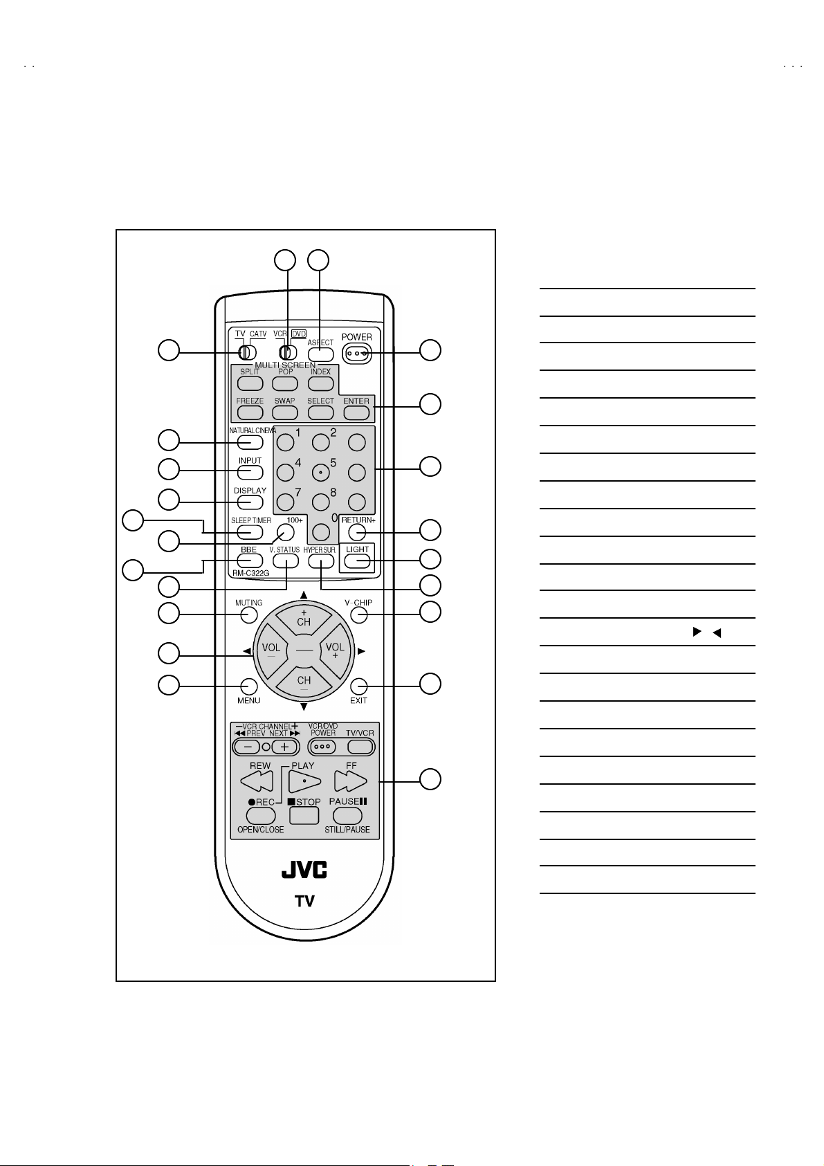
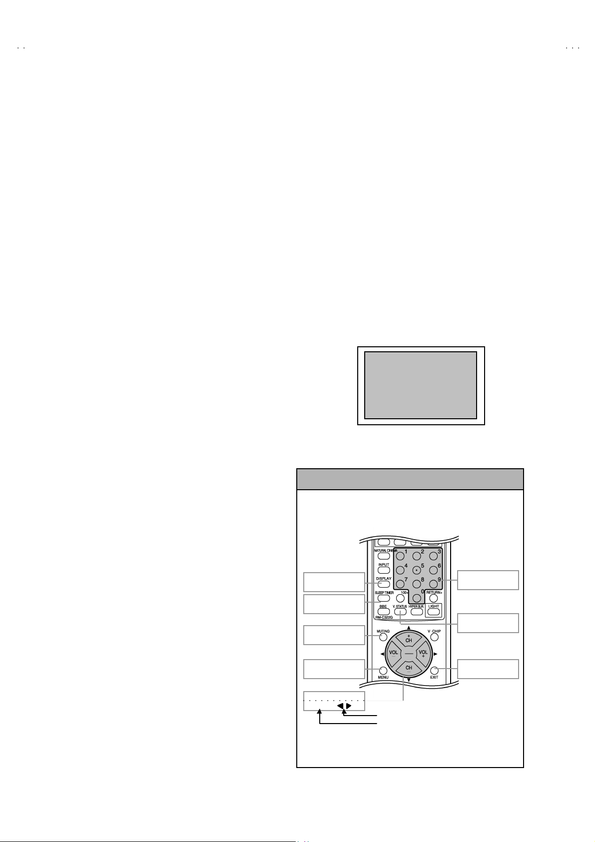
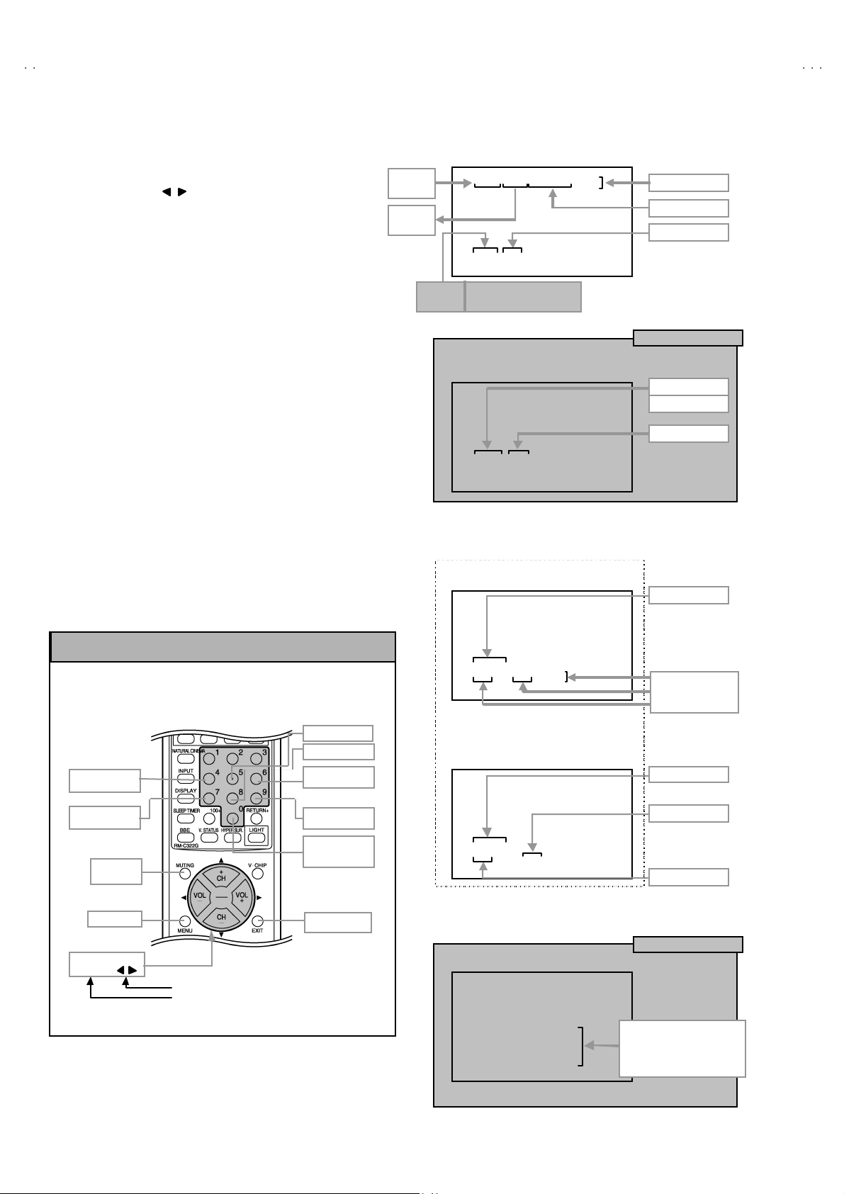
■■■■ REMOTE C ONTROL UNIT [RM -C322G]
3 2
V-56WP3
1 POW E R Key
2 AS PECT K ey
4
5
6
7
8
17
15
16
18
1
3
VCR / DVD Switch
4
TV / CATV Switch
5
NATURAL CINEMA Key
6
INPUT K ey
7
DISPLA Y Ke y
8 SL EEP TIMER Ke y
9 BB E Key
A V.S TATUS K ey
19
9
10
12
11
20
13
14
21
B HYPER SURROUND Key
C MUTING Key (memory Key)
D Function Keys (▲ / ▼ / / )
E
ME NU K ey
F
MUL TI SC R EEN op erat io n Key s
G
Number Keys
H
10 0+ K ey
I RETURN+ K ey
22
J LIG HT Key
K V- CHIP Key
L EX IT Key
M VCR / DVD operation Keys
No. 52007
5
Page 6
A
V-56WP30
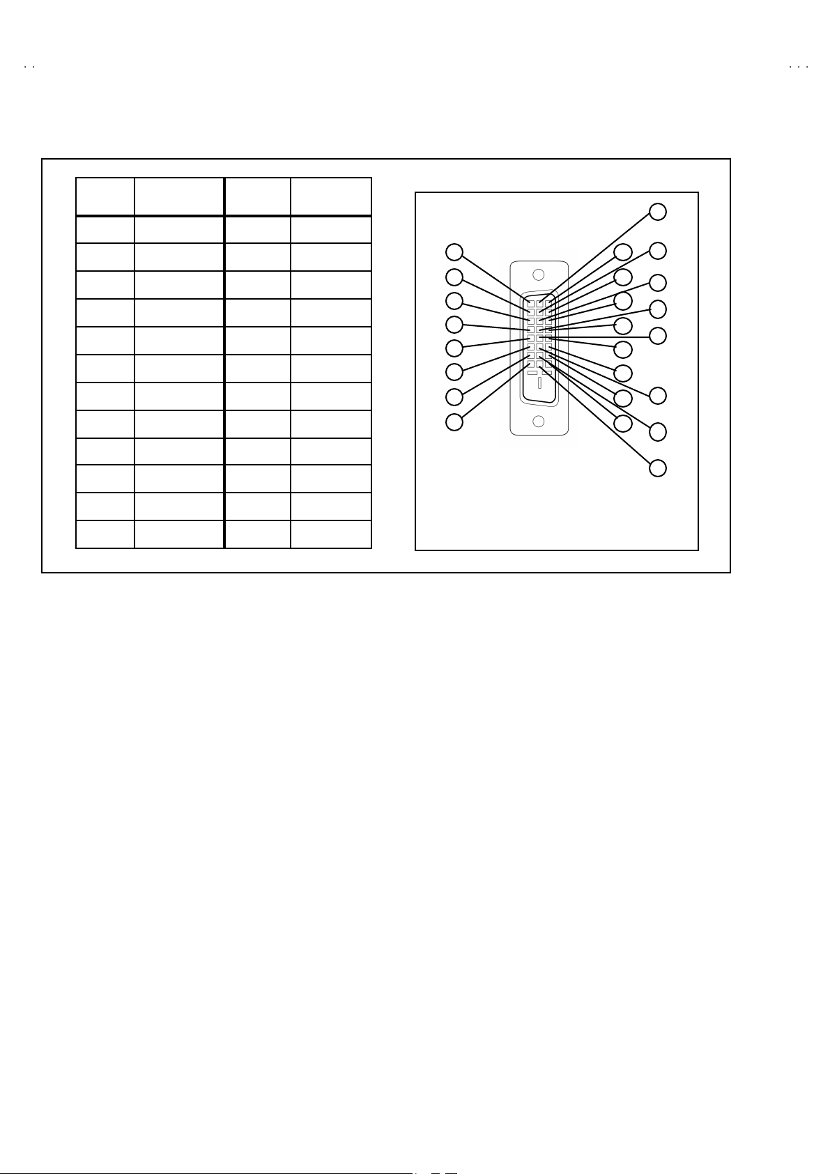
■■■■ DIGITAL-IN TERMIN AL F UNCTIONS
PIN
No .
1 RX2- 13 RX3+
2RX2+14 5V
3 GND2/ 4 15 GND
4
5 RX4+ 17 RX0-
6 SCL 18 RX0+
7 SDA 19 GND0/5
8NC20RX5-
9 RX1- 21 RX5+
10 RX1+ 22 GNDC
11 GND1/3 23 TXC+
12 RX3- 24 TXC-
PIN NAME
RX4-
PIN
No .
16 HTPLG
PIN NAME
PIN ASSIGNMENT
17
18
19
20
21
22
23
24
9
10
1
2
11
3
12
4
13
5
6
14
7
8
15
16
6
No. 52007
Page 7
A
0
INSTALLATION
1. INSTALLATION SITE
1. The re ar of thi s se t is pr ovid ed wi th ven tilation op eni n gs. I nst all t he s et
more t han 5 c m fr om a wa ll and i n a loc ation wit h g ood ve nti l a tion.
2. Avo id th e followi ng type s of locat ions.
(1) Unst able lo cat io ns (loca tion mu s t b e abl e to wi th sta nd heavy w ei g ht).
(2) L ocatio ns subjected to direct sunlight.
(3) Near st oves or ot her heati ng dev i ces.
(4) L ocati o ns su bj ect ed to humidi ty or oily smoke .
(5) Dusty locations.
(6) L ocati o ns with s trong vibr ati on.
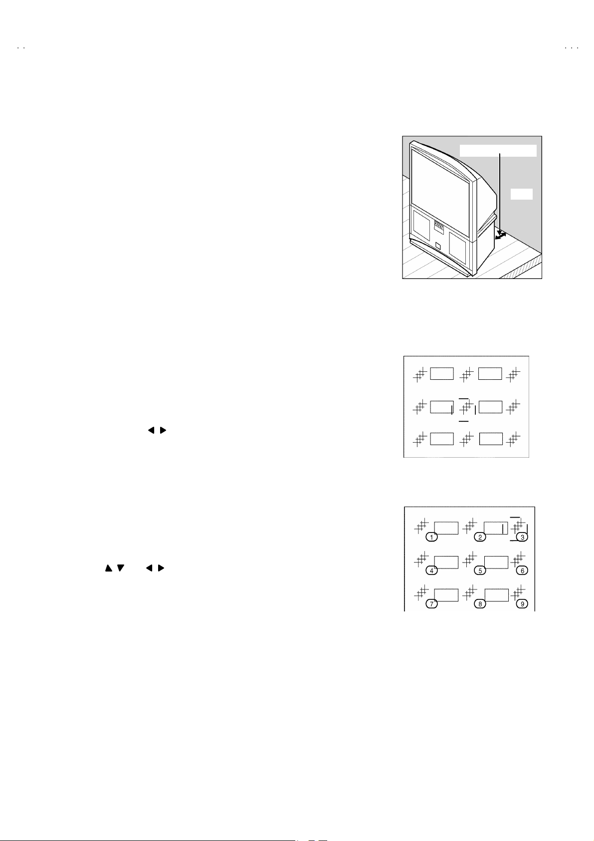
2. INSTALLATION ADJUSTMENT
When ins talling, mo vin g or ch an ging th e or i en tat i on of th e set , p er form
static con verge nce ad ju stm en t acc ordi ng to th e follo win g p roce dure.
V-56WP3
(more than 5cm)
Wall
VENTILATION OPENING
1. Pr ess the ME NU key of the r e mo te c ontrol un it .
2. Se lect the " CONV ERGENC E" in the INI TIAL SETU P menu with Function
▲/▼
key.
3. Pr es s th e F un cti on / key, th e co nve rg en ce ad ju stm en t scr een ap pears
wit h cross es ( +) d is playe d i n 9 l oc ation s.
Locations where the crosses appear in 3 colours:
Conver gence adj us tment i s r eq ui re d. Perf orm st eps 4 t o 5 .
Lo cat io n s wher e t h e c ross es are wh it e:
The con verge nce is adju ste d c o rr ect l y.
"
lf a ll th e cross es a r e w hit e, no c onve rg ence a dj ust me nt is ne ed ed.
4. The locat ions of the crosses correspond to the positions of the number keys on
th e r em ot e c ontro l. A b ox a pp ear s ar oun d the selec ted c r oss.
5. Press t he SE LEC T b utt on to ch ang e t he color of the b ox to th e c olor of t he
cross you want to adjust (red or blue).
" Yo u c annot adj u st th e gr een cross.
6. Use the / and / butto ns t o adjust the p osi tion of the cross.
" To c anc el the ad justmen ts bef ore com pl e ting th e pr oce du re, p r es s the E XIT
bu tto n.
7. Pr ess the ENTER butt on to end the c onve rg ence adj us tment pr oc e du re.
"
lf you do no t use th e T V co ntr ol s f or ro ug hly on e minu te, the con verge nce
ad justmen t s cree n autom aticall y d is appears.
Fi g.1
Fi g.2
No. 52007
7
Page 8
A
V-56WP30
TECHNICAL INFORMATION
■ MAIN M ICRO C OMPUT E R ( CPU) FUNCTION
( M IN1 02 H5 7K )
PIN
№№№№
PIN NAME I/O
1 CONV. SW OOOO CONVER GE NCE SW
2 /VS YN C IIII V.SYNC IN f or OSD
3 LB PR O IIII LOW B Prot ection
4 NC - NC
5 /RST IIII Mico n R es et in pu t
6 CONV. BUSY OOOO CONV.
7 /TES T IIII +3.3V
8 YS OOOO OSD YS OUT
9 NC OOOO Micon test pin
10 NC OOOO NC
11 A_ MUTE OOOO TV S ou nd Muti ng
12 /HSYN C IIII H.sync in put for OSD
13 M_ MU T E OOOO Monito r Out Muting
14 OSDX I -
15 OSDXO
16 SD A2 OOOO I2C BU S ( SDA ) f or MTS
17 AC_IN IIII AC 5 0/60Hz i n
18 SCL2
19 TU _POW OOOO Tuner Power Control
20 VCOI
21 PDO
22 /IP_ RESET OOOO
23 YM
24 B
25 LE D_ POW ER
26 G
27 R
28 VR EF
29 IP_ ER R
30 IREF
31 COMP
32 AV DD
33 CLL
34 VR EFL S
35 SU B_ CCD
36 NC
37 VS S
38 MAIN _CCD
39 VR EFHS
40 CLH
41 VDD
42 LE D_ DATA
I/O FUNCTION
I/OI/O
-
OOOO
I2C BU S ( SCL ) f or MTS
IIII
LP F inpu t
OOOO
LP F outpu t
OOOO
OSD YM out
OOOO
OSD B lue ou t
OOOO
LE D f or P ower
OOOO
OSD G reen Out
OOOO
OSD Red Out
IIII
IIII
AMDP program load det.
IIII
IIII
IIII
+3.3V
IIII
For Sub CCD
IIII
STD VOL in for Sub CCD
IIII
For Sub CCD
-
NC
IIII
GND
IIII
For main CCD
IIII
STD VOL in for CCD
IIII
For main CCD
OOOO
+3.3V
OOOO
Front control Data
PIN
№№№№
PIN NAME I/O
43 LED_ C LOCK OOOO F. LED CLK
44 LED_ON_TIMER OOOO LE D on ti m er
45 SBO0 -
46 SBD0 -
47 AP DAT A -
48 INC -
49 ECO RST OOOO Eco Reset
50 ROT COIL L OOOO Picture rotati on
51 ROT COIL R OOOO Picture rotati on
52 H BL K OOOO H.BLK
53 SN COIL_R OOOO
54 SN COIL_L OOOO ↑
55 BS POW OOOO BS power control
56 I2C STOP OOOO I2C BU S S TOP
57 NC
58 /LO B_P OW OOOO LO B p ower co ntr ol
59 COMPULINK IIII AV Compu linkⅢInput
60 /POWE RGOOD
61 /ME C A_O N IIII Machi n e SW Interrup t
62 /MA IN_PO W
63 NC
64 /B1 POW OOOO B1 POW E R CO NTR OL
65 C / N
66 X- R AY
67 EE CDS
68 KE Y2
69 KE Y1
70 SC L1
71 SDA1
72 REMO
73 AP REQ
74 VS S
75 OSC 2
76 OSC 1
77 VD D
78 SC L0
79 AP CLK
80 SDA0
81 NC
82 NC
83 NC
84 P MUTE
I/O FUNCTION
I/OI/O
Terrestrial Magnet ism Sen sor
-
IIII
Po w er C ond i tion Ch eck
OOOO
MA IN POW E R CO NT R OL
-
NC
-
IIII
X-ray detection
-
IIII
Fr ont Key i npu t 2
IIII
Fr ont Key i npu t 1
OOOO
I2C BUS (CLK) f or E2PROM
I/O
I/O
I/OI/O
I2C BUS (SDA) f or E2PROM
IIII
Remocon IN
-
IIII
GND
OOOO
4MHz OS C
IIII
4MHz OS C
IIII
+3.3V
OOOO
I2C BUS (CLK ) f or G enera l
-
I/O
I/O
I/OI/O
I2C BU S ( SDA ) f or Ge ner a l
-
-
-
NC
OOOO
Picture muting
8
No. 52007
Page 9
A
0
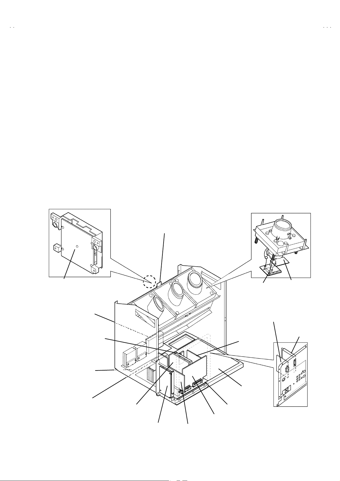
MAIN PARTS LOCATION
■
PWB ASS’Y ARRANGEMENT
The PW B A SS’Y is indic at ed belo w.
V-56WP3
"
MAIN PWB ASS’Y (SS B- 10 53 A-M2)
" POW E R & DEF PW B ASS’ Y (SS B- 20 53 A-M2) " CONVERGE NCE O SD PW B AS S’Y (SS B0T0 53A- M2)
"
R C RT SOCKET PWB A SS’Y (SS B-31 53A -M2)
" G CRT SO CK ET PWB ASS’Y (SS B- 325 3A -M2)
"
B CR T SO CK ET PWB ASS’ Y (SS B- 33 53 A-M2)
" R VM PW B ASS’ Y (SS B- 71 53 A-M2) " LINE FILTE R PWB A SS’ Y ( SS B- 90 53A -M 2)
"
G V M PW B AS S’Y (SS B- 72 53A -M2)
" B V M PW B AS S’Y (SS B-73 53 A- M2) " I-P CONVERT MODULE PWB ASS’Y (SSB0D053A-M2)
"
FR ON T CONTROL PWB ASS’ Y ( SS B0L 05 3A- M 2)
" REMO CO N SENSO R PWB A SS’ Y (SS B- 80 53A -M2) " AV JACK P WB AS S’ Y ( SS B0J0 53 A-M2)
"
DIGITA L INP UT MODULE PWB ASS’Y (SS B- 78 53 A-M2)
FRONT CONTROL ASS’Y
REMO CO N SENSO R
PWB
"
CONVER GE NCE PW B A SS’ Y ( SS B- 50 53A -M2)
"
CEN TER SP EAK ER PW B ASS’Y (SS B0A05 3A- M 2)
" DIGITA L CON VERG ENCE M ODULE PWB A SS’Y
"
DEF OSC PW B ASS’Y (SS B0H0 53A -M2)
"
FRONT I/F PW B ASS ’Y (SS B0L 253A-M2)
"
REC EIVE R PWB ASS’ Y ( SS B0R2 53 A- M2)
(Included in CONVERGENCE PWB)
PROJ ECTION UNIT
FRONT CONTROL
PWB
DIGITAL
CONVERGENCE
MOULE PW B
CONVER GE NCE O SD
PWB
CONVERGENCE
PWB
FRONT I/F
PWB
I-P COVE RT MO DUL E
PWB
LINE FILTE R
PWB
AV JAC K PW B
RECEIVER PWB
POWE R & DEF
PWB
MAIN PWB
CRT SOCKET
PWB (R/G/ B)
CEN TER SP EAKER
PWB
DEF OSC
PWB
AV TERMANEL BOARD
(This fi gure is only MAIN UNIT)
VM
PWB (R/G/ B)
DIGITAL INP UT
MO DU L E PW B
No. 52007
9
Page 10
A
V-56WP30
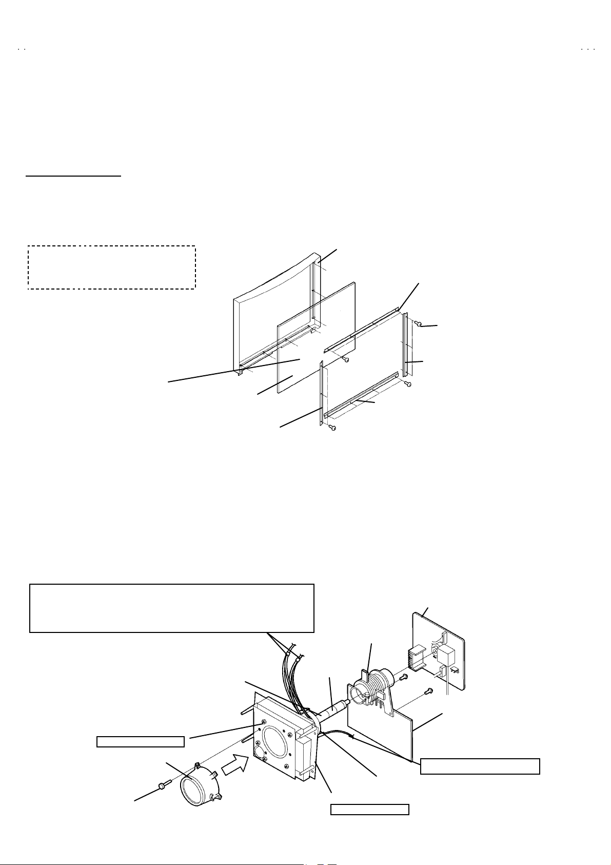
SPECIFIC SERVICE INSTRUCTIONS
SCREEN HANDLING CAUTIONS
■■■■SCREEN STORAGE
St ore th e SC RE EN AS S’Y i n a st an ding pos ition in ord er to avo id d eform at ion. If th e scr e en is s t ored h orizo ntal l y, th ere i s risk of deforming the
screen face.
When n ecessa r y t o pla ce th e SCRE EN ASS ’ Y h orizont all y, po sition the s creen side u pw ar ds an d s u re to p lace s pac ers betw een th e scr een and
resting site (f loor or st an d etc.) to pr event the s cree n f rom sag gi ng .
■ SCREEN SURFACE
Sinc e the scre en s urfac e is ea sil y scr atch ed or soiled , u se a m ple c are w he n han dling .
% DISASSEMBLY PROCEDURE
If the screen or sc reen panel n ee d to
b e r ep la c ed, rem ove th e A s crews
FRONT CABINET
SCR EEN B R ACKET ( TOP)
A(X3)
SCR EEN B R ACKET ( R IGH T)A(X4)
L eave th e scr ee n with fres nel len s an d
d oub l e l en tic ular l en s att ached. If c an no t be
disass embl ed fu rt her .
SCR EEN
SCR EEN B R ACKET
(LEFT)
SCR EEN B R ACKET
(BOTTOM)
A(X3)
A(X4)
PROJECTION UNIT REPLACEMENT
■ ADJUSTMENT DURING REPLACEMENT
When r ep la c ing the thre e R, G and B pr o jection u ni ts , f irst r ep l ace th e R a nd B uni ts and p erfor m foc us / s creen / r ast er cen tering adjustments
wit h ref er en ce to th e G unit. The n r e plac e t he G un it and per fo rm G f ocus / scr ee n / c onve rgen ce ad j ustm en t. F in al l y per f orm R & B .
Conver gence adj us tm ents . Use care to simultaneously removes all three-projection units.
■ DISASSEMBLY CAUTION
The proj ec tion units inc l ud e l o catio ns th at are not to be disas s embl ed dur in g s ervice . Whe n rep laci ng proj ec tion unit part s, d is assemble to the
state i n dicat ed in th e f ig ure bel o w.
The figu re ind ic ates scr ews an d wires t hat ar e not to be rem ove d. Us e c ar e no t t o r em ove th ese.
R CRT SOCKET PW B ASS’ Y
& Deflec tion yoke wires : to con nec tor on POWER & DEF. PWB ASS ’Y.
[R=”RHV”, G=”GHV”, B=”BHV”]
& Convergence yoke wires : to connec tor on CONVERGENCE PW B ASS’Y
[R=”R”, G=”G”, B=”B”]
Check that t ape is ap pli ed to the CRT n eck.
If absent, the d efl ec tion yoke can disl o dge.
PC M AGN ET
PC M AGN ET
TAPE
G CRT SO CK ET PWB ASS ’Y
B CR T SO CK ET PWB ASS ’ Y
VM PW B PW B (R/G/B )
Do not remove screws
10
LENS AS S’Y
LENS AS S’Y S CREW (X 4)
DEF . / CO NV ER. YOKE
CRT ASS’ Y ( COUPLE R AS S’Y)
Do not disassembly
No. 52007
●
ANODE wires : to DI VIDER
Page 11
A
0
DISASSEMBLY PROCEDURE
V-56WP3
!
SPEAKER GRILLE
1. Remove 4 screws A fro m r e ar side .
2. Op en th e do or of t he F R ON T C ON T R OL BOX and r e move 2
screws A’ from front side.
3. Remove th e SPEAK ER GRILLE.
! SPEAKE R (WOOFER )
"
Rem ove the SP EAKER GRIL LE
1. Remove 4 screws B.
2. Tak e ou t th e W O OFER .
3. Disc onnec t t he s p eaker wir e f rom s pe ak er t ermin al.
! SPEAKE R (T WEETER)
"
Rem ove the SP EAKER GRIL LE
1. Remove 2 screws C.
2. Tak e ou t th e TW E ETER .
4. Disc onnec t t he s p eaker wir e f rom s pe ak er t ermin al.
!
FRONT BOARD
" Rem ove the SP EAKER GRIL LE.
1. Remove 4 screws D.
2. Remove the F R ON T BOA RD.
SP EAKER WIRE
B
SP EAKER
(WOOFE R)
SP EAKER
(TWEETER)
A’
A
C
E
D
FRONT CONTROL BOX
FRONT BOARD
SP EAKER GRILL
A
! FRONT CONTROL BOX
"
Rem ove the SP EAKER GRIL LE.
1. Remove 4 screws E attach ing th e FRONT CON TROL BO X.
2. Disc onn ect th e con ne ctor BH
CONTROL PWB.
3. Remove the FRONT CONTRO L BOX.
!
FRONT CONTROL PW B
" Rem ove the SP EAKER GRIL LE.
"
Remove the FRONT CONTROL BO X.
1. Remove 3 screws F f rom r e ar side of FRON T CON TROL BOX .
2. Remove the FRONT CONTRO L PW B.
, X ,
R ,
BG on th e F R ON T
CAUTION AT DISASSEMBLY
56 W P30CP -S
: DIGI TAL INPUT MODUL E
F
BH
FRONT CONTROL BOX
REAR SIDE
X R BG
FRONT CONTROL PWB
" Prior t o di sassem bly, unplu g t he p ower co de fro m t he AC outlet
wit hout f ai l . ( Turn t he powe r “off ”.)
" Sh ort t he SB conne ctor (1) p in and (2) pin of the D IGITA L
INPUT MODU LE. (A t the t ime of asse mbling)
" Be fore th e rea r p ane l i s i ns ert ed i nt o t he cab i net , r el e as e th e
sh ort- cir c uit b etwe en the S B c onn ect or (1) p in an d (2 ) pi n of th e
DIGITAL INP UT MODU LE .
"
After releasing the short-circuit between the SB connectors, do
not turn the power on until the rear panel is inserted into the
cab inet .
* Neglig ence i n c a rr ying out th e a bov e ste ps m ay ca use th e
SB
AV JAC K B OARD
PO W E R CO RD
con nec tor
No. 52007
inact ivation of the TV .
11
Page 12
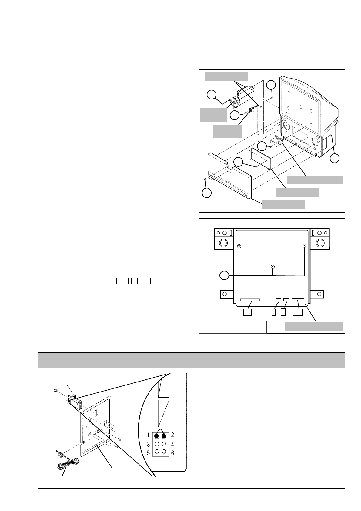
A
V-56WP30
damage to some of the televisio
eatures
! SCREEN ASS’Y
" Rem ove the SP EAKER GRIL LE.
"
Remove the FRONT CONTROL BO X.
1. Remove 4 sc rews G u nd er th e S CREE N ASS ’Y from f r ont side.
2. Remove 10 screws H f ro m r e ar si de .
3. Remove the SCREEN ASS’Y.
NOTE :
"
Plac e th e scr e en with f ace up w ar ds on a flat sta nd.
" Be c aus e of th e lar ge si ze, at lea st tw o pa rs ons are
reco mmen ded f or r em ov a l and reas sem bl e.
" Use c ore n ot t o scr atc h t he s creen du ri ng w or k.
"
During ass em bl y, be su re t o en gage th e left and r i gh t t abs
wit h the c abin et mount ing posit ions.
"
When tha n sp orting th e SCR EEN AS S’ Y, avoid gr aspin g t he
top of the sc r e en pan el, in ste ad gr asp th e left and rig ht a reas.
!
MIRR OR
" Rem ove the SP EAKER GRIL LE.
"
Remove the FRONT CONTROL BO X.
" Remove the SCREEN ASS’Y.
1. Remove 2 sc rews I at tach ing th e mirror st opper.
2. Rais e sligh tly t o dis engag e of th e m i rr or f rom the h ooks.
3. Rem ove th e MIR RO R.
NOTE :
"
The MIRROR is fr ont -c oat ed. D o n ot t ouch t he f ro nt of t he
MI RRO R.
"
At l ea st 2 person s ar e r eco mme nde d f or r em ovab l e an d
reass emb le.
! REAR PANEL
1. L oose n 7 scr ews J.
2. Remove 4 sc rews K.
3. Raise slightly REAR PANEL upward.
4. R em ove th e REA R PANEL .
NOTE :
" Be for e th e r ear pa nel is inser te d i nt o th e cabin et, r ele ase the
sh ort-c i r cuit b etw ee n t he S B co nnector (1) pin an d ( 2) pin of
the digital inp ut unit. ( Refer to “CAUTION AT D ISA SSEMBLY”
on P age 11 ).
" Af ter rele asing th e sho rt -circui t be tween the SB c onn ecto rs,
do not turn the power on until the rear panel is inserted into
th e ca bi ne t.
!
REAR COVER
" Rem ove the SP EAKER GRIL LE.
"
Remove the FRONT CONTROL BO X.
" Remove the SCREEN ASS’Y.
1. Remove 2 sc rews L.
2. Remove 2 sc rews M from front side
3. Slight l y pu l l f or ba ckside t o d is engag e of the REA R COV ER from
hooks.
4. Remove th e REA R CO VER .
H
MIRROR
I
MIRROR STOPPER
PARTITION
GGGG
GGGG
SCREE N ASS’Y
HOOKS
M
M
BRACKET
REAR COVER
L
!!!! Prior to starting the work, be sure to read the following
written instructions on the CAUTIO N LABEL attached to
the REAR PANEL.
UNPLUG THE POWER CORD FROM AC OUTLET BEFORE
OPEN THE REAR COVER (PANEL).
When th e rear co ver (p an el) is r emov e d, f oll ow “CAUTION AT
DISAS SE MB LY” p roced ure in th e s ervice man ual bef or e
pluggin g t he T V’ s p ow er c ord i nt o an AC out le t.
Failure to follow the procedure will result in PERMANENT
12
n f
J
L
J
.
K
REAR PANEL
J
No. 52007
Page 13
A
0
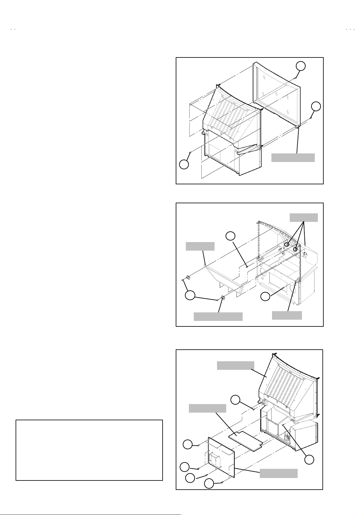
! PARTITION
" R emove th e R EA R PANEL .
1. Pu ll out the PARTITION b ack ward.
! MAIN UNIT
"
Rem ove the SP EAKER GRIL LE.
"
Remove th e co nne ctor BH , X , R , BG on th e
FRONT CONTROL PWB.
" R emove th e R EA R PANEL .
1. Remove 4 sc rews O!from f ront s ide.
2. Pu ll out the MAIN UN IT rea r s ide.
NOTE :
" Exc e pt fo r con fi r ma tion of pr oj ect i on of imag es on the s creen
an d aud io ou tput th roug h the s pe akers, t he re mo v ed ma i n un it
is still workable in the same state as if it is still built in the TV
set . The refor e , th e m ai n uni t c a n b e rem oved , i f nec essar y, f or
b oar d d ia gn osi s, e l ectr ic test ing, e tc. apar t from co nfirmati on
of scr een i m age s and aud io o ut put.
" W hen wir e c l am ps ar e r e mo v ed d uring work, use car e to
restore th em p r ecisely t o th ei r or i gi n al p osition s. P erf orm an ce
can be af f ected if th es e ar e no t r etu rned to th e original
p ositions.
" Be c aus e of th e lar ge si ze, at lea st tw o pe rs ons are
reco mm en ded f or r em ov al a nd reas semble.
" When carr yin g t he ma in un it, us e ca re n ot to drop , sh ock or
sh ake it.
" Do n ot st ain or d am ag e the lens of t he pr oj ec t ion uni t.
"
Do n ot look t hrou gh th e pr o jection u ni t.
# CHECKIN G THE P.W. BOARD
When ch ecking th e MAIN PW B , P OW ER & DEF PWB, etc., raise
the MAIN UNIT with th e HV DIVIDER side down for the sake of
con venienc e. You c an c h ec king the MAIN P WB.
!
LINE FILTER PWB
"
Remove th e REA R PANEL .
" Remove the AV JACK BOARD.
1. Disc onnec t t he c on nector B , F on th e L INE FIL TER PWB.
2. Remove 3 screws P att ac hi n g the L INE FILTE R BRA CK ET and
ea rt h w i r e.
3. Remove 2 sc rews Q atta ching LI NE FILTE R PWB.
4. Remove the L INE F ILT ER PW B.
O
F
EARTH WIRE
P
P
EARTH WIRE
MAIN UNIT
B
LINE FILTER BRACKET
Q
LINE FILT ER PWB
LINE FILTER BRACKET
V-56WP3
! MAIN CH ASSIS
" R emove th e R EA R PANEL .
"
Remove the AV JACK BOARD.
" Rem ove the L IN E FILT ER BRACKE T.
1. Remove 2 sc rews R b oth side of th e MAIN CHASS IS.
2. Remove 1 sc rews R’ att ach ing t he ea rt h wire.
3. Pu ll out the MAIN CH ASS IS f or back side.
NOTE :
"
If nec essar y, r em o ve th e an od e wi r es , c o nn ecto rs,
respectively.
R
MAIN CHASSIS
R
No. 52007
EARTH WIRE
R’
13
Page 14
A
V-56WP30
! PROJECTION UNIT
" Rem ove the SP EAKER GRIL LE
"
Remove the FRONT CONTROL BO X
"
Remove th e REA R PANEL
" Remove the MAIN UNIT.
1. Remove the CRT SOCKET PWB.
2. Remove 4 sc rews S attach ing th e PROJE CT ION UNIT.
3. Pull out the PROJE CTI ON UNIT, up ward.
NOTE :
"
Refer to “PROJE CT I ON UNIT RE PLA CEMENT” on p ag e 10
when ta king out a nd re pl ac in g t he PROJECT ION UNIT.
"
W hen wir e c lam ps ar e r e mo v ed d uring wor k, u se car e to
restore th em p r ecisely t o th ei r or i gi n al p osition s. P erf orm an ce
can be af f ected if th es e ar e no t r etu rned to th e original
p ositions.
!
HV DIVIDER
"
Remove th e REA R PANEL
1. Remove 1 sc rews T!!!! attaching the HV DIVIDER.
2. Remove the HV DIVIDER.
* W ires of the t ra nsf or m er (FBT) a nd CRT of ea ch P RO JECTION
UNIT can be removed by turning the connector portions.
NOTE :
" If n eces sary, remove the an od e wi r es , a nd re placi ng th e H V
DIVIDER, take care to correctly e ng age the U
!!!!
conn ect or.
S
PROJ ECTION UNIT
HV DIVIDER
TurnPull
T
U
AV JACK BOARD
! AV J ACK BOARD
"
Remove th e REA R PANEL
1. Remove 7 sc rews V.
2. Pull out the POWER CORD CLAMP from AV JACK B OARD left
si de.
3. Rem ove nu t W
4. Remove the AV JACK BOARD.
!!!!
att achin g the an te nna t ermi n al .
! DIGITAL INPUT MODULE
"
Remove th e REA R PANEL
1. Remove 2 sc rews X from r ea r side of the AV JAC K BO ARD.
2. R emove the DIGITAL INPUT MO DUL E.
NOTE :
"
When removing the DIGITAL INPUT MODULE, refer to the
"C AU T ION AT DISAS SEMBLY" sec t ion on page 11.
X
DIGITAL INPUT
MODULE
W
ANTENNA TERMINAL
V
V
POWER CORD CLAMP
14
No. 52007
Page 15
A
0
REPLACEMENT OF CHIP COMPONENT
! CAUTIONS
1. Avoid heating for more than 3 seconds.
2. Do n ot ru b t he el ect ro des an d t he r esist p arts of the p att er n.
3. W hen rem oving a c hi p par t, m el t th e s older ad equate ly.
4. Do n ot r euse a ch ip p ar t afte r re mo v ing it .
! SOLDERING IRON
1. Use a hig h i ns ulatio n s older i ng iron with a t hin poin ted end of it.
2. A 3 0w s older ing i r on is r ecommend ed for easil y r em oving p ar ts.
!
REPLACEMENT STEPS
1. How to remove Chip parts
####
Resi st o rs, capacitors , etc
(1) As sh own in the f ig ur e, pu sh th e pa rt w ith tw ee zer s and
alte rn at ely melt the s ol de r at eac h end.
(2) Sh if t with tweeze rs and r em ove th e c h i p p art.
#### Tran s isto rs, dio d es , va ria bl e r esist or s, etc
(1) Ap pl y e xt ra so ld er to eac h le ad .
V-56WP3
2. How to install Chip parts
####
Resi st o rs, capacit ors , etc
(1) Ap ply sold er to the pattern as indic ate d in the figure.
(2) Gr asp the c h i p p art with tw ee zer s and pl ac e it on th e s old er.
The n hea t and me lt th e so lder a t both ends of t he chi p part.
#### Tran s istors, dio des , va ria bl e r esist or s, etc
(1) Ap ply sold er to the pattern as indic ate d in the figure.
(2) Grasp the ch ip p art wit h t we ezers and p lace it on th e so lder .
(3) First s older lead A as indica ted in t he figure.
SOLDE R SOLDE R
(2) As sh own in the f ig ur e, pu sh th e pa rt w ith tw ee zer s and
alte rn at ely melt th e sol d er at each le ad . S hi ft an d r em ove the
chip part.
(4) T he n s o ld er l e ads B and C.
Note : A fte r re moving t he part, r emove rem ain ing solder fr o m the
pattern.
No. 52007
A
B
C
A
B
C
15
Page 16
A
V-56WP30
1.PICTURE/SOUND
I2C BU S
RF AFC
6
VALUE
VALUE
ITEM
ITEM
EXIT
MEMORY
DISPLAY
SLEEP
VIDEO
MEMORY IC REPLACEMENT
1. Memory IC
This model use a memory IC.
Thi s me mo r y I C st or es d ata for pr op er op er ati o n of the vid eo
an d d ef lecti on c ircu it s.
When replacing, be sure to use an IC containing this (initial
valu e) data.
2. Memory IC rep lacemen t procedure
(1) Power off
Switch of f t he p ow er an d dis con nec t th e power co rd from
the wall outlet.
(2) Replace the memory IC
Init ial value m ust be entered into the n ew IC .
(3) Power on
Connect th e pow er c or d t o the wa ll o utlet an d s witc h on t he
power.
SE RVICE MENU
SERVICE MENU
2.YC SEP 8.PP
3.LOW LIGH T 9.IP
4.HIGH LI G HT 0.SELF- CH K
5.
.
7.
Fig.1
SERVICE MENU SELECT KEY
(4) SERVICE MENU setting
1) Pr ess SLEEP TIMER k ey an d, w hi l e the in dicat ion of
SLEE P TIM ER 0 M IN is being displayed, press
DISPLAY key and VI DEO ST ATUS key on the remote
control un it (Fig.2) simultaneous ly.
2) The SER V ICE M ENU sc r ee n of F i g.1 is d isp l ay ed .
3) Verif y what to set i n th e SERV IC E MEN U , and set
what ever is n ec essar y ( Fig.1) .
Refe r to t he SERVI C E ADJU STMENT f or s ett in g.
4) Pr ess the EX IT key t wice to return normal screen.
(5) Rec eiv e channel setting
Refe r to the OPERATIN G I N STRUCTIO NS ( USER ’S
GUID E) a nd set th e rece ive ch an nel s (Chan n els Pr eset ) as
described.
(6) User se tt ing s
Check th e us er s ett ing it ems ac c ordi ng to aft er pa ge .
Wher e th ese d o not a gr ee, r efer to t he OPE RAT ING
INSTRUCTIONS (USER’ S GUIDE) and set th e items as
described.
TIMER
STATUS
(MUTING )
SELECT( -)
FUNCTION
MENU
POWER
NUMBER
SELECT(▲)
SELECT(+)
SELECT(▼)
16
Fig.2
No. 52007
Page 17
A
0
SHIPPING FACTORY SETTING
VIDEO STATUS MEMORY (NT SC / 480p)
Item
T IN T C OL OR PIC T URE BR IG HT DE T AI L
STA NDARD 00 00 00 00 00
TH ATER 00 00 00 00 00
DYNAMIC 00 00 +10 00 +1
(HD)
Item
T IN T C OL OR PIC T URE BR IG HT DE T AI L
STA NDARD 00 00 00 00 00
TH ATER 00 00 00 00 00
DYNAMIC 00 00 +2 00 00
CHANNEL SE TTING (CHANNEL S UMMARY)
BAND CH Display Setting BAND CH Display Setting
02
○
03 O 28 ○
VHF
L
04
○
05 ○ Q30
06
07
○
○
08 T 33
○
VHF
09
H
10 V 35
11 ○
12 A-7 93
13 ○ A-6 394
14
36
○
○
41 A-3 97 ○
UHF
46 A-2 98
63
○
69 ○
A14
○
B15 ○ W+12 48 ○
○
○
MI D
C16
D17
E18 ○ W+23 59 ○
F19
G20 W+29
H21 ○
I22 W+51
J23
SUPE R
K24
L25
○
M26
SETTING VALUE
SETTING VALUE
SUPE R
SUBM ID
HYPE R
ULTRA
N27
P29
R31
S32
U34
W36 ○
A-5 95
A-4 96
A-1 99
A-8 01
W+11 47
W+17 53
W+78
W+84
V-56WP3
○
○
○
○
○
○
No. 52007
17
Page 18

A
V-56WP30
SHIPPING FACTORY SETTING
(USER SETTIN G)
Setting item Setting value Setting item Setting value
POWE R
CHANNEL
BB E
VOL UME
INPUT
OFF
CABL E-02
ON
10
TV
TINT / COLOR / PICTURE
/BRIG HT / DETAIL
COLO R TEMPERATURE
DIG. NOI SE CLEAR
Refe r to s ettin g of Video
status me mo ry at sh i ppi n g
fac tory se tting
HIGH
CENTER
DISPLA Y
NATURAL CINEMA
SLEEP TIMER
AS PECT
VIDEO STATU S
H YPE R S U RRO U ND O F F
SP LIT SO URC E
POP SOURCE
VE RTICA L PO SITIO N
CENTER CH INPUT
XDS I D
CONVERGENCE
PO W E R I N DI C AT O R
OFF
AUT O
0
REGULAR
DYNAMIC
LEFT SIDE : CH 02
RIGHT SI DE : CH 04
LEFT SIDE : CH 02
RIGHT UPPER : C H 04
RIGHT CENTER : CH 05
RIGHT BOTTOM : CH 07
CENTER
OFF
ON
OPT IMUM CONDITION
HIGH
NOISE M UTI NG
BA SS / TREBLE / B ALAN CE
MTS
SE T CLOC K
ON / O FF TIMER
LA NG UA G E
CLOS ED CAPTIO N
FR ONT PAN EL LO CK
AUT O S HUT O FF
AUTO TUNER SET UP
DIGITAL-IN ( at 480p s ignal
input )
CHANNEL SUMMARY
V-CHI P
SET LOCK CODE
AUT O DEMO
ON
CENTER
STEREO
Unnecessary to set
NO
ENG
OFF ( CC1 / T1 )
OFF
OFF
Unnecessary to set
SIZE 1
Refe r to Last memory (CH.
summary)
OFF
Unnecessary to set
OFF
18
No. 52007
Page 19
A
0
SERVICE ADJUSTMENTS
V-56WP3
ADJUSTMENT PREPARATION
1. You c an ma ke the nec es sary adjustme nts for t his unit wi th
eit her t h e R emot e Co ntrol Unit or Wi th the ad just me nt
tool s and parts as given below.
2. Ad justment wit h t he Re mote Control Unit is made on the
bas is of t h e initial sett in g v al ues, howev er, t he ne w s etti ng
values which set the screen to its optimum condition may
differ f rom the init ia l s ettings.
3. M ake sure t hat AC p ower is tu r ned on c orrec tly.
4. T ur n on t he pow e r f or set and test equ ipm ent bef ore us e, an d
start th e adjus tme nt p r oced ur es aft er waitin g at l east 30
min ute s.
5. Unless oth er w is e spec if ied, pr epar e th e most s ui tab le rece ptio n
or inp ut sign al for adjust ment.
6. Never touch any adjustment setting value which are not
specified in the list f or this ad justment .
7. Pr es etti ng b efore adj ustm en t
Unl es s oth er w is e spec if i ed in th e ad justm en t instruct ions,
pres et t he f ollowing function s wi th the rem ote co ntr ol u nit:
ADJUSTMENT EQUIPMENT
1. DC voltmeter (or digital voltmeter)
2. Oscilloscope
3. Si gn al g ener at or (P attern g en erat or)
[NTSC / 480i / 480p / 720p / 1080i / HDCP]
4. Remote control unit
5. TV a ud io multi ple x si gn al ge ne rator
6. Frequ enc y cou nte r
ADJUSTMENT ITEMS
Adjustment item s
1
Check (×3)
2 HOR IZONTAL F REQUE NC Y adjus t ment
3 FOCUS & BEAM SPOT adjustm ent
4 CONVERGENCE & DEFLECTION adjustment
5 VIDEO ad justmen t
6MTS adjustment
" SETTING POSITION
SE TTING IT EM SE TTING POSI TION SE TTING IT EM SE TTING POSI TION
VIDEO STATU S ST A NDAR D AS PECT FULL
BA SS, TREB LE, BA LANCE CEN TER VERTICA L POSITIO N CENT ER
HYPE R SURROUND OFF BBE ON
TINT, COLOR, PICTURE,
BRIGHT, DETAIL
COLOR TEMPERATURE HIGH AUTO SHUTOFF OFF
DIGITAL NOIS E CLEAR CENTER
CENTER ON/OFF TIMER NO
ADJUSTMENT FLOWCHART
WHEN REPLACING SCREEN AND PROJECTION UNIT
●Contai ns on l y the main adj u stment s . Al s o c on firm o ther ad justmen ts as re qu ire d.
No. 52007
19
Page 20
A
V-56WP30
CO
S 801
POWER CORD
1Pi
L
DIGITAL IN P UT
S
ADJUSTMENT LOCATION (1/2)
NVERGENCE PWB
IC 805 IC 804
B G R
FRONT
B
F
LINE FILTER
PWB
SERVIC E
SWITCH
CONVERGENCE OSD PWB
R/G/B CRT SOC KET PWB
MAIN PWB
F
CN 00M
CN 010
TUNER
(TU101)
DIGITAL CON VERGENCE
MODULE PWB
CN 00Y
CN 00P CN 00X
FRONT I/F PWB
M
RECEIVER
PWB
AJ
FRONT CONTROL PWB
FRONT
BG BH
G H
G
CONVERGENCE
OSD PW B
DIGITAL INPUT PWB
TOP
BG R X BH
MEMORY IC
IC70 1
IC70 3
CPU
E
AF
POWER POWER SW
H
CN 001
LED
CH - CH + VOL - VOL +MENU
INPUT 3
REMO CO N S ENS OR PW B
B
POWER/DEF
PW B
P
CN 002
CN 003
J
G VM PW B
G CR T SOCKET PW B
CN 010
20
n :
2Pi n : R
3Pin : GND
4Pi n : SO A
5Pi n : NC
I-P CONVERT.
MODULE
TUNER
2
1
PWB
DEF OSC PWB
AV
S2
5
PWB
DC SY Q2 AJ
CN 007
CN 006
No. 52007
JACK
PWB
S1
Page 21
A
0
ADJUSTMENT LOCATION (2/2)
G C
C
SOC
OCUS
REAR
TOP
TOP
V-56WP3
DIGITAL INPUT MODULE PWB
DVI -D
termin al
F
PACK
MAIN PWB
IC
DC
Q
SY
SB
CONNE CTO R
LINE
FILTE R
PWB
H
RT
TP-E TP-R
R CRT SKT PWB
AV JACK PW B
MAIN PWB
AV JACK PWB
CN 001
KET PWB
RGK
B
KR
SG 001
GBK RGK
TP-E TP-G
E
SG 001
TP-E TP-B
KG
RT SKT PWB B CRT SKT PW B
POWER / DEF PWB
GBK
SG 001
KB
IC70 1
CPU
5Pin : TP-91(B1)
4Pi n : NC
3Pi n : X- ra y1
2Pi n : X- ra y2
1Pin : TP-E ( )
MEMORY IC
IC70 3
E
5
1
CN 00 2
CN 00 3
J
G VM PW B
DEF OSC PWB
CN 010
AB
S1
5
1
RH V
GHV
BH V
FBT
A
No. 52007
21
Page 22
A
V-56WP30
BASIC OPERATION OF SERVICE MENU
1. TOOL OF SERVICE MENU OPERAT ION
Operate the SERVICE MENU with the REMOTE CONTROL UNIT.
2. SERVICE MENU ITEMS
In ge nera l, basic s ett ing ( ad ju stm en ts) it em s or verif ic ations are perf orme d i n th e SE RV ICE M EN U .
1. PICTURE / SOUND ・・・・・・・ ・・・ T his sets th e s etting values of t he VIDEO/CHROM A /A UDIO an d DEFLECTION ci rcuits.
2. YC SEP ・・・・・・・ ・・・・・・・・・・・・・ Thi s is us ed when th e YC m od e is a djust ed. [Do not adjust]
3. LOW LIGHT ・・・・・・・・・・・・・・・・・ This se ts the s etting va lues of t he W HIT E BA LANC E circuit.
4. HIGH LI GHT ・・・・・・・ ・・・・・・・・・ This sets the se tting valu es of th e WHITE BALANCE circu it.
5. RF AFC ・・・・・・・・・・・・・・・・・・・・ This i s us ed w hen the I F VC O i s adjust ed. [Do not adjust]
6. ( BLAN K )
7. I2C B U S
8. PP ・・・・・・・ ・・・・・・・・・・・・・ ・・・・・ T his sets th e s etting value of t he output of P& P d ata .
9. IP
0. SE LF- CHK ・・・・・・・ ・・・・・・・・・・・ This se ts the s elf checking of th e TV c ircuit.
3. BASIC OPERATIONS OF THE SERVICE MENU
(1) Ho w to enter the SERVICE MENU.
Press SLE EP TIMER k ey an d, w hi l e th e i n dic at ion of “ SLE EP
TIMER 0 MIN.” is being displayed, press DI SPLAY key and
VI DEO ST ATUS key on the remote control unit simultaneously
to ent er the SE R VIC E MENU s cree n as sh own i n th e f ig .1.
(2) SE RV ICE MENU screen selecti on
Press the nu mb er key to s elect an y of t he fo llo wi n g ite ms.
・・・・・・・ ・・・・・・・・・・・・・
・・・・・・・ ・・・・・・・・・・・・・ ・・・・・・
This is us ed when ON/O FF if the I2C BUS control is stop. [Do not adjust]
This se ts th e s etting value of t he IP circuit. [Do not adjust]
1.PICTURE/SOUND 7.I2C BUS
2. YC SEP 8.P P
3.LOW L IGH T 9.I P
4.HIG H LIGHT 0.SELF-C HK
5.RF A FC
SERV IC E MENU
1. P I CT URE/ SOUND
2. YC SEP
3. LOW LIGHT
4. HIGH LIGH T
5. RF AFC
6.
7. I2C BU S
8. PP
9. IP
0. SELF-CHK
Fig. 1
KEY F UNCTIO N of SE R VIC EM ENU
( 3) Ent er the any se tt i n g mode
"
1. PICTURE / SOUND mode
1) Select the 1. PICTURE / SOUND items with the number
key, a nd the FUNCTION ( ▲/ ▼) ke y is pres se d th e 1.
PICTURE / SOUND mode, the screen will be displayed as
sh own in fi gu re pa ge late r.
2) T he n the set tings or ver ifi cat i ons c an be perf orme d.
" 2.YC S EP, 3.LOW LIGHT, 4.HI GH LIGHT, 5.RF AFC,
7.I2C BUS , 8.PP, 9. IP and 0. SELF-CHK mode
1) If you se l ect a ny of 2 .YC S EP 3. LO W LIG HT 4.HIGH -
LIG HT 5.R F A F C 7 .I2C B US , 8.P P, 9 .IP a nd 0.SE LF - CHK
mod e item s, and the nu m ber s ke y is presse d fro m
SE RV ICE M EN U, th e ea ch sc r ee ns will be d isp layed as
sh own in fi gu re pa ge late r.
2) Th en the s et ting s or ve ri fi cat i ons can be perf orme d.
22
No. 52007
DISPLAY
key
SLEEP TIMER
key
MU TI N G ke y
MENU key
FUNCTION ke y
(▲/▼) & (
/
NUMBERS
key
VIDEO ST AT US
key
EXT key
(PIP OFF)
)
S ele ct t he se t t i n g valu e
Select the setting Item
Page 23
A
V-56WP3
0
JUS
JUS
JUS
Function
(
/
Function
(
▲/▼
) key
) k ey
SE RVICE MENU
SERV IC E MENU
1. P I CT URE/ SOUND
2. YC SEP
3. LOW LIGHT
4. HIGH LIGH T
5. RF AFC
6.
7. I2C BU S
8. PP
9. IP
0. SELF-CHK
1. PICTURE/ SOU ND
NTSC
***** ****
***** *****
***** **** ***** ****
A01 001
*********
*********
********* *********
*** *** ******* ******
*** *** ******* ******
*** *** ******* ****** *** *** ******* ******
A01 ~~~~ A20
A01
*** **********
*** **********
*** ********** *** **********
*** *** *** *****
*** *** *** *****
*** *** *** ***** *** *** *** *****
S01~~~~S57
*
* *
LO W
4.HIGH LIGHT
HW -BAL
** * * **
** * * **
** * * ** ** * * **
5.RF AFC
TUNER
AFC
FINE
**
**
** **
**
**
** **
** *
** *
** * ***
7.I2C BUS
Press the
0 key → ON/OFF
DO NOT AD
DO NOT ADJUST
T
DO NOT AD
YC001
YC007
** * ** ** ** ** **
** * ** ** ** ** **
S01
** * ** ** ** ** ** ** * ** ** ** ** **
*** *** **********
*** *** **********
*** *** ************* *** **********
D01
D2 0
~~~~
D01
*** *********
*** *********
*** ********* *** *********
*** *** **** **** *
*** *** **** **** *
*** *** **** **** * *** *** **** **** *
F01
F64
~~~~
F0 1
*** *********
*** *********
** * * ** ** ** **** * * ** ** ** **
*** *** ******* **** *
*** *** ******* **** *
*** *** ******* **** * *** *** ******* **** *
T
~
~~
~
YC001
*** *** ******* *** ***
*** *** ******* *** ***
*** *** ******* *** *** *** *** ******* *** ***
LW-BAL
*** *** ***
*** *** ***
*** *** *** *** *** ***
2.Y C SE P
** ** ** ** ** *
** ** ** ** ** *
** ** ** ** ** * ** ** ** ** ** *
3.LOW LIGHT
I2 C
** *
** *
** * ***
PPA001
NT S C FU LL
IP A00 1
XRAY
LOB
SYNC
MEM
VCD
AIO
TUN
PP
8. PP
** *
** *
** * ***
9.I P
*****
*****
***** *****
NTSC OFF LINE 0
***
***
******
0.SELF-CHK
NG2
OCP
OK
TIM
M:OK
S:OK
OK
AVSW
NG2
BS
OK
YC
OK
OK
NG4
OK
LOW
NG2
OK
HD :N G
OK
OK
OK
OK
OK
PPA001
00 8
~~~~
PPB001 ~~~~03 6
PPC001 ~~~~00 7
ADM0 01
ADS0 01
VCM001
VCS001
034
~~~~
03 4
~~~~
03 8
~~~~
04 1
~~~~
DO NOT AD
IPA001~~~~12 0
IPB001
08 8
~~~~
IPC001
04 4
~~~~
IPD001
05 8
~~~~
IPE001~~~~01 5
T
Press the 0 key → ON/OFF
No. 52007
23
Page 24
A
V-56WP30
JUS
SIGNAL
G.CUT O
B.CU T OFF
R.CUT OFF
B.CU T OFF
R.CUT OFF
(4) Setting method
1) UP / DOW N (▲/▼) FUNCTION key
Select t he SETTIN G IT EM .
2) LEFT / RIGHT ( / ) FUNCTION key
Se tting ( ad ju s t) th e set ti ng valu e of the S ET TIN G I TEM .
When the MUTING key is pr es se d t he se tti ng valu e
will be stored (memorized).
3) EX IT key
Retu rn s to th e p re vious scr een.
(5) Releasing SERVICE MENU
1) Af ter r etu rni ng to the SE RV ICE MENU up on completion
of th e s ettin g w or k, pr ess the EXIT key aga in.
NTSC
SYSTEM
ASPECT
SIZE
A00 1
**** ***********
**** ***********
**** *********** **** ***********
SETT ING A01 ~~~~ A20 / S01~~~~S57
ITEM D01~~~~ D2 0 / F 01~~~~F64
YC001
*** *** *** *** ***
*** *** *** *** ***
*** *** *** *** *** *** *** *** *** ***
1. PICTURE/ SOU ND
FULL
DYN AMIC
001
OFF
FRAME
2.Y C SE P
** *
** *
** * ***
LOW
WHITE BAL AN CE
VI DEO ST ATUS
SETTING VALU E
DO NOT AD
SETTING ITEM
YC001~~~~YC107
SETTING VALU E
T
"
WHITE BALANCE setting
The sett in g f or 3 .LOW LIGHT a nd 4.HIGH L IGHT are descr ib ed in
th e WH IT E BALA NCE pa ge of AD J US TME NT.
WHITE BALANCE key function
FF
(▲)
R.DRIVE
R.DRIVE
(▲)
(▼)
MEMORY
(MUTING
MENU key
FUNCTION ke y
(▲/▼) & ( / )
G.C UT OF F
B.DRIVE
B.DRIVE
W.BALANCE
S ele ct t he se t t i n g valu e
Select the setting Item
SETTING V AL UE
(O N o r OFF)
EXIT key
(▼)
(▲)
(▼)
WHITE BALANCE
3.LOW LIGHT
LW-BAL
*** *** ***
*** *** ***
*** *** *** *** *** ***
4.HIGH LIGHT
HW -BAL
*** ***
*** ***
*** *** *** ***
5.RF AFC
SETTING ITEM
・・・・S etting Valu e
B.CU T OF F V ALU E
G.CUT OFF VALUE
R.CU T OF F V ALU E
SETTING ITEM
・・・・S etting Valu e
B.DRIVE VALUE
S etting Value
・・・・
R.DRIVE VALUE
DO NOT ADJUST
24
No. 52007
TUNER 2
AFC O N
FINE
***
***
******
NOTE )
(
T UNER 1 (MAIN )/2 (S UB)
AFC Se le ct ON/O FF
FINE FineTuning(-77~~~~+ 77)
AFC ON:Auto Setting
Page 25
A
0
8. PP
SE TT ING I TEM
PPA001~~~~PPA008
PPB001
PPB036
~~~~
PPC001
PPC007
~~~~
PPA001
***
***
*** ***
ADM0 01
ADM0 34
~~~~
SETTIN G VALU E
8.PP / 9.IP setting
1) FUNCTION(▲/▼) key
・・・・・・・ ・・・・・・・・・・・・・ ・
Se le ct t he sett in g Item
2) FUNCTION ( / ) ke y ・・・・・・・・・・・・・・・・・・・・ Se le ct t he s ett in g va l ue.
3) SL EEP TIME R ke y
・・・・・・・ ・・・・・・・・・・・・・ ・・・
Skip t he each s etting Item.
4) MUT IN G Key ・・・・・・・・・・・・・・・・・・・・ ・・・・・・・・ Setting value will be stored.
5) EX IT key
・・・・・・・ ・・・・・・・・・・・・・ ・・・・・・・・・・・・
Retu rns to the s ervice menu.
* P res s th e EXIT ke y ag ai n, then re l easin g th e s er vic e m en u.
NTSC PI P
IPA 001
***
***
*** ***
9.I P
** ** **
** ** **
** ** ** ** ** **
OFF FRAM
** *
** *
** * ***
V-56WP3
DO NOT ADJUST
SE TT ING I TEM
IPA001
IPA120
~~~~
IPB001
IPA088
~~~~
IPC001~~~~ IPC044
IPD001~~~~ IPD058
IPE001~~~~I PE 015
SETTIN G VALU E
0.SELF-CHK DISPLAY
Press 0 key of remote control unit that checks the circuit
op er at ing s t atus and in eve nt o f m alfun ction di spla ys
sto res the data in memory. (shown in f ig ure)
0.SELF-CHK
XRAY
LOB
SYNC
MEM
VCD
AIO
TUN
PP
NG
OK
M:OK
OK
NG2
OK
OK
NG4
OCP
TIM
S:OK
AVSW
BS
TC
GCR
IP
NG2
OK
HD :N G
OK
OK
OK
OK
OK
No. 52007
25
Page 26
A
V-56WP30
INITIAL SETTING VALUE OF SERVICE MENU
1. Ad ju stm en t of th e SER VICE MEN U is made on th e bas i s of th e ini ti a l s ettin g va lues; however , t he new sett ing v alue s which set the
screen in its opt imum condition may differ from the initial setting.
2. D o n ot c hange the in it ial set tin g value s of th e se tting item s NOT L ISTED IN AD J USTMENT.
3. T he (*1 or *2) m ark ed it ems i n f ollo win g tab le, it is N O REQU IR EM EN T for adj u stm ent . If val ues had ch an ge b y the miss ing, set t he
initial values in the following table.
CAUTION
Ne ve r cha nge the initial setting value any adjustments except for t h ose that are d esi gnated in th e
adju st ment pr oce dure s.
In case where you have made undesignated adjustments by mistake, never press the MUTING key on the
remote control unit.
Whenever you had not pressed the MUTING key, you would be able to recover the initial value by switching
the POWER SW (on/off) key.
1. PICTURE / SOUND
■■■■SOUND SYSTEM
Item
No .
A01 N OISE DET. 0 / 1 001 A1 1 INPU T GA IN 0 / 1 000
A02 INPUT LEVEL
A03 FH MONI TOR 0 / 1 000 A1 3 BB E BA SS
A04 STE RE O VC O
A05 PIL OT CAN 0 / 1 00 0 A15 BA SS
A06 FILTE R
A07 LOW SEP
A08 HI SE P
A09 5FH MON 0 / 1 00 0 A1 9 Not use
A10 SA P VCO
Item name
Variabl e
range
0 ~ 63
0 ~ 63
0 ~ 63
0 ~ 63
0 ~ 63
0 ~ 63
Initial setting
value
02 7 A1 2 FIL O FFSET
035 A1 4 BB E TREBL E
035 A1 6 T REBL E
02 7 A1 7 N ot use
02 8 A1 8 N ot use
04 0 A2 0 N ot use
Item
No .
Item name
Variabl e
range
-128 ~ + 127
-128 ~ + 127
-128 ~ + 127
-128 ~ + 127
-128 ~ + 127
Initial setting
value
00 0
+003
+003
-005
-004
■■■■
DEFLECTION SY STEM
Item
No .
D01 V. SIZE 0~127 013 D11 H. EHT 0~7001
D02 EW P ARABORA
D03 H. SIZ E 0~6 3 03 7 D13
D04 V. S-CORRECT 0~6 3 04 0 D14 H . CENTER 0~255 161
D05 V. LINEARI TY 0~63 041 D15 H. FREQUENCY 0~255 194
D 06 V. CE NTE R 0~6 3 02 7 D16 H . BL K 0~255 063
D07 TRAPEZIUM 0~6 3 02 9 D17 OSD O FFS ET 0~127 080
D08
D09
D10 V. EHT 0~7004D20
Item name
EW CORNER
LOW ER
EW CORNER
UPPE R
26
Variabl e
range
0~63
0~1 5 00 8 D18
0~1 5 00 8 D19
Initial setting
value
02 2 D12 EH T GA IN
No. 52007
Item
No .
Item name
SUBT IT LE
V. AREA
COMPULSION
TW IN SC REEN
COMPULSION
DEF RST
OUTPUT
COMPULSION
10 80 i
Variabl e
range
0~7
0~15 000
0~7000
/
0
1000
/
0
1000
Initial setting
value
00 0
Page 27
A
0
■■■■ PICTURE SYSTEM
( NTSC / 480i / 480p )
Item
No .
S01 SUB COLOR 0~127 080 072 077 071 075 075
S02 SUB TI NT 0~127 075 063 077 074 080 079
( 720p / 1080i / HDCP )
Item
No .
S01 SUB COLOR 0~127 063 063 075 075 074 070
S02 SUB T I NT
( NTSC / 480i )
Item
No .
S03
S04
S05
S06
(1/2)
Item name
Item name
Variabl e
range
Variabl e
range
0~127
Item name
SUB BRIGHT 0~255
SUB CONTRAST 0~127
SUB BRIGHT
OF FSET
SUB CONTRAST
OF FSET
Variabl e
range
-128~127
-128~127
Standard Theat er Stand ard Th eater St andard T heater
Standard T heater
NT SC 48 0i 48 0p
72 0p / 10 80i HDCP
48 0p 10 80i / 720 p
Standard T heater St andard T heater
08 3 07 2 08 0 07 9 07 2 06 1
NT SC 48 0i
Standard T heat er St andar d Theater
13 4 13 5 13 0 13 3
06 3 04 6 080 04 7
----
----
V-56WP3
(2/2)
(1/2)
( 480p / 720p / 1 080i / HDCP )
Item
No .
S03
S04
S05
S06
( NTSC / 480i / 480p / 720p / 1080i / HDCP )
Item
No .
S07
S08
S09
Item name
SUB BRIGHT 0~255
SUB CONTRAST 0~127
SUB BRIGHT
OF FSET
CUB CONTRAST
OF FSET
Item name
B-Y
DEMODURATION
R-Y
DEMODULATION
G- Y MA TRI X SW
Variabl e
-128~127
-128~127
Variabl e
(2/2)
48 0p / 72 0p / 1080i H DCP SP LIT / FR EEZ E
range
range
0~63 013 040 014 031 007 020 004 010
0~7 007 000 007 000 007 002 003 003
0~3 001 003 001 003 001 003 002 002
Standard T heater Stand ard T heater Standard Theater
13 1 13 5
----
08 4 04 6 ----
--000 000 00 0 00 0
--000 000 - 010 00 0
NT SC 480i 48 0p 72 0p / 10 80i / HDCP
Sta ndar d Th eat er S tandard Th eat er S tanda rd Th eat er S tanda rd Th eat er
No. 52007
27
Page 28
A
V-56WP30
( NTSC / 480i)
Item
No .
S10
S11
S12
S13
( 480p / 720p / 1080i )
Item
No .
S10
S11
S12
S13
(1/3)
Item name
R DRIVE 0~255
R DRIVE OFFSET -128~+127
B DRIVE 0~255
B DRIVE OF FSET -128~+127
Item name
R DRIVE 0~255
R DRIVE OFFSET -128~+127
B DRIVE 0~255
B DRIVE OF FSET -128~+127
NT SC 48 0i
Variabl e
range
Standard Theater St andard Theater
High Low High Low High Low High Low
-
07 5
---
07 7
--
+004 000 + 002 +006 +004 00 0 + 003 -004
-
07 3
---
07 6
--
+005 000 -012 - 017 +005 000 - 010 -018
(2/3)
Variabl e
range
Standard Theater St andard Theater
High Low High Low High Low High Low
--- --
+004 000 -005 - 004 +004 000 - 006 +005
--- --07 2 --
+006 000 -002 - 014 +005 000 - 013 -010
48 0p 72 0p / 10 80i
07 8
--
( HDCP )
( NTSC / 480i / 480p / 72 0p / 1080i )
(3/3)
Item
No .
S10
S11
S12
S13
Item
No .
S14
S15
S16
S17
S18
S19
S20
S21
Item name
R DRIVE 0~255
R DRIVE OFFSET -128~+127
B DRIVE 0~255
B DRIVE OF FSET -128~+127
Item name
R CUT OFF 0~255
R CUT OFF
OF FSET
G CUT OF F 0~255
G CUT OF F
OF FSET
B CUT O FF 0~255
B CUT O FF
OF FSET
R CUT OFF SW 0~3
B CU T O FF SW 0~3
Variabl e
range
Variabl e
range
-128~+127
-128~127
-128~+127
HDCP
Standard T heat er
High Low High Low
----
+004 000 -006 +005
----
+005 000 -010 - 013
NT SC 480i 48 0p / 720p / 108 0i H DCP
Sta ndar d Th eat er S tanda rd Th eat er S tanda rd Th eat er S tanda rd Th eat er
23 2
-
23 2
-
23 2
---
00 0 +003 00 0 +004 00 0 - 007 00 0 + 007
04 0 - 04 0 - 040 ---
00 0 00 0 00 0 000 00 0 00 0 00 0 000
04 8 - 04 1 - 054 ---
00 0 - 004 00 0 + 002 00 0 - 005 00 0 - 005
00 0 - 00 0 - 000 ---
00 1 - 00 1 - 001 ---
28
No. 52007
Page 29
A
0
( NTSC / 480i / OTHERS SIGNAL)
Item
No .
S22
S23
S24
S25
S26
S27
Item name
BLACK GRAD CORR
START LE VEL
BLACK GRAD COR R
GAIN
WHITE GR AD CORR
START LE VEL
WHITE GR AD CORR
GAIN
WHITE CHA RA COR R
START LE VEL
WHITE CHA RA COR R
GAIN
Variabl e
range
0~15
0~15
0~15
0~15
0~15
0~15
NT SC 480i
OTHERS
SIG NAL
01 5 01 5 01 5
00 8 00 8 00 8
00 0 00 0 00 0
01 5 01 5 01 5
00 2 00 0 00 2
00 4 00 2 00 0
V-56WP3
Item
No .
S28
S29
S30
S31
S32
S33
S34
( NTSC / 480i / 480p / 720p / 1080i / HDC P )
Item
No .
S35
Item
No .
S36
S37
S38
S39
S40
Item name
ABL GAIN 0~15
ABC START
ACL GAIN
ACL START 0~15
CONTRAST LINK 0 / 1
BLACK GRADIATION
CORRECTIO N OFF
WHITE GRADIAT ION
CORRECTIO N OFF
Item name
TINT HD / NTSC 0 / 1
Item name
ABL OF F 0 / 1
ACL O FF 0 / 1
DC TRANSMIT
POLAR IT Y
DC TRANSMIT CORR 0 / 1
BLANKING ON / OFF 0 / 1
Variabl e
range
Variabl e
range
Variabl e
range
0~15
0~15
0 / 1
0 / 1
0 / 1
Standard Th eat er
01 5 01 5
01 5 01 5
01 5 01 5
00 0 00
00 0 00 0
00 0 00 1
00 0 00 1
NT SC / 4 80i 48 0p 720p / 1080i
HDCP
48 0p 72 0p / 10 80i
00 1 00 1 00 0 001 00 0
Standard Th eat er
00 0 00 0
00 0 00 0
00 1 00 0
00 0 00 0
00 0 00 0
( NTSC / 480i / OTHERS )
Item
No .
S41
Item
No .
S42
Item name
DC REPRODUCE
RATE
Item name
ACL CONTR OL 0~255
Variabl e
range
0~255
Variabl e
range
Sta ndar d Th eat er Standa rd Th ea t er Standard Th eat er
NT SC 480i OTHERS SIGNAL
16 0 14 0 16 0 12 0 16 0 12 0
SP LIT Regular Th eat er
OTHERS
SIG NAL
06 4 07 2 00 0 07 2
No. 52007
29
Page 30
A
V-56WP30
Item
No .
S43
S44
S45
( NTSC / 480i / O THERS )
Item
No .
S46
S47
( AL L S I G N AL )
Item name
CONTRAST
LOWER LIMIT
CONTRAST
UPPER LIMIT
BRIGHT LOWER
LIMIT
Item name
EE THEATER
BRIGHT
EE THEATER
CONTRAST
Item
No .
S48
S49
S50
S51
S52
BRIGHT EE CONT. CORRECTION
REFRAIN EE
CONT. CO RRECTION
REFRAIN EE BRIGH OFFSET
CORR (MAX)
BRIGHT EE ACL CORR . COEFF. 0~255
REFRAIN EE ACL CORR. COEFF. 0~255
S53
S54
S55
S56
S57
Variabl e
range
-128~+127
-128~+127
-128~+127
Variabl e
range
-128~+127
-128~+127
Item name
No use 0 / 1
No use 0 / 1
No use 0 / 1
No use 0 / 1
No use 0 / 1
Setting value
Standard Th eater
-030 -020
+013 +013
-020 -020
NT SC 48 0i
00 0 00 0 00 0
+020 +020 + 020
Variabl e
range
0~31
0~31
0~127
Settin g
value
00 8
02 7
00 4
08 5
14 0
00 0
00 0
00 0
00 0
00 0
OTHERS
SIG NAL
30
No. 52007
Page 31

A
V-56WP3
0
OSCS
3
G
CO
CO
CO
(480 p /
0p) (HDCP / 480p)
(108 0i /
08 0i)
S
ON / O
CO
■■■■
OTHERS
Item
No .
F01 EEPROM Ver 1 0~255 05 3 F32 DIREC T SELECT 2 PIC. 0 / 1 000
F02 EEPROM Ver 2 0~255 001 F33
F03 H.LINE ON (BRIGHT) 0~255 133 F34
F04 H.LINE OFF (BRIGHT) 0~255 137 F35
F05 H.LINE CONTRAST 0~127 000 F36
F06 C38 / C41 SW 0 / 1 001 F37
F07 MODEL SELECT 0~255 000 F38
F08 F39 VS M S HI PPI NG MO DE 0 / 1 00 0
F09 AUTO SCROLL ADJUST 1 0~1 5 00 2 F40 D VD 0 ~3000
F10 AUTO SCROLL ADJUST 2 0~1 5 00 4 F41
F11 AUTO SCROLL ADJUST 3 0~1 5 00 4 F42
F12 AUTO SCROLL ADJUST 4 0~15 00 5 F43 POWE R OFF WHITE 0 / 1 00 0
Item name
Variabl e
range
Settin g
value
Item
No .
Item name
CAPTIO N OSD
ELECT
4 P IC .
HIGH SP EED SEARCH
4 P IC .
AGC REFLESH
4 PIC. HIGH SPEE D
WAIT 1
4 PIC. HIGH SPEE D
WAIT 2
4 PIC. HIGH SPEE D
WAIT
2 P IC T URE
16:9 MODE
V/C DECODE
H.MASK SETTIN
Variabl e
range
0~7002
0~255 225
0~255 000
0~255 040
0~255 020
0~255 040
0 / 1 00 1
0 / 3 00 2
Settin g
value
F13 AUTO SCROLL ADJUST 5 0~15 00 6 F44 WHITE BA CK ON /OFF 0 / 1 000
F14 AUTO SCROLL ADJUST 6 0~1 5 00 7 F45
F15 AUTO SCROLL ADJUST 7 0~1 5 00 7 F46
F16 Not use 0 / 1 00 0 F47
F17 Not use 0 / 1 00 0 F48
F18 Not use 0 / 1 00 0 F49
F19 Not use 0 / 1 000 F53 S / N (RF) CORR.WIDTH 0~255 000
F20 Not use 0 / 1 000 F54 S / N (RF) CORR.START 0~255 000
F21 Not use 0 / 1 000 F55 S / N (BS) CORR.WIDTH 0~255 000
F22 Not use 0 / 1 000 F56 S / N (BS) CORR.START 0~255 001
F23 Not use 0 / 1 00 0 F57
V-CHIP ON/OFF (CANADA)
F24
EA RTH MAGNETIC
F25
F26
F27
F28
F29
F30 PIP 2 PICTURE 0 / 1 000 F64
F31 V.CHIP ON OF F 0 / 1 001
RR. PICTURE
OSD O FFS ET
72
OSD O FFS ET
HDCP1
CH.PROGRAM
EARCH CYCLE
PIP FUNCTION
FF
0 / 1 00 1 F58
0~1 27 12 7 F 59 S / N ( S) CO RR .W I DT H 0~255 000
0~63 033 F60 S / N ( S) START 0~255 000
0~63 018 F61 OCD OF FSET (HORI.) 0~127 000
0~255 011 F62 ATT GAIN 0 / 1 000
0 / 1 000 F63 V.HEIGHT OFFSET -128~+127 001
S / N (COMP.)
RR.W IDT H
S / N (COMP.)
RR.START
TEXT MODE
NT.CORR.
0~255 000
0~255 000
-128 ~+127 000
No. 52007
31
Page 32

A
V-56WP30
(
)
(
)
S
S
Item
No .
F50 SE P.LEVE L 0 ~3 000 002 002 002 002
F51 C LA MP PLU S 0 / 1 00 0 00 0 00 0 00 0 00 0
F52 HD PHASE 0~63 038 035 026 039 024
Item
No .
F50 SE P.LEVE L 0~3 002 002 002 002
F51 C LA MP PLU S 0 / 1 00 0 00 0 00 0 000
F52 HD PHASE 0~63 042 017 047 044
Item name
Item name
Variabl e
range
Variabl e
range
NT SC 48 0i 48 0p 10 80i 72 0p
HDCP 480p
IZ E 1
HDCP 480p
Setting value
Setting value
IZ E 2
HDCP 720p HDCP 1080i
1/2
2/2
32
No. 52007
Page 33

A
0
ADJUSTMENT
(#)
CHECK ITEMS
Item
B1
POWER SUPPLY
che ck
Signal generator
DC vo ltmeter
Measuring
instrument
Test point Ad justment part Description
S1 connec tor
5 pin:TP-91
1 pin:TP-E
1. Recei ve a NTSC bla c k & whi te si gna l (c olor off) .
2. Con nect th e DC v oltm ete r t o T P- 91 ( S 1 co nnecto r 5
pin) and TP- E(
3. Conf irm th at the volta ge is DC1 40V ±2V.
) (S 1 c onnec t or 1 p in).
####
V-56WP3
HI GH V OLT AGE
che ck
X-RAY
PROTECTOR
che ck
Signal generator
High volt ag e
meter
Resi stor
6.8 kΩΩΩΩ 1/6 W
±±±±
5%
CRT Anode
S1 connec tor
2 pin: X-R ay2
3 pin: X-R ay1
HORIZONTAL FREQUENCY ADJUSTM ENT
Item
H. FREQUENCY
adjus tme nt
Measuring
instrument
Signal
gener ator
Remote
control unit
Test point Ad justment part Description
D15 : H. FRE Q.
D19 : DEF . RST
1. Recei ve a NTS C whol e bl ac k signa l.
2. Connect th e hig h volta ge met er b et we en C R T an ode
an d G ND.
3. Check th at th e hi gh volta ge DC 31.0kV ±1 .0kV.
1. Recei v e an y broa dc ast.
2. Con nect r es ist or 6 .8 kΩ(1/6W, ±5 %) b etwee n 2 pi n &
3 p in of th e c onnect or S1 .
3. Conf irm th at the X- R AY pr ot ector f uncti ons op er ate d.
1. Recei v e an y broa dc ast.
2. Pres et f ro m 0 to 1 for D19 < DE F . R ST>.
3. While o bservi ng the s cre en, adju s t the D 15 <H. FREQ
>
so that an o ptimum horizont al synchronization is
ob tai ned.
4. Af ter adjustm ent, to pr es et f rom 1 to 0 f or D19 <DEF .
RST>.
5. Press the MUTING key to memorize the set value.
No. 52007
33
Page 34

A
V-56WP30
FOCU S & BEAM SPOT ADJ USTMENT
Item
FOCUS &
BE AM S PO T
adjus tme nt
LENS FO CUS
SCREW
PROJ ECTION UNIT & LENS AS S’Y
(CRT a dj ustment location)
Measuring
instrume nt
Signal
generator
Simi lar
adhesive
(Securing
adhesive)
DEFLECTION
YOKE
4 POLE
MAG NET
C RT FO C US ad ju s tm e nt po i nt
Test point Adjustment part Description
CENTERING
MAG NET
2 POLE
MAG NET
G Def. Yoke (DY)
R Def. Yoke (DY)
B Def . Yoke (D Y)
[Projection unit]
R LENS FOCUS
sc rew
G LENS FOCUS
sc rew
B LENS FOCUS
sc rew
[Projection unit
(LENS ASS’Y)]
R SCREEN VR
G SCREEN VR
B SCREEN VR
[FOCUS PACK]
4 po le ma gn et
2 po le ma gn et
[Projection unit
(CRT neck)]
R FOCUS VR
G FOCUS VR
B FOC US VR
[FOCUS PACK]
1. Recei ve a cros s-h atc h signa l.
2. Pr ess the AS PECT a nd s elect th e FULL m od e.
3. If th e pi ctur e til te d, a dj ust th e R, G an d B DY posi ti o n to mar k
straigh t horizont al l i ne.
!
LENS FOCUS
4. Makes a red single color.
NOTE : W hen m ak in g a sing l e colo r, It s q ue ezes S CRE EN VR in
ea ch on e, or it d oes a lid to th e l ens in of th e ad j ust me nt
color and it makes it single color.
5. By t ur ni n g t he L ENS FOCUS sc r ew (in L EN S AS S’Y) , for
op ti mu m focu s at th e scr ee n ce nte r. C hec k for ab s en c e of
diff er enc e i n t he p er i ph er al f ocus . If t he periph er al fo cus is
p oor , s light ly s hift t he c ent er foc us to ob tain ove ra ll b alance d
foc us.
6. In th e sam e m ann er, prod uce g reen a nd bl ue s ing l e color an d
adjust their respective focus.
7. After adjustment, it fixes a screw.
NOTE : Th er e i s n ot a d iffer en c e in the f ocus in th e t op an d th e
b otto m, on eith er si de , in t he dia gonal .
When th e dif feren ce of the f ocus is bi g, it rem o ve s a m ai n
lens, and it puts a washer between the main lens and the
cou pler and i t ad j usts it .
!
BEAM SPOT
8. Recei v e a dot p atte rn signal.
9. Makes a red single color.
NOTE : W hen m ak in g a sing l e colo r, It s q ue ezes S CRE EN VR in
ea ch o ne, or it does a l i d t o th e l ens in of th e a dj us t ment
color and it makes it single color.
10 . Turn t he R F OC U S VR to se t th e do t diame ter to abo ut
30 m m.
11 . T ur n th e 4 p ole m agn et of the project ion un it CRT n ec k and t o
where th e dots at the scr een ce nter are n ear ly c ircu lar.
12. Return the R FOCUS VR to it s original p osition (just f ocus) .
13 . Turn t he 2 pol e m a gnet of th e CRT nec k t o mi ni mi ze expa nsio n
of th e d ots.
14 . In th e sam e m an ne r, a dj us t for the gre en an d blu e si n gle color
foc us.
15 . Sec ur e t he 4 a nd 2 pole m agn ets w it h s i m ila r ad hesiv e .
! CRT FOCUS
16 . Recei v e a c r oss hatc h sig na l.
17. Makes a red single color.
NOTE : W hen m ak in g a sing l e colo r, It s q ue ezes S CRE EN VR in
ea ch on e, or it d oes a lid to th e l ens in of th e ad j ust me nt
color and it makes it single color.
18 . Adju s t th e R FOCUS VR fo r optimum focu s at t he posi tio n
ind icated in t he figu re.
19 . In th e sam e m an ne r, a dj us t for the gre en an d blu e si n gle color
foc us.
20. Af ter adjustm ent, retu rn the SCREEN VRs to their ori gina l
p ositions.
NOTE : When moving screen VR, al way s r eturn to orig inal.
φ
34
No. 52007
Page 35

A
V-56WP3
0
V
CONVERGENCE & DEFLE CTION ADJUST MENT
"
The adjustment using the remote control unit is made on the basis of the initial setting values.
" The setting val ues which adjust the screen to the optimum condition ca n be different from the initial setti ng values.
"
At first the adjustment i n FULL mode should be done, the n the data for the other ASPECT mode is c orrected in the respective
value at the same time.
FLOWCHART OF AD JUSTMENT
CAUTION
All ad justmen ts of the DE FLEC TION circui t f or th is mode l sho ul d be carried out und er t he st atus w ith out c on verge nce op er ation .
To e nter th e s t atus w ith ou t co nve rg en ce ope ra tion turn the p ow er o n wh ile pressi ng the s ervic e switch S8 01 o n t he CONVERGENC E PWB.
As a resul t, you c an g et th e s creen as sho wn in F i g. 1. A dj ust the D EFLEC TIO N c ircu it in or d er of th e s tep s ind ic ate d by the downward
arrows.
No te : When every adjustment of the DEFLECTION circuit has completed, start the adjustment of convergence.
Adj ustmen t
location
sequence
Over all position & size
PREPARATION
Without
conve rgence
opera tion
H. SI Z E
Center
Center perimeter
(If center deviated, readjust)
Per imeter
(If center deviated, readjust)
Center (Final adjust)
R and B o nly
※
SCREE N
TILT
RASTER
CENTERING
&
H. PO S IT IO N
/ SIZE
(coarse)
DEF LECTI ON
. PISITI ON
/ SIZE
/ LINEARITY
H. PO S IT IO N
SI DE PI N
TR APEZIU M
CO NVER GENC E
C ONV ER GE NC E
PHASE
OVERALL
C ONV ER GE NC E
Crosshatch Completed
(From a collection of squares)
No. 52007
35
Page 36

A
V-56WP30
[
]
Item
SCREE N TILT
adjust me nt
C ONV ER GE NC E
PWB
SE RVICE SW
(S80 1)
CO NV ER GEN CE P WB
Measuring
instrume nt
Signal
gener ator
Test point Ad justment part Description
SE RVICE SW
(S80 1)
[CONVERGENCE
PWB]
G DEF. YOKE
R DEF. YOKE
B DEF. YOKE
[PROJECTION UNIT]
• Confirm correct FOCUS adjustment.
1. It p ushes a pow er s w it ch while pus hi ng SERVI C E SW S8 01 on
th e C ON VE RG EN C E P W B t hen it m akes pict ure with out
con verg ence oper atio n.
2. Receive a NTSC cross-hatch signal.
3. Makes a g reen s ing le co lo r.
NOTE : W hen m ak in g a sin gle c o l or , It s q ue ezes SCREEN VR i n
ea ch on e, or it d oe s a li d t o the le ns in the adj ustm en t colo r
and it makes it single color.
4. Tem por ar ily sec ure t he G d efl ec t ion yoke t o t he top of t he nec k
an d ad j ust the ti l t of the def lection yoke s o th at t he h ori z ont al
line at the center becomes flat. After adjustment, fasten the
te mp or al s cr ew.
5. Ad ju s t th e ti l t of th e R an d B defl ec ti on yok es i n th e s am e
mann er as fo r gr e en.
NOTE : Make s ur e th at th e adjus tm ent of C R T F OC U S is
op ti mize d a t th e cen ter an d at the fr i ng e o f th e c ent er i n
tur n . If th e pr op er ad j ustm e nt has no t b een do ne, ad j ust
FOCUS VR again.
RASTER
CENTERING &
H. P OSI T I O N /
SIZ E (coarse)
adjust me nt
Signal
gener ator
Remote
control unit
SE RVICE SW
(S80 1)
[CONVERGENCE
PWB]
G CE NTERI NG
magnet
R CENTERING
magnet
B CENTERING
magnet
[DE F. YOKE]
D03 : H. SIZ E
D14 : H. CENTER
1. It pu shes a pow er switch whi l e p ush i ng SE RVIC E SW S8 01 on
th e C ON VERGE NCE PWB th en it makes pi ctu re with ou t
con verg ence oper atio n.
2. Receive a NTSC circle & cross-hatch signal.
3. M ak es a g r een sing le color.
NOTE : W hen mak i ng a sing le color, it s qu eezes SCREEN VR in
ea ch on e, or it d oe s a li d t o the le ns in the adj ustm en t colo r
and it makes it single color.
4. Se lect 1 .PICTUR E/SO UND f rom SERVI CE MENU.
5. Select D03<H. SIZE>an d sh or te n t he le v el un ti l an d
p erp en di c ula r am plit ud e of vi br at ion with un til the bl anki n g in
L eft and Ri ght and on ei th er side can be s ee n.
6. Select D14<H . CE NT ER>an d ad jus t h ori z ont al p osi ti on t o
make the screen ce nte r and sign al c enter.
7. Select D03 < H. SIZE> an d adjust ho rizo nta l si ze t o make
scr een pi ct ur e appr o x. 92% of H- SIZE .
8. Press the MUTING key and memorize the set value.
9. Ad ju st th e G CENTERING m ag net t o make h or izont al an d
ver tic al l ine ce nte r as mech anic al cen ter of s cree n.
10 . Red an d bl ue c olor , t oo, are refl ect ed by it.
11 . Usin g R CENTE RI NG magn et and B C EN T ER IN G m ag net ,
a dju sts f or th e l i ne of the red an d t he blue to bec om e t he
p osition of t he left f igur e .
L1=30mm L2=45mm
36
No. 52007
Page 37

A
0
DEF LECTI ON CI RCUI T A DJUSTMENT
Item
V. POSI T ION /
SIZ E /
LINEARITY
adjus tme nt
Measuring
instrume nt
Signal
gener ator
Remote
control unit
C
Test point Adjustment part Description
D01 : V. S IZE
D 05 : V. LI NE AR I T Y
D06 : V. CE NTER
SE RVICE SW
(S801)
[CONVERGENCE
PWB]
A
B
V-56WP3
"
To memo riz e ev ery tim e a fter f inis h adj ustm en t on ea ch
mode.
1. It p ushes a pow er swit ch whi l e pushing SER VI CE SW S8 01 on
th e C ON VE RG EN C E P W B t hen it m akes pict ure with out
con verg ence oper atio n.
2. Press SERVI CE SW S8 01 again.
3. Pr ess the AS PECT k e y an d s elec t t he FUL L mo de.
4. Receive a NTSC circle pattern signal.
5. Select 1.PICTURE/SOUND from the SERVICE MENU.
6. Select D01<V. SI ZE>, D05<V. LINEARITY>, D06<V.
CENTER> with the FUNCTION (▲/▼) key.
7. Adjust D06, D02 to make A = B (precision ±2mm), and adjust
to make C = 75mm
8. Press the MUTING key and memorize the set value.
NOTE :
Do not adjust D04<V. S-CORRECTION>, if it is d iffer en t ver tical
p osition aft er ad ju s t v e rt ic al l in ea ri t y, to ad ju st ve rtic al po sition.
H. P OSI T I O N
adjus tme nt
H. SIZ E
adjus tme nt
D14 : H. CENTER
DE
D03 : H. SIZ E 12. Receive a NTSC cross-hatch signal.
Screen size
(92%)
9. Select D14<H. CENTER> with FUNCTI ON (▲/▼) key.
10. Adjust D14 with FUNCTION ( / ) key and make D = E as
shown figure.
11. Press the MUTING key and memorize the set value.
13. Sele ct D03<H. SIZE> with t he FUNCTION (▲/ ▼) key.
14. Adju st D03 and make sure t hat the vertical screen size of the
picture size is 92%.
15. Press the MUTING ke y and memorize the set value.
Picture size
10 0%
No. 52007
37
Page 38

A
V-56WP30
Item
SI DE PI N
adjus tme nt
TR APEZIU M
adjus tme nt
Measuring
instrume nt
Test point Adjustment part Description
D02: EW PARABOLA
D08: EW CORNER
LOWER
D09: EW CORNER
UPPER
Straight
D07: TR A PEZ IUM
16. Select D02<EW PARABOLA>, D08<EW CORNER LOWER>,
D09<EW CORNER UPPER> with FUNCTION (▲/▼) key
respectively.
17 . Ad jus t D 02 , D08, D0 9 w it h F UNCT ION ( / ) ke y an d m ake
th e ver t ic al lin es a t th e l ef t a nd rig ht edg es of t he scree n
straight.
18. Press the MUTING ke y and memorize the set value.
NOTE :
Af ter maki ng adjustme nts , con firm t ha t t he horiz o nta l po s iti on is
prop er l y a djust ed. If t he h ori zont al is out of al ig nm en t, r ead j ust it.
Adjust H S IZE & SID E PIN reparab ly .
19. Sele ct D07<TRAPEZIUM> with the FUNCTION (▲/▼) key.
20 . Adju s t D07 wit h ( / ) k ey a nd bri ng the v er ti c al l ines at the
right an d left edge s of th e scr ee n par a ll el.
21. Press the MUTING ke y and memorize the set value.
Paralle l
38
No. 52007
Page 39

A
0
CO NVER GENC E ADJU STM ENT
)
Screen cente
y
Item
C ONV ER GE NCE PHASE
adjust me nt
Dynamic adjustment mode Phase adj ustment mode
Dynamic adjustment mode
Measuring
instrume nt
Test point Adjustment part Description
Signal
gener ator
Remote
control unit
A
A
Fig. 1
Phase adjustment mode
Fig. 3 Fig. 4
REMOTE CONTROL KEY POSITION
SE RVICE SW (S801
[CONVERGENCE
PWB]
A
Fig. 2
BB
B
V-56WP3
1. Receive a NTS C cross-hatch sig nal.
2. Press th e SER VI CE SW S8 01 on t he CONVER GE NCE PWB
to ent er the d yna mic adj us tm ent mode .
3. Pr ess the 10 0+ key to s elect th e gre en l in e.
4. Usin g the FU NCTIO N (▲) ( CH+) key, int ent iona lly exp and the
blink i n g h oriz ontal gr een lin e as sh own in th e Fig. 1.
5. Pr ess the SP LIT k e y to enter th e phas e adj u stment mod e.
6. Using the FUNCTION ( / ) key, adjust the screen so t hat the
point “A” is loc at ed b etwe en th e cr oss- po int of the d ott ed lin e
an d t he ver ti cal line on th e l ef t sid e a s sho wn i n the Fig. 2.
7. Pr ess the S PL IT ke y aga i n to retur n to the dy n am ic adjus tment
mode.
8. Pr ess the 10 0+ key to s elect th e gre en l in e.
9. Retu rn th e po i nt “A”, which was intentionally expanded, to its
origina l pos iti on.
10 . Usin g the FU NCTIO N ( ) key , i nte nti o nall y e xpan d th e
vertical line as shown in the Fig. 3.
11 . Press the SP LIT k e y to enter th e phase adj u stment m ode.
12. Using the FUNCTION (▲/▼) k ey, adj us t th e s cr een so tha t th e
p eak of t he point “ B” me ets with the ad jacent d ott ed line as
sh own i n the Fig. 4.
13. Press the S PL IT ke y again to return to the dynamic adjus tment
mode.
14 . Pr es s the 100+ key to sel ect th e v er ti c a l gr ee n line .
15. U sing the FUNCTION ( ) key, re turn th e p oint “B” , wh ich w as
intentionally expanded, to its original position.
16 . Press the SP LIT key a gain to en ter t he ph ase ad j ustm en t
mode.
17. Using th e 2(up) / 4(left) / 5(d own) / 6(r ight) key, adjust the
scr een so th at th e cross - p oi nt of t he dot ted line is positio ned at
th e scr een c ent er on the s cre en. (Fig. 5)
18. Press the SELECT key twice and memorize the set value.
SP LIT k ey
P HAS E/ DY NA MI C
10 0+ ke y
Select green line
FUNCTION ke
Adjusting the line
SELECT key
Memor y of the
setti ng data
Number k ey
Screen center
adjustment
No. 52007
r
Fig. 5
39
Page 40

A
V-56WP30
Sel
Item
OVERALL
C ONV ER GE NCE
adjust me nt
10 0+ ke y
Select green color
Measuring
instrume nt
Signal
gener ator
Test point Adjustment part Description
SE RVICE SW
(S80 1)
[CONVERGENCE
Remote
PWB]
control unit
Ve rt ic al flash ing lin eHoriz ont al fl as hing line
Fig. 1
REMOTE CONTROL KEY POSITION
INDEX key
Int er polation pr ocess
SELECT key
Memor y of the
setting data
1. Receive a NTS C cross-hatch sig nal.
2. Press th e SER VI CE SW S8 01 on t he CONVER GE NCE PWB
to en ter th e dy n am ic ad just ment m ode and a cr oss- ha tch
si gn al ap pe ar s.
3. Pr ess the 10 0+ key t o se le ct gr e en color. Th en the c e nte r lines
of th e vert ic al an d h or i zontal l i ne s of th e cross - h atch patt ern
will flash.
4. Pr ess MENU ke y to l et g reen cros s-ha tc h pat tern to appea r on
screen.
5. Using the 2(up) / 4 ( left) / 5 (down) / 6 (ri ght) key, move th e
flashing line.
6. Using the FUNCTION (▲/▼/ / ) k ey, ad ju st th e posi ti o n on
th e scr een as sh ow n i n Fig.1.
7. So meti me pr ess IND EX key t o do int er po lati on pr oc ess.
8. Press 0 key to select red color. Then the center lines of the
vertical and horizontal lines of the cross-hatch pattern will
flash .
9. Rep eat ste ps 5 ~ 8.
10. Press RETURN+ key to s elect blu e color. Then the center
lines of th e ve rtic a l an d horiz ont al li nes of th e cr oss- h atch
pattern will flash.
11 . Rep eat ste ps 5 ~ 8.
12. Af ter finish ing th e a djustm ent, press SEL ECT key twice t o
memorize th e s etting dat a.
13 . Press 0 ke ys fi v e t imes and i t c h an ges a sc re en to t he H 7×V5
adjustment point mode.
14 . Rep eat ste ps 3 ~ 12.
15 . Pr es s R ETURN+ k e ys five t imes an d i t ch ange s a s cre en to
the H13×V7 adjustment point mode.
16 . Rep eat ste ps 3 ~ 12.
17 . Af ter adj ustm en t, pr ess the SERVI CE SW S8 01 again.
40
0 k ey
ect red color or
7×5 adjus tment
point mode
MENU key
Cross hatch
color change
Number
2 / 4 / 5 / 6 key
Movement of the
f l as h i ng l ine
RETURN+ key
Select blue color or
13×7 adjus tment
point mode
FUNCTION
▲/▼/ / k ey
Adjusting the line
No. 52007
No te :
For overall c onvergenc e adj u stm ent , the fo llow i n g shou l d be don e
in t urn :
(1) H3×V3 coarse adjustment mode
(2) H7×V5 coarse adjustment mode
(3) H13×V7 fine adjustment mode
" Yo u are un abl e to r etu rn to t he H3 ×V3 mo de from t he
H7×V5 an d H13 × V7 m od es, res pect i ve ly.
Page 41

A
0
]
C
SOC
VIDEO ADJUSTMENT
V-56WP3
Item
A-D CONVERTER
OFF SET
adjus tme nt
No si g nal
Regular mode
screen
Measuring
Instrument
Signal
gener ator
Oscilloscope
Remote
control unit
GBK RGK
TP-E
RT
KE T PW B
Whole blac k signa l (0%)
Test point Ad justment Item Description
KG
[G CRT
SOCKET PWB]
KB
[B CRT
SOCKET PWB]
KR
[R CRT
SOCKET PWB
ADM0 12:
ADM0 13:
ADM0 14:
R OFFSET
G OFFSET
B OFFSET
1. Recei ve a N TSC who le b l ack ( 0%) sign al.
2. Sele ct t he STANDAR D mode fo r the VID EO STATUS .
3. Se le ct REGU L AR m od e of AS PE CT mo de.
4. Se lect t hat COLOR T EMP in s et at the LOW mod e.
5. Connect the oscilloscope to KG (G cathode) on the G
CRT SOCKE T PW B.
6. Se lect 8.PP from th e S ERVIC E MENU.
7. Select ADM 0 13<G OFFSET>.
8. Ad ju s t AD M0 13 s o tha t the cen tr al 0% si g nal po rt ion
an d t he no n- sign al p ort i on of bo th sid es may bec om e
th e sa m e v olta ge.
9. Connect th e o sci llos c op e t o K B ( B cat hod e) on the B
CRT SOCKE T PW B.
10. Se lect ADM0 14<B O FFSET>.
E
KG / KB / KR
CR T ca tho de
11 . Adju s t AD M0 14 s o tha t the cen tr al 0% si g nal po rt ion
an d t he no n- sign al p ort i on of bo th sid es may bec om e
th e sa m e v olta ge.
12. Connect the oscilloscope to KR (R cathode) on the R
CRT SOCKE T PW B.
13. Se lect ADM0 12<R OFFSE T>.
14 . Adju s t AD M0 12 s o tha t the cen tr al 0% si g nal po rt ion
an d t he no n- sign al p ort i on of bo th sid es may bec om e
th e sa m e v olta ge.
15. Press the MUTING key and memorize the set values.
16 . Input 48 0i / 480p / 750 p / 10 80 i c om po ne nt whol e bl ack
signal fro m COM PONENT VIDEO termina l
respectively.
17. Set the data of ADM012, ADN013 and ADM014, which
were obt ai ne d i n the ad justm en ts abo ve, b y each
No si g nal
si gnal .
18 . Press the SP LIT k e y to disp la y two pictures .
19 . Input NTSC / 4 80I / 4 80p / 7 50p / 10 80 i c om pon en t
whole blac k signa l to the MA IN p ict ure, re spec tively.
20 . Se t the da ta o f AD M 01 2, AD N01 3 an d ADM0 14 in th e
sam e mann er as f or ste p 1 6 abov e.
21. Press the POP key to display four pictures.
22 . Reg ar dl ess of t he typ e of si gn al , in put a s ig nal.
23 . Se t th e data o f ADM 01 2, ADN013 a nd ADM0 14 in th e
sam e mann er as f or ste p 1 6 abov e.
Oscilloscope
The same potential
waveform
No. 52007
41
Page 42

A
V-56WP30
C
SOC
Item
WHITE BALANCE
(Low Light)
adjus tme nt
Settin g
item
R. CUTOFF
se tting
value
Setting item
S14232232232
S16040040040
S18048041050
S20000000000
S21001001001
Measuring
Instrument
Signal
gener ator
Test point Adjustment Item Description
TP-R
[R CRT
SOCKET PWB]
Oscilloscope
TP-G
[G CRT
Remote
control unit
SOCKET PWB]
TP-B
[B CRT
SOCKET PWB]
GBK RGK
TP-E
RT
KE T PW B
E
LOW-BAL
LOW-BAL
LOW-BALLOW-BAL
(***) (***) (***)
G. cutoff
setting value
B. cut o ff
setting value
Press 0 key then appear
Setting value
NT SC 480i 10 80i
S14: R CUTOFF
S16: G CUTOFF
S18: B CUTOFF
S20 : R CUTOFF
SW
S21 : B CUTOFF
SW
R SCREEN VR
G SCREEN VR
B SCREEN VR
[FOCUS PACK]
TP-R
TP-G
TP-B
1. Receive NTSC black & white signa l (include 0%).
2. Selec t t he ST ANDAR D m od e fo r the VID EO STA TUS.
3. Se le ct t he CO LOR TE MP in s e t at th e LOW m ode .
4. Con nect the os c illosc ope to TP-G.
5. Adjust S16 <G CUTOFF > to mach 0 % DC level to
18 0V.
6. Press the MUTING key t o memorize the set value.
NOTE : Ad ju sti ng S1 6, c han ge t he on ly up. If DC lev el is
low, adj ust S0 3 <SU B BRIGHT>.
7. Input 48 0i c omp on en t b l ack l eve l p atte rn s i g nal from
COMPONENT VIDEO terminal and input the value
adjusted at NTSC to S16<G CUTOFF>.
8. Press the MUTING key and memorize the s et values.
9. Input 1 08 0I compo ne nt blac k l e ve l p att er n s i gn al fr om
COMPONENT VIDEO terminal and input the value
adjusted at NTSC to S16<G CUTOFF>.
10. Press the MUTING key and memorize the set values.
11 . In case of TP-R, TP-B, repeat step 4 ~ 6 above.
If the value of S14 or S 18 i s m aximum o r m inimum,
ch ange S2 0<R CUTOFF SW> or S2 1<B CUTOFF
SW > and th en ad just S 14 or S 18.
12. Ad just e ach R / G / B s creen VR and gli mmer +3% poin t
of eac h R / G / B o n the scr een.
13 . R eceive th e NT SC blac k & whi te p atte r n s ig na l (c olor
off ).
14. Se le ct t he STAND AR D mode for the VIDEO ST A T US.
15 . Sele c t t hat COLOR T EMP i s set at the LOW mode.
16 . Se le c t th e 3.L OW LIGHT m od e f r om th e SE R VICE
ME NU.
17 . Press the 0 k ey, t hen se tting valu es a pp ear .
18. Inc rease the bright level t o confirm low-light with
FUNCTION key ( ).
19. A djust using 4 / 7(R CUTOFF), 6 / 9 (B CUTOFF) k ey of
nu mb er ke y so that a bl a ck po rt ion ma y be com e bl ack.
20. Press the MUTING key and memorize the set values.
21 . Inp ut 48 0i c o mp one nt blac k & w hi t e p atte rn sig na l f rom
COMPONENT VIDEO terminal.
22 . Rep eat ste ps 1 6 ~ 20 above.
23. Input 1080i component black & white signal from
COMPONENT VIDEO terminal.
24 . Rep eat ste ps 1 6 ~ 20 above.
REM OTE CO NTROL UNIT
EXIT
1 2 3
R CU TOF F B CUT OFF
G CUTOFF
4 5 6
G CUTOFF
B CUT O FFR CU TOF F
7 8 9
OSD ON/OFF
0
42
No. 52007
Page 43

A
V-56WP30
Item
WHITE
BALANCE
(Hi gh Light)
adjus tme nt
Settin g
ITEM
G DRIVE
se tting
value
Measuring
Instrument
Signal generator
Remote
control unit
HW-BAL
*** ***
Fig.1
Press 0 key then appear.
Test point Adjustment Item Description
S10 : R DRIVE
S12 : B DRIVE
R DRIVE
se tting
value
1. Recei ve th e NTSC b l ack & wh i te sig na l (c olor of f).
2. Select t he STANDARD mode on the VIDEO STATUS.
3. Se le ct t hat COLOR T EMP is set at the LOW m ode.
4. Select the 4.HIGH-LIGHT, and set the initial sett ing
val u es of th e W H ITE BALA NCE ( S1 0 & S1 2 o f HIGH
LIG HT) on t he SERVI CE MEN U.
5. Press the 0 k ey, t hen se tting valu es a pp ear .
6. Adju st usin g 4 / 7 (R D RIVE ), 6 / 9 (B DRIV E) ke y of
nu mb er ke y so th at the natu ral white sh oul d be visib l e.
7. Inp ut the 480i co mpon en t blac k & whit e s i g nal f rom
COMPONENT VIDEO terminal.
8. Repeat ste ps 4 ~ 6 ab ove.
9. Inp ut th e 10 80i c o mp on ent bl ack & wh i te si gn al from
COMPONENT VIDEO terminal.
10 . Rep eat ste ps 4 ~ 6 ab ove.
11. Press the MUTING key and memorize t he set values.
INITIAL SETTING VALUE
Item
S10 075 077 078
S12 073 076 072
Setting value (STANDARD LOW)
NT SC 480i 1080i
REMOTE CONTROL UNIT
EXIT
1 2 3
R DRIVE B DRIVE
4 5 6
B DRIVER DR IVE
7 8 9
OSD ON / OFF
0
Fig.2
No. 52007
43
Page 44

A
V-56WP30
S03
Si
l
Item
SP LIT
WHITE BALANCE
(Hi gh Light)
adjus tme nt
Item
SUB BRIGHT
adjus tme nt
: SUB BRIGHT
gna
Item
Set ting
value
ST ANDARD THEAT ER ST AND ARD T HEAT ER ST ANDARD THEAT ER
13 3 13 5 13 0 13 3 13 1 13 5
Measuring
Instrument
Signal
Test point Adjustment Item Description
ADS012 :
generator
ADS014 :
Remote
control unit
TWIN PICTURE
MA IN
picture
(LEFT) (RIGHT)
SUB
picture
Fig.1
Measuring
Instrument
Signal
Test point Adjustment Item Description
S03 : S UB BRIGHT
generator
Remote
control unit
INITIAL SETTING VALUE
NTSC 480i 1080i
Table 1
R OFFSET
B OFFSET
1. Se le ct SP LIT mode .
2. R eceive th e N T SC bl ac k & wh it e sign al b oth t he
pictures.
3. Se lec t 8 .PP from SE RV IC E MENU.
4. Select ADS012<R OFFSET > an d A DS0 14<B
OFF SET> with FUNCTION (▲/▼) key.
5. Ad ju s t AD S0 12 an d AD S0 14, so t ha t a SU B s creen
may b eco me the same as a MAIN screen. (Fig.1).
6. Press the MUTING key and memorize the set values.
1. Receive the NTSC black & white signal.
2. Select the STANDARD mode on the VIDEO STATUS.
3. Se le ct t hat COLOR T EMP is s et at the LOW mode.
4. Selec t 1 .PICT URE/SO UND f rom SER VI CE ME NU.
5. Se lect S0 3<SUB BRIG HT> wit h FUNCTION (▲/▼)
key.
6. Se t the init ial s etting valu e wit h the FUNCTION ( / )
key. (Table1)
7. Ad ju st S 03, no t t o flas h p ar t o f black o n th e s creen.
8. Press the MUTING key and memorize the set values.
9. Se le ct THEA T ER / LOW w hite bala nce, an d then r epe at
steps 4 ~ 8 ab ove.
10 . Inp ut 48 0i c omp on en t b l ack & white sign al f rom
COMPONENT VIDEO terminal
11. Se lect ST ANDARD / LOW mode, a nd th en re peat ste ps
4 ~ 8 abo v e.
12 . Se le ct TH EA TER / LOW mode, an d then re pe at step s 4
~ 8 abo v e.
13. Input 1080i component black & white signal from
COMPONENT VIDEO terminal
14. Se lect ST ANDARD / LOW mode, a nd th en re peat ste ps
4 ~ 8 abo v e.
15 . Se le ct TH EA TER / LOW mode, an d then re pe at step s 4
~ 8 abo v e.
44
No. 52007
Page 45

A
V-56WP30
S0
Item
SUB CONTRAST
adjus tme nt
4 : SUB CONTRAST
Sig nal
Item
Set ting
value
ST ANDARD THEAT ER ST AND ARD T HEAT ER ST ANDARD THEAT ER
Measuring
Instrument
Signal
Test point Adjustment Item Description
S04 : SUB CONT.
generator
Remote
control unit
INITIAL SETTING VALUE
NTSC 480i 1080i
06 3 04 6 08 0 04 7 08 4 04 6
Table 2
1. Receive the NTSC black & white signal.
2. Select t he STANDARD mode on the VIDEO STATUS.
3. Se le ct t hat COLOR T EMP is set at the LOW m ode.
4. Sele ct 1 .PIC TUR E/SO UND f rom SERVI CE MENU.
5. Select S04< SUB CONT > wit h FUNCTION (▲/▼)
key.
6. Se t th e I nitial s etting value wit h FU NCTION ( / ) key.
(Tabl e 2)
7. If the c ontr ast is not the best wit h th e i niti al se tting va lu e,
make f ine adj ustmen t of th e S0 4<SU B CONT.> unt il
you get th e opt im um c o ntrast.
8. Press the MUTING key and memorize the set values.
9. Se le ct THEATER / LOW , and then r ep eat st eps 4 .~8.
ab ove .
10 . Inp ut 48 0i c omp on ent b l ac k & white sign al f rom
COMPONENT VIDEO terminal.
11 . Rep eat ste ps 4 ~ 9 ab ove.
12 . Recei v e 1 080 i c om po ne nt bl ack & whi te sign al fr om
COMPONENT VIDEO terminal.
13 . Rep eat ste ps 4 ~ 9 ab ove.
Item
SP LIT
SUB BRIGHT /
SUB CONTRAST
adjus tme nt
Measuring
Instrument
Signal
generator
Remote
control unit
Test point Ad justment Item Description
ADS013 :
SUB BRIGHT
VCS0 08 :
SUB CONTRAST
1. Se le ct SP LIT m ode .
2. Recei ve th e NTSC blac k & whi t e sign al to both p ict ur es.
3. Sele ct 8 .PP from SE RV IC E MENU.
4. Select ADS 013<SUB B RIGHT> o r VC S00 8<SUB
CONTRAST
>
with F UNC TIO N (
5. Ad just ADS0 13 or VCS0 08 to righ t p ic tur e is s ame as
left picture .
6. Press the MUTING key and memorize the set valu es.
▲/▼
) key.
No. 52007
45
Page 46

A
V-56WP30
Item
SUB COLOR /
SUB TINT /
B-Y GAIN
adjus tme nt
Measuring
Instrument
Signal
gener ator
Oscilloscope
Test point Adjustment Item Description
TP-R
TP-B
TP-E(####)
S01 : SUB COLOR
S02 : SUB TINT
S07 : B-Y GAIN
VCM004 :
Remote
control unit
W
(W -R)(W -Y )Y
R
SU B CO L OR
VCM001 : SU B TINT
(-)
0
(+)
Fig. 1
(-)
0
W
(W -B)
B
(+)
Fig. 2
Setting value
Set ting
item
Sig nal
NTSC +28 +14 +19 +7 +10 +18
1080i +7 +6 +5 +7 -24 -9
480i +19 +11 +7 +1 -17 +2
480p +19 +14 +11 +2 -25 -12
A[V]
Sta ndar d Th eat er Standar d Th eat er
S01
VCM004
(W-R)
S02
VCM001
(W-Y)
Setting value
B[V]
S01
(W-R)
S02
(W-Y)
Set ting
value
C[V]
S07
(W-B)
Table
Set ting
value
D[V]
S07
(W-B)
NTSC adjustment
1. Receive the NTSC color bar.
2. Sele ct ST ANDARD mode.
3. Connect th e osc il losc ope to TP- R.
4. Sele ct 8 .PP from SE RV IC E MENU.
5. Adj ust VCM004 <SUB COLOR> and VCM001 <SUB
TINT> to be following sett ing value A[V]. ( Refer t o the
bellow table)
6. Se le c t T HE AT ER mo de an d th en adj us t S0 1 < SU B
COLO R> and S 02 < SU B TINT> to be following
set ti ng va lue B[V] s ame as ab ove. (Ref er to th e be llo w
tabl e)
7. Connect th e osc il losc ope to TP- B.
8. Se le ct st and ard an d t hen a dj ust S0 7<B-Y GAIN> to
be setting value C[V ]. (Refer to the be llo w table)
9. Se le ct t heate r and th en adj u s t S07<B-Y GAIN> to be
set ti ng val u e D[V] . (Refe r to the be llo w tab l e)
10 . Conf irm th at low-li g ht is not d if fer en t aft er adjust ing
COLO R, T IN T and B- Y GAIN . If i t is gr een or mage nt a,
to a dj ust l ow - light a ga in. If ad jus t ag ain, to s et off set
value again.
11. Press the MUTING key and memorize the set values.
Comp one nt input (480i / 480p / 1080i) adj us tment
1. Inp ut th e 480 i comp on ent col o r ba r from COM PONENT
VIDEO terminal.
2. Sele ct ST ANDARD mode.
3. Sele ct 1 .PIC TUR E/SO UND f rom SERVI CE MENU.
4. Connect th e osc il losc ope to TP- R.
5. Adjust S0 1< SUB CO LOR> and S02<SU B T IN T>
to be f ollowi ng s ettin g va lue A[V]. (Refer to the bellow
tabl e)
6. Select THEATER and th en ad jus t S01<SU B C OLOR>
an d S 02 <SUB T IN T> t o be fo llo win g s etting valu e
B[V ] sa me as abo ve. (Ref er t o the bellow t ab le )
7. Connect th e osc il losc ope to TP- B.
8. Select STANDARD mode and then adjust S07< B- Y
GAIN> to be s e tti ng va lu e C[V] . ( R ef er to th e be llow
tabl e)
9. Select THEAT ER mode and t he n adjust S 07<B-Y
GAIN> to be s e tti ng va lu e D[V] . ( R ef er to th e be llow
tabl e)
10 . Inp ut 480 p compo nen t col or bar fr om COM PONENT
VID EO terminal and th en r ep eat step s 3 ~ 9 ab ove.
11. Input 1080i component color bar from COMPONENT
VID EO terminal and th en r ep eat step s 3 ~ 9 ab ove.
12 . Conf irm th at low-li g ht is not d if fer en t aft er adjust ing
col or , Tin t and B- Y G ai n. If i t is g reen or ma ge nt a, t o
ad just lo w-light aga in . I f a djust ag ain, to set of fset valu e
ag ain.
13. Press the MUTING key and memorize the set values.
46
No. 52007
Page 47

A
V-56WP30
0
(+)
Item
DIGITAL INPUT
(HDCP)
SUB COLOR /
SUB TINT/
B-Y GAIN
adjustment
Measuring
Instrument
Signal
gener ator
Remote
control unit
Test point Adjustment Item Description
"
TP-R
TP-B
TP-E(#### )
S01:SUB COLOR
S02:SUB TINT
COLO R, TINT, B-Y GAIN ad justmen t at 48 0p should be
finish ed.
1. Inp ut H D CP (d i gi tal ) 480 p col or bar sign al f rom
DIGITAL IN t erminal.
2. Sele ct ST ANDARD on VID EO STATUS.
3. Sele ct 1 .PIC TUR E/SO UND f rom SERVI CE MENU.
4. Inp ut the sam e valu e a dj ust ed a t 48 0p STAN D AR D to
th e se tting valu e S 01 an d S02.
5. Sele ct TH EA TER on VID E O STA TUS.
6. Inp ut th e sa me valu e a djust ed a t 4 80p THEATER t o th e
set ti ng val u e S0 1 and S0 2.
7. Press the MUTING key and memorize the set valu es.
8. Input HDCP (digital) 1080i color bar signal from
DIGITAL IN t erminal
9. Sele ct ST ANDARD on VID EO STATUS.
10 . Inp ut t he sa me va l ue adj u sted at 10 80i ST AN D AR D to
th e set ting v al u e S0 1 and S02.
11. Se lect T HEA TER on VIDE O STA TUS.
12 . Input th e sam e valu e adju sted at 10 80i TH EAT ER to
set ti ng val u e S0 1 and S0 2.
13. Press the MUTING key and memorize the s et valu es.
Item
SP LIT
SUB COLOR /
SUB TINT
ajus tm ent
Measuring
Instrument
Signal
gener ator
Oscilloscope
Remote
control unit
MA IN
picture
Fig. 1
Test point Adjustment Item Description
TP- R VCS0 04: SUB
DECODER COLOR
VCS0 01: SUB
DECODER TINT
1. Se le ct SP LIT m ode .
2. Recei ve N TSC col or b ar signa l to su b ( rig ht) scr ee n and
NTSC w ho le blac k signa l to ma i n ( l eft ) s creen (Fig. 1) .
3. Sele ct 8 .PP from SE RV IC E MENU.
4. Connect the oscilloscope t o TP-R.
5. Adjust VCS0 04< SUB DECODER COLOR>, VCS001
<SUB DECODER TINT> to adjustment point (A)[V ]
SUB
picture
(Fig. 2).
6. Press the MUTING key and memorize the set valu es.
setting value
Ad justment Point (A[V] )
(-)
(A)
VCS0 04( W -R) VCS0 01C( W-Y)
+22V + 12V
(Y)(W) (R)
(W-R)(W-Y)
Fig. 2
No. 52007
47
Page 48

A
V-56WP30
MTS ADJUSTMENT
Item
MTS IN PUT
LEVE L
che ck
Remote
control unit
Measuring
Instrument
Test point Adjustment Item Description
A02 : IN LEV EL
1. Select 1.PICTURE / SOUND from SERVICE MENU.
2. Se le c t th e A0 2<IN LEVE L> wit h FUNCTION (▲/▼)
key.
3. Ve ri f y that the A0 2 <IN L EVE L> is set at its initial
set ti ng val u e.
MTS STE REO
VCO
adjus tme nt
MTS SAP
VCO
adjus tme nt
TV audio
mult iplex si gnal
gener ator
Frequency
counter
Remote
control unit
TV audio
mult iplex si gnal
gener ator
Frequency
counter
Remote
control unit
AUDIO OUT
R output
S2
Connector
3-pin:GND
4-pin:SOA
[RECEIVER
PWB]
AUDIO OUT R
output
A03 : FH MONITOR
A04 :STE REO VCO
A09 : 5FH MON.
A10 : SAP VCO
1. Recei v e th e RF si gn al ( no n-modu lat ed s oun d sign al)
fr om th e ant enna t er mi n al .
2. Se le ct th e A0 3<FH MONITOR> with FUNCTION (▲/
▼
) key , and ch an ge the set ting valu e from 0 to 1.
3. Connect th e f r equ ency c ou nte r to R out put p in of t he
AUDIO O UT.
4. Se le c t th e A0 4<STEREO VCO> with FUNCTION
(▲/▼) key.
5. Se t th e i ni ti a l s etti n g va l ue of t he No.4 ST E REO VCO
with th e F UNCTION ( / ) key.
6. Adjust the A0 4 < STEREO VCO > so th at th e
frequency counter will displa y 15.73kHz±0. 1kHz .
* The freq uency c o unt er i nd ic ation sho u ld be sta bl e.
7. Se le ct th e A0 3<FH MONITOR> with FUNCTION (▲/
▼
) key , and r ese t th e s etti n g v a lu e f rom 1 t o 0.
1. Recei v e th e RF si gn al ( no n-modu l ate d so un d si gn al )
fr om th e ant enna t er mi n al .
2. Con nect be twee n p in ④ of S2 c o nnec tor an d G ND (p in
③ of S 2 co nne c tor ) th r oug h 1MΩ resistor.
3. Se le c t th e A0 9<5F H MON > with FUNCTION (▲/▼)
key, and r eset the s e tti ng valu e f rom 0 t o 1.
4. Con nect th e f r equ en cy coun ter to R ou tp ut pin of th e
AUDIO O UT.
5. Se le c t th e A1 0<SA P VCO> with FUNCTIO N (▲/▼)
key.
6. Set the initial setting value of A10<SA P VC O> with
of FUNCTION ( / ) key.
7. Ad ju s t t he A10<SA P V CO> so th at the fr equen cy
counter will displa y 78.67kHz±0.5kH z.
*
The freq uenc y co unter ind ic ation shou ld be s ta ble.
8. Se le c t th e A0 9<5F H MON > with FUNCTION (▲/▼)
key, and r eset the s etti ng value f r om 1 to 0 .
MTS FILTER
che ck
48
TV audio
mult iplex si gnal
gener ator
Oscilloscope
Remote
control unit
S2
Connector
2-pin:R
[RECEIVER
PWB]
A05 : PILOT
A06 : FILTER
No. 52007
1. Receive the RF signal (MTS pilot signal) from the
antenna terminal.
2. Se le ct th e A0 5<PI LOT > with FUNCTION (▲/▼) key,
an d r es et t he sett in g va lue from 1 to 0.
3. Connect the oscilloscope to ② pin of S2 connec tor .
4. Se le ct t he A06<FILTER> with FUNCTION (▲/▼) key.
5. Ad ju s t th e A0 6<FILTER> so that the waveform will
because minimum.
6. Se le ct th e A0 5<PI LOT > with FUNCTION (▲/▼) key,
an d r es et t he sett in g va lue from 1 to 0.
Page 49

A
V-56WP30
Item
MTS
SE PARATIO N
adjus tme nt
1 cycle
Measuring
Instrument
TV audio
mult iplex
signal
gener ator
Oscilloscope
Remote
control unit
L- Chann el
signal wave form
Test point Adjustment Item Description
AUDIO OUT
L output
R output
R-C hannel
crosstalk por ti on
Mi n i m u m
A07 : LOW SEP.
A08 : HI SE P.
1. Input the stereo L signal (300Hz) from the TV audio
multiplex s igna l gener a tor to th e ant enna termin al.
2. Connect an oscilloscope to L OUTPUT pin of the
AUDIO OUT, and display one cycle portion of the
30 0Hz s i gn al .
3. C ha nge t he c onnectio n of th e os c ill osc ope t o R
OUTPUT pi n o f th e AUDIO OU T , an d e nlarg e th e
voltage axis.
4. Se l ec t th e A0 7<LOW SEP .> with FUNCTION (▲/
▼
)key.
5. Se t th e ini ti a l set ting va lue of th e A0 7<LO W SEP.>
with th e FU NCTION ( / ) ke y.
6. Ad ju s t th e A0 7<LOW SEP.> so that the stroke
element of the 300Hz signal will become minimum.
7. Change the signal to 3kHz, and similarly adjust the A08
<HI SEP.>.
No. 52007
49
Page 50

A
V-56WP30
S1 S
(
)
HOW TO CHECK THE HIGH VOLTAGE HOLD DOWN CIRCUIT
1. HIGH VOLTAGE HOLD DOWN CIRCU IT
After repairing the high voltage hold down circuit.
Thi s ci r cuit sh all b e ch ecked to op erat e co rrect ly .
2. CHECKIN G OF THE HIGH VOLTAGE HOLD DOW N CIRCUIT
(1) Turn the power switch ON.
(2) As s hown i n fi g ure b el l ow , s et t he r esistor (be tw een S2 co nn ec to r 1 & 5).
(3) Make sure that the screen pic ture disappears (no raster).
(4) Temporarily unplug the power cord.
(5) Remove the resistor (between S2 co nn ecto r 1 & 5).
(6) Ag ai n plug th e pow er c o rd , make sure tha t normal pic tu res is d isp layed on t he sc r een .
RESISTOR
6.8 K
Ω±
0.5% 1/4W
4
12
CN003 2
X- RAY
T502
FBT
12345
TP-E
R561
C562R565
R563
C811R562
ER VICE CONN EN TOR
B1TP-91
Y5 03
R811 D812
10
5
6
8
3
1
9
1
2
7
S1 CONNENTOR
12345
TP-E
X- RAY2
X- RAY1
NC
TP-91
1 40V
50
No. 52007
Page 51

A
0
TROUBLESHOOTING
SELF CHECK FUNCTIONS
This m odel has self-chec k functions that inform of the failure of the TV by detecting abnormality. Operational state is always
monitor ed and the identified is memorized on the record.
HOW TO ENTER T HE SELF-CHECK MODE
1. D ur i ng the s ta nd-b y mod e, t ur n th e po we r on wh i le pr e ssin g
the volu me (▼) bu tto n o n the TV se t.
HOW TO EXIT FROM THE SELF-CHECK MODE
1. By using th e remote control u nit, tu rn t he power off. At this time,
th e f ailu r e r eco rd i s cl ea red.
2. Take off the AC plug from the wall outl et. At th is tim e, the failure
recor d is not clea red.
SELF -CHECK D ISPLAY
The self- ch eck r esults are shown on the f oll ow i ng di spla y.
Meth od of indic at ion wh en the r ast er i s no t d is playe d ( F ig.1 ).
V-56WP3
Ea ch fa ilur e is show n by tur n ing P OW ER LE D on and of f at
sp ecif i ed in te rva ls.
Item
X-ray protection
B1 Ov er-cur rent
protection
Low B short protection
POWER LE D ON / OFF int er val s
Tur ni n g o n and off 0. 1-s eco nd inte rva ls
Tur nin g o n and off 1- s ec ond int erv al s
Tur nin g o n and off 2- s ec ond int erv al s
EXPLANATION FOR ACT IVATION OF SELF- CHECK
FUNCTIONS
"
F or X-r ay p ro tec ti o n, B1 over -c urre nt prot ec ti o n and low B shor t
prot ec ti on , the po we r of the TV is t urne d off if NG is detect ed.
Im m edi at ely aft er th e p ower i s tu rned off , POW E R LED will b e
tur n in g on an d of f.
When the p ower is tur n ed of f, you can not tur n t he p ower on
ag ain unt il t he AC p lu g i s t aken o ut and p ut in agai n .
"
The late s t f ailu r e i s st ored on th e reco rd at the e nd.
The fa ilu r e rec ord f or each ch eck i tem is cou nte d to th e nu mb er
of 9 at t he m ax imum , W hen more th an 9 failures are s to red o n
th e r ec o rd , the cou nt er r em ai ns st opped at 9.
"
Be caus e of th e timing of Vcc star t- up and shu t- do wn of th e IC
con nec ting to the I2C bus during which the power is turned on
an d off, the o per a tion may b e i nt erpr et ed as a n e rror .
In or de r to a void the misin ter pr e tati o n, t he sel f- c h ec k fu ncti on s
sh ould b e st arted at abo ut 3 seco nds aft er th e po wer i s tu r ne d
on .
ITEM RESULT CO UNT
XRAY
LO B
SYNC
MEM
VCD
AIO
TUN
PP
NG 2
OK
M:OK
OK
NG 2
OK
OK
NG 4
Fig . 1 SELF-CHECK SCREEN
OCP
TIM
S:OK
AVSW
BS
YC
GCR
IP
NG 2
OK
HD:NG
OK
OK
OK
OK
OK
No. 52007
51
Page 52

A
V-56WP30
Indication Check item Details of detection Method of detection
XRA Y X- r ay rad iati on prot ectio n Op er ation of X-r ay
prot ec ti on cir c ui t.
OCP B1 over-current protection An B1 over-current is
d etect ed.
LO B Low B s h or t p r otec t ion Op er ati on of low B sho rt
prot ec ti on circu i t.
TIM T i mer The AC p ower fr e quency i s
ch anged as f ol l ows :
50 Hz→60 Hz
60 Hz→50 Hz
SY NC Pres ence or a bs e nc e of
synchronized signal
MEM Memory (EEP-ROM) ACK is re tur ne d when I2C
AV SW AV switch D itto
VCD Video / chroma process
(RG B pr oc ess)
BS Broadcas t satellite tuner Not used
AIO Audio pr oces s
(MTS dec ode / audio c ontro l)
YC 3D YC s epar ation Ditto
TUN RF tuner Dit to
GCR Gh os t r ed uct io n Not used
PP Pi cture & Pic ture
(Multi- scr een)
IP I-P c onversio n
(DSD : en ha nc er )
Pres ence of synchro ni zed
si gnal .
HD : HD signal
M : NTSC main signal
S : NT SC sub si gn al
* AN 5 392F BQ
tr aff ic is car r i ed ou t.
MM151 9XQ an d C XA 2069Q
Ditto
AN53 92 FBQ
Ditto
UPC1851BCU
UPD64083GF
Main & sub RF tuner
Ditto
TMS57128GJG
Ditto
JC C505 4
At ab ou t 3 s econ ds aft er th e po we r i s t ur ne d on, the
self-check function st arts. If NG is d etected for 200ms,
th e p ower is tu rn ed off auto mati c ally.
At ab ou t 3 s econ ds aft er th e po we r i s t ur ne d on, the
self-check function st arts. If NG is d etected for 200ms,
th e p ower is tu rn ed off auto mati c ally.
At ab ou t 3 s econ ds aft er th e po we r i s t ur ne d on, the
self-check function st arts. If NG is d etected for 200ms,
th e p ower is tu rn ed off auto mati c ally.
Pe riod i call y ch eck t he po we r fr eq uenc y by cou nti ng the
AC pu ls e and mo ni tor w he th er or no t th e freq u enc y is
ch anged exce pt for th e time immediat el y af ter r ese tting .
When en teri ng the s elf-c heck mo de, “OK” is sh own.
While runn i ng th e m od e with pictu re s i g nal , if th e
synch roni zed signal is d is appeare d, “N G” i s sh own.
The st ate is mon it or ed ever y time when I2C tr affic is
car r i ed out. The n th e st ate is c ounted as a f ail u re if ACK
is not r eturne d.
Ditto
Ditto
Ditto
Ditto
Ditto
Ditto
Ditto
52
No. 52007
Page 53

A
V-56WP3
0
PARTS LIST
CAUTION
! The parts ide ntified by the ! symbol ar e i m por t ant for t he s afe ty. W h enev er r ep laci ng thes e par ts, be s ure t o use spec if ied o nes to se cur e
the safety .
!
The parts n ot i nd ic ated in th is P ar ts L ist a nd tho se whi c h ar e fil l ed with l i nes in the Parts No. columns will not be supplied.
! P. W. Board Ass'y will not be supplied, but those which are filled with the Parts No. in the Parts No. columns will be supplied.
ABBREVIATIONS OF RESISTOR S, CAPACITORS AND TOLERANCES
RESISTORS CAPACITORS
C R Carbon Resistor C CAP. Ceramic Capacitor
F R Fusible Resistor E CAP . Electrolytic Capacitor
P R Plate Resistor M CAP. Mylar Capacitor
V R
HV R High Voltage Resistor MF CAP. Metalized Film Capac itor
MF R Metal Film Resistor MM CAP . Metalized Mylar Capacitor
MG R Metal Glazed Resistor MP CAP. Metalize d Polystyrol Capacitor
MP R M etal Pl ate Resi s to r PP CA P. Po lyp ropylen e Ca pa citor
OM R M etal Oxi de F ilm Resi stor
CMF R Coating Metal Film Resistor TF CAP. Thin F ilm Capacitor
UNF R Non-Fl am m able R esis to r MP P C AP . Metalize d Pol y pr op y l ene C ap acito r
CH V R Chip Variable Resistor TAN. CAP. Tantalum Capacitor
CH MG R Chip Metal G lazed Resistor CH C CAP. Chip Ceramic Capac itor
COMP . R Com pos i t io n Re s ist or BP E C AP . Bi-Pola r E l ectr ol yti c Ca pacit or
LP TC R
Variable Resistor
Linear P ositiv e T emperat ur e C o effici e nt
Resistor
HV CAP. High Voltage Capacitor
PS CAP.
CH AL E CAP. Chip A luminum Electrolytic Capacitor
CH AL BP CAP.
CH TAN. E CAP.
Polystyrol Capacitor
Chip A lum i num B i- Po lar Cap acitor
Chip T ant alum Elec trol y tic Cap ac itor
CH AL BP E CAP.
Chip T ant alum Bi-Po l ar El ec tr o lytic C a pac itor
TOLERANCES
FGJ KMNRHZ P
±
1%
±
2%
±
5%
±
10 %
±
20 %
±
30 %
+30%
-10%
No. 52007
+50%
-10%
+80%
-20%
+100 %
-0%
53
Page 54

A
V-56WP30
CONTENTS
!!!!
USIN G PW B OAR D & REM OTE CON TROL UN IT
!!!!
EXPLOD ED VI EW PARTS LIST
!!!!
EXPLOD ED VI EW
!!!!
PRINTED WIRING BOARD PARTS LIST
"
MAIN PW BOARD ASS’Y
"
POWER & DEF. PW BOARD ASS’Y
"
R CRT SOCKET PW BO ARD ASS’Y
"
G CRT SO CKET PW BOARD ASS’Y
"
B CRT SOCKET PW BOARD ASS’Y
"
CONVERGENCE PW BOARD ASS’Y
"
R VM PW BOARD ASS’Y
"
G VM PW BOARD ASS’Y
"
B VM PW BOARD ASS’Y
"
REMOCON SENSOR PW BOARD ASS’Y
"
LINE FILTER PW BOARD ASS’Y
"
CENTER SPEAKER PW BOARD ASS’Y
"
DEF. OSC. PW BOARD ASS’Y
"
AV JACK PW BOARD ASS’Y
"
FRONT CONTRO L PW BOARD ASS’Y
"
RECEIVER PW BOARD ASS’Y
"
CONVERGENCE OSD PW BOARD ASS ’Y
"
DIGITAL INPUT MODULE PW BOARD ASS’Y
"
I-P CONVERT MOD ULE PW BOARD ASS’Y
・・・・・・・ ・・・・・・・・・・・・・ ・・・・・・・・・・・・・・・・・・・ ・・・・・・・・・・・・・・・・・・・・・・・・・ ・・・・・・・ ・・・・・・・・・・・・・ ・・・・・ 56, 57, 58
・・・・・・・ ・・・・・・・・・・・・・ ・・・・・・・・・・・・・・・・・・・ ・・・・・・・・・・・・・・・・・・・・・・・・・ ・・・・・・・ ・・・・・・・・ 56, 58
・・・・・・・ ・・・・・・・・・・・・・ ・・・・・・・・・・・・・・・・・・・ ・・・・・・・・・・・・・・・・・・・・・・・・・ ・・・・・・・ ・・・・・・・・・・・・・ ・・ 59
・・・・・・・ ・・・・・・・・・・・・・ ・・・・・・・・・・・・ ・・・・・・・・・・・・・・・・・・・・ ・・・・・・・・・・・・・・・・・・・ ・・・・・ 65
・・・・・・・ ・・・・・・・・・・・・・ ・・・・・・・・・・・・ ・・・・・・・・・・・・・・・・・・・・ ・・・・・・・・・・・・ ・・・・・・・ ・・・・ 67
・・・・・・・ ・・・・・・・・・・・・・ ・・・・・・・・・・・・ ・・・・・・・・・・・・・・・・・・・・ ・・・・・・・・・・・・ ・・・・・・・ ・・・・ 68
・・・・・・・ ・・・・・・・・・・・・・ ・・・・・・・・・・・・ ・・・・・・・・・・・・・・・・・・・・ ・・・・・・・・・・・・ ・・・・・・・ ・・・・ 68
・・・・・・・ ・・・・・・・・・・・・・ ・・・・・・・・・・・・・・・・・・・ ・・・・・・・・・・・・・・・・・・・・・・・・・ ・・・・・・・ ・・・ 69
・・・・・・・ ・・・・・・・・・・・・・ ・・・・・・・・・・・・・・・・・・・ ・・・・・・・・・・・・・・・・・・・・・・・・・ ・・・・・・・ ・・・・・・・・・・・・・ ・・ 70
・・・・・・・ ・・・・・・・・・・・・・ ・・・・・・・・・・・・・・・・・・・ ・・・・・・・・・・・・・・・・・・・・・・・・・ ・・・・・・・ ・・・・・・・・・・・・・ ・・ 70
・・・・・・・ ・・・・・・・・・・・・・ ・・・・・・・・・・・・・・・・・・・ ・・・・・・・・・・・・・・・・・・・・・・・・・ ・・・・・・・ ・・・・・・・・・・・・・ ・・ 71
・・・・・・・ ・・・・・・・・・・・・・ ・・・・・・・・・・・・ ・・・・・・・・・・・・・・・・・・・・ ・・・・・・・・・・・・・・・・・・・ ・・・・・・・・ 71
・・・・・・・ ・・・・・・・・・・・・・ ・・・・・・・・・・・・・・・・・・・ ・・・・・・・・・・・・・・・・・・・・・・・・・ ・・・・・・・ 71
・・・・・・・ ・・・・・・・・・・・・・ ・・・・・・・・・・・・ ・・・・・・・・・・・・・・・・・・・・ ・・・・・・・・・・・・・・・・・・・ ・・・・・・・・・・
・・・・・・・ ・・・・・・・・・・・・・ ・・・・・・・・・・・・・・・・・・・ ・・・・・・・・・・・・・・・・・・・・・・・・・ ・・・・・・・ ・・・・・・・・・・・・
・・・・・・・ ・・・・・・・・・・・・・ ・・・・・・・・・・・・・・・・・・・ ・・・・・・・・・・・・・・・・・・・・・・・・・ ・・・・・・・ ・・
・・・・・・・ ・・・・・・・・・・・・・ ・・・・・・・・・・・・ ・・・・・・・・・・・・・・・・・・・・ ・・・・・・・・・・・・・・・・・・・ ・・・・・・・・・
・・・・・・・ ・・・・・・・・・・・・・ ・・・・・・・・・・・・ ・・・・・・・・・・・・・・・・・・・・ ・・・・・・・・・・・・・
・・・・・・・ ・・・・・・・・・・・・・ ・・・・・・・・・・・・・・・・・・・ ・・・・・・・・・・・・・・・・・・・・・・・・・ ・・・・・・ 71
55
72
73
75
75
・・・・・・・ ・・・・・・・・・・・・・ ・・・・・・・・・・・・・・・・・・・ ・・・・・・・・・・・・・・・・・・・・・・・・・ ・・・・・
・・・・・・・ ・・・・・・・・・・・・・ ・・・・・・・・・・・・ ・・・・・・・・・・・・・・・・・・・・ ・・・・・・・・・・・・・・
・・・・・・・ ・・・・・・・・・・・・・ ・・・・・・・・・・・・ ・・・・・・・・・・・・・・・・・・・・ ・・・・・・・・・・・・・・・ 77
77
77
!
REM OT E CONT ROL U NI T PA RT S LIST ・・・・・・・ ・・・・・・・・・・・・・ ・・・・・・・・・・・・・・・・・・・・・・・・・・・・・・・・ ・・・・・・・・・・・・ ・・・・・・・ ・・・ 78
!
PA CK I N G
!
PACKING PARTS LIST・・・・・・・ ・・・・・・・・・・・・・ ・・・・・・・・・・・・・・・・・・・ ・・・・・・・・・・・・・ ・・・・・・・・・・・・・・・・・・・ ・・・・・・・・・・・・・・・・・・・・ 78
・・・・・・・ ・・・・・・・・・・・・・ ・・・・・・・・・・・・ ・・・・・・・・・・・・・・・・・・・・ ・・・・・・・・・・・・・・・・・・・ ・・・・・・・・・・・・・ ・・・・・・・・・・・・ ・・・・・・・ 78
54
No. 52007
Page 55

A
0
USING PW BOARD & REMOTE CONTROL UNIT
V-56WP3
Model
PW B AS S’ Y
MAIN PW B AS SY
POWE R& DEF. PW B AS SY
R CRT SOCKET PW B ASSY
G CRT SO CK ET PWB ASS Y
B CR T SO CK ET PWB ASS Y
CONVER GE NCE PWB AS SY
R VM PW B ASSY
G VM PWB ASS Y
B VM PWB ASS Y
FR ONT CO NTR OL PWB ASSY
FRONT I/F PW B ASS Y
REC EIVE R PWB AS SY
CEN TER SP EAKER PW B ASSY
AV JAC K PWB ASS Y
LINE F ILTE R PWB ASS Y
DEF. OS C. PW B ASS Y SS B0H05 3A-M 2
CONVER GE NCE OSD PWB ASSY
REMO CO N SENSO R PWB ASSY
DIGITAL INP UT MODU LE PWB
I-P CONVERT MODULE PWB
REMOTE CONTROL UNIT RM-C322G-1A
AV-56WP30
SS B-1053A-M 2
SS B-2053A-M 2
SS B-3153A-M 2
SS B-3253A-M 2
SS B-3353A-M 2
SS B-5053A-M 2
SS B-7153A-M 2
SS B-7253A-M 2
SS B-7353A-M 2
SS B0L 05 3A-M2
SS B0L 25 3A-M2
SS B0R253A-M2
SS B0A 05 3A- M2
SS B0J0 53A-M2
SS B-9053A-M 2
SS B0T0 53A- M2
SS B-8053A-M 2
SS B-7853A-M 2
SS B0D053A-M2
No. 52007
55
Page 56

A
V-56WP30
!
EXPLODED VIEW PARTS LIST (
Ref.No. Part No. Part Name Description
!
1 QY SBS FG4 016M TA P S CRE W (x 19)
3 QY SBS AG4 018M TA P S CRE W (x 8)
4LC317 49- 001A-A LED LENS
5LC31751- 002A -A KN OB
6 QY SBS F30 12M TA P S CRE W (x 2)
7 CM 477 52- 004 BR AND MA RK
8 QY NSS 300 0P PU SH NUT
9LC319 54- 001A -A MIRRO R
! 10LC114 07- 001B -A BA CK COV ER
11 LC406 90- 001A CL AMP (x 2)
! 12LC31139- 001A -A RA TIN G LABE L
13LC412 37- 001A RU BBE R C ATC H (x 6)
14QAS0113-001 SP EAK ER (x2)S P01 -02
15QAS01 05- 001 SP EAK ER (x 2)S P03 -04
16LC317 57- 001D -A FRONT BOARD
17 LC209 81- 003A -A SHADI NG BOA RD
18LC11406- 001B-A SPEAK ER GRI LL
19 QYSBS FG4 020M TA P S CRE W (x 4)
! 20 LC 20982- 001B -A BA CK BO AR D
! 21 LC 41424- 001A -A HD CP WAR NING
22 QYSBS F30 12M TA P S CRE W (x 2)
23 CM227 65- 001- A CO OLA NT P
24 QYSBS F40 12Z TA P S CRE W (x 2)
! 100 LC 318 83-002B -A CO NTR OL ASS Y In c.No.1 01~102
! 101 LC 318 29-002A -A DO OR
! 102 PU 601 09 CA TCH ER
! 200 56 WP3 0SCSAM2 SC REE N A SSY In c.N o.2 01(S ERV ICE)
! 201 LC 114 05-001B -A FR ONT PA NEL
! 300 LC 114 08-001A -A BO DY In c.N o.3 01
30 1 CM 363 96- 00B- A CASTE R (x 4)
ⅠⅠⅠⅠ
)
EXPLODED VIEW (ⅠⅠⅠⅠ)
CONT ROL PANEL
13
6
10 1
10 0
FRONT CONTROL PWB
!
5
4
!
10 2
13
56
No. 52007
Page 57

A
V-56WP3
0
!
11
10
1
11
3
20 1
!
!
13
20 0
24
23
9
!
12
3
193
17
to UNIT BEA M
21
1
3
1
!
1
3
!
10 0
8
13
30 1
22
7
18
16
No. 52007
19
!
30 0
14
!
20
15
57
Page 58

A
V-56WP30
RECEIVER PW B
!
!
!
DIGITAL INPUT MODULE
EXPLODED VIEW PARTS LIST (
!
Re f.N o. Pa rt No. Pa rt Nam e De scr ipt ion
ⅡⅡⅡⅡ
)
25 LC31736-001A-A PJ LENS D
!
26 R CRT SA-M2 R CRT ASSY
!
27 G CRT SA-M2 G CRT ASSY
!
28 B CRT SA-M2 B CRT ASSY
!
29 QQD0069-001 DEF YOKE
30 QAL0398-001 PC MAGNET
!
31 QAE0006-001 FOCUS PACK
!
32 QAE0005-001 DIVIDER
33 QNZ0563-001 ANODE WIRE
!
!
34 LC11249-001A-A CHASSIS BASE
35 LC11250-001B-A AV BOARD
!
EXPLODED VIEW (ⅡⅡⅡⅡ)
!
31
REMOCON SENSOR P WB
!
Re f.N o. Pa rt No. Pa rt Nam e Des cri pti on
36 QYSBSF3012M TAP SCREW (x7)
37 CHFD125-06BD FFC WIRE (x2)
38 WJX0014-001A E-COAXIAL
!
39 QMPD200-200-JC POWER CORD or QMPD390-200-JS
!
40 LC20106-001D-A POWER CORD CLAMP
!
41 GQ30034-001A-A WARNING LABEL
!
42 QAM0411-001 F CABLE
!
43 QQR0490-001 NOISE FILTER
!
T2502 QQH0113-002 FBT
!
!
!
41
QQR0491-001 CORE FILTER (x3)
QQR0942-001 CORE FILTER
25
!
26
27!28
FRO NT I /F P WB
CONVERGENCE
PWB
LINE FILT ER PWB
!
32
CONVERGENCE
OSD P WB
37
MAIN PWB
CENTER SPEAK ER PWB
POWER&DEF. PWB
38
29
30
DEF. OSC. PWB
!
43
R VM PWB
G VM PW B
B VM PWB
R CRT SOCKET PWB
G CRT SOCKET PWB
B CRT SOCKET PWB
I-P CONVERT MODULE PWB
!
33
!
42
!
T2502
AV J ACK PWB
!
34
PWB
!
35
36
58
No. 52007
40
!
39
Page 59

A
0
PRINTED WIRING BOARD PARTS LIST
MAIN P.W. BOARD ASS’Y (S SB -1053A-M 2)
Symbol No. Part No. Part Name Description
!
RESISTOR
R1001 NRSA63J-222X MG R 2.2kΩ 1/16W J
R1004 NRSA63J-332X MG R 3.3kΩ 1/16W J
R1005 NRSA63J-473X MG R 47kΩ 1/16W J
R1006 NRSA63J-473X MG R 47kΩ 1/16W J
R1007 NRSA63J-152X MG R 1.5kΩ 1/16W J
R1011 NRSA63J-102X MG R 1kΩ 1/16W J
R1013 NRSA63J-101X MG R 100Ω 1/16W J
R1014 NRSA63J-223X MG R 22kΩ 1/16W J
R1020 NRSA63J-473X MG R 47kΩ 1/16W J
R1021 NRSA63J-103X MG R 10kΩ 1/16W J
R1022 NRSA63J-101X MG R 100Ω 1/16W J
R1023 NRSA63J-101X MG R 100Ω 1/16W J
R1024 NRSA63J-391X MG R 390Ω 1/16W J
R1025 NRSA63J-182X MG R 1.8kΩ 1/16W J
R1050 NRSA63J-0R0X MG R 0.0Ω 1/16W J
R1051 NRSA63J-0R0X MG R 0.0Ω 1/16W J
R1052 NRSA63J-0R0X MG R 0.0Ω 1/16W J
R1101 NRSA63J-473X MG R 47kΩ 1/16W J
R1102 NRSA63J-0R0X MG R 0.0Ω 1/16W J
R1103 NRSA63J-0R0X MG R 0.0Ω 1/16W J
R1104 NRSA63J-0R0X MG R 0.0Ω 1/16W J
R1117 QRN143J-0R0X C R 0.0Ω 1/4W J
R1122 NRSA63J-0R0X MG R 0.0Ω 1/16W J
R1131 NRSA63J-0R0X MG R 0.0Ω 1/16W J
R1133 NRSA63J-121X MG R 120Ω 1/16W J
R1134 NRSA63J-0R0X MG R 0.0Ω 1/16W J
R1135 NRSA63J-121X MG R 120Ω 1/16W J
R1136 NRSA63J-0R0X MG R 0.0Ω 1/16W J
R1137 NRSA63J-121X MG R 120Ω 1/16W J
R1140 NRSA63J-222X MG R 2.2kΩ 1/16W J
R1141 NRSA63J-222X MG R 2.2kΩ 1/16W J
R1143 NRSA63J-101X MG R 100Ω 1/16W J
R1144 NRSA63J-222X MG R 2.2kΩ 1/16W J
R1145 NRSA63J-471X MG R 470Ω 1/16W J
R1147 NRSA63J-681X MG R 680Ω 1/16W J
R1149 NRSA63J-681X MG R 680Ω 1/16W J
R1153 NRSA63J-221X MG R 220Ω 1/16W J
R1154 NRSA63J-221X MG R 220Ω 1/16W J
R1157 NRSA63J-470X MG R 47Ω 1/16W J
R1158 NRSA63J-0R0X MG R 0.0Ω 1/16W J
R1159 NRSA63J-0R0X MG R 0.0Ω 1/16W J
R1161 NRSA63J-222X MG R 2.2kΩ 1/16W J
R1163 NRSA63J-224X MG R 220kΩ 1/16W J
R1164 NRSA63J-224X MG R 220kΩ 1/16W J
R1165 NRSA63J-224X MG R 220kΩ 1/16W J
R1166 NRSA63J-471X MG R 470Ω 1/16W J
R1167 NRSA63J-0R0X MG R 0.0Ω 1/16W J
R1174 NRSA63J-101X MG R 100Ω 1/16W J
R1175 NRSA63J-224X MG R 220kΩ 1/16W J
R1176 NRSA63J-224X MG R 220kΩ 1/16W J
R1177 NRSA63J-224X MG R 220kΩ 1/16W J
R1179 NRSA63J-0R0X MG R 0.0Ω 1/16W J
R1180 NRSA63J-221X MG R 220Ω 1/16W J
R1181 NRSA63J-221X MG R 220Ω 1/16W J
R1182 NRSA63J-221X MG R 220Ω 1/16W J
R1183 NRSA63J-101X MG R 100Ω 1/16W J
R1184 NRSA63J-101X MG R 100Ω 1/16W J
R1185 NRSA63J-101X MG R 100Ω 1/16W J
R1186 NRSA63J-101X MG R 100Ω 1/16W J
R1187 NRSA63J-224X MG R 220kΩ 1/16W J
R1188 NRSA63J-224X MG R 220kΩ 1/16W J
R1189 NRSA63J-224X MG R 220kΩ 1/16W J
R1190 NRSA63J-101X MG R 100Ω 1/16W J
R1198 NRSA63J-271X MG R 270Ω 1/16W J
R1199 NRVA63D-102X MF R 1kΩ 1/16W D
R1202 NRSA63J-101X MG R 100Ω 1/16W J
R1203 NRSA63J-101X MG R 100Ω 1/16W J
R1213 NRSA63J-101X MG R 100Ω 1/16W J
R1214 NRSA63J-101X MG R 100Ω 1/16W J
R1218 NRSA63J-822X MG R 8.2kΩ 1/16W J
R1219 NRSA63J-331X MG R 330Ω 1/16W J
V-56WP3
Symbol No. Part No. Part Name Description
!
RESISTOR
R1220 NRSA63J-101X MG R 100Ω 1/16W J
R1221 NRSA63J-101X MG R 100Ω 1/16W J
R1224 NRSA63J-101X MG R 100Ω 1/16W J
R1225 NRSA63J-101X MG R 100Ω 1/16W J
R1226 NRSA63J-103X MG R 10kΩ 1/16W J
R1227 NRSA63J-103X MG R 10kΩ 1/16W J
R1228 NRSA63J-222X MG R 2.2kΩ 1/16W J
R1229 NRSA63J-103X MG R 10kΩ 1/16W J
R1230 NRSA63J-101X MG R 100Ω 1/16W J
R1231 NRSA63J-221X MG R 220Ω 1/16W J
R1232 NRSA63J-562X MG R 5.6kΩ 1/16W J
R1234 NRSA63J-562X MG R 5.6kΩ 1/16W J
R1235 NRSA63J-221X MG R 220Ω 1/16W J
R1236 NRSA63J-562X MG R 5.6kΩ 1/16W J
R1241 NRSA63J-0R0X MG R 0.0Ω 1/16W J
R1242 NRSA63J-0R0X MG R 0.0Ω 1/16W J
R1250 NRSA63J-332X MG R 3.3kΩ 1/16W J
R1251 NRSA63J-101X MG R 100Ω 1/16W J
R1252 NRSA63J-152X MG R 1.5kΩ 1/16W J
R1253 NRSA63J-102X MG R 1kΩ 1/16W J
R1254 NRSA63J-393X MG R 39kΩ 1/16W J
R1258 NRSA63J-102X MG R 1kΩ 1/16W J
R1260 NRSA63J-102X MG R 1kΩ 1/16W J
R1264 NRSA63J-152X MG R 1.5kΩ 1/16W J
R1265 NRSA63J-153X MG R 15kΩ 1/16W J
R1268 NRSA63J-272X MG R 2.7kΩ 1/16W J
R1269 NRSA63J-332X MG R 3.3kΩ 1/16W J
R1270 NRSA63J-222X MG R 2.2kΩ 1/16W J
R1271 NRSA63J-332X MG R 3.3kΩ 1/16W J
R1272 NRSA63J-101X MG R 100Ω 1/16W J
R1273 NRSA63J-101X MG R 100Ω 1/16W J
R1274 NRSA02J-394X MG R 390kΩ 1/10W J
R1275 NRSA63J-101X MG R 100Ω 1/16W J
R1276 NRSA63J-101X MG R 100Ω 1/16W J
R1278 NRSA63J-471X MG R 470Ω 1/16W J
R1279 NRSA63J-331X MG R 330Ω 1/16W J
R1280 NRSA63J-101X MG R 100Ω 1/16W J
R1282 NRVA63D-103X MF R 10kΩ 1/16W D
R1283 NRSA63J-682X MG R 6.8kΩ 1/16W J
R1284 NRSA63J-391X MG R 390Ω 1/16W J
R1301 NRSA63J-0R0X MG R 0.0Ω 1/16W J
R1302 NRSA63J-472X MG R 4.7kΩ 1/16W J
R1303 NRSA63J-392X MG R 3.9kΩ 1/16W J
R1304 NRSA63J-101X MG R 100Ω 1/16W J
R1306 NRSA63J-105X MG R 1MΩ 1/16W J
R1307 NRSA63J-123X MG R 12kΩ 1/16W J
R1308 NRSA63J-222X MG R 2.2kΩ 1/16W J
R1309 NRSA63J-124X MG R 120kΩ 1/16W J
R1310 NRSA63J-272X MG R 2.7kΩ 1/16W J
R1311 NRSA63J-101X MG R 100Ω 1/16W J
R1312 NRSA63J-101X MG R 100Ω 1/16W J
R1313 NRSA63J-222X MG R 2.2kΩ 1/16W J
R1314 NRSA63J-103X MG R 10kΩ 1/16W J
R1317 NRSA63J-0R0X MG R 0.0Ω 1/16W J
R1318 NRSA63J-821X MG R 820Ω 1/16W J
R1319 NRSA63J-222X MG R 2.2kΩ 1/16W J
R1320 NRSA63J-222X MG R 2.2kΩ 1/16W J
R1321 NRSA63J-222X MG R 2.2kΩ 1/16W J
R1322 NRSA63J-222X MG R 2.2kΩ 1/16W J
R1323 NRSA63J-104X MG R 100kΩ 1/16W J
R1324 NRSA63J-221X MG R 220Ω 1/16W J
R1325 NRSA63J-221X MG R 220Ω 1/16W J
R1326 NRSA63J-0R0X MG R 0.0Ω 1/16W J
R1327 NRSA63J-221X MG R 220Ω 1/16W J
R1328 NRSA63J-101X MG R 100Ω 1/16W J
R1329 NRSA63J-101X MG R 100Ω 1/16W J
R1330 NRSA63J-182X MG R 1.8kΩ 1/16W J
R1331 NRSA63J-223X MG R 22kΩ 1/16W J
R1332 NRSA63J-182X MG R 1.8kΩ 1/16W J
R1333 NRSA63J-104X MG R 100kΩ 1/16W J
R1334 NRSA63J-151X MG R 150Ω 1/16W J
No. 52007
59
Page 60

A
V-56WP30
!
Symbol No. Part No. Part Name Description
RESISTOR
R1335 NRSA63J-151X MG R 150Ω 1/16W J
R1336 NRSA63J-151X MG R 150Ω 1/16W J
R1337 NRSA63J-151X MG R 150Ω 1/16W J
R1338 NRSA63J-182X MG R 1.8kΩ 1/16W J
R1339 NRSA63J-104X MG R 100kΩ 1/16W J
R1340 NRSA63J-151X MG R 150Ω 1/16W J
R1341 NRSA63J-151X MG R 150Ω 1/16W J
R1342 NRVA63D-152X MF R 1.5kΩ 1/16W D
R1343 NRVA63D-122X MF R 1.2kΩ 1/16W D
R1344 NRSA63J-471X MG R 470Ω 1/16W J
R1345 NRSA63J-471X MG R 470Ω 1/16W J
R1346 NRSA63J-680X MG R 68Ω 1/16W J
R1347 NRSA63J-680X MG R 68Ω 1/16W J
R1348 NRSA63J-680X MG R 68Ω 1/16W J
R1349 NRSA63J-471X MG R 470Ω 1/16W J
R1350 NRSA63J-563X MG R 56kΩ 1/16W J
R1352 NRSA63J-103X MG R 10kΩ 1/16W J
R1353 NRSA63J-223X MG R 22kΩ 1/16W J
R1354 NRSA63J-471X MG R 470Ω 1/16W J
R1355 NRSA63J-562X MG R 5.6kΩ 1/16W J
R1356 NRSA63J-182X MG R 1.8kΩ 1/16W J
R1359 NRSA63J-101X MG R 100Ω 1/16W J
R1363 NRSA63J-101X MG R 100Ω 1/16W J
R1364 NRSA63J-102X MG R 1kΩ 1/16W J
R1366 NRSA63J-471X MG R 470Ω 1/16W J
R1367 NRSA63J-222X MG R 2.2kΩ 1/16W J
R1368 NRSA63J-103X MG R 10kΩ 1/16W J
R1369 NRSA63J-0R0X MG R 0.0Ω 1/16W J
R1370 NRVA63D-182X MF R 1.8kΩ 1/16W D
R1371 NRSA63J-222X MG R 2.2kΩ 1/16W J
R1373 NRSA63J-332X MG R 3.3kΩ 1/16W J
R1374 NRSA63J-472X MG R 4.7kΩ 1/16W J
R1377 NRSA63J-103X MG R 10kΩ 1/16W J
R1378 NRSA63J-152X MG R 1.5kΩ 1/16W J
R1379 NRSA63J-102X MG R 1kΩ 1/16W J
R1380 NRSA63J-562X MG R 5.6kΩ 1/16W J
R1391 NRSA63J-221X MG R 220Ω 1/16W J
R1392 NRSA63J-221X MG R 220Ω 1/16W J
R1395 NRSA63J-102X MG R 1kΩ 1/16W J
R1396 NRSA63J-561X MG R 560Ω 1/16W J
R1401 NRSA63J-101X MG R 100Ω 1/16W J
R1408 NRSA63J-0R0X MG R 0.0Ω 1/16W J
R1415 NRSA63J-0R0X MG R 0.0Ω 1/16W J
R1430 NRSA63J-101X MG R 100Ω 1/16W J
R1432 NRSA63J-682X MG R 6.8kΩ 1/16W J
R1434 NRSA63J-103X MG R 10kΩ 1/16W J
R1435 NRSA63J-473X MG R 47kΩ 1/16W J
R1441 NRSA63J-223X MG R 22kΩ 1/16W J
R1442 NRSA63J-103X MG R 10kΩ 1/16W J
R1450 NRSA63J-221X MG R 220Ω 1/16W J
R1451 NRSA63J-182X MG R 1.8kΩ 1/16W J
R1452 NRSA63J-101X MG R 100Ω 1/16W J
R1453 NRSA63J-391X MG R 390Ω 1/16W J
R1454 NRSA63J-561X MG R 560Ω 1/16W J
R1455 NRSA63J-562X MG R 5.6kΩ 1/16W J
R1456 NRSA63J-223X MG R 22kΩ 1/16W J
R1463 NRSA63J-102X MG R 1kΩ 1/16W J
R1464 NRSA63J-122X MG R 1.2kΩ 1/16W J
R1465 NRSA63J-102X MG R 1kΩ 1/16W J
R1467 NRSA63J-103X MG R 10kΩ 1/16W J
R1468 NRSA63J-101X MG R 100Ω 1/16W J
R1469 NRSA63J-472X MG R 4.7kΩ 1/16W J
R1470 NRSA63J-563X MG R 56kΩ 1/16W J
R1472 NRSA63J-101X MG R 100Ω 1/16W J
R1473 NRSA63J-152X MG R 1.5kΩ 1/16W J
R1474 NRSA63J-562X MG R 5.6kΩ 1/16W J
R1475 NRSA63J-102X MG R 1kΩ 1/16W J
R1477 NRSA63J-562X MG R 5.6kΩ 1/16W J
R1478 NRSA63J-152X MG R 1.5kΩ 1/16W J
R1479 NRSA63J-101X MG R 100Ω 1/16W J
R1480 NRSA63J-223X MG R 22kΩ 1/16W J
R1481 NRSA63J-101X MG R 100Ω 1/16W J
R1482 NRSA63J-103X MG R 10kΩ 1/16W J
!
Symbol No. Part No. Part Name Description
RESISTOR
R1483 NRSA63J-182X MG R 1.8kΩ 1/16W J
R1484 NRSA63J-221X MG R 220Ω 1/16W J
R1485 NRSA63J-391X MG R 390Ω 1/16W J
R1486 NRSA63J-561X MG R 560Ω 1/16W J
R1487 NRSA63J-562X MG R 5.6kΩ 1/16W J
R1488 NRSA63J-223X MG R 22kΩ 1/16W J
R1490 NRSA63J-102X MG R 1kΩ 1/16W J
R1491 NRSA63J-122X MG R 1.2kΩ 1/16W J
R1492 NRSA63J-102X MG R 1kΩ 1/16W J
R1493 NRSA63J-102X MG R 1kΩ 1/16W J
R1495 NRSA63J-103X MG R 10kΩ 1/16W J
R1496 NRSA63J-101X MG R 100Ω 1/16W J
R1497 NRSA63J-472X MG R 4.7kΩ 1/16W J
R1498 NRSA63J-563X MG R 56kΩ 1/16W J
R1501 NRSA63J-221X MG R 220Ω 1/16W J
R1502 NRSA63J-221X MG R 220Ω 1/16W J
R1503 NRSA63J-103X MG R 10kΩ 1/16W J
R1507 NRSA63J-101X MG R 100Ω 1/16W J
R1508 NRSA63J-101X MG R 100Ω 1/16W J
R1514 NRSA63J-102X MG R 1kΩ 1/16W J
R1515 NRSA63J-221X MG R 220Ω 1/16W J
R1516 NRSA63J-682X MG R 6.8kΩ 1/16W J
R1517 NRSA63J-221X MG R 220Ω 1/16W J
R1518 NRSA63J-682X MG R 6.8kΩ 1/16W J
R1519 NRSA63J-221X MG R 220Ω 1/16W J
R1521 NRSA63J-221X MG R 220Ω 1/16W J
R1522 NRSA63J-221X MG R 220Ω 1/16W J
R1524 NRSA63J-221X MG R 220Ω 1/16W J
R1526 NRSA63J-682X MG R 6.8kΩ 1/16W J
R1527 NRSA63J-221X MG R 220Ω 1/16W J
R1528 NRSA63J-682X MG R 6.8kΩ 1/16W J
R1529 NRSA63J-221X MG R 220Ω 1/16W J
R1530 NRSA63J-102X MG R 1kΩ 1/16W J
R1531 NRSA63J-101X MG R 100Ω 1/16W J
R1532 NRSA63J-0R0X MG R 0.0Ω 1/16W J
R1533 NRSA63J-221X MG R 220Ω 1/16W J
R1534 NRSA63J-682X MG R 6.8kΩ 1/16W J
R1535 NRSA63J-221X MG R 220Ω 1/16W J
R1536 NRSA63J-682X MG R 6.8kΩ 1/16W J
R1537 NRSA63J-221X MG R 220Ω 1/16W J
R1538 NRSA63J-221X MG R 220Ω 1/16W J
R1539 NRSA63J-682X MG R 6.8kΩ 1/16W J
R1547 NRSA63J-682X MG R 6.8kΩ 1/16W J
R1548 NRSA63J-0R0X MG R 0.0Ω 1/16W J
R1549 NRSA63J-682X MG R 6.8kΩ 1/16W J
R1551 NRSA63J-0R0X MG R 0.0Ω 1/16W J
R1554 NRSA63J-0R0X MG R 0.0Ω 1/16W J
R1555 NRSA63J-103X MG R 10kΩ 1/16W J
R1556 NRSA63J-101X MG R 100Ω 1/16W J
R1557 NRSA63J-101X MG R 100Ω 1/16W J
R1560 NRSA63J-102X MG R 1kΩ 1/16W J
R1561 NRSA63J-101X MG R 100Ω 1/16W J
R1562 NRSA63J-101X MG R 100Ω 1/16W J
R1570 NRSA63J-103X MG R 10kΩ 1/16W J
R1571 NRVA63D-152X MF R 1.5kΩ 1/16W D
R1572 NRSA02F-471X MG R 470Ω 1/10W F
R1576 NRSA63J-273X MG R 27kΩ 1/16W J
R1577 NRSA63J-221X MG R 220Ω 1/16W J
R1578 NRSA63J-682X MG R 6.8kΩ 1/16W J
R1579 NRSA63J-221X MG R 220Ω 1/16W J
R1581 NRSA63J-101X MG R 100Ω 1/16W J
R1586 NRSA63J-0R0X MG R 0.0Ω 1/16W J
R1587 NRSA63J-0R0X MG R 0.0Ω 1/16W J
R1588 NRSA63J-0R0X MG R 0.0Ω 1/16W J
R1589 NRSA63J-0R0X MG R 0.0Ω 1/16W J
R1611 NRSA63J-563X MG R 56kΩ 1/16W J
R1612 NRSA63J-563X MG R 56kΩ 1/16W J
R1613 NRSA63J-102X MG R 1kΩ 1/16W J
R1614 NRSA63J-104X MG R 100kΩ 1/16W J
R1615 NRSA63J-563X MG R 56kΩ 1/16W J
R1616 NRSA63J-153X MG R 15kΩ 1/16W J
R1618 NRSA63J-0R0X MG R 0.0Ω 1/16W J
R1619 NRSA63J-0R0X MG R 0.0Ω 1/16W J
60
No. 52007
Page 61

A
V-56WP3
0
Ref.No. Part No. Part Name Description
!
RESISTOR
R1634 NRSA63J-0R0X MG R 0.0Ω 1/16W J
R1635 NRSA63J-0R0X MG R 0.0Ω 1/16W J
R1638 NRSA63J-0R0X MG R 0.0Ω 1/16W J
R1639 NRSA63J-0R0X MG R 0.0Ω 1/16W J
R1644 NRSA63J-0R0X MG R 0.0Ω 1/16W J
R1654 NRSA63J-0R0X MG R 0.0Ω 1/16W J
R1655 NRSA63J-0R0X MG R 0.0Ω 1/16W J
R1656 NRSA63J-0R0X MG R 0.0Ω 1/16W J
R1658 NRSA63J-103X MG R 10kΩ 1/16W J
R1659 NRSA63J-103X MG R 10kΩ 1/16W J
R1661 NRSA63J-0R0X MG R 0.0Ω 1/16W J
R1663 NRSA63J-0R0X MG R 0.0Ω 1/16W J
R1665 NRSA63J-222X MG R 2.2kΩ 1/16W J
R1666 NRSA63J-472X MG R 4.7kΩ 1/16W J
R1667 NRSA63J-222X MG R 2.2kΩ 1/16W J
R1668 NRSA63J-222X MG R 2.2kΩ 1/16W J
R1669 NRSA63J-472X MG R 4.7kΩ 1/16W J
R1670 NRSA63J-222X MG R 2.2kΩ 1/16W J
!
R1671 QRJ146J-2R2X C R 2.2Ω 1/4W J
R1672 QRJ146J-2R2X C R 2.2Ω 1/4W J
!
R1673 QRK126J-102X C R 1kΩ 1/2W J
!
R1674 QRK126J-102X C R 1kΩ 1/2W J
!
R1680 NRSA63J-822X MG R 8.2kΩ 1/16W J
R1681 NRSA63J-473X MG R 47kΩ 1/16W J
R1682 NRSA63J-103X MG R 10kΩ 1/16W J
R1691 NRSA63J-104X MG R 100kΩ 1/16W J
R1701 NRSA63J-104X MG R 100kΩ 1/16W J
R1702 NRSA63J-103X MG R 10kΩ 1/16W J
R1703 NRSA63J-0R0X MG R 0.0Ω 1/16W J
R1704 NRSA63J-221X MG R 220Ω 1/16W J
R1706 NRSA63J-104X MG R 100kΩ 1/16W J
R1707 NRSA63J-0R0X MG R 0.0Ω 1/16W J
R1709 NRSA63J-104X MG R 100kΩ 1/16W J
R1710 NRSA63J-104X MG R 100kΩ 1/16W J
R1712 NRSA63J-0R0X MG R 0.0Ω 1/16W J
R1714 NRSA63J-103X MG R 10kΩ 1/16W J
R1715 NRSA63J-101X MG R 100Ω 1/16W J
R1716 NRSA63J-101X MG R 100Ω 1/16W J
R1719 NRSA63J-0R0X MG R 0.0Ω 1/16W J
R1721 NRSA63J-102X MG R 1kΩ 1/16W J
R1722 NRSA63J-0R0X MG R 0.0Ω 1/16W J
R1724 NRSA63J-103X MG R 10kΩ 1/16W J
R1725 NRSA63J-101X MG R 100Ω 1/16W J
R1726 NRSA63J-101X MG R 100Ω 1/16W J
R1727 NRSA63J-103X MG R 10kΩ 1/16W J
R1728 NRSA63J-102X MG R 1kΩ 1/16W J
R1729 NRSA63J-101X MG R 100Ω 1/16W J
R1730 NRSA63J-272X MG R 2.7kΩ 1/16W J
R1731 NRSA63J-101X MG R 100Ω 1/16W J
R1732 NRSA63J-272X MG R 2.7kΩ 1/16W J
R1733 NRSA63J-102X MG R 1kΩ 1/16W J
R1735 NRSA63J-104X MG R 100kΩ 1/16W J
R1736 NRSA63J-333X MG R 33kΩ 1/16W J
R1737 NRSA63J-101X MG R 100Ω 1/16W J
R1738 NRSA63J-333X MG R 33kΩ 1/16W J
R1744 NRSA63J-101X MG R 100Ω 1/16W J
R1746 NRSA63J-332X MG R 3.3kΩ 1/16W J
R1747 NRSA63J-0R0X MG R 0.0Ω 1/16W J
R1748 NRSA63J-102X MG R 1kΩ 1/16W J
R1749 NRSA63J-124X MG R 120kΩ 1/16W J
R1750 NRSA63J-104X MG R 100kΩ 1/16W J
R1751 NRSA63J-473X MG R 47kΩ 1/16W J
R1752 NRSA63J-333X MG R 33kΩ 1/16W J
R1753 NRSA63J-333X MG R 33kΩ 1/16W J
R1754 NRSA63J-0R0X MG R 0.0Ω 1/16W J
R1756 NRSA63J-103X MG R 10kΩ 1/16W J
R1760 NRSA63J-0R0X MG R 0.0Ω 1/16W J
R1761 NRSA63J-102X MG R 1kΩ 1/16W J
R1762 NRSA63J-124X MG R 120kΩ 1/16W J
R1763 NRSA63J-333X MG R 33kΩ 1/16W J
R1764 NRSA63J-333X MG R 33kΩ 1/16W J
Symbol No. Part No. Part Name Description
!
RESISTOR
R1765 NRSA63J-102X MG R 1kΩ 1/16W J
R1766 NRSA63J-332X MG R 3.3kΩ 1/16W J
R1767 NRSA63J-151X MG R 150Ω 1/16W J
R1768 NRSA63J-101X MG R 100Ω 1/16W J
R1770 NRSA63J-101X MG R 100Ω 1/16W J
R1773 NRSA63J-0R0X MG R 0.0Ω 1/16W J
R1775 NRSA63J-332X MG R 3.3kΩ 1/16W J
R1776 NRSA63J-333X MG R 33kΩ 1/16W J
R1777 NRSA63J-103X MG R 10kΩ 1/16W J
R1778 NRSA63J-103X MG R 10kΩ 1/16W J
R1779 NRSA63J-102X MG R 1kΩ 1/16W J
R1780 NRSA63J-103X MG R 10kΩ 1/16W J
R1781 NRSA63J-333X MG R 33kΩ 1/16W J
R1782 NRSA63J-681X MG R 680Ω 1/16W J
R1783 NRSA63J-101X MG R 100Ω 1/16W J
R1784 NRSA63J-682X MG R 6.8kΩ 1/16W J
R1785 NRSA63J-103X MG R 10kΩ 1/16W J
R1787 NRSA63J-472X MG R 4.7kΩ 1/16W J
R1788 NRSA63J-680X MG R 68Ω 1/16W J
R1789 NRSA63J-680X MG R 68Ω 1/16W J
R1790 NRSA63J-680X MG R 68Ω 1/16W J
R1791 NRSA63J-101X MG R 100Ω 1/16W J
R1792 NRSA63J-102X MG R 1kΩ 1/16W J
R1793 NRSA63J-104X MG R 100kΩ 1/16W J
R1794 NRSA63J-101X MG R 100Ω 1/16W J
R1802 NRSA63J-104X MG R 100kΩ 1/16W J
R1803 NRSA63J-473X MG R 47kΩ 1/16W J
R1804 NRSA63J-101X MG R 100Ω 1/16W J
R1806 NRSA63J-101X MG R 100Ω 1/16W J
R1808 NRSA63J-151X MG R 150Ω 1/16W J
R1811 NRSA63J-101X MG R 100Ω 1/16W J
R1814 NRSA63J-102X MG R 1kΩ 1/16W J
R1815 NRSA63J-0R0X MG R 0.0Ω 1/16W J
R1816 NRSA63J-0R0X MG R 0.0Ω 1/16W J
R1817 NRSA63J-101X MG R 100Ω 1/16W J
R1818 NRSA63J-0R0X MG R 0.0Ω 1/16W J
R1820 NRSA63J-393X MG R 39kΩ 1/16W J
R1822 NRSA63J-472X MG R 4.7kΩ 1/16W J
R1823 NRSA63J-124X MG R 120kΩ 1/16W J
R1829 NRSA63J-103X MG R 10kΩ 1/16W J
R1830 NRSA63J-102X MG R 1kΩ 1/16W J
R1831 NRSA63J-102X MG R 1kΩ 1/16W J
R1832 NRSA63J-103X MG R 10kΩ 1/16W J
R1834 NRSA63J-102X MG R 1kΩ 1/16W J
R1836 NRSA63J-101X MG R 100Ω 1/16W J
R1837 NRSA63J-333X MG R 33kΩ 1/16W J
R1838 NRSA63J-101X MG R 100Ω 1/16W J
R1839 NRSA63J-333X MG R 33kΩ 1/16W J
R1840 NRSA63J-102X MG R 1kΩ 1/16W J
R1843 NRSA63J-103X MG R 10kΩ 1/16W J
R1844 NRSA63J-103X MG R 10kΩ 1/16W J
R1847 NRSA63J-101X MG R 100Ω 1/16W J
R1850 NRSA63J-0R0X MG R 0.0Ω 1/16W J
R1880 NRSA63J-102X MG R 1kΩ 1/16W J
R1881 NRSA63J-221X MG R 220Ω 1/16W J
R1882 NRSA63J-222X MG R 2.2kΩ 1/16W J
R1883 NRSA63J-103X MG R 10kΩ 1/16W J
R1884 NRSA63J-102X MG R 1kΩ 1/16W J
R1887 NRSA63J-221X MG R 220Ω 1/16W J
R1888 NRSA63J-222X MG R 2.2kΩ 1/16W J
R1889 NRSA63J-103X MG R 10kΩ 1/16W J
R1891 NRSA63J-221X MG R 220Ω 1/16W J
R1892 NRSA63J-221X MG R 220Ω 1/16W J
R1893 NRSA63J-221X MG R 220Ω 1/16W J
R1894 NRSA63J-221X MG R 220Ω 1/16W J
R1895 NRSA63J-221X MG R 220Ω 1/16W J
R1896 NRSA63J-563X MG R 56kΩ 1/16W J
R1897 NRSA63J-563X MG R 56kΩ 1/16W J
R1901 NRSA63J-471X MG R 470Ω 1/16W J
R1902 NRSA63J-182X MG R 1.8kΩ 1/16W J
R1904 NRSA02F-222X MG R 2.2kΩ 1/10W F
No. 52007
61
Page 62

A
V-56WP30
Symbol No. Part No. Part Name Description
!
RESISTOR
R1905 NRSA02F-222X MG R 2.2kΩ 1/10W F
R1907 NRSA63J-0R0X MG R 0.0Ω 1/16W J
R1908 NRSA63J-183X MG R 18kΩ 1/16W J
R1931 NRSA63J-332X MG R 3.3kΩ 1/16W J
R1932 NRSA63J-101X MG R 100Ω 1/16W J
R1933 NRSA63J-683X MG R 68kΩ 1/16W J
R1935 QRT039J-8R2 MF R 8.2Ω 3W J
R1936 QRL039J-100 OM R 10Ω 3W J
R1941 QRK126J-5R6X C R 5.6Ω 1/2W J
R1942 NRSA63J-152X MG R 1.5kΩ 1/16W J
R1943 NRSA63J-152X MG R 1.5kΩ 1/16W J
R1944 QRK126J-220X C R 22Ω 1/2W J
R1945 NRSA63J-102X MG R 1kΩ 1/16W J
R1946 NRSA63J-102X MG R 1kΩ 1/16W J
R1947 NRSA63J-152X MG R 1.5kΩ 1/16W J
R1949 NRSA02F-122X MG R 1.2kΩ 1/10W F
R1950 NRSA63J-822X MG R 8.2kΩ 1/16W J
R1952 NRSA63J-0R0X MG R 0.0Ω 1/16W J
R1953 NRSA63J-224X MG R 220kΩ 1/16W J
R1954 NRSA63J-473X MG R 47kΩ 1/16W J
R1955 NRSA63J-473X MG R 47kΩ 1/16W J
R1959 NRSA02F-182X MG R 1.8kΩ 1/10W F
R1961 NRSA63J-821X MG R 820Ω 1/16W J
R1962 NRSA63J-682X MG R 6.8kΩ 1/16W J
R1963 NRSA63J-182X MG R 1.8kΩ 1/16W J
R1964 NRSA63J-223X MG R 22kΩ 1/16W J
R1965 NRSA63J-821X MG R 820Ω 1/16W J
R1966 NRSA63J-123X MG R 12kΩ 1/16W J
R1967 NRSA63J-122X MG R 1.2kΩ 1/16W J
R1968 NRSA63J-821X MG R 820Ω 1/16W J
R1969 NRSA63J-821X MG R 820Ω 1/16W J
R1981 QRG01GJ-181 OM R 180Ω 1W J
R1986 QRG01GJ-331 OM R 330Ω 1W J
R1991 NRSA63J-273X MG R 27kΩ 1/16W J
R1992 NRSA63J-123X MG R 12kΩ 1/16W J
R1993 NRSA63J-123X MG R 12kΩ 1/16W J
R1994 NRSA63J-333X MG R 33kΩ 1/16W J
R1996 NRSA63J-101X MG R 100Ω 1/16W J
R1997 NRSA63J-101X MG R 100Ω 1/16W J
R1998 NRSA63J-101X MG R 100Ω 1/16W J
CAPACITOR
C1001 QETN0JM-108Z E CAP. 1000μF 6.3V M
C1002 NCF31AZ-105X C CAP. 1µF 10V Z
C1003 NCF31AZ-105X C CAP. 1µF 10V Z
C1011 NDC31HJ-100X C CAP. 10pF 50V J
C1012 NCF31CZ-104X C CAP. 0.1µF 16V Z
C1013 NDC31HJ-5R0X C CAP. 5.0pF 50V J
C1021 NCF11EZ-105X C CAP. 1µF 25V Z
C1102 QETN1CM-477Z E CAP. 470µF 16V M
C1103 QETN1HM-106Z E CAP. 10µF 50V M
C1104 QETN1HM-106Z E CAP. 10µF 50V M
C1108 QETN1HM-106Z E CAP. 10µF 50V M
C1131 QETN1EM-476Z E CAP. 47µF 25V M
C1132 QETN1EM-476Z E CAP. 47µF 25V M
C1133 QETN1EM-476Z E CAP. 47µF 25V M
C1134 NCF11EZ-105X C CAP. 1µF 25V Z
C1135 NCB11CK-105X C CAP. 1µF 16V K
C1136 NCB11CK-105X C CAP. 1µF 16V K
C1137 NCB11CK-105X C CAP. 1µF 16V K
C1138 QRN143J-0R0X C R 0.0Ω 1/4W J
C1139 QRN143J-0R0X C R 0.0Ω 1/4W J
C1140 QRN143J-0R0X C R 0.0Ω 1/4W J
C1148 NCB31EK-104X C CAP. 0.1µF 25V K
C1149 QETN1CM-107Z E CAP. 100µF 16V M
C1150 NCF21CZ-105X C CAP. 1µF 16V Z
C1151 NCF21CZ-105X C CAP. 1µF 16V Z
C1152 NCF21CZ-105X C CAP. 1µF 16V Z
C1160 QETN1CM-107Z E CAP. 100µF 16V M
!
Symbol No. Part No. Part Name Description
CAPACITOR
C1162 NCB31EK-104X C CAP. 0.1µF 25V K
C1173 NCB11CK-105X C CAP. 1µ F 16V K
C1174 NCB11CK-105X C CAP. 1µ F 16V K
C1175 NCB11CK-105X C CAP. 1µ F 16V K
C1176 NCB31HK-103X C CAP. 0.01µF 50V K
C1177 NCB31HK-103X C CAP. 0.01µF 50V K
C1178 NCB31HK-103X C CAP. 0.01µF 50V K
C1213 QETN1CM-107Z E CAP. 100µF 16V M
C1214 QETN1HM-225Z E CAP. 2.2µF 50V M
C1215 QFLC1HJ-103Z M CAP. 0.01µF 50V J
C1216 NCF11CZ-475X C CAP. 4.7µF 16V Z
C1218 QENC1HM-105Z E CAP. 1µ F 50V M
C1219 NCF11CZ-475X C CAP. 4.7µF 16V Z
C1233 NDC31HJ-180X C CAP. 18pF 50V J
C1241 NCF31CZ-104X C CAP. 0.1µF 16V Z
C1242 NCF31CZ-104X C CAP. 0.1µF 16V Z
C1243 QETN1CM-476Z E CAP. 47µF 16V M
C1244 NCF31CZ-104X C CAP. 0.1µF 16V Z
C1245 QETN1CM-476Z E CAP. 47µF 16V M
C1250 NCF31CZ-104X C CAP. 0.1µF 16V Z
C1251 NCF31CZ-104X C CAP. 0.1µF 16V Z
C1252 QENC1EM-106Z BP E CAP. 10µF 25V M
C1253 NCB31HK-103X C CAP. 0.01µF 50V K
C1254 QETN1CM-227Z E CAP. 220µF 16V M
C1255 QETN1HM-474Z E CAP. 0.47µF 50V M
C1256 NCB11CK-105X C CAP. 1µF 16V K
C1259 NCF31CZ-104X C CAP. 0.1µF 16V Z
C1260 NCF31CZ-104X C CAP. 0.1µF 16V Z
C1261 NDC31HJ-150X C CAP. 15pF 50V J
C1262 NDC31HJ-471X C CAP. 470pF 50V J
C1263 NCB31HK-103X C CAP. 0.01µF 50V K
C1264 NDC31HJ-101X C CAP. 100pF 50V J
C1265 NDC31HJ-101X C CAP. 100pF 50V J
C1266 NCF31CZ-104X C CAP. 0.1µF 16V Z
C1269 QETN1HM-475Z E CAP. 4.7µF 50V M
C1270 QETN1HM-474Z E CAP. 0.47µF 50V M
C1271 QETN1HM-474Z E CAP. 0.47µF 50V M
C1272 QETN1HM-105Z E CAP. 1µ F 50V M
C1273 NCB31HK-472X C CAP. 4700pF 50V K
C1275 QETN1HM-105Z E CAP. 1µ F 50V M
C1276 QETN1CM-227Z E CAP. 220µF 16V M
C1277 NCB31HK-103X C CAP. 0.01µF 50V K
C1278 NCB31HK-103X C CAP. 0.01µF 50V K
C1301 QENC1HM-105Z E CAP. 1µ F 50V M
C1302 QENC1HM-105Z E CAP. 1µ F 50V M
C1303 QENC1HM-105Z E CAP. 1µ F 50V M
C1304 QETN1HM-105Z E CAP. 1µ F 50V M
C1305 NCF11CZ-475X C CAP. 4.7µF 16V Z
C1306 QETN1AM-477Z E CAP. 470µF 10V M
C1307 NCB31HK-472X C CAP. 4700pF 50V K
C1308 NCB31CK-104X C CAP. 0.1µF 16V K
C1309 NCB31CK-104X C CAP. 0.1µF 16V K
C1310 NCB31CK-104X C CAP. 0.1µF 16V K
C1311 NCB31CK-104X C CAP. 0.1µF 16V K
C1312 NCB31CK-104X C CAP. 0.1µF 16V K
C1313 NCB31CK-104X C CAP. 0.1µF 16V K
C1315 NCB31HK-472X C CAP. 4700pF 50V K
C1316 NCB31HK-472X C CAP. 4700pF 50V K
C1317 QETN1CM-227Z E CAP. 220µF 16V M
C1318 QETN1HM-225Z E CAP. 2.2µF 50V M
C1319 QETN1HM-105Z E CAP. 1µ F 50V M
C1320 QETN1HM-475Z E CAP. 4.7µF 50V M
C1321 QETN1HM-335Z E CAP . 3.3μF 50V M
C1322 QETN1HM-335Z E CAP . 3.3μF 50V M
C1323 QETN1HM-335Z E CAP . 3.3μF 50V M
C1325 NCB11CK-105X C CAP. 1µ F 16V K
C1326 NCB11CK-105X C CAP. 1µ F 16V K
C1327 NCB11CK-105X C CAP. 1µ F 16V K
C1329 NCB31HK-103X C CAP. 0.01µF 50V K
C1332 NCB21AK-105X C CAP. 1μF 10V K
C1333 NCB21AK-105X C CAP. 1μF 10V K
C1334 NCB21AK-105X C CAP. 1μF 10V K
C1335 QETN1EM-476Z E CAP. 47µF 25V M
C1336 NCB31HK-472X C CAP. 4700pF 50V K
62
No. 52007
Page 63

A
0
!
Symbol No. Part No. Part Name Description
CAPACITOR
C1339 NCF11CZ-475X C CAP. 4.7µF 16V Z
C1341 NCF11EZ-105X C CAP. 1µF 25V Z
C1342 NCF11EZ-105X C CAP. 1µF 25V Z
C1343 NCF11EZ-105X C CAP. 1µF 25V Z
C1344 NCF11EZ-105X C CAP. 1µF 25V Z
C1345 NCF11EZ-105X C CAP. 1µF 25V Z
C1346 NCF11EZ-105X C CAP. 1µF 25V Z
C1351 NCF31AZ-105X C CAP. 1µF 10V Z
C1352 NDC31HJ-151X C CAP. 150pF 50V J
C1357 NCB31HK-102X C CAP. 1000pF 50V K
C1358 NDC31HJ-100X C CAP. 10pF 50V J
C1359 NCB31HK-472X C CAP. 4700pF 50V K
C1361 QETN1HM-226Z E CAP. 22µF 50V M
C1362 NCB31CK-563X C CAP. 0.056μF 16V K
C1363 QETN1HM-226Z E CAP. 22µF 50V M
C1364 NCB31CK-104X C CAP. 0.1µF 16V K
C1366 NCF11EZ-105X C CAP. 1µF 25V Z
C1386 NCF31AZ-105X C CAP. 1µF 10V Z
C1391 NCF31AZ-105X C CAP. 1µF 10V Z
C1401 QETN1AM-477Z E CAP. 470µF 10V M
C1402 QETN0JM-108Z E CAP. 1000μF 6.3V M
C1403 QETN1CM-107Z E CAP. 100µF 16V M
C1404 QETN1AM-108Z E CAP. 1000µF 10V M
C1405 QETN0JM-108Z E CAP. 1000μF 6.3V M
C1409 QETN1HM-106Z E CAP. 10µF 50V M
C1410 NCB31CK-104X C CAP. 0.1µF 16V K
C1411 NCB31CK-104X C CAP. 0.1µF 16V K
C1413 NCB31HK-103X C CAP. 0.01µF 50V K
C1414 QETN1EM-476Z E CAP. 47µF 25V M
C1415 NCB31HK-103X C CAP. 0.01µF 50V K
C1416 QETN1EM-476Z E CAP. 47µF 25V M
C1417 NCB31HK-103X C CAP. 0.01µF 50V K
C1418 QETN1EM-476Z E CAP. 47µF 25V M
C1424 QETN1CM-336Z E CAP. 33µF 16V M
C1425 QETN1CM-336Z E CAP. 33µF 16V M
C1426 QETN1CM-336Z E CAP. 33µF 16V M
C1428 QRN143J-0R0X C R 0.0Ω 1/4W J
C1429 QRN143J-0R0X C R 0.0Ω 1/4W J
C1438 NCB31HK-103X C CAP. 0.01µF 50V K
C1442 NCB31HK-103X C CAP. 0.01µF 50V K
C1444 NCB11CK-225X C CAP. 2.2µF 16V K
C1445 NCB31HK-103X C CAP. 0.01µF 50V K
C1446 NCB31HK-102X C CAP. 1000pF 50V K
C1447 NDC31HJ-151X C CAP. 150pF 50V J
C1449 NDC31HJ-560X C CAP. 56pF 50V J
C1450 NCB31HK-103X C CAP. 0.01µF 50V K
C1451 NCB31HK-103X C CAP. 0.01µF 50V K
C1452 NCB31HK-102X C CAP. 1000pF 50V K
C1453 NCB31AK-474X C CAP. 0.47µF 10V K
C1454 NCB11CK-225X C CAP. 2.2µF 16V K
C1480 NCB31HK-103X C CAP. 0.01µF 50V K
C1481 NCB31HK-103X C CAP. 0.01µF 50V K
C1482 NCB11CK-225X C CAP. 2.2µF 16V K
C1483 NCB31HK-103X C CAP. 0.01µF 50V K
C1484 NCB31HK-103X C CAP. 0.01µF 50V K
C1485 NCB31HK-102X C CAP. 1000pF 50V K
C1486 NDC31HJ-151X C CAP. 150pF 50V J
C1487 NCB31HK-102X C CAP. 1000pF 50V K
C1488 NDC31HJ-7R0X C CAP. 7.0pF 50V J
C1489 NDC31HJ-560X C CAP. 56pF 50V J
C1490 NCB31HK-103X C CAP. 0.01µF 50V K
C1491 NCB11CK-225X C CAP. 2.2µF 16V K
C1501 NCB31EK-104X C CAP. 0.1µF 25V K
C1502 QETN1EM-476Z E CAP. 47µF 25V M
C1519 QETN1EM-476Z E CAP. 47µF 25V M
C1520 NDC31HJ-100X C CAP. 10pF 50V J
C1521 QENC1CM-336Z E CAP. 33μF 16V M
C1522 NCB31HK-103X C CAP. 0.01µF 50V K
C1532 QETN1HM-226Z E CAP. 22µF 50V M
C1539 QETN1HM-106Z E CAP. 10µF 50V M
C1560 NCF11EZ-105X C CAP. 1µF 25V Z
C1579 QETN1EM-476Z E CAP. 47µF 25V M
C1582 QENC1CM-336Z E CAP. 33μF 16V M
C1583 NCB11CK-225X C CAP. 2.2µF 16V K
C1663 NRSA63J-0R0X MG R 0.0Ω 1/16W J
C1665 NRSA63J-0R0X MG R 0.0Ω 1/16W J
V-56WP3
!
Symbol No. Part No. Part Name Description
CAPACITOR
C1667 QETN1HM-106Z E CAP. 10µF 50V M
C1668 NDC31HJ-101X C CAP. 100pF 50V J
C1669 NCB11CK-105X C CAP. 1µ F 16V K
C1670 QETN1HM-106Z E CAP. 10µF 50V M
C1671 NDC31HJ-101X C CAP. 100pF 50V J
C1672 NCB11CK-105X C CAP. 1µ F 16V K
C1673 QETN1HM-107Z E CAP. 100µF 50V M
C1674 QETM1VM-228 E CAP. 2200µF 35V M
C1675 QFV71HJ-124Z MF CAP. 0.12µF 50V J
C1676 QFV71HJ-124Z MF CAP. 0.12µF 50V J
C1677 QETN1EM-108Z E CAP. 1000µF 25V M
C1678 QETN1EM-108Z E CAP. 1000µF 25V M
C1679 QETN1HM-475Z E CAP. 4.7µF 50V M
C1680 QETN1HM-106Z E CAP. 10µF 50V M
C1696 QETN1HM-106Z E CAP. 10µF 50V M
C1697 QETN1EM-476Z E CAP. 47µF 25V M
C1701 NCB31EK-104X C CAP. 0.1µF 25V K
C1702 NCB11CK-225X C CAP. 2.2µF 16V K
C1703 QETN1EM-476Z E CAP. 47µF 25V M
C1704 NCB11CK-225X C CAP. 2.2µF 16V K
C1706 NCB11CK-105X C CAP. 1µF 16V K
C1708 NDC31HJ-470X C CAP. 47pF 50V J
C1709 NDC31HJ-101X C CAP. 100pF 50V J
C1710 NCB31EK-104X C CAP. 0.1µF 25V K
C1711 NCF31CZ-104X C CAP. 0.1µF 16V Z
C1712 QETN1HM-106Z E CAP. 10µF 50V M
C1715 NDC31HJ-102X C CAP. 1000pF 50V J
C1716 NCB31HK-103X C CAP. 0.01µF 50V K
C1717 NCF31CZ-104X C CAP. 0.1µF 16V Z
C1718 QETN1EM-476Z E CAP. 47µF 25V M
C1719 QETN1HM-475Z E CAP. 4.7µF 50V M
C1720 NDC31HJ-102X C CAP. 1000pF 50V J
C1721 NCB31HK-103X C CAP. 0.01µF 50V K
C1722 QETN1HM-475Z E CAP. 4.7µF 50V M
C1723 NCB31HK-152X C CAP. 1500pF 50V K
C1724 QETN1HM-105Z E CAP. 1µ F 50V M
C1725 NDC31HJ-470X C CAP. 47pF 50V J
C1726 QETN1HM-105Z E CAP. 1µ F 50V M
C1727 QETN1HM-105Z E CAP. 1µ F 50V M
C1728 NCB21AK-105X C CAP. 1μF 10V K
C1729 QETN1EM-476Z E CAP. 47µF 25V M
C1730 QETN1HM-105Z E CAP. 1µ F 50V M
C1731 QETN1HM-105Z E CAP. 1µF 50V M
C1732 NCB31HK-103X C CAP. 0.01µF 50V K
C1733 QETN1HM-475Z E CAP. 4.7µF 50V M
C1734 NDC31HJ-470X C CAP. 47pF 50V J
C1735 NCB31HK-153X C CAP. 0.015 µF 50V K
C1743 NDC31HJ-8R0X C CAP. 8.0pF 50V J
C1744 NDC31HJ-8R0X C CAP. 8.0pF 50V J
C1745 NCB31HK-153X C CAP. 0.015 µF 50V K
C1752 NCB11CK-105X C CAP. 1µ F 16V K
C1754 NCB31HK-122X C CAP. 1200pF 50V K
C1755 QETN1HM-105Z E CAP. 1µ F 50V M
C1756 NCB31HK-122X C CAP. 1200pF 50V K
C1757 QETN1HM-105Z E CAP. 1µ F 50V M
C1801 NDC31HJ-391X C CAP. 390pF 50V J
C1802 QETN1HM-106Z E CAP. 10µF 50V M
C1901 QETN1EM-107Z E CAP. 100µF 25V M
C1902 QETN1CM-107Z E CAP. 100µF 16V M
C1908 QETN1CM-107Z E CAP. 100µF 16V M
C1909 QETN1CM-107Z E CAP. 100µF 16V M
C1932 QETN1EM-476Z E CAP. 47µF 25V M
C1941 QETN1VM-108Z E CAP . 1000μF 35V M
C1942 QETN1CM-108Z E CAP. 1000µF 16V M
C1944 QETN1VM-108Z E CAP . 1000μF 35V M
C1945 QEZ0256-128 E CAP. 1200µF 10V M
C1947 QETN1CM-477Z E CAP. 470µF 16V M
C1948 QETN1CM-477Z E CAP. 470µF 16V M
C1949 QETN0JM-108Z E CAP . 1000μF 6.3V M
C1950 QETN0JM-108Z E CAP . 1000μF 6.3V M
C1951 QETN1VM-108Z E CAP . 1000μF 35V M
C1952 QEZ0256-128 E CAP. 1200µF 10V M
C1953 QETN0JM-108Z E CAP . 1000μF 6.3V M
C1954 QETN0JM-108Z E CAP . 1000μF 6.3V M
C1957 QETN0JM-108Z E CAP . 1000μF 6.3V M
C1958 QETN0JM-228Z E CAP . 2200μF 6.3V M
No. 52007
63
Page 64

A
V-56WP30
!
Symbol No. Part No. Part Name Description
CAPACITOR
C1961 QETN1HM-105Z E CAP. 1µF 50V M
C1988 NCB31HK-222X C CAP. 2200pF 50V K
COIL
L1101 QRN143J-0R0X C R 0.0Ω 1/4W J
L1102 QRN143J-0R0X C R 0.0Ω 1/4W J
L1211 QQL25CK-100Z COIL 10µH K
L1243 NQL024J-100X COIL 10µH
L1244 NQL024J-100X COIL 10µH
L1401 QQL25CK-100Z COIL 10µH K
L1402 QQL26AK-100Z CHOKE COIL
L1403 QRN143J-0R0X C R 0.0Ω 1/4W J
L1404 QRN143J-0R0X C R 0.0Ω 1/4W J
L1430 NQL085J-560X INDUCTOR
L1431 NQL085J-560X INDUCTOR
L1481 NQL085J-560X INDUCTOR
L1482 NQL085J-560X INDUCTOR
L1711 NQL085J-2R2X INDUCTOR
L1712 NQL085J-3R3X INDUCTOR
L1713 NQL085J-3R3X INDUCTOR
L1714 NQL085J-3R3X INDUCTOR
L1941 QQR1129-001 CHOKE COIL
L1942 QQR1127-001 CHOKE COIL
L1943 QQL50AK-330Z CHOKE COIL
L1944 QQL26AK-330Z COIL 33µH K
L1945 QQL26AK-220Z COIL 22µH K
L1946 QQL26AK-220Z COIL 22µH K
L1947 QQR1127-001 CHOKE COIL
L1948 QQL50AK-100Z CHOKE COIL
L1949 QQL26AK-220Z COIL 22µH K
L1950 QQL26AK-820Z COIL 82µH K
DIODE
D1301 MA111-X SI.DIODE
D1302 MA111-X SI.DIODE
D1304 MA111-X SI.DIODE
D1305 MA111-X SI.DIODE
D1306 MA111-X SI.DIODE
D1308 MA8100/M/-X ZENER DIODE
D1352 MA111-X SI.DIODE
D1353 MA8150/M/-X ZENER DIODE
D1354 MA8030/H/-X ZENER DIODE
D1431 MA111-X SI.DIODE
D1432 MA111-X SI.DIODE
D1481 MA111-X SI.DIODE
D1482 MA111-X SI.DIODE
D1662 MA3330/L/-X ZENER DIODE
D1663 MA3330/L/-X ZENER DIODE
D1667 MA111-X SI.DIODE
D1668 MA111-X SI.DIODE
D1669 MA111-X SI.DIODE
D1701 1SR35-400A-T2 DIODE
D1702 MA111-X SI.DIODE
D1704 MA111-X SI.DIODE
D1708 MA111-X SI.DIODE
D1709 MA111-X SI.DIODE
D1710 MA111-X SI.DIODE
D1711 MA111-X SI.DIODE
D1713 MA111-X SI.DIODE
D1714 MA111-X SI.DIODE
D1715 MA111-X SI.DIODE
D1716 MA111-X SI.DIODE
D1718 MA111-X SI.DIODE
D1719 NRSA63J-0R0X MG R 0.0Ω 1/16W J
D1721 MA704A-X S B DIODE
D1722 MA704A-X S B DIODE
D1891 UDZS8.2B-X ZENER DIODE
D1892 UDZS8.2B-X ZENER DIODE
D1893 UDZS5.1B-X ZENER DIODE
D1894 UDZS5.1B-X ZENER DIODE
D1895 UDZS5.1B-X ZENER DIODE
D1901 1SR35-400A-T2 DIODE
D1903 1SR35-400A-T2 DIODE
D1931 MA111-X SI.DIODE
D1932 MA111-X SI.DIODE
Symbol No. Part No. Part Name Description
!
DIODE
D1933 UDZS5.1B-X ZENER DIODE
D1941 RK34-LFC4 S B DIODE
D1942 SF5S4 S B DIODE
D1943 SF5S4 S B DIODE
D1962 MA3030/H/-X ZENER DIODE
D1964 MA111-X SI.DIODE
D1965 MA111-X SI.DIODE
D1967 PTZ11B-X ZENER DIODE
D1968 PTZ6.8B-X ZENER DIODE
D1969 PTZ11B-X ZENER DIODE
D1970 MA111-X SI.DIODE
TRANSISTOR
Q1001 2SC2412K/QR/-X SI.TRANSISTOR
Q1021 2SC2412K/QR/-X SI.TRANSISTOR
Q1151 2SC3837K/NP/-X SI.TRANSISTOR
Q1152 2SC3837K/NP/-X SI.TRANSISTOR
Q1153 2SC3837K/NP/-X SI.TRANSISTOR
Q1232 2SA1037AK/QR/-X SI.TRANSISTOR
Q1242 2SC2412K/QR/-X SI.TRANSISTOR
Q1243 2SC2412K/QR/-X SI.TRANSISTOR
Q1246 2SC2412K/QR/-X SI.TRANSISTOR
Q1248 2SA1037AK/QR/-X SI.TRANSISTOR
Q1249 2SA1037AK/QR/-X SI.TRANSISTOR
Q1301 2SA1022/BC/-X SI.TRANSISTOR
Q1302 2SA1022/BC/-X SI.TRANSISTOR
Q1303 2SA1022/BC/-X SI.TRANSISTOR
Q1304 2SC3837K/NP/-X SI.TRANSISTOR
Q1305 2SC3837K/NP/-X SI.TRANSISTOR
Q1306 2SC3837K/NP/-X SI.TRANSISTOR
Q1321 IMX1-XW TRANSISTOR
Q1323 2SC2412K/QR/-X SI.TRANSISTOR
Q1324 2SA1022/BC/-X SI.TRANSISTOR
Q1431 2SC2412K/QR/-X SI.TRANSISTOR
Q1432 2SA1037AK/QR/-X SI.TRANSISTOR
Q1433 2SC2412K/QR/-X SI.TRANSISTOR
Q1436 2SC2412K/QR/-X SI.TRANSISTOR
Q1437 2SC2412K/QR/-X SI.TRANSISTOR
Q1438 2SC2412K/QR/-X SI.TRANSISTOR
Q1439 2SA1037AK/QR/-X SI.TRANSISTOR
Q1481 2SC2412K/QR/-X SI.TRANSISTOR
Q1482 2SC2412K/QR/-X SI.TRANSISTOR
Q1483 2SC2412K/QR/-X SI.TRANSISTOR
Q1484 2SC2412K/QR/-X SI.TRANSISTOR
Q1485 2SA1037AK/QR/-X SI.TRANSISTOR
Q1505 2SC2412K/QR/-X SI.TRANSISTOR
Q1668 DTC144EKA-X SI.TRANSISTOR
Q1669 2SC2412K/QR/-X SI.TRANSISTOR
Q1672 2SC2412K/QR/-X SI.TRANSISTOR
Q1673 2SA1037AK/QR/-X SI.TRANSISTOR
Q1701 DTC144EKA-X SI.TRANSISTOR
Q1702 2SA1037AK/QR/-X SI.TRANSISTOR
Q1703 2SA1037AK/QR/-X SI.TRANSISTOR
Q1704 2SA1037AK/QR/-X SI.TRANSISTOR
Q1705 2SA1037AK/QR/-X SI.TRANSISTOR
Q1706 2SC2412K/QR/-X SI.TRANSISTOR
Q1707 2SC2412K/QR/-X SI.TRANSISTOR
Q1710 2SC2412K/QR/-X SI.TRANSISTOR
Q1711 2SC2412K/QR/-X SI.TRANSISTOR
Q1714 2SC2785/JH/-T SI.TRANSISTOR
Q1715 2SA1037AK/QR/-X SI.TRANSISTOR
Q1931 2SC2412K/QR/-X SI.TRANSISTOR
Q1961 2SC2412K/QR/-X SI.TRANSISTOR
Q1962 2SC2412K/QR/-X SI.TRANSISTOR
Q1964 2SC2412K/QR/-X SI.TRANSISTOR
Q1965 2SC2412K/QR/-X SI.TRANSISTOR
Q1981 2SC4682-T TRANSISTOR
Q1984 2SC4682-T TRANSISTOR
IC
IC1001 TC74HC02AF-X I.C.
IC1002 TC74HC14AF-X I.C.
IC1011 TC7W04F-X I.C.
IC1021 TC4W66F-X I.C.
IC1131 M52055FP-X I.C.
IC1151 MM1519XQ I.C.
64
No. 52007
Page 65

A
0
Symbol No. Part No. Part Name Description
!
IC
IC1211 TA1318N I.C.
IC1212 TC7W08F-X I.C.
IC1241 CXA2019AQ I.C.
IC1242 TA78L09F-X I.C.
IC1301 AN5392FBQ I.C.
IC1302 CXA1875AM-X I.C.
IC1351 TC74HC4538AF-X I.C.
IC1431 TC4W66F-X I.C.
IC1501 CXA2069Q I.C.
IC1502 M62320FP-X I.C.
IC1511 PQ15RW11 I.C.
IC1521 CE42599-002 COMB FILTER
IC1560 BU2098F-X I.C.
IC1661 AN5277 I.C.
IC1701 MN102H57KPB I.C.
IC1702 S-80828CLNB-W I.C.
IC1703 AT24C32-48WP30 I.C. (SERVICE)
IC1704 TA48M033F-X I.C.
IC1901 PQ12RF1 I.C.
IC1903 BA17805T I.C.
IC1903 AN7805F I.C.
IC1941 SI-8090S I.C.
IC1942 SI-8050S I.C.
IC1943 PQ1CG2032FZ I.C.
IC1944 PQ070XH02Z-W I.C.
OTHERS
CF1241 QAX0529-001 C RESONATOR
CN1001 QGB1506L1-16 B TO B CONNECTOR
CN1002 QGB1506L1-16 B TO B CONNECTOR
CN1003 QGB1506L1-16 B TO B CONNECTOR
CN1004 QGC2507C1-96 CARD EDGE
CN1005 QGB1505J1-40 B TO B CONNECTOR
CN1006 QGB1505J1-40 B TO B CONNECTOR
CN1007 QGB1505J1-25 B TO B CONNECTOR
CN1010 QGB1505J1-40 B TO B CONNECTOR
K1151 NRSA63J-0R0X MG R 0.0Ω 1/16W J
K1703 NQR0199-004X FERRITE BEADS
K1704 NQR0413-003X BEADS CORE
K1705 NQR0413-003X BEADS CORE
K1943 CE42050-001Z BEADS CORE
K1944 CE42050-001Z BEADS CORE
LC1131 NQR0169-001X EMI FILTER
SL1211 CSB503F30-T2 C RESONATOR
SL1701 QAX0248-001Z C RESONATOR
TU1101 QAU0206-001 TUNER
!
X1241 CE41651-001Z X-TAL
V-56WP3
POWER & DEF. P.W. BOARD ASS’Y
(SS B-2 05 3A-M2 )
Symbol No. Part No. Part Name Description
!
RESISTOR
R2201 QRA14CF-1803Y MF R 180kΩ 1/4W F
R2202 QRA14CF-2703Y MF R 270kΩ 1/4W F
R2203 QRA14CF-2703Y MF R 270kΩ 1/4W F
R2401 QRE141J-562Y C R 5.6kΩ 1/4W J
R2402 QRE141J-103Y C R 10kΩ 1/4W J
R2403 QRE121J-180Y C R 18Ω 1/2W J
R2404 QRA14CF-6801Y MF R 6.8kΩ 1/4W F
R2405 QRA14CF-6801Y MF R 6.8kΩ 1/4W F
R2406 QRA14CF-1002Y MF R 10kΩ 1/4W F
R2407 QRA14CF-8200Y MF R 820Ω 1/4W F
R2408 QRA14CF-8200Y MF R 820Ω 1/4W F
R2409 QRL029J-221 OM R 220Ω 2W J
R2410 QRT029J-2R2 MF R 2.2Ω 2W J
R2411 QRE121J-8R2Y C R 8.2Ω 1/2W J
R2412 QRE141J-472Y C R 4.7kΩ 1/4W J
R2413 QRE141J-104Y C R 100kΩ 1/4W J
R2415 QRE141J-154Y C R 150kΩ 1/4W J
R2416 QRE141J-103Y C R 10kΩ 1/4W J
R2418 QRE141J-222Y C R 2.2kΩ 1/4W J
R2420 QRE141J-101Y C R 100Ω 1/4W J
R2421 QRE141J-682Y C R 6.8kΩ 1/4W J
R2430 QRE121J-101Y C R 100Ω 1/2W J
R2431 QRE121J-101Y C R 100Ω 1/2W J
R2432 QRE121J-101Y C R 100Ω 1/2W J
R2501 QRE141J-471Y C R 470Ω 1/4W J
R2502 QRE121J-123Y C R 12kΩ 1/2W J
R2503 QRE121J-152Y C R 1.5kΩ 1/2W J
R2504 QRL039J-272 OM R 2.7kΩ 3W J
R2505 QRL039J-332 OM R 3.3kΩ 3W J
R2506 QRE121J-5R6Y C R 5.6Ω 1/2W J
R2512 QRL029J-331 OM R 330Ω 2W J
R2521 QRE141J-103Y C R 10kΩ 1/4W J
R2522 QRE141J-103Y C R 10kΩ 1/4W J
R2523 QRE141J-822Y C R 8.2kΩ 1/4W J
R2524 QRE141J-682Y C R 6.8kΩ 1/4W J
R2525 QRE141J-102Y C R 1kΩ 1/4W J
R2526 QRE141J-470Y C R 47Ω 1/4W J
R2531 QRL029J-102 OM R 1kΩ 2W J
R2532 QRL029J-820 OM R 82Ω 2W J
R2533 QRL029J-820 OM R 82Ω 2W J
R2534 QRE141J-102Y C R 1kΩ 1/4W J
R2535 QRE141J-470Y C R 47Ω 1/4W J
R2536 QRE141J-470Y C R 47Ω 1/4W J
R2561 QRA14CF-4701Y MF R 4.7kΩ 1/4W F
R2562 QRA14CF-5601Y MF R 5.6kΩ 1/4W F
R2565 QRE141J-223Y C R 22kΩ 1/4W J
R2591 QRF154K-3R3 UNF R 3.3Ω 15W K
R2701 QRL01EJ-220X OM R 22Ω 1W J
R2702 QRE121J-123Y C R 12kΩ 1/2W J
R2703 QRZ0056-103Z COMP R 10kΩ 1/2W K
R2901 QRF154K-R51 UNF R 0.51Ω 15W K
R2902 QRG01GJ-470 OM R 47Ω 1W J
R2903 QRF154K-R51 UNF R 0.51Ω 15W K
R2910 QRE121J-152Y C R 1.5kΩ 1/2W J
R2911 QRL029J-183 OM R 18kΩ 2W J
R2912 QRT029J-R18 MF R 0.18Ω 2W J
R2913 QRT029J-R18 MF R 0.18Ω 2W J
R2914 QRK126J-681X C R 680Ω 1/2W J
!
R2916 QRT029J-R22 MF R 0.22Ω 2W J
!
R2917 QRK126J-332X C R 3.3kΩ 1/2W J
R2918 QRE121J-152Y C R 1.5kΩ 1/2W J
R2920 QRE121J-684Y C R 680kΩ 1/2W J
R2941 QRL039J-333 OM R 33kΩ 3W J
R2944 QRE121J-222Y C R 2.2kΩ 1/2W J
R2951 QRE141J-473Y C R 47kΩ 1/4W J
R2952 QRE141J-222Y C R 2.2kΩ 1/4W J
R2953 QRE121J-181Y C R 180Ω 1/2W J
R2954 QRE121J-221Y C R 220Ω 1/2W J
R2955 QRT039J-1R0 MF R 1.0Ω 3W J
R2959 QRE121J-121Y C R 120Ω 1/2W J
R2960 QRE141J-473Y C R 47kΩ 1/4W J
R2961 QRE141J-103Y C R 10kΩ 1/4W J
R2962 QRE141J-472Y C R 4.7kΩ 1/4W J
R2963 QRA14CF-4701Y MF R 4.7kΩ 1/4W F
No. 52007
65
Page 66

A
V-56WP30
Symbol No. Part No. Part Name Description
!
RESISTOR
R2964 QRA14CF-4701Y MF R 4.7kΩ 1/4W F
R2965 QRE141J-153Y C R 15kΩ 1/4W J
R2966 QRE141J-473Y C R 47kΩ 1/4W J
R2967 QRE141J-473Y C R 47kΩ 1/4W J
R2968 QRA14CF-1802Y MF R 18kΩ 1/4W F
R2972 QRA14CF-1101Y MF R 1.1kΩ 1/4W F
R2973 QRA14CF-7501Y MF R 7.5kΩ 1/4W F
R2975 QRE121J-223Y C R 22kΩ 1/2W J
R2977 QRE141J-473Y C R 47kΩ 1/4W J
R2978 QRE141J-333Y C R 33kΩ 1/4W J
!
R2999 QRZ0111-685 C R 6.8MΩ 1/2W K
CAPACITOR
C2201 QFV71HJ-334Z MF CAP. 0.33µF 50V J
C2401 QETN1VM-108Z E CAP. 1000μF 35V M
C2402 QFN31HJ-152Z M CAP. 1500pF 50V J
C2403 QCS32HJ-180Z C CAP. 18pF 500V J
C2404 QFLC2AJ-104Z M CAP. 0.1µF 100V J
C2405 QFV71HJ-104Z MF CAP. 0.1µF 50V J
C2406 QETN1VM-107Z E CAP. 100µF 35V M
C2407 QETN1HM-105Z E CAP. 1µF 50V M
C2408 QFLC2AJ-104Z M CAP. 0.1µF 100V J
C2409 QETN1HM-106Z E CAP. 10µF 50V M
C2411 QCB31HK-222Z C CAP. 2200pF 50V K
C2412 QENC1CM-226Z E CAP. 22μF 16V M
C2413 QENC1CM-226Z E CAP. 22μF 16V M
C2416 QCB31HK-682Z C CAP. 6800pF 50V K
C2417 QETN1VM-107Z E CAP. 100µF 35V M
C2501 QCB32HK-331Z C CAP. 330pF 500V K
C2502 QFN32DK-103 M CAP. 0.01µF 200V K
C2503 QFV71HJ-224Z MF CAP. 0.22µF 50V J
C2506 QFZ0122-452 MPP CAP. 4500pF1.8kVH±3%
!
C2507 QFZ0122-392 MPP CAP. 3900pF1.8kVH±3%
!
C2508 QFP32JJ-153 PP CAP. 0.015µF 630V J
C2509 QFZ0128-154 MPP CAP. 0.15µF 400V±3%
!
!
C2510 QFZ0197-154 MPP CAP. 0.15µF 250V J
!
C2511 QFZ0128-254 MPP CAP. 0.25µF 400V±3%
C2513 QEZ0414-226 E CAP. 22µF 50V M
C2514 QCS32HJ-561 C CAP. 560pF 500V J
C2521 QCZ0122-681 C CAP. 680pF 2kV K
C2522 QCZ0122-681 C CAP. 680pF 2kV K
C2523 QFN32AJ-682Z M CAP. 6800pF 100V J
C2524 QCS31HJ-470Z C CAP. 47pF 50V J
C2525 QCB31HK-682Z C CAP. 6800pF 50V K
C2527 QETN1EM-476Z E CAP. 47µF 25V M
C2533 QCS32HJ-561 C CAP. 560pF 500V J
C2534 QFN32DK-222Z M CAP. 2200pF 200V K
C2536 QFN32DK-222Z M CAP. 2200pF 200V K
C2562 QETN1HM-475Z E CAP. 4.7µF 50V M
C2591 QEZ0203-107 E CAP. 100µF 160V M
C2701 QFLC2AJ-273Z M CAP. 0.027µF 100V J
C2801 QETN1EM-108Z E CAP. 1000µF 25V M
C2802 QETN1EM-108Z E CAP. 1000µF 25V M
C2803 QETM2EM-336 E CAP. 33µF 250V M
C2811 QETN1VM-107Z E CAP. 100µF 35V M
C2902 QFZ9072-104 MF CAP. 0.1µFAC275V K
!
C2904 QCZ9054-102 C CAP. 1000pFAC250V Z
!
!
C2905 QCZ9054-102 C CAP. 1000pFAC250V Z
!
C2906 QCZ9054-102 C CAP. 1000pFAC250V Z
C2907 QEZ0572-128 E CAP. 1000μF 35V M
C2908 QCZ9054-102 C CAP. 1000pFAC250V Z
!
C2912 QCZ0340-332 C CAP. 3300pF 2kV K
C2913 QFLC1HJ-471Z M CAP. 470pF 50V J
C2914 QETN1HM-227Z E CAP. 220μF 50V M
C2916 QCS31HJ-331Z C CAP. 330pF 50V J
C2917 QFN31HJ-182Z M CAP. 1800pF 50V J
C2918 QFV71HJ-104Z MF CAP. 0.1µF 50V J
C2919 QFP32GJ-103Z PP CAP. 0.01µF 400V J
C2920 QCZ0115-151Z C CAP. 150pF 2kV K
C2930 QCS31HJ-181Z C CAP. 180pF 50V J
C2931 QEZ0203-227 E CAP. 220μF 160V M
C2932 QETM1EM-228 E CAP. 2200µF 25V M
C2934 QETM1VM-228 E CAP. 2200µF 35V M
C2935 QETM1VM-228 E CAP. 2200µF 35V M
Symbol No. Part No. Part Name Description
!
CAPACITOR
C2937 QCZ0340-152 C CAP. 1500pF 2kV K
C2942 QETN1HM-105Z E CAP. 1µF 50V M
C2943 QETN1CM-477Z E CAP. 470µF 16V M
C2944 QETN1CM-227Z E CAP. 220µF 16V M
C2945 QETM1VM-228 E CAP. 2200µF 35V M
C2946 QETN1VM-108Z E CAP. 1000μF 35V M
C2954 QETN1HM-226Z E CAP. 22µF 50V M
C2971 QETN1CM-107Z E CAP. 100µF 16V M
C2972 QETN1EM-476Z E CAP. 47µF 25V M
C2973 QETN1HM-106Z E CAP. 10µF 50V M
!
C2993 QCZ9074-472 C CAP. 4700pFAC250V M
C2994 QCZ9074-472 C CAP. 4700pFAC250V M
!
C2995 QCZ9074-472 C CAP. 4700pFAC250V M
!
!
C2997 QCZ9074-472 C CAP. 4700pFAC250V M
!
C2998 QCZ9074-472 C CAP. 4700pFAC250V M
!
C2999 QCZ9074-472 C CAP. 4700pFAC250V M
TRANSF
T2501 QQR1111-001 DRIVE TRANSF.
T2502 QQH0113-002 FBT
!
T2701 QQR1096-001 DEF TRANSF
T2921 QQS0133-001 SW TRANSF.
!
COIL
L2501 QQLZ025-180 CHOKE COIL
L2502 QQR1230-001 CHOKE COIL
L2504 QQR0915-003 LINEARITY COIL
L2531 QQL43AJ-222 COIL 2.2mH J
L2701 QQL43AJ-222 COIL 2.2mH J
L2801 QQLZ026-140 HEATER CHOKE
L2931 QQL26AK-470Z COIL 47µH K
L2933 QQL26AK-470Z COIL 47µH K
L2934 QQLZ018-220 HEATER CHOKE
L2935 QQL60AK-220 INDUCTOR
L2936 QQL26AK-220Z COIL 22µH K
DIODE
D2201 1SR35-400A-T2 DIODE
D2401 MTZJ75-T2 ZENER DIODE
D2402 1SR35-400A-T2 DIODE
D2403 1SS133-T2 SI.DIODE
D2404 MTZJ9.1B-T2 ZENER DIODE
D2405 1SS133-T2 SI.DIODE
D2406 MTZJ6.8C-T2 ZENER DIODE
D2407 1SR35-400A-T2 DIODE
D2501 1SS81-T5 SI.DIODE
D2504 RG2A-LFC4 SI.DIODE
D2505 V11CA-C1 SI.DIODE
D2506 FMV-3FU-F1 SI.DIODE
D2521 MTZJ12C-T2 ZENER DIODE
D2522 1SS81-T5 SI.DIODE
D2531 RGP10J-5025-T3 SI.DIODE
D2561 MTZJ7.5S-T2 ZENER DIODE
D2562 MTZJ7.5S-T2 ZENER DIODE
D2583 1SS133-T2 SI.DIODE
D2801 EU2-T3 SI.DIODE
D2802 EU2-T3 SI.DIODE
D2803 RU30A-F1 SI.DIODE
D2811 1SR124-400A-T2 SI.DIODE
D2901 RBV-606 BRIDGE DIODE
!
D2910 MA700A-T2 S B DIODE
D2911 RGP10J-5025-T3 SI.DIODE
D2912 AU01Z-T2 SI.DIODE
D2913 AU01Z-T2 SI.DIODE
D2914 1SS133-T2 SI.DIODE
D2915 SARS01-T2 DIODE
D2916 1SS133-T2 SI.DIODE
D2917 MTZJ27B-T2 ZENER DIODE
D2918 MTZJ5.1B-T2 ZENER DIODE
D2920 1SS133-T2 SI.DIODE
D2931 RU4AM-F1 SI.DIODE
D2932 RU30A-F1 SI.DIODE
D2934 RU4AM-F1 SI.DIODE
D2935 RU3YX-LFC4 SI.DIODE
66
No. 52007
Page 67

A
V-56WP3
0
Symbol No. Part No. Part Name Description
!
DIODE
D2936 FMX-G12S SI.DIODE
D2937 EU2-T3 SI.DIODE
D2938 FMX-G12S SI.DIODE
D2941 MTZJ33B-T2 ZENER DIODE
D2952 MTZJ12C-T2 ZENER DIODE
D2953 1SS244-T2 SI.DIODE
D2954 1SS133-T2 SI.DIODE
D2956 1SS133-T2 SI.DIODE
D2958 MTZJ6.8C-T2 ZENER DIODE
D2959 1SS133-T2 SI.DIODE
D2972 MTZJ15B-T2 ZENER DIODE
D2973 1SS133-T2 SI.DIODE
TRANSISTOR
Q2401 2SC3311A/QR/-T SI.TRANSISTOR
Q2402 2SC3311A/QR/-T SI.TRANSISTOR
Q2501 BSN304-T F.E.T.
Q2503 2SC5552-RL POWER TRANSISTOR H.OUT
!
Q2521 2SC3311A/QR/-T SI.TRANSISTOR
Q2531 IRFI620G F.E.T.
Q2532 2SC1959/Y/-T SI.TRANSISTOR
Q2533 2SA562TM/Y/-T SI.TRANSISTOR
Q2951 2SC1627A/Y/-T SI.TRANSISTOR
Q2952 2SC3311A/QR/-T SI.TRANSISTOR
Q2953 2SC3311A/QR/-T SI.TRANSISTOR
Q2954 2SC3311A/QR/-T SI.TRANSISTOR
Q2971 2SA1208/ST/Z1-T SI.TRANSISTOR
IC
IC2401 LA7876NZ I.C.
IC2911 STR-F6629B/F7 I.C.
IC2921 SE140N I.C.
OTHERS
CN2001 QGB1506M1-16 B TO B CONNECTOR
CN2002 QGB1506M1-16 B TO B CONNECTOR
CN2003 QGB1506M1-16 B TO B CONNECTOR
CN2010 QGB1505J1-35 B TO B CONNECTOR
CP2934 ICP-N70-T I.C.PROTECT
!
CP2936 ICP-N38-Y I.C.PROTECT
!
!
CP2941 ICP-N70-T I.C.PROTECT
!
CP2942 ICP-N70-T I.C.PROTECT
!
CP2943 ICP-N20-Y I.C.PROTECT
F2905 QMFZ034-5R0Z-J1 FUSE 5.0A
!
!
FR2801 QRZ9011-1R0 F R 1.0 Ω 1/2W J
!
FR2802 QRZ9011-1R0 F R 1.0 Ω 1/2W J
!
FR2811 QRZ9011-4R7 F R 4.7Ω 1/2W J
FR2915 QRZ9017-330 F R 33 Ω 1/4W J
!
K2401 QQR0621-002Z BEADS CORE
K2504 QQR0679-001 FERRITE BEADS
K2505 QQR0679-001 FERRITE BEADS
K2912 QQR0582-001Z BEADS CORE
K2914 QQR0582-001Z BEADS CORE
K2930 QQR0621-002Z BEADS CORE
K2931 QQR0621-002Z BEADS CORE
K2935 QQR0621-002Z BEADS CORE
K2937 QQR0621-002Z BEADS CORE
K2938 QQR0621-002Z BEADS CORE
!
PC2921 PC123F2 PHOTO COUPLER
RY2951 QSK0118-001 RELAY
!
RY2952 QSK0083-001 RELAY
!
!
RY2952 or QSK0084-001 RELAY
R CRT SOCKET P.W. BOARD ASS’Y
(SS B-3 15 3A-M2 )
!
Symbol No. Part No. Part Name Description
RESISTOR
R3005 QRE121J-105Y C R 1MΩ 1/2W J
R3006 QRC121K-102Z MF R 1kΩ 1/2W K
R3008 QRC121K-152Z MF R 1.5kΩ 1/2W K
R3101 NRSA63J-681X MG R 680Ω 1/16W J
R3103 NRSA63J-821X MG R 820Ω 1/16W J
R3104 QRL039J-473 OM R 47kΩ 3W J
R3106 NRSA63J-0R0X MG R 0.0Ω 1/16W J
R3107 NRSA63J-0R0X MG R 0.0Ω 1/16W J
R3108 QRC121K-561Z MF R 560Ω 1/2W K
R3110 NRSA63J-0R0X MG R 0.0Ω 1/16W J
CAPACITOR
C3002 QETN2EM-106Z E CAP. 10µF 250V M
C3006 QFZ9027-472 MF CAP. 4700pFAC125V K
C3007 QETN2EM-106Z E CAP. 10µF 250V M
C3101 QETN1 HM-106Z E CAP. 10µF 50V M
C3102 NCB31HK-103X C CAP. 0.01µF 50V K
C3103 QETN1EM-476Z E CAP. 47µF 25V M
C3106 QFK62EK-104Z MM CAP. 0.1µF 250V K
C3107 NDC31HJ-561X C CAP. 560pF 50V J
C3108 NDC31HJ-100X C CAP. 10pF 50V J
COIL
L3002 QQL26AJ-102Z COIL 1mH J
DIODE
D3001 RM2C-LFA1 SI.DIODE
D3101 EU01N-T2 SI.DIODE
D3102 1SR124-400A-T2 SI.DIODE
IC
IC3101 TDA6111Q I.C.
OTHERS
SG3001 CE42447-501 ARRESTOR
!
SK3001 CE42535-001J1 CRT SOCKET
No. 52007
67
Page 68

A
V-56WP30
G CRT SOCKET P.W. BOARD ASS’Y
(SS B-3 25 3A-M2 )
Symbol No. Part No. Part Name Description
!
RESISTOR
R3001 NRVA63D-123X MF R 12kΩ 1/16W D
R3002 NRVA63D-223X MF R 22kΩ 1/16W D
R3003 NRVA63D-472X MF R 4.7kΩ 1/16W D
R3005 QRE121J-105Y C R 1MΩ 1/2W J
R3006 QRC121K-102Z MF R 1kΩ 1/2W K
R3008 QRC121K-152Z MF R 1.5kΩ 1/2W K
R3013 NRSA63J-0R0X MG R 0.0Ω 1/16W J
R3014 NRSA63J-0R0X MG R 0.0Ω 1/16W J
R3101 NRSA63J-681X MG R 680Ω 1/16W J
R3102 NRSA63J-182X MG R 1.8kΩ 1/16W J
R3103 NRSA63J-821X MG R 820Ω 1/16W J
R3104 QRL039J-473 OM R 47kΩ 3W J
R3106 NRSA63J-0R0X MG R 0.0Ω 1/16W J
R3107 NRSA63J-103X MG R 10kΩ 1/16W J
R3108 QRC121K-561Z MF R 560Ω 1/2W K
R3110 NRSA63J-0R0X MG R 0.0Ω 1/16W J
CAPACITOR
C3001 QETN2EM-106Z E CAP. 10µF 250V M
!
C3002 QETN2EM-106Z E CAP. 10µF 250V M
C3003 QFLC1HJ-223Z M CAP. 0.022 µF 50V J
C3006 QFZ9027-472 MF CAP. 4700pFAC125V K
C3007 QETN2EM-106Z E CAP. 10µF 250V M
C3101 QETN1HM-106Z E CAP. 10µF 50V M
C3102 NCB31HK-103X C CAP. 0.01µF 50V K
C3103 QETN1EM-476Z E CAP. 47µF 25V M
C3105 NDC31HJ-120X C CAP. 12pF 50V J
C3106 QFK62EK-104Z MM CAP. 0.1µF 250V K
C3107 NDC31HJ-561X C CAP. 560pF 50V J
C3108 NDC31HJ-100X C CAP. 10pF 50V J
COIL
L3001 QQL26AJ-102Z COIL 1mH J
L3002 QQL26AJ-102Z COIL 1mH J
L3101 QQL244K-5R6Z COIL 5.6µH K
DIODE
D3001 RM2C-LFA1 SI.DIODE
D3101 EU01N-T2 SI.DIODE
D3102 1SR124-400A-T2 SI.DIODE
IC
IC3101 TDA6111Q I.C.
OTHERS
!
FR3007 QRZ9009-1R5 F R 1.5 Ω 1/2W J
SG3001 CE42447-501 ARRESTOR
!
SK3001 CE42535-001J1 CRT SOCKET
B CRT SOCKET P.W. BOARD ASS’Y
(SS B-3 35 3A-M2 )
Symbol No. Part No. Part Name Description
!
RESISTOR
R3005 QRE121J-105Y C R 1MΩ 1/2W J
R3006 QRC121K-102Z MF R 1kΩ 1/2W K
R3008 QRC121K-152Z MF R 1.5kΩ 1/2W K
R3031 NRVA63D-123X MF R 12kΩ 1/16W D
R3032 NRVA63D-562X MF R 5.6kΩ 1/16W D
R3033 NRSA63J-104X MG R 100kΩ 1/16W J
R3101 NRSA63J-681X MG R 680Ω 1/16W J
R3102 NRSA63J-332X MG R 3.3kΩ 1/16W J
R3103 NRSA63J-821X MG R 820Ω 1/16W J
R3104 QRL039J-473 OM R 47kΩ 3W J
R3105 NRSA63J-681X MG R 680Ω 1/16W J
R3106 NRSA63J-0R0X MG R 0.0Ω 1/16W J
R3107 NRSA63J-103X MG R 10kΩ 1/16W J
R3108 QRC121K-561Z MF R 560Ω 1/2W K
R3110 NRSA63J-0R0X MG R 0.0Ω 1/16W J
CAPACITOR
C3002 QETN2EM-106Z E CAP. 10µF 250V M
C3006 QFZ9027-472 MF CAP. 4700pFAC125V K
C3007 QETN2EM-106Z E CAP. 10µF 250V M
C3101 QETN1HM-106Z E CAP. 10µF 50V M
C3102 NCB31HK-103X C CAP. 0.01µF 50V K
C3103 QETN1EM-476Z E CAP. 47µF 25V M
C3105 NDC31HJ-270X C CAP. 27pF 50V J
C3106 QFK62EK-104Z MM CAP. 0.1µF 250V K
C3107 NDC31HJ-561X C CAP. 560pF 50V J
C3108 NDC31HJ-100X C CAP. 10pF 50V J
C3109 NDC31HJ-270X C CAP. 27pF 50V J
COIL
L3002 QQL26AJ-102Z COIL 1mH J
L3101 QQL244K-5R6Z COIL 5.6µH K
DIODE
D3001 RM2C-LFA1 SI.DIODE
D3101 EU01N-T2 SI.DIODE
D3102 1SR124-400A-T2 SI.DIODE
D3103 MA111-X SI.DIODE
TRANSISTOR
Q3031 2SA1037AK/QR/-X SI TRANSISTOR
IC
IC3101 TDA6111Q I.C.
OTHERS
SG3001 CE42447-501 ARRESTOR
SK3001 CE42535-001J1 CRT SOCKET
!
68
No. 52007
Page 69

A
0
CONVERGENCE P.W. BOARD ASS’Y
(SS B-5 05 3A-M2 )
!
Symbol No. Part No. Part Name Description
RESISTOR
R5801 NRSA63J-272X MG R 2.7kΩ 1/16W J
R5802 NRSA63J-272X MG R 2.7kΩ 1/16W J
R5803 NRSA63J-272X MG R 2.7kΩ 1/16W J
R5804 NRSA63J-272X MG R 2.7kΩ 1/16W J
R5805 NRSA63J-272X MG R 2.7kΩ 1/16W J
R5806 NRSA63J-272X MG R 2.7kΩ 1/16W J
R5807 NRSA63J-272X MG R 2.7kΩ 1/16W J
R5808 NRSA63J-272X MG R 2.7kΩ 1/16W J
R5809 QRE121J-471Y C R 470Ω 1/2W J
R5810 NRSA63J-122X MG R 1.2kΩ 1/16W J
R5812 NRSA63J-102X MG R 1kΩ 1/16W J
R5813 NRSA63J-102X MG R 1kΩ 1/16W J
R5814 NRSA63J-333X MG R 33kΩ 1/16W J
R5815 NRSA63J-473X MG R 47kΩ 1/16W J
R5818 NRSA63J-101X MG R 100Ω 1/16W J
R5826 NRSA63J-473X MG R 47kΩ 1/16W J
R5827 NRSA63J-103X MG R 10kΩ 1/16W J
R5828 NRSA63J-101X MG R 100Ω 1/16W J
R5829 NRSA63J-101X MG R 100Ω 1/16W J
R5830 NRSA63J-101X MG R 100Ω 1/16W J
R5831 NRSA63J-102X MG R 1kΩ 1/16W J
R5832 NRSA63J-102X MG R 1kΩ 1/16W J
R5833 NRSA63J-102X MG R 1kΩ 1/16W J
R5834 NRSA63J-473X MG R 47kΩ 1/16W J
R5835 NRSA63J-473X MG R 47kΩ 1/16W J
R5836 NRSA63J-473X MG R 47kΩ 1/16W J
R5837 NRSA63J-473X MG R 47kΩ 1/16W J
R5838 NRSA63J-473X MG R 47kΩ 1/16W J
R5839 NRSA63J-473X MG R 47kΩ 1/16W J
R5840 NRSA63J-332X MG R 3.3kΩ 1/16W J
R5842 QRX01GJ-2R2 MF R 2.2Ω 1W J
R5843 QRL029J-221 OM R 220Ω 2W J
R5844 NRSA63J-332X MG R 3.3kΩ 1/16W J
R5846 QRX01GJ-1R5 MF R 1.5Ω 1W J
R5847 QRL029J-151 OM R 150Ω 2W J
R5848 NRSA63J-332X MG R 3.3kΩ 1/16W J
R5850 QRX01GJ-2R2 MF R 2.2Ω 1W J
R5851 QRL029J-221 OM R 220Ω 2W J
R5852 NRSA63J-332X MG R 3.3kΩ 1/16W J
R5854 QRX01GJ-1R5 MF R 1.5Ω 1W J
R5855 QRL029J-151 OM R 150Ω 2W J
R5856 NRSA63J-332X MG R 3.3kΩ 1/16W J
R5858 QRX01GJ-3R3 MF R 3.3Ω 1W J
R5859 QRL029J-221 OM R 220Ω 2W J
R5860 NRSA63J-332X MG R 3.3kΩ 1/16W J
R5862 QRX01GJ-1R8 MF R 1.8Ω 1W J
R5863 QRL029J-151 OM R 150Ω 2W J
R5864 NRSA63J-101X MG R 100Ω 1/16W J
R5893 NRSA63J-0R0X MG R 0.0Ω 1/16W J
C5801 QETN1CM-107Z E CAP. 100µF 16V M
C5802 QETN1CM-107Z E CAP. 100µF 16V M
C5803 QETN1CM-107Z E CAP. 100µF 16V M
C5804 NCB31EK-104X C CAP. 0.1µF 25V K
C5805 QETN1CM-107Z E CAP. 100µF 16V M
C5806 NCB31EK-104X C CAP. 0.1µF 25V K
C5807 QETN1CM-107Z E CAP. 100µF 16V M
C5808 NCB31EK-104X C CAP. 0.1µF 25V K
C5809 NCB31EK-104X C CAP. 0.1µF 25V K
C5810 QETN1EM-107Z E CAP. 100µF 25V M
C5813 NCB31EK-104X C CAP. 0.1µF 25V K
C5814 NCB31EK-104X C CAP. 0.1µF 25V K
C5815 NCB31HK-102X C CAP. 1000pF 50V K
C5818 NCB31HK-103X C CAP. 0.01µF 50V K
C5819 NCB31HK-103X C CAP. 0.01µF 50V K
C5820 NDC31HJ-151X C CAP. 150pF 50V J
C5821 NDC31HJ-151X C CAP. 150pF 50V J
C5822 NDC31HJ-151X C CAP. 150pF 50V J
C5823 NDC31HJ-151X C CAP. 150pF 50V J
C5824 NDC31HJ-151X C CAP. 150pF 50V J
C5825 NDC31HJ-151X C CAP. 150pF 50V J
C5827 QETN1HM-477Z E CAP. 470μF 50V M
C5828 QETN1HM-477Z E CAP. 470μF 50V M
C5829 NDC31HJ-151X C CAP. 150pF 50V J
C5830 NDC31HJ-151X C CAP. 150pF 50V J
C5831 NDC31HJ-151X C CAP. 150pF 50V J
C5832 NDC31HJ-151X C CAP. 150pF 50V J
V-56WP3
!
Symbol No. Part No. Part Name Description
CAPACITOR
C5833 NDC31HJ-151X C CAP. 150pF 50V J
C5834 NDC31HJ-151X C CAP. 150pF 50V J
C5838 NCB31EK-104X C CAP. 0.1µF 25V K
C5843 NCB31HK-103X C CAP. 0.01µF 50V K
COIL
L5802 QQL521J-470 INDUCTOR
DIODE
D5804 1SR153-400-T2 SI.DIODE
D5805 1SR153-400-T2 SI.DIODE
D5816 RD33E/B2/-T2 ZENER DIODE
D5817 RD33E/B2/-T2 ZENER DIODE
D5818 RD33E/B2/-T2 ZENER DIODE
D5819 RD33E/B2/-T2 ZENER DIODE
D5820 RD33E/B2/-T2 ZENER DIODE
D5821 RD33E/B2/-T2 ZENER DIODE
D5822 RD33E/B2/-T2 ZENER DIODE
D5823 RD33E/B2/-T2 ZENER DIODE
D5824 RD33E/B2/-T2 ZENER DIODE
D5825 RD33E/B2/-T2 ZENER DIODE
D5826 RD33E/B2/-T2 ZENER DIODE
D5827 RD33E/B2/-T2 ZENER DIODE
D5839 NRSA63J-0R0X MG R 0.0Ω 1/16W J
D5841 PTZ6.8B-X ZENER DIODE
D5842 PTZ6.8B-X ZENER DIODE
D5843 PTZ6.8B-X ZENER DIODE
TRANSISTOR
Q5801 2SC3852A SI TRANSITOR
Q5802 2SA673/C/-T SI TRANSITOR
Q5803 2SA673/C/-T SI TRANSITOR
Q5806 2SD601A/QR/-X SI TRANSITOR
Q5807 2SD601A/QR/-X SI TRANSITOR
Q5808 2SD601A/QR/-X SI TRANSITOR
Q5811 2SD601A/QR/-X SI TRANSITOR
IC
IC5801 BA17805T I.C.
IC5803 BA178 05T I.C.
IC5804 STK392-110 I.C.
IC5805 STK392-110 I.C.
OTHERS
CN5011 QGB2510J1-15 B TO B CONNECTOR
CN5012 QGB2510J1-09 B TO B CONNECTOR
K5801 QQR0621-002Z BEADS CORE
K5802 QQR0621-002Z BEADS CORE
K5803 QQR0621-002Z BEADS CORE
K5804 QQR0621-002Z BEADS CORE
K5805 QQR0621-002Z BEADS CORE
K5806 QQR0621-002Z BEADS CORE
K5807 QQR0621-002Z BEADS CORE
K5808 QQR0621-002Z BEADS CORE
K5809 QQR0621-002Z BEADS CORE
K5810 QQR0621-002Z BEADS CORE
K5811 QQR0621-002Z BEADS CORE
MD5001 QAL0382-003 CONVER MODULE
S5801 QSW0619-003Z PUSH SWITCH SERVICE SW
No. 52007
69
Page 70

A
V-56WP30
R VM P.W. BOAR D ASS’Y (SSB-7153A-M2)
!
Symbol No. Part No. Part Name Description
RESISTOR
R7101 NRSA63J-101X MG R 100Ω 1/16W J
R7102 NRSA63J-223X MG R 22kΩ 1/16W J
R7103 NRSA63J-332X MG R 3.3kΩ 1/16W J
R7104 NRSA63J-332X MG R 3.3kΩ 1/16W J
R7105 NRSA63J-391X MG R 390Ω 1/16W J
R7106 NRSA63J-471X MG R 470Ω 1/16W J
R7107 NRSA63J-392X MG R 3.9kΩ 1/16W J
!
R7110 QRJ146J-182X C R 1.8kΩ 1/4W J
R7111 NRSA63J-104X MG R 100kΩ 1/16W J
R7112 NRSA63J-104X MG R 100kΩ 1/16W J
R7113 QRJ146J-182X C R 1.8kΩ 1/4W J
!
R7114 QRJ146J-470X UNF C R 47Ω 1/4W J
!
!
R7115 QRJ146J-470X UNF C R 47Ω 1/4W J
R7116 QRG01GJ-150 OM R 15Ω 1W J
R7117 NRSA63J-104X MG R 100kΩ 1/16W J
R7118 NRSA63J-104X MG R 100kΩ 1/16W J
R7119 QRG01GJ-180 OM R 18Ω 1W J
R7120 QRL039J-330 OM R 33Ω 3W J
R7121 QRL039J-330 OM R 33Ω 3W J
R7122 QRL039J-330 OM R 33Ω 3W J
R7124 NRSA63J-101X MG R 100Ω 1/16W J
CAPACITOR
C7101 NCB31HK-102X C CAP. 1000pF 50V K
C7102 QETN1HM-106Z E CAP. 10µF 50V M
C7103 NCF21HZ-104X C CAP. 0.1µF 50V Z
C7104 NCB31HK-472X C CAP. 4700pF 50V K
C7107 QFN32DK-103 M CAP. 0.01µF 200V K
C7108 QFN32DK-103 M CAP. 0.01µF 200V K
C7109 QETN2CM-106Z E CAP. 10µF 160V M
C7110 QETN2CM-226Z E CAP. 22μF 160V M
C7111 QETN2CM-226Z E CAP. 22μF 160V M
C7112 QFN31HJ-222Z M CAP. 2200pF 50V J
C7113 QFN31HJ-222Z M CAP. 2200pF 50V J
C7116 QCS32HJ-330Z C CAP. 33pF 500V J
C7117 QFN32DK-103 M CAP. 0.01µF 200V K
C7118 QFN32DK-103 M CAP. 0.01µF 200V K
C7119 QCB32HK-103 C CAP. 0.01µF 500V K
C7120 QCB32HK-102Z C CAP. 1000pF 500V K
DIODE
D7101 1SS355-X SI.DIODE
D7102 RH1S-T3 SI.DIODE
D7103 RH1S-T3 SI.DIODE
TRANSISTOR
Q7101 2SC1906-T SI.TRANSISTOR
Q7102 2SA1005/MLK/-T SI.TRANSISTOR
Q7103 2SC1959/Y/-T SI.TRANSISTOR
Q7104 2SA562TM/Y/-T SI.TRANSISTOR
Q7105 2SJ403 F.E.T.
Q7106 IRFI620G F.E.T.
OTHERS
K7101 CE41492-001Z CHOKE COIL
LC7101 NQR0169-001X EMI FILTER
G VM P.W. BOARD ASS’Y (SSB-7253A-M 2)
!
Symbol No. Part No. Part Name Description
RESISTOR
R7101 NRSA63J-101X MG R 100Ω 1/16W J
R7102 NRSA63J-223X MG R 22kΩ 1/16W J
R7103 NRSA63J-332X MG R 3.3kΩ 1/16W J
R7104 NRSA63J-332X MG R 3.3kΩ 1/16W J
R7105 NRSA63J-391X MG R 390Ω 1/16W J
R7106 NRSA63J-471X MG R 470Ω 1/16W J
R7107 NRSA63J-392X MG R 3.9kΩ 1/16W J
!
R7110 QRJ146J-182X C R 1.8kΩ 1/4W J
R7111 NRSA63J-104X MG R 100kΩ 1/16W J
R7112 NRSA63J-104X MG R 100kΩ 1/16W J
R7113 QRJ146J-182X C R 1.8kΩ 1/4W J
!
R7114 QRJ146J-470X UNF C R 47Ω 1/4W J
!
!
R7115 QRJ146J-470X UNF C R 47Ω 1/4W J
R7116 QRG01GJ-150 OM R 15Ω 1W J
R7117 NRSA63J-104X MG R 100kΩ 1/16W J
R7118 NRSA63J-104X MG R 100kΩ 1/16W J
R7119 QRG01GJ-180 OM R 18Ω 1W J
R7120 QRL039J-330 OM R 33Ω 3W J
R7121 QRL039J-330 OM R 33Ω 3W J
R7122 QRL039J-330 OM R 33Ω 3W J
R7124 NRSA63J-101X MG R 100Ω 1/16W J
CAPACITOR
C7101 NCB31HK-102X C CAP. 1000pF 50V K
C7102 QETN1HM-106Z E CAP. 10µF 50V M
C7103 NCF21HZ-104X C CAP. 0.1µF 50V Z
C7104 NCB31HK-472X C CAP. 4700pF 50V K
C7107 QFN32DK-103 M CAP. 0.01µF 200V K
C7108 QFN32DK-103 M CAP. 0.01µF 200V K
C7109 QETN2CM-106Z E CAP. 10µF 160V M
C7110 QETN2CM-226Z E. CAP 22μF 160V M
C7111 QETN2CM-226Z E. CAP 22μF 160V M
C7112 QFN31HJ-222Z M CAP. 2200pF 50V J
C7113 QFN31HJ-222Z M CAP. 2200pF 50V J
C7116 QCS32HJ-330Z C CAP. 33pF 500V J
C7117 QFN32DK-103 M CAP. 0.01µF 200V K
C7118 QFN32DK-103 M CAP. 0.01µF 200V K
C7119 QCB32HK-103 C CAP. 0.01µF 500V K
C7120 QCB32HK-102Z C CAP. 1000pF 500V K
DIODE
D7101 1SS355-X SI.DIODE
D7102 RH1S-T3 SI.DIODE
D7103 RH1S-T3 SI.DIODE
TRANSISTOR
Q7101 2SC1906-T SI.TRANSISTOR
Q7102 2SA1005/MLK/-T SI.TRANSISTOR
Q7103 2SC1959/Y/-T SI.TRANSISTOR
Q7104 2SA562TM/Y/-T SI.TRANSISTOR
Q7105 2SJ403 F.E.T.
Q7106 IRFI620G F.E.T.
OTHERS
K7101 CE41492-001Z CHOKE COIL
LC7101 NQR0169-001X EMI FILTER
70
No. 52007
Page 71

A
V-56WP3
0
B VM P.W. BOAR D ASS’Y (SSB-7353A-M2)
!
Symbol No. Part No. Part Name Description
RESISTOR
R7101 NRSA63J-101X MG R 100Ω 1/16W J
R7102 NRSA63J-223X MG R 22kΩ 1/16W J
R7103 NRSA63J-332X MG R 3.3kΩ 1/16W J
R7104 NRSA63J-332X MG R 3.3kΩ 1/16W J
R7105 NRSA63J-391X MG R 390Ω 1/16W J
R7106 NRSA63J-471X MG R 470Ω 1/16W J
R7107 NRSA63J-392X MG R 3.9kΩ 1/16W J
!
R7110 QRJ146J-182X C R 1.8kΩ 1/4W J
R7111 NRSA63J-104X MG R 100kΩ 1/16W J
R7112 NRSA63J-104X MG R 100kΩ 1/16W J
R7113 QRJ146J-182X C R 1.8kΩ 1/4W J
!
R7114 QRJ146J-470X UNF C R 47Ω 1/4W J
!
!
R7115 QRJ146J-470X UNF C R 47Ω 1/4W J
R7116 QRG01GJ-150 OM R 15Ω 1W J
R7117 NRSA63J-104X MG R 100kΩ 1/16W J
R7118 NRSA63J-104X MG R 100kΩ 1/16W J
R7119 QRG01GJ-180 OM R 18Ω 1W J
R7120 QRL039J-330 OM R 33Ω 3W J
R7121 QRL039J-330 OM R 33Ω 3W J
R7122 QRL039J-330 OM R 33Ω 3W J
R7124 NRSA63J-101X MG R 100Ω 1/16W J
CAPACITOR
C7101 NCB31HK-102X C CAP. 1000pF 50V K
C7102 QETN1HM-106Z E CAP. 10µF 50V M
C7103 NCF21HZ-104X C CAP. 0.1µF 50V Z
C7104 NCB31HK-472X C CAP. 4700pF 50V K
C7107 QFN32DK-103 M CAP. 0.01µF 200V K
C7108 QFN32DK-103 M CAP. 0.01µF 200V K
C7109 QETN2CM-106Z E CAP. 10µF 160V M
C7110 QETN2CM-226Z E CAP. 22μF 160V M
C7111 QETN2CM-226Z E CAP. 22μF 160V M
C7112 QFN31HJ-222Z M CAP. 2200pF 50V J
C7113 QFN31HJ-222Z M CAP. 2200pF 50V J
C7116 QCS32HJ-330Z C CAP. 33pF 500V J
C7117 QFN32DK-103 M CAP. 0.01µF 200V K
C7118 QFN32DK-103 M CAP. 0.01µF 200V K
C7119 QCB32HK-103 C CAP. 0.01µF 500V K
C7120 QCB32HK-102Z C CAP. 1000pF 500V K
DIODE
D7101 1SS355-X SI.DIODE
D7102 RH1S-T3 SI.DIODE
D7103 RH1S-T3 SI.DIODE
TRANSISTOR
Q7101 2SC1906-T SI.TRANSISTOR
Q7102 2SA1005/MLK/-T SI.TRANSISTOR
Q7103 2SC1959/Y/-T SI.TRANSISTOR
Q7104 2SA562TM/Y/-T SI.TRANSISTOR
Q7105 2SJ403 F.E.T.
Q7106 IRFI620G F.E.T.
OTHERS
K7101 CE41492-001Z CHOKE COIL
LC7101 NQR0169-001X EMI FILTER
REMOCON SENSOR P.W. BOARD ASS’Y
(SS B-8 05 3A-M2 )
Symbol No. Part No. Part Name Description
!
RESISTOR
R8001 NRSA63J-102X MG R 1kΩ 1/16W J
CAPACITOR
C8001 NCB31CK-104X C CAP. 0.1µF 16V K
C8002 QETN1EM-476Z E CAP. 47µF 25V M
DIODE
D8001 MA3068/M/-X ZENER DIODE
IC
IC8001 GP1U281Q IR DETECT UNIT
LINE FILTER P.W. BOARD ASS’Y (SSB-9053A-M2)
Symbol No. Part No. Part Name Description
!
RESISTOR
!
R9901 QRZ9041-275 C R 2.7MΩ 1/2W K
R9911 QRE121J-5R6Y C R 5.6Ω 1/2W J
CAPACITOR
C9901 QFZ9072-104 MF CAP. 0.1µFAC275V K
!
!
C9902 QFZ9072-104 MF CAP. 0.1µFAC275V K
!
C9903 QFZ9072-104 MF CAP. 0.1µFAC275V K
C9911 QETN1CM-108Z E CAP. 1000µF 16V M
C9921 QETM1HM-108 E CAP. 1000µF 50V M
TRANSF
T9911 QQT0361-001 POWER TRANSF.
!
DIODE
D9911 1SR35-400A-T2 SI.DIODE
D9912 1SR35-400A-T2 SI.DIODE
D9913 1SR35-400A-T2 SI.DIODE
D9914 1SR35-400A-T2 SI.DIODE
D9921 1SR35-400A-T2 SI.DIODE
OTHERS
CN90PW QMPD200-200-JC POWER CORD or QMPD390-200-JS
!
F9901 QMF61U1-7R0-S FUSE 7.0A
!
LF9901 QQR0972-002 LINE FILTER
!
!
LF9902 QQR0972-002 LINE FILTER
!
LF9903 QQR1281-001 LINE FILTER
VA9901 ERZV10V621CS VARISTOR
!
CENTE R SPEAKER P.W. BOARD ASS’Y
(SSB0A053A-M2)
Symbol No. Part No. Part Name Description
!
OTHERS
J0001 CEMT019-001 SP TERMINAL
No. 52007
71
Page 72

A
V-56WP30
DEF. OSC. P.W. B OAR D ASS’Y (SSB0H053A-M2)
Symbol No. Part No. Part Name Description
!
RESISTOR
R0101 NRSA63J-102X MG R 1kΩ 1/16W J
R0103 NRSA63J-681X MG R 680Ω 1/16W J
R0104 NRSA63J-103X MG R 10kΩ 1/16W J
R0105 NRSA63J-473X MG R 47kΩ 1/16W J
R0106 NRSA63J-123X MG R 12kΩ 1/16W J
R0107 NRSA63J-103X MG R 10kΩ 1/16W J
R0109 NRSA63J-682X MG R 6.8kΩ 1/16W J
R0110 NRSA63J-223X MG R 22kΩ 1/16W J
R0111 NRVA63D-153X MF R 15kΩ 1/16W D
R0112 NRVA63D-182X MF R 1.8kΩ 1/16W D
R0113 NRVA63D-123X MF R 12kΩ 1/16W D
R0114 NRSA63J-222X MG R 2.2kΩ 1/16W J
R0116 NRVA63D-182X MF R 1.8kΩ 1/16W D
R0117 NRSA63J-332X MG R 3.3kΩ 1/16W J
R0120 NRSA63J-183X MG R 18kΩ 1/16W J
R0121 NRSA63J-152X MG R 1.5kΩ 1/16W J
R0122 QRG01GJ-470 OM R 47Ω 1W J
!
R0123 QRK126J-101X C R 100Ω 1/2W J
R0126 NRSA63J-103X MG R 10kΩ 1/16W J
R0127 NRSA63J-103X MG R 10kΩ 1/16W J
R0129 NRVA63D-183X MF R 18kΩ 1/16W D
R0131 NRSA63J-102X MG R 1kΩ 1/16W J
R0133 NRSA63J-151X MG R 150Ω 1/16W J
R0134 NRSA63J-334X MG R 330kΩ 1/16W J
R0137 NRSA63J-103X MG R 10kΩ 1/16W J
R0139 NRSA63J-223X MG R 22kΩ 1/16W J
R0140 NRSA63J-103X MG R 10kΩ 1/16W J
R0141 NRSA63J-472X MG R 4.7kΩ 1/16W J
R0142 NRSA63J-103X MG R 10kΩ 1/16W J
R0143 NRSA63J-471X MG R 470Ω 1/16W J
R0161 NRSA63J-221X MG R 220Ω 1/16W J
R0162 NRSA63J-221X MG R 220Ω 1/16W J
R0163 NRSA63J-101X MG R 100Ω 1/16W J
R0164 NRSA63J-101X MG R 100Ω 1/16W J
R0167 NRSA63J-472X MG R 4.7kΩ 1/16W J
R0168 NRSA63J-472X MG R 4.7kΩ 1/16W J
R0169 NRSA63J-332X MG R 3.3kΩ 1/16W J
R0170 NRSA63J-472X MG R 4.7kΩ 1/16W J
R0171 NRSA63J-223X MG R 22kΩ 1/16W J
R0172 NRSA63J-473X MG R 47kΩ 1/16W J
R0174 NRSA63J-102X MG R 1kΩ 1/16W J
R0175 NRSA63J-102X MG R 1kΩ 1/16W J
R0176 NRSA63J-222X MG R 2.2kΩ 1/16W J
R0177 NRSA63J-123X MG R 12kΩ 1/16W J
R0178 NRSA63J-821X MG R 820Ω 1/16W J
R0179 NRVA63D-562X MF R 5.6kΩ 1/16W D
R0180 NRVA63D-152X MF R 1.5kΩ 1/16W D
R0182 NRSA63J-102X MG R 1kΩ 1/16W J
R0183 NRSA63J-102X MG R 1kΩ 1/16W J
R0184 NRVA63D-473X MF R 47kΩ 1/16W D
R0185 NRVA63D-103X MF R 10kΩ 1/16W D
R0186 NRSA63J-103X MG R 10kΩ 1/16W J
R0187 NRSA63J-472X MG R 4.7kΩ 1/16W J
R0188 NRVA63D-101X MF R 100Ω 1/16W D
R0189 NRSA63J-0R0X MG R 0.0Ω 1/16W J
R0190 NRSA63J-181X MG R 180Ω 1/16W J
R0216 NRSA63J-221X MG R 220Ω 1/16W J
R0217 NRSA63J-221X MG R 220Ω 1/16W J
R0223 NRSA63J-101X MG R 100Ω 1/16W J
R0224 NRSA63J-101X MG R 100Ω 1/16W J
R0226 NRSA63J-101X MG R 100Ω 1/16W J
R0227 NRSA63J-102X MG R 1kΩ 1/16W J
R0230 NRSA63J-223X MG R 22kΩ 1/16W J
R0321 NRSA63J-0R0X MG R 0.0Ω 1/16W J
R0326 NRSA63J-224X MG R 220kΩ 1/16W J
R0327 NRSA63J-224X MG R 220kΩ 1/16W J
R0328 NRSA63J-563X MG R 56kΩ 1/16W J
R0329 NRSA63J-224X MG R 220kΩ 1/16W J
R0330 NRSA63J-683X MG R 68kΩ 1/16W J
R0751 NRSA63J-183X MG R 18kΩ 1/16W J
R0752 NRSA63J-103X MG R 10kΩ 1/16W J
R0753 NRSA63J-822X MG R 8.2kΩ 1/16W J
!
Symbol No. Part No. Part Name Description
RESISTOR
R0754 NRSA63J-183X MG R 18kΩ 1/16W J
R0755 NRSA63J-183X MG R 18kΩ 1/16W J
R0756 NRSA63J-392X MG R 3.9kΩ 1/16W J
R0757 NRSA63J-152X MG R 1.5kΩ 1/16W J
R0761 QRE121J-184Y C R 180kΩ 1/2W J
R0762 QRE121J-184Y C R 180kΩ 1/2W J
R0763 QRE121J-184Y C R 180kΩ 1/2W J
R0764 QRE121J-184Y C R 180kΩ 1/2W J
R0765 QRE121J-184Y C R 180kΩ 1/2W J
CAPACITOR
C0102 NCB31HK-103X C CAP. 0.01µF 50V K
C0103 NCB31HK-103X C CAP. 0.01µF 50V K
C0104 NDC31HJ-561X C CAP. 560pF 50V J
C0106 NDC31HJ-102X C CAP. 1000pF 50V J
C0107 NDC21HJ-122X C CAP. 1200pF 50V J
C0108 QETN1HM-475Z E CAP. 4.7µF 50V M
C0109 NCB31HK-103X C CAP. 0.01µF 50V K
C0110 NCB31HK-102X C CAP. 1000pF 50V K
C0111 QETN1HM-225Z E CAP. 2.2µF 50V M
C0112 QETN1HM-225Z E CAP. 2.2µF 50V M
C0113 NDC21HJ-122X C CAP. 1200pF 50V J
C0114 NDC31HJ-102X C CAP. 1000pF 50V J
C0115 NDC31HJ-102X C CAP. 1000pF 50V J
C0116 NCB31HK-103X C CAP. 0.01µF 50V K
C0117 QTMN1CM-477Z E CAP. 470µF 16V M
C0118 NCB31HK-103X C CAP. 0.01µF 50V K
C0119 QETN1EM-476Z E CAP. 47µF 25V M
C0120 QETN1EM-476Z E CAP. 47µF 25V M
C0121 QETN1CM-107Z E CAP. 100µF 16V M
C0122 NCB31HK-103X C CAP. 0.01µF 50V K
C0123 NCB31HK-103X C CAP. 0.01µF 50V K
C0124 NCB31HK-103X C CAP. 0.01µF 50V K
C0131 NDC31HJ-101X C CAP. 100pF 50V J
C0132 QETN1HM-105Z E CAP. 1µF 50V M
C0133 NCB21EK-124X C CAP. 0.12µF 25V K
C0134 NCB31EK-273X C CAP. 0.027 µF 25V K
C0135 NDC31HJ-102X C CAP. 1000pF 50V J
C0136 NDC31HJ-102X C CAP. 1000pF 50V J
C0137 NDC31HJ-102X C CAP. 1000pF 50V J
C0138 NDC31HJ-151X C CAP. 150pF 50V J
C0161 QETN1CM-108Z E CAP . 1000µF 16V M
C0162 NCB31HK-103X C CAP. 0.01µF 50V K
C0163 QETN1AM-477Z E CAP. 470µF 10V M
C0164 NCB31HK-103X C CAP. 0.01µF 50V K
C0165 NCB31CK-104X C CAP. 0.1µF 16V K
C0166 QETN1HM-106Z E CAP. 10µF 50V M
C0167 NCB31HK-332X C CAP. 3300pF 50V K
C0168 NCB31HK-103X C CAP. 0.01µF 50V K
C0169 NCB31CK-104X C CAP. 0.1µF 16V K
C0170 NCB31HK-103X C CAP. 0.01µF 50V K
C0171 QFV71HJ-184Z MF CAP. 0.18µF 50V J
C0172 QFV71HJ-394Z MF CAP. 0.39µF 50V J
C0173 NCB31HK-153X C CAP. 0.015 µF 50V K
C0174 NCB31HK-272X C CAP. 2700pF 50V K
C0175 NCB31HK-152X C CAP. 1500pF 50V K
C0176 QFV71HJ-184Z MF CAP. 0.18µF 50V J
C0178 NCB31CK-104X C CAP. 0.1µF 16V K
C0179 NCB31CK-104X C CAP. 0.1µF 16V K
C0180 NCB31CK-104X C CAP. 0.1µF 16V K
C0181 NCB31CK-104X C CAP. 0.1µF 16V K
C0182 NCB31CK-104X C CAP. 0.1µF 16V K
C0212 QETN1HM-106Z E CAP. 10µF 50V M
C0221 QETN1HM-105Z E CAP. 1µF 50V M
C0321 NCB31HK-102X C CAP. 1000pF 50V K
C0751 QFLC1HJ-563Z M CAP. 0.056 µF 50V J
C0752 QETN1VM-476Z E CAP . 47μF 35V M
C0753 QFZ0200-153 MPP CAP. 0.015μF1.5kVH±3%
!
!
C0761 QFZ0122-682 MPP CAP. 6800pF1.8kVH±3%
C0762 QCZ0122-471 C CAP. 470pF 2kV K
C0763 QCZ0122-471 C CAP. 470pF 2kV K
72
No. 52007
Page 73

A
0
!
Symbol No. Part No. Part Name Description
COIL
L0101 QQL01BK-470Z COIL 47µH K
L0103 NQL092K-100X COIL 10µH
L0104 NQL092K-100X COIL 10µH
L0105 QQL01BK-101Z COIL 100µH K
DIODE
D0164 1SS355-X SI.DIODE
D0165 NRSA63J-0R0X MG R 0.0Ω 1/16W J
D0221 1SS355-X SI.DIODE
D0321 1SS355-X SI.DIODE
D0751 ES1F-LFG2 SI.DIODE
D0752 ES1F-LFG2 SI.DIODE
TRANSISTOR
Q0101 2SD601A/QR/-X SI.TRANSISTOR
Q0102 2SD601A/QR/-X SI.TRANSISTOR
Q0131 2SD601A/QR/-X SI.TRANSISTOR
Q0132 2SD601A/QR/-X SI.TRANSISTOR
Q0162 2SD601A/QR/-X SI.TRANSISTOR
Q0167 2SD601A/QR/-X SI.TRANSISTOR
Q0168 2SD601A/QR/-X SI.TRANSISTOR
Q0751 2SD601A/QR/-X SI.TRANSISTOR
Q0752 2SD601A/QR/-X SI.TRANSISTOR
Q0753 2SC4632 POWER TRANSISTOR
IC
IC0101 LA7860M-X I.C.
IC0102 BA12FP-X I.C.
IC0161 AN5441SA-W I.C.
IC0162 BA10393F-XE I.C.
IC0212 CXA1875AM-X I.C.
V-56WP3
AV J ACK P.W. BOARD ASS’Y (SSB0J053A-M2)
!
Symbol No. Part No. Part Name Description
RESISTOR
R0101 NRSA63J-333X MG R 33kΩ 1/16W J
R0102 NRSA63J-750X MG R 75Ω 1/16W J
R0103 NRSA63J-750X MG R 75Ω 1/16W J
R0104 NRSA63J-750X MG R 75Ω 1/16W J
R0105 NRSA63J-224X MG R 220kΩ 1/16W J
R0106 NRSA63J-224X MG R 220kΩ 1/16W J
R0107 NRSA63J-0R0X MG R 0.0Ω 1/16W J
R0108 NRSA63J-0R0X MG R 0.0Ω 1/16W J
R0125 NRSA63J-750X MG R 75Ω 1/16W J
R0126 NRSA63J-224X MG R 220kΩ 1/16W J
R0127 NRSA63J-224X MG R 220kΩ 1/16W J
R0131 NRSA63J-0R0X MG R 0.0Ω 1/16W J
R0132 NRSA63J-0R0X MG R 0.0Ω 1/16W J
R0133 NRSA63J-0R0X MG R 0.0Ω 1/16W J
R0141 NRSA63J-333X MG R 33kΩ 1/16W J
R0142 NRSA63J-750X MG R 75Ω 1/16W J
R0143 NRSA63J-750X MG R 75Ω 1/16W J
R0144 NRSA63J-750X MG R 75Ω 1/16W J
R0145 NRSA63J-224X MG R 220kΩ 1/16W J
R0146 NRSA63J-224X MG R 220kΩ 1/16W J
R0147 NRSA63J-0R0X MG R 0.0Ω 1/16W J
R0148 NRSA63J-0R0X MG R 0.0Ω 1/16W J
R0201 NRSA63J-0R0X MG R 0.0Ω 1/16W J
R0202 NRSA63J-0R0X MG R 0.0Ω 1/16W J
R0203 NRSA63J-0R0X MG R 0.0Ω 1/16W J
R0204 NRSA63J-0R0X MG R 0.0Ω 1/16W J
R0205 NRSA63J-0R0X MG R 0.0Ω 1/16W J
R0206 NRSA63J-0R0X MG R 0.0Ω 1/16W J
R0207 NRSA63J-0R0X MG R 0.0Ω 1/16W J
R0209 NRSA63J-0R0X MG R 0.0Ω 1/16W J
R0211 NRSA63J-151X MG R 150Ω 1/16W J
R0213 NRSA63J-151X MG R 150Ω 1/16W J
R0215 NRSA63J-0R0X MG R 0.0Ω 1/16W J
R0216 NRSA63J-0R0X MG R 0.0Ω 1/16W J
R0217 NRSA63J-0R0X MG R 0.0Ω 1/16W J
R0218 NRSA63J-0R0X MG R 0.0Ω 1/16W J
R0219 NRSA63J-0R0X MG R 0.0Ω 1/16W J
R0220 NRSA63J-151X MG R 150Ω 1/16W J
R0322 NRSA63J-750X MG R 75Ω 1/16W J
R0325 NRSA63J-750X MG R 75Ω 1/16W J
R0328 NRSA63J-750X MG R 75Ω 1/16W J
R0342 NRSA63J-750X MG R 75Ω 1/16W J
R0345 NRSA63J-750X MG R 75Ω 1/16W J
R0348 NRSA63J-750X MG R 75Ω 1/16W J
R0401 NRSA63J-0R0X MG R 0.0Ω 1/16W J
R0402 NRSA63J-0R0X MG R 0.0Ω 1/16W J
R0403 NRSA63J-0R0X MG R 0.0Ω 1/16W J
R0404 NRSA63J-0R0X MG R 0.0Ω 1/16W J
R0405 NRSA63J-0R0X MG R 0.0Ω 1/16W J
R0409 NRSA63J-0R0X MG R 0.0Ω 1/16W J
R0410 NRSA63J-0R0X MG R 0.0Ω 1/16W J
R0411 NRSA63J-0R0X MG R 0.0Ω 1/16W J
R0412 NRSA63J-0R0X MG R 0.0Ω 1/16W J
R0436 NRSA63J-0R0X MG R 0.0Ω 1/16W J
R0438 NRSA63J-0R0X MG R 0.0Ω 1/16W J
R0439 NRSA63J-0R0X MG R 0.0Ω 1/16W J
R0440 NRSA63J-0R0X MG R 0.0Ω 1/16W J
R0441 NRSA63J-0R0X MG R 0.0Ω 1/16W J
R0471 NRSA02J-221X MG R 220Ω 1/10W J
R0473 NRSA02J-121X MG R 120Ω 1/10W J
R0475 NRSA02J-221X MG R 220Ω 1/10W J
R0477 NRSA02J-121X MG R 120Ω 1/10W J
R0481 NRSA02J-101X MG R 100Ω 1/10W J
R0482 NRSA02J-101X MG R 100Ω 1/10W J
R0601 NRSA02J-0R0X MG R 0.0Ω 1/10W J
R0602 NRSA02J-103X MG R 10kΩ 1/10W J
R0603 NRSA02J-473X MG R 47kΩ 1/10W J
R0604 NRSA02J-393X MG R 39kΩ 1/10W J
R0605 NRSA02J-104X MG R 100kΩ 1/10W J
R0607 NRSA02J-333X MG R 33kΩ 1/10W J
R0608 NRSA02J-103X MG R 10kΩ 1/10W J
R0609 NRSA02J-0R0X MG R 0.0Ω 1/10W J
No. 52007
73
Page 74

A
V-56WP30
Symbol No. Part No. Part Name Description
!
CAPACITOR
C0101 NCB11CK-105X C CAP. 1µF 16V K
C0102 NCB31HK-103X C CAP. 0.01µF 50V K
C0103 QETN1HM-106Z E CAP. 10µF 50V M
C0104 QETN1HM-106Z E CAP. 10µF 50V M
C0105 QETN1HM-105Z E CAP. 1µF 50V M
C0106 QETN1HM-105Z E CAP. 1µF 50V M
C0126 QETN1HM-106Z E CAP. 10µF 50V M
C0127 QETN1HM-105Z E CAP. 1µF 50V M
C0128 QETN1HM-105Z E CAP. 1µF 50V M
C0141 NCB11CK-105X C CAP. 1µF 16V K
C0142 NCB31HK-103X C CAP. 0.01µF 50V K
C0143 QETN1HM-106Z E CAP. 10µF 50V M
C0144 QETN1HM-106Z E CAP. 10µF 50V M
C0145 QETN1HM-105Z E CAP. 1µF 50V M
C0146 QETN1HM-105Z E CAP. 1µF 50V M
C0321 QETN1EM-476Z E CAP. 47µF 25V M
C0322 QETN1EM-476Z E CAP. 47µF 25V M
C0323 QETN1EM-476Z E CAP. 47µF 25V M
C0341 QETN1HM-105Z E CAP. 1µF 50V M
C0342 QETN1HM-105Z E CAP. 1µF 50V M
C0343 QETN1HM-105Z E CAP. 1µF 50V M
C0421 NCF11EZ-105X C CAP. 1µF 25V Z
C0431 NDC21HJ-221X C CAP. 220pF 50V J
C0432 QENC1HM-106Z BP E CAP. 10µF 50V M
C0433 QENC1HM-106Z BP E CAP. 10µF 50V M
C0434 NDC21HJ-221X C CAP. 220pF 50V J
C0435 QENC1HM-106Z BP E CAP. 10µF 50V M
C0436 QENC1HM-106Z BP E CAP. 10µF 50V M
C0601 NDC21HJ-680X C CAP. 68pF 50V J
C0602 QENC1HM-105Z E CAP. 1µF 50V M
C0603 QETN1EM-476Z E CAP. 47µF 25V M
C0604 QETN1EM-476Z E CAP. 47µF 25V M
C0605 QETN1HM-474Z E CAP. 0.47µF 50V M
C0606 NCB21HK-222X C CAP. 2200pF 50V K
C0607 NCB21HK-472X C CAP. 4700pF 50V K
C0608 NCB21HK-473X C CAP. 0.047µF 50V K
C0610 QETN1HM-474Z E CAP. 0.47µF 50V M
C0612 QETN1HM-475Z E CAP. 4.7µF 50V M
C0613 NDC21HJ-681X C CAP. 680pF 50V J
C0614 NCB21HK-153X C CAP. 0.015 µF 50V K
C0615 NDC21HJ-102X C CAP. 1000pF 50V J
C0616 NDC21HJ-821X C CAP. 820pF 50V J
C0617 NDC21HJ-680X C CAP. 68pF 50V J
C0618 NDC21HJ-121X C CAP. 120pF 50V J
C0619 NCF11EZ-105X C CAP. 1µF 25V Z
C0620 NCF11EZ-105X C CAP. 1µF 25V Z
C0621 NDC21HJ-100X C CAP. 10pF 50V J
C0622 NDC21HJ-331X C CAP. 330pF 50V J
COIL
!
Symbol No. Part No. Part Name Description
DIODE
D0402 UDZS9.1B-X ZENER DIODE
D0403 UDZS9.1B-X ZENER DIODE
D0404 UDZS9.1B-X ZENER DIODE
D0405 UDZS9.1B-X ZENER DIODE
D0406 UDZS9.1B-X ZENER DIODE
D0471 MA153A-X SI.DIODE
D0473 MA153A-X SI.DIODE
IC
IC0601 M52001SP I.C.
OTHERS
CN0006 QGB1505K1-40 B TO B CONNECTOR
CN0007 QGB1505K1-25 B TO B CONNECTOR
J0101 QNZ0484-006 AV JACK
J0141 QNZ0484-004 AV JACK
J0321 QNN0463-001 JACK
J0341 QNN0463-001 JACK
LC0321 NQR0169-001X EMI FILTER
LC0322 NQR0169-001X EMI FILTER
LC0323 NQR0169-001X EMI FILTER
LC0341 NQR0169-001X EMI FILTER
LC0342 NQR0169-001X EMI FILTER
LC0343 NQR0169-001X EMI FILTER
L0431 QQL25CK-100Z COIL 10µH K
DIODE
D0101 UDZS10B-X ZENER DIODE
D0141 UDZS10B-X ZENER DIODE
D0201 UDZS10B-X ZENER DIODE
D0202 UDZS10B-X ZENER DIODE
D0203 UDZS10B-X ZENER DIODE
D0204 UDZS10B-X ZENER DIODE
D0207 UDZS10B-X ZENER DIODE
D0209 UDZS10B-X ZENER DIODE
D0210 UDZS10B-X ZENER DIODE
D0211 UDZS10B-X ZENER DIODE
D0212 UDZS10B-X ZENER DIODE
D0213 UDZS10B-X ZENER DIODE
D0215 UDZS10B-X ZENER DIODE
D0216 UDZS10B-X ZENER DIODE
D0217 UDZS10B-X ZENER DIODE
D0218 UDZS10B-X ZENER DIODE
D0219 UDZS10B-X ZENER DIODE
D0220 UDZS10B-X ZENER DIODE
D0401 UDZS9.1B-X ZENER DIODE
74
No. 52007
Page 75

A
V-56WP3
0
FRONT CONTROL P.W. BOARD ASS’Y
(SS B0L 053A- M2)
Symbol No. Part No. Part Name Description
!
RESISTOR
R0201 NRSA63J-472X MG R 4.7kΩ 1/16W J
R0202 NRSA63J-0R0X MG R 0.0Ω 1/16W J
R0203 NRSA63J-822X MG R 8.2kΩ 1/16W J
R0204 NRSA63J-0R0X MG R 0.0Ω 1/16W J
R0401 NRSA63J-750X MG R 75Ω 1/16W J
R0402 NRSA63J-224X MG R 220kΩ 1/16W J
R0403 NRSA63J-224X MG R 220kΩ 1/16W J
R0404 NRSA63J-750X MG R 75Ω 1/16W J
R0405 NRSA63J-750X MG R 75Ω 1/16W J
R0406 NRSA63J-0R0X MG R 0.0Ω 1/16W J
R0411 NRSA63J-0R0X MG R 0.0Ω 1/16W J
R0412 NRSA63J-0R0X MG R 0.0Ω 1/16W J
R0413 NRSA63J-0R0X MG R 0.0Ω 1/16W J
R0414 NRSA63J-0R0X MG R 0.0Ω 1/16W J
R0415 NRSA63J-0R0X MG R 0.0Ω 1/16W J
R0416 NRSA63J-0R0X MG R 0.0Ω 1/16W J
R0417 NRSA63J-0R0X MG R 0.0Ω 1/16W J
R0418 NRSA63J-0R0X MG R 0.0Ω 1/16W J
R0419 NRSA63J-0R0X MG R 0.0Ω 1/16W J
R0420 NRSA63J-0R0X MG R 0.0Ω 1/16W J
R0702 NRSA63J-0R0X MG R 0.0Ω 1/16W J
R0703 NRSA63J-0R0X MG R 0.0Ω 1/16W J
R0706 NRSA63J-101X MG R 100Ω 1/16W J
R0707 NRSA63J-103X MG R 10kΩ 1/16W J
R0708 NRSA63J-333X MG R 33kΩ 1/16W J
R0711 NRSA63J-102X MG R 1kΩ 1/16W J
R0712 NRSA63J-333X MG R 33kΩ 1/16W J
R0732 NRSA63J-333X MG R 33kΩ 1/16W J
R0748 NRSA63J-562X MG R 5.6kΩ 1/16W J
R0749 NRSA63J-153X MG R 15kΩ 1/16W J
R0750 NRSA63J-562X MG R 5.6kΩ 1/16W J
R0751 NRSA63J-153X MG R 15kΩ 1/16W J
CAPACITOR
C0442 QETN1HM-105Z E CAP. 1µF 50V M
C0443 QETN1HM-105Z E CAP. 1µF 50V M
C0444 QETN1HM-106Z E CAP. 10µF 50V M
C0445 QETN1HM-106Z E CAP. 10µF 50V M
C0446 QFLC1HJ-103Z M CAP. 0.01µF 50V J
C0711 QETN1CM-336Z E CAP. 33µF 16V M
C0712 NCB31CK-104X C CAP. 0.1µF 16V K
C0713 NCB31CK-104X C CAP. 0.1µF 16V K
DIODE
D0402 UDZS10B-X ZENER DIODE
D0403 UDZS10B-X ZENER DIODE
D0404 UDZS10B-X ZENER DIODE
D0405 UDZS10B-X ZENER DIODE
D0406 UDZS10B-X ZENER DIODE
D0701 SELU5E20C LED
D0735 UDZS10B-X ZENER DIODE
TRANSISTOR
Q0201 DTC124EKA-X DIGI.TRANSISTOR
Q0701 2SC2412K/QR/-X SI.TRANSISTOR
Q0702 2SC2412K/QR/-X SI.TRANSISTOR
IC
IC0201 PC123F2 I.C.(PHOTO COUPLER)
IC0702 MM1437AF-X I.C.
OTHERS
J0401 QNZ0438-001 AV JACK
S0701 QSW0619-003Z PUSH SWITCH POWER
S0702 QSW0619-003Z PUSH SWITCH MENU
S0703 QSW0619-003Z PUSH SWITCH CH-
S0704 QSW0619-003Z PUSH SWITCH CH+
S0705 QSW0619-003Z PUSH SWITCH VOL-
S0706 QSW0619-003Z PUSH SWITCH VOL+
S0707 QSW0619-003Z PUSH SWITCH POWER
RECEIVER P.W. BOARD ASS’Y (SSB0R253A-M 2)
!
Symbol No. Part No. Part Name Description
RESISTOR
R0101 NRSA63J-103X MG R 10kΩ 1/16W J
R0102 NRSA63J-103X MG R 10kΩ 1/16W J
R0103 NRSA63J-333X MG R 33kΩ 1/16W J
R0104 NRSA63J-103X MG R 10kΩ 1/16W J
R0105 NRSA63J-0R0X MG R 0.0Ω 1/16W J
R0106 NRSA63J-0R0X MG R 0.0Ω 1/16W J
R0107 NRSA63J-0R0X MG R 0.0Ω 1/16W J
R0108 NRSA63J-473X MG R 47kΩ 1/16W J
R0109 NRSA63J-0R0X MG R 0.0Ω 1/16W J
R0110 NRSA63J-0R0X MG R 0.0Ω 1/16W J
R0111 NRSA63J-101X MG R 100Ω 1/16W J
R0113 NRSA63J-0R0X MG R 0.0Ω 1/16W J
R0125 NRSA63J-0R0X MG R 0.0Ω 1/16W J
R0126 NRSA63J-0R0X MG R 0.0Ω 1/16W J
R0201 NRSA63J-102X MG R 1kΩ 1/16W J
R0202 NRSA63J-682X MG R 6.8kΩ 1/16W J
R0203 NRSA63J-153X MG R 15kΩ 1/16W J
R0204 NRSA63J-332X MG R 3.3kΩ 1/16W J
R0205 NRVA02D-153X MF R 15kΩ 1/10W D
R0206 NRSA63J-333X MG R 33kΩ 1/16W J
R0207 NRSA63J-683X MG R 68kΩ 1/16W J
R0208 NRVA02D-152X MF R 1.5kΩ 1/10W D
R0209 NRSA63J-101X MG R 100Ω 1/16W J
R0210 NRSA63J-101X MG R 100Ω 1/16W J
R0211 NRSA63J-563X MG R 56kΩ 1/16W J
R0212 NRSA63J-562X MG R 5.6kΩ 1/16W J
R0213 NRSA63J-221X MG R 220Ω 1/16W J
R0214 NRSA63J-221X MG R 220Ω 1/16W J
R0217 NRSA63J-0R0X MG R 0.0Ω 1/16W J
R0218 NRSA63J-0R0X MG R 0.0Ω 1/16W J
R0531 NRSA63J-221X MG R 220Ω 1/16W J
R0532 NRSA63J-221X MG R 220Ω 1/16W J
R0533 NRSA63J-823X MG R 82kΩ 1/16W J
R0534 NRSA63J-221X MG R 220Ω 1/16W J
R0535 NRSA63J-221X MG R 220Ω 1/16W J
R0536 NRSA63J-823X MG R 82kΩ 1/16W J
R0537 NRSA63J-223X MG R 22kΩ 1/16W J
R0538 NRSA63J-223X MG R 22kΩ 1/16W J
R0539 NRSA63J-223X MG R 22kΩ 1/16W J
R0540 NRSA63J-223X MG R 22kΩ 1/16W J
R0543 NRSA63J-153X MG R 15kΩ 1/16W J
R0551 NRSA63J-224X MG R 220kΩ 1/16W J
R0552 NRSA63J-224X MG R 220kΩ 1/16W J
R0631 NRSA63J-102X MG R 1kΩ 1/16W J
R0632 NRSA63J-223X MG R 22kΩ 1/16W J
R0633 NRSA63J-223X MG R 22kΩ 1/16W J
R0634 NRSA63J-102X MG R 1kΩ 1/16W J
R0635 NRSA63J-223X MG R 22kΩ 1/16W J
R0636 NRSA63J-223X MG R 22kΩ 1/16W J
R0637 NRSA63J-0R0X MG R 0.0Ω 1/16W J
R0640 NRSA63J-0R0X MG R 0.0Ω 1/16W J
R0641 NRSA63J-103X MG R 10kΩ 1/16W J
R0651 NRSA63J-101X MG R 100Ω 1/16W J
R0653 NRSA63J-101X MG R 100Ω 1/16W J
R0654 NRSA63J-103X MG R 10kΩ 1/16W J
R0656 NRSA63J-101X MG R 100Ω 1/16W J
R0657 NRSA63J-101X MG R 100Ω 1/16W J
R0658 NRSA63J-103X MG R 10kΩ 1/16W J
R0659 NRSA63J-104X MG R 100kΩ 1/16W J
R0660 NRSA63J-103X MG R 10kΩ 1/16W J
R0661 NRSA63J-472X MG R 4.7kΩ 1/16W J
R0662 NRSA63J-562X MG R 5.6kΩ 1/16W J
R0663 NRSA63J-472X MG R 4.7kΩ 1/16W J
R0664 NRSA63J-562X MG R 5.6kΩ 1/16W J
R0666 NRSA63J-0R0X MG R 0.0Ω 1/16W J
R0667 NRSA63J-0R0X MG R 0.0Ω 1/16W J
R0669 NRSA63J-0R0X MG R 0.0Ω 1/16W J
R0670 NRSA63J-0R0X MG R 0.0Ω 1/16W J
R0701 NRSA63J-102X MG R 1kΩ 1/16W J
No. 52007
75
Page 76

A
V-56WP30
!
Symbol No. Part No. Part Name Description
CAPACITOR
C0102 QETN1CM-477Z E CAP. 470µF 16V M
C0103 QETN1HM-106Z E CAP. 10µF 50V M
C0104 QETN1HM-106Z E CAP. 10µF 50V M
C0201 QETN1HM-105Z E CAP. 1µF 50V M
C0202 NCF31CZ-104X C CAP. 0.1µF 16V Z
C0203 QETN1CM-107Z E CAP. 100µF 16V M
C0204 QETN1EM-476Z E CAP. 47µF 25V M
C0207 QENC1HM-105Z E CAP. 1µF 50V M
C0208 NCB31HK-104X C CAP. 0.1µF 50V K
C0209 QENC1HM-475Z E CAP. 4.7µF 50V M
C0210 NCB31HK-473X C CAP. 0.047 µF 50V K
C0211 QETN1HM-474Z E CAP. 0.47µF 50V M
C0212 QETN1HM-225Z E CAP. 2.2µF 50V M
C0213 NCB31HK-104X C CAP. 0.1µF 50V K
C0214 NCB31HK-104X C CAP. 0.1µF 50V K
C0215 QBTC1CK-335Z TAN.CAP. 3.3µF 16V K
C0216 QETN1HM-105Z E CAP. 1µF 50V M
C0217 QBTC1CK-106Z TAN.CAP. 10µF 16V K
C0218 QETN1HM-105Z E CAP. 1µF 50V M
C0219 QETN1HM-105Z E CAP. 1µF 50V M
C0220 QETN1HM-475Z E CAP. 4.7µF 50V M
C0221 QETN1HM-105Z E CAP. 1µF 50V M
C0531 QETN1HM-474Z E CAP. 0.47µF 50V M
C0532 QETN1HM-474Z E CAP. 0.47µF 50V M
C0551 QETN1HM-105Z E CAP. 1µF 50V M
C0552 QETN1HM-105Z E CAP. 1µF 50V M
C0601 QENC1HM-105Z E CAP. 1µF 50V M
C0602 QENC1HM-105Z E CAP. 1µF 50V M
C0605 QETN1HM-225Z E CAP. 2.2µF 50V M
C0606 QETN1HM-225Z E CAP. 2.2µF 50V M
C0607 NCB31HK-104X C CAP. 0.1µF 50V K
C0608 NCB31HK-222X C CAP. 2200pF 50V K
C0609 NCB31HK-104X C CAP. 0.1µF 50V K
C0610 NCB31HK-222X C CAP. 2200pF 50V K
C0611 NCB21HK-273X C CAP. 0.027 µF 50V K
C0631 QENC1HM-106Z BP E CAP. 10µF 50V M
C0632 QENC1HM-106Z BP E CAP. 10µF 50V M
C0633 QETN1HM-226Z E CAP. 22µF 50V M
C0634 QFLC1HJ-473Z M CAP. 0.047 µF 50V J
C0635 QFLC1HJ-333Z M CAP. 0.033 µF 50V J
C0636 QFLC1HJ-473Z M CAP. 0.047 µF 50V J
C0637 QFLC1HJ-333Z M CAP. 0.033 µF 50V J
C0638 QETN1EM-476Z E CAP. 47µF 25V M
C0639 NCF31CZ-104X C CAP. 0.1µF 16V Z
C0640 QETN1HM-106Z E CAP. 10µF 50V M
C0651 NCF31CZ-104X C CAP. 0.1µF 16V Z
C0652 QETN1EM-476Z E CAP. 47µF 25V M
C0661 QEZ0206-335Z E CAP. 3.3µF 50V M
C0662 QEZ0206-335Z E CAP. 3.3µF 50V M
Symbol No. Part No. Part Name Description
!
TRANSISTOR
Q0101 2SC2412K/QR/-X SI.TRANSISTOR
Q0531 DTC323TK-X DIGI.TRANSISTOR
Q0532 DTC323TK-X DIGI.TRANSISTOR
Q0533 DTC323TK-X DIGI.TRANSISTOR
Q0534 DTC323TK-X DIGI.TRANSISTOR
Q0651 2SC2412K/QR/-X SI.TRANSISTOR
Q0652 2SA1037AK/QR/-X SI.TRANSISTOR
Q0661 2SC3311A/QR/-T SI.TRANSISTOR
Q0662 2SC3311A/QR/-T SI.TRANSISTOR
IC
IC0201 UPC1851BCU I.C.
IC0631 NJM2150AD I.C.
IC0651 M62320FP-X I.C.
OTHERS
CN0005 QGB1505K1-40 B TO B CONNECTOR
J0531 CEMN036-004 PIN JACK
J0701 QNS0001-001 JACK
RY0661 QSK0133-001 RELAY
RY0662 QSK0133-001 RELAY
TU0101 QAU0206-001 TUNER
!
UD0101 QAU0283-001 RF SPLITTER
COIL
L0101 QRN143J-0R0X C R 0.0Ω 1/4W J
L0102 QRN143J-0R0X C R 0.0Ω 1/4W J
DIODE
D0213 UDZS8.2B-X ZENER DIODE
D0214 UDZS8.2B-X ZENER DIODE
D0531 UDZS10B-X ZENER DIODE
D0532 UDZS10B-X ZENER DIODE
D0533 MA111-X SI.DIODE
D0534 MA111-X SI.DIODE
D0551 UDZS9.1B-X ZENER DIODE
D0552 UDZS9.1B-X ZENER DIODE
D0661 1SS133-T2 SI.DIODE
D0662 1SS133-T2 SI.DIODE
D0701 UDZS8.2B-X ZENER DIODE
76
No. 52007
Page 77

A
V-56WP3
0
CONVERGENCE OSD P.W. BOARD ASS’Y
(SS B0T 053A- M2)
Symbol No. Part No. Part Name Description
!
RESISTOR
R0701 NRSA63J-562X MG R 5.6kΩ 1/16W J
R0702 NRSA63J-471X MG R 470Ω 1/16W J
R0703 NRSA63J-0R0X MG R 0.0Ω 1/16W J
R0704 NRSA63J-562X MG R 5.6kΩ 1/16W J
R0705 NRSA63J-471X MG R 470Ω 1/16W J
R0706 NRSA63J-0R0X MG R 0.0Ω 1/16W J
R0707 NRSA63J-0R0X MG R 0.0Ω 1/16W J
R0708 NRSA63J-471X MG R 470Ω 1/16W J
R0709 NRSA63J-562X MG R 5.6kΩ 1/16W J
R0713 NRSA63J-0R0X MG R 0.0Ω 1/16W J
R0714 NRSA63J-473X MG R 47kΩ 1/16W J
R0715 NRSA63J-102X MG R 1kΩ 1/16W J
R0716 NRSA63J-473X MG R 47kΩ 1/16W J
R0717 NRSA63J-102X MG R 1kΩ 1/16W J
R0718 NRSA63J-0R0X MG R 0.0Ω 1/16W J
R0721 NRSA63J-183X MG R 18kΩ 1/16W J
R0722 NRSA63J-333X MG R 33kΩ 1/16W J
R0723 NRSA63J-221X MG R 220Ω 1/16W J
R0724 NRSA63J-221X MG R 220Ω 1/16W J
R0725 NRSA63J-221X MG R 220Ω 1/16W J
R0731 NRSA63J-683X MG R 68kΩ 1/16W J
R0732 NRSA63J-0R0X MG R 0.0Ω 1/16W J
R0733 NRSA63J-683X MG R 68kΩ 1/16W J
R0735 NRSA63J-102X MG R 1kΩ 1/16W J
R0736 NRSA63J-683X MG R 68kΩ 1/16W J
R0737 NRSA63J-683X MG R 68kΩ 1/16W J
R0738 NRSA63J-0R0X MG R 0.0Ω 1/16W J
R0740 NRSA63J-102X MG R 1kΩ 1/16W J
R0741 NRSA63J-683X MG R 68kΩ 1/16W J
R0742 NRSA63J-683X MG R 68kΩ 1/16W J
R0743 NRSA63J-0R0X MG R 0.0Ω 1/16W J
R0745 NRSA63J-102X MG R 1kΩ 1/16W J
CAPACITOR
C0701 QETN1HM-106Z E CAP. 10µF 50V M
C0702 NCF31CZ-104X C CAP. 0.1µF 16V Z
C0707 NCB11CK-105X C CAP. 1µF 16V K
C0708 NCB11CK-105X C CAP. 1µF 16V K
C0709 NCB11CK-105X C CAP. 1µF 16V K
C0711 NCF31CZ-104X C CAP. 0.1µF 16V Z
C0714 NDC31HJ-181X C CAP. 180pF 50V J
COIL
L0701 NQL054J-100X COIL 10µH
TRANSISTOR
Q0701 2SC2412K/QR/-X SI.TRANSISTOR
Q0702 2SC2412K/QR/-X SI.TRANSISTOR
Q0703 2SC2412K/QR/-X SI.TRANSISTOR
Q0704 2SC2412K/QR/-X SI.TRANSISTOR
Q0705 2SC2412K/QR/-X SI.TRANSISTOR
IC
IC0701 TC74HC4053AF-XE I.C.
DIGITAL INPUT MODUL E P.W. BOARD ASS’Y
((((SSB- 7853 A-M2 ))))
!
Symbol No. Part No. Part Name Description
OTHER
SSB-7853A-M2 DIGITAL INPUT MODULE
I-P CONVERT MODULE P.W. BOARD AS S’Y
((((
!
Symbol No. Part No. Part Name Description
OTHER
SSB0D053A-M2 I-P CONVERT MODULE
SSB0D053A-M2
))))
No. 52007
77
Page 78

A
V-56WP30
!
REMOTE CONTROL UNIT PARTS LIST (RM-C322G-1A)
1
!
Ref.No. Part No. Part Name Description
1 UR52EC1286C BATTERY COVER
PACKING
3
14
1
4
13
5
6
!
8 9 10
11
12
7
7
3
6
2
PACKING PARTS LIST
Ref.No. Part No. Part Name Description
!
1 LC11253-002A-A P.CASE
2 LC31759-002A-A BOTTOM CASE
3 LC11410-002A-A CUSHION ASSY 4pcs in 1set
4 CP30055-007-A TOP COVER
5 CP30056-011-A POLY BAG
6 LC31956-001A-A PAD (x4)
7 LC32083-001A-A PROTECT PAD (x2)
8 RM-C322G-1A REMOCON UNIT
!
9 LCT1237-001A-A INST BOOK
10 LCT1238-001A-A INST BOOK
!
11 BT-51028-2Q REGISTRATION C
12 BT-52006-1Q WARRANTY CARD
13 QPA02503505 POLY BAG
14 GQ30037-001A-A CORNER LABEL
78
No. 52007
Page 79

A
0
Memo
V-56WP3
No. 52007
79
Page 80

JVC SERVICE & ENGINEERING COMPANY OF AMERICA
DIVISION OF JVC AMERICAS CORP.
He ad o ffi ce : 1700 Valley Road, Wayne, New Jersey 07470 (973)315-5000
East Coast : 10 New Maple Avenue, Pine Brook, New Jersey 07058 (973)396-1000
Midwe st : 705 Enterpri se St. Aurora, Illin ois 605 04 (6 30)851-7855
West C oast : 5665 Corporate Avenue, Cypress, California 90630 (714)229-8011
Southwest : 10700 Hammerly, Suite 105, Houston,Texas 77043 (713)935-9331
Hawaii : 2969 Mapunapuna Place, Honolulu, Hawaii 96819 (808)833-5828
South east
: 150 0 La ke s Par kway, Lawre nce v i lle, Ge orgia 3024 3 (7 70 )339 -258 2
JVC CANADA INC.
He ad o ffi ce : 21 Finchdene Square Scarborough, Ontario M1X 1A7 (416)293-1311
Vancouver : 13040 Worster Court Richmond B.C. V6V 2B3 (604)270-1311
4
56W P30-UCM
VP 0206
DP205180
Page 81

SCHEMATIC DIAGRAMS
REAR PROJECTION TELEVISION
AV-56WP30
AV-56WP30
CD-ROM No.SML200206
BASIC CHASSIS
SB2
TV
CONTENTS
NOTE ON USING CIRCUIT DIAGRAMS
SEMICONDUCTOR SHAPES
BLOCK DIAGRAM
CIRCUIT DIAGRAMS
PATTERN DIAGRAMS
CHANNEL CHART
COPYRIGHT 2002 VICTOR COMPANY OF JAPAN, LTD.
2-1
2-2
2-3
2-5
2-59
2-79
No.52007
Jun. 2002
Page 82

AV-56WP30
STANDARD CIRCUI T DIAGRAM
NOTE ON USING CIRCUIT DIAGRAMS
1.SAFETY
The components identified by the symbol and shading are
critical for safety. For continued safety replace safety critical
components only with ma nu factures recommended parts .
2.SPECIFIED VOLTAGE AND WAVEFORM VALUES
The voltage and waveform values have been measured under the
following conditions.
(1)Input signal : Color bar signal
(2)Setting positions of
each knob/button and
variable resistor
(3)Internal resistance of tester
:DC 20k
/V
(4)Oscilloscope sweeping time
:H
20µS/div
:V
5mS/div
:Others
Sweeping time is
specified
(5)Voltage values
:All DC voltage values
Sin ce th e vo l tage val ue s of si gn a l cir cuit va ry to s ome exte n t
according to adjustments, use them as reference values.
3.INDICATION OF PARTS SYMBOL [EXAMPLE]
In the PW board
:R1209
R209
4.INDICATIONS ON THE CIRCUIT DIAGRA M
(1)Resistors
Resistance value
No unit :[
]
K
:[K
]
M
Rated allowable power
No indication :1/ 16 [W]
Others :As specified
Type
No indication
:Carbon resistor
OMR
:Oxide metal film resistor
MFR
:Meta l film resist or
MPR
:Metal plate resistor
UNFR
:Uninflammable resistor
FR
:Fusibl e resistor
Composition resistor 1/2 [W] is specified as 1/2S or Comp.
(2)Capacitors
: Original setting position
when shipped
5.NOTE FOR REPAIR ING S ERVI CE
This mod el's power cir cuit is pa rtly diffe rent in the GND. The
difference of the GND is shown by the LIVE : ( ) side GND and the
ISOLATED(NEUTRAL) : ( ) side GND.Therefore, care must be
taken for the following points.
(1)Do not touch the LIVE side GND or the LIVE side GND and the
ISOLATED(NEUTRAL) side GND simultaneously. If the above
caution is not respected, an electric shock may be caused.
Therefore, make sure that the power cord is surely removed from
the receptacle when, for example, the chassis is pulled out.
(2)Do not short between the LIVE side GND and ISOLATED(NEUTRAL)
side GND or never measure with a measuring apparatus measure
with a measuring apparatus ( oscilloscope, etc.) the LIVE side GND
and ISOLATED(NEUTRAL) side GND at the same time.
If the above precaution is not respected , a fuse or any parts wi ll be broken.
Since the circuit diagram is a standard one, the ci rcuit and
c irc uit co nst ant s may be su bje ct to c han ge f or i mpro vem ent
without any notice .
NOTE
Due improvement in performance, some part numbers show
in th e ci rcui t diag ram may not ag ree wi th th ose i ndica ted in
the part list.
When or dering parts, pl ease use t he numbers t hat ap pear
in the Pa rts List.
Type
MM
:M eta lized mylar cap ac i tor
PP
:Polypropylene capacitor
MPP
:Metalized polypropylene capacitor
MF
:Metalized film capacit or
TF
:Thin film capacitor
BP
:Bipolar electrolytic capacitor
TAN
:Tantalum capacitor
(3)Coils
No unit
:[
µ
H]
Others
:As specified
(4)Power Supply
:B1
:9V
:5V
Respective voltage values are indicated
(5)Test point
:T est point
:Only test point display
(6)Connecting method
:Connector
:Wrapping or so ldering
:Receptacle
(7)Ground symbol
:LIVE side ground
:ISOLATED(NEUTRAL) side ground
:EARTH ground
:DIGITAL ground
:[M ]
Capacitance value
1 or higher :[pF]
less than 1
:[µF]
Withstand voltage
No indication :DC50[V]
Others :DC withstand voltage [V]
AC indicated
:AC withstand voltage [V]
Electrolytic Capacitors
47/50[Example]:Capacitance value [µF]/withstand voltage[V]
No indication
:Ceramic capacitor
:B2 (12V)
AV-56WP30
CHANNEL CHART (CA)
MODE CHANNEL
TV CATV
2-80
BAND
MID E 18
SUPER P 29
HYPER W+15 51
ULTRA W+31 67
REAL DISP
02
VL 04
VH 10
03
05
06
07
08
09
11
12
13
A14
B15
C16
D17
F19
G20
H21
I22
J23
K24
L25
M26
N27
O28
Q30
R31
S32
T33
U34
V35
W36
W+1 37
W+2 38
W+3 39
W+4 40
W+5 41
W+6 42
W+7 43
W+8 44
W+9 45
W+10 46
W+11 47
W+12 48
W+13 49
W+14 50
W+16 52
W+17 53
W+18 54
W+19 55
W+20 56
W+21 57
W+22 58
W+23 59
W+24 60
W+25 61
W+26 62
W+27 63
W+28 64
W+29 65
W+30 66
W+32 68
W+33 69
W+34 70
TUNER
BAND
.
MODE CHANNEL
TV CATV REAL DISP
NOTE:
TO RECEIVE THE SUBSCRIPTION OR
PREMIUM PROGRAMMING FROM CERTAIN
CABLE COMPANIES.
SPECIAL ADAPTERS MAY BE REQUIRED.
No.52007
BAND
W+35 71
W+36 72
W+37 73
W+38 74
W+39 75
W+40 76
W+41 77
W+42 78
W+43 79
W+44 80
ULTRA W+60 101
SUB
MID
UHF
TOTAL 180CH
W+45 81
W+46 82
W+47 83
W+48 84
W+49 85
W+50 86
W+51 87
W+52 88
W+53 89
W+54 90
W+55 91
W+56 92
W+57 93
W+58 94
W+59 100
W+61 102
W+62 103
W+63 104
W+64 105
W+65 106
W+66 107
W+67 108
W+68 109
W+69 110
W+70 111
W+71 112
W+72 113
W+73 114
W+74 115
W+75 116
W+76 117
W+77 118
W+78 119
W+79 120
W+80 121
W+81 122
W+82 123
W+83 124
W+84 125
A-8 01
A-4 96
A-3 97
A-2 98
A-1 99
VHF 124CH
UHF 56CH
14
69
TUNER
BAND
.
VP0206
DP6060
A V-56WP30
Jun. 2002 No. 52007
Page 83

A V-56WP30
CHANNEL CHART (US)
MODE CHANNEL
TV CATV
BAND
REAL DISP.
TUNER
BAND
02
03
VL 04
05
06
07
08
09
VH 10
11
12
13
A14
B15
C16
D17
MID E 18
F19
G20
H21
I22
J23
K24
L25
M26
N27
O28
P29
SUPER Q 30
R31
S32
T33
U34
V35
W36
W+1 37
W+2 38
W+3 39
W+4 40
W+5 41
W+6 42
W+7 43
W+8 44
W+9 45
W+10 46
W+11 47
W+12 48
W+13 49
W+14 50
HYPER W+15 51
W+16 52
W+17 53
W+18 54
W+19 55
W+20 56
W+21 57
W+22 58
W+23 59
W+24 60
W+25 61
W+26 62
W+27 63
W+28 64
W+29 65
W+30 66
ULTRA W+31 67
W+32 68
W+33 69
W+34 70
MODE CHANNEL
TUNER
TV CATV REAL DISP
.
BAND
W+35 71
W+36 72
W+37 73
W+38 74
W+39 75
W+40 76
W+41 77
W+42 78
W+43 79
W+44 80
W+45 81
W+46 82
W+47 83
W+48 84
W+49 85
W+50 86
W+51 87
W+52 88
W+53 89
W+54 90
W+55 91
W+56 92
W+57 93
W+58 94
W+59 100
ULTRA W+60 101
W+61 102
W+62 103
W+63 104
W+64 105
W+65 106
W+66 107
W+67 108
W+68 109
W+69 110
W+70 111
W+71 112
W+72 113
W+73 114
W+74 115
W+75 116
W+76 117
W+77 118
W+78 119
W+79 120
W+80 121
W+81 122
W+82 123
W+83 124
W+84 125
A-8 01
A-4 96
SUB A-3 97
MID A-2 98
A-1 99
14
UHF
69
TOTAL 180CH
VHF 124CH
UHF 56CH
NOTE:
TO RECEIVE THE SUBSCRIPTION OR
PREMIUM PROGRAMMING FROM CERTAIN
CABLE COMPANIES.
SPECIAL ADAPTERS MAY BE REQUIRED.
BAND
CONTENTS
SEMICONDUCTOR SHAPES
BLOCK DIAGRAM
CIRCUIT DIAGRAMS
MAIN PWB CIRCUIT DIAGRA M
RECEIVER PWB
RECEIVER PWB
POWER & DEF. PWB CIRCUIT DIAGRAM
DEF OSC PWB CIRCUIT DIAG RAM
LINE FILTER PWB CIRCUIT DIAG RAM
CONVERGENCE OSC PWB CIRCUIT DIAGRAM
CONVERGENCE PWB CIRCUIT DIAGRAM
FRONT CONTROL PWB CIRCUI T DIAGRAM
FRONT I/F PWB & REMOCON SENSOR PWB CIRCUIT DIAGRAM
AV JACK PWB CIRCUIT DIAG RAM
R/G/B CRT SOCKET PWB CIRCUIT DIAGRAM
R/G/B VM PWB CIRCUIT DIAGRAM
PATTERN DIAGRAMS
POWER & DEF. PWB PATTERN
MAIN PWB PATTERN
RECEIVER PWB PATTERN
AV JACK PWB PATTERN
R/G/B CRT SOCKET PWB PATTERN
R/G/B VM PWB PATTERN
LINE FILTER PWB PATTERN
DEF OSC PWB PATTERN
FRONT CONTROL PWB PATTERN
FRONT I/F PWB PATTERN
CENTER SPEAKER PWB PATTERN
REMOCON SENSOR PWB PATTERN
CONVERGENCE PWB PATTERN
CONVERGENCE OSD PWB PATTERN
CHANNEL CHART
CHANNEL CHART
SEMICONDUCTOR SHAPES
TRANSISTOR
BOTTOM VIE W
IC
B O TT OM VI EW F R O NT VIEW TO P VI EW
CHIP IC
2-2
E
C
B
OUT
E
IN
N
N
(1/2)
CIRCUIT DIAGRAM
(2/2)
& CENTER SPEAKER PWB CIRCUIT DIAGRAM
ECB
N
1
N
(US)
(CA)
IN OUTE
BCE
(G)(D)(S)
FRONT VIEW
1 N
TO P VI EW
ECB
1
N
1 N
ECB
CHIP TR
1
TO P VI EW
C
BE
N
2-2
2-3
2-5
2-29
2-31
2-33
2-37
2-39
2-41
2-43
2-45
2-47
2-49
2-55
2-57
2-59
2-61
2-65
2-67
2-69
2-71
2-73
2-74
2-75
2-76
2-76
2-76
2-77
2-77
2-79
2-80
AV-56WP30
No.52007No.52007
2-79
Page 84

BLOCK DIAGRAM
AV-56WP30
AV-56WP30
VIDEO 1
VIDEO 2
VIDEO 3
MONITOR
OUT
VIDEO 2
VIDEO 3
UD001
SPRITER
D AUDIO IN
TU001
TUNER
AV JACK PWB
Y/C 1
V 1
L 1/R1
V 2
L 2/R2
Y/C3
V 3
L 3/R3
MON V
MON L/R
Y/PB/PR
Y/PB/PR
TU001
TUNER
FIX OUT
IC601
SYNC
SEPA
TV V1
MPX
TV V2
VIDEO 1
VIDEO 2
VIDEO 3
VIDEO 4
REMOCON
SENSOR PWB
IC001
REMOCON
RECIVER
MPX
IC501
AV SELECTOR
IC201
TONE / VOL.
MEMORY
L-OUT
R-OUT
IC703
IC631
RECEIVER PWB
MAIN PWB
MAIN Y
MAIN C
Q432
Q433
TAKE OFF
SW (MAIN)
Q481
Q485
TAKE OFF
SW (SUB)
MAIN V/H
IC211
HD SYNC
Y/PB/PR
REMO
IC241
CROMA
DECODER
IC151
COMPONENT
IC701
MICRO COMPUTER
BBE
SW
3D C
H/V
YCC
SUB Y
SUB C
3D Y
PB
PR
L
L
R
R
SP L
SP R
IC661
POWER AMP
CENTER
VM PWB
R
SPEAKER
PWB
VM
G
B
R-CRT SOCKET PWB
IC101
AMP
IC101
AMP
CRT
CRT
I-P
CONVERT
MODULE
IC301
RGB
PROCESSOR
R
G-CRT SOCKET PWB
G
B-CRT SOCKET PWB
B
Y
CONVERGENCE
PWB
MD001
IC 701
CONVER.
OSD
CONVER. OSD
DIGITAL CONVER
MODULE
IC804
IC805
IC101
AMP
DEF OSC PWB
IC 101
DEF
OSC
IC 162
SIDE PIN
PWM OUT
CRT
IC 161
DEF
CONTROL
PWB
VIDEO 4
Y/C 4
V 4
L/R 4
KEY
FRONT CONTROL
PWB
No.52007
IC001
DIGITAL INPUT
MODULE
AC IN
FUSE
LINE FILTER PWB
POWER & DEF PWB
2-3 2-4
D901
T921
SW
TRANS
B1
T551
HVT
SCREEN
EHV
FOCUS2
FOCUS1
No.52007
Q503
H.OUT
IC401
V.OUT
R/G/B
CONVERGENCE
COIL
H.DY R/G/B
V.DY R/G/B
Page 85

A V-56WP30
A V-56WP30
CIRCUIT DIAGRAMS MAIN PWB CIRCUIT DIAGRAMS
Y157
Y241
QAU0206-001!
TU101
U/V
QUB130-06A5EM
CHASSIS
FRAME
CN0E1
CE41507-001P
LINE
FILTER
PWB
BS_5V
L_SWOUT
R_SWOUT
HDD_DIN
HDD_CLK
HDD_REQ
SDA0
TV_V1
TV_V1GND
TV_L1
TV_R1
C/N_AFT1
BS_POW
AMP_MU
S_MU
AMP_PRO
L_BBEOUT
R_BBEOUT
BBEAMP_G
BBE_SW
TU_5V
TU_POW
TU_9V
A5V
21V
M7V
SCL0
14V
AFT2
12V
TUNER
C
G
S
C
R
L
A
C
C
D
S
S
N
C
4.3V
N
X
X
3
8
2
0
1
1
R
R
1.3V
S
C
_
D
-1
1
E
D
O
M
0V
X
X
5
6
1
1
1
1
R
R
BS_5V
L_SWOUT
R_SWOUT
21V
HDD_DIN
HDD_CLK
HDD_REQ
M7V
SCL0
SDA0
14V
TV_V1
TV_L1
TV_R1
C/N_AFT1
AFT2
BS_POW
AMP_MU
S_MU
AMP_PRO
L_BBEOUT
BBE_SW
v
C
C
P
v
0
N
IF
N
5
3
T
C
C
C
C
8.8V
N
N
N
N
32.9V
C103
10/50
5.1V
2
U
D
S
D
M
C
_
V
P
M
A
A
D
IL
T
S
B
S
5.1V
5.1V
4.4V
4.4V
X
X
X
2
4
3
1
1
1
1
1
1
R
R
R
U
D
G
T
A
A
5V
C
1.3V
4.5V
N
E2
C101
5V
9V
C102
X
470/16
F_MONO
X
X
6
7
0
0
1
1
R
R
0V
5.1V
O
W
N
S
_
O
E
M
B
_
B
F
-1
2
E
D
D
O
N
G
M
0V
R_BBEOUT
BBEAMP_G
D
T
N
F
IF
V
A
G
9
S
0V
4.6V
1.4V
K
1
7
0
4
1
R
L101
QRN143J-0R0X
C104
10/50
1
0
S
S
C
C
IC101
MICOM
L
C
O
S
S
NC
X
1
1
1
R
O
A
E
_
F
ID
V
R
2V
0
0R102
0R103
X
MODE1 MODE2
GND GND
GND
5V
5V 5V
C974
O
N
E
O
D
D
M
O
N
C
IL
T
_
N
G
F
B
M
S
0V
C
5.1V
0.1V
5.1V
N
L102
QRN143J-0R0X
C110
C109
X
X
PS
LATCH
MAIN
5V
BOTH
GND
SUB
ST
BIL
Y974
0
R973
X
Y972
R975
R977
X
R978
X
E
T
U
M
Q974
X
D971
R104
0
R
L
C106
4.1V
4.1V
C107
C108
0
X
X
9
0
0
1
1
1
R
R
S
C
_
D
Y971
0
R971
X
R972
X
R970
Q972
X
SW
C971
X
R974
X
0
X
Q973
X
R976
SW
X
R979
X
X
SW
C972
X
C973
X
X
[1/12]
0
0
R105
X
X
X
10/50
U
W
M
S
_
_
P
E
B
M
B
A
Q971
X
SW
X
Y973
X
IC971
X
5V REGULATOR
R117
0
QRN143J-0R0X
C/N_AFT1
C105
X
TV_L1
N
TV_R1
N
TV_V1
MPX_GND
MPX
AGCMU1
BT30V
V
5
_
S
B
1
U
2
2
M
L
A
V
C
D
C
2
G
S
3
S
A
X
P
C
1
0
1
1
P
U
C
V
2
2
S
M
0
L
A
B
C
3
D
C
T
B
_
G
S
S
V
A
XR124
XR125
RECEIVER PWB
CN005
QGB1505J1-40
B
B
H
T
U
U
T
U
S
S
S
O
P
R
_
W
W
B
D
M
D
S
S
_
N
_
O
S
_
B
L
G
R
IR
C
B
B
H
U
U
T
U
S
S
O
P
_
W
W
M
D
S
S
_
O
S
_
L
R
B
C
MAIN_BUS
BS DIGITAL
AUDIO INPUT
ONLY
AV-28A2
J598
X
L
S
U
B
_
R
IN
A
M
TU101 18
1
S
B
_
V
S
B
_
G
V
B
U
S
_
IN
A
M
5
L
R598
B
U
S
_
IN
A
M
S
B
_
G
V
X
5
L
TV_L2
TV_R2
D
D
H
W
S
_
C
D
D
H
W
S
_
C
D
T
U
D
B
D
B
U
P
C
M
D
O
5
1
5
S
C
L
R
U
P
C
M
D
O
5
1
C
S
R
D
H
D
D
V
W
S
9
S
S
B
_
B
_
_
V
_
L
C
A
R
D
D
H
D
D
V
W
S
9
S
S
B
_
B
_
_
V
_
L
A
C
R
U
U
H
U
O
S
S
C
W
E
W
S
W
_
S
R
S
_
Y
_
_
V
L
V
R
D
T
B
D
U
B
U
H
U
O
S
S
C
W
W
E
S
W
_
S
R
S
_
Y
_
_
V
R
L
V
MAIN_BUS
SSB-0R253A-M2
)
)
2
2
5
R
D
N
G
C599
R599
D
D
H
W
S
_
Y
V
C598
X
X
D
D
H
W
S
_
Y
V
U
R
H
T
_
D
D
H
X
T
U
D
D
D
U
R
S
(W
O
H
(W
B
T
D
C
D
V
D
_
S
E
9
S
D
D
D
H
D
S
B
_
L
D
B
_
R
B
H
N
_
_
V
_
L
V
R
A
M
G
W
S
T
D
D
U
S
D
O
B
H
D
C
V
D
_
S
E
9
L
D
B
_
R
H
_
_
V
R
M
A
V
X
W
P
O
M
P
_
S
C
B
D
1
S
D598
X
D599
X
2
2
A
L
W
W
D
C
S
S
D
/S
D
D
H
_
L
W
S
_
E
B
B
/S
V
0
D
0
5
D
D
L
A
_
H
N
N
_
D
C
S
S
S
G
B
R
G
W
S
D
D
H
_
R
X
5
0
1
Y
V
0
2
0
5
L
A
A
_
D
D
S
C
S
S
B
S
XY103
XR119
XR120
XR121
XR122
MAIN PWB
B
D
W
R
W
S
D
D
H
_
L
W
W
S
S
D
D
D
D
H
H
_
_
L
R
D
V
N
1
2
G
2
L
C
S
0Y104
H
U
S
S
T
H
S
B
D
T
O
_
D
D
D
H
H
_
R
M
D
S
B
D
D
H
M
)
S
)
U
_
S
C
U
_
D
2
1
V
S
(
_
V
W
(T
O
S
P
_
B
_
S
V
B
0
6
0
1
Y
S
B
V
_
1
V
2
2
_
_
L
IN
D
D
_
A
D
S
V
B
M
T
H
R_BBEOUT
C646
C645
X
U
B
R
H
U
T
H
S
T
O
_
2
_
_
L
IN
D
D
_
A
D
S
V
T
B
M
H
C621
X
BP
N
R640
X
)
)
S
S
)
)
)
S
S
S
U
U
U
_
_
_
X
R
L
1
P
_
_
T
O
M
F
O
(
C
A
C
C
_
D
D
E
(E
D
(
N
N
/N
5
1
5
L
R
C
S
G
G
X
X
7
1
6
8
R
1
D
1
1
T
U
N
R
F
G
M
S
A
_
_
B
_
X
P
_
G
V
P
5
/N
M
5
M
A
L
R
C
XY107
XY108
XY109
U
U
)
_
_
1
S
1
R
L
(U
_
D
_
D
D
V
V
N
N
N
(T
G
G
(T
G
2
2
2
2
2
_
V
V
L
A
R
X
_
_
_
_
_
P
V
V
V
V
V
T
T
T
T
T
M
2
2
2
V
L
R
_
_
_
V
V
V
T
T
T
N
C622
X
BP
R625
X
RECEIVER PWB
QGB1505J1-40CN010
D
W
W
N
/S
/S
G
2
2
V
V
9
2
5
V
D
N
G
V
D
_
_
T
_
_
N
F
V
U
V
U
A
T
T
G
T
T
2
5.4V
T
F
2
A
V
_
V
T
XC623
XC624
R622
X
XCKC626
C625
X
CH
R624
X
C627
XCH
X
C628
CK
R626
X
C629
X
D
N
G
2
2
2
V
L
R
0
A
_
_
3
_
V
V
T
V
V
V
4
4
T
T
B
T
1
1
2
V
2
0
R
L
3
_
_
V
T
V
V
4
B
1
T
T
(1/12)
IC621
X
TONE&VOL
4.3V
FT1
4.3V
FT2
R621
X
4.3V
IN1
4.3V
LOUD1
XR623
4.3V
IN2
4.3V
LOUD2
0V
CHIP
0V
R627
X
FILTER
GND SDA
SSB-0R253A-M2
P
E
M
D
H
D
_
V
N
V
1
5
2
G
0
9
1
6
R
V
1
2
D
T
N
U
0
0
D
D
L
A
G
M
N
N
_
_
C
D
D
S
S
S
G
G
X
0
2
6
R
0
0
L
A
C
D
S
S
V
U
7
M
M
_
S
FB22
FB21
FB11
FB12
OUT2
OUT1
VCC
SCL
D
N
G
_
D
C630
X
R629
CK
R628
X
0V
4.3V
R631
4.3V
4.3V
4.3V
4.3V
8.8V
0V
4.4V
D
V
IN
N
5
_
G
L
D
0
4
5
6
R
T
U
O
W
S
_
L
X
C631
XCK
C632
X
XCK
R630
X
XCKC633
C634
X
R633
R632
X
X
R635
0
T
T
R
D
IN
N
_
G
R
0
5
5
6
R
T
U
O
W
S
_
R
D
D
U
U
V
V
5
2
1
A
0
8
3
6
R
N
N
O
O
G
G
R
L
0
9
3
6
R
X
X
6
7
3
3
6
6
R
R
NOTE
R
V
E
9
Q
E
IN
D
R
_
_
D
D
D
D
H
H
*1 2SC2412K/QR/-X
*2 2SA1037AK/QR/-X
*3 MA111-X
*6 MA3062/M/-X
X NON MOUNT
BW BUS WIRE
C641
X
R641
BP
X
N
R651
X
N
C651
X
BP
R634
0
O
K
R
C
A
P
O
T
_
L
A
P
D
C
S
_
_
M
C
A
D
D
O
K
L
R
P
C
_
_
S
P
D
C
D
_
M
H
A
D
:
:
:
:
:
:
R644
T
U
P
-IN
L
0
0
A
D
S
4.4V
4.4V
R642
T
U
P
-IN
R
R652
X
X
0R618
0
L
C
S
C642
X
MY
4.4V
4.4V
R
R
-
1
F
P
R
H
C
L
L
-
1
F
P
R
H
C
4.4V 4.4V 4.4V
C652
X
MY
4.4V
R
F
P
B
L
F
P
B
R643
R653
X
X
C647
X
C643
X
MY
4.4V 4.4V 4.4V 4.4V
T
R
R
-
-
U
2
F
P
R
P
T
L
C
U
T
S
U
S
-O
P
E
R
T
L
2
R
C
4.4V
-L
U
F
P
-O
L
L
4.4V 8.8V 8.8V 4.8V
4.4V
C653
X
MY
T
U
O
E
B
B
_
L
C
O
R
P
X
6
4
6
R
F
E
R
V
XPS
IC641
X
BBE
8.8V
0V
c
D
c
N
V
R
G
U
O
T
N
O
E
-C
B
0
B
L
XR645
R649
XR647
X
C648
X
G
_
P
M
A
E
B
B
X
8
4
6
R
W
S
_
E
B
B
(U/V TUNER/AUDIO)
SSB-1053A-M2
No.52007 No.52007
2-5 2-6
Page 86

MAIN PWB CIRCUIT DIAGRAM [2/12]
AV-56WP30
AV-56WP30
RECEIVER
BLOCK
AV JACK PWB
AV JACK PWB
MHDDBSD
HDD_THRU
MAIN_SUB
BSD_OTH
R_GAIN
COMPONENT
SW
BLOCK
Audio_R
AS_MU
Audio_L
R_GAIN
Mon_R
M_MU
Mon_L
Mon_V
V1_V3
BSD_V
BSD_H
COM_RG
COM_R
COM_BG
COM_B
COM_YG
COM_Y
BSD_RG
BSD_R
BSD_BG
BSD_B
BSD_YG
BSD_Y
GND
AV9V
V3_G
S2-3
Y3_G
S2-2
V2_G
Y2_G
V_RT
V1_G
S2-1
Y1_G
GND
BSDJ
BSD3
BSD2
BSD1
D33
D32
D31
D13
D12
D11
R3
S3
L3
V3
C3
Y3
S2
R2
L2
V2
C2
Y2
L1
S1
R1
V1
C1
Y1
9V
R_SWOUT
AS_MU
L_SWOUT
R_GAIN
MON_RSW
MON_LSW
MON_V
CN007
QGB1505J1-25
CN006
QGB1505J1-40
Y152
X
Y153
0
BSDJ
BSD3
BSD2
BSD1
BSD_V
BSD_H
COM_RG
COM_R
COM_BG
COM_B
COM_YG
COM_Y
BSD_RG
BSD_R
BSD_BG
BSD_B
BSD_YG
BSD_Y
M_MU
GND
S2_3
GND
S2_2
GND
GND
V_RT
GND
S2_1
GND
D33
D32
D31
D13
D12
D11
R3
S3
L3
V3
C3
Y3
S2
R2
L2
V2
C2
Y2
L1
S1
R1
V1
C1
MICOM
LATCH
IC560
BU2098F-X
S2_2
S2
V1
L1
Y1
R1
C1
S2_1
S1
G
G
G
Y
B
R
R
B
_
_
_
_
_
M
M
M
M
M
O
O
O
O
O
C
C
C
C
C
B
R
G
G
G
_
_
B
Y
R
_
_
_
M
M
M
M
O
M
O
C
C
O
O
O
C
C
C
No.52007
R569
X
XR553
XR568
XR566
XR564
R570
10K
L_HDDSW
V_RECOUT
R_HDDSW
IC521 2 3
Y
V
H
_
_
_
M
D
D
O
S
S
C
B
B
Y
V
_
_
D
M
S
O
B
C
R555
R556
R544
0V
10k
100
R545
H
_
D
S
B
XR565
R567
X
R563
*
R562
NC
0V
1.5V
1.5V
_
B
D
D
S
D
B
H
_
_
M
D
N
G
BUFFER
X
X
D
H
U
IN
D
T
S
U
R
A
D
B
S
O
H
M
_
_
H
T
1
U
IN
D
M
A
S
C
B
G
_
_
G
R
M
A
0V
1.4V
7.3V
R558
X
R510
X
R538
220
R539
6.8k
R577
220
R578
6.8k
R579
220
C514
X
XR523
C516
X
XR520
C515
X
XR525
Q520
X
R546
X
IC521 5
G
G
G
B
R
R
Y
Y
B
_
_
_
_
_
_
D
D
D
D
D
D
S
S
S
S
S
S
B
B
B
B
B
B
3
Y
B
R
G
G
G
_
_
_
R
D
_
S
D
B
S
B
COMPONENT SW BLOCK
V
Y
B
_
D
D
_
_
1
S
S
D
D
V
B
B
S
S
B
B
R554
CF1
2
2
R
C
6
k
3
0
5
2
.8
2
6
R
3
C
V1
HDD/BSD
L
C
S
0
L
C
S
J
1
2
1
1
D
D
D
S
B
1
2
1
1
D
D
0
L560
X
220R501
220R502
100R507
4.7V
4.9V
4.5V
L
O
C
S
2.2/16
C583
S
0
1
S
S
C
C
4.9V
C501
.1/25
IC521
SUB
Vcc GND
8.8V
B1
C582
33/16
NOTE
:
*1 2SC2412K/QR/-X
:
*2 2SA1037AK/QR/-X
:
*3 MA111-X
NON MOUNT
X
:
4
X
1
S
FRONT
2
T
U
O
R
T
U
O
W
S
_
R
SWR
4
4
T
S
C
R
R
U
4
4
_
_
R
C
V
4
S
4
K
1
0
1
5
k
2
R
2
.8
6
6
2
2
2
5
5
R
R
7
1
5
CH
C
1
1
1
-
V
C
2
R
S
V4V3
S
2
2
T
E
P
T
U
A
U
O
R
C
M
T
0
3
5
R
C520
10p
CH
IN
A
M
C521
W
S
33/16
_
C
C543
BP
X
4
4
Y
L
V
4
4
4
V
Y
L
k
0
0
2
2
.8
2
2
6
9
7
8
2
2
2
5
5
5
R
R
R
IC501
8
X
X
1
5
CH
1
Y
BS
TV
SUB
1
IN
Y
k
1
C532 C_SWHDD
22/50
R531
100
BP
M_BSD
CXA2069Q
C
AV
SELECTER
1
1
V
V
L
S
IA
B
COUT1
VGND
YOUT1
TRAP1
ROUT1
VOUT1
LOUT1
1
IN
C
R532
0
C522
.01
4.5V
RTV
4.5V
TV
4.5V
LTV
4.5V
RV6
4.5V
V6
4.5V
LV6
4.5V
4.5V
NC
C535
CH
X
C536
CH
X
C537
CH
X
C538
CH
X
4.5V
4.5V
4.5V
V
_
W-1
B
U
S
C581
X
H
C
R581
100
R585
X
Y505
0
3
2
2
Y
5
3
0
5
2
2
R
3
V
R
3
2
V
L
S
3
4
k
3
3
0
5
5
2
.8
2
R
6
R
3
3
3
Y
V
V
L
3
3
C
R
_
2
S
9
8
k
1
1
0
5
5
2
.8
2
R
6
R
2
2
2
2
-
S
Y
C
2
R
S
V2
MONITOR
T
A
D
S
J
D
S
B
R524
220
0
A
D
S
3
D
S
B
2
D
S
B
3
D
S
B
G
A
C
D
1
S
MON_RSW
MON_LSW
1
D
S
B
1
2
D
D
S
S
B
B
C
D
C545
O
C
X
3
U
T
D
O
U
_
N
3
3
3
3
T
T
T
T
U
U
U
U
O
O
O
O
L
L
_
N
O
M
BP
D
S
B
_
L
Y
BP
D
S
B
_
R
R
R
_
N
O
M
R541
X
C544
X
RECEIVER
V
V
_
N
O
M
3
3
3
V
L
Y
7
6
5
k
1
1
1
0
0
5
5
5
2
.8
2
2
6
R
R
2
R
3
1
5
R
2
2
2
Y
V
V
L
-
l
e
d
US
o
M
MAIN
2
T
2
U
T
O
U
c
c
/Y
O
L
V
V
9
1
5
5
/2
C
7
4
IN
A
T
M
U
O
W
S
W
_
S
Y
_
V
L
XR542
C542
BP
X
L1 L2 Lo
Vcc SWL
IC541
SELECTER
X
R1 R2 RoGND
C541
X
BLOCK
DETECT
0V
2
1
A
V
V
D
T
T
S
L
L
E
E
S
S
2
D
7
S
D
D
V
C
0V
4.9V
2
1
5
X
R
C502
47/25
6.8kR547
0R548
6.8kR549
XR550
0R551
XR552
C
Y
CE42599-002
Y/C SEP.
Y/C SEP.
VC Y
3.3V
3.3V
V
P
B
C
_
L
2
3
2
D
D
2
V
E
6
L
D
B
0V
3.3V
Y
_
L
2
MAIN PWB
100R508
D
N
G
IC502
M62320FP-X
1
V
MICOM
LC501
X
R505
X
R591
R592
LATCH
XR506
X
C539
10/50
0R588
0R589
Y504
X
X
X
Y503
X
R594
X
R595
X
E
L
B
0V
0R586
0R587
LC502
(AV SELECTOR)
SSB-1053A-M2
2-7 2-8
TV_V1GND
C_SWSUB
VY_SWSUB
VY_SWSUBG
R_SWSUB
L_SWSUB
C_SWHDD
R593
X
Q591
X
BUFFER
VY_SWHDD
R596
X
Q592
X
BUFFER
VCHIP
AGCMU1
M_BSD
SCL0
SDA0
SELTV1
SELTV2
BLEV1
BLEV2
V_BS
VG_BS
TV_R1
TV_V1
TV_L1
R5
L5
(2/12)
No.52007
0
0
L
A
C
D
S
C560
S
1/25
R561
100
100
4.5V
5.1V
4.7V
0
0
C
N
IP
H
C
V
0V
P
B
P
B
P
B
D
L
A
D
C
D
V
S
S
2
0
1
A
A
A
5.1V
R557
100
R503
10k
7
3
5
R
S2-3
S-3
V4
LV4
Y4
RV4
C4
S2-4
S-4
LV5
V5
RV5
ADR
R521
220
3
1
2
3
1
3
3
3
D
D
D
D
3
1
2
3
1
3
3
3
D
D
D
D
R4
L4
V4
Y4
C4
S4_US
SCL0
SDA0
AS_MU
M_MU
TV_V1GND
AGCMU1
TV_V1
TV_L1
TV_R1
V_BS
VG_BS
L5
R5
SELTV2
SELTV1
VCHIP
C_SWMAIN
VY_SWMAIN
C_SWSUB
VY_SWSUB
VY_SWSUBG
C_SWHDD
VY_SWHDD
R_SWSUB
L_SWSUB
V_RECOUTY1
L_HDDSW
R_HDDSW
S1DC
BLEV1
BLEV2
L_SWOUT
R_SWOUT
Q505
*1
BUFFER
R560
1K
R4
V4_GND
L4
V4_GND
V4
V4_GND
Y4
V4_GND
C4
V4_GND
S4_US
SCL0
SDA0
AS_MU
M_MU
TV_V1GND
AGCMU1
TV_V1
TV_L1
TV_R1
V_BS
VG_BS
L5
R5
SELTV2
SELTV1
VCHIP
C_SWMAIN
VY_SWMAIN
SUB_CCD
C_SWSUB
VY_SWSUB
VY_SWSUBG
VY_SWHDD
R_SWSUB
L_SWSUB
V_RECOUT
L_HDDSW
R_HDDSW
S1DC
BLEV1
BLEV2
L_SWOUT
R_SWOUT
AV_9V
9V
BS_5V
5V
MICOM
BLOCK
MICOM
BLOCK
MICOM
BLOCK
IP
BASE
BLOCK
RECEIVER
BLOCK
AUDIO
BLOCK
REGULATOR
BLOCK
RECEIVER
BLOCK
IP
BASE
BLOCK
Page 87

MAIN PWB CIRCUIT DIAGRAM [3/12]
A V-56WP30
A V-56WP30
VY_SWMAIN
C_SWMAIN
3D_Y
3D_C
SELTV1
VY_SWSUB
VY_SWSUBG
C_SWSUB
SELTV2
0
0
L
A
C
D
S
S
0
0
L
A
C
D
S
S
9V
C438
0.01
R442
10k
TAKE-OFF SW (MAIN)
R441
22k
2
V
B
U
S
T
N
R452
100
2
H
B
U
S
T
N
2
V
B
U
S
T
N
2.7V
R454
560
G
G
R
B
R
B
G
C
V
_
B
U
S
2
H
B
V
_
U
B
S
T
U
S
N
2V
H
_
B
U
S
H
_
B
U
S
R451
1.8k
7.2V
Q433
AMP
*1
_
B
U
S
R453
390
C442
0.01
R456
22k
3.2V
C
C
C
Y
_
_
_
_
B
B
B
B
U
U
U
U
S
S
S
S
R
B
C
C
_
_
B
B
U
U
S
S
R450
220
7.8V
Q432
*2
AMP
R457
MAIN PWB
SSB-1053A-M2
G
Y
_
B
U
S
R455
5.6k
X
G
G
B
R
R
B
G
C
H
V
Y
_
_
_
IN
IN
B
A
A
U
M
M
S
H
V
Y
_
_
_
IN
IN
B
A
A
U
M
M
S
C454
2.2/16
R463
1k
R464
1.2k
R465
1k
R466
X
Q436
*1
SW
Y
C
C
C
Y
_
_
_
_
_
_
IP
IN
IN
IN
IN
IN
IN
H
A
A
A
A
A
A
C
M
M
M
M
R
C
_
IN
A
M
B1
NQL085J-560X
R468
100
M
M
B
Y
C
_
_
IN
IN
A
A
M
M
C444
2.2/16
B1
C447
150p
CH
L430
56
NQL085J-560X
C449
56p
C448
CH
X
CH
L431
56
R469
4.7k
R470
56k
C450
.01
V
C446
.001
R435
R471
47K
X
(3/12)
(IP BASE )
R434
10K
C452
.001
R475
R467
10k
C445
0.01
1k
D431
Q431
*3
Q438
*1
SW
*1
D432
*3
C451
0.01
R433
R472
100
X
R474
5.6k
H
R473
1.5k
C453
0.47/10
H
VY_SWMAIN
Q437
*1
C BUFFER
MAIN_C
R430
100
IC431
TC4W66F-X
Y404
0
VY_SWSUB
VY_SWSUBG
R432
6.8k
Q439
*2
BUFFER
Y
_
P
A
I/P CONVERT MODULE
CN004
QGC2507C1-96
T
T
D
D
D
D
U
U
N
N
N
N
O
O
IN
_
/Y
V
4.5V
Y401
0
B
G
B
U
S
U
S
W
S
W
Y
S
V
Y
V
LC402
X
Y405
G
_
C
Y
0
4.4V
G
IN
_
_
C
C
Y
_
_
G
_
Y
C
C
C
C
Y
Y
Y
3.6V
1.9V
QRN143J-0R0X
7
1
4
C
G
Y
_
B
U
S
G
V
_
.3
C
3
Y
3.1V
L404
8
5
1
1
/2
4
.0
7
C
4
Y
_
C427
B
X
U
S
CN004
0
2
R483
R480
1.8k
22k
C480
R481
0.01
100
Q481
*1
AMP
R482
R486
10k
560
R488
V
.3
3
22k
D
N
G
_
C
Y
C481
0.01
D
N
G
_
C
Y
5
1
4
C
R406
4.9V
49
AMP
R485
D
N
G
_
V
V
C
5
5
Y
L403
QRN143J-0R0X
0
6
5
1
1
/2
4
.0
7
C
4
R405
X
R484
220
Q485
*2
390
R487
5.6k
R489
X
D
N
G
_
C
Y
X
LC401
V
V
2
2
1
1
3
1
4
C
X
CN004
2
2.2/16
Q482
*1
SW
1
.0
C482
D
N
G
_
C
Y
4
1
4
C
B1
R490
R491
1.2k
R492
R494
IN
D
_
N
S
G
Y
_
C
C
Y
Y
B
U
S
W
S
5
Y
/2
V
7
4
IP
Y
_
B
U
S
1k
1k
X
R496
100
C490
0.01
SSB0D053A-M2
T
T
U
U
IN
_
O
O
S
_
_
S
D
N
G
-4.2V
G
B
U
S
W
S
Y
V
51
NQL085J-560X
C488
NQL085J-560X
D
C
S
C
D
N
C
D
Y
N
V
H
G
2V
0.1V
0.1V
2
B
2
V
H
U
B
B
S
U
U
C
_
S
S
T
T
C
Y
N
N
Y403
0
CN004
1
C483
0.01
C486
C485
150p
.001
CH
L482
C489
56p
CH
7p
CH
L481
R497
4.7k
R498
56k
R499
X
A
E
T
T
R
D
D
D
D
D
N
N
G
G
3.1V
Y
_
IN
A
M
CN004
IN
_
_
_
_
IN
D
D
_
M
Y
M
M
M
N
N
Y
Y
D
G
G
R
B
V
3.1V
3.1V
0.1V
B
R
V
C
C
_
_
_
IN
IN
IN
A
A
A
M
M
M
6
6
6
/1
/1
/1
3
3
3
3
3
3
6
4
5
2
2
2
4
4
4
C
C
C
R402
X
0.4V
0
0
D
D
D
D
N
G
V
5
A
4.9V
C410
0.1/16
D
V
N
N
5
A
G
G
C401
470/10
L
A
M
N
N
C
D
D
G
G
S
S
H
4.5V
4.4V
H
_
0
0
IN
L
A
A
C
D
M
S
S
C409
10/50
59
IN
IN
IN
IN
_
_
_
_
IN
D
D
D
N
G
5.2V
Y406
Y407
S
S
S
S
N
D
Y
Y
D
G
R
B
V
H
0V
0.1V
5.3V
R
B
C
C
V
H
_
_
_
_
B
B
B
B
U
U
U
U
S
S
S
S
8
9
2
2
X
X
4
4
0
0
C
C
R
R
-0
-0
J
J
3
3
4
4
1
1
N
N
R
R
Q
Q
X
W-E1
X
_
N
S
G
Y
5.4V
IP
Y
_
B
U
S
52
IN
IN
IN
D
D
D
N
N
G
G
_
_
D
D
1000/6.3
C405
V
.3
3
D
V
V
V
V
.4
.4
.3
.3
3
3
3
3
3.3V
3.1V
QQL26AK-100Z
D
N
G
C411
0.1/16
L402
D
D
V
V
N
N
2
2
1
G
G
1
11.8V
C403
100/16
N
N
D
D
G
G
_
_
V
V
5
5
D
D
4.9V
C402
1000/6.3
F
U
U
A
F
_
O
O
D
O
_
_
IX
N
M
P
P
G
M
V
H
V
0
0
0.9V
0.1V
0.9V
0.3V
1
1
0
4
R
T
T
U
U
O
_
O
D
D
D
D
_
W
N
N
N
N
W
Y
G
G
G
G
Y
R
3.5V
2.5V
T
U
O
_
D
W
N
Y
G
B
3.5V
IC904
T
U
O
D
_
N
M
G
V
7.3V
Y922
X
X
9V REG
T
E
S
R
E
R
R
E
D
D
N
G
0
N
V
V
9
9
G
8.8V
C404
1000/10
QQL25CK-100Z
D
D
D
V
V
N
N
N
.5
.5
G
2
2
G
G
14.6V
C406
X
L401
D
_
_
N
IP
G
/IP
3V
3.1V
Y921
R906
X
Y402
X
R410
W-H1
W-G2
W-2
2.5V
X
DPCRST
VM_OFF
BLK_AREA
VM_OUT
IP_ERR
IP_RST
9V
12V
14V
5V
3.3V
A5V
V_SYNC
H_SYNC
2
C487
.001
R493
C484
0.01
1k
Q483
*1
SW
D482
D481
R495
10k
*3
*3
C491
2.2/16
IC511
PQ15RW11
B1
R479
100
R477
5.6k
R478
1.5k
Q484
*1
C BUFFER
YC_CSUB
CN004
1.2
30
CN004
1.5
C579
47/25
D511
3.4V
REG.
R572
470
k
7
2
CN004
1.5
MFR
R571
1.5k
NRVA63D-152X
69
CN004
0.7
Q401
BUFFER
0
88
C419
X
B_Y
X
R_Y
Y
89
CN004
0.6
R414
X
R408
0
R413
X
87
R415
CN004
0.5
6
7
X
5
R
C540
X
29
TAKE-OFF SW (SUB)
NOTE
:
2SC2412K/QR/-X
*1
:
2SA1037AK/QR/-X
*2
:
MA111-X
*3
:
NON MOUNT
X
No.52007 No.52007
2-9 2-10
Page 88

AV-56WP30
AV-56WP30
MAIN PWB CIRCUIT DIAGRAM [4/12]
IC242
TA78L09F-X
9V REG
12V
C241
0.1
PS
9V
3D_C
3D_Y
C242
0.1
C244
0.1
PS
H
V
IN
IN
A
A
M
M
T
T
N
N
C012
0.1
PS
R011
1K
C011
10p
CH
L243
R252
1.5k
R254
39k
C243
47/16
C257
R258
R250
3.3k
*L21
L244
*L21
1k
X
W-K2
BUFFER
C251
0.1
PS
Q246
*1
R272
100
MAIN
T
T
T
U
U
U
O
O
C259
PS
0.1
0.1 PS
C254 XR266
220/16
C261
15p CH
C253
.01
C255
0.47
R260
1k
X241
CE41651-001Z
R265
15k
C262
470p
CH
C256
*C1
Q248
*2
R269
BUFFER
3.3k
C264
100p
CH
R271
3.3k
C265
100p
CH
C260
C263
0.01
BUFFER
R264
1.5k
Q249
*2
/R-YIN
/B-YIN
NC
/B-YOUT
NC
/R-YOUT
SVCC
XNTSC
NC
X358
NC
X433/358
APC
NC CERA
SECAMREF
R268
2.7k
R270
2.2k
O
Y
V
U
CXA2019AQ
CHROMA DECODER
D
D
N
E
IN
P
G
A
C
S
C269
4.7/50
C271
0.47/50
C272
R278
470
1/50
R279
C273
330
0.0047
2
P
D
C
N
S
G
S
IC241
IN
/Y
S
S
R
B
V
D
A
C
R273
100
C267
X
C268
X
IN
IN
IN
IM
IM
2
2
2
T
T
Y
V
U
V
H
L
C
S
0
0
1
5
7
2
R
CPIN
ABLFILIN
Y2OUT
U2OUT
V2OUT
JGND
IREF
JVCC
AFC
IN
IN
C
D
C
L
N
N
O
Y
A
Y
S
H
S
D
V
H
V
S
0
0
1
6
7
2
R
C270
.47/50
R274
390k
C266
0.1
PS
R280
100
1/10W
C274
X
PS
10k VASR282
R284
390
CF241
QAX0529-001
C245
47/16
PS
C250
0.1
PS
Q242
Q243
*1
*1
CLAMP
BUFFER
R251
100
R253
1k
10/25
C252
N
R2410R242
0
XR267
6.8kR283
C275
1/50
C277
.01
CHROMA DECODER
GND
IC011
TC7W04F-X
C276
220/16
Y156
BLOCK
C278
.01
0
MAIN PWB
VCC
BUFFER
BLOCKIP
R014
22k
V
5
R013
C013
5p
100
CH
NOTE
:
2SC2412K/QR/-X
*1
:
*2
2SA1037AK/QR/-X
1SS355-X
:
*3
2SC3837K/NP/-X
:
*4
2SA1022/BC/-X
:
*5
*6
:
IMX1-XW
NON MOUNT
X
:
VDMOUT
HDMOUT
Y_MAIN
CB_MAIN
CR_MAIN
(4/12)
(CHROMA DECODER)
SCL2
SDA2
SCL0
SDA0
0Y242
0Y243
XY244
XY245
No.52007
2-11 2-12
SSB-1053A-M2
No.52007
Page 89

A V-56WP30
A V-56WP30
MAIN PWB CIRCUIT DIAGRAM [5/12]
COM_Y
COM_YG
AV
SELECTER
COM_B
BLOCK
COM_BG
COM_R
COM_RG
Y171
REGULATOR
BLOCK
MICOM
BLOCK
HD
SYNC
BLOCK
C.DECODER
BLOCK
SDA0
BSD_V
BSD_H
NTSUBV2
NTSUBH2
CN0AE
BSD_Y
BSD_YG
BSD_CB
BSD_CBG
BSD_CR
BSD_CRG
BSD_HS
BSD_VS
BLANKER
Y_MAIN
CB_MAIN
CR_MAIN
SCL0
GND
9V
5V
XR053
XR054
R055XR056XR057
X
X
W-K1
LC131
NQR0169-001
PC_Y
IC301_GND
PC_PB
PC_PR
MAIN PWB
C133
C132
47/25
47/25
IC131_GND
R133
R137
R131
R134
R135
R136
R132
120
0
C131
47/25
X
C138
120
*4
0
C139
120
*4
0
(5/12)
(COMPONENT SW)
SSB-1053A-M2
C134
1/25
PC
V1/V3
CF1
COMPONENT
SW
Y
PB
IC131
M52055FP-X
L
3.2V
3.2V
GND
3.2V
PR
XR142
XR138
H
4.6V 4.6V
GND
L
4.6V
VCC
H
4.6V
GND
4.6V 4.6V
LH
C140
BLOCK
Y
_
C
P
1
V
9
k
5
0
6
2
1
2
R
SELECTER
MAIN_YG
MAIN_CB
MAIN_CBG
MAIN_CR
MAIN_CRG
R161XR160
2.2k
0
5
1
C
C
1
C
T
V
U
A
O
Y
1
2
L
L
_
_
1
1
V
V
k
3
4
0
6
6
2
1
1
2
R
R
R166
470
AV
BLOCK
IN
A
G
_
R
INVERTER
MAIN_Y
Z
E
1
D
D
1
N
N
T
G
G
U
O
B
P
COMPONENT
V1_SW
IN
3
L
Y
C
_
_
C
1
2
V
V
V
k
0
2
2
W
S
_
P
N
O
C
Y
R020
47k
Q021
1
T
U
O
R
P
D
N
G
0
7
6
1
R
R021
*1
C
C
V
IN
B
P
_
2
V
W
S
_
B
C
10k
Z
1
E
5
1
1
C
D
2
2
N
T
T
G
U
U
O
O
Y
B
P
IC151
MM1519XQ
IN
R
W
P
S
D
_
_
N
2
2
G
V
V
k
0
2
2
5
5
X
5
7
1
1
C
R
0
9
W
7
1
S
_
R
R
C
C021
NCF11EZ-105X
R170
X
R171
X
R173
X
D
C
2
3
N
C
T
T
V
G
U
U
O
O
Y
R
P
SW
2
3
1
L
L
L
C
_
_
_
2
2
C
2
V
V
V
V
k
k
7
6
0
0
7
7
2
2
1
1
2
2
R
R
X
6
5
1
C
2
5
1
C
0
2
2
0
8
1
R
Y
_
D
S
B
BUFFER
R018
X
R169
X
R172
X
Z
E
1
D
3
N
T
G
U
O
B
P
IN
Y
D
_
N
3
V
G
G
Y
_
D
S
B
0
2
2
1
8
1
R
B
_
D
S
B
Q161
D
N
G
IN
R
P
_
3
V
IN
B
P
_
3
V
X
R022
100
H
R023
100
R024
D
3
N
T
G
U
O
R
MONSW
P
L1OUT
L2OUT
L3OUT
DVCC
ADDRESS
DGND
V3_L3
V3_L2
V3_L1
V3_SW
D
N
G
0
2
2
2
8
1
R
G
G
R
B
R
_
_
_
D
D
D
S
S
S
B
B
B
NOTE
*1 2SC2412K/QR/-X
:
:
*2 2SA1037AK/QR/-X
:
*3 1SS355-X
:
*4 QRN143J-0R0X
:
X NON MOUNT
H
IC021
TC4W66F-X
R-Y GAIN SW
R025
390
1.8k
MAIN_Y
MAIN_YG
MAIN_CB
MAIN_CBG
MAIN_CR
MAIN_CRG
R168
R019
X
SCL
SDA
R190
C153
C154
C161
R191
X
100
X
X
X
R184
X
SUB_CBG
SUB_CRG
R183
100
R185
100
R187
220k
R188
220k
R189
220k
R186
100
100
2
D
N
G
C160
100/16
K151
0
C162
.1/25
R174
100
SUB_YG
MAIN_Y
MAIN_YG
MAIN_CB
MAIN_CBG
MAIN_CR
MAIN_CRG
SUB_Y
SUB_YG
SUB_CB
SUB_CBG
SUB_CR
SUB_CRG
Y_SW
SELBSD
V1_V3
AV
SELECTER
BLOCK
BASE
BLOCK
HD
SYNC
BLOCK
IP
G
B
_
D
S
B
X
R148
G
B
_
D
S
B
Q151
*5
Q152
Q153
X
RGB PROCESS
BLOCK
G
R
R
_
_
D
D
S
S
B
B
G
R
R
_
_
D
D
S
S
B
B
R145
470
*5
R147
*5
R149
C176
.01
C177
.01
C178
.01
R
B
P
P
_
_
C
C
P
P
R
B
Y
P
P
_
_
_
C
C
C
P
P
P
R157
47
R158
0
680
R159
0
680
Y151
X
C149
100/16
C148
.1/25
VCC
YIN
GND
PBIN
GND
PRIN
VCC
V1_YIN
GND
V1_PBIN
GND
V1_PRIN
AV SELECTER
G
Y
Y
B
_
_
_
D
D
D
S
S
S
B
B
B
G
Y
Y
B
_
_
_
D
D
D
S
S
S
B
B
B
R143
100
C135
1/16
CB1
R195
X
R139
X
R141
R140
R144
2.2K
2.2K
Y102
Y101
Y158
Y159
*2.2K
R198
0
0
0
0
*4
YCONP_SW
CB_SW
C136
1/16
CB1
XR196
CR_SW
C137
1/16
CB1
R197
X
XCB1C170
XCB1C171
XCB1C172
1/16 CB1C173
1/16 CB1C174
1/16 CB1C175
R199270
1k
VAS
Y160
0
Y161
0
Y162
0
Y163
0
R017
XR150
XR151
XR152
220R153
220R154
Y154
Y155
BUFFER
X
BUFFER
R146
BUFFER
0
0
J
3
2
1
D
D
D
D
S
S
S
S
B
B
B
B
AV
1
2
1
1
D
D
SELECTER
3
1
D
BLOCK
1
3
2
3
3
3
D
D
D
No.52007 No.52007
2-13 2-14
Page 90

MAIN PWB CIRCUIT DIAGRAM [6/12]
NTSUBH2
NTSUBV2
PC_V
PC_G
PC_H
NTMAINV
NTMAINH
SELBSD
BSD_V
R201
100R202
100R203
R215
X
XR207
XR204
X
R222
2
H
B
U
S
T
N
0
0
0
0
1
1
5
4
2
2
2
2
R
R
in
2
D
H
AV-56WP30
MAIN PWB
(6/12)
(HD SYNC)
SSB-1053A-M2
AV-56WP30
V
V
.3
9
3
L211
QQL25CK-100Z
C213
100/16
2
2
2
V
H
V
B
IN
IN
U
A
A
S
T
M
M
T
T
N
NTSUBH2
NTSUBV2
NTMAINV2
NTMAINH2
100R213
100R214
R205
X
R206
X
X
2.2/50
SL211
CSB503F30
C214
C216
4.7
CZ
R217
R219
X
R218
8.2k
330
C215
0.01
MY
N
N
BSD_H
Y_SW
SCL0
SDA0
C201
CZ
X
R208
R212
X
X
R216
SCL0
SDA0
IC211
W-E2
TA1318N
NOTE
:
0
0
0
0
1
1
1
0
2
2
2
2
R
R
R227
C218
1/50
N
BP
R228
2.2k
C217
X
0
0
L
A
C
D
S
S
R226
10k
R229
10k
10k
IC212
TC7W08F-X
IC212
TC7W08F-X
IC212
TC7W08F-X
R231
220
R230
100
R235
220
*1 2SC2412K/QR/-X
:
*2 2SA1037AK/QR/-X
*3 1SS355-X
:
*6 MA3062/M/-X
:
X
:
NON MOUNT
SUB_V
SUB_H
MAIN_H
MAIN_V
3
A
C
G
2
C
V
IC201
X
G
B
1
R209
X
R210XR211
X
C
C
2
2
1
2
3
C
C
C
1
1
1
X
R232
5.6k
R236
5.6k
XR233
Q231
Y
2
C
C
2
2
D
0
N
Y
C
G
1
1
R234
5.6k
Q232
C232
X
C233
18p
X
*2
CH
0
1
2
No.52007
2-15 2-16
C219
4.7
CZ
No.52007
Page 91

A V-56WP30
A V-56WP30
MAIN PWB CIRCUIT DIAGRAM [7/12]
0
L
C
S
0
C391
2
1/10
2
CF3
1
9
3
R
c
L
c
C
V
S
T
A
T
S
0
A
D
S
R392
220
A
D
S
IC302
CXA1875AM-X
DAC
I
T
L
U
M
2
1
V
_
K
C
E
N
R393
X
K
C
E
N
D
N
C
E
D
E
G
V
9
S
R
G
B
Y
_
_
_
_
D
D
D
D
S
S
S
S
O
O
O
O
N
U
O
M
IC
I
_
P
M
D
MICON_V
P_MU
NECK
SCL0
SDA0
V
5
DI
MAIN PWB
(7/12)
(RGB SIGNAL PROCESSING)
SSB-1053A-M2
C360
Q322
R375
X
X
456
123
Q321
IMX1-XW
456
123
Q322
X
R371
2.2k
Q321
IMX1-XW
R373
3.3k
M
Y
_
D
S
O
C359
0.0047
Q321
IMX1-XW
R374
4.7k
R372
X
Q322
R376
X
OSD_R
OSD_G
OSD_B
OSD_YS
OSD_YM
CN00Z_G
BLK_AREA
V/C_CLP
PC_PB
PC_Y
PC_PR
PC_H
PC_V
C366
1/25
Q323
*4
R397
R399
X
BUFFER
R377
10k
R378
1.5k
X
OSD_R
OSD_G
OSD_B
OSD_YS
OSD_YM
R308
2.2k
K
2
1
1
3
3
R
R356
R310
2.7k
Yout
ABL
RY(S)in
Y(S)in
BY(S)in
Vcc_9V
M/S
CLP(M1)
RY(M1)in
Y(M1)in
BY(M1)in
CLP(M2)in
RY(M2)in
Y(M2)in
BY(M2)in
GND
1.8K
C332
C333
C334
2.2/50
C320
4.7/50
100
C318
C
D
100
100
D
N
G
R311
100
R309
120k
R350
56k
)
k
V
C
g
a
9
D
lo
e
_
_
a
c
P
g
n
c
_
in
k
V
(A
c
m
la
o
B
lo
B
AN5392FBQ
PROCESSOR
t
u
t
o
u
Y
o
Y
B
D
_
_
N
C
C
P
G
P
R050
0
R051
0
R052
0
C383
R306
1M
R307
12k
0
/5
.3
3
1
2
3
C
t
k
e
a
D
e
_
P
L
_
P
ite
A
h
W
IC301
t
u
P
o
L
Y
R
C
_
_
C
C
P
P
X
Y301
*0
C305
4.7/16
CF1
0.1/16
C308
0.1/16
C309
0.1/16
C310
R303
0.0047
C316
3.9K
0.1/16 CB3C311
0.1/16 CB3C312
0.1/16 CB3C313
0.0047
C315
1/50
C302
N
C301
1/50
N
1/50
R_Y
Y
B_Y
9V1
C303
N
0.0047C307
C317
220/16
R302
4.7k
R354
470
CB3
CN0AF
QGA250
1C1-09
C306
470/10
CB3
XR305
PC_V
PC_H
PC_B
PC_G
PC_R
C304
1/50
CB3
100R304
R
_
P
L
C
RGB
in
R
_
C
P
C319
1/50
2
2
3
C
X
X
X
5
5
5
0
0
0
1
1
1
-
-
K
K
K
C
C
C
1
1
1
1
1
1
B
B
B
C
C
C
N
N
N
C324
R313
X
2.2k
6
6
6
/1
/1
1
1
5
2
3
6
C
2
3
C
0
/5
0
.3
/5
3
.3
3
3
2
3
C
B
B
R
G
G
_
_
_
_
_
P
D
D
P
D
L
L
S
S
S
C
C
O
O
O
im
L
_
B
G
R
Muting
W
V
in
in
S
9
G
B
_
_
_
_
in
d
c
C
C
c
P
d
P
P
V
V
A
R317
0
C385
X
C384
X
R312
/1
1
100
7
2
3
C
s
Y
r
ille
tK
o
p
S
A
D
S
R315
X
m
Y
Vcc_9V(G)
GND_G
Vcc_9V(B)
GND_B
Vcc_9V(R)
GND_R
GND_Analog
Vcc_5V
BLKin
V
5
_
L
c
C
c
S
V
GND
C335
47/25
Gout
Neck
RGB
Bout
Rout
CRT
R316
X
DI
10k
R314
C329
R319
2.2k
C341
1/25 CF1
C342
1/25 CF1
C343
1/25 CF1
C386
1/10
C336
0.0047
R318
820
0.01
R353
22k
R320
2.2k
R321
2.2k
R322
2.2k
0R369
220R324
220R325
0R326
W-H2
CF3
220R327
100R328
100R329
R352
10k
P_MU
MICON_V
DI
NECK
SCL0
SDA0
C382
Q307
R379
1k
C361
22/50
R336
150
R387
X
MFR
R388
470
X
R389
CF1
X
MFR
D309
X
D310
X
X
SW
C362
CB3
0.056/16
R330
1.8k
R334
150
Q301
*2
BUFFER
R337
150
C381
R380
5.6k
Q324
*2
BUFFER
C363
X
R338
1.8k
R340
150
Q303
*2
BUFFER
X
X
X
R385
X
R342
1.5K
MFR
R343
1.2K
MFR
D306
*3
C388
X
Q332
X
BUFFER
1k
22/50
R395
R394
D307
X
CEX45394-082-X
R381
MFR
X
R332
1.8k
R335
150
Q302
*2
BUFFER
R341
150
R382
R383
MFR
D303
X
C387
R384
X
Q331
X
R386
X
D304
*3
X
CF1
R370
1.8k
MFR
C339
4.7/16 CF1
Q304
*1
BUFFER
R344
470
BUFFER
C389
X
Q333
BUFFER
R396
560
D308
MA8100/M/-X
X
C344
1/25
D305
Q305
R345
CF1
*1
470
*3
C364
0.1/16
C345
1/25
D301
*3
Q306
*1
BUFFER
C365
X
CB3
C346
1/25
CF1
R349
470
CF1
R346
68
R347
68
D302
*3
R348
68
K
K
K
0
0
0
0
0
0
1
1
1
3
2
3
R
C340
9
3
3
3
R
X
3
3
R
G
B
R
R301
0
R
B
G
NOTE
*0
:
NRSA63J-0R0X
:
*1
2SC3837K/NP/-X
:
*2
2SA1022/BC/-X
:
*3
MA111-X
:
*4
2SC2412K/QR/-X
:
*5
2SA1037AK/QR/-X
:
X
NON MOUNT
ABL
EHT
VM_OUT
CN00E
GND
Rout
GND
Bout
GND
Gout
GND
VM_OUT
GND
12V
12V
No.52007 No.52007
2-17 2-18
Page 92

MAIN PWB CIRCUIT DIAGRAM [8/12]
AV-56WP30
H
V
_
_
N
N
O
V
.3
3
O
IC
IC
M
M
W
K
O
0
0
L
P
L
A
B
_
_
D
C
1
S
S
B
H
AV-56WP30
Y
3
A
R
/3
_
1
3
X
A
E
G
R
E
W
O
P
P
M
S
L
Y
Y
C
_
_
_
D
T
L
I
B
H
A
E
D
D
S
S
/C
O
O
V
C
N
K
Y
C
S
E
_
V
N
F
C
F
N
Y
S
_
H
R
A
O
_
_
K
M
L
V
B
V
1
2
MAIN PWB
(8/12)
(BLK)
SSB-1053A-M2
H
_
N
O
IC
M
C351
1/10
CF3
V
_
N
0
O
A
IC
D
M
S
C352
W
K
L
B
0
_
L
H
C
S
R355
5.6k
150p
2T1 2T2 2CD
VCC
IC351
TC74HC4538AF-X
O
P
_
1
B
CH
tw(out)=0.70Cx*Rx
1CD1T21T1
Y
A
R
_
X
S1
SSB-1051A.009 SSB-1051A.009
D932 D932
G
R
3
/3
1
3
E
W
O
P
R359
100
2Q2Q2A 2B
1Q1Q1A 1B
GND
C354
T
L
I
H
B
D
E
A
R364
1k
X
CH
XR362
R365
X
P
L
C
_
/C
V
C358
IC002
10p
CH
M
Y
_
D
S
O
S2
S
Y
_
D
S
O
R363
100
TC74HC02AF-X
IC001
K
C
E
N
IC002
TC74HC02AF-X
C
C
N
N
Y
Y
S
S
_
_
V
H
TC74HC02AF-X
IC001
IC001
C355
CH
F
F
O
_
M
V
IC002
Y002
0
R366
X
Y003
R390
470
0
X
A
E
R
A
_
K
L
B
IC002
IC002
D354
MA8030/H/-X
D352
C357
0.001
*3
XY001
DEF_HP2
D353
MA8150/M/-X
R367
2.2k
R368
10k
IC001IC002
TC74HC02AF-X
BLK_AREA
R007
1.5k
R001
2.2k
POWERG
MICON_V
H_SYNC
V/C_CLP
VM_OFF
OSD_YS
OSD_YM
DEF_HP
MICON_H
DEF_VP
ABL
X_RAY
31/33
DEF_HP
H_SYNC
V_SYNC
EHT
DEF_VP
NECK
OSD_VD
B1_POW
SDA0
SCL0
Y302
X
DI
ABL
X-RAY
NC
31/33
DEF_HP
H_SYNC
V_SYNC
EHT(DC)
DEF_VP
NECK
OSD_VD
B1_POW
GND
SDA0
GND
SCL0
CN003
QGB1506L1-16
DEF
POWER
PWB
No.52007
NOTE
*1
*2
*3
X
2SC2412K/QR/-X
:
:
2SA1037AK/QR/-X
:
MA111-X
NON MOUNT
:
C001
1000/6.3
C002
1/10
CF3
C003
1/10
CF3
Vcc
123456
IC001
TC74HC02AF-X
Vcc
123456
IC002
TC74HC14AF-X
2-19 2-20
GND
GND
8910111213
R004
3.3k
V
C356
_
N
X
O
IC
8910111213
M
Q001
*1
BUFFER
OSD_VD2
R006
47k
R005
47k
OSD_VD
No.52007
Page 93

A V-56WP30
A V-56WP30
MAIN PWB CIRCUIT DIAGRAM [9/12]
LF PWB
V
V
2
5
1
D
B
B
N
T
T
C
A
CN00F
S
G
S
C932
47/25
AU_VCC
SOUND
PROCESS
AU_GND
BLOCK
REGULATOR BLOCK
REGULATOR BLOCK
TUNER BLOCK
BLK BLOCK
TUNER BLOCK
AUTO WIDE BLOCK
REGULATOR BLOCK
AV_9V
BS_5V
LOB_POW
BS_POW
TU_POW
AFT2
X_RAY
C/N_AFT1
SCL0
SDA0
AP_DATA
AP_CLK
AP_REQ
TV_L2
5V
D701
1SR35-400A-T5
AFT2
X_RAY
C/N_AFT1
SCL0
SDA0
2.2/16
C702
XR795
*3D715
*3D716
R702
10k
C701
.1/25
B3
Y915
B1
D719
X
0
R994
Q715
R993
12K
33k
*2
D931
R701
100k
Q701
*4
D702
*3
IC704
TA48M033F-X
C703
47/25
2.2/16
R992
12k
C802
10/50
MAIN PWB
(MICOM)
SSB-1053A-M2
C933
*3
C704
B1
2SC2785/JH/-T
(9/12)
C707
R991
R932
X
Y702
27k
R933
100
X
Q714
R931
3.3K
68K
Q931
*1
X
D718
*3
AP_DATA
AP_CLK
AP_REQ
K
L
_
IL
O
C
R
I
X
D
S
,O
6
4
P
R770
T
S
R
O
C
E
H
C
p
8
3
4
7
C
L711
100
R769
D709
R846
T
S
R
_
O
C
\E
O
X
D
S
,O
5
4
P
H
_
N
O
IC
M
X
*3
X
0
0
5
8
R
R794
100
R771
8
0
7
D
8
0
8
R
C
O
L
B
S
S
E
C
O
R
U
P
P
D
M
N
O
U
O
C
S
R825
X
R898
D707
R828
R827
R826
R824
G
K
P
L
M
B
O
_
C
H
Q
E
R
_
P
A
R779
R765
1k
1k
X
R763
33k
R764
33k
0
1
0
A
T
D
O
T
B
B
A
B
S
S
D
S
_
P
LED_DATA
A
VDD/VPP
CLH
K
IM
L
VREFHS
T
C
_
_
MAIN_CCD
N
D
O
E
VSS
L
NC
SUB_CCD
VREFLS
CLL
AVDDVSS
COMP
IREF
IP_ERR
VREF
OSD_R
OSD_G
PowerLED
OSD_B
OSD_YM
IP_RESET
W
O
I
2
2
IN
P
O
O
L
_
A
_
C
D
D
C
C
U
V
P
S
A
S
T
R766
3.3k
R767
150
H
C
p
8
4
4
7
C
k
0
0
1
0
1
3
3
4
*
4
0
8
8
R
R
2
U
A
IN
M
_
D
_
S
C
A
M
0
5
1
U
M
K
_
C
M
O
L
B
K
L
B
T
S
R
C
P
D
K
C
O
L
B
H
C
IT
W
S
L
A
N
IG
S
X
X
X
K
L
C
_
P
A
R780
10k
R776
33k
C730
R782
680
3
5
2
1
7
0
C
.0
k
0
0
0
1
1
4
4
8
6
R
0
8
R
2
L
C
S
T
S
R
C
P
D
IP BASE BLOCK
X
X
R772
D706
X
X
1
T
B
S
A
T
A
D
_
P
A
R777
10k
3.3KR781
1/50C724
1/50
1/50C731
X
3
5
0
0
0
7
-
K
3
1
4
0
R
Q
N
X
2
k
9
1
1
7
0
R
8
R
W
O
P
_
U
T
R
R
E
_
IP
T
R
S
R
R
E
_
_
IP
IP
K
C
O
L
B
E
S
A
W
O
B
P
G
_
P
1
E
B
SSB-1051A.008
D932
*3
NECK
S
D933
*5.1
V
R703
5
B
T
S
0
Y701
W
O
P
R735
_
1
100k
B
Q702
*2
INVERTER
R812
X
X
IC702
S-80828ALNP-W
D
N
G
T
c
U
c
V
O
C711
.1
CZ
C864
X
R866
X
RESET IC
R867
X
W
R706
100k
INVERTER
R705
X
C712
10/50
.1/25
W
O
O
P
P
_
_
M
B
O
L
R707
IC703
AT24C32-48WP30
IC854
X
OUT1
VCC
-IN1
OUT2
+IN1
-IN2
GND
+IN2
W
W
O
O
P
P
_
_
1
IN
B
A
M
Q703
*2
R704
220
C709
R714
100p
10k
CH
D704
*3
C710
B3
C869
X
R835
X
C867
X
R841
X
R833
X
C868
X
IN
_
C
A
Q704
R708
X
0
Y956
*2
R877
0
C706
1/16
QGB1506L1-16
R709
100k
INVERTER
I2C MEMORY
0
1
A
A
T
c
S
c
E
V
T
B1
R878
X
X
R890
X
D703
R879
CN001
x
X
C865
W
O
P
_
O
L
2
A
1
L
C
S
D705
x
X
K
C
V
O
2
L
1
B
R
O
T
A
L
U
G
E
R
No.52007 No.52007
DEF. POWER PWB
C
L
E
.G
.V
.G
.V
A
A
R
A
A
W
O
P
_
IN
A
M
Q705
*2
R712
0
INVERTER
C705
R713
X
X
0Y742
STAT
s
s
V
1
D713
*3
C866
X
JST_CLK
R896
56k
CN00C
D714
*3
R716
100
R715
100
*8.2D891
*8.2D892
*5.1D893
*5.1D894
*5.1D895
R891
220
R897
56k
D
N
G
A
D
S
D
N
G
STB12V
R710
100k
0
0
L
A
D
C
S
S
0
2
2
2
9
8
R
0
L
C
S
D
B
N
T
S
G
W
O
P
_
S
B
R717
AFT2
C/N_AFT1
EE_CDS
SCL1
SDA1
REMO
SCL0
SDA0
I2C_STOP
1
1
L
A
D
C
S
S
0
0
2
2
2
2
4
5
9
9
8
8
R
R
1
0
L
A
C
D
S
S
D
D
D
N
N
N
G
G
G
R821
Q708
X
XR718
X
X_RAY
C714
X
SL701
QAX0248-001Z
P
O
T
S
_
C
I2
R893
220
1
P
A
O
D
T
S
S
_
C
I2
D
V
N
1
G
2
X
INVERTER
4MHz
V
V
V
1
1
1
2
2
2
W
O
P
_
U
T
K
V
C
5
O
_
L
S
B
B
R
O
T
A
L
U
G
E
R
V
Y
2
D
D
C
C
A
1
N
N
C
2-21 2-22
D711
X
R730
2.7k
R732
2.7k
U
M
_
P
R811
100
R719
R721
47/16
R722
10kR724
R742
K
C
O
L
B
S
S
E
C
O
R
P
B
G
R
1k
C713
0
X
K
C
O
L
B
R
O
T
A
L
V
U
1
G
2
E
R
R737
100
0
R720
R803
47K
R723
XD710
0R725
0R726
R727
10k
R728
1k
1kR733
X
9
5
7
R
K
L
C
_
D
D
H
C801
390p
CH
V
V
2
5
1
_
S
B
D712
*5.6
C745
D
N
G
X
.015
X
C715
.001
R729
100
R731
100
R743
X
CN0AJ
K
C
O
L
G
B
R
K
E
L
B
W
O
P
C732
0.01
K
L
B
_
H
R829
10k
R830
C735
CH
C717
0.1 CZ
R813
X
K
C
O
L
B
K
K
L
L
B
B
_
H
R818
0
C733
4.7/50
2
1
Y
Y
E
E
K
K
R832
10k
1k
NCB31HK-153X
R802
100k
C718
47/25
K
1
8
4
X
7
R
9
3
7
R
IN
W
D
.S
V
_
N
D
O
D
C
H
R814
1k
R831
1k
V
_
N
C
M
R
_
O
C
_
N
S
1k
K
1
Y
S
U
B
V
N
O
C
R760
C721
0.01
W
S
_
A
C
E
M
R793
100k
B1_POW
C/N
X_RAY
EE_CDS
KEY2
KEY1
SCL1
SDA1
REMO
AP_REQ
OSC2
OSC1
VDD
SCL0
AP_CLK
SDA0
NC(DOLBY)
NC(DOLBY)
NC
P_MU
R755
X
k
0
1
6
5
7
R
K
L
C
_
T
S
J
0
4.7/50
MA704A-X
C722
R747
0
C716
0.01
L
_
O
C
4.7/50
_
N
S
R750
100k
C720
0.001
CH
C
N
W
.S
V
N
O
C
R774
W
S
_
A
C
E
M
C719
W
O
P
_
IN
A
M
V
_
N
O
IC
M
X
S
Y
_
S
O
R819
R822
X
4.7k
R820
R823
39k
120k
G
K
L
B
_
H
W
W
O
O
P
P
_
_
M
1
B
R736
R738
R834
33k
33k
X
R741
4
X
3
7
R
R783
100
1
0
X
4
7
R
V
_
N
K
O
C
IC
O
L
M
B
K
L
B
6
7
R
R711
O
X
R
P
T
_
S
B
R
L
K
C
O
O
L
R
P
B
_
R
B
O
L
T
A
L
U
G
E
R
R775
3.3k
R762
120k
D721
R745
X
MA704A-X
D
W
O
S
_
O
A
G
C
R
E
E
M
W
O
P
D722
P
M
O
C
K
IN
L
U
P
M
O
C
R746
3.3k
R749
120k
W
W
O
P
_
O
L
R752
R751
W
O
P
_
B
O
L
G
O
K
P
L
_
B
S
_
B
H
33k
R753
0
0
0
33K
5
6
4
1
1
5
8
8
7
R
R
R
47k
.
L
P
R
W
_
_
.C
O
O
IL
N
T
IL
P
S
O
O
_
_
C
C
S
C
_
_
B
N
I2
N
S
S
)
)
X
X
R
T
_
_
A
A
(IL
(IL
MAIN MICRO PROCESSOR
IC701
MN102H57KPB
)
Y
Y
S
B
U
T
S
O
R
P
_
B
L
R848
x
Q709
C
N
0
0
1
4
4
7
R
R849
x
x
L
S
.B
Y
O
V
_
R
U
T
N
D
(D
T
C
S
M
S
O
S
P
C
_
E
C
R
T
D
O
N
A
4
0
X
7
3
K
0
0
3
1
4
0
R
Q
N
0
0
X
X
8
5
7
R
T
S
R
C
P
D
0
1
8
R
D717
1
X
9
8
0
6
8
7
R
R
Q
E
R
_
D
D
H
x
K
C
U
O
M
L
_
B
A
S
S
E
C
O
R
P
D
N
U
O
S
R
L
_
_
O
O
C
C
_
_
T
T
O
O
R
R
0
0
1
7
1
8
R
K
R
L
_
B
IL
_
O
H
C
R
)
K
C
_
A
(IL
H
_
N
U
O
M
IC
_
M
M
NQL085J-2R2X
H
_
N
C
M
R807
X
K
C
V
9
O
_
L
V
B
A
R
O
T
A
L
U
G
E
R
X
R899
X
C729
47/25
0
0
1
1
9
7
R
L901
X
Y910
X
Y708
X
Y707
X
1
1
0
0
O
D
B
B
S
S
R778
10k
K702
C728
1/10
NCB21AK-105X
R847
100
6
8
7
R
C742
X
8
8
6
6
9
0
8
9
7
7
R
R
Y745
L712 L713 L714
NQL085J-3R3X
S
B
Y
_
_
D
D
S
S
O
O
B
M
S
_
Y
Y
D
_
_
S
D
D
S
S
O
O
O
BLK BLOCK
R839
8
8
7
R
IN
D
_
D
D
H
33k
X
X
8
6
C734
47p
G
_
D
S
O
G
_
D
S
O
A
T
A
D
_
D
T
S
N
O
G
H
D
K
L
C
_
D
D
H
R787
4.7K
4
1
7
L
XY743
XY744
X
CH
R
_
D
S
O
R
_
D
S
O
Q
K
T
L
E
S
C
R
_
_
R
T
T
_
S
S
D
O
O
D
C
H
H
H
N
Y706
X
Q
E
R
_
D
D
H
100R836
33kR837
R838
100
R773
0
C726
1/50
6.8KR784
NQR0199-004K703
IP_ERR
1kR840
POW_LED
R785
10k
OS_R
100R996
100R997
100R998
.3
.3
3
3
3
1
7
L
C725
47p
CH
3
/3
1
3
3
/3
1
3
SIGNAL SWITCH BLOCK
CN00Q
XC741
OS_G
OS_B
C708
4
C
X
.3
3
2
1
7
L
OS_YM
47p
CH
4
Y
4
C
K
XY705
XY704
31/33
C
O
L
Q
K
B
L
E
R
C
R
O
T
_
_
A
D
D
V
L
D
D
U
.3
G
3
H
H
E
R
S4_US
*
CN016
X
VPP
VDD
RST
SBT1
SBD1/BS_TXD
SBO1/BS_RXD
GND
CN00G
ROT_CO_L
ROT_CO_R
MECA_SW
REMO
STB5V
ON_TIM
POWERLED
LED_CLK
LED_DATA
3.3V
3.3V
SN_CO_L
SN_CO_R
EE_CDS
B1
C755
C752
.1/16
R883
R882
R889
C757
R888
2.2K
1/50
10K
1/50
10K
2.2K
C754
.0012
PC_V
PC_G
PC_H
V4_GND
C4
V4_GND
Y4
V4_GND
V4
V4_GND
L4
V4_GND
R4
C753
R797
R796
R887
XY733
0Y740
0Y736
0Y737
XC758
X
X
X
C756
S4_US
KEY1
KEY2
GND
GND
SCL0
SDA0
12V
12V
LOB_POW
X_RAY
220
.0012
0
1
2
8
2
8
R
CN00Z
OSD_R
GND
SW_R
OSD_G
GND
SW_G
OSD_B
GND
SW_B
OSD_CK
GND
OSD_YM
OSD_YS
OSD_H
OSD_V
BUSY
SW
31/33
STAT
3.3V
GND
5V
GND
H_BLK
B1_POW
HP_MU
GND
STB3.3V
5V
HP_MU
AP_Y
SUB_CCD
CN00Z_G
CN00H
FRONT CONTROL PWB
AV SELECTOR
B
W
P
W
S
D
S
O
R
E
V
N
O
C
FRONT CONTROL PWB
SOUND PROCESS BLOCK
IN
D
_
2
2
L
C
S
SCL2
SDA2
ROT_CO_L
ROT_CO_R
MECA_SW
REMO
STB5V
POW_LED
LED_CLK
LED_DATA
SN_CO_L
SN_CO_R
EE_CDS
KEY1
KEY2
SCL0
SDA0
LOB_POW
VPP
X_RAY
X
6
8
8
R
OSD_R
OSD_G
OSD_B
OS_YM
OS_YS
CONVBUSY
CONV.SW
MCN_H
MCN_V
OSD_YS
STAT
H_BLK
B1_POW
X
5
0
8
R
4
V
4
Y
R798
X
C751
X
4
V
G
D
4
_
L
4
V
_
R
N
C
C
G
P
P
_
4
V
4
4
V
D
L
R
_
N
C
G
P
_
4
V
R885
G
_
C
P
A
D
S
C727
X
1/50
IC705
H
_
C
P
H
_
C
P
Q710
R880
Vcc
VPP
RST
SBT1
SBD01
SBO01
ECORST
Q706
*1
*1
1K
Q707
Q711
R884
XY732
D
D
H
*1
*1
1K
0Y734
0Y735
XR799
GND
X
Page 94

MAIN PWB CIRCUIT DIAGRAM [10/12]
AV-56WP30
REGULATOR BLOCK
AV-56WP30
V
5
P20
P17
P16
P15
P14
P13
P12
P11
P10
P07
P06
P05
P04
P03
P02
P01
P00
Vss
P30
MAIN PWB
(10/12)
(AUT O WIDE)
SSB-1053A-M2
CF851
X
s
1
1
2
3
4
5
6
2
2
P
P
3
4
3
3
P
P
7
2
2
2
P
P
P
IC851
X
5
6
c
3
c
3
P
V
P
2
2
P
P
1
2
3
3
P
P
0
1
0
s
X
X
D
D
V
O
O
M
M
7
0
1
2
3
3
4
4
4
4
P
P
P
P
P
R851
X
T
S
R
4
4
P
P64
INT3
INT2
INT1
INT0
AVss
AVR
AVcc
P57
P56
P55
P54
P53
P52
P51
AN0
P47
P46
P45
C853
D851
X
C854
X
X
XR855
XR856
XR857
R860XR858XR859
X
IC852
X
d
T
d
U
V
O
D
C
N
2
X
5
N
G
8
C
XD852
AP_REQ
AP_CLK
XD853
5
4
6
6
8
8
R
R
X
X
AP_REQ
AP_CLK
AP_DATA
No.52007
C851
X
R852
X
R854
X
XR853
R863
AP_DATA
R861
X
XC855
Q853
X
X
2-23 2-24
R868XR869
X
Q851
X
R871
X
C859
X
XR872
R873
Q854
X
C858
X
X
C857
X
R862
X
D854
X
R870
R875
X
R876
X
X
C861
X
NOTE
:
2SC2412K/QR/-X
*1
:
2SA1037AK/QR/-X
*2
:
MA111-X
*3
:
NION MOUNT
X
T
T
Y
U
U
_
O
O
P
M
M
A
D
D
H
V
O
C
L
K
B
E
S
A
B
IP
No.52007
Page 95

MAIN PWB CIRCUIT DIAGRAM [11/12]
MAIN PWB
(11/12)
(SOUND PROCESS)
SSB-1053A-M2
A V-56WP30
A V-56WP30
NOTE
:
*1 2SC2412K/QR/-X
:
*2 2SA1037AK/QR/-X
:
*3 MA111-X
*6 MA3062/M/-X
:
X
:
NON MOUNT
BW
:
BUS WIRE
R_BBEOUT
BBEAMP_G
L_BBEOUT
BS_5V
AMP_MU
12V
BBE_SW
AMP_PRO
S_MU
A_MU
AS_MU
C663
R657
X
9V
S_MU
X
X
X
7
6
5
6
6
6
6
6
6
Y
Y
Y
D667
*3
R614
R613
100k
Q673
1k
*2
MUTING
Q672
*1
MUTING
C695
X
C696
10/50
R611
56k
R612
56k
R616
15k
C697
47/25
D668
*3
D669
*3
C661
R615
56k
X
C662
D661
X
X
X
2
8
6
C
L+R&LPF
N
4
X
8
6
R
IC663
X
AMP
N
C683
X
1
8
6
C
3
X
8
6
R
5
8
X
6
R
Vcc
X
C684
8
8
XEK
X
6
R
R662
Vcc
R687
R686
X
D672
X
GND
X
X
R664
R663
X
0
R661
D665XD666
0
0
X
GND
C666
C665
0
C664
X
IC662
X
AMP
HPF
X
C686
R695
X
R607
R608
X
X
C692
X
R696
C693
D671
R656
AN5277
AN7585
C667
10/50
C670
10/50
X
X
R604
X
Q663
X
SW
XR609
Q664
X
XR610
C694
X
X
D670
0
X
AUDIO AMP
R665
2.2k
R666
4.7k
R669
4.7k
R668
2.2k
X
SW
Q665
X
SW
DTC144EKA-X
pin
pin
X
5
0
6
R
IC661
AN5277
No.
No.
R667
2.2K
C671
100p
CH
R670
2.2K
R697
X
X
6
0
6
R
Q668
SW
123456789101112
C669
1
C668
100p
C672
C688
C687
X
CH
R603
R682
CH
R602
Q666
10k
R681
R658
10k
1
X
X
X
X
SW
47k
Q669
MUTING
R659
10k
R660
X
Q667
MUTING
*1
0V
0V
29.4V
0
3
/5
7
0
6
0
C
1
R601
X
X
0V
C691
R680
8.2k
C680
10/50
14.7V
.2
2
1
7
6
R
2
.1
0
5
7
6
C
X
0V
0V
30.9V
0Y661
0Y662
0Y663
0Y664
X
2
R
W
-2
J
/4
6
1
4
1
J
R
/-X
Q
/L
0
F
3
3
T
2
3
6
A
6
D
M
Q671
MUTING
4
7
6
C
R698
X
C689
R677
R676
X
15V
30.9V
8
2
2
M
V
1
M
T
E
Q
X
X
Q
X
D664
R
J
R672
2.2
4
1
C676
0.12
TF
R691
100k
R675X
X
/-
3
/L
6
0
6
3
D
3
3
A
M
1/4W
X
R
2
-2
J
6
X
C679
4.7/50
C690
X
C678
1000/25
C677
1000/25
R699
X
1/2W
R674
1k 1/2W
Q
2
R
K
1
R673
1k 1/2W
Q
2
R
K
1
XCN0M1
BASS
NC
BASS_GND
C698
X
L_OUT
L
L_GND
RECEIVER
PWB
R_OUT
R
R_GND
CN00M
QGA2501C5-04Z
X
2
J
0
6
-1
CN0AG
X
X
2
J
0
6
-
1
AU_VCC
NC
AU_GND
AU_VCC
AU_GND
BLEV1
BLEV2
HP_MU
CN00V
X
C
N
XCN00T
No.52007 No.52007
2-25 2-26
Page 96

14.6V
11.8V
2.4V
22.1V
9V
1.2V
6.1V
22.1V
5.2V
1.2V
6.1V
22.1V
3.5V
1.2V
5.6V
0.5V
0V
4.9V
BW
X
*1 2SC2412K/QR/-X
*2 2SA1037AK/QR/-X
*3 MA111-X
SSB-1053A-M2
:
:
:
:
:
MAIN PWB
(REGULATOR)
(12/12)
DEF
POWER
PWB
NOTE
BUS WIRE
NON MOUNT
QGB1506L1-16
CN002
PQ12RF1
IC901
SI-8090S
IC941
SI-8050S
IC942
1SR35-400A-T5
D901
100/25
C901
100/16
C902
470
R901
1.8k
R902
RK34-LFC4
D941
1000/35
QETN1VM-108Z
C941
X
R937
X
C943
QQR1129-001
L941
1000/16
C942
5.6
1/2W
QRK126J-5R6X
R941
1.5k
R942
1.5k
R943
1000/35
QETN1VM-108Z
C944
SF5S4
D942
QQR1127-001
L942
1200/10
QEZ0256-128
C945
22
1/2W
QRK126J-220X
R944
1k
R945
1k
R946
TU_9V
X
C946
*1
Q965
1SR35-400A-T5
D903
AN7805F
IC903
LB_PRO
0
R952
220k
R953
X
C956
1.5k
R947
10
QQL50AK-100Z
L948
1000/6.3
C953
*1
Q964
14V
A5V
100/16
C909
AV_9V
9V
TU_5V
2SC4682-T
Q984
X
C983
1000/6.3
C950
22
QQL26AK-220Z
L946
22
QQL26AK-220Z
L945
1000/6.3
C949
2SC4682-T
Q981
X
C981
33
QQL50AK-330Z
L943
33
QQL26AK-330Z
L944
470/16
C947
470/16
QETN1CM-477Z
C948
QQL26AK-220Z
L949
1000/6.3
C954
6.8k
R962
1.8k
R963
2SC2412K/QR/-X
Q961
MA3030/H/-X
D962
1/50
C961
22k
R964
820
R965
820
R961
MA111-X
D964
12V
X
R903
32V
21V
100/16
C908
LOB_POW
12k
R966
1.2k
R967
X
D902
0
Y943
2SC2412K/QR/-X
Q962
M7V
X
C903
82
QQL26AK-820Z
L950
X
R956
X
R957
1.8k
1%
R959
OMF1
QRG01GJ-181
R981
OMF1
QRG01GJ-331
R986
GND
820
R969
5V
3.3V
0
Y946
820
R968
BS_5V
MA111-X
D965
PTZ11B-X
D969
PTZ6.8B-X
D968
PTZ11B-X
D967
X
R958
X
C986
X
C987
.0022 NCB31HK-222X
C988
X
Y912
x
Y911
47k
R954
47k
R955
PQ1CG2032FZ
IC943
SF5S4
D943
1000/35
QETN1VM-108Z
C951
X
C955
QQR1127-001
L947
1200/10
QEZ0256-128
C952
X
R948
1.2k
1%
R949
8.2k
R950
8.2 3WOMR
QRT039J-8R2
R935
10 3WOMR
QRL039J-100
R936
W-G1
X
Y951
PQ070XH02Z-W
IC944
1000/6.3
C957
2200/6.3
C958
0
R907
2.2k
1%
R905
18k
R908
2.2k
1%
R904
2.5V
X
CN0AK
*3
D970
CE42050-001Z
K944
CE42050-001Z
K943
9VCHOP
GND
GND
GND
9V
GND
12V
5V
14V
BT32V
IN
O
U
T
G
N
D
O
N
/O
F
F
IN
O
N
/O
F
F
O
N
/O
F
F
O
U
T
G
N
D
IN
O
U
T
G
N
D
G
N
D
O
U
T
IN
O
N
/O
F
F
GND
5V
14V
SWITCH
SWITCH
PRO
LB
GND
14V
PRO
12V
5V
9V
SWITCH
REGULATOR
SWITCH
V
a
d
j
V
a
d
j
V
a
d
j
SWITCH
M7V
9V
5V
14V
2.5V
LB
2.5V
GND
GND
2.5V
SWITCH
O
N
/O
F
F
O
U
T
V
a
d
j
G
N
D
IN
REGULATOR
REGULATOR
REGULATOR
REGULATOR
REGULATOR
3.3V
QGA2501C5-04Z
MAIN PWB CIRCUIT DIAGRAM [12/12]
No.52007
AV-56WP30
AV-56WP30
2-27 2-28
No.52007
Page 97

RECEIVER PWB CIRCUIT DIAGRAM [1/2]
CEGA008-001
CEMN036-004
VARI/FIX_OUT
J701
QNS0001-001
COMPULINK
J531
J531
CEMN036-004
DIGITAL_IN_AUDIO
J801
X
UD101
QAU0283
W-E4
QUB130
-14A5EM
SPLITTER
-001
R531
220
R533
82k
R534
220
R551
220k
NOTE
*1
*2
*3
R536
82k
C552
1/50
R552
220k
R701
1k
R812
:
2SC2412K/QR/-X
:
2SA1037AK/QR/-X
:
MA111-X
:
NON MOUNT
X
C551
1/50
X
R801
R813
X
R532
R535
X
R101
220
220
C
G
A
10k
R102
10k
C531
.47/50
C532
.47/50
R537
22k
D551
UDZS9.1B-X
D552
UDZS9.1B-X
D701
UDZS8.2B-X
C801
X
C803
X
S
R
U
D
T
A
C
N
STB9V
GND
INPUTA/B
UDZS10B-X
GND1GND1
D532
UDZS10B-X
C802
X
D801
C804
X
TU101
U/V
L
A
D
C
S
S
C102
470/16
Q101
*1
AGC_MUTING
9V
CN101
X
D531
Q531
DTC323TK-X
MUTING
W-A1
X
D802
X
TUNER
C
N
C
N
QAU0206-001!
v
C
0
v
3
5
N
C
N
4
k
0
0
1
1
R
Q532
DTC323TK-X
R802
R803
BUFFER
R814
R815
BUFFER
C
N
IF
C
C
N
N
C103
10/50
C108
X
MUTING
R538
22k
R539
22k
MUTING
DTC323TK-X
X
X
X
X
R107
0
E
T
U
L
R
M
R113
0
C106
X
LC101
X
0
Y531
0
R541
X
Q535
X
P
V
T
9
C
N
L101
QRN143J-0R0X
10/50
C107
X
X
3
3
5
C
R805
X
Q802
X
AMP
R804
X
XQ801
R817
X
Q805
X
AMP
R816
X
XQ804
C104
IF
S
Q533
D
T
N
F
A
G
IC531
X
R807
X
C
G
O
A
E
_
F
ID
V
R
0
0R105
0R106
Q534
DTC323TK-X
R806
X
Q803
X
AMP
R808
X
R818
X
R819
X
Q806
X
AMP
R820
C
N
SW
X
D
N
T
G
S
R540
22k
MUTING
IL
B
0Y532
O
N
E
O
D
M
O
_
F
M
L102
QRN143J-0R0X
MUTING
R809
X
R811
X
R810
X
R821
X
R823
X
R822
X
RECEIVER PWB
(TUNER/MTS/BBE)
SSB0R253A-M2
R108
R542
X
47k
0R109
R110
Q536
X
MUTING
TV_V2GND
0
TU_9V/SW
TU_5V/SW
VARI_FIX
(1/2)
C105
TV_V2
BT30V
SDA0
SCL0
R_FIX
L_FIX
L_VARI
R_VARI
AFT2
X
R651
100
AMP_MU
BBE_SW
SDA0
SCL0
C
G
_
_
O
C
_
C
O
E
C
E
k
3
3
3
0
1
R
U
-M
M
U
M
_
D
P
N
M
G
A
CN0AT
X
D533
*3
R543
15k
U
M
_
M
Y
G
_
_
O
Y
C
_
E
O
C
E
QGB1505K1-40
U
M
_
O
C
E
D535
2
U
U
M
_
M
C
O
C
G
A
E
W
S
_
E
B
B
X
2
5
6
R
9V_REGULATOR
C121
X
U
M
_
S
CN005
X
R112
X
IX
I/F
R
A
V
0
0
1
3
5
6
R
IC121
D805
X
X
U
M
_
D534
M
*3
R
D
E
D
T
V
N
E
C
/B
A
0
X
0
1
5
5
1
6
1
1
R
R
IX
F
I_
R
A
V
R121XR122
X
C122
C671
X
U
M
_
O
C
E
C
N
T
U
S
P
R
M
B
O
_
C
IR
R654
10k
Q651
*1
MUTING
1
2
S
S
C
C
L
A
C
D
S
S
0
0
0
0
1
1
6
7
5
5
6
6
R
R
X
D671
X
R672
X
L
R
G
_
_
_
L
L
A
E
E
_
S
S
L
E
S
C
N
B
B
D
H
T
U
U
N
S
S
O
G
_
W
W
D
S
S
S
_
_
B
L
R
A V-56WP30
R658
10k
R659
100k
R660
10k
C651
.1
PS
0
S
C
IC651
M62320FP-X
O
S
MICOM
LATCH
NC
IC122
X
5V_REGULATOR
C123
X
R123
X
R124
X
R671
X
Q671
X
MUTING
R673
X
V
G
_
_
L
V
E
_
S
L
E
S
C
C
C
C
N
N
N
N
B
B
B
D
D
V
U
9
S
U
U
U
N
R
V
B
S
S
S
H
G
A
_
_
T
W
W
L
_
IN
S
S
D
_
_
A
D
Y
C
M
H
V
A V-56WP30
R
E
T
N
E
C
k
.3
3
C
N
D
N
G
2
V
_
V
T
0
/5
.2
2
6
0
6
C
%
1
5
k
0
5
2
1
R
C217
10/16
TAN
C
C
N
N
2
D
L
N
_
G
V
2
T
A
_
V
T
CN0S3
QGA2501F1-03
UDZS8.2B-X
7
2
.0
1
1
6
C
VVVVVVVVVV
OUT
LINE
d01
2
k
1
2
.6
R
5
1
8
1
k
0
1
2
6
2
/5
5
R
1
C
V
0
3
T
B
C
C
C
N
N
N
2
V
V
V
0
4
4
R
3
1
1
_
T
V
B
T
1
1
IX
Q652
*2
SW
R126
0
C652
47/25
XR127
XR128
C203
100/16
W-A2
V
L
G
R
G
_
_
_
_
_
O
O
V
O
A
_
C
C
_
C
O
E
E
O
E
C
C
E
E
C
C
N
N
T
D
D
D
D
W
W
U
S
S
N
N
S
S
B
B
O
G
G
D
D
_
D
C
D
D
R
D
E
H
H
H
R
_
_
_
L
M
R
V
F
_
L
0R125
C601
1/50
BP
C201
1/50
NC NC
MOA
FOL FOR EL1
FIXED
LINE OUT
VRE
Vcc
1/2
9V
Vcc
9V 4.5 4.5 4.5 4.5 4.4 4.7 0.2 3.2 4.5 0V4.42.74.44.15V1.2
C202
0.1
PS
C204
47/25
2
2
L
A
D
C
S
S
W-A3
C
N
0
0
V
V
D
D
L
5
1
A
N
N
_
2
C
D
G
G
S
S
S
B
N
F
N
_
O
O
R
T
T
IN
IN
_
_
R
L
C602
N
N
1/50
BP
X
3
0
6
C
4.5V4.5V4.4V4.4
4.4V4.4V4.4
V
ER1 EL2 ER2 TVL TVR LBC LTC TLO RBC RTC TRO SUR LOT ROT D-GND
EXT1 IN INEXT2 TV OUT
PHASE
DET
2
PD1 PD2
.1
B2
2
V
_
V
T
D
N
G
2
V
_
V
T
S
B
_
V
1
D
D
H
H
P
P
4.5
VVVVV
N
C207
1/50
N
BP
C209
BP
4.7/50
C212
2.2/50
R203
15k
U
M
_
P
M
A
)
)
)
5
5
D
D
N
G
S
S
U
L
R
N
U
M
(U
G
_
_
D
X
P
N
P
M
G
M
(
_
(A
1
X
C
T
P
D
F
1
M
A
S
_
/N
C
PIROT DET
C208
C
N
)
W
S
_
E
B
B
(
W
O
P
_
S
B
E
IX
E
C206
R
L
X
_
_
V
V
BP
T
T
C205
N
N
X
BP
0
/5
.2
2
5
0
6
C
TONE/VOL
4.5 5V
VVVVVV
C215
3.3/16
TAN
W
/S
V
9
_
U
T
D
D
N
N
G
G
_
_
U
U
T
T
2
B
2
B
2
2
0
.1
.0
9
0
0
1
6
6
C
C
CONTROLMTS &
4.5
k
3
3
4
0
6
2
0
2
R
R
6
0
1
2
/5
1
C
R208
1.5k
1%
2
W
T
F
/S
A
V
5
_
U
T
C
N
)
2
W
W
S
V
U
_
/S
/S
(
V
V
V
2
T
5
9
T
_
_
F
U
U
A
T
T
2
B
2
B
2
2
X
4
0
6
C
SAP DEMODULATION dbx NR
COM SDT NDT SOT SI1 SOA STI SRB ITI WTI WRB do2 VOF
1
0
k
2
1
R
1
0
1
2
/5
7
C
.4
C210
.047
B2
R202
6.8k
1
1
L
R
_
_
V
V
T
T
QGB1505K1-40
C
C
N
N
2
2
2
D
D
L
V
R
N
N
_
_
_
G
G
V
V
V
T
T
T
0
.1
.0
8
7
0
0
6
6
C
C
TONE/SURROUND VARIABLE
IC201
UPC1851BCU
C213
.1
B2
C214
.1
B2
R207
68k
CN010
D213
R215
R216
4.54.54.54.54.54.54.54.54.54.54.5
R213
220
VV
9
1
2
C
C
N
P
M
D
H
_
V
5
D
N
G
X
X
0
0
1
0
1
2
R
0V
IIC BUS
0
0
0
/5
2
2
/5
.7
1
C
4
XR901
XR902
XR903
XR904
C
C
N
N
V
D
1
N
2
G
_
D
D
H
2
2
L
A
D
C
S
S
R214
220
D214
UDZS8.2B-X
0
0
1
9
0
2
R
2.4
2.6V
V
SDASCL
A-GND
VVVVVV
1
0
2
2
/5
C
1
R218
0
0
0
U
L
A
M
C
D
_
S
S
S
C
C
N
N
)
2
D
D
S
L
N
N
U
C
(
G
G
S
_
_
G
D
D
IN
D
D
T
H
H
U
M
_
S
MAIN PWB
R
L
_
_
IO
IO
D
A
D
D
N
C
O
U
U
A
0R217
D
Q222
X
E
N
O
T
IN
_
L
C
N
2
V
D
D
D
5
A
N
N
N
D
D
G
G
G
-
-
S
_
D
D
S
_
_
S
S
CN0S2
N
A
S
G
QGA2501F1-05
C631
10/50
R631
BP
1k
N
R634
1k
N
C632
10/50
BP
R219
X
R220
R221
X
X
G
G
D
S
Q221
X
S
E
N
O
T
IN
_
R
C
N
)
D
IN
IN
V
-
-
N
5
L
R
G
A
(
_
V
S
9
C222
X
D222
X
I
R
A
V
_
L
T
T
U
O
R
V
2
1
V
2
1
R
_
U
O
O
L
C
E
C
N
)
T
T
U
O
R
)
D
D
G
S
3
U
F
N
N
U
C
_
(
O
G
G
D
L
V
_
_
(A
3
9
S
S
A
T
A
D
_
D
C634
R632
22k
T
R
-
U
F
P
P
IN
H
-
R
T
U
L
-
P
F
P
-IN
H
L
C636
R633
22k
R501
X
R502
X
I
R
A
V
_
R
L
Y
C
G
G
G
_
_
_
_
_
_
O
A
O
Y
O
C
_
_
C
_
C
C
E
O
O
E
O
E
C
C
C
E
E
E
C
C
N
N
)
)
S
3
S
C
C
(U
A
(
O
K
R
C
P
_
O
L
P
C
M
_
A
D
C635
.047
MY
R
1
R
C
L
1
R
C
.047
MY
G
_
V
_
O
C
E
.033
R635
MY
22k
R
R
R
-
-
2
F
F
P
R
P
L
B
C
L
-
-L
-L
2
F
F
R
P
P
C
L
B
R636
C637
22k
.033
MY
C501
X
C504
X
L
V
R
G
G
_
_
_
_
_
L
L
A
V
O
E
E
_
_
C
S
L
L
S
E
E
E
S
S
Q808
X
MUTING
R842
X
T
U
P
T
U
-O
L
IC501
AMP
V
_
C805
L
E
S
R831
D803
X
D804
X
C633
22/50
T
U
P
T
U
-O
R
X
X
X
XC807
C638
47/25
c
F
c
E
V
R
R
V
U
O
S
T
S
N
E
O
C
C
O
-
R
0
L
P
X
0
8
7
3
3
6
6
R
R
IC501
X
AMP
R503
R505
X
R507
R504
X
XQ807
R836
X
XC808
R839
X
R843XR844
X
Q809
X
MUTING
GND1
IC631
NJM2150AD
BBE
D
N
G
E
B
B
R641
10k
X
X
R832
X
R833
X
C806
BUFFER
Q810
C639
0.1 PS
10/50
R834
R835
X
D806
X
R838
R837
X
R840
X
MUTING
X
C640
X
XC809
XC810
XC811
XC812
XC813
XR639
0R640
N
C502
X
BP
R506
X
R508
X
N
C503
X
BP
X
X
R841
X
Q811
X
MUTING
CN0AL
R845
X
CN0AM
ROUT
BBE_SW
LOUT
LOUT
ROUT
X
XR846
XR847
XR848
XR849
XR850
X
No.52007 No.52007
2-29 2-30
Page 98

RECEIVER PWB [2/2] & CENTER SPEAKER PWB CIRCUIT DIAGRAM
CENTER
GND
CN0AD
QGA2501C5-03Z
AV-56WP30
AV-56WP30
CENTER SPEAKER
PWB
SSB0A053A-M2
1SS133-T2
R661
4.7k
R662
5.6k
1SS133-T2
R663
4.7k
R664
5.6k
D661
Q661
2SC3311A/QR/-T
SW
D662
Q662
2SC3311A/QR/-T
SW
RY661
QSK0133-001
SWITCH
RY662
QSK0133-001
SWITCH
N
C662
3.3/50
BP
QEZ0206-335Z
0R666
0R667
0R669
0R670
R668
X 1/4!
N
C661
3.3/50
BP
QEZ0206-335Z
R665
X 1/4!
CN00S
QGA2501C5-08Z
R_T_GND
R_TWEETER
R_GND
R
L_T_GND
L_TWEETER
L_GND
L
TO SPEAKER
R_GND
R
L_GND
L
MAIN PWB
No.52007
CN00M
QGA2501C5-04Z
RECEIVER PWB
(2/2)
SSB0R253A-M2
V
R
2
E
1
T
N
E
C
2-31 2-32
No.52007
Page 99

POWER & DEF. PWB CIRCUIT DIAGRAM [1/2]
CN003
QGB1506M1-16
C
C
N
N
Y
Y
S
S
_
_
V
H
A V-56WP30
D
E
D
N
V
IV
G
_
_
R
D
F
P
D
S
A
_
B
D
F
O
V
D
N
G
_
F
C
A
D
N
F
F
C
N
CN010
C
C
A
A
D
D
N
N
QGB1505J1-35
A V-56WP30
MAIN PWB
)
D
W
V
O
_
0
0
P
D
D
L
C
S
D
A
_
N
N
S
D
1
G
S
B
G
O
C
C
P
P
C
N
N
V
H
Y
R
D
K
_
_
(
3
Y
Y
F
C
T
S
E
E
_
H
V
D
N
E
A
F
S
_
H
L
R
/3
E
C
B
_
1
D
3
A
N
X
E
IV
R
P
D
C
C
_
O
N
H
)
C
2
(D
D
N
V
5
G
W
T
L
V
B
W
H
.S
4
A
E
E
1
S
DEF OSC PWB
P
E
0
3
0
D
D
G
L
A
/3
N
N
E
C
D
1
R
3
G
G
S
S
H
_
D
N
G
IZ
D
F
S
V
V
N
E
_
2
2
G
D
1
1
V
B1_POW
PROTECT
28V/10V
W
E
D404
X
R413
X
C562
C524
X
R524
2.7K
47
C525
.0068
QCZ0122-681
T501
QQR1111-001
Y585
X
R423
MF
5.6K
VD+
R424
2.2K
MF
VD-
R425
5.6K
V_PROT
Q402
*1
R420
100
R418
C411
.0022
X RAY PROTECTOR
D562
BW
Y588
BW
D521
MTZJ22B
-T2
C522
680
2KV
QCZ0122-681
H OUT
Q503
!
2SC5521-RL
R506
GND
1/2W
GND
MF
2.2k
BUFFER
Q521
R525
X
C521
680 2KV
5.6
C503
.22
TF
Y403
BW
R419
D561
MTZJ7.5S-T2
0
0
L
A
C
D
S
S
R416
33K
X
R562
3.3k
1/4W,1%
C526
X
D505
V11CA-C1
FMV-3FU-F1
P
H
_
F
E
D
R421
X
Q503 B
2
D506
2SC1959/Y/-T
R534
C
N
Y
S
_
H
X
D405
*3
!
C506
.0045
1.8KVH
QFZ0122
MPP
QQR0679-001
Q532
1k
C
N
Y
S
_
V
C412
R401
X
12k 1/4W,1%
-452
K504
D
V
_
D
P
S
B
F
O
C413
X
C402
MY,5%
QFV71HJ-104Z
R561
R563
18k
1/4W,1%
D504
RG2A-LFC4
QQR0679-001
THERMAL
PROTECTION
-Vcc
X
C405
.1
!
C507
.0039
1.8KVH
QFZ0122-392
Y501
X
K505
R535
47
R536
47
Q533
2SA562TM/Y/-T
IC401
C404
.1/100
MY,5%
MPP
C508
QFP32JJ-123
630V
QRL02EJ-102X
D401
MTZJ75-T2
V
L501
18
QEZ0414-226
QCS32HJ-561
IRFI620G
LA7876NZ
C401
1000/35
C403
18p/500
5%
C811
100/35
!
QFZ0197-154
C513
22/50 BP
R531
2WOMR
C533
560
Q531
C416
.0068
R402
2.2K
BWY401
XY402
C201
.33 TF
QFV71HJ-334Z
C802
1000/25
C801
1000/25
1250
.15
C509
400V MPP
QFZ0128-154
!
C510
MPP
.15
250V
N
RGP10J-5025-T3
L531
QQL43AJ-222
V OUT
PUMP UP1
Vcc
1SR35-400A-T2
FR811
!
4.7 1/2W
QRZ9011-4R7
!
C511
.25
QFZ0128-254
L502
200
QQR1230-001
QRL029J-820
R533
82
2W
C406
100/35
D402
R403
QQR0621-002Z
D201
1SR35-400A-T2
!
FR802
1 1/2W
QRZ9011-1R0
FR801
!
1 1/2W
QRZ9011-1R0
D811
1SR124-400A-T2
MPP
400V
R532
82
2W
D531
C534
C536
QFM72DK-472Z
200V
PUMP UP2
1SR35-400A-T2
18 1/2W*
K401
QQLZ026-140
QFM72DK-472Z
200V
C417
100/35
D407
EU2-T3
D801
EU2-T3
R404
R405
X
R406
X
1/4W,1%
R407
X
R408
X
F.B. T
T502
QQH0113-002
D403
X
C408
.1
MY
QFLC2AJ-104Z
R411
8.2
1/2W
X
1/4W,1%
C407
X
QQL43AJ-222
IC401 2
60
XR201
XR202
XR203
HV
QRL01EJ-220X
PACK
R701
C701
QFLC2AJ-123Z
22
T701
QQR1096-001
DAF TRNSF .
R702
12k
1/2W
IC401 3 7
30
MF
R426
QRT01EJ-1R0X
C414
.47
C415
.47
R703
10k
QRZ0056-103Z
AB
CN0AB
OGZ8001C1-03
DAF
Y701
X
C563
X
GND
CN0AA
QGA2501C5-03Z
GND
GND
FB
S1
QGA2501C5-05Z
TP-91B
NC
XRAY1
XRAY2
TP-E
CN0S1
FOCUS
PACK
AA
HV
L701
R
CRT
G
CRT
B
CRT
R
CRT
G
CRT
CRT
B
ADJ CONNECTOR
1/4W,1%
1/4W,1%
1/4W,1%
R409
QRL02EJ-221X
2WOMR
R410
QRT029J-R62
2WMFR
!
D802
FOCUS
A
CN00A
QGA2501C5-04Z
HEATER
CRT
GND
SOCKET
NC
L801
R591
3.3 7WUNF
QRF154K-3R3
C591
100/160
QEZ0203-107
T502 3
25
T502 7
90
D803
RU30A-F1
B1 140V
T502 5
140
T502 8
380
FR803
Y801
X
Z
215V
C803
QETM2EM-106
QQR0915-003
R512
2WOMR
QRL029J-331
T502 6
L504
H
C514
560p 500V
QCS32HJ-561
V
R430
100
1/2W
R431
R432
24
HB
RHV
DEF YORK
CNRHV
CHC802T-05N-J
GHV
DEF YORK
100
1/2W
CNGHV
CHC802T-05N-J
BHV
DEF YORK
100 1/2W
CNBHV
CNC802T-05N-J
DEF OSC
CN00L
WJV0033-001A
W-E3
X
PWB
!
QQD0069-001
(V)
(H)
!
QQD0069-001
(V)
(H)
!
QQD0069-001
(V)
(H)
DY01
DY02
DY03
L
E
IV
R
D
_
H
R412
4.7k
Q401
*1
R422
100K
C410
10/50
ABL
R206
R205
1.8K
1.8K
R565
22k
C527
X
1SS81-T5
C523
.0068
100V
MY
QFLC2AJ-682Z
HORI DRIVE TRANSF.
C504
X
R503
1.5k
1/2W
C501
330p
QCB32HK-331Z
GND
31/33R
R415
X
R427
10K
R428
4.7K
D408
1SS133-T2
4.7/50
QETN1HM-475Z
R523 X
1.5K
D522
R526
C502
.01
200V
QFM72DK-103
BW
Y587
Y582
BW
Y581
X
R204
40
HORI DRIVE
BUFFER
Q501
R502
12k
1/2W
R505
3.3k
3WOMR
QRL039J-332
BUS WIRE
NON MOUNT
DEFFENCE LIST
2SC3311A/QR/-T
2SA1309A/QR/-T
1SS133-T2
Y502
BW
MF
C409
X
2.7K
D202
MTZJ3.9B-T2
R521
47K
R522
QRE141J-593Y
Q502 C
D501
1SS81-T5
D
V
_
0
0
D
L
A
S
D
C
S
S
O
T
O
R
F
P
_
M
H
D583
X
D582
*3
DEF_HP
Y586
BW
T
O
F
R
M
P
_
H
FBP
14V
5V
H_DRIVE
OCP
B1
12V
B1
EW
C
C
P
N
N
H
_
Y
Y
F
S
S
_
E
_
V
H
D
D406
MTZJ6.8C-T2
D581
*3
Q581
*1
Y589
X
Q502 B
1.5
BSN304-T
H
R501
470
R504
2.7k
3WOMR
QRL039J-272
NOTE:
BW :
OPT:
* :
*1 :
*2 :
*3 :
1/4W,1%
R972
QRA14CF-5800Y
C971
100/16
Q971
2SA1208/ST/Z1-T
R975
22k
MTZJ15B-T2
1/2W*
R977
C972
47k
47/25
R973
QRE121J-392Y
1/2W*
OVER CARR DET
D972
D973
*3
R978
33k
Y584
X
POWER&DEF. PWB
(1/2)
SSB-2053A-M2
J
1
V
V
8
2
2
1
CN00J
D
C
B
N
N
QGA2501CS-03Z
G
VM PWB
No.52007 No.52007
2-33 2-34
Page 100

POWER & DEF. PWB CIRCUIT DIAGRAM [2/2]
CONVERGENCE
PWB
POWER&DEF PWB
(0Ω)
SSB-2053A-M2
NOTE
BUS WIRE
NON MOUNT
2SC3311A/QR/-T
2SA1309A/QR/-T
1SS133-T2
BW :
X
*1 :
*2 :
*3 :
LINE FILTER
BWB
(2/2)
MAIN PWB
BWK932
.001 AC250V
QCZ9054-102
!
C908
QQR0621-002Z
K935
47
QQL26AK-470Z
L933
RU3YX-LFC4
D935
X
C941
2200/35
QETM1VM-228
C935
FMX-G12S
D938
X
C947
BW
K933
QGB1506M1-16
CN001
QQR0621-002Z
K937
C993
X
C938
X
Y935
BW
Y940
.51
15W
QRF154K-R51
R903
X
1/2W
R990
BW
Y936
3.3k
1/2W*
QRK126J-332X
! R917
QSK0118-001
!
RY951
X
C939
22
QQL60AK-220
L935
QGB1506M1-16
CN002
N70
ICP-N70-T
!
CP941
BW
CP935
47k
R951
X
C903
X
5A 125V
!
F931
X
D
CN00D
P
QJB003-102610
CN00P
X
Y941
BW
Y942
X
F933
28V/10V
12V
BW
Y933
B1OCP
FMX-G12S
D936
X
F932
BW
Y934
13WOMR
QRT039J-1R0
R955
!
C998
180
1/2W*
R953
BW
Y937
X
R956
BW
Y938
BW
Y932
BW
Y904
1SS244-T2
D953
X
R909
!
C999
X
Y909
6.8M 1/2W
QRZ0111-685
!
R999
18k
2WOMR
R911
AU01Z-T2
D913
QQR0582-001Z
K912
220/50
C914
.0033 2KV
QCZ0340-332
C912
2200/35
QETM1VM-228
C934
.22
2WMFR
R916
1.5k
1/2W*
R918
*3
D916
1800P
MY,5%
C917
X
C952
AU01Z-T2
D912
QQR0582-001Z
K914
X
C915
SARS01-T2
D915
X
C940
BW
Y910
.01 400V
QFP32GJ-103Z
C919
1200/200
QEZ0572-128
C907
RBV-606
! D901
.001 AC250V
QCZ9054-102
!
C904
.001 AC250V
QCZ9054-102
!
C906
BW
Y939
X
Y914
RU4AM-F1
D931
QQR0621-002Z
K931
.0015
2kV
QCZ0340-152
C937
220/160
QEZ0203-227
C931
N70
ICP-N70-T
!CP942
X
Y915
QQLZ018-220
L934
X
C921
680
1/2W*
QRK126J-681X
!
R914
.18
2WMFR
R912
X
R921
470p
MY,5%
C913
SE140N
IC921
.1
QFV71HJ-104Z
C918
2SC1627A/Y/-T
Q951
2.2k
R952
X
C922
X
Y916
BW
D933
STR-F6629B/F7
IC911
X
R957
X
R958
X
D955
BW
Y903
PROTECT
XY944
X
Y943
1000/35
C946
2200/35
QETM1VM-228
C945
QSK0083-001
RY952
*1
Q952
X
C953
47k
R960
10k
R961
120
1/2W
R959
BW
D957
*3
D956
B1_POW
QQS0133-001
!
T921
X
Y951
MTZJ12C-T2
D952
X
Y952
ICP-N20-Y
!
CP943
4.7k
1/4W,1%
R963
4.7k
1/4W,1%
R964
15k
R965
4.7k
R962
*1
Q953
MTZJ6.8C-T2
D958
*1
Q954
47k
R967
47k
R966
X
1/2W
R991
X
R992X
D975
BW
Y953
PC123F2
!
PC921
47
QQL26AK-470Z
L931
BW
Y954
X
D960
1SS133-T2
D959
22/50
C954
RGP10J-5025-T3
D911
47
1WMFR
QRG01GJ-470
R902
2.2k
1/2W*
R944
.001 AC250V
QCZ9054-102
!
C905
18k
1/4W,1%
R968
5V
X
Y955
14V
X
Y901
XY907
.18
2WMFR
R913
22
QQL26AK-220Z
L936
BWY906
X
Y902
33
1/4W
QRZ9017-330
!
FR915
XY908
BWY905
33k
3WOMR
R941
180p
5%
C930
X
C936
X
D942
680k
1/2W*
R920
*3
D914
2200/25
QETM1EM-228
C932
.1 275V
QFZ9072-104
!
C902
QCZ9074-472
4700p AC250V
X
Y945
QCZ0115-151Z
C920
BW
K916
BW
K917
B
QGA7901C1-02
CN00B
EU2-T3
D937
MA700A-T2
D910
470/16
C943
!!
C997
220/16
C944
MTZJ33B-T2
D941
330p
5%
C916
X
1/2W*
R948
RU30A-F1
D932
BW
Y911
MTZJ5.1B-T2
D918
1.5k
1/2W*
R910
1/50
C942
MTZJ27B-T2
D917
220
1/2W*
R954
BW
K936
N70
ICP-N70-T
!
CP934
X
C910
*3
D954
AU_GND
QQR0621-002Z
K930
X
3WOMR
R947
X
D919
X
Q911
X
R908
RU4AM-F1
D934
QQR0621-002Z
K938
QMFZ034-5R0Z-J1
!F905
X
LF901
X
C901
*3
D920
X
R983
X
R984
X
R985
10/50
C973
X
Q973
X
D974
X
K920
.51 15W
QRF154K-R51
R901
C995
BW
K934
C994
N38
ICP-N38-Y
!
CP936
RELAY
B1
28V/10V
M28V
14V
OCP
STBVCC
P
R
O
T
E
C
T
28V/10V
M28V
M7.5V
BT
AU_VCC
AU_GND
RELAY
STBVCC
28V/10V
M28V
O
C
P
B
1
2
8
V
/1
0
V
1
2
V
12V
14V
M7.5V
PROTECT
B1_POW
B
1
_
P
O
W
5V
5
V
1
4
V
14V
BT
AU_VCC
AU_GND
14V
FEED
ERROR
-7.5V
GND
GND
GND
GND
-28V
-28V
28V
28V
AC
AC
/AU-VCC
LIVE
ISOLATED
POWER
NC
AMP
BACK
REGULATOR
SWITCH
SWITCH
SWITCH
SWITCH
SWITCH
ERROR AMP
SW TRANSF
MAIN RELAY
B1 RELAY
DRIVE
OSC
TSD
LINE
()
FILTER
(
)
GND
NC
OVP
GND
Vcc
GND/AU-VCC
5V
28V/10V
GND
GND
28V/10V
GND
GND
AC
AC
14V
14V
14V
14V
NC
GND
NC
BT32V
GND
12V
A.VCC
A.VCC
A.GND
A.GND
RELAY
GND/AU-VCC
STBVCC
GND
GND
2
8
V
/
1
0
V
28V/10V
QCZ9074-472
4700p AC250V
QCZ9074-472
4700p AC250V
QCZ9074-472
4700p AC250V
QCZ9074-472
4700p AC250V
QCZ9074-472
4700p AC250V
AV-56WP30
AV-56WP30
No.52007
2-35 2-36
No.52007
 Loading...