

Page 1

Page 2
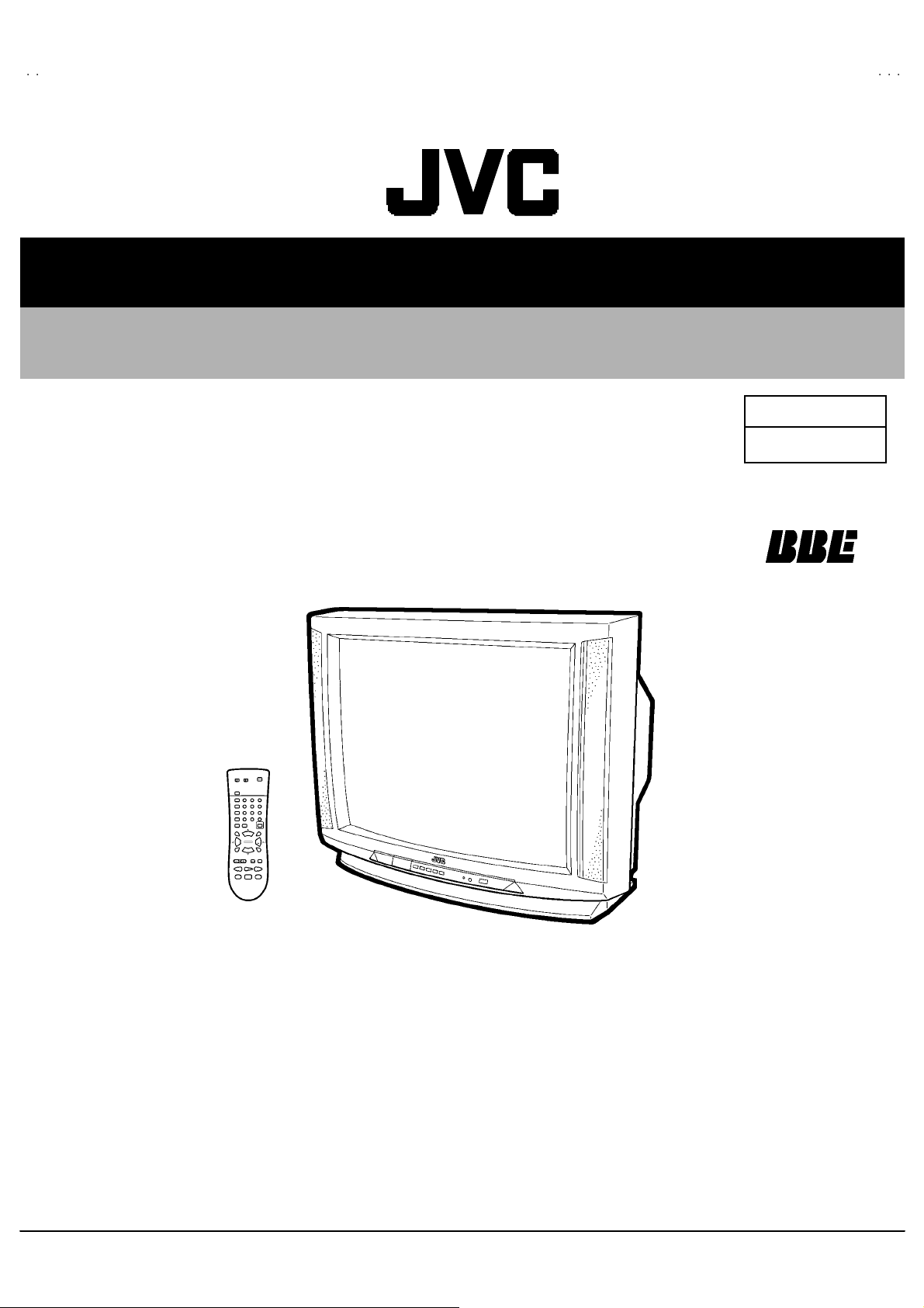
SERVICE MANUAL
COLOR TELEVISION
AV-27D303
/S
AV-27D303
AV-27D203
BASIC CHAS SIS
FE
AV-27D303
AV-27D203
AV-27D203
/R
/S
/R
CONTENTS
! SPECIFICATIONS ・・・・・・・・・・・・・・・・・・・・・・・・・・・・・・・・
!
SAFETY PRECAUT IONS ・・・・・・・・・・・・・・・・・・・・・・・・・・・・・・・・
! FEATU RES・・・・・・・・・・・・・・・・・・・・・・・・・・・・・・・・
! MAIN DIF FERENCE LIST ・・・・・・・・・・・・・・・・・・・・・・・・・・・・・・・・
!
HOW TO IDENTIFY MOD ELS
! FUNCTIONS ・・・・・・・・・・・・・・・・・・・・・・・・・・・・・・・・
!
SPECIFIC SERVICE INSTRUCTIONS
!
SERVICE ADJUSTMENTS ・・・・・・・・・・・・・・・・・・・・・・・・・・・・・・・・
! PARTS LIST ・・・・・・・・・・・・・・・・・・・・・・・・・・・・・・・・
★ OPER ATING INSTRUCTIONS
★
STAND ARD CIRCUIT DIAGRAM
1
・・・・・・・・・・・・・・・・・・・・・・・・・・・・・・・・・・・・・・・・・・・・・・・・・・・・・・・・・・・・・・・・
・・・・・・・・・・・・・・・・・・・・・・・・・・・・・・・・・・・・・・・・・・・・・・・・・・・・・・・・・・・・・・・・
・・・・・・・・・・・・・・・・・・・・・・・・・・・・・・・・・・・・・・・・・・・・・・・・・・・・・・・・・・・・・
・・・・・・・・・・・・・・・・・・・・・・・・・・・・・・・・・・・・・・・・・・・・・・・・・・・・・・・・・・・・・・・・
・・・・・・・・・・・・・・・・・・・・・・・・・・・・・・・・・・・・・・・・・・・・・・・・・・・・・・・
・・・・・・・・・・・・・・・・・・・・・・・・・・・・・・・・・・・・・・・・・・・・・・・・・・・・・・・・・・・・・・・・
・・・・・・・・・・・・・・・・・・・・・・・・・・・・・・・・・・・
・・・・・・・・・・・・・・・・・・・・・・・・・・・・・・・・・・・・・・・・・・・・・・・・・・・・・・・・・・・・・・・・
・・・・・・・・・・・・・・・・・・・・・・・・・・・・・・・・・・・・・・・・・・・・・・・・・・・・・・・
・・・・・・・・・・・・・・・・・・・・・・・・・・・・・・・・・・・・・・・・・・・・・・・・・・・・・・・・・・・・・・・・
・・・・・・・・・・・・・・・・・・・・・・・・・・・・・・・・
・・・・・・・・・・・・・・・・・・・・・・・・・・・・・・・・・・・・・・・・・・・・・・・・・・・・
・・・・・・・・・・・・・・・・・・・・・・・・・・・・・・・・・・・・・・・・・・・・・・・・・・・・・・・・・・・・・・・・
・・・・・・・・・・・・・・・・・・・・・・・・・・・・・・・・・・・・・・・・・・・・・・・・・・・・・・・・・・・・・・・・
・・・・・・・・・・・・・・・・・・・・・・・・・・・・・・・・・・・・・・・・・・・・・・・・・・・・・・・・・・・・・・・・
・・・・・・・・・・・・・・・・・・・・・・・・・・・・・・・・
・・・・・・・・・・・・・・・・・・・・・・・・・・・・・・・・・・・・・・・・・・・・・
・・・・・・・・・・・・・・・・・・・・・・・・・・・・・・・・・・・・・・・・・・・・・・・・・・・・・・・・・・・・・・・・
・・・・・・・・・・・・・・・・・・・・・・・・・・・・・・・・・・・・・・・・・・・・・・・・・・・・・
・・・・・・・・・・・・・・・・・・・・・・・・・・・・・・・・・・・・・・・・・・・・・・・・・・・・・・・・・・・・・・・・
・・・・・・・・・・・・・・・・・・・・・・・・・・・・・・・・・・・・・・・・・・・・・・・・・・・・・・・・・・・・・・・・
・・・・・・・・・・・・・・・・・・・・・・・・・・・・・・・・・・・・・・・・・・・・・・・・・・・・・・・・・・・・・・・・
・・・・・・・・・・・・・・・・・・・・・・・・・・・・・・・・
・・・・・・・・・・・・・・・・・・・・・・・・・・・・・・・・・・・・・・・・・・・・・・・・
・・・・・・・・・・・・・・・・・・・・・・・・・・・・・・・・・・・・・・・・・・・・・・・・・・・・・・・・・・・・・・・・
COPYRIGHT © 2002 VICTOR COMPANY OF JAPAN, LTD.
・・・・・・・・・・・・・・・・・・・・・・・・・・・・・ 2
・・・・・・・・・・・・・・・・・・・・・・・・・・・・・・・・・・・・・・・・・・・・・・・・・・・・・・・・・・
・・・・・・・・・・・・・・・・・・・・・・・・・・・・・・・・・・
・・・・・・・・・・・・・・・・・・・・・・・・・・・・・・・・・・・・・・・・・・・・・・・・・・・・・・・・・・・・・・・・
・・・・・・・・・・・・・・・・・・・・・・・・・・・・・・・・・・・・ 31
・・・・・・・・・・・・・・・・・・・・・・・・・・・・・・・・・・・・・・・・・・・・・・・・・・・・・・・・・・・・・・・・
・・・・・・・・・・・・・・・・・・・・・・・ 3
・・・・・・・・・・・・・・・・・・・・・・・・・・・・・・・・・・・・・・・・・・・・・・
・・・ 4
・・・・・・
・・・・・・・・・・・・・・・・・・・・・・・ 5
・・・・・・・・・・・・・・・・・・・・・・・・・・・・・・・・・・・・・・・・・・・・・・
・・・・・・・・・・・・・・・・・・・・
・・・・・・・・・・・・・・・・・・・・・・・・・・・・・・・・・・・・・・・・
・・ 6
・・・・
・・・・・・・・・・・・・
・・・・・・・・・・・・・・・・・・・・・・・・・・
・・・・・・・・・・・・・・・・・・・・・ 12
・・・・・・・・・・・・・・・・・・・・・・・・・・・・・・・・・・・・・・・・・・
・・・・・・・・・・・・・・・・
・・・・・・・・・・・・・・・・・・・・・・・・・・・・・・・・
2- 1
5
8
No.519 40
Apr. 2002
May 2002
Page 3

A
V-27D303
A
(
)
)
)
V-27D203
SPECIFICATIONS
Contents
Items
Dimensions (W×××× H×××× D) 29 -5/8 ”×23”-1/4”×23” (752mm×590mm ×53 1mm )
Mass 70.8 Ib s ( 3 2.2 kg)
TV System and Color System
TV RF System
Color Sy st em
Sound System
TV Receiving Channels and Frequency
VL B a nd
VH B and
UHF Band
CATV Receiving Channels and Frequency
Low Band
High B an d
Mid Band
Super Band
Hyper Band
Ul tr a B an d
Sub Mid Band
TV/CATV Total Channel
Intermediate Fr equency
Vide o IF Car rier
Sound IF Carrier
Color Sub Carrier
Power Input
Power Consumpti on
CCIR(M)
NTSC
BTS C S ystem (M ulti -Ch an nel S ound )
(02~0 6) 54 MHz~88MHz
(07~1 3) 17 4M H z~21 6MHz
(14~6 9) 47 0M H z~80 6MHz
(02~06, A-8) by (02~06 &0 1)
(07~13) by (07~13)
(A~1) b y (14~22)
(J~W) by (23~36)
(W +1~W+ 28) b y (3 7~64 )
(W +29~W+ 84) b y ( 65~1 25)
(A8, A4~A1) by (01, 96~99 )
18 1 C ha nn els
45 .75 MHz
41.25 MHz ( 4 .5MHz)
3.58MHz
12 0V AC , 6 0Hz
11 3W
AV-2 7D30 3/S
AV-2 7D30 3/R
(54MHz~80 4MH z)
AV-2 7D20 3/S
AV-2 7D20 3/R
Picture Tube
Hi gh Vo l t ag e
Spe ake r
Audio Powe r Output
Input terminal s
Input 1 S-Video
Video(V)
Au dio (L , R )
Input 2 Video
Component (V/Y, PB, PR)
Audio(L, R)
Input 3
Fr on t
Output t er minals
Antenna termina l 75 Ω(VHF/UHF) Terminal, F-Type Connector
Remote Contr ol Unit RM-C25 2 ( AA /R6/U M- 3 batt ery×2)
Video(V
Au di o(L, R
Variabl e Audio Output (R/L) More than 0~1550mVrms (+6dBs)
27 ” (6 8cm) Mea sured D iag on ally
29 kV±1kV (at zero b eam current)
2”×3 -1/ 2” (5×9cm) Oval type×2
1.2 W + 1.2 W
Y: 1Vp-p P ositive ( neg ative s ync p rovi ded , wh en terminat ed with 7 5Ω)
C: 0. 286V
1V p- p, 75Ω ( RCA pin jack)
50 0m Vr ms ( -4 dBs ), High I mp ed anc e (RCA pin j ack)
1V p- p, 75Ω ( RCA pin jac k)
1V p- p 7 5Ω(positive sync)
50 0m Vr ms ( -4 dBs ), High I mp ed anc e (RCA pin j ack)
1V p- p, 75Ω ( RCA pin jack)
50 0m Vr ms ( -4 dBs ), High I mp ed anc e (RCA pin j ack)
Low impedance (400Hz when modulated 100%) (RCA pin jack)
p-p
(bu rst si gnal, when t erm inate d with 75Ω)
De s ign & speci ficatio ns ar e su bje ct to cha ng e wi thout no t ice.
2
No.51940
Page 4
A
3
A
3
SAFETY PRECAUTIONS
V-27D30
V-27D20
1. The desi gn of t his p ro du ct c ont ai ns spec i al h ar dw ar e, man y
ci rcu its and c o mp on ent s s peci al ly for saf ety pur p oses. For
continued protection, no changes should be made to the
origina l des ig n u nless a uth or i zed in wri ting by t he m an ufactu re r.
Rep lacem en t par ts m ust be id ent ic al to thos e u sed in th e
origina l cir cuit s . S ervic e sho ul d be per f orme d by qu ali fied
p ers onnel o nly.
2. Alte r ation s of the desig n or circu i tr y of the p r odu c ts s hould n ot
b e mad e. A ny de si gn al te rations o r additio ns wil l vo id th e
manufact urer's warranty and will further relieve the
manu fac t urer of resp ons ib i lit y f or pe rs ona l in ju r y or p r ope rt y
d am age r esult in g t heref rom .
3. M an y e l ectr ical an d mech anic al pa rt s in th e p r odu c ts h av e
sp ecial s af ety-r elat ed charact eris tics. Th ese charac teri stics are
oft en not e vid en t fr om visu al in spe cti on no r can the prote c ti on
aff orde d by th em neces s ar ily be obta in ed by using
replac ement comp on ent s ra ted for h ig her vo l tag e, wa ttage, etc.
Rep lacem en t pa rt s wh ic h have t hes e sp ec i al s afet y
ch aracter istics a re i d entifi e d in th e par ts l ist of S ervic e man ua l.
Electrical components having such featur es are identified
by shading on the schematics and by (!!!!) on the parts list
in S erv ice manual. Th e us e of a s u bs t itu te re pl ac emen t whi ch
does not have the same safety characteristics as the
reco mmen ded replac emen t pa rt sho wn i n the pa rts l ist of
Se rvi c e ma nual m ay c aus e sh ock , f ire, or o th er haz ards .
4. Use iso la t io n tr ansforme r when hot c hass is .
The chassis and any sub-chassis contained in some products
are c onnect ed to on e s ide of th e AC p ower li ne . An i sola ti on
tr ansf or m er of ad equ ate cap acity sh ould be i nsert ed bet we en
th e p rodu ct and t he AC p ower s u pp ly p oi nt while p er for mi ng
an y ser v ice on so me pr o ducts wh en th e H OT ch assis is
exp ose d.
5. Don't short between the LIVE side ground and ISOLATED
(NEUTRAL) side ground or EARTH side ground when
repairing.
So m e mod el 's p ow er circ uit i s part ly dif fer en t in t he GN D . T h e
diff erenc e of t he GND is sh own by th e LI VE : (") side GND,
th e ISO LAT ED(NEU TRAL) : (#) side GND an d EAR T H : ( $)
si de GND. D on 't sho rt be tw ee n t he LIVE s id e GN D a nd
ISO LATE D(N EU TRAL) side GND or EARTH si de GN D and
never measure with a measuring ap paratus (oscilloscope etc.)
th e LI VE side GND a nd ISO LATED ( N EUTRA L) si d e G ND or
EARTH sid e GND at th e s ame time.
If above note will not be kept, a fuse or any parts will be broken.
6. If any re pa ir h as b ee n mad e to th e c h as sis , i t is re commend ed
th at t he B1 se ttin g sh ould b e c hec ked or ad juste d (See
ADJUSTM EN T OF B 1 POWE R SUPPL Y) .
7. The hig h v olt age a pplied t o the pi ctu re tu be mu s t c o nfo rm with
that specified in Service manual. Excessive high voltage can
cau se an incr ease i n X-R a y emission , arcin g and pos sible
com po nent d am age, th eref or e op eratio n un der excess ive hi gh
vol ta ge c ondit i ons sh ould be ke pt to a m in i mu m, or sh ou ld be
preve nt ed. I f seve re arc in g oc cu rs, remove th e AC p ower
immediately and determine the cause by visual inspection
(incor r ec t i nsta ll a tion , crac ked o r m el te d high vol tag e har ness,
p oor s olde rin g, etc. ). T o ma in ta in the prop er mi ni m um le v el of
soft X-Ray emission, components in the high voltage circuitry
incl ud i ng the pi ctu r e tu be mu st be the ex a c t r ep lac em en ts or
alte rn at ives a ppr o v ed b y th e ma nuf actu r er of th e co mp l ete
prod uct.
8. Do n ot c hec k high volta ge by d r awin g a n arc . U s e a hi gh
vol ta ge mete r or a hi gh volt age p robe with a VTVM . Disc h ar ge
th e p ictu r e tu be bef or e a tte mp ting me ter c o nne cti on , b y
con nec ting a cl i p l ead to th e gr ou nd fr am e a nd c on n ecti ng t he
oth er e nd of t he lead th r oug h a 10k Ω 2W resi st or to t he ano de
bu tto n.
9. W hen s e rvice is r equ i r ed, ob ser ve th e orig inal l ea d dress .
Extra p r ecau ti on s h ou ld be given to ass u r e c or re ct l ea d dr es s
in the hi gh volta ge c ircu it area . W her e a sh ort circui t ha s
occu rr e d, th os e c ompon en ts th at i nd ic ate ev i den c e of
overheating should be replaced. Always use the
manu fac t urer 's r eplace ment comp on ents.
10 . Isolation Check
(Safety for Electrical Shock Hazard)
Af ter re-a ssem bl i ng th e pr od uc t , always pe rf orm an iso l ati on
ch eck on th e expo sed m eta l p ar ts of th e c abi n et ( ant en na
ter m i na ls, vide o/a ud io in pu t and out put ter mi n al s , C on trol
knobs, metal cabinet, screwheads, earphone jack, control
sh afts, etc.) to be s ur e th e pr o duct is saf e t o op er at e wi th out
d ang er of elec t rica l shoc k.
(1) Dielectric Strength Test
The is olat ion b etwe en the AC pr i ma r y circu it and all m eta l par ts
exp osed t o the us er, par t icu lar l y an y expo sed metal p art h aving
a re tur n pat h to the ch as sis sh ou ld w i ths t and a volta ge of
11 00V AC ( r .m .s.) f or a per i od of on e sec ond.
(. . . . Withs tand a volta ge of 1100V A C (r.m. s.) to an applian ce
rate d up to 1 20V , and 3 000V AC ( r .m. s.) t o an appl i anc e ra ted
200V or more, for a period of one second.)
Thi s m eth od of test re qu ires a t est eq uip me nt n ot g enerally
fou nd in t he servi c e t ra de.
(2) Leakage Current Check
Plug t he A C li ne c or d di r ect ly int o th e AC ou tl et ( do not us e a
line is olati on tra nsf ormer dur i ng this che ck.). U sing a " L eakage
Current Test er ", mea sur e t he lea kag e c ur r en t fr om each
exp ose d m eta l par t of th e ca bi ne t, p ar tic ul ar l y an y expo sed
metal part having a return p ath to t he ch assis , to a known good
ea rt h gr o und ( wa ter p ipe, etc.) . A ny l ea kag e c ur r en t must not
exce ed 0.5m A AC ( r .m. s.) .
Howev e r, in t ro pi cal a rea, this m us t not e xc eed 0 .2m A AC
(r.m.s.).
"""" Alte rn at e Che ck M et ho d
Plug t he A C li ne c or d di r ect ly int o th e AC ou tl et ( do not us e a
line isolation transformer during this check.). Use an AC
vol tm et er h aving 100 0 o hms per v ol t or m or e s en s i ti vit y in the
follo win g ma nne r. Con nec t a 150 0Ω 1 0W resis tor pa ralle l ed
by a 0.15μ F AC - typ e cap ac i tor b etwe en an ex p os e d m eta l
p art and a k no wn go od earth gr ou nd (wate r pip e, et c.).
Measu re th e A C vo l tag e acr os s th e r es i st or w it h t he AC
voltmeter. Move the res istor connection to each exposed m etal
part, particularly any exposed metal part having a return path to
th e c h assis , an d m easur e t he A C v olta ge acr os s th e r es isto r.
Now, reve rs e th e plu g i n t he A C out let a nd r ep eat e ac h
measu rem ent. An y volta ge measu red m ust not exce ed 0.7 5V
AC (r.m. s.) . This corresponds t o 0.5mA AC (r.m. s.).
Howev e r, in trop ic al ar ea, thi s must n ot excee d 0 .3V AC
(r.m.s.). This corr esp on ds t o 0 .2mA AC ( r.m.s.).
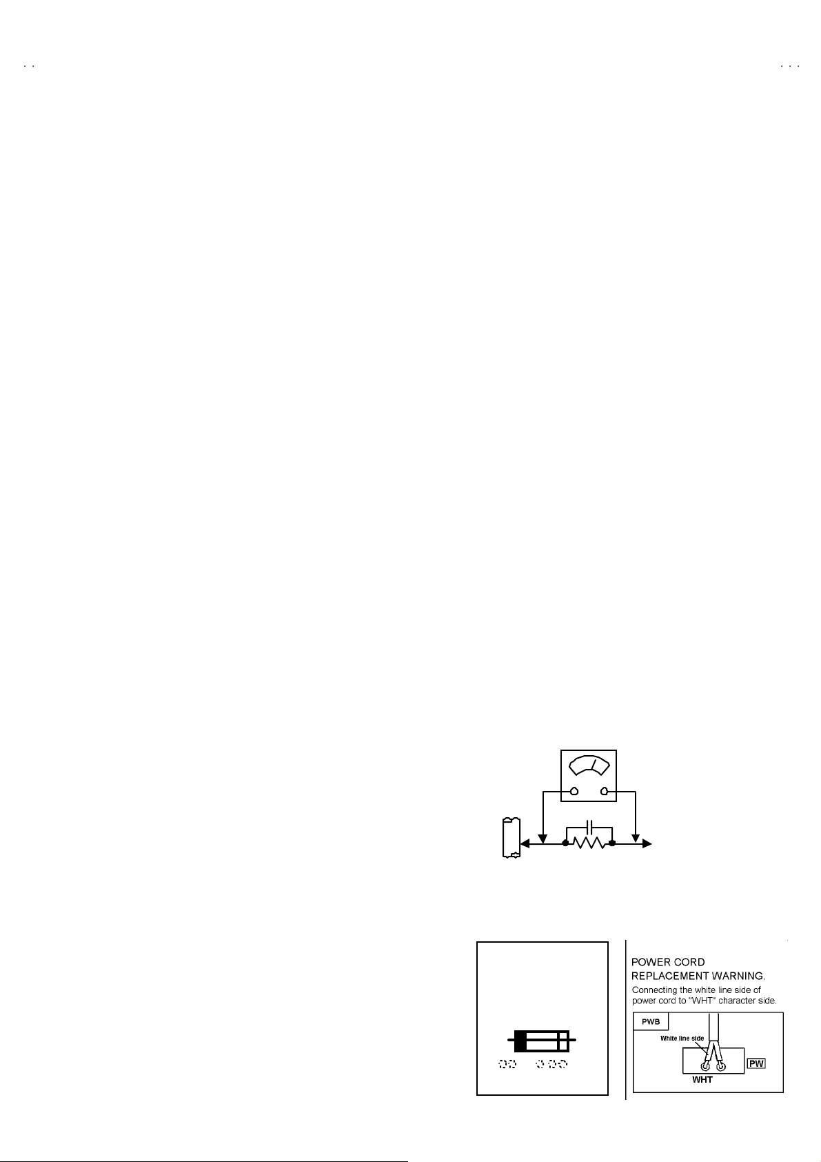
AC VOLT METER
(HAVING 1000 Ω/V,
GOOD
EARTH
GR OUND
11 . High voltage hold down circuit check.
Af ter r ep ai r of th e high vol t ag e h ol d down ci r cuit, th is ci rcu it
sh all be c hec ked to oper ate correctly.
See item "Ho w to check the high voltage hold down
cir cuit".
This mark shows a fast
operating fuse, the
letters indicated below
show the rating.
0.15μF AC-T YPE
1500Ω 10W
OR MOR E SENSIT IVITY)
PLACE THIS PROBE
ON E A C H EX PO SE D
ME T AL PA RT
A V
No. 51940
3
Page 5

A
V-27D303
A
V-27D203
FEATURES
New chas sis design enabl es use of a si ngl e boar d with si mp lif ied
"
circuitry.
User s can m ak e fun t o c onnect th e Digital Video Disk pl ay er with
"
the c omp onent vi deo signal i npu t terminal .
Provid ed w ith miniatu re tuner (TV/CATV ).
"
Mult if unct ional remote con trol p erm i ts pictu re a dj ustm ent.
"
Ad opti on of t he C HAN NEL GUARD fu ncti on prevents th e s pecific
"
chan nels from being selected, unl ess th e “ ID nu mber” is k ey in.
2
"
I
C bus control utilizes single chip ICs.
"
Adopti on of the VID EO STATUS f unction .
"
Adoption of the ON/OFF TIM ER fun cti on.
Built-in V-CHIP system.
"
With 75ΩV/U in c ommon ( F-Type) AN T Terminal.
"
SLEEP TIMER for setti ng in real t ime.
"
"
Clos ed-caption b roa dcasts can be view ed.
"
Bu ilt - in MT S sys tem.
"
Built-in H YPER-SURROUND system.
Becau se bu ilt -in the BBE circ uit im pr oved the sound of
"
conver sation
S-VID EO input terminal for taking best adv antag e of Super VHS .
"
Variable Au di o outp ut te rminal.
"
"
3 LINE Digital Comb f ilter Im proved pi c tu re q ual i ty.
4
No.51940
Page 6
A
A
MAIN DIFFERENCE LIST
V-27D303
V-27D203
!!!!
Parts Name
MAIN PW B SFE-10 01A -M2 SFE-10 02A -M2 SFE-10 01A -M2 SFE-10 02A -M2
!
ITC TU BE (C) A6 8QD N 891 X001 A6 8ADT25 X01 A6 8QD N 891 X001 A6 8ADT 25 X01
!
FR ONT CA BI. A SS’Y GQ1 0018- 001 B-A GQ1 0018- 002 B-A
!
DOOR GQ3 0024-002 A- A GQ3 0024-001 A- A
JVC M ARK CM48006 -0 07- C CM48006 -0 06- C
!
POW ER KN OB GQ3 0026- 002 A-A GQ3 0026- 001 A-A
!
CONTROL K NOB GQ3 0025- 002 A-A GQ3 0025- 001 A-A
Model name
AV-2 7D30 3/S AV-2 7D30 3/R AV -27D 203/S AV-2 7D20 3/R
HOW TO IDENTIFY MODELS
The differenc e between AV -27D 303 S and AV- 27 D3 03/ R is i n th e PIC T U R E T UBE.
As t he res ul t of the diffe rence in pictu re tube, the MAIN PW B al s o dif fers.
In the sam e w ay, the d if ference betw een A V-27D 20 3/S and A V- 27D20 3/R i s in th e PICTUR E TU BE t oo.
!
Parts na me
Model
! RAT IN G L ABEL GQ3 003 2-001A-A
AV-2 7D30 3/S AV-2 7D303/R AV-2 7D20 3/S AV-2 7D203/R
Ind icat ed AV -27 D 303 Ind icat ed AV -27 D 303 Ind icat ed AV -27 D 203 Ind icat ed AV -27 D 203
Indic ated “S” Indic ated “S”Indic ated “R”
Indic ated “R”
No.51940
5
Page 7
A
V-27D303
A
V-27D203
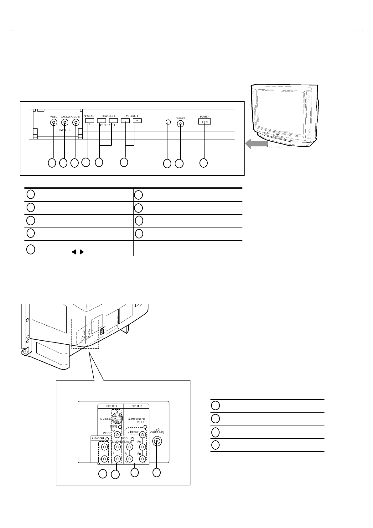
FUNCTIONS
■■■■
FRONT PANEL CONTROL
1
2 3
1
INPUT3 VIDEO terminal VOLUME
2
INPUT3 AUDIO L MONO terminal REMOCON LENS
3
INPUT3 AUDIO R terminal ON TIMER LED
4
MENU button
CHANNEL -/+ buttons
5
OPERATE / buttons
■■■■
REAR TERMINAL
4
65
6
7
8
9
POWER button
7
8
-/+
9
buttons
1
AUD IO O UTPUT (L, R)t e rm ina ls
INPUT1 (S, V, L, R) terminals
2
INPUT2 (V/Y, PR, PB, L, R) terminal s
3
VHF / UHF terminal
4
1
2
3
6
4
No.51940
Page 8

A
A
■■■■
REMOTE CONT ROL UN IT [R M-C2 52]
⑱
⑲
②
③
④
⑤
⑥
⑦
⑧
⑨
⑩
①
⑫
⑬
⑭
⑮
①
POWER key
INPUT key
②
DISPLAY key
③
SLEEP TIMER key
④
HYPER SUR. key
⑤
⑥
VIDEO STATUS key
⑦
THEATER PR O key
BBE key
⑧
MUTI N G key
⑨
VOL-/+(MENU / ) keys
⑩
MENU key
⑪
CHANNEL keys
⑫
LIGHT key
⑬
V-27D303
V-27D203
⑪
⑯
⑰
V-CHIP key
⑭
CH-/+(M ENU
⑮
⑯
EXI T / PIP OFF key
VCR CONTROL key
⑰
VCR / DVD switch
⑱
⑲
TV / CATV switch
NOTE
The CH- /+ k eys an d V OL- /+ key s o per ate
CHANNE and VOLU M E normally.
Thes e keys are al s o used to navigate MENU
system.
▼/▲
) keys
No.51940
7
Page 9

A
V-27D303
A
V-27D203
SPECIFIC SERVICE INSTRUCTIONS
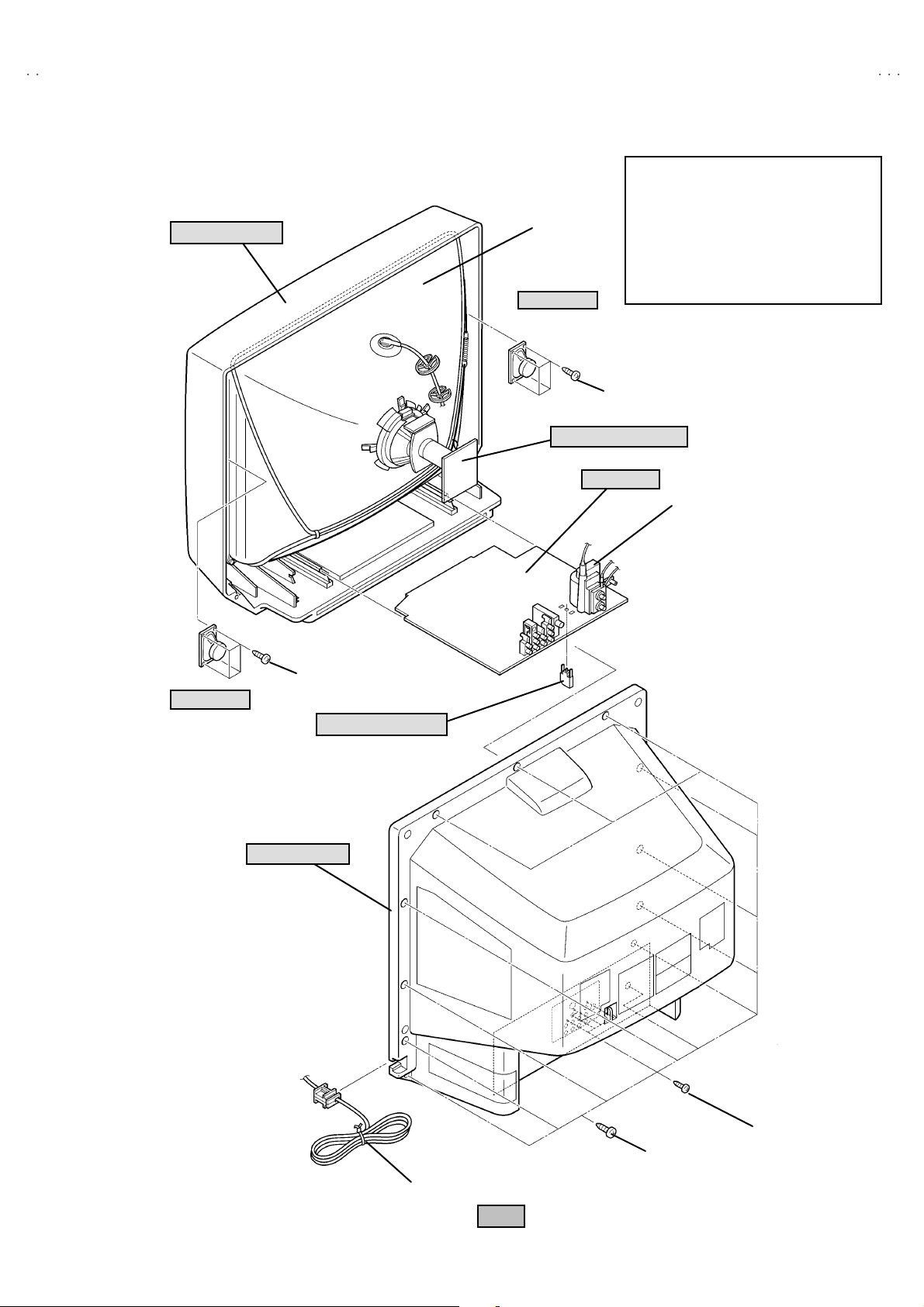
DISASSEMBLY PROCEDURE
REMOVING THE REAR COVE R
1. Disc onnec t t he po w er pl u g f rom wa ll out le t.
2. As s hown i n th e Fig .1, r em o ve th e 11 screws marked
3. As s hown i n Fig.1 , re mo ve t he 4 screws marked
4. Then r emo ve th e RE AR COVE R toward you .
""""
.
!!!!
.
CHECKIN G THE PW BOARD
To check the PW Board from back side.
1. Pull out the chassis (refer t o REMOVI NG THE MAIN PWB).
2. Erect th e chas sis ver tica lly s o th at you c an ea si ly ch eck th e bac k
si de of the PW Boar d.
REMOVING THE MAIN PWB
" After r emoving th e REAR COV ER.
1. Pick th is s i de of th e MA IN PW B an d rai se on e slig htly, take of f the
PW B stopp er m ar k ed
2. W ithdr a w t he chass is back w a rd .
(If n ecess ary , r emove t he wire clam p, c onn ect ors etc.)
####
f rom th e c abi n et b ott om.
REMOVING THE SPEAKER
"
After removing the rear cover.
1. As shown in Fig. 1, removing the screws marked
remove the speaker.
2. Fol l ow th e s ame st eps when r em oving th e oth er ha nd sp eak er.
NOTE : When removing the screws marked
remove th e l ow er side s crew fi r st, an d th en r em ove the
up per one .
$$$$
of th e sp eak er ,
$$$$
then
,
CAUTION
"
When erecting th e ch as sis, b e car ef ul so tha t th er e w ill b e no
contacting with other PW Board.
"
Befor e tu rning o n p ow er , make s ur e th at t he wire con nec tor is
prop er l y con nec ted .
"
When conducting a check with power supplied, be sure to
confirm that the CRT EARTH WIRE (BRAIDED ASS’’’’ Y) is
connec ted to the CRT SOCKET PW board.
WIRE CLAMPIN G AND CABLE T YING
1. Be sure t o cl a mp th e wire.
2. Never rem o ve th e c able tie use d for tying th e wi res together.
Should it be inadverte ntly removed, be sure to tie the wir es with a
new cable tie.
8
No.51940
Page 10
A
3
A
3
FRONT CABINET
CRT
SP EAKER
CRT SOCKE T PWB
MAIN PWB
V-27D30
V-27D20
Thi s exp lode d view descr i be s ab out th e
AV -2 7D 30 3/R and /S.
Alth ou gh t he AV -2 7D 20 3/R, /S i s sl i gh tly
diff erent f r om th is fi gu re, you c an u se th e
exp lode d vie w f or d is assem b lin g t he AV27D 203/R , /S in the s ame step as for this
on e.
$$$$
HV T
SP EAKER
$$$$
####
PWB STOP PER
REAR COVER
""""
!!!!
POWER CORD
Fig .1
No.51940
9
Page 11
A
V-27D303
A
C BUS
S)
)
SYS0
V-27D203
MEMORY IC REPLACEMENT
1. Memory IC
This TV uses memory IC.
Thi s m em or y IC st or es d at a f or pr op er o per a tion of the vide o a nd deflectio n circui ts.
When r ep la cing the mem or y IC, be sure to use an IC co ntai ni ng this (initi a l value ) d at a.
2. Memory IC replacement procedure
(1) Power off
Switch off the p ow er an d di scon nec t th e p ow er c o rd fro m t he out let.
(2) Replace the memory IC
Be sure t o use a memory I C writte n with th e initia l s ettin g data.
(3) Power on
Con nect th e power cord to the outlet a nd s witch on th e power.
(4)Conf irm the sy st em con st an t v alu e
"
12 .S YSTEM (SYS ) do not adjust normally.
"
The adjustment should not be done without signal.
! Ho w t o ent er t he SY ST EM (SYS ).
1) Pr ess the SLEEP TIME R ke y and se t SLEEP TIMER f or 「0 min」.
2) Be fore disap pear the di spla y of S LEE P TIM ER set tings , si mu l tan eous l y
press th e DISP LAY key an d VIDEO ST A TUS ke y of the r emot e cont rol
un i t.
3) The SERV ICE M ENU sc r ee n of F i g.1 is d isp layed .
4) While the SERVICE MENU is displayed, select the SYSTEM(SYS) item
wi t h ME NU ▼/▲ (CH-/+) keys, and the MENU / (VOL-/+) keys is
pressed, the scree n will be displayed as shown in Fig.2.
5) R efe r to the SY STEM ( SY STEM C ON STA NT) TAB LE 1 a nd ch eck t he
setting items. If the value is different, select the setting item with the
ME NU ▼ / ▲ (CH -/ +) keys and adju st the s ett ing with th e
MENU / (VOL-/+) keys. (The letters of the selected item are
displayed in yellow.)
6) W hen adjustment has co mp le te d, t he v al ues sto re into memory IC
automat ically
7) Press the EX IT key t wice to return the normal scree n.
SE RVICE MENU
SERVICE MEN U
1.V/C(S) 2.DEF(D)
3. SOUND(A) 4 .OTHERS( F)
5.PIP(PIP) 6.3L Y/C(LYC)
7.LOW LIGHT 8.HIGH LIGHT
9.RF AFC 10.VCO
12.SYSTEM(SY
11.I2
SELECT BY
OPERATE BY EXIT BY
EXIT
Fig.1
12 .SY STEM(SY S
SETTING ITEM
***
SETTING VAL UE
SETTING N o
1 VI DEO IN
Fig.2
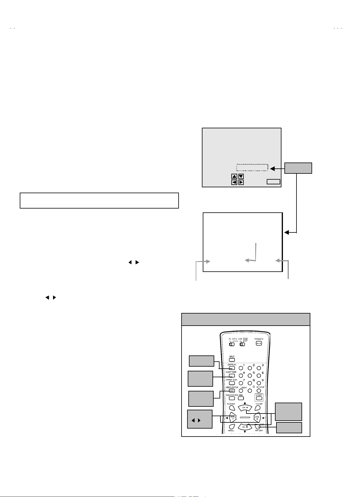
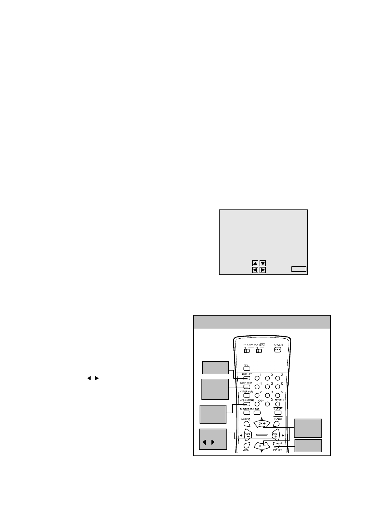
KEY ASSIGNMENT OF REMOTE CONTROL UNIT
Verif ied
(5) Rec eiv e channel setting
DISPLAY
Refe r to the O PERA TING IN S TRUCTIO NS ( USER'S GUIDE) an d set
th e r ec e i ve ch annel s ( C ha nn els Pres et) as des cri b ed.
SLEEP
TIMER
(6) User sett in gs
Check th e us er s ett ing it em s acc ording to TABL E 2.
Wher e thes e do not ag r ee, ref er to th e OP ERATIN G I NSTRUC TION S
(USER'S GUIDE) an d s et t he it em s as de scrib ed.
VIDE O
STA TUS
MENU
/
MENU
▲
▼/
EXI T
(7) SERVICE MENU setting
Ve rif y what to s et i n th e SER VI CE MENU, a nd s et wh at ever is
necessary. (Fig.1) Refer to th e SE RVIC E A DJUSTMENT f or setting.
10
No. 51940
Page 12
A
3
A
3
TABLE 1 (System Constant setting)
No Setting item Variabl e range
SY S01 VIDEO IN 0~4 3
SY S02 PIP 0~1 0
SY S03 3D Y/ C 0~1 0
SY S04 Y CV 0~1 0 SY S16 EZ SU RF 0~1 0
SY S05 CCD P CHK 0~1 1 SY S17 ID DISP 0~1 1
SY S06 PUR IT Y 0~1 0 SY S18 COMPU LINK 0~1 0
SY S07 VM 0 ~1 0 SY S19 CCD 0~1 1
SY S08 NOISE CR 0~1 0
SY S09 CLR TEMP 0~1 1
SY S10 TH EATE R 0 ~1 1
SY S11 TH EATE R PRO 0~1 1
SY S12 BB E 0~1 1 SY S24 CXA1 875 0~1 0
Initial setting
value
No Settin g ite m Variabl e ra nge
SYS 13 HYP S URR
SY S14 16:9 MD
SY S15 HYP S CA N
SY S20 VCH IP
SY S21 VCH IP C A
SY S22 JVC L OGO
SY S23 CMP IN
0~1
0~1
0~1
0~1
0~1
0~1
0~1
TABLE 2 (User setting)
Setting item Setting value Setting item Setting value
Use remo t e co ntrol ler ke ys
V-27D30
V-27D20
Initial setting
value
1
0
1
1
1
1
1
POWE R OFF DISPLA Y OFF
CHANNEL CH-02 VIDEO STATUS DYNAMIC
VOL UME 10 HYPE R S URROUND OFF
TV/V IDEO TV BBE ON
Settings of MENU
PICTURE MENU INITIAL SETUP MENU
TINT CENTER
COLO R CENTER FRONT PANELLOCK OFF
PICTURE CENTER+8 V2 CO MPONENT-IN NO
BRIGHT CENTER AUTO SHUT O FF OFF
DETAIL CENTER+10
COLO R TEMPERATURE HIGH
NOISE MUTING ON C HA N NE L S UMMARY U nn ecess ary to set
SOUND ADJUST MENU
BASS CEN TER
TR EBL E CEN TER XDS ID
MTS ST ERE O
LA NG U AGE
CLOS ED CAPTIO N OFF
AUTO TUNER SET UP AIR
V-CHI P OFF
SE T LOC K C ODE (000 0) Unn eces sary to set
ENG
ON
CLOCK / TIMERS MENU
SE T CLOC K MANUA L
TIME ZONE : PACIFIC
D.S.T. : OFF
ON / O FF TIMER OFF
No. 51940
11
Page 13
A
V-27D303
A
V-27D203
SERVICE ADJUSTMENTS
ADJUSTMENT PREPARATION
1. You c an ma ke the nec es sary adjust me nts f or t his u n it wi t h
eit her t h e R emot e Co ntrol Unit or With t he adju st me nt
tools and parts as given below.
2. Ad justment wit h t he Re mote Control Unit is made on th e
bas is of t h e initial sett ing v alu es, howev er, the ne w setti n g
values which set the screen to its optimum condition may
differ f rom the init ia l s ettin gs.
3. M ake sure t hat AC p ower i s tu r ned on c orrec tly.
4. T ur n on t he pow e r f or set and test equ ipm ent bef ore us e, an d
sta rt th e adjus tme nt p r oced ur es aft er wai tin g at l east 30
min ute s.
5. Unless oth er w is e spec if i ed, prep ar e the m ost s uitab le rece ptio n
or inp ut sign al for adjust m ent.
6. Never touc h an y ad ju stm en t p ar ts w hich a re n ot sp ecifi ed i n th e
list for this adjustment - variable resistors, transformers,
condensers, etc.
7. Pr es etti ng b efore adj ustm en t.
Unl es s oth er w is e spec if i ed i n th e adjustmen t i ns tr uc t ions ,
pres et t he f ollowing fu nction s with the rem ote co ntr ol u nit:
User menu preset value
MENU ITEM PRES ET VALUE
PICTURE MODE (VSM) DYNAMIC 0
BA SS, TREB LE, BA LANCE
HYPE R SURROUND
TINT, COLOR,
PICTURE, BRIGHT , DETAIL
MTS
CENTER
OFF
CENTER
STEREO
ADJUSTMENT EQUIPMENT
1. DC voltmeter (or digit al voltmeter)
2. Oscilloscope
3. Si gn al g ener at or (P atter n g en erat or)[NTSC
4. Remote control unit
5. TV a ud io multi pl e x si gnal ge ne rator .
6. Frequ enc y cou nte r
]
ADJUSTMENT ITEMS
Ad just ment it em s Ad just men t it ems
B1 POW ER SU PPL Y SUB B RI GHT
MAIN VCO SUB CONTRAST
BB E
KEY ASSIGNMENT OF REMOTE CONTROL UNIT
DISPLAY
ON
RF. AGC SUB COLOR
FOC U S SUB T I NT
V. HE IGH T V. CENTER MTS IN PUT L EVEL check
H. CENTER
WHITE BA LANC E (Low L i gh t)
WHITE BA LANC E (Hig h Li ght )
12
MTS SEP ARATIO N
No.51940
SLEEP
TIMER
VIDE O
STA TUS
MENU
/
MENU
▼/▲
EXI T
Page 14
A
3
A
3
ADJUSTMENT LOCATIONS
(
)
V-27D30
V-27D20
FRONT
POWER
MAIN PWB
POWER
CRT SOCKET PWB
Within MAIN PWB ASS'Y
TP-B
T
TP-E
(SOLDER SIDE)
VOL+ VOL- CH+ CH- MENU
E1
TOP
CR T EAR TH
(BRAIDED ASS' Y)
S
IC70 2
F901
IC20 1
T111
HV
IC42 1
IC10 1
S401
TUNER
HV T
IC90 1
U
B1
X
UPPE R : FOCU S
AV IN / OUT
No.51940
LOWER : SCREEN
13
Page 15
A
V-27D303
A
V-27D203
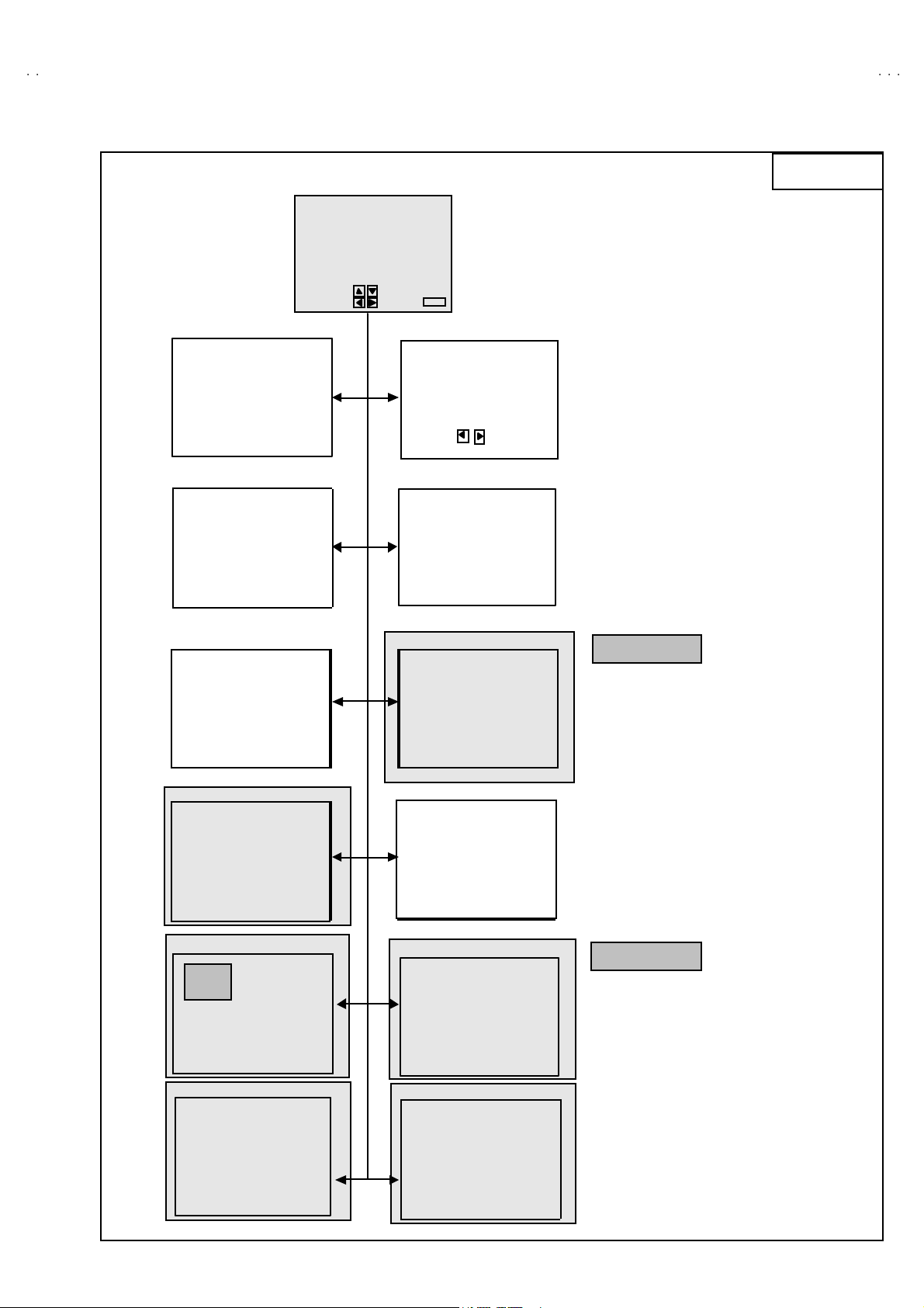
BASIC OPERATION OF SERVICE MENU
1. Operate the SERVICE MENU with the REMOTE CONTROL UNI T.
2. In general, basic setting (adjustments) items or verifications are performed in the SERVICE MENU.
(1) V/C (S) ・・・・・・・・・・・・・・・・・・・・ ・ This se t the s ettin g valu es ( a djustm ent valu es) of the VIDEO/CHRO MA circuits.
(2) DEF (D)
(3) SOUND (A) ・・・・・・・・・・・・・・・・・ This se t th e s ettin g valu es (adjustment values) of th e AUDIO cir cuit.
(4) OTHERS (F)
(5) PIP (PIP) ・・・・・・・・・・・・・・・・・・・ This se t th e s ettin g values(ad justmen t values) of the PICTURE-IN-PICTU RE circ uit.
(6) 3L Y/C (LCY) ・・・・・・・ ・・・・・・・・・ T hi s is us ed when th e 3L Y/C MOD E is verified . [Do not adjust]
(7) LOW LIGHT
(8) HIGH LIGHT ・・・・・・・・・・・・・・・・ This se ts th e s etting va lu es (a dj ust me nt values ) of t he W HITE BAL AN C E circui t
(9) RF AFC
(10) VCO ・・・・・・・ ・・・・・・・・・・・・・ ・・・ Thi s is us ed wh en th e IF V CO i s ad j uste d.
(11) I2C BU S
(12) SY STEM (SYS) ・・・・・・・ ・・・・・・・ T hi s is us ed when th e SYSTE M is ver if i ed. [Do not adjust]
3. Basi c Op erations of th e SERVI CE M ENU
(1) Ho w to enter the SERVICE MENU.
(2) SERVICE MENU screen selection
・・・・・・・ ・・・・・・・・・・・・・
・・・・・・・ ・・・・・・・・・
・・・・・・・ ・・・・・・・・・・
・・・・・・・ ・・・・・・・・・・・・・
・・・・・・・ ・・・・・・・・・・・・・
Press the SLE EP TIM ER key and set the SL E EP T IM ER for
「0 MIN 」 .
Then press the DISPLA Y key and VIDEO ST ATU S key of
the remote contr ol u nit at th e sa me ti me to ent er the
SERVICE MENU screen.
In SER VICE MENU, press t he MEN U▼/▲(CH-/+) key to
sel ect any of th e SU B MEN U it em s .
(The l e tte rs of t he s elect ed it em s are disp layed in ye llo w. )
This se t th e s ettin g valu es (adjustment values) of th e DEFLECTIO N circuit.
Thi s is us ed w hen th e O THERS MO D E i s ver ifi ed . [Do not adjust]
(PIP i s me ans as P icture I n Pi ctur e) [Do not have Function]
Thi s se ts th e setti ng va lues ( adj ust me nt v al ues ) of t he W HITE BAL AN C E circui t.
This is us ed when the RF AFC MODE is verified. [Do not adjust]
Thi s is us ed w hen ON/O FF of the I2C BUS CTRL is set. [Fixed ON ]
SERVIC E MENU
1.V/C(S) 2.DEF(D)
3.SOUND(A) 4.OTHERS(F)
5.PIP(PIP) 6.3L Y/C(LYC)
7.LOW LIGHT 8.HIGH LIGHT
9.RF AFC 10.VCO
11.I2C BUS 12.SYSTEM(SYS)
SELECT BY
OPERATE BY EXIT BY
EXIT
(3) Enter the any setting ( adjustment ) mode
" 1.V/C (S), 2.DEF (D), 3.SOUND (A), 4.OTHERS (F),
5. PIP ( P) , 6 .3L Y/C ( LYC), 7 .L OW LIG HT, 8. HIGH
LIGHT, 9.RF AFC 10.VCO 1 1.I2C BUS an d 12.SYSTEM
(SYS ) mode
1) If selec t an y of 1.V/C (S) / 2.DEF (D) / 3.SO UND (A)
/ 4.OT HERS (F) / 5.PIP (PIP ) / 6.3L Y/C ( LYC ) /
7.LOW LIG HT / 8.HIGH LIGHT / 9.RF AFC /
10 .VC O / 11.I2C BUS /12.SY STEM (SYS) it ems ,
an d th e ME NU
SERVICE MENU ( MAIN MENU ), the each screens
will be dis played as shown in figure page late r.
2) The n the sett in gs or verifi cation s ca n be p erfor med
/
(VOL-/+) key is pressed from
KEY ASSIGNMENT OF REMOTE CONTROL UNIT
DISPLAY
SLEEP
TIMER
VIDE O
STA TUS
MENU
MENU
/
▼/▲
EXI T
14
No. 51940
Page 16
A
V-27D30
3
A
3
V-27D20
1.V/C(S)
R F 4 : 3 S TD L O W
S0 1 BR IG H T
2.DEF(D)
R F 4 : 3 S TD L O W
D 01 V F REQ
SERVICE M ENU ( M AIN M E NU )
SE RV ICE M E NU
1. V/ C(S) 2.D EF(D )
3.SOUND( A) 4. OTHERS (F)
5. PI P(P IP) 6 .3L Y/C (LYC )
7. LOW LIGHT 8.HIG H L IGHT
9. RF AFC 10.V CO
11.12 C BUS 1 2.SYSTEM(SYS)
SELECT B Y
OPE RAT E BY EX IT BY
EXIT
7.LO W L IGHT
***
***
B RIG H T
***
***
SUB MENU
***
***
8.HIGH LI GHT
3.SO UND(A)
A 01 IN L E VE L
4.OTH ERS (F)
F 01 O S D P O SI
5.PI P( PIP )
PI P01 B RIGH T
6.3L Y/C(LYC)
***
***
***
9.RF AFC MAIN
TOO HIGH GOOD TOO LOW
T UN ER M A IN
AF G O N
FIN E
10.VCO M AIN
T UN ER M AI N
HIGH LE VEL
RE FERE NCE L EVE L
LO W LEVE L
SY N C NO
11.I2C BUS
I2 C B U S O N
12.SYSTEM(SYS)
DO not adjust
**
DO not adjust
LYC01 MODE
***
SY S0 1 VI DE O IN
No. 51940
***
15
Page 17
A
V-27D303
A
G
V-27D203
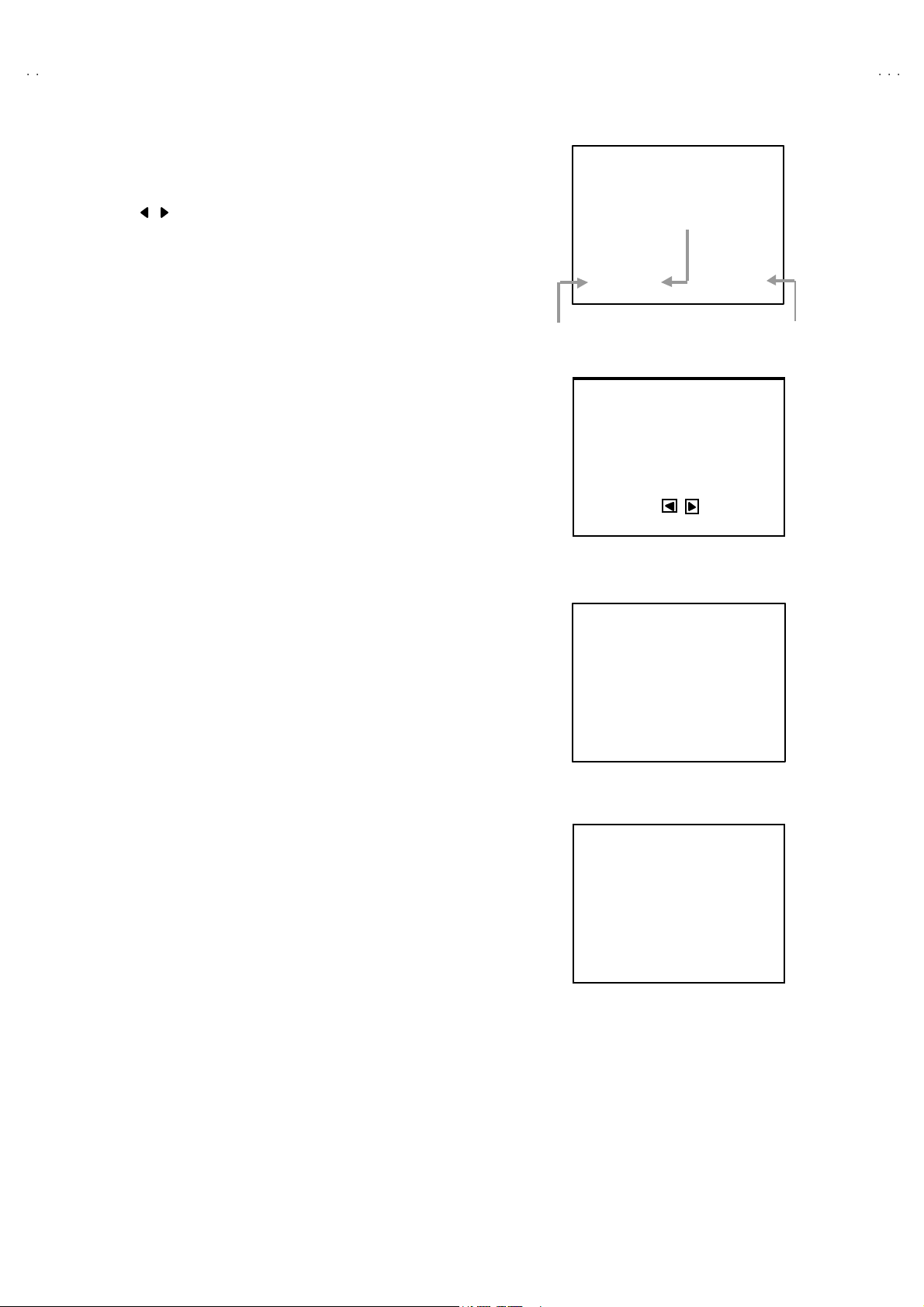
(4) Setting method
1) ME NU ▼/▲ (CH-/+) key.
Select t he SETT IN G IT EM.
2) MENU / (VOL-/+) ke y
Setti ng (adjust) the SETTIN G VA LUE of t he SETTIN G ITEM.
When the key i s relea sed th e SETTI NG VAL UE w il l b e st or ed
(memorized).
3) EX IT key
Retu rn s to the pre vious scr een .
(5) Rel easing SERVICE MENU
1) Af ter retu rn i ng to t he SE RV ICE M EN U up on co mp l etion of th e s etti n g
(adjus tment) wo rk, pr ess t he EXI T key ag ain.
★ The s etting s f or LOW LIGH T and HI GH LIGH T ar e des cribe d in th e
WHITE BA LANCE p ag e of AD JU STMENT.
★ The s et ting f or MA IN VCO ar e desc r ib ed in th e VCO p age of
ADJUSTM EN T.
SETTING N o
RF 4 : 3 STD LOW
SETTING
ITEM
1.V/C (S)
BRIGHT
***
***
***
7.LOW LIGHT
***S 01 B RIGHT
SETTING VAL UE
***
8.HIGH LIGHT
TUNER MAIN
HI
H LEVEL
REF ERE NCE L EVEL
LOW LEVEL
SYNC NO
10.VCO
16
No. 51940
Page 18
A
V-27D30
3
A
3
V-27D20
INITIAL SETTING VALUE OF SERVICE MENU
1. Adjustment of the SERVICE MENU is made on the basis of the initial setting va lu es ; ho wev er, the new setting values whic h
set the screen in its optimum condition may differ from the initial setting.
2. Do no t c hange the initial Setting Values of the Setti ng (Adjustment) items not listed In “ADJUSTMENT”.
"
V / C M O DE
Initial setting value
RF EXTERNAL (S,CV) COMPONENTNo Setting item Variabl e range
STANDARD THEATER STANDARD THEATER STANDARD THEATER
S01 BRIGHT
S02 PICTURE
S03 COLO R
S04 TIN T
S05 DET AIL
S06 BRIGHT +-
S07 PICT+ -
S08 COLOR +-
S09 TIN T+-
S10 DETAIL + -
No Setting item Variabl e range
S11 R CUT OFF 0~255 50 --- --- --- --- --- --- ---
S12 G CUT OFF 0~255 50 --- --- --- --- --- --- ---
S13 B CUT OFF 0~255 50 --- --- --- --- --- --- ---
S14 R DRIVE 0~127 64 --- --- --- --- --- --- ---
S15 B DRIVE 0~127 64 0 --- - -- - -- - -- - -- - --
S16 R CUT+ - - 128 ~+127
S17 G CUT+- -128~+1 27 ---0000---------
S18 B CUT+- -128~+1 27 --- 0 0 0 -10 --- --- ---
S19 R DRV+- -128~+1 27 --- 0 +5 +7 0 --- --- ---
S20 B DRV+- -128~+1 27 --- 0 +6 -9 0 --- --- ---
S21 NT SC MAT 0 ~3 33312211
S22 BLACK S T 0~3 1 --- - -- - -- - -- - -- - -- - --
S23 DCRE ST 0~1 1 --- - -- - -- - -- - -- - -- - --
S24 DCRSW 0~1 1 - -- - -- - -- - -- - -- - -- - --
0~127 64 --- --- --- --- ---
0~127
0~127
0~127 60 --- --- --- 64 ---
0~63 30 - -- 35 --- 40 ---
-128 ~+1 27
-128 ~+1 27 ----150--- 0---
-128 ~+1 27 --- -3 -2 --- --- ---
-128~+1 27 --- -6 +2 --- --- ---
-128 ~+1 27
65 --- --- --- --- ---
45 --- --- --- 47 ---
--- 0 0 --- +1 ---
--- +3 --- --- --- ---
Initial setting value
RF /EXT (S, C V)
STANDARD THEATER STANDARD
LOW HI GH L OW HI GH LOW HIGH LOW HIGH
--- 0 0 0 -10 --- --- ---
--- c a n not b e ad ju stm ent
COMPONENT
THEATER
No Setting item Variabl e range
S25 AS Y SHRP 0~7 444
S26 BP F FO 0~1 00---
S27 KIL R OFF 0~1 00---
S28 KIL R SEN 0~1 11---
RF EXTERNAL (S,CV) COMPONENT
No. 51940
Initial setting value
17
Page 19
A
V-27D303
A
V-27D203
No Se tting item Variabl e ra nge Initial setting value No Setting ite m Variabl e ra nge Initial setting value
S29 RGB MU TE 0~1 0 S39 Y MUTE 0~1 0
S30 BLUE B 0~1 0 S40 SV M GAIN 0~3 0
S31 VIDEO SW 0~3 3 S4 1 SV M PH 0~3 0
S32 CMP ABCL 0~15 0
S33 RGB ABCL 0~1 0 S4 3
S34 OSD CON T
S35 SUB CONT 0~15 8 S45 AGC ADJ 0~127 80
S36 AB L GA IN
S37 ABL PNT 0~3 3 S47 AP C CL K 0~1 1
S38 Y G AM MA
0~63
0~3
0~3
9 S44 V1 GAI N
0 S46 VMOFF DE
1
S42 WPL
COL G MM
0~1 0
0~1 0
0~1
-128~+127
4
0
"
DE F M O D E
No Setting it e m Variabl e range Initial se tting v al ue No Se tting it em Variabl e range Initial set ting value
D01 V FREQ
D02 AFC GAI N 0~3 0 D19
D03 H POSI 0~31 12 D20 EWCR T+- -128~+127 ---
D04
H POSI+-
D05 V PHASE
D06
V P H+-
D07 V SIZE
D08
V S IZE+-
D09 V CENTER
D10
V CENT+-
D11
V S CORR
D12
V S CO+-
D13
V LIN
D14 V LIN+- -128~+127 --- D31 V AGC 0~1 0
D15
H SIZE
D16 H SIZE +- - 128~+127 --- D33 VRMP BI 0~1 0
D17
WVMT TOP
0~3
-128 ~+127 --- D21
0~7
-128 ~+127 --- D23
0~+127
-128 ~+127 --- D25
0~63
-128 ~+127 --- D27
0~15 4 D28
-128 ~+127 --- D29
0~15
0~63
0~3 0
0 D18 W VM T BTM 0~3 0
0 D22 EWCR B+- -128~+127 ---
55 D24 EW PRA+- -128~+127 ---
32 D26 V E HT+- -128~+127 ---
11
32
D30
D32
EWCR TOP
EWCR BTM
EW P ARA
V E HT
H EHT
H EHT+-
TR APE Z
TR APE Z+ -
BLANK SW
-128 ~+127 ---
-128 ~+127
--- c a n not b e ad ju stm ent
0~31 16
0~31 16
0~63 26
0~7 0
0~7 0
0~63 34
0~1
---
0
"
SOUND MODE
No Settin g it e m Va riabl e range Initial setting value
A01 IN LEVEL 0 ~15 01 2
A02 LOW SEP 0~63 039
A03 HI SE P 0~63 016
A04 SA PC 0~1 00 0
A05 BB E BA SS -128 ~+127 -006
A0 6 BB E TRE - 128 ~+127 - 006
18
No. 51940
Page 20

A
V-27D30
3
A
3
V-27D20
" OTHERS MODE (Do not adjust)
No Se tting it e m Va riabl e ra nge Initial se tting v al ue No Setting item Va riabl e ra ng e Initial setting value
F01 OSD P OSI 0~255 27 F15 VCSN 1 0~63 0
F02 OSD PREQ 0~255 83 F16 VCSN 2 0~255 10
F03 CCD P OSI 0~63 45 F17 VCSN 3 0~63 20
F04 CCD FREQ 0~255 93 F18 VCSN ST P 0~63 02
F05 OSD CONT 0~63 11 F19 VN DAT A -128 ~+127 +8
F06 PUR WBCK 0 ~2 0 F20 VM D AT B - 128~+1 27 -4
F07 PUR CONT 0~255 62 F21 VM DAT C - 128~+1 27 -10
F08 SN TYP E 0~255 0 F22 VM DAT D -128 ~+127 -16
F09 YCSN TM 0~255 5 F23 VM D AT E 0~255 0
F10 YCSN E 0~63 5 F24 VMOFF TY 0~63 0
F11 YCSN F 0~255 16 F25 YC V MOFF 0~255 25 5
F12 YCSN G 0~255 32 F26 EZ SF T M 0~255 40
F13 VNR CHK 0~63 3 F27 XD SID TM 0~255 15
F14 VCSN TM 0~255 5 F28 FM TRAP 0~1 1
"
3L Y / C MODE (Do not adjust)
No Setting it e m Va riabl e range Initial se t ting v al ue
LYC01 MO DE 0~7 4
LYC02 VE NH 0~7 1
LYC03 PDSO FF 0~1 0
LYC04 CB 0~1 0
LYC05 VNLR 0~15 2
LYC06 GSE L0 0~1 0
LYC07 GSE L1 0~1 1
LYC08 COR 0~3 0
LYC09 TRAP 0~1 1
LYC10 CHT RAP 0~1 0
LYC11 CBPF 0~1 0
LYC12 ENHOFF 0~1 0
Se tting i tem c a n n ot displ a y
" SY STEM MODE ( Do not a djust )
No Setting item Variable range
SY S01 VIDEO IN
SY S02 PIP 0~1 0
SY S03 3D Y/ C 0~1 0
SY S04 Y CV 0~1 0
SY S05 CCD P CHK 0~1 1
SY S06 PUR IT Y 0~1 0
SY S07 VM 0 ~1 0
SY S08 NOISE CR 0~1 0
SY S09 CLR TEMP 0 ~1 1
SY S10 TH EATE R 0 ~1 1
SY S11 TH EATE R PRO 0~1 1
SY S12 BB E 0~1 1
0~4
Initial setting
value
3
No Settin g ite m Variabl e ra nge
SY S13 HYP SU R R
SY S14 16:9 MD
SY S15 HYP S CA N
SY S16 EZ SU RF
SY S17 ID DISP
SY S18 COMPULIN K
SY S19 CCD
SY S20 VCH IP
SY S21 VCH IP C A
SY S22 JVC L OGO
SY S23 CMP IN
SY S24 CXA1 875
0~1
0~1
0~1
0~1
0~1
0~1
0~1
0~1
0~1
0~1
0~1
0~1
No. 51940
Initial setting
value
1
0
1
0
1
0
1
1
1
1
1
0
19
Page 21

A
V-27D303
A
V-27D203
" PIP MODE (Do not adjust)
No Se tting item Variabl e ra nge Init ial setting v al ue No Setting it e m Va riabl e range Initial setting value
PIP01 BRIGHT 0~15 0 PIP 27 U VPO LAR 0~1 0
PIP02 PICTURE 0~255 30 PIP28 MAT 0~1 1
PIP 03 TINT I 0~63 42 PIP29 YCOR 0~1 1
PIP 04 COLO R 0~15 6 PIP 30 XFR EQF 0~1 1
PIP 05 R CUTO FF 0~15 0 PIP31 WTCHDG 0~1 1
PIP06 G CUTOFF 0~15 0 PIP 32 COLO N 0~1 0
PIP07 B CUTOFF 0~15 0 PIP33 ACQNEW 0~1 0
PIP 08 R DRI VE 0~255 65 PIP 34 DST DET 0~1 1
PIP 09 G DRIVE 0~255 65 PIP 35 CRI BEOK 0~1 0
PIP 10 B DRIVE 0~255 63 PIP 36 FC BEOK 0~1 0
PIP11 L POSI 0~255 22 PIP 37 NOCRID 0~1 0
PIP 12 R POS I 0~255 15 PIP 38 NON SED 0~1 0
PIP 13 UPR POS I 0~127 12 PIP 39 PIP ADJ 0~15 4
PIP 14 LWR PO SI
PIP 15 PICT L CK 0~1 1 PIP41 PCT EX T - 128 ~+127 0
PIP16 SELDEL 0~15 0 PIP 42 TN T EXT - 128~+127 0
PIP 17 AGCFIX 0~1 1 PIP 43 COR EXT -128~+127 0
PIP18 AGCADST 0~1 0 PIP44 R-D EXT -128~+127 0
PIP 19 AGC 0~15 7 PIP 45 G- D EXT -128 ~+127 0
PIP 20 BL KIN VB 0~1 0 PIP 46 B-D EXT -128~+127 0
PIP 21 BL KIN VR 0~1 0 PIP47 BRT COMP -128~+127 0
PIP22 VSPDEL 0~31 0 PIP48 PCT COMP -128~+127 0
PIP23 VSPISQ 0~1 1 PIP49 TNT COMP 0~40 0
PIP24 R GBIN 0~1 0 PIP 50 COR COMP 0~15 0
PIP 25 FR SEL
PIP26 OUTFOR 0~1 0 PIP52 G-D COMP -128~+127 0
0~127
0~1
11 PIP40 BRI EXT
1 PIP 51 R-D COMP
PIP53 B-D COMP -128~+127 0
-128 ~+127
-128 ~+127
0
0
NOTE
"
LOW LIGHT MODE
No Settin g it e m Va riabl e range Initial setting value
1RED 0~255 50
2GREEN 0~255 50
3BLUE 0~255 50
"
HIGH LIGH T M ODE
No Settin g it e m Variabl e range Initial setting value
1RED 0~255 64
2BLUE 0~255 64
20
The AV-27D30 3/S /R, AV -27D 20 3/ S /R m od el d o no t ha ve P IP fun ction , B ut, i f mem or y d ata is ou t of v a ri a bl e rang e, occ asion ally
som e pr ob lems ha pp en. The n we ne ed to inpu t these da ta .
No. 51940
Page 22

A
3
A
3
■
)
ADJUSTMENTS
B1 POWER SUPPLY
Item
Check of
B1 POWER
SUPP LY
Measuring
instrume nt
DC Volt m et er 【【【【B1 】】】】
ADJUS TMENT OF VCO
Test point Ad justment part Description
1. Recei ve th e blac k-a nd -w hit e sign al. ( colo r off )
Connector
TP-91
TP-E(#)
2. Con nect th e D C voltmet er to 【B1 】co nne ctor 【1】pin (TP-91)
an d TP -E (#) (B1 c on nect or【3】pin ).
3. Confirm that the voltage is DC134V±2V.
V-27D30
V-27D20
Item
MAIN VCO
adjus tme nt
TUNER MAIN
HIGH LEVEL
REF ERE NCE L EVEL
LOW LEVEL
SYNC NO
Measuring
instrume nt
Signal
gener ator
Test point Ad justment part Description
10.VCO MAIN
CW TRANSF.(T111
[MAIN PWB]
GREE N
" It must n ot adjust w ithout sig nal
1. Se le ct a rece iva ble br oa dcast .
2. Pu s h the MENU▼/▲(CH- /+) key, an d selec t th e 10 .VC O
mod e from th e S ERVIC E MENU.
3. Push the MENU / (VOL-/+) key, and select MAIN.
4. Conf irm t hat t he co lor ch an ge from 「HIGH LEVEL」 to 「LOW
LEVEL 」 b y CW TRAN SF T11 1 at M AIN PW B, and ch eck th e
「
SYNC : YES」.
5. Adjust until 「REFFERENCE LEVEL」 mark tu rn s gre en.
And th en con firm t ha t th e 「SY NC : YES」 ag ai n.
ADJUS TMENT OF RF AGC
Item
RF. AGC
adjus tme nt
No Setting item
S45 AGC ADJ 0~127 80
Measuring
instrume nt
Test point Ad justment part Description
S45 AGC ADJ 1. Recei ve a black and whit e sign al ( color off).
2. Select S45 AGC ADJ of th e V /C MODE.
3. Pr ess the MUT IN G ke y and t urn of f c ol or .
4. With the MENU (VOL-) key to get the noise in the scr e en
pictu re ( zer o s ide of s etting va lue) .
5. Press the MENU (VOL+) key s everal times and step when
Variabl e
range
Initial setting
value
n ois e dis appear s f rom th e scr ee n ( a t th at ti me , n ot to incr eas e
th e v a lu e too mu ch).
6. Cha nge to oth er ch anne ls a nd make sur e t hat th er e I s n o
irregularity.
7. Press the MUTING key and get color out.
No. 51940
21
Page 23

A
V-27D303
A
(
)
)
V-27D203
ADJUS TMENT OF FOCUS
Item
FOCUS
adjus tme nt
Measuring
instrume nt
Signal
gener ator
Test point Ad justment part Description
FOCUS VR
[In HVT]
ADJUS TMENT OF DEFLECTION CIRCUIT
1. Recei ve th e cross -hatch sign al .
2. Whi l e l oo k ing at t he s cree n, adju st th e F OCU S VR to the
vertical and horizontal lines will be clear and in fine detail.
3. Make sur e t hat th e p ict ure is in f ocus ev en w he n t he s cree n
g ets d ar k en ed.
Item
V. HE IGHT
V. CENTER
adjus tme nt
Scr een
size
Measuring
instrume nt
Signal
gener ator
Scr een s ize
Picture size (100 %
Test point Ad justment part Description
D05 V P HAS E
D07 V SI Z E
V. CENTER SW
(S40 1)
[MAIN PWB]
Picture
size
100 %
1. Rec ei ve the cr oss -h atch sign al.
2. Se le c t t he D05 V PHASE of th e DEF (D ) mod e, a nd it che cks
th at t he valu e of D05 V PHASE is 0.
3. Ad jus t t he ver tic al s cree n size of th e scree n to p t o 92% wit h
the D07 V SIZ E an d V CENTER SW S401
Mod el Ve rti cal scree n siz e
AV-27D303/S 89.0%
AV-27D203/S 89.0%
AV-27D303/R 92.0%
AV-27D203/R
No Setting item
D05 V PHASE 0~7 0
D07 V SIZE 0 ~127 55
Variabl e
range
92 .0 %
Initial setting
value
H. CENTER
adjus tme nt
22
Signal
gener ator
D03. H POSI 1. Recei v e th e cross -hatch sign al.
2. Select D0 3. H PO S I fr om DEF (D) mode .
3. Adjust b y H POSITION to b e sa me size at b oth side .
No Setting item
D03 H POSI 0~31 12
Variabl e
No. 51940
range
Initial setting
value
Page 24

A
3
A
3
ADJUS TMENT OF WHITE BALANC E
Item
WHITE
BALANCE
(Low Light)
adjus tme nt
Measuring
instrume nt
Signal
gener ator
BRIGHT
***
Test point Ad justment part Description
[LOW LIGHT]
***
***
R CUTOFF (S11)
G CUTOFF (S12)
B CUTOFF (S13)
BR IG HT (S 01)
SCREEN VR
[ in HVT]
V-27D30
V-27D20
1. Recei ve th e bl ac k an d wh it e sign al ( color o ff ).
2. Se lect t he [LOW LIGHT] MOD E f r om th e SERVICE MENU.
3. Set the initial setting valu e of “R CUTOFF”, “G CUTOFF”
“B CUTOFF” and BRIGHT.
1. Disp l ay a si ng l e horiz o nta l lin e by p r essin g t he ①①①① key of t he
remote control unit.
5. Turn t he scr een VR a l l the way t o t he left.
6. Turn th e s creen VR g ra du all y t o the righ t from th e l eft u nti l
eith er o ne of the red, blu e o r g r een colors ap pears f aintl y.
7. Adju s t th e tw o color s whi c h d id no t a ppe ar unti l th e sing l e
h orizo ntal l in e t hat is displ a yed bec omes whit e using th e ④④④④ to
⑨⑨⑨⑨
key s o f th e re mo te c ont r ol un it .
8. Turn th e scr ee n VR u ntil the s i ng l e hor i zon tal lin e i s di spla yed
fain tly.
9. Pr ess the
10 . Ad ju s t th e BRIG HT lev el to becom e th e bl ac k c omp on en t
shines whit e slight ly.
11 . C onf irm that w het her the color ing redie nt of R ,G, or B is vi s ible
to th e b l ack c o mp one nt, w hi ch shine s white slightly
12 . When the c ol o r ingred i ent can be s een , t wo c olor s o th er tha n a
visible color are adjusted, and it is made to look white.
13. Return the value of BRIGHT to initial s etting value.
②②②②
key to cancel the single horizontal line mode.
REMOTE CONTROL UNIT
H. LI NE ON EX I TH. LI NE OFF
1 2 3
R CU TOFF B CUT OFFG C UTO FF
54
R CU TOFF B CUT OFFG C UTO FF
●
③③③③
The
EXIT key is the cancel ke y for the WHIT E BALANCE.
No Setting item
Variabl e
range
Initial setting
value
S11 R CUT OFF 0~255 50
S12 G C UT OFF
6
S13 B CUT OFF
S01 BRIG HT
987
0~255
0~255
0~127
50
50
64
No.51940
23
Page 25

A
V-27D303
A
V-27D203
Item
WHITE
BALANCE
(Hi gh Light)
adjus tme nt
Measuring
instrume nt
Signal
gener ator
[HIGH LIGHT]
***
Test point Ad justment part Description
R DRI VE ( S1 4)
B DR I VE (S1 5)
1. Recei ve th e bl ac k-a nd -whit e s i gn al ( colo r off ).
2. Se lect t he [HIGH LI GHT] M ODE in the SE RVIC E MENU.
3. Set the initial setting value of “R DRIVE” and “B DRIVE” with
the ④④④④, ⑥⑥⑥⑥ , ⑦⑦⑦⑦and ⑨⑨⑨⑨ k eys of the r em ot e c ontr o l uni t.
4. Ad ju st th e screen u nti l i t b ecomes w h ite usi ng th e ④④④④ , ⑥⑥⑥⑥, ⑦⑦⑦⑦
an d ⑨⑨⑨⑨ keys of the r em ot e c ontr o l uni t.
●The ③③③③ EXIT key is the cancel ke y for the WHIT E BALANCE.
Remote Control Unit
①key : H.LI NE ON
②key : H.LI NE OFF
③key : EXIT
④key : R DRIVE ▲
⑥
key : B D RIVE
⑦key : R DRIVE ▼
⑨key : B DRIVE ▼
Settin g ite m Va riabl e
No
S14 R DRI VE
range
0~127
▲
Initial setting
value
64
SUB BRIGHT
adjus tme nt
No Settin g item Va riabl e
S01 BRIG HT
SUB
CONT RAST
adjus tme nt
No Settin g item Va riabl e
S02 PICT URE
range
0~127
range
0~127
S15 B DRIVE
S0 1. BR I G HT 1. Recei v e th e b r oad cast.
2. Select S0 1. BRI G HT of th e V /C MODE.
3. Set the in it ial s etting valu e o f the S01. B RIGHT with th e
ME NU / (VOL - /+) k ey .
4. If the brightness is not the best with the initial setting value,
make fine a dj ustm en t of th e S01. BRIGHT until you get the
Initial setting
value
64
S02. PICTURE 1. Recei ve th e br oadcast.
Initial setting
value
65
op ti mu m br i ght ness .
2. Select S0 2 . PI CT URE of the V/C M ODE.
3. Set th e i n itial se tting valu e of th e S0 2. PICTU RE with the
ME NU / (VOL - /+) k ey .
4. If the contrast is not the best with the initial setting value, make
fin e adj ust me nt of th e S02. PICTURE until you get the
optimum contrast.
0~127
64
24
No.51940
Page 26

A
V-27D30
3
A
3
y
G
g
V-27D20
Item
adjus tme nt
Measuring
instrume nt
Signal
gener ator
Remote
control unit
gener ator
Oscilloscope
Remote
control unit
Test point Ad justment part Description
[ Method of adjustment without mea suring instrument ]SUB COLOR
1. Recei ve th e b r oad cast.
2. Select S03. COLOR of the V/C M ODE.
3. Set the initial setting va lue of the S03. COL OR with the
MENU / (VOL-/+) key.
4. If t he c olor i s n ot t he best with th e I nitial se tti ng v alu e, mak e
fin e a djust ment of the S0 3. COLOR unt il y ou get t he o ptim um
color.
No Settin g item Variabl e
range
S03 COLOR 0~127 45
[ Method of adjustment using measuring instrument ]Signal
1. Inp ut th e fu l l fi el d c olor b ar sign al ( 7 5% whi t e).
2. Select S03. COLOR of th e V /C MOD E.
3. Se t th e i ni ti al sett ing v al u e of th e S0 3. COL OR with the
MENU / (VOL-/+) key.
4. C on nec t the os c illosc ope be twee n TP-B and TP-E.
5. Ad just COL OR and b rin g t he v al u e of (A) in the illustration to
th e v o lt age sh ow n i n th e t able be llo w.
TP-B
TP-E(#### )
[CRT
SOCKET
PWB]
S03. COLOR
S03. COLOR
Initial setting
value
C
M
RY
W-B
W
B
(A)
(-)
0V
(+)
Models
AV-27 D303/ S +15V
AV-27 D203/ S +15V
AV-27 D303/ R + 17V
AV-27D203/R
No. 51940
Volt age
+17V
25
Page 27

A
V-27D303
A
(B)
g
(-)
V-27D203
Item
SUB TINT
adjus tme nt
Measuring
instrume nt
Signal
gener ator
Remote
control unit
gener ator
Oscilloscope
Remote
control unit
Test point Ad justment part Description
[ Method of adjustment without mea suring instrument ]
1. Recei ve th e b r oad cast.
2. Select S0 4. T INT of th e V /C MODE.
3. Se t the initi al s etti ng val u e of t he S04. TI NT with the
MENU / (VOL-/+) key.
4. If the tin t is not th e bes t wi th the initi a l set ti ng valu e, m ak e fi ne
ad j ustm en t of th e S0 4. T INT u ntil yo u g et t he optim um tint.
No Setting item
S04 TINT
[ Method of adjustment using measuring instrument ]Signal
1. Inp ut the fu l l fi el d c olor bar sign al ( 7 5% whi t e).
2. Select S04. TINT of the V/C M ODE.
3. Se t the initia l s ettin g value of th e S0 4. T I NT with the
MENU / (VOL-/+) key.
4. Con nect th e osc illos c ope be tw ee n TP-B and TP-E.
5. Ad ju st TI NT an d bri ng th e valu e of (B) in the illustr atio n to the
voltage shown in the table bellow.
Variabl e
range
0~127
TP-B
TP-E(#### )
[CRT
SOCKET
PWB]
S04. TI NT
S04. TI NT
Initial setting
value
60
CyG
W
BRY
0V
(+)
M
26
No. 51940
W-Mg
Models
AV-27 D303/ S +20V
AV-27 D203/ S +20V
AV-27 D303/ R + 25V
AV-27 D203/ R + 25V
Volt age
Page 28

A
3
A
3
ADJUS TMENT OF MTS CIRCUIT
V-27D30
V-27D20
Item
MTS IN PUT
LEVE L
che ck
MTS
SE PARATIO N
adjus tme nt
Measuring
instrume nt
TV audio
mult iplex
signal
gener ator
Oscilloscope
Test point Ad justment part Description
A01 IN LEV EL 1. Se lec t t he A 01 IN LEVEL of the SOUND MODE.
2. Verif y that the A01 IN LEVE L is set at its initial sett ing value.
No Se tting ite m Variabl e
range
A01 IN LEVEL 0~15 01 2
R OUT
L OUT
[AUDIO OUT]
A02 LOW SEP.
A03 HI SE P.
1. Inp ut th e ste reo L s ig na l (30 0H z ) f r om the TV au di o m ul ti pl e x
si gn al g ene r ator t o the ant enna term inal.
2. Connect an oscilloscope to R OUT pin of the AUDIO OUT, and
disp lay on e c ycle p ort i on of the 30 0Hz s ig nal .
3. Se lec t t he A02 LOW SE P. of the SOUND MODE.
4. Set the initial setting value of the A02 LOW SEP. wit h the
MENU / (VOL-/+) key.
5. Ad jus t t he A02 LOW SE P. so that the strok e element of the
300Hz signal will bec ome minimum.
6. Cha nge th e c on nec t ion of th e os cillo s cop e t o L OUT pi n of th e
AUDIO O UT, and en large th e volt age axis .
7. Cha nge t he si g nal to 3 kHz, an d si milarly a djus t t he A0 3 H I
SE P.
Initial setting
value
1 cycle
L- Chann el
signal wave for m
R-C hannel
crosstalk por ti on
Mi n i m u m
Setting item
No
A02 LOW SEP.
A03 HI SE P.
Variabl e
range
0~63
0~63 01 6
Initial setting
value
03 9
No. 51940
27
Page 29

A
V-27D303
A
9XC529R53 3D526
3
Q9
Q923R9
V-27D203
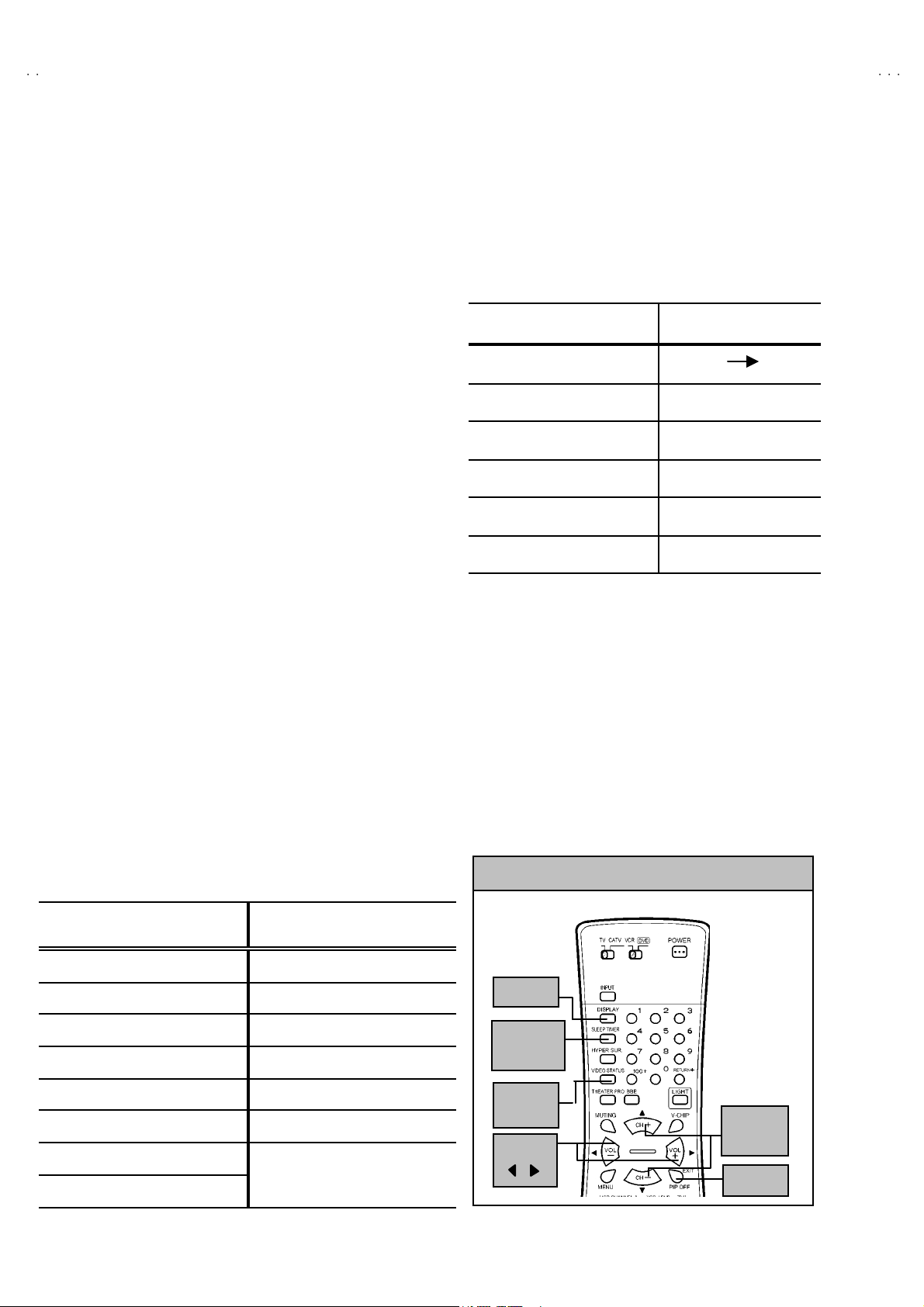
HOW TO CHECK THE HIGH VOLTAGE HOLD DOWN CIRCUIT
1. HIGH VOLTAGE HOLD DOWN CIRCUIT
After repairing the high voltage hold down circuit shown in Fig. 1.
Thi s cir cuit sh all b e ch ecked to op er at e co rrect ly.
2. CHECKING OF THE HIGH VOLTAG E HOLD DOWN CIRCUIT
(1) Turn the power switch to on.
(2) As shown in Fig. 1, set the resistor between X c on nec tor 1 a nd 3 .
(3) Make sure t hat th e scr ee n pic ture disap pear s.
(4) Temporarily unplug the power plug.
(5) Remove the resistor replaced X c on nec t or 1 an d 3 .
(6) Ag ai n plug th e pow er pl u g, make s u re th at t he no rmal pi ctur e is di s pla yed on the s cree n.
RESISTOR
Ω±
Ω±
Ω±Ω±
D931
22
HEATER
2 1
22
4
R52
Fig. 1
28
No. 51940
Page 30

A
3
A
3
REPLACEMENT OF CHIP COMPONENT
!
CAUT IONS
1. Avoid heating for more than 3 seconds.
2. Do n ot rub t he el ec t ro des an d the resist p ar ts of the p att ern.
3. W hen r emovi ng a c hi p par t, m el t th e s older ad equate ly.
4. Do n ot reuse a ch i p p ar t afte r re mo ving it .
! SOLDERING IRON
1. Use a hig h i ns ulatio n s older i ng iron with a t hin poin ted end of it .
2. A 3 0 w s oldering i r on is r ec omm ended for easil y r em oving p ar ts.
! REPLACEMENT STEPS
1. How to remove Chip parts
#### Resi st o rs, ca pacit ors , et c
(1) As s h own in the f ig ur e, pu sh th e part with tw ee zer s and
alte rn at ely melt the s ol de r at eac h end.
(2) Sh if t wi th tweeze rs and r emo ve th e chip p ar t.
#### T ran s isto rs, dio d es , va ria bl e r esist or s, etc
(1) Ap pl y e xt ra so ld er to eac h l e ad .
SOLDE R SO LD ER
V-27D30
V-27D20
2. How to install Chip parts
####
Resi st o rs, capacit ors , et c
(1) Ap ply sold er to the pattern as indic ate d in the fig ure.
(2) Gr as p the ch ip p art with tw ee zer s and plac e it on th e s old er.
The n hea t and me lt th e so ld er a t b oth ends of t he chip par t.
#### T ran s isto rs, dio d es , va ria bl e r esist or s, etc
(1) Ap ply sold er to the pattern as indic ate d in the fig ure.
(2) Grasp the ch ip p art wit h t we eze rs and p lace it on the s o lder.
(3) First solder lead A as indica ted in t he figure .
A
(2) As s h own in the f ig ur e, pu sh th e part with tw ee zer s and
alte rn at ely melt th e sol d er at each l e ad. Shi ft an d r em ov e the
chip part.
(4) T he n solder le ads B and C.
Note : A fte r re mo ving t he part , r emove remain ing solder fr o m the
pattern.
C
A
C
No.51940
B
B
29
Page 31

A
V-27D303
A
V-27D203
30
No.51940
Page 32

A
V-27D30
3
A
3
V-27D20
PARTS LIST
CAUTION
! The parts ide ntifi ed by th e ! sym bol are impor t ant for t he safe ty. W h enev er r ep l ac ing the se par ts , be sur e t o use s pecif i ed o nes to se cur e
the safety .
!
The parts n ot i nd ic ated i n this P ar ts L i st a nd those w hi ch ar e filled with l i nes in the Parts No. columns will not be supplied.
! P. W. Board Ass'y will not be supplied, but thos e which are filled with the Parts No. in the Parts No. columns will be s upplied.
ABBREVIATIONS OF RESISTORS, CAPACITORS AND TOLERANCES
RESISTORS CAPACITORS
C R Carbon Resistor C CAP. Ceramic Capacitor
F R Fusible Resistor E CAP. Electrolytic Capacit or
P R Plate Resistor M CAP. Mylar Capacitor
V R Variable Res isto
HV R High Voltage Resistor MF CAP. Metalized Film Capac itor
MF R Metal Film Resistor MM CAP. Metalized Mylar Capacitor
MG R Metal Glazed Resistor MP CAP. Metalized Polystyrol Capacitor
MP R Metal Plate R esisto r PP CA P. Po lyp ropylen e Ca pa citor
OM R M etal Oxi de F ilm Resi stor PS CA P. Polystyrol Capacitor
CMF R Coating Metal Film Resistor TF CAP. Thin Film Capacitor
UNF R N on- F lam m abl e R esisto r MPP C AP . M etal i ze d P olypr opylene C ap ac i to r
CH V R Chip Variable Resistor TAN. CAP. Tantalum Capacitor
CH MG R Chip Metal Glazed Resistor CH C CAP. Chip Ceramic Capacitor
COMP . R Com posit ion Re sist or BP E C AP . Bi- Pol a r E lectrolytic C a pacit or
LP T C R
Lin ear P ositive T emperat ur e Co eff icie nt
Resistor
r
HV CAP. High Voltage Capacitor
CH AL E CAP. Chip Aluminum Electrolytic Capacito r
CH AL BP CA P.
CH TAN. E CAP.
Chip A lum i num B i-Po l ar C ap acitor
Chip T ant alum Elec trol y tic Cap ac i tor
CH AL BP E CAP.
Chip T ant alum Bi- Po lar Electro l yt ic C a pacit or
TOLERANCES
FGJ KMNRHZ P
±1% ±2% ±5% ±10 % ±20% ±30 %
+30%
-10%
No.51940
+50%
-10%
+80%
-20%
+100 %
-0%
31
Page 33

A
V-27D303
A
V-27D203
CONTENTS
!
USING P.W. BOARD & REMOTE CONTROL UNIT
!
EXPLODED VIEW PARTS LIST
!
EXPLODED VIEW ・・・・・・・・・・・・・・・ ・・・・・・・・・・・・・・・・・・・・・・・・・・・・・・・・・・・・・・・・・・・・・・・・・・・・・・・・・・ 33, 35
!
PRINTED WIRING BOARD PARTS LIST
AV-27D303/S / AV-27D203/S
"
MAIN PW BOARD ASS'Y
AV-27D303/R / AV-27D203/R
" MAIN PW BOARD ASS'Y
!
REMOTE CONTROL UNIT PARTS LIST ・・・・・・・・・・・・・・・ ・・・・・・・・・・・・・・・・・・・・・・・・・・・・・・・・・・・・・・・・・ 44
! PACKING ・・・・・・・・・・・・・・・ ・・・・・・・・・・・・・・・・・・・・・・・・・・・・・・・・・・・・・・・・・・・・・・・・・・・・・・・・・・・・・・・・ ・・・・ 45
!
PACKING PA RTS LI ST
・・・・・・・・・・・・・・・・・・・・・・・・・・・・・・・・・・・・・・・・・・・・・・・ ・・・・・・・・・・・・・・・・・・・・・・・・・
・・・・・・・・・・・・・・・・・・・・・・・・・・・・・・・・・・・・・・・・・・・・・・・ ・・・・・・・・・・・・・・33,
[
SFE-1001A-M2
[
SFE-1002A-M2
・・・・・・・・・・・・・・・・・・・・・・・・・・・・・・・・・・・・・・・・・・・・・・・
] (W ith CRT SOCKET PW BO AR D) ・・・・・・・・・・・・・・・・・・・・・・・・・・
]
(Wi th CRT S OCKET PW BO ARD) ・・・・・・・・・・・・・・・・・・・・・・・・・・ 40
32
34
36
45
USING P.W. BOARD & REMOTE CONTROL UNIT
Model
P.W.B AS S'Y
MAIN P.W.B SFE-1001A-M2
REM OTE CO NTROL UNI T RM-C2 52-1H
AV-2 7D30 3/S AV-2 7D 203/S AV-2 7D 303/R AV-2 7D 203/R
←←←←
←←←←←
SFE-1002A-M2
←←
←←
←←←←
←
←←
32
No.51940
Page 34

A
3
A
3
EXPLODED VIEW PARTS LIST (1)
V-27D30
V-27D20
AV-27D303
Ref.No. Part No. Part Name Description
!
!
1 GQ30025-002A-A CONTROL KNOB
2 LC30191-004A-A REMOCON LENS
!
3 GQ30026-002A-A POWER KNOB
!
4 CM48006-007-C JVC MARK
!
100 GQ10018-001B-A FRONT CABINET ASSY Inc.No.101
!
101 GQ30024-002A-A DOOR
AV-27D203
Ref.No. Part No. Part Name Description
!
!
1 GQ30025-001A-A CONTROL KNOB
!
2 LC30191-004A-A REMOCON LENS
!
3 GQ30026-001A-A POWER KNOB
4 C M4 80 0 6- 00 6 -C JVC MA RK
100 GQ10018-002B-A FRONT CABINET ASSY Inc.No.101
!
!
101 GQ30024-001A-A DOOR
AV-27D303
Ref.No. Part No. Part Name Description
!
!
1 GQ30025-002A-A CONTROL KNOB
!
2 LC30191-004A-A REMOCON LENS
3 GQ30026-002A-A POWER KNOB
!
4 CM48006-007-C JVC MARK
!
100 GQ10018-001B-A FRONT CABINET ASSY Inc.No.101
!
101 GQ30024-002A-A DOOR
AV-27D203
!
Ref.No. Part No. Part Name Description
1 GQ30025-001A-A CONTROL KNOB
!
!
2 LC30191-004A-A REMOCON LENS
!
3 GQ30026-001A-A POWER KNOB
4 CM48006-006-C JVC MARK
100 GQ10018-002B-A FRONT CABINET ASSY Inc.No.101
!
101 GQ30024-001A-A DOOR
!
/S
/S
/R
/R
EXPLODED VIEW (1)
!
101
4
!!!
1
No. 51940
2 3
!
100
33
Page 35

A
V-27D303
A
V-27D203
EXPLODED VIEW PARTS LIST (2)
AV-27D303
Ref.No. Part No. Part Name Description
!
!
V01 A68QDN891X001 ITC TUBE(C) Inc.DY,PC MAGNET,WEDGE
!
L01 CE41329-00DJB DEG COIL
T1521 QQH0129-001 H.V.TRANSF.
!
5 CHGB0016-0C BRAIDED WIRE
6 CHGB0015-0B BRAIDED WIRE (SUB)
7 CEBSS09D-03KJ2 SPEAKER (×2)SP01,02
!
!
8 CM48144-001-A PWB STOPPER
!
9 GQ10017-001B-A REAR COVER
10 LC20106-001D-A POWER CORD CLAMP
!
!
11 QMPD390-200-JS POWER CORD or QMPD200-200-JC
12 QYSBSFG4016Z TAPPING SCREW (×11)
13 QYSBSB3010Z TAPPING SCREW (×4)
!
14 GQ30032-001A-A RATING LABEL
!
15 GQ30034-001B-A WARNING LABEL
AV-27D203
Ref.No. Part No. Part Name Description
!
V01 A68QDN891X001 ITC TUBE(C) Inc.DY,PC MAGNET,WEDGE
!
!
L01 CE41329-00DJB DEG COIL
!
T1521 QQH0129-001 H.V.TRANSF.
5 CHGB0016-0C BRAIDED WIRE
6 CHGB0015-0B BRAIDED WIRE (SUB)
7 CEBSS09D-03KJ2 SPEAKER (×2)SP01,02
!
!
8 CM48144-001-A PWB STOPPER
!
9 GQ10017-001B-A REAR COVER
10 LC20106-001D-A POWER CORD CLAMP
!
!
11 QMPD390-200-JS POWER CORD or QMPD200-200-JC
12 QYSBSFG4016Z TAPPING SCREW (×11)
13 QYSBSB3010Z TAPPING SCREW (×4)
14 GQ30032-001A-A RATING LABEL
!
!
15 GQ30034-001B-A WARNING LABEL
/S
Within MAIN PWB (CN10PW)
/S
Within MAIN PWB (CN10PW)
AV-27D303
!
Ref.No. Part No. Part Name Description
!
V01 A68ADT25X01 ITC TUBE(C) Inc.DY,PC MAGNET,WEDGE
L01 CE41329-00DJB DEG COIL
!
T1521 QQH0129-001 H.V.TRANSF.
!
5 CHGB0016-0C BRAIDED WIRE
6 CHGB0015-0B BRAIDED WIRE (SUB)
!
7 CEBSS09D-03KJ2 SPEAKER (×2)SP01,02
8 CM48144-001-A PWB STOPPER
!
9 GQ10017-001B-A REAR COVER
!
!
10 LC20106-001D-A POWER CORD CLAMP
11 QMPD390-200-JS POWER CORD or QMPD200-200-JC
!
12 QYSBSFG4016Z TAPPING SCREW (×11)
13 QYSBSB3010Z TAPPING SCREW (×4)
!
14 GQ30032-001A-A RATING LABEL
15 GQ30034-001B-A WARNING LABEL
!
AV-27D203
!
Ref.No. Part No. Part Name Description
!
V01 A68ADT25X01 ITC TUBE(C) Inc.DY,PC MAGNET,WEDGE
L01 CE41329-00DJB DEG COIL
!
T1521 QQH0129-001 H.V.TRANSF.
!
5 CHGB0016-0C BRAIDED WIRE
6 CHGB0015-0B BRAIDED WIRE (SUB)
7 CEBSS09D-03KJ2 SPEAKER (×2) SP01,02
!
8 CM48144-001-A PWB STOPPER
!
9 GQ10017-001B-A REAR COVER
!
10 LC20106-001D-A POWER CORD CLAMP
!
!
11 QMPD390-200-JS POWER CORD or QMPD200-200-JC
12 QYSBSFG4016Z TAPPING SCREW (×11)
13 QYSBSB3010Z TAPPING SCREW (×4)
!
14 GQ30032-001A-A RATING LABEL
15 GQ30034-001B-A WARNING LABEL
!
/R
Within MAIN PWB (CN10PW)
/R
Within MAIN PWB (CN10PW)
34
No. 51940
Page 36

A
3
A
3
EXPLODED VIEW (2)
!
L0 1
!
15
!
V01
5
6
MAIN PWB
!
7
CRT SOCKE T PWB
!
T1521
V-27D30
V-27D20
(Within MAIN PWB)
!
!
!
7
8
9
!
!
10
14
13
!
11
No. 51940
12
(×11 )
(×4)
35
Page 37

A
V-27D303
A
V-27D203
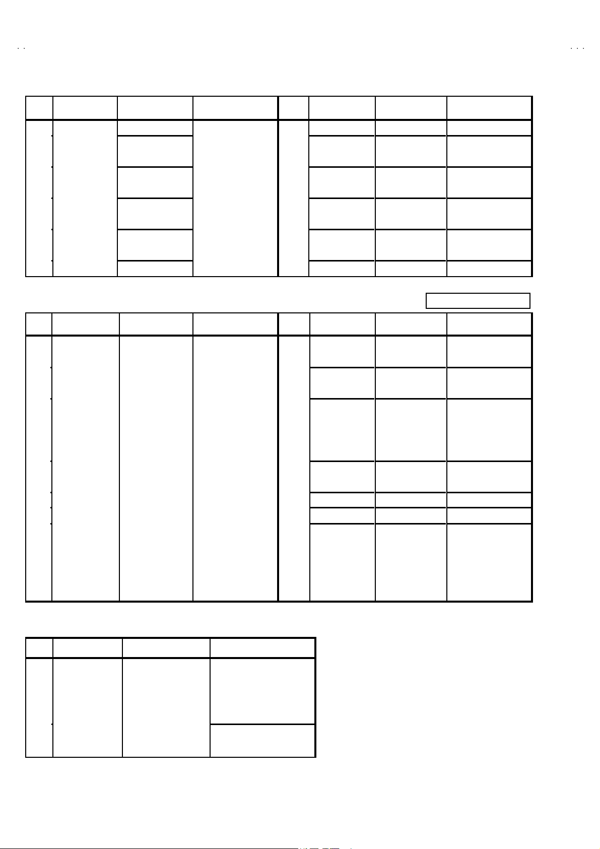
AV-27D 303/S / AV-27D203/S
PRINTED WIRING BOARD PARTS LIST
MAIN P.W. BOARD ASS ’Y (SF E-1001A-M2)
!
Symbol No. Part No. Part Name Description
RESISTOR
R1003-04 NRSA63J-221X MG R 220Ω 1/16W J
R1005 NRSA63J-0R0X MG R 0.0Ω 1/16W J
R1006 NRSA63J-223X MG R 22kΩ 1/16W J
R1008 NRSA63J-820X MG R 82Ω 1/16W J
R1101 NRSA63J-562X MG R 5.6kΩ 1/16W J
R1102 NRSA63J-182X MG R 1.8kΩ 1/16W J
R1103 QRE121J-101Y C R 100Ω 1/2W J
R1104 NRSA63J-180X MG R 18Ω 1/16W J
R1105 NRSA63J-270X MG R 27Ω 1/16W J
R1111-12 NRSA63J-154X MG R 150kΩ 1/16W J
R1113 NRSA63J-101X MG R 100Ω 1/16W J
R1115 NRSA63J-101X MG R 100Ω 1/16W J
R1116 NRSA63J-680X MG R 68Ω 1/16W J
R1117 NRSA63J-273X MG R 27kΩ 1/16W J
R1131 NRSA63J-102X MG R 1kΩ 1/16W J
R1132 NRSA63J-221X MG R 220Ω 1/16W J
R1133 NRSA63J-821X MG R 820Ω 1/16W J
R1134 NRSA63J-681X MG R 680Ω 1/16W J
R1135 NRSA63J-102X MG R 1kΩ 1/16W J
R1161 NRSA63J-332X MG R 3.3kΩ 1/16W J
R1163 NRSA63J-223X MG R 22kΩ 1/16W J
R1164 NRSA63J-102X MG R 1kΩ 1/16W J
R1165 NRSA63J-223X MG R 22kΩ 1/16W J
R1166 NRSA63J-103X MG R 10kΩ 1/16W J
R1167 NRSA63J-102X MG R 1kΩ 1/16W J
R1168 NRSA63J-101X MG R 100Ω 1/16W J
R1169 NRSA63J-561X MG R 560Ω 1/16W J
R1171 NRSA63J-103X MG R 10kΩ 1/16W J
R1201 NRSA63J-223X MG R 22kΩ 1/16W J
R1227 NRSA63J-104X MG R 100kΩ 1/16W J
R1251 NRSA63J-332X MG R 3.3kΩ 1/16W J
R1252 NRSA63J-103X MG R 10kΩ 1/16W J
R1253 NRSA63J-102X MG R 1kΩ 1/16W J
R1254 NRSA63J-181X MG R 180Ω 1/16W J
R1255-56 NRSA63J-152X MG R 1.5kΩ 1/16W J
R1257 NRSA63J-222X MG R 2.2kΩ 1/16W J
R1261-63 NRSA63J-101X MG R 100Ω 1/16W J
R1264 NRSA63J-821X MG R 820Ω 1/16W J
R1280 QRE141J-102Y C R 1kΩ 1/4W J
R1282 NRSA63J-222X MG R 2.2kΩ 1/16W J
R1283 NRSA63J-821X MG R 820Ω 1/16W J
R1285 NRSA63J-331X MG R 330Ω 1/16W J
R1286-87 NRSA63J-102X MG R 1kΩ 1/16W J
R1288 NRSA63J-0R0X MG R 0.0Ω 1/16W J
R1289 QRE141J-102Y C R 1kΩ 1/4W J
R1290 QRE141J-102Y C R 1kΩ 1/4W J
R1292 NRSA63J-222X MG R 2.2kΩ 1/16W J
R1293 NRSA63J-471X MG R 470Ω 1/16W J
R1295 NRSA63J-331X MG R 330Ω 1/16W J
R1296-97 NRSA63J-102X MG R 1kΩ 1/16W J
R1298 NRSA63J-0R0X MG R 0.0Ω 1/16W J
R1299 QRE141J-102Y C R 1kΩ 1/4W J
R1301 NRSA63J-151X MG R 150Ω 1/16W J
R1302 QRL029J-123 OM R 12kΩ 2W J
R1303 QRZ0111-152 C R 1.5kΩ 1/2W K
R1304 NRSA63J-103X MG R 10kΩ 1/16W J
R1305 NRSA63J-331X MG R 330Ω 1/16W J
R1306 NRSA63J-101X MG R 100Ω 1/16W J
R1311 NRSA63J-151X MG R 150Ω 1/16W J
R1312 QRL029J-123 OM R 12kΩ 2W J
R1313 QRZ0111-152 C R 1.5kΩ 1/2W K
R1314 NRSA63J-103X MG R 10kΩ 1/16W J
R1315 NRSA63J-331X MG R 330Ω 1/16W J
R1316 NRSA63J-101X MG R 100Ω 1/16W J
R1321 NRSA63J-151X MG R 150Ω 1/16W J
R1322 QRL029J-123 OM R 12kΩ 2W J
!
Symbol No. Part No. Part Name Description
RESISTOR
R1323 QRZ0111-152 C R 1.5kΩ 1/2W K
R1324 NRSA63J-103X MG R 10kΩ 1/16W J
R1325 NRSA63J-331X MG R 330Ω 1/16W J
R1326 NRSA63J-101X MG R 100Ω 1/16W J
R1354 NRSA63J-331X MG R 330Ω 1/16W J
R1356 NRSA63J-123X MG R 12kΩ 1/16W J
R1359 NRSA63J-103X MG R 10kΩ 1/16W J
R1360 NRSA63J-0R0X MG R 0.0Ω 1/16W J
R1364-66 NRSA63J-101X MG R 100Ω 1/16W J
R1401 NRSA63J-102X MG R 1kΩ 1/16W J
R1402 NRSA63J-472X MG R 4.7kΩ 1/16W J
R1403 NRSA63J-103X MG R 10kΩ 1/16W J
R1405 NRSA63J-103X MG R 10kΩ 1/16W J
R1407-08 QRE121J-681Y C R 680Ω 1/2W J
R1409 QRX01GJ-1R0 MF R 1.0Ω 1W J
R1411 NRSA63J-123X MG R 12kΩ 1/16W J
R1412 NRSA63J-153X MG R 15kΩ 1/16W J
R1414 NRSA63J-103X MG R 10kΩ 1/16W J
R1416 QRE121J-102Y C R 1kΩ 1/2W J
R1501 NRSA63J-472X MG R 4.7kΩ 1/16W J
R1502 NRSA63J-681X MG R 680Ω 1/16W J
R1504 NRSA63J-392X MG R 3.9kΩ 1/16W J
R1505 NRSA63J-154X MG R 150kΩ 1/16W J
R1506 NRSA63J-471X MG R 470Ω 1/16W J
R1507 NRSA63J-561X MG R 560Ω 1/16W J
R1508 NRSA63J-101X MG R 100Ω 1/16W J
R1509 NRSA63J-271X MG R 270Ω 1/16W J
R1510 QRE121J-103Y C R 10kΩ 1/2W J
R1511-12 QRG029J-182 OM R 1.8kΩ 2W J
R1521 QRE121J-220Y C R 22Ω 1/2W J
R1522 QRE121J-681Y C R 680Ω 1/2W J
R1523 QRL039J-152 OM R 1.5kΩ 3W J
R1524 QRE121J-224Y C R 220kΩ 1/2W J
R1525 QRE121J-184Y C R 180kΩ 1/2W J
R1526 QRK129J-150 C R 15Ω 1/2W J
!
R1527 QRX01GJ-1R0 MF R 1.0Ω 1W J
R1528 QRE121J-472Y C R 4.7kΩ 1/2W J
R1529 QRK126J-4R7X C R 4.7Ω 1/2W J
R1530 QRX029J-1R5 MF R 1.5Ω 2W J
!
R1531 NRZ0032-7151X MF R 7.15kΩ 1/10W±0.5%
!
!
R1533 NRZ0032-2941X MF R 2.94kΩ 1/10W±0.5%
R1541 QRE121J-683Y C R 68kΩ 1/2W J
R1601-04 NRSA63J-223X MG R 22kΩ 1/16W J
R1605 NRSA63J-0R0X MG R 0.0Ω 1/16W J
R1607 NRSA63J-0R0X MG R 0.0Ω 1/16W J
R1609 NRSA63J-103X MG R 10kΩ 1/16W J
R1614 QRL039J-100 OM R 10Ω 3W J
R1615-16 NRSA63J-123X MG R 12kΩ 1/16W J
R1617-18 NRSA63J-332X MG R 3.3kΩ 1/16W J
R1619-20 NRSA63J-471X MG R 470Ω 1/16W J
R1621 QRE121J-4R7Y C R 4.7Ω 1/2W J
R1622 QRE121J-4R7Y C R 4.7Ω 1/2W J
R1625 NRSA63J-333X MG R 33kΩ 1/16W J
R1627 NRSA63J-101X MG R 100Ω 1/16W J
R1651-52 NRSA63J-101X MG R 100Ω 1/16W J
R1653 NRSA63J-105X MG R 1MΩ 1/16W J
R1654 NRSA63J-104X MG R 100kΩ 1/16W J
R1655 NRSA63J-682X MG R 6.8kΩ 1/16W J
R1656 NRSA63J-123X MG R 12kΩ 1/16W J
R1657 NRSA63F-623X MG R 62kΩ 1/16W F
R1658 NRSA63J-332X MG R 3.3kΩ 1/16W J
R1659 NRSA63J-302X MG R 3kΩ 1/16W J
R1661 NRSA63J-392X MG R 3.9kΩ 1/16W J
R1662-63 NRSA63J-681X MG R 680Ω 1/16W J
R1664-65 NRSA63J-101X MG R 100Ω 1/16W J
R1681-82 NRSA63J-681X MG R 680Ω 1/16W J
36
No. 51940
Page 38

A
3
A
3
AV-27D 303/S / AV-27D203/S
V-27D30
V-27D20
Symbol No. Part No. Part Name Description
!
RESISTOR
R1683-86 NRSA63J-223X MG R 22kΩ 1/16W J
R1687-88 NRSA63J-221X MG R 220Ω 1/16W J
R1691-92 NRSA63J-823X MG R 82kΩ 1/16W J
R1701-02 NRSA63J-102X MG R 1kΩ 1/16W J
R1703 NRSA63J-103X MG R 10kΩ 1/16W J
R1704-06 NRSA63J-472X MG R 4.7kΩ 1/16W J
R1707 NRSA63J-103X MG R 10kΩ 1/16W J
R1708-09 NRSA63J-101X MG R 100Ω 1/16W J
R1714 NRSA63J-823X MG R 82kΩ 1/16W J
R1718 NRSA63J-223X MG R 22kΩ 1/16W J
R1720 QRJ149J-1R0 C R 1.0Ω 1/4W J
R1721 NRSA63J-102X MG R 1kΩ 1/16W J
R1731-32 NRSA63J-101X MG R 100Ω 1/16W J
R1733-34 NRSA63J-472X MG R 4.7kΩ 1/16W J
R1739 NRSA63J-272X MG R 2.7kΩ 1/16W J
R1740 NRSA63J-101X MG R 100Ω 1/16W J
R1751-52 NRSA63J-102X MG R 1kΩ 1/16W J
R1753 NRSA63J-152X MG R 1.5kΩ 1/16W J
R1754 NRSA63J-272X MG R 2.7kΩ 1/16W J
R1755 NRSA63J-562X MG R 5.6kΩ 1/16W J
R1756 NRSA63J-122X MG R 1.2kΩ 1/16W J
R1757-58 NRSA63J-101X MG R 100Ω 1/16W J
R1764-67 NRSA63J-471X MG R 470Ω 1/16W J
R1768 NRSA63J-682X MG R 6.8kΩ 1/16W J
R1769 NRSA63J-102X MG R 1kΩ 1/16W J
R1770 NRSA63J-103X MG R 10kΩ 1/16W J
R1771 NRSA63J-153X MG R 15kΩ 1/16W J
R1772-75 NRSA63J-103X MG R 10kΩ 1/16W J
R1776-77 NRSA63J-101X MG R 100Ω 1/16W J
R1778 NRSA63J-103X MG R 10kΩ 1/16W J
R1801 NRSA63J-680X MG R 68Ω 1/16W J
R1802-04 NRSA63J-750X MG R 75Ω 1/16W J
R1805 NRSA63J-101X MG R 100Ω 1/16W J
R1821 NRSA63J-124X MG R 120kΩ 1/16W J
R1831-33 NRSA63J-750X MG R 75Ω 1/16W J
R1834-36 NRSA63J-101X MG R 100Ω 1/16W J
R1851-54 NRSA63J-101X MG R 100Ω 1/16W J
R1855 NRSA63J-153X MG R 15kΩ 1/16W J
R1856 NRSA63J-101X MG R 100Ω 1/16W J
R1857 NRSA63J-103X MG R 10kΩ 1/16W J
R1858-61 NRSA63J-101X MG R 100Ω 1/16W J
R1862 NRSA63J-104X MG R 100kΩ 1/16W J
R1863 NRSA63J-473X MG R 47kΩ 1/16W J
R1901 QRF074K-R47 UNF R 0.47Ω 7W K
!
R1902-03 QRE121J-473Y C R 47kΩ 1/2W J
!
R1904-05 QRT029J-R22 MF R 0.22Ω 2W J
R1906 QRE121J-2R2Y C R 2.2Ω 1/2W J
R1907 QRE121J-472Y C R 4.7kΩ 1/2W J
R1908 QRK126J-681X C R 680Ω 1/2W J
R1910 QRE121J-684Y C R 680kΩ 1/2W J
R1911 QRG01GJ-470 OM R 47Ω 1W J
R1921 QRE121J-100Y MF R 10Ω 1/2W J
!
R1922 NRSA63J-472X MG R 4.7kΩ 1/16W J
R1923 NRSA63J-473X MG R 47kΩ 1/16W J
!
R1924 QRX01GJ-1R0 MF R 1.0Ω 1W J
R1925 QRX01GJ-1R0 MF R 1.0Ω 1W J
!
R1926 QRT029J-1R2 MF R 1.2Ω 2W J
!
R1927 QRT029J-1R2 MF R 1.2Ω 2W J
!
R1928 QRE121J-272Y C R 2.7kΩ 1/2W J
R1929 QRE121J-223Y C R 22kΩ 1/2W J
R1930 QRE121J-473Y C R 47kΩ 1/2W J
R1932-33 NRSA63J-123X MG R 12kΩ 1/16W J
R1934 NRSA63J-273X MG R 27kΩ 1/16W J
R1935 NRSA63J-333X MG R 33kΩ 1/16W J
R1936 QRE121J-103Y C R 10kΩ 1/2W J
R1938-39 QRE121J-103Y C R 10kΩ 1/2W J
R1941 QRG029J-180 OM R 18 Ω 2W J
R1942 QRE121J-5R6Y C R 5.6Ω 1/2W J
R1943 QRE121J-820Y C R 82Ω 1/2W J
R1991 QRZ9041-275 C R 2.7MΩ 1/2W K
Symbol No. Part No. Part Name Description
!
CAPACITOR
C1001 QETN1HM-475Z E CAP. 4.7µF 50V M
C1002 NCB31HK-103X C CAP. 0.01µF 50V K
C1003 QETN1EM-476Z E CAP. 47µF 25V M
C1004 QETN1AM-227Z E CAP. 220µF 10V M
C1005 NCB31HK-103X C CAP. 0.01µF 50V K
C1101-02 NCB31HK-103X C CAP. 0.01µF 50V K
C1104-05 NCB31HK-103X C CAP. 0.01µF 50V K
C1106 QETN1EM-476Z E CAP. 47µF 25V M
C1107 NCB31HK-103X C CAP. 0.01µF 50V K
C1113-14 NCB31HK-103X C CAP. 0.01µF 50V K
C1116 NCB31CK-224X C CAP. 0.22µF 16V K
C1117 QETN1EM-476Z E CAP. 47µF 25V M
C1118 NCB31 HK-103X C CAP. 0.01µF 50V K
C1119 NDC31HJ-681X C CAP. 680pF 50V J
C1120 QETN1HM-474Z E CAP. 0.47µF 50V M
C1124 NCB31HK-103X C CAP. 0.01µF 50V K
C1131 NCB31HK-103X C CAP. 0.01µF 50V K
C1161-62 QETN1HM-106Z E CAP. 10µF 50V M
C1163-64 NDC31HJ-470X C CAP. 47pF 50V J
C1165-66 NCB31HK-103X C CAP. 0.01µF 50V K
C1202 QETN1HM-105Z E CAP. 1µF 50V M
C1203 NCB31HK-152X C CAP. 1500pF 50V K
C1221 QETN1HM-106Z E CAP. 10µF 50V M
C1222 NCB31HK-104X C CAP. 0.1µF 50V K
C1237 NCB31HK-103X C CAP. 0.01µF 50V K
C1241 NCB31HK-103X C CAP. 0.01µF 50V K
C1243 QETN1EM-476Z E CAP. 47µF 25V M
C1244 NCB31HK-103X C CAP. 0.01µF 50V K
C1247 QETN1HM-225Z E CAP. 2.2µF 50V M
C1252 NDC31HJ-101X C CAP. 100pF 50V J
C1253 NDC31HJ-470X C CAP. 47pF 50V J
C1254 NDC31HJ-181X C CAP. 180pF 50V J
C1261 NCB31HK-103X C CAP. 0.01µF 50V K
C1262 QETN1EM-476Z E CAP. 47µF 25V M
C1263-64 NCB31HK-103X C CAP. 0.01µF 50V K
C1265 QETN1HM-474Z E CAP. 0.47µF 50V M
C1266-67 NCB31HK-103X C CAP. 0.01µF 50V K
C1268 QETN1EM-476Z E CAP. 47µF 25V M
C1269 NCB31HK-103X C CAP. 0.01µF 50V K
C1270 QETN1EM-476Z E CAP. 47µF 25V M
C1272-73 NCB31HK-103X C CAP. 0.01µF 50V K
C1274 NDC31HJ-181X C CAP. 180pF 50V J
C1275 QETN1EM-476Z E CAP. 47µF 25V M
C1276-78 NCB31HK-103X C CAP. 0.01µF 50V K
C1283 NDC31HJ-330X C CAP. 33pF 50V J
C1285 QETN1EM-476Z E CAP. 47µF 25V M
C1293 NDC31HJ-150X C CAP. 15pF 50V J
C1295 QFLC1HJ-103Z M CAP. 0.01µF 50V J
C1302 NDC31HJ-331X C CAP. 330pF 50V J
C1312 NDC31HJ-271X C CAP. 270pF 50V J
C1322 NDC31HJ-271X C CAP. 270pF 50V J
C1341 QETN1EM-476Z E CAP. 47µF 25V M
!
C1343 QCZ0121-102 C CAP. 1000pF 3kV Z
C1352 QETN1EM-476Z E CAP. 47µF 25V M
C1354 NCB31HK-103X C CAP. 0.01µF 50V K
C1361 QETN1EM-476Z E CAP. 47µF 25V M
C1362 NCB31HK-103X C CAP. 0.01µF 50V K
C1401 QFV71HJ-474Z MF CAP. 0.47µF 50V J
C1402 NCB31HK-102X C CAP. 1000pF 50V K
C1403 QENC1CM-106Z E CAP. 10µF 16V M
C1404 NCB31HK-222X C CAP. 2200pF 50V K
C1405 QETN1HM-106Z E CAP. 10µF 50V M
C1406 NCB31HK-102X C CAP. 1000pF 50V K
C1407 QETN1VM-107Z E CAP. 100µF 35V M
C1408 QCS32HJ-100Z C CAP. 10pF 500V J
C1409-10 QFLC2AK-104Z M CAP. 0.1µF 100V K
C1411 QETM1VM-228 E CAP. 2200µF 35V M
C1412 QETN1HM-225Z E CAP. 2.2µF 50V M
C1501 QETN1EM-476Z E CAP. 47µF 25V M
C1502-03 NCB31HK-103X C CAP. 0.01µF 50V K
C1504 QETN1HM-225Z E CAP. 2.2µF 50V M
C1505 NCB31AK-474X C CAP. 0.47µF 10V K
No. 51940
37
Page 39

A
V-27D303
A
V-27D203
AV-27D 303/S / AV-27D203/S
Symbol No. Part No. Part Name Description
!
CAPACITOR
C1506 QETN1EM-476Z E CAP. 47µF 25V M
C1507 NCB31HK-103X C CAP. 0.01µF 50V K
C1508 QCB32HK-151Z C CAP. 150pF 500V K
C1509 QCB32HK-331Z C CAP. 330pF 500V K
C1510 QETN2EM-225Z E CAP. 2.2µF 250V M
C1522 QFZ0198-133 MPP CAP. 0.013 µF1.5kVH±3%
!
!
C1523 QFZ0197-624 MPP CAP. 0.62µF 250V J
C1524 QCB32HK-561Z C CAP. 560pF 500V K
C1525 QEZ0203-107 E CAP. 100µF 160V M
C1526 QFLC1HJ-823Z M CAP. 0.082 µF 50V J
C1527 QETN2EM-106Z E CAP. 10µF 250V M
C1528 QETN1VM-477Z E CAP. 470µF 35V M
C1529 QETN1VM-476Z E CAP. 47µF 35V M
C1530 QFLC2AJ-103Z M CAP. 0.01µF 100V J
C1601-02 NCF31AZ-105X C CAP. 1µF 10V Z
C1603-04 NCB31HK-332X C CAP. 3300pF 50V K
C1605-06 NCB31HK-333X CHIP CAP. 0.033 µF 50V K
C1607-08 QETN1HM-106Z E CAP. 10µF 50V M
C1609 QETN1EM-476Z E CAP. 47µF 25V M
C1610 NCB31HK-103X C CAP. 0.01µF 50V K
C1611-12 QETN1HM-106Z E CAP. 10µF 50V M
C1614 QETN1CM-477Z E CAP. 470µF 16V M
C1616 QETN1HM-106Z E CAP. 10µF 50V M
C1617 QETN1CM-227Z E CAP. 220µF 16V M
C1618 QETN1CM-107Z E CAP. 100µF 16V M
C1619 QETN1CM-477Z E CAP. 470µF 16V M
C1620 NCF31CZ-104X C CAP. 0.1µF 16V Z
C1622 QETN1HM-106Z E CAP. 10µF 50V M
C1623 QETN1CM-227Z E CAP. 220µF 16V M
C1624 QETN1HM-107Z E CAP. 100µF 50V M
C1625 QETN1CM-477Z E CAP. 470µF 16V M
C1626 NCF31CZ-104X C CAP. 0.1µF 16V Z
C1627 QETN1EM-476Z E CAP. 47µF 25V M
C1651 QENC1HM-475Z E CAP. 4.7µF 50V M
C1652 NCB31HK-104X C CAP. 0.1µF 50V K
C1653 QENC1HM-475Z E CAP. 4.7µF 50V M
C1654 NCB31HK-562X C CAP. 5600pF 50V K
C1655 NCB31HK-123X C CAP. 0.012µF 50V K
C1656 QETN1HM-105Z E CAP. 1µF 50V M
C1657-58 QETN1HM-106Z E CAP. 10µF 50V M
C1659 QETN1HM-475Z E CAP. 4.7µF 50V M
C1660 QETN1EM-476Z E CAP. 47µF 25V M
C1661 NCB31HK-103X C CAP. 0.01µF 50V K
C1662 QENC1HM-475Z E CAP. 4.7µF 50V M
C1663 QETN1HM-475Z E CAP. 4.7µF 50V M
C1664 QENC1HM-475Z E CAP. 4.7µF 50V M
C1665 NCB31HK-272X C CAP. 2700pF 50V K
C1666 NCB31HK-473X C CAP. 0.047 µF 50V K
C1667 QETN1HM-335Z E CAP. 3.3µF 50V M
C1668 QENC1HM-475Z E CAP. 4.7µF 50V M
C1669 QETN1HM-106Z E CAP. 10µF 50V M
C1670 QETN1HM-105Z E CAP. 1µF 50V M
C1671-72 QETN1HM-106Z E CAP. 10µF 50V M
C1673 NCB31HK-223X C CAP. 0.022µF 50V K
C1674 NCB31HK-472X C CAP. 4700pF 50V K
C1675 QENC1HM-475Z E CAP. 4.7µF 50V M
C1676 NCB31HK-104X C CAP. 0.1µF 50V K
C1677 NCB31HK-472X C CAP. 4700pF 50V K
C1681-88 QETN1HM-106Z E CAP. 10µF 50V M
C1701 NCB31HK-102X C CAP. 1000pF 50V K
C1702-03 QETN1HM-106Z E CAP. 10µF 50V M
C1704 QETN1EM-476Z E CAP. 47µF 25V M
C1705 NCB31HK-103X C CAP. 0.01µF 50V K
C1708-09 NDC31HJ-220X C CAP. 22pF 50V J
C1711 QETN1EM-476Z E CAP. 47µF 25V M
C1712 NCB31HK-103X C CAP. 0.01µF 50V K
C1716 QETN1HM-106Z E CAP. 10µF 50V M
C1751 QETN1EM-476Z E CAP. 47µF 25V M
C1801-02 QETN1HM-106Z E CAP. 10µF 50V M
C1803 QETN1HM-105Z E CAP. 1µF 50V M
C1804 QETN1HM-106Z E CAP. 10µF 50V M
C1807 NCB31HK-103X C CAP. 0.01µF 50V K
Symbol No. Part No. Part Name Description
!
CAPACITOR
C1815 NCB31HK-103X C CAP. 0.01µF 50V K
C1831-33 NCB31HK-104X C CAP. 0.1µF 50V K
C1834 QETN1HM-106Z E CAP. 10µF 50V M
C1851-52 NCB31HK-103X C CAP. 0.01µF 50V K
C1853 QETN1HM-106Z E CAP. 10µF 50V M
C1854-56 NCB31HK-103X C CAP. 0.01µF 50V K
C1857 QETN1HM-106Z E CAP. 10µF 50V M
C1858-60 NCB31HK-103X C CAP. 0.01µF 50V K
C1861 QETN1EM-476Z E CAP. 47µF 25V M
C1862 QETN1HM-106Z E CAP. 10µF 50V M
!
C1901 QFZ9072-104 MF CAP. 0.1µFAC275V K
!
C1902 QFZ9072-104 MF CAP. 0.1µFAC275V K
C1903 QEZ0169-477 E CAP. 470µF 200V M
!
C1904 QCZ9054-102 C CAP. 1000pFAC250V Z
C1905 QCZ9054-102 C CAP. 1000pFAC250V Z
!
C1907 QETN1HM-476Z E CAP. 47µF 50V M
C1908 QCZ0340-102 C CAP. 1000pF 2kV K
C1909 NDC31HJ-102X C CAP. 1000pF 50V J
C1910 NDC31HJ-471X C CAP. 470pF 50V J
C1911 QFP32GJ-103Z PP CAP. 0.01µF 400V J
!
C1921 QETN1EM-477Z E CAP. 470µF 25V M
C1922 QETN1CM-107Z E CAP. 100µF 16V M
C1923 QEZ0203-107 E CAP. 100µF 160V M
C1924 QETN2CM-476Z E CAP. 47µF 160V M
C1925 QETN1CM-477Z E CAP. 470µF 16V M
C1926 QETN1CM-107Z E CAP. 100µF 16V M
C1927 QETN1CM-477Z E CAP. 470µF 16V M
C1929 QCZ0340-102 C CAP. 1000pF 2kV K
C1930-31 QCB32HK-102Z C CAP. 1000pF 500V K
C1932 QETN0JM-107Z E CAP. 100µF 6.3V M
C1933 QETN1VM-476Z E CAP. 47µF 35V M
C1935 QETN1CM-476Z E CAP. 47µF 16V M
C1940 NCB31HK-103X C CAP. 0.01µF 50V K
C1941-42 QETN1CM-107Z E CAP. 100µF 16V M
C1943 NCB31HK-103X C CAP. 0.01µF 50V K
C1944 QETN1CM-107Z E CAP. 100µF 16V M
C1945 NCB31HK-103X C CAP. 0.01µF 50V K
!
C1991 QCZ9074-103 C CAP. 0.01µFAC250V M
C1992 QCZ9074-103 C CAP. 0.01µFAC250V M
!
TRANSFORMER
T1111 QQR0907-001 I.F.TRANSFOMER
T1501 CE42034-002 H.DRIVE TRANSF.
!
T1521 QQH0129-001 H.V.TRANSF.
!
T1901 QQT0355-001 POWER TRANSF.
!
T1921 QQS0158-001 SWITCH.TRANSF.
COIL
L1101 QQLZ014-R39 PEAKING COIL
L1131 QQL244K-220Z PEAKING COIL
L1161 QQL244K-220Z PEAKING COIL
L1251 QQL244K-4R7Z COIL 4.7µH K
L1281 QQL244K-150Z COIL 15µH K
L1291 QQL244K-150Z COIL 15µH K
L1341 QQL03BJ-390Z COIL 39µH J
L1521 QQR1027-004 LINE FILTER
L1921-22 QQL26AK-470Z COIL 47µH K
DIODE
D1352 MTZJ9.1C-T2 ZENER DIODE
D1353 1SS133-T2 SI.DIODE
D1365 1SS133-T2 SI.DIODE
D1366 1SS133-T2 SI.DIODE
D1367 1SS133-T2 SI.DIODE
D1368 1SS133-T2 SI.DIODE
D1369 1SS133-T2 SI.DIODE
D1370 1SS133-T2 SI.DIODE
D1401 1SR35-400A-T2 SI.DIODE
D1402 MTZJ75-T2 ZENER DIODE
D1501 MTZJ3.3A-T2 ZENER DIODE
38
No. 51940
Page 40

A
3
A
3
AV-27D 303/S / AV-27D203/S
V-27D30
V-27D20
Symbol No. Part No. Part Name Description
!
DIODE
D1521 1SR35-400A-T2 SI.DIODE
D1522 RH1S-T3 SI.DIODE
D1523 1SR35-400A-T2 SI.DIODE
D1524 RGP10J-5025-T3 SI.DIODE
D1525 MTZJ5.6A-T2 ZENER DIODE
D1526 MA4068N/Z1/-T2 ZENER DIODE
D1661 MTZJ9.1C-T2 ZENER DIODE
D1681-88 MTZJ9.1C-T2 ZENER DIODE
D1705 1SS133-T2 SI.DIODE
D1751 SLR-342VR3F L.E.D.
D1801-04 MTZJ9.1C-T2 ZENER DIODE
D1807 MTZJ9.1C-T2 ZENER DIODE
D1831-34 MTZJ9.1C-T2 ZENER DIODE
D1901 GSIB460-S1 DIODE
!
D1902 RGP10J-5025-T3 SI.DIODE
D1903 RGP10J-5025-T3 SI.DIODE
D1904 RGP10J-5025-T3 SI.DIODE
D1905 SARS01-T2 SI.DIODE
D1908 MTZJ15C-T2 ZENER DIODE
D1921-24 1SR35-400A-T2 SI.DIODE
D1925 1SS133-T2 SI.DIODE
D1926 RU3AM-LFC4 SI.DIODE
D1927 RU3YX-LFC4 SI.DIODE
D1928 RU3YX-LFC4 SI.DIODE
D1930 1SS133-T2 SI.DIODE
D1931 1SS133-T2 SI.DIODE
D1932 MTZJ33B-T2 ZENER DIODE
D1933 1N4002G-T2 SI.DIODE
TRANSISTOR
Q1001 DTC124EKA-X DIGI.TRANSISTOR
Q1101 2SC5083/L-P/-T SI.TRANSISTOR
Q1131 2SB709A/QR/-X SI.TRANSISTOR
Q1161 2SC2412K/QR/-X SI.TRANSISTOR
Q1251-52 2SD601A/QR/-X SI.TRANSISTOR
Q1281 2SB709A/QR/-X SI.TRANSISTOR
Q1282 2SD601A/QR/-X SI.TRANSISTOR
Q1283 2SB709A/QR/-X SI.TRANSISTOR
Q1291 2SB709A/QR/-X SI.TRANSISTOR
Q1292 2SD601A/QR/-X SI.TRANSISTOR
Q1293 2SB709A/QR/-X SI.TRANSISTOR
Q1301 2SC4544-LB SI.TRANSISTOR
Q1311 2SC4544-LB SI.TRANSISTOR
Q1321 2SC4544-LB SI.TRANSISTOR
Q1352 2SD601A/QR/-X SI.TRANSISTOR
Q1501 2SC4212/Z1/ SI.TRANSISTOR
!
Q1521 2SD2634-YD SI.TRANSISTOR H.OUT
Q1602 DTC124EKA-X DIGI.TRANSISTOR
Q1681 2SB709A/QR/-X SI.TRANSISTOR
Q1682 2SD601A/QR/-X SI.TRANSISTOR
Q1683 2SB709A/QR/-X SI.TRANSISTOR
Q1684 2SD601A/QR/-X SI.TRANSISTOR
Q1701 2SB709A/QR/-X SI.TRANSISTOR
Q1751 DTA124EKA-X DIGI.TRANSISTOR
Q1851 2SD601A/QR/-X SI.TRANSISTOR
Q1921 2SD1383K/AB/-X SI.TRANSISTOR
Q1922 2SC2785/JH/-T SI.TRANSISTOR
Q1923 2SA1037AK/QR/-X SI.TRANSISTOR
Q1924 2SA1208/ST/Z1-T SI.TRANSISTOR
IC
IC1101 M52342SP I.C(MONO-ANA)
IC1201 TM8812CSANG3PF2 I.C(M)
IC1251 TC90A49P I.C(DIGI-MOS)
!
IC1421 AN5522 I.C(MONO-ANA)
IC1601 NJM2150AD I.C(MONO-ANA)
IC1602 LA4446 I.C(MONO-ANA)
!
IC1603 CXA2134Q-X I.C(M)
IC1702 AT24C04-27D303 I.C (SERVICE)
IC1703 S-80840CNY-T I.C(MONO-ANA)
IC1704 AN78L05-T I.C(MONO-ANA)
IC1751 GP1UM281QK IFR DETECT UNIT
IC1851 TA1218AN I.C(MONO-ANA)
Symbol No. Part No. Part Name Description
!
IC
IC1901 STR-G5624A/F8 I C
IC1921 AN7809F I.C(MONO-ANA)
IC1922 AN7805F I.C(MONO-ANA)
OTHERS
CF1001 QAX0349-001 CERAMIC FILTER
CF1131 QAX0639-001Z CERAMIC FILTER
CF1161 QAX0642-001Z CERAMIC FILTER
!
CN10PW QMPD390-200-JS POWER CORD or QMPD200-200-JC
F1901 QMF51N1-5R0-J5 FUSE 5.0A
!
FC1901 CEMG002-001Z FUSE CLIP (×2)
J1001 QNZ0454-001 PIN JACK
J1002 QNN0348-001 PIN JACK
J1003 QNN0349-002 PIN JACK
J1004 QNN0348-001 PIN JACK
J1005 CEMN065-001 PIN JACK
J1006 CEMN065-002 PIN JACK
J1007 CEMN072-003 PIN JACK
K1001 QQR0582-001Z BEADS CORE
K1101 QQR0582-001Z BEADS CORE
K1251 QQR0582-001Z BEADS CORE
K1253-54 QQR0582-001Z BEADS CORE
K1401 QQR0582-001Z BEADS CORE
K1701-02 QQR0582-001Z BEADS CORE
K1901-02 QQR0582-001Z BEADS CORE
K1921-23 QQR0582-001Z BEADS CORE
!
LF1901 QQR0527-003 LINE FILTER
!
RY1901 QSK0085-001 RELAY
S1401 QSL4A13-C02 LEVER SWITCH
S1751-56 QSW0619-003Z PUSH SWITCH POWER
S1752 QSW0619-003Z PUSH SWITCH VOL+
S1753 QSW0619-003Z PUSH SWITCH VOLS1754 QSW0619-003Z PUSH SWITCH CH+
S1755 QSW0619-003Z PUSH SWITCH CHS1756 QSW0619-003Z PUSH SWITCH MENU
SF1101 QAX0723-001 SAW FILTER
!
SK1351 QNZ0537-001 C.R.T.SOCKET
TH1901 QAD0129-3R0 P.THERMISTOR
!
TU1001 QAU0275-001 TUNER
!
!
VA1901 ERZV10V621CS VARISTOR
W1602 QRX029J-3R3 MF R 3.3Ω 2W J
W1603 QRE141J-101Y C R 100Ω 1/4W J
W1605 QRE141J-101Y C R 100Ω 1/4W J
X1701 QAX0717-001Z CRYSTAL
LC30190-001B-A L.E.D.HOLDER
No. 51940
39
Page 41

A
V-27D303
A
V-27D203
AV-27D 303/R / AV-27D203/R
PRINTED WIRING BOARD PARTS LIST
MAIN P.W. BOARD ASS ’Y (SF E-1002A-M2)
!
Symbol No. Part No. Part Name Description
RESISTOR
R1003-04 NRSA63J-221X MG R 220Ω 1/16W J
R1005 NRSA63J-0R0X MG R 0.0Ω 1/16W J
R1006 NRSA63J-223X MG R 22kΩ 1/16W J
R1008 NRSA63J-820X MG R 82Ω 1/16W J
R1101 NRSA63J-562X MG R 5.6kΩ 1/16W J
R1102 NRSA63J-182X MG R 1.8kΩ 1/16W J
R1103 QRE121J-101Y C R 100Ω 1/2W J
R1104 NRSA63J-180X MG R 18Ω 1/16W J
R1105 NRSA63J-270X MG R 27Ω 1/16W J
R1111-12 NRSA63J-154X MG R 150kΩ 1/16W J
R1113 NRSA63J-101X MG R 100Ω 1/16W J
R1115 NRSA63J-101X MG R 100Ω 1/16W J
R1116 NRSA63J-680X MG R 68Ω 1/16W J
R1117 NRSA63J-273X MG R 27kΩ 1/16W J
R1131 NRSA63J-102X MG R 1kΩ 1/16W J
R1132 NRSA63J-221X MG R 220Ω 1/16W J
R1133 NRSA63J-821X MG R 820Ω 1/16W J
R1134 NRSA63J-681X MG R 680Ω 1/16W J
R1135 NRSA63J-102X MG R 1kΩ 1/16W J
R1161 NRSA63J-332X MG R 3.3kΩ 1/16W J
R1163 NRSA63J-223X MG R 22kΩ 1/16W J
R1164 NRSA63J-102X MG R 1kΩ 1/16W J
R1165 NRSA63J-223X MG R 22kΩ 1/16W J
R1166 NRSA63J-103X MG R 10kΩ 1/16W J
R1167 NRSA63J-102X MG R 1kΩ 1/16W J
R1168 NRSA63J-101X MG R 100Ω 1/16W J
R1169 NRSA63J-561X MG R 560Ω 1/16W J
R1171 NRSA63J-103X MG R 10kΩ 1/16W J
R1201 NRSA63J-223X MG R 22kΩ 1/16W J
R1227 NRSA63J-104X MG R 100kΩ 1/16W J
R1251 NRSA63J-332X MG R 3.3kΩ 1/16W J
R1252 NRSA63J-103X MG R 10kΩ 1/16W J
R1253 NRSA63J-102X MG R 1kΩ 1/16W J
R1254 NRSA63J-181X MG R 180Ω 1/16W J
R1255-56 NRSA63J-152X MG R 1.5kΩ 1/16W J
R1257 NRSA63J-222X MG R 2.2kΩ 1/16W J
R1261-63 NRSA63J-101X MG R 100Ω 1/16W J
R1264 NRSA63J-821X MG R 820Ω 1/16W J
R1280 QRE141J-102Y C R 1kΩ 1/4W J
R1282 NRSA63J-222X MG R 2.2kΩ 1/16W J
R1283 NRSA63J-821X MG R 820Ω 1/16W J
R1285 NRSA63J-331X MG R 330Ω 1/16W J
R1286-87 NRSA63J-102X MG R 1kΩ 1/16W J
R1288 NRSA63J-0R0X MG R 0.0Ω 1/16W J
R1289 QRE141J-102Y C R 1kΩ 1/4W J
R1290 QRE141J-102Y C R 1kΩ 1/4W J
R1292 NRSA63J-222X MG R 2.2kΩ 1/16W J
R1293 NRSA63J-471X MG R 470Ω 1/16W J
R1295 NRSA63J-331X MG R 330Ω 1/16W J
R1296-97 NRSA63J-102X MG R 1kΩ 1/16W J
R1298 NRSA63J-0R0X MG R 0.0Ω 1/16W J
R1299 QRE141J-102Y C R 1kΩ 1/4W J
R1301 NRSA63J-151X MG R 150Ω 1/16W J
R1302 QRL029J-123 OM R 12kΩ 2W J
R1303 QRZ0111-152 C R 1.5kΩ 1/2W K
R1304 NRSA63J-103X MG R 10kΩ 1/16W J
R1305 NRSA63J-331X MG R 330Ω 1/16W J
R1306 NRSA63J-101X MG R 100Ω 1/16W J
R1311 NRSA63J-151X MG R 150Ω 1/16W J
R1312 QRL029J-123 OM R 12kΩ 2W J
R1313 QRZ0111-152 C R 1.5kΩ 1/2W K
R1314 NRSA63J-103X MG R 10kΩ 1/16W J
R1315 NRSA63J-331X MG R 330Ω 1/16W J
R1316 NRSA63J-101X MG R 100Ω 1/16W J
R1321 NRSA63J-151X MG R 150Ω 1/16W J
!
Symbol No. Part No. Part Name Description
RESISTOR
R1322 QRL029J-123 OM R 12kΩ 2W J
R1323 QRZ0111-152 C R 1.5kΩ 1/2W K
R1324 NRSA63J-103X MG R 10kΩ 1/16W J
R1325 NRSA63J-331X MG R 330Ω 1/16W J
R1326 NRSA63J-101X MG R 100Ω 1/16W J
R1354 NRSA63J-331X MG R 330Ω 1/16W J
R1356 NRSA63J-123X MG R 12kΩ 1/16W J
R1359 NRSA63J-103X MG R 10kΩ 1/16W J
R1360 NRSA63J-0R0X MG R 0.0Ω 1/16W J
R1364-66 NRSA63J-101X MG R 100Ω 1/16W J
R1401 NRSA63J-102X MG R 1kΩ 1/16W J
R1402 NRSA63J-472X MG R 4.7kΩ 1/16W J
R1403 NRSA63J-103X MG R 10kΩ 1/16W J
R1405 NRSA63J-103X MG R 10kΩ 1/16W J
R1407-08 QRE121J-681Y C R 680Ω 1/2W J
R1409 QRX01GJ-1R0 MF R 1.0Ω 1W J
R1411 NRSA63J-123X MG R 12kΩ 1/16W J
R1412 NRSA63J-153X MG R 15kΩ 1/16W J
R1414 NRSA63J-103X MG R 10kΩ 1/16W J
R1416 QRE121J-102Y C R 1kΩ 1/2W J
R1501 NRSA63J-472X MG R 4.7kΩ 1/16W J
R1502 NRSA63J-681X MG R 680Ω 1/16W J
R1504 NRSA63J-392X MG R 3.9kΩ 1/16W J
R1505 NRSA63J-154X MG R 150kΩ 1/16W J
R1506 NRSA63J-471X MG R 470Ω 1/16W J
R1507 NRSA63J-561X MG R 560Ω 1/16W J
R1508 NRSA63J-101X MG R 100Ω 1/16W J
R1509 NRSA63J-271X MG R 270Ω 1/16W J
R1510 QRE121J-103Y C R 10kΩ 1/2W J
R1511-12 QRG029J-182 OM R 1.8kΩ 2W J
R1521 QRE121J-220Y C R 22Ω 1/2W J
R1522 QRE121J-681Y C R 680Ω 1/2W J
R1523 QRL039J-152 OM R 1.5kΩ 3W J
R1524 QRE121J-224Y C R 220kΩ 1/2W J
R1525 QRE121J-184Y C R 180kΩ 1/2W J
R1526 QRK129J-150 C R 15Ω 1/2W J
!
R1527 QRX01GJ-1R0 MF R 1.0Ω 1W J
R1528 QRE121J-472Y C R 4.7kΩ 1/2W J
R1529 QRK126J-4R7X C R 4.7Ω 1/2W J
R1530 QRX029J-1R5 MF R 1.5Ω 2W J
!
R1531 NRZ0032-7151X MF R 7.15kΩ 1/10W±0.5%
!
R1533 NRZ0032-2941X MF R 2.94kΩ 1/10W±0.5%
!
R1541 QRE121J-683Y C R 68kΩ 1/2W J
R1601-04 NRSA63J-223X MG R 22kΩ 1/16W J
R1605 NRSA63J-0R0X MG R 0.0Ω 1/16W J
R1607 NRSA63J-0R0X MG R 0.0Ω 1/16W J
R1609 NRSA63J-103X MG R 10kΩ 1/16W J
R1614 QRL039J-100 OM R 10Ω 3W J
R1615-16 NRSA63J-123X MG R 12kΩ 1/16W J
R1617-18 NRSA63J-332X MG R 3.3kΩ 1/16W J
R1619-20 NRSA63J-471X MG R 470Ω 1/16W J
R1621 QRE121J-4R7Y C R 4.7Ω 1/2W J
R1622 QRE121J-4R7Y C R 4.7Ω 1/2W J
R1625 NRSA63J-333X MG R 33kΩ 1/16W J
R1627 NRSA63J-101X MG R 100Ω 1/16W J
R1651-52 NRSA63J-101X MG R 100Ω 1/16W J
R1653 NRSA63J-105X MG R 1MΩ 1/16W J
R1654 NRSA63J-104X MG R 100kΩ 1/16W J
R1655 NRSA63J-682X MG R 6.8kΩ 1/16W J
R1656 NRSA63J-123X MG R 12kΩ 1/16W J
R1657 NRSA63F-623X MG R 62kΩ 1/16W F
R1658 NRSA63J-332X MG R 3.3kΩ 1/16W J
R1659 NRSA63J-302X MG R 3kΩ 1/16W J
R1661 NRSA63J-392X MG R 3.9kΩ 1/16W J
R1662-63 NRSA63J-681X MG R 680Ω 1/16W J
40
No. 51940
Page 42

A
3
A
3
RESISTOR
AV-27D 303/R / AV-27D203/R
V-27D30
V-27D20
Symbol No. Part No. Part Name Description
!
RESISTOR
R1664-65 NRSA63J-101X MG R 100Ω 1/16W J
R1681-82 NRSA63J-681X MG R 680Ω 1/16W J
R1683-86 NRSA63J-223X MG R 22kΩ 1/16W J
R1687-88 NRSA63J-221X MG R 220Ω 1/16W J
R1691-92 NRSA63J-823X MG R 82kΩ 1/16W J
R1701-02 NRSA63J-102X MG R 1kΩ 1/16W J
R1703 NRSA63J-103X MG R 10kΩ 1/16W J
R1704-06 NRSA63J-472X MG R 4.7kΩ 1/16W J
R1707 NRSA63J-103X MG R 10kΩ 1/16W J
R1708-09 NRSA63J-101X MG R 100Ω 1/16W J
R1714 NRSA63J-823X MG R 82kΩ 1/16W J
R1718 NRSA63J-223X MG R 22kΩ 1/16W J
R1720 QRJ149J-1R0 C R 1.0Ω 1/4W J
R1721 NRSA63J-102X MG R 1kΩ 1/16W J
R1731-32 NRSA63J-101X MG R 100Ω 1/16W J
R1733-34 NRSA63J-472X MG R 4.7kΩ 1/16W J
R1739 NRSA63J-272X MG R 2.7kΩ 1/16W J
R1740 NRSA63J-101X MG R 100Ω 1/16W J
R1751-52 NRSA63J-102X MG R 1kΩ 1/16W J
R1753 NRSA63J-152X MG R 1.5kΩ 1/16W J
R1754 NRSA63J-272X MG R 2.7kΩ 1/16W J
R1755 NRSA63J-562X MG R 5.6kΩ 1/16W J
R1756 NRSA63J-122X MG R 1.2kΩ 1/16W J
R1757-58 NRSA63J-101X MG R 100Ω 1/16W J
R1764-67 NRSA63J-471X MG R 470Ω 1/16W J
R1768 NRSA63J-682X MG R 6.8kΩ 1/16W J
R1769 NRSA63J-102X MG R 1kΩ 1/16W J
R1770 NRSA63J-103X MG R 10kΩ 1/16W J
R1771 NRSA63J-153X MG R 15kΩ 1/16W J
R1772-75 NRSA63J-103X MG R 10kΩ 1/16W J
R1776-77 NRSA63J-101X MG R 100Ω 1/16W J
R1778 NRSA63J-103X MG R 10kΩ 1/16W J
R1801 NRSA63J-680X MG R 68Ω 1/16W J
R1802-04 NRSA63J-750X MG R 75Ω 1/16W J
R1805 NRSA63J-101X MG R 100Ω 1/16W J
R1821 NRSA63J-124X MG R 120kΩ 1/16W J
R1831-33 NRSA63J-750X MG R 75Ω 1/16W J
R1834-36 NRSA63J-101X MG R 100Ω 1/16W J
R1851-54 NRSA63J-101X MG R 100Ω 1/16W J
R1855 NRSA63J-153X MG R 15kΩ 1/16W J
R1856 NRSA63J-101X MG R 100Ω 1/16W J
R1857 NRSA63J-103X MG R 10kΩ 1/16W J
R1858-61 NRSA63J-101X MG R 100Ω 1/16W J
R1862 NRSA63J-104X MG R 100kΩ 1/16W J
R1863 NRSA63J-473X MG R 47kΩ 1/16W J
!
R1901 QRF074K-R47 UNF R 0.47Ω 7W K
R1902-03 QRE121J-473Y C R 47kΩ 1/2W J
R1904-05 QRT029J-R22 MF R 0.22Ω 2W J
!
R1906 QRE121J-2R2Y C R 2.2Ω 1/2W J
R1907 QRE121J-472Y C R 4.7kΩ 1/2W J
R1908 QRK126J-681X C R 680Ω 1/2W J
R1910 QRE121J-684Y C R 680kΩ 1/2W J
R1911 QRG01GJ-470 OM R 47Ω 1W J
!
R1921 QRE121J-100Y MF R 10Ω 1/2W J
R1922 NRSA63J-472X MG R 4.7kΩ 1/16W J
R1923 NRSA63J-473X MG R 47kΩ 1/16W J
R1924 QRX01GJ-1R0 MF R 1.0Ω 1W J
!
R1925 QRX01GJ-1R0 MF R 1.0Ω 1W J
!
!
R1926 QRT029J-1R2 MF R 1.2Ω 2W J
!
R1927 QRT029J-1R2 MF R 1.2Ω 2W J
R1928 QRE121J-272Y C R 2.7kΩ 1/2W J
R1929 QRE121J-223Y C R 22kΩ 1/2W J
R1930 QRE121J-473Y C R 47kΩ 1/2W J
R1932-33 NRSA63J-123X MG R 12kΩ 1/16W J
R1934 NRSA63J-273X MG R 27kΩ 1/16W J
R1935 NRSA63J-333X MG R 33kΩ 1/16W J
R1936 QRE121J-103Y C R 10kΩ 1/2W J
R1938-39 QRE121J-103Y C R 10kΩ 1/2W J
R1941 QRG029J-180 OM R 18 Ω 2W J
R1942 QRE121J-5R6Y C R 5.6Ω 1/2W J
R1943 QRE121J-820Y C R 82Ω 1/2W J
R1991 QRZ9041-275 C R 2.7MΩ 1/2W K
Symbol No. Part No. Part Name Description
!
CAPACITOR
C1001 QETN1HM-475Z E CAP. 4.7µF 50V M
C1002 NCB31HK-103X C CAP. 0.01µF 50V K
C1003 QETN1EM-476Z E CAP. 47µF 25V M
C1004 QETN1AM-227Z E CAP. 220µF 10V M
C1005 NCB31HK-103X C CAP. 0.01µF 50V K
C1101-02 NCB31HK-103X C CAP. 0.01µF 50V K
C1104-05 NCB31HK-103X C CAP. 0.01µF 50V K
C1106 QETN1EM-476Z E CAP. 47µF 25V M
C1107 NCB31HK-103X C CAP. 0.01µF 50V K
C1113-14 NCB31HK-103X C CAP. 0.01µF 50V K
C1116 NCB31CK-224X C CAP. 0.22µF 16V K
C1117 QETN1EM-476Z E CAP. 47µF 25V M
C1118 NCB31HK-103X C CAP. 0.01µF 50V K
C1119 NDC31HJ-681X C CAP. 680pF 50V J
C1120 QETN1HM-474Z E CAP. 0.47µF 50V M
C1124 NCB31HK-103X C CAP. 0.01µF 50V K
C1131 NCB31HK-103X C CAP. 0.01µF 50V K
C1161-62 QETN1HM-106Z E CAP. 10µF 50V M
C1163-64 NDC31HJ-470X C CAP. 47pF 50V J
C1165-66 NCB31HK-103X C CAP. 0.01µF 50V K
C1202 QETN1HM-105Z E CAP. 1µF 50V M
C1203 NCB31HK-152X C CAP. 1500pF 50V K
C1221 QETN1HM-106Z E CAP. 10µF 50V M
C1222 NCB31HK-104X C CAP. 0.1µF 50V K
C1237 NCB31HK-103X C CAP. 0.01µF 50V K
C1241 NCB31HK-103X C CAP. 0.01µF 50V K
C1243 QETN1EM-476Z E CAP. 47µF 25V M
C1244 NCB31HK-103X C CAP. 0.01µF 50V K
C1247 QETN1HM-225Z E CAP. 2.2µF 50V M
C1252 NDC31HJ-101X C CAP. 100pF 50V J
C1253 NDC31HJ-470X C CAP. 47pF 50V J
C1254 NDC31HJ-181X C CAP. 180pF 50V J
C1261 NCB31HK-103X C CAP. 0.01µF 50V K
C1262 QETN1EM-476Z E CAP. 47µF 25V M
C1263-64 NCB31HK-103X C CAP. 0.01µF 50V K
C1265 QETN1HM-474Z E CAP. 0.47µF 50V M
C1266-67 NCB31HK-103X C CAP. 0.01µF 50V K
C1268 QETN1EM-476Z E CAP. 47µF 25V M
C1269 NCB31HK-103X C CAP. 0.01µF 50V K
C1270 QETN1EM-476Z E CAP. 47µF 25V M
C1272-73 NCB31HK-103X C CAP. 0.01µF 50V K
C1274 NDC31HJ-181X C CAP. 180pF 50V J
C1275 QETN1EM-476Z E CAP. 47µF 25V M
C1276-78 NCB31HK-103X C CAP. 0.01µF 50V K
C1283 NDC31HJ-330X C CAP. 33pF 50V J
C1285 QETN1EM-476Z E CAP. 47µF 25V M
C1293 NDC31HJ-150X C CAP. 15pF 50V J
C1295 QFLC1HJ-103Z M CAP. 0.01µF 50V J
C1302 NDC31HJ-331X C CAP. 330pF 50V J
C1312 NDC31HJ-271X C CAP. 270pF 50V J
C1322 NDC31HJ-271X C CAP. 270pF 50V J
C1341 QETN1EM-476Z E CAP . 47µF 25V M
!
C1343 QCZ0121-102 C CAP. 1000pF 3kV Z
C1352 QETN1EM-476Z E CAP. 47µF 25V M
C1354 NCB31HK-103X C CAP. 0.01µF 50V K
C1361 QETN1EM-476Z E CAP. 47µF 25V M
C1362 NCB31HK-103X C CAP. 0.01µF 50V K
C1401 QFV71HJ-474Z MF CAP. 0.47µF 50V J
C1402 NCB31HK-102X C CAP. 1000pF 50V K
C1403 QENC1CM-106Z E CAP. 10µF 16V M
C1404 NCB31HK-222X C CAP. 2200pF 50V K
C1405 QETN1HM-106Z E CAP. 10µF 50V M
C1406 NCB31HK-102X C CAP. 1000pF 50V K
C1407 QETN1VM-107Z E CAP. 100µF 35V M
C1408 QCS32HJ-100Z C CAP. 10pF 500V J
C1409-10 QFLC2AK-104Z M CAP. 0.1µF 100V K
C1411 QETM1VM-228 E CAP. 2200µF 35V M
C1412 QETN1HM-225Z E CAP. 2.2µF 50V M
C1501 QETN1EM-476Z E CAP. 47µF 25V M
C1502-03 NCB31HK-103X C CAP. 0.01µF 50V K
C1504 QETN1HM-225Z E CAP. 2.2µF 50V M
C1505 NCB31AK-474X C CAP. 0.47µF 10V K
No. 51940
41
Page 43

A
V-27D303
A
V-27D203
RESISTOR
AV-27D 303/R / AV-27D203/R
Symbol No. Part No. Part Name Description
!
CAPACITOR
C1506 QETN1EM-476Z E CAP. 47µF 25V M
C1507 NCB31HK-103X C CAP. 0.01µF 50V K
C1508 QCB32HK-151Z C CAP. 150pF 500V K
C1509 QCB32HK-331Z C CAP. 330pF 500V K
C1510 QETN2EM-225Z E CAP. 2.2µF 250V M
C1522 QFZ0198-133 MPP CAP. 0.013 µF1.5kVH±3%
!
!
C1523 QFZ0197-624 MPP CAP. 0.62µF 250V J
C1524 QCB32HK-561Z C CAP. 560pF 500V K
C1525 QEZ0203-107 E CAP. 100µF 160V M
C1526 QFLC1HJ-823Z M CAP. 0.082 µF 50V J
C1527 QETN2EM-106Z E CAP. 10µF 250V M
C1528 QETN1VM-477Z E CAP. 470µF 35V M
C1529 QETN1VM-476Z E CAP. 47µF 35V M
C1530 QFLC2AJ-103Z M CAP. 0.01µF 100V J
C1601-02 NCF31AZ-105X C CAP. 1µF 10V Z
C1603-04 NCB31HK-332X C CAP. 3300pF 50V K
C1605-06 NCB31HK-333X CHIP CAP. 0.033 µF 50V K
C1607-08 QETN1HM-106Z E CAP. 10µF 50V M
C1609 QETN1EM-476Z E CAP. 47µF 25V M
C1610 NCB31HK-103X C CAP. 0.01µF 50V K
C1611-12 QETN1HM-106Z E CAP. 10µF 50V M
C1614 QETN1CM-477Z E CAP. 470µF 16V M
C1616 QETN1HM-106Z E CAP. 10µF 50V M
C1617 QETN1CM-227Z E CAP. 220µF 16V M
C1618 QETN1CM-107Z E CAP. 100µF 16V M
C1619 QETN1CM-477Z E CAP. 470µF 16V M
C1620 NCF31CZ-104X C CAP. 0.1µF 16V Z
C1622 QETN1HM-106Z E CAP. 10µF 50V M
C1623 QETN1CM-227Z E CAP. 220µF 16V M
C1624 QETN1HM-107Z E CAP. 100µF 50V M
C1625 QETN1CM-477Z E CAP. 470µF 16V M
C1626 NCF31CZ-104X C CAP. 0.1µF 16V Z
C1627 QETN1EM-476Z E CAP. 47µF 25V M
C1651 QENC1HM-475Z E CAP. 4.7µF 50V M
C1652 NCB31HK-104X C CAP. 0.1µF 50V K
C1653 QENC1HM-475Z E CAP. 4.7µF 50V M
C1654 NCB31HK-562X C CAP. 5600pF 50V K
C1655 NCB31HK-123X C CAP. 0.012µF 50V K
C1656 QETN1HM-105Z E CAP. 1µF 50V M
C1657-58 QETN1HM-106Z E CAP. 10µF 50V M
C1659 QETN1HM-475Z E CAP. 4.7µF 50V M
C1660 QETN1EM-476Z E CAP. 47µF 25V M
C1661 NCB31HK-103X C CAP. 0.01µF 50V K
C1662 QENC1HM-475Z E CAP. 4.7µF 50V M
C1663 QETN1HM-475Z E CAP. 4.7µF 50V M
C1664 QENC1HM-475Z E CAP. 4.7µF 50V M
C1665 NCB31HK-272X C CAP. 2700pF 50V K
C1666 NCB31HK-473X C CAP. 0.047 µF 50V K
C1667 QETN1HM-335Z E CAP. 3.3µF 50V M
C1668 QENC1HM-475Z E CAP. 4.7µF 50V M
C1669 QETN1HM-106Z E CAP. 10µF 50V M
C1670 QETN1HM-105Z E CAP. 1µF 50V M
C1671-72 QETN1HM-106Z E CAP. 10µF 50V M
C1673 NCB31HK-223X C CAP. 0.022µF 50V K
C1674 NCB31HK-472X C CAP. 4700pF 50V K
C1675 QENC1HM-475Z E CAP. 4.7µF 50V M
C1676 NCB31HK-104X C CAP. 0.1µF 50V K
C1677 NCB31HK-472X C CAP. 4700pF 50V K
C1681-88 QETN1HM-106Z E CAP. 10µF 50V M
C1701 NCB31HK-102X C CAP. 1000pF 50V K
C1702-03 QETN1HM-106Z E CAP. 10µF 50V M
C1704 QETN1EM-476Z E CAP. 47µF 25V M
C1705 NCB31HK-103X C CAP. 0.01µF 50V K
C1708-09 NDC31HJ-220X C CAP. 22pF 50V J
C1711 QETN1EM-476Z E CAP. 47µF 25V M
C1712 NCB31HK-103X C CAP. 0.01µF 50V K
C1716 QETN1HM-106Z E CAP. 10µF 50V M
C1751 QETN1EM-476Z E CAP. 47µF 25V M
C1801-02 QETN1HM-106Z E CAP. 10µF 50V M
C1803 QETN1HM-105Z E CAP. 1µF 50V M
C1804 QETN1HM-106Z E CAP. 10µF 50V M
C1807 NCB31HK-103X C CAP. 0.01µF 50V K
Symbol No. Part No. Part Name Description
!
CAPACITOR
C1815 NCB31HK-103X C CAP. 0.01µF 50V K
C1831-33 NCB31HK-104X C CAP. 0.1µF 50V K
C1834 QETN1HM-106Z E CAP. 10µF 50V M
C1851-52 NCB31HK-103X C CAP. 0.01µF 50V K
C1853 QETN1HM-106Z E CAP. 10µF 50V M
C1854-56 NCB31HK-103X C CAP. 0.01µF 50V K
C1857 QETN1HM-106Z E CAP. 10µF 50V M
C1858-60 NCB31HK-103X C CAP. 0.01µF 50V K
C1861 QETN1EM-476Z E CAP. 47µF 25V M
C1862 QETN1HM-106Z E CAP. 10µF 50V M
!
C1901 QFZ9072-104 MF CAP. 0.1µFAC275V K
!
C1902 QFZ9072-104 MF CAP. 0.1µFAC275V K
C1903 QEZ0169-477 E CAP. 470µF 200V M
!
C1904 QCZ9054-102 C CAP. 1000pFAC250V Z
C1905 QCZ9054-102 C CAP. 1000pFAC250V Z
!
C1907 QETN1HM-476Z E CAP. 47µF 50V M
C1908 QCZ0340-102 C CAP. 1000pF 2kV K
C1909 NDC31HJ-102X C CAP. 1000pF 50V J
C1910 NDC31HJ-471X C CAP. 470pF 50V J
C1921 QETN1EM-477Z E CAP. 470µF 25V M
C1922 QETN1CM-107Z E CAP. 100µF 16V M
C1923 QEZ0203-107 E CAP. 100µF 160V M
C1924 QETN2CM-476Z E CAP. 47µF 160V M
C1925 QETN1CM-477Z E CAP. 470µF 16V M
C1926 QETN1CM-107Z E CAP. 100µF 16V M
C1927 QETN1CM-477Z E CAP. 470µF 16V M
C1929 QCZ0340-102 C CAP. 1000pF 2kV K
C1930-31 QCB32HK-102Z C CAP. 1000pF 500V K
C1932 QETN0JM-107Z E CAP. 100µF 6.3V M
C1933 QETN1VM-476Z E CAP. 47µF 35V M
C1935 QETN1CM-476Z E CAP. 47µF 16V M
C1940 NCB31HK-103X C CAP. 0.01µF 50V K
C1941-42 QETN1CM-107Z E CAP. 100µF 16V M
C1943 NCB31HK-103X C CAP. 0.01µF 50V K
C1944 QETN1CM-107Z E CAP. 100µF 16V M
C1945 NCB31HK-103X C CAP. 0.01µF 50V K
!
C1991 QCZ9074-103 C CAP. 0.01µFAC250V M
!
C1992 QCZ9074-103 C CAP. 0.01µFAC250V M
TRANSFORMER
T1111 QQR0907-001 I.F.TRANSFOMER
T1501 CE42034-002 H.DRIVE TRANSF.
!
T1521 QQH0129-001 H.V.TRANSF.
T1901 QQT0355-001 POWER TRANSF.
!
T1921 QQS0158-001 SWITCH.TRANSF.
!
COIL
L1101 QQLZ014-R39 PEAKING COIL
L1131 QQL244K-220Z PEAKING COIL
L1161 QQL244K-220Z PEAKING COIL
L1251 QQL244K-4R7Z COIL 4.7µH K
L1281 QQL244K-150Z COIL 15µH K
L1291 QQL244K-150Z COIL 15µH K
L1341 QQL03BJ-390Z COIL 39µH J
L1521 QQR1027-004 LINE FILTER
L1921-22 QQL26AK-470Z COIL 47µH K
DIODE
D1352 MTZJ9.1C-T2 ZENER DIODE
D1353 1SS133-T2 SI.DIODE
D1365 1SS133-T2 SI.DIODE
D1366 1SS133-T2 SI.DIODE
D1367 1SS133-T2 SI.DIODE
D1368 1SS133-T2 SI.DIODE
D1369 1SS133-T2 SI.DIODE
D1370 1SS133-T2 SI.DIODE
D1401 1SR35-400A-T2 SI.DIODE
D1402 MTZJ75-T2 ZENER DIODE
D1501 MTZJ3.3A-T2 ZENER DIODE
D1521 1SR35-400A-T2 SI.DIODE
D1522 RH1S-T3 SI.DIODE
42
No. 51940
Page 44

A
3
A
3
RESISTOR
AV-27D 303/R / AV-27D203/R
V-27D30
V-27D20
Symbol No. Part No. Part Name Description
!
DIODE
D1523 1SR35-400A-T2 SI.DIODE
D1524 RGP10J-5025-T3 SI.DIODE
D1525 MTZJ5.6A-T2 ZENER DIODE
D1526 MA4068N/Z1/-T2 ZENER DIODE
D1661 MTZJ9.1C-T2 ZENER DIODE
D1681-88 MTZJ9.1C-T2 ZENER DIODE
D1705 1SS133-T2 SI.DIODE
D1751 LH22440 L.E.D.
D1801-04 MTZJ9.1C-T2 ZENER DIODE
D1807 MTZJ9.1C-T2 ZENER DIODE
D1831-34 MTZJ9.1C-T2 ZENER DIODE
D1901 GSIB460-S1 DIODE
!
D1902 RGP10J-5025-T3 SI.DIODE
D1903 RGP10J-5025-T3 SI.DIODE
D1904 RGP10J-5025-T3 SI.DIODE
D1905 SARS01-T2 SI.DIODE
D1908 MTZJ15C-T2 ZENER DIODE
D1921-24 1SR35-400A-T2 SI.DIODE
D1925 1SS133-T2 SI.DIODE
D1926 RU3AM-LFC4 SI.DIODE
D1927 RU3YX-LFC4 SI.DIODE
D1928 RU3YX-LFC4 SI.DIODE
D1930 1SS133-T2 SI.DIODE
D1931 1SS133-T2 SI.DIODE
D1932 MTZJ33B-T2 ZENER DIODE
D1933 1N4002G-T2 SI.DIODE
TRANSISTOR
Q1001 DTC124EKA-X DIGI.TRANSISTOR
Q1101 2SC5083/L-P/-T SI.TRANSISTOR
Q1131 2SB709A/QR/-X SI.TRANSISTOR
Q1161 2SC2412K/QR/-X SI.TRANSISTOR
Q1251-52 2SD601A/QR/-X SI.TRANSISTOR
Q1281 2SB709A/QR/-X SI.TRANSISTOR
Q1282 2SD601A/QR/-X SI.TRANSISTOR
Q1283 2SB709A/QR/-X SI.TRANSISTOR
Q1291 2SB709A/QR/-X SI.TRANSISTOR
Q1292 2SD601A/QR/-X SI.TRANSISTOR
Q1293 2SB709A/QR/-X SI.TRANSISTOR
Q1301 2SC4544-LB SI.TRANSISTOR
Q1311 2SC4544-LB SI.TRANSISTOR
Q1321 2SC4544-LB SI.TRANSISTOR
Q1352 2SD601A/QR/-X SI.TRANSISTOR
Q1501 2SC4212/Z1/ SI.TRANSISTOR
!
Q1521 2SD2634-YD SI.TRANSISTOR H.OUT
Q1602 DTC124EKA-X DIGI.TRANSISTOR
Q1681 2SB709A/QR/-X SI.TRANSISTOR
Q1682 2SD601A/QR/-X SI.TRANSISTOR
Q1683 2SB709A/QR/-X SI.TRANSISTOR
Q1684 2SD601A/QR/-X SI.TRANSISTOR
Q1701 2SB709A/QR/-X SI.TRANSISTOR
Q1751 DTA124EKA-X DIGI.TRANSISTOR
Q1851 2SD601A/QR/-X SI.TRANSISTOR
Q1921 2SD1383K/AB/-X SI.TRANSISTOR
Q1922 2SC2785/JH/-T SI.TRANSISTOR
Q1923 2SA1037AK/QR/-X SI.TRANSISTOR
Q1924 2SA1208/ST/Z1-T SI.TRANSISTOR
IC
IC1101 M52342SP I.C(MONO-ANA)
IC1201 TM8812CSANG3PF2 I.C(M)
IC1251 TC90A49P I.C(DIGI-MOS)
!
IC1421 AN5522 I.C(MONO-ANA)
IC1601 NJM2150AD I.C(MONO-ANA)
!
IC1602 LA4446 I.C(MONO-ANA)
IC1603 CXA2134Q-X I.C(M)
IC1702 AT24C04-27D303 I.C (SERVICE)
IC1703 S-80840CNY-T I.C(MONO-ANA)
IC1704 AN78L05-T I.C(MONO-ANA)
IC1751 GP1UM281QK IFR DETECT UNIT
IC1851 TA1218AN I.C(MONO-ANA)
IC1901 STR-G5624A/F8 I C
IC1921 AN7809F I.C(MONO-ANA)
IC1922 AN7805F I.C(MONO-ANA)
Symbol No. Part No. Part Name Description
!
OTHERS
CF1001 QAX0349-001 CERAMIC FILTER
CF1131 QAX0639-001Z CERAMIC FILTER
CF1161 QAX0642-001Z CERAMIC FILTER
CL1003 QZW0028-001 WIRE CLAMP
!
CN10PW QMPD390-200-JS POWER CORD or QMPD200-200-JC
!
F1901 QMF51N1-5R0-J5 FUSE 5.0A
FC1901 CEMG002-001Z FUSE CLIP (×2)
J1001 QNZ0454-001 PIN JACK
J1002 QNN0348-001 PIN JACK
J1003 QNN0349-002 PIN JACK
J1004 QNN0348-001 PIN JACK
J1005 CEMN065-001 PIN JACK
J1006 CEMN065-002 PIN JACK
J1007 CEMN072-003 PIN JACK
K1001 QQR0582-001Z BEADS CORE
K1101 QQR0582-001Z BEADS CORE
K1251 QQR0582-001Z BEADS CORE
K1253-54 QQR0582-001Z BEADS CORE
K1401 QQR0582-001Z BEADS CORE
K1701-02 QQR0582-001Z BEADS CORE
K1901-02 QQR0582-001Z BEADS CORE
K1921-23 QQR0582-001Z BEADS CORE
!
LF1901 QQR0527-003 LINE FILTER
!
RY1901 QSK0085-001 RELAY
S1401 QSL4A13-C02 LEVER SWITCH
S1751 QSW0619-003Z PUSH SWITCH POWER
S1752 QSW0619-003Z PUSH SWITCH VOL+
S1753 QSW0619-003Z PUSH SWITCH VOLS1754 QSW0619-003Z PUSH SWITCH CH+
S1755 QSW0619-003Z PUSH SWITCH CHS1756 QSW0619-003Z PUSH SWITCH MENU
SF1101 QAX0723-001 SAW FILTER
!
SK1351 QNZ0537-001 C.R.T.SOCKET
TH1901 QAD0129-3R0 P.THERMISTOR
!
TU1001 QAU0275-001 TUNER
!
VA1901 ERZV10V621CS VARISTOR
!
W1602 QRX029J-3R3 MF R 3.3Ω 2W J
W1603 QRE141J-101Y C R 100Ω 1/4W J
W1605 QRE141J-101Y C R 100Ω 1/4W J
X1701 QAX0717-001Z CRYSTAL
LC30190-001B-A L.E.D.HOLDER
No. 51940
43
Page 45

A
V-27D303
A
V-27D203
REMOTE COTROL UNIT PARTS LIST (RM-C252-1H)
1
!
Ref.No. Part No. Part Name Description
1 UR77EC0603 BATTERY COVER (RM-C252-1H)
44
No. 51940
Page 46

A
3
A
3
PACKING
V-27D30
V-27D20
2
3
!
657 8 9
4
10
1
2
10
PACKING PARTS LIST
Ref.No. Part No. Part Name Description
!
1 GQ10009-007B-A PACKING CASE
2 GQ10019-001A-A CUSHION ASSY 4pcs in 1set
3 CP30055-001-A TOP COVER
4 CP30056-008-A POLY BAG
5 QPA02503505 POLY BAG
6 RM-C252-1H REMOCON UNIT
!
7 LCT1145-001A-A INST.BOOK
8 BT-52004-2Q WARRANTY CARD
9 BT-51028-1Q REGISTER CARD
10 CM36616-001-A CORNER LABEL 2pcs in 1set
No. 51940
45
Page 47

A
V-27D303
A
V-27D203
Mem o
46
No. 51940
Page 48

A
3
A
3
Mem o
V-27D30
V-27D20
No. 51940
47
Page 49

JVC SERVICE & ENGINEERING COMPANY OF AMERICA
DIVISION OF JVC AMERICAS CORP.
He ad o ffi ce : 1700 Valley Road, Wayne, New Jersey 07470 (973)315-5000
East Coast : 10 New Maple Avenue, Pine Brook, New Jersey 07058 (973)396-1000
Midwe st : 705 Enterpri se St. Aurora, Ill in ois 605 04 (630)851-7 85 5
West C oast : 5665 Corporate Avenue, Cypress, California 90630 (714)229-8011
Southwest : 10700 Hammerly, Suite 105, Houston,Texas 77043 (713)935-9331
Hawaii : 2969 Mapunapuna Place, Honolulu, Hawaii 96819 (808)833-5828
South east
: 1500 La ke s Par kway, Lawre nce vi lle, Georg ia 30 243 (7 70 )339 -258 2
JVC CANADA INC.
He ad o ffi ce : 21 Finchdene Square Scarborough, Ontario M1X 1A7 (416)293-1311
Vancouver : 13040 Worster Court Richmond B.C. V6V 2B3 (604)270-1311
4
27D303S-UCM #12 27D303R-UCM #12
27D203S-UCM #3 27D203R -UCM #3
VP 0205
DP7058
Page 50

SCHEMATIC DIAGRAMS
COLOR TELEVISION
AV-27D303
AV-27D203
AV-27D303/S/R AV-27D203/S/R
CD-ROM No.SML200206
BASIC CHASSIS
FE
CONTENTS
NOTE ON USING CIRCUIT DIAGRAMS
SEMICONDUCTOR SHAPES
BLOCK DIAGRAM
CIRCUIT DIAGRAMS
PATTERN DIAGRAMS
CHANNEL CHART
COPYRIGHT 2002 VICTOR COMPANY OF JAPAN, LTD.
2-1
2-2
2-3
2-5
2-9
2-11
No.51940
May 2002
Page 51

AV-27D303
STANDARD CIRCUIT DIAGRAM
NOTE ON USING CIRCUIT DIAGRAMS
1.SAFETY
The components identified by the symbol and shading are
critic al for safety. For continued safety replace safety critical
components only with manufactures recommended parts.
2.SPECIFIED VOLTAGE AND WAVEFORM VALUES
The voltage and waveform values have been measured under the
following condit ions.
(1)Input signal : Colour bar signal
(2)Setting positions of
each knob/button and
variable resistor
(3)Internal resistance of tester
:DC 20k
/V
(4)Oscilloscope sweeping time
:H
20µS/div
:V
5mS/div
:Others
Sweeping time is
specified
(5)Voltage values
:All DC voltage values
Since the voltage values of signal circuit vary to some extent
according to adjustments, use them as reference values.
3.INDICATION OF PARTS SYMBOL [EXAMPLE]
In the PW board
:R1209
R209
4.IND ICATIONS ON THE CIRCUIT DIAGRAM
(1)Resistors
Resistance value
No unit :[
]
K
:[K
]
M
Rated allowa ble power
No indication :1 / 16 [W]
Others :As specified
Type
No indication
:Carbon resistor
OMR
:Oxide metal film resistor
MFR
:Metal film resistor
MPR
:Metal plate resistor
UNFR
:Uninflammable resistor
FR
:Fusible resist or
Composition resistor 1 /2 [W ] is specified as 1/2S o r Comp.
(2)Capacitors
: Original setting position
when shipped
5.NO T E FOR REPAIR IN G S ERV ICE
This model's power circuit is partly different in the GND. The
difference of the GND is shown by the LIVE : ( ) side GND and the
ISOLATED(NEUTRAL) : ( ) side GND.Therefore, care must be
taken for the following points.
(1)Do not touch the LIVE side GND or the LIVE side GND and the
ISOLATED(NEUTRAL) side GND simultaneously. If the above
caution is not respected, an electric shock may be caused.
Therefore, make sure that the power cord is surely removed from
the receptacle when, for example, the chassis is pulled out.
(2)Do not short between the LIVE side GND and ISOLATED(NEUTRAL)
side GND or never measure with a measuring apparatus measure
with a measuring apparatus ( oscilloscope, etc.) the LIVE side GND
and ISOLATED(NEUTRAL) side GND at the same time.
If the above precaution is not respected , a fuse or any parts will be broken.
Since the circuit diagram is a standard one, the ci rcuit and
circuit constants may be subject to change for improvement
without any notice.
NOTE
Due improvement in performance, some part numbers show
in th e ci rcui t diag ram may not agre e w ith those i ndica ted i n
the part list.
When ordering parts, pl ease use the numbers t hat appear
in the Parts List.
Type
MM
:M eta lized mylar cap ac i tor
PP
:Polypropylene capacitor
MPP
:Metalized polypropylene capacitor
MF
:Metalized film ca pacitor
TF
:Thin film capacitor
BP
:Bipolar electrolytic capacitor
TAN
:Tantalum capacitor
(3)Coils
No unit
:[
µ
H]
Others
:As specified
(4)Power Supply
:B1
:9V
:5V
Respective voltage values are indicated
(5)Test p oint
:T est point
:Only test point display
(6)Connecting method
:Connector
:Wrapping or soldering
:Receptacle
(7)Ground symbol
:LIVE side ground
:ISOLATED(NEUTRAL) s ide ground
:EARTH ground
:DIGITAL ground
:[M ]
Capacitance value
1 or higher :[pF]
less tha n 1
:[µF]
Withstand v oltage
No indication :DC50[V]
Others :DC withstand voltage [V]
AC indicated
:AC withstand voltage [V]
Electrolytic Capacitors
47/50[Example]:Capacitance value [µF]/withstand voltage[V]
No indication
:Ceramic capacitor
:B2 (12V)
AV-27D303
/S/R
,AV-27D203
/S/R
AV-27D203
May 2002 No. 51940
Page 52

AV-27D303
CHANNEL CHART (US)
MODE CHANNEL
TV CATV
BAND
REAL DISP
.
TUNER
BAND
02
03
VL 04
05
06
07
08
09
VH 10
11
12
13
A14
B15
C16
D17
MID E 18
F19
G20
H21
I22
J23
K24
L25
M26
N27
O28
P29
SUPER Q 30
R31
S32
T33
U34
V35
W36
W+1 37
W+2 38
W+3 39
W+4 40
W+5 41
W+6 42
W+7 43
W+8 44
W+9 45
W+10 46
W+11 47
W+12 48
W+13 49
W+14 50
HYPER W+15 51
W+16 52
W+17 53
W+18 54
W+19 55
W+20 56
W+21 57
W+22 58
W+23 59
W+24 60
W+25 61
W+26 62
W+27 63
W+28 64
W+29 65
W+30 66
ULTRA W+31 67
W+32 68
W+33 69
W+34 70
MODE CHANNEL
TUNER
TV CATV REAL DISP
.
BAND
W+35 71
W+36 72
W+37 73
W+38 74
W+39 75
W+40 76
W+41 77
W+42 78
W+43 79
W+44 80
W+45 81
W+46 82
W+47 83
W+48 84
W+49 85
W+50 86
W+51 87
W+52 88
W+53 89
W+54 90
W+55 91
W+56 92
W+57 93
W+58 94
W+59 100
ULTRA W+60 101
W+61 102
W+62 103
W+63 104
W+64 105
W+65 106
W+66 107
W+67 108
W+68 109
W+69 110
W+70 111
W+71 112
W+72 113
W+73 114
W+74 115
W+75 116
W+76 117
W+77 118
W+78 119
W+79 120
W+80 121
W+81 122
W+82 123
W+83 124
W+84 125
A-8 01
A-4 96
SUB A-3 97
MID A-2 98
A-1 99
14
UHF
69
TOTAL 180CH
VHF 124CH
UHF 56CH
NOTE:
TO RECEIVE THE SUBSCRIPTION OR
PREMIUM PROGRAMMING FROM CERTAIN
CABLE COMPANIES.
SPECIAL ADAPTERS MAY BE REQUIRED.
BAND
AV-27D203
CONTENTS
SEMICONDUCTOR SHAPES
BLOCK DIA GRAM
CIRCUIT DIAGRAMS
MAIN PWB CIRCUIT DIAGRAM
MAIN & SOCKET PWB CIRCUIT DIAGRAM
P ATTERN DIAGRAMS
MAIN & CRT SOCKET PWB PATTERN
CHANNEL CHART
CHANNEL CHART
SEMICONDUCTOR SHAPES
TRANSISTOR
BOTTOM VIE W
IC
B O TT OM VI EW F RONT VIEW TO P VI EW
CHIP IC
2-2
OUT
E
IN
N
N
E
C
B
N
1
N
ECB
(US)
(CA)
IN OUTE
BCE
(G)(D)(S)
FRONT VI EW
1 N
TO P VI EW
ECB
1
N
ECB
1 N
CHIP TR
1
2-2
2-3
2-5
2-7
2-9
2-11
2-12
TO P VI EW
C
BE
N
Page 53

BLOCK DIAGRAM
AV-27D303
AV-27D203
INPUT 1
VIDEO
AUDIO
AUDIO
OUT
COMPO-
-NENT
INPUT
INPUT 2
AUDIO
V1
L1
R1
L
R
Y
L2
R2
Pb
Pr
Y/C
Y/Pb/Pr
TU001
TUNER
IF
Y/C
V1
L1/R1
L2/R2
V3
L3/R3
VTV
IC101
IF DET
IC851
AV SW
MPX
IC603
V
Y
C
Y/C OUT
SW
L/R OUT
IC251
Y/C SEP
L/R
IC601
BBE
Y
C
R/G/B
Y/C
AC IN
MAIN PWB
LF901
Y/Pb/Pr
IC201
MICOM/V/C/DEF
IC702
MEMORY
T921
SW.
TRANSF.
D901
IC901
POWER IC
No.51940
2-3 2-4
Page 54

AV-27D303
AV-27D203
IC601
BBE
R/G/B
L/R
RM SW
Q301
R/G/B
Q321
RG
B DRV
CRT SOCKET
PWB
(Within MAIN PWB)
V3
L3
R3
CRT
INPUT 3
VIDEO
AUDIO
HV
B1
2-3 2-4
Q521
H.OUT
IC421
VERT OUT
IC602
AUDIO AMP
L , R
L R
T521
HVT
No.51940
FOCUS
SCREEN
L
SP L
R
SP R
H
V
DY01
(ITC)
Page 55

CIRCUIT DIAGRAMS MAIN PWB CIRCUIT DIAGRAMS
AV-27D303
AV-27D203
AV-27D303
AV-27D203
MAIN PWB
SFE-1001A-M2
SFE-1002A-M2
R656
12k
R655
C658
10k
10/50
C657
R657
10/50
62k
4V
1.2V
1.2V
15
14
13
VGR
PLINT
PCINT2
PCINT1
MAIN OUT
MAIN IN
DG GND
SCL
SDA
LSOUT-L
LSOUT-R
BASS-L
TOUT-L
4700p
COMP IN
VOLIN-L
48
4V
C677
IREF
TRE-LNCBASS-R
4647
0V0V
C676
0.1
C656
3.4V
1/50
12
C655
0.012
4V
11
4V
R654
10
100k
C654
R653
1M
5600p
4V
9
N
C653
4.7/50
4V
8
7
R652
100
LOT
ROT
R651
100
W603
QRE141J-101Y
W605
QRE141J-101Y
C652
0.1
N
C651
4.7/50
4.5V
6
4.5V
5
4V
4
0V
3
0V
2
4V
1
SCL0
SDA0
D661
MTZJ3.3A-T2
C660
C659
47/25
4.7/50
0V
3V 4V 3.8V
0V
17
19
18
16
NC
VCC
GND
SAPTC
IC603
CXA2134AQ-X
TOUT-R
VOLIN-RNCTRE-R
434241
44
45
4V
4V
0V
0V
N
C675
4.7/50
C674
4700p
[AV-27D303/S,AV-27D203/S]
[AV-27D303/R,AV-27D203/R]
C661
C662
C663
0.01
4.7/50
4.7/50
232221
NOISETC
TVOUT-R
38
R662
100
24
SAPOUT
SAP IN
VEWGT
VEOUT
VCAIN
VCATC
VCAWGT
AUX1-R
AUX1-L
AUX2-R
AUX2-L
37
4V
VETC
R720
821/2W
VE
NC
C664
4.7/50
10.6V
N
4V
25
4V
26
4V
27
2V
28
4V
29
4V
30
1.9V
31
4V
32
4V
33
0V
34
0V
35
0V
36
C665
2700p
C666
0.047
C667
3.3/50
N
C668
4.7/50
C669
10/50
C670
1/50
C671
10/50
C672
10/50
IC704
5V REGULATOR
1
3
C702
10/50
R658
3.3k
R659
3k
R661
3.9k
R664
100
R665
100
AN78L05-T
2
ER3
EL3
R
L
5V
C703
10/50
R703
10k
IC703
S-80840CNY-T
N
0V 0V
20
NC
ST IN
SUB OUT
TVOUT-L
SURRTC
39
40
4V4V4V 4V
R663
100
C673
2200p
4
21
3
IC702
MEMORY
AT24C04-27D303
SDA
SCL
5
67
4.9V
4.9V
IC201
TM8812CSANG3PF2
D705
*5
R707
RESET IC
10k
2
1
3
POWER
R201
22k
2.3V
37
fsc_OUT
Chroma Proc.
C-BPF
NTSC
TINT
Y Proc.
C-Trap
Black stretch
Sharpness
X-RAY
20
R505
150k
0.47
C505
1/50
C202
Ys
2.4V
36
APC_FIL
21
KEY1
0.0015
C203
Cb_IN
QSW0619-003Z
4.7/50
C247
1.4V
35
APL_FIL
100
R834
CMP_PB
R751
X
R241
34
Y_IN
2322
1.9V 1.8V
100
R835
CMP_Y
S751
1k
100k
R227
33
SVM_OUT
Cr_IN
24
100
R836
CMP_PR
R506
470
D353
*5
C221
10/50
32
BLACK_DET.
MONITOR_OUT
TV_DVcc
4.2V
MTZJ3.3A-T2
D501
0.01
10k
C354
R359
1.9V2V0V
5.7V
31
30
V1_IN
ABCL
V3IN/CIN
EHT_IN
262725
1.8V
C237
0.01
C506
47/25
C507
0.01
R507
560
IC201 41
5
SDA1
SCL1
C807
0.01
VDD
8
4.9V
C701
0.001
56
COMPULINK
10 I/O port
14-bit PWM x1
7-bit PWM x1
8-bit ADC Ext. x3
Remote preprocessor
16-bit int. timerx2
8-bit int. timerx2
Watchdog timer
Interrupt
Ext.x5 Int.x11
IIC bus interface
Ext.x1 Int.x1
AFT2
1
R706
4.7k
R821
120k
C815
0.01
LED
R716
REMOCON
100
1k
R701
R721
4.9V0V4.9V
55
54
LED
REMOCON
I/O
Int. x1
AFT1
KEY
2
3
4.9V 0V
1.9V
R702
KEY1
R714
82k
AFT
AGC
_ADJ
22k
*5
D702
R718
22k
R705
4.7k
4.7k
100
R704
100
R709
R708
4.9V
1.7V
53 52
51
SCL1
SDA1
AGC
ADJUST
ROM:64kB
RAM:2kB
ROM:corre
870X CPU core
STOP/IDLE mode
XO
RESET
uP_DVSS
8MHzOUT
4
5
6
2.2V
100
X701
C709
22p
QQR0582-001Z
IC201 40 IC201 39
4
SDA0
SCL0
R768
6.8k
C716
6V
10/50
4.7k
4.7k
0.01
C712
R734
R733
100
100
R740
100
R732
R731
4.6V
4.5V0V0.2V5V0V
47
50
49
48
SCL0
SDA0
HAZARD
MAIN_POWER
OSD R/G/B/Ys/I
Font:16 x 18
Display:32C x 8L
Color:8
Character:256
Half-tone
Transparent
CCD
AGC_MUTE
TEST
8MHzIN
uP_DVDD
9
8
7
10
0V
2V
0V
R739
C705
2.7k
0.01
C708
C704
22p
47/25
AGC_MUTE
K701
QQR0582-001Z
1.4V
46
uP_AVdd
uP_VVSS
0V 0V
K702
R769
1k
Q701
*1
1.3V
R770
10k
C711
47/25
45
uP_AGND
Sync. sepa
Hor. VCO HAFC-1
HAFC-2 H-shift
TV_HGND
R501
4.7k
0V
44
TV_AGND
Int/Ext switch
Color Uni-color
RGB Matrix
Hor. proc.
FBP_SCP
131211
0.8V
FBP
Brightness
Half-tone
Transparent
R502
D367
*5
D366
*5
D365
*5
0.01
47/25
0
C362
C361
R360
8.7V
43 42
IK_IN
RGB_Vcc
RGB switch
Base Band Proc.
HOUT
H_Vcc
15
14
8.8V
1.8V
C504
X
680
R504
R503
HD
C502
0.01
5
CN00T
R
G
B
9V
GND
D370
*5
D369
*5
D368
*5
X
100R366
100
100
0.01
47/25
R365
R364
R363
X
XR362
C243
C244
R361
2.2V 2.5V
2.3V
41
40
39
38
B_OUT
R_OUT
G_OUT
YC_Vcc
Cut-off Drive
AKB
Vert. proc.
V.C /D
V.r am p
V.geometry
0V
V.D ri ve
HAFC_1
Vsaw
EW_OUT
VOUT
18
19
16 17
6.4V3V3.8V 0V 1.8V
2.2/50
R401
1k
0.01
C503
0.47
C401
3.9K
V-OUT
C402
C501
1000p
47/25
0.01
C241
LED
29
28
2.1V
C222
YC_GND
V2_IN/Y_IN
0.1
Q751
*3
R756
1.2k
D751
SLR-342VR3F
RED
(LED HOLDER:LC30190-001B-A)
IC201 26
0.5
IC201 28
0.8
IC201 14
5
IC201 18
2
R289
1K
R299
1K
C285
R290
47/25
C295
1K
0.01
Cout
NOTE
*1
*3
*4
*5
*6
*7
*8
*9
2SA1037AK/QR/-X
:
2SC2412K/QR/-X
:
DTA124EKA-X
:
DTC124EKA-X
:
1SS133-T2
:
MTZJ9.1C-T2
:
MTZJ5.6A-T2
:
RGP10J-5025-T3
:
1SR35-400A-T2
:
OR
OR
2SB709A/QR/-X
2SD601A/QR/-X
BW
X
0
*
:
BUS WIRE
:
NON-MOUNT(OPEN)
:
SAFETY PARTS
:*20 RESISTOR
Ω
DIFFERENCE
:
R282
K256
R683
22K
R685
22K
Q681
SWITCH
BUFFER
*1
Q281
*1
Q683
BUFFER
2.1V
D681
*6
D682
*6
*1
SWITCH
2.2k
2.6V
R283
2V
820
C281
X
R292
2.2k
2.7V
Q291
*1
R293
470
C291
X
R684
22K
Q682
*2
SWITCH
R681
C681
220
10/50
R691
82K
C682
10/50
R682
220
R692
22K
R686
Q684
*2
SWITCH
K255 BW
BW
K251
4.2V
R251
3.3k
Q251
C253
*2
3.1V
R257
2.2k
R252
10k
BBE_SW
IC851 10 38
1
0.1V
IC851 34
0.5
PART S
IC851 36
1
FIX_L
FIX_R
VOUT2
LOUT2
1
IC851
TA1218AN
Y852
5
TOUT2
2
X
L
R
Yout
Cout
47/25
36
YOUT
VINTV
V1
V1
3.6V
7
C851
0.01
3.8V 3.6V
35
ROUT1
LINV1
8
C852
0.01
34
COUT
RINV1
10/50
9
5V
C853
0.01
C861
C860
8.7V 5V 5V 5V 5V
32
33
CIN
VCC
VINV1
LINS1
11
10
5V 5V 5V
C854
0.01
VTV
R778
10k
C862
10/50
3.3V 3.8V
37
40 39
38
LOUT1
VOUT1
LOUTTV
ROUTTV
DET_IN
DET_SELECT
LINTV
RINTV
5
4
6
3
5V 5V 5V 5V
R851
R852
R853
100
100
100
EL1
ER1
BUFFER
2.5V
R254
R253
1k
0.01
C859
0.01
C858
31
RINV2
Y/VINS1
12
C855
R854
0.01
100
R855
15K
Y1
Y851
OPT
47p
R255
1.5k
L251
180
4.7
C252
100p
F_V
100
0.01
C857
C856
R861
10/50
5V 0V 4.6V
29
304142
28
YIN
LINV2
VINV2
RINS1
CINS1
LINS2
14
15
13
5V 1.7V 5V 5V 5V
100R859
100
R858
R856
100
C864
EL2
C1
27
ADDRESS
Y/VINS2
16
OPT
BUFFER
2.5V
C254
180p
100
R860
C863
CMP_Y2
Q252
*2
26
SYNC_OUT
RINS2
17
15k
R771
OPT
C865
ER2
4.2V
SDA0
R777
25
SDA
CINS2
18
1.9V
R256
OPT
1.5k
100
1.7V
R772
10k
QQR0582-001Z
Y251
QQR0582-001Z
SCL0
SCL0
100
R776
4.6V 0V
23
24
SCL
GND
I/01
I/02
20
19
4.2V 0V 0V
R773
10k
0
K253
22
I/03 I/04
21
A_MUTING
C261
0.01
C262
47/25
C263
0.01
C264
0.01
C265
.47/50
C266
0.01
K252
C268
BW
47/25
C267
0.01
C269
0.01
47/25
R261
K257
X
R775
10k
4.2V
R774
10k
R857
10k
2.5V
1.5V
4.2V
C270
4.6V
100
4.5V
R262
100
4.2V
1
VDD2 YOUT
1.2V
BIAS
2
VRT
3
2V
VIN
4
5
VRB
4.2V
6
VDD3
0V
VSS2
7
VDD4
8
9
SDA
10
SCL
Q851
SWITCH
IC251
TC90A49P
*1
DAVRB
DAVRT
COUT
VDD1
APCFIL
KILLER
2V
20
C278
1.5V
0.01
19
C277
2.6V
0.01
18
2.1V
17
0V
K254
16
VSS1
C276
QQR0582
-001Z
0.01
4.2V
15
C275
47/25
1.6V
180p
C274
14
C273
2.1V
0.01
13
FSC
R264
C272
0.01
12
0V
11
TEST
0V
R862
100k
R863
47k
R263
820
100
FIX_L
FIX_R
C282
X
R284
L281
QQL244K
C292
R294
L291
QQL244K
D803
*6
C803
1/50
QNN0348-001
4
2
22K
R285
2.6V
X
C283
-150Z
33p
X
Q292
*2
BUFFER
2.7V
X
C293
-150Z
15p
C1
QNZ0454-001
R803
75
J002
1
VIDEO
3
Y855
X
No.51940 No.51940
2-5 2-6
Page 56

AV-27D303
AV-27D203
0V
2.1V
C222
R282
2.2k
2.2k
YC_GND
0.1
V2_IN/Y_IN
2.6V
R283
820
C281
X
2.7V
R293
470
C291
X
Q751
*3
R756
1.2k
D751
SLR-342VR3F
RED
(LED HOLDER:LC30190-001B-A)
IC201 26
0.5
IC201 28
0.8
IC201 14
5
IC201 18
2
R289
1K
R299
1K
C285
R290
47/25
C295
1K
0.01
Yout
Cout
R285
C282
330
X
2.6V
R284
X
L281
QQL244K
C283
R286
-150Z
33p
1k
R295
330
C292
X
Q292
*2
BUFFER
2.7V
R294
X
L291
QQL244K
C293
R296
-150Z
15p
1k
R280
1K
4.2V
2V
4.2V
2V
Q282
*2
BUFFER
Q293
R287
VOL+
S752
QSW0619-003Z
R752
1k
Q283
*1
AMP
1K
R298
0
*1
AMP
R297
1K
CH+
VOL-
S754
S753
QSW0619-003Z
QSW0619-003Z
R754
R753
1.5k
2.7k
ROT
LOT
Y602
OPT
C615
X
C602
R602
1
C601
1
5.2V
R356
R288
0
C284
R604
C606
C604
N
22K
3300p
22K
.033
4.3V 4.3V 4.3V
4.3V 4.3V
20 19 18 1617 15 14 13 12 11
R_INPUT
L_INPUT
1
4.3V 4.3V
C613
8.7V
12k
X
C294
X
N
X
Q352
C352
47/25
HPF_R
HPF_L
2
R601
22K
BUFFER
*2
CR1_R
CR1_L
4.3V 4.3V 4.3V
C603
3300p
Y601
5.8V
BPF_R
BPF_L
R603
OPT
CR_R
CR2_L
543
C605
.033
22K
R354
330
D352
*6
CH-
S755
QSW0619-003Z
R755
5.6k
C608
10/50
4.3V
LPF_R
R_OUTPUT
LPF_L
L_OUTPUT
67
4.3V
R605
IC251 4
1
IC251 17
0.5
IC251 20
1
C609
47/25
4.3V4.4V 8.8V
VREF
L_BOOST
8
8.8V4.3V 8.8V 0V
R607
0
R606
X
0
C610
.01
VCC
H_BOOST
9
R608
X
MENU
S756
QSW0619-003Z
IC601
NJM2150AD
BBE
GND
BBE
ON_OFF
10
R609
10K
BBE_SW
J007
QNN0282-001
IC751
GP1UM281QK
REMOCON
OUT
Vcc
GND
1
2
3
R758
100
C751
47/25
R757
100
C752
X
REMOCON
1
3
R687
220
C687
10/50
D687
*6
ER3
IN
CH1
0V
R617
3.3k
R618
3.3k
C607
10/50
F_V
A_MUTING
VTV
C616
10/50
C627
47/25
R615
R616
12K
12K
C612
C611
10/50
10/50
AGC_MUTE
C131
0.01
AFT
AGC_ADJ
Q001
*4
0V
R627
100
Q602
*4
R625
SWITCH
33k
C629
X
R135
1k
1.1V
1.7V
Q131
*1
BUFFER
1.8V
J006
QNN0281-002
2
R688
220
C688
10/50
IC602
MUTE
2
16
.8V
R134
680
R133
820
IC101
M52342SP
IFDET
R117
27k
2
1
D688
*6
EL3
C804
10/50
LA4446!AUDIO
LNF
POGND
3
4
1V
0V 15
C617
220/16
R619
390
100/16
QRL039J-100
QRX029J-3R3
L131
QQL244K-220Z
QAX0639-001Z
R112
150k
J005
QNN0281-003
R805
100
LBS
5
.7V
C618
CF131
C121
L114
R119
R111
150k
R115
100
R113
100
C113
0.01
4
6
POGND
101
0V 1V 0V
A_GND
47/25
C117
1617
VREG.OUT
VIFIN
1
R628
OPT
RNF
Y605
BW
C623
220/16
R620
390
T111
4V
VCOCOIL
VIFIN
3
2
R629
127
4.1V 4.7V
151413 12 1120 19
VCOCOIL
GND
GND
0V 0V
OPT
PRGND
C625
470/16
0.01C107
5
7
CH2
13IN11
R164
1k
47/25C106
VCC
QIFDETIN
C116
9
8
Y603
Y604
0V
C622
10/50
QAX0642-001Z
C163
47p
QQL244K-220Z
2.2V 3.1V
QIFOUT
IFAGCFILTER
2.4V 2V
0.22
C161
10/50
J008
OPT
BW
BW
C619
470/16
C620
R621
C626
R622
CF161
C164
47p
L161
22K
10K
R171
R163
LIMITERINAUDIOOUT
AFTSW/NPSW
NFB
109867554433221
3.3k
R161
!
CEBSS09D-03KJ2
STEREO
SP01
L
1
2
3
4
SP02
A_VCC
A_GND
V-OU T
FBP
R
A_VCC
A_GND
V-OU T
HD
HD
FBP
ABCL
MAIN_PW
9V
CN00S
S
QGA2501C5-04Z
0.1
4.7
0.1
4.7
R167
R165
1K
22K
Q161
*2
BUFFER
R166
R168
10K
100
R169
560
C165
0.01
Y161
X
C166
0.01
2V
IC101 18
2
4.4V
C162
10/50
VLR
2
1
R804
75
D804
*6
OUT
OUT
CH1
CH2
RBS
Vcc
6
8
9
8.8V
8.8V
16
15
.8V
.7V
C624
100/16
C614
470/16
R614
W602
A_VCC
R132
220
R131
1k
QQR0907-001
C119
680p
0.01
.47/50
X
C118
C120
X
R116
68
X
2.1V 4.9V
1.5V
3.5V
18
EQF/B
VIDEOOUT
APCFILTER
RFAGCOUT
AFTOUT
RFAGCDELAY
1.7V
5.6V
1.7V 1.3V 1.4V
C114
C124
0.01
0.01
1
SF101
R101
5.6k
C101
0.01
R008
82
K001
C004
220/10
QAX0349-001
CF001
C003
47/25
R005
0
R006
22k
F072FPL
!
TU001
QAU0275-001
0V
IF
33.1V
BT
C005
0.01
4.2V
5V
C002
0.01
C006
4.6V
X
SDA
R004
4.4V
220
SCL
R003
4.2V
220
ADRS
C007
X
1.8V
AGC
C001
4.7/50
K101
QQR0582-001Z
BT
5V
STBVCC
Y1
C1
D803
*6
C803
1/50
R684
R803
22K
75
Q682
J002
*2
QNN0348-001
SWITCH
R681
220
10/50
1
4
R691
82K
10/50
2
R682
220
R692
22K
R686
Q684
22K
*2
SWITCH
D807
*6
J001
QNZ0454-001
10 9
87
2
VIDEO
L
3
R
5
Y855
X
V1
ER1
EL1
D801
*6
C801
10/50
R801
68
C802
1
10/50
R802
75
3
6
C683
10/50
Y
4
C684
10/50
J003
QNN0349-002
D802
*6
5
D683
*6
D684
*6
CMP_Y2
C834
D834
*6
10/50
C831
0.1
1
2
3
6
4
CMP_Y
D831
R831
*6
75
C832
0.1
CMP_PB
D832
R832
*6
75
C833
0.1
CMP_PR
D833
R833
*6
75
EL2
ER2
D686
D685
*6
*6
Y852
X
C686
C685
10/50
10/50
L
4
R
J004
QNN0348-001
Y856
X
Y854
0
CN00C
QGA2501F1-06
QQLZ014-R39
L101
R103
QRE121J
-101Y
C104
0.01
Q101
2SC5083/
L-P/-T
0.7V
1.6V
C105
0.01
8.7V
R104
18
R102
C102
1.8k
0.01
R105
27
QQR0582-001Z
SCL0
SDA0
SCL1
SDA1
470
470
470
470
R765
R764
R766
R767
2211334
56
SDA0
SCL0
Page 57

MAIN & CRT SOCKET PWB CIRCUIT DIAGRAM
AV-27D303
AV-27D203
CN0PW
QMPD390-200-JS
POWER CORD
AC120V
60HZ
L01
DEG. COIL.
CE41329-00DJB
CNDEG
QGA7901C1-02
NOTE
*1
2SA1037AK/QR/-X BUS WIRE
:
*2
:
2SC2412K/QR/-X
DTA124EKA-X
*3
:
*4
DTC124EKA-X
:
*5
:
1SS133-T2
*6 MTZJ9.1C-T2
:
MTZJ5.6A-T2
*7
:
:
*8
RGP10J-5025-T3
*9
1SR35-400A-T2
:
F901
QMF51N1-5R0-J5
5.0A
DEG
2
1
PW
2
1
IC901
STR-G5624/F8
ERZV10V621CS
QRZ9041-275
R904
.22 2W
QRT029J-R22
K903
POWER IC
1
D907
2
3
4
5
BW
X
R991
C910
470p
VA901
CH
R908
QRK126J-681X
BW
X
0
*
1N4003-T2or
C901
.1 AC275V
125V
QFZ9072-104 QFZ9072-104
QQR0527-003
C904
.001 AC250V
QCZ9054-102
TH901
QAD0129-3R0
R901
UNFR .47 7W
QRF074K-R47
R905
.22 2W
QRT029J
-R22
K904
BW
QQR0582-001Z
K901
K902
QQR0582-001Z
D904
R907
*8
4.7K
C909
1000p
D908
MTZJ15C-T2
:
NON-MOUNT(OPEN)
:
SAFETY PARTS
:
:
0 RESISTOR
Ω
:
DIFFERENCE PARTS
4
231
LF901
C903
QEZ0169-477
C908
QCZ0340-102
R902
47K
R903
47K
1/2W
CH
C907
47/50
D906
C902
.1 AC275V
D901
GSIB460-S1
C905
.001 AC250V
QCZ9054-102
C911
*
1/2W
D905
SARS01-T2
1/2W
D902
*8
D903
*8
X
LIVE
( )
QQT0355-001
.01 AC250V
QCZ9074-103
QQS0158-001
R910
680K
1/2W
R911
47
1W
R906
2.2
1/2W
T901
D922
*9
RELAY
RY901
QSK0085-001
1
2
34
C922
100/16
0.1V
C991
T921
D921
*9
D923
*9
D925
*5
R921
10
1/2W
QRE121J
-100Y
SWITCH
0.6V
Q921
2SD1383K/AB/-X
C992
.01 AC250V
QCZ9074-103
K921
QQR0582-001Z
K924
QQR0582-001Z
QCB32HK-102Z
K922
QQR0582-001Z
R925
1 1W
QRX01GJ-1R0
K923
QQR0582-001Z
ISOLATED
( )
MAIN PWB
SFE-1001A-M2
SFE-1002A-M2
D924
*9
R922
4.7K
R923
47K
C929
QCZ0340-102
C930
QRX01GJ-1R0
D927
RU3YX-LFC4
C931
QCB32HK-102Z
D928
RU3YX-LFC4
C921
470/25
R934
27K
D931
*5
Q922
2SC2785/JH/-T
CN0B1
CH41169-R03Y
D926
RU3AM-LFC4
QQL26AK-470Z
C923
QEZ0203-107
1 1W
R924
QQL26AK-470Z
C925
470/16
C927
470/16
10.6V
123
L921
L922
R933
C946
0.01
12K
R935
10.7V
0V
33K
C926
100/16
[1/2]
[AV-27D303/S,AV-27D203/S]
[AV-27D303/R,AV-27D203/R]
STBVCC
MAIN_PW
STB-GND
10.7V
Q923
0V
133.6V
R929
22K
1/2W
R930
47K
1/2W
C924
47/160
C940
0.01
*1
R932
12K
C935
47/16
R939
10K
1/2W
R937
X
133.2V
Q924
2SA1208/ST/Z1-T
11.4V
IC921
AN7809F
REGULATOR
R938
10K
1/2W
R936
10K
C933
47/10
18R941 2WOMR
1
3
1/2W
D929
C932
100/6.3
2
R926
R928
2.7K
X
R926,R927
1.2
9V
C941
100/16
R927
2W
C943
0.01
D933
1N4002G-T2
D932
MTZJ33B-T2
1/2W
D930
R931
X
QRT029J-1R2
8.8V
R942
5.6
1/2W
C942
100/16
B1
IC922
AN7805F
5.9V
BT
BT-GND
82R943 1/2W
REGULATOR
1
3
C944
100/16
5V
4.2V
C945
0.01
GND
A_VCC
A_GND
ABCL
9V
5V
2
HD-GND
HD
FBP
FBP-GND
Q501 B
1
2SC4212/Z1/
0.2V
R508
100
R509
270
Y501
V-GND
Q501
0
No.51940
2-7 2-8
Page 58

AV-27D303
AV-27D203
HD-GND
HD
FBP
FBP-GND
Q501 B
1
2SC4212/Z1/
0.2V
R508
100
R509
270
Y501
Q501
0
V-GND
V-OUT
200
64.9V
C508
QCB32HK
Q501 C
VP
VP-GND
R535
X
R510
QRE121J-103Y
QCB32HK
-151Z
R403
10k
R404
X
R405
10k
D526
MA4068N/Z1/-T2
R534
R511
1.8K 2W
R512
1.8K 2W
CE42034-002
1
3
C510
2.2/250
C509
-331Z
X
T501
R406
4
X
5
C403
10/16
N
123
R532
!
!
R533
2.94K 1/10W
NRZ0032-2914X
Q521
2SD2634-YD
-0.1V
R521
QRE121J
-220Y
Q521 B
2
DEFFERENCE LIST
C911
C405
10/50
R402
4.7K
CNHHS
X
R531
7.15K 1/10W
NRZ0032-7151X
C521
OPT
.013 1.5KVH
QFZ0198-133
SFE-1001A-M2 SFE-1002A-M2
A68QDN891X001V01 A68ADT25X01
.01 400V
QFP32GJ-103Z
IC421 AN5522! V.OUT
27
3.2V
.2V
C408
10P
C404
2200P
D525
C522
MPP
*7
!
47/35
C529
L521
QQR1027-004
QCB32HK-561Z
OPTY521
OPTY522
C523
.62 250V
QFZ0197-624
MPP
QRK126J-4R7X
QFLC2AJ-103Z
!
C528
470/35
C524
!
Q301 C
130
Q311 C
150
Q321 C
120
OPT
UPPUMP
4
1.8V
R529
C530
R530
1.5 2W
QRX029J
-1R5
R522
QRE121J-681Y
R523
QRL039J-152
MAIN
PWB
AMP
5
12
0V
.1V
D402
C413
X
C407
100/35
D401
*9
D523
R528
QRE121J-472Y
C531
QCB32HK
D524
RGP10J
-5025-T3
R525
QRE121J-184Y
CN10T
T
5
GND
4
9V
3
B
G
R
CRT SOCKET
711223
6
2.8V
3.2V
C406
1000p
K401
QQR0582-001Z
MTZJ75-T2
R415
X
R414
10K
1SR35-400A-T2
T521
!
QQH0129-001
8
-102Z
7
6
10
9
C525
QEZ0203-107
QRE121J-683Y
R524
220K 1/2W
C331
X
R331
X
R332
D331
X
X
C341
47/25
PWB
SFE-1001A-M2
SFE-1002A-M2
IC421 5
60
QRE121J-681Y
C409
QFLC2AK-104Z
R413
C410
X
QFLC2AK-104Z
R411
12k
R412
15K
C412
2.2/50
R410
X
QCB32HK-102Z
R526
QRK129J-150
3
R527
!
QRX01GJ-1R0
1 1W
2
L522
QQLZ026-880
1
C526
0.082
R541
MY
D521
1SR35-400A-T2
or RGP10J-5025-T3
R301
150
R333
Q332
X
X
Q331
X
R311
C321
[2/2]
(Within MAIN PWB ASS'Y)
IC421 3 6
30
R407
R408
QRE121J-681Y
R416
QRE121J-102Y
S401
C411
QSL4A13-C02
2200/35
R409
QRX01GJ-1R0
C532
D522
C527
RH1S-T3
10/250
FOCUS
EHT
FOCUS
SCREEN
SCREEN
CN0HV
C301
150
C311
Y341
X
X
R321
150
H
V01
G1 G2 G3
Y343
X
C343
0.001
3KV
QCZ0121-102
T521
*
B
R
G
E1
!
100
8
60
CRT SOCKET
SK351
C302
330p5
1/2W
270p5
(V)
270p5C312
R306
100
R316
100
R326
100
!
QNZ0537-001
L341
C342
X
NC
123
BK
4
CN10U
11
RK
8
GK
6
H
10
9
412 571
Y342
X
TP-E
QQL03BJ-390Z
U
23
28
7
250
10
R302
12K
R303
2WOMR
1.5k1/2W
170.5V
Q301
2SC4544-LB
B.OUT
2.3V
1.9V
R305
330
R304
10K
R312
12K
R313
1.5k
2WOMR
161.4V
Q311
2.6V
2SC4544-LB
R.OUT
2.2V
R314
R315
10K
330
R323
R322
12K
1.5k
2WOMR
1/2W
175.3V
Q321
2.2V
2SC4544-LB
G.OUT
C322X
18V
R325
R324
330
10K
X
CN0HV
DEF. Y OKE
V
6
5
!
DY01
(ITC)
CN00U
U
HB
1
2
3
4
HEATER
1200
(H)
DEF. Y OKE
1
3
!
(ITC)
DY01
2-7 2-8
No.51940
Page 59

PATTERN DIAGRAMS MAIN PWB PATTERN
E
MARK
E
C
B
B
C
5
1
T
C311
C312
C321
C331
C341
Y341
W351
L341
Q311
R302
R306
R314
R315
R316
R321
R323
R331
R332
Y342
TP-E
W412
MARK
TP-R
E
BK
H
HE
RK
G2
G1
GK
C
E
B
1
4
E1
U
Q321
C301
C302
C322
C343
D331
Q331
Q332
R301
R304
R305
R311
R322
R324
R325
R326
R333
C342
Y343
W352
SK351
SCREEN
Q301
C
KF1662
/2!
0
R
3
0
3
R
3
1
2
R
3
1
3
UL MARK
MLKJIH
9
9
C909
R907
8
8
7
7
6
6
5
5
4
4
3
D904
R908
C910
IC901
D908
3
1
K901
K902
C903
W901
C904
R901
LF901
C901
VA901
CL003
2
2
WHT
1
0
2
D901
125V 5A
45
C905
CL002
HS009
C991
C902
F901
R991
D903
D902
W902
W903
D907
K904
R905
R904
C992
W905
W904
DEG
R932 R933
Q922
R935
W918
PW
S751
C682
POWER
C911
Q923
L
R906
C907
K903
R910
C935
C908
C681
D906
R934
D905
R911
R937
D930
D929
D681
W911
R931
C672
2
1
C932
RY901
TH901
W912
R661
R921
R662
R663
T901
C922
D931
C669
C671
D682
K
L131
R501
C244
C247
D369
D368
D370
R860
C124
C120
R111
W831
C607
R117
C118
C121
C203
R625
R603
R604
C609
MENUCH -CH +
AV-27D303
AV-27D203
FEDCBA
TU001
AGC
R006
R005
ADRS
C102
R112
R134
W835
W255
W291
C241
C221
R003
SCL
SDA
5V
R105
C101
R113R115
R116
W281
C506
R201
R627
R605
W111
R607
R004
R936
R101
C104
T111
R133
R354
W206
D353
C627
2
F
1
SF101
5
R161
R171
R164
Q131
C131
R135
W834
C616
C001
C004
C003
Q101
C163
L161
W954
W207
R356
R614
D687
C687
1
C007
C006
C002
C005
R008
W833
R241
BT
IF
C853
1
20
CF131
W254
W272
C507
R227
2935
R359
C202
R102
R119
C354
Q602
C629
C605
C606
CF001
D501
AV-27D303
AV-27D203
JKLM
31
8
7
6
5
4
3
Q924
R929
C668
C670
C673
POWER
D751
R928
C666
C674
Q921
C667
35
40
C675
T921
D923
D924
W909
R659
R756
R903
R902
R923
R922
30
C676
R926
45
D925
W908
C665
25
C677
3
D922
D933
R658
48
C651
IC751
W920
9
10
11
12
13
14
15
16
K921
R927
C924
C664
2
R941
C752
K924
C923
R930
W917
W928
W927
W926
W923
W922
W925
W924
C663
1
K923
1
C652
B1
C929
20
C751
R925
K922
L921
D921
IC921
W907
C941
C943
C662
15
5
IN
W910
C661
IC603
10
C654
R924
C660
R653
R757
D927D928
C921
W803
W611
C659
R657
R758
D926
C933
C925
L922
C926
C940
OUT
W202
W614
R655
Q751
GND
W201
C658
R656
W919
C927
C930
C946
W804
W814
C703
W713
R664
C656
C655
R654
C653
R652
R651
R254
C702
C657
Q682
Q683
C931
Q681
R685
R252
R720
R665
VOL +
R682
R692
Q684
Q251
IC704
R684
R257
R251
W718
S752
R686
C294
R706
W717
W607
R691
C252
R255
C254
R256
W711
C701
W608
W609
W610
2
J002
W251
W813
W613
W716
3
R681
R683
D807
W681
Q851
R863
R862
R852
C253
K254
W811
IC703
D705
W715
W719
W942
W941
W601
W602
W604
W916
W915
C684
W810
W709
W603
W605
D684
D803
R253
K255
K256
R702
R701
R721
W732
W710
4
C859
R295
R292
R263
W205
Q293
C862
W714
24
1
R803
1
8
J001
C803
15
W812
W815
R296R297
Q292
R298
R293
R294
L251
C276
C274
Y251
R261
R262
W253
W204
W203
R714
C815
R821
C704
C711
IC201
1
C807
IC702
R751
R752
5
Q252
W612
D683
314
R802
IC851
C292
Q291
C266
C602
2
6
J004
3
9
R801
C293
C291
C273
X701
C705
R707
50
4
58
C860
C270
K253
C613
C615
R853
C851
R264
K701
R705
C716
R716
W913
7
D802
C858
W271
C272
C709
R718
R708
W914
R753
W801
10
35
C708
R704
R731
IC601
S754S753
C802
R854
C852
W808
L291
C268
R739
R733
D702
R732
C683
W802
R857
C854
C861
C275
C267
R734
R740
Y601
R601
1
R602
Y602
510
K702
45
R768
20
C801
C855
W809
W707
C712
Q701
R769
R855
C265
W256
W501
C502
R503
R770
121110
W805
R851
R861
R778
402242
K257
11 15
C269
15 10
R703
56
R709
C601
VOL -
Y854Y855
Y852
C864C865
C361
No.51940 No.51940
G
R832
254
6
R831
1
Y856
C834
25
C278
C277
C504
C503
R362
D832
R773
C283
C261
C262
W708
R361
R606
C833
R287
C284
L281
C281
R401
R505
D834
R774
R777
R286
R283
Q281
W113
R365
R616
C608
GHI J
W131
21
R776
W132
R285
Q282
R288
C282
R284
R282
R834
W112
C401
R364
R617
C610
C831
D831
Q001
R856
R775
Q283
R132
R835
R502
251520
C505
C243
R608
R609
105
3
D833
W001
R858
W002
C113
C119
C402
C603
C604
11
S756
R833
D686
J003
C686
D685
D801
C685
W836
Y851
15
C863
R771
R772
C856
30
W807
C857
20
C263
C264
1
IC251
K251
K252
W252
C501
W706
R504
R363
R360
40
C362
R366
51
D366
D365
D367
W362
W361
C612
15
C611
S755
R754 R755
2-9 2-10
C832
R859
C114
C117
L114
R131
R836
W832
C237
C222
Page 60

R860
E
MARK
E
C
B
B
C
5
1
T
C311
C312
C321
C331
C341
Y341
W351
L341
Q311
R302
R306
R314
R315
R316
R321
R323
R331
R332
Y342
TP-E
W412
MARK
TP-R
E
BK
H
HE
RK
G2
G1
GK
C
E
B
1
4
E1
U
Q321
C301
C302
C322
C343
D331
Q331
Q332
R301
R304
R305
R311
R322
R324
R325
R326
R333
C342
Y343
W352
SK351
SCREEN
Q301
C
KF1662
/2!
0
R
3
0
3
R
3
1
2
R
3
1
3
UL MARK
R117
C124
C120
C121
R111
W831
C203
R625
C607
R006
R005
C007
C006
C002
C005
R008
C118
R603
R604
C609
MENUCH -CH +
C853
20
CF131
W254
W833
R241
AV-27D303
AV-27D203
FEDCBA
BT
IF
1
W272
C507
R227
2935
R359
C202
R102
R119
C354
Q602
C629
C605
C606
C102
CF001
R112
R134
W835
W255
W291
D501
C241
TU001
AGC
ADRS
R003
SCL
SDA
5V
R105
C101
R113R115
R116
W111
W281
C506
R201
C221
R627
R605
R607
R004
R936
R101
C104
1
SF101
5
R161
R171
T111
R164
Q131
R133
C131
R135
W834
R354
W206
D353
C616
C627
2
F
C001
C004
C003
Q101
L161
W954
W207
R356
R614
D687
C687
1
R103
L101
C107
C163
W953
Q352
6
D932
C161
C116
11
C164
W963
D352
C352
3
C
NC
R104
W102
10
C166
R163
SDA2
C162
K101
W962
W952
Y605
R618
R615
R687
SCL2
C105
IC101
CF161
W101
W705
W961
W951
R620
SDA1
C106
R167
W104
W704
R506
R619
D688
C688
1
2
J006J007
R939
R938
K001
W703
R507
SCL1
Y161
R165
C622
GND
R767
R166
R169
C165
W103
C617
C614
C623
R688
1
1
R766
Q161
R168
W702
R765
R530
H602
1
5
10
13
R805
R764
C528
W701
IC602
J005
E
C531
S401
C804
D524
R528
W401
D401
C618
2
4
1
W403
W404
C530
D525
W353
C624
C626
R622
D804
R804
1
U
24.FEB.02
W506
W505
R
409
R404 R405
R403
R942
R621
C619
W622
JIM
R402
C404
IC421
C405
R406
HS004
W409
C625
J008
1
4
R410
C412
R413
426
C406
C403
W507
W406
W405
C942
C620
Y603
Y604
R628
R629
5
96
D
14
2
6
7
R415
8
5
GND
28V
35 71
W408
GND
IC922
R943
W621
CKF1662-BU1-1
4
NC
Heater
T521
8
FBP B1
910
R416
R414
R412
C411
R411
C408
K401
D402
W402
C413
C407
W407
C945
5V9V
2
1
0
3
7
/2!
UL MARK
23
1
ABLNCHB
COL
C522
Y521
Y522
R407
R408
C409
C944
C410
CA
TOP
C527
D522
R526
C532
C521
H002
C523
L521
R522
C524
Q501
R508 R509
Y501
B
C508
C509
R523
T501
D523
R525
Q521
R521
L522
W503
R510
R527
R529
W502
W509
C529
R524
R534
C525
C510
R531
D526
R541
W504
X
R535
W508
D521
C526
W510
R533
R532
R511
R512
1
3
9
8
7
TP-91
6
5
4
3 3
TP-E
FRONT
TP-E
(B1)
CRT SOCKET
PWB PATTERN
Page 61

CHANNEL CHART (US)
MODE CHANNEL
TV CATV
BAND
REAL DISP
.
TUNER
BAND
02
03
VL 04
05
06
07
08
09
VH 10
11
12
13
A14
B15
C16
D17
MID E 18
F19
G20
H21
I22
J23
K24
L25
M26
N27
O28
P29
SUPER Q 30
R31
S32
T33
U34
V35
W36
W+1 37
W+2 38
W+3 39
W+4 40
W+5 41
W+6 42
W+7 43
W+8 44
W+9 45
W+10 46
W+11 47
W+12 48
W+13 49
W+14 50
HYPER W+15 51
W+16 52
W+17 53
W+18 54
W+19 55
W+20 56
W+21 57
W+22 58
W+23 59
W+24 60
W+25 61
W+26 62
W+27 63
W+28 64
W+29 65
W+30 66
ULTRA W+31 67
W+32 68
W+33 69
W+34 70
MODE CHANNEL
TUNER
TV CATV REAL DISP
.
BAND
W+35 71
W+36 72
W+37 73
W+38 74
W+39 75
W+40 76
W+41 77
W+42 78
W+43 79
W+44 80
W+45 81
W+46 82
W+47 83
W+48 84
W+49 85
W+50 86
W+51 87
W+52 88
W+53 89
W+54 90
W+55 91
W+56 92
W+57 93
W+58 94
W+59 100
ULTRA W+60 101
W+61 102
W+62 103
W+63 104
W+64 105
W+65 106
W+66 107
W+67 108
W+68 109
W+69 110
W+70 111
W+71 112
W+72 113
W+73 114
W+74 115
W+75 116
W+76 117
W+77 118
W+78 119
W+79 120
W+80 121
W+81 122
W+82 123
W+83 124
W+84 125
A-8 01
A-4 96
SUB A-3 97
MID A-2 98
A-1 99
14
UHF
69
TOTAL 180CH
VHF 124CH
UHF 56CH
NOTE:
TO RECEIVE THE SUBSCRIPTION OR
PREMIUM PROGRAMMING FROM CERTAIN
CABLE COMPANIES.
SPECIAL ADAPTERS MAY BE REQUIRED.
BAND
No.51940No.51940
AV-27D303
AV-27D203
2-11
Page 62

AV-27D303
STANDARD CIRCUIT DIAGRAM
NOTE ON USING CIRCUIT DIAGRAMS
1.SAFETY
The components identified by the symbol and shading are
critic al for safety. For continued safety replace safety critical
components only with manufactures recommended parts.
2.SPECIFIED VOLTAGE AND WAVEFORM VALUES
The voltage and waveform values have been measured under the
following condit ions.
(1)Input signal : Colour bar signal
(2)Setting positions of
each knob/button and
variable resistor
(3)Internal resistance of tester
:DC 20k
/V
(4)Oscilloscope sweeping time
:H
20µS/div
:V
5mS/div
:Others
Sweeping time is
specified
(5)Voltage values
:All DC voltage values
Since the voltage values of signal circuit vary to some extent
according to adjustments, use them as reference values.
3.INDICATION OF PARTS SYMBOL [EXAMPLE]
In the PW board
:R1209
R209
4.IND ICATIONS ON THE CIRCUIT DIAGRAM
(1)Resistors
Resistance value
No unit :[
]
K
:[K
]
M
Rated allowa ble power
No indication :1 / 16 [W]
Others :As specified
Type
No indication
:Carbon resistor
OMR
:Oxide metal film resistor
MFR
:Metal film resistor
MPR
:Metal plate resistor
UNFR
:Uninflammable resistor
FR
:Fusible resist or
Composition resistor 1 /2 [W ] is specified as 1/2S o r Comp.
(2)Capacitors
: Original setting position
when shipped
5.NO T E FOR REPAIR IN G S ERV ICE
This model's power circuit is partly different in the GND. The
difference of the GND is shown by the LIVE : ( ) side GND and the
ISOLATED(NEUTRAL) : ( ) side GND.Therefore, care must be
taken for the following points.
(1)Do not touch the LIVE side GND or the LIVE side GND and the
ISOLATED(NEUTRAL) side GND simultaneously. If the above
caution is not respected, an electric shock may be caused.
Therefore, make sure that the power cord is surely removed from
the receptacle when, for example, the chassis is pulled out.
(2)Do not short between the LIVE side GND and ISOLATED(NEUTRAL)
side GND or never measure with a measuring apparatus measure
with a measuring apparatus ( oscilloscope, etc.) the LIVE side GND
and ISOLATED(NEUTRAL) side GND at the same time.
If the above precaution is not respected , a fuse or any parts will be broken.
Since the circuit diagram is a standard one, the ci rcuit and
circuit constants may be subject to change for improvement
without any notice.
NOTE
Due improvement in performance, some part numbers show
in th e ci rcui t diag ram may not agre e w ith those i ndica ted i n
the part list.
When ordering parts, pl ease use the numbers t hat appear
in the Parts List.
Type
MM
:M eta lized mylar cap ac i tor
PP
:Polypropylene capacitor
MPP
:Metalized polypropylene capacitor
MF
:Metalized film ca pacitor
TF
:Thin film capacitor
BP
:Bipolar electrolytic capacitor
TAN
:Tantalum capacitor
(3)Coils
No unit
:[
µ
H]
Others
:As specified
(4)Power Supply
:B1
:9V
:5V
Respective voltage values are indicated
(5)Test p oint
:T est point
:Only test point display
(6)Connecting method
:Connector
:Wrapping or soldering
:Receptacle
(7)Ground symbol
:LIVE side ground
:ISOLATED(NEUTRAL) s ide ground
:EARTH ground
:DIGITAL ground
:[M ]
Capacitance value
1 or higher :[pF]
less tha n 1
:[µF]
Withstand v oltage
No indication :DC50[V]
Others :DC withstand voltage [V]
AC indicated
:AC withstand voltage [V]
Electrolytic Capacitors
47/50[Example]:Capacitance value [µF]/withstand voltage[V]
No indication
:Ceramic capacitor
:B2 (12V)
AV-27D303
/S/R
,AV-27D203
/S/R
AV-27D203
CHANNEL CHART (CA)
MODE CHANNEL
TV CATV
2-12
BAND
SUPER P 29
HYPER W+15 51
ULTRA W+31 67
REAL DISP
02
VL 04
VH 10
MID E 18
03
05
06
07
08
09
11
12
13
A14
B15
C16
D17
F19
G20
H21
I22
J23
K24
L25
M26
N27
O28
Q30
R31
S32
T33
U34
V35
W36
W+1 37
W+2 38
W+3 39
W+4 40
W+5 41
W+6 42
W+7 43
W+8 44
W+9 45
W+10 46
W+11 47
W+12 48
W+13 49
W+14 50
W+16 52
W+17 53
W+18 54
W+19 55
W+20 56
W+21 57
W+22 58
W+23 59
W+24 60
W+25 61
W+26 62
W+27 63
W+28 64
W+29 65
W+30 66
W+32 68
W+33 69
W+34 70
TUNER
BAND
.
MODE CHANNEL
TV CATV REAL DISP
NOTE:
TO RECEIVE THE SUBSCRIPTION OR
PREMIUM PROGRAMMING FROM CERTAIN
CABLE COMPANIES.
SPECIAL ADAPTERS MAY BE REQUIRED.
No.51940
BAND
W+35 71
W+36 72
W+37 73
W+38 74
W+39 75
W+40 76
W+41 77
W+42 78
W+43 79
W+44 80
ULTRA W+60 101
SUB
MID
UHF
TOTAL 180CH
W+45 81
W+46 82
W+47 83
W+48 84
W+49 85
W+50 86
W+51 87
W+52 88
W+53 89
W+54 90
W+55 91
W+56 92
W+57 93
W+58 94
W+59 100
W+61 102
W+62 103
W+63 104
W+64 105
W+65 106
W+66 107
W+67 108
W+68 109
W+69 110
W+70 111
W+71 112
W+72 113
W+73 114
W+74 115
W+75 116
W+76 117
W+77 118
W+78 119
W+79 120
W+80 121
W+81 122
W+82 123
W+83 124
W+84 125
A-8 01
A-4 96
A-3 97
A-2 98
A-1 99
VHF 124CH
UHF 56CH
14
69
TUNER
BAND
.
VP0205
DP6060
Page 63

JVC SERVICE & ENGINEERING COMPANY OF AMERICA
.DIVISION OF JVC AMERICAS CORP
Head office
East Coast
Midwest
West Coast
Southwest
Hawaii
Southeast
:
10 New Maple Avenue, Pine Brook, New Jersey 07058
:
705 Enterprise St. Aurora, Illinois 60504
:
5665 Corporate Avenue, Cypress, California 90630
:
10700 Hammerly, Suite 105, Houston,Texas 77043
:
2969 Mapunapuna Place, Honolulu, Hawaii 96819
:
1500 Lakes Parkway, Lawrenceville, Georgia 30243
:
(973)315-5000
(973)396-1000
(630)851-7855
(714)229-8011
(713)935-9331
(808)833-5828
(770)339-2582
1700 Valley Road, Wayne, New Jersey 07470
JVC CANADA INC.
Head office
Vancouver
21 Finchdene Square Scarborough, Ontario M1X 1A7
:
13040 Worster Court Richmond B.C. V6V 2B3
:
(416)293-1311
(604)270-1311
VP 0205
DP6060
 Loading...